Schindler 9300. La escalera mecánica. Disfrute del movimiento.
Upload
khangminh22Category
view
0download
0
EDSVF9383V.;((
Ä.;((ä
System Manual
9300 vector 110 ... 400 kW
�
EVF9335 ... EVF9338, EVF9381 ... EVF9383
Frequency inverter

� Tip!
Current documentation and software updates concerning Lenze products can be foundon the Internet in the "Services & Downloads" area under
http://www.Lenze.com
© 2008 Lenze Drive Systems GmbH, Hans−Lenze−Straße 1, D−31855 AerzenNo part of this documentation may be reproduced or made accessible to third parties without written consent by Lenze DriveSystems GmbH.All information given in this documentation has been selected carefully and complies with the hardware and software descri-bed. Nevertheless, discrepancies cannot be ruled out. We do not take any responsibility or liability for any damage that mayoccur. Necessary corrections will be included in subsequent editions.

Contents i
� iEDSVF9383V EN 5.0−05/2008
1 Preface 1−1 . . . . . . . . . . . . . . . . . . . . . . . . . . . . . . . . . . . . . . . . . . . . . . . . . . . . . . . . . .
1.1 How to use this System Manual 1.1−1 . . . . . . . . . . . . . . . . . . . . . . . . . . . . . . .
1.1.1 Information provided by the System Manual 1.1−1 . . . . . . . . . . . . .
1.1.2 Document history 1.1−2 . . . . . . . . . . . . . . . . . . . . . . . . . . . . . . . . . . .
1.1.3 Products to which the System Manual applies 1.1−3 . . . . . . . . . . . .
1.2 Legal regulations 1.2−1 . . . . . . . . . . . . . . . . . . . . . . . . . . . . . . . . . . . . . . . . . . . .
2 Safety instructions 2−1 . . . . . . . . . . . . . . . . . . . . . . . . . . . . . . . . . . . . . . . . . . . . . . . . .
2.1 General safety and application notes for Lenze controllers 2.1−1 . . . . . . . . .
2.2 General safety and application instructions for Lenze motors 2.2−1 . . . . . .
2.3 Residual hazards 2.3−1 . . . . . . . . . . . . . . . . . . . . . . . . . . . . . . . . . . . . . . . . . . . .
2.4 Definition of notes used 2.4−1 . . . . . . . . . . . . . . . . . . . . . . . . . . . . . . . . . . . . . .
3 Technical data 3−1 . . . . . . . . . . . . . . . . . . . . . . . . . . . . . . . . . . . . . . . . . . . . . . . . . . . .
3.1 General data and operating conditions 3.1−1 . . . . . . . . . . . . . . . . . . . . . . . . .
3.2 Weights 3.2−1 . . . . . . . . . . . . . . . . . . . . . . . . . . . . . . . . . . . . . . . . . . . . . . . . . . .
3.3 Open and closed−loop control 3.3−1 . . . . . . . . . . . . . . . . . . . . . . . . . . . . . . . . .
3.4 Safety relay KSR 3.4−1 . . . . . . . . . . . . . . . . . . . . . . . . . . . . . . . . . . . . . . . . . . . . .
3.5 Rated data (devices in 400V design) 3.5−1 . . . . . . . . . . . . . . . . . . . . . . . . . . . .
3.6 Rated data (devices for 400/500V mains) 3.6−1 . . . . . . . . . . . . . . . . . . . . . . .
3.6.1 Rated data for 400 V mains voltage 3.6−1 . . . . . . . . . . . . . . . . . . . . .
3.6.2 Rated data for 500 V mains voltage 3.6−2 . . . . . . . . . . . . . . . . . . . . .
3.7 Fuses and cable cross−sections 3.7−1 . . . . . . . . . . . . . . . . . . . . . . . . . . . . . . . .
3.7.1 Mains supply 3.7−1 . . . . . . . . . . . . . . . . . . . . . . . . . . . . . . . . . . . . . . .
3.7.2 DC supply 3.7−2 . . . . . . . . . . . . . . . . . . . . . . . . . . . . . . . . . . . . . . . . . .
3.7.3 Notes for mains and motor cables 3.7−3 . . . . . . . . . . . . . . . . . . . . . .
4 Installation of the standard device 4−1 . . . . . . . . . . . . . . . . . . . . . . . . . . . . . . . . . . .
4.1 Important notes 4.1−1 . . . . . . . . . . . . . . . . . . . . . . . . . . . . . . . . . . . . . . . . . . . .
4.2 Basic devices in the power range 110 ... 200 kW 4.2−1 . . . . . . . . . . . . . . . . . .
4.2.1 Dimensions 4.2−1 . . . . . . . . . . . . . . . . . . . . . . . . . . . . . . . . . . . . . . . . .
4.2.2 Drilling the holes into the mounting plate 4.2−2 . . . . . . . . . . . . . . .
4.2.3 Fasten the mounting rails on the mounting plate 4.2−3 . . . . . . . .
4.2.4 Fasten controller on mounting plate 4.2−4 . . . . . . . . . . . . . . . . . . . .
4.3 Basic devices in the power range 250 ... 400 kW 4.3−1 . . . . . . . . . . . . . . . . . .
4.3.1 Dimensions 4.3−1 . . . . . . . . . . . . . . . . . . . . . . . . . . . . . . . . . . . . . . . . .
4.3.2 Drilling the holes into the mounting plate 4.3−2 . . . . . . . . . . . . . . .
4.3.3 Fasten the mounting rails on the mounting plate 4.3−3 . . . . . . . .
4.3.4 Fasten controller on mounting plate 4.3−4 . . . . . . . . . . . . . . . . . . . .

Contentsi
� ii EDSVF9383V EN 5.0−05/2008
5 Wiring of the standard device 5−1 . . . . . . . . . . . . . . . . . . . . . . . . . . . . . . . . . . . . . . .
5.1 Important notes 5.1−1 . . . . . . . . . . . . . . . . . . . . . . . . . . . . . . . . . . . . . . . . . . . .
5.1.1 Protection of persons 5.1−1 . . . . . . . . . . . . . . . . . . . . . . . . . . . . . . . .
5.1.2 Device protection 5.1−3 . . . . . . . . . . . . . . . . . . . . . . . . . . . . . . . . . . . .
5.1.3 Motor protection 5.1−3 . . . . . . . . . . . . . . . . . . . . . . . . . . . . . . . . . . . .
5.1.4 Supply forms / electrical supply conditions 5.1−4 . . . . . . . . . . . . . .
5.1.5 Interaction with compensation equipment 5.1−4 . . . . . . . . . . . . . .
5.2 Basics for wiring according to EMC 5.2−1 . . . . . . . . . . . . . . . . . . . . . . . . . . . .
5.2.1 Shielding 5.2−1 . . . . . . . . . . . . . . . . . . . . . . . . . . . . . . . . . . . . . . . . . . .
5.2.2 Mains connection, DC supply 5.2−1 . . . . . . . . . . . . . . . . . . . . . . . . . .
5.2.3 Motor cables 5.2−2 . . . . . . . . . . . . . . . . . . . . . . . . . . . . . . . . . . . . . . . .
5.2.4 Control cables 5.2−3 . . . . . . . . . . . . . . . . . . . . . . . . . . . . . . . . . . . . . . .
5.2.5 Installation in the control cabinet 5.2−4 . . . . . . . . . . . . . . . . . . . . . .
5.2.6 Wiring outside the control cabinet 5.2−5 . . . . . . . . . . . . . . . . . . . . .
5.2.7 Detecting and eliminating EMC interferences 5.2−6 . . . . . . . . . . . .
5.3 Basic devices in the power range 110 ... 200 kW 5.3−1 . . . . . . . . . . . . . . . . . .
5.3.1 Wiring according to EMC (CE−typical drive system) 5.3−1 . . . . . . . .
5.3.2 Mains connection of the controller for 400 V mains voltage 5.3−3
5.3.3 Supply and fan connection of the controller for 400 V/500V mains voltage 5.3−4 . . . . . . . . . . . . . . . . . . . . . . . . . . . . . . . . . . . . . . .
5.3.4 Motor connection 5.3−7 . . . . . . . . . . . . . . . . . . . . . . . . . . . . . . . . . . .
5.3.5 Wiring of motor temperature monitoring 5.3−8 . . . . . . . . . . . . . . .
5.4 Basic devices in the power range 250 ... 400 kW 5.4−1 . . . . . . . . . . . . . . . . . .
5.4.1 Wiring according to EMC (CE−typical drive system) 5.4−1 . . . . . . . .
5.4.2 Master and slave connection 5.4−3 . . . . . . . . . . . . . . . . . . . . . . . . . .
5.4.3 Mains connection of the controller for 400 V mains voltage 5.4−7
5.4.4 Supply and fan connection of the controller for 400 V/500V mains voltage 5.4−8 . . . . . . . . . . . . . . . . . . . . . . . . . . . . . . . . . . . . . . .
5.4.5 Motor connection 5.4−12 . . . . . . . . . . . . . . . . . . . . . . . . . . . . . . . . . . .
5.4.6 Wiring of motor temperature monitoring 5.4−14 . . . . . . . . . . . . . . .
5.5 Connection terminal of the control card 5.5−1 . . . . . . . . . . . . . . . . . . . . . . . . .
5.6 Control terminals 5.6−1 . . . . . . . . . . . . . . . . . . . . . . . . . . . . . . . . . . . . . . . . . . .
5.6.1 Important notes 5.6−1 . . . . . . . . . . . . . . . . . . . . . . . . . . . . . . . . . . . . .
5.6.2 With function "Safe torque off" active 5.6−2 . . . . . . . . . . . . . . . . . .
5.6.3 With function "Safe torque off" deactivated 5.6−5 . . . . . . . . . . . . .
5.6.4 Terminal assignment 5.6−7 . . . . . . . . . . . . . . . . . . . . . . . . . . . . . . . . .
5.7 Wiring of the system bus (CAN) 5.7−1 . . . . . . . . . . . . . . . . . . . . . . . . . . . . . . .
5.8 Wiring of the feedback system 5.8−1 . . . . . . . . . . . . . . . . . . . . . . . . . . . . . . . .
5.8.1 Important notes 5.8−1 . . . . . . . . . . . . . . . . . . . . . . . . . . . . . . . . . . . . .
5.8.2 Incremental encoder with TTL level at X8 5.8−2 . . . . . . . . . . . . . . . .
5.8.3 Incremental encoder with HTL level at X9 5.8−3 . . . . . . . . . . . . . . . .

Contents i
� iiiEDSVF9383V EN 5.0−05/2008
5.9 Wiring of digital frequency input / digital frequency output 5.9−1 . . . . . . .
5.10 Communication modules 5.10−1 . . . . . . . . . . . . . . . . . . . . . . . . . . . . . . . . . . . . .
6 Commissioning 6−1 . . . . . . . . . . . . . . . . . . . . . . . . . . . . . . . . . . . . . . . . . . . . . . . . . . .
6.1 Before switching on 6.1−1 . . . . . . . . . . . . . . . . . . . . . . . . . . . . . . . . . . . . . . . . .
6.2 Selection of the correct operating mode 6.2−1 . . . . . . . . . . . . . . . . . . . . . . . .
6.3 Parameter setting with the XT EMZ9371BC keypad 6.3−1 . . . . . . . . . . . . . . .
6.3.1 Commissioning example in V/f characteristic control mode 6.3−1
6.3.2 Commissioning example in vector control mode 6.3−5 . . . . . . . . . .
6.4 Controller inhibit 6.4−1 . . . . . . . . . . . . . . . . . . . . . . . . . . . . . . . . . . . . . . . . . . . .
6.5 Changing the assignment of the control terminals X5 and X6 6.5−1 . . . . . .
6.5.1 Free configuration of digital input signals 6.5−1 . . . . . . . . . . . . . . .
6.5.2 Free configuration of digital outputs 6.5−3 . . . . . . . . . . . . . . . . . . .
6.5.3 Free configuration of analog input signals 6.5−4 . . . . . . . . . . . . . . .
6.5.4 Free configuration of analog outputs 6.5−6 . . . . . . . . . . . . . . . . . . .
6.6 Adjusting the motor 6.6−1 . . . . . . . . . . . . . . . . . . . . . . . . . . . . . . . . . . . . . . . . .
6.6.1 Entry of motor data 6.6−1 . . . . . . . . . . . . . . . . . . . . . . . . . . . . . . . . . .
6.6.2 Motor selection list 6.6−4 . . . . . . . . . . . . . . . . . . . . . . . . . . . . . . . . . .
6.6.3 Motor temperature monitoring with PTC or thermal contact 6.6−9
6.6.4 Motor temperature monitoring with KTY 6.6−11 . . . . . . . . . . . . . . . .
6.6.5 Current limits 6.6−15 . . . . . . . . . . . . . . . . . . . . . . . . . . . . . . . . . . . . . .
6.6.6 Automatic collection of motor data 6.6−16 . . . . . . . . . . . . . . . . . . . . .
6.7 Setting the speed feedback 6.7−1 . . . . . . . . . . . . . . . . . . . . . . . . . . . . . . . . . . .
6.7.1 Incremental encoder with TTL level at X8 6.7−2 . . . . . . . . . . . . . . . .
6.7.2 Incremental encoder with HTL level at X9 6.7−3 . . . . . . . . . . . . . . . .
6.8 Operating mode 6.8−1 . . . . . . . . . . . . . . . . . . . . . . . . . . . . . . . . . . . . . . . . . . . .
6.8.1 V/f characteristic control 6.8−4 . . . . . . . . . . . . . . . . . . . . . . . . . . . . .
6.8.2 Vector control 6.8−8 . . . . . . . . . . . . . . . . . . . . . . . . . . . . . . . . . . . . . .
6.9 Switching frequency of the inverter 6.9−1 . . . . . . . . . . . . . . . . . . . . . . . . . . . .
6.10 Acceleration, deceleration, braking, stopping 6.10−1 . . . . . . . . . . . . . . . . . . . .
6.10.1 Speed range 6.10−1 . . . . . . . . . . . . . . . . . . . . . . . . . . . . . . . . . . . . . . . .
6.10.2 Setting acceleration times and deceleration times in speed mode 6.10−3 . . . . . . . . . . . . . . . . . . . . . . . . . . . . . . . . . . . . . . . .
6.10.3 Quick stop 6.10−4 . . . . . . . . . . . . . . . . . . . . . . . . . . . . . . . . . . . . . . . . . .
6.10.4 Changing the direction of rotation 6.10−5 . . . . . . . . . . . . . . . . . . . . .
6.11 Optimising the operating behaviour 6.11−1 . . . . . . . . . . . . . . . . . . . . . . . . . . .
6.11.1 Slip compensation 6.11−1 . . . . . . . . . . . . . . . . . . . . . . . . . . . . . . . . . .
6.11.2 Oscillation damping 6.11−3 . . . . . . . . . . . . . . . . . . . . . . . . . . . . . . . . .
6.11.3 Boost correction with V/f characteristic control 6.11−5 . . . . . . . . . . .
6.11.4 Motor magnetising current with vector control 6.11−9 . . . . . . . . . . .

Contentsi
� iv EDSVF9383V EN 5.0−05/2008
7 Parameter setting 7−1 . . . . . . . . . . . . . . . . . . . . . . . . . . . . . . . . . . . . . . . . . . . . . . . . .
7.1 Important notes 7.1−1 . . . . . . . . . . . . . . . . . . . . . . . . . . . . . . . . . . . . . . . . . . . .
7.2 Parameter setting with the XT EMZ9371BC keypad 7.2−1 . . . . . . . . . . . . . . .
7.2.1 General data and operating conditions 7.2−1 . . . . . . . . . . . . . . . . .
7.2.2 Installation and commissioning 7.2−2 . . . . . . . . . . . . . . . . . . . . . . .
7.2.3 Display elements and function keys 7.2−2 . . . . . . . . . . . . . . . . . . . .
7.2.4 Changing and saving parameters 7.2−4 . . . . . . . . . . . . . . . . . . . . . .
7.2.5 Loading a parameter set 7.2−6 . . . . . . . . . . . . . . . . . . . . . . . . . . . . . .
7.2.6 Transferring parameters to other standard devices 7.2−7 . . . . . . .
7.2.7 Activating password protection 7.2−9 . . . . . . . . . . . . . . . . . . . . . . . .
7.2.8 Diagnostics 7.2−10 . . . . . . . . . . . . . . . . . . . . . . . . . . . . . . . . . . . . . . . . .
7.2.9 Menu structure 7.2−11 . . . . . . . . . . . . . . . . . . . . . . . . . . . . . . . . . . . . .
8 Configuration 8−1 . . . . . . . . . . . . . . . . . . . . . . . . . . . . . . . . . . . . . . . . . . . . . . . . . . . . .
8.1 Important notes 8.1−1 . . . . . . . . . . . . . . . . . . . . . . . . . . . . . . . . . . . . . . . . . . . .
8.2 Function blocks 8.2−1 . . . . . . . . . . . . . . . . . . . . . . . . . . . . . . . . . . . . . . . . . . . . .
8.2.1 Diameter calculator (DCALC) 8.2−1 . . . . . . . . . . . . . . . . . . . . . . . . . .
8.2.2 Master frequency input (DFIN) 8.2−5 . . . . . . . . . . . . . . . . . . . . . . . . .
8.2.3 Master frequency output (DFOUT) 8.2−8 . . . . . . . . . . . . . . . . . . . . .
8.2.4 Master frequency ramp−function generator (DFRFG) 8.2−13 . . . . . .
8.2.5 Master frequency processing (DFSET) 8.2−18 . . . . . . . . . . . . . . . . . . .
8.2.6 Internal motor control with V/f characteristic control (MCTRL1) 8.2−25 . . . . . . . . . . . . . . . . . . . . . . . . . . . . . . . . . . . . . . . . . . .
8.2.7 Internal motor control with vector control (MCTRL2) 8.2−40 . . . . . .
8.3 Monitoring 8.3−1 . . . . . . . . . . . . . . . . . . . . . . . . . . . . . . . . . . . . . . . . . . . . . . . . .
8.3.1 Responses 8.3−1 . . . . . . . . . . . . . . . . . . . . . . . . . . . . . . . . . . . . . . . . . .
8.3.2 Monitoring times for process data input objects 8.3−2 . . . . . . . . . .
8.3.3 Maximum speed 8.3−3 . . . . . . . . . . . . . . . . . . . . . . . . . . . . . . . . . . . .
8.3.4 Motor 8.3−3 . . . . . . . . . . . . . . . . . . . . . . . . . . . . . . . . . . . . . . . . . . . . .
8.3.5 Controller current load (I x t monitoring) 8.3−4 . . . . . . . . . . . . . . . .
8.3.6 Motor temperature 8.3−5 . . . . . . . . . . . . . . . . . . . . . . . . . . . . . . . . . .
8.3.7 Heatsink temperature 8.3−5 . . . . . . . . . . . . . . . . . . . . . . . . . . . . . . . .
8.3.8 DC−bus voltage 8.3−6 . . . . . . . . . . . . . . . . . . . . . . . . . . . . . . . . . . . . . .
8.3.9 External error (EEr) 8.3−6 . . . . . . . . . . . . . . . . . . . . . . . . . . . . . . . . . . .
8.4 Overview of monitoring functions 8.4−1 . . . . . . . . . . . . . . . . . . . . . . . . . . . . .
8.5 Code table 8.5−1 . . . . . . . . . . . . . . . . . . . . . . . . . . . . . . . . . . . . . . . . . . . . . . . . .

Contents i
� vEDSVF9383V EN 5.0−05/2008
8.6 Selection lists 8.6−1 . . . . . . . . . . . . . . . . . . . . . . . . . . . . . . . . . . . . . . . . . . . . . . .
8.6.1 Selection list 1: Analog output signals 8.6−1 . . . . . . . . . . . . . . . . . .
8.6.2 Selection list 2: Digital output signals 8.6−3 . . . . . . . . . . . . . . . . . . .
8.6.3 Selection list 3: Angle signals 8.6−6 . . . . . . . . . . . . . . . . . . . . . . . . . .
8.6.4 Selection list 4: Speed signals 8.6−6 . . . . . . . . . . . . . . . . . . . . . . . . . .
8.6.5 Selection list 5: Function blocks 8.6−7 . . . . . . . . . . . . . . . . . . . . . . . .
8.7 Table of attributes 8.7−1 . . . . . . . . . . . . . . . . . . . . . . . . . . . . . . . . . . . . . . . . . . .
9 Troubleshooting and fault elimination 9−1 . . . . . . . . . . . . . . . . . . . . . . . . . . . . . . .
9.1 Display of operating data, diagnostics 9.1−1 . . . . . . . . . . . . . . . . . . . . . . . . .
9.1.1 Display of operating data 9.1−1 . . . . . . . . . . . . . . . . . . . . . . . . . . . . .
9.1.2 Diagnostics 9.1−2 . . . . . . . . . . . . . . . . . . . . . . . . . . . . . . . . . . . . . . . . .
9.2 Troubleshooting 9.2−1 . . . . . . . . . . . . . . . . . . . . . . . . . . . . . . . . . . . . . . . . . . . .
9.2.1 Status display via LEDs at the controller 9.2−1 . . . . . . . . . . . . . . . . .
9.2.2 Fault analysis with the history buffer 9.2−1 . . . . . . . . . . . . . . . . . . .
9.3 Drive behaviour in the event of faults 9.3−1 . . . . . . . . . . . . . . . . . . . . . . . . . . .
9.4 Fault elimination 9.4−1 . . . . . . . . . . . . . . . . . . . . . . . . . . . . . . . . . . . . . . . . . . .
9.4.1 Drive errors 9.4−1 . . . . . . . . . . . . . . . . . . . . . . . . . . . . . . . . . . . . . . . . .
9.4.2 Controller in clamp operation 9.4−2 . . . . . . . . . . . . . . . . . . . . . . . . .
9.4.3 Behaviour in case of overvoltage in the DC bus (OU message) 9.4−3 . . . . . . . . . . . . . . . . . . . . . . . . . . . . . . . . . . . . . . .
9.5 System error messages 9.5−1 . . . . . . . . . . . . . . . . . . . . . . . . . . . . . . . . . . . . . . .
9.5.1 General error messages 9.5−1 . . . . . . . . . . . . . . . . . . . . . . . . . . . . . . .
9.5.2 Resetting system error messages 9.5−5 . . . . . . . . . . . . . . . . . . . . . . .
10 DC−bus operation 10−1 . . . . . . . . . . . . . . . . . . . . . . . . . . . . . . . . . . . . . . . . . . . . . . . . .
10.1 Function 10.1−1 . . . . . . . . . . . . . . . . . . . . . . . . . . . . . . . . . . . . . . . . . . . . . . . . . . .
10.2 Conditions for trouble−free DC−bus operation 10.2−1 . . . . . . . . . . . . . . . . . . .
10.2.1 Possible combinations of Lenze controllers in a network of several drives 10.2−1 . . . . . . . . . . . . . . . . . . . . . . . . . . . . . . . . . . . . . . .
10.3 Mains chokes for DC−bus operation 10.3−1 . . . . . . . . . . . . . . . . . . . . . . . . . . . .
10.4 Fuses and cable cross−sections 10.4−1 . . . . . . . . . . . . . . . . . . . . . . . . . . . . . . . .
10.4.1 Mains supply 10.4−1 . . . . . . . . . . . . . . . . . . . . . . . . . . . . . . . . . . . . . . .
10.4.2 DC supply 10.4−2 . . . . . . . . . . . . . . . . . . . . . . . . . . . . . . . . . . . . . . . . . .
10.5 Basic dimensioning 10.5−1 . . . . . . . . . . . . . . . . . . . . . . . . . . . . . . . . . . . . . . . . . .
10.5.1 Conditions 10.5−1 . . . . . . . . . . . . . . . . . . . . . . . . . . . . . . . . . . . . . . . . .
10.5.2 Calculation of the additional DC supply input 10.5−1 . . . . . . . . . . . .
10.5.3 Dimensioning examples 10.5−2 . . . . . . . . . . . . . . . . . . . . . . . . . . . . . .
10.6 Distributed supply (several supply points) 10.6−1 . . . . . . . . . . . . . . . . . . . . . . .
10.7 Braking operation in the network 10.7−1 . . . . . . . . . . . . . . . . . . . . . . . . . . . . . .

Contentsi
� vi EDSVF9383V EN 5.0−05/2008
11 Safety engineering 11−1 . . . . . . . . . . . . . . . . . . . . . . . . . . . . . . . . . . . . . . . . . . . . . . . .
11.1 Important notes 11.1−1 . . . . . . . . . . . . . . . . . . . . . . . . . . . . . . . . . . . . . . . . . . . .
11.2 Method of functioning 11.2−1 . . . . . . . . . . . . . . . . . . . . . . . . . . . . . . . . . . . . . . .
11.3 Safety relay KSR 11.3−1 . . . . . . . . . . . . . . . . . . . . . . . . . . . . . . . . . . . . . . . . . . . . .
11.4 Functional test 11.4−1 . . . . . . . . . . . . . . . . . . . . . . . . . . . . . . . . . . . . . . . . . . . . . .
11.4.1 Important notes 11.4−1 . . . . . . . . . . . . . . . . . . . . . . . . . . . . . . . . . . . . .
11.4.2 Manual safety function check 11.4−2 . . . . . . . . . . . . . . . . . . . . . . . . .
11.4.3 Monitoring the safety function with a PLC 11.4−3 . . . . . . . . . . . . . . .
12 Braking operation 12−1 . . . . . . . . . . . . . . . . . . . . . . . . . . . . . . . . . . . . . . . . . . . . . . . . .
12.1 Brake operation with external brake resistor 12.1−1 . . . . . . . . . . . . . . . . . . . . .
12.1.1 Selection of the brake resistors 12.1−1 . . . . . . . . . . . . . . . . . . . . . . . .
12.2 Lenze brake resistors 12.2−1 . . . . . . . . . . . . . . . . . . . . . . . . . . . . . . . . . . . . . . . . .
12.2.1 Rated data 12.2−1 . . . . . . . . . . . . . . . . . . . . . . . . . . . . . . . . . . . . . . . . .
12.2.2 Dimensions 12.2−2 . . . . . . . . . . . . . . . . . . . . . . . . . . . . . . . . . . . . . . . . .
12.2.3 Selection 12.2−2 . . . . . . . . . . . . . . . . . . . . . . . . . . . . . . . . . . . . . . . . . . .
12.2.4 Connection of external brake resistor 12.2−3 . . . . . . . . . . . . . . . . . . .
12.3 Rated data of the integrated brake transistor 12.3−1 . . . . . . . . . . . . . . . . . . . .
12.4 Braking operation in the network 12.4−1 . . . . . . . . . . . . . . . . . . . . . . . . . . . . . .
12.4.1 Selection 12.4−2 . . . . . . . . . . . . . . . . . . . . . . . . . . . . . . . . . . . . . . . . . . .
13 Accessories (overview) 13−1 . . . . . . . . . . . . . . . . . . . . . . . . . . . . . . . . . . . . . . . . . . . . .
13.1 General accessories 13.1−1 . . . . . . . . . . . . . . . . . . . . . . . . . . . . . . . . . . . . . . . . . .
13.2 Type−specific accessories 13.2−1 . . . . . . . . . . . . . . . . . . . . . . . . . . . . . . . . . . . . .
14 Appendix 14−1 . . . . . . . . . . . . . . . . . . . . . . . . . . . . . . . . . . . . . . . . . . . . . . . . . . . . . . . .
14.1 Glossary 14.1−1 . . . . . . . . . . . . . . . . . . . . . . . . . . . . . . . . . . . . . . . . . . . . . . . . . . .
14.1.1 Terminology and abbreviations used 14.1−1 . . . . . . . . . . . . . . . . . . .
14.2 Index 14.2−1 . . . . . . . . . . . . . . . . . . . . . . . . . . . . . . . . . . . . . . . . . . . . . . . . . . . . . .

Preface and general informationContents
1
� 1−1EDSVF9383V EN 5.0−05/2008
1 Preface
Contents
1.1 How to use this System Manual 1.1−1 . . . . . . . . . . . . . . . . . . . . . . . . . . . . . . .
1.1.1 Information provided by the System Manual 1.1−1 . . . . . . . . . . . .
1.1.2 Document history 1.1−2 . . . . . . . . . . . . . . . . . . . . . . . . . . . . . . . . . . .
1.1.3 Products to which the System Manual applies 1.1−3 . . . . . . . . . . .
1.2 Legal regulations 1.2−1 . . . . . . . . . . . . . . . . . . . . . . . . . . . . . . . . . . . . . . . . . . . .


Preface and general informationHow to use this System Manual
Information provided by the System Manual
11.1
1.1.1
� 1.1−1EDSVF9383V EN 5.0−05/2008
1.1 How to use this System Manual
1.1.1 Information provided by the System Manual
This System Manual is intended for all persons who design, install,commission, and adjust the 9300 vector frequency inverter.
Together with the System Manual (extension), document numberEDSV9383V−EXT and the catalog it forms the basis for project planning forthe manufacturer of plants and machinery.
The System Manual is the basis for the description of the 9300 vectorfrequency inverter. Together with the System Manual (extension),document number EDSVF9383V−EXT, a complete System Manual isavailable:
ƒ The features and functions are described in detail.
ƒ Examples describe how to set the parameters for typical applications.
ƒ In case of doubt, the Operating Instructions enclosed with the 9300vector frequency inverter always apply.
Contents of the System Manual Contents of the System Manual (extension)
1 Preface 1 Preface
2 Safety ˘
3 Technical data ˘
4 Installing the basic device ˘
5 Wiring the basic device ˘
6 Commissioning ˘
7 Parameter setting ˘
8 Configuration 2 Configuration
8.1 Description of the function blocksDiameter calculator (DCALC)Digital frequency input (DFIN)Digital frequency output (DFOUT)Digital frequency ramp functiongenerator (DFRFG)Digital frequency processing(DFSET)Internal motor control with V/fcharacteristic control (MCTRL1)Internal motor control with vectorcontrol (MCTRL2)
2.1 Configuration with Global DriveControl
2.2 Basic configurations
2.3 How to use function blocks
2.4 Function blocks(description of the other functionblocks)
2.5 Monitoring
8.2 Code table
8.3 Selection lists
8.4 Table of attributes
9 Troubleshooting and fault elimination ˘
10 DC−bus operation ˘
11 Safety engineering ˘
12 Braking operation ˘
˘ 3 Application examples
˘ 4 Signal flow diagrams
13 Accessories ˘
14 Appendix 5 Appendix
Target group
Contents

Preface and general informationHow to use this System ManualDocument history
11.11.1.2
� 1.1−2 EDSVF9383V EN 5.0−05/2008
Use the System Manual as the basis. It contains references to thecorresponding chapters in the System Manual (Extension):
ƒ Each chapter is a complete unit and comprehensively informs about asubject.
ƒ The Table of Contents and Index help you to find all information abouta certain topic.
ƒ Descriptions and data of other Lenze products (Drive PLC, Lenze gearedmotors, Lenze motors, ...) can be found in the corresponding catalogs,Operating Instructions and manuals. The required documentation canbe ordered at your Lenze sales partner or downloaded as PDF file fromthe Internet.
� Tip!
Current documentation and software updates concerning Lenzeproducts can be found on the Internet in the "Services &Downloads" area under
http://www.Lenze.com
1.1.2 Document history
Material number Version Description
.;(( 5.0 08/2008 TD19 Revision for software version 8.0 and errorcorrections.
13154762 3.0 09/2006 TD23 Complete revision for software version 7.0.The System Manual also comprises theSystem Manual (extension), document no.EDSVF9383V−EXT.
00476715 1.0 10/2003 TD23 Documentation for hardware version 1.xand software version 6.x.
How to find information
What is new / what haschanged?
Preface and general informationHow to use this System Manual
Products to which the System Manual applies
11.1
1.1.3
� 1.1−3EDSVF9383V EN 5.0−05/2008
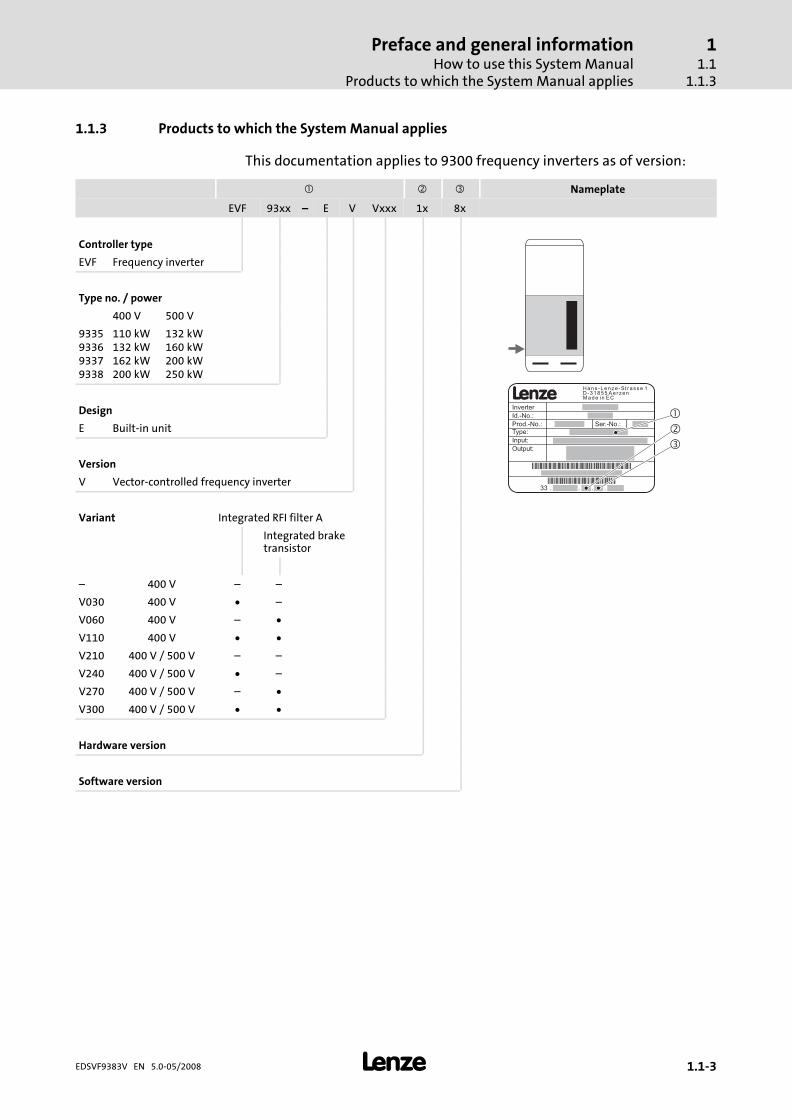
1.1.3 Products to which the System Manual applies
This documentation applies to 9300 frequency inverters as of version:
� � � Nameplate
EVF 93xx ˘ E V Vxxx 1x 8x
Controller type
LHans -Lenze -St rasse 1D-31855 Ae rzenMade in EC
Ser.-No.:
Id.-No.:
Inverter
Prod.-No.:
Type:
Input:
Output:
0045042000129567000005
33 . 9335VE . 1A . 70 . V03033.9335VE.1A.70
�
�
�
EVF Frequency inverter
Type no. / power
400 V 500 V
9335933693379338
110 kW132 kW162 kW200 kW
132 kW160 kW200 kW250 kW
Design
E Built−in unit
Version
V Vector−controlled frequency inverter
Variant Integrated RFI filter A
Integrated braketransistor
– 400 V – –
V030 400 V � –
V060 400 V – �
V110 400 V � �
V210 400 V / 500 V – –
V240 400 V / 500 V � –
V270 400 V / 500 V – �
V300 400 V / 500 V � �
Hardware version
Software version

Preface and general informationHow to use this System ManualProducts to which the System Manual applies
11.11.1.3
� 1.1−4 EDSVF9383V EN 5.0−05/2008
� � � Nameplate
EVF 93xx ˘ E V Vxxx 1x 8x
Product series
��
�
LHans -Lenze -St rasse 1D-31855 Ae rzenMade in EC
Ser.-No.:
Id.-No.:
Inverter
Prod.-No.:
Type:
Input:
Output:
0045042000129567000005
33 . 9335VE . 1A . 70 . V03033.9335VE.1A.70
�
�
LHans -Lenze -St rasse 1D-31855 Ae rzenMade in EC
Master Slave
Type:
Inverter
Input:
Output:
EVM EVL
EVF
�
�
�
�
EVM... EVL...EVF Frequency inverter
EVM: Master of EVFEVL: Slave of EVF
Type no. / power
400 V 500 V
938193829383
250 kW315 kW400 kW
315 kW400 kW500 kW
Type
E Built−in unit
Design
V Vector−controlled frequency inverterX: Slave
Variant Integrated RFI filter A
Integrated braketransistor
– 400 V – –
V030 400 V � –
V060 400 V – �
V110 400 V � �
V210 400 V / 500 V – –
V240 400 V / 500 V � –
V270 400 V / 500 V – �
V300 400 V / 500 V � �
Hardware version
Software version
– Slave (no software version)
Preface and general informationLegal regulations
11.2
� 1.2−1EDSVF9383V EN 5.0−05/2008
1.2 Legal regulations
Lenze controllers are unambiguously designated by the contents of thenameplate.
Lenze Drive Systems GmbH, Hans−Lenze−Straße 1, D−31855 Aerzen,Germany
Conforms to the EC Low−Voltage Directive
9300 vector frequency inverter and accessories
ƒ must only be operated under the conditions prescribed in this SystemManual.
ƒ are components
– for open and closed loop control of variable speed drives withasynchronous standard motor or asynchronous servo motors
– for installation in a machine
– for assembly with other components to form a machine.
ƒ comply with the requirements of the Low−Voltage Directive.
ƒ are not machines for the purpose of the Machinery Directive.
ƒ are not to be used as domestic appliances, but only for industrialpurposes.
Drives with 9300 vector frequency inverters
ƒ comply with the EMC Directive if they are installed according to theguidelines of CE−typical drive systems.
ƒ can be used
– for operation on public and non−public mains
– for operation in industrial premises and residential areas.
ƒ The user is responsible for the compliance of his application with theEC directives.
Any other use shall be deemed as inappropriate!
Labelling
Manufacturer
CE conformity
Application as directed
Preface and general informationLegal regulations
11.2
� 1.2−2 EDSVF9383V EN 5.0−05/2008
The information, data, and notes in this System Manual met the state of theart at the time of printing. Claims on modifications referring to controllersand components which have already been supplied cannot be derived fromthe information, illustrations, and descriptions.
The specifications, processes, and circuitry described in this System Manualare for guidance only and must be adapted to your own specific application.Lenze does not take responsibility for the suitability of the process and circuitproposals.
The specifications in this System Manual describe the product featureswithout guaranteeing them.
Lenze does not accept any liability for damage and operating interferencecaused by:
ƒ Disregarding the System Manual
ƒ Unauthorised modifications to the controller
ƒ Operating errors
ƒ Improper working on and with the controller
See terms of sales and delivery of the Lenze Drive Systems GmbH.
Warranty claims must be made to Lenze immediately after detecting thedeficiency or fault.
The warranty is void in all cases where liability claims cannot be made.
Liability
Warranty

Safety instructionsContents
2
� 2−1EDSVF9383V EN 5.0−05/2008
2 Safety instructions
Contents
2.1 General safety and application notes for Lenze controllers 2.1−1 . . . . . . . . .
2.2 General safety and application instructions for Lenze motors 2.2−1 . . . . . .
2.3 Residual hazards 2.3−1 . . . . . . . . . . . . . . . . . . . . . . . . . . . . . . . . . . . . . . . . . . . .
2.4 Definition of notes used 2.4−1 . . . . . . . . . . . . . . . . . . . . . . . . . . . . . . . . . . . . . .


Safety instructionsGeneral safety and application notes for Lenze controllers
22.1
� 2.1−1EDSVF9383V EN 5.0−05/2008
2.1 General safety and application notes for Lenze controllers
(in accordance with Low−Voltage Directive 2006/95/EC)
Depending on their degree of protection, some parts of the Lenze controllers(frequency inverters, servo inverters, DC speed controllers) and theiraccessory components can be live, moving and rotating during operation.Surfaces can be hot.
Non−authorised removal of the required cover, inappropriate use, incorrectinstallation or operation, creates the risk of severe injury to persons ordamage to material assets.
For more information, please see the documentation.
High amounts of energy are produced in the controller. Therefore it isrequired to wear personal protective equipment (body protection, headgear,eye protection, ear protection, hand guard).
All operations concerning transport, installation, and commissioning as wellas maintenance must be carried out by qualified, skilled personnel (IEC 364or CENELEC HD 384 or DIN VDE 0100 and IEC report 664 or DIN VDE 0110and national regulations for the prevention of accidents must be observed).
According to this basic safety information, qualified, skilled personnel arepersons who are familiar with the assembly, installation, commissioning,and operation of the product and who have the qualifications necessary fortheir occupation.
Controllers are components which are designed for installation in electricalsystems or machines. They are not to be used as domestic appliances, butonly for industrial purposes according to EN 61000−3−2.
When controllers are installed into machines, commissioning (i.e. starting ofthe operation as directed) is prohibited until it is proven that the machinecomplies with the regulations of the EC Directive 98/37/EC (MachineryDirective); EN 60204 must be observed.
Commissioning (i.e. starting of the operation as directed) is only allowedwhen there is compliance with the EMC Directive (2004/108/EC).
The controllers meet the requirements of the Low−Voltage Directive2006/95/EC. The harmonised standard EN 61800−5−1 applies to thecontrollers.
The technical data and supply conditions can be obtained from thenameplate and the documentation. They must be strictly observed.
Warning: Controllers are products which can be installed in drive systems ofcategory C2 according to EN 61800−3. These products can cause radiointerferences in residential areas. In this case, special measures can benecessary.
Please observe the notes on transport, storage, and appropriate handling.
Observe the climatic conditions according to the technical data.
For your personal safety
Application as directed
Transport, storage
Safety instructionsGeneral safety and application notes for Lenze controllers
22.1
� 2.1−2 EDSVF9383V EN 5.0−05/2008
The controllers must be installed and cooled according to the instructionsgiven in the corresponding documentation.
Ensure proper handling and avoid excessive mechanical stress. Do not bendany components and do not change any insulation distances duringtransport or handling. Do not touch any electronic components andcontacts.
Controllers contain electrostatic sensitive devices which can easily bedamaged by inappropriate handling.
Do not damage or destroy any electrical components since this mightendanger your health!
When working on live controllers, observe the applicable nationalregulations for the prevention of accidents (e.g. VBG 4).
The electrical installation must be carried out according to the appropriateregulations (e.g. cable cross−sections, fuses, PE connection). Additionalinformation can be obtained from the documentation.
This documentation contains information on installation in compliancewith EMC (shielding, earthing, filters, and cables). These notes must also beobserved for CE−marked controllers. The manufacturer of the system isresponsible for compliance with the limit values demanded by EMClegislation. The controllers must be installed in housings (e.g. controlcabinets) to meet the limit values for radio interferences valid at the site ofinstallation. The housings must enable an EMC−compliant installation.Observe in particular that e.g. the control cabinet doors have acircumferential metal connection to the housing. Reduce housing openingsand cutouts to a minimum.
Lenze controllers can cause a direct current in the protective conductor. If aresidual current device (RCD) is used as a protective means in case of director indirect contact, only a residual current device (RCD) of type B may be usedon the current supply side of the controller. Otherwise, another protectivemeasure such as separation from the environment through double orreinforced insulation or disconnection from the mains by means of atransformer must be applied.
If necessary, systems including controllers must be equipped with additionalmonitoring and protection devices according to the valid safety regulations(e.g. law on technical equipment, regulations for the prevention ofaccidents). The controllers can be adapted to your application. Pleaseobserve the corresponding information given in the documentation.
After the controller has been disconnected from the supply voltage, all livecomponents and power connections must not be touched immediatelybecause capacitors can still be charged. Please observe the correspondingstickers on the controller.
All protection covers and doors must be shut during operation.
Notes for UL−approved systems with integrated controllers: UL warnings arenotes that only apply to UL systems. The documentation contains special ULnotes.
Special controller variants support safety functions (e.g. "safe torque off",formerly "safe standstill") according to the requirements of Appendix INo. 1.2.7 of the EC Directive "Machinery" 98/37/EC, EN 954−1 Category 3and EN 1037. Strictly observe the notes on the safety functions given in thedocumentation for the respective variants.
Installation
Electrical connection
Operation
Safety functions

Safety instructionsGeneral safety and application notes for Lenze controllers
22.1
� 2.1−3EDSVF9383V EN 5.0−05/2008
The controllers do not require any maintenance if the prescribed operatingconditions are observed.
If the ambient air is polluted, the cooling surfaces of the controller maybecome dirty or the air vents may be obstructed. Therefore, clean the coolingsurfaces and air vents periodically under these operating conditions. Do notuse sharp or pointed tools for this purpose!
Recycle metal and plastic materials. Ensure professional disposal ofassembled PCBs.
The product−specific safety and application notes given in these instructionsmust be observed!
Maintenance and servicing
Disposal


Safety instructionsGeneral safety and application instructions for Lenze motors
22.2
� 2.2−1EDSVF9383V EN 5.0−05/2008
2.2 General safety and application instructions for Lenze motors
(According to: Low−Voltage Directive 2006/95/EC)
Low−voltage machines have hazardous live and rotating parts and possiblyalso hot surfaces.
Synchronous machines induce voltages at open terminals during operation.
All operations concerning transport, connections, commissioning andmaintenance must be carried out by qualified, skilled personnel(EN 50110−1 (VDE 0105−100) and IEC 60364 must be observed).Inappropriate use creates the risk of severe injury to persons and damage tomaterial assets.
Low−voltage machines may only be operated under the conditions that areindicated in the section "Application as directed".
The conditions at the place of installation must comply with the data givenon the nameplate and in the documentation.
Low−voltage machines are intended for commercial installations. Theycomply with the harmonised standards of the series EN�60034 (VDE 0530).Their use in potentially explosive atmospheres is prohibited unless they areexpressly intended for such use (follow additional instructions).
Low−voltage machines are components for installation into machines asdefined in the Machinery Directive 98/37/EC. Commissioning is prohibiteduntil the conformity of the end product with this directive has beenestablished (follow i. a. EN 60204−1).
Low−voltage machines with IP23 protection or less are only intended foroutdoor use when applying special protective features.
The integrated brakes must not be used as safety brakes. It cannot be ruledout that factors which cannot be influenced, such as oil ingress due to adefective A−side shaft seal, cause a brake torque reduction.
Damage must be reported immediately to the forwarder upon receipt; ifrequired, commissioning must be excluded. Tighten screwed−in ring boltsbefore transport. They are designed for the weight of the low−voltagemachines, do not apply extra loads. If necessary, use suitable and adequatelydimensioned means of transport (e. g. rope guides).
Remove transport locking devices before commissioning. Reuse them forfurther transport. When storing low−voltage machines, ensure a dry,dust−free and low−vibration (veff � 0.2 mm/s) environment (bearing damagewhile being stored).
General
Application as directed
Transport, storage
Safety instructionsGeneral safety and application instructions for Lenze motors
22.2
� 2.2−2 EDSVF9383V EN 5.0−05/2008
Ensure an even surface, solid foot/flange mounting and exact alignment ifa direct clutch is connected. Avoid resonances with the rotational frequencyand double mains frequency which may be caused by the assembly. Turnrotor by hand, listen for unusual slipping noises. Check the direction ofrotation when the clutch is not active (observe section "Electricalconnection").
Use appropriate means to mount or remove belt pulleys and clutches(heating) and cover them with a touch guard. Avoid impermissible belttensions.
The machines are half−key balanced. The clutch must be half−key balanced,too. The visible jutting out part of the key must be removed.
If required, provide pipe connections. Designs with shaft end at bottom mustbe protected with a cover which prevents the ingress of foreign particles intothe fan. Free circulation of the cooling air must be ensured. The exhaust air− also the exhaust air of other machines next to the drive system − must notbe taken in immediately.
All operations must only be carried out by qualified and skilled personnel onthe low−voltage machine at standstill and deenergised and provided with asafe guard to prevent an unintentional restart.This also applies to auxiliarycircuits (e. g. brake, encoder, blower).
Check safe isolation from supply!
If the tolerances specified in EN 60034−1; IEC 34 (VDE 0530−1) − voltage ±5 %,frequency ±2 %, waveform, symmetry − are exceeded, more heat will begenerated and the electromagnetic compatibility will be affected.
Observe the data on the nameplate, operating notes, and the connectiondiagram in the terminal box.
The connection must ensure a continuous and safe electrical supply(no loose wire ends); use appropriate cable terminals. The connection to thePE conductor must be safe. The plug−in connectors must be bolted tightly(to stop).
The clearances between blank, live parts and to earth must not fall below8 mm at Ur � 550 V, 10 mm at Ur � 725 V, 14 mm at Ur � 1000 V.
The terminal box must be free of foreign particles, dirt and moisture. Allunused cable entries and the box itself must be sealed against dust andwater.
Installation
Electrical connection

Safety instructionsGeneral safety and application instructions for Lenze motors
22.2
� 2.2−3EDSVF9383V EN 5.0−05/2008
Before commissioning after longer storage periods, measure insulationresistance. In case of values � 1 k� per volt of rated voltage, dry winding.
For trial run without output elements, lock the featherkey. Do not deactivatethe protective devices, not even in a trial run.
Check the correct operation of the brake before commissioning low−voltagemachines with brakes.
Integrated thermal detectors do not provide full protection for the machine.If necessary, limit the maximum current. Parameterise the controller so thatthe motor will be switched off with I > Ir after a few seconds of operation,especially at the risk of blocking.
Vibrational severities veff � 3.5 mm/s (Pr � 15 kW) or 4.5 mm/s (Pr > 15 kW) areacceptable if the clutch is activated.
If deviations from normal operation occur, e.g. increased temperatures,noises, vibrations, find the cause and, if required, contact the manufacturer.In case of doubt, switch off the low−voltage machine.
If the machine is exposed to dirt, clean the air paths regularly.
Shaft sealing rings and roller bearings have a limited service life.
Regrease bearings with relubricating devices while the low−voltage machineis running. Only use the grease recommended by the manufacturer. If thegrease drain holes are sealed with a plug, (IP54 drive end; IP23 drive andnon−drive end), remove plug before commissioning. Seal bore holes withgrease. Replace prelubricated bearings (2Z bearing) after approx.10,000 h − 20,000 h, at the latest however after 3 − 4 years.
The product−specific safety and application notes given in these instructionsmust be observed!
Commissioning and operation

Safety instructionsResidual hazards
22.3
� 2.3−1EDSVF9383V EN 5.0−05/2008
2.3 Residual hazards
ƒ Before working on the controller, check that no voltage is applied tothe power terminals:
– The power terminals U, V, W, +UG, −UG, BR1, BR2 and 101 ... 104remain live for at least five minutes after disconnecting from themains.
– The power terminals L1, L2, L3, U, V, W, +UG, −UG, BR1, BR2 and101 ... 104 remain live when the motor is stopped.
ƒ The leakage current to earth (PE) is >3.5 mA. EN 50178 requires a fixedinstallation.
ƒ The heatsink of the controller has an operating temperature of > 80 °C:
– Direct skin contact causes burns.
ƒ During the parameter set transfer, the control terminals of thecontroller can assume undefined states.
– For this reason, the connectors X5 and X6 have to be unpluggedbefore the transfer is executed. This ensures that the controller isinhibited and all control terminals are in the defined state �LOW".
ƒ Frequent mains switching (e.g. inching mode via mains contactor) canoverload and destroy the input current limitation of the controller.
– Thus, at least five minutes have to pass between two switch−onprocesses.
– In case of frequent, safety−related disconnections use the"safe torque off" safety function (STO).
ƒ Certain drive controller settings can overheat the connected motor:
– E. g. long−time operation of the DC injection brake.
– Long−time operation of self−ventilated motors at low speeds.
ƒ Drives can reach dangerous overspeeds (e. g. setting of high outputfrequencies in connection with motors and machines not suitable forthis purpose):
– The drive controllers do not provide protection against suchoperating conditions. For this purpose, use additional components.
Protection of persons
Device protection
Motor protection
Protection of themachine/system

Safety instructionsDefinition of notes used
22.4
� 2.4−1EDSVF9383V EN 5.0−05/2008
2.4 Definition of notes used
The following pictographs and signal words are used in this documentationto indicate dangers and important information:
Structure of safety instructions:
� Danger!
(characterises the type and severity of danger)
Note
(describes the danger and gives information about how toprevent dangerous situations)
Pictograph and signal word Meaning
� Danger!
Danger of personal injury through dangerous electricalvoltage.Reference to an imminent danger that may result indeath or serious personal injury if the correspondingmeasures are not taken.
� Danger!
Danger of personal injury through a general source ofdanger.Reference to an imminent danger that may result indeath or serious personal injury if the correspondingmeasures are not taken.
� Stop!
Danger of property damage.Reference to a possible danger that may result inproperty damage if the corresponding measures are nottaken.
Pictograph and signal word Meaning
� Note! Important note to ensure troublefree operation
� Tip! Useful tip for simple handling
� Reference to another documentation
Safety instructions
Application notes


Technical dataContents
3
� 3−1EDSVF9383V EN 4.0−11/2007
3 Technical data
Contents
3.1 General data and operating conditions 3.1−1 . . . . . . . . . . . . . . . . . . . . . . . . .
3.2 Weights 3.2−1 . . . . . . . . . . . . . . . . . . . . . . . . . . . . . . . . . . . . . . . . . . . . . . . . . . .
3.3 Open and closed−loop control 3.3−1 . . . . . . . . . . . . . . . . . . . . . . . . . . . . . . . . .
3.4 Safety relay KSR 3.4−1 . . . . . . . . . . . . . . . . . . . . . . . . . . . . . . . . . . . . . . . . . . . . .
3.5 Rated data (devices in 400V design) 3.5−1 . . . . . . . . . . . . . . . . . . . . . . . . . . . .
3.6 Rated data (devices for 400/500V mains) 3.6−1 . . . . . . . . . . . . . . . . . . . . . . .
3.6.1 Rated data for 400 V mains voltage 3.6−1 . . . . . . . . . . . . . . . . . . . .
3.6.2 Rated data for 500 V mains voltage 3.6−2 . . . . . . . . . . . . . . . . . . . .
3.7 Fuses and cable cross−sections 3.7−1 . . . . . . . . . . . . . . . . . . . . . . . . . . . . . . . .
3.7.1 Mains supply 3.7−1 . . . . . . . . . . . . . . . . . . . . . . . . . . . . . . . . . . . . . . .
3.7.2 DC supply 3.7−2 . . . . . . . . . . . . . . . . . . . . . . . . . . . . . . . . . . . . . . . . . .
3.7.3 Notes for mains and motor cables 3.7−3 . . . . . . . . . . . . . . . . . . . . .


Technical dataGeneral data and operating conditions
33.1
� 3.1−1EDSVF9383V EN 4.0−11/2007
3.1 General data and operating conditions
Conformity and approval
Conformity
CE 2006/95/EC Low−Voltage Directive
Protection of persons and equipment
Type of protection EN 60529 IP20
NEMA 250 Protection against accidental contact according totype 1
Earth leakage current EN 61800−5−1 > 3.5 mA Observe regulations andsafety instructions!
Insulation of controlcircuits
EN 61800−5−1 Safe mains isolation by double (reinforced)insulation for the terminals X1 and X5.Basic insulation (single isolating distance) for theterminals X3, X4, X6, X8, X9, X10 and X11.
Insulation resistance EN 61800−5−1 Site altitude < 2000 m: Overvoltage category III
Site altitude > 2000 m: Overvoltage category II
Protective measures Against short circuit, earth fault (earth−faultprotected during operation, limited earth−faultprotection during mains power−up), overvoltage,motor stalling, motor overtemperature (input forPTC or thermal contact)
EMC
Noise emission EN 61800−3 Cable−guided, up to 50 m motor cable length withRFI filter: Category C2.
Radiation, with RFI filter and installation in controlcabinet: Category C2
Noise immunity EN 61800−3 Category C3
General data

Technical dataGeneral data and operating conditions
33.1
� 3.1−2 EDSVF9383V EN 4.0−11/2007
Ambient conditions
Climatic
Storage IEC/EN 60721−3−1 1K3 (−20 ... +60 °C) < 6 months
1K3 (−25 ... +40 °C) > 6 months> 2 years: form DC buscapacitors
Transport IEC/EN 60721−3−2 2K3 (−25 ... +70 °C)
Operation IEC/EN 60721−3−3
EVF9335 3K3 (0 ... +50 °C)
EVF9336 ...EVF9338EVF9381 ...EVF9383
3K3 (0 ... +50 °C)> +40 °C: reduce the rated output current by2.5 %/°C.
Pollution EN 61800−5−1 Degree of pollution 2
Site altitude < 4000 m amsl> 1000 m amsl: reduce the rated output current by5 %/ 1000 m.
Internal fan 975 m3/h volume flow
Mechanical
Vibration resistance EN 50178
Electrical
Mains connection
Power system
TT, TN(with earthedneutral)
Operation is permitted without restrictions.
DC−bus operation Possible for the variants V210, V240, V270, V300
Motor connection
Length of themotor cable
At rated mains voltage and a switching frequencyof � 2 kHz without additional output filter.For compliance with EMC regulations, thepermissible cable lengths may change.
shielded 100 m
unshielded 200 m
Mounting conditions
Mounting place In the control cabinet
Mounting position Vertical
Free spaces 4−1
Operating conditions

Technical dataWeights
33.2
� 3.2−1EDSVF9383V EN 4.0−11/2007
3.2 Weights
9300 Without RFI filter A With integrated RFI filter A
Type [kg] [kg]
EVF9335−EV 160 175
EVF9336−EV 160 175
EVF9337−EV 160 175
EVF9338−EV 200 215
EVF9381−EV 320 350
EVF9382−EV 320 350
EVF9383−EV 400 430


Technical dataOpen and closed−loop control
33.3
� 3.3−1EDSVF9383V EN 4.0−11/2007
3.3 Open and closed−loop control
Field Values
Control methods V/f characteristic control (linear, square), vector control
Switching frequency 1 kHz, 2 kHz or 4 kHz
Torque behaviour in the case of vectorcontrol
Maximum torque 1.5 × Mr for 60 s if rated motor power = rated 9300 vector power
Setting range Up to 1 : 10(1 : 20 with feedback)
in the range 6 ... 100 % fr
Speed control without feedback
Min. mechanical motor frequency 1 % fr torque 0 ... Mr
Setting range 1 : 100 relating to fr and Mr
Accuracy ± 0.5 % fr in the range 6 ... 100 % fr
Speed control with feedback
Min. mechanical motor frequency 0.1 % fr torque 0 ... Mr
Setting range 1 : 1000 relating to fr and Mr
Accuracy ± 0.1 % of fr
Output frequency
Field − 300 Hz ... + 300 Hz
Absolute resolution 0.06 Hz
Standardised resolution Parameter data: 0.01 %,Process data: 0.006 % (= 214)
Digital setpoint selection
Accuracy ± 0.005 Hz (= ± 100 ppm)
Analog setpoint selection
Linearity ± 0,15 % signal level: 5 V or 10 V
Temperature sensitivity ± 0,1 % 0 ... 50 Nm
Offset ± 0 %
Analog inputs/analog outputs � 2 inputs (bipolar)� 2 outputs (bipolar)
Digital inputs/digital outputs � 6 inputs (freely assignable)� 1 input for controller inhibit� 4 outputs (freely assignable)� 1 incremental encoder input (500 kHz, TTL level); Design: 9−pole Sub−D socket� 1 digital frequency input (500 kHz, TTL level or 200 kHz, HTL level); type: 9−pole Sub−D
socket; can be alternatively used as incremental encoder input (200 kHz, HTL level)� 1 master frequency output (500 kHz, TTL level); Design: 9−pole Sub−D socket
Cycle times
Digital inputs 1 ms
Digital outputs 1 ms
Analog inputs 1 ms
Analog outputs 1 ms (smoothing time: �= 10 ms)
Operation in generator mode Integrated brake transistor (optional)
fr rated motor frequencyMr rated motor torque


Technical dataSafety relay KSR
33.4
� 3.4−1EDSVF9383V EN 4.0−11/2007
3.4 Safety relay KSR
Terminal Description Field Values
X11/K32X11/K31X11/33X11/34
Safety relay KSR1st disconnecting path
Coil voltage at +20 °C DC 24 V (20 ... 30 V)
Coil resistance at +20 °C 823 � ±10 %
Rated coil power Approx. 700 mW
Max. switching voltage AC 250 V, DC 250 V (0.45 A)
Max. AC switching capacity 1500 VA
Max. switching current (ohmic load) AC 6 A (250 V), DC 6 A (50 V)
Recommended minimum load > 50 mW
Max. switching rate 6 switchings per minute
Mechanical service life 107 switching cycles
Electrical service life
at 250 V AC(ohmic load)
105 switching cycles at 6 A106 switching cycles at 1 A107 switching cycles at 0.25 A
at 24 V DC(ohmic load)
6 × 10³ switching cycles at 6 A106 switching cycles at 3 A1.5 × 106 switching cycles at 1 A107 switching cycles at 0.1 A


Technical dataRated data (devices in 400V design)
33.5
� 3.5−1EDSVF9383V EN 4.0−11/2007
3.5 Rated data (devices in 400V design)
Basis of the data
Voltage Frequency
Supply
3/PE AC 400 V [UN] 340 V − 0� % ... 456 V + 0 % 45 Hz − 0 % ... 65 Hz + 0 %
DC (alternatively) [UDC] Not possible
Output voltage [UOUT] 3 ~ 0 ... UN 0 ... 300 Hz
9300 Mains current 1) Typical motor powerASM (4−pole)
Power loss
Type Ir [A] PN [kW] PN [hp] PV [kW]
EVF9335−EVEVF9335−EVVxxx 2) 200 110
150 2.8
EVF9336−EVEVF9336−EVVxxx 2)
238 132 200 3.3
EVF9337−EVEVF9337−EVVxxx 2)
285 160 250 4.0
EVF9338−EVEVF9338−EVVxxx 2)
356 200 300 5.0
EVF9381−EVEVF9381−EVVxxx 2) 475 250 350 6.6
EVF9382−EVEVF9382−EVVxxx 2) 570 315 450 8.0
EVF9383−EVEVF9384−EVVxxx 2) 713 400 550 10.0
The currents for EVF9381 ... EVF9383 are to be considered as total currents of master and slave1) For a controller switching frequency of 2 kHz2) Device in variant V030, V060 or V110
9300 Output currents
Rated current Maximum current 2)
1 kHz 1) 2 kHz 1) 4 kHz 1) 1 kHz 1) 2 kHz 1) 4 kHz 1)
Type IN1 [A] IN2 [A] IN4 [A] IM1 [A] IM2 [A] IM4 [A]
EVF9335−EVEVF9335−EVVxxx 3) 210 210 210 315 315 315
EVF9336−EVEVF9336−EVVxxx 3) 250 250 250 375 375 375
EVF9337−EVEVF9337−EVVxxx 3) 300 300 270 450 450 405
EVF9338−EVEVF9338−EVVxxx 3) 375 375 330 560 560 495
EVF9381−EVEVF9381−EVVxxx 3) 500 500 500 750 750 750
EVF9382−EVEVF9382−EVVxxx 3) 600 600 540 900 900 810
EVF9383−EVEVF9384−EVVxxx 3) 750 750 660 1125 1125 990
The currents for EVF9381 ... EVF9383 are to be considered as total currents of master and slaveBold print = Lenze setting1) Switching frequency of the inverter2) The currents apply to a periodic load change with an overcurrent time of 1 minute at a maximum
and a base load time of 2 minutes with maximally 75 % INx3) Device in variant V030, V060 or V110


Technical dataRated data (devices for 400/500V mains)
Rated data for 400 V mains voltage
33.6
3.6.1
� 3.6−1EDSVF9383V EN 4.0−11/2007
3.6 Rated data (devices for 400/500V mains)
� Note!
Types EVF9335 ... EVF9383 for 400 V/500 V mains voltage aresuitable for DC supply or DC−bus operation together withcontrollers of the 9300 series.
3.6.1 Rated data for 400 V mains voltage
Basis of the data
Voltage Frequency
Supply
3/PE AC 400 V [UN] 340 V − 0� % ... 577 V + 0 % 45 Hz − 0 % ... 65 Hz + 0 %
DC 565 V (alternatively) [UDC] DC 480 V − 0 % ... 800 V + 0 % ˘
Output voltage [UOUT] 3 ~ 0 ... UN 0 ... 300 Hz
9300 Mains current 1) Typical motor powerASM (4−pole)
Power loss
Type Ir [A] PN [kW] PN [hp] PV [kW]
EVF9335−EVVxxx 2) 200 110 150 2.8
EVF9336−EVVxxx 2) 238 132 200 3.3
EVF9337−EVVxxx 2) 285 160 250 4.0
EVF9338−EVVxxx 2) 356 200 300 5.0
EVF9381−EVVxxx 2) 475 250 350 6.6
EVF9382−EVVxxx 2) 570 315 450 8.0
EVF9384−EVVxxx 2) 713 400 550 10.0
The currents for EVF9381 ... EVF9383 are to be considered as total currents of master and slave1) For a controller switching frequency of 2 kHz2) Device in variant V210, V240, V270 or V300
9300 Output currents
Rated current Maximum current 2)
1 kHz 1) 2 kHz 1) 4 kHz 1) 1 kHz 1) 2 kHz 1) 4 kHz 1)
Type IN1 [A] IN2 [A] IN4 [A] IM1 [A] IM2 [A] IM4 [A]
EVF9335−EVVxxx 3) 210 210 210 315 315 315
EVF9336−EVVxxx 3) 250 250 250 375 375 375
EVF9337−EVVxxx 3) 300 300 270 450 450 405
EVF9338−EVVxxx 3) 375 375 330 560 560 495
EVF9381−EVVxxx 3) 500 500 500 750 750 750
EVF9382−EVVxxx 3) 600 600 540 900 900 810
EVF9384−EVVxxx 3) 750 750 660 1125 1125 990
The currents for EVF9381 ... EVF9383 are to be considered as total currents of master and slaveBold print = Lenze setting1) Switching frequency of the inverter2) The currents apply to a periodic load change with an overcurrent time of 1 minute at a maximum
and a base load time of 2 minutes with maximally 75 % INx3) Device in variant V210, V240, V270 or V300

Technical dataRated data (devices for 400/500V mains)Rated data for 500 V mains voltage
33.63.6.2
� 3.6−2 EDSVF9383V EN 4.0−11/2007
3.6.2 Rated data for 500 V mains voltage
Basis of the data
Voltage Frequency
Supply
3/PE AC 500 V [UN] 340 V − 0� % ... 577 V + 0 % 45 Hz − 0 % ... 65 Hz + 0 %
DC 705 V (alternatively) [UDC] DC 480 V − 0 % ... 800 V + 0 % ˘
Output voltage [UOUT] 3 ~ 0 ... UN 0 ... 300 Hz
9300 Mains current 1) Typical motor powerASM (4−pole)
Power loss
Type Ir [A] PN [kW] PN [hp] PV [kW]
EVF9335−EVVxxx 2) 200 132 200 3.0
EVF9336−EVVxxx 2) 238 160 250 3.5
EVF9337−EVVxxx 2) 285 200 300 4.3
EVF9338−EVVxxx 2) 356 250 350 5.3
EVF9381−EVVxxx 2) 475 315 450 7.0
EVF9382−EVVxxx 2) 570 400 550 8.6
EVF9383−EVVxxx 2) 713 500 ??? 700 ??? 10.6
The currents for EVF9381 ... EVF9383 are to be considered as total currents of master and slave1) For a controller switching frequency of 2 kHz2) Device in variant V210, V240, V270 or V300
9300 Output currents
Rated current Maximum current 2)
1 kHz 1) 2 kHz 1) 4 kHz 1) 1 kHz 1) 2 kHz 1) 4 kHz 1)
Type IN1 [A] IN2 [A] IN4 [A] IM1 [A] IM2 [A] IM4 [A]
EVF9335−EVVxxx 3) 210 210 210 315 315 315
EVF9336−EVVxxx 3) 250 250 250 375 375 375
EVF9337−EVVxxx 3) 300 300 270 450 450 405
EVF9338−EVVxxx 3) 375 375 330 560 560 495
EVF9381−EVVxxx 3) 500 500 500 750 750 750
EVF9382−EVVxxx 3) 600 600 540 900 900 810
EVF9384−EVVxxx 3) 750 750 660 1125 1125 990
The currents for EVF9381 ... EVF9383 are to be considered as total currents of master and slaveBold print = Lenze setting1) Switching frequency of the inverter2) The currents apply to a periodic load change with an overcurrent time of 1 minute at a maximum
and a base load time of 2 minutes with maximally 75 % INx3) Device in variant V210, V240, V270 or V300

Technical dataFuses and cable cross−sections
Mains supply
33.7
3.7.1
� 3.7−1EDSVF9383V EN 4.0−11/2007
3.7 Fuses and cable cross−sections
Field Description
Fuses and cable cross−sections All information given in this chapter are recommendations.They refer to� controllers installed in control cabinets.� cables with a distance to the wall which is at least as wide
as the cable cross−section.� a max. ambient temperature of +40 °C.
Selection of the cablecross−section
Consider the voltage drop under load (� 3 % acc. toDIN 18015 part 1) for the selection.
Protection of the cables on theAC side (L1, L2, L3)
On the AC side, the cables are protected by means of commonfuses.Fuses in UL−conform plant must have UL approval.
Protection of the cables on themotor side (U, V, W)
It is not necessary to fuse the motor cable.
Further information In the chapter "Wiring the basic device" � "Important notes"� "Device protection"
Standards and regulations The user is responsible for the compliance with national andregional standards and regulations (e.g. VDE 0113, VDE 0298,EN 60204).
3.7.1 Mains supply
For fusing the mains supply you can use the following fuses (gRL) and cablecross−sections:
9300 vector Installation in accordance with EN 60204−1
Fuse Cable cross−sections
L1, L2, L3 PE
Type [A] [mm2] [mm2]
EVF9335−EVEVF9335−EVVxxx
250150
2 × 50 1) 95
EVF9336−EVEVF9336−EVVxxx
315150
2 × 50 1) 95
EVF9337−EVEVF9337−EVVxxx
315150
2 × 50 1) 95
EVF9338−EVEVF9338−EVVxxx
400240
2 × 95 1) 150
Master Slave Master Slave Master Slave
EVF9381−EVEVF9381−EVVxxx
315 315150
2 × 50 1)150
2 × 50 1) 95 95
EVF9382−EVEVF9382−EVVxxx
315 315150
2 × 50 1)150
2 × 50 1) 95 95
EVF9383−EVEVF9383−EVVxxx
400 400240
2 × 95 1)240
2 × 95 1) 150 150
1) Multiple conductor; both conductors must have the same cross−section
� Note!
We recommend to use semiconductor fuses (gRL).
Information about fuses andcable cross−sections

Technical dataFuses and cable cross−sectionsDC supply
33.73.7.2
� 3.7−2 EDSVF9383V EN 4.0−11/2007
3.7.2 DC supply
A DC supply is only possible for the variants V210, V240, V270, V300.
� Stop!
ƒ Only use semiconductor fuses (gRL).
ƒ On principle, fuse DC cables as 2−pole (+UG, −UG).
9300 vector Installation in accordance with EN 60204−1
Fuse Cable cross−sections
+UG, −UG PE
Type [A] [mm2] [mm2]
EVF9335−EVV2xxEVF9335−EVV300
315150
2 × 50 1) 95
EVF9336−EVV2xxEVF9336−EVV300
350150
2 × 50 1) 95
EVF9337−EVV2xxEVF9337−EVV300
400240
2 × 95 1) 95
EVF9338−EVV2xxEVF9338−EVV300
500240
2 × 95 1) 150
Master Slave Master Slave Master Slave
EVF9381−EVV2xxEVF9381−EVV300
350 350150
2 × 50 1)150
2 × 50 1) 95 95
EVF9382−EVV2xxEVF9382−EVV300
400 400240
2 × 95 1)240
2 × 95 1) 95 95
EVF9383−EVV2xxEVF9383−EVV300
500 500240
2 × 95 1)240
2 × 95 1) 150 150
1) Multiple conductor; both conductors must have the same cross−section
Technical dataFuses and cable cross−sections
Notes for mains and motor cables
33.7
3.7.3
� 3.7−3EDSVF9383V EN 4.0−11/2007
3.7.3 Notes for mains and motor cables
� Danger!
Observe all national and regional regulations for the cables.
You can use single and multi−core cables. If a cable consists of several coresper phase, it can be necessary to connect the controller by means of commoncable glands.
Maximum cable cross−section for power connections (screw terminals):
9300 vector Maximum cable cross−section
L1, L2, L3U, V, W, BR1, BR2
+UG, −UG PE
Type [mm2] [mm2] [mm2]
EVF9335−EVEVF9335−EVxxx
150(2 × 50) 1)
150(2 × 50) 1) 95
EVF9336−EVEVF9336−EVxxx
150(2 × 50) 1)
150(2 × 50) 1) 95
EVF9337−EVEVF9337−EVxxx
150(2 × 50) 1)
240(2 × 95) 1) 95
EVF9338−EVEVF9338−EVxxx
240(2 × 95) 1)
240(2 × 95) 1) 150
Master Slave Master Slave Master Slave
EVF9381−EVEVF9381−EVxxx
150(2 × 50) 1)
150(2 × 50) 1)
150(2 × 50) 1)
150(2 × 50) 1) 95 95
EVF9382−EVEVF9382−EVxxx
150(2 × 50) 1)
150(2 × 50) 1)
240(2 × 95) 1)
240(2 × 95) 1) 95 95
EVF9383−EVEVF9383−EVxxx
240(2 × 95) 1)
240(2 × 95) 1)
240(2 × 95) 1)
240(2 × 95) 1) 150 150
1) Multiple conductor; both conductors must have the same cross−section
The effectively required cable cross−section depends e.g. on the applicationand environmental conditions and the cable type used. It is not required thatmains and motor cable have the same cable cross−section.
It is not necessary to shield the mains cable. In DC−bus operation or with DCsupply we recommend shielded cables.
It is not necessary to fuse the motor cable. For EMC reasons we recommendshielded motor cables. You can use common metal clamps to connect theshield.
Mains cable, DC cable
Motor cable


Installing of the standard deviceContents
4
� 4−1EDSVF9383V EN 5.0−05/2008
4 Installation of the standard device
Contents
4.1 Important notes 4.1−1 . . . . . . . . . . . . . . . . . . . . . . . . . . . . . . . . . . . . . . . . . . . .
4.2 Basic devices in the power range 110 ... 200 kW 4.2−1 . . . . . . . . . . . . . . . . . .
4.2.1 Dimensions 4.2−1 . . . . . . . . . . . . . . . . . . . . . . . . . . . . . . . . . . . . . . . .
4.2.2 Drilling the holes into the mounting plate 4.2−2 . . . . . . . . . . . . . . .
4.2.3 Fasten the mounting rails on the mounting plate 4.2−3 . . . . . . . .
4.2.4 Fasten controller on mounting plate 4.2−4 . . . . . . . . . . . . . . . . . . .
4.3 Basic devices in the power range 250 ... 400 kW 4.3−1 . . . . . . . . . . . . . . . . . .
4.3.1 Dimensions 4.3−1 . . . . . . . . . . . . . . . . . . . . . . . . . . . . . . . . . . . . . . . .
4.3.2 Drilling the holes into the mounting plate 4.3−2 . . . . . . . . . . . . . . .
4.3.3 Fasten the mounting rails on the mounting plate 4.3−3 . . . . . . . .
4.3.4 Fasten controller on mounting plate 4.3−4 . . . . . . . . . . . . . . . . . . .


Installing of the standard deviceImportant notes
44.1
� 4.1−1EDSVF9383V EN 5.0−05/2008
4.1 Important notes
ƒ Manual lifting is only permitted up to the following weight limitations:
– max. 30 kg [max. 66 lbs] for men
– max. 10 kg [max. 22 lbs] for women
– max. 5 kg [max. 11 lbs] for pregnant women
Above these limits, use appropriate hoists or conveyors! Weights of thedevices: ( 3.2−1)
ƒ For transport with hoists, observe the following basic rules:
– The payload of the hoists and load handling devices at least has tocorrespond to the weight of the device. Weight of the devices:( 3.2−1)
– Secure the device so that it cannot topple over or fall down.
– Stay out from suspended loads!
– Avoid heavy impacts during transport.
ƒ The devices are equipped with an eye bolt. The load hook can beattached directly to the eye bolt.
ƒ Alternatively the devices can be transported with lifting straps.
– Attach the lifting straps so that the device is balanced and cannot slipfrom the lifting straps.
ƒ Controller must only be used as built−in unit.
ƒ Possible mounting position: Vertically at the rear panel of the controlcabinet.
ƒ Observe free mounting spaces.
ƒ Do not exceed the permissible operating and ambient temperatures:
– Please ensure unimpeded ventilation of cooling air.
– If the cooling air contains pollutants (dust, lint, grease, aggressivegases), which may impair the function of the controller takemeasures against it, such as separate air flow, filters, regularcleaning, etc..
Transport
Mounting


Installing of the standard deviceBasic devices in the power range 110 ... 200 kW
Dimensions
44.2
4.2.1
� 4.2−1EDSVF9383V EN 5.0−05/2008
4.2 Basic devices in the power range 110 ... 200 kW
� Tip!
ƒ Lenze recommends to install an air lock. It serves to dissipatethe heated cooling air directly from the control cabinet.– Order no. E93ZWL
ƒ A drilling jig for marking the bore holes is available as dxf−fileon the Internet in the "Download" area under www.Lenze.de.
4.2.1 Dimensions
a1
a2
d
�
b b1
c
a
b2 d
�
9300VEC002
Fig. 4.2−1 Dimensions
� Eyebolts
Type a[mm]
a1[mm]
a2[mm]
b[mm]
b1[mm]
b2[mm]
c[mm]
d[mm]
EVF9335−EVEVF9335−EVVxxxEVF9336−EVEVF9336−EVVxxxEVF9337−EVEVF9337−EVVxxxEVF9338−EVEVF9338−EVVxxx
500 450 225 1145 1005 15 4369
(8×)
Installing of the standard deviceBasic devices in the power range 110 ... 200 kWDrilling the holes into the mounting plate
44.24.2.2
� 4.2−2 EDSVF9383V EN 5.0−05/2008
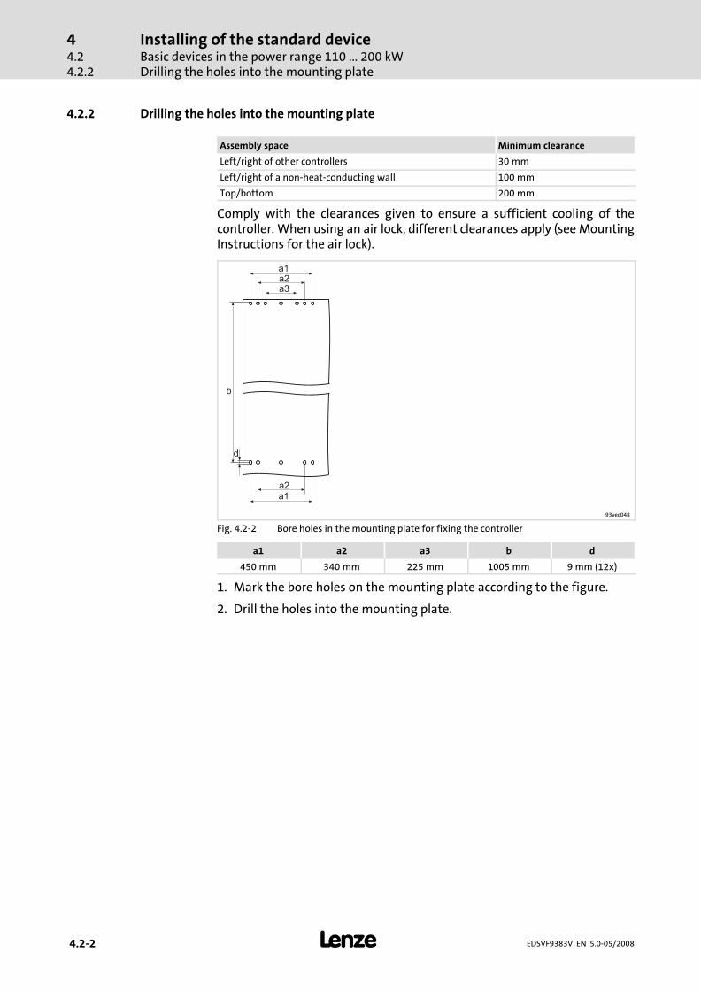
4.2.2 Drilling the holes into the mounting plate
Assembly space Minimum clearance
Left/right of other controllers 30 mm
Left/right of a non−heat−conducting wall 100 mm
Top/bottom 200 mm
Comply with the clearances given to ensure a sufficient cooling of thecontroller. When using an air lock, different clearances apply (see MountingInstructions for the air lock).
a1
a1
a3a2
a2
d
b
93vec048
Fig. 4.2−2 Bore holes in the mounting plate for fixing the controller
a1 a2 a3 b d
450 mm 340 mm 225 mm 1005 mm 9 mm (12x)
1. Mark the bore holes on the mounting plate according to the figure.
2. Drill the holes into the mounting plate.

Installing of the standard deviceBasic devices in the power range 110 ... 200 kW
Fasten the mounting rails on the mounting plate
44.2
4.2.3
� 4.2−3EDSVF9383V EN 5.0−05/2008
4.2.3 Fasten the mounting rails on the mounting plate
� �
�
�
�
�
�
��
93vec071
Fig. 4.2−3 Fastening the mounting rails on the mounting plate
� Mounting rail� Mounting plate Hexagon socket screw M8 × 25 mm� Spring washer M8
1. Hold the mounting rails behind the mounting plate.
2. Fasten the mounting rails exactly at the illustrated points using 2hexagon socket screws and spring washers on each side.

Installing of the standard deviceBasic devices in the power range 110 ... 200 kWFasten controller on mounting plate
44.24.2.4
� 4.2−4 EDSVF9383V EN 5.0−05/2008
4.2.4 Fasten controller on mounting plate
� Danger!
Risk of injury due to the high weight of the controller.
The controller has to be carried using the eyebolts and anadequate lifting tool.
� �
�
�
�
�
�
�
�
9300vec070
Fig. 4.2−4 Fastening the controller on mounting plate
� Eye bolts � 8 hexagon socket screws M8 × 25 mm� Controller � 8 spring washers M8 Mounting plate
1. Put the controller on the mounting plate.
2. Fasten the controller exactly at the illustrated points using 5 hexagonsocket screws and spring washers at the top and 3 hexagon socketscrews and spring washers at the bottom.

Installing of the standard deviceBasic devices in the power range 250 ... 400 kW
Dimensions
44.3
4.3.1
� 4.3−1EDSVF9383V EN 5.0−05/2008
4.3 Basic devices in the power range 250 ... 400 kW
� Tip!
ƒ Lenze recommends to install an air lock. The air lock serves todissipate the heated cooling air directly from the controlcabinet.– Order no. E93ZWL2
ƒ A drilling jig for marking the bore holes is available as dxf−filein the Internet in the "Download" area under www.Lenze.de.
4.3.1 Dimensions
a1
a2
d
� �
b b1
ca3
a
b2 d
�
9300VEC039
Fig. 4.3−1 Dimensions
� Eyebolts
Type a[mm]
a1[mm]
a2[mm]
a3[mm]
b[mm]
b1[mm]
b2[mm]
c[mm]
d[mm]
EVF9381−EVEVF9381−EVVxxxEVF9382−EVEVF9382−EVVxxxEVF9383−EVEVF9383−EVVxxx
1050 450 225 50 1145 1005 15 4369
(16×)

Installing of the standard deviceBasic devices in the power range 250 ... 400 kWDrilling the holes into the mounting plate
44.34.3.2
� 4.3−2 EDSVF9383V EN 5.0−05/2008
4.3.2 Drilling the holes into the mounting plate
Assembly space Minimum clearance
Left/right of other controllers 30 mm
Left/right of a non−heat−conducting wall 100 mm
Top/bottom 200 mm
Comply with the clearances given to ensure a sufficient cooling of thecontroller. When using an air lock, different clearances apply (see MountingInstructions for the air lock).
aa1 a1
a1 a1
a3 a3a2 a2
a2 a2
d
b
93vec079
Fig. 4.3−2 Bore holes in the mounting plate for fixing the controller
a a1 a2 a3 b d
550 mm 450 mm 340 mm 225 mm 1005 mm 9 mm (24x)
1. Mark the bore holes on the mounting plate according to the figure.
2. Drill the holes into the mounting plate.

Installing of the standard deviceBasic devices in the power range 250 ... 400 kW
Fasten the mounting rails on the mounting plate
44.3
4.3.3
� 4.3−3EDSVF9383V EN 5.0−05/2008
4.3.3 Fasten the mounting rails on the mounting plate
� �
�
� �� �
� �
� ��
�
9300vec080
Fig. 4.3−3 Fastening the mounting rails on the mounting plate
� Mounting rail� Mounting plate Hexagon socket screw M8 × 25 mm� Spring washer M8
1. Hold the mounting rails behind the mounting plate.
2. Fasten the mounting rails exactly at the illustrated points using 2hexagon socket screws and spring washers on each side.

Installing of the standard deviceBasic devices in the power range 250 ... 400 kWFasten controller on mounting plate
44.34.3.4
� 4.3−4 EDSVF9383V EN 5.0−05/2008
4.3.4 Fasten controller on mounting plate
� Danger!
Risk of injury due to the high weight of the controller.
The controller has to be carried using the eyebolts and anadequate lifting tool.
� �
� �
�
�
�� �
�
�
9300vec081
Fig. 4.3−4 Fastening the controller on mounting plate
� Eyebolts � Mounting plate� Master � 16 hexagon socket screws M8 × 25 mm Slave � 16 spring washers M8
1. Put master and slave on the mounting plate.
2. Fasten the master and slave each with five hexagon socket screws andspring washers at the top and 3 hexagon socket screws and springwashers at the bottom exactly at the marked point.

Wiring of the standard deviceContents
5
� 5−1EDSVF9383V EN 5.0−05/2008
5 Wiring of the standard device
Contents
5.1 Important notes 5.1−1 . . . . . . . . . . . . . . . . . . . . . . . . . . . . . . . . . . . . . . . . . . . .
5.1.1 Protection of persons 5.1−1 . . . . . . . . . . . . . . . . . . . . . . . . . . . . . . . .
5.1.2 Device protection 5.1−3 . . . . . . . . . . . . . . . . . . . . . . . . . . . . . . . . . . .
5.1.3 Motor protection 5.1−3 . . . . . . . . . . . . . . . . . . . . . . . . . . . . . . . . . . . .
5.1.4 Supply forms / electrical supply conditions 5.1−4 . . . . . . . . . . . . . .
5.1.5 Interaction with compensation equipment 5.1−4 . . . . . . . . . . . . . .
5.2 Basics for wiring according to EMC 5.2−1 . . . . . . . . . . . . . . . . . . . . . . . . . . . .
5.2.1 Shielding 5.2−1 . . . . . . . . . . . . . . . . . . . . . . . . . . . . . . . . . . . . . . . . . . .
5.2.2 Mains connection, DC supply 5.2−1 . . . . . . . . . . . . . . . . . . . . . . . . . .
5.2.3 Motor cables 5.2−2 . . . . . . . . . . . . . . . . . . . . . . . . . . . . . . . . . . . . . . .
5.2.4 Control cables 5.2−3 . . . . . . . . . . . . . . . . . . . . . . . . . . . . . . . . . . . . . .
5.2.5 Installation in the control cabinet 5.2−4 . . . . . . . . . . . . . . . . . . . . .
5.2.6 Wiring outside the control cabinet 5.2−5 . . . . . . . . . . . . . . . . . . . . .
5.2.7 Detecting and eliminating EMC interferences 5.2−6 . . . . . . . . . . . .
5.3 Basic devices in the power range 110 ... 200 kW 5.3−1 . . . . . . . . . . . . . . . . . .
5.3.1 Wiring according to EMC (CE−typical drive system) 5.3−1 . . . . . . . .
5.3.2 Mains connection of the controller for 400 V mains voltage 5.3−3
5.3.3 Supply and fan connection of the controller for 400 V/500V mains voltage 5.3−4 . . . . . . . . . . . . . . . . . . . . . . . . . . . . . . . . . . . . . . .
5.3.4 Motor connection 5.3−7 . . . . . . . . . . . . . . . . . . . . . . . . . . . . . . . . . . .
5.3.5 Wiring of motor temperature monitoring 5.3−8 . . . . . . . . . . . . . . .
5.4 Basic devices in the power range 250 ... 400 kW 5.4−1 . . . . . . . . . . . . . . . . . .
5.4.1 Wiring according to EMC (CE−typical drive system) 5.4−1 . . . . . . . .
5.4.2 Master and slave connection 5.4−3 . . . . . . . . . . . . . . . . . . . . . . . . . .
5.4.3 Mains connection of the controller for 400 V mains voltage 5.4−7
5.4.4 Supply and fan connection of the controller for 400 V/500V mains voltage 5.4−8 . . . . . . . . . . . . . . . . . . . . . . . . . . . . . . . . . . . . . . .
5.4.5 Motor connection 5.4−12 . . . . . . . . . . . . . . . . . . . . . . . . . . . . . . . . . . .
5.4.6 Wiring of motor temperature monitoring 5.4−14 . . . . . . . . . . . . . . .
5.5 Connection terminal of the control card 5.5−1 . . . . . . . . . . . . . . . . . . . . . . . .
5.6 Control terminals 5.6−1 . . . . . . . . . . . . . . . . . . . . . . . . . . . . . . . . . . . . . . . . . . .
5.6.1 Important notes 5.6−1 . . . . . . . . . . . . . . . . . . . . . . . . . . . . . . . . . . . . .
5.6.2 With function "Safe torque off" active 5.6−2 . . . . . . . . . . . . . . . . . .
5.6.3 With function "Safe torque off" deactivated 5.6−5 . . . . . . . . . . . . .
5.6.4 Terminal assignment 5.6−7 . . . . . . . . . . . . . . . . . . . . . . . . . . . . . . . .
5.7 Wiring of the system bus (CAN) 5.7−1 . . . . . . . . . . . . . . . . . . . . . . . . . . . . . . .

Wiring of the standard deviceContents
5
� 5−2 EDSVF9383V EN 5.0−05/2008
5.8 Wiring of the feedback system 5.8−1 . . . . . . . . . . . . . . . . . . . . . . . . . . . . . . . .
5.8.1 Important notes 5.8−1 . . . . . . . . . . . . . . . . . . . . . . . . . . . . . . . . . . . . .
5.8.2 Incremental encoder with TTL level at X8 5.8−2 . . . . . . . . . . . . . . . .
5.8.3 Incremental encoder with HTL level at X9 5.8−3 . . . . . . . . . . . . . . .
5.9 Wiring of digital frequency input / digital frequency output 5.9−1 . . . . . .
5.10 Communication modules 5.10−1 . . . . . . . . . . . . . . . . . . . . . . . . . . . . . . . . . . . .
Wiring of the standard deviceImportant notes
Protection of persons
55.1
5.1.1
� 5.1−1EDSVF9383V EN 5.0−05/2008
5.1 Important notes
� Stop!
The drive controller contains electrostatically sensitivecomponents.
The personnel must be free of electrostatic charge when carryingout assembly and service operations.
5.1.1 Protection of persons
� Danger!
Before working on the controller, check that no voltage is appliedto the power terminals:
ƒ The power terminals U, V, W, +UG, −UG, BR1, BR2 and101 ... 104 remain live for at least five minutes afterdisconnecting the mains.
ƒ The power terminals L1, L2, L3, U, V, W, +UG, −UG, BR1, BR2 and101 ... 104 remain live when the motor is stopped.
All pluggable terminals must only be connected or disconnected when novoltage is applied!
Pluggable terminal strips

Wiring of the standard deviceImportant notesProtection of persons
55.15.1.1
� 5.1−2 EDSVF9383V EN 5.0−05/2008
The terminals X1 and X5 have a double (reinforced) insulation in accordancewith EN 61800−5−1. The protection against accidental contact is ensuredwithout any further measures.
� Danger!
ƒ Terminals X3, X4, X6, X8, X9, X10, X11 have a single basicinsulation (single isolating distance).
ƒ Protection against accidental contact in case of a defectiveisolating distance is only guaranteed through externalmeasures, e.g. double insulation.
ƒ If an external DC 24 V voltage source is used, the insulationlevel of the controller depends on the insulation level of thevoltage source.
59 39 A1…A4 E1…E5, ST1, ST2 28
L124 VDC
N
X1X5
X3W
V
U
PE
BR1
BR2
-UG
PE
+UG
L3
L2
L1
101
102
103
104
X4 X6 X8 X9 X10 X11
9300VEC009
Fig. 5.1−1 Electrical isolation between power terminals, control terminals and housing
Double (reinforced) insulationBasic insulation
Only replace defective fuses in the deenergised state to the type specified.
Only carry out the safety−related disconnection of the controller from themains via a contactor on the input side or a manually operated toggle switch.
Electrical isolation
Replacing defective fuses
Disconnecting the controllerfrom the mains

Wiring of the standard deviceImportant notes
Device protection
55.1
5.1.2
� 5.1−3EDSVF9383V EN 5.0−05/2008
5.1.2 Device protection
ƒ In the event of condensation, connect the controller to the mainsvoltage only after the humidity has evaporated.
ƒ The controller is protected by external fuses.
ƒ Length of the screws for connecting the shield sheet for the controlcables: 12 mm.
ƒ Cyclic connection and disconnection of the supply voltage can overloadand destroy the input current limitation of the controller. In case ofcyclic mains switching over a longer period of time, the controller mustnot be switched on more frequently than every 5 minutes!
ƒ Switching on the motor side of the controller is only permitted foremergency switch−off.
ƒ Provide unused control inputs and outputs with terminal strips. Coverunused Sub−D sockets with protective covers included in the scope ofsupply.
5.1.3 Motor protection
ƒ Extensive protection against overload:
– By overcurrent relays or temperature monitoring.
– We recommend the use of PTC thermistors or thermostats to monitorthe motor temperature.
– PTC thermistors or thermostats can be connected to the controller.
ƒ Only use motors with an insulation suitable for the inverter operation:
– Insulation resistance: max. û = 1.5 kV, max. du/dt = 5 kV/�s
– When using motors with an unknown insulation resistance, pleasecontact your motor supplier.
� Note!
To avoid bearing currents, Lenze recommends to use motorswith insulated non−drive end bearings. Optionally, motor chokescan be used to reduce bearing currents.

Wiring of the standard deviceImportant notesSupply forms / electrical supply conditions
55.15.1.4
� 5.1−4 EDSVF9383V EN 5.0−05/2008
5.1.4 Supply forms / electrical supply conditions
Please observe the restrictions of each mains type!
Mains Controller operation Notes
With insulatedneutral point(TT/TN systems)
No restrictions Comply with controller ratings.� Effective mains current: See
chapter "Technical data"
With insulatedneutral point(IT systems)
Possible if the controller is protectedin the event of an earth fault in themains supply� by means of suitable equipment
for detecting an earth fault and� the controller is disconnected
directly from the mains
Safe operation cannot beguaranteed in the event of an earthfault at the inverter output.
DC−supply via+UG/−UG
Permitted if the DC voltage issymmetrical to PE
The controller will be destroyedwhen grounding +UG conductor or−UG conductor.
5.1.5 Interaction with compensation equipment
ƒ Controllers only consume very little reactive power of the fundamentalwave from the AC supply mains. Therefore, a compensation is notrequired.
ƒ If the controllers are connected to a supply system with compensationequipment, this equipment must be used with chokes.
– For this, contact the supplier of the compensation equipment.

Wiring of the standard deviceBasics for wiring according to EMC
Shielding
55.2
5.2.1
� 5.2−1EDSVF9383V EN 5.0−05/2008
5.2 Basics for wiring according to EMC
5.2.1 Shielding
The shielding quality is determined by a good shield connection:
ƒ Connect the shield with a surface as large as possible.
ƒ Use a conductive clamp to connect the shield to the conductive andgrounded mounting plate with a surface as large as possible.
ƒ Unshielded cable ends must always be as short as possible.
5.2.2 Mains connection, DC supply
ƒ You can use unshielded single cores or unshielded cables to connectthe controller and the mains choke to the mains.
ƒ For DC−bus operation or DC supply, use shielded cables.
ƒ The cable cross−section must be dimensioned for the assigned fuseprotection (national and regional regulations).

Wiring of the standard deviceBasics for wiring according to EMCMotor cables
55.25.2.3
� 5.2−2 EDSVF9383V EN 5.0−05/2008
5.2.3 Motor cables
ƒ Use only shielded motor cables with braid made of tinned ornickel−plated copper. Shields made of steel braid are not suitable.
– The overlap rate of the braid must be at least 70 % with an overlapangle of 90 °.
ƒ The cables used must meet the requirements of the application (e.g.EN 60204−1).
ƒ The cable for the motor temperature monitoring (PTC or thermalcontact) must be shielded and separated from the motor cable.
– With Lenze system cables, the cable for the motor temperaturemonitoring is integrated into the motor cable.
ƒ Always place the shield of the motor cable at both sides − at the drivecontroller and at the motor.
– Always connect the shields to the conductive and groundedmounting plate with a surface as large as possible.
ƒ The motor cable is perfectly installed if
– it is routed separately of mains cables and control cables,
– crosses mains cables and control cables only at a right angle,
– is not interrupted.
ƒ If it is inevitable to have an interruption (e.g. through chokes,contactors or terminals):
– The unshielded cable must not be longer than 100 mm (dependingon the cable cross−section).
– Chokes, contactors, terminals, etc. must be separated from othercomponents (min. distance = 100 mm).
– The motor cable shield must be connected to the mounting platewith a surface as large as possible directly before and after the pointof interruption.
ƒ Connect the shield in the motor terminal box or at the motor housingto PE with a surface as large as possible.
– Metal cable glands at the motor terminal box ensure that the shieldis connected to the motor housing with a surface as large as possible.
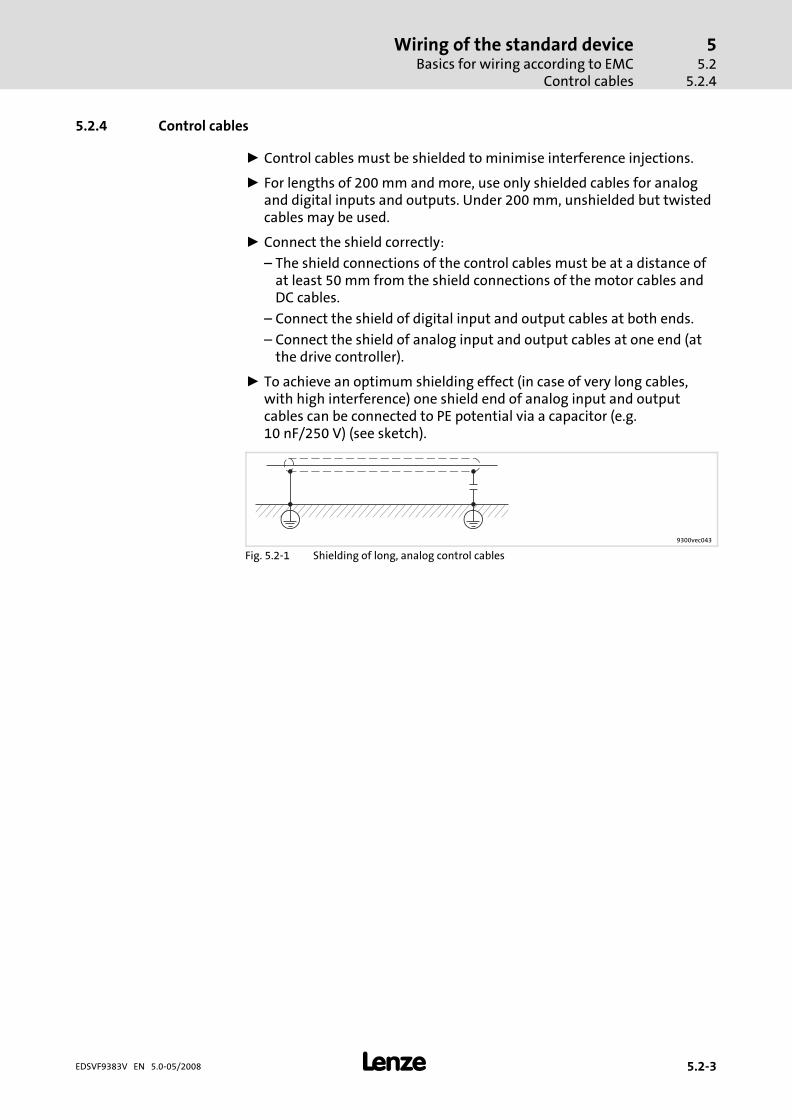
Wiring of the standard deviceBasics for wiring according to EMC
Control cables
55.2
5.2.4
� 5.2−3EDSVF9383V EN 5.0−05/2008
5.2.4 Control cables
ƒ Control cables must be shielded to minimise interference injections.
ƒ For lengths of 200 mm and more, use only shielded cables for analogand digital inputs and outputs. Under 200 mm, unshielded but twistedcables may be used.
ƒ Connect the shield correctly:
– The shield connections of the control cables must be at a distance ofat least 50 mm from the shield connections of the motor cables andDC cables.
– Connect the shield of digital input and output cables at both ends.
– Connect the shield of analog input and output cables at one end (atthe drive controller).
ƒ To achieve an optimum shielding effect (in case of very long cables,with high interference) one shield end of analog input and outputcables can be connected to PE potential via a capacitor (e.g.10 nF/250 V) (see sketch).
9300vec043
Fig. 5.2−1 Shielding of long, analog control cables

Wiring of the standard deviceBasics for wiring according to EMCInstallation in the control cabinet
55.25.2.5
� 5.2−4 EDSVF9383V EN 5.0−05/2008
5.2.5 Installation in the control cabinet
ƒ Only use mounting plates with conductive surfaces (zinc−coated orV2A−steel).
ƒ Painted mounting plates are not suitable even if the paint is removedfrom the contact surfaces.
ƒ If several mounting plates are used, ensure a large−surface connectionbetween the mounting plates (e.g. by using earthing strips).
ƒ Connect the controller and the chokes to the grounded mounting platewith a surface as large as possible.
ƒ The motor cable is optimally installed if
– it is separated from mains cables and control cables,
– it crosses mains cables and control cables at right angles.
ƒ Always install cables close to the mounting plate (reference potential),as freely suspended cables act like aerials.
ƒ Lead the cables to the terminals in a straight line (avoid tangles ofcables).
ƒ Use separated cable channels for motor cables and control cables. Donot mix up different cable types in one cable channel.
ƒ Minimise coupling capacities and coupling inductances by avoidingunnecessary cable lengths and reserve loops.
ƒ Short−circuit unused cores to the reference potential.
ƒ Install the positive and negative wires for DC 24 V close to each otherover the entire length to avoid loops.
ƒ Connect all components (controller, chokes) to a central earthing point(PE rail).
ƒ Set up a star−shape earthing system.
ƒ Comply with the corresponding minimum cable cross−sections.
Mounting plate requirements
Mounting of the components
Optimum cable routing
Earth connections

Wiring of the standard deviceBasics for wiring according to EMCWiring outside the control cabinet
55.2
5.2.6
� 5.2−5EDSVF9383V EN 5.0−05/2008
5.2.6 Wiring outside the control cabinet
Notes for cable routing outside the control cabinet:
ƒ The longer the cables the greater the space between the cables mustbe.
ƒ If cables for different signal types are routed in parallel, theinterferences can be minimized by means of a metal barrier orseparated cable ducts.
Cover
Barrier withoutopening
Power cablesSignal cables
EMVallg001
Fig. 5.2−2 Cable routing in the cable duct with barrier
Cover
Communication cables
Cable duct
Measuring cablesAnalog cables
Control cables
Power cables
EMVallg002
Fig. 5.2−3 Cable routing in separated cable ducts

Wiring of the standard deviceBasics for wiring according to EMCDetecting and eliminating EMC interferences
55.25.2.7
� 5.2−6 EDSVF9383V EN 5.0−05/2008
5.2.7 Detecting and eliminating EMC interferences
Fault Cause Remedy
Interferences ofanalog setpoints ofyour own or otherdevices andmeasuring systems
Unshielded motor cable Use shielded motor cable
Shield contact is not extensiveenough
Carry out optimal shielding asspecified
Shield of the motor cable isinterrupted by terminal strips,switched, etc.
� Separate components fromother component part with aminimum distance of 100 mm
� Use motor choke/motor filter
Install additional unshieldedcables inside the motor cable (e.g.for motor temperaturemonitoring)
Install and shield additional cablesseparately
Too long and unshielded cableends of the motor cable
Shorten unshielded cable ends tomaximally 40 mm
Conductedinterference level isexceeded on thesupply side
Terminal strips for the motorcable are directly located next tothe mains terminals
Spatially separate the terminalstrips for the motor cable frommain terminals and other controlterminals with a minimumdistance of 100 mm
Mounting plate varnished Optimise PE connection:� Remove varnish� Use zinc−coated mounting
plate
HF short circuit Check cable routing

Wiring of the standard deviceBasic devices in the power range 110 ... 200 kW
Wiring according to EMC (CE−typical drive system)
55.3
5.3.1
� 5.3−1EDSVF9383V EN 5.0−05/2008
5.3 Basic devices in the power range 110 ... 200 kW
5.3.1 Wiring according to EMC (CE−typical drive system)
The drives comply with the EC Directive on "Electromagnetic Compatibility"if they are installed in accordance with the specifications for the CE−typicaldrive system. The user is responsible for the compliance of the machineapplication with the EC Directive.
� Note!
Observe the notes given in chapter "Basics for wiring accordingto EMC"!

Wiring of the standard deviceBasic devices in the power range 110 ... 200 kWWiring according to EMC (CE−typical drive system)
55.35.3.1
� 5.3−2 EDSVF9383V EN 5.0−05/2008
EVF9335-EV …
EVF9338-EV
K10
L1
L2
L3
N
PE
F1 … F3
PES
PES
PES PES
PES
PESPES
PES
3
7
4
63
2
62
1
7
X6
28
E1
E2E3
E5
E4
ST1
ST2
39
A1
A3
A2
A4
59
X5
33
34
K32
K31IN2
IN3
IN4
IN1 X11
PE U V WT1 T2 BR1BR2+UG -UG
S1 K10
K10
S2
PE101 102 103 104 L1 L2 L3
DC 24 V
Z1
+
–
PE
PE
M
3~
M
3~
KTY
X8/5
X8/8
PE
��
PES
PES
PES
PES
PES
PES PES
PES PES
PE
Z2
�RB
RB
RB2 T2T1RB1PE
PE
9300VEC007
Fig. 5.3−1 Example for wiring in accordance with EMC regulations
F1 ... F3 FusesK10 Mains contactorZ1 Programmable logic controller (PLC)Z2 Brake resistorS1 Mains contactor onS2 Mains contactor off+UG, −UG DC−bus connectionPES HF shield termination through large−surface connection to PE

Wiring of the standard deviceBasic devices in the power range 110 ... 200 kW
Mains connection of the controller for 400 V mains voltage
55.3
5.3.2
� 5.3−3EDSVF9383V EN 5.0−05/2008
5.3.2 Mains connection of the controller for 400 V mains voltage
� Stop!
The user is responsible for sufficient strain relief!
BR2BR1 PE U V WL1 L2 L3 PE
L1, L2,
L3
25-30 Nm
M8
221-264 lb-in
PE 15-20 Nm
M6
133-176 lb-in
40 mm
9300VEC003
Fig. 5.3−2 Mains connection example
BR1, BR2 Brake resistors can only be operated with variants V060 andV110
9300 vector Installation in accordance with EN 60204−1
Fuse 2) Cable cross−sections
L1, L2, L3 PE
Type [A] [mm2] [mm2]
EVF9335−EVEVF9335−EVVxxx
250150
2 × 50 1) 95
EVF9336−EVEVF9336−EVVxxx
315150
2 × 50 1) 95
EVF9337−EVEVF9337−EVVxxx
315150
2 × 50 1) 95
EVF9338−EVEVF9338−EVVxxx
400240
2 × 95 1) 150
1) Multiple conductor; both conductors must have the same cross−section2) Lenze recommends to use fuses of the gRL utilisation categoryObserve the national and regional legislation
Fuses and cable cross−sectionsfor the mains connection

Wiring of the standard deviceBasic devices in the power range 110 ... 200 kWSupply and fan connection of the controller for 400 V/500V mains voltage
55.35.3.3
� 5.3−4 EDSVF9383V EN 5.0−05/2008
5.3.3 Supply and fan connection of the controller for 400 V/500V mains voltage
� Stop!
The user is responsible for sufficient strain relief!
BR2BR1+UG -UG PE U V WL1
10
1
10
2
10
3
10
4L2 L3 PE
L1, L2,
L3
25-30 Nm
M8
221-264 lb-in
PE 15-20 Nm
M6
133-176 lb-in
40 mm
9300VEC032
Fig. 5.3−3 Mains connection example
BR1, BR2 Brake resistors can only be operated with variants V270 andV300
9300 vector Installation in accordance with EN 60204−1
Fuse 2) Cable cross−sections
L1, L2, L3 PE
Type [A] [mm2] [mm2]
EVF9335−EVEVF9335−EVVxxx
250150
2 × 50 1) 95
EVF9336−EVEVF9336−EVVxxx
315150
2 × 50 1) 95
EVF9337−EVEVF9337−EVVxxx
315150
2 × 50 1) 95
EVF9338−EVEVF9338−EVVxxx
400240
2 × 95 1) 150
1) Multiple conductor; both conductors must have the same cross−section2) Lenze recommends to use fuses of the gRL utilisation categoryObserve the national and regional legislation
Mains connection
Fuses and cable cross−sectionsfor the mains connection

Wiring of the standard deviceBasic devices in the power range 110 ... 200 kW
Supply and fan connection of the controller for 400 V/500V mains voltage
55.3
5.3.3
� 5.3−5EDSVF9383V EN 5.0−05/2008
ƒ For compliance with EMC requirements, Lenze recommends to useshielded DC−bus cables.
ƒ Shield clamps are not included in the scope of supply.
BR2BR1+UG -UG PE U V WL1101
102
103
104
L2 L3 PE
40 mm
PE 15-20 Nm
M6
133-176 lb-in+UG
-UG
25-30 Nm
M8
221-264 lb-in
max.
300 mm
�
�
9300VEC074
Fig. 5.3−4 Connection example to +UG and −UG
BR1, BR2 Brake resistors can only be operated with variants V270 and V300� Connect the DC−bus cable shield to the conductive control cabinet
mounting plate with a contact surface as large as possible by usingthe shield clamps.
� Conductive surfaceEnsure to have the poles right!
9300 vector Installation in accordance with EN 60204−1
Fuse 2) Cable cross−sections
+UG, −UG PE
Type [A] [mm2] [mm2]
EVF9335−EVV2xxEVF9335−EVV300
315150
2 × 50 1) 95
EVF9336−EVV2xxEVF9336−EVV300
350150
2 × 50 1) 95
EVF9337−EVV2xxEVF9337−EVV300
400240
2 × 95 1) 95
EVF9338−EVV2xxEVF9338−EVV300
500240
2 × 95 1) 150
1) Multiple conductor; both conductors must have the same cross−section2) Only use fuses of the gRL utilisation categoryObserve the national and regional legislation
Lay a bridge between the terminals when a controller is operated on a mains.
AC 340 ... 440 V AC 440 ... 577 V(when being delivered)
L1 L2
101
102
103
104
101
102
103
104
L1 L2
9300vec044 9300vec045
Connection to the DC bus(+UG, −UG)
Fuses and cable cross−sectionsfor DC−bus connection
Fan connection whencontroller is supplied withmains voltage

Wiring of the standard deviceBasic devices in the power range 110 ... 200 kWSupply and fan connection of the controller for 400 V/500V mains voltage
55.35.3.3
� 5.3−6 EDSVF9383V EN 5.0−05/2008
� Danger!
When the fan is externally supplied with voltage, the terminal L2carries dangerous mains voltage!
When the controller is supplied via the DC bus, the fan must be separatelysupplied with mains voltage (see �). In this case, the bridge between theterminals 102 and 103 must be removed (see �).
Remove bridge Mains connection for the operation of the fan on
AC 340 ... 440 V AC 440 ... 577 V
10
1
10
2
10
3
10
4
�
�
L1 L2
AC 340 … 440 V101
102
103
104
�
L1 L2
AC 440 … 577 V
101
102
103
104
�
L1 L2
9300vec160 9300vec046 9300vec047
In case of an external voltage supply the fan is protected by a fuse integratedin terminal 104.
101
102
103
104
L1 L2
��
9300vec161
Fig. 5.3−5 Fusing of the fan
� Open the fuse holder.� Remove the defect fuse from the support and replace it by the following
type:
Type: 500V SA 2A 6.32Ref. no.: P098131Manufacturer: Ferraz Shawmut
Fan connection whencontroller is supplied via theDC bus
Exchange defect fuse

Wiring of the standard deviceBasic devices in the power range 110 ... 200 kW
Motor connection
55.3
5.3.4
� 5.3−7EDSVF9383V EN 5.0−05/2008
5.3.4 Motor connection
ƒ To comply with the EMC regulations, Lenze recommends to useshielded motor cables.
ƒ Shield clamps are not included in the scope of supply.
� Stop!
The user is responsible for sufficient strain relief!
BR2BR1 PE U V W
40 mm
PE 15-20 Nm
M6
133-176 lb-in
U, V, W 25-30 Nm
M8
221-264 lb-in
�
max.
300 mm
�
9300VEC005
Fig. 5.3−6 Motor connection example
BR1, BR2 Brake resistors can only be operated with variants V060, V110, V270and V300
� Connect the motor cable shield with a surface as large as possible tothe control cabinet mounting plate by using the clamps.
� Conductive surfaceEnsure to have the poles right!Do not exceed the maximum motor cable length!
9300 vector Installation in accordance with EN 60204−1
U, V, W PE
Type [mm2] [mm2]
EVF9335−EVEVF9335−EVVxxx
1502 × 50 1) 95
EVF9336−EVEVF9336−EVVxxx
1502 × 50 1) 95
EVF9337−EVEVF9337−EVVxxx
1502 × 50 1) 95
EVF9338−EVEVF9338−EVVxxx
2402 × 95 1) 150
1) Multiple conductor; both conductors must have the same cross−sectionObserve the national and regional legislation
Cable cross−sections

Wiring of the standard deviceBasic devices in the power range 110 ... 200 kWWiring of motor temperature monitoring
55.35.3.5
� 5.3−8 EDSVF9383V EN 5.0−05/2008
5.3.5 Wiring of motor temperature monitoring
The drive controller features 2 connections for motor temperaturemonitoring:
ƒ Terminals T1, T2 for connecting a PTC thermistor or thermal contact(NC contact).
ƒ Pin X8/5 and X8/8 of the incremental encoder input (X8) forconnecting a KTY thermal sensor.

Wiring of the standard deviceBasic devices in the power range 110 ... 200 kW
Wiring of motor temperature monitoring
55.3
5.3.5
� 5.3−9EDSVF9383V EN 5.0−05/2008
Wire T1, T2 only if the motor is equipped with a PTC thermistor or thermalcontact (NC contact).
ƒ An "open" cable acts like an antenna and can cause faults on the drivecontroller.
� Danger!
ƒ All control terminals only have basic insulation (singleisolating distance) after connecting a PTC thermistor or athermal contact.
ƒ Protection against accidental contact in case of a defectiveisolating distance is only guaranteed through externalmeasures, e.g. double insulation.
PE U V WT1 T2 +UG -UG
PES PES
PE M
3~
��
PES PES
PES
2.7 k
MONIT-OH8
15 V
3.3 k
7.4 k
T1 T2
9300vec139 9300std328
Fig. 5.3−7 Connection of PTC thermistor or thermal contact (NC contact) at T1, T2
Characteristics of the connection for motor temperature monitoring:
Terminals T1, T2
Connection � PTC thermistor– PTC thermistor with defined tripping temperature (acc. to
DIN 44081 and DIN 44082)� Thermal contact (NC contact)
– Thermostat as NC contact
Tripping point � Fixed (depending on the PTC/thermal contact)� PTC: R� 1600 �� Configurable as warning or error (TRIP)
Notes � Monitoring is not active in the Lenze setting.� If you do not use a Lenze motor, we recommend the use of a PTC
thermistor up to 150°C.
Motor with PTC thermistor orthermal contact (NC contact)
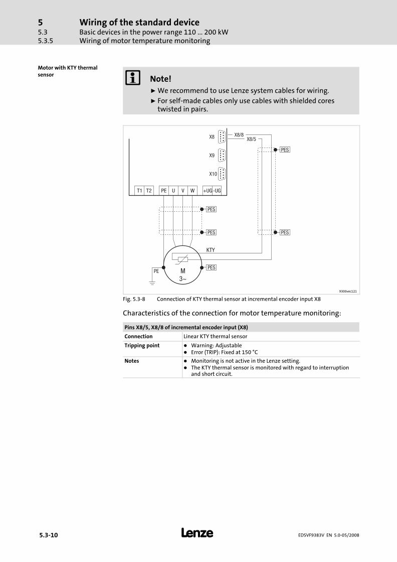
Wiring of the standard deviceBasic devices in the power range 110 ... 200 kWWiring of motor temperature monitoring
55.35.3.5
� 5.3−10 EDSVF9383V EN 5.0−05/2008
� Note!
ƒ We recommend to use Lenze system cables for wiring.
ƒ For self−made cables only use cables with shielded corestwisted in pairs.
PE U V WT1 T2 +UG -UG
PES
PES
PE M
3~
PESPES
KTY
X8/5X8/8
PES
X8
X9
X10
9300vec121
Fig. 5.3−8 Connection of KTY thermal sensor at incremental encoder input X8
Characteristics of the connection for motor temperature monitoring:
Pins X8/5, X8/8 of incremental encoder input (X8)
Connection Linear KTY thermal sensor
Tripping point � Warning: Adjustable� Error (TRIP): Fixed at 150 °C
Notes � Monitoring is not active in the Lenze setting.� The KTY thermal sensor is monitored with regard to interruption
and short circuit.
Motor with KTY thermalsensor

Wiring of the standard deviceBasic devices in the power range 250 ... 400 kW
Wiring according to EMC (CE−typical drive system)
55.4
5.4.1
� 5.4−1EDSVF9383V EN 5.0−05/2008
5.4 Basic devices in the power range 250 ... 400 kW
5.4.1 Wiring according to EMC (CE−typical drive system)
The drives comply with the EC Directive on "Electromagnetic Compatibility"if they are installed in accordance with the specifications for the CE−typicaldrive system. The user is responsible for the compliance of the machineapplication with the EC Directive.
� Note!
Observe the notes given in chapter "Basics for wiring accordingto EMC"!
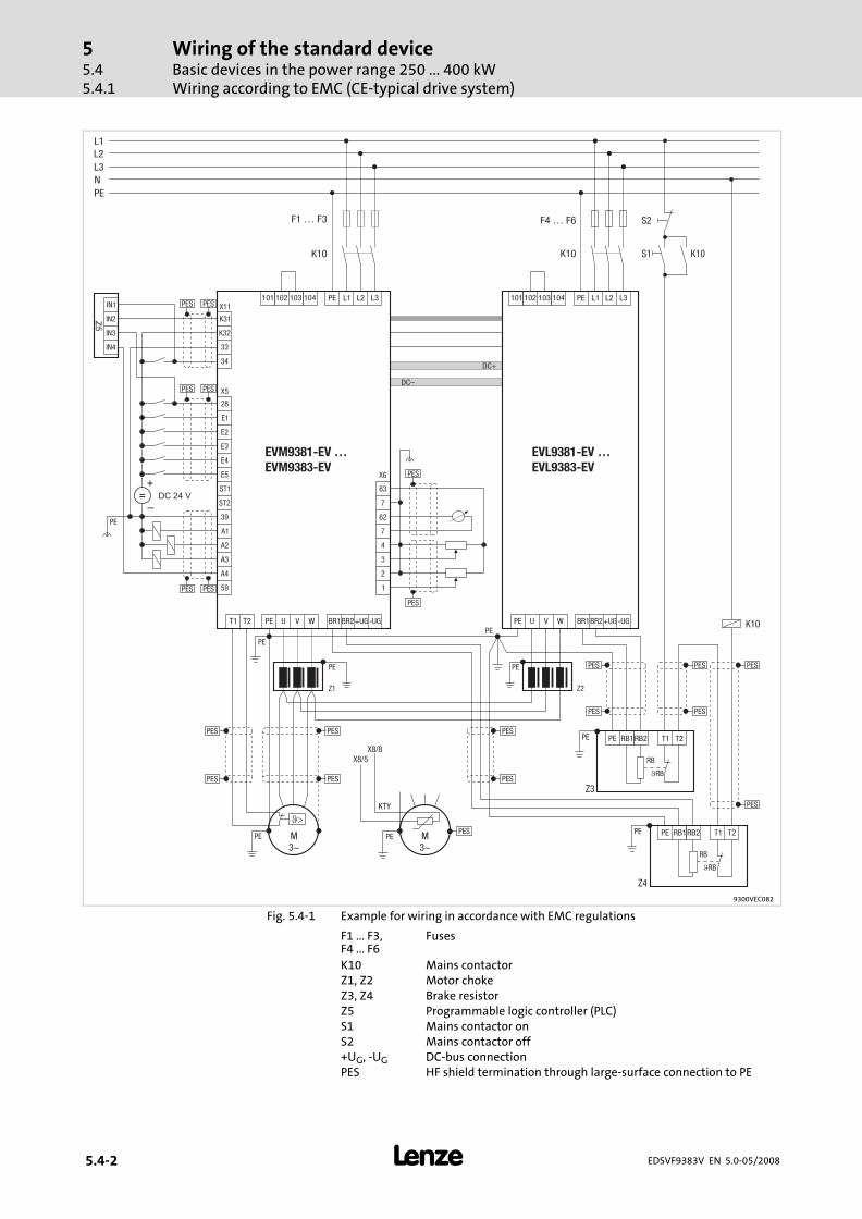
Wiring of the standard deviceBasic devices in the power range 250 ... 400 kWWiring according to EMC (CE−typical drive system)
55.45.4.1
� 5.4−2 EDSVF9383V EN 5.0−05/2008
EVM9381-EV …EVM9383-EV
EVL9381-EV …EVL9383-EV
K10 K10
L1L2L3NPE
F1 … F3 F4 … F6
PE
PE
PE
PEPE
PE
M3~
M3~
KTY
X8/5X8/8
PE
��
PES
PES PES PES
PES
PES PES
PES
PES
PES
PES PES
PES
PESPES
PES
PESPES
PES PES
PES
3
7
4
63
2
62
1
7
X6
28
E1
E2E3
E5
E4
ST1
ST2
39
A1
A3
A2
A4
59
X5
33
34
K32
K31IN2
IN3
IN4
IN1 X11
PE PEU UV VW WT1 T2 BR1 BR1BR2 BR2+UG +UG-UG -UG
S1 K10
K10
Z2Z1
S2
PE PE101 101102 102103 103104 104L1 L1L2 L2L3
DC+
DC–
L3
DC 24 V
Z5
+
–
PE
PE
Z3
Z4
�RB
RB
RB2 T2T1RB1PE
�RB
RB
RB2 T2T1RB1PE
9300VEC082
Fig. 5.4−1 Example for wiring in accordance with EMC regulations
F1 ... F3,F4 ... F6
Fuses
K10 Mains contactorZ1, Z2 Motor chokeZ3, Z4 Brake resistorZ5 Programmable logic controller (PLC)S1 Mains contactor onS2 Mains contactor off+UG, −UG DC−bus connectionPES HF shield termination through large−surface connection to PE

Wiring of the standard deviceBasic devices in the power range 250 ... 400 kW
Master and slave connection
55.4
5.4.2
� 5.4−3EDSVF9383V EN 5.0−05/2008
5.4.2 Master and slave connection
� Danger!
Danger of personal injury! Destruction of the controller!
Damaged control cables in the controller (master and slave) maycause a faulty control of the output stage.
Possible consequences:
ƒ When switching on the mains voltage, high energies maydischarge like an explosion.
ƒ Explosive noises may damage your hearing. A shock by anunexpected and loud explosion may cause distress.
ƒ The controller will be destroyed.
Protective measures:
ƒ When working with the DC busbars, make sure that you donot damage any internal connectors and cables.
ƒ Before attaching the cover again:– Check all plugs selected in Fig. 5.4−5 for damage and correct
fit.– Check all cables involved for damages.– If the plugs do not fit correctly, or the plugs or cables are
damaged, commissioning is prohibited. Contact the Lenzeservice.
� �
9300vec164
Fig. 5.4−2 Fastening the covers to the master and slave
ƒ Remove the upper cover from the master � and the slave � to accessthe power sections. Each cover is fastened with 4 screws.
Important notes
Preliminary work

Wiring of the standard deviceBasic devices in the power range 250 ... 400 kWMaster and slave connection
55.45.4.2
� 5.4−4 EDSVF9383V EN 5.0−05/2008
Installation of the DC busbars
DC+
DC-
�
��
�
�
�
�
�
�
�
�
�
�
�
�
�
�
�
9300VEC024
Fig. 5.4−3 Mounting of +DC/−DC busbars
1. Mount +DC busbar � :
– Remove hexagon socket screws M8 �.
– Position the DC busbar in the master and the slave.
– Fasten the DC busbar in the master and the slave with 1 hexagonsocket screw M8 × 45 mm �, 1 plain washer � and 1 distancesleeve each.
– Tighten the hexagon socket screws � (tightening torque: 10.9 Nm).
2. Mount −DC busbar � :
– Remove hexagon socket screws M8 �.
– Put both connecting cables � aside.
– Position the DC busbar in the master and the slave.
– Insert 2 hexagon socket screws M8 × 45 mm � each with plainwashers � into the bore holes of the DC busbar, finally passing themthrough the distance sleeves �.
– Screw the hexagon socket screws � into the threaded holes in themaster and slave.
– Lay the connecting cable � in the master and slave with cable lugbetween the busbar � and plain washer �.
– Tighten the hexagon socket screws � (tightening torque: 10.9 Nm).
How to mount the DC busbars

Wiring of the standard deviceBasic devices in the power range 250 ... 400 kW
Master and slave connection
55.4
5.4.2
� 5.4−5EDSVF9383V EN 5.0−05/2008
Connection of the control cables between master and slave
DC+
DC-
�
�
��
�
��
�
�
�
9300VEC028
Fig. 5.4−4 Connection of the control cables between master and slave
1. Installation and connection of the ribbon cable �:
By default the ribbon cable is inside the master. The plug is alreadyattached to the Drive Board.
– Route the ribbon cable from the master to the Drive Boardconnection in the slave, inserting the ribbon cable into the cableducts �.
– Plug the ribbon cable plug � into the socket � at the Drive Board.
2. Laying and connecting 2−core cables with plugs �:
By default the cable is inside the master. The corresponding cable withsocket is in the slave.
– Lay the two−core cable from the master to the socket in the slave.
– Connect the 2−pole plug with the 2−pole socket in the slave.
3. Laying and connecting 10−core cables with plugs �:
By default the cable is inside the master. The corresponding cable withsocket is in the slave.
– Lay the two−core cable from the master to the socket in the slave.
– Connect the 10−pole plug with the 10−pole socket in the slave.
How to connect the controlcables
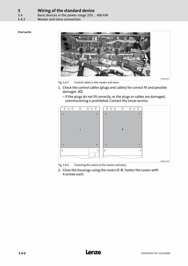
Wiring of the standard deviceBasic devices in the power range 250 ... 400 kWMaster and slave connection
55.45.4.2
� 5.4−6 EDSVF9383V EN 5.0−05/2008
9300vec163
Fig. 5.4−5 Control cables in the master and slave
1. Check the control cables (plugs and cables) for correct fit and possibledamages. (�)
– If the plugs do not fit correctly, or the plugs or cables are damaged,commissioning is prohibited. Contact the Lenze service.
� �
9300vec164
Fig. 5.4−6 Fastening the covers to the master and slave
2. Close the housings using the covers ���. Fasten the covers with4 screws each.
Final works

Wiring of the standard deviceBasic devices in the power range 250 ... 400 kW
Mains connection of the controller for 400 V mains voltage
55.4
5.4.3
� 5.4−7EDSVF9383V EN 5.0−05/2008
5.4.3 Mains connection of the controller for 400 V mains voltage
� Stop!
The user is responsible for sufficient strain relief!
ƒ Both, the master and the slave must be supplied!
BR2 BR2BR1 BR1PE PEU UV VW WL1 L1L2 L2L3 L3PE PE
L1, L2,
L3
L1, L2,
L3
25-30 Nm 25-30 Nm
M8 M8
221-264 lb-in 221-264 lb-in
PE PE15-20 Nm 15-20 Nm
M6 M6
133-176 lb-in 133-176 lb-in
40 mm 40 mm
� �
9300VEC013
Fig. 5.4−7 Mains connection example
BR1, BR2 Brake resistors can only be operated with variants V060 andV110
� Master terminals� Slave terminals
9300 vector Installation in accordance with EN 60204−1
Fuse 2) Cable cross−sections
L1, L2, L3 PE
Type [A] [mm2] [mm2]
Master Slave Master Slave Master Slave
EVF9381−EVEVF9381−EVVxxx
315 315150
2 × 50 1)150
2 × 50 1) 95 95
EVF9382−EVEVF9382−EVVxxx
315 315150
2 × 50 1)150
2 × 50 1) 95 95
EVF9383−EVEVF9383−EVVxxx
400 400240
2 × 95 1)240
2 × 95 1) 150 150
1) Multiple conductor; both conductors must have the same cross−section2) Lenze recommends to use fuses of the gRL utilisation categoryObserve the national and regional legislation
Fuses and cable cross−sectionsfor the mains connection

Wiring of the standard deviceBasic devices in the power range 250 ... 400 kWSupply and fan connection of the controller for 400 V/500V mains voltage
55.45.4.4
� 5.4−8 EDSVF9383V EN 5.0−05/2008
5.4.4 Supply and fan connection of the controller for 400 V/500V mains voltage
� Stop!
The user is responsible for sufficient strain relief!
ƒ Both, the master and the slave must be supplied!
BR2 BR2BR1 BR1+UG +UG-UG -UGPE PEU UV VW WL1 L1
101
101
102
102
103
103
10
4
10
4
L2 L2L3 L3PE PE
L1, L2,
L3
25-30 Nm
M8
221-264 lb-in
L1, L2,
L3
25-30 Nm
M8
221-264 lb-in
PE 15-20 Nm
M6
133-176 lb-in
PE 15-20 Nm
M6
133-176 lb-in
40 mm 40 mm
� �
9300VEC035
Fig. 5.4−8 Mains connection example
BR1, BR2 Brake resistors can only be operated with variants V270 andV300
� Master terminals� Slave terminals
9300 vector Installation in accordance with EN 60204−1
Fuse 2) Cable cross−sections
L1, L2, L3 PE
Type [A] [mm2] [mm2]
Master Slave Master Slave Master Slave
EVF9381−EVEVF9381−EVVxxx
315 315150
2 × 50 1)150
2 × 50 1) 95 95
EVF9382−EVEVF9382−EVVxxx
315 315150
2 × 50 1)150
2 × 50 1) 95 95
EVF9383−EVEVF9383−EVVxxx
400 400240
2 × 95 1)240
2 × 95 1) 150 150
1) Multiple conductor; both conductors must have the same cross−section2) Lenze recommends to use fuses of the gRL utilisation categoryObserve the national and regional legislation
Mains connection
Fuses and cable cross−sectionsfor the mains connection

Wiring of the standard deviceBasic devices in the power range 250 ... 400 kW
Supply and fan connection of the controller for 400 V/500V mains voltage
55.4
5.4.4
� 5.4−9EDSVF9383V EN 5.0−05/2008
ƒ For compliance with EMC requirements, Lenze recommends to useshielded DC−bus cables.
ƒ Shield clamps are not included in the scope of supply.
ƒ Both, the master and the slave must be supplied!
BR2 BR2BR1 BR1+UG +UG-UG -UGPE PEU UV VW WL1 L1
101
101
102
102
103
103
104
104
L2 L2L3 L3PE PE
40 mm 40 mm
PE 15-20 Nm
M6
133-176 lb-in
PE 15-20 Nm
M6
133-176 lb-in+UG +UG
-UG -UG
25-30 Nm 25-30 Nm
M8 M8
221-264 lb-in 221-264 lb-in
max.
300 mm
max.
300 mm
� �
� �
� �
9300VEC083
Fig. 5.4−9 Connection example to +UG and −UG
BR1, BR2 Brake resistors can only be operated with variants V270 and V300� Master terminals� Slave terminals Connect the DC−bus cable shield to the conductive control cabinet
mounting plate with a contact surface as large as possible by usingthe shield clamps.
� Conductive surfaceEnsure to have the poles right!
9300 vector Installation in accordance with EN 60204−1
Fuse 2) Cable cross−sections
+UG, −UG PE
Type [A] [mm2] [mm2]
Master Slave Master Slave Master Slave
EVF9381−EVV2xxEVF9381−EVV300
350 350150
2 × 50 1)150
2 × 50 1) 95 95
EVF9382−EVV2xxEVF9382−EVV300
400 400240
2 × 95 1)240
2 × 95 1) 95 95
EVF9383−EVV2xxEVF9383−EVV300
500 500240
2 × 95 1)240
2 × 95 1) 150 150
1) Multiple conductor; both conductors must have the same cross−section2) Only use fuses of the gRL utilisation categoryObserve the national and regional legislation
Connection to the DC bus(+UG, −UG)
Fuses and cable cross−sectionsfor DC−bus connection

Wiring of the standard deviceBasic devices in the power range 250 ... 400 kWSupply and fan connection of the controller for 400 V/500V mains voltage
55.45.4.4
� 5.4−10 EDSVF9383V EN 5.0−05/2008
� Note!
Connect the fan to the master and the slave.
Lay a bridge between the terminals when a controller is operated on a mains.
AC 340 ... 440 V AC 440 ... 577 V(when being delivered)
L1 L2
101
102
103
104
101
102
103
104
L1 L2
9300vec044 9300vec045
� Danger!
When the fan is externally supplied with voltage, the terminal L2carries dangerous mains voltage!
When the controller is supplied via the DC bus, the fan must be separatelysupplied with mains voltage (see �). In this case, the bridge between theterminals 102 and 103 must be removed (see �).
Remove bridge Mains connection for the operation of the fan on
AC 340 ... 440 V AC 440 ... 577 V
10
1
10
2
10
3
10
4
�
�
L1 L2
AC 340 … 440 V
101
102
103
104
�
L1 L2
AC 440 … 577 V
101
102
103
104
�
L1 L2
9300vec160 9300vec046 9300vec047
Fan connection
Fan connection whencontroller is supplied withmains voltage
Fan connection whencontroller is supplied via theDC bus

Wiring of the standard deviceBasic devices in the power range 250 ... 400 kW
Supply and fan connection of the controller for 400 V/500V mains voltage
55.4
5.4.4
� 5.4−11EDSVF9383V EN 5.0−05/2008
In case of an external voltage supply the fan is protected by a fuse integratedin terminal 104.
101
102
103
104
L1 L2
��
9300vec161
Fig. 5.4−10 Fusing of the fan
� Open the fuse holder.� Remove the defect fuse from the support and replace it by the following
type:
Type: 500V SA 2A 6.32Ref. no.: P098131Manufacturer: Ferraz Shawmut
Exchange defect fuse

Wiring of the standard deviceBasic devices in the power range 250 ... 400 kWMotor connection
55.45.4.5
� 5.4−12 EDSVF9383V EN 5.0−05/2008
5.4.5 Motor connection
ƒ To comply with the EMC regulations, Lenze recommends to useshielded motor cables.
ƒ Shield clamps are not included in the scope of supply.
� Stop!
The user is responsible for sufficient strain relief!
In order to connect the motor cables of master and slave to the motor, theoutputs must be connected in parallel.
It is important for the parallel connection of the inverter outputs that theoutputs are decoupled by means of an inductance between master andslave. The length of the motor cables determine whether the inductance ofthe cables is sufficient for a decoupling.
2 motor connections ensure sufficient decoupling.
ƒ Decoupling via motor chokes
If the single motor cable length is � 10 m, master and slave must beconnected in parallel via chokes on the motor side to achieve a sufficientdecoupling between master and slave.
ƒ Decoupling via motor cables
If the single motor cable length is > 10 m, the motor cables of master andslave can be connected in parallel at the motor to achieve a sufficientdecoupling between master and slave.
Decoupling via motor chokes Decoupling via motor cables
M3~
PE PEU UV VW W
Z1 Z2PE
�1
0m
PE PE
PE
PE U V W
M3~
PE U V W
PE
PE
PE
>10
m
9300VEC026 9300VEC008
Fig. 5.4−11 Variants for parallel connection of master and slave (motor side)
Z1, Z2 Motor choke for controllerELM3−0003H275 EVF9381ELM3−0002H320 EVF9382ELM3−0002H410 EVF9383
Parallel connection of masterand slave (motor side)

Wiring of the standard deviceBasic devices in the power range 250 ... 400 kW
Motor connection
55.4
5.4.5
� 5.4−13EDSVF9383V EN 5.0−05/2008
� �
BR2 BR2BR1 BR1PE PEU UV VW W
40 mm 40 mm
PE 15-20 Nm
M6
133-176 lb-in
PE 15-20 Nm
M6
133-176 lb-in
U, V, W 25-30 Nm
M8
221-264 lb-inU, V, W 25-30 Nm
M8
221-264 lb-in
� �� �
max.
300 mm
max.
300 mm
9300VEC036
Fig. 5.4−12 Motor connection example
BR1, BR2 Brake resistors can only be operated with variants V060, V110, V270and V300
� Master terminals� Slave terminals Connect the motor cable shield with a surface as large as possible to
the control cabinet mounting plate by using the clamps.
� Conductive surfaceEnsure to have the poles right!Do not exceed the maximum motor cable length!
9300 vector Installation in accordance with EN 60204−1
U, V, W PE
Type [mm2] [mm2]
Master Slave Master Slave
EVF9381−EVEVF9381−EVVxxx
1502 × 50 1)
1502 × 50 1) 95 95
EVF9382−EVEVF9382−EVVxxx
1502 × 50 1)
1502 × 50 1) 95 95
EVF9383−EVEVF9383−EVVxxx
2402 × 95 1)
2402 × 95 1) 150 150
1) Multiple conductor; both conductors must have the same cross−sectionObserve the national and regional legislation
Motor connection
Cable cross−sections
Wiring of the standard deviceBasic devices in the power range 250 ... 400 kWWiring of motor temperature monitoring
55.45.4.6
� 5.4−14 EDSVF9383V EN 5.0−05/2008
5.4.6 Wiring of motor temperature monitoring
The drive controller features 2 connections for motor temperaturemonitoring:
ƒ Terminals T1, T2 for connecting a PTC thermistor or thermal contact(NC contact).
ƒ Pin X8/5 and X8/8 of the incremental encoder input (X8) forconnecting a KTY thermal sensor.

Wiring of the standard deviceBasic devices in the power range 250 ... 400 kW
Wiring of motor temperature monitoring
55.4
5.4.6
� 5.4−15EDSVF9383V EN 5.0−05/2008
Wire T1, T2 only if the motor is equipped with a PTC thermistor or thermalcontact (NC contact).
ƒ An "open" cable acts like an antenna and can cause faults on the drivecontroller.
� Danger!
ƒ All control terminals only have basic insulation (singleisolating distance) after connecting a PTC thermistor or athermal contact.
ƒ Protection against accidental contact in case of a defectiveisolating distance is only guaranteed through externalmeasures, e.g. double insulation.
PE U V WT1 T2 +UG -UG
PES PES
PE M
3~
��
PES PES
PES
2.7 k
MONIT-OH8
15 V
3.3 k
7.4 k
T1 T2
9300vec139 9300std328
Fig. 5.4−13 Connection of PTC thermistor or thermal contact (NC contact) at T1, T2
Characteristics of the connection for motor temperature monitoring:
Terminals T1, T2
Connection � PTC thermistor– PTC thermistor with defined tripping temperature (acc. to
DIN 44081 and DIN 44082)� Thermal contact (NC contact)
– Thermostat as NC contact
Tripping point � Fixed (depending on the PTC/thermal contact)� PTC: R� 1600 �� Configurable as warning or error (TRIP)
Notes � Monitoring is not active in the Lenze setting.� If you do not use a Lenze motor, we recommend the use of a PTC
thermistor up to 150°C.
Motor with PTC thermistor orthermal contact (NC contact)

Wiring of the standard deviceBasic devices in the power range 250 ... 400 kWWiring of motor temperature monitoring
55.45.4.6
� 5.4−16 EDSVF9383V EN 5.0−05/2008
� Note!
ƒ We recommend to use Lenze system cables for wiring.
ƒ For self−made cables only use cables with shielded corestwisted in pairs.
PE U V WT1 T2 +UG -UG
PES
PES
PE M
3~
PESPES
KTY
X8/5X8/8
PES
X8
X9
X10
9300vec121
Fig. 5.4−14 Connection of KTY thermal sensor at incremental encoder input X8
Characteristics of the connection for motor temperature monitoring:
Pins X8/5, X8/8 of incremental encoder input (X8)
Connection Linear KTY thermal sensor
Tripping point � Warning: Adjustable� Error (TRIP): Fixed at 150 °C
Notes � Monitoring is not active in the Lenze setting.� The KTY thermal sensor is monitored with regard to interruption
and short circuit.
Motor with KTY thermalsensor

Wiring of the standard deviceConnection terminal of the control card
55.5
� 5.5−1EDSVF9383V EN 5.0−05/2008
5.5 Connection terminal of the control card
5
1
5
1
1
5
E2
E4
E5
39
13
42
8E1
E3
23
37
K3
26
2K
31
GN
DA
1A
2A
3A
4S
T1
ST2
59
34
76
3LO
HI
�
X4
X3
X1
X11
X8
X9
X10
X5
X6
9300VEC001
Fig. 5.5−1 Connection terminal of the control card
� 2 light−emitting diodes (red, green) for status displayx1 Automation interface (AIF)
Slot for communication modules (e. g. keypad XT)X3 Preselection of signal type with jumper for input signal at X6/1, X6/2X4 Terminal strip for system bus (CAN)X5 Terminal strips for digital inputs and outputsX6 Terminal strips for analog inputs and outputsX8 Sub−D socket for incremental encodersX9 Sub−D socket for master frequency inputX10 Sub−D socket for master frequency outputX11 Terminal strip for safety relay KSR

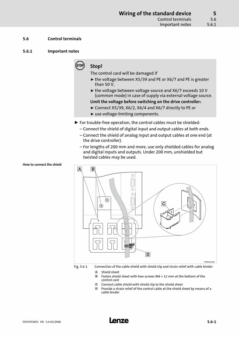
Wiring of the standard deviceControl terminals
Important notes
55.6
5.6.1
� 5.6−1EDSVF9383V EN 5.0−05/2008
5.6 Control terminals
5.6.1 Important notes
� Stop!
The control card will be damaged if
ƒ the voltage between X5/39 and PE or X6/7 and PE is greaterthan 50 V,
ƒ the voltage between voltage source and X6/7 exceeds 10 V(common mode) in case of supply via external voltage source.
Limit the voltage before switching on the drive controller:
ƒ Connect X5/39, X6/2, X6/4 and X6/7 directly to PE or
ƒ use voltage−limiting components.
ƒ For trouble−free operation, the control cables must be shielded:
– Connect the shield of digital input and output cables at both ends.
– Connect the shield of analog input and output cables at one end (atthe drive controller).
– For lengths of 200 mm and more, use only shielded cables for analogand digital inputs and outputs. Under 200 mm, unshielded buttwisted cables may be used.
�
��
�
9300vec063
Fig. 5.6−1 Connection of the cable shield with shield clip and strain relief with cable binder
� Shield sheet� Fasten shield sheet with two screws M4 × 12 mm at the bottom of the
control card
Connect cable shield with shield clip to the shield sheet� Provide a strain relief of the control cable at the shield sheet by means of a
cable binder
How to connect the shield

Wiring of the standard deviceControl terminalsWith function "Safe torque off" active
55.65.6.2
� 5.6−2 EDSVF9383V EN 5.0−05/2008
� Stop!
ƒ Connect or disconnect the terminal strips only if the controlleris disconnected from the mains!
ƒ Wire the terminal strips before connecting them!
ƒ Unused terminal strips must also be plugged on to protect thecontacts.
Cable type Wire end ferrule Maximum cablecross−section
Tighteningtorque
Strippinglength
Rigid — 2.5 mm2 (AWG 14)
0.5 ... 0.6 Nm(4.4 ... 5.3 lb−in)
5 mm
FlexibleWithout wire endferrule
2.5 mm2 (AWG 14)
FlexibleWire end ferrulewithout plasticsleeve
2.5 mm2 (AWG 14)
FlexibleWire end ferrulewith plastic sleeve
2.5 mm2 (AWG 14)
5.6.2 With function "Safe torque off" active
ƒ The installation and commissioning of the �Safe torque off" functionmust be carried out by skilled personnel only.
ƒ All safety−relevant cables (e.g. control cable for the safety relay,feedback contact) outside the control cabinet must be protected, forinstance by a cable duct. Short circuits between the single cables mustbe ruled out!
ƒ Wiring of the safety relay KSR with insulated wire end ferrules or rigidcables is absolutely vital.
ƒ The electrical reference point for the coil of the safety relay KSR must beconnected with the protective conductor system (DIN EN 60204−1paragraph 9.4.3). Only this measure guarantees that the operation isprotected against earth faults.
� Tip!
A complete description can be found in the chapter "Safe torqueoff".
Terminal data
Safety instructions for theinstallation of the "Safetorque off" function

Wiring of the standard deviceControl terminals
With function "Safe torque off" active
55.6
5.6.2
� 5.6−3EDSVF9383V EN 5.0−05/2008
ƒ If a freely assignable digital output (e.g. X5/A1) is assignedpermanently to HIGH level, it serves as an internal voltage source. Everyoutput has a maximum load capacity of 50 mA.
– The relay KSR and two digital inputs (X5/28 and e.g. X5/E1) can besupplied with voltage via a digital output.
– Two digital outputs must be connected in parallel and assignedpermanently to HIGH level in order to obtain the maximum wiring(relays KSR and X5/E1 ... X5/E5, X5/ST1).
ƒ For the supply of the analog inputs (X6/1, X6/2 and X6/3, X6/4) youhave to set a freely assignable analog output (e. g. X6/63) permanentlyto HIGH level.
GND2 +24V+5 V
DIG
OU
T4
E5 A2 A3 A4 ST1ST2 5939
3k
47k
50m
A
50m
A
50m
A
50m
A
X5 28 E1 E2 E3 E4
3k
3k
3k
3k
3k
X11 K31K32 33 34
S1 S2
IN1 IN2 IN3 IN4
+
KSR
A1
Z1
X3GND1 GND1
X6 1 2 3 4 7 762 63
242R
1
2
3
4
5
6
100k
100k
100k
100k
3.3nF
AIN1 AIN2
AOUTx
AOUT2AOUT1
1 32 4 7
10k 10k
9300vec135
Fig. 5.6−2 Wiring of digital and analog inputs/outputs with active "Safe torque off" functionand internal voltage source
S1 Deactivate pulse inhibit (1st disconnecting path)S2 Enable controller (2nd disconnecting path)Z1 Programmable logic controller (PLC)
The PLC monitors the ˜Safe torque off˜ functionX5/A4 Feedback via a digital output (e. g. DIGOUT4)
NO contact or NC contact
Z LoadMinimum wiring required for operation
Terminal assignment in the Lenze setting: 5.6−7
� Note!
If you load a basic configuration C0005 = xx1x (e.g. 1010 forspeed control with control via terminals), the following terminalsare switched to a fixed signal level:
ƒ Terminal X5/A1 to FIXED1 (corresponds to DC 24 V).
ƒ Terminal X6/63 to FIXED100% (corresponds to 10 V).
Supply via internal voltagesource

Wiring of the standard deviceControl terminalsWith function "Safe torque off" active
55.65.6.2
� 5.6−4 EDSVF9383V EN 5.0−05/2008
Supply via external voltage source
GND2 +24V+5 V
DIG
OU
T4
E5 A2 A3 A4 ST1ST2 5939
3k
47k
50m
A
50m
A
50m
A
50m
A
X5 28 E1 E2 E3 E4
3k
3k
3k
3k
3k
DC 24 V(+18 V … +30 V)
X11 K31K32 33 34
S1 S2
IN1 IN2 IN3 IN4
+
KSR
+–
A1
Z1
X3GND1 GND1
X6 1 2 3 4 7 762 63
242R
3.3nF
100k
100k
100k
100k
1
2
3
4
5
6
AIN1 AIN2
AOUTx
AOUT2AOUT1
1 32 4 7
10k 10k
9300vec136
Fig. 5.6−3 Wiring of digital and analog inputs/outputs with active "Safe torque off" functionand external voltage source
S1 Deactivate pulse inhibit (1st disconnecting path)S2 Enable controller (2nd disconnecting path)Z1 Programmable logic controller (PLC)
The PLC monitors the ˜Safe torque off˜ functionX5/A4 Feedback via a digital output (e. g. DIGOUT4)
NO contact or NC contact
Z LoadMinimum wiring required for operation
Terminal assignment in the Lenze setting: 5.6−7
� Note!
Supplying the digital inputs via an external voltage sourceenables a backup operation in case of mains failure. Afterswitching off the mains voltage, all actual values are continuedto be detected and processed.
ƒ Connect the positive pole of the external voltage source withX5/59 to establish the backup operation in the event of mainsfailure.
ƒ The external voltage source must be able to supply a current 1 A.
ƒ The starting current of the external voltage source is notlimited by the controller. Lenze recommends the use ofvoltage sources with current limitation or with an internalimpedance of Z > 1 �.
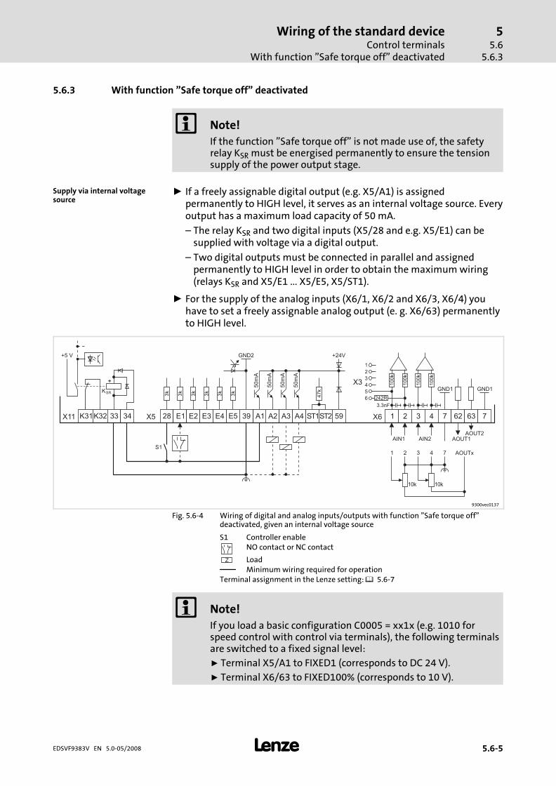
Wiring of the standard deviceControl terminals
With function "Safe torque off" deactivated
55.6
5.6.3
� 5.6−5EDSVF9383V EN 5.0−05/2008
5.6.3 With function "Safe torque off" deactivated
� Note!
If the function "Safe torque off" is not made use of, the safetyrelay KSR must be energised permanently to ensure the tensionsupply of the power output stage.
ƒ If a freely assignable digital output (e.g. X5/A1) is assignedpermanently to HIGH level, it serves as an internal voltage source. Everyoutput has a maximum load capacity of 50 mA.
– The relay KSR and two digital inputs (X5/28 and e.g. X5/E1) can besupplied with voltage via a digital output.
– Two digital outputs must be connected in parallel and assignedpermanently to HIGH level in order to obtain the maximum wiring(relays KSR and X5/E1 ... X5/E5, X5/ST1).
ƒ For the supply of the analog inputs (X6/1, X6/2 and X6/3, X6/4) youhave to set a freely assignable analog output (e. g. X6/63) permanentlyto HIGH level.
GND2 +24V+5 V
E5 A2 A3 A4 ST1ST2 5939
3k
47k
50m
A
50m
A
50m
A
50m
A
X5 28 E1 E2 E3 E4
3k
3k
3k
3k
3k
X11 K31K32 33 34
S1
+
KSR
A1
X3
X6 1 2 3 4
242R
1
2
3
4
5
6
100k
100k
100k
100k
3.3nF
GND1 GND1
7 762 63
AIN1 AIN2
AOUTx
AOUT2AOUT1
1 32 4 7
10k 10k
9300vec0137
Fig. 5.6−4 Wiring of digital and analog inputs/outputs with function "Safe torque off"deactivated, given an internal voltage source
S1 Controller enableNO contact or NC contact
Z LoadMinimum wiring required for operation
Terminal assignment in the Lenze setting: 5.6−7
� Note!
If you load a basic configuration C0005 = xx1x (e.g. 1010 forspeed control with control via terminals), the following terminalsare switched to a fixed signal level:
ƒ Terminal X5/A1 to FIXED1 (corresponds to DC 24 V).
ƒ Terminal X6/63 to FIXED100% (corresponds to 10 V).
Supply via internal voltagesource

Wiring of the standard deviceControl terminalsWith function "Safe torque off" deactivated
55.65.6.3
� 5.6−6 EDSVF9383V EN 5.0−05/2008
Supply via external voltage source
GND2 +24V+5 V
E5 A2 A3 A4 ST1ST2 5939
3k
47k
50m
A
50m
A
50m
A
50m
A
X5 28 E1 E2 E3 E4
3k
3k
3k
3k
3k
DC 24 V(+18 V … +30 V)
X11 K31K32 33 34
S1
+
KSR
+–
A1
X3GND1 GND1
X6 1 2 3 4 7 762 63
242R
1
2
3
4
5
6
100k
100k
100k
100k
3.3nF
AIN1 AIN2
AOUTx
AOUT2AOUT1
1 32 4 7
10k 10k
9300vec138
Fig. 5.6−5 Wiring of digital and analog inputs/outputs with function "Safe torque off"deactivated, given an external voltage source
S1 Controller enableNO contact or NC contact
Z LoadMinimum wiring required for operation
Terminal assignment in the Lenze setting: 5.6−7
� Note!
Supplying the digital inputs via an external voltage sourceenables a backup operation in case of mains failure. Afterswitching off the mains voltage, all actual values are continuedto be detected and processed.
ƒ Connect the positive pole of the external voltage source withX5/59 to establish the backup operation in the event of mainsfailure.
ƒ The external voltage source must be able to supply a current 1 A.
ƒ The starting current of the external voltage source is notlimited by the controller. Lenze recommends the use ofvoltage sources with current limitation or with an internalimpedance of Z > 1 �.

Wiring of the standard deviceControl terminals
Terminal assignment
55.6
5.6.4
� 5.6−7EDSVF9383V EN 5.0−05/2008
5.6.4 Terminal assignment
Terminal
FunctionBold print = Lenze setting
Level / state Technical data
X11/K32X11/K31
Safety relay KSR1stdisconnectingpath
Feedback − pulse inhibit Open contact: Pulse inhibit isinactive (operation)
See chapter "Technicaldata"
Closed contact: Pulse inhibit isactive
X11/33 – coil of safety relay KSR Coil is not carrying anycurrent: Active pulse inhibit
X11/34 + coil of safety relay KSR Coil is carrying current:Inactive pulse inhibit(operation)
X5/28 Controller inhibit(DCTRL−CINH)2nddisconnectingpath
Controller enable/inhibit LOW: Controller inhibitedHIGH: Controller enabled
LOW: 0 ... +3 VHIGH: +12 ... +30 V
Input current at +24 V:8 mA per input
Reading and processingthe input signals − 1/ms(mean value)
X5/E1 Digital inputs(freelyassignable)
Deactivate CW rotation / quick stop HIGH
X5/E2 Deactivate CCW rotation / quick stop HIGH
X5/E3 Activate fixed frequency 1 (JOG1) HIGH
X5/E4 Set error message (TRIP SET) LOW
X5/E5 Reset error message (TRIP RESET) LOW−HIGH edge
X5/ST1X5/ST2
Additional digital input (E6) HIGH
X5/A1 Digital outputs(freelyassignable)
Error message present LOW LOW: 0 ... +3 VHIGH: +12 ... +30 V
Load capacity:Max. 50 mA per output(load resistance at least480 � at +24 V)
Update of the outputsignals − 1/ms
X5/A2 Switching threshold QMIN:Actual speed < setpoint speed in C0017
LOW
X5/A3 Ready for operation (DCTRL−RDY) HIGH
X5/A4 Maximum current reached(DCTRL−IMAX)
HIGH
X5/39 – GND2, reference potential for digitalsignals
– Isolated against GND1
X5/59 – Connection of external voltage sourcefor backup operation of the drivecontroller in case of mains failure
DC 24 V (+18 ... +30 V) Current consumption:Max. 1 A at 24 V
X6/1X6/2
Analog input 1 Voltage inputrangeMain setpoint
642
531
−10 V ... +10 V Resolution:5 mV (11 bits + sign)
Jumper X3
Current inputrange 6
42
531
−20 mA ... +20 mA Resolution: 20 �A(10 bits + sign)
Jumper X3
X6/3X6/4
Analog input 2 Voltage inputrangeNot active
Jumper X3 has noeffect
−10 V ... +10 V Resolution: 5 mV(11 bits + sign)
X6/62 Analog output 1 Monitor 1Actual speed value
−10 V ... +10 Vmax. 2 mA
Resolution: 20 mV(9 bits + sign)
X6/63 Analog output 2 Monitor 2Actual motor current value
−10 V ... +10 Vmax. 2 mA
Resolution: 20 mV(9 bits + sign)
X6/7 – GND1, reference potential for analogsignals
– –


Wiring of the standard deviceWiring of the system bus (CAN)
55.7
� 5.7−1EDSVF9383V EN 5.0−05/2008
5.7 Wiring of the system bus (CAN)
A1 A2 A3 An
93XX 93XX 93XX
GND GND GND GNDLO LO LO LOHI HI HI HIX4 X4 X4PE PE PE PE
120 120
9300VEC054
Fig. 5.7−1 System bus (CAN) wiring
A1 Bus device 1 (controller)A2 Bus device 2 (controller)A3 Bus device 3 (controller)An Bus device n (e. g. PLC), n = max. 63X4/GND CAN−GND: System bus reference potentialX4/LO CAN−LOW: System bus LOW (data line)X4/HI CAN−HIGH: System bus HIGH (data line)
� Stop!
Connect a 120 � terminating resistor to the first and last busdevice.
For the use of the transmission cable, follow our recommendations:
Specification of the transmission cable
Total length � 300 m � 1000 m
Cable type LIYCY 2 x 2 x 0.5 mm2(paired with shielding)
CYPIMF 2 x 2 x 0.5 mm2
(paired with shielding)
Cable resistance � 80 �/km � 80 �/km
Capacitance per unitlength
� 130 nF/km � 60 nF/km
Wiring


Wiring of the standard deviceWiring of the feedback system
Important notes
55.8
5.8.1
� 5.8−1EDSVF9383V EN 5.0−05/2008
5.8 Wiring of the feedback system
5.8.1 Important notes
ƒ An incremental encoder can be connected to input X8 or input X9:
– Incremental encoders with TTL level are connected to X8.
– Incremental encoders with HTL level are connected to X9.
ƒ The incremental encoder signal can be output for slave drives at thedigital frequency output X10.
� Note!
ƒ We recommend to use Lenze system cables for wiring.
ƒ For self−made cables only use cables with shielded corestwisted in pairs.

Wiring of the standard deviceWiring of the feedback systemIncremental encoder with TTL level at X8
55.85.8.2
� 5.8−2 EDSVF9383V EN 5.0−05/2008
5.8.2 Incremental encoder with TTL level at X8
Field Values
Connectable incrementalencoder
Incremental encoder with TTL level� Encoder with two 5�V complementary signals electrically
offset by 90°� Connection of zero track is possible (optional)
Connection at drive controller 9−pin Sub−D socket
Input frequency 0 ... 500 Nm
Current consumption 6 mA per channel
Internal voltage source(X8/4, X8/5)
5 V DC / max. 200 mA
B
VCC
GND
Z
+KTY
-KTY
1
2
3
4
5
6
7
8
9
A
X8
< 50 m
A
A
A
B
Z
B
B
Z
Z
KTY
�
9300VEC018
Fig. 5.8−1 Connection of incremental encoder with TTL level
� Signals for CW rotationCores twisted in pairs
Assignment of 9−pin Sub−D socket (X8) at the controller
Pin 1 2 3 4 5 6 7 8 9
Signal B A A VCC GND(−KTY)
Z Z +KTY B
0.14 mm2 (AWG 26) 1 mm2 (AWG 18) 0.14 mm2 (AWG 26)
Technical data
Wiring
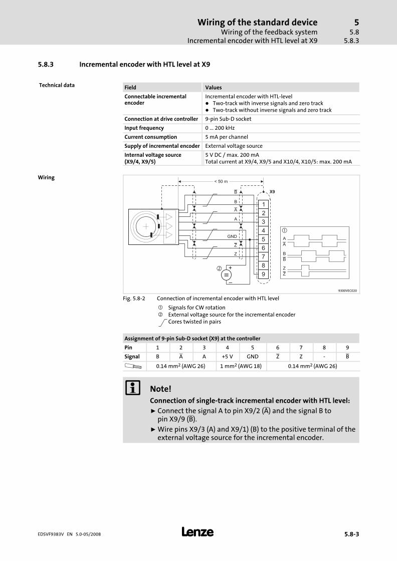
Wiring of the standard deviceWiring of the feedback system
Incremental encoder with HTL level at X9
55.8
5.8.3
� 5.8−3EDSVF9383V EN 5.0−05/2008
5.8.3 Incremental encoder with HTL level at X9
Field Values
Connectable incrementalencoder
Incremental encoder with HTL−level� Two−track with inverse signals and zero track� Two−track without inverse signals and zero track
Connection at drive controller 9−pin Sub−D socket
Input frequency 0 ... 200 kHz
Current consumption 5 mA per channel
Supply of incremental encoder External voltage source
Internal voltage source(X9/4, X9/5)
5 V DC / max. 200 mATotal current at X9/4, X9/5 and X10/4, X10/5: max. 200 mA
B
GND
Z
1
2
3
4
5
6
7
8
9
A
X9
< 50 m
A
B
Z
�+
–
A
A
B
Z
B
Z
�
9300VEC020
Fig. 5.8−2 Connection of incremental encoder with HTL level
� Signals for CW rotation� External voltage source for the incremental encoder
Cores twisted in pairs
Assignment of 9−pin Sub−D socket (X9) at the controller
Pin 1 2 3 4 5 6 7 8 9
Signal B A A +5 V GND Z Z − B
0.14 mm2 (AWG 26) 1 mm2 (AWG 18) 0.14 mm2 (AWG 26)
� Note!
Connection of single−track incremental encoder with HTL level:
ƒ Connect the signal A to pin X9/2 (A) and the signal B topin X9/9 (B).
ƒ Wire pins X9/3 (A) and X9/1) (B) to the positive terminal of theexternal voltage source for the incremental encoder.
Technical data
Wiring


Wiring of the standard deviceWiring of digital frequency input / digital frequency output
55.9
� 5.9−1EDSVF9383V EN 5.0−05/2008
5.9 Wiring of digital frequency input / digital frequency output
Field Digital frequency output X10
Connection at drive controller 9−pin Sub−D socket
Pin assignment Dependent on the selected basic configuration
Output frequency 0 ... 500 kHz
Signal Two−track with inverse 5 V signals (RS422) and zero track
Load capacity Maximum 20 mA per channel(up to 3 slave drives can be connected)
Special features The "Enable" output signal at X10/8 switches to LOW if thedrive controller is not ready for operation (e.g. disconnectedfrom mains). This may trip SD3 monitoring at the slave drive.
Internal voltage source(X10/4, X10/5)
DC 5 V / max. 50 mATotal current at X9/4, X9/5 and X10/4, X10/5: max. 200 mA
Field Digital frequency input X9
Connection at drive controller 9−pin Sub−D socket
Input frequency TTL level: 0 ... 500 kHzHTL level: 0 ... 200 kHz
Signal Two−track with inverse signals and zero trackSingle−track without inverse signals and zero track (only forHTL level)
Signal evaluation Via code C0427
Current consumption Maximum 5 mA
Special features With activated SD3 monitoring, TRIP or warning is tripped ifthe "Lamp Control" input signal at X9/8 switches to LOW.This may cause the drive controller to respond if the masterdrive is not ready for operation.
Technical data

Wiring of the standard deviceWiring of digital frequency input / digital frequency output
55.9
� 5.9−2 EDSVF9383V EN 5.0−05/2008
� Note!
ƒ We recommend to use Lenze system cables for wiring.
ƒ For self−made cables only use cables with shielded corestwisted in pairs.
B
Enable (EN) Lampcontrol (LC)
GND
Z
1
2
3
4
5
6
7
8
9
1
2
3
4
5
6
7
8
9
A
X9X10
< 50 m
A
B
Z
A
A
B
Z
B
Z
�
9300VEC019
Fig. 5.9−1 Connection of digital frequency input (X9) / digital frequency output (X10)
X9 Slave drive � Signals for CW rotationX10 Master drive Cores twisted in pairs
Assignment of 9−pin Sub−D socket (X9) at the controller
Pin 1 2 3 4 5 6 7 8 9
Signal B A A +5 V GND Z Z LC B
0.14 mm2
(AWG 26)0.5 mm2
(AWG 20)0.14 mm2
(AWG 26)0.5 mm2
(AWG 20)0.14 mm2
(AWG 26)
Assignment of 9−pin Sub−D socket (X10) at the controller
Pin 1 2 3 4 5 6 7 8 9
Signal B A A +5 V GND Z Z EN B
0.14 mm2
(AWG 26)0.5 mm2
(AWG 20)0.14 mm2
(AWG 26)0.5 mm2
(AWG 20)0.14 mm2
(AWG 26)
Evaluation of the input signals at X9
Code Function
C0427 = 0CW rotation Track A leads track B by 90 ° (positive value at DFIN−OUT)
CCW rotation Track A lags track B by 90 ° (negative value at DFIN−OUT)
C0427 = 1
CW rotation Track A transmits the speedTrack B = LOW (positive value at DFIN−OUT)
CCW rotation Track A transmits the speedTrack B = HIGH (negative value at DFIN−OUT)
C0427 = 2
CW rotation Track A transmits the speed and direction of rotation (positivevalue at DFIN−OUT)Track B = LOW
CCW rotation Track B transmits the speed and direction of rotation (negativevalue at DFIN−OUT)Track A = LOW
Wiring
Adjustment

Wiring of the standard deviceCommunication modules
55.10
� 5.10−1EDSVF9383V EN 5.0−05/2008
5.10 Communication modules
� Further information ....
on wiring and application of communication modules can befound in the corresponding Mounting Instructions andCommunication Manuals.
Communication module Type/order number
Keypad XT EMZ9371BC
LECOM−A/B (RS232/485) EMF2102IBV001
LECOM−B (RS485) EMF2102IBV002
LECOM−LI (optical fibre) EMF2102IBV003
LON EMF2141IB
INTERBUS EMF2113IB
INTERBUS Loop EMF2112IB
PROFIBUS−DP EMF2133IB
DeviceNet/CANopen EMF2175IB
Plug the communication module onto the AIF interface (X1) or pull it off fromthe interface. The communication module can also beconnected/disconnected during operation.
Possible communicationmodules
Handling


CommissioningContents
6
� 6−1EDSVF9383V EN 5.0−05/2008
6 Commissioning
Contents
6.1 Before switching on 6.1−1 . . . . . . . . . . . . . . . . . . . . . . . . . . . . . . . . . . . . . . . . .
6.2 Selection of the correct operating mode 6.2−1 . . . . . . . . . . . . . . . . . . . . . . . .
6.3 Parameter setting with the XT EMZ9371BC keypad 6.3−1 . . . . . . . . . . . . . . .
6.3.1 Commissioning example in V/f characteristic control mode 6.3−1
6.3.2 Commissioning example in vector control mode 6.3−5 . . . . . . . . .
6.4 Controller inhibit 6.4−1 . . . . . . . . . . . . . . . . . . . . . . . . . . . . . . . . . . . . . . . . . . . .
6.5 Changing the assignment of the control terminals X5 and X6 6.5−1 . . . . . .
6.5.1 Free configuration of digital input signals 6.5−1 . . . . . . . . . . . . . . .
6.5.2 Free configuration of digital outputs 6.5−3 . . . . . . . . . . . . . . . . . . .
6.5.3 Free configuration of analog input signals 6.5−4 . . . . . . . . . . . . . . .
6.5.4 Free configuration of analog outputs 6.5−6 . . . . . . . . . . . . . . . . . .
6.6 Adjusting the motor 6.6−1 . . . . . . . . . . . . . . . . . . . . . . . . . . . . . . . . . . . . . . . . .
6.6.1 Entry of motor data 6.6−1 . . . . . . . . . . . . . . . . . . . . . . . . . . . . . . . . . .
6.6.2 Motor selection list 6.6−4 . . . . . . . . . . . . . . . . . . . . . . . . . . . . . . . . . .
6.6.3 Motor temperature monitoring with PTC or thermal contact 6.6−9
6.6.4 Motor temperature monitoring with KTY 6.6−11 . . . . . . . . . . . . . . .
6.6.5 Current limits 6.6−15 . . . . . . . . . . . . . . . . . . . . . . . . . . . . . . . . . . . . . .
6.6.6 Automatic collection of motor data 6.6−16 . . . . . . . . . . . . . . . . . . . .
6.7 Setting the speed feedback 6.7−1 . . . . . . . . . . . . . . . . . . . . . . . . . . . . . . . . . . .
6.7.1 Incremental encoder with TTL level at X8 6.7−2 . . . . . . . . . . . . . . . .
6.7.2 Incremental encoder with HTL level at X9 6.7−3 . . . . . . . . . . . . . . .
6.8 Operating mode 6.8−1 . . . . . . . . . . . . . . . . . . . . . . . . . . . . . . . . . . . . . . . . . . .
6.8.1 V/f characteristic control 6.8−4 . . . . . . . . . . . . . . . . . . . . . . . . . . . .
6.8.2 Vector control 6.8−8 . . . . . . . . . . . . . . . . . . . . . . . . . . . . . . . . . . . . . .
6.9 Switching frequency of the inverter 6.9−1 . . . . . . . . . . . . . . . . . . . . . . . . . . . .
6.10 Acceleration, deceleration, braking, stopping 6.10−1 . . . . . . . . . . . . . . . . . . .
6.10.1 Speed range 6.10−1 . . . . . . . . . . . . . . . . . . . . . . . . . . . . . . . . . . . . . . . .
6.10.2 Setting acceleration times and deceleration times in speed mode 6.10−3 . . . . . . . . . . . . . . . . . . . . . . . . . . . . . . . . . . . . . . . .
6.10.3 Quick stop 6.10−4 . . . . . . . . . . . . . . . . . . . . . . . . . . . . . . . . . . . . . . . . . .
6.10.4 Changing the direction of rotation 6.10−5 . . . . . . . . . . . . . . . . . . . .
6.11 Optimising the operating behaviour 6.11−1 . . . . . . . . . . . . . . . . . . . . . . . . . . .
6.11.1 Slip compensation 6.11−1 . . . . . . . . . . . . . . . . . . . . . . . . . . . . . . . . . .
6.11.2 Oscillation damping 6.11−3 . . . . . . . . . . . . . . . . . . . . . . . . . . . . . . . . .
6.11.3 Boost correction with V/f characteristic control 6.11−5 . . . . . . . . . .
6.11.4 Motor magnetising current with vector control 6.11−9 . . . . . . . . . .


CommissioningBefore switching on
66.1
� 6.1−1EDSVF9383V EN 5.0−05/2008
6.1 Before switching on
� Note!
ƒ Observe the corresponding switch−on sequence.
ƒ In the event of faults or errors during commissioning, seechapter "Troubleshooting and fault elimination".
To avoid injury to persons and damage to material, check ...
... before connecting the mains voltage:
ƒ Wiring for completeness, short−circuit, and earth fault
ƒ The supply of the internal fan in case of the variants V210, V240, V270and V300.
– The bridge position depends on the mains voltage applied
ƒ The function "emergency−off" of the total system.
ƒ The motor circuit configuration (star/delta) must be adapted to theoutput voltage of the controller.
– E. g. the in−phase connection of the motor.
ƒ The direction of rotation of the incremental encoder
... the setting of the main drive parameters before enabling the controller:
� Stop!
Only the variants V210, V240, V270, V300:
ƒ Adapt the DC bus voltage threshold to the mains voltage viaC0173.– The Lenze setting of C0173 = 1 (OU = 770 V) is only
permissible for controller operation with a mains voltage of400 V.
ƒ Only the variants V210, V240, V270, V300:
Adapt the brake transistor threshold to the mains voltage via C0174. TheLenze setting of code C0174 = 3 (UBr = 885 V) is valid for operating thecontroller on a 500 V mains voltage.
ƒ Is the V/f rated frequency adapted to the motor connection?
ƒ Are the drive parameters relevant for your application set correctly?
ƒ Is the configuration of the analog and digital inputs and outputsadapted to the wiring?

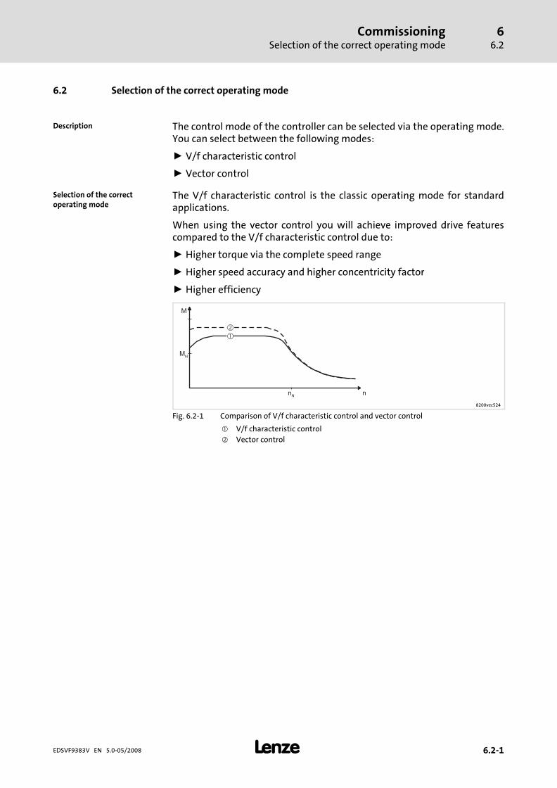
CommissioningSelection of the correct operating mode
66.2
� 6.2−1EDSVF9383V EN 5.0−05/2008
6.2 Selection of the correct operating mode
The control mode of the controller can be selected via the operating mode.You can select between the following modes:
ƒ V/f characteristic control
ƒ Vector control
The V/f characteristic control is the classic operating mode for standardapplications.
When using the vector control you will achieve improved drive featurescompared to the V/f characteristic control due to:
ƒ Higher torque via the complete speed range
ƒ Higher speed accuracy and higher concentricity factor
ƒ Higher efficiency
M
nnN
MN
�
�
8200vec524
Fig. 6.2−1 Comparison of V/f characteristic control and vector control
� V/f characteristic control
� Vector control
Description
Selection of the correctoperating mode

CommissioningSelection of the correct operating mode
66.2
� 6.2−2 EDSVF9383V EN 5.0−05/2008
The frequency inverter is mainly designed for the applications listed in thebelow table.
The table helps you to select the correct operating mode for your application:
ƒ C0006 = 5: V/f characteristic control with constant Vmin boost
ƒ C0006 = 1: Vector control
Power range 110 ... 400 kW Selection of the operating mode in C0006
Motor cableshielded � 100 m
unshielded � 200 m
Motor cableshielded 100 m
unshielded 200 m
Applications with asynchronousmotors
recommended alternatively recommended alternatively
Single drives
Drives with constant load 5 1 5 −
Drives with heavy startconditions
1 5 5 −
Travelling drives, conveyor belts 5 1 5 −
Pump drives, fan drives 1) 5 − 5 −
Extruder drives 5 1 5 −
Drives for wire drawingmachines
5 1 5 −
Drives for rolling machines 5 1 5 −
Drives for rewinders with dancer(speed−controlled)
1 5 − −
Group drives(the resulting motor cable lengthis decisive Ires)
5 − 5 −
lres � (i� � (l1 � l2 � ��� � li))
1) A square voltage characteristic (C0014 = 1) is recommended for this application
Recommended operatingmodes

CommissioningParameter setting with the XT EMZ9371BC keypad
Commissioning example in V/f characteristic control mode
66.3
6.3.1
� 6.3−1EDSVF9383V EN 5.0−05/2008
6.3 Parameter setting with the XT EMZ9371BC keypad
6.3.1 Commissioning example in V/f characteristic control mode
The example describes how to commission a speed control for the controllerwith power−related three−phase asynchronous motor.
Switch−on sequence Note
1. Insert the keypad
2. Ensure that the controller is inhibited afterswitching on the mains
misc008
59 28
X5� Terminal X5/28 = LOW(see chapter "Commissioning"�"controller inhibit")
3. Ensure that no external error is active Terminal X5/E4 = HIGH
4. Switch on
A The control card is supplied via an external voltage:Switch on the external DC 24 V supply voltage ON
misc002B The control card is supplied via the internal voltage:
Switch on the mains. The controller provides theDC 24 V supply.
5. After approx. 2 s the controller is initialised and thekeypad is in the operating level and displays thecurrent speed (C0051)
9371BC004
� ���
005000
0.00 Hz
0 %
6. Change to the "Terminal I/O" menu and configurethe function of the control terminals to adapt themto your application.Lenze setting: C0005 = 1000 (basic configuration"speed control")
Use C0002 = 0 to restore the Lenzesetting(see chapter "Commissioning"�"Change assignment of the controlterminal X5 and X6")
7. For quick commissioning select the menu "Shortsetup" � ���
�SHPRG
Para
Code
Menu
4 2
Quick start
V / f q u i c k
9371BC007
The submenu "Setup V/f" contains thecodes that are required forcommissioning a standard application.The digital inputs are configured in theLenze setting:X5/E1: Deactivate CW rotation/quickstopX5/E2: Deactivate CCW rotation/quickstopX5/E3: Activate fixed setpoint 1 (JOG1)X5/E4: Set error message (TRIP SET)X5/E5: Reset error message (TRIPRESET)(see chapter "Parameter setting")
A Use � to change to the menu level
B Use � � � � to change to the menu "Short setup"and then to the submenu "Setup V/f"
C Use � to change to the code level to parameteriseyour drive � �
�
� � �
� �
� ����SHPRG
Para
Code
Menu
003400
0
A I N 1 r a n g e
9371BC008
8. Adapt the controller to the mains (C0173)Lenze setting: 1 (400 V mains voltage)
9. Only for the variants V060, V110, V270, V300 in thepower range of 110 ... 400 kW:Adapt the brake transistor threshold (C0174)Lenze setting: 3 (500 V mains voltage, 885 V brakevoltage)
See code table

CommissioningParameter setting with the XT EMZ9371BC keypadCommissioning example in V/f characteristic control mode
66.36.3.1
� 6.3−2 EDSVF9383V EN 5.0−05/2008
NoteSwitch−on sequence
10. Enter the motor data See motor nameplate and chapter"Commissioning" � "Adapt motordata"
A If you use a Lenze motor:Select the motor type connected under C0086.
The data of the Lenze motors are savedunder C0086.
B If you do not use a Lenze motor:Enter the data of the motor nameplate
� Rated motor power (C0081)– Lenze setting: device−dependent
� Rated motor speed (C0087)– Lenze setting: device−dependent
� Rated motor current (C0088)– Lenze setting: device−dependent
Enter value for the selected motorconnection method (star/delta)!
� Rated motor frequency (C0089)– Lenze setting: device−dependent
� Rated motor voltage (C0090)– Lenze setting: device−dependent
Enter value for the selected motorconnection method (star/delta)!
� Motor cos� (C0091)– Lenze setting: device−dependent
11. If required, set a base frequency which differs fromthe rated motor frequency (C0015)Lenze setting: C0015 = C0089
100%
00 C0015
Umin
Uout
f
Changes in C0086 and C0089 overwritethe setting in C0015(see chapter "Commissioning"�"Operating mode" � "V/fcharacteristic control")
12. If required, adapt the slip compensation (C0021)Lenze setting: Rated slip in [%] with regard to Nmaxin C0011. The value is calculated from the data ofthe nameplate and is thus suitable for the majorityof applications.
Due to changes in C0086, C0087, C0089the rated slip is recalculated andautomatically entered into C0021(see chapter "Commissioning" �"Slipcompensation")
13. For protecting the motor, set the current limitvalues "Imax current" (C0022, C0023)Guide value � 2−fold rated motor current
Power range 0.37 ... 90 kW:For dissipating the regenerative energy,use a brake chopper or feedbackmodule, if necessaryPower range 110 ... 400 kW:For dissipating regenerative energy, usea brake resistor, if necessary(see chapter "Commissioning" �"Motor adjustment" � "Current limitvalues")
A In motor mode and generator mode (C0022)
B Additional limitation in generator mode (C0023)Condition: C0023 < C0022
14. Set the operating mode "V/f" (C0006)Lenze setting: 5 (V/f characteristic control)
(see chapter "Commissioning"�"Operating mode" � "V/fcharacteristic control")15. Set the V/f characteristic (C0014)
Lenze setting: 0 (linear characteristic)
A Linear characteristic (C0014 = 0)
0 1
0
C0089
C0090100 %
N
nn
Umin
Uout
B Square−law characteristic (C0014 = 1)
0 1
0
C0089
C0090100 %
N
nn
Umin
Uout For applications with e. g. pumps orfans
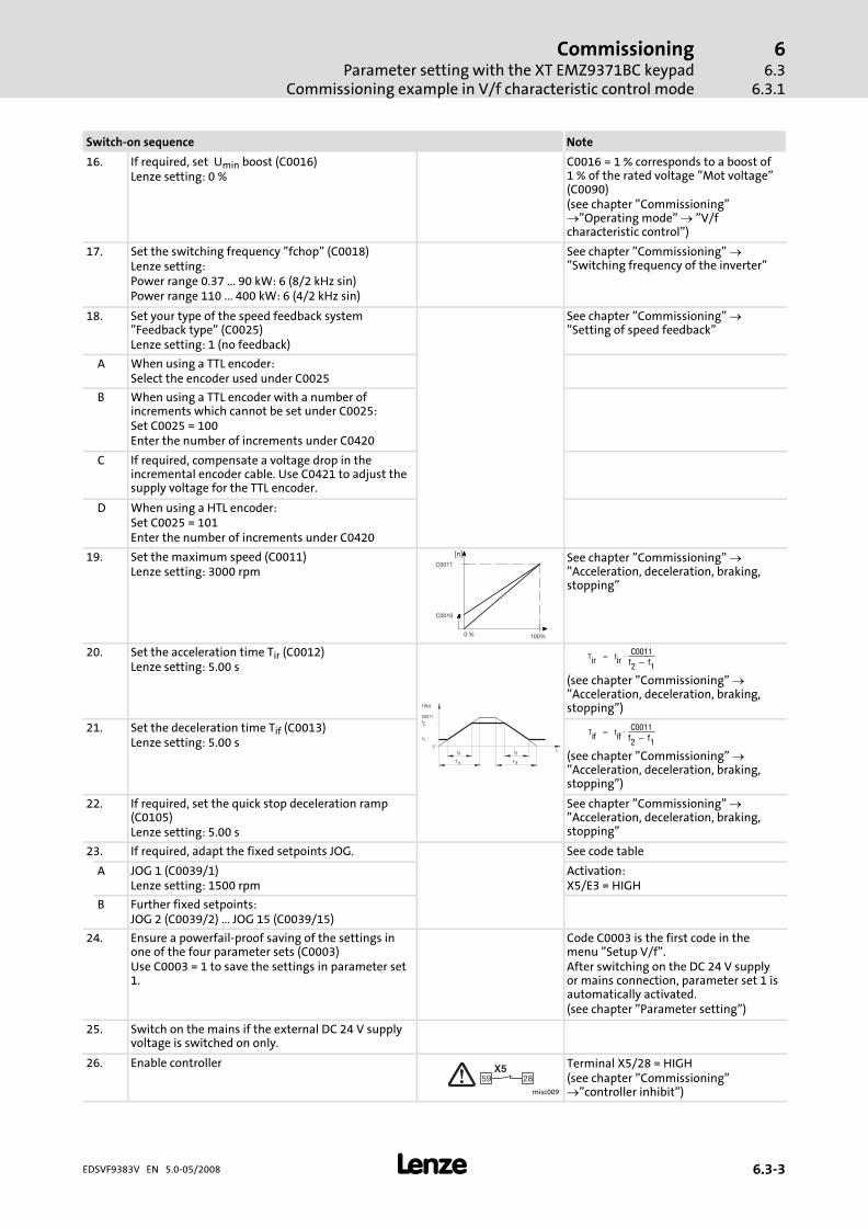
CommissioningParameter setting with the XT EMZ9371BC keypad
Commissioning example in V/f characteristic control mode
66.3
6.3.1
� 6.3−3EDSVF9383V EN 5.0−05/2008
NoteSwitch−on sequence
16. If required, set Umin boost (C0016)Lenze setting: 0 %
C0016 = 1 % corresponds to a boost of1 % of the rated voltage "Mot voltage"(C0090)(see chapter "Commissioning"�"Operating mode" � "V/fcharacteristic control")
17. Set the switching frequency "fchop" (C0018)Lenze setting:Power range 0.37 ... 90 kW: 6 (8/2 kHz sin)Power range 110 ... 400 kW: 6 (4/2 kHz sin)
See chapter "Commissioning" �"Switching frequency of the inverter"
18. Set your type of the speed feedback system"Feedback type" (C0025)Lenze setting: 1 (no feedback)
See chapter "Commissioning" �"Setting of speed feedback"
A When using a TTL encoder:Select the encoder used under C0025
B When using a TTL encoder with a number ofincrements which cannot be set under C0025:Set C0025 = 100Enter the number of increments under C0420
C If required, compensate a voltage drop in theincremental encoder cable. Use C0421 to adjust thesupply voltage for the TTL encoder.
D When using a HTL encoder:Set C0025 = 101Enter the number of increments under C0420
19. Set the maximum speed (C0011)Lenze setting: 3000 rpm
0 %
[n]
100%
C0011
C0010
See chapter "Commissioning" �"Acceleration, deceleration, braking,stopping"
20. Set the acceleration time Tir (C0012)Lenze setting: 5.00 s
� � � � � �
� �
� �
� �
� � � �
� � � �
�
Tir� �� t
ir�C0011
f2� f
1
(see chapter "Commissioning" �"Acceleration, deceleration, braking,stopping")
21. Set the deceleration time Tif (C0013)Lenze setting: 5.00 s
Tif� �� t
if�C0011
f2� f
1
(see chapter "Commissioning" �"Acceleration, deceleration, braking,stopping")
22. If required, set the quick stop deceleration ramp(C0105)Lenze setting: 5.00 s
See chapter "Commissioning" �"Acceleration, deceleration, braking,stopping"
23. If required, adapt the fixed setpoints JOG. See code table
A JOG 1 (C0039/1)Lenze setting: 1500 rpm
Activation:X5/E3 = HIGH
B Further fixed setpoints:JOG 2 (C0039/2) ... JOG 15 (C0039/15)
24. Ensure a powerfail−proof saving of the settings inone of the four parameter sets (C0003)Use C0003 = 1 to save the settings in parameter set1.
Code C0003 is the first code in themenu "Setup V/f".After switching on the DC 24 V supplyor mains connection, parameter set 1 isautomatically activated.(see chapter "Parameter setting")
25. Switch on the mains if the external DC 24 V supplyvoltage is switched on only.
26. Enable controller
misc009
59 28
X5�Terminal X5/28 = HIGH(see chapter "Commissioning"�"controller inhibit")

CommissioningParameter setting with the XT EMZ9371BC keypadCommissioning example in V/f characteristic control mode
66.36.3.1
� 6.3−4 EDSVF9383V EN 5.0−05/2008
NoteSwitch−on sequence
27. Enter the setpoint Analog setpointselection:−10 ... +10 V viapotentiometer at X6/1and X6/2
Fixed speed:Activate JOG 1 withX5/E3 = HIGH
JOG 1 is parameterised in C0039/1
28. The drive is running now CW rotation:X5/E1 = HIGH and X5/E2 = LOWCCW rotation:X5/E1 = LOW and X5/E2 = HIGHIf the drive does not start, press � inaddition(see chapter "Commissioning" �"Acceleration, deceleration, braking,stopping")
� Note!
In the menu "Diagnostic" the most important drive parameterscan be monitored

CommissioningParameter setting with the XT EMZ9371BC keypad
Commissioning example in vector control mode
66.3
6.3.2
� 6.3−5EDSVF9383V EN 5.0−05/2008
6.3.2 Commissioning example in vector control mode
The example describes how to commission a speed control for the controllerwith power−related three−phase asynchronous motor.
Switch−on sequence Note
1. Insert the keypad
2. Ensure that the controller is inhibited afterswitching on the mains
misc008
59 28
X5� Terminal X5/28 = LOW(see chapter "Commissioning"�"controller inhibit")
3. Ensure that no external error is active Terminal X5/E4 = HIGH
4. Switch on
A The control card is supplied via an external voltage:Switch on the external DC 24 V supply voltage ON
misc002B The control card is supplied via the internal voltage:
Switch on the mains. The controller provides theDC 24 V supply.
5. After approx. 2 s the controller is initialised and thekeypad is in the operating level and displays thecurrent speed (C0051)
9371BC004
� ���
005000
0.00 Hz
0 %
6. Change to the "Terminal I/O" menu and configurethe function of the control terminals to adapt themto your application.Lenze setting: C0005 = 1000 (basic configuration"speed control")
Use C0002 = 0 to restore the Lenzesetting(see chapter "Commissioning"�"Change assignment of the controlterminal X5 and X6")
7. For quick commissioning select the menu "Shortsetup" � ���
�SHPRG
Para
Code
Menu
4 2
Quick start
V / f q u i c k
9371BC007
The submenu "Setup vector" containsthe codes that are required forcommissioning a standard application.The digital inputs are configured in theLenze setting:X5/E1: Deactivate CW rotation/quickstopX5/E2: Deactivate CCW rotation/quickstopX5/E3: Activate fixed setpoint 1 (JOG1)X5/E4: Set error message (TRIP SET)X5/E5: Reset error message (TRIPRESET)(see chapter "Parameter setting")
A Use � to change to the menu level
B Use � � � � to change to the menu "Short setup"and then to the submenu "Setup vector"
C Use � to change to the code level to parameteriseyour drive � �
�
� � �
� �
� ����SHPRG
Para
Code
Menu
003400
0
A I N 1 r a n g e
9371BC008
8. Adapt the controller to the mains (C0173)Lenze setting: 1 (400 V mains voltage)
9. Only for the variants V060, V110, V270, V300 in thepower range of 110 ... 400 kW:Adapt the brake transistor threshold (C0174)Lenze setting: 3 (500 V mains voltage, 885 V brakevoltage)
See code table

CommissioningParameter setting with the XT EMZ9371BC keypadCommissioning example in vector control mode
66.36.3.2
� 6.3−6 EDSVF9383V EN 5.0−05/2008
NoteSwitch−on sequence
10. Enter the motor data See motor nameplate and chapter"Commissioning" � "Adapt motordata"
A If you use a Lenze motor:Select the motor type connected under C0086.
The data of the Lenze motors are savedunder C0086.
B If you do not use a Lenze motor:Enter the data of the motor nameplate
� Rated motor power (C0081)– Lenze setting: device−dependent
� Rated motor speed (C0087)– Lenze setting: device−dependent
� Rated motor current (C0088)– Lenze setting: device−dependent
Enter value for the selected motorconnection method (star/delta)!
� Rated motor frequency (C0089)– Lenze setting: device−dependent
� Rated motor voltage (C0090)– Lenze setting: device−dependent
Enter value for the selected motorconnection method (star/delta)!
� Motor cos� (C0091)– Lenze setting: device−dependent
11. For protecting the motor, set the current limitvalues "Imax current" (C0022, C0023)Guide value � 2−fold rated motor current
Power range 0.37 ... 90 kW:For dissipating the regenerative energy,use a brake chopper or feedbackmodule, if necessaryPower range 110 ... 400 kW:For dissipating regenerative energy, usea brake resistor, if necessary(see chapter "Commissioning" �"Motor adjustment" � "Current limitvalues")
A In motor mode and generator mode (C0022)
B Additional limitation in generator mode (C0023)Condition: C0023 < C0022
12. If the motor temperature is monitored with athermal sensor KTY:Activate the temperature feedback with C0594(fault SD6)Lenze setting: 3 (switched off)
A temperature feedback with KTY has apositive effect on the vector control,since the motor data identificationconsiders the temperature influence inthe motor model.(see chapter "Commissioning" �"Motor adjustment")
13. Start the motor data identification "ident run"(C0148)
(see chapter "Commissioning"�"Adjusting the motor")
A Ensure that the controller inhibit is active
misc008
59 28
X5� Terminal X5/28 = LOW
B Switch on the mains
C Set C0148 = 1
D Enable controller
misc009
59 28
X5�Terminal X5/28 = HIGHThe identification starts:� The segment � goes off� "WRK run" is displayed� The motor is energised and
"whistles"� The motor does not rotate
E If after approx. 1 ... 2 min the segment � is activeagain, inhibit the controller
misc008
59 28
X5� Terminal X5/28 = LOWThe identification is completed. Thefollowing values have been detectedand entered into the codes:� Inverter error characteristic
(C1753/xx)� Rotor resistance "Mot Rr" (C0082)� Stator resistance "Mot Rs" (C0084)� Leakage inductance "Mot Lss"
(C0085)� Stator inductance "Mot Ls" (C0092)

CommissioningParameter setting with the XT EMZ9371BC keypad
Commissioning example in vector control mode
66.3
6.3.2
� 6.3−7EDSVF9383V EN 5.0−05/2008
NoteSwitch−on sequence
14. Set the operating mode "vector ctrl" (C0006)Lenze setting: 5 (V/f characteristic control)
(see chapter "Commissioning" �"Operating mode" � "Vector control")
15. Set the switching frequency "fchop" (C0018)Lenze setting:Power range 0.37 ... 90 kW: 6 (8/2 kHz sin)Power range 110 ... 400 kW: 6 (4/2 kHz sin)
See chapter "Commissioning" �"Switching frequency of the inverter"
16. Set your type of the speed feedback system"Feedback type" (C0025)Lenze setting: 1 (no feedback)
See chapter "Commissioning" �"Setting of speed feedback"
A When using a TTL encoder:Select the encoder used under C0025
B When using a TTL encoder with a number ofincrements which cannot be set under C0025:Set C0025 = 100Enter the number of increments under C0420
C If required, compensate a voltage drop in theincremental encoder cable. Use C0421 to adjust thesupply voltage for the TTL encoder.
D When using a HTL encoder:Set C0025 = 101Enter the number of increments under C0420
17. Set the maximum speed (C0011)Lenze setting: 3000 rpm
0 %
[n]
100%
C0011
C0010
See chapter "Commissioning" �"Acceleration, deceleration, braking,stopping"
18. Set the acceleration time Tir (C0012)Lenze setting: 5.00 s
� � � � � �
� �
� �
� �
� � � �
� � � �
�
Tir� �� t
ir�C0011
f2� f
1
(see chapter "Commissioning" �"Acceleration, deceleration, braking,stopping")
19. Set the deceleration time Tif (C0013)Lenze setting: 5.00 s
Tif� �� t
if�C0011
f2� f
1
(see chapter "Commissioning" �"Acceleration, deceleration, braking,stopping")
20. If required, set the quick stop deceleration ramp(C0105)Lenze setting: 5.00 s
See chapter "Commissioning" �"Acceleration, deceleration, braking,stopping"
21. If required, adapt the fixed setpoints JOG. See code table
A JOG 1 (C0039/1)Lenze setting: 1500 rpm
Activation:X5/E3 = HIGH
B Further fixed setpoints:JOG 2 (C0039/2) ... JOG 15 (C0039/15)
22. Ensure a powerfail−proof saving of the settings inone of the four parameter sets (C0003)Use C0003 = 1 to save the settings in parameter set1.
Code C0003 is the first code in themenu "Setup V/f".After switching on the DC 24 V supplyor mains connection, parameter set 1 isautomatically activated.(see chapter "Parameter setting")
23. Switch on the mains if the external DC 24 V supplyvoltage is switched on only.
24. Enable controller
misc009
59 28
X5�Terminal X5/28 = HIGH(see chapter "Commissioning"�"controller inhibit")

CommissioningParameter setting with the XT EMZ9371BC keypadCommissioning example in vector control mode
66.36.3.2
� 6.3−8 EDSVF9383V EN 5.0−05/2008
NoteSwitch−on sequence
25. Enter the setpoint Analog setpointselection:−10 ... +10 V viapotentiometer at X6/1and X6/2
Fixed speed:Activate JOG 1 withX5/E3 = HIGH
JOG 1 is parameterised in C0039/1
26. The drive is running now CW rotation:X5/E1 = HIGH and X5/E2 = LOWCCW rotation:X5/E1 = LOW and X5/E2 = HIGHIf the drive does not start, press � inaddition(see chapter "Commissioning" �"Acceleration, deceleration, braking,stopping")
� Note!
In the menu "Diagnostic" the most important drive parameterscan be monitored

CommissioningController inhibit
66.4
� 6.4−1EDSVF9383V EN 5.0−05/2008
6.4 Controller inhibit
If the controller inhibit is active, the power outputs are inhibited.
ƒ The drive coasts in zero−torque mode.
ƒ Status display of keypad: Pulse inhibit �
ƒ Status display at the controller: The green LED is blinking.
� Danger!
Do not use the "controller inhibit" function (DCTRL1−CINH) foremergency−off. The controller inhibit only inhibits the poweroutputs and does not disconnect the controller from the mains!
The drive could start again any time.
Codes for parameter setting
Code Possible settings IMPORTANT
No. Name Lenze Selection
C0040 Ctrl enable 0 Controller enable� Controller can only be enabled
if X5/28 = HIGH
6.4−1
0 Ctrl inhibit Controller inhibited
1 Ctrl enable Controller enabled
Via terminal X5/28:
ƒ A LOW level at the terminal inhibits the controller (cannot be inverted)
ƒ A HIGH level re−enables the controller
Via the keys of the keypad (if C0469 = 1):
ƒ � inhibits the controller
ƒ � re−enables the controller
Via code C0040:
ƒ C0040 = 0 inhibits the controller
ƒ C0040 = 1 re−enables the controller
� Note!
ƒ The sources for controller inhibit are ANDed, i.e. the drive willonly restarts if the controller inhibit signals of all signalsources have been eliminated.
ƒ The restart starts with zero speed. If centrifugal masses arestill rotating, this can lead to an overcurrent.
Description
Activation

CommissioningChanging the assignment of the control terminals X5 and X6
Free configuration of digital input signals
66.5
6.5.1
� 6.5−1EDSVF9383V EN 5.0−05/2008
6.5 Changing the assignment of the control terminals X5 and X6
� Danger!
If you select a configuration in C0005, the signal assignment ofthe inputs and outputs will be overwritten with thecorresponding basic assignment!
ƒ Adapt the signal assignment to your wiring!
6.5.1 Free configuration of digital input signals
ƒ Internal digital signals can be freely linked with external digital signalsources. This serves to establish a freely configurable control of thedrive controller.
– Digital inputs X5/E1 ... X5/E5
ƒ A signal source can be linked with several targets. Ensure reasonablelinkages for not activating functions that are mutually exclusive (e. g.linking a digital input with quick stop and DC injection braking at thesame time).
Codes for parameter setting
Code Possible settings IMPORTANT
No. Name Lenze Selection
C0114 0 High active HIGH level isactive
Inversion of digital input signals atX5, function block DIGIN
6.5−1See SystemManual(extension)
1 LOW active LOW level is active
1 DIGIN1 pol 0 Terminal X5/E1
2 DIGIN2 pol 0 Terminal X5/E2
3 DIGIN3 pol 0 Terminal X5/E3
4 DIGIN4 pol 1 Terminal X5/E4
5 DIGIN5 pol 0 Terminal X5/E5
5 DIGIN6 (ST) pol 0 Terminal X5/ST
Description
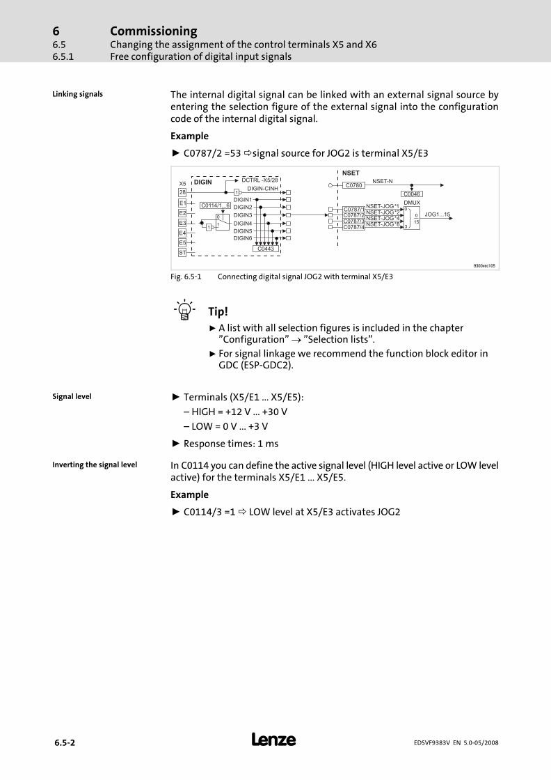
CommissioningChanging the assignment of the control terminals X5 and X6Free configuration of digital input signals
66.56.5.1
� 6.5−2 EDSVF9383V EN 5.0−05/2008
The internal digital signal can be linked with an external signal source byentering the selection figure of the external signal into the configurationcode of the internal digital signal.
Example
ƒ C0787/2 =53 �signal source for JOG2 is terminal X5/E3
E1
E2
E3
E4
E5
1
0
C0114/1...6
DIGIN
DIGIN1
DIGIN2
DIGIN3
DIGIN4
DIGIN5
28
DCTRL -X5/28X5
DIGIN-CINH
1
1
ST
DIGIN6
C0443
NSET
C0046
NSET-N
DMUX0
3
0
15
NSET-JOG*1NSET-JOG*2NSET-JOG*4NSET-JOG*8
JOG1...15
C0780
C0787/1C0787/2C0787/3C0787/4
9300vec105
Fig. 6.5−1 Connecting digital signal JOG2 with terminal X5/E3
� Tip!
ƒ A list with all selection figures is included in the chapter"Configuration" � "Selection lists".
ƒ For signal linkage we recommend the function block editor inGDC (ESP−GDC2).
ƒ Terminals (X5/E1 ... X5/E5):
– HIGH = +12 V ... +30 V
– LOW = 0 V ... +3 V
ƒ Response times: 1 ms
In C0114 you can define the active signal level (HIGH level active or LOW levelactive) for the terminals X5/E1 ... X5/E5.
Example
ƒ C0114/3 =1 � LOW level at X5/E3 activates JOG2
Linking signals
Signal level
Inverting the signal level
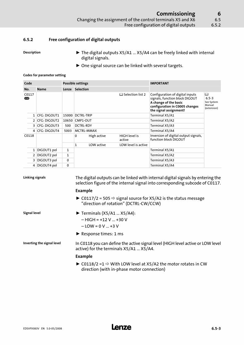
CommissioningChanging the assignment of the control terminals X5 and X6
Free configuration of digital outputs
66.5
6.5.2
� 6.5−3EDSVF9383V EN 5.0−05/2008
6.5.2 Free configuration of digital outputs
ƒ The digital outputs X5/A1 ... X5/A4 can be freely linked with internaldigital signals.
ƒ One signal source can be linked with several targets.
Codes for parameter setting
Code Possible settings IMPORTANT
No. Name Lenze Selection
C0117�
Selection list 2 Configuration of digital inputssignals, function block DIGOUTA change of the basicconfiguration in C0005 changesthe signal assignment!
6.5−3See SystemManual(extension)
1 CFG: DIGOUT1 15000 DCTRL−TRIP Terminal X5/A1
2 CFG: DIGOUT2 10650 CMP1−OUT Terminal X5/A2
3 CFG: DIGOUT3 500 DCTRL−RDY Terminal X5/A3
4 CFG: DIGOUT4 5003 MCTRL−MMAX Terminal X5/A4
C0118 0 High active HIGH level isactive
Inversion of digital output signals,function block DIGOUT
1 LOW active LOW level is active
1 DIGOUT1 pol 1 Terminal X5/A1
2 DIGOUT2 pol 1 Terminal X5/A2
3 DIGOUT3 pol 0 Terminal X5/A3
4 DIGOUT4 pol 0 Terminal X5/A4
The digital outputs can be linked with internal digital signals by entering theselection figure of the internal signal into corresponding subcode of C0117.
Example
ƒ C0117/2 = 505 � signal source for X5/A2 is the status message"direction of rotation" (DCTRL−CW/CCW)
ƒ Terminals (X5/A1 ... X5/A4):
– HIGH = +12 V ... +30 V
– LOW = 0 V ... +3 V
ƒ Response times: 1 ms
In C0118 you can define the active signal level (HIGH level active or LOW levelactive) for the terminals X5/A1 ... X5/A4.
Example
ƒ C0118/2 =1 � With LOW level at X5/A2 the motor rotates in CWdirection (with in−phase motor connection)
Description
Linking signals
Signal level
Inverting the signal level

CommissioningChanging the assignment of the control terminals X5 and X6Free configuration of analog input signals
66.56.5.3
� 6.5−4 EDSVF9383V EN 5.0−05/2008
6.5.3 Free configuration of analog input signals
ƒ Internal analog signals can be freely linked with external analog signalsources:
– Analog inputs X3/1, X3/2 and X3/3, X3/4
ƒ One signal source can be linked with several targets.
Codes for parameter setting
Code Possible settings IMPORTANT
No. Name Lenze Selection
C0026 −199.99 {0.01 %} 199.99 Free control code FCODE 26/1 andFCODE26/2
6.5−4See SystemManual(extension)
1 FCODE (offset) 0.00 Offset of AIN1 (X6/1, X6/2)
2 FCODE (offset) 0.00 Offset of AIN2 (X6/3, X6/4)
C0027 −199.99 {0.01 %} 199.99 Free control code FCODE 27/1 andFCODE27/2
1 FCODE (gain) 100.00 Gain AIN1 (X6/1, X6/2)� 100 % = gain 1
2 FCODE (gain) 100.00 Gain AIN2 (X6/3, X6/4)� 100 % = gain 1
C0034 Mst current 0 0 −10 V ... +10 V Voltage / current range for analogsignals at input X6/1, X6/2� Observe jumper position of X3
5.6−7 6.5−4
1 4 mA ... 20 mA
2 −20 mA ... +20 mA
The internal analog signals can be linked with an external signal source byentering the selection figure of the external signal into the configurationcode of the internal analog signal.
Example
ƒ C0780 = 50 � Signal source for the main setpoint (NSET−N) is terminalX6/1, X6/2
NSET
C0046
NSET-N
DMUX0
3
0
15
NSET-JOG*1NSET-JOG*2NSET-JOG*4NSET-JOG*8
C0780
C0787/1C0787/2C0787/3C0787/4
C0034
1
2
AIN1
+
+
AIN1-OUT
AIN1-GAIN
AIN1-OFFSET
C0404/1
C0404/2
C0402
C0403
C0400
X6
C0010
+
+
9300vec106
Fig. 6.5−2 Linking analog signal NSET−N with terminal X6/1, X6/2
� Tip!
ƒ A list with all selection figures is included in the chapter"Configuration" � "Selection lists".
ƒ For signal linkage we recommend the function block editor inGDC (ESP−GDC2).
Description
Linking signals

CommissioningChanging the assignment of the control terminals X5 and X6
Free configuration of analog input signals
66.5
6.5.3
� 6.5−5EDSVF9383V EN 5.0−05/2008
Gain and offset
Set gain (C0027) and offset (C0026) to adapt the input signal to theapplication.
Input range of X6/1, X6/2
Input range C0034 Position of jumper at X3
−10 V ... +10 V C0034 = 0 642
531
+4 mA ... +20 mA C0034 = 1 642
531−20 mA ... +20 mA C0034 = 2
� Note!
Different settings in C0034 and of X3 result in a wrong inputsignal.
Adjustment

CommissioningChanging the assignment of the control terminals X5 and X6Free configuration of analog outputs
66.56.5.4
� 6.5−6 EDSVF9383V EN 5.0−05/2008
6.5.4 Free configuration of analog outputs
ƒ The analog outputs (X6/62, X6/63) can be freely linked with internalanalog process or monitoring signals. The controller outputs a voltageproportional to the internal signal at the analog outputs.
ƒ One signal source can be linked with several targets.
Codes for parameter setting
Code Possible settings IMPORTANT
No. Name Lenze Selection
C0108 −199.99 {0.01 %} 199.99 Free control code FCODE108/1and FCODE108/2
6.5−6See SystemManual(extension)
1 FCODE (gain) 100.00 Gain of analog output signalAOUT1 (X6/62)� 100 % = gain 1
2 FCODE (gain) 100.00 Gain of analog output signalAOUT2 (X6/63)� 100 % = gain 1
C0109 −199.99 {0.01 %} 199.99 Free control code FCODE109/1and FCODE109/2
1 FCODE (offset) 0.00 Offset of analog output signalAOUT1 (X6/62)
2 FCODE (offset) 0.00 Offset of analog output signalAOUT2 (X6/63)
Analog outputs can be linked with internal analog signals by entering theselection figure of the internal signal into the code of C0431 (AOUT1, X6/62)or C0436 (AOUT2, X6/63).
Example
ƒ C0436 = 5006 � signal source for X6/63 is the actual motor voltage
� Tip!
ƒ A list with all selection figures is included in the chapter"Configuration" � "Selection lists".
ƒ For signal linkage we recommend the function block editor inGDC (ESP−GDC2).
Set gain (C0108) and offset (C0109) to adapt the output signal to theapplication.
With an internal signal of 100 % and a gain of 1, a voltage of 10 V is outputat the terminal.
Description
Linking signals
Adjustment

CommissioningAdjusting the motorEntry of motor data
66.6
6.6.1
� 6.6−1EDSVF9383V EN 5.0−05/2008
6.6 Adjusting the motor
6.6.1 Entry of motor data
The vector control mode requires considerably more motor data than the V/fcharacteristic control mode.
Basically all motor data should be entered independent of the operatingmode. This enables the controller to detect further data as e.g. slipcompensation (C0021), maximum torque (C0057), number of motor polepairs (C0059) always conclusively and enter them into the correspondingcodes.
Codes for parameter setting
Code Possible settings IMPORTANT
No. Name Lenze Selection
C0081�
Mot power � 0.01 {0.01 kW} 500.00 Rated motor power� Change of C0086 resets value
to factory setting� Change of C0081 sets C0086 =
0
C0086�
Mot type � Motor selection list Motor type selection� depending on the controller
used� Motor selection in C0086 sets
the corresponding parametersin C0021, C0022, C0081,C0087, C0088, C0089, C0090,C0091
6.6−1
C0087�
Mot speed � 50 {1 rpm} 36000 Rated motor speed� depending on C0086� Motor selection in C0086 set
the corresponding rated motorspeed in C0087
� Change of C0087 setsC0086 = 0
6.6−1
C0088�
Mot current � 0.5 {0.1 A} 1000.0 Rated motor current� depending on C0086� Motor selection in C0086 sets
the corresponding rated motorcurrent in C0088
� Change of C0088 sets C0086 =0
6.6−1
C0089�
Mot frequency � 10 {1 Hz} 5000 Rated motor frequency� depending on C0086� Motor selection in C0086 sets
the corresponding rated motorfrequency in C0089
� Change of C0089 setsC0086 = 0
6.6−1
Description

CommissioningAdjusting the motorEntry of motor data
66.66.6.1
� 6.6−2 EDSVF9383V EN 5.0−05/2008
IMPORTANTPossible settingsCode
SelectionLenzeNameNo.
C0090�
Mot voltage � 0 {1 V} 1000 Rated motor voltage� depending on C0086� Motor selection in C0086 sets
the corresponding rated motorvoltage in C0090
� Change of C0090 sets C0086 =0
6.6−1
C0091�
Mot cos phi � 0.50 {0.01 } 1.00 Motor cos �� depending on C0086� Motor selection in C0086 sets
the corresponding motor cos �in C0091
� Change of C0091 setsC0086 = 0
6.6−1
Choose similar motor
in C0086 according to the
criteria circuit configuration
and rated motor power
Operating mode "87 Hz
delta connection”?
Does C0086 contain
the motor?
Enter motor nameplate data:
C0081 = 3 x P
C0087 = ( 3 - 1) n + n
C0088 = I
C0089 = 87 Hz
C0090 = U
C0091 = cos
r
0 r
r
r
��
�
�
�
Enter motor nameplate data:
C0081, C0087, C0088, C0089,
C0090, C0091
Start entry motor data
Entry motor data completed
Choose motor in C0086
yes
yes
no
no
9300vec096
Fig. 6.6−1 Sequence diagram for motor data entry
PN Rated motor powern0 Synchronous speednN Rated motor speedIN� Rated motor current for delta connectionUN� Rated motor voltage for delta connection
Sequence of the motor dataentry
CommissioningAdjusting the motorEntry of motor data
66.6
6.6.1
� 6.6−3EDSVF9383V EN 5.0−05/2008
By selecting the motor in C0086 all required motor data are automaticallyentered into the following codes.
Code Description Code Description
C0022 Limit current for operation in motor mode C0087 Rated motor speed
C0023 Limit current for operation in generatormode
C0088 Rated motor current
C0081 Rated motor power C0089 Rated motor frequency
C0082 Motor rotor resistance C0090 Rated motor voltage
C0084 Motor stator resistance C0091 Power factor cos �
C0085 Motor leakage inductance C0092 Motor stator inductance
1. Select a similar motor in C0086.
– Selection criteria: Connection method, rated motor power, ratedmotor frequency
2. Enter the motor data of the motor nameplate or data sheet into C0081,C0087, C0088, C0089, C0090 and C0091.
By changing from star to delta connection and changing the base frequency(fbase = 87 Hz), the induction machine (fN = 50 Hz) develops �three times thepower with a frequency of 87 Hz. In the total range the machine runs witha �3 times higher delta current, which must be provided by the controller.
Example
A motor with the following data is to be connected in delta connection:
ƒ DSM 50 Hz; �/Y 230/400 V; 18.5 kW; 62/35 A, 1450 min−1, cos � = 0.88
Sequence Note
1. Enter C0086 = 263(DXRAXX 180−12−87; 32.4 kW;87 Hz)
Select a motor in C0086, which has a �3 timeshigher rated motor power with delta connection.
2. Enter C0087 = 2548 min−1 Consider the slip speed. With a rated motor torquethe slip speed of an asynchronous motor is nearlyconstant over the total speed range.Calculation of the rated motor speed:
C0087 � ( 3� � 1) � n0 � nN
C0087 � ( 3� � 1) � 1500 min�1 � 1450 min�1
n0 = synchronous speednN = rated motor speed at 50 Hz
3. Enter C0088 = 62 A Rated motor current for delta connection
4. Enter C0090 = 400 V Rated motor voltage for star connection
5. Enter C0089 = 87 Hz Rated motor frequency
6. Enter C0091 = 0.88 Power factor cos �
Lenze motor which is includedin C0086
Motor of anothermanufacturer or a Lenzemotor which is not included inC0086
Operating mode "87 Hz deltaconnection"

CommissioningAdjusting the motorMotor selection list
66.66.6.2
� 6.6−4 EDSVF9383V EN 5.0−05/2008
6.6.2 Motor selection list
The following table contains all asynchronous motors, which can be selectedvia C0086.
The "reference list of asynchronous motors" contains the asynchronousmotors, the data of which must be entered manually. ( 6.6−6)
� �9300VEC058
Fig. 6.6−2 Nameplate of a Lenze motor
� � Lenze type C0081PN
[kW]
C0087nN
[rpm]
C0088Ir [A]
C0089fN [Hz]
C0090UN [V]
Motor type Temperature sensor
9 DSGA56−22−100 SDSGA056−22−100 0.24 2790 0.8 100 390 Asynchronousinverter − motor
(Star connection)
KTY
10 MDSKA56−140 MDSKAXX056−22 0.80 3950 2.4 140
390
Asynchronous servomotor
KTY
11 MDFKA71−120 MDFKAXX071−22 2.20 3410 6.0 120
12 MDSKA71−140 MDSKAXX071−22 1.70 4050 4.4 140
13 MDFKA80−60 MDFKAXX080−22 2.10 1635 4.8 60
14 MDSKA80−70 MDSKAXX080−22 1.40 2000 3.3 70
15 MDFKA80−120 MDFKAXX080−22 3.90 3455 9.1 120
16 MDSKA80−140 MDSKAXX080−22 2.30 4100 5.8 140
17 MDFKA90−60 MDFKAXX090−22 3.80 1680 8.5 60
18 MDSKA90−80 MDSKAXX090−22 2.60 2300 5.5 80
19 MDFKA90−120 MDFKAXX090−22 6.90 3480 15.8 120
20 MDSKA90−140 MDSKAXX090−22 4.10 4110 10.2 140 350
21 MDFKA100−60 MDFKAXX100−22 6.40 1700 13.9 60
39022 MDSKA100−80 MDSKAXX100−22 4.00 2340 8.2 80
23 MDFKA100−120 MDFKAXX100−22 13.20 3510 28.7 120
24 MDSKA100−140 MDSKAXX100−22 5.20 4150 14.0 140 330
25 MDFKA112−60 MDFKAXX112−22 11.00 1710 22.5 60
39026 MDSKA112−85 MDSKAXX112−22 6.40 2490 13.5 85
27 MDFKA112−120 MDFKAXX112−22 20.30 3520 42.5 120
28 MDSKA112−140 MDSKAXX112−22 7.40 4160 19.8 140 320
30 DFQA100−50 MDFQAXX100−22 10.60 1420 26.5 50
360
31 DFQA100−100 MDFQAXX100−22 20.30 2930 46.9 100
32 DFQA112−28 MDFQAXX112−22 11.50 760 27.2 28
33 DFQA112−58 MDFQAXX112−22 22.70 1670 49.1 58
34 DFQA132−20 MDFQAXX132−32 17.00 555 45.2 20
35 DFQA132−42 MDFQAXX132−32 35.40 1200 88.8 42
40 DFQA112−50 MDFQAXX112−22 20.10 1425 43.7 50
41 DFQA112−100 MDFQAXX112−22 38.40 2935 81.9 100
42 DFQA132−36 MDFQAXX132−32 31.10 1035 77.4 36
43 DFQA132−76 MDFQAXX132−32 60.10 2235 144.8 76 340
Three−phase asynchronousmotors

CommissioningAdjusting the motor
Motor selection list
66.6
6.6.2
� 6.6−5EDSVF9383V EN 5.0−05/2008
Temperature sensorMotor typeC0090UN [V]
C0089fN [Hz]
C0088Ir [A]
C0087nN
[rpm]
C0081PN
[kW]
Lenze type��
210 DXRAXX071−12−50 DXRAXX071−12 0.25 1410 0.9
50 400
Asynchronousinverter − motor
(Star connection)Thermal contact
211 DXRAXX071−22−50 DXRAXX071−22 0.37 1398 1.2
212 DXRAXX080−12−50 DXRAXX080−12 0.55 1400 1.7
213 DXRAXX080−22−50 DXRAXX080−22 0.75 1410 2.3
214 DXRAXX090−12−50 DXRAXX090−12 1.10 1420 2.7
215 DXRAXX090−32−50 DXRAXX090−32 1.50 1415 3.6
216 DXRAXX100−22−50 DXRAXX100−22 2.20 1425 4.8
217 DXRAXX100−32−50 DXRAXX100−32 3.00 1415 6.6
218 DXRAXX112−12−50 DXRAXX112−12 4.00 1435 8.3
219 DXRAXX132−12−50 DXRAXX132−12 5.50 1450 11.0
220 DXRAXX132−22−50 DXRAXX132−22 7.50 1450 14.6
221 DXRAXX160−12−50 DXRAXX160−12 11.00 1460 21.0
222 DXRAXX160−22−50 DXRAXX160−22 15.00 1460 27.8
223 DXRAXX180−12−50 DXRAXX180−12 18.50 1470 32.8
224 DXRAXX180−22−50 DXRAXX180−22 22.00 1456 38.8
225 30kW−ASM−50 ˘ 30.00 1470 52.0
50 400
Asynchronousinverter − motor
(Star connection)˘
226 37kW−ASM−50 ˘ 37.00 1470 66.0
227 45kW−ASM−50 ˘ 45.00 1480 82.0
228 55kW−ASM−50 ˘ 55.00 1480 93.0
229 75kW−ASM−50 ˘ 75.00 1480 132.0
230 75kW−ASM−50 ˘ 90.00 1480 132.0
250 DXRAXX071−12−87 DXRAXX071−12 0.43 2525 1.5
87 400
Asynchronousinverter − motor
(Delta connection)Thermal contact
251 DXRAXX071−22−87 DXRAXX071−22 0.64 2515 2.0
252 DXRAXX080−12−87 DXRAXX080−12 0.95 2515 2.9
253 DXRAXX080−22−87 DXRAXX080−22 1.3 2525 4.0
254 DXRAXX090−12−87 DXRAXX090−12 2.0 2535 4.7
255 DXRAXX090−32−87 DXRAXX090−32 2.7 2530 6.2
256 DXRAXX100−22−87 DXRAXX100−22 3.9 2535 8.3
257 DXRAXX100−32−87 DXRAXX100−32 5.35 2530 11.4
258 DXRAXX112−12−87 DXRAXX112−12 7.10 2545 14.3
259 DXRAXX132−12−87 DXRAXX132−12 9.7 2555 19.1
260 DXRAXX132−22−87 DXRAXX132−22 13.2 2555 25.4
261 DXRAXX160−12−87 DXRAXX160−12 19.3 2565 36.5
262 DXRAXX160−22−87 DXRAXX160−22 26.4 2565 48.4
263 DXRAXX180−12−87 DXRAXX180−12 32.4 2575 57.8
264 DXRAXX180−22−87 DXRAXX180−22 38.7 2560 67.4
265 30kW−ASM−87 ˘ 52.00 2546 90.0
87 400
Asynchronousinverter − motor
(Delta connection)˘
266 37kW−ASM−87 ˘ 64.00 2546 114.0
267 45kW−ASM−87 ˘ 78.00 2563 142.0
268 55kW−ASM−87 ˘ 95.00 2563 161.0
269 75kW−ASM−87 ˘ 130.00 2563 228.0
270 90kW−ASM−87 ˘ 156.00 2590 277.0
410 MDXMAXM−071−12−50 MDXMAXM−071−12 0.25 1400 0.82 50 400
Asynchronousinverter − motor
(Star connection)Thermal contact
411 MDXMAXM−071−32−50 MDXMAXM−071−32 0.37 1400 1.20 50 400
412 MDXMAXM−080−12−50 MDXMAXM−080−12 0.55 1400 1.60 50 400
413 MDXMAXM−080−32−50 MDXMAXM−080−32 0.75 1380 2.00 50 400
414 MDXMAXM−090−12−50 MDXMAXM−090−12 1.10 1410 2.60 50 400
415 MDXMAXM−090−32−50 MDXMAXM−090−32 1.50 1420 3.50 50 400
416 MDXMAXM−100−12−50 MDXMAXM−100−12 2.20 1400 5.60 50 400
417 MDXMAXM−100−32−50 MDXMAXM−100−32 3.00 1400 7.30 50 400
418 MDXMAXM−112−22−50 MDXMAXM−112−22 4.00 1430 8.50 50 400

CommissioningAdjusting the motorMotor selection list
66.66.6.2
� 6.6−6 EDSVF9383V EN 5.0−05/2008
Temperature sensorMotor typeC0090UN [V]
C0089fN [Hz]
C0088Ir [A]
C0087nN
[rpm]
C0081PN
[kW]
Lenze type��
440 MDXMAXM−071−12−87 MDXMAXM−071−12 0.43 2510 1.40 87 400
Asynchronousinverter − motor
(Delta connection)Thermal contact
441 MDXMAXM−071−32−87 MDXMAXM−071−32 0.64 2510 2.10 87 400
442 MDXMAXM−080−12−87 MDXMAXM−080−12 0.95 2510 2.80 87 400
443 MDXMAXM−080−32−87 MDXMAXM−080−32 1.30 2490 3.50 87 400
444 MDXMAXM−090−12−87 MDXMAXM−090−12 2.00 2520 4.50 87 400
445 MDXMAXM−090−32−87 MDXMAXM−090−32 2.70 2530 6.10 87 400
446 MDXMAXM−100−12−87 MDXMAXM−100−12 3.90 2510 9.70 87 400
447 MDXMAXM−100−32−87 MDXMAXM−100−32 5.40 2510 12.70 87 400
448 MDXMAXM−112−22−87 MDXMAXM−112−22 7.10 2540 14.80 87 400
449 MDXMAXM−112−32−50 MDXMAXM−112−32 5.50 1440 12.50 50 400
450 MDXMAXM−132−22−50 MDXMAXM−132−22 7.50 1460 16.80 50 400
451 MDXMAXM−132−32−50 MDXMAXM−132−32 9.20 1450 19.50 50 400
The motors listed under "motor nameplate" are not available inGlobal Drive Control (GDC) and the device software.
1. Enter the corresponding value listed under C0086 into the code C0086.
2. Compare the codes for the motor data with the values in the table.
– If necessary, adapt the values in the controller to the values in thetable.
3. If necessary, optimise the dynamic behaviour of your machine via thecodes C0070 and C0071.
Information on the motornameplate
Motor data
Field C0086 C0022 C0081 C0084 C0085 C0087 C0088 C0089 C0090 C0091 C0070 C0071 C0075 C0076
C86 Type Imax[A]
Pr
[kW]Rs
[�]L
[mH]nN
[rpm]IN[A]
fr
[Hz]Ur
[V]cos � Vpn Tnn Vpi Tni
1006 MDXMAxx−071−12 210 1.28 0.25 39.90 157.20 1355 0.85 50 400 0.70 6 300 3.6 2
1007 MDXMAxx−071−12 250 2.25 0.47 39.90 157.20 2475 1.50 87 400 0.66 6 300 2 2
1008 MDXMAxx−071−32 211 1.73 0.37 25.03 122.60 1345 1.15 50 400 0.74 6 300 3.4 2
1009 MDXMAxx−071−32 251 3.00 0.67 25.03 122.60 2470 2.00 87 400 0.70 6 300 2.5 2
1010 MDXMAxx−080−12 212 2.40 0.55 20.69 89.00 1370 1.60 50 400 0.78 6 300 3.2 2
1011 MDXMAxx−080−12 252 3.90 1.00 20.69 89.00 2480 2.60 87 400 0.73 6 300 1.6 2
1012 MDXMAxx−080−32 213 2.85 0.75 11.69 65.20 1390 1.90 50 400 0.80 6 300 3.5 2
1013 MDXMAxx−080−32 253 4.95 1.35 11.69 65.20 2510 3.30 87 400 0.77 6 300 1.9 3
1014 MDXMAxx−090−12 214 3.90 1.10 10.01 40.20 1405 2.60 50 400 0.80 6 300 2.5 2
1015 MDXMAxx−090−12 254 6.75 2.00 10.01 40.20 2520 4.50 87 400 0.77 6 300 2 2
1016 MDXMAxx−090−32 215 5.25 1.50 5.85 28.80 1410 3.50 50 400 0.78 6 300 2 2
1017 MDXMAxx−090−32 255 9.15 2.70 5.85 28.80 2525 6.10 87 400 0.76 6 300 1 2
1018 MDXMAxx−100−12 216 7.20 2.20 2.90 20.00 1425 4.80 50 400 0.80 6 300 1 1.5
1019 MDXMAxx−100−12 256 12.45 3.90 2.90 20.00 2535 8.30 87 400 0.76 6 300 0.8 1.5
1020 MDXMAxx−100−32 217 9.75 3.00 2.10 17.00 1415 6.50 50 400 0.81 6 300 2.5 1.5
1021 MDXMAxx−100−32 257 17.10 5.40 2.10 17.00 2530 11.40 87 400 0.78 6 300 1.4 1.8
1022 MDXMAxx−112−22 218 12.45 4.00 1.50 11.00 1435 8.30 50 400 0.82 6 300 2 2
1023 MDXMAxx−112−22 258 21.45 7.10 1.50 11.00 2545 14.30 87 400 0.83 6 300 1 2
1024 MDXMAxx−132−12 219 16.50 5.50 0.86 13.00 1450 11.00 50 400 0.84 6 300 1.5 2
1025 MDXMAxx−132−12 259 28.65 9.70 0.86 13.00 2555 19.10 87 400 0.83 6 300 1.3 2
1026 MDXMAxx−132−22 220 21.90 7.50 0.80 11.00 1450 14.60 50 400 0.85 6 300 1.5 2
1027 MDXMAxx−132−22 260 38.10 13.20 0.80 11.00 2555 25.40 87 400 0.84 6 300 0.95 1.8
1028 MDXMAxx−160−22 221 31.50 11.00 0.50 7.00 1460 21.00 50 400 0.85 6 300 1.9 2.2
1029 MDXMAxx−160−22 261 54.75 19.30 0.50 7.00 2565 36.50 87 400 0.85 6 300 1 2
1030 MDXMAxx−160−32 222 41.70 15.00 0.40 5.50 1460 27.80 50 400 0.87 6 300 1.7 2.5
1031 MDXMAxx−160−32 262 72.60 26.40 0.40 5.50 2565 48.40 87 400 0.86 6 300 1 1.8
Reference list ofasynchronous motors

CommissioningAdjusting the motor
Motor selection list
66.6
6.6.2
� 6.6−7EDSVF9383V EN 5.0−05/2008
Motor dataInformation on the motornameplate
C0076C0075C0071C0070C0091C0090C0089C0088C0087C0085C0084C0081C0022C0086Field
TniVpiTnnVpncos �Ur
[V]fr
[Hz]IN[A]
nN
[rpm]L
[mH]Rs
[�]Pr
[kW]Imax
[A]TypeC86
1032 MDXMAxx−180−12 223 49.20 18.50 0.40 4.00 1470 32.80 50 400 0.90 6 300 1.4 1.7
1033 MDXMAxx−180−12 263 86.70 32.40 0.40 4.00 2575 57.80 87 400 0.89 6 300 1 1.7
1034 MDXMAxx−180−22 224 58.20 22.00 0.20 3.80 1456 38.80 50 400 0.90 6 300 1 1.5
1035 MDXMAxx−180−22 264 101.1 38.70 0.20 3.80 2560 67.40 87 400 0.89 6 300 1 1.5
1036 MDXMAXM−63−12 210 0.68 0.12 87.58 610.53 1390 0.45 50 400 0.65 6 300 1.5 10
1037 MDXMAXM−63−12 250 1.17 0.21 87.58 610.53 2500 0.78 87 400 0.65 6 300 1.5 10
1038 MDXMAXM−63−32 210 0.98 0.18 56.90 342.11 1400 0.65 50 400 0.65 6 300 1.5 10
1039 MDXMAXM−63−32 250 1.70 0.31 56.90 342.11 2510 1.13 87 400 0.65 6 300 1.5 10
1040 MDXMAXM−112−32 219 18.75 5.50 0.86 7.20 1440 12.50 50 400 0.78 6 300 1.5 10
1041 MDXMAXM−112−32 259 32.55 9.60 0.86 7.20 2550 21.70 87 400 0.78 6 300 1.5 10
1042 MDXMAXM−132−22 220 25.20 7.50 0.54 4.80 1460 16.80 50 400 0.77 6 300 1.5 10
1043 MDXMAXM−132−22 260 43.80 13.10 0.54 4.80 2570 29.20 87 400 0.77 6 300 1.5 10
1044 MDXMAXM−132−32 221 29.25 9.20 0.46 4.70 1450 19.50 50 400 0.85 6 300 1.5 10
1045 MDXMAXM−132−32 261 50.70 16.00 0.46 4.70 2560 33.80 87 400 0.85 6 300 1.5 10
1046 MDXMAXM−160−22 260 31.50 11.00 1.27 18.97 1466 21.00 50 400 0.86 6 300 1.5 10
1047 MDXMAXM−160−32 260 42.30 15.00 0.87 14.28 1466 28.20 50 400 0.87 6 300 1.5 10
1048 MDXMAXM−180−22 260 54.60 18.50 0.40 4.00 1440 36.40 50 400 0.87 6 300 1.5 10
1049 MDXMAXM−180−32 260 66.15 22.00 0.20 3.80 1465 44.10 50 400 0.85 6 300 1.5 10
1050 MDXMAXM−200−32 260 90.00 30.00 0.17 3.50 1455 60.00 50 400 0.85 6 300 1.5 10
1051 MDXMAXM−225−12 260 108.0 37.00 0.15 2.00 1460 72.00 50 400 0.86 6 300 1.5 10
1052 MDXMAXM−225−22 260 128.25 45.00 0.15 2.00 1475 85.50 50 400 0.84 6 300 1.5 10
1053 MDXMAXM−063−11 210 1.43 0.18 51.00 273.7 2760 0.95 50 400 0.80 6 300 1.5 10
1054 MDXMAXM−063−31 210 1.65 0.25 33.00 93.4 2760 1.10 50 400 0.83 6 300 1.5 10
1055 MDXMAXM−071−11 211 1.50 0.37 22.50 90.2 2840 1.00 50 400 0.78 6 300 1.5 10
1056 MDXMAXM−071−31 212 2.25 0.55 16.90 62.9 2840 1.50 50 400 0.82 6 300 1.5 10
1057 MDXMAXM−080−11 213 2.85 0.75 11.36 47.4 2850 1.90 50 400 0.80 6 300 1.5 10
1058 MDXMAXM−080−31 214 4.20 1.10 6.86 33.4 2810 2.80 50 400 0.82 6 300 1.5 10
1059 MDXMAXM−090−11 215 4.80 1.50 5.10 22.2 2840 3.20 50 400 0.85 6 300 1.5 10
1060 MDXMAXM−090−31 216 7.20 2.20 3.20 14.5 2840 4.80 50 400 0.86 6 300 1.5 10
1061 MDXMAXM−100−31 217 9.30 3.00 1.81 10.7 2850 6.20 50 400 0.88 6 300 1.5 10
1062 MDXMAXM−100−41 218 12.75 4.00 1.45 8.6 2830 8.50 50 400 0.85 6 300 1.5 10
1063 MDXMAXM−112−31 250 18.30 5.50 3.10 17 2890 12.20 50 400 0.83 6 300 1.5 10
1064 MDXMAXM−112−41 250 23.25 7.50 1.96 12 2900 15.50 50 400 0.87 6 300 1.5 10
1065 MDXMAXM−132−21 250 28.05 9.00 1.41 11.292 2925 18.70 50 400 0.89 6 300 1.5 10
1066 MDXMAXM−071−13 210 1.13 0.18 58.93 342 870 0.75 50 400 0.71 6 300 1.5 10
1067 MDXMAXM−071−13 250 1.95 0.31 58.93 342 1610 1.30 87 400 0.71 6 300 1.5 10
1068 MDXMAXM−071−33 210 1.50 0.25 37.90 116.8 920 1.00 50 400 0.63 6 300 1.5 10
1069 MDXMAXM−071−33 250 2.55 0.43 37.90 116.8 1660 1.70 87 400 0.63 6 300 1.5 10
1070 MDXMAXM−080−13 211 2.10 0.37 28.00 112.7 900 1.40 50 400 0.67 6 300 1.5 10
1071 MDXMAXM−080−13 251 3.60 0.64 28.00 112.7 1640 2.40 87 400 0.67 6 300 1.5 10
1072 MDXMAXM−080−33 212 2.85 0.55 16.60 78.6 900 1.90 50 400 0.68 6 300 1.5 10
1073 MDXMAXM−080−33 252 4.95 0.95 16.60 78.6 1640 3.30 87 400 0.68 6 300 1.5 10
1078 MDFMAxx−250−22 224 147.75 55.00 0.04 1.92 1475 98.50 50 400 0.86 6 300 1 2
1079 MDFMAxx−250−22 264 255.90 95.00 0.04 1.92 2585 170.60 87 400 0.86 6 300 1 2
1080 MDEBAXM−063−12 210 0.68 0.12 87.58 610.53 1390 0.45 50 400 0.65 6 300 1.5 10
1081 MDEBAXM−063−12 250 1.17 0.21 87.58 610.53 2500 0.78 87 400 0.65 6 300 1.5 10
1082 MDEBAXM−063−32 210 0.98 0.18 56.90 342.11 1400 0.65 50 400 0.65 6 300 1.5 10
1083 MDEBAXM−063−32 250 1.70 0.31 56.90 342.11 2510 1.13 87 400 0.65 6 300 1.5 10
1084 MDEBAXM−071−12 210 1.35 0.25 39.90 157.20 1390 0.90 50 400 0.64 6 300 3.6 2
1085 MDEBAXM−071−12 250 2.34 0.43 39.90 157.20 2500 1.56 87 400 0.64 6 300 2 2
1086 MDEBAXM−071−32 211 1.95 0.37 25.03 122.60 1380 1.30 50 400 0.64 6 300 3.4 2
1087 MDEBAXM−071−32 251 3.38 0.64 25.03 122.60 2490 2.25 87 400 0.64 6 300 2.5 2
1088 MDEBAXM−080−12 212 2.40 0.55 20.69 89.00 1400 1.60 50 400 0.68 6 300 3.2 2

CommissioningAdjusting the motorMotor selection list
66.66.6.2
� 6.6−8 EDSVF9383V EN 5.0−05/2008
Motor dataInformation on the motornameplate
C0076C0075C0071C0070C0091C0090C0089C0088C0087C0085C0084C0081C0022C0086Field
TniVpiTnnVpncos �Ur
[V]fr
[Hz]IN[A]
nN
[rpm]L
[mH]Rs
[�]Pr
[kW]Imax
[A]TypeC86
1089 MDEBAXM−080−12 252 4.16 0.95 20.69 89.00 2510 2.77 87 400 0.68 6 300 1.6 2
1090 MDEBAXM−080−32 213 3.00 0.75 11.69 65.20 1400 2.00 50 400 0.72 6 300 3.5 2
1091 MDEBAXM−080−32 253 5.20 1.30 11.69 65.20 2510 3.46 87 400 0.72 6 300 1.9 3
1092 MDEBAXM−090−12 214 4.05 1.10 6.40 37.00 1420 2.70 50 400 0.77 6 300 2.5 2
1093 MDEBAXM−090−12 254 7.05 2.00 6.40 37.00 2535 4.70 87 400 0.77 6 300 2 2
1094 MDEBAXM−090−32 215 5.40 1.50 4.80 26.00 1415 3.60 50 400 0.77 6 300 2 2
1095 MDEBAXM−090−32 255 9.30 2.70 4.80 26.00 2530 6.20 87 400 0.77 6 300 1 2
1096 MDEBAXM−100−12 216 7.20 2.20 2.90 20.00 1425 4.80 50 400 0.80 6 300 1 1.5
1097 MDEBAXM−100−12 256 12.45 3.90 2.90 20.00 2535 8.30 87 400 0.80 6 300 0.8 1.5
1098 MDEBAXM−100−32 217 9.90 3.00 2.10 17.00 1415 6.60 50 400 0.81 6 300 2.5 1.5
1099 MDEBAXM−100−32 257 17.10 5.35 2.10 17.00 2530 11.40 87 400 0.81 6 300 1.4 1.8
1100 MDEBAXM−112−22 218 12.45 4.00 1.50 11.00 1435 8.30 50 400 0.82 6 300 2 2
1101 MDEBAXM−112−22 258 21.45 7.10 1.50 11.00 2545 14.30 87 400 0.82 6 300 1 2
1102 MDEBAXM−112−32 219 17.85 5.50 2.71 21.40 1425 11.90 50 400 0.84 6 300 1.5 10
1114 MDFMAxx−200−32 224 83.25 30.00 ˘ ˘ 1465 55.50 50 400 0.85 6 300 1 2
1115 MDFMAxx−200−32 264 145.50 52.00 ˘ ˘ 2575 97.00 87 400 0.85 6 300 1 2
CommissioningAdjusting the motor
Motor temperature monitoring with PTC or thermal contact
66.6
6.6.3
� 6.6−9EDSVF9383V EN 5.0−05/2008
6.6.3 Motor temperature monitoring with PTC or thermal contact
PTC resistors according to DIN 44081 and DIN 44082 can be connected viathe terminal inputs T1 and T2. The motor temperature is measured andintegrated into the drive monitoring.
A thermal contact (NC contact) can also be connected to T1 and T2. Lenzethree−phase AC motors provide thermal contacts as default.
When using motors equipped with PTC resistors or thermostats, werecommend to always activate the PTC input. This prevents the motor frombeing destroyed by overheating.
� Stop!
ƒ The motor temperature monitoring may only be connected toT1, T2 if the cable is terminated with a PTC or thermal contact(NC contact) on the motor side.– An "open" cable acts like an antenna and can cause faults on
the drive controller.– Input signals at T1, T2 are processed with a delay of 2 s.
ƒ The drive controller can only evaluate one PTC resistor! Do notconnect several PTC resistors in series or in parallel:– The motor temperature would be measured incorrectly.– The motors could be destroyed by overheating.
ƒ If you operated several motors on a drive controller, usethermal contacts (NC contacts) for motor temperaturemonitoring and connect these in series.
ƒ To achieve full motor protection, an additional temperaturemonitoring with separate evaluation must be installed.
Codes for parameter setting
Code Possible settings IMPORTANT
No. Name Lenze Selection
C0585 MONIT OH8 3 0 TRIP Configuration of motortemperature monitoring� Temperature monitoring via
PTC input (T1, T2)
6.6−9See SystemManual(extension)
2 Warning
3 Off
Description

CommissioningAdjusting the motorMotor temperature monitoring with PTC or thermal contact
66.66.6.3
� 6.6−10 EDSVF9383V EN 5.0−05/2008
� Note!
ƒ In the Lenze setting, the motor temperature monitoring isswitched off!
ƒ If you work with several parameter sets, the monitoring mustbe activated separately in each parameter set!
1. Connect the monitoring circuit of the motor to T1 and T2.
– With 1.6�k� < R < 4�k�, the monitoring responds.
2. Set the controller reaction:
– C0585 = 3: Temperature monitoring of the motor is switched off.
– C0585 = 0: TRIP error message (display of keypad: OH8 �)
– C0585 = 2: Warning signal (display of keypad: OH8 �)
Connect the PTC input with a fixed resistor:
ƒ R�>�4�k�� The fault message OH8 must be activated.
ƒ R�<�1�k�� Fault message must not be activated.
Activation
Function test

CommissioningAdjusting the motor
Motor temperature monitoring with KTY
66.6
6.6.4
� 6.6−11EDSVF9383V EN 5.0−05/2008
6.6.4 Motor temperature monitoring with KTY
Via the incremental encoder connection X8 a KTY resistor can be connectedto pin X8/5 and X8/8. The motor temperature is detected and integrated inthe drive monitoring.
The KTY resistor is monitored with regard to interruption and short circuit.
We recommend to always activate the KTY input when using motors whichare equipped with KTY resistors. This serves to prevent the motor from beingdestroyed by overheating.
� Stop!
ƒ The controller can only evaluate one KTY resistor! Do notconnect several KTY resistors in series or parallel:– The motor temperature would be measured incorrectly.– The motors could be destroyed by overheating.
ƒ If several motors are operated on one controller, use thermalcontacts (NC contacts) connected in series for motortemperature monitoring.
ƒ To achieve full motor protection, an additional temperaturemonitoring with separate evaluation must be installed.
Codes for parameter setting
Code Possible settings IMPORTANT
No. Name Lenze Selection
C0121 OH7 limit 150 45 {1 °C} 150 Setting of the operatingtemperature for monitoring OH7� Only for KTY at X8� Monitoring OH7 is configured
in C0584
6.6−11See SystemManual(extension)
C0583 MONIT OH3 3 0 TRIP Configuration of motortemperature monitoring withfixed operating temperature� Only for KTY at X8� The operating temperature is
fixed at 150 °C
6.6−11See SystemManual(extension)3 Off
C0584 MONIT OH7 3 2 Warning Configuration of monitoringmotor temperature with variableoperating temperature� Only for KTY at X8� When reaching the
temperature set in C0121 thewarning OH7 is activated
6.6−11See SystemManual(extension)3 Off
Description
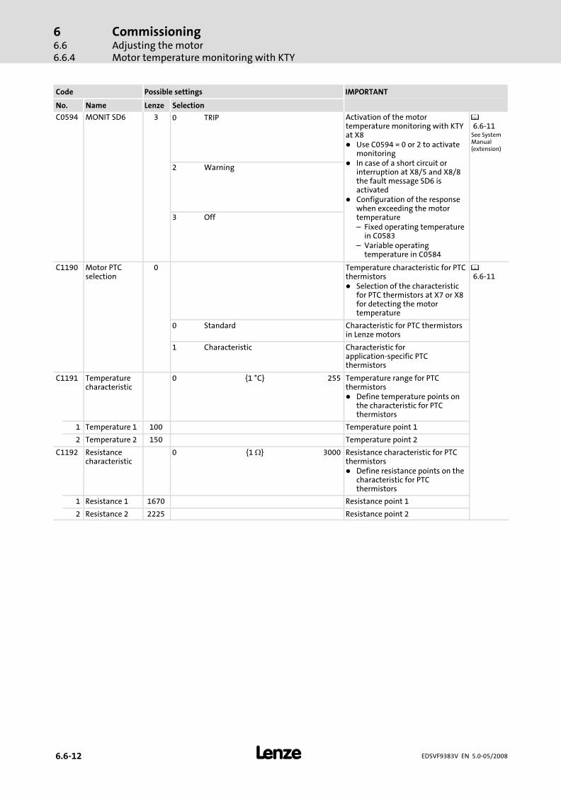
CommissioningAdjusting the motorMotor temperature monitoring with KTY
66.66.6.4
� 6.6−12 EDSVF9383V EN 5.0−05/2008
IMPORTANTPossible settingsCode
SelectionLenzeNameNo.
C0594 MONIT SD6 3 0 TRIP Activation of the motortemperature monitoring with KTYat X8� Use C0594 = 0 or 2 to activate
monitoring� In case of a short circuit or
interruption at X8/5 and X8/8the fault message SD6 isactivated
� Configuration of the responsewhen exceeding the motortemperature– Fixed operating temperature
in C0583– Variable operating
temperature in C0584
6.6−11See SystemManual(extension)
2 Warning
3 Off
C1190 Motor PTCselection
0 Temperature characteristic for PTCthermistors� Selection of the characteristic
for PTC thermistors at X7 or X8for detecting the motortemperature
6.6−11
0 Standard Characteristic for PTC thermistorsin Lenze motors
1 Characteristic Characteristic forapplication−specific PTCthermistors
C1191 Temperaturecharacteristic
0 {1 °C} 255 Temperature range for PTCthermistors� Define temperature points on
the characteristic for PTCthermistors
1 Temperature 1 100 Temperature point 1
2 Temperature 2 150 Temperature point 2
C1192 Resistancecharacteristic
0 {1 �} 3000 Resistance characteristic for PTCthermistors� Define resistance points on the
characteristic for PTCthermistors
1 Resistance 1 1670 Resistance point 1
2 Resistance 2 2225 Resistance point 2

CommissioningAdjusting the motor
Motor temperature monitoring with KTY
66.6
6.6.4
� 6.6−13EDSVF9383V EN 5.0−05/2008
� Note!
ƒ In the Lenze setting, the motor temperature monitoring isswitched off!
ƒ If you work with several parameter sets, the monitoring mustbe activated separately in each parameter set!
Use C0594 = 0 or C0594 = 2 to activate the motor temperature monitoringvia X8. In addition, the connection is monitored for short circuit andinterruption.
1. Connecting the monitoring circuit of the motor to X8/5 and X8/8.
2. Setting controller reaction to short circuit or interruption of theconnection:
– C0594 = 3: Monitoring is switched off.
– C0594 = 0: TRIP error message (display of keypad: Sd6 �)
– C0594 = 2: Warning signal (display of keypad: Sd6 �)
Monitoring with fixed operating temperature (150 °C)
1. Set the controller reaction:
– C0583 = 3: Temperature monitoring of the motor is switched off.
– C0583 = 0: TRIP error message (display of keypad: OH3 �)
Monitoring with variable operating temperature (45 ... 150 °C)
1. Set the operating temperature in C0121.
2. Set the controller reaction:
– C0584 = 3: Temperature monitoring of the motor is switched off.
– C0584 = 2: Warning signal (display of keypad: OH7 �)
Activation
Adjustment

CommissioningAdjusting the motorMotor temperature monitoring with KTY
66.66.6.4
� 6.6−14 EDSVF9383V EN 5.0−05/2008
The temperature and resistance range can be adapted to the KTY used.
ƒ C1190 = 0: Fixed operating range for KTY in Lenze motors (Lenzesetting)
ƒ C1190 = 1: Adjustable operating range
� � � � �
� � � � �
� � � � � � � � � � � � � �
� � � � � � � � � � � � � � �
� � � � � � � � � � � � � �
� � � � � � � � � � � � � � �
�
Fig. 6.6−3 Setting of the operating range for the KTY (C1190 = 1)
The operating range is specified by means of limit values and is in the almostlinear section of the graph (a). The operating values are determined byinterpolation.C1191/1C1191/2
Setting of the lower and upper temperature value (T1, T2)corresponding to the KTY used.
C1192/1C1192/2
Setting of the lower and upper resistance value corresponding tothe KTY used.
Adjustment of KTY operatingrange

CommissioningAdjusting the motor
Current limits
66.6
6.6.5
� 6.6−15EDSVF9383V EN 5.0−05/2008
6.6.5 Current limits
The controllers are provided with a current limit value control whichdetermines the dynamic behaviour under load. The resulting utilisation iscompared to the current limit value set under C0022 for motor load andunder C0023 for generator load. If the current limit values are exceeded, thecontroller changes its dynamic behaviour.
Motor overload during acceleration:
The controller extends the acceleration ramp.
Generator overload during deceleration:
The controller extends the deceleration ramp.
With increasing load and constant speed:
ƒ When the current limit of the motor mode is reached:
– The controller reduces the speed up to 0�min−1 .
– The controller cancels the change of the speed if the load falls belowthe limit value again.
ƒ When the current limit in the generator mode is reached:
– The controller increases the speed up to the maximum speed(C0011).
– The controller cancels the change of the speed if the load falls belowthe limit value again.
ƒ If a sudden load is built up at the motor shaft (e. g. the drive is blocked),the overcurrent disconnection can respond (fault message OCx).
Codes for parameter setting
Code Possible settings IMPORTANT
No. Name Lenze Selection
C0022 Imax current � 0 {0.1 A} − Imax limit in motor mode� depending on C0086
6.6−15
C0023 Imax gen. � 0 {0.1 A} − Imax limit in generator mode� depending on C0086
6.6−15
Description
Controller performance whena limit value is reached
CommissioningAdjusting the motorAutomatic collection of motor data
66.66.6.6
� 6.6−16 EDSVF9383V EN 5.0−05/2008
ƒ Set the acceleration and deceleration times so that the drive can followthe speed profile without reaching Imax of the controller.
ƒ A correct current control during operation in generator mode is onlypossible with an external brake resistor.
ƒ Drive behaviour with motor or generator overload (C0054 > C0022 orC0023):
– The controller reduces the speed up to 0�min−1 .
– The controller cancels the change of the speed if the load falls belowthe limit value again.
ƒ When operating with switching frequency > 2 kHz, C0022 and C0023must be adapted to the permissible output currents (derating).
ƒ A correct current control (C0075, C0076) in generator mode is onlypossible with a connected brake resistor or in DC bus connection withenergy exchange.
6.6.6 Automatic collection of motor data
The motor data identification serves to detect the required motor data andinfluences of the motor cable.
Before executing the identification you must manually enter the motor datafrom the motor nameplate into the corresponding codes.
Vector control (C0006 = 1)
In the vector control mode the motor data identification must be executedbefore initial commissioning.
ƒ In case of vector control without temperature feedback, the heating ofthe motor in the motor model is not taken into consideration.
ƒ In case of vector control with thermal sensor KTY a motor temperatureof 20 °C in the motor model is considered.
Important: The temperature feedback must be activated (C0594 = 0 orC0594 = 2) before you execute the motor data identification.
V/f characteristic control (C0006 = 5)
In the Lenze setting, the controllers are defined for a power−adapted motorwith 10�m of motor cable. Therefore the motor data identification is notessential.
ƒ The identification of the motor data also influences the smoothrunning behaviour. When identifying the motor data for this operatingmode, you can optimise the smooth running behaviour at low speeds.
Adjustment
Description

CommissioningAdjusting the motor
Automatic collection of motor data
66.6
6.6.6
� 6.6−17EDSVF9383V EN 5.0−05/2008
Codes for parameter setting
Code Possible settings IMPORTANT
No. Name Lenze Selection
C0084�
Mot Rs � 0.00 {0.01 m�} 100000.00
Motor stator resistance� Value is determined by motor
parameter identification(C0148, C0149)
6.6−1 6.6−16
C0087�
Mot speed � 50 {1 rpm} 36000 Rated motor speed� depending on C0086� Motor selection in C0086 set
the corresponding rated motorspeed in C0087
� Change of C0087 setsC0086 = 0
6.6−1
C0088�
Mot current � 0.5 {0.1 A} 1000.0 Rated motor current� depending on C0086� Motor selection in C0086 sets
the corresponding rated motorcurrent in C0088
� Change of C0088 sets C0086 =0
6.6−1
C0089�
Mot frequency � 10 {1 Hz} 5000 Rated motor frequency� depending on C0086� Motor selection in C0086 sets
the corresponding rated motorfrequency in C0089
� Change of C0089 setsC0086 = 0
6.6−1
C0090�
Mot voltage � 0 {1 V} 1000 Rated motor voltage� depending on C0086� Motor selection in C0086 sets
the corresponding rated motorvoltage in C0090
� Change of C0090 sets C0086 =0
6.6−1
C0091�
Mot cos phi � 0.50 {0.01 } 1.00 Motor cos �� depending on C0086� Motor selection in C0086 sets
the corresponding motor cos �in C0091
� Change of C0091 setsC0086 = 0
6.6−1
C0092�
Mot Ls � 0.00 {0.01 mH} 6553.50 Motor stator inductance� Value is determined by motor
parameter identification fromC0088, C0089, C0090 andC0091
� Motor selection in C0086 setscorresponding statorinductance value in C0092
6.6−1

CommissioningAdjusting the motorAutomatic collection of motor data
66.66.6.6
� 6.6−18 EDSVF9383V EN 5.0−05/2008
IMPORTANTPossible settingsCode
SelectionLenzeNameNo.
C0148�
ident run 0 0 WRKstop
Ready Motor data identification1. Inhibit controller, wait until
drive has stopped2. Enter the correct values of the
motor nameplate into C0087,C0088, C0089, C0090, C0091
3. Set C0148 = 1, confirm with�
4. Enable controllerThe identification– starts, � goes off. The
motor "whistles" but doesnot rotate!
– lasts approx. 1 ... 2 min– is completed when � is lit
again5. Inhibit controller:
6.6−16
1 WRK run Start identification
C0149�
Auto ident 0 0 Idinactive
Automatic identification isinactive
Automatic motor dataidentification1. Inhibit controller, wait until
drive has stopped2. Enter the correct values of the
motor nameplate into C0087,C0088, C0089, C0090, C0091
3. Set C0149 = 1, confirm with�
4. Enable controllerThe identification– starts, � goes off. The
motor "whistles" but doesnot rotate!
– lasts approx. 1 ... 2 min– is completed when � is lit
again5. Inhibit controller:
6.6−16
1 Id active Automatic identification isactive� The identification starts
automatically aftercontroller enable
� After a faultyidentification, the processis restarted after TRIPRESET or mains switchingand subsequentcontroller enable

CommissioningAdjusting the motor
Automatic collection of motor data
66.6
6.6.6
� 6.6−19EDSVF9383V EN 5.0−05/2008
The identification is only executed for the parameter set which is activatedat the moment:
ƒ If you want to identify the motor data for another parameter set, youmust switch to this parameter set and restart the identification.
� Note!
ƒ During the identification the motor is supplied with current.The motor does not rotate.
ƒ The load machine can remain to be connected. Existingholding brakes can be kept in the braking position.
ƒ If the motor is idling, a small phase offset may occur at themotor shaft.
1. Enter C0087, C0088, C0089, C0090 and C0091 of your motor (seenameplate):
– It is vital to enter the correct values since these entries influenceimportant parameters such as slip compensation and no−loadcurrent.
– Enter the values according to the connection method (star or delta)for the rated motor current (C0088) and rated motor voltage (C0090).
1. Inhibit the controller. Wait until drive stands still.
2. Select C0148 = 1, confirm with �.
3. Enable the controller. The identification starts.
– The green LED at the controller is blinking very fast.
– "WRK run" is displayed at the keypad.
– The rotor resistance is calculated and saved in C0082.
– The motor stator resistance is detected and saved in C0084.
– The motor leakage inductance is measured and saved in C0085.
– The inverter compensation characteristic is calculated from themeasured motor stator resistance and saved in C1751/1 ... C1751/17.
– The motor stator inductance is calculated from the entered data andsaved in C0092.
– The identification takes approx. 1 ... 2 min (dependent on the ratedmotor power).
– The identification is completed when the green LED at the controlleris lit (keypad, GDC: � is active).
4. Inhibit the controller.
If the motor data identification is has been completed incorrectly
If the identification is incorrect, the fault ID1 or ID2 is displayed.
ƒ If the motor data identification is incorrect, the process must berepeated from step 2.
Adjustment
Manual motor dataidentification (C0148)
CommissioningAdjusting the motorAutomatic collection of motor data
66.66.6.6
� 6.6−20 EDSVF9383V EN 5.0−05/2008
The automatic motor data identification is suitable for standard andreplacement devices which are pre−parameterised in the workshop andcommissioned on site:
ƒ Enter the motor data of the motor nameplate, set C0149 = 1 and savethe settings.
ƒ The motor data identification is started with the first controller enable.After a successful identification the settings are automatically saved inthe parameter set 1.
1. Inhibit controller (X5/28 = LOW).
2. Switch on the mains.
3. Select a Lenze motor under C0086 or enter motor data of thenameplate.
4. If required, select C0149 = 1 and confirm with �.
5. Enable the controller. The identification starts.
– The green LED at the controller is blinking very fast.
– "WRK run" is displayed at the keypad.
– The rotor resistance is calculated and saved in C0082.
– The motor stator resistance is detected and saved in C0084.
– The motor leakage inductance is measured and saved in C0085.
– The inverter compensation characteristic is calculated from themeasured motor stator resistance and saved in C1751/1 ... C1751/17.
– The motor stator inductance is calculated from the entered data andsaved in C0092.
– The identification takes approx. 1 ... 2 min (dependent on the ratedmotor power).
– The identification is completed when the green LED at the controlleris lit (keypad, GDC: � is active).
– Controller is inhibited.
– If required, select C0149 = 0 and confirm with �. The automaticmotor data identification is deactivated.
6. Inhibit the controller.
If the motor data identification is has been completed incorrectly
If the identification is incorrect, the fault ID or ID is displayed.
1. Acknowledge fault with TRIP RESET or switch the mains.
2. Enable the controller. The identification restarts.
Automatic motor dataidentification (C0149)

CommissioningSetting the speed feedback
66.7
� 6.7−1EDSVF9383V EN 5.0−05/2008
6.7 Setting the speed feedback
For speed monitoring, the feedback signal via incremental encoder caneither be supplied via input X8 or X9.
ƒ At input X8 you can only attach an incremental encoder withTTL−levels.
ƒ Incremental encoders with HTL−level can only be connected to inputX9.
The incremental encoder signal can be output for slaves at the digitalfrequency output X10.
The master frequency input (DFIN) and master frequency output (DFOUT)are described in the chapter "Function library".
� Note!
You can use maximally two of the three interfaces X8, X9, X10 atthe same time. This may lead to the fact that the incrementalencoder input cannot be activated or the master frequency inputor master frequency output does not work.
ƒ This does not apply if the input signal at X8 or X9 is directlyoutput to master frequency output X10 (C0540 = 4 or 5).
ƒ To deactivate the master frequency input, the internal signalconnection of function block DFIN to the following functionblock must be removed. Remove the function block DFIN fromthe processing table.
Codes for parameter setting
Code Possible settings IMPORTANT
No. Name Lenze Selection
C0025�
Feedback type 1 Speed feedback 6.7−11 no feedback No feedback
100 IT (C420) − X8 Input of thenumber ofincrements inC0420
Incremental encoder at X8� Incremental encoders with TTL
level can only be connected toX8.
101 IT (C420) − X9 Input of thenumber ofincrements inC0420
Incremental encoder at X9� Connect incremental encoders
with HTL−level on X9 only
Number ofincrements:
Incremental encoder at X8� Incremental encoders with TTL
level can only be connected toX8.
110 IT512−5V 512 inc
111 IT1024−5V 1024 inc
112 IT2048−5V 2048 inc
113 IT4096−5V 4096 inc
Description

CommissioningSetting the speed feedbackIncremental encoder with TTL level at X8
66.76.7.1
� 6.7−2 EDSVF9383V EN 5.0−05/2008
IMPORTANTPossible settingsCode
SelectionLenzeNameNo.
C0420�
Encoder const 512 1 {1 inc/rev} 8192 Number of increments forincremental encoder at X8 or X9� Connect incremental encoders
with HTL−level on X9 only
6.7−1
C0421�
Enc voltage 5.00 5.00 {0.1 V} 8.00 Supply voltage for the incrementalencoder at X8CAUTION! A wrong entry candestroy the incremental encoder!
6.7.1 Incremental encoder with TTL level at X8
On X8, only incremental encoders with TTL level can be operated. Wiringdiagram and pin assignment of X8 are described in chapter "Wiring of thebasic device" � "Wiring of the feedback system".
ƒ C0025 = 100. In addition, you have to set the number of increments inC0420.
ƒ C0025 = 110, 111, 112 or 113. The number of increments (512, 1024,2048 or 4096) is automatically set.
The incremental encoder is supplied with voltage by the drive controller.
� Stop!
If the supply voltage is too high, it may destroy the incrementalencoder.
Under C0421 you can adjust the supply voltage VCC (5 V) of the incrementalencoder in order to compensate for the voltage drop along the incrementalencoder cable (if required).
Calculation of the voltage drop
�U l�[m] �R�[�]
[m]� IInc�[A]
l Length of the incremental encoder cable
R Resistance of the incremental encoder cable
IInc Current consumption of the incrementalencoder
Activation
Adjustment

CommissioningSetting the speed feedback
Incremental encoder with HTL level at X9
66.7
6.7.2
� 6.7−3EDSVF9383V EN 5.0−05/2008
6.7.2 Incremental encoder with HTL level at X9
On X9, incremental encoders with HTL level can be operated. Wiring diagramand pin assignment of X9 are described in chapter "Wiring of the basicdevice" � "Wiring of the feedback system".
ƒ C0025 = 101. In addition, you have to set the number of increments inC0420.
The incremental encoder must be operated with an external supply voltage.C0421 has no influence.
ƒ Incremental encoders with HTL level require DC 8 ... 30 V supplyvoltage. Please observe the information by the manufacturer.
Activation
Adjustment

CommissioningOperating mode
66.8
� 6.8−1EDSVF9383V EN 5.0−05/2008
6.8 Operating mode
The control mode of the controller can be selected via the operating mode.You can select between the following modes:
ƒ V/f characteristic control
ƒ Vector control
The V/f characteristic control is the classic operating mode for standardapplications.
When using the vector control you will achieve improved drive featurescompared to the V/f characteristic control due to:
ƒ Higher torque via the complete speed range
ƒ Higher speed accuracy and higher concentricity factor
ƒ Higher efficiency
Description
Selection of the correctoperating mode

CommissioningOperating mode
66.8
� 6.8−2 EDSVF9383V EN 5.0−05/2008
V/f characteristic control
No feedback With feedback
��
� �
nN
MN
M
-MN
-nN n
��
� �
nN
MN
M
-MN
-nN n
9300vec092 9300vec093
Fig. 6.8−1 Speed/ torque characteristics
� Operation in motor mode (CW rotation)� Operation in generator mode (CCW rotation) Operation in motor mode (CCW rotation)� Operation in generator mode (CW rotation)
Vector control
without feedback with feedback
��
� �
nN
MN
M
-MN
-nN n
��
� �
nN
MN
M
-MN
-nN n
9300vec095 9300vec094
Fig. 6.8−2 Speed/ torque characteristics
� Operation in motor mode (CW rotation)� Operation in generator mode (CCW rotation) Operation in motor mode (CCW rotation)� Operation in generator mode (CW rotation)
Speed/ torque characteristics

CommissioningOperating mode
66.8
� 6.8−3EDSVF9383V EN 5.0−05/2008
The frequency inverter is mainly designed for the applications listed in thebelow table.
The table helps you to select the correct operating mode for your application:
ƒ C0006 = 5: V/f characteristic control with constant Vmin boost
ƒ C0006 = 1: Vector control
Power range 110 ... 400 kW Selection of the operating mode in C0006
Motor cableshielded � 100 m
unshielded � 200 m
Motor cableshielded 100 m
unshielded 200 m
Applications with asynchronousmotors
recommended alternatively recommended alternatively
Single drives
Drives with constant load 5 1 5 −
Drives with heavy startconditions
1 5 5 −
Travelling drives, conveyor belts 5 1 5 −
Pump drives, fan drives 1) 5 − 5 −
Extruder drives 5 1 5 −
Drives for wire drawingmachines
5 1 5 −
Drives for rolling machines 5 1 5 −
Drives for rewinders with dancer(speed−controlled)
1 5 − −
Group drives(the resulting motor cable lengthis decisive Ires)
5 − 5 −
lres � (i� � (l1 � l2 � ��� � li))
1) A square voltage characteristic (C0014 = 1) is recommended for this application
� Note!
Only switch between the operating modes if the controller isinhibited!
Recommended operatingmodes

CommissioningOperating modeV/f characteristic control
66.86.8.1
� 6.8−4 EDSVF9383V EN 5.0−05/2008
6.8.1 V/f characteristic control
The output voltage of the controller follows a defined characteristic. At lowoutput frequencies, the characteristic can be boosted. It can be adapted todifferent load profiles.
ƒ Linear characteristic for drives with constant load torque over thespeed.
ƒ Quadratic characteristic for drives with quadratic load torque over thespeed:
– Quadratic V/f characteristics are preferably used in centrifugal pumpand fan drives. However, it must be checked whether your pump orfan drive can be operated in this operating mode!
– If your pump or fan drive cannot be used for the operation with aquadratic V/f characteristic, the linear V/f characteristic or vectorcontrol mode must be used.
0 1
0
C0089
C0090100 %
N
nn
Umin
Uout
0 1
0
C0089
C0090100 %
N
nn
Umin
Uout
9300vec085 9300vec086
Fig. 6.8−3 Linear and square−law V/f characteristic
Codes for parameter setting
Code Possible settings IMPORTANT
No. Name Lenze Selection
C0006�
Op mode 5 Selection of the operating modefor the motor control
1 vector ctrl Vector controlwithout or withspeed feedback
In case of the first selection enterthe motor data and identify themwith C0148.
6.8−8
5 V / f V/f characteristiccontrol
Commissioning withoutidentification of the motor data ispossible� Advantage of identification
with C0148: Improved smoothrunning at low speeds
6.8−4
C0014 V/f charact. 0 Characteristic in the V/fcharacteristic control mode
8.2−25
0 Linear Linear V/f characteristic
1 square Square V/f characteristic
C0015 Rated freq 50 10 {1 Hz} 5000 V/f−rated frequencyIn C0015 you can set a basefrequency which differs from therated motor frequency (C0089)� Lenze setting: C0015 = C0089� Changing C0086 or C0089
overwrites the value in C0015
8.2−25
Description
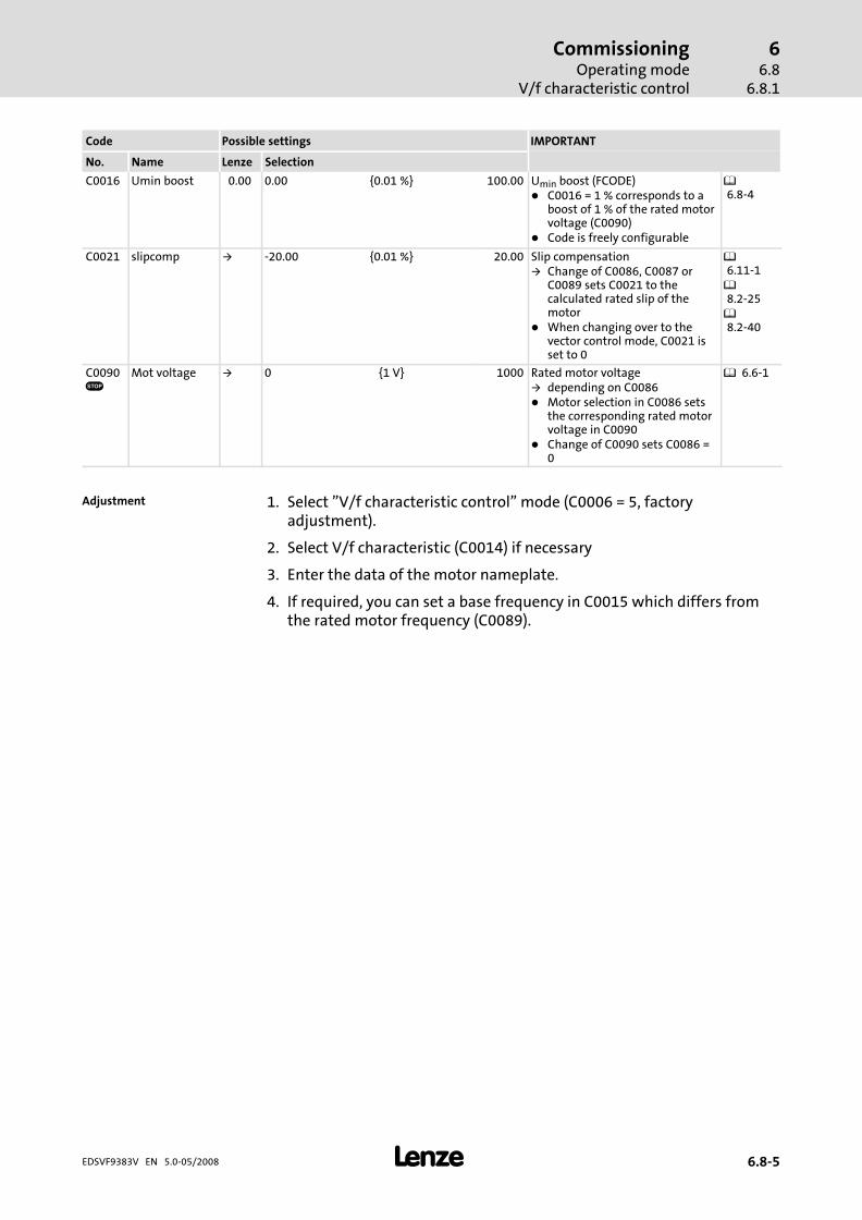
CommissioningOperating mode
V/f characteristic control
66.8
6.8.1
� 6.8−5EDSVF9383V EN 5.0−05/2008
IMPORTANTPossible settingsCode
SelectionLenzeNameNo.
C0016 Umin boost 0.00 0.00 {0.01 %} 100.00 Umin boost (FCODE)� C0016 = 1 % corresponds to a
boost of 1 % of the rated motorvoltage (C0090)
� Code is freely configurable
6.8−4
C0021 slipcomp � −20.00 {0.01 %} 20.00 Slip compensation� Change of C0086, C0087 or
C0089 sets C0021 to thecalculated rated slip of themotor
� When changing over to thevector control mode, C0021 isset to 0
6.11−1 8.2−25 8.2−40
C0090�
Mot voltage � 0 {1 V} 1000 Rated motor voltage� depending on C0086� Motor selection in C0086 sets
the corresponding rated motorvoltage in C0090
� Change of C0090 sets C0086 =0
6.6−1
1. Select "V/f characteristic control" mode (C0006 = 5, factoryadjustment).
2. Select V/f characteristic (C0014) if necessary
3. Enter the data of the motor nameplate.
4. If required, you can set a base frequency in C0015 which differs fromthe rated motor frequency (C0089).
Adjustment
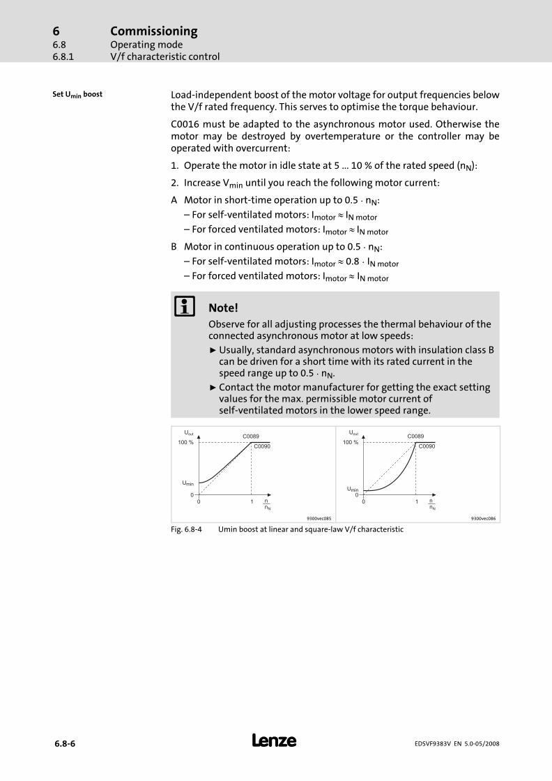
CommissioningOperating modeV/f characteristic control
66.86.8.1
� 6.8−6 EDSVF9383V EN 5.0−05/2008
Load−independent boost of the motor voltage for output frequencies belowthe V/f rated frequency. This serves to optimise the torque behaviour.
C0016 must be adapted to the asynchronous motor used. Otherwise themotor may be destroyed by overtemperature or the controller may beoperated with overcurrent:
1. Operate the motor in idle state at 5 ... 10 % of the rated speed (nN):
2. Increase Vmin until you reach the following motor current:
A Motor in short−time operation up to 0.5 � nN:
– For self−ventilated motors: Imotor � IN motor
– For forced ventilated motors: Imotor � IN motor
B Motor in continuous operation up to 0.5 � nN:
– For self−ventilated motors: Imotor � 0.8���IN motor
– For forced ventilated motors: Imotor���IN motor
� Note!
Observe for all adjusting processes the thermal behaviour of theconnected asynchronous motor at low speeds:
ƒ Usually, standard asynchronous motors with insulation class Bcan be driven for a short time with its rated current in thespeed range up to 0.5 � nN.
ƒ Contact the motor manufacturer for getting the exact settingvalues for the max. permissible motor current ofself−ventilated motors in the lower speed range.
0 1
0
C0089
C0090100 %
N
nn
Umin
Uout
0 1
0
C0089
C0090100 %
N
nn
Umin
Uout
9300vec085 9300vec086
Fig. 6.8−4 Umin boost at linear and square−law V/f characteristic
Set Umin boost

CommissioningOperating mode
V/f characteristic control
66.8
6.8.1
� 6.8−7EDSVF9383V EN 5.0−05/2008
In general the V/f characteristic control can be operated without any furthermeasures. The V/f characteristic control must only be optimised in case ofthe following drive behaviour:
Drive behaviour Remedy
Does not rotate concentrically at lowspeeds, especially when operatingwith long motor cables
Executing motor identification
Problems in case of high startingduty (high mass inertia), in extremecases, the error message OC1 occurs
Adjusting the voltage increase (C0016).� Set C0016 so that with an enabled controller and
5 ... 10 % of the rated speed an approx.0.8−fold ... single rated motor current flows
� 6.8−6
The set voltage increase (C0016)does not result in the desired currentflow (controller has problems at highstarting duty, error message OC1during acceleration).
Adapting the voltage increase with boost correction( 6.11−5)
Drive does not follow the speedsetpoint.Reason: The current controllerintervenes in the rated fieldfrequency to limit the controlleroutput current to the maximumcurrent (C0022, C0023)
� Increasing acceleration / deceleration time� Consider sufficient magnetising time of the motor.
the magnetising time amounts to 0.1 ... 2 sdepending on the motor power
� Increase permissible maximum current (C0022,C0023)
For operation without speedfeedback (C0025 = 1):Lack of speed stability at high load(setpoint and motor speed are notproportional anymore)
� Increase slip compensation (C0021). Important:unstable drive due to overcompensation!
� In case of cyclic load impulses (e.g. centrifugal pump)a smoother motor characteristic can be achieved bysmaller values in C0021 (maybe negative values)
Note: The slip compensation is only active for operationwithout speed feedback.
Error messages OC1 or OC3 withshort acceleration times (C0012)compared with the load (controllercannot follow the dynamicprocesses)
� Increase gain of the Imax controller (C0075)� Reduce integral−action time of the Imax controller
(C0076)� Increase acceleration time (C0012)
Mechanical resonances at certainspeeds
The function block NLIM1 serves to suppress thosespeed ranges in which resonances occur (see chapter"Function library").
Speed oscillations in no−loadoperation at speeds > 1/3 ratedspeed
The oscillation damping minimises speed oscillations(see "Optimising operational performance" in chapter"Commissioning")
Optimising V/f characteristiccontrol

CommissioningOperating modeVector control
66.86.8.2
� 6.8−8 EDSVF9383V EN 5.0−05/2008
6.8.2 Vector control
Compared to the V/f characteristic control, the vector control serves toachieve a considerably higher torque and lower current consumption in idlestate.
� Note!
ƒ The connected motor may be maximally two power classessmaller than the motor assigned to the drive controller.
ƒ The motor data identification is essential.
Codes for parameter setting
Code Possible settings IMPORTANT
No. Name Lenze Selection
C0006�
Op mode 5 Selection of the operating modefor the motor control
1 vector ctrl Vector controlwithout or withspeed feedback
In case of the first selection enterthe motor data and identify themwith C0148.
6.8−8
5 V / f V/f characteristiccontrol
Commissioning withoutidentification of the motor data ispossible� Advantage of identification
with C0148: Improved smoothrunning at low speeds
6.8−4
C0021 slipcomp � −20.00 {0.01 %} 20.00 Slip compensation� Change of C0086, C0087 or
C0089 sets C0021 to thecalculated rated slip of themotor
� When changing over to thevector control mode, C0021 isset to 0
6.11−1 8.2−25 8.2−40
C0075 Vp curr CTRL 0.04 0.00 {0.01 } 0.99 Gain of current controller� Vector control: Gain of current
controller� V/f characteristic control:
Maximum current controller
8.2−25 8.2−40
C0076 Tn curr CTRL 10.0 0.1 {0.1 ms} 2000.0 Integral−action time of currentcontroller� Vector control: integral−action
time of current controller� V/f characteristic control:
maximum current controller� C0076 = 2000 ms: current
controller is switched off
8.2−25 8.2−40
C0077 Ti field CTRL 4.0 0.3 {0.1 ms} 6000.0 Integral−action time of fieldcontroller� Only active in case of vector
control with feedback
C0081�
Mot power � 0.01 {0.01 kW} 500.00 Rated motor power� Change of C0086 resets value
to factory setting� Change of C0081 sets C0086 =
0
Description

CommissioningOperating mode
Vector control
66.8
6.8.2
� 6.8−9EDSVF9383V EN 5.0−05/2008
IMPORTANTPossible settingsCode
SelectionLenzeNameNo.
C0087�
Mot speed � 50 {1 rpm} 36000 Rated motor speed� depending on C0086� Motor selection in C0086 set
the corresponding rated motorspeed in C0087
� Change of C0087 setsC0086 = 0
6.6−1
C0088�
Mot current � 0.5 {0.1 A} 1000.0 Rated motor current� depending on C0086� Motor selection in C0086 sets
the corresponding rated motorcurrent in C0088
� Change of C0088 sets C0086 =0
6.6−1
C0089�
Mot frequency � 10 {1 Hz} 5000 Rated motor frequency� depending on C0086� Motor selection in C0086 sets
the corresponding rated motorfrequency in C0089
� Change of C0089 setsC0086 = 0
6.6−1
C0090�
Mot voltage � 0 {1 V} 1000 Rated motor voltage� depending on C0086� Motor selection in C0086 sets
the corresponding rated motorvoltage in C0090
� Change of C0090 sets C0086 =0
6.6−1
C0091�
Mot cos phi � 0.50 {0.01 } 1.00 Motor cos �� depending on C0086� Motor selection in C0086 sets
the corresponding motor cos �in C0091
� Change of C0091 setsC0086 = 0
6.6−1
C0092�
Mot Ls � 0.00 {0.01 mH} 6553.50 Motor stator inductance� Value is determined by motor
parameter identification fromC0088, C0089, C0090 andC0091
� Motor selection in C0086 setscorresponding statorinductance value in C0092
6.6−1
C0148�
ident run 0 0 WRKstop
Ready Motor data identification1. Inhibit controller, wait until
drive has stopped2. Enter the correct values of the
motor nameplate into C0087,C0088, C0089, C0090, C0091
3. Set C0148 = 1, confirm with�
4. Enable controllerThe identification– starts, � goes off. The
motor "whistles" but doesnot rotate!
– lasts approx. 1 ... 2 min– is completed when � is lit
again5. Inhibit controller:
6.6−16
1 WRK run Start identification

CommissioningOperating modeVector control
66.86.8.2
� 6.8−10 EDSVF9383V EN 5.0−05/2008
C0006 = 1 set the vector control mode.
� Note!
When setting the vector control mode, the slip compensation(C0021) is automatically set to 0.0 %.
ƒ When you switch back to the V/f characteristic control mode,the slip compensation must be re−adapted.
The motor data of the motor nameplate must be entered:
ƒ Rated motor speed (C0087)
ƒ Rated motor current (C0088)
ƒ Rated motor frequency (C0089)
ƒ Rated motor voltage (C0090)
ƒ Motor cos � (C0091)
Execute the motor data identification. ( 6.6−16)
Set vector control
Prepare the motor dataidentification
Executing the motor dataidentification

CommissioningOperating mode
Vector control
66.8
6.8.2
� 6.8−11EDSVF9383V EN 5.0−05/2008
In general the vector control can be operated without any further measures.The vector control must only be optimised in case of the following drivebehaviour:
Drive behaviour Remedy
Operation without feedback:� The current consumption in idle
state differs widely from therated magnetising current (ImR �IN × sin �) . Calculate sin � fromthe cos � of the motornameplate.
� The drive has an uneven startingperformance
1. Optimise setpoint for the motor magnetisingcurrent. ( 6.11−9)
2. Stator inductance (C0092) must be adapted aftermotor parameter identification.The calculation of the stator inductance by themotor data identification is based on the motor dataentered before and does not consider the physicalleakage of the motor and the inductive reactance ofthe motor cable.
0,37 22 90
C0092 C0092
-15 %
+15 %
0
400 P [kW]N
9300vec040
Tendency of the correction of C0092PN: rated motor power
Lack of speed stability at high load(setpoint and motor speed are notproportional anymore)
Use C0021 (slip compensation) to change the influenceof the rotor resistance (C0082) proportionally:� Reduce the value in C0021 at an increasing speed
(negative values)� Increase the value in C0021 at a decreasing speedNote: If you activate the vector control (C0006 = 1),C0021 is automatically set to 0 %.
Unstable control at higher speeds � Reduce the gain of the speed controller (C0070) (ifrequired, speed−dependent adaptation via functionblock CURVE1 and MCTRL−VP−ADAPT)
� Control value in C0092 by comparing the currentconsumption in no−load operation with the ratedmagnetising current (ImR � IN × sin �).
� Optimise oscillation damping (C0234 ... C0236)
Unstable control at higher speedsand high torque at high power(> 55 kW)
� Reduce gain of the Imax controller (C0075) or reducegain and influence of the oscillation damping (at apower of 55 ... 90 kW).
� For operation with feedback, deactivate oscillationdamping with C0234 = 0.
Unstable control in field weakeningrange for operation with speedfeedback
� Reduce integral−action time of the field controller viaC0077
� Increase gain of the Imax controller (C0075)
Error messages OC1 or OC3 withshort acceleration times (C0012)compared with the load (controllercannot follow the dynamicprocesses).
� Increase gain of the Imax controller (C0075)� Reduce integral−action time of the Imax controller
(C0076)� Increase acceleration time (C0012)
Mechanical resonances at certainspeeds
The function block NLIM1 serves to suppress thosespeed ranges in which resonances occur (see chapter"Function library").
Speed oscillations in no−loadoperation at speeds > 1/3 ratedspeed
The oscillation damping minimises speed oscillations(see "Optimising operational performance" in chapter"Commissioning")
Optimising vector control


CommissioningSwitching frequency of the inverter
66.9
� 6.9−1EDSVF9383V EN 5.0−05/2008
6.9 Switching frequency of the inverter
The switching frequency of the inverter influences the smooth runningbehaviour, the power loss in the controller and the noise generation in theconnected motor. The Lenze setting is the optimal value for standardapplications. The following general rule applies:
The lower the switching frequency, the
ƒ lower the power loss.
ƒ higher the noise generation.
ƒ better the concentricity factor.
You can select between two switching frequency modes:
CoDe sine−wave modulated (sin) flat−top modulated (f_top)
C0018 1, 2, 4, 6 3
� Note!
ƒ The concentricity factor at low speeds is lower with flat topmodulation than with sine−wave modulation. For standardapplication a sine−wave modulated switching frequency isoptimal.
ƒ The maximum output frequency of the controller depends onthe selected switching frequency (see C0018).
ƒ With C0018 = 6, the switching frequency will be automaticallychanged depending on the output current of the controller.
ƒ Please observe that the output current must be reduced whenoperating with high switching frequencies to prevent animpermissible heating of the controller (derating).
ƒ Adapt the current limit values (C0022 and C0023) so that thecurrents specified in the technical data are not exceeded.
Moreover, you can adjust whether it is switched to a lower switchingfrequency when the heatsink temperature reaches an adjustable limit value.This prevents the drive from being inhibited by the error "overtemperature"and the motor coasts without torque.
Description

CommissioningSwitching frequency of the inverter
66.9
� 6.9−2 EDSVF9383V EN 5.0−05/2008
Codes for parameter setting
Code Possible settings IMPORTANT
No. Name Lenze Selection
C0018 fchop 6 Switching frequency of theinverter� General rule: The lower the
switching frequency the– lower the power loss– higher the noise generation– better the concentricity
factor� Observe derating indications
for high switching frequencies� The max. output frequency
(fmax) is:– fchop = 4 kHz �
fmax = 300 Hz– fchop = 2 kHz �
fmax = 150 Hz– fchop = 1 kHz �
fmax = 150 Hz
6.9−1
1 1 kHz sin loss−optimised
2 2 kHz sin concentricity−optimised
3 4 kHz f_top power−optimised
4 4 kHz sin noise−optimised
6 4/2 kHz sin noise/concentricity−optimised withautomaticchange−over tolow switchingfrequency
C0144�
OH switch 1 0 Switch off Switch−over is notactive
Temperature−dependentswitching frequency reduction� If the heatsink temperature set
in C0122 is reached (warningOH4), the controller switchesto 2 kHz
1 Switch on Switch−over isactive
C0144�=�0 (no temperature−dependent switching frequency reduction)
If the maximum permissible heatsink temperature (�max ) is exceeded whenoperating with automatic switching frequency reduction, the inverter isinhibited, TRIP "OH" (overtemperature) is set and the motor coasts withouttorque.
C0144�=�1 (temperature−dependent switching frequency reduction isactive):
ƒ If the heatsink temperature set in C0122 (overtemperature OH4) isreached when operating with automatic switching frequencyreduction, the controller automatically reduces the switchingfrequency to 2�kHz, thus keeping the operation running.
ƒ After the heatsink has cooled down, the controller automaticallyswitches to the set switching frequency again.
Function of automaticswitching frequencyreduction

CommissioningAcceleration, deceleration, braking, stopping
Speed range
66.10
6.10.1
� 6.10−1EDSVF9383V EN 5.0−05/2008
6.10 Acceleration, deceleration, braking, stopping
6.10.1 Speed range
The speed range required for the application is set in the codes C0010 andC0011:
ƒ The minimum speed (C0010) corresponds to a speed setpoint selectionof 0 %.
ƒ The minimum speed (C0011) corresponds to a speed setpoint selectionof 100 %.
n
0 % 100 %
C0011
C0010
9300vec097
Fig. 6.10−1 Relation between setpoint and minimum and maximum output frequency
Codes for parameter setting
Code Possible settings IMPORTANT
No. Name Lenze Selection
C0010 Nmin 0 0 {1 rpm} 36000 � Reference valuefor the absoluteand relativesetpoint selectionfor theacceleration anddecelerationtimes
� C0059 must beset correctly
� Set C0010 <C0011
� C0010 is onlyeffective in caseof analog setpointselection via AIN1
Important: Forparameter settingvia interface, majorchanges in one stepshould only be madewhen the controlleris inhibited.
Minimumspeed
6.10−1
C0011 Nmax 3000 0 {1 rpm} 36000 Maximumspeed
Features "minimum speed" (nmin):
ƒ C0010 is approached via the acceleration ramp.
ƒ C0010 is only effective with analog setpoint selection via AIN1(terminal X6/1 and X6/2).
Description
C0010

CommissioningAcceleration, deceleration, braking, stoppingSpeed range
66.106.10.1
� 6.10−2 EDSVF9383V EN 5.0−05/2008
Features "maximum output frequency" (nmax):
ƒ For defining fixed setpoints (JOG) C0011 acts as limitation.
ƒ C0011 is an internal scaling value! Therefore, changes must only bemade when the controller is inhibited!
� Stop!
Set C0011 so that the maximum motor speed is not exceeded.
Otherwise the motor can be destroyed.
Observe the internal speed limits (p = number of motor pole pairs):
ƒ Switching frequency 2/4�kHz: nmax = 36000/4p min−1
ƒ Switching frequency 1�kHz: nmax = 36000/4p min−1
C0011
Adjusting tips

CommissioningAcceleration, deceleration, braking, stopping
Speed range
66.10
6.10.2
� 6.10−3EDSVF9383V EN 5.0−05/2008
6.10.2 Setting acceleration times and deceleration times in speed mode
The acceleration and deceleration times determine the controller responsetime after a setpoint change.
Codes for parameter setting
Code Possible settings IMPORTANT
No. Name Lenze Selection
C0012 Tir (acc) 5.00 0.00 {0.01 s} 9999.90 Acceleration time Tir of the mainsetpoint� Refers to speed change
0 ... C0011
6.10−3
C0013 Tif (dec) 5.00 0.00 {0.01 s} 9999.90 Deceleration time Tif of the mainsetpoint� Refers to speed change
0 ... C0011
ƒ The acceleration and deceleration times refer to a speed change from0�min−1 to the max. speed set in C0011.
ƒ Calculate the times Tir and Tif, which you can set under C0012 andC0013.
n [min-1]
C0011
tir tift
Tir Tif
n2
n1
0
9300vec098
Fig. 6.10−2 Acceleration and deceleration times
Tir� �� tir �C0011
n2 � n1
tir and tif are the desired times for the changebetween n1 and n2
Tif� �� tif �C0011
n2 � n1
� Note!
If the acceleration and deceleration times are set too short andunder unfavourable operating conditions the controller can beswitched off with TRIP OC1 or OC3. In these cases, theacceleration and deceleration times must be set so that the drivecan follow the speed profile without Imax reaching a drivesystem.
Description
Adjustment

CommissioningAcceleration, deceleration, braking, stoppingQuick stop
66.106.10.3
� 6.10−4 EDSVF9383V EN 5.0−05/2008
6.10.3 Quick stop
Quick stop brakes the drive to standstill with the deceleration time set inC0105.
ƒ DC−injection braking (GSB) has priority over quick stop.
Codes for parameter setting
Code Possible settings IMPORTANT
No. Name Lenze Selection
C0105 QSP Tif 5.00 0.00 {0.01 s} 999.90 Quick stop deceleration time� The deceleration time refers to
a speed variation of C0011 ... 0
8.2−25 8.2−40
Via digital signal:
ƒ MCTRL−QSP = HIGH.
ƒ Activating signal DCTRL−QSP. The signal can be activated via 3 OR’dinputs:
– Control word CAN−CTRL.B3 from CAN−IN1
– Control word AIF−CTRL.B 3 from AIF−IN
– Control word C0135.B3
Via keyboard of the keypad:
For this the key must be assigned with the quick stop function (C0469 = 2):
– � activates quick stop
– � restarts the drive
Description
Activation
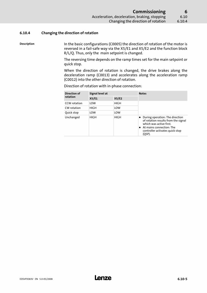
CommissioningAcceleration, deceleration, braking, stopping
Changing the direction of rotation
66.10
6.10.4
� 6.10−5EDSVF9383V EN 5.0−05/2008
6.10.4 Changing the direction of rotation
In the basic configurations (C0005) the direction of rotation of the motor isreversed in a fail−safe way via the X5/E1 and X5/E2 and the function blockR/L/Q. Thus, only the main setpoint is changed.
The reversing time depends on the ramp times set for the main setpoint orquick stop.
When the direction of rotation is changed, the drive brakes along thedeceleration ramp (C0013) and accelerates along the acceleration ramp(C0012) into the other direction of rotation.
Direction of rotation with in−phase connection:
Direction ofrotation
Signal level at Notes
X5/E1 X5/E2
CCW rotation LOW HIGH
CW rotation HIGH LOW
Quick stop LOW LOW
Unchanged HIGH HIGH � During operation: The directionof rotation results from the signalwhich was active first.
� At mains connection: Thecontroller activates quick stop(QSP).
Description


CommissioningOptimising the operating behaviour
Slip compensation
66.11
6.11.1
� 6.11−1EDSVF9383V EN 5.0−05/2008
6.11 Optimising the operating behaviour
6.11.1 Slip compensation
The speed of an asynchronous machine decreases when being loaded. Thisload−dependent speed drop is called slip. By setting C0021 the slip can bepartly compensated.
In the V/f characteristic control mode the slip compensation is only active atoperation without feedback (C0025 = 1).
Codes for parameter setting
Code Possible settings IMPORTANT
No. Name Lenze Selection
C0021 slipcomp � −20.00 {0.01 %} 20.00 Slip compensation� Change of C0086, C0087 or
C0089 sets C0021 to thecalculated rated slip of themotor
� When changing over to thevector control mode, C0021 isset to 0
6.11−1 8.2−25 8.2−40
C0078 Tn slip CTRL 100 1 {1 ms} 6000 Integral−action time of slipcontroller� Filter time for slip
compensation (C0021)� Only active with V/f
characteristic control
8.2−25
Description

CommissioningOptimising the operating behaviourSlip compensation
66.116.11.1
� 6.11−2 EDSVF9383V EN 5.0−05/2008
V/f characteristic control
The slip compensation (C0021) is automatically calculated from the ratedmotor speed (C0087) and the rated motor frequency (C0089). The enteredslip constant [%] is the rated slip of the motor in [%] relating to thesynchronous speed of the motor.
ƒ Calculating the slip compensation and entering it into C0021:
s �nrsyn � nr
nrsyn� 100�%
nrsyn �fr � 60
p
E Slip constant (C0021) [%]
nrsyn Synchronous motor speed [min−1]
nr Rated motor speed according tomotor nameplate [min−1]
fr Rated motor frequency according tomotor nameplate [Hz]
p Number of motor pole pairs(1, 2, 3, ...)
ƒ If required, the slip compensation can be adapted manually:
– If C0021 is set too high, the drive may get unstable.
– With cyclic load impulses (e. g. centrifugal pump) a smooth motorcharacteristic is achieved by smaller values in C0021 (possiblynegative values)
– Parameterise C0078 (filter time for the slip compensation) if youwant to change the motor response time to load changes(dynamic � slow).
ƒ The actual speed is output as an analog signal (in [%] of nmax (C0011))to MCTRL−NACT.
� Note!
When operating synchronous or reluctance motors, C0021 mustbe set to 0.
Vector control
Use C0021 to change the influence of the rotor resistance (C0082)proportionally:
ƒ Reduce the value in C0021 at an increasing speed (negative values)
ƒ Increase the value in C0021 at a decreasing speed
� Note!
When setting the vector control mode, the slip compensation(C0021) is automatically set to 0.0 %.
ƒ When you switch back to the V/f characteristic control mode,the slip compensation must be re−adapted.
Adjustment

CommissioningOptimising the operating behaviour
Oscillation damping
66.11
6.11.2
� 6.11−3EDSVF9383V EN 5.0−05/2008
6.11.2 Oscillation damping
Suppressing no−load oscillations in case of:
ƒ Drives with different rated power of controller and motor, e. g. whenoperating with high switching frequency and the power deratinginvolved.
ƒ Operation of higher−pole motors.
ƒ Operation of three−phase AC drives > 10 kW.
Compensation of resonances in the drive kit:
ƒ Certain asynchronous motors may show this behaviour above 1/3 ofthe rated speed (1/3 � nn). This may result in an unstable operation(current and speed variations).
Codes for parameter setting
Code Possible settings IMPORTANT
No. Name Lenze Selection
C0234 damp value 20 −100 {1 %} 100 Influence of the oscillationdamping, function block MCTRL� Minimising a tendency to
oscillation of the drive� Influences the tendency to
oscillation of the drive� When C0025 >1 and C0006 = 1,
C0234 is set to 0
8.2−25 8.2−40
C0235 damping 2 1 {1 ms} 600 Filter time of the oscillationdamping, function block MCTRL� Filter time for the internal
signal for oscillation damping
8.2−25 8.2−40
C0236 damp limit 1.0 0.0 {0.1 Hz} 20.0 Limit value of oscillation damping,function block MCTRL� Limit value for the internal
signal of oscillation damping
Description

CommissioningOptimising the operating behaviourOscillation damping
66.116.11.2
� 6.11−4 EDSVF9383V EN 5.0−05/2008
The Lenze setting is designed for power−adapted motors.
Usually, the speed oscillations can be reduced by changing the Lenze settingof the codes C0234 oder C0236 by the factor 2 ... 5.
1. Approach the range with speed oscillations.
2. Change the influence of the oscillation damping in C0234 (generally,increase it).
3. Increase the limitation of the oscillation damping in C0236.
4. Change filter time in C0235 in the range of 1 ... 20 ms, if necessary.
ƒ These can be indicators for smooth running:
– Constant motor current characteristic
– Reduction of the mechanical oscillations in the bearing seat
� Note!
Restricted effect with vector control
ƒ The oscillation damping has no influence on the drivebehaviour at low tendency to oscillation of the speedcontroller.
ƒ Especially for drives > 55 kW with a tendency to oscillation itmay be necessary to deactivate the oscillation damping(C0234 = 0 %).
ƒ For operation with feedback the oscillation damping has noinfluence.
Adjustment

CommissioningOptimising the operating behaviour
Boost correction with V/f characteristic control
66.11
6.11.3
� 6.11−5EDSVF9383V EN 5.0−05/2008
6.11.3 Boost correction with V/f characteristic control
In the V/f characteristic control mode (C0006 = 5), a constant voltage boost(in [%] von C0090) can be preset in code C0016 at low speeds or motorstandstill.
If due to the setting in C0016 no current or a nonuniform current flows, thevoltage boost can be further increased via the boost correction to inject asufficiently high and uniform current into the motor.
If the voltage boost is insufficient, the following drive behaviour occurs:
ƒ The required torque is not achieved at standstill.
ƒ When the load is accelerated from standstill, the current overshoots asthe motor had not been magnetised sufficiently before. OC1 can trip.
� Note!
If the motor magnetising current is too low, Lenze recommendsto operate the controller with sine−wave modulated switchingfrequency (C0018 = 0, 1, 4, 5 oder 6) only.
Codes for parameter setting
Code Possible settings IMPORTANT
No. Name Lenze Selection
C0080 Vp field CTRL 0.50 0.00 {0.01 } 0.99 Influence on the motormagnetising current selectedunder C0095� Not effective with C0006 = 1
and C0025 > 1 at the sametime
� Influence is effective from 0 Hzto the frequency selectedunder C1583
6.6−1
C0095�
Mot Io � 0.0 {0.1 A} 1000.0 Motor magnetising current� dependent on C0086, C0088
and C0091� Change of C0086 sets C0095 to
the Lenze setting� Change of C0095 sets
C0086 = 0
6.6−1
C1583 fset high 100.00
0.00 {0.01 %} 199.99 Alterations by Lenze service only!Adaptation of the motormagnetising current set in C0095(with V/f characteristic control:influence limit of the boostcorrection; with vector control:influence limit of the fieldprecontrol)� The output frequency is set up
to which the motormagnetising current set inC0095 is to have an effect.
� C1583 = 100 % half therated motor frequency inC0089
6.11−5
Description

CommissioningOptimising the operating behaviourBoost correction with V/f characteristic control
66.116.11.3
� 6.11−6 EDSVF9383V EN 5.0−05/2008
� Stop!
A longer operation of the motor in standstill may destroy themotor by overheating, especially in case of small motors.
ƒ Connect the thermal contact (NC contact), PTC, or KTY of themotor and activate the motor temperature monitoring of thecontroller.
ƒ Operate self−ventilated motors with a blower, if required.
Setting voltage boost
1. Set a voltage boost in C0016. ( 6.8−6)
– When C0016 = 0 % no boost is possible.
2. For magnetising the motor, consider enough time from controllerenable to the start of the speed ramp−function generator.
– The bigger the motor the longer the time for magnetisation. A motorwith the power of 90 kW requires up to 2 s.
– If the desired continuous current does not flow, correct the boostusing the codes C0080, C0095 and C1583.
Carry out a boost correction
3. If required, set the desired motor magnetising current (standstillcurrent) in C0095 which is to be achieved by the boost correction.
– The value in the Lenze setting has been evaluated by the controllerfrom the entered motor data of the motor nameplate.
– When C0095 = 0, the boost correction is deactivated.
4. Set the influence of the boost correction in C0080.
Adjustment
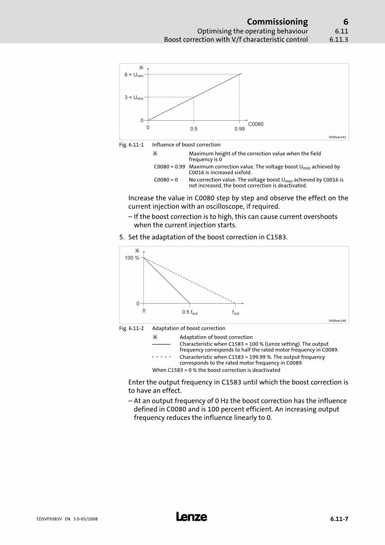
CommissioningOptimising the operating behaviour
Boost correction with V/f characteristic control
66.11
6.11.3
� 6.11−7EDSVF9383V EN 5.0−05/2008
6 × Umin
3 × Umin
0
0 0.5 0.99C0080
�
9300vec141
Fig. 6.11−1 Influence of boost correction
� Maximum height of the correction value when the fieldfrequency is 0
C0080 = 0.99 Maximum correction value. The voltage boost Umin achieved byC0016 is increased sixfold.
C0080 = 0 No correction value. The voltage boost Umin achieved by C0016 isnot increased, the boost correction is deactivated.
Increase the value in C0080 step by step and observe the effect on thecurrent injection with an oscilloscope, if required.
– If the boost correction is to high, this can cause current overshootswhen the current injection starts.
5. Set the adaptation of the boost correction in C1583.
100 %
0
0 0.5 fout fout
�
9300vec140
Fig. 6.11−2 Adaptation of boost correction
� Adaptation of boost correctionCharacteristic when C1583 = 100 % (Lenze setting). The outputfrequency corresponds to half the rated motor frequency in C0089.
Characteristic when C1583 = 199.99 %. The output frequencycorresponds to the rated motor frequency in C0089.
When C1583 = 0 % the boost correction is deactivated
Enter the output frequency in C1583 until which the boost correction isto have an effect.
– At an output frequency of 0 Hz the boost correction has the influencedefined in C0080 and is 100 percent efficient. An increasing outputfrequency reduces the influence linearly to 0.
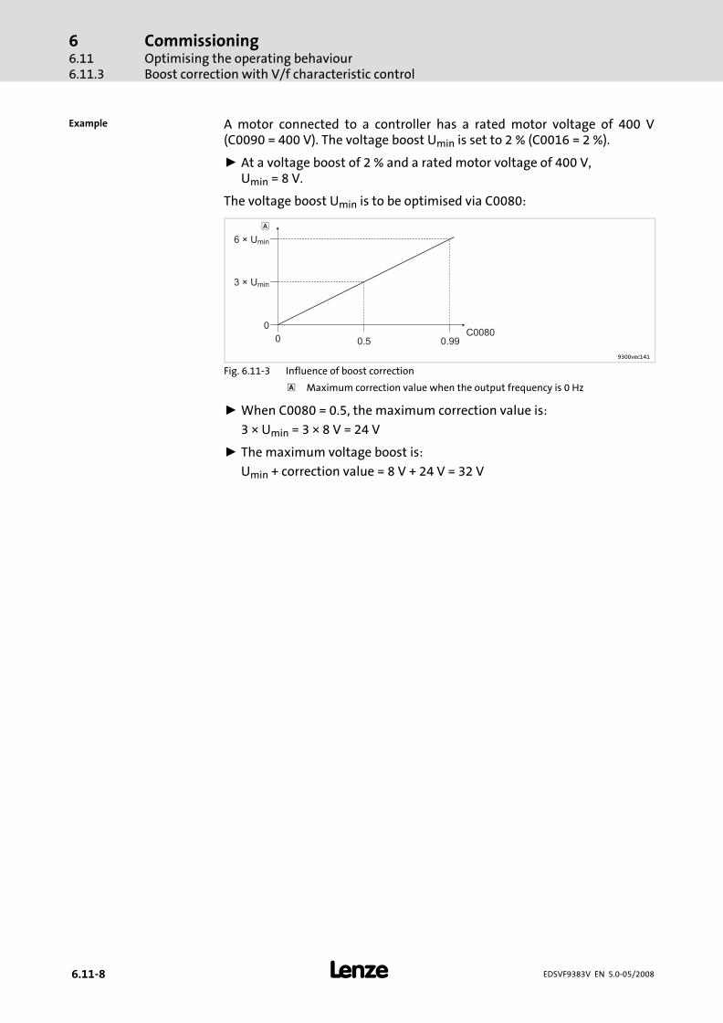
CommissioningOptimising the operating behaviourBoost correction with V/f characteristic control
66.116.11.3
� 6.11−8 EDSVF9383V EN 5.0−05/2008
A motor connected to a controller has a rated motor voltage of 400 V(C0090 = 400 V). The voltage boost Umin is set to 2 % (C0016 = 2 %).
ƒ At a voltage boost of 2 % and a rated motor voltage of 400 V,Umin = 8 V.
The voltage boost Umin is to be optimised via C0080:
6 × Umin
3 × Umin
0
0 0.5 0.99C0080
�
9300vec141
Fig. 6.11−3 Influence of boost correction
� Maximum correction value when the output frequency is 0 Hz
ƒ When C0080 = 0.5, the maximum correction value is:
3 × Umin = 3 × 8 V = 24 V
ƒ The maximum voltage boost is:
Umin + correction value = 8 V + 24 V = 32 V
Example

CommissioningOptimising the operating behaviour
Motor magnetising current with vector control
66.11
6.11.4
� 6.11−9EDSVF9383V EN 5.0−05/2008
6.11.4 Motor magnetising current with vector control
This chapter describes how to optimise the setpoint for the motormagnetising current (C0095) via the codes C0080 and C1583 in case ofvector control without feedback.
ƒ In case of vector control with feedback the setpoint for the motormagnetising current is only determined by C0095. An optimisation isnot required. The codes C0080 and C1583 have no effect.
The motor current consists of the exciting and active part. Themagnetisation of the motor is determined by the excitation current(magnetising current). To create a torque the motor needs active current.
In the vector control mode (C0006 = 1) a magnetising current is injected intothe motor after controller enable. The current level is detected by thecontroller from the motor data.
If a too low motor magnetising current is injected after controller enable, thefollowing drive behaviour occurs:
ƒ The required torque is not achieved at standstill.
ƒ When a high load is accelerated from standstill, the current overshoots.OC1 can be activated.
ƒ The machine runs irregularly as the motor is underexcited.
� Note!
If the motor magnetising current is too low, Lenze recommendsto operate the controller with sine−wave modulated switchingfrequency (C0018 = 0, 1, 4, 5 oder 6) only.

CommissioningOptimising the operating behaviourMotor magnetising current with vector control
66.116.11.4
� 6.11−10 EDSVF9383V EN 5.0−05/2008
Codes for parameter setting
Code Possible settings IMPORTANT
No. Name Lenze Selection
C0080 Vp field CTRL 0.50 0.00 {0.01 } 0.99 Influence on the motormagnetising current selectedunder C0095� Not effective with C0006 = 1
and C0025 > 1 at the sametime
� Influence is effective from 0 Hzto the frequency selectedunder C1583
6.6−1
C0095�
Mot Io � 0.0 {0.1 A} 1000.0 Motor magnetising current� dependent on C0086, C0088
and C0091� Change of C0086 sets C0095 to
the Lenze setting� Change of C0095 sets
C0086 = 0
6.6−1
C1583 fset high 100.00 0.00 {0.01 %} 199.99 Alterations by Lenze service only!Adaptation of the motormagnetising current set in C0095(with V/f characteristic control:influence limit of the boostcorrection; with vector control:influence limit of the fieldprecontrol)� The output frequency is set up
to which the motormagnetising current set inC0095 is to have an effect.
� C1583 = 100 % half therated motor frequency inC0089
6.11−5

CommissioningOptimising the operating behaviour
Motor magnetising current with vector control
66.11
6.11.4
� 6.11−11EDSVF9383V EN 5.0−05/2008
� Stop!
A longer operation of the motor in standstill may destroy themotor by overheating, especially in case of small motors.
ƒ Connect the thermal contact (NC contact), PTC, or KTY of themotor and activate the motor temperature monitoring of thecontroller.
ƒ Operate self−ventilated motors with a blower, if required.
Basic setting
1. Enter the motor data of the motor nameplate and execute the motoridentification. ( 6.6−16)
2. For magnetising the motor, consider enough time. The motor is beingmagnetised between controller enable and motor start.
A delayed start of the motor can be achieved using e.g. the quick stopfunction:
– Activate quick stop. Enable the controller and wait until the motor ismagnetised sufficiently. Deactivate quick stop for the motor to start.
The bigger the motor the longer the time for magnetisation. A motor withthe power of 90 kW requires up to 2 s.
If the desired continuous current does not flow, the magnetisation of themotor can be optimised using the codes C0080, C0095 and C1583.
Adjustment

CommissioningOptimising the operating behaviourMotor magnetising current with vector control
66.116.11.4
� 6.11−12 EDSVF9383V EN 5.0−05/2008
Optimisation
3. If required, select a setpoint for the motor magnetising current inC0095.
– The value in the Lenze setting has been evaluated by the controllerfrom the entered motor data of the motor nameplate.
4. The influence, the setpoint of the motor magnetising current is tohave, can be set in C0080.
– A P controller which increases or reduces the setpoint can beparameterised via C0080.
– Increase the value in C0080 step by step and observe the effect onthe current injection with an oscilloscope, if required.
– When C0080 = 0 the P controller is deactivated. No setpoint isselected for the motor magnetising current.
5. Set the adaptation of the setpoint for the motor magnetising current inC1583.
100 %
0
0 0.5 fout fout
�
9300vec140
Fig. 6.11−4 Adaptation of the setpoint for the motor magnetising current
� Adaptation of the setpointCharacteristic when C1583 = 100 % (Lenze setting). The outputfrequency corresponds to half the rated motor frequency in C0089.
Characteristic when C1583 = 199.99 %. The output frequencycorresponds to the rated motor frequency in C0089.
When C1583 = 0 % the adaptation is deactivated. No setpoint is selected for themotor magnetising current.
Select the output frequency in C1583, up to which the setpoint of themotor magnetising current is to have an effect.
– At an output frequency of 0 Hz the setpoint has the influence definedin C0080 and is 100 percent efficient. An increasing output frequencyreduces the influence linearly to 0.

Parameter settingContents
7
� 7−1EDSVF9383V EN 5.0−05/2008
7 Parameter setting
Contents
7.1 Important notes 7.1−1 . . . . . . . . . . . . . . . . . . . . . . . . . . . . . . . . . . . . . . . . . . . .
7.2 Parameter setting with the XT EMZ9371BC keypad 7.2−1 . . . . . . . . . . . . . . .
7.2.1 General data and operating conditions 7.2−1 . . . . . . . . . . . . . . . . .
7.2.2 Installation and commissioning 7.2−2 . . . . . . . . . . . . . . . . . . . . . . .
7.2.3 Display elements and function keys 7.2−2 . . . . . . . . . . . . . . . . . . . .
7.2.4 Changing and saving parameters 7.2−4 . . . . . . . . . . . . . . . . . . . . . .
7.2.5 Loading a parameter set 7.2−6 . . . . . . . . . . . . . . . . . . . . . . . . . . . . . .
7.2.6 Transferring parameters to other standard devices 7.2−7 . . . . . . .
7.2.7 Activating password protection 7.2−9 . . . . . . . . . . . . . . . . . . . . . . . .
7.2.8 Diagnostics 7.2−10 . . . . . . . . . . . . . . . . . . . . . . . . . . . . . . . . . . . . . . . . .
7.2.9 Menu structure 7.2−11 . . . . . . . . . . . . . . . . . . . . . . . . . . . . . . . . . . . . .


Parameter settingImportant notes
77.1
� 7.1−1EDSVF9383V EN 5.0−05/2008
7.1 Important notes
The controller functions can be adapted to your applications by means ofparameterisation. You can either parameterise via keypad, PC or via theparameter channel of a bus system.
The function library contains a detailed description of the functions, thesignal flow diagrams contain all configurable signals.
The parameters for the functions are stored in numbered codes:
ƒ Codes are marked in the text with a "C" (e.g. C0002).
ƒ The code table provides a quick overview of all codes. The codes aresorted according to their numbers and can be used as reference.( 8.5−1)
A quick parameter setting is provided by the keypad XT. Moreover, it servesas status display, error diagnosis and transfer of parameters to other drivecontrollers.
Keypad XTEMZ9371BC
Can be used with 8200 vector, 8200 motec, starttec, Drive PLC,9300 vector, 9300 servo
Operator buttons 8
Plain text display yes
Menu structure yes
Configurable menu (�user menu") yes
Predefined basic configurations yes
Non−volatile memory for parameter transfer yes
Password protection yes
Diagnosis terminal Keypad XT in handheld design, IP 20(E82ZBBXC)
Installation in control cabinet no
Type of protection IP 20
Detailed description 7.2−1
Adapting the controllerfunctions to the application
Parameters and codes
Parameter setting via keypad
Parameter settingImportant notes
77.1
� 7.1−2 EDSVF9383V EN 5.0−05/2008
You need the parameter setting / operating software »Global Drive Control«(GDC) or »Global Drive Control easy« (GDC easy) and an interface forcommunication:
ƒ Interface for system bus (CAN) (preset in GDC):
– PC system bus adapter
ƒ Serial interface for LECOM:
– Communication module LECOM−A/B (RS232/RS485)EMF2102IB−V001
The parameter setting /operating software of the Global Drive Controlfamily are easy−to−understand and tools for the operation, parametersetting and diagnostics or Lenze drive controllers.
GDC easyESP−GDC2−E
GDCESP−GDC2
Supply Free download from theinternet atwww.lenze.com
Program package must becharged for
Operation in interactive mode yes yes
Comprehensive help functions yes yes
Menu "Short setup" yes yes
Monitor windows for displayingoperating parameters and fordiagnostic purposes
yes yes
Saving and printing of parametersettings as code list
yes yes
Loading of parameter files from thecontroller to the PC
yes yes
Storing of parameter files from the PCin the controller
yes yes
Function block editor no yes
Technology functions for 9300 Servo no yes
Oscilloscope function for 9300 Servoand 9300 vector
no yes
Detailed description Online help of theprogram
Online help of theprogram
Detailed information can be found in the documentation of thecorresponding bus system.
Parameter setting via PC
Parameter setting via bussystem

Parameter settingParameter setting with the XT EMZ9371BC keypad
General data and operating conditions
77.2
7.2.1
� 7.2−1EDSVF9383V EN 5.0−05/2008
7.2 Parameter setting with the XT EMZ9371BC keypad
7.2.1 General data and operating conditions
� ��
� � �
� �
� ����SHPRG
Para
Code
Menu
0050 00
50.00_Hz
M C T R L - N O U T
0 b
ca
9371BC011
Feature Values
Dimensions
Width a 60 mm
Height b 73.5 mm
Depth c 15 mm
Environmental conditions
Climate
Storage IEC/EN 60721−3−1 1K3 (−25 ... +60 °C)
Transport IEC/EN 60721−3−2 2K3 (−25 ... +70 °C)
Operation IEC/EN 60721−3−3 3K3 (−10 ... +60 °C)
Enclosure IP 20

Parameter settingParameter setting with the XT EMZ9371BC keypadInstallation and commissioning
77.27.2.2
� 7.2−2 EDSVF9383V EN 5.0−05/2008
7.2.2 Installation and commissioning
�
��
�
�
�
�
�
�
�
�
���
SHPRG Pa
raCode
Menu 00
5000
50.00_Hz
M CT R
L -N O
U T
E82ZWLxxx
� ��
� � �
� �
� ����SHPRG
Para
Code
Menu
0050 00
50.00_Hz
M C T R L - N O U T
E82ZBBXC
EMZ9371BC
� ��
� � �
� �
� ����SHPRG
Para
Code
Menu
0050 00
G L O B A L D R I V E
I n i t
� ��
� � �
� �
�
0050 00
50.00 Hz
2 0 %
� ��
� � �
� �
�
0050 00
50.00 Hz
2 0 %
�
�
�� ��� �
�
� �
9371BC018
Fig. 7.2−1 Installation and commissioning of XT EMZ9371BC keypad or E82ZBBXC diagnosisterminal
� Connect keypad to the AIF interface on the front of the standard device.The keypad can be connected/disconnected during operation.
� As soon as the keypad is supplied with voltage, it carries out a short self−test.
� The operation level indicates when the keypad is ready for operation:
� Current state of the standard device
� Memory location 1 of the user menu (C0517):Code number, subcode number, and current value
Active fault message or additional status message
� Actual value in % of the status display defined in C0004
� � must be pressed to leave the operation level
7.2.3 Display elements and function keys
� ��
� � �
� �
� ����SHPRG
Para
Code
Menu
0050 00
50.00_Hz
M C T R L - N O U T
��
�
��
�
�
9371BC002
Fig. 7.2−2 Display elements and function keys of the XT EMZ9371BC keypad

Parameter settingParameter setting with the XT EMZ9371BC keypad
Display elements and function keys
77.2
7.2.3
� 7.2−3EDSVF9383V EN 5.0−05/2008
Display Meaning Explanation
� Status displays of standard device
! Ready for operation
� Pulse inhibit is active Power outputs are inhibited
" Set current limit is exceeded inmotor or generator mode
# Speed controller 1 in itslimitation
Drive is torque−controlled(Only active for operation withstandard devices of 9300 series)
$ Active fault
� Parameter acceptance
% Parameter is accepted�immediately �
Standard device operates immediatelywith the new parameter value
SHPRG % Parameter must be confirmedwith & �
Standard device operates with the newparameter value after being confirmed
SHPRG When the controller is inhibitedthe parameter must beconfirmed with & �
Standard device operates with the newparameter value after the controller isre−enabled
None Display parameter Change is not possible
Active level
Menu Menu level is active Select main menu and submenus
Code Code level is active Select codes and subcodes
Para Parameter level is active Change parameters in the codes orsubcodes
None Operating level is active Display operating parameters
� Short text
Alphanumeric Contents of the menus, meaningof the codes and parameters
In the operating level C0004 (in%) and the active fault aredisplayed
� Number
Menu level With active level:Menu number
Only active for operation with standarddevices of 8200 vector or 8200 motecseries
Code level With active level:Four−digit code number
� Number
Menu level With active level:Submenu number
Only active for operation with standarddevices of 8200 vector or 8200 motecseries
Code level With active level:Two−digit subcode number
� Parameter value
Parameter value with unit
� Cursor
In the parameter level, the figure abovethe cursor can be changed directly
� Function keys
For description see the following table
Displays

Parameter settingParameter setting with the XT EMZ9371BC keypadChanging and saving parameters
77.27.2.4
� 7.2−4 EDSVF9383V EN 5.0−05/2008
� Note!
Key combinations with &:
Press & and keep it pressed, then press the second key inaddition.
Key Function
Menu level Code level Parameter level Operating level
�Change to theparameter level
Change to theoperating level
Change to the codelevel
& �
Load predefinedconfigurations inthe menu"Short setup" 1)
Accept parameterswhen SHPRG % orSHPRG is displayed
�'
Change betweenmenu items
Change of codenumber
Change of figureabove cursor
& �& '
Quick changebetween the menuitems
Quick change ofcode number
Quick change offigure above cursor
� Change between main menu, submenusand code level
Cursor to the right
( Cursor to the left
� Cancel the function of ) key, the LED in the key is off
) Inhibit controller, the LED in the key is lit
Reset the fault(TRIP reset):
1. Remedy the cause of malfunction2. Press )3. Press �
1) Only active for operation with standard devices of 8200 vector or 8200 motec series
7.2.4 Changing and saving parameters
� Note!
Your settings have an effect on the current parameters in themain memory. You must save your settings in a parameter set sothat they are not lost when the mains are connected.
If you only need one parameter set, save your settings asparameter set 1, since parameter set 1 is loaded automaticallyafter mains connection.
Step Keysequence
Action
1. Select the menu � ' � ( Use the arrow keys to select the desiredmenu
2. Change to the code level � Display of the first code in the menu
3. Select code or subcode ' � Display of the current parameter value
4. Change to the parameter level �
5. When SHPRG is displayed,inhibit the controller
) 1) The drive coasts
6. Change parameter
A � ( Move cursor below the figure to bechanged
B ' � Change of figure
Function keys

Parameter settingParameter setting with the XT EMZ9371BC keypad
Changing and saving parameters
77.2
7.2.4
� 7.2−5EDSVF9383V EN 5.0−05/2008
ActionKeysequence
Step
& '& �
Quick change of figure
7. Accept the changed parameter
Display of SHPRG or SHPRG % & � Confirm change to accept the parameterDisplay "OK"
Display % − The parameter has been acceptedimmediately
8. Enable the controller, ifrequired
� 1) The drive runs again
9. Change to the code level
A � Display of the operating level
B � Display of the code with changedparameter
10. Change further parameters Restart the "loop" with step 1. or 3.
11. Save changed parameters
A � ' � ( Select the code C0003 "PAR SAVE" in themenu "Load/Store"
B � Change to the parameter levelDisplay "0" and "READY"
Select the parameter setin which the parametersare to be savedpermanently
C � Save as parameter set 1:� Set "1" "Save PS1"
Save as parameter set 2:� Set "2" "Save PS2"
Save as parameter set 3:� Set "3" "Save PS3"
Save as parameter set 4:� Set "4" "Save PS4"
D & � When "OK" is displayed, the settings arepermanently saved in the selectedparameter set.
12. Change to the code level
A � Display of the operating level
B � Display of C0003 "PAR SAVE"
13. Set parameters for anotherparameter set
Restart the "loop" with step 1. or 3.
1) The function of the ) key can be programmed:C0469 = 1: Controller inhibitC0469 = 2: Quick stop (Lenze setting)

Parameter settingParameter setting with the XT EMZ9371BC keypadLoading a parameter set
77.27.2.5
� 7.2−6 EDSVF9383V EN 5.0−05/2008
7.2.5 Loading a parameter set
The keypad serves to load a saved parameter set into the main memorywhen the controller is inhibited. After the controller is enabled, it operateswith the new parameters.
� Danger!
ƒ When a new parameter set is loaded, the controller isreinitialised and acts as if it had been connected to the mains:– ��System configurations and terminal assignments can be
changed. Make sure that your wiring and drive configurationcomply with the settings of the parameter set.
ƒ Only use terminal X5/28 as source for the controller inhibit!Otherwise the drive may start in an uncontrolled way whenswitching over to another parameter set.
� Note!
ƒ After switching on the supply voltage, the controller alwaysloads parameter set 1 into the main memory.
ƒ It is also possible to load other parameter sets into the mainmemory via the digital inputs or bus commands.
Step Keysequence
Action
1. Inhibit controller Terminal X5/28 = LOW
2. Load the saved parameter setinto the main memory
A � ' � ( Select the code C0002 "PAR LOAD" in themenu "Load/Store"
B � Change to the parameter levelThe active parameter set is displayed, e. g.display "0" and "Load Default"If you want to restore the delivery status,proceed with D
Select the parameter setto be loaded
C � Load parameter set 1:� Set "1" "Load PS1"
Load parameter set 2:� Set "2" "Load PS2"
Load parameter set 3:� Set "3" "Load PS3"
Load parameter set 4:� Set "4" "Load PS4"
D & � "RDY" goes off. The parameter set is loadedcompletely into the main memory if "RDY"is displayed again.
3. Change to the code level
A � Display of the operating level
B � Display of C0002 "PAR LOAD"
4. Enable controller Terminal X5/28 = HIGHThe drive is running with the settings ofthe loaded parameter set

Parameter settingParameter setting with the XT EMZ9371BC keypadTransferring parameters to other standard devices
77.2
7.2.6
� 7.2−7EDSVF9383V EN 5.0−05/2008
7.2.6 Transferring parameters to other standard devices
The keypad enables you to copy parameter settings from one standarddevice to another.
For this purpose use the "Load/Store" menu:
� Danger!
During the transfer of the parameters from the keypad to thecontroller, the control terminals may adopt undefined states!
Therefore be absolutely sure to disconnect the connectors X5and X6 from the controller prior to the transfer. Like this you willensure that the drive controller is inhibited and all controlterminals are in the defined "LOW" state.
� Note!
After the parameter sets are copied to the keypad XT(C0003 = 11), the parameter set last loaded using C0002 isalways activated.
So the actual parameters remain active also after copying:
ƒ Prior to copying, save the actual parameters in the parameterset and load this parameter set into the drive controller usingC0002.
Step Keysequence
Action
1. Connect keypad to controller 1
2. Inhibit controller Terminal X5/28 = LOWThe drive coasts.
3. On the "Load/Store" menuselect C0003
� ' � ( On the "Load/Store" menu select codeC0003 "PAR SAVE" using the arrow keys.
4. Change to the parameter level � Display "0" and "READY"
5. Copy all parameter sets to thekeypad
The settings stored in the keypad areoverwritten.
� Set "11" "Save extern"
6. Start copying & � The "RDY" status display goes off. "BUSY"is indicated as parameter value.When "BUSY" goes off after approx. oneminute, all parameter sets have beencopied to the keypad. The "RDY" statusdisplay illuminates.
7. Change to the code level
A � Display of the operating level
B � Display of C0003 and "PAR SAVE"
8. Enable controller Terminal X5/28 = HIGH
9. Remove keypad fromcontroller 1
Copying parameter sets fromthe standard device to thekeypad
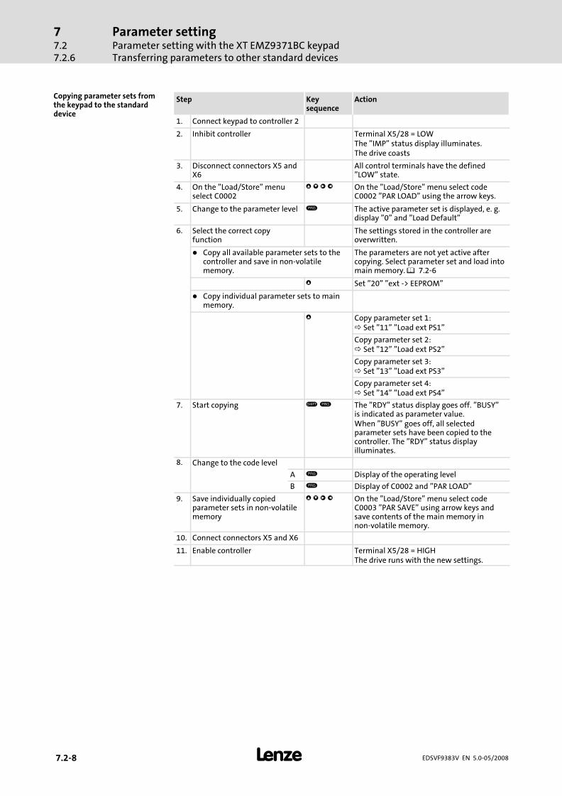
Parameter settingParameter setting with the XT EMZ9371BC keypadTransferring parameters to other standard devices
77.27.2.6
� 7.2−8 EDSVF9383V EN 5.0−05/2008
Step Keysequence
Action
1. Connect keypad to controller 2
2. Inhibit controller Terminal X5/28 = LOWThe "IMP" status display illuminates.The drive coasts
3. Disconnect connectors X5 andX6
All control terminals have the defined"LOW" state.
4. On the "Load/Store" menuselect C0002
� ' � ( On the "Load/Store" menu select codeC0002 "PAR LOAD" using the arrow keys.
5. Change to the parameter level � The active parameter set is displayed, e. g.display "0" and "Load Default"
6. Select the correct copyfunction
The settings stored in the controller areoverwritten.
� Copy all available parameter sets to thecontroller and save in non−volatilememory.
The parameters are not yet active aftercopying. Select parameter set and load intomain memory. 7.2−6
� Set "20" "ext −> EEPROM"
� Copy individual parameter sets to mainmemory.
� Copy parameter set 1:� Set "11" "Load ext PS1"
Copy parameter set 2:� Set "12" "Load ext PS2"
Copy parameter set 3:� Set "13" "Load ext PS3"
Copy parameter set 4:� Set "14" "Load ext PS4"
7. Start copying & � The "RDY" status display goes off. "BUSY"is indicated as parameter value.When "BUSY" goes off, all selectedparameter sets have been copied to thecontroller. The "RDY" status displayilluminates.
8. Change to the code level
A � Display of the operating level
B � Display of C0002 and "PAR LOAD"
9. Save individually copiedparameter sets in non−volatilememory
� ' � ( On the "Load/Store" menu select codeC0003 "PAR SAVE" using arrow keys andsave contents of the main memory innon−volatile memory.
10. Connect connectors X5 and X6
11. Enable controller Terminal X5/28 = HIGHThe drive runs with the new settings.
Copying parameter sets fromthe keypad to the standarddevice

Parameter settingParameter setting with the XT EMZ9371BC keypad
Activating password protection
77.2
7.2.7
� 7.2−9EDSVF9383V EN 5.0−05/2008
7.2.7 Activating password protection
� Note!
ƒ If the password protection is activated (C0094 = 1 ... 9999), youonly have free access to the user menu.
ƒ To access the other menus, you must enter the password. Bythis, the password protection is annulled until you enter a newpassword.
ƒ Please observe that the password−protected parameters canbe overwritten as well when transferring the parameter setsto other standard devices. The password is not transferred.
ƒ Do not forget your password! If you have forgotten yourpassword, it can only be reset via a PC or a bus system!
Step Keysequence
Action
1. Select the "USER menu" � ' � ( Change to the user menu using the arrowkeys
2. Change to the code level � Display of code C0051 "MCTRL−NACT"
3. Select C0094 � Display of code C0094 "Password"
4. Change to the parameter level � Display "0" = no password protection
5. Set password
A � Select password (1 ... 9999)
B & � Confirm password
6. Change to the code level
A � Display of the operating level
B � Display of C0094 and "Password"
7. Change to the "USER menu" ( ( '
The password protection is active now.You can only quit the user menu if you re−enter the password and confirm it with &��.
Step Keysequence
Action
1. Change to the code level in theuser menu
�
2. Select C0094 � Display of code C0094 "Password"
3. Change to the parameter level � Display "9999" = password protection isactive
4. Enter password
A ' Set valid password
B & � ConfirmThe password protection is deactivated byentering the password once again.
5. Change to the code level
A � Display of the operating level
B � Display of C0094 and "Password"
The password protection is deactivated now. All menus can be freely accessed again.
Activate password protection
Remove password protection

Parameter settingParameter setting with the XT EMZ9371BC keypadDiagnostics
77.27.2.8
� 7.2−10 EDSVF9383V EN 5.0−05/2008
7.2.8 Diagnostics
In the "Diagnostic" menu the two submenus "Actual info" and "History"contain all codes for
ƒ monitoring the drive
ƒ fault/error diagnosis
In the operating level, more status messages are displayed. If several statusmessages are active, the message with the highest priority is displayed.
Priority Display Meaning
1 GLOBAL DRIVE INIT Initialisation or communication error betweenkeypad and controller
2 XXX − TRIP Active TRIP (contents of C0168/1)
3 XXX − MESSAGE Active message (contents of C0168/1)
4 Special device states:
Switch−on inhibit
5 Source for controller inhibit (the value of C0004 is displayed simultaneously):
STP1 9300 servo: Terminal X5/28
ECSxS/P/M/A: Terminal X6/SI1
STP3 Operating module or LECOM A/B/LI
STP4 INTERBUS or PROFIBUS−DP
STP5 9300 servo,ECSxA/E:
System bus (CAN)
ECSxS/P/M: MotionBus (CAN)
STP6 C0040
6 Source for quick stop (QSP):
QSP−term−Ext The MCTRL−QSP input of the MCTRL function block is onHIGH signal.
QSP−C0135 Operating module or LECOM A/B/LI
QSP−AIF INTERBUS or PROFIBUS−DP
QSP−CAN 9300 servo,ECSxA:
System bus (CAN)
ECSxS/P/M: MotionBus (CAN)
7 XXX − WARNING Active warning (contents of C0168/1)
8 xxxx Value below C0004

Parameter settingParameter setting with the XT EMZ9371BC keypad
Menu structure
77.2
7.2.9
� 7.2−11EDSVF9383V EN 5.0−05/2008
7.2.9 Menu structure
For simple, user−friendly operation, the codes are clearly arranged infunction−related menus:
Main menu Submenus Description
Display Display
User−Menu Codes defined in C0517
Code list All available codes
ALL All available codes listed in ascending order (C0001 ... C7999)
PS 1 Codes in parameter set 1 (C0001 ... C1999)
PS 2 Codes in parameter set 2 (C2001 ... C3999)
PS 3 Codes in parameter set 3 (C4001 ... C5999)
PS 4 Codes in parameter set 4 (C6001 ... C7999)
Load/Store Parameter set managementParameter set transfer, restore delivery status
Diagnostic Diagnostic
Actual info Display codes to monitor the drive
History Fault analysis with history buffer
Short setup Quick configuration of predefined applicationsConfiguration of the user menuThe predefined applications depend on the type of the standarddevice (frequency inverter, servo inverter, position controller, ...)
Main FB Configuration of the main function blocks
NSET Setpoint processing
NSET−JOG Fixed setpoints
NSET−RAMP1 Ramp function generator
MCTRL Motor control
DFSET Digital frequency processing
DCTRL Internal control
Terminal I/O Connection of inputs and outputs with internal signals
AIN1 X6.1/2 Analog input 1
AIN2 X6.3/4 Analog input 2
AOUT1 X6.62 Analog output 1
AOUT2 X6.63 Analog output 2
DIGIN Digital inputs
DIGOUT Digital outputs
DFIN Digital frequency input
DFOUT Digital frequency output
State bus State bus (not with 9300 frequency inverter)
Controller Configuration of internal control parameters
Speed Speed controller
Current Current controller or torque controller
Phase Phase controller (not with 9300 frequency inverter)
Motor/Feedb. Input of motor data, configuration of speed feedback
Motor adj Motor data
Feedback Configuration of feedback systems
Monitoring Configuration of monitoring functions

Parameter settingParameter setting with the XT EMZ9371BC keypadMenu structure
77.27.2.9
� 7.2−12 EDSVF9383V EN 5.0−05/2008
DescriptionSubmenusMain menu Description
DisplayDisplay
LECOM/AIF Configuration of operation with communication modules
LECOM A/B Serial interface
AIF interface Process data
Status word Display of status words
System bus Configuration of system bus (CAN)
Management CAN communication parameters
CAN−IN1CAN object 1
CAN−OUT1
CAN−IN2CAN object 2
CAN−OUT2
CAN−IN3CAN object 3
CAN−OUT3
Status word Display of status words
FDO Free digital outputs
Diagnostic CAN diagnostic
FB config Configuration of function blocks
Func blocks Parameterisation of function blocksThe submenus contain all available function blocks
FCODE Configuration of free codes
Identify Identification
Drive Software version of standard device
Op Keypad Software version of keypad

ConfigurationContents
8
� 8−1EDSVF9383V EN 5.0−05/2008
8 Configuration
Contents
8.1 Important notes 8.1−1 . . . . . . . . . . . . . . . . . . . . . . . . . . . . . . . . . . . . . . . . . . . .
8.2 Function blocks 8.2−1 . . . . . . . . . . . . . . . . . . . . . . . . . . . . . . . . . . . . . . . . . . . . .
8.2.1 Diameter calculator (DCALC) 8.2−1 . . . . . . . . . . . . . . . . . . . . . . . . . .
8.2.2 Master frequency input (DFIN) 8.2−5 . . . . . . . . . . . . . . . . . . . . . . . .
8.2.3 Master frequency output (DFOUT) 8.2−8 . . . . . . . . . . . . . . . . . . . . .
8.2.4 Master frequency ramp−function generator (DFRFG) 8.2−13 . . . . . .
8.2.5 Master frequency processing (DFSET) 8.2−18 . . . . . . . . . . . . . . . . . . .
8.2.6 Internal motor control with V/f characteristic control (MCTRL1) 8.2−25 . . . . . . . . . . . . . . . . . . . . . . . . . . . . . . . . . . . . . . . . . .
8.2.7 Internal motor control with vector control (MCTRL2) 8.2−40 . . . . . .
8.3 Monitoring 8.3−1 . . . . . . . . . . . . . . . . . . . . . . . . . . . . . . . . . . . . . . . . . . . . . . . . .
8.3.1 Responses 8.3−1 . . . . . . . . . . . . . . . . . . . . . . . . . . . . . . . . . . . . . . . . . .
8.3.2 Monitoring times for process data input objects 8.3−2 . . . . . . . . . .
8.3.3 Maximum speed 8.3−3 . . . . . . . . . . . . . . . . . . . . . . . . . . . . . . . . . . . .
8.3.4 Motor 8.3−3 . . . . . . . . . . . . . . . . . . . . . . . . . . . . . . . . . . . . . . . . . . . . .
8.3.5 Controller current load (I x t monitoring) 8.3−4 . . . . . . . . . . . . . . . .
8.3.6 Motor temperature 8.3−5 . . . . . . . . . . . . . . . . . . . . . . . . . . . . . . . . . .
8.3.7 Heatsink temperature 8.3−5 . . . . . . . . . . . . . . . . . . . . . . . . . . . . . . . .
8.3.8 DC−bus voltage 8.3−6 . . . . . . . . . . . . . . . . . . . . . . . . . . . . . . . . . . . . . .
8.3.9 External error (EEr) 8.3−6 . . . . . . . . . . . . . . . . . . . . . . . . . . . . . . . . . .
8.4 Overview of monitoring functions 8.4−1 . . . . . . . . . . . . . . . . . . . . . . . . . . . . .
8.5 Code table 8.5−1 . . . . . . . . . . . . . . . . . . . . . . . . . . . . . . . . . . . . . . . . . . . . . . . . .
8.6 Selection lists 8.6−1 . . . . . . . . . . . . . . . . . . . . . . . . . . . . . . . . . . . . . . . . . . . . . . .
8.6.1 Selection list 1: Analog output signals 8.6−1 . . . . . . . . . . . . . . . . . .
8.6.2 Selection list 2: Digital output signals 8.6−3 . . . . . . . . . . . . . . . . . . .
8.6.3 Selection list 3: Angle signals 8.6−6 . . . . . . . . . . . . . . . . . . . . . . . . . .
8.6.4 Selection list 4: Speed signals 8.6−6 . . . . . . . . . . . . . . . . . . . . . . . . .
8.6.5 Selection list 5: Function blocks 8.6−7 . . . . . . . . . . . . . . . . . . . . . . . .
8.7 Table of attributes 8.7−1 . . . . . . . . . . . . . . . . . . . . . . . . . . . . . . . . . . . . . . . . . .


ConfigurationImportant notes
88.1
� 8.1−1EDSVF9383V EN 5.0−05/2008
8.1 Important notes
The "Configuration" chapter consists of two parts.
The "Configuration" chapter in the System Manual contains the following:
ƒ Monitoring
ƒ Monitoring functions
ƒ Description of the following function blocks:
– Diameter calculator (DCALC)
– Digital frequency input (DFIN)
– Digital frequency output (DFOUT)
– Digital frequency ramp function generator (DFRFG)
– Digital frequency processing (DFSET)
– Internal motor control with V/f characteristic control (MCTRL1)
– Internal motor control with vector control (MCTRL2)
ƒ Code table
ƒ Selection lists
ƒ Table of attributes
The "Configuration" chapter in the System Manual (extension) contains thefollowing:
ƒ Notes on the configuration with Global Drive Control
ƒ Description of the basic configuration
ƒ Use of function blocks
ƒ Description of the other function blocks for the 9300 vector frequencyinverter
System Manual
System Manual (extension)


ConfigurationFunction blocks
Diameter calculator (DCALC)
88.2
8.2.1
� 8.2−1EDSVF9383V EN 5.0−05/2008
8.2 Function blocks
8.2.1 Diameter calculator (DCALC)
The function block calculates the current reel diameter in winding drives.
DCALC1-N-LINEC1327/1
DCALC1
C1321/1DCALC1-LOAD
C1326/1
C1320DCALC1-SET
C1325
C1322/1
C1321/2DCALC1-HOLD
C1326/2
C1311
DCALC1-I=0
DCALC1-OVFL
*a
b
b
a
C1301
C1300
DCALC1-N-WINDC1327/2
C1322/2
CTRLDCALC1-OUT
C1328
C1307
C1310C1305C1306
DCALC1-DMIN
DCALC1-DMAX
ARIT
C1309C1308
DCALC1-D-OUT
C1302C1303C1304
fb_dcalc1
Fig. 8.2−1 Diameter calculator (DCALC1)
Codes for parameter setting
Code Possible settings IMPORTANT
No. Name Lenze Selection
C1300�
N−motor/Dmax
300 −32767 {1 rpm} 32767 Motor speed at Dmax, functionblock DCALC1� Nominal speed of the winding
drive
8.2−1
C1301�
N−line max 3000 1 {1 rpm} 32767 Maximum line speed, functionblock DCALC1� Nominal speed of the line drive
C1302 calc cycle 0.1 0.1 {0.1 rev} 100.0 Calculation cycle, function blockDCALC1
8.2−1
C1303 time const 0.10 0.01 {0.01 s} 50.00 Filter time constant, functionblock DCALC1
C1304�
Dmax 500 1 {1 mm} 10000 Maximum diameter, functionblock DCALC1� Nominal winding diameter
8.2−1
C1305 lower D−limit 50 1 {1 mm} 10000 Lower diameter limit, functionblock DCALC1� Minimum winding diameter
C1306 upper D−limit 500 1 {1 mm} 10000 Upper diameter limit, functionblock DCALC1� Maximum winding diameter
C1307 hyst D−limit 1.00 0.00 {0.01 %} 100.0 Hysteresis − diameter limitation,function block DCALC1� Hysteresis for Dmin /Dmax
output
C1308�
arit function 1 0 DCALC1−OUT=D DCALC1−OUT =diameter
Selection of the arithmeticfunction, function block DCALC1
8.2−1
1 DCALC1−OUT=1/D DCALC1−OUT =1/diameter
Description
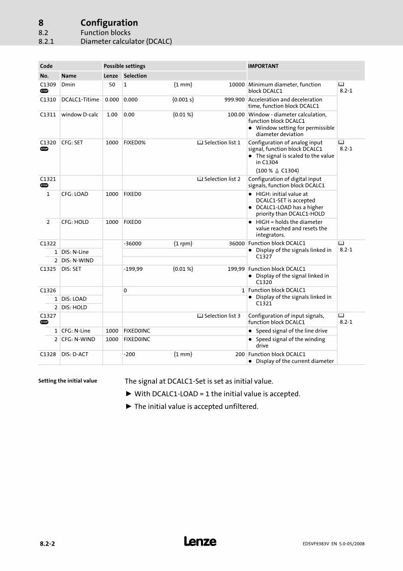
ConfigurationFunction blocksDiameter calculator (DCALC)
88.28.2.1
� 8.2−2 EDSVF9383V EN 5.0−05/2008
IMPORTANTPossible settingsCode
SelectionLenzeNameNo.
C1309�
Dmin 50 1 {1 mm} 10000 Minimum diameter, functionblock DCALC1
8.2−1
C1310 DCALC1−Titime 0.000 0.000 {0.001 s} 999.900 Acceleration and decelerationtime, function block DCALC1
C1311 window D−calc 1.00 0.00 {0.01 %} 100.00 Window − diameter calculation,function block DCALC1� Window setting for permissible
diameter deviation
C1320�
CFG: SET 1000 FIXED0% Selection list 1 Configuration of analog inputsignal, function block DCALC1� The signal is scaled to the value
in C1304
(100 % C1304)
8.2−1
C1321�
Selection list 2 Configuration of digital inputsignals, function block DCALC1
1 CFG: LOAD 1000 FIXED0 � HIGH: initial value atDCALC1−SET is accepted
� DCALC1−LOAD has a higherpriority than DCALC1−HOLD
2 CFG: HOLD 1000 FIXED0 � HIGH = holds the diametervalue reached and resets theintegrators.
C1322 −36000 {1 rpm} 36000 Function block DCALC1� Display of the signals linked in
C1327
8.2−11 DIS: N−Line
2 DIS: N−WIND
C1325 DIS: SET −199,99 {0.01 %} 199,99 Function block DCALC1� Display of the signal linked in
C1320
C1326 0 1 Function block DCALC1� Display of the signals linked in
C13211 DIS: LOAD
2 DIS: HOLD
C1327�
Selection list 3 Configuration of input signals,function block DCALC1
8.2−1
1 CFG: N−Line 1000 FIXED0INC � Speed signal of the line drive
2 CFG: N−WIND 1000 FIXED0INC � Speed signal of the windingdrive
C1328 DIS: D−ACT −200 {1 mm} 200 Function block DCALC1� Display of the current diameter
The signal at DCALC1−Set is set as initial value.
ƒ With DCALC1−LOAD = 1 the initial value is accepted.
ƒ The initial value is accepted unfiltered.
Setting the initial value

ConfigurationFunction blocks
Diameter calculator (DCALC)
88.2
8.2.1
� 8.2−3EDSVF9383V EN 5.0−05/2008
By division of the speed signals at DCALC1−N−LINE and DCALC1−N−WIND, thecurrent diameter is calculated.
ƒ The signal at DCALC1−N−LINE has to correspond to the circumferentialspeed of the reel.
ƒ The signal at DCALC1−N−WIND has to be proportional to the reel speed.
ƒ You have to adapt the signal at DCALC1−N−LINE in C1300 and C1301, sothat the value calculated corresponds to the actual diameter. Thenominal reel diameter dmax is entered in C1304.
– For operation with the nominal reel diameter dmax you have to enterthe value at input DCALC1−N−WIND in C1300 and the value at inputDCALC1−N−LINE in C1301.
ƒ The input signals are integrated cyclically. In C1302 you alter theintegration interval (calculation cycle):
Great value in C1302 �high resolution
Low value in C1302 �low resolution
ƒ If the integrator overflows, DCALC1−OVFL is set to HIGH. The integratoris reset internally and starts again with the calculation of the lastcorrect value.
ƒ A first−order low pass filters the values calculated. The filter timeconstant is set via C1303.
In C1328 the current diameter is displayed.
ƒ For the conversion of the scaled calculated value to the absolute value[mm], the reference diameter dmax has to be entered via C1304.
ƒ At DCALC1−D−OUT the current diameter is output. The signal is scaledto the value in C1304.
With DCALC1−HOLD = HIGH the last diameter value calculated ismaintained and the integrators are reset.
ƒ When the controller is switched off, the current diameter value issaved. When it is switched on, the last value saved is loaded.
In C1305 the minimum diameter (dmin) in [mm] is entered. dmin is reachedwhen DCALC1−DMIN switches to HIGH.
In C1306 the maximum diameter (dmax) in [mm] is entered. dmax is reachedwhen DCALC1−DMAX switches to HIGH.
In C1307 a hysteresis for resetting the display signal is set. The entry in [%]relates to the absolute values in C1305 and C1306.
Calculating the diameter
Displaying the diameter
Maintaining/saving thecurrent value
Setting/displaying thediameter

ConfigurationFunction blocksDiameter calculator (DCALC)
88.28.2.1
� 8.2−4 EDSVF9383V EN 5.0−05/2008
In configurations with a speed forward control it is common to multiply theprecontrol signal with the reciprocal value of the diameter (d). This value isoutput at DCALC1−OUT.
ƒ C1308 = 0: DCALC1−OUT = d
ƒ C1308 = 1: DCALC1−OUT = 1/d
For the conversion to 1/d the reference value for the diameter has to bedefined in C1309, for which the signal at DCALC1−OUT is to be 100 %.
ƒ Normally C1309 corresponds to the minimum diameter in C1305(dmin).
In order to ensure a continuous transition when setting new diametervalues, a ramp function generator is activated if C1310 > 0 s.
A window comparator compares the corresponding newly calculated valueto the value last filtered.
ƒ In C1311 the maximum difference in [%] between the two values isdefined.
ƒ DCALC1−I=0 is set to LOW if the maximum difference is exceeded.
Current diameter (C1328)
C1328 [mm]� ��DCALC1−N−LINE [inc]
DCALC1−N−WIND [inc]� ��
C1300 [rpm]
C1301 [rpm]� �� C1304 [mm]
Output signal at DCALC1−OUT
For C1308 = 0 (DCALC1−OUT = d):
DCALC1−OUT [%]� ��C1328 [mm]
C1304 [mm]� �� 100 %
For C1308 = 1 (DCALC1−OUT = 1/d):
DCALC1−OUT [%]� ��C1304 [mm]
C1328 [mm]� ��
C1309 [mm]
C1304 [mm]� �� 100 %
� Note!
The value at DCALC1−OUT is limited by the maximum reeldiameter (C1306) and the minimum reel diameter (C1305).
Converting the diameter (d)to 1/d
Web break monitoring
Formulas for calculation

ConfigurationFunction blocks
Master frequency input (DFIN)
88.2
8.2.2
� 8.2−5EDSVF9383V EN 5.0−05/2008
8.2.2 Master frequency input (DFIN)
The function block calculates a speed signal from the rectangular signals atX9. TTL signals and HTL signals can be connected. The zero track can beselected as an option.
The edge changes are detected every 1 ms and result directly in the outputvalue.
C0425
C0427 DFIN
DFIN-OUT
C0426
X9
fb_dfin
Fig. 8.2−2 Digital frequency input (DFIN)
Codes for parameter setting
Code Possible settings IMPORTANT
No. Name Lenze Selection
C0425 DFIN const 3 0 256 inc/rev Constant of the master frequencyinput, function block DFIN� Output signal at the connected
encoder or at the upstreamcontroller in the event of amaster frequencycascade/master frequency bus
8.2−51 512 inc/rev
2 1024 inc/rev
3 2048 inc/rev
4 4096 inc/rev
5 8192 inc/rev
6 16384 inc/rev
C0426 DIS: OUT −36000 {1 rpm} 36000 Output signal of the masterfrequency input, function blockDFIN� Display only
C0427 DFIN function 0 Function of the master frequencyinput, function block DFIN
0 2−phase � Phase−displaced signalsequence
1 A pulse/B dir � Control of direction of rotationvia track B
2 Pulse A or B � Control of speed and directionof rotation via track A or trackB
Description

ConfigurationFunction blocksMaster frequency input (DFIN)
88.28.2.2
� 8.2−6 EDSVF9383V EN 5.0−05/2008
In C0427 the different modes for the evaluation of the input signals can beselected.
C0427 = 0 (phase−displaced signal sequence)
OO
BB
ZZ
Fig. 8.2−3 Phase−displaced signal sequence (CW rotation)
Clockwiserotation
Track A leads track B by 90 ° (positive value at DFIN−OUT)
Counter−clockwise rotation
Track A lags track B by 90 ° (negative value at DFIN−OUT)
C0427 = 1 (control of the direction of rotation via track B)
OO
BB
ZZ
Fig. 8.2−4 Control of direction of rotation via track B
Clockwiserotation
Track A transmits the speedTrack B = LOW (positive value at DFIN−OUT)
Counter−clockwise rotation
Track A transmits the speedTrack B = HIGH (negative value at DFIN−OUT)
C0427 = 2 (control of speed and direction of rotation via track A or track B)
OO
BB
ZZ
Fig. 8.2−5 Control of speed and direction of rotation via track A or track B
Clockwiserotation
Track A transmits the speed and direction of rotation (positivevalue at DFIN−OUT)Track B = LOW
Counter−clockwise rotation
Track B transmits the speed and direction of rotation (negativevalue at DFIN−OUT)Track A = LOW
Evaluating input signals

ConfigurationFunction blocks
Master frequency input (DFIN)
88.2
8.2.2
� 8.2−7EDSVF9383V EN 5.0−05/2008
In C0425 the output signal can be adapted:
ƒ To the encoder at X9 or
ƒ To the upstream controller with master frequency cascade/masterfrequency bus.
Transfer function
Calculating the output signal:
DFIN−OUT�[rpm] � f�[Hz] � 60C0425
Example:
The input frequency amounts to 200 kHz, the number of incrementscorresponds to 2048 inc/rev. (C0425 = 3).
DFIN−OUT�[rpm] � 200000�Hz � 602048
� 5859�rpm
Signal adaptation
Signal adaptations other than by squaring in C0425 can be achieved byconnecting a function block.
Example:
The function block CONV3 shall convert the speed signal into a quasi analogsignal.
Calculating the output signal at CONV3:
CONV3−OUT�[%] � f�[Hz] � 0.4C0425
� C0950C0951
Interconnecting function blocks:
CONV3
CONV3-OUTCONV3-IN
C0953
C0952C0950
C0951
C0425
C0427 DFIN
DFIN-OUT
C0426
X9
fb_dfin_01
Fig. 8.2−6 Digital frequency input (DFIN) with connected converter
� Note!
If a master frequency is output to DFOUT−AN−IN or DFOUT−DF(C0540 = 0 or C0540 = 1) and an incremental encoder isevaluated via X8, the function block DFIN cannot be usedanymore.
If the input signals at X8 or X9 are output to X10, (C0540 = 4 orC0540 = 5), this restriction does not exist.
Adjusting the output signal

ConfigurationFunction blocksMaster frequency output (DFOUT)
88.28.2.3
� 8.2−8 EDSVF9383V EN 5.0−05/2008
8.2.3 Master frequency output (DFOUT)
The function block creates rectangular signals from an analog signal orspeed signal, which are output via X10. Alternatively, you can set the masterfrequency output to a signal output at X8 or X9.
C0030C0540
CTRL
DFOUT-AN-IN
C0547
C0541
DFOUT-DF-IN
C0549
C0542
C0548
C0544DFOUT-SYN-RDY
DFOUT-OUT
DFOUT
C0545
1
0
2
3
4
5
X8
X9
X10
C0540
E5X5
fb_dfout
Fig. 8.2−7 Digital frequency output (DFOUT)
Codes for parameter setting
Code Possible settings IMPORTANT
No. Name Lenze Selection
C0030 DFOUT const 3 0 256 inc/rev Function block DFOUT� Setting of the constant
(increments per revolution) forthe master frequency outputX10
8.2−81 512 inc/rev
2 1024 inc/rev
3 2048 inc/rev
4 4096 inc/rev
5 8192 inc/rev
6 16384 inc/rev
Description

ConfigurationFunction blocks
Master frequency output (DFOUT)
88.2
8.2.3
� 8.2−9EDSVF9383V EN 5.0−05/2008
IMPORTANTPossible settingsCode
SelectionLenzeNameNo.
C0540�
Function 0 Function selection, function blockDFOUT� Output signal at X10
8.2−8
0 Analog input Analog input Signal at DFOUT−AN−IN is output.Zero track can be input externally.
1 PH diff input Phase differenceinput
Signal at DFOUT−DF−IN is output.Zero track can be input externally.
2 Not assigned
3 Not assigned
4 X10 = X9 X9 is output onX10
The input signals are bufferedC0030 is without function
5 X10 = X8 X8 is output onX10
C0541�
CFG: AN−IN 5001 MCTRL−NACT Selection list 1 Configuration of analog inputsignal, function block DFOUT� Signal in [%] of C0011
C0542�
CFG: DF−IN 1000 FIXEDPHI−0 Selection list 4 Configuration of input signal,function block DFOUT� Speed signal
C0544�
CFG: SYN−RDY 1000 FIXED0 Selection list 2 Configuration of digital inputsignal, function block DFOUT� DFOUT−SYN−RDY = HIGH:
Generating a zero pulse
C0545 PH offset 0 0 {1 inc.} 65535 Phase offset, function blockDFOUT� Displacing the zero pulse
generated via DFOUT−SYN−RDYby up to 360 °
� 1 rev. = 65535 inc (360 °)

ConfigurationFunction blocksMaster frequency output (DFOUT)
88.28.2.3
� 8.2−10 EDSVF9383V EN 5.0−05/2008
A
A
B
Z
B
Z
fb_dfout_01
Fig. 8.2−8 Signal sequence for CW rotation (definition)
ƒ The output signals correspond to the simulation of an incrementalencoder:
– Track A and track B and, if required, the zero track and thecorresponding inverted tracks are output. The levels areTTL−compatible.
– Positive input values (CW rotation) result in the represented signalsequence.
ƒ With negative input values (CCW rotation) track B leads track A by 90 °.
ƒ The encoder constant of the encoder simulation is set in C0030.
C0540 serves to define which input signal or signal source shall be active.The zero track is output according to the selected setting.
C0540 Signal at X10
0 DFOUT−AN−IN is output to X10. Zero track can be selected externally.
1 DFOUT−DF−IN is output to X10. Zero track can be selected externally.
2 No function
3 No function
4 The signal at input X9 is electrically amplified and directly output (C0030 is withoutfunction)
5 The signal at input X8 is electrically amplified and directly output (C0030 is withoutfunction)
� Note!
The settings C0540 = 0 and C0540 = 1 are not possible when aconnection to the master frequency input X9 (DFIN) wasestablished and an incremental encoder was connected via X8(C0025 = 100, 110 ... 113).
Output signals at X10

ConfigurationFunction blocks
Master frequency output (DFOUT)
88.2
8.2.3
� 8.2−11EDSVF9383V EN 5.0−05/2008
Setting: C0540 = 0
ƒ The analog signal at the input DFOUT−AN−IN is converted into afrequency and output to X10.
ƒ Frequency calculation:
f�[Hz] � DFOUT−AN−IN�[%] � C0030100
� C001160
Example:
The input signal at DFOUT−AN−IN amounts to 50 %, the number ofincrements corresponds to 2048 inc/rev. (C0030 = 3) and the maximumspeed (C0011) is set to 3000 rpm.
f�[Hz] � 50�% � 2048100
� 300060
� �� 51200�Hz
Generating an index pulse
An artificial index signal can be generated for the output frequency.
1. Set the input DFOUT−SYN−RDY = HIGH.
– 360° later, a LOW−HIGH edge generates the index pulse.
– Then a zero pulse is generated every 360 ° according to C0030.
2. If necessary, shift the zero pulse by up to 360 ° (65536 inc = 360 °) viaC0545.
Setting: C0540 = 1
ƒ The speed signal at the input DFOUT−DF−IN is converted into afrequency and output to X10.
ƒ Frequency calculation:
f�[Hz] � DFOUT−DF−IN�[rpm] � C003060
Example:
The input signal at DFOUT−DF−IN amounts to 3000 rpm, the number ofincrements corresponds to 2048 inc/revolution (C0030 = 3).
f�[Hz] � 3000�rpm � 204860
�� 102400�Hz
Generating a zero pulse
An artificial zero pulse can be generated for the output frequency.
1. Set the input DFOUT−SYN−RDY = HIGH.
– 360° later, a LOW−HIGH edge generates the zero pulse.
– Then a zero pulse is generated every 360 ° according to C0030.
2. If necessary, shift the zero pulse by up to 360 ° (65536 inc = 360 °) viaC0545.
Output of analog signal asfrequency
Output of the speed signal asfrequency

ConfigurationFunction blocksMaster frequency output (DFOUT)
88.28.2.3
� 8.2−12 EDSVF9383V EN 5.0−05/2008
ƒ The input signals at X8 are amplified electrically and output directly.
ƒ The signals depend on the assignment of the input X8.
ƒ The codes C0030, C0545 and the output DFOUT−OUT have no function.
ƒ The zero track is only output if it is connected to X8.
ƒ The input signals at X9 are amplified electrically and output directly.
ƒ The signals depend on the assignment of the input X9.
ƒ The codes C0030, C0545 and the output DFOUT−OUT have no function.
ƒ The zero track is output if it is connected to X9.
Signal at X8 is directly outputat X10
Signal at X9 is directly outputat X10
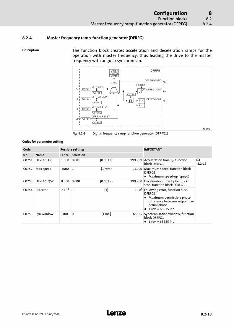
ConfigurationFunction blocks
Master frequency ramp−function generator (DFRFG)
88.2
8.2.4
� 8.2−13EDSVF9383V EN 5.0−05/2008
8.2.4 Master frequency ramp−function generator (DFRFG)
The function block creates acceleration and deceleration ramps for theoperation with master frequency, thus leading the drive to the masterfrequency with angular synchronism.
DFRFG1-OUT
C0764/3
DFRFG1-RESET
DFRFG1
C0764/2
C0764/1
C0760
C0759DFRFG1-QSP
DFRFG1-STOP
C0761
C0765
C0758DFRFG1-IN
C0752
C0754
S
R
QDFRFG1-FAIL
DFRFG1-SYNCCTRL
C0753C0751
C0755
fb_dfrfg
Fig. 8.2−9 Digital frequency ramp function generator (DFRFG1)
Codes for parameter setting
Code Possible settings IMPORTANT
No. Name Lenze Selection
C0751 DFRFG1 Tir 1.000 0.001 {0.001 s} 999.999 Acceleration time Tir, functionblock DFRFG1
8.2−13
C0752 Max speed 3000 1 {1 rpm} 16000 Maximum speed, function blockDFRFG1� Maximum speed−up (speed)
C0753 DFRFG1 QSP 0.000 0.000 {0.001 s} 999.900 Deceleration time Tif for quickstop, function block DFRFG1
C0754 PH error 2.109 10 {1} 2.109 Following error, function blockDFRFG1� Maximum permissible phase
difference between setpoint anactual phase
� 1 rev. = 65535 inc
C0755 Syn window 100 0 {1 inc.} 65535 Synchronisation window, functionblock DFRFG1� 1 rev. = 65535 inc
Description
ConfigurationFunction blocksMaster frequency ramp−function generator (DFRFG)
88.28.2.4
� 8.2−14 EDSVF9383V EN 5.0−05/2008
IMPORTANTPossible settingsCode
SelectionLenzeNameNo.
C0758�
CFG: IN 1000 FIXEDPHI−0 Selection list 4 Configuration of input signal,function block DFRFG1� Speed/phase setpoint signal
8.2−13
C0759�
CFG: QSP 1000 FIXED0 Selection list 2 Configuration of digital inputsignal, function block DFRFG1� HIGH = quick stop active
C0760�
CFG: STOP 1000 FIXED0 Selection list 2 Configuration of input signal,function block DFRFG1� HIGH = Status of the profile
generator is maintained,setpoint is saved
C0761�
CFG: RESET 1000 FIXED0 Selection list 2 Configuration of input signal,function block DFRFG1� HIGH = resetting the
integrators
C0764 0 1 Function block DFRFG1� Display of the signals linked in
C0759, C0760 and C07611 DIS: QSP
2 DIS: STOP
3 DIS: RESET
C0765 DIS: IN −32767 {1 rpm} 32767 Function block DFRFG1� Display of the signal linked in
C0758

ConfigurationFunction blocks
Master frequency ramp−function generator (DFRFG)
88.2
8.2.4
� 8.2−15EDSVF9383V EN 5.0−05/2008
� Stop!
Do not operate the drive with this function at the torquelimitation Mmax, Imax.
The profile generator creates ramps which automatically compensate theresulting phase displacement. If you do not need this compensation, setDFRFG−RESET = HIGH.
�
������� �� �
�� � �� �
��
��������
�
���������
Fig. 8.2−10 Synchronisation on DFRFG
C0751 Setting the deceleration and acceleration timeC0752 Setting the maximum speedC0755 Setting the switching point
When the actual angle has reached its setpoint and the output signalcorresponds to the input signal, the drive runs in synchronism and theoutput DFRFG1−SYNC is set to HIGH. At the same time the profile generatoris switched to the inactive state.
Fig. 8.2−11 Speed−time diagram DFRFG
The number of increments at DFRFG1−IN (master drive) defines the setphase. The set phase can be displayed as a path. The speed−time diagramshows the distance covered (angle) as the area below the speed profile.When synchronisation is reached, master and slave have covered the samedistance (phase).
Profile generator
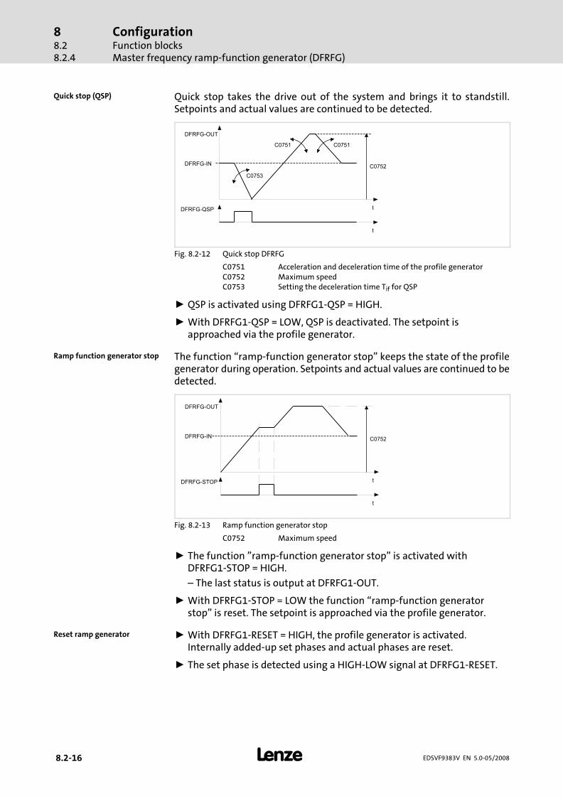
ConfigurationFunction blocksMaster frequency ramp−function generator (DFRFG)
88.28.2.4
� 8.2−16 EDSVF9383V EN 5.0−05/2008
Quick stop takes the drive out of the system and brings it to standstill.Setpoints and actual values are continued to be detected.
�
������� �� �
�� � �� �
���������
�
���������
�� �
Fig. 8.2−12 Quick stop DFRFG
C0751 Acceleration and deceleration time of the profile generatorC0752 Maximum speedC0753 Setting the deceleration time Tif for QSP
ƒ QSP is activated using DFRFG1−QSP = HIGH.
ƒ With DFRFG1−QSP = LOW, QSP is deactivated. The setpoint isapproached via the profile generator.
The function �ramp−function generator stop" keeps the state of the profilegenerator during operation. Setpoints and actual values are continued to bedetected.
�
������� �� �
����������
�
���������
Fig. 8.2−13 Ramp function generator stop
C0752 Maximum speed
ƒ The function "ramp−function generator stop" is activated withDFRFG1−STOP = HIGH.
– The last status is output at DFRFG1−OUT.
ƒ With DFRFG1−STOP = LOW the function �ramp−function generatorstop" is reset. The setpoint is approached via the profile generator.
ƒ With DFRFG1−RESET = HIGH, the profile generator is activated.Internally added−up set phases and actual phases are reset.
ƒ The set phase is detected using a HIGH−LOW signal at DFRFG1−RESET.
Quick stop (QSP)
Ramp function generator stop
Reset ramp generator

ConfigurationFunction blocks
Master frequency ramp−function generator (DFRFG)
88.2
8.2.4
� 8.2−17EDSVF9383V EN 5.0−05/2008
The profile generator can accept a phase difference between the set phaseand the actual phase of up to ±2140000000 inc (= 32000 revolutions).
ƒ A limit value can be set for the permissible phase difference via C0754.
ƒ If the limit value is reached, DFRFG1−FAIL is set to HIGH and the value issaved.
ƒ DFRFG1−FAIL is only set to LOW with DFRFG1−RESET = HIGH.
Monitoring the phasedifference

ConfigurationFunction blocksMaster frequency processing (DFSET)
88.28.2.5
� 8.2−18 EDSVF9383V EN 5.0−05/2008
8.2.5 Master frequency processing (DFSET)
The function block prepares the master frequency for the controller. You canselect values for the stretching and gearbox factor and carry out a speed orphase trimming.
*a
b
b
a
*a
b
b
a
+
+
1
0
+
+
C0537
C0536/2
C0536/1
C0033C0533
C0530
C0252
C0536/3
C0538/2
C0539
DFSET
DFSET-NOUT
+
-
DFSET-A-TRIM
DFSET-N-TRIM
DFSET-RAT-DIV
DFSET-RESET
DFSET-IN
DFSET-PSET
DFSET-VP-DIV DFSET-POUT
DFSET-SET
C0538/3
+
+
C0253
C0531
C0535C0532
2
1
2
1E4
E5
X5
X5
X9/6,7
MCTRL-PHI-ACT
C0538/1
DFSET-0-PULSE
DFSET-ACK
C0525
C0522
C0524
C0521
C0520
C0527
C0526
C0523
C0546C0534C0429
* C0529
C0528/1
C0528/2
CTRL
MCTRL-PHI-ACT
fb_dfset
Fig. 8.2−14 Digital frequency processing (DFSET)
Codes for parameter setting
Code Possible settings IMPORTANT
No. Name Lenze Selection
C0033 Gearboxdenom
1 1 {1} 32767 Gearbox factor − denominator ofthe function block DFSET
8.2−18
C0252 Angle offset 0 −245760000 {1 inc.} 245760000 Phase offset for master frequencyprocessing, function block DFSET� Fixed phase offset for digital
frequency configuration� 1 rev. = 65536 inc
8.2−18
C0253 Angle n−trim � −32767 {1 inc.} 32767 Speed−dependent phase trimmingfor the master frequencyprocessing, function block DFSET� depending on C0005, C0025,
C0490� Change of C0005, C0025 or
C0490 resets C0253 to thecorresponding Lenze setting
� 1 rev. = 65536 inc� Value in C0253 is reached at
15000 rpm
Description
ConfigurationFunction blocks
Master frequency processing (DFSET)
88.2
8.2.5
� 8.2−19EDSVF9383V EN 5.0−05/2008
IMPORTANTPossible settingsCode
SelectionLenzeNameNo.
C0520�
CFG: IN 1000 FIXEDPHI−0 Selection list 4 Configuration of input signal,function block DFSET� Input of speed / phase setpoint
signal
8.2−18
C0521�
CFG: VP−DIV 1000 FIXED0% Selection list 1 Configuration of analog inputsignal, function block DFSET� Signal for numerator of
stretching factor� 100 % = 16384 inc
C0522�
CFG: RAT−DIV 1000 FIXED0% Selection list 1 Configuration of analog inputsignal, function block DFSET� Signal for numerator of
gearbox factor� 100 % = 16384 inc
C0523�
CFG: A−TRIM 1000 FIXED0% Selection list 1 Configuration of analog inputsignal, function block DFSET� Signal for phase trimming via
offset multiplier (C0529)� 100 % = 16384 inc
C0524�
CFG: N−TRIM 1000 FIXED0% Selection list 1 Configuration of analog inputsignal, function block DFSET� Signal for speed trimming� Signal in [%] of C0011
C0525�
CFG: 0−PULSE 1000 FIXED0 Selection list 2 Configuration of digital inputsignal, function block DFSET� Signal for one−time zero pulse
activation� HIGH = release for zero pulse
synchronisation
C0526�
CFG: RESET 1000 FIXED0 Selection list 2 Configuration of digital inputsignal, function block DFSET� Signal for reset of integrators� HIGH sets
– Position difference = 0– DFSET−PSET = 0– DFSET−PSET2 = 0
C0527�
CFG: SET 1000 FIXED0 Selection list 2 Configuration of digital inputsignal, function block DFSET� HIGH = Set phase integrators
to equal values� LOW−HIGH edge sets
DFSET−PSET = 0� HIGH−LOW edge sets
DFSET−PSET to the currentvalue of MCTRL−PHI−SET
� DFSET−SET has a higher prioritythan DFSET−RESET
C0528 −2.109 {1} 2.109 Function block DFSET� Display only
8.2−18
1 DIS: 0−pulse A Phase difference between twozero pulses
2 DIS: Offset Offset = C0523 × C0529 + C0252

ConfigurationFunction blocksMaster frequency processing (DFSET)
88.28.2.5
� 8.2−20 EDSVF9383V EN 5.0−05/2008
IMPORTANTPossible settingsCode
SelectionLenzeNameNo.
C0529 Multip offset 1 −20000 {1} 20000 Offset multiplier, function blockDFSET� Multiplier for the phase offset
(C0252)
8.2−18
C0530 DF evaluation 0 0 with factor With gearboxfactor
Master frequency evaluation,function block DFSET� Evaluation of the setpoint
integrator1 no factor Without gearbox
factor
C0531 Act 0 div 1 1 {1} 16384 Actual zero pulse divisor, functionblock DFSET
C0532 0−pulse/TP 1 1 0−pulse Index pulse Zero pulse / touch probe, functionblock DFSET� Zero pulse of the feedback
system or touch probe2 Touch probe Touch probe
C0533 Vp denom 1 1 {1} 32767 Gain factor of denominator Vp,function block DFSET
C0534 0 pulse fct 0 Zero pulse function, functionblock DFSET� Synchronising the drive
8.2−18
0 inactive Inactive
1 Continuous Continuoussynchronisation,correction in theshortest possibleway
2 Cont. switch Continuoussynchronisation,correction in theshortest possibleway
After a LOW−HIGH signal toDFSET−0−pulse, the zero track issynchronised once
10 Once, fast way One−timesynchronisation,correction in theshortest possibleway
11 Once, CW One−timesynchronisation,correction indirection ofrotation to theright
12 Once, CCW One−timesynchronisation,correction indirection ofrotation to the left
13 Once, 2*0−pulse One−timesynchronisation,correction isdetected fromsetpoint pulse andactual pulse andcorrected to thecorrespondingdirection
C0535 Set 0 div 1 1 {1} 16384 Desired zero pulse divisor,function block DFSET
8.2−18

ConfigurationFunction blocks
Master frequency processing (DFSET)
88.2
8.2.5
� 8.2−21EDSVF9383V EN 5.0−05/2008
IMPORTANTPossible settingsCode
SelectionLenzeNameNo.
C0536 −32767 {1} 32767 Function block DFSET� Display of the signals linked in
C0521, C0522 and C0523
8.2−181 DIS: VP−DIV
2 DIS: RAT−DIV
3 DIS: A−TRIM
C0537 DIS: N−TRIM −199.99 {0.01 %} 199.99 Function block DFSET� Display of the signal linked in
C0524
C0538 0 1 Function block DFSET� Display of the signals linked in
C0525, C0526 and C05271 DIS: 0−pulse
2 DIS: RESET
3 DIS: SET
C0539 DIS: IN −6000 {1 rpm} 6000 Function block DFSET� Display of the signal linked in
C0520
C0546 Min inc/rev 1000 1 {1 inc.} 2147483647 Masking of the touch probe signal,function block DFSET� Suppressing interference
pulses at X5/E4 (actual pulse oftouch probe signal)
� The size of the maskingwindow between two actualpulses is set
8.2−18

ConfigurationFunction blocksMaster frequency processing (DFSET)
88.28.2.5
� 8.2−22 EDSVF9383V EN 5.0−05/2008
Stretching factor
The stretching factor defines the ratio with which the drive is to run fasteror slower than the setpoint.
The setpoint at DFSET−IN is evaluated. The result is output to DFSET−POUT.
DFSET−POUT � DFSET−IN � DFSET−VP−DIVC0533
The stretching factor results from numerator and denominator.
ƒ The numerator (DFSET−VP−DIV) can be defined as a variable from theanalog signal source or as a fixed value from a code.
ƒ Enter the denominator under C0533.
� Note!
When calculating the stretching factor, the input signal atDFSET−VP−DIV is not processed in a scaled mode. A signal of100 % corresponds to a count value of 16384.
Gearbox factor
The gearbox factor defines the ratio by means of which the drive speed canbe changed additionally.
The setpoint at DFSET−IN, multiplied by the stretching factor, is evaluated.The result is output at DFSET−NOUT [in % of nmax (C0011)].
DFSET−NOUT � DFSET−IN � DFSET−VP−DIVC0533
� DFSET−RAT−DIVC0033
The gearbox factor results from numerator and denominator.
ƒ The numerator (DFSET−RAT−DIV) can be defined as a variable from theanalog signal source or as a fixed value from a code.
ƒ Enter the denominator under C0033.
� Note!
When calculating the gearbox factor, the input signal atDFSET−RAT−DIV is not processed in a scaled mode. A signal of100 % corresponds to a count value of 16384.
Setpoint conditioning withstretching and gearbox factor

ConfigurationFunction blocks
Master frequency processing (DFSET)
88.2
8.2.5
� 8.2−23EDSVF9383V EN 5.0−05/2008
Speed trimming
The speed trimming serves to add correction values, e. g. by a superimposedcontrol loop. This enables the drive to accelerate or decelerate.
ƒ At the speed trimming, an analog value at DFSET−N−TRIM is added tothe speed setpoint.
Phase trimming
The phase trimming adds a setpoint at DFSET−A−TRIM to the phase setpointand changes the rotor position to the setpoint with the number ofincrements provided in either direction (drive is leading or lagging). Thephase is trimmed within a range of ±32767 increments (corresponds to±½ revolution). Every analog signal can be used as a source.
ƒ The input is done is increments (1 revolution 65536 increments).
ƒ An analog input signal at DFSET−A−TRIM of
100� % 1/4 revolution 16384 increments.
ƒ You can extend the setting range with a multiplier (C0529).
Phase offset
The phase offset (C0252) adds a fixed phase offset to the setpoint of thedrive.
Phase adjustment proportional to speed
With a phase adjustment proportional to speed, the phase leads or lags withincreasing speed.
ƒ Enter the offset in increments under C0253.
ƒ The set phase offset is reached at 15000 rpm of the drive (linearrelationship).
� Note!
Phase corrections are only reasonable if the controller isoperated with incremental encoder feedback and the calculatedfollowing error is used for correcting the speed setpoint. Thefollowing error is output to DFSET−PSET.
Processing of correctionvalues

ConfigurationFunction blocksMaster frequency processing (DFSET)
88.28.2.5
� 8.2−24 EDSVF9383V EN 5.0−05/2008
� Stop!
When the synchronisation via the terminals X5/E4 and X5/E5(C0532 = 2) is activated, these terminals must not contain anyother signal connections.
When selecting a basic configuration via C0005, the terminalscontain a basic setting.
Selection of synchronisation
C0532 = 1 (zero pulse) The synchronisation is performed on the zero track of thedigital frequency input X9 and the zero track of the feedbacksystem set under C0490.
C0532 = 2 (touch probe) The synchronisation is performed using the terminals X5/E4(actual pulse) and X5/E5 (setpoint pulse).
Touch probe initiators can have delay times which cause a speed−dependentphase offset.
Set the correction for the phase offset under C0429.
C0429� �� 16384� �� Correction�value
The correction value for the phase offset can be obtained from the datasheet of the initiator, or contact the manufacturer.
Synchronisation modes
C0534 Synchronisation mode Note
0 Inactive Function inactive
1 Continuous synchronisation withcorrection in the shortest possible way
2 Continuous synchronisation withcorrection in the shortest possible way
After a LOW−HIGH signal toDFSET−0−pulse, the zero track issynchronised once10 One synchronisation. A phase deviation is
corrected in the shortest possible way.
11 One synchronisation. A phase deviation iscorrected in CW direction.
12 One synchronisation. A phase deviation iscorrected in CCW direction.
13 Single synchronisation. A phase differenceis determined between setpoint pulse andactual pulse and is corrected to thecorresponding direction of rotationaccording to the sign.
ƒ During synchronisation, DFSET−ACK is set to HIGH.
� Note!
Drive synchronisation is only reasonable if the controller isoperated with incremental encoder feedback and the calculatedfollowing error is used for correcting the speed setpoint. Thefollowing error is output to DFSET−PSET.
Synchronising to zero track ortouch probe

ConfigurationFunction blocks
Internal motor control with V/f characteristic control (MCTRL1)
88.2
8.2.6
� 8.2−25EDSVF9383V EN 5.0−05/2008
8.2.6 Internal motor control with V/f characteristic control (MCTRL1)
The function block MCTRL1 controls the motor. It is always carried out so thatit does not need to be entered into the processing table.
In the Lenze setting, the controller is set to V/f characteristic control(C0006 = 5). Without other settings and with analog setpoint selection viaX6/1, X6/2 and connected asynchronous standard motor (50 Hz/400 V)commissioning can be executed immediately.
The V/f characteristic control is suitable for single drives, multi−motor drives,synchronous motors, reluctance motors and asynchronous motors.
1
0
C0022C0015C0036
PWM
MCTRL-N-SETImax
MCTRL1
C0906/1
C0050
C0056
±100%
C0890
C0075C0076
C0023
1
C0090C0912
C0014
C0025
C0234
C0089
C0905
MCTRL-M-ADD
C0906/2
C0891
C0021
V/f
C0074
-
C0018C0142
C0148C0143
QSP
slip compensation
activecurrent
C0105
MCTRL-N/M-SWT
MCTRL-HI-M-LIM
MCTRL-LO-M-LIM
MCTRL-I-SET
C0906/5
MCTRL-I-LOAD
C0907/4
C0907/2
C0906/3
C0906/4
C0893
C0892
C0899
C0902
C0901
n.c.
n.c.
n.c.
n.c.
n.c.
MCTRL-BOOST
C0906/6
C0903
n.c.
MCTRL-NSET2
MCTRL-MSET2
MCTRL-MMAX
MCTRL-IMAX
MCTRL-DCVOLT
MCTRL-IACT
MCTRL-VACT
MCTRL-FACT
MCTRL-IXT
MCTRL-MACT
C0054
C0053
C0052
C0064
C0058
n.c.
C0089C0087
C0086C0909
MCTRL-NACT
MCTRL-PHI-ACT
MCTRL-PHI-ANACONST
MCTRL-PHI-ANG
C0051
C0011Encoder
1
C0025
MCTRL-QSP
C0907/3
C0900
MCTRL-QSP-OUTDCTRL-QSP
C0042
MCTRL-GSBC0904
C0107C0019
MCTRL-GSB-OUT
Auto-GSB
KTYMCTRL-M-TEMP
C0063
C0078
speed control
activecurrent
C0235
oscillation damping
C0236
C0086
MCTRL-VP-N-ADAPT
C0911
C0910
X8
C0420
X9
C0421
C0071C0070
1>–
1>–
fb_mctrl1_01
Fig. 8.2−15 Internal motor control with V/f characteristic control (MCTRL1)
Description

ConfigurationFunction blocksInternal motor control with V/f characteristic control (MCTRL1)
88.28.2.6
� 8.2−26 EDSVF9383V EN 5.0−05/2008
Codes for parameter setting
Code Possible settings IMPORTANT
No. Name Lenze Selection
C0006�
Op mode 5 Selection of the operating modefor the motor control
1 vector ctrl Vector controlwithout or withspeed feedback
In case of the first selection enterthe motor data and identify themwith C0148.
6.8−8
5 V / f V/f characteristiccontrol
Commissioning withoutidentification of the motor data ispossible� Advantage of identification
with C0148: Improved smoothrunning at low speeds
6.8−4
C0010 Nmin 0 0 {1 rpm} 36000 � Reference valuefor the absoluteand relativesetpoint selectionfor theacceleration anddecelerationtimes
� C0059 must beset correctly
� Set C0010 <C0011
� C0010 is onlyeffective in caseof analog setpointselection via AIN1
Important: Forparameter settingvia interface, majorchanges in one stepshould only be madewhen the controlleris inhibited.
Minimumspeed
6.10−1
C0011 Nmax 3000 0 {1 rpm} 36000 Maximumspeed
C0014 V/f charact. 0 Characteristic in the V/fcharacteristic control mode
8.2−25
0 Linear Linear V/f characteristic
1 square Square V/f characteristic
C0015 Rated freq 50 10 {1 Hz} 5000 V/f−rated frequencyIn C0015 you can set a basefrequency which differs from therated motor frequency (C0089)� Lenze setting: C0015 = C0089� Changing C0086 or C0089
overwrites the value in C0015
8.2−25
C0016 Umin boost 0.00 0.00 {0.01 %} 100.00 Umin boost (FCODE)� C0016 = 1 % corresponds to a
boost of 1 % of the rated motorvoltage (C0090)
� Code is freely configurable
6.8−4

ConfigurationFunction blocks
Internal motor control with V/f characteristic control (MCTRL1)
88.2
8.2.6
� 8.2−27EDSVF9383V EN 5.0−05/2008
IMPORTANTPossible settingsCode
SelectionLenzeNameNo.
C0018 fchop 6 Switching frequency of theinverter� General rule: The lower the
switching frequency the– lower the power loss– higher the noise generation– better the concentricity
factor� Observe derating indications
for high switching frequencies� The max. output frequency
(fmax) is:– fchop = 4 kHz �
fmax = 300 Hz– fchop = 2 kHz �
fmax = 150 Hz– fchop = 1 kHz �
fmax = 150 Hz
6.9−1
1 1 kHz sin loss−optimised
2 2 kHz sin concentricity−optimised
3 4 kHz f_top power−optimised
4 4 kHz sin noise−optimised
6 4/2 kHz sin noise/concentricity−optimised withautomaticchange−over tolow switchingfrequency
C0021 slipcomp � −20.00 {0.01 %} 20.00 Slip compensation� Change of C0086, C0087 or
C0089 sets C0021 to thecalculated rated slip of themotor
� When changing over to thevector control mode, C0021 isset to 0
6.11−1 8.2−25 8.2−40
C0022 Imax current � 0 {0.1 A} − Imax limit in motor mode� depending on C0086
6.6−15
C0023 Imax gen. � 0 {0.1 A} − Imax limit in generator mode� depending on C0086
6.6−15
C0036 DC brk value 0.0 0.0 {0.1 A} − Set DC braking current� depends on the controller
8.2−25 8.2−40
C0042 DIS: QSP Quick stop� Display only
8.2−25 8.2−40
0 QSP inactive Quick stop is not active
1 QSP active Quick stop is active
C0050 MCTRL−NSET2 −100.00 {0.01 %} 100.00 Speed setpoint, function blockMCTRL� Display of the speed in [%] of
C0011
8.2−25 8.2−40
C0051 MCTRL−NACT −36000 {1 rpm} 36000 Actual speed value, function blockMCTRL� Read only
8.2−25 8.2−40
C0052 MCTRL−Umot 0 {1 V} 800 Motor voltage, function blockMCTRL� Read only� MCTRL−VACT = 100 % = C0090
8.2−25 8.2−40
C0053 UG−VOLTAGE 0 {1 V} 900 DC−bus voltage, function blockMCTRL� Read only� MCTRL−DCVOLT = 100 % =
1000 V
8.2−25 8.2−40
C0054 Imot 0.0 {0.1 A} 5000.0 Actual motor current, functionblock MCTRL� Read only� MCTRL−IACT = 100 % = C0022
8.2−25 8.2−40

ConfigurationFunction blocksInternal motor control with V/f characteristic control (MCTRL1)
88.28.2.6
� 8.2−28 EDSVF9383V EN 5.0−05/2008
IMPORTANTPossible settingsCode
SelectionLenzeNameNo.
C0056 MCTRL−MSET2 −100.00 {0.01 %} 100.00 Read only. The output signaldepends on the operating mode:� Current motor current in case
of V/f characteristic control,function block MCTRL1
� Torque setpoint in case ofvector control, function blockMCTRL2
8.2−25 8.2−40
C0058 MCTRL−FACT −600.0 {0.1 Hz} 600.0 Output frequency� Display only� MCTRL−FACT = 100.0 % =
1000.0 Hz
8.2−25 8.2−40
C0063 Mot temp 0 {1 °C} 200 Motor temperature� Read only� Monitoring of the motor
temperature must beactivated.
� KTY at X8/5, X8/8:– At 150 °C, TRIP OH3 is set– Early warning is possible viaOH7, temperature is set inC0121
� PTC, thermal contact at T1, T2:– Release sets TRIP or
warning OH8
8.2−25 8.2−40
C0064 Utilization 0 {1 %} 150 Device utilisation I×t� Read only� Device utilisation of the last
180 s operating time� C0064 > 100 % triggers
warning OC5� C0064 > 110 % limits the ouput
current of the controller to67 % of the maximum currentin C0022
8.2−25 8.2−40
C0070 Vp speed CTRL 10.0 0.0 {0.1 } 255.9 Gain of speed controller 8.2−25 8.2−40
C0071 Tn speed CTRL 50 1 {1 ms} 6000 Integral−action time of speedcontrollerC0071 = 6000 ms: Nointegral−action time
C0074 limit N 10.00 0.00 {0.01 %} 100.00 Limitation of the speed controller� Influence of the speed
controller for V/f characteristiccontrol with feedback
� max. setpoint difference inpercent
8.2−25 8.2−40
C0075 Vp curr CTRL 0.04 0.00 {0.01 } 0.99 Gain of current controller� Vector control: Gain of current
controller� V/f characteristic control:
Maximum current controller
8.2−25 8.2−40
C0076 Tn curr CTRL 10.0 0.1 {0.1 ms} 2000.0 Integral−action time of currentcontroller� Vector control: integral−action
time of current controller� V/f characteristic control:
maximum current controller� C0076 = 2000 ms: current
controller is switched off
8.2−25 8.2−40

ConfigurationFunction blocks
Internal motor control with V/f characteristic control (MCTRL1)
88.2
8.2.6
� 8.2−29EDSVF9383V EN 5.0−05/2008
IMPORTANTPossible settingsCode
SelectionLenzeNameNo.
C0078 Tn slip CTRL 100 1 {1 ms} 6000 Integral−action time of slipcontroller� Filter time for slip
compensation (C0021)� Only active with V/f
characteristic control
8.2−25
C0086�
Mot type � Motor selection list Motor type selection� depending on the controller
used� Motor selection in C0086 sets
the corresponding parametersin C0021, C0022, C0081,C0087, C0088, C0089, C0090,C0091
6.6−1
C0087�
Mot speed � 50 {1 rpm} 36000 Rated motor speed� depending on C0086� Motor selection in C0086 set
the corresponding rated motorspeed in C0087
� Change of C0087 setsC0086 = 0
6.6−1
C0089�
Mot frequency � 10 {1 Hz} 5000 Rated motor frequency� depending on C0086� Motor selection in C0086 sets
the corresponding rated motorfrequency in C0089
� Change of C0089 setsC0086 = 0
6.6−1
C0090�
Mot voltage � 0 {1 V} 1000 Rated motor voltage� depending on C0086� Motor selection in C0086 sets
the corresponding rated motorvoltage in C0090
� Change of C0090 sets C0086 =0
6.6−1
C0095�
Mot Io � 0.0 {0.1 A} 1000.0 Motor magnetising current� dependent on C0086, C0088
and C0091� Change of C0086 sets C0095 to
the Lenze setting� Change of C0095 sets
C0086 = 0
6.6−1
C0105 QSP Tif 5.00 0.00 {0.01 s} 999.90 Quick stop deceleration time� The deceleration time refers to
a speed variation of C0011 ... 0
8.2−25 8.2−40
C0107 holding time 0.00 0.00 {0.01 s} 9999.90 Hold time for automatic DCinjection braking (Auto−GSB)
8.2−25 8.2−40
C0143 limit 2 kHz 0.0 0.0 {0.1 Hz} 20.0 Speed−dependent switchingthreshold� Threshold for automatic
switching frequency reduction� The controller changes
automatically to 2 kHz whenthis value falls below thethreshold
8.2−25 8.2−40

ConfigurationFunction blocksInternal motor control with V/f characteristic control (MCTRL1)
88.28.2.6
� 8.2−30 EDSVF9383V EN 5.0−05/2008
IMPORTANTPossible settingsCode
SelectionLenzeNameNo.
C0234 damp value 20 −100 {1 %} 100 Influence of the oscillationdamping, function block MCTRL� Minimising a tendency to
oscillation of the drive� Influences the tendency to
oscillation of the drive� When C0025 >1 and C0006 = 1,
C0234 is set to 0
8.2−25 8.2−40
C0235 damping 2 1 {1 ms} 600 Filter time of the oscillationdamping, function block MCTRL� Filter time for the internal
signal for oscillation damping
8.2−25 8.2−40
C0236 damp limit 1.0 0.0 {0.1 Hz} 20.0 Limit value of oscillation damping,function block MCTRL� Limit value for the internal
signal of oscillation damping
C0890�
CFG: N−SET 5050 NSET−NOUT Selection list 1 Configuration of analog inputsignal, function block MCTRL� Speed setpoint
8.2−25 8.2−40
C0900�
CFG: QSP 10250 R/L/Q−QSP Selection list 2 Configuration of digital inputsignal, function block MCTRL� HIGH = drive performs quick
stop
8.2−25 8.2−40
C0903�
CFG: BOOST 5015 MCTRL−BOOST Selection list 1 Configuration of analog inputsignal, function block MCTRL� Boost of the motor voltage
8.2−25
C0904�
CFG: DC−BREAK 1000 FIXED0 Selection list 2 Configuration of digital inputsignal, function block MCTRL� HIGH = Motor is braked
8.2−25 8.2−40C0905 DIS: DC−BREAK 0 1 Function block MCTRL
� Display of the signal linked inC0904
C0906 −199.99 {0.01 %} 199.99 Function block MCTRL� Display of the signals linked in
C0890, C0891, C0892, C0893,C0901 and C0903
8.2−25 8.2−40
1 DIS: N−SET
2 DIS: M−ADD
3 DIS: LO−M−LIM
4 DIS: HI−M−LIM
5 DIS: I−SET
6 DIS: BOOST
C0907 0 1 Function block MCTRL� Display of the signals linked in
C0899, C0900 and C09021 reserved
2 DIS: N/M−SWT
3 DIS: QSP
4 DIS: I−LOAD
C0909 speed limit 1 1 +/− 175 % Speed limitation, function blockMCTRL� Limitation of direction of
rotation for the speed setpoint
8.2−25 8.2−40
2 0 ... 175 %
3 −175 ... 0 %
C0910�
CFG: VP−ADAPT 1006 FIXED100% Selection list 1 Configuration of analog inputsignal, function block MCTRL� Gain adaptation of the speed
controller� If the gain is varying, join to
CURVE−OUT of FB CURVE
8.2−25 8.2−40
C0911 DIS: VP−ADAPT −199.99 {0.01 %} 199.99 Function block MCTRL� Display of the signal linked in
C0910

ConfigurationFunction blocks
Internal motor control with V/f characteristic control (MCTRL1)
88.2
8.2.6
� 8.2−31EDSVF9383V EN 5.0−05/2008
ƒ The signal at the input MCTRL−N−SET is the setpoint speed in [%] andalways refers to the maximum speed (C0011).
ƒ In most basic configurations, MCTRL−N−SET is connected to the functionblock NSET (speed setpoint conditioning).
– You can also connect MCTRL−N−SET to any other analog output signalof a function block.
ƒ The speed setpoint at MCTRL−N−SET is always limited to ±100 % of themaximum speed nmax (C0011).
ƒ The motor control converts the speed setpoint into a frequencysetpoint, which is limited to a maximum output frequency, dependingon the switching frequency fchop
Switching frequency fchop Maximum output frequency
2 kHz 150 Hz
4 kHz 300 Hz
The motor voltage characteristic is set via the input of the motor ratings.
Via the input MCTRL−BOOST the motor voltage can be raised. The input isconnected to C0016 (freely configurable) in all basic configurations.
ƒ To adapt the motor voltage boost to your application, you can alsoconnect the input with other function blocks.
With feedback operation, a PI controller will control the slip.
Activating the speed control
The speed control is activated when you select an incremental encoder inC0025.
Parameter setting
Code Function
C0070 Gain Vp
C0071 Integral−action time Tn
C0074 Influence of the speed controller at operation with incremental encoder.Reference is nmax (C0011).
� Note!
If the speed controller influence is adapted to the motor slip tobe expected, the motor cannot accelerate in an uncontrolled waywhen the incremental encoder fails.
Adaptation of the speed controller
The gain of the speed controller can be changed online via the inputMCTRL−VP−N−ADAPT. The set gain in C0070 is the reference value for an inputsignal of 100 %.
ƒ You can influence the gain (C0070) by adapting a function block (e.g.CURVE) to MCTRL−VP−N−ADAPT.
ƒ The adaptation is switched off in the Lenze default setting.
Speed setpoint selection
Speed setpoint limitation
Setting of the V/fcharacteristic
Speed control
ConfigurationFunction blocksInternal motor control with V/f characteristic control (MCTRL1)
88.28.2.6
� 8.2−32 EDSVF9383V EN 5.0−05/2008
The limitation of the output current is mainly used for the protection of thecontroller and the stabilisation of the control.
When the maximum permissible motor load is exceeded, you can adapt themax. output current of the controller accordingly.
Parameter setting
Code Function
C0022 Maximum current in motor mode
C0023 Maximum current in generator mode
If you select a motor (via C0086), the maximum current of which is clearlylower than the output current of the controller, the maximum motor current(C0022) is limited automatically to 200% of the rated motor current.
Mode of operation
In the V/f characteristic control mode, a PI controller (Vp = C0075,Tn = C0076) prevents an excess of the max. permissible motor current byreducing (motor overload) or increasing (generator overload) of the outputfrequency.
The N controller is not active in the V/f characteristic control mode withoutfeedback.
Consequences
ƒ The motor cannot follow the speed setpoint.
ƒ MCTRL−IMAX is set to HIGH
ƒ When selecting the automatic switching frequency setting (C0018 = 0or 6), the controller switches to a lower switching frequency so that adisconnection is not required.
� Note!
Due to physical regularities, the operability of the flying restartcircuit depends on the application, the motor and the motorpower.
ƒ With EVF9335 ... EVF9338 and EVF9381 ... EVF9383 devices,the operability of the flying restart circuit can therefore not beguaranteed.
Limitation of the outputcurrent
Automatic speed detectionafter controller enable − flyingrestart circuit

ConfigurationFunction blocks
Internal motor control with V/f characteristic control (MCTRL1)
88.2
8.2.6
� 8.2−33EDSVF9383V EN 5.0−05/2008
After a signal request, the motor is decelerated to standstill when an internalramp function generator has been activated.
Mode of operation
ƒ Quick stop is active
– MCTRL−QSP = HIGH
– The control word DCTRL−QSP is applied
– DC injection braking (GSB) is not active (GSB has priority over quickstop)
ƒ If quick stop is active, the motor brakes to standstill with thedeceleration time set in C0105. MCTRL−QSP−OUT is set to HIGH.
ƒ After a signal, the motor is braked by injecting a DC current.
ƒ Braking in generator mode must be used for controlled brake ramps.
ƒ The hold time (C0107) has no influence. The motor remains brakeduntil MCTRL−GSB is set to LOW.
� Note!
Manual DC injection braking has priority over quick stop.
Setting
Selection Code Description
DC braking current C0036 DC braking current with which the motor is braked
� Stop!
An excessive DC braking current and braking time can thermallyoverload the motor. Special care must be taken when usingself−ventilated motors.
Activation
The input MCTRL−GSB in the function block MCTRL is triggered with HIGHlevel.
ƒ MCTRL−GSB = HIGH: Function is activated
ƒ MCTRL−GSB = LOW: Function is not activated
Quick stop (QSP)
Manual DC injection braking

ConfigurationFunction blocksInternal motor control with V/f characteristic control (MCTRL1)
88.28.2.6
� 8.2−34 EDSVF9383V EN 5.0−05/2008
Function procedure
�
�
�
�
�
�
� � � �
C0036
9300vec089
Fig. 8.2−16 Signal sequence with DC injection braking
� Actual speed value of the motor (e. g. MCTRL−NACT)� Controller output current (e. g. MCTRL−IACT) Pulse inhibit (e. g. DCTRL−IMP)� Activating DC injection braking (MCTRL−GSB)� DC injection braking is active (MCTRL−GSB−OUT)
MCTRL−GSB−OUT = HIGH: Function is activeMCTRL−GSB−OUT = LOW: Function is not active
� The motor rotates with the preset speed. The current adjusts itself as afunction of the load �.
� DC injection braking is activated with MCTRL−GSB = HIGH. Pulse inhibit �is set. The motor coasts.
� The pulse inhibit is deactivated and the DC braking current set in C0036 isinjected
� DC injection braking is deactivated with MCTRL−GSB = LOWThe motor is accelerated to speed setpoint at the set acceleration ramp andis kept there.

ConfigurationFunction blocks
Internal motor control with V/f characteristic control (MCTRL1)
88.2
8.2.6
� 8.2−35EDSVF9383V EN 5.0−05/2008
When the speed falls below a settable speed setpoint threshold, the function"DC injection braking" is activated.
� Note!
Automatic DC−injection braking has priority over quick stop.
Setting
Selection Code Description
DC braking current C0036 DC braking current with which the motor is braked
Speed setpoint threshold C0019 If the values fall below the threshold, DC−injectionbraking is released
Hold time C0107 Duration of DC−injection braking. After the hold time,pulse inhibit is set.
� Stop!
An excessive DC braking current and braking time can thermallyoverload the motor. Special care must be taken when usingself−ventilated motors.
Automatic DC injectionbraking

ConfigurationFunction blocksInternal motor control with V/f characteristic control (MCTRL1)
88.28.2.6
� 8.2−36 EDSVF9383V EN 5.0−05/2008
Function procedure
Automatic DC injection braking provides two function procedures, eachwith a different reaction of the controller. The parameter setting is identicalfor both function procedures.
Function procedure 1:
ƒ After the hold time has elapsed (C0107), the controller automaticallysets pulse inhibit �.
�
�
��
�
�
� � � �
C0107
C0036
9300vec090
Fig. 8.2−17 Signal characteristic with automatic DC injection braking
� Speed setpoint (e. g. AIN−OUT)� Actual speed value of the motor (e. g. MCTRL−NACT) Controller output current (e. g. MCTRL−IACT)� Pulse inhibit (e. g. DCTRL−IMP)� DC injection braking is active (MCTRL−GSB−OUT)
MCTRL−GSB−OUT = HIGH: Function is activeMCTRL−GSB−OUT = LOW: Function is not active
� The motor rotates with the preset speed. The current adjusts itself as afunction of the load �.
� With a speed setpoint < speed threshold (C0019), DC injection braking isactivated. Pulse inhibit � is set. The motor coasts.
� The pulse inhibit is deactivated and the DC braking current set in C0036 isinjected
� After the hold time (C0107) pulse inhibit � is set

ConfigurationFunction blocks
Internal motor control with V/f characteristic control (MCTRL1)
88.2
8.2.6
� 8.2−37EDSVF9383V EN 5.0−05/2008
Function procedure 2:
ƒ If you define a speed setpoint > speed threshold (C0019) before thehold time elapses, DC−injection braking is deactivated and the drivefollows the speed setpoint. If the speed falls below the threshold again,DC−injection braking is reactivated and the hold time is restarted.
�
�
��
�
�
� � � �
C0036
C0019
9300vec091
Fig. 8.2−18 Signal characteristic with automatic DC injection braking
� Speed setpoint (e. g. AIN−OUT)� Actual speed value of the motor (e. g. MCTRL−NACT) Controller output current (e. g. MCTRL−IACT)� Pulse inhibit (e. g. DCTRL−IMP)� DC injection braking is active (MCTRL−GSB−OUT)
MCTRL−GSB−OUT = HIGH: Function is activeMCTRL−GSB−OUT = LOW: Function is not active
� The motor rotates with the preset speed. The current adjusts itself as afunction of the load �.
� With a speed setpoint < speed threshold (C0019), DC injection braking isactivated. Pulse inhibit � is set. The motor coasts.
� The pulse inhibit is deactivated and the DC braking current set in C0036 isinjected
� DC−injection braking is deactivated as soon as the speed setpoint exceedsthe speed threshold (C0019). The motor is accelerated to the defined speedsetpoint and kept there.

ConfigurationFunction blocksInternal motor control with V/f characteristic control (MCTRL1)
88.28.2.6
� 8.2−38 EDSVF9383V EN 5.0−05/2008
Suppressing no−load oscillations in case of:
ƒ Drives with different rated power of controller and motor, e. g. whenoperating with high switching frequency and the power deratinginvolved.
ƒ Operation of higher−pole motors.
ƒ Operation of three−phase AC drives > 10 kW.
Compensation of resonances in the drive kit:
ƒ Certain asynchronous motors may show this behaviour above 1/3 ofthe rated speed (1/3 � nn). This may result in an unstable operation(current and speed variations).
Adjustment
The Lenze setting is designed for power−adapted motors.
Usually, the speed oscillations can be reduced by changing the Lenze settingof the codes C0234 oder C0236 by the factor 2 ... 5.
1. Approach the range with speed oscillations.
2. Change the influence of the oscillation damping in C0234 (generally,increase it).
3. Increase the limitation of the oscillation damping in C0236.
4. Change filter time in C0235 in the range of 1 ... 20 ms, if necessary.
ƒ These can be indicators for smooth running:
– Constant motor current characteristic
– Reduction of the mechanical oscillations in the bearing seat
Oscillation damping

ConfigurationFunction blocks
Internal motor control with V/f characteristic control (MCTRL1)
88.2
8.2.6
� 8.2−39EDSVF9383V EN 5.0−05/2008
The speed of an asynchronous machine decreases when being loaded. Thisload−dependent speed drop is called slip. By setting C0021 the slip can bepartly compensated.
In the V/f characteristic control mode the slip compensation is only active atoperation without feedback (C0025 = 1).
V/f characteristic control
The slip compensation (C0021) is automatically calculated from the ratedmotor speed (C0087) and the rated motor frequency (C0089). The enteredslip constant [%] is the rated slip of the motor in [%] relating to thesynchronous speed of the motor.
ƒ Calculating the slip compensation and entering it into C0021:
s �nrsyn � nr
nrsyn� 100�%
nrsyn �fr � 60
p
E Slip constant (C0021) [%]
nrsyn Synchronous motor speed [min−1]
nr Rated motor speed according tomotor nameplate [min−1]
fr Rated motor frequency according tomotor nameplate [Hz]
p Number of motor pole pairs(1, 2, 3, ...)
ƒ If required, the slip compensation can be adapted manually:
– If C0021 is set too high, the drive may get unstable.
– With cyclic load impulses (e. g. centrifugal pump) a smooth motorcharacteristic is achieved by smaller values in C0021 (possiblynegative values)
– Parameterise C0078 (filter time for the slip compensation) if youwant to change the motor response time to load changes(dynamic � slow).
ƒ The actual speed is output as an analog signal (in [%] of nmax (C0011))to MCTRL−NACT.
� Note!
When operating synchronous or reluctance motors, C0021 mustbe set to 0.
If the motor may only rotate in one direction, you can limit the outputvoltage generation to one direction of rotation via C0909.
Code Description
C0909 = 1 The motor rotates in both directions
C0909 = 2 Motor rotates clockwise, "positive direction of rotation"(View of the motor shaft)
C0909 = 3 Motor rotates counter−clockwise, "negative direction of rotation"(View of the motor shaft)
Slip compensation
Inhibiting the direction ofrotation

ConfigurationFunction blocksInternal motor control with vector control (MCTRL2)
88.28.2.7
� 8.2−40 EDSVF9383V EN 5.0−05/2008
8.2.7 Internal motor control with vector control (MCTRL2)
The function block MCTRL2 controls the motor. Since it is always executed,it does not need to be entered into the processing table.
Compared with the V/f characteristic control the vector control (C0006 = 1)has a much higher torque efficiency at the same motor current. The motoris monitored and controlled via an internal motor model. This serves toachieve an optimum operating behaviour of the motor at any time.
The vector control can be used for single drives, asynchronous motors andmulti−motor drives of the same type with rigid coupling.
1
0
C0105
+
+ -
C0070C0071
+ 1
0
C0022
C0081C0087C0088C0089C0090C0091
PWMMCTRL-N-SET
VECT-CTRL
MCTRL-NSET2
MCTRL2
C0906/1
MCTRL-MSET2
MCTRL-N/M-SWT
1
0
MCTRL-HI-M-LIM
MCTRL-LO-M-LIM
C0050
C0018
C0086
MCTRL-MMAX
MCTRL-IMAX
±100%
C0056
C0054
MCTRL-I-SET
C0906/5
MCTRL-I-LOAD
C0907/4
MCTRL-QSP
C0907/3
C0907/2
C0906/3
C0906/4
C0893
C0892
C0899
C0900
C0902
C0901
C0890
MCTRL-QSP-OUTDCTRL-QSP
MCTRL-DCVOLT
C0042
+
C0497
MCTRL-IACT
MCTRL-GSB
C0905
C0904
C0107C0019
MCTRL-GSB-OUT
C0023 C0021
QSP
C0906/2
MCTRL-M-ADDC0891
Auto-GSB
C0143
MCTRL-VACT
MCTRL-FACT
MCTRL-IXT
MCTRL-MACT
C0036
MCTRL-BOOST
C0906/6
C0903
C0092C0898C0912
C0085C0084C0082
C0148
C0234C0235
C0053
C0052
C0064
C0058
C0075C0076
KTYMCTRL-M-TEMP
C0063
speed control
C0236C0909
MCTRL-VP-N-ADAPT
C0911
C0910
n.c.
MCTRL-NACT
MCTRL-PHI-ACT
MCTRL-PHI-ANACONST
MCTRL-PHI-ANG
C0051
C0011Encoder
1
C0025
X8
C0420
X9
C0421
1>–
1>–
fb_mctrl2_01
Fig. 8.2−19 Internal motor control with vector control (MCTRL2)
Description

ConfigurationFunction blocks
Internal motor control with vector control (MCTRL2)
88.2
8.2.7
� 8.2−41EDSVF9383V EN 5.0−05/2008
Codes for parameter setting
Code Possible settings IMPORTANT
No. Name Lenze Selection
C0006�
Op mode 5 Selection of the operating modefor the motor control
1 vector ctrl Vector controlwithout or withspeed feedback
In case of the first selection enterthe motor data and identify themwith C0148.
6.8−8
5 V / f V/f characteristiccontrol
Commissioning withoutidentification of the motor data ispossible� Advantage of identification
with C0148: Improved smoothrunning at low speeds
6.8−4
C0010 Nmin 0 0 {1 rpm} 36000 � Reference valuefor the absoluteand relativesetpoint selectionfor theacceleration anddecelerationtimes
� C0059 must beset correctly
� Set C0010 <C0011
� C0010 is onlyeffective in caseof analog setpointselection via AIN1
Important: Forparameter settingvia interface, majorchanges in one stepshould only be madewhen the controlleris inhibited.
Minimumspeed
6.10−1
C0011 Nmax 3000 0 {1 rpm} 36000 Maximumspeed
C0018 fchop 6 Switching frequency of theinverter� General rule: The lower the
switching frequency the– lower the power loss– higher the noise generation– better the concentricity
factor� Observe derating indications
for high switching frequencies� The max. output frequency
(fmax) is:– fchop = 4 kHz �
fmax = 300 Hz– fchop = 2 kHz �
fmax = 150 Hz– fchop = 1 kHz �
fmax = 150 Hz
6.9−1
1 1 kHz sin loss−optimised
2 2 kHz sin concentricity−optimised
3 4 kHz f_top power−optimised
4 4 kHz sin noise−optimised
6 4/2 kHz sin noise/concentricity−optimised withautomaticchange−over tolow switchingfrequency
C0019 Thresh nact=0 0 −36000 {1 rpm} 36000 Operating threshold − automaticDC injection brake (Auto−GSB)� Falling below the threshold in
C0019 activates automatic DCinjection braking when theholding time set under C0107 >0
8.2−25 8.2−40

ConfigurationFunction blocksInternal motor control with vector control (MCTRL2)
88.28.2.7
� 8.2−42 EDSVF9383V EN 5.0−05/2008
IMPORTANTPossible settingsCode
SelectionLenzeNameNo.
C0021 slipcomp � −20.00 {0.01 %} 20.00 Slip compensation� Change of C0086, C0087 or
C0089 sets C0021 to thecalculated rated slip of themotor
� When changing over to thevector control mode, C0021 isset to 0
6.11−1 8.2−25 8.2−40
C0022 Imax current � 0 {0.1 A} − Imax limit in motor mode� depending on C0086
6.6−15
C0023 Imax gen. � 0 {0.1 A} − Imax limit in generator mode� depending on C0086
6.6−15
C0025�
Feedback type 1 Speed feedback 6.7−1
1 no feedback No feedback
100 IT (C420) − X8 Input of thenumber ofincrements inC0420
Incremental encoder at X8� Incremental encoders with TTL
level can only be connected toX8.
101 IT (C420) − X9 Input of thenumber ofincrements inC0420
Incremental encoder at X9� Connect incremental encoders
with HTL−level on X9 only
Number ofincrements:
Incremental encoder at X8� Incremental encoders with TTL
level can only be connected toX8.
110 IT512−5V 512 inc
111 IT1024−5V 1024 inc
112 IT2048−5V 2048 inc
113 IT4096−5V 4096 inc
C0036 DC brk value 0.0 0.0 {0.1 A} − Set DC braking current� depends on the controller
8.2−25 8.2−40
C0042 DIS: QSP Quick stop� Display only
8.2−25 8.2−40
0 QSP inactive Quick stop is not active
1 QSP active Quick stop is active
C0050 MCTRL−NSET2 −100.00 {0.01 %} 100.00 Speed setpoint, function blockMCTRL� Display of the speed in [%] of
C0011
8.2−25 8.2−40
C0051 MCTRL−NACT −36000 {1 rpm} 36000 Actual speed value, function blockMCTRL� Read only
8.2−25 8.2−40
C0052 MCTRL−Umot 0 {1 V} 800 Motor voltage, function blockMCTRL� Read only� MCTRL−VACT = 100 % = C0090
8.2−25 8.2−40
C0053 UG−VOLTAGE 0 {1 V} 900 DC−bus voltage, function blockMCTRL� Read only� MCTRL−DCVOLT = 100 % =
1000 V
8.2−25 8.2−40
C0054 Imot 0.0 {0.1 A} 5000.0 Actual motor current, functionblock MCTRL� Read only� MCTRL−IACT = 100 % = C0022
8.2−25 8.2−40

ConfigurationFunction blocks
Internal motor control with vector control (MCTRL2)
88.2
8.2.7
� 8.2−43EDSVF9383V EN 5.0−05/2008
IMPORTANTPossible settingsCode
SelectionLenzeNameNo.
C0056 MCTRL−MSET2 −100.00 {0.01 %} 100.00 Read only. The output signaldepends on the operating mode:� Current motor current in case
of V/f characteristic control,function block MCTRL1
� Torque setpoint in case ofvector control, function blockMCTRL2
8.2−25 8.2−40
C0058 MCTRL−FACT −600.0 {0.1 Hz} 600.0 Output frequency� Display only� MCTRL−FACT = 100.0 % =
1000.0 Hz
8.2−25 8.2−40
C0063 Mot temp 0 {1 °C} 200 Motor temperature� Read only� Monitoring of the motor
temperature must beactivated.
� KTY at X8/5, X8/8:– At 150 °C, TRIP OH3 is set– Early warning is possible viaOH7, temperature is set inC0121
� PTC, thermal contact at T1, T2:– Release sets TRIP or
warning OH8
8.2−25 8.2−40
C0064 Utilization 0 {1 %} 150 Device utilisation I×t� Read only� Device utilisation of the last
180 s operating time� C0064 > 100 % triggers
warning OC5� C0064 > 110 % limits the ouput
current of the controller to67 % of the maximum currentin C0022
8.2−25 8.2−40
C0070 Vp speed CTRL 10.0 0.0 {0.1 } 255.9 Gain of speed controller 8.2−25 8.2−40
C0071 Tn speed CTRL 50 1 {1 ms} 6000 Integral−action time of speedcontrollerC0071 = 6000 ms: Nointegral−action time
C0075 Vp curr CTRL 0.04 0.00 {0.01 } 0.99 Gain of current controller� Vector control: Gain of current
controller� V/f characteristic control:
Maximum current controller
8.2−25 8.2−40
C0076 Tn curr CTRL 10.0 0.1 {0.1 ms} 2000.0 Integral−action time of currentcontroller� Vector control: integral−action
time of current controller� V/f characteristic control:
maximum current controller� C0076 = 2000 ms: current
controller is switched off
8.2−25 8.2−40
C0082�
Mot Rr � 0.0000 {0.0001 �} 65.5350 Motor rotor resistance� Value is determined by motor
parameter identification fromC0087, C0088, C0089, C0090and C0091
� Selection of a motor in C0086sets the corresponding rotorresistance value
6.6−1 6.6−16

ConfigurationFunction blocksInternal motor control with vector control (MCTRL2)
88.28.2.7
� 8.2−44 EDSVF9383V EN 5.0−05/2008
IMPORTANTPossible settingsCode
SelectionLenzeNameNo.
C0084�
Mot Rs � 0.00 {0.01 m�} 100000.00
Motor stator resistance� Value is determined by motor
parameter identification(C0148, C0149)
6.6−1 6.6−16
C0086�
Mot type � Motor selection list Motor type selection� depending on the controller
used� Motor selection in C0086 sets
the corresponding parametersin C0021, C0022, C0081,C0087, C0088, C0089, C0090,C0091
6.6−1
C0087�
Mot speed � 50 {1 rpm} 36000 Rated motor speed� depending on C0086� Motor selection in C0086 set
the corresponding rated motorspeed in C0087
� Change of C0087 setsC0086 = 0
6.6−1
C0088�
Mot current � 0.5 {0.1 A} 1000.0 Rated motor current� depending on C0086� Motor selection in C0086 sets
the corresponding rated motorcurrent in C0088
� Change of C0088 sets C0086 =0
6.6−1
C0089�
Mot frequency � 10 {1 Hz} 5000 Rated motor frequency� depending on C0086� Motor selection in C0086 sets
the corresponding rated motorfrequency in C0089
� Change of C0089 setsC0086 = 0
6.6−1
C0090�
Mot voltage � 0 {1 V} 1000 Rated motor voltage� depending on C0086� Motor selection in C0086 sets
the corresponding rated motorvoltage in C0090
� Change of C0090 sets C0086 =0
6.6−1
C0091�
Mot cos phi � 0.50 {0.01 } 1.00 Motor cos �� depending on C0086� Motor selection in C0086 sets
the corresponding motor cos �in C0091
� Change of C0091 setsC0086 = 0
6.6−1
C0092�
Mot Ls � 0.00 {0.01 mH} 6553.50 Motor stator inductance� Value is determined by motor
parameter identification fromC0088, C0089, C0090 andC0091
� Motor selection in C0086 setscorresponding statorinductance value in C0092
6.6−1

ConfigurationFunction blocks
Internal motor control with vector control (MCTRL2)
88.2
8.2.7
� 8.2−45EDSVF9383V EN 5.0−05/2008
IMPORTANTPossible settingsCode
SelectionLenzeNameNo.
C0093 Drive ident Controller identification� Read only
0 Invalid Defective power section
1 None No power section
14...20
9335VC 400V...9383VC 400V
Display of the controller used
21...28
9334VC 500V...9383VC 500V
9321...9333
9321 VC...9333VC
C0094 Password 0 0 {1} 9999 Password� C0094 = 1 ... 9999: Free access
to the user menu only
7.2−9
C0095�
Mot Io � 0.0 {0.1 A} 1000.0 Motor magnetising current� dependent on C0086, C0088
and C0091� Change of C0086 sets C0095 to
the Lenze setting� Change of C0095 sets
C0086 = 0
6.6−1
C0105 QSP Tif 5.00 0.00 {0.01 s} 999.90 Quick stop deceleration time� The deceleration time refers to
a speed variation of C0011 ... 0
8.2−25 8.2−40
C0107 holding time 0.00 0.00 {0.01 s} 9999.90 Hold time for automatic DCinjection braking (Auto−GSB)
8.2−25 8.2−40
C0143 limit 2 kHz 0.0 0.0 {0.1 Hz} 20.0 Speed−dependent switchingthreshold� Threshold for automatic
switching frequency reduction� The controller changes
automatically to 2 kHz whenthis value falls below thethreshold
8.2−25 8.2−40
C0234 damp value 20 −100 {1 %} 100 Influence of the oscillationdamping, function block MCTRL� Minimising a tendency to
oscillation of the drive� Influences the tendency to
oscillation of the drive� When C0025 >1 and C0006 = 1,
C0234 is set to 0
8.2−25 8.2−40
C0235 damping 2 1 {1 ms} 600 Filter time of the oscillationdamping, function block MCTRL� Filter time for the internal
signal for oscillation damping
8.2−25 8.2−40
C0236 damp limit 1.0 0.0 {0.1 Hz} 20.0 Limit value of oscillation damping,function block MCTRL� Limit value for the internal
signal of oscillation damping

ConfigurationFunction blocksInternal motor control with vector control (MCTRL2)
88.28.2.7
� 8.2−46 EDSVF9383V EN 5.0−05/2008
IMPORTANTPossible settingsCode
SelectionLenzeNameNo.
C0420�
Encoder const 512 1 {1 inc/rev} 8192 Number of increments forincremental encoder at X8 or X9� Connect incremental encoders
with HTL−level on X9 only
6.7−1
C0421�
Enc voltage 5.00 5.00 {0.1 V} 8.00 Supply voltage for the incrementalencoder at X8CAUTION! A wrong entry candestroy the incremental encoder!
C0497 Nact filter 2.0 0.0 {0.1 ms} 50.0 Filter time constant Nact for actualspeed value, function blockMCTRL2� Internal filtering of the speed
signal for control� C0497 = 0 ms: Switched off
8.2−40
C0890�
CFG: N−SET 5050 NSET−NOUT Selection list 1 Configuration of analog inputsignal, function block MCTRL� Speed setpoint
8.2−25 8.2−40
C0891�
CFG: M−Add 1000 FIXED0% Selection list 1 Configuration of analog inputsignal, function block MCTRL� Additional torque setpoint or
torque setpoint
8.2−40
C0892�
CFG: Lo−M−LIM 5700 ANEG1−OUT Selection list 1 Configuration of analog inputsignal, function block MCTRL� Lower torque limit in [%] of
C0057
C0893�
CFG: HI−M−LIM 19523 FCODE−472/3 Selection list 1 Configuration of analog inputsignal, function block MCTRL� Upper torque limit in [%] of
C0057
C0898�
CFG: M−LIMswitch
0 0 M−LIM ON Reduced torquelimit is active
Torque limitation in the fieldweakening range, function blockMCTRL� If the torque limit is reduced,
the maximum possible torquein the field weakening range islowered with 1/f. This providesa higher motor stability in thefield weakening range
8.2−40
1 M−LIM OFF Reduced torquelimit is inactive
C0899�
CFG: N/M−SWT 1000 FIXED0 Selection list 2 Configuration of digital inputsignal, function block MCTRL� LOW = active speed control� HIGH = active torque control
8.2−40
C0900�
CFG: QSP 10250 R/L/Q−QSP Selection list 2 Configuration of digital inputsignal, function block MCTRL� HIGH = drive performs quick
stop
8.2−25 8.2−40
C0901�
CFG: I−SET 1000 FIXED0% Selection list 1 Configuration of analog inputsignal, function block MCTRL� Setting of integral action
component of the speedcontroller
8.2−40
C0902�
CFG: I−LOAD 1000 FIXED0 Selection list 2 Configuration of digital inputsignal, function block MCTRL� HIGH = the integral action
component at MCTRL−I−SET isaccepted by the speedcontroller

ConfigurationFunction blocks
Internal motor control with vector control (MCTRL2)
88.2
8.2.7
� 8.2−47EDSVF9383V EN 5.0−05/2008
IMPORTANTPossible settingsCode
SelectionLenzeNameNo.
C0904�
CFG: DC−BREAK 1000 FIXED0 Selection list 2 Configuration of digital inputsignal, function block MCTRL� HIGH = Motor is braked
8.2−25 8.2−40C0905 DIS: DC−BREAK 0 1 Function block MCTRL
� Display of the signal linked inC0904
C0906 −199.99 {0.01 %} 199.99 Function block MCTRL� Display of the signals linked in
C0890, C0891, C0892, C0893,C0901 and C0903
8.2−25 8.2−40
1 DIS: N−SET
2 DIS: M−ADD
3 DIS: LO−M−LIM
4 DIS: HI−M−LIM
5 DIS: I−SET
6 DIS: BOOST
C0907 0 1 Function block MCTRL� Display of the signals linked in
C0899, C0900 and C09021 reserved
2 DIS: N/M−SWT
3 DIS: QSP
4 DIS: I−LOAD
C0909 speed limit 1 1 +/− 175 % Speed limitation, function blockMCTRL� Limitation of direction of
rotation for the speed setpoint
8.2−25 8.2−40
2 0 ... 175 %
3 −175 ... 0 %
C0910�
CFG: VP−ADAPT 1006 FIXED100% Selection list 1 Configuration of analog inputsignal, function block MCTRL� Gain adaptation of the speed
controller� If the gain is varying, join to
CURVE−OUT of FB CURVE
8.2−25 8.2−40
C0911 DIS: VP−ADAPT −199.99 {0.01 %} 199.99 Function block MCTRL� Display of the signal linked in
C0910
ƒ The signal at the input MCTRL−N−SET is the setpoint speed in [%] andalways refers to the maximum speed (C0011).
ƒ In most basic configurations, MCTRL−N−SET is connected to the functionblock NSET (speed setpoint conditioning).
– You can also connect MCTRL−N−SET to any other analog output signalof a function block.
ƒ The speed setpoint at MCTRL−N−SET is always limited to ±100 % of themaximum speed nmax (C0011).
ƒ The motor control converts the speed setpoint into a frequencysetpoint, which is limited to a maximum output frequency, dependingon the switching frequency fchop
Switching frequency fchop Maximum output frequency
2 kHz 150 Hz
4 kHz 300 Hz
Speed setpoint selection
Speed setpoint limitation

ConfigurationFunction blocksInternal motor control with vector control (MCTRL2)
88.28.2.7
� 8.2−48 EDSVF9383V EN 5.0−05/2008
A PI controller compares the speed setpoint with the actual speed of themotor model and creates a torque setpoint from the speed variation.
ƒ the actual speed is output as an analog signal (in [%] of nmax (C0011))to MCTRL−NACT.
Parameter setting
Code Function
C0070 Gain Vp
C0071 Integral−action time Tn
Operation with speed feedback
To change over to operation with external speed feedback, the incrementalencoder must be selected via C0025. The external speed feedback serves tooperate the motor in all of the four torque/speed quadrants.
Adaptation of the speed controller
Use the input MCTRL−VP−N−ADAPT to change the gain of the speed controlleronline. The set gain in C0070 is the reference value for an input signal of100 %.
ƒ By adapting a function block (e.g. CURVE) to MCTRL−VP−N−ADAPT youcan influence the gain (C0070).
ƒ In the Lenze setting the adaptation is deactivated.
Behaviour when speed setpoint = 0
If the speed setpoint = 0 (MCTRL−N−SET = 0) and actual speed value � 0(MCTRL−NACT � 0), the speed controller is switched off. The motor merelyreceives its magnetising current.
Behaviour in braking operation at very low speed
� Stop!
A longer−lasting braking operation with very low speed can leadto an unstable vector control. Remedy:
ƒ Passing through the critical speed range more quickly.
ƒ Using speed feedback.
Speed control

ConfigurationFunction blocks
Internal motor control with vector control (MCTRL2)
88.2
8.2.7
� 8.2−49EDSVF9383V EN 5.0−05/2008
Temperature detection
For motors with temperature detection (KTY83−110) the controller canconsider temperature changes in its motor model. The accuracy and stabilityof the vector control are improved considerably.
ƒ Sensor connection:
– X8/5 = −KTY (rt/ws/bl)
– X8/8 = +KTY (br/gr/sw)
� Note!
You can also use the thermal sensor (KTY) without speedfeedback.
ƒ When monitoring SD6 (C0594) is activated, temperature feedback isactivated at the same time.
ƒ First, activate the temperature feedback and then start the motoridentification to consider the motor temperature.
ƒ In addition, you can activate and parameterise the monitoringfunctions OH3 (C0583) and OH7 (C0584).
ƒ The current motor temperature can be displayed via C0063.
Setting integral action component
To initialise the speed controller with a starting torque, the integral actioncomponent of the speed controller can be described via MCTRL−I−SET(starting value) and MCTRL−I−LOAD (control signal).
Input signal Effect
MCTRL−I−LOAD = HIGH � The speed controller transmits the value at MCTRL−I−SET to itsintegral action component
� The P component is switched off
MCTRL−I−LOAD = LOW The speed controller is active

ConfigurationFunction blocksInternal motor control with vector control (MCTRL2)
88.28.2.7
� 8.2−50 EDSVF9383V EN 5.0−05/2008
The function is suitable for applications which also require a constant torquein the field weakening range.
ƒ With quick stop (QSP) the torque limitation becomes inactive.
ƒ When the motor torque reaches the defined limit, the drive cannotfollow the speed setpoint anymore and the output MCTRL−MMAX is setto HIGH.
External setting of torque limits
If the maximum torque reached in the field weakening operation is too low,the torque limits can be changed via the inputs MCTRL−HI−M−LIM andMCTRL−LO−M−LIM.
ƒ MCTRL−HI−M−LIM defines the upper torque limit in [%] of the maximumtorque displayed in C0057.
Maximum possible input value: 199.99 %
ƒ MCTRL−LO−M−LIM defines the lower torque limit in [%] of the maximumtorque displayed in C0057.
Minimum possible input value: −199.99 %
� Note!
The maximum possible torque displayed under C0057refers tothe basic speed range (zero speed to rated speed of the motor)and is calculated from the nameplate data and the setting of themaximum motor current under C0022.
Torque limitation in the fieldweakening range

ConfigurationFunction blocks
Internal motor control with vector control (MCTRL2)
88.2
8.2.7
� 8.2−51EDSVF9383V EN 5.0−05/2008
199 %
M
100 %
80 %
nN 2 nN 3 nN n
�
�
�
9300vec153
Fig. 8.2−20 Torque characteristics when being evaluated with C0898
� "Internal limit characteristic" when C0898 = 1 and MCTRL−HI−M−LIM = 199 %Boost of the upper torque limit when MCTRL−HI−M−LIM = 199 % andC0898 = 0
� Torque characteristic when C0898 = 1 and MCTRL−HI−M−LIM = 80 % Torque characteristic when C0898 = 0 and MCTRL−HI−M−LIM = 80 %
Evaluating torque limits using C0898
Code C0898 serves to evaluate the defined torque limits at the inputsMCTRL−LO−M−LIM and MCTRL−HI−M−LIM using the function 1/fact. This servesto reduce the torque.
Selection Code Description
Evaluation of the torquelimit in the fieldweakening range
C0898 = 0 Lenze settingThe input signals at MCTRL−LO−M−LIM andMCTRL−HI−M−LIM are evaluated with 1/fact.
C0898 = 1 An "internal limit characteristic" which correspondsto a maximum torque limit of ±199,99 % is evaluatedwith 1/fact.� The torque remains constant until the limit
characteristic is reached. This requires that thecontroller provides a sufficient amount of currentand the motor is stable within the required speedrange.
� The input signals at MCTRL−LO−M−LIM andMCTRL−HI−M−LIM are not evaluated with 1/fact.

ConfigurationFunction blocksInternal motor control with vector control (MCTRL2)
88.28.2.7
� 8.2−52 EDSVF9383V EN 5.0−05/2008
The output current is mainly limited for protecting the controller andstabilising the drive control.
If the maximum permissible motor load is exceeded, the maximum outputcurrent of the controller must be adjusted accordingly.
Parameter setting
Code Function
C0022 Maximum current in motor mode
C0023 Maximum current in generator mode
If you select a motor via C0086 the maximum current of which is much lowerthan the output current of the controller, the maximum current in motormode (C0022) is automatically limited to the double rated motor current.
Mode of functioning
In the vector control mode the limit values are complied with by means ofthe automatic limitation of the speed controller.
The speed controller is limited if the motor current has reached the limit setunder C0022 or C0023 (the controller supplies the max. output current). Inthis status
Consequences
ƒ The motor cannot follow the speed setpoint.
ƒ MCTRL−IMAX is set to HIGH.
ƒ When selecting the automatic chopper frequency setting (C0018 = 0 or6) a switch−over to a lower chopper frequency is carried out, so that theunit will not be switched off.
Limitation of the outputcurrent

ConfigurationFunction blocks
Internal motor control with vector control (MCTRL2)
88.2
8.2.7
� 8.2−53EDSVF9383V EN 5.0−05/2008
As an alternative to the speed control, the vector control can be switched totorque control with speed limitation.
� Note!
In the basic configurations C0005 = 4xxx the torque control withspeed limitation is already set.
ƒ When MCTRL−N/M−SWT = HIGH, the torque control with speedlimitation is active.
– The torque control with torque setpoint selection via MCTRL−M−ADDis active.
– MCTRL−M−ADD acts as a bipolar torque setpoint.
– The sign of the speed limitation value at MCTRL−N−SET isautomatically created from the sign of the torque setpoint atMCTRL−M−ADD. Thus, the speed limitation value acts in bothdirections of rotation.
– The actual torque is output as analog signal (in [%] of Mmax (C0057))to MCTRL−MACT.
� Stop!
If the motor is to create a holding torque at standstill, the torquesetpoint must not fall below a certain limit.
ƒ Depending on the motor type and accuracy of the identifiedmotor parameters, the vector control can become unstable ifthe torque setpoint <10 % ... 20 %.
ƒ Operate the motor with speed feedback when the requiredholding torque is within the critical region.
� Note!
Due to physical regularities, the operability of the flying restartcircuit depends on the application, the motor and the motorpower.
ƒ With EVF9335 ... EVF9338 and EVF9381 ... EVF9383 devices,the operability of the flying restart circuit can therefore not beguaranteed.
Torque control with speedlimitation
Automatic speed detectionafter controller enable − flyingrestart circuit
ConfigurationFunction blocksInternal motor control with vector control (MCTRL2)
88.28.2.7
� 8.2−54 EDSVF9383V EN 5.0−05/2008
After a signal, the motor is decelerated to standstill when an internal rampfunction generator has been activated.
Mode of operation
ƒ Quick stop is active
– MCTRL−QSP = HIGH
– The control word DCTRL−QSP is applied
– DC injection braking (GSB) is not active (GSB has priority over quickstop)
ƒ When quick stop is active:
– the motor decelerates to standstill with the deceleration time set inC0105,
– A torque control is deactivated and the motor is controlled by thespeed controller.
– The torque limitations MCTRL−LO−M−LIM and MCTRL−HI−M−LIM aredeactivated.
– MCTRL−QSP−OUT is set to HIGH.
� Note!
When the motor is at standstill, the field current is injected intothe motor.
Quick stop (QSP)

ConfigurationFunction blocks
Internal motor control with vector control (MCTRL2)
88.2
8.2.7
� 8.2−55EDSVF9383V EN 5.0−05/2008
ƒ After a signal, the motor is braked by injecting a DC current.
ƒ Braking in generator mode must be used for controlled brake ramps.
ƒ The hold time (C0107) has no influence. The motor remains brakeduntil MCTRL−GSB is set to LOW.
� Note!
Manual DC injection braking has priority over quick stop.
Special features of vector control with feedback
ƒ If the DC braking current (C0036) � than the motor magnetising current,the motor magnetising current is injected.
ƒ If the DC braking current (C0036) than the motor magnetising current,the DC braking current is injected.
Setting
Selection Code Description
DC braking current C0036 DC braking current with which the motor is braked
� Stop!
An excessive DC braking current and braking time can thermallyoverload the motor. Special care must be taken when usingself−ventilated motors.
Activation
The input MCTRL−GSB in the function block MCTRL is triggered with HIGHlevel.
ƒ MCTRL−GSB = HIGH: Function is activated
ƒ MCTRL−GSB = LOW: Function is not activated
Manual DC injection braking
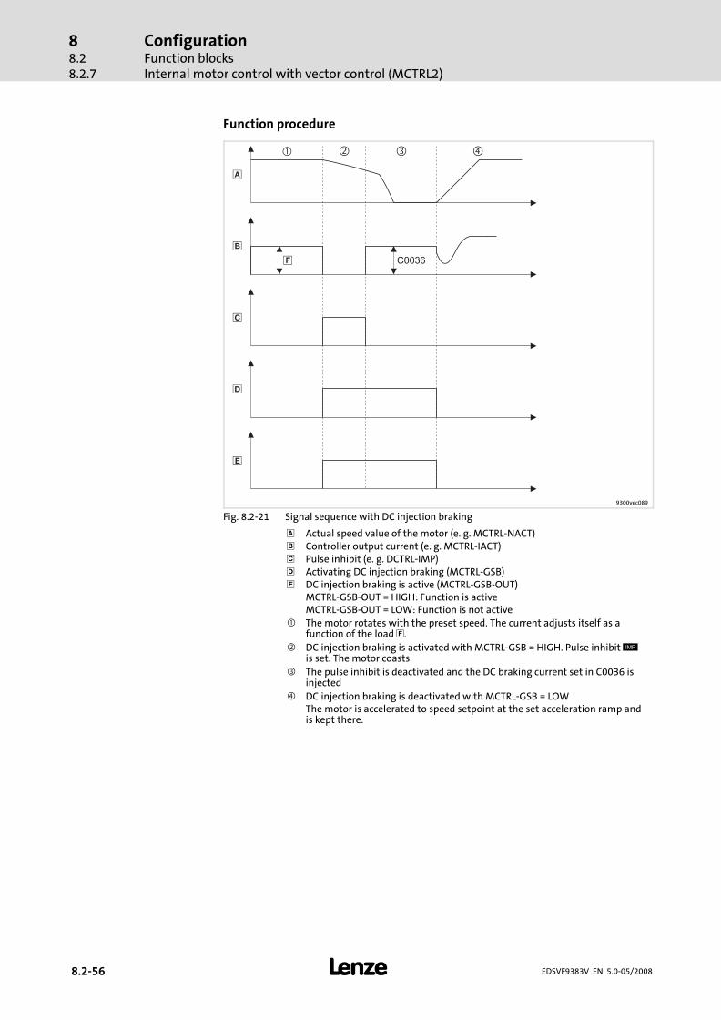
ConfigurationFunction blocksInternal motor control with vector control (MCTRL2)
88.28.2.7
� 8.2−56 EDSVF9383V EN 5.0−05/2008
Function procedure
�
�
�
�
�
�
� � � �
C0036
9300vec089
Fig. 8.2−21 Signal sequence with DC injection braking
� Actual speed value of the motor (e. g. MCTRL−NACT)� Controller output current (e. g. MCTRL−IACT) Pulse inhibit (e. g. DCTRL−IMP)� Activating DC injection braking (MCTRL−GSB)� DC injection braking is active (MCTRL−GSB−OUT)
MCTRL−GSB−OUT = HIGH: Function is activeMCTRL−GSB−OUT = LOW: Function is not active
� The motor rotates with the preset speed. The current adjusts itself as afunction of the load �.
� DC injection braking is activated with MCTRL−GSB = HIGH. Pulse inhibit �is set. The motor coasts.
� The pulse inhibit is deactivated and the DC braking current set in C0036 isinjected
� DC injection braking is deactivated with MCTRL−GSB = LOWThe motor is accelerated to speed setpoint at the set acceleration ramp andis kept there.

ConfigurationFunction blocks
Internal motor control with vector control (MCTRL2)
88.2
8.2.7
� 8.2−57EDSVF9383V EN 5.0−05/2008
When the speed falls below a settable speed setpoint threshold, the function"DC injection braking" is activated.
� Note!
Automatic DC−injection braking has priority over quick stop.
Special features of vector control with feedback
ƒ If the DC braking current (C0036) � than the motor magnetising current,the motor magnetising current is injected.
ƒ If the DC braking current (C0036) than the motor magnetising current,the DC braking current is injected.
Setting
Selection Code Description
DC braking current C0036 DC braking current with which the motor is braked
Speed setpoint threshold C0019 If the values fall below the threshold, DC−injectionbraking is released
Hold time C0107 Duration of DC−injection braking. After the hold time,pulse inhibit is set.
� Stop!
An excessive DC braking current and braking time can thermallyoverload the motor. Special care must be taken when usingself−ventilated motors.
Automatic DC injectionbraking
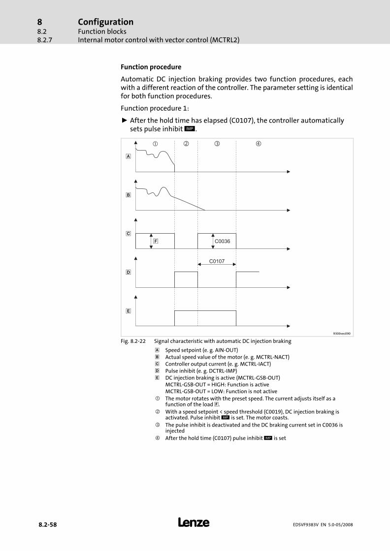
ConfigurationFunction blocksInternal motor control with vector control (MCTRL2)
88.28.2.7
� 8.2−58 EDSVF9383V EN 5.0−05/2008
Function procedure
Automatic DC injection braking provides two function procedures, eachwith a different reaction of the controller. The parameter setting is identicalfor both function procedures.
Function procedure 1:
ƒ After the hold time has elapsed (C0107), the controller automaticallysets pulse inhibit �.
�
�
��
�
�
� � � �
C0107
C0036
9300vec090
Fig. 8.2−22 Signal characteristic with automatic DC injection braking
� Speed setpoint (e. g. AIN−OUT)� Actual speed value of the motor (e. g. MCTRL−NACT) Controller output current (e. g. MCTRL−IACT)� Pulse inhibit (e. g. DCTRL−IMP)� DC injection braking is active (MCTRL−GSB−OUT)
MCTRL−GSB−OUT = HIGH: Function is activeMCTRL−GSB−OUT = LOW: Function is not active
� The motor rotates with the preset speed. The current adjusts itself as afunction of the load �.
� With a speed setpoint < speed threshold (C0019), DC injection braking isactivated. Pulse inhibit � is set. The motor coasts.
� The pulse inhibit is deactivated and the DC braking current set in C0036 isinjected
� After the hold time (C0107) pulse inhibit � is set

ConfigurationFunction blocks
Internal motor control with vector control (MCTRL2)
88.2
8.2.7
� 8.2−59EDSVF9383V EN 5.0−05/2008
Function procedure 2:
ƒ If you define a speed setpoint > speed threshold (C0019) before thehold time elapses, DC−injection braking is deactivated and the drivefollows the speed setpoint. If the speed falls below the threshold again,DC−injection braking is reactivated and the hold time is restarted.
�
�
��
�
�
� � � �
C0036
C0019
9300vec091
Fig. 8.2−23 Signal characteristic with automatic DC injection braking
� Speed setpoint (e. g. AIN−OUT)� Actual speed value of the motor (e. g. MCTRL−NACT) Controller output current (e. g. MCTRL−IACT)� Pulse inhibit (e. g. DCTRL−IMP)� DC injection braking is active (MCTRL−GSB−OUT)
MCTRL−GSB−OUT = HIGH: Function is activeMCTRL−GSB−OUT = LOW: Function is not active
� The motor rotates with the preset speed. The current adjusts itself as afunction of the load �.
� With a speed setpoint < speed threshold (C0019), DC injection braking isactivated. Pulse inhibit � is set. The motor coasts.
� The pulse inhibit is deactivated and the DC braking current set in C0036 isinjected
� DC−injection braking is deactivated as soon as the speed setpoint exceedsthe speed threshold (C0019). The motor is accelerated to the defined speedsetpoint and kept there.

ConfigurationFunction blocksInternal motor control with vector control (MCTRL2)
88.28.2.7
� 8.2−60 EDSVF9383V EN 5.0−05/2008
Suppressing no−load oscillations in case of:
ƒ Drives with different rated power of controller and motor, e. g. whenoperating with high switching frequency and the power deratinginvolved.
ƒ Operation of higher−pole motors.
ƒ Operation of three−phase AC drives > 10 kW.
Compensation of resonances in the drive kit:
ƒ Certain asynchronous motors may show this behaviour above 1/3 ofthe rated speed (1/3 � nn). This may result in an unstable operation(current and speed variations).
Adjustment
The Lenze setting is designed for power−adapted motors.
Usually, the speed oscillations can be reduced by changing the Lenze settingof the codes C0234 oder C0236 by the factor 2 ... 5.
1. Approach the range with speed oscillations.
2. Change the influence of the oscillation damping in C0234 (generally,increase it).
3. Increase the limitation of the oscillation damping in C0236.
4. Change filter time in C0235 in the range of 1 ... 20 ms, if necessary.
ƒ These can be indicators for smooth running:
– Constant motor current characteristic
– Reduction of the mechanical oscillations in the bearing seat
� Note!
Restricted effect with vector control
ƒ The oscillation damping has no influence on the drivebehaviour at low tendency to oscillation of the speedcontroller.
ƒ Especially for drives > 55 kW with a tendency to oscillation itmay be necessary to deactivate the oscillation damping(C0234 = 0 %).
ƒ For operation with feedback the oscillation damping has noinfluence.
Oscillation damping

ConfigurationFunction blocks
Internal motor control with vector control (MCTRL2)
88.2
8.2.7
� 8.2−61EDSVF9383V EN 5.0−05/2008
Vector control
Use C0021 to change the influence of the rotor resistance (C0082)proportionally:
ƒ Reduce the value in C0021 at an increasing speed (negative values)
ƒ Increase the value in C0021 at a decreasing speed
� Note!
When setting the vector control mode, the slip compensation(C0021) is automatically set to 0.0 %.
ƒ When you switch back to the V/f characteristic control mode,the slip compensation must be re−adapted.
If the motor may only rotate in one direction, you can limit the outputvoltage generation to one direction of rotation via C0909.
Code Description
C0909 = 1 The motor rotates in both directions
C0909 = 2 Motor rotates clockwise, "positive direction of rotation"(View of the motor shaft)
C0909 = 3 Motor rotates counter−clockwise, "negative direction of rotation"(View of the motor shaft)
Slip compensation
Inhibiting the direction ofrotation


ConfigurationMonitoringResponses
88.3
8.3.1
� 8.3−1EDSVF9383V EN 5.0−05/2008
8.3 Monitoring
Various monitoring functions ( 8.4−1) protect the drive system againstimpermissible operating conditions.
If a monitoring function is activated,
ƒ the set response is triggered to protect the drive.
ƒ the fault message is entered at position 1 in the history buffer( 9.2−1).
8.3.1 Responses
Depending on the failure, one or more of the following responses arepossible:
Response Effects on the drive and controller Danger warnings
TRIP(highestpriority)
� Switches the power outputs U, V, W to a highresistance until TRIP is reset
� The drive coasts (no control!).� After TRIP reset, the drive accelerates to its
setpoint on the ramps set.
Message Switches the power outputs U, V, W to a highresistance as long as the message is active. � Danger!
The drive restartsautomatically if the messageis no longer available.
� Short−timemessage� 0.5 s
The drive coasts (no control) as longas the message is active.If the message is no longer available,the drive accelerates to its setpointwith maximum torque.
� Longermessage> 0.5 s
The drive coasts (due to internalcontroller inhibit) as long as themessage is active.If required, restart the drive.
Warning � Only display of the failure.� The drive operates in a controlled manner. � Stop!
As these responses have noeffect on the drive behaviour,the drive can be destroyed.
Off � No response on failures! Monitoring isdeactivated.

ConfigurationMonitoringMonitoring times for process data input objects
88.38.3.2
� 8.3−2 EDSVF9383V EN 5.0−05/2008
8.3.2 Monitoring times for process data input objects
Each process data input object can monitor whether a telegram has beenreceived within a time set. As soon as a telegram arrives, the correspondingmonitoring time (C0357) is restarted ("retriggerable monoflop" function).
The following assignments are valid:
Setting the response to the monitoring:
ƒ C0591 for CAN1_IN ("CE1")
ƒ C0592 for CAN2_IN ("CE2")
ƒ C0593 for CAN3_IN ("CE3")
The following can be set:
ƒ 0 = error (TRIP) − controller sets controller inhibit (CINH)
ƒ 2 = warning
ƒ 3 = monitoring is switched off
You can also use the signals as binary output signals, e. g. for the assignmentof the output terminal.
If the controller disconnects from the CAN bus due to faulty telegrams, the"BusOffState" (CE4) signal is set.
"BusOffState" can trigger an error (TRIP) or warning (like CE1, CE2, CE3). Youcan also switch the signal off. The response is set via C0595. You can alsoassign the terminal output.
Changes with regard to the baud rates, the CAN node addresses, or theaddresses of process data objects are only valid after a reset node.
The reset node can be effected by:
ƒ A reconnection of the low−voltage supply
ƒ Reset node via the bus system
ƒ Reset node via C0358
Bus off
Reset node

ConfigurationMonitoring
Maximum speed
88.3
8.3.3
� 8.3−3EDSVF9383V EN 5.0−05/2008
8.3.3 Maximum speed
� Stop!
Destruction of the drive!
ƒ If the fault is triggered, the drive is without torque.
ƒ In the event of an actual speed value encoder failure it is notguaranteed that the monitoring responds.
Protective measures:
ƒ Use a mechanical brake if necessary.
ƒ Special, system−specific measures are to be taken.
The NMAX fault is triggered if the system speed (MCTRL−NACT)
ƒ exceeds the value set under C0596 or
ƒ exceeds the maximum speed nmax (C0011) by twice the max. speedvalue.
A fault initiates TRIP NMAX. Other responses cannot be set.
8.3.4 Motor
The OC1 fault is triggered if the motor current exceeds the rated controllercurrent by more than 2.25 times.
A fault initiates TRIP OC1. Other responses cannot be set.
The OC2 fault is triggered if
ƒ the motor has a short circuit to the frame,
ƒ one of the phases has a short circuit to the shield,
ƒ one of the phases has a short circuit to PE,
ƒ the capacitive charging current of the motor cable is too high.
A fault initiates TRIP OC2. Other responses cannot be set.
Fault OC3 is activated in the case of a too great load during acceleration. Theacceleration times or deceleration times (C0012, C0013, C0105) are set tooshort in proportion to the load.
If a fault occurs, TRIP OC3 is activated. Other responses cannot be set.
Short circuit in the motorcable (OC1)
Earth fault in the motor cable(OC2)
Overload during accelerationor deceleration (OC3)

ConfigurationMonitoringController current load (I x t monitoring)
88.38.3.5
� 8.3−4 EDSVF9383V EN 5.0−05/2008
If a current−carrying motor phase fails, a motor winding is broken or thecurrent limit value set in C0599 is too high, the LP1 fault is triggered.
The monitoring is not appropriate for field frequencies > 480 Hz and whensynchronous servo motors are used. Deactivate the monitoring at theseconditions.
The response to exceeding the thresholds can be set under C0597.
� Note!
The monitoring can only be activated if the function block MLP1is entered in the processing table (C0465).
8.3.5 Controller current load (I x t monitoring)
200 %
Ir
150 %
100 %
70 %
10 60 120 180 t [s]
9300std228
Fig. 8.3−1 I × t diagram
Ir Device output current100 % continuous thermal current at C0022 � 1.5 Ir70 % continuous thermal current at C0022 > 1.5 Ir
The I × t monitoring monitors the current load of the controller. The currentload is calculated from the mean value of the motor current over theacquisition period of 180 s.
The monitoring is set in such a way that the following operation modes arepossible:
ƒ Continuously with device output current = Ir.
ƒ � 60 s with device output current � 1.5 x Ir.
A fault initiates TRIP OC5. Other responses cannot be set.
Failure of a motor phase (LP1)
ConfigurationMonitoring
Motor temperature
88.3
8.3.6
� 8.3−5EDSVF9383V EN 5.0−05/2008
8.3.6 Motor temperature
The motor temperature is monitored with a KTY temperature sensor. Wirethe temperature sensor to the resolver cable at X7 or to the encoder cable atX8.
ƒ Adjustable warning threshold (OH7) via C0121
– The reset point is 15° C below the adjusted threshold.
ƒ Fixed warning threshold (OH3) = 150 °C
– The reset point is at 135° C.
The response to exceeding the thresholds can be set under:
ƒ C0584 (adjustable threshold)
ƒ C0583 (fixed threshold)
The SD6 fault is triggered if there is a short or open circuit between X7/8 andX7/9 or X8/5 and X8/8.
The response can be set under C0594.
The motor temperature is monitored with a PTC thermistor or thermalcontact. Wire the temperature sensor to T1, T2.
ƒ Fixed warning threshold (OH8)
– The switch−off threshold and the hysteresis depend on thetemperature sensor (DIN 44081).
The response to exceeding the threshold can be set under C0585.
� Stop!
Motor could be destroyed!
ƒ If the responses "Warning" or "Off" are set, the motor could bedestroyed by overload.
Protective measure:
ƒ Set the response "TRIP".
8.3.7 Heatsink temperature
Via a temperature threshold, the heatsink temperature of the controller canbe monitored:
ƒ Adjustable threshold (OH4) under C0122
– The reset point is 5° C below the adjusted threshold.
ƒ Fixed threshold (OH) = 85° C
– The reset point is at 80° C.
The response for exceeding the adjustable threshold can be set under C0582.
KTY at X7 or X8
Monitoring of the KTY at X7or X8
PTC thermistor or thermalcontact (NC contact) at T1, T2

ConfigurationMonitoringDC−bus voltage
88.38.3.8
� 8.3−6 EDSVF9383V EN 5.0−05/2008
8.3.8 DC−bus voltage
In C0173 the mains voltage and DC−bus voltage are set. From this theswitching thresholds for overvoltage and undervoltage result.
EVF9335 ... EVF9338EVF9381 ... EVF9383
Selection Mainsvoltage
Operationwith braketransistor
Message LU(undervoltage)
Message OU(overvoltage)
C0173 set reset set reset
[V AC] [V DC] [V DC] [V DC] [V DC]
ExV210ExV240ExV270ExV300
0 < 400 yes / no 285 430 770 755
1 400 yes / no 285 430 770 755
2 460 yes / no 328 473 770 755
3 480 no 342 487 770 755
4 480 yes 342 487 800 785
5 500 yes / no 342 487 900 885
ExExV060ExV110
readonly
400 yes / no 285 430 700 685
C0173 = 1: Lenze setting
If the DC−bus voltage exceeds the upper switch−off threshold set in C0173,warning OU is activated.
If the DC−bus voltage falls below the lower switch−off threshold set in C0173,the LU message is triggered.
ƒ An undervoltage message > 3 seconds is interpreted as an operatingstate (e.g. mains switched off) and entered in the history buffer. Theentry is, however, deleted as soon as the cause has been eliminated(e.g. mains switched on again).
This operating state can occur if the control module is already suppliedexternally via terminals X5/39 and X5/59, but the mains voltage is not yetswitched on.
ƒ An undervoltage message < 3 seconds is interpreted as a fault(e.g.�mains fault), entered in the history buffer and saved.
8.3.9 External error (EEr)
A HIGH signal at DCTRL−TRIP−SET triggers the EEr fault.
You can, for example, connect the digital input DCTRL−TRIP−SET with aninput terminal (X5/Ex). In this way an external encoder can trigger the EErfault.
The response can be set under C0581.
Overvoltage
Undervoltage

Co
nfig
ura
tion
Overview
of m
on
itorin
g fu
nctio
ns
88.4
� 8
.4−1
EDSV
F93
83
V EN
5.0
−05
/20
08
8.4 Overview of monitoring functions
The responses of monitoring functions can be partly parameterised via codes ˘ in GDC in the parameter menu underMonitoring ˘.
Monitoring Possible responses� Lenze setting Setting possible
Error message Description Source CoDe TRIP Message Warning Off
0071 CCr System fault Internal �
x091 EEr External monitoring (activated via DCTRL) FWM C0581 �
Voltage supply
2020 OU Overvoltage in the DC bus (C0173) MCTRL �
1030 LU Undervoltage in the DC bus (C0173) MCTRL �
0107 H07 Internal fault (power section) Internal �
Communication
x061 CE0 Communication error on the automation interface (AIF) AIF C0126 �
x062 CE1 Communication error at process data input object CAN1_IN (monitoring time can be setwith C0357/1)
CAN1_IN C0591 �
x063 CE2 Communication error at process data input object CAN2_IN (monitoring time can be setwith C0357/2)
CAN2_IN C0592 �
x064 CE3 Communication error at process data input object CAN3_IN (monitoring time can be setwith C0357/3)
CAN3_IN C0593 �
x065 CE4 BUS−OFF state of the system bus (CAN)(too many faulty telegrams)
CAN C0595 �
Temperatures / sensors
0050 OH Heatsink temperature > 85° C MCTRL �
x053 OH3 Motor temperature > 150° C MCTRL C0583 �
x054 OH4 Heatsink temperature > C0122 MCTRL C0582 �
x057 OH7 Motor temperature > C0121 MCTRL C0584 �
x058 OH8 Motor temperature across inputs T1 and T2 is too high.Please note: In the case of "Warning" (C0585 = 2) or "Off" (C0585 = 3), the drive can bedestroyed if the fault is not eliminated in time!
MCTRL C0585 �
x086 Sd6 Thermal sensor error at motor (X7 or X8) MCTRL C0594 �
x110 H10 Thermal sensor error at heatsink FWM C0588 � 1) 1)
x111 H11 Thermal sensor error in the device interior FWM C0588 � 1) 1)
Motor / feedback system
0011 OC1 Short circuit of motor cable MCTRL �
0012 OC2 Motor cable earth fault MCTRL �
0013 OC3 Overload at acceleration or deceleration MCTRL �
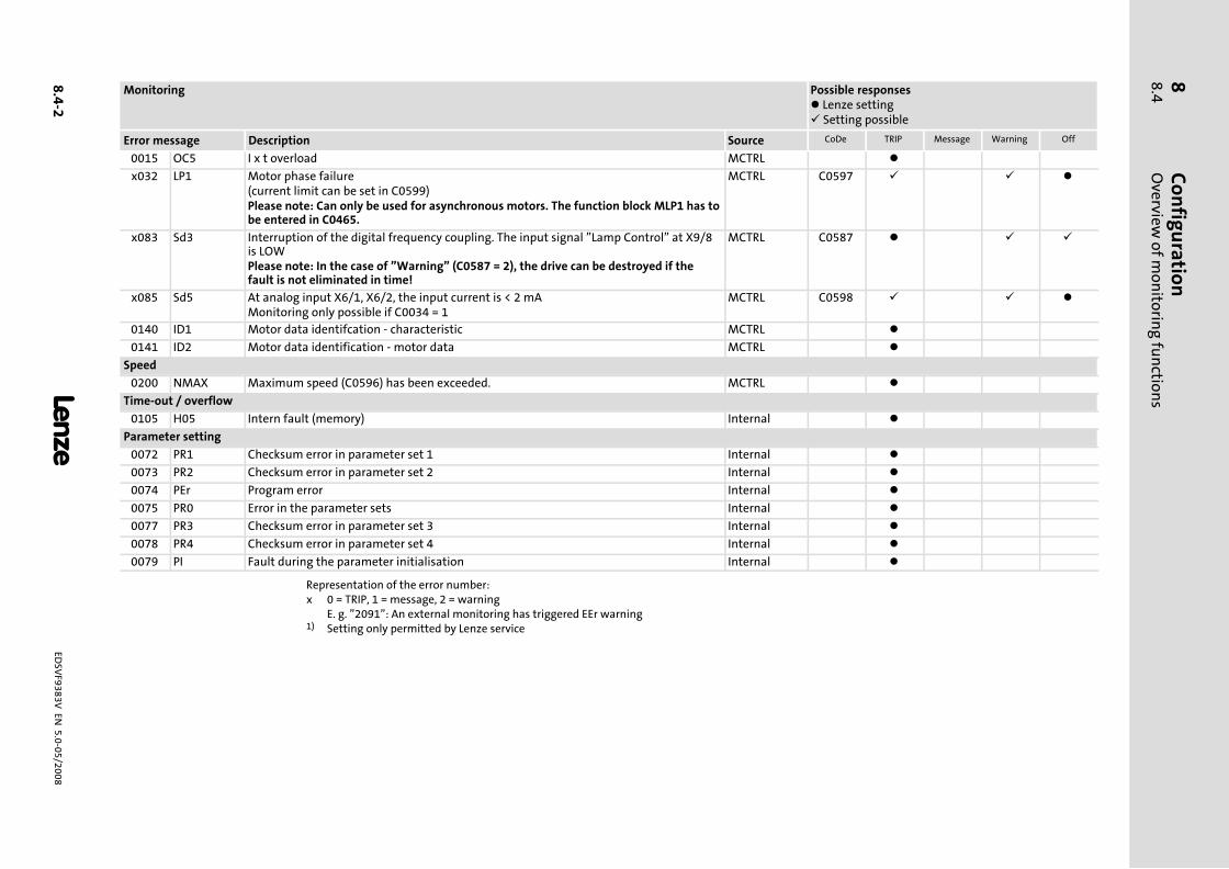
Co
nfig
ura
tion
Overview
of m
on
itorin
g fu
nctio
ns
88.4
� 8
.4−2
EDSV
F93
83
V EN
5.0
−05
/20
08
Possible responses� Lenze setting Setting possible
Monitoring
OffWarningMessageTRIPCoDeSourceDescriptionError message
0015 OC5 I x t overload MCTRL �
x032 LP1 Motor phase failure(current limit can be set in C0599)Please note: Can only be used for asynchronous motors. The function block MLP1 has tobe entered in C0465.
MCTRL C0597 �
x083 Sd3 Interruption of the digital frequency coupling. The input signal ˜Lamp Control˜ at X9/8is LOWPlease note: In the case of "Warning" (C0587 = 2), the drive can be destroyed if thefault is not eliminated in time!
MCTRL C0587 �
x085 Sd5 At analog input X6/1, X6/2, the input current is < 2 mAMonitoring only possible if C0034 = 1
MCTRL C0598 �
0140 ID1 Motor data identifcation − characteristic MCTRL �
0141 ID2 Motor data identification − motor data MCTRL �
Speed
0200 NMAX Maximum speed (C0596) has been exceeded. MCTRL �
Time−out / overflow
0105 H05 Intern fault (memory) Internal �
Parameter setting
0072 PR1 Checksum error in parameter set 1 Internal �
0073 PR2 Checksum error in parameter set 2 Internal �
0074 PEr Program error Internal �
0075 PR0 Error in the parameter sets Internal �
0077 PR3 Checksum error in parameter set 3 Internal �
0078 PR4 Checksum error in parameter set 4 Internal �
0079 PI Fault during the parameter initialisation Internal �
Representation of the error number:x 0 = TRIP, 1 = message, 2 = warning
E. g. "2091": An external monitoring has triggered EEr warning1) Setting only permitted by Lenze service

ConfigurationCode table
88.5
� 8.5−1EDSVF9383V EN 4.0−03/2006
8.5 Code table
How to read the code table:
Column Abbreviation Meaning
Code Cxxxx Code Cxxxx � Parameter value of the code can be defineddifferently in each parameter set
� Parameter value is accepted immediately (ONLINE)1 Subcode 1 of Cxxxx
2 Subcode 2 of Cxxxx
* Parameter value of the code is the same in all parameter sets
� Changed parameter or the code or subcode is accepted after pressing & �
� Changed parameter of the code or subcode is accepted after pressing & �,if the controller is inhibited
Name Name of the code
Lenze Lenze setting (value on delivery or after restoring the delivery status with C0002)
� The column "IMPORTANT" contains further information
Selection 1 {%} 99 min. value {unit} max. value
IMPORTANT − Short, important explanations
Code Possible settings IMPORTANT
No. Name Lenze Selection
C0002�
Par load 1 Loading a parameter set
0 Load default Restore the delivery status
1 Load PS1 � Load parameter set saved inthe controller and activate it
� Parameter set 1 is loadedautomatically after everymains connection
2 Load PS2
3 Load PS3
4 Load PS4
11 Load ext PS1 Load parameter set from thekeypad into the controller andactivate it
12 Load ext PS2
13 Load ext PS3
14 Load ext PS4
20 ext −> EEPROM Load all parameter sets from thekeypad into the controller
C0003�
Par save 0 Save parameter set
0 Ready Saving is completed
1 Save PS1 Save the parameters loaded in thecontroller into a parameter set(PS1 .... PS4)
2 Save PS2
3 Save PS3
4 Save PS4
11 Save extern All parameter sets (PS1 .... PS4)must be transferred from thecontroller to the keypad XT
C0004�
Op display 56 0 {1} 1999 Operating display� Keypad shows selected code in
the operating level if no otherstatus messages of C0183 areactive

ConfigurationCode table
88.5
� 8.5−2 EDSVF9383V EN 4.0−03/2006
IMPORTANTPossible settingsCode
SelectionLenzeNameNo.
C0005�
Signal CFG Selection of the basicconfiguration
1000 0 Common Modified basicconfiguration
The first two digits indicate thepredefined basic function, e. g.:� 01xxx: Speed control
The third digit indicates additionalfunctions:� xx0xx: No additional function� xx1xx: Brake control� xx2xx: Setpoint selection via
motor potentiometer� xx3xx: PID controller� xx4xx: Mains failure control� xx5xx: Setpoint selection via
master frequency� xx6xx: Gearbox factor − analog
trimming� xx7xx: Gearbox factor − digital
trimming� xx8xx: Master frequency ramp
function generator
Die fourth digit indicates thepredefined voltage source for thecontrol terminals:� xxx0x: External supply voltage� xxx1x: Internal supply voltage
The fifth digit indicates thepredefined device control� xxxx0: Terminal control� xxxx1: RS232, RS485 or optical
fibre� xxxx3: INTERBUS or
PROFIBUS−DP� xxxx5: System bus (CAN)
100 CFG: emty All internalconnections areremoved
1000 Speed mode Speed control
2000 Step mode Step control
3000 Lead screw Traversing control
4000 Torque mode Torque control
5000 DF master Digital frequencymaster
6000 DF slv bus Master frequencyslave (bar)
7000 DF slv cas Digital frequencyslave (cascade)
8000 Dancer ctrl e Dancer positioncontrol withexternal diametermeasurement
9000 Dancer ctrl i Dancer positioncontrol withinternal diametermeasurement
C0006�
Op mode 5 Selection of the operating modefor the motor control
1 vector ctrl Vector controlwithout or withspeed feedback
In case of the first selection enterthe motor data and identify themwith C0148.
6.8−8
5 V / f V/f characteristiccontrol
Commissioning withoutidentification of the motor data ispossible� Advantage of identification
with C0148: Improved smoothrunning at low speeds
6.8−4
C0009 LECOM address 1 1 {1} 99 LECOM controller address� Bus device number when
operated via interface� 10, 20 ... 90 reserved for
broadcast to device groupswith RS232, RS485, opticalfibre

ConfigurationCode table
88.5
� 8.5−3EDSVF9383V EN 4.0−03/2006
IMPORTANTPossible settingsCode
SelectionLenzeNameNo.
C0010 Nmin 0 0 {1 rpm} 36000 � Reference valuefor the absoluteand relativesetpoint selectionfor theacceleration anddecelerationtimes
� C0059 must beset correctly
� Set C0010 <C0011
� C0010 is onlyeffective in caseof analogsetpoint selectionvia AIN1
Important: Forparameter settingvia interface, majorchanges in one stepshould only be madewhen the controlleris inhibited.
Minimumspeed
6.10−1
C0011 Nmax 3000 0 {1 rpm} 36000 Maximumspeed
C0012 Tir (acc) 5.00 0.00 {0.01 s} 9999.90 Acceleration time Tir of the mainsetpoint� Refers to speed change
0 ... C0011
6.10−3
C0013 Tif (dec) 5.00 0.00 {0.01 s} 9999.90 Deceleration time Tif of the mainsetpoint� Refers to speed change
0 ... C0011
C0014 V/f charact. 0 Characteristic in the V/fcharacteristic control mode
8.2−25
0 Linear Linear V/f characteristic
1 square Square V/f characteristic
C0015 Rated freq 50 10 {1 Hz} 5000 V/f−rated frequencyIn C0015 you can set a basefrequency which differs from therated motor frequency (C0089)� Lenze setting: C0015 = C0089� Changing C0086 or C0089
overwrites the value in C0015
8.2−25
C0016 Umin boost 0.00 0.00 {0.01 %} 100.00 Umin boost (FCODE)� C0016 = 1 % corresponds to a
boost of 1 % of the rated motorvoltage (C0090)
� Code is freely configurable
6.8−4
C0017 FCODE (Qmin) 50 −36000 {1 rpm} 36000 Qmin−switching threshold (FCODE)� Programmable speed threshold� If the current speed is < C0017,
CMP1−OUT is activated.� Freely configurable code

ConfigurationCode table
88.5
� 8.5−4 EDSVF9383V EN 4.0−03/2006
IMPORTANTPossible settingsCode
SelectionLenzeNameNo.
C0018 fchop 6 Switching frequency of theinverter� General rule: The lower the
switching frequency the– lower the power loss– higher the noise generation– better the concentricity
factor� Observe derating indications
for high switching frequencies� The max. output frequency
(fmax) is:– fchop = 4 kHz �
fmax = 300 Hz– fchop = 2 kHz �
fmax = 150 Hz– fchop = 1 kHz �
fmax = 150 Hz
6.9−1
1 1 kHz sin loss−optimised
2 2 kHz sin concentricity−optimised
3 4 kHz f_top power−optimised
4 4 kHz sin noise−optimised
6 4/2 kHz sin noise/concentricity−optimised withautomaticchange−over tolow switchingfrequency
C0019 Thresh nact=0 0 −36000 {1 rpm} 36000 Operating threshold − automaticDC injection brake (Auto−GSB)� Falling below the threshold in
C0019 activates automatic DCinjection braking when theholding time set under C0107 >0
8.2−25 8.2−40
C0020 turn value 100 0 {1 %} 200 Influence on concentricity factor� Manual influence on the
concentricity factor of themotor
C0021 slipcomp � −20.00 {0.01 %} 20.00 Slip compensation� Change of C0086, C0087 or
C0089 sets C0021 to thecalculated rated slip of themotor
� When changing over to thevector control mode, C0021 isset to 0
6.11−1 8.2−25 8.2−40
C0022 Imax current � 0 {0.1 A} − Imax limit in motor mode� depending on C0086
6.6−15
C0023 Imax gen. � 0 {0.1 A} − Imax limit in generator mode� depending on C0086
6.6−15
C0025�
Feedback type 1 Speed feedback 6.7−1
1 no feedback No feedback
100 IT (C420) − X8 Input of thenumber ofincrements inC0420
Incremental encoder at X8� Incremental encoders with TTL
level can only be connected toX8.
101 IT (C420) − X9 Input of thenumber ofincrements inC0420
Incremental encoder at X9� Connect incremental encoders
with HTL−level on X9 only
Number ofincrements:
Incremental encoder at X8� Incremental encoders with TTL
level can only be connected toX8.
110 IT512−5V 512 inc
111 IT1024−5V 1024 inc
112 IT2048−5V 2048 inc
113 IT4096−5V 4096 inc

ConfigurationCode table
88.5
� 8.5−5EDSVF9383V EN 4.0−03/2006
IMPORTANTPossible settingsCode
SelectionLenzeNameNo.
C0026 −199.99 {0.01 %} 199.99 Free control code FCODE 26/1 andFCODE26/2
6.5−4See SystemManual(extension)1 FCODE (offset) 0.00 Offset of AIN1 (X6/1, X6/2)
2 FCODE (offset) 0.00 Offset of AIN2 (X6/3, X6/4)
C0027 −199.99 {0.01 %} 199.99 Free control code FCODE 27/1 andFCODE27/2
1 FCODE (gain) 100.00 Gain AIN1 (X6/1, X6/2)� 100 % = gain 1
2 FCODE (gain) 100.00 Gain AIN2 (X6/3, X6/4)� 100 % = gain 1
C0030 DFOUT const 3 0 256 inc/rev Function block DFOUT� Setting of the constant
(increments per revolution) forthe master frequency outputX10
8.2−8
1 512 inc/rev
2 1024 inc/rev
3 2048 inc/rev
4 4096 inc/rev
5 8192 inc/rev
6 16384 inc/rev
C0032 FCODEGearbox
1 −32767 {1} 32767 Gearbox factor − numerator of thefunction block DFSET� Freely configurable code
8.2−18
C0033 Gearboxdenom
1 1 {1} 32767 Gearbox factor − denominator ofthe function block DFSET
8.2−18
C0034 Mst current 0 0 −10 V ... +10 V Voltage / current range for analogsignals at input X6/1, X6/2� Observe jumper position of X3
5.6−7 6.5−41 4 mA ... 20 mA
2 −20 mA ... +20 mA
C0036 DC brk value 0.0 0.0 {0.1 A} − Set DC braking current� depends on the controller
8.2−25 8.2−40
C0037 Set−value rpm 0 −36000 {1 rpm} 36000 Setpoint selection
C0038 0 {1 rpm} 36000 Suppress speed ranges, functionblock NLIM1� Speed ranges are only run
through dynamically� Static behaviour in the
inhibited range is suppressed
See SystemManual(extension)
1 N 1 start 0 Suppress speed range 1
2 N 1 stop 0
3 N 2 start 0 Suppress speed range 2
4 N 2 stop 0
5 N 3 start 0 Suppress speed range 3
6 N 3 stop 0

ConfigurationCode table
88.5
� 8.5−6 EDSVF9383V EN 4.0−03/2006
IMPORTANTPossible settingsCode
SelectionLenzeNameNo.
C0039 −36000 {1 rpm} 36000 JOG setpoints for the speedsetpoint conditioning, functionblock NSET� Parameter setting of the fixed
speeds (JOG setpoints)� Activation via binary coding of
digital input signals inC0787/1 ... C0787/4
� For coding see description offunction block NSET
See SystemManual(extension)1 JOG set−value 1500
2 JOG set−value 1000
3 JOG set−value 500
4 JOG set−value 200
5 JOG set−value 100
6 JOG set−value 50
7 JOG set−value 25
8 JOG set−value 10
9 JOG set−value 5
10 JOG set−value 0
... ... ...
15 JOG set−value 0
C0040 Ctrl enable 0 Controller enable� Controller can only be enabled
if X5/28 = HIGH
6.4−1
0 Ctrl inhibit Controller inhibited
1 Ctrl enable Controller enabled
C0042 DIS: QSP Quick stop� Display only
8.2−25 8.2−40
0 QSP inactive Quick stop is not active
1 QSP active Quick stop is active
C0043 Trip reset 0 0 no/trip reset Reset actual error
1 trip active There is a TRIP error
C0045 DIS: act JOG 0 Nset active Nset is active Active JOG setpoint for the speedsetpoint conditioning, functionblock NSET� Display of the activated fixed
speed
See SystemManual(extension)1 JOG1 JOG setpoint 1
2 JOG2 JOG setpoint 2
... ... ...
15 JOG15 JOG setpoint 15
C0046 DIS: N −199.99 {0.01 %} 199.99 Main setpoint for the speedsetpoint conditioning, functionblock NSET� Read only
C0049 DIS: NADD −199.99 {0.01 %} 199.99 Additional setpoint, functionblock NSET� Read only
See SystemManual(extension)
C0050 MCTRL−NSET2 −100.00 {0.01 %} 100.00 Speed setpoint, function blockMCTRL� Display of the speed in [%] of
C0011
8.2−25 8.2−40
C0051 MCTRL−NACT −36000 {1 rpm} 36000 Actual speed value, function blockMCTRL� Read only
8.2−25 8.2−40
C0052 MCTRL−Umot 0 {1 V} 800 Motor voltage, function blockMCTRL� Read only� MCTRL−VACT = 100 % = C0090
8.2−25 8.2−40
C0053 UG−VOLTAGE 0 {1 V} 900 DC−bus voltage, function blockMCTRL� Read only� MCTRL−DCVOLT = 100 % =
1000 V
8.2−25 8.2−40

ConfigurationCode table
88.5
� 8.5−7EDSVF9383V EN 4.0−03/2006
IMPORTANTPossible settingsCode
SelectionLenzeNameNo.
C0054 Imot 0.0 {0.1 A} 5000.0 Actual motor current, functionblock MCTRL� Read only� MCTRL−IACT = 100 % = C0022
8.2−25 8.2−40
C0056 MCTRL−MSET2 −100.00 {0.01 %} 100.00 Read only. The output signaldepends on the operating mode:� Current motor current in case
of V/f characteristic control,function block MCTRL1
� Torque setpoint in case ofvector control, function blockMCTRL2
8.2−25 8.2−40
C0057 Max Torque 0 {1 Nm} 5000 Maximum possible torque of thedrive configuration� Display only� With V/f characteristic control
depending on C0022, C0086,C0088
� With vector control dependingon C0022, C0086, C0088,C0091
C0058 MCTRL−FACT −600.0 {0.1 Hz} 600.0 Output frequency� Display only� MCTRL−FACT = 100.0 % =
1000.0 Hz
8.2−25 8.2−40
C0059 Mot pole no. 1 {1} 50 Pole pair number of the motor� Display only
C0061 Heatsink temp 0 {1 °C} 100 Heatsink temperature� Read only� If the temperature of the
heatsink > 85 °C, the controllersets TRIP OH
� Early warning is possible viaOH4, temperature is set inC0122
See SystemManual(extension)
C0063 Mot temp 0 {1 °C} 200 Motor temperature� Read only� Monitoring of the motor
temperature must beactivated.
� KTY at X8/5, X8/8:– At 150 °C, TRIP OH3 is set– Early warning is possible viaOH7, temperature is set inC0121
� PTC, thermal contact at T1, T2:– Release sets TRIP or
warning OH8
8.2−25 8.2−40
C0064 Utilization 0 {1 %} 150 Device utilisation I×t� Read only� Device utilisation of the last
180 s operating time� C0064 > 100 % triggers
warning OC5� C0064 > 110 % limits the ouput
current of the controller to67 % of the maximum currentin C0022
8.2−25 8.2−40
C0067 Act trip Selection list 10 Momentary fault message� Display only
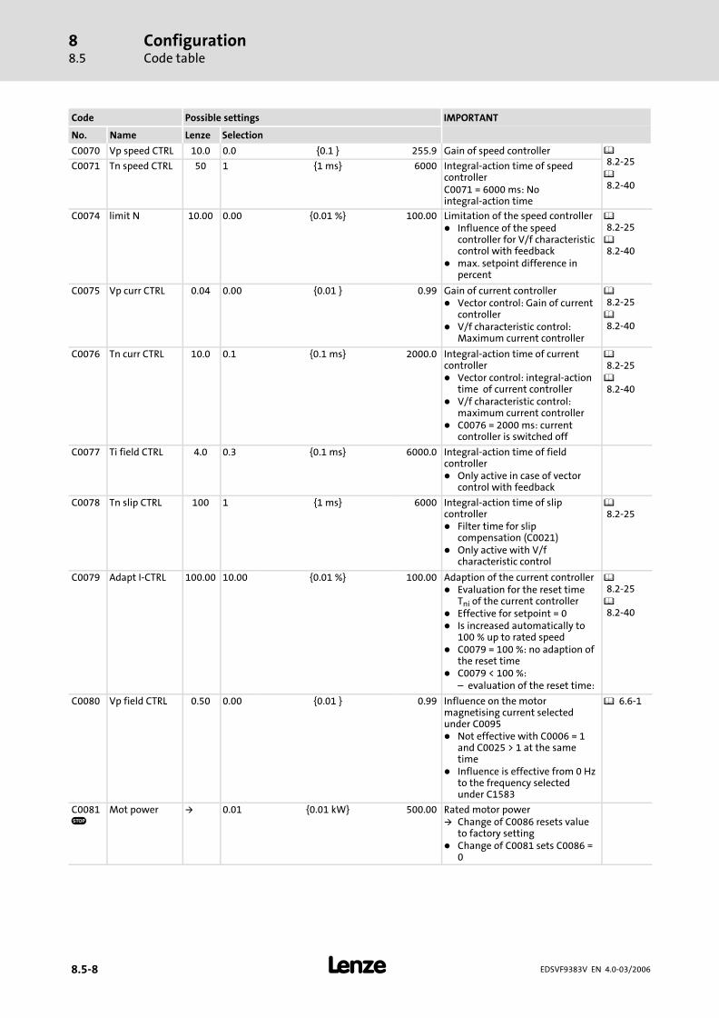
ConfigurationCode table
88.5
� 8.5−8 EDSVF9383V EN 4.0−03/2006
IMPORTANTPossible settingsCode
SelectionLenzeNameNo.
C0070 Vp speed CTRL 10.0 0.0 {0.1 } 255.9 Gain of speed controller 8.2−25 8.2−40
C0071 Tn speed CTRL 50 1 {1 ms} 6000 Integral−action time of speedcontrollerC0071 = 6000 ms: Nointegral−action time
C0074 limit N 10.00 0.00 {0.01 %} 100.00 Limitation of the speed controller� Influence of the speed
controller for V/f characteristiccontrol with feedback
� max. setpoint difference inpercent
8.2−25 8.2−40
C0075 Vp curr CTRL 0.04 0.00 {0.01 } 0.99 Gain of current controller� Vector control: Gain of current
controller� V/f characteristic control:
Maximum current controller
8.2−25 8.2−40
C0076 Tn curr CTRL 10.0 0.1 {0.1 ms} 2000.0 Integral−action time of currentcontroller� Vector control: integral−action
time of current controller� V/f characteristic control:
maximum current controller� C0076 = 2000 ms: current
controller is switched off
8.2−25 8.2−40
C0077 Ti field CTRL 4.0 0.3 {0.1 ms} 6000.0 Integral−action time of fieldcontroller� Only active in case of vector
control with feedback
C0078 Tn slip CTRL 100 1 {1 ms} 6000 Integral−action time of slipcontroller� Filter time for slip
compensation (C0021)� Only active with V/f
characteristic control
8.2−25
C0079 Adapt I−CTRL 100.00 10.00 {0.01 %} 100.00 Adaption of the current controller� Evaluation for the reset time
Tni of the current controller� Effective for setpoint = 0� Is increased automatically to
100 % up to rated speed� C0079 = 100 %: no adaption of
the reset time� C0079 < 100 %:
– evaluation of the reset time:
8.2−25 8.2−40
C0080 Vp field CTRL 0.50 0.00 {0.01 } 0.99 Influence on the motormagnetising current selectedunder C0095� Not effective with C0006 = 1
and C0025 > 1 at the sametime
� Influence is effective from 0 Hzto the frequency selectedunder C1583
6.6−1
C0081�
Mot power � 0.01 {0.01 kW} 500.00 Rated motor power� Change of C0086 resets value
to factory setting� Change of C0081 sets C0086 =
0
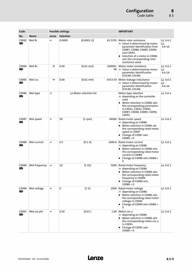
ConfigurationCode table
88.5
� 8.5−9EDSVF9383V EN 4.0−03/2006
IMPORTANTPossible settingsCode
SelectionLenzeNameNo.
C0082�
Mot Rr � 0.0000 {0.0001 �} 65.5350 Motor rotor resistance� Value is determined by motor
parameter identification fromC0087, C0088, C0089, C0090and C0091
� Selection of a motor in C0086sets the corresponding rotorresistance value
6.6−1 6.6−16
C0084�
Mot Rs � 0.00 {0.01 m�} 100000.00
Motor stator resistance� Value is determined by motor
parameter identification(C0148, C0149)
6.6−1 6.6−16
C0085�
Mot Lss � 0.00 {0.01 mH} 6553.50 Motor leakage inductance� Value is determined by motor
parameter identification(C0148, C0149)
6.6−1 6.6−16
C0086�
Mot type � Motor selection list Motor type selection� depending on the controller
used� Motor selection in C0086 sets
the corresponding parametersin C0021, C0022, C0081,C0087, C0088, C0089, C0090,C0091
6.6−1
C0087�
Mot speed � 50 {1 rpm} 36000 Rated motor speed� depending on C0086� Motor selection in C0086 set
the corresponding rated motorspeed in C0087
� Change of C0087 setsC0086 = 0
6.6−1
C0088�
Mot current � 0.5 {0.1 A} 1000.0 Rated motor current� depending on C0086� Motor selection in C0086 sets
the corresponding rated motorcurrent in C0088
� Change of C0088 sets C0086 =0
6.6−1
C0089�
Mot frequency � 10 {1 Hz} 5000 Rated motor frequency� depending on C0086� Motor selection in C0086 sets
the corresponding rated motorfrequency in C0089
� Change of C0089 setsC0086 = 0
6.6−1
C0090�
Mot voltage � 0 {1 V} 1000 Rated motor voltage� depending on C0086� Motor selection in C0086 sets
the corresponding rated motorvoltage in C0090
� Change of C0090 sets C0086 =0
6.6−1
C0091�
Mot cos phi � 0.50 {0.01 } 1.00 Motor cos �� depending on C0086� Motor selection in C0086 sets
the corresponding motor cos �in C0091
� Change of C0091 setsC0086 = 0
6.6−1

ConfigurationCode table
88.5
� 8.5−10 EDSVF9383V EN 4.0−03/2006
IMPORTANTPossible settingsCode
SelectionLenzeNameNo.
C0092�
Mot Ls � 0.00 {0.01 mH} 6553.50 Motor stator inductance� Value is determined by motor
parameter identification fromC0088, C0089, C0090 andC0091
� Motor selection in C0086 setscorresponding statorinductance value in C0092
6.6−1
C0093 Drive ident Controller identification� Read only
0 Invalid Defective power section
1 None No power section
14...20
9335VC 400V...9383VC 400V
Display of the controller used
21...28
9334VC 500V...9383VC 500V
9321...9333
9321 VC...9333VC
C0094 Password 0 0 {1} 9999 Password� C0094 = 1 ... 9999: Free access
to the user menu only
7.2−9
C0095�
Mot Io � 0.0 {0.1 A} 1000.0 Motor magnetising current� dependent on C0086, C0088
and C0091� Change of C0086 sets C0095 to
the Lenze setting� Change of C0095 sets
C0086 = 0
6.6−1
C0096 0 no protection No passwordprotection
Parameter access protection� Extension of the access
protection for AIF bus systemsand CAN with activatedpassword in C0094
� All codes in the user menu cancontinued to be accessed.
1 R protection Read protection
2 W protection Write protection
3 R/W protection Read/writeprotection
1 AIF protect. 0 Parameter access protection AIF
2 CAN protect. 0 Parameter access protection CAN
C0099 S/W version x.y Software version� Read onlyx
yMain versionSubversion

ConfigurationCode table
88.5
� 8.5−11EDSVF9383V EN 4.0−03/2006
IMPORTANTPossible settingsCode
SelectionLenzeNameNo.
C0101 0.00 {0.01 s} 999.90 Additional acceleration times forspeed setpoint conditioning,function block NSET� Additional acceleration and
deceleration times for the mainsetpoint
� Activation via binary coding ofdigital input signals inC0788/1 ... C0788/4
� For coding see description offunction block NSET
See SystemManual(extension)
1 add Tir 0.00
2 add Tir 0.00
... ... ...
15 add Tir 0.00
C0103 0.00 {0.01 s} 999.90 Additional deceleration times forspeed setpoint conditioning,function block NSET� Additional acceleration and
deceleration times for the mainsetpoint
� Activation via binary coding ofdigital input signals inC0788/1 ... C0788/4
� For coding see description offunction block NSET
1 add Tif 0.00
2 add Tif 0.00
... ... ...
15 add Tif 0.00
C0104�
select accel. 0 Selection of acceleration functionof the linear ramp functiongenerator of NSET
See SystemManual(extension)
0 a = const Constant acceleration
1 t = const Constant time
2 s = const Constant path
C0105 QSP Tif 5.00 0.00 {0.01 s} 999.90 Quick stop deceleration time� The deceleration time refers to
a speed variation of C0011 ... 0
8.2−25 8.2−40
C0107 holding time 0.00 0.00 {0.01 s} 9999.90 Hold time for automatic DCinjection braking (Auto−GSB)
8.2−25 8.2−40
C0108 −199.99 {0.01 %} 199.99 Free control code FCODE108/1and FCODE108/2
6.5−6See SystemManual(extension)1 FCODE (gain) 100.00 Gain of analog output signal
AOUT1 (X6/62)� 100 % = gain 1
2 FCODE (gain) 100.00 Gain of analog output signalAOUT2 (X6/63)� 100 % = gain 1
C0109 −199.99 {0.01 %} 199.99 Free control code FCODE109/1and FCODE109/2
1 FCODE (offset) 0.00 Offset of analog output signalAOUT1 (X6/62)
2 FCODE (offset) 0.00 Offset of analog output signalAOUT2 (X6/63)
C0114 0 High active HIGH level isactive
Inversion of digital input signals atX5, function block DIGIN
6.5−1See SystemManual(extension)1 LOW active LOW level is active
1 DIGIN1 pol 0 Terminal X5/E1
2 DIGIN2 pol 0 Terminal X5/E2
3 DIGIN3 pol 0 Terminal X5/E3
4 DIGIN4 pol 1 Terminal X5/E4
5 DIGIN5 pol 0 Terminal X5/E5
5 DIGIN6 (ST) pol 0 Terminal X5/ST

ConfigurationCode table
88.5
� 8.5−12 EDSVF9383V EN 4.0−03/2006
IMPORTANTPossible settingsCode
SelectionLenzeNameNo.
C0116�
Selection list 2 Configuration of free digitaloutputs (FDO)� Signals can only be evaluated
when being networked withautomation interfaced
See SystemManual(extension)
1 CFG: FDO−0 1000 FIXED0
... ... ... ...
32 CFG: FDO−31 1000 FIXED0
C0117�
Selection list 2 Configuration of digital inputssignals, function block DIGOUTA change of the basicconfiguration in C0005 changesthe signal assignment!
6.5−3See SystemManual(extension)
1 CFG: DIGOUT1 15000 DCTRL−TRIP Terminal X5/A1
2 CFG: DIGOUT2 10650 CMP1−OUT Terminal X5/A2
3 CFG: DIGOUT3 500 DCTRL−RDY Terminal X5/A3
4 CFG: DIGOUT4 5003 MCTRL−MMAX Terminal X5/A4
C0118 0 High active HIGH level isactive
Inversion of digital output signals,function block DIGOUT
1 LOW active LOW level is active
1 DIGOUT1 pol 1 Terminal X5/A1
2 DIGOUT2 pol 1 Terminal X5/A2
3 DIGOUT3 pol 0 Terminal X5/A3
4 DIGOUT4 pol 0 Terminal X5/A4
C0121 OH7 limit 150 45 {1 °C} 150 Setting of the operatingtemperature for monitoring OH7� Only for KTY at X8� Monitoring OH7 is configured
in C0584
6.6−11See SystemManual(extension)
C0122 OH4 limit 80 45 {1 °C} 85 Configuration of monitoring OH4� Monitoring of the heatsink
temperature� Activating monitoring with
C0582� Temperature in C0122 reached:
– Warning OH4 is initiated
See SystemManual(extension)
C0125 Baudrate 0 0 9600 baud LECOM baud rate� Baud rate for accessory module
21021 4800 baud
2 2400 baud
3 1200 baud
4 19200 baud
C0126 MONIT CE0 3 0 TRIP Configuration of monitoring CE0� Error message in case of
communication error AIF
See SystemManual(extension)2 Warning
3 Off
C0130 DIS: act Ti Active Ti times for the speedsetpoint conditioning, functionblock NSET� Display of the additional
acceleration and decelerationtimes for the main setpoint(C0101, C0103)
� Activation via binary coding ofC0788/1 ... C0788/4
See SystemManual(extension)0 C12/C13
1 Tir1/Tif1
2 Tir2/Tif2
... ...
14 Tir14/Tif14
15 Tir15/Tif15
C0132�
RFG fly delay May only be changed by Lenzeservice personnel!
C0133�
HLG fly delay May only be changed by Lenzeservice personnel!

ConfigurationCode table
88.5
� 8.5−13EDSVF9383V EN 4.0−03/2006
IMPORTANTPossible settingsCode
SelectionLenzeNameNo.
C0134 RFG charac 0 0 Linear linearcharacteristic
Ramp function generatorcharacteristic, function block NSET� Characteristic of the main
setpoint
See SystemManual(extension)
1 S−shaped S−shapedcharacteristic
C0135 Control word 0 Bit Assignment Control word, function block AIF� Decimal control word when
networked via automationinterface AIF
� 16−bit information, binarycoded
See SystemManual(extension)0 reserved
1 reserved
2 reserved
3 Quick stop
4 reserved
5 reserved
6 reserved
7 reserved
8 Operation inhibited
9 Controller inhibit
10 TRIP SET
11 Trip reset
12 reserved
13 reserved
14 reserved
15 reserved
C0136 Display of the control words inC0135, AIF−IN and CAN−IN1
See SystemManual(extension)
1 Ctrl wrd C135 Control word C0135
2 Ctrl wrd CAN Control word CAN
3 Ctrl wrd AIF Control word AIF
C0141 FCODE (setval) 0.00 −199.9 {0.01 } 199.99 Main setpoint, freely configurablecode (FCODE)� Used as main setpoint in the
basic configurationsC0005 = xxx1
C0142 Start options May only be changed by Lenzeservice personnel!
C0143 limit 2 kHz 0.0 0.0 {0.1 Hz} 20.0 Speed−dependent switchingthreshold� Threshold for automatic
switching frequency reduction� The controller changes
automatically to 2 kHz whenthis value falls below thethreshold
8.2−25 8.2−40
C0144�
OH switch 1 0 Switch off Switch−over is notactive
Temperature−dependentswitching frequency reduction� If the heatsink temperature set
in C0122 is reached (warningOH4), the controller switchesto 2 kHz
1 Switch on Switch−over isactive
C0145�
select ref May only be changed by Lenzeservice personnel!
C0146 fly current May only be changed by Lenzeservice personnel!
C0147 fly dt−f May only be changed by Lenzeservice personnel!

ConfigurationCode table
88.5
� 8.5−14 EDSVF9383V EN 4.0−03/2006
IMPORTANTPossible settingsCode
SelectionLenzeNameNo.
C0148�
ident run 0 0 WRKstop
Ready Motor data identification1. Inhibit controller, wait until
drive has stopped2. Enter the correct values of the
motor nameplate into C0087,C0088, C0089, C0090, C0091
3. Set C0148 = 1, confirm with�
4. Enable controllerThe identification– starts, � goes off. The
motor "whistles" but doesnot rotate!
– lasts approx. 1 ... 2 min– is completed when � is lit
again5. Inhibit controller:
6.6−16
1 WRKrun
Start identification
C0149�
Auto ident 0 0 Idinactive
Automatic identification isinactive
Automatic motor dataidentification1. Inhibit controller, wait until
drive has stopped2. Enter the correct values of the
motor nameplate into C0087,C0088, C0089, C0090, C0091
3. Set C0149 = 1, confirm with�
4. Enable controllerThe identification– starts, � goes off. The
motor "whistles" but doesnot rotate!
– lasts approx. 1 ... 2 min– is completed when � is lit
again5. Inhibit controller:
6.6−16
1 Id active Automatic identification isactive� The identification starts
automatically aftercontroller enable
� After a faultyidentification, theprocess is restarted afterTRIP RESET or mainsswitching andsubsequent controllerenable
C0150 Status word Bit00 — Bit08 Status code Read onlyDecimal status word fornetworking via automationinterface (AIF)� Binary interpretation indicates
the bit states
See SystemManual(extension)Bit01 IMP Bit09 Status code
Bit02 — Bit10 Status code
Bit03 — Bit11 Status code
Bit04 — Bit12 Warning
Bit05 — Bit13 Message
Bit06 n = 0 Bit14 —
Bit07 CINH Bit15 —
C0151 DIS: FDO (DW) Read only� Free digital outputs (FDO)� Hexadecimal representation of
the digital output signalsconfigured in C0116
� Binary interpretation indicatesthe bit states
See SystemManual(extension)
C0155 Status word 2 Bit00 Fail Bit08 R/L Display only� Binary interpretation indicates
the bit statesBit01 Mmax Bit09 —
Bit02 Imax Bit10 —
Bit03 IMP Bit11 —
Bit04 RDY Bit12 —
Bit05 CINH Bit13 —
Bit06 TRIP Bit14 —
Bit07 Init Bit15 —

ConfigurationCode table
88.5
� 8.5−15EDSVF9383V EN 4.0−03/2006
IMPORTANTPossible settingsCode
SelectionLenzeNameNo.
C0156�
Selection list 2 Configuration of digital inputsignals of function block STAT� Input signals are output as
status messages in C0150, AIFstatus word and CAN1 statusword
See SystemManual(extension)
1 CFG: STAT.B0 2000 DCTRL−PAR*1−O
2 CFG: STAT.B2 5002 MCTRL−IMAX
3 CFG: STAT.B3 5003 MCTRL−MMAX
4 CFG: STAT.B4 5050 NSET−RFG I=O
5 CFG: STAT.B5 10650 CMP1−OUT
6 CFG: STAT.B14 505 DCTRL−CW/CCW
7 CFG: STAT.B15 500 DCTRL−RDY
C0157 01
No status messageStatus message is output
Digital status signal of functionblock STAT� Display of the signals linked in
C01561 DIS: STAT.B0
2 DIS: STAT.B2
3 DIS: STAT.B3
4 DIS: STAT.B4
5 DIS: STAT.B5
6 DIS: STAT.B14
7 DIS: STAT.B15
C0161 Act trip Display of history buffer "Activefault"� Keypad: LECOM error number
See SystemManual(extension)
C0167 Reset failmem 0 0 Ready Clear history buffer� Active fault messages are not
cleared
See SystemManual(extension)1 Clear history buffer
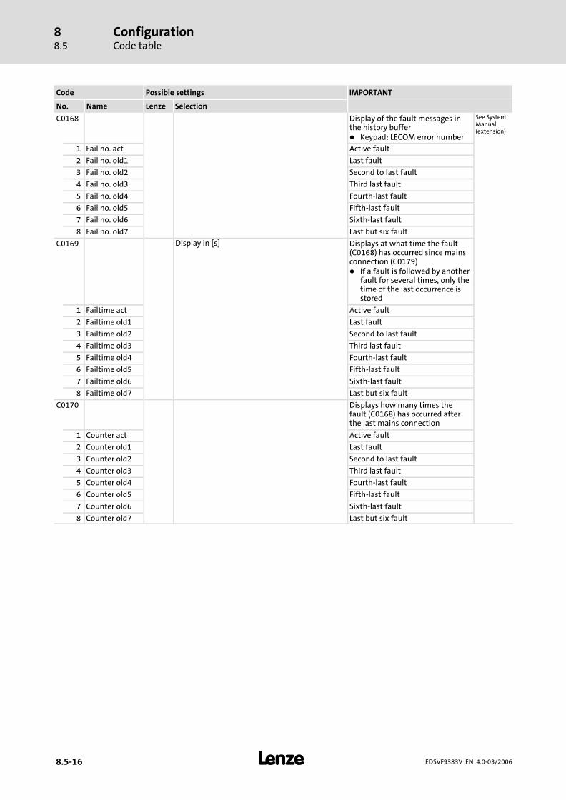
ConfigurationCode table
88.5
� 8.5−16 EDSVF9383V EN 4.0−03/2006
IMPORTANTPossible settingsCode
SelectionLenzeNameNo.
C0168 Display of the fault messages inthe history buffer� Keypad: LECOM error number
See SystemManual(extension)
1 Fail no. act Active fault
2 Fail no. old1 Last fault
3 Fail no. old2 Second to last fault
4 Fail no. old3 Third last fault
5 Fail no. old4 Fourth−last fault
6 Fail no. old5 Fifth−last fault
7 Fail no. old6 Sixth−last fault
8 Fail no. old7 Last but six fault
C0169 Display in [s] Displays at what time the fault(C0168) has occurred since mainsconnection (C0179)� If a fault is followed by another
fault for several times, only thetime of the last occurrence isstored
1 Failtime act Active fault
2 Failtime old1 Last fault
3 Failtime old2 Second to last fault
4 Failtime old3 Third last fault
5 Failtime old4 Fourth−last fault
6 Failtime old5 Fifth−last fault
7 Failtime old6 Sixth−last fault
8 Failtime old7 Last but six fault
C0170 Displays how many times thefault (C0168) has occurred afterthe last mains connection
1 Counter act Active fault
2 Counter old1 Last fault
3 Counter old2 Second to last fault
4 Counter old3 Third last fault
5 Counter old4 Fourth−last fault
6 Counter old5 Fifth−last fault
7 Counter old6 Sixth−last fault
8 Counter old7 Last but six fault

ConfigurationCode table
88.5
� 8.5−17EDSVF9383V EN 4.0−03/2006
IMPORTANTPossible settingsCode
SelectionLenzeNameNo.
C0173�
UG limit 1 Check during commissioning andadapt, if necessary!All controllers in the system musthave the same threshold!� Adaptation of UG thresholds� Only display in case of the
variants for 400 V mains(EVF93xx−EV, EVF93xx−EVV030,EVF93xx−EVV060,EVF93xx−EVV110):– C0173 = 1– OU = 700 ... 685 V
12−1See SystemManual(extension)
Mains LU OU
0 < 400 V 285 V 770 ... 755 V Device with or without braketransistor1 400 V 285 V 770 ... 755 V
2 460 V 328 V 770 ... 755 V
3 480 V 342 V 770 ... 755 V Device without brake transistor
4 480 V 342 V 800 ... 785 V Device with brake transistor
5 500 V 342 V 900 ... 885 V
C0174 BR Limit 3 Display of the brake transistorthresholdsCheck during commissioning andadapt, if necessary!All controllers connected to thebus must have the samethreshold!
12−1See SystemManual(extension)
Mains UBR OU
0 400 V 685 V 700 V Only display in case of the variantsfor 400 V mains (EVF93xx−EV,EVF93xx−EVV030,EVF93xx−EVV060,EVF93xx−EVV110)
1 400 V / 460 V 755 V 770 V Only in case of the variants for400 V/500 V mains(EVF93xx−EVV210,EVF93xx−EVV240,EVF93xx−EVV270,EVF93xx−EVV300)
2 480 V 785 V 800 V
3 500 V 885 V 900 V
C0178 Op timer {s} Display onlyTotal time of the controller enable(X5/28 = HIGH)
C0179 mainstimer {s} Display onlyTotal time of mains "ON"
C0182 Ti S−shaped 20.00 0.01 {0.01 s} 50.00 Integration time of S−shaped rampfunction generator, function blockNSET� C0182 = 0.00: ramp function
generator operates linearly� C0182 > 0.00: ramp function
generator operates in anS−shape (without jerk)
See SystemManual(extension)

ConfigurationCode table
88.5
� 8.5−18 EDSVF9383V EN 4.0−03/2006
IMPORTANTPossible settingsCode
SelectionLenzeNameNo.
C0183 Diagnostics Diagnostics� Display only� If several items or fault or
status information are to beshown, the information withthe smallest number isdisplayed
7.2−10
0 No fault
101 Initialisation
102 TRIP/fault
103 Emergency stop
104 IMP message
105 Power OFF Function is not supported
111 Operation inhibit via C0135
112 Operation inhibit via AIF
113 Operation inhibit via CAN
121 Controller inhibited via X5/28
122 Controller inhibited internally(DCTRL−CINH1)
123 Controller inhibited internally(DCTRL−CINH2)
124 Controller inhibited via �at thekeypad
125 Controller inhibited via AIF
126 Controller inhibited via CAN
141 Switch−on inhibit
142 Pulse inhibit �
151 Quick stop via MCTRL−QSP
152 Quick stop via � at the keypad
153 Quick stop via AIF
154 Quick stop via CAN
161 DC injection braking via terminal
162 DC injection braking via C0135
163 DC injection braking via AIF
164 DC injection braking via CAN
170 Motor parameter identification isactive
250 Warning is active (C0168)
C0190 NSET arit 0 0 OUT = C46 Arithmetic function, functionblock NSETConnects main setpoint (C0046)and additional setpoint (C0040)
See SystemManual(extension)1 C46 + C49
2 C46 − C49
3 C46 * C49
4 C46 / C49
5 C46/(100 − C49)
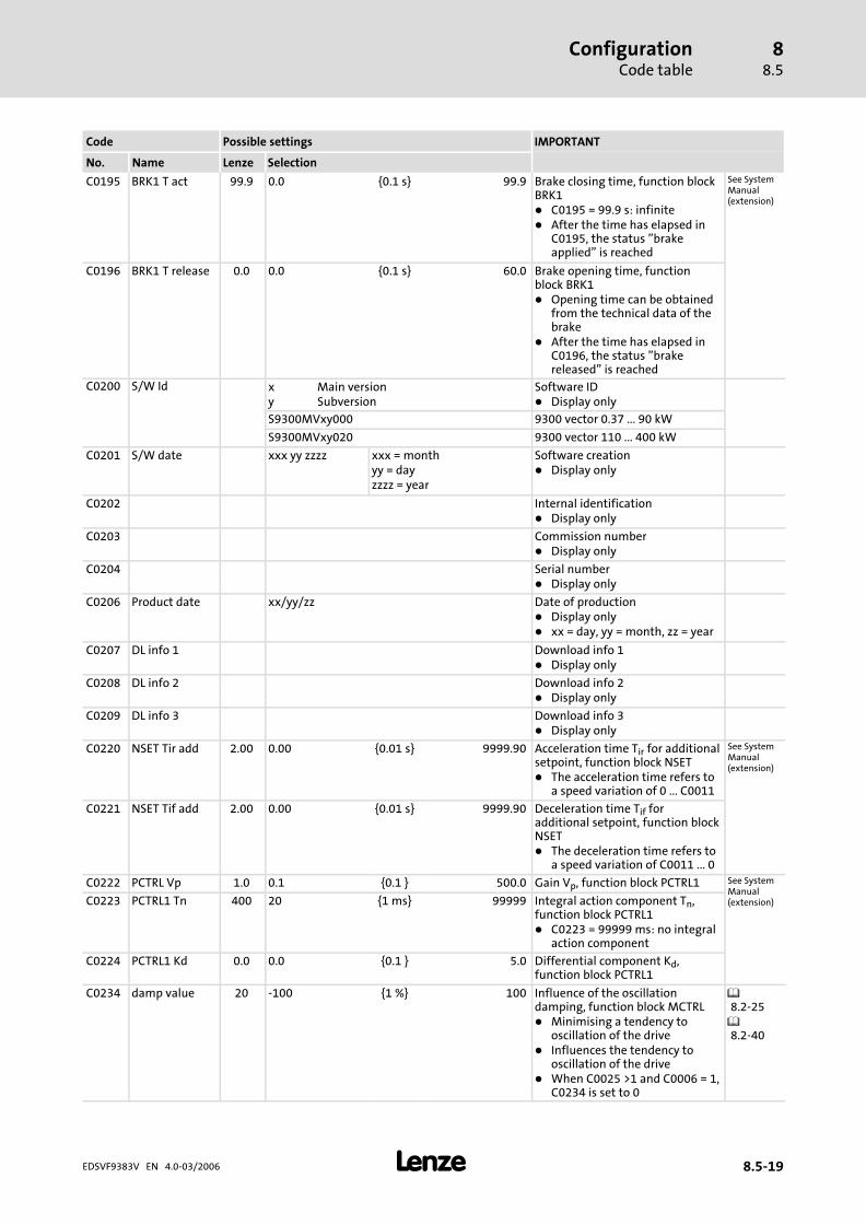
ConfigurationCode table
88.5
� 8.5−19EDSVF9383V EN 4.0−03/2006
IMPORTANTPossible settingsCode
SelectionLenzeNameNo.
C0195 BRK1 T act 99.9 0.0 {0.1 s} 99.9 Brake closing time, function blockBRK1� C0195 = 99.9 s: infinite� After the time has elapsed in
C0195, the status "brakeapplied" is reached
See SystemManual(extension)
C0196 BRK1 T release 0.0 0.0 {0.1 s} 60.0 Brake opening time, functionblock BRK1� Opening time can be obtained
from the technical data of thebrake
� After the time has elapsed inC0196, the status "brakereleased" is reached
C0200 S/W Id xy
Main versionSubversion
Software ID� Display only
S9300MVxy000 9300 vector 0.37 ... 90 kW
S9300MVxy020 9300 vector 110 ... 400 kW
C0201 S/W date xxx yy zzzz xxx = monthyy = dayzzzz = year
Software creation� Display only
C0202 Internal identification� Display only
C0203 Commission number� Display only
C0204 Serial number� Display only
C0206 Product date xx/yy/zz Date of production� Display only� xx = day, yy = month, zz = year
C0207 DL info 1 Download info 1� Display only
C0208 DL info 2 Download info 2� Display only
C0209 DL info 3 Download info 3� Display only
C0220 NSET Tir add 2.00 0.00 {0.01 s} 9999.90 Acceleration time Tir for additionalsetpoint, function block NSET� The acceleration time refers to
a speed variation of 0 ... C0011
See SystemManual(extension)
C0221 NSET Tif add 2.00 0.00 {0.01 s} 9999.90 Deceleration time Tif foradditional setpoint, function blockNSET� The deceleration time refers to
a speed variation of C0011 ... 0
C0222 PCTRL Vp 1.0 0.1 {0.1 } 500.0 Gain Vp, function block PCTRL1 See SystemManual(extension)C0223 PCTRL1 Tn 400 20 {1 ms} 99999 Integral action component Tn,
function block PCTRL1� C0223 = 99999 ms: no integral
action component
C0224 PCTRL1 Kd 0.0 0.0 {0.1 } 5.0 Differential component Kd,function block PCTRL1
C0234 damp value 20 −100 {1 %} 100 Influence of the oscillationdamping, function block MCTRL� Minimising a tendency to
oscillation of the drive� Influences the tendency to
oscillation of the drive� When C0025 >1 and C0006 = 1,
C0234 is set to 0
8.2−25 8.2−40

ConfigurationCode table
88.5
� 8.5−20 EDSVF9383V EN 4.0−03/2006
IMPORTANTPossible settingsCode
SelectionLenzeNameNo.
C0235 damping 2 1 {1 ms} 600 Filter time of the oscillationdamping, function block MCTRL� Filter time for the internal
signal for oscillation damping
8.2−25 8.2−40
C0236 damp limit 1.0 0.0 {0.1 Hz} 20.0 Limit value of oscillation damping,function block MCTRL� Limit value for the internal
signal of oscillation damping
C0241 Cmp−RFG−I=0 1.00 0.00 {0.01 %} 100.00 Speed threshold in [%] for thedigital output NSET−controllerenable−I=0, function block NSET� The analog signals NSET−NOUT
(without arithmetic andlimiting functions) andNSET−controller enable−I arecompared
� NSET−controllerenable−I=0 = HIGH: thedifferential signal betweenNSET−NOUT andNSET−controller enable−I fallsbelow the value in C0241
� C0241 = 100 %: nmax
See SystemManual(extension)
C0244 BRK1 M set 0.00 0.00 {0.01 %} 100.00 Holding torque, function blockBRK1� C0244 = 100 % = C0057
See SystemManual(extension)
C0250 FCODE 1 Bit 0 0 1 Free control code FCODE250
C0252 Angle offset 0 −245760000 {1 inc.} 245760000 Phase offset for master frequencyprocessing, function block DFSET� Fixed phase offset for digital
frequency configuration� 1 rev. = 65536 inc
8.2−18
C0253 Angle n−trim � −32767 {1 inc.} 32767 Speed−dependent phase trimmingfor the master frequencyprocessing, function block DFSET� depending on C0005, C0025,
C0490� Change of C0005, C0025 or
C0490 resets C0253 to thecorresponding Lenze setting
� 1 rev. = 65536 inc� Value in C0253 is reached at
15000 rpm
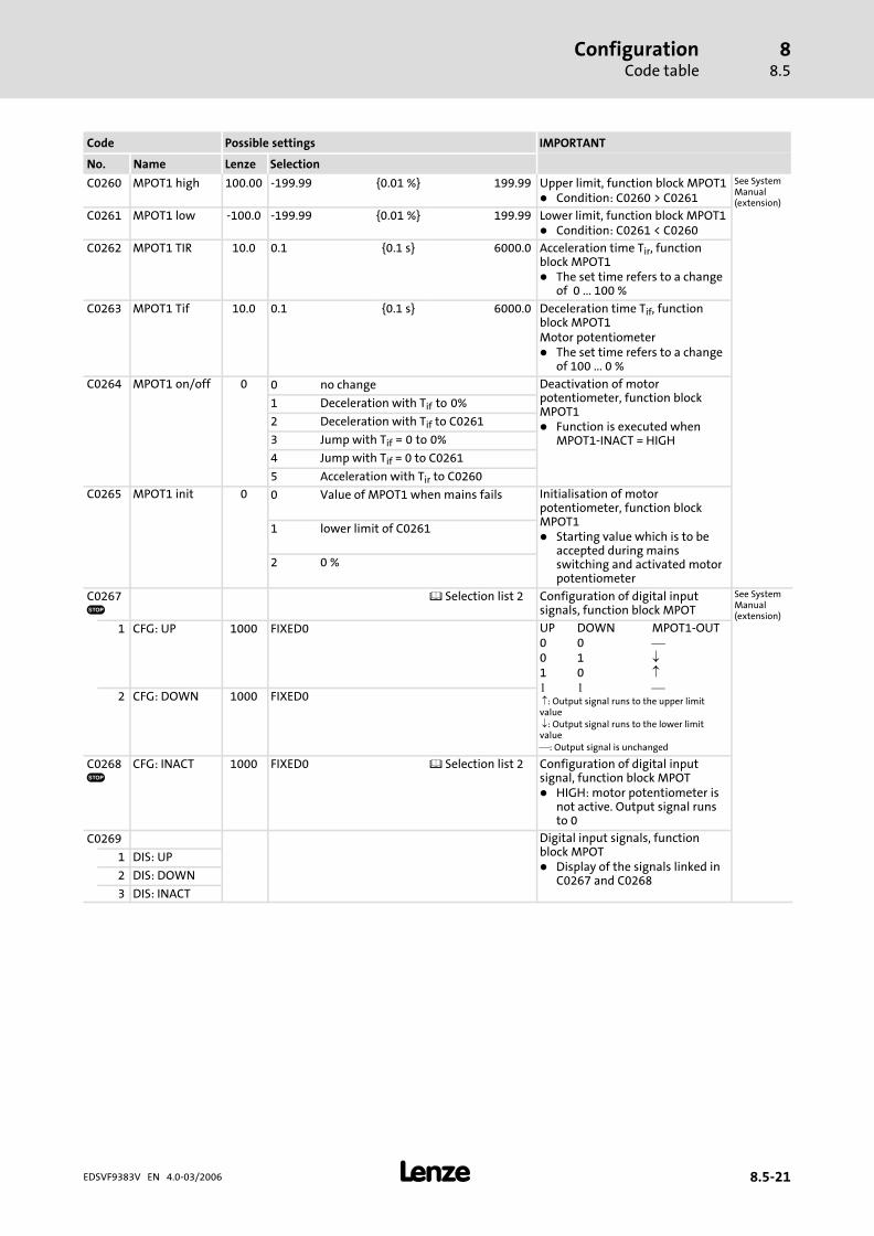
ConfigurationCode table
88.5
� 8.5−21EDSVF9383V EN 4.0−03/2006
IMPORTANTPossible settingsCode
SelectionLenzeNameNo.
C0260 MPOT1 high 100.00 −199.99 {0.01 %} 199.99 Upper limit, function block MPOT1� Condition: C0260 > C0261
See SystemManual(extension)
C0261 MPOT1 low −100.0 −199.99 {0.01 %} 199.99 Lower limit, function block MPOT1� Condition: C0261 < C0260
C0262 MPOT1 TIR 10.0 0.1 {0.1 s} 6000.0 Acceleration time Tir, functionblock MPOT1� The set time refers to a change
of 0 ... 100 %
C0263 MPOT1 Tif 10.0 0.1 {0.1 s} 6000.0 Deceleration time Tif, functionblock MPOT1Motor potentiometer� The set time refers to a change
of 100 ... 0 %
C0264 MPOT1 on/off 0 0 no change Deactivation of motorpotentiometer, function blockMPOT1� Function is executed when
MPOT1−INACT = HIGH
1 Deceleration with Tif to 0�%
2 Deceleration with Tif to C0261
3 Jump with Tif = 0 to 0�%
4 Jump with Tif = 0 to C0261
5 Acceleration with Tir to C0260
C0265 MPOT1 init 0 0 Value of MPOT1 when mains fails Initialisation of motorpotentiometer, function blockMPOT1� Starting value which is to be
accepted during mainsswitching and activated motorpotentiometer
1 lower limit of C0261
2 0 %
C0267�
Selection list 2 Configuration of digital inputsignals, function block MPOT
See SystemManual(extension)
1 CFG: UP 1000 FIXED0 UP DOWN MPOT1−OUT0 0 �0 1 �1 0 �� � � �: Output signal runs to the upper limitvalue �: Output signal runs to the lower limitvalue�: Output signal is unchanged
2 CFG: DOWN 1000 FIXED0
C0268�
CFG: INACT 1000 FIXED0 Selection list 2 Configuration of digital inputsignal, function block MPOT� HIGH: motor potentiometer is
not active. Output signal runsto 0
C0269 Digital input signals, functionblock MPOT� Display of the signals linked in
C0267 and C0268
1 DIS: UP
2 DIS: DOWN
3 DIS: INACT

ConfigurationCode table
88.5
� 8.5−22 EDSVF9383V EN 4.0−03/2006
IMPORTANTPossible settingsCode
SelectionLenzeNameNo.
C0325 Vp2 adapt 1.0 0.1 {0.1 } 500.0 Function block PTCTRL1� Adaptation of gain Vp2
See SystemManual(extension)
C0326 Vp3 adapt 1.0 0.1 {0.1 } 500.0 Function block PTCTRL1� Adaptation of gain Vp3
C0327 Set2 adapt 100.00 0.00 {0.01 %} 100.00 Function block PTCTRL1� Adaptation of setpoint speed
threshold nset2� Condition: C0327 > C0328
C0328 Set1 adapt 0.00 0.00 {0.01 %} 100.00 Function block PTCTRL1� Adaptation of setpoint speed
threshold nset1� Condition: C0328 < C0327
C0329 Adapt on/off 0 0 No adaptation of the processcontroller
Function block PTCTRL1� Adaptation On/Off
1 External adaptation via input
2 Adaptation via setpoint
3 Adaptation via control difference
C0332 PCTRL Tir 0 0 {1 s} 10000 Acceleration time Tir, functionblock PCTRL1� The acceleration time refers to
a setpoint change of 0 ... 100 %
See SystemManual(extension)
C0333 PCTRL1 Tif 0 0 {1 s} 10000 Deceleration time Tif, functionblock PCTRL1� The deceleration time refers to
a setpoint change of 100 % ... 0
C0336 DIS: act Up 0.0 {0.1 } 500.0 Current gain Vp, function blockPCTRL1� Read only
See SystemManual(extension)
C0337 Bi/unipolar 0 Sphere of action, function blockPCTRL1
0 Bipolar � Output value is limited to−100 ... 100 %
1 Unipolar � Output value is limited to0 ... 100 %
C0338 ARIT1 funct 1 0 OUT = IN1 Selection of function, functionblock ARIT1
See SystemManual(extension)1 OUT = IN1 + IN2
2 OUT = IN1 − IN2
3 OUT = IN1 * IN2
4 OUT = IN1 / IN2
5 OUT = IN1 / (100 − IN2)
C0339�
Selection list 1 Configuration of analog inputsignals, function block ARIT1
1 CFG: IN 1000 FIXED0% ARIT1−IN1
2 CFG: IN 1000 FIXED0% ARIT1−IN2
C0340 −199.99 {0.01 %} 199.99 Function block ARIT1� Display of the signals linked in
C0339
1 DIS: IN ARIT1−IN1
2 DIS: IN ARIT1−IN2
C0350 CAN address 1 1 {1} 63 System bus node address� Change is effective after ˜Reset
node˜ command
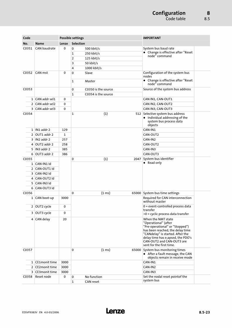
ConfigurationCode table
88.5
� 8.5−23EDSVF9383V EN 4.0−03/2006
IMPORTANTPossible settingsCode
SelectionLenzeNameNo.
C0351 CAN baudrate 0 0 500 kbit/s System bus baud rate� Change is effective after ˜Reset
node˜ command1 250 kbit/s
2 125 kbit/s
3 50 kbit/s
4 1000 kbit/s
C0352 CAN mst 0 0 Slave Configuration of the system busnodes� Change is effective after ˜Reset
node˜ command1 Master
C0353 0 C0350 is the source Source of the system bus address
1 C0354 is the source
1 CAN addr sel1 0 CAN IN1, CAN−OUT1
2 CAN addr sel2 0 CAN IN2, CAN−OUT2
3 CAN addr sel3 0 CAN IN3, CAN−OUT3
C0354 1 {1} 512 Selective system bus address� Individual addressing of the
system bus process dataobjects
1 IN1 addr 2 129 CAN−IN1
2 OUT1 addr 2 1 CAN−OUT2
3 IN2 addr 2 257 CAN−IN2
4 OUT2 addr 2 258 CAN−OUT2
5 IN3 addr 2 385 CAN−IN3
6 OUT3 addr 2 386 CAN−OUT3
C0355 0 {1} 2047 System bus identifier� Read only1 CAN−IN1 Id
2 CAN−OUT1 Id
3 CAN−IN2 Id
4 CAN−OUT2 Id
5 CAN−IN3 Id
6 CAN−OUT3 Id
C0356 0 {1 ms} 65000 System bus time settings
1 CAN boot−up 3000 Required for CAN interconnectionwithout master
2 OUT2 cycle 0 0 = event−controlled process datatransfer>0 = cyclic process data transfer3 OUT3 cycle 0
4 CAN delay 20 When the NMT state"Operational" (after"Pre−operational" or "Stopped")has been reached, the delay time˜CANdelay˜ is started. After thedelay time has e;apsed, the PDO´sCAN−OUT2 and CAN−OUT3 aresent for the first time.
C0357 0 {1 ms} 65000 System bus monitoring times� After a fault message, the CAN
objects remain in receive mode
1 CE1monit time 3000 CAN−IN1
2 CE2monit time 3000 CAN−IN2
3 CE3monit time 3000 CAN−IN3
C0358 Reset node 0 0 No function Set the nodal reset pointof thesystem bus1 CAN reset

ConfigurationCode table
88.5
� 8.5−24 EDSVF9383V EN 4.0−03/2006
IMPORTANTPossible settingsCode
SelectionLenzeNameNo.
C0359 CAN state 0 Operational System bus status� Read only1 Pre−operational
2 Warning
3 Bus off
C0360 0 65535 Telegram counter� Read only� For count values > 65535 the
counter starts at 0
1 Message OUT All telegrams sent
2 Message IN All telegrams received
3 Message OUT1 Telegrams sent on CAN−OUT1
4 Message OUT2 Telegrams sent on CAN−OUT2
5 Message OUT3 Telegrams sent on CAN−OUT3
6 MessagePOUT1
Telegrams sent on parameterchannel1
7 MessagePOUT2
Telegrams sent on parameterchannel2
8 Message IN1 Telegrams received from CAN−IN1
9 Message IN2 Telegrams received from CAN−IN2
10 Message IN3 Telegrams received from CAN−IN3
11 Message PIN1 Telegrams received fromparameter channel1
12 Message PIN2 Telegrams received fromparameter channel2
C0361 0 {1 %} 100 System bus load� Read only� For a perfect operation, the
entire bus load (all nodesconnected) should be less than80 %
1 Load OUT All telegrams sent
2 Load IN All telegrams received
3 Load OUT1 Telegrams sent on CAN−OUT1
4 Load OUT2 Telegrams sent on CAN−OUT2
5 Load OUT3 Telegrams sent on CAN−OUT3
6 Load POUT1 Telegrams sent on parameterchannel1
7 Load POUT2 Telegrams sent on parameterchannel2
8 Load IN1 Telegrams received from CAN−IN1
9 Load IN2 Telegrams received from CAN−IN2
10 Load IN3 Telegrams received from CAN−IN3
11 Load PIN1 Telegrams received fromparameter channel1
12 Load PIN2 Telegrams received fromparameter channel2
C0364�
CFG: CAN activ 1000 FIXED0 Selection list 2 Configuration − digital input signal� Switches the system bus via
the external signal from"Pre−Operational" to"Operational"
C0365 DIS:CAN activ 0 Pre−Operational System bus state� Display only1 Operational
C0366 Sync Response 1 0 No response Response to sync telegram of themaster1 Response

ConfigurationCode table
88.5
� 8.5−25EDSVF9383V EN 4.0−03/2006
IMPORTANTPossible settingsCode
SelectionLenzeNameNo.
C0367 Sync Rx ID 128 1 {1} 256 Receipt identifier (Rx)� Sync Identifier for grouping for
data transfer to CAN−IN1
C0368 Sync Tx ID 128 1 {1} 256 Transmission identifier (Tx)� Identifier for generating a sync
telegram
C0369 Sync Tx Time 0 0 {1} 65000 Sync transmission time (Tx)� Transmission interval for the
object set in C0368
C0400 DIS: OUT −199.99 {0.01 %} 199.99 Analog output signal, functionblock AIN1� Read only
See SystemManual(extension)
C0402�
CFG: OFFSET 19502 FCODE−26/1 Selection list 1 Configuration offset, functionblock AIN1� The offset is added to the input
signal at AIN1−IN
C0403�
CFG: GAIN 19504 FCODE−27/1 Selection list 1 Configuration of gain, functionblock AIN1� The gain is multiplied by the
input signal at AIN1−IN
C0404 −199.99 {0.01 %} 199.99 Function block AIN1� Display of the signals linked in
C0402 and C04041 DIS: OFFSET
2 DIS: GAIN
C0405 DIS: OUT −199.99 {0.01 %} 199.99 Analog output signal, functionblock AIN2� Read only
See SystemManual(extension)
C0407�
CFG: OFFSET 19503 FCODE−26/2 Selection list 1 Configuration of offset, functionblock AIN2� The offset is added to the input
signal at AIN2−IN
C0408�
CFG: GAIN 19505 FCODE−27/2 Selection list 1 Configuration of gain, functionblock AIN2� The gain is multiplied by the
input signal at AIN2−IN
C0409 −199.99 {0.01 %} 199.99 Function block AIN2� Display of the signals linked in
C0407 and C04081 DIS: OFFSET
2 DIS: GAIN
C0420�
Encoder const 512 1 {1 inc/rev} 8192 Number of increments forincremental encoder at X8 or X9� Connect incremental encoders
with HTL−level on X9 only
6.7−1
C0421�
Enc voltage 5.00 5.00 {0.1 V} 8.00 Supply voltage for the incrementalencoder at X8CAUTION! A wrong entry candestroy the incremental encoder!
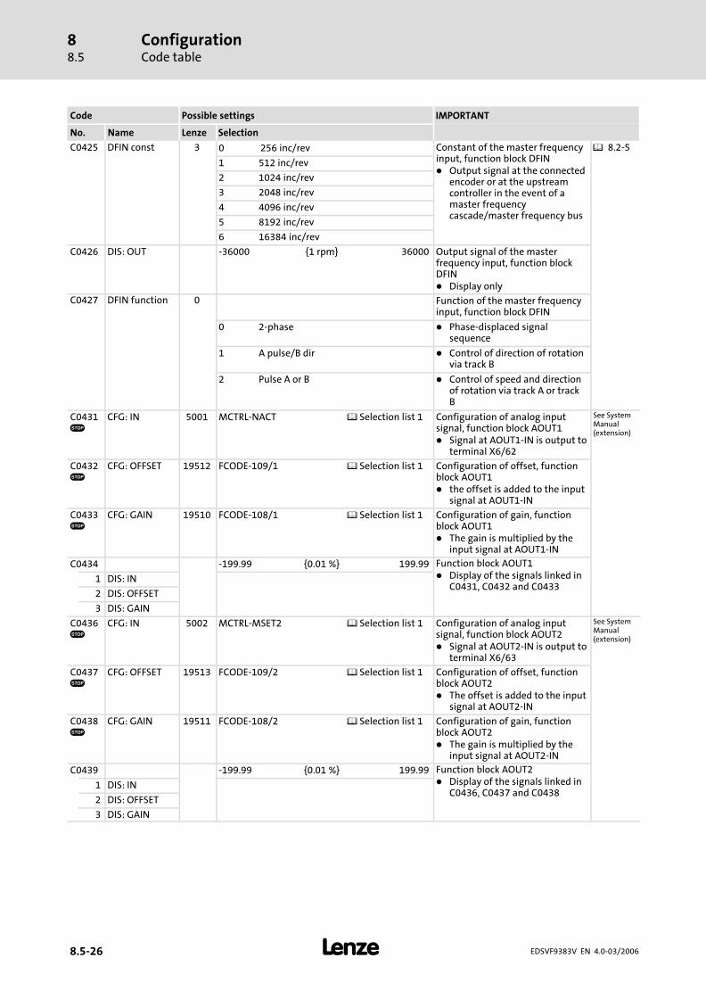
ConfigurationCode table
88.5
� 8.5−26 EDSVF9383V EN 4.0−03/2006
IMPORTANTPossible settingsCode
SelectionLenzeNameNo.
C0425 DFIN const 3 0 256 inc/rev Constant of the master frequencyinput, function block DFIN� Output signal at the connected
encoder or at the upstreamcontroller in the event of amaster frequencycascade/master frequency bus
8.2−5
1 512 inc/rev
2 1024 inc/rev
3 2048 inc/rev
4 4096 inc/rev
5 8192 inc/rev
6 16384 inc/rev
C0426 DIS: OUT −36000 {1 rpm} 36000 Output signal of the masterfrequency input, function blockDFIN� Display only
C0427 DFIN function 0 Function of the master frequencyinput, function block DFIN
0 2−phase � Phase−displaced signalsequence
1 A pulse/B dir � Control of direction of rotationvia track B
2 Pulse A or B � Control of speed and directionof rotation via track A or trackB
C0431�
CFG: IN 5001 MCTRL−NACT Selection list 1 Configuration of analog inputsignal, function block AOUT1� Signal at AOUT1−IN is output to
terminal X6/62
See SystemManual(extension)
C0432�
CFG: OFFSET 19512 FCODE−109/1 Selection list 1 Configuration of offset, functionblock AOUT1� the offset is added to the input
signal at AOUT1−IN
C0433�
CFG: GAIN 19510 FCODE−108/1 Selection list 1 Configuration of gain, functionblock AOUT1� The gain is multiplied by the
input signal at AOUT1−IN
C0434 −199.99 {0.01 %} 199.99 Function block AOUT1� Display of the signals linked in
C0431, C0432 and C04331 DIS: IN
2 DIS: OFFSET
3 DIS: GAIN
C0436�
CFG: IN 5002 MCTRL−MSET2 Selection list 1 Configuration of analog inputsignal, function block AOUT2� Signal at AOUT2−IN is output to
terminal X6/63
See SystemManual(extension)
C0437�
CFG: OFFSET 19513 FCODE−109/2 Selection list 1 Configuration of offset, functionblock AOUT2� The offset is added to the input
signal at AOUT2−IN
C0438�
CFG: GAIN 19511 FCODE−108/2 Selection list 1 Configuration of gain, functionblock AOUT2� The gain is multiplied by the
input signal at AOUT2−IN
C0439 −199.99 {0.01 %} 199.99 Function block AOUT2� Display of the signals linked in
C0436, C0437 and C04381 DIS: IN
2 DIS: OFFSET
3 DIS: GAIN

ConfigurationCode table
88.5
� 8.5−27EDSVF9383V EN 4.0−03/2006
IMPORTANTPossible settingsCode
SelectionLenzeNameNo.
C0443 DIS:DIGIN−OUT
0 {1} 255 Terminal signals, function blockDIGIN� Read only� Binary interpretation of the
terminal signals at X5
See SystemManual(extension)
Bit Assignment
0 DIGIN1 X5/E1
1 DIGIN2 X5/E2
2 DIGIN3 X5/E3
3 DIGIN4 X5/E4
4 DIGIN5 X5/E5
5 ST−DIGIN6 X5/ST
6 DIGIN−CINH X5/28
C0444 01
LOW signalHIGH signal
Terminal signals, function blockDIGOUT� Read only
See SystemManual(extension)
DIS: DIGOUT1 Bit Assignment X5/A1
DIS: DIGOUT2 0 DIGIN1 X5/A2
DIS: DIGOUT3 1 DIGIN2 X5/A3
DIS: DIGOUT4 2 DIGIN3 X5/A4
C0450�
CFG: NX 1000 FIXED0% Selection list 1 Configuration of analog inputsignal, function block BRK1� Speed threshold, from which
the drive may output the signal"Close brake"
See SystemManual(extension)
C0451�
CFG: SET 1000 FIXED0 Selection list 2 Configuration of digital inputsignal, function block BRK1� HIGH = close brake� LOW = open brake
C0452�
CFG: SIGN 1000 FIXED0% Selection list 1 Configuration of analog inputsignal, function block BRK1� Direction of torque with which
the drive is to create a torqueagainst the brake
C0458 −199.99 {0.01 %} 199.99 Function block BRK1� Display of the signals linked in
C0450 and C0452
See SystemManual(extension)1 DIS: NX
2 DIS: SIGN
C0459 DIS: ON Function block BRK1� Display of the signal linked in
C0451
C0464 Customer I/F 0 original Customer interface indicates thestatus of the selected basicconfiguration� Reassignment of terminals in a
basic configuration does notchange C0005 and sets C0464= 1
� Adding or removing functionblocks or changing the signalflow among the functionblocks in a basic configurationsets C0005 = 0 and C0464= 1
1 changed

ConfigurationCode table
88.5
� 8.5−28 EDSVF9383V EN 4.0−03/2006
IMPORTANTPossible settingsCode
SelectionLenzeNameNo.
C0465�
� Selection list 5 Function block − processing list� Defining the sequence in which
the function blocks are to beprocessed internally
� Depending on C0005.Changing C0005 loadsassigned processing list
� The displayed values apply toC0005 = 1000
� After changing the signal flow,adapt the processing list in anycase. Otherwise the controllermay use the wrong signals!
� The function blocks DIGIN,DIGOUT, AIF−IN, CAN−IN, andMCTRL are always processedand do not have to be enteredin the list
1 FB list 200 DFIN
2 FB list 0
3 FB list 50 AIN1
4 FB list 0
5 FB list 0
6 FB list 55 AIN2
7 FB list 0
8 FB list 0
9 FB list 10250 R/L/Q
10 FB list 0
... ... 0
14 FB list 0
15 FB list 5250 NLIM1
16 FB list 5050 NSET
... ... 0
19 FB list 5700 ANEG1
... ... 0
22 FB list 10650 CMP1
... ... 0
25 FB list 70 AOUT1
... ... 0
28 FB list 75 AOUT2
... ... 0
31 FB list 250 DFOUT
... ... 0
41 FB list 25000 AIF−OUT
42 FB list 20000 CAN−OUT
... ... ...
50 FB list 0
C0466 CPU T remain Remaining process time forprocessing the function blocks� Display only
C0469�
Fct STP key 2 0 inactive Inactive Determines the function which isreleased when pressing � on thekeypadChanges are only active aftermains connection!
1 CINH Inhibit controller:
2 qsp Quick stop
C0470 0 {1} 255 Configuration of free controlcodes for digital signals� The data words C0470 and
C0471 are in parallel and areidentical.
1 FCODE 8 Bit 0 FCODE bit 0−7
2 FCODE 8 Bit 0 FCODE bit 8−15
3 FCODE 8 Bit 0 FCODE bit 16−23
4 FCODE 8 Bit 0 FCODE bit 24−31
C0471 Configurationof inputFCODE 32 Bit
0 0 {1} 4294967296 Free control code for digitalsignals� The data words C0470 and
C0471 are in parallel and areidentical.

ConfigurationCode table
88.5
� 8.5−29EDSVF9383V EN 4.0−03/2006
IMPORTANTPossible settingsCode
SelectionLenzeNameNo.
C0472 −199.99 {0.01 %} 199.99 Configuration of free controlcodes for analog signals1 FCODE analog 0.00
2 FCODE analog 0.00
3 FCODE analog 100.00
6 FCODE analog 0.00
... ... 0.00
20 FCODE analog 0.00
C0473 −32767 {1} 32767 Configuration of free controlcodes for absolute analog signals1 FCODE abs 1
2 FCODE abs 1
3 FCODE abs 0
... ... 0
10 FCODE abs 0
C0474 −2147483647 {1} 2147483647 Configuration of free controlcodes for phase signals� 1 rev. = 65536 inc
1 FCODE PH 0
... ... 0
5 FCODE PH 0
C0475 −16000 {1} 16000 Configuration of free controlcodes for phase difference signals� 1 rev. = 65536 inc
1 FCODE DF 0
2 FCODE DF 0
C0497 Nact filter 2.0 0.0 {0.1 ms} 50.0 Filter time constant Nact for actualspeed value, function blockMCTRL2� Internal filtering of the speed
signal for control� C0497 = 0 ms: Switched off
8.2−40
C0510�
CFG: IN1 50 AIN1−OUT Selection list 1 Configuration of analog inputsignal, function block NLIM1� Input for analog speed setpoint
See SystemManual(extension)
C0511 DIS: IN1 −199.99 {0.01 %} 199.99 Function block NLIM1� Display of the input signal
configured in C0510

ConfigurationCode table
88.5
� 8.5−30 EDSVF9383V EN 4.0−03/2006
IMPORTANTPossible settingsCode
SelectionLenzeNameNo.
C0517�
0.00 {0.01 } 1999.00 � The user menu contains in theLenze setting the mostimportant codes forcommissioning the operatingmode ˜V/f characteristiccontrol
� With an active passwordprotection only the codesentered in C0517 can be freelyaccessed
� Enter the numbers of therequired codes in the subcodes
� The input is done in the formatxxx.yy– xxx: Code number– yy: Subcode number
� It is not checked whether theentered code exists.
1 User menu 51.00 Actual speed value (MCTRL−NACT)
2 User menu 54.00 Actual motor current (MCTRL−IACT)
3 User menu 56.00 Torque setpoint (MCTRL−MSET2)
4 User menu 64.00 Device utilisation I×t
5 User menu 183.00 Diagnostics
6 User menu 168.01 History buffer
7 User menu 39.01 JOG−setpoints 1 (NSET)
8 User menu 86.00 Motor type selection
9 User menu 148.00 Identifying motor parameters
10 User menu 22.00 Imax limit in motor mode
11 User menu 23.00 Imax limit in generator mode
12 User menu 11.00 Maximum speed Nmax
13 User menu 12.00 Acceleration time Tir main setpoint
14 User menu 13.00 Deceleration time Tif main setpoint
15 User menu 16.00 Umin boost
16 User menu 70.00 Gain Vp speed controller
17 User menu 71.00 Integral−action time Tn speed controller
18 User menu 75.00 Gain Vp current controller
19 User menu 76.00 Integral−action time Tn current controller
20 User menu 142.00 Starting condition
21 User menu 92.00 Motor stator inductance
22 User menu 36.00 DC braking current
23 User menu 93.00 Controller identification
24 User menu 99.00 Software version
... ... 0 Not assigned
31 User menu 94.00 Password
32 User menu 3.00 Save parameter set
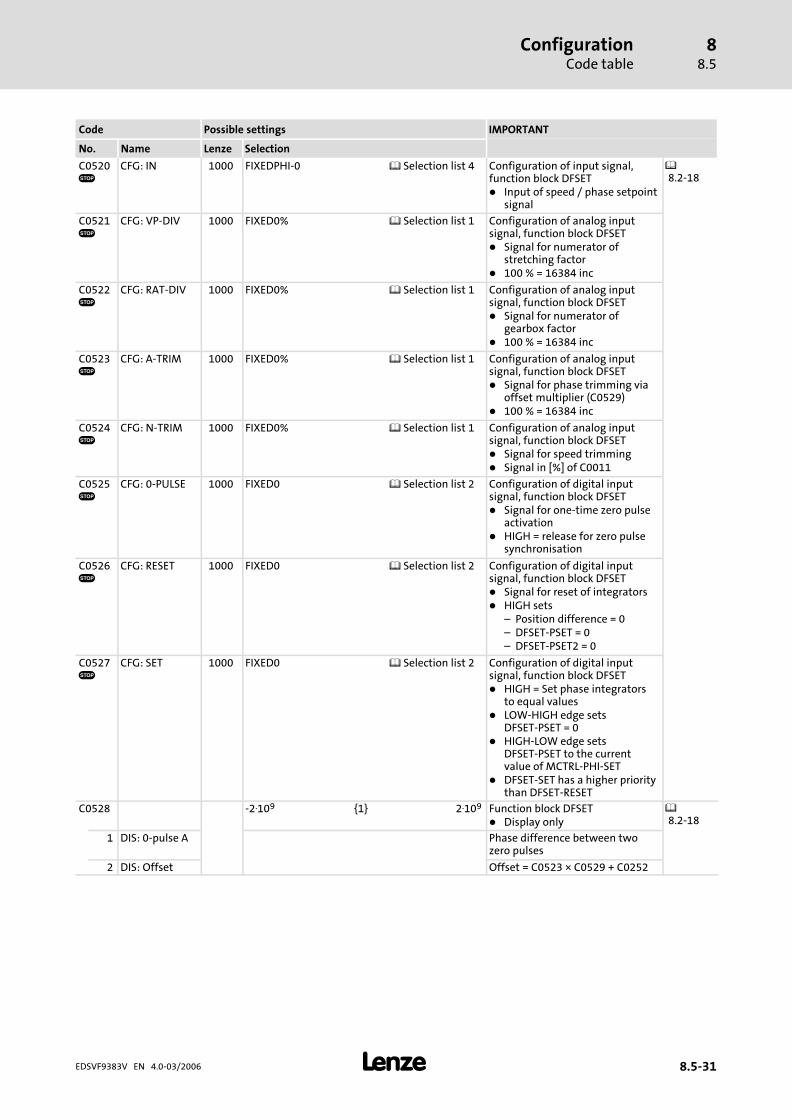
ConfigurationCode table
88.5
� 8.5−31EDSVF9383V EN 4.0−03/2006
IMPORTANTPossible settingsCode
SelectionLenzeNameNo.
C0520�
CFG: IN 1000 FIXEDPHI−0 Selection list 4 Configuration of input signal,function block DFSET� Input of speed / phase setpoint
signal
8.2−18
C0521�
CFG: VP−DIV 1000 FIXED0% Selection list 1 Configuration of analog inputsignal, function block DFSET� Signal for numerator of
stretching factor� 100 % = 16384 inc
C0522�
CFG: RAT−DIV 1000 FIXED0% Selection list 1 Configuration of analog inputsignal, function block DFSET� Signal for numerator of
gearbox factor� 100 % = 16384 inc
C0523�
CFG: A−TRIM 1000 FIXED0% Selection list 1 Configuration of analog inputsignal, function block DFSET� Signal for phase trimming via
offset multiplier (C0529)� 100 % = 16384 inc
C0524�
CFG: N−TRIM 1000 FIXED0% Selection list 1 Configuration of analog inputsignal, function block DFSET� Signal for speed trimming� Signal in [%] of C0011
C0525�
CFG: 0−PULSE 1000 FIXED0 Selection list 2 Configuration of digital inputsignal, function block DFSET� Signal for one−time zero pulse
activation� HIGH = release for zero pulse
synchronisation
C0526�
CFG: RESET 1000 FIXED0 Selection list 2 Configuration of digital inputsignal, function block DFSET� Signal for reset of integrators� HIGH sets
– Position difference = 0– DFSET−PSET = 0– DFSET−PSET2 = 0
C0527�
CFG: SET 1000 FIXED0 Selection list 2 Configuration of digital inputsignal, function block DFSET� HIGH = Set phase integrators
to equal values� LOW−HIGH edge sets
DFSET−PSET = 0� HIGH−LOW edge sets
DFSET−PSET to the currentvalue of MCTRL−PHI−SET
� DFSET−SET has a higher prioritythan DFSET−RESET
C0528 −2.109 {1} 2.109 Function block DFSET� Display only
8.2−18
1 DIS: 0−pulse A Phase difference between twozero pulses
2 DIS: Offset Offset = C0523 × C0529 + C0252

ConfigurationCode table
88.5
� 8.5−32 EDSVF9383V EN 4.0−03/2006
IMPORTANTPossible settingsCode
SelectionLenzeNameNo.
C0529 Multip offset 1 −20000 {1} 20000 Offset multiplier, function blockDFSET� Multiplier for the phase offset
(C0252)
8.2−18
C0530 DF evaluation 0 0 with factor With gearboxfactor
Master frequency evaluation,function block DFSET� Evaluation of the setpoint
integrator1 no factor Without gearbox
factor
C0531 Act 0 div 1 1 {1} 16384 Actual zero pulse divisor, functionblock DFSET
C0532 0−pulse/TP 1 1 0−pulse Index pulse Zero pulse / touch probe, functionblock DFSET� Zero pulse of the feedback
system or touch probe2 Touch probe Touch probe
C0533 Vp denom 1 1 {1} 32767 Gain factor of denominator Vp,function block DFSET
C0534 0 pulse fct 0 Zero pulse function, functionblock DFSET� Synchronising the drive
8.2−18
0 inactive Inactive
1 Continuous Continuoussynchronisation,correction in theshortest possibleway
2 Cont. switch Continuoussynchronisation,correction in theshortest possibleway
After a LOW−HIGH signal toDFSET−0−pulse, the zero track issynchronised once
10 Once, fast way One−timesynchronisation,correction in theshortest possibleway
11 Once, CW One−timesynchronisation,correction indirection ofrotation to theright
12 Once, CCW One−timesynchronisation,correction indirection ofrotation to the left
13 Once, 2*0−pulse One−timesynchronisation,correction isdetected fromsetpoint pulse andactual pulse andcorrected to thecorrespondingdirection
C0535 Set 0 div 1 1 {1} 16384 Desired zero pulse divisor,function block DFSET
8.2−18

ConfigurationCode table
88.5
� 8.5−33EDSVF9383V EN 4.0−03/2006
IMPORTANTPossible settingsCode
SelectionLenzeNameNo.
C0536 −32767 {1} 32767 Function block DFSET� Display of the signals linked in
C0521, C0522 and C0523
8.2−181 DIS: VP−DIV
2 DIS: RAT−DIV
3 DIS: A−TRIM
C0537 DIS: N−TRIM −199.99 {0.01 %} 199.99 Function block DFSET� Display of the signal linked in
C0524
C0538 0 1 Function block DFSET� Display of the signals linked in
C0525, C0526 and C05271 DIS: 0−pulse
2 DIS: RESET
3 DIS: SET
C0539 DIS: IN −6000 {1 rpm} 6000 Function block DFSET� Display of the signal linked in
C0520
C0540�
Function 0 Function selection, function blockDFOUT� Output signal at X10
8.2−8
0 Analog input Analog input Signal at DFOUT−AN−IN is output.Zero track can be input externally.
1 PH diff input Phase differenceinput
Signal at DFOUT−DF−IN is output.Zero track can be input externally.
2 Not assigned
3 Not assigned
4 X10 = X9 X9 is output onX10
The input signals are bufferedC0030 is without function
5 X10 = X8 X8 is output onX10
C0541�
CFG: AN−IN 5001 MCTRL−NACT Selection list 1 Configuration of analog inputsignal, function block DFOUT� Signal in [%] of C0011
C0542�
CFG: DF−IN 1000 FIXEDPHI−0 Selection list 4 Configuration of input signal,function block DFOUT� Speed signal
C0544�
CFG: SYN−RDY 1000 FIXED0 Selection list 2 Configuration of digital inputsignal, function block DFOUT� DFOUT−SYN−RDY = HIGH:
Generating a zero pulse
C0545 PH offset 0 0 {1 inc.} 65535 Phase offset, function blockDFOUT� Displacing the zero pulse
generated via DFOUT−SYN−RDYby up to 360 °
� 1 rev. = 65535 inc (360 °)
C0546 Min inc/rev 1000 1 {1 inc.} 2147483647 Masking of the touch probe signal,function block DFSET� Suppressing interference
pulses at X5/E4 (actual pulse oftouch probe signal)
� The size of the maskingwindow between two actualpulses is set
8.2−18

ConfigurationCode table
88.5
� 8.5−34 EDSVF9383V EN 4.0−03/2006
IMPORTANTPossible settingsCode
SelectionLenzeNameNo.
C0547 DIS: AN−IN −199.99 {0.01 %} 199.99 Function block DFOUT� Display of the signal linked in
C0541
8.2−8
C0548 DIS: SYN−RDY 0 1 Function block DFOUT� Display of the signal linked in
C0544
C0549 DIS: DF−IN −32767 {1 rpm} 32767 Function block DFOUT� Display of the signal linked in
C0542
C0560 −199.99 {0.01 %} 199.99 Configuration of fixed setpoints,function block FIXSET1� Output of the setpoints to
FIXSET1−OUT via binary codingof the inputs FIXSET1−IN1 ...FIXST1−IN4
See SystemManual(extension)1 Fix set−value 100
2 Fix set−value 75
3 Fix set−value 50
4 Fix set−value 25
5 Fix set−value 0
... ... 0
15 Fix set−value 0
C0561�
CFG: AIN 1000 FIXED0% Selection list 1 Configuration of analog inputsignal, function block FIXSET1� The analog input signal is
switched to FIXSET1−OUT if allinputs FIXSET−INx = LOW
C0562�
Selection list 2 Configuration of digital inputsignals, function block FIXSET1� The number of inputs to be
assigned depend on thenumber of the fixed setpointsrequired.
1 CFG: IN 1000 FIXED0 FIXSET1−IN1
2 CFG: IN 1000 FIXED0 FIXSET1−IN2
3 CFG: IN 1000 FIXED0 FIXSET1−IN3
4 CFG: IN 1000 FIXED0 FIXSET1−IN4
C0563 DIS: AIN −199.99 {0.01 %} 199.99 Function block FIXSET1� Display of the signal linked in
C0561
C0564 0 1 Function block FIXSET1� Display of the signals linked in
C0562/1, C0562/2, C0562/3and C0562/4
1 DIS: IN FIXSET1−IN1
2 DIS: IN FIXSET1−IN2
3 DIS: IN FIXSET1−IN3
4 DIS: IN FIXSET1−IN4
C0570�
CFG: IN 1000 FIXED0% Selection list 1 Configuration of analog inputsignal, function block S&H1
See SystemManual(extension)
C0571�
CFG: LOAD 1000 FIXED0 Selection list 2 Configuration of digital inputsignal, function block S&H1
C0572 DIS: IN −199.99 {0.01 %} 199.99 Function block S&H1� Display of the signal linked in
C0570
C0573 DIS: LOAD 0 1 Function block S&H1� Display of the signal linked in
C0571
C0581 MONIT EEr 0 0 TRIP Configuration monitoring EEr,external fault
See SystemManual(extension)1 Message
2 Warning
3 Off

ConfigurationCode table
88.5
� 8.5−35EDSVF9383V EN 4.0−03/2006
IMPORTANTPossible settingsCode
SelectionLenzeNameNo.
C0582 MONIT OH4 2 2 Warning Configuration monitoring OH4,heatsink temperature� The operating temperature can
be set in C0122
See SystemManual(extension)
3 Off
C0583 MONIT OH3 3 0 TRIP Configuration of motortemperature monitoring withfixed operating temperature� Only for KTY at X8� The operating temperature is
fixed at 150 °C
6.6−11See SystemManual(extension)3 Off
C0584 MONIT OH7 3 2 Warning Configuration of monitoringmotor temperature with variableoperating temperature� Only for KTY at X8� When reaching the
temperature set in C0121 thewarning OH7 is activated
6.6−11See SystemManual(extension)3 Off
C0585 MONIT OH8 3 0 TRIP Configuration of motortemperature monitoring� Temperature monitoring via
PTC input (T1, T2)
6.6−9See SystemManual(extension)
2 Warning
3 Off
C0587 MONIT SD3 3 0 TRIP Configuration of monitoring SD3,encoder at X9� Monitors the voltage supply at
X9/pin 8
See SystemManual(extension)2 Warning
3 Off
C0588 MONITH10/H11
0 0 TRIP Configuration of monitoring H10and H11, thermal sensors in thecontroller� H10: Sensor error − heatsink
temperature� H11: Sensor error − interior
temperature
See SystemManual(extension)
3 Off
C0591 MONIT CE1 3 0 TRIP Configuration of monitoring CE1,communication error at CAN−IN1
See SystemManual(extension)2 Warning
3 Off
C0592 MONIT CE2 3 0 TRIP Configuration of monitoring CE2,communication error at CAN−IN22 Warning
3 Off
C0593 MONIT CE3 3 0 TRIP Configuration of monitoring CE3,communication error at CAN−IN32 Warning
3 Off
C0594 MONIT SD6 3 0 TRIP Activation of the motortemperature monitoring with KTYat X8� Use C0594 = 0 or 2 to activate
monitoring� In case of a short circuit or
interruption at X8/5 and X8/8the fault message SD6 isactivated
� Configuration of the responsewhen exceeding the motortemperature– Fixed operating temperature
in C0583– Variable operating
temperature in C0584
6.6−11See SystemManual(extension)
2 Warning
3 Off
C0595 MONIT CE4 3 0 TRIP Configuration of monitoring CE4,BUS−OFF (system bus)
See SystemManual(extension)2 Warning
3 Off

ConfigurationCode table
88.5
� 8.5−36 EDSVF9383V EN 4.0−03/2006
IMPORTANTPossible settingsCode
SelectionLenzeNameNo.
C0596 NMAX limit 4000 0 {1 rpm} 36000 Configuration of monitoring Nmax,maximum system speed exceeded
See SystemManual(extension)
C0597 MONIT LP1 3 0 TRIP Configuration of monitoring themotor phases LP1
See SystemManual(extension)2 Warning
3 Off
C0598 MONIT SD5 3 0 TRIP Configuration of monitoring SD5,open circuit at analog input X6/1,X6/2
See SystemManual(extension)2 Warning
3 Off
C0599 Limit LP1 5.0 1.0 {0.1 %} 10.0 Configuration of current limit LP1,current limit value for monitoringthe motor phases in C0597
See SystemManual(extension)
C0600 Function 1 0 OUT = IN1 Function selection, function blockARIT2
See SystemManual(extension)1 OUT = IN1 + IN2
2 OUT = IN1 − IN2
3 OUT = IN1 * IN2
4 OUT = IN1 / IN2
5 OUT = IN1 / (100 − IN2)
C0601�
Selection list 1 Configuration of analog inputsignal, function block ARIT2
1 CFG: IN 1000 FIXED0% ARIT2−IN1
2 CFG: IN 1000 FIXED0% ARIT2−IN2
C0602 −199.99 {0.01 %} 199.99 Function block ARIT2� Display of the signals linked in
C0601
1 DIS: IN ARIT2−IN1
2 DIS: IN ARIT2−IN2
C0603 Function 1 0 OUT = IN1 Function selection, function blockARIT3
See SystemManual(extension)1 OUT = IN1 + IN2
2 OUT = IN1 − IN2
3 OUT = IN1 * IN2
4 OUT = IN1 / IN2
5 OUT = IN1 / (100 − IN2)
C0604�
Selection list 1 Configuration of analog inputsignal, function block ARIT3
1 CFG: IN 1000 FIXED0% ARIT3−IN1
2 CFG: IN 1000 FIXED0% ARIT3−IN2
C0605 −199.99 {0.01 %} 199.99 Function block ARIT3� Display of the signals linked in
C0604
1 DIS: IN ARIT3−IN1
2 DIS: IN ARIT3−IN2
C0608�
CFG: IN 1000 FIXED0% Selection list 1 Configuration of analog inputsignal, function block SQRT1
See SystemManual(extension)
C0609 DIS: IN −199.99 {0.01 %} 199.99 Function block SQRT1� Display of the signal linked in
C0608
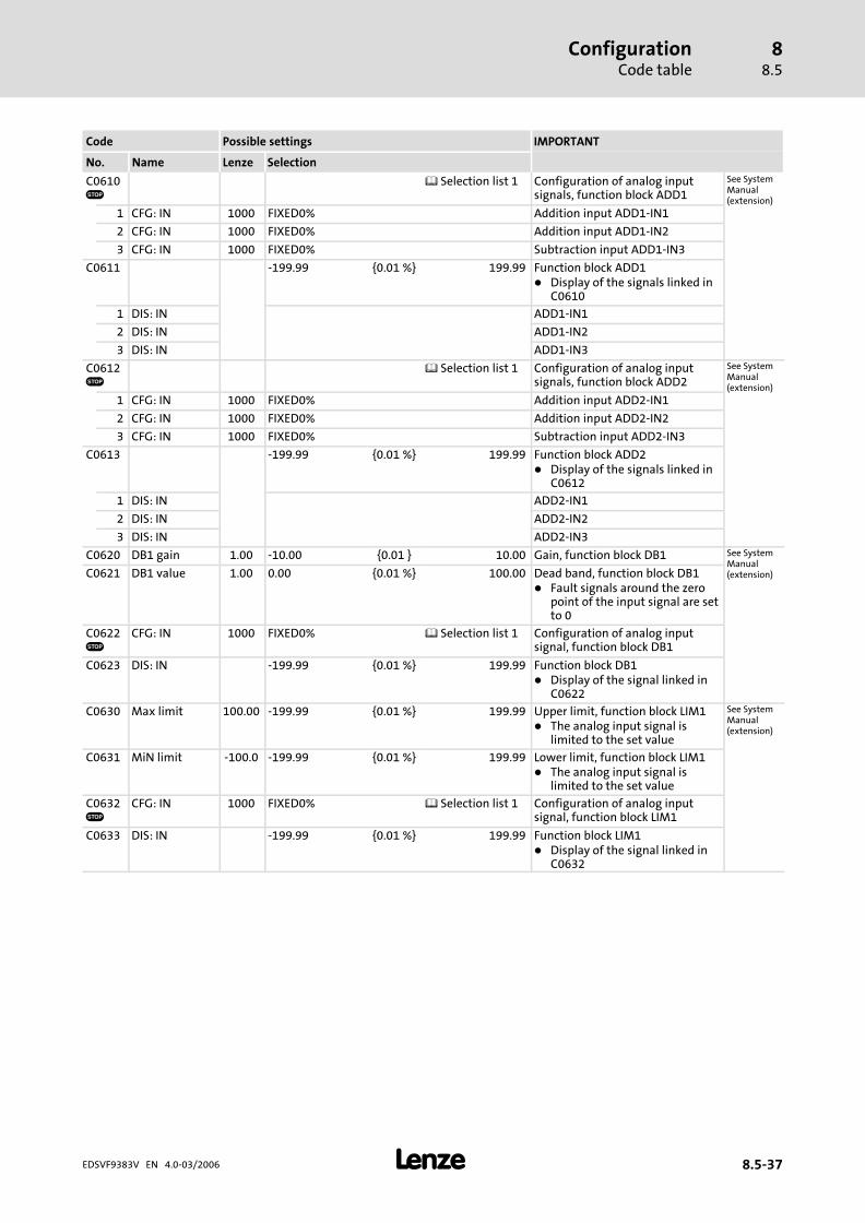
ConfigurationCode table
88.5
� 8.5−37EDSVF9383V EN 4.0−03/2006
IMPORTANTPossible settingsCode
SelectionLenzeNameNo.
C0610�
Selection list 1 Configuration of analog inputsignals, function block ADD1
See SystemManual(extension)
1 CFG: IN 1000 FIXED0% Addition input ADD1−IN1
2 CFG: IN 1000 FIXED0% Addition input ADD1−IN2
3 CFG: IN 1000 FIXED0% Subtraction input ADD1−IN3
C0611 −199.99 {0.01 %} 199.99 Function block ADD1� Display of the signals linked in
C0610
1 DIS: IN ADD1−IN1
2 DIS: IN ADD1−IN2
3 DIS: IN ADD1−IN3
C0612�
Selection list 1 Configuration of analog inputsignals, function block ADD2
See SystemManual(extension)
1 CFG: IN 1000 FIXED0% Addition input ADD2−IN1
2 CFG: IN 1000 FIXED0% Addition input ADD2−IN2
3 CFG: IN 1000 FIXED0% Subtraction input ADD2−IN3
C0613 −199.99 {0.01 %} 199.99 Function block ADD2� Display of the signals linked in
C0612
1 DIS: IN ADD2−IN1
2 DIS: IN ADD2−IN2
3 DIS: IN ADD2−IN3
C0620 DB1 gain 1.00 −10.00 {0.01 } 10.00 Gain, function block DB1 See SystemManual(extension)C0621 DB1 value 1.00 0.00 {0.01 %} 100.00 Dead band, function block DB1
� Fault signals around the zeropoint of the input signal are setto 0
C0622�
CFG: IN 1000 FIXED0% Selection list 1 Configuration of analog inputsignal, function block DB1
C0623 DIS: IN −199.99 {0.01 %} 199.99 Function block DB1� Display of the signal linked in
C0622
C0630 Max limit 100.00 −199.99 {0.01 %} 199.99 Upper limit, function block LIM1� The analog input signal is
limited to the set value
See SystemManual(extension)
C0631 MiN limit −100.0 −199.99 {0.01 %} 199.99 Lower limit, function block LIM1� The analog input signal is
limited to the set value
C0632�
CFG: IN 1000 FIXED0% Selection list 1 Configuration of analog inputsignal, function block LIM1
C0633 DIS: IN −199.99 {0.01 %} 199.99 Function block LIM1� Display of the signal linked in
C0632

ConfigurationCode table
88.5
� 8.5−38 EDSVF9383V EN 4.0−03/2006
IMPORTANTPossible settingsCode
SelectionLenzeNameNo.
C0640 Delay T 20.00 0.01 {0.01 s} 50.00 Time constant, function blockPT1−1� Time period by which the
output of analog signal isdelayed
See SystemManual(extension)
C0641�
CFG: IN 1000 FIXED0% Selection list 1 Configuration of analog inputsignal, function block PT1−1
C0642 DIS: IN −199.99 {0.01 %} 199.99 Function block PT1−1� Display of the signal linked in
C0641
C0643 Delay T 20.00 0.01 {0.01 s} 50.00 Time constant, function blockPT1−2� Time period by which the
output of analog signal isdelayed
C0644�
CFG: IN 1000 FIXED0% Selection list 1 Configuration of analog inputsignal, function block PT1−2
C0645 DIS: IN −199.99 {0.01 %} 199.99 Function block PT1−2� Display of the signal linked in
C0644
C0650 DT1−1 gain 1.00 −320.00 {0.01 } 320.00 Gain, function block DT1−1� Gain of the analog input signal
See SystemManual(extension)
C0651 Delay T 1.000 0.005 {0.01 s} 5.000 Time constant, function blockDT1−1� Time period by which the
output of analog signal isdelayed
C0652�
CFG: IN 1000 FIXED0% Selection list 1 Configuration of analog inputsignal, function block DT1−1
C0653 Sensibility 1 1 15 bits Input sensitivity, function blockDT1−1� According to the setting only
the indicated higher−order bitsare evaluated
2 14 bits
3 13 bits
4 12 bits
5 11 bits
6 10 bits
7 9 bits
C0654 DIS: IN −199.99 {0.01 %} 199.99 Function block DT1−1� Display of the signal linked in
C0652
C0655 Numerator 1 −32767 {1} 32767 Configuration of conversion factorwith numerator and denominator,function block CONV5
See SystemManual(extension)
C0656 Denominator 1 1 {1} 32767OUT�[rpm] � IN�[%] �
15000�rpm
100�%� C0655
C0656
C0657�
CFG: IN 1000 FIXED0% Selection list 1 Configuration of analog inputsignal, function block CONV5
C0658 DIS: IN −199.99 {0.01 %} 199.99 Function block CONV5� Display of the signal linked in
C0657
C0661�
CFG: IN 1000 FIXED0% Selection list 1 Configuration of analog inputsignal, function block ABS1� Converts bipolar signals into
unipolar signals
See SystemManual(extension)
C0662 DIS: IN −199.99 {0.01 %} 199.99 Function block ABS1� Display of the signal linked in
C0661

ConfigurationCode table
88.5
� 8.5−39EDSVF9383V EN 4.0−03/2006
IMPORTANTPossible settingsCode
SelectionLenzeNameNo.
C0671 RFG1 Tir 0.00 0.00 {0.01 s} 999.90 Acceleration time Tir anddeceleration time Tif, functionblock RFG1� Acceleration and deceleration
ramp
See SystemManual(extension)
C0672 RFG1 Tif 0.00 0.00 {0.01 s} 999.90
C0673�
CFG: IN 1000 FIXED0% Selection list 1 Configuration of analog inputsignal, function block RFG1� Selection of a final value at
RFG1−OUT
C0674�
CFG: SET 1000 FIXED0% Selection list 1 Configuration of analog inputsignal, function block RFG1� Selection of a starting value at
RFG1−OUT
C0675�
CFG: LOAD 1000 FIXED0 Selection list 2 Configuration of digital inputsignal, function block RFG1� HIGH: RFG1−OUT is set to the
value at RFG1−Set� LOW: The signal at RFG1−OUT
travels along the rampstowards the input value atRFG1−IN
C0676 −199.99 {0.01 %} 199.99 Function block RFG1� Display of the signals linked in
C0673 and C0674
1 DIS: RFG1 RFG1−IN
2 DIS: RFG1 RFG1−SET
C0677 DIS: LOAD 0 1 Function block RFG1� Display of the signal linked in
C0675
C0680 Function 1 1 IN1 = IN 2 Function selection, function blockCMP1� Compare input signals at
CMP1−IN1 and CMP1−IN2
See SystemManual(extension)2 IN1 > IN2
3 IN1 < IN2
4 |IN1IN2|
5 |IN1IN2|
6 |IN1IN2|
C0681 Hysteresis 1.00 0.00 {0.01 %} 100.00 Hysteresis, function block CMP1� Hysteresis for input signals
which are not stable and hencethe output oscillates
C0682 Window 1.00 0.00 {0.01 %} 100.00 Window, function block CMP1� Set the range in which the
signal comparison is to beapply
C0683�
Selection list 1 Configuration of analog inputsignal, function block CMP1
1 CFG: IN 5001 MCTRL−NACT CMP1−IN1
2 CFG: IN 19500 FCODE−17 CMP1−IN2
C0684 −199.99 {0.01 %} 199.99 Function block CMP1� Display of the signals linked in
C0683
1 DIS: IN CMP1−IN1
2 DIS: IN CMP1−IN2

ConfigurationCode table
88.5
� 8.5−40 EDSVF9383V EN 4.0−03/2006
IMPORTANTPossible settingsCode
SelectionLenzeNameNo.
C0685 Function 1 1 IN1 = IN 2 Function selection, function blockCMP2� Compare input signals at
CMP2−IN1 and CMP2−IN2
See SystemManual(extension)2 IN1 > IN2
3 IN1 < IN2
4 |IN1IN2|
5 |IN1IN2|
6 |IN1IN2|
C0686 Hysteresis 1.00 0.00 {0.01 %} 100.00 Hysteresis, function block CMP2� Hysteresis for input signals
which are not stable and hencethe output oscillates
C0687 Window 1.00 0.00 {0.01 %} 100.00 Window, function block CMP2� Set the range in which the
signal comparison is to beapply
C0688�
Selection list 1 Configuration of analog inputsignal, function block CMP2
1 CFG: IN 1000 FIXED0% CMP2−IN1
2 CFG: IN 1000 FIXED0% CMP2−IN2
C0689 −199.99 {0.01 %} 199.99 Function block CMP2� Display of the signals linked in
C0688
1 DIS: IN CMP2−IN1
2 DIS: IN CMP2−IN2
C0690 Function 1 1 IN1 = IN 2 Function selection, function blockCMP3� Compare input signals at
CMP3−IN1 and CMP3−IN2
See SystemManual(extension)2 IN1 > IN2
3 IN1 < IN2
4 |IN1IN2|
5 |IN1IN2|
6 |IN1| < |IN2|
C0691 Hysteresis 1.00 0.00 {0.01 %} 100.00 Hysteresis, function block CMP3� Hysteresis for input signals
which are not stable and hencethe output oscillates
C0692 Window 1.00 0.00 {0.01 %} 100.00 Window, function block CMP3� Set the range in which the
signal comparison is to beapply
C0693�
Selection list 1 Configuration of analog inputsignal, function block CMP3
1 CFG: IN 1000 FIXED0% CMP3−IN1
2 CFG: IN 1000 FIXED0% CMP3−IN2
C0694 −199.99 {0.01 %} 199.99 Function block CMP3� Display of the signals linked in
C0693
1 DIS: IN CMP3−IN1
2 DIS: IN CMP3−IN2
C0700�
CFG: IN 19523 FCODE−472/3 Selection list 1 Configuration of analog inputsignal, function block ANEG1� The value at ANEG1−IN is
multiplied by −1 and output
See SystemManual(extension)
C0701 DIS: IN −199.99 {0.01 %} 199.99 Function block ANEG1� Display of the signal linked in
C0700

ConfigurationCode table
88.5
� 8.5−41EDSVF9383V EN 4.0−03/2006
IMPORTANTPossible settingsCode
SelectionLenzeNameNo.
C0703�
CFG: IN 19523 FCODE−472/3 Selection list 1 Configuration of analog inputsignal, function block ANEG2� The value at ANEG2−IN is
multiplied by −1 and output
See SystemManual(extension)
C0704 DIS: IN −199.99 {0.01 %} 199.99 Function block ANEG2� Display of the signal linked in
C0703
C0705 Function 1 1 IN1 = IN 2 Function selection, function blockCMP4� Compare input signals at
CMP4−IN1 and CMP4−IN2
See SystemManual(extension)2 IN1 > IN2
3 IN1 < IN2
4 |IN1| = |IN2|
5 |IN1| > |IN2|
6 |IN1| < |IN2|
C0706 Hysteresis 1.00 0.00 {0.01 %} 100.00 Hysteresis, function block CMP4� Hysteresis for input signals
which are not stable and hencethe output oscillates
C0707 Window 1.00 0.00 {0.01 %} 100.00 Window, function block CMP4� Set the range in which the
signal comparison is to beapply
C0708�
Selection list 1 Configuration of analog inputsignal, function block CMP4
1 CFG: IN 1000 FIXED0% CMP4−IN1
2 CFG: IN 1000 FIXED0% CMP4−IN2
C0709 −199.99 {0.01 %} 199.99 Function block CMP4� Display of the signals linked in
C0708
1 DIS: IN CMP4−IN1
2 DIS: IN CMP4−IN2
C0710 Function 0 Function selection, function blockTRANS1
See SystemManual(extension)
0 Rising trans Rising edge 1. LOW−HIGH edge at TRANS1−INswitches TRANS1−OUT = HIGH
2. After the time has elapsed(C0711), TRANS1−OUT switchesto LOW
1 Falling trans Falling edge 1. HIGH−LOW edge at TRANS1−INswitches TRANS1−OUT = HIGH
2. After the time has elapsed(C0711), TRANS1−OUT switchesto LOW
2 Both trans Both edges 1. LOW−HIGH− or HIGH−LOW edgeat TRANS1−IN switchesTRANS1−OUT = HIGH
2. After the time has elapsed(C0711), TRANS1−OUT switchesto LOW
C0711 Pulse T 0.001 0.001 {0.001s}
60.000 Pulse duration, function blockTRANS1� After the time has elapsed,
TRANS1−OUT switches to LOW
C0713�
CFG: IN 1000 FIXED0 Selection list 2 Configuration of digital inputsignal, function block TRANS1
C0714 DIS: IN 0 1 Function block TRANS1� Display of the signal linked in
C0713

ConfigurationCode table
88.5
� 8.5−42 EDSVF9383V EN 4.0−03/2006
IMPORTANTPossible settingsCode
SelectionLenzeNameNo.
C0715 Function 0 Function selection, function blockTRANS2
See SystemManual(extension)
0 Rising trans Rising edge 1. LOW−HIGH edge at TRANS2−INswitches TRANS2−OUT = HIGH
2. After the time has elapsed(C0716), TRANS2−OUT switchesto LOW
1 Falling trans Falling edge 1. HIGH−LOW edge at TRANS2−INswitches TRANS2−OUT = HIGH
2. After the time has elapsed(C0716), TRANS2−OUT switchesto LOW
2 Both trans Both edges 1. LOW−HIGH or HIGH−LOW edgeat TRANS2−IN switchesTRANS2−OUT = HIGH
2. After the time has elapsed(C0716), TRANS2−OUT switchesto LOW
C0716 Pulse T 0.001 0.001 {0.001s}
60.000 Pulse duration, function blockTRANS2� After the time has elapsed,
TRANS2−OUT switches to LOW
C0718�
CFG: IN 1000 FIXED0 Selection list 2 Configuration of digital inputsignal, function block TRANS2
C0719 DIS: IN 0 1 Function block TRANS2� Display of the signal linked in
C0718
C0720 Function 2 Function selection, function blockDIGDEL1
See SystemManual(extension)
0 On delay On delay 1. LOW−HIGH edge at DIGDEL1−INstarts a timing element
2. After the time has elapsed(C0721), DIGDEL1−OUTswitches to HIGH
1 Off delay Off delay 1. LOW−HIGH edge at DIGDEL1−INstarts a timing element andsets DIGDEL1−OUT = HIGH
2. After the time has elapsed(C0721), DIGDEL1−OUTswitches to LOW
2 ON/OFF delay On/off delay 1. LOW−HIGH or HIGH−LOW edgeat DIGDEL1−IN starts a timingelement
2. After the time has elapsed(C0721),DIGDEL1−OUT = DIGDEL1−IN
C0721 Delay T 1.000 0.001 {0.001s}
60.000 Delay time, function blockDIGDEL1
C0723�
CFG: IN 1000 FIXED0 Selection list 2 Configuration of digital inputsignal, function block DIGDEL1
C0724 DIS: IN 0 1 Function block DIGDEL1� Display of the signal linked in
C0723

ConfigurationCode table
88.5
� 8.5−43EDSVF9383V EN 4.0−03/2006
IMPORTANTPossible settingsCode
SelectionLenzeNameNo.
C0725 Function 2 Function selection, function blockDIGDEL2
See SystemManual(extension)
0 On delay On delay 1. LOW−HIGH edge at DIGDEL2−INstarts a timing element
2. After the time has elapsed(C0726), DIGDEL2−OUTswitches to HIGH
1 Off delay Off delay 1. LOW−HIGH edge at DIGDEL2−INstarts a timing element andsets DIGDEL2−OUT = HIGH
2. After the time has elapsed(C0726), DIGDEL2−OUTswitches to LOW
2 ON/OFF delay On/off delay 1. LOW−HIGH or HIGH−LOW edgeat DIGDEL2−IN starts a timingelement
2. After the time has elapsed(C0726),DIGDEL2−OUT = DIGDEL2−IN
C0726 Delay T 1.000 0.001 {0.001s}
60.000 Delay time, function blockDIGDEL2
C0728�
CFG: IN 1000 FIXED0 Selection list 2 Configuration of digital inputsignal, function block DIGDEL2
C0729 DIS: IN 0 1 Function block DIGDEL2� Display of the signal linked in
C0728
C0730 Mode 0 0 Stop measurement Function block OSZ� Starting / stopping the
measured value recording
See SystemManual(extension)1 Start measurement
C0731 Status 0 Measurement completed Oscilloscope function� Read only� Current operating status
1 Measurement active
2 Trigger detected
3 Abort
4 Abort after trigger
5 Read memory
C0732�
Selection list 1 Configuration of analog inputsignals, function block OSZFunction block OSZ
See SystemManual(extension)
1 OSZ channel 1 1000 FIXED0%
2 OSZ channel 2 1000 FIXED0%
3 OSZ channel 3 1000 FIXED0%
4 OSZ channel 4 1000 FIXED0%
C0733�
Selection list 2 Configuration of digital inputsignal, function block OSZ
1 Trigger input 1000 FIXED0
C0734 Trigger source 1 0 OSZ trigger input Function block OSZ� Configure digital input C0732
or C0733 with desired triggersignal
See SystemManual(extension)1 OSZ channel 1
2 OSZ channel 2
3 OSZ channel 3
4 OSZ channel 4
C0735 Trigger level 0 −32767 {1} 32767 Function block OSZ� Trigger level OSZ channel 1 ...
OSZ channel 4
C0736 Trigger edge 0 0 LOW−HIGH edge Oscilloscope function
1 HIGH−LOW edge
C0737 Trigger Delay 0.0 −100.0 {0.1 %} 999.99 Function block OSZ� Setting of pretriggering and
posttriggering
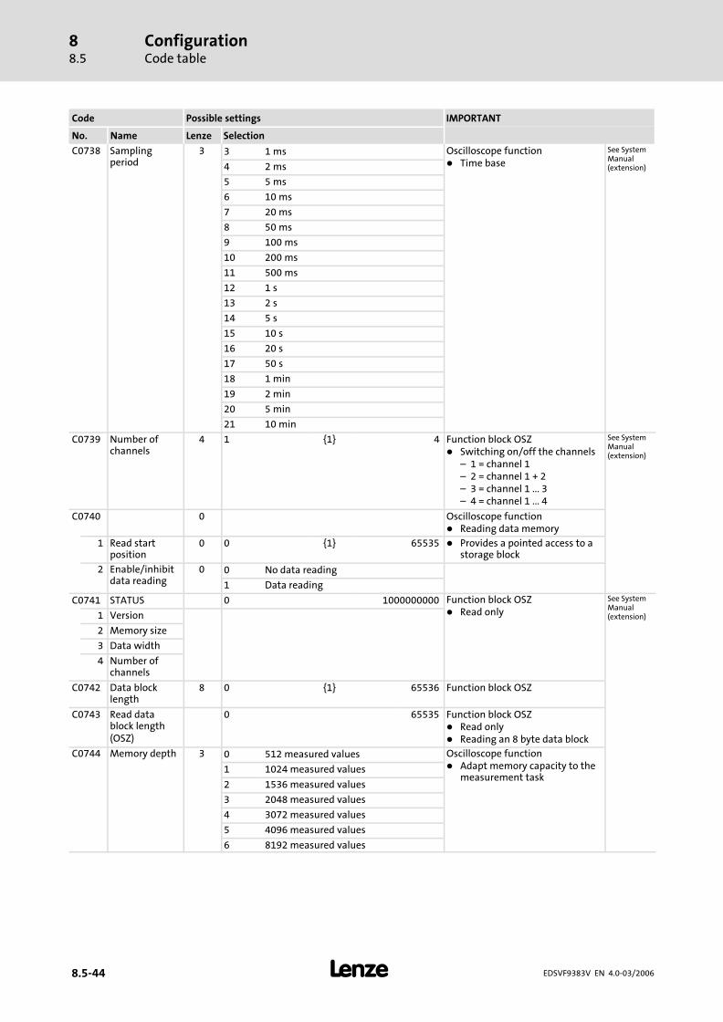
ConfigurationCode table
88.5
� 8.5−44 EDSVF9383V EN 4.0−03/2006
IMPORTANTPossible settingsCode
SelectionLenzeNameNo.
C0738 Samplingperiod
3 3 1 ms Oscilloscope function� Time base
See SystemManual(extension)4 2 ms
5 5 ms
6 10 ms
7 20 ms
8 50 ms
9 100 ms
10 200 ms
11 500 ms
12 1 s
13 2 s
14 5 s
15 10 s
16 20 s
17 50 s
18 1 min
19 2 min
20 5 min
21 10 min
C0739 Number ofchannels
4 1 {1} 4 Function block OSZ� Switching on/off the channels
– 1 = channel 1– 2 = channel 1 + 2– 3 = channel 1 ... 3– 4 = channel 1 ... 4
See SystemManual(extension)
C0740 0 Oscilloscope function� Reading data memory
1 Read startposition
0 0 {1} 65535 � Provides a pointed access to astorage block
2 Enable/inhibitdata reading
0 0 No data reading
1 Data reading
C0741 STATUS 0 1000000000 Function block OSZ� Read only
See SystemManual(extension)1 Version
2 Memory size
3 Data width
4 Number ofchannels
C0742 Data blocklength
8 0 {1} 65536 Function block OSZ
C0743 Read datablock length(OSZ)
0 65535 Function block OSZ� Read only� Reading an 8 byte data block
C0744 Memory depth 3 0 512 measured values Oscilloscope function� Adapt memory capacity to the
measurement task1 1024 measured values
2 1536 measured values
3 2048 measured values
4 3072 measured values
5 4096 measured values
6 8192 measured values

ConfigurationCode table
88.5
� 8.5−45EDSVF9383V EN 4.0−03/2006
IMPORTANTPossible settingsCode
SelectionLenzeNameNo.
C0749 0 65535 Information about storing themeasured values, function blockOSZ� Read only
See SystemManual(extension)
1 Abort index Measured value no. of the aborttime
2 Trigger index Measured value no. of the triggertime
3 End index Measured value no. of the endtime
C0750 Vp denom 16 1 1 Gain VP of the position controller,function block DFRFG1
8.2−132 1/2
4 1/4
8 1/8
16 1/16
32 1/32
64 1/64
128 1/128
256 1/256
512 1/512
1024 1/1024
2048 1/2048
4096 1/4096
8192 1/8192
16384 1/16384
C0751 DFRFG1 Tir 1.000 0.001 {0.001s}
999.999 Acceleration time Tir, functionblock DFRFG1
8.2−13
C0752 Max speed 3000 1 {1 rpm} 16000 Maximum speed, function blockDFRFG1� Maximum speed−up (speed)
C0753 DFRFG1 QSP 0.000 0.000 {0.001s}
999.900 Deceleration time Tif for quickstop, function block DFRFG1
C0754 PH error 2.109 10 {1} 2.109 Following error, function blockDFRFG1� Maximum permissible phase
difference between setpoint anactual phase
� 1 rev. = 65535 inc
C0755 Syn window 100 0 {1 inc.} 65535 Synchronisation window, functionblock DFRFG1� 1 rev. = 65535 inc

ConfigurationCode table
88.5
� 8.5−46 EDSVF9383V EN 4.0−03/2006
IMPORTANTPossible settingsCode
SelectionLenzeNameNo.
C0758�
CFG: IN 1000 FIXEDPHI−0 Selection list 4 Configuration of input signal,function block DFRFG1� Speed/phase setpoint signal
8.2−13
C0759�
CFG: QSP 1000 FIXED0 Selection list 2 Configuration of digital inputsignal, function block DFRFG1� HIGH = quick stop active
C0760�
CFG: STOP 1000 FIXED0 Selection list 2 Configuration of input signal,function block DFRFG1� HIGH = Status of the profile
generator is maintained,setpoint is saved
C0761�
CFG: RESET 1000 FIXED0 Selection list 2 Configuration of input signal,function block DFRFG1� HIGH = resetting the
integrators
C0764 0 1 Function block DFRFG1� Display of the signals linked in
C0759, C0760 and C07611 DIS: QSP
2 DIS: STOP
3 DIS: RESET
C0765 DIS: IN −32767 {1 rpm} 32767 Function block DFRFG1� Display of the signal linked in
C0758
C0770�
CFG: D 1000 FIXED0 Selection list 2 Configuration of digital inputsignal, function block FLIP1
See SystemManual(extension)
C0771�
CFG: CLK 1000 FIXED0 Selection list 2 Configuration of digital inputsignal, function block FLIP1� Each LOW−HIGH edge at
FLIP1−CLK switches the signalat FLIP1−D to FLIP1−OUT
C0772�
CFG: CLR 1000 FIXED0 Selection list 2 Configuration of digital inputsignal, function block FLIP1� Resets the flip−flop� HIGH: Sets FLIP1−OUT = LOW� Input has highest priority
C0773 0 1 Function block FLIP1� Display of the signals linked in
C0770, C0771 and C07731 DIS: D
2 DIS: CLK
3 DIS: CLR
C0775�
CFG: D 1000 FIXED0 Selection list 2 Configuration of digital inputsignal, function block FLIP2
See SystemManual(extension)
C0776�
CFG: CLK 1000 FIXED0 Selection list 2 Configuration of digital inputsignal, function block FLIP2� Each LOW−HIGH edge at
FLIP2−CLK switches the signalat FLIP2−D to FLIP2−OUT
C0777�
CFG: CLR 1000 FIXED0 Selection list 2 Configuration of digital inputsignal, function block FLIP2� Resets the flip−flop� HIGH: sets FLIP2−OUT = LOW� Input has highest priority
C0778 0 1 Function block FLIP2� Display of the signals linked in
C0775, C0776 and C07771 DIS: D
2 DIS: CLK
3 DIS: CLR

ConfigurationCode table
88.5
� 8.5−47EDSVF9383V EN 4.0−03/2006
IMPORTANTPossible settingsCode
SelectionLenzeNameNo.
C0780�
CFG: N 5250 NLIM1−OUT Selection list 1 Configuration of analog inputsignal, function block NSET� Main setpoint
See SystemManual(extension)
C0781�
CFG: N−INV 10251 R/L/Q−R/L Selection list 2 Configuration of digital inputsignal, function block NSET� HIGH: main setpoint (C0780) is
inverted
C0782�
CFG: NADD 55 AIN2−OUT Selection list 1 Configuration of analog inputsignal, function block NSET� Additional setpoint
C0783�
CFG:NADD−INV
1000 FIXED0 Selection list 2 Configuration of digital inputsignal, function block NSET� HIGH: additional setpoint
(C0783) is inverted
C0784�
CFG: CINH−VAL 5001 MCTRL−NACT Selection list 1 Configuration of analog inputsignal, function block NSET� The signal is accepted by the
main setpoint integrator whenthe controller is inhibited
C0785�
CFG: SET 5000 MCTRL−nset2 Selection list 1 Configuration of analog inputsignal, function block NSET� When NSET−LOAD = HIGH, the
signal is accepted by the mainsetpoint integrator
C0786�
CFG: LOAD 5001 MCTRL−QSP−OUT Selection list 2 Configuration of digital inputsignal, function block NSET� HIGH: The signal at NSET−SET is
accepted by the mains setpointintegrator
� Control of both ramp functiongenerators in specialsituations, e.g. quick stop
C0787�
Selection list 2 Configuration of digital inputsignals, function block NSET� Activation of a fixed speed via
binary coding of the digitalinput signals
� For coding see description offunction block NSET
� Parameter setting of the fixedspeeds (JOG setpoints) inC0039
See SystemManual(extension)
1 CFG: JOG 53 DIGIN3 NSET−JOG*1
2 CFG: JOG 1000 FIXED0 NSET−JOG*2
3 CFG: JOG 1000 FIXED0 NSET−JOG*4
4 CFG: JOG 1000 FIXED0 NSET−JOG*8
C0788�
Selection list 2 Configuration of digital inputsignals, function block NSET� Activation of additional
acceleration and decelerationtimes for the mains setpointvia binary coding of the digitalinput signals
� For coding see description offunction block NSET
� Parameter setting of the timesin C0101 and 103
1 CFG: TI 1000 FIXED0 NSET−Ti*1
2 CFG: TI 1000 FIXED0 NSET−Ti*2
3 CFG: TI 1000 FIXED0 NSET−Ti*4
4 CFG: TI 1000 FIXED0 NSET−Ti*8

ConfigurationCode table
88.5
� 8.5−48 EDSVF9383V EN 4.0−03/2006
IMPORTANTPossible settingsCode
SelectionLenzeNameNo.
C0789�
CFG: RFG−0 1000 FIXED0 Selection list 2 Configuration of digital inputsignal, function block NSET� HIGH: Guides the main
setpoint integrator to 0 via thecurrent Ti times
See SystemManual(extension)
C0790�
CFG: RFG−STOP 1000 FIXED0 Selection list 2 Configuration of digital inputsignal, function block NSET� HIGH: Keeps the main setpoint
integrator on its current value
C0798 −199.99 {0.01 %} 199.99 Function block NSET� Display of the signals linked in
C0783 and C0785Read only: analog input signals ofNSET
See SystemManual(extension)
1 DIS: CINH−VAL
2 DIS: SET
C0799 Input signals 0 1 Function block NSET� Display of the signals linked in
C0781, C0783, C0786, C0787,C0788, C0789 and C0790
1 DIS: N−INV
2 DIS: NADD−INV
3 DIS: LOAD
4 DIS: JOG*1
5 DIS: JOG*2
6 DIS: JOG*4
7 DIS: JOG*8
8 DIS: TI*1
9 DIS: TI*2
10 DIS: TI*4
11 DIS: TI*8
12 DIS: RFG−0
13 DIS: RFG−STOP
C0800�
CFG: SET 1000 FIXED0% Selection list 1 Configuration of analog inputsignal, function block PCTRL� Input for the process setpoint� Value range: ±200� %
See SystemManual(extension)
C0801�
CFG: ACT 1000 FIXED0% Selection list 1 Configuration of analog inputsignal, function block PCTRLConfiguration of analog inputsignal of PCTRL1� Input for the actual value� Value range: ±200� %
C0802�
CFG: INFLU 1000 FIXED0% Selection list 1 Configuration of analog inputsignal, function block PCTRL� Evaluation (influence) of the
output signal� Value range: ±200� %
C0803�
CFG: ADAPT 1000 FIXED0% Selection list 1 Configuration of analog inputsignal, function block PCTRL� The gain Vp can be changed via
the adaptation input� Value range: ±200� %
C0804�
CFG: INACT 1000 FIXED0 Selection list 2 Configuration of digital inputsignal, function block PCTRL� HIGH = deactivates the process
controller
C0805�
CFG: I−OFF 1000 FIXED0 Selection list 2 Configuration of digital inputsignal, function block PCTRL� HIGH = Switching off integral
action component� LOW = Switching on integral
action component

ConfigurationCode table
88.5
� 8.5−49EDSVF9383V EN 4.0−03/2006
IMPORTANTPossible settingsCode
SelectionLenzeNameNo.
C0808 −199.99 {0.01 %} 199.99 Function block PCTRL� Display of the signals linked in
C0801, C0802, C0803 andC0804
See SystemManual(extension)1 DIS: SET
2 DIS: ACT
3 DIS: INFLU
4 DIS: ADAPT
C0809 Function block PCTRL� Display of the signals linked in
C0805 and C08061 DIS: INACT
2 DIS: I−OFF
C0810�
Selection list 1 Configuration of analog inputsignals, function block ASW1
See SystemManual(extension)
1 CFG: IN 1000 FIXED0% ASW1−IN1
2 CFG: IN 1000 FIXED0% ASW1−IN2
C0811�
CFG: SET 1000 FIXED0 Selection list 2 Configuration of digital inputsignal, function block ASW1� LOW: signal at ASW1−IN1 is
output to ASW1−OUT� HIGH: signal at ASW1−IN2 is
output to ASW1−OUT
C0812 −199.99 {0.01 %} 199.99 Function block ASW1� Display of the signals linked in
C0810
1 DIS: IN ASW1−IN1
2 DIS: IN ASW1−IN2
C0813 DIS: SET 0 1 Function block ASW1� Display of the signal linked in
C0811
C0815�
Selection list 1 Configuration of analog inputsignals, function block ASW2
See SystemManual(extension)
1 CFG: IN 1000 FIXED0% ASW2−IN1
2 CFG: IN 1000 FIXED0% ASW2−IN2
C0816�
CFG: SET 1000 FIXED0 Selection list 2 Configuration of digital inputsignal, function block ASW2� LOW: signal at ASW2−IN1 is
output to ASW2−OUT� HIGH: signal at ASW2−IN2 is
output to ASW2−OUT
C0817 −199.99 {0.01 %} 199.99 Function block ASW2� Display of the signals linked in
C0815
1 DIS: IN ASW2−IN1
2 DIS: IN ASW2−IN2
C0818 DIS: SET 0 1 Function block ASW2� Display of the signal linked in
C0816
C0820�
Selection list 2 Configuration of digital inputsignals, function block AND1
See SystemManual(extension)
1 CFG: IN 1000 FIXED0 AND1−IN1
2 CFG: IN 1000 FIXED0 AND1−IN2
3 CFG: IN 1000 FIXED0 AND1−IN3
C0821 0 1 Function block AND1� Display of the signals linked in
C0820
See SystemManual(extension)
1 DIS: IN AND1−IN1
2 DIS: IN AND1−IN2
3 DIS: IN AND1−IN3

ConfigurationCode table
88.5
� 8.5−50 EDSVF9383V EN 4.0−03/2006
IMPORTANTPossible settingsCode
SelectionLenzeNameNo.
C0822�
Selection list 2 Configuration of digital inputsignals, function block AND2
See SystemManual(extension)
1 CFG: IN 1000 FIXED0 AND2−IN1
2 CFG: IN 1000 FIXED0 AND2−IN2
3 CFG: IN 1000 FIXED0 AND2−IN3
C0823 0 1 Function block AND2� Display of the signals linked in
C0822
See SystemManual(extension)
1 DIS: IN AND2−IN1
2 DIS: IN AND2−IN2
3 DIS: IN AND2−IN3
C0824�
Selection list 2 Configuration of digital inputsignals, function block AND3
See SystemManual(extension)
1 CFG: IN 1000 FIXED0 AND3−IN1
2 CFG: IN 1000 FIXED0 AND3−IN2
3 CFG: IN 1000 FIXED0 AND3−IN3
C0825 0 1 Function block AND3� Display of the signals linked in
C0824
See SystemManual(extension)
1 DIS: IN AND3−IN1
2 DIS: IN AND3−IN2
3 DIS: IN AND3−IN3
C0826�
Selection list 2 Configuration of digital inputsignals, function block AND4
See SystemManual(extension)
1 CFG: IN 1000 FIXED0 AND4−IN1
2 CFG: IN 1000 FIXED0 AND4−IN2
3 CFG: IN 1000 FIXED0 AND4−IN3
C0827 0 1 Function block AND4� Display of the signals linked in
C0826
See SystemManual(extension)
1 DIS: IN AND4−IN1
2 DIS: IN AND4−IN2
3 DIS: IN AND4−IN3
C0828�
Selection list 2 Configuration of digital inputsignals, function block AND5
See SystemManual(extension)
1 CFG: IN 1000 FIXED0 AND5−IN1
2 CFG: IN 1000 FIXED0 AND5−IN2
3 CFG: IN 1000 FIXED0 AND5−IN3
C0829 0 1 Function block AND5� Display of the signals linked in
C0828
See SystemManual(extension)
1 DIS: IN AND5−IN1
2 DIS: IN AND5−IN2
3 DIS: IN AND5−IN3

ConfigurationCode table
88.5
� 8.5−51EDSVF9383V EN 4.0−03/2006
IMPORTANTPossible settingsCode
SelectionLenzeNameNo.
C0830�
Selection list 2 Configuration of digital inputsignals, function block OR1
See SystemManual(extension)
1 CFG: IN 1000 FIXED0 OR1−IN1
2 CFG: IN 1000 FIXED0 OR1−IN2
3 CFG: IN 1000 FIXED0 OR1−IN3
C0831 0 1 Function block OR1� Display of the signals linked in
C0830
1 DIS: IN OR1−IN1
2 DIS: IN OR1−IN2
3 DIS: IN OR1−IN3
C0832�
Selection list 2 Configuration of digital inputsignals, function block OR2
See SystemManual(extension)
1 CFG: IN 1000 FIXED0 OR2−IN1
2 CFG: IN 1000 FIXED0 OR2−IN2
3 CFG: IN 1000 FIXED0 OR2−IN3
C0833 0 1 Function block OR2� Display of the signals linked in
C0832
1 DIS: IN OR2−IN1
2 DIS: IN OR2−IN2
3 DIS: IN OR2−IN3
C0834�
Selection list 2 Configuration of digital inputsignals, function block OR3
See SystemManual(extension)
1 CFG: IN 1000 FIXED0 OR3−IN1
2 CFG: IN 1000 FIXED0 OR3−IN2
3 CFG: IN 1000 FIXED0 OR3−IN3
C0835 0 1 Function block OR3� Display of the signals linked in
C0834
1 DIS: IN OR3−IN1
2 DIS: IN OR3−IN2
3 DIS: IN OR3−IN3
C0836�
Selection list 2 Configuration of digital inputsignals, function block OR4
See SystemManual(extension)
1 CFG: IN 1000 FIXED0 OR4−IN1
2 CFG: IN 1000 FIXED0 OR4−IN2
3 CFG: IN 1000 FIXED0 OR4−IN3
C0837 0 1 Function block OR4� Display of the signals linked in
C0836
1 DIS: IN OR4−IN1
2 DIS: IN OR4−IN2
3 DIS: IN OR4−IN3

ConfigurationCode table
88.5
� 8.5−52 EDSVF9383V EN 4.0−03/2006
IMPORTANTPossible settingsCode
SelectionLenzeNameNo.
C0838�
Selection list 2 Configuration of digital inputsignals, function block OR5
See SystemManual(extension)
1 CFG: IN 1000 FIXED0 OR5−IN1
2 CFG: IN 1000 FIXED0 OR5−IN2
3 CFG: IN 1000 FIXED0 OR5−IN3
C0839 0 1 Function block OR5� Display of the signals linked in
C0838
1 DIS: IN OR5−IN1
2 DIS: IN OR5−IN2
3 DIS: IN OR5−IN3
C0840�
CFG: IN 1000 FIXED0 Selection list 2 Configuration of digital inputsignal, function block NOT1
See SystemManual(extension)
C0841 DIS: IN 0 1 Function block NOT1� Display of the signal linked in
C0841
C0842�
CFG: IN 1000 FIXED0 Selection list 2 Configuration of digital inputsignal, function block NOT2
See SystemManual(extension)
C0843 DIS: IN 0 1 Function block NOT2� Display of the signal linked in
C0842
C0844�
CFG: IN 1000 FIXED0 Selection list 2 Configuration of digital inputsignal, function block NOT3
See SystemManual(extension)
C0845 DIS: IN 0 1 Function block NOT3� Display of the signal linked in
C0844
C0846�
CFG: IN 1000 FIXED0 Selection list 2 Configuration of digital inputsignal, function block NOT4
See SystemManual(extension)
C0847 DIS: IN 0 1 Function block NOT4� Display of the signal linked in
C0846
C0848�
CFG: IN 1000 FIXED0 Selection list 2 Configuration of digital inputsignal, function block NOT5
See SystemManual(extension)
C0849 DIS: IN 0 1 Function block NOT5� Display of the signal linked in
C0848
C0850�
Selection list 1 Configuration of analog inputsignals, function block AIF−OUT
See SystemManual(extension)
1 CFG: OUT.W1 1000 FIXED0% Process output word 1� 100% = 16384� Signal is output via byte 3 and
byte 4 to X1
2 CFG: OUT.W2 1000 FIXED0% Process output word 2� 100% = 16384
3 CFG: OUT.W3 1000 FIXED0% Process output word 3� 100% = 16384
C0851�
CFG: OUT.D1 1000 FIXED0INC Selection list 3 Configuration of phase inputsignal, function block AIF� 32−bit phase signal

ConfigurationCode table
88.5
� 8.5−53EDSVF9383V EN 4.0−03/2006
IMPORTANTPossible settingsCode
SelectionLenzeNameNo.
C0852 Type OUT.W2 0 Output of the signal type,function block AIF
See SystemManual(extension)
0 analog Analog signal AIF−OUT.W2 (C0850/2) is outputto X1
1 digital 0−15 Digital signal viabit 0 ... bit 15
FDO−00 ... FDO−15 (LOW word,C0116/1 ... C0116/15) are outputto X1
2 low phase Low phase AIF−OUT.D1 (LOW word, C0851) isoutput to X1
C0853 Type OUT.W3 0 Output of the signal type,function block AIF
0 analog Analog signal AIF−OUT.W3 (C0850/3) is outputto X1
1 digital 16−31 Digital signal viabit 16 ... bit 31
FDO−16 ... FDO−31 (HIGH word,C0116/16 ... C0116/31) are outputto X1
2 high phase High phase AIF−OUT.D1 (HIGH word, C0851) isoutput to X1
C0855 0 FFFF Process input words, functionblock AIF−IN� Read only
See SystemManual(extension)
1 DIS: IN (0 ... 15) Bit 0 ... bit 15 (via byte 5 andbyte 6)
2 DIS: IN(16 ... 31)
Bit 16 ... bit 31 (via byte 7 andbyte 8)
C0856 −199.99 {0.01 %} 199.99 Process input words, functionblock AIF−IN� Read only� 100% = 16384
See SystemManual(extension)
1 DIS: IN.W1 Input via byte 3 and byte 4
2 DIS: IN.W2 Input via byte 5 and byte 6
3 DIS: IN.W3 Input via byte 7 and byte 8
C0857 DIS: IN.D1 −2147483648 {1} 2147483647 32−bit phase signal, function blockAIF−IN� Read only� 65536 = 1 rev.
See SystemManual(extension)
C0858 −199.99 {0.01 %} 199.99 Process output words, functionblock AIF−OUT� Display of the signals linked in
C0850� 100% = 16384
See SystemManual(extension)1 DIS: OUT.W1
2 DIS: OUT.W2
3 DIS: OUT.W3
C0859 DIS: OUT.D1 −2147483648 {1} 2147483647 32−bit phase signal, function blockAIF−OUT� Display of the signal linked in
C0851� 1 rev. = 65536
See SystemManual(extension)

ConfigurationCode table
88.5
� 8.5−54 EDSVF9383V EN 4.0−03/2006
IMPORTANTPossible settingsCode
SelectionLenzeNameNo.
C0860�
Selection list 1 Configuration of analog inputsignals, function block CAN−OUT
See SystemManual(extension)
1 CFG: OUT1.W1 1000 FIXED0% CAN−OUT1
2 CFG: OUT1.W2 1000 FIXED0%
3 CFG: OUT1.W3 1000 FIXED0%
4 CFG: OUT2.W1 1000 FIXED0%
5 CFG: OUT2.W2 1000 FIXED0% CAN−OUT2
6 CFG: OUT2.W3 1000 FIXED0%
7 CFG: OUT2.W4 1000 FIXED0%
8 CFG: OUT3.W1 1000 FIXED0% CAN−OUT3
9 CFG: OUT3.W2 1000 FIXED0%
10 CFG: OUT3.W3 1000 FIXED0%
11 CFG: OUT3.W4 1000 FIXED0%
C0861�
Selection list 3 Configuration of input signals,function block CAN−OUT
1 CFG: OUT1.D1 1000 FIXED0INC CAN−OUT1
2 CFG: OUT2.D1 1000 FIXED0INC CAN−OUT2
3 CFG: OUT3.D1 1000 FIXED0INC CAN−OUT3
C0863 0 FFFF Process input words, functionblock CAN−IN� Read only� Bit 0 ... bit 15 (via byte 5 and
byte 6)� Bit 16 ... bit 31 (via byte 7 and
byte 8)
See SystemManual(extension)
1 DIS: IN1 dig0 CAN−IN1, bit 0 ... bit 15
2 DIS: IN1 dig16 CAN−IN1, bit 16 ... bit 31
3 DIS: IN2 dig0 CAN−IN2, bit 0 ... bit 15
4 DIS: IN2 dig16 CAN−IN2, bit 16 ... bit 31
5 DIS: IN3 dig0 CAN−IN3, bit 0 ... bit 15
6 DIS: IN3 dig16 CAN−IN3, bit 16 ... bit 31
C0864 Output of the signal type,function block CAN−OUT
See SystemManual(extension)
1 TYPEOUT1.W2 0 0 analog Analog signal CAN−OUTx.Wx (C0860) is outputto X4
2 TYPEOUT2.W1 0 1 digital 0−15 Digital signalbit 0 ... bit 15
FDO−00 ... FDO−15 (LOW word,C0116/1 ... C0116/15) are outputto X4
3 TypeOUT3.W1 0 2 low phase Low phase CAN−OUTx.D1 (LOW word, C0861)is output to X4
C0865 Output of the signal type,function block CAN−OUT
1 TYPEOUT1.W3 0 0 analog Analog signal CAN−OUTx.Wx (C0860) is outputto X4
2 TYPEOUT2.W2 0 1 digital 16−31 Digital signalbit 16 ... bit 31
FDO−16 ... FDO−31 (HIGH word,C0116/16 ... C0116/31) are outputto X1
3 TYPEOUT3.W2 0 2 high phase High phase CAN−OUTx.D1 (HIGH word, C0861)is output to X4

ConfigurationCode table
88.5
� 8.5−55EDSVF9383V EN 4.0−03/2006
IMPORTANTPossible settingsCode
SelectionLenzeNameNo.
C0866 −32768.00 {0.01 %} 32767.00 Process input words, functionblock CAN−IN� Read only� 100% = 16384
See SystemManual(extension)
1 DIS: IN1.W1 CAN−IN1
2 DIS: IN1.W2
3 DIS: IN1.W3
4 DIS: IN2.W1 CAN−IN2
5 DIS: IN2.W2
6 DIS: IN2.W3
7 DIS: IN2.W4
8 DIS: IN3.W1 CAN−IN3
9 DIS: IN3.W2
10 DIS: IN3.W3
11 DIS: IN3.W4
C0867 −2147483648 {1} 2147483647 32−bit phase signal, function blockCAN−IN� Read only� 1 rev. = 65536
1 DIS: IN1.D1
2 DIS: IN2.D1
3 DIS: IN3.D1
C0868 −199.99 {0.01 %} 199.99 Process output words, functionblock CAN−OUT� Display of the signals linked in
C0860� 100% = 16384
See SystemManual(extension)1 DIS: OUT1.W1
2 DIS: OUT1.W2
3 DIS: OUT1.W3
4 DIS: OUT2.W1
5 DIS: OUT2.W2
6 DIS: OUT2.W3
7 DIS: OUT2.W4
8 DIS: OUT3.W1
9 DIS: OUT3.W2
10 DIS: OUT3.W3
11 DIS: OUT3.W4
C0869 −2147483648 {1} 2147483647 32−bit phase information,function block CAN−OUT� Display of the signals linked in
C0861� 1 rev. = 65536
1 DIS: OUT1.D1
2 DIS: OUT2.D1
3 DIS: OUT3.D1
C0870�
Selection list 2 Configuration of digital inputsignals, function block DCTRL
See SystemManual(extension)
1 CFG: CINH 1000 FIXED0 DCTRL−CINH1HIGH = Controller inhibit
2 CFG: CINH 1000 FIXED0 DCTRL−CINH2HIGH = Controller inhibit
C0871�
CFG: TRIP−SET 54 DIGIN4 Selection list 2 Configuration of digital inputsignal, function block DCTRL� HIGH = fault message EEr
C0876�
CFG: TRIP−RES 55 DIGIN5 Selection list 2 Configuration of digital inputsignal, function block DCTRL� LOW−HIGH edge = TRIP reset
C0878 Function block DCTRL� Display of the signals linked in
C0870, C0871 and C0876
See SystemManual(extension)1 DIS: CINH1
2 DIS: CINH2
3 DIS: TRIP−SET
4 DIS: TRIP−RES

ConfigurationCode table
88.5
� 8.5−56 EDSVF9383V EN 4.0−03/2006
IMPORTANTPossible settingsCode
SelectionLenzeNameNo.
C0879 Resetting control words� C0879 = 1 performs one reset1 Reset C135 0 0 Ready
2 Reset AIF 0 1 Reset
3 Reset CAN 0
C0880�
Selection list 2 Configuration of digital inputsignals, function block DCTRL� Select parameter set� Selection of a parameter set via
binary coding of the digitalinput signals
See SystemManual(extension)
1 CFG: PAR*1 1000 FIXED0 C0880/1
C0880/2
Selectedparameter set
2 CFG: PAR*2 1000 FIXED0 0 0 Parameter set 1
0 1 Parameter set 2
1 0 Parameter set 3
1 1 Parameter set 4
C0881�
CFG: PAR−LOAD 1000 FIXED0 Selection list 2 Configuration of digital inputsignal, function block DCTRL� LOW−HIGH edge = Load
selected parameter set intoC0880
See SystemManual(extension)
C0884 Function block DCTRL� Display of the signals linked in
C0880 and C0881
See SystemManual(extension)1 DIS: PAR*1
2 DIS: PAR*2
3 DIS: PAR−LOAD
C0885�
CFG: R 51 DIGIN1 Selection list 2 Configuration of digital inputsignals, function block R/L/Q� Truth table:Inputs OutputsR L R/L QSP0 0 0/1 11 0 0 00 1 1 01 1 ˘ ˘˘ State is unchanged
See SystemManual(extension)
C0886�
CFG: L 52 DIGIN2 Selection list 2
C0889 0 1 Function block R/L/Q� Display of the signals linked in
C0885 and C08861 DIS: R
2 DIS: L
C0890�
CFG: N−SET 5050 NSET−NOUT Selection list 1 Configuration of analog inputsignal, function block MCTRL� Speed setpoint
8.2−25 8.2−40
C0891�
CFG: M−Add 1000 FIXED0% Selection list 1 Configuration of analog inputsignal, function block MCTRL� Additional torque setpoint or
torque setpoint
8.2−40
C0892�
CFG: Lo−M−LIM 5700 ANEG1−OUT Selection list 1 Configuration of analog inputsignal, function block MCTRL� Lower torque limit in [%] of
C0057
C0893�
CFG: HI−M−LIM 19523 FCODE−472/3 Selection list 1 Configuration of analog inputsignal, function block MCTRL� Upper torque limit in [%] of
C0057
C0898�
CFG: M−LIMswitch
0 0 M−LIM ON Reduced torquelimit is active
Torque limitation in the fieldweakening range, function blockMCTRL� If the torque limit is reduced,
the maximum possible torquein the field weakening range islowered with 1/f. This providesa higher motor stability in thefield weakening range
8.2−40
1 M−LIM OFF Reduced torquelimit is inactive

ConfigurationCode table
88.5
� 8.5−57EDSVF9383V EN 4.0−03/2006
IMPORTANTPossible settingsCode
SelectionLenzeNameNo.
C0899�
CFG: N/M−SWT 1000 FIXED0 Selection list 2 Configuration of digital inputsignal, function block MCTRL� LOW = active speed control� HIGH = active torque control
8.2−40
C0900�
CFG: QSP 10250 R/L/Q−QSP Selection list 2 Configuration of digital inputsignal, function block MCTRL� HIGH = drive performs quick
stop
8.2−25 8.2−40
C0901�
CFG: I−SET 1000 FIXED0% Selection list 1 Configuration of analog inputsignal, function block MCTRL� Setting of integral action
component of the speedcontroller
8.2−40
C0902�
CFG: I−LOAD 1000 FIXED0 Selection list 2 Configuration of digital inputsignal, function block MCTRL� HIGH = the integral action
component at MCTRL−I−SET isaccepted by the speedcontroller
C0903�
CFG: BOOST 5015 MCTRL−BOOST Selection list 1 Configuration of analog inputsignal, function block MCTRL� Boost of the motor voltage
8.2−25
C0904�
CFG: DC−BREAK 1000 FIXED0 Selection list 2 Configuration of digital inputsignal, function block MCTRL� HIGH = Motor is braked
8.2−25 8.2−40C0905 DIS: DC−BREAK 0 1 Function block MCTRL
� Display of the signal linked inC0904
C0906 −199.99 {0.01 %} 199.99 Function block MCTRL� Display of the signals linked in
C0890, C0891, C0892, C0893,C0901 and C0903
8.2−25 8.2−40
1 DIS: N−SET
2 DIS: M−ADD
3 DIS: LO−M−LIM
4 DIS: HI−M−LIM
5 DIS: I−SET
6 DIS: BOOST
C0907 0 1 Function block MCTRL� Display of the signals linked in
C0899, C0900 and C09021 reserved
2 DIS: N/M−SWT
3 DIS: QSP
4 DIS: I−LOAD
C0909 speed limit 1 1 +/− 175 % Speed limitation, function blockMCTRL� Limitation of direction of
rotation for the speed setpoint
8.2−25 8.2−40
2 0 ... 175 %
3 −175 ... 0 %
C0910�
CFG: VP−ADAPT 1006 FIXED100% Selection list 1 Configuration of analog inputsignal, function block MCTRL� Gain adaptation of the speed
controller� If the gain is varying, join to
CURVE−OUT of FB CURVE
8.2−25 8.2−40
C0911 DIS: VP−ADAPT −199.99 {0.01 %} 199.99 Function block MCTRL� Display of the signal linked in
C0910
C0912 OV delay time � − {1 ms} − Delay time of the pulse releaseafter an OU messageThe default value can be changedby the factor 0.5 ... 2� depending on the type
8.2−25 8.2−40
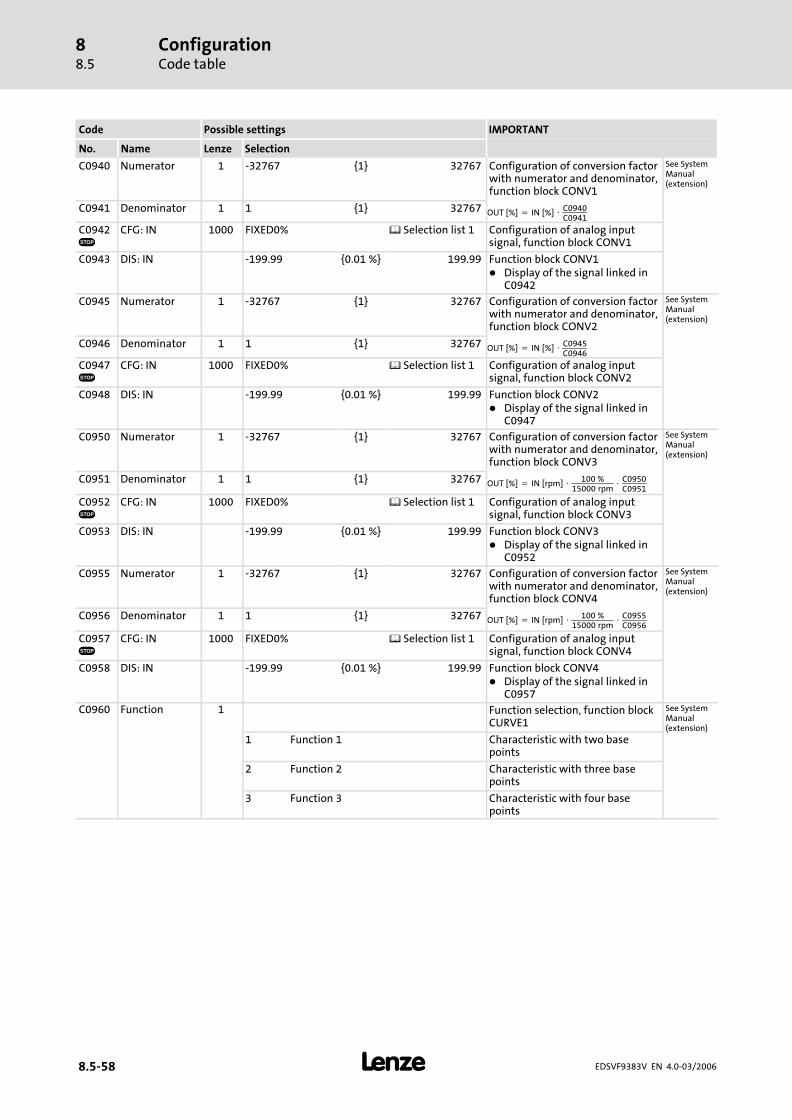
ConfigurationCode table
88.5
� 8.5−58 EDSVF9383V EN 4.0−03/2006
IMPORTANTPossible settingsCode
SelectionLenzeNameNo.
C0940 Numerator 1 −32767 {1} 32767 Configuration of conversion factorwith numerator and denominator,function block CONV1
See SystemManual(extension)
C0941 Denominator 1 1 {1} 32767 OUT�[%] � IN�[%] � C0940C0941
C0942�
CFG: IN 1000 FIXED0% Selection list 1 Configuration of analog inputsignal, function block CONV1
C0943 DIS: IN −199.99 {0.01 %} 199.99 Function block CONV1� Display of the signal linked in
C0942
C0945 Numerator 1 −32767 {1} 32767 Configuration of conversion factorwith numerator and denominator,function block CONV2
See SystemManual(extension)
C0946 Denominator 1 1 {1} 32767 OUT�[%] � IN�[%] � C0945C0946
C0947�
CFG: IN 1000 FIXED0% Selection list 1 Configuration of analog inputsignal, function block CONV2
C0948 DIS: IN −199.99 {0.01 %} 199.99 Function block CONV2� Display of the signal linked in
C0947
C0950 Numerator 1 −32767 {1} 32767 Configuration of conversion factorwith numerator and denominator,function block CONV3
See SystemManual(extension)
C0951 Denominator 1 1 {1} 32767 OUT�[%] � IN�[rpm] � 100�%15000�rpm
� C0950C0951
C0952�
CFG: IN 1000 FIXED0% Selection list 1 Configuration of analog inputsignal, function block CONV3
C0953 DIS: IN −199.99 {0.01 %} 199.99 Function block CONV3� Display of the signal linked in
C0952
C0955 Numerator 1 −32767 {1} 32767 Configuration of conversion factorwith numerator and denominator,function block CONV4
See SystemManual(extension)
C0956 Denominator 1 1 {1} 32767 OUT�[%] � IN�[rpm] � 100�%15000�rpm
� C0955C0956
C0957�
CFG: IN 1000 FIXED0% Selection list 1 Configuration of analog inputsignal, function block CONV4
C0958 DIS: IN −199.99 {0.01 %} 199.99 Function block CONV4� Display of the signal linked in
C0957
C0960 Function 1 Function selection, function blockCURVE1
See SystemManual(extension)
1 Function 1 Characteristic with two basepoints
2 Function 2 Characteristic with three basepoints
3 Function 3 Characteristic with four basepoints

ConfigurationCode table
88.5
� 8.5−59EDSVF9383V EN 4.0−03/2006
IMPORTANTPossible settingsCode
SelectionLenzeNameNo.
C0961 y0 0.00 0.00 {0.01 %} 199.99 Configuration of base point y0,function block CURVE1� Ordinate of the value pair
(x = 0 % / y0)
See SystemManual(extension)
C0962 y1 50.00 0.00 {0.01 %} 199.99 Configuration of base point y1,function block CURVE1� Ordinate of the value pair (x1 /
y1)
C0963 y2 75.00 0.00 {0.01 %} 199.99 Configuration of base point y2,function block CURVE1� Ordinate of the value pair (x2 /
y2)
C0964 y100 100.0 0.00 {0.01 %} 199.99 Configuration of base point y100,function block CURVE1� Ordinate of the value pair
(x 100 % / y100)
C0965 x1 50.00 0.01 {0.01 %} 99.99 Configuration of base point x1,function block CURVE1� Abscissa of the pair (x1 / y1)
C0966 x2 75.00 0.01 {0.01 %} 99.99 Configuration of base point x2,function block CURVE1� Abscissa of the pair (x2 / y2)
C0967�
CFG: IN 1000 FIXED0% Selection list 1 Configuration of analog inputsignal, function block CURVE1
See SystemManual(extension)
C0968 DIS: IN −199.99 {0.01 %} 199.99 Function block CURVE1� Display of the signal linked in
C0967

ConfigurationCode table
88.5
� 8.5−60 EDSVF9383V EN 4.0−03/2006
IMPORTANTPossible settingsCode
SelectionLenzeNameNo.
C0970�
CFG: SET 1000 FIXED0% Selection list 1 Configuration of analog inputsignal, function block MFAIL� Starting value for the
controlled deceleration in [%]of C0011
See SystemManual(extension)
C0971�
CFG: FAULT 1000 FIXED0 Selection list 2 Configuration of digital inputsignal, function block MFAIL� HIGH = activates mains failure
control
C0972�
CFG: RESET 1000 FIXED0 Selection list 2 Configuration of digital inputsignal, function block MFAIL� HIGH = resets mains failure
control
C0973�
CFG: ADAPT 1000 FIXED0% Selection list 1 Configuration of analog inputsignal, function block MFAIL� Dynamic adaptation of the
proportional gain of UGsetlcontroller in [%] of C0980
C0974�
CFG: CONST 1000 FIXED0% Selection list 1 Configuration of analog inputsignal, function block MFAIL� Proportional gain of UGset
controller in [%] of C0980
C0975�
CFG:THRESHLD
1000 FIXED0% Selection list 1 Configuration of analog inputsignal, function block MFAIL� Restart protection when the
value falls below the speedthreshold
� Restart threshold in [%] ofC0011
C0976�
CFG: NACT 1000 FIXED0% Selection list 1 Configuration of analog inputsignal, function block MFAIL� Comparison value for the
restart threshold in [%] ofC0011
� Start for V2 controller
C0977�
CFG: SET 1000 FIXED0% Selection list 1 Configuration of analog inputsignal, function block MFAIL� Speed starting value for the
deceleration in [%] of C0011
C0978�
CFG: DC−SET 1000 FIXED0% Selection list 1 Configuration of analog inputsignal, function block MFAIL� Setting of the voltage setpoint
on which the DC−bus voltage isto be kept (100 % = 1000 V)
C0980 MFAIL Vp 0.500 0.001 {0.001} 31.000 Gain Vp, function block MFAIL See SystemManual(extension)C0981 MFAIL Tn 100 20 {1 ms} 2000 Integral−action time Tn, function
block MFAIL
C0982 MFAIL Tir 2.000 0.001 {0.001s}
16.000 Acceleration time Tir, functionblock MFAIL
C0983 Retrigger T 1.000 0.001 {0.001s}
60.000 Retrigger time, function blockMFAIL� After the time has elapsed, the
mains failure control isterminated
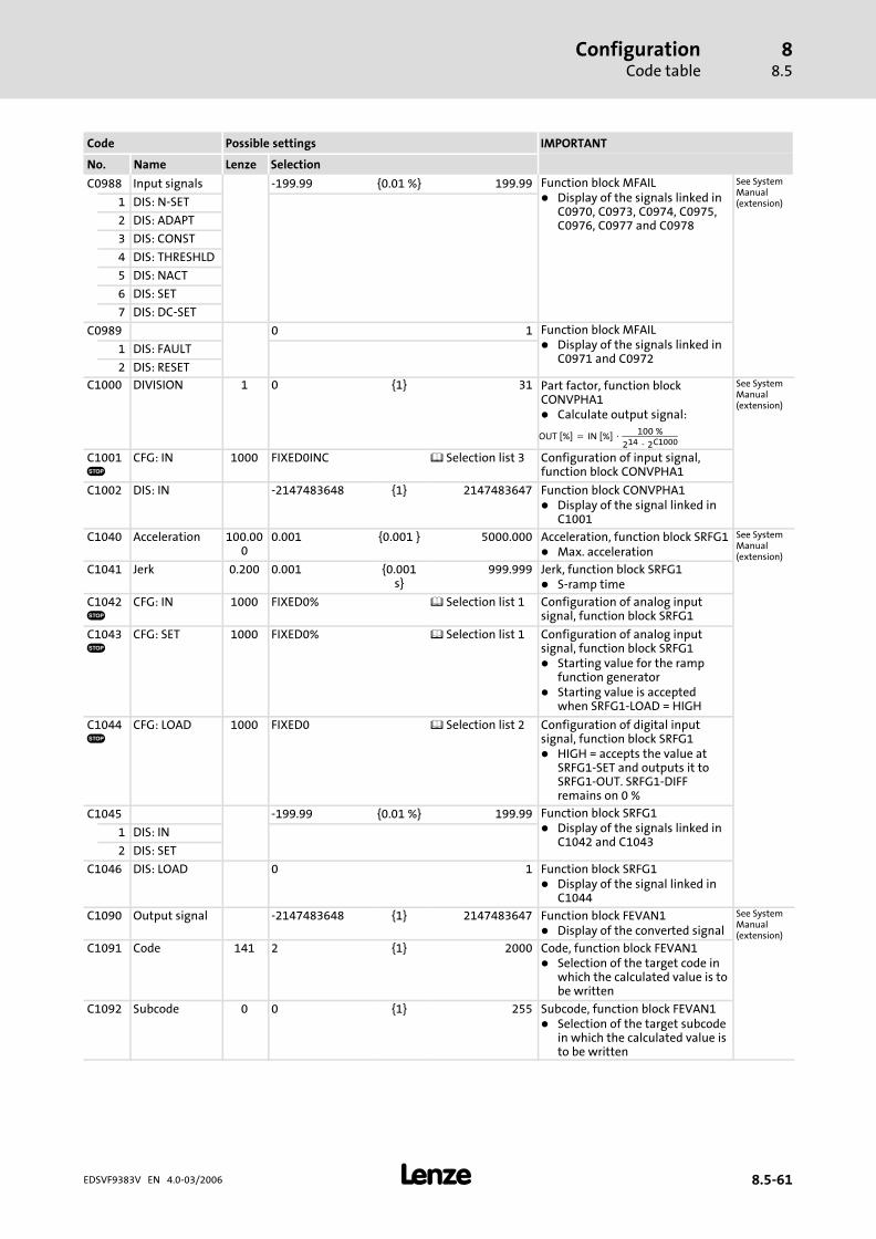
ConfigurationCode table
88.5
� 8.5−61EDSVF9383V EN 4.0−03/2006
IMPORTANTPossible settingsCode
SelectionLenzeNameNo.
C0988 Input signals −199.99 {0.01 %} 199.99 Function block MFAIL� Display of the signals linked in
C0970, C0973, C0974, C0975,C0976, C0977 and C0978
See SystemManual(extension)1 DIS: N−SET
2 DIS: ADAPT
3 DIS: CONST
4 DIS: THRESHLD
5 DIS: NACT
6 DIS: SET
7 DIS: DC−SET
C0989 0 1 Function block MFAIL� Display of the signals linked in
C0971 and C09721 DIS: FAULT
2 DIS: RESET
C1000 DIVISION 1 0 {1} 31 Part factor, function blockCONVPHA1� Calculate output signal:
See SystemManual(extension)
OUT�[%] � IN�[%] � 100�%
214 � 2C1000
C1001�
CFG: IN 1000 FIXED0INC Selection list 3 Configuration of input signal,function block CONVPHA1
C1002 DIS: IN −2147483648 {1} 2147483647 Function block CONVPHA1� Display of the signal linked in
C1001
C1040 Acceleration 100.000
0.001 {0.001 } 5000.000 Acceleration, function block SRFG1� Max. acceleration
See SystemManual(extension)
C1041 Jerk 0.200 0.001 {0.001s}
999.999 Jerk, function block SRFG1� S−ramp time
C1042�
CFG: IN 1000 FIXED0% Selection list 1 Configuration of analog inputsignal, function block SRFG1
C1043�
CFG: SET 1000 FIXED0% Selection list 1 Configuration of analog inputsignal, function block SRFG1� Starting value for the ramp
function generator� Starting value is accepted
when SRFG1−LOAD = HIGH
C1044�
CFG: LOAD 1000 FIXED0 Selection list 2 Configuration of digital inputsignal, function block SRFG1� HIGH = accepts the value at
SRFG1−SET and outputs it toSRFG1−OUT. SRFG1−DIFFremains on 0 %
C1045 −199.99 {0.01 %} 199.99 Function block SRFG1� Display of the signals linked in
C1042 and C10431 DIS: IN
2 DIS: SET
C1046 DIS: LOAD 0 1 Function block SRFG1� Display of the signal linked in
C1044
C1090 Output signal −2147483648 {1} 2147483647 Function block FEVAN1� Display of the converted signal
See SystemManual(extension)
C1091 Code 141 2 {1} 2000 Code, function block FEVAN1� Selection of the target code in
which the calculated value is tobe written
C1092 Subcode 0 0 {1} 255 Subcode, function block FEVAN1� Selection of the target subcode
in which the calculated value isto be written

ConfigurationCode table
88.5
� 8.5−62 EDSVF9383V EN 4.0−03/2006
IMPORTANTPossible settingsCode
SelectionLenzeNameNo.
C1093 Numerator 1.0000 0.0001 {0.0001} 100000.0000 Numerator, function blockFEVAN1� Scaling of the input signal
See SystemManual(extension)
C1094 Denominator 0.0001 0.0001 {0.0001} 100000.0000 Denominator, function blockFEVAN1� Scaling of the input signal
C1095 Offset 0 0 {1} 1000000000 Offset, function block FEVAN1� An offset can be added to the
converted signal
C1096�
CFG: IN 1000 FIXED0% Selection list 1 Configuration of analog inputsignal, function block FEVAN1
See SystemManual(extension)
C1097�
CFG: LOAD 1000 FIXED0 Selection list 2 Configuration of digital inputsignal, function block FEVAN1� A LOW−HIGH edge transmits
the converted signal to thetarget code
C1098 DIS: IN −32768 {1} 32767 Function block FEVAN1� Display of the signal linked in
C1096
See SystemManual(extension)
C1099 DIS: LOAD Function block FEVAN1� Display of the signal linked in
C1097
C1100 Function 1 Function selection, function blockFCNT1
See SystemManual(extension)
1 Return At |countercontent| |FCNT1−CMP−Val|FCNT1−EQUAL is set to HIGH for 1ms
2 Hold if >= At |countercontent| |FCNT1−CMP−Val| thecounter stops
3 Hold if = At |countercontent| = |FCNT1−CMP−Val| thecounter stops
C1101�
Selection list 1 Configuration of analog inputsignals, function block FCNT1
See SystemManual(extension)
1 CFG: LD−VAL 1000 FIXED0% � Starting value
2 CFG: CMP−VAL 1000 FIXED0% � Comparison value
C1102�
Selection list 2 Configuration of digital inputsignals, function block FCNT1
See SystemManual(extension)
1 CFG: CLKUP 1000 FIXED0 LOW−HIGH edge counts upwardsby one
2 CFG: CLKDWN 1000 FIXED0 LOW−HIGH edge countsdownwards by one
3 CFG: LOAD 1000 FIXED0 � HIGH = accepts starting value� Input signal has highest
priority
C1103 −32768 {1} 32768 Function block FCNT1� Display of the signals linked in
C1101
See SystemManual(extension)1 DIS: LD−VAL
2 DIS: CMP−VAL
C1104 0 1 Function block FCNT1� Display of the signals linked in
C11021 DIS: CLKUP
2 DIS: CLKDWN
3 DIS: LOAD

ConfigurationCode table
88.5
� 8.5−63EDSVF9383V EN 4.0−03/2006
IMPORTANTPossible settingsCode
SelectionLenzeNameNo.
C1160�
Selection list 1 Configuration of analog inputsignals, function block ASW3
See SystemManual(extension)
1 CFG: IN 1000 FIXED0% ASW3−IN1
2 CFG: IN 1000 FIXED0% ASW3−IN2
C1161�
CFG: SET 1000 FIXED0 Selection list 2 Configuration of digital inputsignal, function block ASW3� LOW: signal at ASW3−IN1 is
output to ASW3−OUT� HIGH: signal at ASW3−IN2 is
output to ASW3−OUT
C1162 −199.99 {0.01 %} 199.99 Function block ASW3� Display of the signals linked in
C1060
1 DIS: IN ASW3−IN1
2 DIS: IN ASW3−IN2
C1163 DIS: SET Function block ASW3� Display of the signal linked in
C1061
C1190 Motor PTCselection
0 Temperature characteristic for PTCthermistors� Selection of the characteristic
for PTC thermistors at X7 or X8for detecting the motortemperature
6.6−11
0 Standard Characteristic for PTC thermistorsin Lenze motors
1 Characteristic Characteristic forapplication−specific PTCthermistors
C1191 Temperaturecharacteristic
0 {1 °C} 255 Temperature range for PTCthermistors� Define temperature points on
the characteristic for PTCthermistors
1 Temperature 1 100 Temperature point 1
2 Temperature 2 150 Temperature point 2
C1192 Resistancecharacteristic
0 {1 �} 3000 Resistance characteristic for PTCthermistors� Define resistance points on the
characteristic for PTCthermistors
1 Resistance 1 1670 Resistance point 1
2 Resistance 2 2225 Resistance point 2
C1300�
N−motor/Dmax
300 −32767 {1 rpm} 32767 Motor speed at Dmax, functionblock DCALC1� Nominal speed of the winding
drive
8.2−1
C1301�
N−line max 3000 1 {1 rpm} 32767 Maximum line speed, functionblock DCALC1� Nominal speed of the line drive
C1302 calc cycle 0.1 0.1 {0.1 rev} 100.0 Calculation cycle, function blockDCALC1
8.2−1
C1303 time const 0.10 0.01 {0.01 s} 50.00 Filter time constant, functionblock DCALC1

ConfigurationCode table
88.5
� 8.5−64 EDSVF9383V EN 4.0−03/2006
IMPORTANTPossible settingsCode
SelectionLenzeNameNo.
C1304�
Dmax 500 1 {1 mm} 10000 Maximum diameter, functionblock DCALC1� Nominal winding diameter
8.2−1
C1305 lower D−limit 50 1 {1 mm} 10000 Lower diameter limit, functionblock DCALC1� Minimum winding diameter
C1306 upper D−limit 500 1 {1 mm} 10000 Upper diameter limit, functionblock DCALC1� Maximum winding diameter
C1307 hyst D−limit 1.00 0.00 {0.01 %} 100.0 Hysteresis − diameter limitation,function block DCALC1� Hysteresis for Dmin /Dmax
output
C1308�
arit function 1 0 DCALC1−OUT=D DCALC1−OUT =diameter
Selection of the arithmeticfunction, function block DCALC1
8.2−1
1 DCALC1−OUT=1/D DCALC1−OUT =1/diameter
C1309�
Dmin 50 1 {1 mm} 10000 Minimum diameter, functionblock DCALC1
8.2−1
C1310 DCALC1−Titime 0.000 0.000 {0.001s}
999.900 Acceleration and decelerationtime, function block DCALC1
C1311 window D−calc 1.00 0.00 {0.01 %} 100.00 Window − diameter calculation,function block DCALC1� Window setting for permissible
diameter deviation
C1320�
CFG: SET 1000 FIXED0% Selection list 1 Configuration of analog inputsignal, function block DCALC1� The signal is scaled to the value
in C1304
(100 % C1304)
8.2−1
C1321�
Selection list 2 Configuration of digital inputsignals, function block DCALC1
1 CFG: LOAD 1000 FIXED0 � HIGH: initial value atDCALC1−SET is accepted
� DCALC1−LOAD has a higherpriority than DCALC1−HOLD
2 CFG: HOLD 1000 FIXED0 � HIGH = holds the diametervalue reached and resets theintegrators.
C1322 −36000 {1 rpm} 36000 Function block DCALC1� Display of the signals linked in
C1327
8.2−1
1 DIS: N−Line
2 DIS: N−WIND
C1325 DIS: SET −199,99 {0.01 %} 199,99 Function block DCALC1� Display of the signal linked in
C1320
C1326 0 1 Function block DCALC1� Display of the signals linked in
C13211 DIS: LOAD
2 DIS: HOLD
C1327�
Selection list 3 Configuration of input signals,function block DCALC1
8.2−1
1 CFG: N−Line 1000 FIXED0INC � Speed signal of the line drive
2 CFG: N−WIND 1000 FIXED0INC � Speed signal of the windingdrive
C1328 DIS: D−ACT −200 {1 mm} 200 Function block DCALC1� Display of the current diameter

ConfigurationCode table
88.5
� 8.5−65EDSVF9383V EN 4.0−03/2006
IMPORTANTPossible settingsCode
SelectionLenzeNameNo.
C1330 PCTRL2 Tir 1.0 0.1 {0.1 s 6000.0 Acceleration time tir, functionblock PCTRL2� Acceleration time for the
setpoint� The acceleration time refers to
a setpoint change of 0 ... 100 %
See SystemManual(extension)
C1331 PCTRL2 Tif 1.0 0.1 {0.1 s} 6000.0 Deceleration time tif, functionblock PCTRL2� Deceleration time for the
setpoint� The deceleration time refers to
a setpoint change of 100 % ... 0
C1332 PCTRL2 Vp 1.0 0.1 {0.1 } 500.0 Gain Vp, function block PCTRL2 See SystemManual(extension)C1333 PCTRL2 Tn 400 20 {1 ms} 99999 Integral−action time Tn, function
block PCTRL2Setting of reset time Tn of PCTRL2
C1334 PCTRL2 Kd 0.0 0.0 {0.1 } 5.0 Differential component Kd,function block PCTRL2
C1335 bipolar/unipolar
0 Sphere of action, function blockPCTRL2
0 Bipolar � Output value is limited to−100 ... 100 %
See SystemManual(extension)
1 Unipolar � Output value is limited to0 ... 100 %
C1336 Tir overlay 1.0 0.1 {0.1 s} 6000.0 Fade−in time, function blockPCTRL2� Acceleration time of the ramp
generator� Controls the influence of the
process controller
See SystemManual(extension)
C1337 Tif overlay 1.0 0.1 {0.1 s} 6000.0 Fade−out time, function blockPCTRL2� Deceleration time of the ramp
generator� Controls the influence of the
process controller
C1340�
Selection list 1 Configuration of analog inputsignals, function block PCTRL2
See SystemManual(extension)
1 CFG: RFG−SET 1000 FIXED0% � The process setpoint is shownat PCTRL2−SET with a startingvalue via a ramp generator
� PCTRL−RFG−LOAD = HIGHactivates the function
2 CFG: SET 1000 FIXED0% � Input for process value� Value range: ±200� %
3 CFG: ACT 1000 FIXED0% � Input for actual value� Value range: ±200� %
4 CFG: INFL 1000 FIXED0% � Evaluation (influence) of theoutput signal
� Value range: ±200� %

ConfigurationCode table
88.5
� 8.5−66 EDSVF9383V EN 4.0−03/2006
IMPORTANTPossible settingsCode
SelectionLenzeNameNo.
C1341�
Selection list 2 Configuration of digital inputsignals, function block PCTRL2
See SystemManual(extension)
1 CFG: RFG−LOAD 1000 FIXED0 � HIGH = function ofPCTRL2−RFG−SET is active
2 CFG: I−OFF 1000 FIXED0 � HIGH = Switches of integralaction component
� LOW = switches on integralaction component
3 CFG: INACT 1000 FIXED0 � HIGH = deactivates processcontroller
4 CFG: OVERLAY 1000 FIXED0 � HIGH = Shows influence� LOW = hides influence
C1344 −199.99 {0.01 %} 199.99 Function block PCTRL2� Display of the signals linked in
C1340
See SystemManual(extension)1 DIS: RFG−SET
2 DIS: SET
3 DIS: ACT
4 DIS: INFL
C1345 0 1 Function block PCTRL2� Display of the signals linked in
C13411 DIS: RFG−LOAD
2 DIS: I−OFF
3 DIS: INACT
4 DIS: OVERLAY
C1350 INT1 function 0 Function selection, function blockINT1
See SystemManual(extension)
0 PHI >= REF If INT1−IN INT1−REF, INT1−DOUTis set to HIGH
1 |PHI| >= |REF| If |INT1−IN| |INT1−REF|,INT1−DOUT is set to HIGH
C1351 INT1 scaling 6553600
65536 {1} 1000000000 Scaling factor, function block INT1
INT1 � AOUT�[%] �INT1 � IN�[inc]
C1351� 100�%
C1354�
CFG: REF 1000 FIXED0INC Selection list 3 Input signal configuration� Reference value
See SystemManual(extension)
C1355�
CFG: IN 1000 FIXEDPHI−0 Selection list 4 Configuration of input signal,function block INT1� Angle of rotation
C1356�
CFG: RESET 1000 FIXED0 Selection list 2 Configuration of digital inputsignal, function block INT1� HIGH = Sets the integrator to 0
C1357 DIS: REF −2000000000 {1 inc} 2000000000 Function block INT1� Display of the signal linked in
C13554
See SystemManual(extension)
C1358 DIS: IN −32767 {1 rpm} 32767 Function block INT1� Display of the signal linked in
C1355
C1359 DIS: RESET 0 1 Function block INT1� Display of the signal linked in
C1356
C1360 INT2 function 0 Function selection, function blockINT2
See SystemManual(extension)
0 PHI >= REF If INT2−IN INT2−REF, INT2−DOUTis set to HIGH
1 |PHI| >= |REF| If |INT2−IN| |INT2−REF|,INT2−DOUT is set to HIGH
C1361 INT2 scaling 6553600
65536 {1} 1000000000 Scaling factor, function block INT2
INT2 � AOUT�[%] �INT2 � IN�[inc]
C1361� 100�%

ConfigurationCode table
88.5
� 8.5−67EDSVF9383V EN 4.0−03/2006
IMPORTANTPossible settingsCode
SelectionLenzeNameNo.
C1364�
CFG: REF 1000 FIXED0INC Selection list 3 Input signal configuration� Reference value
See SystemManual(extension)
C1365�
CFG: IN 1000 FIXEDPHI−0 Selection list 4 Configuration of input signal,function block INT2� Angle of rotation
C1366�
CFG: RESET 1000 FIXED0 Selection list 2 Configuration of digital inputsignal, function block INT2� HIGH = Sets the integrator to 0
C1367 DIS: REF −2000000000 {1 inc} 2000000000 Function block INT2� Display of the signal linked in
C13564
See SystemManual(extension)
C1368 DIS: IN −32767 {1 rpm} 32767 Function block INT2� Display of the signal linked in
C1365
C1369 DIS: RESET 0 1 Function block INT2� Display of the signal linked in
C1366
C1370 FOLL max 100.00 0.00 {0.01 %} 199.99 Upper limit, function block FOLL1� Upper limit of the ramp
function generator
See SystemManual(extension)
C1371 FOLL min −100.00
−199.99 {0.01 %} 0.00 Lower limit, function block FOLL1� Lower limit of the ramp
function generator
C1372 FOLL Tir 10.0 0.1 {0.1 s} 6000.0 Acceleration time Tir anddeceleration time Tif of the rampfunction generator, function blockFOLL1
C1373 FOLL Tif 10.0 0.1 {0.1 s} 6000.0
C1375�
Selection list 1 Configuration of analog inputsignals, function block FOLL1
See SystemManual(extension)
1 CFG: SIGN 1000 FIXED0% � Negative value: signalcharacteristic at FOLL1−OUT isopposed to the one at FOLL1−IN
� Positive value: signalcharacteristic at FOLL1−OUT isthe same as at FOLL1−IN
2 CFG: IN 1000 FIXED0% If FOLL1−IN > FOLL1−REF, the rampfunction generator starts
3 CFG: REF 1000 FIXED0% Reference value
4 CFG: LOAD 1000 FIXED0% Initial value for the ramp functiongenerator
C1376�
CFG: SET 1000 FIXED0 Selection list 2 Configuration of digital inputsignal, function block FOLL1� HIGH: initial value at
FOLL1−LOAD is accepted
C1377 −199.99 {0.01 %} 199.99 Function block FOLL1� Display of the signals linked in
C1375
See SystemManual(extension)1 DIS: SIGN
2 DIS: IN
3 DIS: REF
4 DIS: LOAD
C1378 DIS: SET 0 1 Function block FOLL1� Display of the signal linked in
C1376
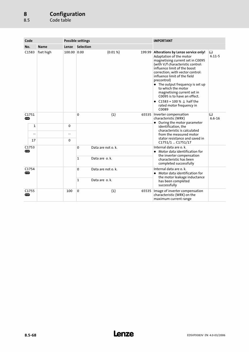
ConfigurationCode table
88.5
� 8.5−68 EDSVF9383V EN 4.0−03/2006
IMPORTANTPossible settingsCode
SelectionLenzeNameNo.
C1583 fset high 100.00 0.00 {0.01 %} 199.99 Alterations by Lenze service only!Adaptation of the motormagnetising current set in C0095(with V/f characteristic control:influence limit of the boostcorrection; with vector control:influence limit of the fieldprecontrol)� The output frequency is set up
to which the motormagnetising current set inC0095 is to have an effect.
� C1583 = 100 % half therated motor frequency inC0089
6.11−5
C1751�
0 {1} 65535 Inverter compensationcharacteristic (WRK)� During the motor parameter
identification, thecharacteristic is calculatedfrom the measured motorstator resistance and saved inC1751/1 ... C1751/17
6.6−16
1 0
... ...
17 0
C1753�
0 Data are not o. k. Internal data are o. k.� Motor data identification for
the inverter compensationcharacteristic has beencompleted successfully
1 Data are o. k.
C1754�
0 Data are not o. k. Internal data are o. k.� Motor data identification for
the motor leakage inductancehas been completedsuccessfully
1 Data are o. k.
C1755�
100 0 {1} 65535 Image of inverter compensationcharacteristic (WRK) on themaximum current range

ConfigurationSelection lists
Selection list 1: Analog output signals
88.6
8.6.1
� 8.6−1EDSVF9383V EN 5.0−05/2008
8.6 Selection lists
8.6.1 Selection list 1: Analog output signals
Parameter Analog output signal (�)
000050 AIN1−OUT
000055 AIN2−OUT
000100 DFSET−NOUT
001000 FIXED0%
001006 FIXED100%
001007 FIXED−100%
005000 MCTRL−nset2
005001 MCTRL−NACT
005002 MCTRL−MSET2
005003 MCTRL−MACT
005004 MCTRL−IACT
005005 MCTRL−DCVOLT
005006 MCTRL−VACT
005007 MCTRL−FACT
005008 MCTRL−IxT
005009 MCTRL−PHI−ACT
005010 MCTRL−M−TEMP
005015 MCTRL−BOOST
005050 NSET−NOUT
005051 NSET−RFG−I
005052 NSET−C10−C11
005100 MPOT1−OUT
005150 PCTRL1−OUT
005250 NLIM1−OUT
005500 ARIT1−OUT
005505 ARIT2−OUT
005510 ARIT3−OUT
005540 SQRT1−OUT
005550 ADD1−OUT
005555 ADD2−OUT
005600 RFG1−OUT
005610 SRFG1−OUT
005611 SRFG1−DIFF
005650 ASW1−OUT
005655 ASW2−OUT
005660 ASW3−OUT
Parameter Analog output signal (�)
005700 ANEG1−OUT
005705 ANEG2−OUT
005750 FIXSET1−OUT
005800 LIM1−OUT
005850 ABS1−OUT
005900 PT1−1−OUT
005905 PT1−2−OUT
005950 DT1−1−OUT
006100 MFAIL−NOUT
006150 DB1−OUT
006200 CONV1−OUT
006205 CONV2−OUT
006210 CONV3−OUT
006215 CONV4−OUT
006230 CONVPHA1−OUT
006300 S&H1−OUT
006350 CURVE1−OUT
006400 FCNT1−OUT
010000 BRK1−M−SET
011000 DCALC1−D−OUT
011001 DCALC1−OUT
011050 PCTRL2−OUT
011100 INT1−AOUT
011105 INT2−AOUT
011150 FOLL1−OUT
019500 FCODE−17
019502 FCODE−26/1
019503 FCODE−26/2
019504 FCODE−27/1
019505 FCODE−27/2
019506 FCODE−32
019507 FCODE−37
019510 FCODE−108/1
019511 FCODE−108/2
019512 FCODE−109/1

ConfigurationSelection listsSelection list 1: Analog output signals
88.68.6.1
�8.6−2 EDSVF9383V EN 5.0−05/2008
Parameter Analog output signal (�)
019513 FCODE−109/2
019515 FCODE−141
019521 FCODE−472/1
019522 FCODE−472/2
019523 FCODE−472/3
019524 FCODE−472/4
019525 FCODE−472/5
019526 FCODE−472/6
019527 FCODE−472/7
019528 FCODE−472/8
019529 FCODE−472/9
019530 FCODE−472/10
019531 FCODE−472/11
019532 FCODE−472/12
019533 FCODE−472/13
019534 FCODE−472/14
019535 FCODE−472/15
019536 FCODE−472/16
019537 FCODE−472/17
019538 FCODE−472/18
019539 FCODE−472/19
019540 FCODE−472/20
019551 FCODE−473/1
Parameter Analog output signal (�)
019552 FCODE−473/2
019553 FCODE−473/3
019554 FCODE−473/4
019555 FCODE−473/5
019556 FCODE−473/6
019557 FCODE−473/7
019558 FCODE−473/8
019559 FCODE−473/9
019560 FCODE−473/10
020101 CAN−IN1.W1
020102 CAN−IN1.W2
020103 CAN−IN1.W3
020201 CAN−IN2.W1
020202 CAN−IN2.W2
020203 CAN−IN2.W3
020204 CAN−IN2.W4
020301 CAN−IN3.W1
020302 CAN−IN3.W2
020303 CAN−IN3.W3
020304 CAN−IN3.W4
025101 AIF−IN.W1
025102 AIF−IN.W2
025103 AIF−IN.W3

ConfigurationSelection lists
Selection list 2: Digital output signals
88.6
8.6.2
� 8.6−3EDSVF9383V EN 5.0−05/2008
8.6.2 Selection list 2: Digital output signals
Parameter Digital output signal (*)
000051 DIGIN1
000052 DIGIN2
000053 DIGIN3
000054 DIGIN4
000055 DIGIN5
000056 DIGIN6(ST)
000065 DIGIN−CINH
000100 DFSET−ACK
000500 DCTRL−RDY
000501 DCTRL−CINH
000502 DCTRL−INIT
000503 DCTRL−IMP
000504 DCTRL−NACT=0
000505 DCTRL−CW/CCW
001000 FIXED0
001001 FIXED1
002000 DCTRL−PAR*1
002001 DCTRL−PAR*2
002002 DCTRL−PAR−BUSY
005001 MCTRL−QSP−OUT
005002 MCTRL−IMAX
005003 MCTRL−MMAX
005006 MCTRL−GSB−OUT
005050 NSET−rfg−i=0
006000 DFRFG1−FAIL
006001 DFRFG1−SYNC
006100 MFAIL−STATUS
006101 MFAIL−I−RESET
006400 FCNT1−EQUAL
010000 BRK1−OUT
010001 BRK1−CINH
010002 BRK1−QSP
010003 BRK1−M−STORE
010250 R/L/Q−QSP
010251 R/L/Q−R/L
010500 AND1−OUT
010505 AND2−OUT
010510 AND3−OUT
010515 AND4−OUT
Parameter Digital output signal (*)
010520 AND5−OUT
010550 OR1−OUT
010555 OR2−OUT
010560 OR3−OUT
010565 OR4−OUT
010570 OR5−OUT
010600 NOT1−OUT
010605 NOT2−OUT
010610 NOT3−OUT
010615 NOT4−OUT
010620 NOT5−OUT
010650 CMP1−OUT
010655 CMP2−OUT
010660 CMP3−OUT
010665 CMP4−OUT
010700 DIGDEL1−OUT
010705 DIGDEL2−OUT
010750 TRANS1−OUT
010755 TRANS2−OUT
010900 FLIP1−OUT
010905 FLIP2−OUT
011000 DCALC1−DMAX
011001 DCALC1−DMIN
011002 DCALC1−I=0
011003 DCALC1−OVFL
011100 INT1−DOUT
011105 INT2−DOUT
013000 FEVAN1−BUSY
013001 FEVAN1−FAIL
015000 DCTRL−TRIP
015001 DCTRL−MESS
015002 DCTRL−WARN
015003 DCTRL−FAIL
015010 MONIT−LU
015011 MONIT−OU
015012 MONIT−EEr
015013 MONIT−OC1
015014 MONIT−OC2
015015 MONIT−LP1
015016 MONIT−OH
015017 MONIT−OH3

ConfigurationSelection listsSelection list 2: Digital output signals
88.68.6.2
�8.6−4 EDSVF9383V EN 5.0−05/2008
Parameter Digital output signal (*)
015018 MONIT−OH4
015019 MONIT−OH7
015020 MONIT−OH8
015022 MONIT−Sd3
015026 MONIT−CE0
015027 MONIT−NMAX
015028 MONIT−OC5
015029 MONIT−SD5
015030 MONIT−SD6
015032 MONIT−H07
015033 MONIT−H10
015034 MONIT−H11
015040 MONIT−CE1
015041 MONIT−CE2
015042 MONIT−CE3
015043 MONIT−CE4
015044 MONIT−OC3
015045 MONIT−ID1
015046 MONIT−ID2
019500 FCODE−250
019521 FCODE−471.B0
019522 FCODE−471.B1
019523 FCODE−471.B2
019524 FCODE−471.B3
019525 FCODE−471.B4
019526 FCODE−471.B5
019527 FCODE−471.B6
019528 FCODE−471.B7
019529 FCODE−471.B8
019530 FCODE−471.B9
019531 FCODE−471.B10
019532 FCODE−471.B11
019533 FCODE−471.B12
019534 FCODE−471.B13
019535 FCODE−471.B14
019536 FCODE−471.B15
019537 FCODE−471.B16
019538 FCODE−471.B17
019539 FCODE−471.B18
019540 FCODE−471.B19
019541 FCODE−471.B20
019542 FCODE−471.B21
019543 FCODE−471.B22
019544 FCODE−471.B23
Parameter Digital output signal (*)
019545 FCODE−471.B24
019546 FCODE−471.B25
019547 FCODE−471.B26
019548 FCODE−471.B27
019549 FCODE−471.B28
019550 FCODE−471.B29
019551 FCODE−471.B30
019552 FCODE−471.B31
019751 FCODE−135.B0
019752 FCODE−135.B1
019753 FCODE−135.B2
019755 FCODE−135.B4
019756 FCODE−135.B5
019757 FCODE−135.B6
019758 FCODE−135.B7
019763 FCODE−135.B12
019764 FCODE−135.B13
019765 FCODE−135.B14
019766 FCODE−135.B15
020001 CAN−CTRL.B0
020002 CAN−CTRL.B1
020003 CAN−CTRL.B2
020005 CAN−CTRL.B4
020006 CAN−CTRL.B5
020007 CAN−CTRL.B6
020008 CAN−CTRL.B7
020013 CAN−CTRL.B12
020014 CAN−CTRL.B13
020015 CAN−CTRL.B14
020016 CAN−CTRL.B15
020101 CAN−IN1.B0
020102 CAN−IN1.B1
020103 CAN−IN1.B2
020104 CAN−IN1.B3
020105 CAN−IN1.B4
020106 CAN−IN1.B5
020107 CAN−IN1.B6
020108 CAN−IN1.B7
020109 CAN−IN1.B8
020110 CAN−IN1.B9
020111 CAN−IN1.B10
020112 CAN−IN1.B11
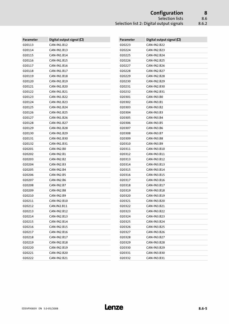
ConfigurationSelection lists
Selection list 2: Digital output signals
88.6
8.6.2
� 8.6−5EDSVF9383V EN 5.0−05/2008
Parameter Digital output signal (*)
020113 CAN−IN1.B12
020114 CAN−IN1.B13
020115 CAN−IN1.B14
020116 CAN−IN1.B15
020117 CAN−IN1.B16
020118 CAN−IN1.B17
020119 CAN−IN1.B18
020120 CAN−IN1.B19
020121 CAN−IN1.B20
020122 CAN−IN1.B21
020123 CAN−IN1.B22
020124 CAN−IN1.B23
020125 CAN−IN1.B24
020126 CAN−IN1.B25
020127 CAN−IN1.B26
020128 CAN−IN1.B27
020129 CAN−IN1.B28
020130 CAN−IN1.B29
020131 CAN−IN1.B30
020132 CAN−IN1.B31
020201 CAN−IN2.B0
020202 CAN−IN2.B1
020203 CAN−IN2.B2
020204 CAN−IN2.B3
020205 CAN−IN2.B4
020206 CAN−IN2.B5
020207 CAN−IN2.B6
020208 CAN−IN2.B7
020209 CAN−IN2.B8
020210 CAN−IN2.B9
020211 CAN−IN2.B10
020212 CAN.IN2.B11
020213 CAN−IN2.B12
020214 CAN−IN2.B13
020215 CAN−IN2.B14
020216 CAN−IN2.B15
020217 CAN−IN2.B16
020218 CAN−IN2.B17
020219 CAN−IN2.B18
020220 CAN−IN2.B19
020221 CAN−IN2.B20
020222 CAN−IN2.B21
Parameter Digital output signal (*)
020223 CAN−IN2.B22
020224 CAN−IN2.B23
020225 CAN−IN2.B24
020226 CAN−IN2.B25
020227 CAN−IN2.B26
020228 CAN−IN2.B27
020229 CAN−IN2.B28
020230 CAN−IN2.B29
020231 CAN−IN2.B30
020232 CAN−IN2.B31
020301 CAN−IN3.B0
020302 CAN−IN3.B1
020303 CAN−IN3.B2
020304 CAN−IN3.B3
020305 CAN−IN3.B4
020306 CAN−IN3.B5
020307 CAN−IN3.B6
020308 CAN−IN3.B7
020309 CAN−IN3.B8
020310 CAN−IN3.B9
020311 CAN−IN3.B10
020312 CAN−IN3.B11
020313 CAN−IN3.B12
020314 CAN−IN3.B13
020315 CAN−IN3.B14
020316 CAN−IN3.B15
020317 CAN−IN3.B16
020318 CAN−IN3.B17
020319 CAN−IN3.B18
020320 CAN−IN3.B19
020321 CAN−IN3.B20
020322 CAN−IN3.B21
020323 CAN−IN3.B22
020324 CAN−IN3.B23
020325 CAN−IN3.B24
020326 CAN−IN3.B25
020327 CAN−IN3.B26
020328 CAN−IN3.B27
020329 CAN−IN3.B28
020330 CAN−IN3.B29
020331 CAN−IN3.B30
020332 CAN−IN3.B31

ConfigurationSelection listsSelection list 3: Angle signals
88.68.6.3
�8.6−6 EDSVF9383V EN 5.0−05/2008
Parameter Digital output signal (*)
020400 CAN−SYNC−OUT
025001 AIF−CTRL.B0
025002 AIF−CTRL.B1
025003 AIF−CTRL.B2
025005 AIF−CTRL.B4
025006 AIF−CTRL.B5
025007 AIF−CTRL.B6
025008 AIF−CTRL.B7
025013 AIF−CTRL.B12
025014 AIF−CTRL.B13
025015 AIF−CTRL.B14
025016 AIF−CTRL.B15
025101 AIF−IN.B0
025102 AIF−IN.B1
025103 AIF−IN.B2
025104 AIF−IN.B3
025105 AIF−IN.B4
025106 AIF−IN.B5
025107 AIF−IN.B6
025108 AIF−IN.B7
025109 AIF−IN.B8
025110 AIF−IN.B9
Parameter Digital output signal (*)
025111 AIF−IN.B10
025112 AIF−IN.B11
025113 AIF−IN.B12
025114 AIF−IN.B13
025115 AIF−IN.B14
025116 AIF−IN.B15
025117 AIF−IN.B16
025118 AIF−IN.B17
025119 AIF−IN.B18
025120 AIF−IN.B19
025121 AIF−IN.B20
025122 AIF−IN.B21
025123 AIF−IN.B22
025124 AIF−IN.B23
025125 AIF−IN.B24
025126 AIF−IN.B25
025127 AIF−IN.B26
025128 AIF−IN.B27
025129 AIF−IN.B28
025130 AIF−IN.B29
025131 AIF−IN.B30
025132 AIF−IN.B31
8.6.3 Selection list 3: Angle signals
Parameter Phase signal (+)
000100 DFSET−PSET
001000 FIXED0INC
005000 MCTRL−PHI−ANG
011100 INT1−POUT
011105 INT2−POUT
Parameter Phase signal (+)
019521 FCODE−474/1
019522 FCODE−474/2
020103 CAN−IN1.D1
020201 CAN−IN2.D1
020301 CAN−IN3.D1
025103 AIF−IN.D1
8.6.4 Selection list 4: Speed signals
Parameter Speed signal (,)
000050 DFIN−OUT
000100 DFSET−POUT
000250 DFOUT−OUT
001000 FIXEDPHI−0
Parameter Speed signal (,)
005000 MCTRL−PHI−ACT
006000 DFRFG−OUT
006220 CONV5−OUT
019521 FCODE−475/1
019522 FCODE−475/2

ConfigurationSelection lists
Selection list 5: Function blocks
88.6
8.6.5
� 8.6−7EDSVF9383V EN 5.0−05/2008
8.6.5 Selection list 5: Function blocks
Parameter Function block
000000 empty
000050 AIN1
000055 AIN2
000070 AOUT1
000075 AOUT2
000100 DFSET
000200 DFIN
000250 DFOUT
005050 NSET
005100 MPOT1
005150 PCTRL1
005250 NLIM1
005500 ARIT1
005505 ARIT2
005510 ARIT3
005540 SQRT1
005550 ADD1
005555 ADD2
005600 RFG1
005610 SRFG1
005650 ASW1
005655 ASW2
005660 ASW3
005700 ANEG1
005705 ANEG2
005750 FIXSET1
005800 LIM1
005850 ABS1
005900 PT1−1
005905 PT1−2
005950 DT1−1
006000 DFRFG1
006100 MFAIL
006150 DB1
006200 CONV1
006205 CONV2
006210 CONV3
006215 CONV4
006220 CONV5
006230 CONVPHA1
Parameter Function block
006300 S&H1
006350 CURVE1
006400 FCNT1
010000 BRK1
010250 R/L/Q
010500 AND1
010505 AND2
010510 AND3
010515 AND4
010520 AND5
010550 OR1
010555 OR2
010560 OR3
010565 OR4
010570 OR5
010600 NOT1
010605 NOT2
010610 NOT3
010615 NOT4
010620 NOT5
010650 CMP1
010655 CMP2
010660 CMP3
010665 CMP4
010700 DIGDEL1
010705 DIGDEL2
010750 TRANS1
010755 TRANS2
010900 FLIP1
010905 FLIP2
011000 DCALC1
011050 PCTRL2
011100 INT1
011105 INT2
011150 FOLL1
013000 FEVAN1
013100 OSZ
015100 MLP1
020000 CAN−OUT
025000 AIF−OUT


ConfigurationTable of attributes
88.7
� 8.7−1EDSVF9383V EN 5.0−05/2008
8.7 Table of attributes
The attribute table describes the properties of the codes used. It enables youto create your own communication programs for the controller.
How to read the table of attributes
Column Abbreviation Meaning
Code Cxxxx Name of the Lenze code
Index dec 24575 − Lenze codenumber
Index under which theparameter is addressedThe subindex of array variablescorresponds to the Lenzesubcode number
Is only required for control via INTERBUS,PROFIBUS DP or system bus (CAN)
hex 5FFFh − Lenze codenumber
Data DS E Data structure Single variable(only one parameter element)
A Array variable(several parameter elements)
DA xx Number of array elements(subcodes)
DT B8 Data type 1 byte bit−coded
B16 2 bytes bit−coded
B32 4 bytes bit−coded
FIX32 32−bit value with sign;decimal with four decimal places
I32 4 bytes with sign
U32 4 bytes without sign
VS ASCII string
Format VD LECOM format(see also Operating Instructionsof the bus module)
ASCII decimal format
VH ASCII hexadecimal format
VS String format
VO Octet string format for data blocks
DL Data length in byte The column "Important" contains furtherinformation
Access LCM−R/W Ra Access authorisation for LECOM Reading is always permitted
Wa Writing is always permitted
W Writing is restricted
Condition CINH Condition for writing Writing permitted only when controller isinhibited

ConfigurationTable of attributes
88.7
� 8.7−2 EDSVF9383V EN 5.0−05/2008
Code Controller Index Data Access
EVF9321...
EVF9333
EVF9335...
EVF9383
dec hex DS DA DT Format DL LCM−R/W Condition
C0002 24573 5FFD E 1 FIX32 VD 4 Ra/W CINH
C0003 24572 5FFC E 1 FIX32 VD 4 Ra/Wa
C0004 24571 5FFB E 1 FIX32 VD 4 Ra/Wa
C0005 24570 5FFA E 1 FIX32 VD 4 Ra/W CINH
C0006 24569 5FF9 E 1 FIX32 VD 4 Ra/W CINH
C0009 24566 5FF6 E 1 FIX32 VD 4 Ra/Wa
C0010 24565 5FF5 E 1 FIX32 VD 4 Ra/Wa
C0011 24564 5FF4 E 1 FIX32 VD 4 Ra/Wa
C0012 24563 5FF3 E 1 FIX32 VD 4 Ra/Wa
C0013 24562 5FF2 E 1 FIX32 VD 4 Ra/Wa
C0014 24561 5FF1 E 1 FIX32 VD 4 Ra/Wa
C0015 24560 5FF0 E 1 FIX32 VD 4 Ra/Wa
C0016 24559 5FsF E 1 FIX32 VD 4 Ra/Wa
C0017 24558 5FEE E 1 FIX32 VD 4 Ra/Wa
C0018 24557 5FED E 1 FIX32 VD 4 Ra/Wa
C0019 24556 5FEC E 1 FIX32 VD 4 Ra/Wa
C0020 24555 5FEB E 1 FIX32 VD 4 Ra/Wa
C0021 24554 5FEA E 1 FIX32 VD 4 Ra/Wa
C0022 24553 5FE9 E 1 FIX32 VD 4 Ra/Wa
C0023 24552 5FE8 E 1 FIX32 VD 4 Ra/Wa
C0025 24550 5FE6 E 1 FIX32 VD 4 Ra/W CINH
C0026 24549 5FE5 A 2 FIX32 VD 4 Ra/Wa
C0027 24548 5FE4 A 2 FIX32 VD 4 Ra/Wa
C0030 24545 5FE1 E 1 FIX32 VD 4 Ra/Wa
C0032 24543 5FDF E 1 FIX32 VD 4 Ra/Wa
C0033 24542 5FDE E 1 FIX32 VD 4 Ra/Wa
C0034 24541 5FDD E 1 FIX32 VD 4 Ra/Wa
C0036 24539 5FDB E 1 FIX32 VD 4 Ra/Wa
C0037 24538 5FDA E 1 FIX32 VD 4 Ra/Wa
C0038 24537 5FD9 A 6 FIX32 VD 4 Ra/Wa
C0039 24536 5FD8 A 15 FIX32 VD 4 Ra/Wa
C0040 24535 5FD7 E 1 FIX32 VD 4 Ra/Wa
C0042 24533 5FD5 E 1 FIX32 VD 4 Ra
C0043 24532 5FD4 E 1 FIX32 VD 4 Ra/Wa
C0045 24530 5FD2 E 1 FIX32 VD 4 Ra
C0046 24529 5FD1 E 1 FIX32 VD 4 Ra
C0049 24526 5FCE E 1 FIX32 VD 4 Ra
C0050 24525 5FCD E 1 FIX32 VD 4 Ra
C0051 24524 5FCC E 1 FIX32 VD 4 Ra
C0052 24523 5FCB E 1 FIX32 VD 4 Ra
C0053 24522 5FCA E 1 FIX32 VD 4 Ra
C0054 24521 5FC9 E 1 FIX32 VD 4 Ra
C0056 24519 5FC7 E 1 FIX32 VD 4 Ra
C0057 24518 5FC6 E 1 FIX32 VD 4 Ra
C0058 24517 5FC5 E 1 FIX32 VD 4 Ra

ConfigurationTable of attributes
88.7
� 8.7−3EDSVF9383V EN 5.0−05/2008
AccessDataIndexControllerCode
ConditionLCM−R/WDLFormatDTDADShexdecEVF9335...
EVF9383
EVF9321...
EVF9333
Code
C0059 24516 5FC4 E 1 FIX32 VD 4 Ra
C0061 24514 5FC2 E 1 FIX32 VD 4 Ra
C0063 24512 5FC0 E 1 FIX32 VD 4 Ra
C0064 24511 5FBF E 1 FIX32 VD 4 Ra
C0067 24508 5FBC E 1 FIX32 VD 4 Ra
C0070 24505 5FB9 E 1 FIX32 VD 4 Ra/Wa
C0071 24504 5FB8 E 1 FIX32 VD 4 Ra/Wa
C0074 24501 5FB5 E 1 FIX32 VD 4 Ra/Wa
C0075 24500 5FB4 E 1 FIX32 VD 4 Ra/Wa
C0076 24499 5FB3 E 1 FIX32 VD 4 Ra/Wa
C0077 24498 5FB2 E 1 FIX32 VD 4 Ra/Wa
C0078 24497 5FB1 E 1 FIX32 VD 4 Ra/Wa
C0079 24496 5FB0 E 1 FIX32 VD 4 Ra/Wa
C0080 24495 5FAF E 1 FIX32 VD 4 Ra/Wa
C0081 24494 5FAE E 1 FIX32 VD 4 Ra/W CINH
C0082 24493 5FAD E 1 FIX32 VD 4 Ra/W CINH
C0084 24491 5FAB E 1 FIX32 VD 4 Ra/W CINH
C0085 24490 5FAA E 1 FIX32 VD 4 Ra/W CINH
C0086 24489 5FA9 E 1 FIX32 VD 4 Ra/W CINH
C0087 24488 5FA8 E 1 FIX32 VD 4 Ra/W CINH
C0088 24487 5FA7 E 1 FIX32 VD 4 Ra/W CINH
C0089 24486 5FA6 E 1 FIX32 VD 4 Ra/W CINH
C0090 24485 5FA5 E 1 FIX32 VD 4 Ra/W CINH
C0091 24484 5FA4 E 1 FIX32 VD 4 Ra/W CINH
C0092 24483 5FA3 E 1 FIX32 VD 4 Ra/W CINH
C0093 24482 5FA2 E 1 FIX32 VD 4 Ra
C0094 24481 5FA1 E 1 FIX32 VD 4 Ra/Wa
C0095 24480 5FA0 E 1 FIX32 VD 4 Ra/W CINH
C0096 24479 5F9F A 2 FIX32 VD 4 Ra/Wa
C0099 24476 5F9C E 1 FIX32 VD 4 Ra
C0101 24474 5F9A A 15 FIX32 VD 4 Ra/Wa
C0103 24472 5F98 A 15 FIX32 VD 4 Ra/Wa
C0104 24471 5F97 E 1 FIX32 VD 4 Ra/W CINH
C0105 24470 5F96 E 1 FIX32 VD 4 Ra/Wa
C0107 24478 5F94 E 1 FIX32 VD 4 Ra/Wa
C0108 24467 5F93 A 2 FIX32 VD 4 Ra/Wa
C0109 24466 5F92 A 2 FIX32 VD 4 Ra/Wa
C0114 24461 5F8D A 6 FIX32 VD 4 Ra/Wa
C0116 24459 5F8B A 32 FIX32 VD 4 Ra/W CINH
C0117 24458 5F8A A 4 FIX32 VD 4 Ra/W CINH
C0118 24457 5F89 A 4 FIX32 VD 4 Ra/Wa
C0121 24454 5F86 E 1 FIX32 VD 4 Ra/Wa
C0122 24453 5F85 E 1 FIX32 VD 4 Ra/Wa
C0125 24450 5F82 E 1 FIX32 VD 4 Ra/Wa
C0126 24449 5F81 E 1 FIX32 VD 4 Ra/Wa
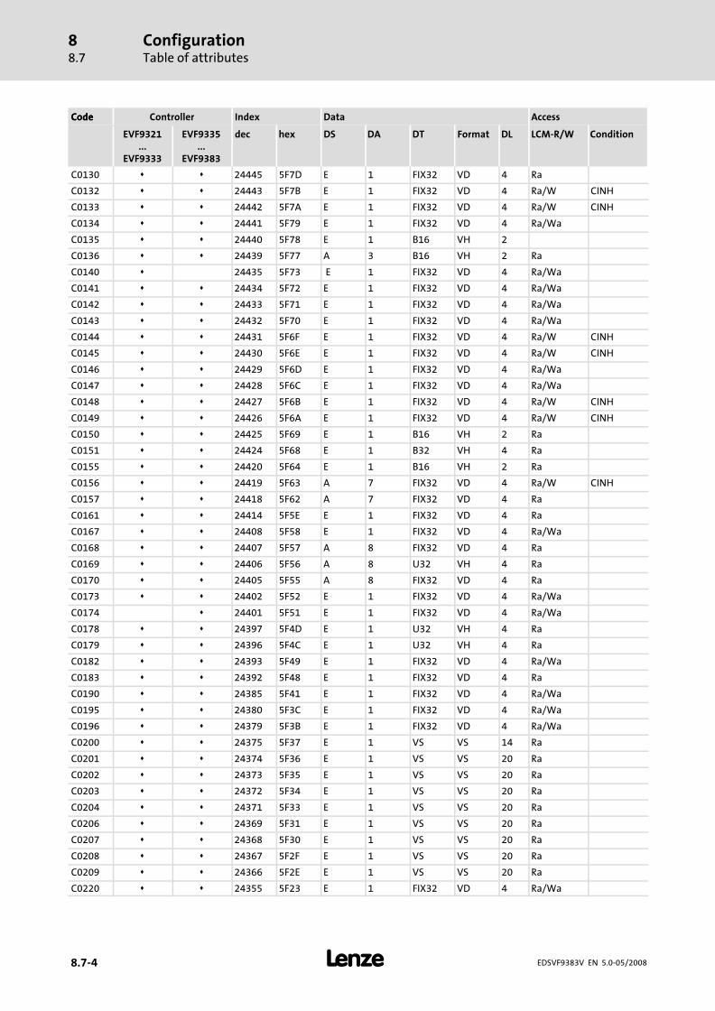
ConfigurationTable of attributes
88.7
� 8.7−4 EDSVF9383V EN 5.0−05/2008
AccessDataIndexControllerCode
ConditionLCM−R/WDLFormatDTDADShexdecEVF9335...
EVF9383
EVF9321...
EVF9333
Code
C0130 24445 5F7D E 1 FIX32 VD 4 Ra
C0132 24443 5F7B E 1 FIX32 VD 4 Ra/W CINH
C0133 24442 5F7A E 1 FIX32 VD 4 Ra/W CINH
C0134 24441 5F79 E 1 FIX32 VD 4 Ra/Wa
C0135 24440 5F78 E 1 B16 VH 2
C0136 24439 5F77 A 3 B16 VH 2 Ra
C0140 24435 5F73 E 1 FIX32 VD 4 Ra/Wa
C0141 24434 5F72 E 1 FIX32 VD 4 Ra/Wa
C0142 24433 5F71 E 1 FIX32 VD 4 Ra/Wa
C0143 24432 5F70 E 1 FIX32 VD 4 Ra/Wa
C0144 24431 5F6F E 1 FIX32 VD 4 Ra/W CINH
C0145 24430 5F6E E 1 FIX32 VD 4 Ra/W CINH
C0146 24429 5F6D E 1 FIX32 VD 4 Ra/Wa
C0147 24428 5F6C E 1 FIX32 VD 4 Ra/Wa
C0148 24427 5F6B E 1 FIX32 VD 4 Ra/W CINH
C0149 24426 5F6A E 1 FIX32 VD 4 Ra/W CINH
C0150 24425 5F69 E 1 B16 VH 2 Ra
C0151 24424 5F68 E 1 B32 VH 4 Ra
C0155 24420 5F64 E 1 B16 VH 2 Ra
C0156 24419 5F63 A 7 FIX32 VD 4 Ra/W CINH
C0157 24418 5F62 A 7 FIX32 VD 4 Ra
C0161 24414 5F5E E 1 FIX32 VD 4 Ra
C0167 24408 5F58 E 1 FIX32 VD 4 Ra/Wa
C0168 24407 5F57 A 8 FIX32 VD 4 Ra
C0169 24406 5F56 A 8 U32 VH 4 Ra
C0170 24405 5F55 A 8 FIX32 VD 4 Ra
C0173 24402 5F52 E 1 FIX32 VD 4 Ra/Wa
C0174 24401 5F51 E 1 FIX32 VD 4 Ra/Wa
C0178 24397 5F4D E 1 U32 VH 4 Ra
C0179 24396 5F4C E 1 U32 VH 4 Ra
C0182 24393 5F49 E 1 FIX32 VD 4 Ra/Wa
C0183 24392 5F48 E 1 FIX32 VD 4 Ra
C0190 24385 5F41 E 1 FIX32 VD 4 Ra/Wa
C0195 24380 5F3C E 1 FIX32 VD 4 Ra/Wa
C0196 24379 5F3B E 1 FIX32 VD 4 Ra/Wa
C0200 24375 5F37 E 1 VS VS 14 Ra
C0201 24374 5F36 E 1 VS VS 20 Ra
C0202 24373 5F35 E 1 VS VS 20 Ra
C0203 24372 5F34 E 1 VS VS 20 Ra
C0204 24371 5F33 E 1 VS VS 20 Ra
C0206 24369 5F31 E 1 VS VS 20 Ra
C0207 24368 5F30 E 1 VS VS 20 Ra
C0208 24367 5F2F E 1 VS VS 20 Ra
C0209 24366 5F2E E 1 VS VS 20 Ra
C0220 24355 5F23 E 1 FIX32 VD 4 Ra/Wa

ConfigurationTable of attributes
88.7
� 8.7−5EDSVF9383V EN 5.0−05/2008
AccessDataIndexControllerCode
ConditionLCM−R/WDLFormatDTDADShexdecEVF9335...
EVF9383
EVF9321...
EVF9333
Code
C0221 24354 5F22 E 1 FIX32 VD 4 Ra/Wa
C0222 24353 5F21 E 1 FIX32 VD 4 Ra/Wa
C0223 24352 5F20 E 1 FIX32 VD 4 Ra/Wa
C0224 24351 5F1F E 1 FIX32 VD 4 Ra/Wa
C0234 24341 5F15 E 1 FIX32 VD 4 Ra/Wa
C0235 24340 5F14 E 1 FIX32 VD 4 Ra/Wa
C0236 24339 5F13 E 1 FIX32 VD 4 Ra/Wa
C0241 24334 5F0E E 1 FIX32 VD 4 Ra/Wa
C0244 24331 5F0B E 1 FIX32 VD 4 Ra/Wa
C0250 24325 5F05 E 1 FIX32 VD 4 Ra/Wa
C0252 24323 5F03 E 1 I32 VH 4 Ra/Wa
C0253 24322 5F02 E 1 FIX32 VD 4 Ra/Wa
C0260 24315 5EFB E 1 FIX32 VD 4 Ra/Wa
C0261 24314 5EFA E 1 FIX32 VD 4 Ra/Wa
C0262 24313 5EF9 E 1 FIX32 VD 4 Ra/Wa
C0263 24312 5EF8 E 1 FIX32 VD 4 Ra/Wa
C0264 24311 5EF7 E 1 FIX32 VD 4 Ra/Wa
C0265 24310 5EF6 E 1 FIX32 VD 4 Ra/Wa
C0267 24308 5EF4 A 2 FIX32 VD 4 Ra/W CINH
C0268 24307 5EF3 E 1 FIX32 VD 4 Ra/W CINH
C0269 24306 5EF2 A 3 FIX32 VD 4 Ra
C0325 24250 5EBA E 1 FIX32 VD 4 Ra/Wa
C0326 24249 5EB9 E 1 FIX32 VD 4 Ra/Wa
C0327 24248 5EB8 E 1 FIX32 VD 4 Ra/Wa
C0328 24247 5EB7 E 1 FIX32 VD 4 Ra/Wa
C0329 24246 5EB6 E 1 FIX32 VD 4 Ra/Wa
C0332 24243 5EB3 E 1 FIX32 VD 4 Ra/Wa
C0333 24242 5EB2 E 1 FIX32 VD 4 Ra/Wa
C0336 24239 5EAF E 1 FIX32 VD 4 Ra
C0337 24238 5EAE E 1 FIX32 VD 4 Ra/Wa
C0338 24237 5EAD E 1 FIX32 VD 4 Ra/Wa
C0339 24236 5EAC A 2 FIX32 VD 4 Ra/W CINH
C0340 24235 5EAB A 2 FIX32 VD 4 Ra
C0350 24225 5EA1 E 1 FIX32 VD 4 Ra/Wa
C0351 24224 5EA0 E 1 FIX32 VD 4 Ra/Wa
C0352 24223 5E9F E 1 FIX32 VD 4 Ra/Wa
C0353 24222 5E9E A 3 FIX32 VD 4 Ra/Wa
C0354 24221 5E9D A 6 FIX32 VD 4 Ra/Wa
C0355 24220 5E9C A 6 FIX32 VD 4 Ra
C0356 24219 5E9B A 4 FIX32 VD 4 Ra/Wa
C0357 24218 5E9A A 3 FIX32 VD 4 Ra/Wa
C0358 24217 5E99 E 1 FIX32 VD 4 Ra/Wa
C0359 24216 5E98 E 1 FIX32 VD 4 Ra
C0360 24215 5E97 A 12 FIX32 VD 4 Ra
C0361 24214 5E96 A 12 FIX32 VD 4 Ra

ConfigurationTable of attributes
88.7
� 8.7−6 EDSVF9383V EN 5.0−05/2008
AccessDataIndexControllerCode
ConditionLCM−R/WDLFormatDTDADShexdecEVF9335...
EVF9383
EVF9321...
EVF9333
Code
C0364 24211 5E93 E 1 FIX32 VD 4 Ra/W CINH
C0365 24210 5E92 E 1 FIX32 VD 4 Ra
C0366 24209 5E91 E 1 FIX32 VD 4 Ra/Wa
C0367 24208 5E90 A 1 FIX32 VD 4 Ra/Wa
C0368 24207 5E8F E 1 FIX32 VD 4 Ra/Wa
C0369 24206 5E8E E 1 FIX32 VD 4 Ra/Wa
C0400 24175 5E6F E 1 FIX32 VD 4 Ra
C0402 24173 5E6D E 1 FIX32 VD 4 Ra/W CINH
C0403 24172 5E6C E 1 FIX32 VD 4 Ra/W CINH
C0404 24171 5E6B A 2 FIX32 VD 4 Ra
C0405 24170 5E6A E 1 FIX32 VD 4 Ra
C0407 24168 5E68 E 1 FIX32 VD 4 Ra/W CINH
C0408 24167 5E67 E 1 FIX32 VD 4 Ra/W CINH
C0409 24166 5E66 A 2 FIX32 VD 4 Ra
C0420 24155 5E5B E 1 FIX32 VD 4 Ra/W CINH
C0421 24154 5E5A E 1 FIX32 VD 4 Ra/W CINH
C0425 24150 5E56 E 1 FIX32 VD 4 Ra/Wa
C0426 24149 5E55 E 1 FIX32 VD 4 Ra
C0427 24148 5E54 E 1 FIX32 VD 4 Ra/Wa
C0429 24146 5E52 E 1 FIX32 VD 4 Ra/Wa
C0431 24144 5E50 E 1 FIX32 VD 4 Ra/W CINH
C0432 24143 5E4F E 1 FIX32 VD 4 Ra/W CINH
C0433 24142 5E4E E 1 FIX32 VD 4 Ra/W CINH
C0434 24141 5E4D A 3 FIX32 VD 4 Ra
C0436 24139 5E4B E 1 FIX32 VD 4 Ra/W CINH
C0437 24138 5E4A E 1 FIX32 VD 4 Ra/W CINH
C0438 24137 5E49 E 1 FIX32 VD 4 Ra/W CINH
C0439 24136 5E48 A 3 FIX32 VD 4 Ra
C0443 24132 5E44 E 1 B8 VH 1 Ra
C0444 24131 5E43 A 4 FIX32 VD 4 Ra
C0450 24125 5E3D E 1 FIX32 VD 4 Ra/W CINH
C0451 24124 5E3C E 1 FIX32 VD 4 Ra/W CINH
C0452 24123 5E3B E 1 FIX32 VD 4 Ra/W CINH
C0458 24117 5E35 A 2 FIX32 VD 4 Ra
C0459 24116 5E34 E 1 FIX32 VD 4 Ra
C0464 24111 5E2F E 1 FIX32 VD 4 Ra
C0465 24110 5E2E A 50 FIX32 VD 4 Ra/W CINH
C0466 24109 5E2D E 1 FIX32 VD 4 Ra
C0469 24106 5E2A E 1 FIX32 VD 4 Ra/W CINH
C0470 24105 5E29 A 4 B8 VH 1 Ra/Wa
C0471 24104 5E28 E 1 B32 VH 4 Ra/Wa
C0472 24103 5E27 A 20 FIX32 VD 4 Ra/Wa
C0473 24102 5E26 A 10 FIX32 VD 4 Ra/Wa
C0474 24101 5E25 A 2 I32 VH 4 Ra/Wa
C0475 24100 5E24 A 2 FIX32 VD 4 Ra/Wa

ConfigurationTable of attributes
88.7
� 8.7−7EDSVF9383V EN 5.0−05/2008
AccessDataIndexControllerCode
ConditionLCM−R/WDLFormatDTDADShexdecEVF9335...
EVF9383
EVF9321...
EVF9333
Code
C0497 24078 5E0E E 1 FIX32 VD 4 Ra/Wa
C0510 24065 5E01 E 1 FIX32 VD 4 Ra/W CINH
C0511 24064 5E00 E 1 FIX32 VD 4 Ra/Wa
C0517 24058 5DFA A 32 FIX32 VD 4 Ra/Wa
C0520 24055 5DF7 E 1 FIX32 VD 4 Ra/W CINH
C0521 24054 5DF6 E 1 FIX32 VD 4 Ra/W CINH
C0522 24053 5DF5 E 1 FIX32 VD 4 Ra/W CINH
C0523 24052 5DF4 E 1 FIX32 VD 4 Ra/W CINH
C0524 24051 5DF3 E 1 FIX32 VD 4 Ra/W CINH
C0525 24050 5DF2 E 1 FIX32 VD 4 Ra/W CINH
C0526 24049 5DF1 E 1 FIX32 VD 4 Ra/W CINH
C0527 24048 5DF0 E 1 FIX32 VD 4 Ra/W CINH
C0528 24047 5DEF A 2 I32 VH 4 Ra
C0529 24046 5DEE E 1 FIX32 VD 4 Ra/Wa
C0530 24045 5DED E 1 FIX32 VD 4 Ra/Wa
C0531 24044 5DEC E 1 FIX32 VD 4 Ra/Wa
C0532 24043 5DEB E 1 FIX32 VD 4 Ra/Wa
C0533 24042 5DEA E 1 FIX32 VD 4 Ra/Wa
C0534 24041 5DE9 E 1 FIX32 VD 4 Ra/Wa
C0535 24040 5DE8 E 1 FIX32 VD 4 Ra/Wa
C0536 24039 5DE7 A 3 FIX32 VD 4 Ra
C0537 24038 5DE6 E 1 FIX32 VD 4 Ra
C0538 24037 5DE5 A 3 FIX32 VD 4 Ra
C0539 24036 5DE4 E 1 FIX32 VD 4 Ra
C0540 24035 5DE3 E 1 FIX32 VD 4 Ra/W CINH
C0541 24034 5DE2 E 1 FIX32 VD 4 Ra/W CINH
C0542 24033 5DE1 E 1 FIX32 VD 4 Ra/W CINH
C0544 24031 5DDF E 1 FIX32 VD 4 Ra/W CINH
C0545 24030 5DDE E 1 FIX32 VD 4 Ra/Wa
C0546 24029 5DDD E 1 U32 VH 4 Ra/Wa
C0547 24028 5DDC E 1 FIX32 VD 4 Ra
C0548 24027 5DDB E 1 FIX32 VD 4 Ra
C0549 24026 5DDA E 1 FIX32 VD 4 Ra
C0560 24015 5DCF A 15 FIX32 VD 4 Ra/Wa
C0561 24014 5DCE E 1 FIX32 VD 4 Ra/W CINH
C0562 24013 5DCD A 4 FIX32 VD 4 Ra/W CINH
C0563 24012 5DCC E 1 FIX32 VD 4 Ra
C0564 24011 5DCB A 4 FIX32 VD 4 Ra
C0570 24005 5DC5 E 1 FIX32 VD 4 Ra/W CINH
C0571 24004 5DC4 E 1 FIX32 VD 4 Ra/W CINH
C0572 24003 5DC3 E 1 FIX32 VD 4 Ra
C0573 24002 5DC2 E 1 FIX32 VD 4 Ra
C0574 24001 5DC1 E 1 FIX32 VD 4 Ra/Wa
C0581 23994 5DBA E 1 FIX32 VD 4 Ra/Wa
C0582 23993 5DB9 E 1 FIX32 VD 4 Ra/Wa
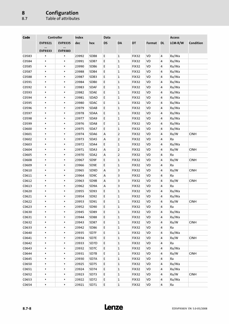
ConfigurationTable of attributes
88.7
� 8.7−8 EDSVF9383V EN 5.0−05/2008
AccessDataIndexControllerCode
ConditionLCM−R/WDLFormatDTDADShexdecEVF9335...
EVF9383
EVF9321...
EVF9333
Code
C0583 23992 5DB8 E 1 FIX32 VD 4 Ra/Wa
C0584 23991 5DB7 E 1 FIX32 VD 4 Ra/Wa
C0585 23990 5DB6 E 1 FIX32 VD 4 Ra/Wa
C0587 23988 5DB4 E 1 FIX32 VD 4 Ra/Wa
C0588 23987 5DB3 E 1 FIX32 VD 4 Ra/Wa
C0591 23984 5DB0 E 1 FIX32 VD 4 Ra/Wa
C0592 23983 5DAF E 1 FIX32 VD 4 Ra/Wa
C0593 23982 5DAE E 1 FIX32 VD 4 Ra/Wa
C0594 23981 5DAD E 1 FIX32 VD 4 Ra/Wa
C0595 23980 5DAC E 1 FIX32 VD 4 Ra/Wa
C0596 23979 5DAB E 1 FIX32 VD 4 Ra/Wa
C0597 23978 5DAA E 1 FIX32 VD 4 Ra/Wa
C0598 23977 5DA9 E 1 FIX32 VD 4 Ra/Wa
C0599 23976 5DA8 E 1 FIX32 VD 4 Ra/Wa
C0600 23975 5DA7 E 1 FIX32 VD 4 Ra/Wa
C0601 23974 5DA6 A 2 FIX32 VD 4 Ra/W CINH
C0602 23973 5DA5 A 2 FIX32 VD 4 Ra
C0603 23972 5DA4 E 1 FIX32 VD 4 Ra/Wa
C0604 23971 5DA3 A 2 FIX32 VD 4 Ra/W CINH
C0605 23970 5DA2 A 2 FIX32 VD 4 Ra
C0608 23967 5D9F E 1 FIX32 VD 4 Ra/W CINH
C0609 23966 5D9E E 1 FIX32 VD 4 Ra
C0610 23965 5D9D A 3 FIX32 VD 4 Ra/W CINH
C0611 23964 5D9C A 3 FIX32 VD 4 Ra
C0612 23963 5D9B A 3 FIX32 VD 4 Ra/W CINH
C0613 23962 5D9A A 3 FIX32 VD 4 Ra
C0620 23955 5D93 E 1 FIX32 VD 4 Ra/Wa
C0621 23954 5D92 E 1 FIX32 VD 4 Ra/Wa
C0622 23953 5D91 E 1 FIX32 VD 4 Ra/W CINH
C0623 23952 5D90 E 1 FIX32 VD 4 Ra
C0630 23945 5D89 E 1 FIX32 VD 4 Ra/Wa
C0631 23944 5D88 E 1 FIX32 VD 4 Ra/Wa
C0632 23943 5D87 E 1 FIX32 VD 4 Ra/W CINH
C0633 23942 5D86 E 1 FIX32 VD 4 Ra
C0640 23935 5D7F E 1 FIX32 VD 4 Ra/Wa
C0641 23934 5D7E E 1 FIX32 VD 4 Ra/W CINH
C0642 23933 5D7D E 1 FIX32 VD 4 Ra
C0643 23932 5D7C E 1 FIX32 VD 4 Ra/Wa
C0644 23931 5D7B E 1 FIX32 VD 4 Ra/W CINH
C0645 23930 5D7A E 1 FIX32 VD 4 Ra
C0650 23925 5D75 E 1 FIX32 VD 4 Ra/Wa
C0651 23924 5D74 E 1 FIX32 VD 4 Ra/Wa
C0652 23923 5D73 E 1 FIX32 VD 4 Ra/W CINH
C0653 23922 5D72 E 1 FIX32 VD 4 Ra/Wa
C0654 23921 5D71 E 1 FIX32 VD 4 Ra

ConfigurationTable of attributes
88.7
� 8.7−9EDSVF9383V EN 5.0−05/2008
AccessDataIndexControllerCode
ConditionLCM−R/WDLFormatDTDADShexdecEVF9335...
EVF9383
EVF9321...
EVF9333
Code
C0655 23920 5D70 E 1 FIX32 VD 4 Ra/Wa
C0656 23919 5D6F E 1 FIX32 VD 4 Ra/Wa
C0657 23918 5D6E E 1 FIX32 VD 4 Ra/W CINH
C0658 23917 5D6D E 1 FIX32 VD 4 Ra
C0661 23914 5D6A E 1 FIX32 VD 4 Ra/W CINH
C0662 23913 5D69 E 1 FIX32 VD 4 Ra
C0671 23904 5D60 E 1 FIX32 VD 4 Ra/Wa
C0672 23903 5D5F E 1 FIX32 VD 4 Ra/Wa
C0673 23902 5D5E E 1 FIX32 VD 4 Ra/W CINH
C0674 23901 5D5D E 1 FIX32 VD 4 Ra/W CINH
C0675 23900 5D5C E 1 FIX32 VD 4 Ra/W CINH
C0676 23899 5D5B A 2 FIX32 VD 4 Ra
C0677 23898 5D5A E 1 FIX32 VD 4 Ra
C0680 23895 5D57 E 1 FIX32 VD 4 Ra/Wa
C0681 23894 5D56 E 1 FIX32 VD 4 Ra/Wa
C0682 23893 5D55 E 1 FIX32 VD 4 Ra/Wa
C0683 23892 5D54 A 2 FIX32 VD 4 Ra/W CINH
C0684 23891 5D53 A 2 FIX32 VD 4 Ra
C0685 23890 5D52 E 1 FIX32 VD 4 Ra/Wa
C0686 23889 5D51 E 1 FIX32 VD 4 Ra/Wa
C0687 23888 5D50 E 1 FIX32 VD 4 Ra/Wa
C0688 23887 5D4F A 2 FIX32 VD 4 Ra/W CINH
C0689 23886 5D4E A 2 FIX32 VD 4 Ra
C0690 23885 5D4D E 1 FIX32 VD 4 Ra/Wa
C0691 23884 5D4C E 1 FIX32 VD 4 Ra/Wa
C0692 23883 5D4B E 1 FIX32 VD 4 Ra/Wa
C0693 23882 5D4A A 2 FIX32 VD 4 Ra/W CINH
C0694 23881 5D49 A 2 FIX32 VD 4 Ra
C0700 23875 5D43 E 1 FIX32 VD 4 Ra/W CINH
C0701 23874 5D42 E 1 FIX32 VD 4 Ra
C0703 23872 5D40 E 1 FIX32 VD 4 Ra/W CINH
C0704 23871 5D3F E 1 FIX32 VD 4 Ra
C0705 23870 5D3E E 1 FIX32 VD 4 Ra/Wa
C0706 23869 5D3D E 1 FIX32 VD 4 Ra/Wa
C0707 23868 5D3C E 1 FIX32 VD 4 Ra/Wa
C0708 23867 5D3B A 2 FIX32 VD 4 Ra/W CINH
C0709 23866 5D3A A 2 FIX32 VD 4 Ra
C0710 23865 5D39 E 1 FIX32 VD 4 Ra/Wa
C0711 23864 5D38 E 1 FIX32 VD 4 Ra/Wa
C0713 23862 5D36 E 1 FIX32 VD 4 Ra/W CINH
C0714 23861 5D35 E 1 FIX32 VD 4 Ra
C0715 23860 5D34 E 1 FIX32 VD 4 Ra/Wa
C0716 23859 5D33 E 1 FIX32 VD 4 Ra/Wa
C0718 23857 5D31 E 1 FIX32 VD 4 Ra/W CINH
C0719 23856 5D30 E 1 FIX32 VD 4 Ra

ConfigurationTable of attributes
88.7
� 8.7−10 EDSVF9383V EN 5.0−05/2008
AccessDataIndexControllerCode
ConditionLCM−R/WDLFormatDTDADShexdecEVF9335...
EVF9383
EVF9321...
EVF9333
Code
C0720 23855 5D2F E 1 FIX32 VD 4 Ra/Wa
C0721 23854 5D2E E 1 FIX32 VD 4 Ra/Wa
C0723 23852 5D2C E 1 FIX32 VD 4 Ra/W CINH
C0724 23851 5D2B E 1 FIX32 VD 4 Ra
C0725 23850 5D2A E 1 FIX32 VD 4 Ra/Wa
C0726 23849 5D29 E 1 FIX32 VD 4 Ra/Wa
C0728 23847 5D27 E 1 FIX32 VD 4 Ra/W CINH
C0729 23846 5D26 E 1 FIX32 VD 4 Ra
C0730 23845 5D25 E 1 FIX32 VD 4 Ra/Wa
C0731 23844 5D24 E 1 FIX32 VD 4 Ra
C0732 23843 5D23 A 4 FIX32 VD 4 Ra/W CINH
C0733 23842 5D22 E 1 FIX32 VD 4 Ra/W CINH
C0734 23841 5D21 E 1 FIX32 VD 4 Ra/Wa
C0735 23840 5D20 E 1 FIX32 VD 4 Ra/Wa
C0736 23839 5D1F E 1 FIX32 VD 4 Ra/Wa
C0737 23838 5D1E E 1 FIX32 VD 4 Ra/Wa
C0738 23837 5D1D E 1 FIX32 VD 4 Ra/Wa
C0739 23836 5D1C E 1 FIX32 VD 4 Ra/Wa
C0740 23835 5D1B A 2 FIX32 VD 4 Ra/Wa
C0741 23834 5D1A A 4 FIX32 VD 4 Ra
C0742 23833 5D19 E 1 FIX32 VD 4 Ra
C0743 23832 5D18 E 1 FIX32 VD 4 Ra
C0744 23831 5D17 E 1 FIX32 VD 4 Ra/Wa
C0749 23826 5D12 A 3 FIX32 VD 4 Ra
C0750 23825 5D11 E 1 FIX32 VD 4 Ra/Wa
C0751 23824 5D10 E 1 FIX32 VD 4 Ra/Wa
C0752 23823 5D0F E 1 FIX32 VD 4 Ra/Wa
C0753 23822 5D0E E 1 FIX32 VD 4 Ra/Wa
C0754 23821 5D0D E 1 U32 VH 4 Ra/Wa
C0755 23820 5D0C E 1 FIX32 VD 4 Ra/Wa
C0756 23819 5D0B E 1 I32 VH 4 Ra/Wa
C0757 23818 5D0A E 1 FIX32 VD 4 Ra/Wa
C0758 23817 5D09 E 1 FIX32 VD 4 Ra/W CINH
C0759 23816 5D08 E 1 FIX32 VD 4 Ra/W CINH
C0760 23815 5D07 E 1 FIX32 VD 4 Ra/W CINH
C0761 23814 5D06 E 1 FIX32 VD 4 Ra/W CINH
C0764 23811 5D03 A 3 FIX32 VD 4 Ra
C0765 23810 5D02 E 1 FIX32 VD 4 Ra
C0770 23805 5CFD E 1 FIX32 VD 4 Ra/W CINH
C0771 23804 5CFC E 1 FIX32 VD 4 Ra/W CINH
C0772 23803 5CFB E 1 FIX32 VD 4 Ra/W CINH
C0773 23802 5CFA A 3 FIX32 VD 4 Ra
C0775 23800 5CF8 E 1 FIX32 VD 4 Ra/W CINH
C0776 23799 5CF7 E 1 FIX32 VD 4 Ra/W CINH
C0777 23798 5CF6 E 1 FIX32 VD 4 Ra/W CINH

ConfigurationTable of attributes
88.7
� 8.7−11EDSVF9383V EN 5.0−05/2008
AccessDataIndexControllerCode
ConditionLCM−R/WDLFormatDTDADShexdecEVF9335...
EVF9383
EVF9321...
EVF9333
Code
C0778 23797 5CF5 A 3 FIX32 VD 4 Ra
C0780 23795 5CF3 E 1 FIX32 VD 4 Ra/W CINH
C0781 23794 5CF2 E 1 FIX32 VD 4 Ra/W CINH
C0782 23793 5CF1 E 1 FIX32 VD 4 Ra/W CINH
C0783 23792 5CF0 E 1 FIX32 VD 4 Ra/W CINH
C0784 23791 5CEF E 1 FIX32 VD 4 Ra/W CINH
C0785 23790 5CEE E 1 FIX32 VD 4 Ra/W CINH
C0786 23789 5CED E 1 FIX32 VD 4 Ra/W CINH
C0787 23788 5CEC A 4 FIX32 VD 4 Ra/W CINH
C0788 23787 5CEB A 4 FIX32 VD 4 Ra/W CINH
C0789 23786 5CEA E 1 FIX32 VD 4 Ra/W CINH
C0790 23785 5CE9 E 1 FIX32 VD 4 Ra/W CINH
C0798 23777 5CE1 A 2 FIX32 VD 4 Ra
C0799 23776 5CE0 A 13 FIX32 VD 4 Ra
C0800 23775 5CDF E 1 FIX32 VD 4 Ra/W CINH
C0801 23774 5CDE E 1 FIX32 VD 4 Ra/W CINH
C0802 23773 5CDD E 1 FIX32 VD 4 Ra/W CINH
C0803 23772 5CDC E 1 FIX32 VD 4 Ra/W CINH
C0804 23771 5CDB E 1 FIX32 VD 4 Ra/W CINH
C0805 23770 5CDA E 1 FIX32 VD 4 Ra/W CINH
C0808 23767 5CD7 A 4 FIX32 VD 4 Ra
C0809 23766 5CD6 A 2 FIX32 VD 4 Ra
C0810 23765 5CD5 A 2 FIX32 VD 4 Ra/W CINH
C0811 23764 5CD4 E 1 FIX32 VD 4 Ra/W CINH
C0812 23763 5CD3 A 2 FIX32 VD 4 Ra
C0813 23762 5CD2 E 1 FIX32 VD 4 Ra
C0815 23760 5CD0 A 2 FIX32 VD 4 Ra/W CINH
C0816 23759 5CCF E 1 FIX32 VD 4 Ra/W CINH
C0817 23758 5CCE A 2 FIX32 VD 4 Ra
C0818 23757 5CCD E 1 FIX32 VD 4 Ra
C0820 23755 5CCB A 3 FIX32 VD 4 Ra/W CINH
C0821 23754 5CCA A 3 FIX32 VD 4 Ra
C0822 23753 5CC9 A 3 FIX32 VD 4 Ra/W CINH
C0823 23752 5CC8 A 3 FIX32 VD 4 Ra
C0824 23751 5CC7 A 3 FIX32 VD 4 Ra/W CINH
C0825 23750 5CC6 A 3 FIX32 VD 4 Ra
C0826 23749 5CC5 A 3 FIX32 VD 4 Ra/W CINH
C0827 23748 5CC4 A 3 FIX32 VD 4 Ra
C0828 23747 5CC3 A 3 FIX32 VD 4 Ra/W CINH
C0829 23746 5CC2 A 3 FIX32 VD 4 Ra
C0830 23745 5CC1 A 3 FIX32 VD 4 Ra/W CINH
C0831 23744 5CC0 A 3 FIX32 VD 4 Ra
C0832 23743 5CBF A 3 FIX32 VD 4 Ra/W CINH
C0833 23742 5CBE A 3 FIX32 VD 4 Ra
C0834 23741 5CBD A 3 FIX32 VD 4 Ra/W CINH
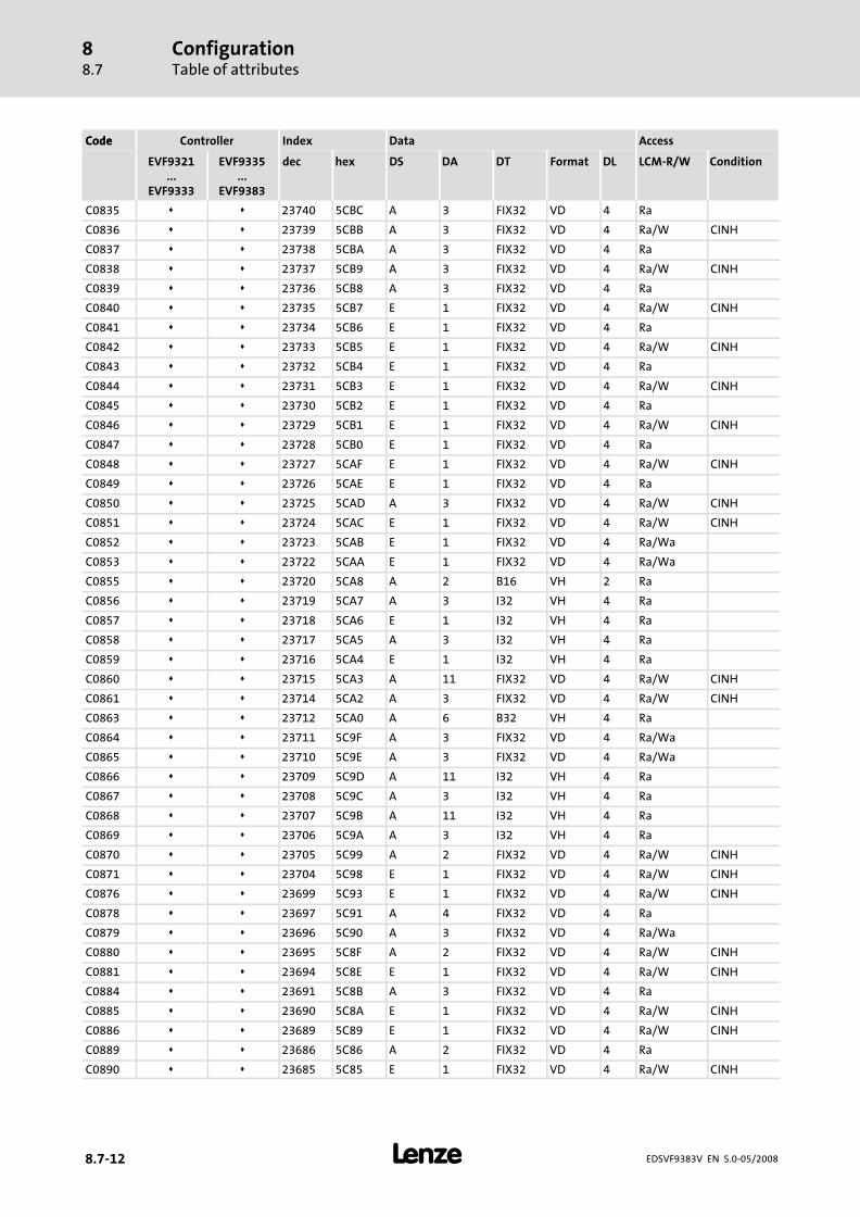
ConfigurationTable of attributes
88.7
� 8.7−12 EDSVF9383V EN 5.0−05/2008
AccessDataIndexControllerCode
ConditionLCM−R/WDLFormatDTDADShexdecEVF9335...
EVF9383
EVF9321...
EVF9333
Code
C0835 23740 5CBC A 3 FIX32 VD 4 Ra
C0836 23739 5CBB A 3 FIX32 VD 4 Ra/W CINH
C0837 23738 5CBA A 3 FIX32 VD 4 Ra
C0838 23737 5CB9 A 3 FIX32 VD 4 Ra/W CINH
C0839 23736 5CB8 A 3 FIX32 VD 4 Ra
C0840 23735 5CB7 E 1 FIX32 VD 4 Ra/W CINH
C0841 23734 5CB6 E 1 FIX32 VD 4 Ra
C0842 23733 5CB5 E 1 FIX32 VD 4 Ra/W CINH
C0843 23732 5CB4 E 1 FIX32 VD 4 Ra
C0844 23731 5CB3 E 1 FIX32 VD 4 Ra/W CINH
C0845 23730 5CB2 E 1 FIX32 VD 4 Ra
C0846 23729 5CB1 E 1 FIX32 VD 4 Ra/W CINH
C0847 23728 5CB0 E 1 FIX32 VD 4 Ra
C0848 23727 5CAF E 1 FIX32 VD 4 Ra/W CINH
C0849 23726 5CAE E 1 FIX32 VD 4 Ra
C0850 23725 5CAD A 3 FIX32 VD 4 Ra/W CINH
C0851 23724 5CAC E 1 FIX32 VD 4 Ra/W CINH
C0852 23723 5CAB E 1 FIX32 VD 4 Ra/Wa
C0853 23722 5CAA E 1 FIX32 VD 4 Ra/Wa
C0855 23720 5CA8 A 2 B16 VH 2 Ra
C0856 23719 5CA7 A 3 I32 VH 4 Ra
C0857 23718 5CA6 E 1 I32 VH 4 Ra
C0858 23717 5CA5 A 3 I32 VH 4 Ra
C0859 23716 5CA4 E 1 I32 VH 4 Ra
C0860 23715 5CA3 A 11 FIX32 VD 4 Ra/W CINH
C0861 23714 5CA2 A 3 FIX32 VD 4 Ra/W CINH
C0863 23712 5CA0 A 6 B32 VH 4 Ra
C0864 23711 5C9F A 3 FIX32 VD 4 Ra/Wa
C0865 23710 5C9E A 3 FIX32 VD 4 Ra/Wa
C0866 23709 5C9D A 11 I32 VH 4 Ra
C0867 23708 5C9C A 3 I32 VH 4 Ra
C0868 23707 5C9B A 11 I32 VH 4 Ra
C0869 23706 5C9A A 3 I32 VH 4 Ra
C0870 23705 5C99 A 2 FIX32 VD 4 Ra/W CINH
C0871 23704 5C98 E 1 FIX32 VD 4 Ra/W CINH
C0876 23699 5C93 E 1 FIX32 VD 4 Ra/W CINH
C0878 23697 5C91 A 4 FIX32 VD 4 Ra
C0879 23696 5C90 A 3 FIX32 VD 4 Ra/Wa
C0880 23695 5C8F A 2 FIX32 VD 4 Ra/W CINH
C0881 23694 5C8E E 1 FIX32 VD 4 Ra/W CINH
C0884 23691 5C8B A 3 FIX32 VD 4 Ra
C0885 23690 5C8A E 1 FIX32 VD 4 Ra/W CINH
C0886 23689 5C89 E 1 FIX32 VD 4 Ra/W CINH
C0889 23686 5C86 A 2 FIX32 VD 4 Ra
C0890 23685 5C85 E 1 FIX32 VD 4 Ra/W CINH
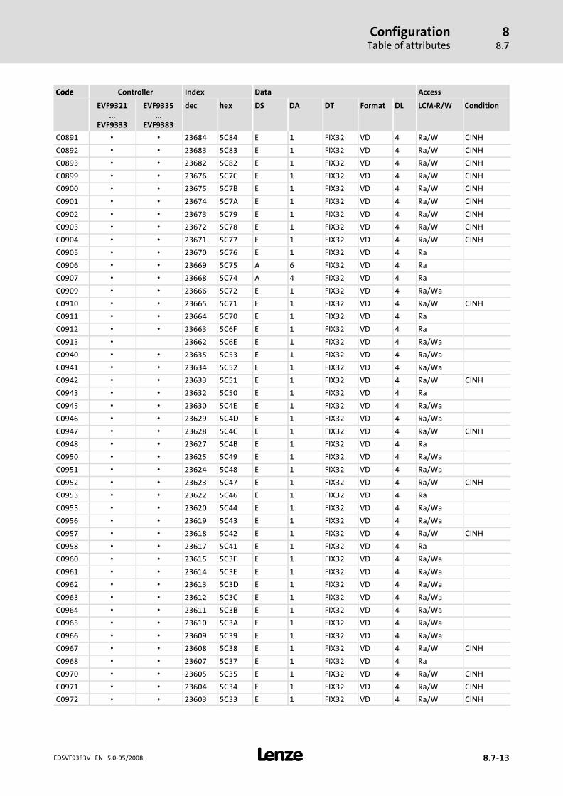
ConfigurationTable of attributes
88.7
� 8.7−13EDSVF9383V EN 5.0−05/2008
AccessDataIndexControllerCode
ConditionLCM−R/WDLFormatDTDADShexdecEVF9335...
EVF9383
EVF9321...
EVF9333
Code
C0891 23684 5C84 E 1 FIX32 VD 4 Ra/W CINH
C0892 23683 5C83 E 1 FIX32 VD 4 Ra/W CINH
C0893 23682 5C82 E 1 FIX32 VD 4 Ra/W CINH
C0899 23676 5C7C E 1 FIX32 VD 4 Ra/W CINH
C0900 23675 5C7B E 1 FIX32 VD 4 Ra/W CINH
C0901 23674 5C7A E 1 FIX32 VD 4 Ra/W CINH
C0902 23673 5C79 E 1 FIX32 VD 4 Ra/W CINH
C0903 23672 5C78 E 1 FIX32 VD 4 Ra/W CINH
C0904 23671 5C77 E 1 FIX32 VD 4 Ra/W CINH
C0905 23670 5C76 E 1 FIX32 VD 4 Ra
C0906 23669 5C75 A 6 FIX32 VD 4 Ra
C0907 23668 5C74 A 4 FIX32 VD 4 Ra
C0909 23666 5C72 E 1 FIX32 VD 4 Ra/Wa
C0910 23665 5C71 E 1 FIX32 VD 4 Ra/W CINH
C0911 23664 5C70 E 1 FIX32 VD 4 Ra
C0912 23663 5C6F E 1 FIX32 VD 4 Ra
C0913 23662 5C6E E 1 FIX32 VD 4 Ra/Wa
C0940 23635 5C53 E 1 FIX32 VD 4 Ra/Wa
C0941 23634 5C52 E 1 FIX32 VD 4 Ra/Wa
C0942 23633 5C51 E 1 FIX32 VD 4 Ra/W CINH
C0943 23632 5C50 E 1 FIX32 VD 4 Ra
C0945 23630 5C4E E 1 FIX32 VD 4 Ra/Wa
C0946 23629 5C4D E 1 FIX32 VD 4 Ra/Wa
C0947 23628 5C4C E 1 FIX32 VD 4 Ra/W CINH
C0948 23627 5C4B E 1 FIX32 VD 4 Ra
C0950 23625 5C49 E 1 FIX32 VD 4 Ra/Wa
C0951 23624 5C48 E 1 FIX32 VD 4 Ra/Wa
C0952 23623 5C47 E 1 FIX32 VD 4 Ra/W CINH
C0953 23622 5C46 E 1 FIX32 VD 4 Ra
C0955 23620 5C44 E 1 FIX32 VD 4 Ra/Wa
C0956 23619 5C43 E 1 FIX32 VD 4 Ra/Wa
C0957 23618 5C42 E 1 FIX32 VD 4 Ra/W CINH
C0958 23617 5C41 E 1 FIX32 VD 4 Ra
C0960 23615 5C3F E 1 FIX32 VD 4 Ra/Wa
C0961 23614 5C3E E 1 FIX32 VD 4 Ra/Wa
C0962 23613 5C3D E 1 FIX32 VD 4 Ra/Wa
C0963 23612 5C3C E 1 FIX32 VD 4 Ra/Wa
C0964 23611 5C3B E 1 FIX32 VD 4 Ra/Wa
C0965 23610 5C3A E 1 FIX32 VD 4 Ra/Wa
C0966 23609 5C39 E 1 FIX32 VD 4 Ra/Wa
C0967 23608 5C38 E 1 FIX32 VD 4 Ra/W CINH
C0968 23607 5C37 E 1 FIX32 VD 4 Ra
C0970 23605 5C35 E 1 FIX32 VD 4 Ra/W CINH
C0971 23604 5C34 E 1 FIX32 VD 4 Ra/W CINH
C0972 23603 5C33 E 1 FIX32 VD 4 Ra/W CINH
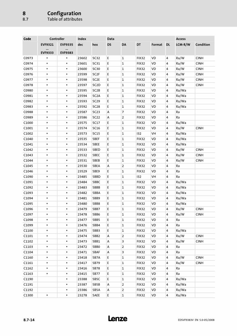
ConfigurationTable of attributes
88.7
� 8.7−14 EDSVF9383V EN 5.0−05/2008
AccessDataIndexControllerCode
ConditionLCM−R/WDLFormatDTDADShexdecEVF9335...
EVF9383
EVF9321...
EVF9333
Code
C0973 23602 5C32 E 1 FIX32 VD 4 Ra/W CINH
C0974 23601 5C31 E 1 FIX32 VD 4 Ra/W CINH
C0975 23600 5C30 E 1 FIX32 VD 4 Ra/W CINH
C0976 23599 5C2F E 1 FIX32 VD 4 Ra/W CINH
C0977 23598 5C2E E 1 FIX32 VD 4 Ra/W CINH
C0978 23597 5C2D E 1 FIX32 VD 4 Ra/W CINH
C0980 23595 5C2B E 1 FIX32 VD 4 Ra/Wa
C0981 23594 5C2A E 1 FIX32 VD 4 Ra/Wa
C0982 23593 5C29 E 1 FIX32 VD 4 Ra/Wa
C0983 23592 5C28 E 1 FIX32 VD 4 Ra/Wa
C0988 23587 5C23 A 7 FIX32 VD 4 Ra
C0989 23586 5C22 A 2 FIX32 VD 4 Ra
C1000 23575 5C17 E 1 FIX32 VD 4 Ra/Wa
C1001 23574 5C16 E 1 FIX32 VD 4 Ra/W CINH
C1002 23573 5C15 E 1 I32 VH 4 Ra/Wa
C1040 23535 5BEF E 1 FIX32 VD 4 Ra/Wa
C1041 23534 5BEE E 1 FIX32 VD 4 Ra/Wa
C1042 23533 5BED E 1 FIX32 VD 4 Ra/W CINH
C1043 23532 5BEC E 1 FIX32 VD 4 Ra/W CINH
C1044 23531 5BEB E 1 FIX32 VD 4 Ra/W CINH
C1045 23530 5BEA A 2 FIX32 VD 4 Ra
C1046 23529 5BE9 E 1 FIX32 VD 4 Ra
C1090 23485 5BBD E 1 I32 VH 4 Ra
C1091 23484 5BBC E 1 FIX32 VD 4 Ra/Wa
C1092 23483 5BBB E 1 FIX32 VD 4 Ra/Wa
C1093 23482 5BBA E 1 FIX32 VD 4 Ra/Wa
C1094 23481 5BB9 E 1 FIX32 VD 4 Ra/Wa
C1095 23480 5BB8 E 1 FIX32 VD 4 Ra/Wa
C1096 23479 5BB7 E 1 FIX32 VD 4 Ra/W CINH
C1097 23478 5BB6 E 1 FIX32 VD 4 Ra/W CINH
C1098 23477 5BB5 E 1 FIX32 VD 4 Ra
C1099 23476 5BB4 E 1 FIX32 VD 4 Ra
C1100 23475 5BB3 E 1 FIX32 VD 4 Ra/Wa
C1101 23474 5BB2 A 2 FIX32 VD 4 Ra/W CINH
C1102 23473 5BB1 A 3 FIX32 VD 4 Ra/W CINH
C1103 23472 5BB0 A 2 FIX32 VD 4 Ra
C1104 23471 5BAF A 3 FIX32 VD 4 Ra
C1160 23418 5B7A E 1 FIX32 VD 4 Ra/W CINH
C1161 23417 5B79 E 1 FIX32 VD 4 Ra/W CINH
C1162 23416 5B78 E 1 FIX32 VD 4 Ra
C1163 23415 5B77 E 1 FIX32 VD 4 Ra
C1190 23388 5B5C E 1 FIX32 VD 4 Ra/Wa
C1191 23387 5B5B A 2 FIX32 VD 4 Ra/Wa
C1192 23386 5B5A A 2 FIX32 VD 4 Ra/Wa
C1300 23278 5AEE E 1 FIX32 VD 4 Ra/Wa

ConfigurationTable of attributes
88.7
� 8.7−15EDSVF9383V EN 5.0−05/2008
AccessDataIndexControllerCode
ConditionLCM−R/WDLFormatDTDADShexdecEVF9335...
EVF9383
EVF9321...
EVF9333
Code
C1301 23277 5AED E 1 FIX32 VD 4 Ra/Wa
C1302 23276 5AEC E 1 FIX32 VD 4 Ra/Wa
C1303 23275 5AEB E 1 FIX32 VD 4 Ra/Wa
C1304 23274 5AEA E 1 VS VS 20 Ra
C1305 23273 5AE9 E 1 VS VS 20 Ra
C1306 23272 5AE8 E 1 FIX32 VD 4 Ra/Wa
C1307 23271 5AE7 E 1 FIX32 VD 4 Ra/Wa
C1308 23270 5AE6 E 1 FIX32 VD 4 Ra/Wa
C1309 23269 5AE5 E 1 FIX32 VD 4 Ra/Wa
C1310 23268 5AE4 E 1 FIX32 VD 4 Ra/Wa
C1311 23267 5AE3 E 1 FIX32 VD 4 Ra/Wa
C1320 23258 5ADA E 1 FIX32 VD 4 Ra/W CINH
C1321 23257 5AD9 A 2 FIX32 VD 4 Ra/W CINH
C1322 23256 5AD8 A 2 FIX32 VD 4 Ra
C1325 23253 5AD5 E 1 FIX32 VD 4 Ra
C1326 23252 5AD4 A 2 FIX32 VD 4 Ra
C1327 23251 5AD3 A 2 FIX32 VD 4 Ra/W CINH
C1328 23250 5AD2 E 1 FIX32 VD 4 Ra
C1330 23248 5AD0 E 1 FIX32 VD 4 Ra/Wa
C1331 23247 5ACF E 1 FIX32 VD 4 Ra/Wa
C1332 23246 5ACE E 1 FIX32 VD 4 Ra/Wa
C1333 23245 5ACD E 1 FIX32 VD 4 Ra/Wa
C1334 23244 5ACC E 1 FIX32 VD 4 Ra/Wa
C1335 23243 5ACB E 1 FIX32 VD 4 Ra/Wa
C1336 23242 5ACA E 1 FIX32 VD 4 Ra/Wa
C1337 23241 5AC9 E 1 FIX32 VD 4 Ra/Wa
C1340 23238 5AC6 A 4 FIX32 VD 4 Ra/W CINH
C1341 23237 5AC5 A 4 FIX32 VD 4 Ra/W CINH
C1344 23234 5AC2 A 4 FIX32 VD 4 Ra
C1345 23233 5AC1 A 4 FIX32 VD 4 Ra
C1350 23228 5ABC E 1 FIX32 VD 4 Ra/Wa
C1351 23227 5ABB E 1 FIX32 VD 4 Ra/Wa
C1354 23224 5AB8 E 1 FIX32 VD 4 Ra/W CINH
C1355 23223 5AB7 E 1 FIX32 VD 4 Ra/W CINH
C1356 23222 5AB6 E 1 FIX32 VD 4 Ra/W CINH
C1357 23221 5AB5 E 1 FIX32 VD 4 Ra
C1358 23220 5AB4 E 1 FIX32 VD 4 Ra
C1359 23219 5AB3 E 1 FIX32 VD 4 Ra
C1360 23218 5AB2 E 1 FIX32 VD 4 Ra/Wa
C1361 23217 5AB1 E 1 FIX32 VD 4 Ra/Wa
C1364 23214 5AAE E 1 FIX32 VD 4 Ra/W CINH
C1365 23213 5AAD E 1 FIX32 VD 4 Ra/W CINH
C1366 23212 5AAC E 1 FIX32 VD 4 Ra/W CINH
C1367 23211 5AAB E 1 FIX32 VD 4 Ra
C1368 23210 5AAA E 1 FIX32 VD 4 Ra

ConfigurationTable of attributes
88.7
� 8.7−16 EDSVF9383V EN 5.0−05/2008
AccessDataIndexControllerCode
ConditionLCM−R/WDLFormatDTDADShexdecEVF9335...
EVF9383
EVF9321...
EVF9333
Code
C1369 23209 5AA9 E 1 FIX32 VD 4 Ra
C1370 23208 5AA8 E 1 FIX32 VD 4 Ra/Wa
C1371 23207 5AA7 E 1 FIX32 VD 4 Ra/Wa
C1372 23206 5AA6 E 1 FIX32 VD 4 Ra/Wa
C1373 23205 5AA5 E 1 FIX32 VD 4 Ra/Wa
C1375 23203 5AA3 E 4 FIX32 VD 4 Ra/W CINH
C1376 23202 5AA2 E 1 FIX32 VD 4 Ra/W CINH
C1377 23201 5AA1 A 4 FIX32 VD 4 Ra
C1378 23200 5AA0 E 1 FIX32 VD 4 Ra
C1583 22995 59D3 E 1 FIX32 VD 4 Ra/Wa
C1751 22827 592B A 17 FIX32 VD 4 Ra/W CINH
C1753 22825 5929 E 1 FIX32 VD 4 Ra/W CINH
C1754 22824 5928 E 1 FIX32 VD 4 Ra/W CINH
C1755 22823 5927 E 1 FIX32 VD 4 Ra/W CINH

Troubleshooting and fault eliminationContents
9
� 9−1EDSVF9383V EN 5.0−05/2008
9 Troubleshooting and fault elimination
Contents
9.1 Display of operating data, diagnostics 9.1−1 . . . . . . . . . . . . . . . . . . . . . . . . .
9.1.1 Display of operating data 9.1−1 . . . . . . . . . . . . . . . . . . . . . . . . . . . .
9.1.2 Diagnostics 9.1−2 . . . . . . . . . . . . . . . . . . . . . . . . . . . . . . . . . . . . . . . . .
9.2 Troubleshooting 9.2−1 . . . . . . . . . . . . . . . . . . . . . . . . . . . . . . . . . . . . . . . . . . . .
9.2.1 Status display via LEDs at the controller 9.2−1 . . . . . . . . . . . . . . . . .
9.2.2 Fault analysis with the history buffer 9.2−1 . . . . . . . . . . . . . . . . . . .
9.3 Drive behaviour in the event of faults 9.3−1 . . . . . . . . . . . . . . . . . . . . . . . . . .
9.4 Fault elimination 9.4−1 . . . . . . . . . . . . . . . . . . . . . . . . . . . . . . . . . . . . . . . . . . .
9.4.1 Drive errors 9.4−1 . . . . . . . . . . . . . . . . . . . . . . . . . . . . . . . . . . . . . . . . .
9.4.2 Controller in clamp operation 9.4−2 . . . . . . . . . . . . . . . . . . . . . . . . .
9.4.3 Behaviour in case of overvoltage in the DC bus (OU message) 9.4−3 . . . . . . . . . . . . . . . . . . . . . . . . . . . . . . . . . . . . . . .
9.5 System error messages 9.5−1 . . . . . . . . . . . . . . . . . . . . . . . . . . . . . . . . . . . . . . .
9.5.1 General error messages 9.5−1 . . . . . . . . . . . . . . . . . . . . . . . . . . . . . .
9.5.2 Resetting system error messages 9.5−5 . . . . . . . . . . . . . . . . . . . . . .


Troubleshooting and fault eliminationDisplay of operating data, diagnostics
Display of operating data
99.1
9.1.1
� 9.1−1EDSVF9383V EN 5.0−05/2008
9.1 Display of operating data, diagnostics
9.1.1 Display of operating data
Important operating parameters are measured by the controller. They canbe displayed with the keypad or PC.
Some operating data can be calibrated to be displayed or selected directlywith the unit of the process quantity (e.g. pressure, temperature, speed).
� Note!
The calibration always affects all specified codes simultaneously.
Codes for parameter setting
Code Possible settings IMPORTANT
No. Name Lenze Selection
C0051 MCTRL−NACT −36000 {1 rpm} 36000 Actual speed value, function blockMCTRL� Read only
8.2−25 8.2−40
C0052 MCTRL−Umot 0 {1 V} 800 Motor voltage, function blockMCTRL� Read only� MCTRL−VACT = 100 % = C0090
8.2−25 8.2−40
C0053 UG−VOLTAGE 0 {1 V} 900 DC−bus voltage, function blockMCTRL� Read only� MCTRL−DCVOLT = 100 % =
1000 V
8.2−25 8.2−40
C0054 Imot 0.0 {0.1 A} 5000.0 Actual motor current, functionblock MCTRL� Read only� MCTRL−IACT = 100 % = C0022
8.2−25 8.2−40
C0061 Heatsink temp 0 {1 °C} 100 Heatsink temperature� Read only� If the temperature of the
heatsink > 85 °C, the controllersets TRIP OH
� Early warning is possible viaOH4, temperature is set inC0122
See SystemManual(extension)
C0063 Mot temp 0 {1 °C} 200 Motor temperature� Read only� Monitoring of the motor
temperature must beactivated.
� KTY at X8/5, X8/8:– At 150 °C, TRIP OH3 is set– Early warning is possible viaOH7, temperature is set inC0121
� PTC, thermal contact at T1, T2:– Release sets TRIP or
warning OH8
8.2−25 8.2−40
Description

Troubleshooting and fault eliminationDisplay of operating data, diagnosticsDiagnostics
99.19.1.2
� 9.1−2 EDSVF9383V EN 5.0−05/2008
IMPORTANTPossible settingsCode
SelectionLenzeNameNo.
C0064 Utilization 0 {1 %} 150 Device utilisation I×t� Read only� Device utilisation of the last
180 s operating time� C0064 > 100 % triggers
warning OC5� C0064 > 110 % limits the ouput
current of the controller to67 % of the maximum currentin C0022
8.2−25 8.2−40
C0150 Status word Bit00 — Bit08 Status code Read onlyDecimal status word fornetworking via automationinterface (AIF)� Binary interpretation indicates
the bit states
See SystemManual(extension)Bit01 IMP Bit09 Status code
Bit02 — Bit10 Status code
Bit03 — Bit11 Status code
Bit04 — Bit12 Warning
Bit05 — Bit13 Message
Bit06 n = 0 Bit14 —
Bit07 CINH Bit15 —
9.1.2 Diagnostics
Display codes for diagnostics
Codes for parameter setting
Code Possible settings IMPORTANT
No. Name Lenze Selection
C0093 Drive ident Controller identification� Read only
0 Invalid Defective power section
1 None No power section
14...20
9335VC 400V...9383VC 400V
Display of the controller used
21...28
9334VC 500V...9383VC 500V
9321...9333
9321 VC...9333VC
C0099 S/W version x.y Software version� Read onlyx
yMain versionSubversion
Description

Troubleshooting and fault eliminationTroubleshooting
Status display via LEDs at the controller
99.2
9.2.1
� 9.2−1EDSVF9383V EN 5.0−05/2008
9.2 Troubleshooting
A breakdown can be detected quickly via the LEDs at the controller or via thestatus information at the keypad.
Analyse the error using the history buffer. The list of fault messages givesyou advice how to remove the fault. ( 9.5−1)
9.2.1 Status display via LEDs at the controller
During operation, the operating status of the controller is indicated by
means of two LEDs.
LED Operating status
Red � Green �
Off On Controller is enabled
On On Mains is switched on and automaticstart is inhibited
Off Blinkingslowly
Controller is inhibited
Off On Motor data identification is beingperformed
Blinkingquickly
Off Undervoltage
Blinkingslowly
Off Active fault
9.2.2 Fault analysis with the history buffer
Faults can be retraced via the history buffer. Fault messages are stored in the8 memory locations in the order of their appearance.
The memory locations can be retrieved via codes.
Detecting breakdowns
Analysing errors
Retracing faults

Troubleshooting and fault eliminationTroubleshootingFault analysis with the history buffer
99.29.2.2
� 9.2−2 EDSVF9383V EN 5.0−05/2008
Structure of the history buffer
Code Memory location Entry Note
C0168/1 C0169/1 C0170/1 Memory location 1 Active fault If the fault is no longer pending or has beenacknowledged:� The contents of the memory locations
1 ... 7 are shifted "up" to the next memorylocation.
� The content of memory location 8 isdeleted from the history buffer and cannotbe retrieved anymore.
� Memory location 1 is deleted (= no activefault).
C0168/2 C0169/2 C0170/2 Memory location 2 Last fault
C0168/3 C0169/3 C0170/3 Memory location 3 Last but one fault
C0168/4 C0169/4 C0170/4 Memory location 4 Last but two fault
C0168/5 C0169/5 C0170/5 Memory location 5 Last but three fault
C0168/6 C0169/6 C0170/6 Memory location 6 Last but four fault
C0168/7 C0169/7 C0170/7 Memory location 7 Last but five fault
C0168/8 C0169/8 C0170/8 Memory location 8 Last but six fault
Explanations regarding the codes
C0168 Fault indication and response� The entry is effected as a LECOM error number� If several faults with different responses occur at the same time:
– Only the fault with the highest priority response is entered (1. TRIP,2. message, 3. warning).
� If several faults with the same response (e.g. 2 messages) occur at thesame time:– Only the fault which occurred first is entered.
C0169 Time of fault occurence� The reference time is provided by the power−on time meter (C0179).� If the same fault occurs several times in succession, only the time of the
last occurrence is stored.
C0170 Fault frequency� Only the time of the last occurrence is stored.
Set C0167�=�1 to clear the history buffer.Clear history buffer

Troubleshooting and fault eliminationDrive behaviour in the event of faults
99.3
� 9.3−1EDSVF9383V EN 5.0−05/2008
9.3 Drive behaviour in the event of faults
The controller responds differently to the three possible fault types TRIP,message, or warning:
TRIP (display in keypad XT: � $)
ƒ Switches the power outputs U, V, W to a high−resistance state untilTRIP reset is executed.
ƒ The fault indication is entered into the history buffer as "current fault"in C0168/1.
ƒ The drive coasts without any control!
ƒ After TRIP reset ( 9.5−5):
– The drive travels along the ramps to its setpoint.
– The fault indication is moved to C0168/2 as "last fault".
Message (display in keypad XT: � $)
ƒ Switches the power outputs U, V, W to a high−resistance state.
ƒ The fault indication is entered into the history buffer as "current fault"in C0168/1.
ƒ In case of a fault �5 s:
– The drive coasts without any control as long as the message is active!
– If the message is not active anymore, the drive travels to its setpointwith maximum torque.
ƒ In case of a fault > 5 s:
– The drive coasts without any control as long as the message is active!
– If the message is not active anymore, the drive travels to its setpointalong the adjusted ramps.
ƒ If the message is not active anymore, the fault indication is moved toC0168/2 as "last fault".
"Heatsink overtemperature" (keypad XT:OH � $)
ƒ The drive continues to travel in a controlled way!
ƒ The warning signal goes off when the fault is not active anymore.
"Error in motor phase" (keypad XT:LP1)
"PTC monitoring" (keypad XT:OH51)
ƒ The drive continues to travel in a controlled way!
ƒ The fault indication is entered into the history buffer as "current fault"in C0168/1.
ƒ After TRIP reset, the fault indication is moved to C0168/2 as "lastfault".
TRIP
Messages
Warnings


Troubleshooting and fault eliminationFault elimination
Drive errors
99.4
9.4.1
� 9.4−1EDSVF9383V EN 5.0−05/2008
9.4 Fault elimination
9.4.1 Drive errors
Malfunction Cause Remedy
An asynchronous motorwith feedback rotates in anuncontrolled manner andwith low speed
The motor phases are reversed so that the rotating fieldof the motor is not identical with the rotating field ofthe feedback system. The drive shows the followingbehaviour:� V/f characteristic control (C0006 = 5)
– The motor rotates faster than the speed setpointby the value set in C0074 (influence of the speedcontroller, Lenze setting 10 % of nmax). After thecontroller is enabled, it does not stop at zero speedsetpoint or quick stop (QSP).
– The final motor current depends, among otherthings, on the set value of the Vmin boost (C0016)and can rise to Imax (C0022). This may activate thefault message OC5.
� Vector control (C0006 = 1)– The motor rotates slowly with maximum slip
speed (depending on motor data and maximumcurrent) and does not react to a speed setpoint. Thedirection of rotation, however, is determined bythe sign of the speed setpoint.
– The motor current rises up to Imax (C0022). Thismay activate the fault message OC5 with a timedelay.
� Check motor cable for correct phaserelation.
� If possible, operate the motor withdeactivated feedback (C0025 = 1) andcheck the direction of rotation of themotor.
Motor does not rotatealthough the controller is
enabled (� is off) and aspeed setpoint has beenspecified.
The two terminal strips X5 are reversed. Since X5/A1 andX5/28 face each other, the controller can be enabled ifthe control terminals are internally supplied. All otherconnections, however, are assigned incorrectly so thatthe motor cannot start.
Check the position of the terminal strips:� If you look at the connection unit in
reading direction, the left terminalstrip X5 must be connected with theinput signals and the right terminalstrip X5 must be connected with theoutput signals.
The monitoring of themotor phases (LP1) doesnot respond if a motorphase is interrupted,although C0597 = 0 or 2
The function block MLP1 is not entered into theprocessing table.
Enter the function block MLP1 into theprocessing table. The function block MLP1requires 30 �s of calculating time.
If during high speedsDC−injection braking (GSB)is activated, the fault OC1(TRIP) or OU (TRIP) occurs
During DC−injection braking the controller sets pulseinhibit for a short time (DCTRL−IMP) to reduce themagnetisation in the motor before a DC voltage isinjected into the motor. At high speeds (e. g. in case ofmid−frequency motors) the residual voltage whichdevelops from the residual magnetism and high speedcan generate such a high motor current that OC1 or OUare activated.
Prolong the duration of the pulse inhibit:� Connect the output signal DCTRL−IMP
to the function block TRANSx andadjust the desired switch−off timethere (usually 500 ms). IfDCTRL−CINH1 is set to HIGH, theduration of the pulse inhibit isprolonged by the time adjusted.

Troubleshooting and fault eliminationFault eliminationController in clamp operation
99.49.4.2
� 9.4−2 EDSVF9383V EN 5.0−05/2008
9.4.2 Controller in clamp operation
The clamp operation is a permissible operating mode. But since, however,pulse inhibit is set again and again, the controller cannot provide theoptimum power. Moreover, the fault OC3 (TRIP) can be activated.
If the output power is optimal, the output current mainly is right below theclamp threshold.
9300vec110
Fig. 9.4−1 Output current when starting a motor with high load (shown with theoscilloscope in GDC)
� Clamp threshold
� Output current
Function
1. When the output current reaches 2.25 × Ir, a software clamp isactivated.
2. The controller sets pulse inhibit for a short time. The motor currentdecreases as a function of the inductance in the motor circuit.
– An internal counter is increased by the value one.
3. After max. 250 �s the pulse inhibit is deactivated.
4. If a software clamp reoccurs within 2 s, the internal counter is againincreased by the value one. Otherwise the counter is set to zero.
– If the counter reaches the value 4300, OC3 (TRIP) is activated.
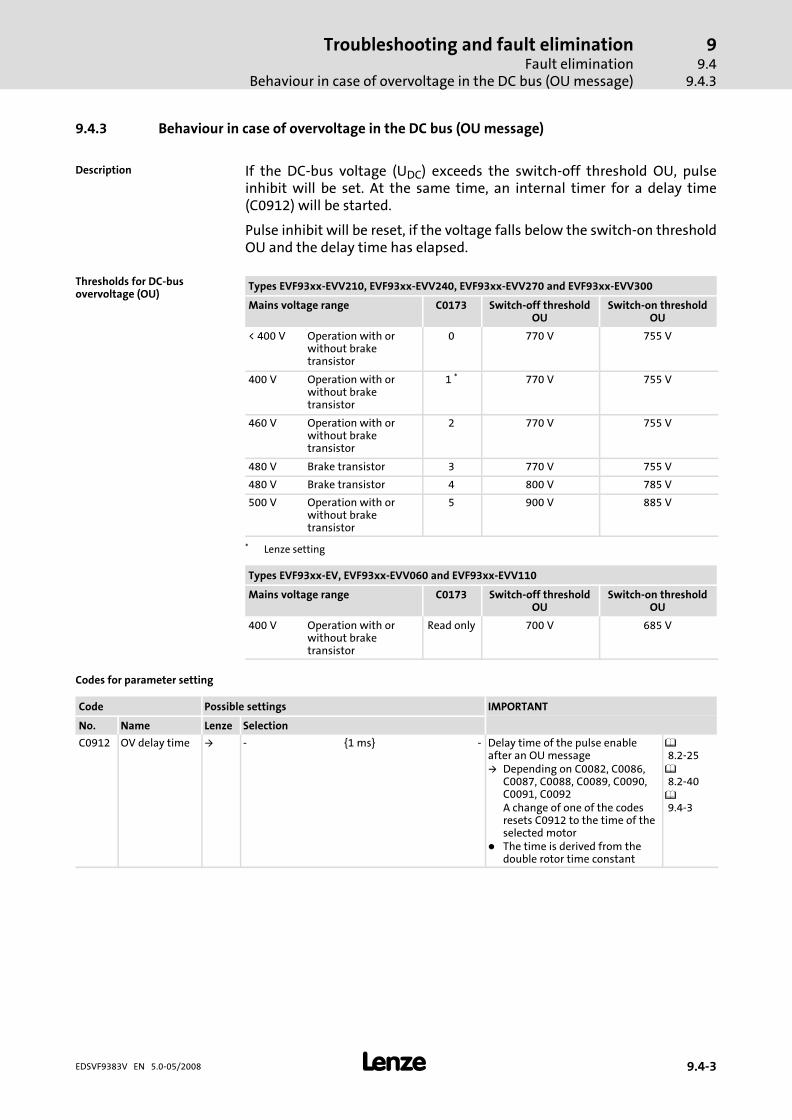
Troubleshooting and fault eliminationFault elimination
Behaviour in case of overvoltage in the DC bus (OU message)
99.4
9.4.3
� 9.4−3EDSVF9383V EN 5.0−05/2008
9.4.3 Behaviour in case of overvoltage in the DC bus (OU message)
If the DC−bus voltage (UDC) exceeds the switch−off threshold OU, pulseinhibit will be set. At the same time, an internal timer for a delay time(C0912) will be started.
Pulse inhibit will be reset, if the voltage falls below the switch−on thresholdOU and the delay time has elapsed.
Types EVF93xx−EVV210, EVF93xx−EVV240, EVF93xx−EVV270 and EVF93xx−EVV300
Mains voltage range C0173 Switch−off thresholdOU
Switch−on thresholdOU
< 400 V Operation with orwithout braketransistor
0 770 V 755 V
400 V Operation with orwithout braketransistor
1 * 770 V 755 V
460 V Operation with orwithout braketransistor
2 770 V 755 V
480 V Brake transistor 3 770 V 755 V
480 V Brake transistor 4 800 V 785 V
500 V Operation with orwithout braketransistor
5 900 V 885 V
* Lenze setting
Types EVF93xx−EV, EVF93xx−EVV060 and EVF93xx−EVV110
Mains voltage range C0173 Switch−off thresholdOU
Switch−on thresholdOU
400 V Operation with orwithout braketransistor
Read only 700 V 685 V
Codes for parameter setting
Code Possible settings IMPORTANT
No. Name Lenze Selection
C0912 OV delay time � − {1 ms} − Delay time of the pulse enableafter an OU message� Depending on C0082, C0086,
C0087, C0088, C0089, C0090,C0091, C0092A change of one of the codesresets C0912 to the time of theselected motor
� The time is derived from thedouble rotor time constant
8.2−25 8.2−40 9.4−3
Description
Thresholds for DC−busovervoltage (OU)

Troubleshooting and fault eliminationFault eliminationBehaviour in case of overvoltage in the DC bus (OU message)
99.49.4.3
� 9.4−4 EDSVF9383V EN 5.0−05/2008
UDC
t C0912�
t < C0912
t = C0912
�
�
� �
IMP
9300vec142
Fig. 9.4−2 Influence of the delay time (C0912)
� Switch−off threshold OU� Switch−on threshold OU� The period of time between exceeding the switch−off threshold OU and
undershooting the switch−on threshold OU equals or is higher than thedelay time set in C0912.After undershooting the switch−on threshold OU, the pulse inhibit isdeactivated.
� The period of time between exceeding the switch−off threshold OU andundershooting the switch−on threshold OU is lower than the delay time setin C0912.The pulse inhibit is deactivated after the delay time in C0912 has elapsed.
ƒ In C0912 the delay time is set in [ms].The Lenze setting can be changedby the factor 0.5 ... 2.
Adjustment
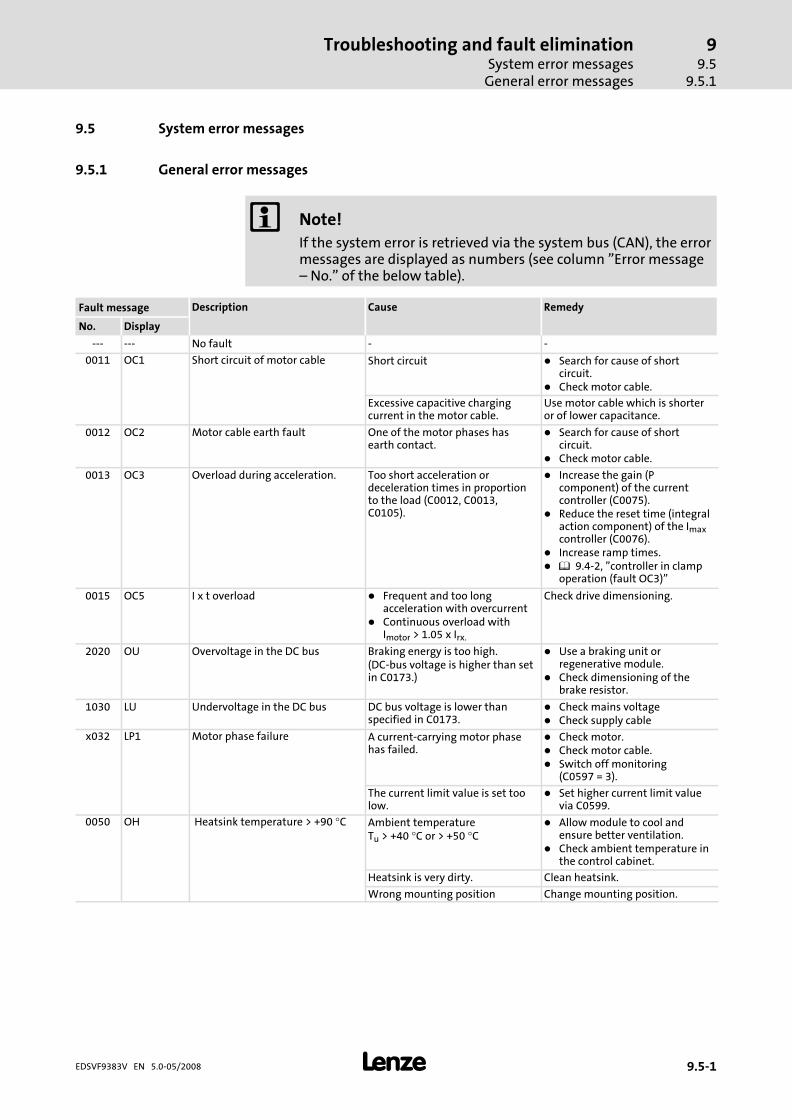
Troubleshooting and fault eliminationSystem error messages
General error messages
99.5
9.5.1
� 9.5−1EDSVF9383V EN 5.0−05/2008
9.5 System error messages
9.5.1 General error messages
� Note!
If the system error is retrieved via the system bus (CAN), the errormessages are displayed as numbers (see column "Error message˘ No." of the below table).
Fault message Description Cause Remedy
No. Display
−−− −−− No fault − −
0011 OC1 Short circuit of motor cable Short circuit � Search for cause of shortcircuit.
� Check motor cable.
Excessive capacitive chargingcurrent in the motor cable.
Use motor cable which is shorteror of lower capacitance.
0012 OC2 Motor cable earth fault One of the motor phases hasearth contact.
� Search for cause of shortcircuit.
� Check motor cable.
0013 OC3 Overload during acceleration. Too short acceleration ordeceleration times in proportionto the load (C0012, C0013,C0105).
� Increase the gain (Pcomponent) of the currentcontroller (C0075).
� Reduce the reset time (integralaction component) of the Imaxcontroller (C0076).
� Increase ramp times.� 9.4−2, "controller in clamp
operation (fault OC3)"
0015 OC5 I x t overload � Frequent and too longacceleration with overcurrent
� Continuous overload withImotor > 1.05 x Irx.
Check drive dimensioning.
2020 OU Overvoltage in the DC bus Braking energy is too high.(DC−bus voltage is higher than setin C0173.)
� Use a braking unit orregenerative module.
� Check dimensioning of thebrake resistor.
1030 LU Undervoltage in the DC bus DC bus voltage is lower thanspecified in C0173.
� Check mains voltage� Check supply cable
x032 LP1 Motor phase failure A current−carrying motor phasehas failed.
� Check motor.� Check motor cable.� Switch off monitoring
(C0597 = 3).
The current limit value is set toolow.
� Set higher current limit valuevia C0599.
0050 OH Heatsink temperature > +90 °C Ambient temperatureTu > +40 °C or > +50 °C
� Allow module to cool andensure better ventilation.
� Check ambient temperature inthe control cabinet.
Heatsink is very dirty. Clean heatsink.
Wrong mounting position Change mounting position.

Troubleshooting and fault eliminationSystem error messagesGeneral error messages
99.59.5.1
� 9.5−2 EDSVF9383V EN 5.0−05/2008
RemedyCauseDescriptionFault message RemedyCauseDescription
DisplayNo.
x053 OH3 Motor temperature> +150 °C threshold(temperature detection viaresolver or incremental valueencoder)
Motor is thermally overloadeddue to:� Impermissible continuous
current� Frequent or too long
acceleration processes
� Check drive dimensioning.� Switch off monitoring
(C0583 = 3).
No PTC/temperature contactconnected.
Correct wiring.
x054 OH4 Heatsink temperature > C0122 Ambient temperature Tu > +40 °Cor > +50 °C
� Allow module to cool andensure better ventilation.
� Check ambient temperature inthe control cabinet.
� Switch off monitoring(C0582 = 3).
Heatsink is very dirty. Clean heatsink
Wrong mounting position Change mounting position.
The value specified under C0122is set too low.
Enter a higher value under C0122.
x057 OH7 Motor temperature > C0121(temperature detection viaresolver or incremental valueencoder)
Motor is thermally overloadeddue to:� Impermissible continuous
current� Frequent or too long
acceleration processes
� Check drive dimensioning.� Switch off monitoring
(C0584 = 3).
No PTC/temperature contactconnected.
Correct wiring.
The value specified under C0121is set too low.
Enter a higher value in C0121.
x058 OH8 Motor temperature via inputs T1and T2 is too high.
Motor is thermally overloadeddue to:� Impermissible continuous
current� Frequent or too long
acceleration processes
� Check drive dimensioning.� Switch off monitoring
(C0585 = 3).
Terminals T1 and T2 are notconnected
Connect PTC/temperaturecontact.
x061 CE0 Automation interface (AIF)communication error
Faulty transfer of controlcommands via AIF.
� Plug in the communicationmodule/keypad XT firmly,screw down, if necessary.
� Switch off monitoring(C0126 = 3).
x062 CE1 Communication error on theprocess data input objectCAN1_IN
CAN1_IN object receives faultydata or communication isinterrupted.
� Check wiring at X4.� Check sender.� Increase monitoring time
under C0357/1, if necessary.� Switch off monitoring
(C0591 = 3).
x063 CE2 Communication error on theprocess data input objectCAN2_IN
CAN2_IN object receives faultydata or communication isinterrupted.
� Check wiring at X4.� Check sender.� Increase monitoring time
under C0357/2, if necessary.� Switch off monitoring
(C0592 = 3).
x064 CE3 Communication error on theprocess data input objectCAN3_IN
CAN3_IN object receives faultydata or communication isinterrupted.
� Check wiring at X4.� Check sender.� Increase monitoring time
under C0357/3, if necessary.� Switch off monitoring
(C0593 = 3).

Troubleshooting and fault eliminationSystem error messages
General error messages
99.5
9.5.1
� 9.5−3EDSVF9383V EN 5.0−05/2008
RemedyCauseDescriptionFault message RemedyCauseDescription
DisplayNo.
x065 CE4 BUS−OFF state of system bus(CAN)
The controller has received toomany faulty telegrams via thesystem bus (CAN) and hasdisconnected from the bus.
� Check wiring at X4: Is the buscorrectly terminated?
� Check shield connection of thecables.
� Check PE connection.� Check bus load, reduce the
baud rate if necessary.(Observe the cable length!)
� Switch off the monitoring(C0595 = 3).
0071 CCr System failure Strong interference injection onthe control cables
Screen control cables
Ground or earth loops in thewiring
� Check wiring� Check PE connection
After troubleshooting: Deenergisethe device completely (disconnect24 V supply, discharge DC bus)!
0072 PR1 Checksum error in parameterset 1CAUTION: The Lenze setting isloaded automatically!
� Fault when loading aparameter set.
� Interruption whiletransmitting the parameter setvia keypad.
� Set the required parametersand store them under C0003 =1.
� As to PLC devices, check theuse of pointers.
The stored parameters areincompatible with the loadedsoftware version.
Store the parameter set underC0003 = 1 first to allow for afaults reset.
0073 PR2 Checksum error in parameterset 2PLEASE NOTE: The Lenze setting isloaded automatically!
� Fault while loading aparameter set.
� Interruption during thetransfer of the parameter setvia keypad.
� Set the required parametersand save them with C0003 = 2.
The parameters saved do notcomply with the software versionloaded.
In order to be able toacknowledge the error, first savethe parameter set with C0003 = 2.
0074 PEr Program error Error in the program flow Send the parameter set (on floppydisk/CD−ROM) with a detaileddescription of the problem toLenze.After troubleshooting: Deenergisethe device completely (disconnect24 V supply, discharge DC bus)!
0075 PR0 Error in parameter set. The operating system softwarehas been updated.
Storage of the Lenze settingC0003 = 1.
After troubleshooting: Deenergisethe device completely (disconnect24 V supply, discharge DC bus)!
0077 PR3 Checksum error in parameterset 3PLEASE NOTE: The Lenze setting isloaded automatically!
� Fault while loading aparameter set.
� Interruption during thetransfer of the parameter setvia keypad.
� Set the required parametersand save them with C0003 = 3.
The parameters saved do notcomply with the software versionloaded.
In order to be able toacknowledge the error, first savethe parameter set with C0003 = 3.
0078 PR4 Checksum error in parameterset 4PLEASE NOTE: The Lenze setting isloaded automatically!
� Fault while loading aparameter set.
� Interruption during thetransfer of the parameter setvia keypad.
� Set the required parametersand save them with C0003 = 4.
The parameters saved do notcomply with the software versionloaded.
In order to be able toacknowledge the error, first savethe parameter set with C0003 = 4.

Troubleshooting and fault eliminationSystem error messagesGeneral error messages
99.59.5.1
� 9.5−4 EDSVF9383V EN 5.0−05/2008
RemedyCauseDescriptionFault message RemedyCauseDescription
DisplayNo.
0079 PI Fault during parameterinitialisation
� An error has been detectedduring the parameter settransfer between two devices.
� The parameter set does notmatch the controller, e.g. ifdata has been transferred froma higher−power controller to alower−power controller.
� Correct parameter set.� Send parameter set (on floppy
disk/CD−ROM) and a detaileddescription of the problem toLenze.
x083 Sd3 Encoder error at X9 Cable interrupted. Check cable for open circuit.
Pin X9/8 not connected. Apply 5 V to pin X9/8 or switch offmonitoring (C0587 = 3).
x085 Sd5 Encoder error at X6/1 and X6/2(C0034 = 1)
Current signal at X6/1 X6/2 <2mA.
� Check cable for open circuit.� Check current signal encoder.� Switch off monitoring
(C0598 = 3).
x086 Sd6 Motor temperature sensor error(X7 or X8)
Encoder for detecting the motortemperature at X7 or X8 indicatesundefined values.
� Check cable for firmconnection.
� Switch off the monitoring(C0594 = 3).
x091 EEr External monitoring has beentriggered via DCTRL.
A digital signal assigned to theTRIP−SET function has beenactivated.
� Check external encoder.� Switch off the monitoring
(C0581 = 3).
0105 H05 Internal fault (memory) Contact Lenze.
0107 H07 Internal fault (power stage) During initialisation of thecontroller, an incorrect powerstage was detected.
Contact Lenze.
x110 H10 Heatsink temperature sensorerror
Sensor for detecting the heatsinktemperature indicates undefinedvalues.
� Contact Lenze.� Switch off the monitoring
(C0588 = 3).
x111 H11 Temperature sensor error:Temperature inside the controller
Sensor for detecting the internaltemperature indicates undefinedvalues.
� Contact Lenze.� Switch off the monitoring
(C0588 = 3).
0140 ID1 Error during motor dataidentification.
No motor connected. Check motor connection.
Stator resistance too high. Check entered motor data.
Controller inhibited externally. Enable controller and repeatmotor data identification. Thecontroller enable must bepending continuously until theend of the identification process.

Troubleshooting and fault eliminationSystem error messages
Resetting system error messages
99.5
9.5.2
� 9.5−5EDSVF9383V EN 5.0−05/2008
RemedyCauseDescriptionFault message RemedyCauseDescription
DisplayNo.
0141 ID2 Error during motor dataidentification.
Motor too small. � Check entered motor data. Forparameterisation with GlobalDrive Control, use the inputassistant for motor data.
� The measurements for theinverter error characteristicand the stator resistance arecorrect (save measured valuesin C0003). For the operatingmode V/f characteristic controlthe motor data identificationcan be completed.
Controller inhibited externally. Enable controller and repeatmotor data identification. Thecontroller enable must bepending continuously until theend of the identification process.
x200 Nmax Maximum speed (C0596) hasbeen exceeded.
� Active load (e.g. for hoists) istoo high
� Drive is not speed−controlled,torque is excessively limited.
� Check drive dimensioning.� Possibly increase torque limit.� Switch off monitoring
(C0607 = 3).
Representation of the error number:x 0 = TRIP, 1 = message, 2 = warning
E. g. "2091": An external monitoring function has triggered EEr warning
9.5.2 Resetting system error messages
Response Measures for resetting the fault message
TRIP Note!If a TRIP source is still active, the pending TRIP cannot be reset.
Resetting the TRIP can be effected by:� Pressing the keypad XT EMZ9371 BC � ). Then press � to re−enable the controller.� Setting code C0043 = 0.� Control word C0135, bit 11� Control word AIF� Control word of system bus (CAN)After resetting the TRIP, the drive remains at standstill.
Message Danger!After elimination of the fault, the fault message is cancelled automatically and the drive restartsautomatically.
Warning After elimination of the fault, the fault message is cancelled automatically.


DC−bus operationContents
10
� 10−1EDSVF9383V EN 5.0−05/2008
10 DC−bus operation
Contents
10.1 Function 10.1−1 . . . . . . . . . . . . . . . . . . . . . . . . . . . . . . . . . . . . . . . . . . . . . . . . . .
10.2 Conditions for trouble−free DC−bus operation 10.2−1 . . . . . . . . . . . . . . . . . . .
10.2.1 Possible combinations of Lenze controllers in a network of several drives 10.2−1 . . . . . . . . . . . . . . . . . . . . . . . . . . . . . . . . . . . . . . .
10.3 Mains chokes for DC−bus operation 10.3−1 . . . . . . . . . . . . . . . . . . . . . . . . . . . .
10.4 Fuses and cable cross−sections 10.4−1 . . . . . . . . . . . . . . . . . . . . . . . . . . . . . . . .
10.4.1 Mains supply 10.4−1 . . . . . . . . . . . . . . . . . . . . . . . . . . . . . . . . . . . . . . .
10.4.2 DC supply 10.4−2 . . . . . . . . . . . . . . . . . . . . . . . . . . . . . . . . . . . . . . . . . .
10.5 Basic dimensioning 10.5−1 . . . . . . . . . . . . . . . . . . . . . . . . . . . . . . . . . . . . . . . . . .
10.5.1 Conditions 10.5−1 . . . . . . . . . . . . . . . . . . . . . . . . . . . . . . . . . . . . . . . . .
10.5.2 Calculation of the additional DC supply input 10.5−1 . . . . . . . . . . . .
10.5.3 Dimensioning examples 10.5−2 . . . . . . . . . . . . . . . . . . . . . . . . . . . . . .
10.6 Distributed supply (several supply points) 10.6−1 . . . . . . . . . . . . . . . . . . . . . . .
10.7 Braking operation in the network 10.7−1 . . . . . . . . . . . . . . . . . . . . . . . . . . . . . .


DC−bus operationFunction
1010.1
� 10.1−1EDSVF9383V EN 5.0−05/2008
10.1 Function
ƒ DC−bus connections of drive systems enable the exchange of energybetween connected controllers.
ƒ If one or more controllers operate in generator mode (brakingoperation), the energy will be fed into the shared DC−voltage bus. Theenergy will then be available to the controllers which operate in motormode.
ƒ The use of brake units and supply units can be reduced.
ƒ The energy consumption from the three−phase AC mains can bereduced.
ƒ The number of mains supplies and the related expenses (e.g. wiring)can be perfectly adapted to your application.


DC−bus operationConditions for trouble−free DC−bus operation
Possible combinations of Lenze controllers in a network of several drives
1010.2
10.2.1
� 10.2−1EDSVF9383V EN 5.0−05/2008
10.2 Conditions for trouble−free DC−bus operation
� Stop!
ƒ Only connect controllers with the same ranges for mainsvoltage or DC−bus voltage.
ƒ Adapt switching threshold of braking unit or brake transistor.
ƒ Operate all input modules only with the mains choke specified( 10.3−1)!
10.2.1 Possible combinations of Lenze controllers in a network of several drives
ƒ Use the controllers EVx9335 ... EVx9338 and EVx9381 ... EVx9383 invariants V210, V240, V270 and V300. They are suitable for DC−busoperation.
� Note!
For the subject "DC−bus operation", read the documentations ofthe other devices used within the interconnection.
Controller In DC−bus connectionwith
Important requirements
EVx9335 ... EVx9338EVx9381 ... EVx9383
EVx9335 ... EVx9338EVx9381 ... EVx9383
� Only supply the controller in a decentralised manner.� Only operate the controller with the mains choke assigned.� Set the mains voltage or DC−bus voltage in C0173.� Adapt the switching thresholds of the brake transistors in C0174.
EVx9321 ... EVx933382008200 vectorECSxA004C4B �ECSx064C4B
� Only central supply via EVx9335 ... EVx9338 or EVx9381 ... EVx9383permitted– A mains supply for EVx9321 ... EVx9333, 8200 and 8200 vector is not
permitted.– If required, use additional 9360 DC power supply units for a sufficient
DC power.� Set the mains voltage or DC−bus voltage in C0173.
– For EVx9335 ... EVx9338 and EVx9381 ... EVx9383 never set C0173 = 5.� Adapt the switching thresholds of the brake transistors in C0174.
9340 � The use of 9340 regenerative power supply modules is not possible.


DC−bus operationMains chokes for DC−bus operation
1010.3
� 10.3−1EDSVF9383V EN 5.0−05/2008
10.3 Mains chokes for DC−bus operation
� Note!
In DC−bus operation mains chokes in front of every input moduleare a basic precondition for trouble−free operation.
Mains chokes specified for the input modules in DC−bus operation:
Controller Mains choke
Type Rated mains current Rated current Inductance Order No.
[A] [A] [mH]
EVx9335 200 200 0.14 ELN3−0014H200
EVx9336 238 270 0.11 ELN3−0011H270
EVx9337 285 300 0.09 ELN3−0009H300
EVx9338 356 370 0.09 ELN3−0009H370
EVx9381 475 2 × 270 2 × 0.11 2 × ELN3−0011H270
EVx9382 570 2 × 300 2 × 0.09 2 × ELN3−0009H300
EVx9383 713 2 × 370 2 × 0.09 2 × ELN3−0009H370


DC−bus operationFuses and cable cross−sections
Mains supply
1010.4
10.4.1
� 10.4−1EDSVF9383V EN 5.0−05/2008
10.4 Fuses and cable cross−sections
10.4.1 Mains supply
For fusing the mains supply you can use the following fuses (gRL) and cablecross−sections:
9300 vector Installation in accordance with EN 60204−1
Fuse Cable cross−sections
L1, L2, L3 PE
Type [A] [mm2] [mm2]
EVF9335−EVEVF9335−EVVxxx
250150
2 × 50 1) 95
EVF9336−EVEVF9336−EVVxxx
315150
2 × 50 1) 95
EVF9337−EVEVF9337−EVVxxx
315150
2 × 50 1) 95
EVF9338−EVEVF9338−EVVxxx
400240
2 × 95 1) 150
Master Slave Master Slave Master Slave
EVF9381−EVEVF9381−EVVxxx
315 315150
2 × 50 1)150
2 × 50 1) 95 95
EVF9382−EVEVF9382−EVVxxx
315 315150
2 × 50 1)150
2 × 50 1) 95 95
EVF9383−EVEVF9383−EVVxxx
400 400240
2 × 95 1)240
2 × 95 1) 150 150
1) Multiple conductor; both conductors must have the same cross−section
� Note!
We recommend to use semiconductor fuses (gRL).

DC−bus operationFuses and cable cross−sectionsDC supply
1010.410.4.2
� 10.4−2 EDSVF9383V EN 5.0−05/2008
10.4.2 DC supply
A DC supply is only possible for the variants V210, V240, V270, V300.
� Stop!
ƒ Only use semiconductor fuses (gRL).
ƒ On principle, fuse DC cables as 2−pole (+UG, −UG).
9300 vector Installation in accordance with EN 60204−1
Fuse Cable cross−sections
+UG, −UG PE
Type [A] [mm2] [mm2]
EVF9335−EVV2xxEVF9335−EVV300
315150
2 × 50 1) 95
EVF9336−EVV2xxEVF9336−EVV300
350150
2 × 50 1) 95
EVF9337−EVV2xxEVF9337−EVV300
400240
2 × 95 1) 95
EVF9338−EVV2xxEVF9338−EVV300
500240
2 × 95 1) 150
Master Slave Master Slave Master Slave
EVF9381−EVV2xxEVF9381−EVV300
350 350150
2 × 50 1)150
2 × 50 1) 95 95
EVF9382−EVV2xxEVF9382−EVV300
400 400240
2 × 95 1)240
2 × 95 1) 95 95
EVF9383−EVV2xxEVF9383−EVV300
500 500240
2 × 95 1)240
2 × 95 1) 150 150
1) Multiple conductor; both conductors must have the same cross−section

DC−bus operationBasic dimensioning
Conditions
1010.5
10.5.1
� 10.5−1EDSVF9383V EN 5.0−05/2008
10.5 Basic dimensioning
10.5.1 Conditions
The input powers specified in the tables are only valid if the followingrequirements for DC−bus operation are observed:
ƒ Central supply only via EVx9335 � EVx9338, EVx9381 � EVx9383, or9360 DC power supply unit.
ƒ Connection to the three−phase system only via mains chokes specified.
10.5.2 Calculation of the additional DC supply input
Required DC power depending on the rated motor power:
PV PDC PV PDC
[kW] [kW] [kW] [kW]
0.37 0.7 15 18
0.55 0.9 18.5 21
0.75 1.1 22 25
1.1 1.6 30 33
1.5 2.1 37 41
2.2 3.1 45 50
3.0 4.1 55 61
4.0 5.0 75 82
5.5 6.7 90 98
7.5 9.0 110 120
11 12.5
PV Rated motor powerIf the rated power of the motor used is settled between two values, the higher value is to beadopted
PDC DC power required
Required DC power relating to the maximum current of the ECS axismodules:
Type PDC Type PDC
[kW] [kW]
ECSxA004C4B 1.5 ECSxA032C4B 12
ECSxA008C4B 3.0 ECSxA048C4B 18
ECSxA016C4B 6.0 ECSxA064C4B 24
PDC DC power required
EVx9321 � EVx9333,8200 vector
ECSxAxxxC4Baxis modules

DC−bus operationBasic dimensioningDimensioning examples
1010.510.5.3
� 10.5−2 EDSVF9383V EN 5.0−05/2008
1. If devices EVx9321 � EVx9333 or 8200 vector are used in the drivesystem:
Look for the rated powers of the connected motors in the table and writedown the corresponding powers PDC.
2. If devices ECSxAxxxC4B are used in the drive system:
Look for the connected axis modules in the table and write down thecorresponding powers PDC.
3. If required, determine the power PDC additionally available for thedevices EVx9335 � EVx9338, EVx9381 � EVx9383 in the drive systemby means of a rough estimate:
Device power ˘ rated power of the motor connected
4. Add all powers PDC from steps 1. and 2. and subtract the power PDCthat is additionally available.
– The result is the input power required.
5. Select the 9360 DC power supply units to provide the input power.
10.5.3 Dimensioning examples
Drive data Detemined power PDC
Controller Motor
Drive Type Power
Drive 1 E82EV113K4C 11 kW 12.5 kW
from tableDrive 2 E82EV453K4B 37 kW 41 kW
Drive 3 EVS9332 75 kW 82 kW
Drive 4 ECSxA048C4B 18 kW
Drive 5(input module)
EVV9336 (132 kW) 110 kW −22 kW roughestimate
1. Determine the required DC power:
PDC� �� 12.5�kW� �� 41�kW� �� 82�kW� �� 18�kW� �� 22�kW� �� 131.5�kW
2. Determine the required 9360 DC power supply units:
If 1 × 9364 (50 kW) and 1 × 9365 (100 kW) are used, a sufficient DC poweris provided with 150 kW.
How to calculate the inputpower required:

DC−bus operationDistributed supply (several supply points)
1010.6
� 10.6−1EDSVF9383V EN 5.0−05/2008
10.6 Distributed supply (several supply points)
Block diagram
EVx9335 9360 EVx9321 … EVx9333 8200 vector
L1
K10
L2
L3
N
PE
F1 … F3
F7, F8 F9, F10 F11, F12 F13, F14
F4 … F6
M3~
M3~
M3~
PE PE PE PEL1 L1 L1 L1L2 L2 L2 L2L3 L3 L3 L3
PE PE PEU U UV V VW W WBR1 BR2
+UG +UG +UG-UG
+UG -UG
-UG -UG
S2
S1K10
K10
Z2
Z3
Z1
9300VEC200
Fig. 10.6−1 Controller with decentralised supply in the drive system
F1...F6 Mains fuses ( 10.4−1)F7 ... F14 Fuses on DC level ( 10.4−2)Z1 Mains choke ( 10.3−1)Z2 Mains choke for 9360 DC power supply units
9364: ELN3−0038H0859365: ELN3−0017H170
Z3 DC choke9364: 0.75 mH, 90 A9365: 2 × 0.75 mH, 90 A (switched parallel)
K10 Mains contactorS1 Mains "ON"S2 Mains "OFF"


DC−bus operationBraking operation in the network
1010.7
� 10.7−1EDSVF9383V EN 5.0−05/2008
10.7 Braking operation in the network
ƒ Controllers EVx9335 ... EVx9383 in variants V270 and V300 areequipped with an integrated brake transistor.
ƒ Controllers EVx9381 ... EVx9383 in variants V270 and V300 consist of amaster and a slave. Both master and slave contain one brake transistor,respectively. The braking energy is normally dissipated in equal sharesvia master and slave.
ƒ In the DC−bus connection you have to set the switching thresholds ofthe brake transistors for all controllers of variants V270 and V300 tothe same value (C0174).
ƒ When the braking energy is low (e. g. operation in generator mode),you can also use 9352 brake choppers. A simultaneous brakingoperation with a 9352 brake chopper and an integrated brake resistoris not possible due to the different switching thresholds.


Safety engineeringContents
11
� 11−1EDSVF9383V EN 5.0−05/2008
11 Safety engineering
Contents
11.1 Important notes 11.1−1 . . . . . . . . . . . . . . . . . . . . . . . . . . . . . . . . . . . . . . . . . . . .
11.2 Method of functioning 11.2−1 . . . . . . . . . . . . . . . . . . . . . . . . . . . . . . . . . . . . . . .
11.3 Safety relay KSR 11.3−1 . . . . . . . . . . . . . . . . . . . . . . . . . . . . . . . . . . . . . . . . . . . . .
11.4 Functional test 11.4−1 . . . . . . . . . . . . . . . . . . . . . . . . . . . . . . . . . . . . . . . . . . . . .
11.4.1 Important notes 11.4−1 . . . . . . . . . . . . . . . . . . . . . . . . . . . . . . . . . . . . .
11.4.2 Manual safety function check 11.4−2 . . . . . . . . . . . . . . . . . . . . . . . . .
11.4.3 Monitoring the safety function with a PLC 11.4−3 . . . . . . . . . . . . . . .


Safety engineeringImportant notes
1111.1
� 11.1−1EDSVF9383V EN 5.0−05/2008
11.1 Important notes
� Stop!
In the case of the devices EVF9335 ... EVF9383 of variants V060,V110, V270, and V300, the integrated brake transistor isdeactivated if the "Safe torque off" function is active.
The controllers support the safety functions "Safe torque off" (formerdesignation "Safe standstill"), "Protection against unexpected start−up", inaccordance with the requirements of control category 3 of ISO 13849−1(former EN 954−1). Depending on the external interconnection, a standardup to "category 3" in accordance with ISO 13849−1 is achieved.
� Note!
In order to comply with control category 3 in accordance withISO 13849−1 (former EN 954−1), the two methods "Pulse inhibitvia safety relay KSR" and "Controller inhibit", which areindependent of each other, have to be used.
ƒ Only qualified personnel may install and commission the �Safe torqueoff" function.
ƒ All control components (switches, relays, PLC, ...) and the controlcabinet have to comply with the requirements of ISO 13849−1 (formerEN 954−1) and ISO 13849−2. These include:
– Control cabinet, switches, relays in enclosure IP54!
– Gather all further requirements from ISO 13849−1 and ISO 13849−2!
ƒ The wiring with insulated wire end ferrules or rigid cables is absolutelyrequired.
ƒ Be absolutely sure to install all safety−relevant cables (e. g. control cablefor the safety relay, feedback contact) outside of the control cabinet ina protected manner, e. g. within the cable duct. In doing this, ensurethat short circuits between the individual cables cannot occur!
ƒ With the �Safe torque off" function no emergency stop can be effectedwithout additional measures:
– Between the motor and controller there is not isolation, no serviceswitch, or maintenance switch!
– For an emergency stop, the isolation of the cable path to the motor isrequired, e. g. by a central mains contactor with an emergency stopwiring.
ƒ If in the case of the "Safe torque off" a force effect is to be expectedfrom outside, (e. g. sagging of hanging loads), additional measures arerequired (e. g. mechanical brakes).

Safety engineeringImportant notes
1111.1
� 11.1−2 EDSVF9383V EN 5.0−05/2008
ƒ After the installation the operator has to check the function of the"Safe torque off" circuit.
– The functional test has to be repeated at regular intervals.
– Basically the time intervals to be selected depend on the applicationand the corresponding risk analysis and the system as a whole(inspection interval). The inspection intervals should not exceed1 year.

Safety engineeringMethod of functioning
1111.2
� 11.2−1EDSVF9383V EN 5.0−05/2008
11.2 Method of functioning
X11/34
X11/33
X11/K32
X11/K31
X5/28
5 V
µC
PWMPWM
-
~
U
V
W
� �
�
DIGOUT
KSR
9300vec100
Fig. 11.2−1 Internal connection of the "Safe torque off" function with 3 electrically isolatedcircuits
Area �: Pulse inhibit via safety relay KSR; forcibly guided feedback formonitoring the safety relay
Area �: Controller inhibit (X5/28), optional feedback via a digital output(DIGOUT)
Area �: Power output stage

Safety engineeringMethod of functioning
1111.2
� 11.2−2 EDSVF9383V EN 5.0−05/2008
The "Safe torque off" status is activated via two different disconnectingpaths which are independent of each other:
1. disconnecting path: Pulse inhibit via safety relay KSR (terminal X11/33,X11/34)
ƒ In the case of LOW level at terminals X11/33, X11/34, the safety relayKSR is deactivated.The driver supply of the power section drivers isinterrupted. The inverter no longer receives pulses.
ƒ The disconnection of the safety relay KSR has to be monitoredexternally, so that a failure of this disconnecting path can be detected.X11/K31, X11/K32 is a forcibly guided break contact, i. e. if the safetyrelay KSR has been deactivated ("Safe torque off" activated), thecontact is closed.
2. disconnecting path: Controller inhibit by input signal at terminal X5/28
ƒ The input signal at X5/28 is fed to the microcontroller system and thePWM unit. In the case of LOW level at terminal X5/28, the output ofpulses to the inverter is inhibited in the microcontroller system.
ƒ The disconnecting path "Controller inhibit" can be evaluated optionallyvia a digital output. Further information can be gathered from thechapter "Functional test" ( 11.4−1).
"Safe torque off" is activated if both disconnecting paths are on LOW level.
An AND operation of the disconnecting paths prevents the drive fromrestarting if only one disconnecting path is enabled.
"Safe torque off" is deactivated if both disconnecting paths are on HIGHlevel.
Activating "Safe torque off"
Deactivating "Safe torqueoff"

Safety engineeringSafety relay KSR
1111.3
� 11.3−1EDSVF9383V EN 5.0−05/2008
11.3 Safety relay KSR
Technical data
Terminal Description Field Values
X11/K32X11/K31X11/33X11/34
Safety relay KSR1st disconnecting path
Coil voltage at +20 °C DC 24 V (20 ... 30 V)
Coil resistance at +20 °C 823 � ±10 %
Rated coil power Approx. 700 mW
Max. switching voltage AC 250 V, DC 250 V (0.45 A)
Max. AC switching capacity 1500 VA
Max. switching current (ohmic load) AC 6 A (250 V), DC 6 A (50 V)
Recommended minimum load > 50 mW
Max. switching rate 6 switchings per minute
Mechanical service life 107 switching cycles
Electrical service life
at 250 V AC(ohmic load)
105 switching cycles at 6 A106 switching cycles at 1 A107 switching cycles at 0.25 A
at 24 V DC(ohmic load)
6 × 10³ switching cycles at 6 A106 switching cycles at 3 A1.5 × 106 switching cycles at 1 A107 switching cycles at 0.1 A
Regulation for wiring of the terminals X11/34, X11/33, X11/K32, X11/K31,X5/28:
Cable type Wire end ferrule Cablecross−section
Tighteningtorque
Strippinglength
Rigid —2.5 mm2
(AWG 14) 0.5 ... 0.6 Nm(4.4 ... 5.3 lb−in)
5 mmFlexible
With plasticsleeve
2.5 mm2
(AWG 14)
Terminal data

Safety engineeringSafety relay KSR
1111.3
� 11.3−2 EDSVF9383V EN 5.0−05/2008
� Danger!
Faulty operation in case of earth faults possible
The correct functioning of the safety function is not ensured if anearth fault occurs.
Possible consequences:
ƒ A failure of the safety function can lead to death, severeinjuries or damage to material.
Protective measures:
The electrical reference point for the coil of the safety relay KSRmust be connected to the PE conductor system (EN 60204−1,paragraph 9.4.3)!
Terminal strip X11 Internal wiring / wiring of terminal strip X11
� �
� �
� � �
� � �
��
��
���
���
DC 24 V
X11
34
33
K32
K31
+5 V
+ +
–
KSR
9300vec103
Fig. 11.3−1 Safety relay KSR
Terminal FunctionBold print = Lenze setting
Level / state Electrical data
X11/K32X11/K31
Safety relay KSR1st disconnectingpath
Feedback − pulse inhibit Open contact: Pulse inhibit isinactive (operation)
See technical data of thesafety relay KSR
Closed contact: Pulse inhibit isactive
X11/33 – coil of safety relay KSR Coil is not carrying any current:pulse inhibit is active
X11/34 + coil of safety relay KSR Coil is carrying current: pulseinhibit is inactive (operation)
X5/28 Controller inhibit(DCTRL−CINH)2nddisconnectingpath
Controller enable/inhibit LOW: Controller inhibitedHIGH: Controller enabled
LOW: 0 ... +3 VHIGH: +12 ... +30 V
Input current at +24 V:8 mA
Reading and processingthe input signals − 1/ms(mean value)
Wiring

Safety engineeringFunctional test
Important notes
1111.4
11.4.1
� 11.4−1EDSVF9383V EN 5.0−05/2008
11.4 Functional test
11.4.1 Important notes
� Danger!
Unexpected start−up of the machine possible
The "Safe torque off" safety function provides protection againstan unexpected start−up of the drive and therefore is animportant item within the safety concept for a machine. It has tobe ensured that this function works correctly.
Possible consequences:
ƒ Death, severe injury, or damage to material assets, when thesafety function fails.
Protective measures:
After the installation and at regular intervals, the operator has tocheck the function of the "Safe torque off" circuit.
ƒ When doing this, check both disconnecting paths separatelywith regard to their disconnection capability.
ƒ The functional test can be carried out manually orautomatically via the PLC.
ƒ Basically the inspection interval depends on the applicationand the corresponding risk analysis, as well as on the systemas a whole. It should not exceed 1 year.
ƒ If the functional test shows impermissible states,– the drive or the machine has to be shut down immediately.– commissioning is not permitted until the safety function
operates correctly.
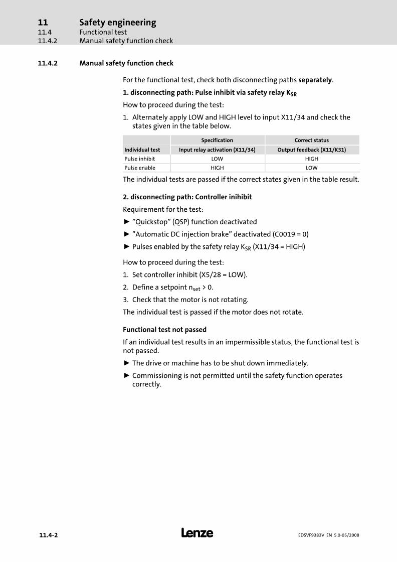
Safety engineeringFunctional testManual safety function check
1111.411.4.2
� 11.4−2 EDSVF9383V EN 5.0−05/2008
11.4.2 Manual safety function check
For the functional test, check both disconnecting paths separately.
1. disconnecting path: Pulse inhibit via safety relay KSR
How to proceed during the test:
1. Alternately apply LOW and HIGH level to input X11/34 and check thestates given in the table below.
Specification Correct status
Individual test Input relay activation (X11/34) Output feedback (X11/K31)
Pulse inhibit LOW HIGH
Pulse enable HIGH LOW
The individual tests are passed if the correct states given in the table result.
2. disconnecting path: Controller inihibit
Requirement for the test:
ƒ "Quickstop" (QSP) function deactivated
ƒ "Automatic DC injection brake" deactivated (C0019 = 0)
ƒ Pulses enabled by the safety relay KSR (X11/34 = HIGH)
How to proceed during the test:
1. Set controller inhibit (X5/28 = LOW).
2. Define a setpoint nset > 0.
3. Check that the motor is not rotating.
The individual test is passed if the motor does not rotate.
Functional test not passed
If an individual test results in an impermissible status, the functional test isnot passed.
ƒ The drive or machine has to be shut down immediately.
ƒ Commissioning is not permitted until the safety function operatescorrectly.

Safety engineeringFunctional test
Monitoring the safety function with a PLC
1111.4
11.4.3
� 11.4−3EDSVF9383V EN 5.0−05/2008
11.4.3 Monitoring the safety function with a PLC
KSR
µC
PWMPWM
RFR
DC 24 V
Z1
9300
S1S2
IN 1
IN 2
IN 3
IN 4
X11/34
X11/33
X11/K32
X11/K31
X5/28
DIGOUT
9300vec104
Fig. 11.4−1 Circuit diagram for monitoring the safety function with a PLC
S1, S2 Separate disconnection options of the two disconnecting pathsKSR Safety relayX11/34 Safety relay controlX11/33 Safety relay control (GND)X11/K32 Forcibly guided feedback contact (24 V)X11/K31 Forcibly guided feedback contactDIGOUT Digital output for evaluating the motor currentX5/28 Controller inhibitZ1 Programmable logic controller (PLC)IN 1 − 4 Digital inputs
The following conditions must be met:
ƒ The PLC must be programmed such that the complete system is set to asafe state immediately when the function check leads to animpermissible state.
ƒ The parameter setting of a digital output must be such that you canconclude to the output current Imotor of the drive (see parameterisationexample).
Requirements

Safety engineeringFunctional testMonitoring the safety function with a PLC
1111.411.4.3
� 11.4−4 EDSVF9383V EN 5.0−05/2008
In the following we will show you a possibility of parameterising a digitaloutput, so that a conclusion with regard to the motor current is provided.
Sequence Parameter Note
1. Configure function block CMP3(comparator)
� Connect CMP3−IN1 toMCTRL−IACT
C0693/1 = 5004
� Connect CMP3−IN2 toFCODE−472/1
C0693/2 = 19521
� Configure the function IN1 < IN2 C0690 = 3
2. Configure output signal of CMP3� Connect DIGOUT4 to CMP3−OUT
C0117/4 = 10660
3. Enter function block CMP3 in theprocessing table
� Select a free space in theprocessing tableIn the Lenze setting, for instancespace 2 of the processing table isfree
C0465/2 = 10660
4. Set the current threshold� Set the current threshold for
Irated_FI to 2 %
C0472/1 = 2.00 IMotor = 0 � DIGOUT4 = HIGHIMotor � 0 � DIGOUT4 = LOW
Example: Parameterising adigital output

Safety engineeringFunctional test
Monitoring the safety function with a PLC
1111.4
11.4.3
� 11.4−5EDSVF9383V EN 5.0−05/2008
For the functional test, check both disconnecting paths separately.
1. disconnecting path: Pulse inhibit via safety relay KSR
The individual tests are passed if the correct states given in the table result.
Specification Correct status
Individual test Input relay activation (X11/34) Output feedback (X11/K31)
Pulse inhibit LOW HIGH
Pulse enable HIGH LOW
2. disconnecting path: Controller inihibit
Requirement for the test:
ƒ "Quickstop" (QSP) function deactivated
ƒ "Automatic DC injection brake" deactivated (C0019 = 0)
ƒ Pulses enabled by the safety relay KSR (X11/34 = HIGH)
The individual tests are passed if the correct states given in the table result.
Specification Correct status
Individual test X5/28 Setpoint Output DIGOUT
Controller inhibit LOW nset > 0 HIGH
Controller enable HIGH LOW
Functional test not passed
If an individual test results in an impermissible status, the functional test isnot passed.
ƒ The drive or machine has to be shut down immediately.
ƒ Commissioning is not permitted until the safety function operatescorrectly.
Functional test within theinspection interval


Braking operationContents
12
� 12−1EDSVF9383V EN 5.0−05/2008
12 Braking operation
Contents
12.1 Brake operation with external brake resistor 12.1−1 . . . . . . . . . . . . . . . . . . . .
12.1.1 Selection of the brake resistors 12.1−1 . . . . . . . . . . . . . . . . . . . . . . . .
12.2 Lenze brake resistors 12.2−1 . . . . . . . . . . . . . . . . . . . . . . . . . . . . . . . . . . . . . . . .
12.2.1 Rated data 12.2−1 . . . . . . . . . . . . . . . . . . . . . . . . . . . . . . . . . . . . . . . . .
12.2.2 Dimensions 12.2−2 . . . . . . . . . . . . . . . . . . . . . . . . . . . . . . . . . . . . . . . .
12.2.3 Selection 12.2−2 . . . . . . . . . . . . . . . . . . . . . . . . . . . . . . . . . . . . . . . . . . .
12.2.4 Connection of external brake resistor 12.2−3 . . . . . . . . . . . . . . . . . . .
12.3 Rated data of the integrated brake transistor 12.3−1 . . . . . . . . . . . . . . . . . . . .
12.4 Braking operation in the network 12.4−1 . . . . . . . . . . . . . . . . . . . . . . . . . . . . . .
12.4.1 Selection 12.4−2 . . . . . . . . . . . . . . . . . . . . . . . . . . . . . . . . . . . . . . . . . . .


Braking operationBrake operation with external brake resistor
Selection of the brake resistors
1212.1
12.1.1
� 12.1−1EDSVF9383V EN 5.0−05/2008
12.1 Brake operation with external brake resistor
Larger moments of inertia or longer generator−mode operation require anexternal brake resistor. It converts mechanical brake energy into heat.
The brake transistor integrated into the controller switches the externalbrake resistor in addition when the DC−bus voltage exceeds a threshold. Itcan thus be avoided that the controller sets pulse inhibit in the event of an"overvoltage" and forces the drive to coast to standstill. External brakeresistors ensure braking operation at any time.
12.1.1 Selection of the brake resistors
The suitable brake resistor must meet the following criteria:
Brake resistor Application
Criteria with active load with passive load
Continuous braking power[W] � Pmax � �e � �m �
t1
tzykl�
Pmax � �e � �m
2�
t1
tzykl
Thermal capacity [Ws]� Pmax � �e � �m � t1 �
Pmax � �e � �m
2� t1
Resistance [�]Rmin � R �
UDC2
Pmax � �e � �m
Field Description
Active load Can move without being influenced by the controller (e.g.unwinders)
Passive load Decelerates to standstill without influence of the controller(e.g. horizontal traversing drives, centrifuges, fans)
VDC [V] Threshold for brake transistor
Pmax [W] Max. brake power determined by the applicationIMPORTANT:With EVF9381−EV, EVF9382−EV, EVF9383−EV only calculatewith Pmax/2 since these devices dissipate the brake energyevenly via master and slave. If the brake power is lower, thebrake energy can also be dissipated via the master or theslave; use Pmax for the calculation.
�e Electrical efficiency (controller + motor)Guide value: 0.94
�m Mechanical efficiency (gearbox, machine)
t1 [s] Braking time
tcycl [s] Cycle time = time between two braking processes(= t1 + break)
Rmin [�] Lowest permissible brake resistance (see rated data for theintegrated brake transistor)


Braking operationLenze brake resistors
Rated data
1212.2
12.2.1
� 12.2−1EDSVF9383V EN 5.0−05/2008
12.2 Lenze brake resistors
12.2.1 Rated data
Field Data
Resistance R 15 �
Continuous power 1) 4.0 kW
Thermal capacity 600.0 kWs
Switch−on cycle Braking for max. 19/15/14/11 s, then at least131/135/136/139 s break 2)
Cable cross−section to beconnected
6 mm2
AWG 10
Mass 12.5 kg
Order No. ERBD015R04K0
Observe the national and regional legislation1) The continuous power is a reference value for the selection of brake resistors. Braking at peak
brake power (V2DC/R).
2) More information on the switching threshold VDC (685 V, 755 V, 785 V, 885 V) of the braketransistor can be found in chapter 12.1
� Note!
As standard the brake resistor is equipped with a temperatureswitch (NC contact max. AC 250 V, 0.5 A).

Braking operationLenze brake resistorsDimensions
1212.212.2.2
� 12.2−2 EDSVF9383V EN 5.0−05/2008
12.2.2 Dimensions
c3 c1
c2
bb1
a2
a3
a4
a
a1
e
e1
c
Achtu
ng!
Cautio
n!
6.5 x 15.5
> 100 mm
> 200 mm
> 25 mm
> 25 mm
9300VEC041
Fig. 12.2−1 Dimensions of the ERBD015R04K0 brake resistor
Type a a1 a2 a3 a4 b b1 c c1 c2 c3 e e1
ERBD015R04K0 273 266 240 152 64 233 229 640 550 526 66.5 51 53
All values in [mm]
12.2.3 Selection
� Stop!
The value must not fall below the lowest permissible resistance.
Connect several brake resistors of type ERBD015R04K0 in parallel to get thebrake resistance that matches your application.
The number of resistors to be connected in parallel is calculated with 1/4 xof the required continuous power (round the result).

Braking operationLenze brake resistors
Connection of external brake resistor
1212.2
12.2.4
� 12.2−3EDSVF9383V EN 5.0−05/2008
12.2.4 Connection of external brake resistor
PES
BR1 BR2
Z1
PES
�RBRB
RB2 T1RB1 T2
9300VEC033
Fig. 12.2−2 Brake resistor connection
RB1, RB2 Controller terminals for connecting the brake resistorZ1 Brake resistorPES HF−shield end by PE connection through shield bracket.
ƒ Brake resistors can get hot and under certain conditions a brakeresistor can even burn down. For this reason, the brake resistors mustbe mounted so that the possibly high temperatures cannot cause anydamage.
ƒ Provide a safety shutdown in the event the brake resistor overheats.
ƒ Use the thermal contacts of the brake resistor (e.g. T1 / T2) as controlcontacts to disconnect the controller from the cable! <U Info:Graphikrahmen Beginn>
ƒ Only use shielded brake resistor cables.
ƒ Connect the shield close to the controller and close to the brake resistorwith a surface as large as possible to the mounting plate by using ashield clamp.
ƒ The shield of the control cables for digital signals (temperaturemonitoring T1 / T2) must be connected at both sides (controller andbrake resistor).
ƒ Unshielded cables between shield clamp and connection terminalsmust not be longer than 40 mm.
Important notes


Braking operationRated data of the integrated brake transistor
1212.3
� 12.3−1EDSVF9383V EN 5.0−05/2008
12.3 Rated data of the integrated brake transistor
Rated data for types EVF93xx−EVV060 and EVF93xx−EVV110 at 400 V rated mains voltage
Brake transistor 9300 vector
EVF9335−EVV060EVF9335−EVV110
EVF9336−EVV060EVF9336−EVV110
EVF9337−EVV060EVF9337−EVV110
EVF9338−EVV060EVF9338−EVV110
Threshold VDC [V DC] 685
Peak brake current [A DC] 315 375 450 560
Max. continuouscurrent
[A DC] 210 250 300 375
Lowest permissiblebrake resistance 1)
[�] 2.2 1.8 1.5 1.2
Current derating Derate the peak brake current by 2.5 %/°C above 40 °CDerate the peak brake current by 5 �%�/�1000 m above 1000 m a.m.s.l.
Switch−on cycle 3) max. 60 s braking at peak brake power, followed by min. 30 s break
Brake transistor 9300 vector
EVF9381−EVV060 2)
EVF9381−EVV110 2)EVF9382−EVV060 2)
EVF9382−EVV110 2)EVF9383−EVV060 2)
EVF9383−EVV110 2)
Threshold VDC [V DC] 685
Peak brake current [A DC] 2 × 375 2 × 450 2 × 560
Max. continuouscurrent
[A DC] 2 × 250 2 × 300 2 × 375
Lowest permissiblebrake resistance 1)
[�] 1.8 1.5 1.2
Current derating Derate the peak brake current by 2.5 %/°C above 40 °CDerate the peak brake current by 5 �%�/�1000 m above 1000 m a.m.s.l.
Switch−on cycle 3) max. 60 s braking at peak brake power, followed by min. 30 s break
1) Please consider the cable resistance if you use longer connection cables. The cable resistance mustbe added to the brake resistance and has therefore a considerable influence on the totalresistance.
2) Device consists of master and slave connected in parallel. Usually, the brake energy is dissipatedevenly via master and slave.
3) Please see the switch−on cycle of the brake resistor used.

Braking operationRated data of the integrated brake transistor
1212.3
� 12.3−2 EDSVF9383V EN 5.0−05/2008
Rated data for types EVF93xx−EVV270 and EVF93xx−EVV300 at 400 V or 460 V rated mains voltage
Brake transistor 9300 vector
EVF9335−EVV270EVF9335−EVV300
EVF9336−EVV270EVF9336−EVV300
EVF9337−EVV270EVF9337−EVV300
EVF9338−EVV270EVF9338−EVV300
Threshold VDC [V DC] 755
Peak brake current [A DC] 315 375 450 560
Max. continuouscurrent
[A DC] 210 250 300 375
Lowest permissiblebrake resistance 1)
[�] 2.5 2.1 1.8 1.4
Current derating Derate the peak brake current by 2.5 %/°C above 40 °CDerate the peak brake current by 5 �%�/�1000 m above 1000 m a.m.s.l.
Switch−on cycle 3) max. 60 s braking at peak brake power, followed by min. 30 s break
Brake transistor 9300 vector
EVF9381−EVV270 2)
EVF9381−EVV300 2)EVF9382−EVV270 2)
EVF9382−EVV300 2)EVF9383−EVV270 2)
EVF9383−EVV300 2)
Threshold VDC [V DC] 755
Peak brake current [A DC] 2 × 375 2 × 450 2 × 560
Max. continuouscurrent
[A DC] 2 × 250 2 × 300 2 × 375
Lowest permissiblebrake resistance 1)
[�] 2.1 1.8 1.4
Current derating Derate the peak brake current by 2.5 %/°C above 40 °CDerate the peak brake current by 5 �%�/�1000 m above 1000 m a.m.s.l.
Switch−on cycle 3) max. 60 s braking at peak brake power, followed by min. 30 s break
1) Please consider the cable resistance if you use longer connection cables. The cable resistance mustbe added to the brake resistance and has therefore a considerable influence on the totalresistance.
2) Device consists of master and slave connected in parallel. Usually, the brake energy is dissipatedevenly via master and slave.
3) Please see the switch−on cycle of the brake resistor used.

Braking operationRated data of the integrated brake transistor
1212.3
� 12.3−3EDSVF9383V EN 5.0−05/2008
Rated data for types EVF93xx−EVV270 and EVF93xx−EVV300 at 480 V rated mains voltage
Brake transistor 9300 vector
EVF9335−EVV270EVF9335−EVV300
EVF9336−EVV270EVF9336−EVV300
EVF9337−EVV270EVF9337−EVV300
EVF9338−EVV270EVF9338−EVV300
Threshold VDC [V DC] 785
Peak brake current [A DC] 315 375 450 560
Max. continuouscurrent
[A DC] 210 250 300 375
Lowest permissiblebrake resistance 1)
[�] 2.5 2.1 1.8 1.4
Current derating Derate the peak brake current by 2.5 %/°C above 40 °CDerate the peak brake current by 5 �%�/�1000 m above 1000 m a.m.s.l.
Switch−on cycle 3) max. 60 s braking at peak brake power, followed by min. 30 s break
Brake transistor 9300 vector
EVF9381−EVV270 2)
EVF9381−EVV300 2)EVF9382−EVV270 2)
EVF9382−EVV300 2)EVF9383−EVV270 2)
EVF9383−EVV300 2)
Threshold VDC [V DC] 785
Peak brake current [A DC] 2 × 375 2 × 450 2 × 560
Max. continuouscurrent
[A DC] 2 × 250 2 × 300 2 × 375
Lowest permissiblebrake resistance 1)
[�] 2.1 1.8 1.4
Current derating Derate the peak brake current by 2.5 %/°C above 40 °CDerate the peak brake current by 5 �%�/�1000 m above 1000 m a.m.s.l.
Switch−on cycle 3) max. 60 s braking at peak brake power, followed by min. 30 s break
1) Please consider the cable resistance if you use longer connection cables. The cable resistance mustbe added to the brake resistance and has therefore a considerable influence on the totalresistance.
2) Device consists of master and slave connected in parallel. Usually, the brake energy is dissipatedevenly via master and slave.
3) Please see the switch−on cycle of the brake resistor used.

Braking operationRated data of the integrated brake transistor
1212.3
� 12.3−4 EDSVF9383V EN 5.0−05/2008
Rated data for types EVF93xx−EVV270 and EVF93xx−EVV300 at 500 V rated mains voltage
Brake transistor 9300 vector
EVF9335−EVV270EVF9335−EVV300
EVF9336−EVV270EVF9336−EVV300
EVF9337−EVV270EVF9337−EVV300
EVF9338−EVV270EVF9338−EVV300
Threshold VDC [V DC] 885
Peak brake current [A DC] 315 375 450 560
Max. continuouscurrent
[A DC] 210 250 300 375
Lowest permissiblebrake resistance 1)
[�] 2.8 2.3 1.9 1.6
Current derating Derate the peak brake current by 2.5 %/°C above 40 °CDerate the peak brake current by 5 �%�/�1000 m above 1000 m a.m.s.l.
Switch−on cycle 3) max. 60 s braking at peak brake power, followed by min. 30 s break
Brake transistor 9300 vector
EVF9381−EVV270 2)
EVF9381−EVV300 2)EVF9382−EVV270 2)
EVF9382−EVV300 2)EVF9383−EVV270 2)
EVF9383−EVV300 2)
Threshold VDC [V DC] 885
Peak brake current [A DC] 2 × 375 2 × 450 2 × 560
Max. continuouscurrent
[A DC] 2 × 250 2 × 300 2 × 375
Lowest permissiblebrake resistance 1)
[�] 2.3 1.9 1.6
Current derating Derate the peak brake current by 2.5 %/°C above 40 °CDerate the peak brake current by 5 �%�/�1000 m above 1000 m a.m.s.l.
Switch−on cycle 3) max. 60 s braking at peak brake power, followed by min. 30 s break
1) Please consider the cable resistance if you use longer connection cables. The cable resistance mustbe added to the brake resistance and has therefore a considerable influence on the totalresistance.
2) Device consists of master and slave connected in parallel. Usually, the brake energy is dissipatedevenly via master and slave.
3) Please see the switch−on cycle of the brake resistor used.
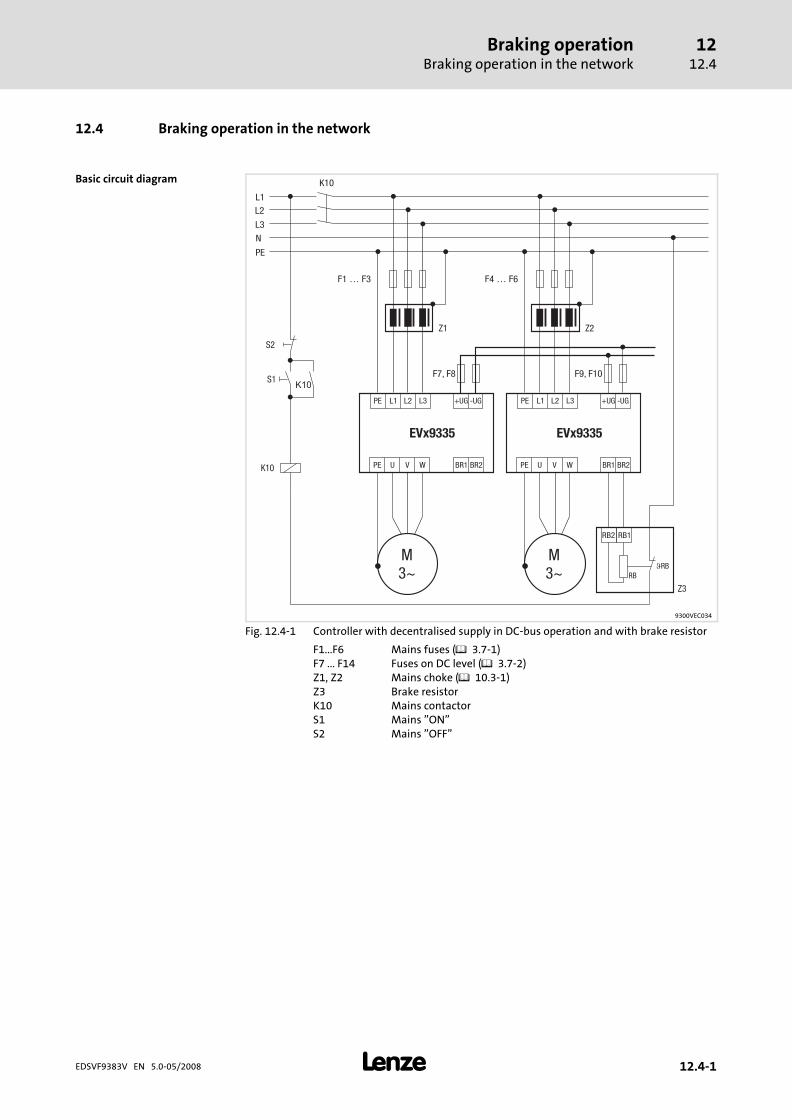
Braking operationBraking operation in the network
1212.4
� 12.4−1EDSVF9383V EN 5.0−05/2008
12.4 Braking operation in the network
EVx9335 EVx9335
L1
K10
L2
L3
N
PE
F1 … F3
F7, F8 F9, F10
F4 … F6
M3~
M3~
PE PEL1 L1L2 L2L3 L3
PE PEU UV VW WBR1 BR1BR2 BR2
+UG +UG-UG -UG
S2
S1K10
K10
Z2Z1
Z3
�RBRB
RB2 RB1
9300VEC034
Fig. 12.4−1 Controller with decentralised supply in DC−bus operation and with brake resistor
F1...F6 Mains fuses ( 3.7−1)F7 ... F14 Fuses on DC level ( 3.7−2)Z1, Z2 Mains choke ( 10.3−1)Z3 Brake resistorK10 Mains contactorS1 Mains "ON"S2 Mains "OFF"
Basic circuit diagram
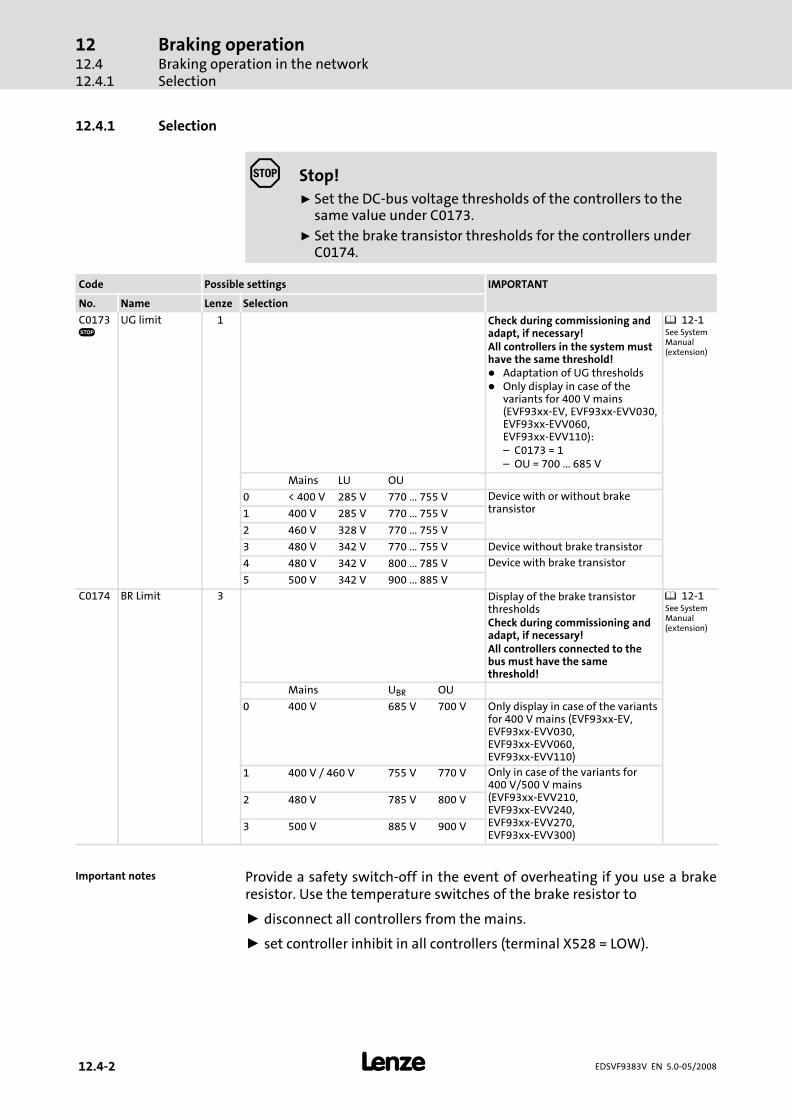
Braking operationBraking operation in the networkSelection
1212.412.4.1
� 12.4−2 EDSVF9383V EN 5.0−05/2008
12.4.1 Selection
� Stop!
ƒ Set the DC−bus voltage thresholds of the controllers to thesame value under C0173.
ƒ Set the brake transistor thresholds for the controllers underC0174.
Code Possible settings IMPORTANT
No. Name Lenze Selection
C0173�
UG limit 1 Check during commissioning andadapt, if necessary!All controllers in the system musthave the same threshold!� Adaptation of UG thresholds� Only display in case of the
variants for 400 V mains(EVF93xx−EV, EVF93xx−EVV030,EVF93xx−EVV060,EVF93xx−EVV110):– C0173 = 1– OU = 700 ... 685 V
12−1See SystemManual(extension)
Mains LU OU
0 < 400 V 285 V 770 ... 755 V Device with or without braketransistor1 400 V 285 V 770 ... 755 V
2 460 V 328 V 770 ... 755 V
3 480 V 342 V 770 ... 755 V Device without brake transistor
4 480 V 342 V 800 ... 785 V Device with brake transistor
5 500 V 342 V 900 ... 885 V
C0174 BR Limit 3 Display of the brake transistorthresholdsCheck during commissioning andadapt, if necessary!All controllers connected to thebus must have the samethreshold!
12−1See SystemManual(extension)
Mains UBR OU
0 400 V 685 V 700 V Only display in case of the variantsfor 400 V mains (EVF93xx−EV,EVF93xx−EVV030,EVF93xx−EVV060,EVF93xx−EVV110)
1 400 V / 460 V 755 V 770 V Only in case of the variants for400 V/500 V mains(EVF93xx−EVV210,EVF93xx−EVV240,EVF93xx−EVV270,EVF93xx−EVV300)
2 480 V 785 V 800 V
3 500 V 885 V 900 V
Provide a safety switch−off in the event of overheating if you use a brakeresistor. Use the temperature switches of the brake resistor to
ƒ disconnect all controllers from the mains.
ƒ set controller inhibit in all controllers (terminal X528 = LOW).
Important notes

Accessories (overview)Contents
13
� 13−1EDSVF9383V EN 5.0−05/2008
13 Accessories (overview)
Contents
13.1 General accessories 13.1−1 . . . . . . . . . . . . . . . . . . . . . . . . . . . . . . . . . . . . . . . . . .
13.2 Type−specific accessories 13.2−1 . . . . . . . . . . . . . . . . . . . . . . . . . . . . . . . . . . . . .


Accessories (overview)General accessories
1313.1
� 13.1−1EDSVF9383V EN 5.0−05/2008
13.1 General accessories
Accessories Designation Order number
Communicationmodules
LECOM−LI (optical fibre) EMF2102IBCV003
LECOM−B (RS485) EMF2102IBCV002
LECOM−A/B (RS232/485) EMF2102IBCV001
LON EMF2141IB
INTERBUS EMF2113IB
INTERBUS−Loop EMF2112IB
PROFIBUS−DP EMF2133IB
DeviceNet/CANopen EMF2175IB
Operating module keypad XT EMZ9371BC
Diagnosis terminal (keypad XT in handheld design, IP20) 1) E82ZBBXC
Other Connecting cable 2.5 m E82ZWL025
5 m E82ZWL050
10 m E82ZWL100
Parameterisation/operating software »Global Drive Control« (GDC) ESP−GDC2
PC system bus adapter(Voltage supply via DIN connection)
EMF2173IB
PC system bus adapter(Voltage supply via PS2 connection)
EMF2173IB−V002
PC system bus adapter(Voltage supply via PS2 connection, electrical isolation)
EMF2173IB−V003
PC system bus adapter USB EMF2177IB
CAN repeater EMF2176IB
PC system cable RS232 5 m EWL0020
10 m EWL0021
Optical fibre adapter (standard output power) EMF2125IB
Optical fibre adapter (increased output power) EMF2126IB
Power supply unit for optical fibre adapter EJ0013
Optical fibre, single−core, black PE sheath (basic protection), sold bythe meter
EWZ0007
Optical fibre, single−core, red PUR sheath (reinforced protection),sold by the meter
EWZ0006
Setpoint potentiometer ERPD0010k0001W
Rotary knob for setpoint potentiometer ERZ0001
Scale for setpoint potentiometer ERZ0002
Digital display EPD203
Encoder cable 2.5 m EWLE002GX−T
5.0 m EWLE005GX−T
10.0 m EWLE010GX−T
15.0 m EWLE015GX−T
20.0 m EWLE020GX−T
25.0 m EWLE025GX−T
30.0 m EWLE030GX−T
35.0 m EWLE035GX−T
40.0 m EWLE040GX−T
45.0 m EWLE045GX−T
50.0 m EWLE050GX−T
Connecting cable for digital frequency coupling 2.5 m EWLD002GGBS93
1) Additional connecting cable required

Accessories (overview)General accessories
1313.1
� 13.1−2 EDSVF9383V EN 5.0−05/2008
� Tip!
Current documentation and software updates concerning Lenzeproducts can be found on the Internet in the "Services &Downloads" area under
http://www.Lenze.com

Accessories (overview)Type−specific accessories
1313.2
� 13.2−1EDSVF9383V EN 5.0−05/2008
13.2 Type−specific accessories
Accessories 9300 vector
EVF9335 EVF9336 EVF9337 EVF9338
Motor choke ELM3−003H275 ELM3−003H275 ELM3−002H320 ELM3−002H410
Air lock E93ZWL
Brake resistor ERBD015R04K0
Accessories 9300 vector
EVF9381 EVF9382 EVF9383
Motor choke 2 × ELM3−003H275 2 × ELM3−002H320 2 × ELM3−002H410
Air lock E93ZWL2
Brake resistor ERBD015R04K0


AppendixContents
14
� 14−1EDSVF9383V EN 5.0−05/2008
14 Appendix
Contents
14.1 Glossary 14.1−1 . . . . . . . . . . . . . . . . . . . . . . . . . . . . . . . . . . . . . . . . . . . . . . . . . . .
14.1.1 Terminology and abbreviations used 14.1−1 . . . . . . . . . . . . . . . . . . .
14.2 Index 14.2−1 . . . . . . . . . . . . . . . . . . . . . . . . . . . . . . . . . . . . . . . . . . . . . . . . . . . . . .


AppendixGlossary
Terminology and abbreviations used
1414.1
14.1.1
� 14.1−1EDSVF9383V EN 5.0−05/2008
14.1 Glossary
14.1.1 Terminology and abbreviations used
Cross−reference to a chapter and the correspondingpage number
AC Alternating current or alternating voltage
AIF Automation interfaceAIF interface, interface for communication modules
CE Communauté Européenne (European Community)
Controller Any frequency inverter, servo inverter or DC speedcontroller
Cxxxx/y Subcode y of code Cxxxx(e.g. C0404/2 = subcode 2 of code C0404)
DC Direct current or direct voltage
DIN Deutsches Institut für Normung (German Institutefor Standardization)
Drive Lenze controller combined with a geared motor,three−phase AC motor and other Lenze drivecomponents
EMC Electromagnetic compatibility
EN Europäische Norm (European standard)
fr [Hz] Rated motor frequency
IEC International Electrotechnical Commission
Imains [A] Mains current
Imax [A] Maximum output current
IP International Protection Code
IPC Industrial PC
IPE [mA] Leakage current
Ir [A] Rated output current
L [mH] Inductance
Mr [Nm] Rated motor torque
NEMA National Electrical Manufacturers Association
PDC [kW] Power which can additionally be drawn from the DCbus at operation with power−adapted motor
PLC Programmable logic controller
Pr [kW] Rated motor power
PV [W] Inverter power loss

AppendixGlossaryTerminology and abbreviations used
1414.114.1.1
� 14.1−2 EDSVF9383V EN 5.0−05/2008
R [�] Resistance
Sr [kVA] Output power of the controller
UDC [V] DC supply voltage
UL Underwriters Laboratories
UM [V] Output voltage
Umains [V] Mains voltage
VDE Verband deutscher Elektrotechniker (Association ofGerman Electrotechnical Engineers)
Xk/y Terminal y on terminal strip Xk (e.g. X5/28 =terminal 28 on terminal strip X5)

AppendixIndex
1414.2
� 14.2−1EDSVF9383V EN 5.0−05/2008
14.2 Index
AAcceleration, 6.10−1
Acceleration time Tir, additional setpoint of NSET, 8.5−19
Accessories, 13−1
− external brake resistor, 12.1−1
− General, 13.1−1
− Type−specific, 13.2−1
Activating the incremental encoder, 6.7−1
Actual motor current, 8.2−27 , 8.2−42 , 8.5−7 , 9.1−1
Actual motor voltage, 8.2−27 , 8.2−42 , 8.5−6 , 9.1−1
Actual speed value, 8.2−27 , 8.2−42 , 8.5−6 , 9.1−1
Additional setpoint, 8.5−6
Ambient conditions
− climatic, 3.1−2
− electrical, 3.1−2
− mechanical, 3.1−2
Analog inputs
− setting input range with jumper X3, 5.6−7
− Signals, 6.5−4
− terminal assignment, 5.6−7
Analog outputs
− Configuration, 6.5−6
− Signals, 6.5−6
− terminal assignment, 5.6−7
Application, as directed, 1.2−1
Application as directed, 1.2−1
Application datum, Display, 9.1−1
BBasic function, 8.5−2
Brake operation, with external brake resistor, 12.1−1
Brake resistors, Selection, 12.1−1
Brake transistor, 12.3−1
Braking, 6.10−1 , 12−1
Braking operation, 12−1
− in the network, 10.7−1 , 12.4−1
Bus off, 8.3−2
CCable
− For control connections, 5.2−3 − For motor connection, 5.2−2
Cable cross−sections, 3.7−1
Cable resistance, 5.7−1
Cable type, 5.7−1
Calibration, Application datum, 9.1−1
CAN bus identifier, 8.5−23
Capacitance per unit length, 5.7−1
CE conformity, 1.2−1
CE−typical drive system, 5.3−1 , 5.4−1
Changing parameters, Keypad EMZ9371BC, 7.2−4 , 7.2−6 ,7.2−7 , 7.2−8 , 7.2−9
Changing the direction of rotation, 6.10−5
Clamp operation, 9.4−2
Code, 7.1−1
Code table, 8.5−1
Commissioning, 6−1
− before switching on, 6.1−1 − Entry of motor data, 6.6−1
Communication modules, 5.10−1

AppendixIndex
1414.2
�14.2−2 EDSVF9383V EN 5.0−05/2008
Configuration, 8−1
− Analog input signals, 6.5−4
− Analog output signals, 6.5−6
− Analog outputs, 6.5−6
− changing the direction of rotation, 6.10−5
− Code table, 8.5−1
− Controller inhibit (DCTRL1−CINH), 6.4−1
− Current limits, 6.6−15
− Digital input signals, 6.5−1
− Digital output signals, 6.5−3
− Digital outputs, 6.5−3
− Display functions, 9.1−1
− Maximum field frequency, 6.10−1
− Minimum field frequency, 6.10−1
− MonitoringCurrent load of controller (Ixt monitoring), 8.3−4 Heatsink temperature, 8.3−5 Monitoring times for process data input objects, 8.3−2 Motor temperature, 8.3−5
− monitoring, 8.3−1 bus off, 8.3−2 DC−bus voltage, 8.3−6 reset node, 8.3−2
− monitoring functionsoverview, 8.4−1 responses, 8.3−1
− motor data collection, 6.6−16
− Oscillation damping, 6.11−3
− Quick stop (QSP), 6.10−4
− Relay output, 6.5−3
− Slip compensation, 6.11−1
− switching frequency of inverter, 6.9−1
− Table of attributes, 8.7−1
− Umin boost, 6.8−6
Conformity, 1.2−1
Control cable, 5.2−3
Control cables, connection between master and slave,5.4−5
Control terminals, 5.6−1
− Changing the assignment of X5, 6.5−1
− Changing the assignment of X6, 6.5−1
Control word (AIF), 8.5−13
Controller
− application as directed, 1.2−1
− in clamp operation, 9.4−2
− labelling, 1.2−1
Controller inhibit, Drive behaviour, 6.4−1
Current limits, 6.6−15
Current load of controller, Ixt monitoring, 8.3−4
DDC bus
− Cable cross−sections for the, 5.3−5 , 5.4−9
− Cable selection, 3.7−3
− connection to the, 5.3−5 , 5.4−9
− Fuses for the, 5.3−5 , 5.4−9
DC busbars, installation between master and slave, 5.4−4
DC injection braking (GSB)
− automatic, 8.2−35 , 8.2−57
− manual, 8.2−33 , 8.2−55
DC supply, 5.2−1
DC−bus cable, shielding, 5.3−5 , 5.4−9
DC−bus connection
− Distributed supply, 10.6−1
− Possible combinations, 10.2−1
DC−bus operation, 10−1
− Braking operation in, 10.7−1 , 12.4−1
− Conditions, 10.2−1
− Several drives, 10−1
DC−bus voltage, 8.2−27 , 8.2−42 , 8.3−6 , 8.5−6 , 9.1−1
− monitoring, 8.3−6
− overvoltage, 8.3−6
− Undervoltage, 8.3−6
Deceleration, 6.10−1
Deceleration time Tif, additional setpoint of NSET, 8.5−19
Definition of notes used, 2.4−1
Definitions, Terms, 14.1−1
Derating, 6.6−16 , 6.9−1 , 6.11−3 , 8.2−38 , 8.2−60
device control, 8.5−2
Device protection, 2.3−1
Diagnostics, 7.2−10 , 9.1−1 , 9.1−2
Diameter calculator (DCALC1), 8.2−1
Digital frequency input, connection to X9, 5.9−1
Digital frequency output, connection to X10, 5.9−1
Digital input signals, 6.5−1
Digital inputs, Terminal assignment, 5.6−7
Digital inputs/outputs, Terminal assignment, 11.3−2
Digital output signals, 6.5−3
Digital outputs
− Configuration, 6.5−3
− terminal assignment, 5.6−7
Dimensions, 4.2−1 , 4.3−1 , 12.2−2
Direction of rotation, inhibiting, 8.2−39 , 8.2−61

AppendixIndex
1414.2
� 14.2−3EDSVF9383V EN 5.0−05/2008
Display
− Application datum, 9.1−1
− Operating status, 9.2−1
Display functions, 9.1−1
− Possible values, 9.1−1
Display of operating data, 9.1−1
Display values, 9.1−1
− Calibration, 9.1−1
Disposal, 2.1−3
Distributed supply, 10.6−1
Drive behaviour
− Controller inhibit, 6.4−1
− in the event of faults, 9.3−1
Drive errors, 9.4−1
EEarth fault in motor cable (OC2), 8.3−3
Electrical installation, system bus (CAN), 5.7−1
EMC, what to do in case of interferences, 5.2−6
Emergency−off, Controller inhibit, 6.4−1
Entry of motor data, 6.6−1
Error analysis, Via history buffer, 9.2−1
Error messages, 9.5−1
− causes and remedies, 9.5−1
− configuration, 8.4−1
− General, 9.5−1
− Resetting, 9.5−5
Exceeding of the maximum speed (NMAX), 8.3−3
Explanations, Code table, 8.5−1
External brake resistors, 12.2−1
External error (EEr), 8.3−6
FFailure of a motor phase, 8.3−4
Fan connection EVx9335 ... EVx9383
− Controller is supplied via the DC bus, 5.3−6 , 5.4−10
− controller is supplied with mains voltage, 5.3−5 , 5.4−10
Fault analysis, Via history buffer, 9.2−1
Fault elimination, 9.4−1
Fault messages
− causes and remedies, 9.5−1
− OC3 in clamp operation, 9.4−2
Feedback system, wiring, 5.8−1
Field controller, 6.8−8 , 8.5−8
Field frequency
− maximum, 6.10−1
− Minimum, 6.10−1
Free mounting spaces, 4.1−1
Function blocks, 8.2−1
− diameter calculator (DCALC1), 8.2−1
− internal motor control, vector control (MCTRL2), 8.2−40
− master frequency input (DFIN), 8.2−5
− master frequency output (DFOUT), 8.2−8
− master frequency processing (DFSET), 8.2−18
− master frequency ramp−function generator (DFRFG1),8.2−13
Functional test, safety function, 11.4−2 , 11.4−5
Ggases, aggressive, 4.1−1
General accessories, 13.1−1
General data, 3.1−1 , 7.2−1
HHeatsink temperature, monitoring, 8.3−5
History buffer, 9.2−1
− Assembly, 9.2−2
− clear, 9.2−2
IImax limit in generator mode, in generator mode, 6.6−15 ,8.2−27 , 8.2−42 , 8.5−4
Imax limit in motor mode, 6.6−15 , 8.2−27 , 8.2−42 , 8.5−4
Incremental encoder
− At X8, 5.8−2 , 6.7−2
− at X9, 5.8−3 , 6.7−3
− operation with, 8.2−48
− with HTL level, 5.8−3 , 6.7−3
− With TTL level, 5.8−2 , 6.7−2
Input signals
− Analog, Configuration, 6.5−4
− Digital, Configuration, 6.5−1
Inputs
− Digital, Response times, 6.5−1
− KTY, 6.6−11
− PTC, 6.6−9
Interferences, eliminating EMC interferences, 5.2−6

AppendixIndex
1414.2
�14.2−4 EDSVF9383V EN 5.0−05/2008
Internal motor control
− V/f characteristic control (MCTRL1), setting of V/fcharacteristic, 8.2−31
− with vector control (MCTRL2)torque control with speed limitation, 8.2−53 torque limitation, 8.2−50
Internal motor control (MCTRL)
− inhibiting the direction of rotation, 8.2−39 , 8.2−61
− limiting output current, 8.2−52
− limiting the output current, 8.2−32
− limiting the speed setpoint, 8.2−31 , 8.2−47
− quick stop (QSP), 8.2−33 , 8.2−54
− speed control, 8.2−31 , 8.2−48
− speed setpoint selection, 8.2−31 , 8.2−47
− with vector control (MCTRL2), 8.2−40
JJOG setpoint, 8.5−6
Jumper X3, for input range of analog setpoint selection,5.6−7
KKeypad EMZ9371BC, Changing parameters, 7.2−4 , 7.2−6 ,7.2−7 , 7.2−8 , 7.2−9
KTY motor monitoring, 6.6−11
LLabelling, controller, 1.2−1
LED display, 9.2−1
LEDs, 9.2−1
Legal regulations, 1.2−1
Liability, 1.2−2
MMains cable, Selection of, 3.7−3
Mains connection, 5.2−1
− fuses for the, 5.3−3 , 5.3−4 , 5.4−7 , 5.4−8
mains connection, cable cross−sections for the, 5.3−3 ,5.3−4 , 5.4−7 , 5.4−8
Mains supply, 3.7−1 , 10.4−1
Manufacturer, 1.2−1
Master frequency input (DFIN), 8.2−5
Master frequency output (DFOUT), 8.2−8
Master frequency processing (DFSET), 8.2−18
Master frequency ramp−function generator (DFRFG1),8.2−13
Master/slave
− Connecting control cables between the devices, 5.4−5
− installing the DC busbars, 5.4−4
Maximum speed, 6.10−1 , 8.2−26 , 8.2−41 , 8.5−3
Menu structure, XT EMZ9371BC keypad, 7.2−11
Message, 8.3−1
Minimum speed, 6.10−1 , 8.2−26 , 8.2−41 , 8.5−3
Monitoring, 8.3−1
− bus off, 8.3−2
− configuring, 8.4−1
− Current load of controller, Ixt monitoring, 8.3−4
− DC−bus voltage, 8.3−6
− Earth fault in motor cable (OC2), 8.3−3
− Exceeding of the maximum speed (NMAX), 8.3−3
− External error (EEr), 8.3−6
− Failure of a motor phase (LP1), 8.3−4
− Heatsink temperature, 8.3−5
− Monitoring times for process data input objects, 8.3−2
− Motor temperature, 8.3−5
− overload acceleration, deceleration (OC3), 8.3−3
− possible responses, 8.4−1
− reset node, 8.3−2
− responses, 8.3−1 message, 8.3−1 TRIP, 8.3−1 warning, 8.3−1
− Short circuit in motor cable (OC1), 8.3−3
Monitoring functions
− Overview, 8.4−1
− responses, 8.3−1
Monitoring times for process data input objects, 8.3−2
Motor, thermal monitoring, with PTC thermistor, 6.6−9 ,6.6−11
Motor cable, 5.2−2
− length, 3.1−2
− Selection of, 3.7−3
− shielding, 5.3−7 , 5.4−12
Motor connection, 5.4−13
Motor cos phi, 6.6−2 , 6.6−17 , 6.8−9 , 8.2−44 , 8.5−9
Motor data, identification, 6.6−16
Motor data collection, 6.6−16
Motor leakage inductance, 8.5−9
Motor magnetising current, optimising in case of vectorcontrol, 6.11−9
Motor potentiometer
− acceleration time Tir, 8.5−21
− deceleration time Tif, 8.5−21
Motor protection, 2.3−1

AppendixIndex
1414.2
� 14.2−5EDSVF9383V EN 5.0−05/2008
Motor rotor resistance, 8.2−43 , 8.5−9
Motor stator inductance, 6.6−17 , 6.8−9 , 8.2−44 , 8.5−10
Motor stator resistance, 6.6−17 , 8.2−44 , 8.5−9
Motor temperature, monitoring, 8.3−5
Motor temperature monitoring, connection, 5.3−8 ,5.4−14
Mounting conditions
− free spaces, 3.1−2
− mounting place, 3.1−2
− mounting position, 3.1−2
NNameplate, 1.1−3 , 1.1−4
Network of several drives
− Basic dimensioning, 10.5−1
− Function, 10.1−1
Noise optimised operation, 6.9−1
Notes, definition, 2.4−1
OOperating behaviour
− Optimise, 6.8−1
− Optimising, 6.11−1
Operating conditions, 3.1−2 , 7.2−1
− ambient conditionsclimatic, 3.1−2 electrical, 3.1−2 mechanical, 3.1−2
− mounting conditionsfree spaces, 3.1−2 mounting place, 3.1−2 mounting position, 3.1−2
Operating mode
− for standard applications, 6.1−2 , 6.8−3
− Select, 6.8−1
− select, 6.1−1 , 6.8−1
− V/f characteristic control, 6.8−4 commissioning example, 6.3−1
− vector control, 6.8−8 commissioning example, 6.3−5
Operating status, Display, 9.2−1
Operation, noise optimised, 6.9−1
Oscillation damping, 6.11−3 , 8.2−38 , 8.2−60
− Reduction of speed oscillations, 6.11−3
Output current, limiting, 8.2−32 , 8.2−52
Output signals
− Analog, Configuration, 6.5−6
− Digital, Configuration, 6.5−3
Outputs
− Analog, 6.5−6
− Digital, 6.5−3
Overload acceleration, deceleration (OC3), 8.3−3
Overspeeds, 2.3−1
Overview, Accessories, 13−1
Overvoltage threshold, DC−bus voltage, 8.3−6
PParameter setting, 7−1
− code, 7.1−1
− with bus system, 7.1−2
− With XT EMZ9371BC keypad, 6.3−1 , 7.2−1
Password, 8.2−45 , 8.5−10
Pollution, 3.1−2
Power system, 3.1−2
Protection against unexpected start−up, 11.1−1
− operating mode, 11.2−2
− safety relay, 3.4−1 , 11.3−1
Protection of persons, 2.3−1
PTC motor monitoring, 6.6−9
QQSP (quick stop), 8.2−33 , 8.2−54
Quick stop, 6.10−4
Quick stop (QSP), 8.2−33 , 8.2−54
Quick stop deceleration time, 6.10−4 , 8.2−29 , 8.2−45 ,8.5−11
RRated data, 12.2−1
− for 400 V mains voltage, 3.6−1
− for 500 V mains voltage, 3.6−2
− integrated brake transistor, 12.3−1
Rated motor current, 6.6−1 , 6.6−17 , 6.8−9 , 8.2−44 ,8.5−9
Rated motor frequency, 6.6−1 , 6.6−17 , 6.8−9 , 8.2−29 ,8.2−44 , 8.5−9
Rated motor power, 6.6−1 , 6.8−8 , 8.5−8
Rated motor speed, 6.6−1 , 6.6−17 , 6.8−9 , 8.2−29 , 8.2−44, 8.5−9
Rated motor voltage, 6.6−2 , 6.6−17 , 6.8−5 , 6.8−9 ,8.2−29 , 8.2−44 , 8.5−9
Reaction times of digital inputs, 6.5−1
Relay output, Configuration, 6.5−3

AppendixIndex
1414.2
�14.2−6 EDSVF9383V EN 5.0−05/2008
Residual hazards, 2.3−1
Responses, 8.3−1
− message, 8.3−1
− TRIP, 8.3−1
− warning, 8.3−1
Running optimisation, 6.11−1
SSafe standstill, 11.1−1
Safe torque off, 11.1−1
− Function deactivated, 5.6−5
− functional test, 11.4−2 , 11.4−5
− operating mode, 11.2−2
− safety relay, 3.4−1 , 11.3−1
Safe torque offt, Function active, 5.6−2
Safety, safety engineering, 11−1
Safety engineering, 11−1
Safety function
− functional test, 11.4−2 , 11.4−5
− Safe torque off, 11.1−1
Safety instructions, 2−1
− Definition, 2.4−1
− Structure, 2.4−1
Safety relay, 3.4−1 , 11.3−1
− Connector X11Terminal assignment, 11.3−2 Wiring, 11.3−2
Safety relay KSR, Terminal assignment, 5.6−7 , 11.3−2
Selecting the operating mode, speed mode, settingacceleration and deceleration times, 6.10−3
Selection, operating mode, 6.1−1 , 6.8−1
Selection of motor type, 6.6−1 , 8.2−29 , 8.2−44 , 8.5−9
Selection of the feedback system, 6.7−1 , 8.2−42 , 8.5−4
Setting integral action component, 8.2−49
Setting the acceleration time, 6.10−3
Setting the deceleration time, 6.10−3
Setting the feedback system, 6.7−1
Setting the speed feedback, 6.7−1
Shielding
− DC−bus cable, 5.3−5 , 5.4−9
− motor cable, 5.3−7 , 5.4−12
Short circuit in motor cable (OC1), 8.3−3
Site altitude, 3.1−2
Slip compensation, 6.11−1 , 8.2−39 , 8.2−61
Speed control, 8.2−31 , 8.2−48
− adapting the speed controller, 8.2−48
− at vector control (MCTRL2), adapting the speedcontroller, 8.2−31
− with vector control (MCTRL2)setting integral action component, 8.2−49 speed feedback, 8.2−48 temperature detection, 8.2−49
Speed feedback, 8.2−48
Speed mode, setting acceleration and deceleration times,6.10−3
Speed oscillations, 6.11−3
Speed setpoint limitation, 8.2−31 , 8.2−47
Speed setpoint selection, 8.2−31 , 8.2−47
Stability, of the motor, 8.2−50
Status word AIF, 8.5−14 , 9.1−2
Stopping, 6.10−1
Supply forms / electrical supply conditions, 5.1−4
Switching frequency, automatic current−dependentchange−over, 6.9−2 , 8.2−27 , 8.2−41 , 8.5−4
Switching frequency of inverter, 6.9−1
− noise optimised, 6.9−1
Switching frequency reduction, 6.9−2
switching on, check before switching on, 6.1−1
System bus (CAN), wiring, 5.7−1
System error messages, 9.5−1
− configuration, 8.4−1
− General, 9.5−1
− Resetting, 9.5−5
TTable of attributes, 8.7−1
Technical data, 3−1
Temperature detection, 8.2−49
Terminal assignment
− analog inputs, 5.6−7
− analog outputs, 5.6−7
− digital inputs, 5.6−7
− Digital inputs/outputs, 11.3−2
− digital outputs, 5.6−7
− Safety relay KSR, 5.6−7 , 11.3−2
Terminal data, 5.6−2 , 11.3−1
Terminology
− Controller, 14.1−1
− Drive, 14.1−1
Terms, Definitions, 14.1−1

AppendixIndex
1414.2
� 14.2−7EDSVF9383V EN 5.0−05/2008
Thermal monitoring, motor, with PTC thermistor, 6.6−9 ,6.6−11
Tn current controller, 6.8−8 , 8.2−28 , 8.2−43 , 8.5−8
Tn slip controller, 6.11−1 , 8.2−29 , 8.5−8
Tn speed controller, 8.2−28 , 8.2−43 , 8.5−8
Torque control with speed limitation, in case of vectorcontrol (MCTRL2), 8.2−53
Torque limitation in the field weakening range, withvector control (MCTRL2), 8.2−50
TRIP, 8.3−1
Troubleshhoting and fault elimination, monitoring,DC−bus voltage, 8.3−6
Troubleshooting, 9.2−1
− Drive behaviour in the event of faults, 9.3−1
− Drive errors, 9.4−1
Troubleshooting and fault elimination, 9−1
− Monitoring, 8.3−1 Current load of controller (Ixt monitoring), 8.3−4 DC−bus voltage, 8.3−6 Heatsink temperature, 8.3−5 Monitoring times for process data input objects, 8.3−2 Motor temperature, 8.3−5
− monitoringbus off, 8.3−2 reset node, 8.3−2 responses, 8.3−1
Type−specific accessories, 13.2−1
UUmin boost, 6.8−6
Undervoltage threshold, DC−bus voltage, 8.3−6
VV/f characteristic, setting of, 8.2−31
V/f characteristic control, 6.8−4
− boost correction, 6.11−5 − commissioning example, 6.3−1
Vector control, 6.8−8
− commissioning example, 6.3−5 − optimising motor magnetising current, 6.11−9
Voltage boost, optimising via boost correction, 6.11−5
Voltage drop, 3.7−1
Voltage supply, Via internal voltage source, 5.6−3 , 5.6−5
Preface, 1−1
Vp current controller, 6.8−8 , 8.2−28 , 8.2−43 , 8.5−8
VP field precontrol, 6.11−5 , 6.11−10 , 8.5−8
Vp speed controller, 8.2−28 , 8.2−43 , 8.5−8
WWarning, 8.3−1
Warranty, 1.2−2
Wiring
− digital frequency input to X9, 5.9−1 − digital frequency output to X10, 5.9−1 − system bus (CAN), 5.7−1
Wiring according to EMC, 5.3−1 , 5.4−1
XXT EMZ9371BC keypad
− Menu structure, 7.2−11 − Parameter setting, 6.3−1 , 7.2−1


-Lenze Drive Systems GmbHHans−Lenze−Straße 1D−31855 AerzenGermany
EDSVF9383VEN 5.0−05/2008
© 08/2008TD19
� +49�(0)�51�54�82−0
� Service 00�80�00�24�4�68�77 (24 h helpline)
� Service +49�(0)�51�54�82−1112
E−Mail [email protected]
Internet www.Lenze.com10 9 8 7 6 5 4 3 2 1
Copyright © 2022 FDOKUMEN