
The calendars for One Week In-Service Training Programme ...
Upload
khangminh22Category
view
1download
0
SERVICE TRAINING"Customer Satisfaction Through Knowledge"
TOSHIBA AMERICA CONSUMER PRODUCTS, INC.NATIONAL SERVICE DIVISIONTRAINING DEPARTMENT1420-B TOSHIBA DRIVELEBANON, TENNESSEE 37087PHONE: (615) 449-2360FAX: (615) 444-7520
NTDPJTV04
SERVICING THE N5SSCOLOR TELEVISIONCHASSIS / DIGITAL
CONVERGENCE

FOREWORD
The material presented in this manual is provided for the technical training of TACP employees andqualified service personnel only.
The specific circuit reference designations, pin numbers, etc., are taken from the TP48E50/60 ServiceManual, File Number 020-9508. The diagrams in this manual are simplified for training and should be usedas a reference guide only when servicing the N5SS CTV Chassis. Refer to the applicable service data fordetailed adjustment and servicing procedures.
NTDPJTV04
SERVICING TOSHIBA'S N5SS TELEVISION CHASSIS©1996
TOSHIBA AMERICA CONSUMER PRODUCTS, INC.National Service Division
National Training Department1420 Toshiba DriveLebanon, TN 37087
(615) 449-2360
No part of this manual may be reproduced in whole or in part without prior written consent fromToshiba America Consumer Products, Inc., Service Division.

CONTENTS
SECTION IOVERALL UNIT CHARACTERISTICS,BLOCK DIAGRAMS, LABS 1 & 2
1. MAIN FEATURES..................................1-22. MERITS OF BUS SYSTEM ....................1-2
2-1. Improved Servciceability .................1-22-2. Reduction of Parts Count ................1-22-3. Quality Control .................................1-2
3. COMPARISON/DIFFERENCES TG-1 ...1-24. SPECIFICATIONS ..................................1-35. FRONT AND REAR CONTROL
VIEWS .....................................................1-45-1. Front View........................................1-45-2. Rear View .........................................1-55-3. Remote Control View.......................1-6
6. '95 PJ-TV CHASSIS LAYOUT ...............1-77. CONSTRUCTION OF CHASSIS............1-88. VIDEO SIGNAL FLOW. .......................1-99. AUDIO SIGNAL FLOW. ......................1-11
10. POWER SUPPLY ..................................1-1211. H and V DEFLECTION.........................1-1312. I2C COMMUNICATIONS. ....................1-1413. DIGITAL CONVERGENCE. ................1-1514. LAB 1 .....................................................1-1615. LAB 2 .....................................................1-20
SECTION IITUNER, IF/MTS/S.PRO MODULE
1. CIRCUIT BLOCK ....................................2-21-1. Outline..............................................2-21-2. Major Features..................................2-21-3. Audio Multiplex Demodulation
Circuit ...............................................2-31-4. A.PRO Section (Audio Processor) ...2-4
2. PIP TUNER..............................................2-62-1. Outline...............................................2-6
SECTION IIICHANNEL SELECTION CIRCUIT
1. OUTLINE OF CHANNELSELECTION CIRCUIT SYSTEM ..........3-2
2. OPERATION OF CHANNELSELECTION CIRCUIT ...........................3-2
3. MICROCOMPUTER ...............................3-34. MICROCOMPUTER TERMINAL
FUNCTION ..............................................3-45. EEPROM (QA02) ....................................3-6
6. ON SCREEN FUNCTION.......................3-67. SYSTEM BLOCK DIAGRAM ................3-78. LOCAL KEY DETECTION METHOD..3-8
9. ENTERING THE SERVICE MODE .......3-910. TEST SIGNAL SELECTION..................3-911. SERVICE ADJUSTMENT ......................3-912. FAILURE DIAGNOSIS PROCEDURE 3-1013. TROUBLE SHOOTING CHARTS .......3-13
SECTION IVAUDIO OUTPUT CIRCUIT
1. OUTLINE.................................................4-22. THEORY OF OPERATION ....................4-2
2-1. Operation of TA8256H ....................4-2
SECTION VDSP CIRCUIT
1. ORIGINS OF DOLBY SURROUND ......5-22. THE DOLBY MP MATRIX ....................5-23. THE DOLBY SURROUND
DECODER ...............................................5-34. DSP CIRCUIT ..........................................5-35. DSP (Digital Surround Processor) IC ......5-6
SECTION VIA/V SWITCHING CIRCUIT
1. OUTLINE.................................................6-22. IN/OUT TERMINALS ............................6-23. CIRCUIT OPERATION ..........................6-2
3-1. Composite Video Signal ...................6-23-2. S-Video Signal .................................6-2
SECTION VIIVIDEO PROCESSING CIRCUIT
1. OUTLINE.................................................7-22. SIGNAL FLOW .......................................7-23. CIRCUIT OPERATION ..........................7-2
SECTION VIIIV/C/D/IC
1. OUTLINE.................................................8-22. LARGE SCALE EMPLOYMENT OF
BUS CONTROL OF PARAMETER FORPICTURE CONTROLS ...........................8-2
3. EMPLOYMENT OF CONTAININGEACH VIDEO BAND FILTERINSIDE.....................................................8-2

4. EMPLOYMENT OF CONTAININGEACH FILTER (FOR S/H) INSIDE .......8-2
5. LOW COST OF IC ..................................8-3
SECTION IXPIP MODULE
1. BOARD LAYOUT...................................9-22. SIGNALS .................................................9-23. BLOCK DIAGRAM ................................9-3
SECTION XSYNC SEPARATION, H-AFC,H-OSCILLATOR CIRCUITS
1. SYNC SEPARATION CIRCUIT ..........10-21-1. Theory of Operation .......................10-2
2. H AFC (Automatic Frequency Control)CIRCUIT ................................................10-3
3. H OSCILLATOR CIRCUIT ..................10-43-1. Outline ............................................10-43-2. Theory of Operation .......................10-4
SECTION XIVERTICAL OUTPUT CIRCUIT
1. OUTLINE...............................................11-21-1. Theory of Operation .......................11-2
2. V OUTPUT CIRCUIT ...........................11-32-1. Actual Circuit .................................11-32-2. Sawtooth Waveform Generation ....11-32-3. V Output .........................................11-42-4. V Linearity Characteristic
Correction .......................................11-63. PROTECTION CIRCUIT FOR
V DEFLECTION STOP ........................11-73-1. +35V Over Current
Protection Circuit ...........................11-8
SECTION XIIHORIZONTAL DEFLECTION CIRCUIT
1. OUTLINE...............................................12-22. HORIZONTAL DRIVE CIRCUIT ........12-2
2-1. Theory of Operation .......................12-23. BASIC OPERATION OF HORIZONTAL
DRIVE ....................................................12-33-1. Theory of Operation .......................12-33-2. Drive System ..................................12-43-3. Circuit Description .........................12-5
4. HORIZONTAL OUTPUT CIRCUIT ....12-64-1. Theory of Operation .......................12-74-2. White Peak Bending
Correction Circuit .........................12-114-3. H Blanking ...................................12-124-4. 200V Low Voltage Protection ......12-13
5. HIGH VOLTAGE GENERATIONCIRCUIT ..............................................12-145-1. Theory of Operation .....................12-145-2. Operation Theory of the Harmonic
Non-Resonant System and TunedWaveforms ...................................12-16
6. HIGH VOLTAGE CIRCUIT ...............12-176-1. High Voltage Regulator................12-17
7. X-RAY PROTECTION CIRCUIT ......12-207-1. Outline ..........................................12-207-2. Operation ......................................12-20
8. OVER CURRENT PROTECTIONCIRCUIT ..............................................12-218-1. Outline ..........................................12-218-2. Operation ......................................12-21
SECTION XIIIDEFLECTION DISTORTIONCORRECTION CIRCUIT (DPC Circuit)
1. DEFLECTION DISTORTIONCORRECTION IC (TA8859P) ..............13-21-1. Outline ............................................13-21-2. Functions and Features ...................13-21-3. Block Diagram ...............................13-2
2. DIODE MODULATOR CIRCUIT ........13-33. ACTUAL CIRCUIT ...............................13-4
3-1. Basic Operation and Current Path ..13-5
SECTION XIVCLOSED CAPTION/EDS CIRCUIT
1. OUTLINE...............................................14-22. DATA TRANSMISSION FORMAT.....14-23. DISPLAY FORMAT .............................14-34. CIRCUIT OPERATION ........................14-4
SECTION XVDIGITAL CONVERGENCE CIRCUIT
1. OUTLINE...............................................15-22. CIRCUIT DESCRIPTION .....................15-2
2-1. Configuration..................................15-22-2. Circuit Operation ............................15-2
3. PICTURE ADJUSTMENT ....................15-43-1. Change of Memory (E2PROM) ......15-43-2. Service Mode ..................................15-4
4. ADJUSTING PICTUREDIMENSION (Green picture) ................15-6
5. KEY FUNCTION OF REMOTE CONTROLUNIT ......................................................15-7
6. CONVERGENCE OUTPUTCIRCUIT ................................................15-86-1. Outline ............................................15-8

6-2. Circuit Description .........................15-87. CONVERGENCE TROUBLESHOOTING
CHART.................................................15-108. LAB 3 ...................................................15-11
SECTION XVIOPTICAL SECTION
1. NECK COMPONENTS .........................16-21-1. Outline of Components Around
Neck of The Projection Tube ......... 16-21-2. Theory of Operation........................16-21-3. Projection Tube ..............................16-3
2. FUNCTION OF KEYCOMPONENTS ..................................... 16-42-1. Outline ............................................ 16-42-2. Theory of Operation .......................16-42-4. Optical Coupling Effect .................16-82-5. Lens ................................................16-92-6. Focus Adjustment .........................16-10
SECTION XVIIPOWER CIRCUIT
1. OVERVIEW...........................................17-3
2. RECTIFYING CIRCUIT ANDSTANDBY POWER SUPPLY ..............17-4
3. MAIN SUPPLY CIRCUIT ....................17-44. OUTLINE OF CURRENT RESONANT
TYPE SUPPLY ...................................... 17-45. FUNDAMENTAL THEORY ................17-56. ACTUAL CIRCUIT ...............................17-67. SCAN DERIVED VOLTAGES.............17-88. PROTECTOR MODULE (Z801) ..........17-99. SUB POWER SUPPLY .......................17-10
10. PROTECT CIRCUITS .........................17-1111. LAB 4 ...................................................17-15
SECTION XVIIIDYNAMIC FOCUS CIRCUIT
1. OUTLINE...............................................18-22. H DYNAMIC FOCUS CIRCUIT ..........18-2
2-1. Theory of Operation .......................18-22-2. Circuit Operation ............................18-3
3. V DYNAMIC FOCUS CIRCUIT ..........18-43-1. Theory of Operation .......................18-43-2. Circuit Operation ............................18-5

1-1
SECTION IOVERALL UNIT
CHARACTERISTICSBLOCK DIAGRAMS
LABS 1 & 2

1-2
SECTION I
OVERALL UNITCHARACTERISTICS
1. MAIN FEATURES
The main feature of Toshiba's projection television modelTP48E60, is the use of the N5SS (TG-1C) chassis. Thischassis utilizes a bus control system, developed by PHILIPSCorporation, called the I2C (or IIC) bus. IIC stands for Inter-Integrated Circuit control. This bus co-ordinates the transferof data and control between ICs inside the Television. It is abi-directional serial bus consisting of two lines, namely SDA(Serial DATA), and SCL (Serial CLOCK).
Digital data which is passed along the bus is received byindividual devices and can be either command or data.Digital-to analog converters are also found within some ofthe ICs, allowing them to be addressed and controlled bystrings of digital instructions, replacing those functionswhich were previously implemented by externalpotentiometers.
2. MERITS OF THE BUS SYSTEM
2-1. Improved ServiceabilityMost of the adjustments previously made by resetting variableresistors and/or capacitors can be made on the new chassisby operating the remote control and seeing the results on thetelevision screen. This allows adjustments to be made withoutremoving covers on the unit thus increasing servicing speedand efficiency.
2-2. Reduction of Parts CountThe use of digital-to-analog converters built into the ICs,allowing them to be controlled by software, has eliminatedor reduced the requirement for many discrete parts such aspotentiometers and trimmers, etc.
2-3. Quality ControlThe central control of adjustment data makes it easier tounderstand, analyze, and review the data, thus improvingthe quality of the product.
Root TG-1 Typical Picture andChassis Chassis Sizes Features
N5E A1 13, 19 LessN5ES A2 20, 32N5S A2 - LEM 20, 32N5S B 27, 32
N5SS C 27 thru 35 More
Typical Chassis ExamplesModel TG-1
CF13E22,23 A1CF19E22 A1CF20E30 A1CF20E40 A1CN27E55 A2CF30E50 A2CF32E50 A2CF32E55 A2CX32E60 BCX32E60 BCN27E90 CCX32E70 CCN32E90 CCN35E15 C
TP48E50,51 CTP48E60,61 CTP55E50,51 CTP55E80.81 C
TP61E80 CTP48E90 C
3. COMPARISON/DIFFERENCES OF TG-1CHASSIS
Toshiba's concept for the TG-1 chassis was to create a sortof universal chassis which, with minimal changes, could beused as a standard throughout the entire Toshiba colortelevision lineup starting in 1995. TG-1 stands for "ToshibaGlobal 1". The TG-1 chassis can be found in severaldifferent models and varies in both complexity and features.
1-3
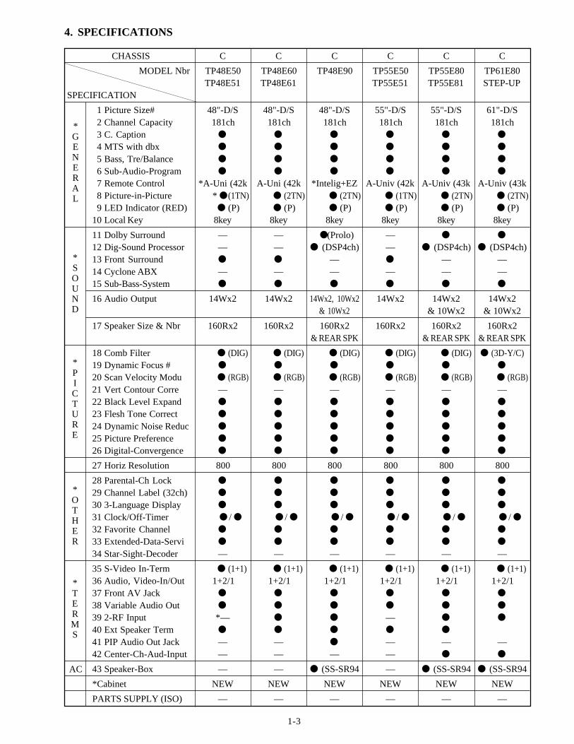
4. SPECIFICATIONS
*GENERAL
*SOUND
*PICTURE
*OTHER
*TERMS
AC
CHASSIS C C C C C C
MODEL Nbr TP48E50 TP48E60 TP48E90 TP55E50 TP55E80 TP61E80TP48E51 TP48E61 TP55E51 TP55E81 STEP-UP
SPECIFICATION
1 Picture Size# 48"-D/S 48"-D/S 48"-D/S 55"-D/S 55"-D/S 61"-D/S2 Channel Capacity 181ch 181ch 181ch 181ch 181ch 181ch3 C. Caption
4 MTS with dbx
5 Bass, Tre/Balance
6 Sub-Audio-Program
7 Remote Control *A-Uni (42k A-Uni (42k *Intelig+EZ A-Univ (42k A-Univ (43k A-Univ (43k8 Picture-in-Picture * (1TN) (2TN) (2TN) (1TN) (2TN) (2TN)9 LED Indicator (RED) (P) (P) (P) (P) (P) (P)
10 Local Key 8key 8key 8key 8key 8key 8key
11 Dolby Surround — — (Prolo) —
12 Dig-Sound Processor — — (DSP4ch) — (DSP4ch) (DSP4ch)13 Front Surround — — —14 Cyclone ABX — — — — — —15 Sub-Bass-System
16 Audio Output 14Wx2 14Wx2 14Wx2, 10Wx2 14Wx2 14Wx2 14Wx2& 10Wx2 & 10Wx2 & 10Wx2
17 Speaker Size & Nbr 160Rx2 160Rx2 160Rx2 160Rx2 160Rx2 160Rx2& REAR SPK & REAR SPK & REAR SPK
18 Comb Filter (DIG) (DIG) (DIG) (DIG) (DIG) (3D-Y/C)19 Dynamic Focus #
20 Scan Velocity Modu (RGB) (RGB) (RGB) (RGB) (RGB) (RGB)21 Vert Contour Corre — — — — — —22 Black Level Expand
23 Flesh Tone Correct
24 Dynamic Noise Reduc
25 Picture Preference
26 Digital-Convergence
27 Horiz Resolution 800 800 800 800 800 800
28 Parental-Ch Lock
29 Channel Label (32ch)
30 3-Language Display
31 Clock/Off-Timer / / / / / /
32 Favorite Channel
33 Extended-Data-Servi
34 Star-Sight-Decoder — — — — — —
35 S-Video In-Term (1+1) (1+1) (1+1) (1+1) (1+1) (1+1)36 Audio, Video-In/Out 1+2/1 1+2/1 1+2/1 1+2/1 1+2/1 1+2/137 Front AV Jack
38 Variable Audio Out
39 2-RF Input *— —
40 Ext Speaker Term
41 PIP Audio Out Jack — — — — —42 Center-Ch-Aud-Input — — — —
43 Speaker-Box — — (SS-SR94 — (SS-SR94 (SS-SR94
*Cabinet NEW NEW NEW NEW NEW NEW
PARTS SUPPLY (ISO) — — — — — —

1-4
5. FRONT AND REAR CONTROL VIEWS
5-1. Front View
Fig. 1-1
Fig. 1-2
Press to open the door.
Behind the door
POWER
POWER indicator
POWER button
Remote sensor location
S-VIDEOIN-VIDEO 3
AUDIOVIDEO
L/MONO R DEMO
MENU-ADV
ANT/VIDEO VOLUME CHANNEL
* These buttons have dual functions.
S-VIDEO INPUT jack
VIDEO/AUDIO INPUTjacks
DEMO button
MENU buttom
ANT/VIDEO button*ADV button
VOLUME buttons*−/+ buttons
CHANNELbutttons

1-5
5-2. Rear View
Fig. 1-3
TV rearS-VIDEO INPUT jack
VARIABLE AUDIOOUTPUT jacks
EXTERNALSPEAKERterminals
MAINSPEAKERswitch
VIDEO 1 INPUTjacks
VIDEO 2 INPUTjacks
VIDEO/AUDIOOUTPUT jacks
A
A AO
A P
R
A RP 8
D O
D O
D OA
O O
R
D O1 D O2
OR VAR
AUDIO
OO
L/MONO
RPIP
AUDIO
VIDEO
O O
R
OD

1-6
5-3. Remote Control View
Fig. 1-4
E N T
R T N
P I C .
100
1
4
7
2
5
8
3
6
9
0
EDS TIMER POWER
TV/VIDEO RECALL MUTE
A U D .S E T U PO P T I O N
R E S E TE X I T
C . C A P TA NT1/2C Y C /S B S D S P / S U R
S T O P R E W P L A Y F F
L O C A T ES W A PS O U R C E P I P
R E CP A U S E /S T IL LS L O W
T V / V C R
S T I L LP I PC H
VCRCABLETV
F A V
CH
VOL
Transmit indicator
EDS*
TV/CABLE/VCR switch
TV/VIDEO*
Channel Number*
PIP function*
AUDio*
PICture*
RESET*
C. CAPT*
ANT1/2*
EXIT*
To operate buttons inside the cover,slide the cover down and toward you.
TIMER/Clock*
POWER
RECALL*
MUTE*
CHANNEL
RTN*
VOLUME
VCR function*
SET UP*
OPTION*
−/+ FAV −/+*
DSP/SUR*
SYC/SBS*
* These functions do not haveduplicate locations on the TV.They can be controlled only bythe Remote Control.
1-7
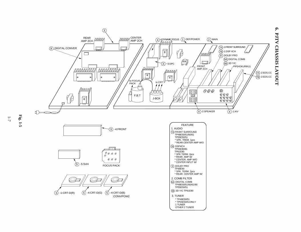
6.P
JTV
CH
AS
SIS
LAY
OU
T
Fig. 1-5
8 :DIGITAL CONVER
REARAMP 2CH
3
CENTERAMP 2CH 4 -4:DYNAMIC FOCUS 1 :DEF/POWER 2 :MAIN
7A -1:FRONT SURROUND
7B -1:DSP 4CH
9 :DOLBY PRO
6A :DIGITAL COMB
6B :3D Y/C
7A -2:EDS.CC
7B -2:EDS.CC
4 -1:A/V4 -2:SPEAKER
FRONTAMP 2CH
3 −3:DPC
to CRTto FOCUSPACK
F.B.TJ-BOX
PIP(HOKURIKU)
5 -4:FRONT
5 -5:SVH
5 -1:CRT-D(R)
5 -4:CRT-D(G) 5 -4:CRT-D(B)
FOCUS PACK
:CONV/POW2
FEATURE1. AUDIO7A FRONT SURROUND
TP48E50/51/60/61TP55E50/51* SPK. TREM. 1pcs* REAR.CENTER AMP W/O
7B :DSP4CHTP55E80/81TP61E80* SPK TERM. 2pcs* REAR. AMP W/* CENTER. AMP W/O* CENTER INPUT W/
9 :DOLBY PROTP48E90* SPK. TERM. 2pcs* REAR. CENTER AMP W/
2. COMB FILTER6A :DIGITAL COMB
TP48E50/51/60/61/90TP55E50/51
6B :3D Y/C TP61E80
3. TUNER* TP48E50/51* TP55E50/51ONLY1 TUNEROTHER 2 TUNER

1-8
10
9
8
1
12
11 7
5
13 14 15
2 18
16 176
4
3
1
2
3
4
5
6
7
8
9
10
11
12
13
14
15
16
17
18
WOOD CABINET
LIGHT BOX
SPEAKER GRILLE
FRONT COVER
CRT MOUNTING
SHIELD FRONT
SHIELD SIDE
SCREEN BEZEL
SCREEN BRACKET L
SCREEN BRACKET S
CONTROL PANEL
BACK BOARD
COUPLING R
COUPLING G
COUPLING B
CHASSIS FRAME MAIN
CHASSIS FRAME POWER
AV TERMINAL BOARD
Fig. 1-6
7. CONSTRUCTION OF CHASSIS

1-9
8. VIDEO SIGNAL FLOW BLOCK DIAGRAM
Basic Circuit OperationThe basic operation of the TG-1 chassis is illustrated in theblock diagrams, figures 1-7 through 1-12. Although thesediagrams focus on the TP48E60, the video and audio signalflow diagrams can be applied to any TG-1 chassis withminor modifications.
Video Signal FlowFigure 1-7 illustrates the video signal flow through the TG-1 chassis. The Antenna 1 (ANT 1) and Antenna 2 (ANT2) inputs allow two separate RF signals to be connected tothe RF switcher. When the switch, which is controlled bythe microcomputer, QA01, is in the up position the ANT 1signal is connected to the HY01 PIP Tuner/IF and the H001Main Tuner. Moving the switch down connects the ANT2 signal to the H001 Tuner. Due to the RF Switch the ANT2 signal can’t be used as the PIP source, but when ANT 2is selected the ANT 1 signal is available at RF OUT. ThePIP Tuner/IF produces a composite video (CV) signal andsends it to the AV Switcher, QV01. An IF signal producedby the Main Tuner is sent to H002, which produces acomposite video signal and sends it to the AV Switcher.
Three video inputs, video 1 through 3, are applied to the AVSwitcher. The video 1 input can be composite video, Y/Cvideo, or the test signal from QA01. Video 2 is compositevideo only, and video 3 is either composite video or Y/Cvideo. A mechanical switch on the video 1 input defaultsto the test signal, so a video connector must not be plugged
into the video 1 input jack when the internal test signals areused.
The selected video signal is output as composite video andapplied to the video output jack, the EDS/CC/RGB SW.,and the Digital Comb Filter or the 3D - Y/C circuit. Afterprocessing the video signal is sent back to the AV Switcheras separate luminance (Y) and chrominance (C) signals.The Y and C signals are then sent to Q501 the VideoChroma Deflection Processing IC. A sync signal is tappedoff the Y signal and applied to Q501. Q501 processes thevideo signal and sends separate R, G, and B signals to theCRT drives and the CRTs.
If the PIP feature is selected, composite video from AVSwitcher is sent to the PIP circuit, ZY01. After processing,the PIP signal is sent to Q501 as R, G, B, and YS where itis mixed with the main video.
On screen display (OSD) R, G, and B signals produced bythe Microcomputer, QA01, are mixed with the ExtendedData Service (EDS) and Closed Caption (CC) data inUM01. These new signals are applied to an OR gate,QB91, and combined with the convergence signals fromthe digital convergence circuit. The convergence signalscan be either the customer convergence cross hairs, or theservice cross hatch pattern. All of these signals are sent toQ501 where they are mixed with the main video signal.

1-1
0
Figure 1-7 V
ideo Signal F
low B
lock Diagram
QV01AV
SWITCHING
VIDEO CHROMADEFLECTIONPROCESSING
UM01EDS/CCRGB SW.
EQ
H002IF/MTSA. PRO
HY01 PIPTUNER/IF
RFSWITCH
DIGITALCOMB
FILTEROR, 3D - Y/C
OR
QB91
ZY01PIP
E031ZRED CRT
DRIVE
E032ZGREEN CRT
DRIVE
E033ZBLUE CRT
DRIVEBLUE CRT
GRN CRT
RED CRT
YS
R
G
B
YS
R
G
B
YS
R
G
B
YSR
GB
FROMDIGITAL
CONV.
Y C
Y Y
C C
SYNC
R G B
TEST SIGNALTO VIDEO 1
ANT 1
RFOUT
ANT 2
TEST
Q503
Q202
YS
R
G
B
CONTROLFROMQA01
MICROCOMPUTER
CV TO VIDEOOUT JACK
H001MAIN
TUNER
Q204
Q501
CV/Y
C
OSDDATA
OSD, EDS, CC, &CONVERGENCE
VIDEO INPUT
PIP VIDEO INPUT
MAIN VIDEOINPUT
CV
CV
CV
CVCV
CV
IF
VIDEO 1
VIDEO 2
VIDEO 3
QA01
12
16
15
28
2
7
7
38 30 32 42
6 2 4 8
22
23
24 21
20
19
18
12
10 13
11
36
39
38
37
9
2
5
9
4 1
3
6
8
6
1
5
2
33
34
35
32
6
5
4
1
36
17
15
1334
43 42 41
9
3
9
CV/Y
C
14
18

1-11
Figure 1-8 Audio Signal Flow Block Diagram
9. AUDIO SIGNAL FLOW BLOCK DIAGRAM
Audio Signal FlowAudio signals are applied to the AV Switcher from thethree video jacks, H002, and the PIP Tuner, as shown inFigure 1-8. Like the video signal, there must not be aconnector in the video 1 jack for the audio test signal to beapplied to the AV Switcher. In the TP48E90, PIP audio isapplied to the PIP output jack. The main audio signals areapplied to the audio output jacks and to the Front Surroundcircuit, the DSP/Dolby circuit, or the Dolby Pro Logiccircuit. Afterprocessing, the left and right audio signalsare applied to the audio processor in H002 where thevolume, balance, treble, and bass are controlled. Next, theaudio signals are amplified by QS101 and applied to thevariable output jacks, and Q601. If the sub bass system(SBS) is selected, a signal is mixed with the left and rightsignals just before Q601 to increase the signals bassresponse. In TP55E80/81 and TP61E80 models, the
jumper is removed so a center signal can be switched in toreplace the main left and right signals. The amplified leftand right audio signals are applied to the internal/externalspeaker switch and routed to the desired speakers.
Sets equipped with Dolby or Dolby Pro Logic have asurround audio signal that is sent to the audio processor inH002 from the Dolby circuit. The surround signal is thensent to the rear amplifier, Q641, amplified, and applied tothe rear speakers. In the TP48E90 the surround signal isrouted through an amplifier in Q690 before it is applied toQ641. Also, the TP48E90 is equipped with Dolby ProLogic, and has a center channel. The center channel isamplified by the Center Amplifier, Q621, and applied tothe front speakers through the internal/external speakerswitch.
H002IF/MTS/A. PRO
TEST SIGNALFROM QA01VIDEO 1
VIDEO 2
VIDEO 3
L
R
MONO AUDIOFROM HY01PIP TUNER
TO PIP OUT JACK(TP48E90 ONLY)
LL
L
L
R
R
R
R
LR
INT/EXTSWITCH
Q601
Q621
QS101
Q641
+
+
Q690
QV01AV
SWITCHING
FRONT SURROUND,DSP/DOLBY,
ORDOLBY PRO LOGIC
L
R
R
L
LR
TO &FROM CENTERINPUT SWITCH & JACKTP55E80/81 & TP61E80
ONLY
QV14
QS04
REARSPEAKERS
TP48E90ONLY
SURROUNDTP48E90
TP55E80/81TP61E80 SURROUND OUT
L R
CENTER OUT
CENTER AMPTP48E90 ONLY
R
LTO VARIABLE AUDIO
OUT JACK
L
R
FRONT ORCENTER
SPEAKERS
TO AUDIOOUT JACK
SBS (SUB BASS SYSTEM)
RLEXTERNAL
IFFROM H001
MAIN TUNER
REAR AMP
11
13
31
29
37 35
17
15
5
6
2
1
9
8
3 2
23 26 24 22 17 16 186
5
10
5
3
7
1
3
1
5
2
7
11
2
4
12
7
2
4
12
7
11

1-12
10. POWER SUPPLY AND PROTECTION BLOCK DIAGRAM
The Control/Protection circuit, Z801, has two functions.The first is to regulate the Main Switch Mode Supply, andthe second is to monitor over current, over voltage, andunder voltage sensors throughout the set. If any one ofthese sensors activates the protection circuit, Z801 turnsoff the switch powering the two switch mode supplies thusturning off the set. If this occurs, a red LED on the frontpanel flashes at half second intervals, and the set must beunplugged to reset Z801.
Figure 1-9 Power Supply/Protection Block Diagram
The E model PTVs actually have three separate powersupplies as shown in Figure 1-9. These supplies consist ofthe Standby Supply, the Main Switch Mode Supply, andthe Sub Switch Mode Supply. The Standby Supply providesthe 5 VDC needed to run the microcomputer and thecustomer interface controls, such as the key pad and the IRreceiver. When the set is turned on, the switch closes toactivate the two switch mode supplies and provide thenumerous DC voltages needed to operate the set.
SWITCHSWITCHMODE(SUB)
CONTROL/PROTECTION
SWITCHMODE(MAIN)
FEEDBACK
STANDBYREGULATOR
+30VDC
+15VDC
-15VDC
+125VDC
+12VDC
+38VDC
REG
REG
REG
TO MICROCOMPUTER
+5VDC
+15VDC
-9VDC
POWERON/OFF FROM
MICROCOMPUTER
X-RAY SENSING
OVERCURRENT,OVERVOLTAGE, &UNDER VOLTAGE
SENSING
POWEROFF
120VAC
+5VDC
RESET
Z801
3
1
1413
16

1-13
11. HORIZONTAL AND VERTICAL DEFLECTION
Deflection circuitry in the E model PTV’s is rather straightforward as show in Figure 1-10. The horizontal pulse fromQ501 drives the horizontal drive circuitry, which in turndrives the Horizontal Yokes and the Flyback Transformer,T461. Numerous low voltage DC supplies are produced bythe Flyback, as well as the high voltages for the anode,focus, and screen drives. To prevent excessive highvoltages, a sample X-Ray protection voltage is monitoredby the over voltage protection circuits.
Figure 1-10 Horizontal and Vertical Deflection Block Diagram
Vertical drive (VD) is applied to the DPC circuit, U421, tocorrect any distortions before it’s sent to the Vertical Drivecircuit, Q301. Then the vertical drive circuit supplies thesignals required by the yokes for deflection.
To enhance horizontal transitions between dark and lightareas of the picture, a Velocity Scan Modulation (VSM)signal is produced by Q501. This signal is sent to the SVMcircuit, E036Z, which in turn drives the SVM coils on theCRTs.
Q501
T461
VIDEOCHROMA
DEFLECTIONPROCESSING
FLYBACKTRANSFORMER
HORIZDRIVE
HVDIST
BLOCK
FOCUSBLOCK
+125VDC FROMMAIN POWER
+200VDC
-27VDC
+35VDC
+12VDC
+23VDC TO X-RAYPROTECT
AC TO HEATERS
TO ABLCIRCUIT
TO HORIZYOKES
TO VERTYOKES
Q301VERTICAL
DRIVEDPC
CIRCUIT
U421
H-OUT
HORIZDRIVE
RGB
RGB
30.7KVTO CRTANODES
FOCUS &SCREEN DRIVE
TO CRTs
EO36ZSVM
CIRCUIT
VSM
TO SVMCOILS
VD
9
7
6
5
3
2
1
8
2
23
2
4
6
4
31
1
2
48
HV

1-14
12. I2C Communications
The TG-1 chassis uses I2C data communications tocontrol all customer features and most of the serviceadjustments that where previously done with discretedevices, refer to Figure 1-11. All communicationsare controlled by the Microcomputer, QA01 throughserial data lines (SDA) and serial clock lines (SCL).Memory settings for customer controls and serviceadjustments (except convergence data) are stored inthe E2PROM Memory, QA02, and communicatedto QA01 by the SCL0 and SDA0 lines. Data andclock lines SDA1 and SCL1 communicate withmost of the circuits in the set. However, there arethree plug in circuits where the data and clocksignals are buffered by QB90 to provide isolation.
All customer functions and most servicesadjustments are implemented through the Key Padand the Remote Sensor. The RMT OUT signal onthe microcomputer drives the IR Transmitter on thefront panel, but it’s only used in the manufacturingprocess. Figure 1-12 shows the Service Registersand their default values used for making adjustmentsin the set.
Figure 1-11 I2C Communication Block Diagram
RCUT RED CUTOFF 40 GCUT GREEN CUTOFF 40BCUT BLUE CUTOFF 40RDRV RED DRIVE 40BDRV BLUE DRIVE 40CNTX SUB-CONTRAST MAX 7FBRTC SUB-BRIGHT CENTER 80 COLC SUB-COLOR CENTER 50TNTC SUB-TINT CENTER 40SCOL SAP-COLOR 15SCNT SUB-CONTRAST 15HPOS HORIZ. POSITION 16VPOS VERTICAL POSITION 00HIT VERTICAL HEIGHT D1GMPS GMPS 00VLIN VERTICAL LINEARITY 12VSC A-S CORRECTION 08VPS VERTICAL SHIFT 15VCP V-COMPENSATION 03WID PICTURE WIDTH 25TRAP TRAPEZIUM 10HCP H-COMPENSATION 02VFC V-F CORRECTION 0FSTRH HORIZ. START POSITION 82
REG ADJUSTMENT PRESET
Figure 1-12 Service Register Default Values
QA01MICRO-
COMPUTER
IC501V/C/D
PROCESSING
H002IF/MTS/A.PRO
H001TUNER
HY01TUNER/IF
COMB FILTEROR
3D-Y/C
QAV01AV
SWITCHING
U421DPC CIRCUIT
Q701CONV.
PROCESSOR
UM01EDS/CCRGB SW.
ZY01PIP
CIRCUIT
F. SURR.,DSP/DOLBY,
D. PRO LOGIC
QB90
SCL1
SDA1
REMOTESENSOR
KEYPAD
KEY A
KEY B
QA02EEPROMMEMORY
SCL0 SDA0
TO IRLED
TRANSRMT OUT
SCL2
SDA2
17
18 35
38
37
27 28 21 20
25 24 44 43
34
219 10
14 15 14 13
5
6
2
3
6 5
11 12
3
14 13

1-15
13. Digital Convergence
The TG-1 model PTV’s are equipped with a new digitalconvergence circuit shown in Figure 1-13. This circuitallows servicers to set the convergence with the remotecontrol. Q701, the Digital Convergence Processor alignsthe convergence from data received from the remote, andsaves the settings in the E2PROM, Q713. The digitalconvergence signals are converted to analog by the D/AConverters Q703, Q704, and Q705. Then they are amplified
by the pre amps (Q715, Q717, & Q719) and power amps(Q751 & Q751) before being applied to the convergenceyokes. The Power Amps Q752 and Q751 dissipate allot ofheat because of their current draw, so the supplies to theseamps have a number of sensors for over current conditions.Most of the convergence circuit is on a shielded board, butthe power amps are easily accessible for service.
Figure 1-13 Convergence Block Diagram
Q701
DIGITALCONVERGENCE
PROCESSOR
RH
RV
GH
GV
BH
BV
Q715
Q717
Q719
Q703D/A
CONV.
Q752
Q751
Q713EEPROM
CLK DATA
HDFROMIC501
VDFROMQ301
CLK
DATA
FROMQAO1
RH
RV
GH
GV
BH
BV
TOCONV.YOKES
Q704D/A
CONV.
Q705D/A
CONV.
6 5
45 46
43
97
96
90
89
87
86
207
6 1
5
3 1
7
44
31 32
207
6 1
207
6 1
5
3 1
7
3
5 7
1
6 9
14 11
1815
6 9
14 11
1815

1-16
LAB 1BASIC OPERATION AND UNIT UNDERSTANDING
As a servicer, it is important now, more than ever, to fully understand the operation and functions ofa television set before proceeding with a repair. This is because many of the problems encountered bya customer today can be caused by an incorrect menu selection or improper setup.
Therefore, the purpose of this lab is to familiarize you with menus and features of the television fromthe customer’s point of view.
SECTION ONEBASIC OPERATION
1. Verify that the unit is connected to an AC supply, and that a signal is connected to the ANT 1input. While verifying signal connections, take time to examine all of the inputs on the rear andfront (behind door) of the unit.
2. Turn on the set with the remote control and tune to an active channel. Refer to page 9 of theservice manual provided and familiarize yourself with all of the keys on the remote paying,particular attention to the following keys:
o EDSo TIMERo PIP Functions
Open the bottom door on the remote control by sliding it down. Try each key starting with the upperrow. Each of these buttons brings up another menu and/or sub-menus.
3. In the Picture Menu, What is Color Temperature?
____________________________________________________________________________
____________________________________________________________________________
4. In the Audio Menu, Where can the speakers be turned off by the user?
____________________________________________________________________________
____________________________________________________________________________
5. In the Setup Menu, What is Favorite Channel?, What is Channel Lock?
____________________________________________________________________________
____________________________________________________________________________

1-17
6. Refer to page 16 of the Service Manual and perform the User Convergence Adjustments. Howis this different from previous Toshiba PJTVs?
____________________________________________________________________________
____________________________________________________________________________
7. In the Option Menu, How many different languages are there? What are they used for? What isChannel Label Used for?
____________________________________________________________________________
____________________________________________________________________________
____________________________________________________________________________
____________________________________________________________________________
NOTES:
____________________________________________________________________________
____________________________________________________________________________
____________________________________________________________________________
____________________________________________________________________________
____________________________________________________________________________
____________________________________________________________________________
SECTION TWODISASSEMBLY & SERVICE POSITION
Follow the procedure listed below to gain access to the tubes and circuit boards.
1. Remove the speaker grill by holding the sides and pulling straight out.
2. Take out the four screws holding the plastic shield in place. Then remove the shield.
3. Remove the control wires from the holder on the metal shield in front of the CRTs.
4. Remove the 4 screws holding the metal shield in place. The shield is notched, so slide it to theright then down to remove it.
5. Remove the two screws holding the front control panel. Then release the tabs on either side andlet it hang down out of the way.
6. Remove the 4 screws holding the bottom of the screen. Then lift up on the top of the screen andpull it away from the cabinet.

1-18
7. Remove the 5 screws holding the back panel. Then remove the back panel.
8. Reattach the control panel to the light box.
9. Remove the six screws on the front of the light box.
10. Remove the three screws on the back of the cabinet.
11. Remove the one screw holding the back of the light box to the cabinet.
12. From the front of the set, lift the light box up just a little, and pull it towards you.
13. Pull the light box all the way out of the cabinet and turn it on its side.
CAUTION: the light box weighs about 85 pounds, so get help if you need it.
SECTION THREEIDENTIFICATION
1. Identify each of the board assemblies and note their locations. Use Figure 1-5 to help youidentify the various boards.
o Convergence/Output/Power Boardo Deflection/Power Boardo Main PCBo Front Surround Boardo Digital Comb Filter Boardo PIP Boardo EDS/CC Board
2. Is there a convergence board in this unit?If so, where?
____________________________________________________________________________
____________________________________________________________________________
3. How does this convergence setup differ from previous models?
____________________________________________________________________________
____________________________________________________________________________
4. Examine the Flyback and HV lead assemblies. What is different about this area from earliermodels?
____________________________________________________________________________
____________________________________________________________________________

1-19
5. Is it possible for one technician to perform a service call on this type of unit?
____________________________________________________________________________
____________________________________________________________________________
6. Put the lightbox in the cabinet, but don't screw it in. Then replace the screen and control panel.Use a few screws to hold the screen and control panel in place.
SUMMARY
In this lab, the operation and function of the unit was determined, and the unit was set up for serviceon the bench. Common user type problems in addition to overall serviceability was also discussed.
END OF LAB 1

1-20
LAB 2TEST SIGNALS, SELF DIAGNOSTICS, & SERVICE REGISTERS
OBJECTIVES: After completing this lab you will be able to:
1. Enter and exit the set’s internal video and audio test signals.
2. Use the test signals for troubleshooting.
3. Use the set’s self diagnostic feature.
4. Make adjustments in the set with the service registers via the remote control.
SECTION ONEVIDEO TEST SIGNALS
1. Verify that the unit is connected to an AC supply, and that a signal is connected to the ANT 1input.
2. Enter the service mode by pressing mute on the remote. Press and hold mute a second timewhile pressing menu on the control panel. An S appears in the upper right corner of the screenindicating that the set is in the service mode. Press menu and the RCUT register appears in theupper left corner of the screen.
3. Push the TV/VIDEO button on the remote once to enter the internal test pattern mode. Thescreen should be red.
4. Slowly cycle through the test signals with the TV/VIDEO button until the white cross hairs ona black background appear. (If the TV/VIDEO button is pushed in rapid succession, the set willjump out of the test signal mode to one of the inputs - ANT 1, VIDEO 1, VIDEO 2, or VIDEO3. The set is still in the service mode, so if this occurs, push the menu button then the TV/VIDEO button to get back into the test signal mode.)
5. Plug a video cable into the VIDEO 1 input jack (make sure the other end of the cable is notplugged into a video source)
6. What happened to the cross hairs?
____________________________________________________________________________
____________________________________________________________________________
7. If something did happen to the cross hairs, why did it happen?
____________________________________________________________________________
____________________________________________________________________________

1-21
8. Is there video on the screen?
____________________________________________________________________________
____________________________________________________________________________
9. If there is video on the screen, where does it come from?
____________________________________________________________________________
____________________________________________________________________________
10. Unplug the video cable.
SECTION TWOAUDIO TEST SIGNALS
1. Push the 8 button on the remote to activate the audio test signal. (NOTE: The internal testpattern mode must be activated for this feature to work.)
2. Push the mute button twice. Now you can control the volume of the signal.
3. Select AUD on the remote control.
4. Select BALANCE and adjust it from left to right with the + and - buttons.
5. Select SPEAKERS and turn them off then on. (NOTE: The speakers are turned off at Q601,refer to Figure 1-8, while the volume, bass, treble, and balance are controlled in H002. Thismeans you can troubleshoot most of the audio system with the speakers off.)
6. Plug an audio cable into the left AUDIO 1 input jack (make sure the other end of the cable isnot plugged into an audio source)
7. What happened to audio?
____________________________________________________________________________
____________________________________________________________________________
8. If something did happen to the audio, why did it happen?
____________________________________________________________________________
____________________________________________________________________________
9. Push the 8 button to turn off the audio test signal.
10. Cycle the video test signals back to the ANT 1 signal with the TV/VIDEO button.

1-22
SECTION THREESELF DIAGNOSTICS
1. Push the 9 button to activate the self diagnostic feature.
2. What does POWER indicate?
____________________________________________________________________________
____________________________________________________________________________
3. What does BUS LINE indicate?
____________________________________________________________________________
____________________________________________________________________________
4. What does BUS CONT indicate?
____________________________________________________________________________
____________________________________________________________________________
5. What does BLOCK indicate?
____________________________________________________________________________
____________________________________________________________________________
6. Push the EXIT button to exit the self diagnostic feature.
7. Select the VIDEO 1 input with the TV/VIDEO button. (Make sure there is no signal applied toVIDEO 1)
8. Push MENU on the control panel to display the registers.
9. Push 9 to activate the self diagnostic feature.
10. Is the display different from the previous display. ______
11. If it is, explain why.
____________________________________________________________________________
____________________________________________________________________________
12. Push the EXIT button to exit the self diagnostic feature.
13. Push MENU on the control panel to display the registers.

1-23
SECTION FOURSERVICE REGISTERS
NOTE: In each of the following exercises write down the register’s value before adjusting it. Thenrestore the register to its original value before proceeding to the next exercise.
1. Enter the internal test pattern mode and select the test signal that has a white window in theupper center of a black background as shown below.
2. Increase the RCUT register value and describe its effect on the picture.
RCUT______
____________________________________________________________________________
____________________________________________________________________________
3. Change the test signal to the white on black cross hatch pattern as shown below.
4. Select the HPOS register and vary its value between 00 and 1F. Describe its effect on thepicture. What happens if you increase the register to 20?
HPOS______
____________________________________________________________________________
____________________________________________________________________________
5. Select the VPOS register and vary its value between 00 and 07. Describe its effect on thepicture. What happens if you increase the register to 08?
VPOS______
____________________________________________________________________________
____________________________________________________________________________

1-24
6. Select the HIT register and vary its value 5 steps above and below the recorded value.Describe its effect on the picture.
HIT______
___________________________________________________________________________
____________________________________________________________________________
7. Select the VLIN register and vary its value 8 steps above and below the recorded value.Describe its effect on the picture.
VLIN______
___________________________________________________________________________
____________________________________________________________________________
8. Select the WID register and vary its value 8 steps above and below the recorded value.Describe its effect on the picture.
WID______
___________________________________________________________________________
____________________________________________________________________________
9. Select the STRH register and vary its value 8 steps above and below the recorded value.Describe its effect on the picture.
STRH______
___________________________________________________________________________
____________________________________________________________________________
SUMMARY
Now that you have completed Lab 2, you should be able to use the internal video and audio testsignals, the self diagnostic feature, and the service registers for making adjustments.
END OF LAB 2

2 - 1
SECTION IITUNER, IF/MTS/S.PRO MODULE

2 - 2
1. CIRCUIT BLOCK
Fig. 2-1 Block diagram
1-1. Outline(1) RF signals sent from an antenna are converted into
intermediate frequency band signals (video: 45.75 MHz,audio: 41.25 MHz) in the tuner. (Hereafter, these signalsare called IF signals.)
(2) The IF signals are band-limited in passing through aSAW filter.
(3) The IF signals band-limited are detected in the VIFcircuit to develop video and AFT signals.
(4) The band-limited IF signals are detected in the SIFcircuit and the detected output is demodulated by theaudio multiplexer, developing R and L channel outputs.These outputs are fed to the A/V switch circuit.
(5) A sound processor (S.PRO.) is provided.
1-2. Major Features(1) The VIF/SIF circuit is fabricated into a small module
by using chip parts considerably.(2) As the tuner, EL466L that which contains an integrated
PLL circuit is employed.(3) Wide band double SAW filter F1802R used.(4) FS (frequency synthesizer) type channel selection system
employed.
(5) VIF/SIF circuit uses PLL sync detection system toimprove performances shown below:• Telop buzz in video over modulation• DP, DG characteristics (video high-fidelity
reproduction)• Cross color characteristic (coloring phenomenon at
color less high frequency signal objects)(6) HIC SBX1637A-22 is used in the audio multiplexer
circuit to minimize the size with increased performance.(7) As a sound control processor, TA1217N is used. I2C-
bus data control the DAC inside the IC to performswitching of the audio multiplexer modes.
EL466L
H001Main Tuner
RF AGC
H002 - IF/MTS/A.PRO Module MVUS34S
SIFoutput Sound
MultiplexCircuit
SAWFilter
VIF/SIFCircuit A.PRO Circuit
AFT output
TP12Video output
To A/V switch circuit
TVR-OUT
TVL-OUT
C-IN
R-IN L-IN
R-OUT L-OUT (L+R)-OUT
C-OUT

2 - 3
1-3. Audio Multiplex Demodulation CircuitThe sound multiplex composite signal FM-detected in thePIF circuit enters pin 12 of HIC (hybrid IC) in passingthrough the separation adjustment VR RV2 and amplified.After the amplification, the signal is split into two: one entersa de-emphasis circuit, and only the main signal with the L-Rsignal and a SAP signal removed enters the matrix circuit. Atthe same time, the other passes through various filters andtrap circuits, and the L-R signal is AM-demodulated, and theSAP is FM-demodulated.
Then, both are fed to the matrix circuit. At the same time,each of the stereo pilot signal fH and the SAP pilot signal 5fHis also demodulated to obtain an identification voltage. Withthe identification voltage thus obtained and the user controlvoltage are used to control the matrix.The audio signals obtained by demodulating the soundmultiplex signal develop at pin 10 and 11 of HIC and developthe terminals of 12 and 14 of the module.
Fig. 2-2 Block diagram of MVUS34S
Note:Of the mode selection voltages, switching voltages for STE,SAP, MONO do not output outside the module.They are used inside the module to control the BUS.
Table 2-1 Matrix for broadcasting conditions andreception mode
Broad- SwitchingOutput OSD display
casted mode12 pin 14 pin
Stereo SAP(R) (L)
Stereo STE R L Y NSAP R L Y NMONO L+R L+R Y N
Mono STE L+R L+R N NSAP L+R L+R N NMONO L+R L+R N N
Stereo STE R L Y Y+ SAP SAP SAP Y Y
SAP MONO L+R L+R Y Y
Mono STE L+R L+R N Y+ SAP SAP SAP N Y
SAP MONO L+R L+R N Y
MVUS34S
MPXOut
DAC-out1(SURR ON/OFF)
DAC-out2(RFSW)
TVR-Out
TVL-Out
9 10 11 12 13 14 15
Stereo 0V SAP 0V OFF 0V
Other 5V Other 5V ON 9V
RF1 0V
RF2 9V
To AV select circuit
Monitor the inputpin for multiplex
sound IC
TV waveform detectionoutput (R)
TV waveform detectionoutput (L)

2 - 4
1-4. A.PRO Section (Audio Processor)The S.PRO section has following functions.(1) Woofer processing (L+R output)(2) High band, low band, balance control(3) Sound volume control, cyclone level control(4) Cyclone ON/OFF
All these processing are carried out according to the BUSsignals sent from a microcomputer.
Fig. 2-3 shows a block diagram of the A.PRO IC.
Fig. 2-3 A.PRO block diagram
TA1217N
Lin
Rin
Cin
Win
SDA
SCL
TONE CONTROL
LPF
CenterLEVEL
WooferLEVEL
VOLUME
BALANCE
I C2 D/A
CONV
I/O
L out
R out
C out
W out
SAP Ident.
STE Ident.
R-in C-in L-in SCL1 SDA1 W-out C-out L-out R-out
From From From A/V Dolby A/V
to Q601 to Q641 to Q601 to Q601
9V
16 17 18 19 20 21 22 23 24 25 26 27
Via QS101
4 5 6 7 31 24 23 22 19
17
16
15
14
13
12
11
26
25
18
10
30 9 8 281 27 29 22 32 36
34
30
2
3
20
21
SBS

2 - 5
Configuration of the audio circuit and signal flow are givenin Fig. 2-4
Fig. 2-4
A/V PCB
QV01VIF+MTS+S.PRO
MODULE
R
L
R
L
LRLR
LR
L
R
L
R
FromMainTuner
From PIPTuner
PIPOUTPUT
VIDEO 1
VIDEO 2
VIDEO 3
FOR PIPIF MODULE
AUDIO
L
RPIP OUT(AUDIO)VIDEO 1
VIDEO 2
VIDEO 3(FRONT INPUT)
R L
R L
R L
R
L
VIDEOOUTPUT
TERMINAL
VARIABLEAUDIO OUTPUT
TERMINAL
R L
DSPCIRCUIT
VIF+MTS+A.PROMODULE
R
L
R
L
Q601
R
L
R OUT
L OUT
W OUT
12
14
EQ
ER
AS
AR
AI
AJ
6
5
111389
1517
29
31
2
1
35
37
16
18
26
24
22
2
5
11
7
AFAG
EN
TP48E90 ONLY
+
+

2 - 6
2. PIP TUNER
TUNERSECTION
SAWFILTER
VIF/SIFCIRCUIT
RF AGC
AFTOUTPUT
VIDEOOUTPUT
AUDIOOUTPUT
Lable
Name
Lot No.
1 15
Fig. 2-5 Terminal No. Name
1 NC
2 32V
3 S-CLOCK
4 S-DATA
5 NC
6 ADDRESS
7 5V
8 RF AGC
9 9V
10 AUDIO
11 GND
12 AFT
13 NC
14 GND
15 VIDEO
Fig. 2-6 Tuner terminal layout
2-1. OutlineThe PIP tuner (EL922L) consists of a tuner and an IF blockintegrated into one unit. The tuner receives RF signalsinduced on an antenna and develops an AFT output, videooutput, and audio output.The tuner has receive channels of 181 as in the tuner for themain screen and it is also controlled through the I2C-bus.As the IC for the IF, a PLL complete sync detection plusaudio inter carrier system are employed.

3-1
SECTION IIICHANNEL SELECTION CIRCUIT

3-2
1. OUTLINE OF CHANNEL SELECTIONCIRCUIT SYSTEM
The channel selection circuit in the N5SS chassis employs abus system which performs central control by connectinga channel selection microcomputer to a control IC in eachcircuit block through control lines called a bus. This bussystem herin referred to as the I2C bus system (two line bus)is licensed from and was developed by Philips.
Integrated circuits controlled by the I2C bus system are :QN06 for audio signal processing, Q501 for V/C/D signalprocessing , QV01 for A/V switching, QA02 for nonvolatile memory, main and sub U/V tuners (H001, HY01),Q302 for deflection distortion correction, QY04 for PIPsignal processing, QM01 for DSP, and Q701 for closedcaption control.
Differences from the previous N5SS chassis include;1. On-screen display generation now originates within
ICA01. A separate IC is no longer used.2. The microcomputer does not perform the closed
caption function, but instead controls a separate ICfor this purpose.
3. The system uses two sperate channels of I2C bus. Oneof these is dedicated for communication with thenon-volatile memory.
2. OPERATION OF CHANNELSELECTION CIRCUIT
An 8 bit, Toshiba microcomputer (series TLCS-870) isused within the television as ICA01. Part numberTMP87CS38N-3152 or similar is employed.With this microcomputer, each IC and circuit shown beloware controlled.
(1) CONTROL OF AUDIO SIGNAL PROCESS IC (QN06Toshiba TA1217N)
• Adjustments for volume, treble, bass and balance• Selection between surround mode and DSP mode,
and level adjustment• Level adjustment of BAZOOKA (Sub-Bass)
system• Audio muting during channel selection or no signal
reception.
(2) CONTROL OF VIDEO/CHROMA/DEF SIGNALPROCESS IC (Q501 Toshiba TA1222N)
• Adjustments for uni-color, brightness, tint, colorgain, sharpness and PIP uni-color
• Setting of adjustment memory values for sub-brightness, sub-color and sub-tint, etc.
• Setting of memory values for video parameterssuch as white balance (RGB cutoff, GB drive) andgcorrection, etc.
• Setting of video parameters of video modes(Standard, Movie, Memory)
(3) CONTROL OF A/V SWITCH IC (QV01 ToshibaTA1218N)
• Preforms source switching for main screen andsub screen
• Performs source switching for TV and up to threevideo inputs
(4) CONTROL OF NON-VOLATILE MEMORY IC(QA02 Microchip 24LC08BI/P)
• Memorizes data for video and audio signaladjustment values, volume and woofer adjustmentvalues, external input status, etc.
• Memorizes adjustment data for white balance(RGB cutoff, GB drive), sub-brightness, sub color,sub tint, etc.
• Memorizes deflection distortion correction valuedata adjusted for each unit.
(5) CONTROL OF U/V TUNER UNIT (H001 MatsushitaEL466L, HY01 Toshiba EL922L)
• A desired channel can be tuned by transferring achannel selection frequency data (divided ratiodata) to the I2C bus type frequency synthesizerequipped in the tuner, and by setting a bandswitch which selects the UHF or VHF band.
(6) CONTROL OF DEFLECTION DISTORTIONCORRECTION IC (Q302 Toshiba TA8859P)
• Sets adjustment memory value for verticalamplitude, linearity, horizontal amplitude,parabola, corner, trapezoid distortion.
(7) CONTROL OF PIP SIGNAL PROCESS IC (QY04Toshiba TC9083F)
• Controls ON/OFF and position shift of PIP.
(8) CONTROL OF DIGITAL SOUND PROCESSOR IC(QM04 Yamaha YSS238-D)
• Performs mode switching of DSP.
(9) CONTROL OF CLOSED CAPTION/EDS (QM01Motorola XC144144P)
• Controls Closed Caption/EDS.

3-3
3. MICROCOMPUTER
The main Microcomputer TMP87CS38N-3152 has 60kbyte of ROM capacity and is equipped with an internal OSDfunction.The specification is as follow.
• Type name : TMP87CS38N-3152• ROM : 60k byte• RAM : 2k byte• Processing speed : 0.5m s (at 8MHz with Shortest
command)• Package : 42 pin shrink DIP• I2C-BUS : two channels• PWM : 14 bit x 1, 7 bit x 9• ADC : 8 bit x 6 (Successive comparison system,
Conversion time 20ms)• OSD
Character kinds : 256Character display : 24 characters x 12 linesCharacter dot : 14 x 18 dotsCharacter size : 3 kinds (Selected by line)Character color : 8 colors (Selected by character)Display position : Horizontal 128 steps, Vertical
256 stepsThis microcomputer performs the functions of an Analog toDigital converter, reception of U/V TV and OSD display in
one chip.IIC device controls through I2C bus. (Timing chart : See fig.3-1)
• Pin 8, (LED) is used to source current and is an outputonly.
• For clock oscillation, an 8MHz ceramic oscillator isused.
• I2C has two channels. One is for EEPROM only.• A Self diagnosis function which utilizes the ACK
function of I2C is employed• Function indication is added to service mode.• Operation by remote control is possible, and controls
and adjustments can be made with no physical contactis possible. (Bus connector in the conventional buschassis is deleted.)
• Substantial self diagnosis function(1) B/W composite video signal generating function
(inside micon, green crossbar added)(2) Generating function of audio signal equivalent
to 1kHz (inside micon)(3) Detecting function of power protection circuit
operation(4) Detecting function of abnormality in I2C bus
line(5) Functions of LED blink indication and OSD
indication(6) Block diagnosis function which uses new VCD
and AV SW
Fig. 3-1
SDA
SCL 1 - 7 8 9 1 - 7 8 9 1 - 7 8 9
Startcondition
Stopcondition
Address R/W Ack Data Ack DATA Ack
Approx.180m S Some device may have no data,or may have data with several bytes continuing.

3-4
4. MICROCOMPUTER TERMINAL FUNCTION
TMP87CS38N3152 (QA01)
1
2
3
4
5
6
7
8
9
10
11
12
13
14
15
16
17
18
19
20
21
42
41
40
39
38
37
36
35
34
33
32
31
30
29
28
27
26
25
24
23
22
I
O
O
O
O
O
O
O
I
O
IO
I
I
I
I
I
I
O
O
I
IO
O
I
I
I
I
O
I
I
O
I
I
I
O
O
O
O
GND
BAL
REM OUT
MUTE
SP MUTE
NC
POWER
LED
NC
NC
SCL0
SDA0
SYNC VCD
NC
AFT2
AFT1
KEY-A
KEY-B
SGV
SGA
GND
GND
P40 (PWM0)
P41 (PWM1)
P42 (PWM2)
P43 (PWM3)
P44 (PWM4)
P45 (PWM5)
P46 (PWM6)
P47 (PWM7)
P50 (PWM8/TC2)
P51 (SCL1)
P52 (SDA1)
P53 (AINO/TC1)
P54 (AIN1)
P55 (AIN2)
P56 (AIN3)
P60 (AIN4)
P61 (AIN5)
P62
P63
VSS
VDD
P57
P32
P57
SDA0
SCL0
(TC3)P31
(RXIN)P30
P20
RESET
XOUT
XIN
TEST
0SC2
0SC1
VD
HD
Y/BL
B
G
R
VDD
ACP
NC
GND
SDA1
SCL1
SYNC AV1
RMT IN
SW IN
RESET
XOUT
XIN
TEST
0SC1
0SC2
VSYNC
HSYNC
Ys
BOUT
GOUT
ROUT
IIC- BUS
IIC-BUS
Fig. 3-2

3-5
<< MICROCOMPUTER TERMINAL NAME AND OPERATION LOGIC >>
No. Terminal Name Function In/Out Logic Remarks
1 GND 0V
2 BAL INPUT BALANCE Out PWM out
3 REM OUT REMOTE CONTROL Out Remote control outputSIGNAL OUT
4 MUTE SOUND MUTE OUT Out Sound mute output
5 SP MUTE SPEAKER MUTE Out In muting = H
6 DEF POW Out
7 POWER POWER ON/OFF OUT Out Power control In ON=H
8 LED POWER LED OUTPUT Out Power LED on-controlLED lighting=L
9 POWER LNB Out 0V
10 LNB DET In 0V
11 SCL() IIC BUS CLOCK OUT Out IIC bus clock output 0
12 SDA() IIC BUS DATA IN/OUT In/Out IIC bus data input/output 0
13 SYNC VCD H SYNC INPUT In Main picture H. sync signal input
14
15 AFT2 IN In Sub tuner AFT S-curve input
16 AFT1 UV MAIN S-CURVE In Main tuner AFT S-curveSIGNAL signal input
17 KEY A LOCAL KEY INPUT In Local key detection: 0 to 5V
18 KEY B LOCAL KEY INPUT In Local key detection: 0 to 5V
19 SGV TEST SIGNAL OUT Out Test signal output In normal=L 0V
20 SGA TEST AUDIO OUT Out Test audio output In normal=L 0V
21 VSS POWER GROUNDING — 0V: Gounding voltage 0V
22 R R Out At display on:Pulse
23 G G Out At dispaly on:Pulse
24 B B Out At dispaly on:Pulse
25 Y/BL BL Out At dispaly on:Pulse
26 HSYNC In HSYNC for OSD display Pulse
27 VSYNC In VSYNC for OSD display Pulse
28 OSC1 DISPLAY CLOCK Out 4.5MHz Pulse
29 OSC2 DISPLAY CLOCK In Pulse
30 TEST TEST MODE In GND fixed 0V
31 XIN SYSTEM CLOCK In System clock input 8MHz pulse
32 XOUT SYSTEM CLOCK Out System clock output 8MHz 8MHz pulse
33 RESET SYSTEM RESET In System reset input (In reset=L) 5V
34 SW IN
35 RMT IN REMOTE CONTROL IN In remote control pulse input=L In reception ofSIGNAL INPUT remote pulse
36 SYNC AV1 HSYNC INPUT In External H. sync signal input Pulse
37 SCL1 IIC BUS CLOCK OUT Out IIC bus clock output 1 Pulse
38 SDA1 IIC BUS DATA IN/OUT In/Out IIC bus data input/output 1 Pulse
39 GND 0V
40 NC
41 ACP NSYNC INPUT In AC pulse input
42 VDD POWER — 5V 5V
3-6
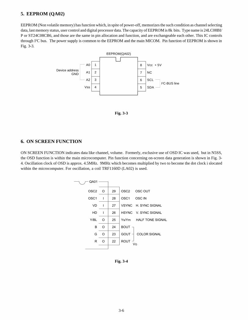
5. EEPROM (QA02)
EEPROM (Non volatile memory) has function which, in spite of power-off, memorizes the such condition as channel selectingdata, last memory status, user control and digital processor data. The capacity of EEPROM is 8k bits. Type name is 24LC08BI/P or ST24C08CB6, and those are the same in pin allocation and function, and are exchangeable each other. This IC controlsthrough I2C bus. The power supply is common to the EEPROM and the main MICOM. Pin function of EEPROM is shown inFig. 3-3.
Fig. 3-3
6. ON SCREEN FUNCTION
ON SCREEN FUNCTION indicates data like channel, volume. Formerly, exclusive use of OSD IC was used, but in N5SS,the OSD function is within the main microcomputer. Pin function concerning on-screen data generation is shown in Fig. 3-4. Oscillation clock of OSD is approx. 4.5MHz. 9MHz which becomes multiplied by two to become the dot clock i slocatedwithin the microcomputer. For oscillation, a coil TRF1160D (LA02) is used.
Fig. 3-4
OSC2
OSC1
VD
HD
Y/BL
B
G
R
QA01
O
I
I
I
O
O
O
O
29
28
27
26
25
24
23
22
OSC2 OSC OUT
OSC1 OSC IN
VSYNC H. SYNC SIGNAL
HSYNC V. SYNC SIGNAL
Ys/Ym HALF TONE SIGNAL
BOUT
GOUT COLOR SIGNAL
ROUTVG
1
2
3
4
8
7
6
5
A0
A1
A2
Vss
Vcc + 5V
NC
SCL
SDAI2C-BUS line
Device addressGND
EEPROM(QA02)

3-7
7. SYSTEM BLOCK DIAGRAM
Fig. 3-5
QA01TMP87CS38N-3152
QA02
SCL 0
SDA 0
HSYNC
VSYNC
R
G
B
YS/TM
RMT OUT
MUTE
SP MUTE
SDA 1
SCL 1
RMT
KEY-A
KEY-B
RST
VDD
GND
VSS
POWER
ACP
LED
XIN
XOUT
OSCI
OSCO
SGV
SGA
SYNC-AV1
AFT1 IN
SYCN-AV2
AFT2 IN
11
12
26
27
22
23
24
25
3
4
5
38
37
35
17
18
33
42
1
21
7
41
8
31
32
28
29
19
20
36
16
13
2
KEY SWITCH
POWERSUPPLYCIRCUIT
REMOTESENSOR
UNIT
MAIN U/V TUNEREL446L
H001
SDA SCL
HY01
SUB U/V TUNEREL922L
SDA SCL
SDA SCL
SDA SCL
VCDTA1222N
Q501
H002
IF/MPXMVUS345
27 28
21 20
SDA SCL
QV01
AV SWTA1218N
26 27
QM01
DSP
SDA SCL
6.1MHz
CLOCK
SIGNALOUTPUT
8MHz
CLOCK
SYNC DET.
AFT DET.
SYNC DET.
AFT DET.
MAIN SCREEN
SUB SCREEN
MEMORY24LC08B1/P
SDA SCL
5 6
H. SYNC PULSE
V. SYNC PULSE
VIDEO SIGNALPROCESS CIRCUIT
REMOTE CONTROLOUTPUT
SOUND MUTE
SPEAKER MUTE
Q701
C/C, EDSXC144144PDATA CLK
DPC UNIT
DATA CLK
QY04
PIP CONTROL
DATA CLK
6 5

3-8
8. LOCAL KEY DETECTION METHOD
Local key detection in the N5SS chassis is carried out byusing an analog voltage divider-like method which detectsa voltage appearing at the local key input terminals (pins 17,18) of the microcomputer whenever a key is depressed.Using this method, a maximum of 14 keys can be interpreted.
The circuit diagram shown at the left is a representation ofthe local key circuit. As can be seen from the diagram, whenone of keys among SA-01 to SA-08 is pressed, each of twoinput terminals (pins 17, 18) develops a voltage (Vin)corresponding to the key pressed. (The voltage measurementand key identification are carried out by an A/D converterinside the microcomputer along with interpreting software.
15 16
S15-1
S15-2
S15-3
S15-4
S15-5
S15-6
S15-7
S16-1
S16-2
S16-3
S16-4
S16-5
S16-6
S16-7
Fig. 3-6. Local key assignment
Table 3-1 Local key assinment
Key No. Function Key No. Function
SA-02 POWER SA-01 DEMO START/STOP
SA-03 CH UP
SA-04 CH DN
SA-05 VOL UP
SA-06 VOL DN
SA-07 ANT/VIDEO, ADV
SA-08 MENU
3-9
9. ENTERING THE SERVICE MODE
1. PROCEDURE(1) Press once MUTE key on the remote hand unit to
indicate MUTE on screen of the television.(2) Press the MUTE key of remote hand unit again and
keep depressed while depressing the MENU key onthe front of the unit.
2. During service mode, indication S is displayed at upperright corner on screen.
10. TEST SIGNAL SELECTION
1. In OFF state of test signal, SGA terminal (Pin 20) andSGV terminal (Pin 21) are kept at a “L” condition.
2. The function of VIDEO test signal selection is cyclicallychanged with each depression of the VIDEO key (on theremote control unit).
11. SERVICE ADJUSTMENT
1. ADJUSTMENT MENU INDICATION ON/OFF,MENU key ( on TV set)
2. During display of the adjustment menu, the followingfunctions are possible:a) Selection of adjustment item :
POS UP/DN key (on TV/remote unit)b) Adjustment of each item :
VOL UP/ DN key (on TV / remote unit)c) Direct selection of adjustment item
R CUTOFF : 1 POS (remote unit)G CUTOFF : 2 POS (remote unit)B CUTOFF : 3 POS (remote unit)
d) Data setting for PC unit adjustmentSUB CONTRAST : 4 POS (remote unit)SUB COLOR : 5 POS (remote unit)SUB TINT : 6 POS (remote unit)
e) Horizontal line ON/OFF :VIDEO (TV)(NOTE: applies only to direct view)
f) Test signal selection : VIDEO (remote unit)* In service mode, serviceable items are limited.
3. Test audio signal ON / OFF : 8 POS (remote unit)* Test audio signal : 1kHz
4. Self check display : 9 POS (remote unit)* Cyclic display (including ON/OFF)
5. Initialization of memory :CALL (remote unit) + POS UP (TV)
6. Initialization of self check data :CALL (remote unit) + POS DN (TV)
7. BUS OFF :CALL (remote unit) + VOL UP (TV)
(3) SGA (audio test signal) output should be squarewave of 1kHz.
Table 3-2
Test Signal No. Name of Pattern
0 Signal OFF
1 All black signal + R single color (OSD)
2 All black signal + G single color (OSD)
3 All black signal + B single color (OSD)
4 All black signal
5 All white signal
6 W/B
7 Black cross bar
8 White cross bar
9 Black cross hatch
10 White cross hatch
11 White cross dot
12 Black cross dot
13 H signal (bright area)
14 H signal (dark area)
15 Black cross + G

3-10
12. FAILURE DIAGNOSIS PROCEDURE
The N5SS chassis is equipped with a self diagnosis function inside, used for troubleshooting.
1. CONTENTS TO BE CONFIRMED BY CUSTOMER BEFORE SERVICE CALL IS MADE
2. CONTENTS TO BE CONFIRMED BY SERVICER (Check in self diagnosis mode)
Contents of self diagnosis Display items and actual operation
A. DISPLAY OF FAILURE INFORMATION IN NO PICTURE (Condition of display)1. When power protection circuit operates;2. When I2C-BUS line is shorted;
Power indicator lamp blinks and picture does not come.
1. Power indicator red lamp blinks. (0.5 seconds interval)2. Power indicator red lamp blinks. (1 seconds interval)If these indication appears, repairing work is required.
Table 3-3
Table 3-4
Contents of self diagnosis Display items and actual operation
Contents of self diagnosis<Countermeasure in case that phenomenon always arises.>B. Detection of shortage in BUS lineC. Check of comunication status in BUS lineD. Check of signal line by sync signal detectionE. Indication of part code of microcom.(QA01)F. Number of operation of power protection circuit
Display items and actual operation
3. EXECUTING SELF DIAGNOSIS FUNCTION [CAUTION](1) When executing block diagnosis, select first the desired input signal source (U/V BS VIDEO1,2,3) screen, and then enter
the self diagnosis mode.(2) When diagnosing other input modes, repeat the diagnosis routines after source selection. The test signals and/or routines
apply only to the video source selected at the time of testing.
(PROCEDURE)(1) Place the unit in the service mode.(2) Press the “9” key on the remote control will display the self diagnosis results on screen.
With each key press the mode will change as shown below.
SERVICE mode SELF DIAGNOSIS mode
(3) To exit from the service mode, turn the power off via the front panel or remote control.
(Example of screen display)
SELF CHECKPart coce of QA01Number of operation of power protection circuit
Short check of bus line
Communication check of busline
NO. 239XXXXPOWER: 000000
BUS LINE: OK
BUS CONT: OK
BLOCK: UV V1 V2 QV01, QV01S
EF
B
C
D

3-11
4. UNDERSTANDING THE RESULTS OF THE SELF DIAGNOSIS FUNCTIONSee Fig. 3-7 .
(Example of screen display)
SELF CHECKPart coce of QA01Number of operation of power protection circuit
Short check of bus line
Communication check of busline
NO. 239XXXXPOWER: 000000
BUS LINE: OK
BUS CONT: OK
BLOCK: UV V1 V2 QV01, QV01S
EF
B
C
D
Fig. 3-7
Table. 3-5
Item Contents Instruction of results
BUS LINE Detection of bus line short Indication of OK for normal result, NG for abnormal
Indication of OK for normal resultIndication of failure place in abnormality(Failure place to be indicated)QA02 NG, H001 NG, Q501 NG, H002 NGQV01 NG, Q302 NG, QY02 NG, HY01 NGQD04 NG, QM01 NG, Q701 NG
BUS CONT Communication state of bus line Note 1. The indication of failure place is only one placet though failure places are plural. When repair of a failure place finishes, the next failure place is indicated. (The order of priority of indication is left side.)
BLOCK: UV1 UV2 V1 V2
The sync signal part in each video signalsupplied from each block is detected.Then by checking the existence or non ofsync part, the result of self diagnosis isdisplayed on screen. Besides, when “9” keyon remote unit is pressed, diagnosisoperation is first executed once.
*Indication by color • Normal block :Green • Non diagnosis block :Cyan

3-12
<Clearing the self diagnosis results>While the error count state is displayed upon the screen, press the “CHANNEL DOWN” button on TV setpressing “DISPLAY” button on remote unit.
[CAUTION]All ways observe the following caution, when in theservice mode screen.• Do not press the “CHANNEL UP” button. This will cause
initialization of the memory IC. (Replacement of memoryIC is required.
• Do not initialize self diagnosis result. This will change useradjusting contents to factory setting value. ( Adjustment isrequired.)
WhiteYellow
CyanGreen
MagentaRed
Blue
( COLOR BAR SIGNAL)Color elements are positioned in sequence of high brightness.
<Troubleshooting method utilizing internal test signal> (VIDEO INPUT 1 terminal should be open.)(1) With service mode screen, press VIDEO button on remote unit. If inner video signal can be received, QV01 and after are
normal.(2) With service mode screen, press “8” button on remote unit. If sound of 1kHz can be heard, QV01 and after are normal.* By utilizing signal of VIDEO input terminal, each circuit can be checked. (Composite video signal, audio signal)

3-13
13. TROUBLE SHOOTING CHARTS
(1) TV DOES NOT TURNED ON
TV does not turned on.
Relay sound
Check of voltage at pin 7 of QA01(DC 5V).
8MHz oscillation waveformat pin 32 of QA01.
Pulse output at pins 37 and 38 of QA01.
Check relay driving circuit.
Check power circuit.
Check OSC circuit.
Replace QA01.
Voltage check at pin 32 of QA01(DC 5V)
Check reset circuit.
Replace QA01.
YES
NG
NG
NG
NG
OK
NO
OK
OK
OK
3-14
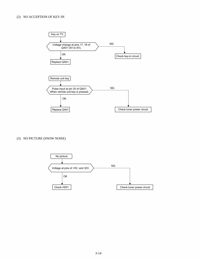
(2) NO ACCEPTION OF KEY-IN
(3) NO PICTURE (SNOW NOISE)
NG
OK
No picture
Voltage at pins of +5V, and 32V.
Check H001. Check tuner power circuit.
Key on TV
Voltage change at pins 17, 18 ofQA01 (5V to 0V).
Replace QA01.
Check key-in circuit.
NG
OK
NG
OK
Remote unit key
Pulse input at pin 35 of QA01,When remote unit key is pressed.
Replace QA01 Check tuner power circuit.

3-15
NG
NG
OK
OK
Memory circuit check
Voltage check at pin 8 of QA02 (5V).
Pulse input at pins 5 and 6 of QA02in memorizing operation.
Replace QA02.
Adjust items of TV set adjustment.
Note: Use replacement parts for QA02.
Check power circuit.
Check QA01.
NG
NG
OK
OK
OK
No indication on screen.
Check of character signal at pin 23 of QA01. (5VP-P)
Input of OSC waveform at pin 29 of QA01with indication key pressed.
Check of sync signal at pins 26, 27 of QA01.
Replace QA01.
Check V/C/D circuit.
Check OSC circuit.
Check sync circuit.
(5) NO INDICATION ON SCREEN
(4) MEMORY CIRCUIT CHECK

3-16
NOTES

4-1
SECTION IVAUDIO OUTPUT CIRCUIT

4-2
1. OUTLINE
The main amplifiers and woofer output amplifiers use abipolar IC (TA8256H) and develop output powers of10Wx2 + 13W.
2. THEORY OF OPERATION
2-1. Operation of TA8256HThe TA8256H is a modified version of the TA8128AHwhich was used in the N4SS chassis as an audio ouput IC.In the TA8256H, one channel has been added and up to 3channels can be used. Performance for each channel is thesame as that of the TA8218H. Fig. 4-1 shows a blockdiagram of the IC.
AMP-2
AMP-3
AMP-1
1
11
7
5
12
10
8
4
3
2
47m F
1m F
47m F
1m F
RR
1m F
WW
6 9
RIPPLE FILTER Vcc4k
30k
350W
PREGND
350W
4k
30k
30k4k
350W
20kW
MUTING
OUTPUT-3
(S) or (W)
OUTPUT-3
OUTPUT-2
POW GND
(R)
Vcc25.5V
470m F
2.2W
0.12m FRL (L)
RL (R)
470m F
0.12m F
2.2W
(mute)
(mute Tc)
1000m F
RL (W)2.2W
0.12m F
LL
Fig. 4-1

5-1
SECTION VDSP CIRCUIT
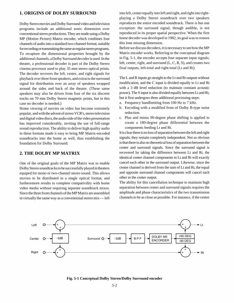
5-2
Fig. 5-1 Conceptual Dolby Stereo/Dolby Surround encoder
into left, center equally into left and right, and right into right-playing a Dolby Stereo soundtrack over two speakersreproduces the entire encoded soundtrack. There is but oneexception: the surround signal, though audible, is notreproduced in its proper spatial perspective. When the firsthome decoder was developed in 1982, its goal was to restorethis lone missing dimension.Before we discuss decoders, it is necessary to see how the MPMatrix encoder works. Referring to the conceptual diagramin Fig. 5-1, the encoder accepts four separate input signals;left, center, right, and surround (L, C, R, S), and creates twofinal outputs, left-total and right-total (Lt and Rt).
The L and R inputs go straight to the Lt and Rt outputs withoutmodification, and the C input is divided equally to Lt and Rtwith a 3 dB level reduction (to maintain constant acousticpower). The S input is also divided equally between Lt and Rt,but it first undergoes three additional processing steps:a. Frequency bandlimiting from 100 Hz to 7 kHz.b. Encoding with a modified from of Dolby B-type noise
reduction.c. Plus and minus 90-degree phase shifting is applied to
create a 180-degree phase differential between thecomponents feeding Lt and Rt.
It is clear there is no loss of separation between the left and rightsignals; they remain completely independent. Not so obviousis that there is also no theoretical loss of separation between thecenter and surround signals. Since the surround signal isrecovered by taking the difference between Lt and Rt, theidentical center channel components in Lt and Rt will exactlycancel each other in the surround output. Likewise, since thecenter channel is derived from the sum of Lt and Rt, the equaland opposite surround channel components will cancel eachother in the center output.The ability for this cancellation technique to maintain highseparation between center and surround signals requires theamplitude and phase characteristics of the two transmissionchannels to be as close as possible. For instance, if the center
1. ORIGINS OF DOLBY SURROUND
Dolby Stereo movies and Dolby Surround video and televisionprograms include an additional sonic dimension overconventional stereo productions. They are made using a DolbyMP (Motion Picture) Matrix encoder, which combines fourchannels of audio into a standard two-channel format, suitablefor recording or transmitting the same as regular stereo programs.To recapture the dimensional properties brought by theadditional channels, a Dolby Surround decoder is used. In thetheatre, a professional decoder is part of the Dolby Stereocinema processor used to play 35 mm stereo optical prints.The decoder recovers the left, center, and right signals forplayback over three front speakers, and extracts the surroundsignal for distribution over an array of speakers wrappedaround the sides and back of the theater. (These samespeakers may also be driven from four of the six discretetracks on 70 mm Dolby Stereo magnetic prints, but in thiscase no decoder is needed.)Home viewing of movies on video has become extremelypopular, and with the advent of stereo VCR's, stereo televisionand digital video discs, the audio side of the video presentationhas improved considerably, inviting the use of full-rangesound reproduction. The ability to deliver high quality audioin these formats made it easy to bring MP Matrix-encodedsoundtracks into the home as well, thus establishing thefoundation for Dolby Surround.
2. THE DOLBY MP MATRIX
One of the original goals of the MP Matrix was to enableDolby Stereo soundtracks to be successfully played in theatersequiped for mono or two-channel stereo sound. This allowsmovies to be distributed in a single optical format, andfurtheremore results in complete compativility with homevideo media without requiring separate soundtrack mixes.Since the three front channels of the MP Matrix are assembledin virtually the same way as a conventional stereo mix --- left
Left
Center
Right
++
++
-3dB Surround -3dB B.P.FDOLBY NRENCORDER
++
++
+90 DEG
-90 DEG
Lt
Rt

5-3
channel components in Lt are not identical to the ones in Rtas a result of a channel balance error, center information willcome out of the surround channel in the form of unwantedcrosstalk.
3. THE DOLBY SURROUND DECODER
This leads us to the original Dolby Surround decoder. Theblock diagram in Fig. 5-2 shows how the decoder works.Except for level and channel balance corrections, the Lt inputsignal passes unmodified and becomes the left output. The Rtinput signal likewise becomes the right output. Lt and Rt alsocarry the center signal, so it will be heard as a "phantom"image between the left and right speakers, and sounds mixedanywhere across the stereo soundstage will be presented intheir proper perspective. The center speaker is thus shown asoptional since it is not needed to reproduce the center signal.
The L-R stage in the decoder will detect the surround signalby taking the difference of Lt and Rt, then passing it througha 7 kHz low-pass filter, a delay line, and complementaryDolby noise reduction. The surround signal will also bereproduced by the left and right speakers, but it will be heardout-of-phase which will diffuse the image.Since the heart of the decoding process is a simple L-Rdifference amplifier, it is referred to generically as a "passive"decoder. This is to distinguish it from decoders using activeprocesses to enhance separation which are known as "active"decoders.
Fig. 5-2 Passive surround decoder block diagram
4. DSP CIRCUIT
A surround component (L-R) is extracted from L, R audiosignals coming through the AV SW in the matrix circuit asshown in Fig. 5-3. The surround component enters the DSPcircuit through the LPF.The signal is A/D converted, delayed by an arbitrary time of0~100 msec (every 3.2 msec) by digital process and then D/A converted and outputs from the DSP IC. The DSP ICdevelops two outputs; (LO) for FRONT (LO) and (RO) forREAR and each output is controlled by the microcomputerfor each surround mode. The output signal (LO) for FRONTis added and subtracted with the input signal in a matrixcircuit and output from the front speaker in passing throughthe audio processor and main amplifiers.At the same time, the output signal (RO) for REAR is fed tothe Dolby NR circuit, but switched to "Dolby surround"mode, and then output from the rear speaker in passingthrough audio processors and rear main amplifiers.In this case, the DSP stands for not only a simple digitalsurround processor but also a digital surround field processor.That is, it works to give a simple surround effect but to giveeffect as if the listener can feel reality suitable for theprograms. For example, it aims to give the listeners a realitymatching to each program they are enjoying in their homelistening room so that they can obtain reality of big concerthall or feel as if they are watching a move at a reserved seatin a movie theater.
INPUTS OUTPUTS
Lt
Rt
INPUTBALANCECONTROL
LEVELCONTROL
MASTERLEVEL
CONTROL
ANTI-ALIAS
FILTER
MODIFIEDB-TYPE NRDECODER
AUDIODELAY
7 kHzLOW PASS
FILTER
Optional passive center signal
DELAY SET
L+R
L-R
L L
R R
C
C
S
S
Left
Right
Center
Surround

5-4
Fig. 5-3 B
lock diagram of D
SP
circuit
FromA/V SW
IN
L
R
QD08Input Balance
QD01Input Buffer
12 14
10 8
R L
6 5
7 3
(L-R)
1 3 1MATRIX(L-R CIRCUIT)
LPF LPF
QD01 QD01 QD02
QD03 DSP IC YM7128 B
A/D
VC
TO
DIGITAL DELAY
4
CONT
BUSCONVERT
QD04
From Microcomputer
VL
VR
D/A
D/A
LO
RO
Buffer
Buffer DQ06
3 1 5 7
7QD05 QD05
LO
5 7 3
8QD06 1
69 14
12
QD07 DQ02
L-R
Dolby NRQ640
Rear Amp
+SL
RSpeaker
QD02DSP
Front Addition CircuitQ670
Front amp
L
R
5 7
8
109
L
R
L+R
L+S
R-S
L
R
Speaker
Sycrone(Super woofer)
AudioProcessor(H002)
LPF
LPF

5-5
As shown in Fig. 5-4, a sound emitted in a sound field canbe classified as a direct sound which directly reaches ears ofa listener, and reflected sound which comes after collisionwith a wall as shown by dotted line or comes after severaltimes of collision as shown by double dotted lines. Thelisteners are determining that they are listing in what type oflocation by perceiving time difference and volume leveldifference between the direct sound and the reflected sound.
For more detail, this situation can be expressed with thedirect sound, initial reflection sound coming after one time ofreflection, and trains of reverberation sound in later period asshown in Fig. 5-5.The DSP circuit develops these initial reflection sound andthe reverberation sound artificially and add them to theoriginal sounds, thereby creating rhe effect that allows thelisteners in the home listening room to feel as if they arelistening in an original location.The DSP IC YM7128B has eight separate output taps andtheir delay time and the output levels can be specifiedseparately, so, various sound fields can be selected by varyingthe initial reflection sound. Moreover, the IC has an internalfeedback loop which controls the delay time and the outputlevel in considering the later time reverberation sound.
Direct Sound
Initial ReflectionSound
ReverberationSound
:
:
Fig. 5-4 Fig. 5-5
Sound Level
Direct Sound
Initial Reflection Sound
Reverberation Sound
Time

5-6
5. DSP (Digital Surround Processor) IC
Input signal entered into analog input pin 4 of DSP IC QD03(YM7128B) is converted to 14 bit digital signal with thesampling frequency 23.6 kHz by A/D converter of 14 bitfloating system, and enters digital delay circuit throughdigital attenuator VM and doubler.The digital delay circuit has nine output taps, and the delaytime of each tap can be controlled independently, also eachtap position can be switched by T0 to T8 register.In a minute, the T0 output passes through the primary FIR(Finite Impulse Response) type low pass filter, and reductionprocessing is performed by VC, then it feed-backed to the
delay input after it is added to the doubler described above.The output of eight taps T1 to T8 is added after performingreduction processing by GL1~GL8, GR1~GR8, and reductionprocessing is performed by the digital attenuator VL or VR,and an analog output is created by D/A converter afterpassing through digital filter, comes out from pin 7 or 8.The digital attenuated value, delay time and the coefficient ofFIR type low pass filter are set by writing the data on theregister.This process is performed by loading three data from submicrocomputer to microcomputer interface.This unit has four modes as surround mode. The settingvalues are described in Table 5-1.
Table 5-1 DSP control factor
Mode OFF DOLBY THEATER STADIUM NIGHT CLUB CONCERT UNITControl SURROUND HALL HALL
-VM (IN) -•¥ P-0 P0 ¥ P0 P0 P0 dB
VL (LO) -•¥ P0~ -• P0~ -¥• P0~ --¥• P0~ --¥•
VR (RO) P0 P0 P0 P0 P0
VC (Echo) -•¥ -•¥ M-6 M-10 M-8
GL1 P-4 M-2 M-2 P-2
2 M-6 -•¥ P-4 P-10
3 P-12 P-6 P-16
4 P-12 M-10 -•¥
5 -•¥ -•¥
6
7
8
GR1 P0
2 -•¥ P0
3 P-18
4 -•¥
5 P-2 P-6 P-4
6 M-2 M-6 P-8
7 P-8 M-10 P-8
8 P-10 P-12 P-14
T0 (Delay) 0 0 0 100.0 19.4 51.6 msec
1 19.4 12.9 93.6 12.9 71.0
2 0 38.7 100.0 19.4 83.9
3 71.0 100.0 22.6 100.0
4 87.1 0 29.0 0
5 29.0 6.5 64.5
6 45.2 9.7 80.7
7 83.9 25.3 90.4
8 100.0 35.5 100.0
C0 (Filter) 0 0.71875 0.59375 0.875 —
1 0.28125 0.40625 0.125 —

5-7
Fig. 5-6
QD03
CD22
FromInput LPF
CD15
RD26
CD23
CV
AIN
CH
/TI
VDD
DIN AO SCI
From Bus convert (ICD04)
A/DCONVERTER
REFERENCEVOLTAGE
GENERATION
DIGITAL DELAYVM
VC
C1
C2
D
TO
T8 T7 T6 T5 T4 T3 T2 T1
5
4
3
6
15 14 13 10 9
8
7
2
1
11 12 16
XD01
CD27 RD32 CD29
D01
CD28
RD33
XO XI /IC Vss
AVDD
LD01
CD21 CD20
LO
DC26
DC25
RO
VSS AVSS
VL
VR
2fs
2fs
To LPF Output(For FRONT ch)
To LPF Output(For REAR ch)
D/ACONVERTER
D/ACONVERTER
TIMING GENERATION
GL1
GL2
GL3
GL4
GL5
GL6
GL7
GL8
GL1
GL2
GL3
GL4
GL5
GL6
GL7
GL8
+B (5V)
MICROCOMPUTERINTERFACE

5-8
NOTES

6-1
SECTION VIA/V SWITCHING CIRCUIT
6-2
1. OUTLINE
The A/V switching circuit selects the desired video andaudio signals from the various inputs. It is controlled by themicrocomputer through IIC bus.
2. IN/OUT TERMINALS
TUNER INPUT U/V Tuner (Main)U/V Tuner (PIP)
EXTERNAL INPUT VIDEO 1 With S-terminalVIDEO 2VIDEO 3 (Front) With S-terminal
OUTPUT VIDEO OUTPUT (V, L, R)AUDIO ON SUB-PICTURE
3. CIRCUIT OPERATION
This circuit consists of A/V SW IC; TA1218N (QV01), andselects signals from U/V tuner (Main), U/V tuner (PIP),E1, E2 and E3.
3-1. Composite Video SignalThe selected video signal is output to pin 38 of QV01, andseparated by comb filter into Y an C. The resulted signalis input to pins 30 and 32 of QV01, and is output to pins 36and 34 to be supplied to Q501 (V/C/D).Video signal for PIP is output to pin 42 of QV01, and issupplied to PIP unit (ZY01).
3-2. S-Video SignalWhen a cable is connected to S-VIDEO terminal, innerswitch of S-VIDEO terminal is shorted to ground to turn offthe transistor (QV05 for VIDEO1 input) for S-VIDEOterminal detection. Then chroma input terminal (Pin 14 forVIDEO1 input) of QV01 turns on.

6-3
AV SW CIRCUIT
Fig. 6-1
H002IF/MTS/A. PRO
HY01PIP TUNER/IF
QV01 TA1218NEQ
VIDEO 3
VIDEO 1
VIDEO 2
PIP AUDIOOUT JACK
A/V OUTJACK
PIP
V in
Y in
C in
Q501
Y out
C out
V in
COMBFILTER
SYNC inQA01
L/R in
DSP
18
17
16
15
14
13
12
11
10
9
8
7
6
5
2
1
26
28
29
30
31
32
34
35
36
37
38
42
C in
R in
S in
L in
C in
R in
S in
L in
V in
R in
L in
V in
R in
L in
PIP R out
PIP L out
SYNC OUT
PIP TV in
PIP L in
Y in
PIP R in
C out
R out
Y out
L out
V out
PIP V out
C in
V AA V
TP48E90 ONLY

6-4
NOTES

7-1
SECTION VIIVIDEO PROCESSING CIRCUIT

7-2
1. OUTLINE
This circuit converts and amplifies video signal (Luminanceand chroma signals) separated into Y/C, to original colorsignal, and is supplied to CRT Drive circuit.
2. SIGNAL FLOW
Signal flow chart is shown in figure 6-1 Block diagram.(1) Luminance signal is input to pin 15 of Q501, and enters
into delayline inside Q501 to be output to pin 4.(2) Chroma signal is input to pin 13, and I/Q signal which
is demodulated in color, is output to pins 5 and 6, andnext supplied to pins 51 and 52.
(3) The signal is processed on luminance and chromasignals, and is converted to original color signal (R,G,B)
by RGB matrix. Next the signal is superimposed withOSD signal to be output to pins 41, 42 and 43, and issupplied to CRT Drive circuit.
(4) The signal for Scan Modulation is processed withdifferential in Q501 to be output to pin 48 Besides, atterminal for adjustment TP501, luminance and chromasignals are automatically output according to theselected items of service mode.
3. CIRCUIT OPERATION
All processing operation of video signal are done insideQ501. The outline of Q501 (TA1222N) is explained in thenext section. Here, major terminals excepting input/outputterminals of Q501 are described.
Table 7-1
Pin No. Name Description
Pin 1 CW output 3.58MHz synchronized with burst is output. This is used for clock of comb filter.
Pin 10 Xtal 1 Terminal for 3.58MHz OSC crystal
Pin 11 APC filter Terminal for phase detection of color sync (OSC frequency control)
Pin 18 SYNC Sync-separated sync signal is output. It is used for detecting no signal inmicrocomputer.
Pin 30 HD Terminal for output of HD pulse syncronized with horizontal sync., and for inputof black expading mask pulse. It is used for timing pulse of OSD, C.C (ClosedCaption) in micro- computer.
Pin 32 Ys OSD change-over pulse input: Ys of OSD is input.
Pin 45 ABL Terminal for ABL control input
Pin 47 Ym Input of pulse for half tone control: It is supplied from microcomputer.
Pin 49 APL DET Detecting average level of video signal for correction of DC transmission
Pin 50 BLACK DET Detecting black area of video signal for black expading circuit
Pin 54 COL Terminal for peak-hold of color limiter
Pin 55 DAC1 Test point (TP501): Functioning test point in service mode


7-4
NOTES
8-1
SECTION VIIIV/C/D/IC

8-2
1. OUTLINEThis IC enables more precise picture setting than that of former IC (TA8845N) by means of large scale employmentof IIC bus, and reduces many peripheral components by containing filters inside.The main features (comparing TA8845) are as follows.
2. LARGE SCALE EMPLOYMENT OF BUS CONTROL OF PARAMETER FOR PICTURECONTROLS
Soft method of picture making
4. EMPLOYMENT OF CONTAINING EACH FILTER (FOR S/H) INSIDE
Circuit operation by extremely low current / Employment of leak current cancel circuit Employment of detection circuitwhich does not suffer from influence of stray capacity
3. EMPLOYMENT OF CONTAINING EACH VIDEO BAND FILTER INSIDE
Employment of automatic adjustment circuit by Fsc to absorb deviation / Employment of deviation aborbing method by highS/N filter and mask triming using fixed CR
Table 8-1
Table 8-2
Table 8-3
Former/TA8845N TA1222N
* Black expanding start point External constant BUS control
* DC transmission correction quantity point External constant BUS control
* Black level correction quantity External constant BUS control
* Each ABCL characteristic External constant BUS control
Former/TA8845N TA1222N
* Y-DL Apa-con DL inside Inside
* Chroma TO/BPF External Inside
* Velocity modulation processing circuit External Inside
* Fsc trap for chroma demodulation output External Inside
Former/TA8845N TA1222N
* Chroma ACC / killer filter External Inside
* Y / color difference clamp filter External Inside
* Filter for filter automatic adjustment External Inside
* AFC 2 filter External Inside

8-3
5. LOW COST OF IC
* Involving peripheral components inside ——> Down sizing of chip ——> Newly employment (NPN Tr area ratio to former: -25%) of miniature process (PLAS-1 S process)
* Involving peripheral components inside——>Increasing of power consumption——>2 power supply system (5V / 9Vused)
* Involving peripheral components inside ——> Reducing of number of elements ——> Employment of new circuit(1) Reducing of gate (change of preset method) of register for IIC decoder(2) Reducing of DAC elements (employment of rudder type DAC + temperature compensation circuit)(3) Deletion of chroma CW, ACC (employment of 90 degree shift phase circuit with automatic adjustment)
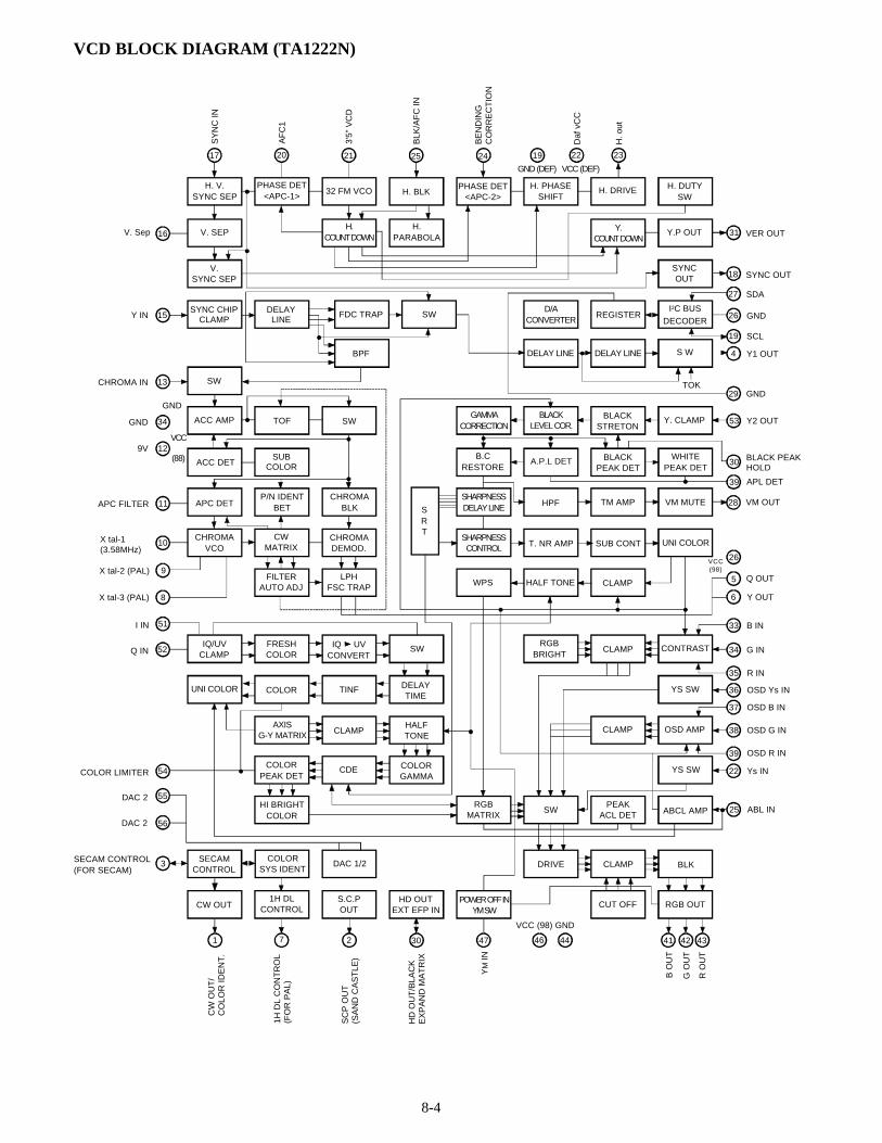
8-4
VCD BLOCK DIAGRAM (TA1222N)
17
SY
NC
IN
H. V.SYNC SEP
V. Sep 16
20
AF
C1
PHASE DET<APC-1>
21
3'5"
VC
D
32 FM VCO
25
BLK
/AF
C IN
H. BLK
24
BE
ND
ING
C
OR
RE
CT
ION
PHASE DET<APC-2>
19 22 23
GND (DEF) VCC (DEF)
H. PHASESHIFT
H. DRIVE
Daf
vC
C
H. o
ut
H. DUTYSW
Y.COUNT DOWN
Y.P OUT 31 VER OUT
SYNCOUT 18 SYNC OUT
27 SDA
D/ACONVERTER
REGISTER
DELAY LINE S WDELAY LINE
I2C BUSDECODER
26 GND
19 SCL
4 Y1 OUT
TOK29 GND
GAMMACORRECTION
BLACKLEVEL COR.
BLACKSTRETON
Y. CLAMP 53 Y2 OUT
30 BLACK PEAKHOLD
39 APL DET
28 VM OUTSRT
26
B.CRESTORE
A.P.L DET BLACKPEAK DET
WHITEPEAK DET
SHARPNESSDELAY LINE HPF TM AMP VM MUTE
SHARPNESSCONTROL T. NR AMP SUB CONT UNI COLOR
VCC (98)
5 Q OUTWPS HALF TONE CLAMP
6 Y OUT
33 B IN
34 G IN
35 R IN
36 OSD Ys IN
37 OSD B IN
38 OSD G IN
39 OSD R IN
22 Ys IN
25 ABL IN
RGB BRIGHT
CLAMP CONTRAST
YS SW
CLAMP OSD AMP
YS SW
RGBMATRIX
SWPEAK
ACL DET ABCL AMP
DRIVE CLAMP BLK
RGB OUTCUT OFF
41 42 43
B O
UT
G O
UT
R O
UT
VCC (98) GND
46 4447
YM
IN
POWER OFF INYM SW
30
HD
OU
T/B
LAC
KE
XP
AN
D M
AT
RIX
HD OUTEXT EFP IN
2
SC
P O
UT
(SA
ND
CA
ST
LE)
S.C.POUT
DAC 1/2COLOR
SYS IDENT
1H DLCONTROLCW OUT
SECAMCONTROL
7
1H D
L C
ON
TR
OL
(FO
R P
AL)
1
CW
OU
T/
CO
LOR
IDE
NT
.
3SECAM CONTROL(FOR SECAM)
56
55
54
DAC 2
DAC 2
COLOR LIMITER
52Q IN
51I IN
HI BRIGHTCOLOR
COLORPEAK DET
CDE COLORGAMMA
IQ/UVCLAMP
FRESHCOLOR
IQ UVCONVERT
SW
UNI COLOR COLOR TINF DELAYTIME
AXISG-Y MATRIX CLAMP
HALFTONE
8
9
10
11
X tal-3 (PAL)
X tal-2 (PAL)
X tal-1 (3.58MHz)
APC FILTER
FILTERAUTO ADJ
LPHFSC TRAP
CHROMAVCO
CWMATRIX
CHROMADEMOD.
CHROMABLK
P/N IDENTBETAPC DET
ACC DETSUB
COLOR
129V
34GND
13CHROMA IN
GND
VCC
(88)
ACC AMP TOF SW
SW
SW
BPF
FDC TRAPDELAYLINE
SYNC CHIPCLAMPY IN 15
V.SYNC SEP
V. SEPH.
COUNT DOWNH.
PARABOLA

9-1
SECTION IXPIP MODULE

9-2
4V
0V
PIN I/O NAME PIN I/O NAME
1 0 YS 9 I 5V
2 - NC 10 I GND
3 I GND 11 I VD
4 O R OUT 12 I HD
5 O G OUT 13 I/O SCL
6 O B OUT 14 I/O SDA
7 I GND 15 - NC
8 I PIP VIDEO
PMUS 02H (SN:23148232)
B-Y OFFSET
R-Y OFFSET
TINT
RY54 RY55 RY50
15
14
13
12
11
10
987654321
4.8V
2.8V
4.8V
4.1V
4.8V
4.1V
4.8V
4.1V
350m S
0V4.2V
3.0V10m S
6V
-0.9V
1m S4.2V
0V
Or
B CHASSIS C CHASSIS

9-3
8 36 14
13
12
10
11
51
49
47
78
76
67
65
64
18
16
19
18
16
23
24
25
4
5
6
11
12
VIDEOIN
B-YOUT
R-YOUT
Y-OUT
HD
VD
QY01m PC 1832GT(PIP V/C/D)
QY03TC9083F
(PIP PROCESSOR)
SLICE
WAVE FORMMODULATION
RY55 RY54
PMUS02H<BLOCK DIAGRAM OF PIP MODULE>
BI
RI
YI
HDCN
VDCN
BO
RO
YO
HDPN
VDPN
B-YIN
R-YIN
YIN
R OUT
G OUT
B OUT
QY01m PC1832GT(PIP V/C/D)
R OUT
G OUT
B OUT
PIP VIDEO
VD
HD

9-4
NOTES

10-1
SECTION XSYNC SEPARATION, H-AFC,H-OSCILLATOR CIRCUITS
10-2
1. SYNC SEPARATION CIRCUIT
The sync separation circuit separates a sync signal from avideo signal and feeds it to an H and V deflection circuits.The separation circuit consists of an amplitude separation (Hand V sync separation circuit) and a frequency separationcircuit (V sync separation circuit) which performs theseparation by using a frequency difference between H and V.In the N5SS chassis, all these sync separation circuits arecontained in a V/C/D IC (TA1222N).Fig. 10-1 shows a block diagram of the sync separationcircuit.
17
Sync input
Compositevideosignal
Q501
H. V SYNCSEPARATION
CIRCUIT
V SYNCSEPARATION
CIRCUIT
WAVEFORMSHAPEINGCIRCUIT
H sync siganl
V sync signal(Reset pulse)
Fig. 10-1 Sync separation circuit block diagram
Fig. 10-2 Synchronous separation by auto slider system
1-1. Theory of Operation1-1-1. Auto slicer type synchronous separation circuitWhen a synchronizing signal is separated, synchronousseparation is made from the beginning with constant voltagein the conventional synchronous separation circuit. The autoslider type circuit employed in this time makes synchronousseparation at a constant rate against the synchronizing signalamplitude. (See Fig. 10-2)In this method, even if an abnormal signal with smallamplitude is applied, stable synchronizing performance canbe obtained without separating pedestal.
B
A
D
B
Pedestal Level
a: Corect Sync. Signal
Sync Separation Level A:B=C:Db: Small Amplitude Sync. Signal

10-3
1-1-2. V Sync Separation CircuitTo separate a V sync signal from the composite sync signalconsisting of V and H sync signals mixed, two stages ofintegration circuits are provided inside the IC. The circuitconsists of a differential circuit and a Miller integrationcircuit, and has following functions.(1) Removes H sync signal component.(2) Maintain stable V sync performance for a tape recorded
with a copy guard.(3) Stabilized V sync performance under special field
conditions (poor field, ghost, sync depressed, adjacentchannel best).
The V sync signal separated in this stage is processed in awaveform shape circuit and then used as a reset pulse in theV division circuit as stated later.
2. H AFC (Automatic Frequency Control)CIRCUIT
A sync system which performs synchronization with eachwaveform of the sync signal as performed in a sync systemin the V circuit is called a direct type sync system. However,if the synchronization for the H oscillator is carried out withthis method, the H oscillator synchronizes with externalnoises and the H synchronization will be disturbed. Toprevent this, an output of the H oscillator is compared witha reference H sync signal to detect deviations of frequencyand phase. The H oscillator is automatically controlled withthe detected output averaged. This circuit is called an AFCcircuit.In the N4SS chassis, a conventional AFC circuit is notemployed but a new double AFC circuit built-in the TA1222Nis used. Fig. 10-3 shows the AFC circuit and the blockdiagram of the circuit.
Fig. 10-3 H AFC circuit block diagram
First, phases of a 32 fH counted-down signal and a H syncsignal contained in broadcasting signal are compared in theAFCI loop and the loop develops an H pulse signal for theAFCII loop. That is, when a phase deference 01 exists incomparison of the phase of fH signal developed by countingdown the 32 fH signal and the phase of H sync signal of thebroadcasting signal, an error signal corresponding to thephase different is detected and a correction voltage V1
corresponding to the error output is generated. With thiscorrection voltage, the 32 fH oscillator circuit is controlled.The correction (control) voltage for the oscillator varies indirection of positive or negative corresponding to phaselead or lag of the fH pulse (developed by counting down)from the H sync signal. As the H oscillator (32 x fH), avoltage controlled oscillator (VCO), oscillation frequencyand phase of which can be controlled with the controlvoltage is used.Next, an H pulse signal is created from the fH signal counteddown, and the pulse is used instead of the H sync signal inthe AFCII circuit. The AFCII circuit differs in the loop ofthe count down circuit and H output circuit.The AFCII circuit compares phase of a H BLK pulse createdby waveform shaping a AFC pulse from the FBT and a phaseof the H pulse, and detects an error component correspondingto the phase difference 02 (if exist) and develops acorrection voltage V2 corresponding to the error, therebycontrolling the phase of Q501 H out.The H output control voltage varies in a positive or negativedirection corresponding to the phase lead or lag of the HBLK pulse from that of the H pulse. The phase of H out isvaried with the control voltage to make synchronizationwith the H pulse phase.The purpose of the double AFC circuit employed this time
SYNC SEPARATIONCIRCUIT
PHASE DETECTIONCIRCUIT
32 x fHVCO
H COUNT DOWN(DIVIDING)
AFC I LOOP
PHASE DETECTIONCIRCUIT
AFC II LOOP
H DRIVEH OUTPUTCIRCUIT
FBT PULSE(AFC PULSE)

10-4
is to improve horizontal jitter under signal reception in apoor electrical field. The jitter in the poor field strength anddistortion due to phase difference are incompatible. Thatis,to improve the jitter under poor field strength, responsespeed must be slowed by lowering the AFC sensitivity. Onthe other hand, to improve distortion due to the phasedifference, the response must be increased by increasing theAFC sensitivity.In a conventional AFC circuit, setting of the sensitivity iscarried out at one part only, so an compromise point for bothcharacteristics must be found. However, with the doubleAFC circuit employed this time, for the jitter the AFCI loopworks best with decreasing the sensitivity and for the phasedistortion the AFCII loop works with increasing thesensitivity.
3. H OSCILLATOR CIRCUIT
3-1. OutlineA 503 kHz (32 x fH) voltage controlled type oscillator witha ceramic oscillation element is used to generate a clockpulse and the clock is counted down, thereby obviating theneed of adjustments for both the H and V deflection processcircuit.
3-2. Theory of Operation(1) The H sync signal used as a reference signal enters
from the sync separation circuit to the AFCI circuit. Atthe same time, the fH pulse created by counting downthe 32 x fH pulse generated in the ceramic oscillatorenters the H AFCI circuit. Phase difference betweenthese two signals enters an integration circuit (low pas
Fig. 10-4
17 20 21
SYNCIN
2VP-P
H Vcc
SYNCSEPARATION
CIRCUIT
H AFC ICIRCUIT
32 x fHVCO
H COUNTDOWN
H AFC IICIRCUIT
TA1222N

10-5
filter) connected to pin 4 and converted into a DCvoltage (AFC voltage).
(2) The AFC voltage controls frequency (32 x fH) of theoscillator (VCO).Fig. 10-5 shows the control characteristics of the VCO.
(3) The H output is obtained by dividing the 32 x fH (503kHz) of the oscillator with flip-flops. Fig. 10-6 showsthe block diagram of this count down circuit.
(4) The V output is created by dividing the 32 x fHoscillator output into 1/8, and then by counting the 4 xfH pulse with a vertical counter which is reset with aV reset pulse (V sync output signal stated under syncseparation).
(5) That is, the V output is not created by simply countingdown the H by performing V synchronization with a Vreset pulse entering within a window provided for Vsynchronization --- called direct type sync system,thus, the circuit can work for non standard signals.
Fig. 10-5
Fig. 10-6 Block diagram of H, V count down circuits
32 x fH VCO32fH
X 1/8 X 1/4 H OUTPUT
V OUTPUTV
COUNTER
Resetpulse
V syncsignal V WAVEFORM
SHAPECIRCUIT
4fH fH
High
Low
OS
C fre
quency
(H
z)
Low High AFC voltage (V)

10-6
NOTES

1 1 - 1
SECTION XIVERTICAL OUTPUT CIRCUIT

1 1 - 2
1. OUTLINE
As can be seen from the block diagram, the sync circuit andthe V trigger circuit are contained in Q501 (TA1222N), andthe sawtooth generation circuit and amplifier (V drive circuit)contained in Q302 (TA8859AP). The output circuit andpump-up circuit circuits are included in Q301 (TA8427K).
Fig. 11-2
1-1. Theory of OperationThe purpose of the V output circuit is to provide a sawtoothwave signal with good linearity in V period to the deflectionyoke.When a switch S is opened, an electric charge charged up toa reference voltage VP discharges in an constant currentrate, and a reference sawtooth voltage generates at point a.This voltage is applied to (+) input (non-inverted input) ofan differential amplifier, A. As the amplification factor ofA is sufficiently high, deflection current flows so that thevoltage V2 at point becomes equal to the voltage at point
.
Fig. 11-1 Block diagram of V deflection circuit
Vp S: SwitchDifferentialamplifier
C2
R3
V2
c
R1 C2 R2
a
V1
LA
Microcomputer
DEFLECTIONYOKE
OUTPUT
PUMP-UPCIRCUIT
Q301 TA8427KQ302 TA8859APQ501 TA1222N
SAM TOOTHWAVE GAIN
CIRCUIT
AMP
LOGICCIRCUIT
SYNCCIRCUIT V. TRIGGER
DPS CIRCUIT

1 1 - 3
2. V OUTPUT CIRCUIT
2-1. Actual Circuit
Fig. 11-4
Fig. 11- 3
2-2. Sawtooth Waveform Generation2-2-1. Circuit OperationThe sawtooth waveform generation circuit consists of asshown in Fig. 11-4. When a trigger pulse enters pin 13, it isdifferentiated in the waveform shape circuit and only thefalling part is detected by the trigger detection circuit, to thewaveform generation circuit is not susceptible to variationsof input pulse width.The pulse generation circuit also works to fix the V rampvoltage at a reference voltage when the trigger pulse enters,so it can prevent the sawtooth wave start voltage fromvariations by horizontal components, thus improvinginterlacing characteristics.
31
15
14
13
3
6
8
7 6
4
1 5
2
3
C322
R329
Q501C321
R320
Q302
+9VD309
+35V
R301
R330
C319
C314
Q301
C309 C311
R308 C308
D301 C313
R303
L301 R336
R307 L462+L463+L464
R306
R313C306
+27VR305
C305R304
C307
D308
FEEDBACK
13
14 15 16
R329 C321 C322 C323
5Vp
DC=0V
WAVEFORMSHAPE
TRIGGERDET.
PULSEGAIN V. RAMP AGC
+
Q302

1 1 - 4
2-3. V Output
2-3-1. Circuit OperationThe V output circuit consists of a V driver circuit Q302,Pump-up circuit and output circuit Q301, and externalcircuit components.(1) Q2 amplifies its input fed from pin 4 of Q301, Q3, Q4
output stage connected in a SEPP amplifies the current
Fig. 11-6 Output stage operation waveform
Fig. 11-5 V output circuit
(2) In Fig. 11-6 (a), the power Vcc is expressed as a fixedlevel, and the positive and negative current flowinginto the deflection yoke is a current (d) = current (b) +(c) in Fig. 11-6, and the emitter voltage of Q3 and Q4is expressed as (e).
(3) Q3 collector loss is i1 x Vce1 and the value is equal tomultiplication of Fig. 11-6 (b) and slanted section ofFig. 11-6 (e), and Q4 collector loss is equal tomultiplication of Fig. 11-6 (c) and dotted section ofFig. 11-6 (e).
Power Vcc
Q3
Q4
Q2
i1
i2
Vce 1
GND (b) Q3 Collector current i1
GND (c) Q4 Collector current i2
GND (d) Deflection yoke current i1+i2
VpVcc1/2 Vcc
GND
(e)
(a) Basic circuit
V 3
V 7
V 2
1
4
2
7
36
Q2
Q4
BIASCIRCUIT
Q3
Q301
+35VD301 C308
D308
D309 R308
DY
C306
R305 Q3 ON
Q4 ON
GND
GND
50V
27V
GND
27V
GND
50V
+
and supplies a sawtooth waveform current to a deflectionyoke. Q3 turns on for first half of the scanning periodand allows a positive current to flow into the deflectionyoke (Q3 DY C306 R305 GND), and Q4 turnson for last half of the scanning period and allows anegative current to flow into the deflection yoke(R305 C306 DY Q4). These operations areshown in Fig. 11-5.
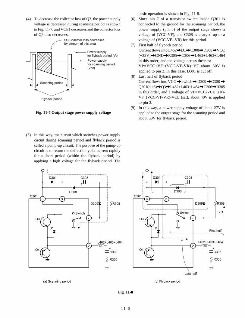
1 1 - 5
(4) To decrease the collector loss of Q3, the power supplyvoltage is decreased during scanning period as shownin Fig. 11-7, and VCE1 decreases and the collector lossof Q3 also decreases.
Fig. 11-8
basic operation is shown in Fig. 11-8.(6) Since pin 7 of a transistor switch inside Q301 is
connected to the ground for the scanning period, thepower supply (pin 3) of the output stage shows avoltage of (VCC-VF), and C308 is charged up to avoltage of (VCC-VF--VR) for this period.
(7) First half of flyback periodCurrent flows into L462 D1 C308 D308 VCC(+35V) GND R305 C306 L462+L463+L464in this order, and the voltage across these is:VP=VCC+VF+(VCC-VF-VR)+VF about 50V isapplied to pin 3. In this case, D301 is cut off.
(8) Last half of flyback periodCurrent flows into VCC switch D309 C308 Q301(pin3) Q3 L462+L463+L464 C306 R305in this order, and a voltage of VP=VCC-VCE (sat)-VF+(VCC-VF-VR)-VCE (sat), about 40V is appliedto pin 3.
(9) In this way, a power supply voltage of about 27V isapplied to the output stage for the scanning period andabout 50V for flyback period.
Q3 Collector loss decreasesby amount of this area
Power supplyfor flyback period (Vp)
Power supplyfor scanning period(Vcc)
Scanning period
Flyback period
Fig. 11-7 Output stage power supply voltage
(5) In this way, the circuit which switches power supplycircuit during scanning period and flyback period iscalled a pump-up circuit. The purpose of the pump-upcircuit is to return the deflection yoke current rapidlyfor a short period (within the flyback period) byapplying a high voltage for the flyback period. The
6 3
7
2
6 3
7
2
D301 C308
D308
Q301
D309 R308
Switch
Q3
Q4
D1
L462+L463+L464
C306
R305
D301 C308
Q301
D309 R308
Q3
Q4
D1
L462+L463+L464
C306
R305
Switch VR
Last half
(a) Scanning period (b) Flyback period
First half
+
D308
+

1 1 - 6
2-4. V Linearity Characteristic Correction
2-4-1. S-character Correction(Up-and Down-ward Extension Correction)
A parabola component developed across C306 is integratedby R306 and C305, and the voltage is applied to pin 6 ofQ302 to perform S-character correction.
2-4-2. Up-and Down-ward Linearity BalanceA voltage developed at pin 2 of Q301 is divided withresistors R307 and R303, and the voltage is applied to pin6 of Q301 to improve the linearity balance characteristic.Moreover, the S-character correction, up- and down-wardbalance correction, and M-character correction are alsoperformed through the bus control.

1 1 - 7
3. PROTECTION CIRCUIT FOR VDEFLECTION STOP
Fig. 11-9
When the deflection current is not supplied to the deflectioncoils, one horizontal line appears on the screen. If thiscondition is not continued for a long time, no trouble willoccur in a conventional TV. But in the projection TV, all theelectron beams are directly concentrated at the fluorescentscreen because of no shadow mask used, and burns out thescreen instantly.To prevent this, the stop of the V deflection is detected whenthe horizontal one line occurs, and the video signals areblanked out so that the electron beams are not emitted.When the V deflection circuit is operating normally, asawtooth wave voltage is obtained across (R305), so Q350repeats on-off operation in cycle of V sync. In this case, thecollector voltage of Q35 is set to develop less than (12V-VBE
(Q351)) with R352 and C350 as shown in Fig. 4-8.Accordingly, Q351 and Q353 are continuously turned on. Asa result, diode D354 is turned off, giving no influence on theblanking operation.Next, when the V deflection stops, the voltage across (R305)does not develop, so Q350 turns off, and both the Q351 andQ353 are turned off. Then, the picture blanking terminal pin13 of ICA05 is set to high through R354 and D354 connectedto 90V power line, BLANKING CIRCUIT ON thus cuttingoff the projection tubes.
Volttage AcrossR305
Q350 BASE
Q351 Collector
Q340 VBE
12V-VBE (Q341)
Fig. 11-10
C306
2
L462+L463+L464
R350R3050.82
Q350
R354
C350
D350
Q351
12V
D354
D353
BLANKINGCIRCUIT
R352
9V
Q353
Q301
VERTICAL DEFLECTION COILS
V-NF
DPC CIRCUIT
V-STOP
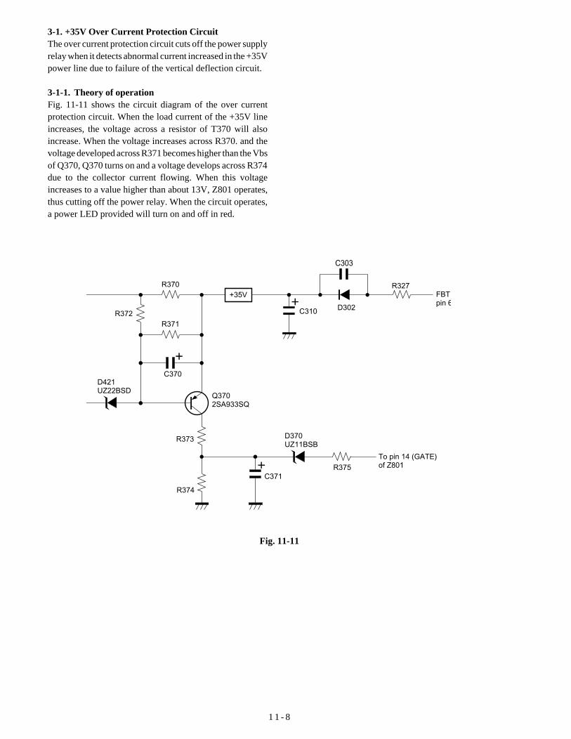
1 1 - 8
3-1. +35V Over Current Protection CircuitThe over current protection circuit cuts off the power supplyrelay when it detects abnormal current increased in the +35Vpower line due to failure of the vertical deflection circuit.
3-1-1. Theory of operationFig. 11-11 shows the circuit diagram of the over currentprotection circuit. When the load current of the +35V lineincreases, the voltage across a resistor of T370 will alsoincrease. When the voltage increases across R370. and thevoltage developed across R371 becomes higher than the Vbsof Q370, Q370 turns on and a voltage develops across R374due to the collector current flowing. When this voltageincreases to a value higher than about 13V, Z801 operates,thus cutting off the power relay. When the circuit operates,a power LED provided will turn on and off in red.
Fig. 11-11
R372
R370
R371
C370
Q3702SA933SQ
D421UZ22BSD
R373
R374
+35V
C310 D302
C303
R327FBTpin 6
C371
D370UZ11BSB
R375
To pin 14 (GATE)of Z801

12-1
SECTION XIIHORIZONTAL DEFLECTION CIRCUIT

12-2
1. OUTLINE
The H deflection circuit works to deflect a beam from left toright by flowing a sawtooth waveform of 15.734 kHz into theDY H deflection coil.
2. HORIZONTAL DRIVE CIRCUIT
The H drive circuit works to start the H output circuit byapplying HVCC (Q501 DEF power source) to pin 22 of Q501(TA1222N) and a bias to the H drive transistor Q402 at themain power on.
2-1. Theory of Operation(1) When the power switch is on, the main power supply of
125V starts to rise. At the same time, AF power supply25V also rises.
(2) With 25V line risen, Q430 base voltage which is createdby dividing the audio power with R433 and D430 alsorises. Then, the transistor Q430 turns on and the HVCCis applied from the audio power line through R432 andD431 to pin 22 of Q501.
Fig. 12-1 H drive circuit block diagram
81 81 22
R432 Q430 D431
R433D430
BB80
BB81
L400
SIGNAL C431 C430
H Vcc
Q501

12-3
3. BASIC OPERATION OF HORIZONTALDRIVE
A sufficient current must flow into base of the horizontaloutput transistor to rapidly make it into a saturated (ON)condition or a cut off (OFF) condition. For this purpose, adrive amplifier is provided between the oscillator circuit andthe output circuit to amplify and to waveshape the pulsevoltage.
3-1. Theory of Operation(1) The horizontal drive circuit works as a so called switching
circuit which applies a pulse voltage to the outputtransistor base and makes the transistor on when thevoltage swings in forward direction and off in reversedirection.
(2) To turn on the output transistor completely and to makethe internal impedance low, a sufficiently high, forwarddrive voltage must be applied to the base and heavy basecurrent ib must be flown. On the contrary, to completely
turn off the transistor, a sufficiently high, reverse voltagemust be applied to the base.
(3) When the transistor is on (collector current is maximum)condition with the sufficiently high forward voltageapplied to the base, the transistor can not be turned offimmediately, if a reverse base bias is applied to the basebecause minority carriers storaged in the base can not bereduced to zero instantly. That is, a reverse currentflows through an external circuit and gradually reducesto zero. The time lag required for the base current todisappear is called a storage time and falling time.
(4) To shorten the storage time and the falling time, asufficiently high reverse bias voltage must be applied toallow a heavy reverse current to flow. This operationalso stabilizes operation of the horizontal outputtransistor.
Fig. 12-2
(a)
ib
V
+
0
-
+
0
-
On period OFF period
t Input waveform (b)
t Base current (c)
Forwardcurrent
Reversecurrent
Fallingtime
Storagetime

12-4
3-2. Drive System3-2-1. ON drive systemWhen the drive transistor is on, the horizontal output transistoralso turns on.
Merit:• The base current can be precisely controlled without
being affected by variation of pulse width which iscaused by the horizontal oscillator circuit and the drivecircuit.
Demerit:• It is difficult to flow a reverse bias current to the horizontal
output transistor to eliminate its storage carrier for transientperiod of on to off period for the horizontal outputtransistor.
3-2-2. OFF drive systemWhen the drive transistor is on, the horizontal output transistoris off.
Merit:• Energy balance between on and off periods of the drive
circuit is better, and the circuit can be simplified.• Reverse base current of the horizontal output transistor
can be controlled easily.
Demerit:• Base-emitter forward current flowing into the horizontal
output transistor is susceptible to on-period variation ofthe drive transistor.
H OSC
H driver
H output
ON(OFF)
ON(OFF)
+B
H OSC
H driver
H output
ON(OFF)
ON(OFF)
+B
Fig. 12-3 Fig. 12-4

12-5
3-3. Circuit DescriptionIn the N5SS chassis, the off drive system is employed.(1) When Q1 inside Q501 is turned on, Q402 base is
forward biased through 9 V pin 22 of Q501 (H.VCC) pin 23 of Q501 (H. Out) R411/R410 resistordivider, and then, Q402 collector current flows through125V R416 T401. In this case, the H outputtransistor Q404 turns on with the base-emitter reversebiased because of the off drive system employed.
(2) On the contrary, when Q1 inside IC501 is off (pin 8 is0V), base-emitter bias of Q402 becomes 0V and Q402turns off, and a collector pulse as shown in Fig. 12-5develops at the collector.The voltage is stepped down and Q404 is forwardbiased with this voltage, thus turning on Q404.
(3) In this way, by stepping down the voltage developed atprimary winding of the drive transformer and by applyingit to Q404, a sufficient base current flows into Q404base, thereby switching the Q404.
Fig. 12-5
Q501
22
23
1 3
2 4
Q1
H. Vcc
C431
R410
R411
9V
Q402H drive
transistor
C417
R415
T401H drive
transistor
Q404H outputtransistor
V1V2
0V
0V
VCP
Q402OFF
Q402ON
R416
C416
+125V
C413
+

12-6
4. HORIZONTAL OUTPUT CIRCUIT
The horizontal output circuit applies a 15.734 kHz sawtoothwave current to the deflection coil with mutual action of thehorizontal output transistor and the damper diode, and deflectsthe electron beam from left to right in horizontal direction.
Fig. 12-6
IC501
H. out
Q1 23 83
10
5
2
3
1
HV
8
S-charactorcapacitor
Hlinearity
coil
Resonatcapacitor
Diode modulator circuit
To DPC output
SIGNAL DEF/POWER PCBPCB
TP-33
BB81
R411
R410
C413
C416R416
125V
Q402H drive
R415
C417
T401H drive
transformer
Q404H output
(With damper diode)
T461FBT
Deflection yoke(H coil)
C463
D461
C444
C440
C423
C467
L441
R441
+
C464
+
L461
C343D444
C418
D443
L462 L463 L464
To High VoltageRegulator Circuit

12-7
4-1. Theory of Operation4-1-1. Operation of Basic Circuit(1) To perform the horizontal scanning, a 15.734 kHz
sawtooth wave current must be flown into the horizontaldeflection coil. Theoretically speaking, this operationcan be made with the circuit shown in Fig. 12-7 a and b.
(2) As the switching operation of the circuit can be replacedwith switching operation of a transistor and a diode, thebasic circuit of the horizontal output can be expressedby the circuit shown in Fig. 12-7 a. That is, the transistorcan be turned on or off by applying a pulse across thebase emitter. A forward switching current flows for on-period, and a reverse switching current flows throughthe diode for off-period. This switching is automaticallycarried out. The diode used for this purpose is called adamper diode.
Description of the basic circuit1. t1~t2:A positive pulse is applied to base of the output transistorfrom the drive circuit, and a forward base current is flowing.The output transistor is turned on in sufficient saturationarea. As a result, the collector voltage is almost equal to theground voltage and the deflection current increases fromzero to a value in proportionally. (The current reachesmaximum at t2, and a right half of picture is scanned up to thisperiod.)
2. t2:The base drive voltage rapidly changes to negative at t2 andthe base current becomes zero. The output transistor turnsoff, collector current reduces to zero, and the deflectioncurrent stops to increase.
3. t2~t3:The drive voltage turns off at t2, but the deflection currentcan not reduce to zero immediately because of inherentnature of the coil and continues to flow, gradually decreasingby charging the resonant capacitor C0. At the same time, thecapacitor voltage or the collector voltage is graduallyincreases, and reaches maximum voltage when the deflectioncurrent reaches zero at t3. Under this condition, all electro-magnetic energy in the deflection coil at t2 is transferred tothe resonant capacitor in a form of electrostatic energy.
4. t3~t4:Since the charged energy in the resonant capacitor dischargesthrough the deflection coil, the deflection current increasesin reverse direction, and voltage at the capacitor graduallyreduces. That is, the electrostatic energy in the resonantcapacitor is converted into a electromagnetic energy in thisprocess.
5. t4:When the discharge is completed, the voltage reduces tozero, and the deflection current reaches maximum value inreverse direction. The t2~t4 is the horizontal flyback period,and the electron beam is returned from right end to the leftend on the screen by the deflection current stated above. Theoperation for this period is equivalent to a half cycle of theresonant phenomenon with L and C0, and the flyback periodis determined by L and C0.
Fig. 12-7
a H output basic circuit
b H output equivalent circuit
H outputtransistor
D Co L
DeflectionyokeResonant
capacitor
Damperdiode
Vcc
Vcc
SW1 SW2 Co L

12-8
6. t4~t6:For this period. C0 is charged with the deflection currenthaving opposite polarity to that of the deflection currentstated in "3.", and when the resonant capacitor voltageexceeds VCC, the damper diode D conducts. The deflectioncurrent decreases along to an exponential function(approximately linear) curve and reaches zero at t6. Here,operation returns to the state described under "1.", and theone period of the horizontal scanning completes. For thisperiod a left half of the screen is scanned.In this way, in the horizontal deflection scanning, a currentflowing through the damper diode scans the left half of thescreen; the current developed by the horizontal outputtransistor scans the right half of the screen; and for theflyback period, both the damper diode and the output transistorare cut off and the oscillation current of the circuit is used.Using the oscillation current improves efficiency of thecircuit. That is, about a half of deflection current (one fourthin terms of power) is sufficient for the horizontal outputtransistor.
Fig. 12-8
A
B
C
D
E
F
G
H
t1 t2 t3 t4 t5 t6
0
0
0
0
0
0
0
0
TRbase voltage
TRbase current
TRcollector current
Ddampercurrent (SW2)
Switchcurrent(TR, SW1)
Resonantcapacitorcurrent (Co)
Deflectioncurrent (Lo)
TRcollectorvoltage

12-9
q 2 q 1
t2 t1
t2 = t1
q 2 q 1<q 2 q 1
t2 t1
t2 > t1
q 2 q 1=
(a) S-character correction (b)
Fig. 12-9
TRD Co
Cs
LH
Deflection coil
(a) H output circuit
(b) Sawtooth wave current
(c) Voltage across LH Fast deflection
Slow deflection
(d) Synthesized current
Vcc
Fig. 12-10
Amplitude CorrectionTo vary horizontal amplitude, it is necessary to vary asawtooth wave current flowing into the deflection coil.These are two methods to vary the current; a method whichvaries LH by connecting a variable inductance L in series withthe deflection yoke, and a method which varies power supplyvoltage (across S-character capacitor) for the deflectionyoke.As the DPC circuits is used in the this chassis, the latermethod which varies the deflection yoke power supplyvoltage by modifying the bus data is used.
4-1-2. Linearity Correction (LIN)(1) S-curve Correction (S Capacitor)Pictures are expanded at left and right ends of the screen evenif a sawtooth current with good linearity flows in the deflectioncoil when deflection angle of a picture tube increases. This isbecause projected image sizes on the screen are different atscreen center area and the circumference area as shown inFig. 12-9. To suppress this expansion at the screencircumference, it is necessary to set the deflection angle q1
to a large value (rapidly deflecting the electron beam) at thescreen center area, and to set the deflection angle q2 to asmall value (scanning the electron beam slowly) at thecircumference area as shown in Fig. 12-9.In the horizontal output circuit shown in Fig. 12-10, capacitorCS connected in series with the deflection coil LH is to blockDC current. By properly selecting the value of CS and bygenerating a parabolic voltage developed by integrating thedeflection coild current across the S capacitor, and by varyingthe deflection yoke voltage with the voltage, the scanningspeed is decreased at beginning and end of the scanning, andincreased at center area of the screen. The S curve correctionis carried out in this way, thereby obtaining pictures withgood linearity.
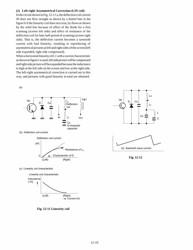
12-10
(2) Left-right Asymmetrical Correction (LIN coil)In the circuit shown in Fig. 12-11 a, the deflection coil currentiH does not flow straight as shown by a dotted line in thefigure b if the linearity coil does not exist, by flows as shownby the solid line because of effect of the diode for a firstscanning (screen left side) and effect of resistance of thedeflection coil for later half period of scanning (screen rightside). That is, the deflection current becomes a sawtoothcurrent with bad linearity, resulting in reproducing ofasymmetrical pictures at left and right sides of the screen (leftside expanded, right side compressed).When a horizontal linearity oil L1 with a current characteristicas shown in figure c is used, left side picture will be compressedand right side picture will be expanded because the inductanceis high at the left side on the screen and low at the right side.The left-right asymmetrical correction is carried out in thisway, and pictures with good linearity in total are obtained.
(a)
(b) Deflection coil current
Deflection coil current
(iH)
0 Characteristic of D
Resistance of LH
(c) Linearity coil characteristic
Linearity coil characteristic
Inductance(m H)
(Left) (Right)
(Left) (Right)Current (A)
TRD Co
LH
Deflectioncoil
FBT
VcciH Li
CsS-charactercapacitor
Fig. 12-11 Linearity coil
Fig. 12-12
TRD Co
LH
LI
L
CCs
(b) Sawtooth wave current

12-11
4-2. White Peak Bending Correction Circuit4-2-1. OutlineWhite peak area in screen picture may sometimes causebending in picture. See figure below.In TP48E60 series, correction signal which consists of videosignal and video ripple in video output circuit power supply200V is input to pin 24 (Bending correction terminal) ofQ501. This corrects white peak bending.
4-2-2. Operation theoryFig. 12-13 shows circuit diagram. From R, G and B output(pins 41, 42 and 43 of Q501), video signal is taken in thedividing ratio of resistor R375 and R378. After that, it suffersDC cut by C360 and integration by R369 and C415, then isinput to pin 24 of Q501. On the other hand, video ripple invideo output circuit power supply 200V suffers DC cut byC475, and is inverted in Q470, then input to pin 24 of Q501via C481. Pin 24 of Q501 is a bending correction terminal.The voltage which is applied to this terminal, controls phaseof video signal to correct white peak bending.
Fig. 12-13 White peak bending correction circuit
Q501
R OUT 43
42
41
G OUT
B OUT
R360
R364
R365
24Bending correction
terminal
EHT
C415
R366
Q360
Integration
R367Q361 Q362
R375
9V
R378
R368
C360 R369
93Receiving Board
Power, Def board
BB91
C481 Inversion
Q470
R481
R482
D470
R483
R484 D474
R478
C475
C466
D406
200V9V
White peak
Bending by white peak
T4163

12-12
4-3. H Blanking4-3-1. OutlineThe H blanking circuit applies a blanking precisely for thehorizontal flyback period so that undesirable pictures foldingdoes not appear at screen ends.This unit allows the users to adjust an horizontal amplitudeadjustment, so, picture quality at screen ends will be improved.This is one of the purposes of the blanking circuit.
4-3-2. Theory of OperationThe H blanking circuit determines the flyback period preciselyfrom the AFC pulse in the FBT and applies the period toemitter of the video output stage transistor on the CRT-D PCboard.
4-3-3. Circuit OperationAs can be seen from Fig. 12-14, the flyback period of theAFC pulse in the FBT starts at a negative side from 0V. Todetects this, the DC component is cut with C493. This is,C493 is always charged through D487 with a negative side(about -17V) of the AFC pulse. As a result, a voltage at pointA in the waveform rises from the ground level. This waveformis sliced in a circuit (R410, C492, D486) to detect the flybackperiod. Thus obtained voltage is applied to Q901, Q903, andQ905 through D912 ~ D914 and cuts off them therebyblanking the resters.
0V
Approx.-17V AFC Pulse
Q487ON period
D486Slice level
Waveform atpoint
Fig. 12-14
Fig. 12-15
T461 (FBT)AFC
7
APoint
C493
C449
R405
R445D441
AFC
D487
R409
C492
R410
D486R417
R438V blanking
Q488
Q489
164
164
P405
P903
R906
+27V
Q487
D912
D913
D914
Q905
Q903
Q901
CRT-D DCB
Deflection/Power PCB
12-13
4-4. 200V Low Voltage Protection4-4-1. OutlineCPT. To prevents this, a 200V low voltage protection circuitis provided.
4-4-2. Theory of OperationFig. 12-16 shows a connection diagram.Under a normal condition Q340 is always on because ofabout 210V supplied from the 200V line. Accordingly Q340collector is kept at about 6.2V or the zener voltage of D341and Q341 is turned off.If some abnormality occurs and 200V line voltage lowers byless than about 160V. Q340 turns off and its collector voltagerises. So Q341 turns on. With Q341 turned on the voltage atpin 14 of Z801 (expander) exceeds a threshold voltage andpin 16 of Z80 is high level and makes the power relay turn off.
CRT-D Circuit Defletion circuit
200V 1 1
2 2
P405
R347
P310A
Z801
14
16
GATE PROTECTOR
VL
VQ
VL
VQ
V circuit
P310BR389 R390
-12V
Q340
Q341
D340
R391D341 R392 C340
Fig. 12-16

12-14
10
9
4
7
6
3
2
1
5
Auxiliarywinding
Primarywinding
AFCblanking
Heater
+27V
-27.5V
+210V
+125V
C310
C303
D302
C460D460
R327
R469
D406
C446
C448
Q404
C463
T401
CRTanode
ABL
H deflection coilL462/L463/L464
R441
C423
L441
01000VP-P
1H(15.75KHz)
R444
R443
Focus Pack
D408C447
R448+12V
5. HIGH VOLTAGE GENERATIONCIRCUIT
The high voltage generation circuit develops an anode voltagefor the picture tube, focus, screen, CRT heater, video output(210V) and so on by stepping up the pulse voltage developedfor flyback period of the horizontal output circuit with theFBT, and supplies the power to various circuit.
5-1. Theory of Operation
Fig. 12-17

12-15
Fig. 12-18
Fig. 12-20
+125V
0
Fig. 12-19
10
4
7
6
2
1
0
0
0
For +12V
+35V
5-1-1. +210VFor the flyback period, pulses are stacked up to DC +125Vwith FBT, and the voltage is rectified by D406 and filtered byC446.
5-1-2. +35V, 12VPin 4 of the FBT is grounded and the shaded area of negativepulse developed for opposite period of the flyback period isrectified, thus developing better regulation power supply.
5-1-3. -27VAs a power for the DPC circuit, a negative pulse signal isrectified by D460 and filtered with C460, thus developing the-27V.
5-1-4. High voltageSingular rectification system which uses a harmonics non-resonant type FBT is employed and a better high voltageregulation is obtained, so amplitude variation of picturesbecomes low.
G
FE
D
C
B
A
E
DC
BA
G
FPrimary
Auxiliary
Picturetube anode
EO
ABL
EH
Pulse
Stackedpulse of4 block
1H15.735KHz
Picturetube capacitor

12-16
Flybackpulse
63.5m s AC0
AC0
AC0
Referencewave45 KHz
Harmonics15 times675 KHz
Tunedwaveform
11m s
20m s
1 122m s 22x10-5
= = 45KHz
Becomes 45 KHz x 15 = 675KHzthis is determined by coil inductance capacitance and stray of FBT.
(In case of 3X) (In case of 15X)
Hightvoltage
Focuscurrent
Picture tube current
E E
In case of 15 times the harmonics as compared with 3 times the harmonics, average conduction peiod of the high voltage diode is wider.As a result, high voltage variations are suppressed.
Fig. 12-21 Tuned waveforms
5-2. Operation Theory of the Harmonic Non-ResonantSystem and Tuned Waveforms
The high voltage coil is of film multi-layer winding type andthe coils are isolated into seven blocks. Each block is connectedthrough a diode.The basic operation is described in the case of 4 blocksconstruction for simplification. Positive or negative pulsedetermined by stray capacitance of each coil develops at
terminal points ( , , , , , F , G ) of each coilas shown in Fig. 12-20, and these pulses are stacked asshown, thus developing the high voltage.Moreover, a capacitance between the internal and externalcoatings of the picture tube works as a smoothing capacitor.Focus voltage is obtained at point EO.The FBT is turned to a harmonic of 15 times the fundamentalfrequency, and the turned waveform is shown in Fig. 12-21.

12-17
6. HIGH VOLTAGE CIRCUIT
6-1. High Voltage Regulator6-1-1. OutlineGenerally, four kinds of methods exist to stabilize a highvoltage in high voltage output circuits using the FBT:(1) Stabilization by varying the power supply voltage.(2) Stabilization by varying L value with a saturable
reactance connected in series with the primary windingof the FBT.
(3) Stabilization by varying equivalent capacitance of theresonant capacitor C0.
(4) Stabilization by superimposing a DC or pulse (thisvaries the high voltage) on a lower voltage side of thehigh voltage winding of the FBT.
In this unit, pulse transformer is eliminated and the regulatorcircuit using the method (3) is employed. The block diagramis shown in Fig. 12-22.
Hotizonaloutput DY
FBT ANODE
125V
PW output
-27V
High voltage Reg.
V.Ref.
Fig. 12-22 Basic circuit for high voltage regulator emplyed in the unit

12-18
Fig. 12-23
6-1-2. Theory of OperationFig 12-23 shows a basic circuit of the high voltage regulatorused in the unit.The high voltage regulator circuit splits a resonant capacitorC0 to C1 and C2. thereby dividing the collector voltage (VCP)of the H output transistor with C1 and C2.Here, assume each voltage developed across C1 and C2 asVCP1 and VCP1, respectively,
VCP1 =
C2 VCP
C1+C2
VCP2 =
C2 VCP
C1+C2
VCP = C2
VCP2 C1+C2
each relation can be expressed by the above equations~ .
The VCP2 developed across C2 is DC-clamped with a diodeD1 and the resultant voltage is smoothed with a diode D2 anda capacitor C3. Thus processed voltage is obtained at thepoint . This voltage is used to provide a base current for thetransistor Q1 or to flow the collector current. The voltage atthe point decreases with the circuit impedance and finallylowers up to a VCE saturation voltage of Q1.Then, VCP2 is not clamped by D2 with the voltage at the pointB. Since the VCP is expressed as a sum of VCP1 and VCP2 asshown by equation , VCP decreases by amount the VCP2 isdecreased. This varies the high voltage.Q1 collector current is controlled by Q1 base current whichis an output of the comparison inverted amplifier. That is, theQ1 base current is controlled by a voltage obtained bycomparing a detection voltage of the top breeder of the FBT(9.1V) and a DC voltage of 9V.
Fig. 12-24
VCP = VCP1 + VCP2
VCP 1
VCP 2..
Horizontaloutput C1 LH
FBTLP
BD1
C2
C3
D2
Q1 High voltageReg.output amp
CS +B
12-19
6-1-3. ActualFig 12-25 shows the actual circuit used in the unit.A resonant capacitor C0 is also split into two capacitors C443and C444 in this circuit. The high voltage regulator cirucitsis structured by splitting the C443 to two capacitors of C443and C448.Here, assume a high voltage increases and the detectionvoltage ED´ obtained by dividing the high voltage alsoincreases in proportional to the high voltage. This makes thevoltage ED increase at pin 7. (The voltage is impedancetransformed by a voltage follower circuit consisting of opamplifier Q483 at pin 7.)The voltage ED and a 9V reference voltage developed by a 3-terminal regulator Q420 are compared. When the ED increases,the voltage at pin 2 of Q483 differential amplifier alsoincreases, and the base current IB of the high voltagetransistor Q480 increases.
As a result, Q480 collector current increases and Q480collector voltage (at the point ) decreases. Then, a peakvalue of VCP2 across C418 is clamped by the diode D443 atthe collector voltage lowered, and the collector voltage VCP
of Q404 (H output transistor) obtained as a sum of the voltageVCP1 across C443 and VCP2 across L418 decreases. Then, thehigh voltage also decreases.When the high voltage lowers, the corrective operation iscarried out in reverse order.* Resustors R451, R452, R453 and R455 are used to correct
undersirable influence (H amplitude increase at minimumIH) by the H amplidude regulator.
Horizontaloutput
Q404 C443
C444CS
L462
D461
C467
L461R463
C440-27V
C464
Q460
R466
R461/R469
R460
Q462 R455
125V
R454
R453R452R451BD443
C418
D444
C419 Q480R434
R431 R492
23
4
R488
C483 R494 R439
R487
Q420
9V
86
7
ED
Q483C482
R435
ED'
FBT EH
R489
R450
R490
Fig. 12-25 Actual high voltage regulator circuit

12-20
15
16
12
13 9
5V
12VMICOMQA01#7
RELAYSR81
Q843 QB30
RB30
R9
R10
R21
R12
R25 R472 T461
D471R26
R20
D3ZD6
C471
Tr10Tr7 Tr9
Tr6
Tr5
C474
C1
R11
R22
ED
+
Z801
Fig. 12-26 X-RAY protection circuit
7. X-RAY PROTECTION CIRCUIT
7-1. OutlineIn case picture tube using high voltage, when high voltagerises abnormally due to components failure and circuitmalfunction, there is possible danger that X-RAY leakageincreases to affect human body. To prevent it, X-RAYprotection circuit is equipped.
7-2. OperationFigure 10-18 shows the circuit diagram. Supposing highvoltage rises abnormally due to some reason, pulse at pin 9of T461 also rises, and detection voltage Eb rectified byD471 and C471 in X-RAY protection circuit rises. When Ebrises, emitter voltage of Tr10 divided by R25 and R26 inprotector module becomes higher than [zener voltage (6.2V)of ZD6 + Tr10 VBE ]. This causes Tr10 turns on to supplybase current to Tr9. Then Tr9 turns on. By this Tr6 and Tr6turn on to make ON/OFF pulse at pin 7of QA01 in low level,QB30 and Q843 turns off, then relay SR81 turns off. Tr6 andTr7 are in thyristor-connection, and 5V of power holdsprotection operation until main power switch is turned off.During circuit operation, power LED near main powerswitch blinks turn on and off in red.Caution : To restart TV set, repair failure first.

12-21
Fig. 12-27 Over current protection circuit
8. OVER CURRENT PROTECTIONCIRCUIT
8-1. Outline If main power (125V) current increases abnormally due tocomponents failure, there is possible danger of the secondarydamage like failure getting involved in other part failure, andabnormal heating. To prevent this, over current protectioncircuit is equipped, which detects current of main B line toturn off power relay in abnormal situation.
8-2. OperationFig. 12-27 shows over current protection circuit. When thecurrent of main B line increases abnormally due to theshortage in load of main B line, voltage drop arises acrossR470. By this voltage drop, when base-emitter voltage of Tr8 in protector module (Z801) becomes appprox. 0.7V ormore, Tr 8 turns on, and the voltage by divided ratio of R15and R16 is applied to cathode of ZD4. When this voltagebecomes higher than zener voltage of ZD4, ZD4 turns on tosupply base current to base of Tr 6 via R14. This causes Tr 5ON and voltage at pin 16 of Z801 becomes Low. Therefore,QB30 and Q843 turns off to set SR81 OFF. Tr 6 and Tr 7 inZ801 are in thyristor- connection, and power 5V-1 suppliedat pin 15 keeps protection operation for standby power untilmain power switch is turned off. During circuit operation,power LED near main power switch blinks in red.Caution : To restart TV set, repair failure first.
16
15
17
2 1
5V
MICONQA01#7
RELAYSR81
Q843
RB30
QB30
MAIN B
R470 F470
To T461
R479 R471
C472
R16
R15R14
R12
R11
R9
R10ZD4
C1
Tr6
Tr5
Tr7Tr8
D1
Z801PROTECTOR MODULE

12-22
NOTES

13-1
SECTION XIIIDEFLECTION DISTORTION
CORRECTION CIRCUIT(DPC Circuit)

13-2
1. DEFLECTION DISTORTIONCORRECTION IC (TA8859P)
1-1. OutlineThe deflection distortion correction IC (TA8859AP), incombination with a V/C/D IC (TA1222N) which has a Vpulse output, performs correction for various deflectiondistortions and V output under I2C bus control. All the I2Cbus controls are carried out by a microcomputer and can becontrolled with the remote control.
1-2. Functions and FeaturesThe IC has functions of V RAMP voltage generation, Vamplitude automatic switching (50/60 Hz), V linearitycorrection, V amplification, EHT correction, side pincushioncorrection, I2C bus interface, etc. and controls followingitems through the I2C bus lines.(1) V amplitude(2) V linearity
(3) V S-character correction(4) V picture position (neutral voltage setting)(5) V M-character correction(6) V EHT correction(7) H amplitude(8) L and R pin-cushion distortion correction I (entire
area)(9) L and R pin-cushion distortion correction II (corner
portions at top and bottom)(10) H trapezoid distortion correction(11) H EHT correction(12) V AGC time constant switching
1-3. Block DiagramFig. 13-1 shows a block diagram of the basic circuit.
V. Trigger-in
(Bus Control Signal) SDA SCL
10
9
12
13
14 15 16 5 3
2
4168
+12V
Control ThroughBus
EW-Drive
V Drive V. Feedback EHT INPUT EW Feedback
WaveformShape
TriggerDet
PuiseGen.
V. Rame A G CV. AGC TimeConstant SW
H. Trapezoid DistortionCorrection
L-R PincushionDistortion Correction I
L-R PincushionDistortion Correction II
(Top & Bottom Comer Section)
H.EHTCorrction
H. AmplitudeAdj.
H.EHTInput
V. EHTCorrection
V. ScreenPosition
V. AmplitudeAdj.
V. M-CharacterCorrection
V. LinearityCorrection
V. S-CharacterCorrection
Logic
Fig. 13-1

13-3
2. DIODE MODULATOR CIRCUIT
Fig. 13-2 shows a basic circuit of the diode modulator usedin the N5SS chassis.A key point in the modulation circuit shown in Fig. 13-2 isthe development of a negative pulse at point B.In this circuit, a current loop of the resonant circuit forflyback period is shown by an arrow, and the energy storedin LDY is transferred to resonant capacitors Cr, Crm inpassing through Cr, Crm, Cs when the scanning completes.As a result, a positive, horizontal pulse as shown in Fig.13-3 will appear at Cr, and the current flows into Crmwith the direction as shown. Then a pulse as shown in Fig.13-3 develops at the point B.On the other hand, since constant amplitude pulses across
Cr, as shown in Fig. 13-3, are applied to the primarywinding, the high voltage of the FBT is also constant.
When the negative pulse developed at point B is integratedwith Lm and Csm, the average value appears at Csm as anegative voltage.
By modulating this voltage to have a parabolic curve withQ460, a waveform of Vm is obtained as shown in Fig. 13-4. As a result, the voltage Vs which is the sum of the powersupply voltage VB and Vm, is applied across the S-curvecapacitor Cs. Vs becomes a power source for the deflectionyoke, and the modulated parabolic waveform, as shown inFig. 13-3 , is applied to the horizontal deflection yokeand corrects the left-right pin-cushion distortion.
Fig. 13-2 Fig. 13-3
Fig. 13-4
VS
VB
0
A
B
HOUT
DD Cr
DM
LDY
FBT
VBCs Vs
Crm Csm
Q460 Vm
Lm a) Waveform at point A
b) Waveform at point B
0
0

13-4
3. ACTUAL CIRCUIT
In the actual circuit, the resonant capacitor is split into twoas shown in Fig. 13-7. One, C440, is inserted between thecollector of the H. OUT transistor and ground. The secondone, C444, is inserted between the collector and emitter. InFig. 13-5, C440 is expressed as C1 and C444 as C2, and theresonant current path for the flyback period is shown byarrows.
In a conventional circuit, when the brightness of a picturetube varies, high voltage current and high voltage also vary.As a result, horizontal amplitude is affected.
However, in this circuit, the horizontal amplitude variationcan be suppressed to near zero if the high voltage currentvaries with variation of the high voltage.
When the scanning period completes, the energy stored inthe deflection yoke LDY is transferred to the resonantcapacitor in a form of current Iy. In this case, the current issplit into two; Iy1 passing through C1, C3 and Iy2 passingthrough C2. In the same way, the energy stored in theprimary winding of the FBT is transferred to the resonantcapacitor in the form of Ip. In this case, the current (path) isalso split into two; Ip1 passing through C1 and Ip2 passingthrough C2, C3. Concequently, the current differencesbetween Iy1 and Ip2 (Iy1-Ip2) passes through C3.
When the high voltage current IH reduces with a darkpicture, the current Ip in the primary circuit decreases, soIp1 and Ip2 also decrease. However, a current flowing into(Iy1-Ip2) increases as Ip2 decreases. As a result, the pulsedeveloping at the point B increases and the voltage Vm atCsm also increases as shown in Fig. 13-8. That is, when adark picture appears, the voltage across S-curve capacitorCs increases as shown in Fig. 13-8, the high voltage rises,and the horizontal amplitude is going to decrease. But, as Vsincreases, the deflection yoke current increases and thisworks to increase the horizontal amplitude. Accordingly, ifthe brightness of a picture changes, the horizontal amplitudeis maintained at a constant value.
Fig. 13-6
VS
VB
0
Fig. 13-5
FBT
IH
VB
VmCsm
C3
VSCS
Lm
C2
IP2
IY1
IY1
C1
IY
IP2IP1
LDYH.OUT
IP

13-5
3-1. Basic Operation and Current Path3-1-1. Later Half Scanning Period
When the power is turned on, the power supply voltage VBis applied to Cs and Csm, and the Cs acts as a power sourcefor a later half of the scanning period for which the H. OUTtransistor is turned on, and the deflection current Iy flows inthe path as shown below
3-1-2. First Half Scanning PeriodWhen the base drive current decreases and the H. OUTtransistor is turned off, each of the energies stored in LDY,Lm, Lp of FTB is transferred to C1, C2 and C3, respectively,and the resonant current becomes zero at a center of theflyback period. Then, VA and VB pulses show a maximumamplitude.
H.OUT
VA
FBT
LDY
lP
Cs
VB
VB
DM
IM LM
IDC
CSM+
IY
+
Fig. 13-7
Fig. 13-10
Voltage & current waveform in H period.
IY
VA
0
0
0
0
IDC
IM
VB
Fig. 13-8
IY
VA
0
0
0
0
IDC
IM
VB
0C1
C2
0C3
C1: IY1+IP1
C2: IY2+IP2
C3: IP2-IY1-IM
Fig. 13-9
VA
FBT
LDY lP
Cs
VBVB
IM LM
IDC
CSM
IY
IY2IP2
C2C1IP1

13-6
3-1-3. Later Half of Flyback PeriodAll energy in the coil has been transferred to the resonantcapacitors at the center of the flyback period, and thevoltage shows the maximum value. However, during nexthalf of the flyback period, the energy of the resonat capacitoris discharged as a reverse current through respective coil.When the discharge has been completed, VA and VBbecomes zero, and the deflection current in reverse directionbecomes the maximum.
3-1-4. First Half of Scanning PeriodWhen the flyback period completes, the damper diode DDand the modulation diode DM turn on, and the Iy and Improportionally decrease from the maximum value to zero.The H. OUT transistor is turned on just preceding at thecenter of the scanning period, and repeats the steps 3-1-1through 3-1-4 stated above.
IP1IP2
C1 C2
VA
L.O.P.T
IY
IY2
LDY
IP
CS
VBVB
LM
IDC
C3
IM
CSM
IY1
DD
VA
FBT
IY
LDY
CS
VBVB
LM
IM
CSM
IMDM
Fig. 13-11 Fig. 13-13
Fig. 13-14
Fig. 13-12
Iy
VA
0
0
0
0
IDC
IM
VB
0C1
C2
0C3
C1: IY1+IP1
C2: IY2+IP2
C3: IP2-Iy1-IM.
Voltage & current waveform in H period.
IY
VA
0
0
0
0
IDC
IM
VB

14-1
SECTION XIVCLOSED CAPTION/EDS CIRCUIT

14-2
1. OUTLINE
The CC (Closed Caption) and EDS (Extended DataServices) circuits extract data from from the incomingvideo signal and decode them to generate displayable textinformation. Major features of the CC/EDS circuit found inthe TG1-C chassis are as follows:
(1) All decoding performed in 1 chip
(2) Capable of processing field 2 data ( CAPTION 3, 4TEXT 1, 2 EDS) as well as field 1 data ( CAPTION 1,2 TEXT 1, 2)
(3) Display of text mode extended from 8 rows to 15 rows.(4) 64 extended characters to handle Spanish and the like.(5) Background attribute capability (8 colors + transparent)
2. DATA TRANSMISSION FORMAT
The CC/EDS data is transmitted having been superimposedon line 21, field 1 (21H) and field 2 (284H). Waveform ofline 21is shown in Fig. 14-1. Line 21 signal is composed of data of7 cycle clock-run-in, start bit and 16 bit (8bits x 2 bytes).
Fig. 14-1 Line 21 waveform
10_50±0.5m s
10.076m s
12_910m s
4.15±0.1m s 33.764m s
0.12m s
20m s
P
A
R
I
T
Y
P
A
R
I
T
Y
b1 b3 b5 b7 b1 b3 b5 b7
b2 b4 b6 b2 b4 b6
1 2 3 4 5 6 7 8 9 10 11 12 13 14 15 16 17 18 19 20 21 22 23 24 25 26

14-3
3. DISPLAY FORMAT
The character display area of caption mode and text modeconsists of 32 characters x 15 rows as shown in Fig. 14-2.On the front and back of each row, 1 character blank area isrespectively added. In caption mode, up to 15 rows can bedisplayed at the same time. Characters viewed while in textmode are displayed in a black rectangular box of 34characters x 15 rows. EDS display format is shown in Fig.14-3. CC or EDS can be displayed only when data of thattype has been transmitted.
Fig. 14-3 EDS display format
(Green)
(White, Slant, Unerline)
(Cyan)
Network Name
Program Name
Prog. Length
(Yellow)
Prog. Type
(Cyan)
Call Letters
Time In Show
(Green)
(Cyan)
Program Description (4rows)
(Character background:black)
Fig. 14-2 Caption / Text display area
SCREEN
LINE 43
LINE 237
ROW1
ROW15
1 CHARACTER BLANK AREA 32 CHARACTERS 1 CHARACTER BLANK AREA

14-4
4. CIRCUIT OPERATION
A block diagram of the CC / EDS circuit is shown in Fig. 14-4, and block diagram of QM01 is shown in Fig. 14-5.
The video signal which is input to pin 9 of UM01 is changedto 1 Vp-p signal which is band-limited to 600kHz by theinput circuit, and it is supplied to pin 7 of QM01.
Inside QA01, line 21 signal information is extracted fromthe input video signal, and is recovered on clock and data.Recovered data is decoded by the command processor andconverted to a display signal of R, G, B, Ys in Output Logicsection.
The display signal is output at pins 18, 2, 3 and 17 in theCMOS level of positive polarity. The display output andOSD are switched by QR01 in UM01, and the selectedsignal is sent to the V/C/D IC.
When CC/EDS and OSD are displayed concurrently, OSDhas the highest priority.
H. sync signal with negative CMOS level is input to pin 5of QM01. This signal becomes the standard signal of a PLLcircuit in the IC. The loop filter for the PLL circuit isconnected to pin 9. QM01 is controlled by the I2C busconnected to pins 14 and 15.

14-5
Fig. 14-4 C
C /E
DS
circuit block diagram
UV01 A/V MODULE
V-AV EH
QA01 uCOM
SCL1
SDA1
37
38
R
G
B
22
23
24
2
3
6
5
SCL1
SDA1
SCL2
SDA2
15
14
SCK
SDA
Videoin
ATT LPF 7 VIDEO
QM01 CC/EDS DECODERXC144144P
5
13
17
18
2
3
BOX
R
G
B
HIN
VIN
INVERTER
QR01 RGB SWITCH
2
5
3
14
1A
2A
3A
4A
1
3
6
10
13
A/B
1B
2B
3B
4B
4
7
9
12
1Y
2Y
3Y
4Y
OSD-YS
OSD-R
OSD-G
OSD-B
36
37
38
39
OSD YS
OSD R
OSD G
OSD B
30
31
HD OUT
VP OUT
Q501 V/C/D
UM01 EDS/CC/RGB SW.
HD
VD
Ys OUT
R OUT
G OUT
B OUT
9
13
14
18
19
20
21
2
5
1
6
11
12
SCK
SDA
Q89- I2C BUFFER
14-6
Fig. 14-5 X
C144144P
QM
01 block diagram
V
COMP Video 7
8
CSYNC
Sllce Level
Clamp
Data Sllcer
+5V
12
VDD
Sllced DataData Recovery
DLCK
Data CLKRecovery
Data MOD&
XFR BUF
SYNC Sllcer
COMP SYNC Timing Logic Command Processor
and
Decoder Control
DisplayRAM
CHARROM
Vertical CTRAnd Control
HorizontalCounter Output
Logic
R
G
B
Box
18
2
3
17
SM
S
SE
N
SC
K
SD
A
SD
O
6 4 15 14 16
DOT CLK
Vss AVSS
1 11
Phase/FreqDET
PFD LoopFIL
LoopFilter
VCO
HIN 5 9LPF
13
VIN
IC XC144144P
+5V NCI2C

15-1
SECTION XVDIGITAL CONVERGENCE CIRCUIT
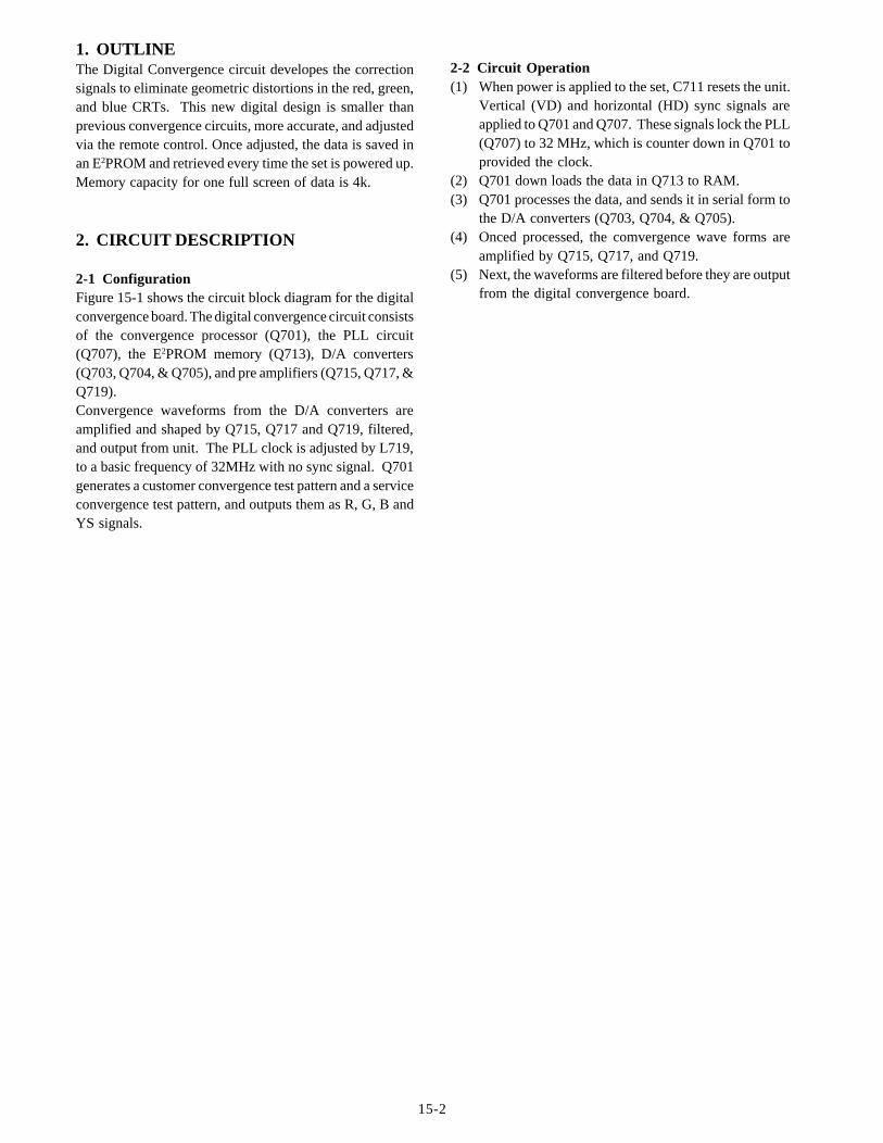
15-2
1. OUTLINEThe Digital Convergence circuit developes the correctionsignals to eliminate geometric distortions in the red, green,and blue CRTs. This new digital design is smaller thanprevious convergence circuits, more accurate, and adjustedvia the remote control. Once adjusted, the data is saved inan E2PROM and retrieved every time the set is powered up.Memory capacity for one full screen of data is 4k.
2. CIRCUIT DESCRIPTION
2-1 ConfigurationFigure 15-1 shows the circuit block diagram for the digitalconvergence board. The digital convergence circuit consistsof the convergence processor (Q701), the PLL circuit(Q707), the E2PROM memory (Q713), D/A converters(Q703, Q704, & Q705), and pre amplifiers (Q715, Q717, &Q719).Convergence waveforms from the D/A converters areamplified and shaped by Q715, Q717 and Q719, filtered,and output from unit. The PLL clock is adjusted by L719,to a basic frequency of 32MHz with no sync signal. Q701generates a customer convergence test pattern and a serviceconvergence test pattern, and outputs them as R, G, B andYS signals.
2-2 Circuit Operation(1) When power is applied to the set, C711 resets the unit.
Vertical (VD) and horizontal (HD) sync signals areapplied to Q701 and Q707. These signals lock the PLL(Q707) to 32 MHz, which is counter down in Q701 toprovided the clock.
(2) Q701 down loads the data in Q713 to RAM.(3) Q701 processes the data, and sends it in serial form to
the D/A converters (Q703, Q704, & Q705).(4) Onced processed, the comvergence wave forms are
amplified by Q715, Q717, and Q719.(5) Next, the waveforms are filtered before they are output
from the digital convergence board.

15
-3
Fig. 15-1
BLO
CK
DIA
GR
AM
Q713
E2PROMMEMORY
Load
Save
Q701 T7K64
RAM (8x8x13bit)x3
C711
RESET
1/2048
COUNTER
CLK
DA
TA
Q767
QA01
µ-CON
MAINBUS LINE
SubBUS LINE
Q707
PLL
L719
32MHz±0.005MHz
VD
HD
R
G
B
Ys
TEST PATTERN
Q703
D/A
Q704
D/A
Q705
D/A
Q715
Q717
Q719
FILTER
FILTER
FILTER
FILTER
FILTER
FILTER
RH
RV
GH
GV
BH
BV
DIGITAL CONV. BOARD

15-4
3. PICTURE ADJUSTMENT
The adjustment is done on 60Hz mode (NTSC).
3-1 Change of Memory (E2PROM)Memory of Q713 E2PROM is nonvolatile, and adjusted datais stored. Since data in RAM of Q701 is eliminated withpower OFF, the RAM is set by soft command ofmicrocomputer QA01 at every power ON. The adjusteddata which is obtained from screen-watching is once storedin RAM inside QA01. The whole data in RAM which iscorrected on each adjusting point and is changed, is savedinto E2PROM (Q713) as a fixed data. The data capacity perone screen requires 4k for 60Hz mode (NTSC).
3-2 Service Mode3-2-1 OutlineService mode is controlled by software of microcomputerQA01, and is one of function of set.
This mode is designed so that ordinary user cannot use this,and special operation is required to use this.Data change is done by direct shift (cursor display) ofadjusting points ; 60Hz mode (NTSC) 8x8 /1 color.
3-2-2 To enter and to exitPress MUTE key on remote hand unit twice and keeppressing the key, press MENU key of set console.Then service data will be displayed on top left of screen.Under the condition, Press “7” key on remote hand unit, andthe screen shows crosshatch picture (Later, the first picture).Press again “7” key, and the screen changes to crosshatch +data display (Later, second picture). This time changeddata are automatically saved.Further, press “7” key on remote, the screen returns tooriginal picture.
Fig. 15-2
Service data display(original picture)
Remote"7" key
The first picture The second picture
Remote "7" key+automatic save
Remote"7" key
X X+ + MENU

15-5
3-2-3. Picture
60Hz mode (NTSC)..................... Correcting point Horizontal 8 x Vertical 8 (Arrow marks denote correcting point)
The first picture The second picure
Data display
Cusor (red) Screen center(Blinking)
Fig. 15-3
The first pictureCrosshatch pattern. Pattern colors are three color display.Cursor is blinking in red. When changed, condition is lastmemory state.Cursor is ........... Data change mode in lighting,
Cursor shifting mode in blinking.Display color shows the color that data change is possible.
The second pictureWhen entering from the first picture to the second picture,correcting wave of convergence is muted for one second.During this period, the changed data is transferred fromRAM Q701 to E2PROM Q713, and saved.The second picture is indicated with data on top left of thefirst picture, therefore, convergence cannot be adjusted bythis picture.
(CAUTION)Receive suitable signal for adjustment. Decide the centerby cross pattern of static convergence in menu, and adjustconvergence from center to circumference.

15-6
4. ADJUSTING PICTURE DIMENSION(Green picture)
60Hz mode (NTSC)B 2
B 2
14xB
2mm
12xA
48 inches 4:3 Screen size: Horizontal 975mm Vertical 732mm Dimension A: 80.9mm Dimension B: 48.8mm
Fig. 15-4

15-7
5. KEY FUNCTION OF REMOTECONTROL UNIT
Fig. 15-5
RNT
ENT
100
1
4
7
2
5
8
3
6
9
0
EDS TIMER POWER
TV/VIDEO RECALL MUTEVCRCABLETV
CH
VOL
TOGGLES CURSOR BETWEEN COLORS
MOVES CURSOR/LINERIGHT
BLUE CRTON/OFF
GREEN CRTON/OFF
RED CRTON/OFF
ENTER CONVERGENCE MODE & SAVE
MOVES CURSOR/LINEDOWN
MOVES CURSOR/LINELEFT
CURSORLOCK/UNLOCK
MOVES CURSOR/LINEUP
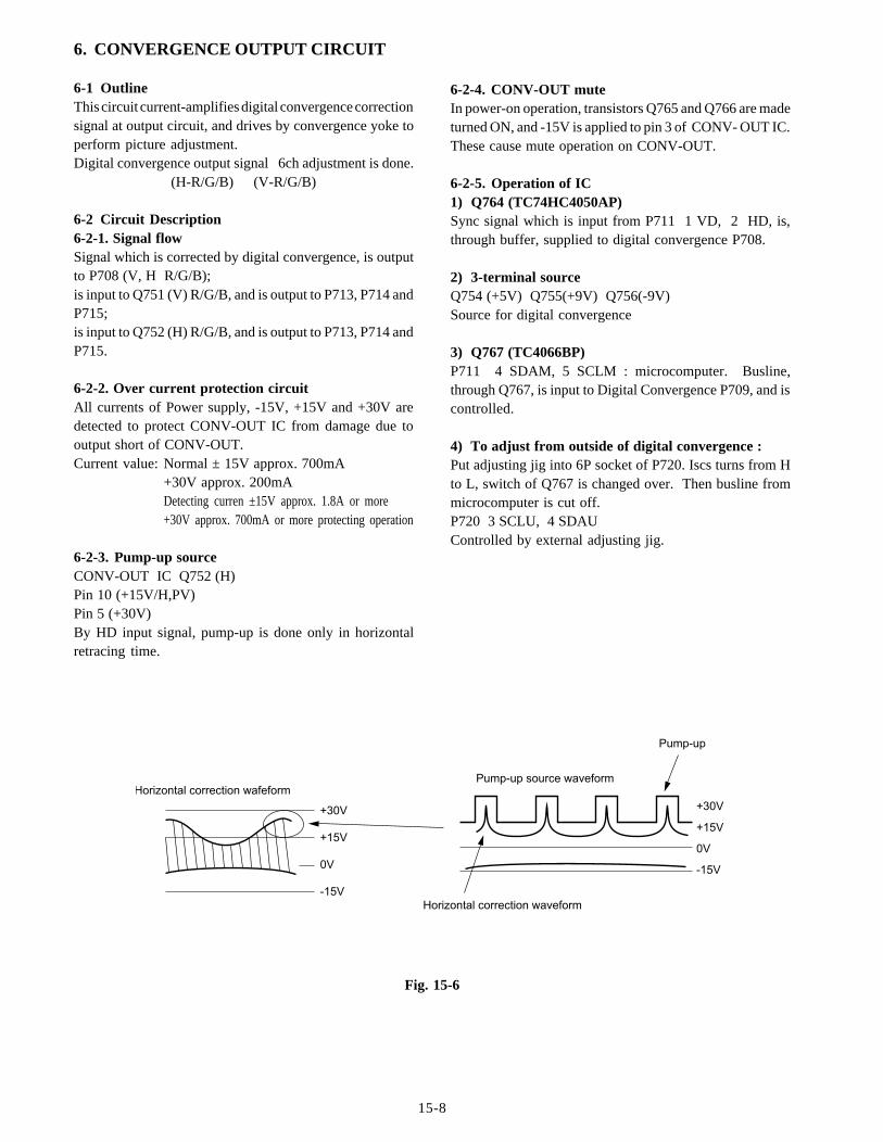
15-8
6. CONVERGENCE OUTPUT CIRCUIT
6-1 OutlineThis circuit current-amplifies digital convergence correctionsignal at output circuit, and drives by convergence yoke toperform picture adjustment.Digital convergence output signal 6ch adjustment is done.
(H-R/G/B) (V-R/G/B)
6-2 Circuit Description6-2-1. Signal flowSignal which is corrected by digital convergence, is outputto P708 (V, H R/G/B);is input to Q751 (V) R/G/B, and is output to P713, P714 andP715;is input to Q752 (H) R/G/B, and is output to P713, P714 andP715.
6-2-2. Over current protection circuitAll currents of Power supply, -15V, +15V and +30V aredetected to protect CONV-OUT IC from damage due tooutput short of CONV-OUT.Current value: Normal ± 15V approx. 700mA
+30V approx. 200mADetecting curren ±15V approx. 1.8A or more+30V approx. 700mA or more protecting operation
6-2-3. Pump-up sourceCONV-OUT IC Q752 (H)Pin 10 (+15V/H,PV)Pin 5 (+30V)By HD input signal, pump-up is done only in horizontalretracing time.
6-2-4. CONV-OUT muteIn power-on operation, transistors Q765 and Q766 are madeturned ON, and -15V is applied to pin 3 of CONV- OUT IC.These cause mute operation on CONV-OUT.
6-2-5. Operation of IC1) Q764 (TC74HC4050AP)Sync signal which is input from P711 1 VD, 2 HD, is,through buffer, supplied to digital convergence P708.
2) 3-terminal sourceQ754 (+5V) Q755(+9V) Q756(-9V)Source for digital convergence
3) Q767 (TC4066BP)P711 4 SDAM, 5 SCLM : microcomputer. Busline,through Q767, is input to Digital Convergence P709, and iscontrolled.
4) To adjust from outside of digital convergence :Put adjusting jig into 6P socket of P720. Iscs turns from Hto L, switch of Q767 is changed over. Then busline frommicrocomputer is cut off.P720 3 SCLU, 4 SDAUControlled by external adjusting jig.
+30V
+15V
0V
-15V
+30V
+15V
0V
-15V
Horizontal correction wafeformPump-up source waveform
Pump-up
Horizontal correction waveform
Fig. 15-6
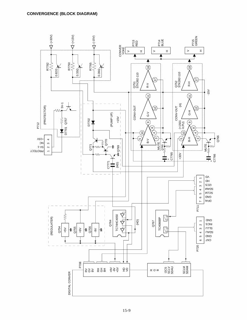
15-9
CONVERGENCE (BLOCK DIAGRAM)
DIG
ITA
L C
ON
VE
R
P70
8
RV
GV
BV
RH
GH
BH
+9V
-9V
+5V
HD
VD R G B
I2C
SS
CLV
SD
AU
SC
LMS
DA
M
(RE
GU
LAT
ER
)
Q75
4
+5V
Q75
5
+9V
Q75
6
-9V
Q76
4
TC
74H
C40
50
(HD
)
Q76
7
TC
4066
BP
P72
0P
711
6 5
4
3
2 1
7 6
5
4
3 2
1
CNTGND
SDAUSLLUINCSGND
DFAIGND
SCLMSDAM
I2CSHDVD
+ C77
66Q
766
MU
TE
+30V
B-H
G-H
R-H
-15V
B-V
G-V
R-V
+ C77
65
MU
TE
510
98
43
11
12
18
17
Q76
5
510
9
84
3
11
12
18
17
CO
NV
-OU
T
CO
NV
-OU
T
(+15
01H
.PU
)(H
)
Q75
2S
TK
392-
110
V H
Q75
1S
TK
392-
110
P71
5G
RE
EN
V H
P71
4B
LUE
V H
P71
3R
ED
C77
71
(HD
)Q
769Q
770
Q77
1
(PU
MP
UP
)
+15V
D77
02
D77
01
Q75
75V
-1
(PR
OT
EC
TO
R)
P71
2
R77
82
0.82
Ω
(+30
V)
R77
50
0.33
Ω
(+15
V)
R77
65
0.39
Ω
(-15
V)
CO
NV
ER
Y
OK
E
1 2
3
4
PROTECT5V-1NC+15V

15-10
Reray OFF Reray ON
Reray ON
Reray ON
Reray OFF Reray OFF
NG
NG
NG
OK
OK
OK
OK
OK
Protect 1
Relay turns ononce but immediatelyturns off.
Relay operation soundat power on.
No Convergencecorrection wave.
Check screen modesof picture.
Convergence PCB,pull out of P712.
Check powersupply circuit.
Check Q751, Q752and repair.
Reray OFF
Proceed to "protectioncircuit diagnosis procedures".
Check P708 R/G/B correction wave.
Check voltage at ±15V+30V pump up.
Check power supplycircuit.
Are output signalsapplied to H, Vblk of P711. Check DEF PC13.
Check voltage across±9V+5V Q754, Q755, Q756.
Check Q754, Q755,Q756 and repair.
Check signals of all ICand associated cirduits.
Pump-up
Convergence output signals correction wave
+30V
-15V
0V
VerticalQ751
(R/G/B)
HorizontalQ752
(R/G/B)
7. CONVERGENCE TROUBLESHOOTING CHART

15-11
LAB 3DIGITAL CONVERGENCE
GREEN GEOMETRY
1. Put the set in the service mode and bring up the convergence cross hatch.
2. Push the 100 button to turn off the red tube, and RTN to turn off the blue tube.
3. Place the convergence template on the screen and align the center cross hairs with the tabs in thebezel.
4. Use low tack masking tape to attach the template to the bezel. Try to get the template flat againstthe screen to reduce parallax errors.
5. Push the 3 button on the remote until the blinking cursor in the upper left corner of the screenturns green.
6. Move the blinking cursor to the right with the 6 button, then down with the 8 button until it’s oneline to the right of center. The 4 button moves the cursor to the left, and the 2 button moves it up.
7. Push the 5 button to lock the cursor in place.
8. Use the 2, 6, 8, and 4 buttons to align the intersection of the cross hairs with those on thetemplate.
9. Push the 5 button to unlock the cursor.
10. Move the cursor to another location and repeat steps 7 and 8. Moving the cursor in a counterclockwise spiral to the various locations works best. Normally, you need to repeat the procedurea second time to make fine adjustments.
RED CONVERGENCE
1. Remove the template and press the 100 button to turn on the red tube.
2. Press the 3 button until the red cursor appears.
3. Align the red cross hatch pattern to the green cross hatch pattern the same way you aligned thegreen with the cross hatch pattern on the template.
BLUE CONVERGENCE
1. Push the 100 button to turn off the red tube, and RTN to turn on the blue tube.
2. Push the 3 button until the blue cursor appears.
3. Align the blue cross hatch pattern to the green cross hatch pattern in the same manner.
4. Push the 100 button to turn on the red tube and check the convergence with all three tubes on.The cross hatch pattern should be white with no red, green, or blue present. However, dependingon how much the blue tube is defocused, a slight blue halo may show.

15-12
5.Push the 7 button then the power button to save the settings and exit the service mode.
ELECTRICAL CENTERING
1. Disconnect all video cables in the video 1 input.
2. Put the set in the service mode.
3. Push the TV/VIDEO button on the remote until the white cross hair pattern on a blackbackground is displayed.
4. Check the centering of the cross hair pattern with the centering tabs in the bezel.
5. If the horizontal position is off, push the channel up button until the HPOS register appears. Usethe volume button to center the pattern.
6. If the vertical position is off, push the channel up button until the VPOS register appears. Usethe volume button to center the pattern.
7. Push the TV/VIDEO button until the TV picture is displayed, then turn the power off.
8. Turn the set on and check the picture quality with a live video signal.
END OF LAB 3

16-1
SECTION XVIOPTICAL SECTION

16-2
1. NECK COMPONENTS
1-1. Outline of Components Around Neck of TheProjection Tube
Fig. 16-1 shows names and mounting locations of neckcomponents around the projection tube.
Fig. 16-1
Projection tubeDeflection yoke Velocity modulation coil
1-2. Theory of Operation
The neck components consist of, a deflection yoke assembly (which consists of a main yoke, a sub-yoke, and a
centering magnet), and a velocity modulation coil .
The main yoke of the deflection yoke assembly consists ofa horizontal and vertical deflection coil, and deflects electronbeams in horizontal and vertical directions.
The sub-yoke is called a convergence yoke and also consistsof a horizontal and vertical coils. The sub-yoke performsdistortion correction and color registration according tocorrection currents supplied from the convergence outputcircuits.
Moreover, a centering magnet consisting of two 2-polemagnets is provided at end of the deflection yoke to adjustthe raster position.
NOTES:

16-3
1-3. Projection Tube
TP4688J, TP4880A• Fluorescent screen: flat
TP48E60/61 TW56D90• Fluorescent screen: inverted R 350mm
Fig 16-2
Electrons around the peripheral of the CRT screen comeinto collision with the A/B lenses and are not used, thuslowering contrast, etc.
• Electromagnetic FocusElectromagnetic focusing with magnets mounted aroundthe CRT neck.
Light beams around the peripheral of the CRT screen arefocused towards the center, thus increasing the amount oflight emitted towards the screens.
• Electrostatic FocusHigh unipotential focus
Since the deflection is carried out by using a magnetic fieldapplied from the outside of the neck, high deflection poweris obtained and focusing quality is high. Moreover, sincethe coils are mounted on the outside of the neck, theconfiguration of the deflection fields created inside the neckhas less distortion, thus the best beam pattern will beobtained.
The best beam pattern is obtained at screen center andscreen edges by applying parabolic voltages for H and Vperiods to the focus terminals.
This also assures a flat focusing characteristic across theentire screen.
To obtain clearer pictures, a velocity modulation circuit isalso provided.
Eb G2 Screen
G5 G4 G3 KFocus
Fig 16-3

16-4
2. FUNCTION OF KEY COMPONENTS
2-1. OutlineThe optical system of the TP48C60/61 consists of a screen,mirror and lens assembly. A description will be given foreach block.
2-2. Theory of Operation
Projectiontube
Screen
Mirror
Lens
Optical couplingsystem
Projection tube
Lens
Projection tube
Lens
Screen
FRESNELSheet
LENTICULARSheet
Refracting light beams running to screenperipheral area to the G-axis direction(screen center direction) with effect ofconvex lenses.
Widening directionalcharacteristic in horizontaldirection.
Fig. 16-4 Fig. 16-5

16-5
2-3-1. Effect of Fresnel SheetThe shape of the lens has been changed to reduce focallength.(This allows the product size to be reduced, specifically inthe distance from front to rear.)
2-3-2. Appearance of LENTICULAR Sheet
Fig. 16-7
Lens
FRESNELsheet
Effect ofFRENSNEL sheet
Without FRESNEL sheet
LENTICULAR lens
Black stripe
Screen side directio
n
Viewer side
Fig. 16-6

16-6
LENTICULAR sheet 2-3-3. Effect by LENTICULAR SheetIf the light enters the front lenticular screen on the diagonal,the light will be diffused in the same way as parallel lightincidence when viewed from the front of the TV.
Diffuser
TP4688JTP4880A(Body diffusion)
TP48C50/51TW56D90(Surface layer diffusion)
Fig. 16-8
Light beams will be effectively used by collecting thediffuser at surface of the layer, thus increasing the brightnessby about 10%.
SCREEN GAINTP48C60/61 5.6TW56D90 6.2
Projectiontube side
Viewer side
F1 F2
Incidentlight
Outgoinglight
When light beams enter LENTICULARsheet in parallel.
F1 F2
Incidentlight
Outgoinglight
When light beams enter LENTICULARsheet diagonally.
Black stripe
LENTICULAR lens
Fig. 16-9

16-7
2-4. Optical Coupling EffectAn liquid with a refraction index near that of glass is filledbetween the projection tube and lens to suppress:
(1) total reflection from the tube, thereby improving thecontrast
(2) interfacial reflection to reduce loss of light. Moreover,with the cooling effect of the liquid, the power output of theprojection tube can be safely increased.
2-4-1. Optical Coupling Effect(1) Light beams , emitted from the fluorescent
surface A advance up to the lens, but light beam returns to the fluorescent surface due to the totalreflection.
(2) This extremely lowers the contrast at the fluorescentsurface.
Assuming that the reflection index of air is 1.0 and that ofglass 1.5, the angle which causes the total reflection is 41.8°That is, the light beams with an angle of q higher than 41.8°can not exit from the projection tube. The light beamsreturned to the fluorescent surface reaches 56% of the totalbeams coming out from A.
Fig. 16-11
Lens
Air
Projection tubeface glass
Fluorenscene plane
Projection tube
A
q
1
3
2
Fig. 16-10
Lens Liquid (ethylene glycol + glycerine)Index of refraction 1.4~1.45
Projection tube
Projection tubefluorescene plane

16-8
2-5. LensThe lens system consists of a main lens (3 pieces of lens),C lens, and the face plate of inverted g CRT (used as a lens),and realizes a short focus optical lens system with lessquantity of lens.With the short focus optical system employed, the depth ofthe unit is reduced by about 30%, thus making the unit slimand compact.
2-5-1. Optical Coupling Effect
Note: When making adjustments on the neck components,it is always best to use dedicated drivers made of nonmagnetic material to avoid any distortion whilemaking adjuctments.
Optical focus will be made according to the proceduresshown below. After completion of the electrical and opticalfocus adjustments, convergence adjustments should bemade.
Plastic lens
Liquid coolant
Negative radius phospher
Glass lens
Black coating
7" High brightelectrostatic focus CRT
Fig. 16-13 Lens focus adjustment
LENSESTP48C60/61 USPL DELTA 77TW56D90 USPL DELTA 79
Fig. 16-12
Fig. 16-14 Mounting position ofdeflection yoke and V.M coil
Projectiontube
Deflection yoke(Mounted projection tube)
Velocity modulation coilV.M.Coil
Loosen screws and adj ust the lens focus atthe best position by moving lenses left and right.

16-9
2-6. Focus Adjustment(1) Turn on the static convergence switch and receives a
cross character signal.(2) For easy adjustment, project one color to be adjusted
at a time on the screen. (Other colors can be interruptedby putting caps on the lens.)
(3) Turn the electrical focus volume for the color to beadjusted clockwise or counterclockwise so that thefocus at center of the cross character shows the best.
(4) Loosen screws securing the lens and move the lenstoward left and right until the best focus is obtained atcenter of the cross character.
(5) repeat steps 3 and 4 to obtain the best focus. Finally,secure the screws.
(6) Perform the convergence adjustment according to theconvergence adjustment method.
Fig. 16-15
Remove 4 screws andtake off the cover which is in frontof the focus block.
Focus pack
Electrical focus and gun drivecontrols.
R G B
SCREEN
FOCUS

16-10
NOTES

17-1
Chapter XVIIPower Supply

17-2
Notes:

17-3
1. Power Supply Overview
A block diagram of the power circuit is shown in fig. 17-1. The power circuit consists of the following:
1) Standby Supply, which supplies the +5V-1 Standby to the microcomputer and +12V Standby to the On/Off Relay(SR81).
2) Main Supply which supplies HORIZONTAL OUTPUT B+ (+125V) and AUDIO OUTPUT Vcc (+38V). The signalprocess circuits are supplied by +5V-3, +5V-2, and +9V-2 via regulators from the 12V source of the Main Supply.
3) Sub Supply which supplies +30V, +15V and -15V for the convergence output board.
Figure 17-1 Power Supply Block Diagram
F801 T801 T802 T840POWERTRANS.
TPW1549AZ
+12V
D840
Q840
REG. +5V-1 (MICROCOMPUTER)
SR81F860
R861D801
T862
TPW3332AS
CO
NV
ER
TE
RT
RA
NS
.
Q801VOLTAGE CONTROLSTR-Z3201
Q843SW
Q830SW
Q862PHOTO COUPLER
+12V
+38V
Q830REG.Q831REG.
Q832REG.
+5V-2 (for TUNER, COMB, V/C/D etc.)
+5V-3 (for PIP, ESD/C.C/RGB. SW)
+9V-2 (for COMB, DSP, CRT-D etc.)
AUDIO OUT Vcc
Defl. Vcc (to V/C/D IC)+9V
Q430
R470R479 R471
F470
R101
F.B.T. V.M
+32V (TUNER)
1 2
13
14
163
Z801PROTECTOR
H1C1019
X-RAY
C471+
D471 R472F.B.T.(HEATER)
200V L.V.P. 35V O.C.P
D802~D805
F850
Q802VOLTAGE CONTROLSTR57041
T888
TPW3330AM
CO
NV
ER
TE
RT
RA
NS
.
+30V
+15V
-15V
F851
LOW VOLTAGE PROTECTORQ853 Q854
R7782
R7750
R7765
O.C.PQ768
O.C.PQ759
O.C.PQ762
CONVERGENCECIRCUIT
R883
B+ (+125V)
Standby Supply
Main Supply
Sub Supply
+30V
+15V
-15V

17-4
2. Rectifying circuit and standby power supplyThe rectifying circuit generates dc voltage sources fromthe 117 Vac input. D899 is a metal oxide varistor used toabsorb surges due to line spikes, lightning, etc. The arrowin fig. 17-2 indicates the path in which the surge is by-passed. C801, T801 and T802 are filters for abnormal ra-diation or line noise. For direct view sets the degaussingcircuit, using a thermistor, is supplied after SR81 (notshown). R810 is used to suppress surge current duringswitch-on. D801, along with C810, output a rectified andsmoothed DC voltage. T840 is the standby power trans-
former. D840 along with C840 output a rectified andsmoothed 12V signal for driving relay SR81 and for sup-plying the +5V regulator, Q840. Q840 supplies the standby+5V-1 and the reset signals for the microcomputer as wellas other circuits. When the power is switched on, QA01(ICA01), the Main Microcomputer, sends a high signal frompin 7 to the base of QB30, turning it on. This causes thebase of Q843 to go high and thereby turn it on. When Q843turns on, current flows through the coil of SR81, activat-ing the relay and thereby switching the main power on.
4. Outline of Current Resonant Type Supply
Fig. 17-3 shows the configuration for the Current Reso-nant type power supply. A start-up voltage is sent to Pin 10to begin operation. VIN source voltage of 160V is appliedto Pin 1. Pin 14 is tied to ground for the negative phase ofthe MOS-FET configuration. The Primary winding of T862and C870 are connected in series to form an LC SeriesResonant Circuit. The converter transformer, which isdriven by a push-pull MOSFET configuration located in-side Q801, operates in forward mode.
3. Main Supply Circuit
The circuit in fig. 17-3 is a current resonant switching typepower supply that incorporates a hybrid IC, Q801 (STR-Z3201). The current resonant power circuit is highly effi-cient in that it operates with very low power consumption
and very little noise. In the case of a short on the load sideof T862, the AUDIO OUTPUT, Low B, and B+ circuits areprotected with F899, F890 and F470 respectively. F860 isused to protect the primary side of T862.
The automatic voltage control operation is performed bythe detection of the B+ voltage (125V) fed into the erroramp, Pin 5, of IC Z801, then output through Pin 3 to thephoto coupler. Next this signal is fed into the primary Os-cillating (OSC) circuit, located inside IC Q801 (Pin 6) whichcontrols the frequency of the ON/OFF time, via an internallogic IC, for the MOS FET configuration.
Figure 17-2 Standby Supply
F801 D899 C801
T801
R810
C810
+5V-1
QB30Q843
SR81Q840
+5V (to MICOM)
Reset
C840T840 D840 C843
C842
1
2
5
43
Surge
160 VdcRectified Output
MICOMPOWEROn=5VOff=0V
10.9Vdc
D801
+
_
117Vac
4.2Vdc
.12VdcAll voltages shown are during ON condition.
5Vdc0V
3.9Vdc

17-5
10 16 3 2
1
15
14
131147568
12
9
CD
OC
Vcc VB G(H)
VIN
OUT
COM
Css
TSD OVP START
LogicR1
R2
DELAY LATCH REF
OCOSC
CONTROL OSC
R4 R3
PHOTOCOUPLER
Q862
ERRORAMPZ801
CONT CT RT GND
L863
HO
150-160Vdc
R864L864
IC Q801 STR-Z3201
T862C870
R862
D862D876C876
D864
R871
B+ 125Vdc+38Vdc+12Vdc
LO G (L)
R867C862C866
R863
D879
R872
R870 R865
C869
+
R861
C867
C874
D801
F860
F890F899F470
72.6Vdc
.O1Vdc
1.3Vdc
4.7Vdc 4.7Vdc 3.5Vdc 0V 7Vdc 7Vdc
0V
78Vdc89Vdc17.4Vdc 78Vdc
5.3Vdc
VL (v)
e
Frequency
1f= 2π LC
NominalOperatingfrequency
Resonant point
increased
load
decreased
load
Fig. 17-4 Resonance Curve
5. Fundamental Theory of LC Series Resonant CircuitThe LC series resonant switch mode power supply is a fre-quency regulated power supply operating above resonance(see figures 17-3 and 17-4). The LC series resonant circuitis composed of the primary winding of T862 and C870. Anegative feedback circuit is used to control the output ofthe transformer. The feedback circuit, which monitors the125Vdc source, is composed of the error amp inside Z801and the photo coupler (Q862). This feedback is applied tothe CONT input (Pin 6) of IC801 to control the frequencyof the internal oscillator (OSC). When the load increaseson the secondary side of the transformer, the frequencydecreases (operates closer to resonance) and the current
increases. Conversely, when the load decreases, the fre-quency increases and the current decreases. Table 17-1shows the voltages developed on T862 secondaries.
* Reference Hot Side Ground (T862, Pin 3) whenmeasuring Pins 2, 4, 5, 6, and 7. CAUTION, USEISOLATION TRANSFORMER .
Figure 17-3 Current Resonant Supply (Main)
Table 17-1 T862 Voltage Chart
T862 Pin # Voltage
Pin 2* 47 Vp-p
Pin 3Ground
Hot Side*
Pins 4, 5* 148 Vp-p
Pins 6, 7* 127 Vp-p
Pin 9 27 Vp-p
Pin 10 27 Vp-p
Pin 11, 12,15
Ground,Signal Side
Pin 13 256 Vp-p
Pin 14 256 Vp-p
Pin 16 81 Vp-p
Pin 17 81 Vp-p

17-6
6. Main Supply Actual operation
Refer to Figure 17-5 diagram and waveforms.
1. Start-up
When power is applied to the set, a start-up voltage of16V is applied to pin 10 of IC Q801. At the same time,charging of C869 (pin 9) induces a delay to the internallatch circuit to prevent the Over Voltage Protect (OVP)circuit from shutting the set down.
2. Output switching element
Two power MOSFETs operating in push-pull mode areused for switching. The on-off timing of each is con-trolled by the logic inside Q801. To avoid a short circuitfrom occuring a delay is used between the turn off of oneMOSFET to the turn on of the next.
3. CT terminal (Pin 5) - basic oscillation
The frequency of the internal oscillator is controlled bythe Oscillator Control block. The frequency is deter-mined by the charge and discharge of capacitor C862connected to CT terminal. The oscillator generates a rampwaveform at Pin 5. The ramp waveform charges up to 4V (typical) and discharges to about 2.5 V. The chargingtime is the output-on period, and discharging time is theoff period (see OSC OUT SIGNAL waveform of Figure17-5). The lowest oscillation frequency is determined bycapacitor C862 and resistor R867.
4. CONT (Pin 6) - frequency control
Current flowing out of the CONT terminal (Pin 6) variesthe charging current of oscillator capacitor C862, whichin turn controls the frequency of the Output (Pin 15) sig-nal. The control current is determined by thePhotocoupler. The Photocoupler phototransister side cur-rent is determined by the feedback current of the photo-diode side. The photodiode current is determined by theError Amp inside of Z801, which is monitoring the+125V source. Thus, the terminal current (CONT) cor-responds to the feedback from the +125V output.
5. Css terminal (Pin 8) - soft start
When power is first applied, the switching frequency isset high by capacitor C866 and resistor R863, resultingin soft start of the switching supply. Thus, current (surge)in the POWER MOSFET output is limited to providestable starting of the supply sources. After initial start-up, the circuit operates at its nominal frequency (70-80kHz).
6. CD terminal (Pin 9) - Latch Delay
The Latch circuit shuts the power supply off (shut-down)when a fault is detected. Shut-down occurs by detectingerrors from the following:
• Over voltage protection (OVP) circuit
• Thermal shock detection (TSD) circuit
• Over current protection (OCP) circuit
• Loss of and no recovery of Main B+
The charging time of capacitor C869 connected to theCD terminal (Pin 9) is used to delay the operation of theLatch circuit when power is initially applied. If the unitgoes into shut-down, temporarily remove ac power toreset the latch circuit.
7. OC terminal (Pin 12) - Over Current Detect
This is to detect over-current in the LC series resonantcircuit.
8. Over voltage protection (OVP) circuit
If the Vcc terminal (Pin 10) exceeds 22V (typical), theLatch circuit is engaged (shutdown) .
9. Thermal shock detection (TSD) circuit
This is to make the Latch circuit operate when the IC'sinternal temperature exceeds 150°C.
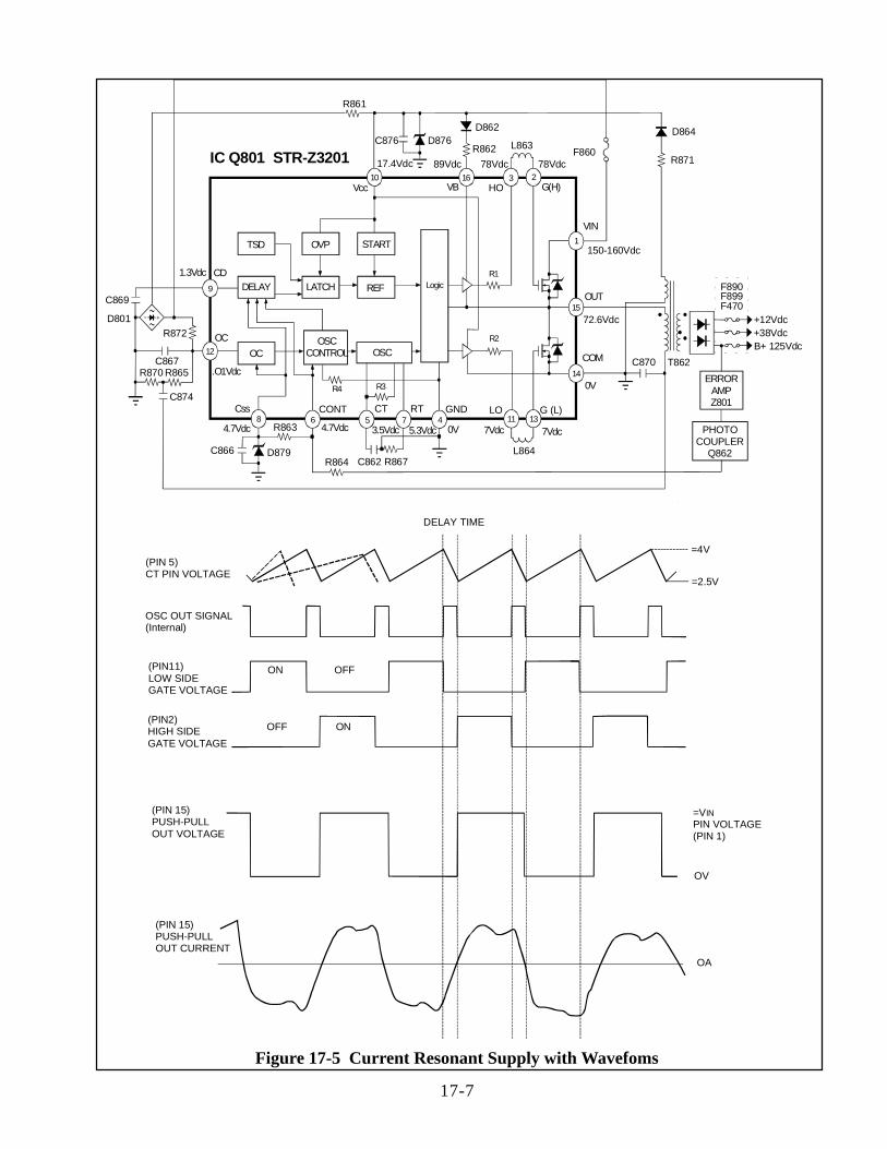
17-7
10 16 3 2
1
15
14
131147568
12
9
CD
OC
Vcc VB G(H)
VIN
OUT
COM
Css
TSD OVP START
LogicR1
R2
DELAY LATCH REF
OCOSC
CONTROL OSC
R4 R3
PHOTOCOUPLER
Q862
ERRORAMPZ801
CONT CT RT GND
L863
HO
150-160Vdc
R864L864
IC Q801 STR-Z3201
T862C870
R862
D862D876C876
D864
R871
B+ 125Vdc+38Vdc+12Vdc
LO G (L)
R867C862C866
R863
D879
R872
R870 R865
C869
+
R861
C867
C874
D801
F860
F890F899F470
72.6Vdc
.O1Vdc
1.3Vdc
4.7Vdc 4.7Vdc 3.5Vdc 0V 7Vdc 7Vdc
0V
78Vdc89Vdc17.4Vdc 78Vdc
5.3Vdc
DELAY TIME
=4V
=2.5V
(PIN 5)CT PIN VOLTAGE
OSC OUT SIGNAL(Internal)
(PIN11)LOW SIDEGATE VOLTAGE
(PIN2)HIGH SIDEGATE VOLTAGE
ON OFF
OFF ON
(PIN 15)PUSH-PULLOUT VOLTAGE
(PIN 15)PUSH-PULLOUT CURRENT
OA
OV
=VIN PIN VOLTAGE(PIN 1)
Figure 17-5 Current Resonant Supply with Wavefoms
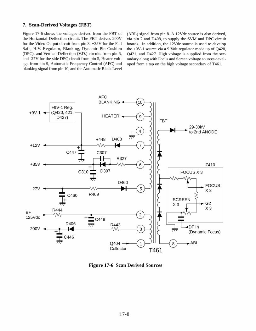
17-8
10
4
7
2
1 8
AFCBLANKING
FBT29-30kVto 2nd ANODE
9HEATER
FOCUS X 3
SCREENX 3
ABL
B+ 125Vdc C448
Q404Collector
6+35V
C310
R327C307
200VD406
3
FOCUSX 3
G2X 3
DF In(Dynamic Focus)
Z410
R443
C446
R444
5-27VR469C460
D460
R448
C447
D408
+12V
+9V-1+9V-1 Reg.(Q420, 421,
D427)
T461
D307
Figure 17-6 Scan Derived Sources
7. Scan-Derived Voltages (FBT)
Figure 17-6 shows the voltages derived from the FBT ofthe Horizontal Deflection circuit. The FBT derives 200Vfor the Video Output circuit from pin 3, +35V for the FailSafe, H.V. Regulator, Blanking, Dynamic Pin Cushion(DPC), and Vertical Deflection (V.D.) circuits from pin 6,and -27V for the side DPC circuit from pin 5, Heater volt-age from pin 9, Automatic Frequency Control (AFC) andblanking signal from pin 10, and the Automatic Black Level
(ABL) signal from pin 8. A 12Vdc source is also derived,via pin 7 and D408, to supply the SVM and DPC circuitboards. In addition, the 12Vdc source is used to developthe +9V-1 source via a 9 Volt regulator made up of Q420,Q421, and D427. High voltage is supplied from the sec-ondary along with Focus and Screen voltage sources devel-oped from a tap on the high voltage secondary of T461.

17-9
Q862
R890
From ICA01
(125V) B+
R470.56
R471 R479
C474
X-RAYProtectT461
* See Protect Circuits starting on page 17-9.+35V Over Current Protect+30V Over Current Protect+15V Over Current Protect-15V Over Current Protect+30V Over Voltage Protect+15V Over Voltage Protect+15V Under Voltage Protect-15V Under Voltage Protect200V Under Voltage Protect
+25V
5 3 16 15 2 1 14 12 13 11
7 17
ErrorAmp
5V-1
GATE terminal
GND1 GND2
4 8 9 10, , ,PIN: VACANT PIN
14
When the voltage at this terminal becomes approx. 1.5V or more, protection circuit operates.
C472
Q843
QB30RB30
+5V-1To SR81Relay
C471 D471 R472
9
Switch/ Latch
X-RayProtect
B+ OCP
IZ C-Out Protect OCP B+ Gate X-Ray
5V
4.9V
4.4V
0.1V
0V
Power (Pin)
Active High
4
3
1
2
(125V) B+
R884
Control
Z801 (HIC1019)
6.2V 116V 4.9V 0V 22V0.1V
8. Protector Module (Z801)
Figure 17-7 shows the standardized protector module(Z801). The following are the four different sections withinthe Protector Module: Error Amp, Switch/Latch, B+ OCP,and X-Ray Protect. In addition the Over Current Protect(OCP), Over Voltage Protect (OVP), and Under VoltageProtect (UVP) circuits are routed through the internalSwitch/Latch circuit to trigger the unit off through the Pro-tect output (Pin 16).
The Error Amp circuit monitors the B+, 125V line, viaPin 1. The Error Amp controls the current through thephotodiode of photocoupler Q862. When the B+ voltagedecreases Q862 conducts less and when it increases, Q862conducts more.
The Switch/Latch circuit is used to turn off SR81 relay incase of over current, over voltage or under voltage. In shut-down mode, Pin 16 (Protect) latches low, which turns QB30off. When QB30 turns off Q843 turns off. This causes therelay (SR81) to open and thereby disconnect the power.
In the B+ Over Current Protect (OCP) circuit , the cur-rent is being compared across R470, which is appliedthrough Pins 1 and 2. The resistance of R470 is so smallthat changes in voltage equate to larger changes in current.When a large enough change in voltage occurs the internallatch circuit outputs a low on Pin 16, which shuts the unitdown.
In the X-Ray Protect circuit, Pin 11 provides a referencevoltage of +25V. If the High Voltage increases abnormally,Pin 9 of T461 senses the increase and increases the voltagethrough R472. This increased voltage is applied to D471,which rectifies AC to DC. The increase in Vdc is appliedto Pin 13, which will trigger the internal latch circuit andoutput a Low on Pin 16. As long as +5v-1 is applied topin15, the remote control hand unit will not recover thepower. The AC power line must be disconnected to resetthe latch.
Figure 17-7 Protector Module Circuit

17-10
9. Sub Supply
The Sub Supply is located on the Convergence Out/Power2board. Figure 17-8 shows that the Sub Supply is a ringingchoke converter, using hybrid IC STR57041. Operationbegins with a start-up voltage that is applied through R852.This provides a trickle base current to Q1 (internal to theIC, Pin 2 of Q802), which causes it to turn on. When Q1turns on, the collector current begins to flow. During thisstart-up time the current is flowing through the primarywinding of T888 through Pins 2 and 5. At the same timecurrent will flow through Pins 7 and 8, which create thedetection winding, as well as Pins 8 and 9, which createthe base drive winding. During the first half cycle of theAC pulse no current flows through the detection windingbecause of the reversed polarity of D856. Pin 9, however,provides positive feedback for the base, as the electromag-netic inductance increases, to rapidly turn Q1 on. As Q1becomes saturated the current through the primary wind-ing decreases.
This decrease in current through the primary winding, re-duces the electromagnetic inductance across the base drivewinding, which decreases the voltage to the base of Q1 andthereby rapidly turns Q1 off.
T888 uses a detection type winding through Pins 7 and 8.The secondary windings are proportional to the detectionwinding. Subsequently, any fluctuation in voltage acrossthe secondary windings is sensed across the detection wind-ing which is fed back through Vo sense (Pin 1). This feed-back is used to regulate the On/Off time of the internalswitching transistor Q1.
R846, C845, R852 and D848 create a voltage clampingcircuit that allow the collector voltage of Q1 to stay withina specified level. R847, C855, R848 and D849 filter thebase voltage. Q850, Q851, Q852, C856, D855, R857 andR859 create the Slow-start circuit. C856 determines therate of the start-up time.
Bridge rectifieroutput
C856D855
R857
R846
R852 L858
C845
5
2C849 D848
R858 C855
R847 D849
9
3
2
4
5
1
Q802STR57041
R859
Q851
Q852
R854
C853 R850
D8567
8
13
12
11
10
15
17
D850
+30V
+15V
−15VR860
R853
-35V
0.0V
0.2V
163.7V
-42V
C850C851
Input (C)
Vo Control
Earth (E)
Base Drive (B)
Vout Sense (-)
D857 L853 F851
C858C857 C859
C882
C846C847C848
D859 L857
C881C880
D858 L855
+
+
+
+
+
T888
Figure 17-8 Sub Supply

17-11
10. Protect Circuits
Figure 17-9 +35V Over Current Protect Circuit(Located on Deflection/Power Board)
Figure 17-10 +30V Over Current Protect Circuit(Located on Convergence Out/Power2 Board)
R77820.82
R7784470
R7783330 C7770
Q768
R77632.2K
+30VLOAD
Q758 Q757
29V
29V0V
Protect (active high)To Pin 14 of Z801
D370
C370 R371 R370
R372
LOAD
+35V
1.5
3.9K
5.6K
Q370
+35V OVER CURRENT PROTECT CIRCUIT(Located on Deflection/Power board)
Protect (active high)To Pin 14 of Z801
35V
35.3V

17-12
R77500.33
R7751470
R7749330 C7760
Q759
R77472.2K
+15VLOAD
Q758 Q757
Protect (active high)To Pin 14 of Z801
16.1V
15.8V0V
R77650.39
R7763470
R7764330 C7763
Q762
R77582.2K
-15VLOAD
Q761 Q757
Protect (active high)To Pin 14 of Z801
-16V
-16.2V
1.5V
Figure 17-11 +15V Over Current Protect Circuit(Located on Convergence Out/Power2 Board)
Figure 17-11 -15V Over Current Protect Circuit(Located on Convergence Out/Power2 Board)

17-13
R848
R849
D865 D863
D860 D861
+30V
+15V Protect (active high)To Pin 14 of Z801
(36V)
(24V)
R876
R875
Q854
R880
D867
D866
R879
R877
Q853
R874
R873
D854
Protect (active high)To Pin 14 of Z801
-15V
+15V
(5.1V)
+12V
0V
0V
0.7V
-14.9V
-15V
-14.3V
Figure 17-12 +30V/+15V Over Voltage Protect Circuit(Located on Convergence Out/Power2 Board)
Figure 17-13 +15V/-15V Under Voltage Protect Circuit(Located on Convergence Out/Power2 Board)

17-14
Figure 17-15 X-Ray Protect Circuit(Located on Deflection/Power Board)
R392
Q341
C340
Protect (active high)To Pin 14 of Z801
R390R389
+9V-1V
200V
R347
Q340
D341
R346
D315
0VQ352
9.4V
0V CRT PROTECT6.2V
0V
6.1V
6.8V
6.2V
Figure 17-14 200V Under Voltage Protect Circuit(Located on Convergence Out/Power2 Board)
To X-RAYPin 13 (Z801)
Q757From X-RAYPin 9 of T461
C471
D471 R472
(23V)

17-15
LAB 4
POWER SUPPLY SHUTDOWN CIRCUITS
SECTION 1VOLTAGES UNDER NORMAL CONDITIONS
Place the unit in the service position by removing the chassis light box and place it on its side in anupright position with the power cord up. (See FIG. 17-16) Connect a signal to the ANT1 input. Youmay want to refer to the actual schematic diagram for a clearer understanding of the circuitry.
PROTECT CIRCUIT MEASUREMENTS:
1. Connect the (-) lead of the peak/hold meter to pin 17 of Z801 (See FIG. 17-16, #1) and recordthe DC voltages on the following pins:
PIN 11)__________PIN 13)__________PIN 14)__________PIN 15)__________PIN 16)__________
RELAY CONTROL CIRCUIT MEASUREMENTS:
2. Locate Q843. (See FIG. 17-16, #2) Record the voltages on the following:
C__________B__________E__________
3. What does Q843 control, and how does it control it?
__________________________________________________________________
__________________________________________________________________
__________________________________________________________________
OVER CURRENT, OVER VOLTAGE, AND UNDER VOLTAGE PROTECT CIRCUITMEASUREMENTS:
4. Connect the (-) lead of the p/h meter to the (-) side of C882 (See FIG.17-16, #3).
5. Measure the voltage on the anode side of D865. (See FIG.17-16, #4)
Anode D865__________

17-16
6. Measure the voltage on the anode side of D860. (See FIG. 17-16, #5)
Anode D860__________
7. Measure the voltage on the collector of Q853. (See FIG. 17-16, #6)
Collector Q853__________
8. Measure the voltage on the anode side of D867. (See FIG. 17-16, #7)
Anode D867__________
9. Measure the voltage on the collector of Q757. (See FIG. 17-16, #8)
Collector Q757__________
10. Connect the (-) lead of the p/h meter to the (-) side of C310 (see FIG. 17-16, #9).
11. Measure the voltage on the collector of Q370. (See FIG. 17-16, #10)
Collector Q370__________
SECTION 2VOLTAGES UNDER SHUTDOWN CONDITION
1. Locate the (X) pin (P415) and the (R) pin (P416) (See FIG. 17-16, #11)
2. While monitoring pins 13 and 16 of Z801 on the p/h meter, jumper pins (X) and (R) together.
3. After the shutdown, record the voltages on pins 13 and 16 of Z801. (See FIG. 17-16, #1)
PIN 13)__________
PIN 16)__________
The above exercise allows you to see what happens when the X-Ray protect circuit shuts downthe set.
4. How is this determined?
__________________________________________________________________
__________________________________________________________________
__________________________________________________________________
NOTE: SHUTDOWN OCCURS WHEN THE VOLTAGE INCREASES TOAPPROXIMATELY 25V.

17-17
5. While shorting the base of Q853 (See FIG. 17-16, #6) to ground, monitor and record thecollector voltage using the p/h meter.
Collector Q853__________
6. What have you simulated by shorting the base to ground?
__________________________________________________________________
__________________________________________________________________
__________________________________________________________________
7. Why does a change occur on the collector and where is this change sensed?
__________________________________________________________________
__________________________________________________________________
__________________________________________________________________
8. Look on the schematic diagram labeled “Convergence Out/Power2”, in the upper right side.Find D865 (zener diode) on the +30V supply line. How would you determine what the peakvoltage would be before the over voltage protect circuit would operate?
__________________________________________________________________
__________________________________________________________________
__________________________________________________________________
9. Look on the schematic diagram labeled “Convergence Out/Power2”, in the upper right side.Find D860 (zener diode) on the +15v supply line. How would you determine what the peakvoltage would be before the over voltage protect circuit would operate?
__________________________________________________________________
__________________________________________________________________
__________________________________________________________________
10. Remember when you measured the anode sides of D865 and D860 earlier? Well, if the set, yourworking on, is in shutdown mode, how would you determine if it was caused by over voltage onthe +30v or +15v lines?
__________________________________________________________________
__________________________________________________________________
__________________________________________________________________

17-18
11. While shorting the base of Q757 (See FIG. 17-16, #8) to ground, monitor and record thecollector voltage using the p/h meter.
Collector Q757__________
12. What have you simulated by shorting the base to ground?
__________________________________________________________________
__________________________________________________________________
__________________________________________________________________
13. Measure the voltage drop across R7750 (See FIG. 17-16, #12), R7782 (See FIG. 17-16, #13)and R7765 (See FIG. 17-16, #14).
R7750__________
R7782__________
R7765__________
14. List a procedure of how would you determine which one of the over current protect circuitswere causing the shutdown?
__________________________________________________________________
__________________________________________________________________
__________________________________________________________________

17-19
Figure 17-16
Q757#8
R7782#13
R7765#14 R7750
#12
Z801#1
1
17
Q843#2
C882#3
Q853#6
D867#7
D860#5
D865 #4
C310#9
Q370#10
X R#11

17-20
NOTES

1 8 - 1
SECTION XVIIIDYNAMIC FOCUS CIRCUIT

1 8 - 2
1. OUTLINE
In TP48C51, a static focus system is employed in the projectiontube.Degradation of the focus quality at peripheral screen isimproved by applying focus correction voltages (parabolavoltages in H/V periods).The dynamic focus circuit creates this focus correctionvoltage and consists of an H and a V dynamic focus circuit.
To obtain a flat focus characteristics at center and peripheralof the screen, the focus correction is carried out by applyingthe H sync parabola correction voltage (efH=700 Vp-p) andthe V sync parabola correction voltage (eifv=300 Vp-p) tothe focus electrode in addition to the focus DC voltage of Ef(=EHx0.27~0.29).
2. H DYNAMIC FOCUS CIRCUIT
2-1. Theory of OperationFig. 18-1 shows a block diagram of the circuit which developsan H parabora correction voltage.
H pulse(AFC)
Integratedcircuit
Step-uptransformer
ef+ef
H
V
CO
Copulingcapasitor
V dynamicfocus circuit
EF
EF
efH
0
ef V
Focuselectrode
Fig. 18-1 Block diagram of H dynamic focus circuit

1 8 - 3
2-2. Circuit OperationThe H pulse developed at pin 10 of the pulse transformerT461 enters the integration circuit consisting of L450 and C1.The C1 does not exist in the actual circuit as shown in a dottedline. The C1 is an equivalent capacitance of the straycapacitance of Cs in secondary side of the step-up transformerT405 converted into the primary side and can be expressedas:
C1=n2CsThe H pulse is integrated with L450 and C1, and a sawtoothwave current of IC1 flows into C1.Accordingly, a parabora voltage V1 integrated is developedacross C1 and this is used as the input voltage (primary sidevoltage) for the step-up transformer. A parabora voltage V2
stepped-up and inverted is obtained at secondary side (F, Pterminals) of T400. This parabola voltage is mixed with theV parabola voltage described under the V dynamic focuscircuit, and the mixed voltage is superimposed with the focusDC voltage (about 9kV) through a coupling capacitor Co,and supplied to the focus electrodes of three R, G, B tubes.
Fig. 18-2
10
9
2
3
1
T461
L450
C1
2
5
9
121:n
T400
L401
F.P
C477
1V V2
Focus Pack
From v dynamic focus circuit
From FBTEF
F F FS S S
To
RE
D D
RIV
E
To
BL
UE
DR
IVE
To
GR
EE
N D
RIV
E
1H
V1
!

1 8 - 4
3. V DYNAMIC FOCUS CIRCUIT
3-1. Theory of OperationFig. 18-3 shows the circuit which develops the V parabolacorrection voltage.
Sawtooth wave
Integratedcircuit
Amplifiercircuit
Rectificationblock
Flyback pulse
Deflectionoutput
H dynamicfocus circuit
efH+efV
CO
Couplingcapacitor EF
Focuselectrode
efH
efV
EF0
Fig. 18-3 Block diagram of V dyanamic focus circuit

1 8 - 5
3-2. Circuit OperationA sawtooth wave voltage developed across (R305) in the Voutput circuit is cut in its DC component and the ACcomponents of the voltage is integrated into a parabola formby a mirror integrator in the first stage and amplified with aspecified gain level set by R362/R361. The amplified parabolawave enters an op. amplifier in the next stage and againamplified. The op. amplifier works as an inverting amplifierand the gain is determined by (R368/R369)/R366. Theparabola voltage amplified in this way enters base of Q361,amplified in an inverted form, and developed as the V focusparabola voltage (300 Vp-p, DC component 60V). Thisvoltage is mixed with the H focus parabola voltage in passingthrough R483, resulting in mixed parabora voltage consistingof a H component of 700 Vp-p and a V component of 300 Vp-p. Thus obtained mixed output is fed to the focus electrodesof R, G, B projection tubes through the coupling capacitorstated under 2-2.
The parabola level of the V focus parabola output voltage canbe adjusted by varying R369 and the DC voltage level byvarying R354.The power for Q361 is obtained by rectifying collector pulseof the deflection output circuit with the rectification circuitZ470. The rectification circuit Z470 is assembled as a separateblock in considering safety because of its high rectifiedoutput voltage of about 1000V.

18
-6
Fig. 18-4 V
output circuit
V Coil
C306
C361
R361
+12V
C300
C362R362
R363
R360D360 C364
D364
C363 R367
R365 R366
R369
R368
R354
R356
Q301R480
R357T400
Z470
1 2 3 4 5 6 7 8 9
Q360
VCC GND VCC
Focus power supply lock
H. deflection output circuit
Q404
H. dynamic focus circuit
12 2
9 5L401
F.PEF
!
F
S
F
S
F
S
ToRED DRIVE
ToGREEN DRIVE
ToBLUE DRIVE
D305
Copyright © 2022 FDOKUMEN