
Service Service Service - OZ1JZN
85
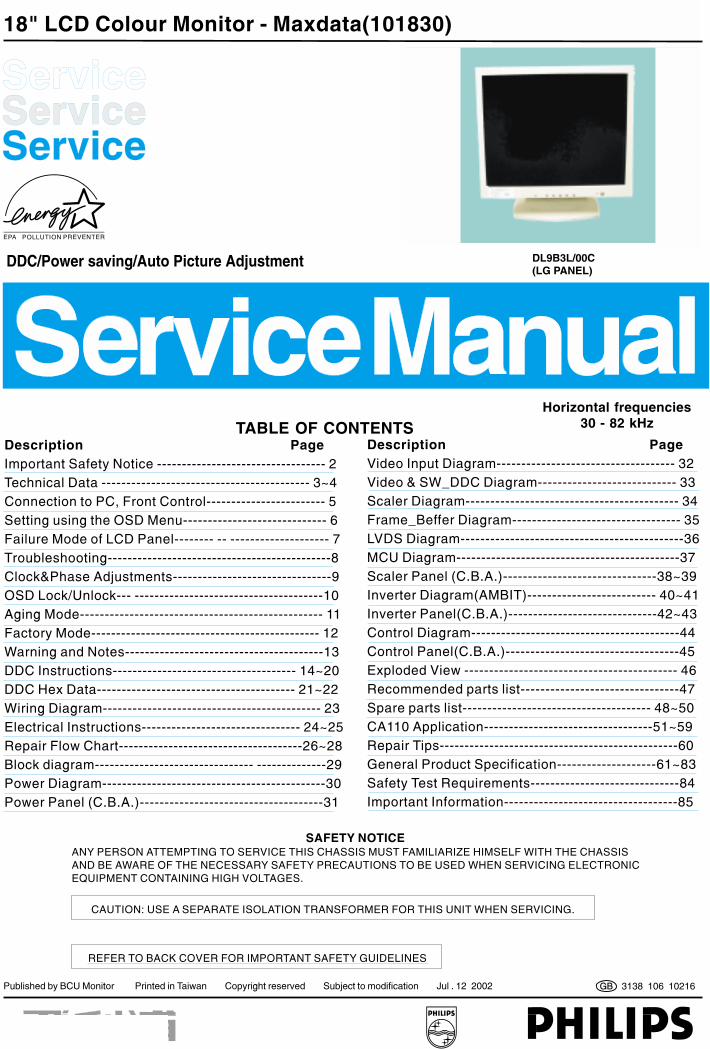
18" LCD Colour Monitor - Maxdata(101830) Horizontal frequencies 30 - 82 kHz Service Service Service TABLE OF CONTENTS Published by BCU Monitor Printed in Taiwan Copyright reserved Subject to modification Jul . 12 2002 DDC/Power saving/Auto Picture Adjustment Description Page Important Safety Notice ---------------------------------- 2 Technical Data ------------------------------------------ 3~4 Connection to PC, Front Control------------------------ 5 Setting using the OSD Menu----------------------------- 6 Failure Mode of LCD Panel-------- -- -------------------- 7 Clock&Phase Adjustments--------------------------------9 OSD Lock/Unlock--- --------------------------------------10 Aging Mode------------------------------------------------- 11 Factory Mode---------------------------------------------- 12 Warning and Notes----------------------------------------13 DDC Hex Data---------------------------------------- 21~22 Wiring Diagram-------------------------------------------- 23 Troubleshooting---------------------------------------------8 DDC Instructions------------------------------------- 14~20 Electrical Instructions-------------------------------- 24~25 Repair Flow Chart-------------------------------------26~28 Block diagram-------------------------------- --------------29 Power Diagram---------------------------------------------30 Power Panel (C.B.A.)-------------------------------------31 Description Page Video Input Diagram--- Video & SW_DDC Diagram---------------------------- 33 Scaler Diagram------------------------------------------- 34 Frame_Beffer Diagram---------------------------------- 35 LVDS Diagram---------------------------------------------36 MCU Diagram---------------------------------------------37 Scaler Panel (C.B.A.)-------------------------------38~39 Inverter Diagram(AMBIT)-------------------------- 40~41 Inverter Panel(C.B.A.)------------------------------42~43 Control Diagram------------------------------------------44 Control Panel(C.B.A.)-----------------------------------45 Exploded View ------------------------------------------- 46 Recommended CA110 Application----------------------------------51~59 General Product Specification--------------------61~83 Safety Test Requirements------------------------------84 Important Information-----------------------------------85 --------------------------------- 32 parts list--------------------------------47 Spare parts list-------------------------------------- 48~50 Repair Tips------------------------------------------------60 REFER TO BACK COVER FOR IMPORTANT SAFETY GUIDELINES CAUTION: USE ASEPARATE ISOLATION TRANSFORMER FOR THIS UNIT WHEN SERVICING. ANY PERSON ATTEMPTING TO SERVICE THIS CHASSIS MUST FAMILIARIZE HIMSELF WITH THE CHASSIS AND BE AWARE OF THE NECESSARY SAFETY PRECAUTIONS TO BE USED WHEN SERVICING ELECTRONIC EQUIPMENT CONTAINING HIGH VOLTAGES. SAFETY NOTICE GB 3138 106 10216 DL9B3L/00C (LG PANEL)
-
Upload
khangminh22 -
Category
Documents
-
view
6 -
download
0
Transcript of Service Service Service - OZ1JZN
18" LCD Colour Monitor - Maxdata(101830)
Horizontal frequencies30 - 82 kHz
ServiceService
Service
TABLE OF CONTENTS
Published by BCU Monitor Printed in Taiwan Copyright reserved Subject to modification Jul . 12 2002
DDC/Power saving/Auto Picture Adjustment
Description Page
Important Safety Notice ---------------------------------- 2
Technical Data ------------------------------------------ 3~4
Connection to PC, Front Control------------------------ 5
Setting using the OSD Menu----------------------------- 6
Failure Mode of LCD Panel-------- -- -------------------- 7
Clock&Phase Adjustments--------------------------------9
OSD Lock/Unlock--- --------------------------------------10
Aging Mode------------------------------------------------- 11
Factory Mode---------------------------------------------- 12
Warning and Notes----------------------------------------13
DDC Hex Data---------------------------------------- 21~22
Wiring Diagram-------------------------------------------- 23
Troubleshooting---------------------------------------------8
DDC Instructions------------------------------------- 14~20
Electrical Instructions-------------------------------- 24~25
Repair Flow Chart-------------------------------------26~28
Block diagram-------------------------------- --------------29
Power Diagram---------------------------------------------30
Power Panel (C.B.A.)-------------------------------------31
Description Page
Video Input Diagram---
Video & SW_DDC Diagram---------------------------- 33
Scaler Diagram------------------------------------------- 34
Frame_Beffer Diagram---------------------------------- 35
LVDS Diagram---------------------------------------------36
MCU Diagram---------------------------------------------37
Scaler Panel (C.B.A.)-------------------------------38~39
Inverter Diagram(AMBIT)-------------------------- 40~41
Inverter Panel(C.B.A.)------------------------------42~43
Control Diagram------------------------------------------44
Control Panel(C.B.A.)-----------------------------------45
Exploded View ------------------------------------------- 46
Recommended
CA110 Application----------------------------------51~59
General Product Specification--------------------61~83
Safety Test Requirements------------------------------84
Important Information-----------------------------------85
--------------------------------- 32
parts list--------------------------------47
Spare parts list-------------------------------------- 48~50
Repair Tips------------------------------------------------60
REFER TO BACK COVER FOR IMPORTANT SAFETY GUIDELINES
CAUTION: USE A SEPARATE ISOLATION TRANSFORMER FOR THIS UNIT WHEN SERVICING.
ANY PERSON ATTEMPTING TO SERVICE THIS CHASSIS MUST FAMILIARIZE HIMSELF WITH THE CHASSIS
AND BE AWARE OF THE NECESSARY SAFETY PRECAUTIONS TO BE USED WHEN SERVICING ELECTRONIC
EQUIPMENT CONTAINING HIGH VOLTAGES.
SAFETY NOTICE
GB 3138 106 10216
DL9B3L/00C(LG PANEL)
MW
MW
MW
GB
MW
Service Service Service
MW
DL9B3L/00C

Important Safety Notice2
FOR PRODUCTS CONTAINING LASER :
DANGER- Invisible laser radiation when open.
AVOID DIRECT EXPOSURE TO BEAM.
CAUTION- Use of controls or adjustments or
performance of procedures other than
those specified herein may result in
hazardous radiation exposure.
CAUTION- The use of optical instruments with this
product will increase eye hazard.
TO ENSURE THE CONTINUED RELIABILITY OF THIS PRODUCT, USE ONLY ORIGINAL MANUFACTURER'S
REPLACEMENT PARTS, WHICH ARE LISTED WITH THEIR PART NUMBERS IN THE PARTS LIST SECTION OF THIS
SERVICE MANUAL.
Proper service and repair is important to the safe, reliable
operation of all Maxdata Company** Equipment. The service
procedures recommended by Maxdata and described in this
service manual are effective methods of performing service
operations. Some of these service operations require the use
of tools specially designed for the purpose. The special tools
should be used when and as recommended.
It is important to note that this manual contains various
CAUTIONS and NOTICES which should be carefully read in
order to minimize the risk of personal injury to service
personnel. The possibility exists that improper service
methods may damage the equipment. It is also important to
understand that these CAUTIONS and NOTICES ARE NOT
EXHAUSTIVE. Maxdata could not possibly know, evaluate
and advise the service trade of all conceivable ways in which
service might be done or of the possible hazardous
consequences of each way. Consequently, Maxdata has not
undertaken any such broad evaluation. Accordingly, a
servicer who uses a service procedure or tool which is not
recommended by Maxdata must first satisfy himself
thoroughly that neither his safety nor the safe operation of the
equipment will be jeopardized by the service method selected.
* * Hereafter throughout this manual, Maxdata Company will be referred to as Maxdata.
WARNING
Critical components having special safety characteristics are
identified with a by the Ref. No. in the parts list and
enclosed within a broken line*(where several critical components are grouped in one area)
along with the safety symbol on the schematics or
exploded views.
Use of substitute replacement parts which do not have the
same specified safety characteristics may create shock, fire,
or other hazards.
Under no circumstances should the original design be
modified or altered without written permission from Maxdada.
Maxdata assumes no liability, express or implied, arising out
of any unauthorized modification of design. Servicer assumes all liability.
* Broken Line
Take care during handling the LCD module with backlight
unit
- Must mount the module using mounting holes arranged in four
corners. - Do not press on the panel, edge of the frame strongly or electric
shock as this will result in damage to the screen. - Do not scratch or press on the panel with any sharp objects, such
as pencil or pen as this may result in damage to the panel. - Protect the module from the ESD as it may damage the electronic
circuit (C-MOS). - Make certain that treatment person’s body are grounded through
wrist band. - Do not leave the module in high temperature and in areas of high
humidity for a long time. - Avoid contact with water as it may a short circuit within the module. - If the surface of panel become dirty, please wipe it off with a soft
material. (Cleaning with a dirty or rough cloth may damage the
panel.)
Go to cover page
Max 101830

3Technical DataGo to cover page
Technical Specifications Pin AssignmentD-Sub connector
Pin No. Assignment
1 Red video input
2 Green video input
3 Blue video input
4 Ground
5 Not connected
6 Red return
7 Green return
8 Blue return
9 + 5v DDC
10 Ground
11 Ground
12 SDA (DDC data)
13 Hor. Sync
14 Vert. Sync
15 SCL (DDC Clock)
The digital/analog DVI-I onnector contains 29 signal contacts organized in three rows of eight contacts. Signal pin assignments are listed in the following table:
15
6
10
1115
Pin No. Description
1 TMDS data2- 2 TMDS data2+ 3 TMDS data2 shield 4 NC 5 NC 6 DDC clock 7 DDC data 8 Not connected- 9 TMDS data1- 10 TMDS data1+ 11 TMDS data1 shield 12 NC 13 NC 14 +5V 15 Ground(return for +5V and H/Vsync) 16 Hot plug detect 17 TMDS data0- 18 TMDS data0+ 19 TMDS data0 shield 20 NC 21 NC 22 TMDS clock shield 23 TMDS clock+ 24 TMDS clock- C1 Analog R C2 Analog G C3 Analog B C4 Analog H-sync C5 Analog Vert. Sync.
1.1 LCD
Type NR. : LM181E05-C3 (LG-Philips)Outside dimensions : 389(w)317.2(h)27(d) (Typ) mmPitch ( mm ) : 0.2805 (per one triad) x 0.2805mmColor pixel arrangement : RGB vertical stripesDisplay surface : low reflection, antiglare with hard coatingNumber of color : 256 gray levels(8 bits)Backlight : CCFL edge light systemActive area(WxH) : 359x287.2mm (18” diagonal)View angle : Horizontal & Vertical 160 degree (CR>=10)Contrast ratio : 350:1White luminance : 250 nits (Typ)
1.2 Scanning frequencies Hor. : 30 82 K Hz Ver. : 56 - 76 Hz1.3 Video dot rate : < 140 MHz1.4 Power input : 90-264 V AC, 50/60 2 Hz1.5 Power consumption : < 60 W maximum ( exclude USB option )1.6 Dimensions : 426 * 454 * 180 mm1.7 Weight : 8.4 KGS
1.8 Functions : D-shell analog R/G/B separate inputs, H/V sync separated, Composite (H+V) TTL level, DVI digital Panel Link TMDS input1.9 Ambient temperature : 5 C - 35 C
2 Electrical characteristics
2.1 Interface signals The input signals can be applied in three different modes : 1). D-shell Analog
Input signal : Video, Hsync., Vsync
Video : 0.7 Vp-p, input impedance, 75 ohm @DC
Sync. : Separate sync TTL level , input impedance 2k2 ohm
terminate
Hor. sync Positive/Negative
Ver. sync Positive/Negative
Composite sync TTL level, input impedance 2k2 ohm terminate
(Positive/Negative)
Sync on green video 0.3 Vp-p Negative (Video 0.7 Vp-p Positive)
2). Intel DVI Digital
Input signal : Single channel TMDS signal
2.1.1 Audio
Input signal level : 500mVrms
Headphone output signal level : 32ohm 0.7+0.7 Vrms
Input signal connector : 3.5 mm mini jack
Loud speaker : 2+2 W stereo firing
2.1.2 Microphone
Sensitivity: -65± 5 dB re 1V/ubar at 1khz
Output impendence : 600 ohm typical
Max 101830

Technical Data(Continued)4
Go to cover page
Max 101830
Allowed 85 Hz overscan signal mode specified
Once the signal input of PC is 85Hz, this monitor is able to displayat least for 10 minutes . An attention signal appears and shows “This is 85Hz overscan for 5 seconds, change computer display input to 1024X768 @ 60 Hz “
Dot rate (MHz) H.freq (KHz) Mode Resolution V.freq (Hz) 36.000 43.269 VESA 640 * 480 85.008 56.250 53.674 VESA 800 * 600 85.061 94.500 68.677 VESA 1024 * 768 84.997
Input signal mode
Factory preset 16 modes (F)
PRESET VIDEO RESOLUTION
Pre-set 32 modes (P)
PRESET VIDEO RESOLUTION
Power management
The power consumption and the status indication of the setwith power management function are as follows,
Note : Disconnect DVI signal cable and audio module.
STATUS Horizontal Vertical Power Spec LEDOn Pulse Pulse as normal on GreenStand-by No Pulse Pulse < 2 W AmberSuspend Pulse No Pulse < 2 W Amberoff No Pulse No Pulse < 2 W Amber
According to VESA power saving signaling. TCO99 power saving requirement EPA energy star requirement
(Power Switch Off)
for Digital input power consumption is less 2W
( In non-DMPM recoverable off mode)
# Resolution Frequency Pixel rate Sync Comment
1 640X350 31.5K/70HZ 25.175 (+/-) IBM VGA 10h
2 720X400 31.5K/70HZ 28.322 (-/+) IBM VGA 3h
3 640X480 37.5K/75HZ 31.501 (-/-)
4 640X480 35.0K/67HZ 30.24 (-/-)
5 640X480 31.5K/60HZ 25.175 (-/-)
6 800X600 35.2K/56HZ 36 (+/+)
7 800X600 46.9K/75HZ 49.498 (+/+)
8 800X600 37.9K/60HZ 40 (+/+)
9 832X624 49.7K/75HZ 57.28 (+/+) MAC
10 1024X768 60.0K/75HZ 78.75 (+/+)
11 1024X768 48.4K/60HZ 65 (-/-)
12 1152X870 68.7K/75HZ 100 (-/-) MAC
13 1152X900 71.8K/76HZ 108 (+/+) SUN Mode II
14 1280X1024 64.0K/60HZ 108 (+/+)
15 1280X1024 80.0K/75HZ 135 (+/+)
16 688X556 31.3K/50HZ 27 (-/+) TV-PAL
# Resolution Frequency Pixel rate Sync Comment
1 640X350 31.5K/70HZ 25.175 (+/-) IBM VGA 10h
2 720X400 31.5K/70HZ 28.322 (-/+) IBM VGA 3h
3 640X480 37.5K/75HZ 31.501 (-/-)
4 640X480 43.3K/85HZ 36 (-/-)
5 640X480 37.9K/72HZ 31.5 (-/-)
6 640X480 35.0K/67HZ 30.24 (-/-)
7 640X480 31.5K/60HZ 25.175 (-/-)
8 800X600 35.2K/56HZ 36 (+/+)
9 800X600 46.9K/75HZ 49.498 (+/+)
10 800X600 37.9K/60HZ 40 (+/+)
11 800X600 53.7K/85HZ 56.251 (+/+)
12 832X624 49.7K/75HZ 57.28 (+/+) MAC
13 800X600 48.1K/72HZ 50 (+/+)
14 1024X768 60.0K/75HZ 78.75 (+/+)
15 1024X768 48.4K/60HZ 65 (-/-)
16 1024X768 56.5K/70HZ 75 (-/-)
17 1024X768 61.1K/76HZ 83.096 (+/+) IBM XGA-2
18 1024X768 68.7K/85HZ 94.5 (+/+)
19 1152X864 67.5K/75HZ 108 (+/+)
20 1152X864 63.9K/70HZ 94.5 (+/+) non-VESA
21 1152X864 54.0K/60HZ 79.9 (+/+) non-VESA
22 1152X870 68.7K/75HZ 100 (-/-) MAC
23 1152X900 61.8K/66HZ 92.94 serr- SUN Mode IV
24 1152X900 71.8K/76HZ 108 (+/+) SUN Mode II
25 1280X960 60.0K/60HZ 108 (+/+)
26 1280X960 75.0K/75HZ 129.895 (+/+) non-VESA
27 1280X1024 76.0K/72HZ 130.223 (+/+) DOS/V
28 1280X1024 64.0K/60HZ 108 (+/+)
29 1280X1024 80.0K/75HZ 135 (+/+)
30 1280X1024 81.1K/76HZ 135.008 (-/-) SUN Mode I
31 1280X1024 71.7K/67HZ 117 (+/+) SUN Mode V
32 688X556 31.3K/50HZ 27 (-/+) TV-PAL
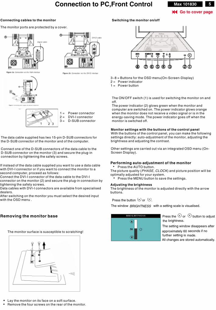
Connection to PC,Front Control 5
Go to cover page
Connecting cables to the monitor
The monitor ports are protected by a cover.
1 = Power connector2 = DVI-I connector3 = D-SUB connector
The data cable supplied has two 15-pin D-SUB connectors forthe D-SUB connector of the monitor and of the computer.
Connect one of the D-SUB connectors of the data cable to theD-SUB connector on the monitor (3) and secure the plug-inconnection by tightening the safety screws.
If instead of the data cable supplied you want to use a data cablewith DVI-I connector or if you want to connect the monitor to asecond computer, proceed as follows:Connect the DVI-I connector of the data cable to the DVI-Iconnector on the monitor (2) and secure the plug-in connection bytightening the safety screws.Data cables with DVI-I connectors are available from specialiseddealers.After switching on the monitor you must select the desired inputwith the OSD menu .
Switching the monitor on/off
The ON/OFF switch (1) is used for switching the monitor on andoff.The power indicator (2) glows green when the monitor andcomputer are switched on. The power indicator glows orangewhen the monitor does not receive a video signal or is in theenergy-saving mode. The power indicator goes off when themonitor is switched off.
3~8 = Buttons for the OSD menu(On-Screen-Display)2 = Power indicator1 = Power button
Monitor settings with the buttons of the control panelWith the buttons of the control panel, you can make the followingsettings directly: auto-adjustment of the monitor, adjusting thebrightness and adjusting the contrast.
Other settings are carried out via an integrated OSD menu (On-Screen Display).
Performing auto-adjustment of the monitorPress the AUTO button.
The picture quality ( , ) and picture position will beoptimally adjusted for your system.
Press the MENU button to save the settings.
The brightness of the monitor is adjusted directly with the arrowbuttons.
PHASE CLOCK
Adjusting the brightness
Press the button or .
BRIGHTNESS
Press the or button to adjust
the brightness.
The setting window disappears after
approximately 60 seconds if no
further setting is made.
All changes are stored automatically.
B R I G H T N E S S
50
The window with a setting scale is visualised.
Removing the monitor base
The monitor surface is susceptible to scratching!
Lay the monitor on its face on a soft surface.Remove the four screws on the rear of the monitor.
1 2 3
Max 101830

Settings using the OSD menu6
With the buttons on the control panel, call up and use theintegrated OSD (On-Screen Display) menu.
The OSD menu is available in different languages. The Englishmenu names are used in the following description (default setting).With the OSD function you can select anotherlanguage.
The main menu appears on the screen with icons for the settingfunctions.
LANGUAGE
The first symbol ( ) ishighlighted.
If necessary, press the orbutton to mark another icon (e.g.
).
Press the MENU button to selectthe highlighted icon.
LANGUAGE
ADJUST POSITION
Press the or button toadjust the selected function(here: HORIZONTAL).
Press the key or tomark another function or pressthe MENU key to return to themain menu.
Select the symbol (EXITMAIN CONTROLS) in themain menu and press the MENUkey to exit the OSD menu.
The corresponding setting window (here: )is displayed.
ADJUST POSITION
Setting language for the OSD menu
Adjusting picture position
?
Calling the ADJUST POSITION setting window
Horizontal picture position ( HORIZONTAL
the picture to the left or to the right
Vertical picture position ( VERTICAL ): Shiftingthe picture down or up
): Shifting
Adjusting the brightness and contrast
Calling the BRIGHTNESS & CONTRAST setting window
Setting the brightness of the display(BRIGHTNESS)
Setting the contrast of the display ( CONTRAST )
Setting the colour temperature
The "warmth" of the screen colours is set using the colourtemperature. The colour temperature is measured in K (= Kelvin).
Setting the picture quality
Eliminating picture interference (VIDEO NOISE )
Eliminating picture noise and horizontal interference(PHASE)
Eliminate vertical interference with local fuzziness(CLOCK)
Calling the ADJUST COLOR setting window
ORIGINAL PANEL COLOR = Setting for general
applications (default setting)
9300K FOR CAD/CAM = Setting for CAD/CAM programmes
6500K FOR IMAGE MANAGEMENT = Setting, for example,
for image processing or playing DVDs
USER PRESET = User - defined setting
In the user - defined setting you can change the colour
ratios of the basic colours (red, green, blue) as required.
Setting position for the OSD menu
Calling the OSD SETTINGS setting window
You can shift the OSD menu up, down, to the left or to theright.
Displaying monitor data
You will find the serial number and the current resolution
of this screen in PRODUCT INFORMATION.
i
Activating the factory settings
Activating the factory settings(RESET TO FACTORY
NO = retain own settings
YES = Activating the factory settings
WithYES all monitor settings are reset to the factory settings.
SETTINGS)
Selecting input signal
The monitor can be operated with analog or digital signals. With this
function you can (depending on the graphics card you use) switch over
between the analog and the digital mode.
Calling the INPUT SELECTION setting window
Switch on the analog mode ( ANALOG DSUB ).The monitor
processes the signals of the analog port (VGA/D- SUB).
Switch on the digital mode ( DIGITAL DVI ). The monitor
processes the signals of the digital port (DVI - I).
Switch on analog mode via digital port ( ANALOG DVI ).
The monitor processes the analog signals of the digitalport (DVI -I).
Locking the OSD menu (OSD Lock)
The OSD menu can be locked to prevent accidental orunauthorised changes to the monitor settings.Press the MENU button and hold it for approx. 10 seconds.Please proceed in the same manner to release the locked OSDmenu again.
Setting language for the OSD menu ( )You can choose from English (default setting), German,French, Spanish, Italian, and Japanese.
LANGUAGE
Go to cover page
Max 101830

7
Go to cover page
Max 101830Failure Mode of LCD panel
Quick reference for failure mode of LCD panel
This page presents problems that could be made by LCD panel. It isnot necessary to repair circuit board. Simply follow the Mechanicalinstruction o n this manual to eliminate failure by replace LCD panelor backlight tubes.
Failure description Phenomenon
Vertical dim lines
Vertical block defect
Vertical lines defect(Always bright or dark)
Horizontal block defect
Horizontal dim lines
Horizontal lines defect(Always bright or dark)
Has bright or dark pixel.
..
.
..
.
..
.
..
Bright pixel
Dark pixel
..
. .. .
Polarizer has bubbles
Polarizer has bubbles
Foreign material insidepolarizer. It shows linear ordot shape.
. .. .
Concentric circle formed
Bottom back light of LCD isbrighter than normal
Backlight un-uniformity
Backlight has foreignmaterial. Black or whitecolor, linear or circular type
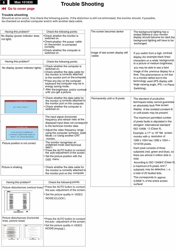
8 Trouble ShootingGo to cover page
Trouble shootingShould an error occur, first check the following points. If the distortion is still not eliminated, the monitor should, if possible,be checked on another computer and/or with another data cable.
Having this problem? Check the following points:
No display (power indicator does
not light)
Check whether the monitor isswitched on.
Checkwhether the power cableon themonitor is connectedcorrectly.
Check whether the computer isswitched on.
Having this problem? Check the following points:
No display (power indicator lights)Check whether the computer isswitched on.Check whether the data cable forthe monitor is correctly attached
to the monitor port on thecomputer.
Press any key on the computerkeyboard the computer may be in
Alter the brightness and/or contrastuntil you get a picture.
Check whether the data cable forthe monitor is correctly attached tothe monitor port on the computer.Check whether the computer isswitched on.
The input signal (horizontalfrequency and refresh rate) at the
displayed input does not correspond
to the technical monitor data.
Adjust the video frequency rangeusing the computer sof tware (safe
Picture position is not correct The monitor recognises anundefined mode (see
").
Press the AUTO button to conductthe
Technicaldata
auto-adjustment of the screen.
Set the picture position with the
OSD menu .
Picture is shaking Check whether the data cable forthe monitor is correctly attached to
the monitor port on the computer.
Having this problem? Check the following points:
Picture disturbances (vertical lines) Press the AUTO button to conduct
the auto-adjustment of the screen.
Set the picture quality in VIDEO
NOISE(CLOCK ).
Picture disturbances (horizontallines, picture noise)
Press the AUTO button to conductthe auto -adjustment of the screen.
Set the picture quality in VIDEONOISE(PHASE).
The screen becomes darker The background lighting has alimited lifetime.If your monitordisplay should become too dark,the
exchanged.background lighting will have to be
Image of last screen display still
visibleIf you switch from a high- contrast
display (for example black lines/
characters on a white background)to a picture of medium brightness,
you may be able to see a faint
image of the previous display for a
time. This phenomenon is not due
to a monitor defect but to the
technology used (IPS display with
large viewing angle, IPS = In Plane
Switching).
Permanently unlit or lit pixels The standard of production
techniques today cannot guarantee
an absolutely fault -free screen
display. A few isolated constant lit
or unlit pixels may be present.
The maximum permitted number
of pixels faults is stipulated in the
stringent international standard
ISO 13406 - 2 (Class II).
Example: a 17" or 18" flat- screen
monitor with a resolution of
1280 x 1024 has 1280 x 1024 =
1310720 pixels.
Each pixel consists of three
subpixels (red, green and blue), so
there are almost 4 million dots in
total.
According to ISO 13406-2 (Class II),
a maximum of 6 pixels and 7
subpixels may be defective, i. e.
a total of 25 faulted dots.
This corresponds to approx.
0,0006 % of the entire screen
surface!
energy saving mode.
Mode ) or Using another CRTmonitor.
Max 101830

CLOCK & PHASE Adjustments 9
Step 1 : Click on the Start button (Win95, Win98 or Win NT)and choose " Shut Down...". as shown in Fig. 2.
Step 2 : The menu of " Shut Down Windows " is as shown in Fig. 3
Step 3 : Retain Shut Down Window on the screen , followthe CLOCK and PHASE adjustment instructions for theoptimal video display.
PHASE phenomenon
Due to the different quality of video signal generated from graphicscards. By press AUTO button for
t is necessary to adjustCLOCK and PHASE functions for the optimal video display of LCDmonitor by manual. Following steps will guide you to make correctadjustment of CLOCK and PHASE.
However, CLOCK and PHASE functions are only available while analogvideo signal is supplied. Operating unit under digital signal state, thevideo clock information can be obtained from graphics cards directly.Therefor, it is unnecessary to adjust these functions.
CLOCK and PHASE adjustmentautomatically. Sometimes, the deviation of video signal which generatedfrom graphics cards is out of control, then i
Manual adjustment
If the quility of display still poor or flicker, you may also improve it bymanual adjust CLOCK and PHASE functions to eliminate the flicker.
Step 4 : Press the MENU button to bring up MAIN CONTROLS(OSD menu).
Step 8 : Press or to adjust PHASE. The picture willbe adjusted as following figure, adjust PHASE and check thepicture, stop at the point that without any vertical jitter barremaining on the screen.
button
Step 5 : Select Video Noise by press button.Step 6 : Press to bring up it s submenu.button
Step 7 : Press or to adjust CLOCK. The picture willbe adjusted as following figure, adjust CLOCK to fine-tune thevideo until optimal display is obtained.
button
Step 9 : Quit OSD menu by press button to save the settings.
CLOCK Phenomenon
Video Noise
(Auto adjustment hotkey)Front control panel
1 = Buttons for the OSD menu (On-Screen-Display)2 = Power indicator3 = Power button
2 31
AUTO MENUINPUT
AUTO button
MENU
MENU
MENU
The monitor has build-in a auto adjustment hotkey on the front panel,you may obtained a optimal video display by simply press thebutton and save the settings. CLOCK, PHASE, Vertical position, andHorizontal position are adjusted automatically.
AUTO
Fig. 1
Fig. 2
(Before)
(Before)
(After)
(After)
Fig. 3 (Win 98)
MENU
MENU
Go to cover page
Max 101830

10 OSD Lock/Unlock, Attention signal, Service ModeGo to cover page
Front control panel
ATTENTION
OSD MAIN CONTROLS LOCKED
ATTENTION
OSD MAIN CONTROLS UNLOCKED
ATTENTION
ATTENTION SIGNAL OFF
ATTENTION
ATTENTION SIGNAL ON
To Lock/Unlock OSD function (User Mode)
The OSD function can be locked by pressing button for more than
10 seconds, the screen shows following windows for 3 seconds.
Everytime when you press or button, this message appears
on the screen automatically. The & (brightness) ,
(input) hotkey are still functional for brightness and input signal
selection while OSD locked.
Switch ON/OFF attention signals (User Mode)
All attention signals can be by keep pressing button
for more than 10 seconds if there is no video signal supplied.
Step 1: Disconnect signal cable (Monitor & PC are still ON.)
Step 2: Press "AUTO" button for more than 10 seconds, bring up
message as below.
switched off
Recover attention signals by pressing button for more than 10
seconds without video signal input.
Step 1: Disconnect signal cable (Monitor & PC are still ON.)
Step 2: Press "AUTO" button for more than 10 seconds again,
bring up message as below.
Access Service Mode (in USER MODE)
Method 1:
Leave service mode by either re-feed video signal or simply turn off
and on the power of monitor.
Step 1: Disconnect signal cable on Rear side of monitor.
Don't disconnect signal cable on PC side, because CPU will
detect pin-9 of D-SUB (15 pin connector).
(Monitor & PC are still ON.)
Bring up "CHECK CABLE CONNECTION" screen.
Step 2: Press MENU" " button for more than 15 seconds.
Bring up message as below.
Access Service Mode (in USER MODE)
Method 2:
Leave service mode by either re-feed video signal or simply turn off
Step 1:
- Turn off monitor.
- Disconnect signal cable on PC side.
- Turn on monitor.
(After 3 seconds)
Bring up "NO VIDEO INPUT"
Step 2: Press MENU" " button for more than 15 seconds.
Bring up "SERVICE MODE".
Access Service Mode (in USER MODE)
Method 3:
Leave service mode :simply turn off and on the power of monitor.
Step 1:
- PC off.
- Signal cable connect to rear side of Monitor only.
- Turn on monitor.
Bring up "NO VIDEO INPUT"
Step 2: Press MENU" " button for more than 15 seconds.
Bring up "SERVICE MODE".
AUTO
AUTO
AUTO
MENU
MENU
Locked OSD function can be released by pressing button for
more than 10 seconds again. While press "MENU" button for OSD
unlocked purpose, the screen will keep showing OSD MAIN
CONTROLS LOCKED u ntil OSD function unlocked and screen
automatically shows following window for 3 seconds.
MENU
1 = Buttons for the OSD menu (On-Screen-Display)2 = Power indicator3 = Power button
2 31
AUTO MENUINPUT
INPUT
ATTENTION
CHECK CABLE CONNECTION
ATTENTION
NO VIDEO INPUT
ATTENTION
NO VIDEO INPUT
MENU
MENU
SERVICE MODE
SERIAL NO. : YEKA105542HOURS OF OPERATION: 000222
MENU
SERVICE MODE
SERIAL NO. : TW211P0022HOURS OF OPERATION: 000205
SERVICE MODE
SERIAL NO. : TW211P0022HOURS OF OPERATION: 000205
Max 101830

11
Go to cover page
AGING Mode
Bring up :
After 15 seconds, bring up :
After 15 seconds, bring up :
After 15 seconds, bring up :
--------------------repeatly
Connect signal cable again => go back to normal display.
Front control panel
Access Aging.. Mode (Method 1)
(Monitor & PC are ON for Step 1.)Step 1: Disconnect signal cable on Rear side of monitor. Bring up "CHECK CABLE CONNECTION" screen.
or Disconnect signal cable on PC side. Bring up "ENTERING SLEEP MODE" about 3 seconds, then disappear.
Step 2:
Turn off LCD monitor.
Push AUTO " " & " " & " " buttons simultaneously ,then release Power buttun only, untill picture comes on the screen. Bring up "AGING ...".
1 = Buttons for the OSD menu (On-Screen-Display)2 = Power indicator3 = Power button
2 31
AUTO MENUINPUT
ATTENTION
CHECK CABLE CONNECTION
ATTENTION
ENTERING SLEEP MODE
AUTO
A G I N G. . .A G I N G. . .
A G I N G. . .A G I N G. . .
Method 2:
Leave AGING mode :connect signal cable to PC, then turn on PC.
Step 1: - PC off and Monitor off.- Signal cable connect to rear side of Monitor only.- Connect Power Cord to rear side of monitor, then insert the plug into a properly grounded electrical outlet. (Power LED of monitor is off now.)
Step 2:Push AUTO " " & " " & " " buttons simultaneously ,then release Power buttun only, untill picture comes on the screen. Bring up "AGING ...".
------------------repeatly
AUTO
A G I N G. . .A G I N G. . .
Max 101830

12
Go to cover page
Factory Mode
Access Factory Mode
Factory Mode:How to Get into Factory Mode Menu
Turn off LCD monitor.
Push AUTO " " & " " & " " buttons simultaneously ,then release Power buttun only, untill picture comes on the screen. Press MENU " " button, bring up Factory mode indication as shown in Fig 2.
Fig. 2
Factory Mode indication==>
MAXDATA 180P V1.88 02-04-17
Contrast adjustment (Sub-Contrast). Use this menu item to adjust the contrast gain of pre-amp ranges from 0 to 255.
(For
9 3 0 0 K R G B6 5 0 0 K R G B Color temperature gain adjustment. Use these menu items to
adjust the RGB gains of pre-amp for different color temperatures, ranges from 0 to 255.
OFFSET R G B Sub-Brightness adjustment. Use this menu item to adjust the brightness level (DC-level) of pre-amp range from 0 to
255.(R/G/B ANALOG DC -level).
example: of Sub-Contrast in factory mode is preset for 100%(Maximum Value) of Contrast Value in user mode).
GAIN R G B R/G/B GAIN adjustment. Use this menu item to adjust the R/G/B (GAIN) of Amp. range from 0 to 255.(R/G/B
ANALOG GAIN Values).
AUTO SUB:
AUTO Colour to Adjust OFFSET R/G/B & GAIN R/G/B automatically by LCD MONITOR CPU.
RESERVE1: NO FUNCTIONED, RESERVED ONLY. RESERVE2: NO FUNCTIONED, RESERVED ONLY.RESERVE3: NO FUNCTIONED, RESERVED ONLY.
AUTO SUB:
Use button to select factory adjustment indication (for example: MAXDATA 180P V1.88 02-04-17), which is the entrance of the factory adjustment menu, press MENU " " button to access it. The window shows as below.
(PS: The “Offset R G B” function can be used on reduce or eliminate snowy noise on the background when the resolution of video signal is 1280 X 1024 vertical 60Hz. Slightly increase or decrease the value until snowy noise completely disappear.)
Default values (example) are as below.Default values (example) are as below.
Leave Factory Mode
Turn off monitor, then turn on monitor again => go backto User mode directly.
Leave Factory Mode
Turn off monitor, then turn on monitor again => go backto User mode directly.
SUB BRI:SUB BRI:-
- OKOK
255255
255255
-SUB CON:SUB CON:
NO FUNCTIONED,”DIGITAL DC-Level” RESERVED for LCD MONITOR 150P usage ONLY.
AUTO
MENU
Fig. 11 = Buttons for the OSD menu (On-Screen-Display)2 = Power indicator3 = Power button
2 31
AUTO MENUINPUT
MENU
9300K R G B9300K R G B
6500K R G B6500K R G B
OFFSET R G BOFFSET R G B
SUB CON:SUB CON:SUB BRI:SUB BRI: --
AUTO SUB:AUTO SUB:- OKOK
GAIN R G B GAIN R G B
RESERVE1: RESERVE1:
RESERVE3: RESERVE3: RESERVE2: RESERVE2:
MAXDATA 180P V1.88 02-04-17
0000
Fig. 3
AUTO
Use or buttons to select SUB-CON, 9300K R G B,..etc.
Use or buttons to decrease/increase the value of each item.
Press " " => go back to MAIN CONTROLS.
All the default values are invisible. Press " " => appear.
To press AUTO " " button on this screen, the values of OFFSET and GAIN will be adjusted by CPU automatically.
MENU
9300K R G B9300K R G B
6500K R G B6500K R G B
OFFSET R G BOFFSET R G B
SUB CON:SUB CON:SUB BRI:SUB BRI: --
AUTO SUB:AUTO SUB:- OKOK
GAIN R G B GAIN R G B
RESERVE1: RESERVE1:
RESERVE3: RESERVE3: RESERVE2: RESERVE2:
MAXDATA 180P V1.88 02-04-17
0000
8484188188
5050
182182
8686181181
8383
251251228228255255252252
255255
205205
255255255255
226226
Max 101830

13
Go to cover page
Warning and Notes
Fig.1
V
Warnings
1. Safety regulations require that the unit should be returned in its original condition and that components identical to the original components are used. The safety components are indicated by the symbol .
2. In order to prevent damage to ICs and transistors, all high-voltage flash-overs must be avoided. In order to prevent damage to the picture tube, the method shown in Fig. 1 should be used to discharge the picture tube. Use a high-voltage probe and a multimeter (position DC-V). Discharge until the meter reading is 0 V (after approximately 30 seconds).
3. ESD All ICs and many other semiconductors are sensitive to electrostatic discharges (ESD). Careless handling during repair can drastically shorten their life. Make sure that during repair you are connected by a pulse band with resistance to the same potential as the ground of the unit. Keep components and tools also at this same potential.
4. When repairing a unit, always connect it to the AC Power voltage via an isolating transformer.
5. Be careful when taking measurements in the high-voltage section and on the picture tube panel.
6. It is recommended that saferty goggles be worn when replacing the picture tube.
7. When making adjustments,use plastic rather than metal tools. This will prevent any short-circuit or the danger of a circuit becoming unstable.
8. Never replace modules or other components while the unit is switched on.
9. Together with the defleciton unit, the picture tube is used as an integrated unit. Adjustment of this unit during repair is not recommended.
10. After repair, the wiring should be fastened in place with the cable clamps.
11. All units that are returned for service or repair must pass the original manufactures safety tests.
Notes
1. The direct voltages and waveforms are average voltages. They have been measured using the Service test software and under the following conditions : - Mode : 640 * 480 (31.5kHz / 60Hz) - Signal pattern : grey scale - Adjust brightness and contrast control for the mechanical mid-position (click position)
2. The picture tube panel has printed spark gaps. Each spark gap is connected between an electrode of the picture tube and the Aquadag coating.
3. The semiconductors indicated in the circuit diagram(s) and in the parts lists are completely interchangeable per position with the semiconductors in the unit, irrespective of the type indication on these semiconductors.
(CRT ONLY)
Max 101830
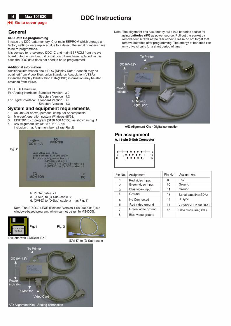
DDC Instructions
General
Pin assignment
1106
11 15
5
Assignment AssignmentPin No. Pin No.
Ground
No Connected
GroundBlue video input
2
7
6
8
4
5
3
1 9
12
11
14
13
15
10
Red video ground
Blue video ground
Green video ground
+5V
Ground
Data clock line(SCL)
V.Sync(VCLK for DDC)
H.Sync
Serial data line(SDA)
Green video input
Red video input
A. 15-pin D-Sub Connector
DDC Data Re-programmingIn case the DDC data memory IC or main EEPROM which storage all factory settings were replaced due to a defect, the serial numbers have to be re-programmed.It is advised to re-soldered DDC IC and main EEPROM from the old board onto the new board if circuit board have been replaced, in this case the DDC data does not need to be re-programmed.
Additional informationAdditional information about DDC (Display Data Channel) may be obtained from Video Electronics Standards Association (VESA). Extended Display Identification Data(EDID) information may be also obtained from VESA.
DDC EDID structure For Analog interface: Standard Version 3.0 Structure Version 1.2For Digital inferface: Standard Version 3.0 Structure Version 1.3
System and equipment requirements1. An i486 (or above) personal computer or compatible.2. Microsoft operation system Windows 95/98.3. EDID301.EXE program (3138 106 10103) as shown in Fig. 14. A/D Alignment kits (3138 106 10079): inclusion : a. Alignment box x1 (as Fig. 2)
b. Printer cable x1 c. (D-Sub) to (D-Sub) cable x1
d. (DVI-D) to (D-Sub) cable x1 (as Fig. 3)
Note: The EDID301.EXE (Release Version 1.58 20000818)is a windows-based program, which cannot be run in MS-DOS.
Diskette with EDID301.EXE
EDID301.EXE
Ver:1.58
(DVI-D) to (D-Sub) cable
Note: The alignment box has already build-in a batteries socket for using batteries (9V) as power source. Pull out the socket by remove four screws at the rear of box. Please do not forget that remove batteries after programming. The energy of batteries can only drive circuits for a short period of time.
To Monitor
DC 8V~12V
Video CardVideo Card
To Printer
Powerindicator
A/D Alignment Kits - Analog connectionA/D Alignment Kits - Analog connection
A/D Alignment Kits - Digital connection A/D Alignment Kits - Digital connection
Fig. 2Fig. 2
Fig. 1Fig. 1 Fig. 3Fig. 3
To Monitor(Digital port)
DC 8V~12V
To Printer
Powerindicator
14
Go to cover page
Max 101830
Go to cover page
15DDC Instructions (Continued)
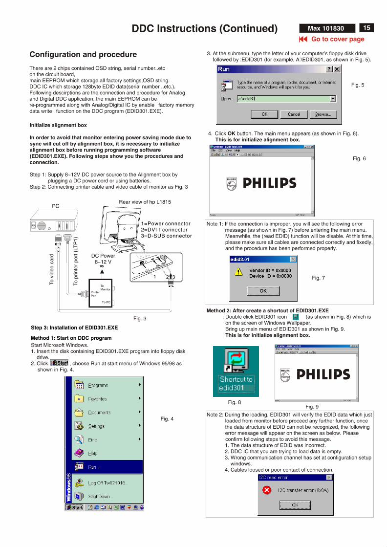
Step 3: Installation of EDID301.EXE
Method 1: Start on DDC program
Start Microsoft Windows.1. Insert the disk containing EDID301.EXE program into floppy disk drive.2. Click , choose Run at start menu of Windows 95/98 as
shown in Fig. 4.
Fig. 4
4. Click OK button. The main menu appears (as shown in Fig. 6). This is for initialize alignment box.
Fig. 6
Fig. 5
Fig. 7
Note 1: If the connection is improper, you will see the following error message (as shown in Fig. 7) before entering the main menu.
Meanwhile, the (read EDID) function will be disable. At this time, please make sure all cables are connected correctly and fixedly, and the procedure has been performed properly.
3. At the submenu, type the letter of your computer's floppy disk drive followed by :EDID301 (for example, A:\EDID301, as shown in Fig. 5).
Method 2: After create a shortcut of EDID301.EXE : Double click EDID301 icon (as shown in Fig. 8) which is on the screen of Windows Wallpaper. Bring up main menu of EDID301 as shown in Fig. 9. This is for initialize alignment box.
Fig. 9
Note 2: During the loading, EDID301 will verify the EDID data which just loaded from monitor before proceed any further function, once the data structure of EDID can not be recognized, the following error message will appear on the screen as below. Please
confirm following steps to avoid this message.1. The data structure of EDID was incorrect.2. DDC IC that you are trying to load data is empty.3. Wrong communication channel has set at configuration setup
windows.4. Cables loosed or poor contact of connection.
Fig. 8
1
Configuration and procedure
There are 2 chips contained OSD string, serial number..etc on the circuit board, main EEPROM which storage all factory settings,OSD string.DDC IC which storage 128byte EDID data(serial number ..etc.). Following descirptions are the connection and procedure for Analogand Digital DDC application, the main EEPROM can be re-programmed along with Analog/Digital IC by enable “factory memory data write” function on the DDC program (EDID301.EXE).
Initialize alignment box
In order to avoid that monitor entering power saving mode due to sync will cut off by alignment box, it is necessary to initialize alignment box before running programming software (EDID301.EXE). Following steps show you the procedures and connection.
Step 1: Supply 8~12V DC power source to the Alignment box by plugging a DC power cord or using batteries.
Step 2: Connecting printer cable and video cable of monitor as Fig. 3
Fig. 3
Rear view of hp L1815
1 2 3
1=Power connector2=DVI-I connector3=D-SUB connector
~~
PC
To p
rin
ter
po
rt (
LTP
1)
DC Power8~12 V
PrinterPort
To v
ide
o c
ard
To Monitor
To PC
Max 101830
MW
MW

16
Go to cover page
DDC Instructions (Continued)Max 101830
Re-programming Analog DDC ICStep 1: After initialize alignment box, connecting all cables and box as shown in Fig. 10
Fig. 11
Step 2: Read DDC data from monitor
1. Click icon as shown in Fig. 11 from the tool bar to bring up the Channels "Configuration Setup" windows as shown in Fig. 12.
Step 3: Modify DDC data (verify EDID version, week, year)
1. Click (new function) icon from the tool bar, bring up Step 1 of 9 as shown in Fig. 14 . EDID301 DDC application provides the function selection and text change (select & fill out) from Step 1 to Step 9.
Step 4: Modify DDC data (Monitor Serial No.)
1. Click Next , bring up Fig. 15.
2. Click Next , bring up Fig. 16.
3. Click OK button to confirm your selection.
4. Click icon (Read EDID function) to read DDC EDID data from monitor. The EDID codes will display on screen as shown in Fig. 13.
Fig. 15
Fig. 16
Fig. 12
2. Select the DDC2B as the communication channel. Select "Enable" & fill out "F0" for Mapped EDID page address as shown in Fig. 12.
Fig. 10
Rear view of hp L1815
1 2 3
1=Power connector2=DVI-I connector3=D-SUB connector
~~
PC
To v
ide
o c
ard
To p
rin
ter
po
rt (
LTP
1)
DC Power8~12 V
PrinterPort
To Monitor
To PC
Fig. 13
Fig. 14
< - -
-
< - -
- For AnalogFor Analog
select and fill out,if necessary.select and fill out,if necessary.
Do
n't
clo
se th
is s
cre
en
. --
->
Go to cover page
17DDC Instructions (Continued) Max 101830
Fig. 17Fig. 20
Fig. 21
Fig. 18
Fig. 19
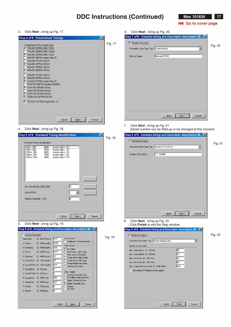
3. Click Next , bring up Fig. 17. 6. Click Next , bring up Fig. 20.
7. Click Next , bring up Fig. 21. (Serial number can be filled up or be changed at this moment.4. Click Next , bring up Fig. 18.
5. Click Next , bring up Fig. 19.
Fig. 22
8. Click Next , bring up Fig. 22. - Click Finish to exit the Step window.

18
Go to cover page
DDC Instructions (Continued)Max 101830
Fig. 25
Fig. 26
Fig. 27
Step 8: Save DDC dataSometimes, you may need to save DDC data as a text file for using in other IC chip. To save DDC data, follow the steps below:
1. Click (Save) icon (or click "file"-> "save as") from the tool bar and give a file name as shown in Fig. 25. The file type is EDID301 file (*.ddc) which can be open in WordPad. By using WordPad, the texts of DDC data & table (128 bytes, hex code) can be modified. If DDC TEXTS & HEX Table are completely correct, it can be saved as .ddc flie to re-load it into DDC IC & EEPROM for DDC Data application.
Step 9: Load DDC data
1. Click from the tool bar.2. Select the file you want to open as shown in Fig. 26.3. Click Open.
2. Click Save.
Step 9: Exit DDC program
Pull down the File menu and select Exit as shown in Fig. 27.
Step 5: Access Factory Mode for DDC data writing
Factory Mode:How to Get into Factory Mode Menu
Turn off LCD monitor.
Push AUTO " " & " " & " " buttons simultaneously ,then release Power buttun only, untill picture comes on the screen. Press MENU " " button, bring up Factory mode indication as shown in Fig 23.
Step 6: Write DDC data
1. Click (Write EDID) icon from the tool bar to write DDC data. (0% ~ 100%, -> READY)2. Click (Read EDID) to re-confirm (check contents) it.
Step 7: Reconfirm Monitor Serial Number in User Mode
1. Turn off monitor, then turn on monitor again => leave factory mode and return to User Mode directly. 2. Press "MENU" button -> select "PRODUCT INFORMATION" -> press "MENU" button -> bring up Fig. 24.
Fig. 24
Fig. 23
2 31
AUTO MENUINPUT
AUTO
MENU
Factory Mode indication==>
PRODUCT INFORMATIONSERIAL NO. : TY 123456RESOLUTION : 1024x768@60HZVIDEO INPUT : ANALOG (D-SUB)MENU BACK TO MAIN CONTROLS
MAXDATA 180P V1.88 02-04-17

19
Go to cover page
DDC Instructions (Continued) Max 101830
Re-programming Digital DDC IC (User mode)Connecting all cables and alignment box as shown in
Fig. 28.Step 1:
After connection for Digital DDC application, if it is still in Analog DDCapplication of EDID301. Exit EDID301 program before Digital DDC application.
Fig. 29
Fig. 30
Step 2: Initialize alignment box(Shortcut of EDID301.EXE on Double click EDID301 icon (as shown in Fig. 29) which is on the screen of Windows Wallpaper. Bring up main menu of EDID301 as shown in Fig. 30.
Windows Wallpaper already.)
Step 3: Read DDC data from monitor
1. Click icon from the tool bar to bring up the Channels Configuration Setup windows as shown in Fig. 30.
2. Select the DDC2B as the communication channel. Disable "Factory memory data write" for Digital DDC
application as shown in Fig. 31.
3. Click OK button to confirm your selection.
4. Click icon (Read EDID function) to read DDC EDID data from monitor. The EDID codes will display on screen as shown in Fig. 32.
Fig. 31
Fig. 32
Step 4: Modify DDC data (verify EDID version, week, year)
1. Click (new function) icon from the tool bar, bring up Step 1 of 9 (Digital) as shown in Fig. 33 . EDID30 DDC application provides the function selection and text change (select & fill out) from Step 1 to Step 9.
Fig. 34 Fig. 35
Fig. 28
Rear view of hp L1815
1 2 3
1=Power connector2=DVI-I connector3=D-SUB connector
~~
PC
To v
ide
o c
ard
To p
rin
ter
po
rt (
LTP
1)
DC Power8~12 V
To Monitor
To PC
PrinterPort
D-Sub connector
1
1
Fig. 33
< - -
< - -
For DigitalFor Digital
select and fill out,if necessary.select and fill out,if necessary.
MW

20
Go to cover page
DDC Instructions (Continued)Max 101830
Step 5: Modify DDC data (Monitor Serial No.)
Monitor Serial No. can be filled up or be changed (for example, TY 123456) as shown in Fig. 40.
Click Finish to exit the Step window as shown in Fig. 41.
Step 6: Write DDC data
1. Click (Write EDID) icon from the tool bar to write DDC data.2. Click (Read EDID) to re-confirm (check contents) it.
The 128bytes DDC data which had been written into DDC IC of Digital Mode.
Fig. 36 Fig. 37
Fig. 43
Fig. 44
2. Click Save.
Step 9: Exit DDC program
Pull down the File menu and select Exit as shown in Fig. 27.
Step 7: Save DDC dataSometimes, you may need to save DDC data as a text file for using in other IC chip. To save DDC data, follow the steps below:
1. Click (Save) icon (or click "file"-> "save as") from the tool bar and give a file name as shown in Fig. 43.
Step 8: Load DDC data1. Click from the tool bar.2. Select the file you want to open as shown in Fig 44.3. Click Open.
Fig. 38
Fig. 41
Fig. 40
Fig. 39
The display of SERIAL NO. by OSD can be change/update byAnalog Mode only.It means "Analog Mode and Digital Mode are using same EEPROMfor display of SERIAL NO. by OSD" as shown in Fig. 42.
Fig. 42
PRODUCT INFORMATIONSERIAL NO. : TY 123456RESOLUTION : 1024x768@60HZVIDEO INPUT : ANALOG (D-SUB)MENU BACK TO MAIN CONTROLS

21DDC Data of Analog Max 101830
Go to cover page
**********************************************************************EDID log file**********************************************************************
Vendor/Product IdentificationID Manufacturer Name : MAXID Product Code : 0726 (HEX.)ID Serial Number : 1234 (HEX.)Week of Manufacture : 22Year of Manufacture : 2002
EDID Version, RevisionVersion : 1Revision : 3
Basic Display Parameters/FeaturesVideo Input Definition : Analog Video Input
0.700V/0.300V (1.00Vpp)without Blank_to_Black SetupSeparate SyncComposite SyncSync on GreenSerration required
Maximum H Image Size : 36Maximum V Image Size : 29
Display Transfer Characteristic : 2.2(gamma)
Feature Support (DPMS) : Standby Suspend Active Off
Display Type : RGB color displayPreferred Timing Mode : Detailed timing block 1
Color CharacteristicsRed X coordinate : 0.633Red Y coordinate : 0.34Green X coordinate : 0.295Green Y coordinate : 0.591Blue X coordinate : 0.141Blue Y coordinate : 0.096White X coordinate : 0.313White Y coordinate : 0.329
Established TimingsEstablished Timings I : 720 x 400 @70Hz (IBM,VGA)
640 x 480 @60Hz (IBM,VGA) 640 x 480 @75Hz (VESA) 800 x 600 @60Hz (VESA)
Established Timings II : 800 x 600 @75Hz (VESA) 832 x 624 @75Hz (Apple,Mac II) 1024 x 768 @60Hz (VESA) 1024 x 768 @75Hz (VESA) 1280 x 1024 @75Hz (VESA)
Manufacturer's timings :1152 x 870 @75Hz (Apple,Mac II)
Standard Timing Identification #1Horizontal active pixels : 640Aspect Ratio : 4:3Refresh Rate : 60
Standard Timing Identification #2Horizontal active pixels : 800Aspect Ratio : 4:3Refresh Rate : 60
Standard Timing Identification #3Horizontal active pixels : 1024Aspect Ratio : 4:3Refresh Rate : 60
Standard Timing Identification #4Horizontal active pixels : 1024Aspect Ratio : 4:3Refresh Rate : 70
Standard Timing Identification #5Horizontal active pixels : 1280Aspect Ratio : 5:4Refresh Rate : 60
Detailed Timing #1Pixel Clock (MHz) : 135H Active (pixels) : 1280H Blanking (pixels) : 408V Active (lines) : 1024V Blanking (lines) : 42H Sync Offset (F Porch) (pixels) : 16H Sync Pulse Width (pixels) : 144V Sync Offset (F Porch) (lines) : 1V Sync Pulse Width (lines) : 3H Image Size (mm) : 359V Image Size (mm) : 287H Border (pixels) : 0V Border (lines) : 0Flags : Non_interlaced
: Normal Display, No stereo : Digital Separate sync. : Negative Vertical Sync. : Negative Horizontal Sync.
Monitor Descriptor #2Monitor Name : Belinea101830
Monitor Descriptor #3Serial Number : TY 123456
Monitor Descriptor #4Monitor Range LimitsMin. Vt rate Hz : 56Max. Vt rate Hz : 75Min. Horiz. rate kHz : 30Max. Horiz. rate kHz : 80Max. Supported Pixel : 140
No secondary GTF timing formula supported.
Extension Flag : 0
Check sum : DE (HEX.)
**********************************************************************EDID data (128 bytes)**********************************************************************
0: 00 1 : ff 2: f f 3: ff 4 : ff 5: f f 6: ff 7 : 00 8: 34 9: 38 10: 26 11: 07 12: 34 13: 12 14: 00 15: 00 16: 16 17: 0c 18: 01 19: 03 20: 0f 21: 24 22: 1d 23: 78 24: ea 25: 09 26: 25 27: a2 28: 57 29: 4b 30: 97 31: 24 32: 18 33: 50 34: 54 35: a5 36: 6b 37: 80 38: 31 39: 40 40: 45 41: 40 42: 61 43: 40 44: 61 45: 4a 46: 81 47: 80 48: 01 49: 01 50: 01 51: 01 52: 01 53: 01 54: bc 55: 34 56: 00 57: 98 58: 51 59: 00 60: 2a 61: 40 62: 10 63: 90 64: 13 65: 00 66: 67 67: 1f 68: 11 69: 00 70: 00 71: 18 72: 00 73: 00 74: 00 75: fc 76: 00 77: 42 78: 65 79: 6c 80: 69 81: 6e 82: 65 83: 61 84: 31 85: 30 86: 31 87: 38 88: 33 89: 30 90: 00 91: 00 92: 00 93: ff 94: 00 95: 54 96: 59 97: 20 98: 20 99: 31 100: 32 101: 33 102: 34 103: 35104: 36 105: 0a 106: 20 107: 20 108: 00 109: 00 110: 00 111: fd112: 00 113: 38 114: 4b 115: 1e 116: 50 117: 0e 118: 00 119: 0a120: 20 121: 20 122: 20 123: 20 124: 20 125: 20 126: 00 127: de
DDC Data of Digital22 Max 101830
Go to cover page
**********************************************************************EDID log file**********************************************************************
Vendor/Product IdentificationID Manufacturer Name : MAXID Product Code : 0726 (HEX.)ID Serial Number : 1234 (HEX.)Week of Manufacture : 22Year of Manufacture : 2002
EDID Version, RevisionVersion : 1Revision : 3
Basic Display Parameters/FeaturesVideo Input Definition : Digital Video Input
Maximum H Image Size : 36Maximum V Image Size : 29
Display Transfer Characteristic : 2.2(gamma)
Feature Support (DPMS) : Standby Suspend Active Off
Display Type : RGB color displayPreferred Timing Mode : Detailed timing block 1
Color CharacteristicsRed X coordinate : 0.633Red Y coordinate : 0.34Green X coordinate : 0.295Green Y coordinate : 0.591Blue X coordinate : 0.141Blue Y coordinate : 0.096White X coordinate : 0.313White Y coordinate : 0.329
Established TimingsEstablished Timings I : 720 x 400 @70Hz (IBM,VGA)
640 x 480 @60Hz (IBM,VGA) 640 x 480 @75Hz (VESA) 800 x 600 @60Hz (VESA)
Established Timings II : 800 x 600 @75Hz (VESA) 832 x 624 @75Hz (Apple,Mac II) 1024 x 768 @60Hz (VESA) 1024 x 768 @75Hz (VESA) 1280 x 1024 @75Hz (VESA)
Manufacturer's timings : 1152 x 870 @75Hz (Apple,Mac II)
Standard Timing Identification #1Horizontal active pixels : 640Aspect Ratio : 4:3Refresh Rate : 60
Standard Timing Identification #2Horizontal active pixels : 800Aspect Ratio : 4:3Refresh Rate : 60
Standard Timing Identification #3Horizontal active pixels : 1024Aspect Ratio : 4:3Refresh Rate : 60
Standard Timing Identification #4Horizontal active pixels : 1024Aspect Ratio : 4:3Refresh Rate : 70
Standard Timing Identification #5Horizontal active pixels : 1280Aspect Ratio : 5:4Refresh Rate : 60
Detailed Timing #1Pixel Clock (MHz) : 108H Active (pixels) : 1280H Blanking (pixels) : 408V Active (lines) : 1024V Blanking (lines) : 42H Sync Offset (F Porch) (pixels) : 48H Sync Pulse Width (pixels) : 112V Sync Offset (F Porch) (lines) : 1V Sync Pulse Width (lines) : 3H Image Size (mm) : 359V Image Size (mm) : 287H Border (pixels) : 0V Border (lines) : 0Flags : Non_interlaced
: Normal Display, No stereo : Digital Separate sync. : Negative Vertical Sync. : Negative Horizontal Sync.
Monitor Descriptor #2Monitor Name : Belinea101830
Monitor Descriptor #3Serial Number : TY 123456
Monitor Descriptor #4Monitor Range LimitsMin. Vt rate Hz : 56Max. Vt rate Hz : 75Min. Horiz. rate kHz : 30Max. Horiz. rate kHz : 80Max. Supported Pixel : 140
No secondary GTF timing formula supported.
Extension Flag : 0
Check sum : 03 (HEX.)
**********************************************************************EDID data (128 bytes)**********************************************************************
0: 00 1 : ff 2: f f 3: ff 4 : ff 5: f f 6: ff 7 : 00 8: 34 9: 38 10: 26 11: 07 12: 34 13: 12 14: 00 15: 00 16: 16 17: 0c 18: 01 19: 03 20: 80 21: 24 22: 1d 23: 78 24: ea 25: 09 26: 25 27: a2 28: 57 29: 4b 30: 97 31: 24 32: 18 33: 50 34: 54 35: a5 36: 6b 37: 80 38: 31 39: 40 40: 45 41: 40 42: 61 43: 40 44: 61 45: 4a 46: 81 47: 80 48: 01 49: 01 50: 01 51: 01 52: 01 53: 01 54: 30 55: 2a 56: 00 57: 98 58: 51 59: 00 60: 2a 61: 40 62: 30 63: 70 64: 13 65: 00 66: 67 67: 1f 68: 11 69: 00 70: 00 71: 18 72: 00 73: 00 74: 00 75: fc 76: 00 77: 42 78: 65 79: 6c 80: 69 81: 6e 82: 65 83: 61 84: 31 85: 30 86: 31 87: 38 88: 33 89: 30 90: 00 91: 00 92: 00 93: ff 94: 00 95: 54 96: 59 97: 20 98: 20 99: 31 100: 32 101: 33 102: 34 103: 35104: 36 105: 0a 106: 20 107: 20 108: 00 109: 00 110: 00 111: fd112: 00 113: 38 114: 4b 115: 1e 116: 50 117: 0e 118: 00 119: 0a120: 20 121: 20 122: 20 123: 20 124: 20 125: 20 126: 00 127: 03

Max 101830 23 Wiring DiagramGo to cover page
Model : DJ9B3L/00Z
LC
D P
AN
EL
LC
D P
AN
EL
MA
IN P
CB
MA
IN P
CB
CO
NT
RO
L P
CB
CO
NT
RO
L P
CB
SO
CK
ET
PC
BS
OC
KE
T P
CB
INVERTER PCB INVERTER PCB
CN4 CN4
PO
WE
R P
CB
PO
WE
R P
CB
CN1 CN1
17
12
17
12
CN
5~
CN
7C
N5
~C
N7
CN
2~
CN
4C
N2
~C
N4

24
Go to cover page
Electrical InstructionsMax 101830
0. GeneralWhen carry-out the electrical settings in many cases a video signal must be applied to the monitor.
0.1 AC/DC Measurement: The measurements for AC waveform and DC figure is based on
640 x 480 31.5 kHz/60 Hz resolution mode with test pattern "16 gray scale". Power input: 110V AC
General points
1.1 During the test and measuring, supply a distortion free AC mains voltage to the apparatus via an isolated transformer with low internal resistance.1.2 All measurements mentioned hereafter are carried out at a normal mains voltage (90 - 132 VAC for USA version, 195 -264 VAC for EUROPEAN version, or 90 - 264 VAC for the model with full range power supply, unless otherwise stated.)1.3 All voltages are to be measured or applied with respect to ground, unless otherwise stated. Note: don't use heat-sink as ground.1.4 The test has to be done on a complete set including LCD panel in a room with temperature of 25 +/- 5 degree C.1.5 All values mentioned in these test instruction are only applicable of a well aligned apparatus, with correct signal.1.6 The letters symbols (B) and (S) placed behind the test instruction denotes (B): carried out 100% inspection at assembly line (S): carried out test by sampling1.7 The white balance (color temperature), has to be tested in subdued lighted room.1.8 Repetitive power on/off cycle are allowed.
2. Input signal
2.1 Signal type
Video : 0.7 Vp-p linear, positive polarity
Sync. : TTL level, separate, positive or negative polarity
Signal source: pattern generator format as attachment.
(table 1 to 32) Reference generator : QuantumData 801GD
2.2 Input signal mode
Pre-set 32 modes (P) PRESET VIDEO RESOLUTION
# Resolution Frequency Pixel rate Sync Comment
1 640X350 31.5K/70HZ 25.175 (+/-) IBM VGA 10h
2 720X400 31.5K/70HZ 28.322 (-/+) IBM VGA 3h
3 640X480 37.5K/75HZ 31.501 (-/-)
4 640X480 43.3K/85HZ 36 (-/-)
5 640X480 37.9K/72HZ 31.5 (-/-)
6 640X480 35.0K/67HZ 30.24 (-/-)
7 640X480 31.5K/60HZ 25.175 (-/-)
8 800X600 35.2K/56HZ 36 (+/+)
9 800X600 46.9K/75HZ 49.498 (+/+)
10 800X600 37.9K/60HZ 40 (+/+)
11 800X600 53.7K/85HZ 56.251 (+/+)
12 832X624 49.7K/75HZ 57.28 (+/+) MAC
13 800X600 48.1K/72HZ 50 (+/+)
14 1024X768 60.0K/75HZ 78.75 (+/+)
15 1024X768 48.4K/60HZ 65 (-/-)
16 1024X768 56.5K/70HZ 75 (-/-)
17 1024X768 61.1K/76HZ 83.096 (+/+) IBM XGA-2
18 1024X768 68.7K/85HZ 94.5 (+/+)
19 1152X864 67.5K/75HZ 108 (+/+)
20 1152X864 63.9K/70HZ 94.5 (+/+) non-VESA
21 1152X864 54.0K/60HZ 79.9 (+/+) non-VESA
22 1152X870 68.7K/75HZ 100 (-/-) MAC
23 1152X900 61.8K/66HZ 92.94 serr- SUN Mode IV
24 1152X900 71.8K/76HZ 108 (+/+) SUN Mode II
25 1280X960 60.0K/60HZ 108 (+/+)
26 1280X960 75.0K/75HZ 129.895 (+/+) non-VESA
27 1280X1024 76.0K/72HZ 130.223 (+/+) DOS/V
28 1280X1024 64.0K/60HZ 108 (+/+)
29 1280X1024 80.0K/75HZ 135 (+/+)
30 1280X1024 81.1K/76HZ 135.008 (-/-) SUN Mode I
31 1280X1024 71.7K/67HZ 117 (+/+) SUN Mode V
32 688X556 31.3K/50HZ 27 (-/+) TV-PAL
2.3 Allowed 85 Hz overscan signal mode specified
Once the signal input of PC is 85Hz, this monitor is able to displayat least for 10 minutes . An attention signal appears and shows “This is 85Hz overscan for 5 seconds, change computer display input to 1024X768 @ 60 Hz “
Dot rate (MHz) H.freq (KHz) Mode Resolution V.freq (Hz) 36.000 43.269 VESA 640 * 480 85.008 56.250 53.674 VESA 800 * 600 85.061 94.500 68.677 VESA 1024 * 768 84.997

25
Go to cover page
Electrical Instructions (Continued) Max 101830
9300°K 6500°K x (center) 0.281 ± 0.020
0.020 0.020 0.312 ±
y (center) 0.311 ± 0.020 0.338 ±
3. AC, DC Adaptor3.1 Setup the AC I/P at 90VAC, and Output DC loading at 5Amp, The DC output voltage is 12.0 ± 1 V DC, Adjusting is no need.3.2 DC setting3.01 Detach 8052 to the scaler board before testing the function. 3.02 Apply 12V DC voltage to 1105. (B)3.03 Connect inverter board to 8051 (B)
3.04 Check voltage at C2067 should be within the range 5V +/- 0.2V
(B)
3.05 Check voltage at C2077 should be within the range 3.3V +/- 0.1V
(B)
4. Display Adjustment
4.1Input signals check
In factory mode, use 64 gray level and set the R,G,B gain to 100%.
4.2 Display quality test
Use timing mode as describe in 2.2, and use the pixel on / off
pattern to adjust the clock until no stripe and adjust the phase
until clear picture.
Check all pre-setting 32 modes.
4.2.1 SOG mode test : Use following timing for SOG test
64 KHz/60Hz, 1280 X 1024, pixel=108 MHz
Horizontal Vertical
Frame border = 0 Frame border = 0 Total size = 15.620 ms Total size = 16.670 ms Display size = 11.852 ms Display size = 16.000 ms Rear porch = 2.000 ms Rear porch = 0.580 ms Sync width = 1.000 ms Sync width = 0.080 ms Sync polarity = - Sync polarity = - Sync on green
4.3 Check of WHITE-D (B)
Apply a 1024*768 / 60Hz signal with white pattern, set brightness control at 100%, and contrast control at 70%. Adjust the R,G,B sub_gain, for the screen center,the 1931 CIE chromaticity (X, Y) co-ordinates shall be;
Use Minolta CA-110 for color coordinates and luminance check.
Luminance : 200 Nits in the center of the screen when brightness at
100% and contrast set to 100%.
4.4 Check the digital interface
Check the 64 gray level color poor & noise condition.
5. PIN ASSIGNMENT OF VARIOUS WAFERS
5.1. PIN ASSIGNMENT OF INVERTER & WAFER 8051
PIN No. SIGNAL (INVERTER BOARD)
1 backlight GND
2 backlight GND
3 backlight GND
4 backlight brightness; 3.3 V : 6.2 mA ± 0.3 mA
0 V : 2.05 mA ± 0.2 mA
5 backlight ; ON/OFF control : ON > 2V, OFF < 1V
6 backlight power (12V)
7 backlight power (12V)
8 backlight power (12V)
PIN No. SIGNAL (WAFER 8051)
1 backlight power (12V)
2 backlight power (12V)
3 backlight power (12V)
4 backlight brightness; 3.3 V : 6.2 mA ± 0.3 mA
0 V : 2.0 mA ± 0.2 mA
5 backlight ; ON/OFF control : ON > 2V, OFF < 1V
6 backlight GND
7 backlight GND
8 backlight GND
5.2 PIN ASSIGNMENT OF WAFER 8052
PIN No. SIGNAL (WAFER 8052)
1 LIGHT_BRI_CTL
2 LIGHT_PWR_CTL
3 GND
4 GND
5 +3.3V
6 GND
7 +5V
8 +5V
9 GND
10 GND
11 +12V
12 +12V
13 GND
14 GND
5.3 PIN ASSIGNMENT OF WAFER 1406
PIN No. SIGNAL (WAFER 1406)
1 DC_SW
2 +3.3V
3 KEY1
4 GND
5 KEY2
6 LEDR
7 LEDG

26 Max 101830 Repair Flow Chart
No Display
CheckPower board
12V/3.3V/5V DC
No
Yes
(Bad AC adapter)
Power Board
Checkvideo signals input
interface
Check inverterpanel
NoVideo source
Yes
CheckInverter panel
~700VAC with load
No
OKCheck fluorescentlamp
Check main panelNo
Front control keydoes not work
CheckFront control panel
(Key & SW)
Yes
CheckSignal connectors
Check main panel
Yes
Go to cover page
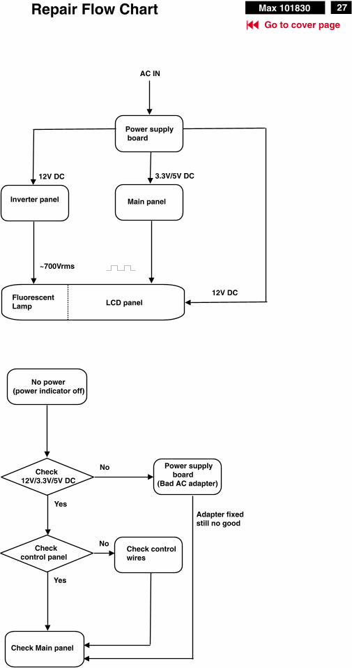
27Max 101830Repair Flow ChartGo to cover page
AC IN
Power supplyboard
Main panel
~700Vrms
Inverter panel
FluorescentLamp
LCD panel
3.3V/5V DC12V DC
12V DC
No power(power indicator off)
Check12V/3.3V/5V DC
Checkcontrol panel
No
No
Yes
Yes
(Bad AC adapter)
Power supplyboard
Check controlwires
Check Main panel
Adapter fixedstill no good
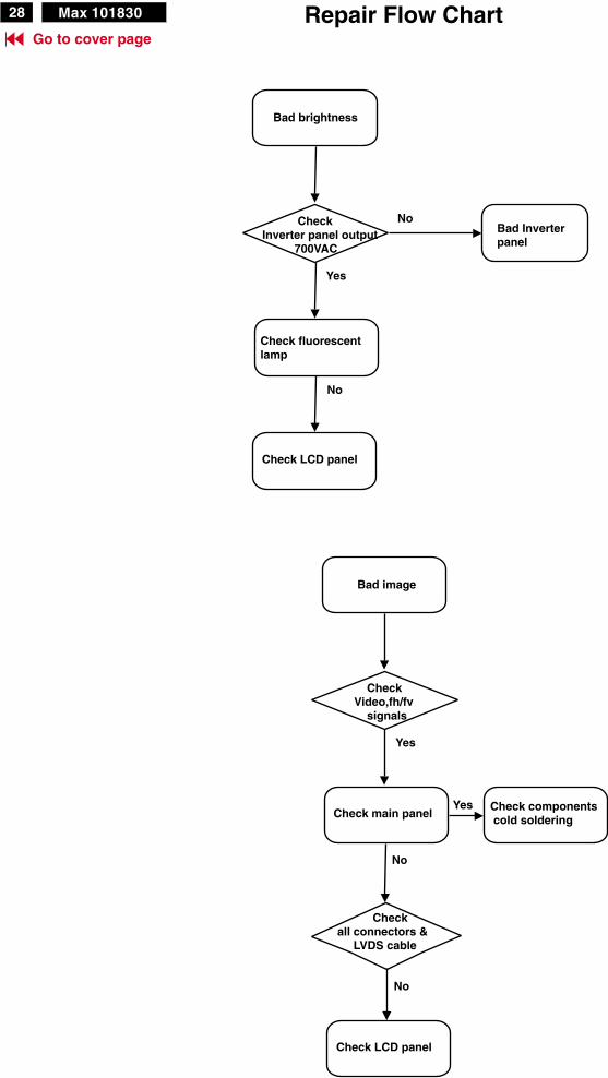
Repair Flow Chart
Bad brightness
CheckInverter panel output
700VAC
No
Yes
Bad Inverterpanel
Check fluorescentlamp
Bad image
CheckVideo,fh/fv
signals
Yes
Yes
Check LCD panel
No
No
Check LCD panel
Checkall connectors &
LVDS cable
No
Check main panelCheck componentscold soldering
28 Max 101830
Go to cover page
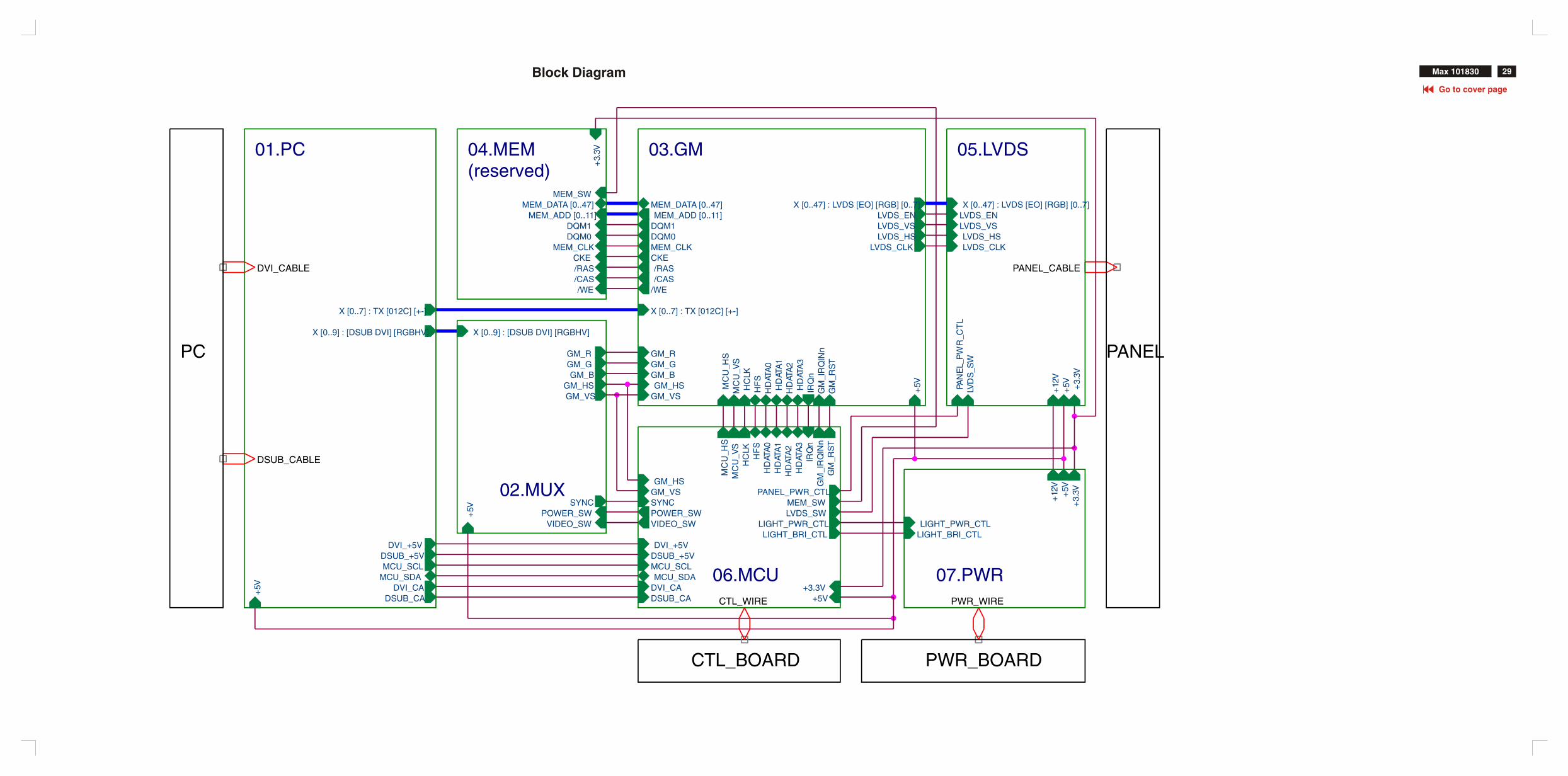
Block Diagram 29Max 101830
CTL_BOARD
06.MCU
HF
SH
CLK
GM
_RS
T
IRQ
n
MCU_SCLMCU_SDA
GM
_IR
QIN
n
PANEL_PWR_CTLMEM_SW
LIGHT_BRI_CTLLIGHT_PWR_CTL
DSUB_+5V
GM_VSGM_HS
MC
U_V
SM
CU
_HS
VIDEO_SW
DVI_+5V
DVI_CADSUB_CA
HD
ATA
0H
DAT
A1
HD
ATA
2H
DAT
A3
+5V+3.3V
SYNCPOWER_SW LVDS_SW
PANEL_CABLE
02.MUX
VIDEO_SW
GM_GGM_B
GM_R
GM_VSGM_HS
X [0..9] : [DSUB DVI] [RGBHV]
+5V POWER_SW
SYNC
05.LVDS
LVDS_CLKLVDS_HS
LVDS_VSLVDS_ENX [0..47] : LVDS [EO] [RGB] [0..7]
+3.
3V
+12
V+
5VPAN
EL_
PW
R_C
TL
LVD
S_S
W
DSUB_CABLE
PWR_BOARD
PWR_WIRE
DVI_CABLE
04.MEM(reserved)
MEM_DATA [0..47]MEM_ADD [0..11]
/RAS
DQM0MEM_CLK
/WE
DQM1
/CAS
CKE
+3.
3V
MEM_SW
PANEL
03.GM
IRQ
n
GM
_RS
T
MEM_ADD [0..11]
HF
S
GM
_IR
QIN
nGM_RGM_GGM_BGM_HS H
CLK
HD
ATA
0H
DAT
A1
HD
ATA
2H
DAT
A3
MEM_DATA [0..47]
DQM1DQM0MEM_CLKCKE/RAS/CAS
/WE
LVDS_EN
GM_VS
LVDS_VSLVDS_HS
LVDS_CLK
X [0..7] : TX [012C] [+-]
X [0..47] : LVDS [EO] [RGB] [0..7]
+5VM
CU
_HS
MC
U_V
S
07.PWR
LIGHT_PWR_CTLLIGHT_BRI_CTL
+5V
+3.
3V
+12
V
CTL_WIRE
PC
01.PC
MCU_SDAMCU_SCLDSUB_+5V
DVI_+5V
DVI_CADSUB_CA
X [0..7] : TX [012C] [+-]
X [0..9] : [DSUB DVI] [RGBHV]
+5V
Go to cover page

9 Go to cover page
30 Max 101830 Schematic diagram(Power)
MW

31Max 101830Power Board C.B.A.(copper track & smc side view)
1006 A3 7061 A2 2051 B3 3110 B1
1101 A1 7071 A2 2055 B3 3111 B2
1102 B1 7085 A3 2056 B3 3116 B2
1105 A1 7101 B2 2062 A1 3117 B2
2061 A1 7102 A2 2063 A1 3118 B2
2067 A1 7104 B3 2064 A2 3119 B2
2068 A1 7106 B3 2065 A2 3120 B1
2077 A2 8051 B3 2066 A2 3122 B3
2080 A3 8052 A2 2069 A1 3123 B3
2081 A3 8102 A1 2070 A2 3124 B2
2082 A3 9005 A1 2072 A2 3125 B3
2084 A3 9007 B2 2073 A2 3126 B3
2101 A1 9008 A2 2074 A2 3128 B2
2102 B1 9012 B3 2075 A2 3129 B2
2103 A1 9013 A3 2076 A2 3131 B1
2104 A1 9014 A3 2078 A2 3132 B1
2105 A1 9015 A3 2079 A1 3133 B1
2111 B2 9016 A3 2083 A3 3134 B2
2112 A1 9017 A3 2085 A2 3136 B2
2113 B3 9018 A3 2106 B2 3191 B2
2115 B3 9019 A3 2107 B2 3192 B2
2116 A3 9021 A3 2108 B2 6081 A3
2117 A3 9022 A2 2109 B2 6107 A3
2118 A3 9023 A1 2110 B2 6108 A2
2121 A3 9024 A2 2114 B2 6112 B1
2123 B1 9025 A2 2119 B3 6113 B3
2124 B2 9026 A1 2120 B3 7051 A2
3051 A2 9027 A2 2122 B2 7052 A2
3053 A2 9028 A1 3052 A2 7081 A3
3063 A1 9030 A3 3054 A2 7082 A3
3064 A1 9031 A3 3056 A2 7083 A3
3085 A3 9033 A3 3057 A2 7084 A3
3101 B1 9034 A3 3059 A2 7107 B1
3104 B1 9035 A1 3061 A1
3112 B2 9036 A1 3062 A2
3113 B2 9101 A1 3071 A2
3114 B2 9111 A1 3072 A2
3115 A2 3073 A2
3121 B3 3074 A2
3127 B2 3075 A3
3130 A3 3076 A3
3181 A1 3080 A2
4101 A2 3081 A3
4102 A3 3082 A3
5061 A2 3083 A3
5071 A2 3084 A3
5101 B1 3086 A3
5103 B3 3087 A3
5105 A1 3088 A3
5106 B1 3089 A3
6061 A1 3091 A3
6062 A1 3092 A2
6071 A2 3093 A2
6072 A2 3102 B1
6101 A1 3103 B1
6105 B1 3105 B1
6106 B2 3106 B2
6109 A3 3107 B2
6111 B2 3108 B2
6114 B1 3109 B2
Go to cover page

Power Board C.B.A. 31Max 101830
Go to cover page

� Go to cover page
32 Max 101830 Schematic diagram(Video - Input) Schematic diagram(DC_Powers)
MW
� Go to cover page
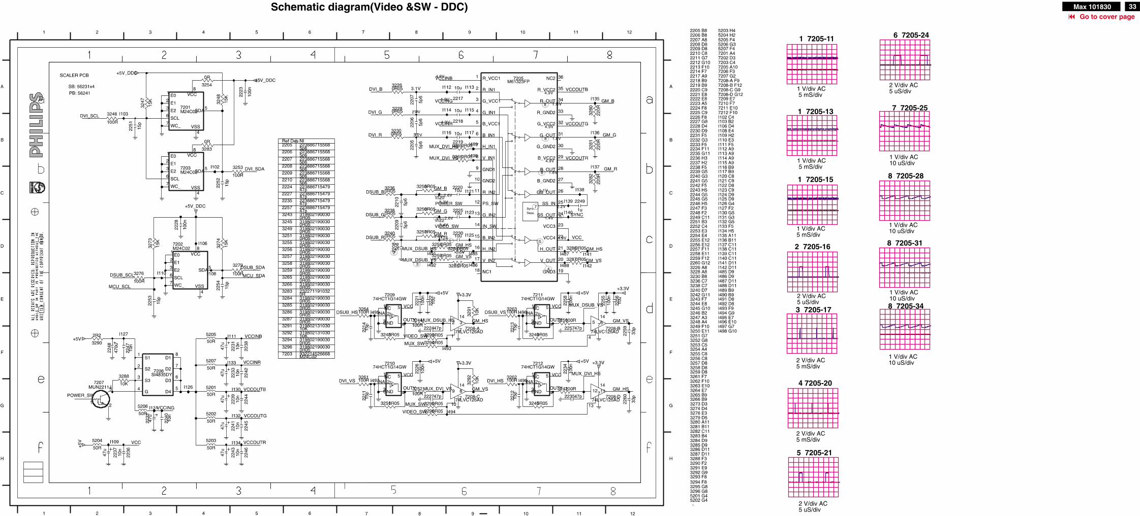
33Max 101830Schematic diagram(Video &SW - DDC)
3 7205-178 7205-34
4 7205-20
5 7205-21
1 7205-13
1 7205-15
7 7205-25
2 7205-168 7205-31
8 7205-28
1 7205-116 7205-24
2 V/div AC
5 mS/div
1 V/div AC
10 uS/div
2 V/div AC
5 mS/div
2 V/div AC
5 uS/div
1 V/div AC
5 mS/div
1 V/div AC
10 uS/div
2 V/div AC
5 uS/div
1 V/div AC
10 uS/div
1 V/div AC
5 mS/div
1 V/div AC
10 uS/div
1 V/div AC
5 mS/div
2 V/div AC
5 uS/div
1
1
1
2
3
4
5
6
7
8
8
8
4.9V
4.9V
4.9V
3.1V
2.4V
3.2V
2.6V
2.6V
2.6V
3.3V
3.4V
0.5V
4.9V
1.8V
4.9V
4.9V
1.8V
1.8V
1.1V
2.2V
1.4V
4.9V
MW
MW

� Go to cover page
34 Max 101830 Schematic diagram(Scaler)
MW
MW

� Go to cover page
35Max 101830Schematic diagram(Frame_Beffer)
MW
MW

� Go to cover page
36 Max 101830 Schematic diagram(LVDS)
23 3528-4
24 3529-1
25 3529-2
26 3529-3
27 3530-8
28 3530-7
29 3530-6
1 V/div AC
5 uS/div
1 V/div AC
1 uS/div
1 V/div AC
1 uS/div
1 V/div AC
5 uS/div
1 V/div AC
5 uS/div
1 V/div AC
2 uS/div
1 V/div AC
5 uS/div
9 3522-1 16 3524-6
10 3522-3 17 3525-1
11 3522-4 18 3525-3
13 3523-2 20 3527-1
15 3524-8
14 3523-4 21 3527-2
12 3523-1 19 3526-2
1 V/div AC
5 mS/div
1 V/div AC
5 uS/div
1 V/div AC
5 uS/div
1 V/div AC
0.5 uS/div
1 V/div AC
5 uS/div1 V/div AC
5 uS/div
1 V/div AC
1 uS/div
1 V/div AC
5 uS/div
1 V/div AC
10 uS/div
1 V/div AC
1 uS/div
1 V/div AC
1 uS/div
1 V/div AC
0.5 uS/div
1 V/div AC
5 uS/div
1 V/div AC
5 uS/div
22 3528-1
30 3531-1
31 3531-2
1 V/div AC
5 uS/div
1 V/div AC
0.5 uS/div
1V39
1V2
100.4V
11
1V3
1V3
0.9V
15
16
19
0.6V
0.7V
1V3
0.9V
22
23
1V3
1V1
0.3V
27
28
29
121V4
1V4
1V4
1V4
1V4
1V4
1V4
1V413
14
17
18
1V3
1V4
1V4
1V4
1V420
21
24
25
26
1V2
0.9V
30
31
MW
MW

� Go to cover page
37Max 101830Schematic diagram(MCU)
36 7401-20
37 7401-30
38 7401-31
33 7401-9
35 7401-19
34 7401-13
32 7401-8
1 V/div AC
10 uS/div
1 V/div AC
5 mS/div
1 V/div AC
10 uS/div
1 V/div AC
5 uS/div
1 V/div AC
5 mS/div
1 V/div AC
0.5 mS/div
1 V/div AC
20 uS/div
1.4V
3.1
V
1.3V
2.5V
0.8V
1.3V
1.1V
1.4V
3.2V
5V3.3V
1.9V
32
34
35
36
38
37
33
MW
MW

� Go to cover page
38 Max 101830 Schematic PWB(Copper track side view)
# GRID BOARD
# REF LABEL SIDE
# ____ _____ _________
1202 A3 B
1203 B3 B
1301 A1 B
1401 B1 B
1403 B1 B
1404 B2 B
1405 B1 B
1406 A3 B
2248 B3 B
2387 A1 B
2388 A1 B
2389 A1 B
5302 A1 B
5303 A1 B
5304 A1 B
7402 B1 B
# GRID BOARD
# REF LABEL SIDE
# ____ _____ _________
2215 A3 A
2216 A3 A
2227 A3 A
2238 A3 A
2240 A3 A
2242 A3 A
2244 A3 A
2245 A3 A
2246 A3 A
2247 B3 A
2249 A3 A
2252 A3 A
2255 A2 A
2256 A2 A
2259 A3 A
2260 A3 A
2301 A2 A
2302 A2 A
2303 A2 A
2304 A2 A
2306 A2 A
2307 A2 A
2308 A2 A
2309 A2 A
2310 A2 A
2311 A2 A
2312 A2 A
2313 A2 A
2314 A2 A
2315 A2 A
2316 A2 A
2317 A2 A
2318 A2 A
2319 A2 A
2320 A2 A
2321 A2 A
2322 A2 A
2323 A2 A
2324 A2 A
2325 A2 A
2326 A2 A
2327 A2 A
2328 A2 A
2329 A2 A
2330 A2 A
2331 A2 A
2332 A2 A
2333 A2 A
2334 A2 A
2335 A2 A
2336 A2 A
2337 A2 A
2338 A2 A
2339 A2 A
2340 A2 A
2341 A2 A
2342 A2 A
2343 A2 A
2344 A2 A
2345 A2 A
2346 A2 A
2347 A2 A
2348 A2 A
2349 A2 A
2350 A2 A
2351 A2 A
2352 A2 A
2369 A1 A
2370 A2 A
2371 A2 A
2372 A2 A
2373 A2 A
2374 A2 A
2375 A2 A
2376 A2 A
2377 A2 A
2380 A1 A
2381 A1 A
2384 A1 A
2385 A1 A
2386 A1 A
2392 A1 A
2393 A1 A
2398 A1 A
2402 B2 A
2403 B2 A
2404 B2 A
2408 B2 A
2503 A2 A
2504 A2 A
2505 A2 A
2506 A2 A
2507 A2 A
2508 A2 A
2510 A2 A
2511 A2 A
2519 A3 A
2527 A2 A
2528 A2 A
2540 A2 A
2541 A2 A
2542 A2 A
2543 A2 A
2544 A2 A
2545 A2 A
2547 A2 A
2548 A2 A
2549 A2 A
2550 A2 A
2551 A2 A
2552 A2 A
3214 A3 A
3215 A3 A
3216 A3 A
3217 A3 A
3218 A3 A
3219 A3 A
3220 A3 A
3221 A3 A
3222 A3 A
3232 A3 A
3234 A3 A
3253 A3 A
3255 A3 A
3256 A3 A
3257 A3 A
3258 A3 A
3259 A3 A
3284 A3 A
3285 A3 A
3287 A3 A
3288 B2 A
3290 B2 A
3292 B2 A
3293 B3 A
3294 B3 A
3295 B3 A
3296 B3 A
3322 A1 A
3326 A1 A
3327 A1 A
3328 A1 A
3329 A1 A
3402 B2 A
3403 B2 A
3444 B2 A
3451 B2 A
3452 B2 A
3453 B2 A
3454 B2 A
3458 B2 A
3478 A2 A
3510 A2 A
3511 A2 A
3513 A2 A
3514 A2 A
3515 A2 A
3517 A2 A
3518 A2 A
5311 A2 A
5312 A2 A
5503 A3 A
5504 A3 A
5512 A2 A
5513 A1 A
5514 A2 A
5515 A2 A
6220 A3 A
6236 A3 A
6237 A3 A
6239 B3 A
7201 A3 A
7203 A3 A
7206 B2 A
7207 B3 A
7208 B3 A
7305 A1 A
7306 A1 A
7309 A1 A
7310 A1 A

� Go to cover page
39Max 101830Schematic PWB(Components side view)
# GRID BOARD
# REF LABEL SIDE
# ____ _____ _________
1302 B2 B
1402 B2 B
1501 A2 B
2201 B1 B
2202 A1 B
2203 A1 B
2204 B1 B
2205 A1 B
2206 A1 B
2207 A1 B
2208 B1 B
2209 A1 B
2210 A1 B
2211 A1 B
2212 A1 B
2213 B1 B
2214 B1 B
2217 A1 B
2218 A1 B
2219 A1 B
2220 A1 B
2221 B1 B
2222 B1 B
2223 A1 B
2224 B1 B
2225 A1 B
2226 A1 B
2228 B1 B
2230 A1 B
2231 A1 B
2232 A1 B
2233 A1 B
2234 A1 B
2235 A1 B
2236 A1 B
2237 A1 B
2239 A1 B
2241 B1 B
2243 B1 B
2251 A1 B
2253 B1 B
2254 B1 B
2257 B1 B
2258 B1 B
2305 A1 B
2353 B2 B
2354 B2 B
2355 B1 B
2356 A1 B
2357 A1 B
2358 A1 B
2359 B2 B
2360 B2 B
2364 B2 B
2365 B2 B
2366 A2 B
2367 A2 B
2368 B1 B
2378 B2 B
2379 B2 B
2394 A3 B
2395 A3 B
2396 A3 B
2397 A3 B
2401 B3 B
2405 B3 B
2406 B2 B
2407 B2 B
2409 B2 B
2410 B2 B
2412 B3 B
2413 B3 B
2414 B3 B
2423 A1 B
2425 A1 B
2427 A1 B
2428 A1 B
2429 A1 B
2430 A1 B
2431 A1 B
2480 A1 B
2500 A2 B
2501 A3 B
2502 A3 B
2509 A1 B
2512 B3 B
2513 B3 B
2514 B3 B
2515 B3 B
2516 A3 B
2517 A3 B
2518 B3 B
2520 A3 B
2521 A3 B
2522 A3 B
2523 A3 B
2524 A3 B
2525 A3 B
2526 A3 B
2529 A1 B
2530 A3 B
2531 A3 B
2532 A3 B
2533 A3 B
2534 A3 B
2535 A3 B
2536 A3 B
2546 A2 B
3223 A1 B
3225 A1 B
3226 A1 B
3227 A1 B
3228 A1 B
3229 A1 B
3230 A1 B
3231 A1 B
3233 B1 B
3235 B1 B
3236 A1 B
3237 B1 B
3238 A1 B
3239 B1 B
3240 B1 B
3241 A1 B
3242 A1 B
3243 B1 B
3244 B1 B
3245 A1 B
3246 A1 B
3247 A1 B
3248 A1 B
3249 B1 B
3250 B1 B
3251 A1 B
3252 A1 B
3254 A1 B
3261 A1 B
3262 A1 B
3263 B1 B
3264 B1 B
3265 A1 B
3266 A1 B
3273 B1 B
3274 B1 B
3276 B1 B
3279 B1 B
3280 A1 B
3281 A1 B
3282 A1 B
3283 A1 B
3286 A1 B
3291 A1 B
3304 A2 B
3305 A2 B
3306 A1 B
3307 A1 B
3308 A1 B
3309 B2 B
3310 B2 B
3312 B2 B
3313 B2 B
3316 B2 B
3317 B2 B
3318 A2 B
3319 A1 B
3321 A3 B
3323 A3 B
3401 B2 B
3404 B2 B
3405 B3 B
3406 B3 B
3407 B3 B
3408 B3 B
3409 B3 B
3410 B3 B
3411 B3 B
3412 B3 B
3413 B2 B
3414 B2 B
3415 B2 B
3416 B2 B
3417 B2 B
3418 B2 B
3419 B2 B
3420 B2 B
3421 B2 B
3422 B2 B
3423 B2 B
3424 B2 B
3425 B2 B
3426 B2 B
3427 B2 B
3428 B2 B
3429 B2 B
3430 B2 B
3431 B2 B
3432 B3 B
3433 B3 B
3434 B3 B
3435 B3 B
3436 B2 B
3437 B2 B
3438 B2 B
3439 B2 B
3440 B3 B
3441 B3 B
3442 B3 B
3443 A1 B
3445 A1 B
3446 B2 B
3447 B2 B
3448 B2 B
3449 B2 B
3450 B2 B
3455 B3 B
3456 B3 B
3457 B3 B
3459 B2 B
3460 B2 B
3461 B2 B
3462 A1 B
3463 A1 B
3464 A1 B
3465 A1 B
3466 A1 B
3467 A1 B
3468 A1 B
3469 A1 B
3470 A1 B
3471 A1 B
3472 A1 B
3473 A1 B
3474 A1 B
3475 B3 B
3476 B2 B
3501 B3 B
3502 A3 B
3503 A3 B
3504 A3 B
3505 B3 B
3520 A2 B
3521 A2 B
3522 A2 B
3523 A2 B
3524 A2 B
3525 A2 B
3526 A2 B
3527 A1 B
3528 A2 B
3529 A2 B
3530 A2 B
3531 A2 B
5201 B1 B
5202 B1 B
5203 B1 B
5204 B1 B
5205 A1 B
5206 A1 B
5207 A1 B
5301 A2 B
5308 B2 B
5309 B2 B
5310 B2 B
5401 B3 B
5501 A1 B
5502 A1 B
5505 A1 B
5506 A1 B
5507 A3 B
5508 A3 B
5509 B3 B
5510 A2 B
5511 A2 B
6201 A1 B
6202 A1 B
6203 A1 B
6204 A1 B
6205 A1 B
6206 A1 B
6207 A1 B
6208 A1 B
6209 A1 B
6210 A1 B
6211 A1 B
6212 A1 B
6213 A1 B
6214 B1 B
6215 B1 B
6216 B1 B
6217 A1 B
6218 A1 B
6219 A1 B
6221 B1 B
6222 B1 B
6223 B1 B
6224 B1 B
6230 B1 B
6231 B1 B
6232 B1 B
6233 B1 B
6234 B1 B
6235 B1 B
6238 B1 B
6401 B3 B
7202 B1 B
7205 A1 B
7209 B1 B
7210 A1 B
7211 B1 B
7212 A1 B
7301 A2 B
7302 B2 B
7303 A2 B
7304 B2 B
7307 B2 B
7401 B2 B
7403 B3 B
7501 B3 B
7502 A3 B
7503 A3 B
7504 B3 B
7505 A2 B
7506 A2 B

Inverter Diagram(AMBIT)� Go to cover page
40 Max 101830
1 2 3 4 5 6 7 8
A
B
C
D
87654321
D
C
B
A
AMBIT
SHEET
File Name
Title
Doc.No.
PREPARED BY
REVIEWED BY
APPROVED BYREV. DESCRIPTION REL. DATE
Schematic Drawing
0 Initial
1 of 2
CTIMR1
OVP2
ENA3
SST4
VDDA5
AGND6
REF7
RT18
FB9
CMP10
NDR_D11
PDR_C12
LPWM13
DIM14
NDR_B20
PDR_A19
CT18
RT17
PGND16
LCT15
U1
U/OZ960\SSOP20
12
R1R/255K
12
R4R/3K
12
R6R/1M
1 2R12
R/51K
1 2R13
R/NC
12
C1C/104Z/0805
1 2C6
C/225K/1206
1 2C10
C/682J
1 2
C14C/101J
12
C11C/103K
12
C15C/NC
12
C12C/103K
12
C21
C/152K
1 2
C22C/474K
1 2
C23C/225K
12C24
C/105Z/0805
1 2F1
F/429005
RT
12 R22
R/68.1K
12
C26C/12pF/1808
12 C28
C/103J/0805
3
21
D1D/BAV99
12
R23R/226
SST
12
R27R/93.1K
12
R28R/10K
5V
Vbri
NDR-B
PDR-A PDR-C
NDR-D
NDR-D
PDR-C
PDR-A
NDR-B
3
2
1
Q1
Q/BSS138
VREF
SST
1 2
R29R/33
12
C3C/104Z
12
C4C/105Z
OVP
1 2C7
C/225K/1206
1 2
C16C/225K/1206
FBK
VIN-1
12
C30
C/103J/0805
1
2
3
Q3Q/3904
1
2
3
Q11Q/3906
12
R25R/10K
12
R26
R/10K
12
+ C32C/22uF
12
C33C/47pF/1808
12
C34C/47pF/1808
11
33
CN2
C/SM02B-BHSS-1-TB
11
33
CN3
C/SM02B-BHSS-1-TB
FBK
OVP
12
C25C/105Z/0805
VbriEnable
Enable
Vin
12 R30
R/NC
12 R31
R/NC
12
R16R/226
12
R17R/1K
1 2CP1
C/CP
LCT
CT
CMP
RT1
VDDA
ENA
CTIM
3
2
1
Q2Q/2N7002
SD
12
C41C/NC
12
R43R/100K
12
R44R/100K
N1
N2
N4
N11
N14
N15
N17
N18
N19
N22
12
R49R/10K/0805
12
R50R/220/1206
12
D15
D/RLZ5.6B
1
2
3
Q8Q/3904
3
4 256
1
Q14Q/NC
4
3
1256
Q16Q/NC
4
3
1256
Q17Q/NC
3
4 256
1
Q15Q/NC
12
R51R/0 ohm
A
T50I026.00
07/30/2001
RT
VREF
1
2
3
Q9Q/3904
1
2
3
Q12Q/3906
3
2
1
Q18Q/2N70025V
VIN-1
B
B
C1
2
R5R/3K
12
R52R/0 ohm
1
2
3
Q10Q/3904
1
2
3
Q13Q/3906
3
2
1
Q19Q/2N70025V
VIN-1
C
12
C44C/333K/0805
12
C45C/333K/0805
12
C46C/104Z
N37
N23
3
4
256
1
78
Q14AQ/FDS4435
3
4
256
1
78
Q15AQ/FDS4435
3
4
256
1
78
Q16AQ/Si4416DY
3
4
256
1
78
Q17AQ/Si4416DY
12
C13C/104Z
1 2R24
R/33K
LPWM
12
C27C/47pF/1808
11
33
CN4
C/SM02B-BHSS-1-TB
FB
FB
12
D8
BZ
M55B
75
12
D9
BZ
M55B
75
12
R7
R/3
40K
/1206
12
L1
L/3
50m
12
R8
R/3
40K
/1206
12
R9
R/3
40K
/1206
12
R10
R/3
40K
/1206
3
21
D24BAV99
FB
3
21
D25BAV99
FB
3
21
D26BAV99
12
D10
BZ
M55B
75
12
D11
BZ
M5
5B
75
12
R37
R/3
40
K/1
20
6
12
L2
L/3
50
m
12
R39
R/3
40K
/1206
12
R40
R/3
40
K/1
20
6
12
R41
R/3
40
K/1
20
6
12 D12
BZ
M55B
75
12
D13
BZ
M5
5B
75
12
R42
R/3
40
K/1
20
6
12
L3 L/3
50
m1
2
R45
R/3
40K
/1206
12
R46
R/3
40
K/1
20
6
12
R54
R/3
40
K/1
20
6
N21
N70
N71
N72
N73
N74
N75
N76
N77
N78
N79
N80
N81
N82
N83
N84
N20
N25 N26
N27 N28
N30
N31
N36
N38
N48
026C3-1
1 2R79
R/0 ohm
1 2R80
R/0 ohm
12
+ C48C/22uF
N3 N7
N2
ENA
12
R3R/0 ohm
12
C53C/NC
12
R15R/NC
VIN-1
12CP3
CP
12C42
C/470pF/0805
12CP4
CP
12C43
C/470pF/0805
12CP5
CP
12C49
C/470pF/0805
1
2
3
Q24Q/3904
1
2
3
Q28Q/3906
1 2R20
R/0 ohm
12
R19R/3K
12
R53R/NC
3
2
1
Q26Q/2N7002
VIN-1
N31
NDR-B
5V
1
2
3
Q25Q/3904
1
2
3
Q29Q/3906
1 2R48
R/0 ohm
12
R47R/3K
12
R74R/NC
3
2
1
Q27Q/2N7002
VIN-1
NDR-D
5V
N30
N118
N119
N120
N122 N123 N124 N125
12345678
CN1
C/B8B-PH-SM3-TB
2
106
73
5
T1
T/20:1400
1 2R64
R/294K
1 2R76
R/511K
1 2
C31 C/104Z
12
R81R/NC
VIN-1
1 2R82
R/NC
1 2CP2
CP
1 2R83
R/NC
1 2CP9
CP
1 2C37
C/NC
1 2CP10CP
1 2R84
R/200K
12
R85R/100K
12
C38C/103J
N61
N62
N63
N69
3
2
1
Q23Q/2N7002
1
2
3
Q4Q/3904
12
R2R/1K/0805
12
C2C/105Z
12
R33R/2.2M
5V
1 2D2
D/4148
SD
1
2
3
Q5Q/3904
12
R11R/1K/0805
12
C5C/105Z
12
R34R/2.2M
5V
1 2D3
D/4148
SD
1
2
3
Q6Q/3904
12
R14R/1K/0805
12
C35C/105Z
12
R35R/2.2M
5V
1 2D4
D/4148
SD
N50
N51
N52
I026v2-2I026v2-2.sch
026ict-2026ict-2.sch
1 Modify 02/19/2001
T50I0I026.00 BOM LISTAmbit's P/N Description
1. 1 90.0007.01 CARTON 560*460*216 mm2. 1 91.0229.03 TRAY-229b T50I026.003. 1 T50I026D00 INVERTER LCD 18" FOR POGOII LG@4. .2 09.0142.01 CAP OS 20SP22M (SANYO)5. .2 11.2041.14 CAP DISC CC45SL3FD470JYPN(TDK)@6. .2 11.2029.14 CAP DISC CC45SL3FD120JYPN(TDK)@7. .2 T50I026S00 INVERTER LCD 18" FOR POGOII LG@8. ..3 08.0000.04 CAP C 101J/50V/NPO/0603 @9. ..3 08.0003.03 CAP C 103J/50V/X7R/0603 @10. ..3 08.0003.01 CAP C 103J/50V/X7R/080511. ..3 08.0100.01 CAP C 103K/50V/X7R/0603 @12. ..3 08.0022.02 CAP C 104Z/25V/Y5V/0603 @13. ..3 08.0032.01 CAP C 104Z/25V/Y5V/080514. ..3 08.0183.01 CAP C 105Z/10V/Y5V/0603 @15. ..3 08.0020.04 CAP C 105Z/16V/Y5V/0805 @16. ..3 08.0355.01 CAP C 152K/50V/X7R/0603 @17. ..3 08.0557.14 CAP C 225K/25V/X7R/1206(TDK) @18. ..3 08.0027.01 CAP C 333K/50V/X7R/0805 @19. ..3 08.0674.21 CAP C 471K/250V/X7R/0805 (HEC)@20. ..3 08.0778.01 CAP C 105K/6.3V/X5R/0603 @21. ..3 26.0534.01 CONN B8B-PH-SM3-TB (JST)22. ..3 26.0246.01 CONN SM02B-BHSS-1 (JST)23. ..3 06.1007.01 DIO SW LS4148 LL-34(TELEFUNKEN24. ..3 06.1003.01 DIO SW BAV99 SOT23 A7,A7P,JE @25. ..3 06.1003.02 DIO SW DAN217 SOT23 (ROHM)26. ..3 06.1752.29 DIO ZEN BZM55B75-TR(TELEFUNKEN@27. ..3 06.1528.02 DIO ZEN RLZ5.6B/TE-11 (ROHM)28. ..3 26.7021.01 FUSE 429005 5A (LITTEL) @29. ..3 16.0490.01 IND SPC-1005P-354 SMD (TMP)30. ..3 06.0602.01 NFET 2N7002(E)(LT1) SOT23 @31. ..3 06.0038.01 TR NPN MMBT3904LT1 SOT23(MOTO)32. ..3 06.0015.01 TR NPN PMBS3904 SOT23(PHILIPS)33. ..3 06.0631.01 NFET BSS138 SOT23 (ZETEX) @34. ..3 06.0039.01 TR PNP MMBT3906LT1 SOT23(MOTO)35. ..3 06.0016.01 TR PNP PMBS3906 SOT23(PHILIPS)36. ..3 06.6003.06 NFET Si4416DY SO8 (SILICONIX) @37. ..3 06.2015.17 PFET FDS4435 SO8 (FAIRCHILD)38. ..3 06.2131.17 PFET Si4435DY SO8 FAIRCHILD @39. ..3 06.2015.01 PFET Si4435DYA SO8 (SILICONIX)@40. ..3 13.0005.03 RES C 0 ohm/0603/5%41. ..3 13.0005.02 RES C 0 ohm /1206/5%42. ..3 14.0011.03 RES C 100K ohm/0603/1%43. ..3 13.0032.02 RES C 10K ohm/0603/5%44. ..3 13.0032.01 RES C 10K ohm/0805/5%45. ..3 13.0271.01 RES C 2M ohm/1206/5%46. ..3 14.0365.01 RES C 1K ohm/0805/1%47. ..3 14.0012.03 RES C 1M ohm/0603/1%48. ..3 14.0125.02 RES C 93.1K ohm/0603/1%49. ..3 13.0088.02 RES C 2.2M ohm/0603/5%50. ..3 14.1022.01 RES C 226 ohm/0603/1%51. ..3 13.0092.01 RES C 200K ohm/0603/5%52. ..3 13.0299.01 RES C 220 ohm/1206/5%53. ..3 14.0751.01 RES C 255K ohm/0603/1%54. ..3 14.0223.01 RES C 3K ohm/0603/1%55. ..3 14.0403.01 RES C 33 ohm/0603/1%56. ..3 14.1105.01 RES C 33K ohm/0603/1% @57. ..3 14.0557.01 RES C 340K ohm/1206/1%58. ..3 14.0824.01 RES C 511K ohm/0603/1%59. ..3 14.0852.01 RES C 51K ohm/0603/1%60. ..3 14.1024.01 RES C 294K ohm/0603/1% @61. ..3 14.0283.01 RES C 68.1K ohm/0603/1%62. ..3 04.3040.02 IC OZ960DS-1.0 +-4% SSOP20(O2)63. ..3 08.0506.01 CAP C 682J/50V/X7R/0603 @64. ..3 13.0199.01 RES C 2K ohm/0603/5%65. ..3 08.0365.01 CAP C 474K/10V/X7R/0603 @66. ..3 22.0528.39 XFMR*XT-1955-12508 A(XTREME)67. ..3 64.0004.02 SOLDER PASTE SE48-M954-2(KOKI)68. ..3 19.0949.01 PCB T50I026.00 REV:2 2L69. ..3 92.0045.01 LABEL 20*10mm U13.010.C

Inverter Diagram(AMBIT)� Go to cover page
41Max 101830
1 2 3 4 5 6 7 8
A
B
C
D
87654321
D
C
B
A
AMBIT
SHEET
File Name
Title
Doc.No.
PREPARED BY
REVIEWED BY
APPROVED BYREV. DESCRIPTION REL. DATE
Schematic Drawing
0 Initial
2 of 2
1 2C8
C/225K/1206
1 2C9
C/225K/1206
1 2
C20C/225K/1206
12
C29C/47pF/1808
12
C40C/47pF/1808
11
33
CN5
C/SM02B-BHSS-1-TB
11
33
CN6
C/SM02B-BHSS-1-TB
N20
T50I026.00
07/30/2001
12
C47C/47pF/1808
11
33
CN7
C/SM02B-BHSS-1-TB
FB
12
D14
BZ
M55B
75
12
D19
BZ
M55B
75
12
R55
R/3
40K
/1206
12
L4
L/3
50m
12
R56
R/3
40K
/1206
12
R57
R/3
40K
/1206
12
R58
R/3
40K
/1206
3
21
D27BAV99
FB
3
21
D28BAV99
FB
3
21
D29BAV99
12
D20
BZ
M55B
75
12
D21
BZ
M55B
75
12
R65
R/3
40K
/1206
12
L5L/350m
12
R66
R/3
40K
/1206
12
R67
R/3
40K
/1206
12
R68
R/3
40K
/1206
12
D22
BZ
M55B
75
12
D23BZM55B75
12
R69
R/3
40K
/1206
12
L6
L/3
50m
12
R70
R/3
40K
/1206
12
R71
R/3
40K
/1206
12
R72
R/3
40K
/1206
N20
12
R73
R/2
M/1
206
1 2D30
D/BZM55B75
1 2D31
D/BZM55B75
12
R75
R/0
ohm
/1206
N21
N91N92
N93
N94
N95
N96
N97
N98
N99
N100
N101
N102
N103
N104
N105
N106
N113
N19
N45
N46
N39
N40
N41
12
C18C/12pF/1808
12 C19
C/103J/0805
3
21
D16D/BAV99
OVP
12
C17
C/103J/0805
N5
12CP6
CP
12C50
C/470pF/0805
12CP7
CP
12C51
C/470pF/0805
12CP8
CP
12C52
C/470pF/0805
N115
N116
N117
2
106
73
5
T2
T/20:1400
1
2
3
Q7Q/3904
12
R18R/1K/0805
12
C36C/105Z
12
R36R/2.2M
5V
1 2D5
D/4148
SD
1
2
3
Q20Q/3904
12
R21R/1K/0805
12
C39C/105Z
12
R38R/2.2M
5V
1 2D6
D/4148
SD
1
2
3
Q21Q/3904
12
R32R/1K/0805
12
C54C/105Z
12
R59R/2.2M
5V
1 2D7
D/4148
SD
N53
N54
N55
026C2-2
1 Modify 12/25/2001
Description Vendor Part name Parts Pcs/Card
IC IC OZ960DS-1.0 +-4% SSOP20 O2 OZ960DS U1 1
Transistor 2N7002(E) 60V 115mA 7.5OHM MOTO 2N7002(E) Q18 Q19 Q2 Q23 Q26Q27 6
MMBT3904LT1 SOT23 40V 200mA MOTO MMBT3904
PMBS3904 SOT23 40V 200mA PHILIPS PMBS3904
Q10 Q20 Q21 Q24 Q25 Q3 Q4 Q5
Q6 Q7 Q8 Q912
MMBT3906LT1 SOT23 40V 200mA MOTO MMBT3906
PMBS3906 SOT23 40V 200mA PHILIPS PMBS3906
Q11 Q12 Q13 Q28 Q29 5
BSS138 SOT23 50V 200mA 3.5ohm ZETEX BSS138 Q1 1
Si4416DY SO8 30V/9A/0.018ohm SILICONIX Si4416DY Q16A Q17A 2
FAIRCHILD4435 SO8 30V
SILICONIX
4435 Q14A Q15A 2
Fuse FUSE 429005 5A 5A/24V/1206/FAST LITTLE 429005 F1 1
Inductor SPC-1005P-354 350mH/K/1.4 Kohm TMP SPC-1005P-354 L1 L2 L3 L4 L5 L6 6
Capacitor CAP OS 20SP22M
22uF/20V/6.3*5.0/105C
SANYO C32 C482
CAP CC45SL3FD470JYPN 47PF/3KV TDK C27 C29 C33 C34 C40 C47 6
CAP CC45SL3FD120JYPN 12PF/3KV TDK C18 C26 2
CAP C 101J/50V/NPO/0603 Murata
Phycomp
TDK
AVX
TaiYuden
C14
1
Murata
Phycomp
TDK
AVX
CAP C 103J/50V/X7R/0603
TaiYuden
C38
1
Murata
Phycomp
TDK
AVX
CAP C 103J/50V/X7R/0805
TaiYuden
C17 C19 C28 C30
4
Murata
Phycomp
TDK
AVX
CAP C 103K/50V/X7R/0603
TaiYuden
C11 C12
2

Inverter Diagram PWB(AMBIT)� Go to cover page
42 Max 101830

43Max 101830
Go to cover page
Inverter Diagram PWB(AMBIT)

44 Max 101830
Go to cover page
Schematic diagram(Control)
MW
MW
MW
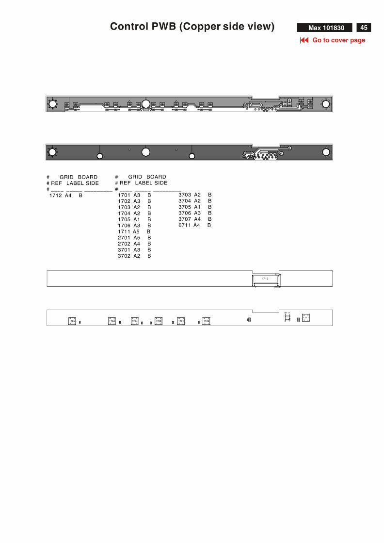
45Control PWB (Copper side view) Max 101830
Go to cover page
# GRID BOARD# REF LABEL SIDE# ____ _____ _________ 1712 A4 B
# GRID BOARD# REF LABEL SIDE# ____ _____ _________ 1701 A3 B 1702 A3 B 1703 A2 B 1704 A2 B 1705 A1 B 1706 A3 B 1711 A5 B 2701 A5 B 2702 A4 B 3701 A3 B 3702 A2 B
3703 A2 B 3704 A2 B 3705 A1 B 3706 A3 B 3707 A4 B 6711 A4 B

46 Max 101830 Exploded View
� Go to cover page
10
56
10
53
10
89
10
52
41
91
10
51
10
91
10
90
30
31
38
15
75
34
71
FR
ON
TB
EZ
EL
AS
SY93
22
18
32
56
82
LM
18
1E
05
-C4
M2
-LG
31
38
15
75
21
51
ME
TA
LS
HIE
LD
ING
AS
SY
31
38
15
85
53
51
SC
AL
ER
AS
SY
31
38
15
85
34
81
PO
WE
RA
SS
Y
31
38
15
85
43
91
ME
TA
LF
RA
M+
7P
WIR
EA
SS
Y
31
38
18
87
38
01
DC
-AC
INV
ER
TE
R(T
50
I02
6.0
0)
31
38
15
85
40
81
CO
NT
RO
LA
SS
Y
82
38
27
71
21
21
MU
LT
IME
DIA
BA
SE
AS
SY
31
38
15
40
72
91
BA
CK
CO
VE
R

47Max 101830
Go to cover page
Recommended Parts List
Model: DJ9B3L/00Z
Item Code number Description
30 313815753471 FRONT BEZEL ASSY
31 313815407231 BEZEL
32 313815407241 POWER KNOB
33 313815407251 CONTROL KNOB
34 313815405181 LENS
41 313815407291 BACK COVER
125 313815521291 D.F.U.
450 313815633611 CARTON
451 313815633621 CUSHION-R
452 313815633631 CUSHION-L
1087 313817878741 MAIN CORD ASSY
1088 313818872051 CORD SUB-D 15/2M0/SUB-D 15GRAY
1089 313818873801 DC-AC INVERTER (T50I026. )
1090 313815854391 METAL FRAME+7P WIRE ASSY
1091 823827712121 MULTIMEDIA BASE ASSY(RAY 7035)
1102 242208610239 FUSE 5X20 HT 3A15 250V IEC B
1402 243854300085 RES XTL SM 24M 0 7P SMD49 R
7061 932217683682 IC L4973V5.1 (ST ) L
7071 932216562682 IC L4978 (ST ) L
7101 932213028682 IC L5991 (ST ) L
7102 932217477687 FET POW STU10NB80 (ST ) L
7104 932214014667 OPT CP TCET1103(G) (VISH) L
7106 933771100686 IC TL431CLP S (MOTA) R
7202 932214526668 IC SM M24C02-WMN6 (ST ) R
7205 932217546668 IC M61323FP (MITJ) R
7206 932202899668 FET POW SM SI4835DY (VISH) R
7208 935241100118 IC SM 74LVC126AD (PHSE) R
7212 935245720115 IC SM 74HCT1G14GW (PHSE) R
7301 932216881671 IC SM GM5020 (GEMI) Y
7303 932217704668 IC SM LD1086DT25 (ST ) R
7401 932216723671 IC SM MC68HC908LD60 (MOTA) Y
7402 932212662682 IC M24C16-BN6 (ST ) L
7503 932216677682 IC SM M12L16161A-7T (ESMT) L
7505 932217686668 IC SM THC63LVDM83A (THIN) R
Recommended parts list of Inverter board :(T501026.00, Ambit)====================================================================Pos. Service code Description supplier code-------------------------------------------------------------------------------------------------------------------------1075 8238 277 11561 DC-AC INVERTER (T501026.00, Ambit)L1,L2 9965 000 12391 IND SPC-10055P-354-SMD(TMP) 16.0490.01F1 9965 000 12955 FUSE 4290005 5A(LITTLE) 26.7021.01Q18 4822 130 11057 2N7002 06.0602.01Q3 9965 000 05478 TR NPN PMBS3904 SOT23(PHILIPS) 06.0015.01Q1 9965 000 12956 NFET BSS138 SOT23(ZETEX) 06.0631.01Q15A 9965 000 12959 PFET SI4435DY SO8(FAIRCHILD) 06.2131.17Q11 9965 000 12957 TR PNP PMBS3906 SOT23(PHILIPS) 06.0016.01Q17A 9965 000 12958 NFET SI4416DY SO8(LILICONIX) 06.6003.01U1 9965 000 12960 IC OZ960DS-0.1+/-4% SSOP20(02) 04.3040.02T1 9965 000 12961 XFMR XT-1955-12508 A(XTREME) 22.0528.39

48 Max 101830 Spare Parts List(Continued)
Go to cover page
Parts indicated onexploded view :CTVs : DJ9B3L/00Z
Accessories
Main Panel
Scaler Panel
Various
30 313815753471 FRONT BEZEL ASSY
31 313815407231 BEZEL
32 313815407241 POWER KNOB
33 313815407251 CONTROL KNOB
34 313815405181 LENS
41 313815407291 BACK COVER
91 313815752151 METAL SHIELDING ASSY
98 313810440571 HOUSING COVER
99 313815551621 PLASTIC COVER-SNI
1088 313818872051 CORD SUB-D 15/2M0/SUB-D 15GRAY
1085 932218325682 TFT-LCD LM181E05-C4M2 (LGPH) B
1086 313818873181 CBLE 334034 40/220/30 321163
1089 313818873801 DC-AC INVERTER (T50I026. )
450 313815633611 CARTON
451 313815633621 CUSHION-R
452 313815633631 CUSHION-L
453 313815633641 P.E. BAG-ANTI-STAT.
1090 313815854391 METAL FRAME+7P WIRE ASSY
1091 823827712121 MULTIMEDIA BASE ASSY(RAY 7035)
1093 313818872241 DSUB CALE
125 313815521291 D.F.U.
145 313810656141 E-D.U.F. BAG
1087 313817878741 MAIN CORD ASSY
1051 313815855351 SCALER PCB ASSY
1051 313815855351 SCALER PCB ASSY
1052 313815853481 POWER ASSY
1053 313815854081 CONTROL ASSY
2201 223824615654 CER2 0603 X7R 10V 220N PM10 R
2202 223824615654 CER2 0603 X7R 10V 220N PM10 R
2203 223824615654 CER2 0603 X7R 10V 220N PM10 R
2204 223824615654 CER2 0603 X7R 10V 220N PM10 R
2211 223886715331 CER1 0603 NP0 50V 330P PM5 R
2212 223886715159 CER1 0603 NP0 50V 15P PM5 R
2213 223886715331 CER1 0603 NP0 50V 330P PM5 R
2214 223886715159 CER1 0603 NP0 50V 15P PM5 R
2215 223886715479 CER1 0603 NP0 50V 47P PM5 R
2216 223886715479 CER1 0603 NP0 50V 47P PM5 R
2217 222224119876 CER2 1206 Y5V 10V 10U P8020 R
2218 222224119876 CER2 1206 Y5V 10V 10U P8020 R
2219 222224119876 CER2 1206 Y5V 10V 10U P8020 R
2220 222224119876 CER2 1206 Y5V 10V 10U P8020 R
2221 223878615649 CER2 0603 X7R 16V 1 N PM10 R
2222 222224119876 CER2 1206 Y5V 10V 10U P8020 R
2223 223878615649 CER2 0603 X7R 16V 1 N PM10 R
2225 222224119876 CER2 1206 Y5V 10V 10U P8020 R
2226 223878615649 CER2 0603 X7R 16V 1 N PM10 R
2228 223878615649 CER2 0603 X7R 16V 1 N PM10 R
2230 222224119876 CER2 1206 Y5V 10V 10U P8020 R
2231 202001293747 ELCAP SM RV2 25V 47U PM20 R
2232 202001293747 ELCAP SM RV2 25V 47U PM20 R
2233 202001293747 ELCAP SM RV2 25V 47U PM20 R
2234 223878615649 CER2 0603 X7R 16V 1 N PM10 R
2236 223858615636 CER2 0603 X7R 50V 10N PM10 R
2237 202001293747 ELCAP SM RV2 25V 47U PM20 R
2238 223858615636 CER2 0603 X7R 50V 10N PM10 R
2239 202001293747 ELCAP SM RV2 25V 47U PM20 R
2240 223858615636 CER2 0603 X7R 50V 10N PM10 R
2241 202001293747 ELCAP SM RV2 25V 47U PM20 R
2242 223858615636 CER2 0603 X7R 50V 10N PM10 R
2243 202001293747 ELCAP SM RV2 25V 47U PM20 R
2244 223858615636 CER2 0603 X7R 50V 10N PM10 R
2245 223858615636 CER2 0603 X7R 50V 10N PM10 R
2246 223858615636 CER2 0603 X7R 50V 10N PM10 R
2247 223858615636 CER2 0603 X7R 50V 10N PM10 R
2248 203803516304 ELCAP RXJ 25V S 470U PM20 B
2249 223824619863 CER2 0603 Y5V 10V 1U P8020 R
2251 223886715159 CER1 0603 NP0 50V 15P PM5 R
2252 223886715159 CER1 0603 NP0 50V 15P PM5 R
2253 223886715159 CER1 0603 NP0 50V 15P PM5 R
2254 223886715159 CER1 0603 NP0 50V 15P PM5 R
2255 223878615649 CER2 0603 X7R 16V 1 N PM10 R
2256 222224119876 CER2 1206 Y5V 10V 10U P8020 R
2258 223878615649 CER2 0603 X7R 16V 1 N PM10 R
2259 223886715339 CER1 0603 NP0 50V 33P PM5 R
2260 223886715339 CER1 0603 NP0 50V 33P PM5 R
2301 223878615649 CER2 0603 X7R 16V 1 N PM10 R
2302 223878615649 CER2 0603 X7R 16V 1 N PM10 R
2303 223878615649 CER2 0603 X7R 16V 1 N PM10 R
2304 223878615649 CER2 0603 X7R 16V 1 N PM10 R
2305 223878615649 CER2 0603 X7R 16V 1 N PM10 R
2306 223878615649 CER2 0603 X7R 16V 1 N PM10 R
2307 223878615649 CER2 0603 X7R 16V 1 N PM10 R
2308 223878615649 CER2 0603 X7R 16V 1 N PM10 R
2309 223878615649 CER2 0603 X7R 16V 1 N PM10 R
2310 223878615649 CER2 0603 X7R 16V 1 N PM10 R
2311 223878615649 CER2 0603 X7R 16V 1 N PM10 R
2312 223878615649 CER2 0603 X7R 16V 1 N PM10 R
2313 223878615649 CER2 0603 X7R 16V 1 N PM10 R
2314 223878615649 CER2 0603 X7R 16V 1 N PM10 R
2315 223878615649 CER2 0603 X7R 16V 1 N PM10 R
2316 223878615649 CER2 0603 X7R 16V 1 N PM10 R
2317 223878615649 CER2 0603 X7R 16V 1 N PM10 R
2318 223878615649 CER2 0603 X7R 16V 1 N PM10 R
2319 223878615649 CER2 0603 X7R 16V 1 N PM10 R
2320 223878615649 CER2 0603 X7R 16V 1 N PM10 R
2321 223878615649 CER2 0603 X7R 16V 1 N PM10 R
2322 223878615649 CER2 0603 X7R 16V 1 N PM10 R
2323 223878615649 CER2 0603 X7R 16V 1 N PM10 R
2324 223878615649 CER2 0603 X7R 16V 1 N PM10 R
2325 223878615649 CER2 0603 X7R 16V 1 N PM10 R
2326 223878615649 CER2 0603 X7R 16V 1 N PM10 R
2327 223878615649 CER2 0603 X7R 16V 1 N PM10 R
2328 223878615649 CER2 0603 X7R 16V 1 N PM10 R
2329 223878615649 CER2 0603 X7R 16V 1 N PM10 R
2330 223878615649 CER2 0603 X7R 16V 1 N PM10 R
2331 223878615649 CER2 0603 X7R 16V 1 N PM10 R
2332 223878615649 CER2 0603 X7R 16V 1 N PM10 R
2333 223878615649 CER2 0603 X7R 16V 1 N PM10 R
2334 223878615649 CER2 0603 X7R 16V 1 N PM10 R
2335 223878615649 CER2 0603 X7R 16V 1 N PM10 R
2336 223878615649 CER2 0603 X7R 16V 1 N PM10 R
2337 223878615649 CER2 0603 X7R 16V 1 N PM10 R
2338 223878615649 CER2 0603 X7R 16V 1 N PM10 R
2339 223878615649 CER2 0603 X7R 16V 1 N PM10 R
2340 223878615649 CER2 0603 X7R 16V 1 N PM10 R
2341 223878615649 CER2 0603 X7R 16V 1 N PM10 R
2342 223878615649 CER2 0603 X7R 16V 1 N PM10 R
2343 223878615649 CER2 0603 X7R 16V 1 N PM10 R
2344 223878615649 CER2 0603 X7R 16V 1 N PM10 R
2345 223878615649 CER2 0603 X7R 16V 1 N PM10 R
2346 223878615649 CER2 0603 X7R 16V 1 N PM10 R
2347 223878615649 CER2 0603 X7R 16V 1 N PM10 R
2348 223878615649 CER2 0603 X7R 16V 1 N PM10 R
2349 223878615649 CER2 0603 X7R 16V 1 N PM10 R
2350 223878615649 CER2 0603 X7R 16V 1 N PM10 R
2351 222224119876 CER2 1206 Y5V 10V 10U P8020 R
2352 222224119876 CER2 1206 Y5V 10V 10U P8020 R
2353 222224119876 CER2 1206 Y5V 10V 10U P8020 R
2354 222224119876 CER2 1206 Y5V 10V 10U P8020 R
2355 222224119876 CER2 1206 Y5V 10V 10U P8020 R
2356 223878615649 CER2 0603 X7R 16V 1 N PM10 R
2357 223878615649 CER2 0603 X7R 16V 1 N PM10 R
2358 223878615649 CER2 0603 X7R 16V 1 N PM10 R
2364 223886715568 CER1 0603 NP0 50V 5P6 PM0P5 R
2365 223886715568 CER1 0603 NP0 50V 5P6 PM0P5 R
2368 222224119876 CER2 1206 Y5V 10V 10U P8020 R
2369 222224119876 CER2 1206 Y5V 10V 10U P8020 R
2370 223878615649 CER2 0603 X7R 16V 1 N PM10 R
2371 223878615649 CER2 0603 X7R 16V 1 N PM10 R
2372 223878615649 CER2 0603 X7R 16V 1 N PM10 R
2373 223878615649 CER2 0603 X7R 16V 1 N PM10 R
2374 223878615649 CER2 0603 X7R 16V 1 N PM10 R
2375 223878615649 CER2 0603 X7R 16V 1 N PM10 R
2376 223878615649 CER2 0603 X7R 16V 1 N PM10 R
2377 222224119876 CER2 1206 Y5V 10V 10U P8020 R
2379 223886715331 CER1 0603 NP0 50V 330P PM5 R
2384 223878615649 CER2 0603 X7R 16V 1 N PM10 R
2385 223878615649 CER2 0603 X7R 16V 1 N PM10 R
2386 223878615649 CER2 0603 X7R 16V 1 N PM10 R
2387 203803516304 ELCAP RXJ 25V S 470U PM20 B
2388 203803516304 ELCAP RXJ 25V S 470U PM20 B
2389 203803516304 ELCAP RXJ 25V S 470U PM20 B
2396 202001293747 ELCAP SM RV2 25V 47U PM20 R
2398 222224119876 CER2 1206 Y5V 10V 10U P8020 R
2401 223878615649 CER2 0603 X7R 16V 1 N PM10 R
2402 223878615649 CER2 0603 X7R 16V 1 N PM10 R
2403 223878615649 CER2 0603 X7R 16V 1 N PM10 R
2404 223878615649 CER2 0603 X7R 16V 1 N PM10 R
2405 222224119876 CER2 1206 Y5V 10V 10U P8020 R
2406 223886715159 CER1 0603 NP0 50V 15P PM5 R
2407 223886715159 CER1 0603 NP0 50V 15P PM5 R
2408 223878615649 CER2 0603 X7R 16V 1 N PM10 R
2412 223878615649 CER2 0603 X7R 16V 1 N PM10 R
2413 223878615649 CER2 0603 X7R 16V 1 N PM10 R
2414 223858115649 CER2 1206 X7R 50V 1 N PM10 R
2500 202001293747 ELCAP SM RV2 25V 47U PM20 R
2503 223878615649 CER2 0603 X7R 16V 1 N PM10 R
2504 223878615649 CER2 0603 X7R 16V 1 N PM10 R
2505 223878615649 CER2 0603 X7R 16V 1 N PM10 R
2506 223878615649 CER2 0603 X7R 16V 1 N PM10 R
2507 223878615649 CER2 0603 X7R 16V 1 N PM10 R
2508 223878615649 CER2 0603 X7R 16V 1 N PM10 R
2509 222224119876 CER2 1206 Y5V 10V 10U P8020 R
2510 223878615649 CER2 0603 X7R 16V 1 N PM10 R
2511 223878615649 CER2 0603 X7R 16V 1 N PM10 R
2512 223878615649 CER2 0603 X7R 16V 1 N PM10 R
2513 223878615649 CER2 0603 X7R 16V 1 N PM10 R
2514 223878615649 CER2 0603 X7R 16V 1 N PM10 R
2515 223878615649 CER2 0603 X7R 16V 1 N PM10 R
2516 223878615649 CER2 0603 X7R 16V 1 N PM10 R
2517 223878615649 CER2 0603 X7R 16V 1 N PM10 R
2518 222224119876 CER2 1206 Y5V 10V 10U P8020 R
2519 222224119876 CER2 1206 Y5V 10V 10U P8020 R
2520 223878615649 CER2 0603 X7R 16V 1 N PM10 R
2521 223878615649 CER2 0603 X7R 16V 1 N PM10 R
2522 223878615649 CER2 0603 X7R 16V 1 N PM10 R
2523 223878615649 CER2 0603 X7R 16V 1 N PM10 R
2524 223878615649 CER2 0603 X7R 16V 1 N PM10 R
2525 223878615649 CER2 0603 X7R 16V 1 N PM10 R
2526 222224119876 CER2 1206 Y5V 10V 10U P8020 R
2527 223878615649 CER2 0603 X7R 16V 1 N PM10 R
2528 223878615649 CER2 0603 X7R 16V 1 N PM10 R
2529 222224119876 CER2 1206 Y5V 10V 10U P8020 R
2530 223878615649 CER2 0603 X7R 16V 1 N PM10 R
2531 223878615649 CER2 0603 X7R 16V 1 N PM10 R
2532 223878615649 CER2 0603 X7R 16V 1 N PM10 R
2533 223878615649 CER2 0603 X7R 16V 1 N PM10 R
2534 223878615649 CER2 0603 X7R 16V 1 N PM10 R
2535 223878615649 CER2 0603 X7R 16V 1 N PM10 R
2536 222224119876 CER2 1206 Y5V 10V 10U P8020 R
2540 223878615649 CER2 0603 X7R 16V 1 N PM10 R
2541 223878615649 CER2 0603 X7R 16V 1 N PM10 R
2542 223878615649 CER2 0603 X7R 16V 1 N PM10 R
2543 223878615649 CER2 0603 X7R 16V 1 N PM10 R
2544 223878615649 CER2 0603 X7R 16V 1 N PM10 R
2545 223878615649 CER2 0603 X7R 16V 1 N PM10 R
2546 222224119876 CER2 1206 Y5V 10V 10U P8020 R
2547 223878615649 CER2 0603 X7R 16V 1 N PM10 R
2548 223878615649 CER2 0603 X7R 16V 1 N PM10 R
2549 222224119876 CER2 1206 Y5V 10V 10U P8020 R
49Max 101830Spare Parts List(Continued)
Go to cover page
2550 223878615649 CER2 0603 X7R 16V 1 N PM10 R
2551 223878615649 CER2 0603 X7R 16V 1 N PM10 R
2552 222224119876 CER2 1206 Y5V 10V 10U P8020 R
3214 319802190030 RST SM 0603 JUMP. 0R05 COL
3215 319802190030 RST SM 0603 JUMP. 0R05 COL
3216 319802190030 RST SM 0603 JUMP. 0R05 COL
3217 319802190030 RST SM 0603 JUMP. 0R05 COL
3218 319802190030 RST SM 0603 JUMP. 0R05 COL
3219 319802190030 RST SM 0603 JUMP. 0R05 COL
3220 319802190030 RST SM 0603 JUMP. 0R05 COL
3221 319802190030 RST SM 0603 JUMP. 0R05 COL
3222 319802190030 RST SM 0603 JUMP. 0R05 COL
3223 319802132220 RST SM 0603 2K2 PM5 COL
3225 319802132220 RST SM 0603 2K2 PM5 COL
3226 319802190030 RST SM 0603 JUMP. 0R05 COL
3227 319802137590 RST SM 0603 75R PM5 COL
3228 319802190030 RST SM 0603 JUMP. 0R05 COL
3229 319802137590 RST SM 0603 75R PM5 COL
3230 319802190030 RST SM 0603 JUMP. 0R05 COL
3231 319802137590 RST SM 0603 75R PM5 COL
3232 319802190030 RST SM 0603 JUMP. 0R05 COL
3233 319802132220 RST SM 0603 2K2 PM5 COL
3235 319802132220 RST SM 0603 2K2 PM5 COL
3236 319802190030 RST SM 0603 JUMP. 0R05 COL
3237 319802137590 RST SM 0603 75R PM5 COL
3238 319802190030 RST SM 0603 JUMP. 0R05 COL
3239 319802137590 RST SM 0603 75R PM5 COL
3240 319802190030 RST SM 0603 JUMP. 0R05 COL
3241 319802137590 RST SM 0603 75R PM5 COL
3242 319802131010 RST SM 0603 1 R PM5 COL
3244 319802131010 RST SM 0603 1 R PM5 COL
3246 319802131010 RST SM 0603 1 R PM5 COL
3247 319802131530 RST SM 0603 15K PM5 COL
3248 319802131530 RST SM 0603 15K PM5 COL
3250 319802131010 RST SM 0603 1 R PM5 COL
3252 319802131010 RST SM 0603 1 R PM5 COL
3253 319802131010 RST SM 0603 1 R PM5 COL
3254 232271191032 RST SM 1206 JUMP. MAX 0R05 R
3261 319802131010 RST SM 0603 1 R PM5 COL
3262 319802131010 RST SM 0603 1 R PM5 COL
3263 319802131010 RST SM 0603 1 R PM5 COL
3264 319802131010 RST SM 0603 1 R PM5 COL
3273 319802131530 RST SM 0603 15K PM5 COL
3274 319802131530 RST SM 0603 15K PM5 COL
3276 319802131010 RST SM 0603 1 R PM5 COL
3279 319802131010 RST SM 0603 1 R PM5 COL
3280 319802132210 RST SM 0603 220R PM5 COL
3281 319802132210 RST SM 0603 220R PM5 COL
3282 319802132210 RST SM 0603 220R PM5 COL
3288 319802131030 RST SM 0603 10K PM5 COL
3290 232271161228 RST SM 1206 RC01 2R2 PM5 R
3293 319802190030 RST SM 0603 JUMP. 0R05 COL
3295 319802190030 RST SM 0603 JUMP. 0R05 COL
3304 319802131020 RST SM 0603 1K PM5 COL
3305 235003510121 RST NETW SM ARV24 4X120R PM5 R
3306 319802132290 RST SM 0603 22R PM5 COL
3307 319802132290 RST SM 0603 22R PM5 COL
3308 319802132290 RST SM 0603 22R PM5 COL
3309 319802190030 RST SM 0603 JUMP. 0R05 COL
3310 319802190030 RST SM 0603 JUMP. 0R05 COL
3312 232271191032 RST SM 1206 JUMP. MAX 0R05 R
3313 319802132220 RST SM 0603 2K2 PM5 COL
3316 319802190030 RST SM 0603 JUMP. 0R05 COL
3317 319802190030 RST SM 0603 JUMP. 0R05 COL
3318 319802131030 RST SM 0603 10K PM5 COL
3319 232270260205 RST SM 0603 RC21 2M PM5 R
3323 232271191032 RST SM 1206 JUMP. MAX 0R05 R
3326 319802131030 RST SM 0603 10K PM5 COL
3327 232271191032 RST SM 1206 JUMP. MAX 0R05 R
3328 232271191032 RST SM 1206 JUMP. MAX 0R05 R
3329 319802131030 RST SM 0603 10K PM5 COL
3401 232270260205 RST SM 0603 RC21 2M PM5 R
3402 319802131030 RST SM 0603 10K PM5 COL
3403 319802131030 RST SM 0603 10K PM5 COL
3404 319802190030 RST SM 0603 JUMP. 0R05 COL
3405 319802190030 RST SM 0603 JUMP. 0R05 COL
3407 319802190030 RST SM 0603 JUMP. 0R05 COL
3409 319802190030 RST SM 0603 JUMP. 0R05 COL
3411 319802190030 RST SM 0603 JUMP. 0R05 COL
3413 319802190030 RST SM 0603 JUMP. 0R05 COL
3415 319802190030 RST SM 0603 JUMP. 0R05 COL
3417 319802131030 RST SM 0603 10K PM5 COL
3419 319802131030 RST SM 0603 10K PM5 COL
3420 319802190030 RST SM 0603 JUMP. 0R05 COL
3424 235003510103 RST NETW SM ARV24 4X 10K PM5 R
3425 235003510103 RST NETW SM ARV24 4X 10K PM5 R
3426 319802131030 RST SM 0603 10K PM5 COL
3427 319802190030 RST SM 0603 JUMP. 0R05 COL
3428 319802131030 RST SM 0603 10K PM5 COL
3430 319802131030 RST SM 0603 10K PM5 COL
3432 319802131030 RST SM 0603 10K PM5 COL
3433 319802131030 RST SM 0603 10K PM5 COL
3434 235003510101 RST NETW SM ARV24 4X1 R PM5 R
3435 319802131030 RST SM 0603 10K PM5 COL
3441 319802131030 RST SM 0603 10K PM5 COL
3442 319802131030 RST SM 0603 10K PM5 COL
3443 319802190030 RST SM 0603 JUMP. 0R05 COL
3444 319802131030 RST SM 0603 10K PM5 COL
3445 319802190030 RST SM 0603 JUMP. 0R05 COL
3448 232270260184 RST SM 0603 RC21 180K PM5 R
3450 232270260184 RST SM 0603 RC21 180K PM5 R
3451 319802131040 RST SM 0603 1 K PM5 COL
3452 319802131040 RST SM 0603 1 K PM5 COL
3453 319802131030 RST SM 0603 10K PM5 COL
3455 319802131030 RST SM 0603 10K PM5 COL
3456 319802131030 RST SM 0603 10K PM5 COL
3457 319802131030 RST SM 0603 10K PM5 COL
3458 319802131030 RST SM 0603 10K PM5 COL
3459 319802131030 RST SM 0603 10K PM5 COL
3461 319802131030 RST SM 0603 10K PM5 COL
3463 319802190030 RST SM 0603 JUMP. 0R05 COL
3464 319802131530 RST SM 0603 15K PM5 COL
3465 319802131010 RST SM 0603 1 R PM5 COL
3469 319802133310 RST SM 0603 330R PM5 COL
3471 319802133310 RST SM 0603 330R PM5 COL
3473 319802190030 RST SM 0603 JUMP. 0R05 COL
3474 319802190030 RST SM 0603 JUMP. 0R05 COL
3501 235003510229 RST NETW SM ARV24 4X 22R PM5 R
3502 319802132290 RST SM 0603 22R PM5 COL
3503 319802132290 RST SM 0603 22R PM5 COL
3504 319802190030 RST SM 0603 JUMP. 0R05 COL
3505 319802131030 RST SM 0603 10K PM5 COL
3510 319802190030 RST SM 0603 JUMP. 0R05 COL
3511 319802131030 RST SM 0603 10K PM5 COL
3513 232271161228 RST SM 1206 RC01 2R2 PM5 R
3514 319802190030 RST SM 0603 JUMP. 0R05 COL
3515 319802131030 RST SM 0603 10K PM5 COL
3520 235003510121 RST NETW SM ARV24 4X120R PM5 R
3521 235003510121 RST NETW SM ARV24 4X120R PM5 R
3522 235003510121 RST NETW SM ARV24 4X120R PM5 R
3523 235003510121 RST NETW SM ARV24 4X120R PM5 R
3524 235003510121 RST NETW SM ARV24 4X120R PM5 R
3525 235003510121 RST NETW SM ARV24 4X120R PM5 R
3526 235003510121 RST NETW SM ARV24 4X120R PM5 R
3527 235003510121 RST NETW SM ARV24 4X120R PM5 R
3528 235003510121 RST NETW SM ARV24 4X120R PM5 R
3529 235003510121 RST NETW SM ARV24 4X120R PM5 R
3530 235003510121 RST NETW SM ARV24 4X120R PM5 R
3531 235003510121 RST NETW SM ARV24 4X120R PM5 R
5201 242254943409 IND FXD 1206 EMI 1 MHZ 50R R
5202 242254943409 IND FXD 1206 EMI 1 MHZ 50R R
5203 242254943409 IND FXD 1206 EMI 1 MHZ 50R R
5204 242254943409 IND FXD 1206 EMI 1 MHZ 50R R
5205 242254943409 IND FXD 1206 EMI 1 MHZ 50R R
5206 242254943409 IND FXD 1206 EMI 1 MHZ 50R R
5207 242254943409 IND FXD 1206 EMI 1 MHZ 50R R
5301 242254944195 IND FXD 0805 EMI 1 MHZ 220R R
5302 242253600035 IND FXD TSL0808 S 10U PM10 A
5303 242253600035 IND FXD TSL0808 S 10U PM10 A
5304 242253600035 IND FXD TSL0808 S 10U PM10 A
5308 242254943409 IND FXD 1206 EMI 1 MHZ 50R R
5309 242254943409 IND FXD 1206 EMI 1 MHZ 50R R
5310 242254943409 IND FXD 1206 EMI 1 MHZ 50R R
5311 242254943409 IND FXD 1206 EMI 1 MHZ 50R R
5312 242254943409 IND FXD 1206 EMI 1 MHZ 50R R
5401 242254943409 IND FXD 1206 EMI 1 MHZ 50R R
5501 242254943409 IND FXD 1206 EMI 1 MHZ 50R R
5502 242254943409 IND FXD 1206 EMI 1 MHZ 50R R
5503 242254943409 IND FXD 1206 EMI 1 MHZ 50R R
5504 242254943409 IND FXD 1206 EMI 1 MHZ 50R R
5505 242254943409 IND FXD 1206 EMI 1 MHZ 50R R
5506 242254943409 IND FXD 1206 EMI 1 MHZ 50R R
5507 242254943409 IND FXD 1206 EMI 1 MHZ 50R R
5508 242254943409 IND FXD 1206 EMI 1 MHZ 50R R
5509 242254943409 IND FXD 1206 EMI 1 MHZ 50R R
5510 242254943409 IND FXD 1206 EMI 1 MHZ 50R R
5511 242254943409 IND FXD 1206 EMI 1 MHZ 50R R
5512 242254943409 IND FXD 1206 EMI 1 MHZ 50R R
5513 242254943409 IND FXD 1206 EMI 1 MHZ 50R R
5514 242254943409 IND FXD 1206 EMI 1 MHZ 50R R
5515 242254943409 IND FXD 1206 EMI 1 MHZ 50R R
6201 319801010620 DIO SIG SM BAV99 (COL) R
6202 319801010620 DIO SIG SM BAV99 (COL) R
6203 319801010620 DIO SIG SM BAV99 (COL) R
6204 319801010620 DIO SIG SM BAV99 (COL) R
6205 319801010620 DIO SIG SM BAV99 (COL) R
6206 319801010620 DIO SIG SM BAV99 (COL) R
6207 319801010620 DIO SIG SM BAV99 (COL) R
6208 319801010620 DIO SIG SM BAV99 (COL) R
6209 319801010620 DIO SIG SM BAV99 (COL) R
6210 319801010620 DIO SIG SM BAV99 (COL) R
6211 319801010620 DIO SIG SM BAV99 (COL) R
6212 319801010620 DIO SIG SM BAV99 (COL) R
6213 319801010620 DIO SIG SM BAV99 (COL) R
6214 319801010620 DIO SIG SM BAV99 (COL) R
6215 319801010620 DIO SIG SM BAV99 (COL) R
6216 319801010620 DIO SIG SM BAV99 (COL) R
6217 319801010620 DIO SIG SM BAV99 (COL) R
6218 319801010620 DIO SIG SM BAV99 (COL) R
6219 319801010620 DIO SIG SM BAV99 (COL) R
6220 319801010620 DIO SIG SM BAV99 (COL) R
6221 319801010620 DIO SIG SM BAV99 (COL) R
6222 319801010620 DIO SIG SM BAV99 (COL) R
6223 319801010620 DIO SIG SM BAV99 (COL) R
6224 319801010620 DIO SIG SM BAV99 (COL) R
6230 933742280215 DIO SIG SM BAT54 (PHSE) R
6231 933742280215 DIO SIG SM BAT54 (PHSE) R
6232 933742280215 DIO SIG SM BAT54 (PHSE) R
6233 933137390215 DIO REG SM BZX84-C5V1 (PHSE) R
6234 933516950215 DIO REG SM BZX84-C3V3 (PHSE) R
6235 933742280215 DIO SIG SM BAT54 (PHSE) R
6236 319801010620 DIO SIG SM BAV99 (COL) R
6237 319801010620 DIO SIG SM BAV99 (COL) R
6238 319801010620 DIO SIG SM BAV99 (COL) R
6239 319801010620 DIO SIG SM BAV99 (COL) R
6401 933913910115 DIO SIG SM BAS32L (PHSE) R
7201 932214526668 IC SM M24C02-WMN6 (ST ) R
7202 932214526668 IC SM M24C02-WMN6 (ST ) R
7205 932217546668 IC M61323FP (MITJ) R
7206 932202899668 FET POW SM SI4835DY (VISH) R
7207 932209265685 TRA SIG SM MUN2211J (ONSE) R
7208 935241100118 IC SM 74LVC126AD (PHSE) R
7209 935245720115 IC SM 74HCT1G14GW (PHSE) R
7210 935245720115 IC SM 74HCT1G14GW (PHSE) R
7211 935245720115 IC SM 74HCT1G14GW (PHSE) R

50 Max 101830 Spare Parts List(Continued)
Go to cover page
(NIEC) L
Power Panel
Control Panel
1052 313815853481 POWER ASSY
1101 313818871461 AC INLET ASSY(2013 9)
1102 242208610239 FUSE 5X20 HT 3A15 250V IEC B
2051 223891015649 CER2 0805 X7R 25V 100N PM10 R
2055 223891015649 CER2 0805 X7R 25V 100N PM10 R
2056 223891015649 CER2 0805 X7R 25V 100N PM10 R
2061 202203100053 ELCAP GL 25V S 470U PM20 A
2062 222286115272 CER1 0805 NP0 50V 2N7 PM5 R
2063 223878019858 CER2 0805 Y5V 16V 470N P8020 R
2064 223891019854 CER2 0805 Y5V 25V 220N P8020 R
2065 223858015641 CER2 0805 X7R 50V 22N PM10 R
2066 223886115221 CER1 0805 NP0 50V 220P PM5 R
2067 202203100053 ELCAP GL 25V S 470U PM20 A
2068 202203100053 ELCAP GL 25V S 470U PM20 A
2069 223891019854 CER2 0805 Y5V 25V 220N P8020 R
2070 223886115102 CER1 0805 NP0 50V 1N PM5 R
2072 222286115272 CER1 0805 NP0 50V 2N7 PM5 R
2073 223891015649 CER2 0805 X7R 25V 100N PM10 R
2074 223891015649 CER2 0805 X7R 25V 100N PM10 R
2075 223858015641 CER2 0805 X7R 50V 22N PM10 R
2076 223886115221 CER1 0805 NP0 50V 220P PM5 R
2077 202203100053 ELCAP GL 25V S 470U PM20 A
2078 223891019854 CER2 0805 Y5V 25V 220N P8020 R
2079 222278019763 CER2 0805 Y5V 16V 1U PM20 R
2080 202203100053 ELCAP GL 25V S 470U PM20 A
2085 222278019763 CER2 0805 Y5V 16V 1U PM20 R
2101 203831000015 CAP MPP 275V S 220N PM10 B
2102 203831000014 CAP MPP 275V S 680N PM10 B
2103 202055490139 CERSAF NSB 250V S4N7 PM20 B
2104 202055490139 CERSAF NSB 250V S4N7 PM20 B
2105 202203100059 ELCAP KM 450V S 150U PM20 B
2106 223886115152 CER1 0805 NP0 50V 1N5 PM5 R
2107 223891015649 CER2 0805 X7R 25V 100N PM10 R
2108 223886115102 CER1 0805 NP0 50V 1N PM5 R
2109 223858015641 CER2 0805 X7R 50V 22N PM10 R
2110 223886115101 CER1 0805 NP0 50V 100P PM5 R
2111 225260108026 CER2 DC X7R 1KV S 1N PM10 A
2112 202055490158 CERSAF CD 250V S 2N2 PM20 B
2113 203803513506 ELCAP RGA 50V S 22U PM20 A
2114 223886115102 CER1 0805 NP0 50V 1N PM5 R
2115 225260108026 CER2 DC X7R 1KV S 1N PM10 A
2116 202203100053 ELCAP GL 25V S 470U PM20 A
2117 202203100053 ELCAP GL 25V S 470U PM20 A
2118 202203100053 ELCAP GL 25V S 470U PM20 A
2119 223886115399 CER1 0805 NP0 50V 39P PM5 R
2120 223858016525 CER2 0805 X7R 50V 6N8 PM5 R
2121 202203100053 ELCAP GL 25V S 470U PM20 A
2122 223891019854 CER2 0805 Y5V 25V 220N P8020 R
2123 203830200203 CAP MPOL 630V S 47N PM10 B
2125 203830200203 CAP MPOL 630V S 47N PM10 B
3051 213810113103 RST CRB CFR-12 A 10K PM5 A
3052 319802151010 RST SM 0805 1 R PM5 COL R
3053 213810113103 RST CRB CFR-12 A 10K PM5 A
3054 319802151030 RST SM 0805 10 K PM5 COL R
3056 319802151010 RST SM 0805 1 R PM5 COL R
3059 319802151030 RST SM 0805 10 K PM5 COL R
3061 319802151830 RST SM 0805 18 K PM5 COL R
3062 232273469102 RST SM 0805 RC12H 9K1 PM1 R
3063 213810100369 RST JUMP CR-12 A MAX 0R01 A
3071 319802151830 RST SM 0805 18 K PM5 COL R
3072 232273469102 RST SM 0805 RC12H 9K1 PM1 R
3073 232271161278 RST SM 1206 RC01 2R7 PM5 R
3074 232271161278 RST SM 1206 RC01 2R7 PM5 R
3080 319802151020 RST SM 0805 1 K PM5 COL R
3091 319802190020 RST SM 0805 JUMP. 0R05 COL R
3092 319802190020 RST SM 0805 JUMP. 0R05 COL R
3093 319802190020 RST SM 0805 JUMP. 0R05 COL R
3101 212261200061 NTC DC SCK-164 S 16R PM15 B
3102 232271161274 RST SM 1206 RC01 270K PM5 R
3103 232271161274 RST SM 1206 RC01 270K PM5 R
3104 213811611004 RST MFLM MFR-5S A100K PM1 A
3105 232271161184 RST SM 1206 RC01 180K PM5 R
3106 232273462703 RST SM 0805 RC12H 27K PM1 R
3107 319802151030 RST SM 0805 10 K PM5 COL R
3108 319802151030 RST SM 0805 10 K PM5 COL R
3109 319802151030 RST SM 0805 10 K PM5 COL R
3110 232271161274 RST SM 1206 RC01 270K PM5 R
3111 319802152240 RST SM 0805 220 K PM5 COL R
3112 213811612209 RST MFLM MFR-5S A22R PM1 A
3113 213811611002 RST MFLM MFR-5S A1K PM1 A
3114 213811612204 RST MFLM MFR-5S A220K PM1 A
3115 212010590708 RST MOX 1W RSS A0R33 PM5 B
3116 232273462702 RST SM 0805 RC12H 2K7 PM1 R
3117 232271161568 RST SM 1206 RC01 5R6 PM5 R
3118 232273461503 RST SM 0805 RC12H 15K PM1 R
3120 232271161184 RST SM 1206 RC01 180K PM5 R
3121 213811611509 RST MFLM MFR-5S A15R PM1 A
3122 319802151520 RST SM 0805 1K 5 PM5 COL R
3123 232273469102 RST SM 0805 RC12H 9K1 PM1 R
3124 319802151020 RST SM 0805 1 K PM5 COL R
3125 319802152240 RST SM 0805 220 K PM5 COL R
3126 232273462402 RST SM 0805 RC12H 2K4 PM1 R
3127 213811611205 RST MFLM MFR-5S A1M2 PM1 A
3128 232272461005 RST SM 1206 RC02H 1M PM1 R
3129 319802151090 RST SM 0805 10 R PM5 COL R
3131 232272461005 RST SM 1206 RC02H 1M PM1 R
3132 232272461005 RST SM 1206 RC02H 1M PM1 R
3133 319802154740 RST SM 0805 470 K PM5 COL R
3134 232271161478 RST SM 1206 RC01 4R7 PM5 R
3136 232271191032 RST SM 1206 JUMP. MAX 0R05 R
3181 212266200101 PTC DC 1A85 30V S 0R045 PM30 A
3191 319802190020 RST SM 0805 JUMP. 0R05 COL R
3192 232271191032 RST SM 1206 JUMP. MAX 0R05 R
5061 313816875391 CHOKE COIL 150UH PM10UH K9257
5071 313816875391 CHOKE COIL 150UH PM10UH K9257
5101 313818872091 FIL MAINS 12MH 1A5 902Y1R3
5103 313818872181 TFM SMT LAYER PQ2620 WIRE
5105 313816874511 FERRITE BEAD
5106 313816874511 FERRITE BEAD
6061 932217529682 DIO REC SB560-F5 (PAJI) B
6071 932216647682 DIO REC SB340-F5 (PAJI) B
6101 932213176671 BRIDGE GBU8J (GI00) Y
6105 932216287683 DIO REC PG4 7 A (PAJI) R
6106 933703700133 DIO REC BYV26E A (PHSE) A
6107 933952580685 DIO SIG SM BAV103 (TEG0) R
6108 933952580685 DIO SIG SM BAV103 (TEG0) R
6109 932214337687 DIO REC FCH20A15
6111 319801010070 DIO SIG BAV21 (COL) A
6112 933952580685 DIO SIG SM BAV103 (TEG0) R
6114 932216287683 DIO REC PG4 7 A (PAJI) R
7051 933508380215 TRA SIG SM BSR14 (PHSE) R
7052 933508380215 TRA SIG SM BSR14 (PHSE) R
7061 932217683682 IC L4973V5.1 (ST00) L
7071 932216562682 IC L4978 (ST00) L
7101 932213028682 IC L5991 (ST00) L
7102 932216376687 FET POW STU9NC80ZI(ST00) L
7102 932217477687 FET POW STU10NB80 (ST00) L
7104 932214014667 OPT CP TCET1103(G) (VISH) L
7106 933771100686 IC TL431CLP S (MOTA) R
7107 933967380685 TRA SIG SM BC858C (ONSE) R
2701 223878615649 CER2 0603 X7R 16V 100N PM10 R
2702 223878615649 CER2 0603 X7R 16V 100N PM10 R
3701 319802131520 RST SM 0603 1K 5 PM5 COL
3702 319802133320 RST SM 0603 3K 3 PM5 COL
3703 319802131030 RST SM 0603 10 K PM5 COL
3704 319802131530 RST SM 0603 15 K PM5 COL
3705 319802133930 RST SM 0603 39 K PM5 COL
3706 319802136830 RST SM 0603 68 K PM5 COL
3707 319802190030 RST SM 0603 JUMP. 0R05 COL
6711 932218082685 LED VS SM KAA-3528 YSGC (KIEL)R
1053 313815854081 CONTROL ASSY
1701 242212803035 SWI TACT SM 1P 1P OS SKQGAB R
1702 242212803035 SWI TACT SM 1P 1P OS SKQGAB R
1703 242212803035 SWI TACT SM 1P 1P OS SKQGAB R
1704 242212803035 SWI TACT SM 1P 1P OS SKQGAB R
1705 242212803035 SWI TACT SM 1P 1P OS SKQGAB R
1706 242212803035 SWI TACT SM 1P 1P OS SKQGAB R
1711 242212803035 SWI TACT SM 1P 1P OS SKQGAB R
7212 935245720115 IC SM 74HCT1G14GW (PHSE) R
7301 932216881671 IC SM GM5020 (GEMI) Y
7303 932217704668 IC SM LD1086DT25 (ST ) R
7309 932202899668 FET POW SM SI4835DY (VISH) R
7310 932209265685 TRA SIG SM MUN2211J (ONSE) R
7401 932216723671 IC SM MC68HC908LD60 (MOTA) Y
7402 932212662682 IC M24C16-BN6 (ST ) L
7403 932209265685 TRA SIG SM MUN2211J (ONSE) R
7501 932216677682 IC SM M12L16161A-7T (ESMT) L
7502 932216677682 IC SM M12L16161A-7T (ESMT) L
7503 932216677682 IC SM M12L16161A-7T (ESMT) L
7504 932209265685 TRA SIG SM MUN2211J (ONSE) R
7505 932217686668 IC SM THC63LVDM83A (THIN) R
7506 932217686668 IC SM THC63LVDM83A (THIN) R
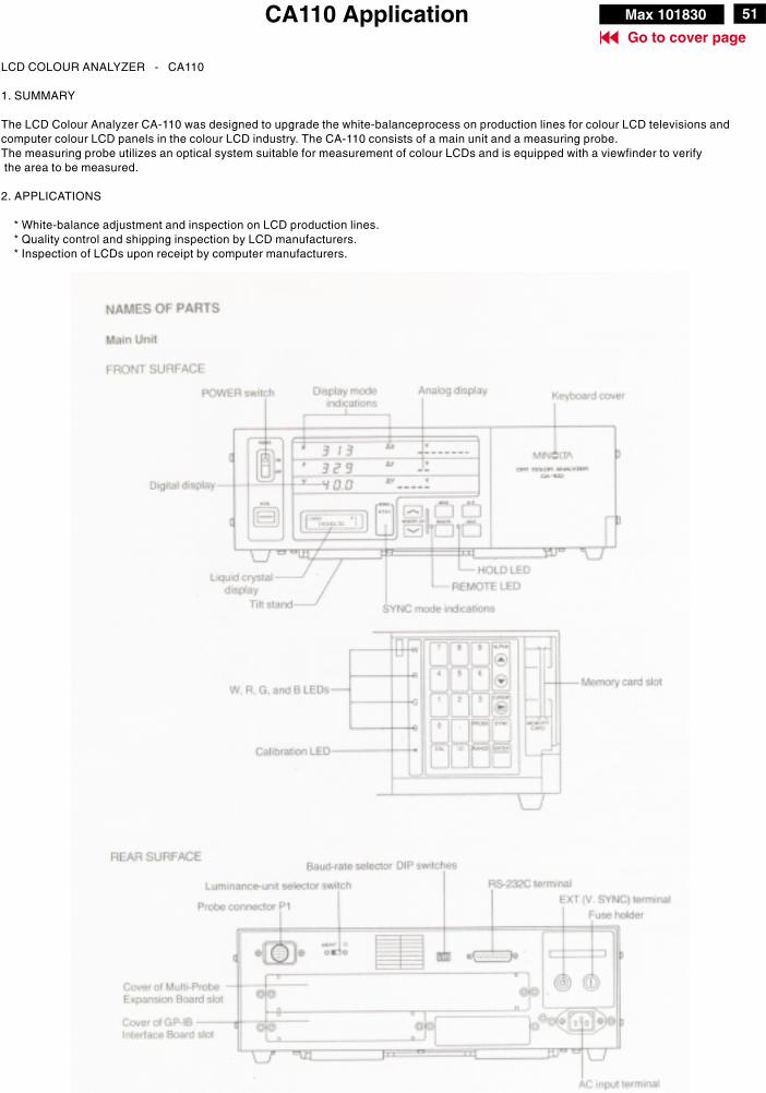
51Max 101830
Go to cover page
LCD COLOUR ANALYZER - CA110
1. SUMMARY
The LCD Colour Analyzer CA-110 was designed to upgrade the white-balanceprocess on production lines for colour LCD televisions and
computer colour LCD panels in the colour LCD industry. The CA-110 consists of a main unit and a measuring probe.
The measuring probe utilizes an optical system suitable for measurement of colour LCDs and is equipped with a viewfinder to verify
the area to be measured.
2. APPLICATIONS
* White-balance adjustment and inspection on LCD production lines.
* Quality control and shipping inspection by LCD manufacturers.
* Inspection of LCDs upon receipt by computer manufacturers.
CA110 Application

52 Max 101830
Go to cover page
CA110 Application (Continued)

CA110 Application (Continued)
ZERO CALIBRATION
Zero calibration is performed to determine the output of the measuring probe when no light reaches the sensor and to set this as the zero
point to which all other measurements are referenced. Zero calibration must be performed after the POWER switch has been set ON
brfore taking any measurements.
To perform zero calibration :
* Before performing zero calibration, check that the measuring probe has been connected to probe
connector P1.
1. Check that the POWER switch is set to ON.
2. Set the measuring/viewing selector to the
(viewing) position. (An image can be seen in the
viewfinder, but no light will reach the sensor.)
3. Press 0-CAL.
* If zero calibration is being performed immediately
after the POWER switch has been set to ON, press
0-CAL after "PUSH 0-CAL KEY" appears in the
liquid crystal display.
4. Set the measuring/viewing selector to the position.
Measurements will be started immediately.
"E1" will appear in the liquid crystal
display the first time the CA-110 is
used after shipment because no
standard color has been set.
Display after POWER
switch is set to ON
Press 0-CAL,
Performing zero
calibration
Zero calibration
completed
Approximately 5 seconds
DARKEN PROBE
DARKEN PROBE
PUSH 0-CAL KEY
ZERO CALIBRATION
-->-->
-->
CH00 P1
E1 [ ]
Measuring/viewing selector
1. POWER switch
3. 0-CAL
Index
53Max 101830
Go to cover page
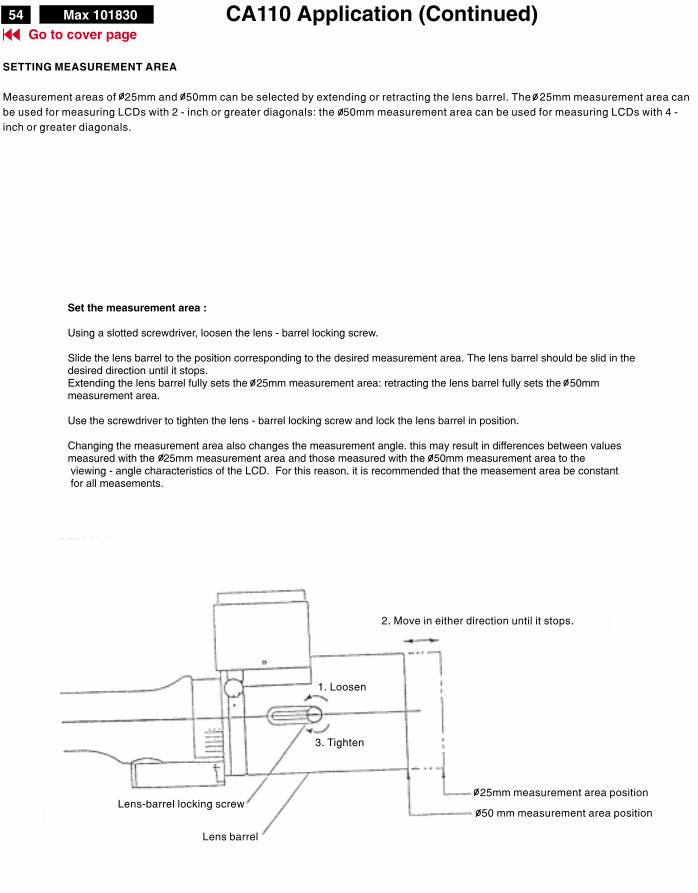
CA110 Application (Continued)
SETTING MEASUREMENT AREA
Measurement areas of 25mm and 50mm can be selected by extending or retracting the lens barrel. The 25mm measurement area can
be used for measuring LCDs with 2 - inch or greater diagonals: the 50mm measurement area can be used for measuring LCDs with 4 -
inch or greater diagonals.
o
I
o
I
o
I
o
I
Set the measurement area :
Using a slotted screwdriver, loosen the lens - barrel locking screw.
Slide the lens barrel to the position corresponding to the desired measurement area. The lens barrel should be slid in thedesired direction until it stops.Extending the lens barrel fully sets the 25mm measurement area: retracting the lens barrel fully sets the 50mmmeasurement area.
Use the screwdriver to tighten the lens - barrel locking screw and lock the lens barrel in position.
Changing the measurement area also changes the measurement angle. this may result in differences between valuesmeasured with the 25mm measurement area and those measured with the 50mm measurement area to theviewing - angle characteristics of the LCD. For this reason. it is recommended that the measement area be constantfor all measements.
o
I
o
I
o
I
o
I
2. Move in either direction until it stops.
o
I
25mm measurement area position
o
I
50 mm measurement area positionLens-barrel locking screw
Lens barrel
3. Tighten
1. Loosen
54 Max 101830
Go to cover page

CA110 Application (Continued)
SETTING MEASUREMENT DISTANCE
The measurement distance (the distance from the front of the measuring probe's lens barrel to the display surface of the LCD ) should be
set using a ruler according to the procedure below.
1. Mount the measuring probe on a tripod or other stand and mount the LCD on a suitable stand.
2. While using a ruler to measure the distance from the front of the measuring probe's lens barrel to the LCD's display surface, move
the measuring probe or the LCD until the distance is the correct distance for the measurement area in use.
o
I
o
I
measurement area 25mm 50mm
measurement distance* 135mm+/-5mm 210mm+/-10mm
* Distance from the tip of the measuring probe's lens barrel to the
LCD's display surface.
LCD panel
Lens barrel
Display surface
Protective glass
Measurement distance
(Measurement distance-D)
Measurement-area indication
Viewfinder
3. While looking through the viewfinder, move the measuring probe or
LCD until the LCD section to be measured is inside the measurement-area
indication in the viewfinder.
55Max 101830
Go to cover page

CA110 Application (Continued)56
Go to cover page
After installation of Chroma 2250, CA110 and LCD monitor.
- Turn on LCD monitor.
- Turn on Chroma 2250 as shown in Fig. 7.
- Provide CROSS-Hatch pattern at timing H=60.023KHz/1024 pixels
V=75.029Hz/768 lines
by Chroma 2250 (as shown in Fig.3 & Fig. 8.).
- Put on the cover (black) of Probe CA-A30 as shown in Fig.9.
- Set "Measurement/viewing selector" to for zero calibration
of CA-110.
- Turn on CA-110 as shown in Fig. 10.
- Press "0-CAL" button as shown in Fig. 11.
LCD monitor & Chroma 2250 :
LCD Colour Analyzer CA-110 :
Step A: Access Factory Mode
Fig. 7 Chroma MODEL 2250Chroma MODEL 2250
Measurement/viewing selectorMeasurement/viewing selector
cover (black)cover (black)
Fig.8
Fig. 9
Fig. 10
(TURN ON)
(Press
0-CAL)
Fig. 11
Access Factory Mode
Factory Mode:
How to Get into Factory Mode Menu
Turn off LCD monitor.
Push AUTO " " & " " & " " buttons simultaneously
,then release Power buttun only, untill picture comes on the screen.
Press MENU " " button, bring up Factory mode indication as
shown in Fig 2.
Use button to select factory adjustment indication (for example:
MAXDATA 180P V1.88 02-04-07), which is the entrance of the factory
adjustment menu, press MENU " " button to access it. The
window shows as below.
AUTO
MENU
Fig. 11 = Buttons for the OSD menu (On-Screen-Display)2 = Power indicator3 = Power button
2 31
AUTO MENUINPUT
MENU
Fig. 2
Factory Mode indication==> MAXDATA 180P V1.88 02-04-17
Max 101830

CA110 Application (Continued) 57
Go to cover page
- Remove the cover (black) of CA-A30 as shown in Fig.13.
- Move the "Lens barrel" back and forth to get the optimal image
as shown in Fig. 14 & Fig. 15.
- Then, turn the "Measurement/viewing selector" counterclockwise
as shown in Fig. 13.
- At this moment the indicator on CA-110 as shown in Fig. 16.
(example only)
Probe CA-A30 :
Fig. 12
Fig. 13
Fig. 14
clear imageunclear image
Fig. 15
Fig. 16
Measurement/viewing selectorMeasurement/viewing selector
cover (black)cover (black)
----->
----->
Step B: Brightness & Contrast setting (pre-setting)
Brightness : at 100%
Contrast : at 70%
Step C: Colour Temperature : Original Panel & 9300K & 6500K
- Provide the "Full White" pattern by Chroma 2250
as shown in Fig. 17.
White pattern & OSD position :
OSD position : Move to optimal position as shown in Fig. 18.
Fig. 17
Fig. 18
--->
--->
MAXDATA 180P V1.88 02-04-17
Max 101830

CA110 Application (Continued)58
Go to cover page
Max 101830
Fig. 22
Fig. 23
Fig. 20
Fig. 21
-->- Select "MAXDATA..." as shown in Fig. 20.
- Press Menu button, bring up Fig. 22.
FACTORY :
Above 200 NIT in the center of the screen as shown in Fig. 19.
Luminance (Y) :
- select 9300K R G B.
- select value of R or G or B
- decrease or increase the value of 9300K R G B.
- confirm/save the value change.
- Adjust the colour temperature of 9300K of R,G,B to x,y value
as below.
R (as shown in Fig. 22), (for example, production value of R is 220)
G (as shown in Fig. 22), (for example, production value of G is 250)
B (as shown in Fig. 22), (for example, production value of B is 255)
x (center) = 0.281+/- 0.005
y (center) = 0.311 +/- 0.005
Luminance (Y) : above 200 Nit in the center of the screen.
(experience: the value of "Y" too low, increase the value of "y" firstly.)
(experience: the value of "y" too high, decrease the value of "G".
the value of "x" too low, decrease the value of "R".)
9300K : As shown in Fig. 22 & 23.
Value of 9300K R G B.
ORIGINAL PANEL COLOR
- Select "
If the
:
ORIGINAL PANEL COLOR" by OSD as shown in Fig. 21.
- Measure Luminance (Y) as shown in Fig. 23.
Luminance (Y) is below 200 Nit in the center of the screen,
then adjust R,G,B Gain till the Luminance (Y) over 200Nit.
After that, check the 32 Gray Scale pattern, all the black and white
scale should be visible on the screen as shown in Fig. 26.
Fig. 19
<----------------------->
Factory Mode==>
Panel color==>
Y value>200 is OKY value>200 is OK
MAXDATA 180P V1.88 02-04-17
9300K R G B9300K R G B
6500K R G B6500K R G B
OFFSET R G BOFFSET R G B
SUB CON:SUB CON:SUB BRI:SUB BRI: --
AUTO SUB:AUTO SUB:- OK
GAIN R G BGAIN R G B
RESERVE1:
RESERVE3:RESERVE2:
MAXDATA 180P V1.88 02-04-17
00
84188
50
182
86181
83
251228
255252255
205
255255
226

CA110 Application (Continued) 59
Go to cover page
Max 101830
Fig. 25
- select 6500K R G B.
- select value of R or G or B
- decrease or increase
the value of 6500K R G B.
- confirm/save the value change.
- Adjust the colour temperature of 6500K of R,G,B to x,y value
as below.
R (as shown in Fig. 22), (for example, production value of R is 241)
G (as shown in Fig. 22), (for example, production value of G is 255)
B (as shown in Fig. 22), (for example, production value of B is 226
x (center) = 0.312+/- 0.005
y (center) = 0.338 +/- 0.005
Luminance (Y) : above 200 Nit in the center of
the screen.
(experience: the value of "Y" too low, increase the value of "y" firstly.)
(experience: the value of "y" too high, decrease the value of "G".
the value of "x" too low, decrease the value of "R".)
6500K : As shown in Fig. 22 & 24.
Value of 6500K R G B.
Full white, Geometry, 32 Gray scale & Pixel on/off pattern check
- Provides the full white pattern by Chroma 2250.
- Check the image of each timing (total: 14 timings) to see if there is
any colour's difference on the screen.
For instance :
at timing 60K/75Hz 1024x768 --> as shown in Fig. 24.
Full White pattern check by eye :
- Provides the cross-hatch pattern by Chroma 2250.
- Check the geometry of each timing to adjust the
geometry of image to optimal position.
For instance :
at timing 31.5K/70Hz 720x400 --> as shown in Fig. 25.
Geometry check and setting by eye :
(total: 14 timings)
- Provides the 32 gray scale pattern by Chroma 2250.
- Check the image of each timing to see if all the
black and white scale are visible on the screen or not.
For instance :
at timing 60K/75Hz 1024x768 --> as shown in Fig. 26.
32 Gray Scale pattern check by eye :
(total: 14 timings)
- Provides the cross talk pattern by Chroma 2250.
- Check the image of each timing to see if there is
any Clock or/and Phase phenomenon on the screen.
For instance :
at timing 60K/75Hz 1024x768 --> as shown in Fig. 27.
Pixel on/off pattern check by eye :
(total: 14 timings)
Fig. 26
Fig. 27
Fig. 24

60 Max 101830
0. Warning
1. Servicing of SMDs (Surface Mounted Devices)
All ICs and many other semi-conductors are susceptible to
electrostatic discharges (ESD). Careless handling during
repair can reduce life drastically. When repairing, make sure
that you are connected with the same potential as the mass
of the unit via a wrist wrap with resistance. Keep components
and tools also at the same potential !
- Oxidation on the terminals of SMDs results in poor soldering.
Do not handle SMDs with bare hands.
- Avoid using storage places that are sensitive to oxidation
such as places with sulphur or chlorine gas, direct sunlight,
high temperatures or a high degree of humidity. The
capacitance or resistance value of the SMDs may be
affected by this.
- Rough handling of circuit boards containing SMDs may
cause damage to the components as well as the circuit
boards. Circuit boards containing SMDs should never be
bent or flexed. Different circuit board materials expand and
contract at different rates when heated or cooled and the
components and/or solder connections may be damaged
due to the stress. Never rub or scrape chip components as
this may cause the value of the component to change.
Similarly, do not slide the circuit board across any surface.
- Heat the solder (for 2-3 seconds) at each terminal of the
chip. By means of litz wire and a slight horizontal force,
small components can be removed with the soldering iron.
They can also be removed with a solder sucker (see Fig.
1A)
- While holding the SMD with a pair of tweezers, take it off
gently using the soldering iron's heat applied to each
terminal (see Fig. 1 B).
- Remove the excess solder on the solder lands by means of
litz wire or a solder sucker (see Fig. 1C).
- When handling the soldering.iron. use suitable pressure and
be careful.
- When removing the chip, do not use undue force with the
pair of tweezers.
- The soldering iron to be used (approx. 30 W) should
1.1 General cautions on handling and storage
1.2 Removal of SMDs
1.3 Caution on removal
preferably be equipped with a thermal control (soldering
temperature: 225 to 250 C).
- The chip, once removed, must never be reused.
o
1.4 Attachment of SMDs
- Locate the SMD on the solder lands by means of tweezers
and solder the component on one side. Ensure that the
component is positioned correctly on the solder lands (see
Fig.2A).
- Next complete the soldering of the terminals of the
component (see Fiq. 2B).
- When soldering the SMD terminals, do not touch them
directly with the soldering iron. The soldering should be
done as quickly as possible, care must be taken to avoid
damage to the terminals of the SMDs themselves.
- Keep the SMD's body in contact with the printed board when
soldering.
- The soldering iron to be used (approx. 30 W ) should
preferably be equipped with a thermal control (soldering
temperature: 225 to 250 C).
- Soldering should not be done outside the solder land.
- Soldering flux (of rosin) may be used, but should not be
acidic.
- After soldering, let the SMD cool down gradually at room
temperature.
- The quantity of solder must be proportional to the size of the
solder land. If the quantity is too great, the SMD might
crack or the solder lands might be torn loose from the
printed board (see Fig. 3).
2. Caution when attaching SMDs
o
SOLDERINGIRON
RIGHT
Fig. 3 Examples
DISMOUNTING
VACUUM PISTON4822 395 10159SOLDERING
IRON
e.g. WELLERSOLDER TIP PT -H7
SOLDERINGIRON
SOLDER WICK4822 321 40042
SOLDERINGIRON
SOLDER WICK
e.g. A PAIR OF TWEEZERS
HEATINGHEATING
Fig. 1
A
B
C
e.g. A PAIR OF TWEEZERS
SOLDER0.5 - 0.8 mm
SOLDER0.5 - 0.8 mm
SOLDERINGIRON
SOLDERING TIME< 3 sec/side
SOLDERINGIRON
PRESURE
PRESURE
MOUNTINGFig. 2
B
A
Repair TipsGo to cover page

61Max 101830GENERAL PRODUCT SPECIFICATION(Continued)
18"TFT SXGA LCD CMTR
01-12-21
01-12-24
590 123EDWARD CHANG
HUDSON-1 18” GENERAL PRODUCT
SPECIFICATION
. ANALOG AND DIGITAL DUAL INPUT
. AUTO PICTURE ADJUSTMENT
. 16 FACTORY PRESET MODES AND 32 PRESET MODES WHICH CAN BE RECOVERED TO PRESET MODES
. USER FRIENDLY OSD DISPLAY FOR MODE IDENTIFICATION /ADJUSTMENT
. DDC 2B COMMUNICATION CAPABILITY
. MAX. RESOLUTION 1280*1024 NON-INTERLACED AT 75 HZ
. 18” COLOR TFT LCD FLAT PANEL
. EASY TILT & SWIVEL BASE
. FULL RANGE POWER SUPPLY 90 – 264 VAC
. CE ENVIRONMENTAL POLICY
. ANTI-GLARE TO REDUCE LIGHT REFLECTION
. POWER MANAGEMENT CAPABILITY
. SOG SUPPORT
. TCO 99
. AUDIO SUPPORT
. PROVIDE USB HUB (OPTION)
. WALL MOUNT KIT (OPTION)
. PROTECTIVE COVER (OPTION)
Go to cover page
MW
MW
MW
HUDSON-1 18”

62 Max 101830 GENERAL PRODUCT SPECIFICATION(Continued)
01-12-21
01-12-21
590 223EDWARD CHANG
CONTENTS
1.0 Foreword
2.0 Product profile
2.1 LCD
2.2 Scanning frequencies
2.3 Video dot rate
2.4 Power input
2.5 Power consumption
2.6 Dimensions
2.7 Weight
2.8 Functions
2.9 Ambient temperature
2.10 Regulatory compliance
3.0 Electrical characteristics
Interface signals
Video 3.2 Interface
3.2.1
3
3
.
.
1
1
.1
D-sub cable
3.2.2 DVI cable
3.2.3 OSD function control
3.3 Timing requirement
3.3.1 Mode storing capacity
3.3.2 Preset timings
3.3.3 Horizontal scanning
3.3.4 Vertical scanning
3.4 Power input connection
3.5 Power management
3.6 Display identification
3.6.1 Analog DDC
3.6.2 Digital DDC
4.0 Visual characteristics
4.1 Test conditions
4.2 Resolution
4.3 Brightness
4.4 Image size
4.4.1 Actual display size
4.4.2 Max. scan size
4.5 Brightness uniformity
4.6 Crosstalk
4.7 White color adjustment
18"TFT SXGA LCD CMTR
Go to cover page
MW
MW

63Max 101830GENERAL PRODUCT SPECIFICATION(Continued)
01-12-21
01-12-21
590 323EDWARD CHANG
5.0 Mechanical characteristics
5.1 Controls
5.2 Unit dimension / weight
5.3 Tilt and swivel base
5.4 Transportation packages
5.4.1 Shipping dimension / weight 5.4.2 Block unit / palletization
6.0 Environmental characteristics
6.1 Susceptibility of display to external environment
6.2 Transportation tests
6.3 Display disturbances from external environment
6.4 Display disturbances to external environment
6.4.1 EMI
7.0 Reliability
7.1 Mean time between failures
8.0 Quality assurance requirements
8.1 Acceptance test
9.0 Serviceability
18"TFT SXGA LCD CMTR
Go to cover page
MW
MW
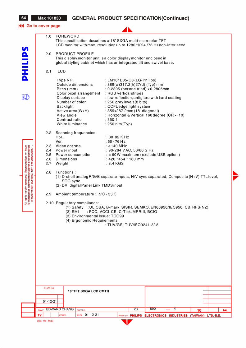
64 GENERAL PRODUCT SPECIFICATION(Continued)
590 423EDWARD CHANG
18"TFT SXGA LCD CMTR
1.0 FOREWORD This specification describes a 18" SXGA multi-scan color TFT LCD monitor with max. resolution up to 1280*1024 /76 Hz non-interlaced.
2.0 PRODUCT PROFILE This display monitor unit is a color display monitor enclosed in
global styling cabinet which has an integrated tilt and swivel base.
2.1 LCD
Type NR. : LM181E05-C3 (LG-Philips) Outside dimensions : 389(w)317.2(h)27(d) (Typ) mm Pitch ( mm ) : 0.2805 (per one triad) x 0.2805mm Color pixel arrangement : RGB vertical stripes Display surface : low reflection, antiglare with hard coating Number of color : 256 gray levels(8 bits)
Backlight : CCFL edge light system Active area(WxH) : 359x287.2mm (18 diagonal) View angle : Horizontal & Vertical 160 degree (CR>=10) Contrast ratio : 350:1 White luminance : 250 nits (Typ)
2.2 Scanning frequencies Hor. : 30 82 K Hz
Ver. : 56 - 76 H z2.3 Video dot rate : < 140 MHz2.4 Power input : 90-264 V AC, 50/60 2 Hz2.5 Power consumption : < 60 W maximum ( exclude USB option )2.6 Dimensions : 426 * 454 * 180 mm2.7 Weight : 8.4 KGS
2.8 Functions :(1) D-shell analog R/G/B separate inputs, H/V sync separated, Composite (H+V) TTL level, SOG sync(2) DVI digital Panel Link TMDS input
2.9 Ambient temperature : 5 C - 35 C
2.10 Regulatory compliance : (1) Safety : UL,CSA, B-mark, SISIR, SEMKO, EN60950/IEC950, CB, RFS(NZ)
(2) EMI : FCC, VCCI, CE, C-Tick, MPRIII, BCIQ(3) Environmental Issue: TCO99
(4) Ergonomic Requirements : TUV/GS, TUV/ISO9241-3/-8
01-12-21
01-12-21
Max 101830
Go to cover page
MW
MW

GENERAL PRODUCT SPECIFICATION(Continued)
590 523EDWARD CHANG
18"TFT SXGA LCD CMTR
3.0 Electrical characteristics
3.1 Interface signals The input signals can be applied in three different modes :
1). D-shell Analog
Input signal : Video, Hsync., Vsync Video : 0.7 Vp-p, input impedance, 75 ohm @DC
Sync. : Separate sync TTL level , input impedance 2k2 ohm terminateHor. sync Positive/NegativeVer. sync Positive/Negative
Composite sync TTL level, input impedance 2k2 ohm terminate (Positive/Negative) Sync on green video 0.3 Vp-p Negative (Video 0.7 Vp-p Positive)
2). Intel DVI Digital
Input signal : Single channel TMDS signal3.1.1 Audio
Input signal level : 500mVrmsHeadphone output signal level : 32ohm 0.7+0.7 VrmsInput signal connector : 3.5 mm mini jackLoud speaker : 2+2 W stereo firing
3.1.2 MicrophoneSensitivity: -65+/- 5 dB re 1V/ubar at 1khzOutput impendence : 600 ohm typical
01-12-21
01-12-21
65Max 101830
Go to cover page
MW
MW

66 GENERAL PRODUCT SPECIFICATION(Continued)
590 623EDWARD CHANG
18"TFT SXGA LCD CMTR
PIN No. SIGNAL 1 Red 2 Green/SOG 3 Blue 4 Sense (GND) 5 Not connected 6 Red GND 7 Green GND 8 Blue GND 9 +5V
10 Sync GND 11 Sense (GND) 12 Bi-directional data 13 H/H+V sync 14 V-sync 15 Data clock
Pin No. Description
1 TMDS data2-
2 TMDS data2+
3 TMDS data2 shield
4 NC
5 NC
6 DDC clock
7 DDC data
8 Analog V-sync
9 TMDS data1-
10 TMDS data1+
11 TMDS data1 shield
12 NC
3.2 Interface
3.2.1 D-Sub CableLength : 1.8 M +/- 50 mm (fixed)Connector type : D-sub male with DDC2B pin assignments.
Blue connector thumb-operated jack screws
pin assignment :
3.2.2 DVI Cable The input signals are applied to the display through DVI-I cable.
Length : 1.8 M +/- 50 mm (fixed) Connector type : DVI-I male with DDC2B pin assignments White connector thumb-operated jack screws
pin assignment :
01-12-21
01-12-21
Max 101830
Go to cover page
MW
MW

GENERAL PRODUCT SPECIFICATION(Continued)
590 723EDWARD CHANG
18"TFT SXGA LCD CMTR
13 NC
14 +5V
15 Ground(return for +5V and H/Vsync)
16 Hot plug detect
17 TMDS data0-
18 TMDS data0+
19 TMDS data0 shield
20 NC
21 NC
22 TMDS clock shield
23 TMDS clock+
24 TMDS clock-
C1 Analog R
C2 Analog G
C3 Analog B
C4 Analog H-sync
C5 Analog GND (Analog R, G, B return)
MAIN CONTROLS
LANGUAGE
ADJUST POSITION
BRIGHTNESS & CONTRAST
VIDEO NOISE
ADJUST COLOR
OSD SETTINGS
PRODUCT INFORMATION
RESET TO FACTORY SETTINGS
INPUT SELECTION
EXIT MAIN CONTROLS
MOVE SELECTION THEN ok
3.2.3 Software control functions via OSD/control
OSD (On Screen Display) function (1) Analog interface OSD : Adjustable functions:
01-12-21
01-12-21
67Max 101830
Go to cover page
MW
MW

68 GENERAL PRODUCT SPECIFICATION(Continued)
590 823EDWARD CHANG
18"TFT SXGA LCD CMTR
LANGUAGE : ENGLISH , ESPANOL , FRANCAIS , DEUTSCH , ITALIANO JAPANESE
ADJUST POSITION : HORIZONTAL VERTICAL
BRIGHTNESS & CONTRAST : brightness and contrast adjustment.
VIDEO NOISE : Phase adjustment, Clock adjustment
ADJUST COLOR : Original panel color , 9300K for CAD/CAM , 6500K for image management, User preset red green blue adjust.
OSD POSITION : OSD H-position, OSD V-position
PRODUCT INFORMATION : Show Serial No./ Resolution / Video input.
RESET TO FACTORY SETTING: recall to Factory preset settings.
INPUT SELECTION : select Analog D-sub, Digital DVI-D or Analog DVI-A.
01-12-21
01-12-21
Max 101830
Go to cover page
MW
MW

GENERAL PRODUCT SPECIFICATION(Continued)
590 923EDWARD CHANG
18"TFT SXGA LCD CMTR
MAIN CONTROLS
LANGUAGE
ADJUST POSITION
BRIGHTNESS & CONTRAST
OSD SETTINGS
PRODUCT INFORMATION
RESET TO FACTORY SETTINGS
INPUT SELECTION
EXIT MAIN CONTROLS
MOVE SELECTION THEN ok
(2) Digital interface OSD : Adjustable functions:
LANGUAGE : ENGLISH , ESPANOL , FRANCAIS , DEUTSCH , ITALIANO, JAPANESE
ADJUST POSITION : HORIZONTAL VERTICAL
BRIGHTNESS & CONTRAST : brightness and contrast adjustment.
OSD POSITION : OSD H-position, OSD V-position
PRODUCT INFORMATION : Show Serial No./ Resolution / Video input.
RESET TO FACTORY SETTING: return to Factory preset timings and settings.
INPUT SELECTION : select Analog D-sub, Digital DVI-D or Analog DVI-A.
3.3 Timing requirement3.3.1 Mode storing capacity
(1) Factory preset modes : 16(2) Preset modes : 32
01-12-21
01-12-21
69Max 101830
Go to cover page
MW
MW

70 GENERAL PRODUCT SPECIFICATION(Continued)
01-12-21
01-12-21
590 1023EDWARD CHANG
18"TFT SXGA LCD CMTR
MODE NO. 5 6 7 8RESOLUTION 640 x 480 640 x 480 640 x 480 800 x 600
Dot clock(MHz) 31.500 30.24 25.175 36
f h 37.861kHz 35 kHz 31.5kHz 35.2kHzA ( us ) 26.413(832 dots) 28.571 (864 dots) 31.778(800 dots) 28.444(1024 dots)B ( us ) 1.270(40 dots) 2.116 ( 64 dots) 3.813( 96 dots) 2.000 ( 72 dots)C ( us ) 3.810(120 dots) 3.175( 96 dots) 1.907( 48 dots) 3.556 ( 128 dots)D ( us ) 20.317(640 dots) 21.164( 640 dots) 25.422( 640 dots) 22.222( 800 dots)E ( us ) 1.016(32 dots) 2.116( 64 dots) 0.636( 16 dots) 0.666 ( 24 dots)
f v 72.809Hz 67Hz 60Hz 56HzO (ms ) 13.735(520 lines) 15 (525 lines) 16.683 (525 lines) 17.778 (625 lines)P ( ms ) 0.079(3 lines) 0.086( 3 lines) 0.064 ( 2 lines) 0.057 ( 2 lines)Q (ms ) 0.528(20 lines) 1.114( 39 lines) 1.049 ( 33 lines) 0.626 ( 22 lines)R ( ms ) 12.678(480 lines) 13.714(480 lines) 15.253 (480 lines) 17.066 (600 lines)S ( ms ) 0.45(17 lines) 0.086( 3 line ) 0.317 ( 10 line ) 0.029 ( 1 line )SYNC. H/V -/- - / - - / - + / +POLARITYSEP . SYNC Y Y Y Y
MODE NO. 1 2 3 4RESOLUTION 640 x 350 720 x 400 640 x 480 640x480
Dot clock(MHz) 25.175 28.321 31.501 36
f h 31.469kHz 31.468kHz 37.5kHz 36kHzA ( us ) 31.778(800 dots) 31.78(900dots) 26.667 (840 dots) 23.111 (832 dots)B ( us ) 3.813(96 dots) 3.813(108dots) 2.032 ( 54 dots) 1.556 (56 dots)C ( us ) 1.907(48 dots) 1.907(54dots) 3.81 ( 120 dots) 2.222 ( 80 dots)D ( us ) 25.422(640 dots) 25.42(720dots) 20.317 (640 dots) 17.778 (640 dots)E ( us ) 0.636(16 dots) 0.636(18dots) 0.508 ( 26 dots) 1.555 (56 dots)
f v 70Hz(70.09) 70Hz(70.085) 75Hz 85Hz O (ms ) 14.27(449 lines) 14.27(449 lines) 13.333 (500 lines ) 11.763 (509 lines )P ( ms ) 0.064(2 lines) 0.064(2 lines) 0.08 ( 3 lines ) 0.069 ( 3 lines )Q (ms ) 1.907(60 lines) 1.112(34 lines) 0.427 ( 16 lines ) 0.578 ( 25 lines )R ( ms ) 11.12(350 lines) 12.71(400 lines) 12.8 (480 lines ) 11.093 (480 lines )S ( ms ) 1.175(37 lines) 0.381(13 lines) 0.026 ( 1 lines) 0.023 ( 1 lines)SYNC. H/V +/- -/+ - / - -/- POLARITY
SEP . SYNC Y Y Y Y
3.3.2 Factory preset timingsThe factory settings of size and centering are according to the reference timing charts
( see fig-4, fig-5 )
Max 101830
Go to cover page
MW
MW

GENERAL PRODUCT SPECIFICATION(Continued)
01-12-21
01-12-21
590 1123EDWARD CHANG
18"TFT SXGA LCD CMTR
MODE NO. 13 14 15 16
RESOLUTION 800 x 600 1024 x 768 1024 x 768 1024 x 768
Dot clock(MHz) 50 78.75 65 75
f h 48.077kHz 60kHz 48.363kHz 56.5kHz
A ( us ) 20.80 (1040dots) 16.66 (1312dots) 20.677(1344 dots) 17.707(1328 dots)
B ( us ) 2.400 ( 120 dots) 1.219 ( 96 dots) 2.092(136 dots) 1.813(136 dots)
C ( us ) 1.280 ( 64 dots) 2.235 ( 176 dots) 2.462(160 dots) 1.920(144 dots)
D ( us ) 16.00 ( 800 dots) 13.003 ( 1024 dots) 15.754(1024 dots) 13.653(1024 dots)
E ( us ) 1.120 ( 56 dots) 0.203 ( 16 dots) 0.369(24 dots) 0.321 (24 dots)
f v 72Hz ( 72.188) 75Hz ( 75.000) 60.004Hz 70.004Hz
O (ms ) 13.85 (666 lines) 13.328 (800 lines) 16.666(806 lines) 14.272(806 lines)
P ( ms ) 0.125 ( 6 lines) 0.05( 3 lines) 0.124(6 lines) 0.106(6 lines)
Q (ms ) 0.478 ( 23 lines) 0.446 ( 28 lines) 0.600(29 lines) 0.514(29 lines)
R ( ms ) 12.48 (600 lines) 12.80 (768 lines) 15.880(768 lines) 13.599(768 lines)
S ( ms ) 0.770 ( 37 line ) 0.017 ( 1 line ) 0.062(3 lines) 0.053(3 lines)
SYNC. H/V + / + + / + - / - -/-
POLARITY
SEP . SYNC Y Y Y Y
MODE NO. 9 10 11 12
RESOLUTION 800 x 600 800 x 600 800 x 600 832 x 624
Dot clock(MHz) 49.498 40 56.251 57.28
f h 46.9kHz 37.9kHz 53.7kHz 49.7kHz
A ( us ) 21.333 (1056 dots) 26.4 (1056 dots) 18.631 (1048 dots) 20.11(1152 dots)
B ( us ) 1.616 ( 80 dots) 3.2 ( 128 dots) 1.138 ( 64 dots) 1.117(64 dots)
C ( us ) 3.232 ( 160 dots) 2.2 ( 88 dots) 2.702 ( 152 dots) 3.91(224 dots)
D ( us ) 16.162 ( 800 dots) 20 ( 800 dots) 14.222 ( 800 dots) 14.52(832 dots)
E ( us ) 0.323 ( 16 dots) 1 ( 40 dots) 0.569 ( 32 dots) 0.563(32 dots)
f v 75Hz 60Hz 85Hz 75Hz
O (ms ) 13.333 (625 lines) 16.579 (628 lines) 11.756(631 lines) 13.41(667 lines)
P ( ms ) 0.064 ( 3 lines) 0.106 ( 4 lines) 0.056 ( 3 lines) 0.06(3 lines)
Q (ms ) 0.448 ( 21 lines) 0.607 ( 23 lines) 0.503 ( 27 lines) 0.784(39 lines)
R ( ms ) 12.8 (600 lines) 15.84 (600lines) 11.179 (600 lines) 12.55(624 lines)
S ( ms ) 0.021 ( 1 line ) 0.026 ( 1 line ) 0.018 ( 1 lines)
0.016(1 lines)
SYNC. H/V + / + + / + + / + +/+
POLARITY
SEP . SYNC Y Y Y Y
71Max 101830
Go to cover page
MW
MW
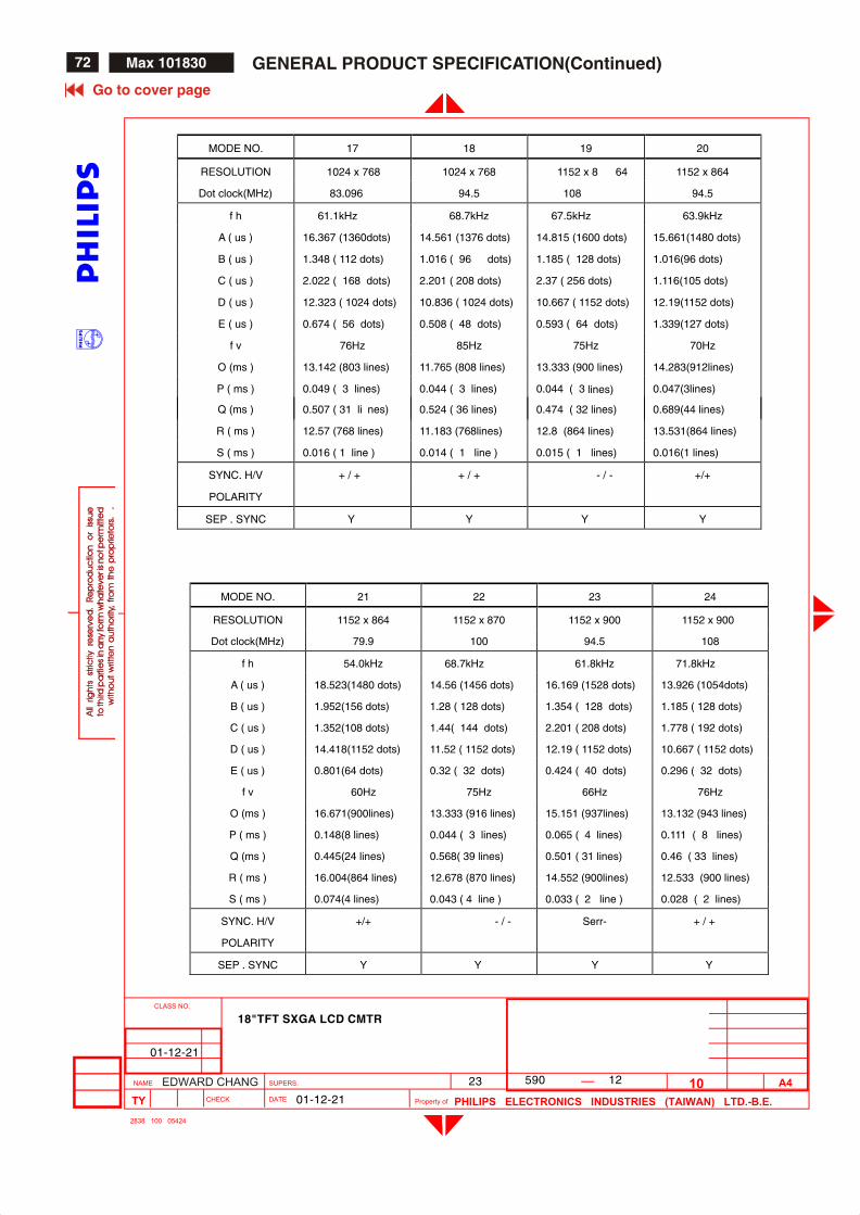
72 GENERAL PRODUCT SPECIFICATION(Continued)
590 1223EDWARD CHANG
18"TFT SXGA LCD CMTR
MODE NO. 21 22 23 24
RESOLUTION 1152 x 864 1152 x 870 1152 x 900 1152 x 900
Dot clock(MHz) 79.9 100 94.5 108
f h 54.0kHz 68.7kHz 61.8kHz 71.8kHz
A ( us ) 18.523(1480 dots) 14.56 (1456 dots) 16.169 (1528 dots) 13.926 (1054dots)
B ( us ) 1.952(156 dots) 1.28 ( 128 dots) 1.354 ( 128 dots) 1.185 ( 128 dots)
C ( us ) 1.352(108 dots) 1.44( 144 dots) 2.201 ( 208 dots) 1.778 ( 192 dots)
D ( us ) 14.418(1152 dots) 11.52 ( 1152 dots) 12.19 ( 1152 dots) 10.667 ( 1152 dots)
E ( us ) 0.801(64 dots) 0.32 ( 32 dots) 0.424 ( 40 dots) 0.296 ( 32 dots)
f v 60Hz 75Hz 66Hz 76Hz
O (ms ) 16.671(900lines) 13.333 (916 lines) 15.151 (937lines) 13.132 (943 lines)
P ( ms ) 0.148(8 lines) 0.044 ( 3 lines) 0.065 ( 4 lines) 0.111 ( 8 lines)
Q (ms ) 0.445(24 lines) 0.568( 39 lines) 0.501 ( 31 lines) 0.46 ( 33 lines)
R ( ms ) 16.004(864 lines) 12.678 (870 lines) 14.552 (900lines) 12.533 (900 lines)
S ( ms ) 0.074(4 lines) 0.043 ( 4 line ) 0.033 ( 2 line ) 0.028 ( 2 lines)
SYNC. H/V +/+ - / - Serr- + / +
POLARITY
SEP . SYNC Y Y Y Y
MODE NO. 17 18 19 20
RESOLUTION 1024 x 768 1024 x 768 1152 x 8 64 1152 x 864
Dot clock(MHz) 83.096 94.5 108 94.5
f h 61.1kHz 68.7kHz 67.5kHz 63.9kHz
A ( us ) 16.367 (1360dots) 14.561 (1376 dots) 14.815 (1600 dots) 15.661(1480 dots)
B ( us ) 1.348 ( 112 dots) 1.016 ( 96 dots) 1.185 ( 128 dots) 1.016(96 dots)
C ( us ) 2.022 ( 168 dots) 2.201 ( 208 dots) 2.37 ( 256 dots) 1.116(105 dots)
D ( us ) 12.323 ( 1024 dots) 10.836 ( 1024 dots) 10.667 ( 1152 dots) 12.19(1152 dots)
E ( us ) 0.674 ( 56 dots) 0.508 ( 48 dots) 0.593 ( 64 dots) 1.339(127 dots)
f v 76Hz 85Hz 75Hz 70Hz
O (ms ) 13.142 (803 lines) 11.765 (808 lines) 13.333 (900 lines) 14.283(912lines)
P ( ms ) 0.049 ( 3 lines) 0.044 ( 3 lines) 0.044 ( 3 lines) 0.047(3lines)
Q (ms ) 0.507 ( 31 li nes) 0.524 ( 36 lines) 0.474 ( 32 lines) 0.689(44 lines)
R ( ms ) 12.57 (768 lines) 11.183 (768lines) 12.8 (864 lines) 13.531(864 lines)
S ( ms ) 0.016 ( 1 line ) 0.014 ( 1 line ) 0.015 ( 1 lines) 0.016(1 lines)
SYNC. H/V + / + + / + - / - +/+
POLARITY
SEP . SYNC Y Y Y Y
01-12-21
01-12-21
Max 101830
Go to cover page
MW
MW
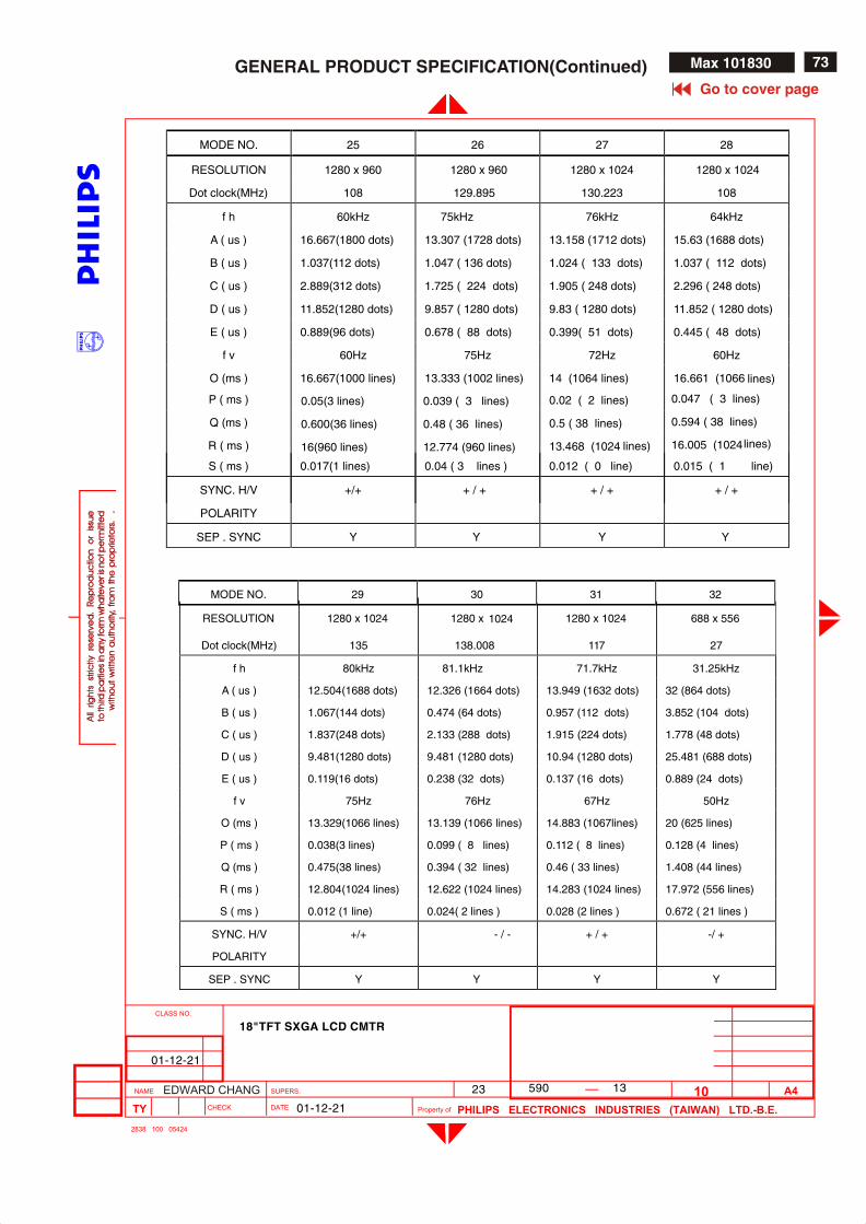
GENERAL PRODUCT SPECIFICATION(Continued)
590 1323EDWARD CHANG
18"TFT SXGA LCD CMTR
MODE NO. 29 30 31 32
RESOLUTION 1280 x 1024 1280 x 1024 1280 x 1024 688 x 556
Dot clock(MHz) 135 138.008 117 27
f h 80kHz 81.1kHz 71.7kHz 31.25kHz
A ( us ) 12.504(1688 dots) 12.326 (1664 dots) 13.949 (1632 dots) 32 (864 dots)
B ( us ) 1.067(144 dots) 0.474 (64 dots) 0.957 (112 dots) 3.852 (104 dots)
C ( us ) 1.837(248 dots) 2.133 (288 dots) 1.915 (224 dots) 1.778 (48 dots)
D ( us ) 9.481(1280 dots) 9.481 (1280 dots) 10.94 (1280 dots) 25.481 (688 dots)
E ( us ) 0.119(16 dots) 0.238 (32 dots) 0.137 (16 dots) 0.889 (24 dots)
f v 75Hz 76Hz 67Hz 50Hz
O (ms ) 13.329(1066 lines) 13.139 (1066 lines) 14.883 (1067lines) 20 (625 lines)
P ( ms ) 0.038(3 lines) 0.099 ( 8 lines) 0.112 ( 8 lines) 0.128 (4 lines)
Q (ms ) 0.475(38 lines) 0.394 ( 32 lines) 0.46 ( 33 lines) 1.408 (44 lines)
R ( ms ) 12.804(1024 lines) 12.622 (1024 lines) 14.283 (1024 lines) 17.972 (556 lines)
S ( ms ) 0.012 (1 line) 0.024( 2 lines ) 0.028 (2 lines ) 0.672 ( 21 lines )
SYNC. H/V +/+ - / - + / + -/ +
POLARITY
SEP . SYNC Y Y Y Y
MODE NO. 25 26 27 28
RESOLUTION 1280 x 960 1280 x 960 1280 x 1024 1280 x 1024
Dot clock(MHz) 108 129.895 130.223 108
f h 60kHz 75kHz 76kHz 64kHz
A ( us ) 16.667(1800 dots) 13.307 (1728 dots) 13.158 (1712 dots) 15.63 (1688 dots)
B ( us ) 1.037(112 dots) 1.047 ( 136 dots) 1.024 ( 133 dots) 1.037 ( 112 dots)
C ( us ) 2.889(312 dots) 1.725 ( 224 dots) 1.905 ( 248 dots) 2.296 ( 248 dots)
D ( us ) 11.852(1280 dots) 9.857 ( 1280 dots) 9.83 ( 1280 dots) 11.852 ( 1280 dots)
E ( us ) 0.889(96 dots) 0.678 ( 88 dots) 0.399( 51 dots) 0.445 ( 48 dots)
f v 60Hz 75Hz 72Hz 60Hz
O (ms ) 16.667(1000 lines) 13.333 (1002 lines) 14 (1064 lines) 16.661 (1066 lines)
P ( ms ) 0.05(3 lines) 0.039 ( 3 lines) 0.02 ( 2 lines) 0.047 ( 3 lines)
Q (ms ) 0.600(36 lines) 0.48 ( 36 lines) 0.5 ( 38 lines) 0.594 ( 38 lines)
R ( ms ) 16(960 lines) 12.774 (960 lines) 13.468 (1024 lines)
16.005 (1024 lines)
S ( ms ) 0.017(1 lines) 0.04 ( 3 lines ) 0.012 ( 0 line) 0.015 ( 1 line)
SYNC. H/V +/+ + / + + / + + / +
POLARITY
SEP . SYNC Y Y Y Y
01-12-21
01-12-21
73Max 101830
Go to cover page
MW
MW
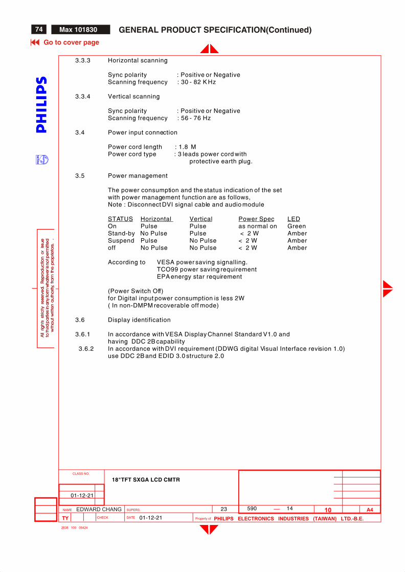
74 GENERAL PRODUCT SPECIFICATION(Continued)
590 1423EDWARD CHANG
18"TFT SXGA LCD CMTR
3.3.3 Horizontal scanning
Sync polarity : Positive or Negative Scanning frequency : 30 - 82 K Hz
3.3.4 Vertical scanning
Sync polarity : Positive or Negative Scanning frequency : 56 - 76 Hz
3.4 Power input connection
Power cord length : 1.8 M Power cord type : 3 leads power cord with protective earth plug.
3.5 Power management
The power consumption and the status indication of the set with power management function are as follows,
Note : Disconnect DVI signal cable and audio module
STATUS Horizontal Vertical Power Spec LED On Pulse Pulse as normal on Green Stand-by No Pulse Pulse < 2 W Amber Suspend Pulse No Pulse < 2 W Amber off No Pulse No Pulse < 2 W Amber
According to VESA power saving signalling. TCO99 power saving requirement EPA energy star requirement
(Power Switch Off)for Digital input power consumption is less 2W ( In non-DMPM recoverable off mode)
3.6 Display identification
3.6.1 In accordance with VESA Display Channel Standard V1.0 and having DDC 2B capability
3.6.2 In accordance with DVI requirement (DDWG digital Visual Interface revision 1.0) use DDC 2B and EDID 3.0 structure 2.0
01-12-21
01-12-21
Max 101830
Go to cover page
MW
MW

GENERAL PRODUCT SPECIFICATION(Continued)
590 1523EDWARD CHANG
18"TFT SXGA LCD CMTR
# Resolution Frequency Pixel rate Sync Comment
1 640X350 31.5K/70HZ 25.175 (+/-) IBM VGA 10h
2 720X400 31.5K/70HZ 28.322 (-/+) IBM VGA 3h
3 640X480 37.5K/75HZ 31.501 (-/-)
4 640X480 31.5K/60HZ 25.175 (-/-)
5 800X600 35.2K/56HZ 36 (+/+)
6 800X600 46.9K/75HZ 49.498 (+/+)
7 800X600 37.9K/60HZ 40 (+/+)
8 832X624 49.7K/75HZ 57.28 (+/+) MAC
9 1024X768 48.4K/60HZ 65 (-/-)
10 1024X768 56.5K/70HZ 75 (-/-)
11 1152X870 68.7K/75HZ 100 (-/-) MAC
12 1152X900 71.8K/76HZ 108 (+/+) SUN Mode II
13 1280X1024 64.0K/60HZ 108 (+/+)
14 1280X1024 80.0K/75HZ 135 (+/+)
15 1280X1024 81.1K/76HZ 135.008 (-/-) SUN Mode I
16 688X556 31.25K/50HZ 27 (-/+) TV-PAL
4.0 Visual characteristics
4.1 Test conditions Unless otherwise specified, this specification is defined under the following conditions. (1) Input signal : As defined in 3.3, 1280 x 1024
non-interlaced mode (80K/75Hz), signal sources must have 75 ohm output impedance.
(2) Luminance setting: controls to be set to 200 nits with full screen 70 % duty cycle white signal
(3) Warm up: more than 30 minutes after power on with signal supplied.
(4) Ambient light: 400 -- 600 lux.
(5) Ambient temperature: 20+/- 5 C
4.2 ResolutionFactory preset modes ( 16 modes )
01-12-21
01-12-21
75Max 101830
Go to cover page
MW
MW

76 GENERAL PRODUCT SPECIFICATION(Continued)
590 1623EDWARD CHANG
18"TFT SXGA LCD CMTR
Note : 1. Screen displays perfect picture at 16 factory preset modes 2. Screen displays visible picture with OSD warning when input modes are
other then 32 preset modes
4.3 Brightness : 200 nits (at panel color temperature, 9 points averaged, Fig. 1 )
4.4 Image size
4.4.1 Actual display size 359x287mm
4.5 Brightness uniformity
Set contrast at 70% and turn the brightness to get average above 200 nitsat center of the screen.Apply the Fig 1, it should comply with the following formula:
B_max X 100% < 1.3
B_min
Where B_max =Average of 5 points maximum brightness B_min = Average of 5 points minimum brightness
4.6 Check Cross talk (S)
Apply Pattern 2. Set contrast and brightness at 100 %.Measure YA. Then output Pattern 3 and measure YB.the cross talk value :
ABS( YA - YB ) X 100% < 1.2 %
YA
01-12-21
01-12-21
Max 101830
Go to cover page
MW
MW

GENERAL PRODUCT SPECIFICATION(Continued)
590 1723EDWARD CHANG
18"TFT SXGA LCD CMTR
4.7 White color adjustment
There are two factory preset white color 9300K, 6500K.
Apply full white pattern, with brightness in 100 % position and the contrast control at 70 % position. The 1931 CIE Chromaticity (color triangle) diagram (x,y) coordinate for the screen center should be:
9300K CIE coordinates X = 0.281+/- 0.020 Y = 0.311+/- 0.020
6500K CIE coordinates X = 0.312 +/- 0.020 Y = 0.338 +/- 0.020
5.0 Mechanical characteristics
5.1 Controls
Front side: - DC power switch- OSD function key- Auto key
- Volume & off control - Bass on/off - Mute on/off
Rear : - Video signal cable- DVI connector.- Power cord socket- DC 12V fly-in- Audio in jack- Microphone out jack
Side : - Earphone jack-External Mic. in jack
5.2 Unit dimension / Weight
Set dimension (incl. pedestal): 414(W) * 406(H) * 180(D) mm
Net weight : : 7.2 KGS
01-12-21
01-12-21
77Max 101830
Go to cover page
MW
MW
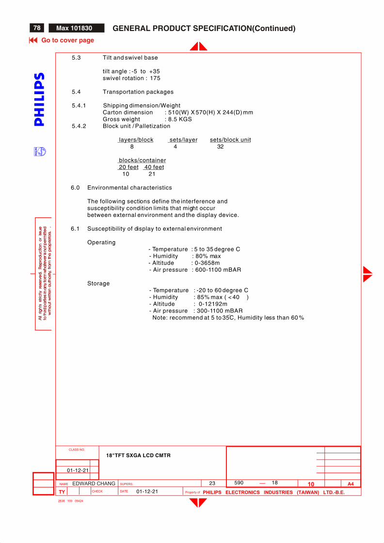
78 GENERAL PRODUCT SPECIFICATION(Continued)
590 1823EDWARD CHANG
18"TFT SXGA LCD CMTR
5.3 Tilt and swivel base
tilt angle : -5 to +35 swivel rotation : 175
5.4 Transportation packages
5.4.1 Shipping dimension/Weight Carton dimension : 510(W) X 570(H) X 244(D) mm Gross weight : 8.5 KGS
5.4.2 Block unit / Palletization
layers/block sets/layer sets/block unit 8 4 32
blocks/container 20 feet 40 feet 10 21
6.0 Environmental characteristics
The following sections define the interference and susceptibility condition limits that might occur between external environment and the display device.
6.1 Susceptibility of display to external environment
Operating- Temperature : 5 to 35 degree C
- Humidity : 80% max- Altitude : 0-3658m
- Air pressure : 600-1100 mBAR
Storage - Temperature : -20 to 60 degree C - Humidity : 85% max ( < 40¢J ) - Altitude : 0-12192m - Air pressure : 300-1100 mBAR
Note: recommend at 5 to 35C, Humidity less than 60 %
01-12-21
01-12-21
Max 101830
Go to cover page
MW
MW

GENERAL PRODUCT SPECIFICATION(Continued)
01-12-21
01-12-21
590 1923EDWARD CHANG
18"TFT SXGA LCD CMTR
Standard Philips UAN-D1400 NSTA
Height 70 cm 61 cm
1 corner 1 corner
Drop Sequence 3 faces 3 edge
Test 6 face
electrical function ok
Test mechanical function ok
Result no serious damage on set appearance
(room temp./-10 c, humidity 70 %)
5-200 Hz 10-50-10 Hz
Sequence 0.73 G 0.35 mm
30 min. for 30 min. for
Vibration each axis each axis
Test Test electrical function ok
Result mechanical function ok
no serious damage on set appearance
For design evaluation only
operating
10 G, 11 msec, 1000 cycles
Bump temperature : 23 C
Test humidity : 60 %
air pressure : 100 kpa
(according to DSD draft standard UAN -D636)
6.2 Transportation tests 6.3
6.3 Display disturbances from external environment According to IEC 801-2 for ESD disturbances
6.4 Display disturbances to external environment
6.4.1 EMI EMI : FCC,VCCI,CE,C-Tick, MPRIII, BCIQ
7.0 Reliability
7.1 Mean Time Between Failures System MTBF (Excluding the LCD panel and CCFL) : 50,000 hrs
CCFL MTBF : 50,000 hrs
79Max 101830
Go to cover page
MW
MW
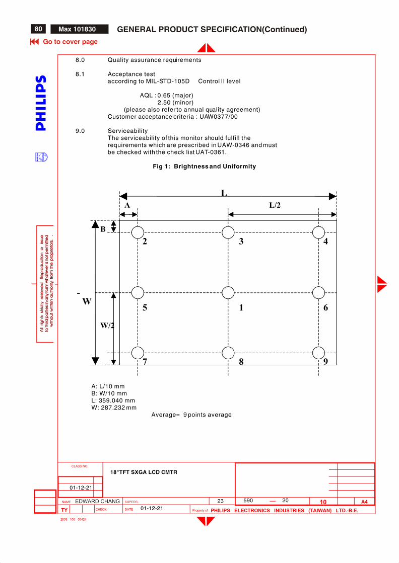
80 GENERAL PRODUCT SPECIFICATION(Continued)
01-12-21
01-12-21
590 2023EDWARD CHANG
18"TFT SXGA LCD CMTR
8.0 Quality assurance requirements
8.1 Acceptance test according to MIL-STD-105D Control II level
AQL : 0.65 (major) 2.50 (minor) (please also refer to annual quality agreement) Customer acceptance criteria : UAW0377/00
9.0 Serviceability The serviceability of this monitor should fulfill the requirements which are prescribed in UAW-0346 and must be checked with the check list UAT-0361.
Fig 1: Brightness and Uniformity
A: L/10 mmB: W/10 mmL: 359.040 mmW: 287.232 mm
Average= 9 points average
2
A
B
Max 101830
Go to cover page
MW
MW
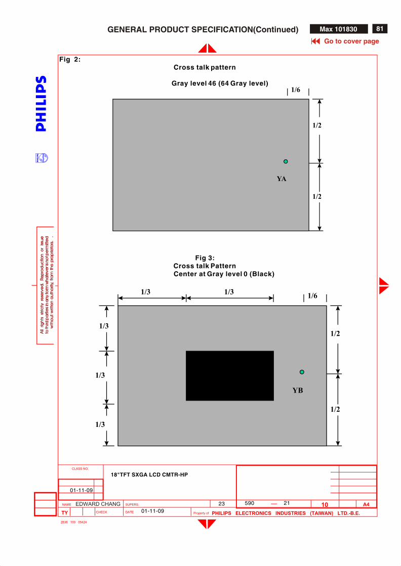
Fig 2: Cross talk pattern
Gray level 46 (64 Gray level)
Fig 3: Cross talk Pattern
Center at Gray level 0 (Black)
GENERAL PRODUCT SPECIFICATION(Continued)
01-11-09
01-11-09
590 2123EDWARD CHANG
18"TFT SXGA LCD CMTR-HP
81Max 101830
YB
1/2
1/2
1/61/3 1/3
1/3
1/3
1/3
YA
1/2
1/2
1/6
Go to cover page
MW
MW

82 GENERAL PRODUCT SPECIFICATION(Continued)
01-11-09
01-11-09
590 2223EDWARD CHANG
18"TFT SXGA LCD CMTR-HP
D
VIDEO
C E
SEPARATE SYNC.
HORIZONTAL
BA
R
VIDEO
Q S
PO
D
VIDEO
C E
BA
VERTICAL
HORIZONTAL
COMPOSITE SYNC.
FIG-4 TIMING CHART -1
Max 101830
Go to cover page
MW
MW
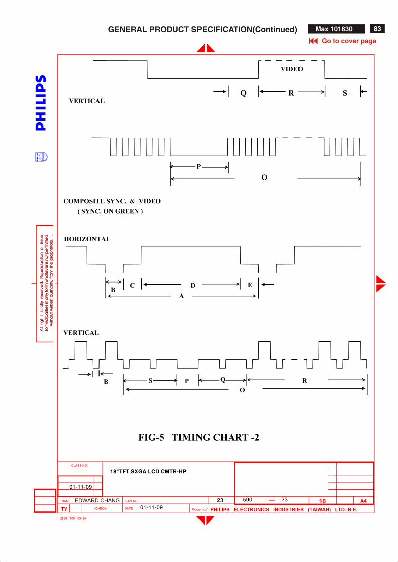
83Max 101830GENERAL PRODUCT SPECIFICATION(Continued)
01-11-09
01-11-09
590 2323EDWARD CHANG
18"TFT SXGA LCD CMTR-HP
D
VIDEO
C E
B
A
VERTICAL
COMPOSITE SYNC.
FIG-5 TIMING CHART -2
O
P
Q R S
& VIDEO
B
S P Q
O
R
( SYNC. ON GREEN )
HORIZONTAL
VERTICAL
Go to cover page
MW
MW
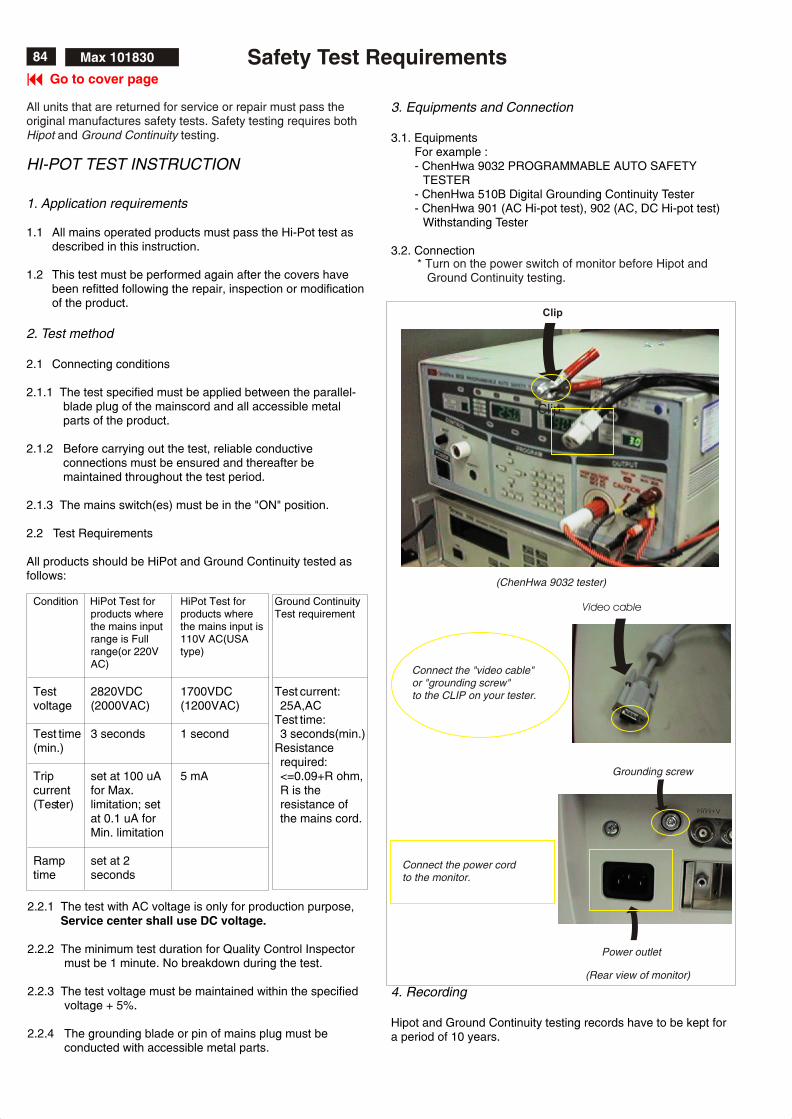
84
9 Go to cover page
Safety Test Requirements
2.2.1 The test with AC voltage is only for production purpose, Service center shall use DC voltage.
2.2.2 The minimum test duration for Quality Control Inspector must be 1 minute. No breakdown during the test.
2.2.3 The test voltage must be maintained within the specified voltage + 5%.
2.2.4 The grounding blade or pin of mains plug must be conducted with accessible metal parts.
All units that are returned for service or repair must pass the original manufactures safety tests. Safety testing requires both Hipot and Ground Continuity testing.
HI-POT TEST INSTRUCTION
1. Application requirements
1.1 All mains operated products must pass the Hi-Pot test as described in this instruction.
1.2 This test must be performed again after the covers have been refitted following the repair, inspection or modification of the product.
2. Test method
2.1 Connecting conditions
2.1.1 The test specified must be applied between the parallel-blade plug of the mainscord and all accessible metal parts of the product.
2.1.2 Before carrying out the test, reliable conductive connections must be ensured and thereafter be maintained throughout the test period.
2.1.3 The mains switch(es) must be in the "ON" position.
2.2 Test Requirements
All products should be HiPot and Ground Continuity tested as follows:
Condition HiPot Test for HiPot Test for Ground Continuityproducts where products where Test requirementthe mains input the mains input is range is Full 110V AC(USA range(or 220V type)AC)
Test 2820VDC 1700VDC Test current:voltage (2000VAC) (1200VAC) 25A,AC
Test time:Test time 3 seconds 1 second 3 seconds(min.)(min.) Resistance
required:Trip set at 100 uA 5 mA <=0.09+R ohm,current for Max. R is the (Tester) limitation; set resistance of
at 0.1 uA for the mains cord.Min. limitation
Ramp set at 2time seconds
3. Equipments and Connection
3.1. Equipments For example :
- ChenHwa 9032 PROGRAMMABLE AUTO SAFETY TESTER
- ChenHwa 510B Digital Grounding Continuity Tester - ChenHwa 901 (AC Hi-pot test), 902 (AC, DC Hi-pot test)
Withstanding Tester
3.2. Connection
4. Recording
Hipot and Ground Continuity testing records have to be kept for a period of 10 years.
* Turn on the power switch of monitor before Hipot and Ground Continuity testing.
Connect the "video cable" or "grounding screw" to the CLIP on your tester.
Video cable
(Rear view of monitor)
Connect the power cord to the monitor.
Grounding screw
Power outlet
(ChenHwa 9032 tester)
Clip
Clip
Max 101830