
SEMESTER V - KTU
242
SEMESTER V ELECTRONICS & COMMUNICATION ENGINEERING
-
Upload
khangminh22 -
Category
Documents
-
view
2 -
download
0
Transcript of SEMESTER V - KTU

SEMESTER V
ELECTRONICS & COMMUNICATION ENGINEERING

ECT301 LINEAR INTEGRATED CIRCUITS CATEGORY L T P CREDITS
PCC 3 1 0 4
Preamble: This course aims to develop the skill to design circuits using operational amplifiers and other linear ICs for various applications.
Prerequisite: EC202 Analog Circuits
Course Outcomes: After the completion of the course the student will be able to
CO 1 Understand Op Amp fundamentals and differential amplifier configurations
CO 2 Design operational amplifier circuits for various applications
CO 3 Design Oscillators and active filters using opamps
CO4 Explain the working and applications of timer, VCO and PLL ICs
CO5 Outline the working of Voltage regulator IC’s and Data converters
Mapping of course outcomes with program outcomes
PO 1 PO 2 PO 3 PO 4 PO 5 PO 6 PO 7 PO 8 PO 9 PO 10
PO 11
PO 12
CO 1 3 3 1 2 1
CO 2 3 3 2 2 2 1
CO 3 3 3 2 2 2 1
CO 4 3 3 1 2 2 1
CO 5 3 3 2 2 2 1
Assessment Pattern
Bloom’s Category Continuous Assessment
Tests End Semester Examination
1 2 Remember K1 10 10 10 Understand K2 30 30 60 Apply K3 10 10 30 Analyse K4 Evaluate Create
Mark distribution
Total Marks
CIE ESE ESE Duration
150 50 100 3 hours
ELECTRONICS & COMMUNICATION ENGINEERING

Continuous Internal Evaluation Pattern:
Attendance : 10 marks
Continuous Assessment Test (2 numbers) : 25 marks Assignment/Quiz/Course project : 15 marks
End Semester Examination Pattern: There will be two parts; Part A and Part B. Part A contain 10 questions with 2 questions from each module, having 3 marks for each question. Students should answer all questions. Part B contains 2 questions from each module of which student should answer any one. Each question can have maximum 2 sub-divisions and carry 14 marks.
Course Level Assessment Questions
Course Outcome 1 (CO1): Analyze differential amplifier configurations.
1. Explain the working of BJT differential amplifiers.
2. Calculate the input resistance, output resistance, voltage gain and CMRR of differential amplifiers.
3. Explain the non-ideal parameters of differential amplifiers.
4. Derive CMRR, input resistance and output resistance of a dual input balanced output differential amplifier configuration.
Course Outcome 2 (CO2): Design operational amplifier circuits for various applications.
1. Design an opamp circuit to obtain an output voltage V0=-(2V1+4V2 + 3V3)2. A 741C op-amp is used as an inverting amplifier with a gain of 50. The voltage gain vs
frequency curve of 741C is flat upto 20kHz.What maximum peak to peak input signal can beapplied without distorting the output?
3. With the help of a neat circuit diagram, derive the equation for the output voltage of anInstrumentation amplifier.
4. With the help of circuit diagrams and graphs, explain the working of a Full wave Precisionrectifier.
Course Outcome 3 (CO3): Design active filters using opamps
1. Derive the design equations for a second order Butterworth active low pass filter.2. Design a Notch filter to eliminate power supply hum (50 Hz).3. Design a first order low pass filter at a cut-off frequency of 2kHz with a pass band gain of 3
Course Outcome 4 (CO4): Explain the working and applications of specialized ICs
1. With the help of internal diagram explain the monostable operation of timer IC 555.Draw the input and different output waveforms. Derive the equation for pulse width.
2. Explain the operation of Phase Locked Loop. What is lock range and capture range?Realize a summing amplifier to obtain a given output voltage.
ELECTRONICS & COMMUNICATION ENGINEERING

3. Design a circuit to multiply the incoming frequency by a factor of 5 using 565 PLL.
Course Outcome 5 (CO5): Outline the working of Voltage regulator IC’s and Data converters
1. What is the principle of operation of Dual slope ADC. Deduce the relationship betweenanalogue input and digital output of the ADC.
2. Explain how current boosting is achieved using I.C 7233. Explain the working of successive approximation ADC
SYLLABUS
Module 1:
Operational amplifiers(Op Amps): The 741 Op Amp, Block diagram, Ideal op-amp parameters, typical parameter values for 741, Equivalent circuit, Open loop configurations, Voltage transfer curve, Frequency response curve.
Differential Amplifiers: Differential amplifier configurations using BJT, DC Analysis- transfer characteristics; AC analysis- differential and common mode gains, CMRR, input and output resistance, Voltage gain. Constant current bias, constant current source; Concept of current mirror-the two transistor current mirror, Wilson and Widlar current mirrors.
Module 2:
Op-amp with negative feedback: General concept of Voltage Series, Voltage Shunt, current series and current shunt negative feedback, Op Amp circuits with voltage series and voltage shunt feedback, Virtual ground Concept; analysis of practical inverting and non-inverting amplifiers for closed loop gain, Input Resistance and Output Resistance. Op-amp applications: Summer, Voltage Follower-loading effects, Differential and Instrumentation Amplifiers, Voltage to current and Current to voltage converters, Integrator, Differentiator, Precision rectifiers, Comparators, Schmitt Triggers, Log and antilog amplifiers.
Module 3:
Op-amp Oscillators and Multivibrators: Phase Shift and Wien-bridge Oscillators, Triangular and Sawtooth waveform generators, Astable and monostable multivibrators. Active filters: Comparison with passive filters, First and second order low pass, High pass, Band pass and band reject active filters, state variable filters.
Module 4 :
Timer and VCO: Timer IC 555- Functional diagram, Astable and monostable operations;. Basic concepts of Voltage Controlled Oscillator and application of VCO IC LM566, Phase Locked Loop – Operation, Closed loop analysis, Lock and capture range, Basic building blocks, PLL IC 565, Applications of PLL.
ELECTRONICS & COMMUNICATION ENGINEERING

Module 5:
Voltage Regulators: Fixed and Adjustable voltage regulators, IC 723 – Low voltage and high voltage configurations, Current boosting, Current limiting, Short circuit and Fold-back protection. Data Converters: Digital to Analog converters, Specifications, Weighted resistor type and R-2R Ladder type. Analog to Digital Converters: Specifications, Flash type and Successive approximation type.
Text Books 1. Roy D. C. and S. B. Jain, Linear Integrated Circuits, New Age International, 3/e, 2010
Reference Books
1. DFranco S., Design with Operational Amplifiers and Analog Integrated Circuits, 3/e,Tata McGraw Hill, 2008
2. Gayakwad R. A., Op-Amps and Linear Integrated Circuits, Prentice Hall, 4/e, 2010
3. Salivahanan S. and V. S. K. Bhaaskaran, Linear Integrated Circuits, Tata McGrawHill, 2008.
4. Botkar K. R., Integrated Circuits, 10/e, Khanna Publishers, 2010
5. C.G. Clayton, Operational Amplifiers, Butterworth & Company Publ. Ltd. Elsevier,1971
6. David A. Bell, Operational Amplifiers & Linear ICs, Oxford University Press,2nd edition,2010
7. R.F. Coughlin & Fredrick Driscoll, Operational Amplifiers & Linear Integrated
Circuits,6th Edition, PHI,2001
8. Sedra A. S. and K. C. Smith, Microelectronic Circuits, 6/e, Oxford University Press,2013.
Course Contents and Lecture Schedule
No TopicNo. of
Lectures
1 Operational amplifiers (9) 1.1 The 741 Op Amp, Block diagram, Ideal op-amp parameters, typical
parameter values for 741 1
1.2 Equivalent circuit, Open loop configurations, Voltage transfer curve, Frequency response curve.
1
1.3 Differential amplifier configurations using BJT, DC Analysis- transfer characteristics
2
1.4 AC analysis- differential and common mode gains, CMRR, input and output resistance, Voltage gain
2
1.5 Constant current bias and constant current source 1
1.6 Concept of current mirror, the two transistor current mirror Wilson and Widlar current mirrors.
2
2 Op-amp with negative feedback and Op-amp applications (11)
ELECTRONICS & COMMUNICATION ENGINEERING

2.1 General concept of Voltage Series, Voltage Shunt, current series and current shunt negative feedback
1
2.2 Op Amp circuits with voltage series and voltage shunt feedback, Virtual ground Concept
1
2.3 Analysis of practical inverting and non-inverting amplifier 2
2.4 Summer, Voltage Follower-loading effect 1
2.5 Differential and Instrumentation Amplifiers 1
2.6 Voltage to current and Current to voltage converters 1
2.7 Integrator, Differentiator 1
2.8 Precision rectifiers-half wave and full wave 1
2.9 Comparators, Schmitt Triggers 1
2.10 Log and antilog amplifier 1
3 Op-amp Oscillators and Multivibrators (10)
3.1 Phase Shift and Wien-bridge Oscillators, 2
3.2 Triangular and Sawtooth waveform generators, Astable and monostable multivibrators
2
3.3 Comparison, design of First and second order low pass and High pass active filters
2
3.4 Design of Second Order Band pass and band reject filters 2
3.5 State variable filters 2
4 Timer, VCO and PLL (9)
4.1 Timer IC 555- Functional diagram, Astable and monostable operations. 2
4.2 Basic concepts of Voltage Controlled Oscillator 1
4.3 Application of VCO IC LM566 2
4.4 PLL Operation, Closed loop analysis Lock and capture range. 2
4.5 Basic building blocks, PLL IC 565, Applications of PLL 2
5 Voltage regulators and Data converters (9)
5.1 Fixed and Adjustable voltage regulators 1
5.2 IC 723 – Low voltage and high voltage configurations, 2
5.3 Current boosting, Current limiting, Short circuit and Fold-back protection. 2
5.4 Digital to Analog converters, Specifications, Weighted resistor type and R-2R Ladder type.
2
5.5 Analog to Digital Converters: Specifications, Flash type and Successive approximation type.
2
ELECTRONICS & COMMUNICATION ENGINEERING

Assignment: Assignment may be given on related innovative topics on linear IC, like Analog multiplier- Gilbert multiplier cell, variable trans-conductance technique, application of analog multiplier IC AD633., sigma delta or other types of ADC etc. At least one assignment should be simulation of opamp circuits on any circuit simulation software. The following simulations can be done in QUCS, KiCad or PSPICE.(The course instructor is free to add or modify the list)
1. Design and simulate a BJT differential amplifier. Observe the input and output signals. Plot the AC frequency response
2. Design and simulate Wien bridge oscillator for a frequency of 10 kHz. Run a transient simulation and observe the output waveform.
3. Design and implement differential amplifier and measure its CMRR. Plot its transfer characteristics.
4. Design and simulate non-inverting amplifier for gain 5. Observe the input and output signals. Run the ac simulation and observe the frequency response and 3− db bandwidth.
5. Design and simulate a 3 bit flash type ADC. Observe the output bit patterns and transfer characteristics
6. Design and simulate R − 2R DAC circuit.
7. Design and implement Schmitt trigger circuit for upper triggering point of +8 V and a lower triggering point of −4 V using op-amps.
ELECTRONICS & COMMUNICATION ENGINEERING
Model Question
APJ ABDUL KALAM TECHNOLOGICAL UNIVERSITY
FIFTH SEMESTER B.TECH DEGREE EXAMINATION, (Model Question Paper)
Course Code: ECT301
Program: Electronics and Communication Engineering Course Name: Linear Integrated Circuits
Max. Marks: 100 Duration: 3 Hours
PART A
Answer ALL Questions. Each Carries 3 mark.
1. Draw and list the functions of 741 IC pins K1 2. Define slew rate with its unit. What is its effect at the output signal? K2 3. How the virtual ground is different from actual ground? K2 4. A differential amplifier has a common mode gain of 0.05 and difference mode gain of
1000.Calculate the output voltage for two signals V1 = 1mV and V2 = 0.9Mv K3 5. Design a non-inverting amplifier for a gain of 11 K3 6. Design a second order Butterworth Low Pass Filter with fH= 2KHz K3
7. Draw the circuit of monostable multivibrator using opamp. K1 8. What is the principle of VCO?. K1 9. Mention 3 applications of PLL. K2 10. Define the following terms with respect to DAC (i)Resolution (ii)Linearity (iii) Full scale output voltage K2
Differentiate between line and load regulations. K3
PART – B Answer one question from each module; each question carries 14 marks.
Module I
11. a) Derive CMRR, input resistance and output resistance of a dual input balanced output differential amplifier configuration.
7 CO1 K3
11. b) What is the principle of operation of Wilson current mirror and its advantages? Deduce the expression for its current gain.
7 CO1 K2
OR
12.a) Draw the equivalent circuit of an operational amplifier. Explain voltage transfer characteristics of an operational amplifier.
6 CO1 K3
12.b) Explain the following properties of a practical opamp (i) Bandwidth (ii) Slew rate (iii) Input offset voltage (iv) Input offset current
8 CO1 K2
Module II
ELECTRONICS & COMMUNICATION ENGINEERING
13. a) Design a fullwave rectifier to rectify an ac signal of 0.2V peak-to-peak. Explain its principle of operation.
7 CO2 K3
13. b) Draw the circuit diagram of a differential instrumentation amplifier with a transducer bridge and show that the output voltage is proportional to the change in resistance.
7 CO2 K2
OR
14.a) Derive the following characteristics of voltage shunt amplifier: i) Closed loop voltage gain ii)Input resistance iii) Output resistance iv)Bandwidth
7 CO2 K3
14.b) Explain the working of an inverting Schmitt trigger and draw its transfer characteristics.
7 CO2 K2
Moduel III
15 a) Derive the equation for frequency of oscillation (f0) of a Wein Bridge oscillator. Design a Wein Bridge oscillator for f0 = 1KHz.
7 CO3 K3
15 b) Derive the equation for the transfer function of a first order wide Band Pass filter.
7 CO3 K3
OR
16a Derive the design equations for a second order Butterworth active low pass filter.
7 CO3 K3
16b Design a circuit to generate 1KHz triangular wave with 5V peak. 7 CO3 K3
Module IV
17 a) Design a circuit to multiply the incoming frequency by a factor of 5 using 565 PLL.
8 CO4 K3
17 b) With the help of internal diagram explain the monostable operation of timer IC 555. Draw the input and output waveforms. Derive the equation for pulse width.
6 CO4 K2
OR
18 a) Design a monostable multi-vibrator for a pulse duration of 1ms using IC555.
7 CO4 K3
18 b) Explain the operation of Phase Locked Loop. What is lock range and capture range?
7 CO4 K2
Module V
19 a) Explain the working of R-2R ladder type DAC. In a 10 bit DAC, reference voltage is given as 15V. Find analog output for digital input of 1011011001.
7 CO5 K2
19 b) Explain how short circuit, fold back protection and current boosting are done using IC723 voltage regulator.
7 CO5 K2
OR
20 a) With a functional diagram, explain the principle of operation of Successive approximation type ADC.
7 CO5 K2
20 b) With a neat circuit diagram, explain the operation of a 3-bit flash converter.
7 CO5 K2
ELECTRONICS & COMMUNICATION ENGINEERING
Preamble: This course aims to provide an understanding of the principles, algorithms and applications of DSP.
Prerequisite: ECT 204 Signals and systems
Course Outcomes: After the completion of the course the student will be able to
CO 1 State and prove the fundamental properties and relations relevant to DFT and solve basic problems involving DFT based filtering methods
CO 2 Compute DFT and IDFT using DIT and DIF radix-2 FFT algorithms
CO 3 Design linear phase FIR filters and IIR filters for a given specification
CO 4 Illustrate the various FIR and IIR filter structures for the realization of the given system function
CO5 Explain the basic multi-rate DSP operations decimation and interpolation in both time and frequency domains using supported mathematical equations
CO6 Explain the architecture of DSP processor (TMS320C67xx) and the finite word length effects
Mapping of course outcomes with program outcomes
PO 1
PO 2
PO 3
PO 4
PO 5
PO 6
PO 7
PO 8
PO 9
PO 10
PO 11
PO 12
CO 1 3 3 2 2 2
CO 2 3 3 3 3 2
CO 3 3 3 3 3 2
CO 4 3 3 2 3 2
CO5 2 2 2 2 2
CO6 2 2 - - 2
Assessment Pattern
Bloom’s Category Continuous Assessment Tests
End Semester Examination
1 2 Remember K1 10 10 10 Understand K2 20 20 30 Apply K3 20 20 60 Analyse K4 Evaluate Create
ECT303 DIGITAL SIGNAL
PROCESSING CATEGORY L T P CREDIT
PCC 3 1 0 4
ELECTRONICS & COMMUNICATION ENGINEERING
Mark distribution
Total Marks CIE ESE ESE Duration
150 50 100 3 hours
Continuous Internal Evaluation Pattern:
Attendance : 10 marks
Continuous Assessment Test (2 numbers) : 25 marks Assignment/Quiz/Course project : 15 marks
End Semester Examination Pattern: There will be two parts; Part A and Part B. Part A contain 10 questions with 2 questions from each module, having 3 marks for each question. Students should answer all questions. Part B contains 2 questions from each module of which student should answer any one. Each question can have maximum 2 sub-divisions and carry 14 marks.
Course Level Assessment Questions
CO1: State and prove the fundamental properties and relations relevant to DFT and solve basic problems involving DFT based filtering methods
1. Determine the N-point DFT X(k) of the N point sequences given by (i) x1(n)=sin(2πn/N) n/N)
(ii) x2(n)=cos2(2πn/N) n/N)
2. Show that if x(n) is a real valued sequence, then its DFT X(k) is also real and even
CO2: Compute DFT and IDFT using DIT and DIF radix-2 FFT algorithms
1. Find the 8 point DFT of a real sequence x(n)=1,2,2,2,1,0,0,0,0 using Decimation infrequency algorithm?
2. Find out the number of complex multiplications require to perform an 1024 point DFTusing(i)direct computation and (ii) using radix 2 FFT algorithm?
CO3: Design linear phase FIR filters and IIR filters for a given specification 1. Design a linear phase FIR filter with order M=15 and cut-off frequency πn/N) /6 .Use a
Hanning Window.
2. Design a low pass digital butter-worth filter using bilinear transformation for the givenspecifications. Passband ripple ≤1dB, Passband edge:4kHz, Stopband Attenuation:≥40dB, Stopband edge:6kHz, Sampling requency:24 kHz
ELECTRONICS & COMMUNICATION ENGINEERING

CO4: Illustrate the various FIR and IIR filter structures for the realization of the given system function
1. Obtain the direct form II and transpose structure of the filter whose transfer function isgiven below.
H ( z )=0
3
.44 z2+2
0.362 z+0.02z +.4 z +.18 z −0.2
2. Realize an FIR system with the given difference equation y(n)=x(n)-0.5x(n-1)+0.25x(n-2)+0.5x(n-3)-0.4x(n-4)+0.2x(n-5)
CO5: Explain the basic multi-rate DSP operations decimation and interpolation in both time and frequency domains using supported mathematical equations
1. Derive the frequency domain expression of the factor of 2 up-sampler whose input isgiven by x(n) and transform by X(k)?
2. Bring out the role of an anti-imaging filter in a sampling rate converter?
CO6: Explain the architecture of DSP processor TMS320C67xx and the finite word length effects
1. Derive the variance of quantization noise in an ADC with step size Δ, assuminguniformly distributed quantization noise with zero mean ?
2. Bring out the architectural features of TMS320C67xx digital signal processor?
ELECTRONICS & COMMUNICATION ENGINEERING

SYLLABUS Module 1
Basic Elements of a DSP system, Typical DSP applications, Finite-length discrete transforms, Orthogonal transforms – The Discrete Fourier Transform: DFT as a linear transformation (Matrix relations), Relationship of the DFT to other transforms, IDFT, Properties of DFT and examples. Circular convolution, Linear Filtering methods based on the DFT, linear convolution using circular convolution, Filtering of long data sequences, overlap save and overlap add methods, Frequency Analysis of Signals using the DFT (concept only required)
Module 2 Efficient Computation of DFT: Fast Fourier Transform Algorithms-Radix-2 Decimation in Time and Decimation in Frequency FFT Algorithms, IDFT computation using Radix-2 FFT Algorithms, Application of FFT Algorithms, Efficient computation of DFT of Two Real Sequences and a 2N-Point Real Sequence
Module 3
Design of FIR Filters - Symmetric and Anti-symmetric FIR Filters, Design of linear phase FIR filters using Window methods, (rectangular, Hamming and Hanning) and frequency sampling method, Comparison of design methods for Linear Phase FIR Filters. Design of IIRDigital Filters from Analog Filters (Butterworth), IIR Filter Design by Impulse Invariance, and Bilinear Transformation, Frequency Transformations in the Analog and Digital Domain.
Module 4
Structures for the realization of Discrete Time Systems - Block diagram and signal flow graph representations of filters, FIR Filter Structures: Linear structures, Direct Form, CascadeForm, IIR Filter Structures: Direct Form, Transposed Form, Cascade Form and Parallel Form, Computational Complexity of Digital filter structures. Multi-rate Digital Signal Processing:
Decimation and Interpolation (Time domain and Frequency Domain Interpretation ), Anti- aliasing and anti-imaging filter.
Module 5
Computer architecture for signal processing: Harvard Architecture, pipelining, MAC, Introduction to TMS320C67xx digital signal processor, Functional Block Diagram.
Finite word length effects in DSP systems: Introduction (analysis not required), fixed-point and floating-point DSP arithmetic, ADC quantization noise, Finite word length effects in IIRdigital filters: coefficient quantization errors. Finite word length effects in FFT algorithms: Round off errors
Text Books
1. Proakis J. G. and Manolakis D. G., Digital Signal Processing, 4/e, Pearson Education,2007
2. Alan V Oppenheim, Ronald W. Schafer ,Discrete-Time Signal Processing, 3rd Edition ,Pearson ,2010
ELECTRONICS & COMMUNICATION ENGINEERING
3. Mitra S. K., Digital Signal Processing: A Computer Based Approach, 4/e McGraw Hill(India) 2014
Reference Books
4. Ifeachor E.C. and Jervis B. W., Digital Signal Processing: A Practical Approach, 2/ePearson Education, 2009.
5. Lyons, Richard G., Understanding Digital Signal Processing, 3/e. Pearson EducationIndia, 2004.
6. Salivahanan S, Digital Signal Processing,4e, Mc Graw –Hill Education New Delhi, 20197. Chassaing, Rulph., DSP applications using C and the TMS320C6x DSK. Vol. 13. John
Wiley & Sons, 2003. 8. Vinay.K.Ingle, John.G.Proakis, Digital Signal Processing: Bookware Companion
Series,Thomson,20049. Chen, C.T., “Digital Signal Processing: Spectral Computation & Filter Design”, Oxford
Univ. Press, 2001.10. Monson H Hayes, “Schaums outline: Digital Signal Processing”, McGraw HillProfessional,
1999
Course Contents and Lecture Schedule
No. Topic No. of
Lectures 1 Module 1 1.1 Basic Elements of a DSP system, Typical DSP
applications, Finite length Discrete transforms, Orthogonal transforms
1
1.2 The Discrete Fourier Transform: DFT as a linear transformation(Matrix relations),
1
1.3 Relationship of the DFT to other transforms, IDFT 1 1.4 Properties of DFT and examples ,Circular convolution 2 1.5 Linear Filtering methods based on the DFT- linear
convolution using circular convolution, Filtering of long data sequences, overlap save and overlap add methods,
3
1.6 Frequency Analysis of Signals using the DFT(concept only required)
1
2 Module 2 2.1 Efficient Computation of DFT: Fast Fourier Transform
Algorithms 1
2.2 Radix-2 Decimation in Time and Decimation in Frequency
FFT Algorithms
4
2.3 IDFT computation using Radix-2 FFT Algorithms 2 2.4 Application of FFT Algorithms-Efficient computation of DFT of
Two Real Sequences and a 2N-Point Real Sequence 1
3 Module 3
ELECTRONICS & COMMUNICATION ENGINEERING

3.1 Design of FIR Filters- Symmetric and Anti-symmetric FIR Filters, Design of linear phase FIR filters using Window methods, (rectangular, Hamming and Hanning)
4
3.2 Design of linear phase FIR filters using frequency sampling Method, Comparison of Design Methods for Linear Phase FIR Filters
2
3.3 Design of IIR Digital Filters from Analog Filters,
(Butterworth), IIR Filter Design by Impulse Invariance
3
3.4 IIR Filter Design by Bilinear Transformation 2 3.5 Frequency Transformations in the Analog and Digital Domain. 1
4 Module 4
4.1 Structures for the realization of Discrete Time Systems- Block diagram and signal flow graph representations of filters
2
4.2 FIR Filter Structures: (Linear structures), Direct Form
Cascade Form
,2
4.3 IIR Filter Structures: Direct Form, Cascade Form and
Parallel Form
3
4.3 Computational Complexity of Digital filter structures. 1 4.4 Multi-rate Digital Signal Processing: Decimation and Interpolation
(Time domain and Frequency Domain Interpretation ), Anti-aliasing and anti-imaging filter.
3
5 Module 5 5.1 Computer architecture for signal processing : Harvard Architecture,
pipelining, MAC, Introduction to TMS320C67xx digital signal processor ,Functional Block Diagram
3
5.2 Finite word length effects in DSP systems: Introduction (analysis not required), fixed-point and floating-point DSP arithmetic, ADC quantization noise,
3
5.3 Finite word length effects in IIR digital filters: coefficient quantization errors.
2
5.4 Finite word length effects in FFT algorithms: Round off errors
1
ELECTRONICS & COMMUNICATION ENGINEERING
Simulation Assignments
The following simulations to be done in Scilab/ Matlab/ LabView/GNU Octave:
1. Consider a signal given by x(n)=[1,1,1,1].
1. Compute the DTFT of the given sequence and plot its magnitude and phase
2. Compute the 4 point DFT of the above signal and plot its magnitude and phase
3. Compare the above plots and obtain the relationship?
2. Zero pad the sequence x(n) by 4 and compute the 8 point DFT and find the corresponding magnitude and phase plots. Compare the spectra with that in (b) and comment on it.
3. The first five values of the 8 point DFT of a real valued sequence x(n) are given by 0.25, 0.125-j0.3, 0, 0.125-j0.06, 0.5. Determine the DFT of each of the following sequences using properties. Hint :IDFT may not be computed.
1. x1(n)=x((2-n))8
2. x3(n)=x2(n)
3. x4(n)=x(n)ejπn/N) in/4
4. a) Develop a function to implement the over-lap add method using circular convolution operation. The format should be function [y]=overlappadd(x,h,N), where y is the output sequence, x is the input sequence and N is the block -length>=2*Length(h)-1.
1. Incorporate the radix-2 FFT implementation in the above function to obtain a high speed overlap add block convolution routine. Choose N=8. Hint :choose N=2k
5. Design a low pass digital filter to be used in the given structure
xa(t) ya(t)A/D H(z) D/A
to satisfy the following requirements. Sampling rate of 8000samples/second, Pass band edge of 1500Hz with a ripple of 3dB, Stopband edge of 2000Hz with attenuation of 40 dB, Equiripple passband but monotonic stopband. (Use impulse invariance technique)
1. Choose T=1 s for impulse invariance and determine the system function H(z) in parallel form.Plot the log-magnitude response in dB and impulse response h(n)
2. Choose T=1/8000 s and repeat the same procedure. Compare this design with that in (a) and comment on the effect of T on the impulse invariant design?
ELECTRONICS & COMMUNICATION ENGINEERING
6. A filter is described by the following difference equation:
16y(n)+12y(n-1)+2y(n-2)-4y(n-3)-y(n-4)=x(n)-3x(n-1)+11x(n-2)-27x(n-3)+18x(n-4)
1. Determine the Direct form filter structure
2. Using the Direct form structure, obtain the cascade form filter structure
7. Consider a signal given by x(n)=(0.5)nu(n). Decimate the signal by a factor 4 and plotthe output in time domain and frequency domain?
1. Interpolate the signal by a factor of 4 and plot the output in time domain andfrequency domain?
2. Compare the spectra and obtain the inference?
Model Question Paper
A P J Abdul Kalam Technological University
Fifth Semester B Tech Degree ExaminationBranch: Electronics and Communication Engg.
Course: ECT 303 DIGITAL SIGNAL PROCESSING
Time: 3 Hrs Max. Marks: 100PART A
Answer All Questions. Each question carry 3 marks
1 .Derive the relationship of DFT to Z-transform? (3)K32.Find the circular convolution of two sequences x1(n)=1, 2,-2,1,3,x2(n)=2,-1,3,1,1 (3)K3 3 Illustrate the basic butterfly computation used in decimation in time radix-2 FFT algorithm?(3)K1 4 Bring out the computational advantage of performing an N-point DFT using radix-2 FFT
compared to direct method?
(3) K3
5. Determine the frequency response of a linear phase FIR filter given by the difference equation y(n)=0.15x(n)+0.25x(n-1)+x(n-3). Also find the phase delay (3) K3
6 .An all pole analog filter is given by the transfer function H(s)=1 /(s2+5s+6). Find out the transfer function H(z) of the equivalent digital filter using impulse invariance method. Use T=1s
7.Obtain the cascade form realization of the third order IIR filter transfer function given by
H( z )=02
.44 z2+
0.362 z+0.02( z +0 .8 z +.0 .5 ) ( z−0.4 )
8 . Prove that a factor of L upsampler is a linear-time varying system.
9. Differentiate between Harvard architecture and Von-Nuemann Architecture used in processors? 10. Express the fraction 7/8 and -7/8 in sign-magnitude, two’s compliment and one’s compliment format? (3) K3
(3) K1
(3) K3
(3) K3
ELECTRONICS & COMMUNICATION ENGINEERING
Part BAnswer any one Question from each module. Each question carries 14 Marks
11. a) How will you perform linear convolution using circular convolution? Find the linearconvolution of the given sequences x(n) = 2, 9,7, 4 and h(n) = 1, 3, 1, 2 using circular convolution? (8) K3
b) Explain the following properties of DFT a) Linearity b) Complex conjugate property c)Circular Convolution d) Time Reversal (6) K2
OR
12.a.) The first eight points of 14-point DFT of a real valued sequence are 12, -1+j3, 3+j4, 1-j5, -2+j2, 6+j3, -2-j3, 10
i) Determine the remaining pointsii) Evaluate x[0] without computing the IDFT of X(k)?
iii) Evaluate IDFT to obtain the real sequence ? (8)K3
b) Explain with appropriate diagrams, the overlap-add method for filtering of long datasequences using DFT? (6) K2
13.a) Compute the 8 point DFT of x(n) = 2,1,-1,3,5,2,4,1 using radix-2 decimation in time
FFT algorithm. (9) K3
b)Bring out how a 2N point DFT of a 2N point sequence can be found using the
computation of a single N point DFT. (5) K3
OR
14 a.) Find the 8 point DFT of a real sequence x(n)=1,2,2,2,1,0,0,0,0 using radix-2 decimation in frequency algorithm (9)K3
b) Bring out how N-point DFT of two real valued sequences can be found by computinga single N-point DFT. (5) K3
15.a. Design a linear phase FIR low pass filter having length M = 15 and cut-off frequency ωc
= πn/N) /6. Use Hamming window. (10) K3
b.Prove that if z1 is a zero of an FIR filter, then 1/z1 is also a zero? (4) K2
OR
16. a. Design a digital Butterworth low pass filter with ωp = πn/N) /6, ωs = πn/N) /4, minimum pass bandgain = -2 dB and minimum stop band attenuation = 8 dB. Use bilinear transformation.(Take T= 1s) (10) K3
b. What is warping effect in bilinear transformation and how it can be eliminated? (4) K2
ELECTRONICS & COMMUNICATION ENGINEERING
17.a) Derive and draw the direct form-I, direct form-II and cascade form realization of the
given filter, whose difference equation is given asy (n )=0.1 y (n−1 )+0.2 y (n−2 )+3 x (n )+3.6 x (n−1 )+0.6 x (n−2 )
b) Differentiate between anti-aliasing and anti-imaging filters. (5) K2
OR
18.a) Obtain the expression of output y(n) as a function of x(n) for the multi-rate structuregiven below? (9) K3
b) Draw the transposed direct form II Structure of the system given by the differenceequation y(n)=05.y(n-1)-0.25y(n-2)+x(n)+x(n-1) . (5)K2
19.a.With the help of a functional block diagram, explain the architecture of TMS320C67xx
DSP processor? (10) K2
b.What are the prominent features of TMS320C67xx compared to its predecessors ?
(4) K2
OR
20.a)Explain how to minimize the effect of finite word length in IIR digital filters? (7) K2
b)Explain the roundoff error models used in FFT algorithms? (7) K2
(9) K3
ELECTRONICS & COMMUNICATION ENGINEERING

ECT305 ANALOG AND DIGITAL
COMMUNICATION CATEGORY L T P CREDIT
PCC 3 1 0 4
Preamble: This course aims to develop analog and digital communication systems.
Prerequisite: ECT 204 Signals and Systems, MAT 204 Probability, Random Process and
Numerical Methods
Course Outcomes: After the completion of the course the student will be able to
CO 1 Explain the existent analog communication systems.
CO 2 Apply the concepts of random processes to LTI systems.
CO 3 Apply waveform coding techniques in digital transmission.
CO 4 Apply GS procedure to develop digital receivers.
CO 5 Apply equalizer design to counteract ISI.
CO 6 Apply digital modulation techniques in signal transmission.
Mapping of course outcomes with program outcomes
PO1 PO2 PO3 PO4 PO5 PO6 PO7 PO8 PO9 PO10 PO11 PO12
CO 1 3 3
CO 2 3 3 2 3 3
CO 3 3 3 2 3 3 2 2
CO 4 3 3 2 3 3 2 2
CO 5 3 3 2 3 3 2 2
CO 6 3 3 2 3 3 2 2
Assessment Pattern
Bloom’s Category Continuous Assessment Tests
End Semester Examination
1 2 Remember 10 10 20 Understand 30 30 60 Apply 10 10 20 Analyse Evaluate Create
ELECTRONICS & COMMUNICATION ENGINEERING

Mark distribution
Total Marks
CIE ESE ESE Duration
150 50 100 3 hours
Continuous Internal Evaluation Pattern: Attendance : 10 marks Continuous Assessment Test (2 numbers) : 25 marks Assignment/Quiz/Course project : 15 marks
End Semester Examination Pattern: There will be two parts; Part A and Part B. Part A contain 10 questions with 2 questions from each module, having 3 marks for each question. Students should answer all questions. Part B contains 2 questions from each module of which student should answer any one. Each question can have maximum 2 sub-divisions and carry 14 marks.
Course Level Assessment Questions
Course Outcome 1 (CO1): The existent analog communication system 1. What are the needs for analog modulation2. Give the mathematical model of FM signal and explain its spectrum.
Course Outcome 2 (CO2): Application of random processes 1. Compute the entropy of a Gaussian random variable.2. A six faced die is thrown by a player. He gets Rs. 100 if face 6 turns up, loses Rs. 20if face 3 or 4 turn up, gets Rs. 50 if face 5 turns up and loses Rs 10 if face 1 or 2 turn up. Draw thepdf and CDF for the random variable. Check if it is profitable based on statistical expectation.
Course Outcome 3 (CO3): Waveform coding 1. Compute the A and mu law quantized values of a signal that is normalized to 0.8 with A=32 andmu=255.2. Design a 3-tap linear predictor for speech signals with the autocorrelation vector[0.95,0.85,0.7,0.6] , based on Wiener-Hopf equation. Compute the minimum mean square error.
Course Outcome 4 (CO4): G-S Procedure and effects in the channel 1. Apply G-S procedure on the following signals and plot their signal space.
ELECTRONICS & COMMUNICATION ENGINEERING

2. Derive the Nyquist criterion for zero ISI.
Course Outcome 5 (CO5): Digital modulation 1. Give the mathematical model of a BPSK signal and plot its signal constellation. 2. Draw the BER-SNR plot for the BPSK system
SYLLABUS
Module 1 Analog Communication Block diagram of a communication system. Need for analog modulation. Amplitude modulation. Equation and spectrum of AM signal. DSB-SC and SSB systems. Block diagram of SSB transmitter and receiver. Frequency and phase modulation. Narrow and wide band FM and their spectra. FM transmitter and receiver. Module 2 Review of Random Variables and Random Processes Review of random variables – both discrete and continuous. CDF and PDF, statistical averages. (Only definitions, computations and significance) Entropy, differential entropy. Differential entropy of a Gaussian RV. Conditional entropy, mutual information.
Stochastic processes, Stationarity. Conditions for WSS and SSS. Autocorrelation and power spectral density. LTI systems with WSS as input.
Module 3 Source Coding Source coding theorems I and II (Statements only). Waveform coding. Sampling and Quantization. Pulse code modulation, Transmitter and receiver. Companding. Practical 15 level A and mu-law companders. DPCM transmitter and receiver. Design of linear predictor. Wiener-Hopf equation. Delta modulation. Slope overload. Module 4 G-S Procedure and Effects in the Channel Gram-Schmitt procedure. Signal space. Baseband transmission through AWGN channel. Mathematical model of ISI. Nyquit criterion for zero ISI. Signal modeling for ISI, Raised cosine and Square-root raised cosine spectrum, Partial response signalling and duobinary coding. Equalization. Design of zero forcing equalizer. Vector model of AWGN channel. Matched filter and correlation receivers. MAP receiver, Maximum likelihood receiver and probability of error. Capacity of an AWGN channel (Expression only) -- significance in the design of communication schemes. Module 5 Digital Modulation Schemes Digital modulation schemes. Baseband BPSK system and the signal constellation. BPSK
ELECTRONICS & COMMUNICATION ENGINEERING

transmitter and receiver. Base band QPSK system and Signal constellations. Plots of BER Vs SNR with analysis. QPSK transmitter and receiver. Quadrature amplitude modulation and signal constellation.
Text Books
1. “Communication Systems”, Simon Haykin, Wiley. 2. “Digital Communications: Fundamentals and Applications”, Sklar, Pearson. 3. “Digital Telephony”, John C. Bellamy, Wiley
References 1. “Principles of Digital Communication,” R. Gallager, Oxford University Press 2. “Digital Communication”, John G Proakis, Wiley. Course Contents and Lecture Schedule
No
Topic
No. of Lectures
1 Analog Communication 1.1 Block diagram of communication system, analog and digital systems , need
for modulation 2
1.2
Amplitude modulation, model and spectrum and index of modulation 2
1.3 DSB-SC and SSB modulation. SSB transmitter and receiver 2 1.4 Frequency and phase modulation. Model of FM, spectrum of FM signal 2
2 Review of Random Variables
2.1 Review of random variables, CDF and PDF, examples 2 2.2 Entropy of RV, Differential entropy of Gaussian RV, Expectation,
conditional expectation, mutual information 4
2.3
Stochastic processes, Stationarity, WSS and SSS. Autocorrelation and power spectral density. Response of LTI systems to WSS
3
3 Source Coding
3.1 Source coding theorems I and II 1
3.2 PCM,Transmitter and receiver, companding Practical A and mu law companders
4
3.3 DPCM, Linear predictor, Wiener Hopf equation 3
3.4 Delta modulator 1
ELECTRONICS & COMMUNICATION ENGINEERING

4 GS Procedure and Channel Effects
4.1 G-S procedure 3
4.2 ISI, Nyquist criterion, RS and SRC, PR signalling and duobinary coding 3
4.3 Equalization, design of zero forcing equalizer 3
4.4 Vector model of AWGN channel, Correlation receiver, matched filter 4
4.5 MAP receiver, ML receiver, probability of error 1
4.6 Channel capacity, capacity of Gaussian channel, Its significance in design of digital communication schemes
2
5 Digital Modulation
5.1 Need of digital modulation in modern communication. 1
5.2 Baseband QPSK system, signal constellation. Effect of AWGN, probability of error (with derivation). BER-SNR curve, QPSK transmitter and receiver.
4
5.3 QAM system 1
ELECTRONICS & COMMUNICATION ENGINEERING

Model Question Paper
A P J Abdul Kalam Technological University
Fifth Semester B Tech Degree Examination Branch:
Electronics and Communication
COURSE: ECT 305 ANALOG AND DIGITAL COMMUNICATION
Time: 3 Hrs Max. Marks: 100
PART A Answer All Questions
1 Explain the need for modulation (3)K2
2 Plot the spectrum of an FM signal (3)K2
3 In a game a six faced die is thrown. If 1 or 2 comes the player
gets Rs 30, if 3 or 4 the player gets Rs 10, if 5 comes he loses
(3) K3
Rs. 30 and in the event of 6 he loses Rs. 100. Plot the CDF and
PDF of gain or loss
4 Give the conditions for WSS (3)K2
5 Compute the step size for a delta modulator without slope over-
load if the input is Acos 2π120t
(3)K3
6 State source coding theorems I and II (3)K1
7 Give the Nyquist criterion for zero ISI. (3)K1
8 Give the mathematical model of ISI (3)K2
9 Plot BER against SNR for a BPSK system (3)K2
10 Draw the signal constellation of a QPSK system with and with-
out AWGN.
(3)K3
ELECTRONICS & COMMUNICATION ENGINEERING

PART B Answer one question from each module. Each question carries 14 mark.
Module I
11(A) Give the model of AM signal and plot its spectrum (10)K2
11(B) If a sinusoidal is amplitude modulated by the carrier (4)K3
5 cos2π300t to a depth of 30 %, compute the power in the resultant AM signal.
OR
12(A) Explain how SSB is transmitted and received. (10)K212(B) Compute the bandwidth of the narrow band FM signal with
modulating signal frequency of 1kHz and index of modulation 0.3
(4) K3
Module II
13(A) Compute the entropy of Gaussian random variable. (10)K313(B) Give the relation between autocorrelation and power
spectral density of a WSS. (4)K2
OR 14(A) Test whether the random process X(t) =Acos 2πft+θ is
WSS if θ is uniformly distributed in the interval [−π,π] (10)K3
14(B) Explain mutual information. Give its relation with self in- (4)K2
formation.
Module III
15(A) A WSS process with autocorrelation RX(τ) = e−α|τ | is ap-plied to an LTI system with impulse response h(t) = e−βt with |α| > 0 and |β| > 0. Find the output power spectral density
15(B) Give the conditions for stationarity in the strict sense. (4)K2
(10)K3
ELECTRONICS & COMMUNICATION ENGINEERING

T
OR 16(A) Find an orthonormal basis set fot the set of signals
s1(t) =Asin(2πf 0t); 0≤ t ≤T
(7)K3
and s2(t) =Acos(2πf 0t); 0≤ t ≤T
where f 0 = m where m is an integer.
16(B) Plot the above signal constellation and draw the decision region on it. Compute the probability of error.
(7)K3
Module IV
17(A) Compute the probability of error for maximum likely hood detection of binary transmission.
(8)K3
17(B) Explain the term matched filter. Plot the BER-SNR curve for a matched filter receiver
(6)K2
OR
18(A) Design a zero forcing equalizer for the channel that is characterized (8)K3 by the filter taps 1,0.7,0.3
18(B) Explain partial rsponse signaling (6)K2
Module V
19 For a shift keying system defined by s(t) =Ac ksin(2πfct) ± Ackcos(2πfct) plot the signal constellation. Compute the probability of error.
(14)K3
OR
20(A) Derive the probability of error for a QPSK system with Gray coding.
20(B) Draw the BER-SNR plot for a QPSK system (4)K3
(10)K3
ELECTRONICS & COMMUNICATION ENGINEERING

ECT 305 Analog and Digital Communication Simulation Assignments
The following simulation assignments can be done with Python/MATLAB/ SCILAB/LabVIEW The following simulations can be done in MATLAB, Python,R or LabVIEW.
1 A-Law and µ-Law Characteristics
• Create a vector with say 1000 points that spans from −1 to 1.
Apply A-Law companding on this vector get another vector. Plot it against the first vector for different A values and appreciate the transfer characteristics.
• Repeat the above steps for µ-law as well.
2 Practical A-Law compander
Implement the 8-bit practical A-law coder and decoder in Appendix B 2 (pp 583–585) in Digital Telephony by Bellamy
Test it with random numbers and speech signals. Observe the 15 levels of quantization.
3 Practical µ-Law compander
Implement the 8-bit practical µ-law coder and decoder in Appendix B 1 (pp 579–581) in Digital Telephony by Bellamy
Test it with random numbers and speech signals. Observe the 15 levels of quantization.
4 BPSK Transmitter and Receiver
Cretae a random binary sequence of 5000 bit. Convert it into a bipolar NRZ code.
Create a BPSK mapper that maps bit 0 to zero phase and bit 1 to π phase.
Plot the real part of the mapped signal against the imaginary part to observe the signal constellation
Add AWGN of difference variances to the base band BPSK signal and observe the changes in constellation.
Realize the BPSK transmitter and receiver in Fig. 6.4 in pager 352 in
•
•
•
•
•
•
•
•
•
•
ELECTRONICS & COMMUNICATION ENGINEERING

4
Communication Systems by Simon Haykin .
Add AWGN of different variances and compute the bit error rate (BER) for different SNR values.
• Plot the BER Vs. SNR.
Plot the theoretical BER-SNR curve, using Eq. 6.19 in pager 351 inCommunication Systems by Simon Haykin .
5 QPSK Transmitter and Receiver
Create a random binary sequence of 5000 bit. Convert it into a bipolarNRZ code.
Create a QPSK mapper that maps bit patterns 00, 10, 11 and 01 tosuitable phase values that are odd multiples of π .
Plot the real part of the mapped signal against the imaginary part toobserve the signal constellation
Add AWGN of difference variances to the base band QPSK signal andobserve the changes in constellation.
Realize the QPSK transmitter and receiver in Fig. 6.8 in page 359 inCommunication Systems by Simon Haykin .
Add AWGN of different variances and compute the bit error rate (BER)for different SNR values.
• Plot the BER Vs. SNR.
Plot the theoretical BER-SNR curve, using Eq. 6.33 in page 358 inCommunication Systems by Simon Haykin .
6 Matched Filter Receiver
The task is to develop a matched filter receiver, with zero ISI, as shown in the figure below.
• Generate 5000 random bits and up sample the stream by 4.
For zero ISI, the impulse reponse of the transmitter and receiver filtersare the RRC pulse with α = 0.2.
•
•
•
•
•
•
•
•
•
•
p(t) = g(t) = (4α
π√T)[cos(1 + α)πt
T+ T
4αtsin(1− α)πt
T
1− (4αtT)2
] (1)
ELECTRONICS & COMMUNICATION ENGINEERING

• Plot p(t) and its approximate spectrum and apprecciate.
w[n]
Receive stream
Sample @ symbol rate
Add AWGN (w[n]) of different variances and compute the BER-SNR curve for the bit patterns received.
Random binary stream 4
y[n] +
e g[n]
p[n]
dDecision
•
ELECTRONICS & COMMUNICATION ENGINEERING
ECT307 CONTROL SYSTEMS CATEGORY L T P CREDIT
PCC 3 1 0 4
Preamble: This course aims to develop the skills for mathematical modelling of various control systems and stability analysis using time domain and frequency domain approaches. Prerequisite: EC202 Signals & Systems
Course Outcomes: After the completion of the course the student will be able to
CO 1 Analyse electromechanical systems by mathematical modelling and derive their transfer functions
CO 2 Determine Transient and Steady State behaviour of systems using standard test signals
CO 3 Determine absolute stability and relative stability of a system
CO 4 Apply frequency domain techniques to assess the system performance and to design a control system with suitable compensation techniques
CO 5 Analyse system Controllability and Observability using state space representation
Mapping of course outcomes with program outcomes
PO1 PO2 PO3 PO4 PO5 PO6 PO7 PO8 PO9 PO 10
PO 11
PO 12
CO 1
3 3 2 1 2
CO 2
3 3 2 1 2
CO 3
3 3 3 1 2
CO 4
3 3 3 1 2
CO 5
3 3 3 1 2
Assessment Pattern
Bloom’s Category Continuous Assessment Tests
End Semester Examination
1 2 Remember K1 10 10 10 Understand K2 20 20 20 Apply K3 20 20 70 Analyse K4 Evaluate Create
ELECTRONICS & COMMUNICATION ENGINEERING
Mark distribution
Total Marks
CIE ESE ESE Duration
150 50 100 3 hours
Continuous Internal Evaluation Pattern:
Attendance : 10 marks Continuous Assessment Test (2 numbers) : 25 marks Assignment/Quiz/Course project : 15 marks End Semester Examination Pattern: There will be two parts; Part A and Part B. Part A contain 10 questions with 2 questions from each module, having 3 marks for each question. Students should answer all questions. Part B contains 2 questions from each module of which student should answer any one. Each question can have maximum 2 sub-divisions and carry 14 marks.
Course Level Assessment Questions
Course Outcome 1 (CO1): Analyse electromechanical systems by mathematical modelling and derive their transfer functions
1. For the given electrical/ mechanical systems determine transfer function.
2. Using block diagram reduction techniques find the transfer function of the given system.
3. Find the overall gain for the given signal flow graph using Mason’s gain equation.
Course Outcome 2 (CO2): Determine Transient and Steady State behaviour of systems using standard test signals
1. Derive an expression for time response of a given first/ second order system to step/ ramp input.
2. Determine step, ramp and parabolic error constants for the given unity feedback control system.
3. Obtain the steady state error of a given system when subjected to an input.
Course Outcome 3 (CO3): Determine absolute stability and relative stability of a system
1. Using Ruth Hurwitz criterion, for the given control system determine the location of roots on S- plane and comment on the stability of the system.
2. Sketch the Root Locus for the given control system.
ELECTRONICS & COMMUNICATION ENGINEERING
3. Compare P, PI and PID controllers.
Course Outcome 4 (CO4): Apply frequency domain techniques to assess the system performance and to design a control system with suitable compensation techniques
1. Explain frequency domain specifications.
2. Draw the Nyquist plot for the given control system and determine the range of K for which the system is stable.
3. Plot the bode plot for the given transfer function and find the gain margin and phase margin.
4. Describe the design procedure of a lag/ lead compensator.
Course Outcome 5 (CO5): Analyse system Controllability and Observability using state space representation
1. Obtain the state space representation of the given electrical/ mechanical system. 2. For the given control system, obtain the state equations and output equations:- 3. Plot the bode plot for the given transfer function and find the gain margin and phase
margin. 4. Determine the controllability and observability of the given system.
SYLLABUS
Module 1: Introduction: Basic Components of a Control System, Open-Loop Control Systems and Closed-Loop Control Systems, Examples of control system Feedback and its effects: Types of Feedback Control Systems, Linear versus Nonlinear Control Systems, Time-Invariant versus Time-Varying Systems. Mathematical modelling of control systems: Electrical Systems and Mechanical systems. Transfer Function from Block Diagrams and Signal Flow Graphs: impulse response and its relation with transfer function of linear systems. Block diagram representation and reduction methods, Signal flow graph and Mason’s gain formula. Module 2: Time Domain Analysis of Control Systems: Introduction- Standard Test signals, Time response specifications. Time response of first and second order systems to unit step input and ramp inputs, time domain specifications. Steady state error and static error coefficients.
ELECTRONICS & COMMUNICATION ENGINEERING
Frequency domain analysis: Frequency domain specifications, correlation between time and frequency responses. Module 3: Stability of linear control systems: Concept of BIBO stability, absolute stability, Routh Hurwitz Criterion, Effect of P, PI & PID controllers. Root Locus Techniques: Introduction, properties and its construction, Application to system stability studies. Illustration of the effect of addition of a zero and a pole. Module 4: Nyquist stability criterion: Fundamentals and analysis Relative stability: gain margin and phase margin. Stability analysis with Bode plot. Design of Compensators: Need of compensators, design of lag and lead compensators using Bode plots. Module 5: State Variable Analysis of Linear Dynamic Systems: State variables, state equations, state variable representation of electrical and mechanical systems, dynamic equations, merits for higher order differential equations and solution. Transfer function from State Variable Representation, Solutions of the state equations, state transition matrix Concept of controllability and observability and techniques to test them - Kalman’s Test.
Text Books 1. Farid Golnaraghi, Benjamin C. Kuo, Automatic Control Systems, 9/e, Wiley India. 2. I.J. Nagarath, M.Gopal: Control Systems Engineering (5th-Edition) ––New Age
International Pub. Co., 2007. 3. Ogata K., Discrete-time Control Systems, 2/e, Pearson Education.
Reference Books
1. I.J. Nagarath, M.Gopal: Scilab Text Companion for Control Systems Engineering (3rd-Edition) ––New Age International Pub. Co., 2007.
2. Norman S. Nise, Control System Engineering, 5/e, Wiley India. 3. M. Gopal, Digital Control and State Variable Method, 4/e, McGraw Hill Education
India, 2012. 4. Ogata K., Modern Control Engineering, Prentice Hall of India, 4/e, Pearson
Education,2002.
ELECTRONICS & COMMUNICATION ENGINEERING
5. Richard C Dorf and Robert H. Bishop, Modern Control Systems, 9/e, Pearson Education,2001.
Course Contents and Lecture Schedule
No. Topic No. of Lectures 1 Introduction 1.1 Basic Components of a Control System, Open-Loop
Control Systems and Closed-Loop Control Systems, Examples of control system
1
1.2 Feedback and its effects: Types of Feedback Control Systems, Linear versus Nonlinear Control Systems, Time-Invariant versus Time-Varying Systems
2
1.3 Mathematical modelling of control systems: Electrical Systems and Mechanical systems
3
Transfer Function from Block Diagrams and Signal Flow Graphs
1.4 Impulse response and its relation with transfer function of linear systems. Block diagram representation and reduction methods
2
Signal flow graph and Mason’s gain formula 2 2 Time Domain Analysis of Control Systems 2.1 Introduction- Standard Test signals, Time response
specifications 2
2.2 Time response of first and second order systems to unit step input and ramp inputs, time domain specifications
3
2.3 Steady state error and static error coefficients 2 2.4 Frequency domain analysis: Frequency domain
specifications, correlation between time and frequency responses.
2
3 Stability of linear control systems 3.1 Stability of linear control systems: concept of BIBO
stability, absolute stability, Routh‘s Hurwitz Criterion 3
3.2 Effect of P, PI & PID controllers 3 Root Locus Techniques 3.3 Introduction, properties and its construction, Application
to system stability studies. Illustration of the effect of addition of a zero and a pole
3
4 Nyquist stability criterion 4.1 Fundamentals and analysis 2 4.2 Relative stability: gain margin and phase margin.
Stability analysis with Bode plot 3
4.3 Design of Compensators: Need of compensators, design of lag and lead compensators using Bode plots
4
ELECTRONICS & COMMUNICATION ENGINEERING

5 State Variable Analysis of Linear Dynamic Systems 5.1 State variables, state equations 3 5.2 State variable representation of electrical and mechanical
systems 2
5.3 Dynamic equations, merits for higher order differential equations and solution
2
5.4 Transfer function from State Variable Representation, Solutions of the state equations, state transition matrix
2
5.5 Concept of controllability and observability and techniques to test them - Kalman’s Test
4
Simulation Assignments
The following simulations can be done in Python/ Scilab/ Matlab/ LabView:
1. Plot the pole-zero configuration in s-plane for the given transfer function.
2. Determine the transfer function for given closed loop system in block diagram representation.
3. Plot unit step response of given transfer function and find delay time, rise time, peak time and peak overshoot.
4. Determine the time response of the given system subjected to any arbitrary input.
5. Plot root locus of given transfer function, locate closed loop poles for different values of k.
6. Plot bode plot of given transfer function and determine the relative stability by measuring gain and phase margins.
7. Determine the steady state errors of a given transfer function.
8. Plot Nyquist plot for given transfer function and determine the relative stability.
9. Create the state space model of a linear continuous system.
10. Determine the state space representation of the given transfer function.
ELECTRONICS & COMMUNICATION ENGINEERING

Model Question paper
APJ ABDUL KALAM TECHNOLOGICAL UNIVERSITY
FIFTH SEMESTER B. TECH DEGREE EXAMINATION, (Model Question Paper)
Course Code: ECT307
Course Name: CONTROL SYSTEMS
Max. Marks: 100 Duration: 3 Hours
PART A
Answer ALL Questions. Each Carries 3 mark.
1 Draw the signal flow graph for the following set of algebraic equations:
x1=ax0+bx1+cx2, x2=dx1+ex3
K2
2
Using block diagram reduction techniques find C(s) / R(s) for the given system:
K2
3 Derive the expression for peak time of a second order system K2
4 Determine the parabolic error constant for the unity feedback control system G(s) = 10 (S+2)/ (s+1) s2
K3
5 Using Routh Hurvitz criterion, determine the number of roots in the right half of S-plane for the system S4+2S3+10S2+20S+5=0.
K3
6 Compare PI, PD and PID controllers. K1
7 State and explain Nyquist Stability criteria. K1
8 Briefly describe the design procedure of a lead compensator. K1
9 A dynamic system is represented by the state equation:
Check whether the system is completely controllable.
K3
ELECTRONICS & COMMUNICATION ENGINEERING
10 Obtain the state space representation of the given electrical system:
K3
PART – B
Answer one question from each module; each question carries 14 marks.
Module - I
11a.
11b.
Find the overall gain C(s)/ R(s) for the signal flow graph shown using Mason’s gain equation
Determine the transfer function X1(s)/ F(s) for the system shown below:
7
CO1 K3
7
CO1 K3
OR
12a.
12b.
Find the transfer function X2(s)/ F(s). Also draw the force voltage analogy of the given system:
8 CO1 K3
ELECTRONICS & COMMUNICATION ENGINEERING

Determine the overall transfer function of the block diagram shown in below figure:
6 CO1
K3
Module - II
13a. The open loop transfer function of a servo system with unity feedback is G(s) = 10/s(0.1s+1). Evaluate the static error constants of the system. Obtain the steady state error of the system when subjected to an input given by r(t)= a0+a1t+a2t2/2
7 CO2 K2
13b. A unity feedback control system is characterized by an open loop transfer function G(s) = K/ s(s+10). Determine the gain K so that the system will have a damping ratio of 0.5 for this value of K. Determine the settling time, peak overshoot, rise time and peak time for a unit step input.
7 CO2 K2
OR
14a.
14b.
Find kp, kv, ka and steady state error for a system with open loop transfer function G(s)H(s) = 15 (s+4) (s+9)/ s(s+3) (s+6) (s+8)
Derive the expression for time response of a second order under damped system to step input.
7 CO2 K2
7 CO2 K2
15a.
Module - III
Sketch the root locus for G(s)H(s) = K/ s(s+6) (s2+4s+13)
7 CO3 K3
15b.
The characteristic equation of a system is s7+9s6+24s5+24s4+24s3+24s2+23s+15. Determine the location of roots on S- plane and hence comment on the stability of the system using Ruth Hurwitz criterion.
7 CO3 K3
OR
ELECTRONICS & COMMUNICATION ENGINEERING

16a.
16b.
17a.
17b.
Prove that the breakaway points of the root locus are the solutions of dK/ds = 0. where K is the open loop gain of the system whose open loop transfer function is G(s). For a system with, F(s) = s4 + 22s3 + 10 s2 + s + K = 0. obtain the marginal value of K, and the frequency of oscillations of that value of K.
Module - IV Plot the bode diagram for the transfer function G(S) = 10/ S(1+0.4S) (1+0.1S) and find the gain margin and phase margin. The open loop transfer function of a feedback system is given by G(s) = K / s (T1s+1) (T2s+1) Draw the Nyquist plot. Derive an expression for gain K in terms of T1, T2 and specific gain margin Gm.
7 CO3 K2 7 CO3 K3 7 CO4 K3
7 CO4
K3
OR
18a. A servomechanism has an open loop transfer function of G(s) = 10 / s (1+0.5s) (1+0.1s) Draw the Bode plot and determine the phase and gain margin. A network having the transfer function (1+0.23s)/(1+0.023s) is now introduced in tandem. Determine the new gain and phase margins. Comment upon the improvement in system response caused by the network.
8 CO4 K3
18b.
Draw the Nyquist plot for the system whose open loop transfer function is G(s)H(s) = K/ S(S+2) (S+10). Determine the range of K for which the closed loop system is stable.
6 CO4 K3
Module - V
19a. Obtain the state model for the given transfer function Y(s)/ U(s) = 1/ (S2+S+1). 7 CO5 K3
19b. What is transfer matrix of a control system? Derive the equation for transfer matrix.
7 CO5 K2
OR
20a. A system is described by the transfer function Y(s)/ U(s) = 10 (s+4)/ s (s+2) (s+3). Find state and output equations of the system.
7 CO5 K3
20b. Determine the state transition matrix of 7 CO5 K3
ELECTRONICS & COMMUNICATION ENGINEERING
ECL331 ANALOG INTEGRATED CIRCUITS AND SIMULATION LAB
CATEGORY L T P CREDIT PCC 0 0 3 2
Preamble: This course aims to (i) familiarize students with the Analog Integrated Circuits and Design and implementation of application circuits using basic Analog Integrated Circuits (ii) familiarize students with simulation of basic Analog Integrated Circuits. Prerequisite: ECL202 Analog Circuits and Simulation Lab Course Outcomes: After the completion of the course the student will be able to CO 1 Use data sheets of basic Analog Integrated Circuits and design and implement
application circuits using Analog ICs.
CO 2 Design and simulate the application circuits with Analog Integrated Circuits using simulation tools.
CO 3 Function effectively as an individual and in a team to accomplish the given task.
Mapping of course outcomes with program outcomes PO1 PO 2 PO3 PO 4 PO5 PO 6 PO7 PO8 PO9 PO
10 PO 11
PO 12
CO1 3 3 3 2 2
CO2 3 3 3 2 3 2 2
CO3 2 2 2 2 3 2 3
Assessment Mark distribution
Total Marks
CIE ESE ESE Duration
150 75 75 3 hours
Continuous Evaluation Pattern Attendance : 15 marks Continuous Assessment : 30 marks Internal Test (Immediately before the second series test) : 30 marks
ELECTRONICS & COMMUNICATION ENGINEERING
End Semester Examination Pattern: The following guidelines should be followed regarding award of marks
(a) Preliminary work : 15 Marks (b) Implementing the work/Conducting the experiment : 10 Marks (c) Performance, result and inference (usage of equipments and trouble shooting): 25 Marks (d) Viva voce : 20 marks (e) Record : 5 Marks
General instructions: End-semester practical examination is to be conducted immediately after the second series test covering entire syllabus given below. Evaluation is to be conducted under the equal responsibility of both the internal and external examiners. The number of candidates evaluated per day should not exceed 20. Students shall be allowed for the examination only on submitting the duly certified record. The external examiner shall endorse the record.
Course Level Assessment Questions (Examples only) Course Outcome 1 (CO1): Use data sheets of basic Analog Integrated Circuits and design and
implement application circuits using Analog ICs.
1. Measure important opamp parameters of µA 741 and compare them with the data provided in the data sheet
2. Design and implement a variable timer circuit using opamp
3. Design and implement a filter circuit to eliminate 50 Hz power line noise.
Course Outcome 2 and 3 (CO2 and CO3): Design and simulate the application circuits with Analog Integrated Circuits using simulation tools.
1. Design a precission rectifier circuit using opamps and simulste it using SPICE
2. Design and simulate a counter ramp ADC
List of Experiments
I. Fundamentals of operational amplifiers and basic circuits [Minimum seven experiments are to be done]
1. Familiarization of Operational amplifiers - Inverting and Non inverting amplifiers, frequency response, Adder, Integrator, Comparators.
2. Measurement of Op-Amp parameters.
3. Difference Amplifier and Instrumentation amplifier.
4. Schmitt trigger circuit using Op–Amps.
5. Astable and Monostable multivibrator using Op-Amps.
6. Waveform generators using Op-Amps - Triangular and saw tooth
7. Wien bridge oscillator using Op-Amp - without & with amplitude stabilization.
ELECTRONICS & COMMUNICATION ENGINEERING
8. RC Phase shift Oscillator.
9. Active second order filters using Op-Amp (LPF, HPF, BPF and BSF).
10. Notch filters to eliminate the 50Hz power line frequency.
11. Precision rectifiers using Op-Amp.
II. Application circuits of 555 Timer/565 PLL/ Regulator(IC 723) ICs [ Minimum three experiments are to be done]
1. Astable and Monostable multivibrator using Timer IC NE555
2. DC power supply using IC 723: Low voltage and high voltage configurations, Short circuit and Fold-back protection.
3. A/D converters- counter ramp and flash type.
4. D/A Converters - R-2R ladder circuit
5. Study of PLL IC: free running frequency lock range capture range
III. Simulation experiments [The experiments shall be conducted using SPICE]
1. Simulation of any three circuits from Experiments 3, 5, 6, 7, 8, 9, 10 and 11 of section I
2. Simulation of Experiments 3 or 4 from section II Textbooks 1. D. Roy Choudhary, Shail B Jain, “Linear Integrated Circuits,” 2. M. H. Rashid, “Introduction to Pspice Using Orcad for Circuits and Electronics”, Prentice Hall
ELECTRONICS & COMMUNICATION ENGINEERING
Preamble:
The following experiments are designed to make the student do real time DSP computing. Dedicated DSP hardware (such as TI or Analog Devices development/evaluation boards) will be used for realization.
Prerequisites:
• ECT 303 Digital Signal Processing
• EST 102 Programming in C
Course Outcomes: The student will be able to
CO 1 Simulate digital signals.
CO 2 verify the properties of DFT computationally
CO 3 Familiarize the DSP hardware and interface with computer.
CO 4 Implement LTI systems with linear convolution.
CO 5 Implement FFT and IFFT and use it on real time signals.
CO 6 Implement FIR low pass filter.
CO 7 Implement real time LTI systems with block convolution and FFT. Mapping of Course Outcomes with Program Outcomes
PO1
PO2
PO3
PO4
PO5
PO6
PO7
PO8
PO9
PO10
PO11
PO12
CO1 3 3 1 2 3 0 0 0 3 0 0 1 CO2 3 3 1 2 3 0 0 0 3 0 0 1 CO3 3 3 3 2 3 0 0 0 3 1 0 1 CO4 3 3 1 2 3 0 0 0 3 0 0 1 CO5 3 3 1 1 3 0 0 0 0 0 0 1 CO6 3 3 1 1 3 0 0 0 0 0 0 1 CO7 3 3 1 3 3 0 0 0 3 3 0 0
ECL333 DIGITAL SIGNAL PROCESSING LABORATORY
CATEGORY L T P CREDIT
PCC 0 0 3 2
•
•
ELECTRONICS & COMMUNICATION ENGINEERING

Assessment Pattern
Mark Distribution:
Total Mark CIE ESE 150 50 100
Continuous Internal Evaluation Pattern:
Each experiment will be evaluated out of 50 credits continuously as
Attribute Mark Attendance 15 Continuous assessment 30 Internal Test (Immediately before 30 the second series test)
End Semester Examination Pattern: The following guidelines should be followed regarding award of marks
Attribute Mark Preliminary work 15 Implementing the work/ Conducting the experiment
10
Performance, result and inference 25 (usage of equipments and trouble shooting) Viva voce 20 Record 5
Course Level Assessment Questions
CO1-Simulation of Signals
1. Write a Python/MATLAB/SCILAB function to generate a rectangular pulse.
2. Write a Python/MATLAB/SCILAB function to generate a triangular pulse.
CO2-Verfication of the Properties of DFT
1. Write a Python/MATLAB/SCILAB function to compute the N -point DFT
ELECTRONICS & COMMUNICATION ENGINEERING

matrix and plot its real and imaginary parts.
2. Write a Python/MATLAB/SCILAB function to verify Parseval’s theorem for N = 1024.
CO3-Familarization of DSP Hardware
1. Write a C function to control the output LEDs with input switches.
2. Write a C function to connect the analog input port to the output port and test with
a microphone.
CO4-LTI System with Linear Convolution
1. Write a function to compute the linear convolution and download to the hardware target and test with some signals.
CO5-FFT Computation
1. Write and download a function to compute N point FFT to the DSP hardware target and test it on real time signal.
2. Write a C function to compute IFFT with FFT function and test in on DSP hardware.
CO6-Implementation of FIR Filter
1. Design and implement an FIR low pass filter for a cut off frequency of 0.1π and
test it with an AF signal generator. CO7-LTI Systems by Block Convolution
1. Implement an overlap add block convolution for speech signals on DSP target.
ELECTRONICS & COMMUNICATION ENGINEERING

≤ ≤
List of Experiments (All experiments are mandatory.)
Experiment 1. Simulation of Signals Simulate the following signals using Python/ Scilab/MATLAB.
1. Unit impulse signal
2. Unit pulse signal
3. Unit ramp signal
4. Bipolar pulse
5. Triangular signal
Experiment 2. Verification of the Properties of DFT
• Generate and appreciate a DFT matrix.
1. Write a function that returns the N point DFT matrix VN for a givenN.
2. Plot its real and imaginary parts of VN as images using matshow orimshow commands (in Python) for N = 16, N = 64 and N = 1024
3. Compute the DFTs of 16 point, 64 point and 1024 point randomsequences using the above matrices.
4. Observe the time of computations for N = 2γ for 2 γ 18 (You may usethe time module in Python).
5. Use some iterations to plot the times of computation against γ. Plotand understand this curve. Plot the times of computation for the fftfunction over this curve and appreciate the computational savingwith FFT.
• Circular Convolution.1. Write a python function circcon.py that returns the circular con-
voluton of an N1 point sequence and an N2 point sequence given atthe input. The easiest way is to convert a linear convolution intocircular convolution with N = max(N1, N2).
• Parseval’s TheoremFor the complex random sequences x1[n] and x2[n],
N∑−1
n=0
x1[n]x∗2[n] =1
N
N∑−1
k=0
X1[k]X2∗[k]
ELECTRONICS & COMMUNICATION ENGINEERING

1. Generate two random complex sequences of say 5000 values.
2. Prove the theorem for these signals.
Experiment 3. Familarization of DSP Hardware
1. Familiarization of the code composer studio (in the case of TI hard- ware) or Visual DSP (in the case of Analog Devices hardware) or any equivalent cross compiler for DSP programming.
2. Familiarization of the analog and digital input and output ports of the DSP board.
3. Generation and cross compilation and execution of the C code to con- nect the input digital switches to the output LEDs.
4. Generation and cross compilation and execution of the C code to con- nect the input analog port to the output. Connect a microphone, speak into it and observe the output electrical signal on a DSO and store it.
5. Document the work.
Experiment 4. Linear convolution
1. Write a C function for the linear convolution of two arrays.
2. The arrays may be kept in different files and downloaded to the DSP hardware.
3. Store the result as a file and observe the output.
4. Document the work.
Experiment 5. FFT of signals
1. Write a C function for N - point FFT.
2. Connect a precision signal generator and apply 1 mV , 1 kHz sinusoid at the analog port.
3. Apply the FFT on the input signal with appropriate window size and observe the result.
4. Connect microphone to the analog port and read in real time speech.
5. Observe and store the FFT values.
6. Document the work.
ELECTRONICS & COMMUNICATION ENGINEERING

πn
Experiment 6. IFFT with FFT
1. Use the FFT function in the previous experiment to compute the IFFT of
the input signal.
2. Apply IFFT on the stored FFT values from the previous experiments and observe the reconstruction.
3. Document the work.
Experiment 7. FIR low pass filter 1. Use Python/scilab to implement the FIR filter response h[n] = sin(ωcn)
for a filter size N = 50, ωc = 0.1π and ωc = 0.3π .
2. Realize the hamming(wH [n]) and kaiser (wK[n]) windows.
3. Compute h[n]w[n] in both cases and store as file.
4. Observe the low pass response in the simulator.
5. Download the filter on to the DSP target board and test with 1 mV sinusoid from a signal generator connected to the analog port.
6. Test the operation of the filters with speech signals.
7. Document the work. Experiment 8. Overlap Save Block Convolution
1. Use the file of filter coefficients From the previos experiment.
2. Realize the system shown below for the input speech signal x[n].
3. Segment the signal values into blocks of length N = 2000. Pad the last
ELECTRONICS & COMMUNICATION ENGINEERING

block with zeros, if necessary.
4. Implement the overlap save block convolution method
5. Document the work.
Experiment 9. Overlap Add Block Convolution
1. Use the file of filter coefficients from the previous experiment.
2. Realize the system shown in the previous experiment for the input speech signal x[n].
3. Segment the signal values into blocks of length N = 2000. Pad the last block with zeros, if necessary.
4. Implement the overlap add block convolution method
5. Document the work.
Schedule of Experiments: Every experiment should be completed in three hours. Textbooks
1. Vinay K. Ingle, John G. Proakis, “Digital Signal Processing Using MATLAB.”
2. Allen B. Downey, “Think DSP: Digital Signal Processing using Python.”
3. Rulph Chassaing, “DSP Applications Using C and the TMS320C6x DSK (Topics in Digital Signal Processing)”
ELECTRONICS & COMMUNICATION ENGINEERING

SEMESTER V MINOR
ELECTRONICS & COMMUNICATION ENGINEERING

ECT381 EMBEDDED SYSTEM DESIGN CATEGORY L T P CREDI T
PCC 3 1 0 4
Preamble: This course aims to design an embedded electronic circuit and implement the same.
Prerequisite: ECT203 Logic Circuit Design, ECT206 Computer Architecture and Microcontrollers
Course Outcomes: After the completion of the course the student will be able to
CO 1 K2
Understand and gain the basic idea about the embedded system.
CO 2 K3
Able to gain architectural level knowledge about the system and hence to program an embedded system.
CO 3 K3
Apply the knowledge for solving the real life problems with the help of an embedded system.
Mapping of course outcomes with program outcomes PO
1 PO 2
PO 3
PO 4
PO 5
PO 6
PO 7
PO 8
PO 9
PO 10
PO 11
PO 12
CO 1
3 3 2 1 2 2
CO 2
3 3 3 3 2 2
CO 3
3 3 3 3 2 3 2
Assessment Pattern Bloom’s Category Continuous Assessment
Tests End Semester Examination
1 2 Remember K1 10 10 10 Understand K2 20 20 20 Apply K3 20 20 70 Analyse Evaluate Create
ELECTRONICS & COMMUNICATION ENGINEERING
Mark distribution Total
Marks CIE ESE ESE
Duration
150 50 100 3 hours
Continuous Internal Evaluation Pattern: Attendance : 10 marks
Continuous Assessment Test (2 numbers) : 25 marks Assignment/Quiz/Course project : 15 marks
End Semester Examination Pattern: There will be two parts; Part A and Part B. Part A contain 10 questions with 2 questions from each module, having 3 marks for each question. Students should answer all questions. Part B contains 2 questions from each module of which student should answer any one. Each question can have maximum 2 sub-divisions and carry 14 marks.
Course Level Assessment Questions
Course Outcome 1 (CO1) : Understand the embedded system fundamentals and system design (K1).
1. Give the challenges of embedded computing.. 2. Give the structural description of embedded system. 3. What are the phases of EDLC?
Course Outcome 2 (CO2): Understand the peripheral devices and their interfacing with the processor. (K2)
1. Compare and contrast the PCI bus and PCI-X bus. 2. How the ROM memories are classified? Explain. 3. How the peripheral devices are connected with processors?
Course Outcome 3 (CO3): To write programs using high level languages for embedded systems. (K3)
1. Write an embedded C program for sorting 64 numbers stored in memory locations and
find the smallest and largest number. 2. How the functions are called by using pointers in embedded ‘C’ ? Discuss with the help
of examples.
3. Give the features of Object Oriented Programming.
ELECTRONICS & COMMUNICATION ENGINEERING
Course Outcome 4 (CO4): To understand the ARM processor architecture and pipeline processor organization. (K2)
1. Give the architecture of the ARM processor and explain the registres. 2. Explain the pipelined architecture of ARM processor. 3. Write an ARM assembly language program to print the sum of two numbers.
Course Outcome 5 (CO5): To write programs in assembly and high level languages for ARM processor. (K3)
1. Write a note on Thumb single register in ARM processor. 2. Briefly discuss about the Advanced Microcontroller Bus Architecture (AMBA). 3. What are the data types supported by ARM programming high level languages.
SYLLABUS
Module 1 : Introduction to Embedded Systems( 08 Hours )
1.1 Complex Systems and Microprocessors
Embedding Computers, Characteristics of Embedded Computing Applications, Application of Microprocessors, The Physics of Software, Challenges in Embedded Computing System, Characteristics and quality attributes of an embedded system, Performance in Embedded Computing
1.2 The Embedded System Design Process Requirements, Specification , Architecture Design, Designing Hardware and Software Components and System Integration.
1.3 Formalisms for System Design Structural Description, Behavioral Description, An embedded system design example.
1.4 Embedded product development cycle (EDLC) Different phases of EDLC and EDLC models
Module 2 : Embedded system interfacing and peripherals (09Hours)
2.1 Communication devices
Serial Communication Standards and Devices - UART, HDLC and SPI. Serial Bus Protocols -
I2C Bus, CAN Bus and USB Bus, Parallel communication standards-ISA, PCI and PCI-X Bus. 2.2 Memory
Memory devices and systems :– ROM-Flash, EEPROM: RAM-SRAM, DRAM, Cache memory, memory mapping and addresses, memory management unit– DMA . 2.3 I/O Device
Interrupts:-Interrupt sources, recognizing an interrupt, ISR – Device drivers for handling ISR, Shared data problem, Interrupt latency.
ELECTRONICS & COMMUNICATION ENGINEERING

Module 3 : Embedded Programming( 11 Hours)
3.1 Programming languages:- Assembly Languages, High level languages, Embedded C, Object oriented programming, C++, JAVA. 3.2 Embedded C programming:- Keywords and Identifiers, Data Types, Storage Class, operators, branching, looping, arrays, pointers, characters, strings, functions, function pointers, structures, unions, pre-processors and macros, constant declaration, volatile type qualifier, delay generation, infinite loops, bit manipulation, ISR, direct memory allocation
Module 4 : ARM Processor fundamentals (07 Hours )
4.1 ARM Processor architecture:-The Acorn RISC Machine- Architectural inheritance, The ARM programmer's model, ARM development tools. 4.2 ARM Assembly Language Programming:-Data processing instructions, Data transfer instructions, Control flow instructions, writing simple assembly language programs. 4.3 ARM Organization and Implementation:-3 stage pipeline ARM organization, 5-stage pipeline ARM organization, ARM instruction execution, ARM implementation, The ARM coprocessor interface
Module 5: ARM Programming (10 Hours)
5.1 Architectural Support for High Level Languages :-Abstraction in software design, Data types, Floating-point data types, The ARM floating-point architecture, Expressions, Conditional statements, Loops, Functions and procedures, Use of memory, Run-time environment. 5.2 The Thumb Instruction Set :-The Thumb bit in the CPSR, The Thumb programmer's model, Thumb branch instructions, Thumb software interrupt instruction, Thumb data processing instructions, Thumb single register data transfer instructions, Thumb multiple register data transfer instructions, Thumb breakpoint instruction, Thumb implementation, Thumb applications. 5.3 Architectural Support for System Development:- The ARM memory interface, The Advanced Microcontroller Bus Architecture (AMBA).
Text Books
1. Raj kamal, Embedded Systems Architecture, Programming and Design, TMH, 2003 2. K.V. Shibu, Introduction to Embedded Systems, 2e, McGraw Hill Education India, 2016.
3. Wayne Wolf, Computers as Components: Principles of Embedded Computing System Design, Morgan Kaufman Publishers - Elsevier 3ed, 2008 4. Steve Furber, ARM system-on-chip architecture, Addison Wesley, Second Edition, 2000
ELECTRONICS & COMMUNICATION ENGINEERING

Reference Books
1. David E. Simon, An Embedded Software Primer, Pearson Education Asia, First Indian Reprint 2000.
2. Steve Heath, Embedded Systems Design, Newnes – Elsevier 2ed, 2002
3. Andrew N. Sloss, Dominic Symes, Chris Wright, ARM System Developer’s Guide De- signing and Optimizing System Software, Morgan Kaufmann Publishers 2004
4. Frank Vahid and Tony Givargis, Embedded Systems Design – A Unified Hardware / Software Introduction, John Wiley, 2002.
5. Tammy Noergaard, Embedded Systems Architecture, A Comprehensive Guide for Engineers and Programmers, Newnes – Elsevier 2ed, 2012
6. Iyer - Embedded Real time Systems, 1e, McGraw Hill Education New Delhi, 2003
7. Lyla B. Das, Embedded Systems: An Integrated Approach, 1/e , Lyla B. Das, Embedded Systems, 2012
Course Contents and Lecture Schedule
No Topic No. of Lectures
1 Introduction to Embedded Systems 1.1 Complex Systems and Microprocessors 3
1.2 The Embedded System Design Process 1
1.3 Formalisms for System Design 2
1.4 Embedded product development cycle (EDLC) 2
2 Embedded system interfacing and peripherals 2.1 Communication devices 3
2.2 Memory 3
2.3 I/O Device 3
3 Embedded Programming 3.1 Programming languages 1
3.2 Embedded C programming 10
4 ARM Processor 4.1 ARM Processor architecture 2
4.2 ARM Assembly Language Programming 3
4.3 ARM Organization and Implementation 2
5 ARM Programming 5.1 Architectural Support for High-Level Languages 4
l The Thumb Instruction Set 4
5.3 Architectural Support for System Development 2
ELECTRONICS & COMMUNICATION ENGINEERING

Simulation Assignments:
1. At least one assignment should be of programming (Both assembly and C languages) of embedded processor with simulation tools like Keil, Eclipse.
2. Another assignment should be an embedded system design mini project like, Programming assignments can be the following
a) Print “HELLO WORLD” or any text, b)Data transfer, copy operations c)Arithmetic operations d)Sorting operations, e)Input/output control, f)Programs using functions, g) Interrupts and ISR h) controller design
3. Mini project can be done in the following areas.
a) Elevator controller design (b) Chocolate vending machine design (c) Industrial controller using sensors (d) IOT applications using sensors, communication devices and actuators
Model Question paper
APJ ABDUL KALAM TECHNOLOGICAL UNIVERSITY
FIFTH SEMESTER B.TECH DEGREE EXAMINATION, (Model Question Paper)
Course Code: ECT381
Course Name: EMBEDDED SYSTEM DESIGN
Max. Marks: 100 Duration: 3 Hours
PART A
(Answer for all questions. Each Question Carries 3 marks)
1. Define an embedded system
2. Write any three challenges of embedded system design
3. Explain how an RS232 device is interfaced to a processor
4. What is interrupt latency?
5. What are the differences between assembly level language and high level language?
6. What is the difference between macros and functions?
7. Write the contents of CPSR register of ARM processor and their use.
8. Draw the five stage pipeline architecture of ARM processor
9. What is the use of thumb instruction set in ARM processor?
10. Write a note on ARM memory interface. [ 10 X 3 = 30 Marks]
ELECTRONICS & COMMUNICATION ENGINEERING
PART – B
(Answer one question from each module; each question carries 14 Marks)
Module – I
11. a). What are the characteristics of an embedded system? Explain. [07 Marks]
b). Explain the different phases of EDLC. [07 Marks] OR
(a) Write different steps involved in the embedded system design process. [07 Marks]
(b) Explain the structural description of embedded system design. [07 Marks]
Module – II
12. (a) What is serial and parallel port communication? Explain with the help of necessary diagrams. [07 Marks] (b) What is interrupt? How interrupts are handled in a processor? Explain ISR.[07 Marks]
OR
13. (a) With the help of a diagram show how ROM and RAM are interfaced to a processor.
Explain the read/write processes. [07 Marks] (b) Explain how a memory management unit is used in a processor. What are its uses? What is DMA ? [07 Marks]
Module – III
14. (a) What are the advantages and disadvantage of object oriented programming like C++ and Java. [07 Marks] (b) Write an embedded C program for adding 64 numbers stored in memory locations and find the average of the same. [07 Marks]
OR
15. (a) What is pre-processor directive? How is a pre-processor directive instruction differentiated from normal program code? What are the different types of pre-processor directives available in ‘Embedded C’? [07 Marks] (b) Write an embedded C program to perform addition, subtraction, multiplication and division operations of 2 numbers stored in specific memory locations using a mode control . [07 Marks]
ELECTRONICS & COMMUNICATION ENGINEERING

Module – IV
16. (a) Write a note on ARM processor architecture and its registers. [07 Marks]
(b) Write a note on data processing and data transfer instructions with the help of examples. [07 Marks]
OR
17. (a) What is pipelined architecture? Explain how an ARM instruction is executed in a five stage pipeline processor with the help of an example. [08 Marks]
(b) Write an ARM assembly language program to print text string “Hello World” .[06Marks]
Module – V
18. (a) Explain ARM floating point architecture and discuss how floating point numbers are handled. [07 Marks] (b) Write a note on Thumb single register and multiple register data transfer instructions with the help of examples. [07 Marks]
OR
19. (a) What is Thumb instruction set? Why it is used? Explain Thumb programmers model.
[07 Marks]
(b) Draw the block diagram of AMBA architecture. What are the different types of buses used in this architecture? [07 Marks]
ELECTRONICS & COMMUNICATION ENGINEERING

ECT383 COMMUNICATION SYSTEMS
CATEGORY L T P CREDIT VAC 3 1 0 4
Preamble: The objective of this course to get awareness about various communication systems using in practice.
Prerequisite: NIL
Course Outcomes: After the completion of the course the student will be able to
CO1 Explain the components required for an Optical Communication Systems CO2 Discuss the principle involved in RADAR and Navigation CO3 Explain the concept and subsystems for Cellular Communication networks CO4 Outline the requirement for Satellite communication systems CO5 Discuss the role of different layers in TCP/IP protocol stack in communication
networks
Mapping of course outcomes with program outcomes
PO1 PO2 PO3 PO4 PO5 PO6 PO7 PO8 PO9 PO10 PO11 PO12 CO1 3 3 CO2 3 3 CO3 3 3 CO4 3 3 CO5 3 3 CO6 3 3
Assessment Pattern
Bloom’s Category Continuous Assessment Test
End Semester Examination
1 2 Remember, K1 10 10 10 Understand, K2 20 20 40 Apply, K3 20 20 50 Analyze Evaluate Create Mark Distribution
Total Marks CIE ESE ESE Duration 150 50 100 3 hours
ELECTRONICS & COMMUNICATION ENGINEERING

Continuous Internal Evaluation Pattern: Attendance : 10 marks Continuous Assessment Test (2 numbers) : 25 marks Assignment/Quiz/Course project : 15 marks End Semester Examination Pattern: There will be two parts; Part A and Part B. Part A contain 10 questions with 2 questions from each module, having 3 marks for each question. Students should answer all questions. Part B contains 2 questions from each module of which student should answer any one. Each question can have maximum 2 sub-divisions and carry 14 marks. Course Level Assessment Questions Course Outcome 1 (CO1): Explain the components required for an Optical Communication Systems
1. Explain the block diagram for Optical Communication Systems 2. Distinguish between step index and graded index fiber 3. Explain various attenuations occurring in optical fiber
Course Outcome 2 (CO2): Discuss the principle involved in RADAR and Navigation
1. Explain Radar range equation and how the range of a radar system is increased? 2. Explain the block diagram for pulsed radar system 3. Explain Instrument landing system
Course Outcome 3 (CO3): Explain the concept and subsystems for Cellular Communication networks
1. What is frequency reuse? 2. Explain the principle of multicarrier communication 3. Explain GSM architecture
Course Outcome 4 (CO4): Outline the requirement for Satellite communication systems
1. Explain the block diagram for satellite uplink 2. What are geostationary satellites? 3. Explain various satellite orbits
Course Outcome 5 (CO5): Discuss the issues, challenges and architecture for various wireless ad hoc networks
1. Explain the issues and challenges of Wireless Ad Hoc Networks 2. What is 6LoWPAN? 3. Explain the function of each layer of TCP/IP protocol stack
ELECTRONICS & COMMUNICATION ENGINEERING

Syllabus
Module 1 (Optical Communication)
Optical Communication System – Block Diagram – Advantages Of Optical Fiber Communication Systems – Principles Of Light Transmission In A Fiber Using Ray Theory – Single Mode Fibers, Multimode Fibers – Step Index Fibers, Graded Index Fibers (Basic Concepts Only) – Attenuation In Optical Fibers – Absorption Losses, Scattering Losses, Bending Losses, Core And Cladding Losses. Optical transmitters: LED and semiconductor LASER, characteristics, transmitter design. Optical receivers: Common photo detectors. Receiver design
Module 2 (Radar and Navigation)
Basic Radar System– Applications – Radar Range Equation (Qualitative Treatment Only) – Factors Influencing Maximum Range – Basic Pulsed Radar System – Block Diagram – Display Methods- A - Scope, PPI Display - Instrument Landing System – Ground Controlled Approach System.
Module 3 (Cellular Communication)
Cellular Communication, Hand off, Frequency Reuse, Principles of Multicarrier communication, Multiple Access techniques, CDMA Systems: General aspects of CDMA cellular systems, IS-95 standard, Downlink and uplink, GSM standard and service aspects – GSM architecture, Evolution to Third Generation systems, WCDMA and CDMA-2000 standards,4G, 5G
Module 4 (Satellite Communication)
Basic concept of satellite communication, Keppler’s law, Satellite orbits, Geosynchronous satellites, Active and Passive satellite, Block diagram for Satellite uplink, Transponder and earth station receiver
Module 5 (Data Communication and Networks)
Study of OSI and TCP/IP protocol suit: The Model, Functions of each layer, TCP/IP Protocol Suites. Wireless Ad Hoc Networks: Issues and Challenges, Wireless Sensor Networks: Architecture, Data dissemination, Data gathering, MAC Protocols, Location discovery, Quality of a sensor network 6LoWPAN
Textbooks
1. Electronic communication system fundamentals Wayne Tomasi, Pearson Education. 2. Data Communication and Networking by Behrouz A. Forouzan (Fourth Edition), Tata
McGraw Hill
References
1. Wireless communication principles and practice T S Rappaport, Pearson Education. 2. G. E. Keiser – Optical Fibre Communication – Mc Graw Hill Publication. 3. D. C. Agarwal – Satellite Communication – Khanna Publications
ELECTRONICS & COMMUNICATION ENGINEERING

4. Jochen Schiller - Mobile Communications- Pearson Education 5. Siva ram Murthy, B S Manoj- Ad Hoc Wireless Networks – Printice Hall
Course Contents and Lecture Schedule
Sl No
Topic No.of Lecture hours
1.1 Module 1 Optical Communication System – Block Diagram – Advantages Of Optical Fiber Communication Systems – Principles Of Light Transmission In A Fiber Using Ray Theory – Single Mode Fibers, Multimode Fibers – Step Index Fibers, Graded Index Fibers (Basic Concepts Only) – Attenuation In Optical Fibers – Absorption Losses, Scattering Losses, Bending Losses, Core And Cladding Losses.
4
1.2 Optical transmitters: LED and semiconductor LASER, characteristics, transmitter design. Optical receivers: Common photo detectors. Receiver design
4
2.1 Module 2 Basic Radar System– Applications – Radar Range Equation (Qualitative Treatment Only) – Factors Influencing Maximum Range – Basic Pulsed Radar System – Block Diagram – Display Methods- A - Scope, PPI Display
4
2.2 Instrument Landing System – Ground Controlled Approach System. 3 3.1 Module 3
Cellular Communication, Hand off, Frequency Reuse, Principles of Multicarrier communication, Multiple Access techniques, CDMA Systems: General aspects of CDMA cellular systems, IS-95 standard, Downlink and uplink
5
3.2 GSM standard and service aspects – GSM architecture, Evolution to Third Generation systems, WCDMA and CDMA-2000 standards,4G, 5G
5
4.1 Module 4 Basic concept of satellite communication, Keppler’s law, Satellite orbits, Geosynchronous satellites
3
4.2 Active and Passive satellite, Block diagram for Satellite uplink, Transponder and earth station receiver
4
5.1 Module 5 Study of OSI and TCP/IP protocol suit: The Model, Functions of each layer, TCP/IP Protocol Suites.
4
5.2 Issues and challenges in Wireless Ad Hoc Networks, Vehicular Ad Hoc Networks
2
5.3 Wireless Sensor Networks: Architecture, Data dissemination, Data gathering, MAC Protocols, Location discovery, Quality of a sensor network, 6LoWPAN
5
ELECTRONICS & COMMUNICATION ENGINEERING
Sample Assignments 1. Explain the block diagram for optical communication systems 2. Write Radar range equation 3. Distinguish between A scope display and PPP display 4. Distinguish between step index and graded index fiber 5. Write Kepler’s law for planetary motion
APJ ABDUL KALAM TECHNOLOGICAL UNIVERSITY FIFTH SEMESTER B.TECH. DEGREE EXAMINATION
ECT 383: Communication Systems Max. Marks: 100 Duration: 3hours
PART A (Answer all questions. Each question carries 3 marks each.)
1. Compare the advantages and disadvantages of fiber-optic cables and metallic cables 2. Define Numerical Aperture 3. Write the RADAR range equation 4. Explain the principle of A-scope display 5. Why a honeycomb pattern was is selected for cell area? 6. Distinguish between soft handoff and hard handoff 7. Define Apogee and Perigee 8. Define look angles, angle of elevation and azimuth 9. List the challenges of wireless ad hoc networks 10. Explain 3-way handshaking
PART B (Answer any one question from each module. Each question carries 14 marks.)
Module 1 11. (a) Explain different losses in Optical Fiber cable
(b) Explain the operation of LED 12. (a)Explain the block diagram for Optical Fiber Communication
(b) Explain the function of photodiode Module 2
13. Explain the block diagram for pulsed RADAR 14. Explain the principle of PPI display
Module 3 15. Explain the architecture for GSM 16. Explain block diagram for CDMA system
Module 4 17. Explain Kepler’s law of planetary motion 18. Explain the block diagram for satellite transponder
Module 5 19. Explain the role of each layer in TCP/IP protocol stack 20. Explain various data dissemination protocols used in wireless sensor networks
ELECTRONICS & COMMUNICATION ENGINEERING
Preamble: This course aims to develop the skills for methods of various transformation and analysis of image enhancement, image reconstruction, image compression, image segmentation and image representation.
Prerequisite: ECT286 Introduction to Digital Signal Processing Course Outcomes: After the completion of the course the student will be able to
CO 1 Analyze the various concepts and restoration techniques for image processing
CO 2 Differentiate and interpret the various image enhancement techniques
CO 3 Illustrate image segmentation algorithm
CO 4 Analyse basic image compression techniques
Mapping of course outcomes with program outcomes
PO 1
PO 2
PO 3
PO 4
PO 5
PO 6
PO 7
PO 8
PO 9
PO 10
PO 11
PO 12
CO 1 3 3 2 1 2 CO 2 3 3 2 1 2 CO 3 3 3 3 1 2 CO 4 3 3 3 1 2
Assessment Pattern
Bloom’s Category Continuous Assessment Tests
End Semester Examination
1 2 Remember K1 10 10 10 Understand K2 20 20 20 Apply K3 20 20 70 Analyse K4 Evaluate Create
Mark distribution
Total Marks
CIE ESE ESE Duration
150 50 100 3 hours
ECT385 TOPICS IN DIGITAL IMAGE PROCESSING
CATEGORY L T P CREDIT VAC 3 1 0 4
ELECTRONICS & COMMUNICATION ENGINEERING

Continuous Internal Evaluation Pattern:
Attendance : 10 marks Continuous Assessment Test (2 numbers) : 25 marks Assignment/Quiz/Course project : 15 marks
End Semester Examination Pattern: There will be two parts; Part A and Part B. Part A contain 10 questions with 2 questions from each module, having 3 marks for each question. Students should answer all questions. Part B contains 2 questions from each module of which student should answer any one. Each question can have maximum 2 sub-divisions and carry 14 marks.
Course Level Assessment Questions Course Outcome 1 (CO1): Analyze the various concepts and restoration techniques for image processing
1. For the given image check whether pixel P and Q have 8 connectivity .
2. Find filtered image using median filter.
3. Explain Weiner filtering. Course Outcome 2 (CO2): Differentiate and interpret the various image enhancement techniques
1. Classify different image enhancement process. Differentiate between spatial domain and frequency domain techniques of image enhancement.
2. What is histogram equalisation? Briefly discuss the underlying logic behind histogram equalisation.
3. Apply mean and median filters over a given image. Course Outcome 3 (CO3): Illustrate image segmentation algorithm
1. Name two basic approaches of image segmentation and mention their differences. 2. How can you decide optimal thresholds when the image contains a background and several
foreground objects? Write down a corresponding algorithm. 3. Write down the region growing algorithm. What are its advantages and disadvantages.
Course Outcome 4 (CO4): Analyze basic image compression techniques
1. What do you mean by compression ratio? Do you consider that lower compression ratio
ensures better images upon reproduction? 2. How can achievable compression ratio to be determined from image histogram? 3. Mention the steps of lossy and lossless JPEG compression
ELECTRONICS & COMMUNICATION ENGINEERING
SYLLABUS
Module 1
Digital Image Fundamentals-Elements of visual perception, image sensing and acquisition, image sampling and quantization, basic relationships between pixels – neighborhood, adjacency, connectivity, distance measures.
Brightness, contrast, hue, saturation, mach band effect, Colour image fundamentals-RGB, CMY, HIS models, 2D sampling, quantization.
Module 2 Image Enhancement: Spatial domain methods: point processing-intensity transformations, histogram processing, image subtraction, image averaging, geometric transformation Sharpening filters – first and second derivative, two-dimensional DFT and its inverse, frequency domain filters – low-pass and high-pass.
Module 3 Image segmentation: Classification of Image segmentation techniques, region approach, clustering techniques Classification of edges, edge detection, Hough transform, active contour Thresholding – global and adaptive
Module 4 Image restoration: Restoration Models, Linear Filtering Techniques: Inverse and Wiener, Non linear filtering: Mean, Median, Max and Min filters Noise Models: Gaussian, Uniform, Additive, Impulse Image restoration applications
Module 5 Image Compression- Need for compression, redundancy, classification of image compression schemes, Huffman coding, arithmetic coding Redundancy–inter-pixel and psycho-visual; Lossless compression – predictive, entropy; Lossy compression- predictive and transform coding – DST, DCT, wavelet transform (basics only); Still image compression standards – JPEG and JPEG-2000
Text Books 1. Farid Gonzalez Rafel C, Digital Image Processing, Pearson Education, 2009
2. S Jayaraman, S Esakkirajan, T Veerakumar, Digital image processing ,Tata Mc Graw Hill, 2015
Reference Books
1. Jain Anil K, Fundamentals of digital image processing, PHI 1988 2. Kenneth R Castleman, Digital image processing, Pearson Education, 2/e, 2003 3. Pratt William K, Digital Image Processing, John Wiley,4/e, 2007.
ELECTRONICS & COMMUNICATION ENGINEERING
Course Contents and Lecture Schedule
No. Topic No. of Lectures 1 Introduction 1.1 Digital Image Fundamentals-Elements of visual
perception, image sensing and acquisition 1
1.2 Image sampling and quantization, basic relationships between pixels – neighbourhood, adjacency, connectivity, distance measures
2
1.3 Brightness, contrast, hue, saturation, mach band effect 3 1.4 Impulse response and its relation with transfer function
of linear systems. Block diagram representation and reduction methods
3
1.5 2D sampling, quantization 1 2 Image Enhancement 2.1 Spatial domain
intensity transformations methods: point processing- 1
2.2 Histogram processing, image subtraction, image
averaging, geometric transformations 3
2.3 Sharpening filters 2 2.4 First and second derivative, two-dimensional DFT and
its inverse, frequency domain filters – low-pass and high-pass
1
3 Image segmentation: 3.1 Spatial domain
intensity transformations methods: point processing- 3
3.2 Classification of Image segmentation techniques, region approach, clustering techniques
2
3.3 Classification of edges, edge detection, Hough transform, active contour
2
3.4 Thresholding – global and adaptive 3
4 Image Restoration:
4.1 Restoration Models -Noise Models : Gaussian , Uniform, Additive, Impulse and Erlang
2
4.2 Linear Filtering Techniques : Inverse and Wiener 3
4.3 Non linear filtering: Mean, Median, Max and Min filters
2
4.3 Applications of Image restoration 1 5 Image Compression- 5.1 Need for compression, redundancy, 1
ELECTRONICS & COMMUNICATION ENGINEERING

5.2 classification of image compression schemes, Huffman coding, arithmetic coding
2
5.3 Redundancy–inter-pixel and psycho-visual; 1 5.4 Lossless compression – predictive, entropy; 2 5.5 Lossy compression- predictive and transform coding
DST, wavelet 2
5.6 Still image compression standards – JPEG and JPEG- 2000
1
ELECTRONICS & COMMUNICATION ENGINEERING
Simulation Assignments The following simulation assignments can be done with Python/MATLAB/ SCILAB /Lab VIEW
1 Simple Image Processing Operations
• Read a gray scale image like Lena or ascent, available in the platform.
• Print the pixel values in [O, 255] and appreciate them.
• Show the image.
• Observe the histogram of this image and appreciate it.
• Apply a nonlinear transformation such as logarithm of pixels and observe the changes in intensity due to compression/ expansion of pixel values.
• Plot the histogram of the transformed image over the previous histgram and appreciate the changes.
• Apply cropping to the image and observe the cropped values.
• transform the gray scale image to a binary image by setting all values above 127 to 255 and those below to O and observe the binary image.
• Read in a color image and separate the RGB channels and observe them in color separately.
• Apply the logarithmic transfomation to all channels separately and combined the transformed images to form a new color image and compare with the original color image.
2 Image Compression with Singular Value Decomposition
• Read in a gray scale and read the pixel values (I) into an array.
• Apply singular value decomposition of this array as
• Plot the eiegn values and appreciate their fading in magnitude.
• Take the first Q = 10 eigen values and make the rest zero.
• Now reconstruct a compressed image for Q = 10, Q = 100 and appre
ciate the compression ratios.
• Take a picture of your face and crop it ito suitable dimensions and
apply the previous steps and observe the compression by SVD.
ELECTRONICS & COMMUNICATION ENGINEERING
3 Filters for Noise Removal
• Read in a gray scale image and observe it.
• Add AWGN to it of known variance.
• Construct mean and median filters and apply on the noisy images and
observe the removal of noise.
• Quantify the noise removal by computing the SNR and PSNR values
as
The peak value of the SNR is expressed as
where r denotes the reference image and t denotes the test image.
• Plot these values against different noise variances for mean and median
filters and appreciate.
4 Gaussian Filter for Smoothing
• Read in a gray scale image and observe it.
• Realize a Gaussian kernel with impulse response
1 4 7 4 1
h= _l_4 16 26 16 4
7 26 41 26 7 273
4 16 26 16 4
1 4 7 4 1
• Perfom the two dimensional convolution and observe the smoothinng,Also observe the blurring.
• Make the image noisy and repeat the procedure.
• Assess the visual quality of the image after Gaussian smoothing bycomputing teh structural similarity index as
The parameters µx and µy are the means and CT; and CT; are the variances of x and y respectively. O";Y is the covariance between x and y.C and C2 are non-zero constants included to avoid unstable results1
when CT;+ CT; orµ;+µ; is very close to zero.
• One may take x as the input image and y as the filtered image andappreciate the performance of the filter.
ELECTRONICS & COMMUNICATION ENGINEERING

5 Edge Detection Filters
• Read in a grayscale image.
• Construct a Laplacian filter with kernel
• Apply Laplacian filter to the image and observe the edges.
• Test the invulnerability of edge detection to noise. Add noise to thesignal of known variance and extract edges.
• Compute the cripness of the edges (1t,) with
where the reference image is the output of filter without noise and the test image is the one with noise.
• Plot K, for different noise variances.
• Use the Gaussian kernel in Sec. 4 to perfom two dimnsion convolutionan the image.
• Perform Laplacian filtering on the resultant image to perform Laplacianof Gaussian (LoG) filtering. Observe the edges detected.
• Compute K, for different noise variances and compare the plots withthose of Laplacian and understand the noise invulnerability of LoGfilter.
6 Image Compression with DCT
• Read in a gray scale image.
• Apply type-II DCT and observe the coefficient.
• Make DCT coefficients that are less than 20% of the maximum equalto zero.
• Take inverse DCT and observe the image. Compute the compressionratio.
• Repeat for 30%, 40% and 50% values and observe the compressed imageand the compression ratios.
ELECTRONICS & COMMUNICATION ENGINEERING

SEMESTER V HONOURS
ELECTRONICS & COMMUNICATION ENGINEERING
ECT393 FPGA BASED SYSTEM DESIGN CATEGORY L T P CREDIT
VAC 3 1 0 4
Preamble: This course aims to develop the skill of FPGA based system design.
Prerequisite: ECT203 Logic Circuit Design
Course Outcomes: After the completion of the course the student will be able to
CO 1 Design simple digital systems with programmable logic devices
CO 2 Analyze the architecture of FPGA
CO 3 Analyze the design considerations of FPGA
CO4 Design simple combinational and sequential circuits using FPGA
Mapping of course outcomes with program outcomes
PO 1 PO 2 PO 3 PO 4 PO 5 PO 6 PO 7 PO 8 PO 9 PO 10
PO 11
PO 12
CO 1 3 3 2 2 CO 2 3 3 2 2 CO 3 3 3 2 2 CO 4 3 3 2 2
Assessment Pattern
Bloom’s Category Continuous Assessment Tests
End Semester Examination
1 2 Remember K1 10 10 10 Understand K2 30 30 60 Apply K3 10 10 30 Analyze K4 Evaluate Create
Mark distribution
Total Marks
CIE ESE ESE Duration
150 50 100 3 hours
Continuous Internal Evaluation Pattern:
Attendance : 10marks Continuous Assessment Test(2numbers) : 25marks
Assignment/Quiz/Course project : 15marks
ELECTRONICS & COMMUNICATION ENGINEERING

End Semester Examination Pattern: There will be two parts; Part A and Part B. Part A contain 10 questions with 2 questions from each module, having 3 marks for each question. Students should answer all questions. Part B contains 2 questions from each module of which student should answer any one. Each question can have maximum 2 sub-divisions and carry 14 marks.
Course Level Assessment Questions
Course Outcome 1 (CO1): Design simple digital systems with programmable logic devices.
1. Design a decade counter using Verilog.
2. Implement a full adder using ROM
Course Outcome 2 (CO2): Analyze the architecture of FPGA
1. Compare coarse and fine grained FPGA.
2. Explain the architecture of logic block of FPGA
Course Outcome 3 (CO3): Analyze the design considerations of FPGA
1. What are the vendor specific issues in FPGA design.
2. Analyze Timing and Power dissipation in a typical FPGA.
Course Outcome 4 (CO4): Design simple combinational and sequential circuits using FPGA.
1. Implement a counter in Xilinx Virtex.
2. Explain how sequential circuit can be mapped into Xilinx Virtex LUT.
ELECTRONICS & COMMUNICATION ENGINEERING

SYLLABUS
Module 1:
Introduction: Digital system design options and tradeoffs, Design methodology and technology
overview, High Level System Architecture and Specification: Behavioral modelling and
simulation, Hardware description languages (emphasis on Verilog), combinational and sequential
design, state machine design, synthesis issues, test benches.
Module 2:
Programmable logic Devices: ROM, PLA, PAL, CPLD, FPGA Features, Limitations,
Architectures and Programming. Implementation of MSI circuits using Programmable logic
Devices.
Module 3:
FPGA architecture: FPGA Architectural options, granularity of function and wiring resources,
coarse V/s fine grained, vendor specific issues (emphasis on Xilinx and Altera), Logic block
architecture: FPGA logic cells, timing models, power dissipation I/O block architecture: Input and
Output cell characteristics, clock input, Timing, Power dissipation.
Module 4:
Placement and Routing: Programmable interconnect - Partitioning and Placement, Routing
resources, delays; Applications -Embedded system design using FPGAs, DSP using FPGAs.
Module 5:
Commercial FPGAs: Xilinx, Altera, Actel (Different series description only), Case study Xilinx
Virtex: implementation of simple combinational and sequential circuits.
Text Books 1. FPGA-Based System Design Wayne Wolf, Verlag: Prentice Hall
2. Modern VLSI Design: System-on-Chip Design (3rd Edition) Wayne Wolf, Verlag
Reference Books
1. Field Programmable Gate Array Technology - S. Trimberger, Edr, 1994, Kluwer Academic 2. Digital Design Using Field Programmable Gate Array, P.K. Chan & S. Mourad, 1994,
Prentice Hall 3. Field programmable gate array, S. Brown, R.J. Francis, J. Rose, Z.G. Vranesic, 2007, BS
ELECTRONICS & COMMUNICATION ENGINEERING

Course Contents and Lecture Schedule
No Topic No. of Lectures
1 Introduction 1.1 Digital system design options and tradeoffs 1 1.2 Design methodology and technology overview 2 1.3 High Level System Architecture and Specification: Behavioral
modelling and simulation 2
1.4 Hardware description languages, combinational and sequential design 2 1.5 State machine design, synthesis issues, test benches. 2
2 Programmable logic Devices 2.1 ROM, PLA, PAL, CPLD 3 2.2 FPGA Features, Limitations, Architectures and Programming. 2
2.3 Implementation of MSI circuits using Programmable logic Devices. 3
3 FPGA architecture 3.1 FPGA Architectural options 1 3.2 Granularity of function and wiring resources, coarse V/s fine grained,
vendor specific issues (emphasis on Xilinx and Altera) 3
3.3 Logic block architecture: FPGA logic cells, timing models, power dissipation
3
3.4 I/O block architecture: Input and Output cell characteristics, clock input, Timing, Power dissipation.
3
4 Placement and Routing 4.1 Programmable interconnect - Partitioning and Placement 3 4.2 Routing resources, delays 3
4.3 Applications -Embedded system design using FPGAs, DSP using FPGAs
3
5 Commercial FPGAs
5.1 Xilinx, Altera, Actel (Different series description only) 2
5.2 Case study Xilinx Virtex 4
5.3 Implementation of simple combinational and sequential circuits 3
ELECTRONICS & COMMUNICATION ENGINEERING

Model Question paper
APJ ABDUL KALAM TECHNOLOGICAL UNIVERSITY
FIFTH SEMESTER B.TECH DEGREE EXAMINATION, (Model Question Paper)
Course Code: ECT393
Program: Electronics and Communication Engineering
Course Name: FPGA Based System Design
Max.Marks: 100 Duration: 3Hours
PART A
Answer ALL Questions. Each Carries 3 mark.
1. What are the synthesis issues in FPGA design.K2
2 Describe FPGA design methodology. K2
3 Differentiate PLA with PAL K2
4 What are the limitations of FPGA. K2
5 Compare coarse and fine grained FPGA architecture. K2
6 What are the timing models in logic block architecture. K2
7 List the applications of FPGA. K2
8 Describe routing resources in FPGA routing. K2
9 Describe how a combnational circuit can be mapped into Xilinx Virtex LUT.
K2
10 List different commercially available FPGAs. K2
PART – B Answer one question from each module; each question carries 14 marks.
Module – I
11. a)
Design a full adder using Verilog. 7 CO1 K3
11. b)
Explain behavioral modeling and simulation with an example. 7 CO1 K2
OR
12.a) What is FSM? How it is used for FPGA. 7 CO1 K2
12.b) Explain the purpose of test bench and how it is written in a HDL. 7 CO1 K2
ELECTRONICS & COMMUNICATION ENGINEERING

Module – II
13 a) Design the function F=XYZ’+Y’ Z+X Y’ using PLA 8 CO2 K3
13 b) Compare CPLD with FPGA 6 CO2 K2
OR
14 a) Implement the following Boolean function using PAL: F(w, x, y, z) = Σm (0, 2, 4, 10, 11, 12, 14, 15)m (0, 2, 4, 10, 11, 12, 14, 15)
8 CO2 K3
14 b) Draw the structure of PAL and explain it. 6 CO2 K2
Module – III
15 a) Draw and explain I/O block architecture of FPGA. 7 CO2 K2
15 b) Draw and explain coarse grained FPGA architecture. 7 CO2 K2
OR
16 a) Explain timing and power dissipation in Logic block and I/O block. 7 CO2 K2
16 b) Draw and explain fine grained FPGA architecture. 7 CO2 K2
Module – IV
17 a) Explain partitioning and placement processes in FPGA 8 CO4 K2
17 b) Explain embedded system design using FPGAs 6 CO4 K2
OR
18 a) Explain the delays associated with placement and routing 7 CO4 K2
18 b) Explain DSP design using FPGAs 7 CO4 K2
Module – V
19 a) With neat diagram explain the architecture of Xilinx Virtex IOB. 7 CO3 K2
19 b) Design a four bit up counter with parallel load feature using Xilinx Virtex.
7 CO3 K3
OR
20 a) Explain the mapping of combinational and sequential circuits using LUTs.
5 CO3 K3
20 b) Explain the architecture of Xilinx Virtex CLB 9 CO3 K2
ELECTRONICS & COMMUNICATION ENGINEERING

ECT395 DETECTION AND ESTIMATION
THEORY CATEGORY L T P CREDIT
VAC 3 1 0 4
Preamble: This course aims to impart the fundamentals of detection and estimation theory in
engineering applications
Prerequisite: MAT 101 Linear Algebra and Calculus
MAT 204 Probability, Random Process, and Numerical Methods
ECT 204 Signals and Systems
Course Outcomes: After the completion of the course the student will be able to
CO1 K2 Understand the fundamentals of statistical detection and estimation principles used
in various engineering problems.
CO2 K3 Apply various types of statistical decision rules in engineering applications.
CO3 K3 Apply different types of estimation algorithms in engineering applications.
Mapping of course outcomes with program outcomes
PO1 PO 2
PO 3
PO 4
PO 5
PO 6
PO 7
PO 8
PO 9
PO1 0
PO11 PO12
CO 1 3 3 2
CO 2 3 3 2
CO 3 3 3 2
Assessment Pattern Bloom’s Category Continuous Assessment
Tests End Semester Examination
1 2 Remember Understand K2 30 30 60 Apply K3 20 20 40 Analyse Evaluate Create
Mark distribution
Total Marks
CIE ESE ESE Duration
150 50 100 3 hours
ELECTRONICS & COMMUNICATION ENGINEERING

Continuous Internal Evaluation Pattern:
Attendance : 10 marks
Continuous Assessment Test (2 numbers) : 25 marks Assignment/Quiz/Course project : 15 marks
End Semester Examination Pattern: There will be two parts; Part A and Part B. Part A contain 10 questions with 2 questions from each module, having 3 marks for each question. Students should answer all questions. Part B contains 2 questions from each module of which student should answer any one. Each question can have maximum 2 sub-divisions and carry 14 marks.
Course Level Assessment Questions
Course Outcome 1 (CO1): Understand the fundamentals of statistical detection and estimation principles used in various engineering problems. (K2)
1. Differentiate estimation and detection techniques.
2. Differentiate classical approach and bayesian approch in detection theory (or estimation).
3. Enumerate different applications which are using estimation and detection techniques.
4. Give the mathematical formulation of estimation and detection methods.
5. Draw receiver operating characteristics with all details
6. Give the significance of Bayes risk
7. How multiple hypothesis testing is done.
8. Give the significance of linear models in estimation and detection theory.
9. Significance of Cramer-Rao Lower Bound in estimation.
10. Differentiate MAP and ML methods in estimation (or detection).
Course Outcome 2 (CO2): Apply various types of statistical decision rules in engineering applications. (K3)
1. Describe Neyman-Pearson theorem (or Bayes risk or minimization of probability of error) and apply it to any binary hypothesis (eg. Signal in white Gaussian noise)
2. Derive/Obtain the matched filters for the detection of deterministic signals
3. Derive/Obtain the estimator-correlator for the detection of random signals
ELECTRONICS & COMMUNICATION ENGINEERING

Course Outcome 3 (CO3): Apply different types of estimation algorithms in engineering applications. (K3)
1. Derive/Obtain the Minimum variance unbiased estimator (or best linear unbiasedestimator) for any simple examples (eg. DC Signal in white Gaussian noise)
2. Derive/Obtain the Maximum likelihood estimator (or least squares estimator or minimummean square error estimator) for any simple examples (eg. DC Signal in white Gaussiannoise)
3. Using Bayesian approach, obtain an estimator for any simple examples.
SYLLABUS
Module 1 : Introduction to Detection and Estimation Theory
Fundamentals of detection theory, the mathematical detection problem. Fundamentals of estimation theory, the mathematical estimation problem. Review of Gaussian distribution. Application examples.
Module 2 : Statistical Detection Theory I
Hypothesis testing, classical approach, Neyman-Pearson theorem, likelihood ratio test, receiver operating characteristics, Bayesian approach, minimum probability of error, Bayes risk, multiple hypothesis testing.
Module 3 : Statistical Detection Theory II
Detection of deterministic signals, matched filters, detection of random signals, estimator- correlator, linear model, application examples.
Module 4 : Statistical Estimation Theory I
Minimum variance unbiased estimation, basics of Cramer-Rao Lower Bound, linear models, best linear unbiased estimation, application examples.
Module 5 : Statistical Estimation Theory II
Maximum likelihood estimation, least squares, Bayesian philosophy, minimum mean square error estimation, application examples.
Text Books 1. S.M. Kay, “Fundamentals of Statistical Signal Processing” Vol I: Estimation Theory,Pearson, 3/e, 2010.2. S.M. Kay, “Fundamentals of Statistical Signal Processing” Vol II: Detection Theory,Pearson, 3/e, 2010.
Reference Books 1. H. L. Van Trees, “Detection, Estimation, and Modulation Theory”, Vol. I, John Wiley &Sons, 19682. Monson H. Hayes ,“Statistical Digital Signal Processing and Modelling" by, John Wiley &Sons, 2002.
ELECTRONICS & COMMUNICATION ENGINEERING

Course Contents and Lecture Schedule
No Topic No. of Lectures
1 Introduction to Detection and Estimation Theory 1.1 Fundamentals of detection theory, review of probability and random
variable 2
1.2 The mathematical detection problem 2
1.3 Fundamentals of estimation theory 1
1.4 The mathematical estimation problem 2
1.5 Review of Gaussian distribution. Application examples. 2
2 Statistical Detection Theory I 2.1 Hypothesis testing 2
2.2 Classical approach, Neyman-Pearson theorem 2
2.3 Likelihood ratio test, Receiver operating characteristics 2
2.4 Bayesian approach, minimum probability of error, Bayes risk 2
2.5 Multiple hypothesis testing. 1
3 Statistical Detection Theory II 3.1 Detection of deterministic signals 1
3.2 Matched filters 2
3.3 Detection of random signals 2
3.4 Estimator-correlator 2
3.5 Linear model, application examples. 2
4 Statistical Estimation Theory I 4.1 Minimum variance unbiased estimation 2
4.2 Basics of Cramer-Rao Lower Bound 2
4.3 Linear models 2
4.4 Best linear unbiased estimation 2
4.5 Application examples 1
5 Statistical Estimation Theory II 5.1 Maximum likelihood estimation 2
5.2 Least squares solution 2
5.3 Bayesian philosophy 2
5.4 Minimum mean square error estimation 2
5.5 Application examples 1
ELECTRONICS & COMMUNICATION ENGINEERING

Simulation Assignments (using MATLAB or Python)
1. Generate and familiarize PDF and CDF of Normal distribution.
2. Generate DC level in White Gaussian Noise.
3. Simulate a Neyman-Pearson Detector.
4. Simulate a Maximum Likelihood Estimator.
5. Simulate a Best Linear Unbiased Estimator.
ELECTRONICS & COMMUNICATION ENGINEERING

MODEL QUESTION PAPER
APJ ABDUL KALAM TECHNOLOGICAL UNIVERSITY FIFTH SEMESTER B.TECH DEGREE
EXAMINATION ECT 395 - Detection and Estimation Theory
Max. Marks: 100 Duration: 3 hrs
PART A (Answer all questions. Each question carries 3 marks
each). 1. Enumerate different applications which are using estimation and detection techniques. (3)
2. Differentiate estimation and detection techniques. (3)
3. Differentiate classical approach and bayesian approch in detection theory. (3)
4. Give the mathematical formulation of detection methods. (3)
5. Draw receiver operating characteristics with all details (3)
6. Give the significance of Bayes risk (3)
7. Give the significance of linear models in estimation theory. (3)
8. Significance of Cramer-Rao Lower Bound in estimation. (3)
9. What is Minimum Variance Unbiased Estimation? (3)
10. Differentiate MAP and ML methods in estimation.
PART B (Answer any one question from each module. Each question carries 14 marks
each.)
Note:
(1) Notation x ∼ N (µ, σ2) denotes x is normally distributed with mean µ and variance σ2.
(2)Also, bold small letters indicate vectors and bold capital letters indicate matrices.
(3)
11. Obtain the mathematical formulation of estimation method with an example.
OR
(14)
12.
Using radar system as an example, differentiate estimation and detection techniques. (14)
ELECTRONICS & COMMUNICATION ENGINEERING

n
13.
Design Neyman-Pearson detector for the unknown level A in White Gaussian Noise with variance σ2.
OR
(14)
14. 15.
Describe the Bayesian approaches in the design of detectors.
Obtain Matched Filter detector for N -sample deterministic signal in noise, w[n] ∼ N (0, σ2 )
(14)
(14)
where w[n]’s are uncorrelated.
OR 16.
Describe estimator-correlator in the detection of random signals. (14)
17.
Consider the multiple observations
x[n] = A + w[n]; n = 0, 1, . . . , N − 1
where w[n] ∼ N (0, σ2). Determine CRLB for A?
OR
(14)
18.
Derive the Best Linear Unbiased Estimator for the multiple observations
x[n] = A + w[n]; n = 0, 1, . . . , N − 1 where A is an unknown level to be estimated and w[n] is White Noise with unspecified PDF and variance σ2.
(14)
19.
Derive the Maximum Likelihood Estimator for the multiple observations
x[n] = A + w[n]; n = 0, 1, . . . , N − 1 where A is an unknown level to be estimated and w[n] is White Gaussian Noise with known variance σ2.
OR
(14)
20.Prove that the optimal estimator which minimizes the Bayesian Mean Square Error is the mean of the posterior PDF.
(14)
ELECTRONICS & COMMUNICATION ENGINEERING
ECT397 COMPUTATIONAL TOOLS FOR SIGNAL PROCESSING
CATEGORY L T P CREDIT VAC 3 1 0 4
Preamble: This course aims to use the computational tools in signal processing to solve industry problems.
Prerequisite: ECL201 Scientific Computing Lab, ECT204 Signals and Systems, ECT303 Digital Signal Processing
Course Outcomes: After the completion of the course the student will be able to CO 1 Compute posterior probability using pymc3 for practical applications CO 2 Compute linear and logistic regression with pymc3 CO 3 Perform Bayesian analysis for practical applications. CO 4 Implement Kalman filters CO 5 Implement partcle fillters for practical applications
Mapping of course outcomes with program outcomes PO1 PO 2 PO 3 PO 4 PO 5 PO 6 PO 7 PO 8 PO 9 PO
10 PO 11
PO 12
CO 1 3 3 3 2 CO 2 3 3 2 3 3 2 CO 3 3 3 2 3 3 2 2 CO 4 3 3 2 3 3 2 2 CO 5 3 3 2 3 3 2 2
Assessment Pattern Bloom’s Category Continuous Assessment
Tests End Semester Examination
1 2 Remember 10 10 20 Understand 30 30 60 Apply 10 10 20 Analyse Evaluate Create
Mark distribution Total Marks
CIE ESE ESE Duration
150 50 100 3 hours
Continuous Internal Evaluation Pattern: Attendance : 10 marks Continuous Assessment Test (2 numbers) : 25 marks Assignment/Quiz/Course project : 15 marks
ELECTRONICS & COMMUNICATION ENGINEERING

End Semester Examination Pattern: There will be two parts; Part A and Part B. Part A contain 10 questions with 2 questions from each module, having 3 marks for each question. Students should answer all questions. Part B contains 2 questions from each module of which student should answer any one. Each question can have maximum 2 sub-divisions and carry 14 marks.
Course Level Assessment Questions
Course Outcome 1 (CO1): Computing posterior probability with pymc3 1. Write Python code to compute the posterior distribution of a 10X10 Gaussian random data set.2. Write Python functio to compute the autocorrelation of a 5X5 unform random data.
Course Outcome 2 (CO2): Compute linear and logistic regression with pymc3 1. Write a python code to design a regression model by coding setosa =0, versicolor =1, andvirginica = 2 in IRIS data set.?2. Write a python code usig pymc3 to estimate regression parameters using a simple linear modely~ax+b, where y is Normally distributed with mean ax+b and variance σ2
Course Outcome 3 (CO3): Perform Bayesian analysis for practical applications. 1. Write a python code using pymc3 to compute the bayes factor for the coin toss using a uniformprior beta(1,1) . Set p(heads)=0.52. Write a python code using pymc3 to implement a bauesian regression model with intercept1 andslope 3.Use posterior predictive checks to validate the model
Course Outcome 4 (CO4): Implement Kalman filters. 1. Write a python code to predict a random walk using discrete Bayes filter2. Write a python code to track the movement of an accelerating aircraft using Kalman filter
Course Outcome 5 (CO5): Implement partcle fillters for practical applications 1. Write a python code using pymc3 to create a model that specifies the posterior probability ofhuman sleeping pattern as a function of time using MCMC method.2. Write a python code to track a robotic movement using Particle Filter
SYLLABUS
Module 1 Probabilistic Programming Statistical Modelling using pymc3, Probability concepts, Bayes theorem, Bayesian Statistics and modelling, Modelling Coin flipping as Bayesian, Choosing the likelihood and prior, Posterior computation, Posterior predictive analysis, Posterior plots. Likelihood theory and Estimation
Module 2 Modelling Linear and Logistic Regression Modelling Linear Regression, Polynomial Regression, Multiple Linear Regression,Logistic Regression, Poisson Regression using pymc3
ELECTRONICS & COMMUNICATION ENGINEERING
Module 3 Bayesian Modelling Bayesian analysis using pymc3, Posterior predictive checks, Model specifications using pymc3,Examples of Bayesian Analytics. Bayes factor, Sequential Monte carlo to compute Bayes factors, Recursive state estimation, Modeling functions using pymc3, Covariance functions and kernels, Bayesian Regression Models Module 4 GH and Kalman Filter GH filter, Choosing G and H factors, Simple simulation models using GH filters, Discrete Bayes Filter for predicting the random movement, Recursive estimation and prediction, Effect of noisy environment. Kalman filter- updation using measurements and observations, Kalman Gain calculation and Prediction, Process noise and Measurement noise. Kalman Filter Equations implementation in python. Module 5 Particle Filter Multivariate Kalman Filter-Modelling and Designing, Effect of Nonlinearity, Nonlinear Filters, Smoothing, Adaptive Filtering. Markov concepts, Monte carlo integration, Basics of Markov chain Monte Carlo, Implementation using filterpy module.Particle Filter algorithm and Implementation.
Textbooks and References
1. “Bayesian Analysis with python”, Osvaldo Martin, PACKT Open Source Publishing 2. “Machine Learning: A Bayesian and Optimization Perspective”,Sergios Theodoridis,
Academic Press. 3. https://github.com/rlabbe/Kalman-and-Bayesian-Filters-in-Python 4. http://140.113.144.123/EnD108/Bayesian%20filtering-%20from%20Kalman%20filters
%20to%20Particle%20filters%20and%20beyond.pdf 5. “Ipython Interactive Computing and Visualization Cookbook”, Cyrille Rossant , PACKT
Open Source Publishing 6. “Bayesian Signal Processing: Classical, Modern, and Particle Filtering Methods”, James V.
Candy, Wiley-IEEE Press Course Contents and Lecture Schedule
No
Topic
No. of Lectures
1 Probabilistic Programming 1.1 Statistical Modelling using pymc3, Probability concepts 2 1.2 Bayes theorem, Bayesian Statistics and modelling 2 1.3 Modelling Coin flipping as Bayesian, Choosing the likelihood and
prior, Posterior computation, 2
1.4 Posterior predictive analysis, Posterior plots. Likelihood theory and Estimation
3
2 Modelling Linear and Logistic Regression 2.1 Modelling Linear Regression 2 2.2 Polynomial Regression, Multiple Linear Regression 2 2.3 Logistic Regression, Poisson Regression using pymc3 4
ELECTRONICS & COMMUNICATION ENGINEERING

3 Bayesian Modelling 3.1 Bayesian analysis using pymc3, Posterior predictive checks, Model
specifications using pymc3,Examples of Bayesian Analytics. 3
3.1 Bayes factor, Sequential Monte carlo to compute Bayes factors, Recursive state estimation, Modeling functions using pymc3, Covariance functions and kernels.
3
3.3 Bayesian Regression Models. 2
4 GH and Kalman Filter 4.1 GH filter, Choosing G and H factors, Simple simulation models using
GH filters. 2
4.2 Discrete Bayes Filter for predicting the random movement, Recursive estimation and prediction, Effect of noisy environment.
2
4.3 Kalman filter- updation using measurements and observations, Kalman Gain calculation and Prediction, Process noise and Measurement noise. Kalman Filter Equations implementation in python.
4
5 Particle Filter
5.1 Multivariate Kalman Filter - Modelling and Designing 2
5.2 Effect of Nonlinearity, Nonlinear Filters, Smoothing, Adaptive Filtering.
2
5.3 Markov concepts, Monte carlo integration, Basics of Markov chain Monte Carlo
2
5.4 Implementation using filterpy module. Particle Filter algorithm and Implementation.
4
ELECTRONICS & COMMUNICATION ENGINEERING

Simulation Assignments
1. Create a noisy measurement system. Design a g-h filter to filter out the noise and plot it. Write a code to filter 100 data points that starts at 5, has a derivative of 2, a noise scaling factor of 10, and uses g=0.2 and h=0.02. Set your initial guess for x to be 100.
2. Design a filter to track the position of a train. Its position is expressed as its position on the track in relation to some fixed point which we say is 0 km. I.e., a position of 1 means that the train is 1 km away from the fixed point. Velocity is expressed as meters per second. Measurement of position is doeonce per second, and the error is ± 500 meters.The train is currently at 23 kilometer, moving at 15 m/s,accelerating at 0.2 m/secˆ2. Plot the results.
3. Using Discrete Bayes Filter, predict the movemet of a dog. The current position of the dog is 17 m. The epoch is 2 seconds long, and the dog is traveling at 15 m/s. Where will the dog be in two seconds?
4. Compute the statistics of a Gaussian function using filterpy() module
5. Design a Kalman filter to track the movement of a dog(parameters same as previous one) in a Noisy environment
6. Prove that the binomial and beta distributions are conjugate pairs with respect to the mean value.
7. Show that the conjugate prior of the multivariate Gaussian with respect to the precision matrix, Q, is a Wishart distribution.
8. Prove that if a probability distribution p satisfies the Markov condition, as implied by a BN, hen p is given as the product of the conditional distributions given the values of the parents.
9. Suppose that n balls are thrown independently and uniformly at random into n bins.
(a) Find the conditional probability that bin 1 has one ball given that exactly one ballfell into the irst three bins.(b) Find the conditional expectation of the number of balls in bin 1 under the condition that bin 2 received no balls.(c) Write an expression for the probability that bin 1 receives more balls than bin 2.
ELECTRONICS & COMMUNICATION ENGINEERING

Model Question Paper A P J Abdul Kalam Technological University
Fifth Semester B Tech Degree Examination
Course: ECT 397 Computational Tools for Signal Processing
Time: 3 Hrs Max. Marks: 100
PART A Answer All Questions
1 (3) K2State Bayes theorem and explain the significance of the terms
prior, likelihood and posterior.
2 Write Python code with pymc3 to realize a Bernoulli trial
with p(head) = 0.4
(3) K3
3 Compare logistic and linear regression (3) K2
4 Explain the concept of Poisson regression and
logistic regression?
(3) K2
5 Write the significance of choosing conjugate priors in
Bayesian analysis
(3) K2
6 Explain Schwarz Criterion. (3) K1
7 Compare process noise and measurement noise in Kalman Filter. (3) K2
8 Write the algorithm for GH filter design (3) K3
9 Write a python code to compute relative error in the true value
of π
(3) K3
10 Compare Nonlinear and Linear filters (3) K2
PART B Answer one question from each module. Each question carries 14 mark.
Module I
ELECTRONICS & COMMUNICATION ENGINEERING
|
∼ ∼
Show that N (x µ, Σ) for known Σ is of an exponential form and that its conjugate prior is also Gaussian.
Module II
13(A) Consider the linear model y ax + b sampled from a probability distribution y N (ax + b, σ2). Use pymc3, write a python code to estimate the parameters a,b and σ.
13(B) Assume that xn, n = 1, 2, ..., N, are iid observations from a Gaussian distribution N (µ, σ2). Obtain the MAP estimate of µ, if the prior follows the exponential distribution p(µ) = λ exp(−λµ), λ > 0, µ >= 0,
(8) K3
(6) K2
OR
14(A) Write a python code to generate random dataset using a noisy linear process with intercept1 , slope 2 and noise variance of 0.5. Simulate 100 data points and write a code to fit a linear regression to the data
14(B) Write the steps involved in multiple linear regression technique
(8) K3
(6) K2
11(A) Assume that you have a dataset with 100 data points of Gaussian distribution with a mean of 13 and standard deviation
(8) K3
of 1.5. Using PyMC3, write Python code to compute:
• The posterior distribution
• The prior distribution
• The posterior predictive distribution
. 11(B) Write a python code to find the Bayesian credible interval
in the above question. How is it different from confidence (6) K3
interval.
OR
12(A) Write a python code to evaluate the statistical correlation (8) K3
12(B) between variables in a 5 × 5 Gaussian random dataset.
(6) K2
ELECTRONICS & COMMUNICATION ENGINEERING
probability distribution y ∼ N (α + β ∗ x, ε). Use pymc3,
OR
20(A) Explain Multivariate Kalman Filter algorithm. (8) K2
20(B) Explain different resampling algorithms used in designing particle filter (6) K2
Module III
15(A) Write a python code to estimate the mean and standard deviation of a randomly generated gaussian data using SMC
(8) K3
method in pymc3 15(B) Explain how posterior predictive checks are used in
validating a model using pymc3 (6) K2
OR
16(A) Consider the linear model y = α + β ∗ x sampled from a (8) K3
write a python code to estimate the best values of α, β using Bayesian Linear Regression model. .
16(B) Explain the steps involved in calculating Bayes factor in pymc3
(6) K2
Module IV
17(A) Design an algorithm using Kalman filter to track a constant velocity aircraft in one dimension.
(8) K3
17(B) Give a brief idea about recursive estimation technique. (6) K2
OR
18(A) Design an algorithm using Kalman filter to track an accelerating aircraft in one dimension.
(8) K3
18(B) Explain the concept of Kalman filter gain factor. (6) K2
Module V
19(A) Describe the essential steps in the derivation of the Particle filter.
(8) K2
19(B) Explain Sequntial Importance sampling algorithm? (6) K2
ELECTRONICS & COMMUNICATION ENGINEERING

SEMESTER VI
ELECTRONICS & COMMUNICATION ENGINEERING

ECT302 ELECTROMAGNETICS CATEGORY L T P CREDIT PCC 3 1 0 4
Preamble: This course aims to impart knowledge on the basic concepts of electric and magnetic fields and its applications. Prerequisite:MAT102 Vector Calculus
Course Outcomes:After the completion of the course the student will be able to
CO 1 K2
To summarize the basic mathematical concepts related to electromagnetic vector fields.
CO 2 K3
Analyse Maxwell’s equation in different forms and apply them to diverse engineering problems.
CO3 K3
To analyse electromagnetic wave propagation and wave polarization
CO4 K3
To analyse the characteristics of transmission lines and solve the transmission line problems using Smith chart.
CO5 K3
To analyse and evaluate the propagation of EM waves in Wave guides.
Mapping of course outcomes with program outcomes
PO 1
PO 2
PO 3
PO 4
PO 5
PO 6
PO 7
PO 8
PO 9
PO 10
PO 11
PO 12
CO1 3 3 1 1 2
CO2 3 3 1 1 2
CO3 3 3 1 1 2
CO4 3 3 1 1 2
CO5 3 3 1 1 2
Assessment Pattern
Bloom’s Category Continuous Assessment Tests
End Semester Examination
1 2 Remember K1 Understand K2 20 20 40 Apply K3 30 30 60 Analyse Evaluate Create
ELECTRONICS & COMMUNICATION ENGINEERING

Mark distribution
Total Marks
CIE ESE ESE Duration
150 50 100 3 hours
Continuous Internal Evaluation Pattern:
Attendance : 10 marks Continuous Assessment Test (2 numbers) : 25 marks Assignment/Quiz/Course project : 15 marks End Semester Examination Pattern: There will be two parts; Part A and Part B. Part A contain 10 questions with 2 questions from each module, having 3 marks for each question. Students should answer all questions. Part B contains 2 questions from each module of which student should answer any one. Each question can have maximum 2 sub-divisions and carry 14 marks.
Course Level Assessment Questions
Course Outcome 1 (CO1): To summarize the basic mathematical concepts related to electromagnetic vector fields. (K2) 1. State and explain divergence theorem. Give a geometrical explanation.
2. Find the curl of the vector A =2rcosϕ aρ +r aϕ in cylindrical coordinates
3. Show that curl grad F and div curl F are identically zero.
4.Show that r
QV
o4
1 where
2/1222 )( zyxr satisfies Laplace’s equation.
Course Outcome 2 (CO2): Analyse Maxwell’s equation in different forms and apply them to diverse engineering problems. (K3)
1. State and explain Maxwell’s equations in the integral and differential forms.
2. Derive the solution of uniform plane wave in lossy dielectric medium.
Course Outcome 3 (CO3): To analyse electromagnetic wave propagation and wave polarization (K3)
1. Derive an expression for reflection coefficient of a plane wave under oblique incidence with parallel polarization at a dielectric interface.
ELECTRONICS & COMMUNICATION ENGINEERING

2. Explain wave polarization and different polarisation with example.
3. Derive the expression for Brewster angle for parallel polarised wave.
Course Outcome 4 (CO4): To analyse the characteristics of transmission lines and solve the transmission line problems using Smith chart. (K3)
1.A transmission line of length 0.2 λ and characteristic impedance 100Ω is terminated with a load impedance of 50+200j . Find input impedance, reflection coefficient at load end, reflection coefficient at the input end and VSWR.
2. A lossless transmission line has a characteristic impedance of 50Ω and phase constant of 3 Rad/ m at 100 MHz . Find Inductance per meter and Capacitance per meter of the transmission line .
3. A 50 + j200 Ω load is connected to a 100Ω lossless transmission line . Using Smith chart , find i. Reflection coefficient at load ii. VSWR
Course Outcome 5 (CO5): To analyse and evaluate the propagation of EM waves in Wave guides.(K3)
1.For TE10 mode of propagation in a rectangular wave guide, with length 8cm and
6 cm respectively , find the following when frequency of operation is 6 GHz .
i. Cut off frequency
ii. Cut off wavelength
iii. Guide wavelength
iv. Phase constant
v. Phase velocity
vi. Group velocity
vii. Wave impedance
2.A rectangular wave guide has a dimension of 3cm x 5cm , and is operating at a frequency of 10 GHz . Calculate the cutoff wavelength, cutoff frequency , guide wavelength , phase velocity and group velocity . and the wave impedance for TE10 mode.
3.Derive the expression for Electric and magnetic field intensities for TM mode of propagation of rectangular waveguide.
ELECTRONICS & COMMUNICATION ENGINEERING

SYLLABUS
MODULE 1 : Introduction to Electromagnetic Theory. Review of vector calculus- curl, divergence gradient. Rectangular, cylindrical and spherical coordinate systems. Expression of curl divergence and Laplacian in cartesian, cylindrical and spherical coordinate system. Electric field and magnetic field, Review of Coulomb’s law, Gauss law and Amperes current law. Poisson and Laplace equations, Determination of E and V using Laplace equation.
MODULE 2 : Derivation of capacitance and inductance of two wire transmission line and coaxial cable. Energy stored in Electric and Magnetic field. Displacement current density, continuity equation. Magnetic vector potential. Relation between scalar potential and vector potential. Maxwell’s equation from fundamental laws. Boundary condition of electric field and magnetic field from Maxwells equations.Solution of wave equation.
MODULE 3 : Propagation of plane EM wave in perfect dielectric, lossy medium, good conductor, media-attenuation, phase velocity, group velocity, skin depth. Reflection and refraction of plane electromagnetic waves at boundaries for normal & oblique incidence (parallel and perpendicular polarization), Snell’s law of refraction, Brewster angle.
MODULE 4 : Power density of EM wave, Poynting vector theorem. Polarization of electromagnetic wave- linear, circular and elliptical polarisation. Uniform lossless transmission line - line parameters.Transmission line equations, Voltage and Current distribution of a line terminated with load .Reflection coefficient and VSWR. Derivation of input impedance of transmission line.
MODULE 5 : Transmission line as circuit elements (L and C). Development of Smith chart - calculation of line impedance and VSWR using smith chart. The hollow rectangular wave guide –modes of propagation of wave-dominant mode, group velocity and phase velocity -derivation and simple problems only
Text Books
1. John D. Kraus, Electromagnetics, 5/e, TMH, 2010.2. Mathew N O Sadiku, Elements of Electromagnetics, Oxford University Press, 6/e, 2014.3. William, H. Hayt, and John A. Buck. Engineering Electromagnetics. McGraw-Hill, 8/eMcGraw-Hill, 2014.
ELECTRONICS & COMMUNICATION ENGINEERING

Reference Books
1. Edminister, “Schaum’s Outline of Elctromagnetics”, 4/e, McGraw-Hill, 2014.
2. Jordan and Balmain , Electromagnetic waves and Radiating Systems, PHI, 2/e,2013
3.Martin A Plonus , Applied Electromagnetics, McGraw Hill, 2/e,1978.
4. Nannapaneni Narayana Rao, Elements of Engineering Electromagnetics, Pearson, 6/e, 2006.
5. Umran S. Inan and Aziz S. Inan, Engineering Electromagnetics, Pearson, 2010.
Course Contents and Lecture Schedule
No Topic No. of Lectures
1 Module 1 1.1 Introduction to Electromagnetic Theory. Review of vector
calculus- curl, divergence gradient. 3
1.2 Rectangular, cylindrical and spherical coordinate systems. Expression of curl divergence and Laplacian in cartesian , cylindrical and spherical coordinate system.
3
1.3 Electric field and magnetic field.Review of Coulomb’s law , Gauss law and Amperes current law.
2
1.4 Poisson and Laplace equations, Determination of E and V using Laplace equation.
2
2 Module 2 2.1 Derivation of capacitance and inductance of two wire transmission
line and coaxial cable. 2
2.2 Energy stored in Electric and Magnetic field. 1
2.3 Displacement current density, continuity equation. Magnetic vector potential. Relation between scalar potential and vector potential.
3
2.4 Maxwell’s equation from fundamental laws. 2
Boundary condition of electric field and magnetic field from Maxwell’s equations.
1
2.5 Solution of wave equation 1
3 Module 3 3.1 Propagation of plane EM wave in perfect dielectric, lossy medium,
good conductor, media-attenuation, phase velocity, group velocity, skin depth.
4
3.2 Reflection and refraction of plane electromagnetic waves at boundaries for normal & oblique incidence (parallel and perpendicular polarization), Snell’s law of refraction, Brewster angle.
4
4 Module 4
ELECTRONICS & COMMUNICATION ENGINEERING

4.1 Power density of EM wave, Poynting vector theorem. 2
4.2 Polarization of electromagnetic wave-linear, circular and elliptical polarisation.
2
4.3 Uniform lossless transmission line - line parameters. Transmission line equations
3
4.4 Voltage and Current distribution of a line terminated with load .Reflection coefficient and VSWR.Derivation of input impedance of transmission line.
3
5 Module 5
5.1 Transmission line as circuit elements (L and C). 1
5.2 Development of Smith chart - calculation of line impedance and VSWR using smith chart.
3
5.3 The hollow rectangular wave guide –modes of propagation of wave-dominant mode, group velocity and phase velocity -derivation and simple problems only
4
Assignments:
Model Question paper
APJ ABDUL KALAM TECHNOLOGICAL UNIVERSITY
SIXTH SEMESTER B.TECH DEGREE EXAMINATION, (Model Question Paper)
Course Code: ECT302
Course Name: ELECTROMAGNETICS
Max. Marks: 100 Duration: 3 Hours
PART A
Answer ALL Questions. Each Carries 3 mark.
1 Define Curl of a vector field. Explain its physical significance. K2
2 Obtain Coulomb’s law from Gauss’ law K2
3 Write Poisson’s and Laplace’s Equation with applications K1
4 A Parallel plate capacitor with plate area of 5cm2 and a plate separation of 3mm
has a voltage 50sin103t Volt applied to its plates. Calculate the displacement
current assuming ε = 2ε0.
K3
5 List all Maxwell’s equations in integral form K1
ELECTRONICS & COMMUNICATION ENGINEERING

6 Explain the significance of skin depth. K2
7 What is Snell’s law? K1
8 What is wave polarisation? What are the different types of polarisation? K1
9 State the relation between standing wave ratio and reflection coefficient. K1
10 How a quarter wave dissipationless line can be used for impedance matching?. K2
PART – B
Answer one question from each module; each question carries 14 marks.
Module - I 11 a. Derive the equation for curl of a vector field in Cartesian co-ordinate system.
7
CO1
K2
b. A Spherical volume charge distribution is given by
ar
ara
r
;0
);1(2
2
0
Find the electric field intensity E; i) inside and ii) outside the charge distribution
7
CO1
K3
OR
12 Interpret the following
i) ∇ × B= μ0J ii) ∇ × E= 0 where B and J stands for magnetic fluxdensity and electric current density
7 CO1 K3
b. Apply Ampere’s circuital law to the case of an infinitely long coaxial cablecarrying a uniformly distributed total current I. Compute the magnetic fieldintensity existing in different parts of the cable.
7 CO1 K3
Module - II
13 a.
Derive the expression of capacitance of two wire transmission line. 7
CO2 K2
b. Show that the energy stored in a system of n point charges is given by 7
ELECTRONICS & COMMUNICATION ENGINEERING
i
n
iiE VQW
12
1 where Vi is the potential of the point charge Qi.
CO2
K3
OR
14a Define vector magnetic potential and show that AB , where B is themagnetic flux density and A is the vector magnetic potential at any point.
7
CO2 K2
7 b State and prove boundary conditions for E and H in accordance with Maxwell’s
equations.
Module - III
CO2
K2
15 a.
Derive the expression for reflection coefficient for a wave of perpendicular
polarization , travelling from one medium to another at oblique incidence .
7
CO3
K2
b. In a lossy dielectric medium,characteristic impedance of the medium is 173 +j100Ω , Expression of Magnetic field of a plane wave is given by
10 e-αxcos(ω t – 0.5x)az A/m . Find
i. Direction of propagation
ii. Loss tangent
iii. Attenuation constant
iv. Phase constant
v. Skin depth
7
CO3 K3
OR
16 a
b
Derive continuity equation from fundamental laws.
Find the skin depth, δ at a frequency of 1.6 MHz in aluminium, where
σ=38.2MS/m and µr= 1. Also find the propagation constant, γ and the wave
7
CO3
K2
ELECTRONICS & COMMUNICATION ENGINEERING

velocity v .
7
CO3
K3
Module - IV
17a
b
Derive the equation for transmission and reflection coefficients of an electromagnetic wave incident normally on the boundary between two different regions.
Derive an expression for net outward power flow associated with an electromagnetic wave, from a surface.
7 CO4K2
7 CO4
K2
OR
18 a.
Derive standard Transmission line equations. 7 CO4 K2
b. Given two dielectric media,the first medium is free space and the second mediumhas ε2 =4ε0 and µ=µ0. Find the reflection coefficient for oblique incidence at θ1= 30o
for i) perpendicular polarisation and ii) parallel polarisation
7 CO4 K3
Module - V
19 a.
A rectangular wave guide has a dimension of 3cm x 5cm , and is operating at a
frequency of 10 GHz . Calculate the cutoff wavelength, cutoff frequency , guide
wavelength , phase velocity and group velocity . and the wave impedance for
TE10 mode.
7
CO5K3
b. At a frequency of 80 MHz, a lossless transmission line has a characteristicimpedance of 300Ω and a wavelength of 2.5m. Find:
i) L ii) C iii) If the line is terminated with a parallel combination of 200Ωand 5pF, determine the reflection co-efficient and the standing wave ratio.
7
CO5
K3
OR
20 a A 50 + j200 Ω load is connected to a 100Ω lossless transmission line . Using smith chart , find
7
ELECTRONICS & COMMUNICATION ENGINEERING

b
i. Reflection coefficient at load ii. VSWR iii. Load admittance
Derive the expression for Electric and magnetic field intensities for TM mode of
propagation of rectangular waveguide.
CO5
K3
7
CO5
K2
ELECTRONICS & COMMUNICATION ENGINEERING

ECT304 VLSI CIRCUIT DESIGN CATEGORY L T P CREDIT
PCC 3 1 0 4
Preamble: This course aims to impart the knowledge of VLSI design methodologies and Digital VLSI circuit design.
Prerequisite: 1. ECT201 Solid State Devices2. ECT202 Analog Circuits3. ECT 203 Logic Circuit Design.
COURSE OUTCOMES. After the completion of the course the student will be able to:
CO1 Explain the various methodologies in ASIC and FPGA design. CO2 Design VLSI Logic circuits with various MOSFET logic families. CO3 Compare different types of memory elements. CO4 Design and analyse data path elements such as Adders and multipliers. CO5 Explain MOSFET fabrication techniques and layout design rules.
Mapping of course outcomes with program outcomes:
PO1 PO2 PO3 PO4 PO5 PO6 PO7 PO8 PO9 PO1
0 PO1
1 PO1
2 CO1 3 3 2 CO2 3 2 3 2 CO3 3 2 3 2 CO4 3 2 3 2 CO5 3 2 2
Assessment Pattern:
Bloom’s Category Continuous Assessment Tests
End Semester Examination
1 2 Remember
10 10 20
Understand 20 20 40
Apply 20 20 40
Analyze
Evaluate
Create
ELECTRONICS & COMMUNICATION ENGINEERING

Mark distribution:
Total Marks CIE ESE Duration 150 50 100 3Hrs
Continuous Internal Evaluation Pattern:
Attendance : 10 marks Continuous Assessment Test (2 numbers) : 25 marks Assignments : 15 marks.
End Semester Examination Pattern
Maximum Marks : 100 Time : 3 hours
End Semester Examination Pattern: There will be two parts; Part A and Part B. Part A contain 10 questions with 2 questions from each module, having 3 marks for each question. Students should answer all questions. Part B contains 2 questions from each module of which student should answer any one. Each question can have maximum 2 sub-divisions and carry 14 marks. Mark patterns are as per the syllabus with 75% for theory and 25% for logical/numerical problems.
Course Level Assessment Questions. CO1: 1. Differentiate between full custom and semi-custom ASIC. 2. With a neat flow chart, explain ASIC design flow. 3. Describe Gate array based ASIC with neat diagram. 4. What are the processes involved in Soc design.
CO2: 1. With a neat diagram explain static and transient analysis of CMOS inverter 2. Realize the given logic function using static CMOS logic and transmission gate logic. 3. Compare the advantages and disadvantages of static and dynamic circuits.
CO3:
1. Compare different ROM structures. 2. Compare static and dynamic RAM structures. 3. Compare the advantages of three transistor and one transistor DRAM cell.
CO4: 1. Design a full adder with static CMOS logic
2. Compare the delay of Carry-Bypass adder, Linear Carry- Select adder, Square- root carry- select adder.
ELECTRONICS & COMMUNICATION ENGINEERING
CO5: 1. Explain how electronic grade silicon (EGS) is developed . 2. Explain the necessity of single crystalline silicon in VLSI fabrication and how single crystal silicon is made. 3. Explain diffusion and ion implantation techniques. 4. Explain the advantages of SiO2 and the oxidation techniques.
Syllabus
Module 1: VLSI Design Methodologies. Introduction: Moore’s law .ASIC design, Full custom ASICs, Standard cell based ASICs, Gate array based ASICs, SoCs, FPGA devices, ASIC and FPGA Design flows, Top-Down and Bottom-Up design methodologies. Logical and Physical design. Speed power and area considerations in VLSI design
Module 2: Static CMOS Logic Design MOSFET Logic Design - NMOS Inverter (Static analysis only), basic logic gates, CMOS logic, Static and transient analysis of CMOS inverter, Switching power dissipation and delays. Realization of logic functions with static CMOS logic, Pass transistor logic, and transmission gate logic
Module 3: Dynamic logic Design and Storage Cells Dynamic Logic Design-Pre charge- Evaluate logic, Domino Logic, NP domino logic. Read Only Memory-4x4 MOS ROM Cell Arrays(OR,NOR,NAND) Random Access Memory –SRAM-Six transistor CMOS SRAM cell, DRAM –Three transistor and One transistor Dynamic Memory Cell. Module 4: Arithmetic circuits Adders: Static adder, Carry-Bypass adder, Linear Carry- Select adder, Square- root carry- select adder. Multipliers: Array multiplier.
Module 5: Fabrication techniques and MOSFET physical Design Material Preparation Purification and Crystal growth (CZ process), wafer preparation Thermal Oxidation- Growth mechanisms, Dry and Wet oxidation. Diffusion and ion implantation techniques. Epitaxy : molecular beam epitaxy. Lithography- Photo lithographic sequence, Electron Beam Lithography, Etching and metal deposition techniques. MOSFET Fabrication techniques Twin-Tub fabrication sequence, Fabrication process flow. Layout Design and Design rules, Stick Diagram and Design rules-micron rules and Lambda rules. (definitions only).layout of CMOS Inverter, two input NAND and NOR gates.
ELECTRONICS & COMMUNICATION ENGINEERING
Text Books: 1. Sung –Mo Kang & Yusuf Leblebici, CMOS Digital Integrated Circuits- Analysis & Design, McGraw-Hill, Third Ed., 2003 2. S.M. SZE, VLSI Technology, 2/e, Indian Edition, McGraw-Hill,2003 3. Wayne Wolf ,Modern VLSI design, Third Edition, Pearson Education,2002.
References: 1. Michael John Sebastian Smith, Application Specific Integrated Circuits, Pearson Education,2001. 2. Neil H.E. Weste, Kamran Eshraghian, Principles of CMOS VLSI Design- A Systems Perspective, Second Edition. Pearson Publication, 2005. 3. Jan M. Rabaey, Digital Integrated Circuits- A Design Perspective, Prentice Hall, Second Edition, 2005. 4. Razavi - Design of Analog CMOS Integrated Circuits,1e, McGraw Hill Education India Education, New Delhi, 2003. 5.
Course Contents and Lecture Schedule.
No Topic No. of. Lectures
Module 1: VLSI Design Methodologies. (11 Hrs)
1.1 Introduction: Moore slaw .ASIC design, Full custom ASICs, Standard cell based ASICs, Gate array based ASICs,
3
1.2 SoCs, FPGA devices 2
1.3 ASIC and FPGA Design flows Top-Down and Bottom-Up design methodologies.
3
1.4 Logical and Physical design. Speed power and area considerations in VLSI design
3
Module 2:Static CMOS Logic Design (9 Hrs)
2.1 MOSFET Logic Design - NMOS logic (Static analysis of Basic gates only) 3
2.2 CMOS logic, Static and transient analysis of CMOS inverter Switching power dissipation and delays
3
2.3 Realization logic functions in static CMOS logic, Pass transistor logic, and transmission gate logic (Static analysis only) 3
Module 3: Dynamic logic Design and Storage Cells (8 Hrs)
3.1 Dynamic Logic Design-Pre charge- Evaluate logic, Domino Logic, NP domino logic. 3
ELECTRONICS & COMMUNICATION ENGINEERING

3.2 Read Only Memory-4x4 MOS ROM Cell Arrays(OR,NOR,NAND) 2
3.3
Random Access Memory –SRAM-Six transistor CMOS SRAM cell, DRAM –Three transistor and One transistor Dynamic Memory Cell.
3
Module 4: Arithmetic circuits (5 Hrs)
4.1 Adders- Static adder, Carry-Bypass adder, Linear Carry- Select adder, Square- root carry- select adder.
3
4.2 Multipliers-Array multiplier. 2
Module 5: MOSFET physical Design and Fabrication techniques (13 Hrs)
5.1
Material Preparation (qualitative analysis only) Purification and Crystal growth (CZ process), wafer preparation.
2
5.2 Thermal Oxidation- Growth mechanisms, Dry and Wet oxidation. Diffusion and ion implantation techniques.
3
5.3 Epitaxy : Molecular beam epitaxy. Lithography- Photo lithographic sequence, Electron Beam Lithography, Etching and metal deposition techniques
3
5.4 MOSFET Fabrication techniques(qualitative analysis only) Twin-Tub fabrication sequence, Fabrication process flow.
2
5.5 Layout Design and Design rules, Stick Diagram and Design rules- micron rules and Lambda rules. Layout of CMOS Inverter, two input NAND and NOR gates,
3
ELECTRONICS & COMMUNICATION ENGINEERING

Time: 3 Hrs Max. Marks: 100
Model Question Paper
A P J Abdul Kalam Technological University Sixth Semester B Tech Degree Examination
Branch: Electronics and Communication Course: ECT 304 VLSI CIRCUIT DESIGN
PART A (Answer All Questions)
1 What is Moore's law in VLSI design? (3) 2 Differentiate between ASIC and FPGA. (3) 3 Switching threshold voltage equation of CMOS inverter and explain each
parameter (3)
4 List the advantage of CMOS logic. (3) 5 List the advantages of dynamic logic over static logic circuits. (3) 6 Differentiate between volatile and non volatile memories. (3) 7 Explain propagate delete and generate signals. (3) 8 What are the different types of power dissipation in a CMOS inverter? (3) 9 List the advantages of SiO2 (3) 10 Define lambda rules and micron rules. (3)
PART B (Answer one question from each module. Each question carries 14 mark.)
11(A) What is FPGA? What are its applications? With block diagram explain its internal architecture?
(6)
11(B) Explain ASIC design flow. (8) OR
12(A) Compare different ASIC design methodologies. (8) 12(A) List the advantages of SOC (6)
13(A) Derive expression for the switching threshold of a CMOS inverter. (7) 13(B) What is meant by pass transistor logic? What are the differences in
transmission characteristics of N MOS and P MOS transistors? OR
14(A) What are the different types of power dissipation in a CMOS inverter? Derive expression for the total power dissipation.
14(B) Why PMOS transistor can pass only strong ones and NMOS can pass strong zeros.
(7)
(8)
(6)
ELECTRONICS & COMMUNICATION ENGINEERING

15(A) Draw the circuit diagram and explain the principle of operation of a CMOS based static RAM cell. Explain the read and write operations. What are the constraints on the sizes of transistors?
15(B) Draw the circuit diagram and explain the principle of operation of a one transistor dynamic RAM cell. Explain the read, write and refresh operations
(7)
(7)
OR 16(A) Explain the read and write operation of a three-transistor DRAM cell (7) 16(B) Explain the read and write operation of a six transistor CMOS SRAM cell. (7)
OR 17(A) With diagram illustrate the principle of operation of an array multiplier.
Show the critical path. Estimate the delay of the multiplier. 17(B) With block diagram illustrate the principle of operation of a square root
carry select adder. Estimate the delay of an n bit adder OR
18(A) Draw circuit diagram of a full adder with not more than 28 transistors in standard CMOS logic
18(B) Explain the working a 16-bit carry-by pass adder and write down the expression for worst-case delay.
(8)
(6)
(8)
(6)
19(A) Illustrate with diagram the principle of crystal growth by Czochralzki method.
19(B) What is photolithography? With diagram illustrate the steps involved in photolithography process.
(7)
(7)
OR 20(A) Explain the principle of molecular beam epitaxy, with schematic diagram
of an MBE system. What are its advantages and disadvantages? 20(B) With schematic diagram and chemical reactions involved, illustrate wet
and dry oxidation processes
(8)
(6)
ELECTRONICS & COMMUNICATION ENGINEERING

MODEL ASSIGNMENT QUESTIONS
Module 1 1. How to choose between FPGA and ASIC ?2. Describe ASIC in terms of Size, power and performance, IP protection and competitive
Edge3. Compare Gate-array design and Full-custom design?4. What are the differences between CPLDs and CLBs5 List some of the commonly used FPGA development board ? 6. Discuss the architecture of any one of the leading FPGA in industry ?
Module 2 1. Power and interconnect delay analysis of CMOS inverter?2. Implement XOR function using pass transistor logic?
3. Derive V IL, V IH,V OH , and V OL of depletion load inverter?
4. Design 8:1 MUX using transmission gate logic?5. What are the advantages of NMOS over CMOS ?
Module 3 1. Explain the working of sense amplifiers in memory structures?2. Design a voltage comparator in precharge-evaluate logic .3. Discuss the cascading problem of P-E logic4. Discuss the architecture of FLASH EPROM5. Explain the working of FGMOS
Module 4 1. With diagram illustrate the principle of operation of an array multiplier. Show the critical
path. Estimate the delay of the multiplier2. Implement a 3x3 array multiplier?
Module 5 1. What is photolithography? With diagram illustrate the steps involved in photolithography
process?2. What is Deal Grove model of oxidation? What are linear and parabolic rate coefficients
with reference to oxidation process?3. Illustrate with diagram the principle of crystal growth by Czochralzki method4. Explain DEAL-GROVE model of oxidation?5. What are the requirements of a "clean-room" in VLSI fabrication
ELECTRONICS & COMMUNICATION ENGINEERING
ECT306 INFORMATION THEORY AND
CODING CATEGORY L T P CREDIT
PCC 3 1 0 4
Preamble: This course aims to lay down the foundation of information theory introducing both source coding and channel coding. It also aims to expose students to algebraic and probabilistic error-control codes that are used for reliable transmission.
Prerequisite: MAT 201 Linear Algebra and Calculus, MAT 204 Probability, Random Process and Numerical Methods, ECT 204 Signals and Systems.
Course Outcomes: After the completion of the course the student will be able to
CO 1 Explain measures of information – entropy, conditional entropy, mutual information
CO 2 Apply Shannon’s source coding theorem for data compression.
CO 3 Apply the concept of channel capacity for characterize limits of error-free transmission.
CO 4 Apply linear block codes for error detection and correction
CO 5 Apply algebraic codes with reduced structural complexity for error correction
CO 6 Understand encoding and decoding of covolutional and LDPC codes
Mapping of course outcomes with program outcomes PO 1
PO 2 PO 3 PO 4 PO 5 PO 6 PO 7 PO 8 PO 9 PO 10
PO 11
PO 12
CO 1 3 3
CO 2 3 3 2 3 3
CO 3 3 3 2 3 3 2 2
CO 4 3 3 2 3 3 2 2
CO 5 3 3 2 3 3 2 2
CO 6 3 3 2 3 3 2 2
Assessment Pattern Bloom’s Category Continuous Assessment
Tests End Semester Examination
1 2 Remember 10 10 20 Understand 30 30 60 Apply 10 10 20 Analyse Evaluate Create
Mark distribution
Total Marks
CIE ESE ESE Duration
150 50 100 3 hours
ELECTRONICS & COMMUNICATION ENGINEERING

Continuous Internal Evaluation Pattern: Attendance : 10 marks Continuous Assessment Test (2 numbers) : 25 marks Assignment/Quiz/Course project : 15 marks
End Semester Examination Pattern: There will be two parts; Part A and Part B. Part A contain 10 questions with 2 questions from each module, having 3 marks for each question. Students should answer all questions. Part B contains 2 questions from each module of which student should answer any one. Each question can have maximum 2 sub-divisions and carry 14 marks.
Course Level Assessment Questions Course Outcome 1 (CO1): Entropy, Mutual Information
1. Prove that entropy of a discrete random variable is upper bounded by logarithm of alphabet size.
2. Prove that I(X:Y|Z) is always greater than or equal to 0.
Course Outcome 2 (CO2): Source Coding 1. State and prove Kraft’s inequality for uniquely decodable codes.
2. Describe operational meaning of entropy in the light of Shannons’s source coding theorem.
Course Outcome 3 (CO2): Channel Capacity 1. Derive the expression for capacity of binary symmetric channel. 2. Define differential entropy and derive its expression for a Gaussian distributed random variable
with zero mean value and variance σ2. 3. Explain the inferences from Shannon Hartley theorem with the help of spectral efficiency versus
SNR per bit graph.
Course Outcome 4 (CO4): Linear Block Codes 1. Construct a table for GF(23) based on the primitive polynomial, p(x) = 1 + x + x3.
2. Find generator and parity check matrix in systematic format of the (6,3) linear block code for the given parity matrix.
P = [
1 1 0 0 1 1 1 1 1 1 0 1
3. Explain standard array decoding of linear block codes.
Course Outcome 4 (CO4): Algebraic codes 1. Draw and explain the decoder circuit of (n, k) cyclic codes. 2. Give the properties of BCH codes.
]
ELECTRONICS & COMMUNICATION ENGINEERING

Course Outcome 5 (CO5): Convlutional and LDPC Codes 1. Obtain the output codeword corresponding to the information sequence (1 1 0 1 1) for a convolu-
tional encoder with rate ½ and constraint length 4, for generator sequences, g(1) = (1011) and g(2) = (1111).
2. Explain the message-passing decoding algorithm for LDPC codes with respect to binary erasure channel.
SYLLABUS
Module 1 – Entropy, Sources and Source Coding Entropy, Properties of Entropy, Joint and Conditional Entropy, Mutual Information, Properties of Mutual Information.
Discrete memoryless sources, Source code, Average length of source code, Bounds on average length, Uniquely decodable and prefix-free source codes. Kraft Inequality (with proof), Huffman code. Shannon’s source coding theorem (both achievability and converse) and operational meaning of entropy.
Module 2 – Channels and Channel Coding Discrete memoryless channels. Capacity of discrete memoryless channels. Binary symmetric channels (BSC), Binary Erasure channels (BEC). Capacity of BSC and BEC. Channel code. Rate of channel code. Shannon’s channel coding theorem (both achievability and converse without proof) and operational meaning of channel capacity.
Modeling of Additive White Gaussian channels. Continuous-input channels with average power constraint. Differential entropy. Differential Entropy of Gaussian random variable. Relation between differential entropy and entropy. Shannon-Hartley theorem (with proof – mathematical subtlities regarding power constraint may be overlooked).
Inferences from Shannon Hartley theorem – spectral efficiency versus SNR per bit, power-limited and bandwidth-limited regions, Shannon limit, Ultimate Shannon limit.
Module 3 – Introduction to Linear Block Codes Overview of Groups, Rings, Finite Fields, Construction of Finite Fields from Polynomial rings, Vector spaces.
Block codes and parameters. Error detecting and correcting capability. Linear block codes. Two simple examples -- Repetition code and single parity-check code. Generator and parity-check matrix. Systematic form.
Maximum likelihood decoding of linear block codes. Bounded distance decoding. Syndrome. Standard array decoding.
ELECTRONICS & COMMUNICATION ENGINEERING
Module 4 – A Few Important Classes of Algebraic codes Cyclic codes. Polynomial and matrix description. Interrelation between polynomial and matrix view point. Systematic encoding. Decoding of cyclic codes.
(Only description, no decoding algorithms) Hamming Codes, BCH codes, Reed-Solomon Codes.
Module 5 – Convolutional and LDPC Codes Convolutional Codes. State diagram. Trellis diagram. Maximum likelihood decoding. Viterbi algorithm.
Low-density parity check (LDPC) codes. Tanner graph representation. Message-passing decoding for transmission over binary erasure channel.
Text Books and References
1. “Elements of Information Theory”, Joy A Thomas, Thomas M Cover, Wiley-Interscience. 2. “Information Theory, Inference and Learning Algorithms”, David JC McKay, Cambridge
University Press 3. “Principles of digital communication”, RG Gallager, Cambridge University Press 4. “Digital Communication Sysmtes”, Simon Haykin, Wiley. 5. “Introduction to Coding Theory”, Ron M Roth, Cambrdige University Press 6. Shu Lin & Daniel J. Costello. Jr., Error Control Coding : Fundamentals and Applications,
2nd Edition. 7. Modern Coding Theory, Rüdiger Urbanke and TJ Richardson, Cambdridge University
Press.
Course Contents and Lecture Schedule
No Topic No. of Lectures
1 Entropy, Sources and Source Coding 1.1 Entropy, Properties of Entropy, Joint and Conditional Entropy 2 1.2 Mutual Information, Properties of Mutual Information 2 1.3 Discrete memoryless sources, Source code, Average length of source 2
code, Bounds on average length 1.4 Uniquely decodable and prefix-free source codes. Kraft Inequality 2
(with proof) 1.5 Huffman code. Shannon’s source coding theorem and operational 2
meaning of entropy
2 Channels and Channel Coding 2.1 Discrete memoryless channels. Capacity of discrete memoryless 1
channels 2.2 Binary symmetric channels (BSC), Binary Erasure channels (BEC). 2
Capacity of BSC and BEC.
ELECTRONICS & COMMUNICATION ENGINEERING

2.3 Channel code. Rate of channel code. Shannon’s channel coding 2 theorem (without proof) and operational meaning of channel capacity.
2.4 Modeling of Additive White Gaussian channels. Continuous-input 1 channels with average power constraint.
2.5 Differential entropy. Differential Entropy of Gaussian random variable. 2 Relation between differential entropy and entropy
2.6 Shannon-Hartley theorem and its proof 1 2.7 Inferences from Shannon Hartley theorem – spectral efficiency versus 2
SNR, power-limited and bandwidth-limited regions, Shannon limit, Ultimate Shannon limit.
3 Introduction to Linear Block Codes 3.1 Overview of Groups, Rings, Finite Fields, Construction of Finite Fields 5
from Polynomial rings, Vector spaces. 3.2 Block codes and parameters. Error detecting and correcting capability 1 3.3 Linear block codes. Generator and parity-check matrix. Systematic 2
form. Two simple examples -- Repetition code and single parity-check code. General examples.
3.5 Maximum likelihood decoding of linear block codes. Bounded distance 3 decoding. Syndrome. Standard array decoding.
4 A Few Important Classes of Algebraic codes 4.1 Cyclic codes. Polynomial and matrix description. Interrelation between 4
polynomial and matrix view point. Systematic encoding. Decoding of cyclic codes.
4.2 Hamming Codes, 1 4.3 BCH codes, Reed-Solomon Codes. 2
5 Convolutional and LDPC Codes 5.1 Convolutional Codes. 1 5.2 State diagram. Trellis diagram. 2 5.3 Maximum likelihood decoding. Viterbi algorithm 5.4 Low-density parity check (LDPC) codes. Tanner graph representation
Message-passing decoding for transmission over binary erasure channel. .
2
ELECTRONICS & COMMUNICATION ENGINEERING
ECT 306 Information Theory and Coding
Simulation Assignments
The following simulation assignments can be done with Python/MATLAB/ SCILAB/LabVIEW
1. Source Coding - Huffman Code1. Generate Huffman code for the source with symbol probabilities 1/2, 1/3, 1/6.
2. Find the entropy, average codeword length and efficiency of the code.
3. Create the second order extended source by taking probabilities of 9 symbols in the
extended source as the product of every possible combinations of two symbols from
the original source.
4. Generate Huffman code for the extended source symbols and find the entropy,
average codeword length and efficiency of the code.
5. Compare the two efficiencies and appreciate the Shannon’s source coding theorem.
2. Binary Symmetric Channel
1. Create a 2 x 2 matrix, P(Y/X) for binary symmetric channel with channel transitionprobability, p < 0.5.
2. Let the input symbol probabilities corresponding to symbol 0 and 1 be α and(1 - α) respectively. For different values of α ranging from 0 to 1, find the joint prob- ability matrix, P(X,Y) and output probability, P(Y)
3. Find mutual information, I(X; Y) = H(Y) – H(Y/X) for each value of α. Plot theI(X; Y) versus α graph and observe the channel capacity.
3. Linear Block Code (LBC)1. Create the k x n generator matrix, G of (n, k) LBC.
2. Generate all possible codewords by multiplying the message vector of length, k
with G.
3. Calculate the Hamming weight of all codewords and obtain the minimum distance,
dmin of the code.
4. Find its error correcting and detecting capability.
5. Cyclic Code – Encoder & Decoder
1. Realize the encoder circuit for (7, 4) cyclic code in Fig. 4.2 in page 96 in ErrorControl Coding: Fundamentals and Applications by Shu Lin & Daniel J. Costello. Jr.
ELECTRONICS & COMMUNICATION ENGINEERING

2. Create a random binary vector of length 4 as input message vector and generate thecodeword.
3. Create binary vector of length 7 with Hamming weight 1 as error vector and add it tothe encoder output to generate the receiver output.
4. Realize the decoder circuit for (7, 4) cyclic code in Fig. 4.9 in page 107 in ErrorControl Coding: Fundamentals and Applications by Shu Lin & Daniel J. Costello. Jr.
5. Observe the encoder and decoder outputs for different message vectors and errorvectors and find the error correcting capability of the code.
6. Convolutional Code
1. Implement (2,1,3) convolutional encoder in Fig. 10.1 in page 288 in Error Control Coding: Fundamentals and Applications by Shu Lin & Daniel J. Costello. Jr.
2. Give a message vector, u of arbitrary length as input to the encoder.
3. Generate the output code sequence.
ELECTRONICS & COMMUNICATION ENGINEERING

APJ ABDUL KALAM TECHNOLOGICAL UNIVERSITY
ECT 306 INFORMATION THEORY AND CODING
Time: 3 hours Max. Marks:100
PART A
Answer all questions. Each question carries 3 marks.
1. A source emits one f four symbols, s0, s1, s2, s3 with probabilities 1/3, 1/6, 1/4 and 1/4respectively. The successive symbols emitted by the source are statistically indepen-dent. Calculate the entropy of the source.
2. Identify the instantaneous codes from the code sets listed below.
3. State Shannon’s channel coding theorem. What is its significance in digital communicationsystem?
4. An analog signal band limited to ‘B’ Hz is sampled at Nyquist rate. The samples are
quantized into 4 levels. The quantization levels are assumed to be independent and occur
with probabilities: p1= p4 = 1/8, p2 = p3 = 3/8. Find the information rate of the source
assuming B = 100Hz.
5. List the properties of group. Give an example.6. Show that C = 0000, 1100, 0011, 1111 is a linear code. What is its minimum distance?
7. Explain generation of systematic cyclic code using polynomial description.8. List the features of Reed Solomon code.9. Draw a (3,2,1) convolutional encoder with generator sequences,
g1(1 )=(11) , g1
(2 )=(01 ) , g1
(3 )=(11) and g2
(1 )=(01 ) , g2
(2 )=(10 ) , g2
(3)= (10 ).
10. Draw the tanner graph of rate 1/3 LDPC code for the given parity check matrix.
H = [1 1 11 0 0
0 0 01 1 0
0 1 00 0 1
1 0 10 1 1
]PART B
Answer any one question from each module. Each question carries 14marks.
MODEL QUESTION PAPERELECTRONICS & COMMUNICATION ENGINEERING

MODULE I
11 (a) The joint probability of a pair of random variables is given below. Determine H(X,Y), H(X/Y), H(Y/X) and I(X,Y). Verify the relationship between joint, conditional andmarginal entropies.
P(X, Y) = [1/3 1/30 1/3]
(10 marks)11 (b) Explain uniquely decodable and prefix-free property of source code. (4 marks)12 (a) Find the binary Huffman code for the source with probabilities 1/3, 1/5, 1/5, 2/15, 2/15. Also find the efficiency of the code. (9 marks)12 (b) Prove that H(Y) ≥ H(Y/X). (5 marks)
MODULE II
13 (a) A voice grade channel of the telephone network has a bandwidth of 3.4 KHz.Calculate channel capacity of the telephone channel for signal to noise ratio of 30 dB. Alsodetermine the minimum SNR required to support information transmission through thetelephone channel at the rate of 4800 bits/sec.
(7 marks)13 (b) Derive the expression for channel capacity for binary erasure channel. (7 marks)
14 (a) A binary channel has the following noise characteristic.
P(Y/X) = [2/3 1/31/3 2/3]
If the input symbols are transmitted with probabilities 3/4 and 1/4 respectively, find I(X;Y).Also compute channel capacity and what are the input symbol probabilities that correspondto the channel capacity. (9 marks)
14 (b) State Shannon Hartley theorem and explain the significance of Shannon limit. (6 marks)
MODULE III15 (a) The parity check matrix of (7,4) linear block code is given as
H = [1 00 10 0
0 1 00 1 11 0 1
1 11 01 1 ].
Compute the minimum distance of the code and find its error detection and correcting capability.Suppose that the received codeword, r = (1001111). Determine whether the received codeword is inerror? If so, form the decoding table and obtain the correct codeword. (9 marks)16 (b) List the properties of vector space. Define subspace. (5 marks)
17 (a)The parity bits of a (8, 4) linear systematic block code are generated by
ELECTRONICS & COMMUNICATION ENGINEERING
c5 = d1+d2+d4c6 = d1+d2+d3c7 = d1+d3+d4c8 = d2+d3+d4
(+ sign denotes modulo-2 addition)where d1, d2, d3 and d4 are message bits and c5, c6, c7 and c8 are parity bits. Find generator matrix G and parity check matrix H for this code. Draw the encoder circuit (7 marks)17 (b) Explain the construction of finite field from polynomial ring with the help of an ex-ample.
MODULE IV
18 (a) Consider a (7, 4) cyclic code with generator polynomial, g(x) = 1 + x + x3. Express the generator matrix and parity-check matrix in systematic and non-systematic form (8 Marks)
18 (b) Find the generator polynomial for single, double and triple error correcting BCH code of block length, n = 15. (6 marks)
19 (a) Draw syndrome circuit for a (7,4) cyclic code generated by g(x)=1+x+x3. If the re-ceived vector r is [0010110] what is the syndrome of r? Explain the circuit with a table showing the contents of the syndrome register. (8 Marks)19 (b) What are the features of Hamming code? Find the parity check matrix for (15, 11) Hamming code. (6 marks)
MODULE V
20 (a) Draw the state diagram of a convolution encoder with rate 1/3 and constraint length
3 for generator sequences g(1) = (1 0 0), g(2) = (1 0 1), g(3) = (1 1 1). (7 marks)
20 (b) Explain message passing decoding algorithm for LDPC codes with the help of an
example. (7 marks)
21 For a (2,1,2) convolutional encoder with generator sequences g(1) = (1 1 1) and g(2) = (1 0 1). Draw Trellis and perform Viterbi decoding on this trellis for the received sequence 01, 10, 10, 11, 01, 01, 11 and obtain the estimate of the transmitted se-quence. (14 marks)
(7 marks)
ELECTRONICS & COMMUNICATION ENGINEERING

ECT308 COMPREHENSIVE COURSE
WORK
CATEGORY L T P CREDIT
PCC 1 0 0 1
Preamble: The objective of this Course work is to ensure the comprehensive knowledge of each student in the most fundamental Program core courses in the curriculum. Five core courses credited from Semesters 3, 4 and 5 are chosen for the detailed study in this course work. This course has an End Semester Objective Test conducted by the University for 50 marks. One hour is assigned per week for this course for conducting mock tests of objective nature in all the listed five courses.
Prerequisite: 1. ECT202 Analog Circuits2. ECT203 Logic Circuit Design3. ECT301 Linear Integrated Circuits4. ECT303 Digital Signal processing5. ECT305 Analog and Digital communication
Course Outcomes: After the completion of the course the student will be able to
CO 1 Apply the knowledge of circuit theorems and solid state physics to solve the problems in electronic Circuits
CO 2 Design a logic circuit for a specific application
CO 3 Design linear IC circuits for linear and non-linear circuit applications.
CO 4 Explain basic signal processing operations and Filter designs
CO 5 Explain existent analog and digital communication systems
Mapping of course outcomes with program outcomes
PO 1
PO 2
PO 3
PO 4
PO 5
PO 6
PO 7
PO 8
PO 9
PO 10
PO 11
PO 12
CO 1 3 3 1 2
CO 2 3 3 1 2
CO 3 3 3 1 2
CO 4 3 2 2
CO 5 3 2 1 2
ELECTRONICS & COMMUNICATION ENGINEERING
Assessment Pattern Bloom’s Category End Semester
Examination Remember 10 Understand 20
Apply 20 Analyse Evaluate Create
Mark distribution
Total Marks CIE ESE ESE Duration
50 0 50 1 hour
End Semester Examination Pattern: Objective Questions with multiple choice (Four). Question paper include Fifty Questions of One mark each covering the five identified courses.
Syllabus Full Syllabus of all five selected courses
. Course Contents and Lecture Schedule
No Topic No. of Lectures
1 Analog Circuits 1.1 Mock Test on Module 1 and Module 2 1 1.2 Mock Test on Module 3, Module 4 and Module 5 1 1.3 Feedback and Remedial 1
2 Logic Circuit design 2.1 Mock Test on Module 1, Module 2 and Module 3 1 2.2 Mock Test on Module 4 and Module 5 1 2.3 Feedback and Remedial 1
3 Linear IC 3.1 Mock Test on Module 1 and Module 2 1 3.2 Mock Test on Module 3, Module 4 and Module 5 1 3.3 Feedback and Remedial 1
4 Digital Signal Processing 4.1 Mock Test on Module 1, Module 2 and Module 3 1 4.2 Mock Test on Module 4 and Module 5 1 4.3 Mock Test on Module 1, Module 2 and Module 3 1
5 Analog and Digital Communication 5.1 Mock Test on Module 1, Module 2 and Module 3 1 5.2 Mock Test on Module 4 and Module 5 1 5.3 Feedback and Remedial 1
ELECTRONICS & COMMUNICATION ENGINEERING

ECL332 COMMUNICATION LAB CATEGORY L T P CREDIT
PCC 0 0 3 2
Preamble:
The experiments are categorized into three parts Part A, Part B and Part C.
The experiments in Part A involves design and setting up of prototype circuits on breadboard or trainer kits.
The experiments in Part B are software simulations and can be done using GNU Octave or Python. Other softwares such as MATLAB/ SCILAB/ LabVIEW can also be used.
The experiments in Part C are emulations using SDR (software-designed- radio) dongle connected to laptops. A control software has to be in- stalled on the laptops. A combination of open-source GNU Radio soft- ware, RTL-SDR (for reception) and HackRF / LimeSDR (for trans- mission) can be used to conduct these experiments. Other platforms such as LabView with NI-USRP or Simulink with RTL-SDR can also be used.
Prerequisites:
• ECT 305 Analog and Digital Communication
• ECT 303 Digital Signal Processing
Course Outcomes :The student will be able to Mapping of Course Outcomes with Program Outcomes
PO1 PO2 PO3 PO4 PO5 PO6 PO7 PO8 PO9 PO10 PO11 PO12
CO1 3 3 3 2 3 0 0 0 3 2 0 1
CO2 3 3 3 2 3 0 0 0 0 0 0 1
CO3 3 3 3 3 3 0 0 0 3 2 0 3
•
•
•
•
CO 1 Setup simple prototype circuits for waveform coding and digial modulation techniques working in a team.
CO 2 Simulate the error performance of a digital communication system using standard binary and M -ary modulation schemes.
CO 3 Develop hands-on skills to emulate a communication system with software-designed-radio working in a team.
ELECTRONICS & COMMUNICATION ENGINEERING
Assessment Pattern Mark
Distribution;
Continuous Internal Evaluation Pattern:
Attribute Mark Attendance 15 Continuous assessment 30 Internal Test (Immediately before 30 the second series test)
End Semester Examination Pattern: The following guidelines should be followed regarding award of marks.
Attribute Mark Preliminary work 15 Implementing the work/Conducting the experiment 10 Performance, result and inference (usage of equipments and trouble shooting)
25
Viva voce 20 Record 5
General instructions: End-semester practical examination is to be conducted immediately after the second series test covering entire syllabus given below. Evaluation is to be conducted under the equal responsibility of both the internal and external examiners. The number of candidates evaluated per day should not exceed 20. Students shall be allowed for the examination only on submitting the duly certified record. The external examiner shall endorse the record.
Experiments
Part A
Any two experiments are mandatory. The students shall design and setup simple prototype circuits with the help of available ICs. They can observe Waveforms produced by these circuits for standard ideal inputs.
1. FM generation and demodulation using PLL
2. Generation and Detection of PCM signals
Total Mark CIE ESE 150 75 75
ELECTRONICS & COMMUNICATION ENGINEERING
3. Generation and Detection of Delta modulated signals
4. Generation and Detection of BPSK
5. Generation and Detection of 16-QPSK
Part B
All experiments are mandatory. The students shall write scripts to simulate components of communication systems. They shall plot various graphs that help to appreciate and compare performance.
1. Performance of Waveform Coding Using PCM
1. Generate a sinusoidal waveform with a DC offset so that it takes only positive amplitude value.
2. Sample and quantize the signal using an uniform quantizer with number of representation levels L. Vary L. Represent each value using decimal to binary encoder.
3. Compute the signal-to-noise ratio in dB.
4. Plot the SNR versus number of bits per symbol. Observe that the SNR increases linearly.
2. Pulse Shaping and Matched Filtering
1. Generate a string of message bits.
2. Use root rasied cosine pulse p(t) as the shapig pulse, and generate the corresponding baseband signal with a fixed bit duration Tb. You may use roll-off factor as α = 0.4.
3. Simulate transmission of baseband signal via an AWGN channel
4. Apply matched filter with frequency response Pr(f ) = P ∗(f ) to the received signal.
5. Sample the signal at mTb and compare it against the message sequence.
3. Eye Diagram
1. Generate a string of message bits.
2. Use rasied cosine pulse p(t) as the shapig pulse, and generate the corresponding baseband signal with a fixed bit duration Tb. You may use roll-off factor as α = 0.4.
3. Use various roll off factors and plot the eye diagram in each case for the
received signal. Make a comparison study among them.
ELECTRONICS & COMMUNICATION ENGINEERING

4. Error Performance of BPSK
1. Generate a string of message bits.
2. Encode using BPSK with energy per bit Eb and represent it using points in a signal-space.
3. Simulate transmission of the BPSK modulated signal via an AWGN
channel with variance N0/2.
4. Detect using an ML decoder and plot the probability of error as a function of SNR per bit Eb/N0.
5. Error Performance of QPSK
1. Generate a string of message bits.
2. Encode using QPSK with energy per symbol Es and represent it using points in a signal-space.
3. Simulate transmission of the QPSK modulated signal via an AWGN
channel with variance N0/2 in both I-channel and Q-channel.
4. Detect using an ML decoder and plot the probability of error as a function of SNR per bit Eb/N0 where Es = 2Eb.
Part C
Any two experiments are mandatory. The students shall emulate communication systems with the help of software-defined-radio hardware and necessary control software. Use available blocks in GNU Radio to implement all the signal processing. These experiments will help students to appreciate better how theoretical concepts are translated into practice.
1. Familiarization with Software Defined Radio (Hardware and Control Software)
1. Familiarize with an SDR hardware for reception and transmission of RF signal.
2. Familiarize how it can be interfaced with computer.
3. Familiarize with GNU Radio (or similar software’s like Simulink/ Lab- View) that can be used to process the signals received through the SDR hardware.
4. Familiarize available blocks in GNU Radio. Study how signals can be generated and spectrum (or power spectral density) of signals can be analyzed. Study how filtering can be performed.
ELECTRONICS & COMMUNICATION ENGINEERING

2. FM Reception
1. Receive digitized FM signal (for the clearest channel in the lab) using the SDR board.
2. Set up an LPF and FM receiver using GNU Radio.
3. Use appropriate sink in GNU Radio to display the spectrum of signal.
4. Resample the voice to make it suitable for playing on computer speaker.
3. FM Transmission
1. Use a wave file source.
2. Set up an FM transmitter using GNU Radio.
3. Resample the voice source and transmit using the SDR. Schedule of Experiments Every experiment should be completed in three hours.
Text books and References
1. Carl Laufer, “The Hobbyist’s Guide to the RTL-SDR: Really Cheap Software Defined Radio”
2. Neel Pandeya, “Implementation of a Simple FM Receiver in GNU Ra- dio,” https://kb.ettus.com/
3. WH Tranter, KS Shanmugan, TS Rappaport, KL Kosbar, “Principles of Communication Systems Simulation with Wireless Applications”, Prentice Hall
4. Michael Ossmann, “Software Defined Radio with HackRF,” YouTube Tutorial
5. Mathuranathan Viswanathan, “Digital Modulations using Python”
ELECTRONICS & COMMUNICATION ENGINEERING

ECD334 MINIPROJECT CATEGORY L T P CREDIT
PWS 0 0 3 2
Preamble: The course aims To estimate the ability of the students in transforming the theoretical knowledge
studied in to a working model of an electronic system For enabling the students to gain experience in organisation and implementation of
small projects. Design and development of Small electronic project based on hardware or a
combination of hardware and software for electronics systems.
Course Plan
In this course, each group consisting of three/four members is expected to design and develop a moderately complex electronic system with practical applications, this should be a working model. The basic concept of product design may be taken into consideration.
Students should identify a topic of interest in consultation with Faculty/Advisor. Review the literature and gather information pertaining to the chosen topic. State the objectives and develop a methodology to achieve the objectives. Carryout the design/fabrication or develop codes/programs to achieve the objectives. Demonstrate the novelty of the project through the results and outputs. The progress of the mini project is evaluated based on a minimum of two reviews.
The review committee may be constituted by the Head of the Department. A project report is required at the end of the semester. The product has to be demonstrated for its full design specifications. Innovative design concepts, reliability considerations, aesthetics/ergonomic aspects taken care of in the project shall be given due weight.
Course Outcomes
CO1 Be able to practice acquired knowledge within the selected area of
technology for project development.
CO2 Identify, discuss and justify the technical aspects and design aspects of the project with a systematic approach.
CO3 Reproduce, improve and refine technical aspects for engineering projects.
CO4 Work as a team in development of technical projects.
CO5 Communicate and report effectively project related activities and findings.
ELECTRONICS & COMMUNICATION ENGINEERING

Mapping of course outcomes with program outcomes
PO 1
PO 2
PO 3
PO 4
PO 5
PO 6
PO 7
PO 8
PO 9
PO 10
PO 11
PO 12
CO 1 3 3 3 2 3 2 CO 2 3 3 3 2 3 3 2 CO 3 3 3 3 2 3 3 2 CO 4 3 3 3 2 CO 5 3 3 3 2
Evaluation The internal evaluation will be made based on the product, the report and a viva- voce examination, conducted by a 3-member committee appointed by Head of the Department comprising HoD or a senior faculty member, Academic coordinator for that program, project guide/coordinator.
The Committee will be evaluating the level of completion and demonstration of functionality/specifications, presentation, oral examination, work knowledge and involvement.
Mark distribution
Total Marks CIE ESE ESE Duration
150 75 75 1 hour
Split-up of CIE Component Marks
Attendance 10
Marks awarded based on guide’s evaluation 15
Project Report 10
Evaluation by Committee 40
Split-up of ESE Component Marks
Level of completion 10
Demonstration of functionality
25
Project Report 10
Viva-voce 20
Presentation 10
ELECTRONICS & COMMUNICATION ENGINEERING

SEMESTER VI PROGRAM ELECTIVE I
ELECTRONICS & COMMUNICATION ENGINEERING

ECT312
DIGITAL SYSTEM DESIGN
CATEGORY L T P CREDIT
PEC 2 1 0 3
Preamble: This course aims to design hazard free synchronous and asynchronous sequential circuits and implement the same in the appropriate hardware device
Prerequisite: ECT203 Logic Circuit Design
Course Outcomes: After the completion of the course the student will be able to
CO 1 K4
Analyze clocked synchronous sequential circuits
CO 2 K4
Analyze asynchronous sequential circuits
CO 3 K3
Design hazard free circuits
CO 4 K3
Diagnose faults in digital circuits
CO 5 K2
Summarize the architecture of FPGA and CPLDs
Mapping of course outcomes with program outcomes
PO 1 PO 2 PO 3 PO 4 PO 5 PO 6 PO 7 PO 8 PO 9 PO 10
PO 11
PO 12
CO1 3 3 3
2
2 2
3
CO2 3 3
2
2 2
3
CO3 3 3 3 3
2 2
3
CO4 3 2
1
2 2
3
CO5 2
2 2
3
Assessment Pattern Bloom’s Category Continuous Assessment
Tests End Semester Examination
1 2 Remember K1 10 10 15 Understand K2 10 20 30 Apply K3 20 20 35 Analyse K4 10 20 Evaluate Create
ELECTRONICS & COMMUNICATION ENGINEERING

Mark distribution Total
Marks CIE ESE ESE
Duration
150 50 100 3 hours
Continuous Internal Evaluation Pattern: Attendance : 10 marks
Continuous Assessment Test (2 numbers) : 25 marks Assignment/Quiz/Course project : 15 marks
End Semester Examination Pattern: There will be two parts; Part A and Part B. Part A contain 10 questions with 2 questions from each module, having 3 marks for each question. Students should answer all questions. Part B contains 2 questions from each module of which student should answer any one. Each question can have maximum 2 sub-divisions and carry 14 marks. Course Level Assessment Questions
Course Outcome 1 (CO1): Analyze clocked synchronous sequential circuits (K4) 1. Construct an ASM chart for a sequence recognizer to recognize the input sequence of pairs
x1x2= 01, 01, 11, 00. The output variable, ‘z’ is asserted when x1x2= 00 if and only if the three preceding pairs of inputs are x1x2= 01, 01 and 11, in that order.
2. Obtain a minimal state table for a clocked synchronous sequential network having a single input line ‘x’ in which the symbols 0 and 1 are applied and a single output line ‘z’. An outputof 1 is to be produced if and only if the 3 input symbols following two consecutive input 0’s consist of at least one 1. An example of input/output sequences that satisfy the conditions of the network specifications is:
x=0100010010010010000000011 z=0000001000000100000000001
3. Analyse the following clocked synchronous sequential network. Derive the next state and output equations. Obtain the excitation table, transition table, state table and state diagram.
ELECTRONICS & COMMUNICATION ENGINEERING

Course Outcome 2 (CO2): Analyze asynchronous sequential circuits (K4) 1. A reduced flow table for a fundamental-mode asynchronous sequential network is given
below. Using the universal multiple-row state assignment, construct the correspondingexpanded flow table and transition table. Assign outputs where necessary such that there is at
most a single output change during the time the network is unstable. Assume that the inputs x1and x2 never change simultaneously.
2. Analyze the asynchronous sequential network by forming the excitation/transition table, statetable, flow table and flow diagram. The network operates in the fundamental mode with therestriction that only one input variable can change at a time.
3. Describe races in ASN with example.
Course Outcome 3 (CO3): Design hazard free circuits (K3)
1. Differentiate between static and dynamic hazard.
2. Examine the possibility of hazards in the (i) OR-AND logic circuit whose Booleanfunction is given by (ii) AND-OR logic circuit whose Boolean function is
given by . Show how the hazard can be detected and eliminated in each circuit.
Present state
Next state Output (z)
Input state (x1x2) Input state (x1x2)
00 01 10 11 00 01 10 11
A A B A D 1 - 0 -
B D B B C - 0 1 -
C A C C C - 1 1 0
D D C A D 0 - - 1
ELECTRONICS & COMMUNICATION ENGINEERING
3. Investigate the problem of clock skew in practical sequential circuits and suggest solutions with justification to minimize or eliminate it.
Course Outcome 4 (CO4): Diagnose faults in digital circuits (K3) 1. Illustrate the fault table method used for effective test set generation for the circuit whose
Boolean function is
2. Find the test vectors of all SA0 and SA1 faults of the circuit whose Boolean function is by the Kohavi algorithm.
3. Write a note on BIST techniques.
Course Outcome 5 (CO5): Summarize the architecture of FPGA and CPLDs (K2) 1. Draw and explain the architecture of Xilinx XC4000 configurable logic block.
2. Draw and explain the architecture of Xilinx 9500 CPLD family.
3. Explain the internal structure of XC4000 input/output block.
SYLLABUS
Module 1: Clocked Synchronous Networks
Analysis of clocked Synchronous Sequential Networks (CSSN), Modelling of CSSN – State assignment and reduction, Design of CSSN, ASM Chart and its realization
Module 2: Asynchronous Sequential Circuits
Analysis of Asynchronous Sequential Circuits (ASC), Flow table reduction- Races in ASC, State assignment problem and the transition table- Design of AS, Design of ALU
Module 3: Hazards
Hazards – static and dynamic hazards – essential, Design of Hazard free circuits – Data synchronizers, Mixed operating mode asynchronous circuits, Practical issues- clock skew and jitter, Synchronous and asynchronous inputs – switch bouncing
Module 4: Faults
Fault table method – path sensitization method – Boolean difference method, Kohavi algorithm, Automatic test pattern generation – Built in Self Test (BIST)
Module 5: CPLDs and FPGA
CPLDs and FPGAs - Xilinx XC 9500 CPLD family, functional block diagram– input output block architecture - switch matrix, FPGAs – Xilinx XC 4000 FPGA family – configurable logic block - input output block, Programmable interconnect
ELECTRONICS & COMMUNICATION ENGINEERING

Text Books 1. Donald G Givone, Digital Principles & Design, Tata McGraw Hill, 2003 2. John F Wakerly, Digital Design, Pearson Education, Delhi 2002 3. John M Yarbrough, Digital Logic Applications and Design, Thomson Learning
Reference Books 1. Miron Abramovici, Melvin A. Breuer and Arthur D. Friedman, Digital Systems Testing
and Testable Design, John Wiley & Sons Inc. 2. Morris Mano, M.D.Ciletti, Digital Design, 5th Edition, PHI. 3. N. N. Biswas, Logic Design Theory, PHI 4. Richard E. Haskell, Darrin M. Hanna , Introduction to Digital Design Using Digilent
FPGA Boards, LBE Books- LLC 5. Samuel C. Lee, Digital Circuits and Logic Design, PHI 6. Z. Kohavi, Switching and Finite Automata Theory, 2nd ed., 2001, TMH
Course Contents and Lecture Schedule
No Topic No. of
Lectures
1 Clocked Synchronous Networks 1.1 Analysis of clocked Synchronous Sequential Networks(CSSN) 2
1.2 Modelling of CSSN – State assignment and reduction 2
1.3 Design of CSSN 2
1.4 ASM Chart and its realization 1
2 Asynchronous Sequential Circuits 2.1 Analysis of Asynchronous Sequential Circuits (ASC) 2
2.2 Flow table reduction- Races in ASC 2
2.3 State assignment problem and the transition table- Design of AS 2
2.4 Design of ALU 2
3 Hazards 3.1 Hazards – static and dynamic hazards – essential 1
3.2 Design of Hazard free circuits – Data synchronizers 1
3.3 Mixed operating mode asynchronous circuits 1
3.4 Practical issues- clock skew and jitter 1
3.5 Synchronous and asynchronous inputs – switch bouncing 2
4 Faults
4.1 Fault table method – path sensitization method – Boolean difference method
2
4.2 Kohavi algorithm 2
4.3 Automatic test pattern generation – Built in Self Test(BIST) 3
5 CPLDs and FPGA 5.1 CPLDs and FPGAs - Xilinx XC 9500 CPLD family, functional
block diagram– input output block architecture - switch matrix 3
5.2 FPGAs – Xilinx XC 4000 FPGA family – configurable logic block - input output block, Programmable interconnect
3
ELECTRONICS & COMMUNICATION ENGINEERING

Simulation Assignments: At least one assignment should be design of digital circuits that can be used in day today life. This has to be done in a phased manner. The first phase involves the design in HDL (VHDL/ Verilog) and the second phase implementing the same in a hardware device. Some of the assignments are as listed below:
1. Design of vending machine
2. Design of ALU
3. Architecture of different FPGAs
4. Architecture of different CPLDs
5. Fault detection methods other than those mentioned in the syllabus
6. Metastability condition and methods to avoid it
ELECTRONICS & COMMUNICATION ENGINEERING

Model Question paper
APJ ABDUL KALAM TECHNOLOGICAL UNIVERSITY
SIXTH SEMESTER B.TECH DEGREE EXAMINATION, (Model Question Paper)
Course Code: ECT312
Course Name: DIGITAL SYSTEM DESIGN
Max. Marks: 100 Duration: 3 Hours
PART A
Answer ALL Questions. Each carries 3 marks.
1 Differentiate Mealy and Moore models. K1
2 What are the elements in an ASM chart? K1
3 Describe one-hot assignment technique. K2
4 Define critical and non-critical races. K1
5 What is jitter? List the sources of clock jitter. K2
6 Differentiate positive skew and negative skew. K2
7 List the different types of faults in digital circuits. K1
8 Differentiate between fault and defect. K2
9 What are FPGA? What are the advantages of FPGA? K1
10 Differentiate between FPGA and CPLD K2
PART – B
Answer one question from each module; each question carries 14 marks.
Module - I
11 a Analyze the following sequential network. Derive the next state and output equations. Obtain its transition table and state table.
8
CO1 K4
ELECTRONICS & COMMUNICATION ENGINEERING

b. Construct an ASM chart for the following state diagram shown. Determine the
model of CSSN that this system conforms to with proper justification. 6
CO1 K3
OR
12 For the clocked synchronous sequential network, construct the excitation table, transition table, state table and state diagram.
8
CO1 K4
b. Obtain a minimal state table for a clocked synchronous sequential network having a single input line ‘x’ in which the symbols 0 and 1 are applied and a single output line ‘z’. An output of 1 is to be produced if and only if the 3 input symbols following two consecutive input 0’s consist of at least one 1. An example of input/output sequences that satisfy the conditions of the network specifications is:
x= 0100010010010010000000011
z= 0000001000000100000000001
6
CO1 K3
ELECTRONICS & COMMUNICATION ENGINEERING

Module - II
13a Analyze the asynchronous sequential network by forming the excitation/transition table, state table, flow table and flow diagram. The network operates in the fundamental mode with the restriction that only one input variable can change at a time.
OR
14a A reduced flow table for a fundamental-mode asynchronous sequential network is given below. Using the universal multiple-row state assignment, construct the corre- sponding expanded flow table and transition table. Assign outputs where necessary such that there is at most a single output change during the time the network is un-stable. Assume that the inputs and never change simultaneously.
14
CO2 K4
14
CO2 K4
Present state
Next state Output (z)
Input state ( Input state (
00 01 10 11 00 01 10 11
A A B A D 1 - 0 -
B D B B C - 0 1 -
C A C C C - 1 1 0
D D C A D 0 - - 1
ELECTRONICS & COMMUNICATION ENGINEERING
Module - III
15a. Examine the possibility of hazard in the OR-AND logic circuit whose Boolean function is given by . Show how the hazard can be detected and eliminated.
b. Explain essential hazards in asynchronous sequential networks. What are theconstraints to be satisfied to avoid essential hazards?
OR
8
CO3 K3
6
CO3 K3
16a Draw the logic diagram of the POS expression Y= (x1+x2’) (x2+x3). Show that there is a static-0 hazard when x1 and x3 are equal to 0 and x2 goes from 0 to 1. Find a way to remove the hazard by adding one or more gates.
9
CO3 K3
5
b Discuss the concept of switch bouncing and suggest a suitable solution. K3
Module - IV
17a Illustrate the fault table method used for effective test set generation for the circuit 8
whose Boolean function is CO 4
K3
b How can the timing problems in asynchronous sequential circuits be solved using 6
mixed operating mode circuits?
OR
18 Find the test vectors of all SA0 and SA1 faults of the circuit whose Boolean a.
function is by the Kohavi algorithm.
K3
8
CO4 K3
b. Identify different test pattern generation for BIST 6
CO4 K3
Module - V 19 Explain the architecture of XC 4000 FPGA family. 14
CO5 K2
OR
20 Draw and explain the architecture of Xilinx 9500 CPLD family. Also explain the function block architecture.
14 CO5 K2
ELECTRONICS & COMMUNICATION ENGINEERING

ECT322 POWER ELECTRONICS CATEGORY L T P CREDIT
PEC 2 1 0 3
Preamble: This course aims to develop the skill of the design of various power electronic circuits.
Prerequisite: ECT201 Solid State Devices, ECT202 Analog Circuits
Course Outcomes: After the completion of the course the student will be able to
CO 1 K2
Understand the characteristics of important power semiconductor switches
CO 2 K3
Apply the principle of drive circuits and snubber circuits for power semiconductor switches
CO 3 K3
Build diode bridge rectifiers and Controlled rectifiers
CO 4 K3
Develop DC – DC Switch-Mode Converter
CO 5 K2
Illustrate the principle of DC – AC Switch-Mode Inverter
CO 6 K3
Apply the principle of power electronics for various applications
Mapping of course outcomes with program outcomes
PO 1
PO 2
PO 3
PO 4
PO 5
PO 6
PO 7
PO 8
PO 9
PO 10 PO 11 PO 12
CO 1 2 2 CO 2 3 2 CO 3 3 2 CO 4 3 2 CO 5 2 2 CO 6 3 2
Assessment Pattern
Bloom’s Category Continuous Assessment Tests
End Semester Examination
1 2 Remember K1 10 10 10 Understand K2 30 30 60 Apply K3 10 10 30 Analyse Evaluate Create
ELECTRONICS & COMMUNICATION ENGINEERING

Mark distribution
Total Marks CIE ESE ESE Duration
150 50 100 3 hours
Continuous Internal Evaluation Pattern: Attendance : 10 marks Continuous Assessment Test (2 numbers) : 25 marks Assignment/Quiz/Course project : 15 marks
End Semester Examination Pattern: There will be two parts; Part A and Part B. Part A contain 10 questions with 2 questions from each module, having 3 marks for each question. Students should answer all questions. Part B contains 2 questions from each module of which student should answer any one. Each question can have maximum 2 sub-divisions and carry 14 marks.
Course Level Assessment Questions
Course Outcome 1 (CO1): Understand the characteristics of important power semiconductor switches.
1. Illustrate the static and dynamic characteristics, Power BJT, Power MOSFET and IGBT.
2. Illustrate the construction and characteristics of SCR and GTO
3. Model and simulate power semiconductor switches.
Course Outcome 2 (CO2): Apply the principle of drive circuits and snubber circuits for power semiconductor switches.
1. Design the base drive circuits for Power BJT.
2. Design the gate drive circuits for Power MOSFET.
3. Outline the principle of snubber circuits for power switches.
4. Model and simulate above circuits.
Course Outcome 3 (CO3): Build diode bridge rectifiers and Controlled Rectifiers.
1. Explain the operation of three phase diode rectifier and the effect of various loads on the rectifier function
2. Explain the operation of controlled rectifiers and the effect of various loads on the rectifier
function
3. Model and simulate diode rectifiers and controlled rectifiers for various loads
ELECTRONICS & COMMUNICATION ENGINEERING

Course Outcome 4 (CO4): Develop the principle of DC – DC Switch-Mode Con- verter
1. Illustrate the principle of DC-DC converters under steady state conditions.
2. Design non-isolated and isolated DC-DC converters for given specifications.
3. Model and simulate non-isolated and isolated DC-DC Switch-Mode converters
Course Outcome 5 (CO5): Illustrate the principle of DC – AC Switch-Mode Inverter.
1. Understand the different types of inverters
2. Construct Driven Inverters for given specifications.
3. Model and simulate Driven Inverters
Course Outcome 6 (CO6): Apply the principle of power electronics for various applications.
1. Illustrate the principle of Adjustable-speed DC drive.
2. Explain the principle of Variable frequency PWM-VSI Induction Motor drives
3. Give at least two applications of power electronic circuits for residential applications.
4. Explain at least two applications of power electronic circuits for industrial applications
SYLLABUS
Module 1 : Power Semiconductor Switches
Power diodes, Power BJT, Power MOSFET and IGBT - static and dynamic characteristics, SCR
and GTO
Module 2 : Protection circuits and Rectifiers
BJT and MOSFET drive circuits, Snubber circuits, Three phase diode bridge rectifiers, Single
phase and three phase controlled rectifiers.
Module 3 : DC – DC Switch Mode Converters
Buck, Boost and Buck-boost DC-DC converters
Waveforms and expression of DC-DC converters for output voltage, voltage and current ripple
under continuous conduction mode. (No derivation required)
Isolated converters: Flyback, Forward, Push Pull, Half bridge and Full bridge converters –
Waveforms and governing equations (No derivation required)
ELECTRONICS & COMMUNICATION ENGINEERING
Module 4 : DC-AC Switch Mode Inverters Inverter topologies, Driven Inverters : Push-Pull, Half bridge and Full bridge configurations,
Three phase inverter, Pulse width modulation
Module 5 : Applications
DC Motor Drives, Induction Motor Drives, Residential and Industrial applications.
Text Books
1. Umanand L, “Power Electronics: Essentials & Applications”, Wiley India, 2015 2. Ned Mohan, Tore M Undeland, William P Robbins., “Power Electronics: Converters, Applications, and Design”., Wiley India Pvt. Ltd, 3/e, 2015
Reference Books
1. Muhammad H. Rashid., “Power Electronics : Circuits, Devices, and Applications”, Pearson Education India, 4/e, 2014. 2. Daniel W. Hart, Power Electronics, McGraw Hill, 2011. Course Contents and Lecture Schedule
No Topic No. of
Lectures 1 Power Semiconductor Switches 1.1 Power diodes and Bipolar power transistors – structure, static and
dynamic characteristics 2
1.2 Power MOSFET and IGBT – structure, static and dynamic characteristics
3
1.3 SCR and GTO – construction and characteristics 2 2 Protection circuits and Rectifiers 2.1 BJT and MOSFET driver circuits (at least two circuits each) 2 2.2 Snubber circuits – ON and OFF snubbers 1 2.3 Three phase diode bridge rectifiers – basic principles only 1 2.4 Single phase and three phase Controlled rectifiers (with R, RL & RLE
loads) – basic principles only 3
3 DC – DC Switch Mode Converters 3.1 Buck, Boost and Buck-Boost DC-DC converters 2 3.2 Waveforms and expression of DC-DC converters for output voltage,
voltage and current ripple under continuous conduction mode (No derivation required)
3
3.3 Isolated converters: Flyback, Forward, Push Pull, Half bridge and Full bridge converters – Waveforms and governing equations (No derivation required)
3
4 DC-AC Switch Mode Inverters 4.1 Inverter topologies 2 4.2 Driven Inverters: Push-Pull, Half bridge and Full bridge 2
ELECTRONICS & COMMUNICATION ENGINEERING

configurations 4.3 Three phase inverter 1 4.4 Sinusoidal and Space vector modulation PWM in three phase
inverters 2
5 Applications 5.1 DC Motor Drives – Adjustable-speed DC drive 2 5.2 Induction Motor Drives – Variable frequency PWM-VSI drives 2 5.3 Residential and Industrial applications 2
Assignment:
At least one assignment should be simulation of power electronic circuits using any circuit simulation software.
Simulation Assignments (ECT 322)
The following simulations can be done in LTspice or any other circuit simulation software.
1. Model and simulate BJT test circuit Fig. 1.50 of Umanand L., Power Electronics
Essentials and Applications, Wiley India, 2015, page no.48.
2. Model and simulate MOSFET test circuit Fig. 1.51 of Umanand L., Power Electronics
Essentials and Applications, Wiley India, 2015, page no.49.
3. Model and simulate IGBT test circuit Fig. 1.52 of Umanand L., Power Electronics
Essentials and Applications, Wiley India, 2015, page no.50.
4. Model and simulate BJT drive test circuit Fig. 2.33 of Umanand L., Power Electronics
Essentials and Applications, Wiley India, 2015, page no.86.
5. Model and simulate MOSFET drive test circuit Fig. 2.36 of Umanand L., Power
Electronics Essentials and Applications, Wiley India, 2015, page no.88.
6. Model and simulate MOSFET shunt snubber test circuit Fig. 2.37of Umanand L., Power
Electronics Essentials and Applications, Wiley India, 2015, page no.89.
7. Model and simulate MOSFET seriessnubber test circuit Fig. 2.39of Umanand L., Power
Electronics Essentials and Applications, Wiley India, 2015, page no.90.
8. Model and simulate diode rectifiers and controlled rectifiers for various loads.
9. Model and simulate Buck converter circuit Fig. 5.68of Umanand L., Power Electronics
Essentials and Applications, Wiley India, 2015, page no.277.
10. Model and simulate Boost converter circuit Fig. 5.70of Umanand L., Power Electronics
Essentials and Applications, Wiley India, 2015, page no.278.
11. Model and simulate Buck-boost converter circuit Fig. 5.71of Umanand L., Power Elec-
tronics Essentials and Applications, Wiley India, 2015, page no.279.
ELECTRONICS & COMMUNICATION ENGINEERING
12. Model and simulate Forward converter circuit Fig. 5.72of Umanand L., Power Electronics
Essentials and Applications, Wiley India, 2015, page no.280.
13. Model and simulate Flyback converter circuit Fig. 5.73of Umanand L., Power Electronics
Essentials and Applications, Wiley India, 2015, page no.281.
14. Model and simulate Driven Inverters
15. Model and simulate Pulse Width Modulator Model Question paper
APJ ABDUL KALAM TECHNOLOGICAL UNIVERSITY
SIXTH SEMESTER B.TECH DEGREE EXAMINATION, (Model Question Paper)
Course Code: ECT 322
Program: Electronics and Communication Engineering Course Name: Power Electronics
Max.Marks: 100 Duration: 3Hours
PART A
Answer ALL Questions. Each Carries 3 mark.
1 What is meant by reverse recovery time for a diode K2 CO1
2 What is the tail current in IGBT ? K2 CO1
3 What is the purpose of snubber circuits ? K2 CO2
4 Obtain the expression for average load voltage in three phase full wave bridge rectifier
K3 CO3
5 What is volt-second balancing? K2 CO4
6 What is the flux walking problem in push-pull converter ? K2 CO4
7 What is the distinction between chopper, oscillators and inverters ? K3 CO5
8 Distinguish between driven and self-driven inverters. K2 CO5
9 How converters are used in induction heating ? K2 CO6
10 What is regenerative breaking in PWM-VSI drive? K2 CO6
PART – B
Answer one question from each module; each question carries 14 marks.
ELECTRONICS & COMMUNICATION ENGINEERING

Module – I
11(a) Compare and contrast power BJT, MOSFET and IGBT for switching applications 7
CO 1 K2
11(b)
A diode and a 10 Ω resistor are connected in series to a square wave voltage source of 50V peak. The reverse recovery time for the diode is 200nsec. Find the switching loss of the diode when the input frequency is 100 KHz.
7 CO 1 K3
OR
12(a) With the two-transistor model of SCR, explain the working principle of SCR 7
CO 1 K2
12(b) Illustrate the dynamic characteristics of GTO 7 CO 1 K2
Module – II
13(a) Illustrate the base current requirement of power BJT 7 CO 2 K2
13(b) Explain the operation of any one type of the power BJT base drive circuit 7CO 2 K2
OR
14(a) Illustrate the principle of operation of a single-phase, 2 pulse, fully controlled rectifier for RL load with circuit diagram and waveforms. 10 CO
3 K2
14(b) Deduce the expression for average load voltage in the circuit. 4 CO 3 K2
Module – III
15(a) Explain the operation of Buck-Boost converter and illustrate the operation with the inductor current and switching waveforms. 8 CO
4 K2
15(b)
A Buck-Boost converter that switching at 50 KHz is supplied with an input voltage that varies between 5V to 10V. The output is required to be regulated at 15V. A load resistor of 15Ω is connected across the output. If the maximum allowable inductor current ripple is 10% of the average inductor current, estimate the value of the inductance to be used in the Buck-Boost converter.
6 CO 4 K3
OR
ELECTRONICS & COMMUNICATION ENGINEERING
16(a)
Describe the principle of operation of the full-bridge converter with circuit diagram and waveforms.
8 CO
4
K2
16(b) How is the flux walking problem solved in full-bridge converter ?
6
CO 4
K2
Module – IV
17(a) Explain the operation of push-pull inverter
8
CO 5
K2
17(b) Illustrate the PWM switching scheme for sine wave output of the inverter
6
CO 5
K2
OR
18(a) Enumerate the principle of operation of three phase inverters
8
CO 5
K2
18(b) What is Space vector modulation in three phase inverters
6
CO 5
K2
Module – V
19(a)
Explain the principle of adjustable speed DC drive using switched mode DC-DC converter.
8 CO
6
K2
19(b)
Compare adjustable speed DC drives using switched mode DC-DC converter and line frequency-controlled converter.
6 CO
6
K2
OR
20 (a)
Illustrate the principle of operation of Variable frequency PWM-VSI Induction Motor drive.
9 CO
6
K2
20(b) Explain dissipative braking scheme in Induction Motor drive.
5
CO 6
K2
ELECTRONICS & COMMUNICATION ENGINEERING
ECT332 DATA ANALYSIS CATEGORY L T P CREDIT
PEC 2 1 0 3
Preamble: This course aims to set the foundation for students to develop new-age skills pertaining to analysis of large-scale data using modern tools. Prerequisite: None Course Outcomes: After the completion of the course the student will be able to
CO 1 Read and write data to and fro spreadsheets and databases
CO 2 Work with large data as pandas data frames
CO 3 Perform PCA and cluster analysis on data frames
CO 4 Perform Bayesian analysis on data frames.
CO 5 Apply machine learning in data analysis problems
CO 6 Apply methods in high performance computing for data analysis
Mapping of course outcomes with program outcomes
PO 1 PO 2 PO 3 PO 4 PO 5 PO 6 PO 7 PO 8 PO 9 PO 10 PO 11 PO 12
CO 1 3 3 3 2
CO 2 3 3 2 3 3
CO 3 3 3 2 3 3 2 2
CO 4 3 3 2 3 3 2 2
CO 5 3 3 2 3 3 2 2
CO 6 3 3 2 3 3 2 2
Assessment Pattern
Bloom’s Category Continuous Assessment
Tests End Semester Examination
1 2 Remember 10 10 20 Understand 30 30 60 Apply 10 10 20 Analyse Evaluate Create
Mark distribution Total Marks
CIE ESE ESE Duration
150 50 100 3 hours
ELECTRONICS & COMMUNICATION ENGINEERING

Continuous Internal Evaluation Pattern: Attendance : 10 marks Continuous Assessment Test (2 numbers) : 25 marks Assignment/Quiz/Course project : 15 marks
End Semester Examination Pattern: There will be two parts; Part A and Part B. Part A contain 10 questions with 2 questions from each module, having 3 marks for each question. Students should answer all questions. Part B contains 2 questions from each module of which student should answer any one. Each question can have maximum 2 sub-divisions and carry 14 marks.
Course Level Assessment Questions
Course Outcome 1 (CO1): Read and write data to and fro spreadsheets and databases 1. Write Python code to read an .xls file using xlrd module. Sve it as a different .xlsx file using openpyxl. 2. Write Python code to read mongodb data base.
Course Outcome 2 (CO2): Work with pandas dataframes 1. Write Python code read a table in a pdf file as a pandas dataframe. 2. Write Python code to create a pandas dataframe. Pickle this data and store it. Write another Python code to retrive the data from the pickle. Course Outcome 3 (CO3): PCA and Cluster Analysis 1. Write Python code to perform PCA on a pandas dataframe. Write code to create a scree plot. 2. Write Python code to do K-means clustering.
Course Outcome 4 (CO4): Bayesian Analysis on Dataframes 1. Write Python code to compute the posterior probability of a data set with Pymc3 2. Write a python code to evaluate the statistical correlation between variables in 5X5 random data set. Course Outcome 5 (CO5): Machine learning in Data Analysis 1. Write python code to use Keras for training a CNN 2. Write Python code to read an RGB image and convert to gray scale and write the grayscale image in .jpg format. Course Outcome 5 (CO6): High Performance Computing Methods in Data analysis 1. Write Python code to use numexpr for faster parallel computation 2. Write Python code with Ipython-parallel to perform parallel computing with 4 cores.
ELECTRONICS & COMMUNICATION ENGINEERING

SYLLABUS
Module 1: Overview of Data Analysis and Python Numpy and Scipy Python modules for data analysis. Reading and processing spreadsheets and csv files with Python using xlrd, xlwt and openpyxl. Data visualization with Matplotlib. Two dimensional charts and plots. Scatter plots with matplotlib. Three dimensional visualization using Mayavi module. Reading data from sql and mongodb databases with Python. Module 2: Big Data Arrays with Pandas Familiarization of the python pandas. Reading and writing pandas dataframes. Reading rows and columns from pandas dataframe. Handling NaN values. Reading and writing .txt, .csv, .pdf, .html and json files with pandas. Merging, concatenating and grouping of data frames. Use of pivot tables. Pickling of data frames in Python. Module 3: PCA and Cluster Analysis Singular value decomposition of a matrix/array. Eigen values and eigen vectors. Principal component analysis of a data frame. Scree plot. Dimensioanality reduction with PCA. Loadings for principal components. Case study with Python. Cluster analysis. Hierarchial and K-means clustering. Interpretation of dendrograms. Module 4: Statistical Data Analysis Hypothesis testing. Bayesian analysis. Meaning of prior, posterior and likelyhood functions. Use of pymc3 module to compute the posterior probability. MAP Estimation. Credible interval, conjugate distributions. Contingency table and chi square test. Kernel density estimation. Module 5: Machine Learning Supervised and unsupervised learning. Use of scikit-learn. Regression using scikit-learn. Deep learning with convolutional newural networks. Structure of CNN. Use of Keras and Tensorflow. Machine learning with pytorch. Reading and writing images with openCV. Case study of character recognition with MNIST dataset. High performance computing for machine learning. Use of numba, jit and numexpr for faster Python code. Use of Ipython-parallel.
Text Books and References
1. “Python Data Analytics”, Fabio Nelli, Apress. 2. “Data Analysis from Scratch with Python”, Peters Morgan, AI Sciences. 3. “Python for Data Analysis”, Wes McKinny, O’Reilly. 4. “Ipython Interactive Computing and Visualization Cookbook”, Cyrille Rossant , PACKT
Open Source Publishing 5. “Deep Learning with Python”, Francois Chollet, Manning
ELECTRONICS & COMMUNICATION ENGINEERING
Course Contents and Lecture Schedule
No Topic No. of Lectures
1 Overview of Data Analysis and Python
1.1 Numpy and Scipy Python modules for data analysis. 2
1.2 Reading and processing spreadsheets and csv files with Python using xlrd, xlwt and openpyxl.
2
1.3 Data visualization with Matplotlib. Two dimensional charts and plots. Scatter plots with matplotlib. Three dimensional visualization using Mayavi module.
2
1.4 Reading data from sql and mongodb databases with Python 2
2 Big Data Arrays with Pandas
2.1 Intro. To Python pandas 1
2.2 Reading and writing of data as pandas dataframes. Separating header, columns row etc and other manipulations
3
2.3 Reading data from different kind of files, Merging, concatenating and grouping of data frames. Use of pivot tables. Pickilng
3
3 PCA and Cluster Analysis
3.1 Singular value decomposition of a matrix/array. Eigen values and eigen vectors.
1
3.2 PCA,Scree plot. Dimensioanality reduction with PCA. Loadings for principal components. Case study with Python. Cluster analysis.
3
3.3 Cluster analysis, dendrograms 2
4 Statistical Data Analysis
4.1 Hypothesis testing. Bayesian analysis. Meaning of prior, posterior and likelyhood functions. Use of pymc3 module to compute the posterior probability.
3
4.2 MAP Estimation. Credible interval, conjugate distributions .Contingency table and chi square test. Kernel density estimation.
3
4.3 Contingency table and chi square test. Kernel density estimation. 3
5 Machine Learning
5.1 Supervised and unsupervised learning. Use of scikit-learn. Regression 2
using scikit-learn.
5.2 Deep learning with convolutional newural networks. Structure of CNN. 2
5.3 Use of Keras and Tensorflow. Machine learning with pytorch. Case study of character recognition with MNIST dataset.
3
5.4 High performance computing for machine learning. Use of numba, jit and numexpr for faster Python code. Use of Ipython-parallel.
2
ELECTRONICS & COMMUNICATION ENGINEERING

Simulation Assignments 1. Download the iris data set and read into a pandas data frame. Extract the heaser and replace
with a new header. Extract colums and rows. Extract pivot tables. Filter the data based onthe labels. Store a pivot table as a pickle and retrieve it.
2. For the same data sert, perform principal component analysis. Observe the scree plot.Identify the principal components. Obtain a low dimensional data, with only the principalcomponents and compute the mean square error between the original data and theapproximated one. Compute the loadings for the principal components.
3. For the same data, perform hierarchical and K-means clustering with Python codes. Obtaindendrograms in each case and appreciate the clusters.
4. Download the MNIST letter data set. Construct a CNN network with appropriate layersusing Keras and Tensorflow. Train the CNN with the MNIST data set. Appreciate theselection and use of training, test and cross-validation data sets. Save the model and weightsand use the model to identify letter images. You may use openCV for reading images.
5. Write a Python script to generate alphanumeric images (26 upper case, 26 lowercase and 10numbers each 12 point in size) of say 16X16 dimension out of windows .ttf files. Create 62folders each containg a data set of every alphanumeric character. Create a new CNN withKeras and Tensorflow. Create a cross validation data set by taking 10 images out of every 62folder. Use 80% of the total data for training and 20% for testing the CNN. Use an HPCClike system to train the model and save the model and weight. Test this model to recognizeletter images. You may use openCV for reading images.
6. Repeat assignment 4 using pytorch instead of Keras7. Repeat assignment 5 using pytorch instead of Keras
ELECTRONICS & COMMUNICATION ENGINEERING

Model Question Paper A P J Abdul Kalam Technological University
Sixth Semester B Tech Degree Examination Course: ECT 332 Data Analysis
Time: 3 Hrs Max. Marks: 100
PART A Answer All Questions
1 Create a two dimensional array of real numbers using numpy. Write Python code to pickle this data.
2 Write Python code to import mayavi module and perform 3-D visualization of x2 + y2 + z2 = 1
3 Write Python code to generate a 5 × 5 pandas data frame of random numbers. Add a header to this dataframe.
4 Write Python code to concatenate two dataframes of same num- ber of columns.
5 Write the expression for the singular value decomposition of a matrix A
(3) K3
(3) K3
(3) K3
(3) K3
(3) K3
6 Explain how principal components are isolated using scree plot. (3) K1
7 State Bayes theorem and explain the significance of the terms prior, likelyhood and posterior.
8 Write Python code with pymc3 to realize a Bernoulli trial with p(head) = 0.2
(3) K1
(3) K3
9 Give the structure a convolutional neural network (3) K1
10 Compare supervised and unsupervised learning (3) K1
PART B Answer one question from each module. Each question carries 14 mark.
Module I 11(A) Write Python code to read a spreadsheet in .xls format a text (8) K3
file in .csv format and put these data into numpy arrays. in both cases, plot the second column against the first column
11(B) using matplotlib Write Python code to read tables from sql and mongodb (6) K3
databases.
OR
12(A) Write Python code to create a normally distributed 5 × 5 (8) K3
random array and convert it into a matrix. Write code to
ELECTRONICS & COMMUNICATION ENGINEERING
12(B) compute its inverse and transpose. Write code to read files in .xlsx format using openpyxl (6) K3
Module II
13(A) Write Python code to import a table in .xls format into a (6) K3
13(B) data frame. Remove all NaN values. Write Python code to generate 10 data frames of size 5 × 5 (8) K3
of random numbers and use a for loop to concatenate them. Pickle the concatenated dataframe and store it. Write another code to retrieve the dataframe from the pickle.
OR
14(A) Write Python code to read in a table from a pdf file into (8) K3
a pandas dataframe. Write code to remove the first two
14(B) columns and write the rest of the dataframe as a json file. Explain the term pivot table. Create a pivot table from the (6) K3
above dataframe
Module III
15 Write Python code to read in table in .xls format, perform (14) K3
PCA analysis on it and produce the scree plot and loadings for the principal components.
OR
16. Write Python code to perform hierarchial cluster analysis on (14) K3
a pandas dataframe. Explain how dendrograms can be usedto classify data.
Module IV
17(A) Assume that you have a dataset with 57 data points of Gaus- (8) K3
sian distribution with a mean of 4 and standard deviation of 0.5. Using PyMC3, write Python code to compute:
• The posterior distribution
• The prior distribution
• The posterior predictive distribution
ELECTRONICS & COMMUNICATION ENGINEERING

. 17(B) Write a python code to find the Bayesian credible interval (6) K3
in the above question. How is it different from confidence interval.
OR
18(A) Write a python code to evaluate the statistical correlation between variables in 10 × 10 random data set.
(8) K3
18(B) Compute the conjugate of the logarithmic function (6) K3
f (x) = lnx, x > 0.
Module V
19(A) Explain the use of numba and numexpr in fatser Python execution with examples (8) K3
19(B) Explain the use of Keras as a frontend for Tensorflow with Python codes
(6) K3
OR
20(A) Explain the use of Ipython-parallel in parallel execution of Python code with examples.
20(B) Explain with Python codes how openCV is used to read and writte images.
(8) K3
(8) K3
ELECTRONICS & COMMUNICATION ENGINEERING
ECT342 EMBEDDED SYSTEMS CATEGORY L T P CREDIT
PEC 2 1 0 3
Preamble: This course aims to design an embedded electronic circuit and implement the same.
Prerequisite: ECT 203 Logic Circuit Design, ECT 202 Analog Circuits ,ECT 206 Computer Architecture and Microcontrollers
Course Outcomes: After the completion of the course the student will be able to
CO 1 K2
Understand and gain the basic idea about the embedded system.
CO 2 K3
Able to gain architectural level knowledge about the system and hence to program an embedded system.
CO 3 K3
Apply the knowledge for solving the real life problems with the help of an embedded system.
Mapping of course outcomes with program outcomes
PO 1
PO 2
PO 3
PO 4
PO 5
PO 6
PO 7
PO 8
PO 9
PO 10
PO 11
PO 12
CO 1
3 3 2 1 2 2
CO 2
3 3 3 3 2 2
CO 3
3 3 3 3 2 3 2
Assessment Pattern
Bloom’s Category Continuous Assessment Tests
End Semester Examination
1 2 Remember K1 10 10 10 Understand K2 20 20 20 Apply K3 20 20 70 Analyse Evaluate Create
ELECTRONICS & COMMUNICATION ENGINEERING

Mark distribution Total
Marks CIE ESE ESE
Duration
150 50 100 3 hours
Continuous Internal Evaluation Pattern: Attendance : 10 marks
Continuous Assessment Test (2 numbers) : 25 marks Assignment/Quiz/Course project : 15 marks
End Semester Examination Pattern: There will be two parts; Part A and Part B. Part A contain 10 questions with 2 questions from each module, having 3 marks for each question. Students should answer all questions. Part B contains 2 questions from each module of which student should answer any one. Each question can have maximum 2 sub-divisions and carry 14 marks.
Course Level Assessment Questions
Course Outcome 1 (CO1) : Understand the embedded system fundamentals and system design (K1).
1. Give the challenges of embedded computing.
2. Give the structural description of embedded system.
3. What are the phases of EDLC ?.
Course Outcome 2 (CO2): Understand the peripheral devices and their interfacing with the processor. (K2)
1. Compare and contrast the PCI bus and PCI-X bus.
2. How the ROM memories are classified? Explain.
3. How the peripheral devices are connected with processors?
Course Outcome 3 (CO3): To understand the ARM processor architecture and pipeline
processor organization. (K3)
1. Give the architecture of the ARM processor and explain the registers.
2. Explain the pipelined architecture of ARM processor.
3. Write an ARM assembly language program to print the sum of two numbers.
ELECTRONICS & COMMUNICATION ENGINEERING

Course Outcome 4 (CO4): To write programs in assembly and high level languages for ARM processor. (K3)
1. Write a note on Thumb single register in ARM processor.
2. Briefly discuss about the Advanced Microcontroller Bus Architecture (AMBA).
3. What are the data types supported by ARM programming high level languages?
Course Outcome 5 (CO5): To understand the basics of real time operating systems and their use in embedded systems. (K2)
1. What are the functions of a Kernel?
2. Describe the process ,” Deadlock”
3. Give the features of a real time operating system.
SYLLABUS
Module 1 : Introduction to Embedded Systems( 06 Hours )
1.1 Complex Systems and Microprocessors Embedding Computers, Characteristics of Embedded Computing Applications, Application of Microprocessors, The Physics of Software, Challenges in Embedded Computing System, Characteristics and quality attributes of an embedded system, Performance in Embedded Computing
1.2 The Embedded System Design Process Requirements, Specification , Architecture Design, Designing Hardware and Software Components ,System Integration.
1.3 Formalisms for System Design Structural Description, Behavioral Description, An embedded system design example.
1.4 Embedded product development cycle (EDLC) Different phases of EDLC, EDLC models
Module 2 : Embedded system interfacing and peripherals (06 Hours)
2.1 Communication devices
Serial Communication Standards and Devices - UART, HDLC and SPI. Serial Bus Protocols - I2C Bus, CAN Bus and USB Bus. Parallel communication standards ISA, PCI and PCI-X Bus. 2.2 Memory Memory devices and systems – ROM-Flash, EEPROM,RAM-SRAM, DRAM, Cache memory, memory mapping and addresses, memory management unit– DMA .
ELECTRONICS & COMMUNICATION ENGINEERING
2.3 I/O Device Interrupts--Interrupt sources, recognizing an interrupt, ISR – Device drivers for handling ISR, Shared data problem, Interrupt latency. Module 3 : ARM Processor fundamentals (07 Hours )
3.1 ARM Processor architecture The Acorn RISC Machine, Architectural inheritance, The ARM programmer's model, ARM development tools. 3.2 ARM Assembly Language Programming Data processing instructions, Data transfer instructions, Control flow instructions, writing simple assembly language programs. 3.3 ARM Organization and Implementation Three stage pipeline ARM organization, Five stage pipeline ARM organization, ARM instruction execution, ARM implementation, The ARM coprocessor interface.
Module 4: ARM Programming (10 Hours)
4.1 Architectural Support for High-Level Languages Abstraction in software design, Data types, Floating-point data types, The ARM floating-point architecture, Expressions, Conditional statements, Loops, Functions and procedures, Use of memory, Run-time environment. 4.2 The Thumb Instruction Set The Thumb bit in the CPSR, The Thumb programmer's model, Thumb branch instructions, Thumb software interrupt instruction, Thumb data processing instructions, Thumb single register data transfer instructions, Thumb multiple register data transfer instructions, Thumb breakpoint instruction, Thumb implementation, Thumb applications. 4.3 Architectural Support for System Development The ARM memory interface, The Advanced Microcontroller Bus Architecture (AMBA). 4.4 Programming Assembly and C language programming applications of embedded systems.
Module 5: Real Time Operating Systems (07 Hours)
5.1 Operating system basics Kernel, types of operating systems. 5.2 Real time operating systems Tasks, process, threads, multiprocessing and multi-tasking, task scheduling, types, threads and process scheduling, task communication, task synchronization, device drivers, choosing an RTOS.
ELECTRONICS & COMMUNICATION ENGINEERING

Text Books
1. 1. Raj kamal, Embedded Systems Architecture, Programming and Design, TMH, 20032. K.V. Shibu, Introduction to Embedded Systems, 2e, McGraw Hill Education India, 2016.3. Wayne Wolf, Computers as Components: Principles of Embedded Computing System
Design, Morgan Kaufman Publishers - Elsevier 3ed, 20084. Steve Furber, ARM system-on-chip architecture, Addison Wesley, Second Edition, 2000
Reference Books
1. David E. Simon, An Embedded Software Primer, Pearson Education Asia, FirstIndian Reprint 2000.
2. Steve Heath, Embedded Systems Design, Newnes – Elsevier 2ed, 20023. Andrew N. Sloss, Dominic Symes, Chris Wright, ARM System Developer’s Guide
Designing and Optimizing System Software, Morgan Kaufmann Publishers 20044. Frank Vahid and Tony Givargis, Embedded Systems Design – A Unified Hardware
/ Software Introduction, John Wiley, 2002.5. Tammy Noergaard, Embedded Systems Architecture, A Comprehensive Guide for
Engineers and Programmers, Newnes – Elsevier 2ed, 20126. Iyer - Embedded Real time Systems, 1e, McGraw Hill Education New Delhi, 20037. Lyla B. Das, Embedded Systems: An Integrated Approach, 1/e , Lyla B. Das,
Embedded Systems, 2012
Course Contents and Lecture Schedule
No Topic No. of Lectures
1 Introduction to Embedded Systems
1.1 Complex Systems and Microprocessors 2
1.2 The Embedded System Design Process 1
1.3 Formalisms for System Design 2
1.4 Embedded product development cycle (EDLC) 1
2 Embedded system interfacing and peripherals 2.1 Communication devices 3
2.2 Memory 2
2.3 I/O Device 2
ELECTRONICS & COMMUNICATION ENGINEERING

3 ARM Processor fundamentals 3.1 ARM Processor architecture 2
3.2 ARM Assembly Language Programming 3
3.3 ARM Organization and Implementation 2
4 ARM Programming
4.1 Architectural Support for High-Level Languages 2
4.2 The Thumb Instruction Set 3
4.3 Architectural Support for System Development 2
4.4 Programming 3
5 Real Time Operating Systems
5.1 Operating system basics 2
5.2 Real time operating systems 5
Simulation Assignments:
1. At least one assignment should be of programming (Both assembly and C languages) of embedded processor with simulation tools like Keil, Eclipse.
2. Another assignment should be an embedded system design mini project.
Programming assignments can be the following
(a) Print “HELLO WORLD” or any text (b) Data transfer, copy operations (c) Arithmetic operations (d) Sorting operations (e) input/output control (f) programs using functions (g) Interrupts and ISR (h) controller design
Mini project can be done in the following areas.
(a) Elevator controller design (b) Chocolate vending machine design (c) Industrial controller using sensors (d) IOT applications using sensors, communication devices and actuators
ELECTRONICS & COMMUNICATION ENGINEERING
Model Question paper
APJ ABDUL KALAM TECHNOLOGICAL UNIVERSITY
SIXTH SEMESTER B.TECH DEGREE EXAMINATION, (Model Question Paper)
Course Code: ECT342
Course Name: EMBEDDED SYSTEM DESIGN
Max. Marks: 100 Duration: 3 Hours
PART A
(Answer ALL Questions. Each Question Carries 3 Marks.)
1. Define an embedded system
2. Write any 3 challenges of embedded system design
3. Explain how an RS232 device is interfaced to a processor
4. What is interrupt latency?
5. Write the contents of CPSR register of ARM processor and their use.
6. Draw the five stage pipeline architecture of ARM processor
7. What is the use of thumb instruction set in ARM processor?
8. What a note on ARM memory interface
9. What is a real time operating system?
10. What are tasks, processes and threads? [10 X 3= 30]
PART – B
(Answer one question from each module; each question carries 14 marks)
Module – I
11. (a) What are the characteristics of an embedded system? Explain. [07 Marks]
(b) Explain the different phases of EDLC. [07 Marks]
OR
12. (a) Write different steps involved in the embedded system design process. [07 Marks]
(b) Explain the structural description of embedded system design. [07 Marks]
Module – II
13. (a) What is serial and parallel port communication? Explain with the help of necessary diagrams. [07 Marks]
ELECTRONICS & COMMUNICATION ENGINEERING
(b) What is interrupt? How interrupts are handled in a processor? Explain ISR.[07 Marks]
OR
14. (a) With the help of a diagram show how ROM and RAM are interfaced to a processor. Explain the read/write processes. [07 Marks]
(b) Explain how a memory management unit is used in a processor. What are its uses? What is DMA ? [07 Marks]
Module – III
15. (a) Write a note on ARM processor architecture and its registers. [07 Marks]
(b) Write a note on data processing and data transfer instructions with the help of examples [07 Marks]
OR
16. (a) What is pipeline architecture? Explain how an ARM instruction is executed in a 5 stage pipeline processor with the help of an example. [08 Marks]
(b) Write an ARM assembly language program to print text string “Hello World”.
Module – IV
[06 Marks]
17. (a) Explain ARM floating point architecture and discuss how floating point numbers are handled [07 Marks]
(b) Write a note on Thumb single register and multiple register data transfer instructions with the help of examples. [07 Marks]
OR
18. (a) What is Thumb instruction set? Why it is used? Explain Thumb progrmmers model. [07 Marks]
(b) Draw the block diagram of AMBA architecture. What are the different types of buses used in the architecture? [07 Marks]
Module V
19. (a) What are the different services of Kernel? Explain different types of Kernels.
[07Marks]
ELECTRONICS & COMMUNICATION ENGINEERING

(b) Explain pre-emptive and non-pre-emptive scheduling algorithms with the help of an example. [07 Marks]
OR
20. (a) What are the basic functions of real time Kernel? Explain. [07 Marks]
(b) Write a note on the following (a) shared memory (b) message passing (c) deadlock [07 Marks]
ELECTRONICS & COMMUNICATION ENGINEERING
ECT352 DIGITAL IMAGE PROCESSING CATEGORY L T P CREDIT
PEC 2 1 0 3
Preamble: This course aims to develop the skills for methods of various transformation and analysis of image enhancement, image reconstruction, image compression, image segmentation and image representation. Prerequisite: ECT 303 Digital Signal Processing
Course Outcomes: After the completion of the course the student will be able to
CO 1 Distinguish / Analyse the various concepts and mathematical transforms necessary for image processing
CO 2 Differentiate and interpret the various image enhancement techniques
CO 3 Illustrate image segmentation algorithm
CO 4 Understand the basic image compression techniques
Mapping of course outcomes with program outcomes
PO 1
PO 2
PO 3
PO 4
PO 5
PO 6
PO 7
PO 8
PO 9
PO 10
PO 11
PO 12
CO 1 3 3 2 1 2 CO 2 3 3 2 1 2 CO 3 3 3 3 1 2 CO 4 3 3 3 1 2
Assessment Pattern
Bloom’s Category Continuous Assessment
Tests End Semester Examination 1 2
Remember K1 10 10 10 Understand K2 20 20 20 Apply K3 20 20 70 Analyse K4 Evaluate Create Mark distribution Total Marks CIE ESE ESE
Duration 150 50 100 3 hours
ELECTRONICS & COMMUNICATION ENGINEERING
Continuous Internal Evaluation Pattern: Attendance: 10 marks Continuous Assessment Test (2 numbers) : 25 marks Assignment/Quiz/Course project : 15 marks
End Semester Examination Pattern: There will be two parts; Part A and Part B. Part A contain 10 questions with 2 questions from each module, having 3 marks for each question. Students should answer all questions. Part B contains 2 questions from each module of which student should answer any one. Each question can have maximum 2 sub-divisions and carry 14 marks. The questions must have 50% representation from theory, and 50% representation from logical/numerical/derivation/ proof.
Course Level Assessment Questions
Course Outcome 1 (CO1): Analyze the various concepts and restoration techniques for image processing
1. For the given image check whether pixel P and Q have 8 connectivity.
2. Find filtered image using median filter.
3. Explain Weiner filtering.
Course Outcome 2 (CO2): Differentiate and interpret the various image enhancement techniques
1. Classify different image enhancement process. Differentiate between spatial domain and frequency domain techniques of image enhancement.
2. What is histogram equalisation? Briefly discuss the underlying logic behind histogram equalisation.
3. Apply mean and median filters over a given image.
Course Outcome 3 (CO3): Illustrate image segmentation algorithm
1. Name two basic approaches of image segmentation and mention their differences.
2. How can you decide optimal thresholds when the image contains a background and several
foreground objects? Write down a corresponding algorithm.
3. Write down the region growing algorithm. What are its advantages and disadvantages?
Course Outcome 4 (CO4): Analyze basic image compression techniques
1. What do you mean by compression ratio? Do you consider that lower compression ratio
ensures better images upon reproduction?
2. How can achievable compression ratio to be determined from image histogram?
3. Mention the steps of lossy and lossless JPEG compression
ELECTRONICS & COMMUNICATION ENGINEERING
SYLLABUS
Module 1
Digital Image Fundamentals: Image representation, basic relationship between pixels, elements of DIP system, elements of visual perception-simple image formation model. Vidicon and Digital Camera working principles Brightness, contrast, hue, saturation, mach band effect Colour image fundamentals-RGB, CMY, HIS models, 2D sampling, quantization. Module 2 Review of matrix theory: row and column ordering- Toeplitz, Circulant and block matrix 2D Image transforms: DFT, its properties, Walsh transform, Hadamard transform, Haar transform, DCT, KL transform and Singular Value Decomposition. Image Compression: Need for compression, Basics of lossless compression – bit plane coding, run length encoding and predictive coding, Basics of lossy compression – uniform and non-uniform quantization techniques used in image compression, Concept of transform coding, JPEG Image compression standard. Module 3 Image Enhancement: Spatial domain methods: point processing- intensity transformations, histogram processing, image subtraction, image averaging. Spatial filtering- smoothing filters, sharpening filters. Frequency domain methods: low pass filtering, high pass filtering, homomorphic filter Module 4 Image Restoration: Degradation model, Unconstraint restoration- Lagrange multiplier and constraint restoration Inverse filtering- removal of blur caused by uniform linear motion, Weiner filtering, Geometric transformations-spatial transformations Module 5 Image segmentation: Classification of Image segmentation techniques, region approach, clustering techniques. Segmentation based on thresholding, edge based segmentation. Classification of edges, edge detection, Hough transform, active contour.
Text Books 1. Gonzalez Rafel C, Digital Image Processing, Pearson Education, 2009 2. S Jayaraman, S Esakkirajan, T Veerakumar, Digital image processing, Tata Mc Graw Hill, 2015 Reference Books
1. Jain Anil K , Fundamentals of digital image processing: , PHI,1988 2. Kenneth R Castleman , Digital image processing:, Pearson Education,2/e,2003 3. Pratt William K , Digital Image Processing: , John Wiley,4/e,2007
ELECTRONICS & COMMUNICATION ENGINEERING

Course Contents and Lecture Schedule No. Topic No. of Lectures 1 Digital Image Fundamentals
1.1 Image representation, basic relationship between pixels, elements of DIP system, elements of visual perception-simple image formation model
3
1.2 Vidicon and Digital Camera working principles 1 1.3 Brightness, contrast, hue, saturation, mach band effect 1 1.4 Colour image fundamentals-RGB, CMY, HIS models 1 1.5 2D sampling, quantization. 1 2 Review of matrix theory
2.1 Row and column ordering- Toeplitz, Circulant and block matrix
2
2.2 2D Image transforms : DFT, its properties, Walsh transform, Hadamard transform, Haar transform
3
2.3 DCT, KL transform and Singular Value Decomposition. 3 2.4 Image Compression: Need for compression, Basics of
lossless compression – bit plane coding, run length encoding and predictive coding, Basics of lossy compression – uniform and non-uniform quantization techniques used in image compression, Concept of transform coding, JPEG Image compression standard..
2
3 Image Enhancement 3.1 Spatial domain methods: point processing- intensity
transformations, histogram processing, image subtraction, image averaging
2
3.2 Spatial filtering- smoothing filters, sharpening filters 1 3.3 Frequency domain methods: low pass filtering, high
pass filtering, homomorphic filter. 2
4 Image Restoration
4.1 Degradation model, Unconstraint restoration- Lagrange
multiplier and constraint restoration 2
4.2 Inverse filtering- removal of blur caused by uniform linear motion, Weiner filtering
2
4.3 Geometric transformations-spatial transformations 2 5 Image segmentation
5.1 Classification of Image segmentation techniques, region approach, clustering techniques
2
5.2 Segmentation based on Thresholding, edge based segmentation
2
5.3 Classification of edges, edge detection, Hough transform, active contour
3
ELECTRONICS & COMMUNICATION ENGINEERING
Simulation Assignments
The following simulations be done in Scilab/ Matlab/ LabView:
1. Read Image data into the workspace.
2. Determine various transforms using matlab functions.
3. Detect and measure circular objects in an image.
4. Adjust the contrast of the given image.
5. Filter images using predefined filter.
6. Create degraded images affected by motion blur and noise by simulating the models for both. Apply inverse filtering and Weiner filtering methods to the simulated images and compare their performance.
7. Detect an object against the background using various edge detection algorithms and compare their performance.
8. Create a histogram for a gray scale image.
9. Create image at various compression level.
10. Use texture segmentation to identify region based on their texture.
ELECTRONICS & COMMUNICATION ENGINEERING
Model Question paper
APJ ABDUL KALAM TECHNOLOGICAL UNIVERSITY
SIXTH SEMESTER B.TECH DEGREE EXAMINATION, (Model Question Paper)
Course Code: ECT352
Course Name: DIGITAL IMAGE PROCESSING
Max. Marks: 100 Duration: 3 Hours
PART A
Answer all questions, each carries 3 marks.
1. Give mathematical representation of digital images? Write down the names of different formats used. K2
2. Explain mach band effect. K2 3. What is SVD? Explain its applications in digital image processing. K3 4. Write the similarity and difference between Hadamard and Walsh transforms K3 5. What are the advantages and disadvantages of block processing K2 6. Name the role of point operators in image enhancement K2 7. What is median filter? Explain the operation in 2D noise image with salt and pepper noise K3 8. Distinguish between linear and nonlinear image restoration. K3 9. Mention the use of derivative operation in edge detection. K4 10. The Pewitt edge operator is much better than Robert operator. Why? Give the matrix. K3
PART B
Answer any one full questions, from each module carries14marks.
Module 1
1. a) State and explain the 2D sampling theorem. Explain how aliasing errors can be eliminated? (7 marks)
b) Define the terms brightness, contrast, hue and saturation with respect to a digital image. Explain the terms False contouring and Machband effect. (K1 – CO1) (7 marks)
OR
2. a) Explain elements of visual perception simple image formation model in detail (K1 – CO1) (8 marks)
b) Explain various color image models and its transformations (K1 - CO1) (6 marks)
Module 2
3. a) Explain the difference between DST and DCT. (K2 - CO1) (4 marks)
b) Compute the 2D DFT of the 4x4 gray scale image given below. (K3-CO1) (10 marks)
ELECTRONICS & COMMUNICATION ENGINEERING

OR
4. a) Construct a Harr transform matrix for N=4. (4 marks) (K3-CO1)
b) Compute the 8-point DCT for following date X=2,4,6,8,10,6,4,2. (10 marks)
Module 3
5. a) List histogram image enhancement techniques? Explain each one in detail. (10 marks) K2-CO2
b) Write a note on color image enhancement. (K2-CO2) (4 marks)
OR
6. a) Describe the following in detail (i) Histogram equalization (ii) LPF and HPF in image enhancement (iii) high boost filters (10 marks)
Module 4
7. a) Assume 4x4 image and filter the image using median filter of 3x3 neighbourhood. Use replicate padding. (K3—CO1) (8 marks)
b) Explain the digital image restoration. (K1—CO1) (6 marks)
OR
8. a) Explain inverse filtering with necessary equations. (K1-CO1) (6 marks)
b) Differentiate various noise models. (K2-CO1) (8 marks)
Module 5
9. a) Explain the active contour algorithm for image segmentation any four geometric transformations on an image. (K2-CO3) (7 marks)
c) Assume 4x4 image and filter the image using median filter of 3x3 neighbourhoods. Use replicate padding (K3—CO1) (7 marks)
OR
10. a) Explain global, adaptive and histogram based thresholding in detail. (7 marks) c) Explain Hough transform in detail (7 marks)
ELECTRONICS & COMMUNICATION ENGINEERING

ECT362 INTRODUCTION TO
MEMS CATEGORY L T P CREDIT
PEC 2 1 0 3
Preamble: This course introduces students to the rapidly emerging, multi-disciplinary, and exciting field of Micro Electro Mechanical Systems.
Prerequisite: EST130-Basics of Electrical and Electronics Engineering, EST 100-Engineering Mechanics
Course Outcomes
CO1 Describe the working principles of micro sensors and actuators CO2 Identify commonly used mechanical structures in MEMS CO3 Explain the application of scaling laws in the design of micro systems CO4 Identify the typical materials used for fabrication of micro systems CO5 Explain the principles of standard micro fabrication techniques CO6 Describe the challenges in the design and fabrication of Micro systems
Mapping of course outcomes with program outcomes
PO1 PO2 PO3 PO4 PO5 PO6 PO7 PO8 PO9 PO10 PO11 PO12 CO1 3 3 CO2 3 3 CO3 3 3 CO4 3 3 2 CO5 3 3 CO6 3 3
Assessment Pattern Bloom’s Category
Continuous Assessment Tests End Semester Examination 1 2
Remember 10 10 20 Understand 30 30 60
Apply 10 10 20 Analyse Evaluate Create
Mark distribution Total Marks CIE ESE ESE Duration 150 50 100 3 hours
ELECTRONICS & COMMUNICATION ENGINEERING

Continuous Internal Evaluation Pattern:
Attendance Continuous Assessment Test (2 numbers) Assignment/Quiz/Course project
: 10 marks : 25 marks : 15 marks
End Semester Examination Pattern: There will be two parts; Part A and Part B. Part A contain 10 questions with 2 questions from each module, having 3 marks for each question. Students should answer all questions. Part B contains 2 questions from each module of which student should answer any one. Each question can have maximum 2 sub-divisions and carry 14 marks.
Course Level Assessment Questions
Course Outcome 1 (CO1):Describe the working principles of micro sensors and actuators
1. Explain the principle of operation of two types of micro-accelerometers2. Explain with relevant examples how the principle of electrostatics may be used for the
design of MEMS based sensors and actuators.3. Explain how smart materials can be used for the design of MEMS based sensors and
actuators.
Course Outcome 2 (CO2): Identify commonly used mechanical structures in MEMS
1. Explain the purpose of micro cantilevers in MEMS systems. What is therelevance of spring constant (k) of a mechanical structure in micro system design?
2. Derive the expression for the magnitude of applied bending moment with reference topure bending of longitudinal beams.
3. Explain how plates and diaphragms can be used for the design
Course Outcome 3(CO3): Explain the application of scaling laws in the design of micro systems
1. Explain force scaling vector, what information does it provide to a MEMS designer?2. Derive equations for acceleration a, time t and power density P/V based on the
Trimmer Force Scaling Vector?3. Explain why electrostatic actuation is preferred over electromagnetic actuation at the
micro-scale.
Course Outcome 4 (CO4): Identify the typical materials used for fabrication of micro systems
1. State the relevant properties of Silicon Carbide and Silicon Nitride for use inMicrosystems.
2. Explain why Silicon evolved as the ideal substrate material for MEMS fabrication.3. Explain with examples the advantages of use of polymers in micro systems
fabrication?
ELECTRONICS & COMMUNICATION ENGINEERING

Course Outcome 5 (CO5): Explain the principles of standard micro fabrication techniques
1. Explain the steps involved in photolithography. State the chemicals used in each of the stages along with the operating conditions.
2. Explain the criteria for choice of surface or bulk micromachining techniques in the design of micro systems.
3. Explain with block diagram the steps in LIGA process. State two advantages of LIGA process over other micro machining techniques.
Course Outcome 6 (CO6): Describe the challenges in the design, fabrication and packaging of Micro systems
1. Explain the challenges involved in the packaging of Microsystems as compared to microelectronic devices
2. Discuss the various fabrication challenges associated with surface micromachining.
SYLLABUS
MODULE I
MEMS and Microsystems: Applications – multidisciplinary nature of MEMS – principles and examples of Micro sensors and micro actuators – micro accelerometer –comb drives - Micro grippers – micro motors, micro valves, micro pumps, Shape Memory Alloys.
Actuation and Sensing techniques: Thermal sensors and actuators, Electrostatic sensors and actuators, Piezoelectric sensors and actuators, magnetic actuators
MODULE II
Review of Mechanical concepts: Stress, Strain, Modulus of Elasticity, yield strength, ultimate strength – General stress strain relations – compliance matrix. Overview of commonly used mechanical structures in MEMS - Beams, Cantilevers, Plates, Diaphragms – Typical applications
Flexural beams: Types of Beams, longitudinal strain under pure bending – Deflection of beams – Spring constant of cantilever – Intrinsic stresses
MODULE III
Scaling laws in miniaturization - scaling in geometry, scaling in rigid body dynamics, Trimmer force scaling vector, scaling in electrostatic and electromagnetic forces, scaling in electricity and fluidic dynamics, scaling in heat conducting and heat convection.
Materials for MEMS – Silicon – Silicon compounds – Silicon Nitride, Silicon Dioxide, Silicon carbide, Poly Silicon, GaAs , Silicon Piezo resistors. Polymers in MEMS – SU-8, PMMA, PDMS, Langmuir – Blodgett Films.
ELECTRONICS & COMMUNICATION ENGINEERING

MODULE IV
Micro System fabrication – Photolithography – Ion implantation- Diffusion – Oxidation – Chemical vapour deposition – Etching
Overview of Micro manufacturing – Bulk micro manufacturing, Surface micro machining , LIGA process –Microstereo lithography
MODULE V
Micro system Packaging: general considerations in packaging design – Levels of Micro system packaging. Bonding techniques for MEMS: Surface bonding, Anodic bonding, Silicon - on - Insulator, wire bonding, Sealing – Assembly of micro systems.
Overview of MEMS areas : RF MEMS, BioMEMS, MOEMS, NEMS
Text Books:
1. Chang Liu, Foundations of MEMS, Pearson 2012
2. Tai-Ran Hsu, MEMS and Microsystems Design and Manufacture, TMH, 2002
Reference Books:
1. Chang C Y and Sze S. M., VLSI Technology, McGraw-Hill, New York, 2000
2. Julian W Gardner, Microsensors: Principles and Applications, John Wiley & Sons, 1994
3. Mark Madou, Fundamentals of Micro fabrication, CRC Press, New York, 1997
4. Stephen D. Senturia, Microsystem design, Springer (India), 2006.
5. Thomas B. Jones, Electromechanics and MEMS, Cambridge University Press, 2001
6. Gregory T.A. Kovacs, Micromachined Transducers Sourcebook, McGraw Hill, 1998
Course Contents and Lecture Schedule
No Topic No. of Lectures
1.1 Introduction to MEMS and Microsystems 1 1.2 Applications – multidisciplinary nature of MEMS – principles and
examples of Micro sensors and micro actuators – micro accelerometer, comb drives -
1
1.3 Micro grippers – micro motors, 1 1.4 micro valves, micro pumps, Shape Memory Alloys. 1 1.5 Actuation and Sensing techniques : Thermal sensors and actuators, 1 1.6 Electrostatic sensors and actuators 1 1.7 Piezoelectric sensors and actuators, 1 1.8 magnetic actuators 1
ELECTRONICS & COMMUNICATION ENGINEERING
2.1 Review of Mechanical concepts: Stress, Strain, Modulus of
Elasticity, yield strength, ultimate strength 1
2.2 General stress strain relations – compliance matrix. 1 2.3 Overview of commonly used mechanical structures in MEMS -
Beams, Cantilevers, Plates, Diaphragms – Typical applications 1
2.4 Flexural beams: Types of Beams, longitudinal strain under pure bending
2
2.5 Deflection of beams – Spring constant of cantilever, Intrinsic stresses
1
3.1 Scaling laws in miniaturization - scaling in geometry, scaling in
rigid body dynamics, Trimmer force scaling vector, 2
3.2 scaling in electrostatic and electromagnetic forces 1 3.3 scaling in electricity and fluidic dynamics, 1 3.4 scaling in heat conducting and heat convection 1 3.5 Materials for MEMS – Silicon – Silicon compounds- Silicon
Nitride 1
3.6 Silicon Dioxide, Silicon carbide 1 3.7 Poly Silicon, GaAs , Silicon Piezo resistors 1 3.8 Polymers in MEMS – SU-8, PMMA, 1 3.9 PDMS, Langmuir – Blodgett Film 1 4.1 Micro System fabrication,Photolithography– Ion implantation 2 4.2 Diffusion, Oxidation 1 4.3 Chemical vapour deposition, Etching 1 4.4 Overview of Micro manufacturing – Bulk micro manufacturing, 1 4.5 Surface micro machining 1 4.6 LIGA process 1 4.7 Microstereo lithography 1 5.1 Micro system Packaging: general considerations in packaging
design 1
5.2 Levels of Micro system packaging 1 5.3 Bonding techniques for MEMS : Surface bonding , Anodic
bonding 1
5.4 Silicon - on - Insulator , wire bonding 1 5.5 Sealing – Assembly of micro systems 1 5.6 Overview of MEMS areas : RF MEMS, BioMEMS, MOEMS,
NEMS 1
ELECTRONICS & COMMUNICATION ENGINEERING
A P J Abdul Kalam Technological University Sixth Semester B Tech Degree Examination Course: ECT 362 Introduction to MEMS
Time: 3 Hrs Max. Marks: 100
PART A Answer All Questions
1 State an example to justify the multidisciplinary nature of MEMS 3 2 State three applications of MEMS devices in the automotive industry 3 3 Define normal stress and strain, how it is different from shear stress
and strain 3
4 Determine the stress in the longitudinal direction of a Silicon rod with rectangular cross section is pulled on both ends with a force of 10mN. The dimensions of the rod being 1 mm X 100µm X 50µm.
3
5 Define the Trimmer force scaling vector 3 6 State one application each of PDMS and PMMA in MEMS fabrication 3 7 Discuss the criteria for selecting materials for the masks used in
etching 3
8 Define etch stop? State the different methods used to stop etching 3 9 State the various levels of micro system packaging 3 10 State two applications of NEMS 3
PART B Answer one question from each module. Each question carries 14 marks.
Module I
11(A) Sketch and explain the working of a silicon capacitive accelerometer attached to a comb drive
6
11(B) Explain the operating principle of piezoelectric sensors and actuators with relevant sketches.
8
OR 12(A) Explain the operating principle of thermal bimorphs with neat
sketches. State any two applications of thermal sensors. 8
12(B) Explain the principle of operation of the following micro sensors (i) Comb drives (ii) Shape Memory Alloys
6
Module II 13(A) Determine the force constant associated with the two beams (a) and
(b) shown in figure below.Which is stiffer, justify with arguments.8
Model Question Paper ELECTRONICS & COMMUNICATION ENGINEERING

13(B) Explain with neat sketches the longitudinal strain experienced by
segment of beam (with rectangular cross-section) under pure bending.
6
OR 14(A) Explain the general stress strain relationship and arrive at the
compliance matrix 8
14(B) Explain with neat sketches the type of mechanical beams and boundary conditions associated with supports
6
Module III 15(A) Explain in the light of scaling, assuming a 10 times reduction of size
of the actuator. Which of the electrostatic and electromagnetic forces are best suited for micro device actuation.
8
15(B) State three relevant properties of Silicon Carbide and Silicon Nitride for use in Microsystems
6
OR 16(A) Explain various scaling laws in miniaturization
6
16(B) State the constraints in pumping fluids in micro channels. What pumping scheme is usually used in micro fluidics, state one example?
8
Module IV 17(A) Explain the steps involved in photolithography. State the chemicals
used in each of the stages along with the operating conditions 6
17(B) Compare and contrast various micro manufacturing techniques 8 OR
18(A) Describe the various mechanical problems associated with surface micromachining
6
18(B) Explain the LIGA process associated with MEMS fabrication
8
Module V 19(A) Explain the following bonding techniques with figures a) Silicon-on-
Insulator b) Wire bonding
19(B) Explain the challenges involved in BioMEMS. List three applications of BioMEMS.
8
OR
ELECTRONICS & COMMUNICATION ENGINEERING

20(A) Explain with diagrams any two applications of RFMEMS 8 20(B) Explain the challenges involved in designing packages for micro
systems 6
ELECTRONICS & COMMUNICATION ENGINEERING
ECT372 QUANTUM COMPUTING CATEGORY L T P CREDIT
PEC 2 1 0 3
Preamble: Quantum computers are not yet built. If such machines become a reality, they will fundamentally change how we perform calculations, and the implications on many applications (including communications and computer security) will be tremendous. This course aims to provide a first introduction to quantum computing with a general understanding of how quantum mechanics can be applied to computational problems. It highlights the paradigm change between conventional computing and quantum computing, and introduce several basic quantum algorithms.
Prerequisite: MAT101 Linear Algebra and Calculus
Course Outcomes: After the completion of the course the student will be able to
CO 1 K2
Explain the basic constructs in linear algebra needed to build the concepts of quantum computing
CO 2 K2
Relate the postulates of quantum mechanics for computation and illustrate/ demonstrate quantum measurement
CO 3 K3
Identify quantum gates and build quantum circuit model in which most of the quantum algorithms are designed.
CO 4 K4
Analyse and design quantum algorithms and grasp the advantage they offer over classical counterparts.
Mapping of course outcomes with program outcomes
PO 1
PO 2
PO 3
PO 4
PO 5
PO 6
PO 7
PO 8
PO 9
PO 10
PO 11
PO 12
CO1 3 3 2
CO2 3 3 2
CO3 3 3 3 2
CO4 3 3 3 2 2
Assessment Pattern
Bloom’s Category Continuous Assessment Tests
End Semester Examination
1 2 Remember K1 10 10 10 Understand K2 20 20 20 Apply K3 20 10 50 Analyse K4 10 20 Evaluate Create
ELECTRONICS & COMMUNICATION ENGINEERING

Mark distribution
Total Marks CIE ESE ESE Duration
150 50 100 3 hours
Continuous Internal Evaluation Pattern: Attendance : 10 marks
Continuous Assessment Test (2 numbers) : 25 marks Assignment/Quiz/Course project : 15 marks
End Semester Examination Pattern: There will be two parts; Part A and Part B. Part A contain 10 questions with 2 questions from each module, having 3 marks for each question. Students should answer all questions. Part B contains 2 questions from each module of which student should answer any one. Each question can have maximum 2 sub-divisions and carry 14 marks.
Course Level Assessment Questions
Course Outcome 1 (CO1): Explain the basic constructs in linear algebra needed to build the concepts of quantum computing (K2) 1. Summarise the basic operators and matrices required for understanding the quantum computing concepts. 2. Find the Eigen values and Eigen vectors of Pauli matrices. 3. Explain spectral decomposition and Spectral theorem. State the spectral theorem for Hermitian operator. 4. Show the matrix representation of the tensor products of the Pauli operators
Course Outcome 2 (CO2): Relate the postulates of quantum mechanics for computation and illustrate/ demonstrate quantum measurement (K2)
1. State and explain the postulates of Quantum Mechanics applied to computing. 2. Show the Bloch sphere representation of quantum bits. 3. Find the various states of a given system using state space analysis. 4. Demonstrate the state space representation of composite systems using tensor product.
Course Outcome 3 (CO3): Identify quantum gates and build quantum circuit model in which most of the quantum algorithms are designed (K3)
1. Model universal gates using standard quantum gates. 2. Illustrate the implementation of quantum operation using quantum gates.
3. Construct and prove circuit identities. 4. Construct a circuit for implementing controlled U operations
5. Design quantum circuits that implements projective measurement in the computational basis.
ELECTRONICS & COMMUNICATION ENGINEERING

Course Outcome 4 (CO4): Analyse and design quantum algorithms and grasp the advantage they offer over classical counterparts (K4)
1. Design a circuit that implements Quantum Fourier Transform(QFT) for an n-bit input. 2. Construct the phase estimation algorithm from basic principles and design the circuit for phase estimation using QFT. 3. Interpret phase estimation algorithm for the implementation of order finding and factorisation algorithms.
SYLLABUS
Module 1: Basics of Linear Algebra
History and Overview of Quantum Computation and Quantum Information, Linear Algebra Basics, Linear Operators and matrices, The Pauli matrices, Inner Products, Eigen values and Eigen vectors, Hermitian operators and Adjoints, Spectral theorem, Tensor Products. Module 2: Basics of Quantum Mechanics
State Space Representation - Bloch Sphere, State Evolution – Unitary transformation, Quantum measurement – Projective measurements, Composite systems - Superposition. Module 3: Quantum Gates and Circuits
Quantum gates – Hadamard gate, NOT gate, controlled-NOT gate, Toffoli gate, Realisation of classical gates with quantum gates – Z Gate, Fredkein Gate, Pauli Matrices – Controlled Swap and Controlled U-operations, Circuit Identities Module 4: Quantum Measurement
Basic principle of quantum measurement - Principle of deferred measurement, Principle of implicit measurement, Gates with projective measurements, Universal quantum gates, Universality of two level unitary gates. Module 5: Algorithms
Quantum Fourier Transform (QFT) – Quantum circuit for QFT, Quantum phase estimation, Modular exponentiation, Order finding and factorisation – Deutsch’s algorithm.
Text Books 1. M. A. Nielsen and I. L. Chuang, Quantum Computation and Quantum Information, Cambridge, UK, Cambridge University Press, 2010. 2. J. Gruska, Quantum Computing, McGraw Hill, 1999.
3. G. Strang, Linear algebra and its applications (4th Edition), Thomson, 2006.
ELECTRONICS & COMMUNICATION ENGINEERING
Reference Books
1. P. Kaye, R. Laflamme, and M. Mosca. An Introduction to Quantum Computing. Oxford, 2007. 2. Eleanor G. Rieffel, Wolfgang H. Polak, “Quantum Computing: A Gentle Introduction,” MIT Press, 2011. 3. Noson Yanofsky and Mirco Mannucci, “Quantum Computing for Computer Scientists”, Cambridge University Press, 2008. 4. Abhijith, J., Adedoyin, Adetokunbo, Ambrosiano, John (and 30 others), “Quantum Algorithm Implementations for Beginners” , arXiv:1804.03719, 2020.
Course Contents and Lecture Schedule
No Topic No. of Lectures
1 Basics of Linear Algebra 1.1 History and Overview of Quantum Computation and Quantum Information 1 1.2 Linear Algebra Basics 1 1.3 Linear Operators and matrices 1 1.4 Pauli matrices 1 1.5 Inner Products, Eigen values and Eigen vectors 1 1.6 Hermitian operators and Adjoints, Spectral theorem 2 1.7 Tensor Products 2
2 Basics of Quantum Mechanics 2.1 State Space Representation - Bloch Sphere 1 2.2 State Evolution – Unitary transformation 2 2.3 Quantum measurement – Projective measurements 2 2.4 Composite systems - Superposition 2
3 Quantum Gates and Circuits 3.1 Quantum gates – Hadamard gate, NOT gate, controlled-NOT gate, Toffoli
gate
2
3.2 Realisation of classical gates with quantum gates – Z Gtae, Fredkein Gate 2 3.3 Pauli Matrices – Controlled Swap and Controlled U-operations 2 3.4 Circuit Identities 1
4 Quantum Measurement 4.1 Basic principle of quantum measurement - Principle of deferred
measurement, Principle of implicit measurement
1
4.2 Gates with projective measurements 2 4.3 Universal quantum gates 1
ELECTRONICS & COMMUNICATION ENGINEERING

4.4 Universality of two level unitary gates 2
5 Algorithms 5.1 Quantum Fourier Transform (QFT) 1 5.2 Quantum circuit for QFT Quantum phase estimation 2 5.3 Modular exponentiation 1 5.4 Order finding and factorisation – Deutsch’s algorithm 2
ELECTRONICS & COMMUNICATION ENGINEERING
APJ ABDUL KALAM TECHNOLOGICAL UNIVERSITY
SIXTH SEMESTER B.TECH DEGREE EXAMINATION, (Model Question Paper)
Course Code: ECT372
Course Name: QUANTUM COMPUTING
Max. Marks: 100 Duration: 3 Hours
PART A
Answer ALL Questions. Each Carries 3 mark.
1 Consider the operator from ₵2 → ₵2 given by T(x,y) = (ix, iy), where ℤ2 = -1. Findthe matrix representation of the Transformation.
K2
2Write the Eigen values and Eigen vectors of the matrix
21
12. Is this operator
Hermitian?
K1
3Write down the Bloch sphere representation of the Quantum bit 1
20
2
1 j .
K1
4 Suppose the first bit of a two bit Quantum System whose state given by11100100 is measured
a. What is the probability that the first bit is observed to be 0?b. Suppose that the first bit is observed to be 0, then what is the resultant state
of the system?
K3
5. Compute the resultant state of the given circuit for input state 00 . K3
6 What is the 4×4 unitary matrix for the circuit given below
.
K2
H
H
CNOT
Hx2
x1
Model Question paper
7 K1
8
State the two basic principles of quantum measurement and explain it’s uses.
For the given circuit, 0 was observed by measuring the second bit. What is theresultant Quantum State of the first bit?
K3
9 K2
10
Give a decomposition of the controlled-Rk gate into single qubit and CNOT gates.
Draw the 3 input Quantum Fourier Transform (QFT) circuit. K2
H
ELECTRONICS & COMMUNICATION ENGINEERING
PART – B
Answer one question from each module; each question carries 14 marks.
Module - I
11 a. Find the eigenvectors and eigenvalues of the following four matrices:
10
010
01
101
0
02 i
i
10
013
7
CO1
K2
b. Give the eigenvalues and eigenvectors of this matrix
1000
0010
0100
0001
7
CO1
K3
OR
12 a. A matrix M is Hermitian if M† = M. Let M be Hermitian.i. Prove that all of its eigenvalues are real.
ii. Prove that v†Mv is real, for all vectors v. When v†Mv > 0, we say that M > 0.
7CO1K3
b. Let M be Hermitian, and define
k
kiM
k
iMeU
!
)(
Prove that U†U = I, where I is the identity matrix. For matrix M, let M† = (MT )*,where MT is the transpose of M, and * is denotes the complex conjugate of M.
7
CO1K3
Module - II
13 a. What is a Quantum State. Explain with examples 2
CO2K2
b. Consider the following two-qubit quantum state, ׀φ›.
1163
510
33
2201
6
100
33
2 ii
i. What are the probabilities of outcomes 0 and 1 if the first qubit of ׀φ› is mea-sured?
ii. What are the probabilities of outcomes 0 and 1 if the second qubit of ׀φ› ismeasured?
iii. What is the state of the system after the first qubit of ׀φ› is measured to be a0?
iv. What is the state of the system if the second qubit of ׀φ› is measured to be a1?
v. What are the probabilities of outcomes 0 and 1 if the second qubit of the sys-tem is measured, after the first qubit of ׀φ› has been measured to be 0?
vi. What are the probabilities of outcomes 0 and 1 if the first qubit of the systemis measured, after the second qubit of ׀φ› has been measured to be 1?
12
CO2
K3
ELECTRONICS & COMMUNICATION ENGINEERING
OR
14 a. State and explain the four postulates of Quantum Mechanics applied to computing. 8
CO2
K2
b. Which quantum state do we get if we apply (H I) CNOT to⊗ I) CNOT to
113
200
3
1
Here I is the 1-qubit identity operation, H is the 1-qubit Hadamard, and CNOT isthe 2-qubit controlled-not operation with the first (=leftmost) qubit being the con-trol.What is the probability of seeing 11 if we measure the resulting state in the com-putational basis?
6
CO2
K3
Module - III
15 a. Show that XYX = −Y and use this to prove that X Ry (θ) X = R) X = Ry (−θ) X = R). 7
CO3
K3
b. An arbitrary single qubit unitary operator can be written in the form
)()exp( ˆ nRiU . for some real numbers α and θ) X = R, and a real three-dimensional
7
CO3unit vector n .
i. Prove this fact.
ii. Find values for α, θ) X = R, and n giving the Hadamard gate H.
iii. Find values for α, θ) X = R, and n giving the phase gate.
K3
OR
16 a. It is useful to be able to simplify circuits by inspection, using well-known identities.
Prove the following three identities:
i. HXH = Z
ii. HY H = −Y
iii. HZH = X
7
CO3
K3
b. Show that
= Z
7
CO3
K3Z
ELECTRONICS & COMMUNICATION ENGINEERING
Module - IV
17 Suppose we have a single qubit operator U with eigenvalues ±1, so that U is both
Hermitian and unitary. Suppose we wish to measure the observable U. How can this
be implemented by a quantum circuit? Show that the following circuit implements a
measurement of U.
0
14
CO3K3
OR
18 a. Derive the circuit implementing the controlled-U operation for an arbitrary singlequbit U, using only single qubit operations and the CNOT gate.
7
CO3K4
b. Using just CNOTs and Toffoli gates, construct a quantum circuit to perform thetransformation given below.
7
CO3
in
HH
Uout
01000000
00100000
00010000
00001000
00000100
00000010
10000000
00000001 K4
Module - V
19 a. Derive the circuitry for computing a 4-input Quantum Fourier Transform (QFT). 7
CO4K3
b. The two qubit Quantum Fourier Transform is given by the following matrix.
ii
iiF
11
1111
11
1111
2
12
Sketch a circuit for implementing the operator F2 using any combination of 1-qubitHadamard gates; 1-qubit Pauli gates; 2-qubit CNOT gates and controlled phaseshifts. Briefly explain your circuit.
7
CO4
K3
ELECTRONICS & COMMUNICATION ENGINEERING
OR
20 a. Explain the phase estimation algorithm using Quantum Fourier Transform (QFT).
Derive the circuitry for the Quantum Phase estimation.
8
CO4
K3
b. Apply Quantum phase estimation to estimate the phase of a T-Gate. 6
CO4
K4
ELECTRONICS & COMMUNICATION ENGINEERING

SEMESTER VI MINOR
ELECTRONICS & COMMUNICATION ENGINEERING

ECT382 VLSI CIRCUITS CATEGORY L T P CREDIT
VAC 3 1 0 4
Preamble: This course aims to impart the knowledge about the fundamentals of Digital Systems, MOSFETs, basic VLSI circuits and Application Specific Integrated Circuits.
Prerequisite: ECT281 Electronic Circuits
Course Outcomes: After the completion of the course the student will be able to:
CO1 Explain the working of various functional building blocks used in digital system design
CO2 Explain Structure and working of MOSFETS and basic VLSI circuits using MOSFET
CO3 Explain the circuit technique used to implement dynamic logic and storage cells
CO4 Explain the application specific integrated circuit design flow and design approached
CO5 Explain the programmable logic cells, programming technologies, different type of i/o cells and different timing constraints in ASIC design
Mapping of course outcomes with program outcomes:
PO1 PO2 PO3 PO 4 PO5 PO6 PO7 PO8 PO9 PO10 PO11 PO12
CO1 3 2 3 2 3 CO2 3 2 2 1 3 CO3 3 2 2 1 3 CO4 3 3 3 3 3 3 CO5 3 3 3 3 3 3
Assessment Pattern: Bloom’s Category Continuous Assessment
Tests End Semester Examination
1 2 Remember K1 15 15 30 Understand K2 25 25 50 Apply K3 10 10 20 Analyse Evaluate Create
ELECTRONICS & COMMUNICATION ENGINEERING

Mark distribution:
Total Marks CIE ESE ESE Duration 150 50 100 3Hrs
Continuous Internal Evaluation Pattern:
Attendance : 10 marks
Continuous Assessment Test (2 numbers) : 25 marks Assignment/Quiz/Course project : 15 marks
End Semester Examination Pattern
Maximum Marks: 100 Time: 3 hours
End Semester Examination Pattern: There will be two parts; Part A and Part B. Part A contain 10 questions with 2 questions from each module, having 3 marks for each question. Students should answer all questions. Part B contains 2 questions from each module of which student should answer any one. Each question can have maximum 2 sub-divisions and carry 14 marks. Mark patterns are as per the syllabus with 75% for theory and 25% for logical/numerical problems.
Course Level Assessment Questions.
Course Outcome 1 (CO1):
1. With circuit and truth table, explain the working of a full adder.
2. Explain the use of 2m:1 multiplexer for realizing a logic function od m variables.
3. With circuit and truth table, explain the working of a 4 bit ripple counter
Course Outcome 2 (CO2): 1. Draw the stricture of a n-channel MOSFET and describe its working
2. Explain the static characteristics of NMOS inverter and derive its pull up to pull downimpedance ratio
3. Draw the circuit diagram of two input NAND gate in CMOS logic and represent it using itsstick diagram
ELECTRONICS & COMMUNICATION ENGINEERING

Course Outcome 3 (CO3):
1. Describe the basic principle of dynamic logic with necessary diagrams
2. Explain the working of np domino logic. What is its merits and demerits over domino logic?
3. Explain the working of one transistor Dynamic Memory Cell.
Course Outcome 4 (CO4): 1. Explain and compare the full custom and semicustom IC design methods
2. Describe the Top-Down and Bottom-Up design methodologies using in ASIC design
3. Discuss the Speed power and area considerations in VLSI design
Course Outcome 5 (CO5): 1. Explain a multiplexer based programmable logic cells
2. Describe the programmable array based logic implementation in Altera MAX3. Define setup time, hold time, propagation delay, clock to output delay
Syllabus
Module 1: Basic Building Blocks in Digital Systems (12 Hrs)
Basic logic gates, binary adder, subtractor, magnitude comparator, decoders, encoders, multiplexers, simple examples for combinational circuits (discuss with respective truth tables) Sequential circuits, Latched and flip-flops, clocked sequential circuits, registers, shift registers, counters (analysis not required)
Module 2: MOSFET Fundamentals and basic VLSI circuits (9 Hrs)
Structure and working principle of MOSFETS, VI characteristics, current equations(derivations not required), NMOS and CMOS inverter circuits, static characteristics and comparison, implementation of CMOS logic gates, stick diagram representation, Layout Design and Design rules- Lambda rules and micron rules (Definitions only).
Module 3: Dynamic logic Design and Storage Cells (8 Hrs)
Dynamic Logic Design-Pre charge- Evaluate logic, Domino Logic, NP domino logic. Read Only Memory-4x4 MOS ROM Cell Arrays (NOR) Random Access Memory –SRAM-Six transistor CMOS SRAM cell, DRAM –Three transistor and One transistor Dynamic Memory Cell.
ELECTRONICS & COMMUNICATION ENGINEERING

Module 4: VLSI Design Methodologies (7 Hrs)
Introduction: Moore slaw .ASIC design, Full custom ASICs, Standard cell based ASICs, Gate array based ASICs, SoCs, FPGA devices, ASIC and FPGA Design flows Top-Down and Bottom-Up design methodologies. Logical and Physical design. Speed power and area considerations in VLSI design
Module 5: FPGA Architecture(8 Hrs) Programmable logic cells: multiplexer based logic cells(ACT1), lookup table based logic implementation(XC3000 CLB), programmable array based logic implementation (Altera MAX). ASIC programming technologies: antifuse, SRAM, EPROM, EEPROM Different types of I/O cells used in programmable ASICs
Timing constraints in ASIC design: setup time, hold time, propagation delay, clock to output delay, critical path (concept only)
Text Books:
1. M. Morris Mano, Digital Design 3/e, Prentice Hall of India, 2002.2. M. J. S. Smith, Application Specific Integrated Circuits, Pearson Education,20073. Sung –Mo Kang & Yusuf Leblebici, CMOS Digital Integrated Circuits- Analysis & Design,
McGraw-Hill, Third Ed., 2003
References:
1. Thomas Floys, Digital Fundamentals, 11th edition, Pearson Publication, 2015
2. Neil H.E. Weste, Kamran Eshraghian, Principles of CMOS VLSI Design- A SystemsPerspective, Second Edition. Pearson Publication, 2005.
3. Jan M. Rabaey, Digital Integrated Circuits- A Design Perspective, Prentice Hall, SecondEdition, 2005.
Course Contents and Lecture Schedule
No Topic No. of. Lectures
Module 1: Basic Building Blocks in Digital Systems (12 hours)
1.1 Basic logic gates, 1
1.2 binary adder, subtractor 2 1.3 magnitude comparator, decoders, encoders 1
ELECTRONICS & COMMUNICATION ENGINEERING

1.4 multiplexers, simple examples for combinational circuits 2
1.5 Sequential circuits, Latches and flip-flops 2 1.6 clocked sequential circuits, registers, shift registers, counters 4
Module 2: MOSFET Fundamentals and basic VLSI circuits (9 hours)
2.1 Structure and working principle of MOSFETS 1 2.2 VI characteristics, current equations 1 2.3 NMOS and CMOS inverter circuits, static characteristics and comparison 3 2.4 Implementation of CMOS logic gates 2
2.5 Stick diagram representation, Layout Design and Design rules- Lambda rules and micron rules (Definitions only)
2
Module 3: Dynamic logic Design and Storage Cells (7 hours)
3.1 Dynamic Logic Design-Pre charge- Evaluate logic 1 3.2 Domino Logic, NP domino logic 2 3.3 ROM, Ram and DRAM 4
Module 4: VLSI Design Methodologies. (8 hours) 4.1 Introduction: Moore slaw .ASIC design, 1
4.2 Full custom ASICs, Standard cell based ASICs, Gate array based ASICs, SoCs, FPGA devices
3
4.3 ASIC and FPGA Design flows Top-Down and Bottom-Up design methodologies. 2
4.4 Logical and Physical design. Speed power and area considerations in VLSI design 2 Module 5: FPGA Architecture (9 hours)
5.1 Programmable logic cells: multiplexer based logic cells(ACT1), lookup table based logic implementation(XC3000 CLB), programmable array based logic implementation (Altera MAX).
3
5.2 ASIC programming technologies: antifuse, SRAM, EPROM, EEPROM 2
5.3 Different types of I/O cells used in programmable ASICs 2
5.4 Timing constraints in ASIC design: setup time, hold time, propagation delay,
clock to output delay, critical path 2
ELECTRONICS & COMMUNICATION ENGINEERING

Time: 3 Hrs Max. Marks: 100
A P J Abdul Kalam Technological University
Sixth Semester B Tech Degree Examination
Course: ECT 382 VLSI CIRCUITS
PART A (Answer All Questions)
1 Which are the universal gates and why are they called as universal gates? (3) 2 Draw the circuit diagram to realize a modulo 15 down counter (3) 3 Draw VI characteristics of n- channel MOSFET and clearly mark different
regions (3)
4 Define lambda rules and micron rules. (3) 5 List out the merits and drawbacks of np domino over domino logic (3) 6 Explain the working of one transistor Dynamic Memory Cell. (3) 7 Explain Moore slaw in VLSI design (3) 8 Differentiate between full custom and semicustom design methods in
ASIC design. (3)
9 List different types of I/O cells used in programmable ASICs. (3) 10 What is mean by critical path in an ASIC? (3)
PART B (Answer one question from each module. Each question carries 14
mark.)
11 (a) With circuit and truth table, explain the working of a full adder. Also draw the schematic of 4 bit binary adder using full adder blocks
(b) Construct a circuit to convert four bit serial data to parallel data andexplain its working.
(8)
(6)
OR 12 (a) Realize a 16:1 multiplexer using four bit multiplexers and basic gates.
Also explain it using its switching expression (8)
(b) Explain the working of JK flip flop with its circuit and truth table (6)
13 (a) Draw VI characteristics of n-channel MOSFET and explain it with the current equation
(8)
Model Question Paper ELECTRONICS & COMMUNICATION ENGINEERING

(b) Draw the circuit diagram of a two input CMOS NAND gate (6)
OR
14 (a) Draw the stick diagram and Layout of a CMOS inverter
OR
16 (a) With neat schematic diagram, explain the working of NP domino logic. What is its advantage over domino logic?
(8)
(b) Explain the working of a three transistor DRAM cell (6)
17 (a) What is FPGA? What are its applications? With block diagram explain its internal architecture?
(7)
(b) Explain ASIC design flow. (7)
OR
18 (a) Explain the Top-Down and Bottom-Up design approaches in FPGA based system designs
(8)
(b) List the advantages of SOC (6)
19 (a) Explain the gate array based ASICs with neat diagram (7)
(b) With necessary diagram illustrate antifuse technique used in programmable ASICs
(7)
OR
20 (a) Discuss the different types of I/O cells that are used in programmable ASICS and their functions
(6)
(b) Define setup time, hold time, propagation delay and clock to output delay (8)
(8)
(b) Explain any 5 Lambda based design rules (6)
15 (a) Explain the Pre charge- Evaluate phase in the dynamic logic. (6)
(b) Draw a 4x4 MOS ROM Cell Array and explain its working (8)
ELECTRONICS & COMMUNICATION ENGINEERING
ECT384 DATA NETWORKS CATEGORY L T P CREDIT
VAC 3 1 0 4
Preamble: This course aims to provide an insight into the concepts of data communication and networking.
Prerequisite: Nil
Course Outcomes: After the completion of the course the student will be able to CO1 K2
Explain the concepts of data communication, structure of networks and compare OSI and TCP/IP networking models
CO2 K2
Explain the responsibilities of the data link layer including framing, addressing, flow control, error control and media access control
CO3 K2
Illustrate the functions and protocols of network layer, transport layer and application layer in inter-networking
CO4 K2
Discuss congestion control techniques and Quality of Service requirements for a network
Mapping of course outcomes with program outcomes
PO 1
PO 2
PO 3
PO 4
PO 5
PO 6
PO 7
PO 8
PO 9
PO 10
PO 11
PO 12
CO 1 3 3 2
CO 2 3 3 2 2
CO 3 3 3 2 2
CO 4 3 3 2
CO 5 3 3 2
Assessment Pattern
Bloom’s Category Continuous Assessment Tests
End Semester Examination
1 2 Remember K1 20 15 20 Understand K2 30 35 80 Apply Analyse Evaluate Create
Mark distribution
Total Marks CIE ESE ESE Duration
150 50 100 3 hours
ELECTRONICS & COMMUNICATION ENGINEERING

Continuous Internal Evaluation Pattern:
Attendance : 10 marks Continuous Assessment Test (2 numbers) : 25 marks Assignment/Quiz/Course project : 15 marks
End Semester Examination Pattern: There will be two parts; Part A and Part B. Part A contain 10 questions with 2 questions from each module, having 3 marks for each question. Students should answer all questions. Part B contains 2 questions from each module of which student should answer any one. Each question can have maximum 2 sub-divisions and carry 14 marks.
Course Level Assessment Questions
Course Outcome 1 (CO1): Explain the concepts of data communication, structure of networks and networking models (K2)
1. Describe the various methods of data representation2. Describe the different topologies of networks3. Illustrate the functions of each layer in the OSI model
Course Outcome 2 (CO2): Explain the responsibilities of the data link layer including framing, addressing, flow control, error control and media access control (K2)
1. Describe the data link control2. Explain the controlled access methods3. Discuss the Pure ALOHA and Slotted ALOHA multiple access methods
Course Outcome 3 (CO3): Illustrate the functions and protocols of network layer, transport layer and application layer in inter-networking (K2)
1. Describe how logical addresses are mapped to physical address using RARP2. Explain the application layer protocols3. Explain the distance vector routing protocol
Course Outcome 4 (CO4): Discuss congestion control techniques and Quality of Service requirements for a network(K2)
1. Explain FIFO queuing and Priority queuing
2. Describe the characteristics attributed to a flow3. Describe the operation of UDP
ELECTRONICS & COMMUNICATION ENGINEERING

SYLLABUS
Module 1: An Overview of Data Communications and Networking
Data Communications- Components, Data representation, Data flow- Simplex, Half Duplex,
Full Duplex Modes, Networks- Network criteria, Physical Structures- Point to Point
Connection, Multipoint Connection, Physical Topology, Switching- Circuit Switched
Networks and Datagram Networks, Categories of Networks, Interconnection of Networks,
Protocols, Network models – OSI Model, Layers in the OSI Model, TCP/IP Protocol Suite
Module 2: Physical Layer and Data Link Layer
Guided Media and Unguided Transmission Media, Data Link Layer – Framing, Flow and
Error Control - Stop and Wait Protocol, Sliding Window Protocol, Error Correction and
Detection - Types of Errors, Redundancy, Detection vs Correction, Forward Error Correction
vs Retransmission, Check Sum, Networking Devices- Hubs, Bridges, Switches
Module 3: Multiple Access, Ethernet, Wireless LANs
Multiple Access Protocols – Random Access, ALOHA, CSMA, CSMA/CD, CSMA/CA,
Controlled Access, Channelization -FDMA, TDMA, CDMA, Ethernet -IEEE standards,
Wireless LANs- IEEE 802.11, Bluetooth.
Module 4: Network Layer
Internetworking- Need for Network Layer, Internet as a Datagram Network, Internet as a
Connectionless Network, Network Layer Logical Addressing – IPv4 and IPv6 Addressing
only, Address Mapping -ARP, RARP, BOOTP, DHCP. Delivery, Forwarding, Routing
Protocols - Distance Vector routing.
Module 5: Transport Layer, Congestion Control and Quality of Service
Transport layer – UDP, TCP, Congestion, Congestion Control, Quality of Service,
Techniques to Improve QoS. Application Layer- FTP, Telnet, DNS, Electronic Mail
Text Book Behrouz A Forouzan, Data Communication and Networking, 4/e, Tata McGraw Hill
Reference Books 1. Andrew S. Tanenbaum, Computer Networks, 4/e, PHI (Prentice Hall India).2. William Stallings, Computer Networking with Internet Protocols, Prentice-Hall, 20043. Fred Halsall, Computer Networking and the Internet, 5/e, Pearson Education4. Larry L Peterson and Bruce S Dave, Computer Networks – A Systems Approach, 5/e,
Morgan Kaufmann
ELECTRONICS & COMMUNICATION ENGINEERING
5. James F. Kurose, Keith W. Ross, Computer Networking: A Top-Down Approach, 6/e,Pearson Education
Course Contents and Lecture Schedule
No Topic No. of Lectures
1 An Overview of Data Communications and Networking (9 hours) 1.1 Components, Data representation, Data flow -Simplex, Half Duplex, Full
Duplex modes 1
1.2 Networks- Network criteria, Physical Structures- Point to Point Connection, Multipoint Connection
1
1.3 Switching- Circuit Switched Networks and Datagram Networks, 2 1.4 Categories of networks, Interconnection of networks, Protocols, 1 1.5 Network models – OSI Model, Layers in the OSI model, 3 1.6 TCP/IP Protocol Suite 1
2 Physical Layer and Data Link Layer(9 hours) 2.1 Guided Media and Unguided Transmission Media 1 2.2 Data Link Control- Framing, Flow and Error Control- Stop and Wait
Protocol, Sliding Window Protocol 2
2.3 Error Detection and Correction – Types of Errors, Redundancy, Detection vs Correction, Forward Error Correction vs Retransmission
2
2.4 Check Sum 2 2.5 Networking devices -Hubs, Bridges, Switches 2
3 Multiple Access, Ethernet, Wireless LANs (8 hours) 3.1 Random Access, ALOHA, CSMA, CSMA/CD, CSMA/CA 2 3.2 Controlled Access 1 3.3 Channelization -FDMA, TDMA, CDMA 2 3.4 Ethernet -IEEE standards, Wireless LANs- IEEE 802.11, Bluetooth 3
4 Network Layer (9 hours) 4.1 Internetworking- Need for Network Layer, Internet as a Datagram Network,
Internet as a Connectionless Network, 1
4.2 Network Layer Logical Addressing -IPv4 and IPv6 Addressing only 2 4.3 Address Mapping -ARP, RARP, BOOTP, DHCP 2 4.4 Delivery, Forwarding 2 4.5 Routing - Distance Vector routing. 2
5 Transport Layer, Congestion Control and Quality of Service (10 hours) 5.1 UDP, TCP 3 5.2 Congestion, Congestion Control 3 5.3 Quality of Service, Techniques to Improve QoS 2
5.4 Application Layer -FTP, Telnet, DNS, Electronic Mail 2
ELECTRONICS & COMMUNICATION ENGINEERING

Model Question paper
APJ ABDUL KALAM TECHNOLOGICAL UNIVERSITY
SIXTH SEMESTER B.TECH DEGREE EXAMINATION, (Model Question Paper)
Course Code: ECT384
Course Name: DATA NETWORKS
Max. Marks: 100 Duration: 3 Hours
PART A
Answer ALL Questions. Each Carries 3 mark.
1 Explain the flow of data between 2 devices CO1,K2
2 Illustrate the factors that determine whether a system is a LAN or a WAN CO1, K2
3 Explain character-oriented protocols CO2, K2
4 Explain how guided media differs from unguided media CO2, K2
5 Compare random access protocol and controlled access protocol CO2, K2
6 Differentiate between BSS and ESS CO2, K2
7 Describe the steps in ARP process CO2, K2
8 Differentiate between a static and dynamic routing table CO3, K2
9 Describe the characteristics attributed to a flow CO4, K2
10 Describe how congestion control is achieved using choke packet CO4, K2
PART – B
Answer one question from each module; each question carries 14 marks.
Module - I
11 Explain the responsibilities of the layers of OSI model. CO1, K2
OR
12 (a) Illustrate the functioning of circuit switched networks and datagram networks
CO2, K2
Module - II
13. Explain how bandwidth spreading is achieved using FSSS and DSSS. CO2, K2
OR
14 Illustrate the Stop and Wait Protocol. CO3, K2
ELECTRONICS & COMMUNICATION ENGINEERING
Module - III
15 Explain the channelization protocols. CO2, K2
OR
16 (a)Describe the Bluetooth layers (7 marks)
(b) Discuss the Hidden station problem and the exposed station problem in
IEEE802.11 (7 marks)
Module - IV
CO2, K2
CO2, K2
17 Describe mapping of logical addresses to physical addresses using ARP Protocol CO3, K2
OR
18 Describe the routing of packets using the distance vector routing protocol (10 marks)
(b) Illustrate the functionality of the network layer at the source (4 marks)
CO3, K2
CO3, K2
Module - V
19 Describe the ports, user datagram, checksum and operation of UDP protocol CO4, K2
OR
20 (a) Explain the different techniques to improve the Quality of Service (10 marks)
(b) Describe the services of user agent in electronic mail systems (4 marks)
CO4, K2
CO3, K2
ELECTRONICS & COMMUNICATION ENGINEERING
ECT386 TOPICS IN COMPUTER
VISION CATEGORY L T P CREDIT
VAC 3 1 0 4
Preamble: This course aims to develop the knowledge of various methods, algorithms and applications of computer vision
Prerequisite: Nil
Course Outcomes: After the completion of the course the student will be able to
CO1 Apply basic point operators and 2D transforms for digital filtering operations
CO 2 Apply various algorithms for morphological operations and binary shape analysis.
CO3 Understand the theoretical aspects of image formation and 3D camera models and vision system.
CO 4
Apply edge, corner detection methods and optical flow algorithms to locate objects in an image/video.
CO5
Analyse 3D images and motion of objects in a given scene using appropriate algorithms computer vision algorithms for real time practical applications.
Mapping of course outcomes with program outcomes PO
1 PO 2
PO 3
PO 4
PO 5
PO 6
PO 7
PO 8
PO 9
PO 10 PO 11
PO 12
CO 1 3 3 2 2 2 2 3 CO 2 3 3 2 2 2 2 3 CO 3 3 3 3 2 2 2 3 CO 4 3 3 3 2 2 2 3 CO 5 3 3 3 2 2 2 3
Assessment Pattern
Bloom’s Category Continuous Assessment Tests
End Semester Examination
1 2 Remember K1 10 10 10 Understand K2 10 10 20 Apply K3 20 20 70 Analyse K4 10 10 Evaluate Create
Mark distribution
Total Marks CIE ESE ESE Duration
150 50 100 3 hours
ELECTRONICS & COMMUNICATION ENGINEERING

Continuous Internal Evaluation Pattern:
Attendance : 10 marks Continuous Assessment Test (2 numbers) : 25 marks Assignment/Quiz/Course project : 15 marks
End Semester Examination Pattern: There will be two parts; Part A and Part B. Part A contain 10 questions with 2 questions from each module, having 3 marks for each question. Students should answer all questions. Part B contains 2 questions from each module of which student should answer any one. Each question can have maximum 2 sub-divisions and carry 14 marks.
Course Level Assessment Questions
Course Outcome 1 (CO1): Apply basic point operators and 2D transforms for digital filtering operations
1. Why histogram transformations are applied in a grey scale image and what output is observed in that case.
2. Find filtered image using LP/HP/Smoothing/Median filter. 3. Describe the working principle of Homomorphic filter.
Course Outcome 2 (CO2): Apply various algorithms for morphological operations and binary shape analysis
1. List different morphological operators and describe about each one in detail. 2. To describe connected component labelling and to apply it in a given image pixel set. 3. Find 8-point connectivity and Chain code of a given image pixel diagram.
Course Outcome 3 (CO3): Understand the theoretical aspects of image formation and 3D camera models and vision system.
1. Differentiate between Monocular and binocular imaging system.
2. Compare and Contrast Orthographic and Perspective Projection methods.
3. Describe image formation and geometric transformations in 3D Camera Models. 4. Write short notes on 3D-Imaging system. 5. Briefly describe a stereo vision system.
Course Outcome 4 (CO4): Apply edge, corner detection methods and optical flow algorithms to locate objects in an image/video.
1. What is the role of edge detection and corner detection in Computer Vision
applications? 2. Describe Canny’s edge detection algorithm.
3. Mention the steps in Harris corner detection algorithm and explain how it is employed to detect corners in an image.
4. State with necessary mathematical steps, how Hough transform is employed for detecting lines and curves in detecting an image.
ELECTRONICS & COMMUNICATION ENGINEERING
[ ]
Course Outcome 5 (CO5): Analyse 3D images and motion of objects in a given scene using appropriate computer vision algorithms for real time practical applications.
1. Find Eigen values and Eigen Vectors of the following matrix 8 −8 − 2
A= 4 −3 − 2 3 − 4 1
2. Analyse a given video to track a moving object in it.
3. To detect a particular object from the background.
4. To detect signboards/ pedestrian crossings/pedestrians from a moving vehicle.
5. To classify/segment a particular set of image using CV algorithms.
6. Analyse a given image/video using Machine learning/Deep learning algorithms.
7. Use trained networks to analyse a video using ML algorithms.
8. To use Deep neural networks/CNN/YOLOvx, to analyse images/videos
SYLLABUS
Module 1
Review of image processing techniques: Filtering, Point operators-Histogram Based operators, neighbourhood operators, Thresholding - linear filtering – development of filtering masks - 2D Fourier transforms – filtering in frequency domain, Homomorphic filtering
Module 2
Mathematical Operators: Binary shape analysis: Basics of Morphological operations, structuring element, Erosion, Dilation, Opening and Closing, Hit-or-Miss Transform, Connectedness, object labelling and counting , Boundary descriptors – Chain codes.
Module 3
Camera models: Monocular and binocular imaging system, Orthographic and Perspective Projection, Image formation, geometric transformations, Camera Models (Basic idea only), 3D-Imaging system-Stereo Vision.
Module 4 Feature Detection: Edge detection – edges, lines, active contours, Split and merge, Mean shift and mode finding, Normalized cuts, Graph cuts, energy-based and Canny’s methods. Corner detection, Harris corner detection algorithm, Line and curve detection, Hough transform SIFT operators, Shape from X, Shape Matching, Structure from motion.
Module 5
Motion Analysis- Regularization theory, Optical Flow: brightness constancy equation, aperture problem, Horn-Shunck method, Lucas-Kanade method. (Analysis not required) Object Detection and Object classification: SVM, Linear discriminant analysis, Bayes rule,
ELECTRONICS & COMMUNICATION ENGINEERING

ML.
Face detection, Face Recognition, Eigen faces, 3D face models
Applications of Computer Vision: Context and scene understanding, Real Time applications: Locating road way and road marking, locating road signs and pedestrians.
Text Books 1. E. R .Davies, Computer and Machine Vision -Theory Algorithm and Practicalities,
Academic Press, 20122. Richard Szeliski, Computer Vision: Algorithms and Applications, ISBN 978-1-
84882-935-0, Springer 2011.3. David Forsyth and Jean Ponce, Computer Vision: A Modern Approach, Pearson India,
2002.
Reference Books 1. Goodfellow, Bengio, and Courville, Deep Learning, MIT Press, 2006.2. Daniel Lelis Baggio, Khvedchenia Ievgen, Shervin Emam, David Millan Escriva,
Naureen Mahmoo, Jason Saragi, Roy Shilkrot, Mastering Open CV with PracticalComputer Vision Projects, Packt Publishing Limited, 2012
3. Simon J D Prince, Computer Vision: Models, Learning, and Inference, CambridgeUniversity Press, 2012.
4. R. J. Schalkoff, Digital Image Processing and Computer Vision, John Wiley, 2004.
Course Contents and Lecture Schedule
No. Topic No. of Lectures
1 Introduction 1.1 Review of image processing techniques: filtering. 2 1.2 Point operators- Histogram, neighbourhood operators, thresholding–
development of filtering masks 3
1.3 2D Fourier transforms – filtering in frequency domain, homomorphic filtering
3
2 Mathematical Operators: 2.1 Basics of Morphological operations , structuring element 2
2.2 Binary shape analysis : Erosion, Dilation, Opening and Closing, Hit-or-Miss Transform
2
2.3 Connectedness, object labelling and counting 2
2.4 Boundary descriptors –Chain Codes. 2 3 Camera models 3.1 Monocular and binocular imaging system 2 3.2 Orthographic & Perspective Projection 2 3.3 Image formation, geometric transformations, camera Models(Basic
idea only) 3
3.4 3D-Imaging system-Stereo Vision 2 4 Feature Detection: 4.1 Edge detection – edges, lines, active contours, Split and merge, Mean
shift and mode finding, Normalized cuts, Graph cuts, energy-based 4
ELECTRONICS & COMMUNICATION ENGINEERING
and Canny’s methods. 4.2 Corner detection, Harris corner detection algorithm, Line and curve
detection, Hough transform 3
4.3 SIFT operators, Shape from X, Shape Matching 3 5 Motion Analysis 5.1 Motion Analysis- Regularization theory, Optical Flow: brightness
constancy equation, aperture problem, Horn-Shunck method, Lucas-Kanade method (Analysis not required)
3
5.2 Object Detection and Object classification: SVM, Linear discriminant analysis, Bayes rule, maximum likelihood, Face detection, Face Recognition, Eigen faces, 3D face models
4
5.3 Applications of Computer Vision: Context and scene understanding, Real Time applications: Locating road way and road marking, locating road signs and pedestrians
3
ELECTRONICS & COMMUNICATION ENGINEERING

4. Apply morphological operations in a selected image like fingerprint/ archaeological scripts.
5. Implement filters in 2D-frequency domain using Gaussian/Homomorphic filters in a particular satellite image or forensic image.
6. Write algorithms for connected component labelling in a given image pixel set.
7. Detect a coin/ball against the background using background subtraction and with appropriate edge detection algorithms.
8. Locate corners of a particular image like boxes/ building/TV screen etc9. Write a program to implement brightness constancy equation.
10. Analyse the optical flow of a given video using Horn-Schunk method or/and Lucas-Kannade method/s.
11. Use PCA for dimensionality reduction in detecting faces using Eigen values.12. Implement SVM/LDA for a practical application.
13. Create an attendance system by implementing face recognition method, among a set of students.
14. With OpenCV library, implement real time scene analysis for traffic regulation.(cases such as detecting road signs/ pedestrians/track a particular vehicle/ detect traffic lights/detect number plate of a vehicle/ detect accidents/ accident scene analysis etc., etc.).
15. Use ML/DL algorithms to implement object detection/identification/classification, with trained neural networks for applications in medical/agricultural/sports fields.
Simulation Assignments
The following simulations can be done in OpenCV/SciLab/ MatLab
1. Design and implementation of basic digital filters.2. Apply thresholding operations in a digital image.3. Apply point operators in an image – averaging/smoothing, 2D - masks(3 types),
ELECTRONICS & COMMUNICATION ENGINEERING
APJ ABDUL KALAM TECHNOLOGICAL UNIVERSITY
SIXTH SEMESTER B.TECH DEGREE EXAMINATION, (Model Question Paper)
Course Code: EC386
Course Name: TOPICS IN COMPUTER VISION
(Minor)
Max. Marks: 100 Duration: 3 Hours
PART A
Answer ALL Questions. Each carries 3 marks.
1 Compare and Contrast DoG and LoG. K1
2 An image is convolved with the matrix given below. Express analytically the relation between original and modified image.
K2
3 List any three computer vision applications of object labeling and counting. K2
4 Describe steps in identifying connected components in 4-connectivity and 8-connectivity cases.
K2
5 Describe the working principle of pin- hole camera K2
6 Compare and contrast perspective and orthographic projection. K2
7 Mention the concept of identifying structure from motion. K2
8 Illustrate how graph cut method is employed for edge detection K2
9 Define eigen values and eigen vectors. K2
10 Differentiate between SVM and LDA. K2
PART – B
Answer one question from each module; each question carries 14 marks.
Module - I
11 a What is thresholding? Briefly describe different methods of thresholding. (6)
CO1
K1
Model Question paperELECTRONICS & COMMUNICATION ENGINEERING
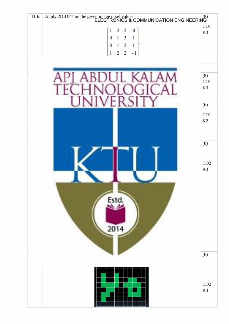
11 b. Apply 2D-DFT on the given image pixel values (8)
CO1K3
OR
12 aDescribe how histogram transformations are applied on a grey scale image and explain what output is observed in each case.
(8)CO1K3
12 b. Describe the working principle of Homomorphic filter, with different
mathematical steps involved.
(6)
CO1K2
Module - II
13a An image A, and a structuring element B are given. Apply B on A, to find
resultant images after the dilation and erosion process. Origin is given as ‘O’; and
note that it is not part of the structuring element.
A =
B =
(8)
CO2K3
13 b. Using Hoshen–Kopelman algorithm, assign connected component labelling for thegiven image in the diagram below.
(6)
CO2K3
1 1 1
1 1
1 1 1
1 1
O
1 O 1
ELECTRONICS & COMMUNICATION ENGINEERING

OR
14a Apply Hit-or-Miss transform on the given binary image to detect right angle
convex corners from left-top to right-bottom.
(8)
CO2K3
14b.
x x x
x x
x x
x x
x x
For the given image grid, find out the 8-chain Freeman Code. Also write down thechain number of the code.
(6)
CO2
K3
15 Describe image formation and geometric transformations in 3D Camera Models. (14)
CO3
K2
OR
16a Briefly describe a stereo vision system. (7)CO3K2
16 b Elucidate on 3D-Imaging Camera system. (7)CO3K2
ELECTRONICS & COMMUNICATION ENGINEERING
Module - IV
17a With the help of a general algorithm, narrate how Hough Transform can be
employed for interest point detection.
(6)
CO4K3
17 b Unveil different steps involved in Harris corner detection algorithm and explain how it is employed to detect corners in an image
OR
(8)
CO4
K3
18 a. Apply Sobel and Prewitt masks on the given image grids and compute Gx and Gy
gradients of the images.
(6)
CO4K3
18 b. Referring to Canny’s algorithm, describe how it is employed to detect edges of an image.
(8)
CO4K3
Module - V
19 a Derive brightness constancy equation. (6)
CO5K3
19 b Describe with algorithmic steps, the Horn-Shunk method used for the estimation
of optical flow.
(8)
CO5K3
20 a Illustrate the concept of dimensionality reduction using Principal Component
Analysis (PCA) with all mathematical steps involved.
(7)
CO5
K3
20b. With the help of a flow chart, illustrate an in-vehicle vision system, for locating
roadways and pedestrians, as a practical application of computer vision.
(7)
CO5
K3
ELECTRONICS & COMMUNICATION ENGINEERING

SEMESTER VI HONOURS
ELECTRONICS & COMMUNICATION ENGINEERING
ECT394 ELECTRONIC DESIGN AUTOMATION
CATEGORY L T P CREDIT VAC 3 1 0 4
Preamble: The course aims to introduce principles behind advanced methods in automation of electronic design.
Prerequisites: Nil
Course Outcomes: After the completion of the course the student will be able to
CO 1 Apply Search Algorithms and Shortest Path Algorithms to find various graph solutions.
CO 2 Outline VLSI Design Flow and Design Styles and apply partitioning algorithms on graphs representing netlist.
CO 3 Illustrate Design Layout Rules and apply different algorithms for layout compaction.
CO 4 Make use of various algorithms to solve placement and floorplan problems. CO 5 Utilise different algorithms to solve routing problems.
Mapping of course outcomes with program outcomes
PO1 PO2 PO3 PO4 PO5 PO6 PO7 PO8 PO9 PO 10
PO 11
PO 12
CO 1 3 2 3 CO 2 3 2 3 CO 3 3 2 3 CO 4 3 2 3 CO 5 3 2 3
Assessment Pattern
Bloom’s Category Continuous Assessment Tests End Semester Examination
1 2 Remember Understand K2 30 30 60 Apply K3 20 20 40 Analyse Evaluate Create
ELECTRONICS & COMMUNICATION ENGINEERING

Mark distribution
Total Marks
CIE ESE ESE Duration
150 50 100 3 hours
Continuous Internal Evaluation Pattern:
Attendance : 10 marks Continuous Assessment Test (2 numbers) : 25 marks Assignment/Quiz/Course project : 15 marks
End Semester Examination Pattern: There will be two parts; Part A and Part B. Part A contain 10 questions with 2 questions from each module, having 3 marks for each question. Students should answer all questions. Part B contains 2 questions from each module of which student should answer any one. Each question can have maximum 2 sub-divisions and carry 14marks.
CO Assessment Questions
CO1: Apply Search Algorithms and Shortest Path Algorithms to find various graph solutions
1.Represent the following graph by Adjacency Matrix.2. List a DFS ordering of vertices for the graph shown in question 1 with starting node as H.3. Perform topological sort on the graph in question1 and order the vertices withStarting node is H.
CO2: Outline VLSI Design Flow and Design Styles and apply partitioning algorithms on graphs representing netlist.
1.Perform KL partitioning on the above graph.You may assume any initial partition ofyour choice.2. Draw the flowchart of VLSI Design Flow and explain the different stages
CO3: Illustrate Design Layout Rules and apply different algorithms for layout compaction.
ELECTRONICS & COMMUNICATION ENGINEERING
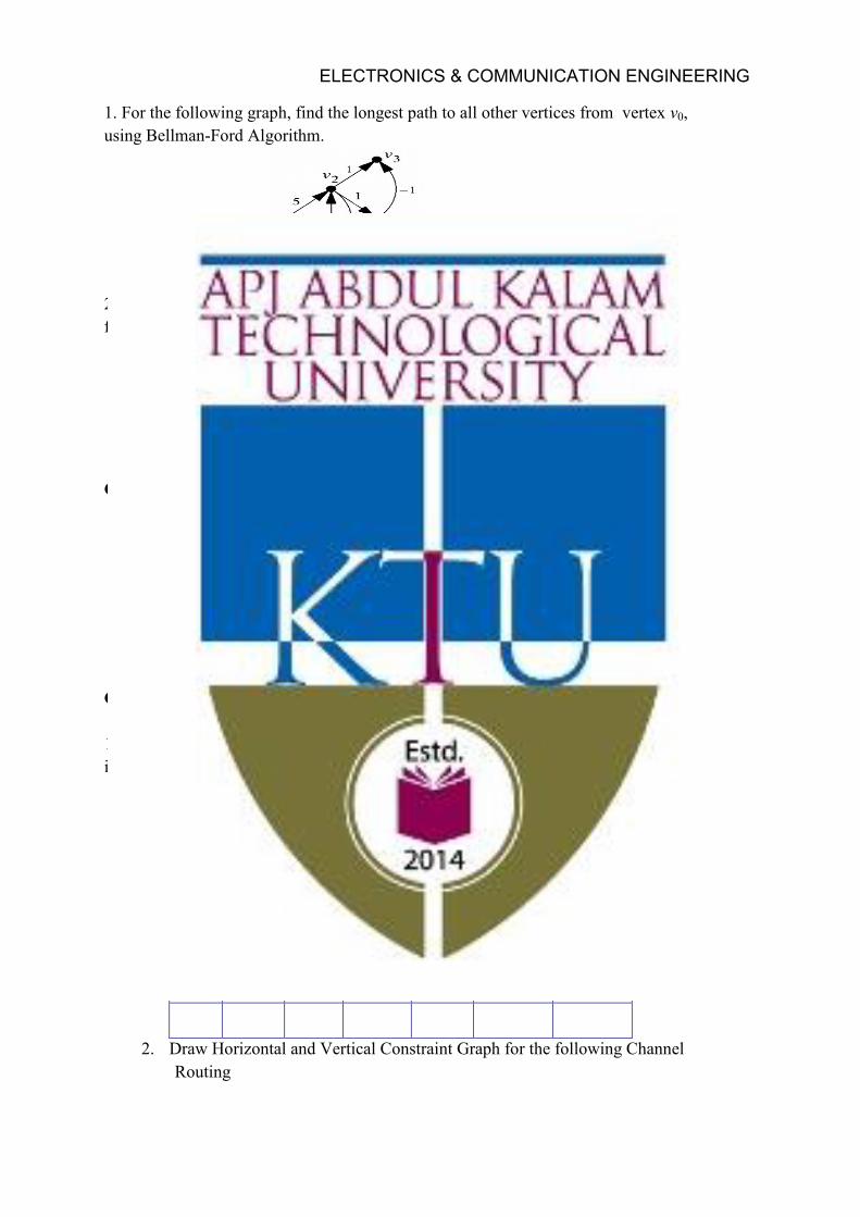
1. For the following graph, find the longest path to all other vertices from vertex v0,using Bellman-Ford Algorithm.
2. Use the Longest Path Algorithm to find the longest path from vertex A, in thefollowing graph
CO4: Make use of various algorithms to solve placement and floorplan problems.
1. Consider the following floorplan.
Draw the floorplan slicing tree and the polar graphs of the above floorplan.
CO5: Utilise different algorithms to solve routing problems.
1.Perform LEE’s Algorithm to find shortest path from S to T. Cells marked Oindicate obstructions.
T
O O O O
O
O S
2. Draw Horizontal and Vertical Constraint Graph for the following ChannelRouting
ELECTRONICS & COMMUNICATION ENGINEERING

3.
Model Question Paper
APJ Abdul Kalam Technological University
Sixth Semester B Tech Degree Examination
Branch: Electronics and Communication
Course: ECT394 Electronic Design Automation
Time: 3 Hrs Max. Marks: 100
PART A
Answer All Questions
1. Define the following giving an example each (3) (K2)(a) Degree of a vertex (b) Subgraph (c) Directed Acyclic Graph (DAG)
2. Represent the following graph by Adjacency Matrix. (3) (K2)
3. Write short note on (a) Full Custom Design (b) Standard Cell Design (3) (K1)4. Explain any three parameters based on which Partitioning is performed. (3) (K1)5. What are the minimum distance rules in Design Rules for layout? (3) (K1)6. Write inequality expressions for minimum distance and maximum distance
constraints between two rectangular edges. (3) (K1)7. For the following placement, calculate the wirelength by (a) Half Perimeter Method
(b) Maximum Rectilinear Tree Method (3) (K3)
ELECTRONICS & COMMUNICATION ENGINEERING

8. Represent the following floorplan using Sequence Pair approach. (3) (K3)
9. How is Global Routing different from Detailed Routing? (3) (K1)10. Define the following terms (a) Reserved Layer Model (b) Channel (c) Dogleg(3)(K1)
PART B
Answer one question from each module. Each question carries 14 marks.
11. (A) List a DFS ordering of vertices for the graph shown in question 2. (7) (K3) Starting node is H. (B) Perform topological sort on the graph and order the vertices. (7) (K3)
Starting node is H.OR
12. (A) List a BFS ordering of vertices for the graph shown in question 2. (10)(K3) Starting node is H. (B) Give an application related to VLSI of BFS. (4) (K2)
13. Draw the flowchart of VLSI Design Flow and explain the different stages. (14) (K1)
OR
14. Perform KL partitioning on the following graph.You may assume any initial (14)(K3)partition of your choice.
15. (A) For the following graph, find the longest path to all other vertices from (10) (K3) vertex v0, using Bellman-Ford Algorithm.
(B) What is the time complexity of Liao-Wong and Bellman-Ford Algorithms?(4) (K2)
OR
ELECTRONICS & COMMUNICATION ENGINEERING

16. (A) Use the Longest Path Algorithm to find the longest path from vertex A, (8) (K3) in the following graph.
(B) What is the limitation of Longest Path Algorithm? (2) (K1)(C) List two methods to find shortest path using Longest Path Algorithm (4) (K2)
17. Consider the following floorplan.
(A) Draw the floorplan slicing tree of the above floorplan. (6) (K3)(B) Draw the polar graphs of above floorplan. (8) (K3)
OR
18. Given: Placement P with two fixed points p1 (100,175) and p2 (200,225), (14) (K3)three free blocks a-c and four nets N1-N4. N1 (P1,a) N2 (a,b) N3 (b,c) N4 (c,P2). Findthe coordinates of blocks (xa, ya), (xb, yb) and (xc, yc).
19. Perform LEE’s Algorithm to find shortest path from S to T. Cells marked (14) (K3)O indicate obstructions.
T O O O O
O O S
ELECTRONICS & COMMUNICATION ENGINEERING

OR
20. Draw Horizontal and Vertical Constraint Graph for the following Channel (14) (K3)Routing.
Simulation Assignments
1. Develop C code for all algorithms in Module 1, 2 and 3.2. A digital circuit can be taken through all steps od VLSI Design Flow (ie. From HDL
to Layout) using any standard tool set from Cadence, Synopsis or Mentor Graphics orsimilar tools
Syllabus
Module 1: Graph Terminology, Search Algorithms and Shortest Path Algorithms:
Graph Terminology: Basic graph theory terminology, Data structures for representation of Graphs Search Algorithms: Breadth First Search, Depth First Search, Topological Sort Shortest Path Algorithms: Dijkstra’s Shortest-Path Algorithm for single pair shortest path, Floyd Warshall Algorithm for all pair shortest path
Module 2: Design Automation and Partitioning Algorithms:
Design Automation: VLSI Design Flow, VLSI Design Styles Partitioning: Levels of Partitioning, Parameters for Partitioning, Classification of Partitioning Algorithms, Kernighan-Lin Algorithm, Fiduccia-Mattheyses Algorithm, Simulated Annealing
Module 3: Layout Compaction:
Layout: Layout Layers and Design Rules, Physical Design Optimizations Compaction: Applications of Compaction, Informal Problem Formulation, Graph Theoretical Formulation, Maximum Distance Constraints, Longest Path algorithm for DAG, Longest path in graph with cycles, Liao-Wong Algorithm, Bellman-Ford Algorithm.
Module 4: Placement and Floorplanning:
Placement: Optimization Objectives, Wirelength Estimation, Weighted Wirelength, Maximum Cut Size, Wire Density Placement Algorithms: Quadratic Placement Floorplanning: Optimization Objectives, Slicing Floorplan, Non-Slicing Floorplan Floorplan Representations: Constraint Graph, Sequence Pair Floorplan Algorithms: Minimum Area Algorithm
ELECTRONICS & COMMUNICATION ENGINEERING

Module 5: Global Routing and Detailed Routing:
Global Routing: Terminology and Definitions, Optimization Goals, Representation of Routing Regions Maze Routing Algorithms: Lee’s Algorithm, Hadlock Algorithm Detailed Routing: Horizontal and Vertical Constraint Graph Channel Routing Algorithms: Left-Edge algorithm
Text Books
1. Jin Hu, Jens Lienig, Igor L. Markov, Andrew B. Kahng, VLSI Physical Design: FromGraph Partitioning to Timing Closure, Springer, 2011th edition.
2. Gerez,Sabih H., “Algorithms for VLSI Design Automation”, John Wiley & Sons,2006.
3. Sherwani, Naveed A., “Algorithms for VLSI Physical Design Automation”, KluwerAcademic Publishers, 1999.
Reference Books
1. Sadiq M. Sait and H. Youssef, “VLSI Physical Design Automation: Theory andPractice”, World Scientific, 1999.
2. Cormen, Thomas H., Charles E. Leiserson, and Ronald L. Rivest. "Introduction toAlgorithms." The MIT Press, 3rd edition, 2009.
Course Contents and Lecture Schedule
No. Topic Number
of Lectures
1 Graph Terminology, Search Algorithms and Shortest Path Algorithms:
1.1 Graph Terminology: Basic graph theory terminology, Data structures for representation of Graphs
2
1.2 Search Algorithms: Breadth First Search, Depth First Search, Topological Sort 2
1.3 Shortest Path Algorithms: Dijkstra’s Shortest-Path Algorithm for single pair shortest path, Floyd Warshall Algorithm for all pair shortest path
4
2 Design Automation and Partitioning Algorithms: 2.1 Design Automation: VLSI Design Flow, VLSI Design Styles 3
2.2 Partitioning: Levels of Partitioning, Parameters for Partitioning, Classification of Partitioning Algorithms 1
2.3 Kernighan-Lin Algorithm, Fiduccia-Mattheyses Algorithm, Simulated Annealing 5
3 Layout Compaction:
ELECTRONICS & COMMUNICATION ENGINEERING
3.1 Layout: Layout Layers and Design Rules, Physical Design Optimizations 1
3.2 Compaction: Applications of Compaction, Informal Problem Formulation, Graph Theoretical Formulation, Maximum Distance Constraints
1
3.3 Longest Path algorithm for DAG, Longest path in graph with cycles, Liao-Wong Algorithm, Bellman-Ford Algorithm. 7
4 Placement and Floorplanning:
4.1 Placement: Optimization Objectives, Wirelength Estimation, Weighted Wirelength, Maximum Cut Size, Wire Density 3
4.2 Placement Algorithms: Quadratic Placement 2
4.3 Floorplanning: Optimization Objectives, Slicing Floorplan, Non-Slicing Floorplan Floorplan Representations: Constraint Graph, Sequence Pair
3
4.4 Floorplan Algorithms: Minimum Area Algorithm 3
5 Global Routing and Detailed Routing:
5.1 Global Routing: Terminology and Definitions, Optimization Goals, Representation of Routing Regions
1
5.2 Maze Routing Algorithms: Lee’s Algorithm, Hadlock Algorithm 2 5.3 Detailed Routing: Horizontal and Vertical Constraint Graph 3 5.4 Channel Routing Algorithms: Left-Edge algorithm 2
ELECTRONICS & COMMUNICATION ENGINEERING

ECT396 MIMO AND MULTIUSER
COMMUNICATION SYSTEMS
CATEGORY L T P CREDIT
VAC 3 1 0 4
Preamble: MIMO systems are rising attention of the academic community and industry because of their potential to increase to capacity and diversity gain proportionally with the number of antennas. OFDM is a promising solution to mitigate the effect of inter symbol interference (ISI) and multipath fading. MIMO OFDM is an attractive air interface solution for multiuser communication and effectively deployed in wireless local area networks, fifth Generation (5G) wireless cellular standards. Prerequisite: MAT 204 Probability and Random Process, ECT 305 Analog and Digital Communication. Course Outcomes: At the end of the course, the students will be able to
CO 1 Describe digital communication over multipath channels
CO 2 Analyse the performance of multiuser communication techniques over generalized fading channel.
CO 3 Describe the concept of MIMO systems and determine the capacity of MIMO channel
CO 4 Introduce OFDM and associated timing and frequency synchronization in MIMO receiver
CO 5 To explain the theory of MIMO multiuser communication systems.
Mapping of course outcomes with program outcomes
PO 1
PO 2 PO 3 PO 4 PO 5 PO 6 PO 7 PO 8 PO 9 PO 10
PO 11
PO 12
CO 1 3 2
CO 2 3 3 2
CO 3 3
CO 4 3 2
CO 5 3 Assessment Pattern
Bloom’s Category Continuous Assessment Tests
End Semester Examination
1 2 Remember Understand K2 30 30 60 Apply K3 20 20 40 Analyse Evaluate Create
ELECTRONICS & COMMUNICATION ENGINEERING
Mark distribution Total
Marks CIE ESE ESE Duration
150 50 100 3 hours
Continuous Internal Evaluation Pattern: Attendance : 10 marks Continuous Assessment Test (2 numbers) : 25 marks Assignment/Quiz/Course project : 15 marks End Semester Examination Pattern: There will be two parts; Part A and Part B. Part A contain 10 questions with 2 questions from each module, having 3 marks for each question. Students should answer all questions. Part B contains 2 questions from each module of which student should answer any one. Each question can have maximum 2 sub-divisions and carry 14 marks.
Course Level Assessment Questions
Course Outcome 1 (CO1)
1. Define doppler spread. 2. Distinguish between flat fading and frequency selective fading 3. Derive the relation between Power spectra and channel correlation.
Course Outcome 2 (CO2)
1. State and infer the capacity of different multiple access techniques. 2. Describe CDMA signal and channel model. 3. Derive the autocorrelation matrix of CDMA multiuser Asynchronous transmission.
Course Outcome 3 (CO3)
1. Determine the channel capacity of SISO and MIMO systems. 2. Determine the channel capacity of MIMO system when CSI is known to the transmitter side. 3. Compare the detection performance of MLSE and ZF equalizer.
Course Outcome 4 (CO4)
1. Describe FFT based implementation of OFDM. 2. Analyze the effect of symbol time offset in OFDM systems. 3. Describe the synchronization using cyclic prefix to OFDM systems.
Course Outcome 5 (CO5)
1. Distinguish between array gain and diversity gain. 2. Define spatial multiplexing. 3. Draw the general block diagram of MIMO system. 4. Write the motivation behind using multiuser communication in wireless scenario.
ELECTRONICS & COMMUNICATION ENGINEERING

MODEL QUESTION PAPER
APJ ABDULKALAM TECHNOLOGICAL UNIVERSITY MODEL QUESTION PAPER
ECT396 MIMO AND MULIUSER COMMUNICATION SYSTEMS
Time: 3 hours Max.Marks:100
PARTA
Answer all questions. Each question carries 3marks.
1. Distinguish between frequency selective and frequency non selective fading.2. Define Doppler spread.3. State the capacity of FDMA4. Mention the applications of TDMA and CDMA5. Draw the channel model for SIMO system.6. Explain the significance of Ergodic capacity.7. What are the gains available in MIMO systems?8. Define spatial multiplexing.9. Define inter symbol interference.10. Write short notes on OFDMA.
PARTB Answer anyone question from each module. Each question carries 14marks.
MODULE I
11. (a) Draw and explain the Tapped delay line channel model used in frequency selective slowlyfading channel . (10 marks)
(b) Distinguish between fast and slow fading. (4 marks)
12. A multipath fading channel has a multipath spread of 1s and a Doppler spread of 0.01 Hz.The total channel bandwidth at band pass available for signal transmission is 10 Hz. Tomitigate the effect of ISI select the pulse duration 10s.
(a) Calculate the coherence bandwidth and coherence time. (5 marks)
(b) Is the channel is frequency selective or not? Justify your answer. (5 marks) (c) Is the channel fading slowly or rapidly? Justify your answer. (4 marks)
MODULE II
13. (a) Briefly describe FDMA and TDMA. (8 marks)
(b) State and infer the capacity of single user CDMA detection scheme. (6 marks) 14. (a) With the aid of Gaussian PDF derive the Maximum Likelihood (ML) criteria of CDMA
decorrelation receiver. (10 marks)
ELECTRONICS & COMMUNICATION ENGINEERING

MODULE II
15. (a) Determine the channel capacity of MIMO system when CSI is known to the transmitterside and when CSI is not available at transmitter side. (10 marks)
(b) Distinguish between outage probability and outage capacity. (4 marks) 16. (a) State the significance of Ergodic capacity. (5 marks)
(b) Determine the capacity of deterministic MIMO channel assuming AWGN capacity. (9 marks)
MODULE IV
17. (a) What is sphere decoding? (4 marks)
(b) Compare the detection performance of ZF and MMSE signal detection techniques inMIMO receiver. (10 marks)
18. (a) Compare array gain and diversity gain. (4 marks)
(b) Briefly describe receive and transmit antenna diversity. (10 marks)
MODULE V
19. (a) Consider a transmitter sends digital information by use of 𝑀signal waveforms𝑠 (𝑡),𝑚 = 1,2,....,𝑀 over an AWGN channel. The channel is assumed to be corrupt the
20.
signal by the addition of white Gaussian noise. Write down the expression for received signal in the interval 0 ≤ 𝑡 ≤ 𝑇and draw the model for received signal passed through the channel.
(4 marks) (b) Describe the FFT based implementation of OFDM system. (10 marks) (a) State and prove Nyquist condition for zero ISI. (4 marks)
(b) Describe the synchronization technique using cyclic prefix in OFDM systems. (10 marks)
SYLLABUS
Module 1 – Digital Communication over Fading Multipath Channels Multipath fading, Coherence time, Coherence bandwidth, Doppler spread, Characterization of fading multipath channels, Statistical model for fading channels (Rayleigh and Rice distribution), Relation between channel correlation and Power spectral density, Signal characteristics on the choice of channel model (frequency selective and frequency nonselective fading), Frequency nonselective slowly fading channel, Frequency selective slowly fading channel, Fast fading, Rake receiver.
Module 2 – Multiuser Communications Types of multiple access techniques (FDMA,TDMA and CDMA), Capacity of multiple access methods (Inference only). Single user detection, Multiuser detection, CDMA signal and channel model, CDMA optimum receiver (Synchronous transmission, Asynchronous transmission), Suboptimum detectors (Single user detector and Decorrelation receiver). Practical applications of multiple access techniques.
ELECTRONICS & COMMUNICATION ENGINEERING

Module 3 – MIMO System Signal and channel model for SISO,SIMO,MISO and MIMO, Capacity of frequency flat deterministic MIMO channel (both channel unknown and known to the transmitter), SIMO channel capacity, MISO channel capacity, Capacity of random MIMO channels, Ergodic capacity, Outage capacity, Capacity of frequency selective MIMO channels (both channel unknown and known to the transmitter) Module 4 – Diversity and Receiver Array gain, Diversity gain, Spatial multiplexing, Receive antenna diversity, Transmit antenna diversity, SISO receiver (MLSE, ZF and Decision feedback equalizer), SIMO receiver, MIMO receiver (both Optimal and suboptimal), Sphere decoding. Module 5 – OFDM Review of AWGN channel and band limited ISI channel, Introduction to multicarrier systems, FFT based multicarrier system, Mitigation of subcarrier fading, SISO-OFDM, MIMO-OFDM, Coarse time synchronization, Fine time synchronization, Coarse frequency synchronization, OFDMA, Wireless standards (WiMAX, and 3GPP LTE) Note: Mathematical model and analysis to be covered for the entire topic. Text Books
1. “Digital Communications”, John G Proakis, 4/e, McGraw-Hill. 2. “Fundamentals of Wireless Communications”, David Tse and Pramod Viswanath,
Cambridge University Press, 2005. 3. “Introduction to Space Time Wireless Communications”, A Paulraj, Nabar and D Gore
Cambridge University Press, 2003. 4. “MIMO OFDM Wireless Communications with MATLAB”, Y S Cho, J Kim, Won Yong
Yang, Chung G Kang, John Wiley& sons private Ltd, 2010.
Reference Books
5. “Space Time Block Coding for Wireless Communications”, Erik G Larsson, Cambrdige University Press, 2003.
6. “MIMO Wireless Communications”, E Biglieri, R Calderbank, A Constantinides, A Goldsmith, A Paulraj, Cambridge University Press.
7. “Digital Communications”, Simon Haykin, John Wiley & Sons Pvt Ltd. 2001. “Wireless Communications” Andrea Goldsmith, Cambridge University Press 2005
ELECTRONICS & COMMUNICATION ENGINEERING

Course Contents and Lecture Schedule
No
Topic
No. of
Lectures 1 Digital Communication over Fading Multipath Channels 1.1 Multipath fading, Coherence time, Coherence bandwidth, Doppler
spread 1
1.2 Characterization of fading multipath channels, Statistical model for fading channels (Rayleigh and Rice distribution), Relation between channel correlation and Power spectral density
4
1.3 Signal characteristics on the choice of channel model (frequency selective and frequency nonselective fading), Frequency nonselective slowly fading channel, Frequency selective slowly fading channel
3
1.4 Fast fading, Rake receiver 2
2 Multiuser Communications 2.1 Types of multiple access techniques (FDMA,TDMA and CDMA),
Capacity of multiple access methods (without proof, Inference only). 2
2.2 Single user detection, Multiuser detection 1 2.3 CDMA signal and channel model, CDMA optimum receiver
(Synchronous transmission, Asynchronous transmission), 2
2.4 Suboptimum detectors (Single user detector and Decorrelation receiver).
1
2.5 Practical applications of multiple access techniques. 1
3 MIMO System 3.1 Signal and channel model for SISO, SIMO, MISO and MIMO 2 3.2 Capacity of frequency flat deterministic MIMO channel (both channel
unknown and known to the transmitter), SIMO channel capacity, MISO channel capacity
4
3.3 Capacity of random MIMO channels 1 3.4 Ergodic capacity, Outage capacity, Capacity of frequency selective
MIMO channels (both channel unknown and known to the transmitter)
2
4 Diversity and Receiver 4.1 Array gain, Diversity gain, Spatial multiplexing. 1 4.2 Receive antenna diversity, Transmit antenna diversity 1 4.3 SISO receiver (MLSE, ZF and Decision feedback equalizer) 2 4.4 SIMO receiver 1 4.5 MIMO receiver (both Optimal and suboptimal), Sphere decoding. 3
5 OFDM 5.1 Review of AWGN channel and band limited ISI channel 1 5.2 Introduction to multicarrier systems, FFT based multicarrier system 2
ELECTRONICS & COMMUNICATION ENGINEERING
5.3 Mitigation of subcarrier fading, SISO-OFDM, MIMO-OFDM 2 5.4 Coarse time synchronization, Fine time synchronization, Coarse
frequency synchronization 3
5.5 OFDMA, Wireless standards (WiMAX, and 3GPP LTE ) 2
SIMULATION ASSIGNMENTS
The following simulation assignments can be done with Python/ MATLAB/ SCILAB /LabVIEW
1 Frequency Non-selective Slowly Fading Channel
Generate binary PSK and binary FSK signals for transmission over a frequency non-selective slowly fading channel.
Obtain the received equivalent lowpass signal of the transmitted signal using equation 13.3-1. Also plot the BER-SNR curve for coherent binary PSK and FSK detector using equations 13.3-2 and 13.3-3 respectively in page 846 in Digital Communications by John G Proakis, 4/e, for fixed attenuation value, α fixed and follows Rayleigh distribution case.
Plot the BER-SNR curve for coherent binary PSK and FSK detector using equations 13.3-13 in page 848 in Digital Communications by John G Proakis, 4/e for α followingRayleigh distribution.
Compare the BER-SNR curve for AWGN and Rayleigh fading channel.
2 CDMA Transmitter and Receiver
Create 2 random binary sequence of 100 bit each as data blocks of 2 users.
Generate the composite transmitted signal, s(t) for 3 users using equations 16.3-7 in page 1037 in Digital Communications by John G Proakis, 4/e.
Add AWGN of different variances to generate the received signal, r(t).
Realize the optimum multiuser receiver for synchronous transmission shown in Fig. 16.3-1 in page 1040 in Digital Communications by John G Proakis, 4/e
Observe the decoded bits for AWGN of different variances.
3 Capacity of MIMO Channels
Create MIMO channel transfer matrix, H of size MR x MT, where MR and MT represents number of receive and transmit antennas respectively.
Compute the capacity of SISO, SIMO, MISO and MIMO channels for different values of SNR using equations in page 138 in Introduction to Space Time Wireless Communications by A Paulraj, Nabar and D Gore.
ELECTRONICS & COMMUNICATION ENGINEERING
Plot Capacity-SNR curve for different channels and compare.
4 Performance of SISO Receiver
Realize the signal model for SISO frequency selective fading channel given in equation 7.5 in page 138 in Introduction to Space Time Wireless Communications by A Paulraj, Nabar and D Gore.
Transmit a sequence of symbols based on signal model.
Obtain the estimated symbol sequence using MLSE receiver based on equation 7.8 in page 139 in Introduction to Space Time Wireless Communications by A Paulraj, Nabar and D Gore.
5 OFDM Communication System
Realize the block diagram of OFDM communication system shown in Fig 11.2-4 in page 750 in Digital Communications by John G Proakis, 4/e.
Create a random bit vector of arbitrary length. Realize the OFDM transmitter by mapping the message bits into a sequence of QAM symbols and convert it into N parallel streams.
Each of N symbols from serial-to-parallel (S/P) conversion is carried out by the different subcarrier. Realize the multicarrier modulation by computing IFFT.
Add cyclic prefix, realize parallel to serial converter and DAC to generate the transmitted signal.
Transmit the signal through a fading channel.
Realize OFDM receiver by first removing cyclic prefix followed by serial to parallel conversion, FFT computation, signal detection and parallel to serial conversion.
Plot the BER-SNR curve and analyse.
ELECTRONICS & COMMUNICATION ENGINEERING
ECT398 DETECTION AND ESTIMATION
THEORY CATEGORY L T P CREDIT
VAC 3 1 0 4
Preamble: This course aims to impart the fundamentals of detection and estimation theory in engineering applications
Prerequisite: MAT 101 Linear Algebra and Calculus MAT 204 Probability, Random Process, and Numerical Methods ECT 204 Signals and Systems
Course Outcomes: After the completion of the course the student will be able to
CO1 K2 Understand the fundamentals of statistical detection and estimation principles used in various engineering problems.
CO2 K3 Apply various types of statistical decision rules in engineering applications.
CO3 K3 Apply different types of estimation algorithms in engineering applications.
Mapping of course outcomes with program outcomes
PO1 PO 2
PO 3
PO 4
PO 5
PO 6
PO 7
PO 8
PO 9
PO1 0
PO11 PO12
CO 1 3 3 2
CO 2 3 3 2
CO 3 3 3 2
Assessment Pattern Bloom’s Category Continuous Assessment
Tests End Semester Examination
1 2 Remember Understand K2 30 30 60 Apply K3 20 20 40 Analyse Evaluate Create
Mark distribution
Total Marks
CIE ESE ESE Duration
150 50 100 3 hours
ELECTRONICS & COMMUNICATION ENGINEERING

Continuous Internal Evaluation Pattern:
Attendance : 10 marks
Continuous Assessment Test (2 numbers) : 25 marks Assignment/Quiz/Course project : 15 marks
End Semester Examination Pattern: There will be two parts; Part A and Part B. Part A contain 10 questions with 2 questions from each module, having 3 marks for each question. Students should answer all questions. Part B contains 2 questions from each module of which student should answer any one. Each question can have maximum 2 sub-divisions and carry 14 marks. Course Level Assessment Questions
Course Outcome 1 (CO1): Understand the fundamentals of statistical detection and estimation principles used in various engineering problems. (K2) 1. Differentiate estimation and detection techniques.2. Differentiate classical approach and bayesian approch in detection theory (or estimation).3. Enumerate different applications which are using estimation and detection techniques.4. Give the mathematical formulation of estimation and detection methods.5. Draw receiver operating characteristics with all details6. Give the significance of Bayes risk7. How multiple hypothesis testing is done.8. Give the significance of linear models in estimation and detection theory.9. Significance of Cramer-Rao Lower Bound in estimation.10. Differentiate MAP and ML methods in estimation (or detection).
Course Outcome 2 (CO2): Apply various types of statistical decision rules in engineering applications. (K3) 1. Describe Neyman-Pearson theorem (or Bayes risk or minimization of probability of error)
and apply it to any binary hypothesis (eg. Signal in white Gaussian noise)2. Derive/Obtain the matched filters for the detection of deterministic signals3. Derive/Obtain the estimator-correlator for the detection of random signals
Course Outcome 3 (CO3): Apply different types of estimation algorithms in engineering applications. (K3) 1. Derive/Obtain the Minimum variance unbiased estimator (or best linear unbiasedestimator) for any simple examples (eg. DC Signal in white Gaussian noise)2. Derive/Obtain the Maximum likelihood estimator (or least squares estimator or minimummean square error estimator) for any simple examples (eg. DC Signal in white Gaussiannoise)
3. Using Bayesian approach, obtain an estimator for any simple examples.
ELECTRONICS & COMMUNICATION ENGINEERING

SYLLABUS
Module 1 : Introduction to Detection and Estimation Theory
Fundamentals of detection theory, the mathematical detection problem. Fundamentals of estimation theory, the mathematical estimation problem. Review of Gaussian distribution. Application examples.
Module 2 : Statistical Detection Theory I
Hypothesis testing, classical approach, Neyman-Pearson theorem, likelihood ratio test, receiver operating characteristics, Bayesian approach, minimum probability of error, Bayes risk, multiple hypothesis testing.
Module 3 : Statistical Detection Theory II
Detection of deterministic signals, matched filters, detection of random signals, estimator- correlator, linear model, application examples.
Module 4 : Statistical Estimation Theory I
Minimum variance unbiased estimation, basics of Cramer-Rao Lower Bound, linear models, best linear unbiased estimation, application examples.
Module 5 : Statistical Estimation Theory II
Maximum likelihood estimation, least squares, Bayesian philosophy, minimum mean square error estimation, application examples.
Text Books 1. S.M. Kay, “Fundamentals of Statistical Signal Processing” Vol I: Estimation Theory,Pearson, 3/e, 2010.
2. S.M. Kay, “Fundamentals of Statistical Signal Processing” Vol II: Detection Theory,Pearson, 3/e, 2010.
Reference Books
1. H. L. Van Trees, “Detection, Estimation, and Modulation Theory”, Vol. I, John Wiley &Sons, 1968
2. Monson H. Hayes ,“Statistical Digital Signal Processing and Modelling" by, John Wiley &Sons, 2002.
ELECTRONICS & COMMUNICATION ENGINEERING

Course Contents and Lecture Schedule
No Topic No. of Lectures
1 Introduction to Detection and Estimation Theory
1.1 Fundamentals of detection theory, review of probability and random variable 2
1.2 The mathematical detection problem 2
1.3 Fundamentals of estimation theory 1
1.4 The mathematical estimation problem 2
1.5 Review of Gaussian distribution. Application examples. 2
2 Statistical Detection Theory I
2.1 Hypothesis testing 2
2.2 Classical approach, Neyman-Pearson theorem 2
2.3 Likelihood ratio test, Receiver operating characteristics 2
2.4 Bayesian approach, minimum probability of error, Bayes risk 2
2.5 Multiple hypothesis testing. 1
3 Statistical Detection Theory II
3.1 Detection of deterministic signals 1
3.2 Matched filters 2
3.3 Detection of random signals 2
3.4 Estimator-correlator 2
3.5 Linear model, application examples. 2
4 Statistical Estimation Theory I
4.1 Minimum variance unbiased estimation 2
4.2 Basics of Cramer-Rao Lower Bound 2
4.3 Linear models 2
4.4 Best linear unbiased estimation 2
4.5 Application examples 1
5 Statistical Estimation Theory II
5.1 Maximum likelihood estimation 2
5.2 Least squares solution 2
5.3 Bayesian philosophy 2
5.4 Minimum mean square error estimation 2
5.5 Application examples 1
ELECTRONICS & COMMUNICATION ENGINEERING
Simulation Assignments (using MATLAB or Python)
1. Generate and familiarize PDF and CDF of Normal distribution.
2. Generate DC level in White Gaussian Noise.
3. Simulate a Neyman-Pearson Detector.
4. Simulate a Maximum Likelihood Estimator.
5. Simulate a Best Linear Unbiased Estimator.
ELECTRONICS & COMMUNICATION ENGINEERING
APJ ABDUL KALAM TECHNOLOGICAL UNIVERSITY
SIXTH SEMESTER B.TECH DEGREE EXAMINATION
ECT 398- Detection and Estimation TheoryMax. Marks: 100 Duration: 3 hrs
PART A(Answer all questions. Each question carries 3 marks each).
1. (3)Enumerate different applications which are using estimation and detection techniques.
2. (3)Differentiate estimation and detection techniques.
3. (3)Differentiate classical approach and bayesian approch in detection theory.
4. (3)Give the mathematical formulation of detection methods.
5. (3)Draw receiver operating characteristics with all details
6. (3)Give the significance of Bayes risk
7. (3)Give the significance of linear models in estimation theory.
8. (3)Significance of Cramer-Rao Lower Bound in estimation.
9. (3)What is Minimum Variance Unbiased Estimation?
10. (3)Differentiate MAP and ML methods in estimation.
PART B(Answer any one question from each module. Each question carries 14 marks each.)
Note:(1) Notation x ∼ N (µ, σ2) denotes x is normally distributed with mean µ and variance σ2.(2)Also, bold small letters indicate vectors and bold capital letters indicate matrices.
11. (14)Obtain the mathematical formulation of estimation method with an example.
OR
12. (14)Using radar system as an example, differentiate estimation and detection techniques.
13. (14)Design Neyman-Pearson detector for the unknown level A in White Gaussian Noise withvariance σ2.
OR
14. (14)Describe the Bayesian approaches in the design of detectors.
15. (14)Obtain Matched Filter detector for N -sample deterministic signal in noise, w[n] ∼ N (0, σ2n)where w[n]’s are uncorrelated.
OR
Page 1 of 2
MODEL QUESTION PAPERELECTRONICS & COMMUNICATION ENGINEERING
16. (14)Describe estimator-correlator in the detection of random signals.
17. (14)Consider the multiple observations
x[n] = A+ w[n]; n = 0, 1, . . . , N − 1
where w[n] ∼ N (0, σ2). Determine CRLB for A?
OR
18. (14)Derive the Best Linear Unbiased Estimator for the multiple observations
x[n] = A+ w[n]; n = 0, 1, . . . , N − 1
where A is an unknown level to be estimated and w[n] is White Noise with unspecified PDFand variance σ2.
19. (14)Derive the Maximum Likelihood Estimator for the multiple observations
x[n] = A+ w[n]; n = 0, 1, . . . , N − 1
where A is an unknown level to be estimated and w[n] is White Gaussian Noise with knownvariance σ2.
OR
20. (14)Prove that the optimal estimator which minimizes the Bayesian Mean Square Error is themean of the posterior PDF.
Page 2 of 2
ELECTRONICS & COMMUNICATION ENGINEERING


![CIVIL ENGINEERING[Full Time] - KTU](https://static.fdokumen.com/doc/165x107/631f36485ff22fc745070d80/civil-engineeringfull-time-ktu.jpg)