Seeing Double: Coupling between SubstrateImageChargesandCollective Plasmon Modes in Self-Assembled...
10
SWANGLAP ET AL. VOL. 5 ’ NO. 6 ’ 4892–4901 ’ 2011 www.acsnano.org 4892 May 11, 2011 C 2011 American Chemical Society Seeing Double: Coupling between Substrate Image Charges and Collective Plasmon Modes in Self-Assembled Nanoparticle Superstructures Pattanawit Swanglap, † Liane S. Slaughter, † Wei-Shun Chang, † Britain Willingham, † Bishnu P. Khanal, † Eugene R. Zubarev, † and Stephan Link †,‡, * † Department of Chemistry and ‡ Department of Electrical and Computer Engineering, Laboratory for Nanophotonics, Rice University, Houston, Texas 77005, United States T he localized surface plasmon reso- nance of metallic nanoparticles (NPs) displays a dramatic dependence on the NP size and shape as well as the sur- rounding environment. 16 The latter prop- erty is actively exploited in NP-based sur- face plasmon resonance sensing. 711 For many practical sensing applications, the effect of the substrate on which the NPs reside is of particular interest. In general, the sensitivity of supported NPs is smaller due to the reduction of the area that is available for analyte sensing. To a first approximation, the sensitivity of the localized surface plas- mon resonance is proportional to the frac- tion of exposed NP surface area, and the shift in the surface plasmon resonance can be modeled as a weighted average be- tween the dielectric constants of the sub- strate and the immersed medium, as verified by ensemble as well as single par- ticle spectroscopy. 1215 Considering only an average medium di- electric effect on the surface plasmon reso- nance for supported NPs is, however, in some cases an oversimplification of the actual optical response. In fact, it is well- known from classical calculations that the electric dipole of an excited molecule or atom placed in the vicinity of a substrate couples to its own partially reflected electric field, resulting in a frequency shift of the emitted radiation. 16,17 A general solution for the scattering of a sphere on a substrate has been obtained by separating the coupled system into the scattering by a sphere in a homogeneous medium, described by Mie theory, and the reflection of radiation by a surface. 18,19 Mirror image multipoles in- duced in the substrate have also been taken into account in the calculations, and their importance has later been verified experi- mentally for latex and copper spheres on silicon wafers. 20 More recent calculations for plasmonic NPs near metallic surfaces have shown that the localized NP surface plasmons couple strongly not only with image multipoles but also with surface plasmon modes of the metallic film. 2123 Hybridization between lo- calized surface plasmons of the NP and delo- calized surface plasmons of the film leads to spectral shifts that depend on the NPfilm separation and the film thickness. 21,22,24 Ex- perimentally, a shift toward lower energies has indeed been observed for the surface plasmon resonance of silver and gold NPs on gold films as a function of film thickness, NP size, and NPfilm separation, which were on the order of a few tens of nanometers and * Address correspondence to [email protected]. Received for review March 14, 2011 and accepted May 11, 2011. Published online 10.1021/nn2009694 ABSTRACT The interaction between adjacent metal nanoparticles within an assembly induces interesting collective plasmonic properties. Using dark-field imaging of plasmon scattering, we investigated rings of gold nanoparticles and observed that the images were dependent on the substrate. In particular, for nanoparticles assembled on carbon and gold substrates, intensity line sections perpendicular to the ring revealed a significant broadening beyond the optical resolution accompanied by an intensity dip in the middle of the line profile. Overall, this appeared in the image as a “splitting” into two offset circles along the direction of the scattered light polarization. This effect was not observed for a substrate with a low permittivity, such as glass. By varying the substrate as well as selecting different detected wavelengths and polarization components of the excitation light, we were able to confirm that the observed effect was due to coupling of collective plasmon modes with their induced image charges in the supporting substrates. These results suggest that plasmon scattering in extended nanostructures can be spatially modulated by tuning the permittivity of the substrate. KEYWORDS: gold nanoparticles . surface plasmon resonance . plasmon coupling . substrate effects . dark-field scattering ARTICLE
Transcript of Seeing Double: Coupling between SubstrateImageChargesandCollective Plasmon Modes in Self-Assembled...
SWANGLAP ET AL. VOL. 5 ’ NO. 6 ’ 4892–4901 ’ 2011
www.acsnano.org
4892
May 11, 2011
C 2011 American Chemical Society
Seeing Double: Coupling betweenSubstrate Image Charges andCollectivePlasmon Modes in Self-AssembledNanoparticle SuperstructuresPattanawit Swanglap,† Liane S. Slaughter,† Wei-Shun Chang,† Britain Willingham,† Bishnu P. Khanal,†
Eugene R. Zubarev,† and Stephan Link†,‡,*
†Department of Chemistry and ‡Department of Electrical and Computer Engineering, Laboratory for Nanophotonics, Rice University, Houston, Texas 77005,United States
The localized surface plasmon reso-nance of metallic nanoparticles (NPs)displays a dramatic dependence on
the NP size and shape as well as the sur-rounding environment.1�6 The latter prop-erty is actively exploited in NP-based sur-face plasmon resonance sensing.7�11 Formany practical sensing applications, theeffect of the substrate on which the NPsreside is of particular interest. In general, thesensitivity of supported NPs is smaller dueto the reduction of the area that is availablefor analyte sensing. To a first approximation,the sensitivity of the localized surface plas-mon resonance is proportional to the frac-tion of exposed NP surface area, and theshift in the surface plasmon resonance canbe modeled as a weighted average be-tween the dielectric constants of the sub-strate and the immersed medium, asverified by ensemble as well as single par-ticle spectroscopy.12�15
Considering only an average medium di-electric effect on the surface plasmon reso-nance for supported NPs is, however, insome cases an oversimplification of theactual optical response. In fact, it is well-known from classical calculations that theelectric dipole of an excited molecule oratom placed in the vicinity of a substratecouples to its own partially reflected electricfield, resulting in a frequency shift of theemitted radiation.16,17 A general solution forthe scattering of a sphere on a substrate hasbeen obtained by separating the coupledsystem into the scattering by a sphere in ahomogeneous medium, described by Mietheory, and the reflection of radiation by asurface.18,19 Mirror image multipoles in-duced in the substrate have also been taken
into account in the calculations, and theirimportance has later been verified experi-mentally for latex and copper spheres onsilicon wafers.20
More recent calculations for plasmonicNPs near metallic surfaces have shown thatthe localized NP surface plasmons couplestrongly not only with imagemultipoles butalso with surface plasmon modes of themetallic film.21�23 Hybridization between lo-calized surface plasmons of the NP and delo-calized surface plasmons of the film leads tospectral shifts that depend on the NP�filmseparation and the film thickness.21,22,24 Ex-perimentally, a shift toward lower energieshas indeed been observed for the surfaceplasmon resonance of silver and gold NPson gold films as a function of film thickness,NP size, and NP�film separation, which wereon the order of a few tens of nanometers and
* Address correspondence [email protected].
Received for review March 14, 2011and accepted May 11, 2011.
Published online10.1021/nn2009694
ABSTRACT The interaction between adjacent metal nanoparticles within an assembly induces
interesting collective plasmonic properties. Using dark-field imaging of plasmon scattering, we
investigated rings of gold nanoparticles and observed that the images were dependent on the
substrate. In particular, for nanoparticles assembled on carbon and gold substrates, intensity line
sections perpendicular to the ring revealed a significant broadening beyond the optical resolution
accompanied by an intensity dip in the middle of the line profile. Overall, this appeared in the image
as a “splitting” into two offset circles along the direction of the scattered light polarization. This
effect was not observed for a substrate with a low permittivity, such as glass. By varying the
substrate as well as selecting different detected wavelengths and polarization components of the
excitation light, we were able to confirm that the observed effect was due to coupling of collective
plasmon modes with their induced image charges in the supporting substrates. These results suggest
that plasmon scattering in extended nanostructures can be spatially modulated by tuning the
permittivity of the substrate.
KEYWORDS: gold nanoparticles . surface plasmon resonance . plasmon coupling .substrate effects . dark-field scattering
ARTIC
LE
SWANGLAP ET AL. VOL. 5 ’ NO. 6 ’ 4892–4901 ’ 2011
www.acsnano.org
4893
controlled by dielectric spacers.24�28 In all cases, thisinteraction is strongest for p-polarized incident light.Furthermore, large field enhancements have beenpredicted for the gaps of the NP�film system22 andobserved experimentally by surface-enhanced Ramanscattering.29�32 In addition to near-field coupling forthe NP�film system, the importance of image chargeshas also been shown by far-field interference of lightscattered by a NP and its mirror image, where a singlegold NP interacted with an aluminum-coated opticalfiber mounted to an atomic force microscope cantile-ver for precise control over gap distances that ex-ceeded 10 μm.33
Interestingly, dielectric substrates can also signifi-cantly alter the surface plasmon resonance of sup-ported NPs despite the absence of film surfaceplasmons. For silver nanocubes, the presence of differ-ent dielectric substrates caused a second localizedsurface plasmon resonance to appear at higher ener-gies in the scattering spectrum, which was assigned toa quadrupolar plasmon mode.9,34 For spherical NPs aswell as nanoshells, the presence of the substrate liftsthe degeneracy of the dipole mode and its componentorientated perpendicular to the substrate shifts tolower energies for p-polarized excitation light. Thistrend is similar to the one observed for plasmonicNPs interacting with metallic films29,35,36 and alsodepends on the NP�film gap, but the amount of redshift is reduced for dielectric substrates.29 The interac-tion strength as measured by the shift in the plasmonresonance maximum increases with the permittivity ofthe substrate.35,37 In addition, higher order plasmonmodes can appear in the optical spectrum of NPssupported on dielectric substrates because of an in-traparticle hybridization of NP plasmonswhose degen-eracy has been lifted due to symmetry breaking by thesubstrate.35,37 Because of the absence of film surfaceplasmons for dielectric substrates, these effects aremediated by induced image charges.37
In addition to the discussed spectral changes for aplasmonic NP brought into the vicinity of a metallic ordielectric film, it has been noted that the elastic andinelastic scattering from individual silver and gold NPsappears as doughnut-shaped patterns in theimages.25,26,29,38 This behavior is indicative of a dipoleemitter that is orientated perpendicular to thesubstrate39�41 and is consistent with a stronger inter-action of the NPs with the substrate for out-of-planepolarized light. When the NP�film interaction strengthis decreased by changing the film material or NP�filmgap, the usual Gaussian intensity point spread functionis obtained, illustrating how the direction and polariza-tion of the light scattered by a plasmonic NP can betuned.25,26,29,38 Beyond the NP�film system, such con-trol is of great current interest in nanophotonics.42�45
However, while most studies of NP�film interactionshave focused on spectral shifts,9,21�29,34�37,46�49 only
a few reports exist on the scattering patterns ofindividual NPs.25,26,29,38 In addition, to the best of ourknowledge, no studies have been carried out on thescattering images of assembled NPs interacting withdifferent substrates. For closely spaced NPs, interparti-cle plasmon coupling becomes important and changesthe optical response.46,50�58 The question thereforearises as to how the scattering pattern for closelyspaced plasmonic NPs depends on the nature of thesubstrate on which the NPs are assembled.In this paper, we investigated the effect of coupling
between collective plasmon modes of a self-assembledNP ring58,59 with the substrate on the far-field scatteringpattern. Using polarization sensitive and wavelengthselective dark-field scattering microscopy, we observedthat the images of NP rings appeared as two offset circlesdisplaced from thephysical locationof the ring for carbonandgold substrates. By varying the substratematerial, weshow that this effect was due to the interaction betweenthe collective surface plasmon modes of the self-as-sembled structure and the substrate as the double ringpattern was visible in the images of the NP rings createdon carbon and gold but not glass substrates.
RESULTS AND DISCUSSION
Large rings (4�7 μm) of 40 nm gold NPs on differentsubstrates were formed by breath figure templating.59
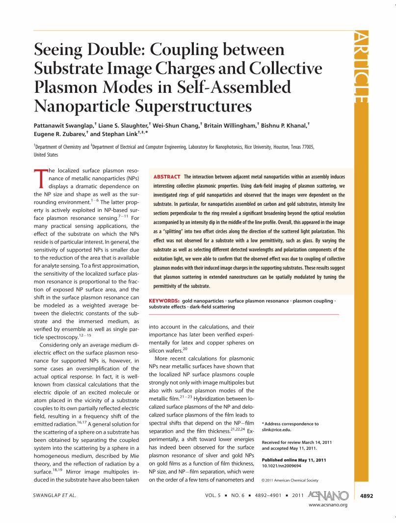
A transmission electron microscope (TEM) image of aring on a 20 nm thick carbon film is shown in Figure 1.The inset is a magnified TEM image of a ring segmentwhich illustrates that the ring was several NPs wide. NPrings were also prepared on glass and gold substrates.The corresponding scanning electron microscope (SEM)images are given in Figure S1 of the Supporting
Figure 1. TEM image of a self-assembled gold NP ring on anamorphous carbon layer on top of a copper grid. The ringwascomposed of 40 nm gold NPs and was 6.8 μm in diameter.The inset shows a magnified TEM image of the ring segmentmarkedby the red box, which illustrates that thewidth of theself-assembled gold NP ring was several NPs wide.
ARTIC
LE
SWANGLAP ET AL. VOL. 5 ’ NO. 6 ’ 4892–4901 ’ 2011
www.acsnano.org
4894
Information. We previously studied the plasmon scat-tering of these NP rings using dark-field spectroscopyand found strong interparticle near-field coupling giv-ing rise to collective plasmon resonances polarizedalong the ring circumference.58 The scattering spectrumshowed several red-shifted plasmon modes that wereassigned tomultipolar resonances of local ring segments.The plasmon scattering images of the self-assembled
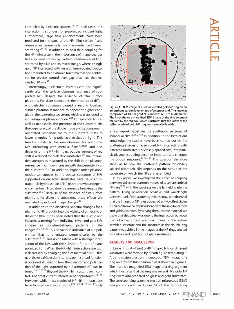
NP rings were strongly influenced by the substrate thatthe assemblies were created on (Figure 2). Surfaceplasmon resonances of NP rings on carbon, gold, and
glass were excited with randomly polarized light in adark-field illumination geometry, and the back-scat-tered light was spectrally integrated (∼450�700 nm)and analyzed for two perpendicular polarizations asindicated by the white arrows in Figure 2. For carbon(2a) and gold (2b) as substrates, the polarized dark-fieldscattering images of the rings appeared as two circlesthat were offset from each other in the direction of thedetected light polarization. However, for the ring on theglass substrate (2c), this effect was not observed. Instead,Figure 2c shows dark-field scattering images of the NPring consistent with the limited resolution of an opticalmicroscope. The observed effect for the carbon and goldsubstrateswasvery reproducibleas confirmedbymultipleindependentmeasurements of the sameanddifferentNPrings. The series of images in Figure S2 taken as a functionof microscope focus position furthermore verifies that amisalignment of the optical setup can be ruled out as apossible explanation. It should be noted that the scatter-ing intensities for ring segments aligned parallel to thedetected polarization were larger. This is particularlypronounced for the glass substrate and is due to near-field coupling between the NPs leading to longitudinallypolarized collective plasmon modes.58 Variations in scat-tering intensity along the ring circumference are alsoinfluenced by differences in the thickness of local ringsegments. The corresponding TEM and SEM images forthe rings shown in Figure 2 are given in Figure 1 for thecarbon substrate and Figure S1 (Supporting Information)for the gold and glass surfaces, respectively.The observed “splitting” into offset rings was further
analyzed by determining intensity line sections for eachpolarization component and for different ring segmentsthat were parallel and perpendicular to the detectedscattered light as indicated by the red and blue lines inthe images shown in Figure 2. The corresponding linesections give the spectrally integrated scattering inten-sities, as analyzed from the images, and are shownbeloweach image for the three substrates. The origin of the x-axis of the intensity line section refers to the position ofthe ring, while negative values indicate positions in theimage outside of the ring and positive values representpositions inside the ring. For thecarbon (2a) andgold (2b)substrates, we observed a broadening of the intensityline sections beyond the optical resolution accompaniedby a dip in themiddle of the line profile for directions thatwere parallel to the scattered light polarization. Thisbroadening corresponds to the splitting into separatedoffset rings in thedark-field scattering images. In contrast,the images in Figure 2c for a NP ring on glass did notshow the same effect.In order toquantify thebroadeningof the intensity line
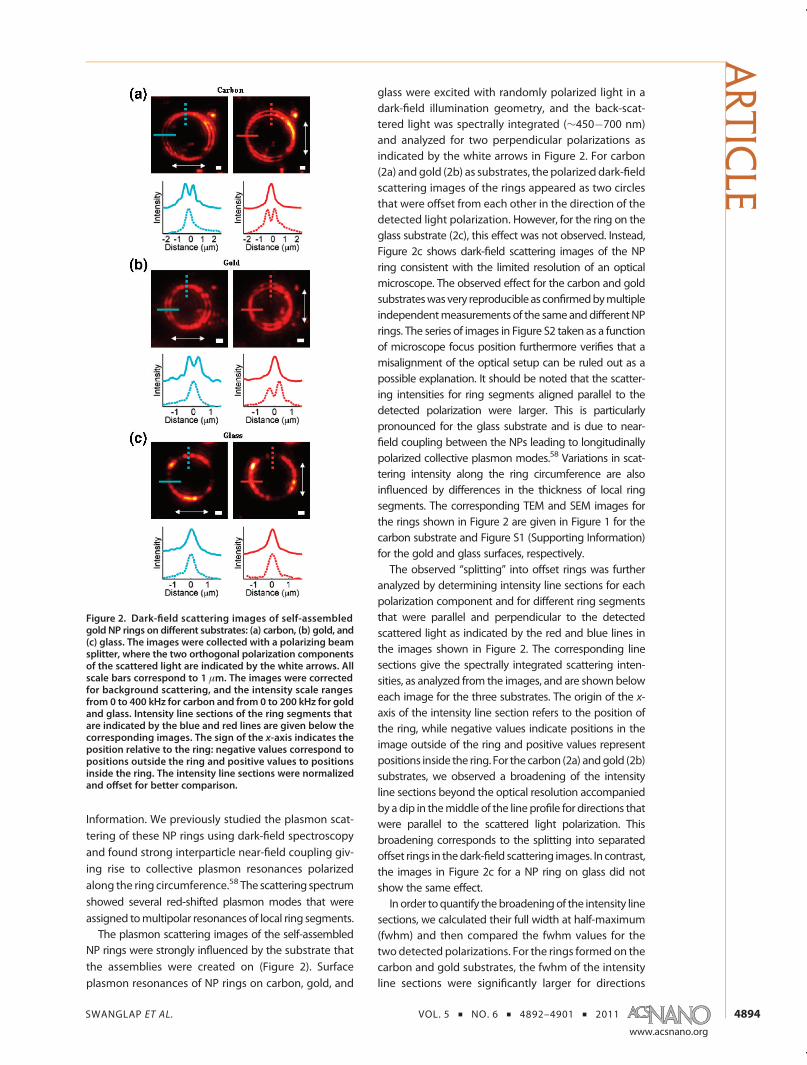
sections, we calculated their full width at half-maximum(fwhm) and then compared the fwhm values for thetwo detected polarizations. For the rings formed on thecarbon and gold substrates, the fwhm of the intensityline sections were significantly larger for directions
Figure 2. Dark-field scattering images of self-assembledgold NP rings on different substrates: (a) carbon, (b) gold, and(c) glass. The images were collected with a polarizing beamsplitter, where the two orthogonal polarization componentsof the scattered light are indicated by the white arrows. Allscale bars correspond to 1 μm. The images were correctedfor background scattering, and the intensity scale rangesfrom 0 to 400 kHz for carbon and from 0 to 200 kHz for goldand glass. Intensity line sections of the ring segments thatare indicated by the blue and red lines are given below thecorresponding images. The sign of the x-axis indicates theposition relative to the ring: negative values correspond topositions outside the ring and positive values to positionsinside the ring. The intensity line sections were normalizedand offset for better comparison.
ARTIC
LE
SWANGLAP ET AL. VOL. 5 ’ NO. 6 ’ 4892–4901 ’ 2011
www.acsnano.org
4895
parallel compared to perpendicular to the polarizationof the detected scattered light, as illustrated in Figure 3.In the parallel case, the average fwhm was 1040 and1100 nm for carbon and gold, respectively, while in theperpendicular case, the average fwhm was 590 and560 nm. However, for the ring formed on the glasssubstrate, the fwhm was independent of the detectedpolarization direction (610 and 540 nm for parallel andperpendicular, respectively). To compare these fwhmvalues to the optical resolution of the dark-field scat-tering microscope, we determined the fwhm fromscattering images of single gold NPs placed on a glasscoverslip. Glass was chosen as the substrate because itdid not alter the image of the plasmon scatteringcollected for the NP ring. We measured dark-field
scattering images for three different average sizes ofNPs: 76, 88, and 155 nm (Figure S3 in the SupportingInformation). The average fwhmof theseNPswere 380,450, and 490 nm, respectively, which demonstrate thatthe fwhm values were a convolution between the NPsize and the microscope resolution. Because the NPringswere usually several NPswide, corresponding to aring thickness of approximately 100�200 nm, asshown in Figure 1, it is most appropriate to comparethe fwhm of the ring and the 155 nm NPs. Thiscomparison confirms that the intensity line sectionsof the ring taken in the direction parallel to thedetected light polarization were significantly broa-dened for the carbon and gold substrates, while theintensity line sections for the perpendicular directionwere mostly governed by the optical resolution.The observed optical effect is assigned to the inter-
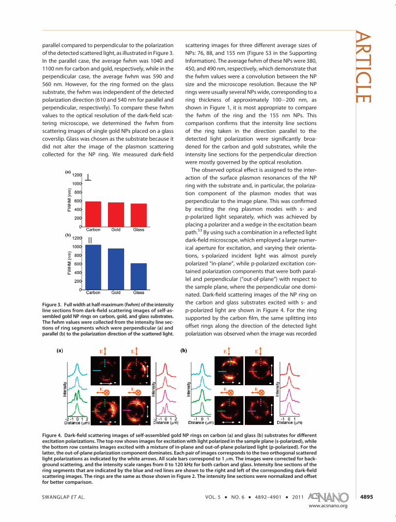
action of the surface plasmon resonances of the NPring with the substrate and, in particular, the polariza-tion component of the plasmon modes that wasperpendicular to the image plane. This was confirmedby exciting the ring plasmon modes with s- andp-polarized light separately, which was achieved byplacing a polarizer and a wedge in the excitation beampath.53 By using such a combination in a reflected lightdark-field microscope, which employed a large numer-ical aperture for excitation, and varying their orienta-tions, s-polarized incident light was almost purelypolarized “in-plane”, while p-polarized excitation con-tained polarization components that were both paral-lel and perpendicular (“out-of-plane”) with respect tothe sample plane, where the perpendicular one domi-nated. Dark-field scattering images of the NP ring onthe carbon and glass substrates excited with s- andp-polarized light are shown in Figure 4. For the ringsupported by the carbon film, the same splitting intooffset rings along the direction of the detected lightpolarization was observed when the image was recorded
Figure 3. Full width at half-maximum (fwhm) of the intensityline sections from dark-field scattering images of self-as-sembled gold NP rings on carbon, gold, and glass substrates.The fwhm values were collected from the intensity line sec-tions of ring segments which were perpendicular (a) andparallel (b) to the polarization direction of the scattered light.
Figure 4. Dark-field scattering images of self-assembled gold NP rings on carbon (a) and glass (b) substrates for differentexcitation polarizations. The top row shows images for excitationwith light polarized in the sample plane (s-polarized), whilethe bottom row contains images excited with a mixture of in-plane and out-of-plane polarized light (p-polarized). For thelatter, the out-of-plane polarization component dominates. Each pair of images corresponds to the two orthogonal scatteredlight polarizations as indicated by the white arrows. All scale bars correspond to 1 μm. The images were corrected for back-ground scattering, and the intensity scale ranges from 0 to 120 kHz for both carbon and glass. Intensity line sections of thering segments that are indicated by the blue and red lines are shown to the right and left of the corresponding dark-fieldscattering images. The rings are the same as those shown in Figure 2. The intensity line sections were normalized and offsetfor better comparison.
ARTIC
LE
SWANGLAP ET AL. VOL. 5 ’ NO. 6 ’ 4892–4901 ’ 2011
www.acsnano.org
4896
withp-polarizedexcitation, as illustrated in thebottomrowof Figure 4a. In contrast, the splitting was clearly absentin the dark-field scattering images for excitation withs-polarized light, as shown in the top row of Figure 4a.These results and comparison to the images in Figure 2arecorded with randomly polarized excitation suggest thatit was primarily the surface plasmon oscillation orientatedperpendicular to the sampleplane that interacted stronglywith the substrate. As expected from Figure 2c, whenthe NP ring was supported by a glass substrate, s- andp-polarized excitation gave the same results as no notice-able splitting intooffset rings is seen inanyof thedark-fieldscattering images shown in Figure 4b.The stronger interaction for p-polarized excitation is
consistent with previous studies of individual plasmo-nic NPs on metallic and dielectric substrates, whichfurthermore found that the distance-dependent near-field coupling between the film and NP plasmonscauses the individual NPs to appear as doughnuts inthe optical scattering images.25,26,29 To test if thesubstrates we used in this study have the same effecton the plasmon scattering images of individual NPsand what role the polarization of the incident anddetected light plays, we recorded single particle scat-tering images of 88 nm gold NPs supported on carbon,gold, and glass substrates. Larger 88 nmNPs were usedinstead of the 40 nmNPs that made up the ring becausethe larger scattering cross section of the 88 nm NPsallowed for better contrast without changing the un-derlying mechanism. As expected, individual NPs on aglass substrate had a two-dimensional Gaussian
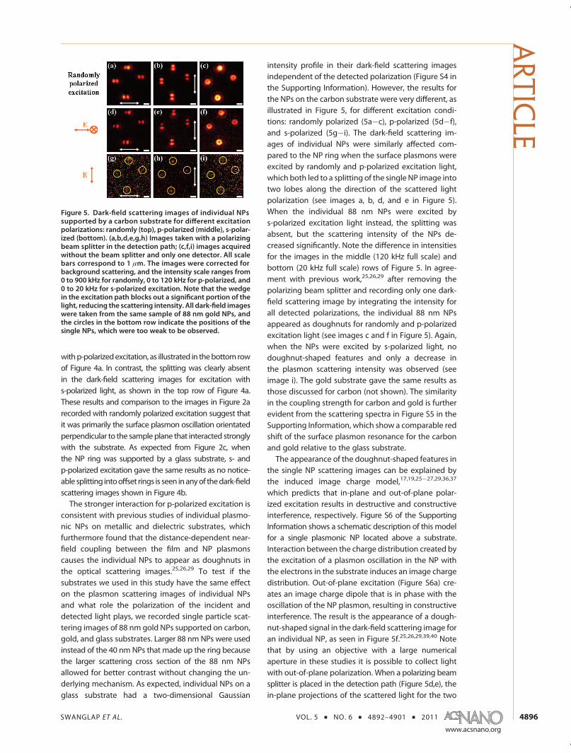
intensity profile in their dark-field scattering imagesindependent of the detected polarization (Figure S4 inthe Supporting Information). However, the results forthe NPs on the carbon substrate were very different, asillustrated in Figure 5, for different excitation condi-tions: randomly polarized (5a�c), p-polarized (5d�f),and s-polarized (5g�i). The dark-field scattering im-ages of individual NPs were similarly affected com-pared to the NP ring when the surface plasmons wereexcited by randomly and p-polarized excitation light,which both led to a splitting of the single NP image intotwo lobes along the direction of the scattered lightpolarization (see images a, b, d, and e in Figure 5).When the individual 88 nm NPs were excited bys-polarized excitation light instead, the splitting wasabsent, but the scattering intensity of the NPs de-creased significantly. Note the difference in intensitiesfor the images in the middle (120 kHz full scale) andbottom (20 kHz full scale) rows of Figure 5. In agree-ment with previous work,25,26,29 after removing thepolarizing beam splitter and recording only one dark-field scattering image by integrating the intensity forall detected polarizations, the individual 88 nm NPsappeared as doughnuts for randomly and p-polarizedexcitation light (see images c and f in Figure 5). Again,when the NPs were excited by s-polarized light, nodoughnut-shaped features and only a decrease inthe plasmon scattering intensity was observed (seeimage i). The gold substrate gave the same results asthose discussed for carbon (not shown). The similarityin the coupling strength for carbon and gold is furtherevident from the scattering spectra in Figure S5 in theSupporting Information, which show a comparable redshift of the surface plasmon resonance for the carbonand gold relative to the glass substrate.The appearance of the doughnut-shaped features in
the single NP scattering images can be explained bythe induced image charge model,17,19,25�27,29,36,37
which predicts that in-plane and out-of-plane polar-ized excitation results in destructive and constructiveinterference, respectively. Figure S6 of the SupportingInformation shows a schematic description of this modelfor a single plasmonic NP located above a substrate.Interaction between the charge distribution created bythe excitation of a plasmon oscillation in the NP withthe electrons in the substrate induces an image chargedistribution. Out-of-plane excitation (Figure S6a) cre-ates an image charge dipole that is in phase with theoscillation of the NP plasmon, resulting in constructiveinterference. The result is the appearance of a dough-nut-shaped signal in the dark-field scattering image foran individual NP, as seen in Figure 5f.25,26,29,39,40 Notethat by using an objective with a large numericalaperture in these studies it is possible to collect lightwith out-of-plane polarization. When a polarizing beamsplitter is placed in the detection path (Figure 5d,e), thein-plane projections of the scattered light for the two
Figure 5. Dark-field scattering images of individual NPssupported by a carbon substrate for different excitationpolarizations: randomly (top), p-polarized (middle), s-polar-ized (bottom). (a,b,d,e,g,h) Images taken with a polarizingbeam splitter in the detection path; (c,f,i) images acquiredwithout the beam splitter and only one detector. All scalebars correspond to 1 μm. The images were corrected forbackground scattering, and the intensity scale ranges from0 to 900 kHz for randomly, 0 to 120 kHz for p-polarized, and0 to 20 kHz for s-polarized excitation. Note that the wedgein the excitation path blocks out a significant portion of thelight, reducing the scattering intensity. All dark-field imageswere taken from the same sample of 88 nm gold NPs, andthe circles in the bottom row indicate the positions of thesingle NPs, which were too weak to be observed.
ARTIC
LE
SWANGLAP ET AL. VOL. 5 ’ NO. 6 ’ 4892–4901 ’ 2011
www.acsnano.org
4897
orthogonal polarization components are selected. Thiscauses the dumbbell-shaped patterns that look like asplitting of the image along the direction of thedetected light polarization. On the other hand, for in-plane excitation (Figure S6b), the NP dipole and theinduced image dipole are out of phasewith each other,which leads to destructive interference and a stronglyreduced far-field scattering intensity, as illustrated inFigure 5i. The described image charge model can alsobe interpreted as the hybridization of the localizedsurface plasmon resonance of the NP with its imagecharge. In fact, the model in Figure S6 (SupportingInformation) resembles the case of a NP dimer.21,47
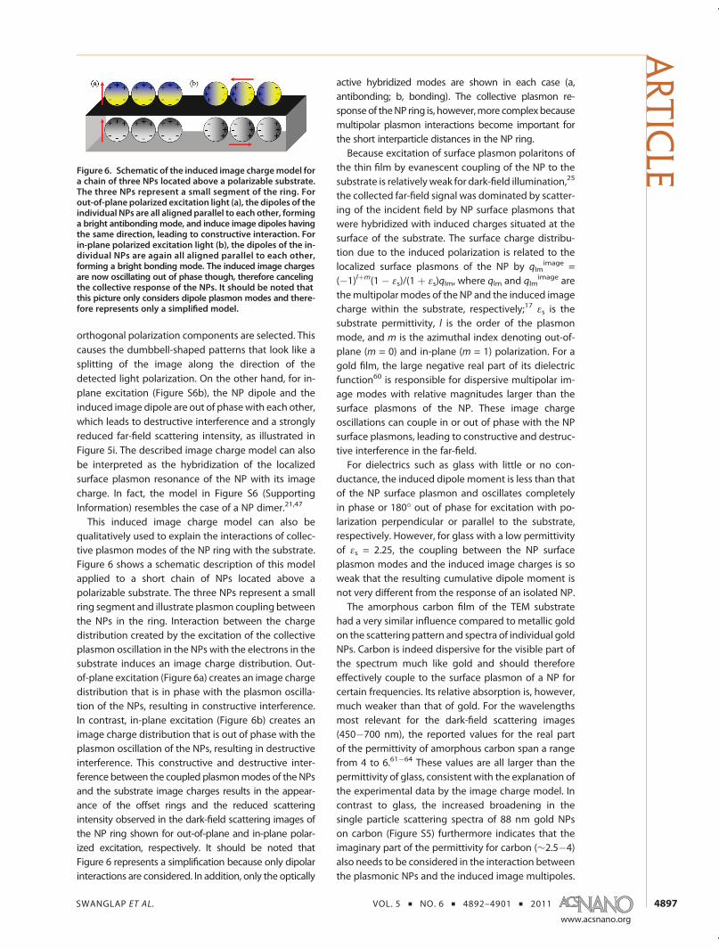
This induced image charge model can also bequalitatively used to explain the interactions of collec-tive plasmon modes of the NP ring with the substrate.Figure 6 shows a schematic description of this modelapplied to a short chain of NPs located above apolarizable substrate. The three NPs represent a smallring segment and illustrate plasmon coupling betweenthe NPs in the ring. Interaction between the chargedistribution created by the excitation of the collectiveplasmon oscillation in the NPs with the electrons in thesubstrate induces an image charge distribution. Out-of-plane excitation (Figure 6a) creates an image chargedistribution that is in phase with the plasmon oscilla-tion of the NPs, resulting in constructive interference.In contrast, in-plane excitation (Figure 6b) creates animage charge distribution that is out of phase with theplasmon oscillation of the NPs, resulting in destructiveinterference. This constructive and destructive inter-ference between the coupled plasmonmodes of the NPsand the substrate image charges results in the appear-ance of the offset rings and the reduced scatteringintensity observed in the dark-field scattering images ofthe NP ring shown for out-of-plane and in-plane polar-ized excitation, respectively. It should be noted thatFigure 6 represents a simplification because only dipolarinteractions are considered. In addition, only the optically
active hybridized modes are shown in each case (a,antibonding; b, bonding). The collective plasmon re-sponseof theNP ring is, however,more complexbecausemultipolar plasmon interactions become important forthe short interparticle distances in the NP ring.Because excitation of surface plasmon polaritons of
the thin film by evanescent coupling of the NP to thesubstrate is relativelyweak for dark-field illumination,25
the collected far-field signal was dominated by scatter-ing of the incident field by NP surface plasmons thatwere hybridized with induced charges situated at thesurface of the substrate. The surface charge distribu-tion due to the induced polarization is related to thelocalized surface plasmons of the NP by qlm
image =(�1)lþm(1 � εs)/(1 þ εs)qlm, where qlm and qlm
image arethemultipolarmodes of the NP and the induced imagecharge within the substrate, respectively;17 εs is thesubstrate permittivity, l is the order of the plasmonmode, and m is the azimuthal index denoting out-of-plane (m = 0) and in-plane (m = 1) polarization. For agold film, the large negative real part of its dielectricfunction60 is responsible for dispersive multipolar im-age modes with relative magnitudes larger than thesurface plasmons of the NP. These image chargeoscillations can couple in or out of phase with the NPsurface plasmons, leading to constructive and destruc-tive interference in the far-field.For dielectrics such as glass with little or no con-
ductance, the induced dipole moment is less than thatof the NP surface plasmon and oscillates completelyin phase or 180� out of phase for excitation with po-larization perpendicular or parallel to the substrate,respectively. However, for glass with a low permittivityof εs = 2.25, the coupling between the NP surfaceplasmon modes and the induced image charges is soweak that the resulting cumulative dipole moment isnot very different from the response of an isolated NP.The amorphous carbon film of the TEM substrate
had a very similar influence compared to metallic goldon the scattering pattern and spectra of individual goldNPs. Carbon is indeed dispersive for the visible part ofthe spectrum much like gold and should thereforeeffectively couple to the surface plasmon of a NP forcertain frequencies. Its relative absorption is, however,much weaker than that of gold. For the wavelengthsmost relevant for the dark-field scattering images(450�700 nm), the reported values for the real partof the permittivity of amorphous carbon span a rangefrom 4 to 6.61�64 These values are all larger than thepermittivity of glass, consistent with the explanation ofthe experimental data by the image charge model. Incontrast to glass, the increased broadening in thesingle particle scattering spectra of 88 nm gold NPson carbon (Figure S5) furthermore indicates that theimaginary part of the permittivity for carbon (∼2.5�4)also needs to be considered in the interaction betweenthe plasmonic NPs and the induced image multipoles.
Figure 6. Schematic of the induced image chargemodel fora chain of three NPs located above a polarizable substrate.The three NPs represent a small segment of the ring. Forout-of-plane polarized excitation light (a), the dipoles of theindividual NPs are all aligned parallel to each other, forminga bright antibondingmode, and induce image dipoles havingthe same direction, leading to constructive interaction. Forin-plane polarized excitation light (b), the dipoles of the in-dividual NPs are again all aligned parallel to each other,forming a bright bonding mode. The induced image chargesare now oscillating out of phase though, therefore cancelingthe collective response of the NPs. It should be noted thatthis picture only considers dipole plasmon modes and there-fore represents only a simplified model.
ARTIC
LE
SWANGLAP ET AL. VOL. 5 ’ NO. 6 ’ 4892–4901 ’ 2011
www.acsnano.org
4898
Because the carbon films used here were only 20 nmthin according to the manufacturer and a direct compar-ison with literature values is difficult because the permit-tivity has been found to vary strongly with thickness andpreparation method as well as crystallinity,62 it is difficultto draw further quantitative conclusions. Qualitatively,however, the dark-field images recorded for both carbonand gold substrates can be explained by the coupling ofinduced image charges with the surface plasmons of theNPs.When the image charge model is applied to the NP
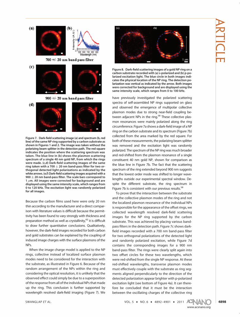
rings, collective instead of localized surface plasmonmodes need to be considered for the interaction withthe substrate, as illustrated in Figure 6. Because of therandom arrangement of the NPs within the ring andconsidering the optical resolution, it is unlikely that theobserved effect could simply be due to a superpositionof the response fromall of the individual NPs thatmadeup the ring. This conclusion is further supported bywavelength resolved dark-field imaging (Figure 7). We
have previously investigated the polarized scatteringspectra of self-assembled NP rings supported on glassand observed the emergence of multipolar collectiveplasmon modes due to strong near-field coupling be-tween adjacent NPs in the ring.58 These collective plas-mon resonances were mainly polarized along the ringcircumference. Figure 7a showsadark-field imageof aNPring on the carbon substrate and its spectrum (Figure 7b)collected from the area marked by the red square. Forbothof thesemeasurements, thepolarizingbeamsplitterwas removed and the excitation light was randomlypolarized. The spectrumof theNP ringwasmuchbroaderand red-shifted from the plasmon resonance of a singleconstituent 40 nm gold NP, shown for comparison asthe blue line in Figure 7b. The fact that the scatteringspectrum of the ring extended beyond 900 nm suggeststhat the lowest order mode was shifted to longer wave-lengths outside our experimental spectral window. De-spite the different substrate, the ring spectrum inFigure 7b is consistent with our previous results.58
To prove that the interaction between the substrateand the collective plasmon modes of the ring and notthe localized plasmon resonance of the individual NPsis responsible for the appearance of the offset rings, wecollected wavelength resolved dark-field scatteringimages for the NP ring supported by the carbonsubstrate. This was achieved by placing various band-pass filters in the detection path. Figure 7c shows dark-field images recorded with a 700 nm band-pass filterfor two orthogonal polarizations of the detected lightand randomly polarized excitation, while Figure 7dcontains the corresponding images for a 900 nmband-pass filter. The rings were clearly split again intotwo offset circles for these two wavelengths, whichwere red-shifted from the single NP response. At thesered-shifted wavelengths, transverse plasmon modesmust effectively couple with the substrate as ring seg-ments aligned perpendicularly to the direction of thedetected polarization appear brighter with p-polarizedexcitation light (see bottom of Figure 4a). It can there-fore be concluded that it must be the interactionbetween the oscillating charges of the collective ring
Figure 7. Dark-field scattering image (a) and spectrum (b, redline) of the sameNP ring supported by a carbon substrate asshown in Figures 1 and 2. The image was taken without thepolarizing beam splitter in the detection path. The red squareindicates the position where the scattering spectrum wastaken. The blue line in (b) shows the plasmon scatteringspectrum of a single 40 nm gold NP, from which the ringswere made. (c,d) Dark-field scattering images of the samering taken with a 700 ( 20 nm band-pass filter for two or-thogonal detected light polarizations as indicated by thewhite arrows. (e,f) Dark-field scattering images acquiredwith a900 ( 20 nm band-pass filter. The scale bars correspond to1 μm. All images were corrected for background and aredisplayed using the same intensity scale, which ranges from0 to 120 kHz. The excitation light was randomly polarizedfor all images.
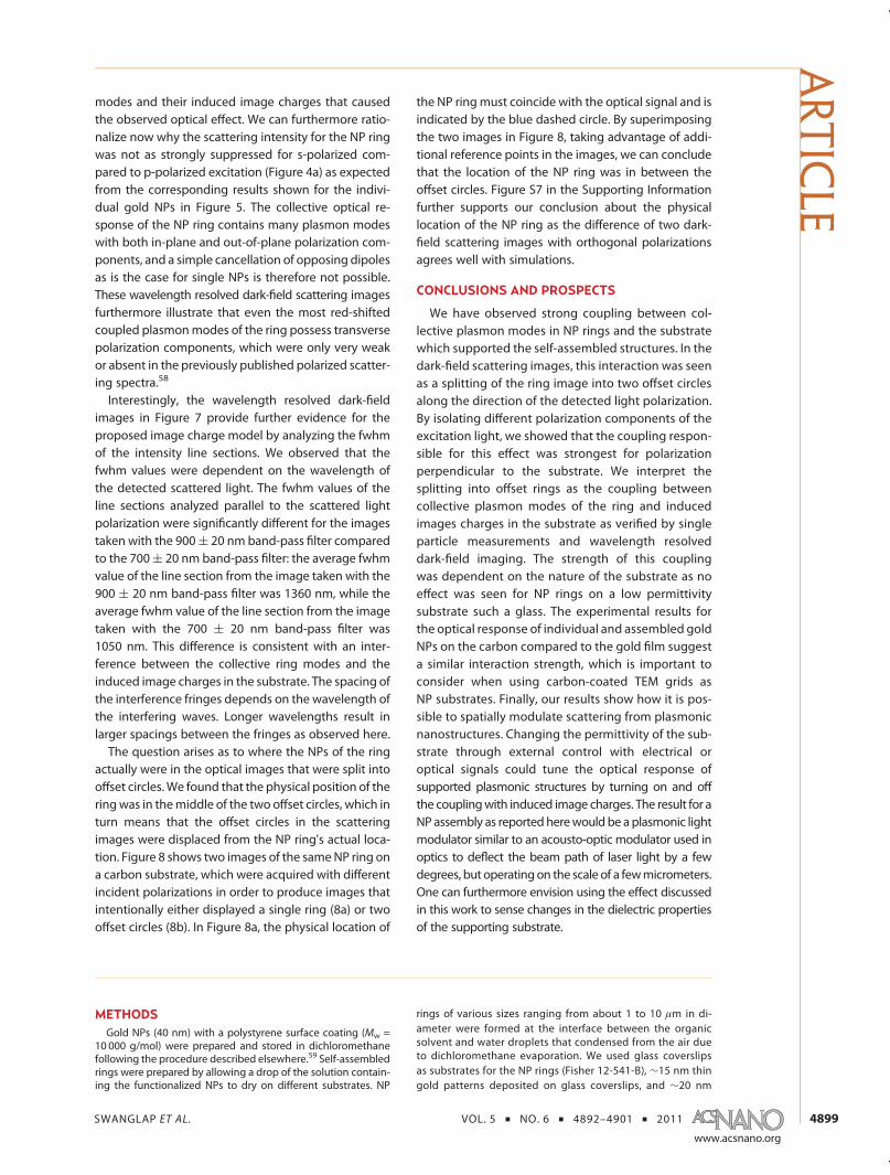
Figure 8. Dark-field scattering images of a goldNP ring on acarbon substrate recordedwith (a) s-polarized and (b) p-po-larized excitation light. The blue circle in both images indi-cates the physical location of the NP ring. The detection po-larization was vertical as indicated by the arrow. Both imageswere corrected for background and are displayed using thesame intensity scale, which ranges from 0 to 100 kHz.
ARTIC
LE
SWANGLAP ET AL. VOL. 5 ’ NO. 6 ’ 4892–4901 ’ 2011
www.acsnano.org
4899
modes and their induced image charges that causedthe observed optical effect. We can furthermore ratio-nalize now why the scattering intensity for the NP ringwas not as strongly suppressed for s-polarized com-pared to p-polarized excitation (Figure 4a) as expectedfrom the corresponding results shown for the indivi-dual gold NPs in Figure 5. The collective optical re-sponse of the NP ring contains many plasmon modeswith both in-plane and out-of-plane polarization com-ponents, and a simple cancellation of opposing dipolesas is the case for single NPs is therefore not possible.These wavelength resolved dark-field scattering imagesfurthermore illustrate that even the most red-shiftedcoupled plasmonmodes of the ring possess transversepolarization components, which were only very weakor absent in the previously published polarized scatter-ing spectra.58
Interestingly, the wavelength resolved dark-fieldimages in Figure 7 provide further evidence for theproposed image charge model by analyzing the fwhmof the intensity line sections. We observed that thefwhm values were dependent on the wavelength ofthe detected scattered light. The fwhm values of theline sections analyzed parallel to the scattered lightpolarization were significantly different for the imagestaken with the 900( 20 nm band-pass filter comparedto the 700( 20 nm band-pass filter: the average fwhmvalue of the line section from the image taken with the900 ( 20 nm band-pass filter was 1360 nm, while theaverage fwhm value of the line section from the imagetaken with the 700 ( 20 nm band-pass filter was1050 nm. This difference is consistent with an inter-ference between the collective ring modes and theinduced image charges in the substrate. The spacing ofthe interference fringes depends on the wavelength ofthe interfering waves. Longer wavelengths result inlarger spacings between the fringes as observed here.The question arises as to where the NPs of the ring
actually were in the optical images that were split intooffset circles.We found that the physical position of theringwas in themiddle of the two offset circles, which inturn means that the offset circles in the scatteringimages were displaced from the NP ring's actual loca-tion. Figure 8 shows two images of the sameNP ring ona carbon substrate, which were acquired with differentincident polarizations in order to produce images thatintentionally either displayed a single ring (8a) or twooffset circles (8b). In Figure 8a, the physical location of
the NP ringmust coincide with the optical signal and isindicated by the blue dashed circle. By superimposingthe two images in Figure 8, taking advantage of addi-tional reference points in the images, we can concludethat the location of the NP ring was in between theoffset circles. Figure S7 in the Supporting Informationfurther supports our conclusion about the physicallocation of the NP ring as the difference of two dark-field scattering images with orthogonal polarizationsagrees well with simulations.
CONCLUSIONS AND PROSPECTS
We have observed strong coupling between col-lective plasmon modes in NP rings and the substratewhich supported the self-assembled structures. In thedark-field scattering images, this interaction was seenas a splitting of the ring image into two offset circlesalong the direction of the detected light polarization.By isolating different polarization components of theexcitation light, we showed that the coupling respon-sible for this effect was strongest for polarizationperpendicular to the substrate. We interpret thesplitting into offset rings as the coupling betweencollective plasmon modes of the ring and inducedimages charges in the substrate as verified by singleparticle measurements and wavelength resolveddark-field imaging. The strength of this couplingwas dependent on the nature of the substrate as noeffect was seen for NP rings on a low permittivitysubstrate such a glass. The experimental results forthe optical response of individual and assembled goldNPs on the carbon compared to the gold film suggesta similar interaction strength, which is important toconsider when using carbon-coated TEM grids asNP substrates. Finally, our results show how it is pos-sible to spatially modulate scattering from plasmonicnanostructures. Changing the permittivity of the sub-strate through external control with electrical oroptical signals could tune the optical response ofsupported plasmonic structures by turning on and offthe couplingwith induced image charges. The result for aNP assembly as reported herewould be a plasmonic lightmodulator similar to an acousto-optic modulator used inoptics to deflect the beam path of laser light by a fewdegrees, but operating on the scale of a fewmicrometers.One can furthermore envision using the effect discussedin this work to sense changes in the dielectric propertiesof the supporting substrate.
METHODSGold NPs (40 nm) with a polystyrene surface coating (Mw =
10 000 g/mol) were prepared and stored in dichloromethanefollowing the procedure described elsewhere.59 Self-assembledrings were prepared by allowing a drop of the solution contain-ing the functionalized NPs to dry on different substrates. NP
rings of various sizes ranging from about 1 to 10 μm in di-ameter were formed at the interface between the organicsolvent and water droplets that condensed from the air dueto dichloromethane evaporation. We used glass coverslipsas substrates for the NP rings (Fisher 12-541-B), ∼15 nm thingold patterns deposited on glass coverslips, and ∼20 nm
ARTIC
LE
SWANGLAP ET AL. VOL. 5 ’ NO. 6 ’ 4892–4901 ’ 2011
www.acsnano.org
4900
thin carbon films on top of standard TEM copper grids (TedPella CF300-Cu-50). The gold patterns were formed using anindexed TEM grid (Ted Pella 79021C) and an electron beamevaporator (Telemark), which also allowed us to locate thesame structures on the glass and gold substrates by opticalmicroscopy and scanning electron microscopy (FEI QuantaESEM2 operated at 25 kV in wet mode).58,65,66 The samplesdeposited on TEM grids were characterized using a transmis-sion electron microscope (JEOL 2010) operated at 120 kV.
Dark-field excitation was performed in a reflected lightgeometry using an inverted microscope (Zeiss Axiovert 200)with a halogen lamp as the excitation source. Dark-fieldcontrast was achieved using incident excitation light with anumerical aperture larger than that for the collected back-scattered light. The polarization of the excitation light wasselected using a combination of a wedge and a polarizer.52 Toallow for coarse and fine adjustments of the sample position,a custom-designed holder was attached to a manual transla-tional stage and mounted on an xyz piezo scanning stage(Physik Instrumente P-517.3CL), which was connected to asurface probe microscope controller (RHK Technology SPM1000). Scattered light was collected with a Zeiss Epiplan100�/0.75 objective and, after passing first through a 50μm pinhole located at the first microscope image plane andthen a polarizing beam splitter, was focused onto twoavalanche photodiode detectors (Perkin-Elmer SPCM-AQR-15). Using an intermediate 2.5� lens gave a total magnifica-tion of 250� at the detectors. Dark-field scattering imageswere collected point by point with the scanning stage.Optical density and band-pass filters were used in the detec-tion path to prevent saturating the detectors and to collectimages for specific wavelength intervals of the scatteredlight, respectively. Scattering spectra were acquired byredirecting the light to the entrance of a spectrometer(Princeton Instruments Acton SP2150i) connected to a CCDcamera (Princeton Instruments PIXIS 400BR). A Zeiss Epiplan-Neofluar 50�/0.8 objective was used to measure spectra andwavelength resolved images because it has a better trans-mission efficiency and chromatic correction for wavelengthslonger than 700 nm compared to the 100� Epiplan objective.The spectra were corrected for background and dark countsbymeasuring spectra at regions with no NPs present andwiththe lamp off, respectively. In addition, correction for thespectral response of the lamp and other optical componentswas carried out by collecting the spectrum of a white lightreflectivity standard (Labsphere SRS-99-010).
Acknowledgment. S.L. thanks the Robert A. Welch Founda-tion (Grant C-1664), NSF (CHE-0955286), the ACS PetroleumResearch Fund (50191-DNI6), and 3M for a Nontenured FacultyGrant. E.R.Z. acknowledges financial support by NSF (DMR-0547399) and the Robert A. Welch Foundation (C-1703). P.S.acknowledges support from the Royal Thai Government, andL.S.S. thanks the NSF IGERT Nanophotonics fellowship program.W.S.C. acknowledges support from the Richard E. SmalleyInstitute for a Peter and Ruth Nicholas fellowship. We thankAvishek Saha for help with TEM measurements.
Supporting Information Available: SEM images of NP rings ongold and glass substrates, a microscope focus dependence of thedark-field scattering images, the optical resolution for dark-fieldscattering of single gold NPs with different sizes, dark-field scatter-ing images of 88 nmNPs on carbon and glass substrates, dark-fieldscattering spectra of 88 nm NPs on carbon, gold, and glasssubstrates, schematic of the induced image charge model for asingle NP on a polarizable substrate, and an analysis for the physicallocation of the NP ring in the dark-field image. This material isavailable free of charge via the Internet at http://pubs.acs.org.
REFERENCES AND NOTES1. Kelly, K. L.; Coronado, E.; Zhao, L. L.; Schatz, G. C. The
Optical Properties of Metal Nanoparticles: The Influence ofSize, Shape, and Dielectric Environment. J. Phys. Chem. B2003, 107, 668–677.
2. Lal, S.; Link, S.; Halas, N. J. Nano-Optics from Sensing toWaveguiding. Nat. Photonics 2007, 1, 641–648.
3. Noguez, C. Surface Plasmons on Metal Nanoparticles: TheInfluence of Shape and Physical Environment. J. Phys.Chem. C 2007, 111, 3806–3819.
4. Jain, P. K.; Lee, K. S.; El-Sayed, I. H.; El-Sayed, M. A. Calcu-lated Absorption and Scattering Properties of Gold Nano-particles of Different Size, Shape, and Composition:Applications in Biological Imaging and Biomedicine.J. Phys. Chem. B 2006, 110, 7238–7248.
5. Miller, M. M.; Lazarides, A. A. Sensitivity of Metal Nanopar-ticle Surface Plasmon Resonance to the Dielectric Envir-onment. J. Phys. Chem. B 2005, 109, 21556–21565.
6. Landes, C. F.; Link, S.; Mohamed, M. B.; Nikoobakht, B.;El-Sayed, M. A. Some Properties of Spherical and Rod-Shaped Semiconductor andMetal Nanocrystals. Pure Appl.Chem. 2002, 74, 1675–1692.
7. Willets, K. A.; Van Duyne, R. P. Localized Surface PlasmonResonance Spectroscopy and Sensing. Annu. Rev. Phys.Chem. 2007, 58, 267–297.
8. Raschke, G.; Kowarik, S.; Franzl, T.; Sönnichsen, C.; Klar, T. A.;Feldmann, J.; Nichtl, A.; Kürzinger, K. Biomolecular Recog-nition Based on Single Gold Nanoparticle Light Scattering.Nano Lett. 2003, 3, 935–938.
9. Sherry, L. J.; Chang, S.-H.; Schatz, G. C.; Van Duyne, R. P.;Wiley, B. J.; Xia, Y. Localized Surface Plasmon ResonanceSpectroscopy of Single Silver Nanocubes.Nano Lett. 2005,5, 2034–2038.
10. Nehl, C. L.; Liao, H.; Hafner, J. H. Optical Properties of Star-Shaped Gold Nanoparticles. Nano Lett. 2006, 6, 683–688.
11. Chen, H. J.; Kou, X. S.; Yang, Z.; Ni, W. H.; Wang, J. F. Shape-and Size-Dependent Refractive Index Sensitivity of GoldNanoparticles. Langmuir 2008, 24, 5233–5237.
12. Malinsky, M. D.; Kelly, K. L.; Schatz, G. C.; Van Duyne, R. P.Nanosphere Lithography: Effect of Substrate on the Loca-lized Surface Plasmon Resonance Spectrum of SilverNanoparticles. J. Phys. Chem. B 2001, 105, 2343–2350.
13. Novo, C.; Funston, A. M.; Pastoriza-Santos, I.; Liz-Marzan,L. M.; Mulvaney, P. Influence of the Medium RefractiveIndex on the Optical Properties of Single Gold TriangularPrisms on a Substrate. J. Phys. Chem. C 2008, 112, 3–7.
14. Sherry, L. J.; Jin, R.; Mirkin, C. A.; Schatz, G. C.; Van Duyne,R. P. Localized Surface Plasmon Resonance Spectroscopyof Single Silver Triangular Nanoprisms. Nano Lett. 2006, 6,2060–2065.
15. Murray, W. A.; Auguie, B.; Barnes, W. L. Sensitivity ofLocalized Surface Plasmon Resonances to Bulk and LocalChanges in the Optical Environment. J. Phys. Chem. C2009, 113, 5120–5125.
16. Chance, R. R.; Prock, A.; Silbey, R. Frequency Shifts of anElectric-Dipole Transition near a Partially Reflecting Sur-face. Phys. Rev. A 1975, 12, 1448–1452.
17. Jackson, J. D. Classical Electrodynamics, 3rd ed.; JohnWiley& Sons, Inc.: Toronto, 1999.
18. Bobbert, P. A.; Vlieger, J. Light Scattering by a Sphere on aSubstrate. Physica A 1986, 137A, 209–242.
19. Wind, M. M.; Vlieger, J.; Bedeaux, D. The Polarizability of aTruncatedSphereonaSubstrate I.PhysicaA1987,141, 33–57.
20. Kim, J. H.; Ehrman, S. H.; Mulholland, G. W.; Germer, T. A.Polarized Light Scattering by Dielectric and MetallicSpheres on SiliconWafers. Appl. Opt. 2002, 41, 5405–5412.
21. Nordlander, P.; Prodan, E. Plasmon Hybridization in Nano-particles near Metallic Surfaces. Nano Lett. 2004, 4,2209–2213.
22. Nordlander, P.; Le, F. Plasmonic Structure and Electromag-netic Field Enhancements in the Metallic Nanoparticle-Film System. Appl. Phys. B: Laser Opt. 2006, 84, 35–41.
23. L�eveque, G.; Martin, O. J. F. Optical Interactions in aPlasmonic Particle Coupled to a Metallic Film. Opt. Exp.2006, 14, 9971–9981.
24. Le, F.; Lwin, N. Z.; Steele, J. M.; Käll, M.; Halas, N. J.; Nordlander,P. Plasmons in the Metallic Nanoparticle�Film System as aTunable Impurity Problem. Nano Lett. 2005, 5, 2009–2013.
25. Mock, J. J.; Hill, R. T.; Degiron, A.; Zauscher, S.; Chilkoti, A.;Smith, D. R. Distance-Dependent Plasmon Resonant
ARTIC
LE

SWANGLAP ET AL. VOL. 5 ’ NO. 6 ’ 4892–4901 ’ 2011
www.acsnano.org
4901
Coupling between a Gold Nanoparticle and Gold Film.Nano Lett. 2008, 8, 2245–2252.
26. Hu, M.; Ghoshal, A.; Marquez, M.; Kik, P. G. Single ParticleSpectroscopy Study of Metal-Film-Induced Tuning of Sil-ver Nanoparticle Plasmon Resonances. J. Phys. Chem. C2010, 114, 7509–7514.
27. Okamoto, T.; Yamaguchi, I. Optical Absorption Study of theSurface Plasmon Resonance in Gold Nanoparticles Immo-bilized onto a Gold Substrate by Self-Assembly Technique.J. Phys. Chem. B 2003, 107, 10321–10324.
28. Abe, S.; Kajikawa, K. Linear and Nonlinear Optical Proper-ties of Gold Nanospheres Immobilized on a Metallic Sur-face. Phys. Rev. B 2006, 74, No. 035416.
29. Chen, S. Y.; Mock, J. J.; Hill, R. T.; Chilkoti, A.; Smith, D. R.;Lazarides, A. A. Gold Nanoparticles on Polarizable Surfacesas Raman Scattering Antennas. ACS Nano 2010, 4,6535–6546.
30. Sisco, P. N.; Murphy, C. J. Surface-Coverage Dependence ofSurface-Enhanced Raman Scattering from Gold Nano-cubes of Self-Assembled Monolayers of Analyte. J. Phys.Chem. A 2009, 113, 3973–3978.
31. Park, W.-H.; Kim, Z. H. Charge Transfer Enhancement in theSERS of a SingleMolecule.Nano Lett. 2010, 10, 4040–4048.
32. Hill, R. T.; Mock, J. J.; Urzhumov, Y.; Sebba, D. S.; Oldenburg,S. J.; Chen, S.-Y.; Lazarides, D. A.; Chilkoti, A.; Smith, D. R.Leveraging Nanoscale Plasmonic Modes To Achieve Re-producible Enhancement of Light. Nano Lett. 2010, 10,4150–4154.
33. Eah, S.-K.; Jaeger, H. M.; Scherer, N. F.; Wiederrecht, G. P.;Lin, X.-M. Scattered Light Interference from a Single MetalNanoparticle and Its Mirror Image. J. Phys. Chem. B 2005,109, 11858–11861.
34. Ringe, E.; McMahon, J. M.; Sohn, K.; Cobley, C.; Xia, Y.;Huang, J.; Schatz, G. C.; Marks, L. D.; Van Duyne, R. P.Unraveling the Effects of Size, Composition, and Substrateon the Localized Surface Plasmon Resonance Frequenciesof Gold and Silver Nanocubes: A Systematic Single-ParticleApproach. J. Phys. Chem. C 2010, 114, 12511–12516.
35. Knight, M. W.; Wu, Y.; Lassiter, J. B.; Nordlander, P.; Halas,N. J. Substrates Matter: Influence of an Adjacent Dielectricon an Individual Plasmonic Nanoparticle. Nano Lett. 2009,9, 2188–2192.
36. Pinchuk, A.; Hilger, A.; von Plessen, G.; Kreibig, U. SubstrateEffect on the Optical Response of Silver Nanoparticles.Nanotechnology 2004, 15, 1890–1896.
37. Wu, Y.; Nordlander, P. Finite-Difference Time-DomainModeling of the Optical Properties of Nanoparticles nearDielectric Substrates. J. Phys. Chem. C 2010, 114, 7302–7307.
38. You, Y.-M.; Du, C.-L.; Ma, Y.; Kasim, J.; Yu, T.; Shen, Z.-X. Effectof Near-Field Coupling on Far-Field Inelastic ScatteringImaging of Gold Nanoparticles. Nanotechnology 2008, 19,395705.
39. Bartko, A. P.; Dickson, R. M. Three-Dimensional Orienta-tions of Polymer-Bound Single Molecules. J. Phys. Chem. B1999, 103, 3053–3056.
40. Moerland, R. J.; Taminiau, T. H.; Novotny, L.; van Hulst, N. F.;Kuipers, L. Reversible Polarization Control of Single PhotonEmission. Nano Lett. 2008, 8, 606–610.
41. Patra, D.; Gregor, I.; Enderlein, J. Image Analysis of DefocusedSingle-Molecule Images for Three-Dimensional MoleculeOrientation Studies. J. Phys. Chem. A 2004, 108, 6836–6841.
42. Curto, A. G.; Volpe, G.; Taminiau, T. H.; Kreuzer, M. P.; Quidant,R.; van Hulst, N. F. Unidirectional Emission of a QuantumDotCoupled to a Nanoantenna. Science 2010, 329, 930–933.
43. Kühn, S.; Mori, G.; Agio, M.; Sandoghdar, V. Modification ofSingle Molecule Fluorescence Close to a Nanostructure:Radiation Pattern, Spontaneous Emission and Quenching.Mol. Phys. 2008, 106, 893–908.
44. Taminiau, T. H.; Stefani, F. D.; Segerink, F. B.; van Hulst, N. F.Optical Antennas Direct Single-Molecule Emission. Nat.Photonics 2008, 2, 234–237.
45. Kosako, T.; Koadoya, Y.; Hofman, H. F. Directional Control ofLight by a Nano-Optical Yagi-Uda Antenna. Nat. Photonics2010, 4, 312–315.
46. Chen, H. J.; Sun, Z. H.; Ni, W. H.; Woo, K. C.; Lin, H. Q.; Sun,L. D.; Yan, C. H.; Wang, J. F. Plasmon Coupling in ClustersComposed of Two-Dimensionally Ordered Gold Nano-cubes. Small 2009, 5, 2111–2119.
47. Gozhenko, V. V.; Grechko, L. G.; Whites, K. W. Electrody-namics of Spatial Clusters of Spheres: Substrate Effects.Phys. Rev. B 2003, 68, No. 125422.
48. Vernon, K. C.; Funston,A.M.; Novo, C.; Gomez,D. E.;Mulvaney,P.; Davis, T. J. Influence of Particle�Substrate Interactionon Localized Plasmon Resonances. Nano Lett. 2010, 10,2080–2086.
49. Xu, G.; Chen, Y.; Tazawa, M.; Jin, P. Surface Plasmon Reso-nance of Silver Nanoparticles on Vanadium Dioxide. J. Phys.Chem. B 2006, 110, 2051–2056.
50. Su, K. H.; Wei, Q. H.; Zhang, X.; Mock, J. J.; Smith, D. R.;Schultz, S. Interparticle Coupling Effects on PlasmonResonances of Nanogold Particles. Nano Lett. 2003, 3,1087–1090.
51. Romero, I.; Aizpurua, J.; Bryant, G. W.; Garcia de Abajo, F. J.Plasmons in Nearly Touching Metallic Nanoparticles: Sin-gular Response in the Limit of Touching Dimers. Opt.Express 2006, 14, 9988–9999.
52. Tamaru, H.; Kuwata, H.; Miyazaki, H. T.; Miyano, K. ResonantLight Scattering from Individual Ag Nanoparticles andParticle Pairs. Appl. Phys. Lett. 2002, 80, 1826–1828.
53. Lassiter, J. B.; Aizpurua, J.; Hernandez, L. I.; Brandl, D. W.;Romero, I.; Lal, S.; Hafner, J. H.; Nordlander, P.; Halas, N. J.Close Encounters between Two Nanoshells. Nano Lett.2008, 8, 1212–1218.
54. Jain, P. K.; Huang, W.; El-Sayed, M. A. On the UniversalScaling Behavior of the Distance Decay of Plasmon Cou-pling in Metal Nanoparticle Pairs: A Plasmon Ruler Equa-tion. Nano Lett. 2007, 7, 2080–2088.
55. Chen, J. I. L.; Chen, Y.; Ginger, D. S. Plasmonic NanoparticleDimers for Optical Sensing of DNA in Complex Media. J.Am. Chem. Soc. 2010, 132, 9600–9601.
56. Chandra, M.; Dowgiallo, A.-M.; Knappenberger, K. L., Jr.Controlled Plasmon Resonance Properties of Hollow GoldNanosphere Aggregates. J. Am. Chem. Soc. 2010, 132,15782–15789.
57. Slaughter, L. S.; Wu, Y.; Willingham, B. A.; Nordlander, P.;Link, S. Effects of Symmetry Breaking and ConductiveContact on the Plasmon Coupling in Gold Nanorod Di-mers. ACS Nano 2010, 4, 4657–4666.
58. Chang, W. S.; Slaughter, L. S.; Khanal, B. P.; Manna, P.;Zubarev, E. R.; Link, S. One-Dimensional Coupling of GoldNanoparticle Plasmons in Self-Assembled Ring Super-structures. Nano Lett. 2009, 9, 1152–1157.
59. Khanal, B. P.; Zubarev, E. R. Rings of Nanorods. Angew.Chem., Int. Ed. 2007, 46, 2195–2198.
60. Johnson, P. B.; Christy, R. W. Optical Constants of the NobleMetals. Phys. Rev. B 1972, 6, 4370–4379.
61. Berlind, T.; Furlan, A.; Czigany, Z.; Neidhardt, J.; Hultman, L.;Arwin, H. Spectroscopic Ellipsometry Characterization ofAmorphous Carbon and Amorphous, Graphitic and Full-erene-like CarbonNitride Thin Films. Thin Solid Films 2009,517, 6652–6658.
62. Gioti, M.; Logothetidis, S. Dielectric Function, ElectronicProperties and Optical Constants of Amorphous Carbonand Carbon Nitride Films. Diamond Relat. Mater. 2003, 12,957–962.
63. Parker, W. G.; Watson, T. J.; Sambles, J. R. The OpticalDielectric Function of Amorphous Carbon Films. Thin SolidFilms 1996, 279, 162–165.
64. Logothetidis, S. Optical and Electronic Properties of Amor-phous Carbon Materials. Diamond Relat. Mater. 2003, 12,141–150.
65. Slaughter, L. S.; Chang, W.-S.; Swanglap, P.; Tcherniak, A.;Khanal, B. P.; Zubarev, E. R.; Link, S. Single-Particle Spec-troscopy of Gold Nanorods beyond the Quasi-Static Limit:Varying the Width at Constant Aspect Ratio. J. Phys. Chem.C 2010, 114, 4934–4938.
66. Tcherniak, A.; Ha, J. W.; Dominguez-Medina, S.; Slaughter,L. S.; Link, S. Probing a CenturyOld PredictionOne PlasmonicParticle at a Time. Nano Lett. 2010, 10, 1398–1404.
ARTIC
LE