Samsung's mobile lines
242
Dezső Sima Samsung's mobile lines Mai 2018 Vers. 1.2
-
Upload
khangminh22 -
Category
Documents
-
view
4 -
download
0
Transcript of Samsung's mobile lines

Dezső Sima
Samsung'smobile lines
Mai 2018
Vers. 1.2

Contents
2. Overview of Samsung's quad- and octa core mobile SOCs•
3. Quad- and octa core SMPs•
4. Octa core big.LITTLE mobile SOCs with exclusive cluster allocation
•
5. Octa core big.LITTLE mobile SOCs supporting GTS•
6. References•
1. Samsung’s earliest mobile SOCs•

1. Samsung’s earliest mobile SOCs

Model Number
Technology CPU ISA CPU GPUMemory
tech.Availability
Utilizing devices
S3C44B00.25 µm CMOS
ARMv466 MHz
single-core ARM7(ARM7TDI)
LCD controller
FP, EDO, SDRAM
2000 Juice Box, Danger Hiptop
S5L2010 ARMv5176 MHz
single-core ARM9(ARM946E-S)
LCD controller
SDRAM, EDO
S3C24100.18 µm CMOS
ARMv4200/266 MHz
single-core ARM9 (ARM920T)
LCD controller
SDRAM 2003HP iPAQ H1930/H1937/H1940/rz1717,,
Acer n30/n35/d155, Palm Z22,LG LN600, Typhoon MyGuide 3610 GO
S3C24120.13 µm CMOS
ARMv5200/266 MHz
single-core ARM9 (ARM926EJ-S)
LCD controller
mSDRAM
S3C24130.13 µm
LPARMv5
266 MHzsingle-core ARM9 (ARM926EJ-S)
LCD controller
mSDRAM, mDDR
S3C24400.13 µm CMOS
ARMv4300/400/533 MHz single-core ARM9
(ARM920T)
LCD controller
SDRAM 2004
HP iPAQ rx3115/3415/3417/3715,Everex E900, Acer n300/311,
Typhoon MyPhone M500,Mio p550/P350/C710 Digi-Walker
S3C224420.13 µm CMOS
ARMv4300/400 MHz
single-core ARM9 (ARM920T)
LCD controller
mSDRAM
S3C2443] ARMv4400/533 MHz
single-core ARM9 (ARM920T)
LCD controller
SDRAM, mSDRAM,
mDDR2007
Asus R300/R600/R700, Mio Digi-Walker (C620T),
LG LN8xx, JL7220, Navigon 8300/8310
1. Samsung’s earliest mobile SOCs (1)
1. Samsung’s earliest mobile SOCs -1 [71]

1. Samsung’s earliest mobile SOCs (2)
Model Number
TechnologyCPU ISA
CPU GPUMemory
tech.Availability
Utilizing devices
S5L8900 90 nm ARMv6412 MHz
single-core ARM11PowerVRMBX Lite
eDRAM 2007Apple iPhone,
Apple iPod touch 1G,Apple iPhone 3G
S3C2416 65 nm LP ARMv5400 MHz
single-core ARM9 (ARM926EJ)
2D graphics accelerator
SDRAM, mSDRAM,
mDDR, DDR2
2008 iconX G310, HP Prime
S3C245065 nm LP
CMOSARMv5
400/533 MHz single-core ARM9
(ARM926EJ)
2D graphics accelerator
SDRAM, mSDRAM,
mDDR, DDR2
2008
Mio Moov 500/510/560/S568/580,Getac PS535F, MENQ EasyPC
E720/E790, Hivision PWS0890AW,SMiT
MTV-PND530 8GB
S3C6410 65 nm LP ARMv6533/667/800 MHz single-core ARM11 (ARM1176ZJF-S)
FIMG 3DSE graphics
accelerator
mSDRAM, mDDR
2009 Samsung S5620 Monte
S5P6442 45 nm ARMv6533/667 MHz
single-core ARM11
FIMG 3DSE graphics
accelerator2010
S5P6450 ARMv6533/667/800 MHz single-core ARM11 (ARM1176JZF-S)
3D graphics accelerator
mDDR, mDDR2, LPDDR
2010
S5PC100 65 nm ARMv7667/833 MHz
single-core ARM Cortex-A8
PowerVRSGX535
LPDDR2, DDR2
2009 Apple iPhone 3GS
Samsung’s earliest mobile SOCs -2 [71]

2. Overview of Samsung's quad- and octa core mobile SOCs

2. Overview of Samsung's quad- and octa core mobile SOCs
2. Overview of Samsung's quad- and octa core mobile SOCs
Exclusive cluster allocation
Symmetrical multicores
(SMPs)
big.LITTLE multicores
Samsung's quad- and octa core mobile SOCs
Exynos 4 Quad 4412 (2012)4x ARM A9
Exynos 7 Octa 7580 (2015)8x ARM A53
Exynos 7 Octa 7870 (2015)8x ARM A53
Exynos 7 Octa 7880 (2016)8x ARM A53
Exynos 5 Octa 5410 (2013)4x ARM A15 + 4x ARM A7
Exynos 5 Octa 5420 (2013)4x ARM A15 + 4x ARM A7
Exynos 5 Octa 5430 (2014)4x ARM A15 + 4x ARM A7
Exynos 5 Octa 5433 (2014)4x ARM A57 + 4x ARM A53
Exynos 7 Octa 7420 (2015)4x ARM A57 + 4x ARM A53
Exynos 7 Octa 7885 (2016)4x ARM A73 + 4x ARM A53
Exynos 8 Octa 8890 (2016)4x Samsung M1 + 4x ARM 53
Exynos 9 Series 8895 (2017)4x Samsung M2 + 4x ARM 53
ARMv7 (32-bit)
ARMv8 (64-bit)
Inclusive core allocation
(Global Task Scheduling (GTS))
(Heterogeneous Multi-Processing) (HPM)
Exynos 9 Series 9810 (2018)4x Samsung M3 + 4x ARM 55
First commercial octa-coreprocessor

3. Quad- and octa core SMPs

3. Quad- and octa core SMPs (1)
3. Quad- and octa core SMPs
Exclusive cluster allocation
Symmetrical multicores
(SMPs)
big.LITTLE multicores
Samsung's quad- and octa core mobile SOCs
Exynos 4 Quad 4412 (2012)4x ARM A9
Exynos 7 Octa 7580 (2015)8x ARM A53
Exynos 7 Octa 7870 (2015)8x ARM A53
Exynos 7 Octa 7880 (2016)
8x ARM A53
Exynos 5 Octa 5410 (2013)4x ARM A15 + 4x ARM A7
Exynos 5 Octa 5420 (2013)4x ARM A15 + 4x ARM A7
Exynos 5 Octa 5430 (2014)4x ARM A15 + 4x ARM A7
Exynos 5 Octa 5433 (2014)4x ARM A57 + 4x ARM A53
Exynos 7 Octa 7420 (2015)4x ARM A57 + 4x ARM A53
Exynos 7 Octa 7885 (2016)4x ARM A73 + 4x ARM A53
Exynos 8 Octa 8890 (2016)4x Samsung M1 + 4x ARM 53
Exynos 9 Series 8895 (2017)
4x Samsung M2 + 4x ARM 53
ARMv7 (32-bit)
ARMv8 (64-bit)
Inclusive core allocation
(Global Task Scheduling (GTS))
(Heterogeneous Multi-Processing) (HPM)
Exynos 9 Series 9810 (2018)
4x Samsung M3 + 4x ARM 55
First commercial octa-coreprocessor

3. Quad- and octa core SMPs (2)
SoC CPU
GPUMemory
technologyAvaila-bility
Utilizing devices(examples)Model number fab
Instr. set
Microarch. coresfc
(GHz)
Exynos 4 Quad(Exynos 4412)
32 nm HKMG
ARMv7
Cortex-A9 4 1.4ARM Mali-T400
MP4 @ 440 MHz; 15.8 GFLOPS
32-bit DCh.DDR3-800
LPDDR3-800 (6.4 GB/sec)
2012Samsung Galaxy SIII
Samsung Galaxy Note 2
Exynos 7 Octa(Exynos 7580)
20 nmFinFET
ARMv8-A
Cortex-A53 8 1.5Mali-T720 MP2 @
668 MHz; 34GFLOPS (FP16)
32-bits DCh. LPDDR3-1866(14.9 GB/s)
Q2 2015
Samsung Galaxy A5/Samsung Galaxy A7
Exynos 7 Octa(Exynos 7870)
14 nmFinFET
ARMv8-A
Cortex-A53 8 1.7Mali-T830 MP2 @ 700 MHz; 47.6GFLOPS (FP16)
32-bits DCh. LPDDR3-1866(14.9 GB/s)
Q12016
Samsung Galaxy Tab A
Exynos 7 Octa(Exynos 7880)
14 nmFinFET
ARMv8-A
Cortex-A53 8 1.9 Mali-T830 MP332-bits DCh.
LPDDR4x2016
Samsung Galaxy A5/
Samsung Galaxy A7
Main features of Samsung’s quad- and octa core SMPs

3. Quad- and octa core SMPs (3)
Example: Samsung Exynos 4412 4-core SMP (2012)
Architecture block diagram

3. Quad- and octa core SMPs (4)
Power management of the Exynos 4 Quad (4412) (2012)
• It has a platform level power management unit, called the PMU.• There are four power planes:
two for the CPUs, one for the GPU and one for the DRAM controller and theother functional blocks.
Per-core DVFS is implemented [63].
• Power gating is used for each core and all major functional units.
• There is also a separate thermal management unit (TMU).
• See the subsequent slide for an illustration of power and thermal management.
3. Quad- and octa core SMPs (5)
Power and thermal management of Samsung's Exynos 4412 (2012) [1]
PMU: Power Management Unit
TMU: Thermal Management Unit

4. Octa core big.LITTLE mobile SOCs with exclusive cluster allocation

4. Octa core big.LITTLE mobile SOC with exclusive cluster allocation (1)
4. Octa core big.LITTLE mobile SOCs with exclusive cluster allocation
Exclusive cluster allocation
Symmetrical multicores
(SMPs)
big.LITTLE multicores
Samsung's quad- and octa core mobile SOCs
Exynos 4 Quad 4412 (2012)4x ARM A9
Exynos 7 Octa 7580 (2015)8x ARM A53
Exynos 7 Octa 7870 (2015)8x ARM A53
Exynos 7 Octa 7880 (2016)8x ARM A53
Exynos 5 Octa 5410 (2013)4x ARM A15 + 4x ARM A7
Exynos 5 Octa 5420 (2013)4x ARM A15 + 4x ARM A7
Exynos 5 Octa 5430 (2014)4x ARM A15 + 4x ARM A7
Exynos 5 Octa 5433 (2014)4x ARM A57 + 4x ARM A53
Exynos 7 Octa 7420 (2015)4x ARM A57 + 4x ARM A53
Exynos 7 Octa 7885 (2016)4x ARM A73 + 4x ARM A53
Exynos 8 Octa 8890 (2016)4x Samsung M1 + 4x ARM 53
Exynos 9 Series 8895 (2017)
4x Samsung M2 + 4x ARM 53
ARMv7 (32-bit)
ARMv8 (64-bit)
Inclusive core allocation
(Global Task Scheduling (GTS))
(Heterogeneous Multi-Processing) (HPM)
Exynos 9 Series 9810 (2018)
4x Samsung M3 + 4x ARM 55
First commercial octa-coreprocessor

4. Octa core big.LITTLE mobile SOC with exclusive cluster allocation (2)
The world's first octa core mobile processor: Samsungs's ExynosOcta 5410 (2013) [2]
• It implements the 32-bit ARMv7 ISA.
• It operates in the big.LITTLE configuration with cluster allocationfor scheduling.
• Announced in 11/2012, launched in Galaxy S4 models in 4/2013.

4. Octa core big.LITTLE mobile SOC with exclusive cluster allocation (3)
SoC CPU
GPUMemory
technologyAvaila-bility
Utilized in the devices(examples)Model number fab.
Instr. set
Microarch. coresfc
(GHz)
Exynos 5 Octa(Exynos 5410)
28nm
HKMG
ARMv7
Cortex-A15+
Cortex-A74+4
1.81.2
IT PowerVRSGX544MP3 @
480 MHz 49 GFLOPS
32-bit DChLPDDR3-1600 (12.8 GB/sec)
Q2 2013
Samsung Galaxy S4 I9500, ZTE Grand S II
TD,
Main features of Samsung’s Exynos 5410 octa core big.LITTLE mobile SOCwith exclusive cluster allocation

4. Octa core big.LITTLE mobile SOC with exclusive cluster allocation (4)
Block diagram of Samsung’s Exynos 5 Octa 5410 [2]
CCI_400
Assumed die photo of Samsung’s Exynos 5 Octa 5410 [3]
Revealed at the International Solid-State Circuit Conference (ISSCC) in 2/2013without specifying the chip designation [3].
4. Octa core big.LITTLE mobile SOC with exclusive cluster allocation (5)
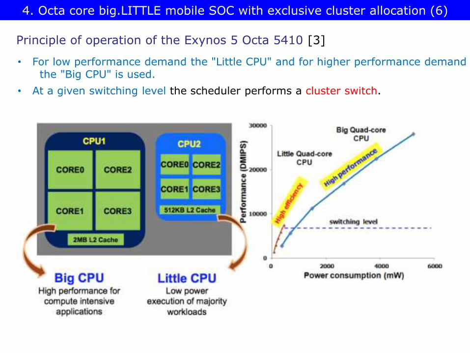
Principle of operation of the Exynos 5 Octa 5410 [3]
• For low performance demand the "Little CPU" and for higher performance demandthe "Big CPU" is used.
• At a given switching level the scheduler performs a cluster switch.
4. Octa core big.LITTLE mobile SOC with exclusive cluster allocation (6)

4. Octa core big.LITTLE mobile SOC with exclusive cluster allocation (7)
Performance points of operation of the LITTLE and big clusters [4]

Remark
• In a White Paper [66] Samsung's engineers compare asynchronous architectureswith per-core DVFS and synchronous big.LITTLE architectures concerning theirenergy efficiency.
• Their conclusion is that concerning the energy efficiency (e.g. power consumptionperformance) or net energy consumption the big.LITTLE architecture is superiorvs. the per-core DVFS for the majority of commonly used applications,such as e-mail messaging, web browsing or multimedia playback.
• The reason is performance degradations due to cache misses or transferring databetween different cores.
• Based on this finding Samsung implemented the big.LITTLE technology in theExynos 5410 with synchronous DVFS (meaning that all cores within a cluster run at the same voltage and frequency).
4. Octa core big.LITTLE mobile SOC with exclusive cluster allocation (8)

Performance and power results of the Exynos 5 Octa 5410 [2]
4. Octa core big.LITTLE mobile SOC with exclusive cluster allocation (9)

Remark
• According to sources there was a troublesome bug in the CCI-400 coherent businterface [3].
• Thus, Samsung disabled the coherency between the two clusters, and as aconsequence after cluster switches they need to invalidate all caches.
• Obviously, this has impeded performance and battery life.
4. Octa core big.LITTLE mobile SOC with exclusive cluster allocation (10)

5. Octa core big.LITTLE mobile SOCs supporting GTS
5.1: Octa core big.LITTLE mobile SOCs supporting GTS -Overview
•
5.2: The world's first octa core big.LITTLE mobile SOCsupporting GTS: The Exynos 5 Octa 5420 (2013)
•
5.4: Samsung's first 64-bit octa core big.LITTLE SOC operating in the ARMv8 AArch64 mode: the Exynos 7 Octa 7420 (2015)
•
5.5: Samsung’s first SoC including an in-house designedCPU core (the M1): the Exynos 8 Octa 8890 (2016)
•
5.3: Samsung's first 64-bit octa core big.LITTLE SOCsupporting GTS and operating in the ARMv8 Aarch32 mode: the Exynos 7 Octa 5433 (2014)
•
5.6: Samsung’s first 10 nm SOC: the Exynos 9 8895 (2017)•
5.7: Samsung’s first SOC supporting the DynamIQ clustertechnology: the Exynos 9 9810 (2018)
•

5.1 Octa core big.LITTLE mobile SOCs supporting GTS - Overview

5.1 Octa core big.LITTLE mobile SOCs supporting GTS - Overview (1)
5.1 Octa core big.LITTLE mobile SOCs supporting GTS – Overview
Exclusive cluster allocation
Symmetrical multicores
(SMPs)
big.LITTLE multicores
Samsung's quad- and octa core mobile SOCs
Exynos 4 Quad 4412 (2012)4x ARM A9
Exynos 7 Octa 7580 (2015)8x ARM A53
Exynos 7 Octa 7870 (2015)8x ARM A53
Exynos 7 Octa 7880 (2016)8x ARM A53
Exynos 5 Octa 5410 (2013)4x ARM A15 + 4x ARM A7
Exynos 5 Octa 5420 (2013)4x ARM A15 + 4x ARM A7
Exynos 5 Octa 5430 (2014)4x ARM A15 + 4x ARM A7
Exynos 5 Octa 5433 (2014)4x ARM A57 + 4x ARM A53
Exynos 7 Octa 7420 (2015)4x ARM A57 + 4x ARM A53
Exynos 7 Octa 7885 (2016)4x ARM A73 + 4x ARM A53
Exynos 8 Octa 8890 (2016)4x Samsung M1 + 4x ARM 53
Exynos 9 Series 8895 (2017)
4x Samsung M2 + 4x ARM 53
ARMv7 (32-bit)
ARMv8 (64-bit)
Inclusive core allocation
(Global Task Scheduling (GTS))
(Heterogeneous Multi-Processing) (HPM)
Exynos 9 Series 9810 (2018)
4x Samsung M3 + 4x ARM 55
First commercial octa-coreprocessor

5.1 Octa core big.LITTLE mobile SOCs supporting GTS - Overview (2)
Evolution of the scheduling techniques [5]
Remark
• In CPU allocation there are big.LITTLE core pairs and the scheduler can activateeither the big or the LITTLE core from each core pair.
• No commercial implementation is known using the CPU allocation.

5.1 Octa core big.LITTLE mobile SOCs supporting GTS - Overview (3)
Example for Global Task Scheduling (GTS) [72]

5.1 Octa core big.LITTLE mobile SOCs supporting GTS - Overview (4)
Benefits of GTS scheduling (designated as big.LITTLE MP in the Figure below)vs. exclusive cluster allocation [6]

Overview of early big.LITTLE implementations supporting GTS
5.1 Octa core big.LITTLE mobile SOCs supporting GTS - Overview (5)
Model Year Cores Techn.Integrated
modem
Samsung Exynos 5 Octa 5420 2013 4x A7 + 4x A15 28 nm no
Samsung Exynos 5 Octa 5422 2014 4x A7 + 4x A15 28 nm no
Samsung Exynos 5 Hexa 5260 2014 4x A7 + 2x A15 28 nm no
Samsung Exynos 5 Octa 5430 2014 4x A7 + 4x A15 20 nm no
Samsung Exynos 7 Octa 5433 2014 4x A53 + 4x A57 20 nm no
Samsung Exynos 7 Octa 7420 2015 4x A53 + 4x A57 14 nm no
Samsung Exynos 8 Octa 8890 2015 4x A53 + 4x M1 14 nm yes
Qualcomm Snapdagon S 808 2014 4x A53 + 2x A57 20 nm no
Qualcomm Snapdagon S 810 2015 4x A53 + 4x A57 20 nm no
Qualcomm Snapdagon S 820 20162x Kryo 1.7 GHz + 2x Kryo 2.2 GHz
14 nmFnFET
no
MediaTek MT8135 2013 2x A7 + 2x A15 28 nm no
MediaTek MT6595 2014 4x A7 + 4x A17 28 nm yes
MediaTek MT6797 2015 8x A53+ 2x A57 20 nm yes
Renesas MP 6530 2013 2x A7 + 2x A15 28 nm yes
Allwinner UltraOcta A80 2014 4x A7 + 4x A15 28 nm no

5.1 Octa core big.LITTLE mobile SOCs supporting GTS - Overview (6)
Use of an integrated application processor and modem
Integration of the application processor and the modem
Qualcomm’s MSM products (since ~ 1996)including their Snapdragon families
Use of a discrete application processor and modem
MediaTek’s 6xxx/8xxx families (since ~ 2007)except the 81xx line
Integration of the application processor and the modem
Samsung’s Exynos 3/4/5/7 families(since ~ 2010)
• Integrating the modem into the chip results in less costs and shorter time to market.
• Qualcomm pioneered this move by designing integrated parts already about 1996.
Samsung’s Exynos 8 (8890)(2015)
Intel’s Atom line (2008)except recent Atom X3 (Sophia (2015)
Intel’s Atom X3 (Sophia) (2015)
NVIDIA’s Tegra 2-4, K1 (since 2011) NVIDIA’s Tegra 4i (2014)
Apple’s own processor designs(even with the latest A10 (2016)
X
X
(2015)
(2016)
X : means cancelled

Samsung Exynos SoCs Specifications
SoC Exynos 9810 Exynos 8895
CPU
4x Exynos M3 @ 2.9 GHz4x 512KB L2 ??
4x Cortex A55 @ 1.9 GHz4x 128KB L2
4096KB L3 DSU ??
4x Exynos M2 @ 2.314 GHz2048KB L2
4x Cortex A53 @ 1.690GHz512KB L2
GPU Mali G72MP18Mali G71MP20
@ 546MHz
MemoryController
4x 16-bit CHLPDDR4x @ 1794MHz
4x 16-bit CHLPDDR4x @ 1794MHz
28.7GB/s B/W
Media10bit 4K120 encode & decode
H.265/HEVC, H.264, VP94K120 encode & decodeH.265/HEVC, H.264, VP9
Modem
Shannon Integrated LTE(Category 18/13)
DL = 1200 Mbps6x20MHz CA, 256-QAM
UL = 200 Mbps2x20MHz CA, 256-QAM
Shannon 355 Integrated LTE(Category 16/13)
DL = 1050 Mbps5x20MHz CA, 256-QAM
UL = 150 Mbps2x20MHz CA, 64-QAM
ISPRear: 24MPFront: 24MP
Dual: 16MP+16MP
Rear: 28MPFront: 28MP
Mfc.Process
Samsung 10nm LPP Samsung 10nm LPE
Main features of the Exynos 9810 vs. the Exynos 8995 [68]
5.7.1 The Exynos 9 Series 9810 – Overview (2)

5.1 Octa core big.LITTLE mobile SOCs supporting GTS - Overview (7)
SoC CPUGPU
Memorytechnology
Availability
Utilizing devices(examples)Model number fab
Instr. set
CoresNo of cores
fc(GHz)
Exynos 5 Octa(Exynos 5420)
28 nm HKMG
ARMv7
Cortex-A15+Cortex-A7
4+41.8-1.91.2-1.3
ARM Mali-T628 MP6 @ 533 MHz;
109 GFLOPS
32-bit DCh LPDDR3e-1866 (14.9 GB/sec)
Q3 2013
Samsung Chromebook 2 11.6", Samsung Galaxy
Note 3/Note 10.1/Note Pro 12.2, Samsung Galaxy Tab
Pro/Tab S
Exynos 5 Octa(Exynos 5422)
28 nm HKMG
Cortex-A15+Cortex-A7
4+41.9-2.11.3-1.5
ARM Mali-T628 MP6 @ 533 MHz
109 GFOPS
32-bit DCh LPDDR3/DDR3-
1866 (14.9 GB/sec)
Q2 2014
Samsung Galaxy S5 (SM-G900H)
Exynos 5 Octa(Exynos 5800)
28 nm HKMG
Cortex-A15+Cortex-A7
4+42.11.3
ARM Mali-T628 MP6 @ 533 MHz
109 GFLOPS
32-bit DCh LPDDR3/DDR3-
1866 (14.9 GB/sec)
Q2 2014
Samsung Chromebook 2 13,3"
Exynos 5 Octa(Exynos 5430)
20 nm HKMG
Cortex-A15+Cortex-A7
4+41.8-2.01.3-1.5
ARM Mali-T628 MP6 @ 600 MHz;
122 GFLOPS
32-bit DCh LPDDR3e/DDR3-
2132 (17.0 GB/sec)
Q3 2014
Samsung Galaxy Alpha (SM-G850F)
Exynos 7 Octa(Exynos 5433
20 nm HKMG
ARMv8-A
Cortex-A57+Cortex-A53
4+41.91.3
Mali-T760 MP6 @ 700 MHz; 206 GFLOPS (FP16)
32-bits DChLPDDR3-1650(13.2 GB/s)
Q3/Q4 2014
Samsung Galaxy Note 4 (SM-N910C)
Exynos 7 Octa(Exynos 7420)
14 nmFinFET
Cortex-A57+Cortex-A53
4+42.11.5
Mali-T760 MP8 @ 772 MHz; 227 GFLOPS (FP16)
32-bits DChLPDDR4-3104(24.9 GB/s)
Q2 2015
Samsung Galaxy S6S6 Edge
Exynos 7 Octa(Exynos 7885)
14 nmHKMG
Cortex-A73+Cortex-A53
4+42.21.6
Mali-G71 MP232-bits DChLPDDR4x
Q1 2016
Samsung Galaxy A8
Exynos 8 Octa(Exynos 8890)
14 nmFinFET
Samsung M1+
Cortex-A534+4
2.6-2.31.6
Mali-T880 MP12 @ 650 MHz; 265.2 GFLOPS (FP16)
32-bits DChLPDDR4-3588(28.7 GB/s)
Q1 2016
Samsung Galaxy S7Samsung Galaxy S7 Edge
Exynos 9 Series (Exynos 8895)
10 nmFinFET
Samsung M2+
Cortex-A534+4
2.51.7
Mali-G71 MP2032-bits DCh?
LPDDR4xQ2
2017Samsung Galaxy S8
Samsung Galaxy S8 Plus
Exynos 9 Series (Exynos 9810)
10 nmFinFET
Samsung M3+
Cortex-A554+4
2.91.9
Mali-G72 MP1832-bits DCh?
LPDDR4xQ1
2018Samsung Galaxy S9
Samsung Galaxy S9 Plus
Main features of Samsung’s octa core big.LITTLE SOCs supporting GTS

5.1 Octa core big.LITTLE mobile SOCs supporting GTS - Overview (8)
• big.LITTLE technology needs suitable OS support for scheduling tasks to theright computing resources to achieve the least possible power consumption.
• ARM and Linaro jointly develop OS support fo GTS, these become available
first as Linux or Android patch sets, later also they will be included intothe mainstream Linux or - Android kernels.
• As an example, ARM/Linaro's IPA (Intelligent Power Management) became firstavailable as a Linaro patch set in 09/2014 and then it was included intoLinux 4.10 in 8/2015.
• It is stated that "software represents the Achilles' heel of the technology andseverely limits its potential [57].
• In the Chapter on big-LITTLE processing we give an overview of the OS supportof GTS.
OS support for GTS
Remark
Linaro is a non-profit foundation of interested firms to foster open source Linuxpackages that are optimized for ARM architectures.
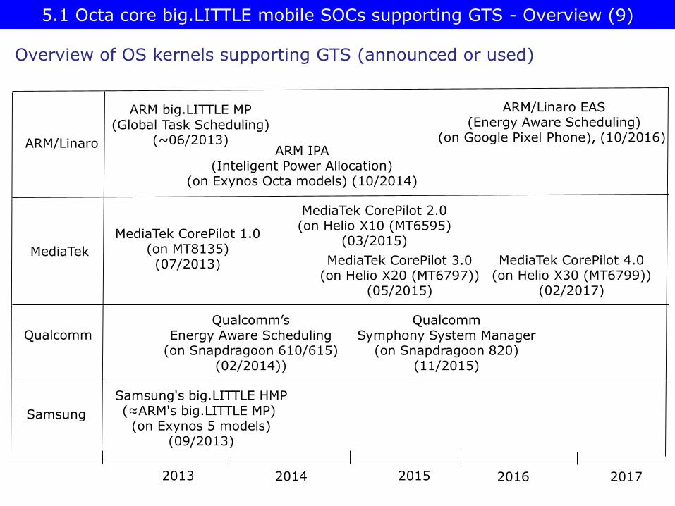
5.1 Octa core big.LITTLE mobile SOCs supporting GTS - Overview (9)
Overview of OS kernels supporting GTS (announced or used)
ARM/Linaro
MediaTek
Qualcomm
2013 2014 2015
ARM big.LITTLE MP(Global Task Scheduling)
(~06/2013)
Samsung's big.LITTLE HMP(≈ARM's big.LITTLE MP)
(on Exynos 5 models)(09/2013)
ARM/Linaro EAS(Energy Aware Scheduling)
(on Google Pixel Phone), (10/2016)
MediaTek CorePilot 1.0(on MT8135)(07/2013)
MediaTek CorePilot 2.0(on Helio X10 (MT6595)
(03/2015)
MediaTek CorePilot 3.0(on Helio X20 (MT6797))
(05/2015)
Qualcomm’sEnergy Aware Scheduling
(on Snapdragoon 610/615)(02/2014))
QualcommSymphony System Manager
(on Snapdragoon 820)(11/2015)
Samsung
ARM IPA(Inteligent Power Allocation)
(on Exynos Octa models) (10/2014)
2016 2017
MediaTek CorePilot 4.0(on Helio X30 (MT6799))
(02/2017)

5.2: The world's first octa core big.LITTLE mobile SOC supporting GTS: Samsungs's Exynos 5 Octa 5420 (2013)

5.2 The Exynos 5 Octa 5420 (1)
5.2: The world's first octa core big.LITTLE mobile SOCsupporting GTS: Samsungs's Exynos 5 Octa 5420 (2013) [2]
• It is a 32-bit ARMv7 mobile processor.
• Announced in 03/2013, launched in Galaxy S4 models in 4/2013.
• Task scheduling supports GTS, called HMP (Heterogeneous Multi-Processing)
by Samsung.

5.2 The Exynos 5 Octa 5420 (2)
Main features of Samsung's Exynos 5 Octa 5420 (2013)
SoC CPUGPU
Memorytechnology
Availability
Utilizing devices(examples)Model number fab
Instr. set
CoresNo of cores
fc(GHz)
Exynos 5 Octa(Exynos 5420)
28 nm HKMG
ARMv7
Cortex-A15+Cortex-A7
4+41.8-1.91.2-1.3
ARM Mali-T628 MP6 @ 533 MHz;
109 GFLOPS
32-bit DCh LPDDR3e-1866 (14.9 GB/sec)
Q3 2013
Samsung Chromebook 2 11.6", Samsung Galaxy
Note 3/Note 10.1/Note Pro 12.2, Samsung Galaxy Tab
Pro/Tab S
Exynos 5 Octa(Exynos 5422)
28 nm HKMG
Cortex-A15+Cortex-A7
4+41.9-2.11.3-1.5
ARM Mali-T628 MP6 @ 533 MHz
109 GFOPS
32-bit DCh LPDDR3/DDR3-
1866 (14.9 GB/sec)
Q2 2014
Samsung Galaxy S5 (SM-G900H)
Exynos 5 Octa(Exynos 5800)
28 nm HKMG
Cortex-A15+Cortex-A7
4+42.11.3
ARM Mali-T628 MP6 @ 533 MHz
109 GFLOPS
32-bit DCh LPDDR3/DDR3-
1866 (14.9 GB/sec)
Q2 2014
Samsung Chromebook 2 13,3"
Exynos 5 Octa(Exynos 5430)
20 nm HKMG
Cortex-A15+Cortex-A7
4+41.8-2.01.3-1.5
ARM Mali-T628 MP6 @ 600 MHz;
122 GFLOPS
32-bit DCh LPDDR3e/DDR3-
2132 (17.0 GB/sec)
Q3 2014
Samsung Galaxy Alpha (SM-G850F)
Exynos 7 Octa(Exynos 5433
20 nm HKMG
ARMv8-A
Cortex-A57+Cortex-A53
4+41.91.3
Mali-T760 MP6 @ 700 MHz; 206 GFLOPS (FP16)
32-bits DChLPDDR3-1650(13.2 GB/s)
Q3/Q4 2014
Samsung Galaxy Note 4 (SM-N910C)
Exynos 7 Octa(Exynos 7420)
14 nmFinFET
Cortex-A57+Cortex-A53
4+42.11.5
Mali-T760 MP8 @ 772 MHz; 227 GFLOPS (FP16)
32-bits DChLPDDR4-3104(24.9 GB/s)
Q2 2015
Samsung Galaxy S6S6 Edge
Exynos 7 Octa(Exynos 7885)
14 nmHKMG
Cortex-A73+Cortex-A53
4+42.21.6
Mali-G71 MP232-bits DChLPDDR4x
Q1 2016
Samsung Galaxy A8
Exynos 8 Octa(Exynos 8890)
14 nmFinFET
Samsung M1+
Cortex-A534+4
2.6-2.31.6
Mali-T880 MP12 @ 650 MHz; 265.2 GFLOPS (FP16)
32-bits DChLPDDR4-3588(28.7 GB/s)
Q1 2016
Samsung Galaxy S7Samsung Galaxy S7 Edge
Exynos 9 Series (Exynos 8895)
10 nmFinFET
Samsung M2+
Cortex-A534+4
2.51.7
Mali-G71 MP2032-bits DCh?
LPDDR4xQ2
2017Samsung Galaxy S8
Samsung Galaxy S8 Plus
Exynos 9 Series (Exynos 9810)
10 nmFinFET
Samsung M3+
Cortex-A554+4
2.91.9
Mali-G72 MP1832-bits DCh?
LPDDR4xQ1
2018Samsung Galaxy S9
Samsung Galaxy S9 Plus

5.2 The Exynos 5 Octa 5420 (3)
LPDDR3/DDR3-186632-bit
7.46 GB/s
LPDDR3/DDR3-186632-bit
7.46 GB/s
Block diagram of Samsung's Exynos 5 Octa 5420 [7]
SCU: Snoop Control Unit
CCI: Cache CoherentInterconnect

5.2 The Exynos 5 Octa 5420 (4)
Contrasting GTS with exclusive cluster switching (Based on [8])
Heterogeneous Mult-Processing (HMP)
Cluster allocation
Exynos 5 Octa5410
Exynos 5 Octa5420
A15
A7

• The 5420 was followed by the 5422, it is Samsung’s second octa core big.LITTLEprocessor operating under GTS, announced in 2/2014, available in Q1 2014.
• It is basically a faster variant of the 5420, as seen in the next Figure.
5.2 The Exynos 5 Octa 5420 (5)
Remark [9]

SCU: Snoop Control Unit
CCI: Cache CoherentInterconnect
Block diagram of the Samsung Exynos 5 Octa 5422 [10]
5.2 The Exynos 5 Octa 5420 (6)

Samsung’s subsequent big.LITTLE models supporting GTS
• In 8/2014 Samsung announced their first 20 nm octa core big.LITTLE processor, the Exynos 5 Octa 5430 with 4 Cortex-A15 and 4 Cortex-A7 cores.
Due to the new low-power High-K Metal Gate (HKMG) process technology power consumption of this processor could be lowered by 28 % compared to the previous 28 nm technology [11].
• About the same time Samsung unveiled also the Exynos 5 Octa 5433, that included 4 Cortex-A57 and 4 Cortex-A53 64-bit cores but runs in 32-bit mode (called AArch32 mode).
The Exynos 5 Octa 5433 incorporates the Mali T760 GPU that is claimed to offer76 % more performance than the previous Mali T628
• Later (in 10/2014) Samsung introduced the Exynos 7 Octa 7420 that includedthe same cores as the Exynos 5 Octa 5 5433 but runs already in 64-bit mode(AArch64).
Samsung announced about 57 % performance increase over the Exynos 5 Octa5433 implementation [12].
• Subsequently, the Examples 2 and 3 give some more details about the Exynos 5 Octa 5433 and the Exynos 7 Octa 7420.
5.2 The Exynos 5 Octa 5420 (7)

5.3: Samsung's first 64-bit octa core big.LITTLE mobile processor supporting GTS and operating in the
ARMv8 Aarch32 mode: the Exynos 5 Octa 5433 (2014)

5.3 The Exynos 5 Octa 5433 (1)
• The Exynos 5 Octa 5433 is Samsung's first mobile processor built up of ARMv8 cores, but it operates in the AARch32 execution mode [13].
This is the reason why the model designation starts with 5 instead of 7.
• Nevertheless, it takes advantage in the architectural improvements of theAarchv8 cores (actually the Cortex-A57 and Cortex-A53 cores), as indicatednext in the performance ranking of this processor.
5.3: Samsung's first 64-bit octa core big.LITTLE SOC supportingGTS and operating in the ARMv8 Aarch32 mode: the Exynos 5 Octa 5433 (2014)

5.3 The Exynos 5 Octa 5433 (2)
Main features of Samsung's Exynos 5 Octa 5433 (2014)
SoC CPUGPU
Memorytechnology
Availability
Utilizing devices(examples)Model number fab
Instr. set
CoresNo of cores
fc(GHz)
Exynos 5 Octa(Exynos 5420)
28 nm HKMG
ARMv7
Cortex-A15+Cortex-A7
4+41.8-1.91.2-1.3
ARM Mali-T628 MP6 @ 533 MHz;
109 GFLOPS
32-bit DCh LPDDR3e-1866 (14.9 GB/sec)
Q3 2013
Samsung Chromebook 2 11.6", Samsung Galaxy
Note 3/Note 10.1/Note Pro 12.2, Samsung Galaxy Tab
Pro/Tab S
Exynos 5 Octa(Exynos 5422)
28 nm HKMG
Cortex-A15+Cortex-A7
4+41.9-2.11.3-1.5
ARM Mali-T628 MP6 @ 533 MHz
109 GFOPS
32-bit DCh LPDDR3/DDR3-
1866 (14.9 GB/sec)
Q2 2014
Samsung Galaxy S5 (SM-G900H)
Exynos 5 Octa(Exynos 5800)
28 nm HKMG
Cortex-A15+Cortex-A7
4+42.11.3
ARM Mali-T628 MP6 @ 533 MHz
109 GFLOPS
32-bit DCh LPDDR3/DDR3-
1866 (14.9 GB/sec)
Q2 2014
Samsung Chromebook 2 13,3"
Exynos 5 Octa(Exynos 5430)
20 nm HKMG
Cortex-A15+Cortex-A7
4+41.8-2.01.3-1.5
ARM Mali-T628 MP6 @ 600 MHz;
122 GFLOPS
32-bit DCh LPDDR3e/DDR3-
2132 (17.0 GB/sec)
Q3 2014
Samsung Galaxy Alpha (SM-G850F)
Exynos 7 Octa(Exynos 5433
20 nm HKMG
ARMv8-A
Cortex-A57+Cortex-A53
4+41.91.3
Mali-T760 MP6 @ 700 MHz; 206 GFLOPS (FP16)
32-bits DChLPDDR3-1650(13.2 GB/s)
Q3/Q4 2014
Samsung Galaxy Note 4 (SM-N910C)
Exynos 7 Octa(Exynos 7420)
14 nmFinFET
Cortex-A57+Cortex-A53
4+42.11.5
Mali-T760 MP8 @ 772 MHz; 227 GFLOPS (FP16)
32-bits DChLPDDR4-3104(24.9 GB/s)
Q2 2015
Samsung Galaxy S6S6 Edge
Exynos 7 Octa(Exynos 7885)
148 nmHKMG
Cortex-A73+Cortex-A53
4+42.21.6
Mali-G71 MP232-bits DChLPDDR4x
Q1 2016
Samsung Galaxy A8
Exynos 8 Octa(Exynos 8890)
14 nmFinFET
Samsung M1+
Cortex-A534+4
2.6-2.31.6
Mali-T880 MP12 @ 650 MHz; 265.2 GFLOPS (FP16)
32-bits DChLPDDR4-3588(28.7 GB/s)
Q1 2016
Samsung Galaxy S7Samsung Galaxy S7 Edge
Exynos 9 Series (Exynos 8895)
10 nmFinFET
Samsung M2+
Cortex-A534+4
2.51.7
Mali-G71 MP2032-bits DCh?
LPDDR4xQ2
2017Samsung Galaxy S8
Samsung Galaxy S8 Plus
Exynos 9 Series (Exynos 9810)
10 nmFinFET
Samsung M3+
Cortex-A554+4
2.91.9
Mali-G72 MP1832-bits DCh?
LPDDR4xQ1
2018Samsung Galaxy S9
Samsung Galaxy S9 Plus

5.3 The Exynos 5 Octa 5433 (4)
Performance ranking of the Exynos 7 Octa 5433 based on the AnTuTu v4.0benchmark [14]

Main features of Samsung’s Exynos 5 Octa SOCs [13]
5.3 The Exynos 5 Octa 5433 (5)

5.3 The Exynos 5 Octa 5433 (6)
Block diagram of Samsung's Exynos 5 Octa 5433 mobile processor [15]
4x Cortex-A53
Mali T760 MP64x Cortex-A57

5.4: Samsung's first 64-bit octa core big.LITTLE SOC operating in the ARMv8 AArch64 mode: the Exynos 7 Octa 7420 (2015)
5.4.2 Introducing binning in form of ASV groups
5.4.1 The Exynos 7 Octa 7420 - Overview•
•
5.4.4 Introducing LPDDR4
5.4.3 Introducing AVS, called ASV
(Adaptive Scaling Voltage) by Samsung•
•
5.4.5 Implementing a hardware memory compressor•

5.4.1: The Exynos 7 Octa 7420 - Overview

5.4.1 The Exynos 7 Octa 7420 - Overview (1)
5.4.1: The Exynos 7 Octa 7420 - Overview
• The Exynos 7 Octa 7420 is the world's first 64-bit octa core big.LITTLE SOC
operating in the ARMv8 AArch64 mode-
• It is the world’s first application processor built on 14 nm FinFET.
• It is the core part of the Samsung Galaxy S6.
• The Exynos 7 Octa 7420 is the 14 nm shrink of the Exynos 5 5433 with majorenhancements, such as ASV (Adaptive Scaling Voltage).

5.4.1 The Exynos 7 Octa 7420 - Overview (2)
Main features of Samsung's Exynos 7 Octa 7420 (2015)
SoC CPUGPU
Memorytechnology
Availability
Utilizing devices(examples)Model number fab
Instr. set
CoresNo of cores
fc(GHz)
Exynos 5 Octa(Exynos 5420)
28 nm HKMG
ARMv7
Cortex-A15+Cortex-A7
4+41.8-1.91.2-1.3
ARM Mali-T628 MP6 @ 533 MHz;
109 GFLOPS
32-bit DCh LPDDR3e-1866 (14.9 GB/sec)
Q3 2013
Samsung Chromebook 2 11.6", Samsung Galaxy
Note 3/Note 10.1/Note Pro 12.2, Samsung Galaxy Tab
Pro/Tab S
Exynos 5 Octa(Exynos 5422)
28 nm HKMG
Cortex-A15+Cortex-A7
4+41.9-2.11.3-1.5
ARM Mali-T628 MP6 @ 533 MHz
109 GFOPS
32-bit DCh LPDDR3/DDR3-
1866 (14.9 GB/sec)
Q2 2014
Samsung Galaxy S5 (SM-G900H)
Exynos 5 Octa(Exynos 5800)
28 nm HKMG
Cortex-A15+Cortex-A7
4+42.11.3
ARM Mali-T628 MP6 @ 533 MHz
109 GFLOPS
32-bit DCh LPDDR3/DDR3-
1866 (14.9 GB/sec)
Q2 2014
Samsung Chromebook 2 13,3"
Exynos 5 Octa(Exynos 5430)
20 nm HKMG
Cortex-A15+Cortex-A7
4+41.8-2.01.3-1.5
ARM Mali-T628 MP6 @ 600 MHz;
122 GFLOPS
32-bit DCh LPDDR3e/DDR3-
2132 (17.0 GB/sec)
Q3 2014
Samsung Galaxy Alpha (SM-G850F)
Exynos 7 Octa(Exynos 5433
20 nm HKMG
ARMv8-A
Cortex-A57+Cortex-A53
4+41.91.3
Mali-T760 MP6 @ 700 MHz; 206 GFLOPS (FP16)
32-bits DChLPDDR3-1650(13.2 GB/s)
Q3/Q4 2014
Samsung Galaxy Note 4 (SM-N910C)
Exynos 7 Octa(Exynos 7420)
14 nmFinFET
Cortex-A57+Cortex-A53
4+42.11.5
Mali-T760 MP8 @ 772 MHz; 227 GFLOPS (FP16)
32-bits DChLPDDR4-3104(24.9 GB/s)
Q2 2015
Samsung Galaxy S6S6 Edge
Exynos 7 Octa(Exynos 7885
14 nmHKMG
Cortex-A73+Cortex-A53
4+42.21.6
Mali-G71 MP232-bits DChLPDDR4x
Q1 2016
Samsung Galaxy A8
Exynos 8 Octa(Exynos 8890)
14 nmFinFET
Samsung M1+
Cortex-A534+4
2.6-2.31.6
Mali-T880 MP12 @ 650 MHz; 265.2 GFLOPS (FP16)
32-bits DChLPDDR4-3588(28.7 GB/s)
Q1 2016
Samsung Galaxy S7Samsung Galaxy S7 Edge
Exynos 9 Series (Exynos 8895)
10 nmFinFET
Samsung M2+
Cortex-A534+4
2.51.7
Mali-G71 MP2032-bits DCh?
LPDDR4xQ2
2017Samsung Galaxy S8
Samsung Galaxy S8 Plus
Exynos 9 Series (Exynos 9810)
10 nmFinFET
Samsung M3+
Cortex-A554+4
2.91.9
Mali-G72 MP1832-bits DCh?
LPDDR4xQ1
2018Samsung Galaxy S9
Samsung Galaxy S9 Plus

5.4.1 The Exynos 7 Octa 7420 - Overview (3)
2x16 bit
2x16 bit
Assumed block diagram of Samsung's Exynos 7 Octa 7420 processor [16]

5.4.1 The Exynos 7 Octa 7420 - Overview (4)
A57 power curves of the Exynos 7 7420 vs. the Exynos 5 5433 [16]

5.4.1 The Exynos 7 Octa 7420 - Overview (5)
A53 power curves of the Exynos 7 7420 [16]

5.4.1 The Exynos 7 Octa 7420 - Overview (6)
Main innovations of the Samsung Exynos 7 7420
a) Introducing binning in form of ASV groups
b) Introducing AVS, called ASV (Adaptive Scaling Voltage) by Samsung
c) Using LPDDR4 memory technology
d) Implementing a hardware memory compressor

5.4.2 Introducing binning in form of ASV groups

5.4.2 Introducing binning in form of ASV groups (1)
5.4.2 Introducing binning in form of ASV groups
Before discussing Samsung's approach for binning let's recall traditional binning.

5.4.2 Introducing binning in form of ASV groups (2)
Traditional binning of processors-1
Electrical parameters of fabricated processor chips vary in a wide range, as illustratedfor the distribution of minimum core voltages needed to sustain a given clockfrequency, as measured post fabrication on the chips.

5.4.2 Introducing binning in form of ASV groups (3)
Example: Distribution of the minimum core voltage needed to sustain a given clock frequency measured on fabricated chips [17]
parts parts

5.4.2 Introducing binning in form of ASV groups (4)
Traditional binning of processors-2
• The distribution of electrical parameters on the fabricated chips will traditionallybe addressed by the manufacturers by testing all chips at the factory andclassifying them into a few number of groups, often called bins.
• These groups are considered then as different models of a processor line (termed also as SKUs (Stock Keeping Units)) with given sets of electrical parameters, first of all with different max. clock frequencies and will be soldtypically at different sales prices.
• As an example, the next Table shows different models (SKUs) of a givenprocessor line.

5.4.2 Introducing binning in form of ASV groups (5)
Product NameIntel Core2 Duo E6400
Intel Core2 Duo E6300
Intel Core2 Duo E4300
Code Name Conroe Conroe Conroe
Essentials
Processor Number E6400 E6300 E4300
Launch Date Q3'06 Q3'06 Q3'06
Lithography 65 nm 65 nm 65 nm
RecommendedCustomer Price
$128.00 N/A $106.00
Performance
# of Cores 2 2 2
Base Frequency 2.13 GHz 1.86 GHz 1.80 GHz
Cache 2 MB L2 2 MB L2 2 MB L2
Bus Speed 1066 MHz FSB 1066 MHz FSB 800 MHz FSB
TDP 65 W 65 W 65 W
VID Voltage Range 0.8500V-1.5V 0.8500V-1.5V 0.8500V-1.5V
Frequency bins of a given model (Intel's Core 2 Duo (2006))

5.4.2 Introducing binning in form of ASV groups (6)
• In the traditional way of binning fabricated chips are classified according totheir max. clock frequency into different groups and each group is soldas a different model of the same line, by contrast Samsung also tests their chips post manufacturing and assigns each chip to a group with similarcharacteristics, called an ASV group, but Samsung sells their chips of a givendesign only as a single model while marking each chip permanently withan ASV group identifier.
• For the Exynos Octa 7 7420 Samsung marks their chips with the ASV group identifiers ASV0 to ASV 15 by burning them into on-chip fuses.
A lower ASV value identifies a worse quality bin whereas a higher one a better quality bin.
Accordingly, ASV0 is the worst and ASV15 the best quality bin whereas bin 9represents the median group.
• As an example, the next Figure shows the target voltage vs. core frequencycharacteristics of the ASV groups.
Samsung's approach to meet variations of electrical parameters of chips [16]

5.4.2 Introducing binning in form of ASV groups (7)
Higher qualityASV group
ASV9
Core voltage - core frequency curves of the Exynos 7 Octa 7420 [16]
ASV 15
ASV 0

5.4.3 Introducing AVS, called ASV (Adaptive Scaling Voltage) by Samsung

5.4.3 Introducing AVS called ASV (Adaptive Scaling Voltage) by Samsung (1)
• Samsung's AVS technology is based on licensing National's PowerWise patentthat is owned now by Texas Instrument (TI), as TI acquired National Semiconductor in 2011.
• Main components of National's PowerWise technology are seen in the nextFigure.
5.4.3 Introducing AVS, called ASV (Adaptive Scaling Voltage) by Samsung

5.4.3 Introducing AVS called ASV (Adaptive Scaling Voltage) by Samsung (2)
Main components of National's PowerWise technology [16]

5.4.3 Introducing AVS called ASV (Adaptive Scaling Voltage) by Samsung (3)
Principle of operation of National's PowerWise technology (simplified)-1 [18]
• Based on the current activity of the considered core the OS forwards a Targetperformance index to the Clock Management Unit (CMU).
• The CMU forwards the Targer performance index to the Advanced PowerController (APC) and also sets the clock frequency of the Hardware Performance Monitor (HPM) to the value corresponding to the Target performance index (this is needed for measuring the actual speed of the core).
• The next step is voltage adjustment in a closed loop.
• The HPM measures the propagation delay of the delay line (critical path) and sends a Performance code (PC) to the APC.
• The APC compares the received PC with the Reference Calibration Code (RCC)that is burnt to on chip fuses and directs the Energy Management Unit (EMU) via the PowerWise Interface (PWI) accordingly.
• If the PC indicates that the propagation delay is longer than required, APMwill let the EMU to increase the core voltage (Vavs) to speed up the core andvice versa.
Nevertheless, depending on whether the gate delays on the chip are too long or too short there are two different avenues to follow subsequently.
Remark
The RCC is determined at the factory in a stress test, as the smallest PerformanceCode (PC) that allows a correct operation of the processor in the given frequency range, and it is burnt to on-chip fuses beyond the ASV identifier.

5.4.3 Introducing AVS called ASV (Adaptive Scaling Voltage) by Samsung (4)
• When the current performance needs to be increased by raising the current clockfrequency, first the supply voltage will be increased adaptively in theclosed loop and only subsequently, after the core voltage has already been adjusted will the clock rate be raised.
• To achieve this the APC informs the CMU about finishing the voltage adjustmentand then the CMU will change the core clock to the desired value.
• By contrast, when a lower performance is requested than recently existing,the ASP immediately instructs the CMU to reduce the clock frequency to the requested value.
• In parallel the core voltage (Vavs) will be adjusted in the closed loop to the appropriate value.
Principle of operation of National's PowerWise technology (simplified)-2 [18]

5.4.3 Introducing AVS called ASV (Adaptive Scaling Voltage) by Samsung (5)
Changing P-states in National's PowerWise technology [18]
Voltage adjustmentin a closed loop
Voltage adjustmentin a closed loop

5.4.3 Introducing AVS called ASV (Adaptive Scaling Voltage) by Samsung (6)
Differences between Samsung's and National's AVS implementations
aa) Implementing AVS in conjunction with ASV binning.
ab) Use of an ARM M3 microcontroller as the APC unit that communicateswith other units by mailbox messages.

5.4.3 Introducing AVS called ASV (Adaptive Scaling Voltage) by Samsung (7)
aa) Implementing AVS in conjunction with ASV binning
• Selecting the manufactured chips into up to 16 ASV groups has the benefitthat the measured Reference Calibration Code (RCC) will fit with a much lesstolerance to a particular chip than would in case when the manufactured chips would be selected into a much less number of models.
• This has a further benefit since then the voltage adjusting process becomes shorter.

5.4.3 Introducing AVS called ASV (Adaptive Scaling Voltage) by Samsung (8)
ab) Use of an ARM M3 microcontroller as the APC unit that communicateswith other units by mailbox messages [16]
• Instead of making use of the Advanced Power Controller (APC) unit offered by National as part of the PowerWise technology Samsung implementsthe APC in form of an ARM M3 microcontroller.
• The M3 communicates with the other system components by mailboxmessages.
Mailboxes represent a kind of interprocess communication that is usedtypically between different architectures such that each unit can only writemessages to its own mailbox (being in the RAM space) but is able to read all other mailboxes.

5.4.3 Introducing AVS called ASV (Adaptive Scaling Voltage) by Samsung (9)
Reducing core voltage and power consumption by using AVS in theExynos 7 7420 vs. the 5 5433 for different clock rates and ASV groups [19]
(Note: Data are not corresponding to the previous figure).

5.4.4 Introducing LPDDR4

5.4.4 Introducing LPDDR4 (1)
5.4.4 Introducing LPDDR4
Using LPDDR4 almost doubles the memory transfer rate of the 32-bit dual channelmemory compared to the LPDDR3's implemented in the Exynos 7 5433 model, actually from 1650 MT/s to 3104 MT/s.

5.4.5 Implementing a hardware memory compressor

5.4.5 Implementing a hardware memory compressor (1)
5.4.5 Implementing a hardware memory compressor [16]
• This is a hardware unit, called M-Comp on the block diagram of the processorthat is designed especially for Android.
• We note that beginning with the Android 4.4 kernel DRAM compression hasalready become a validated part of the OS and all devices support this feature.
• Most vendors support it by the “zram” mechanism, which is a ramdisk with compression support.
The kernel makes use of it as a swapping device to store rarely used memorypages.
Also Samsung had implemented this compression mechanism in their Galaxy devices as far back as Android 4.1.
• The Galaxy S6 implements a more advanced compressor scheme called “zswap”which is able to compress memory pages before they need to get swapped out to a swap device, so it’s a more optimized mechanism that sits closer to the kernel’s memory management part.
As an example "zswap" may compress 1.21GB of pages into 341MB of physical memory.
This is however yet a software implementation running on the CPU cores.
• The available dedicated hardware compressor (M-Comp) is currently not yet activated and its use needs OS support to be provided in a future OS update.

5.5: Samsung’s first SoC including an in-house designedCPU core (the M1): the Exynos 8 Octa 8890 (2016)
5.5.2 The M1 (Mongoose) core
5.5.1 The Exynos 8 Octa 8890 - Overview•
•

5.5.1 The Exynos 8 Octa 8890 - Overview

The Exynos 8 Octa 8890 - Overview (1)
5.5.1 The Exynos 8 Octa 8890 - Overview
• It is fabricated based on Samsung's 2. gen. 14 nm (Low-Power Plus (LPP)
FinFET process.
• It is the kernel piece of Samsung's Galaxy S7, S7 Edge and Galaxy Note 7.
• Introduced in Q1/2016.

The Exynos 8 Octa 8890 - Overview (2)
Main features of Samsung's Exynos 8 Octa 8890 (2016)
SoC CPU
GPUMemory
technology
Availab
ility
Utilizing devices
(examples)Model number fabInstr.
setCores
No of
cores
fc
(GHz)
Exynos 5 Octa
(Exynos 5420)
28 nm
HKMG
ARM
v7
Cortex-A15+
Cortex-A74+4
1.8-1.9
1.2-1.3
ARM Mali-T628 MP6
@ 533 MHz;
109 GFLOPS
32-bit DCh LPDDR3e-
1866 (14.9 GB/sec)
Q3
2013
Samsung Chromebook 2
11.6", Samsung Galaxy Note
3/Note 10.1/Note Pro 12.2,
Samsung Galaxy Tab Pro/Tab
S
Exynos 5 Octa
(Exynos 5422)
28 nm
HKMG
Cortex-A15+
Cortex-A74+4
1.9-2.1
1.3-1.5
ARM Mali-T628 MP6
@ 533 MHz 109
GFOPS
32-bit DCh
LPDDR3/DDR3-1866
(14.9 GB/sec)
Q2
2014
Samsung Galaxy S5
(SM-G900H)
Exynos 5 Octa
(Exynos 5800)
28 nm
HKMG
Cortex-A15+
Cortex-A74+4
2.1
1.3
ARM Mali-T628 MP6
@ 533 MHz
109 GFLOPS
32-bit DCh
LPDDR3/DDR3-1866
(14.9 GB/sec)
Q2
2014
Samsung Chromebook 2
13,3"
Exynos 5 Octa
(Exynos 5430)
20 nm
HKMG
Cortex-A15+
Cortex-A74+4
1.8-2.0
1.3-1.5
ARM Mali-T628 MP6
@ 600 MHz;
122 GFLOPS
32-bit DCh
LPDDR3e/DDR3-2132
(17.0 GB/sec)
Q3
2014
Samsung Galaxy Alpha (SM-
G850F)
Exynos 7 Octa
(Exynos 5433
20 nm
HKMG
ARM
v8-A
Cortex-A57+
Cortex-A534+4
1.9
1.3
Mali-T760 MP6 @
700 MHz; 206
GFLOPS (FP16)
32-bits DCh LPDDR3-
1650 (13.2 GB/s)
Q3/Q4
2014
Samsung Galaxy Note 4 (SM-
N910C)
Exynos 7 Octa
(Exynos 7420)
14 nm
FinFET
Cortex-A57+
Cortex-A534+4
2.1
1.5
Mali-T760 MP8 @
772 MHz; 227
GFLOPS (FP16)
32-bits DCh LPDDR4-
3104 (24.9 GB/s)
Q2
2015
Samsung Galaxy S6
S6 Edge
Exynos 7 Octa
(Exynos 7885)
14 nm
HKMG
Cortex-A73+
Cortex-A534+4
2.2
1.6Mali-G71 MP2 32-bits DCh LPDDR4x
Q1
2016Samsung Galaxy A8
Exynos 8 Octa
(Exynos 8890)
14 nm
FinFET
Samsung M1+
Cortex-A534+4
2.6-2.3
1.6
Mali-T880 MP12 @
650 MHz; 265.2
GFLOPS (FP16)
32-bits DCh LPDDR4-
3588 (28.7 GB/s)
Q1
2016
Samsung Galaxy S7
Samsung Galaxy S7 Edge
Exynos 9 Series
(Exynos 8895)
10 nm
FinFET
Samsung M2+
Cortex-A534+4
2.5
1.7Mali-G71 MP20
32-bits DCh?
LPDDR4x
Q2
2017
Samsung Galaxy S8
Samsung Galaxy S8 Plus
Exynos 9 Series
(Exynos 9810)
10 nm
FinFET
Samsung M3+
Cortex-A554+4
2.9
1.9Mali-G72 MP18
32-bits DCh?
LPDDR4x
Q1
2018
Samsung Galaxy S9
Samsung Galaxy S9 Plus

The Exynos 8 Octa 8890 - Overview (3)
Main innovations of the Exynos 8 Octa 8890 processor
• It is built up as a big.LITTLE architecture while as big cores Samsungmakes use of their first in-house core design, designated as the M1 (Mongoose) core.
• It is based on Samsung's custom SCI (Samsung Coherent Interconnect) bus.
• It is Samsung's first application processor with an integrated modem.
Figure: Basic structure of Samsung's Eynos 8 Octa 8890 [20]

The Exynos 8 Octa 8890 - Overview (4)
High-End SoCs Specifications
SoCQualcomm
Snapdragon 820
Huawei
Kirin 950
Samsung
Exynos 8 Octa 8890
Samsung
Exynos 7 Octa 7420
CPU 2x [email protected]
4x Cortex A72 @2.3 Ghz
4x Cortex A53 @1.8Ghz
4x Exynos M1 @
2.60GHz
(1-2 core load)
2.29GHz
(3-4 core load)
Memory
Controller
2x 32-bit
LPDDR4 @
1803 MT/s
28.8GB/s b/w
2x 32-bit
LPDDR3 or LPDDR4 @
1333 MT/s
21.32 GB/s
2x 32-bit
LPDDR4 @
1794 MT/s
28.7GB/s b/w
2x 32-bit
LPDDR4 @
1555 MT/s
24.8GB/s b/w
GPUAdreno 530
@ 624 MHz
ARM Mali T860
, @ 900 MHzMali T880MP12
@ 650 MHz
Mali T770MP8
@ 770 MHz
Mfc.
Process
Samsung
14nm LPP
TSMC
16 nm FinFET+
Samsung
14nm LPP
Samsung
14nm LPE
Contrasting key features of high-end 14/16 nm mobile processors [21]

5.5.2 The M1 (Mongoose) core
5.5.2 The M1 (Mongoose) core (1)
Main features of the M1 (Mongoose) core
• It implements the ARMv8 ISA.
• It has a 4-wide front-end.
• It has neural net (perceptron) based branch prediction.
• The core is an out-of-order 2.6 GHz design.
• The core design lasted 3 years.
• Subsequently, we point out main features of the Mongoose core design.
5.5.2 The M1 (Mongoose) core

5.5.2 The M1 (Mongoose) core (2)
The overall microarchitecture of the M1 core [22]

5.5.2 The M1 (Mongoose) core (3)
Neural net based branch prediction [22]
5.5.2 The M1 (Mongoose) core (4)
Remarks on the use of perceptrons for branch prediction
• Each miss prediction causes a number of wasted cycles in instruction processing,the more the longer the instruction pipeline is.
• The efficiency of branch prediction and prefetching are decisive for the achievableILP and thus for the processor performance.
• Accordingly, the evolution of processors was accompanied by by the evolutionof branch prediction.
• Recent branch predictors consists of a number of dedicated predictors addressing different types of branches, like direct or indirect branches, loops etc.
• Perceptron based (called also neural) branch prediction was first suggested by Vintan (U. Sibiu) [23] in 1999 and then by Jimenez and Lin (U. Texas) [24]in (2001).

5.5.2 The M1 (Mongoose) core (5)
The perceptron model: a single layer perceptron [24]
• The perceptron, introduced in 1962, is in fact an artificial neuron.
• It receives a number of inputs (xi) that are bipolar (-1 or 1) and calculates anoutput value (y) that is the sum of the product of the input values (xi) andgiven weights (wi), as shown below.
• A perceptron can be trained to provide a prediction.
Figure: A single layer perceptron [24]

5.5.2 The M1 (Mongoose) core (6)
Principle of using perceptrons for branch prediction [24]
Figure: A single layer perceptron [24]
• Inputs (xi) are taken from branch history and are -1 or +1.
• The weights (wi) are small integer values that are learned by on-line training,
• Training finds correlation between history and outcome.
• The output (y) is the dot product of xi's and wi's, as shown below.
• The output (y) is interpreted as prediction is taken if y ≥ 0.
• Once the outcome of the prediction (y) becomes known the training algorithm
uses this value to update the weights (wi).

5.5.2 The M1 (Mongoose) core (7)
Published use of perceptrons (neural networks) for branch prediction
• AMD Bobcat (2011)
Jaguar (2013)
Piledriver (2012)
Zen (2017)
• Oracle SPARCT4 (2011)
• Samsung Exynos Octa 8 8890 M1 (Mongoose) core 2016

5.5.2 The M1 (Mongoose) core (8)
Implementation of perceptron based (neural) branch prediction [24]
• Actually there are no published details about the perceptron based (neural)branch predictors used in the processors enlisted above.
• As an example below we show AMD's related slide "revealing the use of neuralbranch prediction in their Zen processor (2017).

5.5.2 The M1 (Mongoose) core (9)
Example: Perceptron based branch prediction in AMD's Zen microarch. [58]

5.5.2 The M1 (Mongoose) core (10)
Achieved accuracy of recent sophisticated branch predictors
• Since 2004 the The Journal of Instruction-Level Parallelism organizes eachthird year a Championship Branch Prediction (CBP-1 to CPB5) [25].
• Presented predictors for conditional branches are evaluated on a given trace setby calculating the weighted average of Mispredictions Per Thousand Instructions
(MPTI).
• Predictors must be implemented within a fixed storage budget of 8 kB, 64 kB orunlimited.
• The best results reveal astonishingly low misprediction rates [26]:
Storage budget MPTI
8 KB 5.3
64 KB 4.1
Unlimited 3.0

5.5.2 The M1 (Mongoose) core (11)
Remarks on Samsung's perceptron based branch predictor implementation in Zen
• The designer of AMD's first branch prediction logic for the first microprocessor with a neural network branch predictor (AMD Bobcat) (James Dundas) left AMD and joined Samsung in 2012 [27].
• Also the Chief Architect of the Bobcat processor (Brad Burgess) left AMD, joinedSamsung and became the Chief CPU Architect in 2011 [28].

5.5.2 The M1 (Mongoose) core (12)
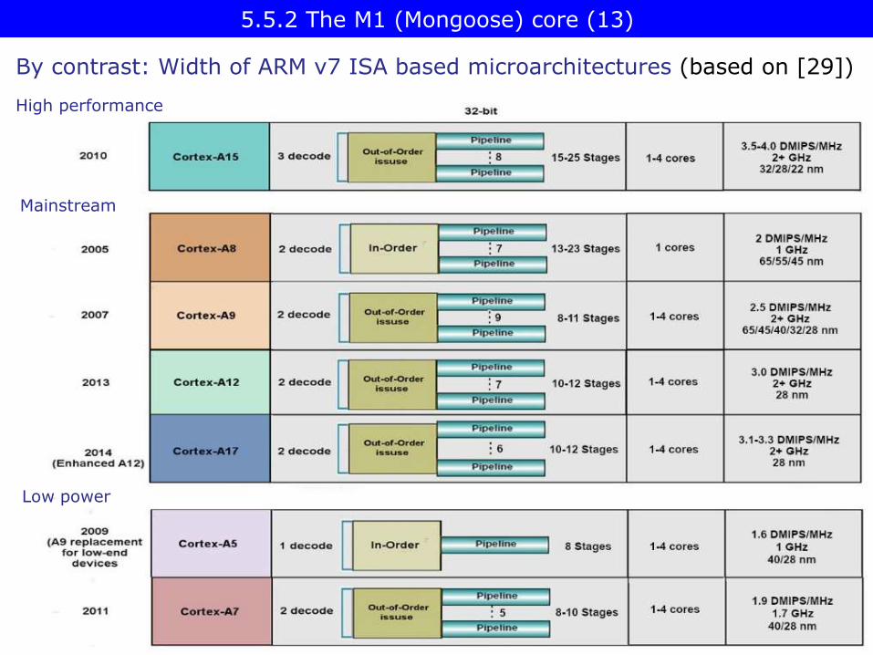
4-wide front end rather than 2 to 3 as in most mobiles [22]

Evolution of the width of mobile cores
3-wide2-wide 4-wide
Width of mobile cores(or of big cores of big.LITTLE or dynamIQ core clusters)
6-wide
ARM v7 Cortex-A (2005-09)except HP A15)/
LP 1-wide A5 (2009)
v7 HP Cortex-A15 (2010)
Intel Atom family(2008-15)
AMD Cat family(2011-2015)
Apple v7 Cortex-A8 (2009) v7 Swift (A6) (2012) v8 Cyclone (A7) (2013)and subsequent cores
Qualcomm v7 Scorpion(S1-S3) (2007-10)
v7 Krait(S4/S400/S60x/S80x)
(2012-14)
v8 Kryo/Kryo 280
(S820/821/835) (2015/2016/2017)
v8.2 Kryo 385 (S845) (2018)
Samsung v8 M1 (2016) (Exynos 8 Octa)
v8 M2 (2017)(Exynos 9 Octa)
v8.2 M3 (2018)(Exynos 9810)
v8.0 HP Cortex-A(2013-15) except HP Cortex-A73
v8.2 HP Cortex-A75 (2017)
v7 Exynos 5(2013-14)
v8 Exynos 7(2016)
v8.2 HP Cortex-A76(2018)
HP: High-Performance
LP: Low-Power
v8.0/8.2 LP Cortex-A
(2013-)/
HP Cortex-A73 (2016)
Airmont-based Atom core (2016)
5.5.2 The M1 (Mongoose) core (12b)
High performance
Mainstream
Low power
By contrast: Width of ARM v7 ISA based microarchitectures (based on [29])
5.5.2 The M1 (Mongoose) core (13)

Low power
High performance
By contrast: Width of ARM v8.0 ISA based microarchitectures (based on [29])
5.5.2 The M1 (Mongoose) core (14)

High performance
By contrast: Width of ARM v8.2 ISA based microarchitectures (based on [29])
5.5.2 The M1 (Mongoose) core (14b)

By contrast: Front-end width of Intel’s and AMD’s recent microarchitectures
• Intel introduced 4-wide front ends beginning with their Core 2 (2006).
• Since Skylake Intel widened the front-end of its processor to 5.
• AMD introduced 4-wide microarchitectures only five years later, along with theBulldozer line in 2011.
5.5.2 The M1 (Mongoose) core (15)
64-bit
Broadwell
Remarks

5.5.2 The M1 (Mongoose) core (16)
7-wide FX- and Load/Store scheduler [22]

5.5.2 The M1 (Mongoose) core (17)
2-wide FP-issue, FMAC and FADD operations [22]

5.5.2 The M1 (Mongoose) core (18)
Pipeline structure of the M1 [22]

5.5.2 The M1 (Mongoose) core (19)
Die layout of the M1 core [22]

5.5.2 The M1 (Mongoose) core (20)
Single-core performance of the 2.6 GHz M1 vs. the 2.1 GHz A57 [22]

5.5.2 The M1 (Mongoose) core (21)
Multi-core performance of the 2.3 GHz M1 vs. the 2.1 GHz A57 [22]

5.5.2 The M1 (Mongoose) core (22)
Single core power and efficiency data of the M1 vs. the A57 [22]

5.6 Samsung’s first 10 nm SOC: the Exynos 9 8895 (2017)
5.6.2 Integrating ARM’s next generation Mali-G71 GPU thatis based on ARM’s 3. gen. (Bifrost) GPU architecture
5.6.1 The Exynos 9 Series 8895 - Overview•
•
5.6.4 Support for LPDDR4x memory
5.6.3 HSA (Heterogeneous System Architecture) compliance•
•
5.6.5 Separate security processing unit•
5.6.6 Vision Processing Unit (VPU)•

5.6.1 The Exynos 9 Series 8895 - Overview

5.6.1 The Exynos 9 Series 8895 - Overview (1)
5.6.1 The Exynos 9 Series 8895 - Overview
• It is Samsung’s first SoC fabricated on their 10 nm FinFET process.
The 10nm FinFET process allows up to 27% higher performance or 40% lower
power consumption when compared to 14nm LPE FinFET [30].
• It is the kernel piece of one alternative of Samsung's Galaxy S8, S8+.
The other alternative is using Qualcomm's Snapdragon 835 for these mobiles(sold in the US).
• It was announced in 02/2017 and shipped in 04/2017.
LPE: Low Power Early

5.6.1 The Exynos 9 Series 8895 - Overview (2)
Main features of Samsung's Exynos 9 Octa 8895 (2017)
SoC CPU
GPUMemory
technology
Availab
ility
Utilizing devices
(examples)Model number fabInstr.
setCores
No of
cores
fc
(GHz)
Exynos 5 Octa
(Exynos 5420)
28 nm
HKMG
ARM
v7
Cortex-A15+
Cortex-A74+4
1.8-1.9
1.2-1.3
ARM Mali-T628 MP6
@ 533 MHz;
109 GFLOPS
32-bit DCh LPDDR3e-
1866 (14.9 GB/sec)
Q3
2013
Samsung Chromebook 2
11.6", Samsung Galaxy Note
3/Note 10.1/Note Pro 12.2,
Samsung Galaxy Tab Pro/Tab
S
Exynos 5 Octa
(Exynos 5422)
28 nm
HKMG
Cortex-A15+
Cortex-A74+4
1.9-2.1
1.3-1.5
ARM Mali-T628 MP6
@ 533 MHz 109
GFOPS
32-bit DCh
LPDDR3/DDR3-1866
(14.9 GB/sec)
Q2
2014
Samsung Galaxy S5
(SM-G900H)
Exynos 5 Octa
(Exynos 5800)
28 nm
HKMG
Cortex-A15+
Cortex-A74+4
2.1
1.3
ARM Mali-T628 MP6
@ 533 MHz
109 GFLOPS
32-bit DCh
LPDDR3/DDR3-1866
(14.9 GB/sec)
Q2
2014
Samsung Chromebook 2
13,3"
Exynos 5 Octa
(Exynos 5430)
20 nm
HKMG
Cortex-A15+
Cortex-A74+4
1.8-2.0
1.3-1.5
ARM Mali-T628 MP6
@ 600 MHz;
122 GFLOPS
32-bit DCh
LPDDR3e/DDR3-2132
(17.0 GB/sec)
Q3
2014
Samsung Galaxy Alpha (SM-
G850F)
Exynos 7 Octa
(Exynos 5433
20 nm
HKMG
ARM
v8-A
Cortex-A57+
Cortex-A534+4
1.9
1.3
Mali-T760 MP6 @
700 MHz; 206
GFLOPS (FP16)
32-bits DCh LPDDR3-
1650 (13.2 GB/s)
Q3/Q4
2014
Samsung Galaxy Note 4 (SM-
N910C)
Exynos 7 Octa
(Exynos 7420)
14 nm
FinFET
Cortex-A57+
Cortex-A534+4
2.1
1.5
Mali-T760 MP8 @
772 MHz; 227
GFLOPS (FP16)
32-bits DCh LPDDR4-
3104 (24.9 GB/s)
Q2
2015
Samsung Galaxy S6
S6 Edge
Exynos 7 Octa
(Exynos 7885)
14 nm
HKMG
Cortex-A73+
Cortex-A534+4
2.2
1.6Mali-G71 MP2 32-bits DCh LPDDR4x
Q1
2016Samsung Galaxy A8
Exynos 8 Octa
(Exynos 8890)
14 nm
FinFET
Samsung M1+
Cortex-A534+4
2.6-2.3
1.6
Mali-T880 MP12 @
650 MHz; 265.2
GFLOPS (FP16)
32-bits DCh LPDDR4-
3588 (28.7 GB/s)
Q1
2016
Samsung Galaxy S7
Samsung Galaxy S7 Edge
Exynos 9 Series
(Exynos 8895)
10 nm
FinFET
Samsung M2+
Cortex-A534+4
2.5
1.7Mali-G71 MP20
32-bits DCh?
LPDDR4x
Q2
2017
Samsung Galaxy S8
Samsung Galaxy S8 Plus
Exynos 9 Series
(Exynos 9810)
10 nm
FinFET
Samsung M3+
Cortex-A554+4
2.9
1.9Mali-G72 MP18
32-bits DCh?
LPDDR4x
Q1
2018
Samsung Galaxy S9
Samsung Galaxy S9 Plus

5.6.1 The Exynos 9 Series 8895 - Overview (3)
• It is built up further on a big.LITTLE architecture while as big cores Samsungemploys their second generation custom core, designated as the M2 (Mongoose)core.
• It is based on Samsung's upgraded custom SCI (Samsung Coherent Interconnect)bus (the SCI was introduced in the Exynos 8 Octa 8890).
Upgrading the SCI bus for supporting HSA (Heterogeneous System Architecture).
• Upgraded modem that implements
Main enhancements of the Samsung Exynos 9 Series 8995 [30]
• Cat 16 LTE for downloading at 1 Gbps by using 5x Carrier Aggregation and
• Cat 13 LTE for uploading at 150 Mbps by using 2x Carrier Aggregation.

Microarchitecture of the M1/M2 cores [67]
5.6.1 The Exynos 9 Series 8895 - Overview (4)

5.6.1 The Exynos 9 Series 8895 - Overview (5)
Key features of the microarchitecture of the M1/M2 cores (1)
The front-end part of the microarchitecture of the M1/M2 cores is 4-wide, i.e. thereare 4-wide in-order stages for decoding and dispatching.
This is an unusual wide front-end considering mobile cores, as seen in the nextslide.

Evolution of the width of mobile cores
3-wide2-wide 4-wide
Width of mobile cores(or of big cores of big.LITTLE or dynamIQ core clusters)
6-wide
ARM v7 Cortex-A (2005-09)except HP A15)/
LP 1-wide A5 (2009)
v7 HP Cortex-A15 (2010)
Intel Atom family(2008-15)
AMD Cat family(2011-2015)
Apple v7 Cortex-A8 (2009) v7 Swift (A6) (2012) v8 Cyclone (A7) (2013)and subsequent cores
Qualcomm v7 Scorpion(S1-S3) (2007-10)
v7 Krait(S4/S400/S60x/S80x)
(2012-14)
v8 Kryo/Kryo 280
(S820/821/835) (2015/2016/2017)
v8.2 Kryo 385 (S845) (2018)
Samsung v8 M1 (2016) (Exynos 8 Octa)
v8 M2 (2017)(Exynos 9 Octa)
v8.2 M3 (2018)(Exynos 9810)
v8.0 HP Cortex-A(2013-15) except HP Cortex-A73,
v8.2 HP Cortex-A75 (2017)
v7 Exynos 5(2013-14)
v8 Exynos 7(2016)
v8.2 HP Cortex-A76(2018)
HP: High-PerformanceLP: Low-Power
v8.0/8.2 LP Cortex-A(2013-)/
HP Cortex-A73 (2016)
Airmont-based Atom core (2016)
5.6.1 The Exynos 9 Series 8895 - Overview (6)

• Two simple ALU pipelines capable of integer additions.• A complex ALU handling simple operations as well as integer multiplication and
division.• A load unit port• A store unit port• Two branch prediction ports• Two floating point and vector operations ports leading to two mixed capability
pipelines.
5.6.1 The Exynos 9 Series 8895 - Overview (7)
Key features of the microarchitecture of the M1/M2 cores (2)
The back-end part of the M1/M2 microarchitecture includes 9 ports, as follows [67]:

5.6.1 The Exynos 9 Series 8895 - Overview (8)
Main innovations of the Exynos 9 Series 8995 [31]
a) Integrating ARM’s next generation Mali-G71 GPU that is based on ARM’s new Bifrost GPU architecture.
b) HSA (Heterogeneous System Architecture) compliant processor implementation.
c) Support for LPDDR4x memory.
d) Separate security processing unit.
e) Vision Processing Unit (VPU).

5.6.1 The Exynos 9 Series 8895 - Overview (9)
Samsung Exynos SoCs Specifications
SoC Exynos 8895 Exynos 8890 Exynos 7420
CPU
4x A53
4x Exynos M2(?)
4x Exynos M1 @ 2.3GHz
GPU Mali G71MP20Mali T880MP12
@ 650MHz
Mali T760MP8
@ 770MHz
Memory
Controller
2x 32-bit(?)
LPDDR4x
2x 32-bit
LPDDR4 @ 1794MHz
28.7GB/s b/w
2x 32-bit
LPDDR4 @ 1555MHz
24.8GB/s b/w
Storage eMMC 5.1, UFS 2.1 eMMC 5.1, UFS 2.0 eMMC 5.1, UFS 2.0
ModemDown: LTE Cat16
Up: LTE Cat13
Down: LTE Cat12
Up: LTE Cat13N/A
ISPRear: 28MP
Front: 28MP
Rear: 24MP
Front: 13MP
Rear: 16MP
Front: 5MP
Mfc.
Process
Samsung
10nm LPE
Samsung
14nm LPP
Samsung
14nm LPE
Comparing key features of Samsung's advanced Exynos models [31]

5.6.1 The Exynos 9 Series 8895 - Overview (10)
Comparing key features of the 10 nm Qualcomm's Snapdragon 835 and Samsung's Exynos 8995 [32]

5.6.2 Integrating ARM’s next generation Mali-G71 GPUthat is based on ARM’s 3. gen. (Bifrost) GPU architecture

5.6.2 Integrating ARM’s next generation Mali-G71 GPU (1)
5.6.2 Integrating ARM’s next generation Mali-G71 GPUthat is based on ARM’s 3. gen. (Bifrost) GPU architecture

5.6.2 Integrating ARM’s next generation Mali-G71 GPU (2)
Remark
Brief history of ARM's Mali GPU development
• The Mali graphics research group of the Norwegian University of Science andTechnology was span off and established the Falanx Microsystems in 2001.
• Originally, Falanx intended to break into the PC video card market but lack of adequate financing the firm changed its profile an started to design SoC-classGPUs and license those designs to SoC integrators.
Such an early design was the Mali-55.
• Later, when SoC industry began to flourish due to growing cell phone sales, ARM purchased Falanx in 2006, in the same year when AMD acquired ATI.
Thus Falanx became ARM’s GPU division.
• The division released their first OpenGL ES 2.0 design in 2007, the Mali-200followed by the successors Mali-300, Mali-400, and Mali-450.
• All these designs were based on the team’s Utgard architecture (see later).
• Recently the division has nearly 500 designers.
• To date the Mali family became the world's no. 1 shipping GPU, as indicated next.

5.6.2 Integrating ARM’s next generation Mali-G71 GPU (3)
Worldwide market share of the Mali GPUs [33]

5.6.2 Integrating ARM’s next generation Mali-G71 GPU (4)
Evolution of the Mali GPU design
Mali GPU generations
First generationUtgard architecture
Third generationBifrost architecture
Second generation
Midgard architecture
Mali 200 - Mali 450 Mali 6xx - Mali 7xx Mali G71
Available for licensingsince 2007
Available for licensingsince 2010
Available for licensingsince 2016??

5.6.2 Integrating ARM’s next generation Mali-G71 GPU (5)
Utgard: is a stronghold surrounding the land of the giants.
Midgard: is the realm of humans that is surrounded by an ocean.
Biforce: is the rainbow bridge that connects Asgard, the world of the gods, withMidgard, the realm of humans.
Figure: Biforce, the rainbow bridge connecting the world of gods with therealm of humans [34]
Remark to the naming of the Mali architecture generations
• The Mali research team comes originally from the Norwegian University of Science and Technology.
• In connection with this Mali's GPU generations were named from the Norse(Scandinavian) mythology, as follows.

5.6.2 Integrating ARM’s next generation Mali-G71 GPU (6)
Key features of the Mali graphics processor generations [33]

5.6.2 Integrating ARM’s next generation Mali-G71 GPU (7)
Utgard architectures Midgard architectures
Main Mali models based on the Utgard and Mitgard architecture [59]

5.6.2 Integrating ARM’s next generation Mali-G71 GPU (8)
Specific issues of 2. and 3. generation Mali GPUs
Subsequently, we will discuss the following issues of 2. and 3. generation Mali GPUs:
a) Arithmetic processing on 2. generation (Midgard) GPUs
b) Arithmetic processing on 3. generation (Biforce) GPUs
c) Vulkan graphics on 2. (Midgard) and 3. (Biforce) generation GPUs
d) Clause execution on 3. generation (Biforce) GPUs

5.6.2 Integrating ARM’s next generation Mali-G71 GPU (9)
a) Arithmetic processing on 2. generation (Midgard) GPUs [35]
Beginning with the 2. gen. (Midgard) GPUs the Mali line supports running computing workloads as well as workloads written in OpenCL.

5.6.2 Integrating ARM’s next generation Mali-G71 GPU (10)
Example block diagram of a 2. gen. (Midgard) GPU (Mali-T880) [35]
Up to 16 shader cores
Shader core
Arithmetic processing on 2. generation (Midgard) GPUs [35]

5.6.2 Integrating ARM’s next generation Mali-G71 GPU (11)
Example: Shader core a 2. gen. (Midgard) GPU (Mali-T880) [35]

5.6.2 Integrating ARM’s next generation Mali-G71 GPU (12)
Compute threads
Pix
el th
reads
Textu
res
Com
pute
data
and r
esults
ExecutionEngines
Thread execution in a shader core of the Mali-T880 [35]

5.6.2 Integrating ARM’s next generation Mali-G71 GPU (13)
Number of Execution Engines in the ARM Mali 2. gen (Midgard) GPUs [36]
GPU model No. of Execution Engines
T628 2
T678 4
T720 1
T760 2
T880 3

5.6.2 Integrating ARM’s next generation Mali-G71 GPU (14)
Layout of an Execution Engine (called Arithmetic Pipe) in 2. gen. (Midgard)Mali GPUs [35], [36]
Each Execution Engine incorporates
• three vector units (VMUL, VADD, V_SPU), these are 4x FP32 SIMD units and
• two scalar units (SADD, SMUL), these are 1x FP32 wide,
as indicated below.
Figure: Layout of an Execution Engine of a 2. gen. (Midgard) Mali GPU [35], [36]
Note that the VMUL, VADD units perform in two cycles MADD operations.
V_SPU

5.6.2 Integrating ARM’s next generation Mali-G71 GPU (15)
Compute capabilities of the VMUL and VADD units [36]
Peak FP32 rate per Execution Engine per cycle:
2x 4x FP32 + 2x FP32 + 7x FP32 (VFSU) = 17 FP32 /Execution Engine per cycle

5.6.2 Integrating ARM’s next generation Mali-G71 GPU (16)
Thread execution model on an Execution Engine [35], [36]
One thread at a timeexecutes in each
pipeline cycle

5.6.2 Integrating ARM’s next generation Mali-G71 GPU (17)
Example block diagram of a 3. gen. (Biforce) GPU [33]
b) Arithmetic processing on 3. generation (Biforce) GPUs [33]

5.6.2 Integrating ARM’s next generation Mali-G71 GPU (18)
Mali-G71 shader core design [33]

5.6.2 Integrating ARM’s next generation Mali-G71 GPU (19)
3. gen. (Bifrost) Execution Engine [33]

5.6.2 Integrating ARM’s next generation Mali-G71 GPU (20)
The FMA functional unit of the 3. gen. (Bifrost) Execution Engine [33]

5.6.2 Integrating ARM’s next generation Mali-G71 GPU (21)
The ADD/SF functional unit of the 3. gen. (Bifrost) Execution Engine [33]

5.6.2 Integrating ARM’s next generation Mali-G71 GPU (22)
Thread execution model on an Execution Engine [33]
5.6.2 Integrating ARM’s next generation Mali-G71 GPU (23)
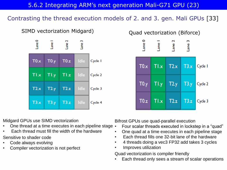
SIMD vectorization Midgard) Quad vectorization (Biforce)
Midgard GPUs use SIMD vectorization
• One thread at a time executes in each pipeline stage
• Each thread must fill the width of the hardware
Sensitive to shader code
• Code always evolving
• Compiler vectorization is not perfect
Bifrost GPUs use quad-parallel execution
• Four scalar threads executed in lockstep in a “quad”
• One quad at a time executes in each pipeline stage
• Each thread fills one 32-bit lane of the hardware
• 4 threads doing a vec3 FP32 add takes 3 cycles
• Improves utilization
Quad vectorization is compiler friendly
• Each thread only sees a stream of scalar operations
Contrasting the thread execution models of 2. and 3. gen. Mali GPUs [33]

5.6.2 Integrating ARM’s next generation Mali-G71 GPU (24)
Remark
Also AMD switched from VLIW4 SIMD vectorization to QUAD vectorization in theirGCN (Graphics Core Next) graphics computing architecture in 2011 [36]

5.6.2 Integrating ARM’s next generation Mali-G71 GPU (25)
• Vulkan is a new generation graphics and compute API that provides high-efficiency, cross-platform access to up-to-date GPUs used in a wide variety ofdevices from PCs and consoles to mobile phones and embedded platforms.
• Khronos launched the Vulkan 1.0 specification in February 2016 and Khronosmembers, like ARM, Intel, NVIDI, released Vulkan drivers and SDKs immediately.
c) Vulkan graphics on 2. (Midgard) and 3. (Biforce) generation GPUs [37]

5.6.2 Integrating ARM’s next generation Mali-G71 GPU (26)
• Clause: a group of instructions which executes atomically.
• Architectural state visible after clause completion.
d) Clause execution on 3. generation (Biforce) gPUs

5.6.2 Integrating ARM’s next generation Mali-G71 GPU (27)
Example for clause execution in 3. gen. (Bifrost) GPUs [33]

5.6.2 Integrating ARM’s next generation Mali-G71 GPU (28)
Benefits of 3. gen. (Bifrost) GPUs vs. 2. gen. (Midgard) GPUs [33]

5.6.3 HSA (Heterogeneous System Architecture) compliance

5.6.3 HSA (Heterogeneous System Architecture) compliance (1)
The road towards HSA (Heterogeneous System Architecture)
The vision of Si-level integration of CPU and GPU cores
• The roots of HSA are going back to 2006 when AMD revealed their planto integrate CPU cores and the GPU on the same silicon die, called theCPU/GPU Silicon Fusion [60].
• At that time AMD planned to introduce their Fusion processors in late 2008or early 2009.
• For supporting their intention AMD acquired ATI, a successful graphics firm, in 10/2006.
• We note that ARM acquired a small, Norwegian graphics firm at the sametime that became the core of ARM's graphics division and developed the Mali GPU line.
5.6.3 HSA (Heterogeneous System Architecture) compliance

5.6.3 HSA (Heterogeneous System Architecture) compliance (2)
Enhancing AMD's Fusion concept to Accelerated Computing [38]
Accelerated computing widens the concept of Si-level integration to the integrationof CPU cores and accelerators in 03/2007.
Here GPUs are considered as a specific type of accelerators (graphics accelerators).

5.6.3 HSA (Heterogeneous System Architecture) compliance (3)
• In 12/2007 at their Financial Analyst Day AMD gave birth to a new term APU(Accelerated Processing Unit) designating their processors implementing the Fusion concept).
• At the same time AMD announced their first APU family, the Swift family [39] as well.
AMD's aim to introduce the first APU family called Swift in 2H/2009 [39]

5.6.3 HSA (Heterogeneous System Architecture) compliance (4)
Intel's aim to introduce in-package integrated graphics in 1H/2009
In 09/2007 Intel announced an in-package integrated GPU that is an alternativeof the 2. gen. Nehalem (Lynnfield) processor, as indicated below.
Lynnfield & Havendale can be supported on one platform
Lynnfield Processor(Monolithic die)
DMI
DDR3
Graphics
DD
R3
IM
CP
CI-E
PowerThreadThreadThreadThread
8M
Co
reC
ore
ThreadThreadThreadThread
Co
reC
ore
Ibexpeak PCH
PCIe, SATA,NVRAM, etc.
Display
Analog
Digital
I/O ControlProcessors
I/O functions
Same LGA 1160 platform
Display
Link
DMI
DDR3
Graphics
HavendaleProcessor
(Multi-Chip Package - MCP)
MCP Processor
Power
4M
PCI-E
DDR3 IMC
GPU
ThreadThreadThreadThread
Co
reC
ore
SDVO, HDMI
Display Port,
DVI
Ibexpeak PCH
VGA
PCIe, SATA,NVRAM, etc.
Display
Analog
Digital
I/O ControlProcessors
I/O functions
Schedule:
• 2H ’08 First Samples
• 1H ’09 Production
• TDP < 95 W
No integratedgraphics

5.6.3 HSA (Heterogeneous System Architecture) compliance (5)
Cancellation of both AMD's and Intel's GPU integration plans in 11/2008and 01/2009 respectively.
Both firms postponed their plans to integrate GPUs in the 45 nm technology until the 32 nm technology with a higher transistor budget becomes available [40], [41].

5.6.3 HSA (Heterogeneous System Architecture) compliance (6)
Implementing integrated graphics
Implementations around1999 - 2009
In the north bridge On the processor die
Intel’s Sandy Bridge (1/2011) AMD’s Bobcat-based APUs (M, 1/2011)
and Llano APUs (DT, 6/2011)
In the processor package(as an MCP on a separate die)
Both the CPU and the GPUare on separate dies
and are mounted into a single package
P
South Bridge
Mem.NBIG
South Bridge
Mem.NB
PGPU CPU
Periph. Contr.
Mem.CPUGPUP
Introducing in package and on-die integrated graphics by Intel and AMD
Intel’s Havendale (DT) andAuburndale (M)
(scheduled for 1H/2009but cancelled in 01/2009)
Arrandale (DT, 1/2010) andClarkdale (M, 1/2010)
MCP: Multi-Chip PackageM: Mobile DT: Desktop

5.6.3 HSA (Heterogeneous System Architecture) compliance (7)
Evolution of integrated graphics in Intel's processor families [42]

5.6.3 HSA (Heterogeneous System Architecture) compliance (8)
Introducing the concept of HSA Heterogeneous Systems Architecture" by AMD
In 01/2012 AMD rebranded their FSA (Fusion System Architecture) term to HSA(Heterogeneous System Architecture) [43] and in 02/2012 introduced the HSAconcept that designates an efficient open ecosystem for accelerated processors(called APUs by AMD), as indicated below [44].

5.6.3 HSA (Heterogeneous System Architecture) compliance (9)
HSA's role in processor evolution [45]
TBB (Threading Building Blocks): is a C++ template library, developed by Intel for parallel programmingon multi-core processors.
OpenMP (Open Multi-Processing) is an application programming interface (API) that supports sharedmemory multiprocessing programming in C, C++, and Fortran on most platforms, instruction set architectures and operating systems, including Solaris, AIX, HP-UX, Linux, and Windows (Wikipedia).

5.6.3 HSA (Heterogeneous System Architecture) compliance (10)
At the initiative of AMD the HSA Foundation was established in 06/2012.
The founding members are: see below. [46]
Announcing the HSA Foundation in 06/2012
Note that neither Intel nor NVIDIA are among the foundation members.

5.6.3 HSA (Heterogeneous System Architecture) compliance (11)
Evolution of the HSA standard [47]
• HSA 1.0: 03/2015
It incorporates changes for efficient implementation of high-level languages, such as C++, Java and Python on heterogeneous computing hardware anda more detailed documentation.
• HSA 1.1: 05/2016
• Backward compatible with HSA 1.0
• Multi-vendor oriented, vendor neutral device drivers
• Wider range of devices supported, including DSPS, ISPs (Image Processors)

5.6.3 HSA (Heterogeneous System Architecture) compliance (12)
• HSA is a multi-vendor, open standard concept to efficiently supportheterogeneous platforms.
• By contrast, both Intel and NVIDIA choose a proprietary solution for this.
• NVIDIA developed their CUDA language and the PTX virtual ISA forheterogeneous systems, built up of either of CPU and GPU cards or SOCswith on-chip integrated CPU and GPU, like the TEGRA K1 (Q2/2014), TEGRA X1 (Q2/2015) SOCS.
• Intel's solution is to provide unified virtual memory, called SVM (shared VirtualMemory) and falling back to OpenCL 2.0 in supporting HLL programming.
Other approaches to support programming of heterogeneous platforms

5.6.3 HSA (Heterogeneous System Architecture) compliance (13)
Specific features and requirements of HSA -1
• HSA relates to a heterogeneous system architecture consisting typically of CPUcores, a GPU and accelerators and it takes for granted that each code segment runs on a unit that provides the fastest and most efficient execution, so e.g.serial, branch intensive code will run on CPU cores whereas data parallel codeon the GPU, as indicated below..
Figure: Running serial workloads on CPU cores and parallel workload on a GPU in HSA [48]

5.6.3 HSA (Heterogeneous System Architecture) compliance (14)
Specific features and requirements of HSA -2
• An efficient, vendor agnostic processing ecosystem for heterogeneous platformshas a number of requirements, as presented e.g. in [49], [50].
• From these requirements subsequently, we will discuss the following four major ones:
b1) Using a vendor agnostic virtual ISA (called HSAIL) for implementing the targeted HSA processing ecosystem to foster industry acceptance,
b2) Providing HLL support for easy of coding of HSA platforms,
b3) Providing a cache coherent, uniform, shared virtual memory for allprocessing units to avoid inefficient data copying between differentmemory spaces and
b4) Providing an efficient mechanism for forwarding tasks between the CPUand the GPU to eliminate in-efficient OS interactions.

5.6.3 HSA (Heterogeneous System Architecture) compliance (15)
b1) Using a vendor agnostic virtual ISA (called HSAIL) for implementingthe targeted HSA processing ecosystem to foster industry acceptance[45]
• HSAIL is a virtual ISA developed for data parallel programs.
HSAIL supports only compute workloads and does not support graphics-specific instructions.
• Source programs, e.g. in OpenCL 2.0 will be compiled to the HSAIL, andthen interpreted (finalized) to the CPU or GPU ISA, as indicated below.
• HSAIL is based on a similar concept as e.g. Java bytecode.

5.6.3 HSA (Heterogeneous System Architecture) compliance (16)
Low-LevelVirtual MachineIntermediate
Language
They take the role of a driver
Concept of the virtual ISA of HSA [49]

5.6.3 HSA (Heterogeneous System Architecture) compliance (17)
Remark 1
• NVIDIA has a similar virtual ISA for GPU computing, designated as PTX(Parallel Thread eXecution).
• NVIDIA supports programming heterogeneous (GPU) systems by the CUDA HLL.
• Then compiling of CUDA is a two stage process, as seen in the next Figure.
Figure: Compiling CUDA for NVIDIA GPUs [51]

5.6.3 HSA (Heterogeneous System Architecture) compliance (18)
• The bytecode is processed by the JVMcomponent of the Java RuntimeEnvironment (JRE).
• Each platform needs one or more JVMsthat suits the OS and the target ISA,as indicated in the Figure.
• It is then the task of the JVM to execute the bytecode e.g. by interpreting eachbytecode instructions.
Remark 2: Compiling and executing Java programs on different platforms
Figure: Different JVMs for different OSs and CPU ISAs [61]
JVM: Java Virtual Mashine

5.6.3 HSA (Heterogeneous System Architecture) compliance (19)
b2) Providing HLL support for easy of coding of HSA platforms [50], [47]
• Obviously, developers for HSA are not expected to write code in HSAIL.Instead, HSA Foundation took care for the availability of HLLs for easy of
programming.
• Major HLL languages available for HSA (04/2017):
• OpenCL 2.0
• C++ AMP 1.2 (C++ Accelerated Massive Parallelism) and
• Python (Continuum Analytics’ Numba Python compiler).
• It was planned also that Java 9 will support HSA by allowing to generate HSAILdirectly from Java bytecode but to date it was not yet released.
• Here we note that rather than participating in the multi vendor HSA Consortiumestablished for providing the needed programming ecosystem for heterogeneous systems NVIDIA followed an alternative, proprietary pathwith their CUDA language and PTX virtual ISA.

5.6.3 HSA (Heterogeneous System Architecture) compliance (20)
Figure: Principle of hUMA [62] providing the same visibility for both the CPUand the GPU into the entire memory space (up to 32 GB)
A uniform memory provides the same visibility for all processing units (e.g. the CPUand the GPU) into the entire memory space (up to 32 GB), as indicated below.
A memory with the said features is called hUMA (HSA UMA or heterogeneous UMA)by AMD.
Uniform memory is implemented by using the same mechanism (e.g. page tables)to translate virtual addresses to physical addresses for both the CPU and the GPU.
b3) Providing a cache coherent, uniform, shared virtual memory for allprocessing units to avoid inefficient data copying betweendifferent memory spaces

Illustration of key features of hUMA [52]
Provides the same visibility
for both the CPU and GPU
in the entire memory space
Uniform memoryCoherent memory
5.6.3 HSA (Heterogeneous System Architecture) compliance (21)
b) HSA (Heterogeneous System Architecture) compliance ()
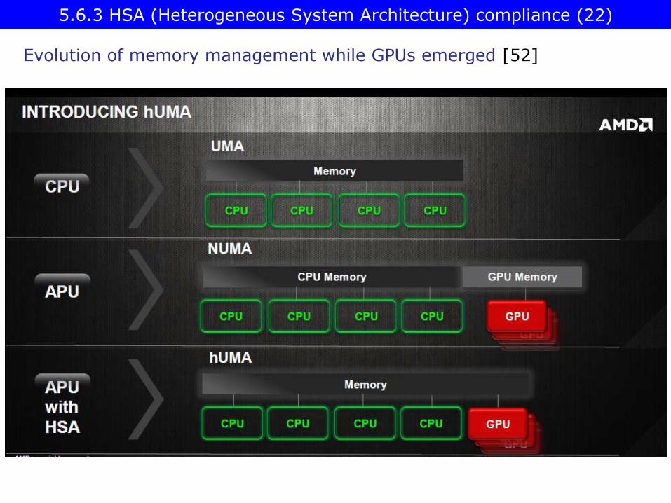
Evolution of memory management while GPUs emerged [52]
5.6.3 HSA (Heterogeneous System Architecture) compliance (22)

Data copying between the CPU and GPU memory without hUMA) [52]
5.6.3 HSA (Heterogeneous System Architecture) compliance (23)

Data copying between the CPU and GPU memory with hUMA) [52]
5.6.3 HSA (Heterogeneous System Architecture) compliance (24)

5.6.3 HSA (Heterogeneous System Architecture) compliance (25)
• AMD Kaveri (2014), (first Steamroller-based APU), first proc. supporting HSA
• AMD's Carizzo (2015) (Excavator-based) HSA 1.0 support
• Samsung Exynos 8895 (2017)
Processors supporting HSA
At this time (05/2017) there are only a few processors that support HSA, including
Remarks -1
• Allegedly, AMD's Zen-based APUs will also support HSA [53].
• According to their roadmap for 2014/2015 NVIDIA planned to introduce unifiedvirtual memory in their Maxwell GPU based Tegra X1 but changed this scheduleand postponed the implementation of unified virtual memory until theirPascal GPU based Tegra Parker (P1) processor, announced in 08/2016.
This modification is the implication of NVIDIA's decision made in 2014/2015 to abandon the mobile market and developing processors for VR, AI andself-driving cars.
• As NVIDIA's next processor, the TegraX1 targeted presumable Nintendo'sSwitch game console there was no need to support data parallel computationslike for scientific/engineering applications on the GPU in an efficient way.
• By contrast, NVIDIA's subsequent Tegra Parker processor targeted self-drivingcars, this however implies a lot of AI tasks, so supporting the efficientexecution of computing intensive tasks on a GPU became a priority that called for the implementation of unified virtual memory.

5.6.3 HSA (Heterogeneous System Architecture) compliance (26)
Remarks -2
• Also Intel began supporting the efficient execution of data parallel workloads ona GPU by implementing unified virtual memory, called SVM (Shared VirtualMemory) first in their Broadwell family in 2014, followed by the Skylake line(2015) as briefly shown subsequently.
• Nevertheless, Intel, like NVIDIA, don't take part in the HSA Consortium but follows an individual approach for supporting efficient computing on GPUs.
Intel's solution is to provide unified virtual memory and falling back to OpenCL 2.0 in supporting HLL programming.

5.6.3 HSA (Heterogeneous System Architecture) compliance (27)
Shared virtual memory in the Broadwell line (2014) [54]
Shared Physical Memory (aka Unified Memory Architecture)

Shared Virtual memory (SVM) [54]
5.6.3 HSA (Heterogeneous System Architecture) compliance (28)

Figure 8: A view of the SoC chip level memory hierarchy and
Coherent memory spaces in Broadwell's SVM (with Gen8 Graphics) [55]
5.6.3 HSA (Heterogeneous System Architecture) compliance (29)

Traditional management of application task queues (based on [56])
5.6.3 HSA (Heterogeneous System Architecture) compliance (30)
b4) Providing an efficient mechanism for forwarding tasks between the CPUand the GPU to eliminate in-efficient OS interactions

Application task management with heterogeneous queuing (hQ) [56]
5.6.3 HSA (Heterogeneous System Architecture) compliance (31)

• Heterogeneous queuing (hQ) is symmetrical.
It allows both the CPU and the GPU to generate tasks for themselves and foreach other.
• Work is specified in a standard packet format that will be supported by allISA-compatible hardware, so there's no need for the software to usevendor-specific code.
• Applications can put packets directly into the task queues that will be accessed
by the hardware.
• Each application can have multiple task queues, and a virtualization layer allowsHSA hardware to see all the queues.
Main features of hQ [56]
5.6.3 HSA (Heterogeneous System Architecture) compliance (32)

5.6.4 Support for LPDDR4x memory

5.6.4 Support for LPDDR4x memory (1)
5.6.4 Support for LPDDR4x memory [36]
• LPDDR4x is an enhancement of the LPDDR4 memory technology.
• It lowers the output driver voltage (VDDQ) from 1.1 V to 0.6 V, this results ina 20 % reduction of DRAM power consumption, as indicated in the nextFigure.
• Vendors began shipping LPDDR4x memory in the beginning of 2017.
• To date only Samsungs Exynos 8895 and Qualcomm's Snapdragon 835 make use of the LPDDR4x memory.

5.6.4 Support for LPDDR4x memory (2)
Contrasting LPDDR4 (LP4) and LPDDR4x (LP4x) [36]

5.6.5 Separate security processing unit

5.6.5 Separate security processing unit (1)
5.6.5 Separate security processing unit
• It is used for user authentication, mobile payments etc.
• It represents an enhanced security subsystem like Apple's Secure Enclave.

5.6.6 Vision processing Unit (VPU)

5.6.6 Vision processing Unit (VPU) (1)
5.6.6 Vision Processing Unit (VPU) -1 [73]
The Vision Processing Unit (VPU) of the Exynos 8895 is designed for enhancingmachine vision technology, including corner detection, recognition of objects,
analyzing visual information coming from a camera, VR etc., as indicated in the nextFigure.

5.6.6 Vision processing Unit (VPU) (2)
Object recognition by Samsung’s VPU implemented in the Exynos 8895 [73]

5.6.6 Vision processing Unit (VPU) (3)
Vision Processing Unit (VPU) -2 []
• VPUs differ from GPUs as they are designed from the ground up to efficientlyprocess computer vision algorithms whereas GPUs target processing graphicsin general [74].
• Presently, there is no available information about the architecture of Samsung’sVPU implemented in the Exynos 8895.
• However, in order to give a glimpse about the built up of a GPU subsequently we briefly present the block diagram of the Miriad 2 VPU from Movidius, now
part of Intel (since 09/2016).

5.6.6 Vision processing Unit (VPU) (4)
Main features of the Miriad 2 VPU (2015) [75]
It is based
• on two 32-bit RISC processors, one is dedicated to scheduling within the SoC,and the other to running user code within a real-time OS (RTOS)
• about 20 hardware accelerators for imaging/vision,
• 12 VLIW cores (termed as SHAVE processors) and
• 2 MB of on-chip memory that is shared between the CPUs, SHAVE processors
and fixed-function accelerators and
as shown in the next two Figures.
5.6.6 Vision processing Unit (VPU) (5)
Block diagram of the Miriad 2 VPU from Movidius, now part of Intel [75]

5.6.6 Vision processing Unit (VPU) (6)
A more detailed block diagram of the Miriad 2 VPU [76]

5.6.6 Vision processing Unit (VPU) (7)
The SHAVE processor [76]
• The 12 SHAVE processors are the kernel piece of the VPU.
• Each SHAVE processor is an 8-way variable length VLIW unit.
• Separate fields of the VLIW instructions control the functional units.
• Individual fields are enabled separately by a header in the variable length VLIW instruction.
• Variable length VLIW instructions are fetched in 128-bit chunks, and the average instruction width is around 80 bits.
• The functional units access their operands from a 128 bits x 32-entry vector register file with 12 ports and a 32-bit x 32-entry integer register file with18 ports, as indicated in the next Figure.

5.6.6 Vision processing Unit (VPU) (8)
CMX: Connection Matrix Memory(holding instructions and data)
VRF: Vector Register File (32x128 bit)IRF: Integer Register File (32x32 bit)
IDC: Instruction Decode UnitDCU: Debug Control Unit
PEU: Predicated Execution Unit
BRU: Branch and Repeat Unit
LSU: Load/Store Unit (64 bit)
IAU: Integer Arithmetic Unit(32)
SAU: Scalar Arithmetic Unit (32)
VAU: Vector Arithmetic Unit (128)
CMU: Compare Move Unit (128)
(8-slot VLIW)
Block diagram of the SHAVE VLIW core (from the Miriad I) [76]

5.7 Samsung’s first SOC supporting the DynamIQcluster technology: the Exynos 9 Series 9810 (2018)
5.7.2 Microarchitecture of the M3 core
5.7.1 The Exynos 9 Series 9810 Overview•
•
5.7.3 The DynamIQ technology as an evolution of the
big.LITTLE technology •

5.7.1 The Exynos 9 9810 - Overview

5.7.1 The Exynos 9 Series 9810 – Overview (1)
5.7.1 The Exynos 9 Series 9810 - Overview
• It is fabricated based on Samsung's 10 nm FinFET LPP process.
• The Exynos 9 9810 is based on the M3 core and provides about 100 %single-core and 40 % multi-core performance increase over the 8895 that arises
LPP: Low Power Plus
• The Exynos 9810 is the kernel piece of one alternative of Samsung's Galaxy S9,S9+.
The other alternative is using Qualcomm's Snapdragon 845 for these mobiles(sold in the US).
• It was announced in 01/2018 and first shipped in 02/2018.
• partly from the 6-wide microarchitecture of the M3 processor used and• partly from using the DynamIQ core technology instead of the big.LITTLE
technology.

SoC CPU
GPUMemory
technology
Availab
ility
Utilizing devices
(examples)Model number fabInstr.
setCores
No of
cores
fc
(GHz)
Exynos 5 Octa
(Exynos 5420)
28 nm
HKMG
ARM
v7
Cortex-A15+
Cortex-A74+4
1.8-1.9
1.2-1.3
ARM Mali-T628 MP6
@ 533 MHz;
109 GFLOPS
32-bit DCh LPDDR3e-
1866 (14.9 GB/sec)
Q3
2013
Samsung Chromebook 2
11.6", Samsung Galaxy Note
3/Note 10.1/Note Pro 12.2,
Samsung Galaxy Tab Pro/Tab
S
Exynos 5 Octa
(Exynos 5422)
28 nm
HKMG
Cortex-A15+
Cortex-A74+4
1.9-2.1
1.3-1.5
ARM Mali-T628 MP6
@ 533 MHz 109
GFOPS
32-bit DCh
LPDDR3/DDR3-1866
(14.9 GB/sec)
Q2
2014
Samsung Galaxy S5
(SM-G900H)
Exynos 5 Octa
(Exynos 5800)
28 nm
HKMG
Cortex-A15+
Cortex-A74+4
2.1
1.3
ARM Mali-T628 MP6
@ 533 MHz
109 GFLOPS
32-bit DCh
LPDDR3/DDR3-1866
(14.9 GB/sec)
Q2
2014
Samsung Chromebook 2
13,3"
Exynos 5 Octa
(Exynos 5430)
20 nm
HKMG
Cortex-A15+
Cortex-A74+4
1.8-2.0
1.3-1.5
ARM Mali-T628 MP6
@ 600 MHz;
122 GFLOPS
32-bit DCh
LPDDR3e/DDR3-2132
(17.0 GB/sec)
Q3
2014
Samsung Galaxy Alpha (SM-
G850F)
Exynos 7 Octa
(Exynos 5433
20 nm
HKMG
ARM
v8-A
Cortex-A57+
Cortex-A534+4
1.9
1.3
Mali-T760 MP6 @
700 MHz; 206
GFLOPS (FP16)
32-bits DCh LPDDR3-
1650 (13.2 GB/s)
Q3/Q4
2014
Samsung Galaxy Note 4 (SM-
N910C)
Exynos 7 Octa
(Exynos 7420)
14 nm
FinFET
Cortex-A57+
Cortex-A534+4
2.1
1.5
Mali-T760 MP8 @
772 MHz; 227
GFLOPS (FP16)
32-bits DCh LPDDR4-
3104 (24.9 GB/s)
Q2
2015
Samsung Galaxy S6
S6 Edge
Exynos 7 Octa
(Exynos 7885
14 nm
HKMG
Cortex-A73+
Cortex-A534+4
2.2
1.6Mali-G71 MP2 32-bits DCh LPDDR4x
Q1
2016Samsung Galaxy A8
Exynos 8 Octa
(Exynos 8890)
14 nm
FinFET
Samsung M1+
Cortex-A534+4
2.6-2.3
1.6
Mali-T880 MP12 @
650 MHz; 265.2
GFLOPS (FP16)
32-bits DCh LPDDR4-
3588 (28.7 GB/s)
Q1
2016
Samsung Galaxy S7
Samsung Galaxy S7 Edge
Exynos 9 Series
(Exynos 8895)
10 nm
FinFET
Samsung M2+
Cortex-A534+4
2.5
1.7Mali-G71 MP20
32-bits DCh?
LPDDR4x
Q2
2017
Samsung Galaxy S8
Samsung Galaxy S8 Plus
Exynos 9 Series
(Exynos 9810)
10 nm
FinFET
Samsung M3+
Cortex-A554+4
2.9
1.9Mali-G72 MP18
32-bits DCh?
LPDDR4x
Q1
2018
Samsung Galaxy S9
Samsung Galaxy S9 Plus
5.7.1 The Exynos 9 Series 9810 - Overview (2)
Main features of Samsung's Exynos 9 Series 9810 (2018)

Evolution of the width of mobile cores
5.7.1 The Exynos 9 Series 9810 – Overview (3)
Single CPU core Multiple CPU cores
CPU cores
big.LITTLECPU clusters
DynamIQCPU clusters
Symmetricalmulticores
Cluster migration Core migration(GTS)
ARM1176 (2007)until A4 (2010)
A5 (2011)(2C)
A10 (2016)(2+2)
A11 (2017)(2+4)
Apple
3110 (2010) 3250 2C (2011)4412 4C (2012)
5410 (2013)(4+4)
5420 (2013)(4+4)
SamsungExynos
9810 (2018)(4+4)
MSM 7225 (2010)
8260 2C (2013)400 4C (2013)
808 (2+4) (2014)810 (4+4) (2015)
QualcommSnapdragon
845 (2018)(4+4)
Huawei
Kirin 920 (4+4)) 2014)(K3V1) (2009) (K3V2 (2012))
MediaTek MT6582 4C (2013)
MT6592 8C (2013)
MT6595 8C (2014)MT6218B
(2003)
MT6795 10C
(2019)
980 (2018)
(4+4)

Samsung Exynos SoCs Specifications
SoC Exynos 9810 Exynos 8895
CPU
4x Exynos M3 @ 2.9 GHz4x 512KB L2 ??
4x Cortex A55 @ 1.9 GHz4x 128KB L2
4096KB L3 DSU ??
4x Exynos M2 @ 2.314 GHz2048KB L2
4x Cortex A53 @ 1.690GHz512KB L2
GPU Mali G72MP18Mali G71MP20
@ 546MHz
MemoryController
4x 16-bit CHLPDDR4x @ 1794MHz
4x 16-bit CHLPDDR4x @ 1794MHz
28.7GB/s B/W
Media10bit 4K120 encode & decode
H.265/HEVC, H.264, VP94K120 encode & decodeH.265/HEVC, H.264, VP9
Modem
Shannon Integrated LTE(Category 18/13)
DL = 1200 Mbps6x20MHz CA, 256-QAM
UL = 200 Mbps2x20MHz CA, 256-QAM
Shannon 355 Integrated LTE(Category 16/13)
DL = 1050 Mbps5x20MHz CA, 256-QAM
UL = 150 Mbps2x20MHz CA, 64-QAM
ISPRear: 24MPFront: 24MP
Dual: 16MP+16MP
Rear: 28MPFront: 28MP
Mfc.Process
Samsung 10nm LPP Samsung 10nm LPE
Main features of the Exynos 9810 vs. the Exynos 8995 [68]
5.7.1 The Exynos 9 Series 9810 – Overview (4)

Snapdragon 845 Exynos 9810
CPU
4 x Kryo 385 @2.8GHz
+
4 x Kryo 385 @1.8 GHz
4 x M3 (Cortex-A75 based) @2.9GHz +
4 x Cortex-A55 @1.9GHz
GPUAdreno 630:
Open GL ES 3.2, Open CL 2.0, Vulkan, DirectX 12
Mali-G72:
18-cores @700MHz
RAM LPDDR4x LPDDR4x
AI co-processor Hexagon 685 DSP 3x VPU
Modem
Qualcomm Snapdragon X20 LTE modem:
•Download speed: 1.2Gbps
•Upload speed: 150Mbps
Custom Cat.18 LTE modem:
•Download speed: 1.2Gbps
•Upload speed: 200Mbps
Battery Charging Quick Charge 4+ (USB PD Compatible)Samsung Adaptive Fast Charge, Fast
Wireless Charging (Qi & PMA)
Wi-Fi Multi-gigabit Wi-Fi ac/b/g/n with MU-MIMODual-Band Wi-Fi ac/b/g/n with
MU-MIMO
Bluetooth 5.0 5.0
Camera 32MP Single, 16MP Dual 24MP Single, 16MP+16MP Dual
Video Recording and
Encoding
4K (3840×2160) @60fps, 10bit HDR, Rec 2020 color
gamut, H.264 (AVC), H.265 (HEVC), VP9
MFC, 4K (3840×2160) @120fps,
10-bit HEVC (H.265), H.264, VP9
Manufacturing 2nd-gen 10nm LPP FinFET 2nd-gen 10nm LPP FinFET
The Samsung Exynos 9810 vs. the Qualcomm Snapdragon 845 [69]
5.7.1 The Exynos 9 Series 9810 – Overview (5)

5.7.1 The Exynos 9 Series 9810 – Overview (6)
Exynos 9810’s enhanced modem speeds vs. the Exynos 8895 [73], [77]
Exynos 8895Exynos 9810

Main innovations of the Exynos 9 Series 9810
• It is built on the M3 core (called Meerkat)
• It includes an L3 cache, shared by 4 cores (exclusive to the private L2 caches)
• It is based on the DynamIQ core technology
5.7.1 The Exynos 9 Series 9810 – Overview (7)
These innovations will be discussed next.

5.7.2 Microarchitecture of the M3 core

5.7.2 Microarchitecture of the M3 core (1)
For comparison: Microarchitecture of the M1/M2 cores [79]

5.7.2 Microarchitecture of the M3 core (2)
Enhancements of the microarchitecture of the M3 core [79]

5.7.2 Microarchitecture of the M3 core (3)
Enhancements of the M3 front-end [79]
MPKI: Mispredictions Per Kilo Instructions

5.7.2 Microarchitecture of the M3 core (4)
Enhancements of the M3 “middle machine” [79]

5.7.2 Microarchitecture of the M3 core (5)
Enhancements of the M3 FPU [79]

5.7.2 Microarchitecture of the M3 core (6)
Enhancements of the M3 Load/Store Unit [79]

5.7.2 Microarchitecture of the M3 core (7)
Longer pipeline of the M3 core [79] -1

5.7.2 Microarchitecture of the M3 core (8)
M3 cache hierarchy [79]

5.7.2 Microarchitecture of the M3 core (9)
M3 cache hierarchy [79] -2
• As seen in the previous Figure M3 has an L3 cache included.
• The L3 cache is implemented sliced, in NUCA style (Non-Uniform CacheArchitecture) rather than in UCA (Uniform cache Architecture) as in AMD’s CCXmodule.
A core can access an adjacent slice in 32 cycles, and the furthest slice in44 cycles.
• The L3 cache is exclusive to the related private L2 cache.
• Further on, an L3 slice is on the same clock plane as the related CPU core.

5.7.2 Microarchitecture of the M3 core (10)
M1 Core Layout [97]

5.7.2 Microarchitecture of the M3 core (11)
M3 Core Layout [97]
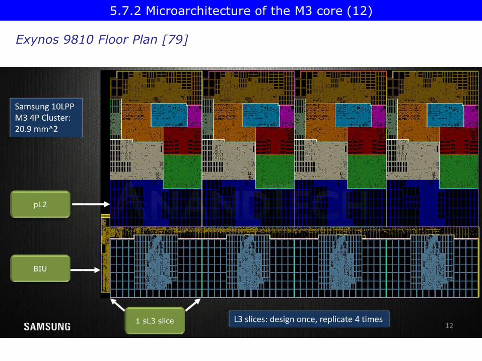
5.7.2 Microarchitecture of the M3 core (12)
Exynos 9810 Floor Plan [79]

5.7.2 Microarchitecture of the M3 core (13)
M2/M3 IPC values across ~4800 traces []

5.7.2 Microarchitecture of the M3 core (14)
It represents commercial performance in the mobiles:
Exynos 8895 (M2), Exynos 9810 (M3) and the Snapdragon 845 (A75).
Single thread performance of A75 and M3 relative to M2 while runningGeekBench 4 [79]

5.7.2 Microarchitecture of the M3 core (15)
Single thread performance/W of M2 and M3 while running GeekBench 4 [79]

5.7.2 Microarchitecture of the M3 core (16)
Evolution of M3 [79]

5.7.2 Microarchitecture of the M3 core (17)
“Samsung’s CPU IP is developed in Austin, Texas, at “Samsung’s Austin R&D Center”, or
SARC. The centre was founded in 2010 with the goal of establishing in-house IP for Samsung’s
S.LSI division and Exynos chipsets. Staffed with ex-AMD, ex-Intel and various other talented
industry veterans, what we saw come out - alongside memory controllers and custom
interconnects - was also the of course more visible IPs: Samsung’s first custom CPUs.
The Exynos M1 is said to have started its design cycle sometime in 2012 and saw a quite short
3 year development phase, starting from scratch to first tape-out. It made its first appearance in
the Exynos 8890 in the 2016 Galaxy S7. Over the years SARC has been expanding, and in
2017 the Advanced Computing Lab (ACL) in San Jose was opened and added to the SARC’s
joint charter – adding custom GPU IP to its design portfolio that we hope to see productised in a
couple of years.
The Exynos M1 being designed from scratch, it’s natural to expect that follow-up generations
would be using it as the starting point for further development. Following the tape-out of the M1,
the SARC team started off the M3 design with the existing M1 RTL back in Q1 of 2015. At first,
this was meant to be an incremental development. However, there was a larger change of plans
later on in Q1 2016, as goals were set higher for a much larger performance push.
The existing improvements were forked in Q3 2015 into what became the M2 – which was
initially meant to only be a 10LPE port of the M1 (Which was 14LPP). As a reminder, the M2
had a robust ~20% IPC improvement across workloads, which allowed it to outperform the M1
even though it was clocked 12% slower in production silicon. Samsung had achieved this by
implementing some of the originally planned M3 features into the M2, while the new M3 design
became more aggressive.”
Remarks to the developments of M1-M3 (taken from [79])

5.7.3 The DynamIQ technology as an evolution of the big.LITTLE technology

CPU0 CPU1
CPU2 CPU3
Cache coherent interconnect
Cluster of
LITTLE cores
Cluster of
big cores
CPU0 CPU1
CPU2 CPU3
To
To cache coherent interconnect through the AMBA4 ACE bus
5.7.3 The DynamIQ technology as an evolution of the big.LITTLE technology
Two big.LITTLE core clusters A single DynamIQ core cluster (65)
Two stand alone clusterswith up to 4 cores (2011)
A single cluster of up to 8 cores of up to two core types(but up to 4 big cores) (2017)
5.7.3 The DynamIQ technology an evolution of the big.LITTLE technology (1)

• support of the v8.2 ISA
• greater flexibility
• redesigned memory subsystem with higher bandwidth and lower access time
• improved power efficiency through intelligent power management, called
EAS (Energy Aware Scheduling) (not discussed).
Benefits of the DynamIQ cluster technology:
5.7.3 The DynamIQ technology an evolution of the big.LITTLE technology (2)

Main enhancements of DynamIQ core clusters
a) Up to 8 CPU cores of up to 2 ARMv8.2 ISA based core types
b) Private (per-core) L2 caches in the CPU cores
c) DynamIQ Shared Unit (DSU) with a shared L3 cache and snoop filter
d) Capability for partitioning the cores and the L3 cache
e) Finer-grain frequency and voltage control
f) Mesh interconnect (CMN-600) for server systems
g) Use of a scratch pad system cache to increase throughput
h) Cache stashing
(Above features are discussed in the Chapter: ARM processor lines).
5.7.3 The DynamIQ technology an evolution of the big.LITTLE technology (3)

Geekbench 4 scores [70]
Samsung Exynos 8895
Qualcomm Snapdragon 845
Qualcomm Snapdragon 835
Apple A11
Samsung Exynos 9810
0 2000 4000 6000 8000 10000
Multi core
Single core
Geekbench is a cross-platform benchmark that simulates real-world scenarios.
Geekbench 4 scores against a baseline of 4000 provided by Intel’s Core i7-6600U @ 2.60 GHz.
5.7.3 The DynamIQ technology an evolution of the big.LITTLE technology (4)

6. References

6. References (1)
[2]: Kim M., Kim H., Chung H., Lim K., Samsung Exynos 5410 Processor – Experience theUltimate Performance and Versatility, White Paper, 2013
[3]: Shin Y., Shin K., Kenkare P., Kashyap R., 28nm high- metal-gate heterogeneous quad-core CPUs for high-performance and energy-efficient mobile application processor, IEEE, 2013
[4]: Greenhaigh P., Big.LITTLE processing with ARM Cortex-A15 & Cortex-A7, EE Times,Oct. 24 2011, http://www.eetimes.com/document.asp?doc_id=1279167&page_number=2
[1]: Se-Hyung Y. et al., A 32nm high-k metal gate application processor with GHz multi-coreCPU, ISSCC, 2012
[5]: Jeff B., big.LITTLE Technology Moves Towards Fully Heterogeneous Global Task Scheduling,ARM TechCon, Nov. 2013, http://community.arm.com/servlet/JiveServlet/previewBody/7763-102-1-12076/big.LITTLE%20technology%20moves%20towards%20fully%20heterogeneous%20Global%20Task%20Scheduling_final%20%28pdf%29.pdf
[6]: Wathan G., ARM big.LITTLE Technology Unleashed, ARM,https://www.arm.com/files/event/A3_big.LITTLE_Technology_Unleashed.pdf
[7]: Мобильные процессоры. Компания Samsung, 4PDA, Jan. 21 2014,http://4pda.ru/2014/01/21/136624/
[8]: Triggs R., A closer look at the Galaxy S6’s Exynos 7420 SoC, Android Authority,http://www.androidauthority.com/samsung-exynos-7420-closer-look-592117/
[9]: Smith C., These are the Galaxy S5’s next-gen processors, BGR, Febr. 26 2014,http://bgr.com/2014/02/26/galaxy-s5-processor-snapdragon-801-exynos-5422/

6. References (2)
[11]: Exynos 5 Octa, Samsung, http://www.samsung.com/global/business/semiconductor/minisite/Exynos/w/solution.html#?v=octa_5430
[12]: Jonnalagadda H., Samsung announces 64-bit Exynos 7 Octa with significant performance improvements, Android Central, Oct. 16 2014, http://www.androidcentral.com/samsung-officially-announces-64-bit-exynos-7-octa-significant-performance-improvements
[13]: Frumusanu A., Samsung's Exynos 5433 is an A57/A53 ARM SoC, AnandTech, Sept. 16 2014,http://www.anandtech.com/show/8537/samsungs-exynos-5433-is-an-a57a53-arm-soc
[10]: Exynos 5 Hexa, Samsung, http://www.samsung.com/global/business/semiconductor/product/application/detail?productId=7979&iaId=2341
[14]: Daniel P., Note 4 with octa-core Exynos 5433 crosses the 40 000 mark on AnTuTu, beats Snapdragon 805, Phone Arena, June 23 2014, http://www.phonearena.com/news/Note-4-with-octa-core-Exynos-5433-crosses-the-40-000-mark-on-AnTuTu-beats-Snapdragon-805_id57393
[15]: Lee H-J., Shin Y., Bae S., Kim M., Kim K., 20nm High-K Metal Gate Heterogeneous 64-bitQuad-core CPUs and Hexa-core GPU for High performance and Energy-efficient Mobile Application Processor, ISOCC, 2015
[16]: Frumusanu A., The Samsung Exynos 7420 Deep Dive - Inside A Modern 14nm SoC,AnandTech, June 29 2015, http://www.anandtech.com/show/9330/exynos-7420-deep-dive
[17]: National Semiconductor PowerWise Adaptive Voltage Scaling Technology, 2012,http://www.ti.com/lit/wp/snvy007/snvy007.pdf

6. References (3)
[19]: Riemenschneider F., Samsungs Exynos 7420 unter der Lupe, CRN, Aug. 20 2015,http://www.crn.de/telekommunikation/artikel-107635-3.html
[20]: Frumusanu A., Samsung Announces Exynos 8890 with Cat.12/13 Modem and Custom CPU,AnandTech, Nov. 12 2015, http://www.anandtech.com/show/9781/samsung-announces-exynos-8890-with-cat1213-modem-and-custom-cpu
[21]: Frumusanu A., Early Exynos 8890 Impressions And Full Specifications, AnandTech, Febr. 21 2016, http://www.anandtech.com/show/10075/early-exynos-8890-impressions
[18]: Advanced Power Controller – APC1, Rev. r0p0, IP Product Description
[22]: Burgess B., Samsung Exynos M1 Processor, Hot Chips 2016,https://www.hotchips.org/wp-content/uploads/hc_archives/hc28/HC28.22-Monday-Epub/HC28.22.20-Moble-Epub/HC28.22.220-ExynosM1-BradBurgess-SAMSUNG-FINAL.pdf
[23]: Vintan L.N., Towards a High Performance Neural Branch Predictor, Proceedings of TheInternational Joint Conference on Neural Networks - IJCNN ’99, USA, July 10-16 1999, https://pdfs.semanticscholar.org/7d78/eb5cc9b9e136f914f1c276d52176b6e83bc4.pdf
[24]: Jiménez D.A., Lin C., Dynamic Branch Prediction with Perceptrons, HPCA 2001,https://www.cs.utexas.edu/~lin/papers/hpca01.pdf
[25]: The Journal of Instruction-Level Parallelism, 5th JILP Workshop on Computer Architecture Competitions (JWAC-5): Championship Branch Prediction (CBP-5)
[26]: Jiménez D.A., Multiperspective Perceptron Predictor with TAGE,https://www.jilp.org/cbp2016/paper/DanielJimenez2.pdf

6. References (4)
[28]: Burgess B., Chief architect of Bobcat, Chief CPU Architect, Samsung Austin R&D Center,Aug. 2011 – Pr, https://www.linkedin.com/in/brad-burgess-093aa926
[29]: Goto H., ARM Cortex – A Family Architecture, 2010,http://pc.watch.impress.co.jp/video/pcw/docs/423/409/p1.pdf
[30]: Exynos 9 Series (8895), A Mobile processor that goes beyond mobile innovation,http://www.samsung.com/semiconductor/minisite/Exynos/w/solution/mod_ap/8895/
[27]: Dundas J., https://www.linkedin.com/in/james-dundas-a6998a/
[31]: Smith R., Samsung Announces Exynos 8895 SoC: 10nm, Mali G71MP20, & LPDDR4x,AnandTech, Febr. 23 2017, http://www.anandtech.com/print/11149/samsung-announces-exynos-8895-soc-10nm
[32]: Banerjee P., Exynos 8895 vs Snapdragon 835: What to expect from Samsung and Qualcomm this year, Digit, Febr. 24 2017, http://www.digit.in/mobile-phones/exynos-8895-vs-snapdragon-835-what-to-expect-from-samsung-and-qualcomm-this-year-33885.html
[33]: Davies J., The Bifrost GPU architecture and the ARM Mali-G71 GPU, Hot Chips 28, Aug. 2016,https://www.hotchips.org/wp-content/uploads/hc_archives/hc28/HC28.22-Monday-Epub/HC28.22.10-GPU-HPC-Epub/HC28.22.110-Bifrost-JemDavies-ARM-v04-9.pdf
[34]: Bifrost, Norse Mythology for Smart People,http://norse-mythology.org/cosmology/bifrost/
[35]: Bratt I., The ARM Mali-T880 Mobile GPU, Hot Chips 27, 2015, https://www.hotchips.org/wp-content/uploads/hc_archives/hc27/HC27.25-Tuesday-Epub/HC27.25.50-GPU-Epub/HC27.25.531-Mali-T880-Bratt-ARM-2015_08_23.pdf

6. References (5)
[37]: Vulkan, Khronos Group, https://www.khronos.org/vulkan/
[38]: Nguyen T., AMD: Bringing "Torrenza" and "Fusion" Together, Daily Tech, March 17 2007,http://www.dailytech.com/article.aspx?newsid=6512
[39]: Rivas M., AMD Financial Analyst Day 2007, Dec. 14 2007
[36]: Smith R., ARM’s Mali Midgard Architecture Explored, AnandTech, July 3 2014,http://www.anandtech.com/print/8234/arms-mali-midgard-architecture-explored
[40]: Hruska J., AMD Fusion now pushed back to 2011, Ars Technica, Nov. 14 2008,http://arstechnica.com/uncategorized/2008/11/amd-fusion-now-pushed-back-to-2011/
[41]: Intel cans 45nm “Auburndale” and “Havendale” Fusion CPUs!, Jan. 31 2009,http://theovalich.wordpress.com/2009/01/31/exclusive-intels-cans-45nm-auburndale-and-havendale-fusion-cpus/
[42]: Blythe D., Technology Insight: Next Generation Intel Processor Graphics ArchitectureCode Name Skylake, IDF15
[43]: Halfacree G., AMD ditches Fusion branding, Bit-Tech, Jan. 19 2012,http://www.bit-tech.net/news/hardware/2012/01/19/amd-ditches-fusion-branding/1
[44]: Papermaster M., Consumerization, Cloud, Convergence, AMD 2012 Financial Analyst Day,Febr. 2 2012
[45]: Rogers P., Heterogeneous System Architecture Overview, Hot Chips Tutorial, Aug. 2013,https://www.hotchips.org/wp-content/uploads/hc_archives/hc25/HC25.0T1-Hetero-epub/HC25.25.100-Intro-Rogers-HSA%20Intro%20HotChips2013_Final.pdf

6. References (6)
[47]: Smith R., HSA 1.1 Specification Launched: Extending HSA to More Vendors & Processor Types,AnandTech, May 31 2016, http://www.anandtech.com/show/10387/hsa-11-specification-launched-multi-vendor-support
[48]: AMD and HSA, http://www.amd.com/en-us/innovations/software-technologies/hsa
[46]: HSA Foundation, http://www.hsafoundation.com/
[49]: Kyriazis G., Heterogeneous System Architecture: A Technical Review, Rev. 1.0, Aug. 30 2012,http://amd-dev.wpengine.netdna-cdn.com/wordpress/media/2012/10/hsa10.pdf
[50]: Moammer K., The One Vision That Intel, AMD And Nvidia Are All Chasing – Why Heterogeneous Computing Is The Future, WCCF Tech, Oct. 13 2015,http://wccftech.com/intel-amd-nvidia-future-industry-hsa/2/
[51]: Zeller C., NVIDIA Tutorial CUDA 2008,https://www.slideshare.net/angelamm2012/nvidia-cuda-tutorialnondaapr08
[52]: Chu H., AMD heterogeneous Uniform Memory Access, June 2013,http://events.csdn.net/AMD/GPUSat%20-%20hUMA_june-public.pdf
[53]: Abazovic F., AMD's Naples Zen has 32 cores, Fudzilla, June 13 2016,http://www.fudzilla.com/news/processors/40888-amd-naples-zen-has-32-cores
[54]: Hux A., 5th Generation Intel Core Processor Graphics: Gen8 Compute Architecture, IDF15, GVCS001

6. References (7)
[56]: Gasior G., AMD's heterogeneous queuing aims to make CPU, GPU more equal partners, Tech Report, October 22 2013, http://techreport.com/news/25545/amd-heterogeneous-queuing-aims-to- make-cpu-gpu-more-equal-partners
[55]: Junkins S., The Compute Architecture of Intel Processor Graphics Gen8, IDF 2014,https://software.intel.com/sites/default/files/managed/71/a2/Compute%20Architecture%20of%20Intel%20Processor%20Graphics%20Gen8.pdf
[57]: Frumusanu A., Smith R., ARM A53/A57/T760 investigated - Samsung Galaxy Note 4 ExynosReview, AnandTech, Febr. 10 2015, http://www.anandtech.com/show/8718/the-samsung-galaxy-note-4-exynos-review
[58]: Cutress I., AMD Gives More Zen Details: Ryzen, 3.4 GHz+, NVMe, Neural Net Prediction, & 25 MHz Boost Steps, AnandTech, Dec. 13 2016, http://www.anandtech.com/show/10907/amd-gives-more-zen-details-ryzen-34-ghz-nvme-neural-net-prediction-25-mhz-boost-steps
[59]: Kirsch N., ARM Announces Mali-T760 GPU and Mali-T720 GPU, Legit Reviews, Oct. 29 2013,http://www.legitreviews.com/arm-announces-mali-t760-gpu-mali-t720-gpu_127366
[60]: AMD Completes ATI Acquisition and Creates Processing Powerhouse, AMD, Oct. 25 2006
[61]: Java Virtual Machine, Free Download Java Virtual Machine, How to Download JVM,Dev Manuals, Sept. 28 2010, http://www.devmanuals.com/tutorials/java/corejava/javavirtualmachine.html
[62]: Tolman H., AMD Kaveri APU Architecture Overview, Jan. 14 2014,http://benchmarkreviews.com/11622/amd-kaveri-apu-architecture-overview/

[63]: Samsung’s New Quad-core Application Processor Drives Advanced Feature Sets inSmartphones and Tablets (Designed on 32nm HKMG process), Samsung, April 26, 2012,http://www.samsung.com/semiconductor/minisite/Exynos/w/newsroom/press_release/Samsungs_New_Quad_core_Application_Processor_Drives_Advanced_Feature_Sets_in_Smartphones_and_Tablets/
6. References (8)
[64]: Merritt R., ARM stretches out with A5 core, graphics, FPGAs, Oct. 21 2009,http://www.embedded.com/print/4085371
[65]: Triggs R., Everything you need to know about ARM’s DynamIQ, Android Authority, May 29, 2017, https://www.androidauthority.com/arm-dynamiq-need-to-know-770349/
[66]: Cho H.-D. et al., Benefits of the big.LITTLE architecture, Samsung, Febr. 2012
[67]: Frumusanu A., The Samsung Exynos M3 - 6-wide Decode With 50%+ IPC Increase,AnandTech, Jan. 23 2018, https://www.anandtech.com/show/12361/samsung-exynos-m3-architecture
[68]: Howse B., Frumusanu A., Samsung Announces New 9810 SoC: DynamiQ & 3rd Gen CPU,AnandTech, Jan. 3 2018, https://www.anandtech.com/show/12212/samsung-announces-new-exynos-9810-soc
[69]: Do T., Samsung Exynos 9810 vs Qualcomm Snapdragon 845 – Which is the Better Processorfor Samsung Galaxy S9?, Techwalls, Jan. 27 2018, https://www.techwalls.com/samsung-exynos-9810-vs-qualcomm-snapdragon-845/
[70]: Kostadinov P., Samsung Galaxy S9 with Exynos 9810 on deck pops up in benchmark, humiliates Snapdragon 845, Febr. 13 2018, https://www.phonearena.com/news/Samsung-Galaxy-S9-S9-Plus-Exynos-9810-benchmarks-destroy-Snapdragon-845_id102444

6. References (9)
[71]: List of Samsung System on Chips, https://en.wikipedia.org/wiki/List_of_Samsung_System_on_Chips
[72]: Chung H., Kang M., Cho H.-D., Heterogeneous Multi-Processing Solution of Exynos 5 Octawith ARM big.LITTLE Technology, Samsung, 2012,https://s3.ap-northeast-2.amazonaws.com/global.semi.static/Heterogeneous_Multi-Processing_Solution_of_Exynos_5_Octa_with_ARM_bigLITTLE_Technology.pdf
[73]: Exynos 9 Series (8895), Samsung, http://www.samsung.com/semiconductor/minisite/exynos/products/mobileprocessor/exynos-9-series-8895/
[74]: Versace M., Does Artificial Intelligence Require Specialized Processors?, TheNewsStack, 20 Oct. 2017, https://thenewstack.io/ai-hardware-software-dilemma
[76]: Brendan Barry B. et al., Always-on Vision Processing Unit for Mobile Applications,IEEE MICRO, March/April 2015, pp. 56-66
[75]: Hruska J., New Movidius Myriad X VPU Packs a Custom Neural Compute Engine,ExtremeTech, August 30, 2017,https://www.extremetech.com/computing/254772-new-movidius-myriad-x-vpu-packs-custom-neural-compute-engine
[77]: Exynos 9 Series (9810), Samsung, http://www.samsung.com/semiconductor/minisite/exynos/products/mobileprocessor/exynos-9-series-9810/
[78]: GPU GFLOPS, https://gflops.surge.sh/

6. References (10)
[79]: Frumusanu A., Hot Chips 2018: Samsung’s Exynos-M3 CPU Architecture Deep Dive,AnandTech, Aug. 20, 2018,https://www.anandtech.com/show/13199/hot-chips-2018-samsungs-exynosm3-cpu-architecture-deep-dive