bibliography, subject index, and author index of the literature ...
Upload
khangminh22Category
view
0download
0
n AMPLIFIER SECTIONRMS Output Power Stereo mode:
Front CH (both ch driven)
95 W per channel (4 Ω), 1 kHz, 10% THD
Subwoofer Ch 95 W (4 Ω), 100 Hz, 10% THD
Total RMS Stereo mode power 285 W
n FM/AM TUNER, TERMINALS SECTIONPreset station FM 15 stations
AM 15 stations
Frequency Modulation (FM)
Frequency range 87.50 to 108.00 MHz (50 kHzstep)
Sensitivity 4.0 µV (IHF)
S/N 26dB 2.2 µV
Antenna terminals 75 Ω (unbalanced)
Amplitude Modulation (AM)
Frequency range 522 to 1629 kHz (9 kHz step)
AM Sensitivity S/N 20dB at 999 kHz
560 µV/m
Digital audio output
Coaxial digital output Pin jack
Phone jack
Terminal Stereo, 3.5 mm jack
Mic jack
Sensitivity 0.7 mV, 600 Ω
© 2006 Matsushita Electric Industrial Co. Ltd.. Allrights reserved. Unauthorized copying anddistribution is a violation of law.
SA-VK650EEColour(S)... Silver Type
Terminal Mono, 6.3 mm jack (2 system)
Music Port Jack (Front)
Sensitivity 100 mV, 4.7 kΩ
Terminal Stereo, 3.5 mm jack
n CASSETTE DECK SECTIONTrack system 4 Tracks, 2 Channels
Heads
Record/playback Solid permalloy head
Erasure Double gap ferrite head
Motor DC servo motor
Recording system AC bias 100 kHz
Erasing system AC erase 100 kHz
Tape speed 4.8 cm/sec
Overall frequency response (+3, -6 dB) at DECK OUT
Normal 35 Hz to 14 kHz
S/N ratio 50 dB (A-WTD)
Wow and flutter 0.18 % (WRMS)
Fast forward and rewind time Approx. 120 seconds with
C-60 cassette tape
n DISC SECTIONDisc played [8 cm or 12 cm]
(1) DVD (DVD-Video, DivX )
(2) DVD-RAM (DVD-VR, JPEG , MP3 , MPEG4 , DivX )
DVD Stereo System
Notes: This model’s DVD/CD mechanism changer unit is CRS1D. Please refer to the original ServiceManual (Order No. MD0603065A3) for this mechanism.
Specifications
ORDER NO. MD0604119C3
* 6,*7
* 6,*7* 4,*7 * 2,*7 * 5,*7

(3) DVD-R (DVD-Video, DVD-VR, JPEG , MP3 , MPEG4 ,DivX* 6,*7)
(4) DVD-R DL (DVD-Video, DVD-VR)
(5) DVD-RW (DVD-Video, DVD-VR, JPEG , MP3 , MPEG4 ,DivX* 6,*7)
(6) +R/ +RW (Video)
(7) +R DL (Video)
(8) CD,CD-R/RW [CD-DA, Video CD, SVCD , MP3 , WMA ,JPEG* 4,*7, MPEG4* 5,*7, DivX* 6,*7, HighMAT Level 2 (Audio andImage)]
Conforming to IEC62107
MPEG-1 Layer 3, MPEG-2 Layer 3
Windows Media Audio Ver 9.0 L3
Not compatible with Multiple Bit Rate (MBR)
Exif Ver 2.1 JPEG Baseline files
Picture resolution: between 160 x 120 and 6144 x 4096 pixels (Subsampling is 4:0:0, 4:2:0, 4:2:2 or 4:4:4). Extremely long and narrowpictures may not be displayed.
MPEG4 data recorded with the Panasonic SD multi cameras orDVD video recorders. Conforming to SD VIDEO specifications (ASFstandard)/ MPEG4 (Simple Profile) video system/ G.726 audiosystem.
Plays all versions of DivX video (including DivX 6) with standardplayback of DivX® media files. Certified to the DixV® Home TheaterProfile. GMC (Global Motion Compensation) is not supported.
The total combined maximum number of recognizable audio,picture and video contents and groups: 4000 audio, picture and videocontents and 400 groups.
Pick up
Wavelength
CD 785 nm
DVD 662 nm
Laser Power
CD CLASS 1M
DVD CLASS 1
Audio output (Disc)
Number of channels (FL, FR) 2 ch (stereo)
n VIDEO SECTIONVideo system PAL625/50, PAL525/60, NTSC
Composite video output
Output level 1 Vp-p (75 Ω)
Terminal Pin jack (1 system)
S-video output
Y output level 1 Vp-p (75 Ω)
C output level 0.3 Vp-p (75 Ω) (PAL)
0.286 Vp-p (75 Ω) (NTSC)
Terminal S terminal (1 system)
Component video output
[NTSC : 480p/480i, PAL : 576p/576i]
Y output level 1 Vp-p (75 Ω)
PB output level 0.7 Vp-p (75 Ω)
PR output level 0.7 Vp-p (75 Ω)
Terminal
Pin jack (Y: green, PB: blue, PR: red) (1 system)
n GENERALPower supply AC 230 V, 50 Hz
Power consumption 105 W
Power consumption in standby mode:
0.9 W (approx.)
Dimensions (W x H x D) 250 mm x 330 mm x 333.6 mm
Mass 7.5 kg
Operating temperature range +5 to +35°C
Operating humidity range 5 to 90% RH (no condensation)
n SYSTEMSC-VK650(EE) Music Center: SA-VK650 (EE)
Speaker: SB-VK650 (EE)
Subwoofer: SB-WVK650 (EE)
For information on speaker system, please refer to the originalService Manual (Order No. MD0605169C3) for SB-VK650EE-S and(Order No. MD0605170C3) for SB-WVK650EE-S.
2
SA-VK650EE
* 4,*7
* 4,*7
* 2,*7
* 2,*7
* 2,*7
* 5,*7
* 5,*7
* 1 * 3,*7
* 1
* 2
* 3
* 4
* 5
* 6
* 7
® ®

Notes: 1. Specifications are subject to change without notice. Mass and
dimensions are approximate.
2. Total harmonic distortion is measured by the digital spectrumanalyzer.
3
SA-VK650EE

1 Safety Precautions 6 1.1. General Guidelines 6
1.2. Before Repair and Adjustment 6
1.3. Protection Circuitry 6
2 Prevention of Electro Static Discharge (ESD) toElectrostatically Sensitive (ES) Devices 7
3 Handling Precautions for Traverse Unit 8 3.1. Handling Optical Pickup 8
3.2. Replacing Precautions for Optical Pickup Unit 8
3.3. Grounding for Preventing Electrostatic Destruction 8
4 Precaution of Laser Diode 9 5 Warning 10
5.1. Service caution based on legal restrictions 10
6 Accessories 11 7 Operation Procedures 12
7.1. Main Unit Operation Control 12
7.2. Remote Control Operation Control 13
7.3. Disc Information 14
7.4. DivX VOD Content 16
8 New Features 17 8.1. CRS1D Mechanism Overview 17
8.2. Music Port 19
9 About HighMAT 20 9.1. What 痴 HighMAT? 20
9.2. Why take advantage of HighMAT? 20
9.3. Benefits of HighMAT? 21
10 Self diagnosis and special mode setting 24 10.1. Service Mode Summary Table 24
10.2. Service Mode Table 1 24
10.3. Special Mode Table 2 31
11 Assembling and Disassembling 39 11.1. Caution 39
11.2. Disassembly flow chart 40
11.3. Main Parts Location 41
11.4. Disassembly of Top Cabinet 42
11.5. Disassembly of Rear Panel 42
11.6. Disassembly of CD/DVD Changer Unit (CRS1D) 42
11.7. Disassembly of Main P.C.B. 44
11.8. Disassembly of Transformer P.C.B. 44
11.9. Disassembly of Power P.C.B. 45
11.10. Disassembly of Front Panel Unit 46
11.11. Disassembly for Panel P.C.B. , Mic P.C.B. & Tact Switch
P.C.B. 47
11.12. Disassembly of Deck mechanism unit 48
11.13. Disassembly of Deck P.C.B. 48
11.14. Disassembly of Traverse Unit 48
11.15. Disassembly of Optical Pickup unit (CD/DVD mechanism)
50
11.16. Disassembly of Deck Mechanism 52
11.17. Replacement for cassette lid 56
11.18. Rectification for tape jam problem 56
12 Service Fixture and Tools 57 13 Service Positions 58
13.1. Checking and Repairing of Main P.C.B. 58
13.2. Checking and Repairing of Transformer P.C.B. 58
13.3. Checking and Repairing of Panel, Deck & Deck
Mechanism P.C.B. 59
13.4. Checking and Repairing of Power P.C.B. 60
14 Adjustment Procedures 61 14.1. Cassette Deck Section 61
14.2. Tuner Section 62
14.3. Alignment Points 63
15 Voltage and Waveform Chart 64 15.1. DVD Module P.C.B. 64
15.2. Main P.C.B. 66
15.3. Panel P.C.B. & Power P.C.B. & Transformer P.C.B. 68
15.4. Deck P.C.B. & Deck Mechanism P.C.B. & Mic P.C.B. &
Tuner P.C.B. 69
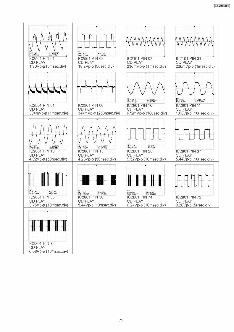
15.5. Waveform Chart 70
16 Wiring Connection Diagram 73 17 Block Diagram 75 18 Notes of Schematic Diagrams 81 19 Schematic Diagram 83
19.1. Optical Pickup Unit Circuit 83
19.2. (A) DVD Module Circuit 84
19.3. (B) Main (Tuner) Circuit 88
19.4. (B) Main Circuit 89
19.5. (C) Panel Circuit & (D) Tact Switch Cirucit 94
19.6. (E) Transformer Circuit 96
19.7. (G) Power Circuit 97
19.8. (H) Deck Circuit & (I) Deck Mechanism Circuit 100
20 Printed Circuit Board 101 20.1. (A) DVD Module P.C.B. (Side: A & B ) 102
20.2. (B) Main P.C.B. 103
20.3. (C) Panel P.C.B. 104
20.4. (D) Tact Switch P.C.B., (F) Mic P.C.B., (H) Deck P.C.B. ,
(I) Deck Mechanism P.C.B. & (J) Tuner P.C.B. 105
20.5. (E) Transformer P.C.B. 106
20.6. (G) Power P.C.B. 107
21 Basic Troubleshooting Guide 109
CONTENTS Page Page
4
SA-VK650EE

21.1. Basic Troubleshooting Guide for Traverse Unit (DVD
Module P.C.B.) 109
22 Illustration of ICs, Transistors and Diodes 110 23 Terminal Function of IC 111
23.1. IC2801 (C2CBYY000267) System Microprocessor 111
24 Exploded Views 113
24.1. Cabinet Parts Location 113
24.2. Cassette Mechanism Unit Parts Location (RAA3413-1S)
115
24.3. Packaging 116
25 Replacement Parts List 117
5
SA-VK650EE

1 Safety Precautions1.1. General Guidelines 1. When servicing, observe the original lead dress. If a short circuit is found, replace all parts which have been overheated or
damaged by the short circuit. 2. After servicing, see to it that all the protective devices such as insulation barriers, insulation papers shields are properly
installed. 3. After servicing, make the following leakage current checks to prevent the customer from being exposed to shock hazards.
1.1.1. Leakage Current Cold Check 1. Unplug the AC cord and connect a jumper between the two prongs on the plug. 2. Measure the resistance value, with an ohmmeter, between the jumpered AC plug and each exposed metallic cabinet part on
the equipment such as screwheads, connectors, control shafts, etc. When the exposed metallic part has a return path to thechassis, the reading should be between 1MΩ and 5.2MΩ.When the exposed metal does not have a return path to the chassis, the reading must be .
Figure 1
1.1.2. Leakage Current Hot Check(See Figure 1)
1. Plug the AC cord directly into the AC outlet. Do not use an isolation transformer for this check. 2. Connect a 1.5kΩ, 10 watts resistor, in parallel with a 0.15µF capacitor, between each exposed metallic part on the set and a
good earth ground such as a water pipe, as shown in Figure 1. 3. Use an AC voltmeter, with 1000 ohms/volt or more sensitivity, to measure the potential across the resistor. 4. Check each exposed metallic part, and measure the voltage at each point. 5. Reverse the AC plug in the AC outlet and repeat each of the above measurements. 6. The potential at any point should not exceed 0.75 volts RMS. A leakage current tester (Simpson Model 229 or equivalent) may
be used to make the hot checks, leakage current must not exceed 1/2 milliamp. In case a measurement is out of the limitsspecified, there is a possibility of a shock hazard, and the equipment should be repaired and rechecked before it is returned tothe customer.
1.2. Before Repair and AdjustmentDisconnect AC power, discharge Power Supply Capacitors C2550, C2556, C5101, C5104, C5165, C5166, C5171, C5172, C5950and C5966 through a 10Ω, 5W resistor to ground.DO NOT SHORT-CIRCUIT DIRECTLY (with a screwdriver blade, for instance), as this may destroy solid state devices.After repairs are completed, restore power gradually using a variac, to avoid overcurrent.Current consumption at AC 230V, 50Hz in NO SIGNAL (vol. min, at CD mode) should be ~200mA.
1.3. Protection CircuitryThe protection circuitry may have operated if either of the following conditions are noticed: · No sound is heard when the power is turned on. · Sound stops during a performance.
The function of this circuitry is to prevent circuitry damage if, for example, the positive and negative speaker connection wires are“shorted”, or if speaker systems with an impedance less than the indicated rated impedance of the amplifier are used.If this occurs, follow the procedure outlines below: 1. Turn off the power.
6
SA-VK650EE

2. Determine the cause of the problem and correct it. 3. Turn on the power once again after one minute.Note :When the protection circuitry functions, the unit will not operate unless the power is first turned off and then on again.
2 Prevention of Electro Static Discharge (ESD) toElectrostatically Sensitive (ES) Devices
Some semiconductor (solid state) devices can be damaged easily by electricity. Such components commonly are calledElectrostatically Sensitive (ES) Devices. Examples of typical ES devices are integrated circuits and some field-effect transistors andsemiconductor “chip” components. The following techniques should be used to help reduce the incidence of component damagecaused by electro static discharge (ESD). 1. Immediately before handling any semiconductor component or semiconductor-equipped assembly, drain off any ESD on your
body by touching a known earth ground. Alternatively, obtain and wear a commercially available discharging ESD wrist strap,which should be removed for potential shock reasons prior to applying power to the unit under test.
2. After removing an electrical assembly equipped with ES devices, place the assembly on a conductive surface such asaluminium foil, to prevent electrostatic charge build up or exposure of the assembly.
3. Use only a grounded-tip soldering iron to solder or unsolder ES devices. 4. Use only an anti-static solder remover device. Some solder removal devices not classified as “anti-static (ESD protected)” can
generate electrical charge to damage ES devices. 5. Do not use freon-propelled chemicals. These can generate electrical charges sufficient to damage ES devices. 6. Do not remove a replacement ES device from its protective package until immediately before you are ready to install it. (Most
replacement ES devices are packaged with leads electrically shorted together by conductive foam, aluminium foil orcomparable conductive material).
7. Immediately before removing the protective material from the leads of a replacement ES device, touch the protective materialto the chassis or circuit assembly into which the device will be installed.Caution
Be sure no power is applied to the chassis or circuit, and observe all other safety precautions. 8. Minimize body motions when handling unpackaged replacement ES devices. (Otherwise harmless motion such as the brushing
together of your clothes fabric or the lifting of your foot from a carpeted floor can generate static electricity (ESD) sufficient todamage an ES device).
7
SA-VK650EE

3 Handling Precautions for Traverse UnitThe laser diode used inside optical pickup could be destroyed due to static electricity as a potential difference is caused byelectrostatic load discharged from clothes or human body. Handling the parts carefully to avoid electrostatic destruction duringrepair.
3.1. Handling Optical Pickup 1. Do not impact on optical pickup as the unit structurally uses an extremely precise technology. 2. Short-circuit the flexible cable of optical pickup remove from the circuit board using a short-circuit pin or clip in order to prevent
laser diode from electrostatic destruction (Refer to Fig. 3.1 and Fig. 3.2) 3. Do not handle flexible cables forcibly as this may cause snapping. Handle the parts carefully (Refer to Fig. 3.1) 4. A new optical pickup is equipped with an anti-static flexible cable. After replacing and connecting to the flexible board, cut the
anti-static flexible cable. (Refer to Fig. 3.1)
Fig 3.1
3.2. Replacing Precautions for Optical Pickup UnitCD/DVD Optical PickupThe optical pickup by which part supply was carried out attaches the short clip to the flexible board for laser diode electrostaticdischarge damage prevention. Please remove the short clip and be sure to check that the short land is open, before connecting.(Please remove solder, when the short land short-circuits.)
3.3. Grounding for Preventing Electrostatic Destruction 1. Human body grounding
Use the anti-static wrist strap to discharge the static electricity accumulated in your body. (Refer to Fig. 3.2) 2. Work place grounding
Place a conductive material (conductive sheet) or ironboard where optical pickup is placed. (Refer to Fig. 3.2)Note :
Keep your clothes away from optical pickup as wrist strap does not release the static electricity charged in clothes.
Fig. 3.2
8
SA-VK650EE

4 Precaution of Laser Diode
Caution :This product utilizes a laser diode with the unit turned "ON", invisible laser radiation is emitted from the pick up lens.Wavelength : 785 nm(CD)/662 nm(DVD)Maximum output radiation power from pick up : 100 µW/VDELaser radiation from pick up unit is safety level, but be sure the followings: 1. Do not disassemble the optical pick up unit, since radiation from exposed laser diode is dangerous. 2. Do not adjust the variable resistor on the pick up unit. It was already adjusted. 3. Do not look at the focus lens using optical instruments. 4. Recommend not to look at pick up lens for a long time.
CAUTION!THIS PRODUCT UTILIZES A LASER.USE OF CONTROLS OR ADJUSTMENTS OR PERFORMANCE OF PROCEDURES OTHER THAN THOSE SPECIFIED HEREIN MAY RESULTIN HAZARDOUS RADIATION EXPOSURE.
n Use of Caution Labels
9
SA-VK650EE

5 Warning5.1. Service caution based on legal restrictions5.1.1. General description about Lead Free Solder (PbF)The lead free solder has been used in the mounting process of all electrical components on the printed circuit boards used for thisequipment in considering the globally environmental conservation.
The normal solder is the alloy of tin (Sn) and lead (Pb). On the other hand, the lead free solder is the alloy mainly consists of tin(Sn), silver (Ag) and Copper (Cu), and the melting point of the lead free solder is higher approx.30 degrees C (86°F) more than thatof the normal solder.
Definition of PCB Lead Free Solder being usedThe letter of “PbF” is printed either foil side or components side on the PCB using the lead free solder.(See right figure)
Service caution for repair work using Lead Free Solder (PbF) · The lead free solder has to be used when repairing the equipment for which the lead free solder is used.
(Definition: The letter of “PbF” is printed on the PCB using the lead free solder.) · To put lead free solder, it should be well molten and mixed with the original lead free solder. · Remove the remaining lead free solder on the PCB cleanly for soldering of the new IC. · Since the melting point of the lead free solder is higher than that of the normal lead solder, it takes the longer time to melt
the lead free solder. · Use the soldering iron (more than 70W) equipped with the temperature control after setting the temperature at 350±30
degrees C (662±86°F).
Recommended Lead Free Solder (Service Parts Route.) · The following 3 types of lead free solder are available through the service parts route.
RFKZ03D01K-----------(0.3mm 100g Reel)RFKZ06D01K-----------(0.6mm 100g Reel)RFKZ10D01K-----------(1.0mm 100g Reel)
Note* Ingredient: Tin (Sn), 96.5%, Silver (Ag) 3.0%, Copper (Cu) 0.5%, Cobalt (Co) / Germanium (Ge) 0.1 to 0.3%
10
SA-VK650EE

6 Accessories
Remote control
AC power supplycord
FM indoor antenna
AM loop antenna
Video cable
Mic
11
SA-VK650EE

7 Operation Procedures7.1. Main Unit Operation Control
12
SA-VK650EE

7.2. Remote Control Operation Control
13
SA-VK650EE

7.3.1. Disc Playability7.3. Disc Information
14
SA-VK650EE

7.3.2. To Play MP3/WMA and still pictures (JPEG/tiff)
15
SA-VK650EE

7.4. DivX VOD Content
16
SA-VK650EE

8 New Features8.1. CRS1D Mechanism Overview
17
SA-VK650EE

8.1.1. General Feature · This is a five disc changer mechanism for CD/DVD. The outline figure is shown below.
· The mechanism has "CHANGE WHILE PLAY" function. It open other trays for disc exchanging while one tray is at PLAYposition performing recording or reproducing.
· The mechanism can quickly change all trays with "CHANGE ALL" function. All trays can be move to OPEN position with oneoperation.
· There is no sensor to indicate presence of disc on any tray.
8.1.2. Hardware composition · Below is the hardware components of the mechanism
Name FunctionOpen Switch (OPEN-SW) The switch is used to detect normal tray opening
The switch is used for detect tray being manually push/trigger when full openHome Switch (HOME-SW) Is used to detect cam gear home positionClose Sensor (CLOSE-SENSOR) Used for normal single tray closing
Used to detect cam gear rotate to Play Driving positionPlay Switch (PLAY-SW) Detect TRV clamping complete positionStocking Switch (STOCK-SW) Detect tray completely transfer for play position to stocking positionUD Sensor (UD-SENSOR) Detect TRV vertical movement positionTop Switch (TOP-SW) Detect a default position of TRV vertical movement positionDriver IC To drive MotorMotor Main driving source for changerPlunger Switching the driving source from motor to:
1. Tray open/close
2. Drive tray to play/stock position and TRV vertical movement
8.1.3. Mechanism Operation · This mechanism has the following state:
1. Driving of a tray to open/close 2. Up/down operation of a traverse performs a state changes of tray.By using the plunger to lift/release of a switching gear, and the cam gear to lift/release the function gear the motor can be linkto several gear trains to perform various operations.
· The functions that can be perform in this mechanism are described as below:
Condition ExplanationOpen current playing tray The state to change current playing disc. All tray will be open at once and current tray at PLAY position
will be expose.Open All The state where all trays being driven to OPEN position. The disc can be taken in or out from tray to tray
by close tray one by one from top to bottom.Stock The state where the trays are stored in STOCK positionPlay The state where one of the tray 5 trays is being driven to PLAY position and clamped by traverse unitPlay & Open Tray-* The state where one of the tray is in playing position performing recording or reproducing, other trays can
be used (OPEN position) for disc exchanging without stopping the recording or reproducing process.
18
SA-VK650EE

8.2. Music Port
With reference to page 29 of the operating instruction manual.
Condition ExplanationChange The state when one of the opened tray being driven from OPEN position to STOCK position and other
opened trays remain still at OPEN position.Close All The state where all open trays will being driven from OPEN position to STOCK position, one by one from
top to bottomNote: * represent tray number (from 1 ~ 5)
8.1.4. New CD/DVD Mechanism (CRS1D)Note:This service manual does not contain the following information for the mention CD/DVD Mechanism drive: · Schematic Diagram, Block Diagram and P.C.B. layout of CD/DVD Loading P.C.B. · Part List for individual parts of the mechanism. · Exploded View and Parts List for individual parts of the CD/DVD Mechanism drive.
Please refer to the original service manual (Order No. MD0603065A3) for the CD/DVD Mechanism Drive CRS1D.
19
SA-VK650EE

9 About HighMAT9.1. What’s HighMAT?Consumers worldwide are using PCs to create their own collections of music, photos and even video by burning them onto CDs.But how these collections can be experienced across different devices can be confusing to navigate, time consuming to access fora DVD player, and be incomplete in terms of music information available to the customer.
HighMAT offers a solution to this growing consumer problem. HighMAT dramatically improves the digital media experience onconsumer electronic devices by delivering a simple, standardized approach that allows consumers who have created personalcollections of digital music, photography and video on their PC to:
>> Create a HighMAT CD or DVD which can be easily played back on consumer electronics devices such as CD and DVD players,and car stereos.>> Move digital media files (using recordable media such as CD-R and CD-RW) between the PC and various playback devicessuch as CD and DVD players.
A new standard for creating personal media on consumer electronic devices, HighMAT enable easier and more seamlessinteroperability between Windows PCs and devices designed for your living room, or the car.
9.2. Why take advantage of HighMAT?A Problem Defined:Today, when consumers create their own digital audio, video or photo collections on CD-R or other physicalformats, there are numerous, inconsistent ways that devices read the data. For the consumer, the playback experience can beconfusing:
20
SA-VK650EE

A Solution Created: HighMAT delivers a better digital media access experience by creating a standard approach for PCs tostructure digital media on various physical formats and for playback devices to read the data.
9.3. Benefits of HighMAT?
Conventional HighMATEven though DVD player is CD-R/RW compatible, the inconsistent waysthat various DVD players can read the music or photos files often leadsto a confusing and inconsistant playback experince.
HighMAT compatible products play content back with consistentinterface. This includes products which are JPEG compatible productswithout HighMAT support.
21
SA-VK650EE
22
SA-VK650EE

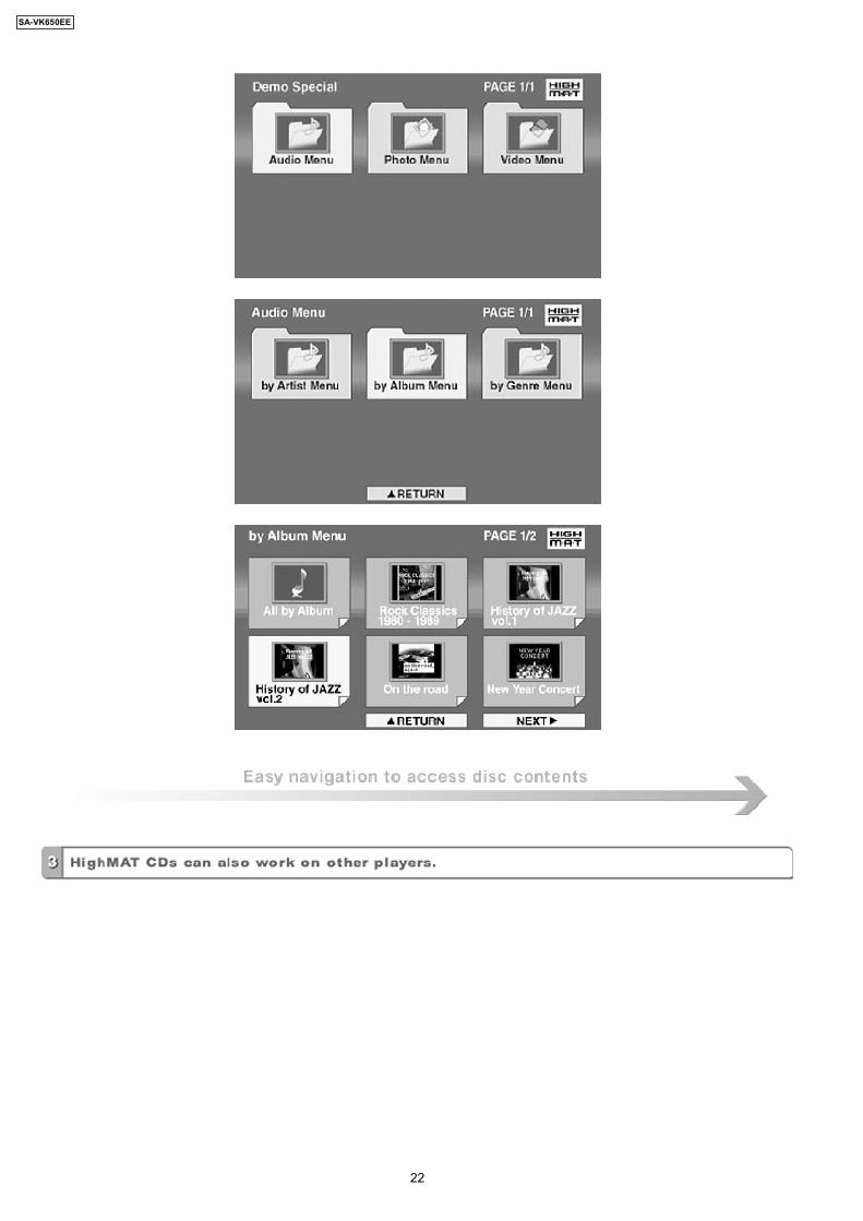
HighMAT is now available for CD Burning and in Leading DVD PlayersHighMAT is a new technology that is now available in leadingsoftware and consumer electronic devices to dramatically improve the digital media experience when you create homemadeCDsHighMAT delivers a simple, standardized way for PC software and consumer electronics devices to talk to each other and workbetter together.
When you create your homemade CDs with software that supports HighMAT CD burning, and then play them back on a DVDplayer that supports HighMAT, you get better, easier navigation. You get folders you can access with a single click of your DVDplayer´s remote control. You can view important information about your music like full song names, artist titles, album names andgenre. And you can get faster startup on your home entertainment device.
To enjoy the benefits of HighMAT, all you need is software that supports HighMAT for CD burning of music or photos, as well asa home entertainment device like a DVD player that supports HighMAT for playback. Always look for the HighMAT logo on yoursoftware or home entertainment device to ensure it supports the HighMAT experience.
23
SA-VK650EE
10 Self diagnosis and special mode settingThis unit is equipped with functions for checking and inspecting namely: Self-Diagnostic and Test Mode.
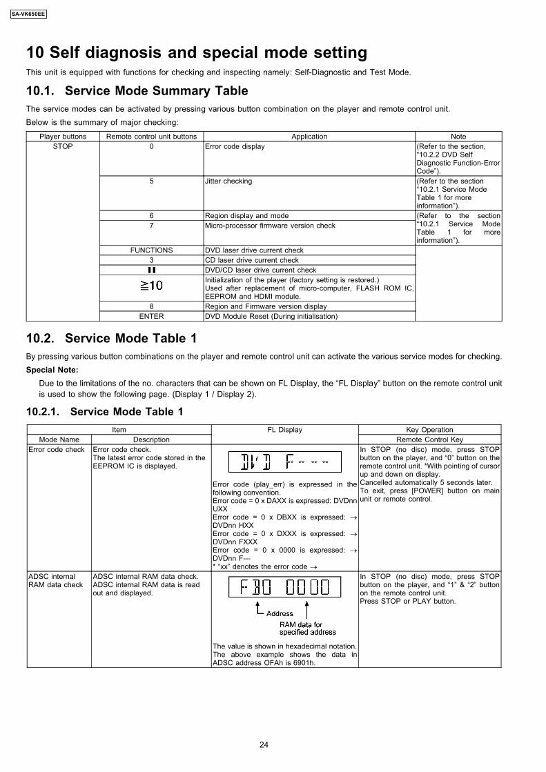
10.1. Service Mode Summary TableThe service modes can be activated by pressing various button combination on the player and remote control unit.Below is the summary of major checking:
Player buttons Remote control unit buttons Application NoteSTOP 0 Error code display (Refer to the section,
“10.2.2 DVD SelfDiagnostic Function-ErrorCode”).
5 Jitter checking (Refer to the section“10.2.1 Service ModeTable 1 for moreinformation”).
6 Region display and mode (Refer to the section“10.2.1 Service ModeTable 1 for moreinformation”).
7 Micro-processor firmware version check
FUNCTIONS DVD laser drive current check3 CD laser drive current check
DVD/CD laser drive current checkInitialization of the player (factory setting is restored.)Used after replacement of micro-computer, FLASH ROM IC,EEPROM and HDMI module.
8 Region and Firmware version displayENTER DVD Module Reset (During initialisation)
10.2. Service Mode Table 1By pressing various button combinations on the player and remote control unit can activate the various service modes for checking.Special Note:
Due to the limitations of the no. characters that can be shown on FL Display, the “FL Display” button on the remote control unitis used to show the following page. (Display 1 / Display 2).
10.2.1. Service Mode Table 1Item FL Display Key Operation
Mode Name Description Remote Control KeyError code check Error code check.
The latest error code stored in theEEPROM IC is displayed.
Error code (play_err) is expressed in thefollowing convention.Error code = 0 x DAXX is expressed: DVDnnUXXError code = 0 x DBXX is expressed: →DVDnn HXXError code = 0 x DXXX is expressed: →DVDnn FXXXError code = 0 x 0000 is expressed: →DVDnn F---* “xx” denotes the error code →
In STOP (no disc) mode, press STOPbutton on the player, and “0” button on theremote control unit. *With pointing of cursorup and down on display.Cancelled automatically 5 seconds later.To exit, press [POWER] button on mainunit or remote control.
ADSC internalRAM data check
ADSC internal RAM data check.ADSC internal RAM data is readout and displayed.
The value is shown in hexadecimal notation.The above example shows the data inADSC address OFAh is 6901h.
In STOP (no disc) mode, press STOPbutton on the player, and “1” & “2” buttonon the remote control unit.Press STOP or PLAY button.
24
SA-VK650EE
Item FL Display Key OperationMode Name Description Remote Control Key
CD laser drivecurrentmeasurement
CD laser drive currentmeasurement.CD laser drive current measuredand the result is displayed togetherwith the initial value stored in theEEPROM IC.After the measurement, CD laseremission is kept on. It is turned offwhen POWER key is switched off.(It is also turned off when POWERbutton on the player is switchedoff.)
The value denotes the current in decimalnotation.The above example shows the initial currentis 25mA and the measured value is 22mA.
In STOP (no disc) mode, press STOPbutton on the player, and “3” button on theremote control unit.Cancelled automatically 5 seconds later.Press “FL Display” button on remotecontrol unit for next page (FL Display).
Device Name Display the device name. 1.
2.
3.
In STOP (no disc) mode, press STOPbutton on the player, and “4” button on theremote control unit. *With pointing of cursorup and down on display.Cancelled automatically 5 seconds later.To exit, press [POWER] button on mainunit or remote control.
Jitter check Jitter check.Jitter rate is measured anddisplayed.Measurement is repeatedly done inthe cycle of one second. Readerror counter starts from zero uponmode setting. When target blockdata failed to be read out, thecounter advances by oneincrement. When the failure iscaused by minor error, it may becorrected when retired to enablesuccessful reading. In this case,the counter advances by one.When the error persists even afterretry, the counter may jump by twoor more.
Jitter rate is shown in decimal notation toone place of decimal.Focus drive value is shown in hexadecimalnotation.
In STOP (no disc) mode, press STOPbutton on the player, and “5” button on theremote control unit.Press STOP or OPEN button to exit.Press “FL DISPLAY” button on remotecontrol unit for next page (FL Display).
Region display Region display & mode In STOP (no disc) mode, press STOPbutton on the player, and “6” button on theremote control unit.Cancelled automatically 5 seconds later.
Micro- processorfirmware versiondisplay &EEPROMchecksum display.
Micro-processor firmware versiondisplay & EEPROM checksumdisplay.
In STOP (no disc) mode, press STOPbutton on the player, and “7” button on theremote control unit.Cancelled automatically 5 seconds later.Press “FL Display” button on remotecontrol unit for next page. (FL Display)
DVD modulefirmware versiondisplay
DVD module firmware versiondisplay is on the FL Display.
In STOP (no disc) mode, press STOPbutton on the player, and “8” button on theremote control unit.Cancelled automatically 5 seconds later.
25
SA-VK650EE
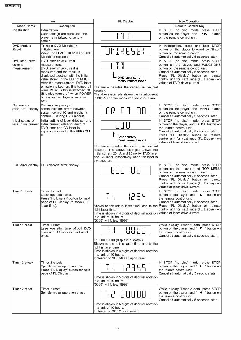
Item FL Display Key OperationMode Name Description Remote Control Key
Initialization Initialization.User settings are cancelled andplayer is initialized to factorysetting.
In STOP (no disc) mode, press STOPbutton on the player, and buttonon the remote control unit.
DVD ModuleReset
To reset DVD Module.(Ininitialisation)When the FLASH ROM IC or DVDModule is replaced.
In initialisation, press and hold STOPbutton on the player followed by “Enter”button on the remote control.Cancelled automatically 5 seconds later.
DVD laser drivecurrentmeasurement
DVD laser drive currentmeasurement.DVD laser drive current ismeasured and the result isdisplayed together with the initialvalue stored in the EEPROM IC.After the measurement, DVD laseremission is kept on. It is turned offwhen POWER key is switched off.(It is also turned off when POWERbutton on the player is switchedoff.)
The value denotes the current in decimalnotation.The above example shows the initial currentis 20mA and the measured value is 20mA.
In STOP (no disc) mode, press STOPbutton on the player, and FUNCTIONSbutton on the remote control unit.Cancelled automatically 5 seconds later.Press “FL Display” button on remotecontrol unit for next page (FL Display) onvalues of DVD drive current.
Communic-ation error display
Displays frequency ofcommunication errors betweensystem control IC and mechanismcontrol IC during DVD module.
In STOP (no disc) mode, press STOPbutton on the player, and “MENU” buttonon the remote control unit.Cancelled automatically 5 seconds later.
Initial setting oflaser drive current
Initial setting of laser drive current.Initial current value for each ofDVD laser and CD laser isseparately saved in the EEPROMIC.
The value denotes the current in decimalnotation. The above example shows theinitial current 20mA and 23mA for DVD laserand CD laser respectively when the laser isswitched on.
In STOP (no disc) mode, press STOPbutton on the player, and PAUSE button onthe remote control unit.Cancelled automatically 5 seconds later.Press “FL Display” button on remotecontrol unit for next page (FL Display) onvalues of laser drive current.
ECC error display ECC decode error display. In STOP (no disc) mode, press STOPbutton on the player, and TOP MENUbutton on the remote control unit.Cancelled automatically 5 seconds later.Press “FL Display” button on remotecontrol unit for next page (FL Display) onvalues of laser drive current.
Time 1 check Timer 1 check.Laser operation time.Press “FL Display” button for nextpage of FL Display (to show CDlaser time). Shown to the left is laser time, and to the
right laser time.Time is shown in 4 digits of decimal notationin a unit of 10 hours.“0000” will follow “9999”.
In STOP (no disc) mode, press STOPbutton on the player, and “ ” button onthe remote control unit.Cancelled automatically 5 seconds later.Press “FL Display” button on remotecontrol unit for next page (FL Display) onvalues of laser drive current.
Timer 1 reset Timer 1 reset.Laser operation timer of both DVDlaser and CD laser is reset all atonce.
T1_0000/0000 (display1/display2)Shown to the left is laser time and to theright is laser time.Time is shown in 4 digits of decimal notationin a unit of 10 hours.It cleared to ‘0000/0000’ upon reset.
While display Timer 1 data, press STOPbutton on the player, and “ “ button onthe remote control unit.Cancelled automatically 5 seconds later.
Timer 2 check Timer 2 check.Spindle motor operation timer.Press “FL Display” button for nextpage of FL Display.
Time is shown in 5 digits of decimal notationin a unit of 10 hours.“0000” will follow “9999”.
In STOP (no disc) mode, press STOPbutton on the player, and “ “ button onthe remote control unit.Cancelled automatically 5 seconds later.
Timer 2 reset Timer 2 reset.Spindle motor operation timer.
Time is shown in 5 digits of decimal notationin a unit of 10 hours.It cleared to ‘0000’ upon reset.
While display Timer 2 data, press STOPbutton on the player, and “ “ button onthe remote control unit.Cancelled automatically 5 seconds later.
26
SA-VK650EE

10.2.2. DVD Self-Diagnostic Function Error CodeErrorCode
Diagnosis Contents Description of error Automatic FL Display Remarks
F010 DVD Media disk A specification value is size from thePARENTAL LOCK value of theappointed country.
Press [ ] on mainunit for next error.
F020 DVD Media disk There is no TT_SRPT. (RLBN is 0). Press [ ] on mainunit for next error.
F021 DVD Media disk The number of TT_SRP is 0. Press [ ] on mainunit for next error.
F022 DVD Media disk A specification value. It is size from thenumber of TT_SRP.
Press [ ] on mainunit for next error.
F023 DVD Media disk VTSN or in agreement with VTS_TTN.There is no SRP.
Press [ ] on mainunit for next error.
F024 DVD Media disk A specification value. It is size fromTT_SRP. PTT_Ns
Press [ ] on mainunit for next error.
F030 DVD Media disk The number of TTU_SRP is 0. Press [ ] on mainunit for next error.
F031 DVD Media disk A specification value. It is size from thenumber of TTU_SRP.
Press [ ] on mainunit for next error.
F040 DVD Media disk The number of SRP1 is 0. Press [ ] on mainunit for next error.
F041 DVD Media disk The number of PGCI_SRP is 0. Press [ ] on mainunit for next error.
F042 DVD Media disk A specification value. It is size from thenumber of PGCI_SRP.
Press [ ] on mainunit for next error.
F043 DVD Media disk It is in agreement with Menu ID. There isno PGCI_SRP.
Press [ ] on mainunit for next error.
F050 DVD Media disk The number of TMAP_SRP is 0. Press [ ] on mainunit for next error.
F051 DVD Media disk A specification value. It is size from thenumber of TMAP_SRP.
Press [ ] on mainunit for next error.
F052 DVD Media disk Specification TMAP_SA is 0. Press [ ] on mainunit for next error.
F053 DVD Media disk The number of MAP_EN is 0. Press [ ] on mainunit for next error.
F060 DVD Media disk Although C_POSIT exists, it is in PGC.There is no PGMAP.
Press [ ] on mainunit for next error.
F061 DVD Media disk Although C_POSIT exists, it is in PGC.There is no PGMAP.
Press [ ] on mainunit for next error.
27
SA-VK650EE

ErrorCode
Diagnosis Contents Description of error Automatic FL Display Remarks
F062 DVD Media disk A specification value inside of PGC. It issize from the number of PGes.
Press [ ] on mainunit for next error.
F063 DVD Media disk Although C_POSIT exists, it is in PGC.There is no C_PBIT.
Press [ ] on mainunit for next error.
F064 DVD Media disk Although C_POSIT exists, it is in PGC.The number of PGes is 0.
Press [ ] on mainunit for next error.
F065 DVD Media disk Specification A cell number is 0.‘ Press [ ] on mainunit for next error.
F066 DVD Media disk A specification value inside of PGC. It issize from the number of Cell(s).
Press [ ] on mainunit for next error.
F067 DVD Media disk A blocked cell is present. Press [ ] on mainunit for next error.
F070 DVD Media disk There is no NV_PACK data. Press [ ] on mainunit for next error.
F080 DVD Media disk Under reference. There is no Cellnumber.
Press [ ] on mainunit for next error.
F0E0 DVD Media disk For [used as a DFD object] a user guide.A PGC control file < impossible.
Press [ ] on mainunit for next error.
F0E1 DVD Media disk DFD main microcomputer. Compatibilitywith a DFD type < download isimpossible.
Press [ ] on mainunit for next error.
F0E2 DVD Media disk DFD download start. PGC reproductionerror.
Press [ ] on mainunit for next error.
F0E3 DVD Media disk Waiting for the completion of DFDdownload. PGC reproduction error.
Press [ ] on mainunit for next error.
F0E4 DVD Media disk At the time of DFD download AVDEC. Press [ ] on mainunit for next error.
F0E5 DVD Media disk It is the farm file lead error at the time ofDFD download.
Press [ ] on mainunit for next error.
F0E6 DVD Media disk DFD alteration check error of the readfirmware.
Press [ ] on mainunit for next error.
F0F0 DVD Media disk There is no farm file used as a DFDobject and it is downloading needlessly.
Press [ ] on mainunit for next error.
F0F1 DVD Media disk The firware which is in agreement withDFD download conditions <unnecessary.
Press [ ] on mainunit for next error.
F103 Illegal highlight Position Big possibility of disc specificationviolation during highlight display
Press [ ] on mainunit for next error.
F4FF Force initialize failure(time out)
Timeout when force initialization fails Press [ ] on mainunit for next error.
28
SA-VK650EE

ErrorCode
Diagnosis Contents Description of error Automatic FL Display Remarks
F500 DSC error DSC (IC8251) stops in the occurrence ofservo error (startup, focus error, etc.)
Press [ ] on mainunit for next error.
F501 DSC not Ready error DSC-system computer communicationerror (Communication failure caused byidling of DSC)
Press [ ] on mainunit for next error.
F502 DSC Time out error Similar as F500 Press [ ] on mainunit for next error.
F503 DSC communicationFailure
Communication error (result erroroccurred although communicationcommand was sent)
Press [ ] on mainunit for next error.
F504 Abnormal adjusting DSCdata slice offset
Press [ ] on mainunit for next error.
F505 DSC Attention error Similar as F500 Press [ ] on mainunit for next error.
F506 Invalid media Disc is flipped over, TOC unreadable,incompatible disc media
Press [ ] on mainunit for next error.
F600 Access failure tomanagement informationcaused by demodulationerror
Operation stopped because navigationdata is not accessible caused by thedemodulation defect
Press [ ] on mainunit for next error.
F601 Indeterminate sector IDrequested
Operation stopped caused by therequest to access abnormal ID data
Press [ ] on mainunit for next error.
F602 Access failure to LEAD-IN caused bydemodulation error
LEAD IN data unreadable Press [ ] on mainunit for next error.
F603 Access failure toKEYDET caused bydemodulation error
Access failure to CSS data of disc Press [ ] on mainunit for next error.
F610 ODC abnormality No permission for command execution Press [ ] on mainunit for next error.
F611 No CRC OK for aspecific time (CD)
Access failure to seek address in CDseries
Press [ ] on mainunit for next error.
F612 No CRC OK for aspecific time (DVD)
Access failure to ID data in DVD series Press [ ] on mainunit for next error.
F620 Laser safeguard: hightemperature condition
High temperature of the laser guide unit(OPU unit)
Press [ ] on mainunit for next error.
F621 Laser safeguard: circuitfailure condition
Circuitry failure of the laser guide unit(OPU unit)
Press [ ] on mainunit for next error.
F700 MBX overflow When replying message to disc manager Press [ ] on mainunit for next error.
F701 Message commanddoes not end
Next message is sent before replying todisc manager
Press [ ] on mainunit for next error.
F702 Message commandchanges
Message is changed before it is sent asa reply to disc manager
Press [ ] on mainunit for next error.
29
SA-VK650EE

ErrorCode
Diagnosis Contents Description of error Automatic FL Display Remarks
F880 Task number is notappropriate
Message coming from a non-existingtask
Press [ ] on mainunit for next error.
F890 Sending message whenmessage is being sent toAV task
Sending message to AV task Press [ ] on mainunit for next error.
F891 Message couldn’t besent to AV task
Begin sending message to AV task Press [ ] on mainunit for next error.
F893 FLASH ROM IC problem FLASH ROM IC installed is not operatingproperly (Neccessary replacement ofFLASH ROM IC) or firmware problem
Press [ ] on mainunit for next error.
F894 EEPROM abnormality EEPROM IC installed is not operating innormal condition (EEPROM containsneccessary data)
Press [ ] on mainunit for next error.
F895 Region settingabnormality
Firm version agreement check for factorypreset setting failure prevention. Checkregion setting & re-initialize
Press [ ] on mainunit for next error.
F896 No existence model Firm version agreement check for factorypreset setting failure prevention
Press [ ] on mainunit for next error.
F897 Initialize is notcompleted
Initialize completion check for factorypreset setting failure prevention
Press [ ] on mainunit for next error.
F898 Disagreement ofhardware and software
Unsuitable combination of AVDECORDER, SDRAM and FLASH ROM(firmware)
Press [ ] on mainunit for next error.
F8A0 Message command isnot appropriate
Begin sending message to AV task Press [ ] on mainunit for next error.
Note:An error code will be canceled if a power supply is turned OFF.*1: CPPM is the copy guard function beforehand written in the disk for protection of copyrights.
10.2.3. Optical Pickup Breakdown DiagnosisThis unit is equipped with the optical pickup self-diagnosis function and the tilt adjustment check function. Follow the proceduredescribed below during repair in order to perform self-diagnosis and tilt adjustment effectively. Especially when “NO DISC” isdisplayed, be sure to apply the self-diagnosis function before replacing with an optical pickup. Replacement of optical pickupgenerally requires when the present value of laser drive exceeds 45 (DVD) or 45 (CD).Note:
Start diagnosis within three minutes after turning on the power (as diagnosis fails when the unit becomes warm).
30
SA-VK650EE

10.3. Special Mode Table 2Item FL Display Key Operation
Mode Name Description Front KeySelf -DiagnosticMode
To enter into selfdiagnostic checking formain unit.
1. Select [ ] for DVD/CD mode.
Ensure no disc is inserted.
2. Press and hold [ ]button for 2seconds follow by [ ].
To exit, press button on mainunit or remote control.
31
SA-VK650EE

Item FL Display Key OperationMode Name Description Front Key
CD ChangerReliability Test(CRS1D)
To determine thereliability of CD/DVDChanger Unit.(For more information,refer to section 10.3.1)
In Self-Diagnostic Mode: 1. Select [ ] for CD mode.
2. Press [1] on remote control..
To exit, press button on mainunit or remote control.(The tray will return to PLAY position and thenpower off)
Doctor Mode To enter into DoctorMode for checking ofvarious items anddisplaying EEPROM andfirmware version.
Below is various steps of display when enterinto doctor mode: 1. FL display will be light for 1 second.
2. It enters into doctor mode:
3. The checksum for EEPROM IC & firmwarewill be display
In CD/DVD or Tape mode: 1. Press [ ] button on main unit
follow by [4] and [7] on remote control.
To exit, press [ENTER] button on remotecontrol or button on main unitor remote control.Refer to Section 10.3.1 on information ofEEPROM checksum & ROM correction.
Cold Start Initialize backup data andstart.
In doctor mode: 1. Press [4] on remote control.
To exit, press [ENTER] button on remotecontrol or button on main unitor remote control.
FL Display Test To check the FLsegments display (Allsegments will light up andLED will blink at 0.5second interval)
In doctor mode: 1. Press [PLAY/REC] button on remote
control.
Tape Eject Test To check on the tapeeject function (For deck1/2)
In tape after entering doctor mode: 1. Press [0] button on remote control.
32
SA-VK650EE

Item FL Display Key OperationMode Name Description Front Key
Software Versionand EEPROMInformationDisplay
Execute Software Versionand EEPROM checksumdisplay for themicrocontroller.
1.
2.
Note:
There is no EEPROM IC install.
3.
In doctor mode: 1. Press [ ] button on main unit
follow by [4] and [7] on remote control.
To exit, press [ENTER] button on remotecontrol or button on main unitor remote control.
Firmware Versionchecking
Execute FirmwareVersion checking display.
In doctor mode: 1. Press [ ] button on main unit
follow by [CANCEL] on remote control.
To exit, press [ENTER] button on remotecontrol or button on main unitor remote control.
10.3.1. EEPROM Checksum (ROM Correction)Purpose: To check for microprocessor firmware version and EEPROM checksum (ROM correction).Below are the procedures for this mode.Step 1: Enter into Doctor mode (for more information, refer to section 10.3 on key operations to enter into this mode.Step 2: Check for firmware version and EEPROM checksum (By pressing STOP button on main unit followed by “4” and “7” onremote control). · When entering into DOCTOR MODE, the firmware version and checksum of EEPROM (if applicable) will appear on FL display.
Below is the information on the EEPROM IC (ROM correction) under 3 possible situations:1. In the case that the correction point existence data is other than 0 (ie. correction file exists), EEPROM checksum display forthe microprocessor shall be made after calculating checksum by summing up the content of data area from EEPROM.
2. In the case that the correction point existence data is 0, [NO] shall be displated.
33
SA-VK650EE

3. In cases that the filename is different even though a EEPROM is set, or no correction file exists, [NG] shall be displayed (thecorrection point existence data is set to 0 at this condition).
Note: Microprocessor firmware refers to version number for microprocessor IC. It is subject to change which would be updatedaccordingly. ROM correction checksum refers to the HEX code that is displayed upon key buttons pressed if an EEPROM is loadedin the unit.
10.3.2. CD/DVD changer unit ageing test modeBelow is the process flow chart of ageing for the CD/DVD changer unit. (CRS1D)
34
SA-VK650EE

10.3.3. Error Code TableSelf-Diagnosis Function (refer Section 10.3) provides information on any problems occuring for the unit and its respectivecomponents by displaying the error codes. These error code such as U**, H** and F** are stored in memory and held unless it iscleared.
35
SA-VK650EE

The error code is automatically display after entering into self-diagnostic mode.
Error Code Diagnosis Contents Description of error Automatic FL Display RemarksH01 Mode SW, plunger
and capstan motorabnormal
The tray is not able toopen.
For deck mechanism unit (For deck 1/2).Press [ ] on main unit fornext error.
H02 Rec INH SWabnormal
(Spindle servo, DSC(IC8251) Spindle motor,CLV servo error)
For deck mechanism unit (For deck 2).Press [ ] on main unit fornext error.
H03 HALF SW abnormal (Traverse motor,IC8251)
For deck mechanism unit (For deck 1/2).Press [ ] on main unit fornext error.
F01 Reel pulse abnormal For deck mechanism unit (For deck 1/2).Press [ ] on main unit fornext error.
F15 RESET SWabnormal
REST SW: ON is notdetected within thespecified time.
For DVD unit (For Traverse).Press [ ] on main unit fornext error.
F26 Transmission errorbetween CD ServoLSI IC andmicroprocessor IC
When set to CD mode,the sense signal doesnot turn “Low”, a fail safetime after systemcommand transmissionis sent.
For DVD unit (For Traverse).Press [ ] on main unit fornext error.
F61 Power Amp IC outputabnormal
Upon power on,PCONT=HIGH,DCDET=L after checkingLSI.
For power.Press [ ] on main unit fornext error.
IHMS Cam gearabnormality
Cam gear does notrotate to “HOME”position.
For DVD/CD changer unit (CRS1D).Press [SINGLE CHANGE] on main unitfor next error.
ICSL Cam gear/gear unitsabnormal
Cam gear does notrotate to “PLAY” drivingposition and hence doesnot drive playing tray to“STOCK” position.
For DVD/CD changer unit (CRS1D).Press [SINGLE CHANGE] on main unitfor next error.
ISTK Drive rack/gearassembly abnormal
The tray drive rack doesnot move to “STOCK”position. (Tray does notmove to “STOCK”position)
For DVD/CD changer unit (CRS1D).Press [SINGLE CHANGE] on main unitfor next error.
IPLY Drive rack/gearassembly abnormal
The tray drive rack doesnot move to “PLAY”position. (Tray does notmove to “PLAY” position)
For DVD/CD changer unit (CRS1D).Press [SINGLE CHANGE] on main unitfor next error.
36
SA-VK650EE
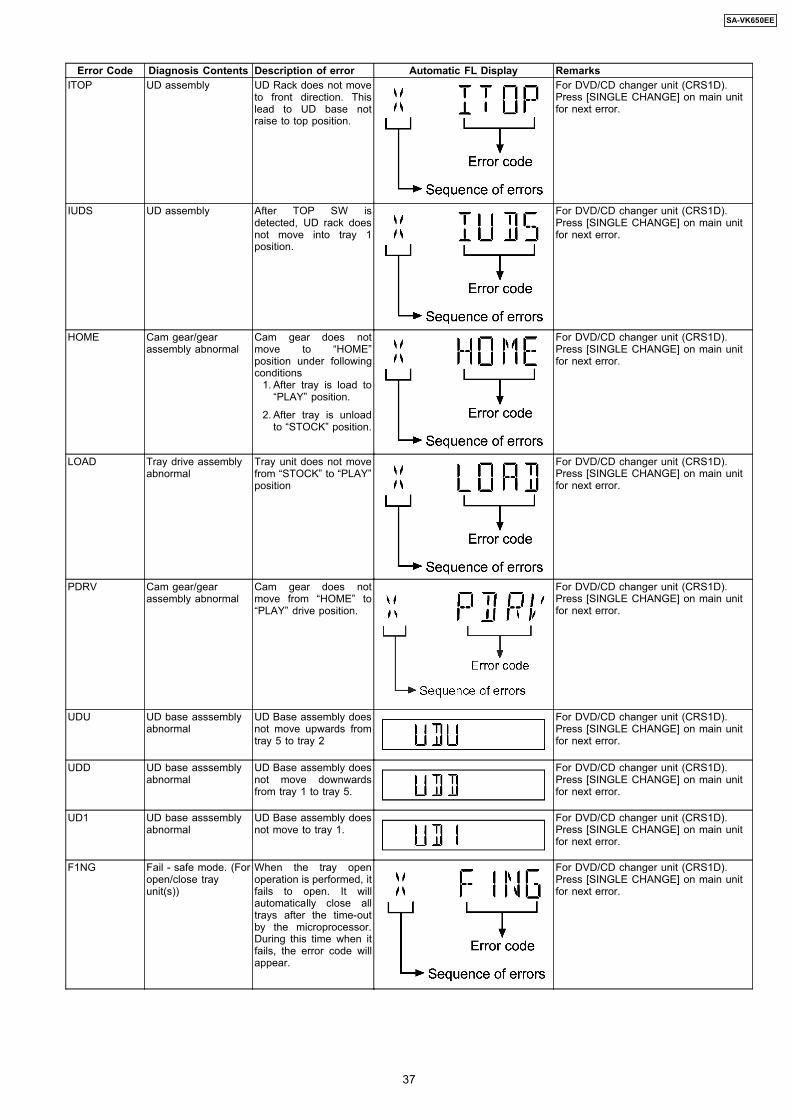
Error Code Diagnosis Contents Description of error Automatic FL Display RemarksITOP UD assembly UD Rack does not move
to front direction. Thislead to UD base notraise to top position.
For DVD/CD changer unit (CRS1D).Press [SINGLE CHANGE] on main unitfor next error.
IUDS UD assembly After TOP SW isdetected, UD rack doesnot move into tray 1position.
For DVD/CD changer unit (CRS1D).Press [SINGLE CHANGE] on main unitfor next error.
HOME Cam gear/gearassembly abnormal
Cam gear does notmove to “HOME”position under followingconditions 1. After tray is load to
“PLAY” position.
2. After tray is unloadto “STOCK” position.
For DVD/CD changer unit (CRS1D).Press [SINGLE CHANGE] on main unitfor next error.
LOAD Tray drive assemblyabnormal
Tray unit does not movefrom “STOCK” to “PLAY”position
For DVD/CD changer unit (CRS1D).Press [SINGLE CHANGE] on main unitfor next error.
PDRV Cam gear/gearassembly abnormal
Cam gear does notmove from “HOME” to“PLAY” drive position.
For DVD/CD changer unit (CRS1D).Press [SINGLE CHANGE] on main unitfor next error.
UDU UD base asssemblyabnormal
UD Base assembly doesnot move upwards fromtray 5 to tray 2
For DVD/CD changer unit (CRS1D).Press [SINGLE CHANGE] on main unitfor next error.
UDD UD base asssemblyabnormal
UD Base assembly doesnot move downwardsfrom tray 1 to tray 5.
For DVD/CD changer unit (CRS1D).Press [SINGLE CHANGE] on main unitfor next error.
UD1 UD base asssemblyabnormal
UD Base assembly doesnot move to tray 1.
For DVD/CD changer unit (CRS1D).Press [SINGLE CHANGE] on main unitfor next error.
F1NG Fail - safe mode. (Foropen/close trayunit(s))
When the tray openoperation is performed, itfails to open. It willautomatically close alltrays after the time-outby the microprocessor.During this time when itfails, the error code willappear.
For DVD/CD changer unit (CRS1D).Press [SINGLE CHANGE] on main unitfor next error.
37
SA-VK650EE

Error Code Diagnosis Contents Description of error Automatic FL Display RemarksF2NG Fail - safe mode. (For
open/close trayunit(s))
When the tray closeoperation is performed, itfails to close. It willautomatically open alltrays after the time-outby the microprocessor.During this time when itfails, the error code willappear.
For DVD/CD changer unit (CRS1D).Press [SINGLE CHANGE] on main unitfor next error.
SRVC_TRV To unlock thetraverse unit forservice
1. All trays set to“STOCK” position
2. Mechanism set totray 5
3. Cam gear set to“HOME” position
For DVD/CD changer unit (CRS1D).Press [SINGLE CHANGE] on main unit.
RSET Cam gear jam/closesensor faulty
During tray re-open, thecam gear will rotate inthe opposite direction toreset the cam gearposition. When it fails,the error code willappear.
For DVD/CD changer unit (CRS1D).Press [SINGLE CHANGE] on main unitfor next error.
CRS1D Error Code display 1. The errors that occured in CRS1D Mechanism can be recalled and displayed, in the order of the occurence under self-
diagnostic (Refer to Section 10.3 for procedures to enter this mode. · Only the first 5 errors will be memorized (in backup memory). The subsequence error shall be ignored and not memorize.
For system with EEPROM as memory backup,memory space in EEPROM is neccesary. 2. To display all error code memorized
In CRS1D Self-Diagnostic mode, press [SINGLE CHANGE] to display subsequence error code.It shall repeat after reaching error no. 5.e.g.:[1 _ _ _ _ I H M S] → [SINGLE CHANGE][2 _ _ _ _ I T O P] → [SINGLE CHANGE][3 _ _ _ _ H O M E] → [SINGLE CHANGE][4 _ _ _ _ L O A D] → [SINGLE CHANGE][5 _ _ _ _ _ U D D] → [SINGLE CHANGE]
3. To clear the error code memoryIn CRS1D Self-Diagnostic mode, long press [SINGLE CHANGE] key (2s or more)
38
SA-VK650EE

11.1. Caution
Below is the list of disassembly sections
11 Assembling and Disassembling
Special Note:This model uses a new CD/DVD changer unit CRS1D. In this following section does not contain the necessary disassembly &assembly information for the CD/DVD changer unit (CRS1D) except the disasembly & assembly of traverse unit. Kindly referto the original service manual for the CD/DVD changer unit. (Order No. MD0603065A3).
“ATTENTION SERVICER”Some chassis components may have sharp edges. Be careful when disassembling and servicing.
1. This section describes procedures for checking the operation of the major printed circuit boards and replacing the maincomponents.
2. For reassembly after operation checks or replacement, reverse the respective procedures.Special reassembly procedures are described only when required.
3. Select items from the following index when checks or replacement are required. 4. Refer to the Parts No. on the page of “Parts Location and Replacement Parts List” (Section 25), if necessary.Warning :-
This product uses a laser diode. Refer to caution statement Precaution of Laser Diode.Caution:
After replacing of CD/DVD Changer Unit, ageing test is necessary. Please confirm operation for CD/DVD Changer Unit.
· Disassembly of Top Cabinet · Disassembly of Rear Panel · Disassembly of CD/DVD Changer Unit · Disassembly of Main P.C.B. · Disassembly of Transformer P.C.B. · Disassembly of Power P.C.B. · Disassembly of Front Panel Unit · Disassembly of Panel P.C.B., Mic P.C.B. & Tact Switch P.C.B. · Disassembly of Deck Mechanism Unit · Disassembly for Deck P.C.B. · Disassembly of Traverse Unit · Disassembly of Optical Pickup unit (DVD Mechanism) · Disassembly of Deck Mechanism · Replacement for cassette lid · Rectification for tape jam problem
39
SA-VK650EE
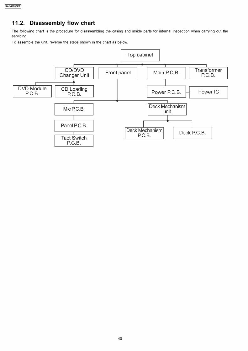
11.2. Disassembly flow chartThe following chart is the procedure for disassembling the casing and inside parts for internal inspection when carrying out theservicing.To assemble the unit, reverse the steps shown in the chart as below.
40
SA-VK650EE

11.3. Main Parts Location
41
SA-VK650EE

Step 1 Remove 3 screws at each side and 5 screws at rearpanel.Step 2 Lift up both sides of the top cabinet, push the topcabinet towards the rear to remove the top cabinet.
Step 1 Remove 8 screws.Step 2 Remove rear panel.
Step 1 Remove 2 screws at rear panel. Step 2 Detach the FFC cables (CN2801 & CN2805).
11.4. Disassembly of Top Cabinet
11.5. Disassembly of Rear Panel · Follow the (Step 1) - (Step 2) of Item 11.4 - Disassembly of Top Cabinet
11.6. Disassembly of CD/DVD Changer Unit (CRS1D) · Follow the (Step 1) - (Step 2) of Item 11.4 - Disassembly of Top Cabinet
42
SA-VK650EE

Step 3 Release the claws on both ends.
Step 4 Lift the CD/DVD changer unit upwards to remove it. · Disassembly of Mecha Chassis
Step 5 Remove 2 screws.Step 6 Remove the Mecha Chassis.Note:For disassembly & assembly of traverse unit, please refer toSection 11.4 of this service manual. Please refer to originalService Manual for the Assembling and DisassemblingProcedures of the CD/DVD Changer Unit (CRS1D), in Section5.
43
SA-VK650EE

11.7. Disassembly of Main P.C.B.
Step 1 Disconnect FFC cables (CN2803, CN2806 andCN2807). Disconnect wire M2 from CN5955
Step 1 Disconnect connectors (CN5950, CN5951 & CN5955).Step 2 Remove 3 screws (Mounting screws for transformer tobottom chassis).
Step 3 Push the Transformer P.C.B. sidewards to remove it.
Step 2 Detach connectors (CN2808 & CN2809).Step 3 Remove Main P.C.B.
· Follow the (Step 1) - (Step 2) of Item 11.4 - Disassembly of Top Cabinet · Follow the (Step 1) - (Step 3) of Item 11.5 - Disassembly of Rear Panel · Follow the (Step 1) - (Step 4) of Item 11.6 - Disassembly of CD/DVD Changer Unit
11.8. Disassembly of Transformer P.C.B. · Follow the (Step 1) - (Step 2) of Item 11.4 - Disassembly of Top Cabinet · Follow the (Step 1) - (Step 3) of Item 11.5 - Disassembly of Rear Panel · Follow the (Step 1) - (Step 4) of Item 11.6 - Disassembly of CD/DVD Changer Unit
44
SA-VK650EE

Step 1 Remove the 4 screws on Power P.C.B..
Step 2 Detach cable connected to CN5950 on TransformerP.C.B.Step 3 Remove Power P.C.B..Note:Insulate the Power P.C.B. with insulating material to avoid shortcircuit. · Replacement of the Power Amp IC or Voltage Regulator
Step 4 Remove 2 screws at the Power Amp ICs and/or 3screws to Voltage Regulators.
Step 5 Cut the joints with a metal cutter as shown below.
Step 6 Desolder the terminals to replace the components.
Step 7 Fix back the cut portion with a screw as shown.
11.9. Disassembly of Power P.C.B. · Follow the (Step 1) - (Step 2) of Item 11.4 - Disassembly of Top Cabinet · Follow the (Step 1) - (Step 4) of Item 11.6 - Disassembly of CD/DVD Changer Unit · Follow the (Step 1) - (Step 3) of Item 11.5 - Disassembly of Rear Panel · Follow the (Step 1) - (Step 3) of Item 11.7 - Disassembly of Main P.C.B.
45
SA-VK650EE
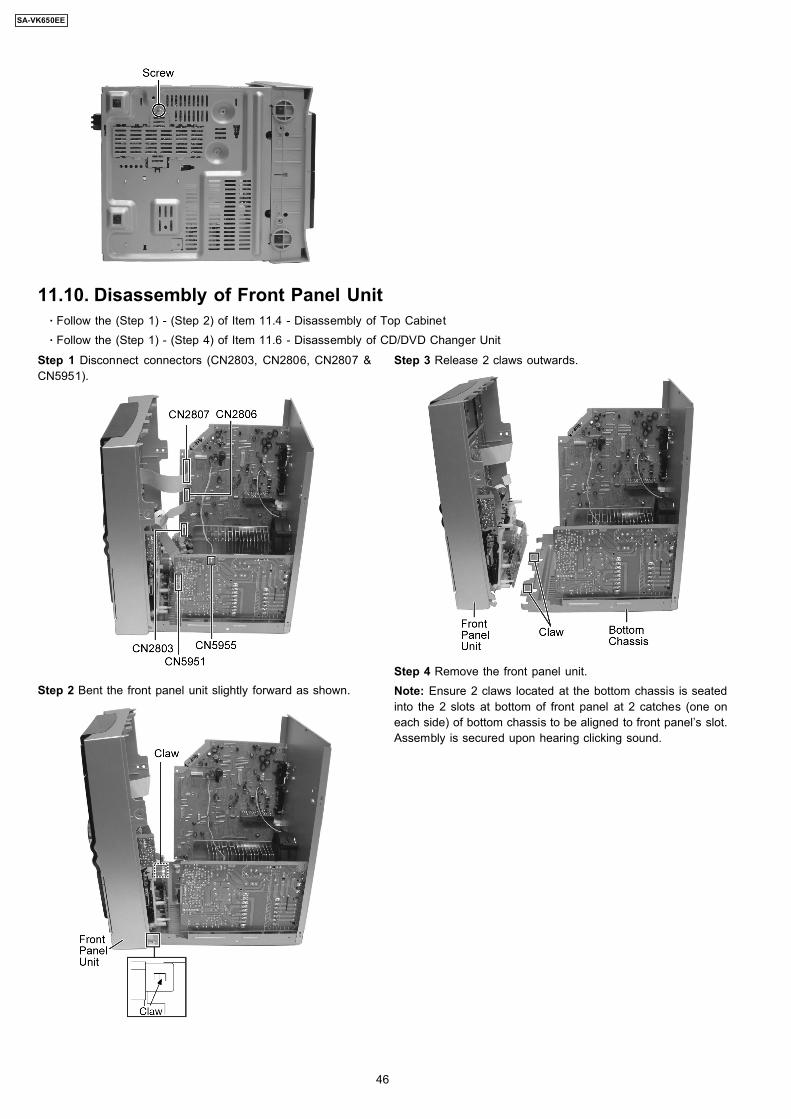
Step 1 Disconnect connectors (CN2803, CN2806, CN2807 &CN5951).
Step 2 Bent the front panel unit slightly forward as shown.
Step 3 Release 2 claws outwards.
Step 4 Remove the front panel unit.Note: Ensure 2 claws located at the bottom chassis is seatedinto the 2 slots at bottom of front panel at 2 catches (one oneach side) of bottom chassis to be aligned to front panel’s slot.Assembly is secured upon hearing clicking sound.
11.10. Disassembly of Front Panel Unit · Follow the (Step 1) - (Step 2) of Item 11.4 - Disassembly of Top Cabinet · Follow the (Step 1) - (Step 4) of Item 11.6 - Disassembly of CD/DVD Changer Unit
46
SA-VK650EE

Step 1 Remove the Volume knob.
Step 2 Remove 1 screw.Step 3 Lift up the Mic P.C.B to remove it.Step 4 Remove 6 screws.
Step 5 Release 2 catches.Step 6 Remove Panel P.C.B..
11.11.1. Disassembly of Tact Switch P.C.B.Step 7 Remove 6 screws..
11.11.2. Disassembly of LidStep 1 Lift the spring sideward.
Step 2 Remove Lid.Note: Do not misplace the spring.
11.11. Disassembly for Panel P.C.B. , Mic P.C.B. & Tact Switch P.C.B. · Follow the (Step 1) - (Step 2) of Item 11.4 - Disassembly of Top Cabinet · Follow the (Step 1) - (Step 4) of Item 11.6 - Disassembly of CD/DVD Changer Unit · Follow the (Step 1) - (Step 4) of Item 11.10 - Disassembly of Front Panel Unit
47
SA-VK650EE

Step 1 Detach FFC cable (CN971).Step 2 Disconnect FFC cable (CN1001).Step 3 Remove the 5 screws.
Step 1 Remove 2 screws.
Important notes: Ensure all the trays are in the “STOCK”position before proceeding to the disassemble of traverseunit. For procedures to set the trays in “STOCK” position,please refer to original Service Manual for CRS1D, Section4.3. Setting the trays in “STOCK” position, Order No.MD0603065A3.
Step 4 Push the lever upward, and then open the cassette lidass’y (For DECK1 and DECK2).
Step 5 Tilt the cassette mechanism unit in the direction ofarrow (1), and then remove it in the direction of arrow (2).Note: For disassembly of parts for deck mechanism unit,refer to Section 11.16.
Step 2 Desolder wire at deck motor terminals (W1002).
Step 3 Remove Deck P.C.B.
11.12. Disassembly of Deck mechanism unit · Follow the (Step 1) - (Step 2) of Item 11.4 - Disassembly of Top Cabinet · Follow the (Step 1) - (Step 4) of Item 11.6 - Disassembly of CD/DVD Changer Unit · Follow the (Step 1) - (Step 4) of Item 11.10 - Disassembly of Front Panel Unit
11.13. Disassembly of Deck P.C.B. · Follow the (Step 1) - (Step 2) of Item 11.4 - Disassembly of Top Cabinet · Follow the (Step 1) - (Step 4) of Item 11.6 - Disassembly of CD/DVD Changer Unit · Follow the (Step 1) - (Step 4) of Item 11.10 - Disassembly of Front Panel Unit
11.14. Disassembly of Traverse Unit · Follow the (Step 1) - (Step 2) of Item 11.4 - Disassembly of Top Cabinet · Follow the (Step 1) - (Step 4) of Item 11.6 - Disassembly of CD/DVD Changer Unit
48
SA-VK650EE

· Assembly of Traverse Unit
49
SA-VK650EE

Step 1 Pull out FFC.
Step 2 Widening the catch, push the pin in.
Step 3 Remove 4 pins.
11.15. Disassembly of Optical Pickup unit (CD/DVD mechanism) · Follow the (Step 1) - (Step 2) of Item 11.4 - Disassembly of Top Cabinet · Follow the (Step 1) - (Step 4) of Item 11.6 - Disassembly of CD/DVD Changer Unit · Follow the (Step 1) - (Step 2) of Item 11.14 - Disassembly of Traverse Unit
50
SA-VK650EE

Step 4 Remove the traverse deck.Note: As floating springs (4 pieces) come off at the same time,be careful not to lose them.
Step 5 Remove 4 screws.Step 6 Remove the DVD Servo P.C.B. and turn it over.Note: Insert a short pin into FFC of the optical pickup.Step 7 Rotate the traverse deck (B) to the arrow direction andshift the optical pickup to the furthest backward.
Step 8 Remove the catch of the drive rack, and take out thedrive rack.
Step 9 Place the convex part of an optical pickup to theconcave part of a traverse base, then take out the opticalpickup.
51
SA-VK650EE

* The mechanism as shown below is for DECK1. For DECK2, perform the same procedures.
11.16. Disassembly of Deck Mechanism · Follow the (Step 1) - (Step 2) of Item 11.4 - Disassembly of Top Cabinet · Follow the (Step 1) - (Step 4) of Item 11.6 - Disassembly of CD/DVD Changer Unit · Follow the (Step 1) - (Step 4) of Item 11.10 - Disassembly of Front Panel Unit · Follow the (Step 1) - (Step 5) of Item 11.12 - Disassembly of Deck Mechanism Unit
11.16.1. Disassembly of the pinch roller ass’y and head block
52
SA-VK650EE

Step 1 Detach the head block connector (Deck P.C.B.).Step 2 Desolder wire(W1002) at motor assembly.Step 3 Remove Deck P.C.B.
Step 1 Release the catch, and then remove the pinch roller (F).Step 2 Release 2 claws and detach the head block connector.
Step 3 Remove 2 screws.Step 4 Remove head block.
Step 4 Remove 3 screws (for deck 1 & 2).Step 5 Remove capstan belt A/B.
Step 6 Remove the flywheel R.Step 7 Release the claw and remove the winding lever andspring.[Installation of the belt]
11.16.2. Disassembly of capstan motor ass’y, capstan belt A, capstan belt B and windingbelt
53
SA-VK650EE
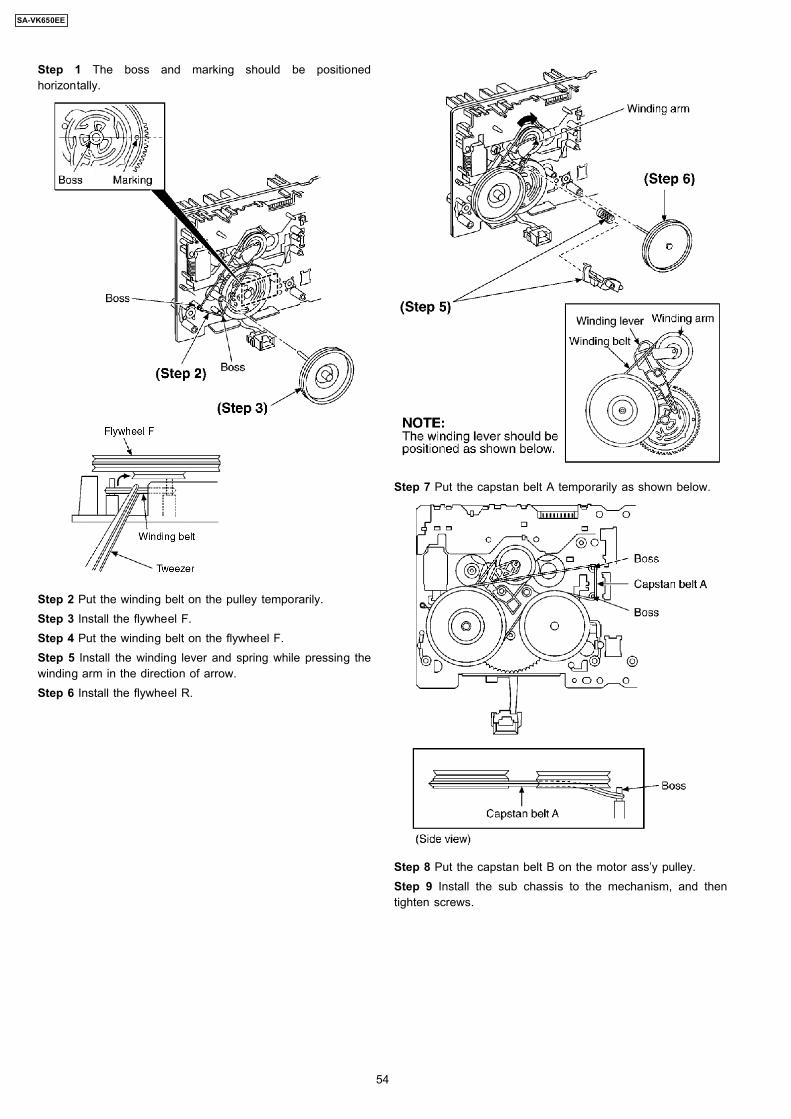
Step 1 The boss and marking should be positionedhorizontally.
Step 2 Put the winding belt on the pulley temporarily.Step 3 Install the flywheel F.Step 4 Put the winding belt on the flywheel F.Step 5 Install the winding lever and spring while pressing thewinding arm in the direction of arrow.Step 6 Install the flywheel R.
Step 7 Put the capstan belt A temporarily as shown below.
Step 8 Put the capstan belt B on the motor ass’y pulley.Step 9 Install the sub chassis to the mechanism, and thentighten screws.
54
SA-VK650EE

Step 10 Install 3 screws.Step 11 Put the capstan belt B as shown below.
Step 12 Put the capstan belt A on the motor ass’y pulley.
55
SA-VK650EE

Step 1 Lift up the lever upward, open the cassette deck. (ForDECK1 and DECK2)
Step 1 If a cassette tape cannot be removed from the deck (thetape is caught by the capstan or pinch roller during playback orrecording), rotate the flywheel F in the direction of the arrow toremove it.
Step 2 Push up the cassette lid (L/R) in the direction of arrow.(For DECK1 and DECK2).
Step 2 Push the lever upward and open the cassette lid.Remove the cassette tape.
11.17. Replacement for cassette lid · Follow the (Step 1) - (Step 2) of Item 11.4 - Disassembly of Top Cabinet
11.18. Rectification for tape jam problem · Follow the (Step 1) - (Step 2) of Item 11.4 - Disassembly of Top Cabinet
56
SA-VK650EE

12 Service Fixture and ToolsService Tools
Extension FFC(A) Deck P.C.B. - Main P.C.B. REEX0485 (14 Pins)(B) Panel P.C.B. - Deck Mechanism P.C.B. REEX0484 (10 Pins)
57
SA-VK650EE

13 Service PositionsNote: For description of the disassembly procedures, see the Section 11.
13.1. Checking and Repairing of Main P.C.B.
13.2. Checking and Repairing of Transformer P.C.B.
58
SA-VK650EE

13.3. Checking and Repairing of Panel, Deck & Deck Mechanism P.C.B.
59
SA-VK650EE

13.4. Checking and Repairing of Power P.C.B.
60
SA-VK650EE

14.1. Cassette Deck Section · Measurement Condition
− − − − Reverse-mode selector switch: − − − − Tape edit: NORMAL − − − − Make sure head, capstan and press roller are clean. − − − − Judgeable room temperature 20 ± 5 °C (68 ± 9°F)
· Measuring instrument − − − − EVM (DC Electronic volmeter) − − − − Digital frequency counter
· Test Tape − − − − Tape speed gain adjustment (3 kHz, -10 dB);
QZZCWAT
14.1.1. Head Azimuth Adjustment (Deck1/2)
Caution: · Please replace both azimuth adjustment screw and springs
simultaneously when readjusting the head azimuth. (shownin Fig. 2) Even if you wish to readjust the head azimuthwithout replacing the acrews and springs, a fine adjustmentto the azimuth screw and spring.
· Please remove the screw-locking bond left on the headbase when replacing the azimuth screw.
· If you wish to readjust the head azimuth, be sure to adjustwith adhering the cassette tape closely to the mechanismby pushing the center of cassette tape with your finger.(shown in Fig. 3)
1. Playback the azimuth adjustment portion (8 kHz, -20dB) ofthe test tape (QZZCFM) in the forward play mode. Vary theazimuth adjustment screw until the output of the R-CH (PBOUT-R) are maximized.
2. Perform the same adjustment in the reverse play mode. 3. After the adjustment, apply screwlock (NEJI-LOCK) to the
azimuth adjusting screw. Screw-Lock applied on the screwmust be more than 180° around screw. (Fig. 4)
14.1.2. Tape Speed Adjustment (Deck 1/2) 1. Set the tape edit button to “NORMAL” position. 2. Insert the test tape (QZZCWAT) to DECK 2 and playback
(FWD side) the middle portion of it. 3. Adjust Motor VR (DECK 2) for the output value shown
below.
Adjustment target: 2940 ~ 3060 Hz (NORMAL speed)
4. After alignment, assure that the output frequency of theDECK 1 FWD are within ±60 Hz of the value of the outputfrequency of DECK 2 FWD.
Fig. 1
14.1.3. Bias Voltage Check 1. Set the unit “AUX” position. 2. Insert the Normal blank tape (QZZCRA) into DECK 2 and
the unit to “REC” mode (use key). 3. Measure and make sure that the output is within the
standard value.
Bias voltage for Deck 2 14±4mV (Normal)
14 Adjustment Procedures
61
SA-VK650EE

Fig. 2
Fig. 3
1. Connect the instrument as shown in Fig. 5. 2. Set the unit to AM mode. 3. Apply signal as shown in Fig. 5 from AM-SG. 4. Adjust Z2602 so that the output frequency is maximized in
Fig. 6.
Fig. 5
Fig. 6
14.2.2. AM RF Adjustment 1. Connect the instrument as shown in Fig. 7. 2. Set the unit to AM mode. 3. Set AM-SG to 520kHz. 4. Receive 520kHz in the unit. 5. Adjust L2601 (OSC) so that the EVM-AC is maximized. 6. Set AM-SG to 600Hz.
14.1.4. Bias Frequency Adjustment (Deck1/2)
1. Set the unit to “AUX” position. 2. Insert the Normal blank tape (QZZCRA) into DECK 2 and
set the unit to “REC” mode (use key). 3. Adjust L1002 so that the output frequency is within the
standard value.
Standard Value: 89 ~ 110 kHz
Fig. 4
7. Receive 600Hz in the unit. 8. Adjust L2601 (ANT) so that the EVM-SG is maximized. 9. Set AM-SG to 520kHz. 10. Receive 520kHz in the unit. 11. Adjust L2602 (OSC) so that the EVM-DC value is with
1.1±0.5V.
Fig. 7
14.2. Tuner Section14.2.1. AM-IF Alignment
62
SA-VK650EE

14.3.1. Cassette Deck Section
14.3.2. Adjustment Point
14.3. Alignment Points
63
SA-VK650EE

15 Voltage and Waveform ChartNote:Circuit voltage and waveform described herein shall be regarded as reference information when probing defect point, because itmay differ from an actual measuring value due to difference of Measuring instrument and its measuring condition and product itself.
15.1. DVD Module P.C.B.
64
SA-VK650EE

65
SA-VK650EE
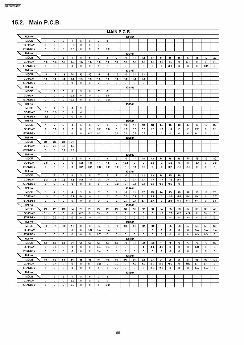
15.2. Main P.C.B.
66
SA-VK650EE

67
SA-VK650EE

15.3. Panel P.C.B. & Power P.C.B. & Transformer P.C.B.
68
SA-VK650EE

15.4. Deck P.C.B. & Deck Mechanism P.C.B. & Mic P.C.B. & Tuner P.C.B.
69
SA-VK650EE

15.5. Waveform Chart
70
SA-VK650EE
71
SA-VK650EE

SA-VK650EE
72

16 Wiring Connection Diagram
C PANEL P.C.B.SOLDER SIDE
G
DECK P.C.B.SOLDER SIDE
DECK MECHANISM P.C.B.SOLDER SIDE
HTACT SWITCH P.C.B.SOLDER SIDED
M112
MOTOR-+
CS1001
(DECK 1)PLAYBACK
HEAD
TO CRS1D(CN1)
SOLENOID SOLENOID
CN971
PbF
PbF
PbF
A DVD MODULE P.C.B.(SIDE B)
TOOPTICAL PICKUP
UNIT
FP8531
1 . . . . . . . . . . . 26
SOLDER SIDE
PbF
PbF
B MAIN P.C.B.SOLDER SIDE
J TUNER P.C.B.
CN2809
1. . . . . . . . . . . . 12
CN2808
1. . . . . . . . . . . . 12
CN2806
1
15
. . . . . . .
2
16
. . . . . . .
COMPONENTVIDEO OUT
VIDEOOUT
S-VIDEOOUT
JK2801
JK2601
JK2800
JK2803
PbF
10 . . . 29 . . . 1
AC IN ~
230V 50HZ
SOLDER SIDEPOWER P.C.B.
PbF
H51049 1. . . . . . .
JK5102
SPEAKER
JK6551
JK6552
Z6400
SENSOR
MUSICPORT
I
TOSPINDLEMOTOR
A DVD MODULE P.C.B.(SIDE A)
PbF
FP810150
1
. . . . . . . . . . . . . . . . . . .
FP82516 . . . .1
CS1002(DECK 2)R/P HEAD,
ERASE HEAD
12 .
54
12 .
54
CN10012 . . . . 10
1 . . . . . . 11
CN2803
1
11
2
10
. . .. . . .
1
CN2807
29
2
30
. . . . . . . . . . . . . . . . . .. . . . . . . . . . . . . . . . . .
CN280514 . . . . . 2
13 . . . . . 1
M212
CN2801
CN2810
FAN
1
1
49
. . . . . . . . . . . . . . .
3
47
. . . . . . . . . . . . .
2
2
50
. . . . . . . . . . . . . . .
4
48
. . . . . . . . . . . . .
FM LOOPANTENNA
DIGITAL OUT(COAXIAL)
AM LOOPANTENNA
H6556
7
1. . . . .
CN6401CN6808
CN68061 . . . . 9
1 . . . . . . . . . . . 14
H65559. . . . . . . . . 1
2 . . . . 10 15 . . . . 116 . . . . 2
1
CN6807
29
2
30
. . . . . . . . . . . . . . . . . .. . . . . . . . . . . . . . . . . .
F MIC P.C.B.SOLDER SIDE
MIC 2
MIC 1
PbFH6900
JK6902
JK6901
7
1
. . . . .
CAUTIONRISK OF ELECTRIC SHOCKAC VOLTAGE LINE.PLEASE DO NOT TOUCH THIS P.C.B
JK5950
T5950 (TRANSFORMER)
T5951 (SUB-TRANSFORMER)
1
CN5955
3.
9
CN59511. . . . .
CN59509 . . . . . . . 1
TRANSFORMER P.C.B.SOLDER SIDE
PbF
E
CN5103
1 . . . . . . . 12CN51021 . . . . . . . 12
PHONES
VR6491
CP6201
VOLUME
1
14
. . . . . . . . .
SA-VK650EE
73

SA-VK650EE
74

17 Block Diagram
LDUHFM
13
VO1-
11
VO2-
12
VO2+
14
VO1+
15
VO4+
16
VO4-
1BIAS
4OPIN+
24LDIN
25BIAS2
26TRIN
VIN3
23MUTE12
9
MUTE4
20
VIN1
2
VIN2
3
TRV_INNER_SW
163 162
X8621
67 66
6 5
TRACKINGCOIL
FOCUSCOIL
Q8551
SWITCH
Q8552
SWITCH
Q8561
SWITCH
Q8562
SWITCH
QR8571
SUPPLYCONTROLSWITCH
VCC
OUT
SW
1521M
8
SUB1
14
SUB2
13
VREF
11
RF
9
FE1
6
FE2
7
TC
4
OPTICAL PICKUP
SPINDLE MOTOR UNIT
TD
5
TB
2
TA
3
3 4 5 6 1
LD(DVD)17
LD(CD)16
B
17
VO3+
18
VO3-
TRVM-
TRVM+
T+
F+F-
T-
TA(DVD)
TB(DVD)
TD(DVD)
TC(DVD)
FE2(DVD/CD)
FE1(DVD/CD)
RF
VREF2(RF-)
VREF1
PIN(CD)
SUBSEL
LDCD
LDDVD
HFM
SUB2
SUB1
PIN(DVD)
SPM-
SPM+
MUTE3
27
86
V5
127 113 114 133 134 135 118 136 117 137 116 138 115 90
V1
88
V3
142 141144 145 12891 140 89
V2
OSCO
OSCI
P2
P1
124 12613981 130 131129132123125 87
DR
VREFH
RFINN
RFINP
VIN7
VIN8
VIN3
VIN3RF
VIN4
VIN4RF
VIN2
VIN2RF
VIN1
VIN1RF
DR
DR AD4
AD2
PWM1
PWM0
VHALF
DRV0
AD1
DR
LPC01
LPC02
AD0
P14
VIN9
VIN5
VIN10
VIN6
LPC1
LPC2
DRV4
5
OPIN-
6
OPOUT
IC8001
DRIVER IC
IC8251
C0GBG0000048
EEPROM(NOT SUPPLIED)
IC8611
DQ0
2,4,5,7,8,10,11,13,42,44,45,47,48,50,51,53
DQ15
198~203, 206~213,216, 217
1
230, 232, 236,237, 240~247,
A0
22-26,29-35
A11
BA0
20
235
BA1
21
231
LDQM
15
219
UDQM
39
220
/CS
19
229
CLK
38
223 225
/RAS
18
228
/CAS
17
227
/WE
16
221
A0
1~8,18-25
A15
18, 42, 43,46~51, 58~64
DQ0
29-36,38-45
DQ15
23~33,36~40
XWE
11
55
XCE
26
19
XOE
28
20
12
1
1
XRESET
84
IC8001
A16
9, 16,17, 48
A19
MDQ0
MDQ15
MA0
MA1
BA0
BA1
DQM0
DQM1
NCSM
MCK
MCKI
NRAS
NCAS
NWE
EXADT0
EXADT15
EXDT0
EXDT15
NEXWE
NEXCE
NEXOE
NRST
EXADR16
EXADR19
41, 54,56, 57
A20
10
65
P0
IC8051
C3ABPG000145
64 SDRAM IC
IC8651
IC8601
C0EBA0000029
IC8606
C0EBE0000455
RESET IC
RESET IC
RFKWMHA0H160
16M FLASH ROM IC
MN2DS0009VP DV3.2 LSIMN2DS0009VP DV3.2 LSI
B
5
8B
1
QR8111
SWITCH B
3.3 REGULATOR IC
IC8111
C0CBCBD00018 INOUT
REGULATOR IC
IC8151
C0DBEHG00006 B2
INB4
OUT
SA-VK650EE
75

74
21
75
OP_CPU_CLK
OP_CPU_STAT
OP_CPU_CMD
21
5 5
B
DVD_STAT
DVD_CLK
4 4
A
IC8001MN2DS0009VP DV3.2 LSI
IC8691
C0JBAA000346
AND GATELOGIC IC
TO MAINBLOCK
IC8695
C0JBAA000346
AND GATELOGIC IC
LRCK
8
167
DATA1
6
169
BCK
7
168
SCK
5
166
MD
4
77
MC
3
78
MS
2
76
ZEROR
16
80
15(14)
VOUTL(R)
QR8420
MUTINGSWITCH
73
LRCK
ADOUT3
SRCK
DACCK
SBO3
SBT3
STBDAC
P13
DVD_MIXL(R)
ZFLAG
DVD_CMD
IC8420
C0FBBK000049
2-CH DAC IC
RCH
B
B
B
B
B
B
IC2601
C1BB00000962FM/AM IF AMP,DET/AM OSC,MIX/FM MPX
SD
ST
SHIFT REGISTER LATCH
12
SWALLOW COUNTER1/6,1/17,4 BITS
12 BITS PROGRAMMABLEDIVIDER
REFERENCEDIVIDER
C2BI/F
PLLCLK
PLLDA
ST/DO
PLLCE
X2603
ST/DO
SD
S-CURVE
REG
FMIF
FMDET
AMOSC
LEVELDET
BUFFER
ALC DECODER
STEREOSWITCH
AMDET
AMIF
TUNINGDRIVE
AM/FMIF
BUFFER COMP
REG
VCO
AMMIX
AMRMAMP
AGC
PHASEDET
PILOTDET
FF FF FF
PILOTCANCEL
(FM)
TUNER15V
SUPPLYSWITCH
Q2606
POWER ONRESET
UNIVERSALCOUNTER
UNLOCKDETECTOR
PHASE DETECTORCHARGE PUMP
TOCDDRIVEBLOCK
PLL FREQUENCYSYNTHESIZER
C1CB00001937
IC2602
X2602
11
15
18
17
16
19 10 7 6 9 8
4CL
3DI
2CE
5DO
13
12
14
20
1
L2602D2602L2601
2324 22 21 20 19 18 17 16 1415 13
1 2 3 4 65 7 8 9 10 11 12
FMIF AMP
A
CF2601 CF2602
FMANT
Z2620
8
(FM)
MIXER
OSC BUFFER
6
5
1 7
AMIFT
Z2602
AMANT
B
RF AMP
149 148 147 156 157
DAC1OUT
DAC2OUT
DAC3OUT
DAC4OUT
DAC5OUT
PY
CB_B
CR_R
S_Y
S_C Q2601
IECOUT
173
OPTICAL JK2801
Q2980
SA-VK650EE
76

PHOTO_2
PHOT0_1
DECK1_H
REC
MTR
HALF_1
MODE_1
IC2801
B
AN7348S-E1
P.B EQ/REC AMP/ALC/TPS AMP
C1AA00000612
R/P SELECT
IC1004
Q1003
SWITCHING(BEAT PROOF/
RECH)
L1002
BIAS OSCCONTROL
Q1004,Q1005,Q1007
NOR/CrO &HI/LO LOGIC
LOGICREC/PB
RIPPLEREJECTION
LOGIC L/H
ALC
Q2978
CONTROLSWITCH
95
IC951
PHOTOINTERRUPTER
CNB13030R2AUIC971
PHOTOINTERRUPTER
CNB13030R2AU
97 60
10
16
14
13
11
6
19
15
12
21(4)
22(3)
17(8)
1(2)
24(23)
18(7)
9
3
5
2
4
59
Q2979
SUPPLYCONTROLSWITCH
58
20(5)
M1002
S951
MODE
5253
S952
HALF
(DECK 2)R/P HEAD
LCH
B
B
Q1017
MOTORSWITCH
M
(DECK 2)ERASE HEAD
(DECK 1)P.B. HEAD
LCH
D951
D1003
PL971
D2912 PLUNGERSUPPLY SWITCH/PLUNGER:ON/OFF
SWITCH
56
Q6415,Q6425
SDSD
JOG VOL
VR6491
IC2801C2CBYY000267 MICROPROCESSOR C2CBYY000267 MICROPROCESSOR
FL_CS
FL_DOUT
FL_CLK
X_OUT
13
X_IN
15
V_JOG_A
67
V_JOG_B
68
X2802X2801
XC_IN
10
XC_OUT
11
32~4214~29,31
S1
C0HBB0000057
FL DRIVER
IC6601
STB
DIN
CLK
9 7 8
G12
G1
S17
FROM POWERTRANSFORMER
SG1
SG17
5~20,41 30~40
GR1
GR11FL6602
FL DISPLAY
IC2701
C9ZB00000498
VIDEOBUFFER IC
37
22
35
36
DVD_CLK
DVD_STAT
DVD_CMD
DVD_CLK
ST/DOST/DO
PLLCLK
PLLDA
PLLCE
PLLCE
PLLCLK
PLLDA
21
29 330
DVD_STAT
DVD_CMD
13CYOUT Y
12CBOUT CR
11CROUT CB
15VOUT
14YOUT
JK2803
16COUT
CRIN9
CBIN8
CIN2
YIN4
CYIN
6
CR_R
CB_B
PY
S_C
S_Y
GY
CJK2800
VIDEOOUT
S-VIDEO
72 73 74
PLG1
IC1001
Z6400REMOTE SENSOR
RMT
18
Z971INTERFACE
91
DECK2
S972
HALF
S975
RECINH_F
S971
MODE
S974
RECINH_R
B
B
ZFLAG
DVD_MIXL(R)
DVD_MUTE
6
Q2051
DVDCONTROLSWITCH
Q2912
MUTESWITCH
Q2052
SWITCH
WIDE_1
4
B
Q2901
SWITCH
TOCD LOADING CIRCUIT
84
MOT_CW
85
MOT_CCW
80
HOME_SW
86
ST_SW
83
OPEN_SW
82 87
PLAY_SW
79
UP_SENSOR
78
BOTTOM_SW
PLUNGER
CAM_SENSOR
81
Q2913
B
Q2914
SUPPLYCONTROLSWITCH
PLUNGERON/OFFSWITCH
SA-VK650EE
77

PL971
PLUNGERSUPPLY SWITCH/PLUNGER:ON/OFF
SWITCH
Q6411,Q6421
57
D971
IC2802
5 4 36
IC2801C2CBYY000267 MICROPROCESSOR
C1L(R)
IC2101
C1BB00000732
ASP IC
18
26 27
9(10)
7(8)
1
3
32
31
5(6)
11(12)
SI
ASP_DAT
ASP_CLK
17
SC
50
MIC_LVL1
51
MIC_LVL2
D1L(R)
B1L(R)
A1L(R)
VIN1(R)
REC1(L)
REC2(L)
VIN2(R)
43
EE_DAT
42
EE_CLK
41
EE_CS/EFP/EPH
PLG2
D6932
D6931
S6101~S6105,S6107,S6201~S6210,S6302~S6312
92 ~ 94
KEY1~KEY3
SYNC
MUTE_D
MUTE_A
IC2103
C0ABBB000230
IC OP-AMP
6(2)7(1)
5(3)
RCH
JK6552MUSIC PORT INPUT
JK6901,JK6902MIC1,MIC2
MICAMP
Q6901-Q6903
20
7F_HOP
46PCONT/EFP_/CE
39
40
Q2806
B
B
D2802
RESETSWITCH
Q6912
Q6904,Q6910
Q6905,Q6911
IC6930
C0ABBB000244
IC OP-AMP
21
3
1
LM_L
D2332
(NOT SUPPLIED)EEPROM
Q6907 Q6908 Q6906 Q6909
IC2061
67
1
5
3
2
C0ABBB000244IC OP AMP
Q2065
SUBWOOFERMUTINGSWITCH
45
SW_LVL2
49
LED_CTRL2
48
LED_CTRL2
44
SW_LVL1
Q2061
Q2062
LEVELCONTROLSWITCH
LEVELCONTROLSWITCH
Q2063
Q2064
SUPPLYCONTROLSWITCH
SUPPLYCONTROLSWITCH
76
LPF_IN
ECHO_MUTE
69
ECHO_1
70
ECHO_2
75
ECHO_3
2
LPF_OUT
LPF2_IN
LPF2_OUT
3
IC6931
C1BB00001061
IC ECHO
10
OP2_IN
OP2_OUT
9 12 11
22(21)
2
5
11
OUTIN1(2)
Q2551
Q6803,Q6804
Q2576
47
D2576
IC2804
C0AABA000009
IC OP-AMP
2(6)1(7)
3(5)
DVDSUPPLYSWITCH
DECK SUPPLYCONTROLSWITCH
Q6805
PCONT SWITCH
Q2366
HEADPHONEMUTINGSWITCH
MUTINGCONTROLSWITCH
DVDDETECTSWITCH
B
B
B
B
B B
B
B
Q2502
Q2501
Q2552
Q2142,Q2242
D2555~D2557
SWITCH
IC2561
C0DAAMH00012REGULATOR
DC_DET
5
DVD_PCONT
AGCCONTROLSWITCH
Q2143,Q2243 MUTING
SWITCH
VIN
VREF2
VOUT
DVDSUPPLYSWITCH
12
/RESET
Q6702
D6707
D6708
Q6703
Q6701
LEDSWITCH
LEDSWITCH
LEDSWITCH
B
MUTINGSWITCH
SWITCH SWITCHSWITCH
MIC LEVELCONTROLSWITCH
SWITCH/MIC LEVEL SWITCH
SWITCH/MIC LEVEL SWITCH
D2578
SEL2(R)
SEL1(L)2
4
75(74)
KA_LOUT64(65)
KA_ROUT
MIC_IN
KA_DAT
KA_CLK
KA_CS
62(63)
77 32 33 34
IC2731
C1BB00001012KA_LIN(RIN)
232425KA_DAT
KA_CLK
KA_CS
IC KARAOKE
SA-VK650EE
78

: MAIN SIGNAL LINE
: FM OSC SIGNAL LINE
: FM SIGNAL LINE
: CD SIGNAL LINE
: AM OSC SIGNAL LINE
: AUX SIGNAL LINE
: AM SIGNAL LINE
: FM/AM SIGNAL LINE
: CD-DA (AUDIO/VIDEO) SIGNAL LINE
: PLAYBACK SIGNAL LINE
: RECORD SIGNAL LINE
SIGNAL LINES
( ) Indicates the Pin No. of Right Channel. NOTE : Signal Lines are applicable to the Left Channel only.
DC_DET
HP_L(R)
DVD_SUPPLY
HP_SW
HP_SW
MPORT_SW
MPORT_SW
MIC_SW
MIC_SW
F_HOP
PCONT/EFP_/CE
SYNC
MUTE_D_AMP
MUTE_A
C1BA00000407
2-CH DIGITAL AMP
IC5301
IN1+
IN1-
21(2)
22(3)
OSC1
MODE
L5301
23
OUT1
OUT2
10
14
B
B
B
B
B
B
T5950
VOLTAGE
REGULATOR
(-VP)
CURRENT CONTROL SWITCH/
VOLTAGE REGULATOR
CURRENT CONTROL SWITCH/
SWITCH/
VOLTAGE REGULATOR
D5959
Q5951 POWERTRANSFORMER
T5951
PCONT
CONTROL
F1
Q5953
D5123,D5214,
D5127,D5128Q5115
Q5950
SYSTEM 6V
VOLTAGE
REGULATOR
JK5950
AC INLETL5950
LINE FILTER
D5950~D5953
D5974~D5977
FP5950
SUB
TRANSFORMER
D5970~D5973Q5112~Q5114
5.7V VOLTAGE
REGULATOR
15V VOLTAGE
REGULATOR
CURRENT STABLISER/
LIMITER SWITCH/
11V VOLTAGE REGULATOR
Q5101,Q5110Q5111
Q5102,Q5108,Q5109
Z5950
RL5950
S5950
TOFL DISPLAY
F2SW
VOLTAGE
SELECTOR
SYNC
Q5952
SYNCHRONISING
SWITCH
Q5151
MODE
SWITCH
MUTE_D_AMP
Q5152
SWITCH
MUTE_A
Q5150
PCONT
SWITCH
PCONT/EFP_/CE
Q5103,
Q5104
FAN
ON/OFF
SWITCH
RCH
JK6551
PHONES
D5126FAN
F_HOP
Q5201
Q5202
X5202
X5201
HOPPING
SWITCH
HOPPING
SWITCH
C0JBAB000011
LOGIC IC
IC5201
1
2
5
3(6)
10
IN1-3
C1BA00000407
2-CH DIGITAL AMP
IC5501
11(13)VSSP1(2)
8(16)VDDP1(2)
11,13VSSP1(2)
8,16VDDP1(2)
IN1+2
OSC1
MODE
OUT1
L5501
23
9(10)
Q5954
CURRENT
LIMITING
SWITCH
DC_DET
DVD_SUPPLY
SUBWOOFER
HP_L(R)
MUTE_A
PCONT/EFP_/CE
Q2942
+VE
-VEQ2943
D2944
Q2949,Q2948
B
REGULATOR
Q5708,Q5709
B REGULATOR
Q5707
FAN
FAN
RIGHT CH
LEFT CH
JK5102
L5402
L5302
L5401
SUBWOOFER
D5961~D5964
SA-VK650EE
79

SA-VK650EE
80

(All schematic diagrams may be modified at any time with thedevelopment of the new technology)S951 : MODE SwitchS952 : HALF SwitchS971 : MODE SwitchS972 : HALF SwitchS974 : RECINH_R SwitchS975 : RECINH_F SwitchS6101 : POWER SwitchS6102 : SSEQ SwitchS6103 : Sound EQ SwitchS6104 : Multi Remaster SwitchS6105 : Subwoofer SwitchS6107 : Deck 1 SwitchS6201 : Tape SwitchS6202 : DVD/CD SwitchS6203 : FWD SwitchS6204 : Stop SwitchS6205 : Rew SwitchS6206 : Rec SwitchS6207 : Deck 1/2 SwitchS6208 : Display/Demo SwitchS6209 : Music Port SwitchS6210 : Tuner SwitchS6302 : Disc Check SwitchS6303 : Open/Close SwitchS6304 : Disc Change SwitchS6305 : DISC 1 SwitchS6306 : DISC 2 SwitchS6307 : DISC 3 SwitchS6308 : DISC 4 SwitchS6309 : DISC 5 SwitchS6310 : Mic Vol + SwitchS6311 : Mic Vol - SwitchS6312 : Deck 2 SwitchVR6491 : VR VOLUME JOG · The voltage value and waveforms are the reference voltage
of this unit measured by DC electronic voltmeter (highimpedance) and oscilloscope on the basis of chassis.Accordingly, there may arise some error in voltage valuesand waveforms depending upon the internal impedance ofthe tester or the measuring unit.
· Importance safety notice :Components identified by mark have specialcharacteristics important for safety. Furthermore, specialparts which have purposes of fire-retardant (resistors), high-quality sound (capacitors), low-noise (resistors), etc. areused. When replacing any of components, be sure to useonly manufacturer´s specified parts shown in the parts list.
Caution !IC, LSI and VLSI are sensitive to static electricity.Secondary trouble can be prevented by taking care duringrepair. · Cover the parts boxes made of plastics with aluminium foil. · Put a conductive mat on the work table. · Ground the soldering iron. · Do not touch the pins of IC, LSI or VLSI with fingers directly.
18 Notes of Schematic Diagrams
81
SA-VK650EE

82
SA-VK650EE

19 Schematic Diagram19.1. Optical Pickup Unit Circuit
16
17
18
19
20
21
25
23
22
24
26
1
2
3
4
5
6
14
12
10
8
7
9
11
13
15
2
4
6
5
3
1
15
14
13
12
11
10
2
4
6
8
9
7
5
3
1
17
18
16
TOACT
TOHFM PCB
TOLDU PCB
L4J0JBC0000105
L1J0JBC0000105
L2J0JCC0000307
C622P
C80.1
C70.1
T+
F+
F-
T-
HFM
TA
TB
TD
TC
FE2
FE1
GND (IM)
GND (IM)
RF
VREF2(RF-)
PIN (DVD)
LD (CD)
LD GND
LD (DVD)
GND (OEIC)
VREF1
VCC
SUB2
SUB1
PIN(CD)
SUBSEL
GND
VCC
GND
GND
OUT
GND
GND
TB
TA
TC
TD
FE1
FE2
IM
RF
GND
VREF
VCC
SUB2
SUB1
SW
LD (CD)
LD (DVD)
LDGND
SCHEMATIC DIAGRAM - 1
OPTICAL PICKUP UNIT CIRCUIT : +B SIGNAL LINE : CD-DA SIGNAL LINE
C40.22
C522P
L3J0JBC0000105
R20
R40
C20.1
C10.1
C30.1
R10
R30
R50
R60
R76.8K
VR26.8K
VR16.8K
SA-VK650EE OPTICAL PICKUP UNIT CIRCUIT
TODVD MODULECIRCUIT(FP8531) ONSCHEMATICDIAGRAM-2
SA-VK650EE
83

19.2. (A) DVD Module Circuit
1 2 3 4 5
DVD MODULE (DV3.2) CIRCUIT : +B SIGNAL LINE : CD-DA SIGNAL LINE
3029
15
16
1712
13
14
1811
1910
209
218
227
236
245
254
263
272
281
16
17
18
19
20
21
25
23
22
24
26
1
2
3
4
5
6
14
12
10
8
7
9
11
13
15
T+
F+
F-
T-
HFM
TA(DVD)
TB(DVD)
TD(DVD)
TC(DVD)
FE2(DVD/CD)
FE1(DVD/CD)
GND
RF
VREF2(RF-)
PIN(DVD)
LDCD
LDGND
LDDVD
GND(OEIC)
VREF1
VCC
SUB2
SUB1
PIN(CD)
SUBSEL
GND(VRCD)
FP8531
LDCNT
MUTE3
TRIN
BIAS2
LDIN
VIN3
PREVCC
FIN
VCC(CH3.4)
MUTE4
GND(CH3.4)
VO3-
VO3+
VO4-
VO4+
BIAS1
VIN1
VIN2
OPIN+
OPIN-
OPOUT
GND(PRE)
FIN
VCC(CH1.2)
MUTE12
GND(CH1.2)
VO2-
VO2+
VO1-
VO1+
VIN1
VIN2
VIN4
VIN3
RFINP
RFINN
LPC1
VREFH
VIN6
VIN5
LPC2
RAM_CD
LB8260 ERJ3GEY0R00V
LB8259 ERJ3GEY0R00V
LB8258 ERJ3GEY0R00V
LB8257 ERJ3GEY0R00V
LB8561 J0JBC0000042
LB8551 J0JBC0000042
LB8531 ERJ2GE0R00X
R8533 0
R8531 1.5K
C8533 0.1
C82560.1
C82530.1
R82516.8
RX8532(56 x 4)
RX8533(56 x 2)
C8531 100P
C8532220P
RX8531
(56 x 2)
IC8251
C0GBG0000048DRIVER IC IC8251
TOOPTICALPICKUPUNITCIRCUITONSCHEMATICDIAGRAM-1
TOSPINDLEMOTOR
C825516V22P
C82580.1
C825716V47P
R8532 2.2K
TRVFTMUTE
C82620.1
C82610.1
R826215K
R826182k
R826382k
R826415K
R823122K
R82302.2K
C82310.1
DRV0
R82327.5K
C82320.1
DRV1
C82520.1
C82516.3V220P
D+5V
2
4
6
5
3
1
FP8251
SPM-
SPM+
TRVM-
TRVM+
DGND
TRV_INNER_SW
M+9V
SPMUTE
AD1
TRDRV
FODRV
VHALF
TRV-I-SW
C8511 1
C8512 1
RX8534(56 x 2)
VIN8
VIN7
1
2
3 6
7
8
4 5
D+5VVO
NC
GND
CN
VIN
CTL VCC ADJ
R8153620
R81541K
GND OUT
NC
NC
Cont
D+3.3V
HFMON
AD0
LPC02
LPC01
A+5V
VDD12
LB8571J0JBC0000042
LB8530J0JHC0000045
C85720.1
C857110
D8571MA2J72800L
C81121
C8113470P
C81110.1
C81521
C81514.7
L8550G1C100KA0055
C85610.1
C85510.1
C85300.1
R855915K
R855847K
R855751
R855656
C85536.3V47P
R85552.2
R85531K
R85521K
R85510
R855468
C855216V10P
R856751
R856847K
R856656
C85636.3V47P
R85652.2
R85631K
C85641
C856216V10P
R856422
R85621K
R85610
C85506.3V33P
C85541
QR8571UNR511V00L
SUPPLY CONTROL SWITCH
Q8562B1ADGB000008
SWITCH
Q8552B1ADGB000008
SWITCH
Q85612SD1819A0L
Q85512SD1819A0L
SWITCH
SWITCH
IC8111
C0CBCBD000183.3 REGULATOR IC
REGULATOR
IC8111
IC8151C0DBEHG00006
2R7V
VDD12
QR8111XP0621400L
SWITCH1 2 3
456
RX8111(22K x 2)
SCHEMATIC DIAGRAM - 2
4
51
2
3
4
51
2
3
VCC
GND
GND
VCC
OP_CPU_CLK
OP_CPU_CMD
OP_CPU_STAT
IC8691C0JBAA000346AND GATE LOGIC IC
IC8695C0JBAA000346AND GATE LOGIC IC
1/4 2/4 3/4 4/4 SA-VK650EE DVD MODULE (DV3.2) CIRCUIT
K8251 0
SA-VK650EE
84

C8424 0.1
1
2 15
16
3 14
4 13
5 12
6 11
7 10
8 9
R832568
K83250
Y/PY/G
CB/PB/B
CR/PR/R
Y
C
K8008 0 K8003 0
C86110.1
36
37
38
39
40
41
49
47
45
43
42
44
46
48
50
21
22
23
24
25
26
34
32
30
28
27
29
31
33
35
15
16
17
18
19
20
1
2
3
4
5
13
11
9
7
6
8
10
12
14
DVD MODULE (DV3.2) CIRCUIT
SCHEMATIC DIAGRAM - 3
TOMAIN CIRCUIT(CN2801) ONSCHEMATICDIAGRAM-7
FP8101
VGND
VGND
VGND
VGND
VGND
ADAC5V
ADAC5V
ADGND
ADGND
ADGND
ADGND
ADGND
ADGND
DGND
DGND
D+5V
D+5V
D+5V
A+5V
A+5V
A+5V
AGND
AGND
2R7V
2R7V
DGND
DGND
M+9V
M+9V
MGND
MGND
DGND
DGND
K8421 0
MIX-LLB8421 ERJ2GE0R00X
MIX-RLB8422 ERJ2GE0R00X
DOP_CPU-CLK
LB8691ERJ2GEJ101X
FL
FR
A-REFLB8423 ERJ2GE0R00X
ZFLAG&AMUTELB8424 ERJ2GE0R00X
AUDIODIGITALLB8491 ERJ2GE0R00X
DOP_CPU-CMD
LB8693ERJ2GEJ101X
DOP_CPU-STAT
LB8692ERJ2GEJ101X
FL8103F1H0J1050022
C86950.1
C86910.1
LB8690J0JBC0000106
IC8420
C0FBBK0000492-CH DAC IC
QR8420UNR521100L
AUDIO MUTING SWITCH
: MAIN SIGNAL LINE
M+9V
IC8420
ZEROR
VOUTL
VOUTR
VCOM
AGND
VCC
NC
NC
ZEROL
XMS
MC
MD
SCK
DATA
BCK
LRCK
C84236.3V33P
C8422 0.1
R84202.2K
C84216.3V100P
AUDIODIGITAL
SBT3
STBDAC
SBO3
P13
ADAC-CLK
DMIXOUT
SRCK
LRCK
FL8104F1J1E1040022
FL8102F1H0J1050022
FL8101F1H0J1050022
: DVD VIDEO SIGNAL LINE
1
2
3 46
47
48
4 45
5 44
6 43
7 42
8 41
9 40
10 39
11 38
12 37
13 36
14 35
15 34
16 33
17 32
18 31
19 30
20 29
21 28
22 27
23 26
24 25
8
72
1
63
54
RX8611(4.7K x 2)
R8611100
RX8691(10K x 2)
C86510.1
C86520.1
A0
A1
A2
GND
VCC
WP
SCL
SDA
A15
A14
A13
A12
A11
A10
A9
A19
A20
XWE
XRESET
NC
WP/ACC
RDY/XBSY
A18
A17
A7
A6
A5
A4
A3
A2
A1
A16
XBYTE
VSS
DQ15/A-1
DQ7
DQ14
DQ6
DQ13
DQ5
DQ12
DQ4
VDD
DQ11
DQ3
DQ10
DQ2
DQ9
DQ1
DQ8
DQ0
XOE
VSS
XCE
A0
EXDT0
EXADR15 EXADR16
EXADR14
EXADR13
EXADR12
EXADR11
EXADR10
EXADR9
EXADR8
EXADR19
EXADR20
NEXWE
EXADR18
EXADR17
EXADR7
EXADR6
EXADR5
EXADR4
EXADR3
EXADR2
EXADR1 EXADR0
PNRST
SCL
SDA
SBT3
OP_CPU_CLK
OP_CPU_CMD
IC8611EEPROM IC
(NOT SUPPLIED)
IC8611
RX8001(10K x 2)
STBDAC
EXDT8
EXDT1
EXDT9
EXDT2
EXDT10
EXDT3
EXDT11
EXDT4
EXDT12
EXDT5
EXDT13
EXDT6
EXDT14
EXDT7
EXDT15
NEXCE
NEXOE
IC8651
EXTRG0
RX8032(4.7K x 2)
A8
IC8651
RFKWMHA0H16016M FLASH ROM IC
: +B SIGNAL LINE : DVD AUDIO SIGNAL LINE
2R7V
1/4 2/4 3/4 4/4
SA-VK650EEDVD MODULE (DV3.2) CIRCUIT
CR/PR/R_A
Y_A
C_A
Y/PY/G_A
CB/PB/B_A
R83320
R83220
R83260
R832168
R834168
K83210
R833168
R833568
K83410
K83350
K83310
Y/PY/G
CB/PB/B
CR/PR/R
Y
C
LB8303 J0JBC0000042
LB8304 J0JBC0000042
LB8305 J0JBC0000042
LB8301 J0JBC0000042
LB8302 J0JBC0000042
Y/PY/G
CB/PB/B
CR/PR/R
Y
C
SA-VK650EE
85

DVD MODULE (DV3.2) CIRCUIT
SCHEMATIC DIAGRAM - 4
1
2
3 52
53
54
4 51
5 50
6 49
7 48
8 47
9 46
10 45
11 44
12 43
13 42
14 41
15 40
16 39
17 38
18 37
19 36
20 35
21 34
22 33
23 32
24 31
25 30
26 29
27 28
C86020.015
VDD
DQ0
VDDQ
DQ1
DQ2
VSSQ
DQ3
DQ4
VDDQ
DQ5
DQ6
VSSQ
DQ7
VDD
LDQM
/WE
/CAS
/RAS
/CS
BA0
BA1
A10/AP
A0
A1
A2
A3
VDD
VSS
DQ15
VSSQ
DQ14
DQ13
VDDQ
DQ12
DQ11
VSSQ
DQ10
DQ9
VDDQ
DQ8
VSS
NC
UDQM
CLK
CKE
NC
A11
A9
A8
A7
A6
A5
A4
VSS
EXADR1
EXADR2
EXADR3
MDQ15
MDQ14
MDQ11
MDQ10
DQM1
CLK
MA7
MA6
MA5
MA4
MDQ0
MDQ1
MDQ4
MDQ5
DQM0
NWE
NCAS
NRAS
NCSM
BA0
BA1
MA0
MA1
MA2
MA3
C80511
C80520.1
C80530.1
C8054220P
C80551
C80562200P
C80571
C8007 0.1
C8019 0.1
C8018 0.1
C8008 0.1
IC8051
IC8051
C3ABPG00014564 SDRAM IC
4 5
123
VSS
VDD
OUT
NC
CD
PNRST
C86060.1
R8601100K
C86010.1
IC8606
C0EBE0000455RESET IC IC8601
C0EBA0000029RESET IC
C8020 0.1
C8021 0.1
C8022 0.1
C8006 0.1
EXADR4
EXADR5
EXADR6
EXADR7
EXADR17
EXADR18
EXADR19
EXADR8
EXADR9
EXADR10
EXADR11
EXADR12
EXADR13
EXADR14
EXADR15
EXADR16
EXDT15
EXDT7
EXDT14
EXDT5
EXDT12
EXDT4
EXDT6
EXDT13
EXDT11
EXDT3
EXDT10
EXDT2
EXDT9
EXDT1
EXDT8
EXDT0
NEXOE
NEXCE
EXADR0
OUT
VDDNIC
GND 1
23
4
NEXWE
MA10
MA8
MA9
RX8015(82 x 4)
MA11
MDQ7
MDQ8
MDQ6
RX8014(82 x 4)
MDQ9
MDQ3
MDQ12
MDQ2
RX8012(82 x 4)
MDQ13
IC8606
IC8601
VHALF
VREFH
LPC02
LPC2
LPC01
LPC1
VIN3
VIN4
VIN2
VIN1
RFINP
RFINN
RAM_CD
TRV-I-SW
HFMON
OP_CPU_STAT
OP_CPU_CMD
OP_CPU_CLK
STBDAC
SBO3
SBT3
DRV1
DRV0
PNRST
MA3
MA4
MA2
MA5
NCSM
C8023
0.1
C8502
0.1
C8527
0.033
C8523
0.1
C8524
0.1
C8525
5600P
C8526
0.018
C8503
0.1
C8504
0.1
C8513
0.1
C8514
0.1
C8516
0.1
C8515
0.1
RX8017(82 x 4)
R8013
22
C8013
0.1
C8014
0.1
C8015
0.1
TRVFTMUTE
SPMUTE
1
2
3
4
5
6
7
8
9
65 66 67 68 69 70 71 72 73
185
186
187
188
189
190
191
192
248249250251252253254255256
10
184
74
247
11
183
75
246
12
182
13
181
76
245
77
244
14
180
15
179
16
178
78
243
79
242
80
241
17
177
18
176
19
175
20
174
81
240
82
239
83
238
84
237
21
173
22
172
23
171
24
170
25
169
85
236
86
235
87
234
88
233
89
232
26
168
27
167
28
166
29
165
30
164
31
163
32
162
90
231
91
230
92
229
93
228
94
227
95
226
96
225
33
161
34
35
159
36
158
97
224
98
223
99
222
100
221
37
157
38
156
39
155
40
154
41
153
42
152
43
151
44
150
101
220
102
219
103
218
104
217
105
216
106
215
107
214
108
213
160
45
149
46
148
47
147
48
146
49
145
50
144
51
143
52
142
109
212
110
211
111
210
112
209
113
208
114
207
115
206
116
205
53
141
54
140
55 138
56 137
57 136
58 135
59 134
60 133
61 132
62 131
63 130
64 129
117
204
118
203
119
202
120
201
121
200
122
199
123
198
124
197
125
196
126
195
127
194
128
193
139
MDQ18
VSS
VDD33
MDQ28
MDQ19
MDQ27
MDQ20
VDD33
VSS
MDQ26
MDQ21
MDQ25
MDQ22
MDQ24
MDQ23
VSS
VDD33
EXADT0
NEXCE
NEXOE
VSS
VDD12
EXDT0
EXDT8
EXDT1
EXDT9
EXTD2
EXDT10
EXDT3
EXDT11
EXDT4
EXDT12
EXDT5
VSS
VDD33
EXDT13
EXDT6
EXDT14
EXDT7
EXDT15
EXADR16
EXADT15
EXADT14
VSS
VDD12
EXADT13
EXADT12
EXADT11
EXADT10
EXADT9
EXADT8
VSS
VDD33
EXADR19
NEXWE
EXADR18
EXADR17
EXADT7
EXADT6
EXADT5
EXADT4
EXADT3
EXADT2
EXADT1
TRCDATA1
TRCDATA0
TRCCLK
EXTRG0
SDATA
SCLOCK
EXTRG1
VSS
VDD33
VDIO0
VDIO1
VDIO2
VDIO3
VDIO4
VDIO5
VDIO6
VDIO7
VDD33
VSS
IECOUT
ADOUT0
ADOUT1
ADOUT2
ADOUT3
SRCK
LRCK
DACCK
VDD12
VSS
OSCO
OSCI
AVSSG
AVDDG
AVSSE
AVDDE
DAC5OUT
DAC4OUT
AVSSF
COMP2
IREF1
VREF
COMP1
AVDDF
DAC1OUT
DAC2OUT
DAC3OUT
AVDDH
PWM0
PWM1
AVSSH
AD4
AD2
AD1
AD0
VIN1
VIN2
VIN4
VIN3
VIN8
VIN7
VIN6
VIN5
VIN9
VIN10
P0
P1
P2
VSS
VDD33
P3
P4
P5
P6
P7
P8
P9
P10
P11
P12
P13
P13
P14
VSS
VDD12
NRST
FG
DRV5
DRV4
DRV3
DRV2
DRV1
DRV0
VSS
VDD33
MONI7
MONI6
MONI5
MONI4
MONI3
MONI2
MONI1
MONI0
AVDDD
PLFIL1
AVSSD
VREFH7
VREFL7
CCAPA
AVSSC
CDATA
AVDDC
ANAMONI1
ANAMONI2
RFINN
RFINP
VIN1RF
VIN2RF
VIN4RF
VIN3RF
AVDDB
VREFH5
VREFL5
AVSSB
LPC1
LPC01
LPC2
LPC02
VREFH
VHALF
MDQ29
MDQ17
MDQ30
MDQ16
MDQ31
DQM3
DQM2
VDD33
VSS
MA3
MA4
MA2
MA5
MA1
MA6
MA0
MA7
VDD33
VSS
MA10
MA8
BA1
VDD12
VSS
MA9
BA0
MA11
NCSM
NRAS
NCAS
VSS
MCKI
VDD33
MCK
VSS
NWE
DQM1
DQM0
VDD12
MDQ7
MDQ8
VSS
VDD33
MDQ6
MDQ9
MDQ5
MDQ10
MDQ4
MDQ11
MDQ3
MDQ12
VSS
VDD33
MDQ2
MDQ13
MDQ1
MDQ14
MDQ0
MDQ15
VDD33
VSS
TRCST
TRCDATA3
TRC
DATA2
IC8001MN2DS0009VP
DV3.2 IC
C8012
0.1
C8016
0.1
C8017
0.1
C8004
0.1
C8003
0.1
R800347K C
8024
0.1
C8521
0.1
C8522
0.1
SCL
SDA
EXADR20
MA1
MA6
MA0
MA7
RX8016
(82x4)
MA10
MA8
MA9
MA11
BA1
BA0
RX8020
(22x2)
NRAS
NCAS
RX8018(22 x 2)
CLK
R8011
22
NWE
R8012
22
DQM1
DQM0
RX8019
(22x2)
MDQ5
MDQ10
MDQ4
MDQ11
MDQ1
MDQ14
MDQ0
MDQ15
MDQ7
MDQ8
MDQ6
MDQ9
MDQ3
MDQ12
MDQ2
MDQ13
RX8013
(82x4)
RX8011
(82x4)
TRCST
TRCDATA3
TRCDATA2
C8505 0.1
: +B SIGNAL LINE
C8528 1
C8529 1
TRCDATA1
TRCDATA0
TRCCLK
R804133
1/4 2/4 3/4 4/4
SA-VK650EE DVD MODULE (DV3.2) CIRCUIT
SA-VK650EE
86

Y/PY/G_A
CR/PR/R_A
CB/PB/B_A
C_A
Y_A
DVD MODULE (DV3.2) CIRCUIT
SCHEMATIC DIAGRAM - 5
D8211MA2J11000L
: +B SIGNAL LINE
: CD-DA SIGNAL LINE
: DVD AUDIO SIGNAL LINE
: DVD VIDEO SIGNAL LINE
VDD12
AUDIODIGITAL
DMIXOUT
SRCK
LRCK
ADAC-CLK
FODRV
TRDRV
AD0
AD1
RX8031(4.7K x 2)
L8302G1C100K00019
VIN1
VIN2
VIN4
VIN3
VIN8
VIN7
VIN6
VIN5
VIN5
VIN6
C85016.3V100P
C82016.3V100P
L8501G1C100K00019
L8201G1C100K00019
R821110K
C85414700P
C82111200P
C82211000P
C8222820P
C82261000P
C82251000P
R854115K
R82218.2K
R82258.2K
C8312 1
LB8401 J0JBC000042
C840115P
R86211M
R8622 1K
C862212P
C862112P
X8621H0J270500085
C8305 0.1
RX8401(100 x 2)
R8401 100
C8025 0.1
C80014V330P
C80116.3V100P
LB8001J0JHC0000045
LB8011J0JHC0000045
D+3.3V
D+3.3V
D+3.3V
R84210
AOUT2
RX8403(100 x 2)
AOUT0
AOUT1
SCLOCK
SDATA
EXTRG0
C8026 0.1
C8005 0.1
C8306 0.1
C83040.1
C8303 0.1
C83026.3V33P
C8313 1
R8313 9.1K R8314 0
C8301 6.3V220P
L8301G1C100K00019
R83112.4K
C8311 0.1
R8312 1K
C8202 0.1 C8203 0.1
1/4 2/4 3/4 4/4 SA-VK650EE DVD MODULE (DV3.2) CIRCUIT
SA-VK650EE
87

19.3. (B) Main (Tuner) Circuit
C2619680P
Q1B1CECC000003
Q1
Q3
Q2
Q4
Q2B1AAAC000016
Q3,Q4B1AAAC000015
MAIN(TUNER) CIRCUIT
SCHEMATIC DIAGRAM - 6
C26471000P
JK2601
IC2602C1CB00001937
C1BB00000962
PLL FREQUENCY SYNTHESIZER
IC2601
FM/AM IF AMPDET/AM OSC MIX/
FM MPX
CF2601J0B1075AA014
X2603
H0H720400007
D2601B0BC5R000009
Q2606
Q2606
B1GCCFJJ0016TUNER 15V
SUPPLY SWITCH
R2634
470
R2635
1K
Q2601
Q2601
B1AABC000003FM IF AMP
+7.5V
SD
DO/ST
15V
TGND
PLLCLK
DO/ST
PLLDA
LCH
CE
RCH
DO/ST
CE
PLLDA
PLLCLK
DO/ST
SD
C26030.01
C26041000P
R26041K
R2606470K
R2607330
R26010
R2605470
C26010.01
C260216V10P
R2603270
TUNER PACK CIRCUIT
C26070.047
R26101K
R2612100K
C26088P
C26361000P
R26145.6K
R26520
C26100.01
TOMAINCIRCUIT(2B) ONSCHEMATICDIAGRAM-7
R26383.3K
R263010K
C263427P
C263327P
C26120.01
R2615
560
R26161K
C261150V4.7P
R2613
10K C2625
16V22
C26321000P
C26306.3V100
R2651
82
C2613
1000P
R26194.7K
R2611390
R262882
R261747K
R26183.3K
C262716V22
Z2602G2BAD0000003
C26261
C26060.01
C261450V3.3P
C26091000P
C2615
50V4.7P
C2616
0.033
R262047K
R2643
22K
C26380.01
R2623
68K
C262016V10P
R2621
22K
R2602
4.7K
C2639
50V4.7P
C2618
0.01
C2617
0.01
C264250V1
R26426.8K
C264150V1
R26416.8K
R26261K
R2625
470
R2629 27K
R2627
470
C2624100P
R263210K
C26480.01
R2624
33
X2602
H3F1065A0002
C2622
50V1
R2622
2.7K
C262150V0.47
R2631120
R2644120
R2633
W2919
0
1K
C26296.3V100
C26490.1
C262350V1
R2645100K
C26436800P
C26446800P
R2646100K
TOMAINCIRCUIT(2A) ONSCHEMATICDIAGRAM-7
1A
1B
1
2
3
4
R2636
1K
R2637
1K
L2601G2A411C00001
L2602G2BPC0000016
D2602B0CDBB000015
: +B SIGNAL LINE
STRQ
SDC
LW
AIN PD
AOUT
VDD
FMIN
AMIN
IFIN
MONO
FM
AM
CE
DI
CL
DO
VSS
XOUT
XIN
IC2601
PILOTOUT
MPXIN
PILOTIN
DETOUT
ST
AMOUT
RCH
LCH
MONO
FM/AM
OSC
AFC
AMRFIN
AGC
AMMIX
OUT
REG
AMIFIN
GND
SD
FMDET
VCC
STRQ
OSCOUT
FMIFIN
1 2 3 4
21222324
5
20
6
19
7
18
8
17
9
16
10
15
11
14
12
13
AM LOOPANT
AM EXTANT
75 OHM
FM EXTANT
GND
C2637
C2631
150P
3300P
1 2
1920
3
18
4
17
5
16
6
15
7
14
8
13
9
12
10
11
1
2
3
5 6
4
1 3
2
CF2602J0B1075AA014
13
2
1
2
3
4
5
7
6
8
5.6P
100K1000P
220
100K180P
2.2P
1.2U
680K
3.3P
18P 390
0.47U
1000P
390
680K 5.6P
2.2P
390
560K
4.7P
2.2P
2.7K
100K
: FM/AM SIGNAL LINE
: FM SIGNAL LINE
: FM OSC SIGNAL LINE
: AM SIGNAL LINE
: AM OSC SIGNAL LINE
C2910100P
SA-VK650EE MAIN(TUNER) CIRCUIT
SA-VK650EE
88

19.4. (B) Main Circuit
1
4
5
2
3 YC
G
1 2 3 4 5
2A
2B
: FM/AM SIGNAL LINE : DVD VIDEO SIGNAL LINE
1/5 2/5 3/5 4/5 5/5
1
215
16
314
413
512
611
710
89
GND
OUTPUT
L2909
J0JBC0000019
C297916V47
R297175
R297010K
R2972220
R29741K
R29731.2K
R29751K
W28400
C298016V47
C297556P
C297856P
C29050.01
C290616V10
R29870
DGND
D+5V
AUDIODIGITAL
Q2980
B1ABCF000176SWITCH
Q2980
JK2801
L2905J0JBC0000019
L2913G0A100G00005
DIGITAL OUT(COAXIAL)
: +B SIGNAL LINE : -B SIGNAL LINE
: MAIN SIGNAL LINE
TO TRANSFORMER CIRCUIT (CN5955)ON SCHEMATIC DIAGRAM-14
TO DVD MODULE (DV 3.2) CIRCUIT (FP8101)ON SCHEMATIC DIAGRAM-3
TOMAINCIRCUIT(1B) ONSCHEMATICDIAGRAM-6
TOMAINCIRCUIT
S-VIDEOOUT
(1A) ONSCHEMATICDIAGRAM-6
36373839404149 47 45 43 4244464850 21222324252634 32 30 28 2729313335 151617181920 1234513 11 9 7 6810121421
DVD_SUPPLYGND
DVD_SUPPLY
DVD_SUPPLY
DGND
DGND
DVD_PCON
M2(REF NO 8)
IC2701
VCC2
CIN
BIAS
VCC1
VIN
VIN
GND1
CBIN
COUT
VOUT
YOUT
CYOUT
CBOUT
CROUT
GND2
CRIN
IC2701
VIDEO BUFFER IC
C9ZB00000498
Q2901B1GBCFJN0033
SWITCH
Q2912B1GBCFJN0033
MUTE SWITCH
Q2576B1GBCFJA0028DC DETECT SWITCH
Q2551B1ADCF000001DVD SUPPLY SWITCH
Q2552B1ACKD000006DVD SUPPLY SWITCH
IC2561C0DAAMH00012
VIN
VOUT
REGULATOR
COM
OADJ
VREF2
C29170.01
C291110V220
R291410K
R29110
R29122.2K
C29150.01
C291350V22
CN2801
JK2803
PB
PR
Y
MAIN CIRCUIT
SCHEMATIC DIAGRAM - 7
JK2800
TUNER RCH
TUNER LCH TUN_L
TUN_R
TUNER DA
TUNER D0/ST
TUNER D0/ST
TUNER CLK
TUNER GND
+15V
+7.5V
+15V
T_GND
PLLCK
PLLDA
PLLCER2033 4.7K
R2031 27
R290275
R290375
R291575
R290175
R291075
R290975
WIDE_1
D+5V
D+12V
T_GND
DGND
DGND
C2902
100P
C2901
100P
C2031 0.01 C2032 0.01
C2904100P
C2908100P
C2909100P
C29320.1
C29300.1
C29310.1
C2910100P
C29330.1
C29030.1
R2920100K
R2921
100K
R2906
100K
R2922
100K
R2908
100K
R2907
100K
L2902J0JCC0000120
D2031 B0BC7R500001
L2903J0JCC0000120
L2908J0JCC0000120
L2901J0JCC0000120
L2907J0JCC0000120
L2906J0JCC0000120
SD
AGND
+9V
ST/D0
TUNER SD
PL CE
C29140.1
C29250.1
C29120.01
C29271
C292650V1
C2924 6.3V1000P
C2923 6.3V1000P
C2922 6.3V1000P
C2920 6.3V1000P
C2919 6.3V1000P
C2918 0.01
C2916100P
VGND
DGND
PY/Y/G
VGND
CB/PB/B
CB/PB/B
CB/PB/B
VGND
CR/PR/R
YVGND
CVGND
ADAC5V
ADAC5V
ADAC5V
DVD_SUPPLY
DGND
AGND
DC_DET
SW5V
MOTOR10V
VREF+
MXL
ADAC5V
MXR
MX_L
MX_R
AGND
ADACGND
FL
ADACGND
FR
ADACGND
SL
ADACGND
SR
ADACGND
CENTER
ADACGND
SUBW
VREF
ZFLAG
ZFLAG
DVD_MUTE
GND1
GND1
-9V
+9V
D2911
B0ACEL000004
DGND
DGND
D+5V
DGND
D+5V
D+5V
DGND
DGND
DGND
A+5V
AGND
A+5V
AGND
R291310K
W2989
0
R257947K
D2578B0ACEL000004
D2576B0ADCJ000020
D+12V
DGND
D+12V
DGND
M+9V
MGND
M+9V
MGND
DSPCLK
CMD
STATUS
DVD_CLK
MOTOR10V
D+12V
DVD_CMD
DVD_STAT
DGND
L2551GOA101ZA0028
D2553B0JCPD000025
L2555G0A100D00002
C25526.3V1000PR2559
3.9K
R2558330C2555
1
D2552
B0BC7R500001
R25571K
R256010K
C255025V220P
C255625V220P
R25561K
R25511
R25633.9K
R2562220
R257739K
W29260
R257815K
C257650V4.7
R25764.7K
C25540.01
C25536.3V100
R2552
1
R2553
1
R2554
1
R2555
1
R25681K
C2551100P
C29776.3V330P
L2912G0A100D00002
D2555B0EAKM000117
D2556B0EAKM000117
D2557B0EAKM000117
SA-VK650EE MAIN CIRCUIT
COMPONENT/VIDEO OUT
N
AUDIODIGITAL
AUDIODIGITAL
D2551B0ACEL000004
R2032 10K
SA-VK650EE
89

1/5 2/5 3/5 4/5 5/5
1 2 3456
12
7 8
3
6
4
5
1
2 31
32
3 30
4 29
5 28
6 27
7 26
8 25
9 24
10 23
11 22
12 21
13 20
14 19
15 18
16 17
1 2 3456
R27290
MIC_KA
LM_L
R23310
R23330
R2337470K
R23381K
C2334
1
D2332B0ADCC000002
R233239K
: FM/AM SIGNAL LINE
: +B SIGNAL LINE : -B SIGNAL LINE
: MAIN SIGNAL LINE
AGND
+9V
-9V
IC2101
VIN1(L)
SEL1(L)
VIN2(R)
SEL2(R)
A1(L)
A2(R)
B1(L)
B2(R)
C1(L)
C2(R)
D1(L)
D2(R)
E1(L)
E2(R)
FILTER
GND
REC1(L)
REC2(L)
NHF1
MOUT1
NHF2
MOUT2
BHF1
BOUT1
BHF2
BOUT2
OUT1
OUT2
CAP
VCC
SC
ASP ICC1BB00000732
IC2103C0ABBB000230
IC OP-AMP
IC2103
C21421
C21411
R2143100K
R2243100K
W29400
R25012.2K
R250256K
C250110V10
R22412.7K
R22421.5K
R21421.5K
R21412.7K
C2242 1
C22411
C2205
560P
C2203
1000P
C2103
1000P
C2108
1000P
C2112
1000P
C2204 0.1
C2104 0.1
C2202 0.1
C2102 0.1
C2207 0.1
C2107 0.1
C2211 0.1
C21110.1
C2412 0.47
C24110.22
C23120.47
C23110.22
C23151
C2586
0.01
C2587
0.01
C231447P
C24151
C231312P
C241312P
R241268K
C241447P
C21201
C22201
R231747K
R20551.5K
SWTICH
R205427K
R20561.5K
MIC_IN
KA_LIN
KA_ROUT
KA_LOUT
KA_RIN
C205150V4.7P
R205356K
R20511K
W28330
D+5V
-9V
R205210K
W21610
ZFLAG
AGND
R21201K
R22201K
R23162.7K
R210312K
Q2051B1GDCFJJ0047DVD CONTROL SWITCH Q2052
B1GFECYY0001
R24201K
D2311
B0BC4R300002
D2411
B0BC4R300002
R210812K
R21135.6K
R21185.6K
R24162.7K
R23201K
W29740
R24195.6K
R23195.6K
R231268K
R241747K
C2212
1000P
C2106
3300P
C2206
3300P
R2112
5.6K
R2212
5.6K
R2107
8.2K
R2207
8.2K
R2102
1.2K
R2202
1.2K
R2105
6.8K
R2205
6.8K
R2204 10K
R2104 10K
R2201 3.3KR2058 6.8K W2821 0C2035 1
R2101 3.3K
R2206 100
R2106 100
R2211 15K
R2111 15K
R24182.7K
R23182.7K
R2057 6.8KC2034 1
REC_RIN
REC_LIN
MPORT_R
MPORT_L
MX_R
MX_L
TUN_R
TUN_L
PBR
PBL
C2208
1000P
C2105
560P
C2219
1
C2119
1
C2581
16V100
C258216V100
C25880.1
C2585
220P
C2584
220P
R2584330K
R25861.2K
R25820
C25830.22
R2587 1.2K
C2236 0.039
C2231 0.039
C2136 0.47
C2131 0.47
C2226 0.047
C2221 0.047
C2126 0.22
C2121 0.22
R2585 330K
Q2502Q2502
SWITCHB1GFECYY0001
Q2501B1GDCFJJ0047
MUTING CONTROL SWITCH R250327K
-9V
+9V
SW5V
ASP_CLK
ASP_DAT
MUTE_A
AGND
SI
MAIN CIRCUIT
SCHEMATIC DIAGRAM - 8
W30020
:PLAYBACK SIGNAL LINE
:RECORD SIGNAL LINE
Q2051
SA-VK650EE MAIN CIRCUIT
1OUT
1IN-
1IN+
VCC-
2OUT
2IN-
2IN+
VCC+
R24391K
R25920
R23391K
R2591330K
R27310
C23311
R23152.2K
R24220
R24152.2K
R27300
R2733 0
R2732 0
SA-VK650EE
90

1/5 2/5 3/5 4/5 5/5
12
7 8
3
6
4
5
87
2 1
6
3
5
4
FAN
: +B SIGNAL LINE : -B SIGNAL LINE
: MAIN SIGNAL LINE
MAIN CIRCUIT
SCHEMATIC DIAGRAM - 9
1 2 3456
HP_L
+9V
A_GND
A_GND
R25320
R24023.3K
C25210.01
C2402
47P
C2520
0.01
1OUT
1IN-
1IN+
VCC-
2OUT
2IN-
2IN+
VCC+
R2403100K
C230247P
R2303100K
C230110P
R23023.3K
C240110P
IC2804C0AABA000009
OP-AMP
-9V
A_GND
R21978.2K
R22978.2K
R22912.2K
R22920
R229915K
C22970
C21950.022
C22950.022
C229450V1
R21912.2K
C219450V1
R2170 0
R2270 0
R2266
10
R2267
10
R2268
10
R2269
10
R2271
3.3K
R2171
3.3K
R2172560
R2272560
R2254100K
R2154100KR2153
1.5K
R22531.5K
R22492.2K
R22486.8KR2247
100K
R22461K
R224510K
R214510K
R21461K
R21492.2K
C224516V10
D2241B0ACEL000004
R2152680
R2252680
C215116V10
C225116V10
C22661000P
C21661000P R
2167
10
R2169
10
R2166
10
R2168
10
HP_R
AGND
R_OUT
Q2142
Q2143
Q2366
Q2366
B1GFECYY0001HEADPHONE MUTING SWITCH
Q2243
Q2143,Q2243B1ABEB000002
MUTING SWITCH
Q2242
B1ABCF000176AGC CONTROL SWITCH
Q2142,Q2242
SA-VK650EE MAIN CIRCUIT
R21920
R219915K
C21970
+VEMOTOR10V
DC_DET
-VE
GND1
GND1
W28390
R295247K
R2953820K
C29400.1
C202116V100
C294516V47
C2944100P
R294510K
R29444.7K
R29555.6K
R295410K
R294947K
R295610K
W29030
C29476.3V100
R2948100
C29486.3V220D2944
B0BC5R600003
W29440
R294727
R294656K
D2946BCADCJ000020
C294116V33
Q2948
Q2949B1ABCF000176DC DETECT SWITCH
Q2943B1ABCF000176
FAN SUPPLY CONTROM SWITCH
Q2942B1ACK0000006
FAN MOTOR ON/OFF SWITCH
Q2948
B1ABCF000176DC DETECT SWITCH
SW_LVL2
SW_LVL1
WOOFER
-9V
L_OUT
IC2061C0ABBB000244
R207547K
R2087330K
R207447K
C20671
C2063100P
C206416V10
C2062 0.01
R20673.3K
R206415K
R20690
C20730.01
C20710.01
R229812K
R219812K
R206818K
R20762.2K
C20690.47
C20681
C2070100P
C207447P
R20863.9K
Q2065
1OUT
1IN-
1IN+
VCC-
2OUT
2IN-
2IN+
VCC+
OP-AMP
R2070820
R20713.9K
R20811K
R2073100K
C25611
R20721K
D2061B0BC2R4A0006
D2062B0BC2R4A0006
Q2062
Q2064
Q2061
Q2063
Q2063,Q2064
B1GDCFJJ0047SUPPLY CONTROL SWITCH
Q2061,Q2062
B1ABCFJJ000176SUBWOOFER LEVEL CONTROL SWITCH
Q2065
B1ABCFJJ000176SUBWOOFER MUTING SWTICH
+9V
R20771.5K
R20780
GND1
SA-VK650EE
91

GND
IN OUT
R2819
100K
R2818
100K
R2817
100K
1
2
5
6
7
8
1
2
3
4
9
15
14
13
16
11
10
12
R2831 10K
1/5 2/5 3/5 4/5 5/5
43
44
45
46
47
48
49
50
42
41
40
39
38
37
36
35
34
33
32
31
3029282726
100
99
98
97
96
95
94
93
92
91
90
89
88
87
86
85
81
82
83
84
25242322212019181716151413121110987654321
7677787980 64 636566676869707172737475 515253545556575859606162
MIC_LVL2
LED_CTRL1
LED_CTRL2
SW_LVL2
SW_LVL1
DC_DET
PCONT/EFP_CE
EE_DAT
EE_CLK
MUTE_A
MOD_DA
MODEL_SLCT
DVD_CLK
DVD_STA
DVD_CMD
REG4
REG3
REG2
REG1
EE_CS/EPP/EPM
LM_L
NC
PLLCE
WIDE_1
DVD_PCONT
DVD_MUTE
F_HOP
BYTE
CNVSS/EFP_CNVSS
XC_IN
XC_OUT
RESET/EFP_RESET
X_OUT
VSS
X_IN
VCC
NMI
RMT
NC
SYNC
ST/DO
SD
ASP_DAT
ASP_CLK
NC
PLL_DAT
PLL_CLK
MOT_CCW
ST_SW
NC
ECHO_1
ECHO_2
ECHO_MUTE
ECHO_LVL3
FL_CLK
FL_DOUT
FL_CS
FL_RESET
V_JOG_B
V_JOG_A
NC
NC
VSS
NC
VCC
NC
DECK1_H
REC
MTR
PLG2
PLG1
NC
MODE_1
MUTE_FHOP
HALF_1
MIC_LVL1
MOT_CW
HOME_SW
CAM_SENSOR
PLUNGER
BUTTON_SW
PLAY_SW
UD_SENSOR
OPEN_SW
NC
DVD_REG
NC
DECK2
KEY3
KEY2
KEY1
PHOTO_2
PHOTO_1
AVSS
VREF
AVCC
NC
IC2801C2CBYY000267MICROPROCESSOR
1
2
3
4
8
7
6
5
NC
VCC
EE_CS
EE_CLK
NC
IC2802
EEPROM(NOT SUPPLIED)
GND
EE.DAT
IC2802
R282710K
ECHO_1
ECHO_2
ECHO_MUTE
FL_CLK
FL_DOUT
FL_CS
FL_RST
V_JOG_B
V_JOG_A
ECHO_3
LED_CTRL1
MIC_LVL2R2004 0
R20070
MIC_LVL2
MIC_LVL1
LED_CTRL2
LED_CTRL1
-9V
R2005 0
R2008 0
R2009 0
W2001 0
MIC_LVL1
LED_CTRL2
-9V
LM_L
: +B SIGNAL LINE : -B SIGNAL LINE
: MAIN SIGNAL LINE
R288210M
R2883330K
C284018P
R28861M
R2881220
C283868P
C283468P
C284118P
X2801H0A327200115
X2802H2B100500004
1
2
3
4
5
11
9
7
6
8
10
12
1
2
3
4
5
11
9
7
6
8
10
12
1
2
3
4
5
11
9
7
6
8
10
14 13 1112 9 8 7 6 4 3 2 1510
MAIN CIRCUIT
SCHEMATIC DIAGRAM - 10
R2849 100
R2850 100
R2851 100
R2863 100
R2875 10K
W29620
R2858 100
R2859 100
R2860 100
R2861 100
C2813100P
C2814100P
W28350
C2818 100P
C2819 100P
C2820 100P
C2821 100P
C2851
0.1
C2853
0.1
R2891
47K
W2972
0
R2892
0
C2815
100P
C2816
100P
C2817
100P
R2840 0
R2839 100
W2002 0
W2958 0
R2852 100
W2825 0
R2838 100
R2854 47K
R2835
100
R2836
100
R2837
100
R2846
4.7K
R2845
10K
R2844
10K
R2841
10K
R2842
10K
R2870
47K
R2869
47K
R2871
47K
C2860 100P
C2861 100P
C2862 100P
C2865
100P
C2864
100P
C2863
100P
R2872
47K
R2873
47K
R2884
47K
VREF+
R287722K
R2876
22K
R2834 1K
R2890 0 R2889 1K
R2888 1K
R2887 1K
W2908 0 W2912 0
W2909 0 W2911 0
W2832 0
R2806 10K
R2002
0
R2003
0
W2943
0
W2942
0
R2001
0
W2003
0
W28420
R2807 10K
R2805 47K
R2804 47K
R2803
10K
W2973
0
C2868
100P
C2867
100P
C2866
100P
R28784.7K
C2832
330P
C2833330P
C2831
0.022
CCW
CW
P_GND
CD_8V
HOME_SW
ST_SW
OPEN_SW
CAM_SENSOR
SW5V
D_GND
PLAY_SW
PLUNGER
UD_SENSOR
BOTTOM_SW
GND1
CD_8V
HOME_SW
ST_SW
OPEN_SW
CAM_SENSOR
SW5V
PLAY_SW
UP_SENSOR
BOTTOM_SW
CN2805
TO CRS1D (CN1)
TO FAN
CN2807
HALF_PB
MODE_PB
PL01
PL02
MOT10V
PGND
ECHO_MUTE
ECHO_3
ECHO_2
ECHO_1
V_JOG_B
V_JOG_A
FL_RST
FL_CS
FL_DOUT
FL_CLK
DECK2
KEY3
KEY2
KEY1
PHOTO_2
PHOTO_1
RMT
GND2
SYNC
PCONT
VREF
SW5V
SYS6V
DVERF
HALF_1
MODE_1
PLG1
PLG2
MOTOR10V
GND1
ECHO_MUTE
ECHO_2
ECHO_3
ECHO_1
V_JOG_B
V_JOG_A
FL_RST
FL_CS
FL_DOUT
FL_CLK
DECK2
KEY3
KEY2
KEY1
PHOTO_2
PHOTO_1
RMT
GND2
SYNC
PCONT
VREF
SW5V
SYS6V
+DVERF
2 134567891011121416171819202122232425262729 2830 1315
TOPANEL CIRCUIT (CN6807) ONSCHEMATIC DIAGRAM-12
R29501K
D2912B0EAKM000117 R2941
10K
C298116V100
Q2913
Q2914
Q2914
B1ACKD000006SUPPLY CONTROL SWITCH
Q2913
B1GBCFJJ0051PLUNGER ON/OFF SWITCH
MOTOR10V
PLUNGER
MUTE_A
MUTE_D
DVD_CLK
DVD_STAT
DVD_CMD
+VREF
P_GND
+VREF
PLLCE
WIDE_1
DVD_PCON
DVD_MUTE
F_HOP
/RESET
SYS6V
VCC
RMT
SYNC
ST/DO
R2802
100
R2810
22K
R2801
10K
R2894
1K
R2895
100
R2856
1K
R2937
0
R2938
0
R2940
0
R2942
0
R2943
0
R2936
0
R2935
0
R2934
0
R2932
0
R2931
0
R28110
D2802B0ADCJ000020
C285750V3.3P
W29130
C28580.01
C28561
C285416V100
C285216V470
C298216V220
SD ASP_DAT
ASP_CLK
SW5V
DECK1_H
REC
MTR
PLG2
PLG1
MODE_1
HALF_1
DC_DET
PCONT
CW
CCW
CCW
ST_SW
CW
P_GND
P_GND
HOME_SW
+DVREF
CAM_SENSOR
PLUNGER
BUTTON_SW
PLAY_SW
UP_SENSOR
OPEN_SW
DECK2
KEY3
KEY2
KEY1
PHOTO_2
R2862 100W2961
0
PHOTO_1
VREF
VCC
PLLDA
SD
ST/DO
RMT
/RESET
P_GND
P_GND
P_GND
D2804B0ACEL000004
D2801
B0ACCK000004
1
3
2
CN2808
CN2809
CN2806
HP_RHP_R
HP_GND
HP_LHP_L
MIC
MIC_GND
MPORT_GND
MPORT_R
MPORT_GND
MPORT_LMPORT_L
MPORT_R
+9V
MIC_INP_GND
P_GND
W2000 0
W2941 0
C2004 0.1
+9V
HP_GND
SA-VK650EE MAIN CIRCUIT
CN2803
PBLK2111 J0JCC0000120
C297616V10
PGND
FL_GND
uP_GNDP_GND
GND
GND1
GND1
PCON
MUTE_A
DC_DETDC_DET
+15V
MUTE_D
AGNDAGND
L_OUT
R_OUT
F_HOP
L_OUT
R_OUT
NC WOOFER_GND
F_HOP
T_GND
T_GNDT_GND
+15V
NC
+9V
-9V
SW5VSW5V
-9V
+9V
MUTE_A
PCONT
PBL
SW5V
MTR
CD_8V
MOTOR10V
R29910
W29180
W2834 0
MUTE_D R2021 0
MOTOR10V
CD8V
NC
PBR
AGNDAGND
REC_LINREC_LIN
REC_RIN
+15V
MOTOR10V
REC_RIN
+B
REC_H
GND
DECK1_HDECK1_H
REC
R29760
R29770
MOTOR
MQT10V
Q2806
B1GBCFJJ0051RESET SWITCH (MICRO-P)
Q2806
Q2979B1GDCFJJ0047
SUPPLY CONTROL SWITCH (DECK MOTOR)
Q2978B1GDCFJJ0047
REC: ON/OFF CONTROL SWITCH
K2211 J0JCC0000120PBR
: MIC SIGNAL LINE
:RECORD SIGNAL LINE
:PLAYBACK SIGNAL LINE
TO PANEL CIRCUIT(CN6806) ON SCHEMATICDIAGRAM-12
TO POWER CIRCUIT(CN5102) ON SCHEMATICDIAGRAM-15
TO POWER CIRCUIT(CN5103) ON SCHEMATICDIAGRAM-15
TO DECK CIRCUIT(CN1001) ON SCHEMATICDIAGRAM-18
PLLCK
PLLDA
KA_CS
KA_CLK
KA_DAT
FANFAN
NC WOOFERWOOFERLED_CTRL1
LED_CTRL2
MIC_LVL1
MIC_LVL2
SW_LVL2
SW_LVL1
-VE
+VE
-VE
+VE
CN2810
R287415K
KA_CS
KA_CLK
KA_DAT
R2825
0
R2823
0
R2824
0
SA-VK650EE
92
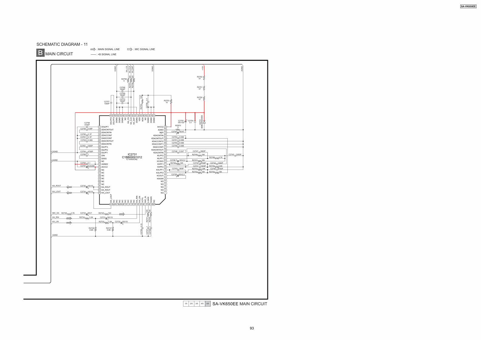
1/5 2/5 3/5 4/5 5/5
1
2
3
4
5
6
7
8
9
252627282930313233
56
57
58
59
60
61
62
63
64
72 73 74 75 76 77 78 79 80
1055
34
71
1154
35
70
1253
1352
36
69
37
68
1451
1550
1649
38
67
39
66
40
65
1748
1847
1946
2045
2144
2243
2342
2441 DOLPF1
DOLPF2
DOLPF3
DGND
DGND
DGND
DGND
DGND
DGND
DGND
VDD
MCK
NC
NC
KA_CS
KA_CLK
KA_DAT
AVCC2
AGND
KDACINTIN
KDACINTIN
KILPF2
KCISIG
KHPF1
KHPF2
KOLPF1
KOLPF2
KCOUT
KSIGIN
KILPF1
KDACCONT2
KDACCONT1
KDACCONT
KDACINTOUT
KDACINTOUT
REF
DILPF3
DILPF2
DILPF1
DIN
DISIG
AGND2
AVCC2
KA_ROUT
KA_ROUT
KA_LOUT
KA_LOUT
NC
NC
NC
NC
NC
NC
NC
NC
NC
NC
NC
NC
NC
NC
NC
NC
NC
NC
NC
NC
NC
KA_RIN
KA_LIN
VCFIL
MIC_IN
LGAIN
NGAIN
DDACINTOUT
DDACINTOUT
DDACINTIN
DDACINTIN
DDACCONT
DADCCONT
IC2731C1BB00001012
C2748 0.047
C2743 560P
C2766 1
C2735 16V10
C2734 16V10
C2733 50V1
C27571000P
C27701000P
C27691000P
C27681000P
R27580
R2757
220
R2756
220
R2754
12K
C2756
0.1
R275310
R275047
R275147
R275247
C275516V100
C27540.1
C2753 16V47
C2739 50V2.2
C2746 50V2.2IC KARAOKE
C2752 0.068
C2747 1800P
C2744 1000P
C2738
1
C2740 4700P
C2742 2700P
C2741 1000P
C2745 3300PR2749 10K
R2747 10K
R2743 3.9K
R2742 15K
R2755
10K
R2740 100R2738 4.7K
C2736
0.15
C2737
1R2741
10K
R2746 12K
R2748 4.7K
W29750
R2745 5.6K
R2744 15K
C2751 0.068
C2750 0.068
C2749 0.068
C27584700P
C2759 0.08P
C2762 0.068
C2763 1000P
C2760 0.1P
C2764 4700P
C2761 0.1P
MAIN CIRCUIT
SCHEMATIC DIAGRAM - 11
SA-VK650EE MAIN CIRCUIT
KA_ROUT
DGND
AGND
KA_CS
KA_CLK
KA_DAT
DGND
DGND
+15V
AGND
KA_LOUT
MIC_KA
R2734 3.3K
R27366.8K
R27376.8K
C2731 50V10KA_RIN
C2732 50V10R2735 3.3KKA_LIN
AGND
: MIC SIGNAL LINE
: +B SIGNAL LINE
: MAIN SIGNAL LINE
D2731
B0BC5R000009
C2765 0.1
C2767 6.3V200
SA-VK650EE
93

19.5. (C) Panel Circuit & (D) Tact Switch Cirucit
R6959 0
C6402 0.01
W6807 0
R6404 2.7
1/2 2/2
15
16
14
13
12
11
10
2
4
6
8
9
7
5
3
1
1
2
3
4
5
6
7
8
9
12 13 14 15 16 17 18 19 20
25
26
27
28
29
30
31
32
33
363738394041424344
10 24
21
35
11 23
22
34
NC
NC
NC
NC
OSC
NC
DIN
CLK
STB
K1
K2
G10
G11
G12/S17
VEE
S16
S15
S14
S13
S12
S11
S10
VSS
VDD
S1
S2
S3
S4
S5
S6
S7
S8
S9
VSS
VDD
G1
G2
G3
G4
G5
G6
G7
G8
G9
C6636 100P
C6604
100P
C6603
100P
C6601
100P
R6605 82K
W6806 0R6604 220
R6603 220
R6601 470
IC6601C0HBB0000057
FL DRIVER
C6623 50V22
FL6602A2BD00000151
FL_DOUT
FL_CLK
FL_CS
GR1
GR2
GR3
GR4
GR5
GR6
GR7
GR8
GR9
SG1
SG2
SG3
SG4
SG5
SG6
SG7
SG8
SG9
SG10
SG11
SG12
SG13
SG14
SG15
SG16
GR10
GR11
SG17
SG1
SG2
SG3
SG4
SG5
SG6
SG7
GR1
GR2
GR3
GR4
GR5
GR6
GR7
GR8
GR9
GR10
GR11
SG17
R6631
SYS6V
47
47
R6632
D6635B0BC5R600003
D6458
B3AAA0000803
R64583.9K
R619910K
H6555
C663550V22
GND2
FL2
-VP
FL1
SYS6V
SYS6V
PCONT
SYNC
DGND HP_R
HP_GND
HP_L
HP_GND
MIC_OUT
MIC_GND
+9V
MPORT_GND
MPORT_R
MPORT_GND
MPORT_L
HP_R
CN6806
HP_GND
HP_L
MIC_OUT
MIC_GND
MPORT_GND
MPORT_R
MPORT_ L
MIC_LVL2
LED_CTRL2
LED_CTRL1
-9V
MIC_LVL1
MIC_LVL2
LED_CTRL2
LED_CTRL1
-9V
MIC_LVL1
+9V
C663250V22
C663150V22
SG16
SG15
SG14
SG13
SG12
SG11
SG10
SG9
SG8
FL_CLK
FL_DOUT
FL_CS
NC
SYS6V
PCONT
SYNC
SW5V
GND2
+VREF
RMT
PHOTO_1
KEY1
KEY2
KEY3
PHOTO_2
DECK2
VJOG_B
ECHO1
ECHO2
ECHO3
ECHO_MUTE
VJOG_A
GND1
MOT10V
PLG2
PLG1
MODE_PB
HALF_PB
DVREF+
GND2
VREF+
VREF+
MIC_SW
GND2
KEY3
KEY1
R61021K
GND2
SYNC
PCONT
SYS6V
-VP_A
1 2 3 4 5 6 7 8 9 10 11 12 13 14 15 16 17 18 19 20 21 22 23 24 25 26 27 28 29 30 31 32 33 34 35 36 37 38 39 40 41 42 43 44 45
9 8 7 6 5 4 23 1
S6101
POWER
S6102
SSEQ
R61031K
S6103
R61041.2K
S6104
MULTI
REMASTER
SOUNDEQ
SUBWOOFER
R61051.8K
S6105
DECK1
S6107
R61062.2K
R61082.7K
S6302
DISC CHANGE
DISC CHECK
S6303
OPEN/CLOSE
S6304
DISC 1
S6305
DISC 2
S6306
DISC 3
S6307
DISC 4
S6308
DISC 5
R63031K
R630110K
R63041K
R63051.2K
R63061.8K
R63072.2K
R63082.7K
S6309
MIC VOL+
R63094.7K
S6310
MIC VOL-
R63106.8K
S6311
DECK 2
S6312
R631110K
R631222K
R631368K
GND1
PLG1
PLGND
PLG2
MOT10V
MODE_PB
HALF_PB
PHOTO_2
DECK2
PLGND
DVREF+
PHOTO_1
HALF_PB
VREF_GND
PHOTO_RB
DECK_2
PL_GND
DVREF
P1
P2
PHOTO_PB
MODE_PB
GND2
RMT
LED_CTRL2
GND2
VREF+
C6481 10V47
C6482 1000P
C6483 0.01R648127
HP_GND
HP_R
HP_L
HP_SW
GND2
JK6551
PHONES C6553
0.01
SW5V
C65510.01
C65520.01
PANEL CIRCUIT
SCHEMATIC DIAGRAM - 12
HP_SWR69600
C64010.1
C6421100P
C6425100P
R642510K
R642110K
C6403100P
R6406270K
R6405270K
R64161K
R641522K
R6412
1K
R6411
22K
C6405100P
2
4
6
7
5
3
1
MPORT_GND
MPORT_R
MPORT_L
MPORT_SW
GND2
MIC_OUT
MIC_GND
MIC_SW
GND2
+9V
MIC_GND
MIC_OUT
MIC_SW
MIC_VOLMIC_VOL
GND2
+9V
JK6552
H6556
CN6807
MUSIC
PORTINPUT
C65560.01
C65540.01
C65550.01
2
4
6
7
5
3
1
3 2 1
Z6400
B3RAB0000125REMOTE SENSOR
1
9
7
5
3
2
4
6
8
10
6
4
2
1
3
5
7
: +B SIGNAL LINE
: -B SIGNAL LINE : MAIN SIGNAL LINE
TO
MAIN
CIRCUIT
(CN2807) ON
SCHEMATIC
DIAGRAM-10
TO
MIC CIRCUIT
(H6900) ON
SCHEMATIC
DIAGRAM-14
TOTRANSFORMER CIRCUIT (CN5951)ON SCHEMATIC DIAGRAM-14
TOMAINCIRCUIT(CN2806) ONSCHEMATICDIAGRAM-10
FL_CLK
FL_DOUT
FL_CS
SYS6V
PCONT
SYNC
SW5V
GND2
+VREF
RMT
PHOTO_1
KEY1
KEY2
KEY3
PHOTO_2
DECK2
VJOG_B
ECHO1
ECHO2
ECHO3
ECHO_MUTE
VJOG_A
GND1
MOT10V
MOT10V
PLG2
PLG1
MODE_PB
HALF_PB
DVREF+
L6553 G0C101JA0052
G0C101JA0052
G0C100JA0052
L6552
L6551
R64032.7
R6401 10K
R6402 10K
C6404100P
Q6415Q6411
Q6421 Q6421,Q6425
B1GBCFJJ0051PLUNGER ON/OFF SWITCH
Q6411,Q6415
B1ACKD000006PLUNGER ON/OFF SWITCH
Q6425
CN6401
TO
DECK
MECHANISM
CIRCUIT
(CN971) ON
SCHEMATIC
DIAGRAM-18
L6555G0C101JA0052
D6707
B2AEA0000083
D6701
B0BC8R100004
D6708
B3AEA0000083
D6702
B0BC8R100004
R67122.7K
R67101K
R67131K
W6808 0
R67032.7K
W68110
R67021K
R67141K
L6554 G0C100JA0052
L6556 G0C101JA0052
: MIC SIGNAL LINE
STGND
PLGND
PCONT
GND2
DVREF+
VREF+
SYS6V
R69000
R695447K
R6957470K
R69501K
R69564.7K
D6803B0ACCE000003
Q6803,Q6804
B1ACCF000094DECK SUPPLY CONTROL SWITCH
Q6805B1GACFJJ0018
PCONT SWITCH
Q6803
Q6804
Q6702
LED_CTRL2
Q6703
LED_CTRL1
Q6701
15
14
13
12
11
10
2
4
6
8
9
7
5
3
1
30
29
28
27
26
25
17
19
21
23
24
22
20
18
16
SA-VK650EE PANEL CIRCUIT
W6801 0
W68090
W6804 0
Q6701-Q6703
B1GBCFJN0033LED DRIVE
SA-VK650EE
94

COMB A
1 2 3
14
13
12
11
10
2
4
6
8
9
7
5
3
1
14
13
12
11
10
2
4
6
8
9
7
5
3
1
DECK 1/2
S6207
S6208
S6203
FWD
S6204
STOP
S6205
REW
S6206
REC
VR6491
EVEKE2F2524BVOLUME JOG
R649147K
R62041.2K
R62051.8K
R62062.2K
C6492
100P
C6491
100P
R62072.7K
DISPPLAY/DEMO
R62084.7K
MUSIC PORT
S6209
R62096.8K
TUNER
S6210
R621010K
R621122K
R649310K
S6201
TAPE
S6202
DVD/CD
R62021K
R649247K
R62031K
SA-VK650EE TACT SWITCH CIRCUIT
NC
NC
NC
NC
KEY2
VREF+
V_JOG_A
V_JOG_B
GND2
MPORT_SW
KEY2
VREF+
V_JOG_A
V_JOG_B
GND2
MPORT_SW
KEY2I
VREF+I
V_JOG_AI
V_JOG_BI
GND
MPORT_SWI
NC
NC
NC
NC
CN6808
CP6201
TACT SWITCH CIRCUIT : +B SIGNAL LINE
W68030
W68050
W68020
PANEL CIRCUIT : +B SIGNAL LINE
: -B SIGNAL LINE
: MIC SIGNAL LINE
SCHEMATIC DIAGRAM - 13
1/2 2/2 SA-VK650EE PANEL/TACT SWITCH CIRCUIT
SA-VK650EE
95

19.6. (E) Transformer Circuit
C596625V2200P
2
3
1
4
C690550V3.3
1
2
4
6
7
5
3
7
6
5
3
1
4
2
10
9
11
12
14
16
13
15
17
1
2
4
6
8
7
5
3
3
2
1
9
VCC+
VCC-
AC GND
AC_IN
SUB+B
SUB+B_GND
SUB+B_GND
SUB+B_GND
SUB+B_GND
DVD_SUPPLY
1
2
4
6
8
7
5
3
9
CN5950
CN5955
CN5951
D5950-D5953B0EAMM000038
D5970-D5973B0EAKM000117
C5950
FP59504A
RL5950K6B1AEA00015
D5965B0AACK000004
C59580.01
C595750V10
R5961150
R59604.7K
D5960B0BA03000020
D5959B0EAKM000117
D5958B0EAKM000117
C595650V47
C595550V22
R59513.3K
Q5953B1AACF000064
PCONT SWITCH
D5966B0AACK000004
R596382
Q5950
C59530.01
R5953150
B1BACD000018
C595210V47
D5963B0AACK000004
D5964B0BA6R800008
R595810K
R595710K
C59540.01
JK5950
FL2
-VP
FL1
SYS6V
SYS6V
PCONT
SYNC
GND
TOPOWERCIRCUIT(H5104)ON SCHEMATICDIAGRAM-17
TOMAINCIRCUIT(M2) ONSCHEMATICDIAGRAM-7
TOPANELCIRCUIT(H6555)ON SCHEMATICDIAGRAM-12
Q5952
Q5952
B1GACFJJ0018SYNCHRONISATION SWITCH
T5951G4C2AAJ00005
C5960
D5952D5950
D5951D5953
0.1
D5974-D5977B0EAKM000117
C5965
D5974D5976
D5977D5975
0.01
D5970 D5971
D5972 D5973
C5959
0.01
Z5950ERZV10V511CS
C597125V470P
D5961
D5987
D5986
D5962
C59510.01
D5961,D6962B0AACK000004
D5986,D6987B0AACK000004
43
21
T5950G4CYBYY00003
SCHEMATIC DIAGRAM - 14
TRANSFORMER CIRCUIT : +B SIGNAL LINE : -B SIGNAL LINE
1
2
3
4
8
7
6
5
F1250V 1A
FC2FC1
VOLTAGE REGULATOR
Q59512SB0621AHA
VOLTAGE REGULATOR
ELF15N035AN
R59552.2K
SA-VK650EE TRANSFORMER CIRCUIT
L5950
C596350V4.7
25V2200P
2
4
6
7
5
3
1
2
4
6
7
5
3
1
H6900
: MIC SIGNAL LINEMIC CIRCUIT
L6901
G0C3R3JA0052
L6902
G0C100JA0052
Q6901Q6902
Q6903
Q6901-Q6903
B1ABCF000176MIC AMP
MIC_VOL
MIC_SW
MIC_OUT
MIC_GND
+9V
NC
GND2
R6902680
R6903560
R6901680
C69020.022
C69041
C69030.01
C6909100P
C69131000P
C691050V0.1
C69110.056
C6914100P
C691250V1
C691550V0.33
R6911100
R69141K
C690850V4.7
C691716V470
R6913330
C69161000P
R69284.7K
R690868
R69104.7K
R691227K
C6907470P
R6905470K
R69042.2K
R6907330K
R69068.2K
R6909330K
W68000
C69010.022
: +B SIGNAL LINE
JK6902
MIC
1
JK6901
MIC
2
SA-VK650EE MIC CIRCUIT
TOPANELCIRCUIT(H6556)ON SCHEMATICDIAGRAM-12
AC IN230V 50Hz
SA-VK650EE
96

19.7. (G) Power Circuit
CN5102
TOMAINCIRCUIT(CN2809)ONSCHEMATICDIAGRAM-10
1
2
3
4
5
6
7
8
9
10
11
12
DC_DET
D-MUTE
+15V +15V
AGND
L_OUT
AGND
T_GND
F_HOP F_HOP
R_OUT
DC_DET
FAN FAN
MODE
AGND
L_OUT
AGND
R_OUT
WOOFER SUBW
2322212019181716151413121110987654321
VSSA1
SGND
VDDAT
IN1-
OSC
PRBT
VDDP1
IN1+
BOOT1
OUT1
VSSP1
STAB1
VSSP2
OUT2
BOOT2
VDDP2
VSSD
VSSA1
SGND
VDDA1
IN2-
IN2+
MODE
C5311
220P
C5310
0.1
R513910
C5313
0.015
C5319
0.015
C5321
0.1
R513810
C5317
100P
C53270.68
R530522 22
R5306
L5301
G0C220Z00002
C5316
0.1
C53140.1
C5312
0.1
C5315
0.1
C5309
0.1
C5308
0.1
C53240.68
C5333220P
C5331220P
C53250.1
C53280.1
C53180.1
C53200.1
C53220.1
C5323
0.1
R5307 10
R5308 10
C53390.47
MODE
AGNDF_HOP1
R53035.6K
R53045.6K
R53015.6K
R53025.6K
C53400.47
C53361000P
C5305330P
C53010.47
C53030.47
C53371000P
C53441000P
C53451000P
C5302330P
2
31
4
R_OUT
L_OUT
AGND
AGND
AGND
AGND
C5330220P
C5332220P
C5123
35V470P
C5124
35V470P
L5102J0JKB0000037
L5101
J0JKB0000037
CN5103
TOMAINCIRCUIT(CN2808)ONSCHEMATICDIAGRAM-10
1
2
3
4
5
6
7
8
9
10
11
12
PGND
SUB+B_GND
DGND
ASP_GND
CD8V CD8V
P_CON
NC
10V
+9V
-9V
SW5V
10V
+9V
-9V
L_OUT1
TGND
R_OUT1
-VCC1
+VCC1
-VCC1
+VCC1
SW5V
SUB_2
AGND
MUTE_A
POWER CIRCUIT
SCHEMATIC DIAGRAM - 15
: +B SIGNAL LINE : -B SIGNAL LINE : MAIN SIGNAL LINE
R51481K
R5153100
R51491K
R5154100
R5155100
R5156100
C5121
16V47
R5146
1K
R5157
100K
Q5150B1GDCFJJ0047
PCONT SWITCH
Q5151
B1GDCFJJ0047MODE SWITCH
Q5152B1ABCF000176
SWTICH
Q5151Q5150
Q5152
SA-VK650EE POWER CIRCUIT1/3 2/3 3/3
IC5301C1BA000004072-CH DIGITALAMP
2322212019181716151413121110987654321
VSSA1
SGND
VDDAT
IN1-
OSC
PRBT
VDDP1
IN1+
BOOT1
OUT1
VSSP1
STAB1
VSSP2
OUT2
BOOT2
VDDP2
VSSD
VSSA1
SGND
VDDA1
IN2-
IN2+
MODE
C5511
220P
C5510
0.1
R514310
C5513
0.015
C5521
0.1
R5142W55040
W5505
0
W5519
0
W55030
10
C5517
100P
R550622
L5501
G0C220Z00002
C5516
0.1
C55140.1
C5512
0.1
C5515
0.1
C5509
0.1
C5508
0.1
C55270.68
C5531220P
C55280.1
R55290
C55180.1
R55264.7K
C5522
0.1
C5520
0.1
C5523
0.1
R5507 10
R55015.6K
R55025.6K
C55381000P
C55010.47
C55030.47
C5502330P
2
31
4
SUBW
C55391000P
AGND
C5530220P
C512035V470
C511935V470
L5502J0JKB0000037
L5503
J0JKB0000037
R55190
R5520 0
IC5501C1BA000004072-CH DIGITALAMP
0R5326 R5329
0
SA-VK650EE
97

AGND
C5202
R520910
H2A375300003
1 14
2
3
4
5
13
12
11
10
6 9
87
R5204100K
R520310K
R55140
C52050.1
C5207100P
R520822
R52061M
R5205100K
W55010
R52076.8K
100PC5203100P
C5201470P
R52011K
R5202100K
R5210150
C5210
470P
C52086.3V680P
C5204100P
X5201H2A415300001
X5202
C52116.3V100
F_HOP
F_HOP1
AGND
AGND
SW5V
IC5201C0JBAB000011
LOGIC
VCC
6A
6Y
5A
5Y
4A
4Y
1A
2A
1Y
2Y
3A
3Y
GND
Q5201B1ABCF000176FREQUENCY HOPPING
SWITCH
Q5202B1ADCF000063FREQUENCY HOPPING
SWITCH
B0EAKP000134
B0EAKM000122
D5129
C51580.01
R51312.2K
R514412
C51116.3V100
R5130150
C511225V10
D5108B0BA5R700008
D5128 D5127
D5128,D5127,D5124,D5123
D5124 D5123
R51352.2
R51362.2
R51372.2
R513310K
C51590.01
R51341.2KR5132
330
C511350V33
D5109B0BA01100004
D5125
B0AACK000004
R51472.2
R5123
4.7
FP5100
400
R5122
4.7
R5126
1KR5127470
C511025V100
C510925V100
D5152B0BA01900005
R5152
0
D5107B0BA01500003
C51570.01
-VCC1
-VCC1
+9V
-9V
L_OUT1
R_OUT1
SUB_2
AGND
+15V
CD8V
+VCC1
DC_DET
FAN
AGND
AGND
TGND
SW5V
10V
POWER CIRCUIT
SCHEMATIC DIAGRAM - 16
: +B SIGNAL LINE : -B SIGNAL LINE : MAIN SIGNAL LINE
Q5115B1AAKD000014
5.7V REGULATOR
Q5114B1ABCF000176
11V REGULATOR
Q5112B1BCCG000023CURRENT STABLISER
Q5111B1BACG000048
+15V REGULATOR
Q5113B1GDCFNA0001
CURRENT LIMITER SWITCH
C57100.01
C571116V10
C570916V100
C57120.01
C571316V10
Q5707B1BACD000018
REGULATOR
Q5708B1ACCF000094
REGULATOR
Q5709B1BCCD000019
REGULATOR
R571627
D5709B0BA9R600002
R511247K
R511347K
R57182.7K
R5719470
R57202.7K
R57213.3K
R5722100
R5723100
R5717100
R57153.3K
Q5707
SA-VK650EE POWER CIRCUIT1/3 2/3 3/3
SA-VK650EE
98

+VCC1
+VCC1
-VCC1
-VCC1
ACIN
SUB+B
AC GND
AC GND
DGND
TO
TRANSFORMER
CIRCUIT
(CN5950) ON
SCHEMATIC
DIAGRAM-14
2
4
6
8
9
7
5
3
1
C5101
35V4700
Q5101
Q5103
Q5104
C5151
0.1
C5161
0.047
C5551
0.1
D5101
B0BA01100004
D5102
B0BA02600018
R5101
10K R5114
2.7
C5102
100V10
R5103
10K
C5103
100V10
C5107
0.1
C5106
0.1
C5167
0.1
C5168
0.1
R5318
5.6K
R5525
5.6K
R5418
5.6K
C517163V1000
C5172
63V1000
C516635V1000
C5165
35V1000
D5122
B0EAKM000122
B0EAKM000122
D5121
D5126
B0ACEL000004
C510435V4700
C5153
0.1
C5163
0.047C5552
0.1
Q5102
D5104
D5105
B0BA02300017
B0BA01100004
D5103
B0BA5R100013
R5110
2.2K
R5109
1K
R5108
47
R5107
560C5152
0.1
W5502
0
W5500 0
R5105
10K
R510622K
R5313
150K
R5413
100K
R5513
330K
R5150
220K
R5317
10K
C5155
1000P
C5105
10V220
R5111
100K
R_GND
SUBWOOFER
SUBWOOFER
R_CHANNEL
L_GND
L_CHANNEL
L5401
G0B9R5K00001
3
1
2
4
6
5
E5100
E5102
POWER CIRCUIT
SCHEMATIC DIAGRAM - 17
: +B SIGNAL LINE : -B SIGNAL LINE : MAIN SIGNAL LINE
Q5103,Q5104
B1ABCF000176FAN ON/OFF SWITCH
Q5109
2SB0709AHLVOLTAGE REGULATOR
Q5110
B1AACF00006426V REGULATOR
Q5101,Q5102
B1DEGM000026CURRENT CONTROL SWITCH
Q5108
B1ABCF000176SWITCH
H5104
C5343
0.015
C5435
0.015
C5438
0.015
C5335
0.015
C5536
0.015
C5537
0.015
1 2
3 4
1 2
3 4
L5302
G0B9R5K00001
1 2
3 4
L5402
G0B9R5K00001
JK5102
SPEAKER
SUBWOOFER
SA-VK650EE POWER CIRCUIT1/3 2/3 3/3
SA-VK650EE
99

19.8. (H) Deck Circuit & (I) Deck Mechanism Circuit
M
6
5
4 3
2
1
1234567
1
2
4
6
8
9
10
7
5
3
1
2
1
2
2
4
5
3
1
L
R
ERASEHEAD
RECORD/PLAYHEAD
2
4
5
3
1
LPLACKBACK
HEAD
R
2
4
5
3
1
2
4
5
3
1
1 2 3 4 5
1 2 3 4
21222324
5
20
6
19
7
18
8
17
9
16
10
15
11
14
12
13
S974
RECINH_R
CS1001
SCHEMATIC DIAGRAM - 18
DECK CIRCUIT
CS1002
L1002G2ZZ000000024
IC1001
AN7348S-E1P.B EQ/REC AMP/ALC/TPS AMP
IC1004C1AA00000612
R/P SELECT
VCC
L
R
C103010V100
R101547
R1018
3.9K
C10320.018
C1036
0.033
R10294.7M
C1043
50V4.7
C1056
16V10
C1031
10V100
R101647
C1027
1000P
C10231000P
C10330.018
R1019
3.9K
C1035
50V3.3
C103750V3.3
C1039
220P
10V22
C1045
R10288.2K
C1041
16V10
C1021470P
C10221000P
R10178.2K
R100918K
C1020470P
C10191000P
C104016V10C1012
1000PC10151000P
R101018K
R10261K
R10054.7K
C100916V47
4
L1001G0C470JA0052
C100650V1
C10022.2
C10074700P
R100310K
D1003B0ACCK000005
Q1003B1AAGC000007
SWITCHING(RECH)
Q1007
R1090220
C104616V220
R10400
C104410V33
R10041.5K
Q1004
Q1005
Q1004, Q1005
B1AAGC000007BIAS OSCILLATOR
C10131000P
C10141000P
C101025V100
R10074.7
C10162200P
C10172200P
R10118.2K
Q1007
B1ABCF000176BIAS OSC CONTROL
C10266.3V47
R10134.7K
R10124.7K
C10183300P
R10144.7K
C10110.047
C100850V1
C103450V3.3
R103210K
R10552.2K
C1038220P
C104216V22
R103127K
R103510K
R1030
100
5
11
12
TAPEB
INPUT
TAPEB
INPUT
TAPEA
INPUT
TAPEA
INPUT
PBAMP
NF
PBAMP
NF
PBAMP
EQ
PBAMP
EQ
PBAMP
OUTPUT
PBAMP
OUTPUT
ABSW
T
RECIN
RECIN
RECOUT
RECOUT
REC/PBSW
ABSW
RIPPLE
FILTER
OUTPUT
GND
VCC
CRO/NOR
HI/LO
ALCT
ALCLOW
CUT
IC1001
SW
GND
CTRL2
CTRL1
3
C10581000P
R11000
R11010
C10571000P
C10590.01
R1099
0
R10020
R10240
R10250
R10270
R10200
R102210K
: PLAYBACK SIGNAL
: RECORD SIGNAL LINE
: +B SIGNAL
R10842.2K
R10862.2K
R10490
R10500
R10920
R10910
R108747K
R108547K
R10572.2K
R1060390
PBL
PBR
AFGND
RECINL
RECINR
+B
REC_H
MO+B
MOGND
DECK1_H
MOTOR
Q1017B1AARC000003
MOTOR SWITCH
M1(REF NO 53)
CN1001
IC951CNB13030R2AUPHOTO INTERRUPTER
IC971CNB13030R2AUPHOTO INTERRUPTER
Z971RGSD12A1445T
MODE
PL
GND
HALF
STBY_5V
VREF_GND
PHOTO_T
D1_CRO2
TOPANELCIRCUIT(CN6401) ONSCHEMATICDIAGRAM-12
MODE
PL
GND
HALF
PHOTO_S
STBY_5V
VREF_GND
PHOTO_T
D1_CRO2
DECK MECHANISM CIRCUIT
CN971
PL1
PL2
STBY_5V
PL_GND
AD_OUT
PHOTO_PB
PHOTO_RP
HALF_PB
VREF_GND
MODE_PB
R972820
R97339K
PL971
R952820
R95339K
D951MA2C16500E
D971MA2C16500E
PL970
S952 HALF
S951MODE
S972
HALF
S971
MODE
S975
RECINH_F
HALF
RECINH_R
MODE
RECINH_F
AD_OUT
VREF_GND
STBY_5V
-
+
C10493300P
C10503300P
R109810K
10
R110210K
TOMAIN CIRCUIT (CN2803) ONSCHEMATIC DIAGRAM-10
R109710K
SA-VK650EE DECK MECHANISM CIRCUIT/DECK CIRCUIT
111098761 5432
SA-VK650EE
100

20 Printed Circuit BoardNote: Circuit board diagrams may be modified at any time with the development of new technology.
SA-VK650EE
101

20.1. (A) DVD Module P.C.B. (Side: A & B )
!
"#"
$$
$
% %
%
%
%
%
%
%
%
%
%
%
%
%
%
%
%
%
#!
&
$$
$
%
%
%
%
"#!
%
&
#!
"""
SA-VK650EE
102

20.2. (B) Main P.C.B.
% !
&
'(
'
'
'
'
'
'
)
)
$
)
)
)
)
)
)
)
)
)
$
$
)
)
)
)
$
)
)
)
)
)
)
)
) )
)
)
)
)
)
) )
)
)
)
)
)
)
%
)
%
)
)
)
)
)
)
)
)
)
)
)
)
)
)
)
)
)
)
)
)
)
)
)
)
)
)
)
)
)
)
)
)
)
)
)
)
) )
)
)
)
)
)
)
)
)
)
)
)
)
)
)
)
)
)
)
)
)
)
)
)
)
)
)
)
)
)
)
)
)
)
)
)
)
)
)
)
)
)
)
)
)
)
)
)
)
)
)
)
)
)
)
)
)
)
)
)
)
)
)
)
)
)
))
)
)
)
)
)
)
)
)
))
)
)
))
))
)
)
) )
)
)
)
)
)
)
)
) )
)
)
)
)
)
)
)
)
)
)
)
)
)
)
)
)
)
)
)
)
)
)
)
)
)
)
)
)
)
)
)
)
)
)
)
)
)
)
)
)
)
)
)
)
)
)
)
)
)
)
)
)
)
)
)
)
)
)
)
)
)
)
))
)
)
)
)
)
)
)
)
)
)
)
)
)
)
)
)
)
))
)
)
)
)
)
)
)
)
)
)
)
)
)
)
)
)
)
)
)
)
)
%
)
)
)
)
)
)
)
)
)
)
%
)
)
)
)
)
)
)
)
)
)
$ )
)
)
)
$
)
)
)
)
)
)
)
)
)
)
)
)
$
$
$
$
$
$
$
$ $
$
$
$ $
$
$
$
$
$
$
$
$
$
$
$
"!
*+,!
$
-
"
"
.
.
#
)
)
' '
"
"
#'"
""
"
""%!
(
SA-VK650EE
103

20.3. (C) Panel P.C.B.
% !
)
$
$
)
)
)
)
)
)
)
)
$
$
$
# #!
# .!
# !
$
$
$
$
$
)
) )
)
)
) )
)
) )
)
)
)
)
)
)
)
)
)
)
)
)
)
)
)
) )
)
)
) )
)
)
)
)
)
)
)
)
)
)
)
)
)
)
) )
)
)
)
)
)
)
)
)
)
)
)
)
)
)
)
)
)
)
)
)
)
)
)
)
)
)
-
)
)
)
)
)
) )
)
)
)
)
# '!
# #!
# #!
# #!
# #!
# #
!
# #!
# /#!
# #)!
# "
#"!
# #$!
# #0#$!
# )!
# !
' '&
)
##
#"
SA-VK650EE
104

20.4. (D) Tact Switch P.C.B., (F) Mic P.C.B., (H) Deck P.C.B. , (I) Deck Mechanism P.C.B. & (J) Tuner P.C.B.
""#)"% !
% !
"!
#% !% !
& ' '
& ' '
& ' '
' '
' '
&
&
#
)
)
)
) # #(/!
# /!
)
)
# !
# "!
# #"!
)
# "!
# /!
# #"!
# )!
# )!
$
$
$
$
.
'
.
'
-
#!
#!
#
#0!
#!
#!
#
#0!
)
)
)
)
)
)
)
)
)
)
)
)
)
) )
) )
)
)
)
) )
$
$
$
$
$
""*+,!
# "/
1
1
"
" "
""
"
1
1
1
1
# "/
SA-VK650EE
105
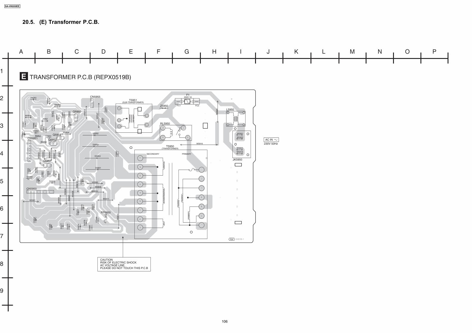
20.5. (E) Transformer P.C.B.
&
)
)
)
)
)
)
)
)
)
)
)
)
)
)
)
)
)
)
)
)
)
)
)
)
)
)
)
)
' '
$
$
-
$
$
2
"#'"#!
" "#!
"#"#"#"""#
#( (
"#% !
SA-VK650EE
106

20.6. (G) Power P.C.B.
)% !
# #
&
$
$
)
)
)
)
)
)
)
$
$
$$
$
$
$
$
$
%
)
)
) )
)
%
)
)
)
)
)
)
)
)
)
)
)
)
)
)
)
)
)
)
$ $
)
)
$
)
)
)
)
)
)
)
)
)
)
)
)
) )
)
$$
)
)
$
$
$
)
)
$
)
)
)
)
)
)
)
)
)
)
)
)
)
)
)
)
)
) ) )
))
)
)
)
)
)
)
)
)
)
)
)
)
)
)
#
SA-VK650EE
107

SA-VK650EE
108

21 Basic Troubleshooting Guide21.1. Basic Troubleshooting Guide for Traverse Unit (DVD Module P.C.B.)
Problems Checking Points Checking Components1) Distorted picture orabnormal sound is heardduring initialisation
a) Check SDRAM address, data bus, CLK and othercontrol signals waveform.b) Check video signals.c) Check audio DAC circuitry.* Compare the above with OK condition Module.
IC8051
LB8301,R8321, R8322, LB8302, R8325, R8326IC8420* Check for solder short and/or componentmissing/damaged.
2) No TOC/Long TOC a) Check motor driver circuitry (voltages).b) Check laser drive circuitry (volrtages and current).c) Check LSI connection to motor drive circuitry.* Compare the above with OK condition Module.
IC8251Q8550,Q8551,Q8552,Q8561,Q8562IC8001* Check for solder short and/or componentmissing/damaged.
3) Disc not spinning4) Traverse not moving5) Traverse and spindleabnormal movement
a) Check connection from Backend Module to Traverseunit.b) Check motor driver circuitry on voltages and controlsignals.* Compare the above with OK condition Module.
FP8201
IC8251
* Check for solder short and/or componentmissing/damaged.
6) Cannot read disc butspindle is spinning- Cannot read CD- Cannot read DVD
a) Check laser drive circuitry (voltages and current)
- Check CD laser drive- Check DVD laser drive* Check voltages and LD current and compare withOK Module.
Q8550,Q8551,Q8552,Q8560,Q8561,Q8562
Q8550,Q8560,Q8561,Q8562Q8550,Q8551,Q8552,Q8560*Check for solder short and/or componentmissing/damaged.
7) Block noise during play a) Check SDRAM address and data bus signal.* Compare the above with OK condition Module.
IC8051* Check for solder short and/or component damaged.
8) Jitter of out specification a) Check LD currentb) Check OPU (change to other unit and confirm)
OPU unit (FFC connection)
109
SA-VK650EE

22 Illustration of ICs, Transistors and DiodesAN7348S-E1 (24P)C0ABBB000230(8P)C0FBBK000049 (16P)C1BB00000732 (32P)C1BB00000962(24P)C1CB00001937 (20P)C0CBCBD000018 (8P)C0JBAB000011(14P)
C0EBA0000029 (4P)C3ABPG000145 (54P)C9ZB00000498 (16P)
B0AACK000004MA2J72800L
C0HBBB0000057 (44P)C1BB00001012 (80P)C2CBYY000267 (100P)MN2DS0009VP (256P)
14
8
5
C0AABA000009 C0DAAMH00012
2SB0621AHA
C1AA00000612C0DBEHG00006
31
1 24
3
2 4
CNB13030R2AU C0GBG0000048 C0EBE0000455C0JBAA000346
B1AAKD000014B1AARC000003B1ACKD000006B1GCCFJJ0016
B1AAGC000007B1AAAC000016B1AAAD000015B1GACFJJ0018
B0ADCJ000020
1
11
5
1
1814
1
28
15
7
2122
8
B0BA01100004B0BA01500003B0BA01900005B0BA02300017B0BA02600018B0BA03000020B0BA5R100013B0BA5R700008
B0BA6R800008B0BA9R600002
A
CaCathode
Anode
B3AAA0000803
Ca
A
Cathode
Anode
A
CaCathode
Anode
B0EAKM000117B0EAKM000122B0EAMM000038
B1AACF000064 B1BACD000018B1BCCD000019
ECB B
C E
B0CDBB000015B0CBAD000004
B0BC2R4A0006B0BC5R600003B0BC5R000009B0BC7R500001B0JCPD000025 Cathode
Ca
A
A
Anode
GSD
ECB
B1AABC000003
EC
B
B1BCCG000023B1DEGM000026
BCE
B0ACCK000005
B1ACCF000094
B1CECC000003
15
13
45
2
2SB0709AHL2SD1819A0LB1ABCF000176B1ABEB000002B1ADCF000001B1ADCF000063B1ADGB000008B1GBCFJA0028
B1GBCFJN0033B1GBCFJJ0051B1GDCFNA0001B1GDCFJJ0047UNR521100LUNR511V00L
Ca
Cathode
AnodeA
B0ACEL000004B0BC4R300002B0ACCE000003MA2J11100L
Cathode
Anode
Ca
A
C1BA00000407
1
24
25
48
RFKWMHA0H160(48P)
BC
E
E
C
B
CBE
B1BACG000048
B0BC8R100004
Ca
Cathode
Anode
C0ABBB000244 (8P)
14
85
CathodeCathode
Anode
B0ADCC000002
XP0621400L
12
3
4 56
A
CaCathode
Anode
MA2C16500E
B3AEA0000083
CaACathodeAnode
110
SA-VK650EE

23.1. IC2801 (C2CBYY000267 )System Microprocessor
Pin No. Mark I/O Function1 LM_L I Level Meter Left2 N.C. - No Connection3 PLLCE O PLL Chip Select4 WIDE1 O S.VIDEO output control5 DVD_PCONT O Power control pin for DVD
module6 DVD_MUTE I Signal from DVD module
control mute circuit7 F_HOP O F_Hop for Digital Amplifier8 BYTE - External Data Bus Width
Select Input(Connect to Ground)
9 CNVss/EFP_CNVss - Flash Mode Terminal(Connected to Ground)
10 XC_IN - 32.768 kHz Sub Clock11 XC_OUT - 32.768 kHz Sub Clock12 RESET/EFP_RESET - Reset Input
(ACTIVE L)13 XOUT - 10 MHz Main Clock14 VSS - Ground (0V)15 XIN - 10 MHz Main Clock16 VCC - Power Supply (+5V)17 NMI - Connect to VCC (+5V)18 RMT I Remote Control Input19 N.C. - No Connection20 SYNC I AC Failure Detect Input21 ST/DO I Tuner IF Data/Stereo Input22 SD I Tuner Signal Detect Input23 KA_CS - No Connection24 KA_CLK - No Connection25 KA_DAT - No Connection26 ASP_DAT O ASP DATA27 ASP_CLK O ASP CLOCK28 N.C. - No Connection29 PLL_DAT O PLL DATA30 PLL_CLK O PLL CLK31 REG 1 I REGION SETTING 1
(Tuner)32 REG 2 I REGION SETTING 2
(Tuner)33 REG 3 I REGION SETTING 3
(Tuner)34 REG 4 I REGION SETTING 4
(Tuner)35 DVD_CMD O CMD signal for the DVD
Module36 DVD_STA I STATUS signal from the
DVD Module37 DVD_CLK I CLOCK signal for the DVD
Module38 MODEL_SLCT I MODEL SELECT (Active
Low)39 MOD_DA O Digital Amplifier Muting40 MUTE_A O Audio Mute41 EE_CS/EFP/EPM O EEPROM Chip Select42 EE_CLK O/I EEPROM CLOCK43 EE_DATA O/I EEPROM DATA44 SW_LVL1 - Subwoofer Level 145 SW_LVL2 - Subwoofer Level 246 PCONT/EFP_CE O Main Transformer Control
Output47 DC_DET I DC Detect Input48 LED_CTRL1 - No Connection
Pin No. Mark I/O Function49 LED_CTRL2 - No Connection50 MIC_LVL1 - No Connection51 MIC_LVL2 - No Connection52 HALF_1 I DECK 1 HALF PLAYBACK
INPUT53 MODE_1 I DECK 1 MODE PLAYBACK
INPUT54 MUTE_FHOP - No Connection55 N.C. - No Connection56 PLG_1 O DECK 1 Plunger Control57 PLG_2 O DECK 2 Plunger Control58 MTR O DECK motor control (“L” for
Motor ON)59 REC O L when record circuit is
operating60 DECK1_H O H when DECK 1 P/B head
is selected61 N.C. - No Connection62 Vcc - Power Supply (+5V)63 N.C. - No Connection64 Vss - Ground (0V)65 N.C. - No Connection66 N.C. - No Connection67 V_JOG_A I Volume Jog A68 V_JOG_B I Volume Jog B69 ECHO_1 O No Connection70 ECHO_2 O No Connection71 FL reset - No Connection72 FL_CS O FL Driver Chip Select73 FL_DATA O Serial Data To FL Driver74 FL_CLK O Serial Clock To FL Driver75 ECHO_3 O No Connection76 ECHO_Mute O Echo Muting77 N.C. - No Connection78 ST_SW I Stock Switch of CRS179 MOT_CCW O CRS1 motor CCW80 MOT_CW O CRS1 motor CW81 HOME_SW I Home Switch for CRS182 CAM_SENSOR I Close Switch for CRS183 PLUNGER O Plunger for CRS184 BOTTOM_SW I Bottom Switch for CRS185 PLAY_SW I Play Switch for CRS186 UD_SENSOR I UD Sensor for CRS187 OPEN_SW I Open Switch for CRS188 N.C. - No Connection89 DVD_REG AD
INDVD Region setting
90 N.C. - No Connection91 DECK2 AD
INDeck Condition Input 2(R_INHF/MODE2/HALF2)
92-94 KEY3-KEY1 ADIN
KEY 3 to KEY 1 INPUT
95 PHOTO_2 ADIN
Rotation Detection Signal(DECK2)
96 AVss - Analog Power Supply Input(Connect to GND)
97 PHOTO_1 ADIN
Rotation Detection Signal(DECK 1)
98 VREF - Reference for A-D (+5V)99 AVcc - Analog Power Supply Input100 N.C. - No Connection
23 Terminal Function of IC
111
SA-VK650EE

112
SA-VK650EE

24 Exploded Views24.1. Cabinet Parts Location
SA-VK650EE
113

SA-VK650EE
114

24.2. Cassette Mechanism Unit Parts Location (RAA3413-1S)
SA-VK650EE
115

24.3. Packaging
SA-VK650EE
116

Notes:
Ref. No. Part No. Part Name & Description RemarksCABINET AND CHASSIS
1 L6FALEFH0030 FAN UNIT [M]2 REEX0212-2 WIRE [M]3 REEX0566 50P FFC (CD-MAIN) [M]4 REEX0567 10P FFC WIRE [M]5 REEX0568 11P FFC WIRE [M]6 REEX0609 16P FFC WIRE [M]7 REEX0617 30P FFC WIRE [M]8 REXX0479 2P FLAT WIRE [M]9 REXX0505 7P FLAT WIRE [M]10 REXX0532 9P FLAT WIRE [M]11 REXX0325 9P FLAT WIRE [M]12 RGKX0367-K TOP ORNAMENT [M]13 RGKX0368-K CD LID [M]14 RGKX0369-K CASSETTE LID ORN. L [M]15 RGKX0370-K CASSETTE LID ORN. R [M]16 RGLX0136-Q LIGHTING PIECE L [M]17 RGLX0137-Q LIGHTING PIECE R [M]18 RGLX0138-Q POWER LIGHT PIECE [M]19 RGPX0256-S FRONT PANEL [M]20 RGRX0059B-C1 REAR PANEL [M]21 RGUX0679-S POWER BUTTON [M]22 RGUX0680-S SOUND BUTTON [M]23 RGUX0681-S CD CONTROL BUTTON [M]24 RGUX0682-S FUNCTION BUTTON L [M]25 RGUX0683-S FUNCTION BUTTON R [M]26 RGUX0684-K CONTROL BUTTON L [M]27 RGUX0685-K CONTROL BUTTON R [M]28 RGUX0686-S DECK BUTTON L [M]29 RGUX0687-S DECK BUTTON R [M]30 RGWX0072-S VOLUME KNOB [M]31 RHD26046-L SCREW [M]32 RHD30008 WASHER HEAD SCREW [M]33 RHD30007-1SJ SCREW [M]34 RHD30111-3 SCREW [M]35 RHD30119-S SCREW [M]36 RKA0072-KJ LEG CUSHION [M]37 RKFX0133-S CASSETTE LID L [M]
Ref. No. Part No. Part Name & Description Remarks38 RKFX0134-S CASSETTE LID R [M]39 RKMX0130-S TOP CABINET [M]40 RKWX0263-H FL WINDOW [M]41 RMBX0036 CASS OPEN SPRING [M]42 RMBX0049 DVD LID SPRING [M]43 RMC0158-S2 TRANSISTOR HOLDER [M]44 RMG0547-K CUSHION [M]45 RMGX0044-1 D.AMP. INSULATOR [M]46 RMKX0118 BOTTOM CHASSIS [M]47 RMKX0119 DVD CHASSIS [M]48 RMNX0188 FL HOLDER [M]49 RMNX0190 LED HOLDER [M]50 RMVX0094-K FL WINDOW BACKGROUND [M]51 RMYX0131 SUB HEAT SINK [M]52 RUS757ZAA CASS HALF SPRING [M]53 RWJ0102050CK MECHA MOTOR WIRE [M]54 RXXX0081 HEAT SINK UNIT [M]55 RXGX0002 DAMPER GEAR [M]56 XTB3+8JFJ SCREW [M]57 XTV3+10GFJ-M SCREW [M]58 XTW3+10TFC SCREW [M]59 XTW3+12TFJ SCREW [M]60 XTWS3+6TFJ SCREW [M]61 RSQX0006-2 DECK SHIELD PLATE [M]
CASSETTE MECHANISM UNIT
101 RED0064-2 R/P HEAD BLOCK UNIT [M]102 RED0063-2 P/B HEAD BLOCK UNIT [M]103 RDG0300 REEL BASE GEAR [M]104 RDG0301 WINDING RELAY GEAR [M]105 RDK0026-4 MAIN GEAR [M]106 RDR0029-4 RELAY PULLEY [M]107 RDV0033-4 WINDING BELT [M]108 RDV0034-2 CAPSTAN BELT A [M]109 RDV0057-1 MAIN BELT B [M]110 RMB0312 TRIGGER LEVER SPRING [M]111 RMB0400 REEL SPRING [M]112 RMB0403 HEAD PANEL SPRING [M]
25 Replacement Parts List
· Important safety notice:
Components identified by mark have special characteristics important for safety.Furthermore, special parts which have purposes of fire-retardent (resistors), high-quality sound (capacitors), low noise(resistors), etc are used.When replacing any of these components, be sure to use only manufacturer’s specified parts shown in the parts list.
· The parenthesized indications in the Remarks columns specify the areas or colour. (Refer to the cover page for area or colour)
Parts without these indications can be used for all areas. · Warning: This product uses a laser diode. Refer to caution statements on “Precaution of Laser Diode”. · Capacitor values are in microfarads (µF) unless specified otherwise, P= Pico-farads (pF), F= Farads. · Resistance values are in ohms, unless specified otherwise, 1K=1,000 (OHM). · The marking (RTL) indicates that the Retention Time is limited for this items. After the discontinuation of this assembly in
production, the item will continue to be available for a specific period of time. The retention period of a availability is dependenton the type of assembly, and in accordance with the laws governing part and product retention. After the end of this period, theassembly will no longer be available.
· [M] markings in the Remarks columns indicates parts supplied by PAVCSG. · [SPG] markings in the Remarks columns indicates parts that are supplied by PAVC. · Reference for O/I book languages are as follows:
Ar: Arabic Du: Dutch It: Italian Sp SpanishCf: Canadian French En: English Ko: Korean Sw: SwedishCz: Czech Fr: French Po: Polish Co: Traditional ChineseDa: Danish Ge: German Ru: Russian Cn: Simplified ChinesePe: Persian Ur: Ukraine
117
SA-VK650EE

Ref. No. Part No. Part Name & Description Remarks113 RMB0404 BRAKE ROD SPRING [M]114 RMB0406-5 FR LEVER SPRING [M]115 RMB0408 THRUST SPRING [M]116 RML0370-4 TRIGGER LEVER [M]117 RML0371 FR LEVER [M]118 RML0372-2 WINDING LEVER [M]119 RML0374-2 EJECT LEVER [M]120 RMM0131-1 BRAKE ROD [M]121 RMM0133-1 EJECT ROD [M]122 RMQ0519 REEL HUB [M]123 RMS0398-1 MOVING CORE [M]124 RSJ0003 PLUNGER ASS’Y [M]125 RMC0061 PACK SPRING [M]126 RXF0061-1 FLYWHEEL F ASS’Y [M]127 RXF0062-1 FLYWHEEL R ASS’Y [M]128 RXG0040 FF RELAY GEAR ASS’Y [M]129 RMK0283A-2 SUB-CHASSIS [M]130 RXL0124 PINCH ROLLER F ASS’Y [M]130-1 RMB0401 PINCH ARM SPRING F [M]131 RXL0125 PINCH ROLLER R ASS’Y [M]131-1 RMB0402 PINCH ARM SPRING R [M]132 RXL0126 WINDING ARM ASS’Y [M]133 RXQ0412-3 HEAD PANEL ASS’Y [M]133-1 RMB0405 FR ROD SPRING [M]133-2 RMM0132 FR ROD [M]134 REM0121 CAP MOTOR ASS’Y [M]135 RHD26022-1 MOTOR SCREW [M]136 XTW2+5LFJ HEAD BLOCK UNIT SCREW [M]137 XTW26+10SFJ SUB-CHASSIS SCREW [M]138 XYC2+JF17FJ PCB EARTH SCREW [M]139 RFKJXED70-K MAIN CHASSIS [M]
TRAVERSE UNIT
360 RAE2018W-S TRAVERSE UNIT [M]361 RMG0598-A FLOATING RUBBER [M]362 RMG0617-H CUSHION RUBBER A [M]363 RMG0618-H CUSHION RUBBER B [M]364 RMRX0066 MIDDLE CHASSIS [M]365 RMS0789 FIXED PIN [M]366 RXQ0946 TRAVERSE MOTOR ASS’Y [M]367 RXQ1389 DVD OPU SUB ASS’Y [M]368 RMEX0041 MIDDLE CHASSIS SPRING [M]369 XTV2+6GFJ SCREW [M]
PRINTED CIRCUIT BOARD
REP4012D DVD MODULE P.C.B. (SIDE:A)
[M](RTL)
REP4012D DVD MODULE P.C.B. (SIDE:B)
[M](RTL)
REPX0547D MAIN P.C.B. [M](RTL)REPX0541C PANEL P.C.B. [M](RTL)REPX0541C TACT SWITCH P.C.B. [M](RTL)REPX0519B TRANSFORMER P.C.B. [M](RTL)REPX0541C MIC P.C.B. [M](RTL)REPX0522B POWER P.C.B. [M](RTL)REPX0331F DECK P.C.B. [M](RTL)REPX0321B DECK MECHANISM P.C.B. [M](RTL)REP1999B TUNER P.C.B. [M](RTL)
INTEGRATED CIRCUITS
IC951 CNB13030R2AU IC PHOTO INTERRUPTER [M]IC971 CNB13030R2AU IC PHOTO INTERRUPTER [M]IC1001 AN7348S-E1 IC P.B. EQ/REC AMP/ALC/TPS
AMP[M]
IC1004 C1AA00000612 IC R/P SELECT [M]IC2061 C0ABBB000244 IC OP-AMP [M]IC2101 C1BB00000732 IC ASP [M]IC2103 C0ABBB000230 IC OP-AMP [M]IC2561 C0DAAMH00012 IC REGULATOR [M]IC2601 C1BB00000962 IC FM/AM IF AMP DET/AM OSC
MIX/FM MPX[M]
Ref. No. Part No. Part Name & Description RemarksIC2602 C1CB00001937 IC PLL FREQUENCY
SYNTHESIZER[M]
IC2701 C9ZB00000498 IC VIDEO BUFFER [M]IC2731 C1BB00001012 IC KARAOKE [M]IC2801 C2CBYY000267 IC MICROPROCESSOR [M]IC2804 C0AABA000009 IC OP-AM [M]IC5201 C0JBAB000011 IC LOGIC [M]IC5301 C1BA00000407 IC 2-CH DIGITAL AMP [M]IC5501 C1BA00000407 IC 2-CH DIGITAL AMP [M]IC6601 C0HBB0000057 IC FL DRIVER [M]IC8001 MN2DS0009VP IC DV3.2 LSI VIDEO [M]IC8051 C3ABPG000145 IC 64 SDRAM [M]IC8111 C0CBCBD00018 IC 3.3 REGULATOR [M]IC8151 C0DBEHG00006 IC REGULATOR [M]IC8251 C0GBG0000048 IC DRIVER [M]IC8420 C0FBBK000049 IC 2 CHANNEL DAC [M]IC8601 C0EBA0000029 IC RESET [M]IC8606 C0EBE0000455 IC RESET [M]IC8651 RFKWMHA0H160 IC 16M FLASH ROM [SPG]IC8691 C0JBAA000346 IC AND GATE LOGIC [M]IC8695 C0JBAA000346 IC AND GATE LOGIC [M]
TRANSISTORS
Q1 B1CECC000003 TRANSISTOR [M]Q2 B1AAAC000016 TRANSISTOR [M]Q3 B1AAAD000015 TRANSISTOR [M]Q4 B1AAAD000015 TRANSISTOR [M]Q1003 B1AAGC000007 TRANSISTOR [M]Q1004 B1AAGC000007 TRANSISTOR [M]Q1005 B1AAGC000007 TRANSISTOR [M]Q1007 B1ABCF000176 TRANSISTOR [M]Q1017 B1AARC000003 TRANSISTOR [M]Q2051 B1GDCFJJ0047 TRANSISTOR [M]Q2052 B1GFECYY0001 TRANSISTOR [M]Q2061 B1ABCF000176 TRANSISTOR [M]Q2062 B1ABCF000176 TRANSISTOR [M]Q2063 B1GDCFJJ0047 TRANSISTOR [M]Q2064 B1GDCFJJ0047 TRANSISTOR [M]Q2065 B1ABCF000176 TRANSISTOR [M]Q2142 B1ABCF000176 TRANSISTOR [M]Q2143 B1ABEB000002 TRANSISTOR [M]Q2242 B1ABCF000176 TRANSISTOR [M]Q2243 B1ABEB000002 TRANSISTOR [M]Q2366 B1GFECYY0001 TRANSISTOR [M]Q2501 B1GDCFJJ0047 TRANSISTOR [M]Q2502 B1GFECYY0001 TRANSISTOR [M]Q2551 B1ADCF000001 TRANSISTOR [M]Q2552 B1ACKD000006 TRANSISTOR [M]Q2576 B1GBCFJA0028 TRANSISTOR [M]Q2601 B1AABC000003 TRANSISTOR [M]Q2606 B1GCCFJJ0016 TRANSISTOR [M]Q2806 B1GBCFJJ0051 TRANSISTOR [M]Q2901 B1GBCFJN0033 TRANSISTOR [M]Q2912 B1GBCFJN0033 TRANSISTOR [M]Q2913 B1GBCFJJ0051 TRANSISTOR [M]Q2914 B1ACKD000006 TRANSISTOR [M]Q2942 B1ACKD000006 TRANSISTOR [M]Q2943 B1ABCF000176 TRANSISTOR [M]Q2948 B1ABCF000176 TRANSISTOR [M]Q2949 B1ABCF000176 TRANSISTOR [M]Q2978 B1GDCFJJ0047 TRANSISTOR [M]Q2979 B1GDCFJJ0047 TRANSISTOR [M]Q2980 B1ABCF000176 TRANSISTOR [M]Q5101 B1DEGM000026 TRANSISTOR [M]Q5102 B1DEGM000026 TRANSISTOR [M]Q5103 B1ABCF000176 TRANSISTOR [M]Q5104 B1ABCF000176 TRANSISTOR [M]Q5108 B1ABCF000176 TRANSISTOR [M]Q5109 2SB0709AHL TRANSISTOR [M]Q5110 B1AACF000064 TRANSISTOR [M]Q5111 B1BACG000048 TRANSISTOR [M]Q5112 B1BCCG000023 TRANSISTOR [M]Q5113 B1GDCFNA0001 TRANSISTOR [M]
118
SA-VK650EE
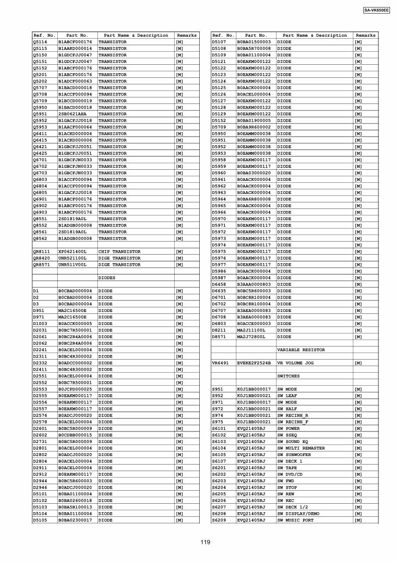
Ref. No. Part No. Part Name & Description RemarksQ5114 B1ABCF000176 TRANSISTOR [M]Q5115 B1AAKD000014 TRANSISTOR [M]Q5150 B1GDCFJJ0047 TRANSISTOR [M]Q5151 B1GDCFJJ0047 TRANSISTOR [M]Q5152 B1ABCF000176 TRANSISTOR [M]Q5201 B1ABCF000176 TRANSISTOR [M]Q5202 B1ADCF000063 TRANSISTOR [M]Q5707 B1BACD000018 TRANSISTOR [M]Q5708 B1ACCF000094 TRANSISTOR [M]Q5709 B1BCCD000019 TRANSISTOR [M]Q5950 B1BACD000018 TRANSISTOR [M]Q5951 2SB0621AHA TRANSISTOR [M]Q5952 B1GACFJJ0018 TRANSISTOR [M]Q5953 B1AACF000064 TRANSISTOR [M]Q6411 B1ACKD000006 TRANSISTOR [M]Q6415 B1ACKD000006 TRANSISTOR [M]Q6421 B1GBCFJJ0051 TRANSISTOR [M]Q6425 B1GBCFJJ0051 TRANSISTOR [M]Q6701 B1GBCFJN0033 TRANSISTOR [M]Q6702 B1GBCFJN0033 TRANSISTOR [M]Q6703 B1GBCFJN0033 TRANSISTOR [M]Q6803 B1ACCF000094 TRANSISTOR [M]Q6804 B1ACCF000094 TRANSISTOR [M]Q6805 B1GACFJJ0018 TRANSISTOR [M]Q6901 B1ABCF000176 TRANSISTOR [M]Q6902 B1ABCF000176 TRANSISTOR [M]Q6903 B1ABCF000176 TRANSISTOR [M]Q8551 2SD1819A0L TRANSISTOR [M]Q8552 B1ADGB000008 TRANSISTOR [M]Q8561 2SD1819A0L TRANSISTOR [M]Q8562 B1ADGB000008 TRANSISTOR [M]
QR8111 XP0621400L CHIP TRANSISTOR [M]QR8420 UNR521100L DIGE TRANSISTOR [M]QR8571 UNR511V00L DIGE TRANSISTOR [M]
DIODES
D1 B0CBAD000004 DIODE [M]D2 B0CBAD000004 DIODE [M]D3 B0CBAD000004 DIODE [M]D951 MA2C16500E DIODE [M]D971 MA2C16500E DIODE [M]D1003 B0ACCK000005 DIODE [M]D2031 B0BC7R500001 DIODE [M]D2061 B0BC2R4A0006 DIODE [M]D2062 B0BC2R4A0006 DIODE [M]D2241 B0ACEL000004 DIODE [M]D2311 B0BC4R300002 DIODE [M]D2332 B0ADCC000002 DIODE [M]D2411 B0BC4R300002 DIODE [M]D2551 B0ACEL000004 DIODE [M]D2552 B0BC7R500001 DIODE [M]D2553 B0JCPD000025 DIODE [M]D2555 B0EAKM000117 DIODE [M]D2556 B0EAKM000117 DIODE [M]D2557 B0EAKM000117 DIODE [M]D2576 B0ADCJ000020 DIODE [M]D2578 B0ACEL000004 DIODE [M]D2601 B0BC5R000009 DIODE [M]D2602 B0CDBB000015 DIODE [M]D2731 B0BC5R000009 DIODE [M]D2801 B0ACEL000004 DIODE [M]D2802 B0ADCJ000020 DIODE [M]D2804 B0ACEL000004 DIODE [M]D2911 B0ACEL000004 DIODE [M]D2912 B0EAKM000117 DIODE [M]D2944 B0BC5R600003 DIODE [M]D2946 B0ADCJ000020 DIODE [M]D5101 B0BA01100004 DIODE [M]D5102 B0BA02600018 DIODE [M]D5103 B0BA5R100013 DIODE [M]D5104 B0BA01100004 DIODE [M]D5105 B0BA02300017 DIODE [M]
Ref. No. Part No. Part Name & Description RemarksD5107 B0BA01500003 DIODE [M]D5108 B0BA5R700008 DIODE [M]D5109 B0BA01100004 DIODE [M]D5121 B0EAKM000122 DIODE [M]D5122 B0EAKM000122 DIODE [M]D5123 B0EAKM000122 DIODE [M]D5124 B0EAKM000122 DIODE [M]D5125 B0AACK000004 DIODE [M]D5126 B0ACEL000004 DIODE [M]D5127 B0EAKM000122 DIODE [M]D5128 B0EAKM000122 DIODE [M]D5129 B0EAKM000122 DIODE [M]D5152 B0BA01900005 DIODE [M]D5709 B0BA9R600002 DIODE [M]D5950 B0EAMM000038 DIODE [M]D5951 B0EAMM000038 DIODE [M]D5952 B0EAMM000038 DIODE [M]D5953 B0EAMM000038 DIODE [M]D5958 B0EAKM000117 DIODE [M]D5959 B0EAKM000117 DIODE [M]D5960 B0BA03000020 DIODE [M]D5961 B0AACK000004 DIODE [M]D5962 B0AACK000004 DIODE [M]D5963 B0AACK000004 DIODE [M]D5964 B0BA6R800008 DIODE [M]D5965 B0AACK000004 DIODE [M]D5966 B0AACK000004 DIODE [M]D5970 B0EAKM000117 DIODE [M]D5971 B0EAKM000117 DIODE [M]D5972 B0EAKM000117 DIODE [M]D5973 B0EAKM000117 DIODE [M]D5974 B0EAKM000117 DIODE [M]D5975 B0EAKM000117 DIODE [M]D5976 B0EAKM000117 DIODE [M]D5977 B0EAKM000117 DIODE [M]D5986 B0AACK000004 DIODE [M]D5987 B0AACK000004 DIODE [M]D6458 B3AAA0000803 DIODE [M]D6635 B0BC5R600003 DIODE [M]D6701 B0BC8R100004 DIODE [M]D6702 B0BC8R100004 DIODE [M]D6707 B3AEA0000083 DIODE [M]D6708 B3AEA0000083 DIODE [M]D6803 B0ACCE000003 DIODE [M]D8211 MA2J11100L DIODE [M]D8571 MA2J72800L DIODE [M]
VARIABLE RESISTOR
VR6491 EVEKE2F2524B VR VOLUME JOG [M]
SWITCHES
S951 K0J1BB000017 SW MODE [M]S952 K0J1BB000021 SW LEAF [M]S971 K0J1BB000017 SW MODE [M]S972 K0J1BB000021 SW HALF [M]S974 K0J1BB000021 SW RECINH_R [M]S975 K0J1BB000021 SW RECINH_F [M]S6101 EVQ21405RJ SW POWER [M]S6102 EVQ21405RJ SW SSEQ [M]S6103 EVQ21405RJ SW SOUND EQ [M]S6104 EVQ21405RJ SW MULTI REMASTER [M]S6105 EVQ21405RJ SW SUBWOOFER [M]S6107 EVQ21405RJ SW DECK 1 [M]S6201 EVQ21405RJ SW TAPE [M]S6202 EVQ21405RJ SW DVD/CD [M]S6203 EVQ21405RJ SW FWD [M]S6204 EVQ21405RJ SW STOP [M]S6205 EVQ21405RJ SW REW [M]S6206 EVQ21405RJ SW REC [M]S6207 EVQ21405RJ SW DECK 1/2 [M]S6208 EVQ21405RJ SW DISPLAY/DEMO [M]S6209 EVQ21405RJ SW MUSIC PORT [M]
119
SA-VK650EE

Ref. No. Part No. Part Name & Description RemarksS6210 EVQ21405RJ SW TUNER [M]S6302 EVQ21405RJ SW DISC CHECK [M]S6303 EVQ21405RJ SW OPEN/CLOSE [M]S6304 EVQ21405RJ SW DISC CHANGE [M]S6305 EVQ21405RJ SW DISC 1 [M]S6306 EVQ21405RJ SW DISC 2 [M]S6307 EVQ21405RJ SW DISC 3 [M]S6308 EVQ21405RJ SW DISC 4 [M]S6309 EVQ21405RJ SW DISC 5 [M]S6310 EVQ21405RJ SW MIC VOL + [M]S6311 EVQ21405RJ SW MIC VOL - [M]S6312 EVQ21405RJ SW DECK 2 [M]
CONNECTORS
CN971 K1MN10B00104 10P FFC CONNECTOR [M]CN1001 K1MN11B00016 11P CONNECTOR [M]CN2801 K1MY50AA0029 50P CONNECTOR [M]CN2803 K1MN11A00008 11P CONNECTOR [M]CN2805 K1MN14A00049 14P FFC CONNECTOR [M]CN2806 K1MN16A00073 16P FFC CONNECTOR [M]CN2807 K1MN30AA0004 30P CONNECTOR [M]CN2808 K1KB12B00036 12P CONNECTOR [M]CN2809 K1KB12B00036 12P CONNECTOR [M]CN2810 K1KA02AA0186 2P FAN CONNECTOR [M]CN5102 K1KA12AA0424 12P CONNECTOR [M]CN5103 K1KA12AA0424 12P CONNECTOR [M]CN5950 K1KA09AA0319 9P CONNECTOR [M]CN5951 K1KA09AA0193 9P CONNECTOR [M]CN5955 K1KA03AA0190 3P CONNECTOR [M]CN6401 K1MN10B00104 10P FFC CONNECTOR [M]CN6806 K1MN16B00133 16P FFC CONNECTOR [M]CN6807 K1MN30AA0004 30P CONNECTOR [M]CN6808 K1KA14AA0481 14P CONNECTOR [M]
CP6201 K1KB14C00004 14P CONNECTOR [M]
CS1001 K1MY05AA0043 5P CONNECTOR [M]CS1002 K1MY05AA0043 5P CONNECTOR [M]
FP8101 K1MN50BA0173 50P FFC CONNECTOR [M]FP8251 K1MN06BA0148 6P FFC CONNECTOR [M]FP8531 K1MY26BA0025 26P CONNECTOR [M]
CERAMIC FILTERS
CF2601 J0B1075AA014 FM CERAMIC FILTER [M]CF2602 J0B1075AA014 FM CERAMIC FILTER [M]
COILS & TRANSFORMERS
L1 G0C1R2KA0029 AXIAL COIL [M]L2 G0CR47KA0029 RF CHOKE COIL [M]L1001 G0C470JA0052 RF CHOKE COIL [M]L1002 G2ZZ00000024 BIAS OCS COIL [M]L2551 G0A101ZA0028 CHOKE COIL [M]L2555 G0A100D00002 CHOKE COIL [M]L2601 G2A411C00001 AM COIL [M]L2602 G2BPC0000016 OSCILLATOR COIL [M]L2901 J0JCC0000120 COIL [M]L2902 J0JCC0000120 COIL [M]L2903 J0JCC0000120 COIL [M]L2905 ERJ3GEY0R00V CHIP JUMPER [M]L2906 J0JCC0000120 COIL [M]L2907 J0JCC0000120 COIL [M]L2908 J0JCC0000120 COIL [M]L2909 J0JBC0000019 CHIP INDUCTOR [M]L2912 G0A100D00002 CHOKE COIL [M]L2913 G0A100G00005 RF CHOKE COIL [M]L5101 J0JKB0000037 FILTER [M]L5102 J0JKB0000037 FILTER [M]L5301 G0C220Z00002 COIL [M]L5302 G0B9R5K00001 CHOKE COIL [M]L5401 G0B9R5K00001 CHOKE COIL [M]
Ref. No. Part No. Part Name & Description RemarksL5402 G0B9R5K00001 CHOKE COIL [M]L5501 G0C220Z00002 COIL [M]L5502 J0JKB0000037 FILTER [M]L5503 J0JKB0000037 FILTER [M]L5950 ELF15N035AN LINE FILTER [M]L6551 G0C100JA0052 INDUCTOR [M]L6552 G0C101JA0052 INDUCTOR [M]L6553 G0C101JA0052 INDUCTOR [M]L6554 G0C100JA0052 INDUCTOR [M]L6555 G0C101JA0052 INDUCTOR [M]L6556 G0C101JA0052 INDUCTOR [M]L6901 G0C3R3JA0052 COIL [M]L6902 G0C100JA0052 INDUCTOR [M]L8201 G1C100K00019 CHIP COIL [M]L8301 G1C100K00019 CHIP COIL [M]L8302 G1C100K00019 CHIP COIL [M]L8501 G1C100K00019 CHIP COIL [M]L8550 G1C100KA0055 CHIP INDUCTOR [M]
LB8001 J0JHC0000045 CHIP INDUCTOR [M]LB8011 J0JHC0000045 CHIP INDUCTOR [M]LB8257 ERJ3GEY0R00V CHIP JUMPER [M]LB8258 ERJ3GEY0R00V CHIP JUMPER [M]LB8259 ERJ3GEY0R00V CHIP JUMPER [M]LB8260 ERJ3GEY0R00V CHIP JUMPER [M]LB8301 J0JBC0000042 CHIP BEAD [M]LB8302 J0JBC0000042 CHIP BEAD [M]LB8303 J0JBC0000042 CHIP BEAD [M]LB8304 J0JBC0000042 CHIP BEAD [M]LB8305 J0JBC0000042 CHIP BEAD [M]LB8401 J0JBC0000042 CHIP BEAD [M]LB8421 ERJ2GE0R00X CHIP JUMPER [M]LB8422 ERJ2GE0R00X CHIP JUMPER [M]LB8423 ERJ2GE0R00X CHIP JUMPER [M]LB8424 ERJ2GE0R00X CHIP JUMPER [M]LB8491 ERJ2GE0R00X CHIP JUMPER [M]LB8530 J0JHC0000045 CHIP INDUCTOR [M]LB8531 ERJ2GE0R00X CHIP JUMPER [M]LB8551 J0JBC0000042 CHIP BEAD [M]LB8561 J0JBC0000042 CHIP BEAD [M]LB8571 J0JBC0000042 CHIP BEAD [M]LB8690 J0JBC0000106 CHIP BEAD [M]LB8691 ERJ2GEJ101X CHIP RESISTOR [M]LB8692 ERJ2GEJ101X CHIP RESISTOR [M]LB8693 ERJ2GEJ101X CHIP RESISTOR [M]
T5950 G4CYBYY00003 TRANSFORMER [M]T5951 G4C2AAJ00005 BACK UP TRANSFORMER [M]
COMPONENT COMBINATIONS
Z971 RGSD12A1445T RADA RESISTOR [M]Z2602 G2BAD0000003 AM IFT [M]Z5950 ERZV10V511CS ZENER [M]Z6400 B3RAD0000125 REMOTE SENSOR [M]
RELAY
RL5950 K6B1AEA00015 POWER RELAY [M]
OSCILLATORS
X2602 H3F1065A0002 DIELECTRIC RESONATOR [M]X2603 H0H720400007 CRYSTAL [M]X2801 H0A327200115 CRYSTAL [M]X2802 H2B100500004 CERAMIC RESONATOR [M]X5201 H2A415300001 CRYSTAL OSCILLATOR [M]X5202 H2A375300003 CRYSTAL OSCILLATOR [M]X8621 H0J270500085 CRYSTAL [M]
DISPLAY TUBES
FL6602 A2BD00000162 FL [M]FL8101 F1H0J1050022 CHIP CAPACITOR [M]
120
SA-VK650EE

Ref. No. Part No. Part Name & Description RemarksFL8102 F1H0J1050022 CHIP CAPACITOR [M]FL8103 F1H0J1050022 CHIP CAPACITOR [M]FL8104 F1J1E1040022 CHIP CAPACITOR [M]
FUSE
F1 K5D102BLA013 FUSE [M]
FUSE HOLDERS
FC1 EYF52BCY FUSE CLIP [M]FC2 EYF52BCY FUSE CLIP [M]
FUSE PROTECTORS
FP5100 K5G401A00008 RESISTOR [M]FP5950 K5G402A00025 FUSE PROTECTOR [M]
HOLDERS
H5104 K1YF09000001 9P WIRE HOLDER [M]H6555 K1YZ09000002 9P CABLE HOLDER [M]H6556 K1YZ07000001 7P WIRE HOLDER [M]H6900 K1KA07AA0193 7P CONNECTOR [M]
JACKS
JK2601 K4BC03A00008 JK ANTENNA [M]JK2800 K1AY105B0002 JK VIDEO [M]JK2801 K2HA1YYB0004 JK VIDEO [M]JK2803 K2HA4YYB0002 JK I/O [M]JK5102 K4AC06B00008 JK SPEAKER [M]JK5950 K2AA2B000011 JK AC INLET [M]JK6551 K2HC103A0024 JK HP [M]JK6552 K2HC1YYA0002 JK MUSIC PORT [M]JK6901 K2HB102J0038 JK [M]JK6902 K2HB102J0038 JK [M]
EARTH TERMINALS
E5100 K4CZ01000027 EARTH LUG [M]E5102 K4CZ01000027 EARTH LUG [M]
PACKING MATERIALS
P1 RPGX1642 PACKING CASE [M]P2 RPNX0429 POLYFOAM UNIT [M]P3 RPFX0007-1 MIRAMAT BAG [M]
ACCESSORIES
A1 EUR7662YE0 REMOTE CONTROLLER [M]A1-1 UR76EC5903A R/C BATTERY COVER [M]A2 K2CQ2CA00002 AC CORD [M]A3 RQTV0144-1R O/I BOOK (Ru/Ur) [M]A4 RSA0007-L FM ANTENNA WIRE [M]A5 N1DAAAA00001 AM LOOP ANTENNA [M]A6 K2KA2CA00011 VIDEO CABLE [M]
RESISTORS
R1 D0AE102JA048 1K 1/4W [M]R1 D0AE104JA048 100K 1/4W [M]R2 D0AE101JA048 100 1/4W [M]R2 D0AE104JA048 100K 1/4W [M]R3 D0AE221JA048 220 1/4W [M]R4 D0AE104JA048 100K 1/4W [M]R5 ERDS2TJ564T 560K 1/4W [M]R6 D0AE391JA048 390 1/4W [M]R7 D0AE272JA048 2.7K 1/4W [M]R8 ERDS2TJ684T 680K 1/4W [M]R9 D0AE391JA048 390 1/4W [M]R10 D0AE391JA048 390 1/4W [M]R11 ERDS2TJ684T 680K 1/4W [M]
Ref. No. Part No. Part Name & Description RemarksR952 ERDS2TJ821T 820 1/4W [M]R953 ERDS2TJ393T 39K 1/4W [M]R972 ERDS2TJ821T 820 1/4W [M]R973 ERDS2TJ393T 39K 1/4W [M]R1002 ERJ3GEY0R00V 0 1/16W [M]R1003 ERJ3GEYJ103V 10K 1/16W [M]R1004 D0GB152JA007 1.5K 1/16W [M]R1005 D0GB472JA041 4.7K 1/16W [M]R1007 ERD25FVJ4R7T 4.7 1/4W [M]R1009 D0GB183JA007 18K 1/16W [M]R1010 D0GB183JA007 18K 1/16W [M]R1011 ERJ3GEYJ822V 8.2K 1/16W [M]R1012 D0GB472JA041 4.7K 1/16W [M]R1013 D0GB472JA041 4.7K 1/16W [M]R1014 D0GB472JA041 4.7K 1/16W [M]R1015 D0GB470JA008 47 1/16W [M]R1016 D0GB470JA008 47 1/16W [M]R1017 ERJ3GEYJ822V 8.2K 1/16W [M]R1018 D0GB392JA007 3.9K 1/16W [M]R1019 D0GB392JA007 3.9K 1/16W [M]R1020 ERJ3GEY0R00V 0 1/16W [M]R1022 ERJ3GEYJ103V 10K 1/16W [M]R1024 ERJ3GEY0R00V 0 1/16W [M]R1025 ERJ3GEY0R00V 0 1/16W [M]R1026 ERJ3GEYJ102V 1K 1/16W [M]R1027 ERJ3GEY0R00V 0 1/16W [M]R1028 ERJ3GEYJ822V 8.2K 1/16W [M]R1029 D0GB475JA007 4.7M 1/16W [M]R1030 D0GB101JA007 100 1/16W [M]R1031 D0GB273JA007 27K 1/16W [M]R1032 ERJ3GEYJ103V 10K 1/16W [M]R1035 ERJ3GEYJ103V 10K 1/16W [M]R1040 ERJ3GEY0R00V 0 1/16W [M]R1049 ERJ3GEY0R00V 0 1/16W [M]R1050 ERJ3GEY0R00V 0 1/16W [M]R1055 D0GB222JA041 2.2K 1/16W [M]R1057 D0GB222JA041 2.2K 1/16W [M]R1060 D0GB391JA041 390 1/16W [M]R1084 D0GB222JA041 2.2K 1/16W [M]R1085 D0GB473JA041 47K 1/16W [M]R1086 D0GB222JA041 2.2K 1/16W [M]R1087 D0GB473JA041 47K 1/16W [M]R1090 D0GB221JA041 220 1/16W [M]R1091 ERJ3GEY0R00V 0 1/16W [M]R1092 ERJ3GEY0R00V 0 1/16W [M]R1097 ERJ3GEYJ103V 10K 1/16W [M]R1098 ERJ3GEYJ103V 10K 1/16W [M]R1099 ERJ3GEY0R00V 0 1/16W [M]R1100 ERJ3GEY0R00V 0 1/16W [M]R1101 ERJ3GEY0R00V 0 1/16W [M]R1102 ERJ3GEYJ103V 10K 1/16W [M]R2001 ERJ3GEY0R00V 0 1/16W [M]R2002 ERJ3GEY0R00V 0 1/16W [M]R2003 ERJ3GEY0R00V 0 1/16W [M]R2004 ERJ3GEY0R00V 0 1/16W [M]R2005 ERJ3GEY0R00V 0 1/16W [M]R2007 ERJ3GEY0R00V 0 1/16W [M]R2008 ERJ3GEY0R00V 0 1/16W [M]R2009 ERJ3GEY0R00V 0 1/16W [M]R2021 ERJ3GEY0R00V 0 1/16W [M]R2031 D0AF270JA039 27 1/4W [M]R2032 ERJ3GEYJ103V 10K 1/16W [M]R2033 D0GB472JA041 4.7K 1/16W [M]R2051 ERJ3GEYJ102V 1K 1/16W [M]R2052 ERJ3GEYJ103V 10K 1/16W [M]R2053 D0GB563JA007 56K 1/16W [M]R2054 D0GB273JA007 27K 1/16W [M]R2055 D0GB152JA007 1.5K 1/16W [M]R2056 D0GB152JA007 1.5K 1/16W [M]R2057 ERJ3GEYJ682V 6.8K 1/16W [M]R2058 ERJ3GEYJ682V 6.8K 1/16W [M]R2064 D0GB153JA007 15K 1/16W [M]R2067 D0GB332JA007 3.3K 1/16W [M]R2068 D0GB183JA007 18K 1/16W [M]
121
SA-VK650EE

Ref. No. Part No. Part Name & Description RemarksR2069 ERJ3GEY0R00V 0 1/16W [M]R2070 ERJ3GEYJ821V 820 1/16W [M]R2071 ERJ3GEYJ392V 3.9K 1/16W [M]R2072 ERJ3GEYJ102V 1K 1/16W [M]R2073 D0GB104JA007 100K 1/16W [M]R2074 D0GB473JA041 47K 1/16W [M]R2075 D0GB473JA041 47K 1/16W [M]R2076 D0GB222JA041 2.2K 1/16W [M]R2077 ERJ3GEYJ152V 1.5K 1/16W [M]R2078 ERJ3GEY0R00V 0 1/16W [M]R2081 ERJ3GEYJ102V 1K 1/16W [M]R2086 ERJ3GEYJ392V 3.9K 1/16W [M]R2087 ERJ3GEYJ334V 330K 1/16W [M]R2101 ERJ3GEYJ332V 3.3K 1/16W [M]R2102 ERJ3GEYJ122V 1.2K 1/16W [M]R2103 D0GB123JA007 12K 1/16W [M]R2104 ERJ3GEYJ103V 10K 1/16W [M]R2105 ERJ3GEYJ682V 6.8K 1/16W [M]R2106 D0GB101JA007 100 1/16W [M]R2107 ERJ3GEYJ822V 8.2K 1/16W [M]R2108 D0GB123JA007 12K 1/16W [M]R2111 ERJ3GEYJ153V 15K 1/16W [M]R2112 ERJ3GEYJ562V 5.6K 1/16W [M]R2113 D0GB562JA007 5.6K 1/16W [M]R2118 D0GB562JA007 5.6K 1/16W [M]R2120 ERJ3GEYJ102V 1K 1/16W [M]R2141 D0GB272JA007 2.7K 1/16W [M]R2142 D0GB152JA007 1.5K 1/16W [M]R2143 D0GB104JA007 100K 1/16W [M]R2145 ERJ3GEYJ103V 10K 1/16W [M]R2146 ERJ3GEYJ102V 1K 1/16W [M]R2149 D0GB222JA041 2.2K 1/16W [M]R2152 ERJ3GEYJ681V 680 1/16W [M]R2153 D0GB152JA007 1.5K 1/16W [M]R2154 D0GB104JA007 100K 1/16W [M]R2166 ERJ3GEYJ100V 10 1/16W [M]R2167 ERJ3GEYJ100V 10 1/16W [M]R2168 ERJ3GEYJ100V 10 1/16W [M]R2169 ERJ3GEYJ100V 10 1/16W [M]R2170 ERJ3GEY0R00V 0 1/16W [M]R2171 D0GB332JA007 3.3K 1/16W [M]R2172 D0GB561JA007 560 1/16W [M]R2191 D0GB222JA041 2.2K 1/16W [M]R2192 ERJ3GEY0R00V 0 1/16W [M]R2197 ERJ3GEYJ822V 8.2K 1/16W [M]R2198 D0GB123JA007 12K 1/16W [M]R2199 D0GB153JA007 15K 1/16W [M]R2201 ERJ3GEYJ332V 3.3K 1/16W [M]R2202 ERJ3GEYJ122V 1.2K 1/16W [M]R2204 ERJ3GEYJ103V 10K 1/16W [M]R2205 ERJ3GEYJ682V 6.8K 1/16W [M]R2206 D0GB101JA007 100 1/16W [M]R2207 ERJ3GEYJ822V 8.2K 1/16W [M]R2211 ERJ3GEYJ153V 15K 1/16W [M]R2212 ERJ3GEYJ562V 5.6K 1/16W [M]R2220 ERJ3GEYJ102V 1K 1/16W [M]R2241 D0GB272JA007 2.7K 1/16W [M]R2242 D0GB152JA007 1.5K 1/16W [M]R2243 D0GB104JA007 100K 1/16W [M]R2245 ERJ3GEYJ103V 10K 1/16W [M]R2246 ERJ3GEYJ102V 1K 1/16W [M]R2247 D0GB104JA007 100K 1/16W [M]R2248 ERJ3GEYJ682V 6.8K 1/16W [M]R2249 D0GB222JA041 2.2K 1/16W [M]R2252 ERJ3GEYJ681V 680 1/16W [M]R2253 D0GB152JA007 1.5K 1/16W [M]R2254 D0GB104JA007 100K 1/16W [M]R2266 ERJ3GEYJ100V 10 1/16W [M]R2267 ERJ3GEYJ100V 10 1/16W [M]R2268 ERJ3GEYJ100V 10 1/16W [M]R2269 ERJ3GEYJ100V 10 1/16W [M]R2270 ERJ3GEY0R00V 0 1/16W [M]R2271 D0GB332JA007 3.3K 1/16W [M]R2272 D0GB561JA007 560 1/16W [M]
Ref. No. Part No. Part Name & Description RemarksR2291 D0GB222JA041 2.2K 1/16W [M]R2292 ERJ3GEY0R00V 0 1/16W [M]R2297 ERJ3GEYJ822V 8.2K 1/16W [M]R2298 D0GB123JA007 12K 1/16W [M]R2299 D0GB153JA007 15K 1/16W [M]R2302 ERJ3GEYJ332V 3.3K 1/16W [M]R2303 D0GB104JA007 100K 1/16W [M]R2312 ERJ3GEYJ683V 68K 1/16W [M]R2315 ERJ3GEY0R00V 0 1/16W [M]R2316 D0GB272JA007 2.7K 1/16W [M]R2317 ERJ3GEYJ473V 47K 1/16W [M]R2318 D0GB272JA007 2.7K 1/16W [M]R2319 D0GB562JA007 5.6K 1/16W [M]R2320 ERJ3GEYJ102V 1K 1/16W [M]R2331 ERJ3GEY0R00V 0 1/16W [M]R2332 D0GB393JA007 39K 1/16W [M]R2333 ERJ3GEY0R00V 0 1/16W [M]R2337 D0GB474JA041 470K 1/16W [M]R2338 ERJ3GEYJ102V 1K 1/16W [M]R2339 ERJ3GEYJ102V 1K 1/16W [M]R2402 ERJ3GEYJ332V 3.3K 1/16W [M]R2403 D0GB104JA007 100K 1/16W [M]R2412 ERJ3GEYJ683V 68K 1/16W [M]R2415 ERJ3GEY0R00V 0 1/16W [M]R2416 D0GB272JA007 2.7K 1/16W [M]R2417 ERJ3GEYJ473V 47K 1/16W [M]R2418 D0GB272JA007 2.7K 1/16W [M]R2419 D0GB562JA007 5.6K 1/16W [M]R2420 ERJ3GEYJ102V 1K 1/16W [M]R2422 ERJ3GEY0R00V 0 1/16W [M]R2439 ERJ3GEYJ102V 1K 1/16W [M]R2501 D0GB222JA041 2.2K 1/16W [M]R2502 D0GB563JA007 56K 1/16W [M]R2503 D0GB273JA007 27K 1/16W [M]R2532 ERJ3GEY0R00V 0 1/16W [M]R2551 D0GB1R0JA007 1 1/16W [M]R2552 D0GB1R0JA007 1 1/16W [M]R2553 D0GB1R0JA007 1 1/16W [M]R2554 D0GB1R0JA007 1 1/16W [M]R2555 D0GB1R0JA007 1 1/16W [M]R2556 ERJ3GEYJ102V 1K 1/16W [M]R2557 ERJ3GEYJ102V 1K 1/16W [M]R2558 D0GB331JA007 330 1/16W [M]R2559 D0GB392JA007 3.9K 1/16W [M]R2560 ERJ3GEYJ103V 10K 1/16W [M]R2562 D0GB221JA041 220 1/16W [M]R2563 D0GB392JA007 3.9K 1/16W [M]R2568 ERJ3GEYJ102V 1K 1/16W [M]R2576 D0GB472JA041 4.7K 1/16W [M]R2577 D0GB393JA007 39K 1/16W [M]R2578 D0GB153JA007 15K 1/16W [M]R2579 D0GB473JA041 47K 1/16W [M]R2582 ERJ3GEY0R00V 0 1/16W [M]R2584 D0GB334JA007 330K 1/16W [M]R2585 D0GB334JA007 330K 1/16W [M]R2586 ERJ3GEYJ122V 1.2K 1/16W [M]R2587 ERJ3GEYJ122V 1.2K 1/16W [M]R2591 D0GB334JA007 330K 1/16W [M]R2592 ERJ3GEY0R00V 0 1/16W [M]R2601 ERJ3GEY0R00V 0 1/16W [M]R2602 D0GB472JA041 4.7K 1/16W [M]R2603 D0GB271JA007 270 1/16W [M]R2604 ERJ3GEYJ102V 1K 1/16W [M]R2605 D0GB471JA041 470 1/16W [M]R2606 D0GB474JA041 470K 1/16W [M]R2607 D0GB331JA007 330 1/16W [M]R2610 ERJ3GEYJ102V 1K 1/16W [M]R2611 D0GB391JA041 390 1/16W [M]R2612 D0GB104JA007 100K 1/16W [M]R2613 ERJ3GEYJ103V 10K 1/16W [M]R2614 D0GB562JA007 5.6K 1/16W [M]R2615 D0GB561JA007 560 1/16W [M]R2616 ERJ3GEYJ102V 1K 1/16W [M]R2617 D0GB473JA041 47K 1/16W [M]
122
SA-VK650EE

Ref. No. Part No. Part Name & Description RemarksR2618 D0GB332JA007 3.3K 1/16W [M]R2619 D0GB472JA041 4.7K 1/16W [M]R2620 D0GB473JA041 47K 1/16W [M]R2621 D0GB223JA041 22K 1/16W [M]R2622 D0GB272JA007 2.7K 1/16W [M]R2623 D0GB683JA007 68K 1/16W [M]R2624 D0GB330JA007 33 1/16W [M]R2625 D0GB471JA041 470 1/16W [M]R2626 ERJ3GEYJ102V 1K 1/16W [M]R2627 D0GB471JA041 470 1/16W [M]R2628 ERJ3GEYJ820V 82 1/16W [M]R2629 D0GB273JA007 27K 1/16W [M]R2630 ERJ3GEYJ103V 10K 1/16W [M]R2631 D0GB121JA007 120 1/16W [M]R2632 ERJ3GEYJ103V 10K 1/16W [M]R2633 ERJ3GEYJ102V 1K 1/16W [M]R2634 D0GB471JA041 470 1/16W [M]R2635 ERJ3GEYJ102V 1K 1/16W [M]R2636 ERJ3GEYJ102V 1K 1/16W [M]R2637 ERJ3GEYJ102V 1K 1/16W [M]R2638 D0GB332JA007 3.3K 1/16W [M]R2641 ERJ3GEYJ682V 6.8K 1/16W [M]R2642 ERJ3GEYJ682V 6.8K 1/16W [M]R2643 D0GB223JA041 22K 1/16W [M]R2644 D0GB121JA007 120 1/16W [M]R2645 D0GB104JA007 100K 1/16W [M]R2646 D0GB104JA007 100K 1/16W [M]R2651 ERJ3GEYJ820V 82 1/16W [M]R2652 ERJ3GEY0R00V 0 1/16W [M]R2729 ERJ3GEY0R00V 0 1/16W [M]R2730 ERJ3GEYJ393V 39K 1/16W [M]R2731 ERJ3GEYJ393V 39K 1/16W [M]R2732 ERJ3GEY0R00V 0 1/16W [M]R2733 ERJ3GEY0R00V 0 1/16W [M]R2734 ERJ3GEYJ332V 3.3K 1/16W [M]R2735 ERJ3GEYJ332V 3.3K 1/16W [M]R2736 ERJ3GEYJ682V 6.8K 1/16W [M]R2737 ERJ3GEYJ682V 6.8K 1/16W [M]R2738 ERJ3GEYJ472V 4.7K 1/16W [M]R2740 D0GB101JA007 100 1/16W [M]R2741 ERJ3GEYJ103V 10K 1/16W [M]R2742 D0GB153JA007 15K 1/16W [M]R2743 D0GB392JA007 3.9K 1/16W [M]R2744 D0GB153JA007 15K 1/16W [M]R2745 D0GB562JA007 5.6K 1/16W [M]R2746 D0GB123JA007 12K 1/16W [M]R2747 ERJ3GEYJ103V 10K 1/16W [M]R2748 D0GB472JA041 4.7K 1/16W [M]R2749 ERJ3GEYJ103V 10K 1/16W [M]R2750 ERDS1FVJ470T 47 1/2W [M]R2751 ERDS1FVJ470T 47 1/2W [M]R2752 ERDS1FVJ470T 47 1/2W [M]R2753 D0GB100JA007 10 1/16W [M]R2754 D0GB123JA007 12K 1/16W [M]R2755 ERJ3GEYJ103V 10K 1/16W [M]R2756 ERJ3GEYJ221V 220 1/16W [M]R2757 ERJ3GEYJ221V 220 1/16W [M]R2758 ERJ3GEY0R00V 0 1/16W [M]R2801 ERJ3GEYJ103V 10K 1/16W [M]R2802 D0GB101JA007 100 1/16W [M]R2803 ERJ3GEYJ103V 10K 1/16W [M]R2804 D0GB473JA041 47K 1/16W [M]R2805 D0GB473JA041 47K 1/16W [M]R2806 ERJ3GEYJ103V 10K 1/16W [M]R2807 ERJ3GEYJ103V 10K 1/16W [M]R2810 D0GB223JA041 22K 1/16W [M]R2811 ERJ3GEY0R00V 0 1/16W [M]R2817 D0GB104JA007 100K 1/16W [M]R2818 D0GB104JA007 100K 1/16W [M]R2819 D0GB104JA007 100K 1/16W [M]R2823 ERJ3GEYJ101V 100 1/16W [M]R2824 ERJ3GEYJ101V 100 1/16W [M]R2825 ERJ3GEYJ101V 100 1/16W [M]R2827 ERJ3GEYJ103V 10K 1/16W [M]
Ref. No. Part No. Part Name & Description RemarksR2831 ERJ3GEYJ103V 10K 1/16W [M]R2834 ERJ3GEYJ102V 1K 1/16W [M]R2835 D0GB101JA007 100 1/16W [M]R2836 D0GB101JA007 100 1/16W [M]R2837 D0GB101JA007 100 1/16W [M]R2838 D0GB101JA007 100 1/16W [M]R2839 D0GB101JA007 100 1/16W [M]R2840 ERJ3GEY0R00V 0 1/16W [M]R2841 ERJ3GEYJ103V 10K 1/16W [M]R2842 ERJ3GEYJ103V 10K 1/16W [M]R2844 ERJ3GEYJ103V 10K 1/16W [M]R2845 ERJ3GEYJ103V 10K 1/16W [M]R2846 D0GB472JA041 4.7K 1/16W [M]R2849 D0GB101JA007 100 1/16W [M]R2850 D0GB101JA007 100 1/16W [M]R2851 D0GB101JA007 100 1/16W [M]R2852 D0GB101JA007 100 1/16W [M]R2854 D0GB473JA041 47K 1/16W [M]R2856 ERJ3GEYJ102V 1K 1/16W [M]R2858 D0GB101JA007 100 1/16W [M]R2859 D0GB101JA007 100 1/16W [M]R2860 D0GB101JA007 100 1/16W [M]R2861 D0GB101JA007 100 1/16W [M]R2862 D0GB101JA007 100 1/16W [M]R2863 D0GB101JA007 100 1/16W [M]R2869 D0GB473JA041 47K 1/16W [M]R2870 D0GB473JA041 47K 1/16W [M]R2871 D0GB473JA041 47K 1/16W [M]R2872 D0GB473JA041 47K 1/16W [M]R2873 D0GB473JA041 47K 1/16W [M]R2874 D0GB153JA007 15K 1/16W [M]R2875 ERJ3GEYJ103V 10K 1/16W [M]R2876 D0GB223JA041 22K 1/16W [M]R2877 D0GB223JA041 22K 1/16W [M]R2878 D0GB472JA041 4.7K 1/16W [M]R2881 D0GB221JA041 220 1/16W [M]R2882 D0GB106JA007 10M 1/16W [M]R2883 D0GB334JA007 330K 1/16W [M]R2884 D0GB473JA041 47K 1/16W [M]R2886 D0GB105JA007 1M 1/16W [M]R2887 ERJ3GEYJ102V 1K 1/16W [M]R2888 ERJ3GEYJ102V 1K 1/16W [M]R2889 ERJ3GEYJ102V 1K 1/16W [M]R2890 ERJ3GEY0R00V 0 1/16W [M]R2891 D0GB473JA041 47K 1/16W [M]R2892 ERJ3GEY0R00V 0 1/16W [M]R2894 ERJ3GEYJ102V 1K 1/16W [M]R2895 D0GB101JA007 100 1/16W [M]R2901 D0HB750ZA003 75 3W [M]R2902 D0HB750ZA003 75 3W [M]R2903 D0HB750ZA003 75 3W [M]R2906 D0GB104JA007 100K 1/16W [M]R2907 D0GB104JA007 100K 1/16W [M]R2908 D0GB104JA007 100K 1/16W [M]R2909 D0HB750ZA003 75 3W [M]R2910 D0HB750ZA003 75 3W [M]R2911 ERJ3GEY0R00V 0 1/16W [M]R2912 D0GB222JA041 2.2K 1/16W [M]R2913 ERJ3GEYJ103V 10K 1/16W [M]R2914 ERJ3GEYJ103V 10K 1/16W [M]R2915 D0HB750ZA003 75 3W [M]R2920 D0GB104JA007 100K 1/16W [M]R2921 D0GB104JA007 100K 1/16W [M]R2922 D0GB104JA007 100K 1/16W [M]R2931 ERJ3GEY0R00V 0 1/16W [M]R2932 ERJ3GEY0R00V 0 1/16W [M]R2934 ERJ3GEY0R00V 0 1/16W [M]R2935 ERJ3GEY0R00V 0 1/16W [M]R2936 ERJ3GEY0R00V 0 1/16W [M]R2937 ERJ3GEY0R00V 0 1/16W [M]R2938 ERJ3GEY0R00V 0 1/16W [M]R2940 ERJ3GEY0R00V 0 1/16W [M]R2941 ERJ3GEYJ103V 10K 1/16W [M]R2942 ERJ3GEY0R00V 0 1/16W [M]
123
SA-VK650EE
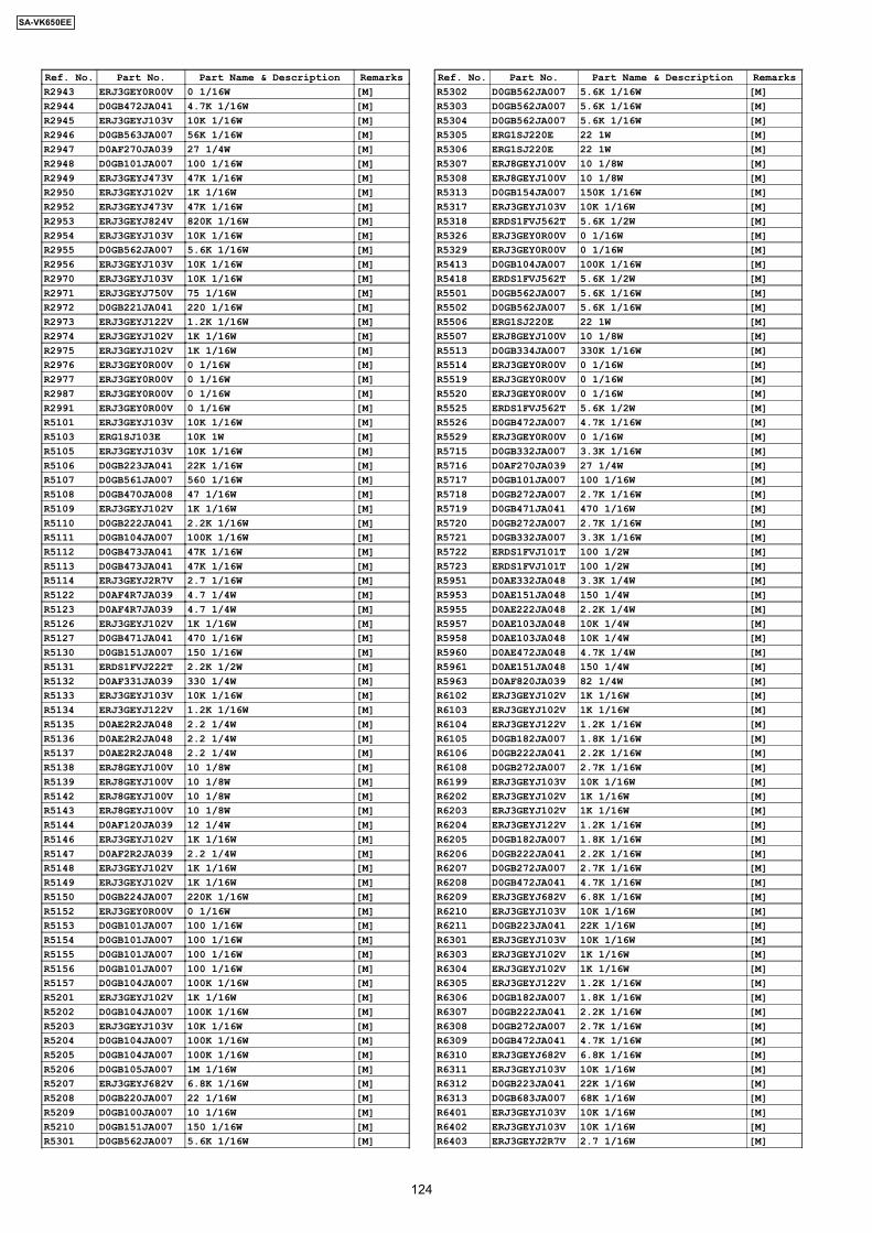
Ref. No. Part No. Part Name & Description RemarksR2943 ERJ3GEY0R00V 0 1/16W [M]R2944 D0GB472JA041 4.7K 1/16W [M]R2945 ERJ3GEYJ103V 10K 1/16W [M]R2946 D0GB563JA007 56K 1/16W [M]R2947 D0AF270JA039 27 1/4W [M]R2948 D0GB101JA007 100 1/16W [M]R2949 ERJ3GEYJ473V 47K 1/16W [M]R2950 ERJ3GEYJ102V 1K 1/16W [M]R2952 ERJ3GEYJ473V 47K 1/16W [M]R2953 ERJ3GEYJ824V 820K 1/16W [M]R2954 ERJ3GEYJ103V 10K 1/16W [M]R2955 D0GB562JA007 5.6K 1/16W [M]R2956 ERJ3GEYJ103V 10K 1/16W [M]R2970 ERJ3GEYJ103V 10K 1/16W [M]R2971 ERJ3GEYJ750V 75 1/16W [M]R2972 D0GB221JA041 220 1/16W [M]R2973 ERJ3GEYJ122V 1.2K 1/16W [M]R2974 ERJ3GEYJ102V 1K 1/16W [M]R2975 ERJ3GEYJ102V 1K 1/16W [M]R2976 ERJ3GEY0R00V 0 1/16W [M]R2977 ERJ3GEY0R00V 0 1/16W [M]R2987 ERJ3GEY0R00V 0 1/16W [M]R2991 ERJ3GEY0R00V 0 1/16W [M]R5101 ERJ3GEYJ103V 10K 1/16W [M]R5103 ERG1SJ103E 10K 1W [M]R5105 ERJ3GEYJ103V 10K 1/16W [M]R5106 D0GB223JA041 22K 1/16W [M]R5107 D0GB561JA007 560 1/16W [M]R5108 D0GB470JA008 47 1/16W [M]R5109 ERJ3GEYJ102V 1K 1/16W [M]R5110 D0GB222JA041 2.2K 1/16W [M]R5111 D0GB104JA007 100K 1/16W [M]R5112 D0GB473JA041 47K 1/16W [M]R5113 D0GB473JA041 47K 1/16W [M]R5114 ERJ3GEYJ2R7V 2.7 1/16W [M]R5122 D0AF4R7JA039 4.7 1/4W [M]R5123 D0AF4R7JA039 4.7 1/4W [M]R5126 ERJ3GEYJ102V 1K 1/16W [M]R5127 D0GB471JA041 470 1/16W [M]R5130 D0GB151JA007 150 1/16W [M]R5131 ERDS1FVJ222T 2.2K 1/2W [M]R5132 D0AF331JA039 330 1/4W [M]R5133 ERJ3GEYJ103V 10K 1/16W [M]R5134 ERJ3GEYJ122V 1.2K 1/16W [M]R5135 D0AE2R2JA048 2.2 1/4W [M]R5136 D0AE2R2JA048 2.2 1/4W [M]R5137 D0AE2R2JA048 2.2 1/4W [M]R5138 ERJ8GEYJ100V 10 1/8W [M]R5139 ERJ8GEYJ100V 10 1/8W [M]R5142 ERJ8GEYJ100V 10 1/8W [M]R5143 ERJ8GEYJ100V 10 1/8W [M]R5144 D0AF120JA039 12 1/4W [M]R5146 ERJ3GEYJ102V 1K 1/16W [M]R5147 D0AF2R2JA039 2.2 1/4W [M]R5148 ERJ3GEYJ102V 1K 1/16W [M]R5149 ERJ3GEYJ102V 1K 1/16W [M]R5150 D0GB224JA007 220K 1/16W [M]R5152 ERJ3GEY0R00V 0 1/16W [M]R5153 D0GB101JA007 100 1/16W [M]R5154 D0GB101JA007 100 1/16W [M]R5155 D0GB101JA007 100 1/16W [M]R5156 D0GB101JA007 100 1/16W [M]R5157 D0GB104JA007 100K 1/16W [M]R5201 ERJ3GEYJ102V 1K 1/16W [M]R5202 D0GB104JA007 100K 1/16W [M]R5203 ERJ3GEYJ103V 10K 1/16W [M]R5204 D0GB104JA007 100K 1/16W [M]R5205 D0GB104JA007 100K 1/16W [M]R5206 D0GB105JA007 1M 1/16W [M]R5207 ERJ3GEYJ682V 6.8K 1/16W [M]R5208 D0GB220JA007 22 1/16W [M]R5209 D0GB100JA007 10 1/16W [M]R5210 D0GB151JA007 150 1/16W [M]R5301 D0GB562JA007 5.6K 1/16W [M]
Ref. No. Part No. Part Name & Description RemarksR5302 D0GB562JA007 5.6K 1/16W [M]R5303 D0GB562JA007 5.6K 1/16W [M]R5304 D0GB562JA007 5.6K 1/16W [M]R5305 ERG1SJ220E 22 1W [M]R5306 ERG1SJ220E 22 1W [M]R5307 ERJ8GEYJ100V 10 1/8W [M]R5308 ERJ8GEYJ100V 10 1/8W [M]R5313 D0GB154JA007 150K 1/16W [M]R5317 ERJ3GEYJ103V 10K 1/16W [M]R5318 ERDS1FVJ562T 5.6K 1/2W [M]R5326 ERJ3GEY0R00V 0 1/16W [M]R5329 ERJ3GEY0R00V 0 1/16W [M]R5413 D0GB104JA007 100K 1/16W [M]R5418 ERDS1FVJ562T 5.6K 1/2W [M]R5501 D0GB562JA007 5.6K 1/16W [M]R5502 D0GB562JA007 5.6K 1/16W [M]R5506 ERG1SJ220E 22 1W [M]R5507 ERJ8GEYJ100V 10 1/8W [M]R5513 D0GB334JA007 330K 1/16W [M]R5514 ERJ3GEY0R00V 0 1/16W [M]R5519 ERJ3GEY0R00V 0 1/16W [M]R5520 ERJ3GEY0R00V 0 1/16W [M]R5525 ERDS1FVJ562T 5.6K 1/2W [M]R5526 D0GB472JA007 4.7K 1/16W [M]R5529 ERJ3GEY0R00V 0 1/16W [M]R5715 D0GB332JA007 3.3K 1/16W [M]R5716 D0AF270JA039 27 1/4W [M]R5717 D0GB101JA007 100 1/16W [M]R5718 D0GB272JA007 2.7K 1/16W [M]R5719 D0GB471JA041 470 1/16W [M]R5720 D0GB272JA007 2.7K 1/16W [M]R5721 D0GB332JA007 3.3K 1/16W [M]R5722 ERDS1FVJ101T 100 1/2W [M]R5723 ERDS1FVJ101T 100 1/2W [M]R5951 D0AE332JA048 3.3K 1/4W [M]R5953 D0AE151JA048 150 1/4W [M]R5955 D0AE222JA048 2.2K 1/4W [M]R5957 D0AE103JA048 10K 1/4W [M]R5958 D0AE103JA048 10K 1/4W [M]R5960 D0AE472JA048 4.7K 1/4W [M]R5961 D0AE151JA048 150 1/4W [M]R5963 D0AF820JA039 82 1/4W [M]R6102 ERJ3GEYJ102V 1K 1/16W [M]R6103 ERJ3GEYJ102V 1K 1/16W [M]R6104 ERJ3GEYJ122V 1.2K 1/16W [M]R6105 D0GB182JA007 1.8K 1/16W [M]R6106 D0GB222JA041 2.2K 1/16W [M]R6108 D0GB272JA007 2.7K 1/16W [M]R6199 ERJ3GEYJ103V 10K 1/16W [M]R6202 ERJ3GEYJ102V 1K 1/16W [M]R6203 ERJ3GEYJ102V 1K 1/16W [M]R6204 ERJ3GEYJ122V 1.2K 1/16W [M]R6205 D0GB182JA007 1.8K 1/16W [M]R6206 D0GB222JA041 2.2K 1/16W [M]R6207 D0GB272JA007 2.7K 1/16W [M]R6208 D0GB472JA041 4.7K 1/16W [M]R6209 ERJ3GEYJ682V 6.8K 1/16W [M]R6210 ERJ3GEYJ103V 10K 1/16W [M]R6211 D0GB223JA041 22K 1/16W [M]R6301 ERJ3GEYJ103V 10K 1/16W [M]R6303 ERJ3GEYJ102V 1K 1/16W [M]R6304 ERJ3GEYJ102V 1K 1/16W [M]R6305 ERJ3GEYJ122V 1.2K 1/16W [M]R6306 D0GB182JA007 1.8K 1/16W [M]R6307 D0GB222JA041 2.2K 1/16W [M]R6308 D0GB272JA007 2.7K 1/16W [M]R6309 D0GB472JA041 4.7K 1/16W [M]R6310 ERJ3GEYJ682V 6.8K 1/16W [M]R6311 ERJ3GEYJ103V 10K 1/16W [M]R6312 D0GB223JA041 22K 1/16W [M]R6313 D0GB683JA007 68K 1/16W [M]R6401 ERJ3GEYJ103V 10K 1/16W [M]R6402 ERJ3GEYJ103V 10K 1/16W [M]R6403 ERJ3GEYJ2R7V 2.7 1/16W [M]
124
SA-VK650EE

Ref. No. Part No. Part Name & Description RemarksR6404 ERJ3GEYJ2R7V 2.7 1/16W [M]R6405 D0GB274JA007 270K 1/16W [M]R6406 D0GB274JA007 270K 1/16W [M]R6411 D0GB223JA041 22K 1/16W [M]R6412 ERJ3GEYJ102V 1K 1/16W [M]R6415 D0GB223JA041 22K 1/16W [M]R6416 ERJ3GEYJ102V 1K 1/16W [M]R6421 ERJ3GEYJ103V 10K 1/16W [M]R6425 ERJ3GEYJ103V 10K 1/16W [M]R6458 ERJ3GEYJ392V 3.9K 1/16W [M]R6481 D0GB270JA007 27 1/16W [M]R6491 D0GB473JA041 47K 1/16W [M]R6492 D0GB473JA041 47K 1/16W [M]R6493 ERJ3GEYJ103V 10K 1/16W [M]R6601 D0GB471JA041 470 1/16W [M]R6603 D0GB221JA041 220 1/16W [M]R6604 D0GB221JA041 220 1/16W [M]R6605 D0GB823JA007 82K 1/16W [M]R6631 ERD2FCVG470T 47 1/4W [M]R6632 ERD2FCVG470T 47 1/4W [M]R6702 ERJ3GEYJ102V 1K 1/16W [M]R6703 ERJ3GEYJ272V 2.7K 1/16W [M]R6710 ERJ3GEYJ102V 1K 1/16W [M]R6712 ERJ3GEYJ272V 2.7K 1/16W [M]R6713 ERJ3GEYJ102V 1K 1/16W [M]R6714 ERJ3GEYJ102V 1K 1/16W [M]R6900 ERJ3GEY0R00V 0 1/16W [M]R6901 ERJ3GEYJ681V 680 1/16W [M]R6902 ERJ3GEYJ681V 680 1/16W [M]R6903 D0GB561JA007 560 1/16W [M]R6904 D0GB222JA041 2.2K 1/16W [M]R6905 D0GB474JA041 470K 1/16W [M]R6906 ERJ3GEYJ822V 8.2K 1/16W [M]R6907 D0GB334JA007 330K 1/16W [M]R6908 D0GB680JA007 68 1/16W [M]R6909 D0GB334JA007 330K 1/16W [M]R6910 D0GB472JA041 4.7K 1/16W [M]R6911 D0GB101JA007 100 1/16W [M]R6912 D0GB273JA007 27K 1/16W [M]R6913 D0GB331JA007 330 1/16W [M]R6914 ERJ3GEYJ102V 1K 1/16W [M]R6928 D0GB472JA041 4.7K 1/16W [M]R6950 ERJ3GEYJ102V 1K 1/16W [M]R6954 D0GB473JA041 47K 1/16W [M]R6956 D0GB472JA041 4.7K 1/16W [M]R6957 D0GB474JA041 470K 1/16W [M]R6959 ERJ3GEY0R00V 0 1/16W [M]R6960 ERJ3GEY0R00V 0 1/16W [M]R8003 ERJ2GEJ473X 47K 2W [M]R8011 ERJ2GEJ220X 22 2W [M]R8012 ERJ2GEJ220X 22 2W [M]R8013 ERJ2GEJ220X 22 2W [M]R8041 ERJ2GEJ330X 33 2W [M]R8153 ERJ2RHD621X 620 2W [M]R8154 ERJ2RHD102X 1K 2W [M]R8211 ERJ2GEJ103X 10K 2W [M]R8221 ERJ2GEJ822X 8.2K 2W [M]R8225 ERJ2GEJ822X 8.2K 2W [M]R8230 ERJ2GEJ222X 2.2K 2W [M]R8231 ERJ2GEJ223X 22K 2W [M]R8232 ERJ2GEJ752X 7.5K 2W [M]R8251 ERJ6GEYJ6R8V 6.8 1/10W [M]R8261 ERJ2GEJ823X 82K 2W [M]R8262 ERJ2GEJ153X 15K 2W [M]R8263 ERJ2GEJ823X 82K 2W [M]R8264 ERJ2GEJ153X 15K 2W [M]R8311 ERJ2RHD242X 2.4K 2W [M]R8312 ERJ2RHD102X 1K 2W [M]R8313 ERJ2RHD912X 9.1K 2W [M]R8314 ERJ2GE0R00X 0 2W [M]R8321 ERJ3RED680V 68 3W [M]R8322 ERJ3GEY0R00V 0 1/16W [M]R8325 ERJ3RED680V 68 3W [M]R8326 ERJ3GEY0R00V 0 1/16W [M]
Ref. No. Part No. Part Name & Description RemarksR8331 ERJ3RED680V 68 3W [M]R8332 ERJ3GEY0R00V 0 1/16W [M]R8335 ERJ3RED680V 68 3W [M]R8341 ERJ3RED680V 68 3W [M]R8401 ERJ2GEJ101X 100 2W [M]R8420 ERJ2GEJ222X 2.2K 2W [M]R8421 ERJ2GE0R00X 0 2W [M]R8531 ERJ2GEJ152X 1.5K 2W [M]R8532 ERJ2GEJ222X 2.2K 2W [M]R8533 ERJ2GE0R00X 0 2W [M]R8541 ERJ2GEJ153X 15K 2W [M]R8551 ERJ2GE0R00X 0 2W [M]R8552 ERJ2GEJ102X 1K 2W [M]R8553 ERJ2GEJ102X 1K 2W [M]R8554 ERJ2GEJ680X 68 2W [M]R8555 ERJ2GEJ2R2X 2.2 2W [M]R8556 ERJ3GEYJ560V 56 1/16W [M]R8557 ERJ3GEYJ510V 51 1/16W [M]R8558 ERJ2GEJ473X 47K 2W [M]R8559 ERJ2GEJ153X 15K 2W [M]R8561 ERJ2GE0R00X 0 2W [M]R8562 ERJ2GEJ102X 1K 2W [M]R8563 ERJ2GEJ102X 1K 2W [M]R8564 ERJ2GEJ220X 22 2W [M]R8565 ERJ2GEJ2R2X 2.2 2W [M]R8566 ERJ3GEYJ560V 56 1/16W [M]R8567 ERJ3GEYJ510V 51 1/16W [M]R8568 ERJ2GEJ473X 47K 2W [M]R8601 ERJ2GEJ104X 100K 2W [M]R8611 ERJ2GEJ101X 100 2W [M]R8621 ERJ2GEJ105X 1M 2W [M]R8622 ERJ2RHD102X 1K 2W [M]
CHIP JUMPERS
W2000 ERJ3GEY0R00V CHIP JUMPER [M]W2001 ERJ3GEY0R00V CHIP JUMPER [M]W2002 ERJ3GEY0R00V CHIP JUMPER [M]W2003 ERJ3GEY0R00V CHIP JUMPER [M]W2161 ERJ3GEY0R00V CHIP JUMPER [M]W2821 ERJ3GEY0R00V CHIP JUMPER [M]W2825 ERJ3GEY0R00V CHIP JUMPER [M]W2832 ERJ3GEY0R00V CHIP JUMPER [M]W2833 ERJ3GEY0R00V CHIP JUMPER [M]W2834 ERJ3GEY0R00V CHIP JUMPER [M]W2835 ERJ3GEY0R00V CHIP JUMPER [M]W2839 ERJ3GEY0R00V CHIP JUMPER [M]W2840 ERJ3GEY0R00V CHIP JUMPER [M]W2842 ERJ3GEY0R00V CHIP JUMPER [M]W2903 ERJ3GEY0R00V CHIP JUMPER [M]W2908 ERJ3GEY0R00V CHIP JUMPER [M]W2909 ERJ3GEY0R00V CHIP JUMPER [M]W2911 ERJ3GEY0R00V CHIP JUMPER [M]W2912 ERJ3GEY0R00V CHIP JUMPER [M]W2913 ERJ3GEY0R00V CHIP JUMPER [M]W2918 ERJ3GEY0R00V CHIP JUMPER [M]W2919 ERJ3GEY0R00V CHIP JUMPER [M]W2926 ERJ3GEY0R00V CHIP JUMPER [M]W2940 ERJ3GEY0R00V CHIP JUMPER [M]W2941 ERJ3GEY0R00V CHIP JUMPER [M]W2942 ERJ3GEY0R00V CHIP JUMPER [M]W2943 ERJ3GEY0R00V CHIP JUMPER [M]W2944 ERJ3GEY0R00V CHIP JUMPER [M]W2958 ERJ3GEY0R00V CHIP JUMPER [M]W2961 ERJ3GEY0R00V CHIP JUMPER [M]W2962 ERJ3GEY0R00V CHIP JUMPER [M]W2972 ERJ3GEY0R00V CHIP JUMPER [M]W2973 ERJ3GEY0R00V CHIP JUMPER [M]W2974 ERJ3GEY0R00V CHIP JUMPER [M]W2975 ERJ3GEY0R00V CHIP JUMPER [M]W2989 ERJ3GEY0R00V CHIP JUMPER [M]W3002 ERJ3GEY0R00V CHIP JUMPER [M]W5500 ERJ3GEY0R00V CHIP JUMPER [M]W5501 ERJ3GEY0R00V CHIP JUMPER [M]
125
SA-VK650EE

Ref. No. Part No. Part Name & Description RemarksW5502 ERJ3GEY0R00V CHIP JUMPER [M]W5503 ERJ3GEY0R00V CHIP JUMPER [M]W5504 ERJ3GEY0R00V CHIP JUMPER [M]W5505 ERJ3GEY0R00V CHIP JUMPER [M]W5519 ERJ3GEY0R00V CHIP JUMPER [M]W6800 ERJ3GEY0R00V CHIP JUMPER [M]W6801 ERJ3GEY0R00V CHIP JUMPER [M]W6802 ERJ3GEY0R00V CHIP JUMPER [M]W6803 ERJ3GEY0R00V CHIP JUMPER [M]W6804 ERJ3GEY0R00V CHIP JUMPER [M]W6805 ERJ3GEY0R00V CHIP JUMPER [M]W6806 ERJ3GEY0R00V CHIP JUMPER [M]W6807 ERJ3GEY0R00V CHIP JUMPER [M]W6808 ERJ3GEY0R00V CHIP JUMPER [M]W6809 ERJ3GEY0R00V CHIP JUMPER [M]W6811 ERJ3GEY0R00V CHIP JUMPER [M]
RX8001 D1H410320002 CHIP RESISTOR [M]RX8011 D1H88204A024 CHIP RESISTOR [M]RX8012 D1H88204A024 CHIP RESISTOR [M]RX8013 D1H88204A024 CHIP RESISTOR [M]RX8014 D1H88204A024 CHIP RESISTOR [M]RX8015 D1H88204A024 CHIP RESISTOR [M]RX8016 D1H88204A024 CHIP RESISTOR [M]RX8017 D1H88204A024 CHIP RESISTOR [M]RX8018 D1H422020001 CHIP RESISTOR [M]RX8019 D1H422020001 CHIP RESISTOR [M]RX8020 D1H422020001 CHIP RESISTOR [M]RX8031 D1H447220001 CHIP RESISTOR [M]RX8032 D1H447220001 CHIP RESISTOR [M]RX8111 D1H422320002 CHIP RESISTOR [M]RX8401 D1H410120001 CHIP RESISTOR [M]RX8403 D1H410120001 CHIP RESISTOR [M]RX8531 D1H456020001 CHIP RESISTOR [M]RX8532 D1H85604A024 CHIP RESISTOR [M]RX8533 D1H456020001 CHIP RESISTOR [M]RX8534 D1H456020001 CHIP RESISTOR [M]RX8611 D1H447220001 CHIP RESISTOR [M]RX8691 D1H410320002 CHIP RESISTOR [M]
K2111 J0JCC0000120 COIL [M]K2211 J0JCC0000120 COIL [M]K6635 ERJ3GEY0R00V CHIP JUMPER [M]K8003 ERJ2GE0R00X CHIP JUMPER [M]K8008 ERJ2GE0R00X CHIP JUMPER [M]K8251 ERJ3GEY0R00V CHIP JUMPER [M]K8321 ERJ2GE0R00X CHIP JUMPER [M]K8325 ERJ2GE0R00X CHIP JUMPER [M]K8331 ERJ2GE0R00X CHIP JUMPER [M]K8335 ERJ2GE0R00X CHIP JUMPER [M]K8341 ERJ2GE0R00X CHIP JUMPER [M]K8421 ERJ3GEY0R00V CHIP JUMPER [M]
CAPACITORS
C1 ECEA1CKA101B 100 16V [M]C1 F1D1H5R6A017 5.6P 50V [M]C2 F1D1H102A029 1000P 50V [M]C3 F1D1H2R2A017 2.2P 50V [M]C4 F1D1H181A012 180P 50V [M]C5 F1D1H5R6A017 5.6P 50V [M]C6 F1D1H3R3A017 3.3P 50V [M]C7 F1D1H4R7A017 4.7P 50V [M]C8 F1D1H3R3A017 3.3P 50V [M]C9 F1D1H2R2A017 2.2P 50V [M]C10 F1D1H180A015 18P 50V [M]C11 F1D1H102A029 1000P 50V [M]C1002 ECEA1HKN2R2B 2.2 50V [M]C1006 ECA1HAK010XB 1 50V [M]C1007 F0A2A472A034 4700P 100V [M]C1008 ECA1HAK010XB 1 50V [M]C1009 ECA1CAK470XB 47 16V [M]C1010 ECA1EAM101XB 100 25V [M]C1011 ECQV1H473JL3 0.047 50V [M]
Ref. No. Part No. Part Name & Description RemarksC1012 F1H1H102A219 1000P 50V [M]C1013 F1H1H102A219 1000P 50V [M]C1014 F1H1H102A219 1000P 50V [M]C1015 F1H1H102A219 1000P 50V [M]C1016 F1H1H222A013 2200P 50V [M]C1017 F1H1H222A013 2200P 50V [M]C1018 F1H1H332A013 3300P 50V [M]C1019 F1H1H102A219 1000P 50V [M]C1020 F1H1H471A219 470P 50V [M]C1021 F1H1H471A219 470P 50V [M]C1022 F1H1H102A219 1000P 50V [M]C1023 F1H1H102A219 1000P 50V [M]C1026 ECA0JAK470XB 47 6.3V [M]C1027 F1H1H102A219 1000P 50V [M]C1030 ECEA1AKA101B 100 10V [M]C1031 ECEA1AKA101B 100 10V [M]C1032 F1C1C183A023 0.018 16V [M]C1033 F1C1C183A023 0.018 16V [M]C1034 ECA1HAK3R3XB 3.3 50V [M]C1035 ECA1HAK3R3XB 3.3 50V [M]C1036 F1H1C333A071 0.033 16V [M]C1037 ECA1HAK3R3XB 3.3 50V [M]C1038 F1H1H221A748 220P 50V [M]C1039 F1H1H221A748 220P 50V [M]C1040 ECA1CAK100XB 10 16V [M]C1041 ECA1CAK100XB 10 16V [M]C1042 ECA1CAK220XB 22 16V [M]C1043 ECA1HAK4R7XB 4.7 50V [M]C1044 ECA1AAK330XB 33 10V [M]C1045 ECA1AAK220XB 22 10V [M]C1046 ECA1CAM221XB 220 16V [M]C1049 F1H1H332A013 3300P 50V [M]C1050 F1H1H332A013 3300P 50V [M]C1056 ECA1CAK100XB 10 16V [M]C1057 F1H1H102A219 1000P 50V [M]C1058 F1H1H102A219 1000P 50V [M]C1059 F1H1H103A219 0.01 50V [M]C2004 F1H1C104A041 0.1 16V [M]C2021 ECA1CAK101XB 100 16V [M]C2031 F1H1H103A219 0.01 50V [M]C2032 F1H1H103A219 0.01 50V [M]C2034 ECJ1VB1C105K 1 16V [M]C2035 ECJ1VB1C105K 1 16V [M]C2051 F2A1H4R7A014 4.7P 50V [M]C2062 F1H1H103A219 0.01 50V [M]C2063 ECJ1VC1H101K 100P 50V [M]C2064 ECA1CAK100XB 10 16V [M]C2067 ECJ1VB1C105K 1 16V [M]C2068 ECJ1VB1C105K 1 16V [M]C2069 ECJ1VB1A474K 0.47 10V [M]C2070 ECJ1VC1H101K 100P 50V [M]C2071 F1H1H103A219 0.01 50V [M]C2073 F1H1H103A219 0.01 50V [M]C2074 ECJ1VC1H470J 47P 50V [M]C2102 F1H1C104A041 0.1 16V [M]C2103 F1H1H102A219 1000P 50V [M]C2104 F1H1C104A041 0.1 16V [M]C2105 ECJ1VB1H561K 560P 50V [M]C2106 F1H1H332A013 3300P 50V [M]C2107 F1H1C104A041 0.1 16V [M]C2108 F1H1H102A219 1000P 50V [M]C2111 F1H1C104A041 0.1 16V [M]C2112 F1H1H102A219 1000P 50V [M]C2119 ECJ1VB1C105K 1 16V [M]C2120 ECJ1VB1C105K 1 16V [M]C2121 ECJ1VB1C224K 0.22 16V [M]C2126 ECJ1VB1C224K 0.22 16V [M]C2131 ECJ1VB1A474K 0.47 10V [M]C2136 ECJ1VB1A474K 0.47 10V [M]C2141 ECJ1VB1C105K 1 16V [M]C2142 ECJ1VB1C105K 1 16V [M]C2151 ECA1CAK100XB 10 16V [M]C2166 F1H1H102A219 1000P 50V [M]C2194 ECA1HAK010XB 1 50V [M]
126
SA-VK650EE

Ref. No. Part No. Part Name & Description RemarksC2195 F1H1C223A001 0.022 16V [M]C2197 ERJ3GEY0R00V 0 1/16W [M]C2202 F1H1C104A041 0.1 16V [M]C2203 F1H1H102A219 1000P 50V [M]C2204 F1H1C104A041 0.1 16V [M]C2205 ECJ1VB1H561K 560P 50V [M]C2206 F1H1H332A013 3300P 50V [M]C2207 F1H1C104A041 0.1 16V [M]C2208 F1H1H102A219 1000P 50V [M]C2211 F1H1C104A041 0.1 16V [M]C2212 F1H1H102A219 1000P 50V [M]C2219 ECJ1VB1C105K 1 16V [M]C2220 ECJ1VB1C105K 1 16V [M]C2221 ECJ1VB1H473K 0.047 50V [M]C2226 ECJ1VB1H473K 0.047 50V [M]C2231 ECJ1VB1C393K 0.039 16V [M]C2236 ECJ1VB1C393K 0.039 16V [M]C2241 ECJ1VB1C105K 1 16V [M]C2242 ECJ1VB1C105K 1 16V [M]C2245 ECA1CAK100XB 10 16V [M]C2251 ECA1CAK100XB 10 16V [M]C2266 F1H1H102A219 1000P 50V [M]C2294 ECA1HAK010XB 1 50V [M]C2295 F1H1C223A001 0.022 16V [M]C2297 ERJ3GEY0R00V 0 1/16W [M]C2301 ECJ1VC1H100D 10P 50V [M]C2302 F1H1H470A230 47P 50V [M]C2311 ECJ1VB1A124K 0.12 10V [M]C2312 ECJ1VB1A474K 0.47 10V [M]C2313 ECJ1VC1H120J 12P 50V [M]C2314 F1H1H470A230 47P 50V [M]C2315 ECJ1VB1C105K 1 16V [M]C2331 ECJ1VB1C105K 1 16V [M]C2334 ECJ1VB1C105K 1 16V [M]C2401 ECJ1VC1H100D 10P 50V [M]C2402 F1H1H470A230 47P 50V [M]C2411 ECJ1VB1A124K 0.12 10V [M]C2412 ECJ1VB1A474K 0.47 10V [M]C2413 ECJ1VC1H120J 12P 50V [M]C2414 F1H1H470A230 47P 50V [M]C2415 ECJ1VB1C105K 1 16V [M]C2501 ECEA1AKN100B 10 10V [M]C2520 F1H1H103A219 0.01 50V [M]C2521 F1H1H103A219 0.01 50V [M]C2550 F2A1E2210050 220P 25V [M]C2551 ECJ1VC1H101K 100P 50V [M]C2552 F2A0J102A130 1000P 6.3V [M]C2553 ECA0JAK101XB 100 6.3V [M]C2554 F1H1H103A219 0.01 50V [M]C2555 ECJ1VB1A105K 1 10V [M]C2556 F2A1E2210050 220P 25V [M]C2561 ECJ1VB1C105K 1 16V [M]C2576 ECEA1HKN4R7B 4.7 50V [M]C2581 ECA1CAK101XB 100 16V [M]C2582 ECA1CAK101XB 100 16V [M]C2583 ECJ1VB1C224K 0.22 16V [M]C2584 F1H1H221A748 220P 50V [M]C2585 F1H1H221A748 220P 50V [M]C2586 F1H1H103A219 0.01 50V [M]C2587 F1H1H103A219 0.01 50V [M]C2588 F1H1C104A041 0.1 16V [M]C2601 F1H1H103A219 0.01 50V [M]C2602 F2A1C1000018 10P 16V [M]C2603 F1H1H103A219 0.01 50V [M]C2604 F1H1H102A219 1000P 50V [M]C2606 F1H1H103A219 0.01 50V [M]C2607 ECJ1VB1E473K 0.047 25V [M]C2608 ECJ1VC1H080D 8P 50V [M]C2609 F1H1H102A219 1000P 50V [M]C2610 F1H1H103A219 0.01 50V [M]C2611 F2A1H4R7A014 4.7P 50V [M]C2612 F1H1H103A219 0.01 50V [M]C2613 F1H1H102A219 1000P 50V [M]C2614 F2A1H3R3A013 3.3P 50V [M]
Ref. No. Part No. Part Name & Description RemarksC2615 F2A1H4R7A014 4.7P 50V [M]C2616 F1H1C333A071 0.033 16V [M]C2617 F1H1H103A219 0.01 50V [M]C2618 F1H1H103A219 0.01 50V [M]C2619 F0A2A681A010 680P 100V [M]C2620 F2A1C1000018 10P 16V [M]C2621 ECA1HAKR47XB 0.47 50V [M]C2622 ECA1HAK010XB 1 50V [M]C2623 ECA1HAK010XB 1 50V [M]C2624 ECJ1VC1H101K 100P 50V [M]C2625 ECA1CAK220XB 22 16V [M]C2626 ECJ2VF1C105Z 1 16V [M]C2627 ECA1CAK220XB 22 16V [M]C2629 ECA0JAK101XB 100 6.3V [M]C2630 ECA0JAK101XB 100 6.3V [M]C2631 ECJ1VC1H151J 150P 50V [M]C2632 F1H1H102A219 1000P 50V [M]C2633 ECJ1VC1H270J 27P 50V [M]C2634 ECJ1VC1H270J 27P 50V [M]C2636 F1H1H102A219 1000P 50V [M]C2637 F1H1H332A013 3300P 50V [M]C2638 F1H1H103A219 0.01 50V [M]C2639 F2A1H4R7A014 4.7P 50V [M]C2641 ECA1HAK010XB 1 50V [M]C2642 ECA1HAK010XB 1 50V [M]C2643 ECJ1VB1H682K 6800P 50V [M]C2644 ECJ1VB1H682K 6800P 50V [M]C2647 F1H1H102A219 1000P 50V [M]C2648 F1H1H103A219 0.01 50V [M]C2649 F1H1C104A008 0.1 16V [M]C2731 ECA1HAK100XB 10 50V [M]C2732 ECA1HAK100XB 10 50V [M]C2733 ECA1HAK010XB 1 50V [M]C2734 ECEA1CKA100B 10 16V [M]C2735 ECEA1CKA100B 10 16V [M]C2736 F1H1A154A001 0.15 10V [M]C2737 ECJ1VB1C105K 1 16V [M]C2738 ECJ1VB1C105K 1 16V [M]C2739 ECEA1HKA2R2B 2.2 50V [M]C2740 ECJ1VB1H472K 4700P 50V [M]C2741 F1H1H102A219 1000P 50V [M]C2742 ECJ1VB1H272K 2700P 50V [M]C2743 ECJ1VB1H561K 560P 50V [M]C2744 F1H1H102A219 1000P 50V [M]C2745 F1H1H332A013 3300P 50V [M]C2746 ECEA1HKA2R2B 2.2 50V [M]C2747 ECJ1VB1H182K 1800P 50V [M]C2748 ECJ1VB1H473K 0.047 50V [M]C2749 ECJ1VB1C683K 0.068 16V [M]C2750 ECJ1VB1C683K 0.068 16V [M]C2751 ECJ1VB1C683K 0.068 16V [M]C2752 ECJ1VB1C683K 0.068 16V [M]C2753 ECEA1CKA470B 47 16V [M]C2754 ECJ1VB1H104K 0.1 50V [M]C2755 ECA1CM101B 100 16V [M]C2756 ECJ1VB1H104K 0.1 50V [M]C2757 F1H1H102A219 1000P 50V [M]C2758 ECJ1VB1H472K 4700P 50V [M]C2759 ECJ1VB1C683K 0.068 16V [M]C2760 ECJ1VB1H104K 0.1 50V [M]C2761 ECJ1VB1H104K 0.1 50V [M]C2762 ECJ1VB1C683K 0.068 16V [M]C2763 F1H1H102A219 1000P 50V [M]C2764 ECJ1VB1H472K 4700P 50V [M]C2765 ECJ1VB1H104K 0.1 50V [M]C2766 ECJ1VB1C105K 1 16V [M]C2767 ECA0JAK221XB 220 6.3V [M]C2768 ECJ1VC1H102K 1000P 50V [M]C2769 ECJ1VC1H102K 1000P 50V [M]C2770 ECJ1VC1H102K 1000P 50V [M]C2813 ECJ1VC1H101K 100P 50V [M]C2814 ECJ1VC1H101K 100P 50V [M]C2815 ECJ1VC1H101K 100P 50V [M]C2816 ECJ1VC1H101K 100P 50V [M]
127
SA-VK650EE

Ref. No. Part No. Part Name & Description RemarksC2817 ECJ1VC1H101K 100P 50V [M]C2818 ECJ1VC1H101K 100P 50V [M]C2819 ECJ1VC1H101K 100P 50V [M]C2820 ECJ1VC1H101K 100P 50V [M]C2821 ECJ1VC1H101K 100P 50V [M]C2831 F1H1C223A001 0.022 16V [M]C2832 F1H1H331A013 330P 50V [M]C2833 F1H1H331A013 330P 50V [M]C2834 ECJ1VC1H680J 68P 50V [M]C2838 ECJ1VC1H680J 68P 50V [M]C2840 ECJ1VC1H180J 18P 50V [M]C2841 ECJ1VC1H180J 18P 50V [M]C2851 F1H1C104A041 0.1 16V [M]C2852 ECA1CAM471XB 470 16V [M]C2853 F1H1C104A041 0.1 16V [M]C2854 ECA1CAK101XB 100 16V [M]C2856 ECJ1VB1C105K 1 16V [M]C2857 F2A1H3R3A013 3.3P 50V [M]C2858 F1H1H103A219 0.01 50V [M]C2860 ECJ1VC1H101K 100P 50V [M]C2861 ECJ1VC1H101K 100P 50V [M]C2862 ECJ1VC1H101K 100P 50V [M]C2863 ECJ1VC1H101K 100P 50V [M]C2864 ECJ1VC1H101K 100P 50V [M]C2865 ECJ1VC1H101K 100P 50V [M]C2866 ECJ1VC1H101K 100P 50V [M]C2867 ECJ1VC1H101K 100P 50V [M]C2868 ECJ1VC1H101K 100P 50V [M]C2901 ECJ1VC1H101K 100P 50V [M]C2902 ECJ1VC1H101K 100P 50V [M]C2903 ECJ1VB1H104K 0.1 50V [M]C2904 ECJ1VC1H101K 100P 50V [M]C2905 F1H1H103A219 0.01 50V [M]C2906 ECA1CAK100XB 10 16V [M]C2908 ECJ1VC1H101K 100P 50V [M]C2909 ECJ1VC1H101K 100P 50V [M]C2910 ECJ1VC1H101K 100P 50V [M]C2911 ECA1AAK221XB 220 10V [M]C2912 F1H1H103A219 0.01 50V [M]C2913 ECA1HAK220XB 22 50V [M]C2914 F1H1C104A041 0.1 16V [M]C2915 F1H1H103A219 0.01 50V [M]C2916 ECJ1VC1H101K 100P 50V [M]C2917 F1H1H103A219 0.01 50V [M]C2918 F1H1H103A219 0.01 50V [M]C2919 F2A0J102A130 1000P 6.3V [M]C2920 F2A0J102A130 1000P 6.3V [M]C2922 F2A0J102A130 1000P 6.3V [M]C2923 F2A0J102A130 1000P 6.3V [M]C2924 F2A0J102A130 1000P 6.3V [M]C2925 F1H1C104A041 0.1 16V [M]C2926 ECA1HAK010XB 1 50V [M]C2927 ECJ1VB1C105K 1 16V [M]C2930 F1H1C104A041 0.1 16V [M]C2931 F1H1C104A041 0.1 16V [M]C2932 F1H1C104A041 0.1 16V [M]C2933 F1H1C104A041 0.1 16V [M]C2940 F1H1C104A041 0.1 16V [M]C2941 ECA1CAK330XB 33 16V [M]C2944 ECJ1VC1H101K 100P 50V [M]C2945 ECA1CAK470XB 47 16V [M]C2947 ECA0JAK101XB 100 6.3V [M]C2948 ECA0JAK221XB 220 6.3V [M]C2975 ECJ1VC1H560J 56P 50V [M]C2976 ECA1CAK100XB 10 16V [M]C2977 F2A0J331A015 330P 6.3V [M]C2978 F1H1C104A041 0.1 16V [M]C2979 ECA1CAK470XB 47 16V [M]C2980 ECA1CAK470XB 47 16V [M]C2981 ECA1CAK101XB 100 16V [M]C2982 ECEA1CKA221B 220 16V [M]C5101 ECA1VM472E 4700 35V [M]C5102 ECA2AM100B 10 100V [M]C5103 ECA2AM100B 10 100V [M]
Ref. No. Part No. Part Name & Description RemarksC5104 ECA1VM472E 4700 35V [M]C5105 ECA1AAK221XB 220 10V [M]C5106 F1K2A1040006 0.1 100V [M]C5107 F1K2A1040006 0.1 100V [M]C5109 ECA1EAM101XB 100 25V [M]C5110 ECA1EAM101XB 100 25V [M]C5111 ECA0JAK101XB 100 6.3V [M]C5112 ECA1EAK100XB 10 25V [M]C5113 ECA1HM330B 33 50V [M]C5119 F2A1V471A141 470P 35V [M]C5120 F2A1V471A141 470P 35V [M]C5121 ECA1CAK470XB 47 16V [M]C5123 F2A1V471A141 470P 35V [M]C5124 F2A1V471A141 470P 35V [M]C5151 ECJ1VB1H104K 0.1 50V [M]C5152 ECJ1VB1H104K 0.1 50V [M]C5153 ECJ1VB1H104K 0.1 50V [M]C5155 F1H1H102A219 1000P 50V [M]C5157 F1H1H103A219 0.01 50V [M]C5158 F1H1H103A219 0.01 50V [M]C5159 F1H1H103A219 0.01 50V [M]C5161 ECJ1VB1H473K 0.047 50V [M]C5163 ECJ1VB1H473K 0.047 50V [M]C5165 ECA1JM102E 1000 63V [M]C5166 ECA1JM102E 1000 63V [M]C5167 F1K2A1040006 0.1 100V [M]C5168 F1K2A1040006 0.1 100V [M]C5171 ECA1JM102E 1000 63V [M]C5172 ECA1JM102E 1000 63V [M]C5201 F1H1H471A219 470P 50V [M]C5202 ECJ1VC1H101K 100P 50V [M]C5203 ECJ1VC1H101K 100P 50V [M]C5204 ECJ1VC1H101K 100P 50V [M]C5205 ECJ1VB1H104K 0.1 50V [M]C5207 ECJ1VC1H101K 100P 50V [M]C5208 ECA0JAK221XB 220 6.3V [M]C5210 F1H1H471A219 470P 50V [M]C5211 ECEA0JKS101B 100 6.3V [M]C5301 ECJ1VB1A474K 0.47 10V [M]C5302 F1H1H331A013 330P 50V [M]C5303 ECJ1VB1A474K 0.47 10V [M]C5305 F1H1H331A013 330P 50V [M]C5308 ECJ1VB1H104K 0.1 50V [M]C5309 ECJ1VB1H104K 0.1 50V [M]C5310 F1K2A1040006 0.1 100V [M]C5311 F1H1H221A748 220P 50V [M]C5312 F1K2A1040007 0.1 100V [M]C5313 ECJ1VB1H153K 0.015 50V [M]C5314 F1K2A1040006 0.1 100V [M]C5315 ECJ1VB1H104K 0.1 50V [M]C5316 ECJ1VB1H104K 0.1 50V [M]C5317 ECJ1VC1H101K 100P 50V [M]C5318 F1K2A1040006 0.1 100V [M]C5319 ECJ1VB1H153K 0.015 50V [M]C5320 F1K2A1040007 0.1 100V [M]C5321 F1K2A1040006 0.1 100V [M]C5322 ECJ1VB1H104K 0.1 50V [M]C5323 ECJ1VB1H104K 0.1 50V [M]C5324 ECQV1H684JL3 0.68 50V [M]C5325 ECJ1VB1H104K 0.1 50V [M]C5327 ECQV1H684JL3 0.68 50V [M]C5328 ECJ1VB1H104K 0.1 50V [M]C5330 F1H2A221A009 220P 100V [M]C5331 F1H2A221A009 220P 100V [M]C5332 F1H2A221A009 220P 100V [M]C5333 F1H2A221A009 220P 100V [M]C5335 ECJ1VB1H153K 0.015 50V [M]C5336 F1H1H102A219 1000P 50V [M]C5337 F1H1H102A219 1000P 50V [M]C5339 ECJ1VB1A474K 0.47 10V [M]C5340 ECJ1VB1A474K 0.47 10V [M]C5343 ECJ1VB1H153K 0.015 50V [M]C5344 F1H1H102A219 1000P 50V [M]C5345 F1H1H102A219 1000P 50V [M]
128
SA-VK650EE
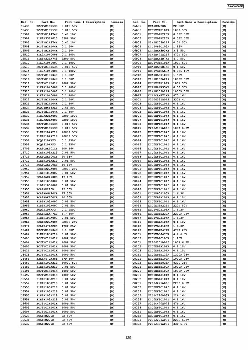
Ref. No. Part No. Part Name & Description RemarksC5435 ECJ1VB1H153K 0.015 50V [M]C5438 ECJ1VB1H153K 0.015 50V [M]C5501 ECJ1VB1A474K 0.47 10V [M]C5502 F1H1H331A013 330P 50V [M]C5503 ECJ1VB1A474K 0.47 10V [M]C5508 ECJ1VB1H104K 0.1 50V [M]C5509 ECJ1VB1H104K 0.1 50V [M]C5510 F1K2A1040006 0.1 100V [M]C5511 F1H1H221A748 220P 50V [M]C5512 F1K2A1040007 0.1 100V [M]C5513 ECJ1VB1H153K 0.015 50V [M]C5514 F1K2A1040006 0.1 100V [M]C5515 ECJ1VB1H104K 0.1 50V [M]C5516 ECJ1VB1H104K 0.1 50V [M]C5517 ECJ1VC1H101K 100P 50V [M]C5518 F1K2A1040006 0.1 100V [M]C5520 F1K2A1040007 0.1 100V [M]C5521 F1K2A1040006 0.1 100V [M]C5522 ECJ1VB1H104K 0.1 50V [M]C5523 ECJ1VB1H104K 0.1 50V [M]C5527 ECQV1H684JL3 0.68 50V [M]C5528 ECJ1VB1H104K 0.1 50V [M]C5530 F1H2A221A009 220P 100V [M]C5531 F1H2A221A009 220P 100V [M]C5536 ECJ1VB1H153K 0.015 50V [M]C5537 ECJ1VB1H153K 0.015 50V [M]C5538 F1H1H102A219 1000P 50V [M]C5539 F1H1H102A219 1000P 50V [M]C5551 ECQE2104KF3 0.1 250V [M]C5552 ECQE2104KF3 0.1 250V [M]C5709 ECA1CAK101XB 100 16V [M]C5710 F1H1H103A219 0.01 50V [M]C5711 ECA1CAK100XB 10 16V [M]C5712 F1H1H103A219 0.01 50V [M]C5713 ECA1CAK100XB 10 16V [M]C5950 F2B1E222A005 2200P 25V [M]C5951 F1B1H103A007 0.01 50V [M]C5952 ECA1AAK470XB 47 10V [M]C5953 F1B1H103A007 0.01 50V [M]C5954 F1B1H103A007 0.01 50V [M]C5955 ECA1HM220B 22 50V [M]C5956 ECA1HAM470XB 47 50V [M]C5957 ECA1HAK100XB 10 50V [M]C5958 F1B1H103A007 0.01 50V [M]C5959 F1B1H103A007 0.01 50V [M]C5960 ECQE2104KF3 0.1 250V [M]C5963 ECA1HAK4R7XB 4.7 50V [M]C5965 F1B1H103A007 0.01 50V [M]C5966 F2B1E222A005 2200P 25V [M]C5971 F2A1E471A205 470P 25V [M]C6401 ECJ1VB1H104K 0.1 50V [M]C6402 F1H1H103A219 0.01 50V [M]C6403 ECJ1VC1H101K 100P 50V [M]C6404 ECJ1VC1H101K 100P 50V [M]C6405 ECJ1VC1H101K 100P 50V [M]C6421 ECJ1VC1H101K 100P 50V [M]C6425 ECJ1VC1H101K 100P 50V [M]C6481 F2A1A470A388 47P 10V [M]C6482 F1H1H102A219 1000P 50V [M]C6483 F1H1H103A219 0.01 50V [M]C6491 ECJ1VC1H101K 100P 50V [M]C6492 ECJ1VC1H101K 100P 50V [M]C6551 F1H1H103A219 0.01 50V [M]C6552 F1H1H103A219 0.01 50V [M]C6553 F1H1H103A219 0.01 50V [M]C6554 F1H1H103A219 0.01 50V [M]C6555 F1H1H103A219 0.01 50V [M]C6556 F1H1H103A219 0.01 50V [M]C6601 ECJ1VC1H101K 100P 50V [M]C6603 ECJ1VC1H101K 100P 50V [M]C6604 ECJ1VC1H101K 100P 50V [M]C6623 ECA1HM220B 22 50V [M]C6631 ECA1HM220B 22 50V [M]C6632 ECA1HM220B 22 50V [M]
Ref. No. Part No. Part Name & Description RemarksC6635 ECA1HM220B 22 50V [M]C6636 ECJ1VC1H101K 100P 50V [M]C6901 ECJ1VB1H223K 0.022 50V [M]C6902 ECJ1VB1H223K 0.022 50V [M]C6903 F1H1H103A219 0.01 50V [M]C6904 ECJ1VB1C105K 1 16V [M]C6905 ECA1HAK3R3XB 3.3 50V [M]C6907 F1H1H471A219 470P 50V [M]C6908 ECA1HAK4R7XB 4.7 50V [M]C6909 ECJ1VC1H101K 100P 50V [M]C6910 ECA1HAK0R1XB 0.1 50V [M]C6911 ECJ1VB1C563K 0.056 16V [M]C6912 ECA1HAK010XB 1 50V [M]C6913 F1H1H102A219 1000P 50V [M]C6914 ECJ1VC1H101K 100P 50V [M]C6915 ECA1HAKR33XB 0.33 50V [M]C6916 F1H1H102A219 1000P 50V [M]C6917 ECA1CAM471XB 470 16V [M]C8001 F2G0G331A012 330P 4V [M]C8003 ECJ0EF1C104Z 0.1 16V [M]C8004 ECJ0EF1C104Z 0.1 16V [M]C8005 ECJ0EF1C104Z 0.1 16V [M]C8006 ECJ0EF1C104Z 0.1 16V [M]C8007 ECJ0EF1C104Z 0.1 16V [M]C8008 ECJ0EF1C104Z 0.1 16V [M]C8011 F2G0J101A066 100P 6.3V [M]C8012 ECJ0EF1C104Z 0.1 16V [M]C8013 ECJ0EF1C104Z 0.1 16V [M]C8014 ECJ0EF1C104Z 0.1 16V [M]C8015 ECJ0EF1C104Z 0.1 16V [M]C8016 ECJ0EF1C104Z 0.1 16V [M]C8017 ECJ0EF1C104Z 0.1 16V [M]C8018 ECJ0EF1C104Z 0.1 16V [M]C8019 ECJ0EF1C104Z 0.1 16V [M]C8020 ECJ0EF1C104Z 0.1 16V [M]C8021 ECJ0EF1C104Z 0.1 16V [M]C8022 ECJ0EF1C104Z 0.1 16V [M]C8023 ECJ0EF1C104Z 0.1 16V [M]C8024 ECJ0EF1C104Z 0.1 16V [M]C8025 ECJ0EF1C104Z 0.1 16V [M]C8026 ECJ0EF1C104Z 0.1 16V [M]C8051 ECJ1VB0J105K 1 6.3V [M]C8052 ECJ0EB1A104K 0.1 10V [M]C8053 ECJ0EF1C104Z 0.1 16V [M]C8054 ECJ0EC1H221J 220P 50V [M]C8055 ECJ1VB0J105K 1 6.3V [M]C8056 ECJ0EB1E222K 2200P 25V [M]C8057 ECJ1VB0J105K 1 6.3V [M]C8111 ECJ0EB1A104K 0.1 10V [M]C8112 ECJ1VB0J105K 1 6.3V [M]C8113 ECJ0EB1E471K 470P 25V [M]C8151 ECJ1VB0J475K 4.7 6.3V [M]C8152 ECJ1VB1C105K 1 16V [M]C8201 F2G0J101A066 100P 6.3V [M]C8202 ECJ0EB1A104K 0.1 10V [M]C8203 ECJ0EB1A104K 0.1 10V [M]C8211 ECJ0EB1E122K 1200P 25V [M]C8221 ECJ0EB1E102K 1000P 25V [M]C8222 ECJ0EB1E821K 820P 25V [M]C8225 ECJ0EB1E102K 1000P 25V [M]C8226 ECJ0EB1E102K 1000P 25V [M]C8231 ECJ0EB1A104K 0.1 10V [M]C8232 ECJ0EB1A104K 0.1 10V [M]C8251 F2G0J221A065 220P 6.3V [M]C8252 ECJ0EF1C104Z 0.1 16V [M]C8253 ECJ0EF1C104Z 0.1 16V [M]C8255 F2G1C220A037 22P 16V [M]C8256 ECJ0EF1C104Z 0.1 16V [M]C8257 F2G1C470A076 47P 16V [M]C8258 ECJ0EF1C104Z 0.1 16V [M]C8261 ECJ0EF1C104Z 0.1 16V [M]C8262 ECJ0EF1C104Z 0.1 16V [M]C8301 F2G0J221A031 220P 6.3V [M]C8302 F2G0J330A031 33P 6.3V [M]
129
SA-VK650EE
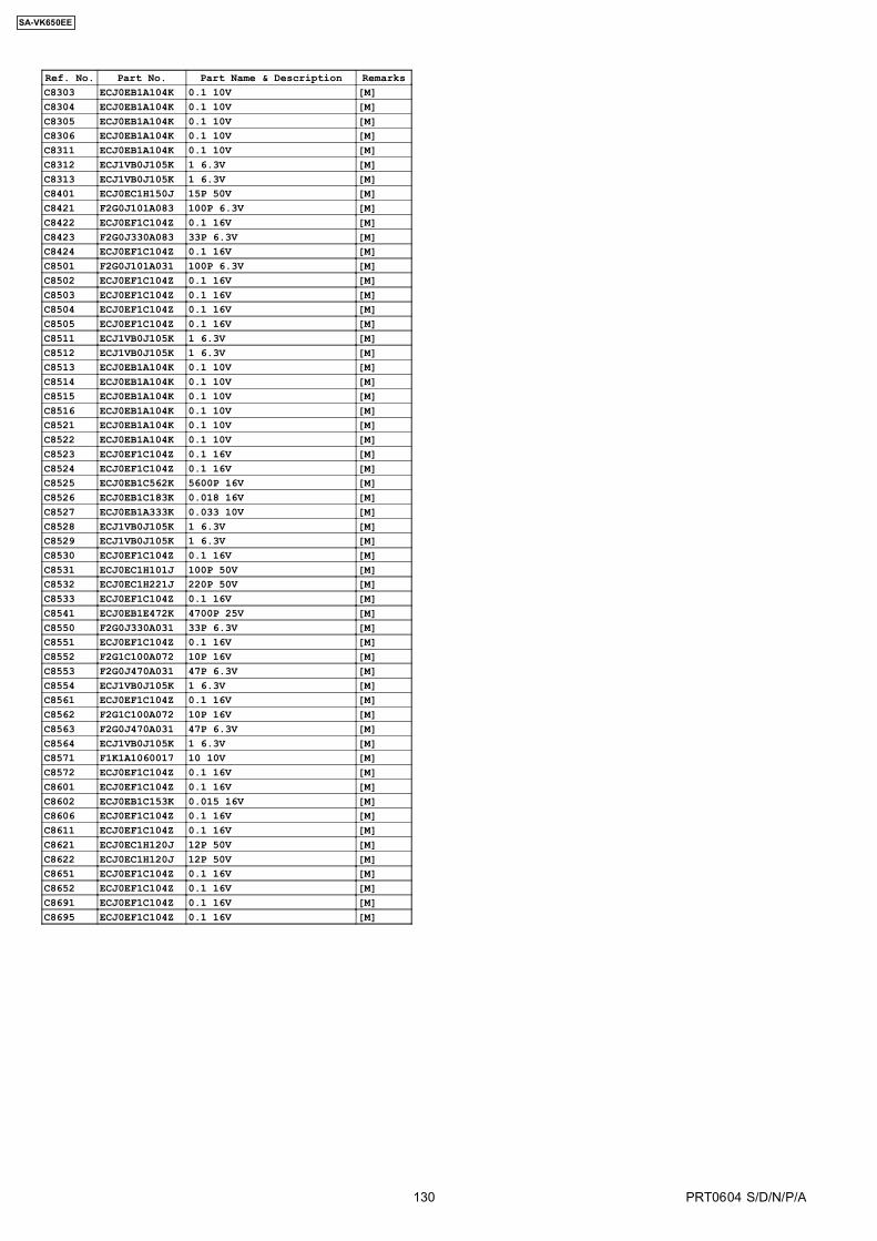
Ref. No. Part No. Part Name & Description RemarksC8303 ECJ0EB1A104K 0.1 10V [M]C8304 ECJ0EB1A104K 0.1 10V [M]C8305 ECJ0EB1A104K 0.1 10V [M]C8306 ECJ0EB1A104K 0.1 10V [M]C8311 ECJ0EB1A104K 0.1 10V [M]C8312 ECJ1VB0J105K 1 6.3V [M]C8313 ECJ1VB0J105K 1 6.3V [M]C8401 ECJ0EC1H150J 15P 50V [M]C8421 F2G0J101A083 100P 6.3V [M]C8422 ECJ0EF1C104Z 0.1 16V [M]C8423 F2G0J330A083 33P 6.3V [M]C8424 ECJ0EF1C104Z 0.1 16V [M]C8501 F2G0J101A031 100P 6.3V [M]C8502 ECJ0EF1C104Z 0.1 16V [M]C8503 ECJ0EF1C104Z 0.1 16V [M]C8504 ECJ0EF1C104Z 0.1 16V [M]C8505 ECJ0EF1C104Z 0.1 16V [M]C8511 ECJ1VB0J105K 1 6.3V [M]C8512 ECJ1VB0J105K 1 6.3V [M]C8513 ECJ0EB1A104K 0.1 10V [M]C8514 ECJ0EB1A104K 0.1 10V [M]C8515 ECJ0EB1A104K 0.1 10V [M]C8516 ECJ0EB1A104K 0.1 10V [M]C8521 ECJ0EB1A104K 0.1 10V [M]C8522 ECJ0EB1A104K 0.1 10V [M]C8523 ECJ0EF1C104Z 0.1 16V [M]C8524 ECJ0EF1C104Z 0.1 16V [M]C8525 ECJ0EB1C562K 5600P 16V [M]C8526 ECJ0EB1C183K 0.018 16V [M]C8527 ECJ0EB1A333K 0.033 10V [M]C8528 ECJ1VB0J105K 1 6.3V [M]C8529 ECJ1VB0J105K 1 6.3V [M]C8530 ECJ0EF1C104Z 0.1 16V [M]C8531 ECJ0EC1H101J 100P 50V [M]C8532 ECJ0EC1H221J 220P 50V [M]C8533 ECJ0EF1C104Z 0.1 16V [M]C8541 ECJ0EB1E472K 4700P 25V [M]C8550 F2G0J330A031 33P 6.3V [M]C8551 ECJ0EF1C104Z 0.1 16V [M]C8552 F2G1C100A072 10P 16V [M]C8553 F2G0J470A031 47P 6.3V [M]C8554 ECJ1VB0J105K 1 6.3V [M]C8561 ECJ0EF1C104Z 0.1 16V [M]C8562 F2G1C100A072 10P 16V [M]C8563 F2G0J470A031 47P 6.3V [M]C8564 ECJ1VB0J105K 1 6.3V [M]C8571 F1K1A1060017 10 10V [M]C8572 ECJ0EF1C104Z 0.1 16V [M]C8601 ECJ0EF1C104Z 0.1 16V [M]C8602 ECJ0EB1C153K 0.015 16V [M]C8606 ECJ0EF1C104Z 0.1 16V [M]C8611 ECJ0EF1C104Z 0.1 16V [M]C8621 ECJ0EC1H120J 12P 50V [M]C8622 ECJ0EC1H120J 12P 50V [M]C8651 ECJ0EF1C104Z 0.1 16V [M]C8652 ECJ0EF1C104Z 0.1 16V [M]C8691 ECJ0EF1C104Z 0.1 16V [M]C8695 ECJ0EF1C104Z 0.1 16V [M]
130
SA-VK650EE
PRT0604 S/D/N/P/A
Copyright © 2022 FDOKUMEN