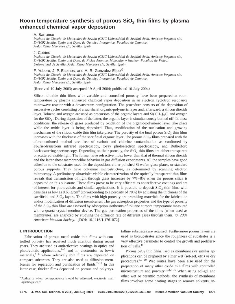
Room temperature synthesis of porous SiO2 thin films by plasma enhanced chemical vapor deposition
10
Room temperature synthesis of porous SiO 2 thin films by plasma enhanced chemical vapor deposition A. Barranco Instituto de Ciencia de Materiales de Sevilla (CSIC-Universidad de Sevilla) Avda, Ame ´rico Vespucio s/n, E-41092 Sevilla, Spain and Dpto. de Quı ´mica Inorga ´nica, Facultad de Quı ´mica, Avda, Reina Mercedes s/n, Sevilla, Spain J. Cotrino Instituto de Ciencia de Materiales de Sevilla (CSIC-Universidad de Sevilla) Avda, Ame ´rico Vespucio s/n, E-41092 Sevilla, Spain and Dpto. de Fı ´sica Ato ´mica, Molecular y Nuclear, Facultad de Fı ´sica, Universidad de Sevilla, Avda, Reina Mercedes s/n, Sevilla, Spain F. Yubero, J. P. Espino ´ s, and A. R. Gonza ´ lez-Elipe a) Instituto de Ciencia de Materiales de Sevilla (CSIC-Universidad de Sevilla) Avda, Ame ´rico Vespucio s/n, E-41092 Sevilla, Spain and Dpto. de Quı ´mica Inorga ´nica, Facultad de Quı ´mica, Avda, Reina Mercedes s/n, Sevilla, Spain ~Received 10 July 2003; accepted 19 April 2004; published 16 July 2004! Silicon dioxide thin films with variable and controlled porosity have been prepared at room temperature by plasma enhanced chemical vapor deposition in an electron cyclotron resonance microwave reactor with a downstream configuration. The procedure consists of the deposition of successive cycles consisting of a sacrificial organic-polymeric layer and, afterward, a silicon dioxide layer. Toluene and oxygen are used as precursors of the organic layers and Si(CH 3 ) 3 Cl and oxygen for the SiO 2 . During deposition of the latter, the organic layer is simultaneously burned off. In these conditions, the release of gases produced by oxidation of the organic-polymeric layer take place while the oxide layer is being deposited. Thus, modification of the nucleation and growing mechanism of the silicon oxide thin film take place. The porosity of the final porous SiO 2 thin films increases with the thickness of the sacrificial organic layer. The porous SiO 2 films prepared with the aforementioned method are free of carbon and chlorine contamination as confirmed by Fourier-transform infrared spectroscopy, x-ray photoelectron spectroscopy, and Rutherford backscattering spectroscopy. Depending on their porosity, the SiO 2 thin films are either transparent or scattered visible light. The former have refractive index lower than that of thermal silicon dioxide and the latter show membranelike behavior in gas diffusion experiments. All the samples have good adhesion to the substrates used for the deposition, either polished Si wafer, glass plates, or standard porous supports. They have columnar microstructure, as determined by scanning electron microscopy. A preliminary ultraviolet-visible characterization of the optically transparent thin films reveals that transmission of light through glass increases by 7%– 8% when the porous silica is deposited on this substrate. These films prove to be very efficient as antireflective coatings and are of interest for photovoltaic and similar applications. It is possible to deposit SiO 2 thin films with densities as low as 0.65 g/cm 3 ~corresponding to a porosity of 70%! by adjusting the thickness of the sacrificial and SiO 2 layers. The films with high porosity are promising materials for the fabrication and/or modification of diffusion membranes. The gas adsorption properties and the type of porosity of the SiO 2 thin films are assessed by adsorption isotherms of toluene at room temperature measured with a quartz crystal monitor device. The gas permeation properties of the films ~when used as membranes! are analyzed by studying the diffusion rate of different gases through them. © 2004 American Vacuum Society. @DOI: 10.1116/1.1761072# I. INTRODUCTION Fabrication of porous metal oxide thin films with con- trolled porosity has received much attention during recent years. They are used as antireflective coatings in optics and photovoltaic applications, 1–3 and in electronics as low-k materials, 4–6 where relatively thin films are deposited on compact substrates. They are also used as diffusion mem- branes for separation and purification of fluids. 7–10 In this latter case, thicker films deposited on porous and polycrys- talline substrates are required. Furthermore porous layers are used as biosubstrates since the roughness of substrates is a very effective parameter to control the growth and prolifera- tion of cells. 11 Porous SiO 2 thin films used as membranes or similar ap- plications can be prepared by either wet ~sol-gel, etc.! or dry procedures. 3,7–10 Wet routes have been also used for the preparation of many other oxide thin films with controlled microstructure and porosity. 10,12–15 When using sol-gel and other wet or ceramic methods, the synthesis of membrane films involves some heating stages to remove solvents, in- a! Author to whom correspondence should be addressed; electronic mail: [email protected] 1275 1275 J. Vac. Sci. Technol. A 22„4…, JulÕAug 2004 0734-2101Õ2004Õ22„4…Õ1275Õ10Õ$19.00 ©2004 American Vacuum Society
-
Upload
independent -
Category
Documents
-
view
0 -
download
0
Transcript of Room temperature synthesis of porous SiO2 thin films by plasma enhanced chemical vapor deposition
Room temperature synthesis of porous SiO 2 thin films by plasmaenhanced chemical vapor deposition
A. BarrancoInstituto de Ciencia de Materiales de Sevilla (CSIC-Universidad de Sevilla) Avda, Ame´rico Vespucio s/n,E-41092 Sevilla, Spain and Dpto. de Quı´mica Inorganica, Facultad de Quı´mica,Avda, Reina Mercedes s/n, Sevilla, Spain
J. CotrinoInstituto de Ciencia de Materiales de Sevilla (CSIC-Universidad de Sevilla) Avda, Ame´rico Vespucio s/n,E-41092 Sevilla, Spain and Dpto. de Fı´sica Atomica, Molecular y Nuclear, Facultad de Fı´sica,Universidad de Sevilla, Avda, Reina Mercedes s/n, Sevilla, Spain
F. Yubero, J. P. Espinos, and A. R. Gonzalez-Elipea)
Instituto de Ciencia de Materiales de Sevilla (CSIC-Universidad de Sevilla) Avda, Ame´rico Vespucio s/n,E-41092 Sevilla, Spain and Dpto. de Quı´mica Inorganica, Facultad de Quı´mica,Avda, Reina Mercedes s/n, Sevilla, Spain
~Received 10 July 2003; accepted 19 April 2004; published 16 July 2004!
Silicon dioxide thin films with variable and controlled porosity have been prepared at roomtemperature by plasma enhanced chemical vapor deposition in an electron cyclotron resonancemicrowave reactor with a downstream configuration. The procedure consists of the deposition ofsuccessive cycles consisting of a sacrificial organic-polymeric layer and, afterward, a silicon dioxidelayer. Toluene and oxygen are used as precursors of the organic layers and Si(CH3)3Cl and oxygenfor the SiO2 . During deposition of the latter, the organic layer is simultaneously burned off. In theseconditions, the release of gases produced by oxidation of the organic-polymeric layer take placewhile the oxide layer is being deposited. Thus, modification of the nucleation and growingmechanism of the silicon oxide thin film take place. The porosity of the final porous SiO2 thin filmsincreases with the thickness of the sacrificial organic layer. The porous SiO2 films prepared with theaforementioned method are free of carbon and chlorine contamination as confirmed byFourier-transform infrared spectroscopy, x-ray photoelectron spectroscopy, and Rutherfordbackscattering spectroscopy. Depending on their porosity, the SiO2 thin films are either transparentor scattered visible light. The former have refractive index lower than that of thermal silicon dioxideand the latter show membranelike behavior in gas diffusion experiments. All the samples have goodadhesion to the substrates used for the deposition, either polished Si wafer, glass plates, or standardporous supports. They have columnar microstructure, as determined by scanning electronmicroscopy. A preliminary ultraviolet-visible characterization of the optically transparent thin filmsreveals that transmission of light through glass increases by 7%–8% when the porous silica isdeposited on this substrate. These films prove to be very efficient as antireflective coatings and areof interest for photovoltaic and similar applications. It is possible to deposit SiO2 thin films withdensities as low as 0.65 g/cm3 ~corresponding to a porosity of 70%! by adjusting the thickness of thesacrificial and SiO2 layers. The films with high porosity are promising materials for the fabricationand/or modification of diffusion membranes. The gas adsorption properties and the type of porosityof the SiO2 thin films are assessed by adsorption isotherms of toluene at room temperature measuredwith a quartz crystal monitor device. The gas permeation properties of the films~when used asmembranes! are analyzed by studying the diffusion rate of different gases through them. ©2004American Vacuum Society.@DOI: 10.1116/1.1761072#
n-ena
ne
ry
ares is ara-
p-
hed
anein-
ma
I. INTRODUCTIONFabrication of porous metal oxide thin films with co
trolled porosity has received much attention during recyears. They are used as antireflective coatings in opticsphotovoltaic applications,1–3 and in electronics as low-kmaterials,4–6 where relatively thin films are deposited ocompact substrates. They are also used as diffusion mbranes for separation and purification of fluids.7–10 In thislatter case, thicker films deposited on porous and polyc
a!Author to whom correspondence should be addressed; [email protected]
1275 J. Vac. Sci. Technol. A 22 „4…, Jul ÕAug 2004 0734-2101 Õ2004
tnd
m-
s-
talline substrates are required. Furthermore porous layersused as biosubstrates since the roughness of substratevery effective parameter to control the growth and prolifetion of cells.11
Porous SiO2 thin films used as membranes or similar aplications can be prepared by either wet~sol-gel, etc.! or dryprocedures.3,7–10 Wet routes have been also used for tpreparation of many other oxide thin films with controllemicrostructure and porosity.10,12–15When using sol-gel andother wet or ceramic methods, the synthesis of membrfilms involves some heating stages to remove solvents,il:
1275Õ22„4…Õ1275Õ10Õ$19.00 ©2004 American Vacuum Society
mneppoio
briob
thhreor
oibcrex
steo
thyinino
ioa
fos.itythre
ern
Ath
nideon
oa
pr
stivpl
rateby
the-
thatth
ly-
aheut
ch
Or. It
ncehero-ub-
ofthedi-ionn-nsityionsub-
ertheioniledeenn
nda
ub-genne,-rl-uce
1276 Barranco et al. : Room temperature synthesis of porous SiO 2 thin films 1276
duce sintering, etc., particularly if the substrate is a ceramaterial. However, for other applications or if the membrais a polymer or any heat-sensitive material, heating stmay have to be avoided and other methods such as evation or plasma enhanced chemical vapor deposit~PECVD! are required.
The synthesis of porous thin films can also be achievedusing template procedures. An easily removable mate~usually organic! serves to incorporate the inorganic compnent with a defined morphology, being then removedcombustion or similar methods.10,16,17 After removing thetemplate, voids are left in the inorganic or ceramic part ofporous film, thus defining a microstructural arrangement treplicates the distribution of the template. Usually, themoval of the template requires a heating stage with the afmentioned inconveniences.
The method described in this article for the depositionporous thin films resembles the template approach descrabove. Thus, an organic material that acts as a sacrifilayer is used in the procedure. This organic material ismoved simultaneously to the deposition of the silicon dioide by PECVD.
Preparation of porous SiO2 coatings in photovoltaic cellsby PECVD has recently been reported.2 The synthesis wascarried out in a microwave reactor with SiH4 as a precursorof Si and N2O as plasma gas. The control of porosity of thethin films was achieved by adjusting deposition paramesuch as the geometry of the reactor, pressure during deption, etc. However, these variables mainly act by alteringgas phase deposition and agglomeration, so that porositsults from the accumulation of oxide aggregates comfrom the gas phase. However, in such a case the obtalayers usually have poor mechanical properties. Also, remPECVD has been a widely utilized procedure for depositof SiO2 ,18–20although the main purpose of these works wnot the preparation of thin films with controlled porosity.
In the present article, we propose a PECVD procedurethe room temperature synthesis of porous oxide thin film21
The method provides an effective control of film poroswithin a large range of values. The procedure consists ofdeposition of an organic material that is subsequentlymoved during the formation of the SiO2 film. The porositycorrelates with the thickness of the organic and oxide layThe final oxide thin films have good adhesion and mechacal stability, even when the films’ porosity is very high.critical point of this procedure is the requirement that bodeposition of the inorganic layer and removal of the orgapolymer occur simultaneously. This is accomplished bypositing an organic layer with a high oxygen concentratiRecently, we have reported on the PECVD depositionsuch an organic thin film by using oxygen and tolueneprecursors.22
This article describes the experimental procedure andsents some results of the characterization of porous SiO2 thinfilms with different porosities and light scattering propertieThese films have been obtained by changing the relathickness of the organic and inorganic layers. A set of ap
J. Vac. Sci. Technol. A, Vol. 22, No. 4, Jul ÕAug 2004
icesra-n
yal-y
eat-e-
fedial-
-
erssi-ere-gedtens
r
e-
s.i-
c-.fs
e-
.e
i-
cations of these thin films are also reported to demonstthe ample variety of porous structures that can be tailoredthis method of synthesis. Thus, transparent SiO2 thin filmsare examined as antireflective coatings, while SiO2 thin filmswith very high porosities and low densities are used formodification of diffusion properties of commercial membranes. Finally, a phenomenological model is proposedaccounts for the development of porosity during growbased on the characterization of the porous SiO2 films andtheir growth rate.
II. EXPERIMENT
A. Preparation of porous SiO 2 thin films
The PECVD procedure to control the porosity of the SiO2
thin films consists of the deposition of intermediate pomeric oxygenated layers (CxOy :H), and subsequently, SiO2thin films. The polymeric layer is easily removed by plasmoxidation under the experimental conditions utilized for tdeposition of SiO2 . Several deposition cycles are carried osequentially to control the porosity of the films. In eacycle, an organic film and a SiO2 thin film are deposited.
Deposition of oxygen-rich organic layers and porous Si2
thin films are carried out sequentially in the same reactoconsists of a remote microwave plasma source~SLAN! sup-plied with magnets to achieve electron cyclotron resona~ECR! working conditions. This source is separated from tdeposition chamber by a metallic grid preventing the micwave irradiation of the substrates. The distance from the sstrates to the grid is;10 cm. Basically, the SLAN systemconsists of an annular waveguide~ring resonator! with axialslot antennas positioned azimuthally at regular intervalsthe waveguide’s inner side. The ring resonator surroundsplasma chamber that consists of a quartz bell jar with aameter of 16 cm and a height of 20 cm. An ion concentratof 1011 cm23 is achieved at the SLAN center. The concetration decays downstream and the average electron deand energy shows the same behavior. An estimation ofconcentration and average electron energy close to thestrate position gives values of 109 cm23 and 1 eV, respec-tively. Typical ion energies range from 5 to 10 eV. Undthese working conditions, a sheath potential results insubstrate where it is expected that a very low energybombardment induces minimum damage. A more detadescription of the source and experimental setup has bpublished previously.22–25The source is fitted to a depositiochamber, where a base pressure lower than 1026 Torr can beobtained with a turbomolecular pump. The toluene aSi(CH3)3Cl flows were dosed over the sample holder withshower-type annular dispenser placed 6 cm from the sstrate to ensure its homogeneous spatial distribution. Oxywas dosed directly into the plasma source. Oxygen, tolueand Si(CH3)3Cl flows were controlled with mass flow controllers. The organic and the SiO2 layers were prepared undecompletely different working conditions of the source, athough in both cases a plasma of oxygen was used to indthe deposition. SiO2 thin films were deposited at 2
20
leth
ne-ahAttmh-
hise-
nefo
tiotiores
eia
hiaro
-heroni
rm
e
reth
ech
s
0
hefor
theEMur-trixth
ing-nedwasd
CMse,
a-rmse-o-
l
r-ob-
ade
re to
nd
,of asnnanal
R
1277 Barranco et al. : Room temperature synthesis of porous SiO 2 thin films 1277
31022 Torr using 5 sccm of the organosilicon precursor,sccm of oxygen, and 200 W of microwave power.24
Deposition of the organic sacrificial layer was possibonly when the working parameters were adjusted aroundfollowing values: microwave power 600 W, oxygen/tolueflow ratio 4:1, and total pressure;1 Torr. To get these conditions, a very precise adjustment was required of the mflow controllers and the pumping capacity of the system, tlatter with a throttle valve placed prior to a primary pump.lower pressures, the organic layer was always burned outhe oxygen plasma and no deposition of the organic polywas detected. The material of the organic layer was a higoxygenated polymer with a high concentration of COOCvO, and C–OH groups. An important characteristic of tpolymeric-like thin film is that it is easily removed by thplasma of oxygen used for SiO2 deposition. Under these conditions, an etching rate of about 200 nm/min was determifor the polymer. This value is lower than rates selectedthe deposition of the silicon oxide~;16 nm/min!.24 It seemscritical that this sacrificial layer has a very high O/C raand, consequently, that the PECVD protocol of preparaof this polymeric layer utilizes an oxygen rich plasma. Modetails about the synthesis, characterization and propertiethese highly oxygenated polymeric thin films, including thetching properties under oxidizing plasma treatments, hbeen published recently.22
B. Chemical and microstructural characterization
Chemical and microstructural characterization of the tfilms was studied using several techniques. Chemical ansis was carried out by Rutherford backscattering spectcopy ~RBS!, electron recoil detection analysis~ERDA!, andx-ray photoelectron spectroscopy~XPS!. Fourier-transforminfrared spectroscopy~FTIR! was also used to verify the removal of organic functional groups after deposition of tinorganic silicon dioxide. Meanwhile, assessment of micstructure was done by observation of samples by scanelectron microscopy ~SEM!, atomic force microscopy~AFM!, and the measurement of gas adsorption isothewith a quartz crystal microbalance~QCM!.
RBS and ERDA measurements of porous SiO2 thin filmsdeposited on polished Si~100! wafers were performed at thIon Accelerator ARAMIS~Orsay, France! by using 1.5 and3.0 MeV a11 particles, respectively. The RBS spectra werecorded in channeling conditions. The quantification ofmeasured ion spectra was performed by means of theRUMP
code.XPS spectra were acquired in a VG-ESCALAB 210 sp
trometer working in the constant pass energy mode witvalue of 20 eV. Unmonochromatized Mg Ka radiation (hn51253.6 eV) was used as excitation source.
FTIR spectra in the 400– 4000 cm21 energy range werecollected in transmission mode at normal incidence inNicolet 510 spectrometer for samples deposited on intrinSi wafers.
Images of the surface of the porous SiO2 thin films de-posited on Si~100! wafers were taken with a JEOL-JSM540
JVST A - Vacuum, Surfaces, and Films
e
ssis
byerly,
dr
n
ofrve
nly-s-
-ng
s
e
-a
aic
SEM microscope after metallization of the surface of tsamples. Cross-section SEM images were also obtainedSiO2 thin films deposited on either aluminum foil or Si~100!wafers properly cut for examination. The thicknesses offilms were obtained from either these cross-sectional Simages and also by using a DekTak profilometer. AFM sface images were also obtained in air by using a TopomeExplorer microscope working in the noncontact mode. Botopographic ~constant force! and direct signal~constantheight! images were acquired. The cantilever, with a sprconstant of 42.6 N m21, was oscillated at 130 kHz. Amplitude reduction was monitored while the surface was scanat a typical rate of one line per second. The scannercalibrated in X, Y, and Z directions with gratings providewith the equipment.
Adsorption isotherms were measured by means of a Qin a temperature controlled vacuum chamber. In this caporous SiO2 thin films were deposited on the quartz oscilltors used in the QCM. Thus, toluene adsorption isothewere measured at 29260.8 K. This procedure has been prviously applied for the characterization of thin films and prvides a qualitative assessment of their porous structure.26,27
C. Optical and gas diffusion properties
Porous SiO2 thin films can find applications as opticacoatings and gas diffusion membranes.
Ultraviolet-visible ~UV-vis! transmission spectra at nomal incidence of samples deposited on glass plates weretained with a Shimadzu UV-2101PC spectrometer.
Measurements of gas diffusion through porous SiO2 thinfilms acting as membranes were carried out in a homemapparatus consisting of two chambers~chambers 1 and 2!separated by the membrane. The experimental proceduget the permeability of a membrane to a gas A (PA) was thefollowing. Chamber 2 was set initially under vacuum achamber 1 under a certain pressure of a gas (P1). Then, thevariation of the pressure with time in chamber 2 (DP2 /Dt)was monitored. In these conditions,PA can be determinedusing the equation12,28
PA5d
A~P12P2!
V2
RT
DP2
Dt,
whered is the thickness of the membrane,V2 is the volumeof chamber 2,A the membrane area,T is the temperatureandR the ideal gas constant. The ideal separation factormembrane for two gasesA andB, aB
A , can be determined aaB
A5PA /PB . To carry out this analysis, the porous silicodioxide thin films were deposited on commercial alumiporous substrates Anodisc 47 from Anopore with nomipore sizes of 100 and 20 nm~in the following Anodisc-100and Anodisc-20, respectively!.
III. RESULTS AND DISCUSSION
A. Composition of the porous silicon oxide thin films
The method of preparation of porous SiO2 thin films con-sists of depositing the silicon oxide by PECVD using EC
l oar
oO
man
mrib
siO
thon
helr
con
al
ps
es
aredof
arendeent inthethe
niconctalm-
f-
in-ates
mes
de-renic
r
ent
1278 Barranco et al. : Room temperature synthesis of porous SiO 2 thin films 1278
conditions that are very effective for the complete removaa previously deposited organic sacrificial layer. It is criticthat during this process, total removal of the organic layeaccomplished and that, therefore, the final SiO2 thin film isfree from any organic contaminant. Survey XPS spectrathe sacrificial organic layer and after deposition of a Si2
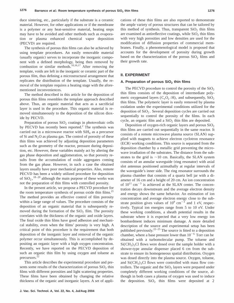
layer on this sacrificial layer are shown in Fig. 1~a!. Note thatthe sacrificial layer shows only peaks due to C and O atothat evidences the presence of a highly oxygenated orglayer. After deposition of the SiO2 film, the C1s peak disap-pears from the spectrum, indicating that no carbon contanation remains in the sample. Moreover, only peaks attuted to silicon~in particular Si41 species! and oxygen atomscan be seen in this spectrum.
Since XPS is a surface sensitive probe, we have also uchanneling RBS to prove the absence of carbon in the S2
layers. Thus, we found that the bulk compositions offilms are stoichiometric silicon dioxide and that their carbcontent is below the detection limit of this technique.
Figure 1~b! shows the FTIR spectra corresponding to tsacrificial layer~top! and a SiO2 deposit on this sacrificialayer ~bottom!. In the FTIR spectrum of the sacrificial layethere are signals due to C and O groups22,29 ~i.e., C—O,CvO, CvC, etc.! typical of a highly oxygenated organipolymeric layer. After silicon oxide deposition, the signalscarbon-oxygen groups completely vanish, indicating thatcarbon remains in the sample after this treatment. Note
FIG. 1. ~a! XPS spectra of a sacrificial organic layer of;45 nm thick and thefilm resulting from the deposition of a;220 nm SiO2 thin film on top it.~b!FTIR spectra for the same samples.
J. Vac. Sci. Technol. A, Vol. 22, No. 4, Jul ÕAug 2004
flis
f
sic
i--
ed
e
foso
that, the FTIR spectrum after removal of the organic groudepicts the typical bands of SiO2 .24,30,31
B. Microstructure of the SiO 2 thin films
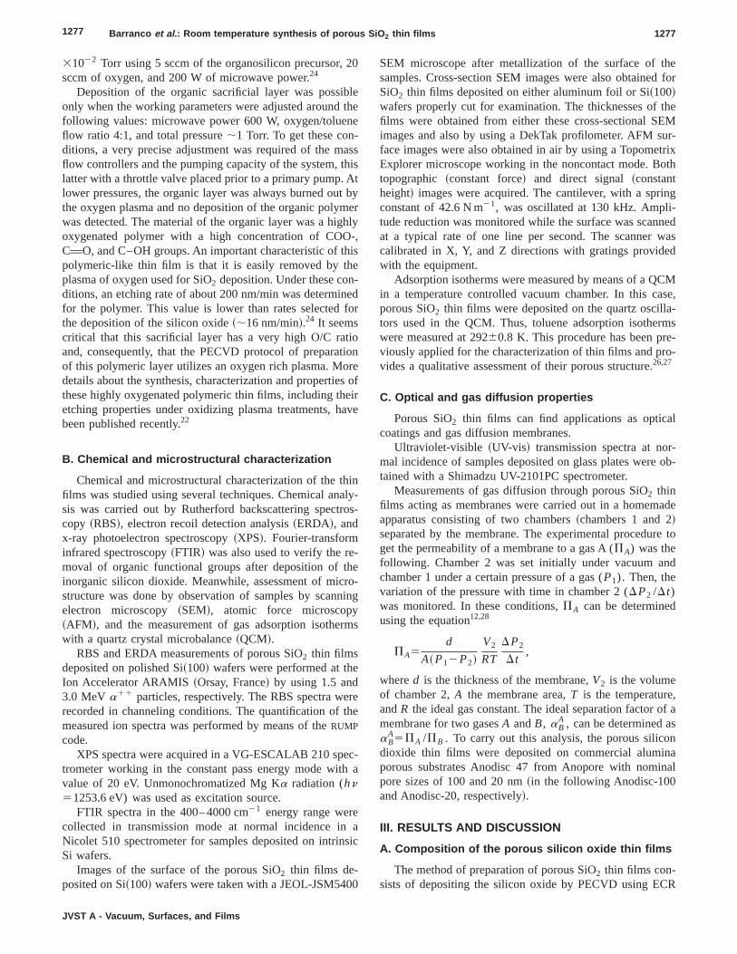
Control of the porosity of the SiO2 thin films is achievedby adjusting the thicknesses of the polymeric CxOy :H andSiO2 layers. As an example of the possibilities of thmethod, Figs. 2~a!–2~d! shows a series of SEM micrographof SiO2 thin films with a similar total thickness of;600 nmbut increasing porosity. These samples have been prepby different preparation protocols consisting of two cyclesdeposition. In each cycle, an organic thin film~i.e., the poly-meric CxOy :H described below! and a SiO2 thin film aredeposited. The preparation protocols of these samplesshown in Table I. Deposition is carried out in two steps athe thickness of the organic and inorganic materials has badjusted to achieve the desired porosities. It is apparenthis set of micrographs that, for a constant thickness offinal SiO2 , the porosity increases as the thickness oforganic phase increases.
However, for the same thickness of the sacrificial orgalayer, the final microstructure of the films also dependsthe final thickness of the oxide film. An example of the effeof the thickness of the intermediate oxide films in the finmicrostructure of the porous films is evidenced by the coparison of Figs. 2~d! and 2~e!. The corresponding films areobtained by two cycles with similar polymeric films, but diferent thickness of the final oxide films~cf. Table I!. It ispossible to see that as the thickness of the oxide layerscreases, the percolation degree of the individual aggreg~i.e., the degrade of interconnection among them! of thelayer increases and the final structure at the surface becomore compact.
It can be also seen in this figure that the percolationgree of the SiO2 aggregates is relatively high, and the posize small, when the oxide is deposited on top of an orgalayer of;25 [email protected]., Fig. 5~b!#. For an organic layer thinnethan approximately 25 nm, the final SiO2 thin films, althoughstill having much porosity, are transparent and do not presany observable light scattering. However, SiO2 films pre-
FIG. 2. SEM micrographs of SiO2 thin films with increasing porosities. Thepreparation protocols of samples A–F are reported in Table I.
1279 Barranco et al. : Room temperature synthesis of porous SiO 2 thin films 1279
JVST A - Vacuum, S
TABLE I. Preparation protocols of selected porous SiO2 samples.
Sample Step 1 Step 2 SubstrateDensity(g/cm3)
Porosity~%!
A 600 nm SiO2 – Si~100! 1.98 10.0B 25 nm CxOy :H1
150 nm SiO2
25 nm CxOy :H1450 nm SiO2
Si~100! 1.66 24.6
C 40 nm CxOy :H1150 nm SiO2
40 nm CxOy :H1450 nm SiO2
Si~100! 1.25 43.2
D 60 nm CxOy :H1150 nm SiO2
60 nm CxOy :H1450 nm SiO2
Si~100! 1.10 55.4
E 60 nm CxOy :H1475 nm SiO2
60 nm CxOy :H1475 nm SiO2
Si~100! 1.56 29.4
F 250 nm CxOy :H1150 nm SiO2
250 nm CxOy :H1375 nm SiO2
Si~100! 0.78 64.5
G 40 nm CxOy :H1275 nm SiO2
40 nm CxOy :H1275 nm SiO2
Al sheet – –
H 7 cycles~50 nm CxOy :H1275 nm SiO2) Al sheet – –
kyre
ngibes
o-ein
of
-e
thnTo. 3
o-nd
teerlyi
thd
ves
ci
thleth
-
a
gy
nic
ly
d H
pared after deposition of thicker organic films had a milappearance due to light dispersion in the individual agggates or columns of SiO2 .
The micrographs in Fig. 2 also show that by controllithe thickness of the oxide and polymeric layers, it is possto achieve precise control of the final pore size and conctration of the films. With our procedure, successive depotion of different oxide layers with specific and tailored prosity would permit the fabrication of thin films with variablin-depth porosity and optical properties. This type of thfilm with gradient porosity is of interest for certain typeoptical filters, the so-called rugate filters.32,33
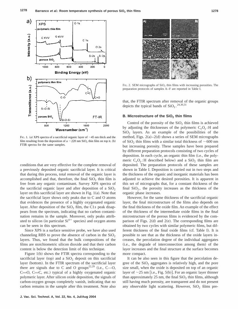
The microstructure of the SiO2 samples was of the columnar type in all cases, except when deposited on top of a vthick organic film~i.e., 250 nm!. In this case, Fig. 2~f! showsthat the film has a granular microstructure. This sample isresult of the aggregation of small powdered particles atherefore, this film’s mechanical stability was very poor.illustrate the columnar growth of the porous thin films, Figshows two cross-sectional views of SiO2 samples depositedon an aluminum foil. Both views depict a well-defined clumnar microstructure. Sample G in this figure correspoto a film deposited by two cycles CxOy :H polymer/SiO2 ,while sample H corresponds to a thick film obtained afseven cycles of deposition of organic and inorganic lay~cf. Table I!. The micrograph of this latter sample clearshows that a common columnar microstructure developsdependently of the final thickness of the films~i.e.,;500 and;2850 nm for the films shown in Figs. 3~g! and 3~h!, respec-tively! and of the number of cycles used for deposition offilm. No boundary interfaces between the intermediate invidual SiO2 layers can be detected in sample G. This prothat the final porous thin films are homogeneous in thickneeven for several deposition-removal steps of the sacrifiorganic layers.
A similar microstructure to that reported in Fig. 3, wivertical pores and columns, was found for all the sampalthough the pore size and type of columns depend onactual preparation conditions used in each case. Such alumnar microstructure does not develop in the SiO2 films
urfaces, and Films
-
len-i-
ry
ed,
s
rs
n-
ei-ss,al
s,e
co-
deposited at 231022 Torr without deposition of the intermediate polymeric films~i.e., sample A in Table I!. The devel-opment of columns in the porous thin films is justified byphenomenological model described below.
AFM images were taken to study the surface morpholoand growing mechanisms of the porous SiO2 thin films. Fig-ure 4~a! shows the surface of a dense SiO2 thin film ~i.e.,prepared without mediation of the intermediate orgalayer! of ;110 nm thickness and Fig. 4~b! that of an porousoxide film of a similar thickness grown onto a previousdeposited organic layer of;25 nm. At first glance, the
FIG. 3. Cross-sectional SEM micrograph corresponding to samples G anin Table I.
Ttea11isgono
lv-
,
d/or-
ol
omhe. 2.
ofthehe
msa-
rmsinengdonr-
fII
ry-idthceso-
s
s.in
-lms
n
.
rous
1280 Barranco et al. : Room temperature synthesis of porous SiO 2 thin films 1280
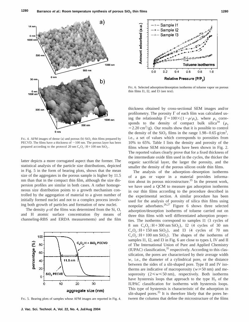
latter depicts a more corrugated aspect than the former.statistical analysis of the particle size distributions, depicin Fig. 5 in the form of bearing plots, shows that the mesize of the aggregates in the porous sample is higher bynm than that in the compact thin film, although the size dpersion profiles are similar in both cases. A rather homoneous size distribution points to a growth mechanism ctrolled by the aggregation of material to a given numberinitially formed nuclei and not to a complex process invoing both growth of particles and formation of new nuclei.
The densityr of the films was determined from the Si, Oand H atomic surface concentration~by means ofchanneling-RBS and ERDA measurements! and the film
FIG. 4. AFM images of dense~a! and porous~b! SiO2 thin films prepared byPECVD. The films have a thickness of;100 nm. The porous layer has beeprepared according to the protocol 20 nm CxOy :H1100 nm SiO2 .
FIG. 5. Bearing plots of samples whose AFM images are reported in Fig
J. Vac. Sci. Technol. A, Vol. 22, No. 4, Jul ÕAug 2004
hedn.5-e--f
thickness obtained by cross-sectional SEM images anprofilometry. The porosityG of each film was calculated using the relationshipG51003(12r/rs), where rs corre-sponds to the density of compact bulk silica34 (rs
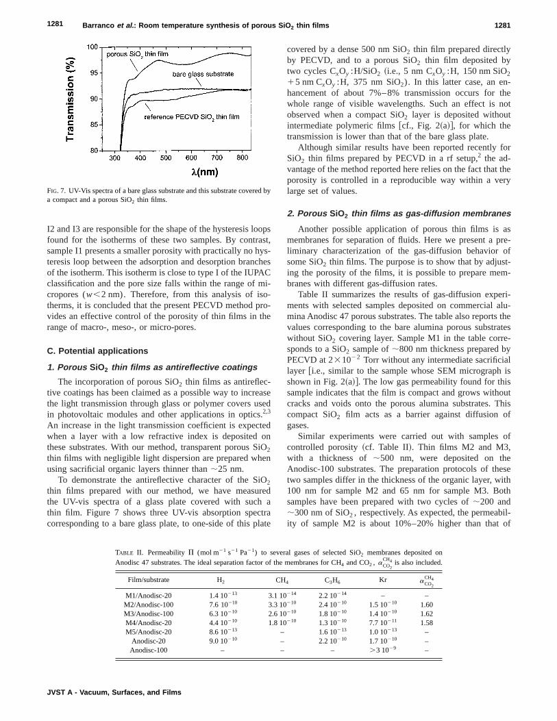
52.20 cm3/g). Our results show that it is possible to contrthe density of the SiO2 films in the range 1.98– 0.65 g/cm3,i.e., a set of values which corresponds to porosities fr10% to 65%. Table I lists the density and porosity of tfilms whose SEM micrographs have been shown in FigThe reported values clearly prove that for a fixed thicknessthe intermediate oxide film used in the cycles, the thickerorganic sacrificial layer, the larger the porosity, and tsmaller the density of the porous silicon oxide thin films.
The analysis of the adsorption–desorption isotherof a gas or vapor in a material provides informtion about its porous microstructure.35 In the present work,we have used a QCM to measure gas adsorption isothein our thin films according to the procedure describedthe experimental section. A similar procedure has beused for the analysis of porosity of silica thin films usinnonpolar adsorbates.26,27 Figure 6 shows three selecteadsorption/desorption isotherms of toluene carried outthree thin films with well differentiated adsorption propeties. The isotherms correspond to samples I1~3 cycles of8 nm CxOy :H1300 nm SiO2), I2 ~4 cycles of 30 nmCxOy :H1150 nm SiO2), and I3 ~4 cycles of 70 nmCxOy :H1100 nm SiO2). The shapes of the isotherms osamples I1, I2, and I3 in Fig. 6 are close to types I, IV andof The International Union of Pure and Applied Chemist~IUPAC! classification,35 respectively. According to this classification, the pores are characterized by their average ww, i.e., the diameter of a cylindrical pore, or the distanbetween the sides of a slit-shaped pore. Type II and IV itherms are indicative of macroporosity (w>50 nm) and me-soporosity (2<w<50 nm), respectively. Both isothermhave hysteresis loops that approach to the type H3 of theIUPAC classification for isotherms with hysteresis loopThis type of hysteresis is characteristic of the adsorptionslit-shaped pores.35 It is therefore likely that the pores between the columns that define the microstructure of the fi4.
FIG. 6. Selected adsorption/desorption isotherms of toluene vapor on pothin films I1, I2, and I3~see text!.
oasyschCi
-re
ease.teonSien
iOre
trala
-thenott
for
t thery
aspre-oft-
m-
ri-alu-the
atese-ylis
soutThisf
of
eeseithth
il-of
ed
1281 Barranco et al. : Room temperature synthesis of porous SiO 2 thin films 1281
I2 and I3 are responsible for the shape of the hysteresis lofound for the isotherms of these two samples. By contrsample I1 presents a smaller porosity with practically no hteresis loop between the adsorption and desorption branof the isotherm. This isotherm is close to type I of the IUPAclassification and the pore size falls within the range of mcropores (w,2 nm). Therefore, from this analysis of isotherms, it is concluded that the present PECVD method pvides an effective control of the porosity of thin films in thrange of macro-, meso-, or micro-pores.
C. Potential applications
1. Porous SiO2 thin films as antireflective coatings
The incorporation of porous SiO2 thin films as antireflec-tive coatings has been claimed as a possible way to incrthe light transmission through glass or polymer covers uin photovoltaic modules and other applications in optics2,3
An increase in the light transmission coefficient is expecwhen a layer with a low refractive index is depositedthese substrates. With our method, transparent porous2thin films with negligible light dispersion are prepared whusing sacrificial organic layers thinner than;25 nm.
To demonstrate the antireflective character of the S2
thin films prepared with our method, we have measuthe UV-vis spectra of a glass plate covered with suchthin film. Figure 7 shows three UV-vis absorption speccorresponding to a bare glass plate, to one-side of this p
FIG. 7. UV-Vis spectra of a bare glass substrate and this substrate covera compact and a porous SiO2 thin films.
JVST A - Vacuum, Surfaces, and Films
pst,-es
-
o-
sed
d
O
da
te
covered by a dense 500 nm SiO2 thin film prepared directlyby PECVD, and to a porous SiO2 thin film deposited bytwo cycles CxOy :H/SiO2 ~i.e., 5 nm CxOy :H, 150 nm SiO2
15 nm CxOy :H, 375 nm SiO2). In this latter case, an enhancement of about 7%–8% transmission occurs forwhole range of visible wavelengths. Such an effect isobserved when a compact SiO2 layer is deposited withouintermediate polymeric films@cf., Fig. 2~a!#, for which thetransmission is lower than that of the bare glass plate.
Although similar results have been reported recentlySiO2 thin films prepared by PECVD in a rf setup,2 the ad-vantage of the method reported here relies on the fact thaporosity is controlled in a reproducible way within a velarge set of values.
2. Porous SiO2 thin films as gas-diffusion membranes
Another possible application of porous thin films ismembranes for separation of fluids. Here we present aliminary characterization of the gas-diffusion behaviorsome SiO2 thin films. The purpose is to show that by adjusing the porosity of the films, it is possible to prepare mebranes with different gas-diffusion rates.
Table II summarizes the results of gas-diffusion expements with selected samples deposited on commercialmina Anodisc 47 porous substrates. The table also reportsvalues corresponding to the bare alumina porous substrwithout SiO2 covering layer. Sample M1 in the table corrsponds to a SiO2 sample of;800 nm thickness prepared bPECVD at 231022 Torr without any intermediate sacrificialayer @i.e., similar to the sample whose SEM micrographshown in Fig. 2~a!#. The low gas permeability found for thisample indicates that the film is compact and grows withcracks and voids onto the porous alumina substrates.compact SiO2 film acts as a barrier against diffusion ogases.
Similar experiments were carried out with samplescontrolled porosity~cf. Table II!. Thin films M2 and M3,with a thickness of;500 nm, were deposited on thAnodisc-100 substrates. The preparation protocols of thtwo samples differ in the thickness of the organic layer, w100 nm for sample M2 and 65 nm for sample M3. Bosamples have been prepared with two cycles of;200 and;300 nm of SiO2 , respectively. As expected, the permeabity of sample M2 is about 10%–20% higher than that
by
n
TABLE II. Permeability P (mol m21 s21 Pa21) to several gases of selected SiO2 membranes deposited oAnodisc 47 substrates. The ideal separation factor of the membranes for CH4 and CO2 , aCO2CH4 is also included.
Film/substrate H2 CH4 C3H6 Kr aCO2
CH4
M1/Anodisc-20 1.4 10213 3.1 10214 2.2 10214 – –M2/Anodisc-100 7.6 10210 3.3 10210 2.4 10210 1.5 10210 1.60M3/Anodisc-100 6.3 10210 2.6 10210 1.8 10210 1.4 10210 1.62M4/Anodisc-20 4.4 10210 1.8 10210 1.3 10210 7.7 10211 1.58M5/Anodisc-20 8.6 10213 – 1.6 10213 1.0 10213 –
Anodisc-20 9.0 10210 – 2.2 10210 1.7 10210 –Anodisc-100 – – – .3 1029 –
i
eesohi
e4gch5,
trothpffeon
rtic. Iis
aced
Oret-
leagg
dseoan
ptha
sihgafier
ped
phe-elyof
lmemse tothericCR
hertewsrtzl-
sre-wed
iatendex-ionre-ncetlyourut
esyered
ng
ro-of
cil-nic
1282 Barranco et al. : Room temperature synthesis of porous SiO 2 thin films 1282
sample M3, although the permeability of both samplesmuch smaller than that of the Anodisc-100 substrate~cf.Table II!. The permeabilities of samples M2 and M3 are evlower than those found for the Anodisc-20 substrate. Thresults evidence the possibility of adjusting the transpproperties of commercial bulk membranes by depositing tporous layers on their surface.
Samples M4 and M5 in Table II have a thickness of;750nm and were deposited on Anodisc-20 substrates. They wprepared using two intermediate organic layers 60 andnm thick, respectively. In the first case, the decrease inpermeability was higher than for samples M2 and M3, reaing a percentage of 40%–55%. In the case of sample Mis possible to observe in the table a dramatic decrease ingas permeability of several orders of magnitude. Many pcedures have been reported in the literature to restrictflow of gases through bulk porous membranes. For exammethods have been reported that consist of depositing dient oxide thin films by thermal chemical vapor depositi~CVD! or the impregnation with colloidal SiO2 par-ticles.36–40The deposition of either compact or porous SiO2
thin films by PECVD according to the present procedumay be an interesting alternative to these methods, parlarly when no heating step during preparation is requiredthis sense, it could also be expected that our method, furning an arrangement of pores perpendicular to the surfcould be an alternative to the anodic oxidation used commcially for the synthesis of supports with controllepermeability.7,40
Table II also reports the separation coefficients for C2
and CH4 through the different films. The obtained values arather similar for the four samples M2, M3, and M4, indicaing that within the degree of porosity studied here, the setivity for these two gases is practically the same. This behior is expected when diffusion of gases occurs throumembrane thin films whose porous size falls within the ranof mesopores.8,12,40
D. Growth mechanism of porous SiO 2 thin films
Porosity in SiO2 or other metal oxide thin films prepareby plasma CVD procedures is usually controlled by adjuing the pressure during deposition and/or by modifying gmetrical parameters of the plasma reactor, such as distbetween the shower dispenser and the substrate.2 Thesechanges modify the condensation processes of oxideticles in the gas phase. Thereby, porosity is controlled bydifferent size of particles and nuclei coming from the plasmDeposition of porous SiO2 thin films by accumulation ofaggregates was also possible with our reactor setup by uSi(CH3)3Cl as precursor and oxygen as plasma gas, witworking pressure over 0.5 Torr. Under these conditions,phase deposition processes were maximized and thegrew by the accumulation of powder particles. Howevthese films had very poor mechanical properties.
The sacrificial layer method relies on a different conceA polymeric-organic film is plasma oxidized and removsimultaneously to the deposition of the inorganic SiO2 layer.
J. Vac. Sci. Technol. A, Vol. 22, No. 4, Jul ÕAug 2004
s
ne
rtn
re.5as-ithe-e
le,r-
eu-nh-e,r-
c-v-he
t--ce
ar-e.
ngas
lm,
t.
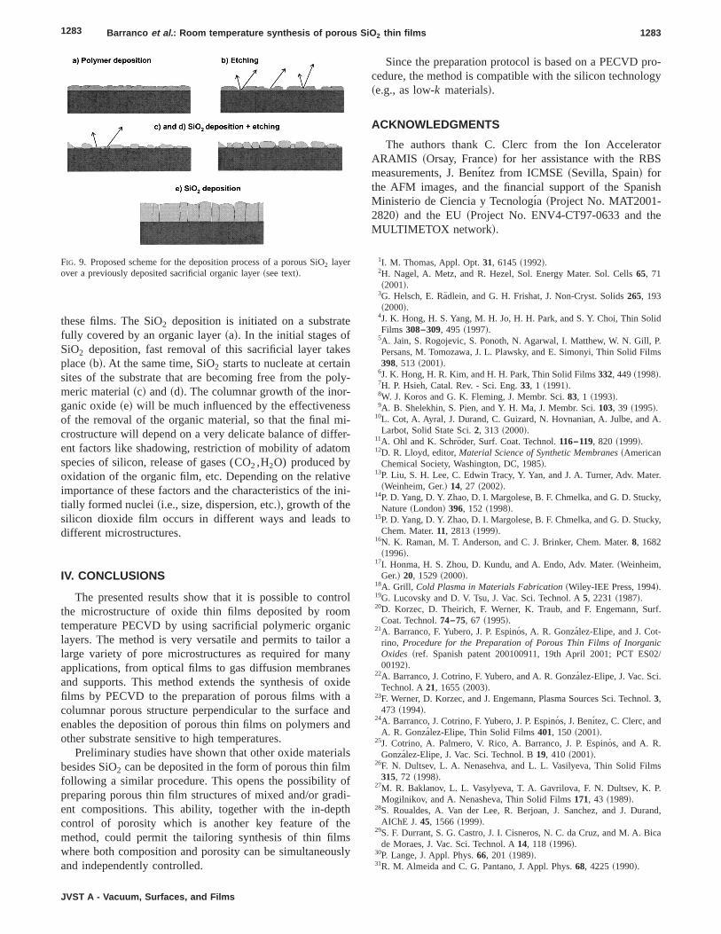
Although a model of the SiO2 deposition cannot be fullyoutlined at the present stage, we can consider severalnomena which, under our experimental conditions, are likto control the final porosity. The first is the modificationthe nucleation and initial growth steps of SiO2 because of thepresence of the organic layer. The fact that this organic fiis formed by highly oxygenated carbonaceous chains secritical to provide access pathways to the substrate surfacactivated precursor molecules and other species ofplasma. A critical clue for the process is that the polymelayer is easily removed by plasma oxidation under the Econditions utilized for SiO2 deposition.22 Under these condi-tions, the polymer etching rates are about ten times higthan the deposition rate of the SiO2 layers. This means thadeposition of the inorganic film mainly occurs when thpolymeric layer has already been burned off. Figure 8 shoa plot of the amount of material Q deposited on the quaoscillator during a deposition cycle of an organic layer folowed by the SiO2 material. Initially, during the initial depo-sition of the organic layer, Q increases~a!. Then, during theinitial stages of deposition of the SiO2 ~b!, Q decreases, thuindicating that the removal of the organic layer is the pdominant process. The zone where Q decreases is folloby the other with a smooth increase of Q~c! and~d! that endsup with a last region with a sharp increase of Q~e!. The latterindicates a net deposition of the SiO2 without interference byany other removal process. We assume that the intermedzones~b!–~d!, characterized first by a negative slope athen by a small positive slope, reflect a sequence of theperiment where etching of the organic layer and depositof the inorganic oxide take place simultaneously. Withspect to this behavior, it is important to stress the importaof using sacrificial organic layers which can be efficienremoved by plasma etching. Experiments carried out inlaboratory with other sacrificial layers which are burned omore slowly show the formation of sandwich structurwhere the organic layer is embedded within an oxide lawith less porosity than that of the porous thin films describin the previous sections.
Taking into account the results of Fig. 8 obtained durieach cycle of deposition of the porous SiO2 thin films, Fig. 9shows a schematic description of a mechanism which is pposed to account for the evolution of the microstructure
FIG. 8. Evolution of the amount of material Q deposited on a quartz oslator and detected with a QCM during deposition of the sacrificial orgalayer and posterior deposition of the SiO2 thin film ~see text!.
te
esnol-si
erm
ivein
to
trm
nicrnexiaa
an
iamodithess
ro-gy
orS
ish
e
lid
P.lms
A.
r.
ky,
ky,
urf.
ic02/
ol.
s
.
and,
ica
1283 Barranco et al. : Room temperature synthesis of porous SiO 2 thin films 1283
these films. The SiO2 deposition is initiated on a substrafully covered by an organic layer~a!. In the initial stages ofSiO2 deposition, fast removal of this sacrificial layer takplace~b!. At the same time, SiO2 starts to nucleate at certaisites of the substrate that are becoming free from the pmeric material~c! and~d!. The columnar growth of the inorganic oxide~e! will be much influenced by the effectivenesof the removal of the organic material, so that the final mcrostructure will depend on a very delicate balance of diffent factors like shadowing, restriction of mobility of adatospecies of silicon, release of gases (CO2,H2O) produced byoxidation of the organic film, etc. Depending on the relatimportance of these factors and the characteristics of thetially formed nuclei~i.e., size, dispersion, etc.!, growth of thesilicon dioxide film occurs in different ways and leadsdifferent microstructures.
IV. CONCLUSIONS
The presented results show that it is possible to conthe microstructure of oxide thin films deposited by rootemperature PECVD by using sacrificial polymeric orgalayers. The method is very versatile and permits to tailolarge variety of pore microstructures as required for maapplications, from optical films to gas diffusion membranand supports. This method extends the synthesis of ofilms by PECVD to the preparation of porous films withcolumnar porous structure perpendicular to the surfaceenables the deposition of porous thin films on polymersother substrate sensitive to high temperatures.
Preliminary studies have shown that other oxide materbesides SiO2 can be deposited in the form of porous thin filfollowing a similar procedure. This opens the possibilitypreparing porous thin film structures of mixed and/or graent compositions. This ability, together with the in-depcontrol of porosity which is another key feature of thmethod, could permit the tailoring synthesis of thin filmwhere both composition and porosity can be simultaneouand independently controlled.
FIG. 9. Proposed scheme for the deposition process of a porous SiO2 layerover a previously deposited sacrificial organic layer~see text!.
JVST A - Vacuum, Surfaces, and Films
y-
--
i-
ol
aysde
ndd
ls
f-
ly
Since the preparation protocol is based on a PECVD pcedure, the method is compatible with the silicon technolo~e.g., as low-k materials!.
ACKNOWLEDGMENTS
The authors thank C. Clerc from the Ion AcceleratARAMIS ~Orsay, France! for her assistance with the RBmeasurements, J. Benı´tez from ICMSE~Sevilla, Spain! forthe AFM images, and the financial support of the SpanMinisterio de Ciencia y Tecnologı´a ~Project No. MAT2001-2820! and the EU~Project No. ENV4-CT97-0633 and thMULTIMETOX network!.
1I. M. Thomas, Appl. Opt.31, 6145~1992!.2H. Nagel, A. Metz, and R. Hezel, Sol. Energy Mater. Sol. Cells65, 71~2001!.
3G. Helsch, E. Ra¨dlein, and G. H. Frishat, J. Non-Cryst. Solids265, 193~2000!.
4J. K. Hong, H. S. Yang, M. H. Jo, H. H. Park, and S. Y. Choi, Thin SoFilms 308–309, 495 ~1997!.
5A. Jain, S. Rogojevic, S. Ponoth, N. Agarwal, I. Matthew, W. N. Gill,Persans, M. Tomozawa, J. L. Plawsky, and E. Simonyi, Thin Solid Fi398, 513 ~2001!.
6J. K. Hong, H. R. Kim, and H. H. Park, Thin Solid Films332, 449~1998!.7H. P. Hsieh, Catal. Rev. - Sci. Eng.33, 1 ~1991!.8W. J. Koros and G. K. Fleming, J. Membr. Sci.83, 1 ~1993!.9A. B. Shelekhin, S. Pien, and Y. H. Ma, J. Membr. Sci.103, 39 ~1995!.
10L. Cot, A. Ayral, J. Durand, C. Guizard, N. Hovnanian, A. Julbe, andLarbot, Solid State Sci.2, 313 ~2000!.
11A. Ohl and K. Schro¨der, Surf. Coat. Technol.116–119, 820 ~1999!.12D. R. Lloyd, editor,Material Science of Synthetic Membranes~American
Chemical Society, Washington, DC, 1985!.13P. Liu, S. H. Lee, C. Edwin Tracy, Y. Yan, and J. A. Turner, Adv. Mate
~Weinheim, Ger.! 14, 27 ~2002!.14P. D. Yang, D. Y. Zhao, D. I. Margolese, B. F. Chmelka, and G. D. Stuc
Nature~London! 396, 152 ~1998!.15P. D. Yang, D. Y. Zhao, D. I. Margolese, B. F. Chmelka, and G. D. Stuc
Chem. Mater.11, 2813~1999!.16N. K. Raman, M. T. Anderson, and C. J. Brinker, Chem. Mater.8, 1682
~1996!.17I. Honma, H. S. Zhou, D. Kundu, and A. Endo, Adv. Mater.~Weinheim,
Ger.! 20, 1529~2000!.18A. Grill, Cold Plasma in Materials Fabrication~Wiley-IEE Press, 1994!.19G. Lucovsky and D. V. Tsu, J. Vac. Sci. Technol. A5, 2231~1987!.20D. Korzec, D. Theirich, F. Werner, K. Traub, and F. Engemann, S
Coat. Technol.74–75, 67 ~1995!.21A. Barranco, F. Yubero, J. P. Espino´s, A. R. Gonza´lez-Elipe, and J. Cot-
rino, Procedure for the Preparation of Porous Thin Films of InorganOxides ~ref. Spanish patent 200100911, 19th April 2001; PCT ES00192!.
22A. Barranco, J. Cotrino, F. Yubero, and A. R. Gonza´lez-Elipe, J. Vac. Sci.Technol. A21, 1655~2003!.
23F. Werner, D. Korzec, and J. Engemann, Plasma Sources Sci. Techn3,473 ~1994!.
24A. Barranco, J. Cotrino, F. Yubero, J. P. Espino´s, J. Benı´tez, C. Clerc, andA. R. Gonzalez-Elipe, Thin Solid Films401, 150 ~2001!.
25J. Cotrino, A. Palmero, V. Rico, A. Barranco, J. P. Espino´s, and A. R.Gonzalez-Elipe, J. Vac. Sci. Technol. B19, 410 ~2001!.
26F. N. Dultsev, L. A. Nenasehva, and L. L. Vasilyeva, Thin Solid Film315, 72 ~1998!.
27M. R. Baklanov, L. L. Vasylyeva, T. A. Gavrilova, F. N. Dultsev, K. PMogilnikov, and A. Nenasheva, Thin Solid Films171, 43 ~1989!.
28S. Roualdes, A. Van der Lee, R. Berjoan, J. Sanchez, and J. DurAIChE J.45, 1566~1999!.
29S. F. Durrant, S. G. Castro, J. I. Cisneros, N. C. da Cruz, and M. A. Bde Moraes, J. Vac. Sci. Technol. A14, 118 ~1996!.
30P. Lange, J. Appl. Phys.66, 201 ~1989!.31R. M. Almeida and C. G. Pantano, J. Appl. Phys.68, 4225~1990!.
sity
1284 Barranco et al. : Room temperature synthesis of porous SiO 2 thin films 1284
32L. Martinu and D. Poltras, J. Vac. Sci. Technol. A18, 2619~2000!.33W. H. Southwell, J. Opt. Soc. Am. A5, 1558~1988!.34W. A. Weyl and E. C. Marbone,The Constitution of Glasses~Wiley-
Interscience, New York, 1964!.35S. J. Gregg and K. S. W. Sing, Adsorption,Surface Area and Porosity,
2nd ed.~Academic, New York, 1997!, and references therein.
J. Vac. Sci. Technol. A, Vol. 22, No. 4, Jul ÕAug 2004
36M. Tsapatsis and G. R. Gavalas, AIChE J.38, 847 ~1992!.37M. Tsapatsis and G. R. Gavalas, J. Membr. Sci.87, 281 ~1994!.38M. Moaddeb and W. J. Koros, J. Membr. Sci.125, 143 ~1997!.39M. Moaddeb and W. J. Koros, J. Membr. Sci.136, 273 ~1997!.40E. J. Jakobs, Ph. D. thesis, The University of Texas at Austin, Univer
Microfilms International Dissertation Services, Ann Harbor, 1996.