Computer Experiments with Fractional Gaussian Noises Part 2, Rescaled Ranges and Spectra
Upload
khangminh22Category
view
4download
0
sensors
Article
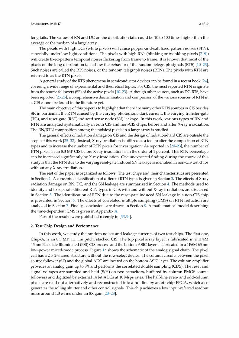
Random Telegraph Noises from the Source Follower,the Photodiode Dark Current, and the Gate-InducedSense Node Leakage in CMOS Image Sensors †
Calvin Yi-Ping Chao 1,* , Shang-Fu Yeh 1, Meng-Hsu Wu 1, Kuo-Yu Chou 1, Honyih Tu 1,Chih-Lin Lee 1, Chin Yin 1, Philippe Paillet 2 and Vincent Goiffon 3
1 Taiwan Semiconductor Manufacturing Company (TSMC), Hsinchu 30077, Taiwan;[email protected] (S.-F.Y.); [email protected] (M.-H.W.); [email protected] (K.-Y.C.);[email protected] (H.T.); [email protected] (C.-L.L.); [email protected] (C.Y.)
2 Atomique Energie Commission, Direction des Applications militaries, DAM Ile-de-France, F-91297 Arpajon,France; [email protected]
3 Institut supérieur de l’aéronautique et de l’espace, Université de Toulouse, 31055 Toulouse, France;[email protected]
* Correspondence: [email protected]; Tel.: +886-03-563-6688 (ext. 703-8243)† This is an expanded version of two papers ”Identifying the sources of random telegraph noises in pixels of
CMOS image sensor” and “Random telegraph noise caused by MOSFET channel traps and variable gateinduced leakage with multiple-sampling readout” published in Proceedings of the 2019 International ImageSensor Workshop (IISW), Snowbird, Utah, US, 24–27 June 2019.
Received: 25 October 2019; Accepted: 7 December 2019; Published: 10 December 2019�����������������
Abstract: In this paper we present a systematic approach to sort out different types of randomtelegraph noises (RTN) in CMOS image sensors (CIS) by examining their dependencies on the transfergate off-voltage, the reset gate off-voltage, the photodiode integration time, and the sense node chargeretention time. Besides the well-known source follower RTN, we have identified the RTN caused byvarying photodiode dark current, transfer-gate and reset-gate induced sense node leakage. Thesefour types of RTN and the dark signal shot noises dominate the noise distribution tails of CIS andnon-CIS chips under test, either with or without X-ray irradiation. The effect of correlated multiplesampling (CMS) on noise reduction is studied and a theoretical model is developed to account for themeasurement results.
Keywords: CMOS image sensor (CIS); random telegraph signal (RTS); random telegraph noise(RTN); MOSFET channel RTN (MC-RTN); variable junction leakage (VJL); dark current (DC); gateinduced drain leakage (GIDL); correlated double sampling (CDS); correlated multiple sampling(CMS); X-ray irradiation
1. Introduction
The readout random noise (RN) and the dark current (DC) are two key performance indices forCMOS image sensors (CIS). For state-of-art smartphones, CIS with 0.8 µm pixels have been in productionin 2018–2019 [1–5]. The 0.7 µm [6] and 0.6 µm pixels are expected to come very soon. Given the smallareas of these ever-shrinking pixels, the light sensitivities and the full-well capacities (FWC) are inevitablylimited. Therefore, it is increasingly important to further drive down the RN and DC in order to achievesatisfactory signal-to-noise ratios. In literature and product datasheets, usually the average values of RNand DC are quoted. However, they are not sufficient to reveal the true performance of CIS, because thestatistical distribution of RN and DC are typically non-Gaussian and highly asymmetrical with significant
Sensors 2019, 19, 5447; doi:10.3390/s19245447 www.mdpi.com/journal/sensors
Sensors 2019, 19, 5447 2 of 19
long tails. The values of RN and DC on the distribution tails could be 10 to 100 times higher than theaverage or the median of a large array.
The pixels with high DCs (white pixels) will cause pepper-and-salt fixed pattern noises (FPN),especially under low light conditions. The pixels with high RNs (blinking or twinkling pixels [7–9])will create fixed-pattern temporal noises flickering from frame to frame. It is known that most of thepixels on the long distribution tails show the behavior of the random telegraph signals (RTS) [10–23].Such noises are called the RTS noises, or the random telegraph noises (RTN). The pixels with RTN arereferred to as the RTN pixels.
A general study of the RTS phenomena in semiconductor devices can be found in a recent book [24],covering a wide range of experimental and theoretical topics. For CIS, the most reported RTN originatefrom the source followers (SF) of the active pixels [10–23]. Although other sources, such as DC-RTS, havebeen reported [25,26], a comprehensive discrimination and comparison of the various sources of RTN ina CIS cannot be found in the literature yet.
The main objective of this paper is to highlight that there are many other RTN sources in CIS besidesSF, in particular, the RTN caused by the varying photodiode dark current, the varying transfer-gate(TG), and reset-gate (RST) induced sense node (SN) leakage. In this work, various types of RN andRTN are analyzed systematically in both CIS and non-CIS chips, before and after X-ray irradiation.The RN/RTN composition among the noisiest pixels in a large array is studied.
The general effects of radiation damage on CIS and the design of radiation-hard CIS are outside thescope of this work [25–32]. Instead, X-ray irradiation is utilized as a tool to alter the composition of RTNtypes and to increase the number of RTN pixels for investigation. As reported in [20–23], the number ofRTN pixels in an 8.3 MP CIS before X-ray irradiation is in the order of 1 percent. This RTN percentagecan be increased significantly by X-ray irradiation. One unexpected finding during the course of thisstudy is that the RTN due to the varying reset-gate induced SN leakage is identified in non-CIS test chipswithout any X-ray irradiation.
The rest of the paper is organized as follows. The test chips and their characteristics are presentedin Section 2. A conceptual classification of different RTN types is given in Section 3. The effects of X-rayradiation damage on RN, DC, and the SN leakage are summarized in Section 4. The methods used toidentify and to separate different RTN types in CIS, with and without X-ray irradiation, are discussedin Section 5. The identification of RTN due to the reset-gate induced SN leakage in a non-CIS chipis presented in Section 6. The effects of correlated multiple sampling (CMS) on RTN reduction areanalyzed in Section 7. Finally, conclusions are drawn in Section 8. A mathematical model describingthe time-dependent CMS is given in Appendix A.
Part of the results were published recently in [33,34].
2. Test Chip Design and Performance
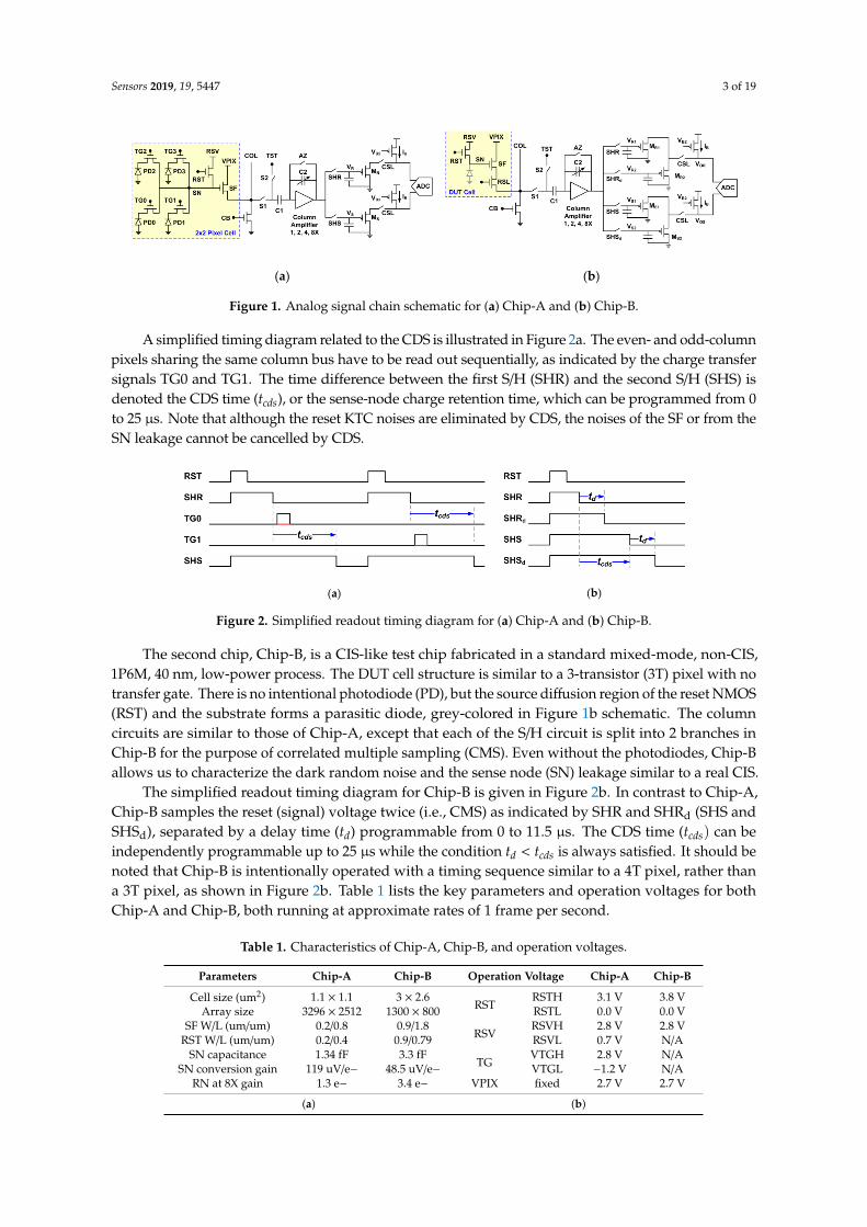
In this work, we study the random noises and leakage currents of two test chips. The first one,Chip-A, is an 8.3 MP, 1.1 µm pitch, stacked CIS. The top pixel array layer is fabricated in a 1P4M45 nm Backside Illuminated (BSI) CIS process and the bottom ASIC layer is fabricated in a 1P6M 65 nmlow-power mixed-mode process. Figure 1a shows the schematic of the analog signal chain. The pixelcell has a 2 × 2-shared structure without the row-select device. The column circuits between the pixelsource follower (SF) and the global ADC are located on the bottom ASIC layer. The column amplifierprovides an analog gain up to 8X and performs the correlated double sampling (CDS). The reset andsignal voltages are sampled and held (S/H) on two capacitors, buffered by column PMOS sourcefollowers and digitized by external 14 bit ADCs at 10 Msps rates. The half-line even- and odd-columnpixels are read out alternatively and reconstructed into a full line by an off-chip FPGA, which alsogenerates the rolling shutter and other control signals. This chip achieves a low input-referred readoutnoise around 1.3 e-rms under an 8X gain [20–23].
Sensors 2019, 19, 5447 3 of 19
Sensors 2019, 19, x FOR PEER REVIEW 3 of 20
programmed from 0 to 25 s. Note that although the reset KTC noises are eliminated by CDS, the
noises of the SF or from the SN leakage cannot be cancelled by CDS.
The second chip, Chip-B, is a CIS-like test chip fabricated in a standard mixed-mode, non-CIS,
1P6M, 40 nm, low-power process. The DUT cell structure is similar to a 3-transistor (3T) pixel with
no transfer gate. There is no intentional photodiode (PD), but the source diffusion region of the reset
NMOS (RST) and the substrate forms a parasitic diode, grey-colored in Figure 1b schematic. The
column circuits are similar to those of Chip-A, except that each of the S/H circuit is split into 2
branches in Chip-B for the purpose of correlated multiple sampling (CMS). Even without the
photodiodes, Chip-B allows us to characterize the dark random noise and the sense node (SN)
leakage similar to a real CIS.
The simplified readout timing diagram for Chip-B is given in Figure 2b. In contrast to Chip-A,
Chip-B samples the reset (signal) voltage twice (i.e., CMS) as indicated by SHR and SHRd (SHS and
SHSd), separated by a delay time (𝑡𝑑) programmable from 0 to 11.5 s. The CDS time (𝑡𝑐𝑑𝑠) can be
independently programmable up to 25 s while the condition 𝑡𝑑 < 𝑡𝑐𝑑𝑠 is always satisfied. It should
be noted that Chip-B is intentionally operated with a timing sequence similar to a 4T pixel, rather
than a 3T pixel, as shown in Figure 2b. Table 1 lists the key parameters and operation voltages for
both Chip-A and Chip-B, both running at approximate rates of 1 frame per second.
(a)
(b)
Figure 1. Analog signal chain schematic for (a) Chip-A and (b) Chip-B.
(a)
(b)
Figure 2. Simplified readout timing diagram for (a) Chip-A and (b) Chip-B.
Table 1. Characteristics of Chip-A, Chip-B, and operation voltages.
Parameters Chip-A Chip-B Operation Voltage Chip-A Chip-B
Cell size (um2) 1.1 × 1.1 3 × 2.6 RST
RSTH 3.1 V 3.8 V
Array size 3296 × 2512 1300 × 800 RSTL 0.0 V 0.0 V
SF W/L (um/um) 0.2/0.8 0.9/1.8 RSV
RSVH 2.8 V 2.8 V
RST W/L (um/um) 0.2/0.4 0.9/0.79 RSVL 0.7 V N/A
SN capacitance 1.34 fF 3.3 fF TG
VTGH 2.8 V N/A
SN conversion gain 119 uV/e 48.5 uV/e VTGL –1.2 V N/A
RN at 8X gain 1.3 e 3.4 e VPIX fixed 2.7 V 2.7 V
Figure 1. Analog signal chain schematic for (a) Chip-A and (b) Chip-B.
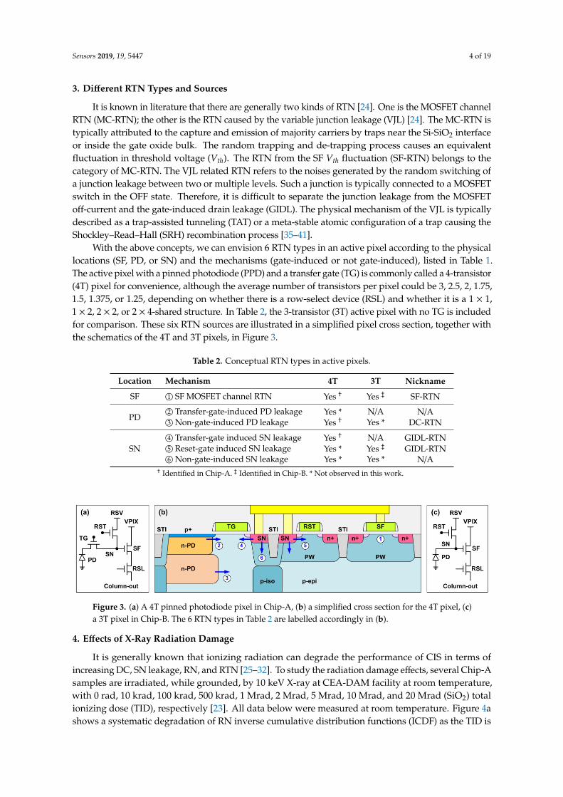
A simplified timing diagram related to the CDS is illustrated in Figure 2a. The even- and odd-columnpixels sharing the same column bus have to be read out sequentially, as indicated by the charge transfersignals TG0 and TG1. The time difference between the first S/H (SHR) and the second S/H (SHS) isdenoted the CDS time (tcds), or the sense-node charge retention time, which can be programmed from 0to 25 µs. Note that although the reset KTC noises are eliminated by CDS, the noises of the SF or from theSN leakage cannot be cancelled by CDS.
Sensors 2019, 19, x FOR PEER REVIEW 3 of 20
programmed from 0 to 25 s. Note that although the reset KTC noises are eliminated by CDS, the
noises of the SF or from the SN leakage cannot be cancelled by CDS.
The second chip, Chip-B, is a CIS-like test chip fabricated in a standard mixed-mode, non-CIS,
1P6M, 40 nm, low-power process. The DUT cell structure is similar to a 3-transistor (3T) pixel with
no transfer gate. There is no intentional photodiode (PD), but the source diffusion region of the reset
NMOS (RST) and the substrate forms a parasitic diode, grey-colored in Figure 1b schematic. The
column circuits are similar to those of Chip-A, except that each of the S/H circuit is split into 2
branches in Chip-B for the purpose of correlated multiple sampling (CMS). Even without the
photodiodes, Chip-B allows us to characterize the dark random noise and the sense node (SN)
leakage similar to a real CIS.
The simplified readout timing diagram for Chip-B is given in Figure 2b. In contrast to Chip-A,
Chip-B samples the reset (signal) voltage twice (i.e., CMS) as indicated by SHR and SHRd (SHS and
SHSd), separated by a delay time (𝑡𝑑) programmable from 0 to 11.5 s. The CDS time (𝑡𝑐𝑑𝑠) can be
independently programmable up to 25 s while the condition 𝑡𝑑 < 𝑡𝑐𝑑𝑠 is always satisfied. It should
be noted that Chip-B is intentionally operated with a timing sequence similar to a 4T pixel, rather
than a 3T pixel, as shown in Figure 2b. Table 1 lists the key parameters and operation voltages for
both Chip-A and Chip-B, both running at approximate rates of 1 frame per second.
(a)
(b)
Figure 1. Analog signal chain schematic for (a) Chip-A and (b) Chip-B.
(a)
(b)
Figure 2. Simplified readout timing diagram for (a) Chip-A and (b) Chip-B.
Table 1. Characteristics of Chip-A, Chip-B, and operation voltages.
Parameters Chip-A Chip-B Operation Voltage Chip-A Chip-B
Cell size (um2) 1.1 × 1.1 3 × 2.6 RST
RSTH 3.1 V 3.8 V
Array size 3296 × 2512 1300 × 800 RSTL 0.0 V 0.0 V
SF W/L (um/um) 0.2/0.8 0.9/1.8 RSV
RSVH 2.8 V 2.8 V
RST W/L (um/um) 0.2/0.4 0.9/0.79 RSVL 0.7 V N/A
SN capacitance 1.34 fF 3.3 fF TG
VTGH 2.8 V N/A
SN conversion gain 119 uV/e 48.5 uV/e VTGL –1.2 V N/A
RN at 8X gain 1.3 e 3.4 e VPIX fixed 2.7 V 2.7 V
Figure 2. Simplified readout timing diagram for (a) Chip-A and (b) Chip-B.
The second chip, Chip-B, is a CIS-like test chip fabricated in a standard mixed-mode, non-CIS,1P6M, 40 nm, low-power process. The DUT cell structure is similar to a 3-transistor (3T) pixel with notransfer gate. There is no intentional photodiode (PD), but the source diffusion region of the reset NMOS(RST) and the substrate forms a parasitic diode, grey-colored in Figure 1b schematic. The columncircuits are similar to those of Chip-A, except that each of the S/H circuit is split into 2 branches inChip-B for the purpose of correlated multiple sampling (CMS). Even without the photodiodes, Chip-Ballows us to characterize the dark random noise and the sense node (SN) leakage similar to a real CIS.
The simplified readout timing diagram for Chip-B is given in Figure 2b. In contrast to Chip-A,Chip-B samples the reset (signal) voltage twice (i.e., CMS) as indicated by SHR and SHRd (SHS andSHSd), separated by a delay time (td) programmable from 0 to 11.5 µs. The CDS time (tcds) can beindependently programmable up to 25 µs while the condition td < tcds is always satisfied. It should benoted that Chip-B is intentionally operated with a timing sequence similar to a 4T pixel, rather thana 3T pixel, as shown in Figure 2b. Table 1 lists the key parameters and operation voltages for bothChip-A and Chip-B, both running at approximate rates of 1 frame per second.
Table 1. Characteristics of Chip-A, Chip-B, and operation voltages.
Parameters Chip-A Chip-B Operation Voltage Chip-A Chip-B
Cell size (um2) 1.1 × 1.1 3 × 2.6RST
RSTH 3.1 V 3.8 VArray size 3296 × 2512 1300 × 800 RSTL 0.0 V 0.0 V
SF W/L (um/um) 0.2/0.8 0.9/1.8RSV
RSVH 2.8 V 2.8 VRST W/L (um/um) 0.2/0.4 0.9/0.79 RSVL 0.7 V N/A
SN capacitance 1.34 fF 3.3 fFTG
VTGH 2.8 V N/ASN conversion gain 119 uV/e− 48.5 uV/e− VTGL −1.2 V N/A
RN at 8X gain 1.3 e− 3.4 e− VPIX fixed 2.7 V 2.7 V
(a) (b)
Sensors 2019, 19, 5447 4 of 19
3. Different RTN Types and Sources
It is known in literature that there are generally two kinds of RTN [24]. One is the MOSFET channelRTN (MC-RTN); the other is the RTN caused by the variable junction leakage (VJL) [24]. The MC-RTN istypically attributed to the capture and emission of majority carriers by traps near the Si-SiO2 interfaceor inside the gate oxide bulk. The random trapping and de-trapping process causes an equivalentfluctuation in threshold voltage (Vth). The RTN from the SF Vth fluctuation (SF-RTN) belongs to thecategory of MC-RTN. The VJL related RTN refers to the noises generated by the random switching ofa junction leakage between two or multiple levels. Such a junction is typically connected to a MOSFETswitch in the OFF state. Therefore, it is difficult to separate the junction leakage from the MOSFEToff-current and the gate-induced drain leakage (GIDL). The physical mechanism of the VJL is typicallydescribed as a trap-assisted tunneling (TAT) or a meta-stable atomic configuration of a trap causing theShockley–Read–Hall (SRH) recombination process [35–41].
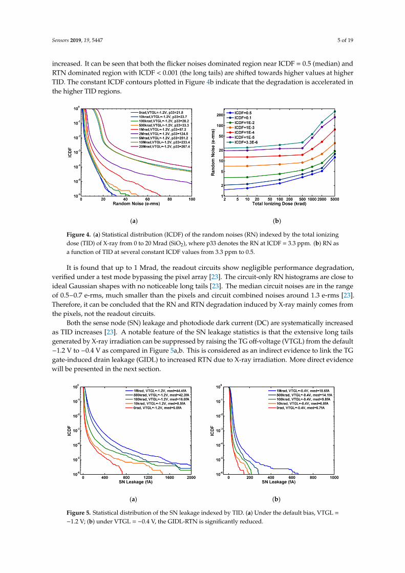
With the above concepts, we can envision 6 RTN types in an active pixel according to the physicallocations (SF, PD, or SN) and the mechanisms (gate-induced or not gate-induced), listed in Table 1.The active pixel with a pinned photodiode (PPD) and a transfer gate (TG) is commonly called a 4-transistor(4T) pixel for convenience, although the average number of transistors per pixel could be 3, 2.5, 2, 1.75,1.5, 1.375, or 1.25, depending on whether there is a row-select device (RSL) and whether it is a 1 × 1,1 × 2, 2 × 2, or 2 × 4-shared structure. In Table 2, the 3-transistor (3T) active pixel with no TG is includedfor comparison. These six RTN sources are illustrated in a simplified pixel cross section, together withthe schematics of the 4T and 3T pixels, in Figure 3.
Table 2. Conceptual RTN types in active pixels.
Location Mechanism 4T 3T Nickname
SF 1O SF MOSFET channel RTN Yes † Yes ‡ SF-RTN
PD2O Transfer-gate-induced PD leakage Yes * N/A N/A3O Non-gate-induced PD leakage Yes † Yes * DC-RTN
SN4O Transfer-gate induced SN leakage Yes † N/A GIDL-RTN5O Reset-gate induced SN leakage Yes * Yes ‡ GIDL-RTN6O Non-gate-induced SN leakage Yes * Yes * N/A
† Identified in Chip-A. ‡ Identified in Chip-B. * Not observed in this work.
Sensors 2019, 19, x FOR PEER REVIEW 4 of 20
(a) (b)
3. Different RTN Types and Sources
It is known in literature that there are generally two kinds of RTN [24]. One is the MOSFET
channel RTN (MC-RTN); the other is the RTN caused by the variable junction leakage (VJL) [24]. The
MC-RTN is typically attributed to the capture and emission of majority carriers by traps near the Si-
SiO2 interface or inside the gate oxide bulk. The random trapping and de-trapping process causes an
equivalent fluctuation in threshold voltage (𝑉𝑡ℎ). The RTN from the SF 𝑉𝑡ℎ fluctuation (SF-RTN)
belongs to the category of MC-RTN. The VJL related RTN refers to the noises generated by the
random switching of a junction leakage between two or multiple levels. Such a junction is typically
connected to a MOSFET switch in the OFF state. Therefore, it is difficult to separate the junction
leakage from the MOSFET off-current and the gate-induced drain leakage (GIDL). The physical
mechanism of the VJL is typically described as a trap-assisted tunneling (TAT) or a meta-stable atomic
configuration of a trap causing the Shockley–Read–Hall (SRH) recombination process [35–41].
With the above concepts, we can envision 6 RTN types in an active pixel according to the
physical locations (SF, PD, or SN) and the mechanisms (gate-induced or not gate-induced), listed in
Table 1. The active pixel with a pinned photodiode (PPD) and a transfer gate (TG) is commonly called
a 4-transistor (4T) pixel for convenience, although the average number of transistors per pixel could
be 3, 2.5, 2, 1.75, 1.5, 1.375, or 1.25, depending on whether there is a row-select device (RSL) and
whether it is a 1 × 1, 1 × 2, 2 × 2, or 2 × 4-shared structure. In Table 2, the 3-transistor (3T) active pixel
with no TG is included for comparison. These six RTN sources are illustrated in a simplified pixel
cross section, together with the schematics of the 4T and 3T pixels, in Figure 3.
Table 2. Conceptual RTN types in active pixels.
Location Mechanism 4T 3T Nickname
SF SF MOSFET channel RTN Yes † Yes ‡ SF-RTN
PD Transfer-gate-induced PD leakage Yes * N/A N/A
Non-gate-induced PD leakage Yes † Yes * DC-RTN
SN
Transfer-gate induced SN leakage Yes † N/A GIDL-RTN
Reset-gate induced SN leakage Yes * Yes ‡ GIDL-RTN
Non-gate-induced SN leakage Yes * Yes * N/A
† Identified in Chip-A. ‡ Identified in Chip-B. * Not observed in this work.
Figure 3. (a) A 4T pinned photodiode pixel in Chip-A, (b) a simplified cross section for the 4T pixel,
(c) a 3T pixel in Chip-B. The 6 RTN types in Table 2 are labelled accordingly in (b).
4. Effects of X-Ray Radiation Damage
It is generally known that ionizing radiation can degrade the performance of CIS in terms of
increasing DC, SN leakage, RN, and RTN [25–32]. To study the radiation damage effects, several
Chip-A samples are irradiated, while grounded, by 10 keV X-ray at CEA-DAM facility at room
temperature, with 0 rad, 10 krad, 100 krad, 500 krad, 1 Mrad, 2 Mrad, 5 Mrad, 10 Mrad, and 20 Mrad
(SiO2) total ionizing dose (TID), respectively [23]. All data below were measured at room temperature.
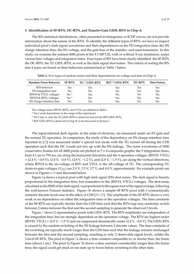
Figure 4a shows a systematic degradation of RN inverse cumulative distribution functions (ICDF) as
Figure 3. (a) A 4T pinned photodiode pixel in Chip-A, (b) a simplified cross section for the 4T pixel, (c)a 3T pixel in Chip-B. The 6 RTN types in Table 2 are labelled accordingly in (b).
4. Effects of X-Ray Radiation Damage
It is generally known that ionizing radiation can degrade the performance of CIS in terms ofincreasing DC, SN leakage, RN, and RTN [25–32]. To study the radiation damage effects, several Chip-Asamples are irradiated, while grounded, by 10 keV X-ray at CEA-DAM facility at room temperature,with 0 rad, 10 krad, 100 krad, 500 krad, 1 Mrad, 2 Mrad, 5 Mrad, 10 Mrad, and 20 Mrad (SiO2) totalionizing dose (TID), respectively [23]. All data below were measured at room temperature. Figure 4ashows a systematic degradation of RN inverse cumulative distribution functions (ICDF) as the TID is
Sensors 2019, 19, 5447 5 of 19
increased. It can be seen that both the flicker noises dominated region near ICDF = 0.5 (median) andRTN dominated region with ICDF < 0.001 (the long tails) are shifted towards higher values at higherTID. The constant ICDF contours plotted in Figure 4b indicate that the degradation is accelerated inthe higher TID regions.
Sensors 2019, 19, x FOR PEER REVIEW 5 of 20
the TID is increased. It can be seen that both the flicker noises dominated region near ICDF = 0.5
(median) and RTN dominated region with ICDF < 0.001 (the long tails) are shifted towards higher
values at higher TID. The constant ICDF contours plotted in Figure 4b indicate that the degradation
is accelerated in the higher TID regions.
It is found that up to 1 Mrad, the readout circuits show negligible performance degradation,
verified under a test mode bypassing the pixel array [23]. The circuit-only RN histograms are close
to ideal Gaussian shapes with no noticeable long tails [23]. The median circuit noises are in the range
of 0.50.7 e-rms, much smaller than the pixels and circuit combined noises around 1.3 e-rms [23].
Therefore, it can be concluded that the RN and RTN degradation induced by X-ray mainly comes
from the pixels, not the readout circuits.
Both the sense node (SN) leakage and photodiode dark current (DC) are systematically increased
as TID increases [23]. A notable feature of the SN leakage statistics is that the extensive long tails
generated by X-ray irradiation can be suppressed by raising the TG off-voltage (VTGL) from the
default –1.2 V to –0.4 V as compared in Figure 5a,b. This is considered as an indirect evidence to link
the TG gate-induced drain leakage (GIDL) to increased RTN due to X-ray irradiation. More direct
evidence will be presented in the next section.
(a)
(b)
Figure 4. (a) Statistical distribution (ICDF) of the random noises (RN) indexed by the total ionizing
dose (TID) of X-ray from 0 to 20 Mrad (SiO2), where p33 denotes the RN at ICDF = 3.3 ppm. (b) RN as
a function of TID at several constant ICDF values from 3.3 ppm to 0.5.
(a)
(b)
Figure 4. (a) Statistical distribution (ICDF) of the random noises (RN) indexed by the total ionizingdose (TID) of X-ray from 0 to 20 Mrad (SiO2), where p33 denotes the RN at ICDF = 3.3 ppm. (b) RN asa function of TID at several constant ICDF values from 3.3 ppm to 0.5.
It is found that up to 1 Mrad, the readout circuits show negligible performance degradation,verified under a test mode bypassing the pixel array [23]. The circuit-only RN histograms are close toideal Gaussian shapes with no noticeable long tails [23]. The median circuit noises are in the rangeof 0.5−0.7 e-rms, much smaller than the pixels and circuit combined noises around 1.3 e-rms [23].Therefore, it can be concluded that the RN and RTN degradation induced by X-ray mainly comes fromthe pixels, not the readout circuits.
Both the sense node (SN) leakage and photodiode dark current (DC) are systematically increasedas TID increases [23]. A notable feature of the SN leakage statistics is that the extensive long tailsgenerated by X-ray irradiation can be suppressed by raising the TG off-voltage (VTGL) from the default−1.2 V to −0.4 V as compared in Figure 5a,b. This is considered as an indirect evidence to link the TGgate-induced drain leakage (GIDL) to increased RTN due to X-ray irradiation. More direct evidencewill be presented in the next section.
Sensors 2019, 19, x FOR PEER REVIEW 5 of 20
the TID is increased. It can be seen that both the flicker noises dominated region near ICDF = 0.5
(median) and RTN dominated region with ICDF < 0.001 (the long tails) are shifted towards higher
values at higher TID. The constant ICDF contours plotted in Figure 4b indicate that the degradation
is accelerated in the higher TID regions.
It is found that up to 1 Mrad, the readout circuits show negligible performance degradation,
verified under a test mode bypassing the pixel array [23]. The circuit-only RN histograms are close
to ideal Gaussian shapes with no noticeable long tails [23]. The median circuit noises are in the range
of 0.50.7 e-rms, much smaller than the pixels and circuit combined noises around 1.3 e-rms [23].
Therefore, it can be concluded that the RN and RTN degradation induced by X-ray mainly comes
from the pixels, not the readout circuits.
Both the sense node (SN) leakage and photodiode dark current (DC) are systematically increased
as TID increases [23]. A notable feature of the SN leakage statistics is that the extensive long tails
generated by X-ray irradiation can be suppressed by raising the TG off-voltage (VTGL) from the
default –1.2 V to –0.4 V as compared in Figure 5a,b. This is considered as an indirect evidence to link
the TG gate-induced drain leakage (GIDL) to increased RTN due to X-ray irradiation. More direct
evidence will be presented in the next section.
(a)
(b)
Figure 4. (a) Statistical distribution (ICDF) of the random noises (RN) indexed by the total ionizing
dose (TID) of X-ray from 0 to 20 Mrad (SiO2), where p33 denotes the RN at ICDF = 3.3 ppm. (b) RN as
a function of TID at several constant ICDF values from 3.3 ppm to 0.5.
(a)
(b)
Figure 5. Statistical distribution of the SN leakage indexed by TID. (a) Under the default bias, VTGL =
−1.2 V; (b) under VTGL = −0.4 V, the GIDL-RTN is significantly reduced.
Sensors 2019, 19, 5447 6 of 19
5. Identification of SF-RTN, DC-RTN, and Transfer-Gate GIDL-RTN in Chip-A
The RN statistical distributions, often presented in histograms or ICDF curves, do not provideinformation about the nature of the RTN. To identify the different types of RTN, we have to inspectindividual pixel’s dark signal waveforms and their dependences on the PD integration time, the SNcharge retention time, the SN voltage, and the gate bias of the transfer- and reset-transistors. In thisstudy, we examine the noisiest 4000 pixels of the 8.3 MP CIS, with or without X-ray irradiation, undervarious bias voltages and integration times. Four types of RN have been clearly identified: the SF-RTN,the DC-RTN, the TG GIDL-RTN, as well as the dark signal shot noises. The criteria of sorting the RNinto 4 types are based on their behaviors summarized in Table 3 below.
Table 3. Five types of random noises and their dependencies on voltage and time in Chip-A.
Random Noise Behavior SF-RTN TG † GIDL-RTN RST ‡ GIDL-RTN DC-RTN Shot Noises
RTS behavior Yes Yes Yes Yes NoPD integration time No No No Yes Yes
RSVH & VTGL voltages No * Yes No No NoRSVH & RSTL voltages No * No Yes No No
SN charge retention time No Yes Yes No No
The voltage names RSVH, RSTL, and VTGL are defined in Table 1.* Very weak dependence in the range of the experiment.† For Chip-A, only the TG GIDL-RTN is observed, but not the RST GIDL-RTN.‡ RST GIDL-RTN is observed in Chip-B, to be discussed in Section 6.
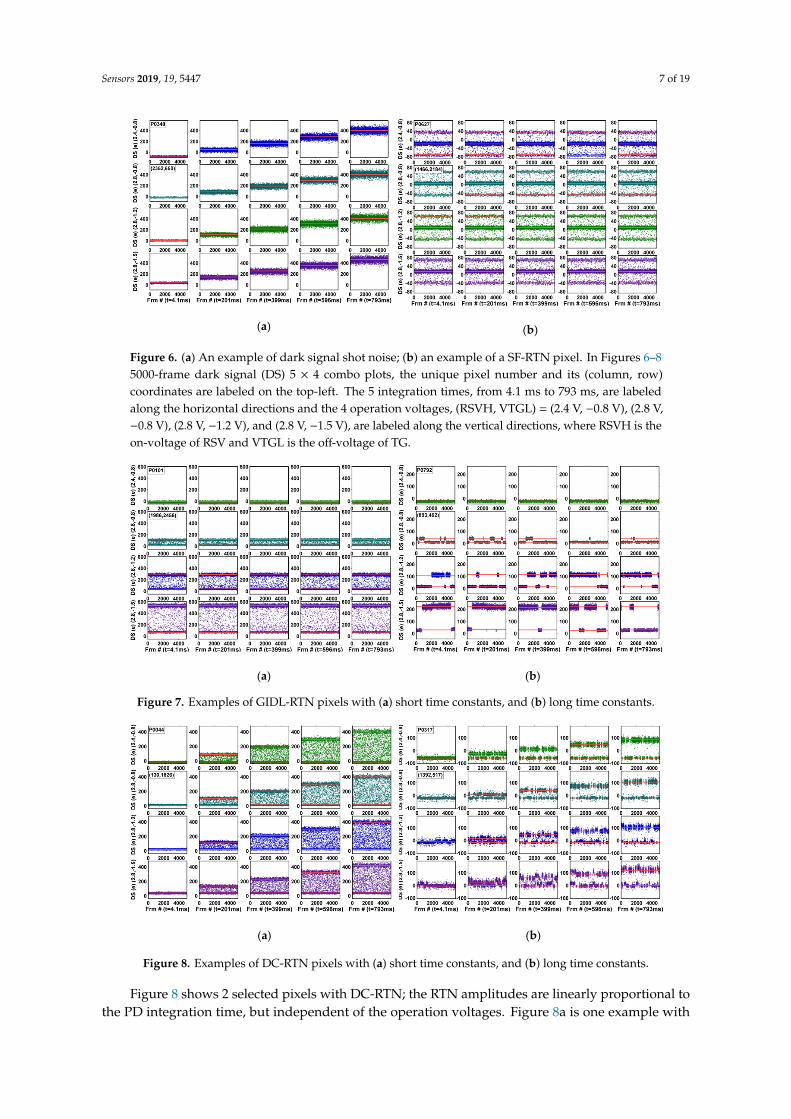
The input-referred dark signals, in the units of electrons, are measured under an 8X gain andthe normal TG operation. In comparison, the study of the dependency on SN charge retention timereported in [23] was measured under a special test mode with the TG turned off during the CDSoperation such that the DC would not mix up with the SN leakage. The noise waveforms of 5000consecutive frames for all 4000 pixels are plotted in 5 × 4 composite graphs; the 5 integration times,from 4.1 ms to 793 ms, are along the horizontal directions and the 4 operation voltages, (RSVH, VTGL)= (2.4 V, −0.8 V), (2.8 V, −0.8 V), (2.8 V, −1.2 V), and (2.8 V, −1.5 V), are along the vertical directions,where RSVH is the on-voltage of RSV and VTGL is the off-voltage of TG. The corresponding TGdrain-to-gate voltages (VDG) are 2.9 V, 3.3 V, 3.7 V, and 4.0 V, approximately. Six example pixels areshown in Figures 6–8 and discussed below.
Figure 6a shows a typical pixel with high dark signal (DS) shot noises. The dark signal is linearlyproportional to the integration time, but insensitive to the (RSVH, VTGL) voltages. The shot noise,calculated as the RMS of the dark signal, is proportional to the square root of the signal average, followingthe well-known Poisson statistics. Figure 6b shows a sample SF-RTN pixel with 3 symmetricallycentered discrete levels due to the effect of CDS [20–23]. The amplitude of the SF-RTN shows a veryweak or no dependence on either the integration time or the operation voltages. The time constantsof the SF-RTN are typically shorter than the CDS time such that the RTN trap may randomly switchbetween 2 states between the first and the second sampling to generate the observed 3 levels.
Figure 7 shows 2 representative pixels with GIDL-RTN. The RTN amplitudes are independent ofthe integration time, but are strongly dependent on the operation voltage. The RTN are highest under(RSVH, VTGL) = (2.8 V, −1.5 V) and are suppressed dramatically under (2.4 V, −0.8 V). The GIDL-RTNis caused by the random switching of the SN leakage between 2 discrete values. The time constants ofthe switching are typically much longer than the CDS time such that the leakage remains unchangedbetween the first and the second sampling, resulting in only 2 observable signal levels, unlike the3-level SF-RTN. The pixel in Figure 7a shows a time constant comparable to, or shorter than, the frametime (about 1 sec). The pixel in Figure 7b shows a time constant considerably longer than the frametime; the signal could get stuck at one state up to hours before switching to the other state.
Sensors 2019, 19, 5447 7 of 19Sensors 2019, 19, x FOR PEER REVIEW 7 of 20
(a)
(b)
Figure 6. (a) An example of dark signal shot noise; (b) an example of a SF-RTN pixel. In Figures 6–8
5000-frame dark signal (DS) 5 × 4 combo plots, the unique pixel number and its (column, row)
coordinates are labeled on the top-left. The 5 integration times, from 4.1 ms to 793 ms, are labeled
along the horizontal directions and the 4 operation voltages, (RSVH, VTGL) = (2.4 V, –0.8 V), (2.8 V, –
0.8 V), (2.8 V, –1.2 V), and (2.8 V, –1.5 V), are labeled along the vertical directions, where RSVH is the
on-voltage of RSV and VTGL is the off-voltage of TG
Figure 7 shows 2 representative pixels with GIDL-RTN. The RTN amplitudes are independent
of the integration time, but are strongly dependent on the operation voltage. The RTN are highest
under (RSVH, VTGL) = (2.8 V, –1.5 V) and are suppressed dramatically under (2.4 V, –0.8 V). The
GIDL-RTN is caused by the random switching of the SN leakage between 2 discrete values. The time
constants of the switching are typically much longer than the CDS time such that the leakage remains
unchanged between the first and the second sampling, resulting in only 2 observable signal levels,
unlike the 3-level SF-RTN. The pixel in Figure 7a shows a time constant comparable to, or shorter
than, the frame time (about 1 sec). The pixel in Figure 7b shows a time constant considerably longer
than the frame time; the signal could get stuck at one state up to hours before switching to the other
state.
(a)
(b)
Figure 7. Examples of GIDL-RTN pixels with (a) short time constants, and (b) long time constants.
Figure 8 shows 2 selected pixels with DC-RTN; the RTN amplitudes are linearly proportional to
the PD integration time, but independent of the operation voltages. Figure 8a is one example with a
Figure 6. (a) An example of dark signal shot noise; (b) an example of a SF-RTN pixel. In Figures 6–85000-frame dark signal (DS) 5 × 4 combo plots, the unique pixel number and its (column, row)coordinates are labeled on the top-left. The 5 integration times, from 4.1 ms to 793 ms, are labeledalong the horizontal directions and the 4 operation voltages, (RSVH, VTGL) = (2.4 V, −0.8 V), (2.8 V,−0.8 V), (2.8 V, −1.2 V), and (2.8 V, −1.5 V), are labeled along the vertical directions, where RSVH is theon-voltage of RSV and VTGL is the off-voltage of TG.
Sensors 2019, 19, x FOR PEER REVIEW 7 of 20
(a)
(b)
Figure 6. (a) An example of dark signal shot noise; (b) an example of a SF-RTN pixel. In Figures 6–8
5000-frame dark signal (DS) 5 × 4 combo plots, the unique pixel number and its (column, row)
coordinates are labeled on the top-left. The 5 integration times, from 4.1 ms to 793 ms, are labeled
along the horizontal directions and the 4 operation voltages, (RSVH, VTGL) = (2.4 V, –0.8 V), (2.8 V, –
0.8 V), (2.8 V, –1.2 V), and (2.8 V, –1.5 V), are labeled along the vertical directions, where RSVH is the
on-voltage of RSV and VTGL is the off-voltage of TG
Figure 7 shows 2 representative pixels with GIDL-RTN. The RTN amplitudes are independent
of the integration time, but are strongly dependent on the operation voltage. The RTN are highest
under (RSVH, VTGL) = (2.8 V, –1.5 V) and are suppressed dramatically under (2.4 V, –0.8 V). The
GIDL-RTN is caused by the random switching of the SN leakage between 2 discrete values. The time
constants of the switching are typically much longer than the CDS time such that the leakage remains
unchanged between the first and the second sampling, resulting in only 2 observable signal levels,
unlike the 3-level SF-RTN. The pixel in Figure 7a shows a time constant comparable to, or shorter
than, the frame time (about 1 sec). The pixel in Figure 7b shows a time constant considerably longer
than the frame time; the signal could get stuck at one state up to hours before switching to the other
state.
(a)
(b)
Figure 7. Examples of GIDL-RTN pixels with (a) short time constants, and (b) long time constants.
Figure 8 shows 2 selected pixels with DC-RTN; the RTN amplitudes are linearly proportional to
the PD integration time, but independent of the operation voltages. Figure 8a is one example with a
Figure 7. Examples of GIDL-RTN pixels with (a) short time constants, and (b) long time constants.
Sensors 2019, 19, x FOR PEER REVIEW 8 of 20
time constant comparable to or shorter than the frame time (but still longer than the CDS time); Figure
8b is one example with a time constant much longer than the frame time.
(a)
(b)
Figure 8. Examples of DC-RTN pixels with (a) short time constants, and (b) long time constants.
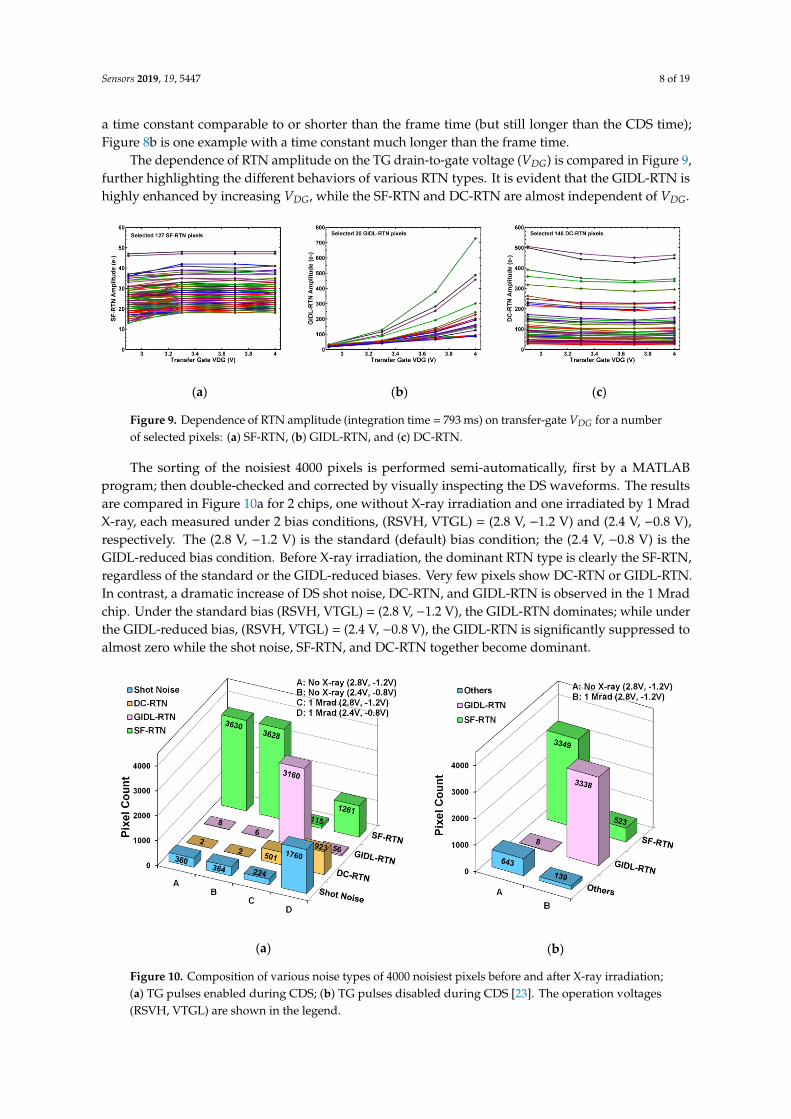
The dependence of RTN amplitude on the TG drain-to-gate voltage (𝑉𝐷𝐺) is compared in Figure
9, further highlighting the different behaviors of various RTN types. It is evident that the GIDL-RTN
is highly enhanced by increasing 𝑉𝐷𝐺, while the SF-RTN and DC-RTN are almost independent of
𝑉𝐷𝐺.
(a)
(b)
(c)
Figure 9. Dependence of RTN amplitude (integration time = 793 ms) on transfer-gate 𝑉𝐷𝐺 for a
number of selected pixels: (a) SF-RTN, (b) GIDL-RTN, and (c) DC-RTN.
The sorting of the noisiest 4000 pixels is performed semi-automatically, first by a MATLAB
program; then double-checked and corrected by visually inspecting the DS waveforms. The results
are compared in Figure 10a for 2 chips, one without X-ray irradiation and one irradiated by 1 Mrad
X-ray, each measured under 2 bias conditions, (RSVH, VTGL) = (2.8 V, –1.2 V) and (2.4 V, –0.8 V),
respectively. The (2.8 V, –1.2 V) is the standard (default) bias condition; the (2.4 V, –0.8 V) is the GIDL-
reduced bias condition. Before X-ray irradiation, the dominant RTN type is clearly the SF-RTN,
regardless of the standard or the GIDL-reduced biases. Very few pixels show DC-RTN or GIDL-RTN.
In contrast, a dramatic increase of DS shot noise, DC-RTN, and GIDL-RTN is observed in the 1 Mrad
chip. Under the standard bias (RSVH, VTGL) = (2.8 V, –1.2 V), the GIDL-RTN dominates; while under
the GIDL-reduced bias, (RSVH, VTGL) = (2.4 V, –0.8 V), the GIDL-RTN is significantly suppressed to
almost zero while the shot noise, SF-RTN, and DC-RTN together become dominant.
The data in Figure 10a are measured with the TG pulses enabled during the CDS (normal
operation). For comparison, the data reported in [23] are measured with the TG pulses disabled
Figure 8. Examples of DC-RTN pixels with (a) short time constants, and (b) long time constants.
Figure 8 shows 2 selected pixels with DC-RTN; the RTN amplitudes are linearly proportional tothe PD integration time, but independent of the operation voltages. Figure 8a is one example with
Sensors 2019, 19, 5447 8 of 19
a time constant comparable to or shorter than the frame time (but still longer than the CDS time);Figure 8b is one example with a time constant much longer than the frame time.
The dependence of RTN amplitude on the TG drain-to-gate voltage (VDG) is compared in Figure 9,further highlighting the different behaviors of various RTN types. It is evident that the GIDL-RTN ishighly enhanced by increasing VDG, while the SF-RTN and DC-RTN are almost independent of VDG.
Sensors 2019, 19, x FOR PEER REVIEW 8 of 20
time constant comparable to or shorter than the frame time (but still longer than the CDS time); Figure
8b is one example with a time constant much longer than the frame time.
(a)
(b)
Figure 8. Examples of DC-RTN pixels with (a) short time constants, and (b) long time constants.
The dependence of RTN amplitude on the TG drain-to-gate voltage (𝑉𝐷𝐺) is compared in Figure
9, further highlighting the different behaviors of various RTN types. It is evident that the GIDL-RTN
is highly enhanced by increasing 𝑉𝐷𝐺, while the SF-RTN and DC-RTN are almost independent of
𝑉𝐷𝐺.
(a)
(b)
(c)
Figure 9. Dependence of RTN amplitude (integration time = 793 ms) on transfer-gate 𝑉𝐷𝐺 for a
number of selected pixels: (a) SF-RTN, (b) GIDL-RTN, and (c) DC-RTN.
The sorting of the noisiest 4000 pixels is performed semi-automatically, first by a MATLAB
program; then double-checked and corrected by visually inspecting the DS waveforms. The results
are compared in Figure 10a for 2 chips, one without X-ray irradiation and one irradiated by 1 Mrad
X-ray, each measured under 2 bias conditions, (RSVH, VTGL) = (2.8 V, –1.2 V) and (2.4 V, –0.8 V),
respectively. The (2.8 V, –1.2 V) is the standard (default) bias condition; the (2.4 V, –0.8 V) is the GIDL-
reduced bias condition. Before X-ray irradiation, the dominant RTN type is clearly the SF-RTN,
regardless of the standard or the GIDL-reduced biases. Very few pixels show DC-RTN or GIDL-RTN.
In contrast, a dramatic increase of DS shot noise, DC-RTN, and GIDL-RTN is observed in the 1 Mrad
chip. Under the standard bias (RSVH, VTGL) = (2.8 V, –1.2 V), the GIDL-RTN dominates; while under
the GIDL-reduced bias, (RSVH, VTGL) = (2.4 V, –0.8 V), the GIDL-RTN is significantly suppressed to
almost zero while the shot noise, SF-RTN, and DC-RTN together become dominant.
The data in Figure 10a are measured with the TG pulses enabled during the CDS (normal
operation). For comparison, the data reported in [23] are measured with the TG pulses disabled
Figure 9. Dependence of RTN amplitude (integration time = 793 ms) on transfer-gate VDG for a numberof selected pixels: (a) SF-RTN, (b) GIDL-RTN, and (c) DC-RTN.
The sorting of the noisiest 4000 pixels is performed semi-automatically, first by a MATLABprogram; then double-checked and corrected by visually inspecting the DS waveforms. The resultsare compared in Figure 10a for 2 chips, one without X-ray irradiation and one irradiated by 1 MradX-ray, each measured under 2 bias conditions, (RSVH, VTGL) = (2.8 V, −1.2 V) and (2.4 V, −0.8 V),respectively. The (2.8 V, −1.2 V) is the standard (default) bias condition; the (2.4 V, −0.8 V) is theGIDL-reduced bias condition. Before X-ray irradiation, the dominant RTN type is clearly the SF-RTN,regardless of the standard or the GIDL-reduced biases. Very few pixels show DC-RTN or GIDL-RTN.In contrast, a dramatic increase of DS shot noise, DC-RTN, and GIDL-RTN is observed in the 1 Mradchip. Under the standard bias (RSVH, VTGL) = (2.8 V, −1.2 V), the GIDL-RTN dominates; while underthe GIDL-reduced bias, (RSVH, VTGL) = (2.4 V, −0.8 V), the GIDL-RTN is significantly suppressed toalmost zero while the shot noise, SF-RTN, and DC-RTN together become dominant.
Sensors 2019, 19, x FOR PEER REVIEW 9 of 20
during the CDS (test mode). They are plotted in Figure 10b, where the DC-RTN and DS shot noises
not observable without the charge transfer from PD to SN. The common feature of Figure 10a,b is
that the SF-RTN dominates in the chip without X-ray and the GIDL-RTN dominates in the chip after
1 Mrad X-ray irradiation.
(a)
(b)
Figure 10. Composition of various noise types of 4000 noisiest pixels before and after X-ray
irradiation; (a) TG pulses enabled during CDS; (b) TG pulses disabled during CDS [23]. The
operation voltages (RSVH, VTGL) are shown in the legend.
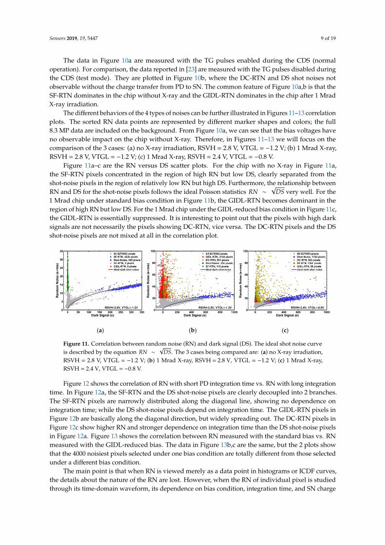
The different behaviors of the 4 types of noises can be further illustrated in Figures 11–13
correlation plots. The sorted RN data points are represented by different marker shapes and colors;
the full 8.3 MP data are included on the background. From Figure 10a, we can see that the bias
voltages have no observable impact on the chip without X-ray. Therefore, in Figures 11–13 we will
focus on the comparison of the 3 cases: (a) no X-ray irradiation, RSVH = 2.8 V, VTGL = –1.2 V; (b) 1
Mrad X-ray, RSVH = 2.8 V, VTGL = –1.2 V; (c) 1 Mrad X-ray, RSVH = 2.4 V, VTGL = –0.8 V.
Figures 11a–c are the RN versus DS scatter plots. For the chip with no X-ray in Figure 11a, the
SF-RTN pixels concentrated in the region of high RN but low DS, clearly separated from the shot-
noise pixels in the region of relatively low RN but high DS. Furthermore, the relationship between
RN and DS for the shot-noise pixels follows the ideal Poisson statistics 𝑅𝑁 ~ √𝐷𝑆 very well. For the
1 Mrad chip under standard bias condition in Figure 11b, the GIDL-RTN becomes dominant in the
region of high RN but low DS. For the 1 Mrad chip under the GIDL-reduced bias condition in Figure
11c, the GIDL-RTN is essentially suppressed. It is interesting to point out that the pixels with high
dark signals are not necessarily the pixels showing DC-RTN, vice versa. The DC-RTN pixels and the
DS shot-noise pixels are not mixed at all in the correlation plot.
Figure 12 shows the correlation of RN with short PD integration time vs. RN with long
integration time. In Figure 12a, the SF-RTN and the DS shot-noise pixels are clearly decoupled into 2
branches. The SF-RTN pixels are narrowly distributed along the diagonal line, showing no
dependence on integration time; while the DS shot-noise pixels depend on integration time. The
GIDL-RTN pixels in Figure 12b are basically along the diagonal direction, but widely spreading out.
The DC-RTN pixels in Figure 12c show higher RN and stronger dependence on integration time than
the DS shot-noise pixels in Figure 12a. Figure 13 shows the correlation between RN measured with
the standard bias vs. RN measured with the GIDL-reduced bias. The data in Figures 13b and 13c are
the same, but the 2 plots show that the 4000 noisiest pixels selected under one bias condition are
totally different from those selected under a different bias condition.
Figure 10. Composition of various noise types of 4000 noisiest pixels before and after X-ray irradiation;(a) TG pulses enabled during CDS; (b) TG pulses disabled during CDS [23]. The operation voltages(RSVH, VTGL) are shown in the legend.
Sensors 2019, 19, 5447 9 of 19
The data in Figure 10a are measured with the TG pulses enabled during the CDS (normaloperation). For comparison, the data reported in [23] are measured with the TG pulses disabled duringthe CDS (test mode). They are plotted in Figure 10b, where the DC-RTN and DS shot noises notobservable without the charge transfer from PD to SN. The common feature of Figure 10a,b is that theSF-RTN dominates in the chip without X-ray and the GIDL-RTN dominates in the chip after 1 MradX-ray irradiation.
The different behaviors of the 4 types of noises can be further illustrated in Figures 11–13 correlationplots. The sorted RN data points are represented by different marker shapes and colors; the full8.3 MP data are included on the background. From Figure 10a, we can see that the bias voltages haveno observable impact on the chip without X-ray. Therefore, in Figures 11–13 we will focus on thecomparison of the 3 cases: (a) no X-ray irradiation, RSVH = 2.8 V, VTGL = −1.2 V; (b) 1 Mrad X-ray,RSVH = 2.8 V, VTGL = −1.2 V; (c) 1 Mrad X-ray, RSVH = 2.4 V, VTGL = −0.8 V.
Figure 11a–c are the RN versus DS scatter plots. For the chip with no X-ray in Figure 11a,the SF-RTN pixels concentrated in the region of high RN but low DS, clearly separated from theshot-noise pixels in the region of relatively low RN but high DS. Furthermore, the relationship betweenRN and DS for the shot-noise pixels follows the ideal Poisson statistics RN ∼
√DS very well. For the
1 Mrad chip under standard bias condition in Figure 11b, the GIDL-RTN becomes dominant in theregion of high RN but low DS. For the 1 Mrad chip under the GIDL-reduced bias condition in Figure 11c,the GIDL-RTN is essentially suppressed. It is interesting to point out that the pixels with high darksignals are not necessarily the pixels showing DC-RTN, vice versa. The DC-RTN pixels and the DSshot-noise pixels are not mixed at all in the correlation plot.
Sensors 2019, 19, x FOR PEER REVIEW 10 of 20
The main point is that when RN is viewed merely as a data point in histograms or ICDF curves,
the details about the nature of the RN are lost. However, when the RN of individual pixel is studied
through its time-domain waveform, its dependence on bias condition, integration time, and SN
charge retention time [23], it becomes very clear that different types of RN can be unambiguously
identified and distinguished.
(a)
(b)
(c)
Figure 11. Correlation between random noise (RN) and dark signal (DS). The ideal shot noise curve
is described by the equation 𝑅𝑁 ~ √𝐷𝑆. The 3 cases being compared are: (a) no X-ray irradiation,
RSVH = 2.8 V, VTGL = –1.2 V; (b) 1 Mrad X-ray, RSVH = 2.8 V, VTGL = –1.2 V; (c) 1 Mrad X-ray, RSVH
= 2.4 V, VTGL = –0.8 V.
(a)
(b)
(c)
Figure 12. Correlation between RN measured with short (4.1 ms) integration time vs. RN measured
with long (793 ms) integration time. The 3 cases being compared are: (a) no X-ray irradiation, RSVH
= 2.8 V, VTGL = –1.2 V; (b) 1 Mrad X-ray, RSVH = 2.8 V, VTGL = –1.2 V; (c) 1 Mrad X-ray, RSVH = 2.4
V, VTGL = –0.8 V.
(a)
(b)
(c)
Figure 11. Correlation between random noise (RN) and dark signal (DS). The ideal shot noise curveis described by the equation RN ∼
√DS. The 3 cases being compared are: (a) no X-ray irradiation,
RSVH = 2.8 V, VTGL = −1.2 V; (b) 1 Mrad X-ray, RSVH = 2.8 V, VTGL = −1.2 V; (c) 1 Mrad X-ray,RSVH = 2.4 V, VTGL = −0.8 V.
Figure 12 shows the correlation of RN with short PD integration time vs. RN with long integrationtime. In Figure 12a, the SF-RTN and the DS shot-noise pixels are clearly decoupled into 2 branches.The SF-RTN pixels are narrowly distributed along the diagonal line, showing no dependence onintegration time; while the DS shot-noise pixels depend on integration time. The GIDL-RTN pixels inFigure 12b are basically along the diagonal direction, but widely spreading out. The DC-RTN pixels inFigure 12c show higher RN and stronger dependence on integration time than the DS shot-noise pixelsin Figure 12a. Figure 13 shows the correlation between RN measured with the standard bias vs. RNmeasured with the GIDL-reduced bias. The data in Figure 13b,c are the same, but the 2 plots showthat the 4000 noisiest pixels selected under one bias condition are totally different from those selectedunder a different bias condition.
The main point is that when RN is viewed merely as a data point in histograms or ICDF curves,the details about the nature of the RN are lost. However, when the RN of individual pixel is studiedthrough its time-domain waveform, its dependence on bias condition, integration time, and SN charge
Sensors 2019, 19, 5447 10 of 19
retention time [23], it becomes very clear that different types of RN can be unambiguously identifiedand distinguished.
Sensors 2019, 19, x FOR PEER REVIEW 10 of 20
The main point is that when RN is viewed merely as a data point in histograms or ICDF curves,
the details about the nature of the RN are lost. However, when the RN of individual pixel is studied
through its time-domain waveform, its dependence on bias condition, integration time, and SN
charge retention time [23], it becomes very clear that different types of RN can be unambiguously
identified and distinguished.
(a)
(b)
(c)
Figure 11. Correlation between random noise (RN) and dark signal (DS). The ideal shot noise curve
is described by the equation 𝑅𝑁 ~ √𝐷𝑆. The 3 cases being compared are: (a) no X-ray irradiation,
RSVH = 2.8 V, VTGL = –1.2 V; (b) 1 Mrad X-ray, RSVH = 2.8 V, VTGL = –1.2 V; (c) 1 Mrad X-ray, RSVH
= 2.4 V, VTGL = –0.8 V.
(a)
(b)
(c)
Figure 12. Correlation between RN measured with short (4.1 ms) integration time vs. RN measured
with long (793 ms) integration time. The 3 cases being compared are: (a) no X-ray irradiation, RSVH
= 2.8 V, VTGL = –1.2 V; (b) 1 Mrad X-ray, RSVH = 2.8 V, VTGL = –1.2 V; (c) 1 Mrad X-ray, RSVH = 2.4
V, VTGL = –0.8 V.
(a)
(b)
(c)
Figure 12. Correlation between RN measured with short (4.1 ms) integration time vs. RN measured withlong (793 ms) integration time. The 3 cases being compared are: (a) no X-ray irradiation, RSVH = 2.8 V,VTGL = −1.2 V; (b) 1 Mrad X-ray, RSVH = 2.8 V, VTGL = −1.2 V; (c) 1 Mrad X-ray, RSVH = 2.4 V,VTGL = −0.8 V.
Sensors 2019, 19, x FOR PEER REVIEW 10 of 20
The main point is that when RN is viewed merely as a data point in histograms or ICDF curves,
the details about the nature of the RN are lost. However, when the RN of individual pixel is studied
through its time-domain waveform, its dependence on bias condition, integration time, and SN
charge retention time [23], it becomes very clear that different types of RN can be unambiguously
identified and distinguished.
(a)
(b)
(c)
Figure 11. Correlation between random noise (RN) and dark signal (DS). The ideal shot noise curve
is described by the equation 𝑅𝑁 ~ √𝐷𝑆. The 3 cases being compared are: (a) no X-ray irradiation,
RSVH = 2.8 V, VTGL = –1.2 V; (b) 1 Mrad X-ray, RSVH = 2.8 V, VTGL = –1.2 V; (c) 1 Mrad X-ray, RSVH
= 2.4 V, VTGL = –0.8 V.
(a)
(b)
(c)
Figure 12. Correlation between RN measured with short (4.1 ms) integration time vs. RN measured
with long (793 ms) integration time. The 3 cases being compared are: (a) no X-ray irradiation, RSVH
= 2.8 V, VTGL = –1.2 V; (b) 1 Mrad X-ray, RSVH = 2.8 V, VTGL = –1.2 V; (c) 1 Mrad X-ray, RSVH = 2.4
V, VTGL = –0.8 V.
(a)
(b)
(c)
Figure 13. Correlation between RN measured with the standard bias vs. the GIDL-reduced bias. The 3cases being compared are: (a) no X-ray irradiation, RSVH = 2.8 V, VTGL = −1.2 V; (b) 1 Mrad X-ray,RSVH = 2.8 V, VTGL = −1.2 V; (c) 1 Mrad X-ray, RSVH = 2.4 V, VTGL = −0.8 V.
6. Identification of Reset-Gate GIDL-RTN in Chip-B
In this section, we switch the subject to the non-CIS Chip-B (standard 40 nm process) operatedunder the CDS mode with the time delay td set to zero. The effects of non-zero td (the CMS mode) isdiscussed in the Section 7.
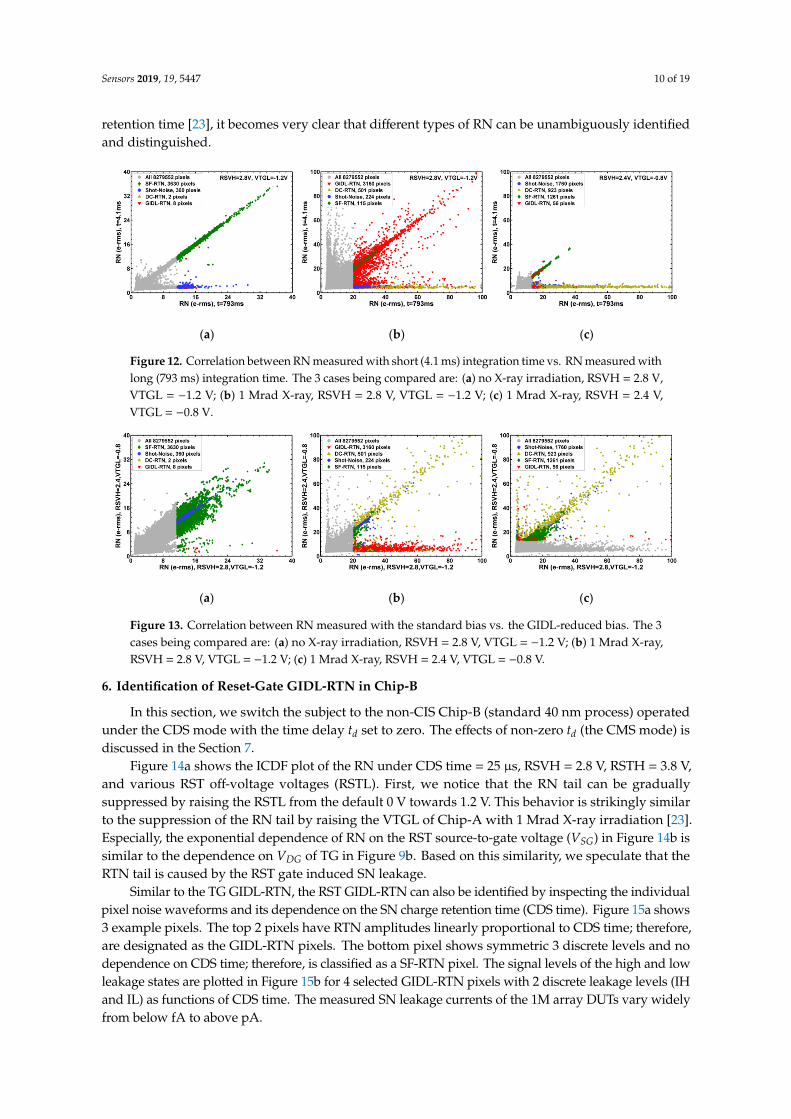
Figure 14a shows the ICDF plot of the RN under CDS time = 25 µs, RSVH = 2.8 V, RSTH = 3.8 V,and various RST off-voltage voltages (RSTL). First, we notice that the RN tail can be graduallysuppressed by raising the RSTL from the default 0 V towards 1.2 V. This behavior is strikingly similarto the suppression of the RN tail by raising the VTGL of Chip-A with 1 Mrad X-ray irradiation [23].Especially, the exponential dependence of RN on the RST source-to-gate voltage (VSG) in Figure 14b issimilar to the dependence on VDG of TG in Figure 9b. Based on this similarity, we speculate that theRTN tail is caused by the RST gate induced SN leakage.
Similar to the TG GIDL-RTN, the RST GIDL-RTN can also be identified by inspecting the individualpixel noise waveforms and its dependence on the SN charge retention time (CDS time). Figure 15a shows3 example pixels. The top 2 pixels have RTN amplitudes linearly proportional to CDS time; therefore,are designated as the GIDL-RTN pixels. The bottom pixel shows symmetric 3 discrete levels and nodependence on CDS time; therefore, is classified as a SF-RTN pixel. The signal levels of the high and lowleakage states are plotted in Figure 15b for 4 selected GIDL-RTN pixels with 2 discrete leakage levels (IHand IL) as functions of CDS time. The measured SN leakage currents of the 1M array DUTs vary widelyfrom below fA to above pA.
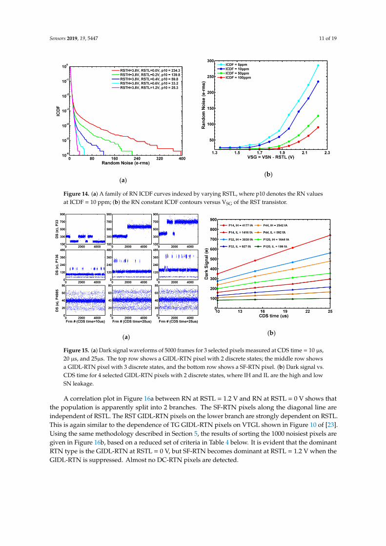
Sensors 2019, 19, 5447 11 of 19Sensors 2019, 19, x FOR PEER REVIEW 12 of 20
(a)
(b)
Figure 14. (a) A family of RN ICDF curves indexed by varying RSTL, where p10 denotes the RN
values at ICDF = 10 ppm; (b) the RN constant ICDF contours versus VSG of the RST transistor.
(a)
(b)
Figure 15. (a) Dark signal waveforms of 5000 frames for 3 selected pixels measured at CDS time = 10
s, 20 s, and 25s. The top row shows a GIDL-RTN pixel with 2 discrete states; the middle row shows
a GIDL-RTN pixel with 3 discrete states, and the bottom row shows a SF-RTN pixel. (b) Dark signal
vs. CDS time for 4 selected GIDL-RTN pixels with 2 discrete states, where IH and IL are the high and
low SN leakage.
Figure 14. (a) A family of RN ICDF curves indexed by varying RSTL, where p10 denotes the RN valuesat ICDF = 10 ppm; (b) the RN constant ICDF contours versus VSG of the RST transistor.
Sensors 2019, 19, x FOR PEER REVIEW 12 of 20
(a)
(b)
Figure 14. (a) A family of RN ICDF curves indexed by varying RSTL, where p10 denotes the RN
values at ICDF = 10 ppm; (b) the RN constant ICDF contours versus VSG of the RST transistor.
(a)
(b)
Figure 15. (a) Dark signal waveforms of 5000 frames for 3 selected pixels measured at CDS time = 10
s, 20 s, and 25s. The top row shows a GIDL-RTN pixel with 2 discrete states; the middle row shows
a GIDL-RTN pixel with 3 discrete states, and the bottom row shows a SF-RTN pixel. (b) Dark signal
vs. CDS time for 4 selected GIDL-RTN pixels with 2 discrete states, where IH and IL are the high and
low SN leakage.
Figure 15. (a) Dark signal waveforms of 5000 frames for 3 selected pixels measured at CDS time = 10 µs,20 µs, and 25µs. The top row shows a GIDL-RTN pixel with 2 discrete states; the middle row showsa GIDL-RTN pixel with 3 discrete states, and the bottom row shows a SF-RTN pixel. (b) Dark signal vs.CDS time for 4 selected GIDL-RTN pixels with 2 discrete states, where IH and IL are the high and lowSN leakage.
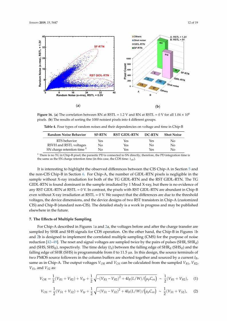
A correlation plot in Figure 16a between RN at RSTL = 1.2 V and RN at RSTL = 0 V shows thatthe population is apparently split into 2 branches. The SF-RTN pixels along the diagonal line areindependent of RSTL. The RST GIDL-RTN pixels on the lower branch are strongly dependent on RSTL.This is again similar to the dependence of TG GIDL-RTN pixels on VTGL shown in Figure 10 of [23].Using the same methodology described in Section 5, the results of sorting the 1000 noisiest pixels aregiven in Figure 16b, based on a reduced set of criteria in Table 4 below. It is evident that the dominantRTN type is the GIDL-RTN at RSTL = 0 V, but SF-RTN becomes dominant at RSTL = 1.2 V when theGIDL-RTN is suppressed. Almost no DC-RTN pixels are detected.
Sensors 2019, 19, 5447 12 of 19Sensors 2019, 19, x FOR PEER REVIEW 13 of 20
(a)
(b)
Figure 16. (a) The correlation between RN at RSTL = 1.2 V and RN at RSTL = 0 V for all 1.04106 pixels.
(b) The results of sorting the 1000 noisiest pixels into 4 different groups.
7. The Effects of Multiple Sampling
For Chip-A described in Figures 1a and 2a, the voltages before and after the charge transfer are
sampled by SHR and SHS signals for CDS operation. On the other hand, the Chip-B in Figures 1b
and 2b is designed to implement the correlated multiple sampling (CMS) for the purpose of noise
reduction [42–49]. The reset and signal voltages are sampled twice by the pairs of pulses (SHR, SHRd)
and (SHS, SHSd), respectively. The time delay (𝑡𝑑) between the falling edge of SHRd (SHSd) and the
falling edge of SHR (SHS) is programmable from 0 to 11.5 s. In this design, the source terminals of
two PMOS source followers in the column buffers are shorted together and sourced by a current 𝐼𝐵,
same as in Chip-A. The output voltages 𝑉𝑂𝑅 and 𝑉𝑂𝑆 can be calculated from the sampled 𝑉𝑅1, 𝑉𝑅2,
𝑉𝑆1, and 𝑉𝑆2 as:
𝑉𝑂𝑅 = 1
2(𝑉𝑅1 + 𝑉𝑅2) + 𝑉𝑡𝑝 + 1
2√−(𝑉𝑅1 − 𝑉𝑅2)2 + 4𝐼𝐵(𝐿 𝑊⁄ )/(𝜇𝑝𝐶𝑜𝑥) ~ 1
2(𝑉𝑅1 + 𝑉𝑅2), (1)
𝑉𝑂𝑆 = 1
2(𝑉𝑆1 + 𝑉𝑆2) + 𝑉𝑡𝑝 + 1
2√−(𝑉𝑆1 − 𝑉𝑆2)2 + 4𝐼𝐵(𝐿 𝑊⁄ )/(𝜇𝑝𝐶𝑜𝑥) ~ 1
2(𝑉𝑆1 + 𝑉𝑆2), (2)
where 𝜇𝑝 is the hole mobility, 𝐶𝑜𝑥 is the gate oxide capacitance, 𝑉𝑡𝑝 is the PMOS source follower
threshold voltage, and (L/W) is the length/width. Since 𝑉𝑅1 and 𝑉𝑅2 are sampled from the same
source, they are roughly equal. Under this approximation, 𝑉𝑂𝑅 (𝑉𝑂𝑆) can be simplified to the average
of 𝑉𝑅1 and 𝑉𝑅2 (𝑉𝑆1 and 𝑉𝑆2), respectively. The differential output 𝑉𝑂𝑅 − 𝑉𝑂𝑆 is digitized by the
ADC, similar to the CDS operation. The benefit of averaging two sampled voltages is that the
uncorrelated noises from the pixel SF, which is not cancelled by CDS, will be reduced by a factor of
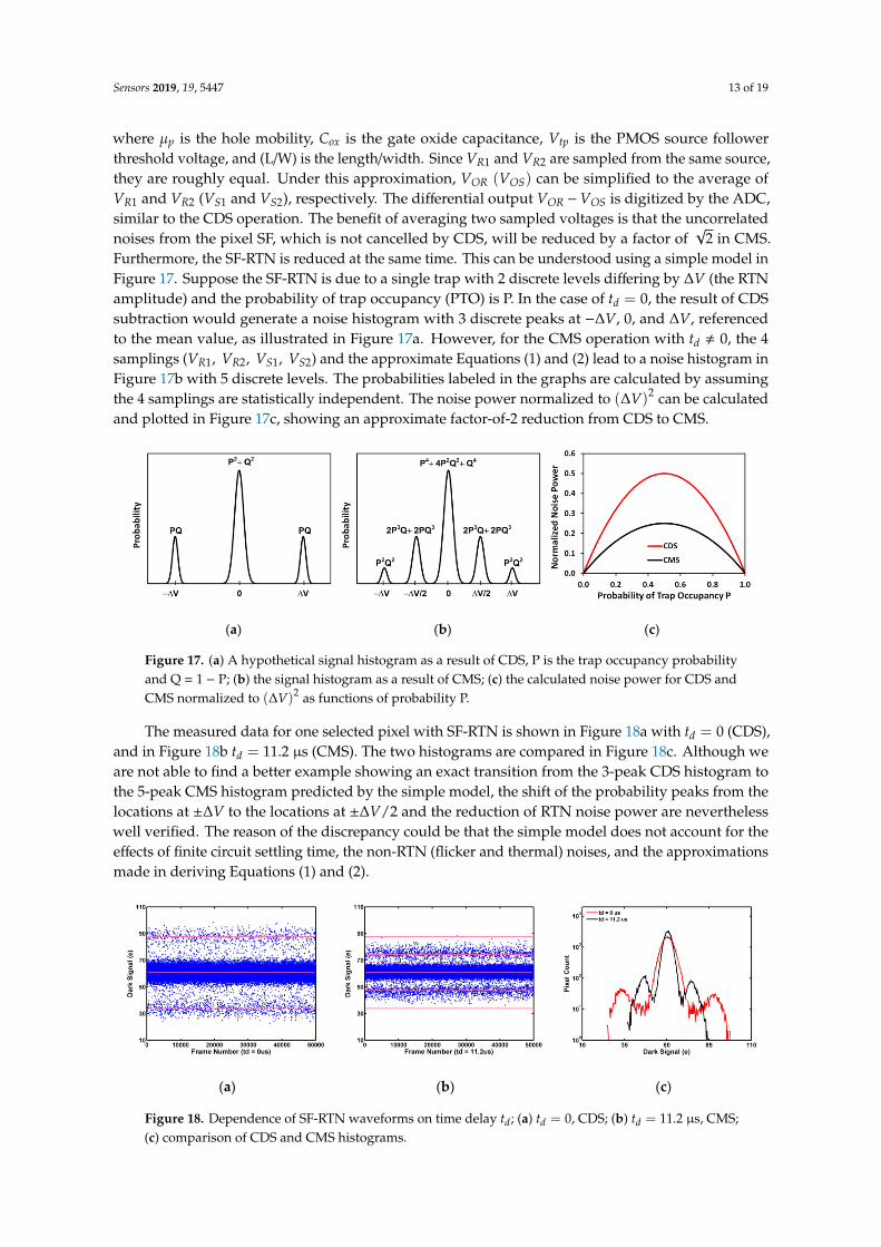
√2 in CMS. Furthermore, the SF-RTN is reduced at the same time. This can be understood using a
simple model in Figure 17. Suppose the SF-RTN is due to a single trap with 2 discrete levels differing
by ∆𝑉 (the RTN amplitude) and the probability of trap occupancy (PTO) is P. In the case of 𝑡𝑑 = 0,
the result of CDS subtraction would generate a noise histogram with 3 discrete peaks at −∆𝑉, 0, and
∆𝑉, referenced to the mean value, as illustrated in Figure 17a. However, for the CMS operation with
𝑡𝑑 ≠ 0, the 4 samplings (𝑉𝑅1, 𝑉𝑅2, 𝑉𝑆1, 𝑉𝑆2) and the approximate Equations (1) and (2) lead to a noise
histogram in Figure 17b with 5 discrete levels. The probabilities labeled in the graphs are calculated
by assuming the 4 samplings are statistically independent. The noise power normalized to (∆𝑉)2
can be calculated and plotted in Figure 17c, showing an approximate factor-of-2 reduction from CDS
to CMS.
Figure 16. (a) The correlation between RN at RSTL = 1.2 V and RN at RSTL = 0 V for all 1.04 × 10⁶
pixels. (b) The results of sorting the 1000 noisiest pixels into 4 different groups.
Table 4. Four types of random noises and their dependencies on voltage and time in Chip-B
Random Noise Behavior SF-RTN RST GIDL-RTN DC-RTN Shot Noise
RTS behavior Yes Yes Yes NoRSVH and RSTL voltages No Yes No NoSN charge retention time † No Yes Yes No
† There is no TG in Chip-B pixel; the parasitic PD is connected to SN directly; therefore, the PD integration time isthe same as the SN charge retention time (in this case, the CDS time: tcds).
It is interesting to highlight the observed differences between the CIS Chip-A in Section 5 andthe non-CIS Chip-B in Section 6. For Chip-A, the number of GIDL-RTN pixels is negligible in thesample without X-ray irradiation for both of the TG GIDL-RTN and the RST GIDL-RTN. The TGGIDL-RTN is found dominant in the sample irradiated by 1 Mrad X-ray, but there is no evidence ofany RST GIDL-RTN at RSTL = 0 V. In contrast, the pixels with RST GIDL-RTN are abundant in Chip-Beven without X-ray irradiation at RSTL = 0 V. We suspect that the differences are due to the thresholdvoltages, the device dimensions, and the device designs of two RST transistors in Chip-A (customizedCIS) and Chip-B (standard non-CIS). The detailed study is a work in progress and may be publishedelsewhere in the future.
7. The Effects of Multiple Sampling
For Chip-A described in Figures 1a and 2a, the voltages before and after the charge transfer aresampled by SHR and SHS signals for CDS operation. On the other hand, the Chip-B in Figures 1band 2b is designed to implement the correlated multiple sampling (CMS) for the purpose of noisereduction [42–49]. The reset and signal voltages are sampled twice by the pairs of pulses (SHR, SHRd)and (SHS, SHSd), respectively. The time delay (td) between the falling edge of SHRd (SHSd) and thefalling edge of SHR (SHS) is programmable from 0 to 11.5 µs. In this design, the source terminals oftwo PMOS source followers in the column buffers are shorted together and sourced by a current IB,same as in Chip-A. The output voltages VOR and VOS can be calculated from the sampled VR1, VR2,VS1, and VS2 as:
VOR =12(VR1 + VR2) + Vtp +
12
√−(VR1 −VR2)
2 + 4IB(L/W)/(µpCox
)∼
12(VR1 + VR2), (1)
VOS =12(VS1 + VS2) + Vtp +
12
√−(VS1 −VS2)
2 + 4IB(L/W)/(µpCox
)∼
12(VS1 + VS2), (2)
Sensors 2019, 19, 5447 13 of 19
where µp is the hole mobility, Cox is the gate oxide capacitance, Vtp is the PMOS source followerthreshold voltage, and (L/W) is the length/width. Since VR1 and VR2 are sampled from the same source,they are roughly equal. Under this approximation, VOR (VOS) can be simplified to the average ofVR1 and VR2 (VS1 and VS2), respectively. The differential output VOR −VOS is digitized by the ADC,similar to the CDS operation. The benefit of averaging two sampled voltages is that the uncorrelatednoises from the pixel SF, which is not cancelled by CDS, will be reduced by a factor of
√2 in CMS.
Furthermore, the SF-RTN is reduced at the same time. This can be understood using a simple model inFigure 17. Suppose the SF-RTN is due to a single trap with 2 discrete levels differing by ∆V (the RTNamplitude) and the probability of trap occupancy (PTO) is P. In the case of td = 0, the result of CDSsubtraction would generate a noise histogram with 3 discrete peaks at −∆V, 0, and ∆V, referencedto the mean value, as illustrated in Figure 17a. However, for the CMS operation with td , 0, the 4samplings (VR1, VR2, VS1, VS2) and the approximate Equations (1) and (2) lead to a noise histogram inFigure 17b with 5 discrete levels. The probabilities labeled in the graphs are calculated by assumingthe 4 samplings are statistically independent. The noise power normalized to (∆V)2 can be calculatedand plotted in Figure 17c, showing an approximate factor-of-2 reduction from CDS to CMS.
Sensors 2019, 19, x FOR PEER REVIEW 14 of 20
(a)
(b)
(c)
Figure 17. (a) A hypothetical signal histogram as a result of CDS, P is the trap occupancy probability
and Q = 1 – P; (b) the signal histogram as a result of CMS; (c) the calculated noise power for CDS and
CMS normalized to (∆𝑉)2 as functions of probability P.
The measured data for one selected pixel with SF-RTN is shown in Figure 18a with 𝑡𝑑 = 0
(CDS), and in Figure 18b 𝑡𝑑 = 11.2 s (CMS). The two histograms are compared in Figure 18c.
Although we are not able to find a better example showing an exact transition from the 3-peak CDS
histogram to the 5-peak CMS histogram predicted by the simple model, the shift of the probability
peaks from the locations at ±∆𝑉 to the locations at ± ∆𝑉 2⁄ and the reduction of RTN noise power
are nevertheless well verified. The reason of the discrepancy could be that the simple model does not
account for the effects of finite circuit settling time, the non-RTN (flicker and thermal) noises, and the
approximations made in deriving Equations (1) and (2).
(a)
(b)
(c)
Figure 18. Dependence of SF-RTN waveforms on time delay 𝑡𝑑; (a) 𝑡𝑑 = 0, CDS; (b) 𝑡𝑑 = 11.2 s,
CMS; (c) comparison of CDS and CMS histograms.
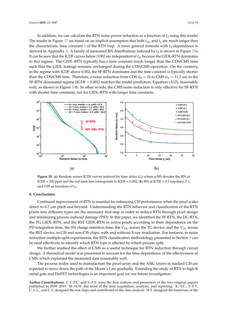
In addition, we can calculate the RTN noise power reduction as a function of 𝑡𝑑 using this
model. The results in Figure 17 are based on an implicit assumption that both 𝑡𝑐𝑑𝑠 and 𝑡𝑑 are much
longer than the characteristic time constant 𝜏 of the RTN trap. A more general formula with 𝑡𝑑-
dependence is derived in Appendix A. A family of measured RN distributions indexed by 𝑡𝑑 is
shown in Figure 19a. It can be seen that the ICDF curves below 0.002 are independent of 𝑡𝑑, because
the GIDL-RTN dominates in this regime. The GIDL-RTN typically has a time constant much longer
than the CDS/CMS time such that the GIDL leakage remains unchanged during the CDS/CMS
operation. On the contrary, in the regime with ICDF above 0.002, the SF-RTN dominates and the time
constant is typically shorter than the CDS/CMS time. Therefore, a noise reduction from CDS (𝑡𝑑 = 0)
to CMS (𝑡𝑑 = 11.2 s) in the SF-RTN dominated regime (ICDF > 0.002) matches the model prediction,
Equation (A12), reasonably well, as shown in Figure 19b. In other words, the CMS noise reduction is
only effective for SF-RTN with shorter time constants, not for GIDL-RTN with longer time constants.
Figure 17. (a) A hypothetical signal histogram as a result of CDS, P is the trap occupancy probabilityand Q = 1 − P; (b) the signal histogram as a result of CMS; (c) the calculated noise power for CDS andCMS normalized to (∆V)2 as functions of probability P.
The measured data for one selected pixel with SF-RTN is shown in Figure 18a with td = 0 (CDS),and in Figure 18b td = 11.2 µs (CMS). The two histograms are compared in Figure 18c. Although weare not able to find a better example showing an exact transition from the 3-peak CDS histogram tothe 5-peak CMS histogram predicted by the simple model, the shift of the probability peaks from thelocations at ±∆V to the locations at ±∆V/2 and the reduction of RTN noise power are neverthelesswell verified. The reason of the discrepancy could be that the simple model does not account for theeffects of finite circuit settling time, the non-RTN (flicker and thermal) noises, and the approximationsmade in deriving Equations (1) and (2).
Sensors 2019, 19, x FOR PEER REVIEW 14 of 20
(a)
(b)
(c)
Figure 17. (a) A hypothetical signal histogram as a result of CDS, P is the trap occupancy probability
and Q = 1 – P; (b) the signal histogram as a result of CMS; (c) the calculated noise power for CDS and
CMS normalized to (∆𝑉)2 as functions of probability P.
The measured data for one selected pixel with SF-RTN is shown in Figure 18a with 𝑡𝑑 = 0
(CDS), and in Figure 18b 𝑡𝑑 = 11.2 s (CMS). The two histograms are compared in Figure 18c.
Although we are not able to find a better example showing an exact transition from the 3-peak CDS
histogram to the 5-peak CMS histogram predicted by the simple model, the shift of the probability
peaks from the locations at ±∆𝑉 to the locations at ± ∆𝑉 2⁄ and the reduction of RTN noise power
are nevertheless well verified. The reason of the discrepancy could be that the simple model does not
account for the effects of finite circuit settling time, the non-RTN (flicker and thermal) noises, and the
approximations made in deriving Equations (1) and (2).
(a)
(b)
(c)
Figure 18. Dependence of SF-RTN waveforms on time delay 𝑡𝑑; (a) 𝑡𝑑 = 0, CDS; (b) 𝑡𝑑 = 11.2 s,
CMS; (c) comparison of CDS and CMS histograms.
In addition, we can calculate the RTN noise power reduction as a function of 𝑡𝑑 using this
model. The results in Figure 17 are based on an implicit assumption that both 𝑡𝑐𝑑𝑠 and 𝑡𝑑 are much
longer than the characteristic time constant 𝜏 of the RTN trap. A more general formula with 𝑡𝑑-
dependence is derived in Appendix A. A family of measured RN distributions indexed by 𝑡𝑑 is
shown in Figure 19a. It can be seen that the ICDF curves below 0.002 are independent of 𝑡𝑑, because
the GIDL-RTN dominates in this regime. The GIDL-RTN typically has a time constant much longer
than the CDS/CMS time such that the GIDL leakage remains unchanged during the CDS/CMS
operation. On the contrary, in the regime with ICDF above 0.002, the SF-RTN dominates and the time
constant is typically shorter than the CDS/CMS time. Therefore, a noise reduction from CDS (𝑡𝑑 = 0)
to CMS (𝑡𝑑 = 11.2 s) in the SF-RTN dominated regime (ICDF > 0.002) matches the model prediction,
Equation (A12), reasonably well, as shown in Figure 19b. In other words, the CMS noise reduction is
only effective for SF-RTN with shorter time constants, not for GIDL-RTN with longer time constants.
Figure 18. Dependence of SF-RTN waveforms on time delay td; (a) td = 0, CDS; (b) td = 11.2 µs, CMS;(c) comparison of CDS and CMS histograms.
Sensors 2019, 19, 5447 14 of 19
In addition, we can calculate the RTN noise power reduction as a function of td using this model.The results in Figure 17 are based on an implicit assumption that both tcds and td are much longer thanthe characteristic time constant τ of the RTN trap. A more general formula with td-dependence isderived in Appendix A. A family of measured RN distributions indexed by td is shown in Figure 19a.It can be seen that the ICDF curves below 0.002 are independent of td, because the GIDL-RTN dominatesin this regime. The GIDL-RTN typically has a time constant much longer than the CDS/CMS timesuch that the GIDL leakage remains unchanged during the CDS/CMS operation. On the contrary,in the regime with ICDF above 0.002, the SF-RTN dominates and the time constant is typically shorterthan the CDS/CMS time. Therefore, a noise reduction from CDS (td = 0) to CMS (td = 11.2 µs) in theSF-RTN dominated regime (ICDF > 0.002) matches the model prediction, Equation (A12), reasonablywell, as shown in Figure 19b. In other words, the CMS noise reduction is only effective for SF-RTNwith shorter time constants, not for GIDL-RTN with longer time constants.
Sensors 2019, 19, x FOR PEER REVIEW 15 of 20
(a)
(b)
Figure 19. (a) Random noises ICDF curves indexed by time delay (𝑡𝑑) where p300 denotes the RN
at ICDF = 300 ppm and the red dash line corresponds to ICDF = 0.002; (b) RN at ICDF = 0.5
(median), 0.1, and 0.05 as functions of 𝑡𝑑.
8. Conclusions
Continued improvement of RTN is essential for enhancing CIS performance when the pixel
scales down to 0.7 m pitch and beyond. Understanding the RTN behavior and classification of the
RTN pixels into different types are the necessary first step in order to reduce RTN through pixel
design and minimizing process-induced damage (PID). In this paper, we identified the SF-RTN, the
DC-RTN, the TG GIDL-RTN, and the RST GIDL-RTN in active pixels according to their dependence
on the PD integration time, the SN charge retention time, the 𝑉𝐷𝐺 across the TG device, and the 𝑉𝑆𝐺
across the RST device, in CIS and non-CIS chips, with and without X-ray irradiation. For instance, in
noise reduction multiple-split experiments, the RTN classification methodology presented in Section
5 can be used effectively to identify which RTN type is affected by which process split.
We further studied the effect of CMS as a useful technique for RTN reduction through circuit
design. A theoretical model was presented to account for the time-dependence of the effectiveness of
CMS, which explained the measured data reasonably well.
The process nodes used to manufacture the pixel-array and the ASIC layers in stacked CIS are
expected to move down the path of the Moore’s Law gradually. Extending the study of RTN to high-
K metal gate and FinFET technologies is an important goal for our future investigation.
Author Contributions: C. Y.-P. Chao and S.-F. Yeh were the first authors and presenters of the two original
papers published in IISW 2019. M. H. Wu did most of the data acquisition, analysis, and reporting. K.-Y. Chou,
S.-F. Yeh, C.-L. Lee, and C. Yin designed the test chips and contributed to the data analysis. H.-Y. Tu designed
the hardware of the characterization system. P. Paillet performed the X-ray irradiation experiments in CEA
laboratories. V. Goiffon proposed the study of X-ray on RTN and facilitated the collaboration among CEA, ISAE,
and TSMC.
Author Contributions: Investigation, S-F.Y., M.-H.W., K.-Y.C., H.T., C.-L.L. and C.Y.; Resources, P.P. and V.G.;
Writing—original draft, C.Y.-P.C.
Funding: This research received no external funding.
Acknowledgments: The support by TSMC CIS process development team is greatly appreciated.
Conflicts of Interest: The authors declare no conflict of interest.
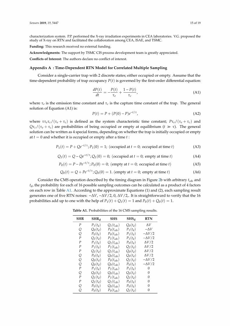
Appendix A: Time-Dependent RTN Model for Correlated Multiple Sampling
Figure 19. (a) Random noises ICDF curves indexed by time delay (td) where p300 denotes the RN atICDF = 300 ppm and the red dash line corresponds to ICDF = 0.002; (b) RN at ICDF = 0.5 (median), 0.1,and 0.05 as functions of td.
8. Conclusions
Continued improvement of RTN is essential for enhancing CIS performance when the pixel scalesdown to 0.7 µm pitch and beyond. Understanding the RTN behavior and classification of the RTNpixels into different types are the necessary first step in order to reduce RTN through pixel designand minimizing process-induced damage (PID). In this paper, we identified the SF-RTN, the DC-RTN,the TG GIDL-RTN, and the RST GIDL-RTN in active pixels according to their dependence on thePD integration time, the SN charge retention time, the VDG across the TG device, and the VSG acrossthe RST device, in CIS and non-CIS chips, with and without X-ray irradiation. For instance, in noisereduction multiple-split experiments, the RTN classification methodology presented in Section 5 canbe used effectively to identify which RTN type is affected by which process split.
We further studied the effect of CMS as a useful technique for RTN reduction through circuitdesign. A theoretical model was presented to account for the time-dependence of the effectiveness ofCMS, which explained the measured data reasonably well.
The process nodes used to manufacture the pixel-array and the ASIC layers in stacked CIS areexpected to move down the path of the Moore’s Law gradually. Extending the study of RTN to high-Kmetal gate and FinFET technologies is an important goal for our future investigation.
Author Contributions: C.Y.-P.C. and S.-F.Y. were the first authors and presenters of the two original paperspublished in IISW 2019. M.-H.W. did most of the data acquisition, analysis, and reporting. K.-Y.C., S.-F.Y.,C.-L.L., and C.Y. designed the test chips and contributed to the data analysis. H.T. designed the hardware of the
Sensors 2019, 19, 5447 15 of 19
characterization system. P.P. performed the X-ray irradiation experiments in CEA laboratories. V.G. proposed thestudy of X-ray on RTN and facilitated the collaboration among CEA, ISAE, and TSMC.
Funding: This research received no external funding.
Acknowledgments: The support by TSMC CIS process development team is greatly appreciated.
Conflicts of Interest: The authors declare no conflict of interest.
Appendix A : Time-Dependent RTN Model for Correlated Multiple Sampling
Consider a single-carrier trap with 2 discrete states; either occupied or empty. Assume that thetime-dependent probability of trap occupancy P(t) is governed by the first-order differential equation:
dP(t)dt
= −P(t)τe
+1− P(t)τc
, (A1)
where τe is the emission time constant and τc is the capture time constant of the trap. The generalsolution of Equation (A1) is:
P(t) = P + (P(0) − P)e−t/τ, (A2)
where ττeτc/(τe + τc) is defined as the system characteristic time constant; Pτe/(τe + τc) andQτc/(τe + τc) are probabilities of being occupied or empty at equilibrium (t � τ). The generalsolution can be written as 4 special forms, depending on whether the trap is initially occupied or emptyat t = 0 and whether it is occupied or empty after a time t :
P1(t) = P + Qe−t/τ; P1(0) = 1; (occupied at t = 0; occupied at time t) (A3)
Q1(t) = Q−Qe−t/τ; Q1(0) = 0; (occupied at t = 0; empty at time t) (A4)
P0(t) = P− Pe−t/τ; P0(0) = 0; (empty at t = 0; occupied at time t) (A5)
Q0(t) = Q + Pe−t/τ; Q0(0) = 1. (empty at t = 0; empty at time t) (A6)
Consider the CMS operation described by the timing diagram in Figure 2b with arbitrary tcds andtd, the probability for each of 16 possible sampling outcomes can be calculated as a product of 4 factorson each row in Table A1. According to the approximate Equations (1) and (2), each sampling resultgenerates one of five RTN noises: −∆V, −∆V/2, 0, ∆V/2,. It is straightforward to verify that the 16probabilities add up to one with the help of P1(t) + Q1(t) = 1 and P0(t) + Q0(t) = 1.
Table A1. Probabilities of the 16 CMS sampling results.
SHR SHRd SHS SHSd RTN
P P1(td) Q1(tcds) Q0(td) ∆VQ Q0(td) P0(tcds) P1(td) −∆VQ P0(td) P0(tcds) P1(td) −∆V/2P Q1(td) P1(tcds) P1(td) −∆V/2P P1(td) Q1(tcds) P0(td) ∆V/2P P1(td) P1(tcds) Q1(td) ∆V/2P Q1(td) Q1(tcds) Q0(td) ∆V/2Q P0(td) Q0(tcds) Q0(td) ∆V/2Q Q0(td) P0(tcds) Q1(td) −∆V/2Q Q0(td) Q0(tcds) P0(td) −∆V/2P P1(td) P1(tcds) P1(td) 0Q Q0(td) Q0(tcds) Q0(td) 0P Q1(td) P1(tcds) Q1(td) 0P Q1(td) Q1(tcds) P0(td) 0Q P0(td) Q0(tcds) P0(td) 0Q P0(td) P0(tcds) Q1(td) 0
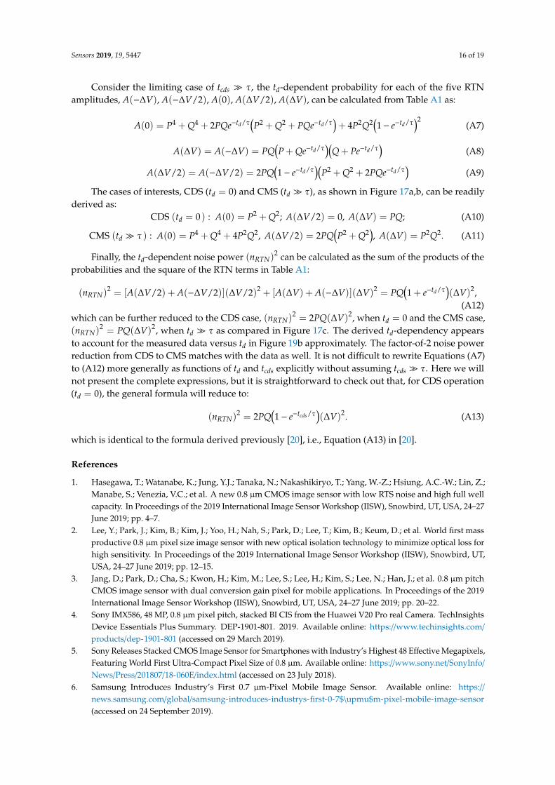
Sensors 2019, 19, 5447 16 of 19
Consider the limiting case of tcds � τ, the td-dependent probability for each of the five RTNamplitudes, A(−∆V), A(−∆V/2), A(0), A(∆V/2), A(∆V), can be calculated from Table A1 as:
A(0) = P4 + Q4 + 2PQe−td/τ(P2 + Q2 + PQe−td/τ
)+ 4P2Q2
(1− e−td/τ
)2(A7)
A(∆V) = A(−∆V) = PQ(P + Qe−td/τ
)(Q + Pe−td/τ
)(A8)
A(∆V/2) = A(−∆V/2) = 2PQ(1− e−td/τ
)(P2 + Q2 + 2PQe−td/τ
)(A9)
The cases of interests, CDS (td = 0) and CMS (td � τ), as shown in Figure 17a,b, can be readilyderived as:
CDS (td = 0 ) : A(0) = P2 + Q2; A(∆V/2) = 0, A(∆V) = PQ; (A10)
CMS (td � τ ) : A(0) = P4 + Q4 + 4P2Q2, A(∆V/2) = 2PQ(P2 + Q2
), A(∆V) = P2Q2. (A11)
Finally, the td-dependent noise power (nRTN)2 can be calculated as the sum of the products of the
probabilities and the square of the RTN terms in Table A1:
(nRTN)2 = [A(∆V/2) + A(−∆V/2)](∆V/2)2 + [A(∆V) + A(−∆V)](∆V)2 = PQ
(1 + e−td/τ
)(∆V)2,
(A12)which can be further reduced to the CDS case, (nRTN)
2 = 2PQ(∆V)2, when td = 0 and the CMS case,(nRTN)
2 = PQ(∆V)2, when td � τ as compared in Figure 17c. The derived td-dependency appearsto account for the measured data versus td in Figure 19b approximately. The factor-of-2 noise powerreduction from CDS to CMS matches with the data as well. It is not difficult to rewrite Equations (A7)to (A12) more generally as functions of td and tcds explicitly without assuming tcds � τ. Here we willnot present the complete expressions, but it is straightforward to check out that, for CDS operation(td = 0), the general formula will reduce to:
(nRTN)2 = 2PQ
(1− e−tcds/τ
)(∆V)2. (A13)
which is identical to the formula derived previously [20], i.e., Equation (A13) in [20].
References
1. Hasegawa, T.; Watanabe, K.; Jung, Y.J.; Tanaka, N.; Nakashikiryo, T.; Yang, W.-Z.; Hsiung, A.C.-W.; Lin, Z.;Manabe, S.; Venezia, V.C.; et al. A new 0.8 µm CMOS image sensor with low RTS noise and high full wellcapacity. In Proceedings of the 2019 International Image Sensor Workshop (IISW), Snowbird, UT, USA, 24–27June 2019; pp. 4–7.
2. Lee, Y.; Park, J.; Kim, B.; Kim, J.; Yoo, H.; Nah, S.; Park, D.; Lee, T.; Kim, B.; Keum, D.; et al. World first massproductive 0.8 µm pixel size image sensor with new optical isolation technology to minimize optical loss forhigh sensitivity. In Proceedings of the 2019 International Image Sensor Workshop (IISW), Snowbird, UT,USA, 24–27 June 2019; pp. 12–15.
3. Jang, D.; Park, D.; Cha, S.; Kwon, H.; Kim, M.; Lee, S.; Lee, H.; Kim, S.; Lee, N.; Han, J.; et al. 0.8 µm pitchCMOS image sensor with dual conversion gain pixel for mobile applications. In Proceedings of the 2019International Image Sensor Workshop (IISW), Snowbird, UT, USA, 24–27 June 2019; pp. 20–22.
4. Sony IMX586, 48 MP, 0.8 µm pixel pitch, stacked BI CIS from the Huawei V20 Pro real Camera. TechInsightsDevice Essentials Plus Summary. DEP-1901-801. 2019. Available online: https://www.techinsights.com/
products/dep-1901-801 (accessed on 29 March 2019).5. Sony Releases Stacked CMOS Image Sensor for Smartphones with Industry’s Highest 48 Effective Megapixels,
Featuring World First Ultra-Compact Pixel Size of 0.8 µm. Available online: https://www.sony.net/SonyInfo/
News/Press/201807/18-060E/index.html (accessed on 23 July 2018).6. Samsung Introduces Industry’s First 0.7 µm-Pixel Mobile Image Sensor. Available online: https://
news.samsung.com/global/samsung-introduces-industrys-first-0-7$\upmu$m-pixel-mobile-image-sensor(accessed on 24 September 2019).
Sensors 2019, 19, 5447 17 of 19
7. Ackerson, K.; Musante, C.; Gambino, J.; Ellis-Monaghan, J.; Maynard, D.; Rassel, R.J.; Ogg, K.; Jaffe, M.Characterization of “blinking pixels” in CMOS image sensors. In Proceedings of the 2008 IEEE AdvancedSemiconductor Manufacturing Conference (ASMC), Cambridge, MA, USA, 5–7 May 2008.
8. Pain, B.; Cunningham, T.J.; Hancock, B.; Sun, C.; Wrigley, C. Twinkling pixels: random telegraph signals atreset gate edge. In Proceedings of the 2007 International Image Sensor Workshop (IISW), Ogunquit, ME,USA, 6–10 June 2007.
9. Peters, I.; Bogaart, E.; Manoury, E.-J.; Mierop, A.; Bosiers, J. Analysis of blinking pixels in CCD imagerswith and without surface pinning. In Proceedings of the 2011 International Image Sensor Workshop (IISW),Hokkaido, Japan, 8–11 June 2011; pp. 216–219.
10. Wang, X.; Rao, P.R.; Mierop, A.; Theuwissen, A.J.P. Random telegraph signal in CIS pixels. In Proceedings ofthe 2006 IEEE International Electron Devices Meeting (IEDM), San Francisco, CA, USA, 11–13 December2006; pp. 115–118.
11. Wang, X.; Snoeij, M.F.; Rao, P.R.; Mierop, A.; Theuwissen, A.J.P. A CMOS image sensor with a buried-channelsource follower. In Proceedings of the 2008 IEEE International Solid-State Circuits Conference (ISSCC),San Francisco, CA, USA, 3–7 February 2008; pp. 62–63.
12. Chen, Y.; Wang, X.; Mierop, A.; Theuwissen, A.J.P. A CMOS image sensor with in-pixel buried-channelsource follower and optimized row selector. IEEE Trans. Electron Devices 2009, 56, 2390–2397. [CrossRef]
13. Janesick, J.; Andrews, J.T.; Elliott, T. Fundamental performance differences between CMOS and CCD imagers;Part I. Proc. SPIE 2006, 6276, 743907.
14. Janesick, J.; Pinter, J.; Potter, R.; Elliott, T.; Andrews, J.; Tower, J.; Grygon, M.; Keller, D. Fundamentalperformance differences between CMOS and CCD imagers; Part IV. Proc. SPIE 2010, 7742, 77420B.
15. Abe, K.; Sugawa, S.; Kuroda, R.; Watabe, S.; Miyamoto, N.; Teramoto, A.; Ohmi, T.; Kamata, T.; Shibusawa, K.Analysis of source follower random telegraph signal using nMOS and pMOS array TEG. In Proceedings ofthe 2007 International Image Sensor Workshop (IISW), Ogunquit, ME, USA, 6–10 June 2007; pp. 62–65.
16. Fujisawa, T.; Abe, K.; Watabe, S.; Miyamoto, N.; Teramoto, A.; Sugawa, S.; Ohmi, T. Analysis of hundredsof time constant ratios and amplitudes of random telegraph signal with very large scale array test pattern.Jpn. J. Appl. Phys. 2010, 49, 04DC06. [CrossRef]
17. Kuroda, R.; Yonezawa, A.; Teramoto, A.; Li, T.L.; Tochigi, Y.; Sugawa, S. A statistical evaluation of randomtelegraph noise of in-pixel source follower equivalent surface and buried channel transistors. IEEE Trans.Electron Devices 2013, 60, 3555–3561. [CrossRef]
18. Obara, T.; Yonezawa, A.; Teramoto, A.; Kuroda, R.; Sugawa, S.; Ohmi, T. Extraction of time constants ratioover nine orders of magnitude for understanding random telegraph noise in MOSFETs. Jpn. J. Appl. Phys.2014, 53, 04ECI9. [CrossRef]
19. Kuroda, R.; Teramoto, A.; Sugawa, S. Impact of random telegraph noise with various time constants andnumber of states in CMOS image sensors. In Proceedings of the 2017 International Image Sensor Workshop(IISW), Hiroshima, Japan, 30 May–2 June 2017; pp. 35–38.
20. Chao, C.Y.-P.; Tu, H.; Wu, T.M.-H.; Chou, K.-Y.; Yeh, S.-F.; Hsueh, F.-L. CMOS image sensor random telegraphnoise time constant extraction from correlated to uncorrelated double sampling. IEEE J. Electron Devices Soc.2017, 5, 79–89. [CrossRef]
21. Chao, C.Y.-P.; Tu, H.; Wu, T.M.-H.; Chou, K.-Y.; Yeh, S.-F.; Hsueh, F.-L. Random telegraph noise pixelclassification and time constant extraction for a 1.1 µm pitch 8.3 MP CMOS image sensor. In Proceedings ofthe 2017 International Image Sensor Workshop (IISW), Hiroshima, Japan, 30 May–2 Jun 2017; pp. 35–38.
22. Chao, C.Y.-P.; Tu, H.; Wu, T.M.-H.; Chou, K.-Y.; Yeh, S.-F.; Yin, C.; Lee, C.-L. Statistical analysis of the randomtelegraph noise in a 1.1 µm pixel, 8.3 MP CMOS image sensor using on-chip time constant extraction method.Sensors 2017, 17, 2704. [CrossRef]
23. Chao, C.Y.; Wu, T.M.; Yeh, S.F.; Chou, K.Y.; Tu, H.; Lee, C.L.; Yin, C.; Paillet, P.; Goiffon, V. Random telegraphnoises in CMOS image sensors caused by variable gate-induced sense node leakage due to X-Ray irradiation.IEEE J. Electron Devices Soc. 2019, 7, 227–238. [CrossRef]
24. Simoen, E.; Claeys, C.L. Random Telegraph Signals in Semiconductor Devices; IOP Publishing Ltd.: Bristol, UK,2016.
25. Goiffon, V.; Virmontois, C.; Magnan, P. Investigation of dark current random telegraph signal in pinnedphotodiode CMOS image sensors. In Proceedings of the 2011 IEEE International Electron Devices Meeting(IEDM), Washington, DC, USA, 5–7 December 2011; pp. 1–4.
Sensors 2019, 19, 5447 18 of 19
26. Goiffon, V.; Magnan, P.; Martin-Gonthier, P.; Virmontois, C.; Gaillardin, M. New source of random telegraphsignal in CMOS image sensors. In Proceedings of the IEEE International Image Sensor Workshop (IISW),Hokkaido, Japan, 8–11 June 2011; pp. 212–215.
27. Martin-Gonthier, P.; Goiffon, V.; Magnan, P. In-pixel source follower transistor RTS noise behavior underionizing radiation in CMOS image sensors. IEEE Trans. Electron Devices 2012, 59, 1686–1692. [CrossRef]
28. Virmontois, C.; Goiffon, V.; Robbins, M.S.; Tauziède, L.; Geoffray, H.; Raine, M.; Girard, S.; Gilard, O.;Magnan, P.; Bardoux, A. Dark current random telegraph signals in solid-state image sensors. IEEE Trans.Nucl. Sci. 2013, 60, 4323–4331. [CrossRef]
29. Durnez, C.; Goiffon, V.; Virmontois, C.; Belloir, J.-M.; Magnan, P.; Rubaldo, L. In-depth analysis on radiationinduced multi-level dark current random telegraph signal in silicon solid state image sensors. IEEE Trans.Nucl. Sci. 2017, 64, 19–26. [CrossRef]
30. Durnez, C.; Goiffon, V.; Virmontois, C.; Rizzolo, S.; Le Roch, A.; Magnan, P.; Paillet, P.; Marcandella, C.;Rubaldo, L. Total ionizing dose radiation-induced dark current random telegraph signal in pinned photodiodeCMOS image sensors. IEEE Trans. Nucl. Sci. 2018, 65, 92–100. [CrossRef]
31. Le Roch, A.; Goiffon, V.; Paillet, P.; Belloir, J.A.; Magnan, P.; Virmontois, C. Leakage current non-uniformityand random telegraph signal in CMOS image sensor floating diffusions used for in-pixel charge storage. InProceedings of the 2019 International Image Sensor Workshop (IISW), Snowbird, UT, USA, 24–27 June 2019;pp. 142–145.
32. Le Roch, A.; Virmontois, C.; Paillet, P.; Belloir, J.-M.; Rizzolo, S.; Pace, F.; Durnez, C.; Magnan, P.; Goiffon, V.Radiation-induced leakage current and electric field enhancement in CMOS image sensor sense node floatingdiffusions. IEEE Trans. Nucl. Sci. 2019, 48, 616–624. [CrossRef]
33. Chao, C.Y.-P.; Wu, M.-H.; Yeh, S.-F.; Chou, K.-Y.; Tu, H.; Lee, C.-H.; Yin, C.; Paillet, P.; Goiffon, V. Identifyingthe sources of random telegraph noises in pixels of CMOS image sensor. In Proceedings of the 2019International Image Sensor Workshop (IISW), Snowbird, UT, USA, 24–27 June 2019; pp. 36–39.
34. Yeh, S.-F.; Wu, M.-H.; Lee, C.-L.; Yin, C.; Chou, K.-Y.; Chao, C.Y.-P. Random telegraph noise caused byMOSFET channel traps and variable gate induced leakage with multiple-sampling readout. In Proceedingsof the 2019 International Image Sensor Workshop (IISW), Snowbird, UT, USA, 24–27 June 2019; pp. 44–47.
35. Mori, Y.; Ohyu, K.; Okonogi, K.; Yamada, R. The origin of variable retention time in DRAM. In Proceedingsof the 2005 IEEE International Electron Devices Meeting (IEDM), Baltimore, MD, USA, 7–9 December 2005.
36. Ohyu, K.; Umeda, T.; Okonogi, K.; Tsukada, S.; Hidaka, M.; Fujieda, S.; Mochizuki, Y. Quantitativeidentification for the physical origin of variable retention time: A vacancy-oxygen complex defect model.In Proceedings of the 2006 IEEE International Electron Devices Meeting (IEDM), San Francisco, CA, USA,11–13 December 2006.
37. Lee, J.-W.; Lee, B.H.; Shin, H.; Lee, J.-H. Investigation of random telegraph noise in gate-induced drainleakage and gate edge direct tunneling currents of high-k MOSFETs. IEEE Trans. Electron Devices 2010, 57,913–918. [CrossRef]
38. Mori, Y.; Takeda, K.; Yamada, R.-I. Random telegraph noise of junction leakage current in submicron devices.J. Appl. Phys. 2010, 107, 1–10. [CrossRef]
39. Shimizu, S.; Aikawa, H.; Okamoto, S.; Kakehi, K.; Ohsawa, K.; Yoshimura, H.; Asami, T.; Ishimaru, K.Comprehensive Study of Systematic and Random Variation in Gate-Induced Drain Leakage for LSTPApplications. In Proceedings of the 2011 IEEE Symposium on VLSI Technology (VLSI-T), Honolulu, HI,USA, 14–16 June 2011; pp. 196–197.
40. Mori, Y.; Yoshimoto, H.; Takeda, K.; Yamada, R. Mechanism of RTN in junction leakage current of MOSFET.Jpn. J. Appl. Phys. 2012, 111, 104513. [CrossRef]
41. Yoo, S.-W.; Son, Y.; Shin, H. Capture cross section of traps causing random telegraph noise in gate-induceddrain leakage current. IEEE Trans. Electron Devices 2013, 60, 1268–1271. [CrossRef]
42. Kawahito, S.; Suh, S.; Shirei, T.; Itoh, S.; Aoyama, S. Noise reduction effects of column-parallel correlatedmultiple sampling and source-follower driving current switching for CMOS image sensors. In Proceedingsof the 2009 International Image Sensor Workshop (IISW), Bergen, Norway, 25–28 June 2009.
43. Suh, S.; Itoh, S.; Aoyama, S.; Kawahito, S. Column-parallel correlated multiple sampling circuits for CMOSimage sensors and their noise reduction effects. Sensors 2010, 10, 9139–9154. [CrossRef]
Sensors 2019, 19, 5447 19 of 19
44. Chen, Y.; Xu, Y.; Chae, Y.; Mierop, A.; Wang, X.; Theuwissen, A.J.P. A 0.7e−rms temporal-readout-noiseCMOS image sensor for low-light-level imaging. In Proceedings of the 2012 IEEE International Solid-StateCircuits Conference (ISSCC), San Francisco, CA, USA, 19–23 February 2012; pp. 384–385.
45. Yeh, S.-F.; Chou, K.-Y.; Tu, H.; Chao, C.Y.-P.; Hsueh, F.-L. A 0.66e−rms temporal-readout-noise 3D-stackedCMOS image sensor with conditional correlated multiple sampling (CCMS) technique. In Proceedings of the2015 IEEE Symposium on VLSI Circuits (VLSI-C), Kyoto, Japan, 17–19 June 2015; pp. 84–85.
46. Kawahito, S.; Seo, M.-W. Noise reduction effect of multiple-sampling-based signal-readout circuits forultra-low noise CMOS image sensors. Sensors 2016, 16, 1867. [CrossRef]
47. Shiraishi, K.; Shinozuka, Y.; Yamashita, T.; Sugiura, K.; Watanabe, N.; Okamoto, R.; Ashitani, T.; Furuta, M.;Itakura, T. A 1.2e- temporal noise 3D-stacked CMOS image sensor with comparator-based multiple-samplingPGA. In Proceedings of the 2012 IEEE International Solid-State Circuits Conference (ISSCC), San Francisco,CA, USA, 31 January–4 February 2016; pp. 122–123.
48. Wakabayashi, H.; Yamaguchi, K.; Yamagata, Y. Noise reduction effect and analysis through serial multiplesampling in a CMOS image sensor with floating diffusion boost-driving. Jpn. J. Appl. Phys. 2017, 56, 04CF07.[CrossRef]
49. Yeh, S.-F.; Chou, K.-Y.; Tu, H.; Chao, C.Y.-P.; Hsueh, F.-L. A 0.66e−rms temporal-readout-noise 3D-stackedCMOS image sensor with conditional correlated multiple sampling technique. IEEE J. Solid-State Circuits2018, 53, 527–536. [CrossRef]
© 2019 by the authors. Licensee MDPI, Basel, Switzerland. This article is an open accessarticle distributed under the terms and conditions of the Creative Commons Attribution(CC BY) license (http://creativecommons.org/licenses/by/4.0/).
Copyright © 2022 FDOKUMEN