QHx220 Hardware User Guide - Farnell
19
1 Application Note 1559 QHx220 Hardware User Guide Table of Contents QHx220 System Overview ................................................................................................................... 2 General Application System Block Diagram for QHx220 .......................................................................... 2 Description of QHx220 System Block Diagram....................................................................................... 2 Essential Factors to Integrating the QHx220 Device into Your System ..................................................... 3 Connecting the QHx220 Evaluation Board to a PC for Manual Control ...................................................... 4 MTV Product Application ..................................................................................................................... 5 QHx220 Board Layout ....................................................................................................................... 5 QHx220 Board Schematics (for MTV) ................................................................................................... 6 QHx220 Board Bill of Materials (for MTV) .............................................................................................. 7 MTV Optimization Setup (Static Coupling Channel) ................................................................................ 7 MTV Application Setup ....................................................................................................................... 9 GPS Product Application ................................................................................................................... 10 QHx220 Board Layout ...................................................................................................................... 10 QHx220 Board Schematics (for GPS) ................................................................................................. 11 QHx220 Board Bill of Materials (for GPS) ............................................................................................ 12 GPS Optimization Setup (Static Coupling Channel)............................................................................... 12 GPS Application Setup ..................................................................................................................... 14 WLAN Product Application ................................................................................................................. 15 QHx220 Board Layout ...................................................................................................................... 15 QHx220 Board Schematics (for WLAN) ............................................................................................... 16 QHx220 Board Bill of Materials (for WLAN) ......................................................................................... 17 WLAN Optimization Setup (Static Coupling Channel) ............................................................................ 17 WLAN Application Setup ................................................................................................................... 19 Q:ACTIVE........................................................................................................................................... 19 CAUTION: These devices are sensitive to electrostatic discharge; follow proper IC Handling Procedures. 1-888-INTERSIL or 1-888-468-3774 | Intersil (and design) is a registered trademark of Intersil Americas Inc. Copyright Intersil Americas Inc. 2010. All Rights Reserved All other trademarks mentioned are the property of their respective owners. July 6, 2010 AN1559.0
-
Upload
khangminh22 -
Category
Documents
-
view
1 -
download
0
Transcript of QHx220 Hardware User Guide - Farnell

1 CAUTION: Th1-888-INTERSIL or 1
July 6, 2010AN1559.0
Application Note 1559
QHx220 Hardware User Guide
Table of ContentsQHx220 System Overview ................................................................................................................... 2
General Application System Block Diagram for QHx220 .......................................................................... 2Description of QHx220 System Block Diagram....................................................................................... 2Essential Factors to Integrating the QHx220 Device into Your System ..................................................... 3Connecting the QHx220 Evaluation Board to a PC for Manual Control ...................................................... 4
MTV Product Application ..................................................................................................................... 5
QHx220 Board Layout ....................................................................................................................... 5QHx220 Board Schematics (for MTV) ................................................................................................... 6QHx220 Board Bill of Materials (for MTV).............................................................................................. 7MTV Optimization Setup (Static Coupling Channel) ................................................................................ 7MTV Application Setup ....................................................................................................................... 9
GPS Product Application ................................................................................................................... 10
QHx220 Board Layout...................................................................................................................... 10QHx220 Board Schematics (for GPS) ................................................................................................. 11QHx220 Board Bill of Materials (for GPS) ............................................................................................ 12GPS Optimization Setup (Static Coupling Channel)............................................................................... 12GPS Application Setup ..................................................................................................................... 14
WLAN Product Application................................................................................................................. 15
QHx220 Board Layout...................................................................................................................... 15QHx220 Board Schematics (for WLAN) ............................................................................................... 16QHx220 Board Bill of Materials (for WLAN) ......................................................................................... 17WLAN Optimization Setup (Static Coupling Channel) ............................................................................ 17WLAN Application Setup................................................................................................................... 19
Q:ACTIVE........................................................................................................................................... 19
ese devices are sensitive to electrostatic discharge; follow proper IC Handling Procedures.-888-468-3774 | Intersil (and design) is a registered trademark of Intersil Americas Inc.
Copyright Intersil Americas Inc. 2010. All Rights ReservedAll other trademarks mentioned are the property of their respective owners.

Application Note 1559
QHx220 System OverviewGeneral Application System Block Diagram for QHx220
Description of QHx220 System Block DiagramThe block diagram shown in Figure 1 illustrates the typical system architecture for the implementation of the QHx220 noise canceller. The QHx220 integrates the LNA gain stages in the sampler path as well as the DACs which control the I and Q (or ultimately the gain and phase) of the device. The LNA gain stages and the I and Q are controlled via the SPI bus interface. The GUI software supplied with the evaluation board provides a means to manually tune all of these parameters.
A known noise source is sampled by a variety of tapping methods depending on the accessibility of sampling the noise source. The sampled noise is then filtered by a bandpass filter that has the same bandwidth as the victim receive band. It may be possible to eliminate this filter stage. However, this is dependent on the characteristics of the aggressor source, the sampling methodology and the location of the cancellation node
within the receiver chain. The QHx220 has internal LNA gain stages that can be set to pre-amplify the sampled input noise if necessary. The amount of pre-amplification required (if any) depends on coupling factors between the noise source and the victim antenna as well as the level of the sampled noise at the input of the QHx220. Since the dynamic range of the QHx220 is typically 50dB, the noise level at the input of the QHx220 should be approximately 25dB higher than the noise level present at the victim receiver (when using the minimum gain setting). Higher gain settings should be used when it is not possible to find a strong enough tapping point of the noise source. Setting this level correctly will allow for a maximum tuning range when using the QHx220 tuning control. This characterization will determine the amount of pre-amplification necessary for any given application. It is important to remember not to exceed the -45dBm maximum input power of the QHx220 device. The QHx220 has a high output impedance which only introduces, on the order of tenths of a dB, insertion loss
FIGURE 1. TYPICAL APPLICATION DIAGRAM
SAMPLER
CANCELLATION NODE
COUPLING CHANNEL
VICTIMANTENNA
NOISE SOURCE
SIGNAL INTEGRITY
VIA SPI BUS
VICTIMRECEIVER
ANDBASEBANDPARAMETER FEEDBACK
FCFC
QHx220
2 July 6, 2010AN1559.0
Application Note 1559
to the victim receiver path. It taps the victim receive path directly.
The QHx220 evaluation platform is an open loop system, meaning that the optimization is performed manually. With the addition of a microcontroller and some kind of signal quality parameter fed back from the victim receiver such as C/N, BER, RSSI, etc., the system can operate closed loop. A simple algorithm can be coded to optimize the gain and phase of the cancellation signal based on the previous state of the quality parameter provided by the victim receiver. Seed values can also be used to improve the initial starting point state for the optimization algorithm. Thus minimizing the number of iterations required to achieve convergence. A look-up table could also be implemented for systems operating on multiple channel frequencies, but this may not be necessary for extremely narrow band applications.
Essential Factors to Integrating the QHx220 Device into Your System The purpose of this section is to provide some design guidelines to ensure the successful integration of the QHx220 into your system.
1. DO NOT exceed approximately -45dBm (exact limits are specified within the datasheet depending on frequency band) maximum input power of the QHx220 device.
2. The sampled noise must be the same noise (correlated with) as the noise that aggresses the victim antenna. The amount of correlation is proportional to the amount of cancellation that can
be achieved using the QHx220 device. It is often necessary to try multiple tapping points and tapping methods in order to achieve the best possible correlation to the noise present in the victim antenna.
3. Be sure to choose the correct level of pre-amplification as described in the previous sections. If this is not set correctly, it will limit the tuning range of the QHx220 device and hence limit the amount of cancellation that it is possible to achieve.
4. The delay from the noise source to the cancellation node (via the coupling channel) should be matched with the delay of noise source to the cancellation node (via the sampler path). The main source of mismatched delay is often due to the filter in the receiver path. Using the same filter in the sampler path is often a simple means of achieving sufficient matching of the delay of both paths. One could also move the cancellation node to precede the filter in the receive path and eliminate the filter in the sampler path. This could have drawbacks in some applications depending on the out-of-band noise characteristics and the noise sampling method used.
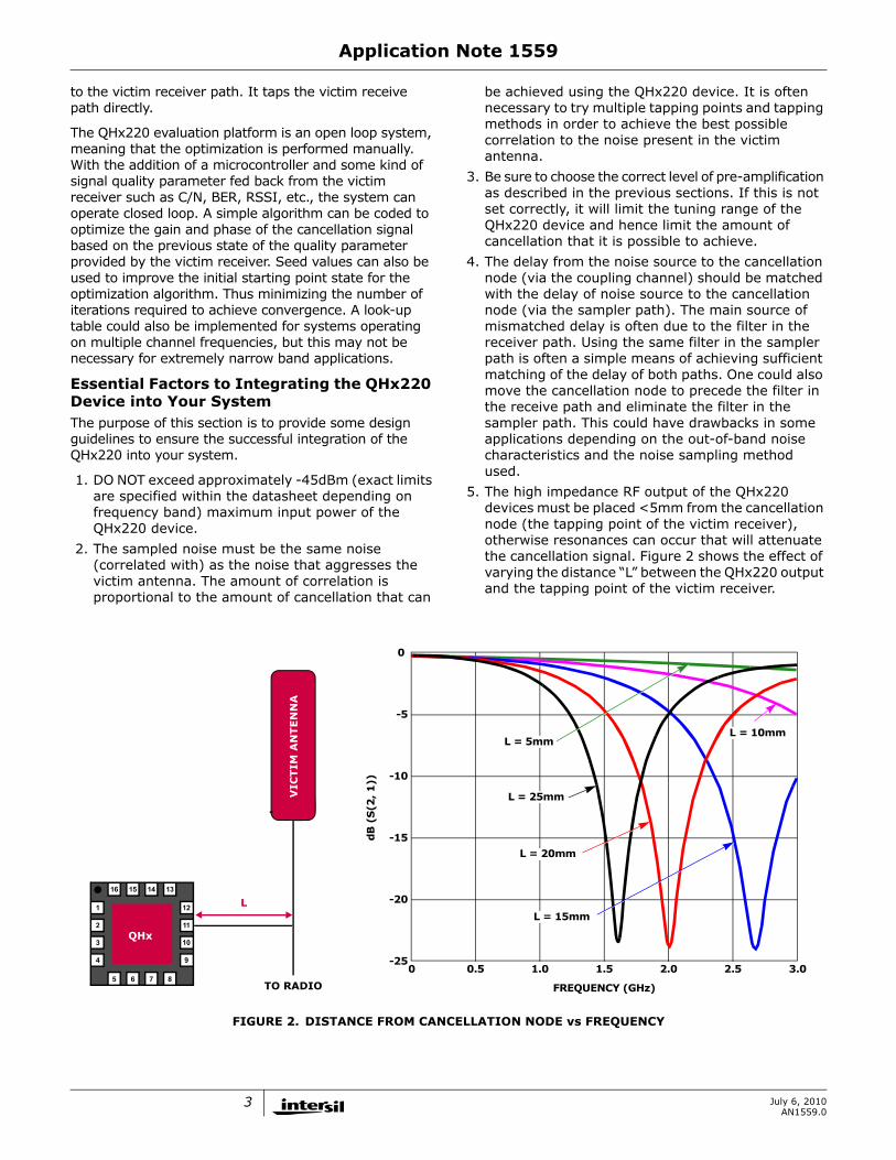
5. The high impedance RF output of the QHx220 devices must be placed <5mm from the cancellation node (the tapping point of the victim receiver), otherwise resonances can occur that will attenuate the cancellation signal. Figure 2 shows the effect of varying the distance “L” between the QHx220 output and the tapping point of the victim receiver.
FIGURE 2. DISTANCE FROM CANCELLATION NODE vs FREQUENCY
VIC
TIM
AN
TE
NN
A
TO RADIO FREQUENCY (GHz)
dB
(S
(2, 1))
-5
-10
-15
-20
-25
0
0 0.5 1.0 1.5 2.0 2.5 3.0
L = 10mmL = 5mm
L = 20mm
L = 25mm
L = 15mm
1516 14 13
12
10
9
11
65 7 8
QHx
1
3
4
2
L
3 July 6, 2010AN1559.0

Application Note 1559
Connecting the QHx220 Evaluation Board to a PC for Manual Control The Basic I-Q Control Software User Guide (AN1563) provides a detailed description of how to install the software GUI program that is used to manually control the QHx220 evaluation board. The software should be installed prior to connecting the hardware to the PC. The Basic I-Q Control Software User Guide (AN1563) also provides detailed instruction on how to configure all the software settings required to control the frequency band, gain, and gain and phase of the device. Please note that the evaluation boards are populated to operate in a specific frequency band. A tank circuit and matching components are specifically chosen for each desired band of operation. If a different frequency band is chosen via the software GUI, then the QHx220 board should be reconfigured accordingly. The correct BOM for MTV, GPS, and WLAN frequency bands can be found in the subsequent sections of this user guide.
A USB controller board plugs into the USB port of the PC and is used to control the SPI bus interface of the QHx220 device. The USB controller board also has a 1.8V regulated supply that is used to power the QHx220 device. The user may alternatively power the device with an external power supply if so desired. A custom cable is also provided which is keyed so that it plugs into the USB controller board in the correct orientation. Figure 3 shows the USB controller board and cable connection.
The opposite end of the cable plugs into the QHx220 evaluation board to provide the 1.8V power supply voltage and SPI connection to control the device. These connectors are not “keyed” so please be sure that they are oriented correctly. There are markings on the socket and plug of each connector to identify the correct orientation. Figure 4 shows these markings and the orientation of the cable connections.
Three Hirose to SMA cables are provided for all of the RF connections (Noise Sampler Input and Rx Input/Output).
FIGURE 3. THE QHx220 USB CONTROLLER BOARD
FIGURE 4. QHx220 USB CONTROLLER BOARD WITH PARTS LABELED
1.8VINPUT
LED
NOISE SAMPLER INPUT
Rx INPUT (FROM ANTENNA)
Rx OUTPUT (TO RECEIVER)
INTERSIL QHX220
SPI
INTERFACE
4 July 6, 2010AN1559.0

Application Note 1559
MTV Product Application The following is a general overview on how the QHx220 can be applied for use in Mobile TV product applications.
QHx220 Board Layout
SPI INTERFACE
NOISESAMPLER
INPUT
INTERSIL QHx220
1.8V INPUT
Rx INPUT
(FROM ANTENNA)
Rx OUTPUT
(TO RECEIVER)
GND
LED
FIGURE 5. QHx220 EVALUATION BOARD LAYOUT (MTV)
5 July 6, 2010AN1559.0
6Ju
ly 6, 2
010
AN
1559.0
Ap
plica
tion
No
te 1
55
9
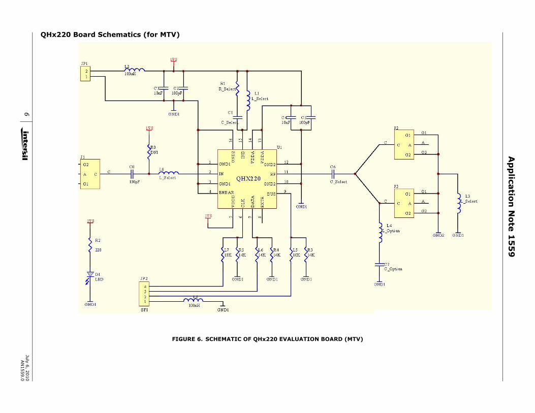
QHx220 Board Schematics (for MTV)FIGURE 6. SCHEMATIC OF QHx220 EVALUATION BOARD (MTV)
Application Note 1559
QHx220 Board Bill of Materials (for MTV)
MTV Optimization Setup (Static Coupling Channel)The following sections explain how to set up a static coupling channel which is used to perform self cancellation. The test setup in the following section is a useful environment to become familiar with tuning the device to the desired frequency the user would like to cancel in the final application. It will also provide an intuitive means of obtaining the starting I and Q values for achieving cancellation in the MTV Application setup.
A network analyzer is used to show the frequency response of the QHx220 while performing the optimization to achieve cancellation. It is suggested to perform the following setup of the network analyzer before connecting it to the rest of the test setup.
1. Set the desired frequency bandwidth for the application.
2. Change the output power to -45dBm. This provides some margin for the -45dBm maximum input requirement of the QHx220 since there is an additional 6dB loss from the power splitter. However, if pre-amplification is used (operating in high gain or boost mode) then the power should be reduced an additional 10dB to 15dB per gain stage.
3. Perform a 2-port calibration of the network analyzer.
4. Select the S21 measurement mode.
The power splitter connected to the output of the network analyzer is used to divide the aggressor signal into two separate paths. One path goes to the sampler input of the QHx220 which samples the aggressor signal. The other path is fed to what will later be used as part of the receive path for the MTV receiver. An attenuator pad is used in this path to set the coupling losses. This loss represents the coupling loss between the aggressor source and the MTV victim antenna. For the purpose of this evaluation the attenuator should be roughly 10dB to 20dB for a typical coupling factor. Keep in mind that the second power splitter adds an additional 6dB to the coupling factor. Since the QHx220 has ~50dB dynamic range, this range of attenuation should set the aggressor power in the middle of the tuning range of the QHx220 when using the lowest gain setting of the QHx220. Higher gain settings can be used for stronger coupling factors or weaker noise sampling or tapping methods.
It is important to set the power level of the network analyzer to -45dBm. This will ensure that the sampler input maximum power level is not exceeded. The
TABLE 1. QHx220 MTV-SPECIFIC EVALUATION BOARD BILL OF MATERIALS
ITEM QTY REFERENCE PART VENDOR VENDOR PART # DISTRIBUTOR
1 3 C0, C2, C5 100pF KEMET C0402C101J3GACTU Digikey_399_1022_1_ND
2 2 C3, C4 10nF KEMET C0402C103K3RACTU Digikey_399_1278_1_ND
3 2 C1 2pF Panasonic ECJ-0EC1H020C Digikey_PCC020CQCT
4 1 C6 22pF Murata GRM0335C1E220JD01D Digikey_490-1253-1-ND
5 1 C7 DNP
6 1 L0 39nH Panasonic ELJ-RE39NJF2 Digikey_PCD1158CT
7 1 L1 22nH Panasonic ELJ-RE22NJF2 Digikey_PCD1155CT
8 1 L3 10nH Panasonic ELJ-RE10NJF2 Digikey_PCD1151CT
9 2 L2, L8 100nH Panasonic ELJ-RER10JF3 Digikey_PCD1201CT-ND
10 1 L4 DNP
11 2 L5, L7 (L or R) 10kΩ Yageo 9C04021A1001FLHF3 Digikey_311-1.00KLCT-ND
12 1 L6 (L or R) 14kΩ Yageo RC0402FR-0714KL Digikey_311-14KLRCT
13 1 D1 LED Lumex SML_LXT0805GW Digikey_67_1553_1_ND
14 1 JP1 HD1x4 Waldom 87758_0416 Digikey_WM18833_ND
15 1 JP2 HD1x2 Waldom 22_28_4040 Digikey_WM6404_ND
16 3 J1, J2, J3 Hirose Digikey_H9161-ND
17 1 R0 DNP
18 1 R1 10Ω Yageo 9C04021A10RFLHF3 Digikey_311-10.0LCT-ND
19 1 R2 220Ω ROHM RC04022FR-07220RL Digikey_311-220LRCT-ND
20 3 R3, R4, R5 14kΩ ROHM RC04022FR-0714KL
21 1 U1 QNX220 Intersil QNX220
7 July 6, 2010AN1559.0

Application Note 1559
measurement of interest is S21 in order to optimize the MTV aggressor cancellation. Once the “MTV Optimization Setup (Static Coupling Channel)” is ready, use the software provided to configure the device as previously described.
1. Select the MTV frequency band of operation.
2. Start with the lowest gain setting.
3. Then adjust the I and Q (or gain and phase) until the maximum attenuation is achieved at the desired frequency.
Figure 8 is an example of the type of cancellation that should be achieved when the I and Q values have been optimized.
Once the cancellation has been optimized, record the I and Q values for the optimization of the setup used.
FIGURE 7. MTV OPTIMIZATION SETUP DIAGRAM
ATTENUATOR PAD TO SET COUPLING LOSS
MTV AGGRESSOR
NETWORK ANALYZER
QHx220
CANCELLATION NODE
POWER SPLITTER
PORT 1 PORT 2
50ΩTERMINATION
POWER SPLITTER
PATH
FIGURE 8. EXAMPLE OF OPTIMUM CANCELLATION (MTV)
-35
-30
-25
-20
-15
-10
-5
0
400 420 440 460 480 500 520 540 560 580 600
FREQUENCY (MHz)
AFTER CANCELLATION
BEFORE CANCELLATION
8 July 6, 2010AN1559.0

Application Note 1559
MTV Application SetupThe following setup should be used for testing QHx220 noise cancellation ability for a MTV application. It is important to maintain the identical core setup used in the “MTV Optimization Setup (Static Coupling Channel)” section on page 7. Otherwise, the optimization values will not be valid.
Begin with the aggressor source (signal generator) and QHx220 board powered off. Turn on the MTV generator and MTV tuner and record the receiver’s signal quality parameters (C/N, BER, etc.) once a channel synch is achieved. Find the weakest MTV generator level that will still enable the tuner to maintain synchronization. Next, set the aggressor signal generator to the same channel frequency and set the power level to roughly 10dB above the peak of the broadcast MTV signal. The aggressor signal needs to be high enough to show degradation of the receive signal strength reported by the MTV receiver. Remember not to exceed ~ -45dBm at the input of the
QHx220. Once an aggressor power level is found that degrades the receive signal strength reported by the MTV receiver, turn on the QHx220 board and set the optimized I and Q values that were determined in the “MTV Optimization Setup (Static Coupling Channel)” section on page 7. This should result in a <15dB recovery of the receive signal strength power reported by the MTV receiver if the board was optimized correctly. However, since the setup was slightly modified from the original optimization setup, it should be possible to fine tune the QHx220 to improve the in-band noise cancellation. Please note that any changes to the cable lengths or slight impedance changes will slightly impact the optimal gain and phase of the QHx220. Therefore, in the MTV application setup, adjust the gain and/or phase one step at a time and monitor the MTV receiver sensitivity (or any other signal quality parameter (i.e. C/N, BER, etc.). Continue to adjust the gain and phase one step at a time until no further improvement to the receiver sensitivity can be achieved.
FIGURE 9. MTV TESTING SETUP DIAGRAM
MTV AGGRESSOR
PATH
MTV
GENERATOR
QHx220
MTVTUNER
CANCELLATION NODE
MTV RECEIVE PATH
POWER SPLITTER
ATTENUATOR PAD TO SET COUPLING LOSS
POWER SPLITTER
AGGRESSOR GENERATOR
9 July 6, 2010AN1559.0

Application Note 1559
GPS Product Application The following is a general overview on how the QHx220 can be applied for use in GPS product applications.
QHx220 Board Layout
SPI INTERFACE
INTERSIL QHx220
1.8V INPUT
Rx INPUT (FROM ANTENNA)
Rx OUTPUT (TO RECEIVER)
GND
LED
NOISESAMPLER
INPUT
FIGURE 10. QHx220 EVALUATION BOARD LAYOUT (GPS)
10 July 6, 2010AN1559.0

11
July 6
, 2010
AN
1559.0
C
G1 G1
G2 G2
AA
J2
C
G1 G1
G2 G2
A A
J3
GND2
L3L_Select
GND1ption
Option
Ap
plica
tion
No
te 1
55
9
QHx220 Board Schematics (for GPS)CC
G1G1
G2G2
AA
J1
C
C
L0
L_Select
C0
100pF
L8, 100nH
L1L_Select
C310nF
C1
C_Select
C2100pF
R1R_Select
GND1
1V8
GND1C410nF
GND1
1V8
L2
100nH
C5100pF
D1LED
R2220
1V8
GND1
GND1
C6
C_Select
L4L_O
C7C_
GND1
1V8
R0DNI
12
JP 1
1234
JP 2
SPI
L710k
L614k
L510k
R514k
R414k
R314k
GND1 GND1
GND1
QHx220
GND11
GND13
IN2
ENBAR4
VD
DD
5
CLK
6
DA
TA7
EXTR
8
BUS 9
GND2 10
RF 11
GND212V
DD
A13
VD
DA
14
IND
15
GN
D2
16
U1
FIGURE 11. SCHEMATIC OF QHx220 EVALUATION BOARD (GPS)

Application Note 1559
QHx220 Board Bill of Materials (for GPS)
GPS Optimization Setup (Static Coupling Channel)The following sections explain how to set up a static coupling channel which is used to perform self cancellation. The test setup in the following section is a useful environment to become familiar with tuning the device to the desired frequency the user would like to cancel in the final application. It will also provide an intuitive means of obtaining the starting I and Q values for achieving cancellation in the GPS Application setup.
A network analyzer is used to show the frequency response of the QHx220 while performing the optimization to achieve cancellation. It is suggested to perform the following setup of the network analyzer before connecting it to the rest of the test setup.
1. Set the desired frequency bandwidth for the application.
2. Change the output power to -45dBm. This provides some margin for the -45dBm maximum input requirement of the QHx220 since there is an additional 6dB loss from the power splitter. However, if pre-amplification is used (operating in high gain or boost mode) then the power should be reduced an additional 10dB to 15dB per gain stage.
3. Perform a 2 port calibration of the network analyzer.
4. Select the S21 measurement mode.
The power splitter connected to the output of the network analyzer is used to divide the aggressor signal into two separate paths. One path goes to the sampler input of the QHx220 which samples the aggressor signal. The other path is fed to what will later be used as part of the receive path for the GPS receiver. An attenuator pad is used in this path to set the coupling losses. This loss represents the coupling loss between the aggressor source and the GPS victim antenna. For the purpose of this evaluation the attenuator should be roughly 10dB to 20dB for a typical coupling factor. Keep in mind that the second power splitter adds an additional 6dB to the coupling factor. Since the QHx220 has ~50dB dynamic range, this range of attenuation should set the aggressor power in the middle of the tuning range of the QHx220 when using the lowest gain setting of the QHx220. Higher gain settings can be used for stronger coupling factors or weaker noise sampling or tapping methods.
It is important to set the power level of the network analyzer to -45dBm. This will ensure that the sampler input maximum power level is not exceeded. The measurement of interest is S21 in order to optimize the
TABLE 2. QHx220 GPS-SPECIFIC EVALUATION BOARD BILL OF MATERIALS
ITEM QTY REFERENCE PART VENDOR VENDOR PART # DISTRIBUTOR
1 3 C0, C2, C5 100pF KEMET C0402C101J3GACTU Digikey_399_1022_1_ND
2 2 C3, C4 10nF KEMET C0402C103K3RACTU Digikey_399_1278_1_ND
3 1 C1 DNP
4 1 C6 22pF Murata GRM0335C1E220JD01D Digikey_490-1253-1-ND
5 1 C7 DNP
6 1 L0 6.2nH MURATA LQG15HS6N2SO2D Digikey_490-2620-1
7 1 L1 5.6nH Panasonic ELJ-RE5N6JF2 Digikey_PCD1148CT
8 1 L3 0.0Ω ROHM MCR01MZPJ000 Digikey_rhm0.0JCT-ND
9 2 L2, L8 100nH Panasonic ELJ-RER10JF3 Digikey_PCD1201CT-ND
10 1 L4 DNP
11 2 L5, L7 (L or R) 10kΩ Yageo 9C04021A1001FLHF3 Digikey_311-1.00KLCT-ND
12 1 L6 (L or R) 14kΩ Yageo RC0402FR-0714KL Digikey_311-14KLRCT
13 1 D1 LED Lumex SML_LXT0805GW Digikey_67_1553_1_ND
14 1 JP1 HD1x4 Waldom 87758_0416 Digikey_WM18833_ND
15 1 JP2 HD1x2 Waldom 22_28_4040 Digikey_WM6404_ND
16 3 J1, J2, J3 Hirose Digikey_H9161-ND
17 1 R0 DNP
18 1 R1 DNP
19 1 R2 220Ω ROHM RC04022FR-07220RL Digikey_311-220LRCT-ND
20 3 R3, R4, R5 14kΩ ROHM RC04022FR-0714KL Digikey_311-14.0KLRCT
21 1 U1 QNX220 Intersil QNX220
12 July 6, 2010AN1559.0

Application Note 1559
GPS aggressor cancellation. Once the “GPS Optimization Setup (Static Coupling Channel)” is ready, use the software provided to configure the device as previously described.
1. Select the GPS frequency band of operation.
2. Start with the lowest gain setting.
3. Then adjust the I and Q (or gain and phase) until the maximum attenuation is achieved at the desired frequency.
Figure 13 is an example of the type of cancellation that should be achieved when the I and Q values have been optimized.
Once the cancellation has been optimized, record the I and Q values for the optimization of the setup used.
ATTENUATOR PAD TO SET COUPLING LOSS
GPS AGGRESSOR
NETWORK ANALYZER
QHX220
CANCELLATION NODE
POWER SPLITTER
PORT 1 PORT 2
POWER SPLITTER
50Ω TERMINATION
PATH
FIGURE 12. GPS OPTIMIZATION SETUP DIAGRAM
FIGURE 13. EXAMPLE OF OPTIMUM CANCELLATION (GPS)
-80
-70
-60
-50
-40
-30
1400 1450 1500 1550 1600 1650 1700
FREQUENCY (MHz)
AFTER CANCELLATION
BEFORE CANCELLATION
GPS BAND
CO
UP
LIN
G C
HA
NN
EL (
dB
)
13 July 6, 2010AN1559.0
Application Note 1559
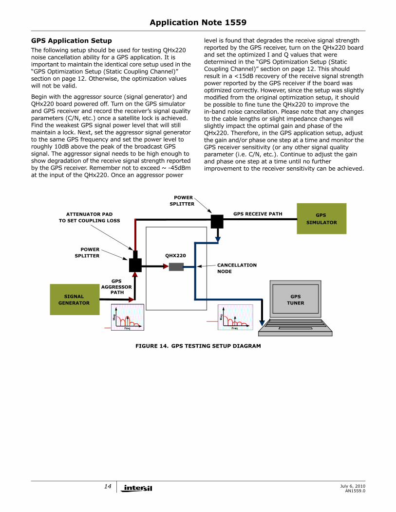
GPS Application SetupThe following setup should be used for testing QHx220 noise cancellation ability for a GPS application. It is important to maintain the identical core setup used in the “GPS Optimization Setup (Static Coupling Channel)” section on page 12. Otherwise, the optimization values will not be valid.
Begin with the aggressor source (signal generator) and QHx220 board powered off. Turn on the GPS simulator and GPS receiver and record the receiver’s signal quality parameters (C/N, etc.) once a satellite lock is achieved. Find the weakest GPS signal power level that will still maintain a lock. Next, set the aggressor signal generator to the same GPS frequency and set the power level to roughly 10dB above the peak of the broadcast GPS signal. The aggressor signal needs to be high enough to show degradation of the receive signal strength reported by the GPS receiver. Remember not to exceed ~ -45dBm at the input of the QHx220. Once an aggressor power
level is found that degrades the receive signal strength reported by the GPS receiver, turn on the QHx220 board and set the optimized I and Q values that were determined in the “GPS Optimization Setup (Static Coupling Channel)” section on page 12. This should result in a <15dB recovery of the receive signal strength power reported by the GPS receiver if the board was optimized correctly. However, since the setup was slightly modified from the original optimization setup, it should be possible to fine tune the QHx220 to improve the in-band noise cancellation. Please note that any changes to the cable lengths or slight impedance changes will slightly impact the optimal gain and phase of the QHx220. Therefore, in the GPS application setup, adjust the gain and/or phase one step at a time and monitor the GPS receiver sensitivity (or any other signal quality parameter (i.e. C/N, etc.). Continue to adjust the gain and phase one step at a time until no further improvement to the receiver sensitivity can be achieved.
FIGURE 14. GPS TESTING SETUP DIAGRAM
GPS AGGRESSOR
PATHSIGNAL
GENERATOR
GPS
SIMULATOR
QHX220
GPSTUNER
CANCELLATION NODE
GPS RECEIVE PATH
POWER SPLITTER
ATTENUATOR PAD TO SET COUPLING LOSS
POWER SPLITTER
14 July 6, 2010AN1559.0
Application Note 1559
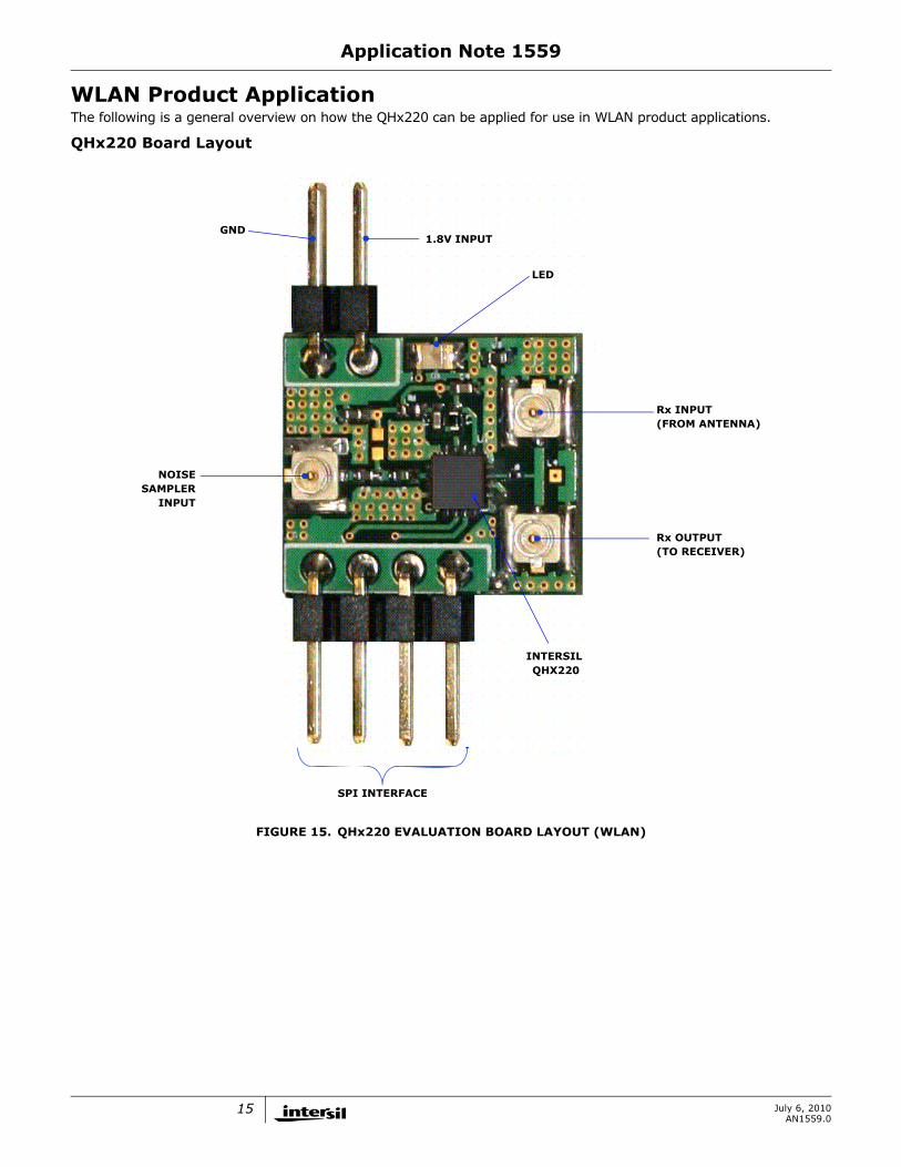
WLAN Product ApplicationThe following is a general overview on how the QHx220 can be applied for use in WLAN product applications.
QHx220 Board Layout
SPI INTERFACE
INTERSIL QHX220
1.8V INPUT
Rx INPUT (FROM ANTENNA)
Rx OUTPUT (TO RECEIVER)
GND
LED
NOISESAMPLER
INPUT
FIGURE 15. QHx220 EVALUATION BOARD LAYOUT (WLAN)
15 July 6, 2010AN1559.0
16
July 6
, 2010
AN
1559.0
C
G1G1
G2G2
AA
J2
C
G1G1
G2G2
AA
J3
GND2
L3L_Select
GND1Option
7_Option
Ap
plica
tion
No
te 1
55
9
QHx220 Board Schematics (for WLAN)CC
G1G1
G2G2
AA
J1
C
C
L0
L_Select
C0
100pF
L8, 100nH
L1L_Select
C310nF
C1
C_Select
C2100pF
R1R_Select
GND1
1V8
GND1C410nF
GND1
1V8
L2
100nH
C5100pF
D1LED
R2220
1V8
GND1
GND1
C6
C_Select
L4L_
CC
GND1
1V8
R0DNI
12
JP 1
1234
JP 2
SPI
L710k
L614k
L510k
R514k
R414k
R314k
GND1 GND1
GND1
QHX2 20
GND11
GND13
IN2
ENBAR4
VD
DD
5
CLK
6
DA
TA7
EXTR
8
BUS9
GND2 10
RF 11
GND2 12VD
DA
13
VD
DA
14
IND
15
GN
D2
16
U1
FIGURE 16. SCHEMATIC OF QHx220 EVALUATION BOARD (WLAN)

Application Note 1559
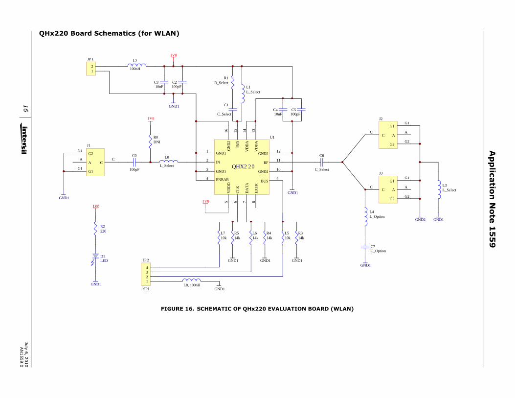
QHx220 Board Bill of Materials (for WLAN)
WLAN Optimization Setup (Static Coupling Channel)The following sections explain how to set up a static coupling channel which is used to perform self cancellation. The test setup in the following section is a useful environment to become familiar with tuning the device to the desired frequency the user would like to cancel in the final application. It will also provide an intuitive means of obtaining the starting I and Q values for achieving cancellation in the WLAN Application setup.
A network analyzer is used to show the frequency response of the QHx220 while performing the optimization to achieve cancellation. It is suggested to perform the following setup of the network analyzer before connecting it to the rest of the test setup.
1. Set the desired frequency bandwidth for the application.
2. Change the output power to -45dBm. This provides some margin for the -45dBm maximum input requirement of the QHx220 since there is an additional 6dB loss from the power splitter. However if pre-amplification is used (operating in high gain or boost mode) then the power should be reduced an additional 10dB to 15dB per gain stage.
3. Perform a 2 port calibration of the network analyzer.
4. Select the S21 measurement mode.
The power splitter connected to the output of the network analyzer is used to divide the aggressor signal into two separate paths. One path goes to the sampler input of the QHx220 which samples the aggressor signal. The other path is fed to what will later be used as part of the receive path for the WLAN receiver. An attenuator pad is used in this path to set the coupling losses. This loss represents the coupling loss between the aggressor source and the WLAN victim antenna. For the purpose of this evaluation the attenuator should be roughly 10dB to 20dB for a typical coupling factor. Keep in mind that the second power splitter adds an additional 6dB to the coupling factor. Since the QHx220 has ~50dB dynamic range, this range of attenuation should set the aggressor power in the middle of the tuning range of the QHx220 when using the lowest gain setting of the QHx220. Higher gain settings can be used for stronger coupling factors or weaker noise sampling or tapping methods.
It is important to set the power level of the network analyzer to -45dBm. This will ensure that the sampler input maximum power level is not exceeded. The measurement of interest is S21 in order to optimize the
TABLE 3. QHx220 WLAN-SPECIFIC EVALUATION BOARD BILL OF MATERIALS
ITEM QTY REFERENCE PART VENDOR VENDOR PART # DISTRIBUTOR
1 3 C0, C2, C5 100pF KEMET C0402C101J3GACTU Digikey_399_1022_1_ND
2 2 C3, C4 10nF KEMET C0402C103K3RACTU Digikey_399_1278_1_ND
3 1 C1 DNP
4 1 C6 0.0Ω Panasonic ERJ-1GE0R00C Digikey_P0.0AGCT-ND
5 1 C7 DNP
6 1 L0 3.3nH Panasonic ELJ-RE3N3DF2 Digikey_PCD1145CT
7 1 L1 1.5nH Panasonic ELJ-RE1N5DF2 Digikey_PCD1196CT
8 1 L3 0.0Ω ROHM MCR01MZPJ000 Digikey_RHM0.0JCT_ND
9 2 L2, L8 100nH Panasonic ELJ-RER10JF3 Digikey_PCD1201CT-ND
10 1 L4 DNP
11 2 L5, L7 (L or R) 10kΩ Yageo 9C04021A1001FLHF3 Digikey_311-1.00KLCT-ND
12 1 L6 (L or R) 14kΩ Yageo RC0402FR-0714KL Digikey_311-14KLRCT
13 1 D1 LED Lumex SML_LXT0805GW Digikey_67_1553_1_ND
14 1 JP1 HD1x4 Waldom 87758_0416 Digikey_WM18833_ND
15 1 JP2 HD1x2 Waldom 22_28_4040 Digikey_WM6404_ND
16 3 J1, J2, J3 Hirose Digikey_H9161-ND
17 1 R0 DNP
18 1 R1 DNP
19 1 R2 220Ω ROHM RC04022FR-07220RL Digikey_311-220LRCT-ND
20 3 R3, R4, R5 14kΩ ROHM RC04022FR-0714KL Digikey_311-14.0KLRCT
21 1 U1 QNX220 Intersil QNX220
17 July 6, 2010AN1559.0

Application Note 1559
WLAN aggressor cancellation. Once the “WLAN Optimization Setup (Static Coupling Channel)” is ready, use the software provided to configure the device as previously described:
1. Select the WLAN frequency band of operation.
2. Start with the lowest gain setting.
3. Then adjust the I and Q (or gain and phase) until the maximum attenuation is achieved at the desired frequency.
Figure 18 is an example of the type of cancellation that should be achieved when the I and Q values have been optimized.
ATTENUATOR PAD TO SET COUPLING LOSS
WLAN AGGRESSOR
NETWORK ANALYZER
QHX220
CANCELLATION NODE
POWER SPLITTER
PORT 1 PORT 2
POWER SPLITTER
50Ω TERMINATION
PATH
FIGURE 17. WLAN OPTIMIZATION SETUP DIAGRAM
-90
-40
-30
-20
-10
0
-50
-60
-70
-80
AFTER CANCELLATION
BEFORE CANCELLATION
FIGURE 18. EXAMPLE OF OPTIMUM CANCELLATION (WLAN)
18 July 6, 2010AN1559.0

Application Note 1559
Intersil Corporation reserves the right to make changes in circuit design, software and/or specifications at any time without notice. Accordingly, thereader is cautioned to verify that the Application Note or Technical Brief is current before proceeding.
For information regarding Intersil Corporation and its products, see www.intersil.com
WLAN Application SetupThe following setup should be used for testing QHx220 noise cancellation ability for a WLAN application. It is important to maintain the identical core setup used in the “WLAN Optimization Setup (Static Coupling Channel)” section on page 17. Otherwise, the optimization values will not be valid.
Begin with the aggressor source (signal generator) and QHx220 board powered off. Turn on the WLAN simulator and WLAN receiver and record the receiver’s signal quality parameters (C/N, etc.). Find the weakest WLAN signal power level that will still maintain a WLAN link. Next set the aggressor signal generator to the same WLAN frequency and set the power level to roughly 10dB above the peak of the broadcast WLAN signal. The aggressor signal needs to be high enough to show degradation of the receive signal strength reported by the WLAN receiver. Remember not to exceed ~ -45dBm at the input of the QHx220. Once an aggressor power level is found that degrades the receive signal strength reported by the WLAN receiver, turn on the QHx220 board and set the optimized I and Q values that were determined in the “WLAN Optimization Setup (Static Coupling Channel)” section on page 17. This should result in a <15dB recovery of the receive signal strength power reported by the WLAN receiver if the board was
optimized correctly. However, since the setup was slightly modified from the original optimization setup, it should be possible to fine tune the QHx220 to improve the in-band noise cancellation. Please note that any changes to the cable lengths or slight impedance changes will slightly impact the optimal gain and phase of the QHx220. Therefore, in the WLAN application setup, adjust the gain and/or phase one step at a time and monitor the WLAN receiver sensitivity (or any other signal quality parameter (i.e. C/N, etc.). Continue to adjust the gain and phase one step at a time until no further improvement to the receiver sensitivity can be achieved.
Q:ACTIVEQ:ACTIVE Technology is behind Intersil’s ability to insert its ICs inside radios, automotive infotainment systems, satellite broadcast equipment, and various consumer electronic devices such as GPS units, cell phones, and portable gaming systems. By doing so, Intersil achieves the ability to reduce electromagnetic interference by as much as 30dB. This breakthrough in radio sensitivity allows for several signals to run simultaneously and enables new technologies such as mobile TV on hand held games, cell phones, and in automotive systems.
FIGURE 19. WLAN TESTING SETUP DIAGRAM
WLAN AGGRESSOR
PATH SIGNAL
GENERATOR
WLAN
SIMULATOR
QHX220
WLANRECEIVER
CANCELLATION NODE
WLAN RECEIVE PATH
POWER SPLITTER
ATTENUATOR PAD TO SET COUPLING LOSS
POWER SPLITTER
19 July 6, 2010AN1559.0