Proceedings of the 8th IEEE Benelux Young Researchers ...
165
Proceedings of the 8th IEEE Benelux Young Researchers symposium in electrical power engineering Citation for published version (APA): Jansen, J. W., & Roes, M. G. L. (Eds.) (2016). Proceedings of the 8th IEEE Benelux Young Researchers symposium in electrical power engineering: YRS2016, 12-13 May, Eindhoven University of Technology. Technische Universiteit Eindhoven. Document status and date: Published: 01/05/2016 Please check the document version of this publication: • A submitted manuscript is the version of the article upon submission and before peer-review. There can be important differences between the submitted version and the official published version of record. People interested in the research are advised to contact the author for the final version of the publication, or visit the DOI to the publisher's website. • The final author version and the galley proof are versions of the publication after peer review. • The final published version features the final layout of the paper including the volume, issue and page numbers. Link to publication General rights Copyright and moral rights for the publications made accessible in the public portal are retained by the authors and/or other copyright owners and it is a condition of accessing publications that users recognise and abide by the legal requirements associated with these rights. • Users may download and print one copy of any publication from the public portal for the purpose of private study or research. • You may not further distribute the material or use it for any profit-making activity or commercial gain • You may freely distribute the URL identifying the publication in the public portal. If the publication is distributed under the terms of Article 25fa of the Dutch Copyright Act, indicated by the “Taverne” license above, please follow below link for the End User Agreement: www.tue.nl/taverne Take down policy If you believe that this document breaches copyright please contact us at: [email protected] providing details and we will investigate your claim. Download date: 18. Mar. 2022
-
Upload
khangminh22 -
Category
Documents
-
view
3 -
download
0
Transcript of Proceedings of the 8th IEEE Benelux Young Researchers ...

Proceedings of the 8th IEEE Benelux Young Researcherssymposium in electrical power engineeringCitation for published version (APA):Jansen, J. W., & Roes, M. G. L. (Eds.) (2016). Proceedings of the 8th IEEE Benelux Young Researcherssymposium in electrical power engineering: YRS2016, 12-13 May, Eindhoven University of Technology.Technische Universiteit Eindhoven.
Document status and date:Published: 01/05/2016
Please check the document version of this publication:
• A submitted manuscript is the version of the article upon submission and before peer-review. There can beimportant differences between the submitted version and the official published version of record. Peopleinterested in the research are advised to contact the author for the final version of the publication, or visit theDOI to the publisher's website.• The final author version and the galley proof are versions of the publication after peer review.• The final published version features the final layout of the paper including the volume, issue and pagenumbers.Link to publication
General rightsCopyright and moral rights for the publications made accessible in the public portal are retained by the authors and/or other copyright ownersand it is a condition of accessing publications that users recognise and abide by the legal requirements associated with these rights.
• Users may download and print one copy of any publication from the public portal for the purpose of private study or research. • You may not further distribute the material or use it for any profit-making activity or commercial gain • You may freely distribute the URL identifying the publication in the public portal.
If the publication is distributed under the terms of Article 25fa of the Dutch Copyright Act, indicated by the “Taverne” license above, pleasefollow below link for the End User Agreement:www.tue.nl/taverne
Take down policyIf you believe that this document breaches copyright please contact us at:[email protected] details and we will investigate your claim.
Download date: 18. Mar. 2022
Current-Based ZVS Modulation Strategy for a 3-5Level Bidirectional Dual Active Bridge
DC–DC ConverterGeorgios E. Sfakianakis, Student Member, IEEE
Electromechanics and Power Electronics (EPE) groupDepartment of Electrical Engineering
Eindhoven University of Technology (TU/e)Eindhoven, The Netherlands
Abstract—This paper presents a Zero Voltage Switching (ZVS)modulation strategy for the 3 Level – 5 Level (3-5L) Dual ActiveBridge (DAB) DC–DC converter. The DAB accommodates a fullbridge in the primary side and two 3-level T-Type bridge legs inthe secondary side, linked by a high-frequency transformer andan inductor. A ZVS modulation strategy is presented, in whichcommutation inductances are utilized to extend the ZVS regionto the entire operating range of the converter. The configurationof the secondary-side bridge allows further flexibility, comparedto a full bridge configuration, to minimize the RMS current inthe inductor. The nominal power of the converter is 2.8 kW withinput voltage range from 8 V to 16 V, and output voltage rangefrom 175 V to 450 V. The RMS currents of the 3-5L DAB arecompared with those of a typical 3-3L full bridge - full bridgeDAB, by applying the proposed modulation strategy in the 3-5L DAB, and a strategy proposed in literature in the 3-3L DAB.
Index Terms—DC–DC Converters, Dual Active Bridge, ZeroVoltage Switching, Modulation Schemes.
I. INTRODUCTION
Power converters are widely used in powertrains of plug-inhybrid electric vehicles (PHEVs) and plug-in battery electricvehicles (PBEVs). DC-AC converters transfer power from thehigh-voltage (HV) batteries to the electric motors, an AC-DCconverter connects the HV batteries to the grid (i.e. batterycharger) and a DC-DC converter interfaces the low voltage(LV) batteries with the HV batteries (LV2HV interface). Highpower density and efficiency are required in such applicationsin order to increase the driving range and space utilization.Concerning the LV2HV interface, where a significant dif-ference in the input and output voltage is imposed (12 V→ 400 V), the Dual Active Bridge (DAB) converter is apromising choice due to its soft-switching capability. TheDAB can bring advantages by equalizing the input and outputvoltages using the transformer turns ratio (N). Moreover, theDAB is operated more efficiently when the output voltagereferred to the primary side is equal to the input voltage(N · VDC,2 ≈ VDC,1) [1], [2].
The DAB was introduced in [3] for the realization ofhigh-efficiency, high-power-density, isolated DC-DC convert-ers with buck-boost operation and bidirectional power flow
TABLE ICONVERTER SPECIFICATIONS
LV SideVDC,1 8 V ≤ VDC,1 ≤ 16 V, nom. 14 V
IDC,1,max ±200 A
HV Side VDC,2 175 V ≤ VDC,2 ≤ 450 V, nom. 400 V
AC-link
n1/n2 = N 1/9
L 0.0683 µH
fs 120 kHz
capability. Since then, various modulation strategies have beenproposed for the traditional 3 Level - 3 Level (3-3L) full bridge- full bridge DAB, where the main objective is to minimize theRMS current of the inductor/transformer under full-operating-range zero voltage switching [4]–[6]. The extra voltage levels(±VDC/2) of the 3-5L DAB provide more flexibility in theinductor/transformer current shaping, which leads to lowerRMS current [7]. On top of that, the extra switches used forthe extra levels need to be able to block only half the DC-busvoltage, which requires devices with half blocking voltage andtypically less than half on-resistance.
In this paper, a 3-5L DAB [8] is considered for a Low-to-High voltage DC-bus, DC–DC interface converter. The inputvoltage range is 8 V ≤ VDC,1 ≤ 16 V, the output voltagerange is 175 V ≤ VDC,2 ≤ 450 V, and the maximum inputcurrent is ± 200 A. Further details about the specificationsare listed in Table I. In Section II, a detailed explanation isgiven for the DAB topology. Section III contains an analysis ofthe different switching modes, the mode selection procedure,as well as the derivations of the piecewise linear equationsand the soft-switching constraints. The proposed modulationstrategy is discussed in Section IV. In Section V, a comparisonis performed between the 3-5L DAB and the traditional 3-3LDAB.
978-1-5090-2464-3/16/$31.00 ©2016 European Union
(a) (b) (c)
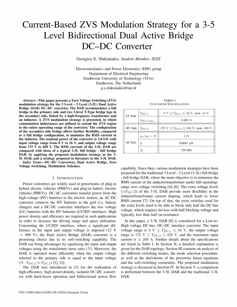
Fig. 1. (a) Circuit schematic of the 3-5L Dual Active Bridge converter [8], (b) Equivalent circuit of the Dual Active Bridge, and (c) DAB phase leg withparasitic capacitances.
II. 3-5L DAB CONVERTER TOPOLOGY
Fig. 1(a) shows the schematic of the considered 3-5L DAB[8], consisting of a full-bridge at the primary side (LV-side)and two T-Type bridge-legs at the secondary side (HV-side),coupled by a high frequency (HF) transformer and seriesinductor L. For the realization of the HV-side bridge, otheroptions are possible like the Neutral Point Clamped (NPC)[9]–[12] or the flying capacitor bridge leg. However, this workfocuses on the modulation strategy and does not further discussimplementation variants.
The operating principle of the 3-5L DAB is presented in[8]–[12], and it is similar to the operating principle of thetraditional 3-3L DAB. Both active bridges produce phase-shifted edge resonant square wave voltages v1 and v2 at theterminals of the HF AC link (inductor and HF transformer),resulting in an inductor current iL . Voltages v1 and v2 are alsoapplied to the commutation inductances (L1 and L2), resultingin currents iL1 and iL2 , respectively, which enhance the ZVSoperation [5] by injecting reactive current into the bridgeswithout contributing to the power flow. The bridges transformthe iHF1 and iHF2 into DC currents iDAB,1 and iDAB,2, on theprimary and secondary side respectively. Fig. 1(b) shows theequivalent circuit of the considered DAB, where all quantitiesare referred to the primary side. The switching frequency ischosen fs = 120 kHz in order to achieve compact converterdesign without excessive high-frequency losses.
The main inductor L, is chosen to be L ≈ 0.75 · Lmax,where Lmax is determined by the maximum input power ofthe DAB. According to [13], maximum positive DAB poweris achieved when τ1 = τ2 = τ2B = π and φ = φB = π/2,thus, the input current equation is (acc. to eqn. (14) of [13]):
IDC,1 =N · VDC,2,min
8 · fs,max · L,
IDC,1 ≥ IDC,1,max = 200 A.
(1)
The result of solving the inequality of eqn. (1) for L, is theinequality L ≤ Lmax, where Lmax is:
Lmax =N · VDC,2,min
8 · fs,max · IDC,1,max. (2)
III. SWITCHING CONTROL ANALYSIS
In the 3-3L DAB, the inductor current iL is controlled bythree variables, i.e. the pulse-width of the voltages v1 and v2produced by the primary and secondary side active bridgesand the phase shift between them. Depending on the sequenceof the voltage edges (falling or rising), 12 unique switchingmodes are distinguished. In the 3-5L DAB, the extra voltagelevels (±VDC,2/2) of the secondary side bridge, increase thecontrol variables to five. This results in more flexibility for theoptimal shaping of the inductor current, but the total numberof modes is increased to 40 and the analysis of the DAB isgetting more complex.
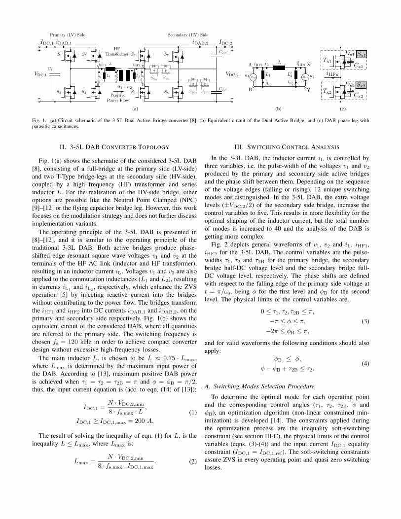
Fig. 2 depicts general waveforms of v1, v2 and iL, iHF1,iHF2 for the 3-5L DAB. The control variables are the pulse-widths τ1, τ2 and τ2B for the primary bridge, the secondarybridge half-DC voltage level and the secondary bridge full-DC voltage level, respectively. The phase shifts are definedwith respect to the falling edge of the primary side voltage att = π/ωs, being φ for the first level and φB for the secondlevel. The physical limits of the control variables are,
0 ≤ τ1, τ2, τ2B ≤ π,−π ≤ φ ≤ π,−2π ≤ φB ≤ π,
(3)
and for valid waveforms the following conditions should alsoapply:
φB ≤ φ,
φ− φB + τ2B ≤ τ2.(4)
A. Switching Modes Selection Procedure
To determine the optimal mode for each operating pointand the corresponding control angles (τ1, τ2, τ2B, φ andφB), an optimization algorithm (non-linear constrained min-imization) is developed [14]. The constraints applied duringthe optimization process are the inequality soft-switchingconstraint (see section III-C), the physical limits of the controlvariables (eqns. (3)-(4)) and the input current IDC,1 equalityconstraint (IDC,1 = IDC,1,ref ). The soft-switching constraintsassure ZVS in every operating point and quasi zero switchinglosses.
0
0
(a)
0
00
(b)
Fig. 2. General waveforms of v1, v2 and iL, iHF1, iHF2 for the 3-5L DAB.The waveforms were obtained for VDC,1 = 15.5 V, VDC,2 = 175 V, τ1 =3π4
, τ2 = 3π4
, τ2B = π4
, φ = π5
, φB = π10
, fs = 120 kHz, L = 0.0683 µH,L1 = 0.77 µH and L2 = 62.1 µH. Fig. 2(a) focuses on the control variablesand the names of the edges and Fig. 2(b) on the currents in the inductors L,L1 and L2.
Under ZVS operation, the conduction losses of the tran-sistors account for the biggest part (≥ 50 %) of the totalconverter losses [15]. Thus, the objective function used in theoptimization is related to the overall conduction losses and iscalculated using the equation:
fobj = I2RMS,HF1 +I2RMS,HF2
N2, (5)
where I2RMS,HF1 and I2RMS,HF2 are proportional to the primaryand secondary side conduction losses, respectively.
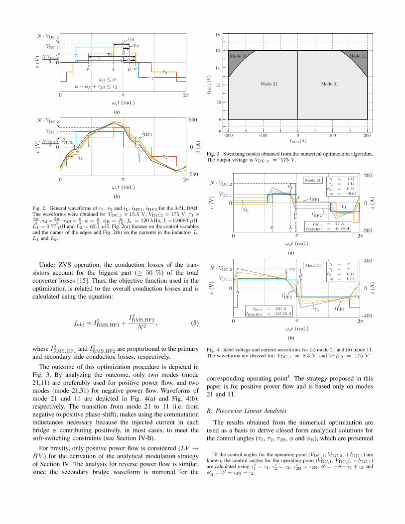
The outcome of this optimization procedure is depicted inFig. 3. By analyzing the outcome, only two modes (mode21,11) are preferably used for positive power flow, and twomodes (mode 21,31) for negative power flow. Waveforms ofmode 21 and 11 are depicted in Fig. 4(a) and Fig. 4(b),respectively. The transition from mode 21 to 11 (i.e. fromnegative to positive phase-shift), makes using the commutationinductances necessary because the injected current in eachbridge is contributing positively, in most cases, to meet thesoft-switching constraints (see Section IV-B).
For brevity, only positive power flow is considered (LV →HV ) for the derivation of the analytical modulation strategyof Section IV. The analysis for reverse power flow is similar,since the secondary bridge waveform is mirrored for the
Fig. 3. Switching modes obtained from the numerical optimization algorithm.The output voltage is VDC,2 = 175 V.
0
00
(a)
0
00
(b)
Fig. 4. Ideal voltage and current waveforms for (a) mode 21 and (b) mode 11.The waveforms are derived for: VDC,1 = 8.5 V, and VDC,2 = 175 V.
corresponding operating point1. The strategy proposed in thispaper is for positive power flow and is based only on modes21 and 11.
B. Piecewise Linear Analysis
The results obtained from the numerical optimization areused as a basis to derive closed form analytical solutions forthe control angles (τ1, τ2, τ2B, φ and φB), which are presented
1If the control angles for the operating point (VDC,1, VDC,2, +IDC,1) areknown, the control angles for the operating point (VDC,1, VDC,2, −IDC,1)are calculated using τ ′1 = τ1, τ ′2 = τ2, τ ′2B = τ2B, φ′ = −φ− τ1 + τ2 andφ′B = φ′ + τ2B − τ2.

TABLE IIINPUT CURRENT (IDC,1) EXPRESSIONS FOR MODE 21 AND 11
Mode 21N VDC,2 ((2φ+τ1−τ2) τ2+(2φB+τ1) τ2B−τ22B)
4L π ωs
Mode 11−NVDC,2
4πLωs[2φ2 − 2φ(−τ1 + τ2 + π)
+2φ2B − 2φB(−τ1 + τ2B + π) + 2τ21 − τ1τ2 − τ1τ2B
−4πτ1 + τ22 + τ22B + 2π2]
in Section IV. The respective inductor currents, induced by v1and v′2 are depicted in Fig. 2(b) and derived by:
diL(t)
dt=v1(t)− v′2(t)
L, (6)
diL1(t)
dt=v1(t)
L1, (7)
diL′2(t)
dt=v′2(t)
L′2. (8)
Solving equations (6)-(8) in each interval within half theswitching period and assuming steady state operation (i.e.iL(t) = −iL(t + Ts/2), iL1
(t) = −iL1(t + Ts/2) and
iL′2(t) = −iL′
2(t + Ts/2)), results in the expressions for the
currents at every switching instance θi = α, β, κ, λ, µ, ν,where θi = ωst and ωs = 2πfs. The bridge currents iHF1(t)and iHF2(t) are calculated using:
iHF1(t) = iL(t) + iL1(t), (9)iHF2(t) = N · i′HF2(t) = N · (iL(t)− iL′
2(t)). (10)
The current expressions for mode 21 and mode 11, applyingthe aforementioned procedure for each mode, are summarizedin Table V and in Table VI of the Appendix, respectively.By analyzing the conduction state of the switches, currentsiDAB,1(t) and iDAB,2(t) can be derived from iHF1(t) andiHF2(t), respectively. Averaging iDAB,1(t) over a switchingperiod Ts, yields the expressions for input current IDC,1.Table II denotes the input current expressions for modes 21and 11.
C. Soft-Switching Constraints
Zero-voltage-switching operation of the switches (acc. toFig. 1(c), Sx1, Sx2), is explained for a voltage transition that isinitiated by the turn-off of the transistor Tx1. The current iHFx
transfers the charge of the nonlinear parasitic capacitance Cx2
(discharge) to the respective nonlinear parasitic capacitanceCx1 (charge). By the time instant the Diode Dx2 takes overthe current, the transistor Tx2 can be turned-on under ZVS. Aminimum turn-off current is needed to complete the resonanttransition within the dead-time interval and avoid voltagetransition delay. The current-based soft-switching constraintsfor bridge currents iHF1 and iHF2 are summarized in Table III.A minimum commutation current value of 2 A is usedfor the primary and secondary side high-frequency switches(ISS,Prim = ISS,Prim = 2 A).
TABLE IIISOFT-SWITCHING CONSTRAINTS
Critical ZVSConstraintsper Region
Edge Current Constraint Type 1 2 3 4
α iHF1(α) ≤ −ISS,Prim Rising
β iHF1(β) ≥ ISS,Prim Falling x x x x
κ iHF2(κ) ≥ ISS,Sec Rising x
λ iHF2(λ) ≥ ISS,Sec Rising x
ν ≡ µ iHF2(ν) ≤ −ISS,Sec Falling x x x x
IV. ANALYTICALLY DERIVED MODULATION SCHEME
The results of the numerical optimization are presented inFig. 3. A close look into the results, shows that the optimizerchooses to keep the edges µ and ν in the same switchinginstant for both modes (21 and 11), leading to the constraint:
φ = φB, (11)
as shown in Fig. 4.In order to derive an analytical modulation scheme, the
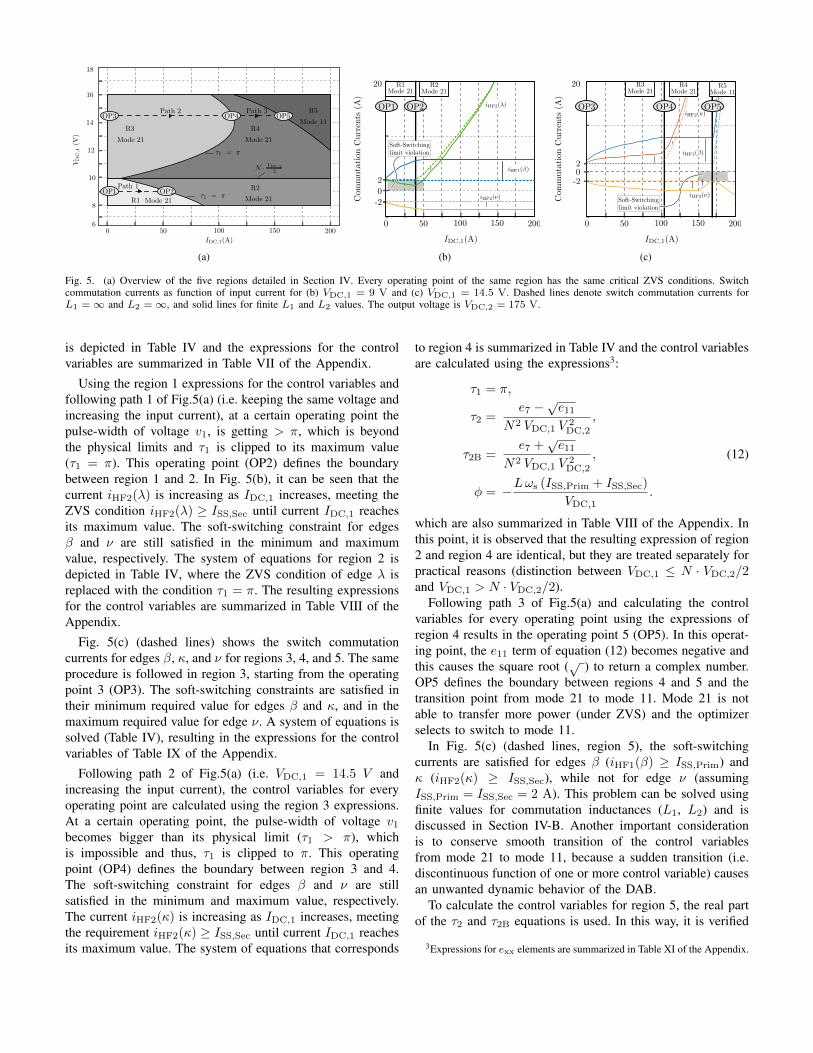
operating points were checked step-by-step and critical ZVSconditions were identified. For each operating point, in totalthree constraints should be identified, on top of the constraintsdenoted by the equation (11) and the input power expres-sion (Table II), in order to be able to solve the system ofequations towards the control variables (τ1, τ2, τ2B, φ andφB). Following this procedure, five regions were identified,where every operating point of the same region has the samecritical ZVS conditions, which are summarized in Table III2.Fig. 5(a) depicts an overview of them and their boundaries. InFig. 5(c) and Fig. 5(b) the critical switch commutation currentsare shown as function of input current for VDC,1 = 9 V andVDC,1 = 14.5 V, respectively. Dashed lines denote commuta-tion currents for L1 = ∞, L2 = ∞ and solid lines for finiteL1 and L2. The resulting ZVS conditions of the commutationcurrents that are not shown in Fig. 5(b) and Fig. 5(c) areeither less important (iHF2(x) ISS,Sec) or identical to ZVSconditions of another voltage edge ((iHF1(α) ≤ −ISS,Prim) ≡(iHF1(β) ≥ ISS,Prim)).
A. Infinite L1 and L2
Starting from operating point 1 (OP1) of Fig. 5, the soft-switching constraints (edges β, λ, and ν) are satisfied. Asit can be seen in Fig.5(b) (dashed lines), each commutationcurrent has the minimum required value for edges β and λ, andthe maximum required value for the edge ν. Thus, from everysoft-switching inequality constraint the equal part is true (”≤”,”≥” → ”=”). The resulting system of equations for region 1
2Region 5 is separately discussed in the end of this section.
(a) (b) (c)
Fig. 5. (a) Overview of the five regions detailed in Section IV. Every operating point of the same region has the same critical ZVS conditions. Switchcommutation currents as function of input current for (b) VDC,1 = 9 V and (c) VDC,1 = 14.5 V. Dashed lines denote switch commutation currents forL1 =∞ and L2 =∞, and solid lines for finite L1 and L2 values. The output voltage is VDC,2 = 175 V.
is depicted in Table IV and the expressions for the controlvariables are summarized in Table VII of the Appendix.
Using the region 1 expressions for the control variables andfollowing path 1 of Fig.5(a) (i.e. keeping the same voltage andincreasing the input current), at a certain operating point thepulse-width of voltage v1, is getting > π, which is beyondthe physical limits and τ1 is clipped to its maximum value(τ1 = π). This operating point (OP2) defines the boundarybetween region 1 and 2. In Fig. 5(b), it can be seen that thecurrent iHF2(λ) is increasing as IDC,1 increases, meeting theZVS condition iHF2(λ) ≥ ISS,Sec until current IDC,1 reachesits maximum value. The soft-switching constraint for edgesβ and ν are still satisfied in the minimum and maximumvalue, respectively. The system of equations for region 2 isdepicted in Table IV, where the ZVS condition of edge λ isreplaced with the condition τ1 = π. The resulting expressionsfor the control variables are summarized in Table VIII of theAppendix.
Fig. 5(c) (dashed lines) shows the switch commutationcurrents for edges β, κ, and ν for regions 3, 4, and 5. The sameprocedure is followed in region 3, starting from the operatingpoint 3 (OP3). The soft-switching constraints are satisfied intheir minimum required value for edges β and κ, and in themaximum required value for edge ν. A system of equations issolved (Table IV), resulting in the expressions for the controlvariables of Table IX of the Appendix.
Following path 2 of Fig.5(a) (i.e. VDC,1 = 14.5 V andincreasing the input current), the control variables for everyoperating point are calculated using the region 3 expressions.At a certain operating point, the pulse-width of voltage v1becomes bigger than its physical limit (τ1 > π), whichis impossible and thus, τ1 is clipped to π. This operatingpoint (OP4) defines the boundary between region 3 and 4.The soft-switching constraint for edges β and ν are stillsatisfied in the minimum and maximum value, respectively.The current iHF2(κ) is increasing as IDC,1 increases, meetingthe requirement iHF2(κ) ≥ ISS,Sec until current IDC,1 reachesits maximum value. The system of equations that corresponds
to region 4 is summarized in Table IV and the control variablesare calculated using the expressions3:
τ1 = π,
τ2 =e7 −
√e11
N2 VDC,1 V 2DC,2
,
τ2B =e7 +
√e11
N2 VDC,1 V 2DC,2
, (12)
φ = −Lωs (ISS,Prim + ISS,Sec)
VDC,1.
which are also summarized in Table VIII of the Appendix. Inthis point, it is observed that the resulting expression of region2 and region 4 are identical, but they are treated separately forpractical reasons (distinction between VDC,1 ≤ N · VDC,2/2and VDC,1 > N · VDC,2/2).
Following path 3 of Fig.5(a) and calculating the controlvariables for every operating point using the expressions ofregion 4 results in the operating point 5 (OP5). In this operat-ing point, the e11 term of equation (12) becomes negative andthis causes the square root (√ ) to return a complex number.OP5 defines the boundary between regions 4 and 5 and thetransition point from mode 21 to mode 11. Mode 21 is notable to transfer more power (under ZVS) and the optimizerselects to switch to mode 11.
In Fig. 5(c) (dashed lines, region 5), the soft-switchingcurrents are satisfied for edges β (iHF1(β) ≥ ISS,Prim) andκ (iHF2(κ) ≥ ISS,Sec), while not for edge ν (assumingISS,Prim = ISS,Sec = 2 A). This problem can be solved usingfinite values for commutation inductances (L1, L2) and isdiscussed in Section IV-B. Another important considerationis to conserve smooth transition of the control variablesfrom mode 21 to mode 11, because a sudden transition (i.e.discontinuous function of one or more control variable) causesan unwanted dynamic behavior of the DAB.
To calculate the control variables for region 5, the real partof the τ2 and τ2B equations is used. In this way, it is verified
3Expressions for exx elements are summarized in Table XI of the Appendix.
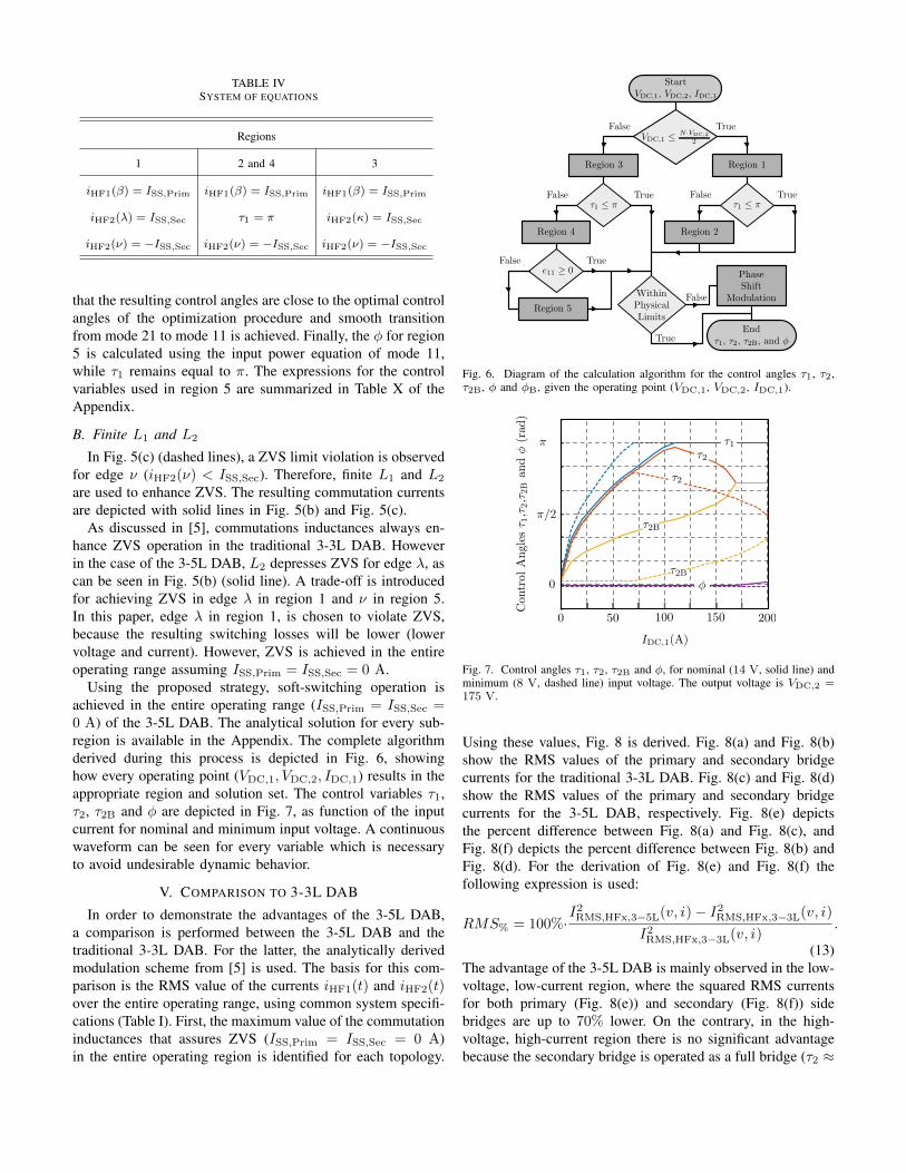
TABLE IVSYSTEM OF EQUATIONS
Regions
1 2 and 4 3
iHF1(β) = ISS,Prim iHF1(β) = ISS,Prim iHF1(β) = ISS,Prim
iHF2(λ) = ISS,Sec τ1 = π iHF2(κ) = ISS,Sec
iHF2(ν) = −ISS,Sec iHF2(ν) = −ISS,Sec iHF2(ν) = −ISS,Sec
that the resulting control angles are close to the optimal controlangles of the optimization procedure and smooth transitionfrom mode 21 to mode 11 is achieved. Finally, the φ for region5 is calculated using the input power equation of mode 11,while τ1 remains equal to π. The expressions for the controlvariables used in region 5 are summarized in Table X of theAppendix.
B. Finite L1 and L2
In Fig. 5(c) (dashed lines), a ZVS limit violation is observedfor edge ν (iHF2(ν) < ISS,Sec). Therefore, finite L1 and L2
are used to enhance ZVS. The resulting commutation currentsare depicted with solid lines in Fig. 5(b) and Fig. 5(c).
As discussed in [5], commutations inductances always en-hance ZVS operation in the traditional 3-3L DAB. Howeverin the case of the 3-5L DAB, L2 depresses ZVS for edge λ, ascan be seen in Fig. 5(b) (solid line). A trade-off is introducedfor achieving ZVS in edge λ in region 1 and ν in region 5.In this paper, edge λ in region 1, is chosen to violate ZVS,because the resulting switching losses will be lower (lowervoltage and current). However, ZVS is achieved in the entireoperating range assuming ISS,Prim = ISS,Sec = 0 A.
Using the proposed strategy, soft-switching operation isachieved in the entire operating range (ISS,Prim = ISS,Sec =0 A) of the 3-5L DAB. The analytical solution for every sub-region is available in the Appendix. The complete algorithmderived during this process is depicted in Fig. 6, showinghow every operating point (VDC,1, VDC,2, IDC,1) results in theappropriate region and solution set. The control variables τ1,τ2, τ2B and φ are depicted in Fig. 7, as function of the inputcurrent for nominal and minimum input voltage. A continuouswaveform can be seen for every variable which is necessaryto avoid undesirable dynamic behavior.
V. COMPARISON TO 3-3L DAB
In order to demonstrate the advantages of the 3-5L DAB,a comparison is performed between the 3-5L DAB and thetraditional 3-3L DAB. For the latter, the analytically derivedmodulation scheme from [5] is used. The basis for this com-parison is the RMS value of the currents iHF1(t) and iHF2(t)over the entire operating range, using common system specifi-cations (Table I). First, the maximum value of the commutationinductances that assures ZVS (ISS,Prim = ISS,Sec = 0 A)in the entire operating region is identified for each topology.
Fig. 6. Diagram of the calculation algorithm for the control angles τ1, τ2,τ2B, φ and φB, given the operating point (VDC,1, VDC,2, IDC,1).
Fig. 7. Control angles τ1, τ2, τ2B and φ, for nominal (14 V, solid line) andminimum (8 V, dashed line) input voltage. The output voltage is VDC,2 =175 V.
Using these values, Fig. 8 is derived. Fig. 8(a) and Fig. 8(b)show the RMS values of the primary and secondary bridgecurrents for the traditional 3-3L DAB. Fig. 8(c) and Fig. 8(d)show the RMS values of the primary and secondary bridgecurrents for the 3-5L DAB, respectively. Fig. 8(e) depictsthe percent difference between Fig. 8(a) and Fig. 8(c), andFig. 8(f) depicts the percent difference between Fig. 8(b) andFig. 8(d). For the derivation of Fig. 8(e) and Fig. 8(f) thefollowing expression is used:
RMS% = 100%·I2RMS,HFx,3−5L(v, i)− I2RMS,HFx,3−3L(v, i)
I2RMS,HFx,3−3L(v, i).
(13)The advantage of the 3-5L DAB is mainly observed in the low-voltage, low-current region, where the squared RMS currentsfor both primary (Fig. 8(e)) and secondary (Fig. 8(f)) sidebridges are up to 70% lower. On the contrary, in the high-voltage, high-current region there is no significant advantagebecause the secondary bridge is operated as a full bridge (τ2 ≈

(a) (b)
(c) (d)
(e) (f)
Fig. 8. RMS current of (a) LV-side bridge (IRMS,HF1) and (b) HV-side bridge(IRMS,HF2) of the 3-3L DAB topology. (c) and (d) show the RMS currentof LV-side bridge (IRMS,HF1) and HV-side bridge (IRMS,HF2) of the 3-5LDAB topology, respectively. Figure (e) shows the percent difference of (a)and (c), and figure (f) shows the percent difference of (b) and (d), accordingto eqn. (13).
τ2B).
VI. CONCLUSION
In this paper a modulation strategy for the 3 Level –5 Level (3-5L) Dual Active Bridge (DAB) DC–DC converter,achieving ZVS in the whole operating range, is presented. Ananalysis of the possible switching modes is provided, as wellas, a selection procedure to select the optimum mode for everyoperating point. Two modes are selected and by interpretingthe results of the numerical optimization, a final switchingcontrol strategy is derived. Both bridges use commutationinductances in order to assure ZVS in the transition betweenmodes. The proposed strategy is compared with a similarstrategy derived for the traditional 3-3L DAB in literature.The comparison shows the advantage of the 3-5L DAB in thelow-voltage, low-current region.
ACKNOWLEDGMENTS
This paper is part of the ADvanced Electric PowertrainTechnology (ADEPT) project which is an EU funded MarieCurie ITN project, grant number 607361 [16].
REFERENCES
[1] M. N. Kheraluwala, R. W. Gascoigne, D. M. Divan, and E. D. Baumann,“Performance characterization of a high-power dual active bridge DC-to-DC converter,” IEEE Transactions on Industry Applications, vol. 28,no. 6, pp. 1294–1301, Nov. 1992.
[2] F. Krismer and J. W. Kolar, “Efficiency-Optimized High-Current DualActive Bridge Converter for Automotive Applications,” IEEE Transac-tions on Industrial Electronics, vol. 59, no. 7, pp. 2745–2760, July 2012.
[3] R. W. De Doncker, D. M. Divan, and M. H. Kheraluwala, “A Three-Phase Soft-Switched High Power Density DC/DC Converter for HighPower Applications,” in IEEE Industry Applications Society AnnualMeeting, vol. 1, Oct. 1988, pp. 796–805.
[4] G. G. Oggier, G. O. Garcia, and A. R. Oliva, “Modulation Strategyto Operate the Dual Active Bridge DC-DC Converter Under SoftSwitching in the Whole Operating Range,” IEEE Transactions on PowerElectronics, vol. 26, no. 4, pp. 1228–1236, April 2011.
[5] J. Everts, J. Van den Keybus, F. Krismer, J. Driesen, and J. W. Kolar,“Switching Control Strategy for Full ZVS Soft-Switching Operation ofa Dual Active Bridge AC/DC Converter,” in IEEE 27th Annual AppliedPower Electronics Conference and Exposition (APEC 2012), Feb. 2012,pp. 1048–1055.
[6] J. Everts, F. Krismer, J. Van den Keybus, J. Driesen, and J. W. Kolar,“Optimal ZVS Modulation of Single-Phase Single-Stage BidirectionalDAB AC–DC Converters,” IEEE Transactions on Power Electronics,vol. 29, no. 8, pp. 3954–3970, Aug. 2014.
[7] P. A. M. Bezerra, F. Krismer, R. M. Burkart, and J. W. Kolar,“Bidirectional Isolated non-Resonant DAB DC-DC Converter for Ultra-Wide Input Voltage Range Applications,” in IEEE International PowerElectronics and Application Conference and Exposition (PEAC 2014),Nov. 2014, pp. 1038–1044.
[8] J. Everts and J. W. Kolar, “Elektrischer Leistungswandler zur DC/DC-Wandlung mit Dualen Aktiven Brucken,” Swiss patent CH707 553 (A2),August 15, 2014.
[9] M. A. Moonem and H. Krishnaswami, “Control and configuration ofthree-level dual-active bridge DC-DC converter as a front-end interfacefor photovoltaic system,” in IEEE 29th Applied Power ElectronicsConference and Exposition (APEC 2014), March 2014, pp. 3017–3020.
[10] ——, “Analysis and control of multi-level dual active bridge DC-DCconverter,” in IEEE Energy Conversion Congress and Exposition (ECCE2012), Sept. 2012, pp. 1556–1561.
[11] A. Filba-Martinez, S. Busquets-Monge, and J. Bordonau, “Modulationand capacitor voltage balancing control of a three-level NPC dual-active-bridge DC-DC converter,” in IEEE 39th Annual Conference of IndustrialElectronics Society (IECON 2013), Nov. 2013, pp. 6251–6256.
[12] A. K. Tripathi, K. Hatua, H. Mirzaee, and S. Bhattacharya, “A three-phase three winding topology for Dual Active Bridge and its D-Q modecontrol,” in IEEE 27th Annual Applied Power Electronics Conferenceand Exposition (APEC 2012), Feb. 2012, pp. 1368–1372.
[13] F. Krismer and J. W. Kolar, “Closed Form Solution for MinimumConduction Loss Modulation of DAB Converters,” Power Electronics,IEEE Transactions on, vol. 27, no. 1, pp. 174–188, Jan. 2012.
[14] J. Everts, G. E. Sfakianakis, and E. A. Lomonova, “Using Fourier Seriesto Derive Optimal Soft-Switching Modulation Schemes for Dual ActiveBridge Converters,” in IEEE 7th Annual Energy Conversion Congressand Exposition (ECCE 2015), Sept. 2015, pp. 4648–4655.
[15] J. Everts, F. Krismer, J. Van den Keybus, J. Driesen, and J. Kolar, “Com-parative Evaluation of Soft-Switching, Bidirectional, Isolated AC/DCConverter Topologies,” in Applied Power Electronics Conference andExposition (APEC), 2012 Twenty-Seventh Annual IEEE, Feb 2012, pp.1067–1074.
[16] A. Stefanskyi, A. Dziechciarz, F. Chauvicourt, G. E. Sfakianakis,K. Ramakrishnan, K. Niyomsatian, M. Curti, N. Djukic, P. Romanazzi,S. Ayat, S. Wiedemann, W. Peng, A. Tamas, and S. Stipetic,“Researchers within the EU funded Marie Curie ITN project ADEPT,grant number 607361,” 2013-2017. [Online]. Available: adept-itn.eu
APPENDIX

TABLE VCURRENT EXPRESSIONS FOR MODE 21
iHF1(0) =L1 N VDC,2 (τ2+τ2B)−2 τ1 VDC,1 (L+L1)
4L L1 ωs
iHF1(α) =L1 N VDC,2 (τ2+τ2B)−2 τ1 VDC,1 (L+L1)
4L L1 ωs
iHF1(β) =2 τ1 VDC,1 (L+L1)−L1 N VDC,2 (τ2+τ2B)
4L L1 ωs
iHF1(κ) =2VDC,1 (L+L1) (2φ+τ1−2 τ2)+L1 N VDC,2 (τ2+τ2B)
4L L1 ωs
iHF1(λ) =2VDC,1 (L+L1) (2φ+τ1)−L1 N VDC,2 (τ2+τ2B)
4L L1 ωs
iHF1(µ) =
2VDC,1 (L+L1) (2φB+τ1−2 τ2B)
4L L1 ωs
+L1 N VDC,2 (2φ−2φB−τ2+3 τ2B)
4L L1 ωs
iHF1(ν) =2VDC,1 (L+L1) (2φB+τ1)−L1 N VDC,2 (2φB−2φ+τ2+τ2B)
4L L1 ωs
iHF2(0) =N VDC,2 (L+L2) (τ2+τ2B)−2L2 τ1 VDC,1
4L L2 ωs
iHF2(α) =N VDC,2 (L+L2) (τ2+τ2B)−2L2 τ1 VDC,1
4L L2 ωs
iHF2(β) =2L2 τ1 VDC,1−N VDC,2 (L+L2) (τ2+τ2B)
4L L2 ωs
iHF2(κ) =N VDC,2 (L+L2) (τ2+τ2B)+2L2 VDC,1 (2φ+τ1−2 τ2)
4L L2 ωs
iHF2(λ) =2L2 VDC,1 (2φ+τ1)−N VDC,2 (L+L2) (τ2+τ2B)
4L L2 ωs
iHF2(µ) =
N VDC,2 (L+L2) (2φ−2φB−τ2+3 τ2B)
4L L2 ωs
+2L2 VDC,1 (2φB+τ1−2 τ2B)
4L L2 ωs
iHF2(ν) =2L2 VDC,1 (2φB+τ1)−N VDC,2 (L+L2) (2φB−2φ+τ2+τ2B)
4L L2 ωs
TABLE VICURRENT EXPRESSIONS FOR MODE 11
iHF1(0) =L1NVDC,2(−2φ−2φB+τ2+τ2B)−2τ1VDC,1(L+L1)
4LL1ωs
iHF1(α) =
L1 N VDC,2 (−2φ−2φB−4 τ1+τ2+τ2B+4π )
4L L1 ωs
− 2 τ1 VDC,1 (L+L1)
4L L1 ωs
iHF1(β) =2 τ1 VDC,1 (L+L1)+L1 nVDC,2 (2φ+2φB−τ2−τ2B)
4L L1 ωs
iHF1(κ) =2VDC,1 (L+L1) (2φ+τ1−2 τ2)+L1 N VDC,2 (τ2+τ2B)
4L L1 ωs
iHF1(λ) =2VDC,1 (L+L1) (2φ+3 τ1−2π )−L1 N VDC,2 (τ2+τ2B)
4L L1 ωs
iHF1(µ) =
2VDC,1 (L+L1) (2φB+τ1−2 τ2B)
4L L1 ωs
+L1 N VDC,2 (2φ−2φB−τ2+3 τ2B)
4L L1 ωs
iHF1(ν) =
2VDC,1 (L+L1) (2φB+3 τ1−2π )
4L L1 ωs
−L1 N VDC,2 (2φB−2φ+τ2+τ2B)
4L L1 ωs
iHF2(0) = −N VDC,2 (L+L2) (2φ+2φB−τ2−τ2B)+2L2 τ1 VDC,1
4LL2 ωs
iHF2(α) =N VDC,2 (L+L2) (−2φ−2φB−4 τ1+τ2+τ2B+4π )−2L2 τ1 VDC,1
4L L2 ωs
iHF2(β) =N VDC,2 (L+L2) (2φ+2φB−τ2−τ2B)+2L2 τ1 VDC,1
4L L2 ωs
iHF2(κ) =N VDC,2 (L+L2) (τ2+τ2B)+2L2 VDC,1 (2φ+τ1−2 τ2)
4L L2 ωs
iHF2(λ) =2L2 VDC,1 (2φ+3 τ1−2π )−nVDC,2 (L+L2) (τ2+τ2B)
4L L2 ωs
iHF2(µ) =N VDC,2 (L+L2) (2φ−2φB−τ2+3 τ2B)+2L2 VDC,1 (2φB+τ1−2 τ2B)
4L L2 ωs
iHF2(ν) =2L2 VDC,1 (2φB+3 τ1−2π )−N VDC,2 (L+L2) (2φB−2φ+τ2+τ2B)
4L L2 ωs
TABLE VIIEXPRESSIONS FOR CALCULATION OF CONTROL VARIABLES FOR REGION 1
τ1e5 e4−
√e44 e3 L N VDC,2 ωs
e42 VDC,1 (2VDC,1−N VDC,2)
τ22(√
e44 e3 L N VDC,2 ωs+e6
)e42 N VDC,2 (N VDC,2−2VDC,1)
τ2B − 2 ISS,Sec Lωs
e4
φ −Lωs (ISS,Prim+ISS,Sec)
VDC,1
TABLE VIIIEXPRESSIONS FOR CALCULATION OF CONTROL VARIABLES FOR REGION 2
AND 4
τ1 π
τ2e7−√e11
N2 VDC,1 V2DC,2
τ2Be7+√e11
N2 VDC,1 V2DC,2
φ −Lωs (ISS,Prim+ISS,Sec)
VDC,1

TABLE IXEXPRESSIONS FOR CALCULATION OF CONTROL VARIABLES FOR REGION 3
τ1e13−
√e12 VDC,1
e4 VDC,1 (2VDC,1−N VDC,2)
τ2ISS,Sec L ωs (3N VDC,2−4VDC,1)−
√e12
e4 (2VDC,1−N VDC,2)
τ2B√e12+ISS,Sec L N VDC,2 ωs
−e4 N VDC,2
φ −Lωs (ISS,Prim+ISS,Sec)
VDC,1
TABLE XEXPRESSIONS FOR CALCULATION OF CONTROL VARIABLES FOR REGION 5
τ1 π
τ2 <(
e7−√e11
N2 VDC,1 V2DC,2
)
τ2B <( √
e11+e7N2 VDC,1 V
2DC,2
)
φ−√e15+e16+2N τ2 VDC,2+2N τ2B VDC,2
8N VDC,2
TABLE XIEXPRESSIONS FOR exx ELEMENTS
e1 2 ISS,Prim + ISS,Sec
e2 I2SS,Sec L N VDC,2 ωs
e3 e2 + 2π IDC,1 VDC,1 (N VDC,2 − 2VDC,1)
e4 VDC,1 −N VDC,2
e5 L ωs
(e1N2 V 2
DC,2 − 3 e1N VDC,1 VDC,2 + 4 ISS,Prim V 2DC,1
)e6 e4 ISS,Sec L N VDC,1 VDC,2 ωs
e7 N VDC,1 VDC,2 (π VDC,1 − 2 ISS,Prim L ωs)
e8 4 ISS,Prim L2 ω2s (N VDC,2 (ISS,Prim + ISS,Sec)− ISS,Prim VDC,1)
e9 N VDC,2 (e1 + IDC,1)− 2 ISS,Prim VDC,1
e10 −π 2 e4 V 2DC,1
e11 N2 VDC,1 V2DC,2 (e8 − 2π e9 L VDC,1 ωs + e10)
e12 LN VDC,2 ωs (e2 − 2π e4 IDC,1 (2VDC,1 −N VDC,2))
e13
Lωs
(−3 e1N VDC,1 VDC,2 + 2N2 V 2
DC,2 (ISS,Prim + ISS,Sec))
+Lωs
(4 ISS,Prim V 2
DC,1
)e14 4π IDC,1 L ωs
e15 (−2N τ2 VDC,2 − 2N τ2B VDC,2)2
e16
−16N VDC,2
(e14 +N τ22 VDC,2 − π N τ2 VDC,2 +N τ22B VDC,2
)−16N VDC,2
(−π N τ2B VDC,2
)
DESIGN AND APPLICATION OF A BOOTSTRAP CIRCUIT CONTROLLED BY PIC24 FOR A GRID
INVERTER
Mohannad Jabbar Mnati 1,2, Alex Van den Bossche 2 and Jean Marie Vianney Bikorimana 2,3
1 Department of Electronic Technology, Institute of Technology Baghdad, Baghdad, Iraq,
E-mail: [email protected]
2 Electrical Energy Laboratory, Ghent University, Ghent, Belgium
E-mail: [email protected]
3 Department of Electrical and Electronics, University of Rwanda, Kigali, Rwanda
E-mail: [email protected]
Abstract— The standard bootstrap circuit consists of three important external components (diode, resistance and capacitor) for a PWM standard application. However, bootstrap circuits have shown some weakness such as having adequate components to allow a high performance. This article shows a bootstrap driver circuit using IR2112 to drive a power IGBTs inverter with a low energy consumption. In this paper, the PWM signal is generated by using a PIC24FJ128GA010 microcontroller and interfaced to the bootstrap circuit. The paper discusses the advantage and disadvantages of the bootstrap circuits.
Keywords— Bootstrap components, PIC24FJ128GA010, IGBT, driver circuit, IR2112.
I. INTRODUCTION
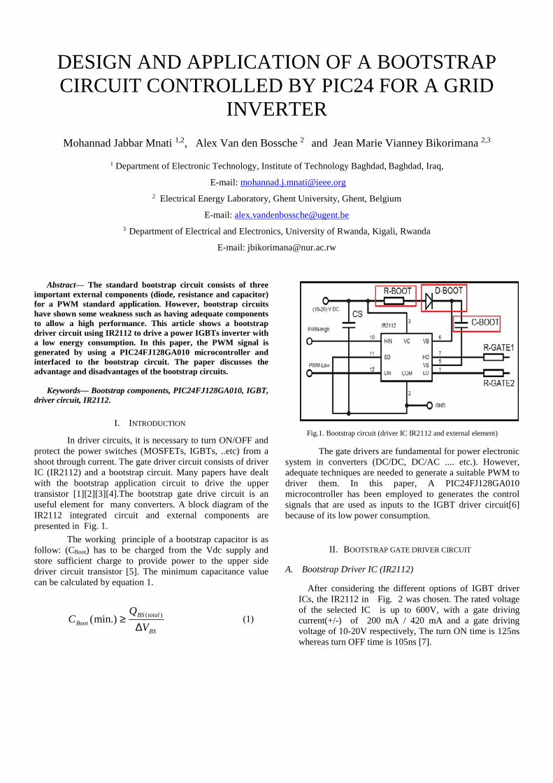
In driver circuits, it is necessary to turn ON/OFF and protect the power switches (MOSFETs, IGBTs, ..etc) from a shoot through current. The gate driver circuit consists of driver IC (IR2112) and a bootstrap circuit. Many papers have dealt with the bootstrap application circuit to drive the upper transistor [1][2][3][4].The bootstrap gate drive circuit is an useful element for many converters. A block diagram of the IR2112 integrated circuit and external components are presented in Fig. 1.
The working principle of a bootstrap capacitor is as follow: (CBoot) has to be charged from the Vdc supply and store sufficient charge to provide power to the upper side driver circuit transistor [5]. The minimum capacitance value can be calculated by equation 1.
BS
totalBSBoot V
QC
∆≥ )()min.( (1)
Fig.1. Bootstrap circuit (driver IC IR2112 and external element)
The gate drivers are fundamental for power electronic system in converters (DC/DC, DC/AC .... etc.). However, adequate techniques are needed to generate a suitable PWM to driver them. In this paper, A PIC24FJ128GA010 microcontroller has been employed to generates the control signals that are used as inputs to the IGBT driver circuit[6] because of its low power consumption.
II. BOOTSTRAP GATE DRIVER CIRCUIT
A. Bootstrap Driver IC (IR2112)
After considering the different options of IGBT driver ICs, the IR2112 in Fig. 2 was chosen. The rated voltage of the selected IC is up to 600V, with a gate driving current(+/-) of 200 mA / 420 mA and a gate driving voltage of 10-20V respectively, The turn ON time is 125ns whereas turn OFF time is 105ns [7].

Fig. 2 IR2112 Block Diagram
B. Bootstrap External Conponent
The bootstrap circuit consists of three external components (RBoot , DBoot and CBoot ) as shown in Fig. 1.
1) Bootstrap Resistance(RBoot):The first element in the bootstrap circuit is a bootstrap resistance as a small value connected in series with bootstrap diode(DBoot) ,This resistance (RBoot) is used to limit charger current flowing to bootstrap capacitor(CBoot) [2] .
Boot
onBoot C
lowerIGBTTR
×≤
4)(
(2)
2) Bootstrap Diode(DBoot): The bootstrap diode (DBoot)
provide route to charge bootstrap capacitor (CBoot) and it must be able to have a fast recovery time to block the fed back voltage from this capacitor to driver power supply. There are some parameter that must be considered when choosing diode [8].
• TRR =Reverse Recovery Time
• VRRM = Maximum Repetitive reverse Voltage
• IF(AV) = Average Rectified Forward Current
3) The main principle of bootstrap capacitor (CBoot) is to store sufficient charge to supply the enough power exhaustion of IGBT gate driver and necessary gate charge to turn the upper side transistor ''ON'', The minimum bootstrap capacitor required can be calculated using the equation 1.
ONDSLKDIODELKLKQBS
GELKCAPLKLSgtotalBS
TIIII
IIQQQ
*)
(
,,
,,)(
++++
+++= (3)
)( )(.)(min ONCEGEFDCBS VVVVV −−−≤∆ (4)
Where, Qg : IGBT Turn on Required Gate Charge QLS : Charge required by The Internal Level Shifters ILK,CAP : Capacitor Leakage Current ILK,GC : Gate Leakage Current of The IGBT IQBS : High Side Floating Supply Leakage Current ILK : Bootstrap Circuit Leakage Current ILK,DS : Bootstrap Diode Leakage Current VBS : Minimum Voltage Drop VDC : Section logic voltage source VF : Bootstrap Diode Forward voltage VLS :Low – Side IGBT Drop Voltage VCE(ON) : Minimum voltage Between VC and VE TON : Turning on Interval of lower IGBT
III. PROGRAMMABLE PWM CONTROLLER
PIC24FJ128GA010 microcontroller is the main unit used in the implementation to control the Half-Bridge. It is programmed by C language and using a MPLAB X IDEV3.15 software compiler for programing[6][9][10].
The control signals that are used as inputs to the IGBT driver circuit are generated by PIC24FJ128GA010 microcontroller. This controller was used because of its low power consumption, Pin terminals and the salient features are observed in Table 1.
TABLE I. Specifications of PIC24FJ128GA010
PIC24FJ128GA010 is often used in industry, automotive applications, medical electronics applications and consumer electronics. The signal levels are directly compatible but they are not galvanic separated. Some applications do not need it. Therefore, in this case the bootstrap circuits have advantages.
IV. CALCULATION AND EXPERIMENTAL RESULTS
A. Mathematical Results
To accurately calculate the value of the bootstrap capacitor, equations 1,3 and 4 and following bootstrap circuit components, an switching frequency of 10kHz have been. (IRG4BC10UD Power IGBT[11] ,bootstrap diode DO-204AL (DO-41),Driver IC 2112). Table 2 shows all the equations parameters used to calculate the bootstrap capacitor value. The values are from the datasheets.

TABLE 2. Bootstrap Component Parameters
The (Cboot) used in the present paper has been calculated as follows:
VVBS 7.06.2157.120 =−−−=∆ based on eq. (4)
nC
Q totalBS
01.32
)10*10(
0)10*10()10*50()10*60()10*100(0
)10*5()10*15(
3
6699
99)(
=
+++++
++=−−−−
−−
based on eq. (1)
Hence, a (Cboot ) of 100nF can be used for the bootstrap driver circuit. Fig. 3. Illustrates the minimum value of bootstrap capacitor depending on the switching frequency. Once the switching frequency varies from 5KHz to 50KHz, 100 times more, the used electrolytic capacitor ageing is (2 – 200)times more.
Fig. 3. Minimum Bootstrap capacitor
B. Experimrntal Results
The Final circuit diagram of the bootstrap circuit and Half-Bridge topology are shown in the Fig. 4.
Fig. 4. Complete Half-Bridge Circuit
The practical circuit in the Fig. 5 explains the final bootstrap circuit , Half-Bridge IGBT and 5 volt voltage regulator are used to supply the driver IC(IR2112). However, if ON time of (10 ms) are considered, much higher values for charging are required. Large electrolytic capacitor is connected in parallel with the bootstrap capacitor to improve the charge of the upper gate only and cope with long ON time of the upper transistor. The value of electrolytic capacitor can be calculate by multiply the bootstrap capacitor by factor 20 depended to the transistor and high DC link Voltage
Fig. 5. Final Driver Circuit
Figures 6 through 8 show the experimental results for the bootstrap circuit of IGBT Half-Bridge without load.
Parameter was selected parameter of the data sheets
Element Value Device Notes IQBS 60 uA IR2112 Driver
IC ILK 50uA IR2112 QLS 5nC
20nC 500-600V
/1200V QG 15 nC IRG4BC10UD
IGBT Transistor
IGES 100 nA IRG4BC10UD VCE(on) 2.6v IRG4BC10UD VGE 15v IRG4BC10UD Vf 1.7 V DO-204AL
(DO-41) Bootstrap
Diode IKL,DIODE 10 uA DO-204AL
(DO-41) ILK_CAP 0 Typical

Fig. 6 shows the PWM waveforms of the PIC24FG128GA010 and gate driver circuits without connect IGBT transistor,Ch1 and Ch2 output PWM of the microcontroller Ch3 and Ch4 the output PWM of the bootstrap driver circuit .
Fig. 6. Bootstrap capacitor depending on the
Fig. 7 shows the PWM waveforms of the PIC24FG128GA010 and gate driver circuits with IGBT transistor (half-bridge circuit),Ch1 and Ch2 output PWM of the microcontroller Ch3 and Ch4 the output PWM of the driver circuit. The main deferent between Fig 6 and Fig 7 is voltage of Ch4 (lower transistor) is lease than the voltage of Ch3 due to drop voltage across the freewheel diode .
Fig. 7. PWM waveforms with connect IGBT
The voltage of the output of the driver circuit and half-bridge circuit is shown in the Fig. 8 , Ch1 and Ch2 is the PWM of the driver circuit and Ch3 is the output voltage of half-bridge circuit
Fig. 8. Output waveform of Half-Bridge and driver circuit
The experiment shows that they are some advantages and disadvantages of the bootstrap circuits.
A. Advantages /Steght
• Low power consumption,
• No inductive components ,
• Low number of internal supplies.
B. Disadvantages /Weakess
• No galvanic separation,
• High reach current occurs in internal supplies,
• A long pulse is needed to charge the upper bootstrap capacitor.
V. conclusion
This paper present to design a bootstrap circuit based on power IGBT and IR2112 driver IC. The bootstrap resistance is first parameter of bootstrap circuit, series with bootstrap diode to limit charger current flowing to bootstrap capacitor. Then the paper showed how to calculate the bootstrap capacitor for different switching frequency. It presented the technique of connecting electrolytic capacitor in parallel with film capacitor in order to improve the of the upper gate. Moreover, the paper discussed the advantage and disadvantages of the bootstrap circuit. PIC24FJ128GA010 was used to generate control signals that are used as inputs to the IGBT driver circuit

REFERENCES
[1] A. Seidel, M. Costa, J. Joos, and B. Wicht, “Bootstrap circuit with high-voltage charge storing for area efficient gate drivers in power management systems,” Eur. Solid-State Circuits Conf., pp. 159–162, 2014.
[2] Fairchild Semiconductors, “Design and Application Guide of Bootstrap Circuit for High-Voltage Gate-Driver IC,” 2008.
[3] T. Y. Elganimi, “Design and Analysis of a Bootstrap Ramp Generator Circuit Based on a Bipolar Junction Transistor ( BJT ) Differential Pair Amplifier,” vol. I, no. September, pp. 22–24, 2014.
[4] S. Chung and J. Lim, “Design of Bootstrap Power Supply for Half-Bridge Circuits using Snubber Energy Regeneration,” JPE, vol. 7, no. 4, pp. 294–300, 2007.
[5] H. V Floating and M. D. Ics, “Application Note AN-978 Table of Contents,” Int. Rectifier, vol. 2092, pp. 1–30, 1998.
[6] G. Purpose and F. Microcontrollers, “Pic24Fj128Ga010 Family,” Microchip, 2012.
[7] I. I. Rectifier, “Datasheet IR2112,” vol. 2112, pp. 1–18.
[8] J. Zhu, W. Sun, S. Member, Y. Zhang, S. Lu, L. Shi, S. Zhang, and W. Su, “An Integrated Bootstrap Diode Emulator for 600-V High Voltage Gate Drive IC With P-Sub / P-Epi Technology,” 518 IEEE Trans. POWER Electron., vol. 31, no. 1, pp. 518–523, 2016.
[9] A. . Fallis, ADVANCED PIC MICROCONTROLLER PROJECTS IN C, vol. 53, no. 9. 2013.
[10] Microchip Technology Inc., MPLAB ® X IDE User ’ s Guide. 2012.
[11] I. Gate, B. Transistor, U. Soft, and R. Diode, “IRG4BC10UD IRG4BC10UD,” Int. Rectifier, pp. 1–11.
An Observer-based MPC Approach by SensingPrimary Signals in Transformer-isolated Converters
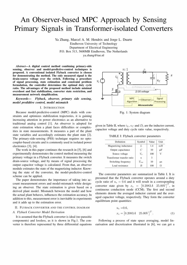
Ya Zhang, Marcel A. M. Hendrix and Jorge L. DuarteEindhoven University of TechnologyDepartment of Electrical Engineering
P.O. Box 513, 5600MB Eindhoven, The [email protected]
Abstract—A digital control method combining primary-sidesensing, observer and model-predictive-control techniques isproposed. A conventional isolated Flyback converter is chosenfor demonstrating the method. The only measured signal is thedrain-source voltage over the switch. Following a procedureof signal processing, state estimation and constraint problemformulation, the controller determines the optimal duty cycleratio. The advantages of the proposed method include minimalovershoot and fast stabilization, converter state restriction, andmeasurement network simplification.
Keywords— Flyback, observer, primary side sensing,model predidtive control, model mismatch
I. INTRODUCTION
Because model-predictive-control (MPC) deals with con-straints and optimizes stabilization trajectories, it is gainingincreasing attention in power electronics as an alternative totraditional analog control [1]. An observer is adopted forstate estimation when a plant faces difficulties or complex-ities in state measurements. It measures a part of the plantstate variables and accordingly estimates the plant state [2].The primary-side-sensing (PSS) technique requires no opto-coupler-based circuits and is commonly used in isolated powerelectronics [3], [4].
The work in this paper continues the research in [5], [6] andexperimentally demonstrates the control method measuring theprimary voltage in a Flyback converter. It measures the switchdrain-source voltage, and by means of signal processing theoutput capacitor voltage is calculated. From that, an observermodule estimates the state of the magnetizing inductor. Know-ing the state of the converter, the model-predictive-controlscheme can be applied.
The paper demonstrates the importance of taking into ac-count measurement errors and model-mismatch while design-ing an observer. The state estimation is given based on aderived plant model. Mismatch between the model and howthe actual plant behaves, influences the estimation accuracy. Inaddition to this, measurement error is inevitable in experimentsand it adds up to the estimation error.
II. FLYBACK CONVERTER AND THE CONTROL DIAGRAM
A. Flyback Converter Model DerivationIt is assumed that the Flyback converter is ideal (no parasitic
components) and lossless, as it is shown in Fig.1. The con-verter is therefore represented by three differential equations
Signal Processing
MPC Algorithm
Observer
1) Primary Current
2) DS voltage
Microcontroller
Fig. 1: System diagram
given in Table II, where iL, vC and Dt are the inductor current,capacitor voltage and duty cycle ratio value, respectively.
TABLE I: Flyback converter parameters
Definition Symbol Value Unit
Magnetizing inductance L 1.4 mH
Output capacitance C 10 µF
Source voltage Vs 100 V
Transformer transfer ratio n 3
Switching frequency Tsw 10 µs
Load resistance R 100 Ω
The converter parameters are summarized in Table I. It ispresumed that the Flyback converter operates around a dutycycle ratio of ue = 0.6 and it will result in a correspondingconverter state given by xe =
[0.2083A 25.00V
]T, in
continuous conduction mode (CCM). The first and secondelements denote the averaged inductor current and the aver-aged capacitor voltage, respectively. They form the converterequilibrium point quantities:
ue =0.6,
xe =[0.2083A 25.00V
]T. (1)
Following a process of state space averaging, model lin-earisation and discretization illustrated in [6], we can get a

TABLE II: State space representation of the Flyback converter,switched model.
SS description
xt = Axt + bt
xt =
[iLvC
],
Dwelltime
Switch ON,diode OFF
A = A1, bt = bt,1
A1 =
[0 0
0−1
RC
]
bt,1 =
[Vs
L0
] DtTsw
Switch OFF,diode ON
A = A2, bt = bt,2
A2 =
0−n
Ln
C
−1
RC
bt,2 =
[0
0
] Dt,1Tsw
Switch OFF,diode OFF
A = A3, bt = bt,3
A3 =
[0 0
0−1
RC
]
bt,3 =
[0
0
] Dt,2Tsw
simplified model of the converter, given by
xk+1 =Adxk +Bduk,
yk =Cmxk, (2)
where Cm is the measurement matrix, yk the measured value,and Ad, Bd are constant matrices represented by the Flybackconverter parameters and the equilibrium point quantities, andxk and uk are discrete small signals given by
uk =Dt − uexk =xt − xe. (3)
Because the capacitor voltage is the only measured variablefed into the micro-controller, as highlighted in Fig.1, theinductor current (associated with the first element of xk) hasno contribution to the measured value yk. The measurementmatrix is therefore given by
Cm =[0 1
]. (4)
B. Observer-Based Model Predictive Controller
1) Capacitor Voltage Calculation from DS Voltage : Whenthe switch is OFF and the diode is ON, the switch drain-sourcevoltage is
vDS = Vs + nvC , (5)
where Vs is the source voltage and n the transformer primary-to-secondary transfer ratio. Accordingly the capacitor voltageis calculated.
2) Converter State Estimation by Observer: Now that thecapacitor voltage is known, we are able to estimate theconverter state accordingly. The observer elaborated on in [2]is adopted, described by
xk+1 = Adxk +Bduk + Lm(yk − Cmxk), (6)
where xk is the estimation of xk, and Lm is the observerfeedback gain. Comparing (2) and (6) yields
xk+1 − xk+1 = (Ad − LmCm)(xk − xk). (7)
Therefore, the observation design turns out to be a classicpole-placement problem, and that is, to place the eigenvaluesof (Ad −LmCm) within the unit cycle in the complex plane.The tunable parameter is Lm and Ad and Cm are constantmatrices.
3) MPC for Trajectory Restriction: The algorithm is de-signed to fast stabilize the converter while considering theconverter constraints and input efforts. Its mathematical de-scription is to minimize the cost function defined by
F (x0, U) =xTNPxN +
N−1∑i=0
(xTi Qxi + uTi Rui),
with U =[u0 u1 · · · uN−1
]T,
xi =Adxi−1 +Bdui−1, i = 1, 2,· · ·N, (8)
where ui−1, xi are subjected to
ulow,i ≤ui−1 + ue ≤ uhigh,i,and xlow,i ≤xi + xe ≤ xhigh,i, (9)
and N is the prediction horizon; ulow,i,i=1···N anduhigh,i,i=1···N are constraints about the input (associated withthe duty cycle ratio); xlow,i,i=1···N and xhigh,i,i=1···N areconstraints about the state (associated with the inductor currentand the capacitor voltage); P,Q,R are the weights on terminalstate, the rest state, and the input, respectively [7].
III. IMPACTS OF MEASUREMENT ERROR AND MODELMISMATCH ON OBSERVATION
The work in [5] demonstrates that the observer convergencetime selection influences its performance. This section elabo-rates on additional criteria to assess an observer’s performance:its abilities to deal with inevitable model mismatch andmeasurement errors.
A. Measurement Error
The analysis of measurement error is performed in absenceof model mismatch. The normalized measurement offset erroris defined as
δy =∆y∞xe(2)
, (10)
where ∆y∞ is the static measurement error of the capacitorvoltage, and xe(2) denotes the second element of xe (thecapacitor voltage at the equilibrium point). According tothe analysis in section II-A, xe(2) can be also written as

xe(2) = Cmxe. The normalized observation offset error isdefined as
δx =
1
xe(1)0
01
xe(2)
∆x∞,
with
∆x∞ =[∆x∞(1) ∆x∞(2)
]T(11)
where ∆x∞ is the state estimation error when the observer isin steady state. The observation error gain from the measure-ment error is defined as
Gmag =δxδy. (12)
Next, we show a procedure to derive the algebraic expressionof the observation error gain. When the observer is in steadystate, equations
xk+1 =x∞
xk =x∞
yk =y∞, k →∞ (13)
hold for (6). When there is no measurement error, yk and xkare zero. Therefore, the offset errors are ∆y∞ = y∞ − 0 and∆x∞ = x∞ − 0. Substituting xk+1 = xk = x∞ = ∆x∞ andyk = y∞ = ∆y∞ into (6), and by comparing (11) and (10) ,we get the explicit algebraic expression of the error gain
Gmag =
1
xe(1)0
01
xe(2)
(I −Ad + LmCm)−1
LmCmxe. (14)
This gain is independent of the measurement offset error ∆y∞and dependent on the chosen equilibrium point.
B. Observer Design by Pole Placement
The function of an observer is to estimate a system state ina certain time interval. The observer design by pole placementis simple and effective for linear models, as it is illustrated in[2]. Bessel Polynomials further simplify the observer designby indicating the pole locations. However, practical systemshave imperfect models and are therefore sensitive to modelderivation errors and measurement inaccuracies. Consequently,the effectiveness of observer design by pole placement can becompromised.
1) Closed Loop Observer Design by Pole Placement: theobserver settling time 650µs is borrowed from [6] whichdemonstrated an effective current observer with the sameobserver settling time. Bessel polynomials are adopted forpole placement. The resulting observer gain matrix and itscorresponding error gain factor are
Lm,1 =[−0.1056 1.1494
]T,
Gmag,1 =[−39.5568 0.1876
]T(15)
respectively. The error gain indicates that -1% offset error inmeasuring the voltage will lead to an estimation offset errorof 39.5% in current, -0.187% in voltage, as highlighted by theblue small solid sphere in Fig.2.
Since the estimation error is linearly proportional to themeasurement error, the observer becomes more inaccuratewhen the measurement error increases (see Fig.2 for theexample of -5% measurement error). Please note that theobservation error gain discussed here is oriented to the chosenequilibrium point given in (1).
2) Open Loop observer: An open loop observer (not fea-sible in practice) is obtained by setting the observer gainLm,0 =
[0 0
]T. It means the observer disregards the infor-
mation from the measurement, and there is no communicationbetween the converter and the controller. Consequently, themeasurement error has no influence on the estimation and from(12) we have Gmag,0 = 0 .
C. Observer Design Adaptation
An observer designed by pole placement is confined tocoordinate the convergence speed. The tolerance to measure-ment and model derivation errors is not regarded or promisedby this method. The observer obtained by the method ofpole placement in section III-B1 is very sensitive to themeasurement error. A open loop observer discards convertermeasurement information and makes itself very dependent onthe correctness of the derived converter model. Hence, theobserver is heuristically adjusted towards a small error gainGmag (not a zero gain). The extreme design is to set theobserver gain matrix L =
[0 0
]T(resulting in a zero error
gain). It is not feasible in practice, but it indicates that anobserver gain matrix whose elements are close to zero couldbe a solution. Please note that a small observer gain matrix(not zero) will prolong the observer convergence time from(7). This means that the MPC algorithm cannot give reasonableresponse in time and overshoots are possible.
An observer with a relatively small error gain is found aftera series of manual attempts. The resulting observer gain matrixand its corresponding error gain factor are
Lm,2 =[−0.0106 −0.0460
]T,
Gmag,2 =[1.0698 −0.0612
]T, (16)
respectively. The observer with the adapted observer gainmatrix is chosen because it yields a relatively small errorgain. As a consequence, the observer becomes more tolerant tothe measurement error compared to the one obtained by pole-placement. Despite the fact that this observer results in 122msobservation settling time, it is adopted for the experiments andwe have Lm = Lm,2.
D. Model Mismatch
1) Switched Model and Simplified Model: The premise foran observer design is an accurate model of the converter.Regardless of power loss and parasitic components, the mostaccurate model for the Flyback converter is the switched model
described in Table II. However, adopting this switched modelmakes an observer design very complex. A common solution ismodel simplification by means of averaging and linearisation.
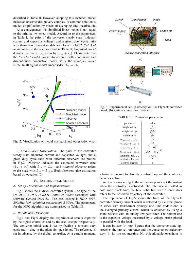
As a consequence, the simplified linear model is not equalto the original switched model. According to the parametersin Table I, the pairs of the converter steady state (inductorcurrent and capacitor voltage) and a given duty cycle ratiowith these two different models are plotted in Fig.2: Switchedmodel refers to the one described in Table II; Simplified modeldenotes the one in (2) given by (x∞ + xe). Please note thatthe Switched model takes into account both continuous anddiscontinuous conduction modes, while the simplified modelis the small signal model linearised at Dt = 0.6.
0.50.6
0.7
−0.20
0.20.410
20
30
40
DtiL [A]
v C [V
]
Switched model
Simplified model
Observer
Adapted observer
−5%−1%
Fig. 2: Visualization of model mismatch and observation error
2) Model-Based Observation: The pairs of the convertersteady state (inductor current and capacitor voltage) and agiven duty cycle ratio with different observers are plottedin Fig.2: Observer indicates the estimated converter state(x∞ + xe) with Lm = Lm,1 and Adapted observer refersto the state with Lm = Lm,2. Both observers give estimationbased on equation (6).
IV. EXPERIMENTAL RESULTS
A. Set-up Description and Implementation
Fig.3 shows the Flyback converter system. The type of theDSPACE is DS1104 R&D Controller Board associated withsoftware Control Desk 5.1. The oscilloscope is HDO 4024,200MHz high definition oscilloscope 2.5Gs/s. The parametersfor the MPC algorithm are summarized in Table III.
B. Results and Discussion
Fig.4 and Fig.5 display the experimental results capturedby the digital controller and by the oscilloscope, respectively.The converter initial state is set by feeding a constant dutycycle ratio value to the plant (in open loop). The reference isset in advance by the digital controller. At a certain moment,
DSpace connection interface
Power supply
Transformer DiodeSwitch
Capacitor
Load
(a)
(b)
Fig. 3: Experimental set-up description: (a) Flyback converterboard; (b) system connection diagram.
TABLE III: Controller parameters
parameter valueweight on iL
1xe(1)
weight on vC100
xe(2)
weight on u 1ue
ulow,i=0 ...N−1 0.1uhigh,i=0 ...N−1 0.7
xlow,i=0 ...N−1
[0 0
]Txhigh,i=0 ...N−1
[0.6A 34V
]Tsampling time Ts 330µs
prediction horizon 5control horizon 1
a button is pressed to close the control loop and the controllerbecomes active.
As it is shown in Fig.4, the red arrow points out the instantwhen the controller is activated. The reference is plotted inbold solid black line; the blue solid line with discrete dotsrefers to the observed trajectory of the converter.
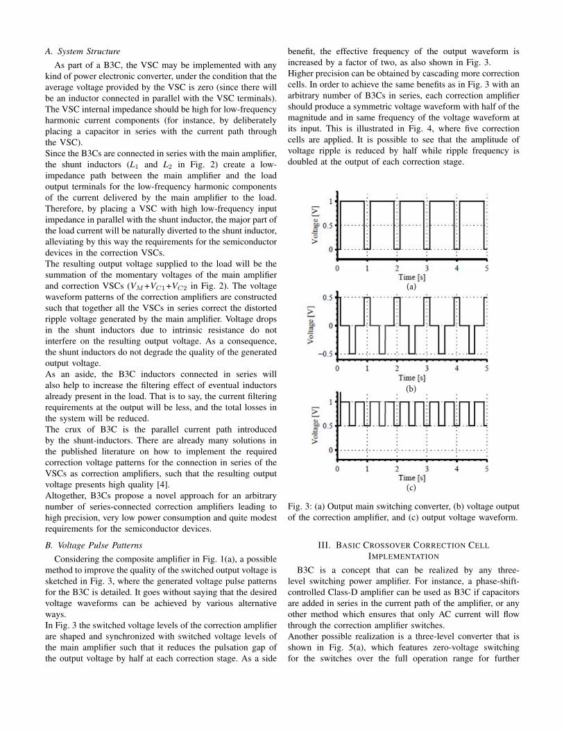
The top curve of Fig.5 shows the trace of the Flybackconverter primary current which is detected by a current probein series with transformer primary side. The middle one isthe averaged primary current which is obtained by using ashunt resistor with an analog low-pass filter. The bottom oneis the capacitor voltage measured by a voltage probe placedin parallel with the load.
It can be seen in both figures that the converter state ap-proaches the pre-set reference and the convergence trajectorystays in its pre-set margins. No objectionable overshoot is
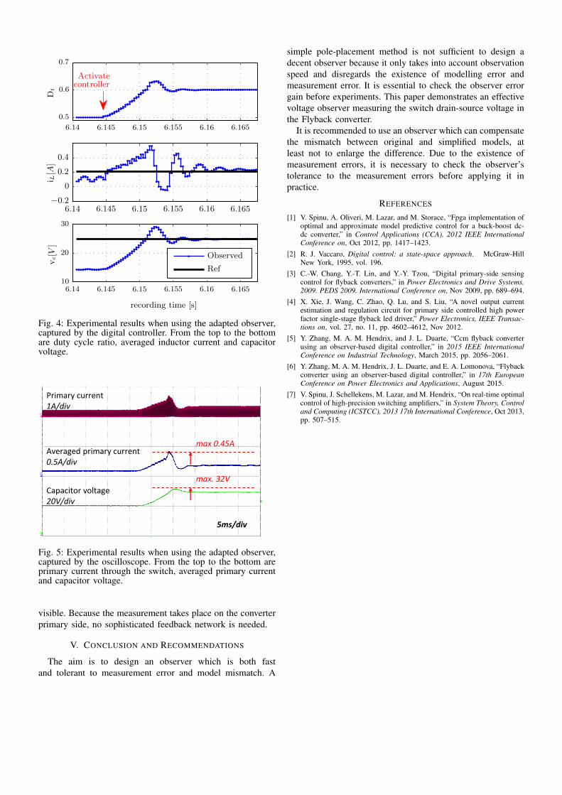
Ref
Observed
vc[V
]
recording time [s]
i L[A
]D
t
Activatecontroller
6.14 6.145 6.15 6.155 6.16 6.165
6.14 6.145 6.15 6.155 6.16 6.165
6.14 6.145 6.15 6.155 6.16 6.165
10
20
30
0.5
0.6
0.7
−0.2
0
0.2
0.4
Fig. 4: Experimental results when using the adapted observer,captured by the digital controller. From the top to the bottomare duty cycle ratio, averaged inductor current and capacitorvoltage.
Primary current 1A/div
Averaged primary current 0.5A/div
Capacitor voltage 20V/div
5ms/div
max 0.45A
max. 32V
Fig. 5: Experimental results when using the adapted observer,captured by the oscilloscope. From the top to the bottom areprimary current through the switch, averaged primary currentand capacitor voltage.
visible. Because the measurement takes place on the converterprimary side, no sophisticated feedback network is needed.
V. CONCLUSION AND RECOMMENDATIONS
The aim is to design an observer which is both fastand tolerant to measurement error and model mismatch. A
simple pole-placement method is not sufficient to design adecent observer because it only takes into account observationspeed and disregards the existence of modelling error andmeasurement error. It is essential to check the observer errorgain before experiments. This paper demonstrates an effectivevoltage observer measuring the switch drain-source voltage inthe Flyback converter.
It is recommended to use an observer which can compensatethe mismatch between original and simplified models, atleast not to enlarge the difference. Due to the existence ofmeasurement errors, it is necessary to check the observer’stolerance to the measurement errors before applying it inpractice.
REFERENCES
[1] V. Spinu, A. Oliveri, M. Lazar, and M. Storace, “Fpga implementation ofoptimal and approximate model predictive control for a buck-boost dc-dc converter,” in Control Applications (CCA), 2012 IEEE InternationalConference on, Oct 2012, pp. 1417–1423.
[2] R. J. Vaccaro, Digital control: a state-space approach. McGraw-HillNew York, 1995, vol. 196.
[3] C.-W. Chang, Y.-T. Lin, and Y.-Y. Tzou, “Digital primary-side sensingcontrol for flyback converters,” in Power Electronics and Drive Systems,2009. PEDS 2009. International Conference on, Nov 2009, pp. 689–694.
[4] X. Xie, J. Wang, C. Zhao, Q. Lu, and S. Liu, “A novel output currentestimation and regulation circuit for primary side controlled high powerfactor single-stage flyback led driver,” Power Electronics, IEEE Transac-tions on, vol. 27, no. 11, pp. 4602–4612, Nov 2012.
[5] Y. Zhang, M. A. M. Hendrix, and J. L. Duarte, “Ccm flyback converterusing an observer-based digital controller,” in 2015 IEEE InternationalConference on Industrial Technology, March 2015, pp. 2056–2061.
[6] Y. Zhang, M. A. M. Hendrix, J. L. Duarte, and E. A. Lomonova, “Flybackconverter using an observer-based digital controller,” in 17th EuropeanConference on Power Electronics and Applications, August 2015.
[7] V. Spinu, J. Schellekens, M. Lazar, and M. Hendrix, “On real-time optimalcontrol of high-precision switching amplifiers,” in System Theory, Controland Computing (ICSTCC), 2013 17th International Conference, Oct 2013,pp. 507–515.

Basic Crossover Correction CellsR. Baris Dai
Electrical Engineering DepartmentEindhoven University of Technology
Eindhoven, The NetherlandsEmail: [email protected]
Jorge L. DuarteElectrical Engineering Department
Eindhoven University of TechnologyEindhoven, The Netherlands
Email: [email protected]
Noud SlaatsProdrive Technologies B.V.Eindhoven, The Netherlands
Email: [email protected]
Abstract—In electric power processing converters for high-precision voltage supply, usually correction amplifiers are con-nected in series with a main low-accuracy power amplifier. Assuch, conventional switched-mode correction amplifiers have alsoto process the total current as delivered by the main amplifier.Therefore, switching semiconductors with high current ratinghave to be selected for implementing correction amplifiers. Thispaper proposes a solution this problem by separating the majorpart of the current delivered by the main amplifier from thecurrent part that flows through the switches in the correctionamplifiers. As a result, the switching semiconductors used in thecorrection amplifiers have a much reduced current rating, andthe overall system efficiency can be increased.
I. INTRODUCTION
Cascading power amplifiers is a well-known method in highprecision applications. In this method, the power amplificationsystem consists of a main power amplifier supplying thebulk power, while other converters are connected in seriesor in parallel, and operating as correction amplifiers, aimingat achieving a high-quality output waveform. The correctionamplifiers only process a small portion of the bulk load [1].The cascading connection of two or more converters is alsoknown as composite amplifiers, and the dependence on thepassive filters is much less compared to single-stage poweramplifiers. The fundamental idea for improving voltage outputthrough composite amplifier realizations based on Voltage-Source Converters (VSC) or Current-Source Converters (CSC)is shown in Fig. 1. Systems that employ a shunt or series activepower filters are notable examples of composite amplifiers.
+−
+−
+−VM VC
VCIMVOUT
+
-
VOUT
+
-
(a) (b)
Fig. 1: (a) Series connection of a main VSC (VM ) with acorrection VSC (VC), and (b) a parallel connection of a mainCSC (IM ) with a correction VSC (VC) for voltage outputcomposite amplifiers.
Even though the low efficiency of linear power amplifiersis a drawback, they are still used as amplifiers where high-fidelity is a priority, since a conventional switching power
amplifier cannot ensure this property. The composite poweramplifier idea arose with the demand on a high efficiencyand high-bandwidth AC power source by combining linearpower amplifiers and switching power amplifiers. In this caseswitching converters are used as main amplifiers and amplifiersare used to perform the correction [2]. However, compositeamplifiers may also employ another switching amplifier as thecorrection amplifier, aiming at even higher efficiency [3].In view of Fig. 1, correction amplifiers have to process thefull rated current if they are connected in series with themain amplifier (Fig. 1(a)), or they have to process full ratedvoltage if they are connected in parallel (Fig. 1(b)). As a result,conventional composite amplifiers are good for high precisionand reduce the necessity to passive components, nonethelessthey have to process the rated current or rated voltage.
II. BASIC CROSSOVER CELL OPERATION
Basic Crossover Correction Cell is a new electronic circuitfor providing a high-precision voltage supply for electricloads, which operates with a main amplifier together with anarbitrary number of cascaded-connected correction amplifiers.In this new concept the correction amplifiers, referred to asBasic Crossover Correction Cells (B3Cs) in the following,are realized in such a way that the majority of the currentdelivered by the main amplifier does not circulate through theswitches of the correction cells. As a consequence, B3Cs canbe implemented with simpler (therefore cheaper) low-currentrated semiconductor switches.A Basic Crossover Correction Cell combines a shunt inductorin parallel with a VSC, as described in the following. For thesake of illustration, a cascaded connection of a main amplifierwith two B3Cs is given in Fig. 2.
+−
+−
VM
VC1
+−
VC2
+−
+−
VM
VC1
+−
VC2
VO VO
Fig. 2: Transformation of a composite amplifier from us-ing conventional series correction amplifiers to using BasicCrossover Correction Cells (B3C).
A. System Structure
As part of a B3C, the VSC may be implemented with anykind of power electronic converter, under the condition that theaverage voltage provided by the VSC is zero (since there willbe an inductor connected in parallel with the VSC terminals).The VSC internal impedance should be high for low-frequencyharmonic current components (for instance, by deliberatelyplacing a capacitor in series with the current path throughthe VSC).Since the B3Cs are connected in series with the main amplifier,the shunt inductors (L1 and L2 in Fig. 2) create a low-impedance path between the main amplifier and the loadoutput terminals for the low-frequency harmonic componentsof the current delivered by the main amplifier to the load.Therefore, by placing a VSC with high low-frequency inputimpedance in parallel with the shunt inductor, the major part ofthe load current will be naturally diverted to the shunt inductor,alleviating by this way the requirements for the semiconductordevices in the correction VSCs.The resulting output voltage supplied to the load will be thesummation of the momentary voltages of the main amplifierand correction VSCs (VM+VC1+VC2 in Fig. 2). The voltagewaveform patterns of the correction amplifiers are constructedsuch that together all the VSCs in series correct the distortedripple voltage generated by the main amplifier. Voltage dropsin the shunt inductors due to intrinsic resistance do notinterfere on the resulting output voltage. As a consequence,the shunt inductors do not degrade the quality of the generatedoutput voltage.As an aside, the B3C inductors connected in series willalso help to increase the filtering effect of eventual inductorsalready present in the load. That is to say, the current filteringrequirements at the output will be less, and the total losses inthe system will be reduced.The crux of B3C is the parallel current path introducedby the shunt-inductors. There are already many solutions inthe published literature on how to implement the requiredcorrection voltage patterns for the connection in series of theVSCs as correction amplifiers, such that the resulting outputvoltage presents high quality [4].Altogether, B3Cs propose a novel approach for an arbitrarynumber of series-connected correction amplifiers leading tohigh precision, very low power consumption and quite modestrequirements for the semiconductor devices.
B. Voltage Pulse Patterns
Considering the composite amplifier in Fig. 1(a), a possiblemethod to improve the quality of the switched output voltage issketched in Fig. 3, where the generated voltage pulse patternsfor the B3C is detailed. It goes without saying that the desiredvoltage waveforms can be achieved by various alternativeways.In Fig. 3 the switched voltage levels of the correction amplifierare shaped and synchronized with switched voltage levels ofthe main amplifier such that it reduces the pulsation gap ofthe output voltage by half at each correction stage. As a side
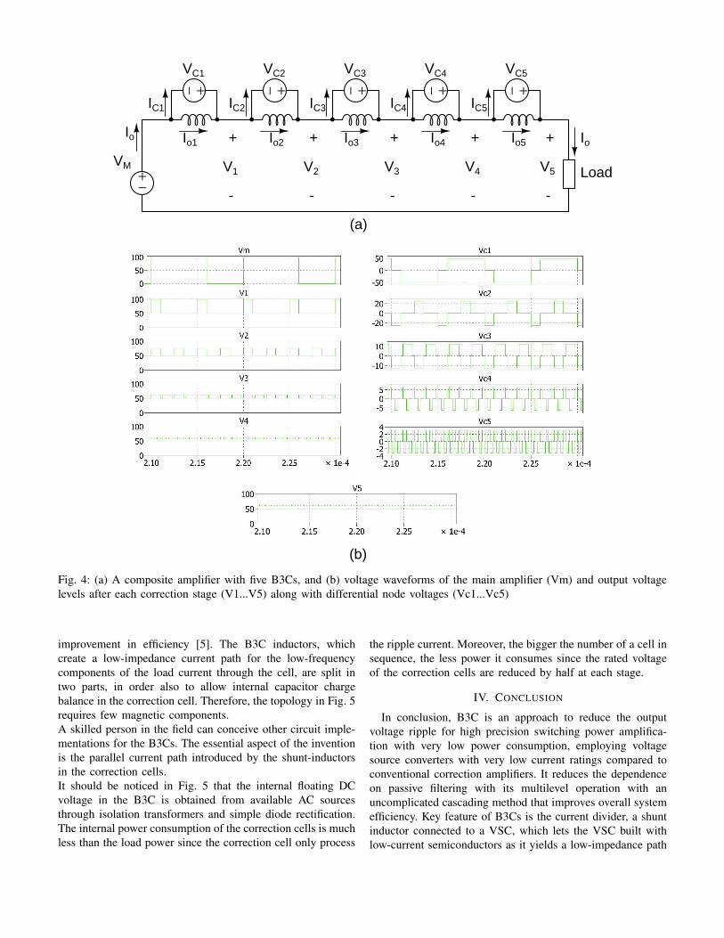
benefit, the effective frequency of the output waveform isincreased by a factor of two, as also shown in Fig. 3.Higher precision can be obtained by cascading more correctioncells. In order to achieve the same benefits as in Fig. 3 with anarbitrary number of B3Cs in series, each correction amplifiershould produce a symmetric voltage waveform with half of themagnitude and in same frequency of the voltage waveform atits input. This is illustrated in Fig. 4, where five correctioncells are applied. It is possible to see that the amplitude ofvoltage ripple is reduced by half while ripple frequency isdoubled at the output of each correction stage.
(a)
(b)
(c)
Fig. 3: (a) Output main switching converter, (b) voltage outputof the correction amplifier, and (c) output voltage waveform.
III. BASIC CROSSOVER CORRECTION CELLIMPLEMENTATION
B3C is a concept that can be realized by any three-level switching power amplifier. For instance, a phase-shift-controlled Class-D amplifier can be used as B3C if capacitorsare added in series in the current path of the amplifier, or anyother method which ensures that only AC current will flowthrough the correction amplifier switches.Another possible realization is a three-level converter that isshown in Fig. 5(a), which features zero-voltage switchingfor the switches over the full operation range for further
+−
+−
VM
VC1
+−
VC2
Io Io1 Io2
IC1 IC2
Io
Load
+− +−
Io3 Io4
IC4IC3
VC3 VC4
+−
Io5
VC5
IC5
+
-
V1
+
-
V2
+
-
V3
+
-
V4
+
-
V5
(a)
(b)
Fig. 4: (a) A composite amplifier with five B3Cs, and (b) voltage waveforms of the main amplifier (Vm) and output voltagelevels after each correction stage (V1...V5) along with differential node voltages (Vc1...Vc5)
improvement in efficiency [5]. The B3C inductors, whichcreate a low-impedance current path for the low-frequencycomponents of the load current through the cell, are split intwo parts, in order also to allow internal capacitor chargebalance in the correction cell. Therefore, the topology in Fig. 5requires few magnetic components.A skilled person in the field can conceive other circuit imple-mentations for the B3Cs. The essential aspect of the inventionis the parallel current path introduced by the shunt-inductorsin the correction cells.It should be noticed in Fig. 5 that the internal floating DCvoltage in the B3C is obtained from available AC sourcesthrough isolation transformers and simple diode rectification.The internal power consumption of the correction cells is muchless than the load power since the correction cell only process
the ripple current. Moreover, the bigger the number of a cell insequence, the less power it consumes since the rated voltageof the correction cells are reduced by half at each stage.
IV. CONCLUSION
In conclusion, B3C is an approach to reduce the outputvoltage ripple for high precision switching power amplifica-tion with very low power consumption, employing voltagesource converters with very low current ratings compared toconventional correction amplifiers. It reduces the dependenceon passive filtering with its multilevel operation with anuncomplicated cascading method that improves overall systemefficiency. Key feature of B3Cs is the current divider, a shuntinductor connected to a VSC, which lets the VSC built withlow-current semiconductors as it yields a low-impedance path
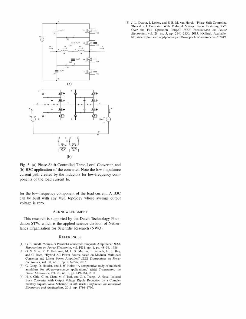
(a)
(b)
Fig. 5: (a) Phase-Shift-Controlled Three-Level Converter, and(b) B3C application of the converter. Note the low-impedancecurrent path created by the inductors for low-frequency com-ponents of the load current Io.
for the low-frequency component of the load current. A B3Ccan be built with any VSC topology whose average outputvoltage is zero.
ACKNOWLEDGMENT
This research is supported by the Dutch Technology Foun-dation STW, which is the applied science division of Nether-lands Organisation for Scientific Research (NWO).
REFERENCES
[1] G. B. Yundt, “Series- or Parallel-Connected Composite Amplifiers,” IEEETransactions on Power Electronics, vol. PE-1, no. 1, pp. 48–54, 1986.
[2] G. S. Silva, R. C. Beltrame, M. L. S. Martins, L. Schuch, H. L. Hey,and C. Rech, “Hybrid AC Power Source based on Modular MultilevelConverter and Linear Power Amplifier,” IEEE Transactions on PowerElectronics, vol. 30, no. 1, pp. 216–226, 2015.
[3] G. Gong, D. Hassler, and J. W. Kolar, “A comparative study of multicellamplifiers for AC-power-source applications,” IEEE Transactions onPower Electronics, vol. 26, no. 1, pp. 149–164, 2011.
[4] H.-h. Chiu, C.-m. Chen, M.-f. Tsai, and C.-s. Tseng, “A Novel IsolatedBuck Converter with Output Voltage Ripple Reduction by a Comple-mentary Square-Wave Scheme,” in 6th IEEE Conference on IndustrialElectronics and Applications, 2011, pp. 1786–1790.
[5] J. L. Duarte, J. Lokos, and F. B. M. van Horck, “Phase-Shift-ControlledThree-Level Converter With Reduced Voltage Stress Featuring ZVSOver the Full Operation Range,” IEEE Transactions on PowerElectronics, vol. 28, no. 5, pp. 2140–2150, 2013. [Online]. Available:http://ieeexplore.ieee.org/lpdocs/epic03/wrapper.htm?arnumber=6287049

Peer-to-Peer Control of MicrogridsHamada Almasalma∗, Jonas Engels∗, Geert Deconinck
ESAT-ELECTA, KU Leuven, Kasteelpark Arenberg 10, 3001 Leuven, BelgiumEnergyVille, Thor Park 8300, 3600 Genk, Belgium
[email protected], [email protected]∗Equally contributing authors
Abstract—In this paper, the motivation to develop microgridsas an effective solution for the control of distribution networkswith high level penetration of Distributed Energy Resources(DERs) is discussed. As many different control methods formicrogrids can be found in literature, this paper proposesa classification from highly centralized to distributed peer-to-peer control architectures. A peer-to-peer control paradigm isproposed as a way to control the distribution network with a highpenetration of distributed energy resources. Different controlalgorithms suited for the proposed peer-to-peer control strategyare discussed.
Index Terms—Microgrid Control, Distributed Energy Re-sources, Peer-to-Peer Control, Distributed Coordination andControl.
I. INTRODUCTION
Growing concerns about energy sustainability, security ofsupply and an increasing penetration of renewable energy andother distributed energy resources (DERs), such as storagesystems and electrical vehicles, are impacting the operationand the architecture of the electricity system. While currentlyplacing a burden on the distribution grid, it is generally agreedthat DERs could also be used for active grid control, therebycontributing to a stable and secure grid. To accomplish this,new control systems have to be designed that are able to fullyharness the potential of the installed DERs [1]. This activemonitoring and control of the distribution grid is commonlyreferred to as an essential part of the smart grid, which isregarded to be key in the future integration of electricityconsumers, generators and those that do both (prosumers).
Current distribution networks are not designed to accom-modate a large amount of DERs. A large penetration of DERsmay create problems to maintain the quality of supply toall customers connected to the distribution network. Besides,the intermittent nature of DERs can create issues with thesecond-by-second balance of demand and supply. However, bycoordinating the DERs, these issues could be resolved withoutthe need for additional investments in grid infrastructure [2].
In the literature [3], the idea of a microgrid is an oftenmentioned alternative to controlling the whole distributiongrid with a large amount of DERs. The main idea is that,when there are many DERs in a wide network, it can be
This work is partially supported by H2020-LCE-2014-3 Peer to Peer SmartEnergy Distribution Networks (P2PSmartTest) project (European Commis-sion).
very complex and difficult to control. Thus, a potential way tomanage this complexity is by breaking down the entire gridinto a smaller microgrids, containing only a limited amountof DERs. This paper elaborates this idea and proposes anoperational control paradigm for the future distribution grid,based on the concept of microgrids.
When considering such a microgrid and the coordination ofmultiple microgrids, different control methods can be found inliterature [4]. This paper proposes a taxonomy of these controlmethods, from fully centralized to completely decentralized. Ahighly decentralized control method, the peer-to-peer controlarchitecture, is further elaborated in this paper, as it is apromising way for future control of the distribution grid.Since the DERs are typically highly distributed, operated bymany different owners and with different objectives, it isdesirable that the microgrid control system operates in a highlydistributed way as well. Besides, a robust control system isneeded that does not depend on a single point of failure, asmost of the more centralized control methods do.
The rest of the paper is organized as follows: section IIintroduces the most prominent issues with regard to theintegration of DERs in the electrical grid, together with anelaboration of the microgrid concept that would be able toovercome these issues. Section III proposes a categorizationfor the different architectures of microgrid control. Section IVthen proposes a new control paradigm for the distribution grid,based on the microgrid concept and the previously identifiedpeer-to-peer architecture. Finally, the paper is concluded insection V.
II. ISSUES WITH THE INTEGRATION OF DERS IN THEELECTRICAL GRID
This section summarizes the most prominent issues withregard to the integration of DERs in the current electricalgrid. Both voltage issues and frequency or stability issues arediscussed. Other type of issues, such as harmonics, securityissues and power fluctuations are not discussed here. Themicrogrid concept is presented as a possible solution that isable to overcome these issues.
A. Voltage Issues
A large penetration of DERs may create problems to main-tain the voltage quality of all customers connected to thesame part of the distribution network. Up till now, voltage

quality in the distribution grid is achieved based on the layout of grid infrastructure that is capable of operating withinlimits even in worst case scenarios, with the assumption ofunidirectional power flows. The planning of the infrastructureis quite straightforward: minimum and maximum load condi-tions are considered and minimum and maximum voltages inthe grid are examined. The network is dimensioned in such away that the minimum voltage is near the lower limit of theallowed voltage range and the maximum voltage is near theupper limit of the allowed voltage range. When connectingsignificant amounts of distributed generation to the network,the assumption of unidirectional power flows is not alwaysvalid any more and the voltage profile of the network can bequite different than in the case without any generation. Withmaximum load conditions, distributed generation increases thevoltage level in the network and, hence, enhance the voltagequality in the grid. However, when the load on the network is ata minimum, the generated power of the distributed generationcan reverse the power flows in the grid, what could lead to arise of the voltage profile beyond its allowed limits.
Therefore, the hosting capacity for renewable generationof many traditional distribution networks is limited by thevoltage variations that occur between maximum and minimumload conditions. The traditional solution to this problem is toreinforce the local distribution grid by installing more cables.However, generally this is quite expensive, as new infrastruc-ture has to be installed in residential neighborhoods. Anotherapproach is by using the already installed infrastructure in amore optimal way, by coordination of the local generation, on-load tap changers or other equipment used to control voltagein distribution networks. This is the purpose of the smart grid[5].
B. Frequency and Stability Issues
The consumption and generation in the electricity systemhas to be balanced on a second-by-second basis. Traditionally,this balance is maintained by flexible generation units that arestandby and are able to regulate their generated amount ofelectricity as required. However, the intermittent and unpre-dictable nature of new renewable energy sources creates issueswith this traditional approach, as these new sources are usuallynot dispatchable.
Any deviation from the demand and supply balance resultsin a deviation of the system frequency from its nominal value,while large frequency deviations will affect the system stabil-ity. Therefore, the system operators maintain frequency withinstrict limits by using ancillary services for balancing of thegrid, that are able to respond within various time frames [6].Up till now these balancing services are exclusively organizedby the transmission system operator (TSO). However, with thehigh penetration of DERs, maintaining the supply and demandbalance and thus the system frequency within limits becomesmore challenging. Spinning reserves or energy storage canaddress this problem but with a considerable cost. Therefore,power system operators are increasingly seeking new reservesfor frequency response from demand flexibility, instead of
supply. As most of the demand is connected to the distributiongrid, this means that the distribution system operators (DSOs)will be involved in this process.
C. Towards a New Control Paradigm for the Distribution GridOne of the key solutions to overcome the above mentioned
challenges of integrating DERs in the distribution grid is thedesign of a smart grid, containing control systems for thecoordination of these DERs, thereby ensuring a reliable, secureand economical operation of the distribution network at alltimes.
Controlling the distribution network to be able to utilize theemerging diversity of DERs at significant levels of penetration,means that the control system has to be able to manage awide and dynamic set of resources. Controlling such a complexnetwork is not a trivial task. A potential way to manage thiscomplexity is by breaking the entire grid down into smallermicrogrids, containing only a limited amount of DERs. Thesemicrogrids should be able to control their local resources asoptimal as possible, while being connected to the rest of thegrid through a point of common coupling (PCC) [7].
These microgrids can be coordinated on a higher level intoa system of multi-microgrids. The main idea is to design thecontrol of the microgrid in such a way that the microgrid isperceived by the main grid as a single element respondingto appropriate control signals. There are different possiblearchitectures of operating such a microgrid, for which thispaper proposes a classification ranging from fully centralizedmethods to fully distributed in section III.
A conventional way of controlling such a microgrid, is by ahierarchy of three control levels, each operating on a differenttimescale and with a different priority: primary, secondary andtertiary [8], [9]. Primary control is focused on keeping the gridstable in all circumstances, thus it needs the largest priorityand should act on the smallest time scale. A robust controlmethod is needed, so that in case e.g. the communicationnetwork fails, the primary control is still able to maintainstability of the microgrid. Therefore, as little communicationas possible is desired. As primary control is often implementedas some kind of proportional controller, a steady state errorremains, that shall have to be eliminated with the use ofa secondary control method. Secondary control is activatedon a slower time scale, e.g. every 15 minutes, and with alower priority than primary control. Finally, tertiary control isimplemented as the slowest level of control, with as purposethe economically optimal operation of the microgrid. Bothsecondary and tertiary controls usually require at least somekind of communication, as knowledge about the state of theentire system is needed.
These three control levels can be implemented throughvarious organizational architectures of the microgrid. In thefollowing section, this paper proposes a classification for thesedifferent architectures.
III. ARCHITECTURES OF MICROGRID CONTROL
The control of the DERs in a single microgrid can beorganised according to many different control architectures.
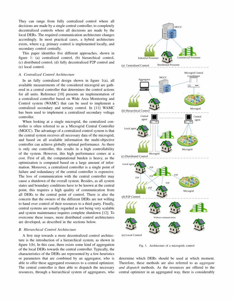
They can range from fully centralized control where alldecisions are made by a single central controller, to completelydecentralized controls where all decisions are made by thelocal DERs. The required communication architecture changesaccordingly. In most practical cases, a hybrid architectureexists, where e.g. primary control is implemented locally, andsecondary control centrally.
This paper identifies five different approaches, shown infigure 1: (a) centralized control, (b) hierarchical control,(c) distributed control, (d) fully decentralized P2P control and(e) local control.
A. Centralized Control Architecture
In an fully centralized design shown in figure 1(a), allavailable measurements of the considered microgrid are gath-ered in a central controller that determines the control actionsfor all units. Reference [10] presents an implementation ofa centralized controller based on Wide Area Monitoring andControl system (WAMC) that can be used to implement acentralized secondary and tertiary control. In [11] WAMChas been used to implement a centralized secondary voltagecontroller.
When looking at a single microgrid, the centralized con-troller is often referred to as a Microgrid Central Controller(MGCC). The advantage of a centralized control system is thatthe central system receives all necessary data of the microgrid,and based on all available information the multi-objectivecontroller can achieve globally optimal performance. As thereis only one controller, this results in a high controllabilityof the system. However, this high performance comes at acost. First of all, the computational burden is heavy, as theoptimization is computed based on a large amount of infor-mation. Moreover, a centralized controller is a single point offailure and redundancy of the central controller is expensive.The loss of communication with the central controller maycause a shutdown of the overall system. Besides, as all systemstates and boundary conditions have to be known at the centralpoint, this requires a high quality of communication fromall DERs to the central point of control. There is also theconcern that the owners of the different DERs are not willingto hand over control of their resources to a third party. Finally,central systems are usually regarded as not being very scalableand system maintenance requires complete shutdown [12]. Toovercome these issues, more distributed control architecturesare developed, as described in the sections below.
B. Hierarchical Control Architecture
A first step towards a more decentralized control architec-ture is the introduction of a hierarchical system, as shown infigure 1(b). In this case, there exists some kind of aggregationof the local DERs towards the central controller. Typically, thecharacteristics of the DERs are represented by a few heuristicsor parameters that are combined by an aggregator, who isable to offer these aggregated resources to a central optimizer.The central controller is then able to dispatch the necessaryresources, through a hierarchical system of aggregators, who
(a) Centralized Control
(b) Hierarchical Control
(c) Distributed Control
(d) P2P Control
(e) Local Control
Microgrid Central
Coordinator
Aggregator MGCC
MGCC
P2P
P2P P2P
P2P
P2P
P2P
Without communication
Central
agent
Local agent
Local agent
Residential Prosumer
Industrial Prosumer Commercial Prosumer
Microgrid
Microgrid
Microgrid
Microgrid
Central
agent
Fig. 1. Architecture of a microgrids control
determine which DERs should be used at which moment.Therefore, these methods are also referred to as aggregateand dispatch methods. As the resources are offered to thecentral optimizer in an aggregated way, there is considerably

less information needed at the central controller, which resultsin a more scalable system. However, the single point of failureremains, and the points of aggregation might even become newpoints of failure.
Nowadays, this approach is used for exploiting demand re-sponse resources. Examples are the Intelligator algorithm [13],or the demand response reserves offered by aggregators toa TSO for e.g. automatic or manual frequency restorationreserves (aFRR or mFRR). The coordination of multiple,centrally controlled microgrids can also be organized in ahierarchical way. In that case, a central coordinator coordi-nates multiple microgrids, each controlled by a local MGCC.The MGCC of a single microgrid tries to reach an optimaloperation point using only its local resources. If the internalresources are not sufficient, the MGCC shall ask the microgridcentral coordinator for external resources from other micro-grids [14].
C. Distributed Control Architecture
In both architectures described above, the DERs are con-trolled by a third party. However, since the owners of theDERs impose the operational boundary conditions, one canargue that it might be better to keep the control of the DERslocally. Besides, not all DER owners want to exchange all theirinformation with a third party for privacy reasons. However,to reach a (near) optimal operation of the grid, these DERsshould be coordinated. It is at this point that distributed controlarchitectures come into play. The idea behind distributedcontrol is to divide the centralized problem into a certainnumber of local controllers or agents. Therefore, each agentdoes not have a global vision of the problem [15], but bymeans of correct coordination they can reach a globally (near)optimal state.
Coordination is organised by a central agent that is ableto communicate global constraints, such as the power limitof a transformer, or exceeding voltage limits. This can bedone by the communication of Lagrange multipliers. Examplesof algorithms that are suited for this approach are dualdecomposition methods or the alternating direction methodof multipliers (ADMM) [16]. Both are based on the dualascent method, where price vectors are sent iteratively fromthe central controller to the DERs. The DERS optimize theirconsumption towards such a price vector and return demandvectors to the central agent. The central agent then analysesthe demand vectors with regard to operational grid constraints,and updates the prices when constraints are being violated.The DERs optimize again according to this new price vector.This iteration goes on until a steady state solution is found.Figure 1(c) represents such a distributed control scheme,consisting of local DERs that optimize and a central agentthat controls the global constraints.
Distributed approaches have important advantages that jus-tify their use. As the global optimization problem is dividedinto several sub-problems, the computational requirements arelower. Besides, the information exchange between local andcentral agents is limited, which relaxes the requirements of
the communication system. This approach results in a veryscalable method. As the local DERs perform an optimizationby themselves, they do not need to hand over private informa-tion to a third party that controls their resources. However, acentral agent still exists, inherently resulting in a single pointof failure.
D. Peer-to-Peer Control ArchitectureTo eliminate the problems that a more centralized control
method possesses, having a single point of failure, the ideaof peer-to-peer microgrids has been developed. This type ofarchitecture, inspired by P2P computer networking [17], ischaracterized by the complete absence of a central controller.All local DERs or agents, are equally important and cancommunicate to other agents [18], in a peer-to-peer fashion, asshown in figure 1(d). The absence of a central controller leadsto the term of autonomous control.Peer-to-peer communicationis used for dissemination of the grid state to all requiredagents in the microgrid. The grid-supporting agents can thenact according to the received information, in cooperation witheach other. In this way they should be able to reach a (near)optimal operation of the considered microgrid. Examples ofalgorithms that could be used for such P2P communicationare gossiping [19] and consensus algorithms [20]. This archi-tecture will be elaborated further in section IV.
In this architecture, there is a clear absence of a single pointof failure. In the case a single agent fails, the other agentscan still operate the grid in a stable way. Also when a singlecommunication channel fails, the required information canstill reach all necessary participants, via other agents. Theseproperties makes this architecture a robust way of controllinga microgrid. Besides, all information is kept local, eliminatingpossible privacy concerns. On the other hand, all agents needa considerable amount of local intelligence, as they need tobe able to execute the necessary optimizations.
E. Local Control ArchitectureFinally, there also exist control architectures without any
form of communication, as shown in figure 1(e). This paperclassifies them as local control architectures. In this case,optimal operation of the microgrid is rather difficult, as itis impossible to know the complete state of the grid and alloperational boundary conditions of the DERs. However, thismethod is robust against all communication failerus, as theabsence of any communication will ensure that the grid is stillcontrolled when all communication channels fail. As primaryfrequency control should be able to operate even when com-munication fails, this is often implemented as a local controlarchitecture. Thereby it uses droop characteristics that varyactive power with variations in locally measured frequency.Another example is local voltage control, implemented by avoltage-reactive power droop [21].
IV. PROPOSED PEER-TO-PEER BASED CONTROLPARADIGM FOR THE DISTRIBUTION GRID
As the new DERs are typically highly distributed in thegrid, operated by a lot of different owners and with different
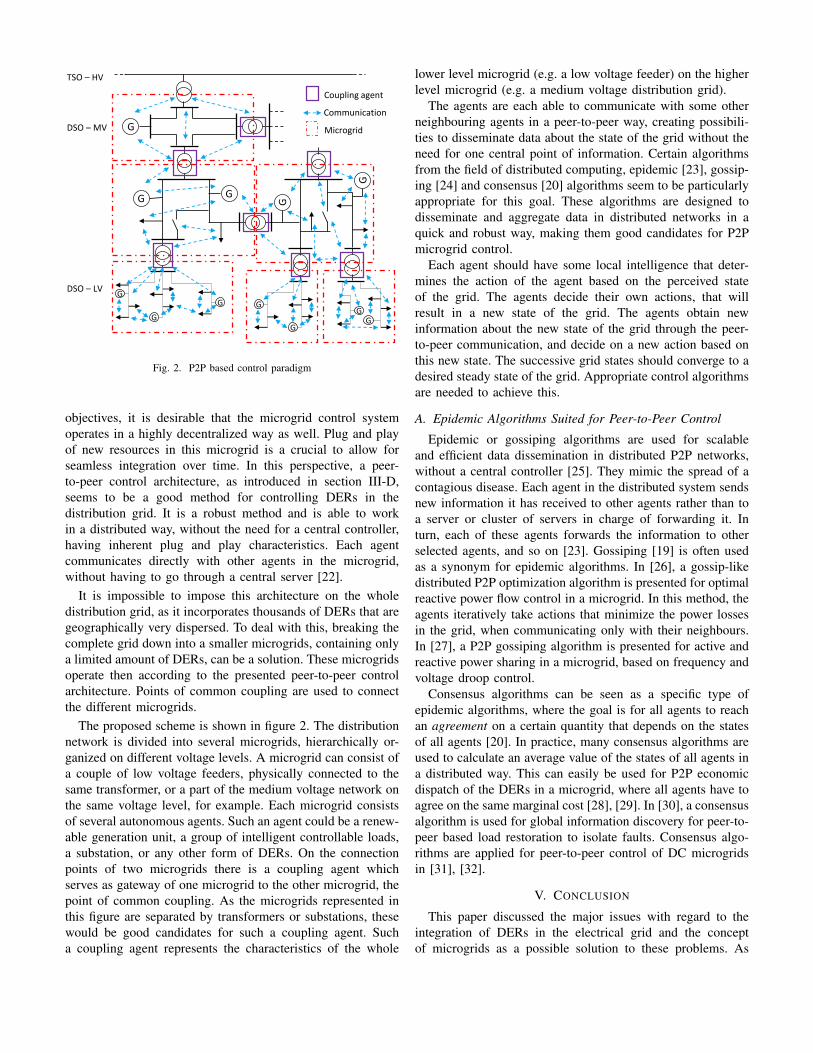
Coupling agent
Communication
Microgrid
TSO – HV
DSO – MV
DSO – LV
G
G G
GG
G
G G
G
GG
GFig. 2. P2P based control paradigm
objectives, it is desirable that the microgrid control systemoperates in a highly decentralized way as well. Plug and playof new resources in this microgrid is a crucial to allow forseamless integration over time. In this perspective, a peer-to-peer control architecture, as introduced in section III-D,seems to be a good method for controlling DERs in thedistribution grid. It is a robust method and is able to workin a distributed way, without the need for a central controller,having inherent plug and play characteristics. Each agentcommunicates directly with other agents in the microgrid,without having to go through a central server [22].
It is impossible to impose this architecture on the wholedistribution grid, as it incorporates thousands of DERs that aregeographically very dispersed. To deal with this, breaking thecomplete grid down into a smaller microgrids, containing onlya limited amount of DERs, can be a solution. These microgridsoperate then according to the presented peer-to-peer controlarchitecture. Points of common coupling are used to connectthe different microgrids.
The proposed scheme is shown in figure 2. The distributionnetwork is divided into several microgrids, hierarchically or-ganized on different voltage levels. A microgrid can consist ofa couple of low voltage feeders, physically connected to thesame transformer, or a part of the medium voltage network onthe same voltage level, for example. Each microgrid consistsof several autonomous agents. Such an agent could be a renew-able generation unit, a group of intelligent controllable loads,a substation, or any other form of DERs. On the connectionpoints of two microgrids there is a coupling agent whichserves as gateway of one microgrid to the other microgrid, thepoint of common coupling. As the microgrids represented inthis figure are separated by transformers or substations, thesewould be good candidates for such a coupling agent. Sucha coupling agent represents the characteristics of the whole
lower level microgrid (e.g. a low voltage feeder) on the higherlevel microgrid (e.g. a medium voltage distribution grid).
The agents are each able to communicate with some otherneighbouring agents in a peer-to-peer way, creating possibili-ties to disseminate data about the state of the grid without theneed for one central point of information. Certain algorithmsfrom the field of distributed computing, epidemic [23], gossip-ing [24] and consensus [20] algorithms seem to be particularlyappropriate for this goal. These algorithms are designed todisseminate and aggregate data in distributed networks in aquick and robust way, making them good candidates for P2Pmicrogrid control.
Each agent should have some local intelligence that deter-mines the action of the agent based on the perceived stateof the grid. The agents decide their own actions, that willresult in a new state of the grid. The agents obtain newinformation about the new state of the grid through the peer-to-peer communication, and decide on a new action based onthis new state. The successive grid states should converge to adesired steady state of the grid. Appropriate control algorithmsare needed to achieve this.
A. Epidemic Algorithms Suited for Peer-to-Peer Control
Epidemic or gossiping algorithms are used for scalableand efficient data dissemination in distributed P2P networks,without a central controller [25]. They mimic the spread of acontagious disease. Each agent in the distributed system sendsnew information it has received to other agents rather than toa server or cluster of servers in charge of forwarding it. Inturn, each of these agents forwards the information to otherselected agents, and so on [23]. Gossiping [19] is often usedas a synonym for epidemic algorithms. In [26], a gossip-likedistributed P2P optimization algorithm is presented for optimalreactive power flow control in a microgrid. In this method, theagents iteratively take actions that minimize the power lossesin the grid, when communicating only with their neighbours.In [27], a P2P gossiping algorithm is presented for active andreactive power sharing in a microgrid, based on frequency andvoltage droop control.
Consensus algorithms can be seen as a specific type ofepidemic algorithms, where the goal is for all agents to reachan agreement on a certain quantity that depends on the statesof all agents [20]. In practice, many consensus algorithms areused to calculate an average value of the states of all agents ina distributed way. This can easily be used for P2P economicdispatch of the DERs in a microgrid, where all agents have toagree on the same marginal cost [28], [29]. In [30], a consensusalgorithm is used for global information discovery for peer-to-peer based load restoration to isolate faults. Consensus algo-rithms are applied for peer-to-peer control of DC microgridsin [31], [32].
V. CONCLUSION
This paper discussed the major issues with regard to theintegration of DERs in the electrical grid and the conceptof microgrids as a possible solution to these problems. As

there are different methods for organizing the control ofthese microgrids found in literature, this paper presented aclassification of these methods, from highly centralized to fullydecentralized architectures. The drawbacks of the centralizedcontrol and the advantages of the distributed control architec-ture have been discussed as a motivation to propose a newcontrol paradigm for the distributed grid, based on peer-to-peer controlled microgrids. Coupling agents are introduced toestablish a connection between two microgrids.
The absence of a central point and peer-to-peer communica-tion are found to be key elements in this control method. Epi-demic algorithms, such as gossip and consensus are proposedas suited algorithms for peer-to-peer control, as they are able todisseminate data in a distributed way. Finally, a short literaturereview on peer-to-peer microgrid control based on gossipingand consensus algorithms is presented as an illustration ofpossible algorithms for peer-to-peer controlled microgrids.
Future work may consist of validation and demonstration ofa peer-to-peer controlled microgrid, as well as a comparison ofthe performance of the different algorithms found in literature.
REFERENCES
[1] R. O’Gorman and M. A. Redfern, “Enhanced autonomous control ofdistributed generation to provide local voltage control,” in Power andEnergy Society General Meeting - Conversion and Delivery of ElectricalEnergy in the 21st Century, 2008 IEEE, July 2008, pp. 1–8.
[2] J. P. Lopes, N. Hatziargyriou, J. Mutale, P. Djapic, and N. Jenkins, “In-tegrating distributed generation into electric power systems: A review ofdrivers, challenges and opportunities,” Electric power systems research,vol. 77, no. 9, pp. 1189–1203, 2007.
[3] R. H. Lasseter and P. Paigi, “Microgrid: a conceptual solution,” in PowerElectronics Specialists Conference, PESC, June 2004, pp. 4285–4290.
[4] N. Hatziargyriou, “Microgrid control issues,” in Microgrids: Architec-tures and Control, 1st ed. John Wiley and Sons, 2014, ch. 3, pp.25–80.
[5] T. Xu and P. Taylor, “Voltage control techniques for electrical distri-bution networks including distributed generation,” in The InternationalFederation of Automatic Control, 17th World Congress Seoul, 2008.
[6] I. A. Erinmez, D. O. Bickers, G. F. Wood, and W. W. Hung, “Ngcexperience with frequency control in england and wales-provision offrequency response by generators,” in Power Engineering Society 1999Winter Meeting, IEEE, vol. 1, Jan 1999, pp. 590–596 vol.1.
[7] R. H. Lasseter, “Smart distribution: Coupled microgrids,” Proceedingsof the IEEE, vol. 99, no. 6, pp. 1074–1082, June 2011.
[8] A. Bidram and A. Davoudi, “Hierarchical structure of microgrids controlsystem,” IEEE Transactions on Smart Grid, vol. 3, no. 4, pp. 1963–1976,Dec 2012.
[9] D. E. Olivares, A. Mehrizi-Sani, A. H. Etemadi, C. A. Caizares,R. Iravani, M. Kazerani, A. H. Hajimiragha, O. Gomis-Bellmunt,M. Saeedifard, R. Palma-Behnke, G. A. Jimnez-Estvez, and N. D.Hatziargyriou, “Trends in microgrid control,” IEEE Transactions onSmart Grid, vol. 5, no. 4, pp. 1905–1919, July 2014.
[10] M. Chenine, E. Karam, and L. Nordstrom, “Modeling and simulationof wide area monitoring and control systems in ip-based networks,” in2009 IEEE Power Energy Society General Meeting, July 2009, pp. 1–8.
[11] A. Mohamed, A. Ghareeb, T. Youssef, and O. A. Mohammed, “Widearea monitoring and control for voltage assessment in smart grids withdistributed generation,” in Innovative Smart Grid Technologies (ISGT),2013 IEEE PES, Feb 2013, pp. 1–6.
[12] S. Sojoudi, J. Lavaei, and A. G. Aghdam, Structurally ConstrainedControllers: Analysis and Synthesis. Springer Science and BusinessMedia, 2011, ch. 1, pp. 1–8.
[13] S. Vandael, B. Claessens, M. Hommelberg, T. Holvoet, and G. Decon-inck, “A scalable three-step approach for demand side management ofplug-in hybrid vehicles,” IEEE Transactions on Smart Grid, vol. 4, no. 2,pp. 720–728, June 2013.
[14] L. Che, M. Shahidehpour, A. Alabdulwahab, and Y. Al-Turki, “Hi-erarchical coordination of a community microgrid with ac and dcmicrogrids,” IEEE Transactions on Smart Grid, vol. 6, no. 6, pp. 3042–3051, Nov 2015.
[15] M. Yazdanian and A. Mehrizi-Sani, “Distributed control techniques inmicrogrids,” IEEE Transactions on Smart Grid, vol. 5, no. 6, pp. 2901–2909, Nov 2014.
[16] D. Alaerts and J. De Turck, “Investigation and comparison of dis-tributed algorithms for demand-side management,” Master’s thesis,ESAT-ELECTA, KU Leuven, 2013.
[17] R. Schollmeier, “A definition of peer-to-peer networking for the classi-fication of peer-to-peer architectures and applications,” in Peer-to-PeerComputing, 2001. Proceedings. First International Conference on, Aug2001, pp. 101–102.
[18] S. D. J. McArthur, E. M. Davidson, V. M. Catterson, A. L. Dimeas,N. D. Hatziargyriou, F. Ponci, and T. Funabashi, “Multi-agent systemsfor power engineering applications–part i: Concepts, approaches, andtechnical challenges,” IEEE Transactions on Power Systems, vol. 22,no. 4, pp. 1743–1752, Nov 2007.
[19] D. Kempe, A. Dobra, and J. Gehrke, “Gossip-based computation ofaggregate information,” in Foundations of Computer Science, 2003.Proceedings. 44th Annual IEEE Symposium on, Oct 2003, pp. 482–491.
[20] R. Olfati-Saber, J. A. Fax, and R. M. Murray, “Consensus and coop-eration in networked multi-agent systems,” Proceedings of the IEEE,vol. 95, no. 1, pp. 215–233, Jan 2007.
[21] E. Demirok, P. C. Gonzlez, K. H. B. Frederiksen, D. Sera, P. Rodriguez,and R. Teodorescu, “Local reactive power control methods for overvolt-age prevention of distributed solar inverters in low-voltage grids,” IEEEJournal of Photovoltaics, vol. 1, no. 2, pp. 174–182, Oct 2011.
[22] K. Eger, C. Gerdes, and S. ztunali, “Towards p2p technologies forthe control of electrical power systems,” in 2008 Eighth InternationalConference on Peer-to-Peer Computing, Sept 2008, pp. 180–181.
[23] P. T. Eugster, R. Guerraoui, A. M. Kermarrec, and L. Massoulie,“Epidemic information dissemination in distributed systems,” Computer,vol. 37, no. 5, pp. 60–67, May 2004.
[24] A. G. Dimakis, S. Kar, J. M. F. Moura, M. G. Rabbat, and A. Scaglione,“Gossip algorithms for distributed signal processing,” Proceedings of theIEEE, vol. 98, no. 11, pp. 1847–1864, Nov 2010.
[25] A. Demers et al., “Epidemic algorithms for replicated database main-tenance,” in Proceedings of the Sixth Annual ACM Symposium onPrinciples of Distributed Computing, ser. PODC ’87. New York, NY,USA: ACM, 1987, pp. 1–12.
[26] S. Bolognani and S. Zampieri, “A gossip-like distributed optimization al-gorithm for reactive power flow control,” in Proc. IFAC World Congress,2011, pp. 1–14.
[27] K. De Brabandere, “Voltage and frequency droop control in low voltagegrids by distributed generators with inverter frond-end,” Ph.D. disserta-tion, KU Leuven, 2006.
[28] J. Cao, “Consensus-based distributed control for economic dispatchproblem with comprehensive constraints in a smart grid,” Ph.D. dis-sertation, The Florida State University, 2014.
[29] Z. Zhang and M. Y. Chow, “Incremental cost consensus algorithm ina smart grid environment,” in 2011 IEEE Power and Energy SocietyGeneral Meeting, July 2011, pp. 1–6.
[30] Y. Xu and W. Liu, “Novel multiagent based load restoration algorithmfor microgrids,” IEEE Transactions on Smart Grid, vol. 2, no. 1, pp.152–161, March 2011.
[31] L. Meng, T. Dragicevic, J. Roldn-Prez, J. C. Vasquez, and J. M.Guerrero, “Modeling and sensitivity study of consensus algorithm-baseddistributed hierarchical control for dc microgrids,” IEEE Transactions onSmart Grid, vol. PP, no. 99, pp. 1–1, 2015.
[32] L. Meng, T. Dragicevic, J. M. Guerrero, and J. C. Vasquez, “Dynamicconsensus algorithm based distributed global efficiency optimization of adroop controlled dc microgrid,” in Energy Conference (ENERGYCON),2014 IEEE International, May 2014, pp. 1276–1283.
Modelling and Emulation of an Unbalanced LVFeeder with Photovoltaic Inverters
Ramon Lopez-ErauskinJohan Gyselinck, IEEE Member
Bio-, Electro- and Mechanical Systems departmentUniversite Libre de Bruxelles
[email protected], [email protected]
Frederic Olivier, IEEE Student MemberDamien Ernst, IEEE Member
Department of Electrical Engineering and Computer ScienceUniversite de Liege
[email protected], [email protected]
Marıa Emilia Hervas, Alexis FabreGreenWatch SAWavre, Belgium
Abstract—In this paper, the penetration of grid-connected pho-tovoltaic systems is studied, experimentally tested and comparedto simulation results. In particular, how the inverse current flowand unbalance situations affect the voltage in the low-voltagegrid. Thus, a test platform has been developed for obtainingexperimental results with grid-tied commercial inverters. Photo-voltaic arrays are emulated and subjected to different irradianceprofiles and the inverters are controlled to produce at differentpower conditions. A model has been developed in order to repro-duce the same operating conditions and working environment.Simulations are performed with the software PowerFactory andthe results compared to the experimental ones.
Index Terms—distributed power generation, photovoltaic sys-tems, power distribution, reactive power.
I. INTRODUCTION
The operation of grid-tied photovoltaic (PV) units is charac-terized by several uncertainties due to the number of currentlyoperating units, the points where they are connected, and thedelivered power. Due to the historical design of low-voltage(LV) feeders, PV generation (PVG) can have adverse effectsand cause voltage deviations due to reversed power flow [1].Some authors have also studied the overvoltage in low-voltagegrids based in probabilistic models [2], [3]. In this context, ascheme that controls the active and reactive power of inverterswas previously designed and numerically tested [4]. The firststep toward the validation of the control scheme in a realsetting is to reproduce in a laboratory the behavior of a LVfeeder under different voltage and unbalance conditions.
In previous research, the impact of the penetration of PVunits in the low-voltage network with dispersed loads wasinvestigated [5], [6]. The former presents modeling and fieldmeasurements and addresses the problems of increasing PVinstallations in these networks. In the latter, a benchmarkLV microgrid network is presented, which is suitable forsteady state and transient simulations. In validation, laboratoryreproduction allows time-, cost- effective and repeatable tests
of overvoltage conditions of the grid without need of deployingexpensive equipment close to large concentrations of PVsystems.
In this paper, we present the test platform (Fig. 1) emulatinga LV feeder, and the voltage and power variations for severaloperation scenarios. The effect of active and reactive powervariations on the voltage profile is studied. The lab feeder ismodeled numerically and simulations are performed for eachoperation scenarios. The results from the measurements andthe simulations are then compared.
II. TEST PLATFORM AND MODEL IN POWERFACTORY
A LV feeder is composed of several elements: the mainones are the external grid, the distribution transformer, thecables, the PV systems and the loads which represent housesconsumptions. In our study, loads are not considered. Sincethey would be connected at the same point as the PV systems,they would reduce the power injected into the network and thusdecrease the voltage variations, a behavior that we specificallywant to exhibit in our simulations. In this section, everypart of the test platform in Fig. 1 is described and its labimplementation explained. The network reproduced in the labis modeled in PowerFactory, a power system analysis software,with the electrical and hardware characteristics of the externalgrid, cables and inverters to allow a meaningful comparison.
A. External gridIn a typical setting, the external grid would be the medium
voltage network at a voltage close to 15 kV and the distributiontransformer would bring this voltage down to 400 V. In thelab setting, the external grid is the low voltage network. InPowerFactory, it is modeled as a slack bus with a constantvoltage.
B. Distribution transformerThe transformer that feeds the reproduced LV-grid has the
following characteristics: ∆-Y configuration, Strafo = 100
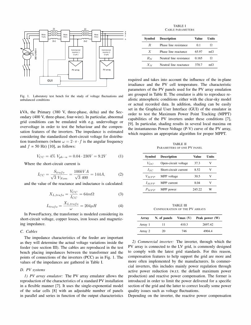
abc
n
Commercial inverter 2
(3-ph)
Commercial inverter 1
(1-ph )
PV array PV array
Δ-Y
38
0 V
/40
0 V
GUI
Meas Trafo
Meas PCC1
Meas PCC2
Z1
Zn1
Z2
Zn2
Fig. 1. Laboratory test bench for the study of voltage fluctuations andunbalanced conditions
kVA, the Primary (380 V, three-phase, delta) and the Sec-ondary (400 V, three-phase, four-wire). In particular, abnormalgrid conditions can be emulated with e.g. undervoltage orovervoltage in order to test the behaviour and the compen-sation features of the inverters. The impedance is estimatedconsidering the standardized short-circuit voltage for distribu-tion transformers (where ω = 2 ·π ·f is the angular frequencyand f = 50 Hz) [10], as follows:
VCC = 4% Vph−n = 0.04 · 230V = 9.2V (1)
Where the short-circuit current is
ICC =Strafo√3 VNom
=100kV A√
3 400= 144A, (2)
and the value of the reactance and inductance is calculated:
XL,trafo =VCC
ICC= 64mΩ (3)
Ltrafo =XL,trafo
ω= 204µH (4)
In PowerFactory, the transformer is modeled considering itsshort-circuit voltage, copper losses, iron losses and magnetiz-ing impedance.
C. Cables
The impedance characteristics of the feeder are importantas they will determine the actual voltage variations inside thefeeder (see section III). The cables are reproduced in the testbench placing impedances between the transformer and thepoints of connections of the inverters (PCC) as in Fig. 1. Thevalues of the impedances are gathered in Table I.
D. PV systems
1) PV array emulator: The PV array emulator allows thereproduction of the characteristics of a standard PV installationin a flexible manner [7]. It uses the single-exponential modelof the solar cells [8] with an adjustable number of panelsin parallel and series in function of the output characteristics
TABLE ICABLE PARAMETERS
Symbol Description Value Units
R Phase line resistance 0.1 Ω
X Phase line reactance 65.97 mΩ
RN Neutral line resistance 0.165 Ω
XN Neutral line reactance 370.7 mΩ
required and takes into account the influence of the in-planeirradiance and the PV cell temperature. The characteristicparameters of the PV panels used for the PV array emulationare grouped in Table II. The emulator is able to reproduce re-alistic atmospheric conditions either with the clear-sky modelor actual recorded data. In addition, shading can be easilyset in the Graphical User Interface (GUI) of the emulator inorder to test the Maximum Power Point Tracking (MPPT)capabilities of the PV inverters under these conditions [7],[9]. In particular, shading results in several local maxima onthe instantaneous Power-Voltage (P-V) curve of the PV array,which requires an appropriate algorithm for proper MPPT.
TABLE IIPARAMETERS OF ONE PV PANEL
Symbol Description Value Units
VOC Open-circuit voltage 37.3 V
ISC Short-circuit current 8.52 V
VMPP MPP voltage 30.5 V
IMPP MPP current 8.04 V
PMPP MPP power 245.22 W
TABLE IIICONFIGURATION OF THE PV ARRAYS
Array N. of panels Vmax (V) Peak power (W)
Array 1 11 410.3 2697.42
Array 2 20 746 4904.4
2) Commercial inverter: The inverter, through which thePV array is connected to the LV grid, is commonly designedto comply with the latest grid standards. For this reason,compensation features to help support the grid are more andmore often implemented by the manufacturers. In commer-cial inverters, this includes mainly power regulation throughactive power reduction (w.r.t. the default maximum powerproduction) and reactive power compensation. The former isintroduced in order to limit the power delivered for a specificsection of the grid and the latter to correct locally some powerquality issues such as voltage fluctuations.Depending on the inverter, the reactive power compensation
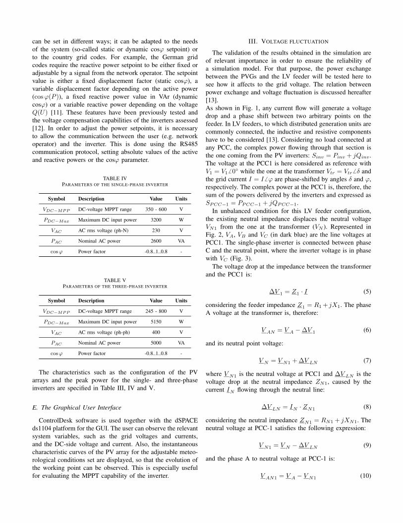
can be set in different ways; it can be adapted to the needsof the system (so-called static or dynamic cosϕ setpoint) orto the country grid codes. For example, the German gridcodes require the reactive power setpoint to be either fixed oradjustable by a signal from the network operator. The setpointvalue is either a fixed displacement factor (static cosϕ), avariable displacement factor depending on the active power(cosϕ(P )), a fixed reactive power value in VAr (dynamiccosϕ) or a variable reactive power depending on the voltageQ(U) [11]. These features have been previously tested andthe voltage compensation capabilities of the inverters assessed[12]. In order to adjust the power setpoints, it is necessaryto allow the communication between the user (e.g. networkoperator) and the inverter. This is done using the RS485communication protocol, setting absolute values of the activeand reactive powers or the cosϕ parameter.
TABLE IVPARAMETERS OF THE SINGLE-PHASE INVERTER
Symbol Description Value Units
VDC−MPP DC-voltage MPPT range 350 - 600 V
PDC−Max Maximum DC input power 3200 W
VAC AC rms voltage (ph-N) 230 V
PAC Nominal AC power 2600 VA
cosϕ Power factor -0.8..1..0.8 -
TABLE VPARAMETERS OF THE THREE-PHASE INVERTER
Symbol Description Value Units
VDC−MPP DC-voltage MPPT range 245 - 800 V
PDC−Max Maximum DC input power 5150 W
VAC AC rms voltage (ph-ph) 400 V
PAC Nominal AC power 5000 VA
cosϕ Power factor -0.8..1..0.8 -
The characteristics such as the configuration of the PVarrays and the peak power for the single- and three-phaseinverters are specified in Table III, IV and V.
E. The Graphical User Interface
ControlDesk software is used together with the dSPACEds1104 platform for the GUI. The user can observe the relevantsystem variables, such as the grid voltages and currents,and the DC-side voltage and current. Also, the instantaneouscharacteristic curves of the PV array for the adjustable meteo-rological conditions set are displayed, so that the evolution ofthe working point can be observed. This is especially usefulfor evaluating the MPPT capability of the inverter.
III. VOLTAGE FLUCTUATION
The validation of the results obtained in the simulation areof relevant importance in order to ensure the reliability ofa simulation model. For that purpose, the power exchangebetween the PVGs and the LV feeder will be tested here tosee how it affects to the grid voltage. The relation betweenpower exchange and voltage fluctuation is discussed hereafter[13].As shown in Fig. 1, any current flow will generate a voltagedrop and a phase shift between two arbitrary points on thefeeder. In LV feeders, to which distributed generation units arecommonly connected, the inductive and resistive componentshave to be considered [13]. Considering no load connected atany PCC, the complex power flowing through that section isthe one coming from the PV inverters: Sinv = Pinv + jQinv .The voltage at the PCC1 is here considered as reference withV1 = V1 6 0 while the one at the transformer Vtr = Vtr 6 δ andthe grid current I = I 6 ϕ are phase-shifted by angles δ and ϕ,respectively. The complex power at the PCC1 is, therefore, thesum of the powers delivered by the inverters and expressed asSPCC−1 = PPCC−1 + jQPCC−1.
In unbalanced condition for this LV feeder configuration,the existing neutral impedance displaces the neutral voltageVN1 from the one at the transformer (VN ). Represented inFig. 2, VA, VB and VC (in dark blue) are the line voltages atPCC1. The single-phase inverter is connected between phaseC and the neutral point, where the inverter voltage is in phasewith VC (Fig. 3).
The voltage drop at the impedance between the transformerand the PCC1 is:
∆V 1 = Z1 · I (5)
considering the feeder impedance Z1 = R1 + jX1. The phaseA voltage at the transformer is, therefore:
V AN = V A −∆V 1 (6)
and its neutral point voltage:
V N = V N1 + ∆V LN (7)
where V N1 is the neutral voltage at PCC1 and ∆V LN is thevoltage drop at the neutral impedance ZN1, caused by thecurrent IN flowing through the neutral line:
∆V LN = IN · ZN1 (8)
considering the neutral impedance ZN1 = RN1 + jXN1. Theneutral voltage at PCC-1 satisfies the following expression:
V N1 = V N −∆V LN (9)
and the phase A to neutral voltage at PCC-1 is:
V AN1 = V A − V N1 (10)
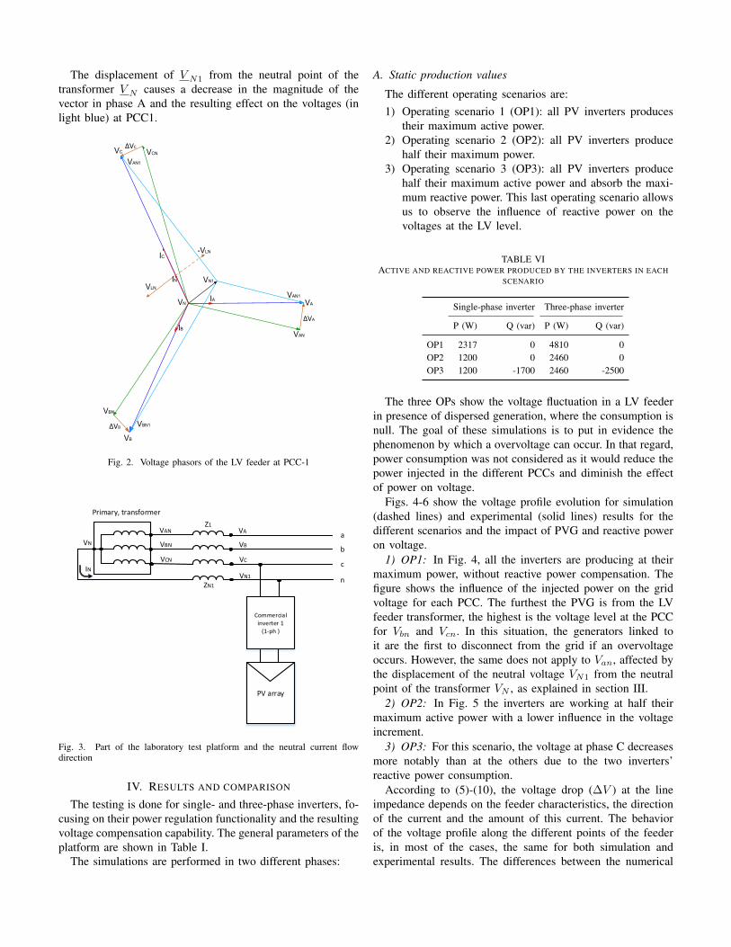
The displacement of V N1 from the neutral point of thetransformer V N causes a decrease in the magnitude of thevector in phase A and the resulting effect on the voltages (inlight blue) at PCC1.
IC
IN
-VLN
VLNVN1
IA VA
VANIB
VN
VB
VBN
VC VCNVAN1
VBN1
VAN1
ΔVC
ΔVA
ΔVB
Fig. 2. Voltage phasors of the LV feeder at PCC-1
a
b
c
n
Commercial inverter 1
(1-ph )
PV array
Z1
ZN1
VN
VAN
VBN
VCN
VA
VB
VC
IN
Primary, transformer
VN1
Fig. 3. Part of the laboratory test platform and the neutral current flowdirection
IV. RESULTS AND COMPARISON
The testing is done for single- and three-phase inverters, fo-cusing on their power regulation functionality and the resultingvoltage compensation capability. The general parameters of theplatform are shown in Table I.
The simulations are performed in two different phases:
A. Static production values
The different operating scenarios are:1) Operating scenario 1 (OP1): all PV inverters produces
their maximum active power.2) Operating scenario 2 (OP2): all PV inverters produce
half their maximum power.3) Operating scenario 3 (OP3): all PV inverters produce
half their maximum active power and absorb the maxi-mum reactive power. This last operating scenario allowsus to observe the influence of reactive power on thevoltages at the LV level.
TABLE VIACTIVE AND REACTIVE POWER PRODUCED BY THE INVERTERS IN EACH
SCENARIO
Single-phase inverter Three-phase inverter
P (W) Q (var) P (W) Q (var)
OP1 2317 0 4810 0OP2 1200 0 2460 0OP3 1200 -1700 2460 -2500
The three OPs show the voltage fluctuation in a LV feederin presence of dispersed generation, where the consumption isnull. The goal of these simulations is to put in evidence thephenomenon by which a overvoltage can occur. In that regard,power consumption was not considered as it would reduce thepower injected in the different PCCs and diminish the effectof power on voltage.
Figs. 4-6 show the voltage profile evolution for simulation(dashed lines) and experimental (solid lines) results for thedifferent scenarios and the impact of PVG and reactive poweron voltage.
1) OP1: In Fig. 4, all the inverters are producing at theirmaximum power, without reactive power compensation. Thefigure shows the influence of the injected power on the gridvoltage for each PCC. The furthest the PVG is from the LVfeeder transformer, the highest is the voltage level at the PCCfor Vbn and Vcn. In this situation, the generators linked toit are the first to disconnect from the grid if an overvoltageoccurs. However, the same does not apply to Van, affected bythe displacement of the neutral voltage VN1 from the neutralpoint of the transformer VN , as explained in section III.
2) OP2: In Fig. 5 the inverters are working at half theirmaximum active power with a lower influence in the voltageincrement.
3) OP3: For this scenario, the voltage at phase C decreasesmore notably than at the others due to the two inverters’reactive power consumption.
According to (5)-(10), the voltage drop (∆V ) at the lineimpedance depends on the feeder characteristics, the directionof the current and the amount of this current. The behaviorof the voltage profile along the different points of the feederis, in most of the cases, the same for both simulation andexperimental results. The differences between the numerical
TFM PCC1 PCC2
Measured points
228
230
232
234
236
238
240
Ph-n
voltages (
V)
Van
Vbn
Vcn
Fig. 4. Voltage profile of the LV feeder, PV inverters producing at full power.Simulation (dashed lines) and experimental (solid lines) results.
TFM PCC1 PCC2
Measured points
228
230
232
234
236
238
Ph-n
voltages (
V)
Van
Vbn
Vcn
Fig. 5. Voltage profile of the LV feeder, PV inverters producing at halfmaximum power. Simulation (dashed lines) and experimental (solid lines)results.
TFM PCC1 PCC2
Measured points
228
230
232
234
236
238
240
Ph-n
voltages (
V)
Van
Vbn
Vcn
Fig. 6. Voltage profile of the LV feeder, PV inverters producing at halfmaximum power and absorbing maximum reactive power. Simulation (dashedlines) and experimental (solid lines) results.
results and the measured ones (e.g. measured Van = 231.7V and simulated Van = 233.9 V in Fig. 4) are due to thevoltage differences in the real transformer, not reproduciblein software reliably. However, these divergences need to bestudied more deeply to bring the simulations and the realenvironment measurements closer.
Table VII gathers the values of Figs. 4-6 for the threedifferent operation scenarios: OP1, OP2, and OP3, where theadded letter ”L” means ”Laboratory” and ”S” ”Simulation”.
TABLE VIIVOLTAGES MEASURED AT THE LV FEEDER
Operation scenario OP1L OP1S OP2L OP2S OP3L OP3S
Van,Tr (V) 231.7 233.9 232 233.5 233.5 233.3Vbn,Tr (V) 233.9 234 233.4 233.6 233.2 233.3Vcn,Tr (V) 233.1 234.7 232.5 234 230.2 233
Van,PCC1 (V) 228.7 230.8 230 231.7 229 231.8Vbn,PCC1 (V) 235.3 237.2 234.4 235.4 235.5 237.1Vcn,PCC1 (V) 236.7 237.6 234.9 235.7 230.5 231.3
Van,PCC2 (V) 228.7 231 229.8 232 228.7 231.8Vbn,PCC2 (V) 238.4 237.9 237 235.8 238.1 237.2Vcn,PCC2 (V) 238.7 238.3 236.8 236.1 232.2 231.4
B. Dynamic production valuesThe PV array emulators follow predefined irradiance pro-
files to simulate realistic behavior of the inverters during a day.The irradiance profile used for the simulations is the one ofa sunny day in Belgium and its acquisition time is 1 minute.The variation of the irradiance is reproduced in the laboratoryevery 2 seconds, accelerating the execution 30 times. This way,faster experimental results than in field measurements can beobtained, as can be seen in Fig. 8. The variation of voltages,active and reactive power flows are studied and comparedto the numerical results to validate them thanks to the realhardware emulation.
0 5 10 15
time (h)
0
0.2
0.4
0.6
0.8
1
Irra
dia
nce (
kW
/m2)
Fig. 7. Irradiation profile during a sunny day
Fig. 9 shows the evolution of the output voltages of theinverters, as well as the active and reactive power flows thatcorresponds to the irradiance profile for a sunny day (Fig.7). The output behavior of the inverters is analyzed in thePowerFactory model, as for the static production values, withthe same predefined parameters as in the test platform. Theresults obtained also present a similar evolution, although thevoltage differences between phases cannot be reproduced withPowerFactory due to an small initial unbalance in the testplatform.
V. CONCLUSIONS
In this manuscript, an unbalanced LV feeder caused bythe grid-tied inverters has been studied for different values
0 500 1000 1500 2000
time (s)
0
0.5
1
1.5
2
Active p
ow
er
(kW
)
PA
PB
PC
Fig. 8. Time variation of the active power at PCC2 during a sunny day
Time (h)2 4 6 8 10 12 14 16 18 20
Ph
ase
to
ne
utr
al vo
lta
ge
(V
)
228
230
232
234
236
238
240
Van,lab
Van,sim
Vbn,lab
Vbn,sim
Vcn,lab
Vcn,sim
Fig. 9. Time variation of the phase-to-neutral voltages at PCC2 during asunny day
of active and reactive power production. A test bench thatreproduces an specific LV feeder has been designed for thisstudy and its behavior compared to its numerical model.This comparison has illustrated the reproduction of a similarbehavior between the experimental work and the simulatedmodel but also the difficulties of obtaining reliable resultsin simulations, due to the lack of information for some ofthe parameters of the system. In addition, the effect of localneutral point displacement has been exhibited and explained.It changes the shape of the phase-to-neutral voltages in mag-nitude and phase and can aggravate the unbalance situation.
ACKNOWLEDGEMENT
This research is financed by the Walloon region in theframework of the PREMASOL project (C-6829).
REFERENCES
[1] P. P. Barker and R. W. De Mello, “Determining the impact of distributedgeneration on power systems. I. Radial distribution systems,” Power Eng.Soc. Summer Meet, vol. 3, pp. 1645-1656, 2000.
[2] V. Klonari, F. Vallee, O. Durieux, J. Lobry, “Probabilistic tool basedon smart meters data to evaluate the impact of distributed photovoltaicgeneration on voltage profiles in low voltage grids,” Solar IntegratonWorkshop, 2013.
[3] V. Klonari, F. Vallee, O. Durieux, Z. De Greve, J. Lobry, “ProbabilisticModeling of Short Term Fluctuations of Photovoltaic Power Injectionfor the Evaluation of Overvoltage Risk in Low Voltage Grids,” IEEEInternational Energy Conference (ENERGYCON)., pp. 897-903, 2014.
[4] F. Olivier, P. Aristidou, D. Ernst, and T. Van Cutsem, “Active Man-agement of Low-Voltage Networks for Mitigating Overvoltages Due toPhotovoltaic Units,” IEEE Trans. Smart Grid, pp. 1-9, 2015.
[5] Ioulia T. Papaioannou, Minas C. Alexiadis, Charis S. Demoulias,Dimitris P. Labridis, and Petros S. Dokopoulos, “Modeling and FieldMeasurements of Photovoltaic Units Connected to LV Grid. Study ofPenetration Scenarios,” IEEE Trans. Power Delivery, vol. 26, no. 2, pp.979-987, April 2011.
[6] S. Papathanassiou, N. Hatziargyriou, K. Strunz “A Benchmark LowVoltage Microgrid Network,” CIGRE Symposium, 2005.
[7] T. Geury, and J. Gyselinck, “Emulation of photovoltaic arrays withshading effect for testing of grid- connected inverters,” Proc. 2013 EPEEuropean Conference on Power Electronics and Applications., pp. 1-9.
[8] M. G. Villalva, J. R. Gazoli, and E. R. Filho, “Comprehensive approachto modeling and simulation of photovoltaic arrays,” IEEE Trans. PowerElectron., vol. 24, no. 5, pp. 11981208, May 2009.
[9] I. R. Balasubramanian, S. Ilango Ganesan, and N. Chilakapati, “Impactof partial shading on the output power of pv systems under partialshading conditions,” IET Power Electron., vol. 7, no. 3, pp. 657666,2014.
[10] B. Metz-Noblat, F. Dumas, and C. Poulain, “Calculation of short-circuitcurrents,” Scheinder Electric, Grenoble, France, Tech. Rep. TR-0158, p.13, 2005.
[11] E. Troester, “New german grid codes for connecting pv systems to themedium voltage power grid,” 2nd Int. Work. Conc. Photovolt. PowerPlants Opt. Des. Prod. Grid Connect., pp. 1-4, 2009.
[12] R. Lopez-Erauskin, T. Geury, A. Gonzalez, J. Gyselinck, M.E. Hervas,A. Fabre, “Testing the Enhanced Functionalities of Commercial PVInverters Under Realistic Atmospheric and Abnormal Grid Conditions,” Solar Integraton Workshop, 2015.
[13] R. A. Mastromauro, M. Liserre, and A. D. Aquila, “Single-phase grid-connected photovoltaic systems with power quality conditioner function-ality,” European Conference on Power Electronics and Applications, pp.1-11, 2007.
[14] R. Kabiri, D. G. Holmes, and B. P. McGrath, “The influence of pvinverter reactive power injection on grid voltage regulation,” IEEE 5thInt. Symp. Power Electron. Distrib. Gener. Syst., pp. 1-8, Jun. 2014.
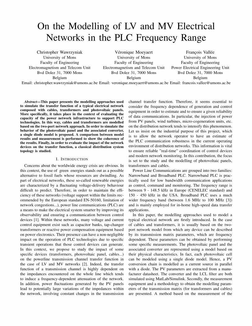
On the Modelling of LV and MV ElectricalNetworks in the PLC Frequency Range
Christopher WawrzyniakUniversity of Mons
Faculty of EngineeringElectromagnetism and Telecom Unit
Bvd Dolez 31, 7000 MonsBelgium
Email: [email protected]
Veronique MoeyaertUniversity of Mons
Faculty of EngineeringElectromagnetism and Telecom Unit
Bvd Dolez 31, 7000 MonsBelgium
Email: [email protected]
Francois ValleeUniversity of Mons
Faculty of EngineeringPower Electrical Engineering Unit
Bvd Dolez 31, 7000 MonsBelgium
Email: [email protected]
Abstract—This paper presents the modelling approaches usedto simulate the transfer function of a typical electrical networkcomposed with cables, transformers and photovoltaic panels.More specifically, it takes place in the context of evaluating thecapacity of the power network infrastructure to support PLCtechnologies. In this way, cables and transformers are modelledbased on the two-port network approach. In order to simulate thebehavior of the photovoltaic panel and the associated converter,a single diode model is proposed. A comparison between modelresults and measurement is performed to show the coherence ofthe results. Finally, in order to evaluate the impact of the networkdevices on the transfer function, a classical distribution systemtopology is studied.
I. INTRODUCTION
Concerns about the worldwide energy crisis are obvious. Inthis context, the use of green energies stands out as a possiblealternative to fossil fuels whose resources are dwindling. Aspart of electrical networks, these so-called renewable energiesare characterized by a fluctuating voltage-delivery behaviourdifficult to predict. Therefore, in order to maintain the effi-ciency of these networks (voltage support within the limits rec-ommended by the European standard EN-50160, limitation ofnetwork congestions...), power line communications (PLC) area means to make the electrical system smarter by improving itsobservability and ensuring a communication between controldevices [1]. Within these networks, many voltage and currentcontrol equipment exist such as capacitor banks, tap-changertransformers or reactive power compensation equipment basedon power electronics. Their presence can have a non-negligibleimpact on the operation of PLC technologies due to specifictransient operations that those control devices can generate.In this context, we propose to study the impact of somespecific devices (transformers, photovoltaic panel, cables...)on the powerline transmission channel transfer function inthe case of LV and MV networks [2]. Indeed, the transferfunction of a transmission channel is highly dependent onthe impedances encountered on the whole line which tendsto induce a frequency-dependent attenuation of the network.In addition, power fluctuations generated by the PV panelslead to potentially large variations of the impedances withinthe network, involving constant changes in the transmission
channel transfer function. Therefore, it seems essential toconsider the frequency dependence of generation and controlequipment in order to estimate and to ensure a given reliabilityof data communications. In particular, the injection of powerfrom PV panels, wind turbines, micro-cogeneration units, etc.on the distribution network tends to intensify this phenomenon.Let us insist on the industrial purpose of this project, whichis to allow the network operator to have an estimate ofthe PLC communication robustness in the current operatingenvironment of distribution networks. This information is vitalto ensure reliable ”real-time” coordination of control devicesand modern network monitoring. In this contribution, the focusis set to the study and the modelling of photovoltaic panels,transformers and cables.
Power Line Communications are grouped into two families:Narrowband and Broadband PLC. Narrowband PLC is prac-tically used for low bandwidth communication applicationsas control, command and monitoring. The frequency range isbetween 9 - 148.5 kHz in Europe (CENELEC standard) and150 - 450 kHz in the USA. Broadband PLC uses a muchwider frequency band (between 1.6 MHz to 100 MHz [3])and is mainly employed for in-home high-speed data transferapplications.
In this paper, the modelling approaches used to model atypical electrical network are firstly introduced. In the caseof cables and transformers, it is usually based on the two-port network model from which any device can be describedby its transmission matrix parameters, which are frequencydependent. These parameters can be obtained by performingsome specific measurements. The photovoltaic panel and theassociated converter are represented using a model based ontheir physical characteristics. In fact, each photovoltaic cellcan be modeled using a single diode model. Hence, a PVconversion chain is modelled as a current source in parallelwith a diode. The PV parameters are extracted from a manu-facturer datasheet. The converter and the LCL filter are bothsimulated using MatLab/Simulink. Secondly, the measurementequipment and a methodology to obtain the modelling param-eters of the transmission matrix (for transformers and cables)are presented. A method based on the measurement of the

reflection coefficient at the input of the device when the outputis successively open and short-circuited is used. Anothermeasurement equipment and a methodology to measure theperformance of the PV unit are also proposed. For each equip-ment, a comparison between each model and measurementsis performed in order to conclude about the efficiency of themodelling approaches. Finally, a representative topology of LVsystems is simulated and a time dependant transfer functionis evaluated in the PLC frequency range.
II. MODELLING APPROACHES OF ELECTRICAL NETWORKDEVICES
A. Power cables modelling
1) Transmission Line Theory: In the literature, most of themethods proposed to study a transmission line are based onthe transmission line theory ([4]-[10]). Following this theory,an elementary line transmission cell can be represented as inFig.1 and the time dependent telegraphers equations can beapplied as follows:
−∂u(z, t)
∂z= ri+ l
∂i(z, t)
∂t, −∂i(z, t)
∂z= gu+ c
∂u(z, t)
∂t(1)
Fig. 1. Elementary line transmission cell
In these equations z represents the position on the line, t thetime and the linear resistance r (Ω/m), inductance l (H/m),capacitance c (F/m) and conductance g (S/m) are the primaryline parameters.
A transmission line can also be described by its secondaryparameters, the characteristic impedance Zc and the propaga-tion constant γ, which depend on the primary parameters andare given by:
Zc =
√r + jωl
g + jωc, γ =
√(r + jωl)(g + jωc) (2)
where ω represents the angular frequency.2) ABCD matrix: The knowledge of the secondary param-
eters allows to describe the relationship between the inputvoltage U1 and current I1, and output voltage U2 and currentI2 of a two-port network using the frequency dependent chainparameters matrix A, B, C and D as represented in Fig. 2:
[U1
I1
]=
[A(f) B(f)C(f) D(f)
] [U2
I2
](3)
Fig. 2. Two-port network connected to a source and a load
The transfer function of the two-port network can then begiven by:
H =U2
US
=Zr
AZr +B + CZrZs +DZs
(4)
where Zs is the source impedance, Zr the load impedanceand A, B, C and D are calculated as follows, x being thelength of the line:
Tj =
[A BC D
]=
[cosh(γx) Zc sinh(γx)1Zc
sinh(γx) cosh(γx)
](5)
3) Derivations on the line: The chain matrix that we haveconsidered previously does not take into account the eventualpresence of derivation branches on the line. Fig. 3 shows abranch of length xbranch located at a distance x1 of the sourceand x2 of the load and terminated by load impedance Zbranch.
Fig. 3. Transmission line with one branch
In this context, this branch can be replaced by an equivalentimpedance Zeq placed on the main line (Fig. 4) and given bythe following expression:
Zeq =AbranchZbranch +Bbranch
CbranchZbranch +Dbranch(6)
where Abranch, Bbranch, Cbranch and Dbranch are thetransmission matrix parameters of the branch and Zbranch isthe load at the end of the branch.
Once this step is done, we can split the transmission lineinto four areas when dealing with the representation given inFig. 4, each zone being characterized by its own chain matrix(x1 and x2 inside Tj matrices are related to Fig. 3):
T1=
[1 Zs
0 1
]T2=
[cosh(γ
1x1) Zc1 sinh(γ
1x1)
1Zc1
sinh(γ1x1) cosh(γ
1x1)
]
T3=
[1 01
Zeq1
]T4=
[cosh(γ
2x2) Zc2 sinh(γ
2x2)
1Zc2
sinh(γ2x2) cosh(γ
2x2)
](7)
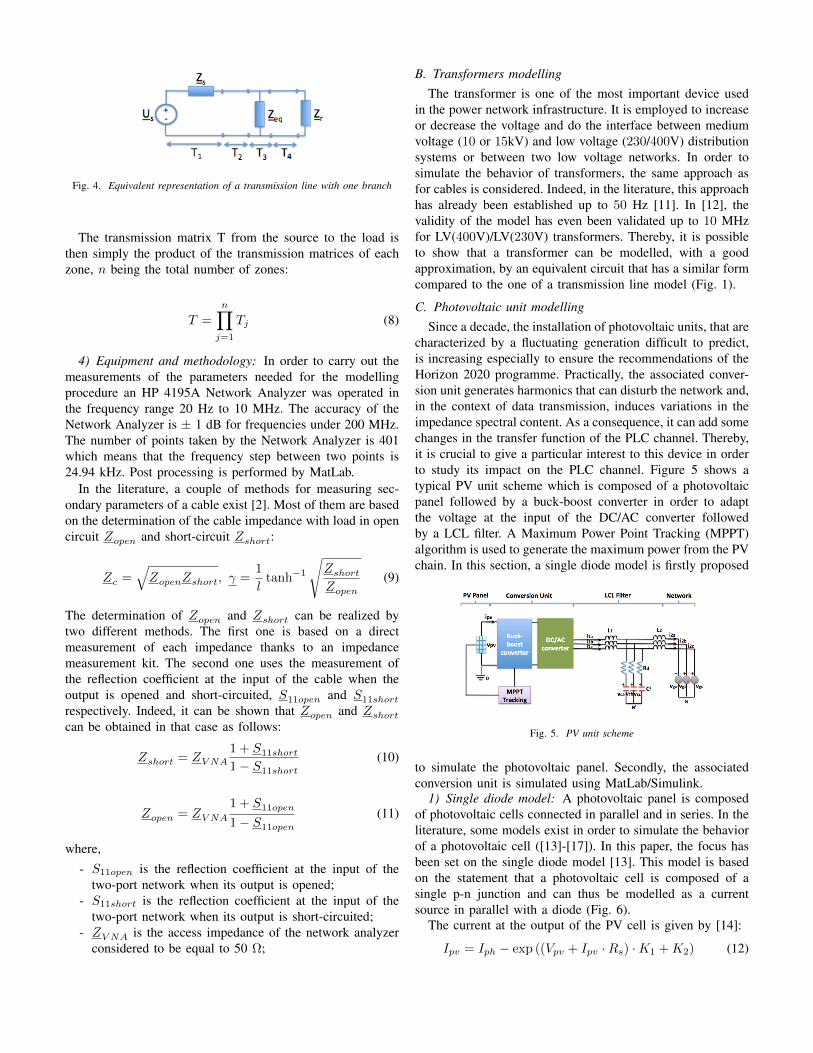
Fig. 4. Equivalent representation of a transmission line with one branch
The transmission matrix T from the source to the load isthen simply the product of the transmission matrices of eachzone, n being the total number of zones:
T =
n∏j=1
Tj (8)
4) Equipment and methodology: In order to carry out themeasurements of the parameters needed for the modellingprocedure an HP 4195A Network Analyzer was operated inthe frequency range 20 Hz to 10 MHz. The accuracy of theNetwork Analyzer is ± 1 dB for frequencies under 200 MHz.The number of points taken by the Network Analyzer is 401which means that the frequency step between two points is24.94 kHz. Post processing is performed by MatLab.
In the literature, a couple of methods for measuring sec-ondary parameters of a cable exist [2]. Most of them are basedon the determination of the cable impedance with load in opencircuit Zopen and short-circuit Zshort:
Zc =√ZopenZshort, γ =
1
ltanh−1
√Zshort
Zopen
(9)
The determination of Zopen and Zshort can be realized bytwo different methods. The first one is based on a directmeasurement of each impedance thanks to an impedancemeasurement kit. The second one uses the measurement ofthe reflection coefficient at the input of the cable when theoutput is opened and short-circuited, S11open and S11short
respectively. Indeed, it can be shown that Zopen and Zshort
can be obtained in that case as follows:
Zshort = ZV NA
1 + S11short
1 − S11short
(10)
Zopen = ZV NA
1 + S11open
1 − S11open
(11)
where,
- S11open is the reflection coefficient at the input of thetwo-port network when its output is opened;
- S11short is the reflection coefficient at the input of thetwo-port network when its output is short-circuited;
- ZV NA is the access impedance of the network analyzerconsidered to be equal to 50 Ω;
B. Transformers modellingThe transformer is one of the most important device used
in the power network infrastructure. It is employed to increaseor decrease the voltage and do the interface between mediumvoltage (10 or 15kV) and low voltage (230/400V) distributionsystems or between two low voltage networks. In order tosimulate the behavior of transformers, the same approach asfor cables is considered. Indeed, in the literature, this approachhas already been established up to 50 Hz [11]. In [12], thevalidity of the model has even been validated up to 10 MHzfor LV(400V)/LV(230V) transformers. Thereby, it is possibleto show that a transformer can be modelled, with a goodapproximation, by an equivalent circuit that has a similar formcompared to the one of a transmission line model (Fig. 1).
C. Photovoltaic unit modellingSince a decade, the installation of photovoltaic units, that are
characterized by a fluctuating generation difficult to predict,is increasing especially to ensure the recommendations of theHorizon 2020 programme. Practically, the associated conver-sion unit generates harmonics that can disturb the network and,in the context of data transmission, induces variations in theimpedance spectral content. As a consequence, it can add somechanges in the transfer function of the PLC channel. Thereby,it is crucial to give a particular interest to this device in orderto study its impact on the PLC channel. Figure 5 shows atypical PV unit scheme which is composed of a photovoltaicpanel followed by a buck-boost converter in order to adaptthe voltage at the input of the DC/AC converter followedby a LCL filter. A Maximum Power Point Tracking (MPPT)algorithm is used to generate the maximum power from the PVchain. In this section, a single diode model is firstly proposed
Fig. 5. PV unit scheme
to simulate the photovoltaic panel. Secondly, the associatedconversion unit is simulated using MatLab/Simulink.
1) Single diode model: A photovoltaic panel is composedof photovoltaic cells connected in parallel and in series. In theliterature, some models exist in order to simulate the behaviorof a photovoltaic cell ([13]-[17]). In this paper, the focus hasbeen set on the single diode model [13]. This model is basedon the statement that a photovoltaic cell is composed of asingle p-n junction and can thus be modelled as a currentsource in parallel with a diode (Fig. 6).
The current at the output of the PV cell is given by [14]:
Ipv = Iph − exp ((Vpv + Ipv ·Rs) ·K1 +K2) (12)
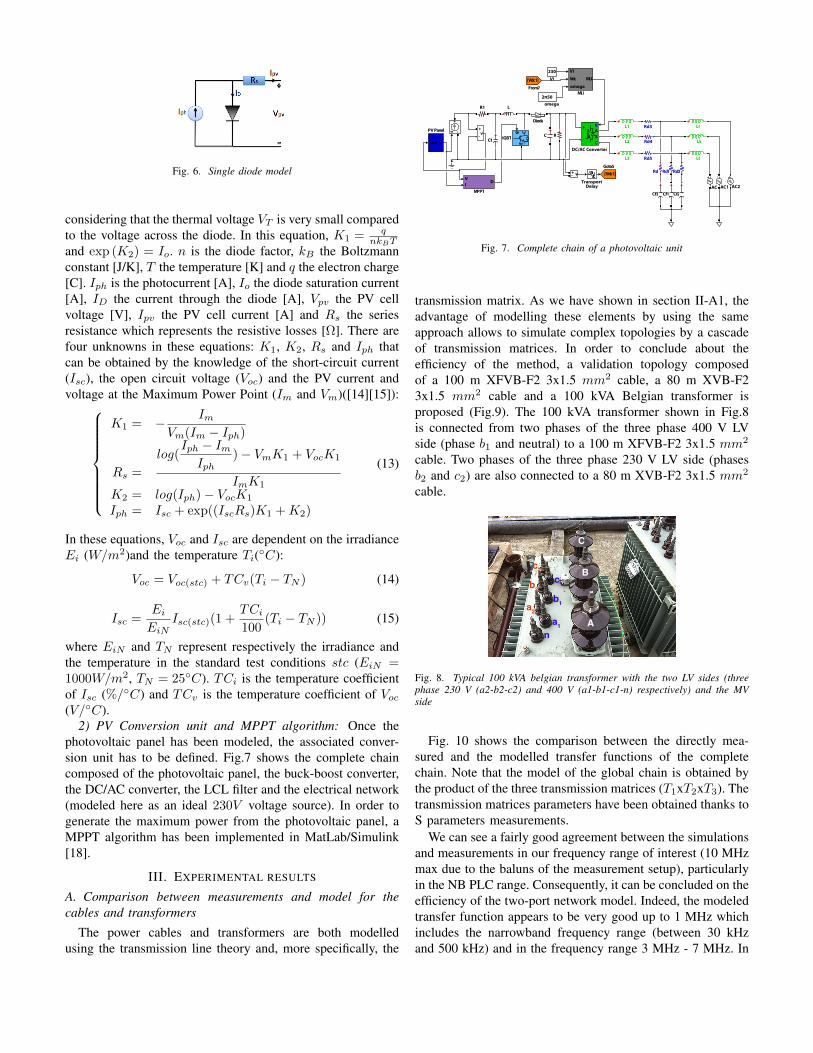
Fig. 6. Single diode model
considering that the thermal voltage VT is very small comparedto the voltage across the diode. In this equation, K1 = q
nkBTand exp (K2) = Io. n is the diode factor, kB the Boltzmannconstant [J/K], T the temperature [K] and q the electron charge[C]. Iph is the photocurrent [A], Io the diode saturation current[A], ID the current through the diode [A], Vpv the PV cellvoltage [V], Ipv the PV cell current [A] and Rs the seriesresistance which represents the resistive losses [Ω]. There arefour unknowns in these equations: K1, K2, Rs and Iph thatcan be obtained by the knowledge of the short-circuit current(Isc), the open circuit voltage (Voc) and the PV current andvoltage at the Maximum Power Point (Im and Vm)([14][15]):
K1 = − ImVm(Im − Iph)
Rs =
log(Iph − ImIph
) − VmK1 + VocK1
ImK1K2 = log(Iph) − VocK1
Iph = Isc + exp((IscRs)K1 +K2)
(13)
In these equations, Voc and Isc are dependent on the irradianceEi (W/m2)and the temperature Ti(C):
Voc = Voc(stc) + TCv(Ti − TN ) (14)
Isc =Ei
EiNIsc(stc)(1 +
TCi
100(Ti − TN )) (15)
where EiN and TN represent respectively the irradiance andthe temperature in the standard test conditions stc (EiN =1000W/m2, TN = 25C). TCi is the temperature coefficientof Isc (%/C) and TCv is the temperature coefficient of Voc(V/C).
2) PV Conversion unit and MPPT algorithm: Once thephotovoltaic panel has been modeled, the associated conver-sion unit has to be defined. Fig.7 shows the complete chaincomposed of the photovoltaic panel, the buck-boost converter,the DC/AC converter, the LCL filter and the electrical network(modeled here as an ideal 230V voltage source). In order togenerate the maximum power from the photovoltaic panel, aMPPT algorithm has been implemented in MatLab/Simulink[18].
III. EXPERIMENTAL RESULTS
A. Comparison between measurements and model for thecables and transformers
The power cables and transformers are both modelledusing the transmission line theory and, more specifically, the
AC AC1 AC2
v+
-
+R1
+
R
VI
D
MPPT
+L
g CE
IGBT
Diode
s -+
+
C1C
230V1
+
-
DC/AC Converter+
L3
+L2
+L1
V1
Vdc MLI
MLI
+L6
+L5
+L4
+
+
+
+
Cf3
+
Cf1
+
Cf2
+
Rd
+
Rd1
+
Rd2
[Vdc1]
From7
[Vdc1]
Goto5
v+-
Uout I
PV Panel
2π50omega
+
omega
Rd3
Rd4
Rd5
gABC
TransportDelay
230
Fig. 7. Complete chain of a photovoltaic unit
transmission matrix. As we have shown in section II-A1, theadvantage of modelling these elements by using the sameapproach allows to simulate complex topologies by a cascadeof transmission matrices. In order to conclude about theefficiency of the method, a validation topology composedof a 100 m XFVB-F2 3x1.5 mm2 cable, a 80 m XVB-F23x1.5 mm2 cable and a 100 kVA Belgian transformer isproposed (Fig.9). The 100 kVA transformer shown in Fig.8is connected from two phases of the three phase 400 V LVside (phase b1 and neutral) to a 100 m XFVB-F2 3x1.5 mm2
cable. Two phases of the three phase 230 V LV side (phasesb2 and c2) are also connected to a 80 m XVB-F2 3x1.5 mm2
cable.
a2
b2
c2
c1
b1
a1
nA
B
C
Fig. 8. Typical 100 kVA belgian transformer with the two LV sides (threephase 230 V (a2-b2-c2) and 400 V (a1-b1-c1-n) respectively) and the MVside
Fig. 10 shows the comparison between the directly mea-sured and the modelled transfer functions of the completechain. Note that the model of the global chain is obtained bythe product of the three transmission matrices (T1xT2xT3). Thetransmission matrices parameters have been obtained thanks toS parameters measurements.
We can see a fairly good agreement between the simulationsand measurements in our frequency range of interest (10 MHzmax due to the baluns of the measurement setup), particularlyin the NB PLC range. Consequently, it can be concluded on theefficiency of the two-port network model. Indeed, the modeledtransfer function appears to be very good up to 1 MHz whichincludes the narrowband frequency range (between 30 kHzand 500 kHz) and in the frequency range 3 MHz - 7 MHz. In
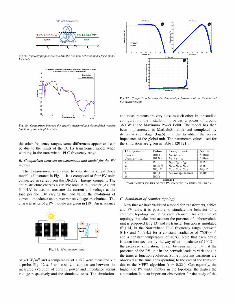
Fig. 9. Topology proposed to validate the two-port network model for a globalLV chain
0 2 4 6 8 10x 106
−45
−40
−35
−30
−25
−20
−15
−10
−5
0
5
Comparison between the directly measured and the modeledtransfer function of the complete chain
|H(f)
|(dB
)
Frequency(Hz)
SimulationMeasurement
Fig. 10. Comparison between the directly measured and the modeled transferfunction of the complete chain
the other frequency ranges, some differences appear and canbe due to the limits of the 50 Hz transformer model whenworking in the narrowband PLC frequency range.
B. Comparison between measurements and model for the PVmodule
The measurement setup used to validate the single diodemodel is illustrated in Fig.11. It is composed of four PV unitsconnected in series from the DROBen Energy company. Theentire structure charges a variable load. A multimeter (Agilent34401A) is used to measure the current and voltage at theload position. By varying the load value, the evolutions ofcurrent, impedance and power versus voltage are obtained. Thecharacteristics of a PV module are given in [19]. An irradiance
Fig. 11. Measurement setup
of 750W/m2 and a temperature of 40C were measured viaa probe. Fig. 12 a, b and c show a comparison between themeasured evolution of current, power and impedance versusvoltage respectively and the simulated ones. The simulations
0 10 20 30 40 50 60 70 800
1
2
3
4
5
6
7I−V Curves
Voltage (V)
Mod
ule
Cur
rent
(A)
0 10 20 30 40 50 60 70 800
50
100
150
200
250
300
350
400
450
500R−V Curves
Voltage (V)
Mod
ule
Res
ista
nce
(Ohm
s)
0 10 20 30 40 50 60 70 800
50
100
150
200
250
300
350
400P−V Curves
Voltage (V)
Mod
ule
Pow
er (W
)
a b
Meas.Sim.
c
Fig. 12. Comparison between the simulated performance of the PV unit andthe measurements
and measurements are very close to each other. In the studiedconfiguration, the installation provides a power of around360 W at the Maximum Power Point. The model has thenbeen implemented in MatLab/Simulink and completed byits conversion stage (Fig.5) in order to obtain the accessimpedance of the global unit. The parameters values used forthe simulation are given in table I [20][21].
Component Value Component Valueffund 50Hz L1, L2, L3 500µHfDC/ACconv 10kHz L4, L5, L6 130µHR1 1Ω Rd, Rd1, Rd2 0.3ΩL 100mH Rd3, Rd4, Rd5 0.1ΩC1 500µF Cf1, Cf2, Cf3 99µFC 10mF AC voltage sources 230VR 500Ω
TABLE ICOMPONENTS VALUES OF THE PV CONVERSION UNIT (CF. FIG.7)
C. Simulation of complex topology
Now that we have validated a model for transformers, cablesand PV units it is possible to simulate the behavior of acomplex topology including each element. An example oftopology that takes into account the presence of a photovoltaicunit is proposed (Fig.13) and its transfer function is simulated(Fig.14) in the Narrowband PLC frequency range (between0 Hz and 500kHz) for a constant irradiance of 750W/m2
and a constant temperature of 40C. Note that each houseis taken into account by the way of an impedance of 100Ω inthe proposed simulation. It can be seen in Fig. 14 that thepresence of the PV unit in the network leads to variations inthe transfer function evolution. Some important variations areobserved at the time corresponding to the end of the transientdue to the MPPT algorithm (t = 0.22s). Consequently, thehigher the PV units number in the topology, the higher theattenuation. It is an important observation for the study of the
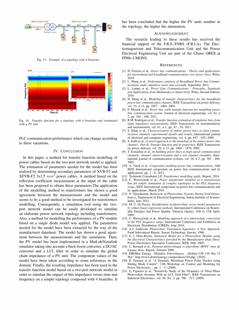
PV
Fig. 13. Example of a topology with 4 branches
0
1
2
3
4
5
6
X 105
Freq
uenc
y (H
z)
0 0.1 0.2 0.3 0.4 0.5 0.6 0.7 0.8Time (s)
0.9 1
0.2 0.205 0.21 0.215 0.22 0.225 0.23 0.235 0.240
1
2
3
4
5
6
X 105
Time (s)
Fig. 14. Transfer function for a topology with 4 branches and terminatedwith a PV unit
PLC communication performance which can change accordingto these variations.
IV. CONCLUSION
In this paper, a method for transfer function modelling ofpower cables based on the two-port network model is applied.The estimation of parameters needed for the model has beenrealized by determining secondary parameters of XVB-F2 andXFVB-F2 3x1.5 mm2 power cables. A method based on thereflection coefficient measurement at the input of the cablehas been proposed to obtain these parameters.The applicationof the modelling method to transformers has shown a goodagreement between the measurements and the model andseems to be a good method to be investigated for transformersmodelling. Consequently, a simulation tool using the two-port network model can be easily developed to simulatean elaborate power network topology including transformers.Also, a method for modelling the performance of a PV modulebased on a single diode model was applied. The parametersneeded for the model have been extracted by the way of themanufacturer datasheet. The model has shown a good agree-ment between the measurements and the simulation. Then,the PV model has been implemented in a MatLab/Simulinksimulator taking into account a buck-boost converter, a DC/ACconverter and a LCL filter in order to simulate the globalchain impedance of a PV unit. The component values of themodel have been taken according to some references in thedomain. Finally, the resulting impedance has been used in thetransfer function model based on a two-port network model inorder to simulate the impact of this impedance versus time andfrequency on a simple topology composed with 4 branches. It
has been concluded that the higher the PV units number inthe topology, the higher the attenuation.
ACKNOWLEDGMENT
The research leading to these results has received thefinancial support of the F.R.S.-FNRS (F.R.I.A). The Elec-tromagnetism and Telecommunication Unit and the PowerElectrical Engineering Unit are part of the Chaire ORES atFPMs-UMONS.
REFERENCES
[1] H. Ferreira et al., Power line communications - Theory and applicationsfor narrowband and broadband communications over power lines, Wiley,2010.
[2] L. Wang et al., Performance analysis of Broadband Power line Commu-nications under impulsive noise and crosstalk, September 2012.
[3] L. Lampe et al., Power Line Communications - Principles, Standardsand Applications from Multimedia to Smart Grid, Wiley, Second Edition,2016.
[4] H. Meng et al., Modeling of transfer characteristics for the broadbandpower line communication channel, IEEE Transactions on power delivery,vol. 19, n 13, pp. 1057 - 1064, 2004.
[5] P. Mlynek et al., Power line cable transfer function for modelling powerline communication system, Journal of electrical engineering, vol. 62, n2, pp. 104 - 108, 2011.
[6] R.M. Rodrigues et al., Transfer function estimation of telephone lines frominput impedance measurements, IEEE Transactions on instrumentationand measurement, vol. 61, n 1, pp. 43 - 54, 2011.
[7] S. Khan et al., Characterization of indoor power lines as data commu-nication channels experimental details and results, International journalof electrical and computer engineering, vol. 4, pp. 647 - 652, 2009.
[8] S. Galli et al., A novel approach to the modeling of the indoor power linechannel - Part II: Transfer function and its properties, IEEE Transactionson power delivery, vol. 20, n 13, pp. 1869 - 1878, 2005.
[9] T. Esmailian et al., In-building power lines as high-speed communicationchannels: channel characterization and a test channel ensemble, Inter-national journal of communication systems, vol. 16, n 5, pp. 381 - 400,2003.
[10] A. Vinck et al., Cooperative multihop power line communications, 16thIEEE International symposium on power line communications and itsapplications, pp. 1 - 6, 2012.
[11] Teshmont Consultants LP, Transformer modelling guide, Report, 2014.[12] C. Wawrzyniak et al., Power transformer modeled as a transmission
line for simple simulation of complex topologies in the PLC frequencyrange, IEEE International symposium on power line communications andits applications, March 2016.
[13] S. Vijayakumar, Behaviour of Photovoltaic Systems During Grid Distur-bances. Department of Electrical Engineering, Indian Institute of Science,India, June 2012.
[14] M. C. Di Piazza, Identification of photovoltaic array model parametersby robust linear regression methods. International Conference on Renew-able Energies and Power Quality, Valencia (Spain), 15th to 17th April,2009.
[15] C. Wawrzyniak et al., Modeling approach of a photovoltaic conversionin the PLC frequency range, International Conference and Exhibition onElectricity Distribution (CIRED), June 2016.
[16] A.J. Anderson, Photovoltaic Translation Equations: A New Approach.Final Subcontract Report, Sunset Technology, Janvier, 1996.
[17] E. I. Ortiz-Rivera, Analytical Model for a Photovoltaic Module usingthe Electrical Characteristics provided by the Manufacturer Data Sheet.Power Electronics Specialists Conference, IEEE 36th, 2005.
[18] C. Bernard et al., Panneau photovoltaque et algorithme MPPT base delogique floue. Report, Automn 2009.
[19] DROBen Energy. “Modulos Fotovoltaicos - Droben CM 130 Wp 15Wp”, http://www.drobenenergy.com/producto130.php, (2016).
[20] E. Jimenez et al. “A Dynamic Maximum Power Point Tracker usingSliding Mode Control”, 11th Workshop on Control and Modeling forPower Electronics, , pp. 1 - 5, (2008).
[21] E. Figueres et al. “Sensitivity Study of the Dynamics of Three-PhasePhotovoltaic Inverters With an LCL Grid Filter”, IEEE Transactions onIndustrial Electronics, vol. 56, No. 3, pp. 706 - 717, (2009).
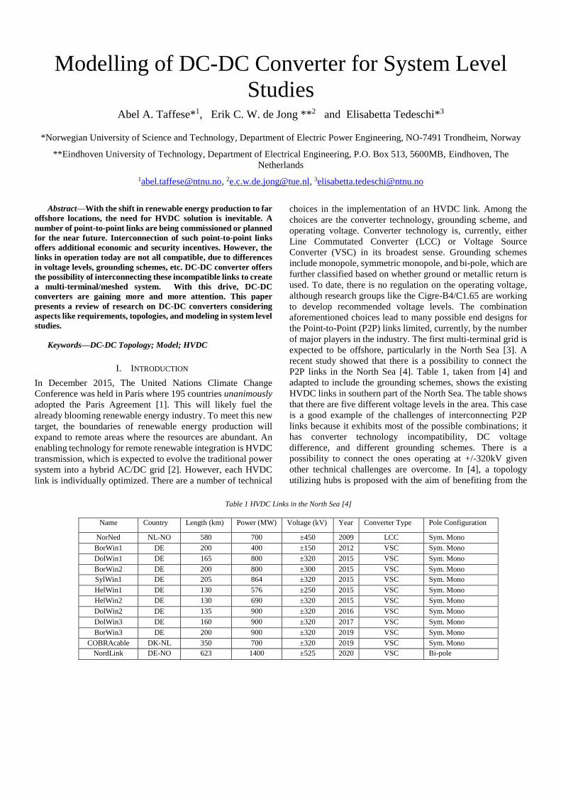
Modelling of DC-DC Converter for System Level
Studies Abel A. Taffese*1, Erik C. W. de Jong **2 and Elisabetta Tedeschi*3
*Norwegian University of Science and Technology, Department of Electric Power Engineering, NO-7491 Trondheim, Norway
**Eindhoven University of Technology, Department of Electrical Engineering, P.O. Box 513, 5600MB, Eindhoven, The
Netherlands
[email protected], [email protected], [email protected]
Abstract—With the shift in renewable energy production to far
offshore locations, the need for HVDC solution is inevitable. A
number of point-to-point links are being commissioned or planned
for the near future. Interconnection of such point-to-point links
offers additional economic and security incentives. However, the
links in operation today are not all compatible, due to differences
in voltage levels, grounding schemes, etc. DC-DC converter offers
the possibility of interconnecting these incompatible links to create
a multi-terminal/meshed system. With this drive, DC-DC
converters are gaining more and more attention. This paper
presents a review of research on DC-DC converters considering
aspects like requirements, topologies, and modeling in system level
studies.
Keywords—DC-DC Topology; Model; HVDC
I. INTRODUCTION
In December 2015, The United Nations Climate Change
Conference was held in Paris where 195 countries unanimously
adopted the Paris Agreement [1]. This will likely fuel the
already blooming renewable energy industry. To meet this new
target, the boundaries of renewable energy production will
expand to remote areas where the resources are abundant. An
enabling technology for remote renewable integration is HVDC
transmission, which is expected to evolve the traditional power
system into a hybrid AC/DC grid [2]. However, each HVDC
link is individually optimized. There are a number of technical
choices in the implementation of an HVDC link. Among the
choices are the converter technology, grounding scheme, and
operating voltage. Converter technology is, currently, either
Line Commutated Converter (LCC) or Voltage Source
Converter (VSC) in its broadest sense. Grounding schemes
include monopole, symmetric monopole, and bi-pole, which are
further classified based on whether ground or metallic return is
used. To date, there is no regulation on the operating voltage,
although research groups like the Cigre-B4/C1.65 are working
to develop recommended voltage levels. The combination
aforementioned choices lead to many possible end designs for
the Point-to-Point (P2P) links limited, currently, by the number
of major players in the industry. The first multi-terminal grid is
expected to be offshore, particularly in the North Sea [3]. A
recent study showed that there is a possibility to connect the
P2P links in the North Sea [4]. Table 1, taken from [4] and
adapted to include the grounding schemes, shows the existing
HVDC links in southern part of the North Sea. The table shows
that there are five different voltage levels in the area. This case
is a good example of the challenges of interconnecting P2P
links because it exhibits most of the possible combinations; it
has converter technology incompatibility, DC voltage
difference, and different grounding schemes. There is a
possibility to connect the ones operating at +/-320kV given
other technical challenges are overcome. In [4], a topology
utilizing hubs is proposed with the aim of benefiting from the
Table 1 HVDC Links in the North Sea [4]
Name Country Length (km) Power (MW) Voltage (kV) Year Converter Type Pole Configuration
NorNed NL-NO 580 700 ±450 2009 LCC Sym. Mono
BorWin1 DE 200 400 ±150 2012 VSC Sym. Mono
DolWin1 DE 165 800 ±320 2015 VSC Sym. Mono
BorWin2 DE 200 800 ±300 2015 VSC Sym. Mono
SylWin1 DE 205 864 ±320 2015 VSC Sym. Mono
HelWin1 DE 130 576 ±250 2015 VSC Sym. Mono
HelWin2 DE 130 690 ±320 2015 VSC Sym. Mono
DolWin2 DE 135 900 ±320 2016 VSC Sym. Mono
DolWin3 DE 160 900 ±320 2017 VSC Sym. Mono
BorWin3 DE 200 900 ±320 2019 VSC Sym. Mono
COBRAcable DK-NL 350 700 ±320 2019 VSC Sym. Mono
NordLink DE-NO 623 1400 ±525 2020 VSC Bi-pole

geographical proximity of the farms. Although the final
decision will be based on economic benefits, DC-DC converters
provide the technical solution for interconnecting the remaining
links. However, such converters are not well established for
high voltage, high power applications. Moreover, limited
research effort is put into the development of correct models for
system level studies. This paper presents a review of the DC-
DC converter for HVDC application. The rest this paper is
organized as follows. The next section outlines requirements for
DC-DC converters followed by a review of selected few
topologies that are considered suitable for high power HVDC
applications. Section IV discusses the models for DC-DC
converters for system level studies.
II. REQUIREMENTS FOR DC-DC CONVERTERS
There are different sets of requirements placed on DC-DC
converters for solving each of the challenges mentioned in the
previous section. Ref. [5] addresses requirements for DC-DC
converters under different applications. The major
requirements, which vary with the type of application, are
input-output voltage ratio or stepping ratio, need of galvanic
isolation, and bi-directional power flow capability. In the
remainder of this paper, stepping ratio is defined as low when
it is below 1.5 and high when it is above 5 [5]. In order for the
DC-DC converter to become economically sound, it also has to
offer additional features such as fault blocking and isolation.
This is very important since the current difficulty in the
implementation of MTDC is partly due to absence of DC circuit
breakers at acceptable ratings and price. High-level
requirements for selected application are presented in
subsequent sections.
A. Power Flow Control
Power flow controller is required in a DC system with more
lines than converters [6]. For this application, the primary role
of the DC-DC converter is to adjust the DC voltage on the two
sides in order to achieve the desired power flow on the link. The
converter plays the role of phase angle regulator in AC system.
The stepping ratio is normally close to one unless the converter
is also used for voltage matching. Therefore, a low ratio
converter with bi-direction power flow capability is required in
this application.
B. Voltage Level Matching
If the sole purpose of the converter is to match the voltage on
the two sides, the main requirements are to produce the proper
voltage ratio and meet the isolation needs of the application. Bi-
directional power flow might be required depending on
application.
C. Interconnection of Different Converter Technologies
Interconnection of LCC and VSC technologies poses a special
set of challenges because the converter on one side is a current
source and on the other side is a voltage source [5]. The most
important difficulty is handling power reversal. For LCC,
power is reversed by reversing the voltage; while for the VSC,
it is done by reversing the current. Therefore, the DC-DC
converter should be able to emulate an LCC behavior with
bipolar voltage on the LCC side while maintaining VSC
behavior with bipolar current in the VSC side.
III. CONVERTER TOPOLOGIES
Over the past couple of years, a number of DC-DC converter
topologies have been proposed for high voltage DC-DC
converter. A comprehensive review of these topologies is given
in [7]. They can be broadly grouped into two categories: those
with single stage conversion and those with double stage
conversion. These groups are described in the next sections.
This section also discusses the double-Π and the diode rectifier
dual active bridge converter which are not included in [7].
A. Single Stage DC-DC Topologies
Single stage topologies convert a DC input to a DC output
without an intermediate AC stage [8–10]. Although these
topologies do not involve an AC stage, balancing of arm and
sub-module energies is facilitated by an AC circulating current
commonly known as the secondary current. The main
advantage of these topologies is reduced component count, and
hence footprint. These advantages, however, come at the cost
Arm Arm
Arm Arm
seciiI
o iI I
iV
oV
1L
2L
Fig. 1 Modular Multilevel DC Converter
Fig. 2 Single String DC-MMC [9]

of being limited low ratio applications for efficient, cost
effective operation. Some of the most promising topologies in
this class are briefly described below.
1) The Modular Multilevel DC (M2DC)
The M2DC, proposed by Ferreira [8], is a topology based on
push-pull configuration [11], (Fig. 1). It introduced the concept
of a secondary current which opened the door for a new class
of non-isolated DC-DC converter topologies [9,10]. This
topology has four arms for single pole operation. For bi-polar
configuration, four more arms are needed. In Fig. 1, the current
directions indicate a step down operation. In order to achieve
power balance between the input and output sides, the output
current has to be greater than the input current. The two upper
arms carry the input current to the output while, the two lower
arms supply the current difference between the input and
output. This upsets the power balance in each arm causing the
arm energy to drift. The secondary current transfers power in
the opposite direction establishing average power balance in
each arm. This principle is common to all the topologies in this
class. The difference is on how secondary current is established
and circulated in the circuit. For this purpose, the M2DC has
two coupled inductors, per pole, used to direct the different
current components in the system. The secondary current is
forced to stay within the loop formed by the four arms as
indicated in Fig. 1. The lower arms are rated for the output
voltage (half in the case of bi-polar) if the secondary voltage is
neglected. The remaining arms are on average rated for more
than half the difference between the input and output voltages.
Fault blocking capability can included in this topology by using
full bridge modules.
2) The DC Modular Multilevel Converter (DC-MMC)
A single stage converter that uses less number of arms, only two
per pole, is the DC-MMC [9]. It has a similar structure to the
M2DC with one of the legs removed. The operation principle is
also similar to the M2DC. The two outer arms, labeled k in Fig.
, have full bridge sub-modules. This choice enables step-up
operation and fault blocking capability. Step-up operation is
implemented by reversing the polarity of the outer arm voltage
in effect causing a negative voltage drop. The secondary
current serves the same purpose as for M2DC. The secondary
current is blocked from the output side by a coupled inductor
filter. However, this current component is allowed to flow
through the input side. Additional filtering on the input side is,
therefore, required in order to avoid possible issues in the circuit
upstream. Multi-string versions have also been proposed in [12]
with added benefit of increased power capacity. Similar to the
M2DC, the two inner arms are approximately rated for half the
output voltage while the two inner arms are rated for half the
difference between input and output voltages.
3) The Double-П Topology
The last topology in this class, (Fig. 3), is the double-π
configuration [10]. This topology does not require the coupled
output filter as the previous ones. It has three arms per pole,
input shunt, output shunt, and series arms. The input, and output
shunt arms are rated for half the input and output voltages,
respectively. The series arms are rated for half the difference
between the input and output voltages. Fault blocking capability
can be incorporated in to this topology by making the sub-
modules full bridge type. The main shortcoming of this
topology is the fact that the secondary voltage appears as
voltage ripple in the pole to ground voltage.
4) Summary of Single Stage Topologies
The M2DC has the highest arm count among the topologies
presented above. However, the current shared by each arm is
half of the one taken by a corresponding arm in the DC-MMC
topology. Both of these topologies have coupled inductor to
block the secondary current from reaching the output. The DC-
MMC allows the secondary current to flow in the input side.
Additional filtering might be required to cope with this
challenge. The double-π, on the other hand, contains the
secondary current within the converter without the need for
coupled inductor filter. However, the ripple in the pole to
ground voltage is the major limitation of this topology.
B. Double Stage DC-DC Topologies
This group of topologies has an AC intermediate stage linking
the two DC sides. These can be with or without coupling
transformer, (Fig. 4). The transformer’s purpose is twofold, to
provide additional voltage stepping, and galvanic isolation. The
additional stepping makes these topologies suitable for high
ratio applications. Galvanic isolation helps stop DC fault from
propagating to the healthy side [5]. Additionally, having a
Fig. 3 Double-П Topology [10]
AC
DCAC
DC
VSC1 VSC2
AC
DCAC
DC
VSC1 VSC2
Fig. 4 Font to Front Connected Topologies

transformer isolated topology offers the possibility of extension
to multiport operation with a modification to the transformer
design. A few isolated topologies were presented in [5,13,14].
Among these, the Front-to-Front (F2F) converter, the Dual
Active Bridge (DAB) system, the Autotransformer, and DAB
with thyristor rectifier are found to be promising and hence,
described briefly in this section.
1) The F2F Topology
The F2F is the interconnection of two full power AC-DC
converters on their AC sides. The major difference from back-
to-back arrangement is that the AC side is internal and its
quantities can be optimized for cost, size, and efficiency.
Operation frequency of 350Hz was suggested in [13] as a result
of a tradeoff between size and efficiency. Different
technologies can be used for each AC-DC converter depending
the application and voltage level. Candidate topologies include
Modular Multilevel Converter (MMC), Alternate Arm
Converter (AAC), and even passive rectifiers when bi-
directional power flow is not required. The F2F is well suited
for bulk power applications and DC hubs [15].
2) The Dual Active Bridge Topology
The DAB is modular converter with a leg formed by series
connection of F2F building blocks, Fig. 5. It offers a very
compact and modular design since the transformer is also
distributed. The submodules can be connected in series on the
high voltage side and in series and parallel on the low voltage
side in order to increase the power capacity. The DAB
submodule is normally operated in soft-switched mode for
improved efficiency [16]. In [16], the DAB is extensively
compared with the M2DC under different operational
scenarios. The results show that the DAB performs better under
most scenarios in terms of size, efficiency, and cost. On the
contrary, the M2DC was found to be more efficient in the
scenario where the ration is unity and the converter was used
for power flow control.
3) The DC Auto-transformer
The DC autotransformer, proposed in [17], is a special case of
F2F converter based on MMC. It is made up of full bridge sub-
modules. Its operation is equivalent to an AC autotransformer
where the output is adjusted in discrete levels. This topology
offers high efficiency operation. However, it results in poor
utilization factor when comparing the number of components
with the functionality gained.
4) DAB with Thyristor Rectifier
The thyristor rectifier DAB [5] is an adaptation of the DAB
where the one side of the AC-DC stages is replaced by the
thyristor bridge and the other side is a full bridge MMC, Fig. 6.
Each thyristor bridge can be bypassed by the parallel switch in
case of failure. This type of converter is particularly suited for
wind farm interconnection where the power flow is
predominantly unidirectional. When wind power is not
available, active parts of the farm should be supplied from the
connected AC grid to keep functioning properly [5]. The
thyristor rectifier can reverse the power flow direction, by
reversing the DC voltage, and supply the auxiliary demand.
This solution might not be optimal from cost perspective
considering the fact that the auxiliary demand is very low
compared the rating the rectifier.
Siemens AG recently released a new solution, based on a
similar topology, using diode rectifier instead of the thyristor
[18]. Since the diode bridge is unidirectional, other means of
supplying this auxiliary power is needed. Siemens has proposed
the use of umbilical cable to supply the auxiliary demand from
shore. As per the press release, the solution can potentially
reduce the total topside volume by up to 80% compared to the
traditional AC collection grids.
In summary, the double stage converter topologies provide
better flexibility with the penalty of added cost. Therefore,
selection of the best topology for a given application is a
tradeoff between cost and functionality.
Fig. 5 Dual Active Converter System [16]
Fig. 6 DC-DC Converter Topology for Wind Farm Integration [5]

IV. MODELS OF DC-DC CONVERTERS
The DC-DC converters are going to be part of a larger system,
the multi-terminal DC grid. Therefore, it is of high importance
that the whole system, the grid, be studied in detail. System
level studies are performed to investigate interactions between
components or sub-systems that are individually designed and
optimized. With emergence of new DC-DC converter
topologies, new tools are needed for analyzing, and studying
these topologies at the system level. For such studies, models
with varying level of detail are required. For instance, transient
studies require high level of detail compared to small signal
interaction studies, which normally utilize simplified models
[19]. With these applications in mind, models for other
components of the DC grid have been developed [19,20].
However, DC-DC converter models have not been developed
at the same level. A simplified model proposed by Cigre is
shown in Fig. 7 [21]. This kind of models can accurately
describe the high-level features but do not correctly capture the
internal dynamics of most of the topologies presented in this
paper. Therefore, there is a need for development of dynamic
models of these emerging topologies. The following section
discusses the requirements placed on such models.
A. Model Requirements
There are two major requirements for models to be used in
system level studies.
Accuracy/Detail: The models should be accurate
enough for the type of study under consideration.
Accuracy, in this context, is defined as the ability of
the model to predict the system behavior of interest.
The level of detail is also dependent on the available
degree of detail in the models of other components.
Simplicity: The models should be simple enough for
the system to be simulated as fast as possible.
These two requirements are contradictory leading to a tradeoff
between speed and accuracy. For small systems, accuracy is
given priority since the difference in simulation speed achieved
by using simplified models is not significant. On the other hand,
in large systems, these requirements are equally important.
Therefore, specific applications should be considered for
selection of model detail. The following three example cases
emphasize this point.
1) Electromechanical Interaction Study Over DC Grid
Electromechanical interaction between AC generators over a
DC grid are normally studied using simplified models [22].
These type of interactions typically range in time from few
milliseconds to tens of seconds [23]. In this time range, the
dynamics of different elements such as AC lines and other
elements with similar or faster time constants are normally
ignored without significant loss of accuracy. The DC grid is
represented by the DC link capacitance and cable resistances.
2) DC Grid Interaction Study
In contrast to the previous case, DC grid interaction studies
require detailed models [24]. These interactions normally span
the range from few microseconds to hundreds of milliseconds.
Therefore, simplification adopted in the electromechanical case
lead to loss of accuracy possibly resulting in wrong conclusions
about system stability [24].
3) DC Grid Transient Study
Transient studies investigate response of the system to fast
changes in the system, such as faults. These phenomena usually
span a few microseconds, which is typically in the same range
or faster than the time constants of almost all the system
components. In the previous two cases, AC signals are
represented by phasors; this is commonly known as RMS
simulation. Transient studies, on the other hand, are performed
in time domain using instantaneous values. Therefore, the
models used in such studies should be more detailed that the
other two cases. In general, the choice of model detail should
be based on: objective of the study, size of the system, and
desired level of accuracy.
The other difficulty with these requirements is that they are
subjective. The terms accurate and simple may mean different
things for different persons. Ref. [19] is an effort to objectify
these definitions based on experience of experts in the field.
Guides like this should be continuously updated to
accommodate new components and types of study.
B. Modeling Approaches
There are two categories of modelling approaches, analytic and
black-box [25]. There are also approaches that lie between the
two extremes, called gray-box modelling. Analytic modelling
requires knowledge of the system dynamics. Although, the
development of analytic models is difficult for large system,
once developed, they give powerful insight into the system.
Black and gray-box models come in handy when there is little
or no knowledge about the system. For the case of DC-DC
converters, analytic models are easy to develop with the level
of detail required by most system level studies. Analytic models
are also easy to simplify since they are based on equations.
Once models are developed, they should be validated against a
reference system. The reference system can be an experimental
setup or a more detailed model.
C. Available Models
There is a very limited number of models developed for the
topologies presented in this paper. The first one is dynamic
model for the DC-MMC [9] which gives average and small
signal models based on phasor modelling of the AC qualities.
The model was validated against the full detailed model. While
this model is accurate enough for different studies, it has to be
Fig. 7 Simplified DC-DC Converter Model [21]

simplified in order for it to be better suited for large system
studies. Other available models are for the double stage
converters which can utilize existing MMC models [26–28].
Once again, these models should also be simplified. As can be
seen, all of the converters, except the DC-MMC, do not have
accurate dynamic model so far.
V. CONCLUSION
A review of ongoing research around the DC-DC converter was
presented in this paper. The need and requirements of DC-DC
converter in HVDC transmission was presented with focus on
a potential DC grid in the North Sea. DC-DC converters can
make it possible to connect existing HVDC point-to-point
schemes that are already in service to create a multi-
terminal/meshed HVDC grid. A number of different topologies
have been proposed recently. Although, isolated topologies are
attractive in high ratio application, the single stage converters
might be economically attractive in low ratio application such
as power flow control. Despite the emergence of a number of
DC-DC converter topologies, development of their dynamic
models is yet to be undertaken for system level studies; such
studies are needed for the design and performance assessment
of the completer system.
REFERENCES
[1] “The Paris Agreement,” Dec. 2015, http://newsroom.unfccc.int/paris-
agreement/ [2] Y. Yang, M. Jafar, P. Vaessen, A. Yanushekvich, Y. Fu, R. Marshall,
T. Bosma, and M. Irvine, Hybrid Grid: Towards a Hybrid AC/DC
Transmission Grid, DNV GL Strategic Research & Innovation,
Position Paper, 2015.
[3] T.K. Vrana, J. Beerten, R. Belmans, and O.B. Fosso, “A Classification
of DC node voltage control methods for HVDC grids,” Electric power systems research, vol. 103, 2013, pp. 137–144.
[4] R. Irnawan, F.M.F. da Silva, C.L. Bak, and T.C. Bregnhøj, “An Initial
Topology of Multi-terminal HVDC Transmission System in Europe: A Case Study of the North-Sea Region,” Ieee International Energy
Conference (enrgycon) 2016, 2016.
[5] C. Barker, C. Davidson, D. Trainer, and R. Whitehouse, “Requirements of DC-DC Converters to facilitate large DC Grids,”
Cigre Session 2012, 2012.
[6] D. Jovcic, M. Hajian, H. Zhang, and G. Asplund, “Power flow control in DC transmission grids using mechanical and semiconductor based
DC/DC devices,” AC and DC Power Transmission (ACDC 2012), 10th
IET International Conference on, 2012, pp. 1–6. [7] G.P. Adam, I.A. Gowaid, S.J. Finney, D. Holliday, and B.W. Williams,
“Review of dc–dc converters for multi-terminal HVDC transmission
networks,” IET Power Electronics, vol. 9, 2016, pp. 281–296. [8] J.A. Ferreira, “The multilevel modular DC converter,” IEEE
Transactions on Power Electronics, vol. 28, 2013, pp. 4460–4465. [9] G. Kish and P. Lehn, “Modeling Techniques for Dynamic and Steady-
State Analysis of Modular Multilevel DC/DC Converters,” 2015.
[10] R. Vidal, D. Soto, I. Andrade, J. Riedemann, C. Pesce, E. Belenguer, R. Pena, and R. Blasco-Gimenez, “A multilevel modular DC–DC
converter topology,” Mathematics and Computers in Simulation,
2015. [11] N. Mohan and T.M. Undeland, Power electronics: converters,
applications, and design, John Wiley & Sons, 2007.
[12] G.J. Kish and P.W. Lehn, “A modular bidirectional DC power flow controller with fault blocking capability for DC networks,” Control
and Modeling for Power Electronics (COMPEL), 2013 IEEE 14th
Workshop on, 2013, pp. 1–7. [13] T. Luth, M.M.C. Merlin, T.C. Green, F. Hassan, and C.D. Barker,
“High-Frequency Operation of a DC/AC/DC System for HVDC
Applications,” IEEE Transaction on Power Electronics, vol. 29, 2014, pp. 4107–4115.
[14] N. Soltau, R.U. Lenke, and R.W. De Doncker, High-Power DC-DC
Converter, E.ON Energy Research Center, 2013.
[15] I.A. Gowaid, G.P. Adam, A.M. Massoud, S. Ahmed, D. Holliday, and
B.W. Williams, “Modular multilevel structure of a high power dual
active bridge DC transformer with stepped two-level output,” Power Electronics and Applications (EPE’14-ECCE Europe), 2014 16th
European Conference on, IEEE, 2014, pp. 1–10.
[16] S.P. Engel, M. Stieneker, N. Soltau, S. Rabiee, H. Stagge, and R.W. De Doncker, “Comparison of the Modular Multilevel DC Converter
and the Dual-Active Bridge Converter for Power Conversion in HVDC
and MVDC Grids,” IEEE Transaction on Power Electronics, vol. 30, 2015, pp. 124–137.
[17] S. Kenzelmann, A. Rufer, D. Dujic, F. Canales, and Y.R. De Novaes,
“Isolated DC/DC Structure Based on Modular Multilevel Converter,” IEEE Transaction on Power Electronics, vol. 30, 2015, pp. 89–98.
[18] “Mighty Efficient: Offshore Grid Access.”, https://www.siemens.com
[19] R. Wachal, A. Jindal, and others, Guide for the Development of Models for HVDC Converters in a HVDC Grid, CIGRE B4.57, 2014.
[20] J. Beerten, S. D Arco, and J. Suul, “Identification and Small-Signal
Analysis of Interaction Modes in VSC MTDC Systems,” 2015. [21] T.K. Vrana, Y. Yang, D. Jovcic, S. Dennetière, J. Jardini, and H. Saad,
“The CIGRE B4 DC grid test system,” Electra, vol. 270, 2013, pp. 10–
19. [22] A.G. Endegnanew, J. Beerten, and K. Uhlen, “Dynamic interactions
between asynchronous grids interconnected through an MTDC
system,” Proc. CIGRE International Symposium Lund, 2015, pp. 1–7. [23] J. Machowski, J. Bialek, and J. Bumby, Power system dynamics:
stability and control, John Wiley & Sons, 2011. [24] M. Amin, J.A. Suul, S. D’Arco, E. Tedeschi, and M. Molinas, “Impact
of state-space modelling fidelity on the small-signal dynamics of VSC-
HVDC systems,” AC and DC Power Transmission, 11th IET International Conference on, 2015, pp. 1–11.
[25] L. Arnedo, R. Burgos, D. Boroyevich, and F. Wang, “System-level
black-box DC-to-DC converter models,” Applied Power Electronics Conference and Exposition, 2009. APEC 2009. Twenty-Fourth Annual
IEEE, IEEE, 2009, pp. 1476–1481.
[26] G. Bergna Diaz, J.A. Suul, and S. D’Arco, “Small-signal state-space
modeling of modular multilevel converters for system stability
analysis,” Energy Conversion Congress and Exposition (ECCE), 2015
IEEE, IEEE, 2015, pp. 5822–5829. [27] W. Lin and D. Jovcic, “Average Modelling of Medium Frequency
DC–DC Converters in Dynamic Studies,” Power Delivery, IEEE
Transactions on, vol. 30, 2015, pp. 281–289. [28] N.-T. Trinh, M. Zeller, K. Wuerflinger, and I. Erlich, “Generic Model
of MMC-VSC-HVDC for Interaction Study With AC Power System,”
Power Systems, IEEE Transactions on, vol. 31, 2016, pp. 27–34.

Centralized Model Predictive Control ofMulti-Terminal Direct Current Grids
Lampros PapangelisDept. of Elec. Eng. and Comp. Science
University of Liège, [email protected]
Abstract—This work describes a centralized control for Multi-Terminal Direct Current (MTDC) grids. It is based on ModelPredictive Control (MPC) whose aim is to satisfy a desiredschedule, while avoiding or correcting any system limit violation.The central controller collects voltage and power measurementsfrom the converters of the system in regular intervals and sendsback converter power setpoints. The latter are calculated bysolving a quadratic programming problem subject to linearconstraints and using a simplified model for the DC system. Inaddition, the overall MTDC grid control structure including thelocal and the centralized controllers is described.
Index Terms—Model Predictive control, Multi-terminal DCgrids, Voltage Source Converter.
I. INTRODUCTION
The increasing need for bulk power transfer over long dis-tances driven by the shift to renewable energy production andthe gradual replacement of conventional power plants has ledto the development of HVDC systems, whereas MTDC gridsare the next step envisaged [1]. One of the biggest challengesthat have to be addressed is the secure and robust operationof such grids. To achieve this, a control structure has to bedevised, which will ensure system stability without relying onextensive communications, smoothly drive the system betweentwo operating points, respect the operating limits of the MTDCsystem and the constraints imposed by the surrounding ACareas, and correct or prevent any possible limit violation.
The control of MTDC grids has recently received significantattention. Various methods have been proposed in order tocontrol the DC grid power flows and the DC voltages. In[2] the authors are proposing a control structure based on theDC voltage droop control at the lower level and an OptimalPower Flow (OPF) at a higher level. The droop control ensuresthe robust operation of the MTDC grid while the higherlevel sends new DC voltage setpoints to the Voltage SourceConverters (VSC) in regular intervals, aiming to minimize thelosses of the MTDC grid and the VSCs.
The work in [3] proposes a three-level control structureinspired from the AC frequency control practice, i.e. primary,secondary and tertiary control. The primary control includesa simple current-based droop scheme. The secondary controlconsists of a slow PI controller, whichaims at restoring thepowers of all VSCs to their reference values, and a centralpower redispatch scheme which sends new power referencesin regular intervals. The tertiary controller is not detailed, butit is noted that it will be based on an OPF. In [4] a coordinated
control is proposed for a droop controlled MTDC grid. Themethod calculates new voltage and power setpoints using aDC load flow algorithm and sends them to the converters inregular intervals. Similarly, in [5] and [6] the authors proposea method to estimate the changes in the setpoints that haveto be sent to the VSCs so that the power flows of selectedterminals are restored.
In [7] an analysis and comparison of various redispatchschemes is reported. The aim was to define new DC voltagesetpoints that will be sent to the converters in order to cancelthe voltage offset caused after a disturbance due to the droopeffect. Moreover, the ability of the various schemes to trackthe desired power setpoints is evaluated.
Reference [8] introduces the concept of the pilot voltagedroop for DC grid control. In this case, a common DC voltageis communicated to all converters of an MTDC grid to makethe power sharing between the converters more efficient. Inaddition, two methods were employed to achieve power set-point tracking, one based on using a simple PI controller andthe other by redispatching setpoints calculated by a centralizedentity.
A different approach is described in [9]. The authorspropose the direct current matching control which uses fastcommunication in order to match at each time the sum ofthe DC currents injected by the WFs to the sum of the DCcurrents of the grid side converters. However, it is noted thatthis method requires fast communications in order to workproperly.
This paper focuses on a hierarchical control structure foran MTDC grid inspired of MPC [10]. MPC has been alsoproposed as a secondary control in [11]. However, the focuswas on minimizing the losses in the MTDC grid whilesatisfying some operational constraints and the performance ofthe controller after a contingency or in alleviating violationswas not reported.
The rest of the paper is organized as follows. Section IIdescribes the first level, acting locally on the converters. Sec-tion III describes the centralized control. Illustrative simulationresults are provided in Section IV. Finally, concluding remarksare offered in Section V.
II. FIRST LEVEL: LOCAL CONTROL
Proper operation of an MTDC grid requires keeping thevoltages at all its nodes stable and in acceptable ranges. This
is achieved by balancing the active powers injected in andextracted from the MTDC grid. As shown in [4], a powerdeficit/surplus in a DC system leads to a DC voltage drop/risein the same way a power deficit/surplus leads to a frequencydrop/rise in an AC system.
The rate of change of AC frequency is inversely proportionalto the total inertia of the synchronous machines connected tothe system, and is usually in the order of several seconds. Onthe contrary, the DC voltage response is much faster becauseit depends only on the electrostatic constant of the DC grid,which is proportional to the total DC capacitance connected toit and is usually in the order of some hundreds milliseconds.This renders the DC voltage control a very challenging task,for which various methods have been proposed (e.g. [5], [12]and [13]).
The DC voltage droop method is generally considered themost appropriate for multi-terminal MTDC operation due to itsredundancy, good dynamic performance and its direct analogywith the AC frequency control practice. It allows multipleconverters to share any power imbalance in the MTDC grid. Ina droop-controlled MTDC grid, some of the VSCs are givena P − V characteristic defined by a power setpoint (P set),a voltage setpoint (V set) and a droop gain (KV ). The power(P ) of the VSC then follows the variation of the DC voltage(V ) according to the relation:
P = P set −KV (V − V set) (1)
where positive power corresponds to rectifier operation.The DC voltage droop control results in a voltage offset after
an imbalance in the MTDC grid, as is the case for primaryfrequency control in an AC system.
III. SECOND LEVEL: CENTRALIZED CONTROL
A. Principle
The primary objective of the centralized control is tosmoothly drive the system between different operating pointsin a coordinated way. Meanwhile, it corrects any DC voltageviolation to ensure the reliable operation of the grid andalleviates any DC branch current violation. In addition, aclosed-loop control system is needed to account for modelinaccuracies and react to unscheduled events.
The controller proposed in this work is based on MPC.MPC is a multi-step, optimization-based, closed-loop controlscheme. It relies on the determination of an optimal sequenceof control actions using a (simplified) model of the systemunder concern, in order to satisfy an objective in the future. Itsbasic principle is recalled in Fig. 1. At the current time instantk, the controller receives the latest available measurements andcalculates the optimal Nc control changes from k up to theend of the control horizon k+Nc−1, so that the system meetsa desired target at the end of the prediction horizon k + Np.After the calculation, only the first control action ∆u(k) isapplied. Then, at the next time instant k+ 1, the procedure isrepeated for the updated control and prediction horizon basedon the new measurements received.
Fig. 1. Definition of MPC control and prediction horizons
B. MPC Formulation
This work focuses on MTDC grids consisting of dispatch-able and non-dispatchable VSCs. The former correspond toVSCs that have been assigned a P −V droop characteristic asdiscussed in Section II. These VSCs are either participatingin DC voltage control (if assigned a positive KV ) or keeptheir power to a constant value as specified e.g. by marketagreements. It generally includes VSCs connected to strongAC areas. The non-dispatchable VSCs, on the other hand, havetheir power determined by external factors. For instance, aVSC connecting an offshore wind farm to the MTDC gridis considered a non-dispatchable terminal, since its powerinjection will match the power produced by the WF, usuallyoperating in Maximum Power Point Tracking (MPPT) mode.
The centralized controller should mainly act on the dis-patchable terminals. Control actions can also be sent to non-dispatchable terminals (e.g. decrease of WF power), althoughthey should be reserved for emergency cases.
The proposed control structure is shown in Fig. 2. Thelower level includes a total of Nterm terminals, out of whichND are dispatchable and the rest non-dispatchable. The upperlevel consists of the centralized (or supervisory) controller andthe Power Rescheduler, whose function is described in thefollowing.
The MPC objective is to satisfy a specific schedule at eachtime instant, given by the Power Rescheduler. Meanwhile, itshould ensure that the wind farm power is directed to specificAC areas or shared between the areas according to a pre-specified ratio. This should be done in a smooth manneravoiding any constraint violations. These constraints include:
• DC voltage limits,• limits on the rate of change of VSC power because large
changes of power injection into an AC area could causeunacceptable frequency excursions,
• maximum and minimum power of each VSC,• HVDC branch current limits, etc.
Based on the aforementioned, the optimization problem atthe heart of the MPC is formulated as follows:
Term. 1 Term. ND
V
P
V setN
P setND
V
P
V set1
P set1
WF Term. ND + 1
MPPT MPPT
Dispatchable Terminals
P setND+1 P set
Nterm
SupervisoryMTDC grid control
Dispatchable Terminals Non-Dispatchable Terminals
wind speed wind speed
Power MarketTSOs etc.
Control Actions (∆Pset) Measurements (P,V) Other settings
WF Term. Nterm
PowerRescheduler
Fig. 2. Proposed hierarchical control structure
min
Nc−1∑j=0
(rD(k + j)
ND∑i=1
(∆P set
i (k + j))2)
+
Nc−1∑j=0
(rND(k + j)
Nterm∑i=ND+1
(∆P set
i (k + j))2)
+ w
Nterm∑i=1
ζ2i + v
Nc∑j=1
Nterm∑i=1
ε2i (k + j)
+ q
Nc∑j=1
Nterm∑i=1
η2i (k + j)
(2)
where Nc is the control horizon (taken equal to the predictionhorizon Np), ∆P set
i (k+j) is the change of the power setpointof converter i at time k+ j, εi and ζi are relaxation variablesto prevent infeasibility, rD is the weighting factor of controlactions on the dispatchable VSCs, rND is the weighting factorof control actions on the non-dispatchable VSCs, and v, w, qare weighting factors for the relaxation variables.
By choosing to minimize the L2 norm the total controleffort is distributed throughout the whole control horizon anda smooth response is achieved.
The optimization is subject to the following constraints:
For i = 1, . . . , Nterm, j = 1, . . . , Nc, m = 1, . . . , Nterm
−δP − ζi ≤ P refi − Pi(k +Nc) ≤ δP + ζi (3)
V mini (k+j)−εi(k+j) ≤ Vi(k+j) ≤ V max
i (k+j)+εi(k+j)(4)
Pmini ≤ Pi(k + j) ≤ Pmax
i (5)
∆Pmini − ηi(k + j) ≤ Pi(k + j) − Pi(k + j − 1)
≤ ∆Pmaxi + ηi(k + j)
(6)
Imini,m (k + j) ≤ Vi(k + j) − Vm(k + j)
Ri,m≤ Imax
i,m (k + j) (7)
εi(k + j) ≥ 0, ζi ≥ 0, ηi(k + j) ≥ 0 (8)
Constraint (3) is the schedule constraint which states that thepower of VSC i at the end of the control horizon Pi(k+NC)should be equal (inside a tolerance δP ) to its reference powerP refi . Non-satisfaction of this constraint is heavily penalized
in the objective function through the relaxation variable ζi.Constraint (4) sets the normal operating range of the DC
voltage Vi at each converter bus i. At each time step the(predicted) DC voltage must remain between the minimumand maximum limits (V min
i and V maxi , respectively). In order
to prevent infeasibility the relaxation variable εi is introduced,which is also heavily penalized in the objective function.

Constraint (5) relates to the maximum capacity of eachVSC, which cannot be exceeded.
Constraint (6) stems from the AC networks. Too fastchanges in the power injections into or from the AC areascould cause unacceptable frequency deviations. Therefore, thisconstraint limits the power change of each VSC i between twodiscrete time steps to ∆Pmin
i and ∆Pmaxi . The relaxation
variable ηi is introduced for the same reason as εi.Finally, constraint (7) keeps the current in the DC branch
between nodes i and m between Imaxi,m and Imin
i,m (normallyequal to −Imax
i,m ). Ri,m is the DC branch resistance.The measurements received at each time step are the powers
and DC voltages of all the converters (i = 1, . . . , Nterm):
Pmeasi = Pi(k) (9)
V measi = Vi(k) (10)
The predicted DC voltage evolution due to the changes inthe power setpoints is found from the following equalityconstraints:
∆P seti (k+j−1) =
Nterm∑l=1
[Sp]i,l[Vl(k+j)−Vl(k+j−1)] (11)
where Sp is the sensitivity matrix that relates the DC voltagechanges to power setpoint changes:
Sp = Jdc + diag(Kv) (12)
where Jdc is the Jacobian matrix of the DC grid power flowsand diag(Kv) is a diagonal matrix with the (i, i) term equal tothe droop gain Kv,i of VSC i. Obviously, for non-dispatchableterminals the corresponding droop gain is equal to zero. Theanalytical derivation of (12) has been detailed in [5].
Following the DC voltage predictions, the power predictionof each VSC is given by
Pi(k + j) =Pi(k + j − 1) + ∆P seti (k + j − 1)
−Kv,i[Vi(k + j) − Vi(k + j − 1)].(13)
C. Power Rescheduler - Determination of reference power
The Power Rescheduler is provided with a power scheduleP schi for each VSC i. This schedule corresponds to a specific
non-dispatchable VSC power and may satisfy various criteria.Due to the non-dispatchable VSC power variability, it isnecessary to make the power references of the dispatchableVSCs to also vary. This can be made by following specificrules, indicating how the deviation of the non-dispatchableVSC power should be distributed over the dispatchable VSCs.One simple option is to introduce a participation factor ρi foreach VSC, as discussed in the following.
First, for non-dispatchable VSCs (e.g. WFs), the referencepower is taken equal to the last available measurement, i.e.
P refi = Pmeas
i . (14)
A better prediction could be used (e.g. based on wind speedforecast), if available. However, due to the short-term horizonconsidered here, this is not obvious.
Then, the power references of the dispatchable VSCs areadjusted as follows (i = 1, . . . , ND):
P refi = P sch
i − ρi
ND∑m=1
P schm︸ ︷︷ ︸
disp. schedules
+
non-disp. references︷ ︸︸ ︷Nterm∑
l=ND+1
P refl
(15)
where ND the number of the dispatchable VSCs,∑ND
i=1 ρi = 1and ρi ≥ 0.
If the losses are neglected, the first term in the bracketsin (15) is constant and opposite of the total non-dispatchableVSC power at the schedule, i.e.:
ND∑l=1
P schm = −
Nterm∑l=ND+1
P schm (16)
As a result, the total sum in the parentheses in (15) accountsfor the deviation of the non-dispatchable VSCs from the P sch
values. In addition, (15) also accounts for the case the powerschedule of a VSC has been updated, e.g. after the trippingof another VSC. An example will be given in the simulationresults of Section IV.
Equation (15) is used to correct the power references ofthe dispatchable VSCs. If the setpoints of the VSCs were notvaried according to the change of the wind power, the MPCwould try to track an infeasible operating point, leading to asteady-state which would be decided by the relative values ofthe weighting factors rD, rND, v, w in the objective function(2), which is not desirable.
D. Treatment of limit violations
It is possible that after a disturbance the DC voltage and/orbranch current limits are temporarily violated. The MPCshould alleviate this violation before it leads to equipmenttripping or damage. On the other hand, abrupt correctionsshould be avoided. To this purpose, a progressive constrainttightening has been chosen in order to remove the violation.Therefore, if the DC voltage of terminal i violates one ofthe limits V min
i , V maxi the latter is progressively enforced by
specifying for j = 1, . . . , Nc:
V mini (k + j) = V meas
i +(V mini − V meas
i
) j
Nc(17)
V maxi (k + j) = V meas
i + (V maxi − V meas
i )j
Nc(18)
Similarly, for the DC current of branch i:
Imini,m (k + j) = Ii,m(k) +
(−Imax
i,m − Ii,m(k)) j
Nc(19)
Imaxi,m (k + j) = Ii,m(k) +
(Imaxi,m − Ii,m(k)
) j
Nc(20)
This is also illustrated in Fig. 3, where the dash-dotted lineshows the progressive tightening of the V min
i constraint attime instant k. After the new measurements are collected at
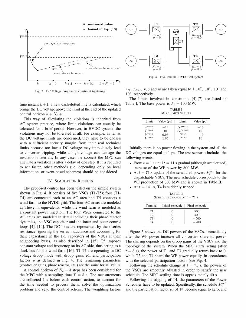
V min
V max
k k + 1 k +Nct
V
past system response
k +Nc + 1k + 2
measured value
bound in Eq. (18)
constraint evolution at k
constraint evolution at k + 1
Fig. 3. DC Voltage progressive constraint tightening
time instant k+1, a new dash-dotted line is calculated, whichbrings the DC voltage above the limit at the end of the updatedcontrol horizon k +Nc + 1.
This way of alleviating the violations is inherited fromAC system practice, where limit violations can usually betolerated for a brief period. However, in HVDC systems theviolations may not be tolerated at all. For example, as far asthe DC voltage limits are concerned, they have to be chosenwith a sufficient security margin from their real technicallimits because too low a DC voltage may immediately leadto converter tripping, while a high voltage can damage theinsulation materials. In any case, the soonest the MPC canalleviate a violation is after a delay of one step. If it is requiredto act faster, other methods (i.e. depending only on localinformation, or event-based schemes) should be considered.
IV. SIMULATION RESULTS
The proposed control has been tested on the simple systemshown in Fig. 4. It consists of five VSCs (T1-T5); four (T1-T4) are connected each to an AC area and T5 connects awind farm to the HVDC grid. The four AC areas are modeledas Thevenin equivalents, while the wind farm is modeled asa constant power injection. The four VSCs connected to theAC areas are modeled in detail including their phase reactordynamics, the VSC capacitor and the inner and outer controlloops [4], [14]. The DC lines are represented by their seriesresistance, ignoring the series inductance and accounting fortheir capacitance in the DC capacitors of the VSCs at theirneighboring buses, as also described in [15]. T5 imposesconstant voltage and frequency on its AC side, thus acting as aslack bus for the wind farm [16]. T1-T4 are operating in DCvoltage droop mode with droop gains Kv and participationfactors ρ as defined in Fig. 4. The remaining parameters(controller gains, phase reactor, etc.) are the same for all VSCs.
A control horizon of Nc = 3 steps has been considered forthe MPC with a sampling time T = 5 s. The measurementsare collected 1 s before each control action, to account forthe time needed to process them, solve the optimizationproblem and send the control actions. The weighting factors
WF
= '
= '' =
'=
' =T1 T2
T5
T3 T4
∞
∞ ∞
∞Kv = 5 Kv = 5
Kv = 5Kv = 5
ρ = 0
ρ = 0
ρ = 0.5
ρ = 0.5
Fig. 4. Five terminal HVDC test system
rD, rND, v, q and w are taken equal to 1, 107, 109, 103 and107, respectively.
The limits involved in constraints (4)-(7) are listed inTable I. The base power is Pb = 100 MW.
TABLE IMPC LIMITS VALUES
Limit Value (pu) Limit Value (pu)
Pmin −10 ∆Pmin −10Pmax 10 ∆Pmax 10V min 0.95 Imin −10V max 1.05 Imax 10
Initially there is no power flowing in the system and all theDC voltages are equal to 1 pu. The test scenario includes thefollowing events:
• From t = 1 s until t = 11 s gradual (although accelerated)increase of the WF power by 300 MW.
• At t = 71 s update of the scheduled powers P schi for the
dispatchable VSCs. The new schedule corresponds to theWF production of 300 MW and is shown in Table II.
• At t = 141 s, T4 is suddenly tripped.
TABLE IISCHEDULE CHANGE AT t = 71 S
Terminal Initial schedule Final schedule
T1 0 500T2 0 400T3 0 −500T4 0 −700
Figure 5 shows the DC powers of the VSCs. Immediatelyafter the WF power increase all converters share its power.The sharing depends on the droop gains of the VSCs and thetopology of the system. When the MPC starts acting (aftert = 5 s), the power of T1 and T3 gradually return back to 0,while T2 and T4 share the WF power equally, in accordancewith the selected participation factors (see Fig. 4.
Following the schedule change at t = 71 s, the powers ofthe VSCs are smoothly adjusted in order to satisfy the newschedule. The MPC settling time is approximately 40 s.
Following the tripping of T4, the parameters of the PowerScheduler have to be updated. Specifically, the schedule P sch
4
and the participation factor ρ4 of T4 become equal to zero, and
-800
-600
-400
-200
0
200
400
600
0 50 100 150 200
t (s)
T1T2T3T4T5
Fig. 5. VSC DC powers (MW)
1
1.01
1.02
1.03
1.04
1.05
1.06
1.07
1.08
0 50 100 150 200
t (s)
DC1DC2DC3DC4DC5
Fig. 6. HVDC grid voltages (pu)
so does P ref4 . Meanwhile, it is chosen to direct the whole lost
power of T4 to T2 by specifying ρ2 = 1 (ρi = 0 for the otherVSCs). The P ref values of the remaining dispatchable VSCsremain unchanged. As can be seen in Fig. 5, immediatelyafter the tripping of T4 all the VSCs react according to theirdroop gains in order to stabilize the DC voltage. Then, theMPC restores the powers of T1 and T3 to their schedule andredirects the lost power to T2.
The HVDC grid voltages are presented in Fig. 6. At thebeginning, the voltages rise due to the increased injection bythe WF. At t = 71 s, the difference between the DC voltagesincreases to accommodate the larger power flow in the HVDCgrid. Finally, following the tripping of T4, there is a suddenincrease of all voltages stabilized by the local droop controlof the remaining VSCs. This increase causes a violation of theupper DC voltage limit which is corrected by the MPC.
V. CONCLUSION
This paper has presented a novel centralized control schemefor MTDC grids. The control scheme relies on the concept ofMPC and is intended to act on MTDC grids including VSCsoperating in DC voltage droop control and non-dispatchableVSCs, such as those of offshore WFs.
Simulation results on a simple test system have shown theefficiency of this formulation to track the desired power ref-erence while maintaining the system between security limits.
Ongoing research investigates the coordination of the cen-tralized controller with other local control schemes that changethe behavior of the DC grid, such as the activation of frequencysupport by one terminal. Furthermore, the implementation of athird level is considered, to adapt the parameters of the lowerlevels and refine the rules defining how to distribute the powerafter a disturbance.
ACKNOWLEDGMENT
Research supported by the R&D department of RTE, theFrench Transmission System Operator. The author especiallythanks Mrs. Marie-Sophie Debry and Mr. Patrick Panciaticifor their valuable comments and suggestions. This research isperformed under the supervision of Dr. Thierry Van Cutsemat University of Liège.
REFERENCES
[1] D. Van Hertem and M. Ghandhari, “Multi-terminal VSC HVDC forthe European supergrid: Obstacles,” Renewable and Sustainable EnergyReviews, vol. 14, pp. 3156–3163, dec 2010.
[2] M. Aragüés-Peñalba, A. Egea-Àlvarez, S. G. Arellano, and O. Gomis-Bellmunt, “Droop control for loss minimization in HVDC multi-terminaltransmission systems for large offshore wind farms,” Electric PowerSystems Research, vol. 112, pp. 48–55, 2014.
[3] A. Egea-Alvarez, J. Beerten, D. V. Hertem, and O. Gomis-Bellmunt,“Hierarchical power control of multiterminal HVDC grids,” ElectricPower Systems Research, vol. 121, pp. 1–7, apr 2015.
[4] P. Rault, Dynamic Modeling and Control of Multi-Terminal HVDCGrids. PhD thesis, Ecole Centrale de Lille, L2EP, 2014.
[5] T. Haileselassie, Control, Dynamics and Operation of Multi-terminalVSC-HVDC Transmission Systems. PhD thesis, 2012.
[6] T. M. Haileselassie, A. G. Endegnanew, and K. Uhlen, “Secondarycontrol in multi-terminal VSC-HVDC transmission system,” in 2015IEEE Power & Energy Society General Meeting, pp. 1–5, IEEE, jul2015.
[7] J. Beerten and D. Van Hertem, “Analysis of power redispatch schemesfor HVDC grid secondary voltage control,” in IEEE Power & EnergySociety General Meeting, no. 3, pp. 1–5, IEEE, jul 2015.
[8] B. Berggren, K. Linden, and R. Majumder, “DC Grid Control Throughthe Pilot Voltage Droop Concept - Methods for Establishing Set-Point Tracking,” IEEE International Energy Conference (Energycon),pp. 1562–1569, 2014.
[9] J. Zhu, C. D. Booth, G. P. Adam, and A. J. Roscoe, “Coordinated directcurrent matching control strategy for multi-terminal DC transmissionsystems with integrated wind farms,” Electric Power Systems Research,vol. 124, pp. 55–64, 2015.
[10] J. M. Maciejowski, Predictive control: with constraints. Pearsoneducation, 2002.
[11] M. J. Carrizosa, Hierarchical control scheme for multi-terminal highvoltage direct current power networks. PhD thesis, Universite ParisSud, 2015.
[12] R. T. Pinto, Multi-terminal DC networks - System integration, controletc. PhD thesis, Techincal University of Delft, 2014.
[13] T. K. Vranaa, L. Zenib, and O. B. Fosso, “Active Power Control withUndead-Band Voltage & Frequency Droop for HVDC Converters inLarge Meshed DC Grids,” EWEA2012presentation, 2012.
[14] M. Imhof and G. Andersson, “Dynamic modeling of a VSC-HVDCconverter,” in Proceedings of the Universities Power Engineering Con-ference, 2013.
[15] X. Guillaud, L. Papangelis, and T. Van Cutsem, “Frequency supportamong asynchronous AC systems through VSCs emulating powerplants,” in 11th IET International Conference on AC and DC PowerTransmission, Institution of Engineering and Technology, 2015.
[16] L. Xu, L. Yao, and C. Sasse, “Grid Integration of Large DFIG-BasedWind Farms Using VSC Transmission,” IEEE Transactions on PowerSystems, vol. 22, pp. 976–984, aug 2007.

Combined Centralized and Local Voltage correctionin Active Distribution Network
Hamid Soleimani BidgoliDept. of Elec. Eng. and Comp. Science University of Liège, Belgium
Abstract—This paper presents a two-level real-time voltagecontrol scheme to address the voltage violations in distributiongrids hosting a significant number of Dispersed Generation Units(DGUs). The proposed scheme consists of a centralized anda local reactive power control. The local control provides fastresponse after a disturbance, reducing its impact and enhancingvoltage quality. The centralized control relies on Model PredictiveControl (MPC). It uses measurements collected throughout thenetwork to bring the voltages inside desired limits. To do so, itadjusts in a coordinated way the reactive power set-points of theDGUs taking into account the local controls. The control methodeffectiveness has been evaluated on a 75-bus 11-kV test systemhosting 22 DGUs.
Index Terms—distribution network, model predictive control,real-time control, voltage correction.
I. INTRODUCTION
The progressive growth of renewable energy sources con-nected to medium-voltage distribution systems is expected tocreate new operational problems. Over- or under-voltages aresome of the main issues caused by intermittent productionof Distributed Generation Units (DGUs). Although excessivevoltages can be tolerated for a short period of time, it isrequired to alleviate the violations fast enough. In the contextof active distribution networks, the network equipment and theDGUs must be controlled in real time to obey the operationalconstraints.
Over the last decade, a lot of efforts have been devoted toreal-time voltage control of distribution network with differentcontrol architectures. For example, in [1] a local approachwas proposed for the correction of voltage violations andthermal overloads, using voltage and apparent power flowsensitivities to identify the most effective control actions.Using an Optimal Power Flow, Ref. [2] discussed the im-pact of centralized and distributed voltage control schemeson potential penetration of dispersed generation, while theauthors in [3] developed an agent-based system to control theDGUs of a low voltage test grid in a decentralized manner.The work has been complemented by considering differentlocal reactive power characteristics and comparing the cor-responding system behaviours. References [4], [5] proposed acentralized voltage control scheme inspired by MPC relying onappropriate measurements and communication infrastructures.The problem was formulated as a receding-horizon multi-step optimization using a simple sensitivity model (justifiedby the speed of actions of the power-electronics interfaces
of DGUs). The controller coordinates the power output ofDGUs and the voltage set-point of the transformer Load TapChanger (LTC) to smoothly bring the unacceptable voltagesback within their limits. A combined centralized and localcontrol scheme was proposed in [6] where the local controllersprovide a fast reaction. The centralized controller, using powerinjection prediction for the following hours, updates the droopparameters of the local controllers to ensure the voltages arekept within the admissible limits in the forecasted range.Although it is achieved at different operating points, the localcontroller tuning is highly dependent on the accuracy of theforecasts. The latter can cause the network operates not closeto the optimum.
In this paper a real-time two-level control scheme is pro-posed in which both local and centralized controllers existand interact with each other. With the purpose of exploitingthe benefits of both control schemes, the two-level controlleris able:
• at the local level, to provide a first, fast response afterany limit violation;
• at the central level, to coordinate the DGUs in order toadjust and complement the actions taken locally;
• globally, to improve network reliability, since the localcontrollers still act in case of communication problemsbetween the DGUs and the centralized controller.
The paper is organized as follows. Section II introducesdifferent control architectures for voltage correction whileSection III details the proposed two-level control scheme.Simulation results are reported in Section IV, and concludingare offered in Section V.
II. VOLTAGE CONTROL ARCHITECTURES
Different control schemes can be considered in a distributionsystem taking into account the practical needs, the technicallimitations of the controllable devices (mainly DGUs andLTCs) and the regulatory policies. Two broad categories arethe centralized and the local architectures. The local controlis implemented inside the equipment and adjusts the reactivepower of each DGU based on the local measurements, essen-tially equipment terminal voltage. Unlike the centralized con-troller, the measurements are collected instantaneously. Thus,a fast reaction is obtained while communication infrastructureis not required. The centralized control detects the voltage vio-lations by periodically collecting measurements and smoothly
LC1 LCN LC 1 LC M
CC
LC 1 LC M LCM+1 LC N
CC
DG1 DGN DG1 DGM DGM+1 DGN DG1 DGM DGM+1 DGN
LC : local controllerCC : centralized controllerDG : distributed generation
DistributionNetwork
DistributionNetwork
DistributionNetwork
a: Local control c: Hybrid control d: Combined control
DG1 DGN
DistributionNetwork
b: Centralized control
CC
Fig. 1. Voltage control architectures
driving the system inside the prescribed limits. Having a wide-area view of the system, this controller is able to share thecorrective efforts between DGUs based on market objectivesand technical limits. The two aforementioned schemes aredepicted in Figs. 1.a and 1.b, respectively.
As a variant or due to practical constraints, a control archi-tecture could be implemented where the centralized controllerand the local controllers are acting on separate DGUs in thesame distribution network. This leads to the hybrid controlshown in Fig. 1.c. The challenge in this case is to enable thecentralized controller to take into account the action of localcontrollers on network voltages.
A more attractive scheme consists of appropriately combin-ing the local and centralized controllers, which yields a largerflexibility. This approach, shown in Fig. 1.d, will be the mainfocus of this paper, and is explained in detail in the followingsection.
III. TWO-LEVEL CONTROL SCHEME
In this section a two-level control architecture is presentedwhich relies on DGUs equipped with local controllers at thelower level, and a centralized controller at the upper level.The latter observes the voltage evolution and interacts with thelocal level in order to improve the overall system behaviour.To do so, some parameters of the local controllers are adjustedin discrete steps by the upper level, if needed.
A. Lower level: local controller
The output reactive power of each DGU is locally controlledaccording to a piecewise linear Q(V ) characteristic [7], asdepicted in Fig. 2. As long as the measured terminal voltageis within the dead-band [V loc
min1, V locmax1], the produced reactive
power is kept at zero aiming at minimizing the DGU internallosses. Outside the above mentioned dead-band, the DGUreacts to over or under-voltage by consuming or producingreactive power, respectively. The DGU remains at its highestlevel of reactive power production (consumption), if the termi-nal voltage is lower (higher) than V loc
min2 (V locmax2). Furthermore,
we assume that there is a possibility for the centralizedcontroller to communicate its desired reactive power correctionQcor to the local controller. Then, the Q(V ) characteristic isadjusted accordingly to satisfy the received command. Furtherdetail on this adjustment is provided in Section III-B.
Figure 3 presents the reactive power control loop in eachDGU. The DGU measured reactive power, Qmeas , is driven
Qg
V
Qmin
Qmax
V locmax2
V locmin2
V locmax1
V locmin1
Fig. 2. Local Q(V) control characteristics
DG
Pg,
V
Qg
Qmeas
Q(V) control
characteristic of Fig.2
1R
KP
KI
s
VVf
Qcor
Eord for Wind or Solar unit
for Synchronous Gen.Qr
Vcor
Fig. 3. Reactive power control loop with local Q(V) characteristic
towards the desired reactive power Qr, using a PI controller.The output of the control loop can be used as referencefield voltage Vf , for synchronous generators, or as referenceterminal voltage Eord, for power-electronics based DGUs.
The change of reactive power output of one DGU affectsthe voltages at other buses, including DGU buses. Assumingthat these DGUs are not operating in the dead-band of theirQ(V) characteristics, they will react to the voltage change byalso adjusting their reactive powers. The interactions betweenlocally controlled DGUs is such that the reactive powerincrease of one DGU causes reactive power decrease of otherDGUs. Due to the fast response of local controllers they reachtheir final values in the order of a few seconds.
B. Upper level: centralized controller
The correction Qcor received from the centralized controlleris aimed to adjust the Q(V ) characteristic, as depicted inFig. 3. Namely, the piecewise linear characteristic of Fig. 2is shifted horizontally until the desired reactive power outputis obtained. This is better explained with an example. Figure 4
shows an over-voltage situation and consecutive actions ofboth levels to clear the violation. The initial operating pointof the DGU, shown with the black disk, is at the intersectionof the network and the local control Q(V) characteristics.In the example shown, the voltage falls in the dead-band(Fig. 4.a). Therefore, initially the DGU is operating at unitypower factor. Under the effect of a disturbance, the networkcharacteristic changes and the voltage at the DGU terminalexceeds the upper local limit V loc1
max . The gray disk in Fig. 4.bcorresponds to the terminal voltage if there was no control.Although the violation is partly alleviated by a first and fastreaction of the local controller (black disk in Fig. 4.b), thevoltage is still above the network admissible upper voltageV cntmax monitored by the centralized controller. In the coming
control steps, the latter collects measurements and observesthe violation. It computes the required correction Qcor andcommunicates the latter to the local controller. At the lowerlevel, Vcor, which is linearly related to Qcor is used to shiftthe piecewise linear characteristic Q(V ) to the left. The newoperating point, shown by the black disk in Fig. 4.c, is backbelow the centralized controller limit V cnt
max.As shown in Fig.3, Vcor and Qcor are related through:
Vcor =Qcor
R(1)
where R is the droop coefficient of the Q(V ) characteristic.In this work the same value is considered for both high andlow voltage conditions in Fig. 2.
As seen in Fig. 4.c, the DGU effective reactive powerchange, i.e. the difference of Qg between the black andthe gray disk, is different from the correction Qcor receivedfrom the centralized controller. There is a linear relationbetween both of them though. This relation will be detailedin subsection III-D.
It should be noted that two different voltage limits can bespecified for the local and centralized controllers. Since inthis scheme the objective of the local controller is to mitigate,but not fully remove the violation in the very first moments,a relaxed range of voltage is considered (V loc
max1 > V cntmax)
in the above example. This range is further modified by thecentralized controller to smoothly adjust the operating point.A similar response can be illustrated for an under voltageproblem.
Coming back the reactive power control loop of Fig.3, theexpression of Qr as a function of V and Vcor can be detailedas follows:
Qr =
Qmax if V− Vcor≤ V locmin2
R(V locmin1 + Vcor − V ) if V loc
min2 <V−Vcor< V locmin1
0 if V locmin1 ≤V−Vcor≤ V loc
max1
−R(V − V locmax1 − Vcor) if V loc
max1 <V−Vcor< V locmax2
Qmin if V− Vcor≥ V locmax2
(2)
For very high (resp. very low) voltage the desired value ofreactive power is saturated at its maximum (resp. minimum)
Qg
V
Qmin
V locmax1
V cntmax
Networkcharacteristic
Qg
V
Qmin
V locmax1V cnt
max
Networkcharacteristic
a. Initial operating point b. Overvoltage due to change ofnetwork characteristic corrected
by local control
c. Final operating point with adjustedlocal Q(V) characteristic
Qg
V
Qmin
V locmax1+Vcor V cnt
max
Networkcharacteristic
Qcor
Vcor
Fig. 4. Over voltage correction with combined control
value, while it is kept at zero if the measured voltage is withinthe dead-band. And, in the remaining two voltage intervals, thevariation is linear according to the droop R. Having Vcor inthe right-hand side of the Eq. (2) causes the shift of voltageintervals when needed.
C. Formulation of upper-level Model Predictive Control
As mentioned before, a multi-time step optimization is atthe heart of the MPC used at the centralized level. The controlvariables are the corrections Qcor to be communicated to thelower level, and the controlled variables are DGU reactivepower outputs Qg .
The objective of the centralized control is similar to the oneused in [5]. However, some modifications to account for thelocal controller impacts are required.
Since the focus is only on reactive power of the DGUs, theobjective is:
minQcor,ε
Nc−1∑i=0
‖Qg(k + i)−Qmeas(k)‖2R + ‖ε‖2S (3)
The first term in (3) aims at minimizing the deviations ofDGUs reactive powers from their measured values Qmeas(k).The diagonal matrix R is the weight assigned to those devia-tions. The second term involves the slack variables ε aimed atrelaxing the inequality constraints in case of infeasibility; theentries of the diagonal matrix S are given very high values. kis the given time step and Nc is the control horizon in whichthe objective function is minimized.

The above objective is satisfied subject to the linearizedsystem evolution at the future Np discrete steps:
for i = 1, . . . , Np:
V (k + i | k) = V (k + i− 1 | k) +
+SV [Qg(k + i− 1)−Qg(k + i− 2)] (4)
where V (k + i | k) are the predicted bus voltages, and SV
is sensitivity matrix of those voltages with respect to DGUreactive powers. The prediction is initialized with V (k | k)set to the last received measurements.
Next, the following inequality constraints are imposed:
for i = 1, . . . , Np:
−ε11 + V cntmin1 ≤ V (k + i | k) ≤ V cnt
max1 + ε21 (5)
and for i = 0, . . . , Nc − 1:
Qming ≤ Qg(k + i | k) ≤ Qmax
g (6)
∆Qming ≤ Qg(k + i |k)−Qg(k + i−1 |k) ≤ ∆Qmax
g (7)
where Qming , Qmax
g , ∆Qming and ∆Qmax
g are the lower andupper limits on DGU outputs and on their rate of change. ε1,ε2 and ε3 are the components of ε, and 1 denotes a unit vector.Constraint (6) includes the limits on reactive powers of DGUs,which are updated at each time step based on the measuredactive power and terminal voltage.
The main difference with respect to formulation shown in[5] is that Qg(k) is linearly related to the control variable op-timized by the centralized controller Qcor(k). The sensitivityof DGU reactive power changes ∆Qg(k) with respect to thecontrol variable changes ∆Qcor(k) is derived in the followingsubsection.
D. Sensitivity matrices
Figure 4.c is redrawn with additional information in Fig.5showing the effective change of reactive power, ∆Qg , and thecorrection sent by the centralized controller, Qcor. Hereafter,the relation between these two variables is derived.
Qg
V
Qmin
Networkcharacteristic
Qcor
Vcor
∆V
∆Qg
1
2
Fig. 5. Comparison of requested and effective reactive power adjustments
Assuming Ri is the already defined droop of the i-th DGUQ(V ) characteristic, the equation of the dashed line in Fig. 5is:
Qgi −Qcor,i = −Ri(Vi − V locmax) (8)
Considering small deviations denoted with ∆, Eq. (8) gives:
∆Qgi −∆Qcor,i = −Ri∆Vi (9)
In matrix form, this equation can be rewritten as:
∆Qg = ∆Qcor −R∆V (10)
where R is a diagonal matrix whose entries are the droopcoefficients Ri.
The variation of the bus voltages with the DGU reactivepower is given by:
∆V = SV ∆Qg (11)
The sensitivity matrix SV can be obtained from the transposedinverse of the power flow jacobian matrix. As an alternative,each column of the sensitivity matrix can be computed byrunning a power flow calculation with one DGU reactivepower slightly modified, and simply dividing the variation ofthe monitored bus voltages by the reactive power variation.Interested readers are referred to [5] for more detail.
By substituting (11) in (10), one easily obtains:
∆Qg = (1 + RSV )−1∆Qcor = SQ∆Qcor (12)
where 1 is a unit matrix. SQ = (1+RSV )−1 is the sensitivitymatrix of the DGU reactive powers to the reactive powercontrols.
Equation (12) can be rewritten at time k + i as:
∆Qg(k + i) = (1 + RSV )−1∆Qcor(k + i)
= SQ∆Qcor(k + i) (13)
Finally by substituting ∆Qg(k+i) as Qg(k+i)−Qmeas(k)and ∆Qcor(k+ i) as Qcor(k+ i)−Qcor(k), the sought linearrelation is:
Qg(k + i)−Qmeas(k) = SQQcor(k + i)− SQQcor(k) (14)
This relation is added to the set of constraints (4 -7) treatedin the optimization problem.
IV. SIMULATION RESULTS
A. Test system
In this section the performance of the combined controlarchitecture, is illustrated on a 75-bus, 11-kV distributionnetwork whose one-line diagram is shown in Fig.6 [8]. It isconnected to the upper voltage level (referred to as externalgrid) through a 33/11 kV transformer.
The network hosts 22 DGUs, consisting of 3.33-MVA dou-bly fed induction generators driven by 3-MW wind-turbines,and 3-MVA synchronous generators driven by 2.55-MW tur-bines, respectively. The DGU models and parameters weretaken from [9], [10], and simplified in accordance with thetype of dynamics considered in this work.
The network feeds 52 loads, of which 38 are modelled asconstant current for active power and constant impedance forreactive power, and 14 with induction motors.
It is assumed that the terminal voltage and the active/reactivepower outputs of the 22 DGUs are measured, as well as the
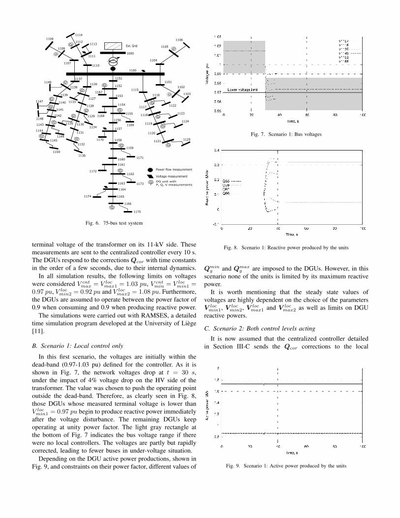
G
G
G
G
G
G
G
G
G
G
G
G
G
G
G
GG
G
G
G
G
G
Ext. Grid
1000
1100
1114
11121113
1111
11101107
1108
1109
1104
1105
1106
1101
1102
11031115
1116
1117 1122
1123
1124
1118
1119
1120
1121 1125
1151
1152
11531167
1154
1155
1169
1156
1157
1158
1159
1168
1170
1161
1162
11731163
1164
1165
1166
1175
1174
1172
1160
1126
1127
1128
1129
11341130
1131
1132
11361150
11451149
1144
1143
11421148
1147 1140 1133
1141
1135
1139
1138
11461137
1171
G
Voltage measurement
DG unit with P, Q, V measurements
Power flow measurement
Fig. 6. 75-bus test system
terminal voltage of the transformer on its 11-kV side. Thesemeasurements are sent to the centralized controller every 10 s.The DGUs respond to the corrections Qcor with time constantsin the order of a few seconds, due to their internal dynamics.
In all simulation results, the following limits on voltageswere considered V cnt
max = V locmax1 = 1.03 pu, V cnt
min = V locmin1 =
0.97 pu, V locmin2 = 0.92 pu and V loc
max2 = 1.08 pu. Furthermore,the DGUs are assumed to operate between the power factor of0.9 when consuming and 0.9 when producing reactive power.
The simulations were carried out with RAMSES, a detailedtime simulation program developed at the University of Liège[11].
B. Scenario 1: Local control only
In this first scenario, the voltages are initially within thedead-band (0.97-1.03 pu) defined for the controller. As it isshown in Fig. 7, the network voltages drop at t = 30 s,under the impact of 4% voltage drop on the HV side of thetransformer. The value was chosen to push the operating pointoutside the dead-band. Therefore, as clearly seen in Fig. 8,those DGUs whose measured terminal voltage is lower thanV locmin1 = 0.97 pu begin to produce reactive power immediately
after the voltage disturbance. The remaining DGUs keepoperating at unity power factor. The light gray rectangle atthe bottom of Fig. 7 indicates the bus voltage range if therewere no local controllers. The voltages are partly but rapidlycorrected, leading to fewer buses in under-voltage situation.
Depending on the DGU active power productions, shown inFig. 9, and constraints on their power factor, different values of
Fig. 7. Scenario 1: Bus voltages
Fig. 8. Scenario 1: Reactive power produced by the units
Qming and Qmax
g are imposed to the DGUs. However, in thisscenario none of the units is limited by its maximum reactivepower.
It is worth mentioning that the steady state values ofvoltages are highly dependent on the choice of the parametersV locmin1, V loc
min2, V locmax1 and V loc
max2 as well as limits on DGUreactive powers.
C. Scenario 2: Both control levels acting
It is now assumed that the centralized controller detailedin Section III-C sends the Qcor corrections to the local
Fig. 9. Scenario 1: Active power produced by the units
Fig. 10. Scenario 2: Bus voltages
Fig. 11. Scenario 2: Reactive power produced by the units
controllers every 10 seconds. Moreover, the voltage dropon the HV side of the transformer is increased to 5%. Bycomparing the light gray rectangle at the bottom of Fig.10 with the voltages in the time interval from t = 30 tot = 40 s, the fast corrective action of the local controllerscan be verified. However, the voltages at some buses are stillbelow the lower admissible limit. Thus, at the next discretetime step, the centralized controller senses the unsatisfactoryvoltages and, consequently, applies the necessary correctiveactions. It adjusts the local controller Q(V ) characteristics,steering them to produce the desired reactive powers. The goalis achieved after three successive discrete steps.
Figure 11 shows the variations reactive power generationsof various DGUs. The evolution between t = 30 and t = 40sis produced by the local controllers, while the response aftert = 40s is due to the higher level sending the Qcor corrections.Similar to the Scenario 1, in the time interval from t = 30 tot = 40 s, the DGU reactive powers are either increased orkept at zero. While from t = 40 to t = 50 s, the centralizedcontroller increases some and decreases other DGU reactivepowers in order to control the voltages in a coordinated way.
V. CONCLUSION
In this paper four control schemes have been briefly intro-duced aiming at voltage control of medium-voltage distribu-tion networks by DGUs. Out of these four configurations, the
combined control scheme has been considered in detail in therest of the paper.
At the lower level, DGU output reactive powers are locallycontrolled according to a piecewise linear Q(V ) characteristic.This local control provides a fast response to disturbances. Adead-band has been considered in the latter to keep DGUsoperating at unity power factor as far as possible.
At the higher (centralized) control level, model predictivecontrol is used to compute and send reactive power correctionsto the local controllers, with the effect of shifting their Q(V )characteristics. This multi-step optimization uses linearizedmodels in which the sensitivity matrices take into account theslope of the local Q(V ) characteristics.
The reported simulation results clearly show the combina-tion of a fast but partial correction by the local controllers,followed by the smooth, coordinated control of the DGUreactive powers by the upper-level control.
ACKNOWLEDGMENT
Work supported by Public Service of Wallonia, Dept. ofEnergy and Sustainable Building, within the framework ofthe GREDOR project. This research is performed under thesupervision of Professor Thierry Van Cutsem at University ofLiège.
REFERENCES
[1] T. Sansawatt, L. F. Ochoa, and G. P. Harrison, “Smart DecentralizedControl of DG for Voltage and Thermal Constraint Management,” IEEETransactions on Power Systems, vol. 27, pp. 1637–1645, aug 2012.
[2] P. N. Vovos, A. E. Kiprakis, A. R. Wallace, and G. P. Harrison,“Centralized and Distributed Voltage Control: Impact on DistributedGeneration Penetration,” IEEE Transactions on Power Systems, vol. 22,pp. 476–483, feb 2007.
[3] A. Seack, J. Kays, and C. Rehtanz, “Time series based distribution gridplanning approach with decentralised voltage regulation,” in 2014 PowerSystems Computation Conference, pp. 1–7, IEEE, aug 2014.
[4] H. Soleimani Bidgoli, M. Glavic, and T. Van Cutsem, “Model predictivecontrol of congestion and voltages problems in active distributionnetworks,” Proc. of CIRED Workshop 2014, no. June, 2014.
[5] H. Soleimani Bidgoli, M. Glavic, and T. Van Cutsem, “Receding-Horizon Control of Distributed Generation to Correct Voltage or ThermalViolations and Track Desired Schedules,” paper accepted for presenta-tion at the 2016 Power System Computation Conference (PSCC), Genoa,Italy, June 2016.
[6] Y. Chistyakov, E. Kholodova, K. Netreba, A. Szabo, and M. Metzger,“Combined central and local control of reactive power in electricalgrids with distributed generation,” 2012 IEEE International EnergyConference and Exhibition, ENERGYCON 2012, pp. 325–330, 2012.
[7] S. Weckx, C. Gonzalez, and J. Driesen, “Combined central and localactive and reactive power control of PV inverters,” IEEE Transactionson Sustainable Energy, vol. 5, no. 3, pp. 776–784, 2014.
[8] “United Kingdom Generic Distribution Network (UKGDS),” Available:http://sedg.ac.uk.
[9] J. D. Hurley, L. N. Bize, and C. R. Mummert, “The adverse effects ofexcitation system var and power factor controllers,” IEEE Transactionson Energy Conversion, vol. 14, no. 4, pp. 1636–1645, 1999.
[10] G. Tsourakis, B. M. Nomikos, and C. D. Vournas, “Effect of windparks with doubly fed asynchronous generators on small-signal stability,”Electric Power Systems Research, vol. 79, no. 1, pp. 190–200, 2009.
[11] P. Aristidou, S. Lebeau, and T. Van Cutsem, “Power System DynamicSimulations Using a Parallel Two-Level Schur-Complement Decompo-sition,” IEEE Transactions on Power Systems, pp. 1–12, 2016.
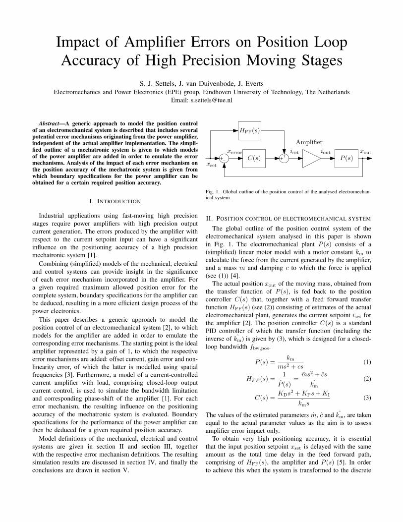
Impact of Amplifier Errors on Position LoopAccuracy of High Precision Moving Stages
S. J. Settels, J. van Duivenbode, J. EvertsElectromechanics and Power Electronics (EPE) group, Eindhoven University of Technology, The Netherlands
Email: [email protected]
Abstract—A generic approach to model the position controlof an electromechanical system is described that includes severalpotential error mechanisms originating from the power amplifier,independent of the actual amplifier implementation. The simpli-fied outline of a mechatronic system is given to which modelsof the power amplifier are added in order to emulate the errormechanisms. Analysis of the impact of each error mechanism onthe position accuracy of the mechatronic system is given fromwhich boundary specifications for the power amplifier can beobtained for a certain required position accuracy.
I. INTRODUCTION
Industrial applications using fast-moving high precisionstages require power amplifiers with high precision outputcurrent generation. The errors produced by the amplifier withrespect to the current setpoint input can have a significantinfluence on the positioning accuracy of a high precisionmechatronic system [1].
Combining (simplified) models of the mechanical, electricaland control systems can provide insight in the significanceof each error mechanism incorporated in the amplifier. Fora given required maximum allowed position error for thecomplete system, boundary specifications for the amplifier canbe deduced, resulting in a more efficient design process of thepower electronics.
This paper describes a generic approach to model theposition control of an electromechanical system [2], to whichmodels for the amplifier are added in order to emulate thecorresponding error mechanisms. The starting point is the idealamplifier represented by a gain of 1, to which the respectiveerror mechanisms are added: offset current, gain error and non-linearity error, of which the latter is modelled using spatialfrequencies [3]. Furthermore, a model of a current-controlledcurrent amplifier with load, comprising closed-loop outputcurrent control, is used to simulate the bandwidth limitationand corresponding phase-shift of the amplifier [1]. For eacherror mechanism, the resulting influence on the positioningaccuracy of the mechatronic system is evaluated. Boundaryspecifications for the performance of the power amplifier canthen be deduced for a given required position accuracy.
Model definitions of the mechanical, electrical and controlsystems are given in section II and section III, togetherwith the respective error mechanism definitions. The resultingsimulation results are discussed in section IV, and finally theconclusions are drawn in section V.
Fig. 1. Global outline of the position control of the analysed electromechan-ical system.
II. POSITION CONTROL OF ELECTROMECHANICAL SYSTEM
The global outline of the position control system of theelectromechanical system analysed in this paper is shownin Fig. 1. The electromechanical plant P (s) consists of a(simplified) linear motor model with a motor constant km tocalculate the force from the current generated by the amplifier,and a mass m and damping c to which the force is applied(see (1)) [4].
The actual position xout of the moving mass, obtained fromthe transfer function of P (s), is fed back to the positioncontroller C(s) that, together with a feed forward transferfunction HFF(s) (see (2)) consisting of estimates of the actualelectromechanical plant, generates the current setpoint iset forthe amplifier [2]. The position controller C(s) is a standardPID controller of which the transfer function (including theinverse of km) is given by (3), which is designed for a closed-loop bandwidth fbw,pos.
P (s) =km
ms2 + cs(1)
HFF (s) =1
P (s)=ms2 + cs
km
(2)
C(s) =KDs
2 +KPs+KI
kms(3)
The values of the estimated parameters m, c and km, are takenequal to the actual parameter values as the aim is to assessamplifier error impact only.
To obtain very high positioning accuracy, it is essentialthat the input position setpoint xset is delayed with the sameamount as the total time delay in the feed forward path,comprising of HFF(s), the amplifier and P (s) [5]. In orderto achieve this when the system is transformed to the discrete
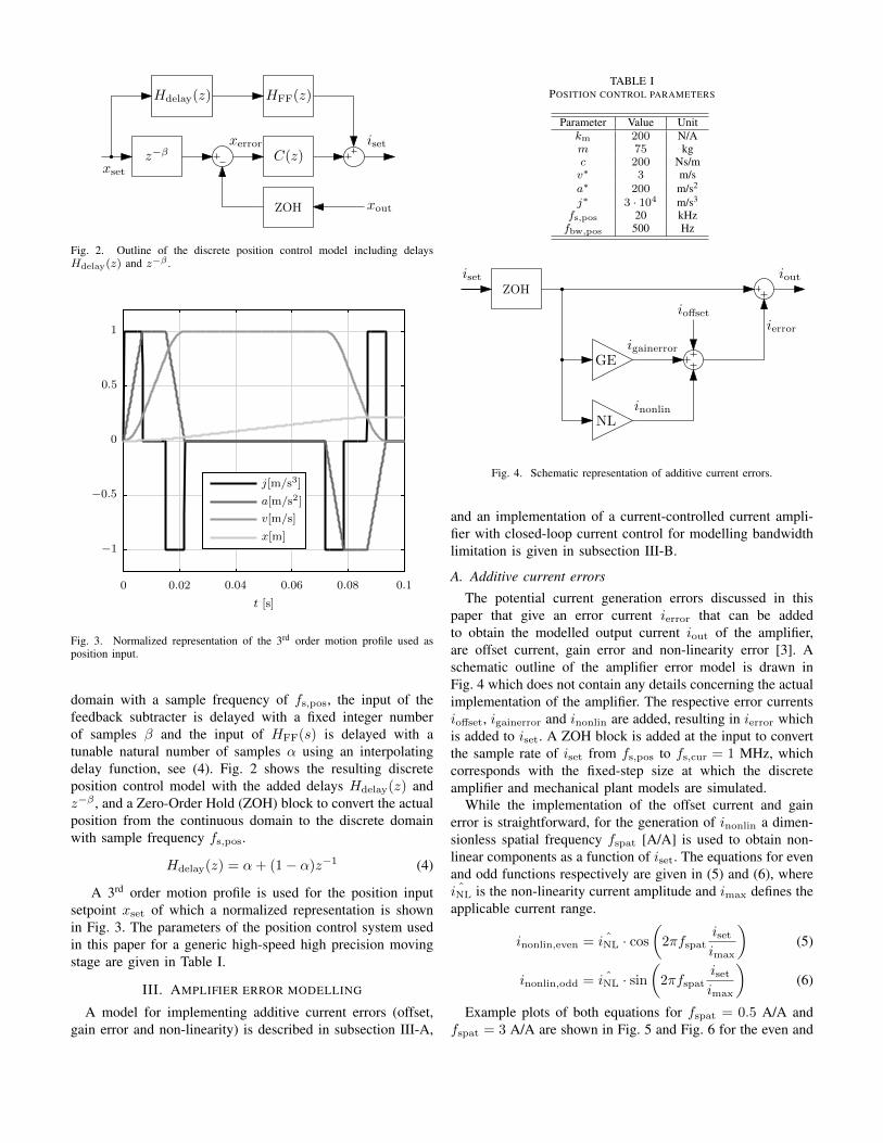
Fig. 2. Outline of the discrete position control model including delaysHdelay(z) and z−β .
t [s]
x[m]
v[m/s]
a[m/s2]
j[m/s3]
0 0.02 0.04 0.06 0.08 0.1
−1
−0.5
0
0.5
1
Fig. 3. Normalized representation of the 3rd order motion profile used asposition input.
domain with a sample frequency of fs,pos, the input of thefeedback subtracter is delayed with a fixed integer numberof samples β and the input of HFF(s) is delayed with atunable natural number of samples α using an interpolatingdelay function, see (4). Fig. 2 shows the resulting discreteposition control model with the added delays Hdelay(z) andz−β , and a Zero-Order Hold (ZOH) block to convert the actualposition from the continuous domain to the discrete domainwith sample frequency fs,pos.
Hdelay(z) = α+ (1− α)z−1 (4)
A 3rd order motion profile is used for the position inputsetpoint xset of which a normalized representation is shownin Fig. 3. The parameters of the position control system usedin this paper for a generic high-speed high precision movingstage are given in Table I.
III. AMPLIFIER ERROR MODELLING
A model for implementing additive current errors (offset,gain error and non-linearity) is described in subsection III-A,
TABLE IPOSITION CONTROL PARAMETERS
Parameter Value Unitkm 200 N/Am 75 kgc 200 Ns/mv∗ 3 m/sa∗ 200 m/s2
j∗ 3 · 104 m/s3
fs,pos 20 kHzfbw,pos 500 Hz
Fig. 4. Schematic representation of additive current errors.
and an implementation of a current-controlled current ampli-fier with closed-loop current control for modelling bandwidthlimitation is given in subsection III-B.
A. Additive current errors
The potential current generation errors discussed in thispaper that give an error current ierror that can be addedto obtain the modelled output current iout of the amplifier,are offset current, gain error and non-linearity error [3]. Aschematic outline of the amplifier error model is drawn inFig. 4 which does not contain any details concerning the actualimplementation of the amplifier. The respective error currentsioffset, igainerror and inonlin are added, resulting in ierror whichis added to iset. A ZOH block is added at the input to convertthe sample rate of iset from fs,pos to fs,cur = 1 MHz, whichcorresponds with the fixed-step size at which the discreteamplifier and mechanical plant models are simulated.
While the implementation of the offset current and gainerror is straightforward, for the generation of inonlin a dimen-sionless spatial frequency fspat [A/A] is used to obtain non-linear components as a function of iset. The equations for evenand odd functions respectively are given in (5) and (6), whereˆiNL is the non-linearity current amplitude and imax defines the
applicable current range.
inonlin,even = ˆiNL · cos(2πfspat
iset
imax
)(5)
inonlin,odd = ˆiNL · sin(2πfspat
iset
imax
)(6)
Example plots of both equations for fspat = 0.5 A/A andfspat = 3 A/A are shown in Fig. 5 and Fig. 6 for the even and
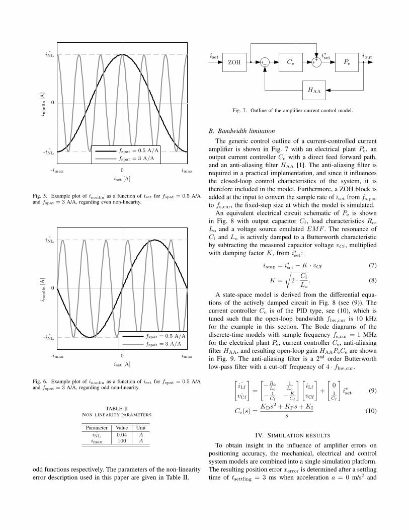
iset [A]
i nonlin[A
]
fspat = 3 A/A
fspat = 0.5 A/A
-imax 0 imax
- ˆiNL
0
ˆiNL
Fig. 5. Example plot of inonlin as a function of iset for fspat = 0.5 A/Aand fspat = 3 A/A, regarding even non-linearity.
iset [A]
i nonlin[A
]
fspat = 3 A/A
fspat = 0.5 A/A
-imax 0 imax
- ˆiNL
0
ˆiNL
Fig. 6. Example plot of inonlin as a function of iset for fspat = 0.5 A/Aand fspat = 3 A/A, regarding odd non-linearity.
TABLE IINON-LINEARITY PARAMETERS
Parameter Value UnitˆiNL 0.04 A
imax 100 A
odd functions respectively. The parameters of the non-linearityerror description used in this paper are given in Table II.
Fig. 7. Outline of the amplifier current control model.
B. Bandwidth limitation
The generic control outline of a current-controlled currentamplifier is shown in Fig. 7 with an electrical plant Pe, anoutput current controller Ce with a direct feed forward path,and an anti-aliasing filter HAA [1]. The anti-aliasing filter isrequired in a practical implementation, and since it influencesthe closed-loop control characteristics of the system, it istherefore included in the model. Furthermore, a ZOH block isadded at the input to convert the sample rate of iset from fs,pos
to fs,cur, the fixed-step size at which the model is simulated.An equivalent electrical circuit schematic of Pe is shown
in Fig. 8 with output capacitor Cf , load characteristics Ro,Lo and a voltage source emulated EMF . The resonance ofCf and Lo is actively damped to a Butterworth characteristicby subtracting the measured capacitor voltage vCf , multipliedwith damping factor K, from i∗set:
iamp = i∗set −K · vCf (7)
K =
√2 · Cf
Lo. (8)
A state-space model is derived from the differential equa-tions of the actively damped circuit in Fig. 8 (see (9)). Thecurrent controller Ce is of the PID type, see (10), which istuned such that the open-loop bandwidth fbw,cur is 10 kHzfor the example in this section. The Bode diagrams of thediscrete-time models with sample frequency fs,cur = 1 MHzfor the electrical plant Pe, current controller Ce, anti-aliasingfilter HAA, and resulting open-loop gain HAAPeCe are shownin Fig. 9. The anti-aliasing filter is a 2nd order Butterworthlow-pass filter with a cut-off frequency of 4 · fbw,cur.[
˙iLf
˙vCf
]=
[−Ro
Lo
1Lo
− 1Cf
− KCf
][iLf
vCf
]+
[01Cf
]i∗set (9)
Ce(s) =KDs
2 +KPs+KI
s(10)
IV. SIMULATION RESULTS
To obtain insight in the influence of amplifier errors onpositioning accuracy, the mechanical, electrical and controlsystem models are combined into a single simulation platform.The resulting position error xerror is determined after a settlingtime of tsettling = 3 ms when acceleration a = 0 m/s2 and
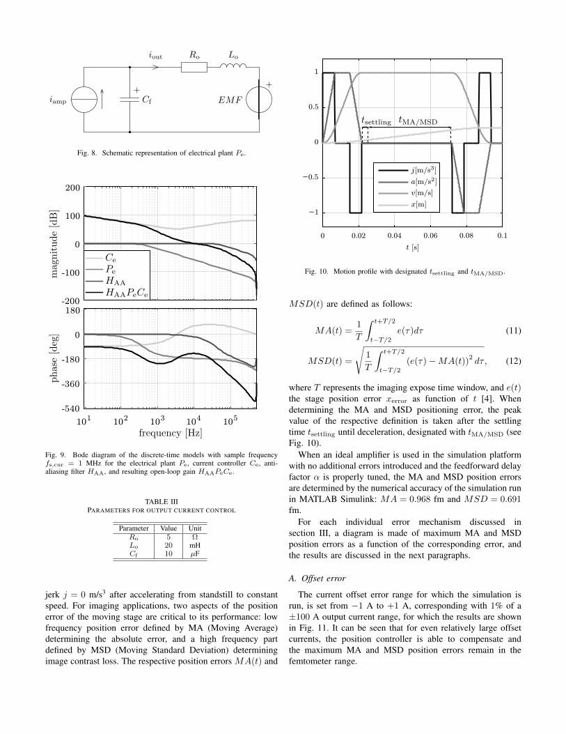
Fig. 8. Schematic representation of electrical plant Pe.
-200
-100
0
100
200
101
102
103
104
105
-540
-360
-180
0
180
Fig. 9. Bode diagram of the discrete-time models with sample frequencyfs,cur = 1 MHz for the electrical plant Pe, current controller Ce, anti-aliasing filter HAA, and resulting open-loop gain HAAPeCe.
TABLE IIIPARAMETERS FOR OUTPUT CURRENT CONTROL
Parameter Value UnitRo 5 ΩLo 20 mHCf 10 µF
jerk j = 0 m/s3 after accelerating from standstill to constantspeed. For imaging applications, two aspects of the positionerror of the moving stage are critical to its performance: lowfrequency position error defined by MA (Moving Average)determining the absolute error, and a high frequency partdefined by MSD (Moving Standard Deviation) determiningimage contrast loss. The respective position errors MA(t) and
t [s]
x[m]
v[m=s]
a[m=s2]
j[m=s3]
0 0:02 0:04 0:06 0:08 0:1
−1
−0:5
0
0:5
1
Fig. 10. Motion profile with designated tsettling and tMA/MSD.
MSD(t) are defined as follows:
MA(t) =1
T
∫ t+T/2
t−T/2e(τ)dτ (11)
MSD(t) =
√1
T
∫ t+T/2
t−T/2(e(τ)−MA(t))
2dτ, (12)
where T represents the imaging expose time window, and e(t)the stage position error xerror as function of t [4]. Whendetermining the MA and MSD positioning error, the peakvalue of the respective definition is taken after the settlingtime tsettling until deceleration, designated with tMA/MSD (seeFig. 10).
When an ideal amplifier is used in the simulation platformwith no additional errors introduced and the feedforward delayfactor α is properly tuned, the MA and MSD position errorsare determined by the numerical accuracy of the simulation runin MATLAB Simulink: MA = 0.968 fm and MSD = 0.691fm.
For each individual error mechanism discussed insection III, a diagram is made of maximum MA and MSDposition errors as a function of the corresponding error, andthe results are discussed in the next paragraphs.
A. Offset error
The current offset error range for which the simulation isrun, is set from −1 A to +1 A, corresponding with 1% of a±100 A output current range, for which the results are shownin Fig. 11. It can be seen that for even relatively large offsetcurrents, the position controller is able to compensate andthe maximum MA and MSD position errors remain in thefemtometer range.
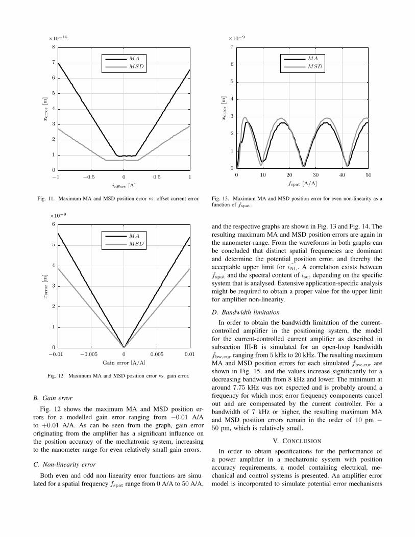
ioffset [A]
xerror[m
]
MSD
MA
−1 −0.5 0 0.5 1
×10−15
0
1
2
3
4
5
6
7
8
Fig. 11. Maximum MA and MSD position error vs. offset current error.
Gain error [A/A]
xerror[m
]
MSD
MA
−0.01 −0.005 0 0.005 0.01
×10−9
0
1
2
3
4
5
6
Fig. 12. Maximum MA and MSD position error vs. gain error.
B. Gain error
Fig. 12 shows the maximum MA and MSD position er-rors for a modelled gain error ranging from −0.01 A/Ato +0.01 A/A. As can be seen from the graph, gain errororiginating from the amplifier has a significant influence onthe position accuracy of the mechatronic system, increasingto the nanometer range for even relatively small gain errors.
C. Non-linearity error
Both even and odd non-linearity error functions are simu-lated for a spatial frequency fspat range from 0 A/A to 50 A/A,
fspat [A/A]
xerror[m
]
MSD
MA
0 10 20 30 40 50
×10−9
0
1
2
3
4
5
6
7
Fig. 13. Maximum MA and MSD position error for even non-linearity as afunction of fspat.
and the respective graphs are shown in Fig. 13 and Fig. 14. Theresulting maximum MA and MSD position errors are again inthe nanometer range. From the waveforms in both graphs canbe concluded that distinct spatial frequencies are dominantand determine the potential position error, and thereby theacceptable upper limit for ˆiNL. A correlation exists betweenfspat and the spectral content of iset depending on the specificsystem that is analysed. Extensive application-specific analysismight be required to obtain a proper value for the upper limitfor amplifier non-linearity.
D. Bandwidth limitation
In order to obtain the bandwidth limitation of the current-controlled amplifier in the positioning system, the modelfor the current-controlled current amplifier as described insubsection III-B is simulated for an open-loop bandwidthfbw,cur ranging from 5 kHz to 20 kHz. The resulting maximumMA and MSD position errors for each simulated fbw,cur areshown in Fig. 15, and the values increase significantly for adecreasing bandwidth from 8 kHz and lower. The minimum ataround 7.75 kHz was not expected and is probably around afrequency for which most error frequency components cancelout and are compensated by the current controller. For abandwidth of 7 kHz or higher, the resulting maximum MAand MSD position errors remain in the order of 10 pm −50 pm, which is relatively small.
V. CONCLUSION
In order to obtain specifications for the performance ofa power amplifier in a mechatronic system with positionaccuracy requirements, a model containing electrical, me-chanical and control systems is presented. An amplifier errormodel is incorporated to simulate potential error mechanisms
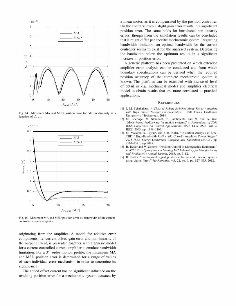
fspat [A/A]
xerror[m
]
MSD
MA
0 10 20 30 40 50
×10−9
0
1
2
3
4
5
6
7
Fig. 14. Maximum MA and MSD position error for odd non-linearity as afunction of fspat.
fbw,cur [kHz]
xerror[m
]
MSD
MA
5 10 15 20
×10−10
0
0.5
1
1.5
2
2.5
3
3.5
Fig. 15. Maximum MA and MSD position error vs. bandwidth of the current-controlled current amplifier.
originating from the amplifier. A model for additive errorcomponents, i.e. current offset, gain error and non-linearity ofthe output current, is presented together with a generic modelfor a current-controlled current amplifier to emulate bandwidthlimitation. For a 3rd order motion profile, the maximum MAand MSD position error is determined for a range of valuesof each individual error mechanism in order to determine itssignificance.
The added offset current has no significant influence on theresulting position error for a mechatronic system actuated by
a linear motor, as it is compensated by the position controller.On the contrary, even a slight gain error results in a significantposition error. The same holds for introduced non-linearityerrors, though from the simulation results can be concludedthat it might differ per specific mechatronic system. Regardingbandwidth limitation, an optimal bandwidth for the currentcontroller seems to exist for the analysed system. Decreasingthe bandwidth below the optimum results in a significantincrease in position error.
A generic platform has been presented on which extendedamplifier error analysis can be conducted and from whichboundary specifications can be derived when the requiredposition accuracy of the complete mechatronic system isknown. The platform can be extended with increased levelof detail in e.g. mechanical model and amplifier electricalmodel to obtain results that are more correlated to practicalapplications.
REFERENCES
[1] J. M. Schellekens, A Class of Robust Switched-Mode Power Amplifierswith High Linear Transfer Characteristics. PhD Thesis, EindhovenUniversity of Technology, 2014.
[2] M. Boerlage, M. Steinbuch, P. Lambrechts, and M. van de Wal,“Model-based feedforward for motion systems,” in Proceedings of 2003IEEE Conference on Control Applications, 2003. CCA 2003., vol. 2.IEEE, 2003, pp. 1158–1163.
[3] M. Mauerer, A. Tuysuz, and J. W. Kolar, “Distortion Analysis of Low-THD / High-Bandwidth GaN / SiC Class-D Amplifier Power Stages,”2015 IEEE Energy Conversion Congress and Exposition (ECCE), pp.2563–2571, sep 2015.
[4] H. Butler and W. Simons, “Position Control in Lithographic Equipment,”in ASPE 2013 Spring Topical Meeting MIT Laboratory for Manufacturingand Productivity Annual Summit, 2013, pp. 7–12.
[5] H. Butler, “Feedforward signal prediction for accurate motion systemsusing digital filters,” Mechatronics, vol. 22, no. 6, pp. 827–835, 2012.

1
Optimizing state trajectories using surrogate modelswith application on a mechatronic example
T.J.P. Lefebvre, F. De Belie, G. CrevecoeurDepartment of Electrical Energy, Systems and Automation (EESA)
Ghent University (UGent), Technologiepark 913, B-9052 Zwijnaarde, Belgiume-mail: [email protected]
Abstract— The classic design- and simulation methodologies,that are constituting today’s engineer main tools, fall behind withindustry’s ever increasing complexity. The strive for technologicaladvancement heralds new performance requirements and opti-mality remains no longer a concern limited to regime operation.Since the corresponding dynamic optimization problems incorpo-rate accurate system models, the current techniques are plaguedby the high computational weight these multi-disciplinary andhighly dimensional system models bear with them. This imbal-ance advocates for the need to adapt the existing approaches. Inthis study we propose an algorithmic framework as an extensionof the direct transcription method, which has already proven itsusefulness concerning this matter. It is suggested to constructa surrogate model of the derivative function that is iterativelyrefined in a region of interest. Thereafter the method will beillustrated on an academic yet nonlinear example.
Index Terms— Direct transcription, Dynamic optimization,Nonlinear mechatronic systems, Surrogate models
I. INTRODUCTION
Optimality of regime operation no longer suffices andtransient phenomena are gaining fast importance in nowadaysindustry, even more for those applications where regime oper-ation loses all meaning and operation merely entails transientbehaviour. Optimality has now direct bearing to the realisedstate trajectory and therefore they should be addressed withinthe corresponding optimality formulation. Techniques thatcope with such problem formulations require the availabilityof a dynamic model. Whilst dynamical accuracy benefits fromincreased model complexity - by including multiple modellingdisciplines, and considering high dimensionality and nonlin-earity - the solution techniques do not and the designatedinfluence can no longer be evaluated analytically; especiallywhen no analytical expression is available and evaluationscorrespond with numerical computer experiments [1], [2].
For the purpose of fast and reliable dynamic optimizationof yet complex and accurate systems, it is necessary toaccommodate this computational burden without affecting op-timality. From the successful and repeated application withinseveral engineering disciplines, the computational strength ofsurrogates already appeared [3]. To that end, we will try toincorporate these surrogate modelling techniques within theframework and methods addressing dynamic optimization.
This article provides a brief introduction to these separateresearch areas and proposes an algorithm to bridge the gap.
II. TRAJECTORY OPTIMIZATION
Whenever it is one’s desire to optimize a system in suchmanner that the time evolution of states - governed by thesystem dynamics - is of significance to the interpretation ofoptimality, it is classified as a dynamic optimization problem[4], [5]. A special class of dynamic optimization problemsis referred to as trajectory optimization [6]. Whilst closelyrelated to optimal control problems, trajectory optimizationis most often practiced offline and before actual systemoperation, as part of the design process. The online problemaddressing the realisation of the optimized trajectory, as ina tracking problem, is then referred to as the correspondingoptimal control problem. So while the input sequence will beconsidered within trajectory optimization in general, it doesnot embody its main result.
A. General formulation
A general formulation is presented in (1), where x ∈ Rnx
and u ∈ Rnu , represent state- and input variables respectively.Each state- and input combination is related to an instanta-neous cost L(·), the term E(·) expresses a possible additionalcost related to the end state of the system. The total costrelated to a specific time evolution of u(t) over the timeinterval [t0, tf ] is denoted by J . Moreover, the state- and inputvariables can be subject to constraint functions g(·) and h(·).It is assumed that dynamics are governed by the derivativenonlinear function f(·) and matrix B(·).
minu(·)
J =
∫ tf
t0
L(x(τ),u(τ))dτ + E(x(tf ))
s.t.
x = f(x) +B(x)u
g(x,u) = 0
h(x,u) < 0
(1)
This mathematical formulation can be moulded to fit a vastamount of existing and powerful optimization algorithms; yet,dynamic optimization of physical plant and control systemof today’s mechatronical applications remains a challengingproblem for which the availability of an assessable dynamicsystem model, and thus function f(·) and B(·), is of vitalessence.

2
B. Direct TranscriptionDirect transcription (DT) has proven to be a helpful instru-
ment for solving nonlinear dynamic optimization problems.Its principle is founded on the idea of transcribing the infiniteinto a finite dimensional problem, resulting into a discretisedproblem that can be approached as a Nonlinear Program(NLP). The NLP is solved thereafter by practice of an effectivenonlinear programming technique.
Transcription is achieved by partitioning and successivelyparameterizing the continuous problem, leading to the desireddiscrete equivalent representation. Agreement with dynamicsis governed by a set of nonlinear constraints that wardscontinuity of the time evolution of states.
The technique sets off by partitioning the time interval intont time segments, Ik, for which the boundaries are denotedby tk and tk+1, respectively:
Ik = [tk, tk+1], k ∈ χ = 0, ... , nt − 1For each time interval we introduce a parameterized zero-
order hold representation of the control variables, uk(t), t ∈Ik, that is uniquely defined by the parameters, qk. Such isan accurate approximation of realistic control scenarios. Moreelaborate representations exist yet would distract more thanthey would contribute.
uk(t) = qk
The major trick entails the parameterisation of the statetrajectory by introducing nt + 1 state node values, sk, asadditional function handles and considering an initial valueproblem for each time segment. Numerical solution yields thetrajectory pieces, xk(t|sk, qk):
xk = f(xk) +B(xk)qk, t ∈ Ikxk(tk) = sk
Continuity of the state trajectory is enforced by introducingnt constraints, ζk, demanding that the propagation of the statetrajectory starting at time instant tk is equal to the state valueat time instant tk+1:
ζk(sk+1, sk, qk) ≡ sk+1 − xk(tk+1|sk, qk) = 0
Arranging these ingredients to our liking allows to cook upa formulation of the problem, that can be approached as aNLP. For a more extensive elaboration of the family of directdynamic optimization methods, we refer to [7].
minsk,qk
nt∑j=1
∫ tj+1
tj
L(xj(τ),uj(τ))dτ + E(snt)
= minsk,qk
nt∑j=1
Lj(sj , qj) + E(snt)
s.t.
ζk(sk+1, sk, qk) = 0
g(sk, qk) = 0
h(sk, qk) < 0
(2)
We end this section by noting that the numerical propagationcan be as simple as trapezoidal quadrature, simplifying thecomputation of constraints yet at the cost of an increaseddiscretization error [8].
III. SURROGATE APPROXIMATIONS IN DIRECTTRANSCRIPTION
The direct transcription methodology offers a powerfulinstrument to handle challenging optimization problems andopens the door to dynamic optimization of systems that exhibitstrong nonlinearity. Nonetheless, is does not omit evaluation ofthe derivative function which is often found to be computation-ally cumbersome; when for example function evaluations cor-respond with a finite element analysis. Moreover, algorithmsthat deal with the resulting NLP, such as Sequential QuadraticProgramming (SQP), depend inherently on reliable gradientevaluations of the nonlinear constraints; and thus by action ofthe chain rule, the gradient of the derivative function.
To accommodate both of these challenges we suggest toreplace the functions f(·) and B(·) by means of the approx-imated but computationally beneficial models f(·) and B(·):
x(x,u) = f(x)+B(x)u → ˆx(x,u) = f(x)+B(x)u (3)
In this way evaluations of the derivative function and itsgradient are computationally effortless albeit with a loss ofaccuracy. Subsequently, the NLP can be solved at lowercomputational cost, thus resulting in shorter computationtimes, therewith making the direct transcription methodologyapplicable for computationally burdened problems.
A. Surrogate modelling
Surrogate modelling techniques address the approximationof computationally cumbersome computer models that effec-tuate a deterministic input-output relation, ω → φ; based on alimited number of known input-output couples. The techniquesaim to construct an elementary model that mimics the genericrelation whilst omitting its complex underlying structure, suchthat the complex model can be evaluated at untried parameterssites with less extensive computational force.
φ = φ(ω) → φ = φ(ω)
The overarching principle originates from the notion that thedistance between input sites is a measure for the correlationbetween the resulting output values. This dissertation considersthe Kriging predictor and it is assumed that we have a set of mtraining sites Ω =
[ω1 ... ωm
]′, ωi ∈ Rn, and responses
Φ =[φ1 ... φm
]′, φi ∈ Rq , to our disposal.
The predictor is premised on a model that expresses the de-terministic response, φ(ω), as the superposition of a regressionmodel, F(ω), and stochastic process, z(ω). The regressionmodel embodies a linear combination of base functions, ψ(ω),whilst the stochastic process is characterised by a mean valueequal to zero and the following covariance expression:
F(ω) = ψ(ω)′β and E(zi(v)zi(w)) = σ2iRθ(v −w)
Where σ2i expresses the process covariance for the ith com-
ponent of the response andRθ(v−w), defines a parameterizedcorrelation model. As was noted the correlation model dependsexplicitly on the distance between parameter sites. Further, we

3
introduce following notations for the design matrix, Ψ, thecorrelation matrix, Π, and correlation function, π(s):
Ψ =[ψ(ω1) ... ψ(ωm)
],
Πij = Rθ(ωi − ωj) and
π(s) =[Rθ(ω1 − ω) ... Rθ(ωm − ω)
]Kriging considers the linear predictor:
φ(ω) = α(ω)′Φ
A definition for the function, α(ω), can be obtained byexpressing the error ε(ω) = φ(ω)−φ(ω). Given the stochas-tic interpretation of φ(ω), we can define the mean squarederror (MSE): E
(ε(ω)2
). Minimization of this expression to
the designated model parameters, yields the desired expressionfor α(s), and thus φ(s):
φ(ω) = ψ(ω)′β + π(s)′Π−1(Φ−Ψβ)
Where β, σ2 and θ are determined by means of a maximumlikelihood estimation. It is easily seen that the predictor entailsthe superposition of the regression model, and a distance basedweighing of the observed deviation between output values andthe regression model at training sites. For a more extensiveelaboration of the methodology and an exposition of typicalregression and correlation models, we refer to [9].
B. Sketch of an algorithmic architecture
Since the surrogate model has to be initiated with noprior knowledge available about the solution nor the genericdynamical behaviour, a space filling approach ought to be pre-ferred. Amongst these space filling methods Latin HypercubeSampling (LHS) is most common practice [10].
The resulting surrogate solution, x∗, will in general,however optimal under the surrogate dynamics, not be inagreement with the simulated trajectory, xsimu∗ , - that is thetrajectory resulting from simulation of the optimized controlsequence with real dynamics - since the surrogate dynamicmodel is only an approximation, and as such only reliableclose to sampled sites. This clearly indicates that the samplingstrategy is of crucial importance when surrogate models areincluded within the trajectory optimization framework.
An iterative solution approach (Fig. 1) is proposed thatassesses the surrogate performance along the momentary tra-jectory. Whenever it is found necessary, the surrogate modelshall be refined in the neighbourhood of the optimal trajectoryresulting from the optimization with the current surrogatemodel. A similar approach has been suggested by Allison andDeshmukh [11] but has not yet been elaborated.
IV. THE ADAPTIVE SURROGATE REFINEMENT ALGORITHM
The proposed algorithm starts by initialising ns trainingsites - by application of the LHS strategy - in the training set,Dini, where we evaluate the functions f ,B. These evalua-tions are used to construct initial surrogate models f0, B0by use of Kriging. Each step is illustrated unambiguouslyhereafter:
x3
x2
x1
x∗
x∗i
x∗i+1
Fig. 1: Illustration of the iterative solution approach through thefeasible solution space. The white dots denote the evaluation sites
whilst the yellow present a possible refinement sampling plan.
1) Acquire momentary solution: Solve the NLP of (2) withthe current surrogate dynamics using a standard NLPsolver, resulting in a momentary optimum x∗, u∗i.
2) Generation of validation sites: We generate nv timeinstants tj , j ∈ ϑi = 1, ... , nv by sampling froma piece wise linear distribution px∗(tk) that relates tothe surrogate’s accuracy along the current solution, andsuch that samples are more likely to be drawn at siteswhere accuracy is lowest. The authors propose:
tjj∈ϑi∼ px∗(tk) =
max(MSEf (x∗(tk)),MSEB(x∗(tk))
The accuracy of the matrix B is assessed by consideringeach column individually.
3) Error estimation: Evaluate the surrogate dynamics alongthe solution by defining an error estimate that comparesreal derivative function evaluations with surrogate eval-uations at the time instants tj . The authors propose:
max
tf−t0nv
nv∑j=1
∣∣∣x (x∗(tj), u∗(tj))− ˆx(x∗(tj), u
∗(tj))∣∣∣
With x(·) and ˆx(·) defined as in in (3), x∗(tj) a splineinterpolation of the discrete vector function x∗(tk), sincegenerally the sampled time instants tj will not coincidewith the time nodes tk, ∃j ∈ ϑi : tj /∈ tkk∈χ; andu∗(tj) an evaluation of the parameterized input.
The corresponding value can be interpreted as themaximum integrated mean derivative error over the con-sidered time interval, which functions as an estimate forthe expected absolute surrogate induced error betweenthe optimal end state, x∗(tnt), and xsimu∗ (tf ). As suchwe will be able to define an intuitive and generic valuefor the convergence threshold.
4) Surrogate refinement: As long as the convergence con-dition has not been met, construct fi+1, Bi+1 byadding the function evaluations from the previous step,to the training set Di+1 = Di ∪ x∗(tj)j∈ϑi andrepeat steps 1:4. As such dynamics will become moreaccurately from iteration to iteration, in that regionseems to contain the true optimum. Crucial is to initializethe next iteration with the solution of the prior.
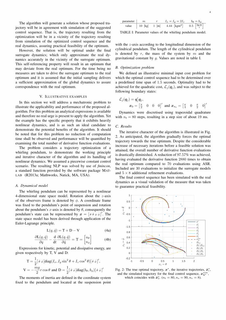
4
The algorithm will generate a solution whose proposed tra-jectory will be in agreement with simulation of the suggestedcontrol sequence. That is, the trajectory resulting from theoptimization will be in a vicinity of the trajectory resultingfrom simulation of the optimized control sequence and thereal dynamics, assuring practical feasibility of the optimum.
However, the solution will be optimal under the finalsurrogate dynamics; which only approximate the real dy-namics accurately in the vicinity of the surrogate optimum.This self-referencing property will result in an optimum thatmay deviate from the real optimum. For the time being nomeasures are taken to drive the surrogate optimum to the realoptimum and it is assumed that the initial sampling deliversa sufficient approximation of the global dynamics to assurecorrespondence with the real optimum.
V. ILLUSTRATIVE EXAMPLES
In this section we will address a mechatronic problem toillustrate the applicability and performance of the proposed al-gorithm. For this problem an analytical expressions is availableand therefore no real urge is present to apply the algorithm. Yetthe example has the specific property that it exhibits heavilynonlinear dynamics, and is as such an ideal candidate todemonstrate the potential benefits of the algorithm. It shouldbe noted that for this problem no reduction of computationtime shall be observed and performance will be quantified byexamining the total number of derivative function evaluations.
The problem considers a trajectory optimization of awhirling pendulum, to demonstrate the working principleand iterative character of the algorithm and its handling ofnonlinear dynamics. We assumed a piecewise constant controlscenario. The resulting NLP was solved by use of fmincon,a standard function provided by the software package MAT-LAB (R2013a; Mathworks, Natick, MA, USA).
A. Dynamical model
The whirling pendulum can be represented by a nonlinear4-dimensional state space model. Rotation about the z-axisof the observers frame is denoted by φ. A coordinate framewas fixed to the pendulum’s point of suspension and rotationabout the pendulum’s x-axis is denoted by θ, consequently thependulum’s state can be represented by x = [ θ θ φ φ ]
′. Thestate space model has been derived through application of theEuler-Lagrange principle.
L(q, q) = T + D− V (4a)
∂L(q, q)
∂q− d
dt∂L(q, q)
∂q= Υ =
[uθuφ
](4b)
Expressions for kinetic, potential and dissipative energy, aregiven respectively by T, V and D:
T =1
2[ θ φ ]diag(Ix, Iy sin2 θ + Iz cos2 θ)[ θ φ ]
′,
V = −mg2r cos θ and D =
1
2[ θ φ ]diag(bθ, bφ)[ θ φ ]
′
The moments of inertia are defined in the coordinate systemfixed to the pendulum and located at the suspension point
parameter m r Ix = Iy = 2Iz bθ = bφ
value 10 [kg] 1 [m] 4.44[kgm2
]0.5
[kg·m
s
]TABLE I: Parameter values of the whirling pendulum model.
with the z-axis according to the longitudinal dimension of thecylindrical pendulum. The length of the cylindrical pendulumis denoted by r, the mass of the system by m and thegravitational constant by g. Values are noted in table I.
B. Optimization problem
We defined an illustrative minimal input cost problem forwhich the optimal control sequence had to be determined overa predefined time span of 1.5 seconds. Optimality had to beachieved for the quadratic cost, Lj(qj), and was subject to thefollowing boundary states:
Lj(qj) = q′jqj ,
x0 =[π2 0 0 0
]′and xnt =
[π4 0 π
2 0]′
Dynamics were discretised using trapezoidal quadraturewith nt = 80 steps, resulting in a step size of about 19 ms.
C. Results
The iterative character of the algorithm is illustrated in Fig.2. As anticipated, the algorithm gradually forces the optimaltrajectory towards the true optimum. Despite the considerableincrease of necessary iterations before a feasible solution wasattained, the overall number of derivative function evaluationsis drastically diminished. A reduction of 97.57% was achieved,having evaluated the derivative function 2880 times to obtainthe real optimum compared to 70 evaluations using ASR.Included are 30 evaluations to initialize the surrogate modelsand 5× 8 additional refinement evaluations.
The final control sequence has been simulated with the realdynamics as a visual validation of the measure that was takento guarantee practical feasibility.
-0.5 0 0.5 1 1.5 2x1 = 3
-1.5
-1
-0.5
0
0.5
1
x2=
_ 3
-1 -0.5 0 0.5 1 1.5 2x1 = 3
-0.2
0
0.2
0.4
0.6
0.8
x4=
_ ?
x$
x$1x$2x$3x$4x$5xsim
u$5
Dini
D1nDini
D2nD1
D3nD2
D4nD3
Fig. 2: The true optimal trajectory, x∗, the iterative trajectories, x∗i ,
and the simulated trajectory for the final control sequence, xsimu∗ ,which coincides with x∗
5. (nt = 80, ns = 90, nv = 8).

5
VI. CONCLUSIONS AND FUTURE DEVELOPMENT
In this treatise we proposed to tackle computational un-wieldiness, introduced by derivative function evaluations in adynamic optimization context, by exploitation of the compu-tational grace of surrogate models. The proposed algorithmicframework managed to enforce reductions in evaluations upto 97.57%, when applied on a highly nonlinear mechatronicproblem, and thus exhibits large potential for future appli-cations where derivative function evaluations correspond withextensive computation time and as such offer a lever to extendthe applicability of trajectory optimization to highly accuratemodels. For the time being a self-referencing mechanismis still inherent to the algorithm and partially subverts theglobal optimization, moreover due to its stochastic nature thesolution may differ for each run. Therefore further sculptingof the algorithm shall be required before a robust and wideapplicability will be possible. Yet the authors are confidentthat within a reasonable timespan such improvements can beobtained.
ACKNOWLEDGEMENTS
The authors acknowledge the support of the Strategic basicresearch project EMODO of the Flanders Make StrategicResearch Centre for the Manufacturing Industry, and the FWOResearch project G.0D93.16N.
REFERENCES
[1] P. J. Moriarty and A. C. Hansen. AeroDyn Theory Manual. NationalRenewable Energy Laborator, 1617 Cole Blvd., Golden, CO 80401-339,August 2005.
[2] Jason P Halloran, Ahmet Erdemir, and Antonie J van den Bogert.Adaptive surrogate modeling for efficient coupling of musculoskeletalcontrol and tissue deformation models. Journal of biomechanicalengineering, 131(1):011014, 2009.
[3] Alexander Forrester, Andras Sobester, and Andy Keane. Engineeringdesign via surrogate modelling: a practical guide. John Wiley & Sons,2008.
[4] Rush D Robinett III, David G Wilson, G Richard Eisler, and John EHurtado. Applied dynamic programming for optimization of dynamicalsystems, volume 9. SIAM, 2005.
[5] Lorenz T. Biegler. An overview of simultaneous strategies for dynamicoptimization. Chemical Engineering and Processing: Process Intensifi-cation, 46(11):1043 – 1053, 2007. Special Issue on Process Optimizationand Control in Chemical Engineering and Processing.
[6] P. Fiorini and Z. Shiller. Time optimal trajectory planning in dynamicenvironments. In Robotics and Automation, 1996. Proceedings., 1996IEEE International Conference on, volume 2, pages 1553–1558 vol.2,Apr 1996.
[7] Moritz Diehl, Hans Georg Bock, Holger Diedam, and Pierre-BriceWieber. Fast direct multiple shooting algorithms for optimal robotcontrol. Fast Motions in Biomechanincs and Robotics, 2005.
[8] Oskar Stryk. Optimal Control: Calculus of Variations, Optimal ControlTheory and Numerical Methods, chapter Numerical Solution of OptimalControl Problems by Direct Collocation, pages 129–143. BirkhauserBasel, Basel, 1993.
[9] H. B. Nielsen, S. N. Lophaven, and J. Søndergaard. DACE - A MatlabKriging Toolbox. Informatics and Mathematical Modelling, TechnicalUniversity of Denmark, DTU, 2002.
[10] Michael D McKay, Richard J Beckman, and William J Conover. Acomparison of three methods for selecting values of input variables inthe analysis of output from a computer code. Technometrics, 42(1):55–61, 2000.
[11] Anand P Deshmukh and James T Allison. Design of nonlineardynamic systems using surrogate models of derivative functions. pagesV03BT03A011–V03BT03A011, 2013.

2D Harmonic Modeling of Eddy Currents inSegmented Rectangular Conductors
C.H.H.M. Custers, J.W. Jansen, and E.A. LomonovaDepartment of Electrical Engineering, Eindhoven University of Technology, Eindhoven, The Netherlands
Abstract—The paper concerns the semi-analytical modeling ofeddy currents in segmented structures of electromagnetic devices.A Fourier series is used to describe the spatial distribution ofthe conductivity and included in the magnetic field solutions. Byincorporating multiple time harmonics in the solution, transientbehavior of forces due to eddy currents can be obtained. Tovalidate the developed method, it is applied to a coreless linearmotor and compared to finite element results. The eddy currentsin segmented conducting structures of motors, such as permanentmagnet arrays, can be accurately determined with this method.
I. INTRODUCTION
In synchronous permanent magnet (PM) machines, the staticfield of the magnets interacts with a time varying field causedby a set of coils. Besides the intended force, also parasiticforces are produced, for instance due to eddy currents inducedin non-laminated conducting parts of the machine, such as themagnets. These currents and their associated force and lossesdepend on the structure of the magnets and can be reducedby segmentation [1]. Hence, to accurately predict the eddycurrent behavior in the magnets, their finite dimensions andsegmentation has to be taken into account.
The 2D Fourier analysis technique [2], [3], is a fast alterna-tive for finite element analysis for the design and analysis ofelectromagnetic devices. With this semi-analytical technique,eddy currents and their reaction field can be modeled. A lim-itation of this method as described in [2], [4] is that the eddycurrents are only calculated in a infinitely long electricallyconducting slab with homogeneous material properties, and asa result, segmentation is not taken into account. To overcomethis limitation, in [5] the eddy currents in a conducting platewith finite length are approximated with the method of images.However, for problems in which the conducting part is smallerthan the source of the magnetic field the results are inaccurate.
In this paper, the Rigorous Coupled Wave Analysis (RCWA)technique [6] is applied to 2D quasi-static magnetic fieldmodeling of motor topologies with a variable conductivityin the Cartesian domain. In [6], the diffraction of a high-frequent electromagnetic wave by a planar grating with aposition dependent permittivity and permeability is modeled.With this technique, inhomogeneous material properties areincluded in the solution of electromagnetic field quantities. Byincorporating a position dependent conductivity function in theFourier based field analysis, eddy currents in segmented partsare modeled. The developed method is applied to a corelessmotor model of which the top half of a periodic section is
2τ
B− B+ A− A+ C− C+
wcbwc
wmhc
2
hmhg
1 2 3 4
Magnet region: magnet - air
Coil regionAir gap region
Back-iron
v
xz
y
Fig. 1. Top half geometric model of a periodic section of a linear corelessmotor.
shown in Fig. 1. The back-iron is assumed to be infinitelypermeable and nonconductive because the focus of the paperis on the eddy currents induced in the segmented region.
II. MAGNETIC FIELD MODELING
The model of the coreless motor of Fig. 1 is divided intothree horizontal regions, respectively the magnet region, airgap region and coil region. To obtain the solutions of themagnetic field quantities, the vector potential formulation isused. The magnetic vector potential ~A is defined as ~B =∇ × ~A, where ~B is the magnetic flux density. Because atwo-dimensional problem is treated, the vector potential isreduced to the z-component. Based on Maxwell’s equationsand the constitutive relations, the Poisson equation is derivedfor nonconducting regions
∂2Az∂x2
+∂2Az∂y2
= −µ0∂My
∂x− µ0µrJ
extz , (1)
where µ0 is the permeability of vacuum and µr is the relativepermeability. My is the remanent magnetization and Jextz isan externally imposed current density.
In the magnet region, eddy currents are induced, which canbe obtained from the vector potential by
Jeddyz = −σ(x)∂Az∂t
, (2)
where σ(x) describes the position dependent conductivityof the magnet array. Generally, the vector potential of aconducting region has to satisfy the diffusion equation
∂2Az∂x2
+∂2Az∂y2
= −µ0∂My
∂x+ µ0µrσ(x)
∂Az∂t
. (3)
III. SEMI-ANALYTICAL SOLUTION
The magnetic field solutions are expressed in terms ofFourier series. The model is assumed to be periodical in thex-direction. As a result, the x-dependent solution is described

by a complex Fourier series. To model the movement of thecoil array, also the time dependent solution is described bya Fourier series. Because there is no correlation between thedifferent time harmonics the principle of superposition is ap-plicable. As a consequence, the vector potential solution can bedetermined for each time harmonic separately and the resultscan be superimposed. The solution to the vector potentialis found by applying the method of separation of variablesand has the following general form with a homogeneous andparticular solution respectively
Az(x, y, t) =∞∑
m=−∞
∞∑n=−∞
(Pm,n(x, y, t) + Ym,n(y) e
j(knx+ωmt)).
(4)
The spatial frequency, kn, is defined as kn = nπτ , where τ
is half of the periodic width of the model and ωm = m2πT ,
where T is the time period. The y-dependent solution Ym,n(y)is equal to
Ym,n(y) = am,n e√λm,ny + bm,n e
−√λm,ny, (5)
where am,n and bm,n are unknown coefficients for eachharmonic which will be determined by applying boundaryconditions between the regions. The eigenvalues λm,n of they-dependent solution are derived in section III-B and III-C.Pm,n(x, y, t) in (4) is the particular solution that is related tothe source terms and will be derived in the following section.
A. Particular solution
For the magnet region the following holds for the particularsolution
P0,n(x) =
µ0
1knMy0,n e
jknx for |n| > 0,
0 for n = 0,(6)
where My0,n are the Fourier coefficients describing the spatialdistribution of the magnetization which does not depend ontime. For the coil region with the source current density thefollowing holds
Pm,n(x, y, t) =
µ0µr
1k2nJextzm,ne
j(knx+ωmt) for |n| > 0,
−µ0µr12J
extzm,ny
2ej(knx+ωmt) for n = 0.(7)
where Jextzm,n are the Fourier coefficients that describe thespatial and time distribution of the externally imposed currentdensity. The three-phase current density in the coil array, de-scribed by Jextzm,n , is sinusoidal and synchronously commutatedfor maximum propulsion force. This means that the frequencyof the current is equal to f = v
τ , where v is the speed of thecoil array. The time varying behavior of the current density iswritten as the complex form of a cosine function
Jph(t) = J1
2
(ej(2π
vτ t+θph) + e−j(2π
vτ t+θph)
), (8)
τ12τ
x0
σ
Fig. 2. Varying conductivity as a function of position in the magnet region.
where J is the peak current density, ph denotes the phase andθA = 0, θB = − 2π
3 and θC = 2π3 . The coefficients Jz,phm,n
of phase ph are calculated by performing the integral
Jz,phm,n = JKphn
1
2T
∫ T
0(ej(2π
vτ t+θph) + e−j(2π
vτ t+θph)
)e−jknvte−jwmtdt,
(9)
where Kphn are the coefficients of the spatial distribution ofthe current density of phase ph. The coefficients Jextzm,n areobtained by Jextzm,n = Jz,Am,n + Jz,Bm,n + Jz,Cm,n .
B. Homogeneous solution for nonconducting regions
For the nonconducting regions the eigenvalues λm,n aredetermined by
λm,n = k2n. (10)
In the nonconducting region, the eigenvalue of harmonicnumber n depends only on spatial frequency kn. This meansthat the spatial harmonics are uncorrelated. The matrix repre-sentation of (10) is given by
Λm =K2, (11)
where K is a diagonal matrix containing the spatial frequen-cies k. The matrix Λm is also diagonal and contains theeigenvalues λm of time harmonic m.
C. Homogeneous solution for conducting regions
The conductivity σ in the magnet region varies as functionof position. A Fourier series is introduced that represents thespatial distribution of σ inside the region
σ(x) =
∞∑n=−∞
ψn ejknx. (12)
The coefficients ψn in (12) are obtained by calculating theFourier transform of the function shown in Fig. 2. For thisfunction it holds that σ > 0 for positions where conductivematerial is present and σ = 0 for positions where air is located.Up on substituting (12) and homogeneous solution of (4) inthe diffusion equation of (3) and performing the derivatives,the following is obtained
∞∑n=−∞
λm,nYm,n(y)ejknx =
∞∑n=−∞
k2nYm,n(y)ejknx+
jωmµ0µr
( ∞∑n=−∞
ψnejknx
)( ∞∑n=−∞
Ym,n(y)ejknx
).
(13)
This equation contains the product of two series with thesame spatial frequencies. A new series with the same spatial

-0.025 -0.02 -0.015 -0.01 -0.005 0 0.005 0.01 0.015 0.02 0.025
J (A/mm2)
x (mm)
y(m
m)
0 20 40 60 80 1000
5
Fig. 3. Eddy current density in the magnets calculated by FEA.
frequencies can be calculated, according to Laurent’s multi-plication rule [7]
jωmµ0µr
( ∞∑n=−∞
ψnejknx
)( ∞∑n=−∞
Ym,nejknx
)=
jωmµ0µr
∞∑n=−∞
∞∑q=−∞
ψq Ym,n−q ejknx.
(14)
This multiplication can be written in matrix form
Ψ ym, (15)
where ym is a vector containing the coefficients of the y-dependent solution. The matrix Ψ is a Toeplitz matrix con-taining the coefficients of σ(x). Using Laurent’s multiplicationrule, the solution of Λm is given by
Λm =K2 + µ0µrjωmΨ. (16)
Contrary to Section III-B, the eigenvalue λm,n of harmonicnumber n depends on multiple spatial frequencies and acoupling of different spatial harmonics occurs. As a result,the matrix Λm is not diagonal and the eigenvalues of the y-dependent solution are not directly obtained. To determine theeigenvalues, an eigenvalue decomposition is performed on Λm
Λm = QmΛ′mQ−1m , (17)
where Λ′m is a diagonal matrix containing the eigenvalues andQm is the matrix containing the corresponding eigenvectors.After performing the decomposition, the solution of Az isequal to
Az(x, y, t) =
∞∑m=−∞
( ∞∑n=−∞
Pm,n(x, y, t)
)+
(ejωmtQm
(Eym(y)am +Eym(−y)bm
))>ejkx,
(18)
whereEym(y) = diag
(e√λ′my). (19)
The unknown coefficients, which are determined by applyingboundary conditions between regions, are collected in vectorsdenoted by am, bm. The vectors λ′m and k contain thediagonal entries of Λ′m and K respectively.
IV. MODEL VERIFICATION
The coreless motor of Fig. 1 is modeled to verify thedeveloped method. Because the model is symmetric withrespect to the x-axis a Neumann boundary condition is appliedin the center of the coils and no forces in the y-direction
TABLE IDIMENSIONS OF THE CORELESS MOTOR
Dimension Symbol Value UnitHalf periodic width τ 56.0 mmAir gap height hg 1.0 mmMagnet width wm 24.0 mmMagnet height hm 9.0 mmCoil width wc 36.0 mmConductor bundle width wcb 12.5 mmCoil height hc 8.0 mm
are considered. The dimension of the simulated motor arelisted in Table I. The force exerted on the segmented magnetarray are calculated using the Maxwell Stress tensor. To onlymodel the eddy current force acting on the magnet array, themagnetization of the magnets is set to 0 A/m and their relativepermeability µr is set to 1. The back-iron is assumed to beinfinitely permeable and nonconductive, and therefore, it isreplaced by a Neumann boundary condition.
The results of the developed semi-analytical method arecompared to results obtained from a transient FE analysisperformed with Cedrat Flux 2D [8]. The back-iron is alsoreplaced by a Neumann boundary. The current density in thecoils is commutated on the q-axis and has a peak value ofJ = 5 A/mm2. A second order triangular mesh is applied tothe model. The mesh size throughout the entire model is equalto 0.5 mm, which results in a total number of 15826 meshelements. Assuming that at least three mesh elements per skindepth are required for simulation of eddy currents, results ofthe FE analysis are accurate up to a frequency of 5.6 kHz forσ = 2 · 107 S/m. Fig. 3 shows the eddy current distribution inthe magnets at one time instant, calculated by FEA.
A. Modeling multiple conducting segments
In the model, eddy currents are induced in four separatemagnets. When the conductivity function describes the con-ductivity of multiple segments as shown in Fig. 2, the obtainedresults are incorrect because the segments are modeled as ifthey are connected while they are in fact electrically isolated.This is illustrated by the solid line in Fig. 4, where thecalculated eddy currents are shown in the center of the magnets(dashed line in Fig. 1) as a function of the position. In thissteady-state simulation, the coils are stationary and excitedwith a frequency of 50 Hz. The sum of currents inside onemagnet is not equal to 0 A. To approach the correct result, theconductivity function has to describe the conductivity of onesegment only and the eddy currents are calculated for eachsegment separately. Afterwards the results are superimposed.This result is shown in Fig. 4 by the dashed line, which isin good agreement with the FE simulation. The error withrespect to the FE analysis result is less than 1 %. The methodof calculating the eddy currents in each segment separately isused in the remainder of the paper. The disadvantage of thismethod is that the effects of the eddy currents in the individualsegments on each other are not modeled.
FE
ANAPM.all.cond.
ANAPM.sep.cond.
× 10-2
x (mm)
Jeddy(A
/mm
2)
0 20 40 60 80 100
−5
0
5
10
Fig. 4. Eddy current density as a function of position in the center ofthe magnets compared to FE results. ANAPM.all.cond. is the result ofusing a conductivity function that describes the conductivity of all magnets.ANAPM.sep.cond. is the result of using a conductivity function that describesthe magnets separately. The conductivity of the magnets is 1 · 106 S/m.
FE
ANA
× 10-3
t (s)
Feddy
x(N
)
0.005 0.01 0.015 0.02 0.025 0.034
4.1
4.2
4.3
Fig. 5. Verification of obtained transient eddy current force in the x-direction.
B. Modeling transient behavior
To verify the transient forces during movement obtainedwith the developed semi-analytical model, a simulation isperformed in which the coil array moves in the positive x-direction with a constant speed of v = 1 m/s. The conductivityof the magnets is set to 1 · 106 S/m, which is a typicalconductivity value for sintered NdFeB magnets. The results areobtained using 61 spatial harmonics and 61 time harmonics.The eddy current force is shown in Fig. 5. The error at thepeak values of the force is less than 3 % with respect to theFE result.
To analyze the accuracy of the method of calculating eddycurrents in individual segments and superimposing the result-ing force, a transient simulation is performed at several speedsand for three values of the conductivity. Two different cases arestudied. Firstly, a simulation is performed in which magnet 1of Fig. 1 is conducting, while the other magnets are not. Themean force due to the eddy currents of both the developedsemi-analytical method and FE analysis is shown in Fig. 6a.The figure shows that for all conductivity values the results arein good agreement and the maximum error with respect to theFE result is less than 4 %. Secondly, a simulation is performedin which all four magnets are conducting (Fig. 6b). For aconductivity value of 1 · 106 S/m, the maximum error is 2 %.However, for conductivity values higher than 1 · 107 S/m theerror significantly increases, especially at high speeds. This iscaused by the influence of the eddy current distribution in onemagnet on another magnet, which is larger at high conductivityvalues.
V. CONCLUSION
In this paper a 2D magnetic field modeling techniquehas been presented that is capable of modeling the spatial
FE
ANA
1·106 S/m
1·107 S/m
2·107 S/m
v (m/s)
meanFeddy
x(N
)
2 4 6 8 10 12 140
0.02
0.04
0.06
0.08
0.1
(a)
FE
ANA
1·106 S/m
1·107 S/m
2·107 S/m
v (m/s)
meanFeddy
x(N
)
2 4 6 8 10 12 140
0.1
0.2
0.3
(b)Fig. 6. Mean eddy current force versus speed for 3 different values ofthe conductivity. (a) Resulting force when only magnet 1 is conducting. (b)Resulting force when all magnets are conducting.
distribution of the conductivity. The conductivity has been de-scribed by a Fourier series and incorporated in the solution ofmagnetic field quantities. With this method the eddy currentsin segmented structures are modeled. The inclusion of multipletime harmonics to the solution makes it possible to modeltransient eddy current forces.
With the presented method it is not possible to modelthe spatial conductivity distribution of multiple conductingsegments at once. When multiple conducting segments areconsidered inside a region, the conductivity of each segmenthas to be separately modeled and the results have to besummed. As a consequence, the effects of the eddy currentsin the individual segments on each other is not modeled.However, for typical conductivity values of NdFeB magnets,accurate results (less than 3 % error with respect to FE) havebeen obtained with superposition.
REFERENCES
[1] K. Yamazaki, M. Shina, Y. Kanou, M. Miwa, and J. Hagiwara, “Effect ofeddy current loss reduction by segmentation of magnets in synchronousmotors: Difference between interior and surface types,” Magnetics, IEEETransactions on, vol. 45, no. 10, pp. 4756–4759, Oct 2009.
[2] K. Binns, P. Lawrenson, and C. Trowbridge, The Analytical and Numer-ical Solution of Electric and Magnetic Fields. Wiley, 1992.
[3] L. Wu, Z. Zhu, D. Staton, M. Popescu, and D. Hawkins, “Analyticalmodel for predicting magnet loss of surface-mounted permanent magnetmachines accounting for slotting effect and load,” Magnetics, IEEETransactions on, vol. 48, no. 1, pp. 107–117, Jan 2012.
[4] J. W. Jansen, E. A. Lomonova, and J. M. M. Rovers, “Effects of eddycurrents due to a vacuum chamber wall in the airgap of a moving-magnetlinear actuator,” Journal of Applied Physics, vol. 105, no. 7, 2009.
[5] K. Pluk, T. van Beek, J. Jansen, and E. Lomonova, “Modeling andmeasurements on a finite rectangular conducting plate in an eddy currentdamper,” Industrial Electronics, IEEE Transactions on, vol. 61, no. 8, pp.4061–4072, Aug 2014.

[6] M. G. Moharam and T. K. Gaylord, “Rigorous coupled-wave analysis ofplanar-grating diffraction,” J. Opt. Soc. Am., vol. 71, no. 7, pp. 811–818,Jul 1981.
[7] L. Li, “Use of fourier series in the analysis of discontinuous periodicstructures,” J. Opt. Soc. Am. A, vol. 13, no. 9, pp. 1870–1876, Sep 1996.
[8] Flux 11 User’s guide, release 11.2 ed., Cedrat Corporation, Grenoble,2012.

Developing for Developing Nations: Exploring aLow-cost PV System Design Methodology
Nishant Narayan*, Jelena Popovic*, Pavol Bauer*, and Miro Zeman**Delft University of Technology, Department of Electrical Sustainable Engineering, P.O. Box 5031, 2600GA,
Delft, The NetherlandsEmail: [email protected]
Abstract—Developing technological solutions for the develop-ing nations is more than simply re-sizing a prevalent solutionfrom the developed world. Not only the environmental condi-tions, but also the technology usage varies greatly between thedeveloping nations in sunnier latitudes around the world and thedeveloped nations of north-western Europe. This paper shedslight on the various technical and non-technical factors to beconsidered for designing a standalone PV system for low-incomehouseholds in developing nations. The importance of battery in alow-cost PV system is examined and the role of power electronicsin such a system design is highlighted. Finally, the paper proposesa system design methodology.
I. INTRODUCTION
Nearly one-fifths of the global population still lacks accessto electricity, with around 85% of them living in the rural areas[1]. Figure 1 shows the distribution of the electricity-starvedpopulation around the world.
China 8 million
Latin America31 million
Rest of Asia387 million
India404 million
Africa587 million
Fig. 1. Global population lacking electricity [2]
Due to the remote location of the unelectrified villages andunstable electricity-grid in many of these developing nations,grid-based electrification is certainly not an immediate solutionto eradicate energy poverty. Therefore, the attention of thiswork was focused on off-grid energy solutions. Since most ofthese locations also happen to lie in the latitude-belts blessedwith abundant sun (refer to Figure 2), the choice of standalonePV-battery energy system is quite obvious.
In an effort to technically contribute towards mitigating thegrowing problem of energy poverty, this work was formulated
Fig. 2. Global solar irradiation [SolarGIS c©2014 GeoModel Solar]
as a low-cost PV system design project tailored for developingnations, with an emphasis on the power electronics develop-ment in the system. Due to the social impact-based natureof this project, it is essential to first get a good grip on thetechnical requirements from the energy system, understand theuser needs and usage environment, and envisage the relationbetween the two. It is also necessary to identify the scientificcontribution in this project that can not only optimize theprimary metric of cost, but also serve as a significant additionto the field of photovoltaic based energy storage systems.
II. LOW-COST PV SYSTEM DESIGN
Since this project is aimed at helping the unelectrifiedcommunities in developing nations, care should be taken thatit does not fall under some of the typical traps, like [3] [4]:
• ‘Designs for developing world’ being no better than quickresizing of prevalent western technology solutions.
• Not understanding the needs of the people who areeventually going to be using the technology.
• Lack of correlation between income of the target groupsand the cost of the system or electricity.
• System designed such that intensive maintenance beingneeded by users who lack even the most basic of technicalskills.
Therefore the first steps taken were to understand the currentstate of rural electrification initiatives with respect to PV-storage systems.

A. Understanding the rural off-grid solar market space
As part of this project, a 2-month extensive literature surveywas carried out to understand the progress of various solarpowered electrification initiatives in developing nations [4].Several present day rural lighting/electrification projects werestudied, mainly in Africa and South-Asia. Figure 3 showssome of the projects that were looked into.
It was observed that the low power (sub 100 W) spaceis quite crowded, with scores of products and initiatives,especially in the portable solar (sub 10 W) segment. Thisis illustrated in Figure 4. The portable solar products seemto outnumber the Solar Home Systems (SHS), like the onesfrom Rural Sparks, Onergy and SolarNow. There are relativelyfewer community level initiatives in comparison that look athigher power levels (0.5 kW to 1.5 kW). For example, theIEEE SunBlazer from the IEEE Smart Village initiative. Forvarious socio-economic as well as technical reasons, there isno one single solution ubiquitous enough to cause a significantimpact to the energy poverty problem as discussed in sectionI.
Between the portable products and the community levelinitiatives, there is a dearth of dedicated household level low-cost solutions, and this is where (around 200 W) the projectdiscussed in this paper aims to fill the gap.
B. Impact of user-environment on system development
Developing a system to be used in emerging economiesin Africa and the Indian subcontinent, for example, requirestaking into account factors that are beyond the electrical realm.For instance, understanding the socio-economic needs of thetarget user groups not only gives the expected electrical loadprofile to be satisfied by the proposed energy system, but alsohighlights the cost-constraints that the system has to eventuallysatisfy. While some of these factors have a direct bearingon system design, some of the factors affect system choicesindirectly.
Examples of social/environmental factors that may havea direct impact on system design include: social needs ofthe people as translated to an electrical load profile, climateendemic to the target region, facade /roofing infrastructure orcommunity space available for PV system implementation,etc. Examples of socio-environmental factors that may havean indirect impact on the system choices include: need fortamper-proof robustness, modularity requirement for future-needs, preferred way of implementation in the community,need for aesthetics, etc.
There are interesting anecdotes from the field that remindus that it is the user that ultimately decides how to use aproduct, while the designers, engineers and scientists have totailor their specs and solutions accordingly. One such anecdotetells of men using solar based lighting (initially given to theirhomes) not for their homes but for their shops - the justificationbeing longer illumination after dusk would ensure a bustlingbusiness for their shops over their competitors’. In anotherincident, households in a part of rural India felt more secureto have the solar panels on the ground in front of their houses
where they can always see them, instead of mounting on theroof where one can’t always have a watchful eye. This isimperceptible to the regular PV system architect, who wouldonly want the panels to be mounted in the highest, shade-freearea of a building. These anecdotes were recalled in a personalinterview (December 2015) of a student who interned with asolar-based startup in India in 2014.
These incidents from the field go to show that the socio-environmental factors are inseparably linked with the systemdesign conundrum.
III. ROLE OF TECHNOLOGY
Technology of course has the primary role to play in sucha project, but its development is a complex mix of severalfactors.
Figure 5 shows a basic block diagram schematic of astandalone PV system. Each block additionally lists variousparameters needed for the electrical design of the PV system.Most of these parameters have a direct or indirect dependencyon the socio-environmental factors as discussed above. Forinstance, the local climate will have an impact on the thermalbehaviour of PV modules, battery and power electronics,which would need to be designed accordingly. Similarly, theload profile of the communities will have a direct impacton the required system and components sizing. An accurateknowledge of the load demand and the load priority mayyield extra room in incorporating features like Demand SideManagement (DSM).
A. Battery in a low-cost PV system
A battery is by-far the most expensive part of a standalonePV system. Although indispensable, it can account for morethan 50% of the total system costs while having the leastlifetime among all PV system components [5]. Therefore thechallenge would lie in minimizing the costs associated withthe battery while increasing its lifetime. There are two kindsof battery costs incurred in an off-grid PV system: upfrontcosts and running costs.
Upfront costs are directly related to the size of the batteryused. Larger the battery, higher the upfront costs. Therefore,if the battery size can be reduced for a given load profile,there can be considerable costs savings. Running costs areassociated with the battery having a limited lifetime, andgenerally far shorter than the other components. Some of themore efficient batteries may last 8 to 10 years in comparison tothe 25-30 years of a PV module. Therefore the battery wouldneed occasional replacement [5] [6].
Ensuring a longer battery life is technically quite demand-ing. Battery performance is a complex interplay of variousbattery parameters, like Depth of Discharge (DOD), C-rate,temperature, and cycle life, amongst others. For example,the energy capacity of a typical Valve Regulated Lead Acid(VRLA) battery is enhanced with temperature due to increasedchemical activity [7]. However, increase of temperature hasa detrimental effect on the battery lifetime. This effect isshown in Figure 6, where the high temperature seems to take
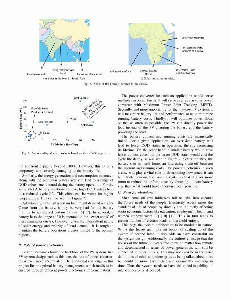
Rural Sparks (India)
Onergy (West Bengal, India) KamWorks (Cambodia)
(a) Solar initiatives in South Asia
Waka-Waka (Africa) Lemnis (South Africa)
SolarWorks ! (East and South Africa)
M-kopa (Uganda, Tanzania and Kenya)
SolarNow (Uganda)
(b) Solar initiatives in Africa
Fig. 3. Some of the projects covered in the survey.
0
20
40
60
80
100
120
0 10 20 30 40 50
Bat
tery
Siz
e (W
h)
PV Module Size (Wp)
M-Kopa
Onergy
Rural Sparks
SolarNowSolarWorks!
Portable Solar Products (< 5 Wp) IEEE SunBlaz
er :
500 Wp - 1
.8 kWp
1.2 kWh - 20kWh
Fig. 4. Various off-grid solar products based on their PV-Storage size.
the apparent capacity beyond 100%. However, this is onlytemporary, and severely damaging to the battery life.
Similarly, the energy generation and consumption mismatchalong with the particular battery size can lead to a range ofDOD values encountered during the battery operation. For thesame VRLA battery mentioned above, high DOD values leadto a reduced cycle life. This effect can be worse for highertemperatures. This can be seen in Figure 7.
Additionally, although a certain load might demand a higherC-rate from the battery, it may be very bad for the batterylifetime to go exceed certain C-rates [6] [7]. In general, abattery lasts the longest if it is operated in the ‘sweet spots’ ofthese parameter curves. However, given the intermittent natureof solar energy and priority of load demand, it is tough tomaintain the battery operations always limited to the optimalregions.
B. Role of power electronics
Power electronics forms the backbone of the PV system. In aPV system design such as this one, the role of power electron-ics is even more accentuated. The additional challenge in thisproject lies in optimal battery management, which needs to beensured through efficient power electronics implementation.
The power converter for such an application would servemultiple purposes: Firstly, it will serve as a regular solar powerconverter with Maximum Power Point Tracking (MPPT).Secondly, and more importantly for the low-cost PV system, itwill maximize battery life and performance so as to minimizerunning battery costs. Thirdly, it will optimize power flowsso that as often as possible, the PV can directly power theload instead of the PV charging the battery and the batterypowering the load.
The battery upfront and running costs are intrinsicallylinked. For a given application, an over-sized battery willlead to lesser DOD states in operation, thereby increasingits lifetime. On the other hand, a smaller battery would havelesser upfront costs, but the larger DOD states would cost thecycle life dearly, as was seen in Figure 7. Ceteris paribus, thebattery size in itself forms an interesting trade-off betweenthe upfront and running costs. The power electronics in sucha case will play a vital role in determining how much it canhelp with reducing the running costs, so that it gives moreroom to reduce the upfront costs by choosing a lower batterysize than what would have otherwise been possible.
C. Need for ModularityMost rural off-grid initiatives fail to take into account
the future needs of the people. Electricity access raises thestandard of life of people by directly and indirectly affectingsocio-economic factors like education, employment, health andwomen empowerment [9] [10] [11]. This in turn leads togreater number of electric loads a household enjoys.
This begs the system architecture to be modular in nature.While this leaves an important option of scaling up of thesystem if needed later, it also adds an extra constraint onthe system design. Additionally, the authors envisage that thehouses of the future, 20 years from now, no matter how remoteand decentralized in terms of power generation, will still beconnected to other houses. This may not even be in the strictdefinitions of mini- and micro-grids as being talked about now,but could be more asymmetric and organically evolving intime. Thus the system needs to have the added capability ofinter-connectivity if needed.
PV Module
Load Demand
Power Converter
• Climate Data • Thermal effects • Technology choice • PV sizing
• Battery Management • Topology • MPPT
• Architecture• Modularity
• PV-Load direct transfer
• Exact load profile • DSM • Future demand
• Cost and Lifetime • Thermal effects • Technology selection • Battery sizing
Fig. 5. Block diagram of a standalone PV system, showing various design parameters
−15 −5 5 15 25 3560
70
80
90
100
Temperature(°C)
Bat
tery
Cap
acity
(%)
Fig. 6. Effect of temperature on battery capacity of a VRLA battery [8].
IV. METHODOLOGY
As shown in Figure 5, the standalone PV system design forthis project has to account for myriads of parameters. Eachcomponent of the system needs to be design individually tothe best performance-to-cost ratio, while taking into accountthe overall system constraints.
The methodology for approaching such a complex projectcannot efficiently work with a linearly planned system designor even a simple pipelined approach. Figure 8 shows a linearsystem design cycle, which would involve the following phasesin serial occurrence:
1) Understanding user needs.
0 20 40 60 80 1000
1000
2000
3000
4000
5000
6000
7000
8000
9000
Cy
cles
(-)
DoD (%)
20oC 25 oC 30 oC 35o C 40 oC 45 oC
Fig. 7. Effect of temperature and DOD on a VRLA Battery life. [Data sourcedfrom [7]]
2) Drawing system constraints and system-level design(system architecture).
3) PV-Battery sizing.4) Power electronics design.
A linear methodology is inadequate to handle the intricacieslinked to a multi-faceted project like this one. The simplepipelined approach also falls short because each phase andaspect of the design may need to be revisited, based on theinflux of user input or field data.
The Spiral Design Approach
A spiral system design cycle is proposed for this project.Spiral design incorporates the added benefits of iteration andfeedback from different phases. This concept is already in usein software design as well as human interaction based system

START END
User needs System constraintsand design
PV batterysizing
Power electronicsdesign
Fig. 8. Linear system design cycle concept.
developments [12]. Figure 9 illustrates this concept as appliedto this project.
START
END
User
Domain
System Leve
l Des
ign PV-Battery Considerations
Power Electronics Design
constraints for optimal battery usage
electrical specifications
modularity
prototype
user feedback and testing
modularity considerations
converter topology
PV - battery technology selection
battery costssystem architecture
understanding user space
user load profile
efficient battery management
component sizing
Wp, kWh specs.
system constraints
Fig. 9. Spiral system design cycle concept.
The spiral shows 4 main phases:1) User domain.2) System level constraints and architecture.3) PV-Battery sizing.4) Power electronic design.
These phases would be iteratively visited, while feedback fromeach phase would interact with and impact every other phase.
In reality, not all phases would last the same duration asshown in the concept illustration (Figure 9). Also, based on thematurity of the project and other constraints, some phase mayhave to be revisited ‘out of turn’. Therefore, robust design-flows need to be ensured so that the design cycle can take inmore data in its different phases.
V. CONCLUSION
A dedicated PV-storage energy system design for commu-nities in developing nations can be a complex task, especiallyif the emphasis is on a low-cost, affordable solution thattakes current and (foreseeable) future needs of the people
into account. Both technical as well as non-technical or socio-economic factors have a huge bearing on the way the systemshould be designed and developed.From a technical design perspective, much of the challenge inoptimizing costs in a low power PV system revolves around thesuccessful optimization of battery. In this respect, the powerelectronics in such a standalone PV system needs to be morethan just a charge-controller with MPPT. The power converterneeds to also efficiently manage the battery operation so as tomaximise its lifetime while requiring the least possible batterysize for a given system power rating.A spiral design methodology is suggested that is flexible toevolve as more data comes in at various stages of the project.Lastly, developing technological solutions for the developingworld calls for a different mindset from the researcher thanwhat maybe usually seen in his or her field of expertise. Theauthors are confident that as more socially inclined scientistsendeavor down this path, technology can indeed become thesolution that transcends socio-economical, geopolitical andother man-made boundaries prevalent today.
Future recommendations
In the future it is important to be able to quantify the socialimpact of this project. Even though the system developmentmay be successful purely based on the project deliverables,i.e., a low-cost, robust PV system built taking into accountthe current and future needs of the target communities, it hasto have a measurable social impact. The sooner this ‘impactassessment tool’ is developed, the more useful this and othersocially driven technical projects can become.
ACKNOWLEDGMENT
The authors would like to thank Natalie Kretzschmar,Thomas den Heeten and Vasilis Marioleas for their contribu-tions. This work is supported by a fellowship from the DelftGlobal Initiative of Delft University of Technology.
REFERENCES
[1] I. E. Agency, Energy Poverty: How to make modernenergy access universal, ser. World Energy Outlook 2010,2010. [Online]. Available: http://www.worldenergyoutlook.org/media/weowebsite/energydevelopment/weo2010 poverty.pdf
[2] C. Gradl and C. Knobloch, Energize the BoP! A Practioner’s Guide,2011.
[3] S. Ofordile ANI, “Low cost small wind turbine generators for developingcountries,” Ph.D. dissertation, Delft University of Technology, 2013.
[4] N. Kretzschmar, Studying the success, failure and progress of various(solar-powered) rural electrification initiatives in developing nations,2016.
[5] J. Hoppmann, J. Volland, T. S. Schmidt, and V. H. Hoffmann, “Theeconomic viability of battery storage for residential solar photovoltaicsystems a review and a simulation model,” Renewable and SustainableEnergy Reviews, vol. 39, pp. 1101 – 1118, 2014. [Online]. Available:http://www.sciencedirect.com/science/article/pii/S1364032114005206
[6] D. G. fur Sonnenenergie, Planning and Installing PhotovoltaicSystems: A Guide for Installers, Architects and Engineers, ser.Planning and Installing. Taylor & Francis, 2008. [Online]. Available:http://books.google.nl/books?id=fMo3jJZDkpUC
[7] “Installation , commissioning and operating instructions for ventedstationary lead-acid batteries - solar battery data sheet,” Hoppecke 2013,Germany.

[8] N. Narayan, “Solar charging station for light electric vehicles: A designand feasibility study,” Master’s thesis, Delft University of Technology,2013.
[9] S. Ray, B. Ghosh, S. Bardhan, and B. Bhattacharyya, “Studies on theimpact of energy quality on human development index,” RenewableEnergy, vol. 92, pp. 117–126, 2016.
[10] T. Dinkelman, “The effects of rural electrification on employment: Newevidence from south africa,” The American Economic Review, pp. 3078–3108, 2011.
[11] S. Aid, Impact Report, 2015. [Online]. Available:http://www.solar-aid.org/assets/Uploads/Impact-week-2015/SolarAid-IMPACT-REPORT-2015.pdf
[12] A. S. Mavor, R. W. Pew et al., Human-System Integration in the SystemDevelopment Process:: A New Look. National Academies Press, 2007.

1
Analytical Surface Charge Method for Rotated Permanent Magnets:Boundary Element Method Comparison and Experimental Validation
J. R. M. van Dam1, J. J. H. Paulides1, W. S. P. Robertson2, M. Dhaens3, and E. A. Lomonova1
1Department of Electrical Engineering, Eindhoven University of Technology, Eindhoven 5612 AP, The Netherlands2School of Mechanical Engineering, The University of Adelaide, SA 5005, Australia
3Advanced Chassis Research, Tenneco Automotive Europe BVBA, B 3800 Sint-Truiden, Belgium
This paper is concerned with the analytical calculation of the interaction force between two permanent magnets (PMs) underrelative rotation by means of the surface charge method, taking into account the non-unity relative permeability of the PMs. Thismodel combines high accuracy and a short calculation time. As the considered PM configuration is a free-space, unbounded problem,the results from the surface charge method are compared to its numerical counterpart, the boundary element method. The analyticalexpressions were validated by means of the measurement results obtained from a 3-D printed test setup.
Index Terms—Analytical models, electromagnetic fields, electromagnetic forces, permanent magnets.
I. INTRODUCTION
THE increasing interest in wireless sensors and wearableelectronics has encouraged the research into renewable
battery-replacement technologies, as to reduce the mainte-nance and resource cost inseparably related to batteries. Anattractive alternative is to harvest energy from natural vibrationsources, as they are widely available, and potentially containa high power density. The conversion of the kinetic energyin vibrations into electrical energy has been achieved usingmany different types of transducers, such as mechanical [1],magnetoelectric [2], electrostatic [3], electromagnetic [4], andpiezoelectric [5]–[7].
In piezoelectric cantilever beam energy harvesters [6], [7],the beam fundamental resonance frequency is usually matchedwith the system excitation frequency, as to yield the largestharvested energy. However, to allow for a range of excitationfrequencies, the interaction forces between permanent magnets(PMs) are applied to tune the beam resonance frequency.In [7], the PM interaction forces result from an approxi-mation function. The optimization of the energy-harvestingcapabilities requires an improved accuracy with respect to thedetermined interaction forces. Hence, a PM modeling methodis desired which provides a 3-D magnetic field solution,works well in free-space unbounded problems, handles relativerotations between PMs, and does not require periodicity ofthe considered magnetic structure. Moreover, to allow forfast optimization and geometry selection, an analytical modelis preferred over numerical alternatives. Both the surfacecharge method [8]–[13] and the Boundary Element Method(BEM) [14] satisfy the above conditions.
This paper provides an improved calculation of the inter-action force between two PMs under relative rotation withrespect to existing cantilever beam vibration energy harvesters.The analytical surface charge method and the BEM simulationresults are compared to the results from the Finite ElementMethod (FEM). Additionally, an experimental setup is de-signed to validate the simulation results.
permanent magnet
mass
piezoelectric cantilever beam
attractive force
repulsive force
∆t
∆b∆c
adjustableheight
y
z
x
l
environmental vibrations
Fig. 1. Energy-harvesting piezoelectric cantilever beam.
II. CONSIDERED GEOMETRY
An implementation of the considered energy harvestingcantilever beam is shown in Fig. 1. Environmental vibrationsare transferred to the beam structure, where minor vibrationsof the tip mass are amplified by the forces between the PMs.The beam oscillates at its resonance frequency, fr, which ispartially determined by the height and length of the beam,∆c and l, respectively, and the distances between the PMs,∆t and ∆b. Energy is generated by the deformation of thepiezoelectric elements in the beam. This is illustrated onan energy-harvesting cantilever beam in Fig. 1, where theenergy harvester consists of a non-magnetic beam to whichpiezoelectric elements, PMs, and a non-magnetic free end tipmass are attached. A simplified representation of the cantileverbeam PMs is shown in Fig. 2, where only two PMs areconsidered. The PM dimensions are summarized in Table I.
III. SURFACE CHARGE METHOD FOR ROTATED PMS
Simplified two-dimensional (2-D) analytical models to ob-tain the interaction force between magnets in radial bearings
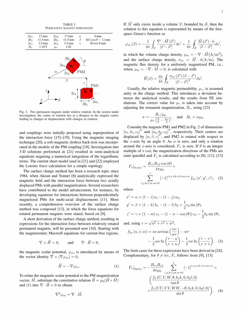
2
TABLE IPERMANENT MAGNET DIMENSIONS
2a1 17 mm 2a2 17 mm α 0 mm2b1 11.5 mm 2b2 11.5 mm β 60 (cos θ − 1)mm2c1 3.5 mm 2c2 3.5 mm γ 60 sin θmmBr 1.18 T µr 1.02
x
z
y
θ
γβ
2b1
2c1
2b2
PM1
PM22c2
2a1
2a2
α
Fig. 2. Two permanent magnets under relative rotation. In the system underinvestigation, the center of rotation lies at a distance to the magnet center,leading to changes in displacement with changes in rotation.
and couplings were initially proposed using superposition ofthe interaction force [15]–[19]. Using the magnetic imagingtechnique [20], a soft-magnetic slotless back-iron was incorpo-rated in the models of the PM coupling [18]. Investigation into3-D solutions performed in [21] resulted in semi-analyticalequations requiring a numerical integration of the logarithmicterms. The current sheet model used in [21] and [22] employedthe Lorentz force calculation for a simple topology.
The surface charge method has been a research topic since1984, when Akoun and Yonnet [8] analytically expressed themagnetic field and the interaction force between two axiallydisplaced PMs with parallel magnetization. Several researchershave contributed to the model advancement, for instance, bydeveloping equations for interactions between perpendicularlymagnetized PMs for multi-axial displacements [11]. Morerecently, a comprehensive overview of the surface chargemethod was composed [13], in which the force equations forrotated permanent magnets were stated, based on [9].
A short derivation of the surface charge method, resulting inexpressions for the interaction force between relatively rotatedpermanent magnets, will be presented now [10]. Starting withthe magnetostatic Maxwell equations for current-free regions,
∇× ~H = 0, and ∇ · ~B = 0,
the magnetic scalar potential, ϕm, is introduced by means ofthe vector identity ∇× (∇ϕm) = 0,
~H = −∇ϕm. (1)
To relate the magnetic scalar potential to the PM magnetizationvector, ~M , substitute the constitutive relation ~B = µ0( ~H+ ~M)and (1) into ∇ · ~B = 0 to obtain
∇2ϕm = ∇ · ~M.
If ~M only exists inside a volume V , bounded by S, then thesolution to this equation is represented by means of the free-space Green’s function as
ϕm (~x) = − 1
4π
∫V
∇′ · ~M (~x′)
|~x− ~x′|dv′ +
1
4π
∮S
~M (~x′) · n|~x− ~x′|
ds′,
in which the volume charge density, ρm = −∇ · ~M(A/m2
),
and the surface charge density, σm = ~M · n(A/m). Themagnetic flux density for a uniformly magnetized PM, i.e.,where ρm = −∇ · ~M = 0, is calculated with
~B (~x) =µ0
4π
∮S
σm (~x′) (~x− ~x′)|~x− ~x′|3
ds′.
Usually, the relative magnetic permeability, µr, is assumedunity in the charge method. This introduces a deviation be-tween the analytical results, and the results from FE sim-ulations. The correct value for µr is taken into account byadjusting the remanent magnetization, Br, using [23]
σ =Br/µ0
µr(32 −
µr
2
) , and Br = σµ0.
Consider the magnets PM1 and PM2 in Fig. 2 of dimensions[a1, b1, c1]
T and [a2, b2, c2]T , respectively. Their centers are
displaced by [α, β, γ]T , and PM2 is rotated with respect to
the x-axis by an angle θ. As α is zero, and only a rotationaround the x-axis is considered, Fx is zero. If θ is an integermultiple of π rad, the magnetization directions of the PMs are(anti-)parallel and Fz is calculated according to [8], [11], [13]
Fz|θ=kπ =Br1Br2 cos (θ)
4πµ0×
1∑i,j,k,l,m,n=0
[−1]i+j+k+l+m+n
f3z (x′, y′, z′) , (2)
where
x′ = α+ (1− i) a1 − (1− j) a2,
y′ = β + (1− k) b1 − (1− l) b2 +1
2c2 sin (θ),
z′ = γ + (1−m) c1 − (1− n− cos (θ)) c2 −1
2b2 sin (θ),
and, using r =√u2 + v2 + w2,
f3z (u, v, w) = uv arctan( uvwr
)− wr
− 1
2uw ln
(r − ur + u
)− 1
2vw ln
(r − vr + v
). (3)
The limit cases for these expressions have been derived in [24].Complementary, for θ 6= kπ, Fz follows from [9], [13]
Fz|θ 6=kπ = −Br1Br24πµ0
1∑i,j,k,l,m,n=0
[−1]i+j+k+l+m+n×(
f3 (U, V,W, θ, b1k, 0, b2l, 0)
tan θ
+f3 (UU, V V,WW,−θ, b1k, 0, b2l, 0)
sin θ
), (4)
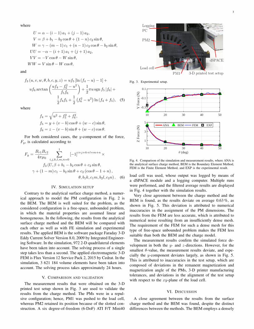
3
where
U = α− (i− 1) a1 + (j − 1) a2,
V = β + b1 − b2 cos θ + (1− n) c2 sin θ,
W = γ − (m− 1) c1 + (n− 1) c2 cos θ − b2 sin θ,
UU = −α− (i+ 1) a1 + (j + 1) a2,
V V = −V cos θ −W sin θ,
WW = V sin θ −W cos θ,
and
f3 (u, v, w, θ, b, c, y, z) = uf5 [ln (f4 − u)− 1] +
uf6 arctan
(uf4 − f26 − u2
f5f6
)+
1
2πu sgn f5 |f6|+
1
2f4f5 +
1
2
(f26 − u2
)ln (f4 + f5), (5)
where
f4 =√u2 + f25 + f26 ,
f5 = y + (v − b) cos θ + (w − c) sin θ,
f6 = z − (v − b) sin θ + (w − c) cos θ.
For both considered cases, the y-component of the force,Fy , is calculated according to
Fy =Br1Br24πµ0
1∑i,j,k,l,m,n=0
[−1]i+j+k+l+m+n×
f3 (U, β + b1 − b2 cos θ + c2 sin θ,
γ + (1−m) c1 − b2 sin θ + c2 (cos θ − 1 + n) ,
θ, b1k, c1m, b2l, c2n) . (6)
IV. SIMULATION SETUP
Contrary to the analytical surface charge method, a numer-ical approach to model the PM configuration in Fig. 2 isthe BEM. The BEM is well suited for the problem, as theconsidered configuration is a free-space, unbounded problem,in which the material properties are assumed linear andhomogeneous. In the following, the results from the analyticalsurface charge method and the BEM will be compared witheach other as well as with FE simulation and experimentalresults. The applied BEM is the software package Faraday 3-DEddy Current Solver Version 8.0, 2009 by Integrated Engineer-ing Software. In the simulation, 972 2-D quadrilateral elementshave been taken into account. The solving process of a singlestep takes less than a second. The applied electromagnetic 3-DFEM is Flux Version 12 Service Pack 2, 2015 by Cedrat. In thesimulation, 3 621 184 volume elements have been taken intoaccount. The solving process takes approximately 24 hours.
V. COMPARISON AND VALIDATION
The measurement results that were obtained on the 3-Dprinted test setup shown in Fig. 3 are used to validate theresults from the charge method. The PMs were in a repul-sive configuration; hence, PM1 was pushed to the load cell,whereas PM2 retained its position because of the slotted con-struction. A six degree-of-freedom (6-DoF) ATI F/T Mini40
PM1
PM2
3-D printed test setup
Load cell
dSPACE
Logging
PC
Fig. 3. Experimental setup.
10 20 30 40 50
-0.3
-0.1
0.1
Y F
orce
(N
)
10 20 30 40 50θ (deg)
1
3
5
Z F
orce
(N
) ANA BEM FEM EXP
Fig. 4. Comparison of the simulation and measurement results, where ANA isthe analytical surface charge method, BEM is the Boundary Element Method,FEM is the Finite Element Method, and EXP is the experimental result.
load cell was used, whose output was logged by means ofa dSPACE module and a logging computer. Multiple runswere performed, and the filtered average results are displayedin Fig. 4 together with the simulation results.
Very close agreement between the charge method and theBEM is found, as the results deviate on average 0.63 %, asshown in Fig. 5. This deviation is attributed to numericalinaccuracies in the assignment of the PM dimensions. Theresults from the FEM are less accurate, which is attributed tonumerical noise resulting from an insufficiently dense mesh.The requirement of the FEM for such a dense mesh for thistype of free-space unbounded problem makes the FEM lesssuitable than both the BEM and the charge model.
The measurement results confirm the simulated force de-velopment in both the y- and z-directions. However, for thesmallest θ-value, the measurement results deviate, and espe-cially the y-component deviates largely, as shown in Fig. 5.This is attributed to inaccuracies in the test setup, which arecomposed of deviations in the remanent magnetization andmagnetization angle of the PMs, 3-D printer manufacturingtolerances, and deviations in the alignment of the test setupwith respect to the xy-plane of the load cell.
VI. DISCUSSION
A close agreement between the results from the surfacecharge method and the BEM was found, despite the distinctdifferences between the methods. The BEM employs a densely
4
10 20 30 40 500.5
0.6
0.7D
evia
tion
(%)
10 20 30 40 50θ (deg)
0
20
40
60
Dev
iatio
n (%
)
Y-directionZ-direction
Fig. 5. Percentage deviation between the analytical surface charge methodand the BEM (top), and the experimental results (bottom).
populated, non-symmetric system matrix that elevates mem-ory usage and could, potentially, increase computer times tothe level of the FEM. Additionally, material properties areassumed linear and homogeneous, which renders the BEMunsuitable for configurations involving soft-magnetic material.A major asset of the BEM surfaces when considering free-space, unbounded problems, as it only requires field sourceboundaries to be discretized, resulting in faster solutions thanthe FEM. Contrary to the BEM, the surface charge methodis analytically formulated, resulting in faster solutions. As aresult of recent developments, the applicability of the surfacecharge method has improved with the introduction of (semi-)analytical solutions to include the relative permeability ofsoft-magnetic materials [25].
For now, the applicability of the surface charge method islimited to rotations around the non-magnetized axis, in combi-nation with a translation with respect to the magnetized axes.Therefore, the method does not serve as a FEM-replacementyet [13]. Model extensions include the forces between cylindri-cal PMs with single-axis rotation. Subsequently, the forces andtorques between pairs of cuboidal and pairs of cylindrical PMswith arbitrary rotation should be considered. Then, force andtorque expressions between pairs of spherical, triangular, anddifferently-shaped permanent magnets should be developed.
VII. CONCLUSION
In this paper, the analytical surface charge method is ap-plied to two relatively rotated permanent magnets (PMs). Thecalculated interaction force is compared with results fromthe Boundary Element Method (BEM), and validated againstexperimental results. Although the surface charge methodalready shows superior applicability and computational time,compared with the BEM, great promise lies in the extensionof the method to allow for multi-axial rotations to providea 6-DoF PM interaction model, which can serve as a fast,analytical replacement to the finite element method.
REFERENCES
[1] Z. Li, L. Zuo, J. Kuang, and G. Luhrs, “Energy-harvesting shockabsorber with a mechanical motion rectifier,” Smart Mater. Struct.,vol. 22, no. 2, p. 025008, 2013.
[2] J. Yang, Y. Wen, P. Li, X. Dai, and M. Li, “A Broadband VibrationEnergy Harvester Using Magnetoelectric Transducer,” in IEEE Sensors,Nov. 2010, pp. 1905–1909.
[3] A. Fowler, S. Moheimani, and S. Behrens, “An Omnidirectional MEMSUltrasonic Energy Harvester for Implanted Devices,” J. Microelec-tromech. S., vol. 23, no. 6, pp. 1454–1462, Dec. 2014.
[4] Q. Zhang and E. S. Kim, “Vibration Energy Harvesting Based on Magnetand Coil Arrays for Watt-Level Handheld Power Source,” Proc. IEEE,vol. 102, no. 11, pp. 1747–1761, Nov. 2014.
[5] J. Jung, P. Kim, J.-I. Lee, and J. Seok, “Nonlinear dynamic and energeticcharacteristics of piezoelectric energy harvester with two rotatableexternal magnets,” Int. J. Mech. Sci., vol. 92, pp. 206–222, 2015.
[6] S. R. Anton and H. A. Sodano, “A review of power harvesting usingpiezoelectric materials (2003-2006),” Smart Mater. Struct., vol. 16, no. 3,pp. R1–R21, 2007.
[7] V. R. Challa, M. G. Prasad, Y. Shi, and F. T. Fisher, “A vibration energyharvesting device with bidirectional resonance frequency tunability,”Smart Mater. Struct., vol. 17, no. 1, p. 015035, 2008.
[8] G. Akoun and J.-P. Yonnet, “3D analytical calculation of the forcesexerted between two cuboidal magnets,” IEEE Trans. Magn., vol. 20,no. 5, pp. 1962–1964, Sep. 1984.
[9] J. F. Charpentier and G. Lemarquand, “Study of Permanent-MagnetCouplings with Progressive Magnetization Using an Analytical Formu-lation,” IEEE Trans. Magn., vol. 35, no. 5, pp. 4206–4217, Sep. 1999.
[10] E. P. Furlani, Permanent Magnet and Electromechanical Devices:Materials, Analysis, and Applications, ser. Academic Press Series inElectromagnetism. Academic, 2001.
[11] J. L. G. Janssen, J. J. H. Paulides, E. Lomonova, F. Boloni, A. Tounzi,and F. Piriou, “Analytical Calculation of Interaction Force BetweenOrthogonally Magnetized Permanent Magnets,” Sensor Letters, vol. 7,no. 3, pp. 442–445, 2009.
[12] H. Allag, “Models and Calculation of Passive Magnetic Suspension –2D and 3D Analytical Calculation of Interactions Between PermanentMagnets,” Ph.D. dissertation, Universite de Grenoble, Jun. 2010.
[13] W. S. P. Robertson, “Modelling and design of magnetic levitationsystems for vibration isolation,” Ph.D. dissertation, The University ofAdelaide, SA, Australia, Nov. 2013.
[14] L. Gaul, M. Kogl, and M. Wagner, Boundary Element Methods forEngineers and Scientists – An Introductory Course with AdvancedTopics, 1st ed. Springer-Verlag Berlin Heidelberg, 2003.
[15] J.-P. Yonnet, “Passive magnetic bearings with permanent magnets,” IEEETrans. Magn., vol. 14, no. 5, pp. 803–805, Sep. 1978.
[16] R. Hornreich and S. Shtrikman, “Optimal design of synchronous torquecouplers,” IEEE Trans. Magn., vol. 14, no. 5, pp. 800–802, Sep. 1978.
[17] J.-P. Yonnet, “Permanent magnet bearings and couplings,” IEEE Trans.Magn., vol. 17, no. 1, pp. 1169–1173, Jan. 1981.
[18] J.-P. Yonnet, S. Hemmerlin, E. Rulliere, and G. Lemarquand, “Analyt-ical calculation of permanent magnet couplings,” IEEE Trans. Magn.,vol. 29, no. 6, pp. 2932–2934, Nov. 1993.
[19] J. M. D. Coey, Rare-Earth Iron Permanent Magnets, 1st ed., ser.Monographs on the Physics and Chemistry of Materials. Oxford, U.K.:Oxford University Press, 1996, vol. 54.
[20] B. Hague, The principles of electromagnetism applied to electricalmachines, 1st ed. New York: Dover Publications, 1962.
[21] J. Tsui, D. Iden, K. Strnat, and A. Evers, “The effect of intrinsicmagnetic properties on permanent magnet repulsion,” IEEE Trans.Magn., vol. 8, no. 2, pp. 188–194, Jun. 1972.
[22] H. S. Nagaraj, “Investigation of Magnetic Fields and Forces Arising inOpen-Circuit-Type Magnetic Bearings,” Tribology Transactions, vol. 31,no. 2, pp. 192–201, 1988.
[23] M. F. J. Kremers, J. J. H. Paulides, E. Ilhan, J. L. G. Janssen, and E. A.Lomonova, “Relative Permeability in a 3D Analytical Surface ChargeModel of Permanent Magnets,” IEEE Trans. Magn, vol. 49, no. 5, pp.2299–2302, May 2013.
[24] J. L. G. Janssen, J. J. H. Paulides, and E. A. Lomonova, Computer fieldmodels of electromagnetic devices - Studies in applied electromagneticsseries. Amsterdam: IOS Press, 2010, ch. Analytical Force and StiffnessCalculations for Magnetic Bearings and Vibration Isolation, pp. 502–511.
[25] D. van Casteren, J. Paulides, and E. Lomonova, “Modeling the FieldInside a Soft-Magnetic Boundary using Surface Charge Modeling,” IEEETrans. Magn., vol. PP, no. 99, pp. 1–1, 2015.
Grid Hybridization using AC-DC ReconfigurableUnderground Cable links in Distribution Networks
Aditya Shekhar, Laura Ramırez-Elizondo and Pavol BauerDC Systems & Storage, Delft University of Technology, The Netherlands
Abstract—This work represents the progressing efforts towardsgrid hybridization and provides an overview of the evolvingconcept of reconfigurable ac-dc links. The motivation for re-furbishing ac infrastructure to operate under dc conditionsis also offered. The possibility of power transmission capacityenhancement with dc links is highlighted. Finally, the objectiveof dc link control and grid integration is presented.
Index Terms—ac, cables, capacity, converter, control, dc, dclink, electric fields, flexibility, grid integration, hybrid, modular-ity, redundancy, reconfigurable, refurbishing.
I. INTRODUCTION
Increasing integration of dispersed renewable energysources in existing electricity supply systems have enabledbidirectional power flows in the distribution networks [1].Looking at the current grid structure, it is possible that dcdistribution has some operation advantages over ac [2]. Newenergy consumers like electric vehicles have changed thelocalized energy consumption patterns, introducing morecomplexity to the grid operability [3].
Infrastructural complexity and investment costs are requiredfor maintaining sufficient and optimized power flow tocope with localized demand deficits and quality of supplyat acceptable voltage deviations [4]. Distribution networkoperators (DNOs) should have adequate flexibility and controlon grid operation‘.
A. Research Objectives
It is anticipated that reconfigurable dc links employingpower electronic devices with advanced controls andprotection algorithms can serve as a flexible backbone toexisting distribution systems.
Possible research directions to be explored in usingreconfigurable dc links are as follows:
• Economical interconnectivity between grid sections en-suring efficient power balancing using interactive powerflow optimization algorithms.
• Maintaining voltage parity at desired level between inter-connected sections using advanced control algorithms.
• Enabling smart integration of renewable energy sourcesoperating at different output voltage levels.
• Protection algorithms to improve safety of operation andisolation in case of fault conditions.
• Exploring different architectures and constraints involvedin utility interactive power balancing, voltage control andprotection algorithms employed in proposed system.
B. Impact Overview
Current solutions like demand response at end users orelectrical storage offer limited flexibility to the distributionnetwork operators. The proposed reconfigurable dc links asutility interactive power electronics offer a possibility to inde-pendently control the power and voltage profiles within thenetwork. The concept of reconfigurability is highlighted inSection II.
In Section III, aspects associated with refurbishing ac cablesto operate under dc conditions are explored.
Reconfigurable dc links can increase the existing capacity,without which the network operators will be forced to expand,incurring additional costs. This thought is further expanded inSection IV.
Furthermore, undesired smart grid phenomena like in-creased dynamic behaviour due to greater fluctuations in loadand generation, decreased power quality, increased harmonicdistortion, reactive power demand and decrease of systeminertia may be mitigated. Section V explores the control andintegration of the dc link with the existing ac distributionnetwork in order to achieve the final goal of grid hybridization.
Finally, Section VI concludes the ideas and research studypresented in this paper.
II. RECONFIGURABLE AC-DC MODULAR OPERATION
Reconfigurability of the underground medium voltage cablelink is considered as central concept around which this projectrevolves. By this way, not only can the operational and techni-cal benefits of the dc transmission be exploited, but the utilityoperators have the option of reverting back to ac operation, ifneed be, in case of contingencies. The concept of hardwareand software reconfigurability of the ac-dc underground cablelink in order to achieve adequate redundancies, modularity andflexibility in the distribution grid is expanded in [5]. In [5],the authors have described the concept of reconfigurable dclinks and discussed the different control functionalities thatcan be incorporated in the dc link in order to obtain a flexibleoperation.
Fig. 1. depicts one of the hardware system reconfigurationthat can work as a bipolar dc link as well as revert back to 3
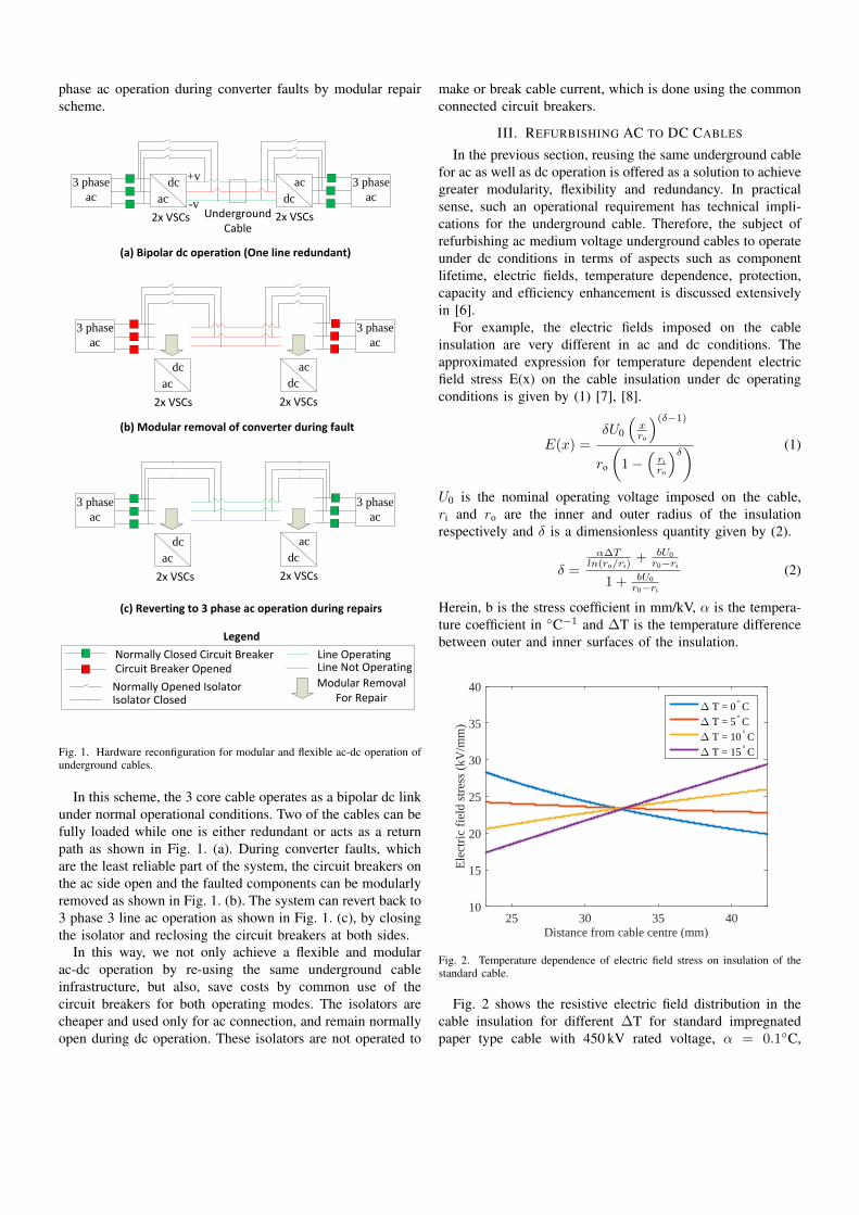
phase ac operation during converter faults by modular repairscheme.
dc
ac
ac
dc
2x VSCs 2x VSCs
3 phase
ac
+v
-v
3 phase
ac
3 phase
ac
3 phase
ac
dc
ac
2x VSCs
ac
dc
2x VSCs
3 phase
ac
3 phase
ac
dc
ac
2x VSCs
ac
dc
2x VSCs
Isolator Closed
UndergroundCable
(a) Bipolar dc operation (One line redundant)
(b) Modular removal of converter during fault
(c) Reverting to 3 phase ac operation during repairs
Normally Closed Circuit BreakerCircuit Breaker Opened
Normally Opened Isolator Modular Removal For Repair
Line OperatingLine Not Operating
Legend
Fig. 1. Hardware reconfiguration for modular and flexible ac-dc operation ofunderground cables.
In this scheme, the 3 core cable operates as a bipolar dc linkunder normal operational conditions. Two of the cables can befully loaded while one is either redundant or acts as a returnpath as shown in Fig. 1. (a). During converter faults, whichare the least reliable part of the system, the circuit breakers onthe ac side open and the faulted components can be modularlyremoved as shown in Fig. 1. (b). The system can revert back to3 phase 3 line ac operation as shown in Fig. 1. (c), by closingthe isolator and reclosing the circuit breakers at both sides.
In this way, we not only achieve a flexible and modularac-dc operation by re-using the same underground cableinfrastructure, but also, save costs by common use of thecircuit breakers for both operating modes. The isolators arecheaper and used only for ac connection, and remain normallyopen during dc operation. These isolators are not operated to
make or break cable current, which is done using the commonconnected circuit breakers.
III. REFURBISHING AC TO DC CABLES
In the previous section, reusing the same underground cablefor ac as well as dc operation is offered as a solution to achievegreater modularity, flexibility and redundancy. In practicalsense, such an operational requirement has technical impli-cations for the underground cable. Therefore, the subject ofrefurbishing ac medium voltage underground cables to operateunder dc conditions in terms of aspects such as componentlifetime, electric fields, temperature dependence, protection,capacity and efficiency enhancement is discussed extensivelyin [6].
For example, the electric fields imposed on the cableinsulation are very different in ac and dc conditions. Theapproximated expression for temperature dependent electricfield stress E(x) on the cable insulation under dc operatingconditions is given by (1) [7], [8].
E(x) =δU0
(xro
)(δ−1)
ro
(1−
(riro
)δ) (1)
U0 is the nominal operating voltage imposed on the cable,ri and ro are the inner and outer radius of the insulationrespectively and δ is a dimensionless quantity given by (2).
δ =
α∆Tln(ro/ri)
+ bU0r0−ri
1 + bU0r0−ri
(2)
Herein, b is the stress coefficient in mm/kV, α is the tempera-ture coefficient in C−1 and ∆T is the temperature differencebetween outer and inner surfaces of the insulation.
Distance from cable centre (mm)25 30 35 40
Ele
ctri
c fi
eld
stre
ss (
kV/m
m)
10
15
20
25
30
35
40
∆ T = 0° C
∆ T = 5° C
∆ T = 10° C
∆ T = 15° C
Fig. 2. Temperature dependence of electric field stress on insulation of thestandard cable.
Fig. 2 shows the resistive electric field distribution in thecable insulation for different ∆T for standard impregnatedpaper type cable with 450 kV rated voltage, α = 0.1C,

b=0.03 mm/kV, ri = 23.2 mm and ro = 42.4 mm [8].
As the temperature difference increases, the electric fieldstarts reducing at the inner insulation surface and increasingat the outer until it is completely inverted. It can be observedthat for ∆T = 10C the electric field distribution in theinsulation is almost flat. It follows that at specific temperaturedistributions, it is possible to increase the operating voltageof the cable to obtain the same maximum field.
The electric field distribution for cables operating underdc voltage illustrated here are for a high voltage XLPEstandard cable used in [8]. However, the same principles ablyfor medium voltage XLPE cables. In [6], the novel idea oftemperature dependent dynamic voltage rating is establishedthat takes into account the varying electric field distributionfor a medium voltage 11 kV XLPE cable.
IV. CAPACITY ENHANCEMENT
Higher power transfer capacity can be achieved with a dclink as compared to ac due to enhanced voltage rating [9],[10], atleast by
√2. In [9], it is offered that the dc cable
transmission capacity enhancement is 294% as against theexisting three phase double circuit ac system. The currentrating enhancement due to thermal proximity is also takeninto account to reach this number.
While it can be recognized that some capacity gains canrealistically be achieved, a more comprehensive study may berequired [6]. For example, different system configurations canlead to different capacity gains, and sometimes even reduction.
Table I highlights the impact of system topology on capacityenhancement. In this only voltage rating enhancement istaken into account.
TABLE ITOPOLOGY DEPENDENT CAPACITY ENHANCEMENT AT UPF
AC Circuit DC Topology Ground Return Enhancement %
Single, 3 line Monopolar Yes√2 41
Double, 3 line Monopolar Yes√2 41
Single, 3 line Bipolar No (2√2)/3 -7
Double, 3 line Bipolar No√2 41
Therefore, for DNOs to ascertain the gains of shifting todc using the existing ac infrastructure, influence of initial andfinal system topology, the consequences of the choice suchas ground return and voltage enhancement and the associatedtrade-offs such as component lifetime reduction must beknown [11]. The subject of this discussion is explored in [6].
Furthermore, an accurate representation of the realisticcapacity gains must also include factors other than voltagerating enhancement and topology, such as:
• Current rating enhancement: skin effect, dielectric losses,thermal proximity effect and capacitive current.
• Voltage regulation with varying line lengths and cablecross-sectional area.
• Power Factor at load sideEquations meticulously taking into account all the asso-
ciated factors while imposing the rated cable current at thesending end of the transmission link have been derived in [12].The results describing the capacity enhancement taking intoaccount all the listed factors with different system topologies,varying cable lengths and cross-sectional areas are presentedin [13].
V. DC LINK CONTROL AND GRID INTEGRATION
Since the objective of this project is to finally benefit fromgrid hybridization using reconfigurable dc links at mediumvoltage level in existing ac distribution networks, interfacinginfrastructure, converter topologies, control functionalities andancillary services are an integral part of the research study. Thefollowing research aspects are important from this context:
• Interfacing options for dc link integration with predom-inantly ac distribution grid based on converter topology,efficiency, costs, protection and reliability of the system.
• Point to point dc link connection feasibility and whetheropportunities exist to extend the infrastructure to ameshed dc grid with integrated renewable energy sources.
• Power balance, bi-directionality and voltage support us-ing the dc link during normal operation and its subsequentimpact on the stable ac grid operation.
• Protection mechanism during a short circuit at differentgrid locations, both at ac and dc side.
The converter topology itself can be voltage source converters(VSC) of two level, three level neutral clamped or multilevelconverters, controlled using dq transformation of the measuredgrid voltage, output converter current and the dc link volt-age [14].
VI. CONCLUSIONS
In this document, the concept of reconfigurable dc links isdescribed. The benefits corresponding to flexibility, modularityand redundancies is highlighted. The aspects associated withrefurbishing ac cables to operate under dc conditions are alsomentioned. The idea of capacity enhancement as a possibleadvantage of employing dc links in distribution networks isput forth. Finally, control functionalities and grid integrationof the dc links is expressed as an important research directiontowards realizing a working reconfigurable dc link technologyin the existing ac distribution grid in order to achieve hybridoperation.
ACKNOWLEDGEMENTS
The authors would like to acknowledge Mr. Epameinon-das Kontos and Dr. Armando Rodrigo Mor for their inputs,with which the framework of the cited publications ([5]-[13]) was established. We are thankful to dutch distribu-tion network operator (DNO) representatives from Alliander(Dr. Maarten Van Riet, Dr. Frans Provoost and Dr. Irina Mel-nik) and Enexis (Dr. Johan Morren) for workshop feedback.

Authors would also like to thank all the partners of theFLINK project funded by TKI switch2smartgrids, includingTU Eindhoven and DNV-GL under the supervision of Dr. ErikC.W. de Jong.
APPENDIX
Based on the author’s research, the following handoutwith discussion points for the workshop feedback with utilityoperators was prepared:
1) What can reconfigurable dc links offer in terms ofoperability and flexibility to the DNOs? The impact ofinstalling such links on conventional grids must also beexplored.
• What are the benefits associated with research pur-poses?
• How and what kind of flexibility and redundanciesbe incorporated using reconfigurability?
• What are the possibilities of grid voltage support,active and reactive power injection?
• What are the protection and integration aspects tobe looked into?
2) What kind of dc link configurations can be employed(monopolar/bipolar/homopolar) according to the existingsystems?
3) What specific situations DNOs may have encounteredin which reconfigurable dc links can be advantageous,for example, in terms of network de-congestion andaddressing local power deficits?
4) Is refurbishing ac to dc lines relevant in context ofcapacity enhancement?
5) What control functionalities should the dc link converterhave?
REFERENCES
[1] D. E. Olivares, A. Mehrizi-Sani, A. H. Etemadi, C. a. Canizares, R. Ira-vani, M. Kazerani, A. H. Hajimiragha, O. Gomis-Bellmunt, M. Saeed-ifard, R. Palma-Behnke, G. a. Jimenez-Estevez, N. D. Hatziargyriou,“Trends in Microgrid Control, ” IEEE Transactions on Smart Grid, 2014.
[2] J. J. Justo, F. Mwasilu, J. Lee, J.-W. Jung, “Ac-microgrids versus dc-microgrids with distributed energy resources: A review, ” Renewableand Sustainable Energy Reviews, 2013.
[3] G.R. Chandra Mouli, P. Bauer, M. Zeman, “System design for a solarpowered electric vehicle charging station for workplaces,” in AppliedEnergy, Volume 168, 15 April 2016, Pages 434-443.
[4] A. Werth, N. Kitamura, K. Tanaka, “Conceptual Study for Open En-ergy Systems: Distributed Energy Network Using Interconnected DCNanogrids, ” IEEE Transactions on Smart Grid, 2015.
[5] A. Shekhar, L. Ramırez-Elizondo, E. Kontos, A. Rodrigo Mor and P.Bauer, “Flexible and Hybrid MV and LV Distribution Grids with Recon-figurable DC Links, ” Energy Congress and Expo, IEEE, Milwaukee,WI, Submitted, 2016.
[6] A. Shekhar, A. Rodrigo Mor, E. Kontos, L. Ramırez-Elizondo and P.Bauer, “Refurbishing Existing MVAC Distribution Cables to OperateUnder DC Conditions, ” Power Electronics and Motion Control Con-ference and Exposition (PEMC) 17th International, Varna, Submitted,2016.
[7] M. M. Mazzanti, G., Extruded Cables for High-Vollage Direcl-CurrenlTransmission: Advances in Research and Development. 2013.
[8] M. Jeroense and P. Morshuis, “Electric fields in hvdc paper-insulatedcables,” Dielectrics and Electrical Insulation, IEEE Transactions on,vol. 5, pp. 225–236, Apr 1998.
[9] J. Arrillaga, “High Voltage Direct Current Transmission ”, vol. SecondEdition, 2008.
[10] D.M. Larruskain, I. Zamora, A.J. Mazon, O. Abarrategui, J. Monasterio,“Transmission and Distribution Networks: AC versus DC, ”
[11] F. Krueger, Industrial High Voltage. Delft University Press, 1992.[12] A. Shekhar, L. Ramırez-Elizondo, E. Kontos, A. Rodrigo Mor and P.
Bauer, “Power Transfer Computations for Medium Voltage AC Linkby Imposing Rated Current at Sending End, ” Power Electronics andMotion Control Conference and Exposition (PEMC) 17th International,Varna, Submitted, 2016.
[13] A. Shekhar, E. Kontos, L. Ramırez-Elizondo, A. Rodrigo Mor and P.Bauer, “Capacity Enhancement in Transmitted Power Using DC Linksin MVAC Distribution Grids, ” Energy Congress and Expo, IEEE,Milwaukee, WI, Submitted, 2016.
[14] Amirnaser Yazdani, Reza Iravani, “Voltage-sourced Converters In PowerSystems - Modeling, Control, and Applications, ” Wiley, IEEE Press,2010.

Long-Term Planning of Industrial MicrogridsCharline Stevanoni, Francois Vallee,
Zacharie De Greve and Olivier DebleckerUniversity of Mons, Faculty of Engineering
Electrical Power Engineering UnitBoulevard Dolez 31, 7000 Mons, Belgium
Email: [email protected]
Pascal CounesonDecube Consult
Quai du Pont Canal 3,7110 Strepy-Bracquegnies, Belgium
Email: [email protected]
Abstract—This paper deals with the context and objectives ofthe long-term planning of industrial microgrids. A first flowchartfor the development of a tool helping to the setting up of industrialmicrogrids is presented. The imagined methodology allows takinginto account the different (possibly conflicting) objectives ofthe microgrid stakeholders, by seeking an equilibrium froma game theoretical perspective. Beforehand, the role of eachstakeholder as well as the decisions they can take have to bewell-defined through an interaction model. The description ofsuch an interaction model is developed in this paper.
I. INTRODUCTION
In order to respond to the plan ”20-20-20” decided bythe European Union and to the current society willingnessof moving towards a greener environment thanks to thereduction of nuclear electricity production, recent yearshave witnessed a large deployment of Renewable EnergySystems (RESs). The network has therefore undergone achange of paradigm in which the electricity production is notcentralized anymore but distributed in the network. However,the proliferation of RESs is limited because of the intermittentoperation of some of them, such as solar photovoltaic (PV)and wind generation units. Those fluctuating energies maycause troubles in transmission and distribution networks.Moreover, the fixed loads of the network have to be fedcontinually and may not face a lack of supply. Those reasonsinvolve that the proliferation of RESs is not possible withouta smart management [1] and the use of Energy StorageSystems (ESSs) to allow flexibility. In order to integratenew productions and load management in the network, thenotion of microgrid is more and more widespread. Accordingto [2], a microgrid is ”a group of interconnected loads anddistributed energy resources (DERs) with clearly definedelectrical boundaries that acts as a single controllable entitywith respect to the grid and can connect and disconnect fromthe grid to enable it to operate in both grid-connected orisland modes”. In this definition, DERs include distributedgenerations (DGs), RESs and ESSs. Microgrids are morethan simple backup generation because they can provide awide range of benefits at a larger scale and they are moreflexible [2]. Indeed, microgrids can be used as a supportfor the distribution network performance such as reliability,resiliency and power quality. The installed microgrid world’scapacity was about 1.1 GW in 2012 and is estimated to
be 4.7 GW in 2017 [2]. In Europe, microgrids that areoften developed in existing networks must be adapted tothe existing configuration and are connected to the generalnetwork. However, the microgrid development is also moreand more intended in emerging countries without initialinfrastructure such as in Africa. In this case, they are builtfrom nothing and operated in island mode [3].
In this work, grid-connected microgrids are considered at aMedium Voltage (MV) industrial level and not at a residentialone. A motivation for industrial microgrids development isto decrease the electricity bill for companies which take partto the microgrid. Indeed, the MV electricity purchase price ismore and more expensive for industries, especially in Belgium.A survey conducted in 2016 showed that, for belgian industrialcompanies, their electricity bill is 16 to 40 % more expensivethan the mean one of the neighbour countries (France, Hollandand Germany) taking into account taxes and network costswhich are also consequent in Belgium, as shown in Fig. 1 [4].
Fig. 1. Electricity Price in 2016 (e/MWh) (profil baseload 100 GWh) [4].
Therefore, investing in decentralized generation such aswind or PV may become interesting for industrial companies.The industries which install those kinds of productions wantto improve their self-consumption, i.e. to make profitable theirinvestment by trying to consume locally all their generatedelectricity and, consequently, to avoid selling it at a cheaperprice than the one paid for direct consumption from the grid.Indeed, the excess of generation is sold to the distributionnetwork at a very low price (market price) compared with thepurchase price (market price + taxes + network price).
As an example, the company partially funding this workpreviously invested in a PV installation of 250 kWp. However,after a few years of operation, the objective of 100% self-consumption has not yet been achieved due to the highvariability of sunshine in Belgium. Indeed, PV generationwas sometimes not sufficient to fully supply the consumption,whereas reverse power flows occurred at other times. Forsuch an installation, the residual produced electricity has tobe sold to the distribution network, but the selling price isvery low compared to the purchasing one. Such a differencerepresents a shortfall for the company. One way to reduce itis to consider electricity storage facilities. However, a firststudy has shown that storage batteries are still too expensiveto be cost-effective for a single company [5].
At a larger scale, in an industrial estate, the consumptionprofiles of the companies can be complementary. Theinstallation of a single storage unit shared among severalcompanies could therefore be more profitable. In suchan industrial estate, in which several companies wouldmassively invest in RESs, a pooling of the production unitscould be considered in a microgrid framework. However,the companies would like to know if such a microgridcould be profitable over the years considering their wishto keep a connection with the distribution network and thecosts that this involves. In order to meet this demand, it isnecessary to plan at a long-term horizon (typically up to20 years) the evolution of the microgrid. In this context,the present work aims at providing a tool for the settingup of industrial MV microgrids with a minimization ofthe electricity costs while taking into account the individual(possibly conflicting) objectives of the microgrid stakeholders.
This paper is organized as follows. In section II, the method-ology of the long-term planning tool is described, includingthe management of the microgrid and the costs objectivefunctions formulation. Section III then presents a first modelof interaction in detail i.e. the role of each stakeholder andthe decisions they can take. Finally, conclusions are drawn andperspectives for future work are given.
II. METHODOLOGY OF THE LONG-TERM PLANNING TOOL
In an industrial microgrid, several parties have to be con-sidered. These are the individual prosumers (which are theconsumers who possibly own their local RESs), the Dis-tribution System Operator (DSO) and the Industrial EstateOperator (IEO). In this contribution, the microgrid is managedby an aggregator. One of the goals of this work, which isalso one of its originalities, is to put as aggregator eachstakeholder of the microgrid alternately. Depending on theaggregator, the management strategy of the microgrid will bedifferent. In addition, two additional strategies are consideredin which the aggregator is, respectively, an independent entityor a state organization. Those strategies are detailed in thispaper. Moreover, for each stakeholder of each strategy, an
annual objective function VaN is written and a global objectivefunction NPV for Net Present Value is written over Ntot years.
A. Costs objective function formulation
The annual objective function VaN for each stakeholder isthe net Value for year N, which is defined by Eq. (1) as thedifference between the revenues and the expenses during theyear N. This expression (inspired from [6]) has two parts: anhourly part (terms in parentheses) and an annual part.
VaN =
(h=8760∑h=1
(Rh,N − Ch,N )
)− CmN − CsN − CiN (1)
where Rh,N and Ch,N are, respectively, the revenue and costper hour, CmN is the annual maintenance cost, CsN is theannual additional cost and CiN is the annual investment cost.
In order to analyze the profitability of the microgrid overNtot years, the NPV is used because costs and revenues inyear 1 are not equivalent to those of the future, as timehas an impact on the value of cash flows. After computingVaN for year N, the Present Value (PVN ) is computed takinginto account the discounting of future cash flows through thediscount rate i and they are cumulated over the planning timehorizon of Ntot years to obtain the NPV (2):
NPV =
Ntot∑N=1
PVN =
Ntot∑N=1
1
(1 + i)NVaN (2)
Thus, a positive NPV indicates that the project is makingbenefits over the planning period.
B. Strategies
The goals pursued by each aggregator are described in thispart. They differ by the direct benefits they expect from themicrogrid (sign of the NPV).
Strategy I (aggregator = DSO): The DSO intends tomake benefits by decreasing transmission costs, even if themicrogrid client electricity bill is expected to decrease. Its roleis also to maintain or improve the quality of the electricityin the distribution system and in the microgrid and to ensuretheir stability ⇒ NPV > 0;
Strategy II (aggregator = a single or a group ofprosumers): They want to make benefits thanks to areduction of the difference between the actual purchasingprice of electricity to supply their needs and the actualselling price of the excess of electricity produced by theirRESs. In that way, an improvement of their self-consumption,i.e. a decrease of the electricity amount exchanged withthe distribution network, is pursued. They can also provideservices to the DSO to obtain an extra revenue ⇒ NPV > 0;
Strategy III (aggregator = IEO): IEO wants to optimizethe proper operation of the microgrid by promoting theRESs of the prosumers. Its first interest is not to make direct
benefits but to provide a social global welfare and to developits industrial estate by attracting new companies in the areathanks to an attractive price of electricity (socio-economicdimension) ⇒ NPV <,= or > 0;
Strategy IV (aggregator = an independant entity): Itsobjective is to make pure benefits thanks to a maximization ofthe revenues coming from the microgrid and the optimizationof its proper operation ⇒ NPV > 0;
Strategy V (aggregator = a state organization): Itsobjective is to manage the microgrid with the goal ofoptimizing its proper operation and keeping a social globalwelfare between all the stakeholders without making anybenefits ⇒ NPV = 0.
In conclusion to this point, it is obvious that the choice ofthe aggregator will influence the decisions to be undertaken inthe management process of the microgrid.
C. General organization of the decision-making toolEach management strategy described above is studied under
a large number of scenarios [7] which represent possibleevolutions of the microgrid in terms of consumption andproduction profiles, as well as in terms of new RESs by theprosumers (note that RESs are supposed to be only placedby the prosumers and not by the DSO). Each scenario iscreated on a planning period of 20 years (which approximatelycorresponds to the life time of RESs). For each hour ofeach scenario, a load flow is performed and the state of themicrogrid is defined through technical [8] and reliability [9]indicators. At the end of the load flow, the flowchart presentedin Fig. 2 is applied. The aggregator and the stakeholders re-cover all those indicators and analyze them. Each one will haveto choose between several decisions among the possibilitiesarising from the interaction model of the concerned strategy,such as investments or flexibility services. Every decision isassociated with a price that has to be taken into account in (1)and, thus, in (2) over 20 years. Following the level of benefit,those decisions are classified in a preference order. Pratically,the final decision will be found thanks to the computationof an equilibrium between all the stakeholders using a gameextracted from the Game Theory [10].
Fig. 2. Flowchart for each microgrid stakeholder (including the aggregator).
Fig. 3. Interaction model for strategy I.
III. A FIRST INTERACTION MODEL
For each strategy, it is necessary to define the interactionmodel between all the stakeholders (with their roles anddecisions), as well as to establish the cost terms in detail.In this paper, an interaction model for the first strategy(aggregator = DSO) is presented (Fig. 3). There are three kindsof interactions: cyan arrows represent interactions related tothe cost of electricity exchanged through the External Market(EM) and the Internal Market (IM), the red double arrowrepresents flexibility services and the purple arrows depict themicrogrid development.
A. Electricity exchanges
The privileged electricity exchanges are those inside themicrogrid. The prosumers who own a RES use their owngeneration in the first instance. Three cases can then appearfor each prosumer. In the first situation, the production andthe consumption are equal and the balance is respected. In thesecond case, there is more generation than consumption and,consequently, the prosumer needs to sell its electricity surplus(prosumer = seller). In the last configuration, generationis lower than consumption and the prosumer has to buyelectricity through the aggregator (prosumer = buyer). Forthe first case, there are no exchanges but, in the two othercases, exchanges have to be managed by the aggregator in theIM. As shown in Fig. 4, each seller gives a minimal priceat which he accepts to sell its electricity surplus and eachbuyer gives a maximal purchase price at which he accepts topurchase the electricity to fully provide its own consumption.Those bounds are then centralised by the aggregator. In thiswork, the optimization part done in the IM is not handled andwill be considered as a ”black box”. The outputs of this blackbox are purchase (Prpurchase,µ) and sale (Prsale,µ) pricesat which prosumers can buy and sell electricity inside themicrogrid. Those prices are computed in such a way that theaggregator is paid for its operator role by a fee Prfee,IM ,which is a percentage of the difference between Prpurchase,µand Prsale,µ.
Fig. 4. Electricity exchanges inside the microgrid.
When the exchanges inside the microgrid are done, thereare three possibilities: either there is a balance (all the gener-ation is used and all the consumption is provided inside themicrogrid), or there is still an electricity surplus (more globalgeneration than the global consumption) or there is a lack ofelectricity (the global consumption is higher than the globalgeneration). In the two last cases, it will be necessary to haveexchanges between the microgrid and the distribution network.Fig. 5 shows how the costs of those exchanges are defined.
Fig. 5. Electricity exchanges between the distribution network and themicrogrid.
The case with a lack of electricity in the microgrid ispresented using the green arrows (on the right part of Fig.5). In the EM, Prfixed is the base price of electricity withthe transmission costs and state taxes. To that price, theDSO adds the distribution cost (PrDSO,in), but since theaggregator is the DSO here, it can be imagined that this pricewill be flexible (the DSO can decide to put it equal, higheror lower than the classical actual price). Then, in the IM, asone objective of the IEO is to make electricity price moreinteresting for the prosumers, IEO could help to reduce theelectricity purchase price thanks to a contribution PrIEO,in.As a result, the electricity purchase price Prpurchase,grid ispaid by the aggregator. The aggregator then grants himselfwith a fee Prfee,in and sells the electricity to the prosumersaccording to their needs (Prpurchase,grid,pros).
Consider now the case in which there is an electricitysurplus from the microgrid. This exchange is presented bythe blue arrows in Fig. 5. First, the prosumers give tothe aggregator their selling price (Prsale,grid,pros). Then theaggregator puts its fee (Prfee,out) and the selling price ofelectricity is defined (Prsale,grid). Afterwards, the IEO takesback a flexible part of its contribution through the increasingof the selling price with the value PrIEO,out. Finally, in thisparticular strategy with the DSO as aggregator, the DSO addsits distribution cost PrDSO,out in the EM. Note that the pricesin red on Fig. 5 are flexible, i.e. their values depend on thedecision of the concerned stakeholder.
B. Flexibility services
In reference [11], the flexibility is defined as a ”modificationof injection or consumption in reaction to an external price(from the DSO) or to the activation of a signal in order toprovide services”. The red double arrow in Fig. 3 representsthe flexibility services exchanges between all the stakeholdersfrom the distribution network and from the microgrid. For aneasier understanding of those services, they are summarizedin tables inspired from [12] and are divided between themicrogrid needs (Table I) and the distribution network needs(Table II). In those tables, the second column indicates whichservice(s) can be done to cater the needs. The third columnindicates how the service is managed and the last two columnsspecify the provider and user of the service, respectively.Note that when the provider or the user is the aggregator,it can be either on its behalf or on behalf of prosumers. Inthe second case, the aggregator charges a fee as operator offlexibility service and the costs or the revenues are sharedbetween the concerned prosumers. In the economical record,the costs linked to flexibility services have to be comparedwith investment costs to make the more profitable choice.
From the microgrid point of vue (Table I), the first needis obviously the electricity which can be provided either bythe distribution network or by other prosumers inside themicrogrid. The exchange mechanisms are those explained insection III. A. The second need is to avoid congestion and anoversize of the microgrid. There are several ways to supply thisneed such as the adjustment of the RES generation and the loadshifting of some prosumers. The goal of this service is to allowthe aggregator to avoid investments inside the microgrid suchas line reinforcement or reconfiguration. A special contractis done between the prosumers and the aggregator in orderto fix the cost and the conditions of that service. Anotherservice is the voltage control inside the microgrid. Indeed,overvoltage can damage prosumer’s equipments. This voltagecontrol is done locally by prosumers thanks to the managementof active and reactive powers. Again, this service is managedby the aggregator who will take a fee. The penultimate serviceis the management of the RESs and ESSs by the aggregator.When the aggregator is the DSO, it knows the production andconsumption previsions and thus he has to manage the RESsand ESSs integration in order to maximize it. Another way to
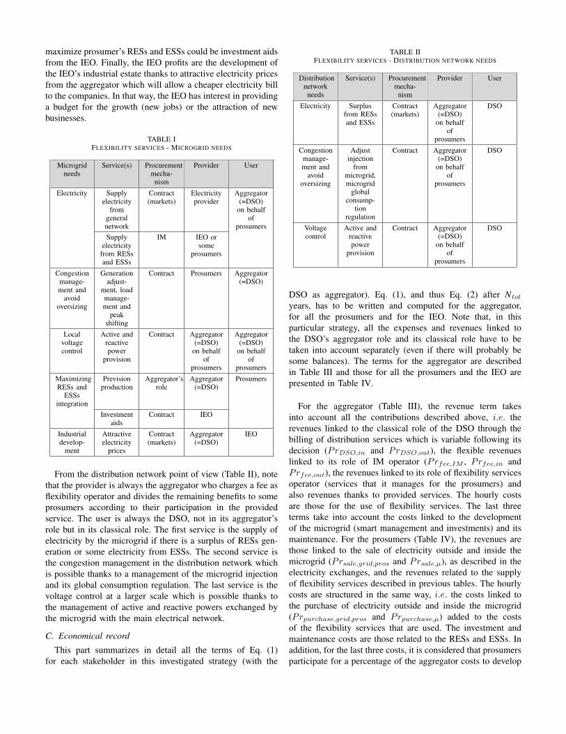
maximize prosumer’s RESs and ESSs could be investment aidsfrom the IEO. Finally, the IEO profits are the development ofthe IEO’s industrial estate thanks to attractive electricity pricesfrom the aggregator which will allow a cheaper electricity billto the companies. In that way, the IEO has interest in providinga budget for the growth (new jobs) or the attraction of newbusinesses.
TABLE IFLEXIBILITY SERVICES - MICROGRID NEEDS
Microgridneeds
Service(s) Procurementmecha-nism
Provider User
Electricity Supplyelectricity
fromgeneralnetwork
Contract(markets)
Electricityprovider
Aggregator(=DSO)
on behalfof
prosumersSupply
electricityfrom RESsand ESSs
IM IEO orsome
prosumers
Congestionmanage-ment and
avoidoversizing
Generationadjust-
ment, loadmanage-ment and
peakshifting
Contract Prosumers Aggregator(=DSO)
Localvoltagecontrol
Active andreactivepower
provision
Contract Aggregator(=DSO)
on behalfof
prosumers
Aggregator(=DSO)
on behalfof
prosumers
MaximizingRESs and
ESSsintegration
Previsionproduction
Aggregator’srole
Aggregator(=DSO)
Prosumers
Investmentaids
Contract IEO
Industrialdevelop-
ment
Attractiveelectricity
prices
Contract(markets)
Aggregator(=DSO)
IEO
From the distribution network point of view (Table II), notethat the provider is always the aggregator who charges a fee asflexibility operator and divides the remaining benefits to someprosumers according to their participation in the providedservice. The user is always the DSO, not in its aggregator’srole but in its classical role. The first service is the supply ofelectricity by the microgrid if there is a surplus of RESs gen-eration or some electricity from ESSs. The second service isthe congestion management in the distribution network whichis possible thanks to a management of the microgrid injectionand its global consumption regulation. The last service is thevoltage control at a larger scale which is possible thanks tothe management of active and reactive powers exchanged bythe microgrid with the main electrical network.
C. Economical record
This part summarizes in detail all the terms of Eq. (1)for each stakeholder in this investigated strategy (with the
TABLE IIFLEXIBILITY SERVICES - DISTRIBUTION NETWORK NEEDS
Distributionnetworkneeds
Service(s) Procurementmecha-nism
Provider User
Electricity Surplusfrom RESsand ESSs
Contract(markets)
Aggregator(=DSO)
on behalfof
prosumers
DSO
Congestionmanage-ment and
avoidoversizing
Adjustinjection
frommicrogrid,microgrid
globalconsump-
tionregulation
Contract Aggregator(=DSO)
on behalfof
prosumers
DSO
Voltagecontrol
Active andreactivepower
provision
Contract Aggregator(=DSO)
on behalfof
prosumers
DSO
DSO as aggregator). Eq. (1), and thus Eq. (2) after Ntot
years, has to be written and computed for the aggregator,for all the prosumers and for the IEO. Note that, in thisparticular strategy, all the expenses and revenues linked tothe DSO’s aggregator role and its classical role have to betaken into account separately (even if there will probably besome balances). The terms for the aggregator are describedin Table III and those for all the prosumers and the IEO arepresented in Table IV.
For the aggregator (Table III), the revenue term takesinto account all the contributions described above, i.e. therevenues linked to the classical role of the DSO through thebilling of distribution services which is variable following itsdecision (PrDSO,in and PrDSO,out), the flexible revenueslinked to its role of IM operator (Prfee,IM , Prfee,in andPrfee,out), the revenues linked to its role of flexibility servicesoperator (services that it manages for the prosumers) andalso revenues thanks to provided services. The hourly costsare those for the use of flexibility services. The last threeterms take into account the costs linked to the developmentof the microgrid (smart management and investments) and itsmaintenance. For the prosumers (Table IV), the revenues arethose linked to the sale of electricity outside and inside themicrogrid (Prsale,grid,pros and Prsale,µ), as described in theelectricity exchanges, and the revenues related to the supplyof flexibility services described in previous tables. The hourlycosts are structured in the same way, i.e. the costs linked tothe purchase of electricity outside and inside the microgrid(Prpurchase,grid,pros and Prpurchase,µ) added to the costsof the flexibility services that are used. The investment andmaintenance costs are those related to the RESs and ESSs. Inaddition, for the last three costs, it is considered that prosumersparticipate for a percentage of the aggregator costs to develop
the microgrid (contract between the stakeholders). For the IEO(Table IV), the revenues are, on the one hand, PrIEO,outdefined above as a recovery of money when electricity is soldto the distribution network and, on another hand, the supply ofelectricity (flexibility service) thanks to their potential RESsand ESSs. Note that in this last case, their selling price isidentical to the one of the other prosumers (IEO takes part tothe IM on the same level as another producer). The hourly costis PrIEO,in which represents its contribution to the reductionof the electricity price inside the IM when the electricityis purchased to the EM. The maintenance costs are relatedto its own RESs and ESSs, whereas investment costs couldalso be related to investment aids provided to prosumers.An additional annual revenue is taken into account in theCsN ’s row thanks to the industrial development. Note thatthis last revenue is not an hourly revenue and is consequentlyconsidered as a negative annual additional cost. Moreover,PrIEO,in and PrIEO,out could possibly be equal to zero.
TABLE IIIDETAILS OF THE COST TERMS FOR THE AGGREGATOR
Terms aggregator = DSO
Rh,N PrDSO,in + PrDSO,out + Prfee,IM + Prfee,in +Prfee,out + flexibility provider + fees as operator of theflexibility services
Ch,N Flexibility user
CmN Grid maintenance + ESSs maintenance
CsN Grid intelligence
CiN Shared ESSs + lines reinforcement + microgrid reconfigu-ration
TABLE IVDETAILS OF THE COST TERMS FOR THE OTHER STAKEHOLDERS
Terms Prosumers IEO
Rh,N Prsale,grid,pros +Prsale,µ + Flexibilityprovider
PrIEO,out + Flexibilityprovider
Ch,N Prpurchase,grid,pros +Prpurchase,µ + Flexibilityuser
PrIEO,in
CmN RESs and ESSs mainte-nance + % aggregator’sCmN
RESs and ESSs mainte-nance
CsN % aggregator’s CsN (-%) of industrial develope-ment (=revenue)
CiN RESs + ESSs + % aggrega-tor’s CiN
RESs + ESSs + investmentaids
IV. CONCLUSION AND FUTURE WORK
This paper deals with the planning of an MV industrialmicrogrid connected to the general network. As many stake-holders take part into those kinds of microgrids, it seemsimportant to consider the objectives and the welfare of eachone. The presented methodology includes a microgrid managercalled aggregator. The originality of this work is to put asaggregator successively each stakeholder in order the see how
the planning of the microgrid is impacted. Indeed, the choiceof the aggregator will influence the decisions to be undertakenin the management process. Concerning those decisions, theyare defined through an interaction model for each strategy.This paper described only the case in which the aggregatoris the DSO. This interaction model summarizes the electricityexchanges, the flexibility services between the microgrid andthe distribution network and details the economical recordfor this strategy. Thanks to this interaction model, possibledecisions are defined, attached to a cost and can be compared.The computation of the Net Present Value defined in thispaper for each stakeholder, including the aggregator, allowsthe ranking of those decisions in a preference order and afinal equilibrium can be computed following the Game Theoryrules. Currently, the imagined tool is deterministic but theobjective of the work is to make preventive planning takinginto account all the possible uncertainties as the installation ofRESs within the microgrid.
ACKNOWLEDGEMENT
The authors would like to thank all the partners of thisthesis. This work is realised within the University of Monsin collaboration with IDEA (inter-communal structure whichis an industrial estate operator) and the Engineering andConsulting office Decube Consult.
REFERENCES
[1] M. Liserre, T. Sauter and J. Y. Hung, Future Energy Systems, IEEEIndustrial Electronics Magazine, March 2010.
[2] S. Parhizi, H. Lofti, A. Khodaei and S. Bahramirad, State of the Art inResearch on Microgrids: A Review, IEEE Access, vol 3, 2015.
[3] B. Martin, E. De Jaeger, F. Glineur and A. Latiers, A dynamic program-ming approach to multi-period planning of isolated microgrids, In proc.ISESO International Symposium on Energy System Optimization, 2016.
[4] Federation of Belgian industrial energy consumers, Less taxes on electric-ity for industrial consumers in our neighbouring countries, Press release,April 2016, http://www.febeliec.be
[5] C. Stevanoni, Study of interest for the shared storage of photovoltaic elec-trical energy in an industrial estate (French), Internal report, Universityof Mons, Faculty of Engineering, Power Electrical Department, 2015.
[6] M.H. Moradi, M. Eskandari and S.M. Hosseinian, Optimal StrategyOptimization in an Optimal Sized Smart Microgrid, IEEE Trans. on smartgrid, vol. 6, no. 3, May 2015.
[7] H. Dutrieux, Multi-year planning methods of the distribution networks.Application to the technical-economic analysis for the integration solu-tions of the intermittent renewables energies (French), PhD Thesis, Ecolecentrale de Lille, 2015.
[8] L.F. Ochoa, A. Padilha-Feltrin and G. P. Harrison, Evaluating DistributedGeneration Impacts with a Multiobjective Index, IEEE Trans. on PowerDelivery, vol. 21, no. 3, July 2006.
[9] S. Wang, Z. Li, L. Wu, M. Shahidehpour and Z. Li, New Metrics forAssessing the Reliability and Economics of Microgrids in DistributionSystem, IEEE Trans. on Power Systems, vol. 28, no. 3, August 2013.
[10] Martin J. Osborne, An Introduction to Game Theory, Departments ofEconomics, University of Toronto, Oxford University Press, 2003.
[11] S. Mathieu, Flexibility services in the electrical system, PhD Thesis,University of Liege, 2015.
[12] European Distribution System Operators for Smart Grids,Flexibility: the role of DSOs in tomorrow’s electricity market, 2014,http://www.edsoforsmartgrids.eu/wp-content/uploads/public/EDSO-views-on-Flexibility-FINAL-May-5th-2014.pdf

Linear Representation of Preventive and CorrectiveActions in OPF Models
T. Van Acker, and D. Van HertemResearch Division ELECTA, Department of Electrical Engineering (ESAT), KU Leuven
Leuven, [email protected]
Abstract—Several preventive and corrective actions are avail-able to the system operator enabling reliability managementwithin a power system. The objective of reliability management istrying to exploit a power system with a minimal socio-economiccost while taking into account the possibility of a contingency onone or multiple elements (e.g. branch, generator) and changingoperating conditions. The operating cost is minimized by opti-mally choosing between all available preventive and correctiveactions, most commonly facilitated by an optimal power flowalgorithm. This paper presents an overview of the most relevantactions for AC power systems and how to efficiently implementthem in an OPF environment.
I. INTRODUCTION
Power system reliability management can be defined asa sequence of decisions which are taken under uncertaintyin order to meet a certain reliability criterion. A reliabilitycriterion is a principle imposing a basis to determine whetheror not the reliability level of a given operating state of thepower system is acceptable [1]. This can be expressed as aset of constraints that must be satisfied by the decisions takenby the system operator (SO). An example of such a reliabilitycriterion is the N-1 criterion, which states that the consideredpower system must be able to withstand any credible singlecontingency (e.g. the loss of a generator), in such a waythat a new operational set point can be reached withoutviolating the security constraints of that power system. TheSO makes use of a power systems inherent flexibility optionsto reach a new operation set point. These flexibility optionsare also referred to as actions and the distinction can be madebetween preventive and corrective actions. Preventive actionsare those flexibility options preventively activated to adaptthe system state, anticipating all possible contingencies anduncertainticing the need for corrective operator interventionwhen a certain contingency occurs. Corrective actions arethose flexibility options available to adapt the system stateimmediately after a contingency has occurred, sufficientlyquick to avoid cascading of the event. It is the responsibilityof the SO to select the actions, both preventive and corrective,that result in an optimal reliability, which ideally leads to aminimal global socio-economic cost. Most efficiently, this isdone by implementing all considered actions in an OptimalPower Flow (OPF) [2], which is adapted to take the possibilityof contingencies into account. This type of OPF is generallyreferred to as a Security Constrained OPF (SCOPF) [3]. Thegeneral formulation of a SCOPF is given by (1)-(5):
minu0,uc
f(u0,uc) (1)
subject to: G0(x0, u0, y0) = 0 (2)H0(x0, u0, y0) ≥ 0 (3)Gc(xc, uc, yc) = 0 ∀c (4)Hc(xc, uc, yc) ≥ 0 ∀c (5)
In this formulation, u, x and y respectively represent thecontrol variables, state variables and parameters. The index0 and c indicate the preventive base case and the correctivecontingent cases. Equation (2)-(3) respectively ensure that thepower flow equations and the operating limits are respectedfor the preventive base case while (4)-(5) does this for theconsidered corrective contingent cases. This paper presentsan overview of available actions for AC power system andthe linear implementation of those actions in an SCOPFenvironment.
II. AVAILABLE ACTIONS IN AC POWER SYSTEMS
In this section, the most common available actions in an ACpower system are listed. There are four main type of actions:
1) Actions that affect the power balance in the system:generator redispatch, demand side management and loadcurtailment [4].
2) Topological actions influencing power flows through thesystem: phase shifting transformer control [5], switchingactions [6].
3) Reactive power and voltage management: generator volt-age set point changes, on-load tap changer transformercontrol.
4) Special protection schemes: Specific actions triggeredby specific grid related events.
This paper focusses on the first two types of actions.
A. Generator Redispatch
Generator redispatch uses the available upward anddownward power reserves in the power system to changethe power injection and consequently change the powerflows within the grid [7]. Generator redispatch can be usedto alleviate congestion or to compensate for a generatoroutage. The implementation of generator redispatch is verycase specific and depends on the market structure as well as
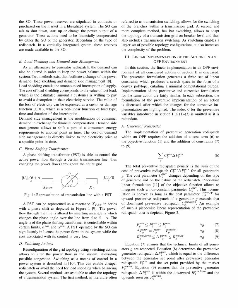
the SO. These power reserves are stipulated in contracts orpurchased on the market in a liberalized system. The SO canask to shut down, start up or change the power output of agenerator. These actions need to be financially compensatedby either the SO or the generator, depending on the type ofredispatch. In a vertically integrated system, these reservesare made available to the SO.
B. Load Shedding and Demand Side Management
As an alternative to generator redispatch, the demand canalso be altered in order to keep the power balance within thesystem. Two methods exist that facilitate a change of the powerdemand: load shedding and demand side management [8].Load shedding entails the unannounced interruption of supply.The cost of load shedding corresponds to the value of lost load,which is the estimated amount a customer is willing to payto avoid a disruption in their electricity service. The value ofthe loss of electricity can be expressed as a customer damagefunction (CDF), which is a non-linear function of load type,time and duration of the interruption.Demand side management is the modification of consumerdemand in exchange for financial compensation. Demand sidemanagement allows to shift a part of a consumers energyrequirements to another point in time. The cost of demandside management is directly linked to the electricity price ata specific point in time.
C. Phase Shifting Transformer
A phase shifting transformer (PST) is able to control theactive power flow through a certain transmission line, thuschanging the power flows throughout the entire grid.
|Us|∠θ + α
XPST
α
XL
|Ur|∠0
Fig. 1: Representation of transmission line with a PST
A PST can be represented as a reactance XPST in serieswith a phase shift as depicted in Figure 1 [9]. The powerflow through the line is altered by inserting an angle α whichchanges the phase angle over the line from δ to δ + α. Theangle α of the phase shifting transformer is controllable withincertain limits, αmax and αmin. A PST operated by the SO cansignificantly influence the power flows in the system while thecost associated with its control is very low.
D. Switching Actions
Reconfiguration of the grid topology using switching actionsallows to alter the power flow in the system, alleviatingpossible congestion. Switching as a means of control in apower system is described in [10]. This can enable cheaperredispatch or avoid the need for load shedding when balancingthe system. Several methods are available to alter the topologyof a transmission system. The first method, in literature often
referred to as transmission switching, allows for the switchingof the branches within a transmission grid. A second andmore complete method, bus bar switching, allows to adaptthe topology of a transmission grid on breaker level and thusalso includes transmission switching. As switching enables alarger set of possible topology configurations, it also increasesthe complexity of the problem.
III. LINEAR IMPLEMENTATION OF THE ACTIONS IN ANOPF ENVIRONMENT
In this section, the linear implementation in an OPF envi-ronment of all considered actions of section II is discussed.The presented formulation generates a finite set of linearconstraints which produces a search space in the form of aconvex polytope, entailing a minimal computational burden.Implementation of the preventive and corrective formulationfor the same action are fairly similar. In each subsection, theformulation of the preventive implementation of an actionis discussed, after which the changes for the corrective im-plementation are highlighted. The index 0 for the preventivevariables introduced in section I in (1)-(3) is omitted as it isredundant.
A. Generator Redispatch
The implementation of preventive generation redispatchwithin an OPF requires the addition of a cost term (6) tothe objective function (1) and the addition of constraints (7)to (9). ∑
g
Cprevg ∆P prev
g (6)
The total preventive redispatch penalty is the sum of thecost of preventive redispatch Cprev
g ∆P prevg for all generators
g. The cost parameter Cprevg changes depending on the type
of generator and on the nature of the redispatch. Piece-wiselinear formulation [11] of the objective function allows tointegrate such a non-constant parameter Cprev
g . This formu-lation is convex as long as the cost parameter Cprev,up
g forupward preventive redispatch of a generator g exceeds thatof downward preventive redispatch Cprev,down
g . An exampleof such a piece-wise linear representation of the preventiveredispatch cost is depicted Figure 2.
Pming ≤ P prev
g ≤ Pmaxg ∀g (7)
∆P prevg = P prev
g − Pmarketg ∀g (8)
Rprev,downg ≤ ∆P prev
g ≤ Rprev,upg ∀g (9)
Equation (7) ensures that the technical limits of all gener-ators g are respected. Equation (8) determines the preventivegenerator redispatch ∆P prev
g , which is equal to the differencebetween the generator set point after preventive generatorredispatch P prev
g and the set point provided by the marketPmarketg . Equation (9) ensures that the preventive generator
redispatch ∆P prevg is within the downward Rprev,down
g and theupwards reserves Rprev,up
g .
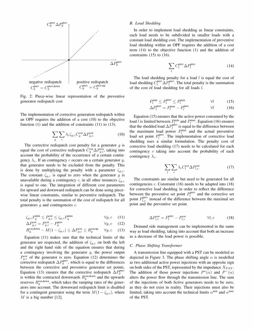
∆P prevg
Cprevg ∆P prev
g
negative redispatchCprev
g = Cprev,downg
positive redispatchCprev
g = Cprev,upg
Fig. 2: Piece-wise linear representation of the preventivegenerator redispatch cost
The implementation of corrective generation redispatch withinan OPF requires the addition of a cost (10) to the objectivefunction (1) and the addition of constraints (11) to (13).∑
g
∑c
λcζg,cCcorg ∆P cor
g,c (10)
The corrective redispatch cost penalty for a generator g isequal the cost of corrective redispatch Ccor
g ∆P corg,c, taking into
account the probability of the occurrence of a certain contin-gency λc. If an contingency c occurs on a certain generator g,that generator needs to be excluded from the penalty. Thisis done by multiplying the penalty with a parameter ζg,c.The constant ζg,c is equal to zero when the generator g isunavailable during a contingency c, in all other instances ζg,cis equal to one. The integration of different cost parametersfor upward and downward redispatch can be done using piece-wise linear constraints, similar to preventive redispatch. Thetotal penalty is the summation of the cost of redispatch for allgenerators g and contingencies c.
ζg,cPming ≤ P cor
g,c ≤ ζg,cPmaxg ∀g, c (11)
∆P corg,c = P cor
g,c − P prevg ∀g, c (12)
Rcor,downg −M(1− ζg,c) ≤ ∆P cor
g,c ≤ Rcor,upg ∀g, c (13)
Equation (11) makes sure that the technical limits of thegenerator are respected, the addition of ζg,c on both the leftand the right hand side of the equation ensures that duringa contingency involving the generator g, the power outputP corg,c of the generator is zero. Equation (12) determines the
corrective redispatch ∆P prevg , which is equal to the differences
between the corrective and preventive generator set points.Equation (13) ensures that the corrective redispatch ∆P prev
g
is within the contracted downwards Rcor,downg and the upwards
reserves Rcor,downg , which takes the ramping rates of the gener-
ators into account. The downward redispatch limit is disabledfor a contingent generator using the term M(1− ζg,c), whereM is a big number [12].
B. Load Shedding
In order to implement load shedding as linear constraints,each load needs to be subdivided in smaller loads with aconstant load shedding cost. The implementation of preventiveload shedding within an OPF requires the addition of a costterm (14) to the objective function (1) and the addition ofconstraints (15) to (16).∑
l
Cprevl ∆P prev
l (14)
The load shedding penalty for a load l is equal the cost ofload shedding Cprev
l ∆P prevl . The total penalty is the summation
of the cost of load shedding for all loads l.
Pminl ≤ P prev
l ≤ Pmaxl ∀l (15)
∆P prevl = Pmax
l − P prevl ∀l (16)
Equation (15) ensures that the active power consumed by theload l is limited between Pmin
l and Pmaxl . Equation (16) ensures
that the shedded load ∆P prevl is equal to the difference between
the maximum load power Pmaxl and the actual preventive
load set point P prevl . The implementation of corrective load
shedding uses a similar formulation. The penalty cost ofcorrective load shedding (17) needs to be calculated for eachcontingency c taking into account the probability of eachcontingency λc. ∑
l
∑c
λcCcorl ∆P cor
l,c (17)
The constraints are similar but need to be generated for allcontingencies c. Constraint (16) needs to be adapted into (18)for corrective load shedding in order to reflect the differencebetween the preventive set point P prev
l and the corrective setpoint P prev
l,c instead of the difference between the maximal setpoint and the preventive set point.
∆P corl,c = P prev
l − P corl,c ∀l, c (18)
Demand side management can be implemented in the sameway as load shedding, taking into account that both an increaseas a decrease of the load power is possible.
C. Phase Shifting Transformer
A transmission line equipped with a PST can be modeled asdepicted in Figure 3. The phase shifting angle α is modelledas two additional active power injections with an opposite signon both sides of the PST, represented by the impedance XPST .The addition of those power injections P +(α) and P−(α)alters the power flow through the transmission line. The sumof the injections of both fictive generators needs to be zero,as they do not exist in reality. Their injections must also belimited, taking into account the technical limits αmin and αmax
of the PST.
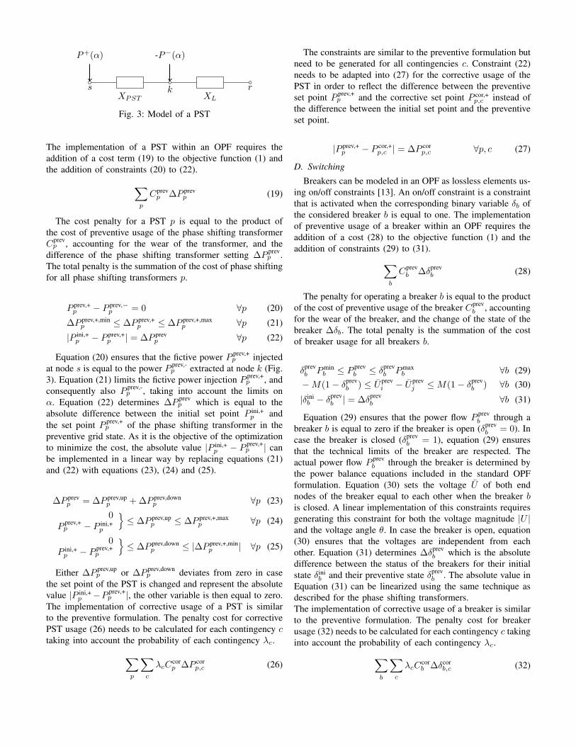
P+(α)
sXPST
-P−(α)
kXL
r
Fig. 3: Model of a PST
The implementation of a PST within an OPF requires theaddition of a cost term (19) to the objective function (1) andthe addition of constraints (20) to (22).∑
p
Cprevp ∆P prev
p (19)
The cost penalty for a PST p is equal to the product ofthe cost of preventive usage of the phase shifting transformerCprev
p , accounting for the wear of the transformer, and thedifference of the phase shifting transformer setting ∆P prev
p .The total penalty is the summation of the cost of phase shiftingfor all phase shifting transformers p.
P prev,+p − P prev,−
p = 0 ∀p (20)
∆P prev,+,minp ≤ ∆P prev,+
p ≤ ∆P prev,+,maxp ∀p (21)
|P ini,+p − P prev,+
p | = ∆P prevp ∀p (22)
Equation (20) ensures that the fictive power P prev,+p injected
at node s is equal to the power P prev,-p extracted at node k (Fig.
3). Equation (21) limits the fictive power injection P prev,+p , and
consequently also P prev,-p , taking into account the limits on
α. Equation (22) determines ∆P prevp which is equal to the
absolute difference between the initial set point P ini,+p and
the set point P prev,+p of the phase shifting transformer in the
preventive grid state. As it is the objective of the optimizationto minimize the cost, the absolute value |P ini,+
p − P prev,+p | can
be implemented in a linear way by replacing equations (21)and (22) with equations (23), (24) and (25).
∆P prevp = ∆P prev,up
p + ∆P prev,downp ∀p (23)
0P prev,+p − P ini,+
p
≤ ∆P prev,up
p ≤ ∆P prev,+,maxp ∀p (24)
0P ini,+p − P prev,+
p
≤ ∆P prev,down
p ≤ |∆P prev,+,minp | ∀p (25)
Either ∆P prev,upp or ∆P prev,down
p deviates from zero in casethe set point of the PST is changed and represent the absolutevalue |P ini,+
p −P prev,+p |, the other variable is then equal to zero.
The implementation of corrective usage of a PST is similarto the preventive formulation. The penalty cost for correctivePST usage (26) needs to be calculated for each contingency ctaking into account the probability of each contingency λc.∑
p
∑c
λcCcorp ∆P cor
p,c (26)
The constraints are similar to the preventive formulation butneed to be generated for all contingencies c. Constraint (22)needs to be adapted into (27) for the corrective usage of thePST in order to reflect the difference between the preventiveset point P prev,+
p and the corrective set point P cor,+p,c instead of
the difference between the initial set point and the preventiveset point.
|P prev,+p − P cor,+
p,c | = ∆P corp,c ∀p, c (27)
D. Switching
Breakers can be modeled in an OPF as lossless elements us-ing on/off constraints [13]. An on/off constraint is a constraintthat is activated when the corresponding binary variable δb ofthe considered breaker b is equal to one. The implementationof preventive usage of a breaker within an OPF requires theaddition of a cost (28) to the objective function (1) and theaddition of constraints (29) to (31).∑
b
Cprevb ∆δprev
b (28)
The penalty for operating a breaker b is equal to the productof the cost of preventive usage of the breaker Cprev
b , accountingfor the wear of the breaker, and the change of the state of thebreaker ∆δb. The total penalty is the summation of the costof breaker usage for all breakers b.
δprevb Pmin
b ≤ P prevb ≤ δprev
b Pmaxb ∀b (29)
−M(1− δprevb ) ≤ U prev
i − U prevj ≤M(1− δprev
b ) ∀b (30)
|δinib − δ
prevb | = ∆δprev
b ∀b (31)
Equation (29) ensures that the power flow P prevb through a
breaker b is equal to zero if the breaker is open (δprevb = 0). In
case the breaker is closed (δprevb = 1), equation (29) ensures
that the technical limits of the breaker are respected. Theactual power flow P prev
b through the breaker is determined bythe power balance equations included in the standard OPFformulation. Equation (30) sets the voltage U of both endnodes of the breaker equal to each other when the breaker bis closed. A linear implementation of this constraints requiresgenerating this constraint for both the voltage magnitude |U |and the voltage angle θ. In case the breaker is open, equation(30) ensures that the voltages are independent from eachother. Equation (31) determines ∆δprev
b which is the absolutedifference between the status of the breakers for their initialstate δini
b and their preventive state δprevb . The absolute value in
Equation (31) can be linearized using the same technique asdescribed for the phase shifting transformers.The implementation of corrective usage of a breaker is similarto the preventive formulation. The penalty cost for breakerusage (32) needs to be calculated for each contingency c takinginto account the probability of each contingency λc.∑
b
∑c
λcCcorb ∆δcor
b,c (32)
The constraints are similar as well but need to be generatedfor all contingencies c. Constraint (31) becomes (33) forthe corrective usage of the breakers in order to reflect thedifference between the preventive set point δprev
b and thecorrective set point δcor
b,c instead of the difference between theinitial set point and the preventive set point.
|δprevb − δcor
b,c| = ∆δcorb,c ∀b, c (33)
IV. CASE STUDY OF PREVENTIVE AND CORRECTIVEACTIONS
In order to test the different preventive and correctiveactions, they are implemented in a DC SCOPF and tested onthe Roy Billinton Test System (RBTS), depicted in Figure 4.The RBTS consists of five substations and a load (Table II)is connected to each substation, except for substation S1. TheRBTS is interconnected by seven transmission lines (Table III).Eleven generators (Table IV) are located in the grid, of whichfour are connected to substation S1 and seven to substationS2.
S1 S2
S3 S4
S5
T1 T2T3
T4
T5
T6
T7
L1
L2 L3
L4
G G
P1
Fig. 4: Roy Billinton Test System
In this section, three case studies are conducted. Each casestudy is a one-hour Day Ahead Congestion Forecast (DACF)where all possible N-1 contingencies are considered. In orderto keep the results clear, it is assumed that the load demandand renewable generation during the considered hour remainconstant. During each case study, the SO has different pre-ventive and corrective actions at his disposal. The availableactions during each case study are depicted in Table I.
TABLE I: Available actions for each case study
Preventive Actions Corrective Actions
Redisp. PST Switch. Redisp. Shed. PST Switch.1 X – – X X – –2 X X – X X X –3 X – X X X – X
The preliminary set points of all generators (Pmarketg ) are
submitted to the SO. Based on that data, a DACF analysis isconducted by the SO in order to determine the preventive andcorrective actions it has to take in order to have a stable systemat all times. During this analysis, the considered contingenciesare the failure of exactly one element (e.g. generator or
transmission line) with the probability of failure λc denotedin their respective tables.
TABLE II: Load Data
Load Sub. Pminl Pmax
l Ccorl
[MW] [MW] [e/MWh]L1 S2 10 20 10206L2 S3 75 85 10206L3 S4 30 40 10206L4 S5 10 20 10206
TABLE III: Transmission Line Data
Line Length Admittance Pmaxt λc
[km] [p.u.] [MW] [-]T1, T6 48 5.555 85 0.001713T2 160 1.666 50 0.005710T3 128 2.083 50 0.004568T4, T5, T7 32 8.333 71 0.001142
A. Case Study 1: Generator Redispatch and Load Shedding
In the first case study, preventive generation redispatch,corrective generation redispatch and corrective load sheddingare the only available actions. The preventive redispatch allowsto adapt the generation set point compared to those set bythe market Pmarket
g . As preventive generation redispatch comesat a cost, it is only activated if the market set points causecongestion in the system or if preventive redispatch is cheaperthen corrective redispatch taking into account the probabilityof the contingencies. The market set points Pmarket
g provided inTable IV cause congestion on the transmission lines T2 and T3as a result of an excessive generation output on substation S2.Preventive generation redispatch alleviates this congestion byreducing the generation of generator G5 and G10 of substationS2 and increasing the generation of generators G1 and G2 ofsubstation S1.
Pg
Gen.G1 G2 G5 G10
10 MW
20 MW
30 MW
40 MWMarketPreventive
Fig. 5: Case Study 1: Preventive generator redispatch
An unbalance in the generation and load due to a contingency,because of the failure of a generator or because of congestioncaused by an outage of a transmission line, can only becorrected by corrective generation redispatch or by sheddingload in the first case study. The corrective generation
TABLE IV: Generator Data
Gen. Sub. Pmaxg Pmarket
g λc Preventive Generator Data Corrective Generator Data
Cpre,downg C
pre,upg R
pre,downg R
pre,upg Ccor,down
g Ccor,upg Rcor,down
g Rcor,upg
[MW] [MW] [-] [e/MWh] [e/MWh] [MW] [MW] [e/MWh] [e/MWh] [MW] [MW]G1 S1 40 4.2 0.015 4.45 12.05 -40 40 44.5 120.5 0 10G2 S1 40 15.8 0.015 4.35 12.05 -40 40 43.5 120.5 -10 10G3 S1 10 8.7 0.015 – – 0 0 -3000.0 – -10 0G4 S1 20 16.3 0.015 – – 0 0 -3000.0 – -20 0G5 S2 40 38.4 0.005 5.00 14.00 -40 40 50.0 140.0 -10 10G6 S2 20 19.7 0.005 4.30 11.90 -20 20 43.0 119.0 -20 0G7 S2 20 19.2 0.005 – – 0 0 -3000.0 – -20 0G8 S2 20 19.8 0.005 – – 0 0 -3000.0 – -20 0G9 S2 20 19.3 0.005 – – 0 0 -3000.0 – -20 0G10 S2 5 3.6 0.005 5.45 15.35 -5 5 54.5 153.5 0 5G11 S2 5 0 0.005 4.40 12.20 -5 5 44.0 122.0 0 5
redispatch and shedded load is depicted in Figure 6 forcontingency C1 to C18.
Fig. 6: Case Study 1: Corrective generator redispatch. Eachsquare of the first eleven rows depicts the corrective generatorset point P cor
g,c relative to the maximal set point Pmaxg of
that generator for each contingency. The corrective generatorset point consist of the preventive generator set point P prev
g ,depicted in gray, adjusted with possible upwards or downwardscorrective generation redispatch, respectively depicted in greenand orange. Each square in the last row depicts the part of thetotal shedable load that is shedded during a contingency.
B. Case Study 2: Generator Redispatch, Load Shedding andPST
The implementation of a PST can help to alleviate con-gestion during certain contingencies and consequently enablecheaper generation redispatch. Case study 2 introduces a PSTP1 to transmission line T4 (Figure 4). For the purpose ofthis case study, the angle limits are set to ±0.4 (rad). Theusage of the PST causes wear of the transformer tap changerand consequently comes at a cost. The cost of using thePST is set equal to 400e/(rad). The implementation of the
PST P1 enables cheaper generator redispatch options duringcontingencies C12 and C17 (Figure 7).Contingencies C12 and C17 exclude either transmission lineT1 or T6, which are equivalent, resulting in the same gridstate. This causes congestion on both T6/T1 and T2. Thetotal power that can be transported by T6/T1 (85 MW) and T2(50 MW) is 135 MW, which is insufficient to supply the loadsconnected to substations S3, S4 and S5 with a total demandof 145 MW. In order to correct this unbalance, 10 MW of loadL2 is shed. To supply the remaining load, the flow through thegrid needs to be adapted. In case study 1, this is accomplishedby downwards redispatch of the generators G2, G3 and G4 ofsubstation S1 and upwards generator redispatch of G5 andG11 of substation S2. The downwards redispatch of G3 andG4 comes at a high cost as these are renewable generators andtheir downwards redispatch cost significantly exceeds that ofa conventional generator.
∆P corL2,C12 + ∆P cor,up
G5,C12 + ∆P cor,upG11,C12
=
∆P cor,downG2,C12 + ∆P cor,down
G3,C12 + ∆P cor,downG4,C12
The redispatch can be avoided by adapting the power flow inthe power system using a PST. In case study 2, the set point ofthe PST for contingencies C12 and C17 is adapted to changethe power flow through T4 changes from 0 to 21 MW. Thisinfluences the power flow in the system in such a way thatthe power flow through T3 is reduced to 20 MW comparedto 30 MW in the case without a PST, negating the need forredispatch between generators of substations S1 and S2. Loadshedding of 10 MW (L2) still takes place as the lines T6/T1and T2 are incapable of supplying the entire load of substationS3, S4 and S5. The corresponding downward redispatch isprovided by generator G2 of substation S1.
∆P corL2,C12 = ∆P cor,down
G2,C12
C. Case Study 3: Generator Redispatch, Load Shedding andSwitching
An alternative approach to adapting the power flow in atransmission system is changing its topology. The case study

Fig. 7: Case study 2: The difference in corrective generationredispatch and load shedding between CS1 without PST in thegrid and CS2 with a PST connected to transmission line T4for contingencies C12 (T1) and C17 (T7).
3 introduces transmission line switching which allows toeliminate transmission lines by opening their breakers. Thiscauses wear of the breakers and consequently comes at a cost.For the purpose of this case study, the cost of breaker operationis set at 400e. Elimination of transmission lines T4 and T5influences the power flow in the system is such a way that thepower flow through T3 is reduced to 10 MW (Fig. 8). Thisallows the negative redispatch needed to compensate for theload shedding of 10 MW (L4) to be done by generator G5.
∆P corL4,C12 = ∆P cor,down
G5,C12
A note must be made on the fact that these switching actionsreduce the RBTS system to a radial system, which in realityis not an acceptable strategy.
Fig. 8: Case study 3: The difference in corrective generationredispatch and load shedding between CS1 without transmis-sion line switching in the grid and CS3 with transmission lineswitching for contingencies C12 (T1) and C17 (T7).
V. CONCLUSION
This paper has presented the preventive and corrective ac-tions as wel as a linear implementation for generator redispach,load shedding, demand side management, PST control andswitching operations in a SCOPF. The effectiveness of theseactions is demonstrated in a test case. Even in a small testnetwork, it can be seen that considering all possible actionscan result in reduced need for generator redispatch.
ACKNOWLEDGEMENT
The ELECTA research group is a founding member ofEnergyVille.
REFERENCES
[1] P. Kundur, J. Paserba, V. Ajjarapu, G. Andersson, A. Bose, T. VanCutsem, C. Canizares, N. Hatziargyriou, D. Hill, V. Vittal, A. Stankovic,and C. Taylor, “Definition and Classification of Power System StabilityIEEE/CIGRE Joint Task Force on Stability Terms and Definitions,” IEEETransactions on Power Systems, vol. 19, no. 3, pp. 1387–1401, 2004.
[2] A. J. Wood and B. F. Wollenberg, Power Generation, Operation andControl, 2nd Edition. Wiley, 1996.
[3] F. Capitanescu, J. L. Martinez Ramos, P. Panciatici, D. Kirschen,A. Marano Marcolini, L. Platbrood, and L. Wehenkel, “State-of-the-art, challenges, and future trends in security constrained optimal powerflow,” Electric Power Systems Research, vol. 81, no. 8, pp. 1731–1741,2011.
[4] R. D. Christie, B. F. Wollenberg, and I. Wangensteen, “Transmissionmanagement in the deregulated environment,” Proceedings of the IEEE,vol. 88, no. 2, pp. 170–195, 2000.
[5] Z. X. Han, “Phase shifter and power flow control,” IEEE Transactionson Power Apparatus and Systems, vol. PAS-101, no. 10, pp. 3790–3795,1982.
[6] K. W. Hedman, S. Member, R. P. O. Neill, E. B. Fisher, and S. S. Oren,“With Contingency Analysis,” vol. 24, no. 3, pp. 1577–1586, 2009.
[7] K. Van den Bergh, D. Couckuyt, E. Delarue, and W. D’haeseleer, “Re-dispatching in an interconnected electricity system with high renewablespenetration,” Electric Power Systems Research, vol. 127, no. January, pp.64–72, 2015.
[8] A. Capozza, C. D’Adamo, G. Mauri, and A. Pievatolo, “Load sheddingand demand side management enhancements to improve the security ofa national electrical system,” 2005 IEEE Russia Power Tech, PowerTech,pp. 1–7, 2005.
[9] J. Verboomen, D. Van Hertem, P. Schavemaker, W. Kling, and R. Bel-mans, “Phase shifting transformers: principles and applications,” 2005International Conference on Future Power Systems, no. February 2016,pp. 6 pp.–6, 2005.
[10] H. Glavitsch, “Switching as means of control in the power system,”International Journal of Electrical Power & Energy Systems, vol. 7,no. 2, pp. 92–100, 1985.
[11] C. B. Somuah and N. Khunaizi, “Application of linear programmingredispatch technique to dynamic generation allocation,” IEEE Transac-tions on Power Systems, vol. 5, no. 1, pp. 20–26, 1990.
[12] T. Ding, R. Bo, W. Gu, and H. Sun, “Big-M based MIQP method foreconomic dispatch with disjoint prohibited zones,” IEEE Transactionson Power Systems, vol. 29, no. 2, pp. 976–977, 2014.
[13] C. Liu, J. Wang, and J. Ostrowski, “Static switching security in multi-period transmission switching,” IEEE Transactions on Power Systems,vol. 27, no. 4, pp. 1850–1858, 2012.
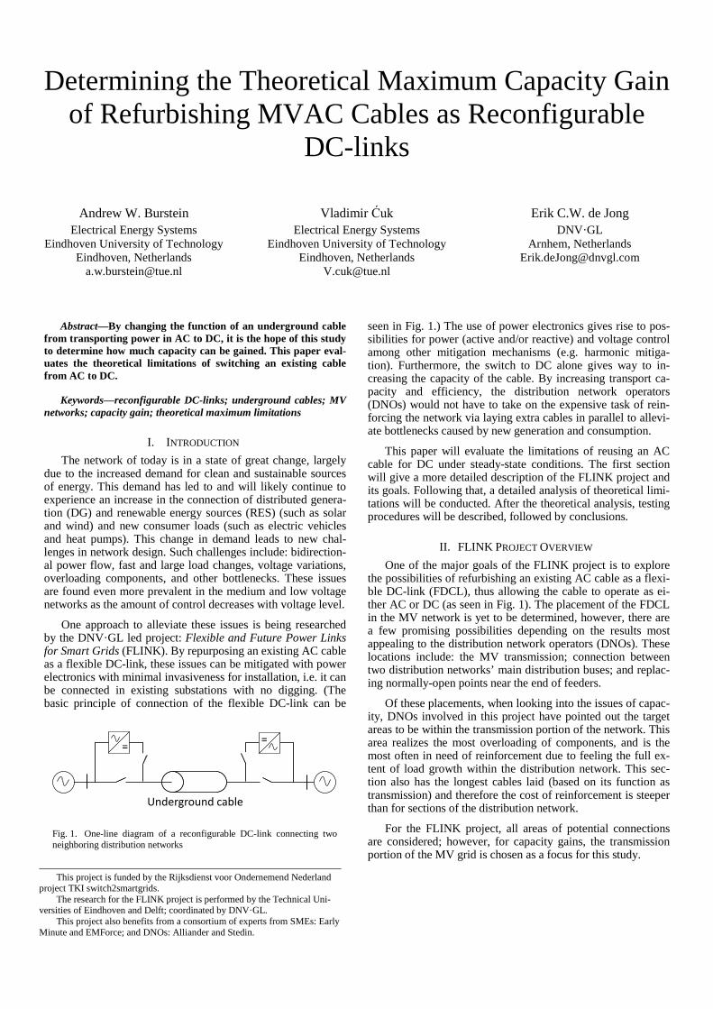
=
Underground cable
=
Fig. 1. One-line diagram of a reconfigurable DC-link connecting two neighboring distribution networks
Determining the Theoretical Maximum Capacity Gain of Refurbishing MVAC Cables as Reconfigurable
DC-links
Andrew W. Burstein Electrical Energy Systems
Eindhoven University of Technology Eindhoven, Netherlands
Vladimir Ćuk Electrical Energy Systems
Eindhoven University of Technology Eindhoven, Netherlands
Erik C.W. de Jong DNV·GL
Arnhem, Netherlands [email protected]
Abstract—By changing the function of an underground cable from transporting power in AC to DC, it is the hope of this study to determine how much capacity can be gained. This paper eval-uates the theoretical limitations of switching an existing cable from AC to DC.
Keywords—reconfigurable DC-links; underground cables; MV networks; capacity gain; theoretical maximum limitations
I. INTRODUCTION The network of today is in a state of great change, largely
due to the increased demand for clean and sustainable sources of energy. This demand has led to and will likely continue to experience an increase in the connection of distributed genera-tion (DG) and renewable energy sources (RES) (such as solar and wind) and new consumer loads (such as electric vehicles and heat pumps). This change in demand leads to new chal-lenges in network design. Such challenges include: bidirection-al power flow, fast and large load changes, voltage variations, overloading components, and other bottlenecks. These issues are found even more prevalent in the medium and low voltage networks as the amount of control decreases with voltage level.
One approach to alleviate these issues is being researched by the DNV·GL led project: Flexible and Future Power Links for Smart Grids (FLINK). By repurposing an existing AC cable as a flexible DC-link, these issues can be mitigated with power electronics with minimal invasiveness for installation, i.e. it can be connected in existing substations with no digging. (The basic principle of connection of the flexible DC-link can be
seen in Fig. 1.) The use of power electronics gives rise to pos-sibilities for power (active and/or reactive) and voltage control among other mitigation mechanisms (e.g. harmonic mitiga-tion). Furthermore, the switch to DC alone gives way to in-creasing the capacity of the cable. By increasing transport ca-pacity and efficiency, the distribution network operators (DNOs) would not have to take on the expensive task of rein-forcing the network via laying extra cables in parallel to allevi-ate bottlenecks caused by new generation and consumption.
This paper will evaluate the limitations of reusing an AC cable for DC under steady-state conditions. The first section will give a more detailed description of the FLINK project and its goals. Following that, a detailed analysis of theoretical limi-tations will be conducted. After the theoretical analysis, testing procedures will be described, followed by conclusions.
II. FLINK PROJECT OVERVIEW One of the major goals of the FLINK project is to explore
the possibilities of refurbishing an existing AC cable as a flexi-ble DC-link (FDCL), thus allowing the cable to operate as ei-ther AC or DC (as seen in Fig. 1). The placement of the FDCL in the MV network is yet to be determined, however, there are a few promising possibilities depending on the results most appealing to the distribution network operators (DNOs). These locations include: the MV transmission; connection between two distribution networks’ main distribution buses; and replac-ing normally-open points near the end of feeders.
Of these placements, when looking into the issues of capac-ity, DNOs involved in this project have pointed out the target areas to be within the transmission portion of the network. This area realizes the most overloading of components, and is the most often in need of reinforcement due to feeling the full ex-tent of load growth within the distribution network. This sec-tion also has the longest cables laid (based on its function as transmission) and therefore the cost of reinforcement is steeper than for sections of the distribution network.
For the FLINK project, all areas of potential connections are considered; however, for capacity gains, the transmission portion of the MV grid is chosen as a focus for this study.
This project is funded by the Rijksdienst voor Ondernemend Nederland project TKI switch2smartgrids.
The research for the FLINK project is performed by the Technical Uni-versities of Eindhoven and Delft; coordinated by DNV·GL.
This project also benefits from a consortium of experts from SMEs: Early Minute and EMForce; and DNOs: Alliander and Stedin.

==
=
=
=
=
=
=
=
=
Fig. 2. DC-link topologies (from left to right): monopolar; bipolar; homopolar
III. THEORETICAL MAXIMUM CAPACITY GAIN In the search for capacity gain, switching from AC to DC,
we are concerned with the active power capacity of the cables. This is defined for one phase as:
cosP U Iφ φ ϕ= (1)
Where Uφ and Iφ are the applied phase voltage and current respectively and ϕ is the phase angle between the voltage and current. Already, an advantage can be seen for capacity with DC, as the power factor, cosϕ , is unity for DC.
Equation (1) also shows that in the search for capacity gain, there are only two areas (excluding power factor) which can be enhanced for greater active power transport, i.e. either voltage or current. In most cases, it is more advantageous to increase the voltage rather than the current, one major advantage is low-er losses for the same transported power. Other advantages are found decreasing the thermal loading of the cable, limiting expansion and contraction of the insulation and sheath which can create gaps where partial discharges can occur.
In the following sections, ways to enhance the voltage and current limits will be overviewed. Another area that offers change of the power capacity is in the topology of the circuit.
A. Topologies In the AC system, three conductors are used in one cable.
The three phases must be in balance, i.e. equivalent magnitudes separated by 120o phase shift between phases. This allows for cancellation of the currents and no return path is required. For DC, on the other hand, there is just the positive and negative poles. To complete the circuit, either a conductive return path is required, or a return path through the ground may be used (if allowed by regulations).
To connect a DC-link, three main topologies exist: mono-polar, bipolar, and homopolar (as seen in Fig. 2). The ad-vantage of the bipolar and homopolar links is that the voltage is effectively doubled. Because of their similar outcomes, further exploration will neglect to mention the homopolar link as the results will be the same as the bipolar link in this paper.
To determine the gains from the topological changes, it is assumed that the current is limited by its thermal rating, and therefore the DC current rating will remain the same as the RMS current rating. Furthermore, it is assumed that the AC cables can withstand continuous operation at its peak phase-to-ground voltage [1],[2],[3]. These assumptions are notated here as:
2
DC
DC
I I
U Uφ
φ
=
= (2)
Where Uφ and Iφ are the RMS: phase-to-ground voltage and phase current respectively.
Assuming only one AC cable is available (three conduc-tors), the monopolar link can create three circuits with ground return, but only one circuit if a conductive return is required. Comparing to the 3-phase active power capacity of the AC
network, the ground-return link can supply 2 / cosϕ times more active power. With the conductive return, however, this value is decreased by one-third.
With a bipolar link, there is also a requirement for a posi-tive and negative pole (two conductors for one circuit), so it is similar to the monopolar with conductive return results, how-ever, the voltage is effectively doubled, doubling its capacity.
If there are two (or a multiple of two) cables running in parallel (which often happens in MV transmission), then the number of circuits that can be made increases. In the case of the ground return, the number of circuits increases for DC at the same rate as for AC, so no change in the capacity ratio
,3/DC ACP P φ occurs. However, for the conductive return mono-polar and the bipolar circuits, when there are two cables, three circuits can be made in comparison to just one, tripling its ca-pacity, whereas the capacity for AC only doubles. These results can be seen in Table I.
When these results are plotted against the displacement power factor, it is easier to see when capacity gains are achieved (Fig. 3). It is important to note, that in this figure, the monopolar curves represent the monopolar link with conduc-tive return. The monopolar link with ground return has the same curve as the bipolar curve with two AC cables available.
In the case of the monopolar circuit with conductive return, there is only capacity gain when there are two cables available and the displacement power factor is less than 0.7 (which is an unlikely power factor to be seen in operation). The bipolar cir-cuit, on the other hand, offers capacity gains when one cable is available when the power factor is less than 0.95 (which is of-ten the case in operation); furthermore, when there are two cables available, it will always give capacity gains, even at unity power factor, reaching a 60% gain at 0.88PF = (a likely possible power factor in operation).
TABLE I. POWER CAPACITY GAIN FOR DC-LINK TOPOLOGIES
DC Topology PDC/PAC,3ϕ
1 AC cable 2 AC cables
Monopolar (w/ ground return)
2cosϕ
2cosϕ
Monopolar (w/ conductive return)
1 23 cosϕ
1 22 cosϕ
Bipolar 2 23 cosϕ
2cosϕ
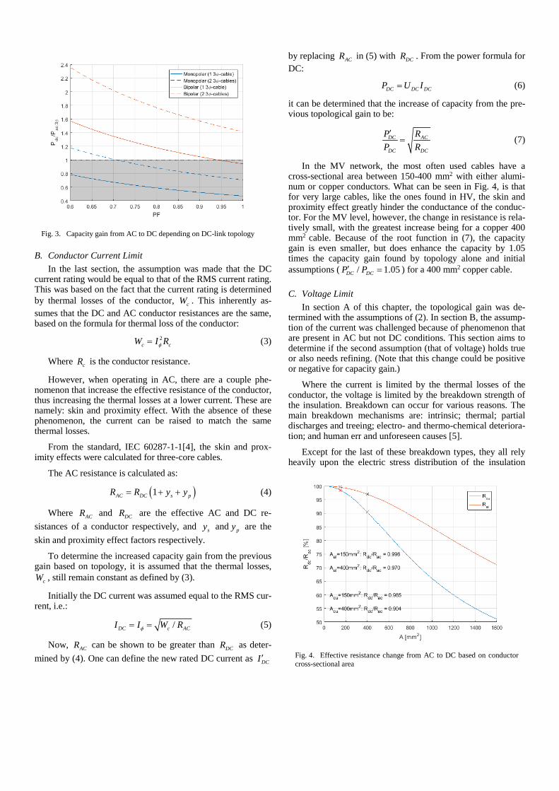
Fig. 3. Capacity gain from AC to DC depending on DC-link topology
Fig. 4. Effective resistance change from AC to DC based on conductor cross-sectional area
B. Conductor Current Limit In the last section, the assumption was made that the DC
current rating would be equal to that of the RMS current rating. This was based on the fact that the current rating is determined by thermal losses of the conductor, cW . This inherently as-sumes that the DC and AC conductor resistances are the same, based on the formula for thermal loss of the conductor:
2c cW I Rφ= (3)
Where cR is the conductor resistance.
However, when operating in AC, there are a couple phe-nomenon that increase the effective resistance of the conductor, thus increasing the thermal losses at a lower current. These are namely: skin and proximity effect. With the absence of these phenomenon, the current can be raised to match the same thermal losses.
From the standard, IEC 60287-1-1[4], the skin and prox-imity effects were calculated for three-core cables.
The AC resistance is calculated as:
( )1AC DC s pR R y y= + + (4)
Where ACR and DCR are the effective AC and DC re-sistances of a conductor respectively, and sy and py are the skin and proximity effect factors respectively.
To determine the increased capacity gain from the previous gain based on topology, it is assumed that the thermal losses,
cW , still remain constant as defined by (3).
Initially the DC current was assumed equal to the RMS cur-rent, i.e.:
/DC c ACI I W Rφ= = (5)
Now, ACR can be shown to be greater than DCR as deter-mined by (4). One can define the new rated DC current as DCI ′
by replacing ACR in (5) with DCR . From the power formula for DC:
DC DC DCP U I= (6)
it can be determined that the increase of capacity from the pre-vious topological gain to be:
DC AC
DC DC
P RP R′= (7)
In the MV network, the most often used cables have a cross-sectional area between 150-400 mm2 with either alumi-num or copper conductors. What can be seen in Fig. 4, is that for very large cables, like the ones found in HV, the skin and proximity effect greatly hinder the conductance of the conduc-tor. For the MV level, however, the change in resistance is rela-tively small, with the greatest increase being for a copper 400 mm2 cable. Because of the root function in (7), the capacity gain is even smaller, but does enhance the capacity by 1.05 times the capacity gain found by topology alone and initial assumptions ( / 1.05DC DCP P′ = ) for a 400 mm2 copper cable.
C. Voltage Limit In section A of this chapter, the topological gain was de-
termined with the assumptions of (2). In section B, the assump-tion of the current was challenged because of phenomenon that are present in AC but not DC conditions. This section aims to determine if the second assumption (that of voltage) holds true or also needs refining. (Note that this change could be positive or negative for capacity gain.)
Where the current is limited by the thermal losses of the conductor, the voltage is limited by the breakdown strength of the insulation. Breakdown can occur for various reasons. The main breakdown mechanisms are: intrinsic; thermal; partial discharges and treeing; electro- and thermo-chemical deteriora-tion; and human err and unforeseen causes [5].
Except for the last of these breakdown types, they all rely heavily upon the electric stress distribution of the insulation

Insulation
Conductor
Metal screen
Fig. 5. Cable cross-section with variables labeled for electric stress distribution calculations
(which is directly related to the applied voltage). Because of this, it is important to know how the electric stress distribution is affected by changing operation from AC to DC.
During AC operation, the electrical stress distribution is dependent on permittivity, rε , and the insulation conductivi-ty,σ , is considered negligible. This is due to the charging cur-rent being far greater than the leakage current. This assumption also means that the electrical stress distribution is not affected by the temperature distribution. With these assumptions, the electrical stress distribution can be estimated with [6]:
( )ln i
c
UE rrr r
=
(8)
Where, ( )E r is the electrical field strength at position r , U is the applied voltage, and the other variables are defined by Fig. 5.
It can be seen by this formula, the maximum electrical field strength will be at cr r= , and the lowest at ir r= .
When calculating the same distribution for DC, the charg-ing current (in steady-state) drops to zero, leaving the leakage current. This current is defined by the conductivity of the insu-lation. This makes calculation more difficult as now, more var-iables are involved, including temperature, and all of the varia-bles depend on each other as such:
( )( )( )
, ,
, ,
, ,
T r E
r T E
E r T
σ
σ
σ
(9)
And this is excluding the effect of space charge, which can either enhance or decrease the electric stress distribution de-pending on how charges can travel through the medium.
From [7], certain assumptions are made and an estimation of the electrical field strength can be determined with:
( )
1
1
i
ci
i
rU rdUE rdr rr r
δ
δ
δ−
= =
−
(10)
( )ln /
1
i c i c
i c
T Ur r r r
Ur r
α β
δ β
∆+
−=
+−
(11)
Where:
i cT T T∆ = − β is the electrical stress coefficient of the insulator [ ]/m V α is the temperature coefficient of electrical resistivi-
ty of the insulator ( ) 1o C−
From Fourier’s law, the expression in (11) can be deter-mined based on load current with the replacement of T∆ :
( )2 ln /2
L c i cI R r rT
πλ∆ = (12)
Where λ is the thermal conductivity of the insulator in ( )/W m K⋅ and cR is the electrical resistance of the conduc-
tor in [ ]Ω .
Equations (8) and (10) were then used to determine what happens to the electric stress distribution with different temper-atures operating as DC as comparing to AC, as well as a com-parison of these results for a typical HV cable vs an MV cable.
The cable parameters used from [6] can be found in Table II, and the resulting distributions in Figs. 6 and 7.
This analysis is performed for a single-core cable to show the electrical stress distribution as affected by temperature. However, for MV AC cables, generally three conductors are in
TABLE II. CABLE PARAMETERS USED FOR HV AND MV CABLES
Variable HV Cable MV Cable
Insulation material PILC
( ) 1 o
ins Cα−
0.1
[ ] /ins m Vβ 0.03×10⁻⁶
( ) /ins W m Kλ ⋅ 1/6
Conductor material Aluminum
[ ], nom RMSU kV 450 10
[ ] cr mm 23.2 11.3
[ ] ir mm 42.4 13.1
2 A mm 1690 400
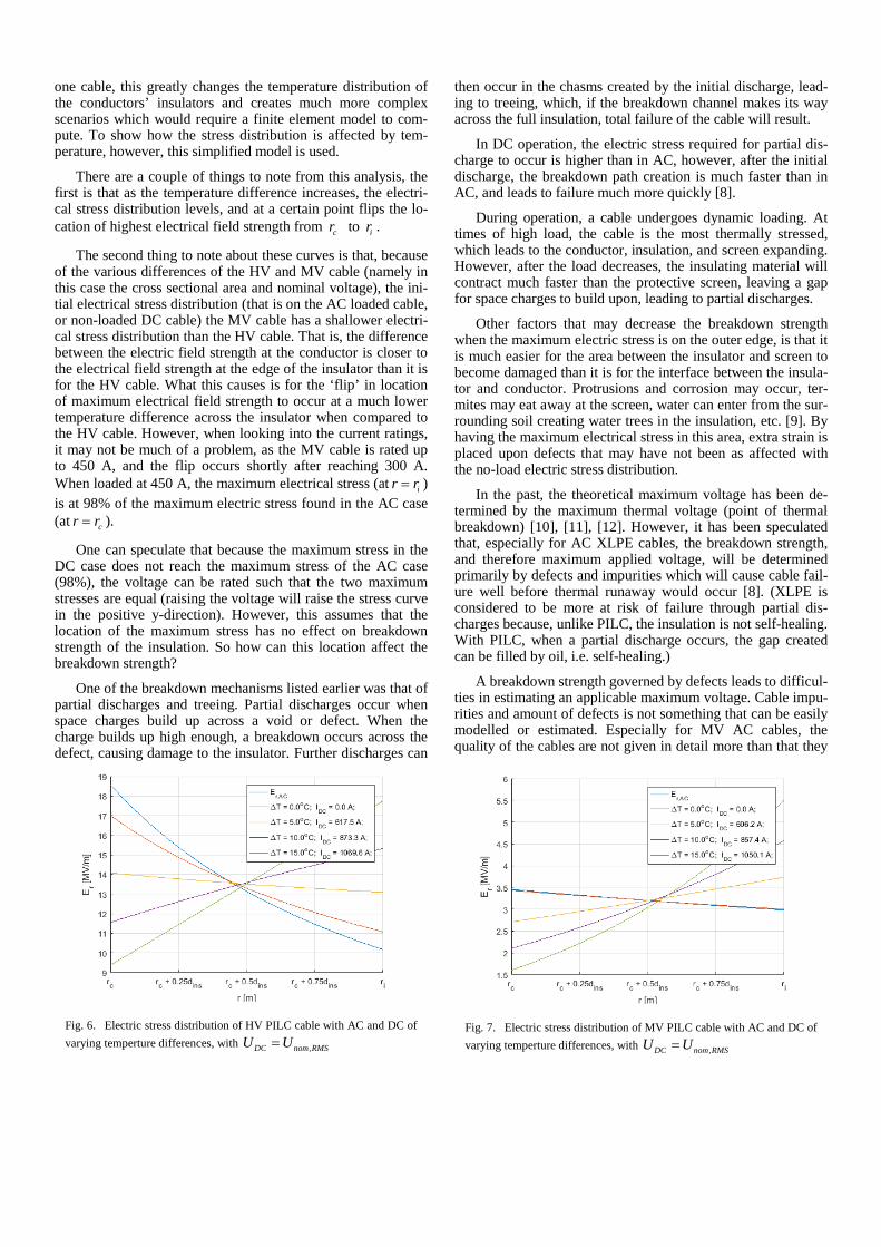
Fig. 6. Electric stress distribution of HV PILC cable with AC and DC of varying temperture differences, with ,DC nom RMSU U=
Fig. 7. Electric stress distribution of MV PILC cable with AC and DC of varying temperture differences, with ,DC nom RMSU U=
one cable, this greatly changes the temperature distribution of the conductors’ insulators and creates much more complex scenarios which would require a finite element model to com-pute. To show how the stress distribution is affected by tem-perature, however, this simplified model is used.
There are a couple of things to note from this analysis, the first is that as the temperature difference increases, the electri-cal stress distribution levels, and at a certain point flips the lo-cation of highest electrical field strength from cr to ir .
The second thing to note about these curves is that, because of the various differences of the HV and MV cable (namely in this case the cross sectional area and nominal voltage), the ini-tial electrical stress distribution (that is on the AC loaded cable, or non-loaded DC cable) the MV cable has a shallower electri-cal stress distribution than the HV cable. That is, the difference between the electric field strength at the conductor is closer to the electrical field strength at the edge of the insulator than it is for the HV cable. What this causes is for the ‘flip’ in location of maximum electrical field strength to occur at a much lower temperature difference across the insulator when compared to the HV cable. However, when looking into the current ratings, it may not be much of a problem, as the MV cable is rated up to 450 A, and the flip occurs shortly after reaching 300 A. When loaded at 450 A, the maximum electrical stress (at ir r= ) is at 98% of the maximum electric stress found in the AC case (at cr r= ).
One can speculate that because the maximum stress in the DC case does not reach the maximum stress of the AC case (98%), the voltage can be rated such that the two maximum stresses are equal (raising the voltage will raise the stress curve in the positive y-direction). However, this assumes that the location of the maximum stress has no effect on breakdown strength of the insulation. So how can this location affect the breakdown strength?
One of the breakdown mechanisms listed earlier was that of partial discharges and treeing. Partial discharges occur when space charges build up across a void or defect. When the charge builds up high enough, a breakdown occurs across the defect, causing damage to the insulator. Further discharges can
then occur in the chasms created by the initial discharge, lead-ing to treeing, which, if the breakdown channel makes its way across the full insulation, total failure of the cable will result.
In DC operation, the electric stress required for partial dis-charge to occur is higher than in AC, however, after the initial discharge, the breakdown path creation is much faster than in AC, and leads to failure much more quickly [8].
During operation, a cable undergoes dynamic loading. At times of high load, the cable is the most thermally stressed, which leads to the conductor, insulation, and screen expanding. However, after the load decreases, the insulating material will contract much faster than the protective screen, leaving a gap for space charges to build upon, leading to partial discharges.
Other factors that may decrease the breakdown strength when the maximum electric stress is on the outer edge, is that it is much easier for the area between the insulator and screen to become damaged than it is for the interface between the insula-tor and conductor. Protrusions and corrosion may occur, ter-mites may eat away at the screen, water can enter from the sur-rounding soil creating water trees in the insulation, etc. [9]. By having the maximum electrical stress in this area, extra strain is placed upon defects that may have not been as affected with the no-load electric stress distribution.
In the past, the theoretical maximum voltage has been de-termined by the maximum thermal voltage (point of thermal breakdown) [10], [11], [12]. However, it has been speculated that, especially for AC XLPE cables, the breakdown strength, and therefore maximum applied voltage, will be determined primarily by defects and impurities which will cause cable fail-ure well before thermal runaway would occur [8]. (XLPE is considered to be more at risk of failure through partial dis-charges because, unlike PILC, the insulation is not self-healing. With PILC, when a partial discharge occurs, the gap created can be filled by oil, i.e. self-healing.)
A breakdown strength governed by defects leads to difficul-ties in estimating an applicable maximum voltage. Cable impu-rities and amount of defects is not something that can be easily modelled or estimated. Especially for MV AC cables, the quality of the cables are not given in detail more than that they

have passed a minimum quality benchmark from the manufac-turer. However, the level of insulation impurities can change, not per cable type, but per manufacturer, internal manufactur-ing processes (e.g. machines used, calibration), year of produc-tion, etc.
In order to determine the applicable voltage limit on the ca-bles within the scope of this project, it is therefore determined that the best method is to physically test cables that are as simi-lar to the cables currently installed and used in the networks that are chosen as targets for the FDCL implementation.
IV. FUTURE WORK In order to assess how an installed AC cable will respond to
being operated as DC, laboratory and field tests must be carried out. As discussed earlier, modelling would likely yield unreal-istic results because of the number of uncontrollable factors that determine a cable’s strength.
In the lab, using cables that are similar to the ones in the field, they would need to go through an advanced aging pro-cess in order to replicate the degradation that field cables had gone through over the years/decades of use. After that, a sam-ple size will be determined to run tests repeatedly in order to gain enough data for reliable results. This is done because of the variances that can be apparent in material over different sections of insulation. However, the amount of cable that will be available in the lab will likely be far shorter than the length of the cable the FDCL will be applied to, and therefore it is likely that the results in the lab will still fare better than in the field. For this reason, careful consideration needs to be taken to perform a proper statistical analysis of the results.
Furthermore, a decision needs to be made if long-term (up-wards of two years) tests will be required to accurately deter-mine the nominal voltage that can be applied to the cable oper-ating as DC. However, these long-term tests may not be neces-sary for breakdown strength predictions [6].
V. CONCLUSIONS The power capacity gain of the network is largely depend-
ent on the topology of the DC circuit. Namely by doubling the effective voltage using a bipolar or homopolar connection. However, there are other areas for capacity gain and other as-pects to be looked into for the benefits of an FDCL.
The flipping of the point of maximum electrical field strength, is a common phenomenon found in DC cable hand-books and literature, such as [6], and the reference used here of [7] is still seen in papers today and used as a test reference to test new methods of calculating the theoretical field distribu-tion because of its extensive work and thorough experiments [13].
What is new from the research presented here is the explo-ration of these stress distributions for MV applications, as be-fore most research in DC has been for HV. What is commonly found is that certain assumptions that can be made for HV can-not be directly applied to MV applications, meaning new methods or assumptions may need to be made, and different models may need to be developed.
One of these assumptions that is common to find in papers is that of the inherent capacity gain by switching to DC based on the increased current from loss of skin and proximity effects and increased voltage due to operating at a continuous peak RMS voltage.
A great enhancement of load current capacity should not be taken as a given in all cases. In the case presented here, it is clear that there is a decrease in losses due to the absence of the skin and proximity effects, however, the lower the voltage level being discussed (i.e. the smaller the conductors) the less impact these phenomena play in capacity gains, as seen in Fig. 4 and calculated by (7).
As for the voltage assumption, in this study the voltage lim-it is yet undetermined, as it is believed by the authors that it cannot be well predicted through models due to its dependence on insulation impurities which vary by too many unpredictable factors. Although some experts claim that an MV AC cable can handle the peak RMS voltage continuously as a DC voltage, other experts are more hesitant to accept this assumption, espe-cially if the cable in question is of type XLPE. It is therefore taken upon this project to test cables that are as close in state and structure to the installed cables that are likely to be used for an FDCL in a lab setting for their breakdown strengths in order to determine the applicable maximum voltage.
REFERENCES [1] E. W. Kimbark, Direct Current Transmission. John Wiley & Sons, Inc.,
1971.
[2] D. Antoniou, A. Tzimas, and S. M. Rowland, “DC utilization of existing LVAC distribution cables,” in 2013 IEEE Electrical Insulation Conference, EIC 2013, 2013, no. June, pp. 518–522.
[3] S. Hay, C. Cleary, G. Mcfadzean, J. Mcgray, and N. Kelly, “MVDC Technology Study – Market Opportunities and Economic Impact,” Feb. 2015.
[4] “International Standard IEC 60287-1-1: Electric cables - Calculation of the current rating,” 2006.
[5] E. F. Steennis, Ed., “Ageing,” in Power Cables in General, Arnhem: DNV KEMA Academy, 2013, p. 40.
[6] G. F. (BICC C. L. Moore, Ed., Electric Cables Handbook, 3rd ed. Wiley-Blackwell, 1997.
[7] C. K. Eòll, “Theory of Stress Distribution in Insulation of High- Voltage DC Cables: Part I and II,” IEEE Trans. Electr. Insul., vol. EI-10, no. 1, pp. 27–54, 1975.
[8] F. H. Kreuger, Industrial High DC Voltage. Delft: Delft University Press, 1995.
[9] E. F. Steennis, Ed., Power Cables in General. Arnhem: DNV KEMA Academy, 2013.
[10] C. C. Reddy, “Theoretical maximum limits on power-handling capacity of HVDC cables,” IEEE Trans. Power Deliv., vol. 24, no. 3, pp. 980–987, 2009.
[11] J. J. O’Dwyer, “Theory of Dielectric Breakdown in Solids,” J. Electrochem. Soc., vol. 116, no. 2, p. 239, 1969.
[12] S. Whitehead, Dielectric Breakdown of Solids. London: Oxford University Press, 1953.
[13] C. C. Reddy and T. S. Ramu, “Estimation of thermal breakdown voltage of HVDC cables - A theoretical framework,” IEEE Trans. Dielectr. Electr. Insul., vol. 14, no. 2, pp. 400–408, 2007.

DC Fault Analysis in Bipolar HVDC GridsMian Wang*, Jef Beerten*, Dirk Van Hertem*
*KU Leuven, ESAT, div. Electa/EnergeVille, Kasteelpark Arenberg 10 - box 2445, 3001 Leuven BelgiumEmail: [email protected]
Abstract—Bipolar High Voltage Direct Current (HVDC) isexpected to form the backbone of future HVDC grids because itoffers advantages in terms of redundancy and added flexibilityin developing and operating the system. This comes at the cost ofintroducing unbalances in the system. However, most DC faultstudies until now have assumed a monopolar configuration ora balanced operation of a bipole, and thereby not addressingthe challenges that comes with the operation of bipolar systems,such as the influence of unbalanced conditions and groundingrelocation on the fault behavior and DC protection systems. Thispaper deals with DC fault analysis in bipolar HVDC grids, par-ticularly taking those unbalances and grounding relocation intoconsideration. DC fault behavior under unbalanced conditionsand different grounding locations is investigated via simulationstudies using PSCAD/EMTDC. The influence of unbalances andgroundings on the development of protection systems is evaluated.
Index Terms—Bipolar configuration, HVDC grid, DC fault,Unbalances, Grounding.
I. INTRODUCTION
Meshed HVDC Grids are seen as a viable option for thefuture transmission system in order to allow massive integra-tion of often remotely-located renewable energy sources andto provide increased reliability and flexibility at a lower cost.Although multi-terminal HVDC systems in operation today arebased on LCC (Line Commutated Converter) technology, it isconsidered that VSC (Voltage Source Converter) technology ismore suitable to build meshed DC grids [1]. VSC technologyprovides better capabilities such as increased controllability,power reversal by changing the current direction and commonvoltage enabling straightforward shunt connection. Moreoverrecent development of the VSC technology has lead to con-verter losses which are comparable to those of the LCC tech-nology. VSC-based HVDC systems are considered as a keytechnology for the European Supergrid, which will connectthe AC grids and offshore wind farms through a HVDC grid[2]. In China, two pilot multi-terminal VSC HVDC projectshave already been commissioned and are in operation [3], [4].
Existing VSC HVDC links are mainly used with symmet-rical monopolar configurations. However, future HVDC gridsare expected to develop into systems with a bipolar configura-tion. The bipolar configuration offers increased flexibility, e.g.for post-fault operation and higher extensibility in developingHVDC grids. Through unbalanced operation, a bipolar linkstill has half of the capacity in case of an outage of one pole.In addition, a bipolar grid can be extended with bipoles or withmonopolar tappings [5], [6]. The importance of system config-uration and grounding has been acknowledged, especially inthe area of system protection, since the fault currents largely
depend on the grounding [1], [5] and [6]. In recent years, moreand more attention has been paid to the bipolar configuration.Nevertheless, most fault detection and protection studies haveeither implicitly assumed or explicitly limited to a symmetricalmonopolar configuration or a balanced operation of a bipolarconfiguration, thereby disregarding the effect of the unbalancesin bipolar grids. Up to now, the influence of the location ofthe grounding points on the fault behavior in bipolar systemshas never been addressed. In [7] and [8], a solidly groundedbipolar configuration with sea return under balanced operationis used to analyze the fault currents, and possible fault clearingoptions. In [9], the specific case of a bipolar scheme with ametallic return was considered to calculate fault currents ina MTDC system for different grounding options. The impactof the HVDC topology on network faults is investigated in[10], but only balanced bipolar operation is considered. Thesituation is very similar in the area of HVDC grid protec-tion studies. For example, the authors proposed a traveling-wave based protection algorithm considering a symmetricalmonopolar configuration in [11]. A wavelet energy baseddifferential protection is proposed in [12] for a bipolar system;however, the paper did not consider unbalanced operation.
At this stage, the influence of the unbalances and thegrounding location in bipolar HVDC grids on fault behaviorand protection systems are not fully understood. This paperespecially focuses on selective primary protection algorithmssuch as [11], which normally use voltages and currents ofthe first few milliseconds to detect and identify the fault.It is essential to evaluate whether these signals are affectedby the unbalances and grounding configuration or not. Thispaper aims at providing a first indication of the potentialinfluence by analyzing DC fault behavior under unbalancedconditions and different grounding locations in bipolar HVDCgrids. The paper is organized as follows. Section II gives briefintroduction on system configurations and grounding options.In section III, the test system and case studies are presented,and in section IV the fault behaviors under different conditionsare explained using travel wave theory. Section V analyzes theinfluence of the unbalances and groundings on the protectionsystem. The conclusions are given in section VI.
II. CONFIGURATION AND GROUNDING OF BIPOLARHVDC GRIDS
Future bipolar DC grids are expected to have intrinsic unbal-ances, which could be unbalanced power flow or unbalancedconfiguration due to an outage of a converter, a line or throughmonopolar tappings. The influence of such unbalances on the
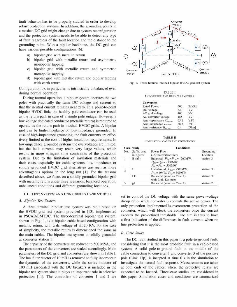
fault behavior has to be properly studied in order to developrobust protection systems. In addition, the grounding points ina meshed DC grid might change due to system reconfigurationand the protection system needs to be able to detect any typeof fault regardless of the fault location and the distance to thegrounding point. With a bipolar backbone, the DC grid canhave various possible configurations [6]:
a) bipolar grid with metallic returnb) bipolar grid with metallic return and asymmetric
monopolar tappingc) bipolar grid with metallic return and symmetric
monopolar tappingd) bipolar grid with metallic return and bipolar tapping
with earth returnConfiguration b), in particular, is intrinsically unbalanced evenduring normal operation.
During normal operation, a bipolar system operates the twopoles with practically the same DC voltage and current sothat the neutral current remains near zero. In a point-to-pointbipolar HVDC link, the healthy pole conductor can be usedas the return path in case of a single pole outage. However, alow voltage dedicated conductor (metallic return) is required tooperate as the return path in meshed HVDC grids. A bipolargrid can be high-impedance or low-impedance grounded. Incase of high-impedance grounding, the fault currents are effec-tively limited at the cost of higher insulation requirements. Inlow-impedance grounded systems the overvoltages are limited,but the fault currents may reach very large values, whichresults in more stringent time constraints of the protectionsystem. Due to the limitation of insulation materials andtheir costs, especially for cable systems, low-impedance orsolidly grounded HVDC grid alternatives are seen as moreadvantageous options in the long run [1]. For the reasonsdescribed above, we focus on a solidly grounded bipolar gridwith metallic return under three scenarios: balanced operation,unbalanced conditions and different grounding locations.
III. TEST SYSTEM AND CONSIDERED CASE STUDIES
A. Bipolar Test System
A three-terminal bipolar test system was built based onthe HVDC grid test system provided in [13], implementedin PSCAD/EMTDC. The three-terminal bipolar test system,shown in Fig. 1, is a bipolar cable-based configuration withmetallic return, with a dc voltage of ±320 KV. For the sakeof simplicity, the metallic return is dimensioned the same asthe main cables. The bipolar test system is solidly groundedat converter station 3.
The capacity of the converters are reduced to 500 MVA, andthe parameters of the converters are scaled accordingly. Mainparameters of the DC grid and converters are shown in Table I.The bus filter reactor of 10 mH is removed to fully incorporatethe dynamics of the converters, while the series inductor of100 mH associated with the DC breakers is included in thebipolar test system since it plays an important role in selectiveprotection [11]. The controllers of converter 1 and 2 are
Fig. 1. Three-terminal meshed bipolar HVDC grid test system
TABLE ICONVERTER AND GRID PARAMETERS
ConvertersRated Power 500 [MVA]DC Voltage 320 [kV]AC grid voltage 400 [kV]AC converter voltage 185 [kV]Arm capacitance Carm 65.1 [µF ]Arm inductance Larm 38.2 [mH]Arm resistance Rarm 0.4 [Ohm]
TABLE IISIMULATION CASES AND CONDITIONS
Case Study ConditionsNo. Suffix used
in figuresPower Flow(+/-:inverter/rectifier)
GroundingLocation
1 B (g3) Balanced, P1p=P1n= -200MW,P2p=P2n= -300MW,P3p=P3n= 500MW
station 3
2 U Unbalanced, P1p= -500MW,P2p= 0MW, P3p= 500MW
station 3
LO Balanced (same as Case 1)with Link 12p open
station 3
3 g2 Balanced (same as Case 1) station 2
set to control the DC voltage with the same power-voltagedroop ratio, while converter 3 controls the active power. Theonly protection implemented is overcurrent protection of theconverter, which will block the converters once the currentexceeds the pre-defined thresholds. The aim is thus to havea first indication of the differences in fault currents when noline protection is applied.
B. Case Study
The DC fault studied in this paper is a pole-to-ground fault,considering that it is the most probable fault in a cable-basedsystem. A solid pole-to-ground fault in the middle of thecable connecting to converter 1 and converter 3 of the positivepole (Link 13p), is incepted at time 0 s in the simulation toinvestigate the natural fault response. Measurements are takenat both ends of the cables, where the protective relays areexpected to be located. Three case studies are considered inthis paper. Simulation cases and conditions are summarized
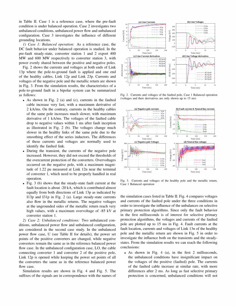
in Table II. Case 1 is a reference case, where the pre-faultcondition is under balanced operation. Case 2 investigates twounbalanced conditions, unbalanced power flow and unbalancedconfiguration. Case 3 investigates the influence of differentgrounding locations.
1) Case 1: Balanced operation: As a reference case, theDC fault behavior under balanced operation is studied. In thepre-fault steady-state, converter station 1 and 2 export 400MW and 600 MW respectively to converter station 3, withpower evenly shared between the positive and negative poles.
Fig. 2 shows the currents and voltages at both ends of Link13p where the pole-to-ground fault is applied and one endof the healthy cables, Link 12p and Link 23p. Currents andvoltages of the negative pole and the metallic return are shownin Fig. 3. From the simulation results, the characteristics of apole-to-ground fault in a bipolar system can be summarizedas follows:
• As shown in Fig. 2 (a) and (c), currents in the faultedcable increase very fast, with a maximum derivative of2 kA/ms. On the contrary, currents in the healthy cablesof the same pole increases much slower, with maximumderivative of 1 kA/ms. The voltages of the faulted cabledrop to negative values within 1 ms after fault inceptionas illustrated in Fig. 2 (b). The voltages change muchslower in the healthy links of the same pole due to thesmoothing effect of the series inductors. The differencesof these currents and voltages are normally used toidentify the faulted link.
• During the transient, the currents of the negative poleincreased. However, they did not exceed the thresholds ofthe overcurrent protection of the converters. Overvoltagesoccurred on the negative pole, with a maximum magni-tude of 1.22 pu measured at Link 12n near the terminalof converter 1, which need to be properly handled in realoperation.
• Fig. 3 (b) shows that the steady-state fault current at thefault location is about -20 kA, which is contributed almostequally from both directions of Link 13p as indicated byI13p and I31p in Fig. 2 (a). Large steady-state currentsalso flow in the metallic returns. The negative voltagesat the ungrounded sides of the metallic return reach veryhigh values, with a maximum overvoltage of -85 kV atconverter station 1.
2) Case 2: Unbalanced conditions: Two unbalanced con-ditions, unbalanced power flow and unbalanced configuration,are considered in the second case study. In the unbalancedpower flow case, U (see Table II for details), the power setpoints of the positive converters are changed, while negativeconverters remain the same as in the reference balanced powerflow case. In the unbalanced configuration case, LO, the cableconnecting converter 1 and converter 2 of the positive pole,Link 12p is opened while keeping the power set points of allthe converters the same as in the reference balanced powerflow case.
Simulation results are shown in Fig. 4 and Fig. 5. Thesuffixes of the signals are in correspondence with the names of
Time [ms]0 50 100 150 200
Cur
rent
[kA
]
-2
0
2
4
6
8
10(a) Line Currents
I13pI31pI12pI23p
Time [ms]0 50 100 150 200
dI/d
t [kA
/ms]
-1
-0.5
0
0.5
1
1.5
2
(c) Line Current derivativesdI13p/dtdI31p/dtdI12p/dtdI23p/dt
Time [ms]-5 0 5 10 15
Vol
tage
[kV
]
-100
0
100
200
300
400
500
(b) Line Voltages
U13pU31pU12pU23p
Time [ms]-5 0 5 10 15
dU/d
t [kV
/ms]
-400
-300
-200
-100
0
100
(d) Line Voltage derivatives
dU13p/dtdU31p/dtdU12p/dtdU23p/dt
Fig. 2. Currents and voltages of the faulted pole, Case 1 Balanced operation(voltages and their derivatives are only shown up to 15 ms)
Time [ms]0 50 100 150 200
Cur
rent
[kA
]
-2
-1
0
1
2(a) Negative pole currents
I13nI31nI12nI23n
Time [ms]0 50 100 150 200
Vol
tage
[kV
]
250
300
350
400(c) Negative pole Voltages
U13nU31nU12nU23n
Time [ms]0 50 100 150 200
Cur
rent
[kA
]
-20
-15
-10
-5
0
(b) Fault current & Neutral line currents
I13mI12mI23mIfault
Time [ms]0 50 100 150 200
Vol
tage
[kV
]
-80
-60
-40
-20
0(d) Neutral line voltages
Um1Um2Um3
Fig. 3. Currents and voltages of the healthy pole and the metallic return,Case 1 Balanced operation
the simulation cases listed in Table II. Fig. 4 compares voltagesand currents of the faulted pole under the three conditions inorder to investigate the influence of the unbalances on selectiveprimary protection algorithms. Since only the fault behaviorin the first milliseconds is of interest for selective primaryprotection algorithms, the voltages and currents of the faultedpole are plotted up to 15 ms in Fig. 4. Fault currents at thefault location, currents and voltages of Link 13n of the healthypole and the metallic return are shown in Fig. 5 in order toinvestigate the influence both on the transients and the steady-states. From the simulation results we can reach the followingconclusions:
• As shown in Fig. 4 (a), in the first 2 milliseconds,the unbalanced conditions have insignificant impact onthe voltages of the positive (faulted) pole. The currentsof the faulted cable increase at similar rate, with moredifferences after 2 ms. As long as fast selective primaryprotection is concerned, unbalanced conditions will not
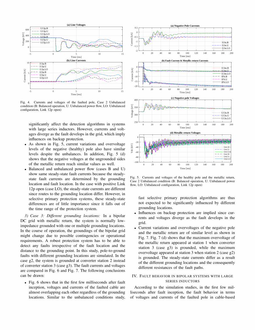
Time [ms]-5 0 5 10 15
Vol
tage
[kV
]
0
200
400
600
(a) Line VoltagesU13p.BU13p.UU13p.LOU23p.BU23p.UU23p.LO
Time [ms]-5 0 5 10 15
Cur
rent
[kA
]
0
5
10(b) Line Currents
I13p.BI13p.UI13p.LOI23p.BI23p.UI23p.LO
Fig. 4. Currents and voltages of the faulted pole, Case 2 Unbalancedcondition (B: Balanced operation, U: Unbalanced power flow, LO: Unbalancedconfiguration, Link 12p open)
significantly affect the detection algorithms in systemswith large series inductors. However, currents and volt-ages diverge as the fault develops in the grid, which implyinfluences on backup protection.
• As shown in Fig. 5, current variations and overvoltagelevels of the negative (healthy) pole also have similarlevels despite the unbalances. In addition, Fig. 5 (d)shows that the negative voltages at the ungrounded sidesof the metallic return reach similar values as well.
• Balanced and unbalanced power flow (cases B and U)show same steady-state fault currents because the steady-state fault currents are determined by the groundinglocation and fault location. In the case with positive Link12p open (case LO), the steady-state currents are differentsince routes to the grounding location differ. However, inselective primary protection systems, these steady-statedifferences are of little importance since it falls out ofthe time range of the protection system.
3) Case 3: Different grounding locations: In a bipolarDC grid with metallic return, the system is normally low-impedance grounded with one or multiple grounding locations.In the course of operation, the groundings of the bipolar gridmight change due to possible contingencies or operationalrequirements. A robust protection system has to be able todetect any faults irrespective of the fault location and thedistance to the grounding point. In this study, pole-to-groundfaults with different grounding locations are simulated. In thecase g2, the system is grounded at converter station 2 insteadof converter station 3 (case g3). The fault currents and voltagesare compared in Fig. 6 and Fig. 7. The following conclusionscan be drawn:
• Fig. 6 shows that in the first few milliseconds after faultinception, voltages and currents of the faulted cable arealmost overlapping each other regardless of the groundinglocations. Similar to the unbalanced conditions study,
Time [ms]0 20 40 60 80 100 120 140 160 180 200
Cur
rent
[kA
]
-2
-1.5
-1
-0.5
0
0.5(a) Negative Pole Currents
I13n.BI13n.UI13n.LO
Time [ms]0 20 40 60 80 100 120 140 160 180 200
Vol
tage
[kV
]
250
300
350
400(c) Negative pole Voltages
U13n.BU13n.UU13n.LO
Time [ms]0 20 40 60 80 100 120 140 160 180 200
Cur
rent
[kA
]
-20
-15
-10
-5
0
(b) Fault Current & Metallic return Currents
I13m.BI13m.UI13m.LOIFlt.BIFlt.UIFlt.LO
Time [ms]
0 20 40 60 80 100 120 140 160 180 200
Vdc
[kV
]
-100
-80
-60
-40
-20
0
(d) Metallic return Voltages
Um1.BUm1.UUm1.LOUm2.BUm2.UUm2.LO
Fig. 5. Currents and voltages of the healthy pole and the metallic return,Case 2 Unbalanced condition (B: Balanced operation, U: Unbalanced powerflow, LO: Unbalanced configuration, Link 12p open)
fast selective primary protection algorithms are thusnot expected to be significantly influenced by differentgrounding locations.
• Influences on backup protection are implied since cur-rents and voltages diverge as the fault develops in thegrid.
• Current variations and overvoltages of the negative poleand the metallic return are of similar level as shown inFig. 7. Fig. 7 (d) shows that the maximum overvoltage ofthe metallic return appeared at station 1 when converterstation 3 (case g3) is grounded, while the maximumovervoltage appeared at station 3 when station 2 (case g2)is grounded. The steady-state currents differ as a resultof the different grounding locations and the consequentlydifferent resistances of the fault paths.
IV. FAULT BEHAVIOR IN BIPOLAR SYSTEMS WITH LARGESERIES INDUCTORS
According to the simulation studies, in the first few mil-liseconds after fault inception, the fault behavior in termsof voltages and currents of the faulted pole in cable-based
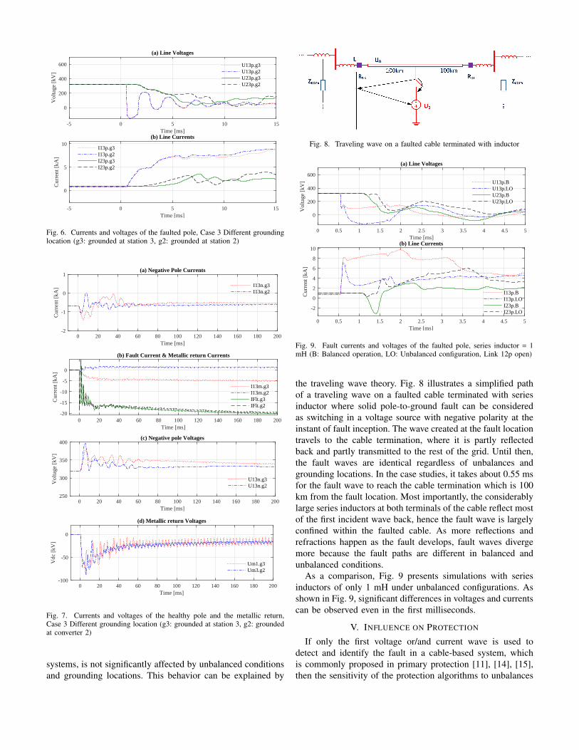
Time [ms]-5 0 5 10 15
Vol
tage
[kV
]
0
200
400
600
(a) Line Voltages
U13p.g3U13p.g2U23p.g3U23p.g2
Time [ms]-5 0 5 10 15
Cur
rent
[kA
]
0
5
10(b) Line Currents
I13p.g3I13p.g2I23p.g3I23p.g2
Fig. 6. Currents and voltages of the faulted pole, Case 3 Different groundinglocation (g3: grounded at station 3, g2: grounded at station 2)
Time [ms]0 20 40 60 80 100 120 140 160 180 200
Cur
rent
[kA
]
-2
-1
0
1(a) Negative Pole Currents
I13n.g3I13n.g2
Time [ms]0 20 40 60 80 100 120 140 160 180 200
Vol
tage
[kV
]
250
300
350
400(c) Negative pole Voltages
U13n.g3U13n.g2
Time [ms]0 20 40 60 80 100 120 140 160 180 200
Cur
rent
[kA
]
-20
-15
-10
-5
0
(b) Fault Current & Metallic return Currents
I13m.g3I13m.g2IFlt.g3IFlt.g2
Time [ms]0 20 40 60 80 100 120 140 160 180 200
Vdc
[kV
]
-100
-50
0
(d) Metallic return Voltages
Um1.g3Um3.g2
Fig. 7. Currents and voltages of the healthy pole and the metallic return,Case 3 Different grounding location (g3: grounded at station 3, g2: groundedat converter 2)
systems, is not significantly affected by unbalanced conditionsand grounding locations. This behavior can be explained by
Fig. 8. Traveling wave on a faulted cable terminated with inductor
Time [ms]0 0.5 1 1.5 2 2.5 3 3.5 4 4.5 5
Vol
tage
[kV
]
0
200
400
600
(a) Line Voltages
U13p.BU13p.LOU23p.BU23p.LO
Time [ms]0 0.5 1 1.5 2 2.5 3 3.5 4 4.5 5
Cur
rent
[kA
]-2
0
2
4
6
8
10(b) Line Currents
I13p.BI13p.LOI23p.BI23p.LO
Fig. 9. Fault currents and voltages of the faulted pole, series inductor = 1mH (B: Balanced operation, LO: Unbalanced configuration, Link 12p open)
the traveling wave theory. Fig. 8 illustrates a simplified pathof a traveling wave on a faulted cable terminated with seriesinductor where solid pole-to-ground fault can be consideredas switching in a voltage source with negative polarity at theinstant of fault inception. The wave created at the fault locationtravels to the cable termination, where it is partly reflectedback and partly transmitted to the rest of the grid. Until then,the fault waves are identical regardless of unbalances andgrounding locations. In the case studies, it takes about 0.55 msfor the fault wave to reach the cable termination which is 100km from the fault location. Most importantly, the considerablylarge series inductors at both terminals of the cable reflect mostof the first incident wave back, hence the fault wave is largelyconfined within the faulted cable. As more reflections andrefractions happen as the fault develops, fault waves divergemore because the fault paths are different in balanced andunbalanced conditions.
As a comparison, Fig. 9 presents simulations with seriesinductors of only 1 mH under unbalanced configurations. Asshown in Fig. 9, significant differences in voltages and currentscan be observed even in the first milliseconds.
V. INFLUENCE ON PROTECTION
If only the first voltage or/and current wave is used todetect and identify the fault in a cable-based system, whichis commonly proposed in primary protection [11], [14], [15],then the sensitivity of the protection algorithms to unbalances

or grounding relocation in a bipolar DC grid is mainlydetermined by the series inductor. If series inductors areinstalled at the ends of the DC cable, it can be expectedthat the impact of the unbalances and grounding relocationon the protection algorithms will not be significant. This isespecially true in non-unit protection methods [11], whichnormally involve using fast DC circuit breaker to interruptthe fault current, and the proposed DC circuit breaker areequipped with series inductors to limit the rise rate of the faultcurrent [16], [17]. Therefore, protection concepts which adoptnon-unit protection methods can be expected to be relativelyinsensitive against unbalances and grounding relocation. Onthe contrary, protection concepts which do not include seriesinductors or use fault voltage and/or current waves in longertime range will be affected by the unbalances and groundingrelocation to a certain extent. In these cases, more detailedsimulation studies are required in order to establish robust andselective relay settings.
Since the operation time range of backup protection fallsinto the region where faults behave differently under unbal-anced conditions or grounding relocation [15], [18], detailedparametric studies are needed when developing backup protec-tions for bipolar grids. In addition, failure mode of protectionequipment might also change the fault behavior and play animportant role in backup protection.
VI. CONCLUSION
This paper analyzed DC fault behavior under unbalancedconditions and different grounding locations in a three-terminal bipolar test system. If series inductors are placed atboth ends of the cables, fault behavior in the first millisecondsis not significantly influenced by unbalanced conditions orgrounding relocation since the inductors reflect most of thefault waves. The voltages and currents diverge more as faultdevelops in the grid regardless of the presence of seriesinductors.
As for the impact on the protection system, as far as theselective primary protection is concerned, the presence of se-ries inductors and time range of signals used for identificationare the most determining factors. If large series inductors areplaced at the ends of the DC cable, the selective primaryprotection algorithms are not likely to be affected by theunbalances and grounding relocation. However, the influenceon the backup protection systems is implied since the operationtime range of the backup protection falls into the regionwhere faults behavior differently under unbalanced conditionsor different grounding locations.
ACKNOWLEDGMENT
The work of Jef Beerten is funded by a research grant ofthe Research Foundation-Flanders (FWO).
REFERENCES
[1] Cigre Working Group B4.52, “HVDC Grid Feasibility Study,” Cigre,Technical Brochure, Apr. 2013.
[2] D. Van Hertem and M. Ghandhari, “Multi-terminal VSC HVDC forthe European supergrid: Obstacles,” Renewable and Sustainable EnergyReviews, vol.14, no.9, pp.3156–3163, Dec. 2010.
[3] X. Li, Z. Yuan, J. Fu, Y. Wang, T. Liu, and Z. Zhu, “Nanao multi-terminal VSC-HVDC project for integrating large-scale wind genera-tion,” Proc. IEEE PES GM 2014, Washington DC, USA, 27-31 July2014, 5 pages.
[4] G. Tang, Z. He, H. Pang, X. Huang, and X. Zhang, “Basic topology andkey devices of the five-terminal DC grid,” in CSEE Journal of Powerand Energy Systems, vol.1, no.2, pp.22-35, June 2015.
[5] S. De Boeck, P. Tielens, W. Leterme, and D. Van Hertem, “Configu-rations and earthing of HVDC grids,” in Proc. IEEE PES GM 2013,Vancouver, Canada, 21-25 July 2013, 5 pages.
[6] W. Leterme, P. Tielens, S. De Boeck, and D. Van Hertem, “Overviewof grounding and configuration options for meshed HVDC grids,” IEEETrans. Power Del., vol. 29, no. 6, pp. 2467–2475, Dec. 2014.
[7] M. K. Bucher, M. M. Walter, M. Pfeiffer, and C. M. Franck, “Optionsfor ground fault clearance in HVDC offshore networks,” in Proc. IEEEECCE 2012, Raleigh, NC, USA, 15-20 Sept. 2012, 8 pages.
[8] M. K. Bucher, R. Wiget, G. Andersson, and C. M. Franck, “Multiter-minal HVDC Networks: What is the preferred topology,” IEEE Trans.Power Del., vol. 29, no. 1, pp. 406–413, Feb. 2014.
[9] E. Berne, G. Bergna, P. Egrot, and Q. Wolff, “Earth currents in HVDCgrids: An example based on 5 terminal bipolar configurations,” in Proc.EPE’14-ECCE Europe, Lappeenranta, Finland, 26-28 Aug. 2014, 10pages.
[10] E. Kontos, R. T. Pinto, S. Rodrigues, and P. Bauer, “Impact of HVDCTransmission System Topology on Multiterminal DC Network Faults,”IEEE Transactions on Power Delivery, vol. 30, no. 2, pp. 844–852, Apr.2015.
[11] W. Leterme, J. Beerten, and D. Van Hertem, “Non-unit protection ofHVDC grids with inductive dc cable termination,” IEEE Transactionson Power Delivery, to be published.
[12] A. E. Abu-Elanien, A. A. Elserougi, A. S. Abdel-Khalik, A. M.Massoud, and S. Ahmed, “A Differential Protection Technique for Multi-Terminal HVDC,” Electric Power Systems Research, vol. 130, pp. 78–88,Jan. 2016.
[13] W. Leterme, N. Ahmed, J. Beerten, L. Angquist, D. Van Hertem, andS. Norrga, “A new HVDC grid test system for HVDC grid dynamicsand protection studies in EMT-type software,” Proc. IET ACDC 2015,Birmingham, UK, 10-12 Feb. 2015, 7 pages.
[14] K. De Kerf, K. Srivastava, M. Reza, D. Bekaert, S. Cole, D. VanHertem, and R. Belmans, “Wavelet-based protection strategy for DCfaults in multi-terminal VSC HVDC systems,” IET Gener. Transm.Distrib., vol. 5, no. 4, p. 496–503, Apr. 2011.
[15] J. Descloux, “Protection contre les courts-circuits des reseaux a courantcontinu de forte puissance,” Ph.D. dissertation, Universite de Grenoble,Grenoble, France, Sept. 2013.
[16] J. Hafner and B. Jacobson, “Proactive hybrid hvdc breakers: A keyinnovation for reliable HVDC grids,” in Cigre Bologna Symp., Bologna,Italy, 13–15 Sep 2011, 8 pages.
[17] K. Tahata, S. El Oukaili, K. Kamei, D. Yoshida, Y. Kono, R. Yamamoto,and H. Ito, “HVDC circuit breakers for HVDC grid applications,” inProc. IET ACDC 2015, Feb. 2015, 9 pages.
[18] W. Leterme, S. P. Azad, and D. Van Hertem, “Fast breaker failure backupprotection for HVDC grids,” in Proc. IPST 2015, Cavtat, Croatia, 15-18June 2015, 6 pages.

The Half-Bridge SiC-MOSFET Switching Cell Implementation in a Three-phase Induction Motor Drive
F. Başkurt
Protonic Holland BV.
Hoorn, the Netherlands
dr. K. Boynov and prof. dr. E. Lomonova
Electromechanics and Power Electronics Group
Eindhoven University of Technology
Eindhoven, the Netherlands
[email protected] and [email protected]
Abstract—In this paper, the concept of the Half-Bridge SiC-
MOSFET Switching Cell (HB-SC), and its design and test
procedures are explained. The HB-SC serves as the basic switching
element of scalable power electronic converter. The HB-SC
combines the power semiconductor switch, optimized power
layout, gate driver, and management circuitry (measurement,
protection, and interface blocks).
Keywords—SiC-MOSFET; integrated switch; half-bridge
inverter leg; power layout for high switching speed applications;
three-phase inverter
I. INTRODUCTION
Electrical machines and variable frequency drives (electric drive systems) are widely used in the industry and they occupy a big and constantly growing market [1,2]. Due to the improvements in renewable energy systems and automotive industry, application areas and power levels of electric drive systems are even increasing [3,4]. In addition, integration of drive systems brings efficiency requirement regulations both for electrical machines and variable frequency drives [5].
The mentioned aspects lead to increasing of the importance of testing environments for electromechanical systems. Because several different types of electrical machines exist and they require different control approaches, the electric drive systems differ for each electrical machine type as well. The commercially available test benches usually have interfaces dedicated to fixed types of electrical machines, and they have restrictions on applicable control algorithms and switching frequencies [6,7].
The PDEng project “Rapid Prototyping and Testing Environment for Electromechanical Systems” is conducted to satisfy the need for a test environment with high flexibility concerning the types of the powered machines as well as the control hardware and software. The main focus of the project is designing, manufacturing, and testing of a generic power electronic drive that can be used for a broad range of electrical machines and power electronic systems while reducing the effort required for system reconfiguration. In [8], the topology and semiconductor switch studies resulted that the use of half-bridge SiC-MOSFET inverter legs provide the highest flexibility and scalability in the proposed generic power electronics drive.
In this work, first, the concept of the Half-Bridge Switching Cell (HB-SC) is explained, its internal structure is given, and possible application areas are mentioned. Second, the design steps for the HB-SC are explained, which includes the selection of SiC-MOSFET power switch, design of power circuitry layout, and design of management circuitry. Last, the assembly of the designed HB-SC is shown and three cells are connected in parallel to construct a three-phase inverter to drive an induction motor. Relevant parameters regarding the power layout and measurement circuitry are measured and presented.
II. HALF-BRIDGE SWITCHING CELL CONCEPT
The main purpose of the “Rapid Prototyping and Testing Environment for Electromechanical Systems” project was creating a flexible and scalable power electronic drive that can power different types of electrical machines (induction machine and switched-reluctance motor), while requiring low effort for reconfiguration. Besides that, this generic power electronic drive could be used to implement complex control algorithms. The use of half-bridge inverter leg modules provides the highest flexibility in aspect of topology requirements and repairability of the power electronic drive [8]. Table I gives the required specifications for the generic power electronic drive.
The given specifications lead to use of two possible semiconductor switches: (1) Si-IGBTs and (2) SiC-MOSFETs. Si-IGBTs are widely accepted in high power industrial systems due to their proved reliability, low conduction losses, and low costs. However, their maximum switching frequency is a limiting factor on the flexibility. The intention of complex control algorithms requires switching frequencies up to 50kHz. For this reason, SiC-MOSFETs provide a better solution than Si-IGBTs. Their ratings can reach up to 1.7kV and 300A, while allowing switching frequencies more than 50kHz.
TABLE I
GENERIC POWER ELECTRONICS DRIVE REQUIREMENTS
Parameter Explanation Value
𝑉𝐷𝐶 DC bus voltage up to 800V
𝐼𝑚𝑎𝑥 Maximum phase current 100A
𝑃𝑚𝑎𝑥 Maximum output power 30kW
𝑓𝑠𝑤 Switching frequency 8kHz – 50kHz

The following solution is, a half-bridge SiC-MOSFET inverter leg that is equipped with its power layout, gate driver, and management circuitry. This integrated power switching unit is called Half-Bridge SiC-MOSFET Switching Cell (HB-SC) and it forms the basic scalable switching element for high power and high speed power electronic applications.
Following facilities are provided by the HB-SC (Fig. 1.):
a low-inductive power circuitry including the PCB layout, half-bridge SiC-MOSFET, DC link capacitors, and power connectors,
a low-noise management circuitry including gate drive & interface, measurement, protection, and power management parts,
galvanic-isolation between the power and management circuitries.
The HB-SC provides an integrated and scalable power electronic solution for various power electronic converters. There are commercially available integrated switching systems in the market [9]. However, these integrated systems are mainly aiming three-phase electric drive applications and have restrictions on control algorithms. The key improvement of the HB-SC is to provide more flexibility respect to the present switching systems.
Fig. 1. Internal structure of the Half-Bridge Switching Cell.
III. DESIGN STEPS OF THE HALF-BRIDGE SWITCHING CELL
In this chapter, the design steps of the HB-SC and the decisions given are explained in detail. First, two commercially available SiC-MOSFETs are compared based on their switching performances and one of them is chosen for the final design. Second, the power layout design is explained and last, the management circuitry is presented.
A. SiC-MOSFET Switch Selection
Two SiC-MOSFETs from two different manufacturers are
compared based on their switching performances: (1) CREE
CAS120M12BM2 (2) ROHM BSM120D12P2C005. Both of the
SiC-MOSFETs are rated at 1200V and 120A. The comparison
is conducted based on the Double Pulse Test (DPT), which is a
widely accepted technique to evaluate the switching
performance of the semiconductor switches. In DPT, the device
under test is subject to a hard switching under test voltage and
test current, and the turn-on and turn-off losses are measured
during the switching transitions.
The circuit schematic of the DPT is shown in Fig. 2, where
the test voltage is set by the DC supply voltage and the inductor
is used to build-up the switch current linearly, until the test
current is reached. The gate signal, and the resulting switch
voltage and current waveforms of the semiconductor switch are
shown in Fig. 3.
Fig. 2. Double Pulse Test schematic [10].
Fig. 3. Double Pulse Test waveforms: gate signal (top), switch current
(middle), and switch voltage (bottom) [10].
The test starts when there is no current flowing through the
switch. At instant 𝑡1, the switch is turned on until the switch
current reaches test current at 𝑡2. Then the switch is turned off
and the inductor current freewheels through the diode D. The
switch is turned on again at 𝑡3, shortly after 𝑡2. Since the turn-
off and turn-on losses are observable at instants 𝑡2 and 𝑡3, test
period is terminated at 𝑡4, shortly after 𝑡3. This test period is
repeated once per second in order to avoid heating of the switch.
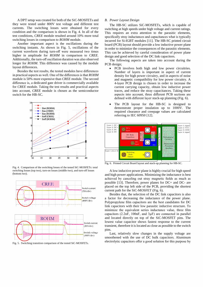
A DPT setup was created for both of the SiC-MOSFETs and
they were tested under 800V test voltage and different test
currents. The switching losses were obtained for every
condition and the comparison is shown in Fig. 4. In all of the
test conditions, CREE module resulted around 10% more total
switching losses in comparison to ROHM module.
Another important aspect is the oscillations during the
switching instants. As shown in Fig. 5, oscillations of the
current waveform during turn-off were measured two times
higher in amplitude for ROHM in comparison to CREE.
Additionally, the turn-off oscillation duration was also observed
longer for ROHM. This difference was caused by the module
layout differences.
Besides the test results, the tested modules have differences
in practical aspects as well. One of the differences is that ROHM
module is 50% more expensive than CREE module. The second
difference is, a dedicated gate driver is commercially available
for CREE module. Taking the test results and practical aspects
into account, CREE module is chosen as the semiconductor
switch for the HB-SC.
Fig. 4. Comparison of the switching losses of the tested SiC-MOSFETs: total
switching losses (top two), turn-on losses (middle two), and turn-off losses (bottom two).
Fig. 5. Switching transition comparison of the tested SiC-MOSFETs.
B. Power Layout Design
The HB-SC utilizes SiC-MOSFETs, which is capable of
switching at high speeds under high voltage and current ratings.
This requires an extra attention to the parasitic elements,
specifically stray inductances and capacitances what is typically
incurred for Si-IGBT modules [11]. The HB-SC printed circuit
board (PCB) layout should provide a low inductive power plane
in order to minimize the consequences of the parasitic elements.
This can be achieved by careful consideration of power plane
design and good selection of the DC link capacitors.
The following aspects are taken into account during the
PCB design;
PCB involves both high and low power circuitries. Number of layers is important in aspect of current density for high power circuitry, and in aspects of noise and magnetic compatibility for low power circuitry. A 4-layer PCB design is chosen in order to increase the current carrying capacity, obtain low inductive power traces, and reduce the stray capacitances. Taking these aspects into account, three different PCB sections are defined with different layer stack-up planning (Fig. 6).
The PCB layout for the HB-SC is designed to demonstrate proper insulation up to 1000V. The required clearance and creepage values are calculated referring to IEC 60950 [12].
Fig. 6. Printed Circuit Board layout and stack-up planning for HB-SC.
A low inductive power plane is highly crucial for high speed
and high power applications. Minimizing the inductance is best
achieved by canceling out stray magnetic fields as much as
possible [13]. Therefore, power planes for DC+ and DC- are
placed on the top left side of the PCB, providing the shortest
current path for the SiC-MOSFET (Fig. 6).
Besides that, the selection of the DC link capacitors is also
a factor for decreasing the inductance of the power plane.
Polypropylene film capacitors are the best candidates for DC
link capacitors with their low parasitic inductive structure. To
minimize the equivalent series inductance value, three film
capacitors (2.2nF, 100nF, and 3µF) are connected in parallel
and located directly on top of the SiC-MOSFET pins. The
lowest value capacitor shows fastest response to the current
transient, therefore it is located as close as possible to the switch
pins.
Last, relatively slow changes in the supply voltage are
smoothened with the use of DC bulk capacitors. Aluminum
electrolytic capacitors offer a good solution for this purpose by

their high capacitance/size ratio. Two parallel branches of two
series aluminum electrolytic capacitors are used to decrease the
equivalent series resistance. Due to series connection, balancing
resistors are used to equalize the voltages on the capacitors.
C. Management Circuitry Design
The Management Circuitry of the HB-SC includes four
different blocks: (1) measurement & conditioning, (2)
protection, (3) gate driver interface, and (4) power
management. These blocks and their relations with the power
circuitry are shown in Fig.7.
Fig. 7. Internal structure and blocks of the management circuitry.
1) Measurement and conditioning block: This block
provides the following measurement information isolated from
the power circuitry:
a) DC bus voltage measurement: The HB-SC senses the
DC bus voltage by a resistor divider network on the power
circuitry side and transfers the signal to the management
circuitry through an isolation amplifier. After that, it conditions
the signal and provides it with a gain of 3.3mV/V. Input to
output delay of the voltage measurement is around 3.3µs.
b) Switching node current (phase current) measurement:
The HB-SC equips a magneto-resistive current sensor to sense
the switching node current and provides it to the management
circuitry through galvanic isolation. After conditioning and
filtering, the current sensor output signal is provided with a gain
of 90mV/A. High bandwidth (400kHz) and low input to output
delay (0.5µs) make this current sensor suitable for complex
control algorithms, which requires fast and accurate current
measurement.
c) Temperature measurement: The temperature of the
SiC-MOSFET module is measured by an integrated-circuit
CMOS temperature sensor with a gain of -8,2mV/C.
2) Protection block: Because SiC-MOSFETs are fast
switching devices and not robust as Si-IGBTs, the protection of
the SiC-MOSFETs gains importance. Therefore, the reliability
of the system can be ensured with a fast and accurately reacting
protection approach. For this purpose, the protection block is
constructed with fast logic circuits. The following conditions
define the thresholds for faults:
Over-voltage fault : 900V
Over-current fault : 70A
Over-temperature fault : 90°C
Gate-driver fault : shoot-through, missing signal
In case of one of these faults, the protection block takes the following actions: (1) generating a “fault” signal, (2) informing other HB-SCs and the controller/user, (3) disabling all PWM signals, and (4) keeping the fault state until it is reset.
3) Gate driver and interface block: Gate drivers are used to
isolate and amplify the gating signals between the signal
circuitry and gate pins. Besides that, they provide protection
against over-current and shoot-through faults. The
PT62SCMD12 gate driver is used in this work because of its
compatibility with the chosen SiC-MOSFET module. The HB-
SC modules accept single-ended PWM signals from the control
platform, while the chosen gate driver accepts differential input
signals. Besides that, the gate driver does not provide an
enable/disable circuitry for the gate signals. Therefore, an
interface circuitry block is added between the PWM input and
gate driver input. This block is responsible for converting the
single-ended PWM signals to differential voltage levels and
disabling the PWM signals during a faulty condition.
Fig. 8. Gate driver (PT62SCMD12) and the chosen SiC-MOSFET
(CAS120M12BM2).
4) Power management block: The management circuitry
consists of sensors, operational amplifiers, logic circuits, and
gate driver. These blocks require different voltage and power
levels. Additionally, an isolated voltage is required for DC bus
voltage measurement. In HB-SC, management circuitry is
powered with 24V and other circuitries are powered through
24V to 5V (nonisolated) and 5V to 5V (isolated) power
supplies.
IV. IMPLEMENTATION OF THE HALF-BRIDGE SWITCHING CELL
IN A THREE-PHASE INDUCTION MOTOR DRIVE
Following the design rules and decisions in Chapter III, the HB-SC printed circuit board layout is designed and assembled as shown in Fig. 9 and 10. The numbered areas in Fig. 9 indicates the following functions:
Area 1 includes the input power connections, DC bulk capacitors, and balancing resistors. As seen in Fig. 9, the power planes are designed as wide as possible to decrease the parasitic inductance of the power traces. DC bulk capacitors are located at the bottom side of the PCB.
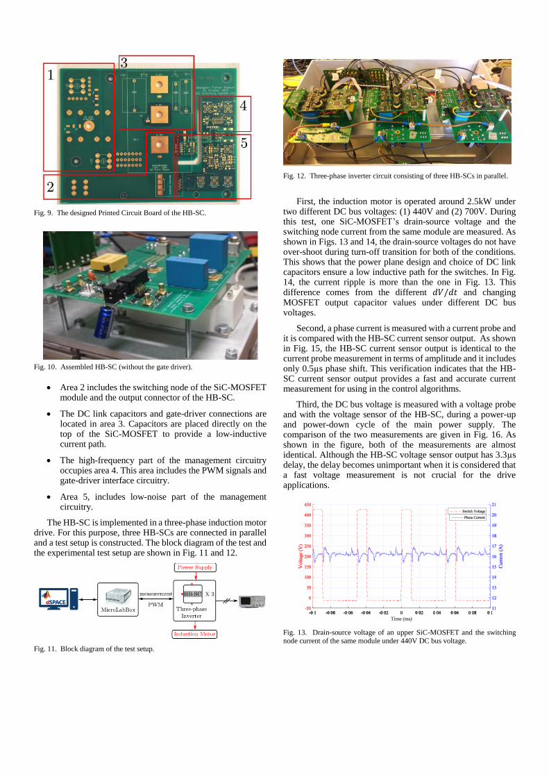
Fig. 9. The designed Printed Circuit Board of the HB-SC.
Fig. 10. Assembled HB-SC (without the gate driver).
Area 2 includes the switching node of the SiC-MOSFET module and the output connector of the HB-SC.
The DC link capacitors and gate-driver connections are located in area 3. Capacitors are placed directly on the top of the SiC-MOSFET to provide a low-inductive current path.
The high-frequency part of the management circuitry occupies area 4. This area includes the PWM signals and gate-driver interface circuitry.
Area 5, includes low-noise part of the management circuitry.
The HB-SC is implemented in a three-phase induction motor drive. For this purpose, three HB-SCs are connected in parallel and a test setup is constructed. The block diagram of the test and the experimental test setup are shown in Fig. 11 and 12.
Fig. 11. Block diagram of the test setup.
Fig. 12. Three-phase inverter circuit consisting of three HB-SCs in parallel.
First, the induction motor is operated around 2.5kW under two different DC bus voltages: (1) 440V and (2) 700V. During this test, one SiC-MOSFET’s drain-source voltage and the switching node current from the same module are measured. As shown in Figs. 13 and 14, the drain-source voltages do not have over-shoot during turn-off transition for both of the conditions. This shows that the power plane design and choice of DC link capacitors ensure a low inductive path for the switches. In Fig. 14, the current ripple is more than the one in Fig. 13. This difference comes from the different 𝑑𝑉/𝑑𝑡 and changing MOSFET output capacitor values under different DC bus voltages.
Second, a phase current is measured with a current probe and it is compared with the HB-SC current sensor output. As shown in Fig. 15, the HB-SC current sensor output is identical to the current probe measurement in terms of amplitude and it includes only 0.5µs phase shift. This verification indicates that the HB-SC current sensor output provides a fast and accurate current measurement for using in the control algorithms.
Third, the DC bus voltage is measured with a voltage probe and with the voltage sensor of the HB-SC, during a power-up and power-down cycle of the main power supply. The comparison of the two measurements are given in Fig. 16. As shown in the figure, both of the measurements are almost identical. Although the HB-SC voltage sensor output has 3.3µs delay, the delay becomes unimportant when it is considered that a fast voltage measurement is not crucial for the drive applications.
Fig. 13. Drain-source voltage of an upper SiC-MOSFET and the switching node current of the same module under 440V DC bus voltage.
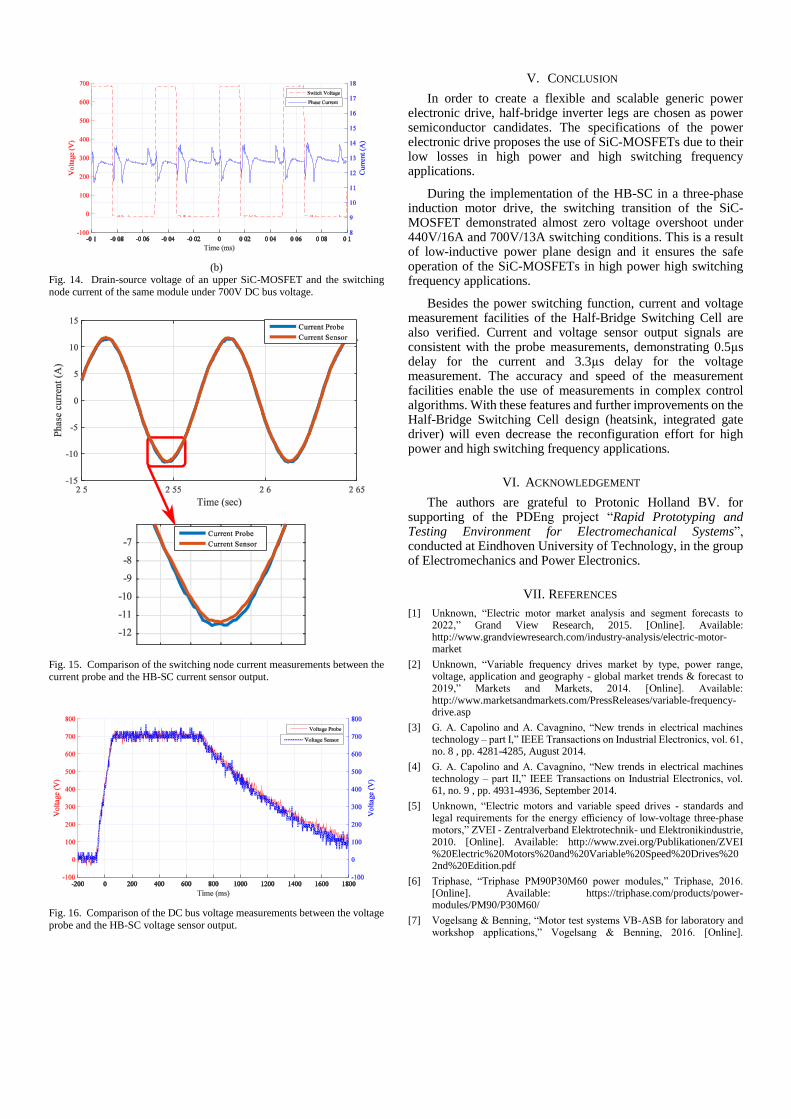
(b)
Fig. 14. Drain-source voltage of an upper SiC-MOSFET and the switching
node current of the same module under 700V DC bus voltage.
Fig. 15. Comparison of the switching node current measurements between the
current probe and the HB-SC current sensor output.
Fig. 16. Comparison of the DC bus voltage measurements between the voltage
probe and the HB-SC voltage sensor output.
V. CONCLUSION
In order to create a flexible and scalable generic power electronic drive, half-bridge inverter legs are chosen as power semiconductor candidates. The specifications of the power electronic drive proposes the use of SiC-MOSFETs due to their low losses in high power and high switching frequency applications.
During the implementation of the HB-SC in a three-phase induction motor drive, the switching transition of the SiC-MOSFET demonstrated almost zero voltage overshoot under 440V/16A and 700V/13A switching conditions. This is a result of low-inductive power plane design and it ensures the safe operation of the SiC-MOSFETs in high power high switching frequency applications.
Besides the power switching function, current and voltage measurement facilities of the Half-Bridge Switching Cell are also verified. Current and voltage sensor output signals are consistent with the probe measurements, demonstrating 0.5µs delay for the current and 3.3µs delay for the voltage measurement. The accuracy and speed of the measurement facilities enable the use of measurements in complex control algorithms. With these features and further improvements on the Half-Bridge Switching Cell design (heatsink, integrated gate driver) will even decrease the reconfiguration effort for high power and high switching frequency applications.
VI. ACKNOWLEDGEMENT
The authors are grateful to Protonic Holland BV. for supporting of the PDEng project “Rapid Prototyping and Testing Environment for Electromechanical Systems”, conducted at Eindhoven University of Technology, in the group of Electromechanics and Power Electronics.
VII. REFERENCES
[1] Unknown, “Electric motor market analysis and segment forecasts to 2022,” Grand View Research, 2015. [Online]. Available: http://www.grandviewresearch.com/industry-analysis/electric-motor-market
[2] Unknown, “Variable frequency drives market by type, power range, voltage, application and geography - global market trends & forecast to 2019,” Markets and Markets, 2014. [Online]. Available: http://www.marketsandmarkets.com/PressReleases/variable-frequency-drive.asp
[3] G. A. Capolino and A. Cavagnino, “New trends in electrical machines technology – part I,” IEEE Transactions on Industrial Electronics, vol. 61, no. 8 , pp. 4281-4285, August 2014.
[4] G. A. Capolino and A. Cavagnino, “New trends in electrical machines technology – part II,” IEEE Transactions on Industrial Electronics, vol. 61, no. 9 , pp. 4931-4936, September 2014.
[5] Unknown, “Electric motors and variable speed drives - standards and legal requirements for the energy efficiency of low-voltage three-phase motors,” ZVEI - Zentralverband Elektrotechnik- und Elektronikindustrie, 2010. [Online]. Available: http://www.zvei.org/Publikationen/ZVEI %20Electric%20Motors%20and%20Variable%20Speed%20Drives%202nd%20Edition.pdf
[6] Triphase, “Triphase PM90P30M60 power modules,” Triphase, 2016. [Online]. Available: https://triphase.com/products/power-modules/PM90/P30M60/
[7] Vogelsang & Benning, “Motor test systems VB-ASB for laboratory and workshop applications,” Vogelsang & Benning, 2016. [Online].

Available: http://www.vogelsangbenning.de/ wp-content/uploads/VB-englisch-Pbl-ASB.pdf
[8] F. Başkurt, “Rapid prototyping and testing environment for electromechanical systems – A unified drive system with SiC-Mosfets,” PDEng final report, Dept. Elec. Eng., Eindhoven Univ. Tech., Eindhoven, the Netherlands, 2016.
[9] Semikron, “Semikron SKAI 2HV Flyer,” Semikron, 2014. [Online]. Available: http://www.semikron.com/dl/service-support/downloads/ download/semikron-flyer-skai-lv-2014-04-08.pdf
[10] A. Anthon, J. C. Hernandez, Z. Zhang, and M. A. E. Andersen, “Switching investigations on a sic mosfet in a to-247 package,” in Industrial Electronics Society (IECON 2014), October 2014, pp. 1854–1860.
[11] Cree, “Minimizing parasitic effects in sic-mosfet modules,” 2015. [Online]. Available: http://www.mouser.com/pdfdocs/Cree CPWRAN12.pdf
[12] D. Lorusso, “Insulation calculator,” 2016. [Online]. Available: http://www.creepage.com
[13] Cree, “Techniques for minimizing parasitic inductance,” 2015. [Online]. Available: http://www.mouser.com/pdfDocs/Cree-Design-Considerations-for-Designing-with-Cree-SiC-Modules-part-2.pdf
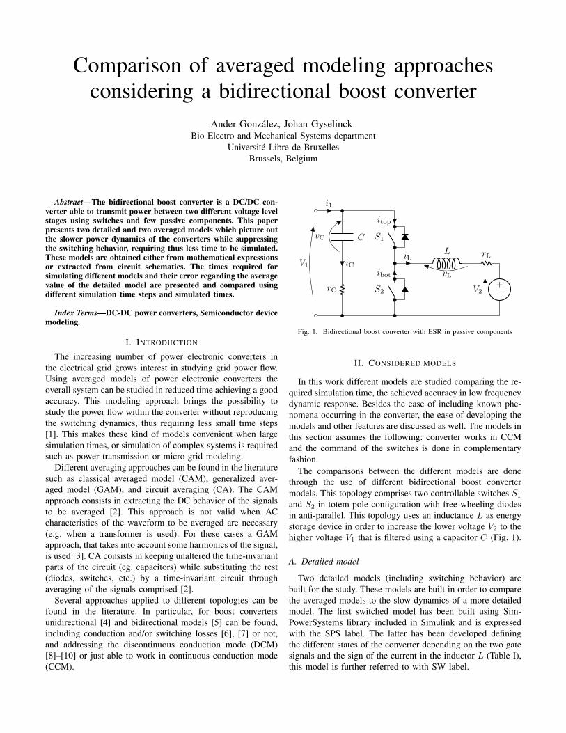
Comparison of averaged modeling approachesconsidering a bidirectional boost converter
Ander Gonzalez, Johan GyselinckBio Electro and Mechanical Systems department
Universite Libre de BruxellesBrussels, Belgium
Abstract—The bidirectional boost converter is a DC/DC con-verter able to transmit power between two different voltage levelstages using switches and few passive components. This paperpresents two detailed and two averaged models which picture outthe slower power dynamics of the converters while suppressingthe switching behavior, requiring thus less time to be simulated.These models are obtained either from mathematical expressionsor extracted from circuit schematics. The times required forsimulating different models and their error regarding the averagevalue of the detailed model are presented and compared usingdifferent simulation time steps and simulated times.
Index Terms—DC-DC power converters, Semiconductor devicemodeling.
I. INTRODUCTION
The increasing number of power electronic converters inthe electrical grid grows interest in studying grid power flow.Using averaged models of power electronic converters theoverall system can be studied in reduced time achieving a goodaccuracy. This modeling approach brings the possibility tostudy the power flow within the converter without reproducingthe switching dynamics, thus requiring less small time steps[1]. This makes these kind of models convenient when largesimulation times, or simulation of complex systems is requiredsuch as power transmission or micro-grid modeling.
Different averaging approaches can be found in the literaturesuch as classical averaged model (CAM), generalized aver-aged model (GAM), and circuit averaging (CA). The CAMapproach consists in extracting the DC behavior of the signalsto be averaged [2]. This approach is not valid when ACcharacteristics of the waveform to be averaged are necessary(e.g. when a transformer is used). For these cases a GAMapproach, that takes into account some harmonics of the signal,is used [3]. CA consists in keeping unaltered the time-invariantparts of the circuit (eg. capacitors) while substituting the rest(diodes, switches, etc.) by a time-invariant circuit throughaveraging of the signals comprised [2].
Several approaches applied to different topologies can befound in the literature. In particular, for boost convertersunidirectional [4] and bidirectional models [5] can be found,including conduction and/or switching losses [6], [7] or not,and addressing the discontinuous conduction mode (DCM)[8]–[10] or just able to work in continuous conduction mode(CCM).
+−V2
iLL
vL
rL
S2
ibot
i1
S1
itop
CvC
iC
rC
V1
Fig. 1. Bidirectional boost converter with ESR in passive components
II. CONSIDERED MODELS
In this work different models are studied comparing the re-quired simulation time, the achieved accuracy in low frequencydynamic response. Besides the ease of including known phe-nomena occurring in the converter, the ease of developing themodels and other features are discussed as well. The models inthis section assumes the following: converter works in CCMand the command of the switches is done in complementaryfashion.
The comparisons between the different models are donethrough the use of different bidirectional boost convertermodels. This topology comprises two controllable switches S1
and S2 in totem-pole configuration with free-wheeling diodesin anti-parallel. This topology uses an inductance L as energystorage device in order to increase the lower voltage V2 to thehigher voltage V1 that is filtered using a capacitor C (Fig. 1).
A. Detailed model
Two detailed models (including switching behavior) arebuilt for the study. These models are built in order to comparethe averaged models to the slow dynamics of a more detailedmodel. The first switched model has been built using Sim-PowerSystems library included in Simulink and is expressedwith the SPS label. The latter has been developed definingthe different states of the converter depending on the two gatesignals and the sign of the current in the inductor L (Table I),this model is further referred to with SW label.

TABLE IDEFINITION OF THE CONVERTER STATES
State iL γ γ S1 S2 u u
1 ≥ 0 1 0 ON OFF 1 02 < 0 0 1 ON OFF 1 03 ≥ 0 1 0 OFF ON 0 14 < 0 0 1 OFF ON 0 1
In this topology the following expressions will always betrue regardless of the state:
V1 − vC − iCrC = 0 (1)
vL = LdiLdt
(2)
iC = CdvCdt
(3)
The current i1 can be defined as follows:
states 1 and 2: i1 = iC + iL (4)states 3 and 4: i1 = iC (5)
The low voltage mesh can be also defined as:
state 1: V1 − VS1 − iLrS1 − vL − iLrL − V2 = 0 (6)state 2: V1 + VF1 − iLrF1 − vL − iLrL − V2 = 0 (7)state 3: −VF2 − iLrF2 − vL − iLrL − V2 = 0 (8)state 4: VS2 − iLrS2 − vL − iLrL − V2 = 0 (9)
where VS1, VS2, VF1 and VF2 are the forward voltages of theswitches 1 and 2 and their anti-parallel diodes respectively dur-ing on state, and rS1, rS2, rF1 and rF2 are the on resistances ofthe switches 1 and 2 and their anti-parallel diodes respectively.Substituting (1) and (2) into (6)-(9) and then substituting iCfor (3), yields:
state 1: LdiLdt
= −iL (rS1 + rC + rL)
+ vC − V2 + i1rC − VS1 (10)
state 2: LdiLdt
= −iL (rF1 + rC + rL)
+ vC − V2 + i1rC + VF1 (11)
state 3: LdiLdt
= −iL (rF2 + rL)− V2 − VF2 (12)
state 4: LdiLdt
= −iL (rS2 + rL)− V2 + VS2 (13)
and
states 1 and 2: CdvCdt
= i1 − iL, (14)
states 3 and 4: CdvCdt
= i1. (15)
Including the corresponding parameters defining the currentsense (γ) and the switching function (u) to each state, yields
+−V2
iLL
vL
rL
vbotibot
i1
+
− vtop
itop
CvC
iC
rC
V1
Fig. 2. Circuit averaged model of bidirectional boost converter with ESR inpassive components
the model describing the switching behavior of the converter
LdiLdt
= − (uA+ uB + rL) iL + uE + uF − V2 (16)
CdvCdt
= i1 − uiL (17)
with A = γrS1 + γrF1 + rC, B = γrF2 + γrS2, E = vC +rCi1 − γVS1 + γVF1, and F = −γVF2 + γVS2.
B. Classical averaged model
The classical averaged model is obtained in the same wayused for the detailed model presented above. This model islabeled as CAM throughout the paper. From (16) and (17),the switching function is averaged as follows [3]:
D = 〈u〉0 =1
Tw
∫ t
t−Tw
u · dt (18)
where Tw is the averaging window. Making Tw to correspondsto the PWM switching period, the duty cycle D will be equalto the average value of u. Doing that, the different states ofthe converter corresponding to u and u, will be averaged as Dand 1−D respectively, with D = TON
Tsw, and 1−D = TOFF
Tsw.
Applying this to (16) and (17) yields:
LdiLdt
= − [DA+ (1−D)B + rL] iL
+DE + (1−D)F − V2 (19)
CdvCdt
= i1 −DiL (20)
C. Circuit averaging model
In this modeling approach the time-invariant part of thetopology and the time-variant or switch network are separated.The time-invariant parts of the circuit (e.g. inductances, capac-itors...) are left without changes whereas the time-variant (eg.controlled switches, diodes...) is substituted by current andvoltage sources to obtain time-invariant circuits. This modelis represented with the label CA throughout the paper.
Applying this to bidirectional boost converter results in thenew circuit shown in Figure 2, where the controlled voltageand current sources are place interchangeable. Following thesame state definition based on the switch function u and
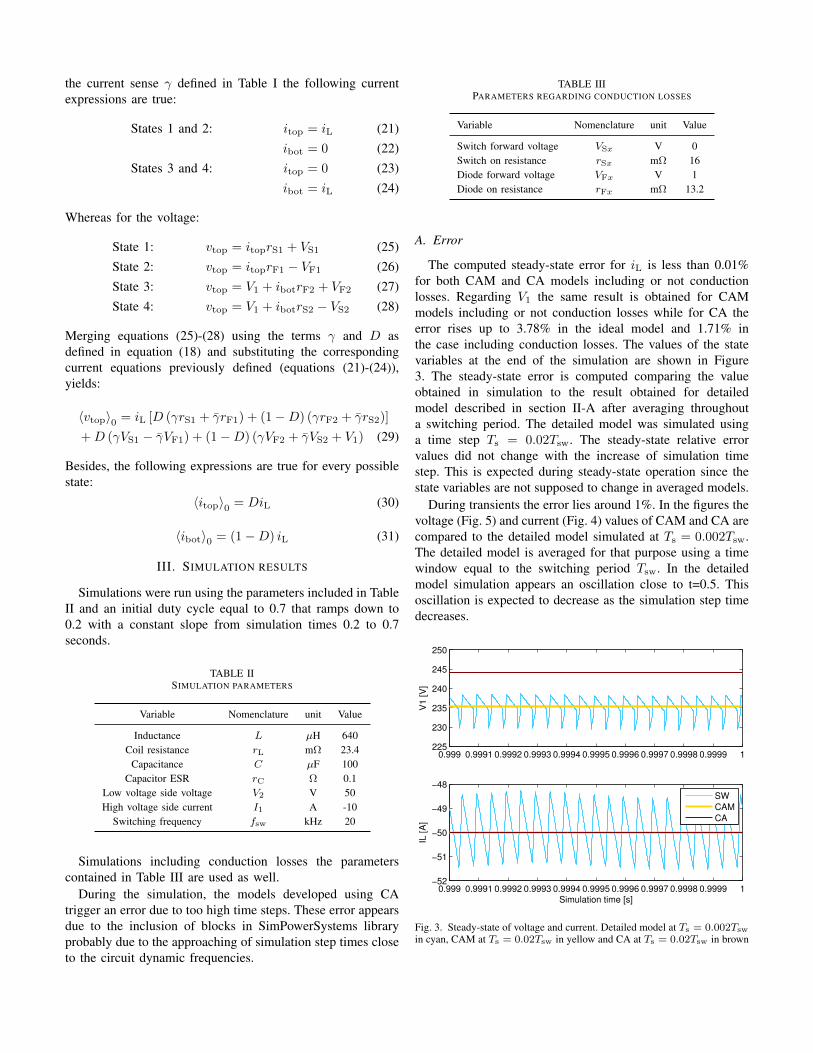
the current sense γ defined in Table I the following currentexpressions are true:
States 1 and 2: itop = iL (21)ibot = 0 (22)
States 3 and 4: itop = 0 (23)ibot = iL (24)
Whereas for the voltage:
State 1: vtop = itoprS1 + VS1 (25)State 2: vtop = itoprF1 − VF1 (26)State 3: vtop = V1 + ibotrF2 + VF2 (27)State 4: vtop = V1 + ibotrS2 − VS2 (28)
Merging equations (25)-(28) using the terms γ and D asdefined in equation (18) and substituting the correspondingcurrent equations previously defined (equations (21)-(24)),yields:
〈vtop〉0 = iL [D (γrS1 + γrF1) + (1−D) (γrF2 + γrS2)]
+D (γVS1 − γVF1) + (1−D) (γVF2 + γVS2 + V1) (29)
Besides, the following expressions are true for every possiblestate:
〈itop〉0 = DiL (30)
〈ibot〉0 = (1−D) iL (31)
III. SIMULATION RESULTS
Simulations were run using the parameters included in TableII and an initial duty cycle equal to 0.7 that ramps down to0.2 with a constant slope from simulation times 0.2 to 0.7seconds.
TABLE IISIMULATION PARAMETERS
Variable Nomenclature unit Value
Inductance L µH 640Coil resistance rL mΩ 23.4
Capacitance C µF 100Capacitor ESR rC Ω 0.1
Low voltage side voltage V2 V 50High voltage side current I1 A -10
Switching frequency fsw kHz 20
Simulations including conduction losses the parameterscontained in Table III are used as well.
During the simulation, the models developed using CAtrigger an error due to too high time steps. These error appearsdue to the inclusion of blocks in SimPowerSystems libraryprobably due to the approaching of simulation step times closeto the circuit dynamic frequencies.
TABLE IIIPARAMETERS REGARDING CONDUCTION LOSSES
Variable Nomenclature unit Value
Switch forward voltage VSx V 0Switch on resistance rSx mΩ 16Diode forward voltage VFx V 1Diode on resistance rFx mΩ 13.2
A. Error
The computed steady-state error for iL is less than 0.01%for both CAM and CA models including or not conductionlosses. Regarding V1 the same result is obtained for CAMmodels including or not conduction losses while for CA theerror rises up to 3.78% in the ideal model and 1.71% inthe case including conduction losses. The values of the statevariables at the end of the simulation are shown in Figure3. The steady-state error is computed comparing the valueobtained in simulation to the result obtained for detailedmodel described in section II-A after averaging throughouta switching period. The detailed model was simulated usinga time step Ts = 0.02Tsw. The steady-state relative errorvalues did not change with the increase of simulation timestep. This is expected during steady-state operation since thestate variables are not supposed to change in averaged models.
During transients the error lies around 1%. In the figures thevoltage (Fig. 5) and current (Fig. 4) values of CAM and CA arecompared to the detailed model simulated at Ts = 0.002Tsw.The detailed model is averaged for that purpose using a timewindow equal to the switching period Tsw. In the detailedmodel simulation appears an oscillation close to t=0.5. Thisoscillation is expected to decrease as the simulation step timedecreases.
0.999 0.9991 0.9992 0.9993 0.9994 0.9995 0.9996 0.9997 0.9998 0.9999 1225
230
235
240
245
250
V1 [V
]
0.999 0.9991 0.9992 0.9993 0.9994 0.9995 0.9996 0.9997 0.9998 0.9999 1−52
−51
−50
−49
−48
Simulation time [s]
IL [A
]
SW
CAM
CA
Fig. 3. Steady-state of voltage and current. Detailed model at Ts = 0.002Tswin cyan, CAM at Ts = 0.02Tsw in yellow and CA at Ts = 0.02Tsw in brown
0.1 0.2 0.3 0.4 0.5 0.6 0.7 0.8 0.9 1−60
−50
−40
−30
−20
−10
i L [
A]
⟨ SW ⟩0
CAM
CA
0.1 0.2 0.3 0.4 0.5 0.6 0.7 0.8 0.9 1−10
−5
0
5
10
Simulation time [s]
i L e
rro
r [%
]
CAM
CA
Fig. 4. Low voltage side current at time step of 1µs for averaged models
0.1 0.2 0.3 0.4 0.5 0.6 0.7 0.8 0.9 150
100
150
200
250
V1
[V
]
⟨ SW ⟩0
CAM
CA
0.1 0.2 0.3 0.4 0.5 0.6 0.7 0.8 0.9 1−4
−2
0
2
4
6
8
Simulation time [s]
V1
err
or
[%]
CAM
CA
Fig. 5. High voltage side voltage at time step of 1µs for averaged models
B. Simulation times
Different tables are presented along this section in orderto quantize the required time to simulate the different modelsunder certain conditions. Each model/conditions pair has beensimulated three times and the average of these is presentedin the tables in order to reduce the effect of different tasks
0 2 4 6 8 10 12 14 164
5
6
7
8
Switching frequency/Sampling frequency ratio
Ma
xim
um
ab
so
lute
err
or
[%]
CAM ideal
CAM cond. losses
CA ideal
CA cond. losses
Fig. 6. High voltage side voltage maximum absolute value of relative errorfor different switching frequency/sampling frequency ratios
0 2 4 6 8 10 12 14 167.8
8
8.2
8.4
8.6
8.8
Switching frequency/Sampling frequency ratioM
axim
um
absolu
te e
rror
[%]
CAM ideal
CAM cond. losses
CA ideal
CA cond. losses
Fig. 7. Low voltage side current maximum absolute value of relative errorfor different switching frequency/sampling frequency ratios
running in background.1) Ideal switches model: Four different ideal switch models
are compared of which two are detailed and other two aver-aged. Detailed models comprise a SimPowerSystems modelusing the Ideal Switch block (SPS) and the model described insection II-A (SW), while averaged models include the modelsdescribed in sections II-B (CAM) and II-C (CA) the latter builtusing SimPowerSystems blocks.
Simulation of the four models was carried out at fixedstep of Tsw/10 (5µs). Besides the averaged models weresimulated at larger step times that are not suitable for switchedmodels following Shannon’s theorem.The average time neededto simulate the models under different conditions is gatheredin Table IV.
2) Including conduction losses: Conduction losses are in-cluded in the model using two different ways. When a switchor diode is on (conducting) the device is modeled as a constantvoltage drop and a series resistance. These are already includedin all model equations in section II. In order to build adetailed model using SimPowerSystems library (SPS), theIdeal Switch block was replaced for Mosfet block. The averagetime required for simulating these models is gathered in TableV.
IV. DISCUSSION
CAM and CA models can be obtained in a similar wayto the detailed model. CA approach can be easily used asbuilding block for developing more complex models while theCAM approach is not easy to be adapted. Since CA approachonly averages the time-variant piece of the circuit this remains
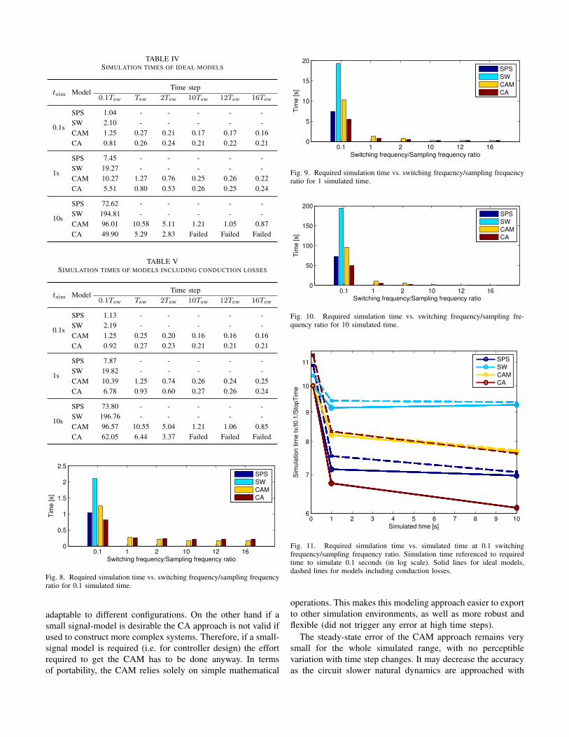
TABLE IVSIMULATION TIMES OF IDEAL MODELS
tsim ModelTime step
0.1Tsw Tsw 2Tsw 10Tsw 12Tsw 16Tsw
0.1s
SPS 1.04 - - - - -SW 2.10 - - - - -CAM 1.25 0.27 0.21 0.17 0.17 0.16CA 0.81 0.26 0.24 0.21 0.22 0.21
1s
SPS 7.45 - - - - -SW 19.27 - - - - -CAM 10.27 1.27 0.76 0.25 0.26 0.22CA 5.51 0.80 0.53 0.26 0.25 0.24
10s
SPS 72.62 - - - - -SW 194.81 - - - - -CAM 96.01 10.58 5.11 1.21 1.05 0.87CA 49.90 5.29 2.83 Failed Failed Failed
TABLE VSIMULATION TIMES OF MODELS INCLUDING CONDUCTION LOSSES
tsim ModelTime step
0.1Tsw Tsw 2Tsw 10Tsw 12Tsw 16Tsw
0.1s
SPS 1.13 - - - - -SW 2.19 - - - - -CAM 1.25 0.25 0.20 0.16 0.16 0.16CA 0.92 0.27 0.23 0.21 0.21 0.21
1s
SPS 7.87 - - - - -SW 19.82 - - - - -CAM 10.39 1.25 0.74 0.26 0.24 0.25CA 6.78 0.93 0.60 0.27 0.26 0.24
10s
SPS 73.80 - - - - -SW 196.76 - - - - -CAM 96.57 10.55 5.04 1.21 1.06 0.85CA 62.05 6.44 3.37 Failed Failed Failed
0.1 1 2 10 12 160
0.5
1
1.5
2
2.5
Switching frequency/Sampling frequency ratio
Tim
e [
s]
SPS
SW
CAM
CA
Fig. 8. Required simulation time vs. switching frequency/sampling frequencyratio for 0.1 simulated time.
adaptable to different configurations. On the other hand if asmall signal-model is desirable the CA approach is not valid ifused to construct more complex systems. Therefore, if a small-signal model is required (i.e. for controller design) the effortrequired to get the CAM has to be done anyway. In termsof portability, the CAM relies solely on simple mathematical
0.1 1 2 10 12 160
5
10
15
20
Switching frequency/Sampling frequency ratio
Tim
e [
s]
SPS
SW
CAM
CA
Fig. 9. Required simulation time vs. switching frequency/sampling frequencyratio for 1 simulated time.
0.1 1 2 10 12 160
50
100
150
200
Switching frequency/Sampling frequency ratioT
ime [s]
SPS
SW
CAM
CA
Fig. 10. Required simulation time vs. switching frequency/sampling fre-quency ratio for 10 simulated time.
0 1 2 3 4 5 6 7 8 9 106
7
8
9
10
11
Simulated time [s]
Sim
ula
tion tim
e tx/t0.1
/Sto
pT
ime
SPS
SW
CAM
CA
Fig. 11. Required simulation time vs. simulated time at 0.1 switchingfrequency/sampling frequency ratio. Simulation time referenced to requiredtime to simulate 0.1 seconds (in log scale). Solid lines for ideal models,dashed lines for models including conduction losses.
operations. This makes this modeling approach easier to exportto other simulation environments, as well as more robust andflexible (did not trigger any error at high time steps).
The steady-state error of the CAM approach remains verysmall for the whole simulated range, with no perceptiblevariation with time step changes. It may decrease the accuracyas the circuit slower natural dynamics are approached with
0.1 0.2 0.3 0.4 0.5 0.6 0.7 0.8 0.9 150
100
150
200
250
300
Simulation time [s]
V1 [V
]
Ts=0.02T
sw
Ts=0.002T
sw
Fig. 12. Output voltage in detailed model SW for different simulation timesteps.
the increase of simulation time step. The CA model presentsa higher steady-state error which is also not affected by theincrease of the simulation time step within an acceptablerange. Including the conduction losses of the semiconductordevices did not change considerably any of the errors exceptthe error in V 1 that was reduced from 3.78% to 1.71%.
The relative error during duty cycle changes does notnotably change for the selected simulation time step range.The maximum of the absolute value of the relative error ofthe voltage and the current are shown in figures 6 and 7respectively. It is predictable that the error will become greateras the time step is increased, specially when circuit naturalfrequencies are reached.
The time required to simulate any of the models increasesnearly in a linear way regarding to the simulated time. Agraphical example of this can be found in Figure 11 whereit can be seen that for short simulated times initializationtime is not negligible anymore. Time measurements are shownstarting at simulation step time of Ts = 0.1Tsw. In the caseof detailed models using fixed step the accuracy obtained isnot good enough due to low resolution of PWM duty cycle.This makes necessary to further reduce the simulation steptime if good accuracy during transients is wanted, makingthus averaged models even more valuable when switchingdynamics of the converter are not interesting. A graphicalexample is shown in Figure 12 where the detailed modelresponse is shown for simulation time steps 0.02Tsw (1µs)and 0.002Tsw (100ns).
V. CONCLUSION
Averaged models show a relatively high accuracy picturingout the power dynamics of the power converters. Averagedmodels do not require small simulation time steps comparedto detailed models even during transients. This makes averagedmodels suitable for long simulation times as well as forsimulation of complex systems. Time savings is just the mostremarkable benefit since some averaged models might belinearized for controller design as well.
ACKNOWLEDGMENT
The work contained in this paper was supported by thegovernment of the Belgian Walloon region under the projectBATWAL.
REFERENCES
[1] D. Maksimovic, a.M. Stankovic, V. Thottuvelil, and G. Verghese,“Modeling and simulation of power electronic converters,” Proceedingsof the IEEE, vol. 89, no. 6, 2001.
[2] R. W. Erickson and D. Maksimovic, Fundamentals of Power Electronics,2001.
[3] S. Bacha, I. Munteanu, and A. I. Bratcu, Power ElectronicConverters Modeling and Control. Springer, 2014. [Online]. Available:http://link.springer.com/10.1007/978-1-4471-5478-5
[4] Y. Lu, G. F. G. Feng, and Y.-F. L. Y.-F. Liu, “A large signal dy-namic model for DC-to-DC converters with average current control,”Nineteenth Annual IEEE Applied Power Electronics Conference andExposition, 2004. APEC ’04., vol. 2, no. C, pp. 797–803, 2004.
[5] S. Abid and A. Ammous, “Average modeling of DC-DC and DC-ACconverters including semiconductor device non-linearities,” InternationalConference on Design and Test of Integrated Systems in NanoscaleTechnology, 2006. DTIS 2006., no. d, 2006.
[6] G. Gatto, I. Marongiu, A. Mocci, A. Serpi, and I. L. Spano, “Animproved averaged model for boost DC-DC converters,” IECON Pro-ceedings (Industrial Electronics Conference), pp. 412–417, 2013.
[7] A. Ammous, K. Ammous, M. Ayedi, Y. Ounajjar, and F. Sellami,“An advanced PWM-switch model including semiconductor devicenonlinearities,” IEEE Transactions on Power Electronics, vol. 18, no. 5,pp. 1230–1237, 2003.
[8] J. Channegowda, B. Saritha, H. R. Chola, and G. Narayanan, “Com-parative evaluation of switching and average models of a DC-DCboost converter for real-time simulation,” IEEE CONECCT 2014 -2014 IEEE International Conference on Electronics, Computing andCommunication Technologies, pp. 1–6, 2014.
[9] T. Pavlovic, T. Bjazi, and Z. Ban, “Simplified averaged models ofdc-dc power converters suitable for controller design and microgridsimulation,” IEEE Transactions on Power Electronics, vol. 28, no. 7,pp. 3266–3275, 2013.
[10] C. Jaen, R. Pindado, J. Pou, A. Arias, and V. Sala, “Adaptive aver-aged model applied to PWM DC-DC converters,” EPE-PEMC 2006:12th International Power Electronics and Motion Control Conference,Proceedings, pp. 118–123, 2007.
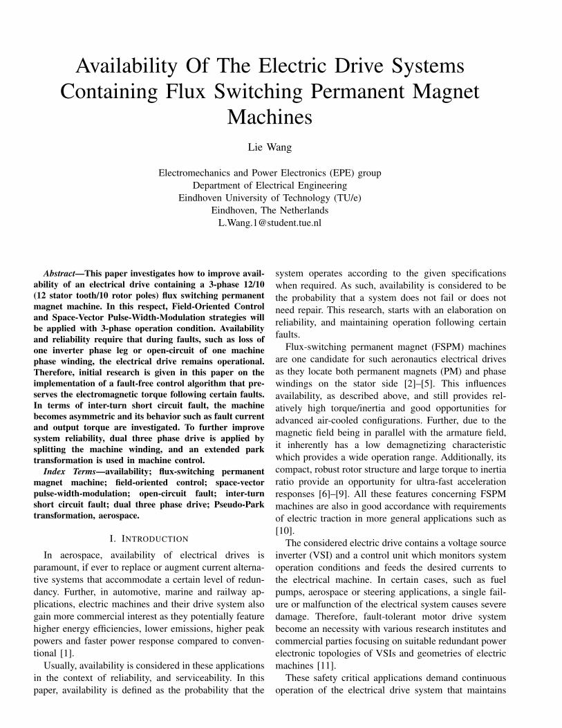
Availability Of The Electric Drive SystemsContaining Flux Switching Permanent Magnet
MachinesLie Wang
Electromechanics and Power Electronics (EPE) groupDepartment of Electrical Engineering
Eindhoven University of Technology (TU/e)Eindhoven, The Netherlands
Abstract—This paper investigates how to improve avail-ability of an electrical drive containing a 3-phase 12/10(12 stator tooth/10 rotor poles) flux switching permanentmagnet machine. In this respect, Field-Oriented Controland Space-Vector Pulse-Width-Modulation strategies willbe applied with 3-phase operation condition. Availabilityand reliability require that during faults, such as loss ofone inverter phase leg or open-circuit of one machinephase winding, the electrical drive remains operational.Therefore, initial research is given in this paper on theimplementation of a fault-free control algorithm that pre-serves the electromagnetic torque following certain faults.In terms of inter-turn short circuit fault, the machinebecomes asymmetric and its behavior such as fault currentand output torque are investigated. To further improvesystem reliability, dual three phase drive is applied bysplitting the machine winding, and an extended parktransformation is used in machine control.
Index Terms—availability; flux-switching permanentmagnet machine; field-oriented control; space-vectorpulse-width-modulation; open-circuit fault; inter-turnshort circuit fault; dual three phase drive; Pseudo-Parktransformation, aerospace.
I. INTRODUCTION
In aerospace, availability of electrical drives isparamount, if ever to replace or augment current alterna-tive systems that accommodate a certain level of redun-dancy. Further, in automotive, marine and railway ap-plications, electric machines and their drive system alsogain more commercial interest as they potentially featurehigher energy efficiencies, lower emissions, higher peakpowers and faster power response compared to conven-tional [1].
Usually, availability is considered in these applicationsin the context of reliability, and serviceability. In thispaper, availability is defined as the probability that the
system operates according to the given specificationswhen required. As such, availability is considered to bethe probability that a system does not fail or does notneed repair. This research, starts with an elaboration onreliability, and maintaining operation following certainfaults.
Flux-switching permanent magnet (FSPM) machinesare one candidate for such aeronautics electrical drivesas they locate both permanent magnets (PM) and phasewindings on the stator side [2]–[5]. This influencesavailability, as described above, and still provides rel-atively high torque/inertia and good opportunities foradvanced air-cooled configurations. Further, due to themagnetic field being in parallel with the armature field,it inherently has a low demagnetizing characteristicwhich provides a wide operation range. Additionally, itscompact, robust rotor structure and large torque to inertiaratio provide an opportunity for ultra-fast accelerationresponses [6]–[9]. All these features concerning FSPMmachines are also in good accordance with requirementsof electric traction in more general applications such as[10].
The considered electric drive contains a voltage sourceinverter (VSI) and a control unit which monitors systemoperation conditions and feeds the desired currents tothe electrical machine. In certain cases, such as fuelpumps, aerospace or steering applications, a single fail-ure or malfunction of the electrical system causes severedamage. Therefore, fault-tolerant motor drive systembecome an necessity with various research institutes andcommercial parties focusing on suitable redundant powerelectronic topologies of VSIs and geometries of electricmachines [11].
These safety critical applications demand continuousoperation of the electrical drive system that maintains

its equivalent output performance when a fault hashappened. These system faults can contain, among manyothers, switch component short and open-circuit, phaseleg short-circuit and machine phase open-circuit [11].Within this paper, a Field-Oriented Control (FOC) isapplied to regulate the phase currents and output elec-tromagnetic torque of the FSPM, which is standard forbrushless ac (BLAC) and induction machines that requirethe maximization of torque-to-ampere (MTPA) ratio andfield weakening operation [12]–[14].
In addition, another common fault, intern turn shortcircuit can happen, caused by the coil insulation break-down. This will create an extra short circuit path thatflows very large current driven with back-emf inducedby coupled flux-linkage in the short turns [15], [16]. Inthis paper, the machine behavior such as fault current,produced torque and required supply voltage will beinvestigated based on the built up model.
To further improve the drive availability and enhanceoperation capability such as speed range, machine wind-ing could be separated into six phases and then a dualVSI drive topology is proposed [17]–[20]. Correspond-ing control and regulation methods are developed withassistant of its specific space vector model.
II. ELECTRIC DRIVE SYSTEM FOR FSPM MACHINE
The machine inductance plays a paramount role inthe prediction of the dynamic machine behavior. Afteracquiring these inductance values, the required specificmachine equivalent circuit parameters can be obtained.These are then used to stipulate the machine within theelectric drive control strategy to achieve high perfor-mance control of the FSPM machine.
A. FSPM Machine Inductance Characteristics
A general mathematical description of the inductancein an electric circuit is given by:
V = Ri+ dψdt = Ri+ dψ
dididt ,
∆L = dψdi .
(1)
where R is the resistance of the inductor, ψ is the flux-linkage and 4L is defined as the incremental inductanceobtained from the tangent value of the hysteresis ψ-icurve. It represents the same value as apparent induc-tance L = ψ/i when the machine operates in the linearregion of the ferromagnetic material, but deviates in thesaturation region [21]. Incremental inductances ratherthan apparent inductances have to be implemented in thecurrent controller design in order to accurately predictthe transient response of drive system [22].
Figure 1: The geometry of the 3-phase 12/10 flux switchingpermanent magnet machine[7].
Furthermore, from a machine analysis and controlperspective, rotor position is defined by using the dq-axis coordinate, where d-axis alignment occurs when themaximum flux-linkage is achieved by phase A and theq-axis is 90 electric degree leading. However, in caseof FSPM machine, the dq-axis definition is modifiedbecause of its special machine topology which is shownin Fig. 1.
Figure 2: The modified dq-axis in FSPM machine and mag-netic field generated by PM and phase winding.
From the knowledge of [23], when the d-axis isaligned, the field ψpm produced by the permanent magnetis illustrated by black arrows, is strengthening the fieldψe that is excited by the phase winding, which is illus-trated by red arrows for a single rotor position. However,ψpm is opposing (i.e. field weakening) the phase windingfield at another position. Therefore, instead of a periodicd and q-axis throughout the machine, two independent d-axis are applicable with two constant q-axis as illustratedin Fig. 2.
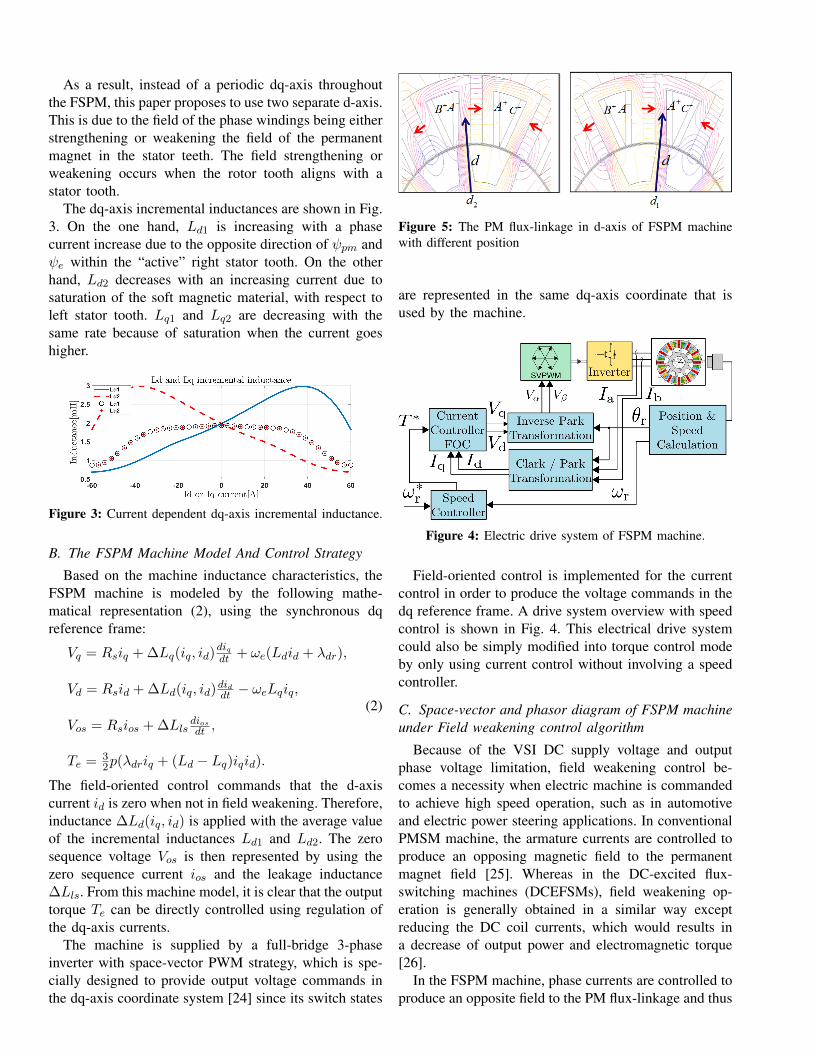
As a result, instead of a periodic dq-axis throughoutthe FSPM, this paper proposes to use two separate d-axis.This is due to the field of the phase windings being eitherstrengthening or weakening the field of the permanentmagnet in the stator teeth. The field strengthening orweakening occurs when the rotor tooth aligns with astator tooth.
The dq-axis incremental inductances are shown in Fig.3. On the one hand, Ld1 is increasing with a phasecurrent increase due to the opposite direction of ψpm andψe within the “active” right stator tooth. On the otherhand, Ld2 decreases with an increasing current due tosaturation of the soft magnetic material, with respect toleft stator tooth. Lq1 and Lq2 are decreasing with thesame rate because of saturation when the current goeshigher.
Figure 3: Current dependent dq-axis incremental inductance.
B. The FSPM Machine Model And Control Strategy
Based on the machine inductance characteristics, theFSPM machine is modeled by the following mathe-matical representation (2), using the synchronous dqreference frame:
Vq = Rsiq + ∆Lq(iq, id)diqdt + ωe(Ldid + λdr),
Vd = Rsid + ∆Ld(iq, id)diddt − ωeLqiq,
Vos = Rsios + ∆Llsdiosdt ,
Te = 32p(λdriq + (Ld − Lq)iqid).
(2)
The field-oriented control commands that the d-axiscurrent id is zero when not in field weakening. Therefore,inductance ∆Ld(iq, id) is applied with the average valueof the incremental inductances Ld1 and Ld2. The zerosequence voltage Vos is then represented by using thezero sequence current ios and the leakage inductance∆Lls. From this machine model, it is clear that the outputtorque Te can be directly controlled using regulation ofthe dq-axis currents.
The machine is supplied by a full-bridge 3-phaseinverter with space-vector PWM strategy, which is spe-cially designed to provide output voltage commands inthe dq-axis coordinate system [24] since its switch states
Figure 5: The PM flux-linkage in d-axis of FSPM machinewith different position
are represented in the same dq-axis coordinate that isused by the machine.
Figure 4: Electric drive system of FSPM machine.
Field-oriented control is implemented for the currentcontrol in order to produce the voltage commands in thedq reference frame. A drive system overview with speedcontrol is shown in Fig. 4. This electrical drive systemcould also be simply modified into torque control modeby only using current control without involving a speedcontroller.
C. Space-vector and phasor diagram of FSPM machineunder Field weakening control algorithm
Because of the VSI DC supply voltage and outputphase voltage limitation, field weakening control be-comes a necessity when electric machine is commandedto achieve high speed operation, such as in automotiveand electric power steering applications. In conventionalPMSM machine, the armature currents are controlled toproduce an opposing magnetic field to the permanentmagnet field [25]. Whereas in the DC-excited flux-switching machines (DCEFSMs), field weakening op-eration is generally obtained in a similar way exceptreducing the DC coil currents, which would results ina decrease of output power and electromagnetic torque[26].
In the FSPM machine, phase currents are controlled toproduce an opposite field to the PM flux-linkage and thus
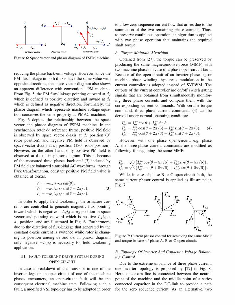
Figure 6: Space vector and phasor diagram of FSPM machine.
reducing the phase back-emf voltage. However, since thePM flux-linkage in both d-axis have the same value withopposite directions, the space-vector diagram also showsan apparent difference with conventional PM machine.From Fig. 5, the PM flux-linkage pointing outward at d2
which is defined as positive direction and inward at d1
which is defined as negative direction. Fortunately, thephasor diagram which represents machine voltage equa-tion conserves the same property as PMAC machine.
Fig. 6 depicts the relationship between the spacevector and phasor diagram of FSPM machine. In thesynchronous rotor dq reference frame, positive PM fieldis observed by space vector d-axis at d2 position (0
rotor position), and negative PM field is observed byspace vector d-axis at d1 position (180 rotor position).However, on the other hand, only positive PM field isobserved at d-axis in phasor diagram. This is becauseof the measured three phases back-emf (3) induced byPM field are balanced sinusoidal AC waveforms, throughPark transformation, constant positive PM field value isobtained at d-axis.
Va = −ωeλPM sin(θ),Vb = −ωeλPM sin(θ − 2π/3),Vc = −ωeλPM sin(θ + 2π/3).
(3)
In order to apply field weakening, the armature cur-rents are controlled to generate magnetic flux pointinginward which is negative −Ldid at d2 position in spacevector and pointing outward which is positive Ldid atd1 position, and are illustrated in Fig. 6. Furthermore,due to the direction of flux-linkage that generated by theconstant d-axis current is switched while rotor is chang-ing its position among d1 and d2, in phasor diagram,only negative −Ldid is necessary for field weakeningapplication.
III. FAULT-TOLERANT DRIVE SYSTEM DURING
OPEN-CIRCUIT
In case a breakdown of the transistor in one of theinverter legs or an open-circuit of one of the machinephases encounters, an open-circuit fault will be theconsequent electrical machine state. Following such afault, a modified VSI topology has to be adopted in order
to allow zero sequence current flow that arises due to thesummation of the two remaining phase currents. Thus,to preserve continuous operation, an algorithm is appliedwith two phase operation that maintains the requiredshaft torque.
A. Torque Maintain Algorithm
Obtained from [27], the torque can be preserved byproducing the same magnetomotive force (MMF) withtwo machine phases in case of a phase open-circuit fault.Because of the open-circuit of an inverter phase leg ormachine phase winding, hysteresis modulation in thecurrent controller is adopted instead of SVPWM. Theoutputs of the current controller are on/off switch gatingsignals that are obtained from simultaneously monitor-ing three phase currents and compare them with thecorresponding current commands. With certain torquecommand, three phase current commands (4) can bederived under normal operating condition:
I∗as = I∗∗qs cos θ + I∗∗ds sin θ,I∗bs = I∗∗qs cos(θ − 2π/3) + I∗∗ds sin(θ − 2π/3),I∗cs = I∗∗qs cos(θ + 2π/3) + I∗∗ds sin(θ + 2π/3).
(4)
However, with one phase open-circuit, e.g. phaseA, the three-phase current commands are modified asfollowing for regaining the same MMF:
I∗bs =√
3(I∗∗qs cos(θ − 5π/6) + I∗∗ds sin(θ − 5π/6)
),
I∗cs =√
3(I∗∗qs cos(θ + 5π/6) + I∗∗ds sin(θ + 5π/6)
).
While, in case of phase B or C open-circuit fault, thesame current phasor control is applied as illustrated inFig. 7
Figure 7: Current phasor control for achieving the same MMFand torque in case of phase A, B or C open-circuit.
B. Topology Of Inverter And Capacitor Voltage Balanc-ing Control
Due to the extreme unbalance of three phase current,one inverter topology is proposed by [27] in Fig. 8.Here, one extra line is connected between the neutralpoint of the machine and the middle point of a seriesconnected capacitor in the DC-link to provide a pathfor the zero sequence current. As an alternative, two
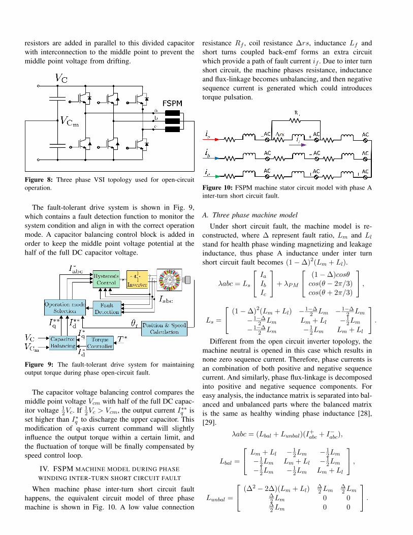
resistors are added in parallel to this divided capacitorwith interconnection to the middle point to prevent themiddle point voltage from drifting.
Figure 8: Three phase VSI topology used for open-circuitoperation.
The fault-tolerant drive system is shown in Fig. 9,which contains a fault detection function to monitor thesystem condition and align in with the correct operationmode. A capacitor balancing control block is added inorder to keep the middle point voltage potential at thehalf of the full DC capacitor voltage.
Figure 9: The fault-tolerant drive system for maintainingoutput torque during phase open-circuit fault.
The capacitor voltage balancing control compares themiddle point voltage Vcm with half of the full DC capac-itor voltage 1
2Vc. If 12Vc > Vcm, the output current I∗∗q is
set higher than I∗q to discharge the upper capacitor. Thismodification of q-axis current command will slightlyinfluence the output torque within a certain limit, andthe fluctuation of torque will be finally compensated byspeed control loop.
IV. FSPM MACHINE MODEL DURING PHASE
WINDING INTER-TURN SHORT CIRCUIT FAULT
When machine phase inter-turn short circuit faulthappens, the equivalent circuit model of three phasemachine is shown in Fig. 10. A low value connection
resistance Rf , coil resistance ∆rs, inductance Lf andshort turns coupled back-emf forms an extra circuitwhich provide a path of fault current if . Due to inter turnshort circuit, the machine phases resistance, inductanceand flux-linkage becomes unbalancing, and then negativesequence current is generated which could introducestorque pulsation.
Figure 10: FSPM machine stator circuit model with phase Ainter-turn short circuit fault.
A. Three phase machine model
Under short circuit fault, the machine model is re-constructed, where ∆ represent fault ratio, Lm and Llstand for health phase winding magnetizing and leakageinductance, thus phase A inductance under inter turnshort circuit fault becomes (1−∆)2(Lm + Ll).
λabc = Ls
IaIbIc
+ λPM
(1−∆)cosθcos(θ − 2π/3)cos(θ + 2π/3)
,
Ls =
(1−∆)2(Lm + Ll) −1−∆2 Lm −1−∆
2 Lm−1−∆
2 Lm Lm + Ll −12Lm
−1−∆2 Lm −1
2Lm Lm + Ll
.Different from the open circuit inverter topology, the
machine neutral is opened in this case which results innone zero sequence current. Therefore, phase currents isan combination of both positive and negative sequencecurrent. And similarly, phase flux-linkage is decomposedinto positive and negative sequence components. Foreasy analysis, the inductance matrix is separated into bal-anced and unbalanced parts where the balanced matrixis the same as healthy winding phase inductance [28],[29].
λabc = (Lbal + Lunbal)(I+abc + I−abc),
Lbal =
Lm + Ll −12Lm −1
2Lm−1
2Lm Lm + Ll −12Lm
−12Lm −1
2Lm Lm + Ll
,
Lunbal =
(∆2 − 2∆)(Lm + Ll)∆2 Lm
∆2 Lm
∆2 Lm 0 0∆2 Lm 0 0
.

The three phase flux-linkage can be transformed intostationary αβ reference frame:
λ+αβ = LssI
+αβ + λPM (1− ∆
3 )
[cos θsin θ
]+ 2
3∆mI+α ,
λ−αβ = LssI−αβ − λPM
∆3
[cos θ− sin θ
]+ 2
3∆mI+α .
In the matrix form representation it becomes:
λ+αβ = (Lss +B)
[I+α
I+β
]+ λPM (1− ∆
3 )
[cos θsin θ
],
λ−αβ = (Lss +B)
[I+α
I+β
]− λPM ∆
3
[cos θ− sin θ
].
with
Lss =
[32Lm + Ll 0
0 32Lm + Ll
],
B = 23∆m
[1 00 0
],
∆m = ∆(∆− 3)Lm + ∆(∆− 2)Ll.
I+αβ− and θ represent the positive, negative sequence
current in stationary frame and electrical rotor angle.After acquiring the αβ flux linkage, it can be transformedin the dq rotor synchronous reference frame by using
I+dq =
[cos θ sin θ− sin θ cos θ
]I+αβ = e−JθI+
αβ
and
I−dq =
[cos θ − sin θsin θ cos θ
]I−αβ = eJθI−αβ
The flux-linkage in dq frame is then derived as
λ+dq = e−Jθ(Lss +B)eJθI+
dq + λPM (1− ∆3 )
[10
],
λ−dq = eJθ(Lss +B)e−JθI−dq + λPM∆3
[−10
].
Then, the machine main circuit voltage equation inpositive and negative sequence can be represented as :
V +dq = rI+
dq + ωeJλ+dq +
dλ+dq
dt
= rI+dq + ωeJLssI
+dq + ωeJLααI
+dq + ωeλPM
[01
]−ωeλPM ∆
3
[01
]+ Lss
dI+dqdt + Lαα
dI+dqdt
,
(5)the negative sequence is :
V −dq = rI−dq − ωeJλ−dq +
dλ−dqdt
= rI−dq − ωeJLssI−dq − ωeJLββI
−dq + ωeλPM
∆3
[01
]+Lss
dI−dqdt + Lββ
dI−dqdt
.
(6)
with Lαα = e−JθBeJθ and Lββ = eJθBe−Jθ. The thirdterms in (5),(6) can be further expand to :
ωeJLααI+dq
= 13∆mωe
([0 −11 0
]+
[sin 2θ cos 2θcos 2θ − sin 2θ
])I+dq
= 13∆mωeJI
+dq + 1
3∆mωe
[0 11 0
]I−dq
and−ωeJLββI−dq= 1
3∆mωe
([0 1−1 0
]+
[sin 2θ − cos 2θ− cos 2θ − sin 2θ
])I−dq
= −13∆mωeJI
−dq + 1
3∆mωe
[0 −1−1 0
]I+dq
.
B. Machine model contains short circuit loop
The full circuit model is a combination of main threephase and the inter turn short circuit loop, the full fluxlinkage equation is
λabcf = Labcf iabcf + λPMabcf .
Where Lf = (2∆−∆2)(Lm + Ll), Lphase = Lm + Lland Labcf is
Lphase − Lf −1−∆2 Lm −1−∆
2 Lm Lf −∆Lphase−1−∆
2 Lm Lm + Ll −12Lm −∆
2 Lm−1−∆
2 Lm −12Lm Lm + Ll −∆
2 LmLf −∆Lphase −∆
2 Lm −∆2 Lm −Lf + 2∆Lphase
, the fault if is derived with
−(Rf + ∆rs)if +Rf ia =dλfdt
,
where
λf = (Lf−∆(Lm2
+Ll))ia+(−Lf+2∆Lphase)if+∆λPM cos θ.
Then fault if current can be represented as following atsteady state:
if =bd+ acωea2ωe2 + b2
sin θ +bc− adωea2ωe2 + b2
cos θ.
The coupled flux-linkage from the fault circuit to ma-chine main phase circuit in αβ frame is :[λαfλβf
]=
2
3(Lf−∆(
Lm2
+Ll)
[bd+acωea2ωe2+b2 sin θ + bc−adωe
a2ωe2+b2 cos θ
0
].
The flux linkage in αβ frame is then decomposedinto positive and negative sequence for applying dqtransformation, and after that the voltage induced by faultflux-linkage in dq reference frame is :[
V +df
V +qf
]=
(Lf−∆(Lm2
+Ll))ωe3(b2+a2ωe2)
[bd+ acωebc− adωe
],[
V −dfV −qf
]=
(Lf−∆(Lm2
+Ll))ωe3(b2+a2ωe2)
[bd+ acωe−bc+ adωe
].
(7)

With the following parameters
a = −Lf + 2∆Lphase,b = Rf + ∆rs,
c = (Lf −∆(Lm2 + Ll))isωe,d = ∆λPMωe −Rf is.
The machine full mathematic model can be achievedby using equation (5)-(7), which including the healthyphase part and inter-turn short circuit part:
V +dq = rI+
dq + ωeJλ+dq +
dλ+dq
dt
= rI+dq + ωeJLssI
+dq + 1
3∆mωeJI+dq
+13∆mωe
[0 11 0
]I−dq + ωeλPM (1− ∆
3 )
[01
]+Lss
dI+dqdt + Lαα
dI+dqdt +
[V +df
V +qf
],
(8)
and
V −dq = rI−dq − ωeJλ−dq +
dλ−dqdt
= rI−dq − ωeJLssI−dq −
13∆mωeJI
−dq
+13∆mωe
[0 −1−1 0
]I+dq + ωeλPM
∆3
[01
]+Lss
dI−dqdt + Lββ
dI−dqdt +
[V −dfV −qf
].
(9)
The output electromagnetic torque under i+d = i−dq = 0is shown in (10) as following, which contains positivealignment torque, a second order component caused bythe back-emf in q-axis of negative sequence, and a torquedue the back-emf in short circuit turns −ωe∆λm sin θand fault current if .
Te = 32Pλm[(1− ∆
3 + ∆3 cos 2θ)i+qe −∆if sin θ]
(10)From equation (11), the short circuit fault can also befurther detected by observing the controller negativesequence output voltage by controlling the negativesequence current to zero.
V −dq = 13∆mωe
[0 −1−1 0
]I+dq + ωeλPM
∆3
[01
]+
[V −dfV −qf
](11)
V. DUAL INVERTER DRIVE TOPOLOGY FOR
SIX-PHASES FSPM MACHINE
In order to further improve the reliability of electricdrive for FSPM machine, a dual inverter drive topologyis proposed by splitting the machine into two threephase sets which is illustrated in Fig. 11. Each of thethree phase set is independently controlled by one VSIand is shown in Fig. 12, therefore higher fault tolerant
capability and reliability is achieved in case of losingmachine phase winding or power inverter leg.
Figure 11: The dual three phase set from separated FSPMmachine stator winding.
Figure 12: Dual inverter drive algorithem with separatedFSPM machine winding.
In addition to that, advantages are accompanying, suchas lower risk is guaranteed due to smaller back-emfinduced by lower PM flux-linkage in case of inter-turnshort circuit. Apart from that, less id current is requiredwhen applying field weakening control, thus higherspeed range might be achieved within certain voltageand current limitation of both VSI and electric machine.Furthermore, less id current also gives advantages onminimizing machine resistive losses and VSI losses.
A. Pseudo-Park transformation of each three phase setunder MTPA operation region
The back-emf of the separated FSPM machine areinvestigated and PM flux-linkage for both of three phaseset contain second harmonic part which compensateseach other, therefore there is no second order componentbefore separation. The existence of second harmonicback-emf in each of the three phase set results inan requirement of two brushless dc (BLDC) machine

operation. Generally, rectangular waveform current isinjected with two phase conduction at each commutationcycle.
Taking advantage of the space-vector control algo-rithm, which allows direct current and flux regulationas well as speed, position control. The ordinary Parktransformation is not applicable since back-emf in d-axisis none zero anymore. Thus an extended transformationmatrix Tpp is created to force zero back-emf on d-axis, which means PM back-emf only exist on q-axis,and after that vector control becomes capable [30]–[32]. The extend matrix is a Park-like or Pseudo-Parktransformation, where λ′αβ0PM and λ′dq0PM are spatialderivative in stationary and Pseudo-Park dq referenceframe respectively. The summation of rotor electric angeland displacement angle becomes the position of new dqframe.
λ′αPM (θ)λ′βPM (θ)λ′0PM (θ)
= Tpp
λ′dPM (θ)λ′qPM (θ)λ′0PM (θ)
,
Tpp =
cos(θ + µ) −sin(θ + µ) 0sin(θ + µ) cos(θ + µ) 0
0 0 1
.Where λ′dPM (θ) = 0 and
sin(θ + µ) = −λ′αPM (θ)√λ′αPM (θ)2+λ′βPM (θ)2
sin(θ + µ) = λ′βPM (θ)√λ′αPM (θ)2+λ′βPM (θ)2
λ′qPM (θ) =√λ′αPM (θ)2 + λ′βPM (θ)2
θ(t) + µ(t) = arctan 2(λ′αPM (θ), λ′βPM (θ))
.
The position of new dq frame is calculated in pre-vious equation, where spatial derivative of flux-linkageλ′qPM (θ) in q-axis is not an constant value but periodicfunction due to second harmonic content in back-emf.With the obtained flux-linkage, PM induced back-emfand the dynamic rotating speed of the Pseudo-Park trans-formed dq reference frame, the entire machine modelcan be derived in a similar form of BLAC machinemodel, where dq voltage and output electromagnetictorque are represented as (12). Maximum torque perampere (MTPA) operation can be achieved once the d-axis current is controlled to zero value and only q-axiscurrent exists which is in line with BLAC machine vector
control.
Vd = Rsid + Lddiddt −
d(θ(t)+µ(t))dt Lqiq,
Vq = Rsiq + Lqdiqdt + d(θ(t)+µ(t))
dt Ldid + ωeλ′qPM (θ),
V0 = ωeλ′0PM (θ),
Te = 32P2 λ′qPM (θ)iq.
(12)
B. Dual three phase machine MTPA and Field weaken-ing operation
After separation, each of the three phase set con-tains two coils rather than four per phase winding,thus the machine parameters are changed where bothphase resistance and PM flux-linkage are halved, theinductance becomes one quarter of its original. Thedual three phase stator winding are treated in phaseand the corresponding two new dq-axis are assumedvery close to each other for simplicity of parame-ter definition. Therefore the dq-axis inductances ofdual three phase machine are assumed to be equal asthey have the same winding topology and turns num-ber. Thus Ld1 = Ld2 = 1/4Ld = Md12 = Md = Md21
and Lq1 = Lq2 = 1/4Lq = Mq12 = Mq = Mq21, andthe machine equation becomes equation (13):
λd12 =
[Ld1id1
Ld2id2
]+Md
[id2
id1
],
λq12 =
[Lq1iq1Lq2iq2
]+Mq
[iq2iq1
],
Vd12 = Rsid12 + ddtλd12 − ωnewλq12,
Vq12 = Rsiq12 + ddtλq12 + ωnewλd12 + ωeλ
′q12PM (θ).
(13)The current command of dual VSI drive in Fig. 12 is
directly from speed controller which contains a torquedivider and will distribute equal iq to both controller.Similar to iq current, id current is also regulated to zerobefore base speed under MTPA region, or distributedwith equal negative reference value to achieve samefield weakening property. Then for each VSI, the voltagelimitation satisfy:
(ωeLdid + ωeλPM )2 + (−ωeLqiq)2 ≤ (2Vdc√
3)2. (14)
When field weakening is applied in dual three phasemachine, d-axis currents can be less negative or evenzero with same q-axis current in case of generating sametorque. Therefore, less resistive losses are generated by
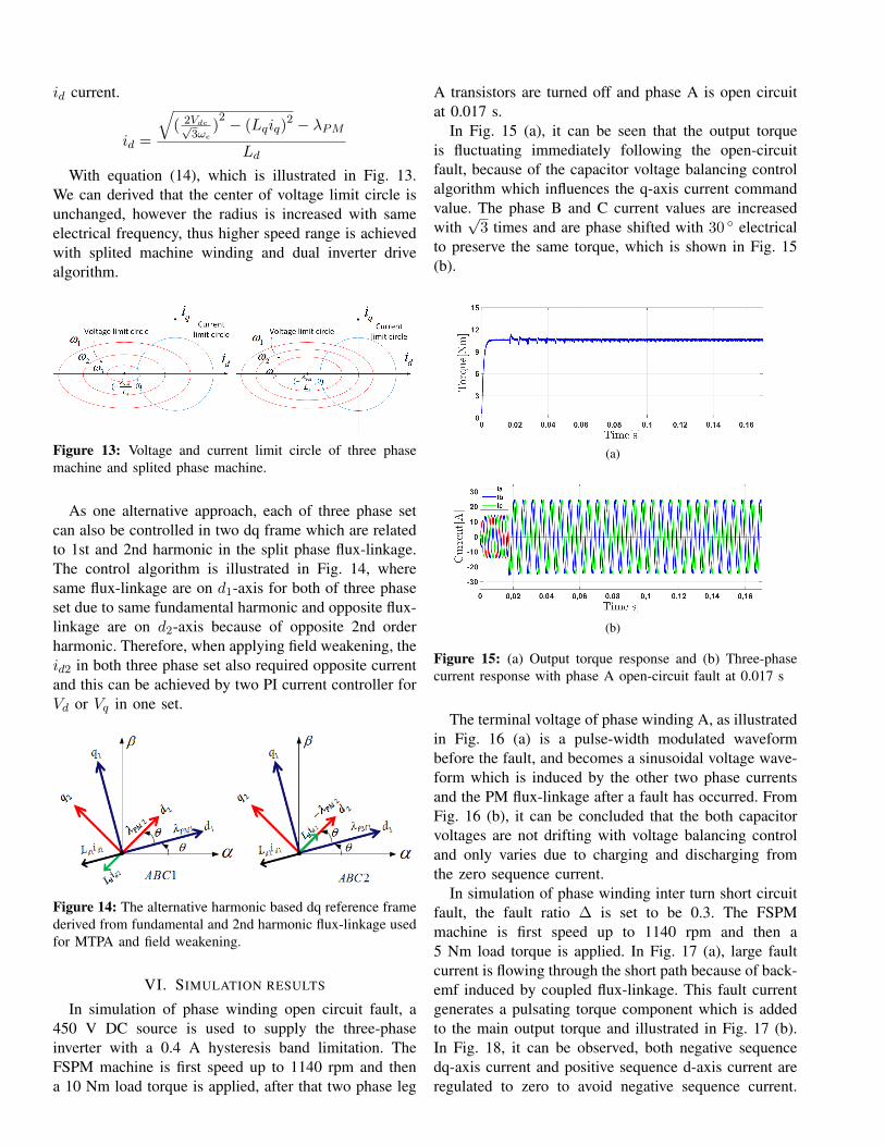
id current.
id =
√( 2Vdc√
3ωe)2 − (Lqiq)
2 − λPMLd
With equation (14), which is illustrated in Fig. 13.We can derived that the center of voltage limit circle isunchanged, however the radius is increased with sameelectrical frequency, thus higher speed range is achievedwith splited machine winding and dual inverter drivealgorithm.
Figure 13: Voltage and current limit circle of three phasemachine and splited phase machine.
As one alternative approach, each of three phase setcan also be controlled in two dq frame which are relatedto 1st and 2nd harmonic in the split phase flux-linkage.The control algorithm is illustrated in Fig. 14, wheresame flux-linkage are on d1-axis for both of three phaseset due to same fundamental harmonic and opposite flux-linkage are on d2-axis because of opposite 2nd orderharmonic. Therefore, when applying field weakening, theid2 in both three phase set also required opposite currentand this can be achieved by two PI current controller forVd or Vq in one set.
Figure 14: The alternative harmonic based dq reference framederived from fundamental and 2nd harmonic flux-linkage usedfor MTPA and field weakening.
VI. SIMULATION RESULTS
In simulation of phase winding open circuit fault, a450 V DC source is used to supply the three-phaseinverter with a 0.4 A hysteresis band limitation. TheFSPM machine is first speed up to 1140 rpm and thena 10 Nm load torque is applied, after that two phase leg
A transistors are turned off and phase A is open circuitat 0.017 s.
In Fig. 15 (a), it can be seen that the output torqueis fluctuating immediately following the open-circuitfault, because of the capacitor voltage balancing controlalgorithm which influences the q-axis current commandvalue. The phase B and C current values are increasedwith
√3 times and are phase shifted with 30 electrical
to preserve the same torque, which is shown in Fig. 15(b).
(a)
(b)
Figure 15: (a) Output torque response and (b) Three-phasecurrent response with phase A open-circuit fault at 0.017 s
The terminal voltage of phase winding A, as illustratedin Fig. 16 (a) is a pulse-width modulated waveformbefore the fault, and becomes a sinusoidal voltage wave-form which is induced by the other two phase currentsand the PM flux-linkage after a fault has occurred. FromFig. 16 (b), it can be concluded that the both capacitorvoltages are not drifting with voltage balancing controland only varies due to charging and discharging fromthe zero sequence current.
In simulation of phase winding inter turn short circuitfault, the fault ratio ∆ is set to be 0.3. The FSPMmachine is first speed up to 1140 rpm and then a5 Nm load torque is applied. In Fig. 17 (a), large faultcurrent is flowing through the short path because of back-emf induced by coupled flux-linkage. This fault currentgenerates a pulsating torque component which is addedto the main output torque and illustrated in Fig. 17 (b).In Fig. 18, it can be observed, both negative sequencedq-axis current and positive sequence d-axis current areregulated to zero to avoid negative sequence current.
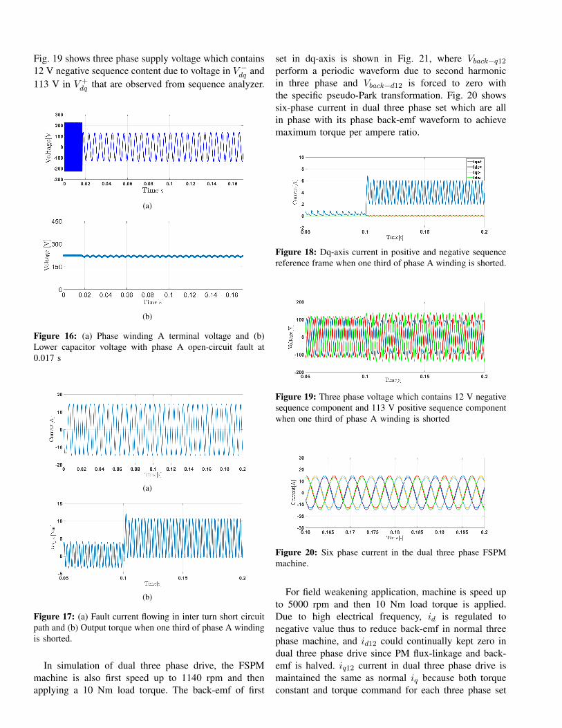
Fig. 19 shows three phase supply voltage which contains12 V negative sequence content due to voltage in V −dq and113 V in V +
dq that are observed from sequence analyzer.
(a)
(b)
Figure 16: (a) Phase winding A terminal voltage and (b)Lower capacitor voltage with phase A open-circuit fault at0.017 s
(a)
(b)
Figure 17: (a) Fault current flowing in inter turn short circuitpath and (b) Output torque when one third of phase A windingis shorted.
In simulation of dual three phase drive, the FSPMmachine is also first speed up to 1140 rpm and thenapplying a 10 Nm load torque. The back-emf of first
set in dq-axis is shown in Fig. 21, where Vback−q12
perform a periodic waveform due to second harmonicin three phase and Vback−d12 is forced to zero withthe specific pseudo-Park transformation. Fig. 20 showssix-phase current in dual three phase set which are allin phase with its phase back-emf waveform to achievemaximum torque per ampere ratio.
Figure 18: Dq-axis current in positive and negative sequencereference frame when one third of phase A winding is shorted.
Figure 19: Three phase voltage which contains 12 V negativesequence component and 113 V positive sequence componentwhen one third of phase A winding is shorted
Figure 20: Six phase current in the dual three phase FSPMmachine.
For field weakening application, machine is speed upto 5000 rpm and then 10 Nm load torque is applied.Due to high electrical frequency, id is regulated tonegative value thus to reduce back-emf in normal threephase machine, and id12 could continually kept zero indual three phase drive since PM flux-linkage and back-emf is halved. iq12 current in dual three phase drive ismaintained the same as normal iq because both torqueconstant and torque command for each three phase set
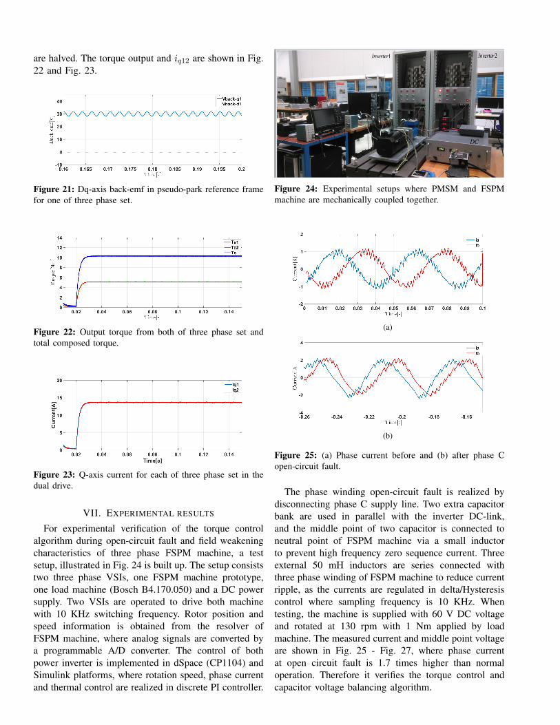
are halved. The torque output and iq12 are shown in Fig.22 and Fig. 23.
Figure 21: Dq-axis back-emf in pseudo-park reference framefor one of three phase set.
Figure 22: Output torque from both of three phase set andtotal composed torque.
Figure 23: Q-axis current for each of three phase set in thedual drive.
VII. EXPERIMENTAL RESULTS
For experimental verification of the torque controlalgorithm during open-circuit fault and field weakeningcharacteristics of three phase FSPM machine, a testsetup, illustrated in Fig. 24 is built up. The setup consiststwo three phase VSIs, one FSPM machine prototype,one load machine (Bosch B4.170.050) and a DC powersupply. Two VSIs are operated to drive both machinewith 10 KHz switching frequency. Rotor position andspeed information is obtained from the resolver ofFSPM machine, where analog signals are converted bya programmable A/D converter. The control of bothpower inverter is implemented in dSpace (CP1104) andSimulink platforms, where rotation speed, phase currentand thermal control are realized in discrete PI controller.
Figure 24: Experimental setups where PMSM and FSPMmachine are mechanically coupled together.
(a)
(b)
Figure 25: (a) Phase current before and (b) after phase Copen-circuit fault.
The phase winding open-circuit fault is realized bydisconnecting phase C supply line. Two extra capacitorbank are used in parallel with the inverter DC-link,and the middle point of two capacitor is connected toneutral point of FSPM machine via a small inductorto prevent high frequency zero sequence current. Threeexternal 50 mH inductors are series connected withthree phase winding of FSPM machine to reduce currentripple, as the currents are regulated in delta/Hysteresiscontrol where sampling frequency is 10 KHz. Whentesting, the machine is supplied with 60 V DC voltageand rotated at 130 rpm with 1 Nm applied by loadmachine. The measured current and middle point voltageare shown in Fig. 25 - Fig. 27, where phase currentat open circuit fault is 1.7 times higher than normaloperation. Therefore it verifies the torque control andcapacitor voltage balancing algorithm.
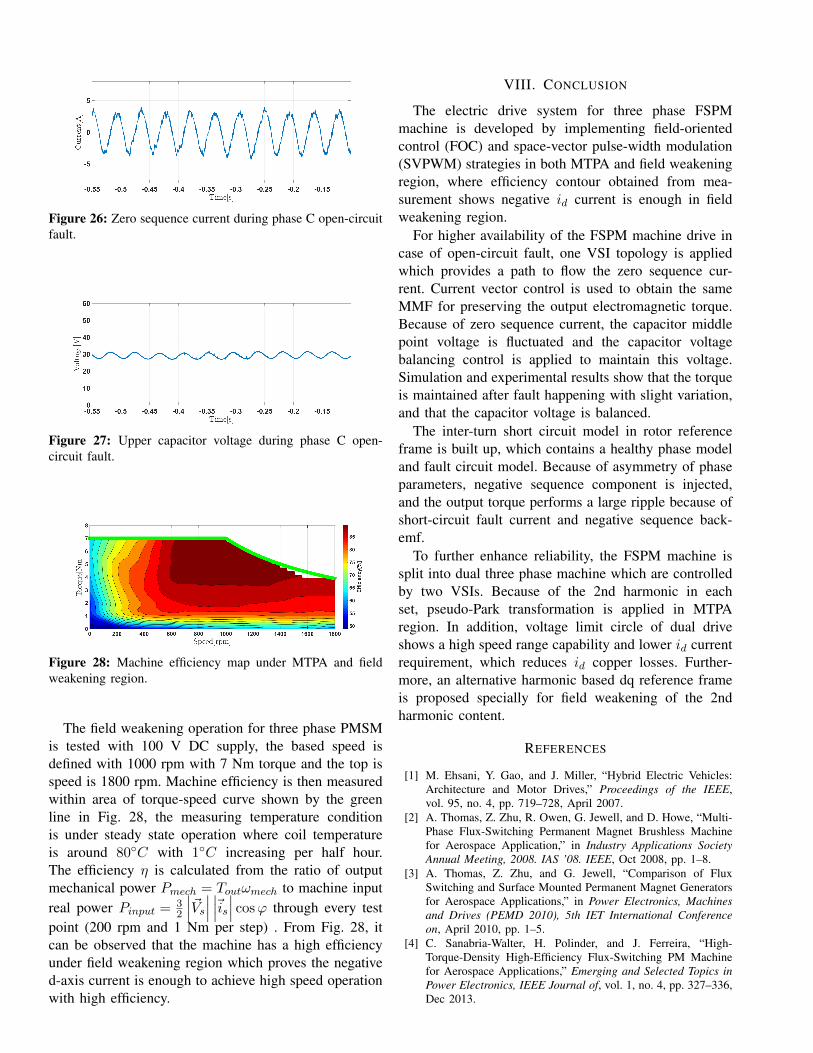
Figure 26: Zero sequence current during phase C open-circuitfault.
Figure 27: Upper capacitor voltage during phase C open-circuit fault.
Figure 28: Machine efficiency map under MTPA and fieldweakening region.
The field weakening operation for three phase PMSMis tested with 100 V DC supply, the based speed isdefined with 1000 rpm with 7 Nm torque and the top isspeed is 1800 rpm. Machine efficiency is then measuredwithin area of torque-speed curve shown by the greenline in Fig. 28, the measuring temperature conditionis under steady state operation where coil temperatureis around 80C with 1C increasing per half hour.The efficiency η is calculated from the ratio of outputmechanical power Pmech = Toutωmech to machine inputreal power Pinput = 3
2
∣∣∣~Vs∣∣∣ ∣∣∣~is∣∣∣ cosϕ through every testpoint (200 rpm and 1 Nm per step) . From Fig. 28, itcan be observed that the machine has a high efficiencyunder field weakening region which proves the negatived-axis current is enough to achieve high speed operationwith high efficiency.
VIII. CONCLUSION
The electric drive system for three phase FSPMmachine is developed by implementing field-orientedcontrol (FOC) and space-vector pulse-width modulation(SVPWM) strategies in both MTPA and field weakeningregion, where efficiency contour obtained from mea-surement shows negative id current is enough in fieldweakening region.
For higher availability of the FSPM machine drive incase of open-circuit fault, one VSI topology is appliedwhich provides a path to flow the zero sequence cur-rent. Current vector control is used to obtain the sameMMF for preserving the output electromagnetic torque.Because of zero sequence current, the capacitor middlepoint voltage is fluctuated and the capacitor voltagebalancing control is applied to maintain this voltage.Simulation and experimental results show that the torqueis maintained after fault happening with slight variation,and that the capacitor voltage is balanced.
The inter-turn short circuit model in rotor referenceframe is built up, which contains a healthy phase modeland fault circuit model. Because of asymmetry of phaseparameters, negative sequence component is injected,and the output torque performs a large ripple because ofshort-circuit fault current and negative sequence back-emf.
To further enhance reliability, the FSPM machine issplit into dual three phase machine which are controlledby two VSIs. Because of the 2nd harmonic in eachset, pseudo-Park transformation is applied in MTPAregion. In addition, voltage limit circle of dual driveshows a high speed range capability and lower id currentrequirement, which reduces id copper losses. Further-more, an alternative harmonic based dq reference frameis proposed specially for field weakening of the 2ndharmonic content.
REFERENCES
[1] M. Ehsani, Y. Gao, and J. Miller, “Hybrid Electric Vehicles:Architecture and Motor Drives,” Proceedings of the IEEE,vol. 95, no. 4, pp. 719–728, April 2007.
[2] A. Thomas, Z. Zhu, R. Owen, G. Jewell, and D. Howe, “Multi-Phase Flux-Switching Permanent Magnet Brushless Machinefor Aerospace Application,” in Industry Applications SocietyAnnual Meeting, 2008. IAS ’08. IEEE, Oct 2008, pp. 1–8.
[3] A. Thomas, Z. Zhu, and G. Jewell, “Comparison of FluxSwitching and Surface Mounted Permanent Magnet Generatorsfor Aerospace Applications,” in Power Electronics, Machinesand Drives (PEMD 2010), 5th IET International Conferenceon, April 2010, pp. 1–5.
[4] C. Sanabria-Walter, H. Polinder, and J. Ferreira, “High-Torque-Density High-Efficiency Flux-Switching PM Machinefor Aerospace Applications,” Emerging and Selected Topics inPower Electronics, IEEE Journal of, vol. 1, no. 4, pp. 327–336,Dec 2013.

[5] C. Sanabria-Walter, “Design of a 600kW Ring-Type Direct-Drive Flux-Switching Permanent Magnet Machine forAerospace Main Propulsion,” in Power Electronics andApplications (EPE’14-ECCE Europe), 2014 16th EuropeanConference on, Aug 2014, pp. 1–10.
[6] Y. Tang, E. Motoasca, J. J. H. Paulides, and E. A. Lomonova,“Comparison of flux switching machines and permanent magnetsynchronous machines in an in wheel traction application,”COMPEL - The international journal for computation andmathematics in electrical and electronic engineering, vol. 32,no. 1, pp. 153–165, 2012.
[7] E. Ilhan, “Hybrid Modeling Techniques Embracing Permanent-Magnet-Biased Salient Machines,” Ph.D. dissertation, Depart-ment of Electrical Engineering, Eindhoven University of Tech-nology, 2014.
[8] E. Ilhan, J. J. H. Paulides, and E. A. Lomonova, “Fast TorqueEstimation of In-Wheel Parallel Flux Switching Machines forHybrid Trucks,” COMPEL - The international journal forcomputation and mathematics in electrical and electronic engi-neering, vol. 31, no. 1, pp. 40–53, 2011.
[9] S. Li, Y. Li, and B. Sarlioglu, “Performance Assessment ofHigh-speed Flux-switching Permanent Magnet Machine UsingFerrite and Rare Earth Permanent Magnet Materials,” in ElectricPower Components and Systems, 2015, pp. 711–720.
[10] Z. Zhu and D. Howe, “Electrical Machines and Drives forElectric, Hybrid, and Fuel Cell Vehicles,” Proceedings of theIEEE, vol. 95, no. 4, pp. 746–765, April 2007.
[11] B. Welchko, T. Lipo, T. Jahns, and S. Schulz, “Fault TolerantThree-Phase AC Motor Drive Topologies; a Comparison of Fea-tures, Cost, and Limitations,” in Electric Machines and DrivesConference, 2003. IEMDC’03. IEEE International, vol. 1, June2003, pp. 539–546 vol.1.
[12] J. Espina, A. Arias, J. Balcells, and C. Ortega, “Speed Anti-Windup PI Strategies Review for Field Oriented Control ofPermanent Magnet Synchronous Machines,” in Compatibilityand Power Electronics, 2009. CPE ’09., May 2009, pp. 279–285.
[13] S. Huang, Z. Chen, K. Huang, and J. Gao, “Maximum Torqueper Ampere and Flux-Weakening Control for PMSM Based onCurve Fitting,” in Vehicle Power and Propulsion Conference(VPPC), 2010 IEEE, Sept 2010, pp. 1–5.
[14] J. Xuewu and L. Yingchao, “Field weakening control of pmsmused in an electric power steering system,” in Electric Infor-mation and Control Engineering (ICEICE), 2011 InternationalConference on, April 2011, pp. 2194–2199.
[15] C. Zhang, F. Wang, Z. Wang, and J. Yang, “Analysis of statorwinding inter-turn short circuit fault of pmsm for electricvehicle based on finite element simulation,” in TransportationElectrification Asia-Pacific (ITEC Asia-Pacific), 2014 IEEEConference and Expo, Aug 2014, pp. 1–6.
[16] B. Vaseghi, N. Takorabet, F. Meibody-Tabar, A. Djerdir, J. A.Farooq, and A. Miraoui, “Modeling and characterizing the inter-turn short circuit fault in pmsm,” in Electric Machines DrivesConference (IEMDC), 2011 IEEE International, May 2011, pp.551–556.
[17] Y. Lee and J.-I. Ha, “High efficiency dual inverter drivesfor a pmsm considering field weakening region,” in PowerElectronics and Motion Control Conference (IPEMC), 2012 7thInternational, vol. 2, June 2012, pp. 1009–1014.
[18] J. Karttunen, S. Kallio, P. Peltoniemi, P. Silventoinen, andO. Pyrhnen, “Dual three-phase permanent magnet synchronousmachine supplied by two independent voltage source inverters,”in Power Electronics, Electrical Drives, Automation and Motion(SPEEDAM), 2012 International Symposium on, June 2012, pp.741–747.
[19] A. Tessarolo, C. Bassi, and D. Giulivo, “Performance of a
high-power induction motor supplied by two in-phase voltage-source inverters,” in EUROCON - International Conference onComputer as a Tool (EUROCON), 2011 IEEE, April 2011, pp.1–4.
[20] Y. Zhao and T. A. Lipo, “Space vector pwm control of dualthree-phase induction machine using vector space decompo-sition,” IEEE Transactions on Industry Applications, vol. 31,no. 5, pp. 1100–1109, Sep 1995.
[21] W. Hua and C. Ming, “Inductance Characteristics of 3-phaseFlux-Switching Permanent Magnet Machine with Doubly-Salient Structure,” in Power Electronics and Motion ControlConference, 2006. IPEMC 2006. CES/IEEE 5th International,vol. 3, Aug 2006, pp. 1–5.
[22] J. H. Jr. and T. Miller, Design of Brushless Permanent-MagnetMachines. Motor Design Books LLC, 2010.
[23] E. Ilhan, M. Kremers, E. Motoasca, J. J. H. Paulides, and E. A.Lomonova, “Sensitivity Analysis for Phase Inductances in Flux-Switching PM Machines,” in Electrical Machines (ICEM), 2012XXth International Conference on, Sept 2012, pp. 763–768.
[24] P. Krause, O. Wasynczuk, and S. Sudhoff, Analysis of ElectricMachinery and Drive Systems, 2nd ed. Purdue: Wiley, 2002.
[25] M. Zordan, P. Vas, M. Rashed, S. Bolognani, and M. Zigliotto,“Field-weakening in high-performance pmsm drives: a com-parative analysis,” in Industry Applications Conference, 2000.Conference Record of the 2000 IEEE, vol. 3, 2000, pp. 1718–1724 vol.3.
[26] Y. Tang, J. J. H. Paulides, and E. A. Lomonova, “Fieldweakening performance of flux-switching machines for hy-brid/electric vehicles,” in Ecological Vehicles and RenewableEnergies (EVER), 2015 Tenth International Conference on,March 2015, pp. 1–10.
[27] T.-H. Liu, J.-R. Fu, and T. Lipo, “A Strategy for Improving Re-liability of Field-Oriented Controlled Induction Motor Drives,”Industry Applications, IEEE Transactions on, vol. 29, no. 5, pp.910–918, Sep 1993.
[28] I. Jeong, K. Nam, B. G. Gu, and I. S. Jung, “Dynamic modelingfor pmsm with internal turn short fault,” in Power Electronicsand ECCE Asia (ICPE ECCE), 2011 IEEE 8th InternationalConference on, May 2011, pp. 2525–2528.
[29] B. G. Gu, J.-H. Choi, and I. S. Jung, “A dynamic modelingand a fault detection scheme of a pmsm under an inter turnshort,” in Vehicle Power and Propulsion Conference (VPPC),2012 IEEE, Oct 2012, pp. 1074–1080.
[30] D. Grenier, L. A. Dessaint, O. Akhrif, and J. P. Louis, “Apark-like transformation for the study and the control of anonsinusoidal brushless dc motor,” in Industrial Electronics,Control, and Instrumentation, 1995., Proceedings of the 1995IEEE IECON 21st International Conference on, vol. 2, Nov1995, pp. 836–843 vol.2.
[31] A. Lidozzi, L. Solero, F. Crescimbini, and R. Burgos, “Vectorcontrol of trapezoidal back-emf pm machines using pseudo-parktransformation,” in Power Electronics Specialists Conference,2008. PESC 2008. IEEE, June 2008, pp. 2167–2171.
[32] D. Grenier and J. P. Louis, “Use of an extension of the park’stransformation to determine control laws applied to a non-sinusoidal permanent magnet synchronous motor,” in PowerElectronics and Applications, 1993., Fifth European Conferenceon, Sep 1993, pp. 32–37 vol.6.
1
A Tightly Regulated PWM-PFM-PD MultipleOutput DC-DC Converter
Mert Turhan, Marcel A.M. Hendrix, Jorge L. Duarte, Juan C. Castellanos and Julia Delose-mail: [email protected]; [email protected]; [email protected]; [email protected]; [email protected]
Eindhoven University of TechnologyEindhoven, The Netherlands
Abstract—In this paper, a multiple output dc-dc converteris proposed. Pulse frequency modulation (PFM), pulse widthmodulation (PWM) and phase delay (PD) methods are usedto regulate output voltages. Two of the output voltages areregulated by PWM, 2 of them by PFM, and the other one byPD. Five regulated outputs are obtained by using only two activeswitches. The switches can be operated at different switchingfrequencies. A hardware prototype was implemented that has1.5V/0.5A, 3.3V/1A, 12V/0.5A, -12V/0.5A and 5V/1A outputsand the efficiency is 89% at the rated power.
Index Terms—dc-dc converter, multiple outputs, PWM-PD,PWM-PFM, PWM-PFM-PD
I. INTRODUCTION
Multiple output converters have been widely used whereindividual outputs are required. Their sizes and costs can beless than the individual converters. However, one of the maindrawbacks of multiple output converters is cross regulation.They regulate only the output that is defined as master output;the other outputs depend on the load conditions [1]. Therefore,post regulators such as linear, magamp and synchronous switchregulators are used to adjust the additional outputs [2], [3].The PWM-PFM converters use PFM in order to regulate thesecond output voltage [4], [5]. One of the converters operatesin continuous conduction mode (CCM), and the other operatesin discontinuous conduction mode (DCM). Both outputs canbe controlled independently by modulating the duty cycle andthe switching frequency of a single active switch. In addition,the work in [6] uses the PWM-PFM method to control bothoutputs. Instead of DCM, the second output is controlledby ZCS quasi resonant mode. The PWM-PD control methodproduces a regulated third output [7], [8]. In this case, twoactive switches are used. The active switches are operated atthe same switching frequency to implement PD, and the PDenables to to adjust the third output voltage. Some researchershave been using the PWM-PFM and the PWM-PD methodswith isolated dc-dc converters [9]–[12]. However, more activeswitches are required to implement these converters. The workin [13] describes a PWM-PFM-PD control method, howeverthis converter can adjust only three output voltages.
In this paper, a PWM-PFM-PD method for multiple outputdc-dc converters is proposed. The proposed solution uses twoactive switches to adjust five-output voltages independently, astwo active switches have five independent control parameterswhich are the duty cycle δ1 and the switching frequency f1
t
vS5
vS1
vS3
iL4
α
δ1
δPD δ2
t
t
t
-10-40 0.1 0.2 0.3 0.4 0.5 0.6 0.7 0.8 0.9 1
VS1(V)
-20
-10
0
10
-10-40 0.1 0.2 0.3 0.4 0.5 0.6 0.7 0.8 0.9 1
VS3(V)
0
10
Time (s) -10-40 0.1 0.2 0.3 0.4 0.5 0.6 0.7 0.8 0.9 1
VS5(V)
0
10
Fig. 1: (a) The waveforms of the applied square voltages to thefirst converter vS1, the third converter vS3, the fifth convertervS5 and (b) their experimental results. The waveforms of vS1
in Fig. 1a and Fig. 1b do not match up with each other becauseof the flyback transformer.
of the first gate signal, the duty cycle δ2 and the switchingfrequency f2 of the second gate signal and the phase delayδPD between the first and the second gate signals. Two ofthe outputs are adjusted using PWM in CCM, other two usesPFM in DCM, and one load is regulated by PD. As shownin Fig. 1, using DCM burst mode in one of the two switchesenables the PD operation at the same switching frequency.In other words, the active switches do not need to operateat the same switching frequency to use the PD. One possibleimplementation of PWM-PF-PD controlled multiple output dc-dc converter is shown in Fig. 2.
2
+−
D1
Q2
Vin
C1
D3
Q1
C3
C2
C4
L2
L4
L3
L1
D2a
D4a
C5
L5
D5b
D5a
R3
R4
R2
R1
R5
D2
vS5
+
-
vS1
+
-
vS3
+
-
DS
CSRS
Vo1
+
-
Vo2
+
-
Vo4
+
-Vo3
+
-
Vo5
+
-
iL4
Fig. 2: One possible implementation of the proposed converter.
Section II describes the principle behind the PWM-PFM-PD converter. Section III presents the simulation and theexperimental results. Conclusions are given in Section IV.
II. THEORY OF THE PRINCIPLE
The new method is based on a combination of the PWM-PFM and the PWM-PD methods. In order to understand thePWM-PFM-PD method, it is essential to know the PWM-PFMand the PWM-PD methods.
The PWM-PFM method for two-output dc-dc converterswith one active switch was proposed in [4]. One output iscontrolled by PWM and the other output by PFM. One ofthe inductors is designed for CCM, and the other inductorfor DCM as can be seen in Fig. 3. Then, while the dutycycle of the switch determines both output voltages, theswitching frequency of the switch determines only one outputvoltage in DCM. Hence both output voltages can be regulatedindependently.
The PWM-PD method for three-output dc-dc converterswith two active switches was presented in [7], [8]. It requirestwo square voltages to obtain the third square voltage as shownin Fig. 4a. As it can be seen in Fig. 4b, the first and the secondoutput voltages are controlled by δ1 and δ2, respectively. Thethird output are adjusted by the third duty cycle δ3, which isequal to the total of δPD and δ2. In order to use this methodthe switching frequencies of the active switches should be thesame. Therefore changing the switching frequency to obtainyet another output is not possible.
In order to use the PD method with different frequencies,it is proposed that the second switch operates in burst mode.The second switch is synchronized to the first switch. Therecan be PD between the starting points of the signals as shownin Fig. 1a. The PD refers to the fifth output voltage Vo5. The
+−
Q1
VinR1
R2
t
t
t
iL2
vG
iL1
L1
L2
C1
C2
CCM Semiconverter
DCM Semiconverter(a)
(b)
Fig. 3: (a) A two-output buck converter controlled by thePWM-PFM method and (b) the inductors current waveforms.
more this phase difference increases, the more Vo5 increases.In burst mode, the time delay between two gate signals isdetermined by the demagnetizing period of the inductor ascan be seen in Fig. 1b. When the inductor current drops tozero, the next signal is triggered.
Many different dc-dc converters such as buck, boost, buck-
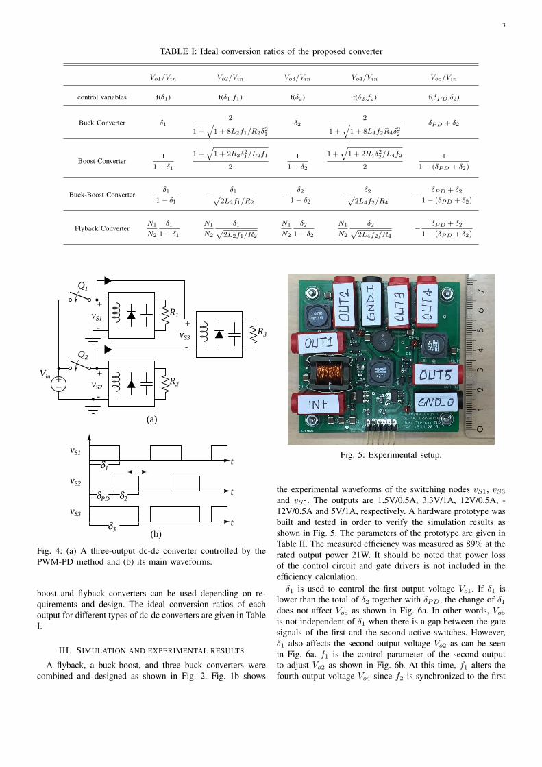
3
TABLE I: Ideal conversion ratios of the proposed converter
Vo1/Vin Vo2/Vin Vo3/Vin Vo4/Vin Vo5/Vin
control variables f(δ1) f(δ1,f1) f(δ2) f(δ2,f2) f(δPD ,δ2)
Buck Converter δ12
1 +√
1 + 8L2f1/R2δ21
δ22
1 +√
1 + 8L4f2R4δ22
δPD + δ2
Boost Converter1
1− δ1
1 +√
1 + 2R2δ21/L2f1
2
1
1− δ2
1 +√
1 + 2R4δ22/L4f2
2
1
1− (δPD + δ2)
Buck-Boost Converter −δ1
1− δ1−
δ1√2L2f1/R2
−δ2
1− δ2−
δ2√2L4f2/R4
−δPD + δ2
1− (δPD + δ2)
Flyback ConverterN1
N2
δ1
1− δ1
N1
N2
δ1√2L2f1/R2
N1
N2
δ2
1− δ2
N1
N2
δ2√2L4f2/R4
−δPD + δ2
1− (δPD + δ2)
t
t
tvS1
vS2
vS3
+−
Q2
Vin
Q1
R2
R1vS1
+
-
vS2
+
-
R3vS3
+
-
(a)
(b)
δ1
δ2
δ3
δPD
Fig. 4: (a) A three-output dc-dc converter controlled by thePWM-PD method and (b) its main waveforms.
boost and flyback converters can be used depending on re-quirements and design. The ideal conversion ratios of eachoutput for different types of dc-dc converters are given in TableI.
III. SIMULATION AND EXPERIMENTAL RESULTS
A flyback, a buck-boost, and three buck converters werecombined and designed as shown in Fig. 2. Fig. 1b shows
Fig. 5: Experimental setup.
the experimental waveforms of the switching nodes vS1, vS3
and vS5. The outputs are 1.5V/0.5A, 3.3V/1A, 12V/0.5A, -12V/0.5A and 5V/1A, respectively. A hardware prototype wasbuilt and tested in order to verify the simulation results asshown in Fig. 5. The parameters of the prototype are given inTable II. The measured efficiency was measured as 89% at therated output power 21W. It should be noted that power lossof the control circuit and gate drivers is not included in theefficiency calculation.δ1 is used to control the first output voltage Vo1. If δ1 is
lower than the total of δ2 together with δPD, the change of δ1does not affect Vo5 as shown in Fig. 6a. In other words, Vo5is not independent of δ1 when there is a gap between the gatesignals of the first and the second active switches. However,δ1 also affects the second output voltage Vo2 as can be seenin Fig. 6a. f1 is the control parameter of the second outputto adjust Vo2 as shown in Fig. 6b. At this time, f1 alters thefourth output voltage Vo4 since f2 is synchronized to the first
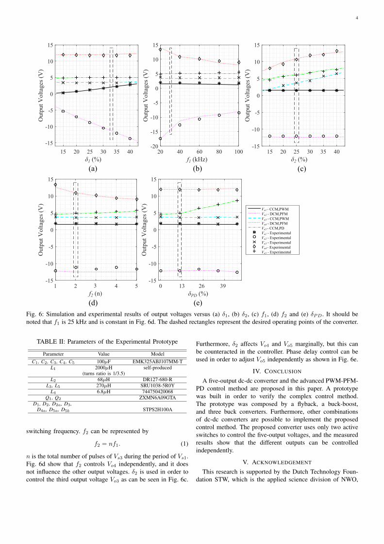
4
δ1xHfz15 20 25 30 35 40
Out
putxV
olta
gesx
HVz
d15
d10
d5
0
5
10
15
1cOutputdCCMbPWM2cOutputdDCMbPFM3cOutputdCCMbPWM4cOutputdDCMbPFM5cOutputdCCMbPD1cOutputdExperimental2cOutputdExperimental3cOutputdExperimental4cOutputdExperimental5cOutputdExperimental
δ2xHfz15 20 25 30 35 40
Out
putxV
olta
gesx
HVz
d15
d10
d5
0
5
10
15
f1xHkHzz20 40 60 80 100
Out
putxV
olta
gesx
HVz
d20
d15
d10
d5
0
5
10
15
1cOutputdCCMbPWM2cOutputdDCMbPFM3cOutputdCCMbPWM4cOutputdDCMbPFM5cOutputdCCMbPD1cOutputdExperimental2cOutputdExperimental3cOutputdExperimental4cOutputdExperimental5cOutputdExperimental
3 f2 Hnz
1 2 4 5
Out
putxV
olta
gesx
HVz
d15
d10
d5
0
5
10
15
1cOutputdCCMbPWM2cOutputdDCMbPFM3cOutputdCCMbPWM4cOutputdDCMbPFM5cOutputdCCMbPD1cOutputdExperimental2cOutputdExperimental3cOutputdExperimental4cOutputdExperimental5cOutputdExperimental
δPDxHfz0 13 26 39
Out
putxV
olta
gesx
HVz
d15
d10
d5
0
5
10
15
Vo1 d CCMbPWM Vo2 - DCMbPFM Vo3 - CCMbPWM Vo4 - DCMbPFM Vo5 - CCMbPD Vo1 - Experimental Vo2 - Experimental Vo3 - Experimental Vo4 - Experimental Vo5 - Experimental
Haz Hbz Hcz
Hdz Hez
Hcz
Fig. 6: Simulation and experimental results of output voltages versus (a) δ1, (b) δ2, (c) f1, (d) f2 and (e) δPD. It should benoted that f1 is 25 kHz and is constant in Fig. 6d. The dashed rectangles represent the desired operating points of the converter.
TABLE II: Parameters of the Experimental Prototype
Parameter Value ModelC1, C2, C3, C4, C5 100µF EMK325ABJ107MM-T
L1 2000µH self-produced(turns ratio is 1/3.5)
L2 68µH DR127-680-RL3, L5 270µH SRU1038-5R0Y
L4 6.8µH 744750420068Q1, Q2 ZXMN6A09GTA
D1, D2, D2a, D3,D4a, D5a, D5b STPS2H100A
switching frequency. f2 can be represented by
f2 = nf1. (1)
n is the total number of pulses of Vs3 during the period of Vs1.Fig. 6d show that f2 controls Vo4 independently, and it doesnot influence the other output voltages. δ2 is used in order tocontrol the third output voltage Vo3 as can be seen in Fig. 6c.
Furthermore, δ2 affects Vo4 and Vo5 marginally, but this canbe counteracted in the controller. Phase delay control can beused in order to adjust Vo5 independently as shown in Fig. 6e.
IV. CONCLUSION
A five-output dc-dc converter and the advanced PWM-PFM-PD control method are proposed in this paper. A prototypewas built in order to verify the complex control method.The prototype was composed by a flyback, a buck-boost,and three buck converters. Furthermore, other combinationsof dc-dc converters are possible to implement the proposedcontrol method. The proposed converter uses only two activeswitches to control the five-output voltages, and the measuredresults show that the different outputs can be controlledindependently.
V. ACKNOWLEDGEMENT
This research is supported by the Dutch Technology Foun-dation STW, which is the applied science division of NWO,

5
and the Technology Programme of the Ministry of EconomicAffairs, Agriculture and Innovation.
REFERENCES
[1] D. Maksimovic and R. Erickson, “Modeling of cross-regulation inmultiple-output flyback converters,” in Applied Power Electronics Con-ference and Exposition, 1999. APEC ’99. Fourteenth Annual, vol. 2,Mar 1999, pp. 1066–1072 vol.2.
[2] G. Levin, “A new secondary side post regulator (sspr) pwm controllerfor multiple output power supplies,” in Applied Power ElectronicsConference and Exposition, 1995. APEC ’95. Conference Proceedings1995., Tenth Annual, no. 0, Mar 1995, pp. 736–742 vol.2.
[3] A. Ferreres, J. Carrasco, E. Maset, and J. Ejea, “Small-signal modelingof a controlled transformer parallel regulator as a multiple outputconverter high efficient post-regulator,” Power Electronics, IEEE Trans-actions on, vol. 19, no. 1, pp. 183–191, Jan 2004.
[4] J. Sebastian and J. Uceda, “The double converter: A fully regulated two-output dc-dc converter,” Power Electronics, IEEE Transactions on, vol.PE-2, no. 3, pp. 239–246, July 1987.
[5] H. Tacca, “Single-switch two-output flyback-forward converter opera-tion,” Power Electronics, IEEE Transactions on, vol. 13, no. 5, pp. 903–911, Sep 1998.
[6] J. Sebastian, J. Uceda, M. Perez, M. Rico, and F. Aldana, “A very simplemethod to obtain one additional fully regulated output in zero-current-switched quasiresonant converters,” in Power Electronics SpecialistsConference, 1990. PESC ’90 Record., 21st Annual IEEE, 1990, pp. 536–542.
[7] A. Barrado, E. Olias, A. Roldan, R. Vazquez, and J. Pleite, “Multipleoutput dc/dc converters based on pwm-pulse delay control (pwm-pd),” inPower Electronics Specialists Conference, 1999. PESC 99. 30th AnnualIEEE, vol. 2, 1999, pp. 1141–1145 vol.2.
[8] A. Barrado, E. Olias, A. Lazaro, J. Pleite, and R. Vazquez, “Pwm-pdmultiple output dc/dc converters: operation and control-loop modeling,”Power Electronics, IEEE Transactions on, vol. 19, no. 1, pp. 140–149,Jan 2004.
[9] S.-H. Cho, C.-S. Kim, and S.-K. Han, “High-efficiency and low-costtightly regulated dual-output llc resonant converter,” Industrial Electron-ics, IEEE Transactions on, vol. 59, no. 7, pp. 2982–2991, July 2012.
[10] C. Liu, B. Gu, J.-S. Lai, M. Wang, Y. Ji, G. Cai, Z. Zhao, C.-L. Chen,C. Zheng, and P. Sun, “High-efficiency hybrid full bridge-half bridgeconverter with shared zvs lagging leg and dual outputs in series,” PowerElectronics, IEEE Transactions on, vol. 28, no. 2, pp. 849–861, Feb2013.
[11] H. Seong, D. Kim, and G.-H. Cho, “A new zvs dc/dc converter with fullyregulated dual outputs,” in Power Electronics Specialists Conference,1993. PESC ’93 Record., 24th Annual IEEE, Jun 1993, pp. 351–356.
[12] Y. Zhang and D. Xu, “Design and implementation of an accuratelyregulated multiple output zvs dc-dc converter,” Power Electronics, IEEETransactions on, vol. 22, no. 5, pp. 1731–1742, Sept 2007.
[13] B.-C. Hyeon and B.-H. Cho, “A tightly regulated triple output asym-metrical half bridge flyback converter,” Journal of Power Electronics,vol. 10, no. 1, pp. 14–20, January 2010.
Impact of Slot Opening on Performance of AxialFlux PMSMs
A. Hemeida, Student Member, and P. Sergeant, Member, IEEE
Abstract—In this paper, a complete investigation of the impactof the slot opening on the performance of the axial flux permanentmagnet synchronous machines (AFPMSMs) is elaborated. Thewidth of the stator slot opening has a major impact on manyparameters including the cogging torque, the ripple torque, themean value of the torque, the permanent magnet (PM) losses,the iron losses, the peak flux density inside the tooth, and thetotal inductance of the machine. Thanks to the presence ofvalidated analytical models that made it possible to obtain allthese parameters. It is found that a good selection of the slotopening width could result in an optimized performance. Fora minimum cogging torque, an optimum selection of the slotopening width is required. On one hand, the increase in thestator slot opening width reduces the iron losses. However, thetotal torque due to the reduced peak flux density inside the toothincrease for large slot openings value. On the other hand, at fullload condition, this selection of slot opening on the PM lossesmight not be an optimum choice and calculation of the PM lossesin this case would be mandatory. In addition, Very large slotopening is not a good choice for machine designers due to thetotal reduction of the total torque. Therefore, a good choice of theslot opening would result in an optimum machine performanceand calculation of all machine parameters would be mandatory.
Index Terms—AFPMSM, Analytical Model, Fractional SlotWinding, Machine Design, Slot opening Width.
I. INTRODUCTION
Due to the high performance of the yokeless and segmentedarmature (YASA) machine, shown in Fig. 1, it has been usedin many applications. Owing to the absence of the yoke, thismachine provides great robustness in terms of power densityand cost. [1]
The slot opening width influences many output parametersin the machine design. In [2], the authors have addressed theeffect of slot opening width on the iron and permanent magnet(PM) losses. It has clearly shown major impact on the ironlosses. However, it has shown that PM losses is increasing atno load with the increase of the slot opening. Nevertheless,It has not addressed the PM loses at full load conditions. In[3], [4], the authors have studied the effect of all differentPM skewing in double rotor axial flux permanent magnetsynchronous machines (AFPMSMs). On the other hand, thecorrect choice of the slot opening width would result in theoptimum value for cogging torque and minimum torque ripple.
In [5], the authors studied the impact of slot opening andtooth profile variations on cogging torque and torque profile.In [6], the a stator slot displacement is used to mitigate thecogging torque.
The analytical model in [7] is based on a combined solutionof Maxwell’s equations based on subdomain model [8] andmagnetic equivalent circuit (MEC). This solution is capable
Fig. 1: The YASA topology of the Axial Flux PMSM.
of obtaining the stator iron losses, voltages waveforms, andinductances in a very accurate way. The PM losses is computedusing the inductance plus resistance network model developedin [9], [10]. They are based on 2D-2D multi-slice modelingtechnique. This is done by dividing the machine into slices.On each slice, the flux densities in addition with all the otheroutput parameters are computed.
The cogging torque and ripple torque computations arebased on a similar subdomain model developed in [11]. Allthese models are verified by full 3D finite element (FE)models.
In this paper, a complete investigation of the effect of theslot opening on the main output parameters of the coggingtorque, the ripple torque, the mean value of the torque, thepermanent magnet (PM) losses, the iron losses, the peak fluxdensity inside the tooth, the total harmonic distortion of theoutput line voltage, and the total inductances of the machine.Thanks to the presence of a completely verified analyticalmodels [9], [7], [10] that made it possible to obtain all therequired data of the machine in a fast appealing time.
This paper is organized as follows. Brief description aboutanalytical models used is done in section II. The effect ofslot opening width variation on the cogging torque and rippletorque is studied in section III. Section IV deals with the effectof the slot opening width on the PM and iron losses. In sectionV, the effect of the slot opening variations on the power qualityoutput of the machine is studied. Finally, conclusions of thepaper are drawn in Section VI.
II. ANALYTICAL MODEL DESCRIPTION
The first part of the solution is to obtain the magnetic fieldin the air gap using the subdomain model based on solutionof Maxwell’s equations described in [11]. This model dividesthe machine into the radial direction into multi-slices. Thismodel for the machine consisting of Ns slots and Nm PMs
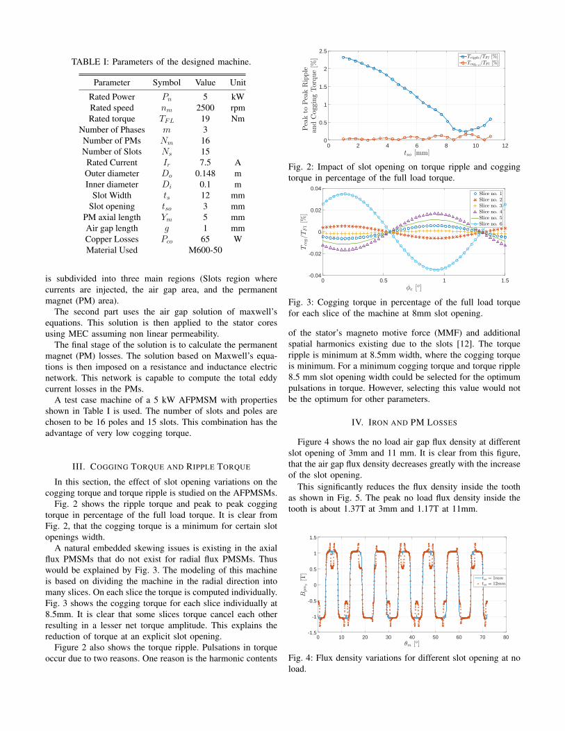
TABLE I: Parameters of the designed machine.
Parameter Symbol Value Unit
Rated Power Pn 5 kWRated speed nm 2500 rpmRated torque TFL 19 Nm
Number of Phases m 3Number of PMs Nm 16Number of Slots Ns 15Rated Current Ir 7.5 AOuter diameter Do 0.148 mInner diameter Di 0.1 m
Slot Width ts 12 mmSlot opening tso 3 mm
PM axial length Ym 5 mmAir gap length g 1 mmCopper Losses Pco 65 WMaterial Used M600-50
is subdivided into three main regions (Slots region wherecurrents are injected, the air gap area, and the permanentmagnet (PM) area).
The second part uses the air gap solution of maxwell’sequations. This solution is then applied to the stator coresusing MEC assuming non linear permeability.
The final stage of the solution is to calculate the permanentmagnet (PM) losses. The solution based on Maxwell’s equa-tions is then imposed on a resistance and inductance electricnetwork. This network is capable to compute the total eddycurrent losses in the PMs.
A test case machine of a 5 kW AFPMSM with propertiesshown in Table I is used. The number of slots and poles arechosen to be 16 poles and 15 slots. This combination has theadvantage of very low cogging torque.
III. COGGING TORQUE AND RIPPLE TORQUE
In this section, the effect of slot opening variations on thecogging torque and torque ripple is studied on the AFPMSMs.
Fig. 2 shows the ripple torque and peak to peak coggingtorque in percentage of the full load torque. It is clear fromFig. 2, that the cogging torque is a minimum for certain slotopenings width.
A natural embedded skewing issues is existing in the axialflux PMSMs that do not exist for radial flux PMSMs. Thuswould be explained by Fig. 3. The modeling of this machineis based on dividing the machine in the radial direction intomany slices. On each slice the torque is computed individually.Fig. 3 shows the cogging torque for each slice individually at8.5mm. It is clear that some slices torque cancel each otherresulting in a lesser net torque amplitude. This explains thereduction of torque at an explicit slot opening.
Figure 2 also shows the torque ripple. Pulsations in torqueoccur due to two reasons. One reason is the harmonic contents
tso [mm]0 2 4 6 8 10 12
Pea
kto
Pea
kR
ipple
and
Coggin
gTorq
ue
[%]
0
0.5
1
1.5
2
2.5Tripple=TF l [%]Tcogp!p
=TF l [%]
Fig. 2: Impact of slot opening on torque ripple and coggingtorque in percentage of the full load torque.
?e [o]0 0.5 1 1.5
Tco
g=T
Fl[%
]
-0.04
-0.02
0
0.02
0.04Slice no. 1Slice no. 2Slice no. 3Slice no. 4Slice no. 5Slice no. 6
Fig. 3: Cogging torque in percentage of the full load torquefor each slice of the machine at 8mm slot opening.
of the stator’s magneto motive force (MMF) and additionalspatial harmonics existing due to the slots [12]. The torqueripple is minimum at 8.5mm width, where the cogging torqueis minimum. For a minimum cogging torque and torque ripple8.5 mm slot opening width could be selected for the optimumpulsations in torque. However, selecting this value would notbe the optimum for other parameters.
IV. IRON AND PM LOSSES
Figure 4 shows the no load air gap flux density at differentslot opening of 3mm and 11 mm. It is clear from this figure,that the air gap flux density decreases greatly with the increaseof the slot opening.
This significantly reduces the flux density inside the toothas shown in Fig. 5. The peak no load flux density inside thetooth is about 1.37T at 3mm and 1.17T at 11mm.
3m [o]0 10 20 30 40 50 60 70 80
Bpm
y[T
]
-1.5
-1
-0.5
0
0.5
1
1.5
tso = 1mmtso = 12mm
Fig. 4: Flux density variations for different slot opening at noload.
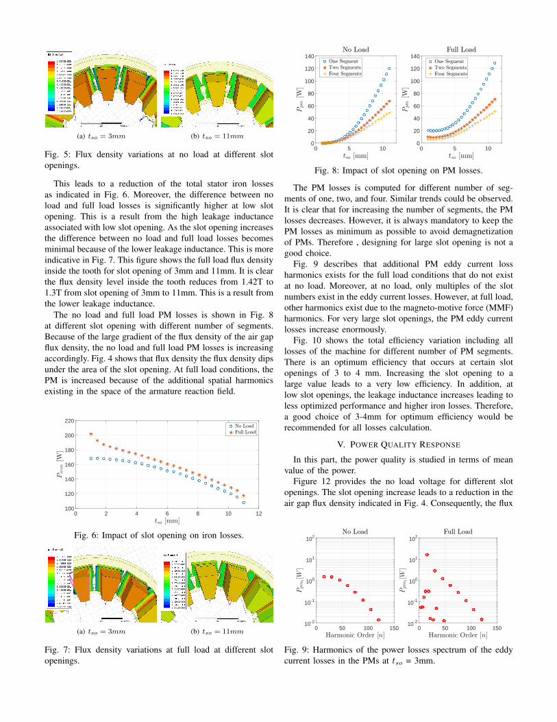
(a) tso = 3mm (b) tso = 11mm
Fig. 5: Flux density variations at no load at different slotopenings.
This leads to a reduction of the total stator iron lossesas indicated in Fig. 6. Moreover, the difference between noload and full load losses is significantly higher at low slotopening. This is a result from the high leakage inductanceassociated with low slot opening. As the slot opening increasesthe difference between no load and full load losses becomesminimal because of the lower leakage inductance. This is moreindicative in Fig. 7. This figure shows the full load flux densityinside the tooth for slot opening of 3mm and 11mm. It is clearthe flux density level inside the tooth reduces from 1.42T to1.3T from slot opening of 3mm to 11mm. This is a result fromthe lower leakage inductance.
The no load and full load PM losses is shown in Fig. 8at different slot opening with different number of segments.Because of the large gradient of the flux density of the air gapflux density, the no load and full load PM losses is increasingaccordingly. Fig. 4 shows that flux density the flux density dipsunder the area of the slot opening. At full load conditions, thePM is increased because of the additional spatial harmonicsexisting in the space of the armature reaction field.
tso [mm]0 2 4 6 8 10 12
Pir
on[W
]
100
120
140
160
180
200
220No LoadFull Load
Fig. 6: Impact of slot opening on iron losses.
(a) tso = 3mm (b) tso = 11mm
Fig. 7: Flux density variations at full load at different slotopenings.
tso [mm]0 5 10
Ppm
[W]
0
20
40
60
80
100
120
140No Load
One SegmentTwo SegmentsFour Segments
tso [mm]0 5 10
Ppm
[W]
0
20
40
60
80
100
120
140Full Load
One SegmentTwo SegmentsFour Segments
Fig. 8: Impact of slot opening on PM losses.
The PM losses is computed for different number of seg-ments of one, two, and four. Similar trends could be observed.It is clear that for increasing the number of segments, the PMlosses decreases. However, it is always mandatory to keep thePM losses as minimum as possible to avoid demagnetizationof PMs. Therefore , designing for large slot opening is not agood choice.
Fig. 9 describes that additional PM eddy current lossharmonics exists for the full load conditions that do not existat no load. Moreover, at no load, only multiples of the slotnumbers exist in the eddy current losses. However, at full load,other harmonics exist due to the magneto-motive force (MMF)harmonics. For very large slot openings, the PM eddy currentlosses increase enormously.
Fig. 10 shows the total efficiency variation including alllosses of the machine for different number of PM segments.There is an optimum efficiency that occurs at certain slotopenings of 3 to 4 mm. Increasing the slot opening to alarge value leads to a very low efficiency. In addition, atlow slot openings, the leakage inductance increases leading toless optimized performance and higher iron losses. Therefore,a good choice of 3-4mm for optimum efficiency would berecommended for all losses calculation.
V. POWER QUALITY RESPONSE
In this part, the power quality is studied in terms of meanvalue of the power.
Figure 12 provides the no load voltage for different slotopenings. The slot opening increase leads to a reduction in theair gap flux density indicated in Fig. 4. Consequently, the flux
Harmonic Order [n]0 50 100 150
Ppm
h[W
]
10-2
10-1
100
101
102No Load
Harmonic Order [n]0 50 100 150
Ppm
h[W
]
10-2
10-1
100
101
102Full Load
Fig. 9: Harmonics of the power losses spectrum of the eddycurrent losses in the PMs at tso = 3mm.
tso [mm]0 2 4 6 8 10 12
2[%
]
92.5
93
93.5
94
94.5
95
95.5One SegmentTwo SegmentsFour Segments
Fig. 10: Total efficiency variations including copper losses.
Time [Sec] #10-30 0.5 1 1.5 2 2.5 3
No
load
Phase
Voltage
[V]
-300
-200
-100
0
100
200
300
tso = 1mmtso = 5:5mmtso = 11mm
Fig. 11: No load voltage for different slot opening.
linkage reduces and hence, the no load voltage. This lowersthe output torque and power of the machine.
Fig. 12 shows the impact of the slot opening variations onthe total power output of the machine in per unit. For smalla slot opening, the power is higher due to the higher air gapflux density. However, when the slot opening increases, thetotal power output reduces.
Therefore, for a good output power it is important to keepthe slot opening as low as possible to attain the required power.
VI. CONCLUSIONS
This paper investigated the effect of slot opening variationson the total performance of the AFPMSM. Three main pa-rameters (Torque waveforms, Losses, and power quality) arestudied in this machine. On the one hand, the right choice ofthe slot opening width might give the optimum cogging andripple torque. However, this choice might not be optimum forthe iron and PM losses.
Increasing the slot width will always lead to a decreaseof the flux density level inside the tooth. In consequence,this leads to a reduction of the iron losses. However, PM
tso [mm]0 2 4 6 8 10 12
Pm
[kW
]
4.8
4.9
5
5.1
5.2
5.3
Fig. 12: Impact of slot opening on full load power.
losses at no load and full load increases for large slot openingwidth. In overall, for a very high slot opening width, the PMlosses is observed to rise enormously due to the high gradientchange of the magnetic flux density near the air gap area.Therefore, to avoid PM demagnetization, it is mandatory tokeep the slot opening as low as possible or to increase thenumber of PM segments. On the other hand, it is importantto deeply investigate the total slot opening variations on thetotal efficiency of the system.
For a very large slot opening, the total output power of themachine lowers. This is a result of the reduction of the meanair gap flux density.
For the particular studied machine, the choice of the slotopening to give minimum torque ripple is 9mm. However, thischoice will lead to an efficiency of 94% for one PM segment.In addition, the output power becomes lesser than the nominalmachine power.
Another good choice from efficiency point of view id the3mm slot opening width which gives an efficiency higher than95% and the required nominal power. However, the torqueripple becomes 2% of the full load torque. Additional PMskewing would be required to reduce the torque ripple.
Therefore, the slot opening should be strictly determinedfor all the aforementioned parameters.
REFERENCES
[1] C. Du-Bar, “Design of an axial flux machine for an in-wheel motorapplication,” Chalmers Reproservice, Goteborg, 2011.
[2] P. Sergeant, H. Vansompel, and L. Dupre, “Effect of stator slot openingsin axial flux permanent magnet machines,” in Int. Conf. Model. Simul.Electr. Mach. Convert. Syst. Proceedings., pp. 512–517, UniversitatPolitecnica de Valencia, 2014.
[3] M. Aydin and M. Gulec, “Reduction of Cogging Torque in Double-Rotor Axial-Flux Permanent-Magnet Disk Motors: A Review of Cost-Effective Magnet-Skewing Techniques With Experimental Verification,”IEEE Trans. Ind. Electron., vol. 61, pp. 5025–5034, Sep. 2014.
[4] M. Aydin, Z. Q. Zhu, T. A. Lipo, and D. Howe, “Minimization ofCogging Torque in Axial-Flux Permanent-Magnet Machines: DesignConcepts,” IEEE Trans. Magn., vol. 43, pp. 3614–3622, Sep. 2007.
[5] J. Wanjiku, M. A. Khan, P. S. Barendse, and P. Pillay, “Influence ofSlot Openings and Tooth Profile on Cogging Torque in Axial-Flux PMMachines,” IEEE Trans. Ind. Electron., vol. 62, pp. 7578–7589, Dec.2015.
[6] A. B. Letelier, D. A. Gonzalez, J. A. Tapia, R. Wallace, and M. A.Valenzuela, “Cogging Torque Reduction in an Axial Flux PM Machinevia Stator Slot Displacement and Skewing,” IEEE Trans. Ind. Appl.,vol. 43, no. 3, pp. 685–693, 2007.
[7] A. Hemeida and P. Sergeant, “Analytical modeling of surface PMSMusing a combined solution of Maxwell’s equations and Magnetic Equiv-alent Circuit (MEC),” IEEE Trans. Magn., vol. 50, no. 12, p. 7027913,2014.
[8] B. Hannon, P. Sergeant, and L. Dupre, “2-D Analytical SubdomainModel of a Slotted PMSM With Shielding Cylinder,” IEEE Trans.Magn., vol. 50, pp. 1–10, Jul. 2014.
[9] A. Hemeida and P. Sergeant, “Analytical modeling of eddy current lossesin Axial Flux PMSM using resistance network,” in 2014 Int. Conf. Electr.Mach., pp. 2688–2694, IEEE, Sep. 2014.
[10] A. Hemeida, P. Sergeant, and H. Vansompel, “Comparison of Methodsfor Permanent Magnet Eddy Current Loss Computations With andWithout Reaction Field Considerations in Axial Flux PMSM,” IEEETrans. Magn., vol. 9464, pp. 1–11, Sep. 2015.
[11] H. Tiegna, A. Bellara, Y. Amara, and G. Barakat, “Analytical Modelingof the Open-Circuit Magnetic Field in Axial Flux Permanent-MagnetMachines With Semi-Closed Slots,” IEEE Trans. Magn., vol. 48, no. 3,pp. 1212–1226, 2012.

[12] M. Aydin, Surong Huang, and T. Lipo, “Torque quality and comparisonof internal and external rotor axial flux surface-magnet disc machines,”IEEE Trans. Ind. Electron., vol. 53, no. 3, pp. 822–830, 2006.
Candidates of Motor Drives for 48V Automotive Applications
Jing Bao, Konstantin Boynov, Johan Paulides, Korneel Wijnands, Elena LomonovaElectrical Engineering
Eindhoven University of TechnologyEindhoven, Netherlands
Email: [email protected]
Abstract—In automotive systems, reliability and cost areparamount for the success of electrical drive systems. Consider-ing the interior permanent magnet motor, the cost of the rare-earth permanent magnet is becoming a big concern. In thispaper, the switched reluctance motor, variable flux reluctancemotor and synchronous reluctance motor are analyzed andcompared as candidates for the 48V automotive applications. Arecommendation is given for the selection of the motor drives.
1. Introduction
Future vehicle electrification needs more electric powerto manage more functions, such as electro-mechanicalvalves, direct electrically driven engine water pump, assistedelectrical power steering, etc. As a result, medium powerelectrical motors are required to assist the main tractiondrive train. A voltage level of 48V is suitable for such amotor drive considering the safety regulation.
Interior permanent magnet motor (IPM) is commonlyconsidered as a candidate for automotive applications. How-ever, the price rise of the rare-earth permanent magnet tendsto restrict the use of the IPM in large scale. Therefore,the utilization of the rare-earth-free motor drive is desired.As a result, the adoption of the switched reluctance mo-tor (SRM) is investigated by researchers and is comparedwith IPM. Additionally, the current analysis of the variableflux reluctance motor (VFRM) and synchronous reluctancemotor (SynRM) also shows a bright prospect. This paperreviews the aforementioned motor drives considering thepower electronic circuit, the motor itself and the controlalgorithm. Finally, the paper is concluded with a summaryon the overall performance of different motor drives.
2. MOTOR DRIVE COMPARISON
Interior permanent magnet motor is used by a lot ofautomakers due to its high efficiency at nominal speeds, highpower density, flux-weakening capability and easy cooling.However, the efficiency of the motor decreases in higherspeed range since an extra magnetization current is requiredto suppress the flux. Moreover, at high demagnetizationcurrent, there is the risk of magnet demagnetization.
Switched reluctance motor is more and more appealingto researchers as the rival of IPM [1]. It has robust and sim-ple rotor structure, utilizes low cost material and is toleranttowards hostile environment. However, shortcomings of thismotor drive are also obvious, for example, it needs complexprofiling of phase current waveforms at low speed, requiresnon-standard power electronic module, demands large DC-link capacitor, generates large acoustic noise, etc.
Three-phase variable flux reluctance motor has beenproposed as another candidate recently. [2]- [3] It has simpleand robust stator and rotor structures as the SRM. It isconcluded in [2] that the VFRM can produce higher outputpower in flux weakening region compared to IPM while gen-erating lower acoustic noise compared to SRM. Moreover,the conventional three-phase inverter is applicable for thismotor, which makes it a competitive option for automotiveapplication.
The synchronous reluctance motor is considered as an-other competitor. [4] This kind of motor has a shortcomingof the low power factor (with a radially laminated structure).Different methods have been presented to overcome this,such as injecting direct capacitance through an auxiliarywinding [5] and adding permanent magnets in the rotor fluxbarriers [6].
The features of the motor drives from the literature areelaborated in the following, as well as the simulation andanalysis for the representatives of the motors.
2.1. Switched reluctance motor
In this subsection, an SRM is analyzed specifically forthe aforementioned shortcomings with some possible solu-tions. To ensure the position-independent starting capabilityof the machine, it is favorable to have at least four phasesin the SRM. It is well known that if the phase windings inSRM are excited by pure square wave current, the torqueripple is large. Therefore, current profiling method is used tosmooth the torque and it works effectively for relatively lowspeed operation [7]. In high speed operation, the SRM maybe operated in the continuous conduction mode since thecurrent has to be increased fast enough to reach the desiredaverage torque.
An 8/6 SRM is simulated using the finite element anal-ysis (FEA) for obtaining the flux-current-position character-
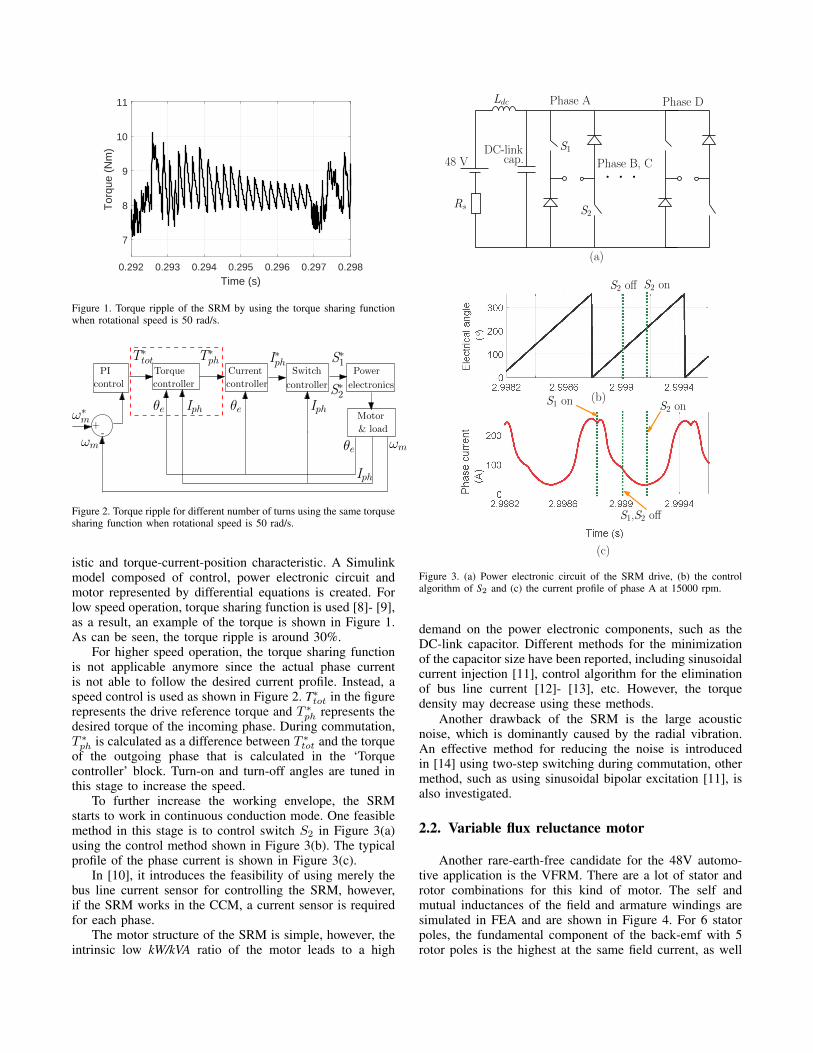
0.292 0.293 0.294 0.295 0.296 0.297 0.298Time (s)
7
8
9
10
11T
orqu
e (N
m)
Figure 1. Torque ripple of the SRM by using the torque sharing functionwhen rotational speed is 50 rad/s.
+-
Torque
controller
PI
control
T∗tot T∗
phCurrent
controller
Switch
controller
I∗ph S∗1
S∗2
Power
electronics
ω∗m
ωm
Motor
& load
θe Iph
Iph
θe ωm
θe Iph
Figure 2. Torque ripple for different number of turns using the same torqusesharing function when rotational speed is 50 rad/s.
istic and torque-current-position characteristic. A Simulinkmodel composed of control, power electronic circuit andmotor represented by differential equations is created. Forlow speed operation, torque sharing function is used [8]- [9],as a result, an example of the torque is shown in Figure 1.As can be seen, the torque ripple is around 30%.
For higher speed operation, the torque sharing functionis not applicable anymore since the actual phase currentis not able to follow the desired current profile. Instead, aspeed control is used as shown in Figure 2. T∗
tot in the figurerepresents the drive reference torque and T ∗
ph represents thedesired torque of the incoming phase. During commutation,T ∗ph is calculated as a difference between T ∗
tot and the torqueof the outgoing phase that is calculated in the ‘Torquecontroller’ block. Turn-on and turn-off angles are tuned inthis stage to increase the speed.
To further increase the working envelope, the SRMstarts to work in continuous conduction mode. One feasiblemethod in this stage is to control switch S2 in Figure 3(a)using the control method shown in Figure 3(b). The typicalprofile of the phase current is shown in Figure 3(c).
In [10], it introduces the feasibility of using merely thebus line current sensor for controlling the SRM, however,if the SRM works in the CCM, a current sensor is requiredfor each phase.
The motor structure of the SRM is simple, however, theintrinsic low kW/kVA ratio of the motor leads to a high
Ldc
48 V
Rs
DC-linkcap.
Phase A Phase D
Phase B, C
S1
S2
S2 off S2 on
S1 on
S1,S2 off
S2 on
(a)
(b)
(c)
Figure 3. (a) Power electronic circuit of the SRM drive, (b) the controlalgorithm of S2 and (c) the current profile of phase A at 15000 rpm.
demand on the power electronic components, such as theDC-link capacitor. Different methods for the minimizationof the capacitor size have been reported, including sinusoidalcurrent injection [11], control algorithm for the eliminationof bus line current [12]- [13], etc. However, the torquedensity may decrease using these methods.
Another drawback of the SRM is the large acousticnoise, which is dominantly caused by the radial vibration.An effective method for reducing the noise is introducedin [14] using two-step switching during commutation, othermethod, such as using sinusoidal bipolar excitation [11], isalso investigated.
2.2. Variable flux reluctance motor
Another rare-earth-free candidate for the 48V automo-tive application is the VFRM. There are a lot of stator androtor combinations for this kind of motor. The self andmutual inductances of the field and armature windings aresimulated in FEA and are shown in Figure 4. For 6 statorpoles, the fundamental component of the back-emf with 5rotor poles is the highest at the same field current, as well
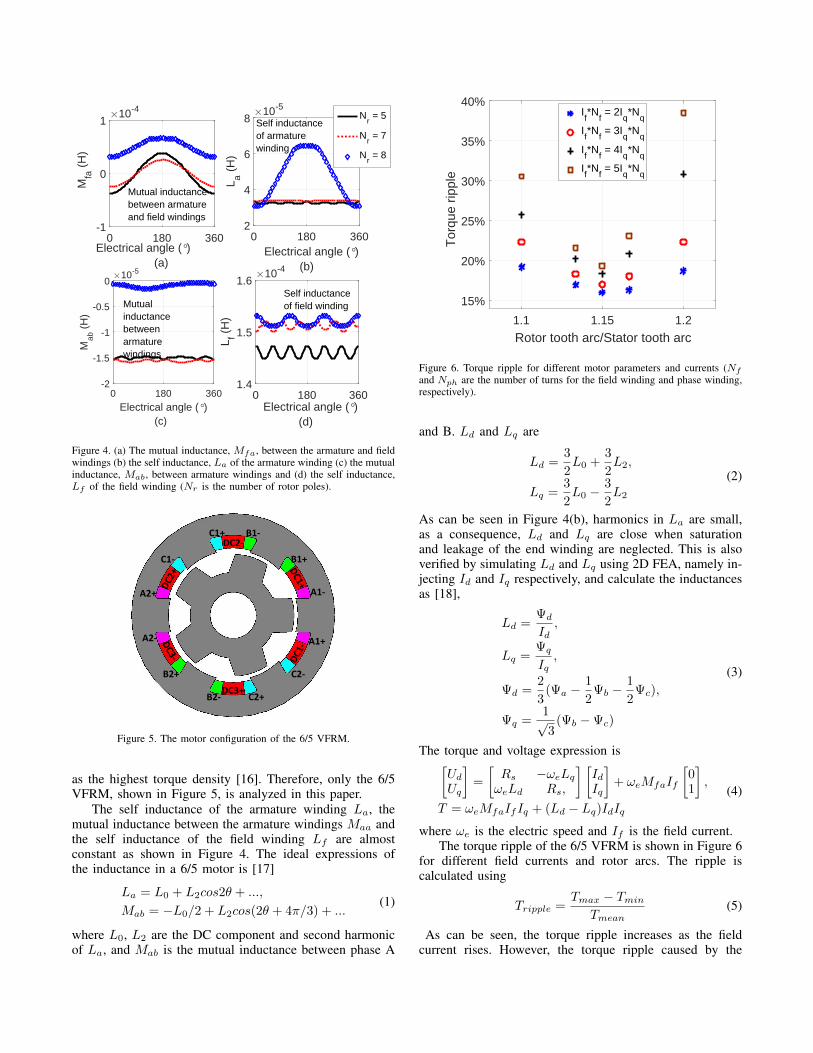
0 180 360Electrical angle (°)
(b)
2
4
6
8
L a (
H)
#10-5
0 180 360Electrical angle (°)
(c)
-2
-1.5
-1
-0.5
0
Mab
(H
)
#10-5
0 180 360Electrical angle (°)
(a)
-1
0
1
Mfa
(H
)
#10-4N
r = 5
Nr = 7
Nr = 8
0 180 360Electrical angle (°)
(d)
1.4
1.5
1.6
L f (H
)
#10-4
Mutualinductancebetweenarmaturewindings
Mutual inductancebetween armatureand field windings
Self inductanceof armaturewinding
Self inductanceof field winding
Figure 4. (a) The mutual inductance, Mfa, between the armature and fieldwindings (b) the self inductance, La of the armature winding (c) the mutualinductance, Mab, between armature windings and (d) the self inductance,Lf of the field winding (Nr is the number of rotor poles).
A1-
A1+
B1-
B1+C1-
C1+
A2+
A2-
B2-
B2+ C2-
C2+
DC2-
DC3+
Figure 5. The motor configuration of the 6/5 VFRM.
as the highest torque density [16]. Therefore, only the 6/5VFRM, shown in Figure 5, is analyzed in this paper.
The self inductance of the armature winding La, themutual inductance between the armature windings Maa andthe self inductance of the field winding Lf are almostconstant as shown in Figure 4. The ideal expressions ofthe inductance in a 6/5 motor is [17]
La = L0 + L2cos2θ + ...,
Mab = −L0/2 + L2cos(2θ + 4π/3) + ...(1)
where L0, L2 are the DC component and second harmonicof La, and Mab is the mutual inductance between phase A
1.1 1.15 1.2
Rotor tooth arc/Stator tooth arc
15%
20%
25%
30%
35%
40%
Tor
que
rippl
e
If*N
f= 2I
q*N
q
If*N
f= 3I
q*N
q
If*N
f= 4I
q*N
q
If*N
f= 5I
q*N
q
Figure 6. Torque ripple for different motor parameters and currents (Nf
and Nph are the number of turns for the field winding and phase winding,respectively).
and B. Ld and Lq are
Ld =3
2L0 +
3
2L2,
Lq =3
2L0 −
3
2L2
(2)
As can be seen in Figure 4(b), harmonics in La are small,as a consequence, Ld and Lq are close when saturationand leakage of the end winding are neglected. This is alsoverified by simulating Ld and Lq using 2D FEA, namely in-jecting Id and Iq respectively, and calculate the inductancesas [18],
Ld =Ψd
Id,
Lq =Ψq
Iq,
Ψd =2
3(Ψa −
1
2Ψb −
1
2Ψc),
Ψq =1√3
(Ψb −Ψc)
(3)
The torque and voltage expression is[Ud
Uq
]=
[Rs −ωeLq
ωeLd Rs,
] [IdIq
]+ ωeMfaIf
[01
],
T = ωeMfaIfIq + (Ld − Lq)IdIq
(4)
where ωe is the electric speed and If is the field current.The torque ripple of the 6/5 VFRM is shown in Figure 6
for different field currents and rotor arcs. The ripple iscalculated using
Tripple =Tmax − Tmin
Tmean(5)
As can be seen, the torque ripple increases as the fieldcurrent rises. However, the torque ripple caused by the
0 0.5 1 1.5 2Speed (rpm)
(a)#104
0
0.5
1P
ower
fact
or
NfIf = 3N
phIq
0 0.5 1 1.5 2Speed (rpm) (b)
#104
0
10
20
30
40
Tor
que
(Nm
)
Efficiency>90%85%<Efficiency<90%80%<Efficiency<85%70%<Efficiency<80%
Figure 7. (a) Power factor and (b) efficiency of the 6/5 VFRM.
current fluctuation due to the small inductance in this lowvoltage application is not considered.
The efficiency and power factor for the 6/5 VFRM areshown in Figure 7. As can be seen, the power factor isrelatively high in the overall working range and it caneven be further increased by adjusting the ratio betweenthe field current and armature current. However, Figure 7shows only an indication, because the values are dependenton the control algorithm.
The torque density of the VFRM is relatively low asshown in [2], which is around 75% of the IPM. The acousticnoise of the VFRM is investigated in [19]. A much lowersound pressure level is generated by this motor compared toSRM, although they have similar stator and rotor structures.
2.3. Synchronous reluctance motor
In this subsection, the permanent-magnet-assistedSynRM is briefly introduced. The permanent magnet addedin the rotor flux barriers of a conventional SynRM signifi-cantly improve the overall performance, such as the opera-tional envelope, efficiency, power factor, etc. The influenceof different types of magnets are analyzed and the resultsare compared with Prius IPM in [21]. By using the ferritemagnet, the torque-speed characteristic, torque density andthe efficiency of the SynRM is competitive with Prius IPM.However, the overall power factor is still relatively low,especially in the high speed region based on the resultin [21].
In the end, a summary of the performance for differentmotor drives is listed in TABLE 1. [22]- [23]
TABLE 1. COMPARISON OF THE MOTOR DRIVES.
Note: + good, − bad, neutral.IPM SRM VFRM SynRM PMA-SynRM
Torque density + − − − +Motor efficiency + + +
Motor cost − + + + Demands on + − + +
power electronicsPower factor + − + −
Controllability −
3. Conclusion
This paper introduces the comparison between theswitched reluctance motor, variable flux reluctance mo-tor, synchronous reluctance motor and permanent magnetassisted synchronous reluctance motor. The strong pointsand the weakness of each motor drive are analyzed. Theswitched reluctance motor itself is cheap and robust, how-ever, its low power factor leads to the demands on thelarge power electronic components, additionally, the highradial force results in large acoustic noise and torque rippletherefore needs complicated control algorithm. The variableflux reluctance motor has good performance for the aspectsof power factor, however, the torque density is relativelylow. The synchronous reluctance motor has the drawbackof relatively low torque density and power factor comparedto IPM, however, these are improved by the assisted magnetsin the rotor.
The final selection of the motor drive should rely on thespecific application and the most important concern in thedesign, such as the cost limit or the size, etc.
References
[1] S. Haghbin, A. Rabiei and E. Grunditz, “Switched reluctance motorin electric or hybrid vehicle applications: A status review”, IEEE Int.Conf. on Industrial Electronics and Applications. pp. 1017-1022, 2013.
[2] X. Liu, Z.Q. Zhu and D. Wu, “Evaluation of efficiency optimizedvariable flux reluctance machine for EVs/HEVs by comparing withinterior PM machine”, IEEE Int. Electric Machines Drives Conf. pp.2648-2654, 2014.
[3] Y. Kano, “Design optimization of brushless synchronous machineswith wound-field excitation for hybrid electric vehicles”, IEEE EnergyConversion Congress and Exposition. pp. 2769-2775, 2015.
[4] A. Vagati, B. Boazzo, P. Guglielmi and G. Pellegrino, “Ferrite assistedsynchronous reluctance machines: A general approach”, IEEE Int.Conf. on Electrical Machines, pp. 1315-1321, 2012.
[5] A.S.O Ogunjuyigbe, A.A Jimoh and D.V. Nicolae, “Improving syn-chronous reluctance machine performance by direct capacitance in-jection through an auxiliary winding”, IEEE Int. Conf. on ElectricalMachines and Systems, pp. 1055-1060, 2007.
[6] E. Carraro, M. Degano, M. Morandin and N. Bianchi, “PM syn-chronous machine comparison for light electric vehicles”, IEEE Int.Electric Vehicle Conf., pp. 1-8, 2014.
[7] S. J. Evangeline and S. Suresh Kumar “Torque ripple minimizationof switched reluctance drives - A survey”, IET Int. Conf. on PowerElectronics, Machines and Drives, pp. 1-6, 2010.
[8] R.H.S Vrenken, J.L. Duarte, K. Boynov, C.G.E. Wijnands, E.A.Lomonova, S. Bervoets and S. Faid, “Switched reluctance motor drivefor full electric vehicles - Part I: Analysis”, Int. Conf, and Exhib. onEcological Vehicles and Renewable Energies. pp. 1-7, 2013.
[9] R.H.S Vrenken, J.L. Duarte, K. Boynov, C.G.E. Wijnands, E.A.Lomonova, S. Bervoets and S. Faid, “Switched reluctance motor drivefor full electric vehicles - Part II: Practical Implementation”, Int. Conf,and Exhib. on Ecological Vehicles and Renewable Energies. pp. 1-7,2013.
[10] C. Gan, J. Wu, Y. Hu and S. Yang, “Online sensorless positionestimation for switched reluctance motors using one current sensor”,IEEE Trans. on Power Electronics., no. 99, 2015.
[11] X. Liu and Z.Q. Zhu, M. Hasegawa, A. Pride and R. Deohar, “DC-link capacitance requirement and noise and vibration reduction in6/4 switched reluctance machine with sinusoidal bipolar excitation”,Energy conversion Congress and Expos. pp. 1596-1603, 2011.
[12] W. Suppharangsan and J. Wang, “A new switching technique for DC-link capacitor minimisation in switched reluctance machine drives”,IET Int. conf. on Power Electronics, Machines and Drives, pp.1-6,2010.
[13] W. Suppharangsan and J. Wang, “Experimental validation of a newswitching technique for DC-link capacitor minimization in switchedreluctance machine drives”, IEEE Int. Electric Machines Drives Conf.,May 2013, pp. 1031-1036.
[14] C. Pollack and C.Y. Wu, “Acoustic noise cancellation techniques forswitched reluctance drives”, IEEE Trans. on Industry Applications vol.33, no. 2, pp. 477-484, 1999.
[15] Y. Kano, “Design optimization of brushless synchronous machineswith wound-field excitation for hybrid electric vehicles”, Energy con-version Congress and Expos. pp. 2769-2775, 2015.
[16] X. Liu and Z.Q. Zhu, “Influence of rotor pole number on electro-magnetic performance of novel variable flux reluctance machine withDC-field coil in stator”, Power Electronics and Motion Control Conf.,pp.1108-1115, 2012.
[17] Y. Tang, J.J.H. Paulides and E.A. Lomonova, “Field weakeningperformance of flux-switching machines for hybrid/electric vehicles”,Inter. Conf. on Ecological Vehicles and Renewable Energies, pp. 1-10,2015.
[18] Y.S. Chen, Z.Q. Zhu and E.A. Lomonova, “Calcualtion of d- and q-axis inductances of PM brushless ac machines accounting for skew ”,IEEE Trans. on Magnetics, vol. 41, no. 10, pp. 3940-3942, 2005.
[19] X. Liu, Z.Q. Zhu, M. Hasegawa, A. Pride and R. Deodhar “Cal-cualtion of d- and q-axis inductances of PM brushless ac machinesaccounting for skew ”, IEEE Trans. on Magnetics, vol. 41, no. 10, pp.3940-3942, 2005.
[20] J. Bao, K. Boynov, J.J.H. Paulides and E.A. Lomonova, “Usage of theinductive energy storage in the field winding for driving the variablereluctance motor”, IEEE Trans. on Magnetics, no.99, 2016.
[21] Y.S. Chen, Z.Q. Zhu and E.A. Lomonova, “Design optimisation andperformance evaluation of a rare-earth-free Permanent Magnet AssistedSynchronous Reluctance Machine for electric vehicle traction”, IETconf. on Power Electronic, Machines and Drives, pp. 1-6, 2014.
[22] T. Finken, M. Felden and K. Hameyer, “Comparison and design ofdifferent electrical machine types regarding their applicability in hybridelectrical vehicles”, Int. Conf. on Elec. Machines, pp. 1-5, 2008.
[23] Z. Yang, F. Shang, I.P. Brown and M. Krishnamurthy, “Comparativestudy of interior permanent magnet, induction, and switched reluctancemotor drives for EV and HEV applications”, IEEE Trans. on Trans-portation Electrification, vol. 1, no. 3, pp. 245-254, 2015.

Performance Evaluation of Synchronous Reluctance
Motors With and Without Permanent Magnets
M. N. Ibrahim1,2, Student Member IEEE, Peter Sergeant1, Member IEEE and E. M. Rashad3, Senior Member IEEE
1Department of Electrical Energy, Systems and Automation, Ghent University, Ghent 9000, Belgium 2Electrical Engineering Department, Kafrelshiekh University, Kafr el-Sheikh 33511, Egypt
3Electrical Power and Machines Department, Tanta University, Tanta 31527, Egypt
E-mail2: [email protected]
Abstract— Nowadays, a growing interest in the efficiency and
the cost of electrical machines has been noticed. Therefore,
Synchronous Reluctance Motors (SynRMs) have become more
attractive, thanks to their higher efficiency and nevertheless
acceptable cost compared to induction machines. The rotor
design of SynRMs with or without permanent magnets (PMs) has
a huge effect on the motor efficiency, torque density and power
factor. This paper introduces an evaluation for the performance
of SynRMs with and without PMs in terms of efficiency, torque
and power factor maps. Three different rotor designs for the
same machine have been compared. For one machine, the
experimental measurements have been obtained and the
validation of the simulation results have been confirmed.
Index Terms—PM, Synchronous Reluctance Motors, Design,
FEM, sensitivity analysis, flux-barriers.
I. NOMENCLATURE
id, iq Direct and quadrature axis stator current
respectively, A
Ld, Lq Direct and quadrature axis stator inductance
of SynRM respectively, H
P Number of pole pairs
p Differential operator (d/dt)
Rs Stator resistance of the motor, Ω
Te Electromagnetic torque of the motor, N.m
Vd, Vq Direct and quadrature component of stator
voltage respectively, V
Vm Maximum input voltage of the motor, V
λs Stator flux linkage of the motor, V. sec
Im Maximum input current of the motor, A
δ, α Load angle and current angle, rad
ωr Mechanical speed of the rotor, rad/s
θr Rotor position, Deg.
II. INTRODUCTION
ecently, Synchronous Reluctance Motors (SynRMs) with
or without permanent-Magnets (PMs) are becoming
attractive machines for industrial application especially
electrical vehicles [1]. This is thanks to their merits of wide
constant power speed range and high torque density. The
power factor and efficiency are good compared to induction
machines [2], [3].
Several papers studied the SynRMs and PMaSynRMs[1],
[11]. For example, in [1], SynRM design suitable for electric
vehicles has presented. In addition, a comparison between
different flux-barrier design for the same stator is investigated.
The effect of four different steel grade on the performance of
SynRMs is studied in [2]. It is noticed that the lower thickness
steel grade has the higher efficiency, however it has not the
higher output torque. In [4], the design characteristics of
SynRM with ferrite magnets and stator skew has investigated.
In addition, mechanical stress and demagnetization of ferrite
has studied as well.
This paper investigates the performance evaluation of
SynRMs and PMaSynRMs. The modelling of PMaSynRM is
introduced in Section III. Performance evaluation of SynRMs
is investigated in Section IV. Experimental results are
implemented to validate the simulation results as depicted in
Section V. At the end, conclusions are figured out in Section
VI.
III. PMASYNRM MODELLING
A. Mathematical dq model of PMaSynRM
The dq model of PMaSynRM can be represented in the
rotor reference frame [2], [5], [6]. The dq-axis reference frame
rotates at ωr, so that the voltage equations are represented by:
pmrqdqrqdddsd PiiPiipiRV ),(),( (1)
),(),( qddrqdqqsq iiPiipiRV (2)
The dq-axis flux-linkage relations are given by:
dqddqdd iiiLii ),(),( , qqdqqdq iiiLii ),(),( (3)
The electromagnetic torque can be calculated as follows:
)),(),((2
3dpmdqdqqqdde iiiiiiiPT (4)
The dq-axis currents can be performed as a function of the
current angle (α), which is the angle of the stator current
space vector with respect to the d-axis of the motor as
described in Fig.1.
)cos(md Ii , )sin(mq Ii (5)
The dq-axis supply voltage can be obtained as follows:
)sin(md VV , )cos(mq VV (6)
where δ is the machine load angle as shown in Fig. 1.
The power factor (PF) of the PMaSynRM can be calculated
by:
R
The authors acknowledge the Egyptian Ministry of Higher Education
(Cultural Affairs and Missions Sector) and Special Research Fund of Ghent
University (BOF) for the financial support during this work.

22
)sin()cos()cos(
qd
qd
VV
VVPF
(7)
The torque ripple can be determined as follows:
)(
)min()max(
e
eeripple
Tavg
TTT
(8)
where max, min and avg are the maximum, the minimum and
the average values of the electromagnetic torque respectively.
The SynRM model can be obtained by inserting λpm=0 in
the previous equations.
d-axis
δ
α
q-axis
iq
id
ωrPλd
-ωrPλq
ωrPλm
ϕ
Rsid
Rsiq
Vm
Im
Fig. 1. Vector diagram of PMaSynRM
The iron losses of the SynRM are calculated based on the
statistical losses theory of Bertotti. The theory depends on the
separation of the losses into hysteresis (hy), classical (cl) and
excess (ex) losses [2], [7].
)(
11)(
)(
...
.
2
.
.
exclhyiron
mmex
mcl
pmhy
PPPP
dt
dB
dt
dBdctP
dt
dBbtP
fBaP m
(9)
where am, αm, bm, cm, dm and σ are material dependent
parameters, and f is the frequency of the applied field.
On the other hand, the SynRM copper losses can be easily
computed using the measured phase resistance as follows:
phPhcopper RIP 23 (10)
The efficiency of the motor can be obtained by :
ironcoppero
o
PPP
P
(11)
where Po is the mechanical output power of the motor
calculated using the computed torque from the FEM model by:
reo TP (12)
IV. PERFORMANCE EVALUATION OF SYNRMS AND
PMASYNRMS
Three different rotors with the same stator and other
geometrical and electromagnetic parameters have been
considered. On the one hand, the stator has 36 slots and 15
turns/slot with conventional star-connected windings. The
stator design is similar to that of induction machines. Several
specifications for the stator of the machine are listed in table I.
On the other hand, all the rotors have 3-flux-barriers per pole
as seen in Figs. 2 and 3. The first rotor has been designed by a
manufacturing company. This motor is called a reference
SynRM and it is the motor for which the experimental
validation has been done. The geometrical rotor parameters of
the reference motor are shown in table I. The second rotor has
been optimized by a conventional optimization technique with
2D FEM for the twelve rotor parameters, depicted in Fig. 2.
This motor is called an optimal SynRM and its rotor
parameters are given in table II. The final rotor has been
obtained by filling all the three flux-barriers of the optimized
rotor (second one) with ferrite PMs. The ferrite PM is selected
due to the lower cost and the availability in the market. In
addition, it can withstand higher temperature [8]. The adopted
ferrite PM properties are shown in [8]. This motor is called a
PMaSynRM.
TABLE I
PROTOTYPE SYNRM PARAMETERS
Parameter Value Parameter Value
Number of rotor flux
barriers per pole
3 Rotor shaft
diameter
35 mm
Number of pole pairs 4 Axial length 140 mm
Number of stator slots 36 Air gap length 0.3 mm
Number of phases 3 Rated speed 6000 RPM
Stator outer diameter 180 mm Rated
frequency
200 Hz
Stator inner diameter 110 mm Rated current 22 A
Rotor outer diameter 109.4 mm Material
grade
M400-50A
θ1 7.5° W1 6 mm
θ2 20.5° W2 4 mm
θ3 33.5° W3 3 mm
L1 25 mm p1 23.5 mm
L2 19 mm p2 36 mm
L3 12 mm p3 46 mm
θ3
L1
W1
q-axi
s
d-axis
W2
W3
L2
L3
θ2
θ1
rib
radiusp 1
p 3
p 2
Fig. 2. Quarter rotor geometry of SynRM
The following results have been obtained by 2D-FEM at the
same conditions. In FEM, only one pole of the considered
four-poles machine needs to be simulated. Sinusoidal currents
are injected in the machine windings at different speeds up to
the rated value (6000 r/min). The currents have different
values up to the rated value (Im=30 A) at fixed current angle
α=56.5°. The selected value of the current angle (56.5°) is the
angle at which the machine can give approximately the
maximum output power, for the different currents and speeds.
The FEM field pattern of the reference motor for quarter
geometry at rated conditions, is depicted in Fig. 3. It can be
noticed that there are some iron regions having higher flux
level (red color). These regions are called flux-barrier
tangential ribs. The thickness of these ribs has a big influence
on the SynRM performance.
TABLE II
OPTIMAL SYNRM ROTOR GEOMETRICAL PARAMETERS
Parameter Value Parameter Value
θ1 8.08° W1 5.5 mm
θ2 16.43° W2 3.5 mm
θ3 28.4° W3 3.5 mm
L1 28.85 mm p1 22.75 mm
L2 28 mm p2 35.5 mm
L3 13.5 mm p3 44.2 mm
q-axis
d-axis θr=0o θr=45o
Fig. 3. Flux paths for the reference SynRM using FEM for a quarter geometry
for two rotor positions
Figure 4 shows the output torque of the reference, optimal
and PM assisted SynRMs at different speeds and currents up
to the rated values. On the one hand, for the same current and
speed, the output torque of the machine depends on the rotor
design which is affected strongly by the design of the twelve
rotor parameters, shown in Fig. 2. Therefore, an optimized
rotor geometry for the SynRMs is necessary and unavoidable
to maximize the machine performance. The SynRM
performance mainly depends on the direct (d) and quadrature
(q) inductances that depend on the rotor flux-barrier
geometrical design. On the other hand, when comparing the
subfigs. of optimal SynRM and PMaSynRM, it can be noticed
that adding ferrite PM in the optimized rotor of the SynRM
leads to an increase of about 25% in the motor torque. This is
because of the effect of PMs on the q-axis inductance of the
SynRM. The PMs saturate the tangential ribs (see: Fig. 2) of
the motor. By consequence, reduce the q-axis inductance, this
leads to a higher output torque.
Figure 5 shows the computed losses (iron and copper) of the
reference, optimal and PM SynRMs for different currents and
speeds up to the rated values. The copper losses are constant
for all the machines due to the same stator windings and
currents. The iron losses depend on the material properties, the
currents and the geometry design of the machine. Only, the
rotor design is different between the reference, optimal and
PM SynRMs. The variation of the flux-barrier parameters,
shown in Fig. 2, has a notable effect on the machine iron
losses. This is due to the variation of the saturation regions of
the iron especially, the stator teeth and rotor tangential ribs.
This can be observed in fig. 5, by comparing the subfigs.
(reference, optimal and PMaSynRM). For the same current
and speed, the iron losses increases for the PMaSynRM that
has the higher output torque (Fig. 4) compared to the others. In
addition, for one machine as expected, the iron losses
increases with increasing the speed and current, approximately
in proportional way.
1000 2000 3000 4000 5000 600010
20
30
666888
101010121212141414161616181818202020222222
Nr [rpm]
I m[A
]
Torque map[N.m]
PMSynRM
1000 2000 3000 4000 5000 600010
20
30
444666888
101010121212141414161616
Nr [rpm]I m
[A]
Optimal SynRM
1000 2000 3000 4000 5000 600010
20
30
444
666
888101010121212
141414
Nr [rpm]
I m[A
]
Reference SynRM
Fig. 4. Motor torque maps for different rotor designs
1000 2000 3000 4000 5000 60005
10
15
20
100
100
200
200
200
300
300
400
400 500600
Nr [rpm]
Te[N
.m]
Losses map[W]
PMSynRM
1000 2000 3000 4000 5000 6000
5
10
15
50100
100
100
150
150
150
200
200
200
250
250
250
300
300
350
350
400
450 500 550
Nr [rpm]
Te[N
.m]
Optimal SynRM
1000 2000 3000 4000 5000 6000
5
10
15
50100
100
100
150
150
150
200
200
200
250
250
250
300
300
350
350 400 450 500
Nr [rpm]
Te[N
.m]
Reference SynRM
Fig. 5. Motor power losses maps for different rotor designs
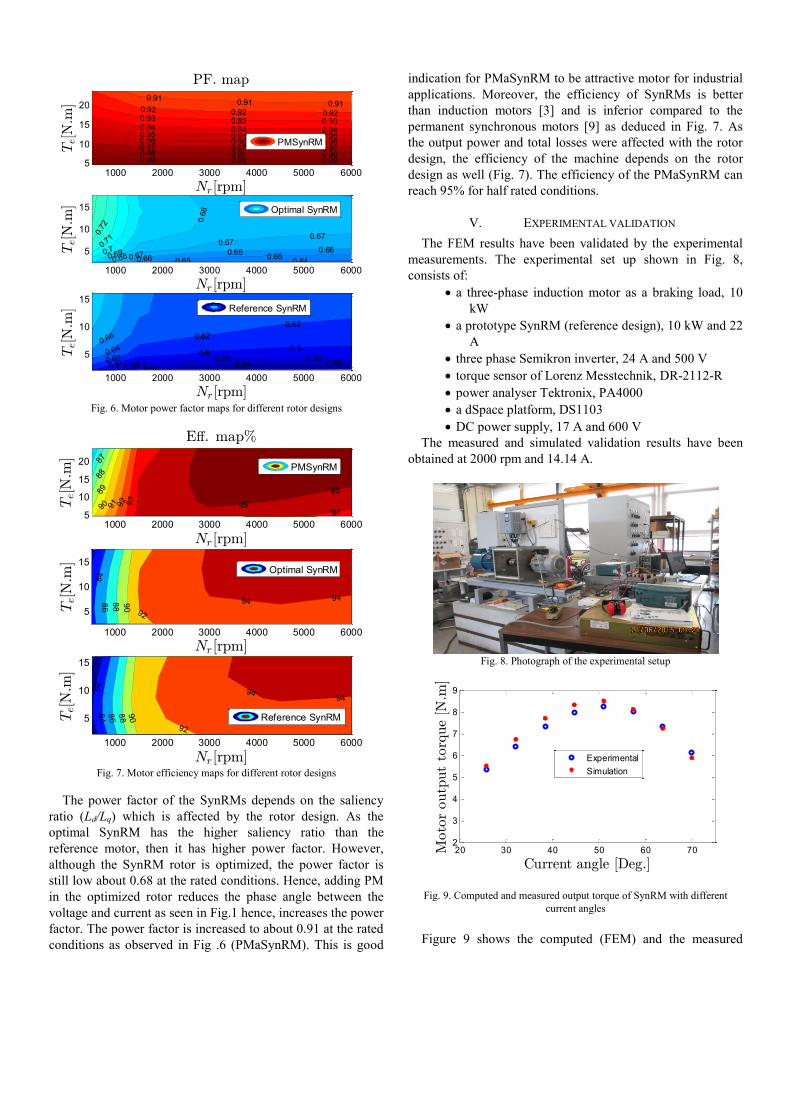
1000 2000 3000 4000 5000 60005
10
15
200.91
0.91 0.910.92 0.92 0.920.93 0.93 0.930.94 0.94 0.940.95 0.95 0.950.96 0.96 0.960.97 0.97 0.970.98 0.98 0.980.99 0.99 0.99
Nr [rpm]
Te[N
.m]
PF. map
PMSynRM
1000 2000 3000 4000 5000 6000
5
10
15
0.640.65
0.65
0.660.660.66
0.670.67
0.67
0.6
8
0.680.690.70.7
1
0.7
2
Nr [rpm]
Te[N
.m]
Optimal SynRM
1000 2000 3000 4000 5000 6000
5
10
15
0.560.560.56
0.580.580.58
0.60.6
0.6
0.62
0.62
0.620.64
0.66
Nr [rpm]
Te[N
.m]
Reference SynRM
Fig. 6. Motor power factor maps for different rotor designs
1000 2000 3000 4000 5000 60005
10
15
20 8788
89
90 91 92 93
94
95
95
Nr [rpm]
Te[N
.m]
E,. map%
PMSynRM
1000 2000 3000 4000 5000 6000
5
10
15
84
86
88 90
92
9494
Nr [rpm]
Te[N
.m]
Optimal SynRM
1000 2000 3000 4000 5000 6000
5
10
15
82
84
86
88
90
92
9494
Nr [rpm]
Te[N
.m]
Reference SynRM
Fig. 7. Motor efficiency maps for different rotor designs
The power factor of the SynRMs depends on the saliency
ratio (Ld/Lq) which is affected by the rotor design. As the
optimal SynRM has the higher saliency ratio than the
reference motor, then it has higher power factor. However,
although the SynRM rotor is optimized, the power factor is
still low about 0.68 at the rated conditions. Hence, adding PM
in the optimized rotor reduces the phase angle between the
voltage and current as seen in Fig.1 hence, increases the power
factor. The power factor is increased to about 0.91 at the rated
conditions as observed in Fig .6 (PMaSynRM). This is good
indication for PMaSynRM to be attractive motor for industrial
applications. Moreover, the efficiency of SynRMs is better
than induction motors [3] and is inferior compared to the
permanent synchronous motors [9] as deduced in Fig. 7. As
the output power and total losses were affected with the rotor
design, the efficiency of the machine depends on the rotor
design as well (Fig. 7). The efficiency of the PMaSynRM can
reach 95% for half rated conditions.
V. EXPERIMENTAL VALIDATION
The FEM results have been validated by the experimental
measurements. The experimental set up shown in Fig. 8,
consists of:
a three-phase induction motor as a braking load, 10
kW
a prototype SynRM (reference design), 10 kW and 22
A
three phase Semikron inverter, 24 A and 500 V
torque sensor of Lorenz Messtechnik, DR-2112-R
power analyser Tektronix, PA4000
a dSpace platform, DS1103
DC power supply, 17 A and 600 V
The measured and simulated validation results have been
obtained at 2000 rpm and 14.14 A.
Fig. 8. Photograph of the experimental setup
20 30 40 50 60 702
3
4
5
6
7
8
9
Current angle [Deg.]
Moto
routp
utto
rque
[N.m
]
Experimental
Simulation
Fig. 9. Computed and measured output torque of SynRM with different
current angles
Figure 9 shows the computed (FEM) and the measured

output torque of the SynRM. There is a good agreement
between the simulated and the measured values. However, the
difference between the measured and computed results is due
to different reasons: the cutting and punching effects on the
steel properties, the manufacturing tolerance and the
measurement error.
VI. CONCLUSION
This paper has discussed the performance evaluation of
Synchronous reluctance motors (SynRMs) with and without
permanent-magnets. same Three different rotors having the
stator design and other geometrical and electromagnetic
parameters are considered. The three rotors are reference,
optimized and optimized assisted by ferrite PMs
(PMaSynRMs) in its flux-barrier. Different performance
indicators for the machine are computed by FEM and
compared at the same conditions. The performance indicators
are efficiency, torque, total losses and power factor maps. It is
found that the PMaSynRMs can reach efficiency and power
factor higher than 95% and 0.91 respectively at the rated
conditions. This means that the PMaSynRMs are much better
than both the induction machines and switched reluctance
machines. In addition, they can be good competitors compared
with the permanent magnet synchronous machines due to
lower cost. Finally, measurements are obtained and validated
FEM model.
VII. REFERENCES
[1] M. Ferrari, N. Bianchi, A. Doria, and E. Fornasiero, “Design of
synchronous reluctance motor for hybrid electric vehicles,” IEEE Trans. Ind. Appl., vol. 51, no. 4, pp. 3030-3040, Jul/Aug. 2015.
[2] M. N. Ibrahim, P. Sergeant, and E. M. Rashad, “Synchronous reluctance
motors performance based on different electrical steel grades,” IEEE Trans. Magn. vol. 51, no. 11, Nov. 2015, Art. ID 7403304.
[3] R. Vartanian and H. A. Toliyat, “Design and comparison of an optimized permanent magnet-assisted synchronous reluctance motor
(PMa-SynRM) with an induction motor with identical NEMA frame
stators,” in Proc. IEEE Electr. Ship Technol. Symp. (ESTS), Apr. 2009, pp. 107–112.
[4] Y. H. Jeong, K. Kim, Y. J. Kim, B. S. Park, and S. Y. Jung, “Design
characteristics of PMa-SynRM and performance comparison with IPMSM based on numerical analysis,” in Proc. 20th ICEM, 2012, pp.
164–170
[5] S. Morimoto, M. Sanada, and Y. Takeda, “Performance of PM-assisted synchronous reluctance motor for high-efficiency and wide constant
power operation,” IEEE Trans. Ind. Appl., vol. 37, no. 5, pp. 1234–1240,
Sep./Oct. 2001 [6] H. Huang, Y. Sh. Hu, Y. Xiao, and H. Lyu, “research of parameters and
antidemagnetization of rare-earth-less permanent magnet-assisted
synchronous reluctance motor,” IEEE Trans. Magn. vol. 51, no. 11, Nov. 2015, Art. ID 8112504.
[7] G. Bertotti, "General properties of power losses in soft ferromagnetic
materials," IEEE Trans. Magn., vol. 24, no. 1, pp. 621 - 630, 1988 [8] http://www.bakkermagnetics.com/sites/default/files/downloads/ferrite_-
_sintered_1.pdf
[9] T. Ahonen, J. Tamminen and J. Montonen, “Comparison of electric motor types for realising an energy efficient pumping system,” in Proc.
16th Eur. Con. Power Electronic. Appl. (EPE'14-ECCE Europe), 2014,
pp. 1–9
[10] Ch.T. Liu, T. Y. Luo, Ch. C. Hwang, and B.Y. Chang, “Field path
design assessments of a high-performance small-power synchronous-reluctance motor,” IEEE Trans. Magn. vol. 51, no. 11, Nov. 2015, Art.
ID 8206504.
[11] R. Lohninger, H. Grabner, G. Weidenholzer, S. Silber, and W. Amrhein, “Modeling, simulation, design of permanent-magnet-assisted
synchronous reluctance machine,” IEEE Trans. Ind. Appl., vol. 51, no. 1,
pp. 196-203, Jan./Feb. 2015.
VIII. BIOGRAPHIES
Mohamed N. Ibrahim was born in Kafrelshiekh,
Egypt on September 18, 1986. He has graduated
from Faculty of Engineering, Kafrelshiekh
University, Egypt on 2008. He received his MSc.
degree in Electrical Power and Machines
Engineering from Tanta University in 2012. Since
2012, he is working as an assistant lecturer at the Department of
Electrical Engineering, Faculty of Engineering, Kafrelshiekh
University, Egypt.
He is currently working towards the PhD at Ghent University,
Belgium. His research interests are in Electrical Machines, Electrical
Drives, Power Electronics and Renewable Energy.
Prof. Essam M. Rashad was born in Shebin
El-Kom, Egypt in 1960. He received his BSc
degree from the department of Electric Power
and Machines Engineering., Faculty of
Engineering, Shebin El-Kom, Menoufiya
University, Egypt in May 1983. In 1987 and
1992 he received MSc and PhD, respectively
both from faculty of Engineering Alexandria
university, Egypt. In 1992 he has joined Faculty of Engineering,
Tanta University, Egypt, where he is currently a Professor and Head
of Electrical Power and Machines Engineering. From Feb. to Aug
2000, he was a visiting researcher in Faculty of Engineering,
Nagasaki University, Japan. In summer 2003, he was a visiting
researcher at Faculty of Engineering and Applied Science, Memorial
University of Newfoundland, St. John’s, NL, Canada. From 2004 to
2009, he was Head of Electrical Technology Department, Buraydah
College of Technology, Kingdom of Saudi Arabia. From 2011 to
2014, he was Vice Dean for Education and Student affairs of Faculty
of Engineering, Tanta University, Egypt.
Prof. Rashad research interests include electrical machine analysis
and design, electrical drives, power electronics and renewable energy
systems.
Peter Sergeant received the M.Sc. degree in
electromechanical engineering in 2001, and
the Ph.D. degree in engineering sciences in
2006, both from Ghent University, Ghent,
Belgium.
In 2001, he became a researcher at the
Electrical Energy Laboratory of Ghent
University. He became a postdoctoral
researcher at Ghent University in 2006
(postdoctoral fellow of the Research Foundation - Flanders) and at
Ghent University College in 2008. Since 2012, he is associate
professor at Ghent University. His current research interests include
numerical methods in combination with optimization techniques to
design nonlinear electromagnetic systems, in particular, electrical
machines for sustainable energy applications.
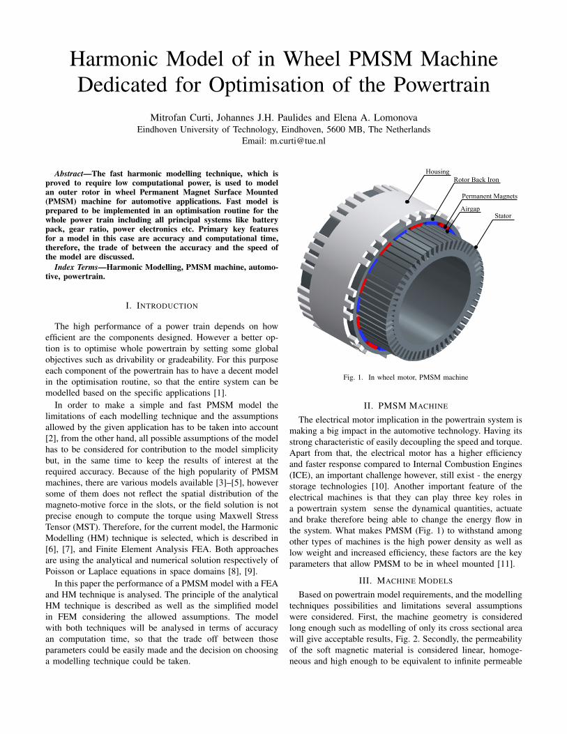
Harmonic Model of in Wheel PMSM MachineDedicated for Optimisation of the Powertrain
Mitrofan Curti, Johannes J.H. Paulides and Elena A. LomonovaEindhoven University of Technology, Eindhoven, 5600 MB, The Netherlands
Email: [email protected]
Abstract—The fast harmonic modelling technique, which isproved to require low computational power, is used to modelan outer rotor in wheel Permanent Magnet Surface Mounted(PMSM) machine for automotive applications. Fast model isprepared to be implemented in an optimisation routine for thewhole power train including all principal systems like batterypack, gear ratio, power electronics etc. Primary key featuresfor a model in this case are accuracy and computational time,therefore, the trade of between the accuracy and the speed ofthe model are discussed.
Index Terms—Harmonic Modelling, PMSM machine, automo-tive, powertrain.
I. INTRODUCTION
The high performance of a power train depends on howefficient are the components designed. However a better op-tion is to optimise whole powertrain by setting some globalobjectives such as drivability or gradeability. For this purposeeach component of the powertrain has to have a decent modelin the optimisation routine, so that the entire system can bemodelled based on the specific applications [1].
In order to make a simple and fast PMSM model thelimitations of each modelling technique and the assumptionsallowed by the given application has to be taken into account[2], from the other hand, all possible assumptions of the modelhas to be considered for contribution to the model simplicitybut, in the same time to keep the results of interest at therequired accuracy. Because of the high popularity of PMSMmachines, there are various models available [3]–[5], howeversome of them does not reflect the spatial distribution of themagneto-motive force in the slots, or the field solution is notprecise enough to compute the torque using Maxwell StressTensor (MST). Therefore, for the current model, the HarmonicModelling (HM) technique is selected, which is described in[6], [7], and Finite Element Analysis FEA. Both approachesare using the analytical and numerical solution respectively ofPoisson or Laplace equations in space domains [8], [9].
In this paper the performance of a PMSM model with a FEAand HM technique is analysed. The principle of the analyticalHM technique is described as well as the simplified modelin FEM considering the allowed assumptions. The modelwith both techniques will be analysed in terms of accuracyan computation time, so that the trade off between thoseparameters could be easily made and the decision on choosinga modelling technique could be taken.
Stator
Permanent Magnets
Rotor Back Iron
Airgap
Housing
Fig. 1. In wheel motor, PMSM machine
II. PMSM MACHINE
The electrical motor implication in the powertrain system ismaking a big impact in the automotive technology. Having itsstrong characteristic of easily decoupling the speed and torque.Apart from that, the electrical motor has a higher efficiencyand faster response compared to Internal Combustion Engines(ICE), an important challenge however, still exist - the energystorage technologies [10]. Another important feature of theelectrical machines is that they can play three key roles ina powertrain system sense the dynamical quantities, actuateand brake therefore being able to change the energy flow inthe system. What makes PMSM (Fig. 1) to withstand amongother types of machines is the high power density as well aslow weight and increased efficiency, these factors are the keyparameters that allow PMSM to be in wheel mounted [11].
III. MACHINE MODELS
Based on powertrain model requirements, and the modellingtechniques possibilities and limitations several assumptionswere considered. First, the machine geometry is consideredlong enough such as modelling of only its cross sectional areawill give acceptable results, Fig. 2. Secondly, the permeabilityof the soft magnetic material is considered linear, homoge-neous and high enough to be equivalent to infinite permeable
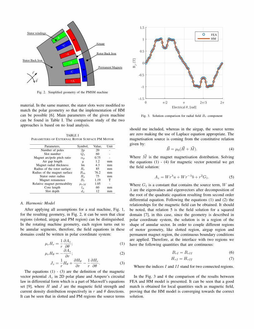
+A
-C
+B
-A
+C
-B
Permanent Magnets
Rotor Back Iron
Airgap
Stator windings
Stator Back Iron
Fig. 2. Simplified geometry of the PMSM machine
material. In the same manner, the stator slots were modified tomatch the polar geometry so that the implementation of HMcan be possible [6]. Main parameters of the given machinecan be found in Table I. The comparison study of the twoapproaches is based on no load analysis.
TABLE IPARAMETERS OF EXTERNAL ROTOR SURFACE PM MOTOR
Parameters, Symbol, Value, UnitNumber of poles 2p 20 -
Slot number Qs 60 -Magnet arc/pole pitch ratio αp 0.75 -
Air gap length g 1.2 mmMagnet radial thickness lm 4.3 mm
Radius of the rotor surface Rr 85 mmRadius of the magnet surface Rm 76.2 mm
Stator outer radius Rs 75 mmMagnet remanence Br 1.19 T
Relative magnet permeability µrM 1.05 -Core length la 60 mmSlot depth ds 12 mm
A. Harmonic Model
After applying all assumptions for a real machine, Fig. 1,for the resulting geometry, in Fig. 2, it can be seen that clearregions (slotted, airgap and PM region) can be distinguished.In the rotating machine geometry, each region turns out tobe annular segments, therefore, the field equations in thesedomains could be written in polar coordinate system:
µrHr =1
r
∂Az∂θ
; (1)
µrHθ = −∂Az∂r
; (2)
Jz =1
rHθ +
∂Hθ
∂r− 1
r
∂Hr
∂θ. (3)
The equations (1) - (3) are the definition of the magneticvector potential Az in 2D polar plane and Ampere’s circuitallaw in differential form which is a part of Maxwell’s equationsset [9], where H and J are the magnetic field strength andcurrent density distribution respectively in r and θ directions.It can be seen that in slotted and PM regions the source terms
0 :/2 : 2:/3 2:Electrical 3 , [rad]
-1.5
-1
-0.5
0
0.5
1
1.5
Br, [
T]
FEAHM
Fig. 3. Solution comparison for radial field Br component
should me included, whereas in the airgap, the source termsare zero making the use of Laplace equation appropriate. Themagnetisation source is coming from the constitutive relationgiven by:
~B = µ0( ~H + ~M). (4)
Where ~M is the magnet magnetisation distribution. Solvingthe equations (1) - (4) for magnetic vector potential we getthe field solution:
Az =Wrλa+Wr−λb+ r2G1. (5)
Where G1 is a constant that contains the source term, W andλ are the eigenvalues and eigenvectors after decomposition ofthe root of the quadratic equation resulting from second orderdifferential equation. Following the equations (1) and (2) therelationships for the magnetic field can be obtained. It shouldbe noted, that relation 5 is the field solution for a squareddomain [7], in this case, since the geometry is described inpolar coordinate system, the solution is in a region of theshape of annular sector. In order to couple different regionsof motor geometry, like slotted region, airgap region andpermanent magnet region, the continuous boundary conditionsare applied. Therefore, at the interface with two regions wehave the following quantities that are continuous:
BrI = BrII (6)HτI = HτII (7)
Where the indices I and II stand for two connected regions.
In the Fig. 3 and 4 the comparison of the results betweenFEA and HM model is presented. It can be seen that a goodmatch is obtained for local quantities such as magnetic field,proving that the HM model is converging towards the correctsolution.
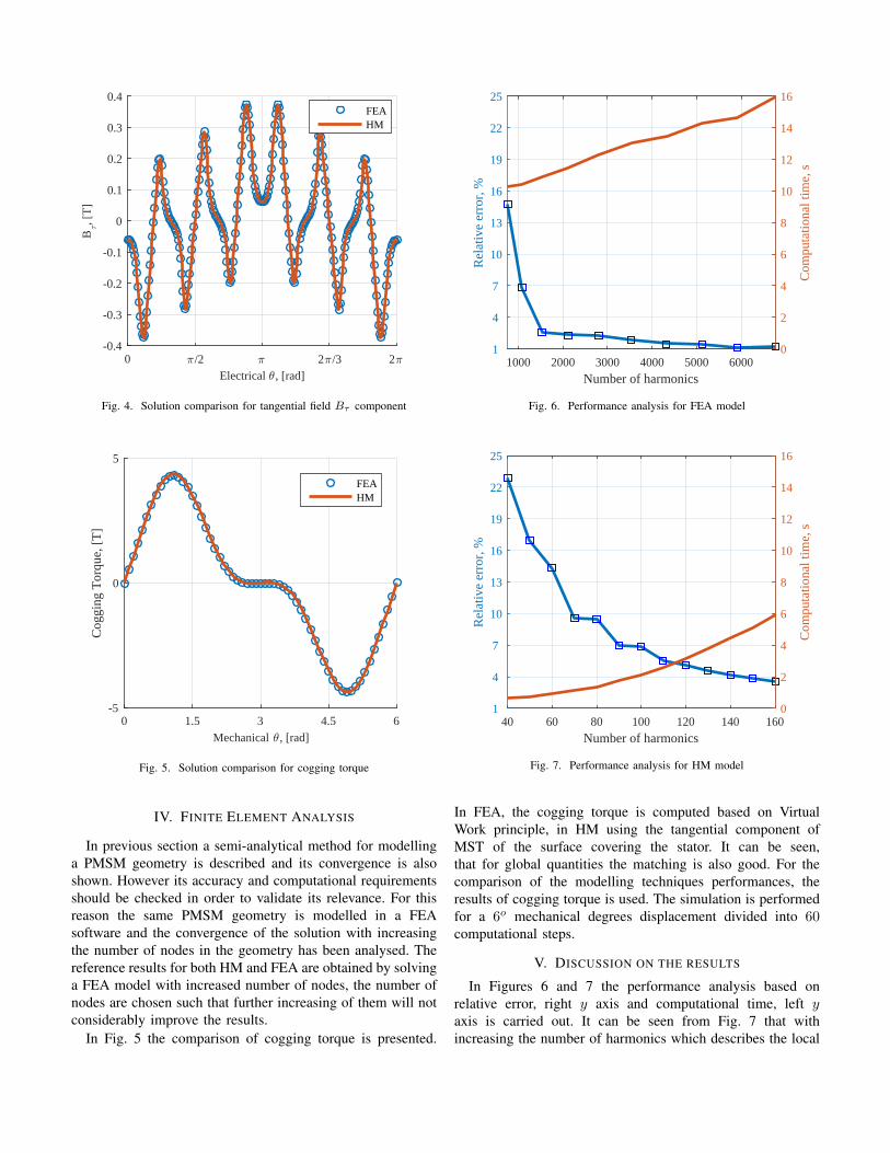
0 :/2 : 2:/3 2:Electrical 3 , [rad]
-0.4
-0.3
-0.2
-0.1
0
0.1
0.2
0.3
0.4B=, [
T]
FEAHM
Fig. 4. Solution comparison for tangential field Bτ component
0 1.5 3 4.5 6Mechanical 3 , [rad]
-5
0
5
Cog
ging
Tor
que,
[T
]
FEAHM
Fig. 5. Solution comparison for cogging torque
IV. FINITE ELEMENT ANALYSIS
In previous section a semi-analytical method for modellinga PMSM geometry is described and its convergence is alsoshown. However its accuracy and computational requirementsshould be checked in order to validate its relevance. For thisreason the same PMSM geometry is modelled in a FEAsoftware and the convergence of the solution with increasingthe number of nodes in the geometry has been analysed. Thereference results for both HM and FEA are obtained by solvinga FEA model with increased number of nodes, the number ofnodes are chosen such that further increasing of them will notconsiderably improve the results.
In Fig. 5 the comparison of cogging torque is presented.
1000 2000 3000 4000 5000 6000Number of harmonics
1
4
7
10
13
16
19
22
25
Rel
ativ
e er
ror,
%
0
2
4
6
8
10
12
14
16
Com
puta
tiona
l tim
e, s
Fig. 6. Performance analysis for FEA model
40 60 80 100 120 140 160Number of harmonics
1
4
7
10
13
16
19
22
25
Rel
ativ
e er
ror,
%
0
2
4
6
8
10
12
14
16
Com
puta
tiona
l tim
e, s
Fig. 7. Performance analysis for HM model
In FEA, the cogging torque is computed based on VirtualWork principle, in HM using the tangential component ofMST of the surface covering the stator. It can be seen,that for global quantities the matching is also good. For thecomparison of the modelling techniques performances, theresults of cogging torque is used. The simulation is performedfor a 6o mechanical degrees displacement divided into 60computational steps.
V. DISCUSSION ON THE RESULTS
In Figures 6 and 7 the performance analysis based onrelative error, right y axis and computational time, left yaxis is carried out. It can be seen from Fig. 7 that withincreasing the number of harmonics which describes the local

field solution, the error is decreasing, but also, in the sametime the computational time is increasing in such a way, thatfor an accuracy of 4% the computational time is 6 seconds.From another hand, the FEA model, from Fig. 6 shows afaster convergence, but the computational time is biased by 10seconds, which means that for an accuracy of 4% with HMmethod, the model will run 2.5 times faster than FEA model.These analysis allow to choose the modelling technique forPMSM model in the power train optimisation routine.
VI. CONCLUSION
An analysis over the PMSM model performances imple-mented with HM and FEA method is presented in this paper.The computational time and the accuracy are the key param-eters for a model which is used for optimisation. Using theassumptions that are allowed by the application, a simplifiedmodel could be obtained. By changing the number of nodesin FEA and number of harmonics in HM, it could be easilyobserved that until a certain accuracy, the HM will require lesscomputational effort. Therefore, as a modelling technique fora PMSM model of powetrain optimisation, the HM method isselected.
ACKNOWLEDGMENT
This paper is part of the ADvanced Electric PowertrainTechnology (ADEPT) project which is an EU funded MarieCurie ITN project, grant number 607361 [12]. Within ADEPT,virtual and hardware tools are created to assist the design andanalysis of future electric propulsions. Especially within thecontext of the paradigm shift from fuel powered combustionengines to alternative energy sources (e.g. fuel cells, solarcells, and batteries) in vehicles like motorbikes, cars, trucks,boats, planes. The design of these high performance, low costand clean propulsion systems has stipulated an internationalcooperation of multiple disciplines such as physics, math-ematics, electrical engineering, mechanical engineering andspecialisms like control engineering and safety. By cooperationof these disciplines in a structured way, the ADEPT programprovides a virtual research lab community from labs of Euro-pean universities and industries [13].
REFERENCES
[1] K. Ramakrishnan, M. Gobbi, and G. Mastinu, “Multi-objective opti-mization of in-wheel motor powertrain and validation using vehiclesimulator,” in Ecological Vehicles and Renewable Energies (EVER),2015 Tenth International Conference on, March 2015, pp. 1–9.
[2] M. Curti, J. Paulides, and E. Lomonova, “An overview of analyticalmethods for magnetic field computation,” in Ecological Vehicles andRenewable Energies (EVER), 2015 Tenth International Conference on,March 2015, pp. 1–7.
[3] B. Hague, The principles of electromagnetism applied to electricalmachines: (formerly titled: Electromagnetic problems in electrical engi-neering). Dover Publications, 1962.
[4] Z. Zhu, D. Howe, and C. Chan, “Improved analytical model forpredicting the magnetic field distribution in brushless permanent-magnetmachines,” Magnetics, IEEE Transactions on, vol. 38, no. 1, pp. 229–238, 2002.
[5] Z. Zhu, D. Howe, E. Bolte, and B. Ackermann, “Instantaneous magneticfield distribution in brushless permanent magnet dc motors. i. open-circuit field,” Magnetics, IEEE Transactions on, vol. 29, no. 1, pp. 124–135, 1993.
[6] B. L. J. Gysen, K. J. Meessen, J. J. H. Paulides, and E. A. Lomonova,“General formulation of the electromagnetic field distribution in ma-chines and devices using fourier analysis,” Magnetics, IEEE Transac-tions on, vol. 46, no. 1, pp. 39–52, Jan 2010.
[7] R. L. J. Sprangers, J. J. H. Paulides, B. L. J. Gysen, and E. A. Lomonova,“Magnetic saturation in semi-analytical harmonic modeling for electricmachine analysis,” IEEE Transactions on Magnetics, vol. 52, no. 2, pp.1–10, Feb 2016.
[8] K. J. Binns, P. J. Lawrenson, and C. W. Trowbridge, The analytitcaland numerical solution of electric and magnetic fields. John Wiley &Sons, 2001.
[9] E. P. Furlani, Electric Machines and Drives, I. Mayergoyz, Ed. Aca-denic Press, 2001.
[10] J. G. W. West, “Dc, induction, reluctance and pm motors for electricvehicles,” Power Engineering Journal, vol. 8, no. 2, pp. 77–88, April1994.
[11] Y. K. Kim, Y. H. Cho, N. C. Park, S. H. Kim, and H. S. Mok, “In-wheelmotor drive system using 2-phase pmsm,” in Power Electronics andMotion Control Conference, 2009. IPEMC ’09. IEEE 6th International,May 2009, pp. 1875–1879.
[12] E. A. Lomonova, J. J. H. Paulides, S. Wilkins, and J. Tegen-bosch, “Adept: ”advanced electric powertrain technology” - virtual andhardware platforms,” in Ecological Vehicles and Renewable Energies(EVER), 2015 Tenth International Conference, March 2015, pp. 1–10.
[13] A. Stefanskyi, A. Dziechciarz, F. Chauvicourt, G. E. Sfakianakis,K. Ramakrishnan, K. Niyomsatian, M. Curti, N. Djukic, P. Romanazzi,S. Ayat, S. Wiedemann, W. Peng, A. Tamas, and S. Stipetic, “Re-searchers within the EU funded Marie Curie ITN project ADEPT, grantnumber 607361,” 2013-2017.