
Power Electronics Lab EE-397 - Aligarh Muslim University
27
Annexure I 0 LAB MANUAL Power Electronics Lab EE-397 Department of Electrical Engineering Zakir Husain College of Engineering and Technology Aligarh Muslim University Aligarh
-
Upload
khangminh22 -
Category
Documents
-
view
5 -
download
0
Transcript of Power Electronics Lab EE-397 - Aligarh Muslim University

Annexure I
0
LAB MANUAL
Power Electronics Lab
EE-397
Department of Electrical Engineering
Zakir Husain College of Engineering and Technology
Aligarh Muslim University
Aligarh

Annexure I
1
Course Title Power Electronics Lab
Course number EE-397
Credit Value 2.0
Course Category DC
Pre-requisite Power Electronics
Contact Hours (L-T-P) 0-0-3
Type of Course Lab
Course
Objectives
To familiarize the different types of characteristics of various types Power
Electronic Devices and realize various power electronic converters and triggering
circuits for specific applications.
Course
Outcomes
At the end of the course the students will be able to:
1. Interpret different characteristics of an SCR.
2. Implement the phase controlled switching using DIAC and TRIAC.
3. Realize different type of triggering circuits for particular application.
4. Use UJT as a relaxation oscillator and for triggering circuits.
5. Implement different types of converters for various applications like speed
control of DC motor.
Syllabus List of Experiments 1. Static Characteristics of SCR
2. TRIAC and AC phase control
3. UJT based relaxation oscillator and trigger circuit. 4. R, RC trigger circuits and speed control of Universal motor. 5. Uncontrolled AC-DC Converter. 6. Monostable based trigger circuits.
7. Speed control of DC motor by a phase controlled converter.
8. MOSFET based flyback DC-DC converter.
Books*/Refere
nces
1. *G.K.Dubey, et al, Thyristorised Power Controllers; New Age International,
New Delhi.
2. *M.H. Rashid, Power Electronics; PHI Learning, New Delhi.
3. V.Subramanyam, Power Electronics, New Age International, New Delhi.
4. Jai P Agarwal, Power Electronics Systems, Addison Wesely.
Course
Assessment/
Evaluation/
Grading
Policy
Sessional
Evaluation of report 40 Marks
Viva 20 Marks
Sessional total 60
End Semester Examination (3 Hours) 40 Marks
Total 100 Marks
PROGRAM OUTCOMES:
a. Students will demonstrate knowledge of mathematics, science and Electrical
Engineering.
b. Students will demonstrate an ability to identify, formulate and solve Electrical
engineering problems.
c. Students will demonstrate an ability to design electrical and electronic circuits and
conduct experiments with electrical systems, analyze and interpret data.

Annexure I
2
d. Students will demonstrate an ability to design a system, component or process as
per needs and specification within realistic constraints.
e. Students will demonstrate an ability to visualize and work on laboratory and
multidisciplinary tasks.
f. Students will demonstrate skills to use modern engineering tools, software and
equipment to analyze problems.
g. Students will demonstrate knowledge of professional and ethical responsibilities.
h. Students will be able to communicate effectively.
i. Students will show the understanding of impact of engineering solutions on the
society and also will be aware of contemporary issues.
j. Students will develop confidence for self-education and ability to engage in life-
long learning.
k. Students who can participate and succeed in competitive examinations.
Mapping with Programme Outcomes (POs)
POs
a b c d e f g h i j k
x x x x x x x
General instructions for the lab
1. All students will carry out same experiment on a particular
turn.
2. They should come prepared with the procedure and related
theory. [Get the observations and other details signed by a
teacher after performing the experiment]
3. Report is to be submitted with calculations and answers to
the related questions on the consecutive next turn.
4. No student will be allowed to proceed to next experiment,
unless he/she submits the report of previous experiment. In
such case no attendance will be marked for the defaulter
student.
5. The lab report will be checked and returned on the same
day of submission.

Annexure I
3
6. A grand viva-voce will be held in the last two turns of the
lab course.
7. The Instructors and lab staff are available to assist the
students in their work.
8. It is prohibited to smoke, eat or drink in the Laboratory.
The related lab experiment sheets are given next:

Annexure I
4
LIST OF EXPERIMENTS
POWER ELECTRONICS LAB (EE 397)
1. Static characteristics of SCR.
2. Triac and AC phase control.
3. UJT based relaxation Oscillator and trigger circuit.
4. R, RC trigger circuits and speed control of UM.
5. Uncontrolled AC to DC converter.
6. Monostable based trigger circuit.
7. Speed control of DC motor by RC trigger circuit.
8. MOSFET based fly-back DC to DC Converter.
Annexure I
5
P/E-1/1
Object: Static characteristics of an SCR.
Experiment:
( i ) To study the forward conducting characteristics of a given SCR ( ii ) To determine latching current and holding current.
Brief Theory: An SCR turn & on, when a positive gate signal is applied and when it is in forward
biased condition.
Simple V-I method can be used to find the forward conducting characteristics of the SCR. Anode
current can be varied with the help of load resistance to find out the static i-v characteristics of
the SCR. Similarly by slowly increasing and decreasing the load resistance the values of the
holding current and latching current, respectively can also be found.
Procedure:
1. Make the connection as shown in Fig 1.
2. Put the ‘toggle switch’ at dc position which provides a dc voltage to the load circuit. 3. Press the push button switch (S) to bring the SCR into conduction mode by providing gate
current. 4. Adjust the anode current about 0.5 Amp. with the help of load resistance RL. Increase RL
gradually. Note the anode current and voltage (vAk) across the SCR. Take about 10 readings. 5. Latching and holding current can be found with the help of variation of the load resistance.
Increase slowly the load resistance. Observe the critical anode current when the SCR returns
to blocking state. Note down this value as holding current of SCR.
6. Now decrease RL slowly and apply the gate pulse (by pressing the press-switch to the gate of SCR. While removing the gate pulse, if the SCR conducts and stays ON, then that value of the anode current is the latching current.
7. Put the toggle switch to AC mode. Now a half – wave voltage is applied to the load circuit. Adjust the load resistance and press the press-switch. The conduction of the SCR will continue only for a period the switch was pressed.

Annexure I
6
Sample Questions:
1. Why SCR conducts so long as gate signal is present in ac test? 2. Why SCR fails to maintain conduction below holding current? 3. What are the specifications of SCR used in the experiment? 4. How much experimental data deviate from specified data?

Annexure I
7
P/E-1/2
A
AC
DC
23
0 V
AC 12 V
AC
Load
Resistance, RL
(Rheostat)
Toggle
Switch
Press
Switch

Annexure I
8
P/E-2
Object: Triac and a.c phase control.
Experiment:
( i ) To study a diac based trigger circuit.
( ii ) To study ac phase controlled switching using a diac and triac.
Brief Theory: A triac can be triggered ON by the application of either a positive or a negative
gate signal in both positive and negative of the ac supply voltage. Therefore a triac has four
modes of triggering. A diac conductors at a particular positive and negative voltage. Therefore it
supplies trigger signals to a triac in both positive and negative half-cycles of ac voltage.
When gate trigger signal is delayed, a thyristor triggers at an instant other than the zero cross
over of the ac supply voltage. Thus the load voltage becomes non-sinusoidal and only a part of
the supply (ac) voltage appears across the load. Therefore by controlling the switching angle, the
output ac voltage is controlled effectively.
Procedure:
1. Complete the circuit connection as shown in figure
2. Connect MT1 to K and A to MT2.
3. Apply 230V ac supply to P and N terminals from an autotransformer.
4. Observe the phase angle control by the variation of potentiometer RP.
5. For a particular setting of RP, measure the load voltage by a multimeter and trace the
voltage waveforms available on CRO for three settings of potentiometer.
Report:
1. What are the advantages and disadvantages of a triac over SCR?
2. Discus the characteristics of a Diac.
3. What are maximum V, I, dt
di and
dt
dv ratings of triac used?
4. Draw load voltage (theoretical) and load voltage (experimental) versus switching angle.
Circuit Diagram:
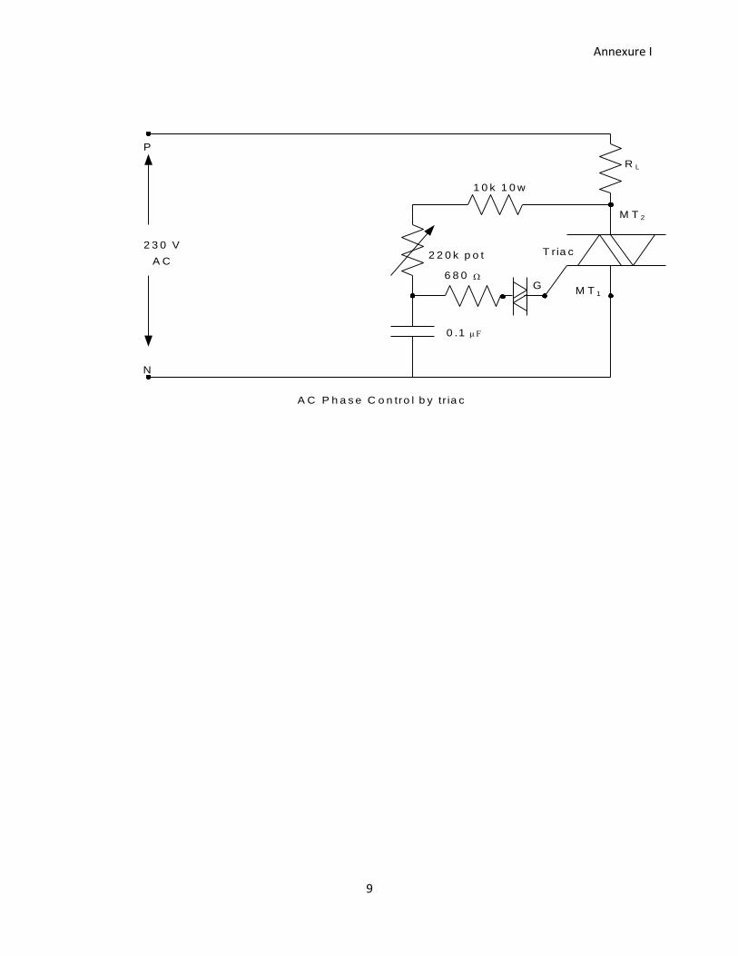
Annexure I
9
R L
M T 2
M T 1
6 8 0
2 2 0 k p o t
1 0 k 1 0 w
μ F0 .1
P
N
2 3 0 V
A CT r ia c
G
A C P h a s e C o n tro l b y tr ia c
Annexure I
10
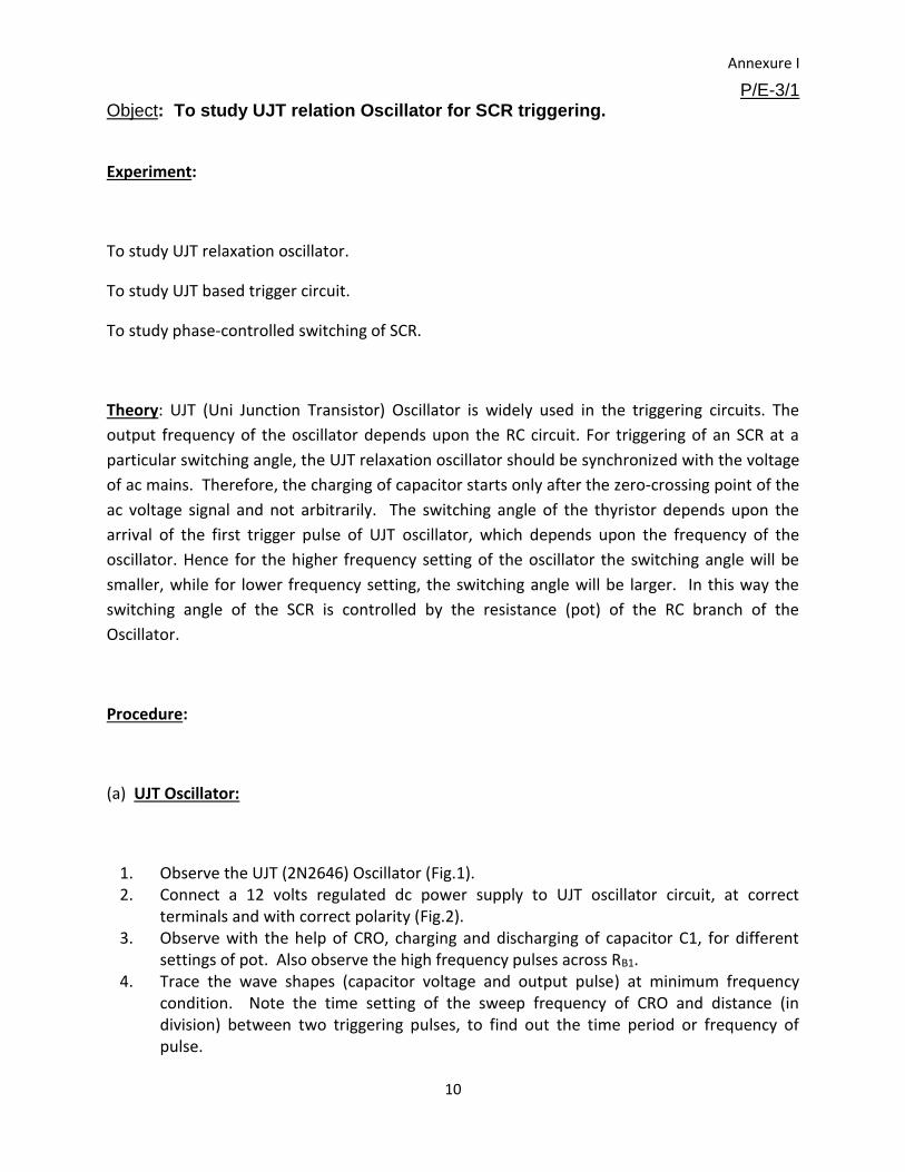
P/E-3/1 Object: To study UJT relation Oscillator for SCR triggering.
Experiment:
To study UJT relaxation oscillator.
To study UJT based trigger circuit.
To study phase-controlled switching of SCR.
Theory: UJT (Uni Junction Transistor) Oscillator is widely used in the triggering circuits. The
output frequency of the oscillator depends upon the RC circuit. For triggering of an SCR at a
particular switching angle, the UJT relaxation oscillator should be synchronized with the voltage
of ac mains. Therefore, the charging of capacitor starts only after the zero-crossing point of the
ac voltage signal and not arbitrarily. The switching angle of the thyristor depends upon the
arrival of the first trigger pulse of UJT oscillator, which depends upon the frequency of the
oscillator. Hence for the higher frequency setting of the oscillator the switching angle will be
smaller, while for lower frequency setting, the switching angle will be larger. In this way the
switching angle of the SCR is controlled by the resistance (pot) of the RC branch of the
Oscillator.
Procedure:
(a) UJT Oscillator:
1. Observe the UJT (2N2646) Oscillator (Fig.1). 2. Connect a 12 volts regulated dc power supply to UJT oscillator circuit, at correct
terminals and with correct polarity (Fig.2). 3. Observe with the help of CRO, charging and discharging of capacitor C1, for different
settings of pot. Also observe the high frequency pulses across RB1. 4. Trace the wave shapes (capacitor voltage and output pulse) at minimum frequency
condition. Note the time setting of the sweep frequency of CRO and distance (in division) between two triggering pulses, to find out the time period or frequency of pulse.

Annexure I
11
5. Add more capacitor (C2 = 0.33 F) to the existing one (C2 = 0.01 F) in the relaxation oscillator. Adjust the pot for minimum frequency. Trace the waveform as in procedure 4.
6. Remove D.C. power supply.
(b) Trigger Circuit:
1. Connect load resistance, SCR voltmeter and ammeter as shown in Fig.3. 2. With the help of an autotransformer, keep the input ac voltage constant (about 12 volts)
before each observation. 3. Connect the oscillator circuit with the gate of the SCR. Take three observations,
including the minimum and maximum switching angles, for various settings of pot. Note down output (load)voltage and load current for each case.
4. Observe and trace voltages waveforms across the load and THEN voltage across the SCR.

Annexure I
12
P/E-3/2
Reports & Sample Questions:
1. Find the frequency of the output signal of the UJT oscillator. 2. Plot graph for output voltage (observed) v/s switching angle. 3. Propose a suitable UJT trigger circuit for a full wave control applications. 4. How can you use a UJT trigger circuit for feed back application. 5. Why steep rising pulses are suitable for thyristor triggering.
N
P
T
E
B 2
B 1
V
A
V
B 2
B 1
E
2 N 2 6 4 6 U J T
T o p V ie w
2 .7 K
1 0 0 K P o t
.
0 .0 4 7
C 2
0 .3 3 K
C 1
2 N 2 6 4 6
B y 1 2 7
1 .1 K
2 2 0
R B 1
T o G a te G
K
A
R L = 2 5
P
2 3 0 V , A C
F ig . 3 .
2 .7 K
1 0 0 K P o t
.
0 .0 4 7 M F D
C 2
0 .3 3 M F D
C 1
2 N 2 6 4 6
1 .1 K
2 2 0
R B 1
1 2 V
D .C .
F ig . 2 .F ig . 1 .
A u to -T ra n s fo rm e r
X
Y
_
+ X
Y
Annexure I
13
P/E-4(a)/1
Object: Phase controlled switching of SCR.
Experiment:
1. To study resistance trigger circuits.
2. To study RC trigger circuits.
Theory: Ac phase controlled switching is done to control the output voltage from the fixed
input ac voltage. Thus delay in switching angle of a thyristor in each half cycle controls
(reduces) the output voltage. The output voltage may be ac or dc which depends upon the
circuit configuration/connection of the thyristors.
The beginning of conduction (switching) of SCR depends upon the magnitude of anode to
cathode voltage (VAK) and the magnitude of the gate current. When thyristor is forward biased
the magnitude of gate current can be controlled by a variable resistance. It changes the
switching instant on the voltage wave. Similarly the triggering signal on the gate can also be
controlled by a simple RC phase shifter circuit. Thus positive half rectified voltage of this signal
controls the switching angle.
Procedure:
Resistance Trigger Circuit:
1. Complete the circuit for resistance triggering as shown in Fig. 1. (Do not connect the capacitor).
2. Connect the fixed terminals of the rheostat as load resistance. 3. Observe the waveforms of the output voltage for different settings of the pot (for three
setting). 4. Note the load current input voltage and output voltage for each case.
RC Trigger Circuit:

Annexure I
14
5. Connect the capacitor and repeat the procedure (1- to - 4) for RC trigger circuit.
Observation Format:
(i) R- Trigger circuit:
S.No. Supply Voltage
(V)
Load current
(mA)
Output voltage
(V)
Output Power
(W)
(Calculated)
(ii) RC – trigger circuit
S.No. Supply Voltage
(V)
Load current
(mA)
Output voltage
(V)
Output Power
(W)
(Calculated)
Annexure I
15
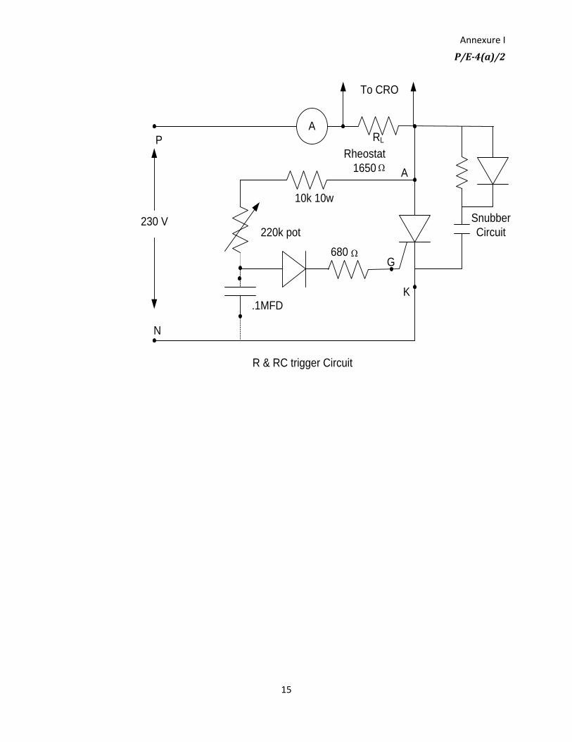
P/E-4(a)/2
220k pot
10k 10w
230 V
680
N
A
K
Snubber
Circuit
G
A
P
Rheostat
1650
RL
To CRO
.1MFD
R & RC trigger Circuit
Annexure I
16
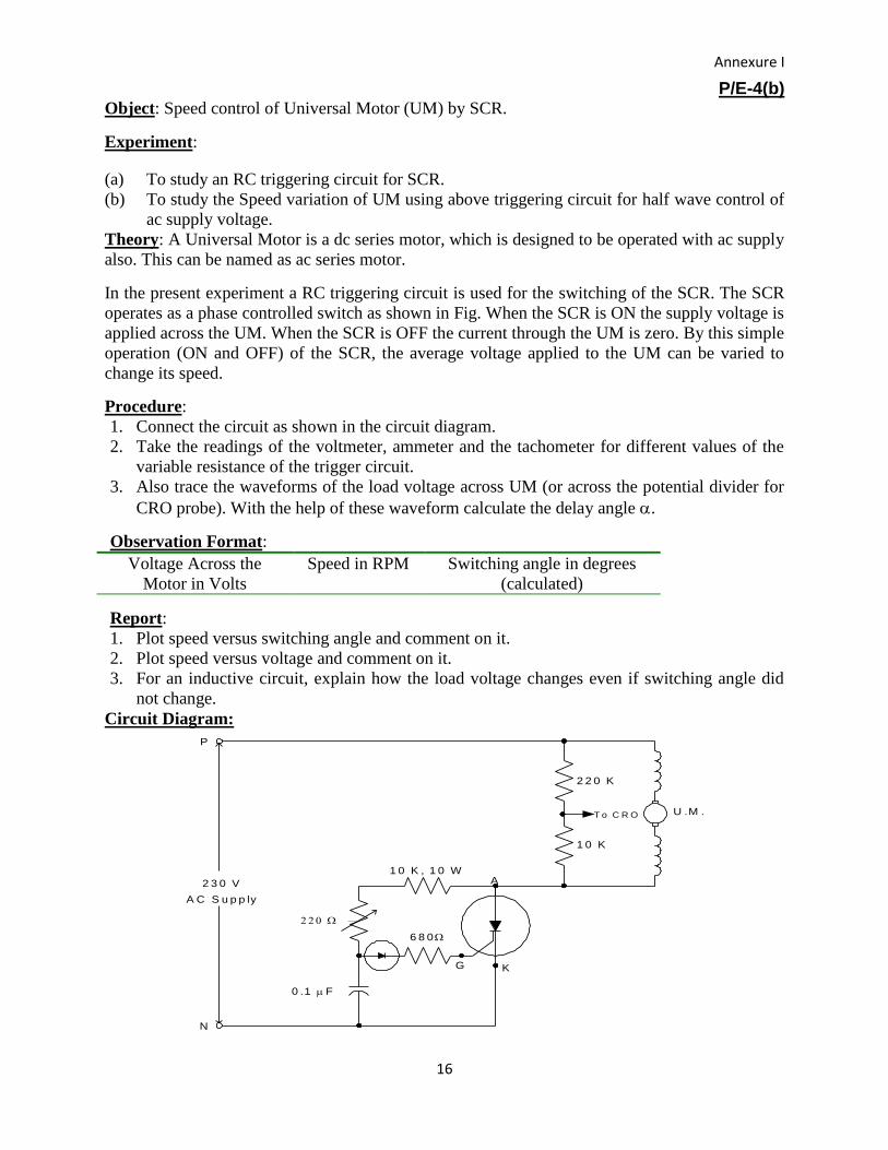
P/E-4(b) Object: Speed control of Universal Motor (UM) by SCR.
Experiment:
(a) To study an RC triggering circuit for SCR.
(b) To study the Speed variation of UM using above triggering circuit for half wave control of
ac supply voltage.
Theory: A Universal Motor is a dc series motor, which is designed to be operated with ac supply
also. This can be named as ac series motor.
In the present experiment a RC triggering circuit is used for the switching of the SCR. The SCR
operates as a phase controlled switch as shown in Fig. When the SCR is ON the supply voltage is
applied across the UM. When the SCR is OFF the current through the UM is zero. By this simple
operation (ON and OFF) of the SCR, the average voltage applied to the UM can be varied to
change its speed.
Procedure:
1. Connect the circuit as shown in the circuit diagram.
2. Take the readings of the voltmeter, ammeter and the tachometer for different values of the
variable resistance of the trigger circuit.
3. Also trace the waveforms of the load voltage across UM (or across the potential divider for
CRO probe). With the help of these waveform calculate the delay angle .
Observation Format:
Voltage Across the
Motor in Volts
Speed in RPM Switching angle in degrees
(calculated)
Report:
1. Plot speed versus switching angle and comment on it.
2. Plot speed versus voltage and comment on it.
3. For an inductive circuit, explain how the load voltage changes even if switching angle did
not change.
Circuit Diagram:
P
N
2 3 0 V
A C S u p p ly
0 .1 F
6 8 0
G K
1 0 K , 1 0 W
2 2 0 K
1 0 K
U .M .
A
T o C R O

Annexure I
17
P/E-5/1
Object: Study of ac to dc uncontrolled converters.
Experiment:
(i) Study of half-wave converter with RL load.
(ii) Study of full-wave mid-point converter with RL load.
(iii) Study of freewheeling action of a diode.
Brief Theory: Thyristor based naturally commutated converters are normally employed for ac to
dc controlled conversion. A fixed ac input voltage supply is used to obtain an adjustable dc
output voltage. When only diodes are used in place of SCR, the converter circuit, is called
uncontrolled converter. When an RL load is connected at the output, the conduction of diode
continues for some portion of the negative half-cycle too (up to , beyond t = ). Because at t
= , diode has sufficient current which prevents the formation of depletion layer to bring back
the diode in reverse biased.
Condition, until the diode current reduces to zero (ideally). Thus negative supply voltage (during
some portion of the negative half cycle) also appears across the load. The value of can be
found with the help of total current response equation of an RL circuit whose power factor angle
is ɸ.
)tan/exp(sin)sin()( ttmV
tiZ
When a free-wheeling diode (Df) is used, it prevents this negative excursion of the load voltage.
When the load voltage becomes negative, Df conducts (as its cathode becomes negative), thus load
voltage due to the conduction of Df1 becomes zero during this period.
In a half-wave or single-pulse uncontrolled converter, the rectification is done with only one diode
in the circuit. This gives only one pulse in the output dc voltage per cycle of the ac supply voltage.
When diode bridge is used to make a converter bridge or a diode pair is used along with a centre-tapped
transformer, there are two output dc voltage pulses per cycle. This converter is called full-wave or two-pulse
converter. In this case line current is symmetrical about time-axis with zero average value per cycle.
Procedure:
1. Connect the resistance and inductor in the load circuit as shown in the figure.
Half-Wave Mode:
2. Complete the connection with only ONE diode (D1) connected between terminals 1 and 3 as
shown in the Figure.
3. Observe the current waveform (across the load resistor or between terminals 5 & 0) and
output voltage waveform (between terminals 4 and 0).

Annexure I
18
P/E-5/2
4. Vary the value of R slowly (but keep the output current below 500 mA). Observe the
variation of extinction angle () due to the change of L/R ratio or the power factor of the
load.
5. Trace the output voltage and output current waveforms, for R = 50 ohms. Note down the
values of the output current and voltage.
6. For study of free-wheeling action, connect the cathode of diode D3 (terminal # 7) to terminal
# 3. Only positive half – cycle appears at output.
Full-Wave Mode
7. Disconnect the cathode of diode D3, connected to terminal # 3.
8. Connect the diode, D2 (terminals # 6 and # 3) as shown in Figure.
9. Repeat steps no. (3) through (5).
Observations:
Output voltage of transformer (ac) = (between terminal # 1 and 0) = ………V
R (in Ohms) =…
L (in millihenry) =…
Output
Voltage
Output
Current Extinction Angle ()
(dc) (ac) Experimental Computed
Half Wave
i) Without free-wheeling
action
ii) With free-wheeling action
Full Wave
(i) Without free-wheeling
action
(ii) With free -wheeling action
Circuit Diagram:

Annexure I
19
A
K
D3
7
3D1
A K
1230 V/ 24 - 0 - 24 V
230 V
(A.C.)
0
2 A K
D2
6
0
500 mA
Ch1(V)
Ch2(I)
4
5
R
L
Common (-)
Report:
a) Why diode conducts even for negative input voltage at its anode?
b) Find and compare the extinction angle from the values of the load
parameter as well as from the experimental values.
c) Compare the performances of 1-pulse & 2- pulse converter circuit.

Annexure I
20
P/E-6/1
Object: An advance mono-stable monostable based trigger circuit.
Experiment:
(i)To study operation of a monostable based triggering circuit for a fully controlled converter.
(ii) To observe the waveforms at different stages of a buffer and driver circuit.
(iii) To observe phase controlled switching operation by this trigger circuit.
Theory: For accurate switching angle control and to incorporate feedback signal advance trigger circuits
are used. Different analog and digital trigger circuits are used for this purpose. When linear and digital
ICs are used they require separate power supply for biasing. Normally driver and buffer circuits are
needed to amplify the weak output signals of CMOS and TTL IC, and to isolate the control circuit from
the power circuit.
In this circuit, zero crossing detectors (ZCD) and a retriggerable monostable with logic gates are used to
generate trigger signals in the positive half cycle between to and in the negative half cycle between (
+ ) to 2. A positive pulse is generated at positive and negative zero cross-over instants by zero crossing
detector circuit. It reaches to a monostable (IC74122). An RC delay network controls the ON period of
output (Q) of monostable from 0 to . Thus the ON - period of the output ( Q ) varies between to
and + to 2. A 555 timer based stable multivibrator generates carrier signal (at 10 KHz) for buffer
and driver circuits. Q with logic combinations, provides independent trigger signals, in positive and
negative half cycles. The output ultimately reaches to the gate of a thyristor through driver and buffer
circuit. This is used to switch thyristor, and hence the output voltage is controlled.
Procedure:
1. Adjust the voltage level of the dual dc regulated power supply to 5V. Put the switch in
tracking mode of d.c. power supply.
2. Connect +5V and –5V dc voltage supply to the monostable based trigger circuit as shown in
Fig. 1. 3. Connect 230V ac signal to transformer (230V/ 3V) of this circuit. Observe the waveforms at each
stage of the trigger circuit.
4. Observe the variation of and the duration of trigger signal (Q) generated at the output of
pulse transformer at G1 K1 and G2 K2 by varying the pot.
5. Connect the power circuit (Fig.2). Vary the pot setting and measure the current and the load
voltage of or different settings.
6. Trace the wave form and calculate the triggering angle.
Observation Format:

Annexure I
21
P/E-6/2
S. No. Supply Voltage Load current
(Experimental)
Load Voltage
(Experimental)
Load current
(Theoretical)
Report:
1. Find theoretically the load current.
2. Draw voltage v/s switching angle characteristics curve.
3. How is the performance of this trigger circuit different from R and RC trigger circuit.
4. Draw the graph of (a) power factor (PF) versus α, and (b) total harmonic distortion (THD)
versus α; for α = 0, 30, …………… 180 for an ac regulator with resistive load.
Circuit Diagram:
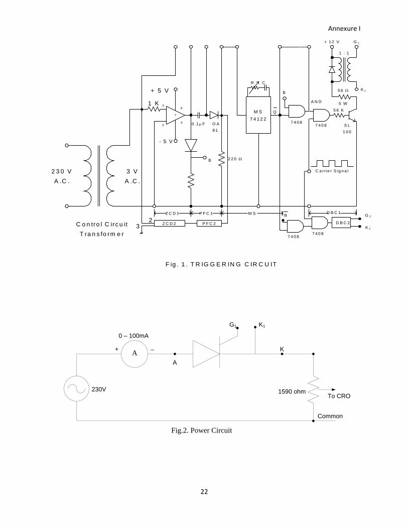
Annexure I
22
7
2 3 0 V
A .C .
C o n tro l C irc u it
T ra n s fo rm e r
3 V
A .C .
1 K
+ 5 V
3
2
6
4
B
0 .1 F O A
8 1
R C
M S
7 4 1 2 2
- 5 V
2 2 0
B
A N D
7 4 0 87 4 0 8
5 6 K
5 6
5 W
K 1
+ 1 2 V G 1
1 : 1
S L
1 0 0
C a rr ie r S ig n a l
Z C D 1 P F C 1 M S D B C 1
F ig . 1 . T R IG G E R IN G C IR C U IT
Z C D 2 P F C 2 D B C 2
7 4 0 87 4 0 8
B
23
G 2
K 2
Q
A
Fig.2. Power Circuit
A
G1 K1
K+ _
230V 1590 ohm
0 – 100mA
To CRO
Common

Annexure I
23
P/E-7/1
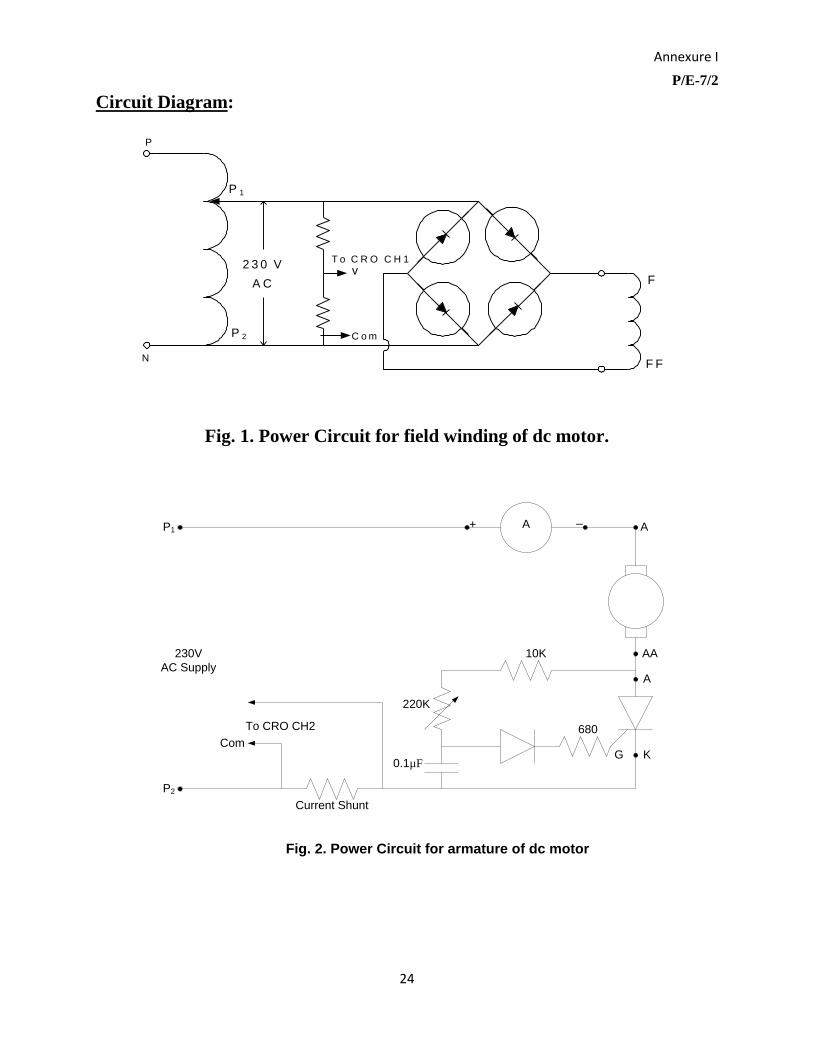
Object: Speed control of dc motor by a phase-controlled converter.
Experiment: To study speed control of separately excited dc motor by half-wave phase
controlled converter.
Theory: A full converter can be used to control the speed of a dc motor in the first quadrant, as
well as in fourth quadrants of torque-speed characteristics. In case of a half-controlled converters
the average output dc voltage can be controlled for between 0o to 180o.
Here half-wave converter (single-pulse with only one thyristor) is used to control the speed of a
separately excited dc motor. With the help of this converter armature-winding voltage is
controlled. Field winding is energized by a constant dc voltage supplied by a diode bridge. An
RC trigger circuit is used to supply the trigger pulse to the SCR between 00 and 1800. The
controlled output voltage of the converter circuit is applied to the armature winding of the dc
motor. Thus by adjusting the switching angle , armature voltage hence the speed of dc motor
is controlled.
Procedure
1. Connect input of the rectifier bridge to the output of an autotransformer and complete the
power circuit as shown in Fig. 1.
2. Complete the connection of the armature circuit with an RC trigger circuit as shown in Fig.2.
3. Connect the input of the autotransformer with ac mains and keep the output voltage constant
(230V).
4. By changing the settings of the pot of the RC trigger circuit control .
5. Note down the speed, armature current. Trace the waveforms of supply (input) voltage and
armature current (vR) for different setting of .
6. Calculate the triggering angle with the help of traces of waveforms.
Observations Format:
S. No. Input voltage
(ac)
Armature Current
(A)
Speed
(r/min)
Triggering Angle
()
Report:
Draw the graph of speed v/s switching angle and comment.
Annexure I
24
P/E-7/2
Circuit Diagram:
P 1
P 2
2 3 0 V
A Cv
F
F F
T o C R O C H 1
P
N
C o m
Fig. 1. Power Circuit for field winding of dc motor.
A A
AA10K
680
220K
A
P1
P2
+_
To CRO CH2
230V
AC Supply
Current Shunt
0.1µFKG
Fig. 2. Power Circuit for armature of dc motor
Com
Annexure I
25
P/E-8/1
Object: Study of dc –dc fly back converters.
Experiment:
(i) Study of a 555-timer based frequency oscillator.
(ii) Study of switching of a power BJT.
(iii) Study of switching of a power MOSFET.
(iv) Study of a BJT based driver circuit for a power MOSFET.
(v) Study of an RC Snubber Circuit used with power MOSFET.
(vi) Study of the performance of an isolated output voltage, flyback converter.
(vii) Study of the performance of an isolated Buck Boost, flyback converter
Theory: The linear ac-dc converters are bulky, less efficient and costly. The switched mode dc-
dc converters are compact, cheap and efficient (as high as 90-99%). There are large number of
circuit topologies of these dc to dc converters. The flyback converter was invented by NASA in
1960 for space applications. The switch, when ON, makes the primary winding at a high
frequency transformer to operate as an inductor to store the energy (with open circuited
secondary winding). When the switch turns off, interrupts a highly inductive current, generates a
high voltage spike dtLdivL
/ across the primary winding of the high frequency transformer.
This voltage also appears across the secondary winding which in turn charge the filter capacitor
and supplies power to the load. Thus, during the OFF period of the switch, the transformer
release energy to the load. The controlling the frequency and the duty ratio of the switch, the
desired (adjustable) output voltage is obtained.
Procedure:
(i) Study of 555 timer and switching of power BJT:
1. Connect the circuit with a 12 volts dc supply a from regulated dc power supply
(linear dc voltage stabilizer).
2. Observe the waveforms of the output voltage of 555 timer and collector terminal
voltage of the power BJT (2N3055).
3. Trace the waveform for the lower and higher settings of frequency.
(ii) MOSFET based fly back converter:
1. Connect the gate of the MOSFET with the collector terminal of the power BJT i.e.
link terminals (1) and (2). Now, BJT becomes driver of MOSFET.
2. Observe the voltage waveforms at Drain (across drain and source) and at the load
(output voltage).
3. For FOUR different frequency of the oscillator (555 timer), take SIX observations
(Three in Buck Mode and Three in Boost Mode).
4. Note dc voltage and frequency of oscillator (555 timer) in each case).

Annexure I
26
P/E-8/2
(iii) Snubber Circuits:
1. Observe the voltage waveform at Drain (across Drain and Source).
2. Vary the magnitude of resistance of the snubber by the pot and observe the
variation of the peak voltage (spike) that appear across the MOSFET.
Observation Table:
S.
No
DC output
voltage
ON period
of oscillator
signal
Time period of
Oscillator signal
Switching
frequency
(calculated)
Duty ratio
(Calculator)
Report:
1. What is the lowest and the highest frequency of oscillator.
2. Plot dc output voltage verses switching frequency curve.
3. Plot dc output voltage verses duty ratio curve
4. What is the use of the transformer in the circuit?
5. Why special design of the transformer is needed?
6. How this circuit can be modified to a forward dc to dc converter?
7. Observe the effects of variation of different parameters of different dc to dc converter.
Reference:
(i) M.S.J. Asghar, “Power Electronics”, PHI.
(ii) M.H. Rashid, “Power Electronics”, PHI.
Circuit diagram: