Pioneers of Semiconductor Physics Remember - Springer Link
81
Appendix: Pioneers of Semiconductor Physics Remember... Semiconductor physics has a long and distinguished history. The early devel- opments culminated in the invention of the transistor by Bardeen, Shockley, and Brattain in 1948. More recent work led to the discovery of the laser diode by three groups independently in 1962. Many prominent physicists have con- tributed to this fertile and exciting field. In the following short contributions some of the pioneers have recaptured the historic moments that have helped to shape semiconductor physics as we know it today. They are (in alphabetical order): Elias Burstein Emeritus Mary Amanda Wood Professor of Physics, University of Pennsylvania, Philadelphia, PA, USA. Editor-in-chief of Solid State Communications 1969-1992; John Price Wetherill Medal, Franklin Institute 1979; Frank Isakson Prize, American Physical Society, 1986. Marvin Cohen Professor of University of California, Berkeley, CA, USA. Oliver Buckley Prize, American Physical Society, 1979; Julius Edgar Lilienfeld Prize, American Physical Society, 1994. Leo Esaki President, Tsukuba University, Tsukuba, Japan. Nobel Prize in Physics, 1973. Eugene Haller Professor of Materials Science and Mineral Engineering, University of California, Berkeley, CA, USA. Alexander von Humboldt Senior Scientist Award, 1986. Max Planck Research Award, 1994. Conyers Herring Professor of Applied Physics, Stanford University, Stanford, CA, USA. Oliver Buckley Prize, American Physical Society, 1959; Wolf Prize in Physics, 1985.
-
Upload
khangminh22 -
Category
Documents
-
view
1 -
download
0
Transcript of Pioneers of Semiconductor Physics Remember - Springer Link
Appendix: Pioneers of Semiconductor Physics Remember ...
Semiconductor physics has a long and distinguished history. The early developments culminated in the invention of the transistor by Bardeen, Shockley, and Brattain in 1948. More recent work led to the discovery of the laser diode by three groups independently in 1962. Many prominent physicists have contributed to this fertile and exciting field. In the following short contributions some of the pioneers have recaptured the historic moments that have helped to shape semiconductor physics as we know it today. They are (in alphabetical order):
Elias Burstein Emeritus Mary Amanda Wood Professor of Physics, University of Pennsylvania, Philadelphia, PA, USA. Editor-in-chief of Solid State Communications 1969-1992; John Price Wetherill Medal, Franklin Institute 1979; Frank Isakson Prize, American Physical Society, 1986.
Marvin Cohen Professor of Physic~~ University of California, Berkeley, CA, USA. Oliver Buckley Prize, American Physical Society, 1979; Julius Edgar Lilienfeld Prize, American Physical Society, 1994.
Leo Esaki President, Tsukuba University, Tsukuba, Japan. Nobel Prize in Physics, 1973.
Eugene Haller Professor of Materials Science and Mineral Engineering, University of California, Berkeley, CA, USA. Alexander von Humboldt Senior Scientist Award, 1986. Max Planck Research Award, 1994.
Conyers Herring Professor of Applied Physics, Stanford University, Stanford, CA, USA. Oliver Buckley Prize, American Physical Society, 1959; Wolf Prize in Physics, 1985.
538 Appendix
Charles Kittel Emeritus Professor of Physics, University of California, Berkeley, CA, USA. Oliver Buckley Prize, American Physical Society, 1957; Oersted Medal, American Association of Physics Teachers, 1978.
Neville Smith Scientific Program Head, Advanced Light Source, Lawrence Berkeley Laboratory, Berkeley, CA, USA. C.] Davisson and L.H. Germer Prize, American Physical Society, 1991.
Jan Tauc Emeritus Professor of Physics and Engineering, Brown University, Providence, RI, USA. Alexander von Humboldt Senior Scientist Award, 1981; Frank Isakson Prize, American Physical Society, 1982.
Klaus von Klitzing Director, Max-Planck-1nstitut fur Festkorperforschung, Stuttgart, Germany. Nobel Prize in Physics, 1985.
Ultra-Pure Germanium 539
Ultra-Pure Germanium: From Applied to Basic Research or an Old Semiconductor Offering New Opportunities Eugene E. Haller University of California, Berkeley, USA
Imagine arriving one morning at the laboratory and somebody comes to ask you if single crystals of germanium with a doping impurity concentration in the 101°_1011 cm3 range can be grown! You quickly compare this concentration with the number of Ge atoms per cm - 3, which is close to 4 x 10²² . Well, you pause and wonder how anybody can ask if a 99.999999999% pure substance can be made. The purest chemicals available are typically 6 or 7 nines pure. Robert N. Hall of the General Electric Company proposed in 1968 [1] that such crystals could be grown and that they would be most useful in fabricating very large volume (up to 400 cm3) p-i-n junctions working as gammaray detectors [2].
When I arrived at Berkeley as a postdoc I joined the group of ES. (Fred) Goulding, who headed one of the leading groups of semiconductor detector and electronics experts at the Lawrence Berkeley Laboratory (LBL), then called the Radiation Laboratory. There I met W.L. (Bill) Hansen, who had started the race towards the ultra-pure Ge single-crystal goal believed to be attainable by Hall. Bill was extremely knowledgeable in chemistry, physics, and general laboratory techniques. In addition, he was the fastest-working experimentalist I had ever encountered. Somewhat overwhelmed, I started to work with Bill and Fred on these Ge crystals. When Bill tried out various Czochralski crystal growth configurations [3], he rigorously pursued ultra-purity by using the simplest crystal growth design, the purest synthetic silica (Si02) container for the Ge melt, and hydrogen gas purified in a Pd diffusion system. I, on the other hand, tried to build up an arsenal of characterization techniques which would allow us to find out within hours the purity and crystalline perfection we had achieved. The IEEE meetings on nuclear science, which were held every fall, provided the forum where we "crossed swords" with Hall [4-7]. It was a close race. Hall had the advantage of enormous experience, which started way back when Ge was first purified and single crystals were grown for transistors. We had the advantage of blissful ignorance but also excellent and helpful colleagues. Furthermore, nobody could match Bill's agility in trying out new purification and crystal growth methods. One major development for us was learning, through Hall, about a super-sensitive photoconductivity technique which was capable of identifying extremely small numbers of impurities in Ge single crystals. The technique had been discovered by Russian scientists at the Institute of Radio-engineering and Electronics in Moscow [8, 6.85]; see Figs. 6.39 and 6.40. They found that a two-step ionization process of
540 Appendix
shallow hydrogenic donors or acceptors in a very cold crystal would lead to photoconductivity peaks which were very sharp and unique for each dopant species. Paul Richards, of the Physics Department at the University of California at Berkeley had a home-built Fourier-transform far-infrared spectrometer and the necessary liquid helium temperature dewar. By the end of the first day of experimenting we had a spectrum of a p-type high-purity Ge crystal with only 1010 cm-3 net amount of acceptors and we knew also that phosphorus and aluminum were the major residual impurities.
In parallel with a number of novel and interesting physics studies we fabricated gamma-ray detectors at LBL. We broke records in the resolution of the gamma-ray photopeaks with our ultra-pure crystals [2]. Soon the commercial detector manufacturers became interested and started their own ultra-pure Ge crystal-pulling programs. In a few years several companies in the US and in Europe succeeded in developing large-diameter (~ 8 cm) single crystals with incredibly good yield, excellent purity « 2 x 1010 cm-3) and very small concentrations (108 cm-3) of deep-level defects which would detrimentally affect the charge collection in large-size coaxial p-i-n diodes. In order to achieve the best spectral resolution, electrons and holes had to have mean-free-paths of up to several meters. Most semiconductor physicists simply shook their heads and could not comprehend these numbers.
How pure is ultra-pure Ge? The person who cares only about electrically active impurities would say that crystals with a few 1010 cm-3 of impurities are routinely grown. But are there other inactive impurities? Yes, of course there are. Hydrogen, oxygen, silicon and carbon are usually present at concentrations of up to 1014 cm-3 , depending on the crystal growth conditions. These impurities do not interfere with Ge's operation as radiation detectors provided certain rules are followed: no heating to temperatures above 350°C and no rapid temperature changes. Can we reduce the concentration of these four electrically inactive impurities? Yes, we can, but we pay a price. Eliminating hydrogen by growing in vacuum leads to the introduction of impurities which can no longer be "flushed" out of the crystal puller. Furthermore, hydrogen will passivate the very small concentrations of deep-level defects and impurities which are always present. Free oxygen and silicon are generated by the reduction of the ultra-pure silica crucible by the liquid Ge. We do not know of any substance which can replace silica with, perhaps, the exception of graphite. Numerous attempts to grow ultra-pure Ge in graphite crucibles have failed so far because the resultant crystals contain too many Al acceptors.
Most recently, the interest in Ge has sharply increased because isotopically pure Ge can be obtained from Russia. Isotopically pure Ge bulk crystals [9-12] and isotope superlattices [13] have been grown. New phonon physics and electronic transport studies are currently being pursued by several groups with these isotopically controlled crystals and multilayers.
Have we arrived at the ultimately ideal material: isotopically and chemically pure and crystallographic ally perfect Ge single crystals? Perhaps the answer is no, but I certainly do not know of another parameter that can be controlled.
Ultra-Pure Germanium 541
References
1 R.N. Hall: in Proc. of the 12th Int. Can! on Physics of Semiconductors, ed. by M.H. Pilkuhn (Teubner, Stuttgart 1974), p. 363
2 E.E. Haller, F.S. Goulding: Handbook on Semiconductors, Vo!. 4, ed. by C. Hilsum (Elsevier, New York 1993), Chap. 11, p. 937~963
3 WL. Hansen, E.E. Haller: Mater. Res. Soc. Proc. 16, 1 (1983) 4 R.N. Hall, T.J. Soltys: IEEE Trans. Nuc!. Sci. NS-18, 160 (1971) 5 E.E. Haller, WL. Hansen, F.S. Goulding: IEEE Trans. Nuc!. Sci. NS-20, 481 (1973) 6 E.E. Haller, WL. Hansen, G.S. Hubbard, F.S. Goulding: IEEE Trans. Nuc!. Sci. NS-
23, 81 (1976) 7 E.E. Haller, WL. Hansen, F.S. Goulding: Adv. Phys. 30, 93 (1981) 8 E.E. Haller: Physics 146B, 201 (1987) 9 E.E. Haller: Semicond. Sci. Techno!. 5, 319 (1990)
10 E.E. Haller: Solid State Phenom. 32~33, 11 (1993) 11 G. Davies, J. Hartung, V. Ozhogin, K. Hoh, WL. Hansen, E.E. Haller: Semicond. Sci.
Techno!. 8, 127 (1993) 12 H.D. Fuchs, P. Etchegoin, M. Cardona, K. Itoh, E.E. Haller: Phys. Rev. Lett. 70, 1715
(1993) 13 J. Spitzer, T. Ruf, M. Cardona, W Dondl, R. Scharer, G. Abstreiter, E.E. Haller:
Phys. Rev. Lett. 72, 1565 (1994)
542 Appendix
Two Pseudopotential Methods: Empirical and Ab Initio Marvin L. Cohen University of California, Berkeley, USA
It took a relatively long time to develop methods capable of determining the detailed electronic structure of solids. In contrast, for gases, unraveling the mysteries of atomic energy levels went hand in hand with the development of quantum theory. Atomic optical spectra yielded sharp lines that could be interpreted in terms of excitations of electrons from occupied to empty states. These studies provided important tests of the theory. However, compared to atomic spectra, solid-state spectra are broad, since the interactions between the atoms spread the allowed occupied and empty energy levels into energy bands. This made interpretation of spectra in terms of electronic transitions very difficult. Trustable precise electronic energy band structures were needed to interpret solid-state spectra, but these were difficult to obtain.
In principle, the Schrodinger equation can describe the behavior of electrons in solids; but without approximations, solutions for the electronic energy levels and wavefunctions are extremely difficult to calculate. Despite considerable effort, the situation around 1960 was stiII unsatisfactory. Creative models of solids had been introduced to explain many physical phenomena such as electronic heat capacities and superconductivity with spectacular success. However, calculations capable of yielding band structures and other properties for specific materials were not available.
An important intermediate step was the introduction of the empirical pseudopotential model (EPM). Pseudopotentials had been around since 1934, when Fermi introduced the concept to examine the energy levels of alkali atoms. Since he was interested in highly excited atoms, he ignored the oscillations of the valence electron wavefunctions in the regions near the nucleus. By assuming a smooth wavefunction responding to a weak potential or pseudopotential, Fermi could easily solve for the outer electron energy levels.
Since most solid-state effects, such as bonding, are principally influenced by the changes in the outermost electrons, this picture is appropriate. For the EPM it is assumed that the solid is composed of a periodic array of positive cores. Each core has a nucleus and core electrons. Each of the outer valence electrons moves in the electrostatic potential or pseudopotential produced by the cores and by the other valence electrons. In this one-electron model, each electron is assumed to respond to this average periodic crystalline pseudopotential. The periodicity allows Fourier decomposition of the potential and the EPM fits data to obtain Fourier coefficients. Usually only three coefficients per atom are needed.
Two Pseudopotential Methods: Empirical and Ab Initio 543
The EPM stimulated interactions between theorists and experimentalists and the result was one of the most active collaborations in physics. Not only were optical and photoemission spectra of solids deciphered, the activities resulted in new experimental techniques and a much deeper understanding of the behavior of electrons in solids. The meeting ground between experiment and theory is usually response functions such as dielectric functions or reflectivity. In the early phases of this work the actual energy band structures, which are plots of energy versus wavevector, were the domain of theorists. However, the introduction of angular resolved photoemission spectroscopy (ARPES) gave energy bands directly and provided further tests of the EPM.
The EPM band structures obtained in the 1960s and 1970s are still used today. In addition, the EPM produced the first plots of electronic charge density for crystals. These plots displayed covalent and ionic bonds and hence gave considerable structural information. Optical constants, densities of states, and many other crystal properties were obtained with great precision using EPMderived energy levels and wavefunctions.
Despite the success of the EPM, there was still considerable motivation to move to a first-principles or ab initio model. The approach chosen was similar to Fermi's. Instead of an EPM potential, the interaction of the valence electron with the core was described using an ab initio pseudopotential constructed from a knowledge of atomic wavefunctions. The valence electronelectron interactions were modeled using a density functional theory which, with approximations, allows the development of an electron-electron potential using the electronic charge density. However, the latter approach is appropriate only for calculating ground-state properties. Excited states such as those needed to interpret atomic spectra require adjustments to this theory. These adjustments are complex and require significant computer time compared to the EPM, but they are successful in reproducing the experimental data and the approach is completely ab initio.
One of the most important applications of the ab initio pseudopotential model was the determination of structural properties. It became possible to explain pressure-induced solid-solid structural transitions and even to predict new structural phases of solids at high pressure using only atomic numbers and atomic masses. Bulk moduli, electron-phonon coupling constants, phonon spectra, and a host of solid-state properties were calculated. The results allowed microscopic explanations of properties and predictions. An example was the successful prediction that semiconducting silicon would become a superconducting hexagonal metal at high pressure.
The two types of pseudopotential approaches, empirical and ab initio, have played a central role in our conceptual picture of many materials. Often the resulting model is referred to as the "standard model" of solids. Unlike the standard model of particle physics, which is sometimes called a theory of everything, the standard model of solids is most appropriate for those solids with reasonably itinerant electrons. Despite this restriction, the model is extremely useful and a triumph of quantum theory.
544 Appendix
The Early Stages of Band-Structures Physics and Its Struggles for a Place in the Sun Conyers Herring Stanford University, Stanford, USA
It is universally recognized today that among the components necessary for a theoretical understanding of the properties of semiconductors, their specific electronic band structures have an extremely fundamental place. Textbooks on semiconductors typically have, among their earliest chapters, one on band structure, which contains diagrams of energy versus wave vector for important semiconductors, usually obtained from first-principles numerical calculations. But obviously these calculations would not be so conspicuously featured if they did not agree with a great body of experimental information. What the present-day student may not realize is that, despite the spurt of activity in the early post-transistor years - roughly 1948-1953 - the workers of this period had almost no knowledge of band structures, and had to muddle through as best they could without it. The evolution of this aspect of semiconductor physics provides a thought-provoking perspective on how science moves toward truth by erratic diffusional steps, rather than with military precision.
The possible range of band structures had, of course, long been known in principle. The standard generalities about Bloch waves and their energy spectra had been known for a couple of decades; symmetry-induced degeneracies had been classified; early band-structure calculations, though not quantitatively reliable, had suggested that degenerate and multi-valley band edges might often occur. The trouble lay elsewhere. When so many possibilities for exciting work were opening up, people tended to avoid projects that would be tedious and time-consuming. Band-structure theorists, equipped only with mechanical calculators, often opted to use incomplete boundary conditions or limited basis sets. Experimentalists, despite rapid improvements in purity and perfection of materials, continued to focus mostly on properties whose interpretation did not depend critically on anisotropies and other special features of the energy bands. Much of the blame for this neglect must be cast on the theorists, not only for their failure to agree on calculated band structures, but also because, for too long, they shied away from the tedium of making detailed calculations of properties such as magnetoresistance for various kinds of nonsimple band structures.
My own experience provides a typical example. In December 1953 I delivered an invited paper at an APS meeting with the title "Correlation of Electronic Band Structures with Properties of Silicon and Germanium". In it I tried to reason as logically as possible from the existing experimental and theoretical literature, to draw plausible conclusions about the possible band-edge symmetries for these elements. While I got a few things right, it was distress-
The Early Stages of Band-Structures Physics and Struggles 545
ing to learn over the next year or so that most of my inferences were wrong. How did I go astray?
My first step, safe enough, was to classify the possible types of band-edge points: those at wavevector k = 0, and those at k t 0 (multi-valley); for each of these the states could be degenerate (two or more states of the same energy and k) or nondegenerate. In surveying the experimental and theoretical evidence bearing on the choices among these numerous alternatives, I began by trying to limit the possible choices to those that could occur for band structures qualitatively similar to that newly calculated by Herman [1] for diamond, which seemed more reliable than any others that had been made for any material with this crystal structure. Using the "k . p method" for qualitative estimations of the energy-band curvatures on moving away from k = 0, this meant that I neglected perturbations of the p-like k = 0 states T25" T I5 by the anti-bonding s-like level r2', which is quite high in diamond but, contrary to my assumption, much lower in silicon and germanium. This neglect turned out to make me omit the possibility of conduction-band edges on the [111] axes in k-space for n-germanium, and to retain the possibility of valence-band edges on the [100] axes for p-silicon.
From this flawed start I tried to narrow the possibilities further by appealing to experimental evidence, and especially to magnetoresistance. The nearvanishing of longitudinal magnetoresistance in [100]-type directions was obviously consistent with multi-valley band-edge regions centered on the [100]type axes in k-space, and this proved to be the correct identification for n-type silicon. But, lacking explicit calculations, I assumed that the energy surfaces of a degenerate hole band at k = 0 would be so strongly warped as to preclude the near-zero [100] longitudinal magnetoresistance observed ·for p-silicon. So my predictions were all wrong here. Finally, I had the tedious task of calculating the complete anisotropy of magnetoresistance for multi-valley models, which a few months later were shown to give strong evidence for [l11]-type valleys for n-germanium.
What all this illustrates is that to achieve an acceptable understanding of band structures, each of three types of information sources had to reach a certain minimum level of sophistication. Band calculations from first principles had to be made with accuracy and self-consistency in an adequately large function space. Experimental measurements of properties sensitive to band structure had to be made under well-controlled conditions. And theoretical predictions of these properties for different band structure models had to be available. There were gaps in all three of these sources up to the end of 1953; it is thus not surprising that Shockley, in writing what was intended as a basic text for the coming semiconductor age [2], stated, in spite of his awareness of the diversity of possible band structures, that the theoretical reasoning in the book would all be based on the simple model with an isotropic effective mass. Remarkably, in a year or so starting in 1954, each of the three sources filled itself in sufficiently so that they could pull together (e. g., better theoretical bands [3], cyclotron resonance [4], magnetoresistance theory [5]) and bandstructure physics became a solid and accepted component of basic knowledge.
546 Appendix
References
1 F. Herman: Phys. Rev. 88, 1210 (1952) 2 W. Shockley: Electrons and Holes in Semiconductors (Van Nostrand, New York
1950), esp. p. 174 3 For an early review of progress 1953-1955, see, for example, F. Herman: Proc. IRE
43, 1703 (1955) 4 See the following contribution by C. Kittel 5 B. Abeles, S. Meiboom: Phys. Rev. 95, 31 (1954); M. Shibuya, Phys. Rev. 95, 1385
(1954)
Cyclotron Resonance and Structure of Conduction and Valence Band Edges 547
Cyclotron Resonance and Structure of Conduction and Valence Band Edges in Silicon and Germanium Charles Kittel University of California, Berkeley, USA
A prime objective of the Berkeley solid-state physics group (consisting of Arthur Kip and myself) from 1951 to 1953 was to observe and understand cyclotron resonance in semiconductors. The practical problems were to gain reliable access to liquid helium, and to obtain an adequate magnet and sufficiently pure crystals of Ge and Si. The liquid helium was obtained from the Shell Laboratories and later from the Giauque laboratory on campus. The magnet was part of a very early cyclotron (from what one may call the Ernest O. Lawrence collection), and the dc current for the magnet came from recycled US Navy submarine batteries. The semiconductor crystals were supplied by the Sylvania and Westinghouse Research Laboratories, and later by the Bell Telephone Laboratories. I think the microwave gear came from war surplus at MIT Radiation Laboratory. Evidently, very little of the equipment was purchased.
The original experiments were on Ge [1], both n-type and p-type. There were too few carriers from thermal ionization at 4 K to give detectable signals, but the carriers that were present were accelerated by the microwave electric field in the cavity up to energies sufficient to produce an avalanche of carriers by impact ionization. This was true cyclotron resonance! A good question is, why not work at liquid hydrogen temperature, where the thermal ionization would be adequate? Hydrogen was then, and perhaps is still now, considered to be too hazardous (explosive) to handle in a building occupied by students.
A better question is, why not work at liquid nitrogen temperature, where there are lots of carriers and the carrier mobilities are known to be much higher than at the lower temperatures? Cyclotron resonance at liquid nitrogen temperature had been tried at several other laboratories without success. The reason for the failures is that the plasma frequencies, being mixed with the cyclotron frequencies to produce a magnetoplasma frequency, are too high at the higher carrier concentrations - you are not measuring a cyclotron resonance but instead a magnetoplasma resonance [2]. Indeed, one can follow the plasma displacement of the original cyclotron lines when the cavity is allowed to warm up. In radio wave propagation in the ionosphere this effect is called magneto-ionic reflection, a subject I had learnt from the lectures of E.V. Appleton at Cambridge.
A better way to produce carriers at 4 K was suggested by the MIT group. They irradiated the crystal with weak light sufficient to excite both electrons and holes. With this method both electrons and holes could be excited in the same crystal. Alternatively, one can excite a known carrier type by infrared
548 Appendix
irradiation of n- or p-type material. By modulating the optical excitation the detection of the absorption signal was made highly sensitive [3]. In addition, if there is any doubt about the sign of the carriers, circularly polarized microwaves can be (and were) used to distinguish the sense of rotation of the carriers in the magnetic field.
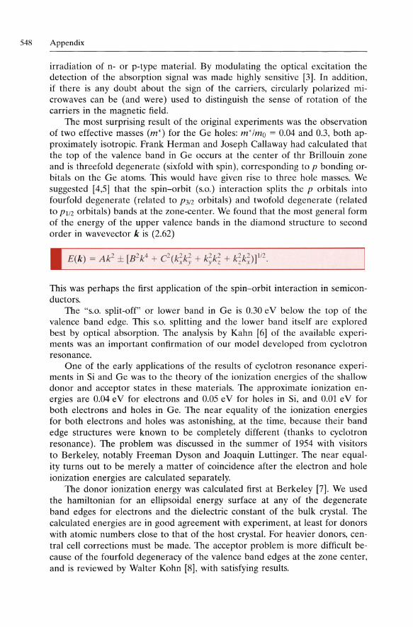
The most surprising result of the original experiments was the observation of two effective masses (m*) for the Ge holes: m*lmo = 0.04 and 0.3, both approximately isotropic. Frank Herman and Joseph Callaway had calculated that the top of the valence band in Ge occurs at the center of thr Brillouin zone and is threefold degenerate (sixfold with spin), corresponding to p bonding orbitals on the Ge atoms. This would have given rise to three hole masses. We suggested [4,5] that the spin-orbit (s.o.) interaction splits the p orbitals into fourfold degenerate (related to P3/2 orbitals) and twofold degenerate (related to P1I2 orbitals) bands at the zone-center. We found that the most general form of the energy of the upper valence bands in the diamond structure to second order in wavevector k is (2.62)
(k ) = Ak2 ± [82k4 + C2(~k~ + ~~ + k~~)]ll2 .
This was perhaps the first application of the spin-orbit interaction in semiconductors.
The "s.o. split-off" or lower band in Ge is 0.30 eV below the top of the valence band edge. This s.o. splitting and the lower band itself are explored best by optical absorption. The analysis by Kahn [6] of the available experiments was an important confirmation of our model developed from cyclotron resonance.
One of the early applications of the results of cyclotron resonance experiments in Si and Ge was to the theory of the ionization energies of the shallow donor and acceptor states in these materials. The approximate ionization energies are 0.04 e V for electrons and 0.05 e V for holes in Si, and 0.01 e V for both electrons and holes in Ge. The near equality of the ionization energies for both electrons and holes was astonishing, at the time, because their band edge structures were known to be completely different (thanks to cyclotron resonance). The problem was discussed in the summer of 1954 with visitors to Berkeley, notably Freeman Dyson and Joaquin Luttinger. The near equality turns out to be merely a matter of coincidence after the electron and hole ionization energies are calculated separately.
The donor ionization energy was calculated first at Berkeley [7]. We used the hamiltonian for an ellipsoidal energy surface at any of the degenerate band edges for electrons and the dielectric constant of the bulk crystal. The calculated energies are in good agreement with experiment, at least for donors with atomic numbers close to that of the host crystal. For heavier donors, central cell corrections must be made. The acceptor problem is more difficult because of the fourfold degeneracy of the valence band edges at the zone center, and is reviewed by Walter Kohn [8], with satisfying results.
Cyclotron Resonance and Structure of Conduction and Valence Band Edges 549
References
1 G. Dresselhaus, A.F. Kip, C. Kittel: Phys. Rev. 92, 827 (1953) 2 G. Dresselhaus, A.F. Kip, C. Kittel: Phys. Rev. 100, 618 (1955) 3 G. Dresselhaus, A.F. Kip, C. Kittel: Phys. Rev. 98, 368 (1955) 4 G. Dresselhaus, A.F. Kip, C. Kittel: Phys. Rev. 95, 568 (1954) 5 R.J. Elliot: Phys. Rev. 96, 266 (1954) 6 A.H. Kahn: Phys. Rev. 97, 1647 (1955) 7 C. KitteL A.H. Mitchell: Phys. Rev. 96, 1488 (1954) 8 W. Kohn, in Advances in Solid State Physics, Vol. 5, ed. by F. Seitz, D. Turnbull (Aca
demic, New York 1957), p. 257-320
550 Appendix
Optical Properties of Amorphous Semiconductors and Solar Cells Jan Tauc Brown University, Providence, USA
In the early 1960s the foundations for an understanding of the optical properties of crystalline semiconductors were established, They were based on the existence of long-range order and k-vector conservation, which led to sharp structures in the spectra associated with the Van Hove singularities. My group working in the Institute of Solid State Physics of the Czechoslovak Academy of Sciences in Prague was making contributions to this ongoing effort which flourished throughout the 1960s. While on leave at Harvard in 1961-1962, I started thinking about what the optical properties should be like when longrange order is absent, and I began working on this problem after my return to Prague.
There is a huge group of materials, called glasses, that lack long-range order; they are produced by quenching the melt, which of course does not have long-range order. In these materials the liquid has the same short-range order as the solid phase. This is not the case for semiconductors with tetrahedral bonding. The efficiency of this bond in lowering energy depends on the geometrical rigidity of the structure; once it is loosened at high temperature, the energetically favorable phase is a metallic one (some kind of close packing). So even if it were possible to quench, say, liquid Ge (which it is not), the short-range order of this "glass" would be completely different from crystalline Ge, and therefore a comparison of the optical properties would be meaningless. There are, however, ways to prepare amorphous Ge (a-Ge) (and other tetrahedral semiconductors) with the same short-range order as crystalline Ge (c-Ge) as a thin film, for example by condensing evaporated Ge on a cold substrate.
In Prague, we first worked on the optical properties of some liquids, which clearly demonstrated the fact that the main optical properties depend on the short-range order. A breakthrough came when we learned that Radu Grigorovici had prepared thin films of a-Ge at the Institute of Physics of the Romanian Academy of Sciences. A close, fruitful and friendly collaboration soon developed, and for some years Radu regularly visited Prague. We spent long hours and days discussing amorphous semiconductors with tetrahedral bonding. At that time, we did not know of anyone else who would be interested in amorphous semiconductors of this kind (there was an important group in Leningrad which had been studying amorphous cha\cogenide semiconductors since the 1950s, but these are real glasses and very different from tetrahedral semiconductors). Radu was interested in the preparation, structure and electronic transport, while we in Prague worked on the optical properties.
Optical Properties of Amorphous Semiconductors and Solar Cells 551
From the reflection spectra, using Kramers-Kronig analysis, we determined the optical constants of a-Ge in the spectral range up to 12 e V and confirmed the expectation that there should be no sharp structures [1). Instead of the three prominent peaks in the fundamental absorption band observed in c-Ge, there is just one band, which has the remarkable feature of having much larger absorption in the low energy region (a "red shift"). From the transmission spectra we determined the dependence of the absorption coefficient a on photon energy in the absorption edge region. The data gave a straight line when ...;wa was plotted as a function of photon energy liw[...;wa =
const. x (lim - Eg)). This plot defines an energy Eg, which it is natural to call the optical gap. Of course, it was the most obvious plot to try: if the k-vector is not conserved, if the density of electron states close to the valence and conduction band extrema is proportional to the square root of energy as in the crystal, and if the matrix element is a constant then a ex (liw - Eg)2jw, as is the case for phonon-assisted indirect transitions in crystalline semiconductors. In fact, in amorphous semiconductors there was no rigorous theoretical justification for this law at that time (and there is no generally accepted one today), so it must be considered as empirical. It is, however, most amazing that this plot works in many amorphous semiconductors. In the literature, this kind of edge is sometimes referred to as a "Tauc edge" and used as a definition of the "optical" gap, which is usually somewhat different from the gap determined from electrical conductivity measurements ("electrical gap").
The "red shift" mentioned above is observed also in a-Si and is the basis for the usefulness of this material for solar cell. Although Radu and I, during our walks in Prague (which was run down at that time but still beautiful), considered various possible applications of these materials, the truth is that they are useless as electronic materials because they are full of defects which act as traps, preventing n- and p-type doping. A prominent defect is a Si atom with only three neighbors, i. e., with an unpaired electron (a "dangling bond"). Our walks ended in 1968 after the tragic political events which put an end to what has since become known as the "Prague Spring".
In the 1970s the oil crisis hit the world, and thinking about renewable energy sources became popular. Among these, solar cells appeared very attractive. Cells made of c-Si are very good but too expensive for large scale deployment. The reason is that c-Si is an indirect-gap semiconductor and the absorption coefficient is small in the spectral region of the solar flux. To absorb it, the cell must be relatively thick (rv 100 f.Lm), which requires a large amount of a rather expensive material, in addition to the expensive technology (crystal growing, wafer cutting, polishing, etc.). Because of the red shift, a-Si absorbs solar light much more efficiently: the cells can be made much thinner, and thin film technology is much cheaper.
A discovery dramatically improved the electronic properties of a-Si. It started with the work of Chittick and coworkers at Standard Telecommunications Laboratories in England in the late 1960s. A standard procedure for the crystal growth of a silicon layer on a Si substrate is the decomposition of SiH4 gas by the high temperature of the substrate. Instead, Chittick et al. [2]
552 Appendix
studied the decomposition of SiH4 by radio frequency glow discharge, which enabled them to deposit silicon on a cool noncrystalline substrate. They produced thin amorphous Si films whose electronic properties were radically improved through a reduced defect state density in the gap. They showed that the resistivity of these films could be lowered by two orders of magnitude by adding PH3 gas to SiH4 - the first demonstration of doping of an amorphous semiconductor. Their company did not let them continue the work. What is quite amazing is that Chittick told many of us about this work in 1969 and no one grasped the enormous significance of his result except Spear and Le Comber at the University of Dundee. They reported in 1975 [3] n- and pdoping and in 1976 production of p-n junctions. It was first believed that the good properties were due to an exceptionally gentle deposition technique, but the work of W. Paul and others showed that they were due to the presence of hydrogen in the films. Hydrogen in a-Si:H reduces the defect state density by compensating the dangling bonds.
The gap of a-Si:H (about 1.8 eV) is larger than that of a-Si (1.4 eV) but the spectrum is also red-shifted with respect to c-Si, and therefore the films can be quite thin (1,um) and still absorb a substantial part of the solar spectrum. One would think that with all these clues in hand someone would go ahead and design an a-Si:H solar cell. It did happen, but not in this way. Carlson and Wronski [4] discovered such cells independently at RCA in thin-film solar cells made of polycrystalline Si. They observed that when the substrate was cold enough the cells had a better efficiency and found that these better cells were amorphous rather than polycrystalline; only then did they realize the connection of their discovery to the current research on a-Si:H. These cells are today produced for small-scale applications and still remain a primary candidate for large-scale photo voltaic energy conversion plants which may be needed someday.
References
1 1. Tauc, A. Abraham, L. Pajasova, R. Grigorovici,A. Vancu: Non-Crystalline Solids (North-Holland, Amsterdam 1965), p. 606
2 R.c. Chittick, 1.H. Alexander, H.F. Sterlin: 1. Electrochem. Soc. 116, 77 (1969) 3 w.E. Spear, P.G. Le Comber: Solid State Commun. 17, 1193 (1975) 4 D.E. Carlson, c.R. Wronski: App!. Phys. Lett. 28, 671 (1976)
Optical Spectroscopy of Shallow Impurity Centers 553
Optical Spectroscopy of Shallow Impurity Centers
Elias Burstein University of Pennsylvania, Philadelphia, USA
In the fall of 1948, Frank Isakson, head of the Physics Section of the Office of Naval Research, was a frequent visitor at the Naval Research Laboratory, where I was a member of the Crystal Branch. During one of our frequent discussions of projects of mutual interest, he informed me about the Navy's interest in developing an infrared (IR) photoconductor with a response beyond 7,um, the long wavelength limit of PbS films, an intrinsic photo conductor developed in Germany during World War II. The properties of the III-V semiconductors were still unknown at that time. In the summer of 1949 I had the good fortune of being able to attend the annual Modern Physics Symposium at the University of Michigan, one of a series of symposia that started in 1928. The lecturers that summer were Luis Alvarez (High Energy Physics), Richard Feynman (Path Integral Method), Frederick Seitz (Solid State Physics) and Gordon B.B. Sutherland (Infrared Spectroscopy of Solids).
In his lectures on semiconductors, Seitz discussed the nature of the impurity levels in Si and Ge and summarized the thermal ionization energies of group III acceptors and group V donors that had been obtained by Pearson and Bardeen at Bell Telephone Laboratories [1] from data on the temperature dependence of the carrier densities derived from resistivity and Hall measurements. He also discussed their conclusions that the ionization energies of the group III acceptors (0.048 e V) and group V donors (0.045 e V) were in reasonable agreement with a simple effective-mass hydrogen model. It was at that point in the lecture that the idea came to me to make use of the photoionization of un-ionized hydrogenic impurity centers in Si and Ge as the basis for IR detectors.
Shortly after returning to Washington, DC, I went to see John Bardeen, who provided me with several Si samples. Together with John J. Oberly, James W. Davisson and Bertha Henvis, I started measurements of the low temperature IR absorption spectra of the Si samples. I wanted to study the absorption spectra associated with photoionization of un-ionized impurity centers before making an effort to observe the photoconductive response. Our first measurements, using a Perkin-Elmer model 12C spectrometer with interchangeable NaCI, KBr, KSR-5(TlBr+I) prisms and mirror optics, were carried out at 77 K, since a simple calculation based on the thermal ionization energy of impurities indicated that over 90% of the impurity centers would remain un-ionized at this temperature.
554 Appendix
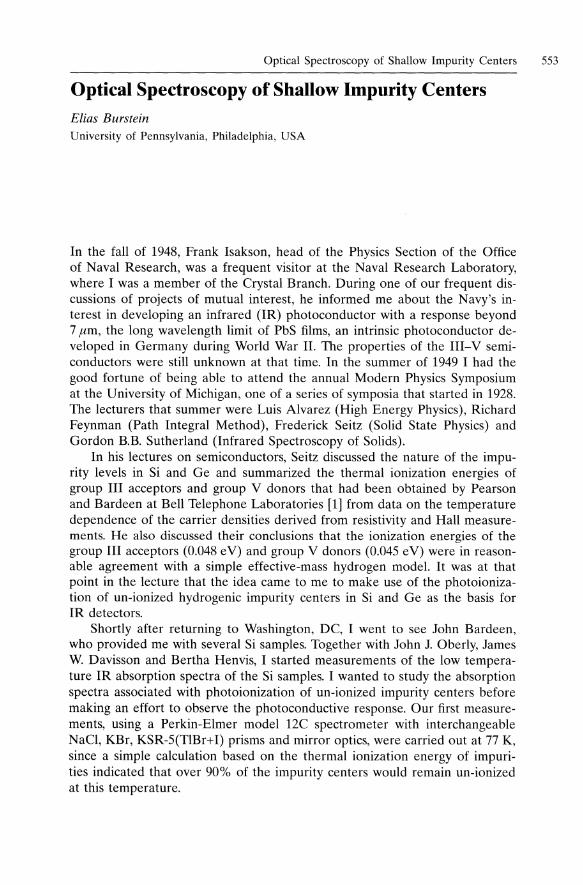
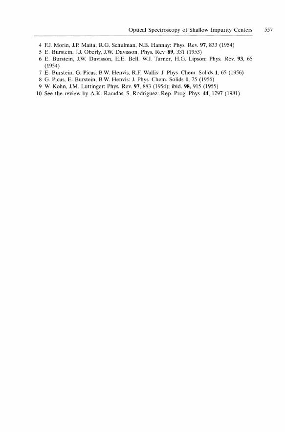
The observed spectrum for a boron-doped Si sample was quite striking, since it exhibited peaks corresponding to transitions from the ground state to excited states of the acceptor centers, as well as the onset of a photoionization continuum [2,3] (Fig. 1). Moreover, the positions of the excitation peaks corresponded closely to the ls-2p, ls-3p and ls-4p transitions of a hydrogenlike center and yielded an ionization energy of 0.046 e V, in good agreement with the thermal ionization data [4]. However, the oscillator strengths of the absorption peaks are markedly different from those for a hydrogenic center. In particular, the oscillator strength of the ls-2p peaks is an order of magnitude smaller than that for a hydrogenic center. The widths of the excitation peaks decrease on cooling to liquid helium temperature, but there is no appreciable shift in the peak positions, indicating that Franck-Condon effects are small. Our data showed no obvious evidence of transitions from the ground state of
40
30
20
10
~ 0 I
20
"'a 15 u
os I 10
0
0: 5 .S
~ 0 vo 2 15 u 0: 0 'g. 10 0 ] <:t: 5
o
3.0
.... auice 2.0 l-Absorplio
Band 1.0 I- '>J
Boron-doped Silicon
0. 15
Aluminum-doped Silicon
0.3
Gallium-doped Silicon
0.1 0.2 OJ
Indium-doped Silicon
o 0.1 0.2 0.3 0.4 0.5 0.6 0.7 PhulOn energy leV)
Fig. 1. Photo excitation and photoionization absorption spectra of group III acceptors in Si at liquid helium temperature [6]. For boron-doped Si, the dashed line is the theoretical photo ionization absorption spectrum of the corresponding hydro genic model
Optical Spectroscopy of Shallow Impurity Centers 555
the split-off valence band, which is not unexpected since the spin-orbit interaction is small in Si and the optical spectra are broadened appreciably.
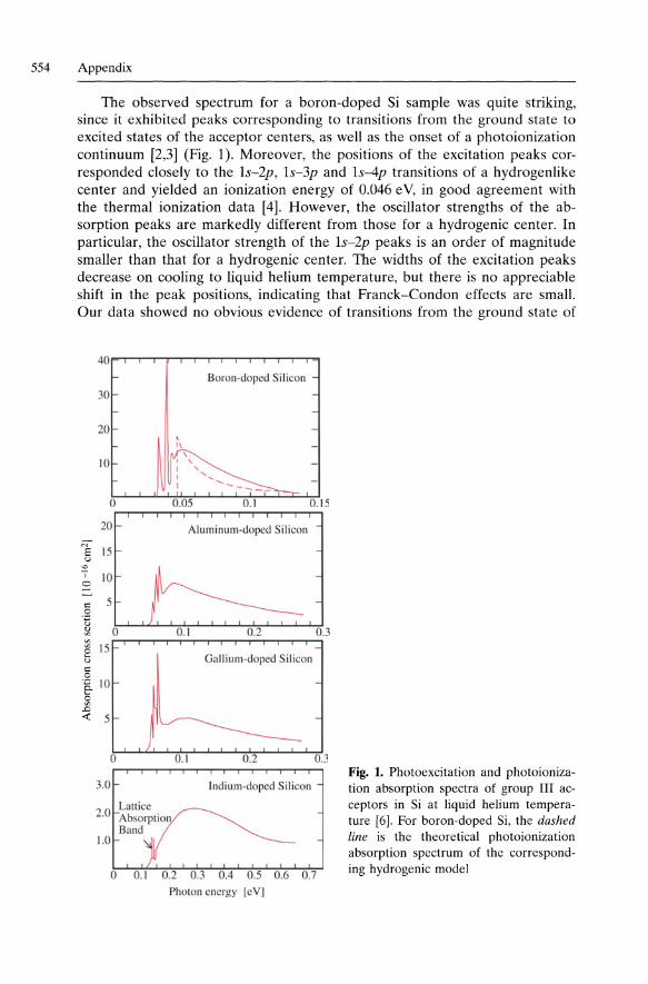
Efforts to detect photoconductivity in n- and p-type Si at 77 K were unsuccessful, due to the presence of large numbers of thermally excited carriers. However, a photoconductive response was observed at liquid helium temperature. The spectral response of relatively pure n-Si is shown in Fig. 2 [5]. The dips in the photoconductive response between 8 and 24 !-Lm correspond to lattice vibration absorption peaks. The data yielded a donor optical ionization energy of 0.04 e V. Photoconductivity studies were later carried out at liquid helium temperature on Ge doped with group III and V impurities. The photoconductive response was found to extend out to 38 !-Lm, the limit of measurement at that time [6].
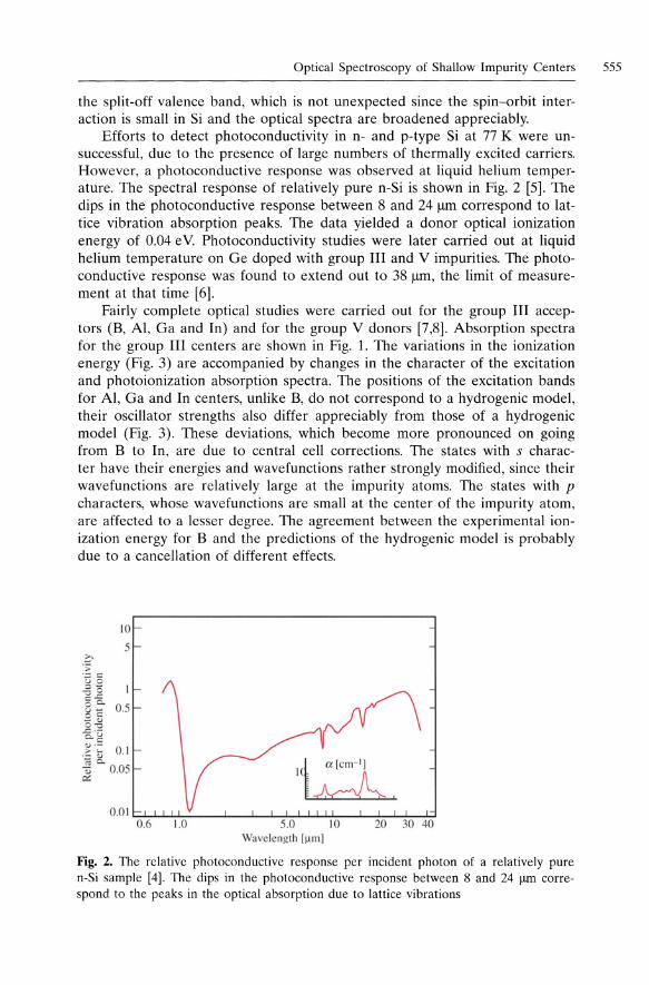
Fairly complete optical studies were carried out for the group III acceptors (B, AI, Ga and In) and for the group V donors [7,8]. Absorption spectra for the group III centers are shown in Fig. 1. The variations in the ionization energy (Fig. 3) are accompanied by changes in the character of the excitation and photoionization absorption spectra. The positions of the excitation bands for AI, Ga and In centers, unlike B, do not correspond to a hydrogenic model, their oscillator strengths also differ appreciably from those of a hydrogenic model (Fig. 3). These deviations, which become more pronounced on going from B to In, are due to central cell corrections. The states with s character have their energies and wavefunctions rather strongly modified, since their wavefunctions are relatively large at the impurity atoms. The states with p characters, whose wavefunctions are small at the center of the impurity atom, are affected to a lesser degree. The agreement between the experimental ionization energy for B and the predictions of the hydrogenic model is probably due to a cancellation of different effects.
~ .;; "= c u C .go
10
5
"..t:: 00.. g C 0.5 'S.g -5.'u tU ·~ 'E: i:; 0. 1 ,.,0.
~ 0.05 1 a lcm- 'I I ~ ,
O.O lc ' ! ! t ? I I ! I I! l'
0.6 1.0 5.0 10 20 30 40 Wuvclengl h 11.11111
Fig. 2. The relative photoconductive response per incident photon of a relatively pure n-Si sample [4]. The dips in the photoconductive response between 8 and 24 Ilm correspond to the peaks in the optical absorption due to lattice vibrations
556 Appendix
:;-~ >. E." ., t:
W
In 0.15 1- \
\ \ \ ,
~ 0. 10
\ Ga AI ----------, O.os " B .!:!. Is ,----
___________________ 2p
Ol -:::;;;;;;:.::=:::=~=== ~~ Valence band
Fig. 3. Suggested term scheme for group III acceptors in Si showing the levels whose energies are derived from the low temperature absorption spectra [6]
The optical ionization energies for donors in Si were found to be 10% larger than the thermal ionization energies, due in part to the presence of low-lying excited states that were not taken into account in the calculation of the activation energies. The positions of the ground state relative to the conduction band are appreciably different for the three donors P, As and Sb, again due to central cell effects. However, their excited p-states are observed at about the same positions relative to the conduction band (see Fig. 3 and [7]). Moreover, they are in good agreement with the results of the effective mass formulation of the donor p levels by Kohn and Luttinger [9], which takes into account the fact that the conduction band of Si has six nondegenerate minima along the [100] and equivalent directions.
The data obtained in these early investigations were limited by the relatively low quality of the Si Samples, the poor resolution of the spectrometers and by the electronics. There has been major progress in the IR spectroscopy of shallow impurity levels in semiconductors since then, made possible by significant improvements in crystal quality, spectrometers and detectors, by the development of photothermal conductance spectroscopy, which has much higher sensitivity than IR detectors, and by the availability of tunable IR lasers [10].
References
1 1. Bardeen, G.L. Pearson: Phys. Rev. 75, 865 (1949) 2 E. Burstein, J.J. Oberly, 1.W Davisson, B.W Henvis: Phys. Rev. 82, 764 (1951) 3 E. Burstein, E.E. Bell, 1.W Davisson, M. Lax: 1. Phys. Chern. 57, 849 (1953)
Optical Spectroscopy of Shallow Impurity Centers 557
4 F.I Morin, IP. Maita, RG. Schulman, N.B. Hannay: Phys. Rev. 97, 833 (1954) 5 E. Burstein, 11 Oberly, IW Davisson, Phys. Rev. 89, 331 (1953) 6 E. Burstein, J.W Davisson, E.E. Bell, WI Turner, H.G. Lipson: Phys. Rev. 93, 65
(1954) 7 E. Burstein, G. Picus, B.W Henvis, RF. Wallis: 1 Phys. Chern. Solids 1, 65 (1956) 8 G. Picus, E. Burstein, B.W Henvis: 1 Phys. Chern. Solids 1, 75 (1956) 9 W Kohn, 1M. Luttinger: Phys. Rev. 97, 883 (1954); ibid. 98, 915 (1955)
10 See the review by A.K. Ramdas, S. Rodriguez: Rep. Prog. Phys. 44, 1297 (1981)
558 Appendix
On the Prehistory of Angular Resolved Photo emission
Neville V. Smith Lawrence Berkeley Laboratory, Berkeley, USA
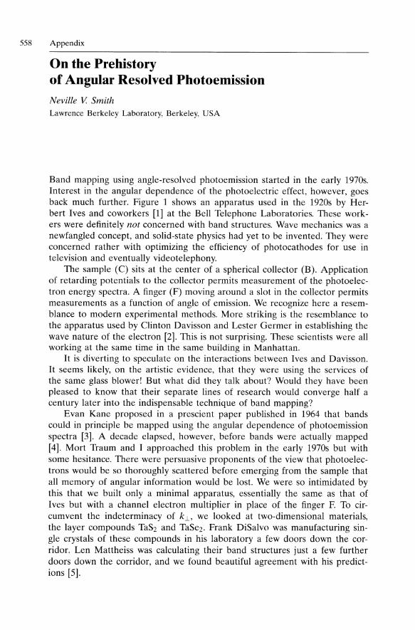
Band mapping using angle-resolved photoemission started in the early 1970s. Interest in the angular dependence of the photoelectric effect, however, goes back much further. Figure 1 shows an apparatus used in the 1920s by Herbert Ives and coworkers [1] at the Bell Telephone Laboratories. These workers were definitely not concerned with band structures. Wave mechanics was a newfangled concept, and solid-state physics had yet to be invented. They were concerned rather with optimizing the efficiency of photocathodes for use in television and eventually videotelephony.
The sample (C) sits at the center of a spherical collector (B). Application of retarding potentials to the collector permits measurement of the photoelectron energy spectra. A finger (F) moving around a slot in the collector permits measurements as a function of angle of emission. We recognize here a resemblance to modern experimental methods. More striking is the resemblance to the apparatus used by Clinton Davisson and Lester Germer in establishing the wave nature of the electron [2]. This is not surprising. These scientists were all working at the same time in the same building in Manhattan.
It is diverting to speculate on the interactions between Ives and Davisson. It seems likely, on the artistic evidence, that they were using the services of the same glass blower! But what did they talk about? Would they have been pleased to know that their separate lines of research would converge half a century later into the indispensable technique of band mapping?
Evan Kane proposed in a prescient paper published in 1964 that bands could in principle be mapped using the angular dependence of photoemission spectra [3]. A decade elapsed, however, before bands were actually mapped [4]. Mort Traum and I approached this problem in the early 1970s but with some hesitance. There were persuasive proponents of the view that photoelectrons would be so thoroughly scattered before emerging from the sample that all memory of angular information would be lost. We were so intimidated by this that we built only a minimal apparatus, essentially the same as that of Ives but with a channel electron multiplier in place of the finger F. To circumvent the indeterminacy of kl., we looked at two-dimensional materials, the layer compounds TaS2 and TaSe2. Frank DiSalvo was manufacturing single crystals of these compounds in his laboratory a few doors down the corridor. Len Mattheiss was calculating their band structures just a few further doors down the corridor, and we found beautiful agreement with his predictions [5].
fS 1~
1J 12 11 10 9 8 7 6 5 ~
3
centimeter.
E
On the Prehistory of Angular Resolved Photo emission 559
'"'--' I I
Fig. 1. Apparatus used by lves et al. [1]
D
With these shortcuts and fine collaborators we were able to perform the first demonstration of band mapping [4]. In hindsight, it is embarrassing to contemplate our hesitance and timidity. It is all now so obvious and commonplace.
References
1 H.E. Ives, A.R. Olpin, A.L. Johnsrud: Phys. Rev. 32, 57 (1928) 2 c.J. Davisson, L.H. Germer: Phys. Rev. 30, 705 (1927) 3 E.O. Kane: Phys. Rev. Lett. 12, 97 (1964) 4 N.V. Smith, M.M. Traum, F.J. DiSalvo: Solid State Commun. 15, 211 (1974) 5 L.F. Mattheiss: Phys. Rev. B 8, 3719 (1973)
560 Appendix
The Discovery and Very Basics of the Quantum Hall Effect Klaus von Klitzing Max-Planck-Institut fUr Festkorperforschung, Stuttgart, Germany
The discovery of the quantum Hall effect (OHE) was the result of basic research on silicon field effect transistors - the most important device in microelectronics. Unlike in other conductors, the electron concentration in these devices can be varied in a wide range just by changing the gate voltage. Therefore this system is ideal for an investigation of the Hall effect at different carrier densities by analyzing the Hall voltage as a function of the gate voltage. The experimental curves together with the notes of February 4, 1980, which characterize the birthday of the quantum Hall effect, are shown in Fig. 9.39. As expected qualitatively from the classical Hall effect, the Hall voltage UH varies (at a fixed magnetic field B = 18 T) inversely proportional to the number N of free electrons (or gate voltage Vg). However, plateaus are visible if the ratio of the number N of electrons to the number N</> of flux quanta within the area of the device is an integer. For one electron per flux quantum (this corresponds to a fully occupied lowest Landau level with the filling factor 1) the Hall voltage divided by the current has the fundamental value RK = h/e2 = (25812.807 ± 0.005) Q. This Hall plateau is barely visible in the upper left corner of Fig. 9.39 and distorted by the large device resistance due to localization phenomena at this relatively small electron density. The plateaus at 2 or 4 times larger electron concentration are much better resolved. Today, electronic systems with higher quality are available so that measurements at much smaller electron densities with filling factors smaller than one are possible. This is the region where the fractional quantum Hall effect is observed [9.68].
A special situation seems to be present if two flux quanta are available for one electron (filling factor 112): Ouasiparticles (composite fermions) are formed which behave like electrons moving in an effective magnetic field B* = O. The Shubnikov-de Haas oscillations of these composite fermions are equivalent to the structures of the fractional quantum Hall effect.
Already the first publication on the OHE [1] with the original title "Realization of a Resistance Standard Based on Fundamental Constants" indicated that an application similar to the Josephson effect may be possible. Today, it is known that different materials (silicon field effect transistors, GaAsl AIGaAs heterostructures) show the same value for the quantized Hall resistance within the experimental uncertainty of 3.5 x 10⁻¹⁰ , and since 1990 all calibrations of resistances are based on the quantum Hall effect with a fixed value RK-1990 = 25812.807 Q for the von Klitzing constant R K .
The Discovery and Very Basics of the Quantum Hall Effect 561
Different approaches can be used to deduce a quantized value for the Hall resistance. The calculation shown in Fig. 9.39, which led to the discovery of the QHE, is simply based on the classical expression for the Hall effect. A quantized Hall resistance Iile2 is obtained for a carrier density corresponding to the filling factor one. It is surprising that this simple calculation leads to the correct result. Laughlin was the first to try to deduce the result of the QHE in a more general way from gauge invariance principles [2]. However, his device geometry is rather removed from the real Hall effect devices with metallic contacts for the injection of the current and for the measurement of the electrochemical potential.
The Landauer-Btittiker formalism, which discusses the resistance on the basis of transmission and reflection coefficients, is much more suitable for analyzing the quantum Hall effect [3]. This formalism was very successful in explaining the quantized resistance of ballistic point contacts [4] and, in a similar way, the quantized Hall resistance is the result of an ideal one-dimensional electronic transport. In a classical picture this corresponds to jumping orbits of electrons at the boundary of the device. In the future, the textbook explanation of the QHE will probably be based on this one-dimensional edge channel transport (see Fig. 9.40).
References
1 K. v. Klitzing, G. Dorda, M. Pepper: Phys. Rev. Lett. 45, 494 (1980) 2 R.B. Laughlin: Phys. Rev. B 23, 5632 (1981) 3 M. Biittiker: Phys. Rev. Lett. 57, 1761 (1986) 4 B.I. von Wees, H. van Houten, S.W.I. Beenakker, I.G. Williamson, L.P. Kouwenhoven,
D. van der Marel, c.T. Foxon: Phys. Rev. Lett. 60, 848 (1988); D.A. Wharam, T.I. Thornton, R. Newbury, M. Pepper, H. Ahmed, lE.F. Frost, D.G. Hasko, D.c. Peacock, D.A. Ritchie, G.A.C. Jones: 1 Phys. C 21, L 209 (1988)
562 Appendix
The Birth of the Semiconductor Superlattice Leo Esaki University of Tsukuba, Tsukuba, Japan
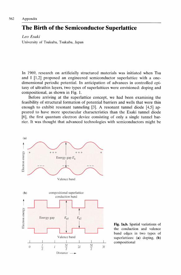
In 1969, research on artificially structured materials was initiated when Tsu and I [1,2] proposed an engineered semiconductor superlattice with a onedimensional periodic potential. In anticipation of advances in controlled epitaxy of ultrathin layers, two types of superlattices were envisioned: doping and compositional, as shown in Fig. 1.
Before arriving at the superlattice concept, we had been examining the feasibility of structural formation of potential barriers and wells that were thin enough to exhibit resonant tunneling [3]. A resonant tunnel diode [4,5] appeared to have more spectacular characteristics than the Esaki tunnel diode [6], the first quantum electron device consisting of only a single tunnel barrier. It was thought that advanced technologies with semiconductors might be
(a)
~ + 0>
~ t:
2 g w
+++ +++ Energy gap Eg
Valence band
(b) compositional supcrlattice conduction band
+
! ~ I L ~ t j Eeagy"p l Er Ul , I
Valence band
I I I I
o L ~ 21 21 31 2 2 2
Distance __
Fig. la,b. Spatial variations of the conduction and valence band edges in two types of superlattices: (a) doping, (b) compositional
The Birth of the Semiconductor Superlattice 563
ready for demonstration of the de Broglie electron waves. Resonant tunneling (see Sect. 9.5) can be compared to the transmission of an electromagnetic wave through a Fabry-Perot resonator. The equivalent of a Fabry-Perot resonant cavity is formed by the semiconductor potential well sandwiched between the two potential barriers.
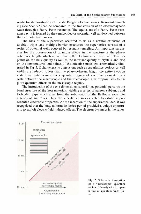
The idea of the superlattice occurred to us as a natural extension of double-, triple- and multiple-barrier structures: the superlattice consists of a series of potential wells coupled by resonant tunneling. An important parameter for the observation of quantum effects in the structure is the phasecoherence length, which approximates the electron mean free path. This depends on the bulk quality as well as the interface quality of crystals, and also on the temperatures and values of the effective mass. As schematically illustrated in Fig. 2, if characteristic dimensions such as superlattice periods or well widths are reduced to less than the phase-coherent length, the entire electron system will enter a mesoscopic quantum regime of low dimensionality, on a scale between the macroscopic and the microscopic. Our proposal was to explore quantum effects in the mesoscopic regime.
The introduction of the one-dimensional superlattice potential perturbs the band structure of the host materials, yielding a series of narrow subbands and forbidden gaps which arise from the subdivision of the Brillouin zone into a series of minizones. Thus, the superlattice was expected to exhibit unprecedented electronic properties. At the inception of the superlattice idea, it was recognized that the long, tailormade lattice period provided a unique opportunity to exploit electric-field-induced effects. The electron dynamics in the super-
liJ.ITl
100 nm
10nm
Inm
0.1 11m
Macroscopic regime
Superlallice or
quantum wells / Ii v'" ,., .... 0,,<:> ~:S'
"I:>' ",'" ,,,,<:> \<..v <$" ;-i!f''''<$"vo,,'''' ,,'1>"" .... ~
.,v ~ ." 0>
/
Q.""':",v~c o<::;,v.<$"'" ~ ~c"<;; <..",0;;
.. ~v·
Interatomic spacing microscopic regime
Crystal quality (dccreasing temperature)
Fig. 2. Schematic illustration of a "mesoscopic" quantum regime (shaded) with a superlattice of quantum wells (inset)
564 Appendix
lattice direction was analyzed for conduction electrons in a narrow subband of a highly perturbed energy-wavevector relationship. The result led to the prediction of a negative differential resistance at a modestly high electric field, which could be a precursor of Bloch oscillations. The superlattice allows us to enter the regime of electric-field-induced quantization: the formation of Stark ladders [7,8], for example, can be proved in a (one-dimensional) superlattice [9], whereas in natural (three-dimensional) crystals the existence and nature of these localized states in a high electric field have been controversial [10,11].
This was, perhaps, the first proposal which advocated using advanced thinfilm growth techniques to engineer a new semiconductor material designed by applying the principles of quantum theory. The proposal was made to the US Army Research Office (ARO), a funding agency, in 1969, daringly stating, with little confidence in a successful outcome at the time, "the study of superlattices and observations of quantum mechanical effects on a new physical scale may provide a valuable area of investigation in the field of semiconductors".
Although this proposal was favorably received by ARO, the original version of the paper [1] was rejected for publication by Physical Review on the referee's unimaginative assertion that it was "too speculative" and involved "no new physics". The shortened version published in IBM Journal of Research and Development [2] was selected as a Citation Classic by the Institute for Scientific Information (lSI) in July 1987. Our 1969 proposal was cited as one of the most innovative ideas at the ARO 40th Anniversary Symposium in Durham, North Carolina, 1991.
At any rate, with the proposal we launched a program to make a "Gedankenexperiment" a reality. In some circles, the proposal was criticized as close to impossible. One of the objections was that a man-made structure with compositional variations on the order of several nanometers could not be thermodynamically stable because of interdiffusion effects. Fortunately, however, it turned out that interdiffusion was negligible at the temperatures involved.
In 1970, Chang, Tsu and I [12] studied a GaAs-GaAso.sPO.5 superlattice with a period of 20 nm synthesized by CVD (chemical vapor deposition) by Blakeslee and Aliotta [13]. Although transport measurements failed to reveal any predicted effect, the specimen probably constituted the first strainedlayer superlattice having a relatively large lattice mismatch. Early efforts in our group to obtain epitaxial growth of Gel-xSix and Cd1- xH& Te superlattices were soon abandoned because of rather serious technical problems at that time. Instead, we focused our research effort on compositional GaAsGal-xAlxAs superlattices grown by MBE (molecular beam epitaxy). In 1972, we found a negative resistance in such superlattices [14], which was interpreted in terms of the superlattice effect.
Following the derivation of the voltage dependence of resonant tunnel currents [5], Chang, Tsu and I observed current-voltage characteristics with a negative resistance [15]. Subsequently, Chang and I measured quantum transport properties in a superlattice with a narrow bandwidth, which exhibited an oscillatory behavior [16]. Tsu et a1. performed photocurrent measurements on
The Birth of the Semiconductor Superlattice 565
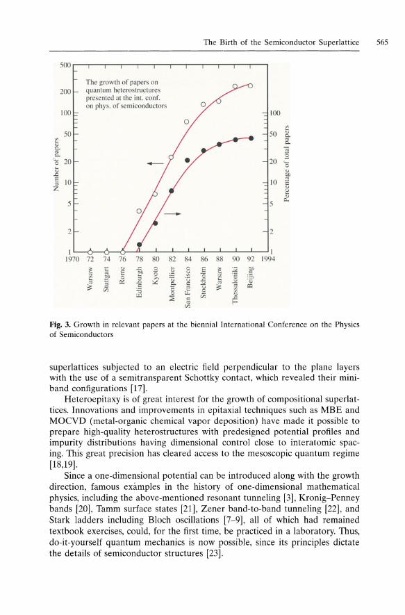
500 I
The growth of papers on
200 I- quantum hcterostructurcs presented .It the i nl. conf.
100 1::::-on phys. of .emiconductors
/ -::::1 100
~
''[ -/ r '-' c.
f 20
'" c.
" 20
§ '0 ~
5 10 10 ;: § ~
:t iI- I ~
I L-....Q----O--- II ' I 1970 72 74 76 78 80 82 84 86 88 90 92 1994
'" - <> ~J 0 - 0 E '"
.0< 01)
E "0 " ~ " " '" "0 '" ·c (': ::!l 0 i5 >-. 8. u ..c:: ~ 0 :~
" :; e<: ~ c -"" " '" 3 cii c " g 3 co ~ t1: ~ 0 cii " ::E c ~ " Vl
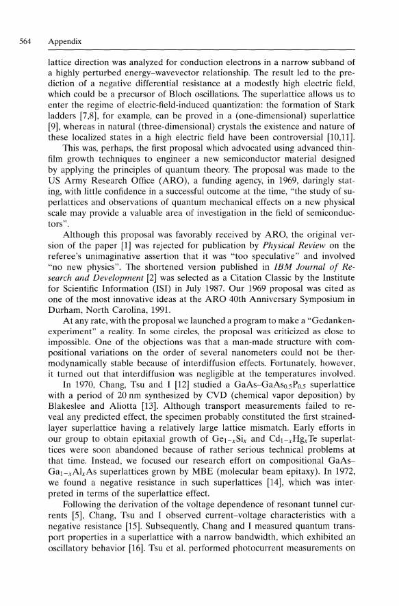
Fig. 3. Growth in relevant papers at the biennial International Conference on the Physics of Semiconductors
superlattices subjected to an electric field perpendicular to the plane layers with the use of a semitransparent Schottky contact, which revealed their miniband configurations [17].
Heteroepitaxy is of great interest for the growth of compositional superlattices. Innovations and improvements in epitaxial techniques such as MBE and MOCVD (metal-organic chemical vapor deposition) have made it possible to prepare high-quality heterostructures with predesigned potential profiles and impurity distributions having dimensional control close to interatomic spacing. This great precision has cleared access to the mesoscopic quantum regime [18,19].
Since a one-dimensional potential can be introduced along with the growth direction, famous examples in the history of one-dimensional mathematical physics, including the above-mentioned resonant tunneling [3], Kronig-Penney bands [20], Tamm surface states [21], Zener band-to-band tunneling [22], and Stark ladders including Bloch oscillations [7-9], all of which had remained textbook exercises, could, for the first time, be practiced in a laboratory. Thus, do-it-yourself quantum mechanics is now possible, since its principles dictate the details of semiconductor structures [23].
566 Appendix
Our original proposal [1] and pioneering experiments have triggered a wide spectrum of experimental and theoretical investigations on superlattices and quantum wells over the last two decades. A variety of engineered structures now exhibit extraordinary transport and optical properties which do not exist in any natural crystal. This new degree of freedom offered in semiconductor research through advanced materials engineering has inspired many ingenious experiments, resulting in observations of not only predicted effects but also totally unknown phenomena. As a measure of the growth of the field, Fig. 3 shows the number of papers related to the subject and the percentage of the total presented at the biennial International Conference on the Physics of Semiconductors. Following 1972, when the first paper [14] was presented, the field went through a short period of incubation before experiencing a phenomenal expansion in the 1980s. It appears that nearly half of all semiconductor physicists in the world are working in this area. Activity at this new frontier of semiconductor physics has in turn given immeasurable stimulus to device physics, provoking new ideas for applications. Thus, a new class of transport and opto-electronic devices has emerged.
References
1 L. Esaki, R. Tsu: IBM Res. Note RC-2418 (1969) 2 L. Esaki, R. Tsu: IBM 1. Res. Devel. 14, 61 (1970) 3 D. Bohm: Quantum Theory (Prentice Hall, Englewood Cliffs, NJ 1951), p. 283 4 L.Y. Iogansen, Zh. Eksp. Teor. Fiz. 45, 207 (1963) [Sov. Phys. - JETP 18, 146 (1964)] 5 R. Tsu, L. Esaki: Appl. Phys. Lett. 22, 562 (1973) 6 L. Esaki: Phys. Rev. 109, 603 (1958) 7 H.M. James: Phys. Rev. 76, 1611 (1949) 8 G.H. Wannier: Elements of Solid State Theory (Cambridge University Press, Cam
bridge 1959), p. 190; Phys. Rev. 117, 432 (1960) 9 W. Shockley: Phys. Rev. Lett. 28, 349 (1972)
10 1. Zak: Phys. Rev. Lett. 20, 1477 (1968); Phys. Rev. B 43, 4519 (1991) 11 A Rabinovitch, 1. Zak: Phys. Rev. B 4, 2358 (1971) 12 L. Esaki, L.L. Chang, R. Tsu: Proc. 12th Int. Conf. Low Temp. Phys., Kyoto, Japan
1970, p. 551 13 AE. Blakeslee, c.F. Aliotta: IBM 1. Res. Devel. 14, 686 (1970) 14 L. Esaki, L.L. Chang, W.E. Howard, Y.L. Rideout: Proc. 11th Int. Conf. Phys. Semi-
conductors, Warsaw, Poland 1972, p. 431 15 L.L. Chang, L. Esaki, R. Tsu: Appl. Phys. Lett. 24, 593 (1974) 16 L. Esaki, L.L. Chang: Phys. Rev. Lett. 33, 495 (1974) 17 R. Tsu, L.L. Chang, G.A Sai-Halasz, L. Esaki: Phys. Rev. Lett. 34, 1509 (1975) 18 L. Esaki: IEEE 1. Quantum Electron. QE-22, 1611 (1986) 19 L. Esaki: in Highlights in Condensed Matter Physics and Future Prospects, ed. by L.
Esaki (Plenum, New York 1991), p. 55 20 R. de L. Kronig, w.G. Penney: Proc. R. Soc. London A 130, 499 (1931) 21 1. Tamm: Phys. Z. Sowjetunion 1, 733 (1932) 22 C. Zener: Proc. R. Soc. London 145, 523 (1934) 23 L. Esaki, Phys. Scr. T42, 102 (1992)
References I
Chapter 1
1.1 J. Czochralski: A new method for measuring the crystallization velocity of metals (in German). Z. Phys. Chern. 92, 219-221 (1918)
1.2 O. Madelung, M. Schulz, H. Weiss (eds.): Landolt-Bornstein, Series III, Vo!. 17c (Semiconductors) (Springer, Berlin, Heidelberg 1984) p.29. This series contains comprehensive references on the growth techniques and properties of individual semiconductors up to 1984
1.3 W.e. Dash: Growth of silicon crystals free of dislocations. J. App!. Phys. 30, 459 (1959)
1.4 C.T. Foxon, B.A. Joyce: Growth of thin films and heterostructures of III-V compounds by molecular beam epitaxy, in Growth and Characterization of Semiconductors ed. by R.A. Stradling, P.C. Klipstein (Hilger, Bristol 1990) p.35
General Reading
Chernov A.A.: Modern Crystallography III - Crystal Growth, Springer Ser. SolidState Sci., Vo!.36 (Springer, Berlin, Heidelberg 1984)
Gilman J.J. (ed.): The Art and Science of Growing Crystals (Wiley, New York 1963) Herman M.A., H. Sitter: Molecular Beam Epitaxy, 2nd edn., Springer Ser. Mater.
Sci., Vo!.7 (Springer, Berlin, Heidelberg 1995) Kittel C.: Introduction to Solid State Physics, 7th edn. (Wiley, New York 1995) Laudies R.A.: The Growth of Single Crystals (Prentice-Hall, New York 1970) Matthews J.W. (eds.): Epitaxial Growth, Pts. a & b (Academic, New York 1975) Pan ish M.B., H. Temkin: Gas Source Molecular Beam Epitaxy, Springer Ser. Mater.
Sci., Vo1.26 (Springer, Berlin, Heidelberg 1993) Williams, 1.0.: Metal Organic Chemical Vapour Deposition (MOCVD) for the prepar
ation of semiconductor materials and devices, in Growth and Characterization of Semiconductors, ed. by R.A. Stradling, P.C. Klipstein (Hilger, Bristol 1990) p.17
Chapter 2
2.1 C. Kittel: Introduction to Solid State Physics, 7th edn. (Wiley, New York 1995) p.37
1 In case several references are listed under one number, it is tacitly assumed that the first reference is a, the second one b, etc.
568 References
2.2 L.M. Falicov: Group Theory and its Physical Applications (Univ. Chicago Press, Chicago 1966)
2.3 G.F. Koster: Space groups and their representations, in Solid State Physics 5, 173-256 (Academic, New York 1957)
2.4 D.L. Greenaway, G. Harbeke: Optical Properties and Band Structure of Semiconductors (Pergamon, New York 1968) p.44
2.5 H. Jones: The Theory of Brillouin Zones and Electronic States in Crystals, 2nd edn. (North-Holland, Amsterdam 1975)
2.6 M.L. Cohen, J. Chelikowsky: Electronic Structure and Optical Properties of Semiconductors, 2nd edn., Springer Ser. Solid-State Sci., Vol.75 (Springer, Berlin, Heidelberg 1989)
2.7 J.R. Chelikowsky, DJ. Chadi, M.L. Cohen: Calculated valence band densities of states and photoemission spectra of diamond and zinc-blende semiconductors. Phys. Rev. B 8, 2786-2794 (1973)
2.8 C. Varea de Alvarez, J.P. Walter, R.W. Boyd, M.L. Cohen: Calculated band structures, optical constants and electronic charge densities for InAs and InSb. J. Chern. Phys. Solids 34,337-345 (1973)
2.9 M.S. Hybertsen, S.G. Louie: Electron correlation in semiconductors and insulators. Phys. Rev. B 34, 5390-5413 (1986)
2.10 E. o. Kane: Band structure of indium antimonide. J. Phys. Chern. Solids 1, 249-261 (1957)
2.11 M. Cardona, F.H. Pollak: Energy-band structure of germanium and silicon. Phys. Rev. 142, 530-543 (1966)
2.12 M. Cardona: Band parameters of semiconductors with zincblende, wurtzite, and germanium structure. 1. Phys. Chern. Solids 24, 1543-1555 (1963); erratum: ibid. 26, 1351E (1965)
2.13 O. Madelung, M. Schulz, H. Weiss (eds.): Landolt-Bornstein, Series III, Vol. 17a-h (Semiconductors) (Springer, Berlin, Heidelberg 1987)
2.14 E.O. Kane: The k·p method. Semiconductors and Semimetals 1, 75-100 (Academic, New York 1966)
2.15 M. Cardona, N .E. Christensen, G. Fasol: Relativistic band structure and spinorbit splitting of zincblende-type semiconductors. Phys. Rev. B 38, 1806-1827 (1988)
2.16 G. Dresselhaus, A.F. Kip, C. Kittel: Cyclotron resonance of electrons and holes in silicon and germanium crystals. Phys. Rev. 98, 368-384 (1955)
2.17 J .M. Luttinger: Quantum theory of cyclotron resonance in semiconductors: General theory. Phys. Rev. 102, 1030-1041 (1956)
2.18 W.A. Harrison: Electronic Structure and the Properties of Solids: The Physics of the Chemical Bond (Dover, New York 1989)
2.19 DJ. Chadi, M.L. Cohen: Tight-binding calculations of the valence bands of diamond and zincblende crystals. Phys. Stat. Solidi B 68, 405-419 (1975)
2.20 W.A. Harrison: The physics of solid state chemistry, in Festk6rperprobleme 17, 135-155 (Vieweg, Braunschweig, FRG 1977)
2.21 F. Herman: Recent progress in energy band theory, in Proc. Int'l Conf. on Physics of Semiconductors (Dunod, Paris 1964) pp. 3-22
2.22 T.N. Morgan: Symmetry of electron states in GaP. Phys. Rev. Lett. 21, 819-823 (1968)
2.23 R.M. Wentzcovitch, M. Cardona, M.L. Cohen, N.E. Christensen: Xl and X3 states of electrons and phonons in zincblende-type semiconductors. Solid State Commun. 67, 927-930 (1988)
References 569
2.24 S.H. Wei, A. Zunger: Band gaps and spin-orbit splitting of ordered and disordered AlxGa1_xAs and GaAsxSb1_x alloys. Phys. Rev. B 39,3279-3304 (1989)
General Reading
Group Theory and Applications
Burns G.: Introduction to Group Theory and Applications (Academic, New York 1977)
Evarestov R.A., V.P. Smirnov: Site Symmetry in Crystals, Springer Ser. Solid-State Sci., VoU08 (Springer, Berlin, Heidelberg 1993)
Falicov L.M.: Group Theory and Its Physical Applications (Univ. Chicago Press, Chicago 1966)
Heine V.: Group Theory in Quantum Mechanics (Pergamon, New York 1960) Inui T., Tanabe, Y., Onodera, Y.: Group Theory and Its Applications in Physics,
Springer Ser. Solid-State Sci., Vol.78 (Springer, Berlin, Heidelberg 1990) Jones H.: Groups, Representations, and Physics (Hilger, Bristol 1990) Koster G.F.: Space groups and their representations. Solid State Physics 5, 173-256
(Academic, New York 1957) Lax M.: Symmetry Principles in Solid State and Molecular Physics (Wiley, New
York 1974) Ludwig W., C. Falter: Symmetries in Physics, 2nd edn., Springer Ser. Solid-State Sci.,
Vol.64 (Springer, Berlin, Heidelberg 1995) Tinkham M.: Group Theory and Quantum Mechanics (McGraw-Hill, New York
1964) Vainshtein B.K.: Fundamentals of Crystals, 2nd edn., Modern Crystallography, VoU
(Springer, Berlin, Heidelberg 1994)
Electronic Band Structures
Cohen M.L. Chelikowsky, J.: Electronic Structure and Optical Properties of Semiconductors, 2nd edn., Springer Ser. Solid-State Sci., Vol. 75 (Springer, Berlin, Heidelberg 1989)
Greenaway D.L., Harbeke, G.: Optical Properties and Band Structure of Semiconductors (Pergamon, New York 1968)
Harrison W.A.: Electronic Structure and the Properties of Solids: The Physics of the Chemical Bond (Dover, New York 1989)
Jones H.: The Theory of Brillouin Zones and Electronic States in Crystals (NorthHolland, Amsterdam 1962)
Phillips J.C.: Covalent Bonding in Crystals, Molecules, and Polymers (Univ. Chicago Press, Chicago 1969)
Chapter 3
3.1 D.N. Talwar, M. Vandevyver, K. Kunc, M. Zigone: Lattice dynamics of zinc chalcogenides under compression: Phonon dispersion, mode Griineisen, and thermal expansion. Phys Rev. B 24, 741-753 (1981)
3.2 H. Goldstein: Classical Mechanics (Addison-Wesley, Reading 1950) p.329 3.3 G. Nilsson, G. Nelin: Study of the homology between silicon and germanium by
thermal-neutron spectroscopy. Phys. Rev. B 6,3777-3786 (1972)
570 References
3.4 W. Weber: Adiabatic bond charge model for the phonons in diamond, Si, Ge, and a-Sn. Phys. Rev. B 15,4789-4803 (1977)
3.5 D. Strauch, B. Dorner: Phonon dispersion in GaAs. J. Phys.: Condens. Matter 2, 1457-1474 (1990)
3.6 M. Born, K. Huang: Dynamical Theory of Crystal Lattices (Oxford Univ. Press, Oxford 1988, reprint of the original 1954 edition)
3.7 M. Born: The space lattice theory of diamond. Ann. Physik 44, 605-642 (1914) in German
3.8 Y.e. Hsieh: The vibrational spectrum and the specific heat of germanium and silicon. J. Chern. Phys. 22, 306-311 (1954)
3.9 F. Herman: Lattice vibrational spectrum of germanium. J. Phys. Chern. Solids 8,405-418 (1959)
3.10 W. Cochran: Theory of the lattice vibrations of germanium. Proc. R. Soc. (London) SeLA 253,260-276 (1959)
3.11 G. Dolling, R.A. Cowley: The thermodynamics and optical properties of germanium, silicon, diamond, and gallium arsenide. Proc. Phys. Soc. 88, 463-494 (1966)
3.12 J.e. Phillips: Covalent bonds in crystals. I. Elements of a structural theory. Phys. Rev. 166, 832-838 (1968); It Partially ionic bonding. ibid. 168, 905-911 (1968)
3.13 MJ.P. Musgrave, J.A. Pople: A general valence force field for diamond. Proc. R. Soc. (London) SeLA 268, 474-484 (1962)
3.14 M.A. Nusimovici, 1.L. Birman: Lattice dynamics of Wurtzite: CdS. Phys. Rev. 156, 925-938 (1967)
3.15 J .M. Rowe, R.M. Nicklow, D.L. Price, K. Zanio: Lattice dynamics of cadmium telluride. Phys. Rev. B 10,671-675 (1974)
3.16 P.N. Keating: Effect of invariance requirements on the elastic strain energy of crystals with application to the diamond structure. Phys. Rev. 145, 637-645 (1966)
3.17 R.M. Martin: Elastic properties of ZnS structure semiconductors. Phys. Rev. B 1,4005-4011 (1970) R.M. Martin: Dielectric screening model for lattice vibrations of diamond-structure crystals. Phys. Rev. 186, 871 (1969)
3.18 1. Noolandi: Theory of crystal distortions in All BIV C2 v and Al BIll C2 VI chalcopyrite semiconductors. Phys. Rev. B 10, 2490-2494 (1974)
3.19 S. Gbttlicher, E. Wolfel: X-ray determination of the electron distribution in crystals (in German). Z. Elektrochem. 63, 891-901 (1959) in German
3.20 L.W. Yang, P. Coppens: On the experimental electron distribution in silicon. Solid State Commun. 15, 1555-1559 (1974)
3.21 1. Chelikowsky, M.L. Cohen: Nonlocal pseudopotential calculations for the electronic structure of eleven diamond and zincblende semiconductors. Phys. Rev. B 14, 556-582 (1976)
3.22 P. Pavone, K. Karch, O. Schutt, W. Windl, D. Strauch, P. Gianozzi, S. Baroni: Ab initio lattice dynamics of diamond. Phys. Rev. B 48,3156-3163 (1993)
3.23 G.P. Srivastava: The Physics of Phonons (Hilger, Bristol 1990) 3.24 A. Biacha, H. Presting, M. Cardona: Deformation potentials of k =0 states of
tetrahedral semiconductors. Phys. Stat. Solidi b 126, 11-36 (1984) 3.25 D.D. Nolte, W. Walukiewicz, E.E. Haller: Critical criterion for axial modes of
defects in as-grown n-type GaAs. Phys. Rev. B 36, 9374-9377 (1987)
References 571
3.26 M. Cardona, N.E. Christensen: Acoustic deformation potentials and heterostructure band offsets in semiconductors. Phys. Rev. B 35,6182-6194 (1987)
3.27 E.O. Kane: Strain effects on optical critical-point structure in diamond-type crystals. Phys. Rev. 178, 1368-1398 (1969)
3.28 G.E. Pikus, G.L. Bir: Effect of deformation on the hole energy spectrum of germanium and silicon. Sov. Phys. - Solid State 1, 1502-1517 (1960)
3.29 G.E. Pikus, G.L. Bir: Symmetry and Strain Induced Effects in Semiconductors (Wiley, New York 1974)
3.30 C. Herring, E. Vogt: Transport and deformattion-potential theory for manyvalley semiconductors with anisotropic scattering. Phys. Rev. 101, 944-961 (1956)
3.31 H. Brooks: Theory of the electrical properties of germanium and silicon. Advances in Electronics and Electron Physics 7, 85-182 (Academic, New York 1955)
3.32 J.P. Nye: Physical Properties of Crystals (Oxford Univ. Press, Oxford 1969) 3.33 G.D. Mahan, J.1. Hopfield: Piezoelectric polaron effects in CdS. Phys. Rev.
Lett. 12,241-243 (1964) 3.34 K. Hubner: Piezoelectricity in zincblende- and wurtzite-type crystals. Phys. Stat.
Solidi B 57,627-634 (1973) 3.35 W.A. Harrison: Electronic Structure and the Properties of Solids: The Physics
of the Chemical Bond (Dover, New York 1989) p.224 3.36 O. Madelung, M. Schulz, H. Weiss (eds.): Landolt-Bornstein, Series III, Vo!.22
(Semiconductors), Subvolume a. Intrinsic Properties of Group IV Elements, IIIV, II-VI and I-VII Compounds (Springer, Berlin, Heidelberg 1987)
3.37 S. Adachi: GaAs, AlAs, and AlxGat_xAs: Materials parameters for use in research and device applications. J. App!. Phys. 58, R 1-29 (1985)
3.38 L. Kleinman: Deformation potentials in Si: I. Uniaxial strain. Phys. Rev. 128, 2614-2621 (1962)
3.39 E. Anastassakis, M. Cardona: Internal strains and Raman-active optical phonons. Phys. Stat. Solidi B 104,589-600 (1981)
3.40 W. Plotz, P. Vogl: Theory of optical-phonon deformation potentials in tetrahedral semiconductors. Phys. Rev. B 24,2025-2037 (1981)
3.41 M. Cardona, M. Grimsditch, D. Olego: Theoretical and experimental determinations of Raman scattering cross sections in simple solids, in Light Scattering in Solids, ed. by J.L. Birman, H.Z. Cummins, K.K. Rebane (Plenum, New York 1979) pp. 249-256
3.42 S. Zollner, S. Gopalan, M. Cardona: Intervalley deformation potentials and scattering rates in zincblende semiconductors. App!. Phys. Lett. 54, 614-616 (1989)
3.43 C. Carabatos, B. Prevot: Rigid ion model lattice dynamics of cuprite (Cu2 0). Phys. Status Solid B 44, 701-712 (1971)
3.44 P. Molinas-Mata, M. Cardona: Planar force-constant models and internal strain parameter of Ge and Si. Phys. Rev. B 43,9799-9809 (1991)
3.45 P. Molinas-Mata, A.1. Shields, M. Cardona: Phonons and internal stresses in IVVI and III-V semicoductors: The planar bond-charge mode!. Phys. Rev. B 47, 1866-1875 (1993)
572 References
General Reading
Lattice Dynamics
Bilz H., W. Kress: Phonon Dispersion Relations in Insulators, Springer Ser. SolidState Sci., Vo1.10 (Springer, Berlin, Heidelberg 1979). This is touted as a "phonon atlas" by its authors. It presents a collection of phonon dispersion curves and densities of states for more than a hundred insulators, including all the well-known semiconductors.
Born M., K. Huang: Dynamical Theory of Crystal Lattices (Oxford Univ. Press, Oxford 1988), reprint of the original 1954 edition
Horton G.K., Maradudin, A.A. (eds.): Dynamical Properties of Solids, Vols.I-5 (North-Holland, Amsterdam 1974)
Sinha S.K.: Phonons in semiconductors. CRC Critical Reviews in Solid State Sciences 3,273-334 (1973)
Srivastava G.P.: The Physics of Phonons (Hilger, Bristol 1990)
Properties related to phonons
Harrison W.A.: Electronic Structure and the Properties of Solids: The Physics of the Chemical Bond (Dover, New York, 1989)
Kittel C.: Introduction to Solid State Physics, 7th edn. (Wiley, New York 1995) Chap.4
Madelung 0.: Introduction to Solid-State Theory, Springer Ser. Solid-State Sci., Vol.2 (Springer, Berlin, Heidelberg 1978)
Madelung 0., Schulz, M., Weiss, H. (eds.): Landolt-Bornstein, Series III, Vol.22 (Semiconductors), Subvolume a) Intrinsic Properties of Group IV Elements, III-V, IIVI and I-VII Compounds (Springer, 'Berlin, Heidelberg 1987)
Nye J .F.: Physical Properties of Crystals (Oxford Univ. Press, Oxford 1969) Pikus G.E., Bir, G.L.: Symmetry and Strain Induced Effects in Semiconductors
(Wiley, New York 1974)
Chapter 4
4.1 G. Wannier: Elements of Solid State Theory (Cambridge Univ. Press, Cambridge 1959), for discussions of Wannier functions
4.2 W. Kohn: Shallow impurity states in silicon and germanium. Solid State Physics 5,257-320 (Academic, New York 1957)
4.3 J.M. Ziman: Principles of the Theory of Solids, 2nd edn (Cambridge Univ. Press, Cambridge 1972), for discussion of the effective-mass approximation, see Chap. 6, pp.147-176
4.4 R.K. Watts: Point Defects in Crystals (Wiley-Interscience, New York 1977) 4.5 N. Chand, T. Henderson, J. Klem, W.T. Masselink, R. Fischer, Y.-C. Chang,
H. Morkoc,:: Comprehensive analysis of Si-doped AlxGa1_xAs (x=O to 1): Theory and experiment. Phys. Rev. B 30, 4481-4492 (1984)
4.6 M. Mizuta, M. Tachikawa, H. Kukimoto, S. Minomura: Direct evidence for the DX center being a substitutional donor in AlGaAs alloy system. Jpn. J. Appl. Phys. 24, L143-146 (1985)
4.7 DJ. Chadi, KJ. Chang: Energetics of DX-center formation in GaAs and AlxGa1_xAs alloys. Phys. Rev. 39, 10063-10074 (1989)
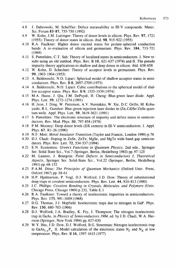
References 573
4.8 1. Dabrowski, M. Scheffler: Defect metastability in III-V compounds. Mater. Sci. Forum 83-87, 735-750 (1992)
4.9 W. Kohn, 1.M. Luttinger: Theory of donor levels in silicon. Phys. Rev. 97,1721 (1955); Theory of donor states in silicon. ibid. 98, 915-922 (1955)
4.10 R.A. Faulkner: Higher donor excited states for prolate-spheroid conduction bands: A re-evaluation of silicon and germanium. Phys. Rev. 184, 713-721 (1969)
4.11 S. Pantelides, C.T. Sah: Theory of localized states in semiconductors. I. New results using an old method. Phys. Rev. B 10, 621-637 (1974) and II. The pseudo impurity theory applications to shallow and deep donos in silicon. ibid. 638-658
4.12 W. Kohn, D. Schechter: Theory of acceptor levels in germanium. Phys. Rev. 99,1903-1904(1955)
4.13 A. Baldereschi, N.O. Lipari: Spherical model of shallow acceptor states in semiconductors. Phys. Rev. B 8, 2697-2709 (1973)
4.14 A. Baldereschi, N.O. Lipari: Cubic contributions to the spherical model of shallow acceptor states. Phys. Rev. B 9, 1525-1539 (1974)
4.15 M.A. Hasse, 1. Qiu, 1.M. DePuydt, H. Cheng: Blue-green laser diode. App!. Phys. Lett. 59,1272-1274 (1991)
4.16 H. leon, 1. Ding, W. Patterson, A.V. Nurmikko, W. Xie, D.C. Grillo, M. Kobayashi, R.L. Gunshor: Blue-green injection laser diodes in (Zn,Cd)Se/ZnSe quantum wells. App!. Phys. Lett. 59, 3619-3621 (1991)
4.17 S. Pantelides: The electronic structure of impurity and defect states in semiconductors. Rev. Mod. Phys. 50, 797-858 (1978)
4.18 P.M. Mooney: Deep donor levels (DX centers) in III-V semiconductors. 1. App!. Phys. 67, RI-26 (1990)
4.19 N.F. Mott: Metal-Insulator Transition (Taylor and Francis, London 1990) p.76 4.20 DJ. Chadi: Doping in ZnSe, ZnTe, MgSe, and MgTe wide-band-gap semicon
dutors. Phys. Rev. Lett. 72, 534-537 (1994) 4.21 E.N. Economou: Green's Functions in Quantum Physics, 2nd edn., Springer
Ser. Solid-State Sci., Vo!.7 (Springer, Berlin, Heidelberg 1983) pp. 97-125 4.22 M. Lannoo, 1. Bourgoin: Point Defects in Semiconductors I, Theoretical
Aspects, Springer Ser. Solid-State Sci., Vo!'22 (Springer, Berlin, Heidelberg 1981) pp. 68-152
4.23 P.A.M. Dirac: The Principles of Quantum Mechanics (Oxford Univ. Press, Oxford 1967) pp.58-61
4.24 H.P. Hjalmarson, P. Vogl, DJ. Wolford, 1.D. Dow: Theory of substitutional deep traps in covalent semiconductors. Phys. Rev. Lett. 44,810-813 (1980)
4.25 1.C. Phillips: Covalent Bonding in Crystals, Molecules. and Polymers (Univ. Chicago Press, Chicago 1969) p.232, Table E.l
4.26 R.A. Faulkner: Toward a theory of isoelectronic impurities in semiconductors. Phys. Rev. 175,991-1009 (1968)
4.27 D.G. Thomas, IJ. Hopfield: Isoelectronic traps due to nitrogen in GaP. Phys. Rev. 150,680-703 (1966)
4.28 DJ. Wolford, J.A. Bradley, K. Fry, 1. Thompson: The nitrogen isoelectronic trap in GaAs, in Physics of Semiconductors 1984, ed. by 1.D. Chadi, W.A. Harrison (Springer, New York 1984) pp.627-630
4.29 W.Y. Hsu, 1.D. Dow, DJ. Wolford, B.G. Streetman: Nitrogen isoelectronic trap in GaAs1_xPx' II. Model calculation of the electronic states Nr and Nx at low temperature. Phys. Rev. B 16,1597-1615 (1977)
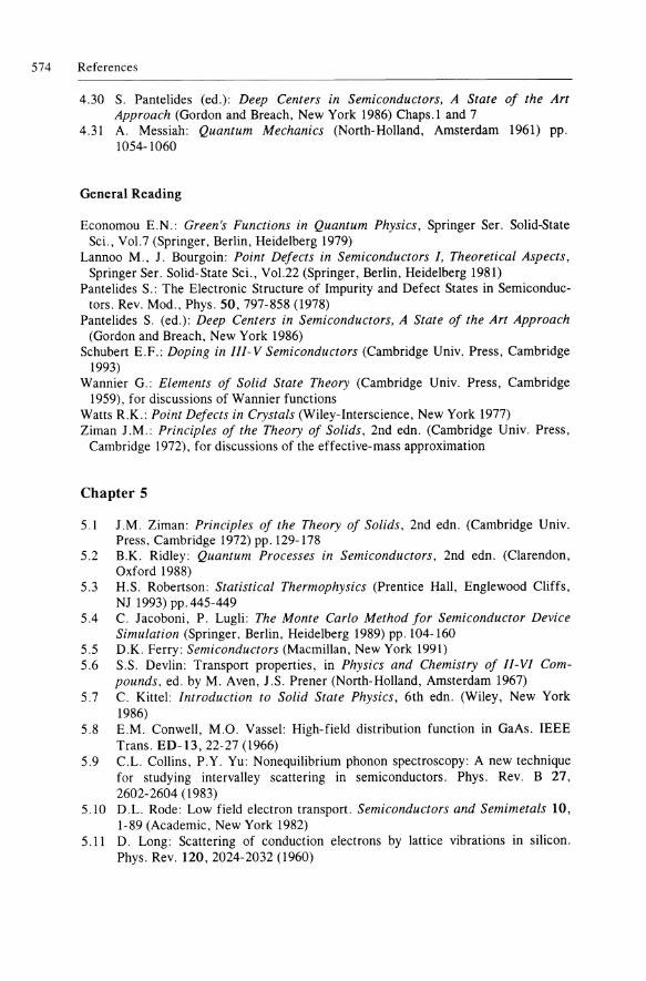
574 References
4.30 S. Pantelides (ed.): Deep Centers in Semiconductors, A State of the Art Approach (Gordon and Breach, New York 1986) Chaps. 1 and 7
4.31 A. Messiah: Quantum Mechanics (North-Holland, Amsterdam 1961) pp. 1054-1060
General Reading
Economou E.N.: Green's Functions in Quantum Physics, Springer Ser. Solid-State Sci., Vol.7 (Springer, Berlin, Heidelberg 1979)
Lannoo M., 1. Bourgoin: Point Defects in Semiconductors I, Theoretical Aspects, Springer Ser. Solid-State Sci., Vo1.22 (Springer, Berlin, Heidelberg 1981)
Pantelides S.: The Electronic Structure of Impurity and Defect States in Semiconductors. Rev. Mod., Phys. 50, 797-858 (1978)
Pantelides S. (ed.): Deep Centers in Semiconductors, A State of the Art Approach (Gordon and Breach, New York 1986)
Schubert E.F.: Doping in /II-V Semiconductors (Cambridge Univ. Press, Cambridge 1993)
Wannier G.: Elements of Solid State Theory (Cambridge Univ. Press, Cambridge 1959), for discussions of Wannier functions
Watts R.K.: Point Defects in Crystals (Wiley-Interscience, New York 1977) Ziman J.M.: Principles of the Theory of Solids, 2nd edn. (Cambridge Univ. Press,
Cambridge 1972), for discussions of the effective-mass approximation
Chapter 5
5.1 1.M. Ziman: Principles of the Theory of Solids, 2nd edn. (Cambridge Univ. Press, Cambridge 1972) pp. 129-178
5.2 B.K. Ridley: Quantum Processes in Semiconductors, 2nd edn. (Clarendon, Oxford 1988)
5.3 H.S. Robertson: Statistical Thermophysics (Prentice Hall, Englewood Cliffs, NJ 1993) pp. 445-449
5.4 C. Jacoboni, P. Lugli: The Monte Carlo Method for Semiconductor Device Simulation (Springer. Berlin, Heidelberg 1989) pp. 104-160
5.5 D.K. Ferry: Semiconductors (Macmillan, New York 1991) 5.6 S.S. Devlin: Transport properties, in Physics and Chemistry of /I-VI Com
pounds, ed. by M. Aven, 1.S. Prener (North-Holland, Amsterdam 1967) 5.7 C. Kittel: Introduction to Solid State Physics, 6th edn. (Wiley, New York
1986) 5.8 E.M. Conwell, M.O. Vassel: High-field distribution function in GaAs. IEEE
Trans. ED-13, 22-27 (1966) 5.9 c.L. Collins, P.Y. Yu: Nonequilibrium phonon spectroscopy: A new technique
for studying intervalley scattering in semiconductors. Phys. Rev. B 27, 2602-2604 (1983)
5.10 D.L. Rode: Low field electron transport. Semiconductors and Semimetals 10, 1-89 (Academic, New York 1982)
5.11 D. Long: Scattering of conduction electrons by lattice vibrations in silicon. Phys. Rev. 120,2024-2032 (1960)
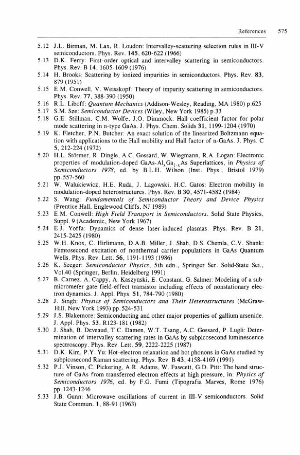
References 575
5.12 J.L. Birman, M. Lax, R. Loudon: Intervalley-scattering selection rules in III-V semiconductors. Phys. Rev. 145,620-622 (1966)
5.13 D.K. Ferry: First-order optical and intervalley scattering in semiconductors. Phys. Rev. B 14,1605-1609 (1976)
5.14 H. Brooks: Scattering by ionized impurities in semiconductors. Phys. Rev. 83, 879 (1951)
5.15 E.M. Conwell, V. Weisskopf: Theory of impurity scattering in semiconductors. Phys. Rev. 77, 388-390 (1950)
5.16 R.L. Liboff: Quantum Mechanics (Addison-Wesley, Reading, MA 1980) p.625 5.17 S.M. Sze: Semiconductor Devices (Wiley, New York 1985) p.33 5.18 G.E. Stillman, C.M. Wolfe, J.O. Dimmock: Hall coefficient factor for polar
mode scattering in n-type GaAs. J. Phys. Chern. Solids 31,1199-1204 (1970) 5.19 K. Fletcher, P.N. Butcher: An exact solution of the linearized Boltzmann equa
tion with applications to the Hall mobility and Hall factor of n-GaAs. J. Phys. C 5,212-224 (1972)
5.20 H.L. Stormer, R. Dingle, A.C. Gossard, W. Wiegmann, R.A. Logan: Electronic properties of modulation-doped GaAs-AlxGa1_xAs Superlattices, in Physics of Semiconductors 1978, ed. by B.L.H. Wilson (Inst. Phys., Bristol 1979) pp.557-560
5.21 W. Walukiewicz, H.E. Ruda, J. Lagowski, H.e. Gatos: Electron mobility in modulation-doped heterostructures. Phys. Rev. B 30,4571-4582 (1984)
5.22 S. Wang: Fundamentals of Semiconductor Theory and Device Physics (Prentice Hall, Englewood Cliffs, NJ 1989)
5.23 E.M. Conwell: High Field Transport in Semiconductors. Solid State Physics, Supp!. 9 (Academic, New York 1967)
5.24 EJ. Yoffa: Dynamics of dense laser-induced plasmas. Phys. Rev. B 21, 2415-2425 (1980)
5.25 W.H. Knox, e. Hirlimann, D.A.B. Miller, J. Shah, D.S. Chemla, e.V. Shank: Femtosecond excitation of nonthermal carrier populations in GaAs Quantum Wells. Phys. Rev. Lett. 56,1191-1193 (1986)
5.26 K. Seeger: Semiconductor Physics, 5th edn., Springer Ser. Solid-State Sci., Vo!.40 (Springer, Berlin, Heidelberg 1991)
5.27 B. Carnez, A. Cappy, A. Kaszynski, E. Constant, G. Salmer: Modeling of a submicrometer gate field-effect transistor including effects of nonstationary electron dynamics. J. App!. Phys. 51, 784-790 (1980)
5.28 J. Singh: Physics of Semiconductors and Their Heterostructures (McGrawHill, New York 1993) pp. 524-531
5.29 1.S. Blakemore: Semiconducting and other major properties of gallium arsenide. J. App!. Phys. 53, R123-181 (1982)
5.30 J. Shah, B. Deveaud, T.e. Damen, W.T. Tsang, A.C. Gossard, P. Lugli: Determination of intervalley scattering rates in GaAs by subpicosecond luminescence spectroscopy. Phys. Rev. Lett. 59, 2222-2225 (1987)
5.31 D.K. Kim, P.Y. Yu: Hot-electron relaxation and hot phonons in GaAs studied by subpicosecond Raman scattering. Phys. Rev. B 43, 4158-4169 (1991)
5.32 PJ. Vinson, e. Pickering, A.R. Adams, W. Fawcett, G.D. Pitt: The band structure of GaAs from transferred electron effects at high pressure, in: Physics of Semiconductors 1976, ed. by F.G. Fumi (Tipografia Marves, Rome 1976) pp. 1243-1246
5.33 1.B. Gunn: Microwave oscillations of current in III-V semiconductors. Solid State Commun. 1,88-91 (1963)
576 References
5.34 J.B. Gunn: Microwave oscillations of current in III-V semiconductors. IBM 1. Res. Dev. 8,141-159 (1964)
5.35 R. Dalven: Introduction to Applied Solid State Physics, 2nd edn. (Plenum, New York 1990) pp. 158-165
5.36 K. Seeger: Semiconductor Physics, 5th edn., Springer Ser. Solid-State Sci., Vol.40 (Springer, Berlin, Heidelberg 1991) pp. 217-272
5.37 C. Herring, E. Vogt: Transport and deformation potential theory for manyvalley semiconductors with anisotropic scattering. Phys. Rev. 101, 944-961 (1956); erratum 105, 1933 (1956)
5.38 E.H. Hall: On a new action of the magnet on electric current. Am. 1. Math. 2, 287-292 (1879)
5.39 L. van der Pauw: A method of measuring specific resistivity and Hall effect of discs of arbitrary shape. Philips Res. Rep. 13, 1-9 (1958)
General Reading Transport Properties
Dalven R.: Introduction to Applied Solid State Physics, 2nd edn. (Plenum, New York 1990)
Ferry D.K.: Semiconductors (Macmillan, New York 1991) Rode D.L.: Low field electron transport. Semiconductors and Semimetals 10, 1-89
(Academic, New York 1982) Kittel c.: Introduction to Solid State Physics 7th edn. (Wiley, New York 1995) Nag B.R.: Electron Transport in Compound Semiconductors, Springer Ser. Solid
State Sci., VoUI (Springer, Berlin, Heidelberg 1980) Ridley B.K.: Quantum Processes in Semiconductors, 2nd edn. (Clarendon, Oxford
1988) Seeger K.: Semiconductor Physics, 5th edn., Springer Ser. Solid-State Sci., Vol.40
(Springer, Berlin, Heidelberg 1991) Wiley J.D.: Mobility of holes in III-V compounds. Semiconductors and Semimetals
10,91-174 (Academic, New York 1982) Ziman J.M.: Principles of the Theory of Solids, 2nd edn. (Cambridge Univ. Press,
Cambridge 1972)
Hot Carriers
Conwell E.M.: High Field Transport in Semiconductors, Solid State Physics, Suppl.9 (Academic, New York 1967)
Conwell E.M.: In Handbook of Semiconductors (North-Holland, Amsterdam 1982) VoU, pp.513-561
Jacoboni C., Lugli P.: The Monte Carlo Method for Semiconductor Device Simulation (Springer, New York 1989)
Devices
Singh J.: Physics of Semiconductors and Their Heterostructures (McGraw-Hill, New York 1993)
Sze S.M.: Semiconductor Devices (Wiley, New York 1985) Wang, S.: Fundamentals of Semiconductor Theory and Device Physics (Prentice Hall
Englewood Cliffs, NJ 1989)
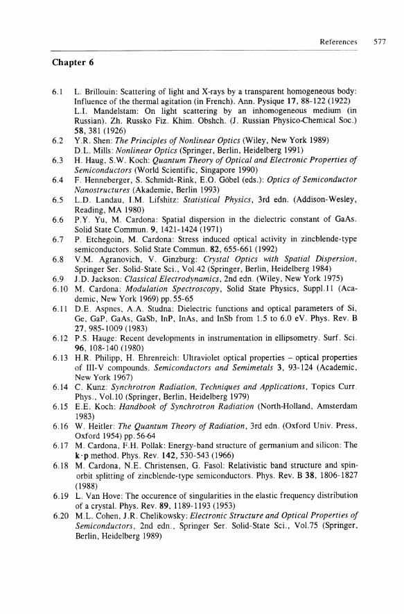
References 577
Chapter 6
6.1 L. Brillouin: Scattering of light and X-rays by a transparent homogeneous body: Influence of the thermal agitation (in French). Ann. Pysique 17,88-122 (1922) L.I. Mandelstam: On light scattering by an inhomogeneous medium (in Russian). Zh. Russko Fiz. Khim. Obshch. (1. Russian Physico-Chemical Soc.) 58,381 (1926)
6.2 Y.R. Shen: The Principles of Nonlinear Optics (Wiley, New York 1989) D.L. Mills: Nonlinear Optics (Springer, Berlin, Heidelberg 1991)
6.3 H. Haug, S.W. Koch: Quantum Theory of Optical and Electronic Properties of Semiconductors (World Scientific, Singapore 1990)
6.4 F. Henneberger, S. Schmidt-Rink, E.O. Gobel (eds.): Optics of Semiconductor Nanostructures (Akademie, Berlin 1993)
6.5 L.D. Landau, I.M. Lifshitz: Statistical Physics, 3rd edn. (Addison-Wesley, Reading, MA 1980)
6.6 P.Y. Yu, M. Cardona: Spatial dispersion in the dielectric constant of GaAs. Solid State Commun. 9,1421-1424 (1971)
6.7 P. Etchegoin, M. Cardona: Stress induced optical activity in zincblende-type semiconductors. Solid State Commun. 82, 655-661 (1992)
6.8 V.M. Agranovich, V. Ginzburg: Crystal Optics with Spatial Dispersion, Springer Ser. Solid-State Sci., Vol.42 (Springer, Berlin, Heidelberg 1984)
6.9 J.D. Jackson: Classical Electrodynamics, 2nd edn. (Wiley, New York 1975) 6.10 M. Cardona: Modulation Spectroscopy, Solid State Physics, Suppl.ll (Aca
demic, New York 1969) pp. 55-65 6.11 D.E. Aspnes, A.A. Studna: Dielectric functions and optical parameters of Si,
Ge, GaP, GaAs, GaSb, InP, InAs, and InSb from 1.5 to 6.0 eV. Phys. Rev. B 27, 985-1009 (1983)
6.12 P.S. Hauge: Recent developments in instrumentation in ellipsometry. Surf. Sci. 96,108-140(1980)
6.13 H.R. Philipp, H. Ehrenreich: Ultraviolet optical properties - optical properties of III-V compounds. Semiconductors and Semimetals 3, 93-124 (Academic, New York 1967)
6.14 C. Kunz: Synchrotron Radiation, Techniques and Applications, Topics Curr. Phys., Vol.lO (Springer, Berlin, Heidelberg 1979)
6.15 E.E. Koch: Handbook of Synchrotron Radiation (North-Holland, Amsterdam 1983)
6.16 W. Heitler: The Quantum Theory of Radiation, 3rd edn. (Oxford Univ. Press, Oxford 1954) pp. 56-64
6.17 M. Cardona, F.H. Pollak: Energy-band structure of germanium and silicon: The k·p method. Phys. Rev. 142,530-543 (1966)
6.18 M. Cardona, N .E. Christensen, G. Fasol: Relativistic band structure and spinorbit splitting of zincblende-type semiconductors. Phys. Rev. B 38, 1806-1827 (1988)
6.19 L. Van Hove: The occurence of singularities in the elastic frequency distribution of a crystal. Phys. Rev. 89, 1189-1193 (1953)
6.20 M.L. Cohen, J .R. Chelikowsky: Electronic Structure and Optical Properties of Semiconductors, 2nd edn., Springer Ser. Solid-State Sci., Vol.75 (Springer, Berlin, Heidelberg 1989)
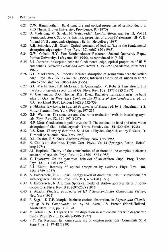
578 References
6.21 C.W. Higginbotham: Band structure and optical properties of semiconductors, PhD Thesis, Brown University, Providence, RI (1970)
6.22 O. Madelung, M. Schulz, H. Weiss (eds.): Landolt-Bornstein, SeLIII, Vo!.22 (Semiconductors), Subvo!. a: Intrinsic properties of group-IV elements, III-V, 11-VI and 1-VII compounds (Springer, Berlin, Heidelberg 1987)
6.23 R.B. Schoolar, J.R. Dixon: Optical constant of lead sulfide in the fundamental absorption edge region. Phys. Rev. 137, A667-670 (1965)
6.24 G.W. Gobeli, H.Y. Fan: Semiconductor Research, Second Quartertly Rept., Purdue University, Lafayette, IN (1956), as reproduced in [6.25]
6.25 EJ. Johnson: Absorption near the fundamental edge, optical properties of III-V compounds. Semiconductor and Semimetals 3, 153-258 (Academic, New York 1967)
6.26 G.G. MacFarlane, V. Roberts: Infrared absorption of germanium near the lattice edge. Phys. Rev. 97, 1714-1716 (1955); Infrared absorption of silicon near the lattice edge. ibid. 98, 1865-1866 (1955)
6.27 G.G. MacFarlane, T.P. McLean, J.E. Quarrington, V. Roberts: Fine structure in the absorption-edge spectrum of Ge. Phys. Rev. 108, 1377-1383 (1957)
6.28 M. Gershenzon, D.G. Thomas, R.E. Dietz: Radiative transitions near the band edge of GaP, in Proc. Int'l Conj. on the Physics of Semiconductors, ed. by A.C. Stickland (lOP, London 1962) p.752-759
6.29 S. Nikitine: Excitons, in Optical Properties of Solids, ed. by S. Nudelman, S.S. Mitra (Plenum, New York 1969) pp. 197-237
6.30 G.H. Wannier: The structure and electronic excitation levels in insulating crystals. Phys. Rev. 52,191-197 (1937)
6.31 N.F. Mott: Conduction in polar crystals: II. The conduction band and ultra-violet absorption of alkali-halide crystals. Trans. Faraday Soc. 34, 500-506 (1938)
6.32 R.S. Knox: Theory of Excitons, Solid State Physics, Supp!.5, ed. by F. Seitz, D. Turnbull (Academic, New York 1963)
6.33 D.L. Dexter, R.S. Knox: Excitons (Wiley, New York 1965) 6.34 K. Cho (ed.): Excitons, Topics Curr. Phys., Vo1.l4 (Springer, Berlin, Heidel
berg 1974) 6.35 J.J. Hopfield: Theory of the contribution of excitons to the complex dielectric
constant of crystals. Phys. Rev. 112, 1555-1567 (1958) 6.36 Y. Toyozawa: On the dynamical behavior of an exciton. Supp!. Prog. Theor.
Phys.12,111-140(1959) 6.37 R.J. Elliott: Intensity of optical absoprtion by excitons. Phys. Rev. 108,
1384-1389 (1957) 6.38 A. Baldereschi, N .0. Lipari: Energy levels of direct excitons in semiconductors
with degenerate bands. Phys. Rev. B 3, 439-450 (1971) 6.39 A. Baldereschi, N.O. Lipari: Spherical model of shallow acceptor states in semi
conductors. Phys. Rev. B 8,2697-2709 (1973) 6.40 S. Adachi: Physical Properties of III-V Semiconductor Compounds (Wiley,
New York 1992) 6.41 B. Segall, D.T.F. Marple: Intrinsic exciton absorption, in Physics and Chemis
try of II- VI Compounds, ed. by M. AVen, J .S. Prener (North-Holland, Amsterdam 1967) pp. 319-378
6.42 M. Altarelli, N.O. Lipari: Exciton dispersion in semiconductors with degenerate bands. Phys. Rev. B 15,4898-4906 (1977)
6.43 P.Y. Yu: Resonant Brillouin scattering of exciton polaritons. Comments Solid State Phys. 9, 37-48 (1979)
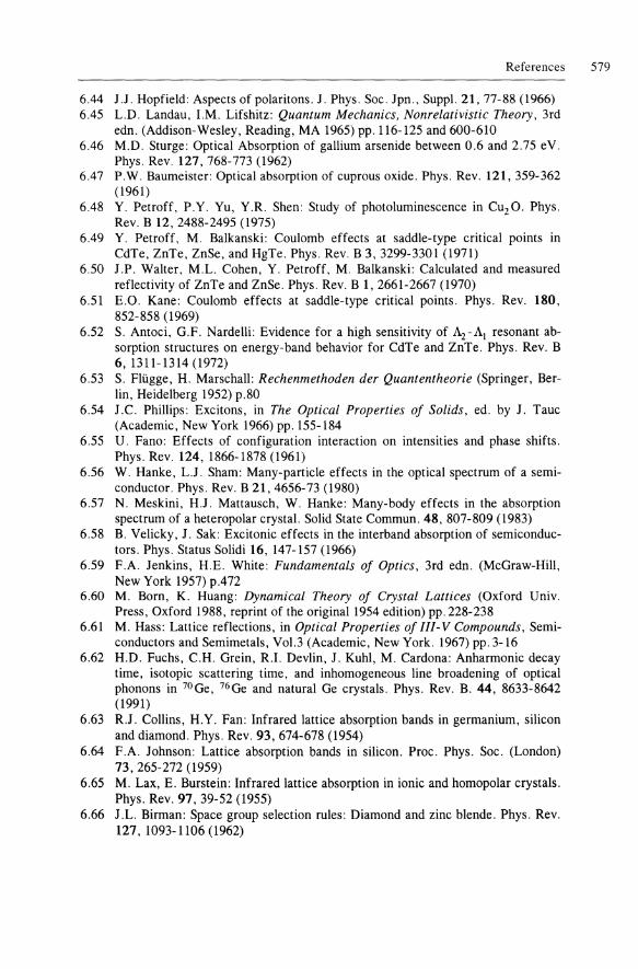
References 579
6.44 J.J. Hopfield: Aspects of polaritons. 1. Phys. Soc. Jpn., Suppl. 21, 77-88 (1966) 6.45 L.D. Landau, I.M. Lifshitz: Quantum Mechanics, Nonrelativistic Theory, 3rd
edn. (Addison-Wesley, Reading, MA 1965) pp.1l6-125 and 600-610 6.46 M.D. Sturge: Optical Absorption of gallium arsenide between 0.6 and 2.75 eV.
Phys. Rev. 127,768-773 (1962) 6.47 P.W. Baumeister: Optical absorption of cuprous oxide. Phys. Rev. 121,359-362
(1961) 6.48 Y. Petroff, P.Y. Yu, Y.R. Shen: Study of photoluminescence in Cu2 0. Phys.
Rev. B 12, 2488-2495 (1975) 6.49 Y. Petroff, M. Balkanski: Coulomb effects at saddle-type critical points in
CdTe, ZnTe, ZnSe, and HgTe. Phys. Rev. B 3,3299-3301 (1971) 6.50 J.P. Walter, M.L. Cohen, Y. Petroff, M. Balkanski: Calculated and measured
reflectivity of ZnTe and ZnSe. Phys. Rev. B 1, 2661-2667 (1970) 6.51 E.O. Kane: Coulomb effects at saddle-type critical points. Phys. Rev. 180,
852-858 (1969) 6.52 S. Antoci, G.F. Nardelli: Evidence for a high sensitivity of Az-A1 resonant ab
sorption structures on energy-band behavior for CdTe and ZnTe. Phys. Rev. B 6,1311-1314 (1972)
6.53 S. Fliigge, H. Marschall: Rechenmethoden der Quantentheorie (Springer, Berlin, Heidelberg 1952) p.80
6.54 J.e. Phillips: Excitons, in The Optical Properties of Solids, ed. by J. Tauc (Academic, New York 1966) pp. 155-184
6.55 U. Fano: Effects of configuration interaction on intensities and phase shifts. Phys. Rev. 124, 1866-1878 (1961)
6.56 W. Hanke, LJ. Sham: Many-particle effects in the optical spectrum of a semiconductor. Phys. Rev. B 21,4656-73 (1980)
6.57 N. Meskini, HJ. Mattausch, W. Hanke: Many-body effects in the absorption spectrum of a heteropolar crystal. Solid State Commun. 48, 807-809 (1983)
6.58 B. Velicky, J. Sak: Excitonic effects in the interband absorption of semiconductors. Phys. Status Solidi 16,147-157 (1966)
6.59 F.A. Jenkins, H.E. White: Fundamentals of Optics, 3rd edn. (McGraw-Hill, New York 1957) p.472
6.60 M. Born, K. Huang: Dynamical Theory of Crystal Lattices (Oxford Univ. Press, Oxford 1988, reprint of the original 1954 edition) pp. 228-238
6.61 M. Hass: Lattice reflections, in Optical Properties of IlI- V Compounds, Semiconductors and Semimetals, Vol.3 (Academic, New York. 1967) pp. 3-16
6.62 H.D. Fuchs, C.H. Grein, R.I. Devlin, J. Kuhl, M. Cardona: Anharmonic decay time, isotopic scattering time, and inhomogeneous line broadening of optical phonons in 70Ge, 76Ge and natural Ge crystals. Phys. Rev. B. 44, 8633-8642 (1991)
6.63 RJ. Collins, H.Y. Fan: Infrared lattice absorption bands in germanium, silicon and diamond. Phys. Rev. 93, 674-678 (1954)
6.64 F.A. Johnson: Lattice absorption bands in silicon. Proc. Phys. Soc. (London) 73, 265-272 (1959)
6.65 M. Lax, E. Burstein: Infrared lattice absorption in ionic and homopolar crystals. Phys. Rev. 97, 39-52 (1955)
6.66 J.L. Birman: Space group selection rules: Diamond and zinc blende. Phys. Rev. 127, 1093-1106 (1962)
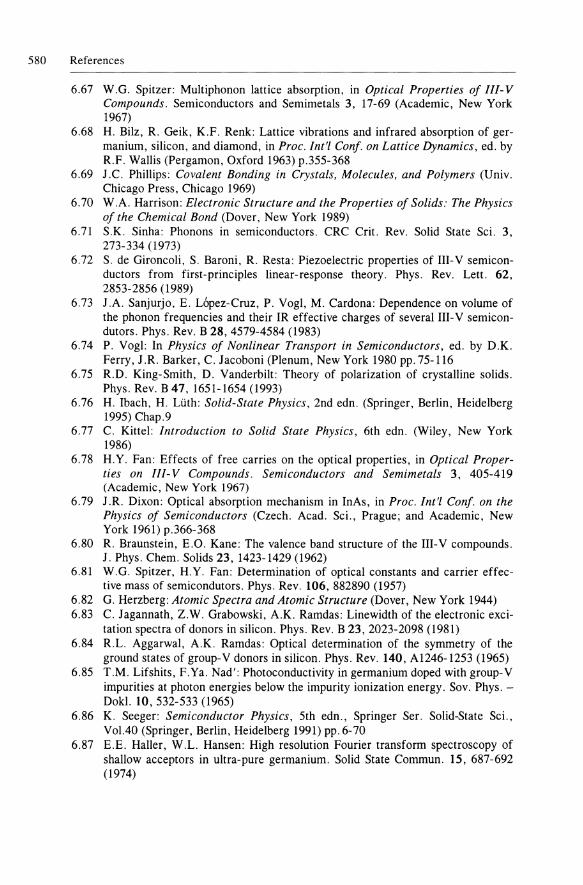
580 References
6.67 W.G. Spitzer: Multiphonon lattice absorption, in Optical Properties of III- V Compounds. Semiconductors and Semimetals 3, 17-69 (Academic, New York 1967)
6.68 H. Bilz, R. Geik, K.F. Renk: Lattice vibrations and infrared absorption of germanium, silicon, and diamond, in Proc. Int'l Conf. on Lattice Dynamics, ed. by R.F. Wallis (Pergamon, Oxford 1963) p.355-368
6.69 J.e. Phillips: Covalent Bonding in Crystals, Molecules, and Polymers (Univ. Chicago Press, Chicago 1969)
6.70 W.A. Harrison: Electronic Structure and the Properties of Solids: The Physics of the Chemical Bond (Dover, New York 1989)
6.71 S.K. Sinha: Phonons in semiconductors. CRC Crit. Rev. Solid State Sci. 3, 273-334 (1973)
6.72 S. de Gironcoli, S. Baroni, R. Resta: Piezoelectric properties of III-V semiconductors from first-principles linear-response theory. Phys. Rev. Lett. 62, 2853-2856 (1989)
6.73 J.A. Sanjurjo, E. Lopez-Cruz, P. Vogl, M. Cardona: Dependence on volume of the phonon frequencies and their IR effective charges of several III-V semicondutors. Phys. Rev. B 28,4579-4584 (1983)
6.74 P. Vogl: In Physics of Nonlinear Transport in Semiconductors, ed. by D.K. Ferry, J.R. Barker, e. Jacoboni (Plenum, New York 1980 pp. 75-116
6.75 R.D. King-Smith, D. Vanderbilt: Theory of polarization of crystalline solids. Phys. Rev. B 47, 1651-1654 (1993)
6.76 H. Ibach, H. Uith: Solid-State Physics, 2nd edn. (Springer, Berlin, Heidelberg 1995) Chap.9
6.77 e. Kittel: Introduction to Solid State Physics, 6th edn. (Wiley, New York 1986)
6.78 H.Y. Fan: Effects of free carries on the optical properties, in Optical Properties on III- V Compounds. Semiconductors and Semimetals 3, 405-419 (Academic, New York 1967)
6.79 1.R. Dixon: Optical absorption mechanism in InAs, in Proc. Int'l Conf. on the Physics of Semiconductors (Czech. Acad. Sci., Prague; and Academic, New York 1961) p.366-368
6.80 R. Braunstein, E.O. Kane: The valence band structure of the III-V compounds. 1. Phys. Chern. Solids 23,1423-1429 (1962)
6.81 W.G. Spitzer, H.Y. Fan: Determination of optical constants and carrier effective mass of semicondutors. Phys. Rev. 106, 882890 (1957)
6.82 G. Herzberg: Atomic Spectra and Atomic Structure (Dover, New York 1944) 6.83 e. Jagannath, Z.W. Grabowski, A.K. Ramdas: Linewidth of the electronic exci
tation spectra of donors in silicon. Phys. Rev. B 23,2023-2098 (1981) 6.84 R.L. Aggarwal, A.K. Ramdas: Optical determination of the symmetry of the
ground states of group-V donors in silicon. Phys. Rev. 140, A1246-1253 (1965) 6.85 T.M. Lifshits, F.Ya. Nad': Photoconductivity in germanium doped with group-V
impurities at photon energies below the impurity ionization energy. Sov. Phys. -DokI. 10,532-533 (1965)
6.86 K. Seeger: Semiconductor Physics, 5th edn., Springer Ser. Solid-State Sci., VoI.40 (Springer, Berlin, Heidelberg 1991) pp. 6-70
6.87 E.E. Haller, W.L. Hansen: High resolution Fourier transform spectroscopy of shallow acceptors in ultra-pure germanium. Solid State Commun. 15, 687-692 (1974)
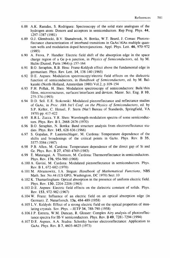
References 581
6.88 A.K. Ramdas, S. Rodriguez: Spectroscopy of the solid state analogues of the hydrogen atom: Donors and acceptors in semiconductors. Rep Prog. Phys. 44, 1297-1387 (1981)
6.89 OJ. Glembocki, B.V. Shanabrook, N. Bottka, W.T. Beard, 1. Comas: Photoreflectance characterization of interband transitions in GaAs/ AlAs multiple quantum wells and modulation doped heterojunctions. Appl. Phys. Lett. 46, 970-972 (1985)
6.90 A. Frova, P. Handler: Electric field shift of the absorption edge in the space charge region of a Ge p-n junction, in Physics of Semiconductors, ed. by M. Hulin (Dunod, Paris 1964) p.157-164
6.91 B.O. Seraphin, R.B. Hess: Franz-Keldysh effect above the fundamental edge in germanium. Phys. Rev. Lett. 14, 138-140 (1965)
6.92 D.E. Aspnes: Modulation spectroscopy/electric field effects on the dielectric function of semiconductors, in Handbook of Semiconductors, ed. by M. Balkanski (North-Holland, Amsterdam 1980) Vol.2, p.109-154
6.93 F.H. Pollak, H. Shen: Modulation spectroscopy of semiconductors: Bulk/thin films, microstructures, surfaces/interfaces and devices. Mater. Sci. Eng. R 10, 275-374 (1993)
6.94 D.D. Sell. E.E. Stokowski: Modulated piezoreflectance and reflectance studies of GaAs, in Proc. 10th lnt'l Conf. on the Physics of Semiconductors, ed. by S.P. Keller, C. Hensel, F. Stern (Nat'l Bureau of Standards, Springfield, VA 1970) pp.417-422
6.95 R.R.L. Zucca, Y.R. Shen: Wavelength-modulation spectra of some semiconductors. Phys. Rev. B 1,2668-2676 (1970)
6.96 B.O. Seraphin, N. Bottka: Band structure analysis from electroreflectance studies. Phys. Rev. 145,628-636 (1966)
6.97 S. Gopalan, P. Lautenschlager, M. Cardona: Temperature dependence of the shifts and broadenings of the critical points in GaAs. Phys. Rev. B 35, 5577-5584 (1987)
6.98 P.B. Allen, M. Cardona: Temperature dependence of the direct gap of Si and Ge. Phys. Rev. B 27,4760-4769 (1983)
6.99 E. Matatagui, A. Thomson, M. Cardona: Thermoreflectance in semiconductors. Phys. Rev. 176,954-960 (1968)
6.100 A. Gavini, M. Cardona: Modulated piezoreflectance in semiconductors. Phys. Rev. B 1,672-682 (1970)
6.101 M. Abramowitz, LA. Stegun: Handbook of Mathematical Functions, NBS Math. Ser. No.44 (US GPO, Washington, DC 1970) Sect. 10
6.102 K. Thamarlingham: Optical absorption in the presence of uniform electric field. Phys. Rev. 130,2204-2206 (1963)
6.103 D.E. Aspnes: Electric field effects on the dielectric constant of solids. Phys. Rev. 153,972-982 (1967)
6.104 W. Franz: Influence of an electric field on an optical absorption edge (in German). Z. Naturforsch. 13a, 484-489 (1958)
6.105 L.V. Keldysh: Effect of a strong electric field on the optical properties of insulating crystals. Sov. Phys. - JETP 34, 788-790 (1958)
6.106 J.P. Estrera, W.M. Duncan, R. Glosser: Complex Airy analysis of photoreflectance spectra for III-V semiconductors. Phys. Rev. B 49, 7281-7294 (1994)
6.107 D.E. Aspnes, A.A. Studna: Schottky barrier electroreflectance: Application to GaAs. Phys. Rev. B 7, 4605-4625 (1973)
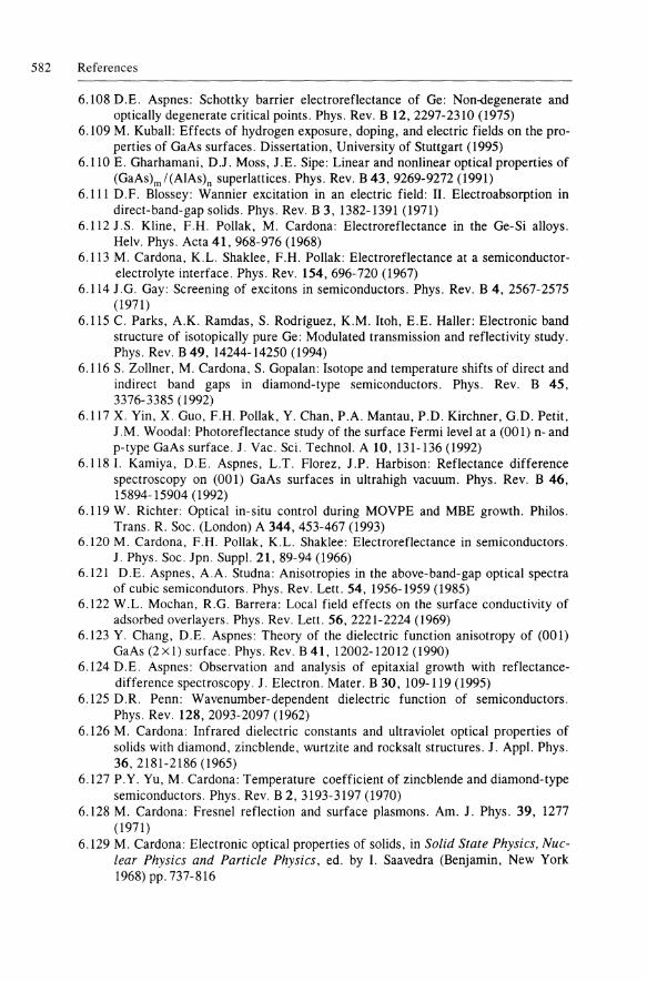
582 References
6.108 D.E. Aspnes: Schottky barrier electroreflectance of Ge: Non-degenerate and optically degenerate critical points. Phys. Rev. B 12,2297-2310 (1975)
6.109 M. Kuball: Effects of hydrogen exposure, doping, and electric fields on the properties of GaAs surfaces. Dissertation, University of Stuttgart (1995)
6.110 E. Gharhamani, D.J. Moss, 1.E. Sipe: Linear and nonlinear optical properties of (GaAs)m / (AlAs)n superlattices. Phys. Rev. B 43, 9269-9272 (199\)
6.111 D.F. Blossey: Wannier excitation in an electric field: II. Electroabsorption in direct-band-gap solids. Phys. Rev. B 3,1382-1391 (1971)
6.112 J.S. Kline, F.H. Pollak, M. Cardona: Electroreflectance in the Ge-Si alloys. Helv. Phys. Acta 41,968-976 (1968)
6.113 M. Cardona, K.L. Shaklee, F.H. Pollak: Electroreflectance at a semiconductorelectrolyte interface. Phys. Rev. 154,696-720 (1967)
6.114 1.G. Gay: Screening of excitons in semiconductors. Phys. Rev. B 4, 2567-2575 (1971)
6.115 C. Parks, A.K. Ramdas, S. Rodriguez, K.M. Itoh, E.E. Haller: Electronic band structure of isotopically pure Ge: Modulated transmission and reflectivity study. Phys. Rev. B 49,14244-14250 (1994)
6.116 S. Zollner, M. Cardona, S. Gopalan: Isotope and temperature shifts of direct and indirect band gaps in diamond-type semiconductors. Phys. Rev. B 45, 3376-3385 (1992)
6.117 X. Yin, X. Guo, F.H. Pollak, Y. Chan, P.A. Mantau, P.D. Kirchner, G.D. Petit, J.M. W oodal: Photoreflectance study of the surface Fermi level at a (001) n- and p-type GaAs surface. J. Vac. Sci. Techno\. A 10,131-136 (1992)
6.118 I. Kamiya, D.E. Aspnes, L.T. Florez, J.P. Harbison: Reflectance difference spectroscopy on (001) GaAs surfaces in ultrahigh vacuum. Phys. Rev. B 46, 15894-15904 (1992)
6.119 W. Richter: Optical in-situ control during MOVPE and MBE growth. Philos. Trans. R. Soc. (London) A 344, 453-467 (1993)
6.120 M. Cardona, F.H. Pollak, K.L. Shaklee: Electroreflectance in semiconductors. 1. Phys. Soc. Jpn. Supp\. 21, 89-94 (1966)
6.121 D.E. Aspnes, A.A. Studna: Anisotropies in the above-band-gap optical spectra of cubic semicondutors. Phys. Rev. Lett. 54,1956-1959 (1985)
6.122 W.L. Mochan, R.G. Barrera: Local field effects on the surface conductivity of adsorbed overlayers. Phys. Rev. Lett. 56, 2221-2224 (1969)
6.123 Y. Chang, D. E. Aspnes: Theory of the dielectric function anisotropy of (001) GaAs (2 x 1) surface. Phys. Rev. B 41, 12002-12012 (1990)
6.124 D.E. Aspnes: Observation and analysis of epitaxial growth with reflectancedifference spectroscopy. J. Electron. Mater. B 30,109-119 (1995)
6.125 D.R. Penn: Wavenumber-dependent dielectric function of semiconductors. Phys. Rev. 128,2093-2097 (1962)
6.126 M. Cardona: Infrared dielectric constants and ultraviolet optical properties of solids with diamond, zincblende, wurtzite and rocksalt structures. 1. App\. Phys. 36,2181-2186 (1965)
6.127 P.Y. Yu, M. Cardona: Temperature coefficient of zincblende and diamond-type semiconductors. Phys. Rev. B 2,3193-3197 (1970)
6.128 M. Cardona: Fresnel reflection and surface plasmons. Am. J. Phys. 39, 1277 (1971)
6.129 M. Cardona: Electronic optical properties of solids, in Solid State Physics, Nuclear Physics and Particle Physics, ed. by I. Saavedra (Benjamin, New York 1968) pp. 737-816
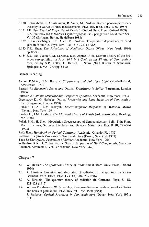
References 583
6.130 P. Wickbold, E. Anastassakis, R. Sauer. M. Cardona: Raman phonon piezospectroscopy in GaAs: Infrared measurements. Phys. Rev B 35, 1362-1368 (1987)
6.131 1.F. Nye: Physical Properties of Crystals (Oxford Univ. Press, Oxford 1969) L.A. Shuvalov (ed.): Modern Crystallography IV, Springer Ser. Solid-State Sci., Vol.37 (Springer, Berlin, Heidelberg 1988)
6.132 P. Lautenschlager, P.B. Allen, M. Cardona: Temperature dependence of band gaps in Si and Ge. Phys. Rev. B 31, 2163-2171 (1985)
6.133 Y.R. Shen: The Principles of Nonlinear Optics (Wiley, New York 1984) pp.86-93
6.134 J.A. Van Vechten, M. Cardona, D.E. Aspnes, R.M. Martin: Theory of the 3rdorder susceptibility, in Proc. 10th Int'l Conf. on the Physics of Semiconductors, ed. by S.P. Keller, C. Hensel, F. Stern (Nat'l Bureau of Standards, Springfield, VA 1970) pp. 82-86
General Reading
Azzam R.M.A., N.M. Bashara: Ellipsometry and Polarized Light (North-Holland, Amsterdam 1977)
Bassani F.: Electronic States and Optical Transitions in Solids (Pergamon, London 1975)
Burstein A.: Atomic Structure and Properties of Solids (Academic, New York 1973) Greenaway D., G. Harbeke: Optical Properties and Band Structure of Semiconduc
tors (Pergamon, London 1968) Ill'inskii Yu.A., L.V. Keldysh: Electromagnetic Response of Material Media
(Plenum, New York 1994) Landau L., I.M. Lifshitz: The Classical Theory of Fields (Addison-Wesley, Reading,
MA 1958) Pollak F.H., H. Shen: Modulation Spectrocsopy of Semiconductors, Bulk, Thin Film,
Microstructures, Surfaces/Interfaces and Devices. Mater. Sci. Eng. R 10, 275-374 (1993)
Palik E.A.: Handbook of Optical Constants (Academic, Orlando, FL 1985) Pankove J.: Optical Processes in Semiconductors (Dover, New York 1971) Tauc 1.: The Optical Properties of Solids (Academic, New York 1966) Willards on R.K., A.C. Beer (eds.): Optical Properties of Ill- V Compounds, Semicon
ductors, Semimetals, Vol.3 (Academic, New York 1967)
Chapter 7
7.1 W. Heitler: The Quantum Theory of Radiation (Oxford Univ. Press, Oxford 1954)
7.2 A. Einstein: Emission and absorption of radiation in the quantum theory (in German). Verh. Dtsch. Phys. Ges. 18,318-323 (1916)
7.3 A. Einstein: The quantum theory of radiation (in German). Phys. Z. 18, 121-128 (1917)
7.4 W. van Roosbroeck, W. Schockley: Photon-radiative recombination of electrons and holes in germanium. Phys. Rev. 94,1558-1560 (1954) 1. Pankove: Optical Processes in Semiconductors (Dover, New York 1971) p.ll0
584 References
7.5 E. Burstein: Anomalous optical absorption limit in InSb. Phys. Rev. 93, 632-633 (1954)
7.6 T.S. Moss: The interpretation of the properties of indium antimonide. Proc. Phys. Soc. (London) B 67,775-782 (1954)
7:7 S. Wang: Fundamentals of Semiconductor Theory and Device Physics (Prentice Hall, Englewood Cliffs, NJ 1989) pp. 760-766
7.8 N. Caswell, J.S. Weiner, P.Y. Yu: A study of non-thermalized luminescence spectra: The case of Cu2 0. Solid State Commun. 40, 843-846 (1981)
7.9 P.Y. Yu, Y.R. Shen: Resonance Raman studies in cuprous oxide. II. The yellow and green excitonic series. Phys. Rev. B 17,4017-4030 (1978)
7.10 L.T. Canham: Silicon quantum wire array fabrication by electrochemical and chemical dissolution of wafers. App!. Phys. Lett. 57,1046-1048 (1990)
7.11 L.T. Canham, W.Y. Leong, T.1. Cox, M.1. Beale, K.1. Nash, P. CaIcott, D. Bmmhead, L.L. Taylor, K.1. Marsh: Efficient visible photoluminescence and electroluminescence from highly porous silicon, in The Physics of Semiconductors, ed. by P. Jiang, H.-Z. Zheng (World Scientific, Singapore 1992) YoI.2, pp. 1423-1430
7.12 K.H. Jung, S. Shih, D.L. Kwong: Developments in luminescent porous Si. J. Electrochem. Soc. 140,3046-3064 (1993)
7.13 J. Zeman, M. Zigone, G.L.1.A. Rikken, G. Martinez: Hydrostatic pressure effects on the porous silicon luminescence. J. Phys. Chern. Solids 56,655-661 (1995) For reviews on the luminescence of porous silicon see: L. Bms: Luminescence of silicon materials: Chains, sheets, nanocrystals, microcrystals, and porous silican. J. Phys. Chern. 98, 3575-3581 (1994) K.H. Jung, S. Shih, D.L. Kwong: Developments in luminescent porous silicon. J. Electrochem. Soc. 140,3046-3064 (1993)
7.14 C. Kittel: Introduction to Solid State Physics, 6th edn. (Wiley, New York 1986)
7.15 1. Pankove. Optical Processes in Semiconductors (Dover, New York 1971) 7.16 P.Y. Yu, B. Welber: High pressure photoluminescence and resonance Raman
studies of GaAs. Solid State Commun. 25, 209-211 (1978) 7.17 H.Y. Fan: Temperature dependence of the energy gap in semiconductors. Phys.
Rev. 82, 900-905 (1951) 7.18 J.c. Inkson: The effect of electron interaction on the band gap of extrinsic semi
conductors. J. Phys. C 9,1177-1183 (1976) 7.19 W.P. Dumke: Optical transitions involving impurities in semiconductors. Phys.
Rev. 132, 1998-2002 (1963) 7.20 F.E. Williams: Theory of the energy levels of donor-acceptor pairs. 1. Phys.
Chern. Solids 12,265-275 (1960) 7.21 P.1. Dean: Inter-impurity recombinations in semiconductors. Progress in Solid
State Chemistry 8, 1-216 (Pergamon, Oxford 1973) 7.22 D.G. Thomas, M. Gershenzon, F.A. Tmmbore: Pair spectra and "edge" emis
sion in gallium phosphide. Phys. Rev. 133, A269-279 (1964) 7.23 P.1. Dean, E.G. Sch6nherr, R.B. Zetterstrom: Pair spectra involving the shallow
acceptor Mg in GaP. J. App!. Phys. 41, 3474-3479 (1970) 7.24 D.G. Thomas, J.1. Hopfield, W.N. Augustyniak: Kinetics of radiative recom
bination of randomly distributed donors and acceptors. Phys. Rev. 140, A202-220 (1965)
References 585
7.25 D.D. Sell, S.E. Stokowski, R. Dingle, 1.V. DiLorenzo: Polariton reflectance and photoluminescence in high-purity GaAs. Phys. Rev. B 7, 4568-4586 (1973)
7.26 F. Askary, P.Y. Yu: Polariton luminescence and additional boundary conditions: Comparison between theory and experiment. Solid State Commun. 47, 241-244 (1983)
7.27 Y. Toyozawa: On the dynamical behavior of an exciton. Prog. Theor. Phys. Supp!. 12, 111-140 (1959)
7.28 J.1. Hopfield: Theory of the contribution of excitons to the complex dielectric constant of crystals. Phys. Rev. 112, 1555-1567 (1958)
7.29 J.D. Jackson: Classical Electrodynamics, 2nd edn. (Wiley, New York 1975) pp.17-22; p.396
7.30 S.l. Pekar: The theory of electromagnetic waves in a crystal in which excitons are produced. Sov. Phys. - JETP 6, 785-796 (1958); ibid. 7, 813-822 (1958)
7.31 C.S. Ting, M.1. Frankel, J.L. Birman: Electrodynamics of bounded spatially dispersive media: The additional boundary conditions. Solid State Commun. 17, 1285-1289 (1975)
7.32 K. Cho (ed.): Ex citons , Topics Curr. Phys., Vo1.14 (Springer, Berlin, Heidelberg 1979)
7.33 A. Stahl, 1. Balslev: Electrodynamics of the Semiconductor Band Edge, Springer Tracts Mod. Phys., Vol.1l0 (Springer, Berlin, Heidelberg 1987)
7.34 T. Steiner. M.L. Thewalt, E.S. Koteles, J.P. Salerno: Effect of neutral donor scattering on the time-dependent exciton-polariton photoluminescence line shape in GaAs. Phys. Rev. B 34,1006-1013 (1986)
7.35 D.G. Thomas, J.1. Hopfield: Optical properties of bound exciton complexes in cadmium sulfide. Phys. Rev. 128,2135-2148 (1962)
7.36 R. McWeeny: Coulson's Valence, 3rd edn. (Oxford Univ. Press, Oxford 1979) p.90
7.37 J.1. Hopfield: The quantum chemistry of bound exciton complexes, in Proc. 7th Int'l Conf. on the Physics of Semiconductors, ed. by M. Hulin (Dunod, Paris 1964) pp. 725-735
7.38 L. Pauling, E.B. Wilson: Introduction to Quantum Mechanics (McGraw-Hill, New York 1935) p.225
7.39 D.D. Thornton, A. Honig: Shallow-donor negative ions and spin-polarized electron transport in silicon. Phys. Rev. Lett. 30, 909-912 (1973)
7.40 S. Huant, S.P. Najda, B. Etienne: Two-dimensional D- centers. Phys. Rev. Lett. 65, 1486-1489 (1980)
7.41 M. Stuke (ed.): Dye Lasers: 25 ~ars, Topics App!. Phys., Vo!.70 (Springer, Berlin, Heidelberg 1992)
7.42 W. Gellermann: Color center lasers. 1. Phys. Chern. Solids 52, 249-279 (1991) 7.43 Y.A. Carts: Titanium sapphire's star rises. Laser Focus World 25, 73-88
(September 1989) 7.44 A. Sanchez, R.E. Fahey, A.1. Strauss, R.L. Aggarwal: Room temperature CW
operation of the Ti:Alz 0 3 laser, in Tunable Solid State Lasers II, ed. by A,B. Budgor, L. Esterowitz, G. DeShazer, Springer Ser. Opt. Sci., Vo!.52 (Springer, Berlin, Heidelberg 1986) p.202
7.45 R. Dingle: Optical properties of semiconductors superlattices, in Proc. 13th Int'l Conf. on the Physics of Semicondutors, ed. by F. Fumi (Tipografia Marves, Rome 1976) pp. 965-974
586 References
7.46 H.W. Liu, R. Ferreira, G. Bastard, C. Delalande, J.F. Palmier, B. Etienne: Optical evidence of assisted tunneling in a biased double quantum well structure. AppI. Phys. Lett. 54, 2082-2084 (1989)
7.47 P.S. Kop'ev, N.N. Ledentsov, B.Ya. Meltser, I.N. UraItsev, A.L. Efros, D.R. Yakovlev: Exciton luminescence probe of interface quality in multi-quantum well structures, in The Physics of Semiconductors, ed. by O. Engstrom (World Scientific, Singapore 1986) pp. 219-222
7.48 H. Tews, H. Venghaus, PJ. Dean: Excited states of shallow acceptors in ZnSe. Phys. Rev. B 19,5178-5184 (1979)
7.49 L. Brillouin: Scattering of light and X-rays by a transparent homogeneous body: Influence of the thermal agitation (in French). Ann. Physique 17, 88-122 (1922)
7.50 L.I. Mandelstam: On light scattering by an inhomogeneous medium (in Russian). Zh. Russko Fiz. Khim. Obshch. (1. Russian Physico-Chemical Soc.) 58, 381 (1926)
7.51 C.V. Raman: A new class of spectra due to secondary radiation. Ind. J. Phys. 2, 387-400 (1928) C.V. Raman: A change of wavelength in light scattering. Nature 121,619-620 (1928)
7.52 R. Loudon: Theory of the first-order Raman effect in crystals. Proc. Roy. Soc. (London) A 275, 218-232 (1963)
7.53 R. Loudon: Raman effect in crystals'. Adv. Phys. 13, 423-482 (1964); erratum ibid. 14,621 (1965)
7.54 E. Burstein, A. Pinczuk: Light scattering by collective excitation in dielectrics and semiconductors, in The Physics of Opto-electronic Matertials, ed. by W.A. Albers Jr (Plenum, New York 1971) pp. 33-79
7.55 Y.R. Shen: The Principles of Nonlinear Optics (Wiley, New York 1984) pp. 141-186
7.56 M.R. Zatzick: How to make every photon count. Electro-Opt. Syst. Design 20-23,26-27 (1972)
7.57 R.K. Chang, M.B. Long: Optical multichannel detection, in Light Scattering in Solids II, ed. by M. Cardona, G. Giintherodt, Topics Appl. Phys., Vol.49 (Springer, Berlin, Heidelberg 1983) Chap. 3, pp. 179-205
7.58 J.e. Tsang: Multichannel detection and Raman spectroscopy of surface layers and interfaces, in Light Scattering in Solids V, ed. by M. Cardona, G. Giintherodt, Topics Appl. Phys., Vol.66 (Springer, Berlin, Heidelberg 1989) Chap. 6, pp.233-284
7.59 e. Firmani, E. Ruiz, e.W. Carlson, M. Lampton, F. Paresce: High-resolution imaging with a two-dimensional resistive anode photon counter. Rev. Sci. Instrum. 53, 570-574 (1982)
7.60 e. Firmani, L. Gutierrez, E. Ruiz, G.F. Bisiacchi, L. Salas, F.E. Paresce, C.W. Carlson, M. Lampton: High dispersion spectrophotometry with the mepsicron photon counter. Astron. Astrophys. 134,251-2574 (1984)
7.61 A. Mooradian. G.B. Wright: First order Raman effect in III-V compounds. Solid State Commun. 4, 431-434 (1966)
7.62 P.A. Temple, e.E. Hathaway: Multiphonon Raman spectrum of silicon. Phys. Rev. B 7, 3685-3697 (1973)
7.63 J.L. Birman: Space group selection rules: Diamond and zinc blende. Phys. Rev. 127,1093-1106 (1965)
7.64 L. Kleinman: Polarization effects in two-phonon Raman scattering in cubic crystals. Solid State Commun. 3,47-53 (1965)
References 587
7.65 B.A. Weinstein, M. Cardona: Second-order Raman spectrum of germanium. Phys. Rev. B 7,2545-2551 (1973)
7.66 G. Nelin, G. Nilsson: Phonon density of states in germanium at 80 K measured by neutron spectrometry. Phys. Rev. B 5,3151-3160 (1972)
7.67 C.H. Henry, 1.1. Hopfield: Raman scattering by polaritons. Phys. Rev. Lett. 15, 964-966 (1965)
7.68 L.B. Humphreys, A.A. Maradudin: Ionic Raman effect. III. First and secondorder ionic Raman effect. Phys. Rev. B 6,3886-3897 (1972)
7.69 V.B. Berestetskii, E.M. Lifshitz, L.P. Pitaevskii: Quantum Electrodynamics (Pergamon, Oxford 1980)
7.70 W.E. Parry: The Many-Body Problem (Clarendon, Oxford 1973) 7.71 V.I. Belitsky, A. Cantarero, M. Cardona, I.G. Lang, S.T. Pavlov: Spatial corre
lation of electrons and holes in multiphonon resonant Raman scattering in a high magnetic field. Phys. Rev. B 46,15767-15788 (1992)
7.72 R.M. Martin, L.M. Falicov: Resonance Raman scattering, in Light Scattering in Solids I, ed. by M. Cardona, 2nd edn., Topics Appl. Phys., Vol.8 (Springer, Berlin, Heidelberg 1983) Chap. 3, pp. 70-145
7.73 A. Pine: Brillouin scattering in semiconductors, in Light Scattering in Solids I, ed. by M. Cardona, 2nd edn., Topics Appl. Phys., Vol.8 (Springer, Berlin, Heidelberg 1983) Chap. 6, pp. 253-273
7.74 A. Dervisch, R. Loudon: Theory of Brillouin scattering line shape in an opaque material. J. Phys. C 9, L669-673 (1976)
7.75 A.S. Pine, G. Dresselhaus: Lineshape asymmetries in light scattering from opaque materials, in Light Scattering in Solids, ed. by M. Balkanski, R.C.C. Leite, S.P.S. Porto (Flammarion, Paris 1976) p.138
7.76 J .R. Sandercock: Brillouin scattering measurements on silicon and germanium. Phys. Rev. Lett. 28, 237-240 (1972)
7.77 1.R. Sandercock: Light scattering from surface acoustic phonons in metals and semiconductors. Solid State Commun. 26, 547-551 (1978)
7.78 1.R. Sandercock: The design and use of a stabilized multipassed interferometer of high contrast ratio, in 2nd Int'l Conj. on Light Scattering in Solids, ed. by M. Balkanski (Flammarion, Paris 1971) pp. 9-12
7.79 1.M. Ralston, R.L. Wadsack, R.K. Chang: Resonant cancellation of Raman scattering from CdS and Si. Phys. Rev. Lett. 25, 814-818 (1970)
7.80 J. Menendez, M. Cardona: Interference between allowed and forbidden Raman scattering by longitudinal-optical phonons in GaAs. Phys. Rev. Lett. 51, 1297-1299 (1983)
7.81 R. Zeyher, H. Bilz, M. Cardona: On the w4 law in microscopic theories of inelastic light scattering. Solid State Commun. 19,57 (1957) R.M. Martin: Resonance Raman scattering near critical points. Phys. Rev. B 10, 2620 (1974)
7.82 B.A. Weinstein, M. Cardona: Resonant first- and second-order Raman scattering in GaP. Phys. Rev. B 8, 2795-2809 (1973)
7.83 A. Cantarero, C. Trallero-Giner, M. Cardona: Excitons in one-phonon resonant Raman scattering. Solid State Commun. 69, 1183-1186 (1989)
7.84 A.K. Ganguly, J.L. Birman: Theory of lattice Raman scattering in insulators. Phys. Rev. 162,806-816 (1967)
7.85 B. Bendow, J.L. Birman: Polariton theory of Raman scattering in insulating crystals. Phys. Rev. B 4,1678-1686 (1971)
588 References
7.86 P.Y. Yu: Study of excitons and exciton-phonon interactions by resonant Raman and Brillouin spectroscopies, in Excitons, ed. by K. Cho, Topics Curr. Phys., Vo1.l4 (Springer, Berlin, Heidelberg 1979) p.211
7.87 e. Weisbuch, R.G. Ulbricht: Resonant light scattering mediated by excitonic polaritons in semiconductors, in Light Scattering in Solids III, ed. by M. Cardona, G. Giintherodt, Topics App!. Phys., Vo!.51 (Springer, Berlin, Heidelberg 1982) Chap. 7
7.88 J. Reydellet, P.Y. Yu, 1.M. Besson, M. Balkanski: Cascade resonant Raman processes in GaSe, in Physics of Semiconductors 1978, ed. by B.L.H. Wilson (lnst. of Phys., Bristol. UK 1979) pp.1271-1274
7.89 E.I. Rashba, G. Gurgenishvili: Edge absorption theory in semiconductors. Sov. Phys. - Solid State 4, 759-760 (1962)
7.90 A.S. Barker Jr., A.J. Sievers: Optical studies of the vibrational properties of disordered solids. Rev. Mod. Phys. 47, SI-178 (1975) P.Y. Yu, M.H. Pilkhun, F. Evangelisti: Resonant Raman scattering of Cl in CdS. Solid State Commun. 25, 371-373 (1978)
7.91 M.A. Washington, A.Z. Genack, H.Z. Cummins, R.H. Bruce, A. Compaan, R.A. Forman: Spectroscopy of excited yellow exciton states in Cu2 0 by forbidden resonant Raman scattering. Phys. Rev. B 15,2145-2153 (1977)
7.92 1.S. Weiner, N. Caswell, P.Y. Yu, A. Mysyrowicz: Ortho- to para-exciton conversion in Cu2 0: A subnanosecond time-resolved photoluminescence study. Solid State Commun. 46, 105-108 (1983)
7.93 M. Cardona, M. Grimsditch, D. otego: Theoretical and experimental determination of Raman scattering cross sections in simple solids, in Light Scattering in Solids, ed. by J.L. Birman, H.Z. Cummins, K.K. Rebane (Plenum, New York 1979) pp. -249-256
7.94 A. Cantarero, e. Trallero-Giner, M. Cardona: Excitons in one-phonon resonant Raman scattering: Deformation potential interaction. Phys. Rev. B 39, 8388-8397 (1989)
7.95 A. Cantarero, e. Trallero-Giner, M. Cardona: Excitons in one-phonon resonant Raman scattering: Frohlich and interference effects. Phys. Rev. B 40, 12290-12295 (1989)
7.96 M. Cardona: Resonance phenomena, in Light Scattering in Solids II, ed. by M. Cardona, G. Giintherodt, Topics App!. Phys., Vo!.50 (Springer, Berlin, Heidelberg 1982) Chap. 2, pp.19-176
7.97 R.M. Martin: Theory of the one-phonon resonance Raman effect. Phys. Rev. B 4,3676-84 (1971)
7.98 R.M. Martin, T.C. Damen: Breakdown of selection rules in resonance Raman scattering. Phys. Rev. Lett. 26, 86-89 (1971)
7.99 P.J. Colwell, M.V. Klein: Wave vector dependence and numerical value of the scattering efficiency for the resonant Raman effect in CdS. Solid State Commun. 8, 2095-2100 (1970)
7.100 S. Permogorov, A. Reznitzky: Wave vector conservation in the first order resonant Raman scattering. Solid State Commun. 18, 781-784 (1976)
7.101 E.F. Gross, S.A. Permogorov, V.V. Travnikov, A.V. Sel/kin: Inelastic scattering of polaritons in CdS crystals, in Light Scattering in Solids, ed. by M. Balkanski (Flammarion, Paris 1971) pp. 238-243
7.102 R.e.C. Leite, J.C. Scott, T.e. Damen: Multiple-phonon resonant Raman scattering in CdS. Phys. Rev. Lett. 22, 780-782 (1969)
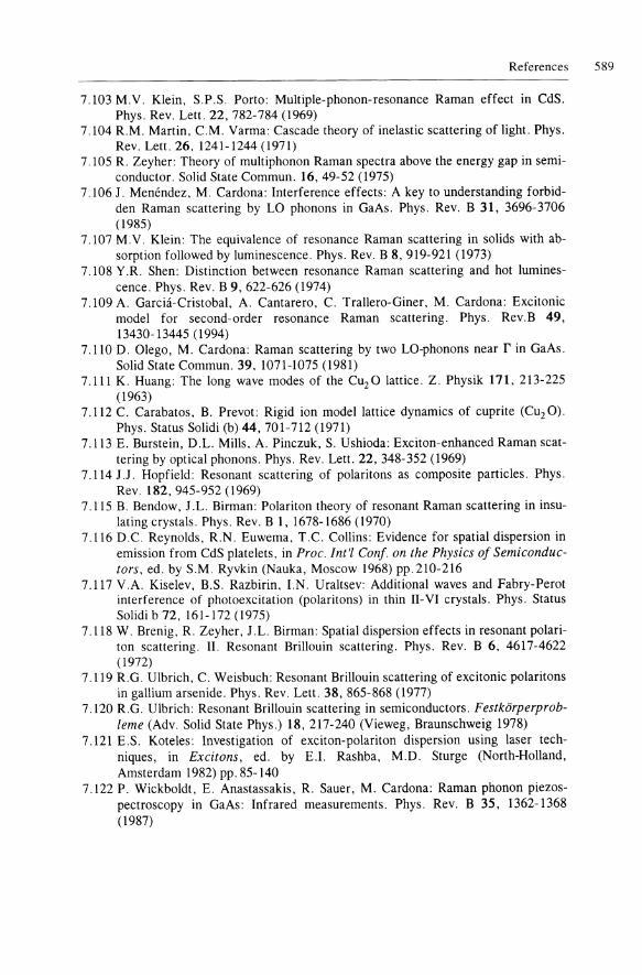
References 589
7.103 M.V. Klein, S.P.S. Porto: Multiple-phonon-resonance Raman effect in CdS. Phys. Rev. Lett. 22, 782-784 (1969)
7.104 R.M. Martin, C.M. Varma: Cascade theory of inelastic scattering of light. Phys. Rev. Lett. 26,1241-1244 (1971)
7.105 R. Zeyher: Theory of multiphonon Raman spectra above the energy gap in semiconductor. Solid State Commun. 16, 49-52 (1975)
7.106 J. Menendez, M. Cardona : Interference effects: A key to understanding f orbidden Raman scattering by LO phonons in GaAs. Phys. Rev. B 31, 3696-3706 (1985)
7.107 M.V. Klein: The equivalence of resonance Raman scattering in solids with absorption followed by luminescence. Phys. Rev. B 8,919-921 (1973)
7.108 Y.R. Shen: Distinction between resonance Raman scattering and hot luminescence. Phys. Rev. B 9,622-626 (1974)
7.109 A. Garcia-Cristobal, A. Cantarero, C. Trallero-Giner, M. Cardona: Excitonic model for second-order resonance Raman scattering. Phys. Rev.B 49, 13430-13445 (1994)
7.110 D. Olego, M. Cardona: Raman scattering by two LO-phonons near r in GaAs. Solid State Commun. 39, 1071-1075 (1981)
7.111 K. Huang: The long wave modes of the Cu20 lattice. Z. Physik 111,213-225 (1963)
7.112 C. Carabatos, B. Prevot: Rigid ion model lattice dynamics of cuprite (Cu20). Phys. Status Solidi (b) 44,701-712 (1971)
7.113 E. Burstein, D.L. Mills, A. Pinczuk, S. Ushioda: Exciton-enhanced Raman scattering by optical phonons. Phys. Rev. Lett. 22, 348-352 (1969)
7.114 J.J. Hopfield: Resonant scattering of polaritons as composite particles. Phys. Rev. 182, 945-952 (1969)
7.115 B. Bendow, J.L. Birman: Polariton theory of resonant Raman scattering in insulating crystals. Phys. Rev. B 1, 1678-1686 (1970)
7.116 D.C. Reynolds, R.N. Euwema, T.C. Collins: Evidence for spatial dispersion in emission from CdS platelets, in Proc. Int'l Conf. on the Physics of Semiconductors, ed. by S.M. Ryvkin (Nauka, Moscow 1968) pp.210-216
7.117 V.A. Kiselev, B.S. Razbirin, LN. Uraltsev: Additional waves and Fabry-Perot interference of photoexcitation (polaritons) in thin II-VI crystals. Phys. Status Solidi b 72,161-172 (1975)
7.118 W. Brenig, R. Zeyher, J.L. Birman: Spatial dispersion effects in resonant polariton scattering. II. Resonant Brillouin scattering. Phys. Rev. B 6, 4617-4622 (1972)
7.119 R.G. Ulbrich, C. Weisbuch: Resonant Brillouin scattering of excitonic polaritons in gallium arsenide. Phys. Rev. Lett. 38, 865-868 (1977)
7.120 R.G. Ulbrich: Resonant Brillouin scattering in semiconductors. Festkorperprobleme (Adv. Solid State Phys.) 18, 217-240 (Vieweg, Braunschweig 1978)
7.121 E.S. Koteles: Investigation of exciton-polariton dispersion using laser techniques, in Excitons, ed. by E.!. Rashba, M.D. Sturge (North-Holland, Amsterdam 1982) pp. 85-140
7.122 P. Wickboldt, E. Anastassakis, R. Sauer, M. Cardona: Raman phonon piezospectroscopy in GaAs: Infrared measurements. Phys. Rev. B 35, 1362-1368 (1987)
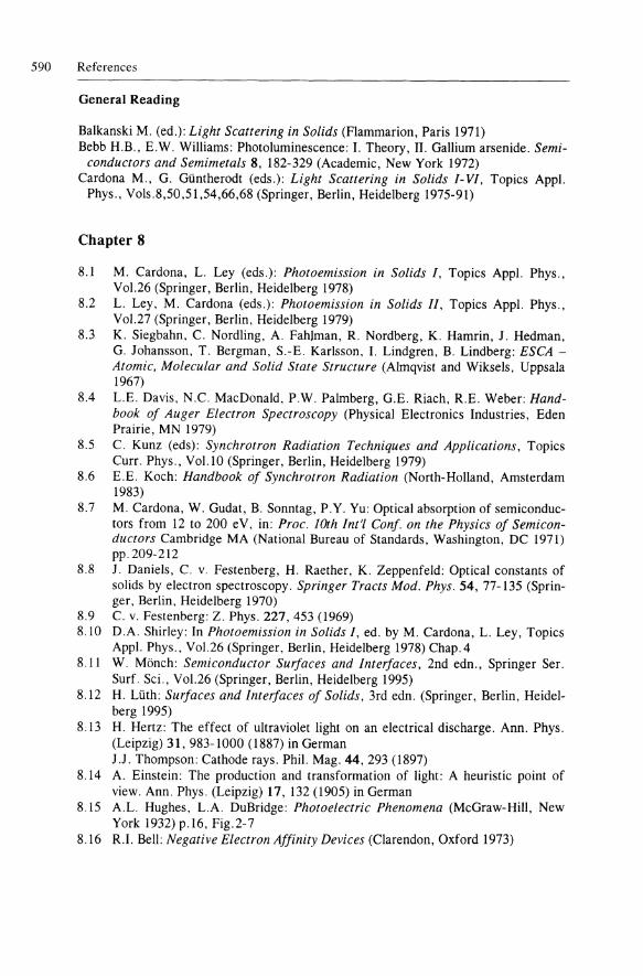
590 References
General Reading
Balkanski M. (ed.): Light Scattering in Solids (Flammarion, Paris 1971) Bebb H.B., E.W. Williams: Photoluminescence: I. Theory, II. Gallium arsenide. Semi
conductors and Semimetals 8, 182-329 (Academic, New York 1972) Cardona M., G. Gtintherodt (eds.): Light Scattering in Solids I-VI, Topics Appl.
Phys., Vols.8,50,51,54,66,68 (Springer, Berlin, Heidelberg 1975-91)
Chapter 8
8.1 M. Cardona, L. Ley (eds.): Photoemission in Solids I, Topics Appl. Phys., Vol.26 (Springer, Berlin, Heidelberg 1978)
8.2 L. Ley, M. Cardona (eds.): Photoemission in Solids II, Topics Appl. Phys., Vol.27 (Springer, Berlin, Heidelberg 1979)
8.3 K. Siegbahn, C. Nordling, A. Fahlman, R. Nordberg, K. Hamrin, J. Hedman, G. Johansson, T. Bergman, S.-E. Karlsson, I. Lindgren, B. Lindberg: ESCA -Atomic, Molecular and Solid State Structure (Almqvist and Wiksels, Uppsala 1967)
8.4 L.E. Davis, N.C. MacDonald, P.W. Palmberg, G.E. Riach, R.E. Weber: Handbook of Auger Electron Spectroscopy (Physical Electronics Industries, Eden Prairie, MN 1979)
8.5 C. Kunz (eds): Synchrotron Radiation Techniques and Applications, Topics Curr. Phys., Vo1.10 (Springer, Berlin, Heidelberg 1979)
8.6 E.E. Koch: Handbook of Synchrotron Radiation (North-Holland, Amsterdam 1983)
8.7 M. Cardona, W. Gudat, B. Sonntag, P.Y. Yu: Optical absorption of semiconductors from 12 to 200 eV, in: Proc. 10th Int'l Conf. on the Physics of Semiconductors Cambridge MA (National Bureau of Standards, Washington, DC 1971) pp.209-212
8.8 J. Daniels, C. v. Festenberg, H. Raether, K. ZeppenfeId: Optical constants of solids by electron spectroscopy. Springer Tracts Mod. Phys. 54, 77-135 (Springer, Berlin, Heidelberg 1970)
8.9 C. v. Festenberg: Z. Phys. 227, 453 (1969) 8.10 D.A. Shirley: In Photo emission in Solids I, ed. by M. Cardona, L. Ley, Topics
Appl. Phys., Vol.26 (Springer, Berlin, Heidelberg 1978) Chap.4 8.11 W. Mi:inch: Semiconductor Surfaces and Interfaces, 2nd edn., Springer Ser.
Surf. Sci., Vol.26 (Springer, Berlin, Heidelberg 1995) 8.12 H. Ltith: Surfaces and Interfaces of Solids, 3rd edn. (Springer, Berlin, Heidel
berg 1995) 8.13 H. Hertz: The effect of ultraviolet light on an electrical discharge. Ann. Phys.
(Leipzig) 31, 983-1000 (1887) in German J.1. Thompson: Cathode rays. Phil. Mag. 44, 293 (1897)
8.14 A. Einstein: The production and transformation of light: A heuristic point of view. Ann. Phys. (Leipzig) 17,132 (1905) in German
8.15 A.L. Hughes, L.A. DuBridge: Photoelectric Phenomena (McGraw-Hill, New York 1932)p.16, Fig.2-7
8.16 R.I. Bell: Negative Electron Affinity Devices (Clarendon, Oxford 1973)
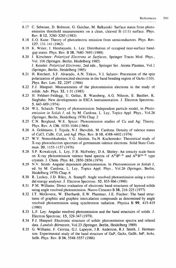
References 591
8.17 C. Sebenne, D. Bolmont, G. Guichar, M. Balkanski: Surface states from photoemission threshold measurements on a clean, cleaved Si (111) surface. Phys. Rev. B 12, 3280-3285 (1983)
8.18 E.O. Kane: Theory of photoelectric emission from semiconductors. Phys. Rev. 127,131-141 (1962)
8.19 K. Winer, I. Hirabayashi, L. Ley: Distribution of occupied near-surface bandgap states. Phys. Rev. B 38, 7680-7693 (1988)
8.20 1. Kirschner: Polarized Electrons at Surfaces, Springer Tracts Mod. Phys., Vol. 106 (Springer, Berlin, Heidelberg 1985) 1. Kessler: Polarized Electrons, 2nd edn., Springer Ser. Atoms Plasmas, VoU (Springer, Berlin, Heidelberg 1985)
8.21 H. Riechert, S.F. Alvarado, A.N. Titkov, V.1. Safarev: Precession of the spin polarization of photoexcited electrons in the band bending region of GaAs (110). Phys. Rev. Lett. 52,2297 (1984)
8.22 F.I. Himpsel: Measurements of the photoemission electrons in the study of solids. Adv. Phys. 32,1-51 (1983)
8.23 H. Feldner-Feldegg, U. Gelius, B. Wannberg, A.G. Nilsson, E. Basilier, K. Siegbahn: New developments in ESCA instrumentation. J. Electron Spectrosc. 5,643-689 (1974)
8.24 W.L. Schaich: Theory of photoemission: Independent particle model, in Photoemission in Solids I, ed. by M. Cardona, L. Ley, Topics Appl. Phys., Vol.26 (Springer, Berlin, Heidelberg 1978) Chap. 2
8.25 C.N. Berglund, W.E. Spicer: Photoemission studies of Cu and Ag: Theory. Phys. Rev. A 136,1030-1044 (1964)
8.26 A. Goldmann, J. Tejeda, N.I. Shevchik, M. Cardona: Density of valence states of CuCl, CuBr, CuI, and Agl. Phys. Rev. B 10,4388-4402 (1974)
8.27 W.V. Nemoshkalenko, V.G. Aleshin, Yu.N. Kucherenko: Theoretical study of X-ray photoelectron spectrum of germanium valence electr~ns. Solid State Commun. 20, 1155-1157 (1976)
8.28 S.P. Kowalczyk, L. Ley, F.R. McFeeley, D.A. Shirley: An ionicity scale basis on X-ray photoemission valence band spectra of ANB8-N and ANBIO-N type crystals. 1. Chern. Phys. 61, 2850-2856 (1974)
8.29 N.V. Smith: Angular dependent phototemission. In Photoemission in Solids I, ed. by M. Cardona, L. Ley, Topics Appl. Phys., Vol.26 (Springer, Berlin, Heidelberg 1978) Chap. 6
8.30 R. Leckey, J.D. Riley, A. Stampfl: Angle resolved photoemission using a toroidal energy analyser. 1. Electron Spectrosc. 52, 855-866 (1990)
8.31 P.M. Williams: Direct evaluation of electronic band structures of layered solids using angle resolved photoemission. Nuovo Cimento B 38, 216-225 (1977)
8.32 LT. McGovern, W. Eberhardt, E.W. Plummer, J.E. Fischer: The band structures of graphite and graphite intercalation compounds as determined by angle resolved photoemission using synchrotron radiation. Physica B 99, 415-419 (1980)
8.33 L.F. Ley: Angular resolved photoemission and the band structuire of solids. J. Electron Spectrosc. 15,329-347 (1979)
8.34 F.I. Himpsel: Electronic structure of solids: photoemission spectra and related data. Landolt-Bornstein, Vol.23 (Springer, Berlin, Heidelberg 1989)
8.35 G. Williams, F. Cerrina, G.I. Lapeyre, 1.R. Anderson, R.I. Smith, J. Hermanson: Experimental study of the band structure of GaP, GaAs, GaSb, InP, InAs, InSb. Phys. Rev. B 34,5548-5557 (1986)
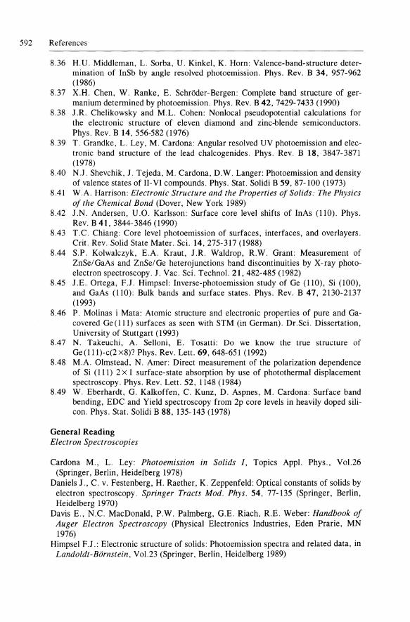
592 References
8.36 H. U. Middleman, L. Sorba, U. Kinkel, K. Horn: Valence-band-structure determination of InSb by angle resolved photoemission. Phys. Rev. B 34, 957-962 (1986)
8.37 X.H. Chen, W. Ranke, E. SchrOder-Bergen: Complete band structure of germanium determined by photoemission. Phys. Rev. B 42, 7429-7433 (1990)
8.38 J .R. Chelikowsky and M.L. Cohen: Nonlocal pseudopotential calculations for the electronic structure of eleven diamond and zinc-blende semiconductors. Phys. Rev. B 14, 556-582 (1976)
8.39 T. Grandke, L. Ley, M. Cardona: Angular resolved UV photoemission and electronic band structure of the lead chalcogenides. Phys. Rev. B 18, 3847-3871 ( 1978)
8.40 N.J. Shevchik, J. Tejeda, M. Cardona, D.W. Langer: Photoemission and density of valence states of II- VI compounds. Phys. Stat. Solidi B 59, 87-100 (1973)
8.41 W.A. Harrison: Electronic Structure and the Properties of Solids: The Physics of the Chemical Bond (Dover, New York 1989)
8.42 J.N. Andersen, U .0. Karlsson: Surface core level shifts of InAs (110). Phys. Rev. B 41,3844-3846 (1990)
8.43 T.C. Chiang: Core level photoemission of surfaces, interfaces, and overlayers. Crit. Rev. Solid State Mater. Sci. 14,275-317 (1988)
8.44 S.P. Kolwalczyk, E.A. Kraut, J.R. Waldrop, R.W. Grant: Measurement of ZnSe/GaAs and ZnSe/Ge heterojunctions band discontinuities by X-ray photoelectron spectroscopy. J. Vac. Sci. Techno!. 21, 482-485 (1982)
8.45 LE. Ortega, FJ. HimpseJ: Inverse-photoemission study of Ge (110), Si (100), and GaAs (110): Bulk bands and surface states. Phys. Rev. B 47, 2130-2137 (1993)
8.46 P. Molinas i Mata: Atomic structure and electronic properties of pure and Gacovered Ge (111) surfaces as seen with STM (in German). Dr.Sci. Dissertation, University of Stuttgart (1993)
8.47 N. Takeuchi, A. Selloni, E. Tosatti: Do we know the true structure of Ge(I11)-c(2x8)? Phys. Rev. Lett. 69, 648-651 (1992)
8.48 M.A. Olmstead, N. Amer: Direct measurement of the polarization dependence of Si (111) 2 x 1 surface-state absorption by use of photothermal displacement spectroscopy. Phys. Rev. Lett. 52, 1148 (1984)
8.49 W. Eberhardt, G. Kalkoffen, C. Kunz, D. Aspnes, M. Cardona: Surface band bending, EDC and Yield spectroscopy from 2p core levels in heavily doped silicon. Phys. Stat. Solidi B 88,135-143 (1978)
General Reading Electron Spectroscopies
Cardona M., L. Ley: Photoemission in Solids /, Topics Appl. Phys., Vo!.26 (Springer, Berlin, Heidelberg 1978)
Daniels J., C. v. Festenberg, H. Raether, K. Zeppenfeld: Optical constants of solids by electron spectroscopy. Springer Tracts Mod. Phys. 54, 77-135 (Springer, Berlin, Heidelberg 1970)
Davis E., N.C. MacDonald, P.W. Palmberg, G.E. Riach, R.E. Weber: Handbook of Auger Electron Spectroscopy (Physical Electronics Industries, Eden Prarie, MN 1976)
Himpsel F.J.: Electronic structure of solids: Photoemission spectra and related data, in Landoldt-Bornstein, Vo!.23 (Springer, Berlin, Heidelberg 1989)
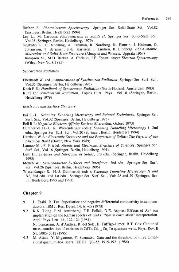
References 593
Hiifner S.: Photoelectron Spectroscopy, Springer Ser. Solid-State Sci., Vo!.82 (Springer, Berlin, Heidelberg 1994)
Ley L., M. Cardona: Photoemission in Solids ll, Springer Ser. Solid-State Sci., Vo!.35 (Springer, Berlin, Heidelberg, 1979)
Siegbahn K., C. Nordling, A. Fahlman, R. Nordberg, K. Hamrin, 1. Hedman, G. Johansson, T. Bergman, S.-E. Karlsson, I. Lindren, B. Lindberg: ESCA-Atomic, Molecular and Solid State Structure (Almqvist and Wiksels, Uppsala 1967)
Thompson M., M.D. Barker, A. Christio, J .F. Tysan: Auger Electron Spectroscopy (Wiley, New York 1985)
Synchrotron Radiation
Eberhardt W. (ed.): Applications of Synchrotron Radiation, Springer Ser. Surf. Sci., Vo1.35 (Springer, Berlin, Heidelberg 1995)
Koch E.E.: Handbook of Synchrotron Radiation (North-Holland, Amsterdam 1983) Kunz C.: Synchrotron Radiation, Topics Curr. Phys., Vol.l0 (Springer, Berlin,
Heidelberg 1979)
Electronic and Surface Structure
Bai C.-L.: Scanning Tunneling Microscopy and Related Techniques, Springer Ser. Surf. Sci., Vo1.32 (Springer, Berlin, Heidelberg 1995)
Bell R.I.: Negative Electron Affinity Devices (Clarendon, Oxford 1973) Giintherodt H.-J., R. Wiesendanger (eds.): Scanning Tunneling Microscopy I, 2nd
edn., Springer Ser. Surf. Sci., Vo!.20 (Springer, Berlin, Heidelberg 1994) Harrison W.A.: Electronic Structure and the Properties of Solids: The Physics of the
Chemical Bond (Dover, New York 1989) Lannoo M., P. Friedel: Atomic and Electronic Structure of Surfaces, Springer Ser.
Surf. Sci., Vo1.16 (Springer, Berlin, Heidelberg 1991) Liith H.: Surfaces and Interfaces of Solids, 3rd edn. (Springer, Berlin, Heidelberg
1995) M6nch W.: Semiconductor Surfaces and Interfaces, 2nd edn., Springer Ser. Surf.
Sci., Vo1.26 (Springer, Berlin, Heidelberg 1995) Wiesendanger R., H.-J. Giintherodt (eds.): Scanning Tunneling Microscopy II and
Ill, 2nd edn. and 1st edn., Springer Ser. Surf. Sci., Vols.28 and 29 (Springer, Berlin, Heidelberg 1995 and 1993)
Chapter 9
9.1 L. Esaki, R. Tsu: Superlattice and negative differential conductivity in semiconductors. IBM 1. Res. Deve!. 14,61-65 (1970)
9.2 K.K. Tiong, P.M. Amirtharaj, F.H. Pollak, D.E. Aspnes: Effects of As+ ion implantation on the Raman spectra of GaAs: "Spatial correlation" interpretation. App!. Phys. Lett. 44, 122-124 (1984) N. Tomassini, A. d'Andrea, R. del Sole, H. Tuffigo-Ulmer, R.T. Cox: Center of mass quantization of excitons in CdTe/Cd1_xZnx Te quantum wells. Phys. Rev. B 51,5005-5012 (1995)
9.3 M. Asada, Y. Migamoto, Y. Suematsu: Gain and the threshold of three dimensional quantum-box lasers. IEEE 1. QE-22, 1915-1921 (1986)
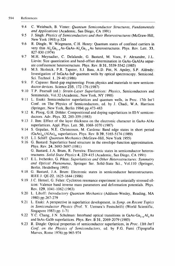
594 References
9.4 C. Weisbuch, B. Vinter: Quantum Semiconductor Structures, Fundamentals and Applications (Academic, San Diego, CA 1991)
9.5 J. Singh: Physics of Semiconductors and their Heterostructures (McGraw-Hill, New York 1993) p.524
9.6 R. Dingle, W. Wiegmann, C.H. Henry: Quantum states of confined carriers in very thin AlxGa'_xAs-GaAs-AlxGa'_xAs heterostructures. Phys. Rev. Lett. 33, 827-830 (1974)
9.7 M.H. Meynadier, C. Delalande, G. Bastard, M. Voos, F. Alexandre, J.L. Lievin: Size quantization and band-offset determination in GaAs-GaA1As separate confinement heterostructure. Phys. Rev. B 31, 5539-5542 (1985)
9.8 M.S. Skolnick, P.R. Tapster, SJ. Bass, A.D. Pitt, N. Apsley, S.P. Aldredy: Investigation of InGaAs-InP quantum wells by optical spectroscopy. Semicond. Sci. Techno!. 1,29-40 (1986)
9.9. F. Capasso: Band-gap engineering: From physics and materials to new semiconductor devices. Science 235, 172-176 (1987)
9.10 T.P. Pearsall (ed.): Strain-Layer Superlattices: Physics, Semiconductors and Semimetals, Vo1.32 (Academic, New York, NY 1990)
9.11 L. Esaki: Semiconductor superlattices and quantum wells, in Proc. 17th Int'l Conf. on The Physics of Semiconductors, ed. by J. Chadi, W.A. Harrison (Springer, New York, Berlin 1984) pp.473-483
9.12 K. Ploog, G.H. Dahler: Compositional and doping superlattices in III-V semiconductors. Adv. Phys. 32, 285-359 (1983)
9.13 J. Ihm: Effect of the layer thickness on the electronic character in GaAs-A1As superlattices. App!. Phys. Lett. 50,1068-1070 (1987)
9.14 S. Gopalan, N.E. Christensen, M. Cardona: Band edge states in short period (GaAs)m (A1As)m superlattices. Phys. Rev. B 39, 5165-5174 (1989)
9.15 L.I. Schiff: Quantum Mechanics (McGraw-Hill, New York 1955) 9.16 G. Bastard: Superlattice band structure in the envelope-function approximation.
Phys. Rev. 24, 5693-5697 (1981) G. Bastard, J .A. Brum, R. Ferreira: Electronic states in semiconductor heterostructures. Solid State Physics 4, 229-415 (Academic, San Diego, CA 1991)
9.17 E.L. Ivchenko, G. Pikus: Superlattices and Other Heterostructures: Symmetry and Optical Phenomena, Springer Ser. Solid-State Sci., Vol.1l0 (Springer, Berlin, Heidelberg 1995)
9.18 G. Bastard, J .A. Brum: Electronic states in semiconductor heterostructures. IEEE J. QE-22, 1625-1644 (1986)
9.19 J.C. Hensel, G. Feher: Cyclotron resonance experiment in uniaxially stressed silicon: Valence band inverse mass parameters and deformation potentials. Phys. Rev. 129, 1041-1062 (1963)
9.20 L. Liboff: Introductory Quantum Mechanics (Addison-Wesley, Reading, MA 1980) pp.267-279
9.21 L. Esaki: A perspective in superlattice development, in Symp. on Recent Topics in Semiconductor Physics (Prof. Y. Uemura's Festschrift) (World Scientific, Singapore 1983) pp. 1-71
9.22 Y.C. Chang, J.N. Schulman: Interband optical transitions in GaAs-Ga'_xAlxAs and InAs-GaSb superlattices. Phys. Rev. B 31, 2069-2079 (1985)
9.23 R. Dingle: Optical properties of semiconductor superlattices, in Proc. 13th Int'l Conf. on the Physics of Semiconductors, ed. by F.G. Fumi (Tipografia Marves, Rome 1976) pp.965-974
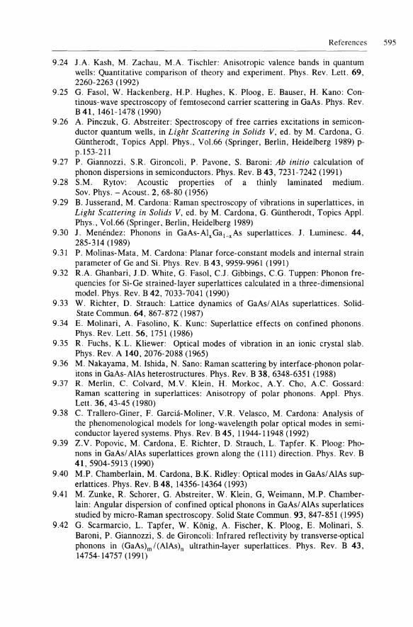
References 595
9.24 1.A. Kash, M. Zachau, M.A. Tischler: Anisotropic valence bands in quantum wells: Quantitative comparison of theory and experiment. Phys. Rev. Lett. 69, 2260-2263 (1992)
9.25 G. Fasol, W. Hackenberg, H.P. Hughes, K. Ploog, E. Bauser, H. Kano: Continous-wave spectroscopy of femtosecond carrier scattering in GaAs. Phys. Rev. B 41,1461-1478 (1990)
9.26 A. Pinczuk, G. Abstreiter: Spectroscopy of free carries excitations in semiconductor quantum wells, in Light Scattering in Solids V, ed. by M. Cardona, G. Giintherodt, Topics Appl. Phys., Vol.66 (Springer, Berlin, Heidelberg 1989) pp.153-211
9.27 P. Giannozzi, S.R. Gironcoli, P. Pavone, S. Baroni: Ab initio calculation of phonon dispersions in semiconductors. Phys. Rev. B 43, 7231-7242 (1991)
9.28 S.M. Rytov: Acoustic properties of a thinly laminated medium. Sov. Phys. - Acoust. 2, 68-80 (1956)
9.29 B. Jusserand, M. Cardona: Raman spectroscopy of vibrations in superlattices, in Light Scattering in Solids V, ed. by M. Cardona, G. Giintherodt, Topics Appl. Phys., Vol.66 (Springer, Berlin, Heidelberg 1989)
9.30 1. Menendez: Phonons in GaAs-AlxGa1_xAs superlattices. J. Luminesc. 44, 285-314 (1989)
9.31 P. Molinas-Mata, M. Cardona: Planar force-constant models and internal strain parameter of Ge and Si. Phys. Rev. B 43,9959-9961 (1991)
9.32 R.A. Ghanbari, J.D. White, G. Fasol, C.J. Gibbings, e.G. Tuppen: Phonon frequencies for Si-Ge strained-layer superlattices calculated in a three-dimensional model. Phys. Rev. B 42, 7033-7041 (1990)
9.33 W. Richter, D. Strauch: Lattice dynamics of GaAsl AlAs superlattices. SolidState Commun. 64, 867-872 (1987)
9.34 E. Molinari, A. Fasolino, K. Kunc: Superlattice effects on confined phonons. Phys. Rev. Lett. 56,1751 (1986)
9.35 R. Fuchs, K.L. Kliewer: Optical modes of vibration in an ionic crystal slab. Phys. Rev. A 140,2076-2088 (1965)
9.36 M. Nakayama, M. Ishida, N. Sano: Raman scattering by interface-phonon polaritons in GaAs-AlAs heterostructures. Phys. Rev. B 38, 6348-6351 (1988)
9.37 R. Merlin, C. Colvard, M.V. Klein, H. Morkoc, A.Y. Cho, A.C. Gossard: Raman scattering in superlattices: Anisotropy of polar phonons. Appl. Phys. Lett. 36,43-45 (1980)
9.38 e. Trallero-Giner, F. Garcia-Moliner, V.R. Velasco, M. Cardona: Analysis of the phenomenological models for long-wavelength polar optical modes in semiconductor layered systems. Phys. Rev. B 45, 11944-11948 (1992)
9.39 Z.V. Popovic, M. Cardona, E. Richter, D. Strauch, L. Tapfer. K. Ploog: Phonons in GaAsl AlAs superlattices grown along the (111) direction. Phys. Rev. B 41,5904-5913 (1990)
9.40 M.P. Chamberlain, M. Cardona, B.K. Ridley: Optical modes in GaAsl AlAs superlattices. Phys. Rev. B 48,14356-14364 (1993)
9.41 M. Zunke, R. Schorer, G. Abstreiter, W. Klein, G, Weimann, M.P. Chamberlain: Angular dispersion of confined optical phonons in GaAsl AlAs superlatices studied by micro-Raman spectroscopy. Solid State Commun. 93, 847-851 (1995)
9.42 G. Scarmarcio, L. Tapfer, W. Konig, A. Fischer, K. Ploog, E. Molinari, S. Baroni, P. Giannozzi, S. de Gironcoli: Infrared reflectivity by transverse-optical phonons in (GaAs)m/(AlAs)n ultrathin-layer superlattices. Phys. Rev. B 43, 14754-14757 (1991)
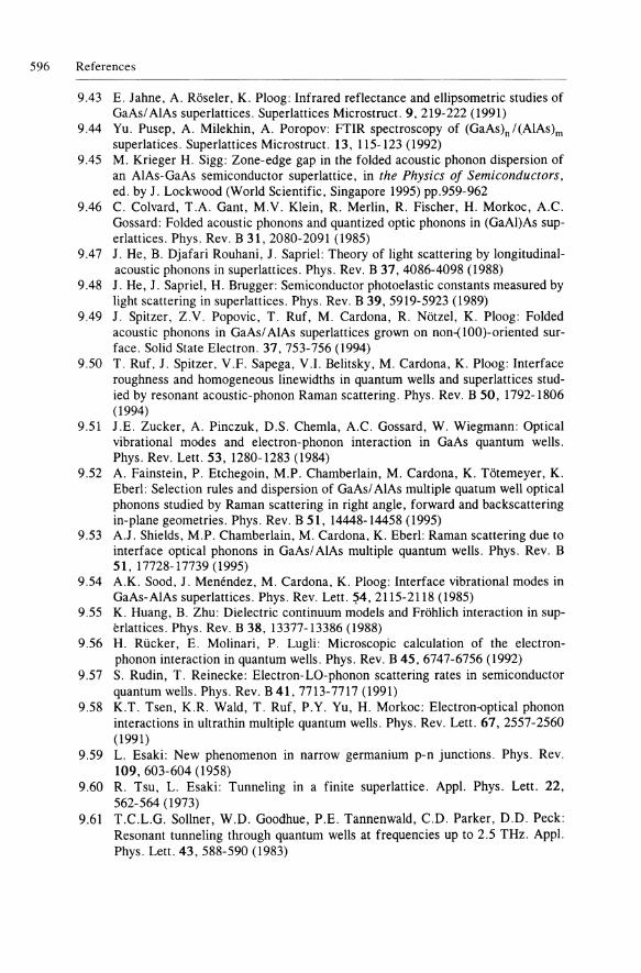
596 References
9.43 E. Iahne, A. Roseler, K. Ploog: Infrared reflectance and ellipsometric studies of GaAsl AlAs superlattices. Superlattices Microstruct. 9, 219-222 (1991)
9.44 Yu. Pusep, A. Milekhin, A. Poropov: FTIR spectroscopy of (GaAs)n/(AlAs)m superlatices. Superlattices Microstruct. 13, 115-123 (1992)
9.45 M. Krieger H. Sigg: Zone-edge gap in the folded acoustic phonon dispersion of an AlAs-GaAs semiconductor superlattice, in the Physics of Semiconductors, ed. by 1. Lockwood (World Scientific, Singapore 1995) pp.959-962
9.46 C. Colvard, T.A. Gant, M.V. Klein, R. Merlin, R. Fischer, H. Morkoc, A.C. Gossard: Folded acoustic phonons and quantized optic phonons in (GaAI)As superlattices. Phys. Rev. B 31, 2080-2091 (1985)
9.47 1. He, B. Djafari Rouhani. 1. Sapriel: Theory of light scattering by longitudinalacoustic phonons in superlattices. Phys. Rev. B 37, 4086-4098 (1988)
9.48 1. He, 1. Sapriel, H. Brugger: Semiconductor photoelastic constants measured by light scattering in superlattices. Phys. Rev. B 39,5919-5923 (1989)
9.49 1. Spitzer, Z.V. Popovic, T. Rut, M. Cardona, R. Notzel, K. Ploog: Folded acoustic phonons in GaAsl AlAs superlattices grown on non-(IOO)-oriented surface. Solid State Electron. 37, 753-756 (1994)
9.50 T. Ruf, 1. Spitzer, V.F. Sapega, V.1. Belitsky, M. Cardona, K. Ploog: Interface roughness and homogeneous line widths in quantum wells and superlattices studied by resonant acoustic-phonon Raman scattering. Phys. Rev. B 50,1792-1806 (1994)
9.51 I.E. Zucker, A. Pinczuk, D.S. Chemla, A.C. Gossard, W. Wiegmann: Optical vibrational modes and electron-phonon interaction in GaAs quantum wells. Phys. Rev. Lett. 53,1280-1283 (1984)
9.52 A. Fainstein, P. Etchegoin, M.P. Chamberlain, M. Cardona, K. Totemeyer, K. Eberl: Selection rules and dispersion of GaAsl AlAs multiple quatum well optical phonons studied by Raman scattering in right angle, forward and backscattering in-plane geometries. Phys. Rev. B 51, 14448-14458 (1995)
9.53 A.I. Shields, M.P. Chamberlain, M. Cardona, K. Eberl: Raman scattering due to interface optical phonons in GaAsl AlAs multiple quantum wells. Phys. Rev. B 51,17728-17739(1995)
9.54 A.K. Sood, 1. Menendez, M. Cardona, K. Ploog: Interface vibrational modes in GaAs-AlAs superlattices. Phys. Rev. Lett. ~4, 2115-2118 (1985)
9.55 K. Huang, B. Zhu: Dielectric continuum models and Frohlich interaction in superlattices. Phys. Rev. B 38,13377-13386 (1988)
9.56 H. Riicker, E. Molinari, P. Lugli: Microscopic calculation of the electronphonon interaction in quantum wells. Phys. Rev. B 45,6747-6756 (1992)
9.57 S. Rudin, T. Reinecke: Electron-LO-phonon scattering rates in semiconductor quantum wells. Phys. Rev. B 41, 7713-7717 (1991)
9.58 K.T. Tsen, K.R. Wald, T. Rut, P.Y. Yu, H. Morkoc: Electron-optical phonon interactions in ultrathin multiple quantum wells. Phys. Rev. Lett. 67, 2557-2560 (1991)
9.59 L. Esaki: New phenomenon in narrow germanium p-n junctions. Phys. Rev. 109,603-604 (1958)
9.60 R. Tsu, L. Esaki: Tunneling in a finite superlattice. Appl. Phys. Lett. 22, 562-564 (1973)
9.61 T.C.L.G. Sollner, W.D. Goodhue, P.E. Tannenwald, C.D. Parker, D.D. Peck: Resonant tunneling through quantum wells at frequencies up to 2.5 THz. Appl. Phys. Lett. 43, 588-590 (1983)
References 597
9.62 A. Silbille, J .F. Palmier, H. Wang, F. Mollot: Observation of Esaki-Tsu negative differential velocity in GaAsl AlAs superlattices. Phys. Rev. Lett. 64. 52-55 (1990)
9.63 J.F. Palmier: Miniband transport and resonant tunneling in superlattices, in Resonant Tunneling in Semiconductors, ed. by L.L. Chang (Plenum, New York 1991) pp.361-375
9.64 E. Merzbacher: Quantum Mechanics (Wiley, New York 1961) pp.94-97 9.65 D.Z.- Y. Ting, S.K. Kirby, T.C. McGill: Interface roughness effects in resonant
tunneling structures. App!. Phys. Lett. 64, 2004-2006 (1994) 9.66 T.P.E. Broekaert, W. Lee, C.G. Fonstad: Pseudomorphic In0.53 Ga0 .47 Asl
AIAslInAs resonant tunneling diodes with peak-to-valley current ratios of 30 at room temperature. App!. Phys. Lett. 53. 1545-1547 (1988)
9.67 K. von Klitzing, G. Dorda, M. Pepper: New method for high-accuracy determination of the fine-structure constant based on quantum Hall resistance. Phys. Rev. Lett. 45. 494-497 (1980)
9.68 D.C. Tsui, H.L. Stormer. A.C. Gossard: Two-dimensional magnetotransport in the extreme quantum limit. Phys. Rev. Lett. 45,1559-1562 (1982)
9.69 L.D. Landau: Diamagnetism of metals (in German). Z. Physik 64, 629-637 (1930)
9.70 L.D. Landau, E.N. Lifshitz: Quantum Mechanics. 3rd edn. (Pergamon. Oxford 1977)
9.71 J.M. Ziman: Principles of the Theory of Solids, 2nd edn. (Cambridge Univ. Press, Cambridge 1972) pp.313-326
9.72 M. Brodsky (ed.): Amorphous Semiconductors, 2nd edn., Topics App!. Phys., Vo1.36 (Springer. Berlin. Heidelberg 1985)
9.73 J. TaucAmorphous and Liquid Semiconductors (Plenum, New York 1974) 9.74 R. Loudon: Raman effect in crystals. Adv. Phys. 13. 423-482 (1964); erratum
ibid. 14,621 (1965)
General Reading
Growth of Quantum Wells and Superlattices
Herman M.A .. H. Sitter: Molecular Beam Epitaxy, 2nd edn., Springer Ser. Mater. Sci., Vo!.7 (Springer, Berlin, Heidelberg 1996)
Pan ish M.B., H. Temkin: Gas Source Molecular Beam Epitaxy, Springer Ser. Mater. Sci., Vo1.26 (Springer, Berlin, Heidelberg 1993)
Ploog K.: Formation of semiconductor interfaces during molecular beam epitaxy, in Semiconductor Interfaces: Formation and Properties. ed. by G. LeLay, J. Denien, N. Boccara (Springer, Berlin, Heidelberg 1987)
Stradling R.A., P.c. Klipstein (eds.): Growth and Characterization of Semiconductors (Hilger, Bristol, UK 1990)
Properties of Quantum Wells and Superlattices
Dekker A.1.: Solid State Physics (Prentice Hall, Englewood Cliffs, NJ 1957) p.244 Ehrenreich H., D. Turnbull (eds.): Semiconductor Heterostructures and Nanostruc
tures, Adv. Res. App!., Vol.44 (Academic, San Diego, CA 1991) Ivchenko E.L., G. Pikus: Superlattices and Other Heterostructures: Symmetry and
Other Optical Phenomena, Springer Ser. Solid-State Sci., Vol.1l0 (Springer, Berlin, Heidelberg 1995)
598 References
Janssen M., O. Viehweger, V. Fastenrath, J. Hajdu: Introduction to the Theory of the Quantum Hall Effect (VCH, Weinheim 1994)
Jaros M.: Superlattices of Semiconductor Microstructures (Clarendon, Oxford 1985) Jusserand B., M. Cardona: Raman spectroscopy of vibrations in superlattices, in Light
Scattering in Solids V, ed. by M. Cardona, G. Giintherodt, Topics Appl. Phys., Vol.66 (Springer, Berlin, Heidelberg 1989) pp.49-152
Kroemer H.: Theory of heterojunction: A critical review, in Molecular Beam Epitaxy and Heterostructures, ed. by L.L. Chang, K. Ploog (Nijhoff, Dordrecht 1985) pp.331-379
Menendez J.: Phonons in GaAs-AlxGa1_xAs superlattices. J. Luminesc. 44, 285-314 (1989)
Pearsall T.P. (ed.): Strain-Layer Superlattices: Physics, Semiconductors and Semimetals, Vo1.32 (Academic, Orlando, FL 1990)
Pinczuk A., G. Abstreiter: Spectroscopy of free carriers excitations in semiconductor quantum wells, in Light Scattering in Solids V, ed. by M. Cardona, G. Giintherod, Topics Appl. Phys., Vol.66 (Springer, Berlin, Heidelberg 1989) ChapA, pp.153-211
Sapriel J., B. Djafari Rouani: Vibrations in superlattices. Surf. Sci. Rept. 10, 189-275 (1989)
Singh 1.: Physics of Semiconductors and their Heterostructures (McGraw-Hill, New York 1993)
Wang S.: Fundamentals of Semiconductor Theory and Device Physics (Prentice Hall, Englewood Cliffs, NJ 1989)
Weisbuch C., B. Vinter: Quantum Semiconductor Structures, Fundamentals and Applications (Academic, San Diego, CA 1991)
Quantum Hall Effect
Chakraborty T., P. Pietilainen: The Quantum Hall Effects - Fractional and Integral, 2nd edn., Springer Ser. Solid-State Sci., Vol.85 (Springer, Berlin, Heidelberg 1995)
Janssen M., O. Viehweger, U. Fastenrath, 1. Hajdu: Introduction to the Theory of the Integer Quantum Hall Effect (VCH, Weinheim 1994)
McDonald A.H. (ed.): Quantum Hall Effect: A Perspective (Kluwer, Boston 1989) Prange R.E., S.M. Girvin (eds.): The Quantum Hall Effect (Springer, New York, Ber
lin 1990)
Subject Index
A
a-Sn (gray tin) 90 ABCs (additional boundary conditions) 352
Abelian groups 21 Absorption - above the fundamental edge 305 - by bound carriers 301 - by free carriers 297 - coefficient 236 - in GaAs/AIGaAs quantum wells (QW) 358
Absorption edge - direct 255 - indirect 255 - Tauc 551 Absorption spectra - excitons 273, 276, 277 - PinSi 301 , 302 Ac amplifier 218 Acceptors 150 - double ISO Acceptor level - binding energies 170 - diamond- and zincblende-type
semiconductors 164 - energy levels calculated with Baldereschi-
Lipari Hamiltonian 171 - one spherical band approximation 166 Acoustic phonon 38, 102, 357 - electron acoustic-phonon scattering 217 - in CU20 129 - in layered structures 482 - Raman scattering 413 Adatoms 446 Additional boundary conditions 352 Adiabatic approximation 14,99, 281
- for impurity levels 162 Adiabatic bond charge model Ill, 112 - phonon dispersion curves 103 AES (Auger electron spectroscopy) 9
AgGaS2 4 Airy function 313
AIGaAs - direct bandgap 213
Al Ka line excitation for XPS 424 AlAs phonon dispersion 481 Amorphous semiconductors 216, 243 - absorption spectra 551
amorphous Ge 550, 552
amorphous Si 552 - doping effect of hydrogen 552 - preparation 552 defect density in gap 552 optical properties 550 short range order 550
- wave vector nonconservation 249 Angular resolved photoemission - photoelectron spectra 431 - prehistory 558 Angular frequency 237 Angular momentum 156 Angular resolution in photoemission 431 Anharmonic interactions in two-phonon
absorption 293 Anti-Stokes Raman shift 364 Anti-crossing 288, 327, 497 Anti-Stokes Raman scattering 364 Antibonding orbital 78, 79
Antibonding states 65 Antiferromagnetism 4 Antisite defect I SO Appearance potential spectroscopy (APS) 416 ARPES (Angle-resolved photoemission
spectroscopy) 431 , 433, 543 - normal emission 435 Arrhenius plots 343 Arsine 7 As2Se3 4 Associated Laguerre polynomials 271 Asymmetric QW 466
Atomic units 325 - effecti ve 166 Atomically clean surface 238 Auger electron spectroscopy 9,416 - schematic diagram 419
Auto-ionizing state - atomic spectra 281
Average gap 325
600 Subject Index
B
Baldereschi-Lipari Hamiltonian 165 - cubic term 169 Band bending 464 - at interfaces 213 - determination by UPS in Si 453 - effect on UPS core level spectra of Si 452 Band dispersion 63 Band dispersion near a degenerate extremum
point 67 Band index 17 Band nonparabolicity effect on plasma
frequency 328 Band offsets 213, 461 Band structure - calculation by k . P method 63 - calculation by pseudopotential methods 54,
61,93,542 - calculation by tight-binding method 78 - determination by photoemission 433, 436 - - in Ge 445 - - in graphite 435 - GaAs 60 - Ge 60 - - showing optical transitions 258 - historical development 544 - nearly-free electrons in zincblende 43,44 - nearly-free electrons in diamond 48 - Si 49 - valence bands in diamond- and zincblende-
type semiconductors 67, 547 - ZnSe 61 Band-to-band emission lineshape 409 Band-to-band transitions in photoluminescence
339 Bandgap I Bandgap engineering 463 Bandgaps vs lattice constant 463 Bare exciton in CdS 274 Basis functions 29 Basis set 17 Biaxial crystals 236 Binding energies - of acceptors in Ge 304 - of an exciton to pairs of nitrogen atoms 187 - of core electrons 417 - of exciton to ionized donors and acceptors 356 Birefringence 236 BIS (Bremsstrahlung Isochromat Spectra) 416,
444 Bloch functions 16, 152,269 Bloch oscillations 564, 565 Body-centered cubic lattice 19
Bohr radius - effective 166 - exciton 271, 272 Boltzmann constant 237 Boltzmann distribution 197 Boltzmann equation 196 Bond bending force 107 bond charge model 109 - adiabatic (ABCM) III Bond charges 110 Bond stretching force 107 Bond orbitals 78, 79 Bonding states 65 Born approximation 207 Born effective charge 293 Born-Oppenheimer approximation 14,99, 113 Born-von Karman boundary conditions 23 Born-von Karman model 105 Bose-Einstein distribution function 118 Bosons 334 Bound electrons 193 Bound exciton 183,350,394 - emission spectra 354 - recombination spectra of CdS 354 - in GaAsP 187 Bound holes 193 Bragg reflection 57 Bremsstrahlung isochromat spectra 417,444 Bremsstrahlung isochromat spectroscopy 417 Bridgman Method 6 Brillouin scattering 234, 333, 362, 385, 387 - resonant 388 - selection rules 411 - spectra of Ge, Si, GaAs 387, 389 Brillouin tensor 392 Brillouin zone 16 - of the fcc lattice 91 de Broglic electron waves 563 Broken bonds 170 Brooks-Herring approach 207 Bulk modulus 131
c
c(2 x 8)(111) surface of Ge - direct photoemission 447 - energy bands 447 c(8 x 2) reconstruction of (III) Ge surface 446 Callan charge 293 Carrier distribution function - degenerate 343 - drifted 227 Carrier lifetime 216
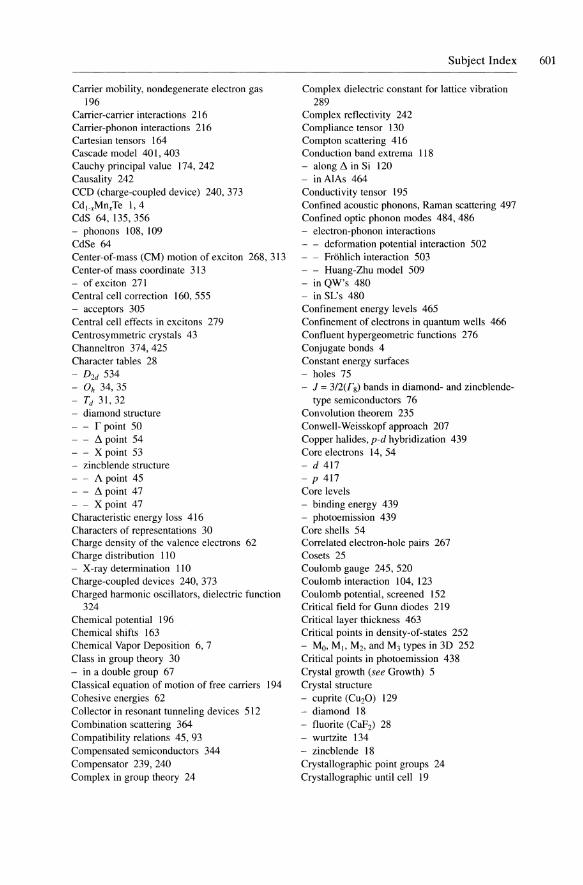
Carrier mobility, nondegenerate electron gas 196
Carrier-carrier interactions 216 Carrier-phonon interactions 216 Cartesian tensors 164 Cascade model 40 I, 403 Cauchy principal value 174, 242 Causality 242 CCD (charge-coupled device) 240,373 Cdl~xMnxTe 1,4 CdS 64, 135, 356 - phonons 108, 109 CdSe 64 Center-of-mass (CM) motion of exciton 268, 313 Center-of mass coordinate 313 - of exciton 271 Central cell correction 160, 555 - acceptors 305 Central cell effects in excitons 279 Centrosymmetric crystals 43 Channeltron 374,425 Character tables 28 - D2d 534 - Oh 34,35 - Td 31,32 - diamond structure
r point 50 - - ~ point 54 - - X point 53 - zincblende structure
1\ point 45 - - ~ point 47 - - X point 47 Characteristic energy loss 416 Characters of representations 30 Charge density of the valence electrons 62 Charge distribution 110 - X-ray determination 110 Charge-coupled devices 240, 373 Charged harmonic oscillators, dielectric function
324 Chemical potential 196 Chemical shifts 163 Chemical Vapor Deposition 6, 7 Class in group theory 30 - in a double group 67 Classical equation of motion of free carriers 194 Cohesi ve energies 62 Collector in resonant tunneling devices 512 Combination scattering 364 Compatibility relations 45, 93 Compensated semiconductors 344 Compensator 239,240 Complex in group theory 24
Subject Index 601
Complex dielectric constant for lattice vibration 289
Complex reflectivity 242 Compliance tensor 130 Compton scattering 416 Conduction band extrema 118 - along ~ in Si 120 - in AlAs 464 Conductivity tensor 195 Confined acoustic phonons, Raman scattering 497 Confined optic phonon modes 484, 486 - electron-phonon interactions
deformation potential interaction 502 - - Frohlich interaction 503 - - Huang-Zhu model 509 - in QW's 480 - in SL's 480 Confinement energy levels 465 Confinement of electrons in quantum wells 466 Confluent hypergeometric functions 276 Conjugate bonds 4 Constant energy surfaces - holes 75 - J = 312(rs) bands in diamond- and zincblende-
type semiconductors 76 Convolution theorem 235 Conwell-Weisskopf approach 207 Copper halides, p-d hybridization 439 Core electrons 14, 54 - d 417 - P 417 Core levels - binding energy 439 - photoemission 439 Core shells 54 Correlated electron-hole pairs 267 Cosets 25 Coulomb gauge 245, 520 Coulomb interaction 104, 123 Coulomb potential, screened 152 Critical field for Gunn diodes 219 Critical layer thickness 463 Critical points in density-of-states 252 - Mo, Mb M2, and M3 types in 3D 252 Critical points in photoemission 438 Crystal growth (see Growth) 5 Crystal structure - cuprite (CU20) 129 - diamond 18 - fluorite (CaF2) 28 - wurtzite 134 - zincblende 18 Crystallographic point groups 24 Crystallographic until cell 19
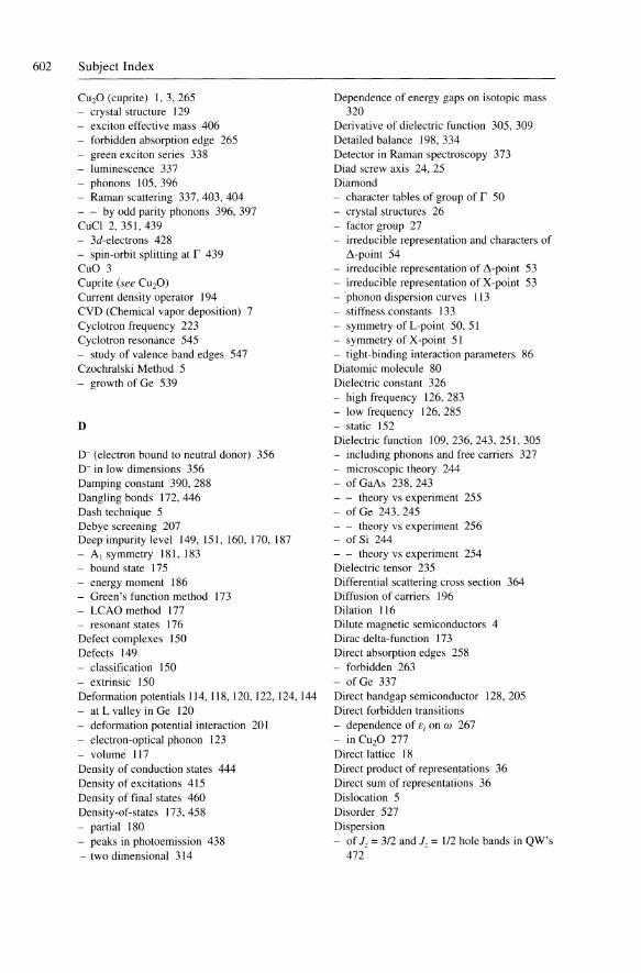
602 Subject Index
CU20 (cuprite) 1,3,265 - crystal structure 129 - exciton effective mass 406 - forbidden absorption edge 265 - green exciton series 338 - luminescence 337 - phonons 105, 396 - Raman scattering 337,403,404 - - by odd parity phonons 396, 397 CuCI 2, 351, 439 - 3d-electrons 428 - spin-orbit splitting at r 439 CuO 3 Cuprite (see CU20) Current density operator 194 CVD (Chemical vapor deposition) 7 Cyclotron frequency 223 Cyclotron resonance 545 - study of valence band edges 547 Czochralski Method 5 - growth of Ge 539
D
D- (electron bound to neutral donor) 356 D- in low dimensions 356 Damping constant 390, 288 Dangling bonds 172,446 Dash technique 5 Debye screening 207 Deep impurity level 149, 151, 160, 170, 187 - Al symmetry 181, 183 - bound state 175 - energy moment 186 - Green's function method 173 - LCAO method 177 - resonant states 176 Defect complexes 150 Defects 149 - classification 150 - extrinsic 150 Deformation potentials 114, 118, 120, 122, 124, 144 - at L valley in Ge 120 - deformation potential interaction 201 - electron-optical phonon 123 - volume 117 Density of conduction states 444 Density of excitations 415 Density of final states 460 Density-of-states 173, 458 - partial 180 - peaks in photoemission 438 - two dimensional 314
Dependence of energy gaps on isotopic mass 320
Derivative of dielectric function 305, 309 Detailed balance 198, 334 Detector in Raman spectroscopy 373 Diad screw axis 24, 25 Diamond - character tables of group of r 50 - crystal structures 26 - factor group 27 - irreducible representation and characters of
~-point 54 - irreducible representation of ~-point 53 - irreducible representation of X-point 53 - phonon dispersion curves 113 - stiffness constants 133 - symmetry of L-point 50, 51 - symmetry of X-point 51 - tight-binding interaction parameters 86 Diatomic molecule 80 Dielectric constant 326 - high frequency 126, 283 - low frequency 126, 285 - static 152 Dielectric function 109,236,243,251,305 - including phonons and free carriers 327 - microscopic theory 244 - of GaAs 238, 243 - - theory vs experiment 255 - of Ge 243, 245 - - theory vs experiment 256 - of Si 244 - - theory vs experiment 254 Dielectric tensor 235 Differential scattering cross section 364 Diffusion of carriers 196 Dilation 116 Dilute magnetic semiconductors 4 Dirac delta-function 173 Direct absorption edges 258 - forbidden 263 - of Ge 337 Direct bandgap semiconductor 128,205 Direct forbidden transitions - dependence of OJ on w 267 - in CU20 277 Direct lattice 18 Direct product of representations 36 Direct sum of representations 36 Dislocation 5 Disorder 527 Dispersion - of 1, = 3/2 and 1, = 112 hole bands in QW's
472
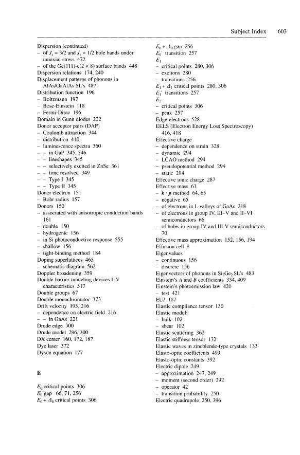
Dispersion (continued) - of lz = 3/2 and 1, = 1/2 hole bands under
uniaxial stress 472 - of the Ge(l11)-c(2 x 8) surface bands 448 Dispersion relations 174, 240 Displacement patterns of phonons in
AIAs/GaAIAs SL's 487 Distribution function 196 - Boltzmann 197 - Bose-Einstein 118 - Fermi-Dirac 196 Domain in Gunn diodes 222 Donor acceptor pairs (DAP) - Coulomb attraction 344 - distribution 410 - luminescence spectra 360 - - in GaP 345, 346
lineshapes 345 selectively excited in ZnSe 361 time resolved 349 Type I 345 Type II 345
Donor electron 151 - Bohr radius 157 Donors 150 - associated with anisotropic conduction bands
161 - double 150 - hydrogenic 156 - in Si photoconductive response 555 - shallow 156 - tight-binding method 184 Doping superlattices 465 - schematic diagram 562 Doppler broadening 359 Double barrier tunneling devices J-V
characteristics 517 Double groups 67 Double monochromator 373 Drift velocity 195, 216 - dependence on electric field 216 - - in GaAs 221 Drude edge 300 Drude model 296, 300 DX center 160, 172, 187 Dye laser 372 Dyson equation 177
E
Eo critical points 306 Eo gap 66,71,256 Eo + ,,10 critical points 306
Eo + ,,10 gap 256 Eo' transition 257 E] - critical points 280, 306 - excitons 280 - transitions 256 E1 + ,,1] critical points 280, 306 E1' transitions 257
E2 - critical points 306 - peak 257 Edge-electrons 528
Subject Index 603
EELS (Electron Energy Loss Spectroscopy) 416,418
Effective charge - dependence on strain 328 - dynamic 294 - LCAO method 294 - pseudopotential method 294 - static 294 Effective ionic charge 287 Effective mass 63 - k· p method 64, 65
negative 65 of electrons in L valleys of GaAs 218 of electrons in group IV, III-V and II-VI semiconductors 66 of holes in group IV and III-V semiconductors 70
Effective mass approximation 152, 156, 194 Effusion cell 8 Eigenvalues - continuous 156 - discrete 156 Eigenvectors of phonons in Si2Ge2 SL's 483 Einstein's A and B coefficients 334, 409 Einstein's photoemission law 420 - test 421 EL2 187 Elastic compliance tensor 130 Elastic moduli - bulk 102 - shear 102 Elastic scattering 362 Elastic stiffness tensor 132 Elastic waves in zincblende-type crystals 133 Elasto-optic coefficients 499 Elasto-optic constants 392 Electric dipole 249 - approximation 247,249 - moment (second order) 292 - operator 42 - transition probability 250 Electric quadrupole 250, 396
604 Subject Index
Electric susceptibilty 234 Electric-field- induced quantization 564 Electrical transport in MQW's 511 Electroluminescence 333, 334 Electromechanical tensor 122, 124 - table 124 - in zincblende-type semiconductors 146 Electron affinity 426 Electron analyzer - cylindrical mirror 425 - retarding grid 425 Electron confinement energies vs well width in
an AlInAs/TnP QW 470 Electron energy loss spectroscopy (EELS) 418 Electron escape depth 438 - universal curve 420 Electron-hole pairs, uncorrelated vs exciton
description 268 Electron mUltiplier 425 Electron spin 67 Electron storage ring 423 Electron volts 237 Electron acoustic-phonon interaction 15 - at degenerate bands 119 - piezoelectric 122 Electron-electron interaction 267 Electron LO-phonon interaction in quantum wells - dielectric models 508 - Huang-Zhu model 509 - macroscopic models 507 - mechanical models 508 Electron optical-phonon interaction 124 Electron-phonon Hamiltonian, piezoelectric 123 Electron-phonon interactions 99, 113 - degenerate heavy and light hole bands at r
119 - effect on bandgaps 330 - Hamiltonian 381 - intervalley 127 - in Si and GaAs 127 Electron-radiation interaction Hamiltonian
247,381 Electronegativity 171 Electronic band structure (see Band structure) Electronic potential, adiabatic 99 Electrons and holes in superlattices 473 - experimental results 475 Electrons in a magnetic field - classical treatment 222 - quantum treatment 521 Electrooptic tensors 328 Electrooptical energy 313 Electroreflectance 305, 312 - contactless 320
- low field 317 - of GaAs at Eo 316 - third derivative 317 Electrotransmission 305 Ellipsometry 239,323 Elliptically polarized light 240 Emission of photons 248 Emission rate vs frequency in Ge 336 Emitter in resonant tunnel device double barriers
512 Energy band mapping 558 Energy distribution from photoemission in
graphite 434 Energy gap I, 57 Energy levels in QW 475 Energy loss function - ofGe 245 - of Si 244 Energy relaxation time 217 Envelope function 156, 159 Envelope function approximation 466 Eo gap 71 Eo transition 256 Epilayer 463 £,.(0) table 326 Esaki tunnel diode 218, 511, 562 Escape depth of electrons 419 EuS 4 Evanescent waves 468 Exchange and correlation 62 Exciton 183,267,325 - at indirect edge 263 - at Mo critical points 269 - at M J critical points 279 - at M3 critical points 281 - bound to neutral donors in CdS - - emission spectra 356 - - quenching by IR radiation 356 - center-of-mass dispersion 268 - continuum states 325 - in CdS 274 - recombination 350 - translational mass 268 Exciton absorption - continuum 276 - discrete spectra 276 Exciton absorption spectra - in CU20 278 - in GaAs 277 Exciton binding energy to neutral donor 355 Exciton confinement 460 Exciton dispersion from Resonant Raman
Scattering 403 Exciton relaxation rate 413
Exciton Rydberg 271 Exciton-LO phonon interaction wave vector
dependence 397 Exciton-polaritons 269, 273, 406 - dispersion 326
CdS 273 - - emission 351-353 - - GaAs 408 Extended states 153 External modulation spectra 307 Extinction coefficient 236 Extrim.ic electrons, optical response 295
F
Fabry-Perot interferometers 387,388 Fabry-Perot resonator 563 Face-centered cubic (fcc) lattice 18 - Brillouin zone template 92 Factor group 25 Fano interference 281 Faraday cage 423, 425 Faraday rotations 4 Femtoseconds 216 Fermi Golden Rule 247,250,275,460 Fermi level 57,426 - at surface 451 - in 2D electron gas 528 - pinning 448 Fermi-Dirac distribution function 196 Ferroelectrics I, 4, 292 Ferromagnetism 4 Feynman diagrams 261, 381 - exercises 411 - for one-phonon Stokes Raman scattering
383 - symbols 382 Field effect transistors 215, 560 Filling factor of Landau levels 523 Final state interaction 344 Fluorite (CaF2) crystal structure 27,28 Folded acoustic phonon modes 480, 485 - scattering etliciency 499 Folded optic phonons 484 Forbidden excitons spectrum of CU20 279 Forbidden Raman scattering in CdS 399 Force constants (interatomic) 100 Fourier transforms 235 Fractals 531 Fractional quantum Hall etlect 524, 531 Franck-Condon effect 554 Franz-Keldysh effect 312, 315 - low field 317
Subject Index 605
Free carrier absorption - energy and wave vector conservation 297
in doped semiconductors 296 - in n-type [nAs 298
interband 299 Free carriers 193 Free exciton emission 351 Free-to-bound transitions luminescence 342 Frenkel excitons 267 Frequency modulated retlectance 309 - spectra in GaAs 306 Frequency modulation 364 Fresnel equations 238 Frohlich electron-phonon interaction 124-126,204 Frozen phonon approximation 109 Full rotation group 165, 188 Full zone k ' P method 257 Fundamental absorption edge 255
G
Gao.47Ino))As-AI0.42ino.52As quantum well 469 GaAIAs alloys 160 GaAs 351 - acceptor level energies 168 - band structure 60 - band energies at X point 93-95 - Brillouin spectrum 389 - conduction band effective mass 66 - core level absorption spectrum 417 - deformation potential for valence bands 118 - dielectric function 238, 246, 255, 318 - - derivatives 318 - donor binding energy 159 - drift velocity 216 - - velocity overshoot 216 - - velocity saturation 216 - etfecti ve charges 295 - electromechanical tensor component 124 - electron-phonon interactions 127 - electroretlectance 316 - exciton
absorption spectra 277 binding energy and Bohr radius 272 emission 352
- - polariton dispersion 408 - free electron to bound hole luminescence 343 - growth
chemical vapor deposition 7 - - liquid phase epitaxy II - - molecular beam epitaxy 10 - Gunn effect 220 - heterojunction 213
606 Subject Index
GaAs (continued) infrared absorption in p-type samples 299 intervalley deformation potentials 128 lattice reflection spectrum 290 Luttinger parameters 77, 165,470 mobility - in n-type samples 212 - in 20 electron gas 214 nitrogen impurities 185 optical phonon (zone center) energies and damping 290 Penn gap 326 phonon dispersion 103, 481 photocathode 373 photoluminescence 350 - at 29.4 Kbar 341
- photoreflectance 321 - quantum wells 464
confined LO phonons 487 confined TO phonons 495 folded acoustic phonon 498 folded LA phonon 500 hole subband dispersion 471,476,479 homogeneous and inhomogeneous broadening 50 I interface modes 491, 496 intersubband scattering rates 511 negative resistance 564 photoluminescence excitation spectra 358 Raman spectrum 505-507 resonant tunneling 513, 517 TEM picture 462
- radiative lifetime 340 - Raman spectra 375 - reflectance 246, 306 - - energies of prominent structures 258 - - frequency modulated 306 - resonant Brillouin scattering 407 - scattering rate of conduction electrons 203 - spin-orbit splitting 257 - stiffness constants 133 - thermoreflectance 310 - transmission spectra 477 - valence band parameters 70 - XPS spectrum 430 GaAsP alloys, - deep centers with A I symmetry 183 - N impurities 183 Galena (PbS) I Gamma-ray detectors 540 Gap problem 62, 445 Gallium phosphide (GaP) type I and II donor
acceptor pair (DAP) recombination spectra 356, 347
Gas discharge lamps - photoemission sources 440 Gas phase epitaxy 7 GaSb spin-orbit splitting 69 GaSe 3 - two-dimensional excitons 281 Gauge - Coulomb 245, 520 - invariance 245 - Landau 520 Ge - (III)-c(2 x 8) surface
band structure 448 - dangling bond surface bands 449
imaged by scanning tunneling microscope 447
- absorption coefficients 264 - absorption from core levels 417 - acceptor energy levels 168, 170, 171 - - binding energies of B,AI,Ga,In,TI 304 - bandgap, temperature dependence 310 - Brillouin spectrum 389 - conduction band - - dispersion determined by inverse
photoemission 445 effecti ve mass 66
- cyclotron resonance 547 - density of valence states 428 - deformation potentials 118 - dielectric function 245 - - energies of prominent structures 258 - - imaginary part 256 - electronic band structure 60
comparison between tight-binding method, pseudopotential method and nearly-free electron model 88
- emission rate 336 - internal strain parameter 145 - isotopically pure 540 - Luttinger parameters 165 - minority carrier radiative lifetime 340 - Penn gap 326 - photomodulated reflectivity 321 - photothermal ionization spectrum 304 - pseudopotential from factors 59 - Raman spectra - - mono1ayers 378-379 - - two-phonon 377 - reflectance 245 - spin-orbit splitting 257 - stiffness constants 133 - tight-binding interaction parameters 86 - ultra-pure 539 - UPS spectrum 428
Ge (continued) - valence band - - dispersion determined by angle-resolved
UPS 437,445 - - parameters 70 - XPS spectrum 428 Ge-Si alloys - interband critical points vs concentration 320 - Raman spectrum 378 GenSim superlattices 487 GeS, GeSe 433 GeTe I Glass 2 550 Glassy semiconductors 2, 4 Glide planes 24, 25 - diamond structure 48 Gray tin 2 - phonon dispersion relation 112 Green's function, real part 180 Green's function method 149, 182 Group 21 Group of the wave vector k 38 Group theory 13, 21 Guiding center of cyclotron orbits 523, 528 Gunn effect 127 Gunn oscillators 215, 221, 222
H
H- 356 Hall coefficient 225, 519, 523 - electrons 230 - holes 230 - thin film 225 Hall effect - classical 222, 224, 225 - for a distribution of electron energies 226 - quantum 519,560 Hall factor 227 - limit of strong and weak magnetic fields 230 Hall measurements 224 Hall mobility 227 Hall plateaus - explanation 527 Hamiltonian - Baldereschi-Lipari 165 - for an electron in a magnetic field 520 - for nuclear motions 99 - Herring and Vogt 121 - Luttinger 77 - Pikus-Bir 137 Harmonic approximation 100 Harmonic oscillators 282
- dielectric function 251 - response to radiation 281 He-Ne laser 372 Heavy hole 75,473 Heavy hole mass 70 Hemispherical analyzer 423 Hertz 237 Hetero-epitaxy 7 Heterojunction 213,462 - modulation-doped 213 Heteropolar molecule 79
HgBaCa2Cu30s 3 HgSe 90 HeTe 2,90 High field transport 215 High frequency oscillators 218 High Tc superconductors 3 Hilbert transform 174 Hole 3 - band 75 - definition 75 - droplets in QHE 528
Subject Index 607
- subband in GaAs/GaAIAs QW's 470,471 Holographic gratings 240 Homo-epitaxy 7 Homogeneous broadening SOl Homogeneous linewidth 359 Homomorphism 25, 28 Homopolar molecule 79 Hot electrons 193,215 - transport 205 Hot luminescence 337 Hubbard model 172 Hybridized sp3 orbitals 54 Hydrogen atom 270 - electronic states 156 - elliptically-deformed 161 Hydrogen molecule binding energy 354 Hydrogenic impurity center 554 Hydrostatic pressure 130 Hyperbolic excitons 279-281
Identity representation 32 Image-intensifier 240, 374 Imaging photomultiplier tube 374 Impact parameter 208 Improper rotations 22 Impurities - hydrogenic lSI - shallow 151 - deep 171
608 Subject Index
Impurity band 342 Impurity core 160 Impurity ionization energies, Ge, Si 548 Incoming and outgoing Raman resonance 390 - GaSe 394 Indirect absorption edge 259 - GaP 266 - Ge 265,337 - Si 265 Indirect bandgap semiconductors 127, 128, 184,
205 Indirect excitons 277 Indirect gap in Si 261 Indirect transitions 255 - dependence on w 263 - Feynman diagrams 411 - phonon absorption and emission 263 - phonon-assisted 551 I nelastic neutron scattering 102 Inelastic scattering of light 362 I nfrared absorption spectra - p-type GaAs 299 - shallow impurities 30 I Infrared detectors 553 Infrared-active transitions 43 Inhomogeneous broadening 50 I Inhomogeneous Iinewidth 359 Initial state interaction 344 InS, InSe 433 InSb - fundamental absorption edge 260 - spin-orbit splitting 69 Insulators I Integral quantum Hall effect 524, 527 Interband scattering - f-processes 206 - g-process 206 inter-valence-band excitations - spin-orbit splitting 300 Intercalation 3 Interface modes 488, 489 - angular dispersion 492, 496 - double heterojunction 488 - GaAs/AIAs QW's 491 - single heterojunction 488 - single QW 489 - SL's 491 Interface plasmons 489 Interface states 464 Internal strain 144, 125, 144 Internal strain parameter 140, 145 - and optical phonons 145 Interstitial defect 150 Intervalley deformation potential 128
Intervalley scattering 127, 205 - by LA phonons 229 - time 219 Intraband scatteri ng 200 - by acoustic phonons 199 - by polar optical phonons 204 Intrinsic defect 150 Invariant subgroup 25 Inverse photoemission 416, 417, 444, 445 Inversion symmetry of energy band 77 Ion lasers 372 Ionic bonding 104 Ionicity 2, 294 Ionization energies 420 - group III acceptors in Si 553 - group V donors in Si 553 Ionized impurities scattering J 98 Infrared absorption parity selection rule 366 Irreducible representations - of group of A 45 - of the double group of r in zincblende 68 Isoelectronic impurity J 50 Isomorphism 25, 28 Isotopic shift of bandgaps 329 Isotopically pure Ge 5, 540 Isovalent impurity J 50 I-V characteristic of resonant tunnel devices
double barriers 513
J
Ioint-density-of-states 25 J
K
k . p method 63-64,247,256,328,545 - band structure of GaAs 73 - dielectric function calculation 253 - spin-orbit interactions 71 k nonconserving photoemission 438 k-conservation in QW's 467 Keating model 108 Kerr effect 328 Knudsen cell 8 Kohn-Luttinger parameters 77, 165,470 Kramers degeneracy J 37 Kramers-Kronig analysis 551 Kramers-Kronig relations (KKR) 174,323,240 Kronig-Penny model 474 Kronig-Penny energy bands 565
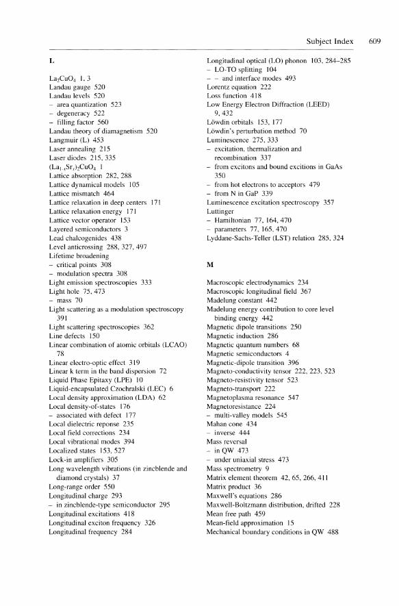
L
La2Cu04 1,3 Landau gauge 520 Landau levels 520 - area quantization 523 - degeneracy 522 - filling factor 560 Landau theory of diamagnetism 520 Langmuir (L) 453 Laser annealing 215 Laser diodes 215,335 (Lal_,Sr,hCu04 I Lattice absorption 282, 288 Lattice dynamical models 105 Lattice mismatch 464 Lattice relaxation in deep centers 171 Lattice relaxation energy 171 Lattice vector operator 153 Layered semiconductors 3 Lead chalcogenides 438 Level anti crossing 288, 327, 497 Lifetime broadening - critical points 308 - modulation spectra 308 Light emission spectroscopies 333 Light hole 75, 473 - mass 70 Light scattering as a modulation spectroscopy
391 Light scattering spectroscopies 362 Li ne defects 150 Linear combination of atomic orbitals (LCAO)
78 Linear electro-optic effect 319 Linear k term in the band dispersion 72 Liquid Phase Epitaxy (LPE) 10 Liquid-encapsulated Czochralski (LEC) 6 Local density approximation (LOA) 62 Local density-of-states 176 - associated with defect 177 Local dielectric reponse 235 Local field corrections 234 Local vibrational modes 394 Localized states 153, 527 Lock-in amplifiers 305 Long wavelength vibrations (in zincblende and
diamond crystals) 37 Long-range order 550 Longitudinal charge 293 - in zincblende-type semiconductor 295 Longitudinal excitations 4 I 8 Longitudinal exciton frequency 326 Longitudinal frequency 284
Subject Index 609
Longitudinal optical (LO) phonon 103,284-285 - LO-TO splitting 104 - - and interface modes 493 Lorentz equation 222 Loss function 4 I 8 Low Energy Electron Diffraction (LEED)
9,432 Uiwdin orbitals 153, 177 Liiwdin's perturbation method 70 Luminescence 275, 333 - excitation, thermalization and
recombination 337 - from excitons and bound excitions in GaAs
350 - from hot electrons to acceptors 479 - from N in GaP 339 Luminescence excitation spectroscopy 357 Luttinger - Hamiltonian 77, 164,470 - parameters 77, 165,470 Lyddane-Sachs-Teller (LST) relation 285, 324
M
Macroscopic electrodynamics 234 Macroscopic longitudinal field 367 Madelung constant 442 Madelung energy contribution to core level
binding energy 442 Magnetic dipole transitions 250 Magnetic induction 286 Magnetic quantum numbers 68 Magnetic semiconductors 4 Magnetic-dipole transition 396 Magneto-conductivity tensor 222, 223, 523 Magneto-resistivity tensor 523 Magneto-transport 222 Magnetoplasma resonance 547 Magnetoresistance 224 - multi-valley models 545 Mahan cone 434 - inverse 444 Mass reversal - in QW 473 - under uniaxial stress 473 Mass spectrometry 9 Matrix element theorem 42, 65, 266, 411 Matrix product 36 Maxwell's equations 286 Maxwell-Boltzmann distribution, drifted 228 Mean free path 459 Mean-field approximation 15 Mechanical boundary conditions in QW 488
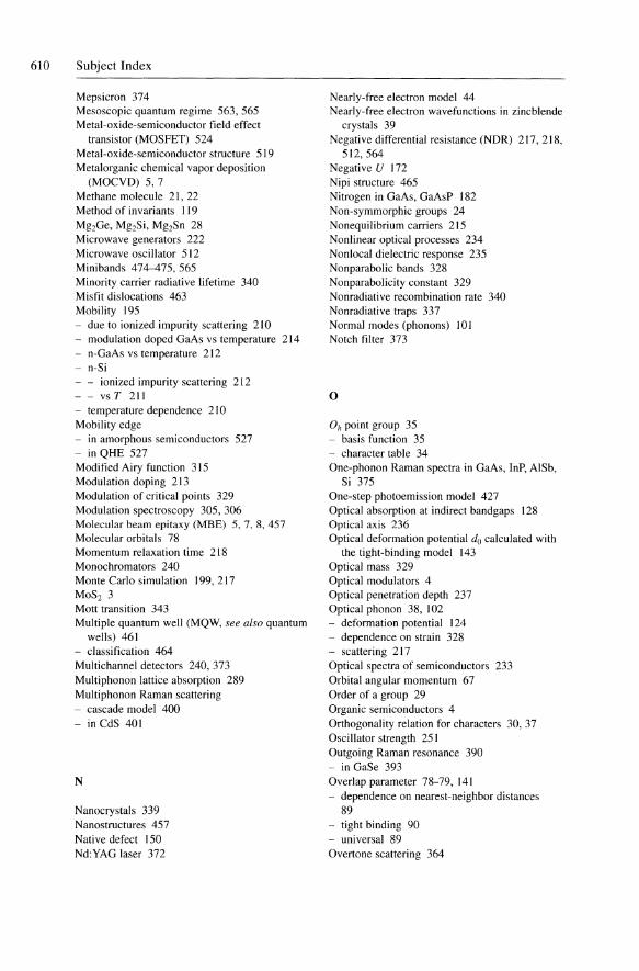
610 Subject Index
Mepsicron 374 Mesoscopic quantum regime 563, 565 Metal-oxide-semiconductor field effect
transistor (MOSFET) 524 Metal-oxide-semiconductor structure 519 Metalorganic chemical vapor deposition
(MOCYD) 5,7 Methane molecule 21,22 Method of invariants 119 Mg2Ge, Mg2Si, Mg2Sn 28 Microwave generators 222 Microwave oscillator 512 Minibands 474-475,565 Minority carrier radiative lifetime 340 Misfit dislocations 463 Mobility 195 - due to ionized impurity scattering 210 - modulation doped GaAs vs temperature 214 - n-GaAs vs temperature 212 - n-Si - - ionized impurity scattering 212 - - vs T 211 - temperature dependence 210 Mobility edge - in amorphous semiconductors 527 - in QHE 527 Modified Airy function 315 Modulation doping 213 Modulation of critical points 329 Modulation spectroscopy 305, 306 Molecular beam epitaxy (MBE) 5,7,8,457 Molecular orbitals 78 Momentum relaxation time 218 Monochromators 240 Monte Carlo simulation 199,217 MoS2 3 Mott transition 343 Multiple quantum well (MQW, see also quantum
wells) 461 - classification 464 Multichannel detectors 240, 373 Multiphonon lattice absorption 289 Multiphonon Raman scattering - cascade model 400 - in CdS 401
N
Nanocrystals 339 Nanostructures 457 Native defect 150 Nd:YAG laser 372
Nearly-free electron model 44 Nearly-free electron wavefunctions in zincblende
crystals 39 Negative differential resistance (NDR) 217,218,
512,564 Negative U 172 Nipi structure 465 Nitrogen in GaAs, GaAsP 182 Non-symmorphic groups 24 Nonequilibrium carriers 215 Nonlinear optical processes 234 Nonlocal dielectric response 235 Nonparabolic bands 328 Nonparabolicity constant 329 Nonradiative recombination rate 340 Nonradiative traps 337 Normal modes (phonons) 101 Notch filter 373
o
Oh point group 35 - basis function 35 - character table 34 One-phonon Raman spectra in GaAs, InP, AISb,
Si 375 One-step photoemission model 427 Optical absorption at indirect bandgaps 128 Optical axis 236 Optical deformation potential do calculated with
the tight-binding model 143 Optical mass 329 Optical modulators 4 Optical penetration depth 237 Optical phonon 38, J 02 - deformation potential 124 - dependence on strain 328 - scattering 217 Optical spectra of semiconductors 233 Orbital angular momentum 67 Order of a group 29 Organic semiconductors 4 Orthogonality relation for characters 30, 37 Oscillator strength 25 J Outgoing Raman resonance 390 - in GaSe 393 Overlap parameter 78-79, 141 - dependence on nearest-neighbor distances
89 - tight binding 90 - universal 89 Overtone scattering 364
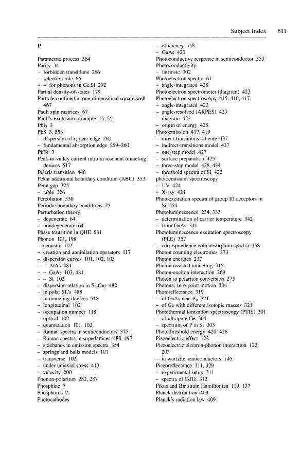
P
Parametric process 364 Parity 34 - forbidden transitions 266 - selection rule 66 - - for phonons in Ge,Si 292 Partial density-of-states 179 Particle confined in one-dimensional square well
467 Pauli spin matrices 67 Pauli's exclusion principle 15,55 Pbl2 3 PbS 3,553 - dispersion of E, near edge 260 - fundamental absorption edge 259-260 PbTe 3 Peak-to-valley current ratio in resonant tunneling
devices 517 Peierls transition 446 Pekar additional boundary condition (ABC) 353 Penn gap 325 - table 326 Percolation 530 Periodic boundary conditions 23 Perturbation theory - degenerate 64 - nondegenerate 64 Phase transition in QHE 53 I Phonon 101, 198 - acoustic 102 - creation and annihilation operators 117 - dispersion curves 10 I, 102, 105
AlAs 481 - - GaAs 103,481 - - Si 103 - dispersion relation in Si2Ge2 482 - in polar SL's 488 - in tunneling devices 518 - longitudinal 102 - occupation number 118 - optical 102 - quantization 101,102 - Raman spectra in semiconductors 375 - Raman spectra in superlattices 480, 497 - sidebands in emission spectra 354 - springs and balls models 10 I - transverse 102 - under uniaxial stress 413 - velocity 200 Phonon-polariton 282, 287 Phosphine 7 Phosphorus 2 Photocathodes
Subject Index 611
- efficiency 558 - GaAs 420 Photoconductive responce in semiconductor 553 Photoconductivity - intrinsic 302 Photoelectron spectra 61 - angle-integrated 428 Photoelectron spectrometer (diagram) 423 Photoelectron spectroscopy 415, 416, 417 - angle-integrated 423 - angle-resolved (ARPES) 423 - diagram 422 - origin of energy 425 Photoemission 417, 419 - direct-transitions scheme 437 - indirect-transitions model 437 - one-step model 427 - surface preparation 425 - three-step model 428, 434 - threshold spectra of Si 422 photoemission spectroscopy - UV 424 - X-ray 424 Photoexcitation spectra of group III acceptors in
Si 554 Photoluminescence 234, 333 - determination of carrier temperature 342 - from GaAs 341 Photoluminescence excitation spectroscopy
(PLE) 357 - correspondence with absorption spectra 358 Photon counting electronics 373 Photon energies 237 Photon-assisted tunneling 315 Photon-exciton interaction 269 Photon to polariton conversion 275 Photons, zero-point motion 334 Photoreflectance 319 - of GaAs near Eo 321 - of Ge with different isotopic masses 321 Photothermal ionization spectroscopy (PTIS) 301 - of ultrapure Ge 304 - spectrum of Pin Si 303 Photothreshold energy 420, 426 Piezoelectric effect 122 Piezoelectric electron-phonon interaction 122,
203 - in wurtzite semiconductors 146 Piezoreflectance 311, 329 - experimental setup 311 - spectra of CdTe 312 Pikus and Bir strain Hamiltonian 119,137 Planck distribution 409 Planck's radiation law 409
612 SUbject Index
Plasma 324 - edge 300 - frequency 243, 296, 324 - - of valence electrons 415 - - screened 296 - oscillations 324 - wave 324 Plasmon-LO phonon coupled modes 327 Plasmons 324 Pockels effect 328 Point defects 150 Point group 23 - C2, 46 - C3,' 45 - Oh 35 - Td 31 Poisson's equation 450 Polariton - bottleneck 351 - Brillouin scattering in GaAs 407 - dispersion in GaP 379, 380 - dispersion curves 406 - emission 351 - emission spectra in CdS, CdSe, CuCl, GaAs
352 - lower and upper branches 352, 379 - transmission coetlicients 351 - scattering 274 Polarity 294 - Harrison 294 Polyacetylene 1, 4 Polydiacetylene 4 Porous Si 339 Porto notation in Raman scattering 367 Position-sensitive photomultiplier tubes 373 Positronium 267 Primitive cell 26 Primitive lattice vectors 17 Primitive reciprocal lattice vectors 19 Principle of detailed balance 335, 409 Projection operators 41 Propagators 382 Pseudo-angular momentum of acceptor levels 167 Pseudo-scalar 35 Pseudo-vector 35 Pseudo-wave equation 55 Pseudo-wavefunction 55 Pseudodielectric functions 238 Pseudomorphic growth 462 Pseudopotential 55 - hard core 55 - local 49 - nonlocal 49 - soft core 55
Pseudopotential band structure calculation by hand 93-95
Pseudopotential form factors 56-57,62 - anti symmetric 57 - for group IV and zincblende semiconductors
59 - symmetric 57 Pseudopotential in superlattice 474 Pseudopotential method 306 - ab initio 542 - band structure calculation 54 - empirical 61-62,542 - self-consistent 61
Q
Quantized Hall resistance 561 Quantum confinement 457,458,459 - of electrons and holes 461 Quantum dots 458 Quantum Hall droplet 528 Quantum Hall Effect (QHE) 519 - discovery 560 - effect of disorder 527 - experiment of von Klitzing, Pepper and Dorda
524, 525 - fractional 519 - gauge invariance 561 - integral 519 - resistance standard 527, 560 - transverse and longitudinal resistivity 526 Quantum of resistance 527 Quantum number, principal 156 Quantum wells (QW's) 461 - absorption spectra 538 - based on GaAs and III-V semiconductors 357 - classification 464 - confinement of electrons 466, 470 - confinement of holes 469,471 - excitonic effect 280 - growth 5 - hot luminescence 479 - mass reversal 473 - phonons (see also superlattices) 480 - photoluminescence excitation (PLE) spectra
357-358 - Raman spectra (see also superlattices) 497 - subbands 469,479 - transmission electron micrograph (TEM) 462 - transmission spectrum 477 Quantum wires 458 Quasi-thermal equilibrium 215 Quasiparticle approach 63
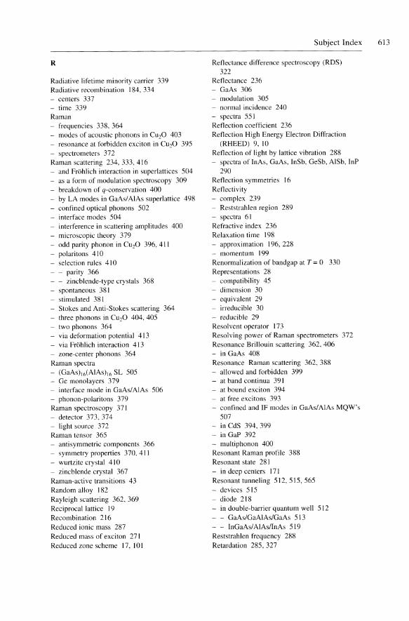
R
Radiative lifetime minority carrier 339 Radiative recombination 184,334 - centers 337 - time 339 Raman - frequencies 338, 364 - modes of acoustic phonons in CU20 403 - resonance at forbidden exciton in CU20 395 - spectrometers 372 Raman scattering 234,333,416 - and Frohlich interaction in superlattices 504 - as a form of modulation spectroscopy 309 - breakdown of q-conservation 400 - by LA modes in GaAs/AIAs superiattice 498 - confined optical phonons 502 - interface modes 504 - interference in scattering amplitudes 400 - microscopic theory 379 - odd parity phonon in CU20 396, 411 - polaritons 410 - selection rules 410 - - parity 366 - - zincblende-type crystals 368 - spontaneous 381 - stimulated 381 - Stokes and Anti-Stokes scattering 364 - three phonons in CU20 404, 405 - two phonons 364 - via deformation potential 413 - via Frohlich interaction 413 - zone-center phonons 364 Raman spectra - (GaAs)16(AIAs)16 SL 505 - Ge monolayers 379 - interface mode in GaAsl AlAs 506 - phonon-polaritons 379 Raman spectroscopy 371 - detector 373, 374 - light source 372 Raman tensor 365 - antisymmetric components 366 - symmetry properties 370, 411 - wurtzite crystal 410 - zincblende crystal 367 Raman-active transitions 43 Random alloy 182 Rayleigh scattering 362, 369 Reciprocal lattice 19 Recombination 216 Reduced ionic mass 287 Reduced mass of exciton 271 Reduced zone scheme 17,101
Subject Index 613
Reflectance difference spectroscopy (RDS) 322
Reflectance 236 - GaAs 306 - modulation 305 - normal incidence 240 - spectra 551 Reflection coefficient 236 Reflection High Energy Electron Diffraction
(RHEED) 9, 10 Reflection of light by lattice vibration 288 - spectra of !nAs, GaAs, InSb, GeSb, AISb, InP
290 Reflection symmetries 16 Reflectivity - complex 239 - Reststrahlen region 289 - spectra 61 Refractive index 236 Relaxation time 198 - approximation 196, 228 - momentum 199 Renormalization of bandgap at T = 0 330 Representations 28 - compatibility 45 - dimension 30 - equivalent 29 - irreducible 30 - reducible 29 Resolvent operator 173 Resolving power of Raman spectrometers 372 Resonance Brillouin scattering 362, 406 - in GaAs 408 Resonance Raman scattering 362, 388 - allowed and forbidden 399 - at hand continua 391 - at bound exciton 394 - at free excitons 393 - confined and IF modes in GaAs/AIAs MQW's
507 - in CdS 394, 399 - in GaP 392 - multi phonon 400 Resonant Raman profile 388 Resonant state 281 - in deep centers 171 Resonant tunneling 512, 515, 565 - devices 515 - diode 218 - in double-barrier quantum well 512 - - GaAs/GaAIAs/GaAs 513 - - InGaAs/AIAsllnAs 519 Reststrahlen frequency 288 Retardation 285, 327
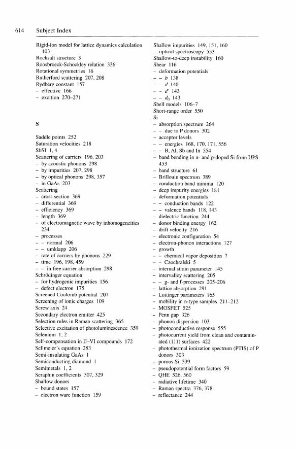
614 Subject Index
Rigid-ion model for lattice dynamics calculation 103
Rocksalt structure 3 Roosbroeck-Schockley relation 336 Rotational symmetries 16 Rutherford scattering 207, 208 Rydberg constant 157 - effective 166 - excition 270-271
S
Saddle points 252 Saturation velocities 218 SbSI 1,4 Scattering of carriers 196, 203 - by acoustic phonons 298 - by impurities 207, 298 - by optical phonons 298, 357 - in GaAs 203 Scattering - cross section 369 - differential 369 - efficiency 369 - length 369 - of electromagnetic wave by inhomogeneities
234 - processes - - normal 206 - - umklapp 206 - rate of carriers by phonons 229 - time 196, 198, 459 - - in free carrier absorption 298 Schriidinger equation - for hydrogenic impurities 156 - defect electron 175 Screened Coulomb potential 207 Screening of ionic charges 109 Screw axis 24 Secondary electron emitter 425 Selection rules in Raman scattering 365 Selective excitation of photoluminescence 359 Selenium I, 2 Self-compensation in II-VI compounds 172 Sellmeier's equation 283 Semi-insulating GaAs I Semiconducting diamond Semi metals 1,2 Seraphin coefficients 307, 329 Shallow donors - bound states 157 - electron ware function 159
Shallow impurities 149, 151, 160 - optical spectroscopy 553 Shallow-to-deep instability 160 Shear \16 - deformation potentials
b 138 d 140 d' 143 do 143
Shell models 106-7 Short-range order 550 Si - absorption spectrum 264 - - due to P donors 302 - acceptor levels - - energies 168, 170, 171, 556 - - B, AI, Sb and In 554 - band bending in n- and p-doped Si from UPS
453 - band structure 61 - Brillouin spectrum 389 - conduction band minima 120 - deep impurity energies 181 - deformation potentials - - conduction bands 122 - - valence bands 118, 143 - dielectric function 244 - donor binding energy 162 - drift velocity 216 - electronic configuration 54 - electron-phonon interactions 127 - growth - - chemical vapor deposition 7 - - Czochralski 5 - internal strain parameter 145 - intervalley scattering 205 - - g- and f-processes 205-206 - lattice absorption 291
Luttinger parameters 165 - mobility in n-type samples 211-212 - MOSFET 525 - Penn gap 326 - phonon dispersion 103 - photoconductive response 555 - photocurrent yield from clean and contamin-
ated (\ 11) surfaces 422 - photothermal ionization spectrum (PTIS) of P
donors 303 - porous Si 339 - pseudopotential form factors 59 - QHE 526, 560 - radiative lifetime 340 - Raman spectra 376, 378 - reflectance 244
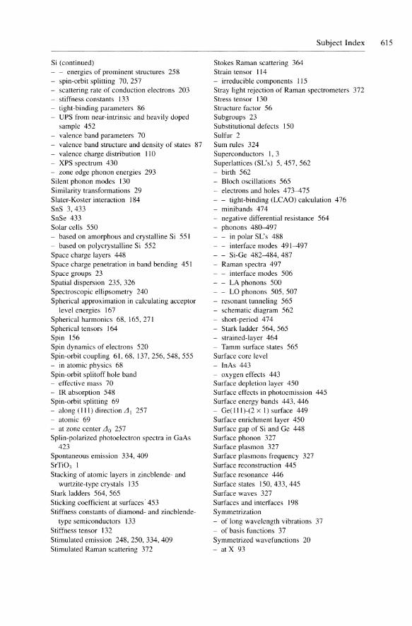
Si (continued) - - energies of prominent structures 258 - spin-orbit splitting 70, 257 - scattering rate of conduction electrons 203 - stiffness constants 133 - tight-binding parameters 86 - UPS from near-intrinsic and heavily doped
sample 452 - valence band parameters 70 - valence band structure and density of states 87 - valence charge distribution 110 - XPS spectrum 430 - zone edge phonon energies 293 Silent phonon modes 130 Similarity transformations 29 Slater-Koster interaction 184 SnS 3,433 SnSe 433 Solar cells 550 - based on amorphous and crystalline Si 551 - based on polycrystalline Si 552 Space charge layers 448 Space charge penetration in band bending 451 Space groups 23 Spatial dispersion 235, 326 Spectroscopic ellipsometry 240 Spherical approximation in calculating acceptor
level energies 167 Spherical harmonics 68, 165, 271 Spherical tensors 164 Spin 156 Spin dynamics of electrons 520 Spin-orbit coupling 61,68, 137,256,548,555 - in atomic physics 68 Spin-orbit splitotf hole band - effective mass 70 - IR absorption 548 Spin-orbit splitting 69 - along (III) direction LlJ 257 - atomic 69 - at zone center Llo 257 Splin-polarized photoelectron spectra in GaAs
423 Spontaneous emission 334,409 SrTi03 I Stacking of atomic layers in zincblende- and
wurtzite-type crystals 135 Stark ladders 564, 565 Sticking coefficient at surfaces 453 Stiffness constants of diamond- and zincblende-
type semiconductors 133 Stiffness tensor 132 Stimulated emission 248, 250, 334, 409 Stimulated Raman scattering 372
Stokes Raman scattering 364 Strain tensor 114 - irreducible components lIS
Subject Index 615
Stray light rejection of Raman spectrometers 372 Stress tensor 130 Structure factor 56 Subgroups 23 Substitutional defects ISO Sulfur 2 Sum rules 324 Superconductors I, 3 Superiattices (SL's) 5,457,562 - birth 562 - Bloch oscillations 565 - electrons and holes 473-475 - - tight-binding (LCAO) calculation 476 - minibands 474 - negative differential resistance 564 - phonons 480-497
in polar SL's 488 - - interface modes 491-497 - - Si-Ge 482-484, 487 - Raman spectra 497
interface modes 506 - - LA phonons 500 - - LO phonons 505, 507 - resonant tunneling 565 - schematic diagram 562 - short-period 474 - Stark ladder 564, 565 - strained-layer 464 - Tamm surface states 565 Surface core level - InAs 443 - oxygen effects 443 Surface depletion layer 450 Surface effects in photoemission 445 Surface energy bands 443, 446 - Ge(111)-(2 xl) surface 449 Surface enrichment layer 450 Surface gap of Si and Ge 448 Surface phonon 327 Surface plasmon 327 Surface pI as mons frequency 327 Surface reconstruction 445 Surface resonance 446 Surface states 150,433,445 Surface waves 327 Surfaces and interfaces 198 Symmetrization - of long wavelength vibrations 37 - of basis functions 37 Symmetrized wavefunctions 20 - at X 93
616 Subject Index
Symmetry operations 21 - equivalent 30 - of diamond and zincblende structures 26 - of methane molecule 21-22 - of wurtzite crystals 135 Symmorphic groups 24 Synchrotron radiation 240,416,436 - absorption spectra of Ge, GaAs, GaP 416 - tunable 451
T
Tamm surface states 565 TaS2 558 TaSe2 558 Td point group - basis function 32 - character table 32 - irreducible representations 33 Tellurium 2 Temperature dependence of bandgaps 329 - Eo gap in Ge 310 Temporal evolution of DAP transition 347 Tetrahedral bonding 550 - lack of it in amorphous semiconductors 550 Thermal expansion 100 - effect on gaps 30 - low temperature anomalies 100 Thermal ionization energy of impurity levels 171 Thermalization time 215 Thermoluminescence 309, 333 Thermoreflectance spectra of GaAs 310 Third-order nonlinear susceptibility in Ge 330 Thomas-Fermi screening 207 Three-dimensional critical points (see also van
Hove singularities) 257 Three-step photoemission model 428, 434 Threshold function in photoemission 421 Ti doped sapphire laser 372 Tight binding - Hamiltonian 85 - model 78, 86
comparison with EPM in Si 87 interaction parameters for C, Si, Ge 86 optical deformation potential do 143 superJattice 474
Time-reversal symmetry 77,370 Transverse optical (TO) phonon 103,287 Total angular momentum 68 Total decay rate 340 Total recombination time 340 Transfer matrices 515 Transferability of pseudopotential 62
- ab initio 62 - selfconsistent 62 Transformation matrix 29 Translation operator 16 Translation symmetry 16 Transmission coefficient of electrons through a
double barriers 516 Transport of carriers - in parabolic bands 197 - quasi-classical approach 193 Transverse acoustic (TA) phonons 102 - fast 134 - slow 134 Transverse charge 293 - in zinc bIen de-type semiconductors 295 Transverse exciton energy 326, 351 Transverse vibrations 284 Triad screw axis 24, 25 Trimethyl gallium 7 Triple spectrometers 373 Tunable cw lasers 372 - dye laser 407 - IR laser 556 Tunnel diode 511 Two-dimensional crystals 433, 558 Two-dimensional critical points (see also van
Hove singularities) 256 Two-dimensional exciton 281 Two-phonon absorption 292 - spectra of Si and Ge 291 Two-phonon Raman scattering 364 - Ge 377 - Si 376 Two-thirds rule for spin-orbit splitting 256 Type I and type" MQW's 464 - type lIA 464 - type lIB 464 Type I and type" superlattice 464 - type IIA 464 - type lIB 465 Type III MQW's 464
U
Ultrahigh vacuum 7,238,421 Ultra-pure germanium 539 Ultraviolet photoemission spectroscopy (UPS) 9,
416,429 - effect of band bending 451 - spectrum of III-V compounds 431 Uncertainty principle 157 Uniaxial crystals 236 Uniaxial stress 130
Units frequency of electromagnetic waves 237
- pressure 422
v
Vacancies 150. 172 - binding energy 182 - in diamond- or zincblende-type 173 Vacuum level 426 Vacuum ultraviolet 415 Valence band - dispersion in GaAs/AIGaAs QW's as deter-
mined by hot luminescence 479 - extrema 118 - Ge determined by UPS 437 - parameters A. B. C 76 - parameters of diamond and zincblende semi-
conductor 70 Valence electrons 14, 54 Valence force field method 107 - force constants 107 Valence plasmons 418 - in GaP 418 Valley-orbit coupling 161,301 Valley-orbit splitting of donor levels 163 Van der Pauw method 224, 225, 226 Van der Waals interaction 3, 344 Van Hove singularities 251,252.257,305,325,
550 - in Ej 252 - in one, two, and three dimensions 253 Vapor-phase epitaxial growth 322 Variational technique for impurity levels 162 Velocity overshoot 216 Velocity saturation 216-217 Vertex in Feynman diagrams 382 Vibrational properties of semiconductors 99 Videotelephony 558 Virtual crystal potential 182 Virtual transitions 261, 317 Volume deformation potential 229 - tight-binding model 138 Von Klitzing constant 560
w
Wannier excitons 267 - absorption spectrum 325 Wannier functions 152-153,269 Wannier-Mott excitons 267
Warm carriers 217 Wave nature of electron 558 Wave vectors 16 Wavenumber 237 Work function 426 wurtzite crystal - acoustic phonons 136
Subject Index 617
- electromechanical tensor elements 124 piezoelectric electron-phonon interactions 146
- phonons 109 stiffness tensor 135
- structure 135 - symmetry operations 135
x
X-ray 9 X-ray fluorescence 416 Xl-X, splitting in zincblende materials 431 XES (X-ray tluorescence emission spectroscopy)
419 X-ray photoemission spectroscopy (XPS) 9,416,
429 - etlect of band bending 451 - spectrum of Ill-V compounds 431
z
Zener band-to-band tunneling 565 Zero bandgap semiconductor 2 Zero-point motion 334 - phonons 365 - photons 334 Zincblende (ZnS) 1.410 - crystal structure 18 - group of ~ and representation 46,47 - group of X and representation 47 - nearly-free electron band structure 44 - symmetry operations 26 - zone center TO and LO phonons 103 ZnO 3 ZnS (see a/so zincblende) 135 ZnSe - band structure 61 - selective excitation spectra of excitons bound
to Na and Li donors 360 - self-compensation 172 ZnTe - self-compensation 172 ZnSiPz 4 Zone folding and splittings of phonons 484