Philips Journalof Research - PEARL HiFi
425
Volume 47 Philips Journalof Research 1992-1993 © Philips International B.V., Eindhoven, The Netherlands, 1993. Articles or illustrations reproduced, in whole or in part, must be accompanied by full acknowledgement of the source: Philips Journalof Research. , ,
-
Upload
khangminh22 -
Category
Documents
-
view
0 -
download
0
Transcript of Philips Journalof Research - PEARL HiFi

Volume 47
Philips JournalofResearch
1992-1993
© Philips International B.V., Eindhoven, The Netherlands, 1993.Articles or illustrations reproduced, in whole or in part, must be accompanied
by full acknowledgement of the source: Philips Journalof Research.
,,

R 1267 M. Moshfegi andH. Rusinek
Three-dimensional registration ofmultimodality medical images using theprincipal axes technique
81-97
Contents of Volume 47
CONTENTSPHILIPS JOURNAL OF RESEARCH, VOL. 47
Pages
R 1262 H. Bouma Human factors in technology 1-2
R 1263 A.J.M. Houtsma Psychophysics and modem digital audio 3-14technology
R 1264 R. Collier, Speech synthesis today and tomorrow 15-34H.C. van Leeuwenand L. F. Willems
R 1265 J.A.J. Roufs Perceptual image quality: concept and 35-62measurement
R 1266 F.L. Engel and Layered approach in user-system 63-80R. Haakma interaction
R 1268 A.J.E.M. JanssenandM.J.J.J.D. Maes
An optimization problem in reflectordesign
99-143
Errata 145
o

Contents of Volume 47
Pages
R 1269 F.J.A.M. Greidanus Introduetion to the special issue on 147-149and M.P.A. Viegers inorganic materials analysis
R 1270 K.Z. Troost Submicron crystallography in the scanning 151-162electron microscope
R 1271 A. Sicignano In situ differential scanning electron 163-183microscopy design and application
R 1272 A.E.M. De Veirman, TEM and XRD characterization of 185-201J. Timrners,F.J.G. epitaxially grown PbTi03 prepared byHakkens, J.F.M. pulsed laser depositionCillessenand R.M.Wolf
R 1273 P. Van der Sluis High-resolution X-ray diffraction of 203-215epitaxiallayers on vicinal semiconductorsubstrates
R 1274 C. Schiller, G.M. Fast and accurate assessment of nanometer 217-234Martin, W. W. v.d. layers using grazing X-ray reflectometryHoogenhof and J.Corno
R 1275 P.F. Fewster Structural characterization of materials by 235-245combining X-ray diffraction space mappingand topography
R 1276 P. vande Weijer and Elemental analysis of thin layers by X-rays 247-262D.K.G. de Boer
R 1277 M. Klee, A. De Analytical study of the growth of 263-285Veirman, P. van de polycrystalline titanate thin filmsWeijer, U. Mackensand H. van Hal
R 1278 P.C. Zalm The application of dynamic SIMS in silicon 287-302semiconductor technology
R 1279 F. Grainger Laser scan mass speetrometry - a novel 303-314method for impurity survey analysis
R 1280 D.J.Oostra RBS and ERD analysis in materials 315-326research of thin films

Contents of Volume 47
R 1281
R 1282
R1283
R 1284
R 1285
C. van der Marel
l.G. Gale
J.C. Jans
J.W.M. Bergmans,K.D. Fisher andH.W. Wong-Lam
W.L.M. Hoeks
Island model for angular-resolved XPS
Quantitative AES analysis of amorphoussilicon carbide layers
Non-destructive analysis by spectroscopieellipsometry
Variations on the Ferguson Viterbidetector
The dynamic behavior of parallel thinningalgorithms
Author index
327-331
333-345
347-360
361-386
387-423
425-427

Philips J. Res. 47 (1992) 1-2 R1262
HUMAN FACTORS IN TECHNOLOGY
by HERMAN BOUMAInstitute for Perception Research. r.o. Box 513.5600 MB Eindhoven (The Netherlands)
The Institute for Perception Research (IPO) in Eindhoven, The Netherlands,is the result of a unique partnership between industry and government. Since1957, the foundation has constituted a cooperative venture between EindhovenUniversity of Technology and Philips Research Laboratories Eindhoven(PRLE). Within PRLE the IPO is a member of the Waumans sector.
At the IPO around 80 people are working closely together on a cohesiveresearch programme. They study in particular how people perceive andprocess information when handling hardware and software. One reason for thechoice of this theme is the technological developments taking place in society.
Fig. 1. The Institute for Perception Research.
Philips Journalof Research Vol. 47 No. I 1992 1

H. Bouma
Because ofthe increased flexibility oftechnical systems and components, thereis an increase in both the complexity of the systems and the alternativefunctionality that can be offered. Since many of these systems must beoperated by humans, the interaction between humans and technology (orHuman Factors in technology) is used increasingly as a basic ingredient.The three discipline groups of the IPO, (1) Hearing and Speech, (2) Vision,
and (3) Cognition and Communication, are primarily concerned with strategicwork, either theory or application-driven. This forms the mainstay of theinstitute. Researchers in the subject groups Information Ergonomics andCommunication Aids examine whether (possible) questions from certain prac-tical fields can be answered on the basis of expertise already present. Due toits interest in both human and technology the IPO's research is highly inter-disciplinary, lying between psychology, physics, mathematics, linguistics, andcomputer and system engineering sciences.Important subjects ofthe IPO's research are (a) speech synthesis and output,
including high-quality text-to-speech systems for a number of European lan-guages; (b) sound perception and quality; (c) image perception and quality and(d) the communication between user and system, including user interfaces.Recently, Philips has shown an increasing interest in the field of HumanFactors. The IPO, together with Corporate Industrial Design, the SystemProject Centre and groups working on user interface tools can play a leadingrole in the further development of this vital element.This special issue of Philips Journalof Research will reflect upon some recent
developments in the IPO's research. It was edited with the greatly appreciatedassistance of Liduine Verhelst-Korpel.
2 Philips Journal of Research Vol.47 No. I 1992

Philips Journal of Research Vol.47 No. I 1992 3
::,,_.:! •. ":" -
Philips J. Res. 47 (1992) 3-14 R1263
PSYCHOPHYSICS AND MODERNDIGITAL AUDIO TECHNOLOGY
by A.I.M. HOUTSMAInstitute for Perception Research (IPO), P.O. Box 5J3, 5600 MB Eindhoven, The Netherlands
AbstractMost ofus today are quite familiar with digital sound through the compactdisc (CD). The sound coding in CD technology is largely based on thesimple psychoacoustic facts that our auditory system's frequency range islimited to about 20 kHz and its effective dynamic range for music not muchmore than 90 dB. This resulted in a bit rate of about 1.4megabits ç I. Insome present applications such as the digital compact cassette (DCC) or infuture applications such as digital audio broadcasting (DAB), these highbit rates pose serious technical problems. Considerable bit saving can beachieved, however, by (1) allowing quantization noise in such a way thatit is always masked by the music signal, and by (2) not coding soundelements which are masked by other sound elements. Psychoacoustic testshave shown that thresholds for discrimination between fulll6 bits/sampleCD sound and variable-bit-rate DCC sound are somewhere between 2.5and 3.0 bits/sample, depending on the type of music fragment and play-back conditions.Keywords: bit rate reduction, digital recording, masking, MUSICAM,
sound quality.
1. Introduetion
When we listen to the radio or to a compact disc, we perceive acousticalimages which are, on the one hand, sufficiently realistic to be interesting andenjoyable but are, on the other hand, also easily distinguishable from the realsituation. Hearing a symphony in high-fidelity stereo may be a real pleasure,but it is not the same as being in the concert hall.The difference between the sensation of a real event and a played-back image
had in the past a lot to do with the relatively poor technical quality of theimage. The noisy mono AM radio broadcasts and the scratchy phonographrecords of the 40s and 50s are examples for which many of us still rememberhow our imagination fills in the voids that exist in less-than-perfect sound

~.~
1J
A.J.M. Houtsma
20
F eli 120 /.110- t-- ~100 l- t--"
- 90 r- r-I--' :,/£êl:::; BO r- t---l--' __,/
ss I:::::~ I- 70 -I- ../1
"t' r--....~ i-- lso r- _./
"'-..........: -I- 50 r- --9,I:'-::: 1--..1- 40 I-
t-...."'- r-, 30 I- L.<, <, 20 1"'-1- j
<; 10 r- ./0 l- r- ..........t-
120
. 100
Î BDIntensitylevel 60(dB)
40
o
20 100 500 1000 5000 10000
Frequency In cycles per second --+
Fig. I. Equal-loudness contours, according to Fletcher and Munson').
representations. Technology has advanced over the years, however, from 78rpm mono discs to 33 rpm stereo LPs and on to CDs, and from mono AM tostereo FM radio. With the compact disc in particular, we seem to have reacheda new perceptual sound quality standard, in the sense that the public is veryunlikely to accept any lesser sound quality in the future.Historically, the development of sound technology has been primarily but
not exclusively a matter of physics and engineering. Perceptual psychology orpsychophysics has also played a significant role. The employment by BellTelephone Laboratories in the USA of people such as Harvey Fletcher, BelaJulesz, and Roger Shepard indicates an awareness, at least at Bell Telephone,that knowledge of the working and operational limits of the human senses isan essential element in the development ofhigh-quality communication equip-ment. Although few other companies developing radio, HiFi or telephoneequipment had this foresight, the Philips Research Laboratories did have apioneer in the field of psychophysics well before the Second World War.Professor Jan F. Schouten's almost solo effort was to result in 1957 in thefounding of the Institute for Perception Research as a cooperative endeavourbetween Philips and Eindhoven University of Technology.Broadly speaking, the role of perception research in the development of
telecommunication and broadcasting equipment is twofold. Firstly, thisresearch provides fundamental knowledge about hearing on which designs ofsound coding, transmission and representation can be based. An example of
4 Philip. Journalor Research Vol.47 No. 1 1992

Psychophysics and digital audio technology
such a perceptual data base is the set of equal-loudness or iso-phone contoursmeasured by Fletcher and Munson") at BellLaboratories, and shown in fig. 1.Each contour represents the locus of intensities and frequencies of sinusoidal
tones which subjectively sound equally loud. They were originally measured toobtain insight into the loudness summation of noise that interfered with thevoice in telephone communication, but have since then proved to be extremelyrelevant for the manner of processing sound in high-fidelity sound systems. Infact, it is difficult to find a stereo amplifier today that does not have a"loudness" button. This button, when engaged, activates a network of filtersthat have the same shape as the iso-phone contours, thus maintaining a propersubjective tone balance at any selected playback intensity.The second function of perception research in the development process of
audio equipment is that its methodology can be used for testing prototypesfrom a perceptual viewpoint during the research and development process.Tests comprising blind subjective comparisons, two-alternative forced-choiceprocedures and scaling methods, originally developed in perceptionlaboratories for the study of auditory behaviour, are to an increasing extenttending to find their way into industrial R&D laboratories and consumerorganizations' test facilities for subjective performance evaluations of loud-speakers and other sound equipment. International organizations such as theInternational Organization for Standardization (ISO) and the InternationalElectrotechnical Commission (lEC) have developed standards for some ofthese test procedures.
Section 2 contains a description of a recent development in sound codingtechnology in which psychoacoustics has played an essential role. This tech-nology will form the backbone of the digital audio broadcasting (DAB) systemto be implemented in Europe after 1995;it is also used in the digital compactcassette (DCC) recorder recently developed at Philips. Although several inter-national standards with respect to particular applications have been agreedupon, the technology is still under further development in a cooperativeresearch effort by the Institut für Rundfunk Technik in Germany, PhilipsResearch in the Netherlands, the Centre Commun d'Etudes de Télédiffusionet Télécommunications in France and, since recently, the Matsushita ElectricCorporation of Japan. It is known under the name MUSICAM, an acronymfor Masking-pattern Universal Sub-band Integrated Coding And Multiplex-ing. Detailed technical information can be found in the literature+"). Alterna-tive technical approaches to the same fundamental objective are described byJohnston") and Brandenburg"). Section 3 illustrates the role psychoacousticscan play for testing prototypes from a perceptual viewpoint.
Philips Journalor Research Vol.47 No. I 1992 5

A.J.M. Houtsma
2. MUSICAM: bit-rate reduction without loss of sound quality
The problem which MUSICAM addresses can briefly be stated as follows.A compact disc (CD) player operates at a rate of two times 44100 samples of16 bits each every second in order to obtain its high audio quality. The 44100samples per second for each stereo channel are needed in order to reproducefaithfully frequencies up to 20 kHz, about the uppermost limit of humanhearing. The 16 bits per sample are needed to allow coding of instantaneousamplitude ofthe sound waveform in sufficiently fine steps to obtain a dynamic(amplitude) range of 90 dB. The question is whether the subsequent high rateof 1411200 bits S-I is always absolutely necessary to obtain the desiredhigh-quality sound. For an application such as the DCC, for instance, therequirement of backwards compatibility with analog tape cassettes, whichentails a fixed tape head and a tape speed of 1 7/8 in s"I, only allows abit rate of less than half that of the CD. In the case of DAB the bit rate canbe directly translated into transmission bandwidth and operating cost. A lowerbit rate almost always saves money in the long run, even with the initialinvestments necessary to achieve it.
As it turns out, the high CD bit rate is not always necessary to obtain CDsound quality. The same perceptual quality can be obtained at much lower bitrates by reduction of redundancy and irrelevance in the sound signal to becoded, stored or transmitted. "Reduction of redundancy" simply means pro-viding an efficient digital representation of a signal that does not contain moreinformation than is necessary to reconstruct it exactly from the digital code.This is mostly a question of logic and mathematics, and does not involve anyknowledge about hearing. "Reduction of irrelevance", on the other hand,means that quantization noise, which is a necessary byproduct of digital soundrepresentation and is inversely related to the number of bits by which samplesare represented, is allowed to such a level that it just fails to be heard. It alsomeans that only those features of a sound which are audible are coded.MUSICAM primarily addresses reduction of irrelevance and is thereforeintricately based on fundamental knowledge of our hearing system.
2.1. Quantization noise, masking and sub band coding
Quantization noise is a direct consequence of the fact that the amplitude ofan audio sample is digitally represented by a discrete number taken from alimited set of integers. The smaller this set is, the higher will be the level of thequantization noise. A crude rule of thumb is that Lqn' the sound pressure levelof the quantization noise in decibels, is given by the expression:
Lqn = Lsm -20 log 102n (1)
where Lsm is the maximum sound pressure level (in decibels) that can be
6 Philips Journalof Research Vol.47 No. I 1992

Psychophysics and digital audio technology
BD
\ fm' 0.25 1 4 Hz 1
\ 1/\ \ (\
\ / \ I \ I-, / \ I \ I \-, 1\ , _\ I \ I
r-, X I -t'N 1'1 /
~
60
Î 40LT
20
o
0.02 0.05 0.1 0.2 0.5 1 2
fr (kHz)-
5 10 20
Fig. 2. Threshold level (Lr) of a test tone in the quiet and in the presence of a masking soundcomprising narrow bands of noise centered around the frequencies fm (250, 1000 and 4000 Hz)having equal power (according to Zwicker and Feldtkeller8). The horizontal line illustrates thebroadband spectrum of digital quantization noise.
reached by the digital sound converter, and n is the number of bits used in theconversion. Quantization noise is broadband and may therefore occur atfrequencies far away from the signal frequencies that ar_ebeing played.
Figure 2 shows the average human hearing threshold and also shows howthis threshold is elevated in the presence of a sound signal.
In this case the sound consists of three very narrow bands of noise, centeredaround 250, 1000 and 4000 Hz, having equal power. The resulting thresholdcurve, i.e. the limit ofaudibility for all other tones in the presence of these threenoise bands, shows a pattern that is locally elevated in an asymmetrie manner,with low-frequency slopes about twice as steep as the high-frequency slopes.If the masker, which can be thought of as a simple music signal, is representeddigitally, an amount of speetrally flat quantization noise will be generated,which is also shown in the figure. The representation ofthis quantization noisecan be thought of as the noise power in 1 Hz wide bands and can therefore bedirectly compared at each frequency with the masked threshold curve causedby the signal. One can easily see that, if the digital steps taken to encode thesignal amplitude are too large, quantization noise may become audible in thedeep valleys between the tone frequencies. Such situations can occur when8-bit or even 12-bit digital signal representations are used since, according toeq. (1), quantization noise will then be 48 or 72 dB below the maximum soundlevels. In CD this level difference is more than 90 dB, rendering it very unlikelythat under normal playback conditions quantization noise will ever be heard.
Philip. Journalof Research Vol.47 No. 1 1992 7

10
10
A.J.M. Houtsma
No.of subband -70~ __ ~ ~2~r3~4~;6~8TT1Drl"2öl,4T16rT18~~rr~n2T4T
60 o
50
Î 40
LT (dB) 30
20
30
20 40
50
o0.02 0.05 0.1 0.2
60
0.5 2 5 10 20
Frequency (kHz)-
Fig. 3. Same as in Fig. 2, but quantization noise allowed in 24 subbands. (From Stoll et al.")
It is also apparent from fig. 2 why our ears are so sensitive to quantizationnoise. If we could manage to shape the spectrum of this noise according to thespectrum of the signal, we could allow much larger amounts of quantizationnoise without it actually being heard. MUSICAM achieves this by first passingthe signal through a set of bandpass filters, similar to the filtering process thattakes place in our ears. The optimal way to choose these filters appears to bein accordance with the critical bands of our hearing system'"). The output ofeach of these filters, i.e. each spectral slice ofthe signal, is then coded separatelyinto digital format. This limits quantization noise to that particular filter band.The advantage of this subband coding scheme is that it allows fairly precisecontrol of the amount of quantization noise in each of the subbands, which,ifproperly implemented, yields a noise spectrum similar to the masking patternof the signal. Such an "ideal" situation is illustrated in fig. 3.In practice, however, it is much easier to make digital filters with constant
bandwidth. The MUSICAM standard as applied to DCC and DAB thereforeuses a bank of 32 filters of equal bandwidth. This bandwidth, which is half thesampling rate divided by 32, comes out somewhere around 700Hz, dependenton the exact sampling rate used. An example is shown in fig. 4 (see Sec. 2.2).
2.2. Dynamic bit allocation
The typical spectra of music or speech, simplistically represented in figs 2and 3 as stationary functions, should actually not be thought of as beingstationary. The filtering process performed by our ears is a spectral analysis
8 Philips Journalof Research Vol. 47 No. I 1992

Psychophysics and digital audio technology
performed over a very short sliding time window that runs from about 5 to 15ms in the past up to the present time. In DCC applications the signal to becoded is similarly divided up into successive time frames of 8 ms, and forgroups of three successive frames a signal spectrum is computed. In thesimplest form this spectrum is no more than a set of 32 numbers representingthe amounts of short-term signal energy in each subband. In DAB applicationsof MUSICAM a l024-point fast Fourier transform is computed every 24 ms,parallel to the computation of the signal energies in each subband. From the"instantaneous" spectrum a masking function is determined based on fun-damental psychoacoustic rules and models. These masking rules mostlyinvolve simultaneous masking, i.e. masking effects that occur within one timeframe, but could in principle also incorporate forward and backward masking,i.e. masking effects of the signal in the present frame on the noise in the nextor in the previous frame.
The masking function obtained for a particular time frame now allows bitallocation for the signal in each subband of that frame according to thefollowing rules:
(a) If the amount of signal energy in a subband falls below the maskingthreshold, that portion of the signal will be inaudible and is allocated 0bits (i.e. it is not coded).
(b) In all other subbands enough bits should be allocated to yield a level ofquantization noise just below the masking threshold. "Just below" impliesa certain safety range known as the "mask-to-noise reserve".
The result of coding a fragment of a vowel sound /~/ (as in the word"battle") is shown in fig. 4.One sees that at around 3 kHz some harmonics of this vowel fall below the
masking threshold and are therefore not coded. Quantization noise has beenkept about 5 dB below masked threshold in each subband. Presumably, if thepsychoacoustical laws about masking of noise by tones were better knownthan they are today, more precise estimates could be made and the mask-to-noise reserve could be decreased for further bit savings.
Because spectral analysis, threshold computation and bit allocation aredone for very short signal segments, the coding system is dynamic and can keepup with all temporal (transient) and spectral details of a speech or music signalat least as well as our ears can.
3. How does it sound?
As mentioned in the introduction, psychoacoustics not only provides essen-
Philips Journalof Research Vol.47 No. I 1992 9

A.J.M. Houtsma
No. of sub band --+
Frequency (kHz) --+
Fig. 4. Amplitude spectrum (sound pressure level, SPL) of the vowel!;,!, masking pattern Lr, andquantization noise, resulting after coding by the 700 Hz constant-bandwith MUSICAM system.(From Stoll and Wiese4)
tial ground rules for the coding algorithm of MUSICAM, but can also be usedto test its performance. From a fragment of music recorded on CD or DATone can produce a series of versions, using the MUSICAM coding scheme,that run at a progressively decreasing bit rate and therefore contain more andmore quantization noise. In terms of fig. 4 this means that the mask-to-noisemargin is made progressively smaller. It can even reach negative values whenthe noise levels exceed the masked threshold levels, in which case the noise willbe audible.
3.1. Perception experiment
In a two-interval two-alternative forced-choice (2I2AFC) test procedurelisteners hear two sequential music fragments, one taken directly from the CDand the other with a reduced bit rate, and have to respond whether the CDversion came first or second. Feedback of the correct answer is provided aftereach trial. When the bit rate of the reduced version is high, for instance closeto 16 bits/sample, the fragments are presumably indistinguishable and 50% ofthe responses will be correct (chance level). When the bit rate is lowered, thedifference becomes audible and the score will asymptotically approach 100%correct. The resulting function, called the "psychometrie function", shows thepercentage correct responses as a function of the independent experimentalvariable, the bit rate. Such a 2I2AFC blind listening test was performed with
10 Philips Journal of Research Vol.47 No. I 1992

Psychophysics and digital audio technology
100
Ba
Î 60Percentcorrect
40
20
00 2 12 14 166 8 104
Av. bil rate (bits/sample) --+
Fig. 5. Psychometrie function of one listener for a music fragment from Mozart's Requiem. Soundwas presented in stereo through broadband insert (ER-2) earphones. Coding was according toDCC protocol.
six subjects and two different music fragments, using an adaptive DCC codingapplication ofMUSICAM as far as that was developed in the summer of 1990.
Figure 5 shows a psychometrie function produced by one subject for a 3 stenor and orchestra fragment taken from Mozart's Requiem.The bit rate corresponding to a performance of75% correct is usually taken
as the discrimination threshold. Such thresholds can also be found withoutmeasuring the entire psychometrie function by following a so-called "adapt-ive" procedure!"). Subjects respond to two sequential 212AFC trials, afterwhich an immediate evaluation is made. If both responses are correct, the bitrate is increased by one step, i.e. the task is made a little more difficult for thenext two trials. If one or both responses are incorrect, the bit rate is decreasedby one step, making the task easier. Such an adaptive procedure can be shownto converge to a bit-rate level which corresponds to a score of 71% correct.Adaptive thresholds of several subjects, measured for two different music
signals (the Mozart Requiem fragment and a simple C4-E4 interval played ona viola without accompaniment), are shown in fig. 6.
In all of these experiments the dynamic bit allocation was done in the samemanner as it is being implemented in DCC, i.e. with subband filters of constant689 Hz bandwidth, with masking threshold functions computed directly fromthe amounts of energy in the various subbands during 24ms time frames, andusing only simultaneous masking. One can generally observe that:
(a) The psychometrie function offig. 5 is rather steep, indicating.that most of
Philips Journalof Research Vol.47 No. 1 1992 11

A.J.M. Houtsma
4T~=---DC-C------------------------------'
3
ÎAV.blt 2rate
(bits/sample)
//
~~// /
~/// / AV: 2.48 bis~~/ SD: 0.26 bis/~/
~~~~~~o+---~~~~~+---~------~~~--~~
AV: 3.16 bis~• ~ SD: 0.09 bis\
Tenor & orch. Viola
Fig. 6. Adaptive discrimination thresholds for two music fragments and groups of 6 and 4listeners. Coding was according to DCC protocol. Averages (AV) and standard deviations (SD)are indicated for each group.
the transition from perfect discriminability to total indiscriminabilityhappens within the span of 1 bit/sample.
(b) Discrimination thresholds vary somewhat between subjects, but varymuch more between the two music fragments that were studied. A higherbit rate is necessary to represent the viola sound adequately because thisfragment contained most of its acoustical energy in the two lowestsubbands. These subbands are, in the present protocol, considerablywider than the corresponding critical bands in human hearing.
(c) The average bit rate to be used in the DCC, 4 bits/sample or roughly353000 bits s", seems sufficient to ensure a subjective sound quality asgood as that of CD music, at least for the fragments of music tested so far.DCC performance tests with much more varied program materialexecuted with professional listeners by the Product Division ConsumerElectronics are now indicating that, at a fixed average rate of 4 bits/sample, these listener groups hardly ever score significantly better thanchance level when asked to distinguish blindly between frozen CD andDCC music fragments.
3.2. Physical versuspsychological measures
Everyone involved in the sale of audio and video equipment knows thatphysical performance specifications play an important and sometimesdominant role in the choices people make. Someone may readily be willing topay twice as much for an audio amplifier which extends to 100000 Hz com-pared with another that has a frequency response up to only 50000 Hz, despite
12 Philip. Journalor Research Vol.47 No. I 1992

Psychophysics and digital audio technology
the fact that this differenceis perceptually quite irrelevant. The bit-rate reductionscheme, when implemented commercially, might cause an acute marketingdilemma. From the publicity around CD technology the public has probablyconcluded that a signal-to-noise (SIN) ratio of at least 90 dB is necessary toobtain a "good" sound. If the SIN ratio of the sound from a DCC recorderor a future DAB receiver is physically measured, one may find a value ofsomewhere between 10 and 20 dB. This is because, as was explained earlier,quantization noise is purposely allowed to a level just below the audible.
Should then the public, including the professional reviewers of HiFi equip-ment, be re-educated to put more trust in psychological, perceptual criteriarather than in the hard physical performance specifications? Or should newphysical test equipment be developed that measures, for instance, not physicalnoise but audible noise? The speech transmission index (STI) and its simplifiedversion, the rapid speech transmission index (RASTI)",12), are examples of anapparently well-functioning physical measure of a subjective, psychologicalattribute of sound, in this case the intelligibility of speech in noisy and rever-berant environments. The development of a device that measures the truenoise-to-mask reserve would perhaps be an adequate solution, but such adevice would only be reliable if we knew precisely how to model the filteringand masking operation of our hearing system for complex and dynamicsounds. As long as this knowledge is less than complete, the best thing to dois to keep pointing at the greater reliability of psychoacoustical measurescompared with physical measures.
4. Conclusions
MUSICAM as applied to DAB and DCC are good examples of consumer-oriented high-tech developments which have drawn from the fields of signalprocessing mathematics, engineering, perceptual psychology and marketing.Because they are solidly based on fundamental knowledge of the functioningof our hearing system, they provide a reliable source of information forrational decisions when, in a particular application, trade-offs have to be madebetween perceptual quality, technical feasibility, market requirements andcosts. They could bemodels for many technical developments in the future thatinvolve interaction between man and machine.
Acknowledgements
DCC-coded music material for listening tests was provided by R. Veldhuisand R. v.d. Waal. Helpful discussions with R. Veldhuis and P. de Wit concern-ing the manuscript are gratefully acknowledged.
Philips Journalof Research Vol.47 No. I 1992 13

A.J.M. Houtsma
REFERENCES
') H. Fletcher and W.A. Munson, J. Acoust Soc. Am., 5, 82-108 (1933).2) G. Stol1, G. Theile and M. Link, MASCAM; using psychoacoustic masking effects of low-bit-
rate coding of high quality complex sounds, in Structure and Perception of ElectroacousticSound and Music, eds S. Nielzén and O. Olsson, Elsevier, Amsterdam, 1989.
J) R.N.J. Veldhuis, M. Breeuwer and R.G. van der Waal, Philips J. Res., 44, 329-343 (1989).4) G. Stoll and D. Wiese, High-quality audio bit-rate reduction considering the psychoacoustic
phenomena of human sound perception, in Proc. Int. Syrnp. on Subjective and ObjectiveEvaluation of Sound, ed. E. Ozimek, World Scientific, London, 1990.
5) G. Stoll ar.d Y.F. Dehery, High-quality audio bit-rate reduction system family for differentapplications, Proc. IEEE Int. Conf. on Communications, Atlanta, GA, USA, 322.2, pp.937-941, 1990.
6) J.D. Johnston, IEEE J. Selected Areas Comrnun., 6, 314-323 (1988).7) K. Brandenburg, High quality sound coding at 2.5 bit/sample, AES Preprint 2582, 1988.8) E. Zwicker and R. Feldtkel1er, Das Ohr als Nachrichtenempfänger, Hirzel, Stuttgart, 1967.9) B.C.J. Moore and B.R. Glasberg, J. Acoust. Soc. Am., 74, 750-753 (1983).'0) H. Levitt, J. Acoust, Soc. Am., 49, 467-476 (1970).") T. Houtgast, H.J.M. Steeneken and R. Plomp, Acustica, 46, 60-72 (1980).12) P.V. Brüel, Intelligibility in classrooms, in Proc. Int. Syrnp. on Subjective and Objective
Evaluation of Sound, ed. E. Ozimek , World Scientific, London, 1990.
Author
A.J.M. Houtsma: State Diploma A (Music), Municipal School of Music,Arnhem, The Netherlands, 1961; B.A. degree (Theology), AugustinianSchool of Theology, Nijmegen, The Netherlands, 1963; S.B. degree(Electrical Engineering), Villanova University, USA, 1965; S.M. degree(Electrical Engineering), Massachusetts Institute of Technology (MIT),USA, 1966; Ph.D., MIT, USA, 1971; MIT Departments of ElectricalEngineering and Humanities, 1971-1982; research staff of the Hearingand Speech Department of the l nstitute for Perception Research, Eind-hoven, 1982; Professor of Psychoacoustics and its Technical Applicationsat the Eindhoven University of Technology, 1989.
14 Philips Journalof Research Vol. 47 No. 1 1992

Philips Journni of Research Vol. 47 No. I 1992 15
Philips J. Res. 47 (1992) 15-34 R1264
SPEECH SYNTHESIS TODAY AND TOMORROW
by R. COLLIER, H.C. VAN LEEUWEN and L.F. WILLEMSInstitute for Perception Research (IPO), P.O. Box 513, 5600 MB, Eindhoven, The Netherlands
AbstractIn this article some relatively new developments in speech synthesisresearch at the Institute for Perception Research (IPO) are described. Atthis moment, artificially produced Dutch, German and British Englishsound quite intelligible. However, the naturalness of synthetic speech stillhas to be improved in order to increase its subjective quality. Therefore,renewed attention is being paid to secondary excitations in the soundsource and research is being conducted into intonation as a function ofsyntax and text structure. Secondly, all the tasks a modern text-to-speechsystem has to perform are being coordinated efficiently and transparentlyfor the user.Keywords: speech synthesis, speech technology, text-to-speech conversion.
1. Introduetion
Speech research has a long tradition at the IPO. In the early 1960sCohen,the first linguist at the institute, started to try and reveal the physical correlatesof the perceived properties of speech. The general question was and still is:which aspects of the speech signal determine what we hear? Cohen and hisassociates therefore had to manipulate independently parameters such aspitch, spectral composition, loudness and temporal structure of speech andto study the perceptual consequences of these manipulations. Methods forachieving this came from speech coding research, particularly from techniquesdeveloped at Bell Labs. Since 1977, the most widely used method is that oflinear predictive coding (LPCn. Recently the PSOLA technique (pitchsynchronous overlap and addj'") has been implemented. As a result, furtherrefinements can be made of our tools for manipulating several prosodicparameters of speech (fundamental frequency, temporal structure and ampli-tude), with a minimum loss of quality.
Besides the manipulation of recorded human speech and the perceptual

R. Collier, H.C. van Leeuwen and L.F. Willems
Fig. I. Theories concerning the melodic aspects of speech are evaluated in perceptual experiments.
evaluation of the results by means of resynthesis, there is also the generationof synthetic speech, as a major module in text-to-speech systems. This is oneof the main research efforts of the fPO's Hearing and Speech Group. Speechsynthesis can be defined as the automatic generation of spoken messages whichhave not been produced by a human speaker. More and more potentialapplications of this technology come to mind, especially when speech synthesisis combined with speech recognition and understanding"). Future applicationsreceive considerable attention and often inspire our strategic research.Nevertheless, our aim to build text-to-speech systems was not in the first placea practical one.
From the beginning, researchers at our institute were especially interested inthe prosodic aspects of speech. In order to evaluate theories in this field, theywere looking for a vehicle to make their predictions audible (fig. I). Syntheticspeech is a more appropriate means than resynthesized speech, because itallows the generation of any spoken message without having to go through thestages of recording, analysis and resynthesis. In short, from a scientific pointof view a text-to-speech system is a continuous test ofwhatever knowledge onehas acquired concerning the process of reading aloud. In fact, such a systemembodies our state-of-the-art knowledge about speech production and percep-tion. As it turns out, synthetic speech is still of a lower quality than the
16 Philips Journalof Research Vol. 47 No. I 1992

Speech synthesis today and tomorrow
resynthesized speech we referred to above. To reduce this difference we haveto increase our knowledge of phonetics, linguistics and signal processing,which is a real scientific challenge.
So far, we have mentioned the underlying reasons for working on speechsynthesis. Now we will briefly consider two methods for the artificial gener-ation of speech. One way of producing synthetic speech is allophone synthesis:speech sounds are generated electronically according to parameter specifi-cations derived from phonological rules. This method is used, for instance, bythe Massachusetts Institute of Technology, which developed the MITalksystem for American English. A similar approach is used at the Royal Instituteof Technology in Stockholm, where the Infovox system is being developed.Allophone synthesis for Dutch is under development at the Catholic Uni-versity of Nijmegen. In this method one has to know the "pronunciation rules"right from the very beginning. Most of these rules specify the complex interac-tion between adjacent speech sounds, in particular the intricate pattern oftransitions between consonants and vowels (the so-called coarticulationphenomena). .The IPO itself, however, uses a different approach, viz. the method of
diphone synthesis. Diphones run from one point in the steady-state portion ofa speech sound to some other point in the steady-state portion of the nextspeech sound. They automatically contain the complex transitions betweensuccessive consonants and vowels. As a result, one does not have to controlthem by rules any more, though that remains a more interesting challenge froma scientific viewpoint.Diphones are excised from human speech and stored in the param-
eter format obtained by LPC analysis (fig. 2). These diphones can bejoined in any desired sequence (concatenation) as determined by themessage to be spoken. Next, their parameter values control a speech syn-thesizer, by which the artificial speech is finally produced. In this process,the original pitch of the diphones is replaced by a rule-generated artificialpitch contour. The same applies to the duration of the speech sounds con-tained in the diphones: the rhythmical pattern of the message is imposed byrules.As a result of research in the field of speech production and perception
we are now able to produce quite intelligible synthetic speech in Dutch,German and British English. The main challenge for the future, however,is to make this speech sound more natural and hence to increase its per-ceptual quality (Sec. 2). Among other things, we have to pay seriousattention to small acoustic details in the sound source of speech (Sec. 2.1),and, at a higher level, to prosody in relation to properties of the text
Philips Journalof Research ' Vol. 47 No. 1 1992 17

R. Collier. HiC. van Leeuwen and L.F. Willems
Fig. 2. Recording human speech for diphone synthesis.
(Sec. 2.2). In Sec. 3 we will emphasize the need for a transparent architecturewhen dealing with such complex systems as those converting text intospeech.
2. Naturalness
2.1. Source sound: phase angles and secondary excitations
There are two major assumptions in the standard LPC approach to theanalysis and synthesis ofspeech. One is that speech perception is indifferent torelative phase angles of components in the speech sound within a single pitchperiod. The second is that speech sounds can be classified as either voiced, i.e.periodic, or voiceless, i.e. noisy.
According to Nooteboorn"), these assumptions are highly questionable.Firstly, human hearing is not as insensitive to phase as was thought before, atleast by speech researchers. In psycho-acoustics, however, it has been knownfor a long time that differences in phase angles between harmonic componentswithin a single critical band may affect sound perception. This wasdemonstrated, for example, by Duifhuis7), Schroeder") and Traunmüller"). Ifsuch findings suffice to show that the human ear seems to be well equipped for
18 Philips Journalof Research Vol. 47 No.! 1992
Speech synthesis today and tomorrow
preserving information on relative phase angles, differences in the phasespectrum cannot perhaps be safely neglected.Secondly, in natural speech we find slightly noisy disturbances in phase
angles from period to period, possibly due to minor irregularities in theotherwise periodic behaviour of the vocal cords. This may give a certainamount of roughness or raspiness to the human voice which is not capturedby standard LPC coding with single pulse excitation. An experiment by Ataland David!") showed, among other things, that preserving the original ampli-tudes of the harmonics in the speech signal is more important to perceivednaturalness than preserving phase relationships between harmonics. Butchanging phase angles to zero phase also gives a slight but audible distortion.Recent IPO research has clearly confirmed the perceptual importance of phaseinformation 11).Thirdly, speech sounds are obviously not either voiced or unvoiced. Take
the case of the voiced fricatives, which appear, for example, at the beginningofvery, zero and that. They have an audibly noisy component, caused by theturbulent airstream; but at the same time they have a buzzy quality, originatingfrom the periodic vibration of the vocal cords. The LPC model, however,cannot cope with the mixture of two sound sources which is typical of theseconsonants. For vowels, too, a simple model that considers them as purelyvoiced may be in error. Indeed, each time the vocal cords open during pho-nation, a somewhat noisy airstream (comparable with the excitation noise inwhispered speech) passes through them into the vocal tract. This potentiallyadds a noisy modulation component to the excitation function, in such a waythat the noise is multiplied by a function that reflects the periodically varyingopening of the glottis. Moreover, it appears, according to measurements byTitze") and Cranen and Boves"), that, at least for some speakers and perhapsfor all, the glottis never closes completely. This leads to an additive noisecomponent.
From all this, it may be concluded that individual voice quality, particularlythe breathiness of the voice, depends on the specific mixture of multiplicativeand additive noise components in the excitation function.Recent results from research on speech production show that the assump-
tions underlying the existing speech production models should be recon-sidered. One of these is the laminar air flow assumption'"). Investigations ofthe sound source in a lingual organ pipe"), which is to a certain extentcomparable with the sound source in human speech, have revealed that duringthe vibration cycle flow separation can occur and that thus the laminar flowassumption cannot be maintained. This is also supported by flow measure-ments in the vocal tract during vowel production, as made by Teager").
Philips Journal of Research Vol.47 No. I 1992 19

R. Collier, H.C. van Leeuwen and L.F. Wil/ems
In addition to the main sound source in speech production, the monopole,i.e. a volume flow interrupted by the opening and closing of the glottis, thereis also room for secondary, nonlinear sound sources. These secondary exci-tations are perceptible in the high-frequency region of the spectrum. Forspeech synthesis these new insights are of great importance. They indicate thata better approximation of the excitation function is required in order to givethe synthetic voice a more human-like quality. At our institute we devoteresearch efforts to such topics as the synthesis of breathy vowels!") andglottal-excited synthesis!").
2.2. Intonation: syntax and text structure
Apart from our interest in better modelling of the source of the speechsignal, we are also dealing with the prosodic aspects of speech, in order toincrease our fundamental knowledge ofhow fundamental frequency, temporalstructure and amplitude relate to the formal properties of a text. A netimprovement of the perceptual quality of synthetic speech is expected as aresult. In the introduetion we have seen that in speech synthesis the originalpitch of the diphones is replaced by a rule-generated artificial pitch contour.The original duration is replaced by rule-generated durations. In what follows,we will only discuss intonation, a field which has always been in the focus ofour attention.
European speech technology is facing the challenge of producing text-to-speech synthesis in a variety of languages, preferably combined into onemodular system. From both a scientific and a practical point of view(generalization and application possibilities, respectively) the rule-basedcontrol of speech melody should preferably be governed by language-indepen-dent principles, fine tuned in compliance with language-specific requirements.In order to achieve this goal, we need a reasonably good understanding ofintonation as a universal feature of speech and detailed insight into the wayindividuallanguages exploit their own subset of the universal melodic possi-bilities. Speech melody can be described as a sequence of pitch movementsgrouped into one or more pitch contours. The gross shape of such contours isoften language independent: the "hat pattern" (a rise followed by a fall) canbe found in several European languages. The rules that govern the permissiblesequences ofpitch movements and contours can be specified in a "grammar ofintonation". This grammar is language dependent, as are the detailed phoneticfeatures of the pitch movements in the contours (fig. 3).
Despite the structural similarity exemplified in fig. 3, the phonetic details ofthe actual pitch movements differ in a perceptually relevant way. For example,
20 Philip. Journalof Research Vol. 47 No. 1 1992

Speech synthesis today and tomorrow
s ~OO'00
JOO
!:! ace=0
LL..100
I
(\_,--.) -
a.
SO0.0 0.6 1.2 I.B 2.4 3.0
t (s)
~500
~OOJOO
!:! 200
0LL..
100
II rL I,..._
---..; -.I
-
b.
SO0.0 0.6 1.~ I.B
t (s)2.4 3.0
=
500;--- ,- -. ,- __
'00 I::00
~OO
:00 Ir--~SO L::--I ----..!......__!....______!__________!0.0 O.E
c.
oLL..
1.2 r.s 2.4 ::.0t (s)
SOO~I----------~-----.------~----------------100 I
-.::d.
t (s)
Fig. 3. "Hat pattern" contours in a) Dutch, b) English, c) German and d) Italian. The verticallinesindicate vowel onsets in accented syllables.
Philips Journni of Research Vol. 47 No. 1 1992 21

R. Collier, H.C. van Leeuwen and L.F. Willems
the rising pitch movements in Italian appear rather late, starting only at theonset ofthe vowel in the accented syllable"). In German, the rises do not occuras late as in Italian, but still audibly later than in Dutch"). The final fall inEnglish") is much faster (75 semitones per second (st S-I)) than in German (40st S-I) and the standard size of Dutch pitch movements is rather small, viz. 6st S-I as opposed to 8 or even 12 st S-I in other languages. Some guidelinesfor the design ofintonation algorithms for speech synthesis have been given byTerken and Collier").In order to build a melodic model for a given language framework, it seems
reasonable to simulate only those features of the natural course of fundamen-tal frequency (Fo) that are relevant for the perception of speech pitch. Todiscover these important characteristics, a so-called stylization method wasdeveloped at the IPO. This approach has been extensively documented by 'tHart et aI.23). The language-specific characteristics ofthe pitch movements andcontours can be revealed through a systematic comparison of acousticmeasurements. However, by adopting a perceptual framework it can easily bedetermined whether any measurable differences also contribute to the percep-tual identity of a given language. It turns out that fairly small acousticdifferences can be perceptually relevant. On the other hand, fairly large acous-tic differences can be perceptually irrelevant. Furthermore, native listenersclearly reject the intonation of an utterance if it has been synthesized with thepitch contour of a foreign language").Intonation grammars are capable of generating all and only the well-formed
pitch contours of a language. However, they do not usually specify whichfactors determine the speaker's choice of one particular melodic possibility outofmany.Intonation is determined on the one hand by the complex interaction of
phonetic and linguistic factors and on the other hand by global features thatpertain to complete utterances or even paragraphs. It is plausible that theselection of pitch contours by the speaker is affected to some extent by theformal properties ofthe utterance. Thus, for example, the sentence "The queensaid the knight is a monster" has two possible readings. Intonation, togetherwith pause location and durational changes, will be different depending onwhether reading (a) or (b) is intended (fig. 4):
(a) The queen said: "The knight is a monster."(b) "The queen", said the knight, "is a monster."
As far as the correlation between syntax and speech melody is concerned, itappears that the prosodic behaviour of a professional speaker is guided, to a
22 Philips Journalof Research Vol.47 No. I 1992

'"e:c::'lil..ocl2-
[...-e~........~
~
~
LA 500r-----~----~------~----~----~----~------~----~----~L400300
200FO(Hz)
100 ....-....
,--',
.....-....._- ....__ .- ..-
50~------------------------------------------------------------_.o 500 1000 1500 2000
time (ma)
LA 500r-----~----~----~----~----~------------~----~----~----~~400300
200FO(Hz)
100....
.-.......
'00::
.... --- .
50~------------------------------------------------------------_.o 500 1000 1500 2000
a
b
2500time (ma)
Fig. 4. Pitch contours belonging to the sentences a) "The queen said: 'The knight is a monster'." and b) '''The queen', said the knight, 'is a monster'."
~~~~:::......;:;..a1:;.......c:>f}~I::>:::I::>.......c:>sc:>....,....,c:>:;t

R. Collier, H.C. van Leeuwen and L.F. Wil/ems
TABLEISchematized effect of syntactic boundary types on prosodic variables. Asentence (S) consists of a noun phrase (NP), the subject, and a verb phrase(VP), the predicate. Within the NP or VP a preprosition phrase (PP) can occur.For example: s[ NP[theNP[boypp[with red hair]]] vp[gaveNP[thegirl] NP[arose]]].
Prosodic variable Boundary type
[NP VP]s [NP NP] [N PP]NP[NP PP]vp
separation integration separationpresent absent absentpresent absent absent
PITCHPAUSELENGTHENING
considerable extent, by the hierarchical organization of the sentence. Terkenand Collier") examine three prosodic variables which can highlight a syntacticboundary: pitch, a silent interval and lengthening of the last segments beforethe pause. One can see in Table I that the boundary between a noun phrase(NP) and a verb phrase (VP) is highlighted by a combination of all threeprosodic variables. Pausing is observed fairly infrequently at junctures withinthe NP or VP constituents. Here pitch is the primary variable to reflect thedegree of syntactic cohesion between adjacent word groups. However, not allsyntactic boundaries are marked by melodic discontinuity: inside the VP thereis a tendency to integrate two constituents melodically ifthe direct object is thesecond of the two; in other cases, the word groups are separated by a pitch riseor an incomplete fall (Table I).These observations show that the nature of the syntactic boundary deter-
mines whether it is to be marked prosodically and, if so, by which means.Furthermore, low-level factors, such as the number of syllables preceding aboundary, may influence the actual values of the prosodic parameters.
Experiments of this kind were initiated because we wanted, among otherthings, to improve the prosody of our Dutch text-to-speech system. We stillhave to show that listeners appreciate the prosodically richer versions more.
So far we have paid attention to language-independent intonation patterns,language-dependent intonation grammars and the dependence of intonationon syntax. Most of this research has focused on intonation as a function ofcertain features within the sentence, such as the length of a phrase or thenumber of sentence accents. As a result, the overall intonation of a synthesized
24 Philips Journalof Research Vol. 47 No. I 1992

.~5i~..C>c
i~
i.g.~~~
~
NU'I
200] r:....../>:./ "'\.: ..
FO(Bz)
100
LA 500r-----~----~----~------~----~----~----------~----~----1400
300
--, -,,. ,,. __.. i: _' .- '<,__
...<:ls<:l::::<:l~
\.:~o;"'-. ....,-
~~s~::s;;.~1:;'...<:lf}~§!:l...
50~----------~------------------------------------~----------_'o 1000 2000 3000 4000time (m8)
Fig. 5. Stylized intonation contour (Fo), with topline and baseline declination, of a Dutch sentence.

R. Collier, H.C. van Leeuwen and L.F. Wil/ems
text may still not sound very natural to the listener to the extent that it soundslike a mere sequence of isolated utterances.
Consequently, we have to explore the correlation between intonation andtext structure. Recently, research was started to examine how pitch contoursmay differ as a function of the position of a sentence in a paragraph"), Wewere looking in particular at the course of the baseline, i.e. the line thatconnects the valleys ofthe pitch contours, and the topline, running through thepitch peaks (fig. 5). We were also interested in the range, i.e. the pitch distancebetween topline and baseline. The research concerned read-aloud speech.
In line with our perceptual approach to intonation, the first thing we wantedto know was if there were audible differences between different realisations ofthe same sentence, related to the position of the sentence in a text paragraph.Sluijter used 10 texts of 3 paragraphs. Each text had one target sentence. Fourversions of each text were made up. In each version the target sentenceappeared in a different position in the paragraph. The texts were read aloudby two trained speakers. Sluijter used, among other paragraphs, the twobelow.
Hay fever can seriously impair the capacity to think and concentrate. A severe attackof hay fever can put someone completely out of action. This can have dramaticconsequences for some schoolchildren. It generally begins in early puberty and is atits most severe in the first few years. On top of that, the exams often take place inthe pollen season.
A severe attack ofhay fever can put someone completely out of action. Hay fever canseriously impair the capacity to think and concentrate. This can have dramaticconsequences for some schoolchildren. It generally begins in early puberty and is atits most severe in the first few years. On top of that, the exams often take place inthe pollen season.
The underlined sentence is the target sentence. In different versions of a textit occurred at the first, the second, the fourth or the fifth position in theparagraph. The texts were originally in Dutch.
The conclusion from the perception experiment (for exact methods andresults, see ref. 26) was that listeners indeed heard differences between theintonation of sentences in different positions. Then, the second question was:what are some of the intonational differences between the sentences placed indifferent positions in a paragraph? Acoustic measurements, inspired by theresults of the perception experiment, showed that the onset frequencies of thebaseline and topline varied systematically as a function of position in theparagraph: later positions in a paragraph were associated with systematicallylower onset frequencies. Furthermore, Sluijter observed that the range betweentopline and baseline and their offset frequencies were constant across different
26 Phillps Journal of Research Vol.47 No. I 1992

PhiUps Journalof Research Vol. 47 No. I 1992 27
Speech synthesis today and tomorrow
positions. Therefore, she concluded that prosodic information about thehierarchical structuring of a text is situated mainly at the beginning of theutterances making up the text. In a follow-up perceptual evaluation, Sluijterapplied these findings to provide a prosodic realization of text structure. Theresults confirmed that this improved the quality of intonation synthesis.
Sluijter's results together with those of future research (concerning longersentences, for example, with pauses in it) may lead to a complete model forparagraph and text intonation. It is an interesting finding that differences inpitch are especially perceived at the beginning of the first sentence of aparagraph: at this position the speaker uses a higher pitch than at otherpositions. As a consequence, the discontinuity in pitch between the end of asentence and a following sentence will be larger at a paragraph boundary thanat the boundary between two sentences within a paragraph.
In the preceding we have shown how syntactic and other structural factorsinfluence prosody, especially intonation. This' information needs to beextracted automatically from a sentence or text in order to control adequatelythe prosody of synthetic speech. For that purpose, a text-to-speech system hasto contain, among other things, a module that performs a linguistic analysisof sentences and texts.
3. System architecture: multilevel structure
Text-to-speech systems have to perform many, often complex, tasks, varyingfrom grapheme-to-phoneme (i.e. letter-to-sound) conversion to computingintonation contours. A suitable software architecture is therefore very import-ant. It should maximize efficiency and speed and offer a flexible researchenvironment to linguists. Most existing systems consist of a serial controlstructure and a linear data representatiorr":"). In a serial control structure thevarious modules needed for text-to-speech conversion (such as the grapheme-to-phoneme conversion unit or the intonation contour generation unit) arecalled in a fixed order and do not interact. In a linear data representation theinformation transferred from one unit to another is coded in a linear way, asa string of characters. For example, the word "uncomfortable" as input for thegrapheme-to-phoneme conversion module can be represented as: "un % c' om-fort % a-bie", where ,,,,, denotes word stress, "-" a syllable boundary and "%"a morphological boundary.
For a linguist, a text-to-speech system has the same function a resynthesissystem has for the phonetician. The linguist uses the text-to-speech system asan instrument to develop and test linguistic rules. When using a linear datarepresentation, the linguist may have to adjust each module when the system

R. Collier, H.C. van Leeuwen and L.F. Willems
is expanded, for it is highly probable that an existing module will be confrontedwith new input it cannot deal with. For example, when we want to addword-class information to the database, we also have to code it in the characterstring. As a result, however, the grapheme-to-phoneme conversion moduleruns into difficulties. For instance, when "[n)" (or some other code) precedesthe orthographic representation of the word "comfort", in order to indicatethat its word class is "noun", the grapheme-to-phoneme conversion modulehas to recognize this as information not to be pronounced. This will generallynot be the case when the system does not deal with word-class information.In the case of a multilevel data structure, however, different types of infor-
mation are represented at different levels. As a result, information introducedat a new level can simply be ignored by the other modules. The multilevel datastructure was introduced first by Hertz et al.32). This alternative to a linear datarepresentation is also applied in SpeechMaker', a language-independent archi-tecture at the basis of a language-dependent implementation of a text-to-speech system. It is being developed by Van Leeuwen and Te Lindert"), Thecore of Speech Maker is a multilevel, synchronized information structureinstead of a linear representation of data. All information transferred betweenlinguistic modules passes through this structure. Information on differentaspects oflinguistic structure is represented at different levels. The informationat these levels is synchronized by means of so-called "sync marks", placedbetween the data items on each level.In fig. 6 one can see how the word "uncomfortable" can be represented in
Speech Maker. The morpheme types are coded explicitly (instead of onlycoding the boundaries), and word stress (as an attribute of the syllable struc-ture) is indicated by a more insightful code (" +" and" - ").A multilevel data structure is also more transparent than a linear data
representation. Each level represents a different and independent type ofinformation. Even the symbols used at a certain level need not necessarlily bedifferent from those used at the other levels, simply because the level itselfdisarribiguates them. This transparency becomes more and more important.Indeed, as text-to-speech systems are being improved by making more linguis-
I) Speech Maker was designed under the auspices of the nationaily co-ordinated researchprogramme 'Analysis and Synthesis of Speech' (ASSP), part of the Dutch StimulationProgramme for Computer Science Research (SPIN). This initiative subsidized a large numberofprojects during the period 1985-1990, covering the whole spectrum of text-to-speech conver-sion for Dutch. In the framework of ASSP the phonetic institutes of the universitites ofAmsterdam, Leiden, Nijmegen and Utrecht, PTT Research, Leidschendam and the IPO workedtogether intensively.
28 PblUps Journal of Research Vol, 47 No. 1 1992

sentence: declarativeinLphrase:word.class: det noun verb p det noun
.accent: + +morpheme: stem stem stem stem stem stem I suffixsyllable: + + + +grapheme:
dieb a I
v 1110101 g0
vlelr die s Iclhu
*1 i Inlg
phon.segm: d @ b A L v lax 0 v @ r d @ s x U tIN.dur: 4669 39 54 100 15446 123 69 123 62 54 46 4654 77 77 63 54 63 126
pitch. type: 0 1 0 A 0.anchor: v.o. v.o..onset: -70 -20.dur: var 120 var 120 var.exc: 6.0 -6.0
Speech synthesis today and tomorrow
morpheme: Iprefix I stem I suffixgrapheme: un corn Ifort a Ibiesyl.stress: - + - - -
Fig. 6. The word "uncomfortable" in a multilevel, synchronized data structure.
tic information available to them, it is essential to code this transparently. Forinstance, word-class information becomes important, because our knowledgeof the relationship between syntax and sentence intonation is increasing. As aresult we have to add word-class information to the system in order to supportthe synatactic analysis. Figure 7 gives a detailed example ofthe multilevel datastructure or "grid" of Speech Maker when all analysis modules have operated.
Figure 8 shows a general architecture of Speech MakerTo give a detailed description of Speech Maker lies beyond the scope of this
paper. Therefore, we will not deal with, for example, the number and orderingof the different modules and the number and nature of the levels in themultilevel data structure. This is dealt with byVan Leeuwen and Te Lindert"),who described a specific implementation for the Dutch language. Here we willbriefly point out those aspects of Speech Maker that serve as a developmenttool, viz. the user interface and the rule formalism.
Fig. 7. An example of the grid when all analysis modules have operated. The sentence "De balvloog over de schutting" (The ball flew over the fence) has been analysed. In the grid the followinginformation has been stored: the scope and type of the sentence (sentence), the scope of theintonation phrase (int phrase), the parts of speech of each word (word.class), the accent in thesentence (word.accentj, the morphological structure of each word (morpheme), the syllablestructure and stress pattern of each word (syllable), the phonemes (phon.segm), their segmentaldurations in milliseconds (phon.dur), and the relevant pitch movement parameters (pitch). Here"0" denotes low declination, "I" an accent-lending rise, "0" high declination and "A" anaccent-lending fall. The accent-lending rise is anchored at the. vowel onset (v.o.), starts 70 msbefore the vowel onset, has a duration of 120 ms, and has an excursion of 6 semitones.
PhiUps Joumal of Researcb Vol. 47 No. I 1992 29

text input
~
R. Collier, H.C. van Leeuwen and L.F. Willems
GRID
User interfaceDJ
speech output
Fig. 8. General architecture of Speech Maker. Linguistic modules are called from top to bottom.They collect their input data from the grid (except for the first module which reads the text fromsome input device), and all modules write their results into the grid. The grid has a multilevel,synchronized data structure and can be inspected and modified by means of a user interface.
The user interface makes three main functions available to the linguist.In the first place, he or she can inspect the grid in order to seewhether a given
module has produced the desired results and how the derivation process insideworked out. It is possible to select smaller portions of information than thewhole text.
By means of a specialized "grid-editor" the developer can insert, delete ormodify certain input elements of the grid and prepare and store a desired inputto the grid independently ofwhether previous linguistic modules have operatedsatisfactorily.For developmen t and testing purposes one can select a portion of the normal
processing trajectory, e.g. instruct the system to stop processing after a certainmodule, and write the grid information to a file. This can, if necessary, be used
30 Phlllps Journalor Research Vol. 47 No. I 1992

Speech synthesis today and tomorrow
sentence: 1word.acc: 1< + 1syllable: 1 + 1 --) pitch: 1 &: A 1
Fig. 9. Example of an SMF rule.
as input for a testing session of the next module. Furthermore, it is possible tointerchange linguistic modules. For instance, when two alternative moduleshave been developed, one can exchange one module for another, run a newsession with the same input and compare the results.
All this can be done easily, because the user has a graphics-oriented tool(X-windows) to control the system in an interactive session, although allfunctions can also be activated with typed-in commands.
These three types of interaction provide a linguist with the most importantfacilities to manipulate Speech Maker's behaviour. One other aspect of SpeechMaker has not yet been mentioned, however. It concerns a specialized ruleformalism called the Speech Maker formalism (SMF). With this a linguist candirectly manipulate the grid by means of rules of different linguistic types(grapheme-to-phoneme conversion, intonation etc.). In their layout (fig. 9) therules reflect the two-dimensional organization of the grid. In other words, theycorrespond to the mental picture one develops of the grid when working withthe system. This differs from the more traditional approach of one-dimension-al rule formalisms such as that described by Kerkhoff et a1.28) and Van Coile")or specialized programming languages such as Delta32).
The purpose of the rule in fig. 9 is to attach a certain pitch movement(indicated by "1 & A") to a stressed syllable in an accented word in finalposition of the sentence. The left-hand side of the arrow has three levels andthe same structure as the grid.
Using such rules a program can be built which specifies a sequence of actionsoperating on the grid (to alter or add information). Such a program forms aspecific linguistic module such as those which are depicted in fig. 8. Writing amodule in SMF has the following advantages. Firstly, the knowledge concern-ing a specific linguistic process is specified in a compact and transparent code.Secondly, newly developed modules can directly access the grid. No specificinterface between grid and module is needed (as is the case for most of thecurrent modules). Thirdly, several important aspects of general-purposeprogramming languages are available in SMF, not as flexible as in thoselanguages, but more dedicated to the task ofmanipulating the grid. We believethat the kind of transparency SMF provides will improve both the speed ofdevelopment and the quality of the new Speech Maker modules .
•Phitips Journal of Research Vol.47 No. I 1992 31

R. Collier, H.C. van Leeuwen and L.F. Willems
In short, Speech Maker is a flexible, language-independent frameworkdesigned to implement a text-to-speech system. The core is the grid database,in which relations between data are expressed in an advantageous way.Furthermore, a user interface and rule formalism enable the user tomanipulate the system in many ways in order to test linguistic rules andevaluate our fundamental knowledge about the production of natural humanspeech.
4. Conclusions
It will be clear from the present overview that speech synthesis, or moregenerally text-to-speech conversion, is a scientific challenge of the first order.To try and model man's most complex cognitive activity, viz. the use oflanguage and speech, is a fascinating research programme that requires amultidisciplinary approach. The ultimate goal, from the standpoint of fun-damental research, is to develop a system that faithfully mimics the speakingperformance of a native language user. At present, several text-to-speechsystems produce fairly intelligible output at the sentence level, but they lacknaturalness, individuality and expressiveness. It is unlikely that an inexperi-enced listener would be able to listen to long passages of running artificialspeech and comprehend the message correctly with little mental effort.However, despite its imperfections, present-day speech synthesis technology ismature enough to allow meaningful applications. These will be foundpredominantly in situations where natural speech would normally be thepreferred medium of communication, but where its use is excluded for a varietyof reasons. Obviously, a synthetic voice is of great help to the vocally handi-capped and the IPO has developed useful talking aids such as the Pockets temand the Tiepstem"). More generally, speech synthesis can be used (sometimesin conjunction with automatic speech recognition) in various sorts of spokeninformation services, when the messages are so numerous or change. sofrequently that the use of prerecorded natural speech is impractical. Examplesare spoken announcements about public transport (timetable, delays etc.),continuously updated stock exchange or other information over the telephone,and spoken instructions or feedback in the operation of complex equipment("hands busy, eyes busy"). In this context the Philips projects CA RIN andCARESSE should be mentioned, in which a synthetic voice provides routingand other information to the driver. Efforts to support meaningful appli-cations with speech technology frequently lead to new fundamental questionsthat inspire the ongoing basic research into the mysteries of man as a talkinganimal"),
32 Philips Journalof Research Vol. 47 No. 1 1992

Speech synthesis today and tomorrow
Acknowledgements
We wish to thank Hans 't Hart (IPO) and Jacques Terken (IPO) kindly fortheir useful comments on earlier versions of the manuscript.
REFERENCES
I) J.D. Markei and A.H. Gray, Linear Prediction of Speech, Springer-Verlag, Berlin, 1976.2) F.J. Charpentier and M.G. Steila, Diphone synthesis using an overlap-add technique for
speech waveform concatenation, Proc. IEEE Int. Conf. on Acoustics, Speech and SignalProcessing (ICASSP) 86, Tokyo, Japan, Vol. 3, pp. 2015-2018, 1986.
3) C. Hamon, E. Moulines and F.J. Charpentier, A diphone synthesis system based on time-domain prosodic modifications of speech, Proc. IEEE Int. Conf. on Acoustics, Speech andSignal Processing (ICASSP) 89, Glasgow, Scotland, pp. 238-241, 1989.
4) F.J. Charpentier and E. Moulines, Pitch-synchronous waveform processing techniques fortext-to-speech synthesis using diphones, Proc. EURO SPEECH 89, Paris, France, Vol. 2, pp.13-19, 1989.
5) D. O'Shaughnessy, Speech Communication; Human and Machine, Addison-Wesley, Reading,MA,1987.
6) S.G. Nooteboom, Speech coding, speech synthesis and voice quality, in Working Models ofHuman Perception, eds B.A.G. Elsendoorn and H. Bouma, Academic Press, London, pp.127-138, 1989.
7) H. Duifhuis, Audibility of high harmonics in a periodic pulse. J. Acoust. Soc. Am., 48, 888-893(1970).
8) M.R. Schroeder, Speech and hearing; some important interactions, in Proc. 10th Int. Congr.ofPhonetic Sciences, Utrecht, The Netherlands, eds M. van den Broecke and A. Cohen, ForisPublishers, Dordrecht, pp. 41-52, 1983.
9) H. Traunmüller, Phase vowels, in The Psychophysics of Speech Perception, ed. M.E.H.Schouten, Martinus Nijhoff, Dordrecht, pp. 377-384, 1987.
10) B.S. Atal and N. David, On synthesizing natural-sounding speech by linear prediction, Proc.IEEE Int. Conf. on Acoustics, Speech and Signal Processing (ICASSP) 79, Washington, DC,USA, pp. 44-47, 1979.
11) C. Ma and L.F. Willems, The audibility of narrow band noise in flat spectral complex sounds,Proc. 2nd European Conf. on Speech Communication and Technology '91, pp. 1125-1128,1991.
12) I.R. Titze, Vocal fold contact area, J. Acoust. Soc. Am., 81, Suppl. I, 13, 37 (1987).13) B. Cranen and L. Boves, The acoustic impedance of the glottis; modeling and measurements,
in Laryngeal Function in Phonation and Respiration, eds Th. Baer, C. Sasaki and K. Harris,College-Hill, Boston, MA, pp. 203-218, 1987.
14) J.L. Flanagan, Speech Analysis and Perception, Springer-Verlag, Berlin, p. 40, 1965.IS) A. Hirschberg, R.W.A. van de Laar, J.P. Marrou-Maurières, A.P.J. Wijnands, H.J. Dane, S.G.
Kruiswijk and A.J.M. Houtsma, A quasi-stationary model of air flow in the reed channel ofsingle-reed woodwind instruments, Acustica, 70, 146-154 (1990).
16) H.M. Teager, Some observations on oral air flow during phonation, IEEE Trans. Acoust.Speech Signal Process., 28, 599-601 (1980).
17) D.J. Hermes, Synthesis of breathy vowels; some research methods, Speech Commun., 10,497-502 (1991).
18) J.H. Eggen, A glottal-excited speech synthesizer, IPO Annual Progress Rep., 24, 25-32 (1989).19) A.L.J. de Zitter, An intonation model for Italian, IPO Rep. 746, 1990.20) L.M.H. Adriaens, Ein Modell deutscher Intonation; Ein experimentell-phonetische Unter-
suchung nach den perzeptiv relevanten Grundfrequenzänderungen in vorgelesenem Text,Dissertation, Eindhoven University of Technology, Eindhoven, 1991.
21) N.J. Willems, R. Collier and J. 't Hart, J. Acoust. Soc. Am., 84, 1250-1261 (1988).22) J.M.B. Terken and R. Collier, Designing algorithms for intonation in synthetic speech, in Proc.
ESCA Workshop on Speech Synthesis, Autrans, France, pp. 205-208, 1990.23) J. 't Hart, R. Collier and A. Cohen, A Perceptual Study of Intonation; An Experimental
Phonetic Approach to Speech Melody, Cambridge University Press, Cambridge, 1990.
Philips Journal of Research Vol.47 No. 1 ,1992 33

24) N.J. Willems, R. Collier and J. 't Hart, J. Acoust. Soc. Am., 84, 1258 If (1988).25) J.M.B. Terken and R. Collier, Syntactic influences on prosody, in Speech Perception, Produc-
tion and Linguistic Structure, eds Y. Tohkura, E. Vatikiotis-Bateson and Y. Sagisaka,Ohmsha, Tokyo, and lOS Press, Amsterdam, pp. 427-438, 1992.
26) A.M.C. Sluijter, Tekstintonatie, Een Akoestisch en Perceptief Onderzoek naar de Relatietussen Tekststructuur en Fo-verloop, IPO Rep., 774, 1991.
27) R. Carlson and B. Ganström, A text-to-speech system based entirely on rules, Proc. IEEE Int.Conf. on Acoustics, Speech and Signal Processing (ICASSP) 76, Philadelphia, PA, USA, pp.686-688, 1976.
28) J. Kerkhoff, J. Wester and L. Boves, A compiler for implementing the linguistic phase of atext-to-speech conversion system, in Linguistics in the Netherlands, eds H. Bennis and W.U.S.van der Kloecke, Foris, Dordrecht, pp. 111-117, 1984.
29) W. Kulas and H.W. Rühl, Syntex; unrestricted conversion of text-to-speech for German, inNew Systems and Architectures for Automatic Speech Recognition and Synthesis, eds R. deMori and C.Y. Suen, Springer-Verlag, Berlin, pp. 517-535, 1985.
30) J. Allen, S. Hunnicutt and D. Klatt, From Text to Speech: The MITalk System, CambridgeUniversity Press, Cambridge, 1987.
31) P.A. van Rijnsoever, A multi-lingual text-to-speech system, IPO Annual Progress Rep., 23,34-40 (1988).
32) S.R. Hertz, J. Kadin and K. Karplus, The delta rule development system for speech synthesisfrom text, Proc. IEEE, 73 (11), pp. 1589-1601, 1985.
33) H.C. van Leeuwen and E. te Lindert, Speech Maker; text-to-speech synthesis based on amultilevel, synchronized data structure, Proc. (ICASSP) 91, Toronto, Canada, 1991.
34) H.C. van Leeuwen and E. te Lindert, Spraakmaker; a text-to-speech system for the Dutchlanguage, IPO Annual Progress Rep., 25, 40-49 (1990).
35) B.M.J. van Coile, The Depes development system for text-to-speech synthesis, Proc. IEEE Int.Conf. on Acoustics, speech and signal Processing (ICASSP) 89, Glasgow, Scotland, pp.250-253, 1989.
36) R.J.H. Deliege, I.M.A.F. Speth-Lemmens and R.P. Waterham, Development and preliminaryevaluation oftwo speech communication aids, J. Med. Eng. Technol., 13 (1/2),18-22 (1989).
37) D.B. Fry, Homo loquens; Man as a Talking Animal, Cambridge University Press, Cambridge,1977.
R. Collier, H.C. van Leeuwen and L.F. Willems
AuthorsR. Collier: (German Philology); associate of the Belgian National Science Foundation, 1969;Ph.D., University of Louvain, 1972; postdoctoral research at Haskins Laboratories, New Haven,CT, USA, 1973-1974; professor of Phonetics and Linguistics at the University of Antwerp,Belgium, 1975-1988; Philips Research Laboratories Eindhoven/Institute for Perception Research,group leader of the Hearing and Speech department, 1988-; part-time professor of ExperimentalLinguistics at the Eindhoven University of Technology, 1989-. He is (co-)author of three booksand some fifty papers dealing with various aspects of the production and perception of speech, inparticular intonation.
H.C. van Leeuwen: Ir. degree (Electrical Engineering), Technical University Delft, The Nether-lands, 1984; Ph.D., Eindhoven University of Technology, 1989; Philips Research LaboratoriesEindhoven/Institute for Perception Research, 1985- . His thesis was on the implementation of adevelopment tool for linguistic rules, focusing on rules for letter-to-sound conversion. He iscurrently working on the implementation of the Speech Maker system, which is a developmenttool for text-to-speech conversion systems.
L.F. Willems: Ir. degree (Electrical Engineering), Technical University Delft, The Netherlands,1961;Philips Research Laboratories Eindhoven/Institute for Perception Research, 1963-1991. Hisinterest has been in the field óf speech processing, mainly pitch detection, speech manipulation andspeech synthesis.
34 Philips Journalof Research Vol. 47 No. 1 1992

Philips r.s»: 47 (1992) 35-62 R1265
PERCEPTUAL IMAGE QUALITY:CONCEPT AND MEASUREMENT
by Jacques A.J. ROUFSInstitutefor Perception Research (IPO), P.O. Box 513, 5600 MB Eindhoven, The Netherlands
AbstractThe concept of perceptual image quality and its measurements arediscussed. A distinction is made between appreciation-oriented and per-formance-oriented quality. It is argued that in both cases psychometricalscaling is a very important method with respect to the measurement ofperceptual quality and the strength of its dimensions and therefore isindispensable if one wants to relate these attributes to the physical imageparameters.
Scaled perceptual image quality and its validity are discussed in connec-tion with physical image parameters such as size, gamma and spatialresolution. Scaled subjective impairments caused by quantisation errorsare also dealt with. Finally, an example of scaled visual comfort and itsrelation with a few objective performance measures is given. It is concludedthat the effect of inter-subject differences is of less concern than the effectsof different scenes.Keywords: brightness contrast, gamma, HDTV, image coding, image
impairments, perceptual image quality, quality assessments,quality dimensions, quality matching, scaling methods, sharp-ness, VDU, visual comfort, visual performance.
1. Introduetion
Nowadays, we are constantly confronted with images which are generatedelectronically or by some other technical means. In particular, electronic imagereproduetion is frequently applied in areas ranging from TV or video whichaim primarily at entertainment to labour-intensive man-machine communi-cation, as is the case with video display units (VDUs), medical diagnostics orair traffic control by means of radar.In all these fields of application, it is possible to distinguish gradations in
perceptual quality. Some images are significantly better than others. Thedemands which we place on perceptual quality are constantly increasing, and
Philips Journal of Research Vol.47 No. 1 1992 35

36 PhiUps Journal of Research Vol.47 No. 1 1992
l.A.I. Roufs
the requirements are becoming more stringent because both the number ofusers and the average amount of time spent in front of the VDU or TV areconstantly increasing. With TV applications, efforts are clearly directedtowards achieving image reproduetion which is as natural as possible and alsotowards ensuring maximum involvement with the image. With VDUs, theemphasis is on visual comfort. From experience we know that a lack of suchvisual comfort will lead to excessive fatigue. With medical images, theemphasis is on the reproduetion and the image-processing techniques facilitatingdiagnosis by reducing image-impairing factors such as noise or inherentunsharpness with the minimum loss ofinformation. There is a growing aware-ness that image reproduetion equipment needs to be tailored to suit thepossibilities and limitations of human vision and that the user's judgementmust be the ultimate criterion for the quality of the image. This also means thatthe equipment does not need to produce quality which is better than that whichcan be perceived by the eye.The task of the designer is to produce good perceptual image quality. It is
also his task to achieve this aim with a minimum of information transfer. Inthe first place, in order to achieve an optimum result, he must have a know-ledge of the eye's spatial and temporal signal processing properties and he mustalso be able to express such knowledge in technical terms. These properties canonly be measured by means of psychophysical methods and, if the range ofvariables is limited, are frequently characterised by basic functions such asfrequency or pulse response (with respect to temporal signals') and themodulation transfer or point spread function (for the spatial signals)'). In thisway, it is possible for instance to predict thresholds for a certain class of time-or space-related stimuli. Because of the complicated nature of the visualsystem, it is usually necessary to employ models based on system theory':")instead of analytical expressions in order to define the relations. If thesemodels(which are also inspired by physiological data) cover greater domains ofvariables, then they rapidly acquire the form of computer algorithms").This research, which is important for understanding visual signal processing
and thus for appreciating image quality, will not, however, be considered inthis paper. A central point of this paper will be the establishment of relationsbetween the quality experience of the perceiver and the physical imageparameters in order to test the consequences of applying visual signal processingknowledge. The science ofmeasuring the nature and strength ofpsychologicalattributes such as quality experience or the underlying dimensions thereof,such as sharpness and brightness contrast, is considered to be a part ofpsychometrics, which is a sub-discipline of mathematical psychology, and it isthus one ofthe disciplines on which image quality research is based. Hopefully

Perceptual image quality
it will become clear that a combination of the achievements in the abovedisciplines can be useful in unravelling the relations between perceptual imagequality and the physical parameters to some extent. We shall illustrate this bymeans of representative examples which have all been taken from the resultsof experiments performed by researchers at the Institute for PerceptionResearch.
2. What is perceptual image quality?
The concept of "image quality" has frequently given rise to confusionbecause the psychological and underlying physical parameters have not beenkept sufficiently separate. In consequence, the concept of "subjective imagequality" is frequently encountered in the literature. Because this concept canalso create confusion in conjunction with aesthetic components (which are notrelevant in this respect), we frequently prefer to use the term "perceptual imagequality". At this point, it might be useful to pose the question of whether it ispossible to define "perceptual image quality" more precisely. Although everyperson has a certain notion of what this means and bases his/her judgement onthis notion, it appears to be difficult to provide a definition which is precise").The term "quality" is assumed to express a certain degree of excellence, butthis cannot be considered separately from the purpose for which the imageshave been generated. In an appreciation-oriented environment such as TVapplications, the requirements are different from those which are necessary ina performance-oriented environment, as is the case with VDU terminals. Inconsequence, it would appear to be advisable to make a distinction betweenperformance-oriented and appreciation-oriented perceptual image quality(whereby it is perfectly possible for a mixture of these two forms to occur'j).
3. Measuring perceptual image quality
However, within a technical environment, the concept of "perceptual imagequality" only becomes useful if it can be measured. As we shall see at a laterpoint in this paper, it is possible to order "perceptual image quality" withouttoo much trouble, and-with a certain number of restrictions-it can even beexpressed as a number which can be regarded as a functional, i.e. mappinggenerated from a multi-dimensional psychological space. The dimensionsthereof are defined by elementary perceptual attributes (sensations) such assharpness, brightness contrast, overall brightness, etc.The general starting point for quantifying the assessments of test subjects is
as follows: their statements or reactions have to be converted into strengths of
Philips Journal or Research Vol.47 No. 1 1992 37

38 Philips Journal of Research Vol.47 No. 1 1992
I.A.J. Roufs
Fig. I. The above symbols represent the essential nature ofthe psychophysical or psychometricalexperiments described here. The stimulus F generates sensations, whereby the strength 'I' of thesensation is expressed by response R in accordance with a specific instruction.
the relevant psychological attributes (see fig. I). Various scaling methods areavailable in this respect; without exception, these methods are based on veryspecific assumptions or models'). For instance, perceptual quality can beclassified according to categories which are characterised by means of adjec-tives such as "good, moderate, poor", whereby the differences in strength ofthe attributes belonging to the adjectives are not specified in advance (adjectivecategory scale), although they can be calculated on the basis of plausibleassumptions set out below. A category scale based on numbers is less restrictedby the number of adjectives which are available and also the feeling associatedwith such adjectives. A so-called numerical category scale is more flexible. Oneexample of such a scale might use the numbers between 1 and 10. Althoughthese numbers suggest that sensations belonging to adjacent categories areequidistant, this is not necessarily the case. Specific algorithms have beendesigned in order to test the equidistance of successive number categories").Thurstone models") which are old but still valid can be used to calculate thedistribution of assessments over the various categories in an interval scale ofthe associated sensations on the basis of various assumptions. The scale isdefined but for a linear transformation, which, however, applies to all scalingmethods. This type of calculation thus establishes a relation between the verbalresponse R and the strength "'P of the sensation in fig. 1. At the same time, thisis the most vulnerable point of all scaling methods which are based on thegeneration ofnumbers. For instance, it would appear that test subjects do nothave a good conception of the magnitude of numbers if they are too large'").As we shall see at a later point in this paper, this problem can be overcome

Perceptual image quality
France Gr.Britain Italy Netherlands I Sweden
Excellent Excellent Ottimo Uitstekend Utmärkt
Bon Good Buono Goad God
Assez bon Fair Discreto Voldoende Acceptable
Médiocre Poor Scadente Onvoldoende Dälig
Mauvais Bad Pessimo Slecht Oanvündbar
Fig. 2. The adjectives in five European languages which were used to scale perceptual imagequality.
by using non-metric methods, whereby test subjects only have to classify thedistance between the sensations or the similarity of two pairs"). In conse-quence, a statement such as "the two images on the left are more similar thanthe two images on the right" is sufficient. Although these scaling methods areconsidered to have a high validity because of the lack of metric strengthassessments made by test subjects and also because of the small number ofunderlying assumptions, they are not used very much because they are verylaborious. However, they are one of the fewmethods available for testing thevalidity of faster scaling methods in a direct manner. An example of this willbe given later on in this paper.
3.1. Representativeness of scaling results
Scaling makes sense only if the results obtained from a limited number oftest subjects are representative of a larger group. In particular, it is importantto know whether the results obtained with test material in a laboratory in onecountry are consistent with results obtained with the same test material in alaboratory in a different country, because of the great significanee of achievingundisputed standardisation or of verifying scientific results. Inter-laboratorytests performed for international organisations such as COST or Eureka '95have indicated that this is indeed the case ifsufficient care is taken with the testconditions and the methods used.
A classic example for our laboratory is the COST 211, in which we par-ticipated and which related to the comparison of four coding algorithms forvideophones"). These algorithms were used to code various image sequences.In this instance, an adjective category scale was used. Figure 2 sets out a listof the adjectives used in five countries. Figure 3 illustrates some results fromthis experiment, whereby the quality scale has been calculated from the
Philips Journalof Research Vol.47 No. I 1992 39

ol:>. AI AJ -mathod (discrete quall!:y acalaa) ~= ~o s t + 5 ~
~f m,3 m'" ~
Cl
• F§_
y GB c.,
• I• NL.,. 5.. ~ ..
3
El!c:11...g[2,
'"l
2
~ti
~
3
2
2 3 ..~ n
..~n
~Fig. 3. Some typical results from the COST 211 evaluation. The scale is set out for two scenes (m = 3; m = 4) with the adjectives specified in fig.3 for four image coding algorithms (11 = 1, ... ,4). The symbols correspond to the participating countries.
Perceptual image quality
distribution of assessments over the categories defined in the Thurstone modelD, according to the Torgerson") classification. This assumes that the responsein the linear psychological continuum is stochastic and has a Gaussiandistribution, a constant standard deviation over the continuum and no interac-tion between the fixed category boundaries and the sensations.
The parallelism of the curves measured in different countries and which areidentified by different symbols demonstrates the consistency of assessments ofthe perceptual consequences of the four algorithms. A suitably selected andpermitted linear transformation is able to ensure that the curves from thevarious countries are virtually identical (within the limits of spread). Thedifferences in the form of the curves for two different scenes, namely m = 3and m = 4, also illustrates the extent to which the assessments are sensitive toscene-related image impairments which differ for the various coding algorithms.
3.2. How attractive is large? (the consistency between matching and scaling)
Experience has shown that bright images within certain limits are givenhigher ratings than dark images. It is also true that larger images are frequentlyj\!dged to be better (indeed this is the reason behind the trend towards largerimages in HDTV applications). In the first case, test subjects describe theexperience as "brilliant" or "more dynamic". In the second case, the testsubjects describe a greater identification with the image and an enhanced senseof presence. However, image area and brightness are inversely related given acertain quantity ofluminous flux which is defined by limitations in technology.One example illustrating this phenomenon is found in cathode-ray tubes whichradiate energy in a roughly diffuse manner. The physical parameter associatedwith brightness, namely luminance, is expressed by the following:
M <l>L = - = - (1)
n nA
where M stands for light emittance, <l> stands for luminous flux and A standsfor the area of the screen.
Ifthe screen area is increased while the luminous flux remains the same, thenluminance will decline, and this will be perceived as lower brightness. Figure4 provides an example of image quality measured in terms of categories in theform of adjectives and subsequently translated into numbers by means of theThurstone model mentioned above. The independent variable is size, theparameter is luminance!"),
Because these images are generated by optical means, there is no impairmenteffect of lines or unsharpness resulting from bandwidth restrictions as occursin normal TV applications. The fact that the lines are parallel points to the
PhiUpsJournal of Research Vol.47 No. I 1992 41

J.A.J. Roufs
"EIcellen."
1.00.& 500 Cdm·o JOS• 100 ..• 157 '0'" 93 Ol
• 6e It
"Good"
0.00
"Fair"
-2.00 --------- ----- -- --- - -- - ~~ ••- - - - j06 0.7 0.8 0.9 1D 1.1 1.2 1.~1·10g size Ilog"1
Fig. 4. Quality scaling on the basis of fivecategories, converted to a psychological scale accordingto Thurstone. The independent variable is size, and luminance is the parameter.
absence of any interaction between size and luminance. It is also possible todraw a line parallel to the abscissa in this figure for a particular quality figure.This is known as an iso-quality line, and the points of intersection between thisline and the various curves produce a relation between luminance and size foreach selected quality figure. These trade-off functions illustrated in fig. 5 canalso be directly measured by means of matching!"). The test subjects arerequired to view a reference image where the mean luminance and size arefixed. The identical test image has a different size, and the test person isinstructed to adjust the luminance of the test image so that it is just asattractive as the reference. This completely different measuring techniquecorroborates the trade-off curves which are calculated on the basis of thescaling results obtained in fig. 4. Matching is a method which is used veryfrequently in psychophysics. It is one of the few methods of checking thevalidity of scaling results where there is more than one independent variable.
3.3. The influence of gamma (and the effect of scenes in comparison with theeffect of individuals)
The perceptual quality of a particular scene also appears to be very muchinfluenced by the way in which the luminance distribution of the scene is
42 PhilipsJournalof Research Vol.47 No. I 1992

Perceptual image quality
~ 1.1o=-1.0Q)
.!:::! 0.9rJJ
~o.a
....... ,['--_
matching , , ,
Subj RB
ä
+.00
350
300
2SO
13
t2
+ 0.7
asQ.5
OA~--------------~--~~------~~--~~--~13 ~ V ~ ~ ~ ~ U ~
.... Iog luminance (log cdm-2)
Fig. 5. The trade-off functions of size against luminance at identical perceptual quality. The ISOquality curves (broken lines) have been obtained with the aid of matching. The ISO quality curvesobtained from the scaling experiments (continuous lines) in fig. 4 are included for comparison.
reproduced on the screen. This is characterised by the luminance reproduetionfunction. Although suggested in many technical TV manuals, a linear (pro-portional) luminance reproduetion in film or TV images is generally not thebest type of reproduction. Indeed, this fact has been known for a long time asa result of research in the photographic industry") and is probably linked tothe viewing conditions for the particular medium. This phenomenon will beconfirmed again at a later point in this paper.
By their very nature, photographic material and TV monitors are non-linear. In practice, it appears that within the operating domain luminance isapproximated fairly well by a power function of the video signal. For acathode-ray tube, luminance can be expressed as follows:
(2)
where V represents the video signal.By applying a correcting network to the camera end of the chain with a
transfer function:
V = bL~Yb
where Lse is the luminance in the scene, the result is as follows:
(3)
Philips Journalof Research Vol.47 No. I 1992 43

l.A.J. Roufs
100
[cd/m2]
o 0
o 100
Fig. 6. The screen luminance Lm as a function ofthe (virtual) scene luminance Lsc. The value ofthe exponent gamma is the parameter. The peak values can be adjusted within certain limits inorder to keep the mean luminance level constant.
According to the engineering manuals which are mentioned, the quotient ofthe two gammas should be approximately 1. However, there have also beenindications that programme directors regulate the adjustable exponent of thecorrecting network at the camera end in such a manner that the total gammabecomes greater than I.The optimum value of gamma has therefore been investigated in exper-
iments using slides which are converted into video signals by means of a slidescanner. Digital image processing equipment is able to transform these signalswith an arbitrary luminance reproduetion function. The luminance criteria inthe actual scene can be reconstructed from the slide because grey steps in thescene are also photographed in a twin exposure. Starting with this constructedvirtual reality, gamma can then be programmed to the desired value. However,if the value of gamma is increased, then the average luminance level willdecline. In the previous paragraph it was also explained that the average levelis also a quality parameter. As illustrated in fig. 6, the average level can beinfluenced by changing the peak value of the luminance. Once the desiredgamma values have been introduced, the location of the various peak valuescan be adjusted in a simultaneous programme within a scene for all gammasto be assessed in such a manner that the same mean luminance is obtained forall values of gamma.
44 Phillps Journ.1 of Research Vol. 47 No. 1 1992
(4)

Phllips Joumal of Research Vol. 47 No. 1 1992 45
Perceptual image quality
QUALITY SCALING
d·24m10
8
6
4
t2
010>-8
ct!:::J0' 6tij:::J 4Ö.Q)
2~Q)0. 0
t10
8
6
4
2
0
TIE 121
rJ~ l::. subj JBo sub] HR
Jg 1\:.' ~o subj JW
1& t\ re10 ['h
DEMER
I~~ [!l;f Ilt!.>
~f Il!Ii to
b
GROEN
2 3 4 5gamma
Fig. 7. Quality assessments of three test subjects on a ten-point numerical category scale as afunction of gamma, the exponent of the complete reproduetion function (the mean luminance ofthe portrait scene TIE is 7.5 cd m": for the street scene DEMER, the mean luminance is 29.3 cdm-2; for a greengrocer's (GROEN), the mean luminance is 13.9 cd m-2).
Figure 7 sets out the results of scaling the "perceptual image quality" ofblack-and-white pictures as a function of gamma on the basis of a ten-pointnumerical category scale. In order not to complicate matters, the diagramincludes only results which have been measured with black-and-whiteimages"). The individual results obtained from various test subjects werecompared for various typical scene examples. Despite their different pastexperience, the differences in assessment between the various test subjects aremuch less than those caused by the contents of the scene. With this type ofexperiment, it has never been possible to identify significant differencesbetween the assessment of institute employees who are used to taking part invisual experiments and students or other test subjects who are not experienced

l.A.J. Roufs
QUALITY SCALING
10
8
>.6+"'
CO::ler 4ti....Q)a. 2
0
t:. TIE121DEMERGROEN
HRAv.subjs. JW
TG
2 3gamma
4 5
Fig. 8. The mean assessment of the test subjects for the three different scenes, as a function ofgamma.
in taking part in such visual experiments and who are not aware of the aim ofthe experiments. In this case, test subjects are apparently clear and unanimouswith respect to the conditions under which the reproduetion of a particularscene is toa soft or toa hard.The mean assessment of the test subjects for the three scenes expressed as a
function of gamma in fig. 8 illustrates the effect of various scenes. The optimalgamma, which in all cases is greater than I, can apparently differ further fromscene to scene. For portraits, we encounter a lower optimum than is the casefor instance with street scenes. In order to obtain more information in thisrespect, it is useful to be aware of what is happening in perceptual terms whengamma varies. When asked this question, test subjects indicate that the mostimportant effect is a change in brightness contrast.They also stated that, for lower values of gamma, the image appears to be
less sharp (in the case of colour reproduction, there are also discolorations).Focusing on the most important perceptual dimension, the overall brightnesscontrast has been scaled as a function of gamma by the same test subjects forthe same scenes. Confirming the statements made by the test subjects, weencounter a monotonic non-decreasing function of gamma, as illustrated in fig.9. Here again, there are no clear distinctions between test subjects, but thereare differences between scenes.The significanee of contrast perception is now demonstrated if we express
the numerically scaled perceptual quality as a function of the numerically
46 Philips Journal of Research Vol.47 No. 1 1992

Perceptual image quality
CONTRAST SCALING
10
8
.....enca 6._.....c:0o 4
"Ei:::Jen 2
0
A TIE 121
10 DEMER0 GROEN
~~ Y 1 1 1.. j lT ITv :q" 1 T I
V 19r) (
7 W,
fIf HR
Av. subjs. JWTG
4 52 3gamma
Fig. 9. The mean values of overall brightness contrast scaled by the three test subjects for the samescenes as those in fig. 8 as a function of gamma.
scaled brightness contrast. The curves are then approximately coincident (fig.10). This fact demonstrates the dominance of brightness contrast as a qualityfactor in this situation.The coincidence of the curves suggests again the critical nature of the value
of gamma for an optimum result. The scene-related contrast perception, asdemonstrated in fig. 9, is apparently the cause ofthe differences in the optimumvalue of gamma in fig. 8. The reason for this is presumably the influence ofspatial factors in the perception ofbrightness contrast. This aspect is still beingstudied (as is the influence of viewing conditions on the somewhat curiouseffect of gamma). From the point of view of simplicity and the potentialcomplications involved in selecting test scenes for research with respect tostandardisation, it is of course unfortunate that the optimum value of gammamay be different for different scenes. However, this is not at all exceptional; wealso .encounter the phenomenon for instance in the comparison betweencoding algorithms (fig. 3), although it was perhaps more obvious in thatinstance.
3.4. Sharpness and gamma (and again the validity of category scaling)
Sharpness is also a recognised and important quality factor"). It is deter-mined primarily by the available bandwidth, but it is also affected by otherparameters, for instance gamma, as already mentioned above. In fig. 10 thepoints at a low contrast value belonging to different scenes might have a
Philips Journalof Research Vol.47 No. I 1992 47
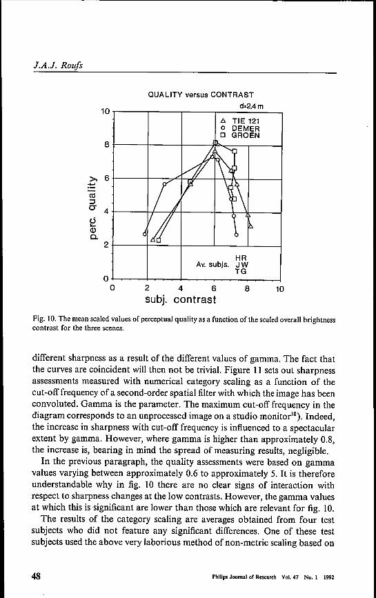
J.A.J. Roufs
Fig. 10. The mean scaled values ofperceptual quality as a function ofthe scaled overall brightnesscontrast for the three scenes.
different sharpness as a result of the different values of gamma. The fact thatthe curves are coincident will then not be trivial. Figure 11 sets out sharpnessassessments measured with numerical category scaling as a function of thecut-off frequency of a second-order spatial filter with which the image has beenconvoluted. Gamma is the parameter. The maximum cut-off frequency in thediagram corresponds to an unprocessed image on a studio monitor"). Indeed,the increase in sharpness with cut-off frequency is influenced to a spectacularextent by gamma. However, where gamma is higher than approximately 0.8,the increase is, bearing in "mindthe spread of measuring results, negligible.In the previous paragraph, the quality assessments were based on gamma
values varying between approximately 0.6 to approximately 5. It is thereforeunderstandable why in fig. 10 there are no clear signs of interaction withrespect to sharpness changes at the low contrasts. However, the gamma valuesat which this is significant are lower than those which are relevant for fig. 10.The results of the category scaling are averages obtained from four test
subjects who did not feature any significant differences. One of these testsubjects used the above very laborious method of non-metric scaling based on
10
8
>. 6......~:::Jer 4èID0-
2
00
48
QUALlTY versus CONTRASTd=2.4m
Á TIE 121oDEMERD GROEN
HRAv. subjs. JW
TG
2 4 6 8 10subj. contrast
PhiUps Journalof Research Vol. 47 No. 1 1992

PhiUps Journal of Research Vol.47 No. I 1992 49
Perceptual image quality
10SHARPNESS
tQ):::Ica> 5
~caC)(/)
-------- category scaling--- pair comparison
.1
~ ....,~_ ..-
.8 1. 1.2
-+- cut off frequenty fe(log cycles/degree)
Fig. 11. Sharpness assessment as a function of the cut-off frequency with gamma as parameter.The sharpness measured with category scaling is the average obtained from four test subjects. Oneof these test subjects used the method of non-metric scaling on the basis of comparison of pairs.
comparison of pairs. The results have been simultaneously fitted to those ofcategory scaling by means of a linear transformation. The coincidence betweenthe results obtained from the (relatively fast) method of category scaling andthe method of non-metric scaling which is regarded as the most valid methodis encouraging for the validity of scaling on the basis of numerical categorieswhich are fast and relatively simple to use.
3.5. Perceptual quality, spatial resolution and image size
The measurement of perceptual image quality as a function of spatialresolution can also be instructive if the intermediate step of measuring subjec-tive sharpness as a function of the resolution parameter is omitted. Thefollowing example may perhaps illustrate this. Figure 12 sets out quality

l.A.J. Roufs
8
7
6
Fig. 12. The perceptual quality as a function of the 6 dB spatial cut-off frequency in periods perdegree. The image width is the parameter.
assessments of projected slides as a function of the 6 dB spatial cut-offfrequency varied by defocusing, with the height of the square images as theparameter'"}, There is a tilting point at approximately 25 periods per degree.This is also expected because we are entering the realms of the eyes' ability todistinguish detail. The parallel nature of the curves points to an absence ofinteraction with image size.In fig. 13, the 6 dB cut-off frequency of fig. 12 has been replaced by the
bandwidth-related cut-off frequency which is obtained by multiplying the firstparameter by the image width and which is a measure ofthe maximum numberof pixels which can be fitted on the width of the image. It is thus in reality ameasure for the bandwidth as defined by the apparatus. The curves are veryclose to each other.It appears that the bandwidth-related resolution is to a first approximation
a physical measure which is quite relevant in perceptual terms. FigureTdillustrates the iso-quality relations between image width and bandwidth-related resolution taken from fig. 12 and SOmeadditional measurements. Thenumbers next to the curves are the quality assessments. The circle indicatesapproximately the location oftoday's TV equipment (impairment with respectto lines, etc., is of course missing in this situation). The figure indicates that anyincrease in the size ofthe image does not provide much assistance in improvingthe quality. The triangle refers to an HDTV system, and the broken linerunning through the triangle demonstrates the quality change with the imagesize which would then be possible. It is clear that the perceptual quality of
50
picture width.92m.72.48.24
0+- __o 2
log(fan9) [ log(-/·)J
Philips Journalof Research Vol,47 No, 1 1992

Perceptual image quality
8
7
6
~5t1lg.4.~ 3Ü.!!?. 2.0::Jen 1
picture width.92m.72.43.24
~B5
o~ __1 2 3
log(fang.b) Ilog(m -/o)J
Fig. 13. The perceptual quality as a function of the bandwidth-related spatial resolution.
E
s: 8-c.~
7.5e 0 /::::,.::J Iti 7.ä.
6.55 6
o~~ __~ ~~ __~ ~ __~o 200 400 600 800 1000
bandwidth-related resolution (periods)
Fig. 14. Image width as a function of bandwidth-related resolution under different image qualityassessments. The curves are based on the data taken from fig. 12 and some complementarymeasurements.
Philips Journal of Research Vol.47 No. I 1992 51

52 Philips Journalof Research Vol.47 No. I 1992
l.A.J. Roufs
reproduetion equipment only really improves as bandwidth-related resolutionincreases if the image width (and thus the overall surface area) is sufficientlylarge.
3.6. Image coding and the assessment of image impairment
The increased possibilities of digital image processing have opened up anentirely new field of image quality research. Analogous to that which occurredseveral years ago in speech technology and which had such a beneficial effectin that discipline, digital processing is now opening up the possibilities ofanalysis by means of synthesis. Images can be broken down in all types ofways, and after any processing which may have been performed they can thenbe reconstituted. In this process, it is possible to check what image informationis relevant in perceptual terms or which processing improves the perceptualquality. We have already seen some examples in this paper.. In the context of what has gone before, it is sometimes useful to describeimages by means of various series or polynomials. Images can be described ina number of ways. In our institute, we prefer descriptions which closelyapproximate analysis such as that performed by the peripheral visual system.So-called Hermite transformations'") are examples in this respect. Also withthe techniques used to compress image information, it is possible to proceedin a manner similar to the early signal processing by the human visualsystem4b•4d). The general motto is that the coding does not have to be betterthan the ability of the eye to perceive. The information gain in conjunctionwith "non-lossless" coding will of course also depend on the quantity of imageimpairment which is acceptable. If several types of fundamentally differentimage impairments occur, then it is frequently a question of how the totalityof such impairments influences the overall quality of the image. The finalcriterion of quality can only be based on the judgement made by the perceiver.It is sometimes more useful to scale image impairment instead of quality"),
This is for instance the case if we wish to study impairment as a result ofquantisation errors with so-called scale-space coding. Figure 15 sets out asimplified diagram of scale-space coding"). This diagram displays only twolayers with binomial convolution kernels of this hierarchical pyramid codingsystem. The first layer illustrates the sampling of the original image by meansof a number of 2D kernels at a distance of 2 pixels. The resultant image canbe found by interpolation and compared with the original image. Only theerror sigrlal is passed on. This process is repeated again in the subsequentlayers. The quantisation steps qo and ql of the uniform quantisers Q are now

."e:c::Ol..oc~s-
r...<:11-~:z!'
~
Ut~
4x4decimation 128x128x8 bit
'"D2 L2 L2
• coarser 1lowpass image I P2 li 2x2 2x2 P2 I2D-kernel interpolation interpolation
J2x2
256x256x8 bit ql =1,2, .. ,127decimation +- ,.---r '\ prediction Q quantized r '\ '"
Dl LI \....-1 error prediction error \....-I LI'--- 1db finest
2D-kernel lowpass image I PI li 2x2 2x2 PIinterpolation interpolation
512x512x8 bit qo=l,2, .. ,127 +- -r:1\ prediction Q quantized r 1\ '"La \...LJ error prediction error \...L/ La
-original image(ûigi tized)
Fig.15. Simplified diagram of a scale-space coding algorithm").
~~~i:l::>--§j"~~:;::l::>--~.

04---~----r---~--~---'----~o
J.A.J. Roufs
Impairment / unsharpness4 subjects
10
90---0 impair..__. unsharp.
8
7Q)
:J 6-0> 5~0o 4Ul
3
2
--====-Q
10 20 30 40 50qO
60 110 120 130
Fig. 16. Impairment and unsharpness defined by means of numerical category scaling as a functionof step size qo.
significant. Large steps create image-impairment artifacts in the form ofunsharpness and/or speckles.
Figure 16 sets out the results of assessment of perceived impairment causedby following step size qo. In this case, only the signals ofthe finest pattern havebeen quantised. The same figure also sets out the degree of unsharpness orblur, which is one of the factors of impairment. Because test subjects statedthat impairment consisted only of blur at the largest quantisation steps, thescale values at that point have been equalised by means of a linear transform-ation. The systematic differences between both measurements are assumed tobe a result of the speckles. Figure 17 is then a linear transformation of thedifferences taken from fig. 16, together with the scaled strength of the speckles.The identical shape of both curves is an indication that the strengths of the
attributes in both dimensions of impairment simply add up in this case, as setout in an assumption made by Allnatt"),A second example ofthe connection between perceptual quality and impair-
ment factors is to be found in research into optical filtering used to blur theimpairment structure of line sampling. The optical blurring filter is charac-
54 Philips Journalof Research Vol. 47 No. I 1992

Philips Journalof Research Vol.47 No. I 1992 55
Perceptual image quality
Speckles / difference4 subjects
10~------------------------
0+---,---,---,---,---,---,-o 10 20 30 40 50 60 110 120 130
qO
9
Q)
::J 6C> 5Q)
CU 4(IJ
7
8
..........
__ speckles0----01.4+6.8.0if
J
Fig. 17. Scaled strength of speckles in comparison with a linear transformation of the differencestaken from fig. 16.
terised by the standard deviation of its Gaussian point spread function. Asillustrated in fig. 18, quality increases initially as a result of the blurring of thedisturbing line structure as (J increases, and subsequently tails off as a result ofincreasing blur"),
3.7. Scaling of comfort and pelformanee measures
Finally, we shall provide a further example taken from a performance-oriented environment, namely VDUs. This will enable us to compare objectiveand subjective measurements.Many people have already experienced that poorly designed VDUs, if they
are used intensively over long periods, lead to all types of complaint, such asfatigue or stinging eyes. Frequent attempts have been made to measure fatiguein an objective manner. However, none of the methods employed so far hasproven satisfactory"). However, the problem can also be tackled from anotherdirection, namely from the point of view of reading comfort"), It turns outthat test subjects have a clear idea of the ease with which a text can be readon a computer screen. Research into the process of reading has indicated thatthe eyes do not glide smoothly over the text during the reading process; on thecontrary, the eyes tend to jump (saccades). The size of these saccades declinesas the text becomes more difficult. In this case, the pause between the saccades

I.A.J. Roufs
columnar structure, circular filter_. 0.090---0 1.78_" 2.67
10
9
8
7>-..... 60::s 5C"
4
3
2
10
__I-'_I-II---.
2 3sigma [minutes of arc]
Fig. 18. Scaled perceptual quality as a function of the standard deviation of the Gaussian pointspread function which characterises the optical filter which blurs the column structure of the pixelarrangement. The parameter is the pixel pitch in minutes of arc.
in which the information is digested, the so-called fixation pause, is also longer.It is now obvious to assume that the same phenomenon would occur if weensure that a text is less legible in another manner, e.g. by means of poorcontrast, blur or a difficult shape. It is possible to measure movements of theeye. Furthermore, it is known that reading speed, which can also be easilymeasured, is a meaningful measure of performance").
In order to eliminate the effect of text semantics, we have chosen a searchtask in a pseudo text. This text has been formed by strings of randomlypositioned characters (letters and digits), where the length of such strings isdistributed as would be the case encountered in normal text. Figure 19 is anexample of the "BEEHIVE" type.
If the viewer squints, it appears almost to be normal text. The task of thetest subjects is to scan the text as quickly as possible in order to establishwhether a certain character is present. In the following examples"), this is thecapitalletter A. Figure 20 sets out the mean comfort assessment on a numericalten-point category scale as a function of the logarithm of the luminancecontrast ratio between the character and the background for the "BEEHIVE"font. The comfort assessment initially increases rapidly with contrast. Theposition of the maximum values of comfort judgement for both polarities isinfluenced by the font. It should be noted that, at the lowest contrasts, the textis still sufficiently legible to ensure that no errors are made.
Let us now compare this with the saccadic lengths also measured during the
56 Philips Journalof Research Vol.47 No. I 1992

Philips Journal of Research Vol.47 No. 1 1992 57
Perceptual image quality
6M 4KVGWY09L9VHVI3F TNJY0 7AFSXOY M8HINOM4EZB6I T08 XAMP 9NFN7ST6IG4GY YOE6 YA10S0FT BGZIHLIT CHIL 9LA7ENO W9HB J1RVHOWGCSUY1X44C8G EEGITU52L44WJ215N618G ZYH 1SJ002 ANO 818X3Y 0LX7M4 B7HH4FR1H HTU 21EP CC VUOXKPZRB TS00 WIW07 VY4THH83301 TOF8H AI4PFYCN71 NH GTY406LV0UHSW24X020 TVY 1J AMN2DH9FOE0WGGFOWGRBA340L 1R 3789 NNVFX9T5 ZU105L IY00V P19V 3R5 IC CF0VR01MUL VEXS 2XOA4S0L9 NT8G7T 59WI6T EAX 4MGEZR 5JJHBH OCKY LP3VFig. 19. Example of a test page set in "BEEHIVE" type.
search task in fig. 21 and the fixation lengths in fig. 22. (As a text becomes lesslegible, the eye requires a longer period of time in order to register theinformation, and the fixation pauses also become longer.) As a consequence,the fixation duration has been set out downwards in order to allow a goodcomparison with the other variables.And finally, the measured performance expressed as the number of
characters per second is set out in fig. 23. The high degree of correlationbetween the four variables is obvious at a glance (the mean Pearson correlationcoefficient between visual comfort and the other three dependent variables isr = 0.87). However, this is probably one of the rare cases where scaling resultscan be verified by means of objectively measurable variables.
4. Conclusions
The above results can be summarised as follows.• The concept of image quality only becomes meaningful within the contextof the objective of image reproduction. It is useful to make a distinctionbetween appreciation-oriented and performance-oriented image quality.• The perceiver is the ultimate criterion of image quality.• Provided that the necessary precautions are taken, psychological scaling canbe a useful aid in defining the relationship between perceptual quality and thephysical parameters, as demonstrated by the examples which have been pro-

J.A.J. Roufs
3 sUbjects: 4 presentations: N-12~: mean luminance 40 cd/m**2~: mean luminance = 200 cd/m**2
....~ 7E~ B -1---1-u.~ 5 -I----+-
9
9
-0.5 0.0 0.5 1.0 1.5 2.0contrast: log [Lc/Lb]
Fig. 20. The mean comfort judgement of three test subjects as a function of the logarithm of theratio between the luminance of the character and the luminance of the background. Positive valuesof this log ratio represent bright letters on a dark background. Negative values represent darkletters on a bright background.
vided. It is the only method if the more familiar methods such as thresholdmeasurements or matching are not capable of providing relevant information.• It is also the appropriate means of measuring the strength of the perceptualattributes on which perceptual quality is based as a function of the relevantphysical parameters, thus obtaining an insight into the relationship betweenimage quality and the physical parameters.• In terms of validity, the numerical category scaling method, which is rela-tively fast and easy to apply, provides encouraging results where it has beentested on laborious non-metric scaling methods with high validity or onpsychophysical matching.• Trade-off functions which are frequently important in practice can bederived from the iso-quality curves or iso-sensation curves which can bededuced from scaling results.• Matching also appears to be a feasible method of defining trade-off func-tions and can also be used as an aid for testing the validity of scaling in certainpoints.
58 Philips Journalof Research Vol. 47 No. I 1992

3 sUbjects; 4 presentationsm: mean luminance 40 cd/m**2~: mean luminance = 200 cd/m**2
Perceptual image quality
5.5
ID Ic,l1l.c~ 1.2
s: 5.0-iJOl CîcOl CD
r-t 10...,o 1.1 CD
·MCD
'C enl1lo 4.5ol1l(IJ
c 1.0mOlE
300
(IJ
§
cl1lOlE
-0.5 0.0 0.5 1.0 1.5 2.0contrast: log [Lc/Lb]
.--l---I---- ._--
450 .I-__ .l-_--I __ --+__ --I-__ -l-__ -l
-1.0
Fig. 21. Mean saccadic length of the same three test subjects, measured during the search task, asa function of the logarithm of luminance contrast ratio.
3 sub j ect.s:4 presentationsm: mean luminance 40 cd/m**2~: mean luminance = 200 cd/m**2
co·M-iJ 350 f----I---l1lc,::J'C
Co'M-iJ~ 400 -1----1--·rt
Fig. 22. Mean fixation durations for the same three test subjects, measured during the search task,as a function of the luminance contrast ratio.
Philips Journalof Research Vol.47 No. 1 1992
-0.5 0.0 0.5 1.0 1.5contrast: log [Lc/Lb]
2.0
S9

1.5
-0.5 0.0 0.5 1.0 1.5 2.0contrast: log [Lc/Lb]
Fig. 23. Mean scanning speed expressed in the number of characters per second and averaged overthe three test subjects as a function of luminance contrast ratio .
• Differences which may occur between test subjects with normal visualfaculties and identical experience are usually of minor importance. Differencesbetween test scenes may cause major differences in results. In other words,greater attention must be paid to the representativeness of scenes than to therepresentativeness of test subjects.
Acknowledgements
I wish to thank Herman Bouma, Frans Blommaert, Jean-Bernard Martensand Huib de Ridder for their comments on an earlier version of themanuscript.
REFERENCESIn) H. de Lange, Experiments on flicker and some calculations ori an electrical analogue of the
foveal systems, Physica, 18,935-950 (1952).Ib) J.A.J. Roufs and F.J.J. Blommaert, Temporal impulse and step responses of the human eye
obtained psychophysically by means ofa drift-correcting perturbation technique, Vision Res.,21, 1203-1221 (1981).
2a) O.H. Schade, Electro-optical characteristics of television systems. I, characteristics of visionand visual systems, RCA Rev., 5 (1948).
2b) O.H. Schade, Optical and photoelectric analog of the eye, J. Opt. Soc. Am., 46, 721-739(1956).
60 Philips JournnI of Research Vol.47 No. I 1992

Philips Journal of Research Vol.47 No. 1 1992 61
Perceptual image quality
2C) F.W. Campbel1 and J.G. Robson, Application of Fourier analysis to the visibility of gratings,J. Physiol., 197, 551-566 (1968).
2d) F.J.J. Blommaert and J.A.J. Roufs, The foveal point spread function as a determinant fordetail vision, Vision Res., 21, 1223-1233 (1981).
3) J.A.J. Roufs, Dynamic properties ofvision. 11, theoretical relationships between flicker andflash thresholds, Vision Res., 14 (12), 279-292 (1972).
4a) D. Marr, Vision, Freeman, San Francisco, CA, 1982.4b) J.B.O.S. Martens and G.M.M. Majoor, The perceptual relevance of scale-space image coding,
Signal Process., 17, 353-364 (1989).40) F.J.J. Blommaert and J.B.O.S. Martens, An object-oriented model for brightness perception,
Spatial Vision, 5, 15-41 (1990).4d) J.B.O.S. Martens, Application of scale space to image coding, IEEE Trans. Commun., 38,
1585-1591 (1990).5) J.A.J. Roufs and H. Bouma, Towards linking perception research and image quality, Proc.
SID 21, 247-270 (1980).6a) M.C. Boschman and J.A.J. Roufs, Comparison of methods for the evaluation of VDUs, 11
The effect of band-width, SID 90 Digest 21, 17-20 (1990).6b) J.A.J. Roufs and M.C. Boschman, Visual comfort and performance, Chap. 3 in Vision and
Visual Dysfunction, gen. ed. J.R. Cronly-Dillon, Vol. 15, The Man-machine Interface, ed.J.A.J. Roufs, MacMillan, pp.24-40, 1991.
7.) W.S. Torgerson, Theory and Methods of Scaling, Wiley, New York, 1958.7b) B. Wegener, Social Attitudes and Psychophysical Measurement, Lawrence Erlbaum Ass.,
Hillsdale, NJ, 1982.8) A.L. Edwards, Techniques of Attitude Scale Construction, Appleton-Century-Crofts, New
York, 1957.9) L.L. Thurstone, A law of comparative judgement, Psychol. Rev., 34, 273-286 (1927).
lOa) W.A. Wagenaar, Misperception of exponential growth and the psychological magnitude ofnumbers, in Social Attitude and Psychophysical Measurement, ed. B. Wegener, LawrenceErlbaum Ass., Hillsdale, NJ, Chap. 11, pp.283-302, 1982.
lOb) S.J. Rule and D.W. Curtis, Levels of sensory and judgmental processing; strategies for theevaluation ofa model, in Social Attitude and Psycholophysical Measurement, ed. B.Wegener,Chap. 4, pp.107-122, 1982.
lIa) J.B. Kruskal and M. Wish, Multidimensional Scaling, Sage Publications, London, 1978.lib) R.N. Shepard, Metric structures in ordinal data, J. Math. Psychol., 3, 287-315 (1966).12) J.W. Al1natt, N. Gleiss, F. Kretz, A. Sciarapa and E. van der Zee, Definition and Validation
of Methods of Subjective Assessment of Visual Telephone Picture Quality CSE2T, Raportitechnici XI, 59-65 (1983).
13) E. van der Zee and M.H.W.A. Boesten, The Influence of Luminance and Size on the ImageQuality of Complex Scenes, IPO Annual Progress Rep. 15,69-75 (1980).
14) M.H.W.A. Boesten and E. van der Zee, Psychophysical versus Psychometrie Methods inImage Quality Measurements, IPO Annual Progress Rep. 16,67-71 (1981).
15a) E.J. Breneman, The effect of level of illumination and relative surround luminance on theappearance ofblack-and-white photographs, Photogr. Sci. Eng., 6,172-179 (1962).
15b) C.J. Bartleson and E.J. Breneman, Brightness reproduetion in the photographic process,Photogr. Sci. Eng., 11,254-262 (1969).
16) J.A.J. Roufs and A.M.J. Goossens, The effect of gamma on perceived image quality, Proc.1988 Int. Display Conf., San Diego, CA, IDRC Digest 1988, IEEE, New York, pp.27-31,1988.
17.) T. Nakayama, K. Massaak, K. Honjyo and K. Nishimoto, Evaluation and prediction ofdisplayed image quality, Proc. SID 80 Digest, pp.l80-181, 1980.
17b) J.H.D.M. Westerink and J.A.J. Roufs, Subjective image quality as a function of viewingdistance, resolution and picture size, SMPTE J., 98, 113-119 (1989).
18) J.A.J. Roufs, Brightness contrast and sharpness, interactive factors in perceptual imagequality, in Human Vision, Visual Processing, and Digital Display, Proc. SPIE, 1077, 66-72(1989).
19a) J.B.O.S. Martens, The Hermite transform; Theory, IEEE Trans. Acoust. Speech SignalProcess.,38, 1595-1606 (1990).

J.A.J. Roufs
19b) J.B.O.S. Martens, The Hermite transform; Applications, IEEE Trans. Acoust. Speech SignalProcess.,38, 1607-1618 (1990).
20) H. de Ridder and G.M.M. Majoor, Subjective Assessment of Impairment in Scale-spaceCoded Images, IPO Annual Progress Rep. 23, 55-64 (1988).
21) J.W. Allnatt, Transmitted Picture Assessment, Wiley, New York, 1983.22) M.R.M. Nijenhuis and F.J.J. Blommaert, Perceptually Optimal Filters for Spatially Sampled
Imagery, IPO Annual Progress Rep., 25, 66-73 (1990).23) P. Padmos, Visual fatigue with work on visual display units; the current state of knowledge,
in Human-Computer Interaction; Psychonomie Aspects, eds G.C. van der Veer and G.Mulder, Springer-Verlag, BerIin, pp.41-52, 1988.
24.) J.A.J. Roufs, M.A.M. Leermakers and M.C. Boschman, Criteria for the subjective quality ofvisual display units, in Work with Display Units 1986; Selected Papers from the Int. ScientificConf. on Work with Display Units, eds B. Knave and P.G. Widebäck, Stockholm, Sweden,pp.412-417, 1987.
24b) J.A.J. Roufs and M.C. Boschman, Visual comfort and performance, in Vision and VisualDysfunction, gen. ed. J.R. Cronly-Dillon, Vol. 15, The Man-machine Interface, ed. J.A.J.Roufs, pp.24-40, 1991.
25') J.D. Gould and N. Grischkowsky, Doing the same work with hard copy and cathode-ray tube(CRT), Human Factors, 26, 323-337 (1984).
25b) J.D. Gould, L. Alfaro, V. Barnes, R. Finn, N. Grischkowsky and A. Minuto, Reading isslower for CRT displays than for paper; attempts to isolate single-variable explanation,Human Factors, 29, 269-299 (1987).
26) J.A.J. Roufs, M.C. Boschman and M.A.M. Leerrnakers, Eye movements, performance andvisual comfort using VDTs, in Eye Movements; from Physiology to Cognition, Selected/Edit-ed Proc. 3rd European Conf. on Eye Movements, Dourdan, France, 1985, eds J.K. O'Reganand A. Levy-Schoen, Amsterdam, pp.612-613, 1985.
AuthorJacques A.J. Roufs: Ir. degree (physics), 1966; Ph.D. degree (technical sciences), EindhovenUniversity of Technology, 1973; Physical Laboratory of Philips Lighting Division, 1946-1958;Eindhoven University of Technology/Institute for Perception Research (IPO), 1958-19 ; groupleader of the Vision department ofthe IPO and professor at Eindhoven University of Technology.An important part of his work has been devoted to the processing of temporal and spatial visualstimuli. In the last decade he has specialised in image quality problems. He is involved in manynational and international committees, concerned with subjects from his field of interest.
62 Philips Journalof Research Vol.47 No. 1 1992

PhiUps Journal of Research Vol.47 No. 1 1992 63
Philips J. Res. 47 (1992) 63-80 R1266
LAYERED APPROACH IN USER-SYSTEMINTERACTION
by F.L. ENGEL and R. HAAKMAInstitute for Perception Research, P.O. Box 513,5600 MB Eindhoven, The Netherlands
AbstractNormal inter-human conversation is very efficient in terms of speed andaccuracy of intention transfer. Firstly, exchanged messages carry onlysufficient information relative to the contextual knowledge assumed to bepresent on the part of the receiver. Secondly, by the reception of layeredfeedback the speaker is able to verify at an early stage of message decodingwhether his intentions are accurately perceived. Thirdly, through verifi-cation of layered expectations about the message elements still to bereceived, the listener might ask the speaker for clarification at an early stageof message interpretation.
Likewise, user-system interaction has to become similarly more efficient.Therefore, machine interfaces should also apply layered feedback aboutearly message interpretations as well as layered expectations about themessage components still to be received. Some. interfaces are identifiedwhich already partly possess these desirable cha-racteristics.
In this paper we extend the "layered protocol model" proposed byTaylor (M.M. Taylor, Int. J. Man-Machine Studies, 28, 175-218 (1988»,containing layered feedback and related repair messages, with layeredexpectations derived from assumed intentions and layered knowledge ofthe interaction history.Keywords: communication efficiency;context-sensitive message decoding;
feedback, error and ambiguity handling; intention transfer;layered communication; man-machine communication; multi-modal interaction; secondary communication; user interface.
1. Introduetion
In general, messages in human communication carry only sufficient infor-mation relative to the knowledge context already available. As a result, humancommunication is very context dependent, i.e. it takes place in close relationto the changing knowledge and beliefs (unverified knowledge) of the inter-acting parties; see for instance ref. 1.Also, people can simply refer to what has

F.L. Engel and R. Haakma
been mentioned earlier in the dialogue, "anaphora"; see for example ref. 2.This makes communication considerably faster. A disadvantage, however, isthe increase in errors and/or ambiguities in communication caused by differ-ences in the contextual knowledge of sender and receiver.On the other hand, user-system interaction makes use of fixed, context-
independent coding conventions. Furthermore, the communication band-width in user-system interaction is increasing rapidly. This is due to technicaldevelopments such as the extension of the user interface with graphics andmultimedia capabilities, like video and natural-language input/output. Thisincreasing bandwidth is indeed beneficial for unhampered communication. Atthe same time, however, the functionality of modern computer-supportedsystems, such as video cassette recorders, car radios and copiers, also continuesto increase, often leading to "hidden functionality'").
For the near future it is expected that such complex computer-controlledappliances will demand extensive and in particular interactive user support(interactive error communication, ambiguity resolution, help, documentationand tutoring) to make them easier to learn and more efficient to handle.Accordingly, it is assumed that communication efficiency of the interactionprocedures as well as their easy mastering by the user will become major issuesin modern user interface design. The main research question will then be: howto apply the increased communication bandwidth in a more natural andefficient way for interactive user support.
In order to be able to appreciate more fully what is involved in efficient andmore natural user-system interaction (i.e. corresponding to the way peoplecommunicate with each other), we shall introduce in Sec. 2 the layered struc-ture of human communication as proposed by Taylor4). The role of layeredfeedback, the first factor supporting communication efficiency, is described inSec. 2.1. A second factor supporting communication efficiency is the active useof receiver expectations, known as "analysis by synthesis": the messagereceiver compares the incoming message elements with his layered expec-tations. This con.cept of expectations will be incorporated in Taylor's layeredcommunication model (Sec. 2.2). The extended model allows for the systematicdesign and analysis of user support in user-system interaction. We also claimits importance for the communication efficiency ofuser-system interaction. InSec. 3 we briefly consider "secondary communication", i.e. the "dialoguecontrol acts" used for the transfer of secondary intentions such as feedback,error recovery etc. In Sec. 4 conclusions are presented.
64 Philips Journalof Research Vol.47 No. I 1992

Layered approach in user-system interaction
Primaryintentionsent
Primaryintentionreceived
Sprlm
Fig. I. Sender Sprim transfers primary intentions to receiver Rprim byencoding them intoprimary messages suitable to be transmitted to the receiver by modulation of the physicalparameters of the selected communication channel(s).ln turn, the receiver ofa message is assumedto decode the incoming messages back again into the intentions originally sent. To minimizepossible errors and ambiguities in communication of the primary intention, secondary corn-munication is frequently needed. Sender Ssec of the receiver of the primary message sends themto receiver Rsec of the sender of the primary message.
2. Taylor's model
"Intention transfer" is a basic notion in Taylor's model of layered com-munication. To obtain information or to let others, men as well as machines,knowor do things, one has to communicate one's intentions by the exchangeof messages. Messages describe these goals in coded form, their coding beingmore or less adapted to the transmission characteristics (modulationparameters, bandwidth, error probability, etc.) of the specific communicationchannels used. Message transmission takes place through the modulation ofthe physical parameters of the selected communication channel(s), such assaying a word, making a gesture, and accordingly in user-system interaction,by pressing a button, moving a trackbalI, etc.
Accordingly, the sender encodes the intention(s) concerned into messages tobe transmitted to the receiving party. In turn, the message receiver is assumedto decode the incoming messages back again into the original intentions of thesender. For handling possible faults (errors and/or ambiguities) in encoding,communication and decoding of the primary intention, secondary com-munication is frequently needed (fig. I).
Feedback, viz. observing the reactions of the receiver to the messages sent,is an important means for the sender to detect faults in the decoding of thismessage.
Philips Journalof Research Vol.47 No. t 1992 65

Intention Intention
F.L. Engel and R. Haakma
Fig. 2. Layered cornrnunication between mutually related message coding and decoding stages. Onthe left-hand side the incoming primary intention becomes successively encoded by the sendercolumn (Sprim) until at the lowest layer the primary message is physically transmiued to thereceiver column (Rprirn) on the right-hand side. The primary receiver stages will successivelydecode the message back until the original intention is recovered again. Ssec and Rsec, respective-ly, represent the secondary message sender and receiver column, needed for communication offeedback messages, calls for clarification about the primary message as well as possible repairmessages.
2.1. Layeredfeedback
The human information processing cycle is considered to have several stagesof coding and decoding (see Wundt (1880), quoted by Boring") at the percep-tion side and Norman") and Levelt") at the production side).
With regard to this hypothesis of subsequent coding stages, it is assumedthat the primary intention to be transmitted becomes repeatedly decomposedby planning procedures into sequences or other temporal combinations oflower-level sub-intentions, until at the lowest (physical) level these (sub- )subintentions are converted into elemental physical actions that modulate theparameters of the communication channel involved. The reverse is assumed tohappen at the receiver side, where incoming messages are sensed and convertedinto sequences of decoded sub-intentions, which are recognized in their turn asrepresenting higher-level (sub-)intentions, etc. (fig. 2). In this approach seman-tics (intention) and syntax (message structure) exist at each level.
The essence of feedback is that the output obtained from a (communication)process is compared with the related input. Consequently, feedback comingfrom a specific message decoding step at the receiver side should be addressedto the corresponding encoder step at the sender side. This is illustrated by the
66 Philips Journalof Research Vol. 47 No. I 1992

Layered approach in user-system interaction
Fig. 3. Intention-to-action encoding scheme for making an inter-local telephone call to the IPQ.The main intention is broken down further into sub-intentions to be achieved. The elementalintentions distinguished at the lowest level are directly converted into physical communicativeactions.
secondary messages in fig. 2. By dividing the receiver's message-to-intentiondecoding process into a number of successive processing steps, feedback of theintermediate decoding results can be given to the message sender at an earlystage, thus enabling the sender to prevent an accumulation of faults and thusincreasing the efficiency of communication.Often, more communication channels of different sensory modality are
simultaneously available. In that case, messages can and will be transmitted inparallel too. Voice is frequently combined, for example, with gestures, direc-tion of gaze, etc. Given that they support the transmission of the sameintention, these parallel, multi-modal messages have to be recombined at acertain stage of decoding, thus offering yet another indication of layeredcoding in communication.
Example of layeredfeedback in user-system interaction: the telephonenumber selection application
Figure 3 shows part of the intention-to-action encoding scheme needed ifone wants to make a national inter-local telephone connection to the Institutefor Perception Research (IPO) in Eindhoven, the Netherlands. Lifting of thehandset for initiating the interaction with the switching centre, as well as thespoken callerfcallee identification protocols have been omitted.At the highest level of this goal tree, the intention of the caller is to send the
telephone number to the telephone switching centre. This intention becomessplit into two sub-intentions, namely to send the area and local code. Thesesub-intentions become decomposed further into sub-sub-intentions about
Sub-sub-intentions:
Sub-in êntlon:Send Area code
040
~Send Send Send
1stdigit 2nd digit 3rd digit040
+ + +Press Press Presskey key keyo 4 0
Sub-sub-sub-intentions:
PhiUps Journalof Research Vol. 47 No. 1 1992
Intention:Send tel. number040 -773873
SendIstdigit
7
+Presskey7
Send3rd digit
3
+Presskey3
Send4thdigit
8
+Presskey8
Send6thdigit
3
+Presskey3
Send5th digit
7
+Presskey7
Send2nddigit
7
+Presskey7
67

F.L. Engel and R. Haakma
sending the individual digits. Finally, these intentions to send digits are con-verted into physical actions by pressing the number keys of the telephone set.During the whole process of making the telephone call the system supplies
the caller with feedback signals. After lifting the handset from its clamp, thepresence or absence of a specific dial tone signals whether a line connection hasbeen made between the telephone set and the telephone centre, so that thedesired number can be keyed in. Another tone indicates when the area code hasbeen received and a line is made available to the desired telephone area. Thecallee's bell signal is also presented to the caller after both successful receptionof an interpretable number and successful realization of the full connection.Note that number reception and line selection are closely coupled in the
telephone system. Decoding of the telephone number and building the connec-tion are realized together, so that the caller in fact receives layered feedbackabout the availability of the lines and whether the set of the callee is busy,instead of whether his messages have been correctly received.
From the above description it follows that the telephone system provideslayered feedback to its user, namely at the layer of telephone numbers and atthe layer of area and local code. The beginning and end of these message unitsare uniquely marked by dialling tones. Note, however, that no feedback isgiven on the area code in the case of international calls. This lack of feedbackleads to a significant decrease in communication efficiency in the case ofoccupied lines, as the entire telephone number has to be keyed in again. At thekeystroke level tactile feedback is given while pressing the telephone keys. Nofeedback is supplied at the digit level, however. The caller is not informedabout what digit is received nor about the number of digits already received.Related input errors cannot be detected by the caller until the phone call hasbeen answered. This presents an inefficient and possibly embarrassing situ-ation with the callee. Happily, modern touch-tone sets show the selected digitson a small LCD panel.
2.2. Expectations in human perception
In addition to layered feedback, the use of context knowledge significantlyenhances accuracy and speed in inter-human communicationê'"). In humanspeech understanding, data-driven, bottorn-up recognition processes are assistedby top-down concept-driven planning processes that support message interpret-ation through the generation of expectations. Expectations arise at differentlevels of decoding. For their generation, structural (syntactic) and interpret-ative (semantic) context knowledge is used at the levels of phonemes, words,
68 Philips Journal of Research Vol.47 No. I 1992

Philips Journal or Research Vol.47 No. I 1992 69
Layered approach in user-system interaction
Recognizedintention
AssumedglobalintentionI-feedback-- - - --
E-feedback-- - -- ---------,I
Expectation IMessage rccognizcr I-__:'---'--I
tAdjustment
Input message
Fig. 4. Illustration of the main signals and functions distinguished in a context-sensitive messagedecoder. The message recognizer makes the conversion from specific chunks of lower-level inputmessages into a recognized (higher-level) intention. The user is assumed to be provided withfeedback about the decoded intention(s) (I-feedback). Expectations constrain the message inter-pretation process. The anticipator derives its expectations from knowledge already available aboutboth the global intention of the interaction and knowledge about the current interaction history.In the case of feedback of machine expectations (E-feedback), the user might be in the positionto adjust them.
utterances and even at the level of discourse, for example in a discourse by firstgiving a rough indication about the intention of primary communication.Expectations improve decoding efficiency in a number of ways. First, by
constraining the look-up activity through early selection of the relevant set(lexicon) of decoding transformations. They also enable verification ofdecoded (sub-)intentions through comparison with the expectations made. Inthe case of a discrepancy, the listener might ask for an explanation at an earlystage of decoding. Finally, in the situation where the listener is so fast that heutters his anticipations even before the speaker has expressed his intentions,the speaker only needs to confirm (one of) them, thus again achieving anincrease in speed.In the next section we will pay further attention to context-dependent
machine expectations in user-system interaction. Two context-sensitivedecoder models will be introduced, single- and multi-layer, and for each anexample will be given. Note that in general implicit, fixed machine expectationsare already built into each machine function.
2.2.1. Single-layer context-sensitive model
A first attempt at a single-layer context-sensitive decoder is illustrated in fig.4. It shows a message recognizer extended with an "anticipator", together withthe most significant signals and the relevant feedback signals. These areI-feedback about the already interpreted message part(s) and E-feedback

giving the current receiver expectations about the message segment(s) still tocome.
The application ofmenus in user interfaces, representing context-dependentmachine expectations, can be compared with the situation in human interac-tion where the receiver already gives his anticipations before the sender hasexpressed his intentions. As machine expectations have to be based in practiceon a very limited amount of contextual knowledge, and therefore can bewrong, their early verification through E-feedback is of special importance inuser-system interaction. Of course, in the case of incompatible machine expec-tations, the user should for efficiency reasons be given the possibility ofadjusting them in an early phase of interaction.It is assumed that the message recognizer in our model contains different sets
of input/output relations (lexicons). Message expectations are assumed toconstrain the decoding process by preselecting the most appropriate lexiconneeded for the current message decoding step. For practical reasons the modelhas been limited to the use of contextual knowledge about the history ofinteraction, combined with knowledge already available about the globalintention of the message to be received.
F.L. Engel and R. Haakma
Example of single-layer expectations: the multi-buffer Teletext application
Teletext television receivers offer the possibility of displaying pages oftextual and/or graphical information along with the television programmeconcerned. These pages are transmitted during the raster-blanking intervals ofthe TV broadcast signal. The Teletext information is broadcasted cyclically inorder to minimize page storage in the Teletext receivers. The Teletext decoderscans the TV signal for the desired page number, after which the related pageinformation is loaded into a screen-image buffer and can be displayed on thescreen.
However, the page cycle duration is dependent on the number of pages, andis rather long in practice, about 20 s, because the raster-blanking intervalsallow for the transmission of a limited amount of data only. As a result, theaverage time between page number specification and page loading is quitelarge. I
A solution could be the advanced "fullievel-one features" (FLOF) Teletextdecoders, which contain more display buffers. The question is then whichpages should be loaded into such a multi-buffer Teletext receiver for optimalperformance. Therefore, machine expectations about the most probable can-didate pages to be selected next are attached to it, given the current page onthe screen. For this purpose, use is made of the informational relations that
70 Philip. Journalof Research Vol. 47 No. I 1992

Layered approach in user-system interaction
TABLE ISurvey of the correspondence between Teletext image buffering and the con-
text-sensitive message decoding structure given in fig. 4.
Multi-buffer Teletext
Message decoder function: Selection of specified page dataInput message:
Full: Keyed-in digits of page numberSimplified: Next/previous-page or menu item number
Recognized intention: Desired page dataI-feedback:
Directly: Selected page numberIndirectly: Desired page display
Error handling:Directly: New keyed-in numberIndirectly: Not available
Philips Journal of Research Vol.47 No. I 1992 71
Anticipator function: Generation of most probable page numbersGlobal intention: Fast access to page dataAdjustment: Not availableExpectation: Set of most probable next pagenumbersE-feedback: None
exist for instance between successive menu pages or between parts of textextending over more than a single page. These pages will then already beloaded during the reading/display period of the current page. Consequently,presentation delays are minimized, provided that the desired page is amongthose expected. Table I surveys more closely the relations between the Teletextimage-buffering strategy and the context-sensitive decoding structure given infig.4.
Context-sensitive machine expectations are applied successfully here todecrease the page access time and accordingly to increase the efficiency ofintention transfer.
2.2.2. Multi-layer context-sensitive model
In the previous sections we have given examples ofimproving the efficiencyof user-system interaction by machine expectations and layered feedback. Asa further improvement of efficiency in communication this section willillustrate the multi-layer, context-sensitive model. We consider more closely

F.L. Engel and R. Haakma
Layer2Interpretation
Assumedintention
Layer 2I·feedback
Assumedintention
Layer 1J-feedback
Layer 1E-feedback
Fig. 5. Illustration of the extended layered protocol model for human-machine communication.The message encoder processes actively support message decoding by generating layered expecta-tions about aspects of the incoming message. These layered expectations are derived from thegiven state of interaction and the assumed higher-level intention of the incoming message.
here how layer-specific expectations arise from message history and assumedmessage intention.
As mentioned earlier, Taylor4) proposed a layered communication protocol(LP) model for the description of human-computer dialogue. In his modeleach communication partner possesses at each communication layer a messagesender (encoder) and receiver (decoder). The LP model will now be extendedwith the concept of layered internal expectations. It is the regular function ofeach higher-level message encoder (planner) stage to convert incoming com-munication intentions into lower-level goals to be subsequently achieved.Therefore, an expected higher-level message intention, combined with thecurrent state of the sub-message reception/interpretation process, might alsotrigger such a planner to hypothesize the sub-messages/intentions still to bereceived. By sending these anticipated sub-messages internally as "expec-tations" to the same layer message receiver (fig. 5), the decoding processultimately diminishes to simple verification of incoming messages.The message encoders at the receiver side may now have a double function.
They can be used both for sending messages to the communication partner andfor the anticipatory generation of message expectations.
Of course, the early top-level assumption about message intention is crucial
72 Philips Journalof Research Vol. 47 No. 1 1992

Philips Journal of Research Vol.47 No. I 1992 73
Layered approach in user-system interaction
here. For this reason, messages should be structured in such a way that theirinitial part contains information about the global intention of what follows.This idea is, for human communication, supported by, for instance, conver-sational analysis of information dialogues; see for instance ref. 11.As an example of the use of level-specific expectations for increased com-
munication efficiency in user-system interaction, the regular selection of atelephone connection will be considered in the following.
Example of multi-layer expectations and earlyfeedback: the telephonenumber decoding application
Here, the same layered telephone selection procedure as in Sec. 2.1 is usedfor a more detailed analysis of layer-specific expectations in message decoding.For decoding the incoming keystroke sequence, the intention-to-action schemeof fig. 3 has to be passed through in reverse order.On the left-hand side of fig. 6 there are two decoders for each level. At the
first decoding level, each incoming keystroke from the button set {O, 1, ... ,9,#, *} is assumed to be interpreted as being either a digital symbol (Sd) typeor an alphabetical symbol (Sa) type, briefly indicated by the set [Sdlêa}. At thenext stage incoming symbol sequences (Sd, ... ,Sd) are classified into clusters,that is into an area-code cluster (Ca) or local-code (Cl) cluster, while at thethird decoding layer <CaiCl) cluster sequences are interpreted as representinga local telephone number (TI) or an inter-local number (Til).A history of successively interpreted messages is maintained at each layer.
As illustrated in the middle part of fig. 6, these histories are in terms of thesemantic units recognized at the given layer. So after input of the keystrokesequence <0, 4, 0), the history at the symbollevel reads (Sd, Sd, Sd) and atthe cluster level, where an area-code cluster of 3 digit length has been recog-nized <Ca3).
On the right-hand side of fig. 6, the anticipatory message planning circuit isindicated. At the top, it is assumed that the incoming message will be atelephone number. This can be either a local number Tl or an inter-localtelephone number Til (Tel.no=>{TiIITI}).Given that no telephone number hasbeen received yet (an empty telephone number history) the anticipator willgenerate its expectation that the next message to be received will be Til or Tl(TiIITI).However, in this case an area code of length 3 has been decoded, andthe system has some grammar knowledge about acceptable area/local-codecombinations (for example in a specific Dutch situation the local-code numberis 5 or 6 digits long, and the totallength of area + local code amounts to 9digits). As a result, the cluster anticipator will generate as its expectation that

Assumed intention:Tel.nr.
F.L. Engel and R. Haakma
Symbol=lSd ISa)
Key stroke=1011' ... 19INI· )
Tel.nr.= ITH In)
LocalTelephone nr.
Decoder
Cluster=IC.:! ICa41C151C16)
Local-codeCluster
Decoder
Telephone nrArulclpatcr
DigitalSymbol
Decoder
Grammarknowledge:Telnr e> [Tlll Tl]
nr.der
TillTI
r---L---, Grammar knowledge:TI =>
ICI5ICI6)Til=>
I(C.3.CI6)1(Ca4.CI5»)
Cluster history staleCa3( Sd(O).Sd(4). Sd(O»
Expectation CI6 CI6
Grammar knowledge:Ct5 => IDt(-o»)CI6=> I Dt(-o»Ca3.CI6=>
101(0).04(-0))'-_--,- __ _J Ca'. Cl 5 =>
101(0).05(-0»)
SymbolAntielpmor
Symbol history SlateSd(O).Sd(4). Sd(O)
Expectation Sd(-O)
Key-stroke history Slate0,4,0
Fig. 6. Illustration of the relations between layered decoding of an inter-local telephone selectionmessage (left-hand part of the figure), layered contextual knowledge about the communicationhistory (central part ofthe figure) and layered message expectations (right-hand part ofthe figure).The temporal situation shown is that the first three digits are keyed in and interpreted as an areacode, while the first digit of the local code, carrying a non-zero value, is expected to be entered.At the symbollevel a non-zero digital symbol (Sd( ~O» is expected, resulting in preference for theuse of the digital rather than the alphabetic symbol decoder/lexicon. At the cluster level a localcode of length 6 (CI6) is expected, resulting in preference for the use of the local-code decoderrather than the area-code decoder. At the level of telephone numbers no preference is expressedyet for a local or inter-local telephone decoder lexicon.
a local-code cluster of length 6 (CI6) will follow. Finally, given that 3 digitalsymbols have already been received and that a local-code cluster is to bereceived next, the symbol anticipator gives as its expectation that the fourthkey stroke will represent a non-zero digital symbol Sd( ",0) .. So there is a digital and an alphabetic decoder at the symbol layer, a
local-code and an area-code decoder at the cluster layer and a local telephonenumber and inter-local telephone number decoder at the number layer. The
74 Philip. Journal of Research Vol.47 No. 1 1992

Phillps Journal of Research Vol.47 No. I 1992 75
Layered approach in user-system interaction
entries in the lexicon of each decoder correspond to the specificmessages thatcan be decoded. If a sequence of message elements at the decoder inputmatches one of its lexical entries, the decoder output will give the relatedsemantic interpretations such as grammatical type and semantic value.If at a certain level there are any layer-specific expectations, a decoder is
activated by means of a decoder selector. In our example, the local-codedecoder will be activated at the cluster level through the expectation of CI6 andthe digital symbol decoder at the symbol level through the expectation ofSd( ~O). Ifthere are no expectations, such as at the level oftelephone numbers,the lexicons will be consulted in prespecified order.At the telephone switching centre incoming numbers are also verified against
built-in expectations about acceptable numbers. The error procedures in thecase of non-available lines or non-existing numbers are less sophisticated,however. Error signals (instead of calls for clarification) are provided in thecase of reception of a non-existing area or local code. However, no E-feedback(for instance about the number of digits still to be given) is given to the caller.For repair, the caller simply has to send the entire number again. There are no"delete last digit" or "delete last code" keys to make repair more efficient.Nowadays, modern telephone sets have expectation-based features such asabbreviated dialling and last number repeat. These enhance the efficiency ofcommunication.
3. Secondary communication
Now that we have described our ideas about the layered transfer of theprimary message, it is time to consider more closely the so-called "dialoguecontrol acts" used for the transfer of secondary intentions such as feedback,requests for clarification in the case of unsatisfied expectations, as well asrepair actions in the case of detected errors and/or ambiguities in com-munication'ê!").
In principle, each message decoder can be provided with a number of inputcheckers. First of all, an "alphabetic check" can be applied to test whether theincoming message elements are members of the relevant alphabet. Next, a"syntax check" might verify whether the incoming sequence of messageelements possesses the correct grammatical characteristics and finally the"entry check" tests whether the incoming message matches an entry in thelexicon selected (fig. 7).
By means of feedback to the sender of the primary message, the output ofthe decoder can be verified. It has to be decidedwhether feedback will be givenall the time, or, for instance, only when recognition has been uncertain.

F.L. Engel and R. Haakma
Primary message
Message decoder
Secondary message t
7h
Feedback, Error LexiconEntry .> semantic type
and Ambiguity - semantic value
Handler
Input verificationand repair
Entry checkSyntax checkAlphabel check
Dialogue controlmessages
Input message
Fig. 7. Illustration of elements to be distinguished in a message decoder. Besides the lexicon, themessage decoder is also assumed to contain an input verification and repair process as well as asystem for handling feedback, error and ambiguity messages, the FEA handler. After messageinterpretation by the decoder lexicon, received secondary messages are separated from the primarymessages by the primary/secondary message switch and sent to the FEA handler. The FEAhandler is capable of initiating and ending secondary communication.
In the case of a negative result of verification, the assumed "feedback, errorand ambiguity handler" (FEA handler) of the given decoder should initiate asecondary interaction about the detected discrepancy between the messagereceived and its expectations by sending a call for clarification.
Ambiguities arise when an incoming message matches an entry present inmore than one lexicon of the same layer, or when multiple interpretations areallowed for by the lexicon, and expectations do not sufficiently constrain thesepossibilities. In that situation, the FEA handler might also call for clarifi-
76 Philip. Journal of Research Vol. 47 No. I 1992

Layered approach in user-system interaction
cation. In general, however, communication protocols for user-system interac-tion have to be designed in such a way that ambiguities are prevented bydesign.To distinguish the incoming secondary messages from the primary mess-
ages, some sort of primary/secondary message switch will be needed in themodel. How the addressing of these secondary messages to the level-specificFEA handler of the other partner should be realized is not trivial, however.The "dialogue handler" of the SPICOS II continuous-speech information
system") can be seen as a first approximation to the layered FEA handlers wehave in mind. The SPICOS dialogue handler allows for various sub-dialoguesabout different level-communication problems. In the case of uncertainty atthe level of speech recognition, the words of the user are echoed and the useris asked to verify whether they are properly recognized. At the utterance levelsyntactic ambiguity is managed by offering the user the competing analyses ofthe posed question. At the supra-sentence level the dialogue handler is capableof interactively resolving ambiguous anaphoric expressions (fig. 8a). Finally,false user presuppositions, incompatible with the information base concerned,can be handled interactively (see fig. 8b). The latter type of error has to do withdiscrepancies between the domain knowledge of user and database system. Inthe current state of development, no layer-specific handlers were defined,however. It might be the next step in its development.
."
Philips Journal of Research Vol.47 No. 1 1992 77
4. Conclusions
Guided by the apparent communication efficiency in goal-oriented inter-human communication, we studied more closely the possible structure ofmessage expectations and early feedback in user-system interaction.The ideas about "layered protocols for computer-human dialogue", as
described by Taylor"), provided a good starting point for our study: Hisproposal distinguishes itself from earlier ones, as given for example byMoran'"), Buxton"), Norman") and Nielsen!"), by the notion that theconcepts of "what" and "how" play their role at each communication level.More precisely, it is claimed that the linguistic concepts of alphabet, syntax,lexicon, semantics and pragmatics can be distinguished at each individuallayer. The layered feedback in his model enables the sender of the message, atan early stage of message communication, to verify whether his message hasbeen understood correctly so far.
In inter-human interaction, however, the receiver of the primary message isalso capable of early verification of the incoming message. By what is knownas "analysis-by-synthesis", the message receiver is able to compare the incoming

F.L. Engel and R. Haakma
Fig. 8. Example cf handling supra-sentence ambiguity and resolving false presuppositions on thepart of the user. In a) a so-called "anaphor" is used, i.e. a word which refers to another word.Normally, SPI COS can resolve an anaphor by itself, because the system knows what has been said.In this case, however, "he" can refer to either Höge or Ney Therefore, the user is asked for help.In b) the user has the wrong presupposition that just one meeting took place. The literal answerof SPICOS could have been "No". However, the dialogue system interprets "a meeting" as "atleast one meeting" and resolves the false presupposition.
message elements with his layered expectations. We claim that in user-systeminteraction too, expectations on the part of the latter can be relevant for thecommunication efficiency and system's "transparency" to the user. We extendedTaylor's layered protocol model accordingly, by explicitly introducing thepossibility of generating expectations about the messages still to be received.Given a higher-level assumption about the intention of the message to bereceived and given the current state of interaction, the message encoder units
78 Philips Journalof Research Vol. 47 No. 1 1992

Philips Journal of Research Vol.47 No. 1 1992 79
Layered approach in user-system interaction
forecast the message units to be received next. For that purpose, each decodinglayer has been extended with a temporal store that contains the current stateof the communication history in terms of the message units relevant for thatlayer.
In normal inter-human communication, messages carry only sufficient infor-mation relative to the contextual knowledge assumed to be available at thereceiver side. In general, this contextual knowledge is very extensive and varied(partner knowledge, interaction knowledge, topic knowledge). In user-systeminteraction, however, machine-available context information is quite limited.As a result, users have little idea in general about what is and is not known bythe system. For that reason, both layered E-feedback about the currentmachine expectations and I-feedback about .the current interpretation of theincoming message are assumed to be essential ingredients for efficient user-system communication. By identifying the presence or absence of E-feedbackand/or I-feedback in a number of existing user interfaces, we have tried toindicate their relevance.
Acknowledgement
We gratefully acknowledge Floris van Nes '(IPO) for his comments on aearlier version of the manuscript. .
REFERENCESI) R.J. Beun, The recognition of declarative questions in information dialogues, Doctoral Thesis,
Tilburg University, Tilburg, pp. 95-120, 1989.2) C.l. van Deemter, On the composition ofmeaning, Doctoral Thesis University of Amsterdam,
Amsterdam, 1991.3) F.L. van Nes and J.P.M. van Itegem, Hidden functionality: how an advanced car radio is really
used, IPQ Annual Progress Rep., 25, 101-112 (1990).4) M.M. Taylor, Layered protocols for computer-human dialogue; I: Principles, Int. J. Man-
Machine Studies, 28, 175-218 (1988).5) E.G. Boring, A History of Experimental Psychology, Apple-Century-Crofts, New York, 1950.6) O.A. Norman, Categorization of action slips, Psychological Rev., 88, I-IS (1981).7) J.M. Levelt, Monitoring self-repair in speech, Cognition, 14,41-104 (1983).8) G.A. Miller, G.A. Heise and W. Lichten, The intelligibility of speech as a function of the
context of the test materials, J. Exp. Psychology, 41, 329-335 (1951).9) G.A. Miller and S. Isard, Some perceptual consequences oflinguistic rules, J. Verbal Learning
Verbal Behavior, 2, 217-228 (1963).10) W.O. Marslen-Wilson, Speech understanding as a psychological process, in Spoken Language
Generation and Understanding, ed. J.C. Simon, Reidel, Dordrecht, pp. 39-67, 1980.11) E.A. Schegloff, Preliminaries to preliminaries; 'Can I ask you a question', Sociological Inquiry,
50, 104-153 (1980).12) H.C. Bunt, F.F. Leopold, H.F. Muller and A.F.V. van Katwijk, In search of pragmatic
principles in man-machine dialogues, IPQ Annual Progress Rep., 13, 94-98 (1978).13) H.C. Bunt, Towards a dynamic interpretation theory of utterances in dialogue, in Working
Models of Human Perception, eds H. Bouma and B.A.G. Elsendoorn, Academic Press,London, 1989.

F.L. Engel and R. Haakma
14) J.H.M. de Vet and C.l. van Deemter, The SPi COS-I! dialogue handler, IPO Annual ProgressRep. 24, 105-112 (1989).
15) T.P. Moran, The command language grammar; a representation for the user interface ofinteractive computer systems, Int. 1. Man-Machine Studies, 15,3-50 (1981).
16) W. Buxton, Lexical and pragmatic considerations of input structures, ACM SIG-GRAPHComputer Graphics, l7, 31-37 (1983).
17) D.A. Norman, Stages and levels in human-machine communication, Int. J. Man-MachineStudies, 21, 365-375 (1984).
18) J. Nielsen, A virtual protocol model for computer-human interaction, Int. J. Man-MachineStudies, 24, 301-312 (1986).
Authors
80
F.L. Engel: Ir. degree (Electrical Engineering), Eindhoven UniversityofTechnology, 1964; Ph.D., Eindhoven University of Technology, 1976;Philips Research Laboratories, Eindhoven, 1964-1968; Institute for Per-ception Research (IPO), 1968-1975; Philips Research Laboratories,Eindhoven and Geldrop, 1975-1988; IPO, 1988- . His thesis work was onvisual conspicuity as an external determinant of eye movements andselective attention. At Philips Research Laboratories he was engaged inthe study of user-system interaction, computer-assisted learning androbotics. In 1991 he was appointed as a scientific advisor at the IPO inthe area of specific communication tools.
R. Haakrna: Ir. degree, Twente University ofTechnology, Enschede, TheNetherlands, 1985; Philips Research Laboratories Eindhoven, 1986-1989; Institute for Perception Research (lPO), 1989- . At Philips ResearchLaboratories he was engaged in robotics. At the IPO his work is con-cerned with user-system interaction.
Philips Journalof Research Vol. 47 No. I 1992

SN0165-5817 Vol. 47 No. 1 1992

Philips Journalof ResearchPhilips Journalof Research, published by Elsevier Science Publishers on behalfofPhilips, is a bimonthly journal containing papers on research carried out inthe various Philips laboratories. Volumes 1-32 appeared under the titlePhilips Research Reports and Volumes 1-43 were published directly by PhilipsResearch Laboratories Eindhoven.
SubscriptionsThe subscription price of Volume 47 (1992-1993) is £79 including postage andthe sterling price is definitive for those paying in other currencies. Subscriptionenquiries should be addressed to Elsevier Science Publishers Ltd., CrownHouse, Linton Road, Barking, Essex IGll 8JU, U.K.
Editorial BoardM. H. Vineken (General Editor), Philips Research Laboratories,
PO Box 80000,5600 JA Eindhoven, The Netherlands(Tel. +3140742603; fax +31 40744947)
R. Kersten, Philips GmbH Forschungslaboratorien,Weisshausstrasse, Postf. 1980, D-5l00 Aachen, Germany
J. Kromme, Philips GmbH Forschungslaboratorien,Forschungsabteilung Technische Systeme, Vogt-Köln-Strasse 30,Postf. 54 08 40, 2000 Hamburg 54, Germany
R.F. Milsom, Philips Research Laboratories, Cross Oak Lane, Redhill,Surrey RHI 5HA, U.K.
J.-C. Tranchart, Laboratoires d'Electronique Philips, 3 Avenue Descartes,BP 15, 94451 Limeil Brévannes Cédex, France
1. Mandhyan, Philips Laboratories, North American Philips Corporation,345 Scarborough Road, Briarcliff Manor, NY 10510,.U.S.A.
The cover design is based on a visual representation of the sound-wave associated with the spokenword "Philips" •
© Philips International B.V., Eindhoven, The Netherlands, 1992. Articles or illustrationsreproduced in whole or in part must be accompanied by a full acknowledgement of the source:Philips Journalof Research.

Philips J. Res. 47 (1992) 81-97
THREE-DIMENSIONAL REGISTRATION OFMULTIMODALITY MEDICAL IMAGES USING THE
PRINCIPAL AXES TECHNIQUE
by MEHRAN MOSHFEGHIa and HENRY RUSINEKb
"Philips Laboratories, 345 Scarborough Road, Briarc/iff Manor, NY 10510, USA"Department of Radiology, New York University Medical Center, 550 First Avenue,
NY 10016, USA
Philips Journal of Research Vol.47 No.2 1992 81
AbstractRegistration of volumetrie images from different medical imagingmodalities is performed by matching surfaces using the principal axestechnique. Translation, rotation, and scaling transformations are cal-culated by eigenvalue analysis of the scatter matrix. After applying thetransformations, reslicing along comparable planes is carried out. Themethod is applied to a clinical case of X-ray computed tomography (CT)and magnetic resonance imaging (MRI) brain scans. The accuracy,measured as the distance between recognizable reference points in theregistered CT and MRI slices, was 1.5mm. Visual confirmation of thequality ofthe registration is provided by compositing the registered images.The method is simple to implement and computationally efficient;calcula-tion of the transformation takes less than I s of computer time. Thismethod requires full scan coverage in both scans and assumes local distor-tions are not present. Potential applications of this technique includeradiation therapy, surgical planning, functionaljanatomical correlation,and retrospective studies.Keywords: affine transform, image correlation, image registration, mag-
netic resonance imaging, moments, principal axes, surfacematching, X-ray computed tomography.
1. Introduetion
Modern radiology increasingly depends on tomographic imagingmodalities, including single photon emission computer tomography (SPECT),positron emission tomography (PET), X-ray computed tomography (CT),magnetic resonance imaging (MRI), and ultrasound. These modalities oftenprovide complementary information, but are characterized by different spatialand contrast resolution. Patient parameters such as position, and orientation

82 Philip. Journal of Research Vol.47 No. 2 1992
M. Moshfeghi and H. Rusinek
can also vary. Side-by-side examination and interpretation of a clinical studycan be difficult if the images are not in registration. It is therefore of interestto develop techniques that permit registration and correlation of 3D imagesfrom different imaging sources, .and also the matching of computerizedanatomie atlases to the images':"). The most important applications of theseregistration techniques are radiation therapy'), surgical planning, functional/anatomie correlation'v'), and retrospective studies.
A general scheme for registration involves three steps: (I) extractingcommon features in the two image scans to be registered, (I1) matching thecommon features, and (Ill) mapping one image into the other. Medicalimage registration techniques can be categorized into four groups: landmark-based methodst"), moment-based techniques"!'), edge and surface-basedregistration methods"!"), and similarity optimization methods"). Within eachgroup there are variations in the preprocessing, matching, and transformimplementation steps. Gerlot and Bizais'"), have discussed the trade-offs ofthese techniques for various applications.The subject of this paper is registration of multiple images of the same
object, using surfaces as common features. Employing object intensities forcalculating image correlation coefficients is not appropriate in multimodalityimage registration since the grey level values may not correlate. Correspondingcontours and surfaces, however, are often present and recognizable in morethan one modality. This is because organ boundaries and surfaces often giverise to large intensity gradients. One can use the position information fromcorresponding contours to register the modalities.
Surface recognition and matching using moment invariants has been investi-gated by several authors":"). One approach is to match the zeroth, first, andsecond order moments of the surfaces to obtain the scaling, translation, androtation components of the affine transformation, respectively"). Anotherapproach uses a non-linear least-squares search technique to minimize themismatch between the two surfaces"). We present and test a surface matchingtechnique based on the principal axis method. It is assumed that the object isrigid and is scanned completely in both modalities. It is further assumed thatno local distortions are present in the images. The registration transformationis therefore limited to global affine transforms; translation, rotation, andscaling. Section 2 presents the theory of the method. The procedure andregistration results are presented in Sec. 3. Section 4 includes comparisons withother surface-fitting and moment-based registration techniques. Potentialapplications of multimodality image registration are also discussed. Finally,Sec. 5 contains some concluding remarks.

3D Registration of multimodality medical images
z
~x SURFACE MODEL
Philips Journalof Research Vol.47 No.2 1992 83
Fig. 1. A set of tomographic images; a surface model is built by outlining contours of a chosensurface in each slice.
2. Theory
Figure I shows a set of tomographic scan data, where 3D information aboutthe anatomy is obtained by stacking up 2D slice images. Let A denote the scanto be transformed, and B the reference scan. A chosen surface, such as theexternal head contour, is extracted and stacked up, as illustrated in fig. 1. Thisprocess is repeated for both scans to give two models representing the samesurfaces in scans A and B. For the purpose of calculating parameters of thematching transformation, the images can be replaced by these surfaces and theproblem reduces to registering two surfaces.
The principal axes of a binary object depend only on its shape and representorthogonal axes about which the moments of inertia are minimum. Two

M. Moshfeghi and H. Rusinek
SCAN A SCAN B .., ""
SURFACEMODELOFA
SUFACEMODELOF B
Fig. 2. Surface matching of scan A with scan B using the principal axis technique; eigenveetors ofthe scatter matrices of the two surfaces are used to align the principal axes of the two surfacemodels, and the eigenvalues are used to calculate the scaling factors along each of the principalaxes.
objects which vary only by rotation and scaling factors can be registered byaligning their principal axes, and then scaling along these axes":"), Theeigenveetors and eigenvalues ofthe scatter matrices ofthe two surfaces lead tothe transformation parameters. The algorithm is illustrated schematically infig. 2.Define riA and riB to represent contour points corresponding to surfaces from
scans A and B, respectively, where r = (X, Y, Z) represents natural cartesiancoordinates in respective scans. The origin and coordinate axes in the twoscans need not be the same, e.g. one set could consist ofaxial, and another ofcoronal sections. If there are NA such points in the surface model of A and NBpoints in B, the centers of gravity, regA of A and regB of B, are given by
1 NA
regA = N L riAA i,=1
and1 NB
= - L riBNB i=1
84 Philips Journalof Research Vol. 47 No. 2. 1992

3D Registration of multimodality medical images
Define new row vectors
(1)
and
(2)
The centroids of the sets qjA and qjB coincide at the origin after the transla-tions of eqs (1) and (2). The scatter matrices of the two sets are calculated tofind the rotational correction around the origin that the objects need toundergo, as well as the scaling operations. In the subsequent analysis subscriptnotations of the A and B data sets are dropped for the sake of brevity. Definethe scatter matrix M of the set of points qj as
1 NM = - L (qj)Tqj
Nj=1
where N is the number of points in the surface model. The 3 x 3 scatter matrixM is real and symmetric. It can be diagonalized by an orthogonal similaritytransformation:
(3)
The transformation Q consists of the orthonormal set of eigenveetors of M.Matrix A is diagonal and contains eigenvalues À.j of M, for i = 1, 2, 3. Theeigenveetors of a scatter matrix of a set of points represent the orthogonaldirections (the principal axes) ofthe dispersion, while the eigenvalues representthe extent of the dispersion. Arbitrary rotation of coordinate axes transformsM into a new matrix D:
Of interest are rotations for which the new matrix D is diagonal. Thus:
R = QT
Matrix Q is not unique owing to arbitrary signs and positions of the eigen-vectors in the matrix. Additional assumptions are needed to make Q unique.Diagonal elements of Q should have positive sign to prevent reflections. Theeigenveetors are also positioned in such a way that the object rotation isminimal. If the determinant of R is equal to - 1, then it represents a reflection.The correct rotation may still be found by changing the sign of the mostsingular column of Q 19). One can also solve the two-way ambiguity problemby computing higher order moments. Ifthe object has multiple symmetry thenthe scatter matrix will have equal eigenvalues and there will be more than one
Phillps Journal of Research Vol. 47 No.2 1992 85

86 Philips Journalof Research Vol.47 No.2 1992
M. M oshfeghi and H. Rusinek
equivalent principal axis for a given eigenvalue. Under such circumstances Rcannot be determined uniquely. Given the shape ofthe human body, the headin particular, this situation is very unlikely.
Scaling takes place when the scatter matrices are diagonal and the objectsare in normal position. Let AA and AB represent the diagonal matrices for thetwo objects after rotations RA and RB, respectively. The scaling matrix") Khaving the scaling factors k., kz, and k3 in the main diagonal follows fromeq. (3):
where À;A and À;B are the eigenvalues of the scatter matrices of A and B,respectively. After applying the centroid matching translation of eqs (1) and(2), the overall transformation U for rotation and scaling is given by
U = R~KRB
Matrix K is the scaling matrix and rotation matrices RA and RB are for thefirst and second object, respectively. The implementation applies the inverse ofU and proceeds as follows. A ray is cast through the untransformed 3D dataset at an angle and position corresponding to a single column of the trans-formed 3D data set. Trilinear interpolation between the eight nearest neigh-bors in the untransformed data set is used to compute the transformed dataset at each sampling interval along the ray. After the transformation andinterpolation have been applied, the two image volumes have the same dimen-sions and equivalent voxels in the two data sets represent the same volumes inthe patient, to within the accuracy of the registration algorithm.
3. Registration results
The principal axis technique was applied to register CT and MRI headscans. The cranial region was selected, because the rigid body assumption islikely to hold. Stereotactically framed CT and MRI scan data of a patient headwere obtained from the Montreal Neurological Institute. The patient had a leftoccipito-parietal arterio-venous malformation, and was treated later withradiosurgery. The original CT and MRI images were pretreatment and non-coplanar. The stereotactic markers were not used in the registration process,and were only used to verify the accuracy of the matching. The CT images wereacquired on a GE9800 scanner with a matrix size of 512 x 512,but were scaleddown to 256 x 256 for further processing. The MRI images were obtainedusing the 1.5T Philips Gyroscan and resolved to a 256 x 256 matrix size. Aspin echo sequence with TR = 2IOOms and TE = 30ms was used. The slices

Philips Journalof Research Vol.47 No. 2. 1992 87
3D Registration of multimodality medical images
were contiguous and the slice thicknesses were 7.5 and 10mm, for the MRI andCT scans, respectively. Pixel sizes were 1.27 mm for the MRI, and 1.35 mm forthe scaled down CT images. The Pixar Image Computer, with a Sun 3 actingas the host, has been used to display and process the images. Numeric calcu-lations were performed with the interactive software package MATLAB20
)
and C programs of our own design.Sixteen MRI slices and twelve CT slices covered the same head volume
because of the different slice thicknesses, and were used to build the surfacemodels of the external head boundary. A threshold is first chosen to segmentthe head from the background. The initial starting point for contour extractionis obtained by traversing down the central axis ofthe image until a pixel greaterthan the threshold is reached. In the last version of the algorithm") anautomatic contour tracing algorithm is used to extract the external headboundary points"), A typical slice contour has 100-600 points, and thesurfaces are formed by stacking up these contours. If a contour has fewer than10-20 points it is discarded and a new off-axis starting point is used. This isto avoid picking up small background artifacts or marker points. A differentthreshold is usually required for CT and MRI. One threshold, however, isusually adequate for all the slices of one modality. The surface points afterregistration are shown in fig. 3a) in depth-shaded perspective. The figure showsall the CT surface points and every fifth point of the MRI surface for clarity.All the points, however, are used in the principal axis calculations. Theresulting pair of 3D models of the surface were stored and used to calculate thegeometric transformation.
The complete transformation was applied to the original CT scan data. TheCT scan was reformatted along comparable MRI planes, using trilinear inter-polation. One pair of registered cross-sections is shown in fig. 3b). Thepositions of the stereotactic markers in this, and in other registered axialCT/MRI slices, are noted and used as a measure of the absolute accuracy ofthe algorithm. These points are congruent to within 1.2 MR pixels, whichcorresponds to 1.5 mm. Another measure for evaluating the accuracy ofregistration is the mean residual distance between the registered surfaces. Theintersection of the line segments connecting the center of the head to the MRIpoints and the closest triangle on the CT surface are calculated. The distancesbetween these points of intersection and the corresponding MRI surface pointsclosely approximate the perpendicular distance between the two surfaces. Forthe registered CT/MRI surfaces of fig. 3a), the mean value of this distance is1.0mm.Table I presents the results of simulating an increased inter-slice gap by
removing intermediate slices from the MRI scan. The rotation system adopted

M. M oshfeghi and H. Rusinek
Fig. 3. Head CT(MRI image 3D registration using surface-fitting: a) MRI (. .) and CT ( .... )surface models after registration. b) One pair of registered MRI and CT sections with thestereotactic frame markers.
88 Philips Journalof Research Vol. 47 No. 2 1992

Philips Journal of Research Vol.47 No. 2 1992 89
3D Registration of multimodality medical images
TABLE IEffect of increasing the slice spacing of the MRI scan by removal of inter-mediate MRI slices on the registration parameters.
% of slices removed 56 75 88X scaling change (%) 0.8 -0.7 4.5Y scaling change (%) 0.6 . -0.8 4.1Z scaling change (%) 1.5 -0.4 -26.3X centroid shift (mm) -0.1 -0.1 0.1Y centroid shift (mm) 0.1 -0.5 -0.5Z centroid shift (mm) 2.8 -2.2 -5.8X angular shift (degs) -0.2 0.3 5.8Y angular shift (degs) 0.1 -0.1 -0.7Z angular shift (degs) 0.1 -0.3 3.1Residual (mm) 0.8 1.5 12.7
.~·II
is the yaw, pitch, and roll model, where a rotation about the X axis is followedby one about the Yaxis, and one about the Z axis. The changes in these threeangles are noted in Table I, as are the X, Y, and Z shiftS',inthe position of thecentroid of the MRI surface. Variations in the scaling factors are given inrelative percentages, since the value of slice thickness is-much larger than thepixel size. The scaling transformation corrects for any deviations from thequoted scanner pixel sizes. Clearly, scaling factors derived from limited datasets are likely to be more erroneous than the scaling obtained from the quotedscanner pixel sizes. In the simulations, rather than matching the surface modelfrom 16MRI slices, those from 7, 4, and 2 slices(56%, 75%, and 88% of slicesremoved) were matched to the full 12 CT slice surface model. The meandistance remained within 1.5mm for four slices;it degraded to 12.7mm for twoslices. The changes in the rotation angles are small. The scaling factors are notaffected significantly at first, because of the symmetry of the head. With onlytwo MRI slices, however, the surface model differs significantly from theoriginal model, and the resultant scaling calculations show considerable error.Thus, if the slice spacing is large enough that large parts of the object aremissing, calculations of center of gravity and scaling become affected. Thecentroid shifts are again primarily along the Z axis. The direction of the shiftis dependent on the choice of the particular slices that are removed. Theapproximations used in calculating the residual overestimate the residualcontributions from the extreme slices forming the edges of the surfaces.Paradoxical reduction of the residual for the model with 56% of slices removed

M. Moshfeghi and H. Rusinek
Fig. 4. Cross-sections formed by joining the left hemisphere of the CT scan (right side of theimage) with the right hemisphere of the M RI scan after the registration. a) The image is at the levelof optical nerves and the stereotactic frames have been removed. b) As in a) but 15 mm above.Note the matching of the skin and the skull bone which appears bright on CT and dark on theMRI scans
is most likely due to the overestimation of the distance near the edges of thesurface, since the removed slices included the top and bottom most MRI slices.
Registration accuracy is also confirmed by forming joint sectional images,where the left hemisphere from the CT and the right hemisphere from the M RIare displayed together. Two such sectional images at different Z values aredisplayed in figs 4a) and 4b). There is a good match of the skin layer, as wellas the skull bone which appears bright in the CT and dark in the MRI image.Three-dimensional renderings from the registered CT/MRT joint sectional
90 Philips Journalof Research Vol. 47 No. 2 1992

3D Registration of multimodality medical images
images (patient left CT, patient right MRI) are shown in fig. 5. It should bestressed, however, that for adequate 3D rendering of the brain surface onerequires slices thinner than 7.5 mm. Figures 5a) and 5b) show top and obliqueposterior views, respectively. Figure 5c) shows an oblique superior-frontalview with the left hemispheric scalp removed. The continuity of the skinsurface in these figures also suggests that registration 'accuracy is comparablewith the pixel size.
Phi6ps Journalof Research Vol.47 No.2 1992 91
4. Discussion
The relative error analysis presented in Table I is in close agreement with theresults of Gamboa-Aldeco et aLII). In computing and matching of shapeproperties, errors are also introduced by the discrete nature of the images andthe surfaces"), These errors can be minimized by making the sampling inter-vals small (slice thickness, slice spacing, pixel size).
Surface matching registration techniques have the advantage of not requir-ing both modalities to have stereotactic frames, externally placed fiducialmarkers, or .internal anatomie landmark points. They require the presence ofwell defined contours, however, to form the surface models. With the proposedsurface matching technique effects of errors in the position ofindividual pointsbecome less critical, since there are typically several thousand points defininga surface. Individual.point pair correspondence information is not needed, andit is sufficient that the points belong to the same surface. The surfaces can havedifferent numbers of points, as is often the case.The principal axis implementation of surface matching eliminates the
need for volume calculations needed in the moment matching technique ofGamboa-Aldeco et aL") to get the scaling factors. Both methods, however,assume that the two surface models of A and B differ only by translation,rotation, and scaling. If either of the two scans do not completely cover theobject, and if the missing portions have an axis of symmetry significantlydifferent from the entire object, then the result of the calculation of the threeprincipal axes will be erroneous.The surface-fitting technique used by Pelizzari et al.4) minimizes the r.m.s.
of distances from the points on surface A to the nearest points on surface B.This is a problem of minimizing a function of nine variables (three eachfor translation, scaling, and rotation angles). The principal axis method iscomputationally more efficient than the method used by Pelizzari et al.;computation of the transformation typically takes less than 1s of computertime, versus up to 1h for minimization of residuals"), The residual minimiz-ation technique can also give suboptimal transformation results by getting

M. Moshfeghi and H. Rusinek
Fig. 5. Three-dimensional renderings from the registered slice data of fig 4 (slice thicknesses were7.5 mm; patient left CT, patient right M RI): a) top view, b) oblique posterior view, andc) oblique superior-frontal view with the lef! hemispheric scalp removed. The continuity of the skinsurface suggests that the registration accuracy is comparable with the pixel size.
92 Philips Journalof Research Vol. 47 No. 2 1992

3D Registration of multimodality medical images
trapped in a local minimum. The principal axis method is less general,however, since it requires that scans A and B encompass the same portion ofthe surface being matched. The residual minimization technique requires onlythat one surface be a subset of the other.
Tensor methods can also be used to calculate moment functions and deter-mine affine transform parameters"). Faber and Stokely") applied this to 3Dtest objects and blood pool studies. They reported that the technique workswell on high resolution images, but that the principal axis method yields betterresults for low resolution images. They used the principal axis technique toregister images of different patients, taken with the same modality. Thealgorithm was applied to thresholded versions of the original images ratherthan to surfaces. For multimodality image registration, however, surfaces arebetter suited than gray-scale intensities because the images come from differentimaging sources, and intensity values often do not correlate as seen on theexample of the arterio-venous malformation in fig. 3b). The external headsurface in both modalities, however, is easily extracted by the algorithm. Theuse of surfaces as reported here, also simplifies and speeds up the algorithm.
Certain imaging modalities, such as MRI, can result in locally distortedimages"). These could be caused if there are non-uniformities in the magneticfield and if the gradients are non-linear. Patient-induced local distortions dueto patient susceptibility variations mayalso cause image distortions. Further-more, some regions ofthe body, such as the chest and abdomen, undergo localdeformations under different patient and scan parameters. If such distortionsare present they should be corrected by local and elastic matchingtechniques'r="), rather than the global matching method discussed here. Wehave also reported techniques for 2D and 3D elastic matching of multimodalityimages which use local registration of contours and surfaces"?"). As far as thehead is concerned, however, the rigid body assumption is a reasonable one. Wealso did not find noticeable scanner- or patient-introduced distortions in theMRI head images that were used. Other groups have also found globalregistration methods for the head adequate in surgical planning"), and func-tional/anatomical correlation studies"). The experience of one group ofsurgeons") has been that I mm accuracy is sufficient for brain surgery. Whenthe brain is opened up there are typically movements of the order of 1mm inany case. Some of the potential applications for registering and correlatingimages from different modalities are outlined below.
(I) Radiation therapy requires CT for computation of dose distributions.CT images display high contrast and resolution for bone but lack sensitivityfor soft tissue, while MRI provides high definition of soft tissue and no bonedetail. Combining information from MRI and CT can result in more accurate
Philips Journalof Research Vol. 47 No.2 1992 93

M. Moshfeghi and H. Rusinek
Fig. 6. a) Saggital, coronal, and axial M RI images of a patient's head with a tumor (arrows).h) Perspective display of the three orthogonal MRI image sections with two simulated therapybeams and wedges.
94 Philips Journalof Research Vol. 47 No.2 1992

Philip. Journalof Research Vol.47 No.2 1992 95
3D Registration of multimodality medical images
treatment plans, better shaped radiation fields for the tumor volume, andreduced dosage to normal tissue").
Figure 6a) shows sagittal, coronal, and axial MRI scans of the patient whohad a malignant astrocytoma (arrows). Figure 6b) is a perspective display ofthe three orthogonal MRI images together with a simulation of two externallyplaced therapy beams and the placement of wedges. With the availability of aregistered CT data set one can calculate isodose surfaces and map dosedistributions onto the MRI cut planes and/or show axial CT slices with sagittaland coronal MRI slices.(II) While radionuclide imaging modalities (SPECT or PET) can determine
physiological functioning of organs, they lack spatial resolution. By overlayingon top of functional images (SPECT or PET) high resolution anatomie images(CT or MRI), one can determine the physiological functioning oforgans4.S.31.32).(lIl) Registered CT and MRI images permit 3D visualization of soft tissue
detail, bone implants, and catheters for surgical planning and simulation.(IV) Retrospective studies require comparison of images taken at different
stages ofthe disease. Detection of changes can be possible only after registrationof such images.
5. Summary
Correlation of 3D images from CT and MRI has been performed with asurface matching technique that employs a global affine transform. Thetechnique requires well-defined corresponding contours to be present, in orderto form surface models. The registration algorithm is automated and does notrequire the presence of fiducial markers, anatomie landmarks, or stereotacticframes, in both modalities. Correspondence information of the points thatdefine the two surfaces is not required. Because many points define the surfacesto be matched, errors in individual point positions are less critical. Compu-tation of the transform parameters takes less than 1 s of computer time.Variations between the surface models can cause errors in the matching. Toensure that the variations are insignificant, the range of the slices should coverthe object completely, and the slice thicknesses and spacings in the scansshould be kept small.
Acknowledgments
S. Ranganath, M. Shneier, K. K. Tan, and H. Blume are thanked for manyinformative discussions. We also thank C-Y. Lee for implementing the contour

M. Moshfeghi and H. Rusinek
detection algorithm. The staff of the radiology department at New YorkUniversity provided valuable assistance. The original scan data of fig. 3 wereprovided by S. Marrett and P. Evans, from The Montreal NeurologicalInstitute.
REFERENCESI) R. Bajcsy and C. Broit, Matching of deformed images, Proc. 6th Int. Conf. on Pattern
Recognition, Munich, pp. 351-353, 1982.2) A.C. Evans, C. Beil, S. Marrett, C.I. Thompson and A. Hakim, Anatomical-functional
correlation using an adjustable MRI based region of interest atlas with positron emissiontomography, J. Cereb. Blood Flow Metabol., 8(4), 513-530 (1988).
3) D.L. McShan and B.A. Fraass, Integration of Multi-Modality imaging for use in radiationtherapy treatment planning, Proc. CAR '87, Berlin, pp. 300-304, 1987.
4) C.A. Pelizzari, G.T.Y. Chen, D.R. Spelbring, R.R. Weichselbaum and C. Chen, Accuratethree-dimensional registration of CT, PET, and/or MR images ofthe brain. J. Comput. Assist.Tomography, 13(1), 20-26 (1989).
5) D.N. Levin, X. Hu, K.K. Tan, S. Galhotra, C.A. Pelizzari, G.T. Chen, R.N. Beck, C. Chen,M.D. Cooper, J.F. Mullan, J. Hekmatpanah and J. Spire, The brain: integrated three-dimen-sional display of MR and PET images, Radiology, 172,783-789 (1989).
6) M. Singh, W. Frei, T. Shibata, G.C. Huth and N.E. Telfer, A digital technique for accuratechange detection in nuclear medical images - with application to myocardial perfusion studiesusing thallium-201, IEEE Trans. Nucl. Sc., NS-26(1), 565-575 (1979).
7) G.Q. Maguire, M.E. Noz, E.M. Lee and J.H. Schimpf, Correlation methods for tomographicimages using two and three dimensional techniques. In S.L. Bacharach (ed), InformationProcessing in MedicalImaging (Proc. 9th IPMI Conf.), Martinus Nijhoff, Dordrecht,pp.266-279, 1986.
8) M. Merickel, 3D Reconstruction: The registration problem, Computer Vision Graphics andImage Processing, 42, 206-219 (1988).
9) M. Hu, Visual pattern recognition by moment invariants, IRE Trans. Information Theory,IT-8, 179-187 (1962).
10) F.A. Sadjadi and E.L. Hall, Three-dimensional moment invariants, IEEE Trans. Pattern Anal.Machine IntelI., 2, 127-136 (1980).
11) A. Gamboa-Aldeco, L.L. Fellingham and G.T.Y. Chen, Correlation of 3D surfaces frommultiple modalities in medical imaging, Medicine XIV/PACS IV, Proc. SPIE, 626, 467-473(1986).
12) F. Mokhtarian and A. Mackworth, Scale-based description and recognition of planar curvesand two-dimensional shapes, IEEE Trans. Pattern Anal. Machine IntelI., 8, 34-43 (1986).
13) AVenot, J.F. Lebruchec and J.C. Roucayrol, A new class of similarity measures for robustimage registration, Computer Vision Graphics and Image Processing, 28, 176-186 (1984).
14) P. Gerlot and Y. Bizais, Image registration: A review and a strategy for medical applications.In C.N. de Graf and M.A. Viergever (eds), Information processing in medical imaging (Proc.10th IPMI Conf.), Plenum Press, Utrecht, pp. 81-89, 1988.
IS) A.1.Borisenko and I.E. Tarapov, Vector and Tensor Analysis with Applications, Prentice Hall,Englewood Cliffs, NJ, pp. 109-120, 1968.
16) K. Fukunaga, Introduetion to Statistical Pattern Recognition, Academic Press, New York,pp.29-33, 1972.
17) T.L. Faber and E.M. Stokely, Orientation of 3-D structures in medical images, IEEE Trans.Pattern Anal. Machine IntelI., 10(5),626-633 (1988).
18) Z. Lin, H. Lee and T.S. Huang, Finding 3-D point correspondences in motion estimation,IEEE Conf. on Pattern Recognition, pp. 303-305, 1986.
19) K.S. Arun, T.S. Huang and S.D. Blostein, Least-squares fitting of two 3-D point sets, IEEETrans. PAMI, 9(5), 698-700 (1987). .
20) C. Moler, J. Little and S. Bangert, PRO-MATLAB User's Guide for Sun Workstations, TheMathWorks, Sherborn, MA, 1987.
21) M. Moshfeghi and M. Shneier, Registration of CT and MR images for stereotactic neuro-surgery, Philips Laboratories, Briarcliff Manor, Technical Note TN-91-076, 1991.
96 Philips JournnI of Research Vol. 47 No. 2 1992

" 3D Registration of multimodality medical images
22) T. Pavilidis, Algorithms for Graphics and Image Processing, Computer Science Press, p. 143,1982. .
23) C.H. Teh and R.T. Chin, On digital approximation of moment invariants, Computer VisionGraphics and Image Processing, 33, 318-326 (1986).
24) D. Cyganski and J.A. Orr, Applications of tensor theory to object recognition and objectdetermination, IEEE Trans. Pattern Ana!. Machine Intel!., PAMI-7, 662-673 (1985).
25) R.M. Henkelman, P.Y. Poon and J.M. Bronskill, Is magnetic resonance imaging useful forradiation therapy planning? In Proc. 8th Int. Conf. on the Use of Computers in RadiationTherapy, Toronto, Canada, pp. 181-185,1984.
26) J.M. Fitzpatrick, JJ. Grefenstette, D.R. Pickens, M. Mazer and J.M. Perry, A system forimage registration in digital subtraction angiography. In C.N. de Graf and M.A. Viergever(eds), Information Processing in MedicalImaging (Proc. 10th IPMI Conf.), Plenum Press,Utrecht, pp. 415-435, 1988.
27) M. Yanagisawa, S. Shigemitsu and T. Akatsuka, Registration of locally distorted images bymul tiwind ow pattern matching and displacement interpolation: The proposal of an algorithmand its application to digital subtraction angiography. Proc. 7th Int. Conf. on Pattern Recog-nition, pp. 1288-1291,1984.
28) M. Moshfeghi, Multimodality image registration techniques in medicine, Proc. II th IEEEEngineering in Medicine and Biology Conf., pp. 2007-2008, 1989.
29) M. Moshfeghi, Elastic matching ofmultimodality medical images, CVGlP: Graphical Modelsand Image Processing, 53(3), 271-282 (1991).
JO) M. Moshfeghi, S. Ranganath and K. Nawyn, Three dimensional elastic matching of imagevolumes, Philips Laboratories, Briarcliff Manor, Technical Report TR-90-046, 1990.
31) DJ. Valentino, J.c. Mazziotta and H.K. Huang, Mapping brain function to brain anatomy,Medicalimaging III, SPIE 914, 445-451 (1988).
32) E.L. Kramer, M.E. Noz, J.J. Sanger, G.Q. Maguire and A. Megibow, CT/SPECT fusion forcorrelation of monoclonal antibody (MoAb) SPECT and abdominal CT, J. Nuc!. Medicine,29,1313 (1988).
Authors
Mehran Moshfeghi: B.Sc (physics and mathematics), University ofBristol, England, 1982; PhD. (Physics), University of Bristol, England,1985; Philips Research Laboratories, Briarcliff Manor, 1985-; His thesiswork was on ultrasound reflection tomography. Since joining Briarcliffhe has worked in the ultrasound imaging group and is currently in theimage processing and network architecture department. His researchinterests are imaging, tomography, signal processing, and image process-ing for non-destructive testing and medical applications.
Henry Rusinek: graduated from Institute d'Informatique, University ofParis, France; BS (physics and mathematics), University of Paris, 1969;MA and PhD (mathematics), Yeshiva University, New York, 1975. Heis now assistant professor of radiology at New York University Schoolof Medicine. His research interests include medical image processing,acquisition, and numerical methods.
Philips Journalof Research Vol. 47 No.2 1992 97

Phlllps Journal of Research Vol.47 No.2 1992 '99
Philips J. Res. 47 (1992) 99-143
AN OPTIMIZATION PROBLEM IN REFLECTORDESIGN
by A.J.E.M. JANSSEN and M.J.J.J.B. MAESPhilips Research Laboratories, P.O. Box 80000, 5600 J A Eindhoven, The Netherlands
AbstractIn this paper we present the mathematical solution to a problem in thedesign of cylindrically symmetric reflectors which, when combined with alinear light source, produce a prescribed luminous intensity distribution.Usually there are many such reflectors and one may try to meet designconstraints on the dimensions of the reflector, so we consider the followingproblem. What are the minimum and the maximum value of the ratio ofthe distances to the light source of the two edges of the reflector surface,under the condition that the reflector realizes the prescribed distribution?It is shown that this problem admits the following mathematical
formulation: what are the extreme values of the functional J(O) =J? j[s + O(s)] ds over all 0: [tl' t2] --> IRhaving a prescribed smooth non-dbcreasing rearrangement 9? Herejis a given smooth, odd function withconvex, non-negative derivative (in the reflector design problem we havejet) = tan (1/2». This problem is shown to have a solution of boundedvariation when 119'11", < 2, but may fail to have such a solution when119'"oo ;;:. 2. The optimizers 0 can be described analytically under theconditions that they are of bounded variation and that 9'(t) = t for onlyfinitely many t. For instance, under these conditions, it is shown that themaximizing 0 is V-shaped and continuous on the left leg of the V, con-tinuous with the exception of at most finitelymany points on the right legofthe V. We work out some examples with relevance to the reflector designproblem.Keywords: constrained optimization, inverse problems, matching,
rearrangement, reflector design.
1. Introduction
1.1. Motivation
In this paper a mathematical problem with applications to reflector designis solved. Reflector design problems occur in many lighting and heating

A.J.E.M. Janssen and M.J.J.J.B. Maes
z
x
Fig. I. A linear light source with a cylindrical reflector.
applications, such as road or playground lighting, car lighting, liquid crystaldisplay backlighting, projection television, oven design, etc. The problem in itsmost general form is the problem of designing a reflector for a fixed lightsource such that a prescribed intensity distribution is realized, while, at thesame time, certain design specifications on the dimensions ofthe optical systemare met.
In this generality, the problem is far too difficult to admit an analyticsolution; such a solution can only be obtained when certain simplifyingassumptions are made. The assumptions we make here are that we have linearlight sources with cylindrically symmetric reflectors, and that the screen to beilluminated is at an infinite distance. Since under these conditions there areusually many reflectors realizing the required distribution, we are led toinvestigate their possible dimensions. In this paper we shall derive bounds onthe dimensions of the reflectors realizing a given distribution. Although ourassumptions are restrictive for most applications, the solution of the problemfor a linear light source can provide considerable insight into the solution ofthe general problem. Indeed, the results of this paper have already proved toprovide useful "rules of thumb" for proximate lighting tasks, such as liquidcrystal display backlighting, as well.
We start with a more mathematical description of the above-mentionedmodel problem. We consider linear light sources and cylindrically symmetricreflector surfaces as depicted in fig. 1, so that the light source coincides withthe z-axis, and the reflector surface is described by its radial distance function
r = r(t), r = (x2 + y2)1/2, ti ~ t ~ t2 (1)
'lOO Philips Journal of Research Vol. 47 No. 2 1992

An optimization problem in reflector design
y
x
Fig. 2. The reflector surface (I, r(/» between angles II and 12,
see fig. 2. The incident ray (r cos t, r sin t) is reflected in accordance with thelaw of reflection, so that
f(t) _ [t + 8(t) ]r(t) - tan 2 ' (2)
if f(t) exists, where 8(t) is the angle corresponding to the reflected beam; seefig. 3. See also ref. 1, where (2) is shown to be a solution to the cylindricalreflector design problem, once an increasing reflected angle function 8(t) isknown. Indeed, given such a function 8(t), ti ~ t :s:; t2, the solution
r(t) = r(tl)exp{Ltan[S+28(S)]dS}, tl:s:;t:s:;t2 (3)
to the differential equation (2) describes a reflector with 8(t) as reflected anglefunction.
In many practical design problems one is interested in the value distributionfunction associated with 8(t), rather than the actual mapping 8(t). That is tosay, one is only interested in the amount of light leaving the reflector undervarious angles, and not in the precise points (t, r(t)) on the surface where thislight comes from. Hence we are interested for all angles ePI' eP2 with ePI < eP2in the size of the set of all t between ti and t2 such that 8(t) lies between ePI and
Pbllips Journalof Research Vol.47 No.2 1992 101
Fig. 3. An illustration of the law of reflection.

A.J.E.M. Janssen and M.J.J.J.B. Maes
CP2· A mathematically interesting, and technically relevant, problem is to findout which values r(t2)/r(tl) can assume, provided that (J has a given valuedistribution function. In this paper we solve this problem under the furtherassumptions that both the reflection coefficient of the reflector and theluminous intensity of the light source do not vary with t; these are the sameassumptions under which part of the problem, to be detailed below, wasinvestigated by the authors in ref. 2.We will now give an example of a result that can be obtained from the results
of this paper. To this end, consider a required luminous intensity distribution
(a)
Fig. 4. The reflectors realizing a uniform intensity distribution on the interval [-n/6, n/6) by a)divergent and b) convergent ray bundles.
102 Philip. Journalof Research Vol.47 No. 2 1992

for the reflected light, described by the function 1(0) = 4 on the interval[-nI6, nI6]. Suppose it to be realized by a reflector that is located betweenangles [- 2n13, 2nI3], which has a lower end point at a fixed distancer( - 2n13) = 1. (Here the tand 8 angles are measured as indicated in fig. 3, seealso the figures below.) From the method described in ref. 2 one easily findstwo "canonical" solutions to this problem, those with convergent anddivergent ray bundles, respectively. The functions O(t) = tl4 and 8(t) = - tl4describe these bundles. The solutions are shown in fig. 4. Since the twosolutions are symmetric, they both have end points at distance 1 from thesource. There are, however, many other solutions, and it can be shown thatr(2nI3) is maximum in the case that
{
-t13 - nl9
O(t) = 8max (t) = t - nl3
tl4
if t E [ - 2n13, nI6],
if t E [nI6, 4nI9], (4)
An optimization problem in reflector design
(b)
Fig. 4. Continued.
if t E [4nI9, 2nI3].
In fig. 5, a graph ofthis function is drawn. Note that this function is V-shaped,i.e. the left part of the graph is decreasing, and the right part of the graph isincreasing. For the ray bundle this means that the lower part is convergent, andthe upper part is divergent. This notion of V-shapedness will turn out to be avery important one. Also, r(2nI3) is minimum in the case that O(t) = - Omax (t).The two solutions are shown in fig. 6. The reflectors of all four solutionsdescribed above are illustrated in fig. 7.
Phllips Journal of Research Vol. 47 No. 2 1992 103

A.J.$.M. Janssen and M.J.J.J.B. Maes
Fig. 5. Graph ofthe function 6(t) ofeq. (4), describing the relation between incident and reflectedrays, which leads to a reflector with maximum endpoint distance r(2n/3).
(a)
104 Phlllps Journal of Research Vol.47 No.2 1992
Fig. 6. The reflectors and ray bundles with a) maximum and b) minimum endpoint distances.

An optimization problem in reflector design
Fig. 6. Continued.
(b)
To prove the statements in the above example, considerable mathematicaleffort is needed. It is this mathematical effort that is described here, rather thanthe practical implementation of the methods. The latter will be discussed at amore appropriate place. We hope that the above example has given a flavourofthe practical applicability ofthe results ofthis paper, ofwhich the remainderis written in purely mathematical terms.
1.2. Mathematical Problem Formulation and Summary of Results
In strict mathematical terms we will consider the maximization and theminimization of the functional
J(fJ) := f '2 f[s + fJ(s)] ds'I
(5)
over all measurable functions fJ: [tl' t2] __. IRthat are equimeasurable with aprescribed smooth function iJ: [tl' t2] __. IR. Here f is a smooth, odd function
PhiUps Journal of Research Vol.47 No.2 1992 105

1.5
A.J.E.M. -Janssen and M.J.J.J.B. Maes
-0.8 -0.6
Fig. 7. Four reflector surfaces that realize the same intensity distribution.
ft
106 Phillps Journal of Research Vol. 47 No. 2 1992

Phllips Journal of Research Vol.47 No. 2 1992 107
An optimization problem in reflector design
(a)
y
(b)Fig. 8. An example of the reflectors that correspond to a) the non-decreasing and b) the non-increasing rearrangements of 11, respectively.

A.J.E.M. Janssen and M.J.J.J.B. Maes
with convex, non-negative derivative!" such asj(t) = tan (t/2) on (-11:,11:).The condition of equimeasurability means that for all tPl' tP2 with tPl < tP2 thesets of all t with tPl < O(t) < tP2 and with tPl < (J(t) < tP2 have equalLebesgue measure. For definiteness we always take (J to be non-decreasing andthus ask for the extreme values of J(O) over all 0 having (J as their commonnon-decreasing rearrangement. We refer to ref. 3, Secs 10.12-16 for moredetails concerning rearrangements.We shall concentrate in this paper on the maximization of (5); the minimiza-
tion of (5) is easily transformed into a maximization problem ofthe consideredtype by replacing t2 by -tl' ti by -t2, and (J(t) by -(J(-t) for -t2 ~t ~ -tl'The answer to the maximization problem is particularly easy in two special
cases, viz. when ti + (J(tl) ~ 0 or t2 + (J(t2) ~ o. We will show that whenti + (J(td ~ 0, then we have
1'2f[s + O(s)]ds ~ 1'2 j[s + (J(s)] ds,'I 'I
(6)
and that when t2 + (J(t2) ~ 0, we have
1'2 1'2j[s + O(s)] ds ~ f[s + (J(tl + t2 - s)] ds'I 'I
(7)
for all allowed e. Hence the non-decreasing rearrangement (J(s) and the non-increasing rearrangement (J(tl + t2 - s) solve the respective maximizationproblems. In fig. 8 we show an example of the resulting reflector surfacesdescribed by (1) and (2) for these extreme cases. This figure has been borrowedfrom ref. 2, where an elegant proof for the special case thatf(t) = tan (t/2) ispresented. In Sec. 3.1 of the present paper we derive a similar result for moregeneral functions!Unfortunately, the results for the case that r, + (J(tl) < 0 < t2 + (J(t2) are
not so easy to state, and the proofs are in keeping with it. Firstly, it may verywell happen that the maximization problem does not admit a solution in thespace of all measurable functions () having (Jas their common non-decreasingrearrangement. Also, in the cases that there does exist a solution, it may bediscontinuous at many places and its actual form, which can be rather com-plicated, usually depends on! (If 0 has n discontinuities, then the correspond-ing reflector will consist of n + I smooth facets.)On the other hand we have certain not too restrictive conditions under
which we can show the optimalOs to be reasonably well behaved (what thismeans will be explained below). These conditions are that (J'(t) < 2 for all
108 PhilipsJournal of Research Vol. 47 No. 2 1992

n
l(f)) := L j[s; + f)(s;)],;=1
(8)
An optimization problem in reflector design
t e [tl' t2], and that iJl(t) = 1/2 for only finitely many points t e [tl' t2]. Inreflector design applications, both these conditions are usually satisfied.
Let us summarize the results of this paper. In Sec. 2 we consider the discreteversion of the maximization problem. That is, given increasing sequencesSI' ••• , Sn and iJl' ••• , iJn, together with a smooth, odd functionjfor whichl' is (strictly) convex and non-negative, then we want to maximize
over all bijections f): {SI' ... , sn} - {iJI' ••• , iJn}. This problem can be seenas a matching problem, and it is solvable in O(n3) time. However, because ofthe conditions on j, several properties of optimizers can be deduced. Forinstance, denoting f); = f)(s;), it will be shown that for any maximizer f) andany k, m with 1 ~ k :;;;m ~ n we have
(9)
Furthermore, when
max (iJ;+1 - iJ;) < min (S;+2 - Si),I ~;~n-l I~i~n-2
(10)
it turns out that for any maximizer and any k, m with I :;;;k ~ m :;;;n wehave
(11)
The latter property is equivalent with e being V -shaped: there is an no with1 ~ no :;;;n, such that
el > e2 > ... > eno-I > eno = iJl < eno+1 < ... < en_I < en· (12)
(If e has the converse property, i.e. if -e is V-shaped, then e is usually saidto be unimodal.) Also, the deviation ofthe maximizing f) from being V-shapedin the general case can be quantified in terms of the extent to which (10) isviolated; see Proposition 2.7. Finally we show that, under the condition that
max (iJ;+2 - iJ;) < min (S;+I - Si),1";"n-2 I";"n-I
(13)
we can even solve the discrete problem by a greedy Oen) algorithm.In Sec. 3.1 we present existence results for the maximization of
1'2
lq,(f)) := j[fjJ(s) + f)(s)] ds,"
(14)
over all measurable f) having iJ as their common non-decreasing rearrange-
PhIUps Joumal of Research Vol.47 No.2 1992 109

110 Philips Journal of Research Vol. 47 No. 2 1992
A.J.E.M. Janssen and M.J.J.J.B. Maes
ment. Here <pis a given bounded function. We shall show the result announcedin connection with (6) and (7) for the case that <p(t), ()(t) ~ 0 for all t E [t" t2].Furthermore we show the following. Let the variation Var (8; t" t2) of ()over[t" t2] be.defined by
sup {t: I ()(Sk+') - ()(sd I such that
t, = s, < S2 < "'Sn = t2; nEN}. (15)
Then we show the following: for any V ~ B(t2) - B(t,) there exists anallowed 8v with Var (()v; t" t2) :::; V such that J</>(()v) ~ J</>(8) for all allowed() with Var((); tI, t2) :::; V. Although in actual reflector design problems therestrietion to mappings ()offinite variation is quite natural, this existence resultis unsatisfactory in the sense that it does not exclude (and indeed, it happens)that Var(8v; tI, t2) - 00 as V --+ 00. A further result that we present inSec. 3.1 is that sup, J;p(()) = sup</>Jo (<p), where the suprema are over all ()and<pwith common non-decreasing rearrangements Band $, respectively. Thisresult is useful when one of the optimizations is easier than the other. Finally,a result is presented showing that the continuous problem can be consideredas a limit case of the discrete problem, so that the results of Sec. 2 can becarried over to the continuous problem.
In Sec. 3.2we consider the case <p(s) = s for all s in (14) in more detail, andwe analyze the optimizers () under the condition that their variation (I5) isfinite. For instance, it is shown that these optimizers are V-shaped. Also, withthe aid of Sec. 3.1 it is shown that there exist optimizers of finite variationwhenever B/(S) < 2 for all SE [t" t2]. Furthermore, it is shown that V-shapedoptimizers are continuous on the left leg of the V and that the number ofdiscontinuities of 8 on the right leg is bounded from above in terms of thenumber of S with ë'(S) = t, if that number is finite. For instance, whenB/(S) < t for all S E [tI, t2], we find that the optimizer () is continuous. Also,the form of (),both on the left leg and between the discontinuities on the rightleg, is determined analytically in terms of the discontinuities of ()and the valuesof () assumed at t, and t2• This allows us to express J(()) as a finite series ofintegrals involving known functions, with integration bounds that are to bechosen so as to yield the highest possible value for J(()). The latter problem canget quite complicated.
In Sec. 4 we present, again under the condition that the optimizers are offinite variation, analytical results for the case that there is at most one pointS with B/(S) = t. (In reflector design problems, this will often be the case.)

An optimization problem in reflector design
Finally, in Sec. 5we present examples, both for the discrete and the continuouscase, some of which are relevant to the reflector design problem. Theseexamples also serve to illustrate a curious duality between the existence ofnon-injective solutions ofthe continuous problem when Ö'(s) < t for all s, andthe non-existence of solutions of this problem when ë'(s) ~ 2 is allowed tooccur.
2. The discrete problem
2.1. The discrete problem seen as a matching problem
In this section we consider an increasing sequence s" ... , Sn and an increas-ing sequence ë" ... , ë", together with a smooth, odd function j'for whichf'is (strictly) convex and non-negative, and we want to maximize
·Philips Journa' of Resea;ch Vo'.47 No. 2 '992 111
n
J(O) := L f[Sj + O(s;)],;=,
(16)
over all bijections 0: {s" ... , sn} - {ë" ... , iJ,,}. This problem is a specialcase of a well-known matching problem. In order to formulate this matchingproblem, we briefly recall some notions from graph theory. For more details,we refer to ref. 4.
A graph G = (V, E) is called bipartite if V = A u B for two disjointnon-empty subsets A and B of V such that all edges in E join a vertex of Ato a vertex of B. A bipartite graph is called complete if each vertex in A isadjacent to each vertex in B.A subset of edges MeE of a graph G is calleda matching of G if no two edges in M have a vertex in common. A matchingM is called perfect if each vertex is covered by an edge in M. If the graph Gis weighted, i.e. if each edge e E E has a weight We E R associated with it, thenthe weight of a matching M is defined to be LeeM lVe• A maximum weight perfectmatching is a perfect matching that has the greatest weight among all perfectmatchings.It is easily seen that maximizing (16) is precisely the problem of finding a
maximum weight perfect matching in a weighted complete bipartite graph. Speci-fically, let A = {SI' S2, ... ' sn}, B = {iJ" iJ2, ... , ë,,}, E = {(Si' Öj)ls;E A,Öj EB}, and lVe = fes; + Öj) for e = (s;, iJj). This problem is solvable inpolynomial time: Gabow'), Lawler"), and Cunningham and Marsh") havedeveloped algorithms which take 0(1 V13) time. In our problem however, the"weight function" has some special properties. From this we can deduceseveral properties of optimal mappings 0 (i.e. optimal matchings). It might beinteresting to investigate whether these properties may lead to a faster match-

A.J.E.M. Janssen and M.J.J.J.B. Maes
ing algorithm for these special weight functions. This topic, however, is notaddressed in this paper.
What is more important for this paper is that the results of this sectionprovide us with insight as to when the continuous problem is solvable (andwhen not), and what the optimal e(t) looks like. It is also for this reason thatthe above problem is formulated as that offinding an optimal mapping, ratherthan one of finding an optimal permutation, another way to present theproblem which would have emphasized the symmetry of the problem (in thesense that the SjS and the lJjs play similar roles). Finally, the restrietion toincreasing sequences is for convenience only; the results of this section can beapplied to non-decreasing sequences as well.
2.2. Basic properties of maximizers
From now on, we assume that e is a bijeetion that maximizes (16), and wewill write ej = e(Sj) for all i E {I, ... , nl. In this subsection we will see thate maps at least one of the extreme points SI' SII onto one of the extreme pointslJl, lJlI• We will also investigate conditions under which any of these situationsmay occur. The following result is basic to the remainder of this section.
Proposition 2.1Let 1 ~ k < I ~ n. Then we have(a) ek < el => -(ek + el) ~ Sk + SI'(b) ek > el=> -(ek + el) ~ Sk + SI'
By optimality of e, we have
Proof
-[SI + (ek + el)/2] ~ s, + (ek. +' el)/2,according to whether ek < el or ek > el' as required.
(20)
D
f(Sk + ek) + f(si + el) ~ f(Sk + el) + f(si + ed. (17)
The assumptions on f (see the beginning of Sec. 2.1) imply that the function .
4J'I,t(S) = f(s + 11) - f(s + r), S E~, (18)
is even, i.e. it is symmetric about the point S = - (11 + .)/2. Furthermore, cPq,tis positive and strictly convex when 11 > r, negative and strictly concave when11 < r. Hence (17) together with Sk < SI imply that
- [SI + (ek + el )/2] ~ Sk + (ek + el )/2, (19)or
112 Philips Journal of Research Vol. 47 No.2 1992

An optimization problem in reflector design
The next result involves three different points; we present only the mostsignificant conclusions that can be drawn concerning three points.
Proposition 2.2Let 1 :::; k < I < m :::;n. Then we have(a) ek > em > el = ek - el :::; SI - Sb
(b) el > ek > em= ek - em ~ Sm - Sb
(c) el > em > ek does not occur.
Proof(a) Because ek > em and em > el it follows from Proposition 2.1 that
-(ek + em) ~ Sk + Sm and -(el + em) :::; SI + Sm. (21)
By combining these two inequalities, implication (a) follows.(b) Because el > ek and el > em it follows from Proposition 2.1 that
-(ek + el) :::; Sk + SI and -(el + e",) ~ SI + S"'. (22)
By combining these two inequalities, implication (b) follows.(c) In the proof of (b) the fact that ek > e",was not used, but this follows
already from the right hand side of the implication (b). Hence el > e", > ekdoes not occur. D
Philips Journal of Research Vol. 47 No.2 1992 113
The next result is an important characteristic of a maximizing e. It says thate maps at least one of the extreme points SI' SIIonto one of the extreme pointslJ I, lJ 11·
Theorem 2.3For a maximizing e we have
(23)
ProofSuppose that (23) is not true. Then there are i,j with 1 < i,j < n such that
ei = lJl < el and ej = lJn > en. (24)
It follows from Proposition 2.2(b) and 2.2(c) with k = 1, I = i.m = n that
(25)

A.J.E.M. Janssen and M.J.J.J.f!. Maes
Next it follows from Proposition 2.2(a) with k = I, I = i, m = n that
el - ÖI :::::;Sj - SI' (26)
However, Sj < s; and en > ÖI, and this shows that (25) and (26) yield acontradiction. 0
An immediate consequence of this proposition is the following.
Corollary 2.4Let 1 :::::;k < m :::::;n. Then we have
{ek> em} (Î {min el> max el} =1= 0.k .. l"m k"I"'"
(27)
Now that we know that an optimal e "matches" at least one pair of extremalpoints, we can investigate necessary and sufficient conditions under which anyof these matchings occur. The following proposition gives some of theseconditions.
Proposition 2.5For a maximizing e we have(a) -(ÖI + (2) < SI + S2 => el = ÖI'(b) -(Ön_1 + Ö,,) > SI + s; => el = Ön,(c) -(ÖI+Ö,,) >S,,_I+s,,=>e,,=öl,(d) -(ÖI + Ö,,) < SI + s; => en = Ön,(e) -(Ö"_I + Ö,,) < SI + S2 => el =1= Ön,(f) -(ÖI+Ö2) >SI+Sn =>el=l=ÖI.
ProofWe will only prove (a) and (b). The rest is proven similarly.
(a) Suppose that the left member of the implication (a) is valid, and thatel > ël = ek for some k > 1. Then by Proposition 2.I(b) we have
-(ÖI + (2) ;;;:: -(el + ek) ;;;:: SI + Sk ;;;:: SI + S2' (28)
a contradiction.(b) Suppose that the left member of the implication (b) is valid, and that
el < Ön = ek for some k > 1. Then by Proposition 2.I(a) we have
-(ë"_1 + Ö,,) :::::; -(el + ek) :::::;SI + Sk :::::;SI + s," (29)
a contradiction. oWe conclude this subsection with the discrete analogue ofthe result in ref. 2,
which is generalized in Proposition 3.1.
114' Phllips Journalof Research Vol. 47 No. 2 1992
An optimization problem in reflector design
Corollary 2.6If SI + S2 + 2lJi ~ 0 then 0i = lJi for all i E {I, ... ,n}. If Sn + Sn_I + 2lJn ~ 0then 0i = lJn+l-i for all i E {I, ... , nl.ProofRepeatedly apply Propositions 2.5(a) and 2.5(c) for the first and secondstatement, respectively. D
2.3. V-shaped maximizers
In the previous subsection we have seen that °satisfies condition (27). Fromthis one can deduce that the number of mappings 0: {SI"'" SII} -{lJl, ••• ,lJn} that can possibly be a maximizer, is reduced from n! torH2 + .J2)"-ll Unfortunately, this is the best one can do: for each functionf and for each mapping ° that satisfies condition (27), one can find numbersSI' ... ,Sn and lJl, ••• , lJlI such that ° is a maximizer (the proof usesProposition 2.5 and induction).
Nevertheless, there is a preference for the Os to be V-shaped. By this wemean that there is an no with 1 ~ no ~ n, such that
Ol > O2 > ... > Ono-I> Ono = lJl < Ono+1 < ... < 011_1 < 011' (30)
Note that ° is V-shaped if and only if for all k, m with 1 ~ k ~ m ~ n, wehave (compare with (27))
Philips Journal of Research Vol.47 No. 2 1992 115
(31)
We will now show that the deviation from being V-shaped puts strong restric-tions on the sets {SI' ... , SII} and {lJl, ... , lJn}. To this end, first note thatif ° is not V-shaped, then there is an I with 1 < I < n such that Ol > 0l_I andOl > °1+1, From Proposition 2.2 it then follows that Ol > 01_1 > 01+1' Thefollowing proposition is formulated, mainly for convenient graphical displayin fig. 9, for the case Si = i for all i. The generalization to the case of arbitraryincreasing Si is straightforward.
Proposition 2.7Let Si = i for all i E {I, ... , nl. Assume that ° is not V-shaped, so that thereis an I with 1 < I < n such that Ol > 0l_I > 01+ I' Let i and j be such that
0i + i = min (Ok + k), and Oj = min Ok' (32)k.;,I.Ok <0/ k';'l
Note that, by definition i ~ j. Now put IX = 0i + i - Ol' Then the graph{ek, Od I k E {I, ... , n}} of ° is restricted to the grey regions in fig. 9. More

A.J.E.M. Janssen and M.J.J.J.B. Maes .
jIX 11+1
----------~--~----~--~~------~> al
.......... -r- ..... : .... ----------.--------------. ai
'.-+----1.-- ..aJ
Fig. 9. In the case that 0 is not V-shaped, its graph is restricted to the grey regions.
precisely, we have(a) k < IX => ()I < ()k ~ ()I + IX - k,(b) IX < k < I=> ()I > ()k ~ max {()j, ()I + IX - k},(c) I < k => ()k > ()I or ()k ~ ()I + IX - k.Moreover, we have(d) I < k < m; ()I > ()k and ()I > ()m => ()k > ()m·Finally, () is increasing between j and I, and decreasing before IX.
Proof(a) Let k < IX. Suppose that ()k < ()I' Then
()k + k < ()k + IX = ()k + ()i + i - ()I < ()i + i, (33)
conflicting the definition of i. So ()k > ()I' Now assume ()k > ()I' Then()k > ()I > ()i' so that ()k - ()i ~ i - k by Proposition 2.2(a), i.e.()k ~ ()I + IX - k.
(b) Let IX < k < l. By definition of i and j, we have ()k ~ max {()j,()I + IX - k}. This leaves us to show that ()k < ()I' To this end, first supposethat we have a k with IX < k < i and ()k > (),.Then ()k > ()I > ()i'so that by Proposition 2.2(a) 'we have ()k - ()i ~ i - k, i.e. ()k ~ ()I +
116 Philips Journal of Research Vol. 47 No.2 1992

An optimization problem in reflector design
ct - k ~ el' a contradiction. Next, suppose we have a k with i < k < I suchthat ek > el > ei. Then by Proposition 2.2(b) we have ei - el ~ I - i, i.e.el ~ el + ct - I < el' a contradiction.(c) Let I < k. When ek < el' we have by Proposition 2.2(b) that
ei - ek ;?; k - i, i.e. ek ~ el + ct - k.(d) Let I < k < m with el > ek and el > em, and suppose that ek < em·
Then we have by Proposition 2.2(a) that el - ek ~ k - I, i.e. ek ;?; el +I - k > el + ct - k, which contradiets (c). This proves monotonicity of e inthe region to the right of I, below el.
Finally, monotonicity in the region betweenj and I and before ct are provedsimilarly, by applying Proposition 2.2. 0
In the situation of Proposition 2.7 it follows that either e is increasing fromj onwards, or that the sequence en exhibits a gap of at least I + I - j ;?; 2.Also, when no is such that eno = lJI, we have that e is increasing from noonwards (so this holds for any optimal e, V-shaped or not). An immediateconsequence of the existence of the gap for non-V-shaped maximizers is thate is V-shaped whenever
Philips Journal <if Research Vol.47 No. 2 1992 117
max (lJi+1 - lJ;) < 2. (34)l~i~n-I
For arbitrary Si' the analogue of this is given by the following corollary. Itsproof is the same as for the case that Si = i for all i.
Corollary 2.8The maximizer e is V-shaped if
max (lJi+1 - lJ;) < min (Si+2 - Si). (35)l~i~n-I 1~i~n-2
In the remainder of this section we shall analyze optimal V-shaped essomewhat further for the case that Si = i, for all i. This special case arisesnaturally when the continuous problem of Sec. 3 is discretized. So assume thate is V-shaped and that no is such that eno = lJl. The following proposition tellsus something about how the points on the left and right leg of the V arerelatively situated.
Proposition 2.9Let k < no. There is at most one I > no such that
ek > el> ek+l·When such an I exists, then we have for all m ;?; k
em - ek ;?; - (Ir{ - k),
(36)
(37)

A.J.E.M. Janssen and M.J.J.J.B. Maes
in particular, fh - eHI ::::;1. Furthermore, when p is such that
ek > el > ek+1 > ... > ek+p > el-I> ek+p+l, (38)
then we have
tp - 1 < Hek + eHI) - Hek+p + ek+p+l) < tP. (39)
ProofLet I > no be such that (36) holds. It follows from Proposition 2.1 that
-(ek + k) ;:;::el + I ;:;::-(eHI + k + 1) > -(ek + k) - I. (40)
Now since
el-I + (l - 1) + 1 ::::;el + I ::::;el+l + (l + 1) - 1, (41)
we see from (40) that
el_I + (I - 1) ::::;-(ek + k) - 1, and el+l + (l + 1) > -(ek + k).(42)
Hence (40), and therefore (36), is not satisfied when I is replaced by I ± I.The validity of (37) follows from Proposition 2.2(a).To show (39) from (38), we observe that Proposition 2.1, together with
ek > el > ek+l, and Ok+p > el_I> ek+p+1 imply that
(43)
and
k + P + 1- 1 < -(ek+p + ek+p+l) < k + P + I. (44)
Combination of these two inequalities yields (39). 0
We will complete this section with a special case in which a greedy Oen)algorithm solves the matching problem.
Proposition 2.10Assume that
(45)
Then(a) -(lJn_1 + lJn) > SI + SI! => el = lJ,,,(b) -(lJn_1 + lJn) < SI + SI! => el! = lJl•
U8 Philips Journal of Research Vol. 47 No.2 1992

PbiUps Journalof Research Vol. 47 No. 2 1992 119
An optimization problem in reflector design
ProofThe implication (a) is the same as 2.5(b). To prove (b), assume that-(iJn_1 + iJn) < SI + Sn and that en < iJ,,, so en = iJn_k for some k ~ 1.Note that (45) implies (35), so e is V-shaped, and consequently, we haveek = iJn-k+l• From Proposition 2.l(b) it then follows that
(46)
On the other hand, we have
-(ën_k+1 + ën-k) = -(iJn + iJn_l) + (ë" - iJ"_2) + (ën_1 - iJn-3) + ...+ (iJn-k+2 - iJ"_k)
< (s, + SI) + (S2 - SI) + (S3 - S2)
+ ... + (Sk - Sk_l)
(47)
Dby (b) and (45). This contradiets (46).
Note that, in the proposition above, in the case that - (iJ"_1+ iJ,,) =SI + Sn, we get {el' en} = {iJl' iJn}; both possible assignments yield the samevalue of the functional. It is clear that the above proposition can be appliedrepeatedly, and we get the following result.
Corollary 2.11If
max (iJi+1 - iJi) < min (Si+2 - Si),l:e;;i~n-I 1~i:S;;n-2
(48)
then we can find a maximizer in Oen) steps.
3. The continuous problem
We consider in this section the maximization of
f/2
J(e) := f[s + e(s)] ds./1
(49)
Herefis a smooth, odd function with non-negative, convex derivativef', andeis equimeasurable with a given, smooth, non-decreasing function ë definedon [tl' t2], i.e. the sets
SoCa, b):= {tla < eet) < b} and SoCa, b):= {tla < ë(t) < b} (50)
have equal measure for all a, b E R The set of all functions e equimeasurable

A.J.E.M. Janssen and M.J.J.J.B. Maes
with lJ will be denoted ë. In solving this problem we are strongly inspired bythe results of Sec. 2 on the discrete problem. However, there are alsoconspicuous differences between the two problems, the most important onebeing the non-trivial matter of the existence of maximizers in the continuousproblem.
The continuous problem can be discretized so that a discrete problem ofthetype dealt with in Sec. 2 is obtained. For instance, when n E N, then let
(j(n) := t2 - ti2n '
(51)
and let for all i E {I, ... , n}sIn) := ti + (2i - l)(j(n), and lJln):= lJ(sln». (52)
In other words, the interval [tl' t2] is divided into n equally sized subintervals,and the midpoints of these intervals are chosen as sIn). We can now considerthe corresponding discrete optimization problem (16). If een) is a maximizer ofthis problem, we can associate with it a step function
n
een) := " e\n) L(n)step i...J'"
j=1(53)
where ein) = e(n)(sin», and where I;(n) is the indicator function of the interval(Sj - (j(n), s, + (j(n)] for all i with 1 < i :::;n, and Ifn) is the indicator functionof [SI - (j(n), SI + (j(n)]. Now we can hope that
J(e~/:~p)-+ sup {J(e) leE ë}, (54)
and that (a subsequence of) e~~~pconverges to a e maximizing J(e) as n -+ 00,
when such a e exists.This section is subdivided as follows. In Subsec. 3.1 we present the solution
of the problem in case that 0 rf: (tl + lJ(tl), t2 + lJ(t2», which is a generaliza-tion of the result in ref. 2. Furthermore, we show existence of a maximizeramong all functions e E ë, whose variation
Var {8; ti, t2):= sup tt: le(Sk+l) - e(sk)lsuch that
ti = SI < S2 < ... Sn = t2; n EN} (55)
does not exceed a prescribed threshold. We will denote by ëv the set of alle E e with Var (e; ti' t2) :::; V. Also, a statement concerning the convergenceof the solution of the discretized problem is given and special attention is paidto the case that lJ'(t) < 2, for all t e [tl' t2].
120 Philip. Journalof Research Vol.47 No. 2 1992

Phllips Journal of Research Vol.47 No. 2 1992 121
An optimization problem in reflector design
In Subsec. 3.2 we assume that there is a e with finite variation Var (e; ti' t2)such that J(e) ;;.: J(r/) for all 17E ê. Then we present the basic properties ofthis e such as being V-shaped, and continuity on the left leg of the V. Weconclude it with a more detailed analysis of these es, and we attempt todescribe them and their functional value J(e) analytically.
3.1. Some existence results
We present in this subsection some existence results for the slightly moregeneral problem of maximizing (over e)
1/2
J",(e) := f[cf>(s) + e(s)] ds,/1
(56)
where cf>has a smooth non-decreasing rearrangement é, see ref. 3, Sec. 10.12.The set of all functions cf>equimeasurable with ;p will be denoted <1>.
Proposition 3.1Let f: [0, 00) -+ [0, 00) be a non-decreasing, smooth, convex function withf(O) = 0, and let cf>and e be two bounded, measurable non-negative functionsdefined on [0, 1]. Then
f f[;P(s) + ~(s)] ds ~ f f[cf>(s) + e(s)] ds ~ f f[;P(s) + i](s)] ds. (57)
Here ~(s) = i](1 - s) and ~(s) = ;P(1 - s) are the non-increasing rearrange-ments of e and cf>,respectively.
ProofFor all t ;;.:0, we have
f(t) = ro
f"(U) max (0, t - u) du + if/CO). (58)
We can assume thatf'(O) = ° since there is equality in (57) for linear fs, andthen we get by Fubini's theorem
f f[cf>(s) + e(s)]ds = ro
f"(U) {f max [0, cf>(s)+ e(s) - U]dS} duo
(59)Since max (0, x - u) = max (u, x) - u, it suffices to show thatr max [u, ;Pes) + Q(s)] ds ~ f max [u, cf>(s)+ e(s)]ds
~f max [u, ;Pes) + i](s)]ds (60)
for any u ;;.:0.

A.J.E.M. Janssen and M.J.J.J.B. Maes
We shall first prove (60) for functions fjJ and 0 of the formn
fjJ(s) = L fjJkIk (s),k=1
n
O(s) = L OkIk (s),k=1
(61)
where Ik(s) is the indicator function of [(k - 1)ln, kin]. In this case theinequality to be proved reduces to
n n nL max (u, iPk + {!g) :s:; L max (u, fjJk + Od :s:; L max (u, iPk + iJk)k=1 k=1 k=1
(62)
for any u ~ 0, where iP I, ... , iPn is the non-decreasing ordering of thesequence fjJl' ... , fjJn, etc.The elementary inequality
a :s:; band c :s:; d = max (u, a + c) + max (u, b + d)
~ max (u, b + c) + max (u, a + cl) (63)
for u ~ 0 gives what is required for proving (62). To show (63) we just notethat for all y, u E IR,we have
max (u,y) = t(y + u + Iy - uI), (64)
and that the function x -T [c + x I - Id + x I is non-increasing in x E IRwhen c :s:; d.The proof of (60) for the general case can now be completed as follows. We
can find sequences of functions fjJ(n),o(n) of the form (61) such that as n -T 00,
we have
f I fjJ(s) - fjJ(n)(s) Ids ~ 0, and f IO(s) - (j{n)(s) Ids ~ O. (65)
Now for any two integrable functions f and g defined on [0, I] and for anya E IR,s > 0 we have
I i I/l({slf(s) ~ a, g(s) :s:; a - e}) :s:; - If(s) - g(s)l,ds.s 0 '\
(66)
This implies that as n -T 00, we have
f I iP(s) - fjJ(n)(s) Ids ~ 0, and f liJ(s) - (j(n)(s) Ids ~ 0, (67)
and then the result follows in a few lines. D
122 Phllips Journalof Research Vol.47 No. 2 1992

An optimization problem in reflector design
The following is an easy consequence.
Corollary 3.2Letf satisfy the properties that were required in connection with (49). Then
f'2 f(t + [J(tl + t2 - t» dt ::::;f'2 f(t + eet»~ dt ::::;f'2 f(t + [J(t» dt (68)'I '1'1
when ti + [J(tl) ~ 0, and the inequality signs are reversed when t2 + [J(t2) ::::;O.
Proposition 3.3Let V > 0 and assume Ë>v =1= 0. Then there is a 0 E Ë>v such that J",(O) ~J",(r/) for all I] E e..ProofLet M = sup {J",(I]) 11] E Ë>v}, and let (O(k»keN be a sequence in Ë>v such thatJ",(O(k» ~ M, as k ~ 00. We can write
O(k)(S) = O~)(s) - O~)(s), for all s E [tl' t2], (69)
where O~)(s) are non-decreasing in s, and
O~)(t2) - O~>Ctl) + O~)(t2) - O~)(tl) ::::;V. (70)
By Helly's theorem (see ref. 8, Sec. 11.2) we can find subsequences (againdenoted by O(k), etc.) and non-decreasing functions O± (s) such that O~)(s) -+
o± (s) in all but countably many points s E [tl' t2]. At the same time it can bearranged that
(71)
just by taking care that ti and 12are among the points s with e~)(s) ~ O±(s).When we let O(s) = O+(s) - O_(s), we thus see that Var (0; 11, 12) ::::;;V, and,by dominated convergence, that
{'2f[<fJ(s) + O(s)] ds
Philips Journalof Research Vol.47 No. 2 1992 123
M. (72)
Finally, for any a, b E ~, we have that
Il({sla < ()(k)(S) < b}) ~Il({sla < O(s) < b}) (73)
when k ~ 00, again by dominated convergence. Since the numbers at the lefthand side of (73) are all equal to /l( {s Ia < [J(s) < b}), we thus see that() E Ë>v, as required. 0

A.J.E.M. Janssen and M.J.J.J.B. Maes
The two following results, whose proofs are omitted, can be shown tohold by employing the same sort of arguments that were used to proveProposition 3.1.
lim J((J~~~) = sup J(8).n-Ol p Oe0(78)
Proposition 3.4We have
~~Ef2f[qi(S) + 8(s)]ds = s~ff2f[c/J(S) + fJ(s)] ds. (74)
We now return to the case that c/J(s) = s for all s (for convenience only) ..
Proposition 3.5Let n E N, and let D,Si"},fJin}and (J~~]pbe defined as in (51), (52) and (53). Thenwe have
f/2
sup f[s + (J(s)] ds = lim J(8~~~p).Oe0 /1 n-Ol
(75)
Note that in this last proposition there does not have to be a 8 such thatJ(8) = limll_OlJ(8~~~p).Although Proposition 3.4 shows that within the set ëvthere is a maximizer, say (Jv, it may well happen that Var(8v; tI, t2) -+ 00 asV --+ 00. See also Example 5.5.From Proposition 3.5 it follows that the continuous problem has a well-
behaved solution when
max lJ'(s) < 2.s
(76)
To see this, note that in this case we have for all n E N
max '(fJln) - lJln}) < min (sIn) - SI"})I"i"n-I /+1 1 l"i"n-2 1+2 I'
(77)
see (35), whence the optimal (J(II)are all V-shaped. It thus follows that thestepfunctions (J~~~phave uniformly bounded variation, they are asymptoticallyequimeasurable with lJ, and
Now proceed as in the proof of Proposition 3.1 to conclude the existence ofa maximizer 8 E ë. Summarizing, we get the following.
124 Philips Journalof Research Vol. 47 No. 2 1992

(:J(s) < (:J(t) and - [(:J(s) + (:J(t)] > s + t.
Denoting Iu = [a, a + b] and I, = [b, b + b], we have
L f[s + (:J(s)]ds + L f[s + (:J(s)] ds
r f[a + x + (:J(a + x)] + f[b + x + (:J(b + x)]dx. (80)
(79)
An optimization problem in reflector design
Corollary 3.6If max. l} I (s) < 2, then a V-shaped maximizer exists.
3.2. Maximisers with finite variation
In this subsection we assume that </J(s) = s for all s, and that we have a(:JE ë, offinite variation such that J«(:J) ~ l(rt) for all I] E ê offinite variation.As we see from Proposition 3.1 this may occur without condition (76) beingsatisfied. Such a (:Jis continuous at all but at most countably many points. Wecan redefine (:Jso that it is continuous from the right on [t" 12) and continuousfrom the left at t2, without violating the condition of being equimeasurablewith l} or changing the value 1(0) of the functional. We start by establishingversions of Propositions 2.1 and 2.2 for the present case.
Proposition 3.7Let t, ~ u < v ~ 12• Then we have(a) (:J(u) < (:J(v) => - «(:J(u) + (:J(v)) ~ u + v,(b) O(u) > OCv) => - «(:J(u) + (:J(v)) ~ u + v
Proof(a) Suppose that (:J(u) < OCv), and that - [(:J(u) + (:J(v)] > u + v. We can
find two non-overlapping closed intervals 1,,, L; of equal length contained in[tl' 12] such that u E 1,,, v E Ivand such that for all SE 1" and I E Iv, we have
Now because of (79), compare with the proof of Proposition 2.1,
f[a + x + (:J(a + x)] + f[b + x + O(b + x)]
< f[a + x + (:J(b + x)] + f[b + x + (:J(a + x)] (81)
for all x E (0, b). Hencer f[a + x + O(a + x)] + f[b + x + (:J(b + x)] dx
< r f[a + x + (:J(b + x)] + f[b + x + O(a + x)] dx. (82)
Philips Journal of Research Vol. 47 No. 2 '992 125

A.J.E.M. Janssen and M.J.J.J.B. Maes
This shows that (J is not a maximizer since interchanging the values of (J on theintervals I; and I; increases the functional J. Contradiction.
(b) is proved similarly. 0
Proposition 3.8Let tI ~ u < v < w ~ t2. Then we have(a) (J(u) > (J(w) > (J(v) => (J(u) - (J(v) ~ v - u,(b) (J(v) > (J(u) > (J(w) => (J(u) - (J(w) ;;:: w - u,(c) (J(v) > (J(w) > (J(u) does not occur.
ProofThe proof is the same as that of Proposition 2.2. o
We are now ready to prove the following result.
Theorem 3.9If the maximizer (J is of finite variation, then it is V-shaped.
ProofFirst note that it suffices to prove the following:Let tI ~ u < v < w ~ 12• Then we have
(J(v) > (J(u) => (J(w) ;;:: (J(v). (83)
To prove (83), suppose that (J(v) > (J(u) and (J(w) < (J(v). Let
(Jo:= inf {(J(x)Ix < v}. (84)
Since (J is right-continuous at v, there is a é > 0 such that
(J(z) > (Jo, for all z with 0 ~ z - v < b. (85)
We shall show that (J(w) ~ (Jo - b. This implies that (J, and therefore ë, doesnot assume values between (Jo - b and (Jo, which contradiets smoothness of ë.
To show that (J(w) ~ (Jo - b, we let e > 0 and y < v be such that(J(y) < (Jo+ s < (J(v). By Propositions 3.8(b) and 3.8(c) we see that
(J(w) ~ (J(y) - (w - y) < (Jo+ e - (w - v). (86)
Hence, by letting e t 0, we get that
(J(w) ~ (Jo - (w - v). (87)
From (85) it then follows that w - v ;;:: b, so that indeed (J(w) ~ (Jo - b,which completes the proof. 0
126 Philip. Journalof Research Vol.47 No. 2 1992

Philips Journa. of Research Vo•• 47 No. 2 1992 127
An optimization problem in reflector design
So, the optimal (J is V-shaped, and consequently there is a Vo E [t., t2] suchthat (J(vo) = lJ(t,) or limtTvo (J(t) = lJ(t.). The following theorem proves con-tinuity of (J on the left leg of the V, provided that there is a left leg.
Theorem 3.10If Vo > t., then (J is continuous on [t., vo).
ProofLet u E (t., vo) be such that
(J(u) < lim (J(t).tTIi
(88)
By Theorem 3.9 and by smoothness of lJ there is a v ~ vo, such that
(J(y) ~ lim (J(t) > (J(v) > (J(u), for all y such that t, ~ Y < u. (89)tTIi
But then by Proposition 3.8(a) we get that
o ~ (J(y) - (J(u) ~ y - u, for all y such that t, ~ Y < u, (90)
showing limtTII(J(t) = (J(u), a contradiction. Hence (J is continuous on (t., vo).Since (J is right-continuous at t., the proof is complete. D
We continue the analysis of (J by studying its behaviour on the right leg ofthe V. In order to simplify the analysis somewhat, we assume that lJ is strictlyincreasing on [t., t2]. As a consequence, (J is strictly decreasing on [t., vo) andstrictly increasing on [vo, t2]. The following result then follows immediatelyfrom Proposition 3.7.
Corollary 3.11Let lJ be strictly increasing on [t., t2] and let u and v with t. ~ u < v ~ t2 besuch that (J(u) = (J(v). Then we have (J(u) = (J(v) = -Hu + v) wheneveru > t. or when (J is continuous at v.
From now on, we assume that t, < Vo < t2; other cases are trivial. In orderto formulate the forthcoming results, it is necessary to introduce some morenotations.
Firstly, let
v := {inf {t E [vo, t2] I (J(t) ~ (J(t,)}, if (J(t2) > (J(t,) (91)
t2 otherwise.
So,if(J(t2) > (J(t.), th en we have (J(v) = (J(v.)and itfollows th at (J(v) = lJ(v)

A.J.E.M. Janssen and M.J.J.J.B. Maes
................ : ê+
Fig. 10_The graph of a V-shaped 0, illustrating some definitions.
for all v > iJ. Now, let
ê+:= (J(iJ), ê_:= lim (J(v),"1"
(92)
and let û+ and û : be the unique solutions u E [t" vol of the equations(J(u) = ê + and (J(u) = ê _, respectively. (So û+ = t, when (J(t2) > (J(t, ).)
Secondly, set
(Jo_ := lim (J(v) = tJ(t,),. "1"0
(93)
let uo.+ be the unique solution u E [t" vol of the equation ecu) (Jo.+ and letuo._ = voo
Finally, let (vkh~, be an enumeration of the discontinuities of (J in (vo, v),let for all k ~ 1
(Jk.+ := (J(Vk), ek._:= lim (J(v),"1"k
and let Uk.+ and Uk._ be the unique solutions u E [t" vol of the equations(J(u) = ek.+ and (J(u) = (Jk._, respectively.
In fig. 10 we have plotted a case where (J is discontinuous at v < t2, at Voand at two other points v" V2 E (vo, v). Of course, all sorts of degeneracies canoccur in the definitions of v, û±' vk.±' etc.
(94)
Theorem 3.12We have
(95)
128 Philips Journal of Research Vol. 47 No.2 '992

An optimization problem in reflector design
HUk,+ + vd, for all k ;;:::I,
1 (' ')'2 u: + v.
(96)
(97)
(98)
-00,+
-ê_Furthermore, we have - 0o,_ ~ Vo ;;:::- HOo,- + 00,+), and, if O(t2) > O(tl),then
(99)
ProofFirst we prove (99). This inequality follows from Proposition 3.7(b) by takingv !v in the inequality
(100)
Similarly, one proves that -Oo,_ ~ Vo ~ -HOo,- + 00,+).Now (95) and (96) follow immediately from Corollary 3.11. This leaves us
to show that
Philips Journalof Research Vol.47 No. 2 1992 129
O~ - 1(' ')- _ - '2 U_ + V, (101)
because (97) is proved similarly. Let 8 > 0 and take a u E (Û_, Û_ + 8) suchthat ê_ - 8 < O(u) < ê_. Next, take a v E (v - 8, v) such that O(u) <OCv) < n.. Then Proposition 3.7 shows that
~ 8 8-ê_ > - HO_ + OCv)] - "2 ~ Hû_ + v) - "2 > Hû_ + v) - 8,
(102)
and
-ê_ < - HO(u) + OCv)] ~ Hu + v) < Hû_ + v) - ~. (103)
Now let 8 !0 to obtain (101). D
Note that if ti < Vo < t2 and if 0 is continuous, then it follows thatVo = - O(tl). Another consequence of this theorem is the following.
Corollary 3.13For each k ~ 1 there is at least one u E (Uk,+, Uk,_) such that 0' (u) = - t.Consequently, the number of discontinuities of 0 is finite whenever the numberof points t E [tl' t2] with lt'(t) = t is finite.

A.J.E.M. lanssen and M.J.J.J.B. Maes
(i ----i :::---::~---:::::c::':"ffI::::-:: ir:~uA. u(s) Up vA. v(s) vp
Fig. I I. Illustration of the intervals (u;., up) and (vl' vp) of Proposition 3.14.
ProofNote that e is smooth on each interval (Uk.+' Uk._), and that
e(Uk._) - e(Uk.+) = -t(Uk.- - Uk.+),
so that the result follows from the mean value theorem.
e) -lJ'(S) [1 0]1 [u(s ] = t + lJ'(S) E -'2' , (108)
(104)
D
Now that we know the conditions on the boundaries of the intervals intowhich [t" t2] is divided, we will describe e in more detail in terms of lJ on eachof these intervals. From now on, assume that the number of points t E [t" t2]with lJ'(t) = t is finite, so that we have discontinuities at, say, v" ... , VK'
with v, < V2 < ... < vK.(HerevKmayormaynotbeequaltov,ifv < t2·)
It is straightforward to express e on the intervals
(Uk.+' Uk._), (uo.+, uo._), (v, t2), (û+, û_) or (t" û+) (105)
in terms of V, and so is their contribution to l(e). This is not true for theremaining intervals (Uk+ '._' Uk.+) and (Vk' Vk+'), which will be treated as pairs,and for which the following result is relevant.
Proposition 3.14Let U = (Ui., up), V = (Vi., vp) be one of the above mentioned pairs ofintervals, and let S = (Si., Sp), where Si. and sp are the solutions s ofV(s) = e(v;.) (= e(up)) and V(s) = e(vp)( = e(u;.)), respectively. Define func-tions U, v: S - U, V by (see fig. 11)
8(u(s)) = e(v(s)) = lJ(s), for all SE S. (106)
Then we have for all s E S
U(s) = -Hs - ti) - V(s), v(s) = Hs - ti) - V (s). (107)
Furthermore, for all s E S we have V'es) ::;; t, and
130 Philips Journal of Research Vo'.47 No.2 '992

Philips Journalof Research Vol.47 No. Z 1992 131
An optimization problem in reflector design
and
8' [v (S)]ë'(s)
]'i e[O,oo].t - IJ'(S)(109)
Finally,
Lf[U + B(u)]du + Lf[V + B(v)]dv -2 Lf[t(S - tl)]ë'(s) ds.
(110)
ProofWe have for any two points u e U and veV with B(u) = B(v) that
-B(u) = -B(v) = Hu + v).
Hence u(s) and v(s) of (106) satisfy
u(s) + v(s) = - 2ë(s),
for all s. Furthermore, since [u(s), v(s)] = {uIB(u) ~ ë(s)}, we have
v(s) - u(s) = s - ti.
(111)
(112)
(113)
Now (107) follows from these two equalities.To show ë'(s) ~ t, we note that v(s) is non-decreasing and is related to ë(s)
by the second formula in (107).To show (108) and (109), we note that
1 dB'(U(S)) = u'(s) ds [B(u(s))] -ë'(s) [1 0]
t + ë'(s) e -2' ,(114)
and
1 d ë'(s)B'(V(S)) = v'(s) ds [B(v(s))] = t _ ë'(s) e [0, 00]. (115)
Finally, to show (110), we note that by the substitutions u = u(s), v = v(s),we get
Lf[U + B(u)]du = - Lf[U(S) + ë(s)]u'(s)ds, (116)
and
Lf[v + B(v)]dv = Lf[V(S) + ë(s)]v'(s)ds, (117)
respectively. Adding these two equalities, and using (107) and oddness offweget the required result. D

A.J.E.M. Janssen and M.J.J.J.B. Maes
A further result is the following. Suppose there is an interval (Uk.+' Uk._) asabove. Then lJ has at least two points s where lJI (s) = t. This is seen as follows.From (104) it follows that there are SJ. and s, such that
lJ(s).) - lJ(sp) = HSl - sp); and lJl(SJ, D'(Sp) ::::;t, (118)
where for the last two inequalities Proposition 3.14 has been used. Therefore,in the cases that D'(S) = t for only one s, there is at most one interval to whichthe analysis ofProposition 3.14 applies. These cases are worked out further inthe next section.
4. Analytic results for the continuous case
In the previous section we have indicated how we can express J(e), in thecase of finitely many points s with lJI (s) = t and under the assumption that theoptimizers are offinite variation, as a series ofintegrals involvingJ, lJ and withintegration bounds (determined by the discontinuities of e) satisfying certainconstraints. Hence the problem has been reduced to a finite-dimensionalconstrained optimization problem. However, this problem can get quiteinvolved since the constraints are not so easy to deal with. In this section wepresent analytic results for the case that D'(S) = t for at most one SE [t" t2],again under the assumption that the optimizers are of finite variation (whichis for instance true if lJl(S) < 2 for all s). This already shows that analyticsolution of the problem quickly gets cumbersome.
4.1. The case D' (s) > t for all s
Suppose that D'(S) > t for all SE [t" t2]. Then e can have at most onediscontinuity: at vo. Furthermore, e must be injective, otherwise there wouldbe two intervals to which the analysis of Proposition 3.14 applies. This wouldimply that lJl(S) ::::;t on a certain interval, contradicting our assumption on D.Therefore, the optimal e is of the form as depicted in fig. 12; where thedegenerate cases Vo = t, or Vo = t2 mayalso occur. From now on, we willwrite v instead of vo. The value of J(e) is given by
Iv I~ljJ(v) := f[t, + v - s + D(s)] ds + f[s + lJ(s)] ds~ v
(119)
where v is constrained so as to satisfy (see Theorem 3.12)
-lJ(v) ::::;Ht, + v), (120)
unless v = t, or v = ./2; Hence we should maximize ljJ(vo) over Vo E [tl' t2]satisfying (120).
132 Philips Journal of Research Vol. 47 No. 2 1992
.!-

Phiiips Journal of Research Va'. 47 No. Z 199Z iJ3
An optimization problem in reflector design
Fig. 12. The optimal B for the case that lJ'(s) > t for all s.
We shall show that I/J"(v) < 0 whenever v E (t" tz) and -l}(v) ::::;;t(t, + v).To that end we note that wé have
I/J'(v) = f[t, + l}(v)] - f[v + l}(v)] + IVf' [-s + t, + v + i'}(s)] dsti
(121)and
I/J"(v) IV f"[t, + v - s + l}(s)]dsti
+ [1 + i'}'(v)] {f'[t, + l}(v)] - f'[v + l}(v)]}. (122)
So
I/J"(v) Iv f"[t, + v - s + l}(s)]dsti
- [1 + i'}'(v)] IV f"[t, + v - s + l}(v)] ds.ti
(123)
Now, by (120) and the fact thatf" is increasing,
Iv f"[t, + v - s + l}(v)] ds ~ IV f"[Ht, + v) - s] dsti ti
o. (124)
Therefore, since l}'(v) ~ 0, we have
I/J"(v) ::::;;IV f"[t, + v - s + l}(s)] - f"[t~ + v ...:....s + f}(v)]dv. (125)ti
Finally, f}(s) < i'}(v) for SE [t" v) andf" is increasing, whence I/J"(v) < 0, asrequired.

A.J.E.M. Janssen and M.J.J.J.B. Maes
~m.m":71~! 1 :
11 Va ~ 12
Q='..···...·..·7: !
11 Ü Va 12
(a) (b)
Fig. 13. In the case that B'(s) < t for all s, discontinuities at va will not occur.
It follows that the optimal 0 has v = t. or v = t2, unless there is av E (t., t2) with tjJ'(v) = O. (To see whether there is such a v, first solve-B(w) = t(t. + w). Then for this w we have tjJ'(w) > O. Now also checkwhether tjJ'(t2) < 0.)
4.2. The case B'(s) < tlor all s
Suppose that B'(s) < t for all SE [t., t2]. Note that in this case the conditionof the optimizer being of finite variation is automatically fulfilled. Then, as inthe previous subsection, 0 can have at most one discontinuity: at voo We willshow that 0 has no discontinuity at all. To this end, consider the situationsdepicted in figs l3(a) and 13(b). We will show that none of these situations canoccur, so that 0 must be of the form as depicted in figs l4(a) or 14(b), where,again, the degenerate cases Vo = t. or t2 may occur. We will consider thesituation of fig. l3(a) only; the other case is treated completely similarly.
Let us introduce some notation. Let, as in Sec. 3, Uo.+ be such thatO(uo.+) = O(vo). Also, let S;. be such that B(s;.) that O(s;_) = O(vo), and let sp besuch that B(sp) = 0(1.). Then Proposition 3.14 applies to the intervals(Ui., up):= (t., uo.+) and (Vi., vp):= (vo, -8). It follows from Proposition 3.14that then J(O) can be written as
tjJ(s).):= C - 2 fSP f[Hs - t.)]B'(s)ds + fS;'I[t. + v(s;.) - u + B(u)]du,SA 'I
(126)
where C does not depend on s)., and where v is the function (see (107» defined
(a) (b). . ~.. ,
Fig. 14, Two possibilities for the optimal 8 for the case that B'(s) < t for all s.
134 Philip. Journal of Research Va.: 47 No,2 1992

Philips Journal ofResearch Vo'.47 No. 2 '992 135
An optimization problem in reflector design
by
V(s) = Hs - ti) - [J(S). (127)
We will show that ""(s;.) < 0 for all S;. < sp, so that Si. = t, yields themaximum value for (126), which implies that the optimal (Jis continuous at Voo
Lemma 4.1We have ""(s;.) < o.ProofDifferentiating (126) gives
""(s;.) = fS" f'[t, + v(s;.) - u + [J(u)]v'(s;.)duti
+ 2f[t(Si. - t,)][J'(s;,) + f[t, + v(s;,) + (J(s;,)]. (128)
It follows from the definition of v and from the oddness off that this equals
",'(s),) = -[t - fJ'(s;.)] {2f[t(S;. - ti)] - f" I'[t, + v(s;.) - u + lJ(U)]dU}.
(129)
We will show that the expression in (129) between braces is positive. Define forall u E [t" sJ
weu) .= - [tl + v(s;.) - u + [J(u)] (130)
and let
a .= ro(t,); b.= t(s;. - t,) = w(s;.).
Then, since I' is even, we get by substituting x = weu),
(131)
fS). • fb
I'[t, + V(S;.) - u + [J(u)]du = . I'(x)h(x) dx,'I . a
(132)
where hex) = [w'(w-' (x))]-'. Since t < w'(u) < 1, we have -b < a < 0and 1 < hex) < 2 for x E [a, b]. Alsor hex) dx = 2b. (133)
From the properties off' (even, increasing on [0,00)) it then follows that. .
tb f'(x)h(x)dx < f~bl'(x),dX .. = .2f(b), = 2fH·(si. - ti)], (134)

A.J.E.M. Janssen and M.J.J.J.B. Maes
(a) (b)
Fig. IS. Two possibilities for the optimal 0 for the case that U'(s) < t for s < S, U'(s) > t fors > s.
as required. D
So the optimal e is ofthe form as depicted in figs 14(a) and 14(b), where thedegenerate cases Va = I, or Va = 12and v = 12or û = I, should be expectedto occur. Note that Va = -lJ(/,).The points v, û are found by solving v, u from
-lJ(v) = Hl, + V), -B(t, + 12 - u) = Hu + 12), (135)
respectively. At most one of these equalities has a solution. The precisesituation can easily be read off from a picture of B: the first equation in (135)has a (unique) solution v E (t" 12) if and only if
lJ(/,) < .-/, and B(/2) > -t(t, + 12), (136)
and the second equation in (135) has a (unique) solution û E (t" 12) if and onlyif
(137)
Note that at most one ofthe conditions (136) and (137) can be fulfilled. Ifnoneof these conditions is fulfilled, we have the following. If lJ(/2) = -t(t, + 12),
then we get the degenerate solution û = ti' If B(t2) > -t(t, + 12) andB(t,) ~ - I" then we get the degenerate solution v = I,. Finally, if B(/2) <-t(t, + 12) and B(/,) ::::;=h, then we get the degenerate solution û = I,.
4.3. The case of one point s with lJ' (sj = ~We distinguish two subcases.
Case 1Suppose B'(s) < t for s < sand lJ'(s)' > t for s > s. In this case the optimale has the form as depicted in figs 15(a) and 15(b) or several degeneraciesthereof. For instance in fig. 15(a), for given v the point û: is determined as the
136 Philip. Journal of Research Vo'.47 NO.,2 1992• • ' '.. "f ',. • ' ~', -,

Philips Journalof Research Vol. 47 No. 2 1992 137
An optimization problem in reflector design
:······;·=:':':0i i i i:: : :
i 1 i 1
I·······(:::::::::(fl
(a) (b)
Fig. 16. Two possibilities for the optimal () for the case that lJ'(s) > t for s < s, lJ'(s) < t fors> s.
solution u of
-l}(tl + t2 - V + u) = Hu + v), (138)
or û : = v when no solution exists. Then the corresponding value of thefunctional J should be maximized as a function of v, using pretty much thesame methods as in the previous subsections. We shall not do this here.
Case 2Suppose l}'(s) > t for s < sand ë'(s) < t for s > s. In this case the optimal() has the form as depicted in figs 16(a) and 16(b) or several degeneraciesthereof. For instance in fig. 16(a), the point û : is determined as the solutionu of
(139)
For determining the points uo.+ and vo, we should use the approach ofSub sec. 4.2. To that end we consider for Si. ~ s, see (129),
fS'c{J(Si.):= 2f[t(s). - ti)] - I'[tl + v(sJ - u + l}(u)]du.'I
(140)
As in (126)-(134) it can be shown that c{J(S) < 0, and that for s > Si.we have
c{J'(Si,) = [t - ()'(s;,)] fSl !"[tl + v(sJ - u + l}(u)] du > 0. (141)'I
It is then easy to see that - [t - l}'(s).)]c{J(s;.) has at most one zero s, > s,and that we should set uo.+ = ti + Vo - Si. if such an s). exists anduo.+ = ti + Vo - s otherwise.
5. Examples
In this section we present some examples that exhibit a number of features

A.J.E.M. Janssen and M.J.J.J.B. Maes
we have shown the optimal e to possess, both for the discrete and the con-tinuous maximization problem. It turns out that the cases of uniform reflectionangle distribution (i.e. such that lJ'(t) or lJIJ - lJlI_1 is constant) already providea good picture of the various phenomena. These cases can be treated analyti-cally, and are of practical relevance to the reflector design problem.
Example 5.1LetO < a < t,letb > O,andconsiderthefunctionlJa:[-b, b] -+ ~,definedby
lJa(s) = a(s - b). (142)
Considering (135), note that we have -lJ(b) = t( -b + b), so v = b = t2•Furthermore, we have Vo = -lJ(tl) = 2ab. Now (see Proposition 3.14), wehave
u(s) -t(s - tI) - lJ(s) = -(t + a)s + (-t + a)b, (143)
v(s) = t(s - tI) - lJ(s) = (t - a)s + (t + a)b. (144)
It easily follows from (106) that
{
1-a
(u+b)z+a
ea(u) =a
-1 -(u - b)z-a
for all u E [-b, 2ab],
(145)for all u E [2ab, b].
For the functional we get
-4a fJ(U)dU. (146)
Note that
(147)
for all u E [-b, b].The more general case, where, instead of ea, we consider
(148)
with f3 E ~ and 0 < a < t, can be reduced to the one above, but we shall notwork this out in detail here.
138 Philip. JournnI of Research Vol. 47 No. 2 1992

An optimization problem in reflector design
Philips Journal of Research Vol.47 No. 2 1992 139
Example 5.2Let 1 =1= ex> t, p E IR and b > 0, and consider {Ja,p:[-b, b] - IR, defined by(148). In case ex ;::::2, it may happen tb at there does not exist a maximizer offinite variation; we come back to this point in Example 5.5. When we assume,however, the existence of such a maximizer, we can apply the analysis ofSecs 3.2 and 4.1, and this we do below. Stated differently we determine themaximum of J(e) over all V-shaped (J equimeasurable with {Ja,P'When
- ab + p - b ;::::0 or ab + P + b ~ 0, (149)
the maximizer is given as ecu) = {Ja,p(u)or ecu) = {Ja,p(-u). Otherwise, thatis, when
I P I < (1 + ex)b, (150)
we should look for a solution v of the equation
-f[v + {J(v)] + f[-b + {J(v)] + fbi' [v - b - s + {J(s)]ds = 0,
(151)
or, in the present case, of
f(v - ab + p) = exf(exv - b + p) + (1 - ex)f[(1 + ex)v + Pl. (152)
Here v is constrained by
-{J(v) ~ Hv - b), (153)
so, in the present case, by
tb - Pv;:::: .t+ex
There is at most one such v; if such a v exists we have Vo = min (v, b), andotherwise Vo = b, see fig. 12. Note that the "obvious" solution v = -b of(152) does not meet the constraint (154) when (150) is valid. Having found vo,we get for the functional
(154)
J = f~:f[(1 - ex)s + P + exvo- exb]ds + L: f[(1 + ex)s + P] ds.(155)
We note that the limiting case ex= t, P = -b12 (see Example 5.1) has v = bas a solution of (152) satisfying the constraint (154) with equality. This agreeswith (147).

A.J.E.M. Janssen and M.J.J.J.B. Maes
Example 5.3Let oe= 1, P E IRand consider (fl,p: [-b, b] -4 IR, defined by
(fI,p(S) = S + p. (156)
The analysis of this case is the same as in the previous example, except that(152) has to be replaced by
f(2v + p) = f(v - b + p) + (v + b)f'(v - b + P). (157)
For instance, in the case p = O,J(s) = SJ, eq. (152) reads (b - 2v)(b + V)2 = 0,so we have Vo = b/2, and we find
J(el,o) = ib4. (158)
Now before we consider a case with (f'es) > 2 for some s, we consider adiscrete problem.
Example 5.4Let n = 2k + 1, and let
SI := i-I - k, (fi = Hi - n). (159)
Then it can be shown by Proposition 2.10 that the optimal e is as plotted infig. 17(a).Whenweexchangetherolesofthesisand{fis,i.e.if{fi:= i-I - kand Si = Hi - n), then the optimal e, depicted in fig. 17(b), is of course theinverse of the one above.
Example 5.5Let b > 0 and consider {f4,-t: [-b/4, b/4] -4 IR, defined by
(fes) = (f4,-t(S) = 4s - t.We wish to calculate
sup fb'4 fes + e(s»ds.Bee -b/4
To that end, let ({J: [-b/4, b/4] -4 IRbe defined by
((J(s) = s,
and we get by Proposition 3.4 and Example 5.1 that
sup fb'4 f[s + e(s)]ds = sup fb'4 f[4S + cfJ(s) - ~Jds~ -~ ~~ -~= ~ sup fb f[S + cfJ (:.) - ~Jds = - ~ rb f(u)d'u.
4,p~ -b 4 4 4 Jo
140 Philips Journalof Research Vol. 47 No. 2 1992
(160)
(161)
(162)
(163)

Philips Journal of Research Vol.47 No. 2 1992 141
An optimization problem in reflector design
o-1/4 ..
....,:
••••~•••"!: :....~....~....,! ! !.... t····t····t·····················..····_-·····.. ·······..... "!: : : :
~~~r~:I:~~CJ., 1._..~....~....~..) ~...., !::::!::::!::t:::!::::!::::!:::~ ·..· ·1 I
::~rrrr=nrh-l I1-7 -6 0
(a)
(b)
Fig. 17. Graphs of the optimizers of Example 5.4 for k = 7.
Here, sUP",is assumed by <IJ given by
<iJ(sj4) - bj4 = 8*(s); (164)
see Example 5.1. For instance, in the special case that b = I, f(s) = S3, wefind that the supremum in (163) equals -0.0625 while the value of(155), thesupremum of J(8) over all V-shaped Os, equals - 0.0664.It should be noted that the optimal <IJ is not injective. Hence the measure
preserving mapping 11: = ;p -10 <IJ of [- b, bl onto itself is not injective. This

A.J.E.M. Janssen and M.J.J.J.B. Maes
9(5)
3b/4
(d)
<.-bf2 ~ •-b 0 -b 5
(a)
$(5)
(b)
-b/4 L- __ f--...:L-_+-+
-b/4 o bIS b/4 5
<1>-1(5)
b/4
o(c)
o bIS b/4 5-Sb/4 L---t----"---+
-b/4 o b/4 s
Fig. 18. Illustration (d) of the "two-valued" optimizer of Example 5.5, and three auxiliary"functions".
explains why the supremum in (161) is not assumed: the only possible can-didate would be l}(n-I(s)), but this is not properly defined as a one-valuedfunction. In fig. 18 we have plotted (Ji on [-b, b], f/J on [-b/4, b/4], thetwo-valued inverse f/J-I of f/J on [-b/4, b/4], and the two-valued "optimal"
(JCs) = 4n-1 Cs) - b/4 = 4f/J -I Cs) - b/4 (165)
on [- b/4, b/4]. If one denotes by (Jv an optimal element of ëv, see Proposition3.3, one would observe that (Jv goes back and forth between the two straightlines in fig. I8(d) at a rate that tends to infinity as V -+ 00.
1'42 Philip. Journal of Research Vol. 47 No. 2 1992

An optimization problem in reflector design
Acknowledgments
The authors wish to thank Hans Melissen and Henk Hollmann for theirvaluable comments on previous versions of this paper.
REFERENCES
I) J.B. Keller, IRE Trans. Antenn. Propag., 146-149 (1958).') M.J.J.J.B. Maes and A.J.E.M. Janssen, Optik, 88 (4),177-181 (1991).J) G.H. Hardy, J.E. Littlewood and G. Pólya, Inequalities, Cambridge University Press,
Cambridge, 2nd edn, 1952.4) L. Lovász and M.D. Plummer, Matching Theory, in Annals of Discrete Mathematics, Vol. 29,
North-Holland, Amsterdam, 1986.5) H.N. Gabow, Implementation ofalgorithms for maximurnmatching on non-bipartite graphs,
Ph.D. Thesis, Stanford University Dept. Comput. Sci., 1973.6) E.L. Lawler, Combinatorial Optimization: Networks and Matroids, Holt, Rinehart and
Winston, New York, 1976.7) W.H. Cunningham and A.B. Marsh, A primal algorithm for optimum matching, in Polyhedral
Combinatorics (dedicated to the memory of D.R. FuIkerson), eds M.L. 8alinski and A.J.Hoffman, Math. Programming Stud. No. 8, North-Holland, Amsterdam, pp. 50-72, 1978.
8) M. Loève, Probability Theory, Van Nostrand, New York, 3rd edn, 1963.
Philips Journalof Research Vol. 47 No.2 1992 143
Authors
Maurice J.J.J.B. Maes: Master's degree (mathematics) University ofNijmegen, the Netherlands, 1987. Philips Research Laboratories, Eind-hoven, 1987- . His research interests are in applied geometry; the mainapplications have been VLSI design, computer vision and reflectordesign.
A.J.E.M. Janssen: Ir. degree (mathematics), Technical University of Eindhoven 1976; Ph.D.degree, Technical University of Eindhoven, 1979; Bateman Research Instructor, MathematicsDepartment of California Institute of Technology, U.s.A. 1979-81; Philips Research Labora-tories, Eindhoven, 1981-. Mathematical analysis is his main interest, in particular Fourieranalysis. Wigner distribution theory, generalized functions and stochastic processes. In this thesiswork he was concerned with non-stationary stochastic processes and the Wigner distribution. Hiscurrent interest is in Fourier-analytical aspects of signal theory and in adaptive systems. He andP. van der Steen are the authors of the book Integration Theory, Springer, Berlin, 1984.

Phitips Journalof Research Vol.41 No. 2 1992 145
Errata
In Volume 46, issues 4-5, p. 199, the title of the paper should have read"Potassium lithiumniobate and its application to intercavity frequency doubling".On the cover of Volume 46, issue 6, the title "Special Issue on Compact Blue
Lasers" should not have appeared.

Nos. 3-5 1993

Philips Journalof ResearchPhilips Journal of Research, published by Elsevier Science Publishers on behalfofPhilips, is a bimonthly journal containing papers on research carried out inthe various Philips laboratories. Volumes 1-32 appeared under the titlePhilips Research Reports and Volumes 1-43 were published directly by PhilipsResearch Laboratories Eindhoven.
SubscriptionsThe subscription price of Volume 47 (1992-1993) is £79 including postage andthe sterling price is definitive for those paying in other currencies. Subscriptionenquiries should be addressed to Elsevier Science Publishers Ltd., CrownHouse, Linton Road, Barking, Essex IG II 8JU, U.K.
Editorial BoardM. H. Vineken (General Editor), Philips Research Laboratories,
PO Box 80000, 5600 JA Eindhoven, The Netherlands(Tel. +3140742603; fax +31 40744947)
R. Kersten, Philips GmbH Forschungslaboratorien,Weisshausstrasse, Postf. 1980, D-5100 Aachen, Germany
J. Krumme, Philips GmbH Forschungslaboratorien,Forschungsabteilung Technische Systeme, Vogt-Köln-Strasse 30,Postf. 54 08 40, 2000 Hamburg 54, Germany
R.F. Milsom, Philips Research Laboratories, Cross Oak Lane, RedhilI,Surrey RHI 5HA, U.K.
J.-C. Tranchart, Laboratoires d'Electronique Philips, 3 Avenue Descartes,BP 15,94451 Limeil Brévannes Cédex, France
I. Mandhyan, Philips Laboratories, North American Philips Corporation,345 Scarborough Road, Briarcliff Manor, NY 10510, U.S.A.
The cover design is based on a visual representation of the sound-wave associated with the spokenword "Philips".
© Philips International B.V., Eindhoven, The Netherlands, 1993. Articles or illustrationsreproduced in whole or in part must be accompanied by a full acknowledgement of the source:Philips Journalof Research.

Philips Journalof Research Vol.47 Nos.3-5 1993 147
Philips J. Res. 47 (1993) 147-149
INTRODUCTION TO THE SPECIAL ISSUE ONINORGANIC MATERIALS ANALYSIS
by F.J.A.M. GREIDANUS and M.P.A. VIEGERS
Philips Research Laboratories, P.O. Box 80000,5600 JA Eindhoven, The Netherlands
1. Developments in materials research and science
Research into materials and devices aims for an ever improving understand-ing ofthe relationship between composition and structure on the one hand andphysical and chemical properties (functionality) on the other. Looking atrecent developments in the fields of superconductors, semiconductors, ceramicmaterials, interfaces, thin-layered structures, coatings, incommensurablestructures, quasi-crystals and many others, the frontiers in materials scienceare moving fast. One of the driving forces for these developments is the needfor new and improved materials properties providing the basis for the tech-nologies oftomorrow. This calls for advanced preparation techniques such asmolecular beam epitaxy (MBE) which enables synthesis of artificial materialsby engineering the structure at the atomic level. Today's solid-state theory isalso making rapid progress. Once structure and composition are known pro-perties of a number of materials systems can be reliably predicted usingunifying phenomenological theories such as those developed by Miedema etaLl) or advanced ab initio calculations. Finally, with state-of-the-art manufac-turing technologies, and good control of the physical and chemical processesinvolved the present knowledge on materials and devices can be translated intoproducts with a level of complexity and integration which could not bedreamed of only a few decades ago.
2. Analytical methods
These advances in materials science emphasize the challenge for analyticalmethods to provide the necessary details on structure and composition. Thiscalls for advanced analytical efforts in research and development. Devices andsystems based on these new materials have to be manufactured with high

F.J.A.M. Greidanus, M.P.A. Viegers
reliability and at low cost. Again analytical methods play a key role, this timein process technology, process control and failure analysis. All together,progress in the field of research on materials, devices and technology is fullydependent on progress in analytical methods.The holy grail of materials analysis would be an instrument capable of
determining structure and composition in three dimensions on any length scaleranging from the macroscopie world down to the atomic level. Obviously suchan instrument does not exist today but with modern analytical tools it isalready possible to cover part of the multidimensional structure and com-position space.
In the area of structural analysis progress is fast, although we still have along way to go to reach a level of being able to determine which atom iswhere.Ultrahigh-resolution transmission electron microscopy (UHR-TEM) is amethod making rapid progress towards this goal. Advanced image reconstruc-tion methods") enable visualization down to the 1.4 Á level.
For new materials in particular, we are dealing increasingly with thin filmsand multilayers ranging from nanometre thickness in semiconductor, metallicand oxidic structures to coatings of micrometre thickness. Properties (electri-cal, magnetic, optical, corrosion, wear etc.) not only relate to the compositionand structure of individual layers-which is already a challenge for today'sanalytical methods-but also to the atomic structure of the interface (e.g.Schottky barrier height, adhesion etc.). In this area X-ray and electron opticalmethods have a particular strength, based on fundamental arguments. Theyboth probe the material with a wavelength of atomic size and thus yieldstructural information of atomic resolution byelastic scattering.The determination of composition by X-rays or electrons is generally based
on inelastic scattering of waves or particles with matter. Inelastic processesresult in the loss of characteristic energy or in the emission of characteristicradiation providing elemental information.Extreme specifications of existing materials provide a different challenge.
Here the role of impurities is an ever returning question of increasing impor-tance (e.g. Si and Si technology, including processing materials, glass fibres,etc.). It requires surveyor trace analysis down to sub-ppb levels. This is thearea where mass speetrometry is of increasing importance. Mass speetrometryserves as a dispersive detector, which combines low detection limits with alarge dynamic range and allows survey analysis.
For the determination at an intermediate resolution range (nanometre tomicrometre), optical methods (UV-IR) can sometimes be very effective. Ellip-sometry e.g. can provide both structural and compositional information.
148 Philips Journalof Research Vol. 47 Nos.3-5 1993
Introduetion to special issue
3. Organization of the special issues
We have not attempted to strive for completeness, but we have chosen aselection of papers from the whole field of analysis. All the analytical methodsdiscussed have in common that particles (electrons, ions) or photons (X-ray,UV, visible or IR) are used for excitation and detection. Charged particles offeran additional advantage in that they can be focused by relatively simple means(electric and magnetic fields) down to very small dimensions (below I nm)allowing for in situ investigation of devices with submicron lateral dimensions.
In all contributions to this issue materials analysis is the central theme. Wehave chosen to elect contributions which either give a survey of a particularfield, discuss a specific methodology or focus on one or more applications.Instrumental developments are not discussed in the special issue. However, itgoes without saying that they form the basis for today's advances in materialsanalysis.
REFERENCES
') F.R. de Boer, R. Boom, W.C.M. Mattens, A.R. Miedema and A.K. Niessen, Cohesion inMetals, North-Holland, Amsterdam, 1988.
2) W. Coene, A.J.E.M. Janssen, M. Op de Beeck and D. Van Dijck, Improving HRTEMperformance by digital processing of focal image series: results from the CM20 FEG-Super-TWIN, Philips Electron Opt. Bul!., 132, 15 (1992).
Authors
F.l.A.M. Greidanus: Drs. degree (experimental physics), University ofLeiden, 1976; Ph.D. degree, University of Leiden, 1982; Philips ResearchLaboratories, Eindhoven. 1982-l989; Philips Laboratories, BriarcliffManor, NY, U.S.A., 1989-1991; Philips Research Laboratories, Eind-hoven 1991- ;. His thesis work was on properties of praseodymiumintermetallic compounds at low temperatures. At Philips Research Lab-oratories he was involved in the study of defects in semiconductors andin the physics of magneto-optical recording. At Philips Laboratories,Briarcliff Manor, he was Department Head of the Materials PhysicsDepartment. At present he is Department Head ofthe Structure AnalysisDepartment of the Philips Research Laboratories, Eindhoven.
M.P.A. Viegers; M.Sc. (physical chemistry, 1972), University of Nij-megen, The Netherlands; Ph.D. University of Nijmegen, 1976; PhilipsResearch Laboratories, Eindhoven, The Netherlands, 1976- In histhesis work he was concerned with hyperfine interactions and dynamicalbehaviour of gold in molecular crystals and small particles by Mössbauerspectroscopy. At Philips he started EXAFS studies of amorphous metalalloys and the design of an in-house EXAFS facility. With TEM hestudied electroceramic materials (including ceramic superconductors)and process-induced structures in semiconductor materials. His researchinterests, broadly covering materials assessment, focused on the atomicstructure of interfaces. Since 1990 he has headed the Analytical andPreparative Chemistry Group.
Phmps Journalof Research Vol. 47 Nos.3-5 1993 149

Philips Journal of Research Vol. 47 Nos. 3-5 1993 151
Philips J. Res. 47 (1993) 151-162
SUBMICRON CRYSTALLOGRAPHY IN THESCANNING ELECTRON MICROSCOPE
by K.Z. TROOSTPhilips Research Laboratories, Prof Holstlaan 4, Eindhoven, The Netherlands
AbstractThe technique of electron backscattering patterns, also called backscatterKikuchi diffraction, for local crystallography in the scanning electronmicroscope is briefly introduced. Four examples of applications arepresented: (i) phase analysis of a glass ceramic; (ii) texture analysis of aPbZrO.S3Tio.4703 layer on Si(IOO)/Si02/Ti/Pt; (iii) strain analysis of anSio.66Ge0.34 layer on Si(JOO)and (iv) damage analysis of Si(IOO)implantedwith 70 keY Ge ions. It is concluded that electron backscattering patternsprovide various types of crystallographic information, in principle on asubmicron lateral scale, while retaining the specific advantages of scanningelectron microscopy: little or no sample preparation and the possibility oflinking diffraction information with morphological and compositionalinformation also obtainable in the scanning electron microscope.Keywords: backscatter Kikuchi diffraction (BKD), electron backscatter-
ing patterns (EBSP), electron channelling, electron diffraction,scanning electron microscopy (SEM).
1. Introduetion
In 1973, Venables') was the first to show that electron backscatteringpatterns (EBSPs), as he called them, provide crystallographic information inthe scanning electron microscope (SEM). In a later publication, he proved thatEBSPs can be recorded with a spatial resolution below 100nm 2). Thisresolution is far superior to that of more conventional diffraction techniquesin the SEM, such as micro Kossel X-ray diffraction (MKXRD) with a spatialresolution of over 10J1.m, and selected area electron channelling patterns(SAECP) with a resolution of 3-10 J1.m 3). Of course, the spatial resolution ofthe order of few nanometres obtainable in the transmission electronmicroscope (TEM) when using selected area diffraction (SAD) or convergentbeam electron diffraction (CBED) is even higher, although at the expense of

K'Z. Troost
elaborate sample preparation and a limited usable sample area. As far asconventional X-ray diffraction (XRD) is concerned, the obtainable angularresolution is unsurpassed, but spatial resolution is essentially absent, whichmeans that no coupling between morphological and diffraction informationcan be made.
2. Physical background
Conventional image formation in an SEM is obtained by the detection ofsecondary electrons of various energies (or X-rays or visible photons)synchronous with raster-scanning of the focused primary electron beam overthe sample. Upon incidence on the sample, primary electrons are incoherentlyscattered by the atomic nuclei and electrons within the sample. The formerprocess results in a large change in momentum of the primary electron and ina small energy loss, the latter process causes a much more gradual stopping.The combined, repeated interaction processes, each with a mean free pathdecreasing substantially with decreasing electron energy and with increasingaverage atomic number of the sample material, results in an interactionvolume of typically microns in size at a 30 keY primary electron energy.Secondary electrons (or photons) emitted all over the interaction volumecontribute to the detected signal, thus degrading the spatial resolution. Themultiple scattering process of primary electrons can be modelled by MonteCarlo simulations, in which incoherent electron scattering by continuouslydistributed nuclei and electrons is assumed.However, in the case of crystalline materials, apart from incoherent scatter-
ing, diffraction ofthe electron waves by the crystallattice also takes place. Thiseffect, often termed electron channelling, causes the weak, heavily orientation-dependent channelling contrast visible in the SEM on flat, polycrystallinespecimens. In the case of transmission electron microscopy (TEM), where theprimary energy is higher by a factor of 10 and the sample is thinned to electrontransparency at a thickness of tens of nanometres, incoherent scattering isalmost absent. Now the primary beam is merely diffracted by the lattice. Forlarger sample thicknesses, of the order of hundreds of nanometres, there is amuch larger probability of large-angle scattering. Electron diffraction afterlarge-angle scattering is called Kikuchi diffraction, named after Kikuchi whofirst observed this process in 19284). In the SEM, where the sample is extendedinfinitely in one direction with respect to electron scattering, the "pure"diffraction regime is never reached. However, diffraction of electrons after alarge-angle backscattering event, called backscatter Kikuchi diffraction(BKD), can also take place in this case.
152 Philips Journal of Research Vol. 47 Nos. 3-5 1993

Submicron crystallography in the SEM .
Fig. I. Schematic diagram of the formation of an EBSP in the SEM.
Philips Journal of Research Vol. 47 Nos. 3-5 1993 153
Briefly, the diffraction of electrons from the crystal lattice proceeds asfollows: electrons with a de Broglie wavelength À = hip travelling at an anglee"kl = Àldm (À~ 1) with respect to a set of lattice planes {hkl} interfereconstructively. Here, h is Planck's constant, p is the primary electron momen-tum and d"k' is the lattice spacing of the set of planes {hkl}. For a 30 keYprimary electron energy typical of conventional SEM, À = 7 pm resulting in8"kl of the order of 1° for a typical lattice spacing of a few ängströms. Quitesimilarly to Kassei diffraction ofX-rays, the directions of constructive interfer-ence lie on flat cones with a top half-angle of 90°- e"kl on either side of the setof lattice planes. Each pair of cones cuts the observation plane as two nearlystraight Kikuchi lines, together forming a Kikuchi band 2e"kl wide, as isdepicted in fig. 1. The middle line of each Kikuchi band can be directlyinterpreted as the intersection of the set of lattice planes itself with the planeof observation. For a given primary electron energy, the width of each Kikuchiband is only determined by the lattice spacing dhkl' The symmetry of theresulting assembly of Kikuchi bands is determined by the crystal symmetry.
3. Experimental
In order to record EBSPs, the samples were mounted in a Philips SEM 525Mat 80° tilt to obtain a grazing incidence of the 30 keY electron beam with thesample surface. EBSPs were detected by a fluorescent screen at a distance ofa few centimetres from the sample and imaged through a lead-glass window bya silicon intensified tube (SIT) video camera. After averaging for 5 s, theimages were stored in the memory of either a personal computer or a micro-

K.z. Troost
VAX computer for further processing using dedicated software (N.-H.Schmidt Scientific Software, Randers, Denmark).The crystallographic information which can be obtained from EBSPs is
multifold, as will be demonstrated in the following applications.
(i) In the case of a multi-phased system, the symmetry of the EBSP can beused to identify the various phases. Here, as an example, the determina-tion of crystalline and amorphous phases in a glass ceramic is presented.
(ii) In single-phased, polycrystalline materials consisting of submicron-sizedgrains, the individual orientation determination of a large number ofgrains enables local texture analysis. An important, quite fundamental,advantage of EBSP over conventional XRD is that the mis-orientationdistribution of neighbouring grains can also be determined, which canhave a strong influence on, e.g., the mechanical strength of the material.Here, we present texture measurements on a 0.311m PbZro.53Tio.4703layerconsisting ofmicron-sized grains on a substrate ofSi(100)jSi02jTijPt andmake a comparison with XRD results.
(iii) With monocrystalline systems, e.g. epitaxial semiconductor heterostruc-tures, EBSP can be used for local elastic strain analysis. We here showresults for a strained 10nm Sio.66Geo.34layer on a Si(IOO)substrate.
(iv) Finally, from the quality ofthe EBSP pattern, information on the crystal-line quality of the sample surface can be obtained. As an example, wediscuss the influence of surface implantation damage in Si(IOO)caused bydifferent fluences of 70 keY Ge ions, on the EBSP quality.
Although part of the studies presented above were performed on large,uniform samples, the major advantage of diffraction information with highspatial resolution in an SEM is, of course, for local crystallographic studies,e.g. of polycrystalline materials with submicron sized grains or man-madestructures of submicron dimension, like semiconductor laser structures orintegrated circuits.
3.1. Crystalline and amorphous phases in a glass ceramic
Glass ceramics are used as vacuum-tight, thermally conductive and chemic-ally stable seals for discharge lamps. In order to obtain their desired properties,it is important to reach a maximum degree of crystallinity of the material. Todetermine the different phases in the 30 J-lm thick glass-ceramic seal, a cross-section was made and mechanically polished. To obtain a surface crystallinequality sufficient for EBSP measurements, a subsequent chemical etch inboiling H3P04 was performed. Figure 2 shows a scanning electron micrograph
154 Philips Journal or Research Vol.47 Nos.3-S 1993

Philips Journalof Research Vol. 47 Nos.3-5 1993 155
Submicron crystallography in the SEM
Fig. 2. SEM micrograph of etched glass-ceramic layer showing strong surface topography due topreferential etching. The thickness of the etched layer is about 30 Jlm.
ofthe etched layer, displaying a marked surface topography due to preferentialetching of certain phases. In fig. 3a), an EBSP pertaining to one of the slowlyetching regions is presented. The pattern shows a distinct Kikuchi bandpattern, from which it can be concluded that this phase is crystalline. At thisstage, no further analysis of the EBSP of the crystalline phase was performed.The absence of Kikuchi bands in the EBSP of Fig. 3b), taken from a prefer-entially etched part of the layer, proves that this phase is amorphous.
3.2. Texture of a PbZro5jTi0470j layer on Si(lOO)/Si02/Ti/Pt
Ferroelectric lead zirconate titanate (PZT) films can be used in non-volatileferroelectric random access memories (FERAMs). The composition of theinvestigated PbZro53 Tio.4703 layers was chosen at the morphotropic transitionbetween the rhombohedral and the tetragonal phase where the system is nearlycubic with a lattice constant of 4.06 Á. The films were prepared in a repeatedprocess of spin coating and thermal annealing and consisted of grains of aboutI ,urn in size. For sufficient spatial resolution, a spot size of 0.2,um was chosen,corresponding to a current of about I nA. EBSPs of three hundred arbitrarilychosen grains were recorded in a region of about 100, lOO,um2 and weresuccessfully indexed, assuming cubic symmetry. In fig. 4a), a typical EBSPof a PbZro.53Tio.4703 grain is presented after enhancement by background

«»: Troost
(a)
Fig. 3. EBSP of a) a slowly etching, chemically stable crystalline phase and b) a faster etchingamorphous phase.
156 Philips Journalof Research Vol. 47 Nos.3-5 1993

Submicron crystallography in the SEM
(a)
T
R
(b)
Fig. 4. A PbZro.S.1Ti0.470] layer: a) EBSP taken at 30 keY of a typical grain with superimposedindexing and b) (OOI) pole figure by EBSP in the SEM (crosses) and by XRD (contours).
Philips Journalof Research Vol.47 Nos.3-5 1993 157

158 Philips Journal or Research Vol.47 Nos.3-5 1993
K.Z. Troost
subtraction with superimposed indexing. In fig. 4b) the individual orientationmeasurements obtained by EBSP are superimposed on the (001) pole figurefrom a 1cm? sample area measured by XRD. Both the XRD and the EBSPpole figure clearly show a (001) texture component in the centre as well as aring-shaped (111) fibre component having a radius which corresponds to thestereographic projection of the 54.7° angle between the [001]and [111] direc-tions. For a more quantitative comparison between XRD and EBSP results,a larger number of grains would have to be measured and a more detailedknowledge on the orientation dependence of the grain sizewould be necessary.The positive R direction was parallel to the tilt axis of the sample stage whichwas aligned parallel to the {IlO} cleaving direction of the Si substrate.
3.3. Elastic strain in a Sio.66Ge0.34 layer on Si(JOO)
Strained epitaxial Sil_xGe., layers on Si are attracting increasing interest inthe electronics industry because the application of these layers as low resistivitybase material in transistors leads to an improved high-frequency behaviour.The mismatch in lattice constant between Si and Ge of about 4% results in aperpendicular elastic strain of epitaxial Sil_xGex layers, which is essential fortheir favourable properties. The tetragonal elongation of the originally cubicunit cell of the Sil_xGex layer along the [100] direction leads to a shift ofKikuchi bands and poles in the EBSP of the epitaxial Sil_xGe., layer towardsthe [100] pole.To iIIustrate this effect, an EBSP of Si(IOO)is presented in fig. 5a), showing
the fourfold [100] pole in the top part and, in the lower part along the vertical(022) Kikuchi band, the threefold [Ill] pole. In fig. 5b), the image resultingfrom a subtraction of an EBSP of alO nm thick Sio.66GeO.34 layer from theEBSP of Si (Fig. 5a) is given. As expected, Fig. 5b) shows a structureless regionaround the [100]pole, but an increasing contrast in the [Ill] direction, evidenc-ing a marked compression of the EBSP of the layer in this region. A moredetailed analysis") yields a value of (2.5 ±O.l)% for the perpendicular strain inthe layer, to be compared with a value of (2.51 ±0.02)% obtained by high-resolution X-ray diffraction (HR-XRD).
3.4. Implantation damage in Si(lOO) by 70 keV Ge
We have also quantified surface damage in Si(IOO)caused by 70 keY Ge ionimplantation using EBSP in the SEM and compared the results with Ruther-ford backscattering (RBS). fig. 6a) shows an EBSP of an unimplanted refer-ence sample. Kikuchi bands with different widths, crossing in poles, are clearlyobserved. In the top part, the fourfold (100) pole is seen. The (022) band,

Philips Journalof Research Vol. 47 Nos. 3-5 1993 159
Submicron crystallography in the SEM
(a)
(b)
Fig. S. a) Enhanced EBSP taken at 30 keY of Si(IOO) with indexing and b) resulting image of asubtraction of an EBSP of a Sio.66Geo34 film on Si(IOO) from the EBSP of Si(IOO).

«r. Troost
(a)
(b)
Fig. 6. EBSPs recorded at 30 keY of a) unimplanted Si(lOO), b) Si(IOO) implanted with 3.1014 cm-2Geand c) the difference image of a) and b) with strongly enhanced Kikuchi contrast.
160 Philips .leurna! of Research Vol. 47 Nos. 3--5 1993

Philips Journalof Research Vol. 47 Nos. J-5 1993 161
Submicron crystallography in the SEM
(c)
Fig. 6. Continued.
running vertically through the (lOO) pole, crosses the bright (211) pole justbelow the centre. Further down along (022), we approach the (lIl) pole.However, the weak contrast of the Kikuchi bands is seen to be superimposedon a much higher background. To illustrate this more clearly, in fig. 6b),an EBSP pertaining to the sample with the maximum implantation dose of3 '1014 cm :", recorded under exactly the same conditions, is presented. Now,no Kikuchi lines are seen at all, indicating (near-)complete amorphization, andwe observe only the uneven and structureless intensity background, which islowest in the top part of the pattern and highest just below the centre. Toisolate the Kikuchi contrast in fig. 6a), the difference image offig. 6a) and fig.6b) is presented in fig. 6c). Indeed, the contrast of fig. 6c) is seen to be verymuch enhanced. In fact, the procedure described above maximizes the Kikuchicontrast, given the experimental conditions, such as sample material, electron-optical parameters, geometry of the experiment, and surface cleanness. Froma more detailed EBSP study of samples with implantation levels below com-plete amorphization and a comparison with RBS measurements to bepublished elsewhere"), it was concluded that surface damage can be deter-mined in a quantitative way using EB SP in the SEM.

K.Z. Troost
4. Conclusions and future prospects
We conclude that EBSP in the SEM provides many valuable types ofcrystallographic information which can be coupled to other information ob-tainable in the SEM on, for example, morphology and composition. Otheradvantages specific to SEM, such as little or no sample preparation, thepossibility of using large samples, and ease of use are fully retained. Theexamples presented above mainly serve as a feasibility study and do not yetfully exploit the submicron spatial resolution. The analysis of devices incor-porating submicron structures, like laser structures and integrated circuits, iscurrently in progress.
Acknowledgement
I would like to thank my colleagues within Philips for preparing the samplesused in the EBSP experiments described above and for their interest in thetechnique.
REFERENCES
') J.A. Venables and c.J. Harland. Philos. Mag .. 27, 1193 (1973).2) c.i. Harland. P Akhter and l.A. Vena bles, l. Phys. E, 14,175 (1981).3) DJ. Dingley, in Scanning Electron Microscopy, SEM Inc., AMF O'Hare, Chicago, IL, 1981,
p. 273.4) S. Kikuchi, Jpn J. Phys., 5, 83 (1928).S) K.Z. Troost, P. van der Sluis and DJ. Gravesteijn, Appl. Phys. Letl., in press.6) K.Z. Troost, to be published.
Author
K.Z. Troost: Ph.D. degree (experimental physics), University of Utrecht,The Netherlands, 1989; Philips Research Laboratories, 1989- . His thesiswork was devoted to the subject of phonon physics in insulating crystalsat I-He temperatures. At Philips, he is currently working in the field ofapplication and instrumentation of scanning electron microscopy, specif-ically on the technique of electron backscallering patterns.
162 Philips Journalof Research Vol. 47 Nos.3-5 1993

Philips J. Res. 47 (1993) 163-183
IN SITU DIFFERENTIAL SCANNING ELECTRONMICROSCOPY DESIGN AND APPLICATION
by A. SICIGNANO
Philips Laboratories, Briarclijf Manor. NY. USA
AbstractThis paper is a review of work on in situ differential imaging in the scanningelectron microscope. In the SEM elementary contrast enhancement isobtained by either of two methods, black level suppression, or differentialimaging. In this paper we are concerned with the second method. Differen-tial imaging as applied to SEM images is typically achieved by either usinga selective electronic filtering circuit (time sensitive) on the video signals, orafter acquisition of a digital image by the application of special kerneloperators (post processing). The method described in this paper is capableof generating in situ SEM differential video signals from local samplefeatures. Important characteristics of this method are improved samplefeature boundary sensitivity, the suppression of often large backgroundsignals, and the capability ofperforming critical pattern-feature-alignmentbefore feature measurements. Examples of results obtained applying thistechnique to the generic field of scanning electron microscopy, and to themeasurement of critical dimensions of integrated circuits are presented.Implementation to commercially available SEMs (this work was doneusing a Philips 535-SEM) can be accomplished in a variety of modes.Keywords: critical dimensions, in situ differential imaging, integrated
circuits, metrology, SEM.
1. Introduetion
This paper is a review of work on in situ differential imaging in the scanningelectron microscope (SEM)I-4). In conventional SEM imaging, the videosignals are first detected at a secondary electron detector (SED) and thenpassed through a series of video amplifiers to obtain linear gain and DCoffsets. 6). The contrast and brightness controls are frequently less adequate forthe imaging of low contrast sample features, especially if a large DC offset(background) is a component of the video signal. We want to concentrate onthe boundaries of features which are often of prime interest in many materials
Philips Journul of Research Vol.47 Nos. 3-S 1993 163

A. Sicignano
studies. Examples of this application include, in particular, stereology and themeasurement of critical dimensions (CDs) of integrated circuits (ICsr' 8). Foreach of these applications improved detection of sample features is needed tolocate feature edges unambiguously with a high sensitivity and accuracy, andsimultaneously to suppress unwanted background signals.
Precision metrology of the various submicron features in the IC world is aprime goal for many existing efforts in the field of SEM9
-11
). The basic drivingforce behind such an intense interest remains the ever increasing need formetro logies displaying a number of important characteristics.
Chief amongst these are high resolution and contrast, reliability, existingsoftware and hardware support, and ease of interpretation of the results. Thetrend in the IC industry is toward continued reduction of CDs. The SEM is atpresent a highly developed tool for metrology of CDs of 0.5 Jlm and smaller.
The enhancement of feature edges is often attempted in the following twoways: (1) using an electronic circuit to provide frequency discrimination/filter-ing (time domain discrimination) or, (2) the post processing of digitallyacquired and stored images through the application of various kernelconstructs"), Electronic differentiation is a time derivative phenomenon.Accordingly, the relationship between electronically differentiated signals andthe spatial variations on the sample is directly dependent on the e-beam scanspeed. Since there are many situations where the lack of sufficient signal/noise(S/N) necessitates slow scanning speeds, electronic differentiation cannot be auniversal solution to the problem of contrast, as this type of differentiation isunsuitable for slow scanning speeds. Even in those cases where one cansuccessfully perform electronic differentiation. the resulting signal is only arepresentation of the x-derivative of the sample, because we are actuallyfrequency filtering the video signal, not monitoring local variations in thesample (by detecting local changes in the signal). There are important cases inwhich this constraint imposes a severe limitation. Computer-aided post-processing of the digitized images, on the other hand, obviously prolongs theprocess of obtaining the final image. Furthermore, it should be stressed thatthe outcome of such an exercise essentially suffers from the limitations of theoriginally acquired image, such as the increased sensitivity of features alongthe primary x-scan direction. In a conventional SEM e-beam rastering, thee-beam continuously traverses a horizontal path (x-scan line), while in thevertical direction there is a discontinuous sampling of features (discrete stepsbetween x-scan lines).
This review paper describes the design and application of an in situ differen-tial imaging technique to general electron microscopy as well as metrology. Afundamental characteristic of this method is that it directly effects an enhance-
164 Philips Journal of Research Vol.47 Nos.3-5 1993

In situ differentlal scanning electron microscopy
Fig. I. Schematic overview comparing conventional SE signal with rectified in situ differentialsignalon two types of samples: a) a sample with varying topography but uniform composition;b) a flat sample of varying composition.
ment of feature boundaries, by providing a true differential video signaloflocal sample features. Since differentiation increases image clarity and sensitiv-ity to subtle variations, for a given SEM resolution, the accuracy of featuremeasurements is expected to increase.These concepts are schematically depictedin fig. I, where a comparison is made between a conventional and a rectified-differential secondary electron (SE) video profile of two types of samples: a) asample of uniform composition but a varying topography, and b) a samplewith no topography but varying composition (the center of the sample havinga different composition than the edges).
2. Principle
The basic aspects of the differential imaging technique are best describedwith reference to fig. 2. In its simplest embodiment, the method calls for asinusoidal alteration of the relative position of the e-beam, to the sample, ata given point. This can be effected by superimposing a high frequency, lowamplitude, signalon the SEM scan generation current (normal scan-coildeflection signal). The video signalsdetected at the secondary electron detectorare fed into a multichannel frequency spectrum analyzer and the in situdifferential video signal (centered around the deflection frequency {Is}) isextracted. The bandwidth (BW)ofthe in situ differential signal can be adjustedfor specific applications and a range of 10-100 Hz is typical. An alternative
c..>»:
varying topographyuniform composition
Philips JournnI of Research VOl.47 Nos.3-5 1993
bI' I I s.r>:JLJLnllt sample
varying yield
165

A. Sicignano
vd.fI.ctlonIIdd.d to
norm.1 scan ~ II
flInt
Fr.Qu.ncy Sp.ctrum "n.lyzersign.' Int.nslty vs fr.Qu.ncy
dlff.rentl.1slgn.1
In Situ diU.Imeg. dlSPI.y
Fig. 2. Schematic diagram of the system configuration showing how the extra deflection is addedto conventional SEM, and how ill situ differential signal is extracted.
method to using a frequency spectrum analyzer is employing a narrow passfilter centered atJ., with an adjustable BW.
In the absence ofa local variation (materialor geometric) on the sample, theresulting video signal consists only of a DC signal, which is representative ofthe general SE signal yield (for the SE mode). However if a variation does existon the sample, then the video signal will include a term, centered on the I.,which is a measure of the differential yield. If the deflection frequency isarranged so that the e-beam performs at least two deflection cycles (over thesame region of the sample) during a given pixel acquisition time, the differen-
166 Philips Journalof Research Vol.47 Nos. 3-5 1993

In situ differential scanning electron microscopy
ti al signal becomes independent of the scan speed. This enables the techniqueto be used with low scan speeds to achieve sufficient SIN.
3. Theory of operation
3.1. Case 1:material variation without topography
To understand the theory of operation, consider first a flat object, whichconsists oftwo different materials with a well-defined boundary between them(see fig. lb). We can use the analysis as applied to the SE emission mode,although the technique, and the analysis are equally applicable to other SEMimaging modalities, including backscattered electrons (BSE). In the simplestcase, we can represent the video signal output of a conventional SEM for anygiven point in a semi-infinite material, in the SE mode, by")
(1)
where 0 is the secondary electron yield, and cP is the sample tilt angle. Here, wehave assumed a zero azimuth angle between the sample and secondary electrondetector (SED). In the differential mode, with the local x-deflection superim-posed on the electron beam x-scan signal, at the moment when the center ofthe local e-beam deflection is coincident with the boundary of the twomaterials, we have
(2)
where om is the mean secondary electron yield of the two materials, /).0 is halfthe difference in the secondary electron yield, and CVs is the added localdeflection frequency. In this expression, we have included only the terms inDC, and the fundamental frequency. Higher harmonics are present because ofthe convolution of the e-beam spot size, and the structure. However, thissimplified form of eq. (2) is adequate for our present purposes. Noting that thedesired signal is obtained at Is (the additional in situ differential modulationfrequency), we have
(3)
that is, the signal obtained at Is is proportional to the differential secondaryelectron yield.
3.2. Case 2: sample with uniform composition but varying geometry
The second case of interest is that of an object that displays topography, butno material variation (see fig. la). We can write for the output ofthe SED, with
Philips Journalof Research Vol. 47 Nos. 3-5 1993 167

A. Sicignano
the local beam deflection superimposed on the x-scan, the expression
Ioul = c5[cos(cPa + LlcPsinwst)]-I [1+ sin (cPa + LlcPsinrost)] (4)
where cPa represents the general sample tilt, and LlcP is the local variation in thistilt due to topography. Once again, (j denotes the secondary electron yield ofthe sample. For small LlcP the expression reduces to
(5)
where JI is the first-order Bessel function of the first kind. The differentialsignal, obtained at!., is given by
IOUI = 2(j[tan cPa][JI (LlcP)] (6)
Therefore, for small LlcP, we have
(7)
that is, the output at!. is proportional to the local slope of the structure.The additional sinusoidal deflection signals (!.) used were in the 50-500 kHz
range, with an amplitude adjusted to result in a local e-beam deflection suchthat the displayed image resolution is not degraded (local deflection ~ pixelwidth). The amplitude is also adjusted for the magnification being used. If theentire surface within the e-beam raster area is to be interrogated, then theamplitude of the local deflection is increased with decreasing magnification.Figure 3 shows the horizontal (x-scan) mode of e-beam deflection in which thein situ differential deflection is added to the normal SEM x-scan deflection. Inthis mode we are sensitive to feature boundaries along the vertical (y) direction(superposition of a small amplitude sinusoidal deflection on the x-scan deflec-tion signal). Figure 4 shows the results of superimposing a periodic local(differential) deflection on the e-beam (normal deflection) position.
The different methods of embodiments for the in situ differential more aregiven in Table I. Feature edge detection direction can be selected by superim-posing the local e-beam deflection signal in a variety of modes or by themechanical displacement ofthe sample during normal e-beam rastering. Whenequal amplitude quadrature signals are added to the x and y deflection signals,the result is an in situ differential video signal equally sensitive to featureboundaries in all directions of the x-y (raster) plane.It should be noted that Balk and co-workers'è 13) have previously used a
similar technique, in one direction, and have presented a number of linescans.However the basic driving force behind their work appears to have been togenerate an AC signal (which could then be detected by a lock-in amplifier) ingeneral, and to suppress the DC bias current in obtaining electron-beam-
168 Philips Journalof Research Vol.47 Nos.3-5 1993

Philips Journal of Research Vol.47 Nos. 3-5 1993 169
In situ differential scanning electron microscopy
Digital X scan with onedimension deflection
t _5,5
·5,5.5_5
_5. 5
_5-5_5
S
se ..n disbne. _
••Fig. 3. The x-scan mode of operation in the ill situ differential SEM, using added deflection thex-direction.
urrec tmn of una-seene-beam
IIII
local uet lec t ren III
obJect
Fig. 4. Effect of added deflection on the position of the beam (highly exaggerated).

A. Sicignano
TABLE I
E-beam deflection mode (direction) Effect on in situ differential signal
x Sensitive to vertical feature edgesSensitive to horizontal feature edgesDefine axis of differentiation withinx-y plane
Equal sensitivity in x and y
yx and y in phase, independently
vary x and y amplitudesx and y in quadrature, equal
amplitude, circularz (through focus), modulate
objective lensMechanical deflection of sample (x,
y or z)
Similar to circular deflection
Similar to e-beam deflection
induced current/electron-beam-induced voltage (EBIC/EBIV) images, in par-ticular. Such goals can, as the authors note, alternatively be achieved byintensity modulating the electron beam. Yet, the in situ differential techniqueoffers some unique features in imaging as well as in metrology, and should berecognized as a powerful and independent imaging modality by those perform-ing CD IC feature measurements using the SEM. The technique can be usedto define the axis of differentiation, as described above. This also provides areliable way to achieve feature alignment.It has been shown in optics") that the in situ differential technique is inherently
capable of feature location, and measurements, with an accuracy which surpassesthe resolution limit of the instrument. It is this feature of the system, togetherwith the contrast, and sample alignment capability, that gives the in situ dif-ferential technique a strong standing amongst CD monitoring methodologies.
4. Applications
In this section we will present a number of results obtained using thedifferent in situ differential SEM modalities. We can divide them into twocategories: (a) general imaging, (b) metrology applications.To begin we present experimental results for the in situ differential technique
(circular deflection mode) compared with existing (conventional) contrastimprovement methods. Figure Sa) shows a low magnification 30 keY SE imageof an IC and clearly demonstrates the shortcomings of'black-level suppression.Most of the detail on the chip is dominated by the bright edges in theforeground. The corresponding in situ differential SE image (fig. Sb) reveals the
170 Philips Journal of Research Vol. 47 Nos. 3-5 1993

Philips Journalof Research Vol. 47 Nos. 3-5 1993 171
In situ differential scanning electron microscopy
b
c
Fig. 5. SE image ora silicon chip: a) conventional, showing inadequacy of black-level suppression;b) in situ differential, showing the internal structure; c) higher magnification differentlal image,showing single pixel accuracy in locating edges.

A. Sieignano
b
Fig. 6. BSE image of a patterned photoresist sample: a) differential by post-processing; b) in si/udifferential.
internal structure of the TC. Also note that variations within the bright edgesare also visible. So, the technique succeeds in imaging small variations in thesample, regardless of the background signal. Figure 5e) is a higher magnifica-tion inverted in situ differential image of the aluminum interconnect patternson the IC. This image was printed using a laser printer and demonstrates apowerful feature of the technique, the ability to determine the location of afeature edges with a single pixel accuracy.
At 1000 x magnification using a 512 x 400 image array size, I pixel =0.23,um x 0.23,um. Tf a feature must be measured with an accuracy > 0.2,um,either the magnification or the array size is be increased.
Post-processing of images has significant limitations in preserving the in-tegrity of the original signal information, as can be seen in figure 6a). Here the
172 Philips Journalof Research Vol. 47 Nos.3--5 1993

Philips Journalof Research Vol.47 Nos.3---5 1993 173
In situ differential scanning electron microscopy
b
Fig. 7. SE image of some gold deposits: a) conventional; b) in situ differential image (the "band"of offset data near the bottom of b) is due to problems during data transfer).
differen tial backscattered electron (BSE) image of a reactive ion-etched (RJE)patterned photoresist structure has been formed by the application of anappropriate kernel") to the digitized image. Figure 6b) is the corresponding insitu differential image of the resist structure. We can see that for the samebrightness level the in situ differential signal is superior. Both images werecollected at IS keY.
The choice of the direction or mode of differentiation selected dependsprimarily on the type of information required, and the type of sample beingstudied. For the images shown in figs Sb) and Sc), two 50 kHz sinusoidal equalamplitude signals in phase quadrature were applied to the x and y scandeflection signals (normal SEM raster signals). This resulted in a local circularmotion of the e-bearn, yielding a two-dimensional differential image.

A. Sicignano
Figure 7a) shows an SE image of gold deposited on a silicon substrate. Thegold has "cracked" forming many intricate structures. Figure 7b) is the corres-ponding in situ differential image using z-modulation. For this purpose thesample was mounted on a small transducer and driven at 10 kHz, and thedifferential signal was extracted at this frequency. In fig. 7b) the only limitationto further resolving details on both the gold and the substrate is the displayresolution (the image array size, and/or display device). This method results ina two-dimensional differential image. Strong candidates for in situ differentialimaging include samples with very small variations on large backgrounds, andsamples with "soft" edges.
A unique feature of in situ differential imaging is that it allows the x and ydifferential signals to be simultaneously and independently collected. Figure8a) is an SE image of a silicon trench structure viewed in cross-section at 20keY. This image consists primarily of orthogonal edges. Figures 8b-c) are thecorresponding x and y in situ differential images. In this example a 50 kHzsignal was superimposed on the x-scan and a 20 kHz signal was superimposedon the y-scan. So we were able to obtain independently the x and y differentialsignals at 50 kHz and 20 kHz respectively.
Figures 9a-c) are higher magnification images of the corners of the resiststructure shown in fig. 8. Figure 9a) is the conventional SE image. Figures9b-c) show the detail of standing wave patterns etched into the resist, using thesimultaneous differentiation technique, this detail is not revealed in the SEimage. This capability to acquire separately and simultaneously informationalong orthogonal directions should be important for metrology.
The metrology of CDs in ICs constitutes the second major category ofexperimental results discussed in this section. The SEM has been extensivelyused in this field, because ofits high resolution and depth of'field!"). A centralproblem common to any SEM determination of CDs in an IC is the samplealignment relative the e-beam scan axis. For precise measurement oflinewidthsit is necessary that the structure be orientated 90° to the direction of the e-beamscan. The in situ differential technique provides a direct way of accuratelyaligning the pattern (IC structure) to be measured. Ideal orientation can bedefined as one which gives rise to a maximum x derivative and a minimum yderivative of the linescan signal. To align a sample the simultaneous indepen-dent x and y differential signals are monitored as the pattern orientation isadjusted to maximize the former and minimize the latter.
After first using the alignment procedure outlined above, a series oflinescans were recorded from a number oftrack-like features (parallel trenchesof varying width etched in silicon).
Figure lOa) shows an SE linescan obtained from these features. Two impor-
174 Philips Journal of Research Vol.47 Nos.3-5 1993

Philips Journalof Research Vol. 47 Nos.3-5 1993 175
In situ differential scanning electron microscopy
b
Fig. 8. SE image of an etched pattern in silicon: a) conventional; b) in situ x differential; c)simultaneous y differential image. Note the selectivity in the images.

A. Sicignano
b
Fig. 9. Simultaneous views of a corner of the sample of fig. 4 at a much higher magnification: a)conventional SE image; b) x differential image; c) y differential image.
176 Philips Journalof Research Vol.47 Nos.3-5 t993

In situ differential scanning electron microscopy
Fig. 10. Linescan showing a series of trenches in silicon: a) conventional SE image; b) in situdifferential trace.
a
b
Philips Journal of Research Vol.47 Nos.3-5 1993
---
177

A. Sicignano
tant characteristics seen in this linescan are the characteristic SE edge enhance-ment, and a variable background signal due to the varying SE yield from thebottom of the Si trenches related to variation in trench width. The correspond-ing in situ differential image of the same feature is shown in fig. lOb). Thebackground signal has been suppressed. More importantly the linescan showsthe position of the maximum SE yield as well as maximum slope of the SEsignal with high accuracy (within a display pixel). Each peak in the differentiallinescan signal corresponds to the location of the maximum slope of the SEsignal, and each zero (between a pair ofpeaks) corresponds to location ofthemaximum in the SE signal.The linescans in figs I la-b) demonstrate the powerof the in situ differential technique in revealing extremely intricate detail of ICstructures. Figure lla) is an SE linescan of a single silicon structure formedbetween two etched trenches, and fig. lIb) is the x-scan differential ofthe samefeature. Each of the peaks in fig. lIb) corresponds to a local maximum in theslope of the SE linescan; these slope variations are themselves hardly notice-able in fig. lla). These results are particularly significant, because they forceus to define the concept of an edge for metrology purposes. The application ofin situ differential metrology can be of great potential value when used togetherwith computer algorithms written for such measurement purposes. Using analgorithm to detect the peak positions in the in situ differentiallinescan signalcan be done more critically than sensing level changes (defining a signallevelcorresponding to a feature boundary) in the normal SE linescan signal.The use of SE signals, while providing a superior SIN for imaging in the
SEM, may be less suitable in some applications where insulating features areimaged. Charge buildup may severely undermine the imaging process. In CDmetrology we may often be examining such objects as photoresist structures.One solution to this problem is the BSE model I). The in situ differentialtechnique can be used in this modality too. Figure 12a) shows a BSE (videosignal was inverted) linescan across an RIE patterned photoresist structure ona silicon substrate. Figure 12b) is the corresponding x differential BSElinescan, showing the exact positions of the BSE maximum slope as peaks indifferential signal.
For the last example, fig. 13a) shows an SE linescan across a raised siliconstructure between two trenches. Figure 13b) shows the two-dimensional dif-ferential linescan signalof the same feature obtained by modulating thee-beam focus. To achieve this we switched the modulation signalon and offwhile adjusting its amplitude, and noted that no observable change occurredin the normal SE linescan or image sharpness. The actual amount of z modula-tion was estimated to be O.OI-O.02,um.The in situ differential technique was
178 Philips Journal of Research Vol.47 Nos.3-S 1993

In situ differential scanning electron microscopy
a
Fig. 11. Linescan of a single Si track, formed between two consecutive trenches of the sample offig. 6: a) conventional 20 keY SE scan; b) in situ x differential trace. Note the emergence of subtlevariations in the structure.
Philips Journal of Research Vol. 47 Nos.3-5 1993 179

......L ........... ,"'' ~IIIL ...J.
l
--./A. Sicignano
a
-- "......31""
b
Fig. 12. BSE linescan of a photoresist track: a) conventional; b) in situ x differential.
180 Philips Journal of Research Vol. 47 Nos. 3-5 1993

In situ differential scanning electron microscopy
3pma
3 pmb
Fig. 13. SE linescan of an Si track formed as in fig. 7: a) conventional; b) differential imageobtained of the same sample by focus modulation.
Philips Journal of Research, Vol. 47 Nos.3-5 1993 181

182 Philips Journal of Research Vol.47 Nos. 3-S 1993
A. Sicignano
able to enhance subtle variations in the SE profile. The focus modulation asused in this example is essentially equivalent to x-differential imaging.
5. Conclusions
The design, theory of operation and various implementations of in situdifferential SEM have been described. The main shortcomings conventionalimage manipulation through black level suppression and electronic differentia-tion can be offset by generating a differential signal from the beginning,capable of accommodating both high and low bandwidths. Differentialimaging for metrology using the SEM can be accomplished in any direction(one dimension) or two-dimensional imaging. In addition, simultaneousderivatives along orthogonal directions can be acquired. The technique can beused for precise alignment of features before CD measurements.
Results on the application of the technique to general imaging and CDmetrology have been presented. It has been demonstrated that the techniqueis capable of achieving high accuracy in the location of sample edges. Thetechnique is also capable of allocating the full dynamic range to a displayedsignal for small sample feature variations. In metrology in situ differentialimaging is able to reveal the most subtle variations in sample features.
The accuracy with which the location of signal peak slope variations can bedetermined exceeds the resolution of the SEM as determined by its spot size.This technique is very flexible and its implementation to an existing SEM iseasily achieved.
Finally the technique can be employed as an acute focusing procedure bymonitoring the amplitude of the in situ differential signal while adjusting thee-beam spot size. Using small in situ deflection signals, sensitivity to detectionof a minimum spot size, and hence highly acute focusing can be achieved. Twoadvantages in using the in situ differential mode for focusing are the generationof sharply defined signals applicable to automated focusing algorithms, andthe ability to focus at lower magnifications without having to sense subtlechanges in the displayed image sharpness during focusing.
Acknowledgement
The author wishes to thank M. Vaez Iravani with whom the original workwas performed, and W. Friday, L.Herezeg and J. Beardsly for their assistancein providing data collection software and modifying the Philips 535-SEM forin situ deflection.

In situ differential scanning electron microscopy
REFERENCES
') A. Sicignano and M. Vaez Iravani, Design and application of in situ differential scanningelectron microscopy, Scanning Microsc .. 2 (I), 25 (1989).
') A. Sicignano and M. Vaez Iravani, Precision metrology ofintegrated circuit critical dimensionsusing in situ differential scanning electron microscopy, Scanning, 10,201 (1988).
J) A. Sicignano and M. Vaez Iravani, Metrology and practice of in situ differential scanningelectron microscopy, Scanning, 12,61 (1989).
4) A. Sicignano and M. Vaez Iravani, Quantitative linewidth measurement using in situ differen-tial SEM techniques, Proc. SPIE, 1261, 2 (1990).
') O.c. Wells, Scanning Electron Microscopy, McGraw-Hill, New York, 1974.6) L. Reirner, Scanning Electron Microscopy, Springer-Verlag, New York, Chap. 5, 1985.7) E.R. Weibel, Stereological Methods, Vol I, Chap. 6, Academic Press, London, 1974.8) S.O. Bennet, 1.T. Lindow and I.R. Smith, Scanning laser microscopy for integrated circuit
metrology, Annu. Meet. Opt. Soc. Am., Washington, DC, 1985.9) K. Monahan (ed.), Proc. SPIE Conf. on Integrated Circuit Metrology, Inspection and Process
Control, Vol 775, 1985.'0) S.O. Bennett, E.A. Peltzer and I.R. Smith, Ultraviolet confocal metrology, Proc. SPIE, 897,
75 (1988).") I. Hejna and L. Reimer, Backscartered electron multidetector system for improved quantitative
topographic contrast, Scanning, 9, 162 (1987).") L.I. Balk and E. Kubalek, Use ofphase sensitive-(Iock-in) amplification with scanning electron
microscopy, Beitr. Elektronmikroskop. Direktabb. Oberfl., 6, 551 (1973)13) L.I. Balk and E. Menzei Time resolved and temperature dependent measurements of electron
beam induced current (EBIC), electron beam induced voltage (EBIV), and cathodolumines-cence (CL) in the SEM, Scanning Electron Microscopy, IITRI, Chicago, IL, 1975, p. 447.
14) C.A. See and M. Vaez Iravani, Differential amplitude scanning optical microscopy: theory andapplications, Appl. Opt., 27, 2786 (1988).
15) K. Monahan (ed.), Proc. SPIE Conf. on Integrated Circuit Metrology, Inspection and ProcessControl, Vol. 775, SPIE, Bellingham, pp. 69-117 (1987).
Author
Alberl Sicignano: M.Sc. (materials science), Polytechnic, Brooklyn, NY,1982; Philips Electronic Instruments, Mahwah, Nl, 1967-1969; PhilipsLaboratories, Briarcliff, NY, 1969-. His early work related to electronbeam microprobe and STEM development, and the commercial intro-duetion of SEMs in the USA. At Philips Laboratories he worked one-bearn interactions with GaAs and ZnSe semiconductor materials, elec-trolytic and semiconductor capacitors, adhesion behavior of CRT emit-ter materials, failure analysis, and improved EDS-based analytical soft-ware and SEM imaging.Presently he is working on new W-mixed oxidemicrocomposite materials for lamp electrodes, and providing SEM-basedmaterials characterization for US business units.
Philips Journalof Research Vol. 47 Nos. 3-5 1993 183

PhiUpsJournal of Research Vol.47 Nos.3-5 1993 185
Philips J. Res. 47 (1993) 185-201
TEM AND XRD CHARACTERIZATION OFEPITAXIALLY GROWN PbTi03 PREPARED BY PULSED
LASER DEPOSITION
by A.E.M. DE VEIRMAN, I. TIMMERS, F.I.G. HAKKENS,I.F.M. CILLESSEN and R.M. WOLF
Philips Research Laboratories, P.O. Box 80000,5600 JA Eindhoven, The Netherlands
AbstractThin epitaxial films of PbTi03 were grown by pulsed laser depositionon different oxidic substrates (LaAI03, SrTi03, BaZr03/SrTi03,Lao.sSrO.SCo03/MgO,MgO, MgAI204)' With transmission electron micro-scopy and X-ray diffraction the lattice distortion, preferred c- or a-orienta-tion and the morphology of the PbTi03 film have been studied.Keywords: morphology, orientation, thin films, transmission electron
microscopy, X-ray diffraction.
1. Introduetion
PbTi03 is a member of the class of oxidic materials that crystallize in theperovskite-type (CaTi03) crystal structure (fig. I). These crystals are veryinteresting, since they comprise various physical phenomena like ferro-, piezo-and pyroelectricity, as well as magnetism. Pb'Ti'O, shows a strong ferroelectricbehaviour (see ref. I). Application of PbTi03 -related compounds in thin filmdevices often requires control of the crystalline quality and orientation. Inferroelectric memory devices the coercive field, i.e. the electric field required forswitching of the material, can be minimized and the remanent polarizationmaximized by growing in the direction of preferred electric polarization. Forapplication in optoelectronic devices the number of lattice defects asintroduced during film growth, should be as low as possible to avoid scatteringof light in the film 2).
At room temperature PbTi03 has a tetragonal structure (TCurie = 763 K),which corresponds to a shift of c5z(Ti4+) = 0.017 nm and c5Z(02-) = 0.047 nmfrom the cubic positions I). As such PbTiû3) has a permanent polarization in

A.E.M. De Veirman et al.
@-s
a b
Fig. l.Three-dimensional (a) and [OIO]projection (b) of AB03 perovskite structure model. Thebasic structural unit is a cube formed by oxygen octahedra, with A cations at the cube corners anda B cation at the cube centre.
the [001] direction. Switching of PbTi03 requires an external electrical field of75 kV cm"! 3) and is most efficient for c-oriented PbTi03 films.In this study thin PbTi03 films (with thicknesses between 40 and 60 nm)
were deposited on various oxidic substrates of different cubic crystal structures(NaCl, spinel and perovskite, see Table I). They were grown using the pulsedlaser deposition technique (ArF excimer laser with À = 193 nm) from targets
TABLE IXRD results for thin PbTi03 films'.
Substrate Film
Formula Structure type a(nm) a(nm) c(nm) cia
Perovskite 0.379 0.393 0.410 1.043Perovskite 0.382 0.392 0.414 1.054Perovskite 0.390 b 0.420 1.077Perovskite 0.419 b 0.420 1.069NaCI 0.421 0.392 0.413 1.054Spinel 0.808 0.392 0.409 1.043
LaAI03Lao.sSro.sCo03 IMgOSrTi03BaZr03/SrTi03MgOMgAl204
a These results are valid for thin PbTi03 films (40-60 nm thick), except for theLao.sSro.sCo03/MgO substrate. For the latter substrate it was impossible todetermine accurately the (100) reflection for thin PbTi03 films.bThe (100) reflection coincides with the substrate peak; cla was calculatedassuming a = 0.390 nm.
186 Philips Journal or Research Vol.47 Nos. 3-5 1993

TEM.and XRD characterization of epitaxially grown PbTi03
with composition 0.7PbTi03.O.3PbO. Deposition on substrates at room tem-perature showed complete preservation of stoichiometry (including excessPbO), whereas deposition at 860 K resulted in stoichiometrie PbTi03. In thelatter case the lead content in the film was strongly dependent on the oxygenpressure during deposition (optimum 0.2 mbar). This demonstrates the lowheat of adsorption of PbO, which results in a competition between theevaporation of PbO and the formation of PbTi03 on the substrate. Thedeposition temperature used is 860 K, so that the cubic to tetragonal transfor-mation of the PbTi03 film occurs during the cooling down. On theLao.sSrO.SCo03/MgOsubstrates (for more information on Lao.sSrO.SCo03seeref. 4) also thicker PbTi03 films with thicknesses up to IJlm were grown.In this paper emphasis is put on the complementarity of the structural
information obtained with transmission electron microscopy (TEM) and X-ray diffraction (XRD). Various growth aspects such as preferred orientation(i.e. a-axis or c-axis perpendicular to the surface), amount of twin defects andfilm morphology for the different substrates have been studied by these twoanalysis techniques.
Philips Journal of Research Vol.47 Nos.3-5 1993 187
1.1. Transmission electron microscopy
The TEM results include both observations of the bright field diffractioncontrast mode (low-magnification mode) and the high resolution TEM(HRTEM) mode. To obtain HRTEM images there are some strong demandson specimen orientation (i.e. viewing along a low index lattice direction isnecessary) and thickness (typically of the order of 10nm). For certain defocus/thickness combinations, the HRTEM image is directly related to the projectedcrystal structure.
In general, however, computer-simulated images have to be compared withexperimental images to derive the imaging code, which yields the relationbetween image contrast and structure (i.e. relating image intensity to atom ortunnel positions). An example of such computer-simulated images is shown asinset of fig. 2, showing the [010] projection of both PbTi03 and SrTi03 (fig.I)for one particular defocus/thickness combination. For the former compounda square pattern of bright dots is envisaged corresponding to the columns ofthe heavy lead atoms and only faint intensity at the titanium positions at thecentre of the square, whereas for the latter compound the intensities for thestrontium and titanium atom columns are about equal, giving rise to a body-centered square pattern. Presently, new methods are being developed, whichaim to give directly interpretable high resolution structure information byimage reconstruction using a focal series of HRTEM images S).

A.E.M. De Veirman et al.
Fig. 2. HRTEM image of the PbTiO] film on the SrTiO) substrate. The SAED pattern (inset atthe left-hand side) also evidences the ('-orientation of the Pb'TrO, film. Also clear is the perfectin-plane matching of PbTiO] and SrTiO]. The two insets at the right-hand side show simulatedimages of the PbTiOJ and SrTiO] along [OIO] for one particular value of thickness (4 nm) anddefocus (-80 nrn).
Most TEM studies of epitaxial growth of thin films use cross-sectionalobservations (XTEM), since they allow the investigation of individual films aswell as the interfaces. One disadvantage of the XTEM method is the limitedspecimen area being investigated (typically about O.I,l1m by 1011111),whichmeans that structural features with a density below 108 per ern? will notnecessarily be observed. Plan-view observations can help to complete thethree-dimensional structural picture. Since these inspect much larger specimenareas, plan-view observations are somewhat better suited to obtain statisticallyreliable information.
Selected area electron diffraction (SAED) patterns can provide additionalinformation on a local scale (0.2I1m diameter).
The TEM images have been obtained with the Philips EM400 (120 kV) andCM30ST (300 kV with a 0.2 nrn point resolution) electron microscopes.
Specimens for XTEM analysis were prepared by cutting two pieces ofmaterialof dimensions 0.5 mm x 1.8 mm. They are then fixed face-to-faceinside a perforated aluminium disc of 3 mm diameter. This assembly IS
mechanically polished to a thickness of about 10 I1m. Further thinning is
188 Philips Journalof Research Vol. 47 Nos.3-5 1993

Philips Journal or Research Vol.47 Nos. 3-5 1993 189
TEM and XRD characterization of epitaxially grown PbTi03
obtained by argon ion milling at 4 kV. Plan-view specimens are prepared bycutting 3mm discs, which are polished and ion milled from the back-side.
1.2. X-ray diffraction
The XRD results include both powder diagrams and pole figures. The XRDpowder diagrams were obtained with a Philips X-ray powder diffractometer(PWI800), pole figures were recorded using a Philips ATC3 texture cradlemounted on a PWI050 goniometer. CuKa radiation was used in all analyses.For a general introduetion in X-ray powder diffractometry the reader isreferred to, for example, ref. 6.In general, X-ray diffraction techniques require no elaborate specimen
preparation. For the techniques used, the specimen should be flat. Thespecimens under consideration have an X-ray penetration depth which ismuchlarger than the layer thickness. Because the typical sampled specimen area is1ern", a relatively large specimen volume contributes to the diffraction signal.Consequently, the data obtained byXRD measurements are-averages over thisvolume.An X-ray powder diffractometer is primarily designed to study polycrystal-
line specimens with a large range of crystallite orientations. However, thisinstrument has also proven to be useful in the routine analysis ofthin epitaxialfilms. Scans can be made in which diffracted X-rays are recorded as a functionof diffraction angle (i.e. lattice-plane spacing d). Incident and diffracted X-raysare at equal angles with the specimen surface. Consequently, only thosecrystallites contribute that have a lattice plane parallel to the specimen surface.The arrangement of the diffractometer is such that the diffracted beam isfocused on the detector slit, which enables sampling of a relatively large areaofthe specimen without degrading the angular resolution very much. With theaid of a powder diffractometer, accurate perpendicular lattice parameters canbe obtained. For thin films deposited on a single-crystal substrate, the lattercan be used as an internal standard. Analysis of laterallattice matching impliesthe use of an asymmetrie diffraction geometry. However, in standard XRDequipment this asymmetry disturbs the focusing, resulting in peak broadeningand inaccuracy of d-values. Therefore, modern XRD techniques for theanalysis of highly oriented (i.e. not perfectly epitaxial) thin films employparallel-beam optics.In general, preferred crystallite orientation (texture) influences the relative
peak intensities in a powder diagram. In the case of PbTiû3 the a- andc-oriented domains show up as separate peaks with intensities that are linearlydependent on the corresponding volume fraction. This is due to the fact that

A.E.M. De Veirman et al.
the corresponding lattice planes are approximately parallel to the specimensurface. It should, however, be noted that the arrangement of a powder dif-fractometer allows only a small (0.5-4°, dependent on the azimuth) deviationof the direction of a lattice plane normal from the specimen surface normal.Reliable relative intensities (i.e. volume fractions) can thus only be obtained ifthe orientational spread in the epitaxial film is sufficiently small. This can bechecked by recording a pole figure. In a pole figure measurement diffractedX-rays are recorded as a function of specimen orientation in order to obtainthe orientation distribution of a certain lattice plane normal.
2. Results and discussion
PbTi03 films were grown on different oxidic substrates (see Table I) in orderto study the influence of the substrate (i.e. geometrical and chemical matching)on the epitaxial growth. Although having different crystallattices, the perov-ski te, spinel and NaCI structures share the same oxygen sublattice, whichexplains their structural compatibility. A subdivision can be made in sub-strates with a~apbTi03 (LaAl03, Lao.sSro.sCo03/MgO, SrTi03) and a>apbTi03(BaZr03/SrTi03, MgO, MgAI204). The lattice parameters listed in Table Iare room temperature values.
2.1. Lattice parameters of the PbTi03 film
From XRD powder diagrams the lattice constants can be deduced veryaccurately. In Table I the values for a and c ofthe PbTi03 film on the differentsubstrates are listed. When compared with the bulk values (a = 0.390 nm andc = 0.415 nm; cla = 1.064) some deviations are distinct. The deviation, whichcan almost completely be ascribed to the c-axis, is significant and depends onthe substrate. This can be intuitively understood, since it is along the c-axis thatthe tetragonal distortion takes place.
Although there was considerable scatter in the TEM measurements, asimilar tendency was confirmed by HRTEM observations. The deviation forc was very large, while it was considerably smaller for a (values between 0.380and 0.395 nm). For this system, HRTEM does not yield accurate informationon lattice spacings. This can be ascribed to the lattice relaxation which occursin this thin TEM specimen foils. Again it is not surprising that the relaxationis larger along the c-axis.
In this particular case, pole figures offer an alternative way to get informa-tion on cja ratios, but only ifboth c- and a-oriented domains are present. Thiswill be illustrated for the 1 J1.mthick PbTi03 film on Lao.sSro.sCo03/MgO. Inthe powder diagram of fig. 3 the (100) and (001) reflections are both present.
190 Philips Journalof Research Vol.47 Nos.3-S 1993

TEM and XRD characterization of epitaxially grown PbTi03
Philips Journal of Research Vol. 47 Nos. 3-5 1993 191
001
PbTi03
La Sr CoOo.s 05 3
lOO~
Fig. 3. Part ofXRD powder diagram ofthick PbTi03 layer on Lao.sSrO.sCo03/MgO. The presenceof both c- and a-oriented material should be noted.
Due to the fact that the (101) and (Ïûl) twin planes (reflection twins) do notexactly make an angle of 45° with the film normal, there is a misorientation (j
between c- and a-oriented domains. From fig. 4 (j can be derived as 2arctan(cla)-nI2. When comparing the central part (0-7.5°) ofthe (100) pole figure(fig. 5a) and the (001) pole figure (fig. Sb), a 4° tilt of the a-oriented domainsrelative to the c-oriented domains is observed. This corresponds with cla1.07.
2.2. Preferred a- and c-orientation of PbTi03
Presently much interest goes to the orientation control of epi taxi al oxidicfilms (for PbTi03 films see refs. 7-9). Therefore it is necessary to understandthe influence of the substrate on the preferred orientation of the PbTi03 films.Thus far no systematic studies have been reported in the literature.
With XRD the volume fractions of c- and a-oriented PbTi03 can be deter-
c (101)twin plane
[001]'
,,,,
Fig. 4. Illustrating the misorientation between c- and a-oriented domains due to twinning.

192 Philips Journalor Research Vol. 47 Nos.3-5 1993
A.E.M. De Veirman et al.
a
b
Fig. 5. Central parts (0-7.5° tilt) of the (100) (a) and (OOI)(b) pole figures of PbTiO) layer onLao.sSro.sCoO)/MgO. The c-domains are slightly tilted with respect to the specimen surface. Thea-domains are tilted in four directions over approximately 4°. Contour levels are at 30%, 50%,70% and 90% of the maximum intensity value.
mined by comparing the relative intensities 1(001) and 1(100) (fig. 3). Hence ac-axis orientation ratio IX can be defined as ct = 1(001)/[1(00 1)+1(100)]. This ct
ratio is considered to represent the volume ratio of c- and a-domains in the thinPbTi03 film, because the structure factors ofthe (100) and (001) reflections arealmost the same 8). In Table II the IX ratio is shown. By comparison with thecorresponding XTEM results it is investigated how this value has to beinterpreted from a microstructural point of view.
For the Lao.sSrO.SCo03/MgOsubstrates PbTi03 films of different thicknes-ses were investigated. The ct ratio was seen to decrease with increasing filmthickness. This result could clearly be correlated with the XTEM image whichshowed the occurrence of wedge-shaped a-oriented domains, bounded bytwins along (101) or (ï01) planes (fig. 6).In the series of perovskite substrates with a::::;aPbTiO) for PbTi03 films of

Philips Journalof Research .Vol. 47 Nos.3-5 1993 193
TEM and XRD characterization of epitaxially grown PbTi03
TABLE II
Substrate a(%) Observed XTEM structure
LaAI03 65a c-oriented film, with many a-orienteddomains bounded by (101) and (Iül) twins
Lao.sSro.sCo03 jMgO 90a c-oriented film, with a small number ofwedge-shaped a-oriented domains
SrTi03 100b c-oriented film, no a-oriented domainsobserved
MgO 50 Island-like film, a- and c-oriented islandswere observed
MgAl204 33 Island-like film, a- and c-oriented islandswere observed
BaZr03 jSrTi03 Ob Island-like film, only a-oriented islandsobserved
"The relative intensities in a powder diagram are unreliable in this case. Amore reliable value was obtained for the Lao.sSro.sCo03jMgO substrate from(lOO)and (OOI)pole figures (not recorded for LaAI03).bThe (lOO)or (OOI)reflection coincides with the substrate peak. rxis estimatedbased on the intensity of the available reflection and on TEM observations.
constant thickness, a was found to increase with decreasing substrate latticeparameter (i.e. decreasing misfit). This observation can be interpreted in termsof the volume fraction of a-oriented domains, as observed with XTEM.Indeed, for the SrTi03 substrate a perfect in-plane matching was observed andcomplete absence of a-domains (fig. 2). Alternatively, for the LaAI03 substrate(about 2.9% misfit at room temperature) misfit dislocations were observed atthe interface, as well as a considerable volume fraction of a-domains in thePbTi03 film (fig. 7). In fig. 7 the occurrence of misfit dislocations was evi-denced by drawing a Burgers circuit, which showed an extra lattice plane ofLaAI03 necessary to accommodate the misfit. The intermediate latticeparameter of the Lao.sSro.sCo03 jMgO substrate (2.1% misfit) resulted in boththe presence of misfit dislocations and a-domains, but to a lesser extent thanfor LaAI03. However, from comparison between the LaAI03 and theLao.sSro.sCo03jMgO substrate it is clear that there is not at all a lineardependence of the volume fraction of a-domains on misfit. The only slightly

A.E.M. De Veirman el al.
O.2iJm
Fig. 6. XTEM image of thick PbTiO, layer on LaosSrosCoO,/MgO. The a-oriented domains canbe observed as wedges oriented at about 45° with respect to the surface normal.
larger misfit for LaA103 gives rise to a considerable increase in volume fractionof a-domains (35% compared with 10%). Another striking difference betweenthe a-domains on the LaA103 and on the La05SrOSCo03/MgO substrate is thaton the latter they are really wedge shaped with almost no width at the interface,while they start with a certain width at the interface and have a less regularshape on LaAI03. The larger width of the a-domains at the PbTi03/LaA103interface compared with the PbTi03/Lao5Sro.sCo03 interface is to a largeextent responsible for the large volume fraction of a-domains in the former
194 Philips Journalof Research Vol. 47 Nos.3-5 1993

TEM and XRD characterization of epitaxially grown PbTi03
Fig. 7. HRTEM image of the interface area of the PbTi03 film on the LaAIO) substrate. TheBurgers circuit at the interface reveals the occurrence of misfit dislocations. In the c-oriented film,a-oriented domains are observed, which are bounded by twins along the (10 I) and (Tû I) planes.The SAED pattern (inset) also illustrates the orientation relationship between PbTiO) andLaAIO).
case. The different configuration of a-domains for different substrates is,however, not yet understood.
For the substrates with a> apbTiO)the situation is not at all that clear. Asexpected there is indeed a competition between c- and a-orientation, but theamount of c- and a-orientation cannot simply be related to the degree ofmismatch. Probably also the different crystal structure and chemistry play arole. For the perovskite BaZrOJ/SrTi03 substrate having a lattice parameteronly slightly larger than CPbTiO)the a-orientation has the smallest misfit.Unfortunately, the (00 I)PbTiO) reflection is completely covered by the(IOO)BazrO)substrate reflection, so that (X cannot be determined. Nevertheless,it can be derived from the considerable intensity of the (IOO)PbTio)reflectionthat the a-orientation is present to a large extent, which is in agreement withthe XTEM observation of only a-orientation. For the MgO(apbTi03<CPbTiO)<aMgO) and for the MgAI204 (apbTiOJ< 1/2 aMgA1204 <CPbTi03'the lattice parameter of the oxygen sublattice of PbTi03 being only half the
Philips Journalof Research Vol.47 Nos. 3-5 1993 195

196 Philips Journalof Research Vol. 47 Nos.3-5 1993
A.E.M. De Veirman et al.
Fig. 8. Plan-view TEM observation ofthe PbTiO, film grown on the MgO substrate. Between thecentral part of the micrograph (area 11)and the matrix (area I) a 45° in-plane rotation is observed,as evidenced by the corresponding SAED pattern (inset). Some voids at the 'island' boundariesare indicated by arrows.
spinel lattice parameter) substrates, no straightforward explanation can begiven concerning the amount of c- and a-orientation of the PbTiOJ film.
2.3. Influence of electrostatic energy on epitaxial orientation relationship
In Sec. 2.2 a- and c-oriented PbTi03 films were considered which had anin-plane orientation relationship with the substrate with <IOO)PbTiO)/< IOO)subslrale' This orientation relationship is most favourable, since it gives thebest geometrical lattice matching (i.e. smallest misfit). Besides misfit it is alsofound that electrostatic energy can determine the film orientation. A structuralfeature (not observed in XTEM due to its relatively small volume fraction) isshown in the plan-view image of fig. 8. By SAED a 45° in-plane rotation wasestablished between the central area and the PbTiO] matrix. Rou et al. 10) whoobserved the same phenomenon in ion-beam sputtered KNbO] on MgO,explained it as being due to minimization of the electrostatic energy, which canplay an important role in the epitaxial growth of an ionic thin film on an ionicsubstrate.

TEM and XRD characterization of epitaxially grown PbTi03
This can be easily envisaged when considering that the PbTi03 latticeconsists of subsequent PbO and Ti02 planes. From an electrostatic energypoint of view the <IOO)PbTio)/<IOO)Mgoorientation relationship does not poseany problems when first depositing a Ti02 layer. Starting with the depositionof a PbO layer, however, means that a lead cation would be positioned on topof a magnesium cation, which is not electrostatically stable. As such the 45°in-plane rotated orientation, although giving an increased lattice misfit, wouldbecome energetically favourable.Right now it is impossible to derive the volume fraction of the 45° in-plane
rotated orientation. For the PbTi03 films on MgO it is probably only minor.More plan-view TEM analyses are required to study this growth phenomenonfurther. In principle XRD pole figures should also be able to detect this 45°in-plane rotation, but in order to do so a certain minimal volume fraction willbe required.
2.4. Film morphology
The subdivision in substrates with a~ {lPbTiOJand a> apbTiOJseems also to bemeaningful regarding the growth morphology of the PbTi03 film (fig. 9). In theformer case a continuous PbTi03 film was grown, whereas for the latter thefilm is island like. An HRTEM image of such an island is shown in fig. 10. Ingeneral, the islands do not contain many twin defects. The plan-view observa-tion (fig. 8) also reveals that the film consists of islands with a diameter ofabout 100 nm, with some voids at the boundaries (these voids are most clearlyvisible when imaged under conditions of weak diffraction). It is also seen thatthe film is quite dense (which was not all that clear in the XTEM images) anddoes not contain large pinholes. Between the islands there is only a smallin-plane orientation difference.. The fact that the substrate has a larger lattice parameter than the depositedfilm cannot be an explanation of this island formation. This was immediatelyclear from the additional observations of flat Lao.sSrO.SCo03films grown onMgO (figs. 6 and 9) (for the deposition conditions see ref. 4) and of a flatSrTi03 film on a BaZr03/SrTi03 substrate (comparable deposition conditionsas for PbTi03). The argument that PbTi03 is tetragonal and that the·com-petition between c- and a-orientation would hamper the growth of a' con-tinuous film, is not satisfactory either, because PbTi03 is cubic at thedeposition temperature. Furthermore, island formation is expected to occurduring film growth, since it is not likely that a continuous film would break upin islands during cooling down. The distinction between c- and a-orientedislands, however, will make it impossible to form a continuous film by coales-
Philips Journalof Research Vol.47 Nos. 3-5 1993 197

198 Philips Journalof Research Vol. 47 Nos. 3--5 1993
A.E.M. De Veirman et al.
Fig. 9. XTEM images of the PbTiO, film grown on the various substrates. At the left-hand sidea continuous PbTiO) film is observed (on Lao.sSrOjCoO)jMgO, SrTiO, and LaAIO)), whereas atthe right-hand side the PbTiO, film is island-like (on MgO, MgAI20. and BaZrOJjSrTiOJ).
cence of the growing islands. From the capillarity model of film nucleation itis possible to get some insight into the thermodynamic parameters influencingthe film growth 11). A continuous film will only grow when 'Ys > 'Yr + 'Yrs -!J.E(const, with 'Y" 'Yr being the surface energies of substrate (s) and film (f), 'Yfsthe interface energy and !J.E the adsorption energy. As already pointed out inthe introduction, PbO has a very low adsorption energy. As a consequence, itwill be much more difficult to grow a continuous film of PbTi03 comparedwith another perovskite like, e.g. SrTi03. Therefore, a continuous PbTi03film can only be expected for substrates with a quite large surface energy.Unfortunately, the values of the surface energies of oxidic materials are notknown, which restrains more quantitative considerations.

TEM and XRD characterization of epitaxially grown PbTi03
Fig. 10. HRTEM image of a PbTiO) island on the BaZrO)jSrTiO) substrate.
Island-like growth was previously reported in the literature for ion-beam-sputtered PbZr07 Tio30] 12 and pulsed-laser-deposited BaTiO) on MgO. Inthe latter investigation TEM studies of the early stages of film growth wereperformed and demonstrated the nucleation and coalescence of discreteislands 13).
3. Conclusions and future work
A clear influence of the substrate on the growth of the epitaxial PbTi03 filmsis observed. The lattice parameters and the tetragonal distortion are seen tovary with substrate. The orientation (c- or a-orientation) of the film clearlydepends on the misfit. For the LaAIO), LaosSrOsCoO)/MgO and SrTiO]substrates (a:( apbTiO)) a flat c-oriented layer was observed containing a-domains bounded by twin planes. The volume fraction of a-domains decreaseswith decreasing misfit. For the BaZrO)/SrTiO], MgO and MgAI204 substrates(a> apbTiO))the film consists of islands of a- or c-orientation. In the latter case
Philips Journalof Research Vol. 47 Nos.3-5 1993 199
200 Philips Journalof Research .vol. 47 Nos. 3-5 1993
A.E.M. De Veirman el al.
chemical and/or structural incompatibility might be responsible for wettingproblems. It was also observed that electrostatic energy may influence theepitaxial growth, favouring the 45° in-plane rotated orientation relationship.
The complementary structural information obtained by TEM and XRDgives a good insight into the growth of epitaxial PbTi03 films.XRD providesaccurate values of the lattice parameters and determines the film orientationas well as the volume fractions of c- and a-oriented material. With TEM,microstructural information is obtained, which also proved helpful in theinterpretation of the XRD data.
Future work on these oxidic films will include more detailed HRTEMstudies of the film/substrate interfaces, using image simulation in combinationwith the newly developed reconstruction methods. XRD studies of laterallattice matching using asymmetrie diffraction will also be undertaken. APhilips X'Pert system fitted with parallel-beam optics will be employed.
REFERENCES
I) F. Jona and G. Shirane, Ferroelectric Crystals, Pergamon Press, Oxford, 1962.2) G.H. Haertling and C.E. Land, J. Am. Ceram. Soc., 54, I (1971).3) V.G. Gavrilyachenko, R.1. Spinko, M.A. Martynenko and E.G. Fesenko, Sov. Phys.-Solid
State, 12, 1203 (1970).4) J.F.M. Cillessen, R.M. Wolf and A.E.M. De Veirman, accepted for publication in Appl. Surf.
Sci.S) W. Coene, A.J.E.M. Janssen, M. Op de Beeck and D. Van Dyck, Philips Electron Opt. Bull.,
132, 15 (1992).6) B.O. Cullity, Elements of X-ray Diffraction, Addison-Wesley, Reading, MA, 1978.7) K. Iijima, Y. Tomita, R. Takayama and I. Ueda, J. Appl. Phys., 60, 361 (1986).8) S. Matsubara, S. Miura, Y. Miyasaka and N. Shohata, J. Appl. Phys., 66, 5826 (1989).9) H. Tabata, T. Kawai, S. Kawai, O. Murata, J. Fujioka and S. Minikata, Mater. Res. Soc. Symp.
Proc., 221,41 (1991).10) S.-H. Rou, T. Graettinger, O. Auciello and A.!. Kingon, Mater. Res. Soc. Symp. Proc., 221,
65 (1991).11) Dunne Schichten und Schichtsysteme, Kernforschungsanlage Julich GmbH, Julich, 1986, p.35.12) A. Kingon, M. Ameen, O. Auciello, K. Gifford, H. Al-Shareef, T. Graettinger, S.-H. Rou and
P. Hren, Ferroelectrics, 116,35 (1991).13) M. G. Norton and C.B. Carter, J. Mater. Res., 5, 2762 (1990).
Authors
Ann E.M. De Veirman: M.Sc. degree (Physics), University of Antwerp, 1985; Ph.D., Universityof Antwerp, 1990; Philips Research Laboratories, Eindhoven, 1990-. In her thesis she performeda transmission electron microscopy study on the formation of buried layers by high-dose ionimplantation in silicon. At present she is involved in materials research with TEM.
Jacques Timmers: M.Sc.degree (Physics), University of Leiden 1985; Delft University ofTechnology1985-1990; Philips Research Laboratories, Eindhoven 1990- . In his Delft period he developed aversatile X-ray powder diffractometer At present, he is mainly concerned with the XRD analysisof bulk polycrystalline materials and thin epitaxial films.
Frank J.G. Hakkens: studied physics at the IHBO, Eindhoven; after graduation he joined the

Philips Journal of Research Vol.47 Nos.3-5 1993 201
TEM and XRD characterization of epitaxially grown PbTi03
Philips Research Laboratories, Eindhoven (1988-). He is currently involved in materials researchusing transmission electron microscopy (1988-1992) and Rutherford backscattering speetrometry(1992-).
Hans F.M. Cillessen: studied chemistry at the IHBO, Eindhoven; after graduation he joined thePhilips Research Laboratories Eindhoven (1982- ). Early work on the development of newBridgman crystal growth techniques on materials for videohead applications. In 1987he startedthe growth of high-Z, superconductor materials by several techniques and is since 1991involvedin the growth of oxide thin films in general for new device applications.
RonaId M. Wolf: M.Sc. degree (inorganic chemistry), University of Leiden, 1985;Ph.D. (catalysis),University of Leiden, 1989;Philips Research Laboratories, Eindhoven 1989-. In his thesis he wasconcerned with the influence of the noble metal surface structure on the metal catalyzed reductionof nitric oxide. At Philips he continued working in the deposition of superconducting thin filmsand the fabrication of high-Z, devices. Currently he is working on heteroepitaxial thin film growthof other oxidic materials evaluating their use for future applications.

Philips J. Res. 47 (1993) 203-215
PbiUps Journal of Research Vol.47 Nos. 3-5 1993 203
HIGH-RESOLUTION X-RAY DIFFRACTION OFEPITAXIAL LAYERS ON VICINAL SEMICONDUCTOR
SUBSTRATES
by P. VAN DER SLUISPhilips Research Laboratories, P'I), Box 80000.5600 JA Eindhoven. The Netherlands
AbstractFor a misoriented (hkl) substrate crystal, the (hkl) lattice plane normal andsurface normal do not coincide. Rocking curve measurements of a samplewith an epitaxial layer grown on such a substrate show a variation ofsubstrate epitaxiallayer peak distances with rotation around the surfacenormal of the sample. The variation in angular peak distances is frequentlyattributed to a relative tilt of the epitaxi al layer with respect to the sub-strate. For exactly oriented substrates the lattice of the epitaxial layer istetragonally distorted because ofthe lattice parameter difference. We showthat for fully strained epitaxial layers of semiconductors with the zincblende structure the variation in peak distance is due to distortion of thetetragonal symmetry, caused by the anisotropic elasticity of thesematerials. The effects of misorientation are calculated quantitatively andsimulated by using an effective asymmetry, consisting of the asymmetryangle of the lattice plane plus a projection of the misorientation onto thediffraction plane.Keywords: high-resolution X-ray diffraction, misorientation, monoclinic
distortion, semiconductor, vicinal substrates.
1. Introduetion
High-resolution X-ray diffraction can be used to determine strain, com-position, thickness and interface roughness of epitaxially grown semiconduc-tor layers on substrates':"), For simple structures (e.g. one or two layers on asubstrate), the lattice mismatch can, normally, be determined by the identifica-tion of epitaxial-layer peaks and measurement of their angular distance to thesubstrate peak. Dynamical simulations are required for an accurate analysis ofthe rocking curve of a more complicated structure').Problems arise with substrates where the surface normal does not coincide

P. van der Sluis
[OOI)
Epitaxial layer
Fig. 1. A sample with misorientation: The sample normal (N) does not coincide with the (OOI)lattice plane normal. e is the misorientation angle.
with a symmetry axis of the sample (usually 001). Rocking curve measure-ments show that the angular distance from an epi taxi al layer peak to thesubstrate peak depends on the rotation around the surface normal. This effectis frequently attributed to a relative tilt ofthe epitaxiallayer with respect to thesubstratev"). We will show that for fully strained epitaxiallayers, lattice planetilt (i.e. lattice deformation) is the cause of this variation. Furthermore,methods for geometrical interpretation and a method to take this effect intoaccount in scattering simulations will be given.
2. Theory
2.1. Reciprocallattice geometry
Consider a misoriented (001) semiconductor substrate crystal with amisorientation angle B overgrown with a thin lattice mismatched epitaxiallayer(fig. I). The misorientation angle s is less than a few degrees and the surfaceof such a crystal is called a vicinal face. The growth direction for such asubstrate is not parallel to any symmetry axis. If the growth direction is exactlyparallel to a symmetry axis the epitaxiallayer will have a tetragonally distortedlattice"). Semiconductors with the zinc blende structure are elasticallyanisotropic. Therefore, the symmetry of the epitaxiallayer grown on a vicinalsubstrate will be even lower than tetragonal owing to shear stresses. Hornstraand Bartels") developed a method, based on elasticity theory, to calculate thislattice deformation for epitaxiallayers grown on any low-index (hkl) face. Forfaces tilted in the (110) direction, such as the (113) face, the lattice deformationis monoclinic').
A vicinal face can be described with very high indices (hkl). We apply the
204 Philips Journal of Research Vol.47 Nos.3-5 1993

High-resolution X-ray diffraction of epitaxial layers
TABLE IMonoclinic distortion and (X) angles for III-V and IV-IV semiconductors, fora misorientation of IOaway from the (001) orientation in the [IlO] direction
and a lattice mismatch of 1%.
Material Deviation P from 900 Angle X(deg) (deg)
Si 0.0227 1.28Ge 0.0210 1.20AISb 0.0216 1.08GaP 0.0211 1.12GaAs 0.0209 1.10GaSb 0.0213 1.11InP 0.0206 0.97InAs 0.0200 0.96InSb 0.0211 1.01
Philips Journal of Research Vol.47 Nos.3-5 1993 205
method of Hornstra and Barrels") to these high index faces. The amount ofdeformation depends on the magnitude of the misorientation angle and thelattice mismatch of the layer. As an example we calculated the lattice deforma-tion of a layer with a lattice mismatch of I% on a substrate with a 10misorientation in the [110]direction. A misorientation in the [IlO] direction isthe most frequently encountered misorientation. The results for most commonIII-Vand IV-IV semiconductors are presented in Table 1. For all the materialsthe monoclinic deviation angles lie within 7% of the average deviation angle.So, although both the elasticity constants and the anisotropy of these materialsvary widely"), the monoclinic distortion is almost identical for the chosenmismatch and misorientation. It can be shown that the distortion is linearlydependent on the lattice mismatch. In addition, calculations show that forsmall misorientation angles, the monoclinic distortion is linearly dependent onthis misorientation. This means that the monoclinic distortion is almost identi-cal for all materials of Table I, irrespective of lattice mismatch, as long asvicinal substrates are considered.The geometry of the reciprocallattice is depicted in fig. 2. The intensity
distribution near the 001 substrate peak is depicted with a dot labelled 001s.Owing to the finite size of the thin epitaxial-Iayer lattice, the intensitydistribution near the layer peak lies on a line, extended in the directionperpendicular to the surface, which makes an angle 8with the direction 0-00Is.The maximum of the layer intensity is depicted with a dot on the line-shaped

P. van der Sluis
E
i X /1\./
001 i...""s
[OOIJ~N
o
Fig. 2. Geometry of the reciprocallattice of a sample with misorientation, overgrown coherentlywith a lattice-mismatched epitaxial layer. Reciprocal lattice parameters are indicated by a*.Angles and reciprocal lattice points are defined in the text.
intensity distribution and labelled 0011• The angle between the lines 0-0011 and0-001s is f3. The angle 90o+f3 is the monoclinic angle of the epitaxiallayerlattice (in real space). The angle X is defined as the angle that the line 001s-0011
makes with 0-001s. From geometrical considerations it follows that
tan f3tan X = (Óa/a)j_ (I)
where (Óa/a)j_ is the perpendicular lattice mismatch. So for a given misorienta-tion e we can calculate, using the method of Hornstra and Barrels"), themonoclinic distortion angle f3 and using eq. (1) we can calculate the angle X.
In Table I we have calculated this angle X for all the materials considered andwe find that X is approximately equal to e. The largest deviation is found forSi and amounts 28%. For the III-V materials the deviation is generally lessthan 10%. Calculation shows that this finding is independent of lattice mis-match and misorientation, as long as vicinal substrates are considered.
Rearranging eq. (1) and substituting X = e we get
tan f3 = (Óa/a)j_ tan e (2)
This relation is identical to the empirical relation proposed by Nagai"),based on a simple geometrical model. This relation has been used extensively
206 Philips Journalof Research Vol.47 Nos.3-S 1993

High-resolution X-ray diffraction of epitaxial layers
004
lakL
004s
.:[10
Fig. 3. Geometry of the reciprocallattice of an exactly oriented sample overgrown coherently witha lattice-mismatched epitaxial layer. The symmetric 004 and asymmetrie 224 lattice points areshown.
to describe the behaviour of layers on vicinal substrates and is known to beaccurate.5,6,8-IO)
2.2. Simulations and geometrical interpretation of rocking curves
The fact that X is approximately identical to e has important advantages forthe interpretation of diffraction patterns of structures on vicinal substrates.Consider reciprocal space near the asymmetrie 224 reflection and thesymmetric 004 reflection of an exactly (001)-oriented substrate overgrown witha thin epitaxiallayer (fig. 3). The substrate reflection is again indicated with adot and the epitaxial layer reflection with a line perpendicular to the growthdirection, which is now coincident with the [001] direction. The asymmetryangle of the asymmetrie lattice plane is called rP. Comparing fig. 2 and fig. 3,it is clear that under the condition that X = e, the geometry of diffraction fromthe vicinal sample is identical to the geometry of diffraction for the asymmetriereflection from the exactly oriented sample: X equals rP and fJ equals (j, whichis the angle between 0-224, and 0-2241, This means that we can consider areflection of a lattice plane on a vicinal substrate with misorientation angle sas if it were a reflection from a lattice plane with an asymmetry angle s. If thislattice plane is already asymmetrie (like the 224lattice plane on a (OOI)-orientedsubstrate) it can be treated as a lattice plane with an effective asymmetry anglerP+e.This opens up the possibility of performing dynamical simulations on these
types of structures with standard unadapted simulation software (see ex-
Philips Journal of Research Vol.47 Nos. 3-S 1993 207

P. van der Sluis
perimental): Simply add the misorientation angle to the asymmetry angle ofthe lattice plane under consideration.
The other way round, the misorientation angle can also be determined fromsimulations. When the crystal (fig. 1) is rotated around the (001) lattice planenormal by 90°, the effective misorientation becomes invisible. For a rotationof 180° the sign of the contribution of /l to the effective misorientation isreversed. In general, the misorientation as a function of rotation (angle r)around the surface normal is
cPeff = cPo + /lCOS r (3)
(7)
where cPo is the asymmetry angle of the lattice plane. For strained layers thisasymmetry angle is not equal to the asymmetry angle of the substrate, butdiffers by an angle fie, which is strain dependent.' ) The misorientation and itsdirection can be determined when at least three rocking curves are measured,and simulated with the same set of parameters except the misorientation angle.
Also geometrical interpretation of the diffraction pattern is now identical tothe geometrical interpretation of the diffraction pattern of an asymmetriereflection. For unrelaxed structures, the diffraction pattern of any asymmetriereflection can be calculated once a symmetric reflection is measured. Thesubstrate to epitaxiallayer peak distance in a rocking curve is the difference incrystal setting for Bragg reflection of the substrate and epitaxial layer. Thisangle is given byll)
(4)
where (j is given by
tan s fiksin cP (5)fikcos cP +2sin es /À
and eL is given by
Àfikcos cP+2sin es2cos(j
where es is the Bragg angle of the substrate, fh is the Bragg angle of the layer,cP is the asymmetry of the lattice plane, À the X-ray wavelength and fik is thedistance in reciprocal space between the substrate and epitaxial layer reflec-tion. It can be obtained from the measurement of a symmetric reflection
(6)
The symmetric reflection can be measured at any orientation around the
208 Phllips Journal of Research Vol.47 Nos. 3-5 1993

Philips Journal of Research Vol.47 Nos. 3-S 1993 209
High-resolution X-ray diffraction of epitaxial layers
Fig. 4. The geometry and orientation of the epitaxiallayer lattice a) in case of the monoclinicdistortion model and b) in case of the tilted layer model, in relation to the substrate latticedirections.
sample normal. From eq. (3) it can be seen that in order to obtain a correctvalue for Sk from a misoriented sample the symmetric reflection has to bemeasured with the diffraction plane at 90° to the misorientation.
2.3. Layer lattice symmetry
The substrate epitaxial layer peak distance Am can be calculated for anyreflection and any misorientation once Ak ismeasured. Calculations show thatAm as a function of rotation (r) around the surface normal varies with cos r.This is generally attributed to tilting of the layer4-6).The tilt is supposed tooriginate from the terracing ofthe substrate. In our model the lattice plane, notthe layer, is tilted, resulting in a lower symmetry (fig. 4). Calculations with eq.(4) show that the variation of Amwith. depends on the reflection. For the lowangle of incidence asymmetrie reflection a smaller variation of Amwith. iscalculated than for the corresponding high angle of incidence asymmetriereflection. In the tilted layer model all lattice planes will be tilted (fig. 4).Therefore, the variation of Amwith rotation. will in this model be indepen-dent of the reflection (except for the effect of projection, as described byrelation (3)). This thus offers a way to find out whether the layers or the latticeplanes are tilted.There is an alternative way to find out which model describes the lattice
geometry. The angular separation calculated with (4) is approximately linearin Sk and 8. This means that the width of a thin-layer peak will depend on 8.
For an 8 causing the layer peak to shift towards the substrate peak we expecta narrower peak width. For an 8 causing the layer peak to shift away from thesubstrate peak we expect a larger width. This narrowing and broadening ofepitaxiallayer peaks is thus also expected for asymmetrie reflections. In thetilted layer model, the tilt of the layer will only shift the layer peak in a rockingcurve. The peak width will thus be independent ofrotation. We have observed

P. van der Sluis
this frequently in samples with relaxed layers. This method is thus a verysimple way to discriminate between layer tilt and lattice plane tilt (i.e. latticedeformation).
3. Experimental
The diffraction curves were obtained with a Philips high-resolution diffrac-tometer (HR-I) using a four-crystal monochromator with (110) Gemonochromator crystals. The 220 reflection and Cu Kal radiation were used.Rocking curves were recorded with an open detector, which has a receivingangle of about 4°. The omega resolution is 0.9 are seconds.
Simulations are carried out with the Philips HRS dynamical scatteringsimulation program, which is based on the Takagi- Taupin equations'<"). Allplots of rocking curves and simulations are on a logarithmic intensity scale,because of the large dynamic range of the recorded intensity.
Misorientations are determined by a mixed optical and XRD technique. Thesurface is aligned perpendicular to the rotation axis using a small He-Ne laser:the reflection of the laser has to be stationary when projected, as a function ofthe rotation. Then a symmetric substrate peak is recorded as a function ofrotation. The amplitude of the variation of the diffraction angle equals twicethe misorientation angle.
4. Results
4.1. Effect of asymmetry
The test sample consists of a 135 Á thick InO•324 GaO•676As strained quantumwell and a 1240 Á thick InP capping layer on a 2° misoriented (001) InPsubstrate. Figure 5 shows the variation ofthe substrate diffraction angle ofthesample aligned with a laser, as a function of rotation angle. From thesemeasurements a misorientation angle IJ of 1.95° (± 0.07°) in the [110] directionis found.
The upper curve of fig. 6 shows the rocking curve near the 004 reflection,taken with the diffraction plane at 90° to the misorientation direction. Thelower curve is a simulation. The broad peak to the right and the small broadhigher order fringes come from the very thin InGaAs layer. The high-frequency interference fringes and the broadening of the lower part of thesubstrate peak originate from the InP top layer. From this reflection thestructural parameters are obtained that are required for the calculations andsimulations.
As an example of an asymmetrie reflection we have chosen the 224 reflec-
210 Philips Journal of Research Vol. 47 Nos.3-5 1993

Philips Journal of Research Vol.47 Nos.3-5 1993 211
High-resolution Xi-ray diffraction of epitaxial layers
360
T (0)
Fig. 5. Variation of the substrate diffraction angle (Os) as a function of rotation (r) of a laser-aligned sample with a misorientation of 1.95° (±O.07°). The line is a fit to the data.
o 90 180 270
tion. This reflection can be measured with either a high angle of incidence anda low exit angle (224h) or with a low angle of incidence and a high exit angle(2241). In this way the asymmetry ofthe reflection changes sign. The results forthe measurements and simulations for the directions perpendicular to themisorientation (B = 0) are shown in fig. 7. It shows not only the expectedvariation of substrate epitaxial layer peak distance, but also the predicted
t 1M
100KI
(cps) 10K
1K
InP
100 InGaAs
5000CJ (")--
Fig. 6. The diffracted intensity I in counts S-I versus rocking angle ((1)) in are seconds near the 004reflection ofthe test sample. The upper curve is the measurement, the lower curve is a simulation,displaced downwards for clarity.
o
10

P. van der Sluis
t lOOK
10KI
(cps) lK
100
10
100K
10K
lK
100
10
çp = -34.512°
o 5000 10000CJ(")_
Fig. 7. The diffracted intensity I in counts S-I versus rocking angle w in are seconds near the 224reflections of the test sample. The two upper curves are for the high angle of incidence and thelower two curves for the low angle of incidence. In both cases the upper curve is the measurementand the lower curve is a simulation, displaced downwards for clarity.
narrowing and broadening of the epitaxial layer peak. The results from thecalculations with (4) for the directions perpendicular to the misorientation areshown in the first line of Table Il. Measurement and calculation agree within2%. Considering the fact that this geometrical approach neglects dynamicalscattering effects, the correspondence is excellent.
4.2. Effect of misorientation
Calculations with (4) show that the effects of misorientation will be mostvisible for an asymmetrie reflection measured at high angle of incidence. Forsuch a reflection the variation of the peak distance is relatively large, while theangular peak distance itself is short. We therefore show the 224 reflection atthe high angle ofincidence. Because the misorientation is in the [IlO] directionwe expect to find one 224 reflection with an effectivemisorientation of -1.95°,two with an effectivemisorientation ofO° and one with an effectivemisorienta-tion of + 1.95°. Actually these four reflections are the 224, 224, 224 and 224.The two extremes are depicted in fig. 8, together with simulations. Calculationsare summarized in Table 11. For this high angle of incidence reflection, the
212 Philips Journalof Research Vol. 47 Nos. 3-S 1993

Philips Journalof Research Vol.47 Nos. 3-5 1993 213
High-resolution X-ray diffraction of epitaxial layers
TABLE IJèalculation of the maximum variation of the substrate-Iayer peak distance in
a rocking curve, when rotated around the surface normal.
Reflection Asymmetry Misorientation(deg) (deg)
Maximum variation in dm (deg)
Measured Monoclinic Layer tiltmodel model
004 (±)34.512 0.0 1.448 1.417004 0.0 (±)1.95 0.101 0.l03 0.110224h -34.512 (±)1.95 0.116 0.l15 0.1102241 34.512 (±)1.95 0.025 0.030 O.110044h -44.20 (±)1.38 0.079 0.070 0.078
t lOOK
I 10K(cps)
lKê= -1.95
100
10
lK
10K
10
100
o 500 1000W(")-
Fig. 8. The diffracted intensity I in counts S-I versus rocking angle (J) in arc seconds near the 224reflection of the test sample measured with a high angle of incidence. The higher two curves havean effective misorientation of - 1.95° and the lower two curves with an effective misorientationof 1.95°. In both cases the upper curve is the measurement and the lower curve is a simulation,displaced downwards for clarity.

P. van der Sluis
effect of the misorientation is indeed very large compared with the peakseparation. The effect is so pronounced that even for nominally orientedsamples, where the misorientation is generally below 0.25°, the effecthas to betaken into account.We established that a misorientation and an asymmetry can be treated in a
similar way. This means that the effects from misorientation and asymmetryshould show up in a similar way in a rocking curve. Comparison of fig. 7(variation ofthe asymmetry) and fig. 8 (variation ofthe misorientation) makesclear that this is indeed the case.
4.3. Lattice geometry
Figure 8 shows that the peak width of the layer peak is smaller when thelayer peak is nearer to the substrate peak. This follows from (4) and is alsosimulated (lower curve). This means that the variation of the epitaxiallayer isnot due to a layer tilt.The (044), (044), (044) and (044) lattice planes are rotated 45° around the
001 lattice plane normal, when compared with the set of 224 reflections. Wetherefore expect two reflections with an effective misorientation ofO.5.J2 times1.95° and two reflections with an effective misorientation of - 0.5J2 times1.95°.We indeed find only two different diffractograms for the four reflections,that can be simulated with the aforementioned misorientations. All measuredpeak distance variations show the same dependence on the reflection as cal-culated by our model (Table II). The layer tilt model, however, predicts nodependence on the reflection in disagreement with the measurements. Thedifferent variation predicted by the tilt model for the 044h reflection is becauseit can only be measured with the diffraction plane rotated 45° away from themisorientation direction. Apparently, for our test sample the epitaxiallayer isnot tilted, but the symmetry is monoclinic.
5. Conclusions
Rocking curve measurements of a sample with misorientation shows avariation of angular peak distances with rotation around the sample normal.We have shown that lattice deformation, caused by the elastic anisotropy ofthe materials, is the cause of this variation. Our model corresponds numeric-ally to a well-established empirical model.The effects of misorientation can be calculated quantitatively or simulated
by using an effective asymmetry, consisting of the asymmetry of the latticeplane plus a projection of the misorientation onto the diffraction plane.
214 Philips Journalor Research Vol.47 Nos. 3-5 1993

High-resolution X-ray diffraction of epitaxial layers
Acknowledgement
The author is indebted to P. Thijs for growing the test sample.
REFERENCES
I) W.J. Bartels and W. Nijman, J. Cryst. Growth, 44,518 (1978).2) P.F. Fewster, Philips J. Res., 41, 268 (1986).3) P.F. Fewster and C.J. Curling, J. App!. Phys., 62, 4154 (1987).4) Y. Kawamura and H. Okamoto, J. Appl. Phys., 50 (6), 4457 (1979).5) H. Nagai, J. App!. Phys., 45, 3789 (1974).6) J.E. Ayers, S.K. Ghandhi and L.J. Schowalter, J. Cryst. Growth, 113,430 (1991).7) J. Hornstra and W.J. Bartels, J. Cryst. Growth, 44,513 (1978).8) P. Auvray, M. Baudet and A. Regreny, J. Cryst. Growth, 95, 288 (1989).9) P. Maigne and A.P. Roth, J. Cryst. Growth, 118, 117 (1992).10) A. Pesek, K. Hingerl, F. Riesz and K. Liscka, Semicond. Sci. Techno!., 6, 705 (1991).") P. van der Sluis, unpublished (1992).12) S. Takagi, Acta Crystallogr., 15, 1311 (1962).13) S. Takagi, J. Phys. Soc. Jpn, 26, 1239 (1969).14) D. Taupin, Bull. Soc. Franç. Minér. Cryst., 87, 469 (1964).
AuthorP. van der Sluis; Drs. degree (chemistry), University of Utrecht, The Netherlands, 1985;Ph.D.,University of Utrecht, The Netherlands, 1989.Post-doctoral appointment, University of Utrecht,The Netherlands, 1989; Philips Research Laboratories, Eindhoven 1990- . His thesis work andpost-doctoral appointment concerned crystal growth and crystallography for single-crystal struc-ture determination. At Phi1ipshis work is in the field ofhigh-resolution X-ray diffraction, mainlyon semiconductor materials.
Philips Journalof Research Vol.47 Nos.3-5 1993 215

Philips J. Res. 47 (1993) 217-234
Philips Journalof Research Vol.47 Nos. 3-5 1993 217
FAST AND ACCURATE ASSESSMENT OFNANOMETER LAYERS USING GRAZING X-RAY
REFLECTOMETRY
by C. SCHILLER", G.M. MARTIN", W.W. v.d. HOOGENHOFb andJ. CORNOc
a Labarataires d'Electronique Philips, 22 avenue Descartes, 94453 Limeil Brévannes Cedex,France
b Philips Analytical Xi-ray, Lelyweg 1. 7602 EA Almelo, The Netherlandsc Institut d'Optique Théorique et Appliquée (IOTA), BP 147, 91409 Orsay Cedex, France
AbstractGrazing X-ray reflectivity is used to assess thin and ultra thin layers in thenanometre range. Different experimental setups have been tested. We triedto optimize the measurements and to develop a method with the mostconvenient performance in resolution and measuring time. Examples willbe given of Ill-V compounds layers, metallic films and thin films used insemiconductor technologies. The limitations and the precision of theseveral techniques will be discussed.
Keywords: metallic films, semiconductor technology, III-V compounds,ultra thin layers, X-ray reflectivity.
1. Introduetion
The need to assess thin and ultra thin layers has been growing very fastduring the last ten years. This is due to several reasons. In the field ofsemiconductors, the race for the best performance devices has required usingthinner and thinner epitaxiallayers with increasing complexity. It is clear thatIII- V compounds have been most demanding, since they offer vast possibilitiesfor innovation in electronics and opto-electronics with very complexheterostructures, such as those used for high electron mobility transistors(HEMT) or multi-quantum well (MQW) lasers. In these structures, criticaldimensions are around a few nanometres. Similar requirements followed forthe assessment of new Si structures, embedding Si-Ge alloys and pseudo-alloysor heavily doped layers. Again, in these layers, the critical dimensions are in

C. Schiller et al.
the order of one to several monolayers. Such ultra thin layers are definitelybeyond the capabilities of assessment of classical techniques such as X-raydiffraction.
Moreover, new demands also came out to probe non crystalline layers. Thisis the case of thinner and thinner dielectric oxide layers in the field of CMOStechnology for Si integrated circuits. This is also the case in the field of glasscoatings where more and more complex multilayers are developed for windowcoatings in the building industry and for windscreens in the car industry.Critical dimensions are there in the order of 10 nm.
In all those fields, it became crucial to develop a technique which could beapplied to both crystalline and non-crystalline layers, which could be nondestructive, reliable and fast enough not only to be able to assess materials inlaboratories, but also to qualify materials in a production environment.It turns out that grazing X-ray reflectometry is the right technique to match
all these demands. This paper will explain the basics, describe the equipmentsetup and then overview its range of applicability. Several examples will begiven which illustrate the applications and discuss its accuracy.
Grazing X-ray reflectivity':") has been used for a long time in the study ofartificial crystals, such as multilayers, whose applications in the field ofX-raylong wavelength detection are essential. It allows the determination of theperiodicity of such stackings with good precision and the following andeventually prediction of the potentialities of such layers, for example for UVor neutrons':"). It was obvious, from working in the field of semiconductorgrowth, that thin film characterization will be achievable using this techniquefrom monocrystalline semiconductors obtained by chemical vapour depositionand epitaxy, to amorphous films obtained by ion sputtering"),
2. General principles
This technique is based on the reflection of X-rays by flat surfaces. Thisreflection follows the classical optical principles of refraction and reflectionwith optical indexes related to the used wavelength and to themedium properties.
For X-rays, the optical index can be given by
n = 1-<5+ipwhere <5is very small, in the order of a few IO:"'5to 10-6, P is the imaginary partof the optical index related to the photoelectric absorption. We can thusconsider the real part and the imaginary part of the optical index as specificparameters for a given medium.
A planar sheet of X-rays, issued from a linear X-ray focus F, falls on the
218 Philips Journalof Research Vol. 47 Nos. 3-5 1993
Philips Journal of Research Vol.47 Nos.3-S 1993 219
Grazing X-ray reflectometry
surface with an angle (Ji (see fig. la)). The detector D collects the X-raysreflected by the surface with an output angle OR . When (Ji = OR' this is theso-called "specular reflection setting". When varying simultaneously incidentand reflected °angles, we can collect the variation of intensity as a function of° = (Ji = OR and record a reflectivity curve.
Using a bulk material with a perfectly flat surface (sample, nl = 1-151+iIJI), the reflectivity curve is given by curve 1 in fig. lb). Starting from (J =0, we observe a reflectivity of 100%, which corresponds to the total reflectionof X-rays by the surface.
When (J increases and exceeds the critical angle (Je for total reflection, thereflected intensity decreases with a shape proportional to u«. The intensity,at a given angle, is also proportional to the value of 151 and dependent on theroughness of the surface which induces an intensity decrease which could bedrastic. (Je is in general chosen at the angle where the reflectivity falls to 50%of the plateau region and has the relation to 15:
We then consider a layer ofindex n2 and thickness e on top ofthe above bulksubstrate. Since n2 is different to nl (02 =1= Ol), the reflectivity curve for this singlelayer will exhibit fringes (curve lb)). These fringes are due to constructiveinterferences at each defined interface and could be assimilated to slit inter-ferences observed in optics.
The analysis of a reflectivity curve consists in extracting the most probablevalues for layer characteristics. Figure lb) gives the example of a silicon nitridelayer of 250 Á with the value of 0 being 10· 10-6 on a silicon substrate of 0 =7.3· 10-6, with a good fringe contrast.
The general features observed are thus fringes with a clear periodicity. Thereare two main factors: the interfringe spacing, which is inversely proportionalto the thickness; the fringes contrast, which is related to difference in 0 betweensuccessive mediums.
The main parameters used for the simulation") of reflectivity curves are thedelta values, difference from 1 in the real part of the optical index, the betavalue related to the photoelectric absorption and the roughness expressed asa Debye Wailer factor affecting the general shape of the reflectivity curve.
Initialization of the simulation curve could be done using classical relationsfor 0 and IJ:
l: J..u = K.p A

c. Schiller et al.
F D
Sample n,
(a)
220 Philips Journal of Research Vol.47 Nos. 3-5 1993
GRAZING ANGLE (OEG)
(b)
Fig. 1. a) Schematic view of the reflectivity experiment, X-rays are issued from focus F with Oiincidence and OR emergence angle to detector D. b) Calculated curve I, of a bulk sample opticalindex "l 2, with a thin film of index "2•
where K is a wavelength dependent constant, p the density of medium,.t; thereal part ofthe diffusion factor of medium atoms and A the mean atomic mass.
The imaginary part of n related to the absorption plays a minor role except

Philips Journal of Research Vol.47 Nos. 3-5 1993 221
Grazing X-ray reflectometry
1
Front side monochromatorMultilayered (Ni,C)
2
Front side monochromatorMonocrystalline
(UF)
3
XR source XR detector
Figure: 2Experimental set-ups
Fig. 2. Experimental setups for X-ray reflectivity measurements. 1, Back monochromator(graphite or silicon (Ill». D and R are divergence and reception slits. 2, Front polycrystallinemultilayered monochromator setup. 3, Front monocrystalline monochromator setup.
for low incidence angle or high values of f3 and is given by
f3 = À..!!_ (!!:.)4n p
where À. is the wavelength, p is the density and fl./ p is the massic absorptioncoefficient (wavelength dependent).These values can be computed from well established values given in the
International Tables of Crystallography (Tome IV)6).When more than one layer is grown on a substrate the reflectivity spectrum
becomes complicated and needs to be interpreted using theoretical calcula-tions. These simulation curves are obtained using the formalism ofthe summa-

C. Schiller et al.
m·11:,
: ," ". .. . .
(c)2 e --- > Plateau 0.4
e
Fig. 3. Experimental setting for specular reflection curves: a) ideal curve; b) modified surfaces; c)cases 1-2 depending on the flatness and/or thickness of thin films on bulk substrates.
z
~ 0z;
>-I-s 0ï=uUJ....Ju..UJ
-1ct:I!J0....J
-2
-3
222
o 0.2 0.4 0.8
GRAZING ANGLE !DEG)
Philips Journat of Research Vol.47 Nos. 3-5 1993
Fig. 4. Grazing reflectivity curve of mono and bilayers. I, Monolayer of GaAIAs on GaAs in insetI the (j evolution as a function of thickness. 2, Double layer of GaAs/GaAI As/GaAs with a {Jcontrast of 2 . 10-6•

Philips Journal of Research Vol.47 Nos. 3-5 1993 .223
Grazing X-ray reflectometry
2
~ 0sï=w.....-'t!::; -1a::I.::lo-' -2
-3
GRAZING ANGLE (DEG)
Fig. 5. Grazing reflectivity curves of triple layers. Effects of contrast lower in case I thanin case 2.
tion of Fresnel coefficients, calculating for each incidence the theoretical valueof reflected intensity.One method of reaching the most probable value for the set of parameters,
thickness, delta, beta and roughness, for each layer is to calculate an errorfunction; difference at each point between the calculated and experimentalvalues. By changing one or more parameters the minimization of the errorfunction will give the most probable set of parameters.To summarize: the fringe contrast is related to the variation of index of
refraction of the layer with respect to the substrate, the "critical angle" is alsodetermined by this parameter and both features provide a measurement of thecomposition ofthe layer; the overall shape ofthe spectrum is, to a large extent,controlled by the roughness of the layer and provides a good tool to quantifythis parameter; the critical angle is determined by the density of the materialat the surface.Since each of the main features of the spectrum (fringe period, fringe

C. Schiller et al.
2
1.2 1.4 1.6 tB
GRAZING ANGLE (DEG)
~2-
>- 0I-sï=uUJ
-1...Ju..UJa::\!J0
-2...J
-3
-40 0.2 0.4 0.6 0.8
Fig. 6. Grazing reflectivity curves of metallic bilayers and monolayers. Note the increasingcontrast due to a high ~ jump.
contrast, critical angle, shape) is, to the first order, controlled by one of themain parameters of the layer (thickness, composition, roughness), grazingX-ray reflectometry is a unique tool to extract these three parameters with theminimum ambiguity and excellent accuracy.
In the rare case where there is some ambiguity, caused by very big c5-jumpsat interfaces, this can be solved by the use of glancing-incidence X-ray analysis(GIXA)6,IO).
3. Experimental procedures
Since reflectivity curves must be recorded down to the direct beam (8 = 0)the size of the X-ray focus and the different slits or monochromators used areessential.
We have seen, for example, that the critical angle which could be defined athalfintensity ofthe plateau is related to the value of c5and consequently to thewavelength and the density of the materials. For copper K. radiation, which
224 Philips Journalor Research Vol.47 Nos.3-5 1993

Philips Journalof Research Vol.47 Nos.3-5 1993 225
Grazing X-ray reflectometry
-3
2
>-l-sï= 0uUJ...Ju..UJCl:
L:Jo...J
-2
-2 -3
-4
o 0.2 0.4 0.6 0.8 1.2 1.4 1.6 1.8 2
GRAZING ANGLE WEG)
Fig. 7. Results obtained on PCVD deposition of silicon nitride on silica. I, Multifrequency moderevealing Bragg peaks due to a period of 5.8 nm. 2, Monofrequency layer of same thickness
is mostly used in X-ray diffraction, the (Je value (Oe = J21) ranges fromapproximately 0.15° for water to 0.55° for gold.The interference features observed from this step of total reflectivity will so
be superimposed with a 1/fJ4variation. Getting good measurements thusrequires a high geometrical resolution, which will be discussed later, and alarge dynamic range ofmeasurements. This dynamic range with classical X-raydetectors is limited to 105 cps S-l for reflectivity curves. As will be describedlater, in some cases measurements were taken over 7 or 8 decades.This could easily be realized by using attenuators at the beginning of the
curves. Up to 3 attenuators have been tested (Ni foils with calibrated absorp-tion (attenuation factor from 9 to 240». Not only is the dynamic rangepositively influenced by this method, also the total measuring time for compar-able ranges can be shortened with the same accuracy.
3.1. Expertmental setups
Three setups have been investigated so far which have specificfeatures which

C. Schiller et al.
~------------------------------------ï2
>-f-si=w....~ -1....ct:l!Jo-'
-4
2
o 0.2 0.4 0.6 0.8
GRAZING ANGLE (DEG)
Fig. 8. Influence of ó antimony doping in silicon MBE growth. I, Well defined 0.4 nm layer at theinterface. 2, Diffused intermediate layer
make them different as regards resolution and dynamic range. All the ex-perimental settings imply the use of X-ray monochromatization, which isobtained using either monochromators at behind the sample (setup I), ormonochromators directly in front of the sample (setups 2 and 3).
3.1.1. Experimental setup 1
With this setting, a horizontal fine-focus X-ray tube ofheight 40 J.Lm, verticalSoller slits of 0.5mm limit lateral dispersion, a divergence slit D of 33 pm, areception slit of 100J.Lm and a graphite monochromator behind placed beforea gas proportional counter. It is possible for the direct beam intensity at themaximum output power for the tube to reach 35.106 cps S-l. The spatialresolution is 2 are min on the sample.
An increase in resolution by a factor of 3 can easily be obtained by replacingthe polycrystalline graphite monochromator by a silicon (Ill)monochromator. This increase in resolution is unfortunately obtained with a
226 Phillps Journal of Research Vol. 47 Nos. 3-5 1993

Philips Journalof Research Vol. 47 Nos.3-5 1993 227
Grazing Xi-ray reflectometry
DDX
-1.0
X= 76% AI
ö~ -2.0
>-.....si=u~-'u.~ex:
-3.0
-4.0 '--_'--_'--_.L.-_.J....__.L.-_'--_.L.-_'--_'-----J16.0 17.6 19.2 20.8 22.4 24.0 25.6 27.2 28.8 30.4 32.0
ANGLE (mradl
Fig. 9. Thick GaAIAs layer on 325nm GaAs. Comparison in the inset of double diffraction ofX-rays and thickness deduced from fringe intervals.
decrease of 10 in the direct beam intensity. The dynamic range of 6 decadeswhich is routinely used when the grazing angles are up to 4° in 2e is thenreduced to 5 decades but this can be helpful when studying thick layers.
3.1.2. Experimental setups 2 and 3
Setup 27•8) uses a front side monochromator with a (Ni,C) multilayer. Itallows the adaptation of the X-ray wavelength from Cu to that of otherradiations, such as Mo. The dynamic range can be as high as 6 decades.
Setup 39) uses a LiF front side monochromator. This source defines aquasi-parallel beam on the sample, so the best resolution is achievable. Thedynamic range of 5 decades is only obtainable when using a long integrating

C. Schiller et al.
4
3
~e;>- 2I-si=uLIJ...Ju..LIJCl::
0
-1
3
-2 ~ __ L- __~ __~ __~ __~ __~ __~ __~ __~~
31.5 31.7 31.9 32.1 32.3 32.5 32.7 32.9 33.1 33.3 33.5
THETA ANGLE (DEG)
Fig. 10. High resolution X-ray diffraction assessment of layers of fig. 5. The first GalnAs layer isclearly in evidence owing to the large lattice mismatch of 3'10-2 for Sa!«
time in the detector, since the direct beam intensity, of around 5 ,105 cps, islower than in the other technique. A great advantage of setups I and 2 is thatthey can be fitted to commercially available multipurpose diffractometers. Forexample, for setup I classical diffraction for e-2e is routinely performed andin some cases, even double diffraction when the silicon back monochromatoris mounted. For setup 2 glancing incidence X-ray analysis and X-rayspeetrometry can be performed simultaneously with the grazing X-ray reflec-tometry. The respective analysis time for these setups will be discussed at theend of this paper, this information being necessary for defining the bestexperimental choice for a given problem.
3.2. Experimental procedure for sample-beam positioning
The objective is to precisely adjust ei = eR with an accuracy of better than1 are min. The proper conditions are established as being at a low angle, belowthe critical angle, in the 100% reflectivity plateau of the curve. The procedure
228 Philips Joumal ofResearch Vol.47 Nos. 3-5 1993

Philips Journalof Research Vol. 47 Nos.3-5 1993 229
Grazing X-ray reflectometry
TABLE IComparison ofresults on three epitaxiallayers between grazing XR and XRD
Sample Grazing XR XRD
WI 325 ± 1nm 318 ± 5nmCl X = 72% ± 5% x = 76% ± 1%
WI 10 ± 0.5nm 10 ± 0.2nmCl Y = 20 ± 5% Y = 21 ± 0.5%W2 45 ± 1nmC2 Y = 50 ± 5% W2 + W3 = 95W3 50nm ± 1nm ± 2nm C?C3 GaAs
WI 21 ± 15nm 21 ± 0.5nmCl 20% ± 5% 21% ± 0.5%W2 45 ± 1nmC2 20 ± 2.5% WI + W2 =W3 50 ± 1nm 95 ± 2nmC3 GaAs C?
RA 320 (fig. 9)
RA 792Figure 5.2andfigure 10-2
RA 794Figure 5-1andfigure 10-1
is then to rotate the sample with fixed source and detector position (Oj +OR =constant), as in the "rocking curve experiment". A common approach is to setthe detector D at the limit of the plateau (20 = 0.4 in fig. 3) and to recordreflected intensities when varying ej• Three cases are observed (see fig. 3). Incase a the maximum intensity detected is equal to ID (direct beam intensity).This is the ideal case and the shape, wide at half height, is related to theresolution of the X-ray beam (which is geometrical due to the slits andmonochromators). In case b the maximum intensity observed is less than theID values and this could be related to the flatness and roughness ofthe surface.In case c a marked decrease in the rocking curve 1 is observed which is relatedto the thin films having different <5-propertiesor roughness on the surface.The optimum setting is chosen to be the maximum in case I and/or at the
centre of the plateau region in cases band c. A subsidiary case is observedwhen the spatial distribution of the X-ray beam is increased to improve theincident intensity and, furthermore, the dynamic range (the observed intensitycould be higher than the direct beam (c-2) due to the lateral spread of theincident beam and flatness of the surface). In this case, the correct settingcorresponds to the e value at the maximum intensity.

NW<:>
TABLE IIMain characteristics of GRX and XRD (shaded areas are unusable for XRD)
III-V
g'[..."c Dielectric3!!.So'"~ Metallicg.-e~......:z~'r''"~
GRX--
Measuring Time Precisionrange (nm) (min)
Single 5-300 2-4 1%layerDouble 5-150 4 1%layerTriple 150+ embedded 4 1-2%layer
Simple 5-200 2-4 1%Multilayer 5-100 4 1%
Simple 5-2000 2-4 1-2%Multiple 5-100 4 >5% on
each layer
XRD
Time(min)
Measuringrange (nm)
Precision
> 100nm 4 Thick 2%
Thick -2%10-20nm forembedded
4
o~~....(1).....e:..
Grazing X-ray reflectometry
4. Range of applications
In the following section the applicability of the technique for determiningthe individual layer thicknesses in a stack is shown for different boundaryconditions corresponding to several relevant applications. Then, in a secondsection, the conditions necessary for measuring the composition of the layer inthese cases are detailed and a comparison is made with the X-ray diffractiontechnique for crystalline layers. Lastly, the effects of roughness and flatnessand the possible ways of quantifying them in relevant cases are explored.
Philips Journal of Research Vol.47 Nos.3-5 1993 231
4.1. Thickness
There are essentially three main issues here: the number of layers in thestack; the total thickness ofthe stack; the relative index variation between eachlayer and the substrate.
4.1.1. Number of layers in the stack
From the fringes created by interference between X-ray reflection comingfrom the relative index change at interfaces, it is clear that the spectrumcorresponds to a single fringe period in the simplest case of a simple layer andthat more and more fringes (periods) are generated when more and more layersare detected in a material.
Figure 4 presents two cases, a single layer of Gal_xAlxAs (x = 60%) onGaAs and a double layer with the same Gal_xAlxAs layer embedded in GaAs.The corresponding index profiles, as deduced from computer fitting, are givenin the insert. These two cases correspond to one and two oscillations in theirrespective spectra. The case of three layers is given in fig. 5 for two structurespresenting similar thicknesses for different compositions of the Gal_xAlxAslayer (x = 20%1) and x = 50%2)). The contrast is not very large (around20%) for low values of x, but the very high signal-to-noise ratio allows clearidentification of peaks and troughs without ambiguity and then calculation ofthe relative thicknesses with good accuracy (see later section). In practice upto 10-15 layers can be assessed using the technique.
4.1.2. Relative index variations between layers
Figure 6 shows the case of glass coatings") which incorporate materials suchas stainless steel (<5 ~ 2 . 10-5) and titanium nitride (<5 = 1.3' 10-5) with largedifferences in <5 values with respect to both air (<5 = 0) and glass substrates(<5 = 7' 10-6). Again one or two periods for a single or double layer arenoticed but, compared to III-V layers mentioned above, the contrast is large(up to a factor of 200 I).

C. Schiller et al.
Figure 7 corresponds to another extreme case of dielectrics on Si, where theb-variation between the layer and the substrate is only equal to 1.10-6• Thefigure shows two layers with the same thickness but made either of a singlematerial (Si3N4) or a material made of a periodic structure of two materials(Si3N4 made at high and low frequencies). The shortest period corresponds tothe total thickness whereas, in the second case, the additional two peakscorrespond to Bragg diffraction on the periodic structures.
4.1.3. Ultimate thickness of the layer
The range of measurable thickness extends from 5nm up to more than300nm. The former case corresponds to a spectrum which presents just a fewoscillations over the 28 = 40 recording range. Nevertheless, it is possible todetect layers down to 0.5 nm, as interface layers in a stack. This is illustratedin fig. 8 which shows the spectrum recorded on a Sb monolayer embedded inSi, as "delta doping". The period of oscillations corresponds to the thicknessofthe top Si layer, but the contrast is directly related to both the thickness andthe composition of the Sb layer, given as equal to 0.4 nm by computer fitting(curve 1).The smooth curve (curve 2) in the figure corresponds to the same Sblayer after annealing (computer fitting indicates a mixing of the Sb layer withSi over a few monolayers).The limitation for thick layers is the difficulty in solving very short periods.In fig. 9, the results for a GaAlAs layer of 325 nm thickness on GaAs are
exhibited. Even with only a 6· 10-4 geometrical resolution of the incidentbeam, it was possible to detect fringes with a 2.10-4 separation.
4.1.4. Precision and accuracy
The precision of measurement is quite high, since a slight departure from agiven thickness induces a shift in position of fringes. In practice, the effectlooks like the well known "Vernier" effect and leads to a precision ofthe orderof 1% on the thickness.Validation of accuracy is quite difficult since there is no other technique
which applies in the same range of layered materials. Nevertheless, a com-parison has been made with results obtained by X-ray double diffraction onsome rather thick layers of crystalline materials. The diffraction spectra aregiven in figs 9 and 10 which were obtained using a Si (111) backmonochromator with (004) reflection, corresponding to the layers assessed byreflectivity in figs 9 and 5 respectively. A detailed comparison of thicknesses isgiven in Table I, showing good agreement within 1%. It also shows that eachindividual layer is easily detectable using reflectivity. This is not the case in
232 Philips Journni of Research Vol.47 Nos. 3-5 1993

Philips Journel of Research Vol.47 Nos.3-5 1993 233
Grazing X-ray reflectometry
diffraction, where the GaAs and GaAIAs layer peaks can be mixed up witheach other, as in fig. 10, since their angular separation is much lower than thepeak width.
4.2. Composition
The determination of composition comes from the fit of the fringes contrastand from the value ofthe critical angle. Both parameters are known or, simply,measured with an accuracy of a few percent, which induces a similar accuracyfor that parameter.The above cases, in figs 4-9, illustrate the power ofthe technique, especially
for ultra thin layers since, for instance, very valuable information on only oneor a few monolayers can be obtained of 15nm using this non destructivetechnique.Again, the results have been validated in a few cases where both this
technique and the diffraction technique apply. As shown in Table I, the latteris more precise in those cases but a good agreement is found in absolute values.Table I gives a comparison of results on three epitaxiallayers between grazingXR and XRD
4.3. Roughness andflatness
Those two parameters have a distinct influence on the reflectivity curve.Roughness is responsible for a decrease in reflected intensity which makes thespectrum more concave, while a departure from flatness introduces variationsin the plateau region below the critical angle and thus may affect the precisionin the determining the composition. Those two effects are being studied indetail on calibrated samples, in order to clarify their importance and so tofurther enhance the accuracy of the technique for any sample.Table II summarizes the main characteristics of the reflectivity technique,
the range of measurement of thickness, the precision and the necessarymeasuring time are given for different layer structures and for different fieldsof applications.
5. Conclusion
Grazing X-ray reflectivity is a very powerful technique for assessing thin andultra thin layers in the nanometre range. In particular, it is extremely valuablefor determining the thickness of any layer in a stack, whatever the crystallinityof the layer. It is so precise and accurate that it could become a reference formetrology.

C. Schiller et al.
6. Acknowledgements
The authors wish to thank: P. Frijlink, l.P. André and B.G. Martin fromLEP; M. Gravenstein from Philips Nat. Lab. (Si/Sb); F. Sacchetti from SlV forthe growth of layers mentioned in this paper. This work is supported by theEuropean BCR Commission within the NAMlX project.
REFERENCES
I) Ph. Houdy, P. Boher, C. Schiller, P. Luzeau, R. Barchewitz, N. Alehayane, M. Ouhhati, SPIE,984, 95 (1988).
2) P. Boher, Ph. Houdy, C. Schiller, J. App!. Phys., 68(12) 6133 (1990).3) E. ZiegIer, M. Krich, L. Varquez, J. Susini, P. Boher, Ph. Houdy, SPIE, 1547, 1187 (1991).4) L. Nevot, P. Croce, Rev. Phys. App!., 15, 761-779 (1980).5) L.G. Parratt, Phys. Rev. 95, 359 (1954).6) International tables for X-ray crystallography, J. Wiley, 4 (1973).7) W.W. v.d. Hoogenhof, D.K.G. de Boer, Proc. 4th Workshop TXRF, Geesthagt, 1992, to be
published in Spectrochimica Acta.8) P. v.d. Weijer, D.K.G. de Boer, Philips J. Res., 47(3-5), 247-262 (1993).9) L. Nevot, Thesis and Acta Electronica, 24(3), 255 (1981-82).10) G. W. Arnold, G. Della Mea, J.C. Dran, H. Kaahara, P. Lehuede, H.J. Matzke, P. Mazzadi,
M. Nushiro, C. Pantano, Glass Techno!., 31(2), 58 (1990).
AuthorsClaude Schiller worked at the CNRS, then at the Applied Chemical Research Institute (IRCHA)from 1962 to 1967where he submitted his Thesis of Docteur es-Sciences. He joined then PhilipsLaboratories at RTC Suresnes, then the Laboratoires d'Electronique Philips in 1970. His maintopic is X-ray analysis of materials, by topography, diffraction, diffusion, and was involved inscanning electron microscopy in X-rays spectrometry.
Gérard-Marie Martin: thèse de Docteur es-Sciences, Solide State Physics, University of Paris,1980; Laboratoires d'Electronique Philips, 1973. In his thesis, he has investigated the electronicproperties of semi-insulating GaAs substrates used for integrated circuits. Since then, he has beeninvolved in the management of industrial research projects on epitaxy, electronic and opticaldevices. He is presently Head ofthe 'Detection and Photonics' group which deals with intelligentsensors and systems.
WaIter W. van den Hoogenhof began his career in 1974 as a technical assistant in the PhilipsResearch Laboratories in Eindhoven. He was initially involved in studies related to the structureand properties of magnetic materials, such as crystalline rare-earth, 3-d metals. Later workextended into layered (amorphous) materials. He obtained his degree in Physics in 1979. Forthe following five years, he was employed by the Group Optical Spectrometry, where he wasresponsible for support and service in optical measurements. In 1985, he left the ResearchLaboratories and he got involved in aspects of design and development of optical emissionspectrometers at Philips Analytical Almelo. Since 1989,he has collaborated with D.K.G. de Boer,Research Laboratories, in pre-development of total reflection X-ray Fluorescence, which isnowadays extended to glancing-incidence X-ray analysis (see elsewhere in this journal).
Joël Corno is Research Engineer at the Institut d'Optique Théorique et Appliquée, Orsay, CNRS.After his thesis in electronics, he became specialist in instrumentation and is responsible for theIOTA Electronic Department. He studied and developed different optical setups, refractometers,interferometers and goniometers from visible infrared then to X-rays for thin film analysis bygrazing incidence reflectometry.
234 Philips Journalor Research Vol.47 Nos. 3-5 1993

,~---------_. ~
Philips Journal of Research Vol.47 Nos. 3-S 1993 235
Philips J. Res. 47 (1993) 235-245
STRUCTURAL CHARACTERISATION OF MATERIALSBY COMBINING X-RAY DIFFRACTION SPACE
MAPPING AND TOPOGRAPHY
by PAUL F. FEWSTERPhilips Research Laboratories, Cross Oak Lane, Redhill, U.K.
AbstractRecent advances in X-ray diffraction has aided the interpretation andextended the possibilities in structural analysis of materials. By creating a"ö-function like" diffraction space probe the 3-dimensional shape of thescattering form from a crystalline sample can be determined. Previously wehave been restricted to "pseudo" I-dimensional scans requiring assump-tions about the material properties or probes with complex instrumentartifacts complicating the interpretation. This additional flexibility hasincreased the ease of interpretation since different scattering features areisolated. This has been further enhanced by using the same probe toperform topography therefore the scattering features can be related directlyto topographic images of defects, etc. This has increased our understandingof the origins of diffuse scattering and improved our understanding of thediffraction shapes. Because of the high resolution obtainable unexpectedfeatures have been revealed and the combination with topography hashelped in the understanding of their origin. The basics of the methods arecovered and illustrated with a few examples of the applications for such aninstrument.Keywords: gallium arsenide, interfaces, porous silicon, surface damage,
surface relaxation, X-ray diffraction, X-ray topography.
1. Introduetion
The structural analysis ofmaterials by X-ray diffraction is often compoundedby difficulties in interpretation. Complications arising from the influence ofthediffractometer instrument convolute have been largely eliminated by using a"é-function" type probe of a High Resolution Multiple-Crystal Multiple-Reflection Diffractometer (HRMCMRD), Fewster (1989). This instrumenthas many attributes including the separation of strain and orientation spreadand this considerably improves the ease of interpretation. Despite this the

P.F. Fewster
MonochromatorCJ
<!.,L'::_' __ ~ple......... film 1
Analyser
film 2
Fig. I. The HRMCMRD illustrating the modes of operation, as a diffractometer (using thedetector) and for collecting topographs (showing the two film positions).
diffraction profiles and diffraction space maps obtainable from such an instru-ment still require careful analysis and what is more it yields additional structur-ally related features hidden by other methods (Fewster, 1993).To assist in the interpretation of these features the instrument has been also
used in topography mode, Fewster (I99Ia, I991b). The potentialof thiscombination of diffraction and topography is the subject of this paper.
236 Philips Journalof Research Vol.47 Nos. 3-5 1993
2. The instrument
A schematic of the HRMCMRD is given in figure 1 and themonochromator and the analyser are made from "perfect" Ge crystals. Themonochromator and analyser crystals are set to reflect from the 220 planesusing CuKal radiation and this gives rise to very high reflectivities and a beamof up to I06 photons ç I arriving at the detector with a conventional 2 kWX-ray source. The parasitic scattering is negligible giving a very large butunknown dynamic range for topography whereas in diffractometry mode it isrestricted by the detector electronics to be '" 10-1 photons S-I, giving 7 ordersof magnitude dynamic range. The X-ray beam covers an area on the sampleof up to '" 10 x (I/sin co) mm; this can be reduced by a slit after themonochromator. The monochromator produces a well collimated beam in thediffraction plane with a wavelength band-pass of t1À/ À = 1.6.10-4, Bartels(1983). The analyser only accepts diffracted beams from the sample within ananalyser acceptance similar to that of the probing beam ('" 12"are in theexamples illustrated) and this creates a "b-function like" probe which can beused throughout diffraction space.
An intensity map of diffraction space can be measured in several ways andthe simplest is to record the accumulated photons after rotating the samplethrough a very small angle in co and the analyser/detector through twice this

Structural characterisation of materials
angular step and by repeating this many times, one row of information isproduced. Further rows, to produce a 2-dimensional map, are obtained byoffsetting the sample rotation by bw and repeating, thus creating a matrix ofintensity of coby w-2 co': this is then transformed (for a limited angular range)into reciprocal space co-ordinates by:
(!lqj_, !lqll) = ~ (nb(w - 2co') cos e, mêco sin e)
where n is the number of steps along co - 2co' and m the number of stepsalong w, À. is the X-ray wavelength and () is the Bragg angle for the mid-pointon the map. These maps are effectively projections of the scattering onto aplane, where the integration is over the vertical divergence which is '" 0.8°.Therefore to rebuild the shape of the 3-dimensional scattering at least twoprojections are required; generally two orthogonal directions are used.
For a perfect sample the X-ray beam at the diffracting condition will passthrough the analyser and the recorded intensity will be the integrated valueover the beam size. This integrated intensity masks the distribution whichconveys information on the lateral variation of strain and orientation spread.This lateral variation of strain and orientation is found by the distribution
of intensity on the photographic emulsion. The ultimate resolution is limitedby the developed grain size of the emulsion and for Ilford L4 it is '" 0.25 ut«.The defect resolution of sensitivity to strain-fields or tilts is governed by theinstrument resolution and the sample's intrinsic diffraction properties. Thesensitivity in the diffraction plane is very high and is limited by the smearingeffect of the beam divergence and the experimental conditions. Therefore anyintensity variation will be averaged over >> 2.5" are, corresponding to '" 5%change in intensity, which can be related to a strain sensitivity >- 1.2 x 10⁻⁵for a 004 reflection of a typical semiconductor. The vertical resolution isdefined by the film to sample distance ratio with the source to sample distanceand the vertical divergence.The film emulsion has two positions either in the diffracted beam from the
sample or after the analyser crystal. In position 1 the angular acceptance ofthe scattered beams is large and governed by the Ewald sphere (representingthe satisfaction of Bragg's law) and therefore will integrate the scatteringdistribution at each position on the sample. This does not lead to significantmisplacement of the image with respect to its relative position on the samplebecause of the very small divergence of the X-ray beam which limits thescattering conditions possible. For studying crystal quality e.g. mosaicity thisis perfectly adequate, Fewster (199Ia). A film in the second position is far morepowerful and now can isolate a region in the diffraction space map and relate
Philips Journalof Research Vol.47 Nos.3-5 1993 237

P.F. Fewster
1,';+15.8"~'
L1q [001]
(10-4A -1)
.i';'-15.8
-1.4 +1.8
L1q [110]
(10-4A-1)
Fig. 2. The 004 diffraction space map of a good quality GaAs substrate, showing the Bragg peak,surface streak and the halo of diffuse scattering.
the scattering to a position on the sample crystal. This has permitted the studyof diffuse scattering, unusual diffraction features, etc. simplifying the inter-pretation considerably. Examples of these methods will be given below.
3. Studying surfaces and interfaces
Consider the diffraction space map of a bulk GaAs crystal, figure 2. TheBragg peak is accompanied by a long streak which arises from the abrupttermination of the crystal and also by a halo of diffuse scattering, Fewster andAndrew (1993) have shown that this diffuse scattering arises primarily from
238 Philips Journalof Research Vol. 47 Nos.3--5 1993

Philips Journalof Research Vol. 47 Nos. 3-5 1993 239
Structural characterisation of materials
Fig. 3. A topograph taken of the diffuse scattering of figure 2. The surface scratches show clearlyand dominate the diffuse scattering (400 counts s : 1 on I1ford L4 emulsion).
surface damage and dislocations. With this probe the dislocations and defectswhich give rise to this diffuse scattering can be imaged without the dominatinginfluence of the Bragg scattering. The image can also be identified as emanatingfrom regions on the sample that have a certain tilt and strain. Thus a defectcan be fully characterised by taking a series of topographs at various tilt andstrain values (different positions in the diffuse scattering, figure 2).
For this topography the film is placed after the analyser. This does not meanthat the intensity is low. Because the probe is so close to a 6-function it can beplaced very close to the Bragg peak without interference from it. In figure 2 atopograph close to the Bragg peak, where the intensity is 400 counts çl, anobservable image can be formed in 1.5 h and a publication ready version, figure3, in ~ 5 h. The damage is clearly visible, yet is difficult to observe at the Braggpeak or along the surface streak. The latter two cases are similar to the imagesobtained by double-crystal topography. The Bragg peak topograph takes~ 5 m which gives a very rapid assessment of the bulk quality.The study of interfaces is important for many applications (magnetic multi-
layers, multiple quantum well structures, etc.,) and have been extensively

P.F. Fewster
studied (metallic multilayers - Clarke, 1987, annealed semiconductors -Fleming, McWhan, Gossard, Weigmann & Logan, 1981, MBE growth -Fewster, 1988, Fewster, Andrew & Curling, 1991, c)-doping - Hart, Fahy,Newman & Fewster, 1993). The concentration of these studies has been in themeasurement of the interface extent perpendicular to the interface plane.Many device properties though, are strongly influenced by the interfacialroughness, which is the interfacial quality laterally, parallel to the interface.These properties can be investigated by studying the diffuse scattering whicharises from the finite correlation lengths in the plane of the interface, Fewster1991b, Holy, Kubena, Ohidal & Ploog (1992). This is only practical with aninstrument such as this with undetectable parasitic scattering from a welldefine instrument function. Also by using topography the diffuse scatteringcan be checked to confirm that it arises from small length-scales and notdefects.
4. Relaxation in layered structures
The previous section concentrated on the analysis of diffuse scattering innear "perfect" or coherent structures. These methods give the enhancedfeatures of the HRMCMRD in diffractometry and topography modes. Thissection is concerned with the information that can be extracted fromheterostructures with large mismatches that generate misfit dislocations at theinterfaces.When the layer mismatch is low then the misfit dislocations are well
separated and contribute to the diffuse scattering. The regions between thedislocations are essentially perfect and the diffraction is coherent across theinterface and this contributes to the Bragg scattering, figure 4. Hence it is nowpossible to separate the scattering contributions from the dislocations fromthat ofthe perfect regions in terms ofthe crystal plane bending and local strain.By combining this with topography it has been shown that the diffuse scatter-ing does emanate from the long range strain-fields ofthe dislocations and thisscattering can be modelled theoretically, Fewster (1992). This combination ofa well defined probe, well defined topography and a procedure for modellingthe diffraction gives tremendous potential in fully characterising imperfectlayered structures.The range of parameters that can now be measured with this combination
is illustrated schematically in figure 5. This now gives us the capability tocharacterise the onset ofrelaxation, Kidd, Fewster, Andrew & Dunstan (1993)and has enabled us to understand the evolution of the relaxation in layersabove the "critical layer" thickness, Fewster & Andrew (1993). In the latter
240 Philips Journal of Research Vol.47 Nos.3-S 1993

Philips Journalof Research Vol.47 Nos.3-5 1993 241
Structural characterisation of materials
+291
:~:"b.q [OOlJ
(10-4A -1)
.1,'"
j"
.~.
-831
-64 +63
b.q [100]
(10-4A -1)Fig. 4. The SiGe layer peak (lower) and the Si substrate peak (upper) showing the Bragg scatteringgiving rise to well shaped peaks and the diffuse scattering from the misfit dislocation strain-fields.
case with diffractometry and modelling it was possible to determine the macro-scopic and microscopie tilts and the relaxation in a series of InoosGao.95Aslayers as well as the extent ofthe dislocation strain-fields. The macroscopie tiltsincreased and the microscopie tilts decreased with thickness, whilst the dimen-sions 1(110) and I(ITO)' figure 5, decreased and the contrast increased as observedin topography. This latter point at first sight is indicative ofincreased relativemicroscopie tilts and appears contradictory. An explanation that satisfies theseobservations is given in figure 6. This is a clear example where topography ordiffractometry alone is inadequate to draw such conclusions.

P.F. Fewster
<001>
t~
t<110> depth
<1;0> ij _ composition
a
Zn--rZn-,
Fig. 5. The structural parameters obtainable from the combination of ditrractometry, topographyand modelling for a layered structure.
5. Porous Si
Considerable interest in recent years has been centred on low cost produc-tion of optical devices on Si. Si is normally an indirect semiconductor andcannot be used in its bulk form for light generation. Work has concentratedon GaAs on Si (GaAs has a direct band gap) but suffers from all the inherentproblems of large lattice mismatch, whereas SijSiGe heterostructures haveshown promise but is an expensive technology. Porous Si on the other handcan be produced by etching the surface with hydrofluoric acid. The porosityarises from voids in the structure up to ~ 50% porosity, whereas above thisvalue the structure consists of complex pillars or quantum wires of Si.Quantum size effects can then be used to engineer the band gap and producefavourable optical transitions in the material. This simple technology couldlead to increased 'density and rates of transfer of data for interconnects inintegrated circuits and for display devices on Si, Halimaoui (1992).'Producing porous Si gives rise to significant strains which can be measured
by X-ray diffraction methods Bellet, Dolino & Ligeon (1992). The dimensionsof the Si pillars or the voids, in lower porosity Si can be determined fromstudying the diffuse scattering, figure 7. A topograph taken on this diffusescattering gave an even distribution of intensity thus confirming that it arisesfrom length-scales less than 1Jlm (the approximate lateral resolution limit of
242 Philips Journal of Research Vol.47 Nos. 3-5 1993

Structural characterisation of materials
~50,um
I I
I Ju~25,um
Fig. 6. The "mosaic grain growth" model explaining the evolution of defect interaction duringlayer growth, which reduces the overall average microscopie tilt spread by the coalescing ofdefects.
the photographic emulsion) and not defects. The width along qu of thisdistribution then directly relates to the lateral dimension of the Si pillars.
6. Summary
The examples described here are just a few applications of the HRMCMRDin diffractometry and topography mode. The potential is limited by timeavailable for collecting the intensity, although these maps can take from a fewminutes to several days depending on the detail and information required. Ithas been shown that polycrystalline samples can also be studied even in thinlayer form in diffractometry and topography mode. This resolution though, isgenerally unnecessarily high for very imperfect samples (mosaic spreads > 2°)and a low resolution diffraction space mapper is adequate (Fewster & Andrew,1992). The reduction in resolution though does require careful interpretation
Philips Journalof Research Vol.47 Nos. 3-5 1993 243

P.F. Fewster
+43.9
i.lq [110]
-18
-39.3
+8.9
i1q [001]
Fig. 7. The diffraction space map close to the 004 Bragg peak for Si. The diffuse scatteringassociated with the porous Si pillars.
since the scattering parallel to the diffraction vector is contaminated withperpendicular components and a combination with the HMCMRD is ideal.This is why the "é-function" of the HRMCMRD helps so much with theinterpretation of imperfect structures and with the addition of HighResolution Multiple Crystal Multiple Reflection Topography (HRMCMRT)much of the guess-work and speculation is removed in X-ray diffraction.
244 Philips Journalof Research Vol. 47 Nos.3-5 1993
The author is indebted to Norman L. Andrew forcarrying out some of theseexperiments.
REFERENCES
I) P.F. Fewster, J. App!. Crysl., 22, 64-69 (1989).2) P.F. Fewster, J. Phys. D., 26, to be published (1993).1) P.F. Fewster, J. App!. Cryst., 24,178-183 (199Ia).4) P.F. Fewster, App!. Surf. Science, 50, 9-18 (199Ib).5) W.J. Bartels, J. Vac. Sci. Techno!. B, 1, 338-345 (1983).6) P.F. Fewster and N.L. Andrew, submitted to J. App!. Phys.7) R. Clarke, NATO AS! Series B: Physics Vo!. 163: "Thin Film Growth Techniques for Low
Dimensional Structures" pp 379-403.8). R.M. Fleming, O.B. Mcwhan, A.C. Gossard, W. Weigmann and R.A. Logan, J. App!. Phys.,
51,357-363 (1981).

Structural characterisation of materials
9) P.F. Fewster, J. App!. Cryst., 21, 524-529 (1988).10) P.F. Fewster, N.L. Andrewand c.r. Curling, Semicond. Sci. Techno!., 6, 5-10 (1991).11) L. Hart, M. Fahy, R.e. Newman and P.F. Fewster, App!. Phys. Lett., to be published.12) V. Holy, J. Kubena, L. Ohidal and K. PIoog, submitted to "Superlattices and Mierostruc-
tures".IJ) P.F. Fewster, J. App!. Cryst. 25 (1992) 714-723.14) P.A. Kidd, P.F. Fewster, N.L. Andrewand D.J. Dunstau. "Microscopy of Semiconducting
Materials" Inst. Phys. Conference Series, to be published.15) P.F. Fewster and N.L. Andrew, submitted to J. App!. Phys.16) A. Halimaoui, Phys. World, 5(12), 20-21 (1992).IJ) D. Bellet, G. Dolino and M. Ligeon, 1. App!. Phys., 71, 145-149 (1992).18) P.F. Fewster and N.L. Andrew. In: E.J. Mittemeijer and R. Delhez, Materials Science Forum,
Trans Tech, Switzerland, 1992.
Authors
Paul F. Fewster, BSc (1971, Physics) MSc (1972, Microwave & SolidState Physics) PhD (1977, Crystallography) University of London,CPhys FlnstP (1989). University of Southampton (1976-1981). PhilipsResearch Laboratories, Redhill (1981-). In his thesis he determined thestereochemistry of biologica! structures. At Southampton he studiedpoint defects in semiconductors by X-ray methods. At Philips he has beendeveloping methods for the characterisation and study of materials byX-ray methods. For his work he was awarded the Paterson Medal andPrize of the Insriture of Physics (1991). He has served on cornmitteesof the Institute of Physics (presently vice-chairman of the PhysicalCrystallography Group), British Crystallographic Association Council(1986-1989), the British National Committee for Crystallogaphy of theRoyal Society (1985-1990) and CNAA Register of Members (1991-1993).He has been a visiting lecturer in the University of Durham (1989-1990)and is a visiting fellow in the IRC for Semiconductor Materials inLondon (1990-).
Philips Journalof Research Vol.47 Nos.3-5 1993 245

Philips J. Res. 47 (1993) 247-262
ELEMENTAL ANALYSIS OF THINLAYERS BY X-RAYS
by PETER VAN DE WEIJER and DICK K.G. DE BOERPhilips Research Laboratories, PiO, Box 80000, 5600 JA Eindhoven, The Netherlands
AbstractThe interaction of X-rays with atoms in thin-layer samples can be used todetermine the composition and thickness of the layer. X-Ray fluorescenceis a fast and precise method of determining these parameters for relativelysimple (multi-)layers. For more complex multilayers, glancing incidenceX-ray analysis (a combination offiuorescence, diffraction and reflection) isa promising method of solving the analytical problem.Keywords: elemental analysis, glancing-incidence X-ray analysis, thin
layer, X-ray fluorescence.
Philips Journal of Research Vol.47 Nos.3-5 1993 247
1. Introduetion
In modern technology thin films are used in a variety of applications fortheir mechanical, magnetic, optical and/or electrical properties. These proper-ties are related to the elemental composition and the thickness of the thinlayers. The determination of these parameters in relation to those propertiesis essential for the research and development of new thin film applications.This paper deals with the determination of the elemental composition andthickness of thin films, based on the interaction of the thin-film material withX-rays. Firstly, we describe the analysis of layers with X-ray fluorescence(XRF), based on a commercially available wavelength-dispersive X-rayfluorescence spectrometer. Secondly, a description is given of a more sophis-ticated technique, glancing-incidence X-ray analysis (GIXA), which combinesXRF, X-ray diffraction and X-ray reflectometry for the analysis of (multi)-layered structures.

P. van de Weijer and D.K.G. de Boer
i2.500
~ 2.000o-'"
1.500
1.000
0.500
ZrKA
PbLB
PbLA
0.000 1-__ -'-__ ...L. __ LL__ _1.__ -L1 J...__....L.-l
0.050
Fig. I. Example of an XRF spectrum. The sample is a layer of PhZr, Ti,_.,O) on platinatedSi02-Si substrates with a thin Ti adhesion layer (see applications below). The continuum is causedby scattering of radiation from the X-ray tube on the sample. The wavelength of the lines arecharacteristic for the elements in the sample.
2. X-ray fluorescence
2.1. Principle
The basic principles ofXRF are described extensively in many textbooks':"),When atoms are irradiated with X-rays, core electrons can be ejected fromthose atoms. The resulting hole can be filled by a transition of an electron froman outer shell. The energy release during that process can be used to eject asecond electron (Auger process) or it can be converted into an X-ray photon(XRF). For inner-shell transitions of heavyelements XRF is the dominantprocess, whereas for outer-shell processes the Auger process is dominant. Thisis one ofthe reasons for the relatively low sensitivity ofXRF for light elements.The energy of the emitted photons in XRF corresponds to the energy differ-ence between the atomic states. As a result this energy, and the correspondingwavelength, is characteristic for the atom under consideration. An example ofan XRF spectrum is given in fig. 1. The fluorescence wavelength varies from0.01 nm for inner-shell transitions in heavyelements to 10nm for lightelements or transitions in the outer shells. The intensity of the XRF signal isa measure for the concentration ofthe element under consideration. However,it also depends on the concentration of the other elements in the sample(matrix), which can complicate the quantification (see below).
248
0.060 0.070 0.080 0.090 0.100 0.1200.110
wavelength (nrn) -
Phllips Journal of Research Vol.47 Nos. 3-5 1993

Elemental analysis of thin layers by X-rays
Crystal changer
Fig. 2. Schematic diagram of a wavelength-dispersive XRF spectrometer,
2.2. Instrument
An XRF instrument consists of three main parts: an X-ray source to inducethe fluorescence, a dispersive element to separate fluorescence from differentatoms and a detector. For the analyses reported here, we use a Philips 1404sequential spectrometer. It consists of a hot-cathode side-window X-ray tubewith chromium anode as the X-ray source, a monochromator, equipped withseveral Bragg diffractors for the different wavelength intervals, and two detec-tors, a gas-flow detector and a scintillation counter, which can be usedseparately or in tandem. A diagram of the spectrometer is given in fig. 2.
2.3. Quantification
Traditionally XRF is used as a relative technique. This means that calibra-tion standards in the composition range of interest are required to transposethe peak intensities into absolute compositions/thicknesses. The quantificationis performed using empirical calibration functions. For simple applications,e.g. bulk analysis with small variation in the elemental composition, straightline calibration functions are sufficient. For large compositional ranges, matrixeffects (X-ray absorption, fluorescence enhancement, inter-layer effects) resultin a concentration dependent slope of the calibration line. Quantification withfundamental parameters') allows XRF to be used as an absolute technique,provided that the instrumental factors (transmission and detection efficiency ofthe spectrometer) are known. In general, these factors are easily obtained fromthe pure elements. With these factors the intensity of any XRF line from asample ofknown composition can be calculated from fundamental parameters(fluorescence yields, absorption coefficients and tube spectra). This approach
PhiUps Journal of Research Vol. 47 Nos.3-5 1993 249

250 Philips JournnI of Research Vol.47 Nos. 3-5 1993
P. van de Weijer and D.K.G. de Boer
can also be applied to calculate the composition of an unknown sample fromits measured intensities. In this procedure the measured intensities are used tomake a rough estimate of the composition. Then, by iteration, the actualcomposition is determined. For thin layer analysis the fundamental parameterapproach is the obvious way since calibration standards with similar com-position and thickness are usually not available. The fundamental parameterapproach is fast and inexpensive compared to the traditional calibrationprocedure. Our fundamental parameter approach (FPMULTI)3,4) calculatesfluorescence for K- and L-lines on basis of excitation by primary and secon-dary X-rays, including interlayer effects"). Fluorescence for M-lines, excitationby photoelectrons and by tertiary X-rays are not taken into account.
2.4. Performance
With this XRF spectrometer, elemental information is obtained in the rangefrom boron to uranium. XRF is a surface sensitive technique. The informationdepth is governed by the escape depth of the fluorescence radiation. It variesbetween 100nm for soft X-rays and 100.um for hard X-rays. Therefore, it isessential for the interpretation of the XRF analysis of bulk materials that thecomposition of the bulk is the same as the composition of the probed top layer.Furthermore, owing to the restricted information depth, the detection limit forbulk analysis (~ 1 ppm) is relatively poor in comparison to many othertechniques which can be used for elemental analysis. For thin-layer analysis,however, the information depth concerns the full layer thickness or, at least,is a substantial part of it. As a result, detection limits of XRF for thin-layeranalyses (~ 0.1 monolayer) can compete with those of many other techniquesused for this purpose. The precision of XRF is generally determined by thecounting statistical error and the instrumental stability; a precision of 0.5% isreadily obtainable. The accuracy ofXRF is primarily determined by the errorsin the quantification method. With traditional calibration methods the accu-racy is usually determined by possible errors in the chemical composition ofthe calibration standards and the fit of the emperical calibration function.With the fundamental parameter method, the accuracy depends on the com-pleteness ofthe model, the uncertainties in the fundamental parameters and inthe description of the sample. The accuracy is not known in advance when anew application is set up, it must be determined by an independent referenceanalysis for which the (high) accuracy is known. In our experience the accuracyof the XRF results when using FPMUL TI is typically 2-5%. The applicationof the fundamental parameter approach in combination with the naturalgeometry of thin-layer samples, which permit XRF analysis without any

Philips Journalof Research Vol.47 Nos. 3-5 1993 251
Elemental analysis of thin layers by X-rays
sample preparation, results in a large sample throughput. In 1992 we analysedmore than 4000 samples with a large variety in composition. 90% of thesesamples were thin-layer samples. The analysis by XRF is non-destructive. Forsome materials, however, radiation damage occurs. Furthermore the sampleshould fit into our sample cup (with dimensions ofbetween 10 and 50mm). Adrawback of the thin-layer analysis with our XRF instrument is the very poorlateral resolution obtained. The smallest sample spot has a diameter of 6mm.For the analysis it must be assumed that the sample is homogeneous over thispart of the sample.
2.5. Applications
In previous publications=:") we described some examples of XRF analysesof thin layers. Here, we present some recent applications, in which the perfor-mance is clearly demonstrated: (i) the analysis of NiFe layers which are usedfor magnetic recording; (ii) the analysis of GeSbTe layers which can be appliedto phase-change recording; (iii) the analysis of PhZr, Til_.~03 layers whichpotentially can be used in binary memories; (iv) the analysis of AlN layerswhich are used in magneto-optical recording.We use XRF for process control of the production ofNiFe layers. In order
to monitor the reproducability of our XRF analysis we include a so-calledquality standard in our series of samples. The quality standard is similar to thesupplied samples in composition and thickness (a 2-3 Jlm layer of 80/20Ni-Feon a glass substrate). Figure 3 shows the Ni concentration in this qualitystandard as measured 120 times over a period of one year. The precision (20",corresponding to the 95% confidence level) is excellent (0.15%). In order tocheck the accuracy of our method a reference analysis has been performedusing inductively coupled plasma optical emission speetrometry (ICP-OES).At the same time the assumption oflateral homogeneity is checked by dividingthe analysed spot into four parts. As can be seen in Table I, the compositionis constant within the (short-term) precision ofICP-OES (1%). The accuracyofICP-OES is 1-2%. The difference between the results ofXRF and ICP-OESare within this accuracy.In the preceeding case the accuracy of the XRF analysis is better than the
expected typical value of2-5%. In the next example the accuracy is worse. TheGeSbTe sample, a thin layer of approximately 100nm on a silicon substrate,is sputtered from a target consisting of 12% Ge, 39% Sb and 49% Te. TheXRF analysis of the thin layer produced from that target suggests that thecomposition of the layer is significantly different from the target composition(see Table II). The increased Ge content is especially striking. Analysis by

P. van de Weijer and D.K.G. de Boer
t 80.8
~ 80.6~!!-
79.8
80.0
.§ 80.4~ës 80.2c8
..-------::-;;:-.---.::::--.------------------:-~-------------.------..... . .... .. .... . .. . ..... . ... . .... .. ..... ...-----------------------!.---i!.----------------------------------
22-11-91 26-11-9279.6 L....L-....L--l._J__...J..._....L--l._li__..L-....L--l._l_.l.--'---'
o 10 20 30 40 50 60 70 80 90 100 110 120 130 140 150
number of the measurement -
Fig. 3. Ni concentration (percentage by weight) in the NiFe quality standard. The solid lines arethe 0.5% intervals. The dashed lines are the 2u lines (see text).
Iep-OES however indicates that this difference is exaggerated by XRF. As theresults are normalised to 100%, the reason for this discrepancy might be anoverestimation of Ge, or an underestimation of Sb and Te by XRF. Therefore,we analysed the sample using a third technique, Rutherford backscatteringspeetrometry (RBS). The mass resolution of RBS is not good enough toseparate Sb and Te. The determination of Ge by RBS, however, clearlyindicates that the discrepancy between XRF and Iep-OES is due to an
TABLE IAnalysis of a NiFe layer by XRF and Iep-OES (see text). Percentages are by
weight.
Sample . Fe(%) Ni(%)
19.70 80.302 19.81 80.193 19.60 80.404 19.82 80.18
average 19.73 80.27Iep-OES
XRF 19.64 80.36
252 Philips Journalof Research Vol.47 Nos.3-5 1993

Philips Journalof Research Vol.47 Nos.3-5 1993 253
Elemental analysis of thin layers by X-rays
TABLE IlAnalysis of a GeSbTe thin layer by XRF, lep-OES and RBS. The upper XRFresults are as determined, the lower ones are corrected for the overestimation
of Ge by XRF. Percentages are by number of atoms.
Ge(%) Sb(%) Te(%)
target 12.0 39.0 49.0XRF 14.1 ± 0.2 39.5 ± 0.1 46.5 ± 0.2Iep 12.8 ± 0.2 40.2 ± 0.2 47.0 ± 0.3
XRF(Ge)/RBS(Ge) = 1.120 ± 0.014
XRF 12.8 ± 0.2 40.0 ± 0.5 47.2 ± 0.6
overestimation by XRF of the Ge content by about 10%. This is more thanthe expected typical accuracy of the XRF analysis. Work is in progress toreveal the reason for this discrepancy. It could be due to the fundamentalparameters of Ge itself or to the interaction with Sb and Te.When analysing the Pb'Zr, Til_.,03 samples, layers of approximately 1pm
on platinated Si02-Si substrates with a thin Ti adhesion layer, we do notexpect an acceptable accuracy for the determination of oxygen. The omissionof excitation of oxygen by photoelectrons and by M-lines oflead in FPMUL TIresults in an enormous overestimation of the oxygen content (Table Ill). Theamount of oxygen is calculated to be 4 times the sum of the metal atomswhereas it is expected to be equal to 1.5. The intended implementation of theM-lines in FPMULTI opens the possibility of quantifying light elements, likeoxygen, in samples where the very heavyelements are also present. For thetime being we neglect the oxygen content in the analysis of PhZr, Til_x03
TABLE IIIAnalysis of a Pb.Zr,Til_x03 layer by XRF and lep-OES.
Pb Zr Ti 01017 atoms cm"?
XRF 6.84 3.46 3.04 53.10
O/(Pb + Zr + Ti) = 4.0
XRF 6.82 3.46 3.02Iep 6.90 3.37 3.06

P. van de Weijer and D.K.G. de Boel'
TABLEIVAnalysis of an AlN layer by XRF and wet chemical techniques. Percentages
are by number of atoms.
Al(%) N(%)
XRFWet Chem.
48.049.4
52.050.6
layers. This does not affect the result of the analysis, since oxygen hardlyabsorbs the fluorescence radiation used to quantify the metal atoms: Ph L-line,Zr K-line and Ti K-line. The difference between the XRF and ICP-OES resultsare in the range of the expected typical accuracy of XRF.
Although the quantification of oxygen in the PhZr, Til_x03 layer is not yetpossible using XRF within a reasonable accuracy, this does not mean that thequantification of light elements in thin layers is impossible. This isdemonstrated with the example of AlN sample (IOOnm layer on silicon sub-strates, see Table IV). The low sensitivity of XRF for light elements results ina precision of the nitrogen signalof about 3%. For quantification withFPMULTI the omission of excitation by M-lines is not relevant as such linesare not produced in the layer or the substrate. As a reference analysis thealuminium content of the layer is determined by ICP-OES and the nitrogencontent with ion chromatography. The good agreement with these resultsmight suggest that the contribution of the photoelectrons to the excitation ofnitrogen is relatively unimportant. However, for calibration of the nitrogenXRF signal, we used a SiN thin-layer standard (quantified with RBS). Theneglect of a possibly significant contribution of photoelectrons in the excita-tion of nitrogen is obscured in the result of the analysis as it is expected to besimilar in magnitude for both standard and sample.
3. Glancing incidence X-ray analysis
3.1. Depth profiling with Xi-rays
The afore-mentioned information depth of 100 nm-l 00 !lm for XRF is validfor large incidence and detection angles. In angle-dependent XRF these anglescan be changed and the information depth can be lowered substantially''").
The information depth is as low as a few nanometers in the region of totalreflection. Total reflection can occur if the incidence angle is smaller than theso-called critical angle for total reflection with respect to the sample surface,which is in the order of tenths of a degree. The increased surface sensitivity is
254 Philips Journal of Research Vol. 47 Nos. 3-5 1993

Elemental analysis of thin layers by X-rays
detector
Fig. 4. Schematics of GIXA equipment
used in total-reflection XRF (TXRF)9) for the analysis of small quantities ofmaterialon flat substrates, e.g. surface contamination on silicon wafers. Detec-tion limits in TXRF can be as low as 10-6 of a monolayer.As the information depth changes from the nm to the pm region, in principle
non-destructive depth profiling is possible if the angle of incidence is scannedin the glancing-incidence region. This technique is called angle-dependentTXRF (AD-TXRF). However the possibilities are limited for smooth depthprofiles (see below) because the information depth rises very sharply at thecritical angle. Recently it was discovered'?'!') that layered materials with sharpinterfaces can be analysed very well with AD-TXRF, exploiting the X-raystanding waves which originate from interference between incoming andreflected X-rays. Below, this is be elucidated using an example.A detailed chemical and structural characterisation of layered materials is
possible if AD-TXRF is combined with X-ray reflectivity, diffuse scatteringand diffraction at glancing-incidence. The combination of these techniques iscalled glancing-incidence X-ray analysis (GIXA)12).
3.2. Types of measurements
In GIXA a sample is irradiated by a highly collimated X-ray beam (in mostcases Mo KC()under a small angle of incidence w. The angle between thedetected (reflected or diffracted) X-rays and the incident beam is called 2e (seefig. 4). An energy-dispersive spectrometer (EDS) is used to measure the XRFradiation emerging from the sample. Using a two-axis goniometer to scan toand 2e the following measurements can be done.In a coupled scan with the incidence angle w equal to the detection angle e
one can measure the specular reflectivity. It contains information on thedensity and the thickness of each layer, as well as on surface roughness!").If the incidence angle is not equal to the detection angle, one can measure
diffusely scattered X-rays. Often this diffuse scattering is due to surface rough-ness. Whereas the specular reflectivity contains information on the average
Philips Journalof Research Vol.47 Nos.3-5 1993 255

P. van de Weijer and D.K.G. de Boer
i~,iicOl
£
0.0 5.0 10.0ro(mrad)-
Fig. 5. Calculated GIXA intensities vs. incidence angle for Mo Ka radiation on a 30 nm Si on Ausample with a Inm Ge layer buried at depth D in the silicon. Dashed, reflectivity; dash-dotted,Si Ka; solid line, Ge Ka for D = 15nm; dotted, Ge Ka for D = 11.25nm.
roughness, the diffuse scattering also depends on the lateral structure of theroughness. Recently we showed") that for an anisotropically machinedmaterial a description of the rough surface can be found from these measure-ments. A common way to measure diffuse scattering, is a rocking-curveexperiment, where the detection angle is fixed and an (I) scan is made.
If on the other hand the incidence angle is fixed at a small value and awide-angle 2e scan is made, the X-ray diffraction peaks of the top layer arerecorded"), giving information on its crystalline properties. In the following,we do not discuss these kind of measurements further.
Finally, in AD-TXRF the XRF spectrum is recorded at each incidence angleand the XRF intensities are plotted versus (I). This gives information on thecomposition and the thickness of each layer.
3.3. Quantification
Just like in XRF, from the intensity in AD-TXRF measured at high angle,the total amount of an element in a thin layer can be determined.
Since the shape ofboth reflectivity and AD-TXRF curves can be describedusing a Fresnel-based forrnalism'S"), simulations of the experimental curvesyield the desired quantities such as densities, layer thicknesses, average inter-face roughness and the depth distribution of the elements.
For the description of diffuse scattering we use a formalism due to Sinha etal.16). A model fit of glancing-incidence rocking curves, e.g. yields values for
256 Philips Journal of Research Vol.47 Nos. 3-5 1993

Philips Journalof Research Vol. 47 Nos.3-5 1993 257
Elemental analysis of thin layers by X-rays
z-'inc:Q)
.5 1.0
0.0 L...o..::L.....J...__--'--_--'-_---'- _ __'0.0 2.0 4.0 6.0 8.0 10.0
m(mrad)-
Fig. 6. As Ka vs. incidence angle for Si implanted with As (see text). Experiment points (thickdots), calculated using SIMS profile (solid line) and using rectangular profile (dotted line).
not only the average interface roughness but also its lateral correlation lengthand the fractal dimension (or 'jaggedness') of the interface.
3.4. Performance
Since GIXA is a relatively new technique, we are not yet able to give aconclusive discussion on its performance. However, we can give an indication.The low detection limits for TXRF indicated above are due to the fact that
below the critical angle hardly any background radiation from the substrate ispresent. In AD-TXRF we also measure above the critical angle where thebackground is much higher. We estimate detection limits to be ca. 10-4monolayer for 3d-transition metals. Like in TXRF, for light elements thedetection limits are much worse, e.g. approximately two orders of magnitudehigher for sulphur. Our measurements are done in air implying that onlyelements up from Na can be detected.The depth resolution depends on the kind of sample. It can be less than 1nm
for layered materials with sharp interfaces. For less pronounced profiles thedepth resolution will be as high as 20% of the depth of interest. Furthermoreit should be noted that the total analysed surface area is ca. 1cm",The speed of the measurements depends on the kind of information desired.
A reflectivitymeasurement or a single TXRF spectrum can bemeasured withinhalf an hour. An AD- TXRF measurement or an angular mapping of diffusescattering, however, typically runs overnight.Finally, as was outlined above, the analysis is non-destructive.
3.5. Examples
First we discuss a theoretical example of a layer with sharp interfaces. In

P. van de Weijer and D.K.G. de Boer
Fig. 7. (a) Au-Co multilayer: reflectivity measured with Mo Koe.(b) Simulation of reflectivity forvarious values of the cobalt thickness (deo) and the gold thickness (dA.). Solid line, deo = 2.16 nm,dAU = 1.08 nm. Dashed (+ I), deo = 2.26 nm, dAu = 0.98 nm; dashed (- I), deo = 2.06 om,dAu = 1.18 om.
fig. 5 calculations are shown for a gold substrate with a silicon layer of 30nmthickness containing a buried germanium layer of 1nm thickness. The reflec-tivity curve (dashed) shows interference fringes from which the total layerthickness can be determined. Inside the silicon layer, the interfering X-raysform an X-ray standing-wave field with maxima and minima which depend onthe incidence angle. Actually, in a reflectivity minimum the silicon layer actsas a wave guide in which the X-rays are more or less confined between the frontand back interfaces"). The resulting high X-ray intensity leads to a high XRFintensity excitation in the layer. This is seen in the calculated Si KO(AD-TXRF(dash-dotted). For the thin germanium layer, however, the XRF intensity is
258
Î.~(J)c~.s
0(a)
Î.?;-·incOl
.SCl..Q
2.0 4.0 6.0
28(°) -
o 2.0 4.0 6.028(°) -(b)
Philips Journal of Research Vol.47 Nos. 3-5 1993

Elemental analysis of thin layers by X-rays
Fig. 8. (a) Au-Co multilayer: Experimental AD-TXRF for Au La and Co Ka. (b) Simulation ofCo Ka·AD-TXRF. The total intensity consists of30% standing-wave effect and 70% evanescent-wave effect.
only high if the layer coincides with an X-ray standing-wave maximum. Thisis shown in fig. 5 for two different layer positions.From this example it is clear that the AD- TXRF is very different for the
various layers. Although in practice the standing-wave effect is somewhat lesspronounced because of interface roughness and instrumental broadening, thisphenomenon can be exploited to determine the depth distribution of atoms inlayered materials. For instance, for a cobalt-gold bilayer on silicon we wereable to determine the amount of cobalt in the gold layer"). Furthermore, fora titanium-nitride-stainless-steel coating on glass, the compositional depthprofile could be found only by combining reflectivity and AD-TXRF measure-ments"). For details we refer to the original publications. .
iz-'iiicID
£<J)
.Q
0(al
Îz-'iiicID.s
0.6 0.7 0.8
Ol (Ol --+-
Co total
-----------------------------------------------<ordered..-_ ..- ......_------------------_.---_ ......-----_ ..--_ ....-
0.6 0.7 0.8Ol (Ol --+-(bl
Philips Journal of Research VoI.47 Nos. 3-5 1993 259

P. van de Weijer and D.K.G. de Boer
iz- 20000ëiicOl.s
0.5 1.0
Fig. 9. Au-Co multilayer: Rocking-curve measurement (dashed, linear; solid line, log scale).
As was mentioned before, if no clear interfaces are present the informationin AD-TXRF is integrated over a larger depth. As an example of this weconsider a silicon wafer implanted (at 100 keY) with 6· 1015 atoms cm"?arsenic"). The profile as measured by secondary-ion mass speetrometry(SIMS) shows a maximum at 70nm and a total implantation depth of 150nm.Figure 6 shows the measured As K« intensity versus the incidence anglecompared with the curve calculated from the SIMS profile (solid line). Theagreement is good, but approximately the same curve is obtained using arectangular profile with a width of 120nm. It can be concluded that GIXA isnot very sensitive for the details of the implantation profile, but gives the totalamount and total depth of the implanted dopant.In periodic multilayers with sharp interfaces GIXA can again be used to
obtain detailed information. In that case, just like for crystalline materials,interference with the periodic structure gives rise to diffraction peaks in thereflectivity. For angles within the diffraction-peak width, X-ray standing wavesexist which can be used for depth profiling. For instance, for a periodicnickel-carbon multilayer, the amount of nickel in the carbon layers could bedetermined with GIXAIO
).
Here we show data for a gold-cobalt multilayer, obtained by Van denHoogenhof and Ryan 18). These materials grow in columns with a width of ca.100nm, as is known from transmission electron microscopy (TEM) pictures.The sample consists of a silicon substrate with a 20nm gold seed layer and 100periods of cobalt and gold. In fig. 7(a) the measured reflectivity is shown. Ascan be seen from fig. 7(b), the thickness of the cobalt and gold layers can bedetermined using a simulation. The fact that the third-order diffraction peakis missing indicates that the (Co-j-Auj/Au thickness ratio is three. From the
260 Philips Journalof Research Vol.47 Nos. 3-5 1993

Philips Journal of Research Vol.47 Nos. 3-5 1993 261
Elemental analysis of thin layers by X-rays
simulation it was also found that the interface roughness changes graduallyfrom 0.35 nm at the substrate to I nm at the top"). Figure 8(a) shows theAD-TXRF measurements for this sample. A modulation of the intensities isseen, but it is approximately a factor of th ree less pronounced than is expectedfor an ideal multilayer. The reason for this is that part of the sample is notordered enough for standing-wave formation. A simulation (fig. 8(b)) showsthat the ordered (or coherent) fraction is ca. 30%. Probably the non-orderedpart is at the column borders. Figure 9 shows the rocking curve with thedetector at the 28 of the first-order diffraction peak. Besides a sharp specularpeak, diffuse scattering tails are seen with a width of ca. 1°. This correspondsto a lateral roughness correlation of ca. lOOnm, which is in agreement with theexpected order of magnitude for the column distance. There seems to be acontradiction with the interface bending at the column borders of severaldegrees infered from TEM and X-ray diffraction"). From this one mightexpect a rocking curve with a width ofseveral degrees instead of 1°. We believethat at the column borders the X-rays are not backscattered but transmittedand absorbed, as can be seen from the AD-TXRF data. For this rathercomplicated example it can be concluded that GrXA helps to obtain a pictureof the sample, not only of the depth profile, but also of the lateral structure.
4. Conclusions
XRF based on the fundamental parameter approach is a fast and precisetechnique for measuring the elemental composition and the thickness ofthin-layer samples. As the accuracy of an application is not known in advanceowing to uncertainties in the fundamental parameter calibration procedure, areference analysis is necessary to determine this accuracy. Therefore, webelieve that XRF is especially appropriate for elemental analysis when theapplication concerns a large number of similar samples.
GrXA is an emerging technique for non-destructive depth analysis, which bycombining AD-TXRF, reflectivity and rocking curves, can yield detailedinformation on the distribution of elements in more complex layered samples.
REFERENCES
I) E.P. Bertin, Principles and Practice ofX-ray Spectrometric Analysis, Plenum Press, New York,1975.
2) R. Tertian and F. Claisse, Principles of Quantitative X-ray Fluorescence Analysis, Heyden,London, 1982.
3) Application Study 91003, Philips Analytical, Almelo, 1991.4) D.K.G. de Boer and P.N. Brouwer, Adv. X-ray Anal. 33, 237 (1990).5) D.K.G. de Boer, X-ray Spectrom., 19, 145 (1990)..6) D.K.G. de Boer, l.J.M. Borstrok, A.l.G. Leenaers, H.A. van Sprang and P.N. Brouwer, X-ray
Spectrom., 22, 33 (1993).

P. van de Weijer and D.K.G. de Boer
7) N. Parekh, C. Nieuwenhuizen, J. Borstrok and O. Elgersma, J. Electrochem. Soc., 138, 1460(1991).
8) D.K.G. de Boer, X-ray Spectrom., 18 119 (1989).9) A. Prange and H. Schwenke, Adv. X-ray Anal., 35 (1992).10) D.K.G. de Boer, Phys. Rev. B, 44, 498 (1991).") U. Weisbrod, R. Gutschke, J. Knoth and H. Schwenke, Appl. Phys. A, 53,449 (1991).12) W.W. van den Hoogenhof and D.K.G. de Boer, Spectrochim. Acta, 48B, 277 (1993).13) C. Schiller, G.M. Martin, W. van den Hoogenhofand J. Corno, Philips J. Research, this issue.14) T.C. Huang, Adv. X-ray Anal., 33, 91 (1990).IS) L.G. Parratt, Phys. Rev., 95, 359 (1954).16) S.K. Sinha, E.B. Sirota, S. Garoff and H.B. Stanley, Phys. Rev. B, 38, 2297 (1988).17) D.K.G. de Boer and W.W. van den Hoogenhof, Adv. X-ray Anal., 34, 35 (1991).18) W.W. van den Hoogenhof and T.W. Ryan, J. Magn. Magn. Mater., in press.
AuthorsPeter van de Weijer studied chemistry at the State University of Utrecht (1968-1974). In his thesis,at the Twente University of Technology (1977),he described acid-base properties ofaza-aromatics,as investigated by nuclear magnetic resonance. At the Philips Research Laboratories (1977- ), hestarted with mechanistic studies on low-pressure mercury discharges by laser-diagnostic measure-ments. With the.same technique he investigated the mechanisms oflow-pressure chemical vapourdeposition and the operation of a nitrogen-phosphorus detector as used in chromatography. Inthe Analytical Chemistry Department he was involved in inductively coupled plasma massspeetrometry and, subsequently, in X-ray fluorescence.
Dick de Boer studied physical chemistry at the State University of Groningen, where he obtainedhis PhD in 1983 on Electronic Structure Determination by Photoelectron Spectroscopy. Then heworked two years in surface analysis at Océ Van der Grinten, Venlo, The Netherlands. At PhilipsResearch Laboratories Eindhoven (1985- ) he did research in X-ray analysis. A main part of hiswork was the development of a fundamental-parameter method for XRF analysis of layeredmaterials. Subsequently he started to exploit the possibilities of glancing-incidence X-ray analysisand to develop theory and instrumentation for it.
262 Philips Journalof Research Vol.47 Nos. 3-5 1993
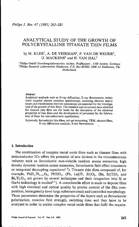
Philips J. Res. 47 (1993) 263-285
ANALYTICAL STUDY OF THE GROWTH OFPOLYCRYSTALLINE TITANATE THIN FILMS
by M. KLEEI, A. DE VElRMAW, P. VAN DE WEIJER2,
U. MACKENSI and H. VAN HAU
J Philips GmbH Forschungslaboratorien Aachen, Weijlhausstr., 5100 Aachen, Germany2Philips Research Laboratories Eindhoven, P.O. Box 80000, 5600 JA Eindhoven, The
Netherlands
AbstractAnalytical methods such as X-ray diffraction, X-ray fluorescence, induc-tively coupled plasma emission spectroscopy, scanning electron micro-scopy and transmission electron microscopy are essential for the investiga-tion ofthe growth ofthin films. The chemical and structural data obtainedfor titanate thin films are the basis for the discussion of the electricalproperties of thin films and the development of processes for the fabrica-tion of films for microelectronic applications.Keywords: ferroelectric thin films, sol-gel processing, TEM, titanate films,
X-ray diffraction analysis, X-ray fluorescence.
Philips Journal of Research Vol. 47 Nos.3-5 1993 263
1. Introduetion
The combination of complex metal oxide films such as titanate films withsemiconductor lCs offers the potentialof new devices in the microelectronicindustry such as ferroelectric non-volatile random access memories, highdensity dynamic random access memories, ferroelectric field effect transistorsor integrated decoupling capacitors': 2). Titanate thin films composed of, forexample, PbZrxTil_x03' PbTi03, (Pb, La)(Ti, Zr)03' (Ba, Sr)Ti03 andBi4Ti3012 are grown by several techniques and their integration into Si orGaAs technology is studied':"). A considerable effort is made to deposit filmswith high electrical and optical quality by precise control of the film com-position, homogeneity (over large substrate areas) and controlled morphology.These parameters determine the properties of the layers such as ferroelectricpolarization, coercive field strength, switching time and they have to beanalyzed in order to realize complex metal oxide films that fulfil the require-

264 Philips Journal of Research Vol.47 Nos. 3-S 1993
M. Klee et al.
ments for the applications':"). The development of thin film processes istherefore always combined with a comprehensive analytical characterizationof the thin films with respect to the materials properties, e.g. crystal structure,composition, grain size, orientation of the grains on the substrate and domainconfiguration. Analytical methods, including scanning electron microscopy,transmission electron microscopy, X-ray diffraction and X-ray fluorescenceanalysis, have been used to study the growth of thin Pb'Zr, Til_x03' PbTi03,BaTi03, SrTi03 and Bi4Ti3012 films. For selected titanate films analyticalmethods such as Rutherford backscattering spectroscopy, Auger electronspectroscopy and secondary ion mass speetrometry have also been applied butwill not be included here. The analytical data are the basis for the discussionof the electrical properties of the thin films and for tailoring of the thin filmswith respect to their application. This paper summarizes our results on theprocessing and properties of complex metal oxide films. Details of our inves-tigations can be found in refs 5-7 and 10-13.
2. Experiments
Thin Bi4Ti3012' BaTi03, SrTi03, PbTi03 and PbZrx Til_x03 films with x =0.35-0.65 were deposited on Si(IOO)substrates with a 0.5 J1m thick Si02 bufferlayer, a 5nm thick Ti adhesion layer and a 70nm thick Pt layer, which servesas the bottom electrode for the ferroelectric capacitors. A modified sol-gelprocess and an MOD (metallo-organic decomposition) process as described inmore detail in refs 5, 10 and 11 were applied. Thin PhZr; Til_x03 films weregrown from sol-gel solutions with a stoichiometrie Pb content as well as fromsolutions with a lead excess ranging from 2% to 21%.
The thin films deposited on the substrates by spin-coating were pretreatedat 573-873 K after each coating either by furnace annealing, hot-plate anneal-ing or rapid thermal annealing and were finally fired at 823-973 K (furnace orrapid thermal annealing).X-ray diffraction analysis (XRD) with a Philips APD-1700 X-ray diffrac-
tometer (Cu fine focus, single-wavelength secondary monochromator, fixeddivergence slit) was carried out to determine the crystallinity of the phases, thecrystallographic orientation of the films and the lattice constants.
X-ray fluorescence analysis (XRF) was carried out for the PbZro.53Tio.4,03films produced from solutions with lead excessesranging from 2% to 21 % (seeTables I and II) to determine the composition of the films with respect to leadevaporation during heating. Therefore, the elements Pb, Zr and Ti werequantified,
As described in more detail in ref. 14 the concentrations of Pb, Zr and Ti in

Growth of titanate thin films
TABLE IX-ray fluorescence analysis (XRF) and inductively coupled plasma emissionspectroscopy (ICP) of two PZT films a,b produced from modified sol-gel
precursors with a Pb:Zr:Ti ratio of 1.1 :0.53:0.47.
A) Atomic densities determined by XRF and ICP
Sample Pb (1015 Zr (1015 Ti (1015atoms cm=") atoms cm ") atoms cm=")
ICP XRF ICP XRF ICP SRF
690 683 337 349 306 305686 686 335 353 305 309
ab
B) Atomic ratios Pb/(Zr + Ti) and Zr/(Zr + Ti) for samples a, b determinedby XRF and ICP
Sample Pb/(Zr + Ti) Zr/(Zr + Ti)
XRF ICP XRF ICP
ab
1.041.04
1.0731.072
0.5340.533
0.5240.523
the films were determined with XRF by measurement of the Pb L-lines, the ZrK-lines and the Ti K-lines. Calibration was performed with samples ofthe pureelements. The composition of the films was determined with an estimatedaccuracy of 2-5 %.To confirm the XRF data the composition of selected PZT films was
checked by chemical analysis (see Table I). To that purpose, thePbZro.53Tio.4703thin films were dissolved in a diluted HF/HN03 solution. Inthese solutions the lead, titanium and zirconium content was determined usinginductively coupled plasma emission spectroscopy (ICP). With this method thePb, Zr and Ti content in the PZT films could be determined with an accuracybetter than 3% relative.
Scanning electron microscopy (SEM) and transmission electron microscopy(TEM), in plan-view and cross-section (XTEM), were càrried out to studygrain size, film morphology and defect structures. Most TEM observationswere made in the bright field diffraction contrast mode, but also some high
Philips Journal of Research Vol.47 Nos.3-5 1993 265

l.02 a) 0.92b) 0.93a) 0.95b) 0.97a) 0.98b) 0.99a) 1.09b) 1.05a) 1.11b) 1.07a) 1.14b) 1.15
M. Klee et al.
TABLE IILead content Pb/(Zr + Ti) of PbZrO•S3Tio.4703films produced in a modifiedsol-gel process with varying lead excess of 2-21% in the precursor solutions.The films were deposited on Si/Si02/Ti/Pt substrates with 5nm Ti and 70nmPt. The samples marked a) correspond to films pretreated at 873K after eachcoating and annealed at 973K; the samples marked b) correspond to filmshotplate-treated at 623K after each coating and annealed at 973K.
Lead content in theprecusor solutions
Lead content in PZT films
.Pb/(Zr + Ti) Pb/(Zr + Ti)
1.06
1.10
1.15
1.l8
1.21
resolution (HRTEM) work is included. A Philips CM30 SuperTWIN electronmicroscope (300 kV, 0.2 nm resolution) was used for this purpose.
The thicknesses of the films were determined from SEM cross-sections andby optical interference reflection spectroscopy with an accuracy of 5-10%.
After forming capacitor structures by sputter depositing a thin Pt layer ontop of the ferroelectric thin films, the electrical characterization of the PZTfilms was carried out by capacity measurements and measurements of thehysteresis loops as a function of the applied electrical field as described in moredetail in ref.5.
266 Philips Journalof Research Vol.47 Nos. 3-5 1993

Growth of titanate thin films
3. Results and discussion
3.1. Xi-ray diffraction analysis
3.1.1. BaTi03, SrTi03 and Bi4Ti3012films
X-ray diffraction analyses revealed that crystalline titanate thin films areproduced from reactive sol-gel and MOD precursors at temperatures of773-973 K. This means that the titanate formation in these thin films occursat temperatures, which are 600-800 K lower than the temperatures used tosinter via conventional processes titanate ceramics. These low reaction tem-peratures are essential for the integration of the ferroelectric thin films into Sior GaAs technology. The alkaline earth and Bi4Ti3012 films have a randomorientation at these temperatures (see fig. 1) with orthorhombic latticeconstants of a = 0.544 nm, b = 0.541 nm and c = 3.284 nm for Bi4Ti3 012 filmsand cubic lattice constants for the perovskite phases with a = 0.3906 nm(SrTi03) and a = 0.4000 nm (BaTi03). The cubic lattice indexing for theBaTi03 thin films, instead of a tetragonally distorted perovskite lattice asknown in BaTi03 bulk ceramics, results from the broadening of the X-raydiffraction lines due to the fine-grained films (see SEM analyses). The asym-metry of the (211) reflection of the BaTi03 films (see fig. la) inset), however,gives an indication of a slightly tetragonal distorted perovskite lattice.
Philips Journal of Research Vol. 47 Nos.3-5 1993 267
3.1.2. PbZr.Jil_x03 films with x = 0.35-0.65
Investigations by XRD analysis have shown that the crystallization of thelead containing perovskite films depends on numerous parameters includingthe kind of substrates, their quality and pretreatment"), the type of precursorsystems as well as their composition and lead excess introduced into thespin-coating solutions and the temperature treatments as well as processing ofthe thin films. The temperature range of 623-823 K as well as the lead contentof the precursor solutions is critical for the crystallization of the lead contain-ing titanates into the single-phase perovskite phase due to the crystallizationofthe non-ferroelectric pyrochlore phase at these temperatures, as reported byseveral authors=" 16, 17). To enhance the perovskite formation spin-coatingsolutions with additional lead were usually used.X-ray diffraction analyses revealed that a lead excess of no less than 10% is
necessary to compensate for lead evaporation during heating and to enhancethe crystallization of the precursors into single-phase perovskite films. Forfilms produced with a lead excess z- 10% no second phases were detected (seefig. 2b). For films produced from stoichiometrie solutions or solutions withonly a slight lead excess of2-8% a second phase with an X-ray diffraction line

M. Klee et al.
V) 3.20- x1O' 11011c 211:J0
2.56u
.è 2.24 ~ïii ~c ~2 1.92 its
1.60 5' 55 56 57 58
1.28 111,
0.96 §0.64 f. 211
0.32
20 25 30 35 40 45 50 55 60----29 inO
5.00V)
";ij x102ë:JoU
4.003.50z-
ïii 3.00
12.50
1.501.00
2.00
0.50
10 20 30 40 60---29ino
50
Fig. 1. a) X-ray diffraction pattern of a BaTi03 film. b) X-ray diffraction pattern of a Bi4Ti3012
film.
at 2e::::::30°was detected (see fig. 2a). Since only one broad diffraction line wasfound for this second phase (abbreviated in fig. 2a as s.p.) a clear identificationof this compound on the basis of the XRD data was not possible. This secondphase might either be a lead-deficient pyrochlore phase or a zirconium titanatephase.
Pb'Zr, Ti I-x 03 films show a tetragonal distortion of the perovski te lattice forTi-rich compositions x <0.53 similar to bulk ceramics" (see fig. 3). Owing tothe broad X-ray diffraction lines of the layers, caused by the fine-grained
268 Philips Journalof Research Vol. 47 Nos. 3-5 1993

Growth of titanate thin films
Fig. 2. a) X-ray diffraction pattern of a PbZrO.S3 Tio.4703 film produced in a modified sol-gelsolution with 2% Pb excess in the precursor solution. b) X-ray diffraction pattern of aPbZro.s3 Tio.4703 film produced in a modified sol-gel solution with 15% Pb excess in the precursorsolution
morphology and the small rhombohedral distortions for PZT ceramics withx> 0.53, only cubic lattice constants were determined for the layers withx ~ 0.53.
All the lead perovskite films produced in the sol-gel processing are texturedwith a (100)- or (111)- and (IOO)-textured orientation (see figs 4a, b). Becauseofthe broad X-ray diffraction lines a tetragonal splitting ofthe PbZro.s3 Tio.4703films could not be detected so that we could not distinguish whether the filmsare (100) or (001) textured. The film orientation is determined by the qualityand pretreatment of the substrates as described in more detail in ref. IS.
x 103
I/)1.60- 1.44.l!lc
j 1.280u>- 1.12
~ 0.96.l!! 0.80c....
10.640.480.320.16
I/) 4.00......
~ 3.60
a 3.20u<, 2.80~'iii 2.1.0~ 2.00c....
11.601.200.800.40
111 " 110
8:::!
100 a: ....................2:!b~~ 26 28 30 32 34j 200u
110 ~I ëi-;::: ~l~E\j :::- a..- s.r;_ .1. jJ a.. I...\_ ~1 la
111
Plllll)
100
200a:ëi
110 ca, 8:.::
_Aj
0::u 'v 211 Ib_,..)
20 25 30 35 40 1.5 50 55 60----29ino
Philips JournnI of Research Vol.47 Nos.3-5 1993 269

M. Klee et al.
ceramic ""
ti
0'"c:'-2.~"0
1°'§al.s:: 30'0.DE0-f 0°
•I
thinfilmtetragonal
o rhombohedral IX X~_...........-_.._._ ....~ x-x-x-x'É pseudocubico__ j__J_ __ 1__ L____j___ .I_l__j __ '--_
o 10 20 30 40 50 60 70 80 90 100
PbZr03 --.,.. Mole % PbTi03
1.06
- 1.05
- 1.04
1.03
1.02
1.01
1.00
Î- 0.99
PbTi03
Fig. 3. Lattice constants for PhZr; Til_.<03 films (- x -) produced in a modified sol-gel processwith 10% Pb excess and for bulk ceramics (-.-) as reported by laffe et a1.18) as a function ofthe zirconium content x.
3.2. X-ray fluorescence analysis
As described in Sec. 3.1 and reported in the literature (see refs 9 and 17)single-phase PZT films are usually grown by applying a lead excess in theprecursor solutions, in order to compensate for lead evaporation duringheating of the layers and to promote the perovskite formation. XRF analysisis a nondestructive method to determine the composition of the PZT layers.PbZro.53Tio.4703films with a lead excess of 10% in the spin-coating solutionswere analyzed by means ofXRF analysis. These data were confirmed by Iep.The analyses revealed for the PZT films Zr/(Zr+ Ti) ratios of 0.524 (Iep) and0.534 (XRF) in agreement with the composition in the solution. The leadcontent in the films Pb/(Zr+ Ti) was calculated to be 1.073 (Iep) and 1.04(XRF) (see Table I). With the accuracy of 3% for the Iep analysis and 2-5%for the XRF analysis both results are in good agreement. These data show thatduring heating of the layers approx. 3-6% oflead, introduced in the precursorsolution, is evaporated. Similar results were found for a series of films with alead excess in the starting solutions ranging from 2% to 21% (see Table 11).Although the accuracy ofthe XRF analyses for these series ofthin film sampleswas not better than 2-5% a general trend could be derived from the data. TheXRF analyses revealed that all the layers produced with low lead excesses(2-6%) in the precursor solutions are non-stoichiometrically grown showinga lead deficiency. This was found for hot-plate-pretreated (at 623 K) and
270 Philips Journalof Research Vol. 47 Nos. 3-S 1993

Philips Journal of Research Vol.47 Nos.3-5 1993 271
Growth of titanate thin films
1.20x10L 100 Pt(1111 ol1.08
I/) 0.96-I/)ë 0.81.:> 2000u- 0.72~] 0.60c..... 0.1.8
1 0.36
0.21.
0.12 11} \
5.00x10³
I/) 1..00~ 3.50:> 3.00.êè 2.50.~ 2.002 1.50.sI 1.00
0.50
- bI100 111 Pt (1111
200
a::110 ca
:.::
Á:>Ü \ 210 211
~ ~ ~ E ~ G 50 ~ 60-28ino
Fig. 4. X-ray diffraction pattern of a PbZro.SJ Tio.470J film produced in a modified sol-gel processwith 10% Pb excess: a) film deposited on a non-annealed Si/Si02/Ti/Pt substrate; b) film depositedon an annealed Si/Si02/Ti/Pt substrate
furnace-pretreated (at 873 K) films, which received a final annealing at 973 K.The lead deficiency in the films results in a second phase besides the perovskitephase. Films without lead deficiency are only produced with a lead excess inthe solutions ofno less than 10% (Table 11).For a lead excess ofapproximately10% in the precursor solution stoichiometrie films have been grown. Here onehas, however, to take into account that the accuracy of XRF for these filmsis not better than 2-5%. For lead excesses of 15%, 18% and 21% in theprecursor solution perovskite films containing some additional lead wereproduced (see Table 11). The lead excess in the perovskite films could not beconfirmed by XRD analysis. We assume that the additionallead in these films

M. Klee et al.
forms an amorphous lead oxide phase. Similar results are discussed by othergroups e.g. ref. 19.
3.3. SEM and TEM analyses
Scanning electron microscopy analyses (fig. 5) revealed for the Bi4Ti3012
and alkaline earth titanate films a fine-grained morphology with grain sizesbelow 0.1 }lm (see figs 5a-c). For the lead perovskites we observed a strongdependence of the grain size on the processing of the films. High temperaturepretreatments of the films after each coating (873-923 K) always lead to afine-grained morphology similar to the morphology found for the alkalineearth titanate films with grain sizes below O.I}lm (see fig. 5d). Low tem-perature pretreatments (573-673 K) of the films followed by a high tem-perature annealing result for the lead perovskite films in a coarse-grainedmorphology with grain sizes of 0.3-0.9 }lm (see fig. 5e).
Detailed TEM analyses were performed for the PbZro.35Tio.6503 films, whichwere produced from solutions containing 10% lead excess and which werepretreated at 873 K (furnace) and 973 K (rapid thermal annealing, RTA),followed by a 973 K final anneal and for films which were pretreated at 573K (furnace) and at 673 K (RTA), followed by final annealing at 973 K. Fromcross-sectional observations it was seen that the films which received a hightemperature pretreatment (873-973 K) have a columnar morphology. Thesubsequent spin-on layers are epitaxially related, which can be explained by thefact that during the high temperature pretreatment the crystallization into theperovskite phase takes place for each spin-on layer. The first perovskite layerserves as a nucleation site for the subsequent layers, giving rise to a columnarmicrostructure. The subsequent coatings can still be distinguished by a faintinterfacial contrast (fig. 6b). The HRTEM image of fig. 7 shows that this faintinterfacial contrast is due to the presence of some amorphous phase. Thismight be an amorphous PZT or a PbO phase, originating from the lead excesswithin the precursor solutions. The fact that the orientation of the grains ismaintained over the whole thickness of the PZT film indicates that no con-tinuous interfaciallayer is present. This is indeed confirmed by the HRTEMobservations. Throughout this paper this columnar growth morphology willbe called fine grained, since the grain sizes are considerably smaller than in thefilms which received low temperature pretreatments followed by a final hightemperature anneal (figs 5e and 6a). It was revealed by XTEM that over thethickness of the coarse-grained films roughly two grains subsist, which do nothave an epitaxial relationship. This can be explained by the fact that during thelow temperature pretreatment at 573-673 K amorphous oxide films are grown
272 Philips Journ.l of Research Vol.47 Nos. 3-5 1993

Philips Journalof Research Vol. 47 Nos. 3-5 1993 273
Fig. 5. SEM micrographs of titanate films: a) BaTiO] film b) SrTi01 film; c) Bi, Tij 0" film: d)
PbZro]S Ti06SO] film, fired at 873 K after each spin-coating and finally annealed at 973 K; e)PbZrO]S Ti06SO] film, fired at 673 K after each spin-coating and finally annealed at 973 K.

(e)
M. Klee el al.
(d)
Fig. 5. Continued.
on top of each other which are crystallized into the perovskite phase in a finalanneal at 973 K. Probably the crystallization starts at the interface with thebottorn electrode and at the top of the amorphous film, giving rise to twograms.
Grain sizes as wel! as defect structures can best be derived from plan-viewTEM observations as shown for PbZro35 Tio650J films in figs 8 and 9. Anneal-ing pretreatrnents at 573 K (furnace) or 673 K (RTA) resulted in coarse-grained morphologies with grains of lateral dimensions of approximately0.1-0.9)1m and 0.4-1.0)1m respectively (see fig. 8a) and fig. 9). The grains arequite dense. Pores can only be found at the grain boundaries. In between the
274 Philips Journalof Research Vol. 47 Nos.3---5 1993

Growth of titanate thin .films
b
Fig. 6. XTEM image of a PbZr035 Tio65 film: a) 573 K furnace pretreatment and final annealingat 973 K; b) 873 K furnace pretreatment and final annealing at 973 K. The subsequent coatingscan be distinguished and are indicated by horizontal white lines at the left.
PZT grains a fine-grained (approx. IOnm diameter) second phase wasobserved. From a comparison of fig. 8a) and fig. 9 it is clear that the volumefraction of this second phase is larger for the RT A than for the furnace-pretreated sample. This is in agreement with the fact that by XTEM no secondphase was observed for the furnace-annealed sample, whereas it was for the
Philips Journalof Research Vol. 47 Nos.3-5 1993 275
276 Philips Journalof Research Vol.47 Nos. 3-5 1993
M. Klee el al.
Fig. 7. a) XTEM image ofthe first two coatings ofwhich the interface is indicated by black arrows(973 K RTA pretreatment and 973 K final annealing); b) HRTEM image of the interface regionindicated by white rectangle in a) (white arrow) evidencing the presence of an amorphous phaseas well as the epitaxial relationship between subsequent coatings.
RT A-annealed sample. However, it should be pointed out that even in thelatter case the occurrence of the second phase is minor and only seems to bepresent over the top 50 nm (i.e. about 10-15% of the thickness of the film).This means that, although from plan view TEM one would derive a surfacefraction of about 10-20%, the total volume fraction amounts to only 1-3%.The latter also illustrates the power of plan-view TEM observations compared

Philips Journalof Research Vol.47 Nos.3-5 1993 277
Growth of titanate thin films
Fig. 8. Plan-view TEM image of a PbZr035 Tio6s03 film: (I) 573 K furnace pretreatment and finalannealing at 973 K; b) 873 K furnace pretreatment and final annealing at 973 K.
with XTEM in the detection of structural phenomena of low density. The lowcontent of this second phase and its fine-grained morphology explain why thissecond phase was not detected by XRD in these samples. From the corres-ponding selected area electron diffraction (SAED) pattern (fig. 9) the pyro-chlore phase could be identified (rings at 0.304, 0.257, 0.186, 0.157, 0.151 nm

M. Klee et al.
278 Philips Journalof Research Vol. 47 Nos. 3-5 1993
Fig. 9. Plan view TEM image of a PbZro.); Tio.6SO) film after 673 K RTA pretreatment and finalannealing at 973 K. The tine-grained second phase is clearly visible and the inset shows thecortesponding SAED .
.. .). The formation of the pyrochlore phase in the low temperature pretreatedPZT samples, produced from solutions with 10% lead excess, indicates that inaddition to the lead excess the pretreatment temperature is also critical for thephase formation. At temperatures of 623-823 K, as reported by Okada") forsputtered PZT films and by Budd et a1.16) for sol-gel processing, the leadtitanates and lead titanate-zirconates crystallize into the pyrochlore phase.Although a high temperature anneal at 973 K for 5-60 min was applied for ourfilms after several pretreatments at 573-673 K small amounts (1-3%) of thepyrochlore phase remained at the grain boundaries.
Investigations of the domain configuration of the coarse-grained filmsrevealed that many grains contain two perpendicular sets of twins: (101) and( - 101), as clearly shown in fig. 10, in which one grain is imaged under differentdiffraction conditions. For the 101 and - 101 two-beam conditions, respectively,the (101) and (-101) twins are in extinction. These twins are 90° boundaries,separating 90° domains (having domain widths of 10-100 nrn). Where the twosets of90° boundaries meet, there is a 180° boundary. Clearly, this grain-andmany grains of the coarse-grained films-have a banded domain structure as

Growth of titanate thin films
Fig. 10. Plan view TEM image of a PbZr035 Tio6s03 film after 673 K RTA pretreatment and finalannealing at 973 K. One grain is imaged under different (two-beam) diffraction conditions,showing the banded 90° domain structure.
shown to occur in coarse-grained BaTi03 ceramics by Arlr"). There are,however, also grains containing only one set of 90° boundaries, i.e. having alamellar domain configuration.
For the fine-grained films grown by high temperature pretreatments at 873K and finally annealed at 973 K grain sizes between 0.07-0.25,um were found.
Philips Journalof Research Vol. 47 Nos.3--5 1993 279

M. Klee et al.
The grains are somewhat less dense than in the coarse-grained films, contain-ing some pores. The porosity is, however, far from the voids found within thegrains grown by sputtered PZT films, e.g. those reported by Goral et a1.22). Nopyrochlore phase was found in these samples. For these fine-grained films alamellar domain structure is now more frequently observed (see fig. 8b). Thesmallest grains do not contain any domains.
3.4. Electrical characterization of titanate films
On the basis of this extensive analytical characterization the specific electri-cal properties of thin titanate films compared with the bulk ceramics will bediscussed. More detailed electrical results will be published in a forthcomingpaper.
3.4.1. Relative permittivity of titanate thin films
The fine-grained titanate thin films and especially the alkaline earth titanatefilms exhibit relatively low permittivities compared with bulk ceramics. For theBaTi03 films relative permittivities of 500-800 and a slight temperature andfield dependence of the relative permittivity was found (see refs 11-13). Theselow relative permittivities of the ferroelectric BaTi03 films compared with thehigh relative permittivities of the bulk ceramics (3000-5000) can be explainedby the small grain sizes, which were obtained in the low temperature processedfilms. The grain sizes of the films are below the critical grain size of 0.08 J.lm,which has been determined'") in BaTi03 for the transition of the ferroelectricinto the superparaelectric state of the BaTi03, thus giving rise to the lowrelative permittivities of the thin films.
In the lead-containing perovskite thin films, in contrast to the alkaline earthtitanate films, a grain size dependence of the relative permittivity was notfound. This is due to the fact that the critical grain size for the transition intothe superparaelectric state occurs in PbTi03 at grain sizes of approx. 0.015 J.lm.Assuming the same value for PZT, the grain sizes in our thin films are one totwo orders of magnitude above this critical grain size. Therefore the relativepermittivities of PZT films are comparable with those found for bulkceramics") (see fig. 11). However, a strong contra I of the composition isnecessary to obtain this bulk ceramic value. For several processing conditions(see fig. 12) it was found that a low lead excess « 10%) in the precursorsolutions and thus formation of a second phase in the PbZro.s3Tio.4703 filmsgives rise to low relative permittivities of 600-900. With increasing lead excess> 15% the relative permittivities reach a saturation value of 1400-1500 andshow at lead excesses of 21% again a slight decrease. The decrease of the
280 Philips Journalof Research Vol.47 Nos.3-5 1993

Growth oJ titanate thin films
lE-lhin-fiIm
1200
E 900
1 600
_bulk
300
o L- ~ ~ ~ ~ ~
0.2
Fig. 11. Relative permittivity ofPbZr xTi.; xOJ films (-lb) and bulk ceramics (-e-) as a functionof the zirconium content x.
relative permittivities for lead excesses above 20% might be caused by theamorphous lead oxide phase remaining in the films.
3.4.2. Ferroelectric properties oJ PZT thin films . \
The analyses of the ferroelectric properties of the PbZro.53Tio.4703 filmsrevealed that not only the small signal (see Sec. 3.4.1) but also the large signal
0.3 0.4 0.60.5
-x
1600~~~~~~~-.~~~~~~TO
>, 1400....:~ 1200........13 1000~ 800c,Cl) 600.:::-:;; 400air.. 200
O~~~~~~~-.~~~~~~~1.00 1.04 1.08 1.12 1.16 1.20 1.24
Fig. 12. Relative permittivity of PbZro.sJTio.470J films as a function of the lead content in theprecursor solution: ., films pretreated at 873 K and finally annealed at 973K; 0, films pretreatedat 623 K and finally annealed at 973 K.
Pb content in precursor solutions
Philips Journal of Research Vol. 47 Nos. 3-5 1993
0.7
281

M. Klee et al.
properties of the thin PZT films are affected by the composition and thus bythe lead content of, the films. In general the remanent polarizations ofPbZro.53Tio.4703 films are increased with increasing lead excess (2-21 %) in theprecursor solutions from P, = 7 flC cm"? (2% Pb excess) to P, = 15 flC ern"?(21 % Pb excess) for films pretreated at 873 K and from P, = 12flC cm ? (2%Pb excess) to P; = 24 flC cm -2 (21 % Pb excess) for films pretreated at 623 K,while the coercive field strengths can be decreased from E, = 55 kV cm -I (2%Pb excess) down to E; = 35 kV cm-I (21% Pb excess). This can again beexplained by the fact that in lead-deficient layers small amounts of a non-ferroelectric second phase are formed, which if homogeneously surroundingthe perovskite grains reduce the remanent polarization and increase the coer-cive field strength.
Additionally, intensive studies of the processing and growth ofPb Zr, Til_x03 thin films (x = 0.35-0.65) have been used to correlate the thinfilm morphology with the ferroelectric properties. The results derived from abroad range of thin film systems with x = 0.35-0.65 will in the following beillustrated for Pb.Zr, Til_x03 films with x = 0.35 and x = 0.65. As describedin Sec. 3.3, two types of morphologies, fine-grained and coarse-grained, werefound for PhZr; Til_x03 films with x = 0.35. These two types ofmorphologiesaffect the ferroelectric properties as shown in fig. 13. The coarse-grained filmsgive rise to relatively slim hysteresis loops if low electrical fields of Eo = 100kV cm-I are applied. The hysteresis curves are widened with increasing fields,giving remanentpolarizations of up to 28-32 flC cm -2 at a field strength of Eo= 500 kV cm-I. Coercive field strengths of E, = 80 kV cm-I(PbZro.35Tio.6503) and E; = 40 kV cm-I (PbZro.65Tio.3503) were measured (seefig. 13). Pb'Zr; Ti'_x03 films (x = 0.35, 0.65) grown with a fine-grainedmorphology show the saturation remanent polarization at low electrical fieldsof Eo = 100 kV cm-I. This is combined with lower absolute values of theremanent polarizations P, = 15 flC ern"? (x = 0.35) and P, = 20 flC cm ? (x= 0.65) and coercive field strengths of E; = 60 kV cm-I (x = 0.35) and E;= 30 kV cm-I (x = 0.65). The influence ofthe grain size on the ferroelectricproperties was also reported for bulk ceramics by Arlr"). High remanentpolarizations for coarse-grained BaTi03 were found and explained by theformation of a banded domain configuration, low remanent polarizations arereported for the fine-grained BaTi03 ceramics and suggested to be due to alamellar domain configuration. As shown in Sec. 3.3 also in thin PZT filmslamellar and banded domain configurations were observed dependent on thegrain size. This type of domain configuration can be correlated with the twotypes ofhysteresis curves, confirming that the domain configuration determin-ing the ferroelectric properties holds also for our thin films.
282 Philips Journalof Research Vol.47 Nos.3-S 1993

Growth of titanate thin films
Fig. 13. a) Hysteresis loops for coarse-grained PbZrO,lSTiO,6S0J films (-) and fine-grainedPbZrO.lSTio.6sOl films (---). Applied fields Eo = 100 kV cm-I, 500 kV cm-I. b) Hysteresis loopsfor coarse-grained PbZrO.65TiO,JSOl films (-) and fine-grained PbZrO.6STio,lsOl films (---). Appliedfields Eo = 100 kV cm-I, 500 kV cm-I
50PZT (35/65) films
- coarse-grained films- - fine - grained ti Ims
N
E.!:!U [.0::L
0...
-[.00 -200 200 [.00E(kVlcm)
-[.0
-50
6050
PZT (65/35) films
- coarse - grained films-- fine-grained films
N
EuU:L.
0... Eo = 500 kVlcm
Eo =100 kV/cm
-400 -200 200 400E (kV/cm)
-30
-40-50. -60
Philips Journal of Research Vol. 47 Nos. 3-5 1993 283

M. Klee et al.
4. Summary"
Structural and wet-chemical analyses carried out by SEM, TEM, XRF,XRD and ICP have been used to characterize the growth of PhZr; Ti.;x 03,PbTi03, BaTiO), SrTi03 and Bi4Ti3012 films produced by modified sol-geland MOD techniques. The investigations have shown that these comprehen-sive analyses of thin films are the basis for investigation and optimization ofthe electrical properties of thin films.
Controlling the composition of the films and especially the lead evaporationin PZT films, single-phase perovskite films are produced at temperatures aslow as 773-973 K. The lead perovskite thin films with thicknesses ofO.l-l Jlmrevealed small signal and large signal electrical properties similar to those ofthe bulk ceramics. For the BaTi03 films relatively low relative permittivities(500-800) as well as a weak temperature and field dependence of the relativepermittivity compared with the bulk ceramics was found, which is explainedby the fine-grained morphology of these films with grain sizes of <0.1 Jlm.
By controlling the processing, fine-grained and coarse-grained lead titanatezirconate thin films can be grown, as derived from SEM and TEM studies.Fine-grained films show a columnar growth with often a lamellar 90° domainconfiguration. In the coarse-grained films a banded domain configuration with90° and 180° domain walls and ferroelectric properties similar to bulk ceramicsare dominating.
284 Philips Journalof Research Vol.47 Nos. 3-5 1993
Acknowledgement
The authors wish to thank W. Brand, H. Knüfer, W. Keur and M. Ulenaersfor their technical assistance as well as D. Bausen, B. Krafczyk, Ing. M.H.J.Bekkers for the structural analysis of the thin films. Thanks are due to Ir. P.J.Rommers for performing the Iep measurements and Dr. B. Spierings for thecooperation and investigation on the substrates. We gratefully acknowledgethe helpful discussion and advice by Drs. P. Larsen and J. Pankert.
REFERENCES
I J.F. Scott, C.A. Araujio and C.D. MacMillan, Condensed Mater. News, 1, 3, 10 (1991).2 P.K. Larsen, R. Cuppens and G.A.C.M. Spierings, Ferroelectrics, 128,265 (1992).3 L.M. Sheppard, Ceram. Bull., 71, 85 (1992).4 S.L. Swartz, IEEE Trans. Elec. Insulation, 25, 5, 935 (1990).5 M. Klee, R. Eusemann, R. Waser, W. Brand and H. van Hal, J. Appl. Phys., 72, 4 (1992).6 M. Klee, U. Mackens, A. De Veirman, Proc. 2nd Int. Symp. on Domain Structure of Fer-roelectric and Related Materials, in press.
7 P.K. Larsen, G.L.M. Kampshöer, M.B. van der Mark, and M. Klee, Proc. ISAF '92, in press.8 A.R. Modak, S.K. Dey, Ferroelectrics, in press.9 S.A. Myers and N. Chapin, Mater. Res. Soc. Symp., 200, 231 (1990).10 M. Klee and P.K. Larsen, Ferroelectrics, 133, 91 (1982).

Philips Journal of Research Vol.47 Nos.3-5 1993 285
Growth of titanate thinfilms
11 M. Klee and R. Waser, Mater. Res. Soc. Symp., 243, 437 (1992).12 D. Hennings, M. Klee and R. Waser, Adv. Ceram. Mater., 3, 7/8, 332 (1991).13 R. Waser and M. Klee, Proc. 3rd Int. Symp. on Integrated Ferroelectrics, 288 (1992).14 P. van de Weijer and D.K. g. de Boer, Philips J. Res., this issue.IS G.A.C.M. Spierings, J.B.A. van Zon, M. Klee and P.K. Larsen, Proc. 4th Int. Symp. on
Integrated Ferroelectrics, Monterey, CA, 9-11 March, 1992.16 S.K. Budd, S.K. Dey and O.A. Payne, Br. Ceram. Proc., 36, 107 (1985).17 S.K. Dey, C.K. Barlingay, J.J. Lee, T.K. Georstadt and C.T.A. Suchicitae, Proc. Int. Fer-
roelectrics, 30 (1991).18 B. Jaffe, W.R. Cook and H. Jaffe, Piezoelectric Ceramics, Academic Press, London, 1971.19 S.K. Dey, personal communication.20 A. Okada, J. Appl. Phys., 48, 2905 (1977).21 G. Arlt, Ferroelectrics, 104,217 (1990).22 J.P. Goral, M. Huffman and M.M. AI-Jassim, Mater. Res. Soc. Symp., 200, 225 (1990).23 K. Uchino, E. Sadanaga, T. Hirose, J. Am. Ceram. Soc., 72, 1555 (1989).
AuthorsMareike Klee (née Jakowski) studied chemistry at the TH Darmstadt (1976-1981). She receivedher Ph.D. in the field of inorganic structure and solid-state chemistry in 1984and then joined theElectronic Ceramics Group of the Philips Research Laboratory, Aachen. She has investigatedadvanced powder preparation techniques and thin film processes for. dielectric and high Tcsuperconducting materials. At present, she is in charge of the chemical activities concerningferroelectric thin film for applications such as non-volatile memories.
Ann E.M. De Veirman: M.Sc. degree (physics), University of Antwerp, 1985; Ph.D., Universityof Antwerp, 1990;Philips Research, Eindhoven, 1990-. In her thesis she performed a transmissionelectron microscopy study on the formation of buried layers by high-dose ion implantation insilicon. At present she is involved in materials research with TEM.
Peter van de Weijer studied chemistry at the State University of Utrecht (1968-1974). In his thesis,at Twente University of Technology (1977), he described acid-base properties of aza-aromatics,as investigated by nuclear magnetic resonance. At the Philips Research Laboratories (1977-), hestarted with mechanistic studies on low-pressure mercury discharges by laser-diagnostic measure-ments. With the same technique he investigated the mechanisms oflow-pressure chemical vapourdeposition and the operation of a nitrogen-phosphorus detector as used in chromatography. Inthe Analytical Chemistry Department he has made use of inductively coupled plasma massspeetrometry and, subsequently, X-ray fluorescence.
Uwe Mackens received his Ph.D. degree in physics from the University of Hamburg in 1986,wherehe studied electronic excitation in microstructured two-dimensional silicon MOS systems. In 1985he joined the Philips Research Laboratory in Hamburg to work on X-ray lithography. He wasmainly involved in the fabrication of sub-half-micron devices and related topics. In 1991hejoinedthe Electronic Ceramics Group of the Philips Research Laboratory in Aachen, where he iscurrently evaluating ferroelectric thin film properties.
Harry A.M. van Hal graduated in chemistry from the Technical High School, Eindhoven, in 1969.He joined the Phi1ips Research Laboratories in Eindhoven in 1965 and is now in the ChemicalAnalysis Department, involved in the development and characterization of chemical processes forinorganic materials.

Philips Journal of Research Vol.47 Nos. 3-5 1993 287
Philips J. Res. 47 (1993) 287-302
THE APPLICATION OF DYNAMIC SIMS IN SILICONSEMICONDUCTOR TECHNOLOGY
by P.C. ZALM
Philips Research Laboratories, P.O. Box 80000.5600 JA Eindhoven, The Netherlands
AbstractAfter a short introduetion of the basic characteristics of secondary ionmass speetrometry (SIMS) as used in sputter depth profiling, a few selectedapplications ofthis technique are discussed. The distribution ofthe variousdopants in a standard npn transistor illustrates its analytical potential. Nextthe role ofSIMS in elucidating the mechanisms underlying impurity diffusion!migration is addressed. Finally an example is given of how the design ofdedicated test structures may help to overcome the inherent limitationsassociated with dynamic SIMS, in the particular case of scaling down lateraldimensions of MOSFET structures into the submicron realm. The paperconcludes by making an inventory of the suggested possibilities for futureimprovements in depth resolution within the constraints of the method.Keywords: depth profiling, impurity, mass spectrometry, MOSFET
structures, SIMS.
1. Introduetion and outline
Modern low-temperature (hetero-) epitaxial growth techniques, that enableformation of extremely well-confined dopant profiles and multilayer struc-tures, have matured to the level that these become a viable production option.In a parallel, but otherwise independent, development, in-depth dimensions inintegrated circuit technology have become progressively smaller. Both trendsrequire an increasingly precise process control which leads to more stringentdemands on the supporting analytical techniques. Of the available charac-terization methods, dynamic secondary ion mass speetrometry (SIMS) isperhaps the only one that can potentially provide the detection limits (typicallydown to the ppm level or better) and depth resolution (presently at best abouta few nanometers) that are currently needed. Others, such as high resolutionX-ray diffraction and transmission electron microscopy, may provide informa-

P.c. Zalm
tion about crystal quality and majority particle confinement but definitely lackthe sensitivity at a sub-percent level of impurity atoms. Ultimately, of course,the electronic and/or optical properties determine the feasibility of an emerg-ing technology but their investigation requires a near-completed device. In theresearch and early development stage SIMS is an indispensable tool.
Unfortunately, in spite of recent instrumental advances, there are fundamentallimitations to SIMS. These originate from the inherent disruption created bythe sputtering (i.e. removal of target atoms by energetic ion bombardment)process itself as well as by the limited lateral resolution. This necessitates theconstruction of model experiments to obtain an approximate solution for manypractical problems which push the technique up to its limits. In this paper wewill present a few typical examples from our own daily routine work to illustratethese remarks. First, however, a fairly condensed description of dynamic SIMSand the routine difficulties encountered will be given. For a detailed account ofbackground, history, instrumentation, implementation etc. the interested readeris referred to the extensive textbooks available':"). Finally we will briefly indi-cate where room is left for improvement within the constraints of the technique.
2. A concise description of SIMS depth profiling
In SIMS ionized species liberated ("sputtered") from a target surface bybombarding it with a primary ion beam are separated according to their massand a proportion are detected. As the exiting particles stem from the outermostfew atomic layers, they carry information about the (local instantaneous)composition of the near-surface region. By monitoring the signal intensity forone or more mass(es) as a function of time during continuous erosion anin-depth distribution is obtained. This roughly summarizes the basic principle,but there are multiple practical snags that have to be taken into account as willbe discussed now.
Usually only a minute fraction of the outgoing species (typically < 10-3)leaves the surface in a charged state. By saturating the topmost layers withrespectively oxygen or cesium, however, the formation/survival probability forpositive or negative secondary ions can be greatly enhanced. The usualapproach is to use an Oi or Cs+ primary ion beam. Further a very flat erosionfront is needed in order to avoid smearing/averaging the depth information.To this end the primary beam is finely focused and rastered over part of thetarget. Contributions from the side walls of the sputtered crater, which carryinformation on shallower depths, are suppressed by allowing only secondaryions from the center of the crater to be analyzed. This can be done by eitheractivating the detector exclusively when the primary beam passes this central
288 Phlllps Journat of Research Vol.47 Nos.3-5 1993

Philips Journal of Research Vol.47 Nos.3-S 1993 289
Dynamic SIMS in Si semiconductor technology
region or by secondary ion optical imaging. Most of the impinging primaryions are implanted in the target and it takes some time (the pre-equilibriumregime) before steady-state conditions build up as erosion proceeds. Theincoming beam not only disrupts the target by this embedding of primaryspecies, but as these come to rest in a sequence of collisions with target atomsthe latter will be redistributed. This form of in-depth information smearing,called ion beam mixing, depends on the impact energy Ei and angle of incidenceBi (relative to the surface normal) ofthe primary ions. It is, very approximately,proportional to Ei/2cos Bi' Thus, lowering of Ei and/or more grazing Bi willlead to a more truthful representation ofthe compositional depth distribution.Unfortunately the sputtering yield decreases with diminishing Ei and alsoprimary beam handling becomes difficult at low Ei owing to space chargeblow-up (Coulomb repulsion). The sputtering yield increases considerably with Bi'but this leads to a reduced incorporation ofprimary beam specieswhich adverselyaffects the secondary ion information/survival probability. Also focusing andrastering becomes more awkward. So, effectively, all attempts to improvedepth resolution lead to a degradation in signal intensity and, thus, in thecapability to detect low concentrations. In addition the total time required foranalysis is prolonged and this puts more stringent demands on stability.Consequently for each problem the analyst is forced to make a trade-off for theproblem at hand between the various possibilities and limitations forced uponhim by the degrees of freedom in the selection of primary beam parameters.As for the secondary ions, one of the drawbacks of the technique lies in the
fact that polyatomic cluster ions and or multiply charged elemental ions willbe emitted, leading to severe mass interferences. Famous examples for dopantsin silicon are the 30SiH/3lPand 29Si30Si160j15As interferences, while the detectionlimit for IOB+ may ultimately be limited by 30Si3+. There are two ways to cir-cumvent this particular problem. One could strive for very high mass resolution,but signal intensity loss and instrumental stability demands limit this inpractice to M/AM < 5000, which is not always enough. Alternatively one mayrestrict the analysis to those secondary species that were ejectedwith a sufficientlyhigh kinetic energy in the sputtering process. Clusters have a strongly reducedsurvival probability under those conditions, since when so much energy istransferred to them they will probably dissociate, and their contribution is thussuppressed (note: this trick fails with highly asymmetric-mass polyatomicions). Also with this solution signal intensities will be reduced, however ..The most important aspect of SIMS is that the departing secondary particles
can still exchange electrons with the receding surface when they are sufficientlyclose ( < 1nm above). The efficiency of this process strongly depends on theirelectronic configuration and that of the (local) target environment. Thus their
P.e. Zalm
formation, survival and detection probabilities vary enormously with speciesand matrix type. A high signal intensity for a specific mass consequently doesnot necessarily imply a high concentration of the corresponding species.Further, a linear relationship between perceived signal intensity and actual(instantaneous, near-) surface concentration is only valid up to about a I at%impurity level, since otherwise the nearby presence of electronic-configuration-altering species will affect their detection efficiency. AU this implies thatcalibration is cumbersome and requires standards. The best solution is to usea gauge implantation ofthe impurity under investigation into the same matrixas for the unknown sample to be calibrated and to measure its depth profileunder identical conditions. Afterwards the perceived intensity is integratedover time, to get the total number of counts in the implant profile, and this isequated to the implanted fluence which is well known. This gives a directconversion from counts to areal density (i.e. impurity atoms cm"). Time-to-depth conversion follows by determining the sputtered crater depth d aftertermination of the measurement at time tslop and assuming a constant erosionrate (i.e. depth at time t equals dt/tsIOP)' Experimental conditions must bechosen such that errors introduced by pre-equilibrium erosion effects aresmall. An additional advantage of gauge implants is that these immediatelyinform you about attainable detection limits, since in principle these extendonly to finite depth and so the signal intensity should drop to zero. Less tediousconcentration calibration schemes exist, but these lack the potential accuracyof the one presented here. No first principle calculations of sensitivities areavailable with a precision of better than an order of magnitude.The target itself is a further factor in dynamic SIMS. Obviously flatness is
important. A corrugated surface gives rise to considerable smearing of in-depth information. But even originally very smooth surfaces may rapidlydevelop topography under ion bombardment. Polycrystalline metals, andother ductile materials, do so excessively because of preferential sputtering ofsome crystallographic orientations which leads to facetting. This makes mean-ingful depth profiling beyond a few tenths of a micrometer virtually impossible(without further precautions, see Sec. 4) and restricts the technique to brittlematerials (that amorphize readily under ion bombardment) such as semicon-ductors or oxides, nitrides etc., although even on these texturing can occur atconsiderable (i.e. of the order of micrometers) eroded depth. Also surfacecontamination may act as a local mask preventing erosion and thereby creat-ing roughness, or, for instance in the case of a native oxide layer, delay theonset of steady-state erosion. Finally special precautions are needed whenexamining insulating targets. Flooding of the target with thermal electrons orconcurrent bombardment with an electron beam can help. Sometimes it is
290 Philips Journalof Research Vol. 47 Nos. 3-5 1993

Philips Journal of Research Vol.47 Nos. 3-S 1993 291
Dynamic SIMS in Si semiconductor technology
enough to coat the surface with a thin ( ~ 25 nm) conductive layer (often gold).Also the use of an 0- primary beam instead of the more common ot ionsalleviates the problem.
Modern equipment, combining many (if not all) of the above-mentionedfacilities and options is commercially available. At our laboratory we use aCAMECA ims3f and an ims4f secondary ion spectrometer annex secondaryion microscope. The heart of this instrument consists of a doubly focusedelectrostatic sector energy/magnetic sector mass analyser. Characteristic forthis type of analyser is the large extraction/bias voltage on the target (of theorder of kilovolts). The primary beam comes in at off-normal angles and isdecelerated (or accelerated depending on polarity) towards the sample. Ei andBi are coupled (i.e. Bi becomes more glancing at lower Ei). The transmission(i.e. the accepted fraction of secondary ions generated) is very high but thesample size is restricted (of the order of cm"), The extraction geometry allowsfor a secondary ion optical imaging system (i.e. position-sensitive detectionwith a lateral resolution down to ~ l um irrespective of primary beam focus,so it is truly a microscope). The alternative widespread, commercially avail-able, type of instrument design combines a band-pass energy filter with aquadrupole mass analyser (which limits mass resolution to about I amu). Herethe target bias is small or zero and the transmission is low (owing to the narrowsecondary ion ejection energy window acceptable to the quadrupole and thelimited opening angle of the energy filter). Ei can be varied independently ofBi (often Bi ~Oo, but the sample may be placed on a slanted holder or a tiltingstage can be used). Potentially, large wafers (up to 6 in) can be examined. Theset-up can be used as an add-on facility to an existing vacuum chamber, or inadverse situations there is room to instaII additional characterizationtechniques in the SIMS instrument.
With such modern equipment it is routinely possible to obtain (sub-) ppmdetection limits for many impurity/matrix combinations. Species that do notionize readily, such as the noble gases and, for instance, gold remainnotoriously difficult. Poor detection limits must also be expected for thoseelements that abound in the residual, background, UHV contaminants such as(foremost) hydrogen, but also carbon, nitrogen and oxygen. Further, problemsare to be expected with those materials used in primary-beam-defining aper-tures in the instrument (e.g. tungsten or tantalum), which will end up on thetarget under investigation. Last but not least, it should be remarked that inpractice the dynamic range (i.e. the change in magnitude over which a con-centration distribution can be followed) is ultimately restricted to less thanabout six decades in secondary ion intensity owing to redeposition onto the

P.C. Zalm
analyzed area of particles that were first sputtered onto the surround (i.e.chamber walls and/or extraction lenses).
3. Selected application examples
3.1. Studies on bipolar transistors
The various processing steps that determine the distribution of the respectivedopant atoms in standard very large-scale integrated circuit technology for theformation of a bipolar transistor can be summarized as follows. Here we takethe example of a typical npn transistor.
1. Starting material is a commercial boron-doped (~1·1015 B atoms cm ")silicon wafer. Antimony- (or arsenic-) doped areas with a sheet resistanceof about 35 n/o are introduced by implantation (to a top concentrationof 1 . 1018 Sb atoms cm "), before an epitaxial Si layer 0.5-1.5 Jlm thickis deposited. During subsequent high temperature processing steps, sub-stantial indiffusion of Sb into this layer will occur.
11. Next, locally, the wafer is implanted with boron (typically at energies ofthe order of 25 keV to fluences of around 5· 1013 IIB atoms cm -2).
Subsequently the wafer is annealed to restore the radiation damage andactivate the B. This leads to redistribution of B and Sb.
Ill. Then, a polycrystalline Si layer is deposited onto the wafer surface (thick-ness ~ 0.1-0.3 Jlm) which is implanted with arsenic at low energies ( < 100keY to a fluence of ~ 1016 As atoms cm"") followed by a heating step (atabout 900-1100 0C). This leads to an extremely rapid redistribution of Asin the poly-Si and a much slower outdiffusion of the As into the mono-Si.Ideally the latter only affects the shallow-depth part of the IIBdistribution.
292 Philips Journalof Research Vol. 47 Nos. 3-S 1993
In the above, emphasis has been placed on those processing steps that affectdopant profiles. In addition there are numerous (photo-) lithographic maskingsteps, which define the lateral confinement of the various implantations,etching steps (e.g. to allow contacting of the Sb-doped collector) and metalliza-tion steps (to contact the B-base and As-emitter) which have been omitted forsimplicity. Usually the lateral confinement in an individual device structure issuch that it does not allow for immediate inspection by SIMS (we willelaborate this aspect in Sec. 3.3). However, for characterization/analysis pur-poses a sufficiently large area can be prepared for inspection by leaving outsome (or all) of these extra and intermediate steps.
An example ofthe resultant depth distributions ofthe dopants is given in fig.

Dynamic SIMS in Si semiconductor technology
1ME.g~c.g 1018e...c:Cl>o§ 1017o
1016
0.00 0.500.25 0.75
depth (urn) ----
1.00
Fig. I. Relevant dopant profiles in an npn transistor. The approximate base width Wois indicated.
1. Roughly speaking the intercept of "B and Sb profiles determines theposition of the base/collector junction and the crossing of the As and 11Bprofiles the emitter/base junction position. The depth difference between thosetwo points is, approximately, the base width Wa. Of course determination ofthe electrical properties of a device, or rather the whole array of those on thewafer, is essential to assess the quality, reliability and reproducibility of thevarious technological steps. Yet, in the early stages of process evaluation andalso for failure analysis, SIMS is an invaluable tool. Errors in parameterselection can be signalled when the penalty in terms of time and investment·losses is stilliow. To namejust one issue of practical importance: the extent ofoutdiffusion of Sb and the remaining depth of undoped epi-Si. Theseparameters are of critical importance for the electrical characteristics of high-speed transistors with very small vertical dimensions.
Further, it was found that an imperfect combination of poly-Si thicknessand As implantation energy led to considerable redistribution of the liB tolarger depths. This is caused by creation of crystal damage by energetic Aspenetrating the mono-Si. Upon thermal processing this damage anneals outreleasing Si interstitials which will rapidly diffuse into the crystal and replacepart of the substitutional !'B atoms which then start to move (we come backto this in more detail in the next subsection). This example is illustrated in fig.2 where, for clarity, only the liB relocation is shown. Note that the emitter/base junction has stayed in place but that the base/collector junction shifts toconsiderably greater depth. As a byproduct of this particular study we would
Philips Journalof Research Vol. 47 Nos.3-5 1993 293

P.C. Zalm
1019
I poly-Si!epi-Si-
M 1018Eu+:r~c 10170.pe...cQ)uc 10160uOl
10150 150 300 450 600
depth(nm) ---
Fig. 2. Distortion of an 11 B base depth distribution during As implantation/indiffusion. Thin fullline, prior to emitter anneal; broken line, after anneal, for a 50 keY As implant in the poly-Si(which does not penetrate the epilayer); thick full line: after anneal for 100keY As (of which atmost 5% penetrates with far less, but still sufficient, energy to create damage in the epi-Si). Notethe accompanying increase of the base width by almost 100nm in the latter case.
294 Philips Journalof Research Vol.47 Nos. 3-5 1993
like to drawattention to the very-near surface 11B "tail" in the poly-Si afterAs implantation but prior to anneal. Although unimportant for the function-ing of the device this spurious tail was reason for some concern. After adetailed investigation of this phenomenon we could prove that it was notsimply surface contamination but originated from so-called cross-contaminationof the incident As ions in the accelerator. That is, the implantation machinehad previously been used for lIB doping and apparently some of this ended upon the inside of the implanter from which it became liberated later during theAs implantation and was deposited onto and implanted (at, on average, lowenergy because it can stem from anywhere in the accelerator tube) into thepoly-Si.
In the most recent extensive study on npn bipolar transistors, the arsenic instep III was replaced by phosphorus. For details of the device aspects of thisswap the interested reader is deferred to ref. 5. Here it suffices to say that itresults in a more efficient emitter while the series resistance of the emitterremains sufficiently low. Here, the complexity for dynamic SIMS lies in theaccurate determination of the P depth distribution, both in terms of resolutionas well as detection limit. Traditionally the 30SiH/31P interference problem istackled by employing Cs+ primary ions in combination with negative secon-

Dynamic SIMS in Si semiconductor technology
dary ion detection together with high mass resolution (M/!J.M ~ 3500) in thecase of non-UHV instruments (i.e. where background pressures are above10-9 Torr such that the residual gas consists mainly of hydrogen whichadsorbs on the surface of the target under investigation). Unfortunately,efficient Cs+ extraction, as well as acceleration to the target in some types ofinstrument (see Sec. 2), implies considerable incident ion energies andconsequently quite some ion-beam-induced dopant atom relocation (mixing).On the basis of theoretical considerations we were able to show") that thebroadening by mixing is, very approximately, proportional to E/12 cos Bi (withEi and Bi impact energy and angle of incidence, respectively) with a prefactorlargely independent ofprimary ion and impurity type but quite sensitive to thematrix (majority species) in good qualitative agreement with experimentalobservations. We therefore attempted to use low energy Oi primary ions atglancing Bi and found that this, in combination with concurrent oxygenflooding of the target to enhance the positive secondary ion yield (and, ofcourse, high mass resolution) generated excellent detection limits and adequatedepth resolution"), Next the extent to which oxygen bleed-in affects the ab-solute depth resolution had to be established. Theoretical and semi-empiricalevidence was conflicting in that it was on the one hand argued that thereduction in erosion rate upon oxidation necessitated an increased flux ofprimary ions to attain the same depth whereas on the other hand the associatedswelling upon oxidation would seem to indicate that more of the mixing takesplace outside the depth-of-interest. We found") that the relation between depthresolution and the parameters Ei' Bi and impurity type is very complicated, butthat around Ei ~2-3 keVand Bi~ 50°-60° reliable and reproducible results canbe achieved in conjunction with oxygen exposure. Thus SIMS depth profilesfor the P-emitter transistor could be realized that were sufficiently reliable tobe used directly in a device modeller to predict its electrical properties accurately.(Note that this necessitates measurements under optimal conditions for eachparticular dopant as well as a "good depth-defining/poor detection limit"quality determination of all three (P or As, 11B and Sb) distributions simul-taneously to establish as accurately as possible their relative positions).
3.2. Studies on dopant mobility
In the previous subsection it was seen (fig. 2) that the creation of Si inter-stitials (and vacancies) invokes a redistribution of dopant atoms upon anneal.This is a well-known phenomenon that manifests itself when for instance adopant implantation/thermal activation cycle is applied to a single-crystal Siwafer. The as-implanted depth distribution changes dramatically on a very
Philips Journalof Research Vol.47 Nos.3-5 1993 295

depth[Ilm]--
P.e. Zalm
1019~--------------------------------,
I
1016
M 1018E.g~co-.;::;~....c:Cl>oc:ooal
1017
Fig. 3. SIMS depth profiles of a series of B "delta"-doped layers in epitaxial Si grown byatmospheric pressure eVD at 750°C. Thin fullline, as grown; broken line, after 20 min annealat 8500e in N2; thick line, after 20 min anneal at 850°C in 02.
short time scale (of the order of minutes) when the sample is heated. Thisso-called transient diffusion is caused by relocation of dopant atoms when thefast-moving Si interstitials sweep through the lattice. Only after this migrationhas progressed to well outside the doped region does the dopant diffusion takeon its normal and much slower, thermally activated, character. It is a par-ticularly severe manifestation of the consequences of radiation-induceddamage that limits the attainable depths of shallow junctions made via implan-tation. It is further an established fact that self-interstitials are also injectedduring (local) oxidation of crystalline Si leading to a similar broadening ofdopant depth distributions. An example of this so-called oxidation-enhanceddiffusion (OED) is given in fig. 3. Here SIMS depth profiles are shown of anSi sample that contains six B-doped "delta" layers (i.e. confined to almost asingle atomic plane), both as grown by low temperature (,.....,7500c) atmospher-ic pressure chemical vapour deposition, and after a 20 min anneal at 850 °C ineither a pure nitrogen or a pure oxygen ambient. In N2 the broadening is smalland solely due to thermal diffusion, but in O2 the reduction in modulationowing to OED is considerable.The apparent broadening of the deeper lying B deltas in fig. 3 in the
as-grown sample (thin full line) is probably a SIMS artefact, although thepossibility that diffusion is somewhat higher during Si deposition cannot beruled out. Clearly one would like to know the true reason. There are, however,
296 Philips Journal of Research Vol.47 Nos. 3-5 1993

Philips Journalof Research Vol.47 Nos. 3-5 1993 297
Dynamic SIMS in Si semiconductor technology
limits as to what can be done with SIMS profiling. Under the most optimalcircumstances, i.e. a primary ot ion beam with Ei ~ 1.5 keY and 8i ....,75°,thebest result to date for the (apparently) most ideal delta yielded a full width athalf-maximum of 2.5-3.0 nm and exponentialleading and trailing slopes withcharacteristic lengths ofO.4 nm and 1.0nm respectively. Such values cannot bemaintained to eroded depths in excess of about 0.1 !lm, owing to erosioninhomogeneities caused by the poor focusability of the slow primary beam.Also detection limits are not very good since the signal intensity is correspon-dingly low. At somewhat higher Ei (~3 keV) and 8i (....,50°) beam handling isfar more easy and resolution can be kept constant to depths of around l umin Si. Unfortunately ion-beam-induced mixing will then approximately havedoubled the above figures. Furthermore, at larger depths, surface rougheningmay become the dominant factor and dictate the perceived resolution. This hasprobably occurred in fig. 3.Obviously it is extremely important to understand the mechanisms underly-
ing the anomalous diffusion behaviour as it will affect the electrical propertiesof future, and perhaps already present, device generations. The realization ofnear-perfect delta-doped layers has proved to be an indispensable aid in thisresearch, because these enable visualization of even very small effects. On thebasis of B deltas in Si grown by molecular beam epitaxy in our laboratory,which were subjected to a variety of heat and low energy (Si-) implantationtreatments and then profiled with SIMS, it was verified that"):
(i) substitutional B is knocked out of its lattice position by interstitial Siatoms and becomes highly mobile,
(ii) although the generation probability decreases at low temperatures the Bmigration step length (the average relocation distance before it is trappedagain) increases.
These and other findings will provide the input parameters necessary for aproper modelling of (anomalous) boron diffusion. Of course one would haveto repeat the above-sketched experiments for all other dopant types used in Sitechnology, which may diffuse by (slightly) different mechanisms. At thismoment it is not yet feasible to fabricate delta layers of, for example, P withthe same quality as those shown in fig. 3. Yet such samples are highly desirablesince, in order to elucidate the processes contributing to dopant migration, itis often essential to evoke minute alterations of the depth distributions byfairly extreme experimental conditions (low temperatures, brief thermal excur-sions, low implant fluences etc.) to enable separation of the various contribut-ing and often competing mechanisms of diffusion.

P.C. Zalm
3.3. The challenge of small lateral dimensions
One of the key elements in failure analysis and also in the characterizationof realistic devices is the ability meaningfully to address individual features ofminute lateral dimensions. For rather trivial reasons dynamic SIMS scorespoorly in this respect. First of all it is virtually impossible to focus a sufficientlyhigh density (to get a fair erosion rate) primary ion beam at low enough energy(to obtain good depth resolution). But even with this problem solved, there isstill simply not enough material available. A minimal requirement for a depthprofile would be one data point per 10nm. For a 1x 1jtm2 analyzed area thisimplies that only a few times 108 matrix atoms are liberated for each datapoint. Since the dopant levels of interest rarely exceed 0.1-0.01 at% and fortypical ionization/collection efficienciesof the order of < 10-3 for most secon-dary ions, even in favourable cases a dynamic range of only two decades anda detection limit of > 5.1017 impurities cm -3 (i.e. well above the commonjunction level) may at best be hoped for. Considerable effort has gone into thedevelopment of post-ionization methods to improve statistics, but even whenthese eventually become successful only half of the problem is remedied.Practical devices often exhibit considerable height differences in the area ofinterest. As we have demonstrated conclusively!"), this leads to distortions ofa profile on a depth scale commensurate with the minimum ofheight or lateraldimensions.
An alternative approach, adopted independently in our laboratory andother R&D facilities"), is to incorporate dedicated test modules in the stan-dard mask package that will allow for inspection by SIMS. Flat 200 x 200 jtm2
patches exposing the equivalent of the fully processed emitter, base andcollector in our bipolar transistor/integrated circuit production line areroutinely made available for a precision analysis in this way. Unfortunately itturns out that sometimes the lateral confinement itself plays a crucial role inthe functioning of a device. In such cases the only reliable road to success,albeit a cumbersome one, is to design model structures that enable extractionof the desired parameters/dopant profiles in some indirect form. An exampleis depicted in fig. 4, which derives from a study to scale down MOSFETdimensions into the deep submicron level!"). The essential processing steps,from the viewpoint of dopant distribution (again all masking steps will beignored), are:
298 Philips Journal of Research Vol.47 Nos. 3-5 1993
r. Starting point is a uniform implantation of liB in an Si wafer;Ir. Growth of a thin ( ,....,10-15 nm) gate oxide, which will be removed locally
later to allow source and drain contacting;

Dynamic SIMS in Si semiconductor technology
I 1018
s:E 1017o+:>~c0.';:;
~ 1016cOl(.)
C0o 0al
_S_-S-fQE PBil poly Si:.7.7. . l Si02
Si(B)
(B)~
}}(C)~
Philips Journal of Research Vol.47 Nos. 3-5 1993 299
100 200 300depth (nm) ___
Fig. 4. 11B depth profiles (left) in test structures (right) used to elucidate the influence of poly-Sigate sidewall oxidation on channel dopant distribution when scaling down the lateral dimensionsof a MOSFET device.
Ill. A dopant activationjdamage restoration anneal cycle;IV. Deposition and structuring of a polycrystalline Si gate;V. Sidewall oxidation of this gate (its top surface will likewise become
oxidized, but this is removed prior to contacting).
It was observed that the last step had a profound effect on the electricalcharacteristics when lateral dimensions became small (,....,0.25 ,urn) and led toanomalous short-channel behaviour. The OED for the shallow 11B implanta-tions used was apparently different from that reported in the literature for deepimplantations on which the original modelling was based. It resulted in amerging of the dopant atom distributions in the source and drain regionsacross the channel. This example stresses once more the necessity ofimprovingour understanding of the dopant migration mechanism as discussed in theprevious subsection. In the meantime a solution had to be sought for theparticular problem at hand to enable correct modelling of the gate-sourcejdrain overlap in process simulations.In a close collaboration of process modeller, IC technologist and SIMS
analyst a test structure was proposed that would allow for a mimicing of thedopant redistribution associated with poly-Si gate sidewall oxidation involvingsome computer-aided deconvolution scheme. The structure made consisted ofa series of gratings, each 0.8 x 0.8 mm", formed by an array of poly-Si stripes(of the appropriate height) deposited onto a Si wafer. Into this waferbeforehand a uniform shallow 11B implant had been applied and activated andalso a thin (gate-) oxide had been grown. Per grating the poly-Si stripe width

P.C. Zalm
S and their spacing S were fixed, but in between gratings S varied from 0.1 to2pm in steps of 0.1pm. A schematic representation of a cross-section of thestructure is given on the right-band-side of fig. 4 (A). Next the poly-Si stripeswere oxidized (B) and all oxide and remnant poly-Si were removed by acombination of mechanical abrasion and wet chemical etching (C). Finally, onthe flat Si surface, the 11B depth distributions underlying each former gratingwere determined with SIMS. A clear dependence ofthe magnitude of diffusionon lateral feature size could be established (cf.Ieft-hand-side of fig. 4 for sometypical values of S). From the whole data array, as well as another one withasymmetrie stripe/separation-width combinations, the OED effect in a truesingle MOSFET configuration can be retrieved. Thus, admittedly in a substan-tially circumferential way, it may be possible to evaluate future devices that areno longer directly accessible for SIMS analysis. Fairness dictates that otherstoo have proposed") to tackle this issue in a conceptually similar manner (i.e.essentially to replace a single feature by a repetitive array to overcome theproblem of poor counting statistics).
300 Philips Journal of Research Vol.47 Nos. 3-S 1993
4. Future prospects
In the previous section a few examples have been given of where and howdynamic SIMS can contribute in (silicon) semiconductor research and technol-ogy. The common denominator in these case studies, and in many others leftunmentioned, is the problem associated with the ongoing drive for smallerdimensions. It has been shown that this no longer allows for routine analysis,but that often intelligent and complex solutions have to be sought to circum-vent the inherent limitations of the technique. Below we will discuss a fewdevelopments, which are largely still in the laboratory stage, that may alleviatepart of the SIMS constraints. Hopefully some of these will prove sufficientlysuccessful to carry this characterization method (deep) into the next century.Other than the approach laid down in Sec. 3.3, little can be done about the
problems associated with smalliateral dimensions (i.e. lack of counting statistics).A beautiful tool to obtain high-resolution images is presently being constructedby Winograd and coworkers of Pennsylvania State University, although othergroups progress along similar lines. He combines a finely focused (cf> '" 50nm)Ga+ primary beam from a liquid-metal ion source with laser-inducedmultiphoton (resonant) ionization to (potentially state selectively) convertejected neutrals to detectable ions in a position-sensitive way. But this methodis, loosely speaking, only a static SIMS technique in that the sub-surfacedisruption is so severe that meaningful depth information cannot be obtained.The central issue that is still open for further improvement is that of depth

Philips Journal of Research Vol.47 Nos.3-5 1993 301
Dynamic SIMS in Si semiconductor technology
resolution. A dynamic SIMS instrument has just been marketed (the S1030,manufactured by Kratos Ltd., Manchester, UK) that allows for a furtherreduction of primary ion impact energy to about 0.5 keVat angles of incidenceof around 60°, where the problems of the considerable increase in beamhandling difficulties seem to have been overcome. A further improvementintroduced recently") is that of sample rotation during analysis. This consider-ably reduces resolution degradation associated with bombardment-inducedsurface roughening. It has paved the path for meaningful SIMS depth profilingof polycrystalline metal (multilayer) structures, a possibility hitherto con-sidered to lie beyond the horizon. A third promising candidate appears to bethe use of reactive gases to flood the target and enhance the sputter yield") sothat reduced primary ion fluxes (i.e. less extensive radiation damage and beammixing) are needed to erode to a given depth. The major drawback of thissolution is that the appropriate gases (mostly halogens) attack not only thetarget, but e.g. vessel walls and vacuum pumps as well. Thus a completeredesign of instruments will be necessary. Of course all three propositions canin principle be combined. All in all an improvement by (optimisticallyestimated) a factor of2-5 in resolution for shallow features and certainly betterfor deep impurity distributions may be hoped for.Finally one other line of approach is worth mentioning. It has been pro-
posed") to take the experimental result for a delta-function distribution as theinstrumental response function. This is then used to estimate the influence of themeasurement parameters on an unknown depth profile of the same impurity/matrix combination determined subsequently under identical conditions. To thisend one has to convolute the empirical response function with a plausible trialinput distribution to mimic the actually observed result and employ somematching criterion. The success of this scheme is rather limited for two reasons.First, only for a few selected dopant/semiconductor pairs have near-perfectdelta-like distributions been realized. And, secondly, convolution will not beable to provide reliable information about features on a scale comparable withthe dimensions measured for the alleged delta. So resolution improvement islimited to less than a factor of 2. A much more universal, semi-theoretical,approach has been suggested by a group at Salford University'"), They applieda sophisticated mathematical model that directly simulates the depth profilingprocess as it proceeds by taking into consideration the combined effects ofsputtering, mixing and primary ion incorporation. The relevant input quan-tities needed to solve the integro-differential equations numerically, are derivedfrom Monte-Carlo type calculations using the binary-collision approximationwhich are fitted to agree with experimental observables such as the (partial)sputter yields. On the outside it looks as if there are so many adjustable

P.e. Zalm
parameters that reproduetion of the experimentally observed profiles becomesa triviality, but this appearance is utterly misleading. In fact only a few (about3) suffice to account for a large variation in measurement conditions for anygiven impurity/matrix combination. Once fully operational, and provided thepromised generality and flexibility come indeed true, this may well turn out tobe a most valuable aid in SIMS depth profile correction.
REFERENCES
I) A. Benninghoven, F.G. Rüdenauer and H.W. Werner, Secondary Ion Mass Spectrometry,Wiley, New York, 1987.
2) R.G. Wilson, F.A. Stevie and e.W. Magee, Secondary Ion Mass Spectrometry, Wiley, NewYork, 1989.
3) J.e. Vickerman, A. Brown and N.M. Reed (eds), Secondary Ion Mass Spectrometry, CIaren-don Press, Oxford, 1989.
4) D. Briggs and M.P. Seah (eds), Practical Surface Analysis, Vo!. 2, Wiley, New York, 1992.5) A. Pruijmboom, W.T.A. van den Einden, D.B.M. Klaassen, J.W. Slotboom, G. Streutkcr,
A.E.M. De Veirman and P.e. Zalm, Ext. Abstr. Int Conf. on Solid State Devices andMaterials, Tsukuba, Japan, 1992, p. 70.
6) P.e. Zalm and e.l. Vriezema, Nucl. Instrum. Methods, B67, 495 (1992).7) e.J. Vriezema, P.e. Zalm, J.W.F.M. Macs and P.J. Roksnoer, J. Vac. Sci. Technol., A9, 2402
(1992).8) P.e. Zalm and C.J. Vriezema, Nuc!. Instrum. Methods. B64. 626 (1992).9) N.E.B. Cowern, K.T.F. Janssen, G.F.A. van de Walle and DJ. Gravesteijn, Phys. Rev. Leu.,
65. 2434 (1990).NEB. Cowern, G.F.A. van de Walle, DJ. Gravesteijn and e.J. Vriezema, Phys. Rev. Leu.,67,212 (1991).N.E.B. Cowern, G.F.A. van de Walie. P.e. Zalm and DJ. Oostra, Phys. Rev. Leu., 69, 116(1992).
10) AJ. Walker, M.T Berehert. C.l. Vriezema and P.e. Zalm. App!. Phys. Lett., 57, 2371 (1990).11) F.A. Stevie, G.W. Cochran, P.M. Kahora, W.A. Russeli, N. Linde, O.M. Wroge. A.M Garcia
and M. Geva, J. Vac. Sci. Techno!., AIO, 2880 (1992).W.e. Harris, H.E. Smith, A.J. Pelillo and J.L. Beagle, J. Vac. Sci. Techno!., AIO, 2887 (1992).
12) M.l. van Dort, P.H. Woerlee, AJ. Walker, e.A.H. Juffermans, H. Lifka and P.e.Zalm, to bepublished.
13) M.G. Dowsett, Fresenius J. Ana!. Chem., 341, 224 (1991).14) E.-M. Cirlin, J.J. Vajo. R.E. Doty and T.e. Hasenberg, J. Vac. Sci. Tecl1l101.. A9. (1991) 1395.15) D.K. Skinner, Surf. Interface Anal., 14, 567 (1989).16) J.B. Clegg and l.G. Gale, Surf. Interface Ana!., 17. 190 (1991).17) R. Badheka, M. Wadsworth, O.G. Armour, J.A. van den Berg and J.B. Clegg, Surf. Interface
Ana!., IS, 550 (1990).
Author
P.e. Zalm: M.Sc. (mathematics, 1973; physics, 1974), Utrecht StateUniversity, The Netherlands; Ph.D. Utrecht State University, 1977;Philips Research Laboratories, Eindhoven, The Netherlands, 1978- . Inhis thesis work he was concerned with electromagnetic moments ofultrashort-lived excited nuclear states. At Philips he first participated inthe high-definition television research programme, then worked on low-energy ion-solid interactions, later on silicon molecular beam epitaxyand subsequently on high temperature superconductivity. Since 1988 hehas been active in the Structural Analysis department where he carriesout secondary ion mass speetrometry investigations in a supportive roleto the laboratory programme.
302 Philips Journalof Research Vol. 47 Nos. 3-S 1993

Philips Journalof Research Vol.47 Nos.3-5 1993 303
Philips J. Res. 47 (1993) 303-314
LASER SCAN MASS SPECTROMETRY-A NOVELMETHOD FOR IMPURITY SURVEY ANALYSIS
by F. GRAINGERPhilips Research Laboratories, Cross Oak Lane, Redhill, UK
AbstractThin layer and bulk semiconductor materials are analysed, by raster scanerosion of the sample surface under a focused Q-switched Nd- YAG laserbeam, in the source chamber of a high resolution MS702 massspectrometer. Interpretation of the spectra produced by the laser plasmagives a complete impurity survey of the material down to detection limitsof approximately I part in 109 (mid 1013 cm="). Results have shown thatsurface impurities are effectively removed in the first scan and subsequentscans over the same area have given true measurements of impurities intypical materials. The method gives automatic successive erosion of samplesurface areas from 0.1-130mm2 with ionisation and mass analysis of thesample material removed. The depth of penetration per scan is dependenton the material being analysed and the laser beam power at the samplesurface. In general it is variable between 0.3 pm and 4 pm for each scan.Most materials, including insulators, can be analysed providing they arenot completely transparent to the laser light. Quantitative measurements ofimportant dopants such as iodine and phosphorus in cadmium mercurytelluride, difficult to make by other assessment methods, can be simplyperformed by laser scan mass spectrometry.Keywords: analysis, impurity, laser scan, mass spectrometry, survey.
1. Introduetion
For many years spark source mass speetrometry (SSMS) was unrivalled forthe survey impurity analysis of semiconductor crystals and related materials.Developed in response to the need for measuring' a broad range of dopant andimpurity elements in these materials, the r.f. spark excitation source gavemulti-element capability with low detection limits. Recently, however, therehas been an increasing demand to provide high sensitivity element surveyanalysis of semiconductor layers for which the r.f. spark is not suited. Assess-ment of thin film semiconductor material requires complete impurity analysis

F. Grainger
to 1 part in 109 (mid 1013 cm") with a depth resolution of a few microns orless. Laser scan mass spectra metry (LSMS) has been developed for thispurpose in these laboratories, based on the original work by lansen andWitmerl) on bulk materials, and has been used successfully as a routinemethod for thin layers as well as bulk materials"), The high power Nd- YAGlaser makes it possible to obtain the ion yield required for trace analysisindependent of sample conductivity. Semi-quantitative impurity surveyanalyses can be made without individual element calibration, since relativesensitivities of the elements are approximately equal for all elements, even ineasily volatilised materials such as cadmium mercury telluride (CMT). LSMShas already proved invaluable in assessing the role of impurities, for examplethe investigation of electrical compensation in heavily silicon doped GaAsgrown by MBE, and the characterisation of CMT grown by LPE and MOVPE.
High frequency energetic light pulses, from the laser, are brought to a fixedfocal point on the ion optical axis ofthe mass spectrometer, to give a reproduc-ible ion yield from a sample eroded at the focal point. Focusing produces anincrease of 104 in the laser power level, ensuring that erosion and ionisation areonly possible from the sample surface and there are no direct backgroundcontributions arising from the internal surfaces of the ion source. The laserenergy is released at the sample surface, providing it is not completely trans-parent at the laser wavelength. The sample area is scanned precisely under thefocused laser beam by a computer-controlled motor-driven manipulatorsystem. Complete coverage of the surface is achieved by successive equallyspaced linear tracks of overlapping craters.
Areas from 0.1 up to 130mm! can be scanned and single scans are shownto effectively eliminate surface impurity errors in layer and bulk analysis.Erosion depth, which can vary from 0.3 to 4,um, is dependent on the materialanalysed and can also be controlled by the laser power and crater overlap.Ionisation efficiency has been shown to be a function of laser beam power,levels of around 5 . 109W cm? being necessary for uniform ionisation. Theion yield at the detector, per unit weight of eroded sample, is up to two ordersof magnitude higher than conventional r.f. excitation for the materialsexamined. The relatively high energy spread of ions, from a few hundreds upto around 1000 eV, makes it essential to use the double focusing mass spec-trometer to obtain high resolution mass spectra on the photoplate detector.
2. System description
The modified Masse MS702 double focusing mass spectrometer (fig. la) isa high resolution system capable of resolving mass lines separated by about 20
304 Philips Journni of Research Vol.47 Nos.3-5 1993

Phihps Journalof Research Vol.47 Nos.3-5 1993 305
Laser scan mass speetrometry for impurity analysis
Spectrometerentrance slit
P'"l 'To ion optics
Lasershutterclosed
LoserShutteropen
Fig. I. a) Complete LSMS system; b) source area; c) raster scan procedure.

F. Grainger
millimass units. The Nd- YAG Q-switched laser (wavelength 1064 nm) is fittedat the front of the MS702 as illustrated and produces up to 10 m.I per pulsewith a duration of 15ns and a repetition rate from 1 to 50Hz. A beam steeringmirror system introduces the laser beam to the source unit where it is focusedat a fixed point on the mass spectrometer ion axis, 1cm in front of thespectrometer slit (fig. lb). A tantalum shield encloses the ion source, to providea field-free ionisation zone and it also reduces any secondary ion productionfrom the internal surfaces of the source chamber. Only a fraction of thepositively ionised material produced passes through the mass spectrometerand the laser lens is protected from evaporated deposits by a removable glassslide.The mass spectrometer gives a seriesof complete element spectra, recordedwith decreasing ion charge exposures on a photographic plate.
The scanning system, attached to the source housing, consists of a sampleplaten angled to the laser beam and spectrometer entrance slit, driven bymicro-manipulators in each ofits three directions oftravel by stepping motorscontrolled by a microcomputer (Hewlett Packard 9816). Initially, the scanningparameters are set and a rectangular area is defined. The sample is then movedunder the stationary laser beam to maintain a focused spot on the surfaceduring the scan motion (fig. le). The selected area is covered by successivelinear erosion tracks as shown. The location of the laser spot on the sample isdisplayed graphically on the computer monitor. The program allows succes-sive scans to be inset thus avoiding the edges of the previously eroded area.
3. Advantages of the laser system
The enhanced efficiency of laser excitation is apparent from a comparisonof the ion yields obtained from CMT and GaAs with LSMS and r.f. sparkionisation"), where the ion charge collected per unit weight of samplevaporised was between one and two orders of magnitude greater with LSMS.This is important since in layer analysis, the sample weight available is in-herently limited by the slicedimensions and the layer thickness. The steady ionyield from the laser source leads to reduced fogging of the photographic plate,normally observed in long exposures generated by the more erratic r.f, spark.The impressive analytical performance of this system may be judged frommeasurements made on 10pm thick layers of MBE-grown GaAs where adetection limit of 1 ppb atomic (4.1013 cm") was obtained for 2J1m depthpenetration over the maximum sampling area of 1.3cm' .The reproducibility of the laser process gives a steady ion beam, typically
better than ± 10% at optimum laser power. This leads to a constant scanningerosion rate and good depth resolution. For overlapping craters (normally
306 Philips Journal of Research Vol. 47 Nos.3-5 1993

Philips Journalof Research Vol.47 Nos.3-5 1993 307
Laser scan mass speetrometry for impurity analysis
30-50 pm in diameter) the erosion depth, with constant laser power and pulsefrequency, is inversely related to scanning speed along the "y" axis. Erosiondepth is measured by the weight loss of a scanned area and represents a meanvalue; typically this is 1 .urn in GaAs, 2.um in silicon and 4 .urn in CMT per scan.
The relative sensitivity factor (RSF) is defined as the ratio of the knownconcentration of an element to the concentration given by isotope line inten-sities on a calibrated mass photoplate; for most matrices this can be assumedto be near unity for r.f, spark excitation. However, CMT is an exception,giving sensitivity factors which can vary by up to 10 times for some elements').Standard multi-element doped CMT, well characterised by atomic absorptionspectrophotometry (AAS), has been used to obtain RSF values by the lasertechnique with this material and are much nearer unity than those obtained bythe r.f. spark source. This allows estimates of impurity concentrations withina factor of two without individual element calibration and is consistent withresults obtained by previous workers on other materials.
Surface cleaning is an important step prior to analysis. With the r.f. spark,extensive etching and pre-sparking of bulk electrodes is used to clean a surfacefor analysis, in the vacuum. With many thin layers surface cleaning is notpossible and the amount of sample is limited for excessive pre-rastering of thesurface. In a typical LSMS analysis of a CMT layer high concentrations foundin the first surface scan are reduced by factors of between 40 and 100 in thesecond for most elements. By the third scan most impurities are reduced belowthe detection limit of the analysis, leaving those which persist into the slice asreal impurities. Providing the first scan contains 100 ppb atomic or less, thesecond scan provides true layer impurity information down to ppb atomiclevels, particularly important when layer thickness is insufficient for multiplescans. The laser beam can be defocused at the sample surface, by moving thesample away from the focal point by a controlled amount, to give a veryeffective and quick method of surface cleaning and reducing the eroded depth.After defocusing by 0.5 mm around l um of CMT and 0.3.um of GaAs areremoved for each scan, although defocusing does not reduce the ion yield.
4. Some typical survey analyses
4.1. CMT layers
Epitaxiallayers of CMT, grown on CdTe substrates, are routinely analysedby LSMS. A typical recent analysis of a 15.um thick layer is given in Table Iand shows the concentrations of elements above the detection limit of 5 ppbatomic") (2'1014 cm "). Analyses are shown for four regions in the structure,i.e. the top surface-where contamination effects arise primarily from

F. Grainger
TABLE ILSMS analysis of undoped CMT layer
Element Concentration (.1015 atomscm ")
Surface Bulk Interface Substrate
C 3000 3000 3000 600 3000 30 600 0.6F 9 0.9 1.5 <0.2Na 9 0.9 1.5 6*Al 6 3 0.6 0.3Si 60 <0.9 1.5 < 1.5p 0.9 <0.2 0.3 <0.2S 150 0.6 15 0.6Cl 90 0.3 30 <0.3K 6 0.9 0.6 6*As 0.3 <0.2 0.6* <0.2Se 60 60 <0.3 <0.6* Heterogeneous distribution.
atmospheric contamination and handling after growth, the bulk or centreregion of the layer, the interface and the CdTe substrate. The surfacecontaminants were removed during the analysis and away from the surfaceregion C and 0 are the major impurities, decreasing significantlyon reachingthe substrate. Experience indicates that the concentrations of these elementsmay show quite large variations without exerting a significant effect on theHall measurements. There is evidence of high impurity levels for someelements in the region ofthe interface but the substrate has impurities at levelsbelow the detection limits in most cases. An interesting feature of LSMSanalysis of other CMT samples is the oxygen detection limit of 5 ppb atomic(2.1014 cm -3), which is extremely low for a large area analysis.A further technique development, arising from CMT studies, has been made
for the analysis of copper. Normally the two isotopic Cu+ lines are masked byTe++ lines originatingfrom the matrix element. Experimentally it has beenshown that the interference is reduced by a factor of about 104 when the Cu ++species are monitored. and the laser excitation process is carried out using alower power density, thus reducing the relative contribution of Te4+. Usingsuch conditions, the detection limit for copper is 50 ppb atomic (2.1015 cm").
308 Philips Journalof Research Vol.47 Nos. 3-S 1993

Laser scan mass speetrometry for impurity analysis
TABLE 11Comparative analyses of spiked CdTe
Element Concentration (ppb atomic)
LSMS GDMS
Li 30 5000B <1 <20Al <30 100Si <30 400S 1000 3000Cl 40 <700K 100 30Cr 5 < 10Fe 3000 8100Cu 3000 23000Ga 3 <10In 1000
I ppb atomic = 3·1013cm-3•
4.2. CdTe substrate material
GFAAS
<30
40005100
2500
The quantitative nature as well as the survey capability of LSMS is clearlydemonstrated by the results of a comparative analytical exercise using a bulkingot of CdTe, widely used as a substrate for the growth of infrared sensitiveCMT layers"). There is a range of electrically active elements which are likelyto diffuse into the active CMT layer; it is therefore important that these areabsent from the substrate material. Consequently, there is a clear need forquantitative methods which directly identify and measure impurities down to20 ppb atomic (6.1014 cm") or lower. The only real contenders for this roleare LSMS, secondary ion mass speetrometry (SIMS) and glowdischarge massspeetrometry (GDMS). Of these only LSMS and GDMS are truly surveytechniques and a comparison of these was made, with other techniques, on aspecial doped ingot of CdTe containing spike elements of Fe, Cu and In at the5000 ppb atomic level (1.1017 cm").The concentrations of the spike elements were determined initially by
graphite furnace atomic absorption (GF AAS), a method known to give excel-lent quantitative values on individual elements"), Table 11shows the valuesobtained by all three techniques on a selection of the elements determined.LSMS shows very good agreement with the known spike concentrations,
Philips Journalof Research Vol. 47 Nos.3-S 1993 309

F. Grainger
TABLE IIILSMS analysis of MBE grown layers
Element Concentration (ppb atomic)
Layer 1 Layer 2 Substrate(Si Doped) (Undoped)
B 20 30 200F 20 30 10Na 20 30 5Al 40 50 20Si 30 7 2P 30 50 200K 30 30 3Ca 2 3 <1Fe 4 5 <1
310 Philips Journal of Research Vol.47 Nos. 3-5 1993
particularly as the levels measured were arrived at by reference to the knownmatrix composition and not calibrated standards. In particular, the measure-ment of Cu and Fe has interference problems at the singly charged mass lineand the value is derived from the response ofthe doubly charged species usinga known calibration factor. For analysing the unintentionally added back-ground impurities in the crystal the results show that LSMS can achieve therequired detection limit of 20 ppb atomic (6·1 014cm -3) or lower.
4.3. Epitaxial GaAs layers
The samples analysed were IO.um thick GaAs layers, produced by theVarian Gen Il molecular beam epitaxy equipment at PRL, on a GaAs sub-strate grown from a boron oxide encapsulated melt"). An area of around1.3 ern? of each sample was scanned successively through the layer and into thesubstrate ( erosion depth for each scan was typically 1 .urn ). The basic sensitiv-ity ofthe analysis, by combining two scans, gave an overall sensitivity of 1 ppbatomic (4.1013 cm "), The elements detected are listed in Table III and theconcentrations in the layer were measured at least 5.um below the surface.Surface impurities were effectively removed before the analysis.
Layer 1 was doped with silicon at 1.1015 cm ? (30 ppb atomic) while layer2 was undoped (carrier concentration was low 1014 cm "). Most of the im-purities found are electrically inactive and the electrical measurements agree

Laser scan mass speetrometry for impurity analysis
very well with the silicon concentrations detected by LSMS, i.e. 30 ppb atomicin layer 1 and 7 ppb atomic in layer 2.
5. Some typical quantitative analyses
5.1. Arsenic concentration profile in CMT
Experience gained from the analysis of semiconductor layers with thicknessesin excess of 1 f1m has shown that the raster scanning LSMS technique iscomplementary to SIMS. While the profile depth resolution (~1 f1m) is notcomparable with that obtained by SIMS (~ 10nm), the detection sensitivitycan often be superior for some elements. This point is illustrated by the dataobtained from comparative analyses of an arsenic-doped CMT layer, 12f1mthick. Defocused laser conditions were used for surface cleaning during theinitial scan and the remaining scans were carried out with focused beamconditions. The mean eroded depth of 5 f1m enabled two scans to be carried outat maximum analytical sensitivity before the CdTe was eroded. ComparativeLSMS and SIMS depth profiles are given in fig. 2, both techniques werecalibrated with an arsenic-doped bulk crystal. It can be seen that the LSMSdata closely follow the SIMS profile in the layer region of the sample. TheLSMS technique, however, has the advantage of showing a lower detectionlimit (5'1014 cm -3) as compared with SIMS (5'1015 cm -3).
Phillps Journalof Research Vol. 47 Nos. 3-5 1993 311
5.2. Other dopant elements in CMT
Important dopant elements in CMT, such as the non-metallic species iodineand phosphorus, are very difficult to measure with known chemical methodsat the dopant levels required. In this area LSMS has proved very successful,as demonstrated by the analysis of a series of iodine-doped layers with increas-ing concentration levels from 2'1015 cm? to 1'1016 cm? (ref. 4). The singlycharged mass ion, normally used for iodine determinations is masked by a linedue to a hydride ofTe. However, the doubly charged species, recorded at halfthe effective mass/charge ratio has about 10 times less sensitivity but is notobscured by any interfering species. A detection limit of 50 ppb atomic (2' 1015cm") is obtained for this analysis, a sensitivity which is not attainable by othermethods. The quantitative agreement with the electrical characteristics is good,i.e. within a factor of2, considering that the LSMS measurements rely on platecalibration factors and not calibrated standards. To quantify the concentra-tions of the dopants, densitometer measurements of the photographic platewere made on a further iodine-doped layer. The density of the minor isotopelines ofTe were used as an internal standard to compare with the mass ion lines

F. Grainger
-- LSMS --SIMS
Cd 0.2 Hg0.8 Te -----..*\ ....CdTe-
Depth (urn)
Fig. 2. Comparative analyses of an arsenic-doped layer by LSMS and SIMS.
due to the Te hydride mass lines. The difference between the ratio of the Tehydride mass lines and the known isotopic ratio of Te gives the contributiondue to the singly charged iodine ion. The measured concentration of 2· 1016
cm -3 requires a factor of 2 for agreement with electrical measurements, whichis consistent with the previous calibration for iodine and is entirely consistentwith the known spread of RSF values.
In a similar manner phosphorus doping levels of ,....,1·1017 ern"? weremeasured in a series of 4 J1.m depth scans into a CMT layer, comparing theeffective density of the 31p+ ion mass line against that of the minor isotopelines of Te. The mean concentration level was found to agree well withelectrical figures.
312 Philips Journalof Research Vol.47 Nos. 3-S 1993

Laser scan mass speetrometry for impurity analysis
6. Conclusions
Laser scan mass spectra metry has been shown to be superior to the earlierspark source procedure. In addition to the obvious advantage of being anelectrodeless technique, LSMS shows a more uniform sensitivity for differentelements. It is more reproducible and is capable of analysing conducting andinsulating materials. Variation of the laser operating conditions providesadditional flexibility not available with the spark technique.Results with GaAs and CMT samples have shown ion yields to be essentially
the same although the mean erosion depth is dependent on the materialanalysed. The stable ion yield gives detection limits of 2 ppb atomic (,...,1'1014
cm-3) with each scan for most elements. Surface impurities can be effectivelyremoved by the first scan and successive scans made over the same areaconfirm the layer impurity concentrations. A defocused laser beam provides aquick and effective means of removing surface impurities as well as allowinganalyses with a reduced scan erosion depth, although with a correspondinglyincreased detection limit.Although primarily developed as a survey technique for impurity analysis of
semiconductor layers, LSMS has been shown to give quantitative informationon selected elements ofparticular interest as dopants. In particular, the deter-mined concentrations of iodine and phosphorus dopants in CMT agree wellwith electrical measurements made on the same samples. LSMS has also beenfound to be a useful and sensitive technique for other types of sample, such asquartz tubing and bulk silicon crystals, used as source material in the growthof amorphous silicon.
Philips Journalof Research Vol. 47 Nos.3-5 1993 313
Acknowledgements
Thanks are due to David Brown for engineering the system; Alan Mills andIan Gale for computer programming, with the latter also providing the AASmeasurements; Barry Clegg for SIMS measurements. Thanks are above all dueto John Roberts without whose help and support this work would not havebeen possible. This work has been carried out with the support ofProcurementExecutive, Ministry of Defence.
REFERENCES
I) J.A.J. Jansen and A.W. Witmer, Spectrochim. Acta., 37B, 483 (1982).2) F. Grainger and J.A. Roberts, Semicond. Sci. Technol., 3, 802 (1988).3) J.B. Clegg, J.B. Mullin, K.J. Timmins, G.W., Blackmore, G.L. Everett and R.J. Snook, J.
Electron Mater., 12, 879 (1983).4) B.C. Easton, C.D. Maxey, P.A.C. Whiffin, J.A. Roberts, l.G. Gale, F. Grainger, P. Cap per,
U.S. Workshop on the Physics and Chemistry of Mercury Cadmium Telluride and Novel IRDetector Materials (1990). In J. Vac. Sci. Technol. B, 9(3), 1682 (1990).

F. Grainger
5) B.E. Dean, C.J. Johnson and F.J. Kramer, Proc. 3rd Workshop on Purification of Materialsfor Crystal Growth and Glass Processing, Orlando, FL, USA (1989).
6) F. Grainger and l.G. Gale, J. Mater. Sci., 14, 1370 (1979).
AuthorFred Grainger: B.Sc. Hons. (chemistry and physics), Birkbeck College, London University, 1964.After joining PRL in 1967,his early work was related to the analysis ofsemiconductor and othermaterials using atomic absorption, polarography, ion exchange, emission spectrography and solidsource mass spectrography. Since 1983 he has been involved in the development of laser sourcemass speetrometry (LSMS) and its exploitation as an analytical technique.
314 Philips Journalof Research Vol.47 Nos. 3-5 1993

Philips Journal of Research Vol.47 Nos. ~5 1993 315
Philips J. Res. 47 (1993) 315-326
RBS AND ERD ANALYSIS IN MATERIALS RESEARCHOF THIN FILMS
by DOEKE J. OOSTRAPhilips Research Laboratories, P.O. Box 80000,5600 JA Eindhoven, The Netherlands
AbstractRutherford backscattering speetrometry (RBS) is a well-establishedtechnique in thin film research. By detection of energetic ions elasticallyscattered from nuclei, both the number of atoms of an element present ina sample and the elementary composition are determined. The techniqueyields the amount of atoms present quantitatively without the need for anycalibration. Furthermore, the crystalline perfection of samples can beinvestigated. Information is obtained from the surface down to a depth ofapproximately 1.51lm without the need of sputtering. This makes thetechnique non-destructive and fast and thus very appropriate for applica-tion in thin film research. Thin film reactions can easily be followed in situby cycles of annealing and analyses of samples. Hydrogen contents insamples can be determined byelastic recoil detection (ERD) of hydrogenrecoiled out of the sample. The combination of ERD and RBS in oneanalysis chamber is a powerful tool for analysis of thin films. Examplesshow that RBS and ERD are indispensable tools in all materials researchin which surface or thin film layers are involved.Keywords: composition, defects, elastic recoil detection, epitaxy, im-
purities, ion beam analysis, Rutherford backscatteringspectrometry, thin films.
1. Basic principles
. In the technique of Rutherford backscattering speetrometry (RBS) a beamof energetic ions is directed on to a target and the energy and quantity of ionsbackscattered from the nuclei are determined"), To make the technique quan-titative it is required that fully elastic Coulomb scattering events take placewith the atomic nuclei. Only then can the (Rutherford) cross-section forscattering into a known geometry be calculated. This condition is fulfilled forhigh energetic ions; typically 2 MeV He+ ions are used. The energy of thebackscattered He+ ions is generally measured with a surface barrier detector,

DJ.Oostra
A12~ _ 2MeV He
~ --, Det
YBa2Cu30x16.0o~
137.3Ba
~
27.0AI
~
1.5 2.0energy (MeV) -
0.5 1.0
Fig. I. RBS spectrum of YBa2Cu30, on A1203• The surface energy positions of the relevantelements are indicated by arrows. The corresponding masses are given in atomic mass units.
positioned at a scattering angle of typically 1700 (lO° to the incoming beam).The pulse generated in the detector is analysed by a multi-channel analyser. Bymeasuring sets of samples with known masses or using radioactive sources alinear conversion from the channel scale to the He energy scale is effected. Theenergy of the backscattered He particles is directly related to the mass of thetarget atom at which the scattering event took place by the laws of conserva-tion of momentum and energy, as follows:
[J(M: - M~sin 2e)+ Mpcos ()J2
E, = KEo = EoM,+Mp
(I)
where Eo and E, , are the kinetic energy of the incoming and backscattered ion,respectively. MI, and 'Mp are the masses of the target and primary particle,respectively, and ()is the scattering angle. The energy ratio E, /Eo or K is knownas the kinematic factor. In an RBS spectrum the number of detected Heparticles is shown as a function of their kinetic energy. In this way a (non-linear) mass scale appears horizontally. The mass resolution is determined bythe kinematic factor and the energy resolution of the detector, which is of theorder of 12 keY. An example is given in fig. 1,which shows the RBS spectrumofa thin layer ofYBa2Cu30x on A1203• The indicated mass positions on theenergy scale clearly demonstrate the non-linear conversion to a mass scale.
The absolute number of atoms, Ni' of a specific element present per squarecentimetre is determined from the total fiuence <p of incoming He+ ions, the
316 Philips Journalof Research Vol:47 Nos. '3-5 ,·1993

.-----------------------------------~---~
(ZpZle2)2 1
a(e) = ~ sin 4(ej2)
where Z, and Z, are the atomic number of the primary and target atomrespectively, e is the scattering angle and e is the elemental charge. In a specificexperimental setting the detection limits are determined by Z~ and by thesubstrate background. The detection limits in silicon substrates range from1011 cm ? for Sb to 1016 cm ? for N.
(3)
RBS and ERD analysis in materials research of thinfilms
differential Rutherford cross-section for scattering into the specific geometry(da/dn) and the opening angle of the detector (An):
Ni = AljJ(dajdQ)AQ (2)
where A is the area of the peak in the spectrum corresponding to mass i. Theabsolute error is determined by the error in the measurement of the totalfluence and is therefore usually of the order of 5%. The Rutherford cross-section is given by
2. Depth scale by electronic stopping
The Rutherford cross-section is very small. Most of the incoming He+ ionstherefore travel through microns of matter without any high-impact nuclearcollision. During this flight path the ions lose energy by electronic stopping, i.e.by interaction with the electron clouds around target atoms. This energy lossintroduces a depth scale in the RBS spectrum. An ion that is scattered at somedepth has experienced an additional energy loss on the way in and out of thetarget. Thus it ends with a kinetic energy lower than that of an ion whichexperiences an elastic collision at the target surface. In a specific geometry thedepth resolution is determined by the energy resolution of the detector. In a1700 scattering geometry the depth resolution is typically 10-20 nm. Theresolution can be improved to approximately 1nm for surface layers by aglancing-angle geometry. A layer with an atomic density N and a thickness xproduces an energy difference AE in the RBS spectrum, given by
AE = [~e in+ Ie oUIJNX (4)cos in COS out
where Ein and EOUI are the electronic stopping cross-sections at the incoming andoutgoing paths respectively. ein and eOUI are the angles between the substratenormal and the incoming and outgoing He beam line respectively. Electronicstopping cross-sections of the elements have been measured and are reportedby Ziegler"), usually in units of eV cm' per 1015 atoms. For a certain element
Philips Journal of Research Vol. 47 Nos. 3-5 1993 317

DJ.Oostra
channeled
II
Si Co
(5)
............... - .... _,,\.... _- ..., .......~,
\ I\ ....;' ... J ,- ...OL-__~ ~ ~ __~~~~~ __~
100 200 400
channel -
Fig. 2. RBS spectrum ofSi(DOl) implanted with Co + and annealed for 30 min at IOOODCobtainedalong a random direction (solid line) and the RBS spectrum obtained along the (DOl) directionofthe Si substrate (broken line). The surface energy positions ofthe relevant elements are indicatedbyarrows.
the energy loss in eV can be transformed into a depth scale, assuming that theatomic density is known. For compounds and alloys the stopping power iscalculated by a linear addition of the elemental values, the so-called Bragg'srule. For a material consisting of elements A and B in a composition A:BI- x:x the total stopping power is given by
where EA and EB are the stopping cross-sections of elements A and B respectively.An example of how depth information is obtained from an RBS spectrum isgiven in fig. 2. In this figure the solid line represents the RBS spectrum of anSi sample implanted with Co+ after an anneal at lOOO°C. The energies of Hebackscattered from Co and Si at the surface as calculated from eq. (1) areindicated by arrows. The spectrum shows a rectangular Co profile. The highenergy edge ofthe Co peak appears at an energy lower than expected from (1).Apparently there is additional electronic stopping in a layer above the Co. Theedge ofthe Si signal appears at the energy as calculated from (1). This indicates
318 Philips Journalof Research Vol.47 Nos. 3-5 1993

Philips Journalof Research Vol.47 Nos.3-5 1993 319
RBS and ERD analysis in materials research of thin films
that an Si layer is present at the surface. In the Si signal a dip is present at alower energy, i.e. below the surface. This dip indicates that over a range whichcauses a certain amount of electronic stopping the total amount of Si atomspresent is lower than in pure Si. Thus, besides Si another element is presentwhich causes electronic stopping. Apparently a layer exists with a compositiondifferent from pure Si. By calculating the stopping by the Si top layer it isdeduced that the Co profile comes from the same depth as the dip in the Sisignal. Thus Co and Si are present in this buried layer. The composition in thislayer is determined as Co:Si = 1:2. This stoichiometry can be given veryaccurately because the integrated areas of the two peaks or the channel heightsin the spectrum are compared. Variations in the parameters in (2), e.g. in theincident ion fluence, therefore do not effect the measurement. Hence, it isconcluded that a CoSi2 layer is present below a Si top layer.It has to be noted that a small non-linearity in the detection system may
cause a systematic error. When the amount of Si in the top layer is deducedsolely from the energy shift of the Co surface peak, it is extremely importantto know exactly the channel corresponding to surface Co atoms. A shift of onechannel typically means a shift of 2-4 keV, which may result in an error of10 nm in the thickness of the Si top layer. In our example this systematic erroris avoided by also evaluating the backscatter signal from the top Si layer in thespectrum.
X-ray diffraction and cross-section transmission electron microscopy studiesconfirm that a buried layer of CoSi2 has formed"). RBS cannot give this typeof information about the material; only the average composition can bedetermined.
3. III situ analyses
RBS is a "non-destructive" technique. Information as a function of depthis obtained without the need for sputtering. Most ofthe He+ ions pass throughthe top 1.5.um without colliding with the target nuclei because of the smallscattering cross-sections. Ion fluences are generally of the order of tens ofmicro-Coulombs. Consequently, extremely little damage is done in the layer tobe investigated. These points make RBS an ideal technique for in situ analyses.Process steps, for example, can easily be followed in this manner. As anexample we discuss the interaction of a ferroelectric material (PbZrTi03(PZT)) with a Pt electrode. New non-volatile memory applications may berealized by using ferroelectrics in a silicon technology"). However, the com-bination of selected materials has to be compatible with all processing steps inthe silicon technology. Figure 3 shows the RBS spectra of a thin film of PZT

DJ. Oostraenergy (MeV)
1.0 1.2 1.4300
-_ PZT as inserted
250.............. +15'@500'C Ti---- +15'@700'C !
200'C0;'s.. 2MeVHe'CQ) 150.!::!
loetëöE0c:
100
50
0200 250 300
1.6 1.8
/.."::..,: / i\i \
\ \i Ii Ii Ii Ii Ii I\ \i Ii Ii I; I
\''1''-'''-''\I iI \I /\ \I/ \ i
\i\\
Pt Pb
l
350 400channel
Fig. 3. RBS spectrum of a Ti/PbZrTi03/Pt/Ti/Si02 layer as deposited (solid line), after annealingfor 15min at 500°C (dotted line) and after annealing for 15 min at 700°C (broken line). The arrowsindicate the surface energy positions of the elements of interest. For explanation of the spectrum,see text.
sandwiched between a Ti top electrode and a Ti/Pt bottom electrode"). Thearrows indicate the surface energy positions of the elements of interest in theas-deposited state. The signal near channel 370 is caused by He+ ions back-scattering from Pb in the PZT layer below the top Ti electrode. The peak atchannel330 is caused by backscattering from the underlying Pt layer. The twosmall peaks near channel 290 and 240 are caused by backscattering from theTi top layer and the bottom Ti layer respectively. The He+ backscatter yieldbetween these two peaks is caused by Ti in the PZT layer. Upon annealing invacuum the backscatter yield near channel 370 of Pb in the PZT layerdecreases. The backscatter yield from the deeper-lying Pt layer increases.Apparently Pb disappears out of the PZT layer and moves into the underlyinglayers. This in situ RBS analysis clearly demonstrates that this selection ofprocessed materials is unstable at certain processing conditions.
4. Crystallinity and ion channelling
Crystallinity of samples is investigated with RBS by aligning a crystal axisof a crystalline material with the incoming ion beam. When the He+ ions enterthe material along a crystal axis or plane, the probability of a Rutherfordcollision with a target atom is dramatically reduced because channels exist
320 Philips Journni of Research Vol. 47 Nos.3-5 1993

RBS and ERD analysis in materials research of thinfilms
Fig. 4. Backscattering yield of Sr from a crystalline SrTi03 substrate as a function of rotation anglebetween the [OOI]substrate direction and the He + ion beam line.
between the atomic rows in this orientation"). This is reflected in a reducedyield of backscattered He particles. An example is given in fig. 4, where thebackscatter yield of He+ ions colliding with Sr in a crystalline SrTi03 targetis shown as a function of the angle between the [OOI]axis and the ion beam.In the channel minimum the yield is decreased to approximately 5% of theyield in a random direction. The full width at half-maximum is typically 1.5°.Channelling is used to investigate, for example, the crystallinity of epitaxiallayers, ion implantation damage or the lattice positions of impurities. Anexample is given in fig. 2. The RBS spectrum obtained in a random direction(solid line) is discussed above. The broken curve indicates the RBS spectrumobtained with the incoming He+ ion beam aligned along the [OOI] direction.In the channelled orientation the yield of backscattered He particles hasdecreased more than an order of magnitude in comparison with "the randomorientation. The spectrum demonstrates that both the top Si layer and theburied CoSi2 are present mainly epitaxial on the Si substrate,
Channelling can also be obtained along various other crystallographic axesor planes. Figure 5 shows an example in which channelling minima areobtained at the (lIl) direction ofepitaxial CoSi2 on an Si(OOI) substrate"),The cubic CoSi2 lattice has a -1.2% lattice mismatch with the Si substrate atroom temperature. For pseudomorphic growth a two-dimensionalIateralextension of the lattice in the interface plane is needed which causes a verticalcontraction. The channelling yield' minimum of the [IiI] Si substrate is at54.74°, as expected for a cubic lattice. The minimum ofthe backscatteririg yieldfrom Co is obtained at an angle 0.30° larger than that ofthe Si substrate. Thisdemonstrates that the CoSi2 crystal has a tetragonal distortion of the cubiclattice. With XRD the strain in the perpendicular direction can be measured.
"C"Q;'s:.."COl.~(ij
E 0.5oc:
Philips Journal of Research Vol.47 Nos. 3-5 1993
O~~~L-L-~~~~~-2.0 -1.0 0.0 2.0
rotation (degrees)
321

DJ.Oostra
0.4
~
. ïJO e
deqcfi ~,.<CoSiz...,..
Si
'C
lO.8'COl.t:!ïiiE 0.6oc:
0.2
o52 54 56 58
angle (degree) -
Fig. 5. Angular scan around the [Ill] axis on the (110) plane ofa sample of Coêi, on Si(OOI).Theyield of Si (8) from the substrate and Co (0) from CoSi2 has been compared with a randommeasurement near the [Ill] axis. In the inset the angular scan measurement is indicated.
By combining the XRD and RBS results the strain in both the vertical and thelateral direction can be calculated"). A second feature in fig. 5 is the fact thatthe full width at half-maximum (FWHM) of the Co yield is larger than thatof the Si substrate, which indicates that the CoSi2 layer consists of grains witha certain distribution in their orientation. The minimum backscatter yield fromthe Si substrate is not as low as is obtained in the [001]direction. The incomingHe+ ions experience small-angle forward-scattering events in the top layer,because the channel minimum is not aligned with that of the substrate. Thiscauses some dechannelling.
5. Hydrogen detection
Backscattering can only occur from atoms with mass numbers greater thanthat ofthe incident ions. Therefore hydrogen cannot be detected in RBS. It canbe detected, however, by the related technique of elastic recoil detection(ERD)8). In this technique energetic He+ ions scatter with H nuclei, as in RBS.However, rather than measuring the scattered He particles, H atoms recoilingout of the sample are detected. From the laws of conservation of momentumand energy it follows that this can only be done in a scatter geometry with theincoming He+ ion beam under a glancing angle, as given in fig. 6. A foil isinserted in front ofthe ERD detector to discriminate recoiling H particles fromother energetic species such as backscattered He particles. The stopping powerof particles increases with the atomic number. All species except H cantherefore be stopped in the foil by ajudicious choice ofthe thickness ofthe foil.In the specific geometry given in fig. 6 this condition is fulfilled by use of a 9 }lm
322 Philips Journal of Research Vol.47 Nos. 3-5 1993

Philips Journalor Research Vol.47 Nos. 3-5 1993 323
RBS and ERD analysis in materials research of thin films
Fig. 6. Scattering geometry in He-ERD.
thick Mylar foil. Because of the scattering geometry and the stopping in theMylar foil, only H recoiled out of a depth up to approximately 200 nm can bedetected. In a glancing angle scattering geometry the depth resolution isoptimized according to eq. (4). However, the final depth resolution in ERD isonly approximately 10 nm because of energy straggling in the Mylar foil. For2 MeV He+ IH collisions the scattering process is inelastic. The scatteringcross-section can therefore not be calculated apriori. Hence, to determine theamount of H quantitatively, a gauge experiment has to be performed, e.g. byuse of a sample implanted with a known amount of hydrogen"). Hydrogenamounts of 0.1 at. % in bulk or 1014 atoms cm -2 can be detected. As anexample of the use of ERD, fig. 7 shows the RBS and ERD spectra of ahydrogenated diamond-like carbon coating deposited on silicon by a plasma-assisted chemical vapour deposition process"). From the step in the RBSspectrum at the surface energy position of C, the total amount of C is cal-culated using eq. (2) (fig. 7a). The Si edge is shifted to a lower energy thanexpected from eq. (1) as a result ofthe stopping ofthe He+ ions in the carbonlayer. The theoretical fit reproduces this energy shift so that the amount of Cas determined from eq. (1) is in agreement with the energy shift of the Si peakas deduced from eq. (4). Thus the RBS spectrum is internally consistent. TheRBS spectrum in fig. 7b) is obtained simultaneously with the ERD spectrumin fig. 7c), hence with the sample rotated such that the He+ ion beam comesin under a glancing angle. The total amount of C being known from the RBSspectrum in fig. 7a), the RBS spectrum in fig. 7b) is then used to check thescattering geometry. The exact angle between the incoming ion beam and thesurface normal is deduced from the shift of the surface peak of Si using (4).This check is very important since small deviations in the determination of thisangle yield large variations in the total amount of C and H probed by theincoming ion beam. From fig. 7b) also the total ion fluence is derived. Fromthe ERD spectrum in fig. 7c) the amount ofH present in the layer can now becalculated. It was concluded that the composition of the layer is COO.63Ho.37'
When the amount ofhydrogen is less than approximately 3%, an additional

DJ. Oostra
energy {MeVl -
4or----o~.4~----._----~OT·8~----._-----lT·2~
energy {MeVl -
80r---~0~.4-----.----~OT·8~----.-----~1.~2~
'Ca;':;''CCl>.!::!mEoc:
al
'Ca;':;''CCl>.!::!mEoc:
bl
300channel -
Si
l
Si
l
150
Fig. 7. RBS spectrum obtained in a standard (5° in, 5° out) scattering geometry of a) a sample ofapproximately O.4Jlm of diamond-like carbon on Si and b) the corresponding RBS spectrumobtained in a 170° scattering geometry with the ion beam arriving at an angle of 75° from thesubstrate normal and c) the corresponding ERD spectrum being obtained simultaneously. Brokenlines indicate fits to the spectra (see text).
324 Philips Joumnl or Research Vol.47 Nos. 3-5 1993
300channel -

RBS and ERD analysis in.materials research of thinfilms
0.2 0.4energy (MeV) _
0.6
t200
cl
"CID's;."Cal
~CD
Ec; 100c:
150 300channel -
H peak at the surface position is observed in ERD spectra 11). This surface peakis caused by adsorbed hydrocarbons, probably cracked at the surface by theincoming ion beam. For low H contents ERD therefore requires high-vacuumconditions.
The basic principles of RBS, channelling-RBS and ERD have been ex-plained. Depth resolutions and detection limits have been indicated. Examplesfrom different studies demonstrate that the techniques discussed are invaluabletools in the analysis of surface layers and thin films. The areas of applicationsare in fields such as integrated circuits, coatings or ceramics.
A drawback of RBS is its relatively low sensitivity to light elements in amatrix of heavy elements. For crystalline samples this drawback can be over-come: channelling is then used to reduce the substrate signal in such a way thatthe signal-to-noise ratio of the light elements is improved. To measurehydrogen (or deuterium) the ERD technique is used. The complementarynature of the two techniques allows for RBS and ERD spectra to be recordedsimultaneously, which is a powerful way of deriving compositions whenhydrogen is involved.
REFERENCES
I) For a detailed treatment of the technique of backscattering spectrometry, see, for example,
Fig. 7 (continued).
6. Conclusions
Philips Journal of Research Vol. 47 Nos. 3-5 1993 325

DJ.Oostra
W.-K. Chu, J.W. Mayer and M.-A. Nicolet, Backscattering Spectrometry, Academic Press,New York, 1978.
2) J.F. Ziegier (ed.), Helium Stopping Powers and Ranges in All Elemental Matter, Pergamon,New York, 1977; L.R. Doolittle, Nucl. Instrum. Methods, B9, 344 (1985).
3) E.H.A. Dekempeneer, J.J.M. Ottenheim, D.W.E. Vandenhoudt, C.W.T. BulleLieuwma andE.G.C. Lathouwers, App!. Phys. Lett., 59, 467 (1991).
4) P.K. Larsen, R. Cuppens and G.A.C.M. Spierings, Ferroelectrics, 128, 265 (1992).5) A.E.T. Kuiper, Thin Solid Films, 224 (I), 33 (1992).6) Channelling is discussed in many reviewarticles. Apart from ref. I, a good introduetion is: L.C.
Feldman, J.W. Mayer and S.T. Picraux, Materials Analysis by Ion Channeling. AcademicPress, New York, 1982.
7) F. La Via, A.H. Reader, J.P.W.B. Duchateau, E.P. Naburgh, D.J. Oostra and AJ. Kinneging,J. Vac. Sci. Techno!., BlO, 2284 (1992).
8) C.P.M. Dunselman, W.M. Arnold Bik, F.H.P.M. Habraken and W.F. van der Weg, MRSBull., 12, 35 (1987).
9) M.F.C. Willemsen, A.E.T. Kuiper, LJ. van Ijzendoorn and B. Faatz, In J.R. Tesner, C.J.Maggiore, M. Nastasi, J.C. Barbour, and J.W. Mayer (eds), Proc. High Energy and Heavy IonBeams in Materials Analysis, Albuquerque, NM, June 14-16, 1989, Materials ResearchSociety, Pittsburgh PA, USA, 1990, p. 103.
10) E.H.A. Dekempeneer, R. Jacobs, J. Smeets, J. Meneve, L. Eerseis, B. Blanpain, J. Roos andDJ. Oost ra, Thin Solid Films, 217, 56 (1992).
'') A.E.T. Kuiper, Surf. Interface Ana!., 16,29 (1990).
AuthorDoeke J. Oostra: M.Sc. (physics), University of Groningen, 1983; Ph.D., F.O.M. Institute forAtomic and Molecular Physics, Amsterdam 1987; Joint Institute for Laboratory Astrophysics,Boulder, CO, 1987-1989; Philips Research Laboratories Eindhoven 1989-. In his doctoral thesishe investigated sputtering of semiconductor materials in a reactive environment. Subsequently, hewas concerned with the interaction of thermal beams of group III and group Velements withsilicon surfaces. At Philips his work is concerned with the interaction of ion beams with materials,namely both ion beam rnodification and ion beam analysis.
,"
326 Philip. Journalof Research Vol.47 Nos.3-5 1993

Philips J. Res. 47 (1993) 327-331
ISLAND MODEL FOR ANGULAR-RESOLVED XPS
by C. VAN DER MARELCentrefor Manufacturing Technology, PiI), Box 218,5600 MD Eindhoven, The Netherlands
AbstractA model is presented describing the angular dependence ofXPS intensitiesof smooth, slightly oxidised metal surfaces. In order to test the model,measurements have been carried out on oxidised Mo layers. Analysis ofthemeasurements provided values for the thickness of the oxide islands, the"overall" oxide thickness and an estimate for the fraction of the surfacewhich is covered with islands. The results are in good agreement withsputter profiles.Keywords: ARXPS, ESCA, metal oxides, MoO." XPS.
1. Introduetion
The interpretation of angular-resolved XPS measurements has been subjectof investigations since the early days of XPSI, 2). It is generally assumed thatthe XPS signal exhibits an exponential attenuation with increasing overlayerthickness; the attenuation can be described by means of the inelastic mean freepath À. For the case of one or more homogeneous overlayers on top of ahomogeneous substrate, expressions can be derived for the XPS intensities asa function of take-off angle. By inverting these expressions') or by means ofa direct approach using the maximum entropy method"), experimental dataobtained from homogeneous systems can be analyzed.However, it is well known that the thickness of an oxide layer on a metal
rarely is homogeneous (e.g. intercrystalline corrosion of M05)). In this papera model is proposed and tested in which the oxide layer is assumed to consistof a homogeneous layer which is partly covered with islands. A similar (but notidentical) model has recently been proposed for the interpretation of ARXPSmeasurements of Ta.O, films on Ta6).
Phillps Journal of Research Vol. 47 Nos.3-5 ·1993 32'7
2. Description of the model
Assume that a flat piece ofmetal is covered with a uniform top layer of oxide

c. van der Marel
<-f->
tb
Fig. 1. Schematic diagram of the island model.
with thickness b (e.g. Al203 on AI). Assume also, that the surface is partlycovered with islands with an average thickness of d and the same compositionas the top layer (i.e. also AI203); the fraction of the surface where there is noisland is indicated by f(see fig. I). In that case, the take-off angle e, which isdefined as the angle between the axis of the analyzer and the sample surface,is related to the intensity I, of a certain line (e.g. the Al2p line) according tothe relation
ln(Q+I) = Àstne-ln~+(I-f)exp( - Às~e)l (I)
with
Q = R(e)/ReoR(e) = IxCoxide layer)/I:,(substrate)
Reo = IxCinfinitely thick oxide)/I:,(inf.substrate)
(2)
(3)
(4)
In these expressions À denotes the inelastic mean free path of the consideredline in the oxide; Reo can be calculated from
(5)
where Pox denotes the metal density in the oxide and Pmet.1 the metal density inthe substrate. Reo also can be determined experimentally.Calculated values of In (Q + 1) versus e can be fitted to experimentally
obtained data by adjusting the values of bIÀ, d/ À and f The fitting is unam-biguous, because each of the three parameters influences a different part of thecurve (see fig. 2):
the thickness of the uniform top layer b mainly determines the slope of thecurves for large I/sine (~3);
328 Phillps Journalor Research Vol.47 Nos. 3-S 1993

Island model for angular resolved XPS
ln(Q+I)5
4
f = 0.88dl}.. = 2.0
bi}..0.2
3<:':2
I
__ ----L __ -'-- __ ___...L...----'-_-'-- ---'
I 3 5 7 9 Ilsine
Fig. 2. Calculated plot of In(Q+ I) versus I/sinO for various values of bI). for dl). = 2.0 andJ= 0.88.
the value off determines the value of In (Q + 1) for large values of I/sin 0;the larger d is, the more the bend in the curve shifts to the left and thesharper the bend becomes.
3. Experimental details
The measurements have been carried out in a Phi Esca 5400, using ameasuring spot of 1.2mm and an analyzer acceptance angle of ±4°. e wasvaried from 5 to 90°. All measurements were carried out with Mg K« radiation.The samples investigated were produced from flat siliconwafers, which were
sputter covered with a layer of Mo (thickness typically 300 nm).
4. Experimental results and discussion
Four Mo samples have been investigated. Samples 1-3 had been cleaned invarious ways, sample 4 had been oxidized by means of an O2 plasma. The Modoublets measured on sample 2 are shown in fig. 3. According to the spectrathe top layers of samples 1, 2 and 3 consisted of metallic Mo, Mo02 andMo03; on sample 4 only Mo03 was found. The measurements were analyzedby means of the island model, adopting À = 1.8 nm in Mo03 7) and Roo = 0.50(experimentally determined from the depth profile of sample 4). In theanalysis, Mo02 and Mo03 were counted together. For the values of h, d andfindicated in Table I, excellent agreement was obtained between the measured
Philips Journal of Research Vol.47 Nos. 3-5 ,.1993 329

242 240 238 23& 234 232BINDING ENERGV. eY
230 228 22& 224
C. van der Marel
10
Fig. 3. Mo 3d doublet obtained from sample 2 for 0 ranging from 5 to 90°.
values of ln(Q+ 1) versus I/sine and eq. (1). As demonstrated in ref. 8, theangular dependence of the XPS intensity of islands with a rectangular andhemispherical shape are nearly indistinguishable. This explains that, althoughit is unrealistic to assume that the oxide islands have a rectangular shape thecalculated data could be fitted perfectly well to the experimental values ofln(Q+ 1) versus I/sine.
In Table I the thickness of the Mof), layer determined from sputter profiles(Ar+ ions, 3 kV, calibrated with Si02 and assuming that y(MoO.,)/y(Si02) =2.7 9)) is also given. The results were corrected for the "2 effect" (page 155 inref. 10). Good agreement is obtained between the results of the ARXPSmeasurements and the results from the sputter profiles.
From the ARXPS results we conclude that the thickness of the oxide layeron slightly oxidized Mo is not homogeneous. This is in agreement with ref. 5.It is found"), that metallic Mo in air first forms a thin skin of MOC?2'The skin
TABLE IResults of the measurements on oxidized Mo, using RaJ = 0.50. The value Ddenotes the thickness of the Moï), layer according to the sputter profiles
f(%) b (nm) d(nm) b + d (nm) D (nm)
sample 1 24.2 0.12 4.7 4.8 4.6 ± 0.5sample 2 11.6 0.40 3.3 3.7 3.9 ± 0.3sample 3 14.2 0.03 2.7 2.7 3.3 ± 0.3sample 4 Only Mo03 measured, independent of e 52
330 Philips Journalof Research Vol.47 Nos.3-5 1993

Island modelfor angular resolved XPS
grows when more oxygen is available, causing intercrystalline corrosion. Thisgives rise to the appearance of islands of Mo03 in addition to a thinhomogeneous layer.
Acknowledgement
Dr. D.M. Knotter is gratefully acknowledged for making available the Mosamples.
REFERENCES
I) C.S. Fadley, J. Electron Spectrosc. Relat. Phenom., 5, 725 (1974).2) J. Brunner and H. Zogg, J. Electron Spectrosc. Relat. Phenom., 5, 911 (1974).3) B.J. Tyler, D.G. Castner and B.D. Ratner, Surf. Interf. Analy., 14,443 (1989).4) G.C. Smith and A.K. Livesey, Surf. Interf. Analy., 19, 175 (1992).S) E.M. Savitskii, G.S. Burkhanov and V.M. Kirillova, Prakt. Metallogr., 15, 395 (1978).6) S. Lecuyer, A. Quemerais and G. Jezequel, Surf. Interf. Anal. 18,257 (1992).7) S. Tanuma, C.J. Powell and D.R. Penn, J. Electron Spectrosc. Relat. Phenom., 52, 285, (1990).8) J. Lörincik, Appl. Surf. Sci., 62, 89, (1992), and personal communication.9) V.1. Nefedov, XPS of Solid Surfaces, VSP, Utrecht, The Netherlands, 1988.10) D. Briggs and M.P. Seah, Practical Surface Analysis, Vol. 1, Wiley, Chicester, UK, 1990.
AuthorC. van der Marel: Ph.D. (electronic properties of liquid metals) University of Groningen, 1981;Inst. Laue-Langevin Grenoble, 1981-1984 (P-NMR); University of Groningen, 1984-1986(X-ray and neutron diffraction); staff member of Philips, 1986- . Since 1989he has been workingin the field of applied XPS.
Philips Journul of Research Vol. 47 Nos. 3-5 1993 331

Philips J. Res. 47 (1993) 333-345
QUANTITATIVE AES ANALYSIS OF AMORPHOUSSILICON CARBIDE LAYERS
by l.G. GALE
Philips Research Laboratories, Cross Oak Lane, Redhill, UK
AbstractAuger electron speetrometry (AES) is now a well-established surfaceanalysis technique and the general principles are well known. Obtainingreliable quantitative results from AES data can still be difficult, however,and quantitative procedures vary widely between analysts. In this work wehave investigated the quantitative AES composition analysis of thin layersof amorphous SixCt_x, deposited by LPCVD at 700-800°C. The basicmatrix corrections needed for quantification from pure elements are out-lined, peak shapes for deposited layers and Si, SiC and graphite referencematerials have been compared and methods to compensate for changes inlineshapes have been shown to reduce the errors associated with chemicaleffects and give improved quantification. The carbon atomic concentra-tions measured in a range of Si-rich samples have been compared withmeasurements made using high energy elastic recoil detection (HE-ERD)and the agreement (± 10%) is within the expected errors associated withthe HE-ERD technique, showing that AES can givequantitative results forSixCt_x alloys provided that sound quantitative techniques are used.Keywords: AES, amorphous silicon carbide, composition.
1. Introduetion
Amorphous silicon carbide alloys, Si.Ci.., and SixCI_x:H, are usefulmaterials in the electronics industry owing to their high bandgap and thermalstability. Furthermore, the electrical, optical and thermal properties can becontrolled by varying the relative amounts of each of the components. Thesealloys are usually prepared by low pressure chemical vapour deposition(LPCVD) or plasma-enhanced chemical vapour deposition (PECVD) as thinlayers up to a few thousand ängströms in thickness. As the properties of thesealloys are affected by composition it is important to have characterisationmethods and we have investigated ABS for the quantitative determination ofthe Si and C concentrations in these thin layers.
Phllips Journal of Research Vol.47 Nos.3-5 1993 333

l.G. Gale
Traditionally AES data have been acquired in differential signal (dN(E)/dE)mode and peak-to-peak heights have been measured. Modern instrumentsacquire data in the direct mode and background-corrected peak heights andpeak areas are used, or the data are differentiated and peak-to-peak heightsused. The quantitative treatment of the data is still not routine and variousschemes are used for calibration, matrix correction and correction for changesin peak shape. Jorgensen and Morgen') investigated AES for the measurementof Si and C on the surface of SiC after sputtering with an Ar ion beam. Theyfound that the shapes of the Si LVV and C KVV lines, measured in differentialsignal mode, were strongly dependent on composition and that results couldbe in error by up to a factor of two unless additional corrections were used totake account of peak width. Cros et a1.2) reported changes in the lineshape ofC KVV N(E) peaks, which gave difficulties in the measurement of carbon-rich,hydrogenated material. Fitzgerald et a1.3) used the Si KLL and C KVV linesto measure the composition of amorphous SiC:H. Rather than use a singlematrix correction factor for this material, they used four factors with each oneweighted according to the structural and chemical bonding in the samples.They concluded that quantification of amorphous alloy films should reflect thechemical bonding in the film but as the method relied on complete structuraland chemical bonding analysis by a range of additional techniques it wasimpractical for regular use.It is evident from these reported studies that the chemical effect on lineshape
is the main problem in the quantification of these materials. Our investigationhas compared the use of the Si KLL and Si LVV Auger lines and varioustechniques for the quantification of data acquired in the differential mode. Wehave shown that by careful choice of measurement conditions, Auger lines,reference materials and quantitative treatment, the lineshape problems can beovercome and reliable results can be obtained for Si.<CI_.<layers deposited byLPCVD.
2. Experimental
The Si.<CI_x layers analysed in this work were deposited onto silicon sub-strates using low pressure chemical vapour deposition (LPCVD) at 700-800°C. The layers varied in thickness from 0.25 to 0.65pm and the gas ratioswere varied to produce a range of compositions. Pure graphite, single-crystalSi and single-crystal SiC reference materials were measured under identicalconditions to the samples.
AES measurements were done using a Physical Electronics PHI Model 545scanning Auger system. This system uses a cylindrical mirror analyser (CMA)
334 Philips Journalof Research Vol.47 Nos.3-5 1993

3.Quantification procedures
In AES the calculation of elemental concentrations from first principles isnot practical due to the difficulty in measuring absolute Auger currents and inobtaining the data necessary for the calculations. If closely matched standardswith known concentrations of the elements of interest are available, then theconcentration of those elements in the test sample can be calculated using:
CA IA-=- (1)
AES analysis of SixCI_x layers
with a coaxial electron gun and is operated at normal incidence to the sample.The resolution of the CMA is 0.6%. Data are acquired in the differential modeusing a sinusoidal modulation voltage and a lock-in amplifier. The URVchamber was constructed in this laboratory and achieves a typical base pres-sure of 3.10-10 mbar. A differentially pumped sputter ion gun (KratosMinibeam Ill), incident at an angle of 75° from the sample normal, is used forsample cleaning and sputter erosion for depth profiles.
The samples were measured after the removal of '" 500 Á using a 5 keY0.3 pA Ar+ beam rastered over an area of 1.5 x 2.5 mm. After this pre-sputterthe oxygen level in the samples was < 1% and the carbon blank in pure siliconwas not measurable. A 5 keY, 0.5/lA primary electron beam rastered over anarea of 0.1 mm square was used as the excitation source and each sample wasmeasured five times between sputter erosion to remove '" 100 Á, so thataveraging could be used to improve the precision of the results. Sputteringbetween measurements allows repeat measurements to be made without usinglong electron beam exposures which can change the surface composition byelectron-stimulated desorption. It is evident that with a sufficiently largenumber of measurements made between sputter erosions, complete com-position depth profiles for the layers could be obtained from which the com-position uniformity with depth could be established. With the samples used forthis work no electron beam-stimulated desorption or systematic changes ofcomposition with depth were observed. The Si LVV, Si KLL and C KVV lineswere monitored, with modulation energies of 1,6 and 2 eV respectively. Signalintensities were measured at energy intervals ofO.05 eV and 25-point smoothedusing the simplified least squares procedures of Savitzky and Golay").
where CA and C~ are the concentrations of element A in the sample andstandard, and IA and lÄ are the measured intensities in the sample andstandard. If no standards are available then pure elements are often used. Anapproximation of the concentration of the element A in a sample can then be
Philips Journal or Research Vol.47 Nos.3-5 1993 335

l.G. Gale
given by:
CA = IA ( L _f_)-IIf i=A..It)
where If is the measured intensity from the pure element measured underidentical conditions to the sample and the summation is for the correspondingintensity ratios for all the elements present in the sample. Equation (2) iscommonly used to calculate the concentrations of all the constituent elementsin a sample. The relative values of If and.the other 1;00 can be used in eq. (2)and these values can be obtained from the literature and handbooks of Augerspectrometry. These published relative sensitivities are valuable for semi-quantitative analysis and where no reference materials are available but areunacceptable for quantitative analysis since it has been reported that their usecan lead to large errors due to differences in analyser resolution, electronmultipliers and measurement conditions''"), For quantitative results it isessential that these relative sensitivities are measured locally under definedexperimental conditions that have been chosen as suitable for the particularsamples to be measured. Further improvements to the accuracy of AES resultscalculated from pure elements or poorly matched standards can be made byconsidering other effects, usually referred to as "matrix effects". The mostimportant of these effects are caused by backscattered electrons, variations inelectron attenuation length and changes in atomic volume.
Elastic and inelastic backscattered primary beam electrons can effectivelyincrease the primary beam intensity. The effect increases with atomic numberof the underlayer and the over-voltage ratio of the primary electron beamenergy to the binding energy, and also varies with the primary electron beamincidence angle. We calculate the backscatter factor r according to the equa-tions of Schimuzu") which are based on Monte Carlo simulations. For normalincidence beams
(2)
r = (2.34-2.IOZo.14)U-o.35 +(2.58Zo.14 -2.98) (3)
where Z is the atomic number of the underlayer, U = Ep/Ex and where, inturn, Ep is the primary electron beam energy and Ex is the binding energy ofthe electron removed prior to the Auger process.
The electron attenuation length À generally varies with the square root oftheelectron energy E and atom size. Seah and Dench") derived empirical equa-tions from a database of over 350 measurements, to calculate the attenuationlengths for various classes ofmaterial. For this work on amorphous materialswe have used their equations derived for elements, given by
À = 538/E2 +0.4I(aE)0.5 (4)
336 Phillps Journal of Research Vol.47 Nos.3-5 1993

AES analysis oJ Six CI_x layers
where À is in monolayers and a, the atom size in nm, is given by
pNna3 = 1024 Ao (5)
where Ao is the atomic or molecular weight, n is the number of atoms in themolecule, Nis Avagadro's number and p is the bulk density in kg m ":
The Auger signal intensity will vary inversely with atomic volume. Thiseffect is particularly important in SixCI_x alloys since the atomic volume variesby almost a factor of two between Si and SiC.
The overall effect of these three major influences can be corrected by the useof matrix correction factors, F, approximately given by9)
A [1 +rj(EA)]Àj(EA)a~FA = -=----'--'--'..:..'-.:........:.-'-""-...;-;,,.I [1+ r, (EA)]ÀA (EA)at
(6)
where Àj(EA) is the electron attenuation length at energy EA in the matrix i,rj(EA) is the fractional contribution of Auger electron intensity arising fromthe backscattered electrons and at is the atomic volume of i atoms etc.Equation (2) then becomes:
(7)
Another factor which may influence results is the chemical effect on Augerpeak shapes. Differences in Auger peak shapes are caused by differences in thelocal density of states in the valence band and Auger electrons escaping to thesurface may lose discrete amounts of energy through plasmon and ionisationlosses to give rise to fine structure at energies below the Auger electron energy.These changes in peak shape can be useful for identifying chemical structurebut can make quantification difficult particularly if the data are acquired in thedifferential mode. For spectra acquired in the differential mode it is recognisedthat the height of the negative going peak-to-background on the high energyside (defined in fig. I) is more reliable than the commonly used peak-to-peakheight (also defined in fig. I) as this reduces the errors associated with lineshapechanges due to energy loss mechanisms. Peak-to-background values weretherefore used for all work reported here. The effects of sputter-inducedchanges in surface composition and morphology have not been considered inthis investigation but it is shown later that this effect is insignificant for thesematerials.
In amorphous SiC materials it is expected that the atoms will be present asvarying proportions of Si-Si, Si-C and C-C bonded forms, dependent on thevalue of x, deposition conditions, annealing treatment etc. Iffull structural andchemical bonding analysis is to be avoided it is important to ensure that any
Philips Journalof Research Vol.47 Nos.3-5 1993 337

l.G. Gale
w~@zu
~---SiC
peak-to- backgroundheight
______J _75 80 85 90 95 100
Electron energy (ev)
Fig. 1. Si LVV Auger peaks measured in SiC and pure Si.
changes in lineshape due to chemical environment do not cause inaccuraciesin the results. For the analysis of Si.,CI_x without closely matched standardsthe analyst must rely on pure Si, pure C and stoichiometrie SiC for themeasurement of lOO values. The likely errors caused by chemical effects can beassessed to some extent by comparing the lineshapes and signals from the pureelements and SiC and this can be used to select suitable Auger lines, referencematerials and quantification procedures.
4. Results and discussion
Figure 1 shows the signals from the Si LVV line in pure Si and stoichiometrieSiC. These peaks were measured under identical experimental conditions andhave been shifted vertically for clarity. Inspection shows the change in chemi-cal environment causes a large change in the lineshape and it is unlikely that
338 Philips Journalof Research Vol.47 Nos. 3-5 1993

AES analysis of Si.Ci ., layers
w~Qz"0
1575 1595 1615 1635Electron energy (ev)
Philips Journal of Research Vol.47 Nos.3-5 1993; l.o.' I
339
Fig. 2. Si KLL Auger peaks measured in SiC and pure Si.
peak-to-peak heights could be used directly for samples with a wide range ofx without serious errors occurring. The Si KLL lines shown in fig. 2 are moreclosely matched in peak shape owing in part to the poorer energy resolutionfor this line but mostly to the use of an Auger transition that does not involvevalence electrons, i.e. the chemical effect on Iineshape is much less severe. Notehere that the smaII difference in signal intensity shown between Si measured inSiC and in pure Si is due to matrix effects, which are large between these twomatrices. The peak shapes obtained for C in graphite and SiC are shown in fig.3. Again there are large differences in the fine structure on the Iow energy sideof the lines but the most noticeable difference is the much broader linemeasured for graphitic carbon.
Comparison of the magnitude of the signals, or· relative sensitivities,obtained from pure element data and SiC data after correction for atomic

h, no matrix correctionh, matrix correctedhw', matrix corrected
0.7110.5500.990
1.4591.0941.011
1.3161.2460.718
l.G. Gale
w~Qz"'Cl
SiC
C
220 240Electron energy (ev )
Fig. 3. C KVV Auger peaks measured in SiC and graphite.
composition, gives a measure ofthe matrix-associated errors. Table I gives thesensitivities of the Si LVV, Si KLL and C KVV lines measured in SiC, relativeto the sensitivities measured in single-crystal Si and graphite, and the samedata after correction for backscattered electrons, attenuation length and
TABLE ISensitivities of Si LVV, Si KLL and C KVV Auger lines measured in SiC,relative to the sensitivities measured in pure Si and graphite: h, P-B signals;
hw', P~B corrected for peak width
Si LVV Si KLL CKVV
340 Philips Journalof Research Vol.47 Nos. 3-S 1993

Phillps Journal of Research Vol.47 Nos. 3-5 1993 341
AES analysis of SixCI_x layers
atomic volume, as described earlier. We note here that no difference in signallevel was measured between amorphous Si and single-crystal Si. Also shownin Table I is the matrix-corrected data with additional correction for peakwidth according to the method of Jorgensen and Morgen who used the factthat the area of a Gaussian peak acquired in the direct mode is proportionalto the product of the peak-to-background value h and the square of the peakwidth w of the same signal acquired in the differential mode, to correct theirdifferential data. SeahlO) also recommends the use of hw' rather than h, but toovercome the effects of the magnitude of the modulation voltage. In this workwe used the peak half-width at half-height for these corrections as it was morereliable than the width at the peak base.Inspection of the figures in Table I shows that the uncorrected sensitivities
measured in SiC vary widely from the sensitivities measured in the pureelements. Matrix correction is effectivewith the Si KLL line and correction forpeak width gives a further improvement. Whilst matrix correction makes theagreement worse for the Si LVV line, additional correction for peak widthagain gives remarkable agreement with the sensitivity measured in pure Si. Asthe corrections for peak width are smaller for the Si KLL line, we conclude thatthe Si KLL line is superior to the Si LVV line for quantitative work. This resultis not unexpected and confirms the recommendations given in ref. 11 to usehigher energy lines for quantitative work. Figure 4 shows the lineshapes of theSiKLL lines in the three LPCVD deposited test samples and, as expected, theyfall between the 1ineshapes measured in the two reference materials. Matrixcorrection of the C data does little to improve the difference in the C sen-sitivities shown in Table I and correction for the peak widths, using hw",appears to over-correct for the large change in peak width shown in fig. 3.However, inspection of the C KVV lines obtained for the test samples, shownin fig. 5, reveals that the peak widths and lineshapes closely resemble thoseobtained for the C KVV line measured in the SiC matrix, indicating that inthese samples the C is bonded mainly as Si-C and not as C-C. The SiCreference material is therefore likely to give a reliable I't value which can beused to quantify these LPCVD deposited samples over a wide compositionrange up to stoichiometrie SiC. For C rich alloys it is likely that the le valuewould be some combination of values obtained from SiC and graphite.With modern instruments data are normally acquired in the direct N(E)
mode and it is reported that the areas ofthe peaks can be related to concentra-tion with no inaccuracies caused by the chemical effect"). Reliable methods ofbackground correction of peaks acquired in the direct mode are still beingdeveloped, however, and the height of N(E) peaks above the adjacent back-ground at higher energy is commonly used for quantification. These peak

l.G. Gale
Fig. 4. Si KLL Auger peaks measured in LPCVD deposited Si.,CI_., layers.
heights should still be much less sensitive to lineshape changes than the heightof differential peaks which vary with the square of the width of peaks measuredin the direct mode"). Integration of the data acquired in the differential modegives N(E) data with the first-order background removed, that we have foundcan be used to improve the quantification of SixCI_xalloys. The integrationis achieved by simply summing the differential data after correcting for theadjacent background at the high energy side ofthe peak. The technique is moresensitive to noise but is less sensitive to changes in lineshape. Table II showsthe sensitivities measured in SiC, relative to those obtained in the pureelements, using integrated differential data. The differences of less than 2% forthe Si KLL line and less than 10% for the C KVV line are a significantimprovement over the results obtained for the peak-to-background values ofdifferential data before correction for peak width.The best test of a quantification procedure is to apply the procedure to a
range of samples that have been reliably analysed by one or more independent
342
wJ21ilz"Cl
1575 1595 16351615Electron energy (ev)
PhiUpsJournalof Research Vol.47 Nos. 3-5 1993

PhiUps Journal o~Research Vol. 47 Nos. 3-5 1993 343
AES analysis of Six CI_x layers
w:g
A
B
c
wZ-0
220 240 260Electron energy(ev)
Fig. 5. C KVV Auger peaks measured in LPCVD deposited Si.,C,_x layers.
TABLE 11Sensitivities of Si LVV, Si KLL and C KVV Auger lines measured in SiC,relative to the sensitivities measured in pure Si and graphite, using integrated
differential data
Si LVV . Si KLL CKVV
hi, no matrix correctionhi, matrix corrected
0.9310.720
1.3100.982
0.9600.909

l.G. Gale
TABLE IIIMeasured atomic concentrations (%) of C in LPCVD deposited layers: h, P-Bused with iteration; hw', P-B corrected for peak width; hi>P-B of N(E) data
obtained by integration of differential data
Sample h hw hi HE-ERD
A 5.9 5.5 5.3 5 ± 0.5B 18.8 18.4 18.3 19 ± 2C 34.3 33.1 32.9 31 ± 2
techniques. Accordingly, the three test layers measured by AES were indepen-dently analysed by HE-ERD using a 50 MeV 63CUion beam, which is expectedto give reliable results for this type of sample'" 14, 15). All AES calculations weredone using the Si KLL and C KVV data, using pure Si and SiC to obtain theIsi values and SiC to obtain the le value. Our results were calculated usingeq. (7) and the concentrations normalised to 100% totals. The measuredcarbon concentrations resulting from three different approaches are shown inTable Ill. The figures calculated from peak-to-background values (h) havebeen corrected for the observed difference in the Isi values as x varies from 0to 1, by use of an iteration procedure that gave stable results after onlythree passes. No iteration was needed for the figures calculated from peak-to-background values with additional correction for peak width, (hw), since theIsi values were nearly identical for SiC and pure Si matrices (Table I). It isworth noting here that, although the Si LVV line also gave nearly identical ISlvalues for SiC and pure Si, sample results calculated using hw' with the Si LVVdata were ~6-l2% low compared to those obtained with the Si KLL line. Thefinal set offigures, (h;), show the results obtained using the peak heights oftheintegrated differential data. Again, since there was no significant difference inthe !si values, no iteration procedure was needed.
Table III shows that all three techniques give acceptable agreement with theHE-ERD results but the iterative technique used with peak-background datagives worse agreement than the other two techniques. The good agreementobtained between the HE-ERD results and the AES results obtained using hw'or integrated data leads us to the conclusion that AES can give quantitativeresults for Si-rich LPCVD deposited material provided that the Si KLL line isused and account is taken ofthe peak widths. For C-rich material we would expectchanges in the C KVV lineshape to cause problems, as reported by Cros et al.').
The agreement shown in Table III and the good agreement between thecorrected m values obtained in SiC and pure Si, shows that sputter effects on
344 Philips Journalof Research Vol.47 Nos. 3-5 1993

AES analysis of S(,Cl_., layers
the surface composition were low and justifies our disregard of this source oferror.
Acknowledgements
The author would like to thank Mr M. Theunissen (Philips ResearchLaboratories, Eindhoven) for supplying the LPCVD deposited layers and DrW.M. Arnold Bik (Utrecht University) for carrying out the HE-ERD analysisof those layers.
REFERENCES
I) B. Jorgensen and P. Morgen, Surf. Interface Anal., 16, 199 (1990).2) B. Cros, R. Berjoan, C. Monteil, E. Gat, N. Azema, D. Perarnau and J. Durand, J. Physique
3, 2, 1373 (1992).3) A.G. Fitzgerald, A.E. Henderson, S.E. Hicks, P.A. Moir and B.E. Storey, Surf. Interface Anal.
14, 376 (1989).4) A. Savitzky and M.J.E. Golay, Anal. Chem., 36, 1627 (1964).5) M.P. Seah, Surf. Interface Anal., 9, 85 (1986).6) C.J. Powell and M.P. Seah, J. Vac. Sci. Technol., 8, 735 (1990).7) R. Schimuzu, Jpn J. Appl. Phys., 22, 1631 (1983).8) M.P. Seah and W.A. Dench, Surf. Interface Anal., 1,2 (1979).9) M.P. Seah, in Practical Surface Analysis by Auger and X-Ray Photoelectron Spectroscopy, eds
D. Briggs and M.P. Seah, Wiley, New York, p. 181 (1983).10) M.P. Seah, in Practical Surface Analysis, 2nd edn, Vol. I, Auger and X-Ray Photoelectron
Spectroscopy, eds D. Briggs and M.P. Seah, Wiley, New York, p. 216 (1990).'') K. Yoshihara, R. Shimuzu, T. Homma, H. Tokutaka, K. Goto, M. Uemura, D. Fujita, A.
Kurokawa, S. Ichimura, C. Oshima, M. Kurahashi, M. Kudo, Y. Hashiguchi, Y. Fukada, T.Suzuki, T. Ohmura, F. Soeda, K. Tanaka, A. Tanaka, T. Sekine, Y. Shiokawa and T.Hayashi,Surf. Interface Anal., 12, 125 (1988).
12) M.P. Seah, Vacuum, 36,399 (1986).13) C.P.M. Dunselman, W.M. Arnold Bik, F.H.P.M. Habraken and W.F. van der Weg, Materials
Analysis with High Energy Ion Beams. Part Ill: Elastic Recoil Detection, MRS Bull., 35(1987).14) W.M. Arnold Bik, C.T.A.M. de Laat and F.H.P.M. Habraken, Nucl. Instrum. Methods Phys.
Res., B64, 832 (1992).IS) W.M. Arnold Bik and F.H.P.M. Habraken, Rep. Progr. Phys., to be published.
Authorl.G. Gale: LRIC in Advanced Analytical Chemistry, Croydon Technical College, 1971; PhilipsResearch Laboratories, RedhilI, England 1969-. Sincejoining Philips he has been involved in thechemical analysis of electronic materials and has worked on various techniques including SSMS,AAS, SIMS and AES.
Phllips Journalof Research Vol.47 Nos.3-5 1993 345

Philips J. Res. 47 (1993) 347-360
NON-DESTRUCTIVE ANALYSIS BYSPECTROSCOPIC ELLIPSOMETRY
by J.C. JANS
Philips Research Laboratories, PiO, Box 80000,5600 JA Eindhoven, The Netherlands
AbstractA concise review on the basic principles and methodology used inspectroscopie ellipsometry analysis is presented. The technique is trulynon-destructive and allows optical and structural parameters to be ac-cessed in a wide range of problems in materials research. Several recentexamples are presented. These include the structural analysis of high-doseoxygen-implanted silicon substrates, the determination of the opticalconstants of thin ZnSe films on c-GaAs grown by molecular beam epitaxyand the determination of the Ge content in Si,_.,Gex alloy films on c-Sigrown by chemical vapour deposition.Keywords: film thickness, multilayer optical modelling, non-destructive
testing, optical constants, spectroscopie ellipsometry.
1. Introduetion
Developments in materials research and technology have led to the rapidimprovement of a wide number of analytical methods'), There is a generaltrend towards more fast and often in-line, non-destructive testing.Spectroscopie ellipsometry is a gradually maturing relatively low-cost opticaltechnique which can satisfy such needs in a wide range ofproblems in materialsresearch. Whereas until recently spectroscopie ellipsometry has been almostexclusively used in advanced research laboratories, several commercial set-upshave now become available'"). In this paper I will review some of thebasic principles of the technique and I will give some recent examples ofapplications.
When a polarized beam of light is reflected at oblique incidence from asample surface, generally a change in polarization state is observed. In anellipsometric experiment this change in polarization state is analyzed. Thisinvolves the analysis ofthe change in both the amplitude and the phase oflightpolarized parallel and perpendicular to the plane of incidence").
Philips Journalof Research Vol.47 Nos.3-5 1993 347

J.C. Jans
medium 1
p Erefl.
Eo
ë1medium 0
Fig. I. Oblique reflection from a planar interface, where <1>0 and <1>1 denote the angles of incidenceand refraction at the interface from medium 0 to medium I, while Êo and ÊI represent the complexdielectric constants of the media.
Traditionally, monochromatic ellipsometry is much used in thin filmanalysis. Here it will enable the measurement of film thickness down to thesub-nanometre range. The reason for this sensitivity is the fact that ellip-sometry is able to analyse a change in phase of two polarization directionsrelative to each other. This means that ellipsometry is basically an inter-ferometric method. The measurement of phase change makes the techniquevery sensitive to the presence of even extremely thin overlayers.
A distinct advantage of ellipsometry over conventional intensity-relatedphotometric measurements is the fact that ellipsometry deals with intensity-independent parameters. Furthermore, as it will allow two parameters (i.e.amplitude ratio and phase change) to be accessed from one observation, it willprovide more information from one single experiment which is of great advan-tage in optical modelling.
2. Theory
2.1. Definition of ellipsometric parameters
Ellipsometry deals with the analysis of polarized light. To understand thebasic principles of ellipsometric analysis it is necessary to concentrate on theinteraction of an electromagnetic plane wave with an interface. Consider aplane wave reflecting at oblique incidence from a planar interface as shown inFig. 1. The incident electric field vector E(inc) can be decomposed into acomponent polarized parallel (p) and a component polarized perpendicular (s,senkrecht in German) to the plane of incidence as:
E = E(inc) = Ep(inc)+Es(inc) (1).
348 Philips Journalof Research Vol.47 Nos. 3-5 1993

andEs (refl)Es (inc)
(2)
Non-destructive analysis by spectroscopie ellipsometry
The amplitude reflection coefficients for pand s polarization directions aredefined as:
By matching the E and H fields of the electromagnetic wave across the.interface between two media 0 and 1 the complex Fresnel amplitude reflectioncoefficients'" ") are obtained:
ft;cos <1>0 - Jfo cos Cl>
ft;cos <1>0 + Jfocos <1>,(3a)
and
fto cos <1>0 - A cos <1>,
ftocos <1>0 + A cos <1>,
Here <1>0 and <1>, represent the angles of incidence and refraction at theinterface, whereas Êo and Ê, represent the complex dielectric constants of themedia j generally given by: Êj = Elj+iE2j' It should be realized that forabsorbing media the angles <1>0 and <1>, are also complex quantities.
By writing the complex Fresnel amplitude reflection coefficients rp and rs as
(3b)
and I I i~srs = rs e , (4)
the convenient introduetion of a complex reflection ratio p is allowed as:
_ rp _ Irpl i(~p-~s) _ t ./, ill.P - - - -:-'--:-e . - an 'I' e .r, Irsl
In this notation the ellipsometric parameters tan Ijl and A represent theamplitude ratio and the phase change for pand s polarized light upon reflec-tion. Figure 2 shows a visualization of these parameters which are accessed inan ellipsometric experiment. In the following I will briefly review some of themost common optical models used in the analysis of ellipsometric data.
(5)
2.2. Modelling the optical properties of bulk materials
For an optically isotropic bulk material the complex dielectric constant Ê, isdirectly related to the complex reflection ratio p by:
~, = sin 2<1>0[1 + (1- p)2 tan 2<1>OJ. (6)Eo l:+p
Strictly speaking this relation") is valid only for a smooth interface. Real
Philips Journal of Research Vo'.47 Nos.3-5 1993 349- ._-~~. - ~~~~~~~~~~__.

(7)
J.C. Jans
Sample
incident:Iin. pol. light
", reflected:
"'::::::'" " I el~~t. pol. light
'-,)11;"---- ------'"' -, , 1 "., Es refl
., ~E,refl
Fig. 2. An illustration of the meaning of ellipsometric parameters i/J and 11.The pand s com-ponents of the incident linearly polarized beam of light generally obtain different phase andamplitude after reflection. The relative phase change is denoted as 11while the amplitude ratio isdenoted as tan i/J.
physical interfaces often will not follow such idealization, but even in this casethe equation can be useful since it eliminates the dependence of the angle ofincidence <Do and it expresses é and ~ in a more direct physical quantity ofinterest. When the equation is applied to non-ideal surfaces the result obtainedis commonly referred to as the pseudodielectric constant <E).
2.3. Modelling of thinfilms
Consider a homogeneous isotropic film with parallel-plane boundaries inbetween a homogeneous isotropic semi-infinite ambient and substrate asshown in Fig. 3. Here the complex reflection ratio p can be derived using theFresnel reflection coefficients at all interfaces and taking into account themultiple reflections in the film"), By taking Êj to be the complex dielectricconstants of the appropriate materials, we will find that:
350 Philips Journalof Research Vol.47 Nos. 3-5 1993

Philips Journal of Research Vol.47 Nos.3-5 1993 351
Non-destructive analysis by spectroscopie ellipsometry
substrate
ambient
film
Fig. 3. Oblique reflection from an ambient-film-substrate system with multiple reflections in thefilm. Here d represents the film thickness whereas Êo, ÊI and Ê2 represent the complex dielectricconstants of the media.
Extension of such modelling to multilayer media is straightforward"),
2.4. Modelling of inhomogeneous materials
Apart from multilayer modelling using stratified layers one of the mainmathematical instruments is effective medium modelling. Inhomogeneity in afilm, which can be the effect of, for example, interface roughness is commonlymodelled by such approach. The theory is based on the assumption thatoptical properties of a mixture can be described by a combination of theoptical properties of its constituents. For this assumption to hold, the mixtureshould be on an atomic scale, that is on a scale which is small compared withthe wavelength of the incident light. The theory connects microscopie (local)and macroscopie (average) electric fields. The underlying idea is thatpolarizabilities of the materials involved can be added".
One of the most widely used effective medium theories is the Bruggemaneffective medium approximation? given by
Here Ea and Eb are the complex dielectric constants of components a and b,J. is the volume fraction of component a, while EelT represents the complexeffective dielectric constant of the mixture. The Bruggeman effective mediummodel is well suited for modelling random configurations'") and will mix theoptical constants of components a and b in an effective background consistingof a mix of components a and b.
2.5. Computational analysis of ellipsometric data
As was shown (eq. 6) the analysis of bulk optical properties is quite straight-forward. The analysis of thin (single or multilayer) film specimens, however,is more intricate. For analysis ofthe experimental complex reflection ratio Pcxp

J.e. Jans
as a function of photon energy by means of a (multi)layered model as givene.g. by eq. 7 generally a regression analysis is used" 11. Here the aim is tominimize the fitting error a, where:
a = IPmodel - Pexp 12• (9)
From a single ellipsometric measurement two independent parameters Ij!and A are obtained. This means that basically it is possible to obtain an exactsolution for up to two unknowns in the model at the same time. In practice,however, problems are often more intricate. Here it should be realized thatmathematical/physical modelling is a substantial and also crucial part of theellipsometric analysis. A thorough discussion on the treatment involved isbeyond the scope of this paper. Further details on actual algorithms forproblems as stated above are readily available in ellipsometric literature".
3. Instrumentation
As a rather extensive review on ellipsometric instrumentation has onlyrecently been published'? covering most of the developments since around1960, I will only briefly discuss some of the instrumental problems andprinciples involved. The photometric rotating analyser ellipsometer in itsoriginal automated concept developed around 197513,14 is one of the mostwidespread instrument types and still can be considered to be the "workhorse"in ellipsometric research.
Fig. 4. Schematic representation of a rotating analyzer spectroscopie ellipsometer.
Figure 4 shows a schematic representation of such a set-up as used to obtainthe examples presented in this paper. The set-up basically consists of a lightsource L, monochromator M, polarizer P, sample under measurement S,analyzer A rotating with constant angular speed WA and detector D. Light isincident at angle of incidence <1>0' The direction of polarization of polarizer andanalyzer, also labelled P and A are defined relative to the plane of incidence.
In a rotating analyzer ellipsometer the ellipticity of the light reflected by thesample under measurement is analyzed by monitoring the intensity of the
352 Philips Journalof Research Vol. 47 Nos. 3-S 1993

(10)
Non-destructive analysis by spectroscopie ellipsometry
reflected light in relation to the angular rotation speed of the analyzer. Thedetected intensity is a sinewave function of the analyzer angle WA given by
By sampling the detector signal as a function of analyzer angle position WA
and subsequent Fourier analysis of this data the Fourier coefficients a, bandc of the signal are obtained. It can be shown'r " that these coefficients arerelated to the ellipsometric parameters l/J and ~ by the following relations:
[c+a]I!2
tanl/J = tanP -- ,c-a
(I la)
bcos à = [2 _a2]1!2'
Before each actual ellipsometric measurement a calibration procedure'< 15)has to be carried out to establish the exact position of the plane of incidence.This is necessary as both the polarizer and analyzer reference azimuths arerelated to this plane and sample exchange will affect the position of the planeof incidence. Furthermore the procedure is used to correct for the additionalphase shift and amplification factor in the detected sinewave rising from theelectronics in the detection circuit.
The calibration consists of evaluating the Fourier coefficients a, band c forvarious polarizer settings in relation to the plane of incidence. The main ideais that, with a polarizer P exactly in the plane of incidence, only linearlypolarized light will be reflected from the specimen under test. This fact can beexploited to establish both the polarizer reference position with respect to theplane of incidence and the phase shift induced by the electronics involved.There is an extensive literature concerning accuracy and instrumental errorsinvolved in the procedures for measurement and calibration as indicatedabove":"). Further discussion is beyond the scope of this paper.
(1 Ib)
4. Applications
4.1. Structural analysis of high-dose oxygen-implanted silicon
Silicon-on-insulator (SOl) structures are of potential interest for the fabri-cation of integrated circuits"), One possibility of creating SOl structures ishigh dose implantation of oxygen in crystalline Si. Subsequent high tem-perature annealing produces a buried oxide layer, showing more or less sharpinterfaces with a thin crystalline Si layer on top. Possible application of theseso-called SIMOX (Separation by IMplanted OXygen) structures, in very large
Philips Journalof Research Vol.47 Nos.3-5 1993 353

J.C. Jans
1.50
I 1.00'00c.c
'" 0.50I-
0.00200 300 400 500 600 700 800Wavelength (nm)
1.00
I 0.50gID 0.00"0III0 -0.50o
-1.00200 300 400 500 600 800Wavelength (nm)
Fig. 5. Experimental spectroscopie ellipsometry spectra (solid lines) obtained for a SIMOX wafer.The dotted lines are calculated with the use of a 5-layer model, which takes into account theinterfaces on both sides of the buried oxide layer.
scale integrated circuit (VLSI) design, is extensively discussed in literature'":").For characterization of these structures several well-established techniques arecommonly used":"). For example, transmission electron microscopy (TEM)will provide structural details and information on the buried oxide layer, whileRutherford backscattering speetrometry (RBS) and also secondary ion massspectroscopy (SIMS) provide depth-selective information on the distributionof elements. While yielding valuable information these techniques (and mostothers) are, however, destructive. Ellipsometric analysis has proven to be apowerful non-destructive method for characterizing SIMOX structures"). Itwill provide information on the thickness and composition of the layersinvolved, as well as on the presence of interface roughness.
Figure 5 shows the measured (solid line) and calculated (dotted line) ellip-sometric data tan tjland cos 11as a function ofwavelength for a typical SIMOXstructure. Owing to the marked change in absorption of the Si top layer,different parts in the SIMOX structure are probed with variation of wave-length. In the region from 230 to 390 nm the absorption is so great that onlythe top Si layer with its native oxide is probed. In this wavelength intervalanalysis can be done by using a single-layer model, with c-Si as a "bulk"-likesubstrate and a transparent Si02 oxide overlayer on top. The structures
354 Philips Journalor Research Vol.47 Nos. 3-5 1993

Philips Journal of Research Vol.47 Nos.3-5 1993 355
Non-destructive analysis by spectroscopie ellipsometry
Structure Thickness Fraction ofI (nm) Si02(-)i
72° !~----Si02 1.6
c-Si 222.8
c-Si/Si02 3.1 0.50
Si02 371.0
c-Si/Si02 20.7 0.50
~j;Jf~Fig. 6. Thickness results obtained for the 5-layer model used in Fig. 5.
observed in the spectra (see Fig. 5) originate from the El and E2 opticaltransitions of c-Si and clearly reflects the crystalline character of the c-Si toplayer. In fact the El and E2 transitions are a sensitive monitor for the crystallinequality ofthe silicon layer"). From a fit ofthe ellipsometric parameters in thiswavelength region the presence of a 20 Á native oxide overlayer is deduced").The spectral region above 390 nm, where the c-Si top layer is much lessabsorbing, provides information on the thickness of both the top layer and theburied oxide layer. In this wavelength region the multilayer structure gives riseto interference effects, which are used in the fit of the multilayer model to theexperimental data. Using a 3-layer model (native oxide, c-Si top layer, buriedoxide) on ac-Si substrate, reasonably good agreement between calculated andexperimental curves is obtained. This model can be further improved by takinginto account the interface regions on both sides of the buried oxide. Thenecessity for such extension has been extensively discussed in literature":").The result of this 5-layer simulation is shown by the dotted lines in Fig. 5,where interfacial regions are modelled by mixing c-Si with Si02 with equalvolume fractions. Introducing a variable volume fraction or even a polysiliconJSi02 interface") did not result in a significant improvement of the fit. Thethicknesses obtained from the 5-layer model are summarized in Fig. 6. Fromthe example given it is clear that spectroscopie ellipsometry can be quite apowerful tool for non-destructive structural analysis with nanometre resolution.
4.2. Optical constants of ZnSe thin films
Developments in the use of wide-gap U-VI semiconductor materials haverecently led to the demonstration of blue-green diode laser action in ZnSe-based heterostructures= 27). Considerable basic research and development willbe needed to attain practical continuous-wave room-temperature laser opera-

J.C. Jans
Is 0.50Qi
1-05: 11I1~lt~--j----------_7"-1.00 L_____ll _...l' _ __!.._ __l__ _J____l _ __!..---:-'
1.50 2.50 3.50 4.50 5.50Photon energy (eV)
Fig. 7. As-measured ellipsometric spectrum for a 1J1m MBE-grown ZnSe film on c-GaAs.
tion. Apart from problems such as the development of ohmic or equivalent lowresistance contacts and controlling doping levels"), knowledge of the opticalconstants of the materials involved will be indispensable for optimization ofthe laser geometry.Up to now very little has been known about the optical constants of most
of the thin film materials involved. Figure 7 shows an as-measured ellip-sometric spectrum for a 1 f1m ZnSe film on c-GaAs grown by molecular beamepitaxy (MBE). Two regimes can clearly be observed. Below the bandgap ofthe ZnSe (approx. 2.68 eV) pronounced interference fringes can be observed.In this region the ZnSe is fully transparent. Above the bandgap a reiativelyfeatureless region can be observed. Here the ZnSe is strongly absorbing. Withincreasing absorbance in the ZnSe the incident light is gradually probing onlythe very surface region of the film. Ellipsometric modelling will allow access tothe above- and below-bandgap optical constants of the ZnSe in a convenientway. Figure 8 shows the result of such analysis"). Here the optical constantsfor the ZnSe thin film are compared with a simplified model of interbandtransitions given by Adachi and Taguchi" for single-crystalline non-dopedZnSe bulk material. As can be seen fairly good agreement is obtained. Theposition and presence of optical transitions Eo, Eo+~o and EI' El +~I in themeasured data is in good agreement with data available on bulk material").Fitting of our data to a model similar to that of Adachi and Taguchi will allowa parametrization of the measured optical response, which will be convenientin the analysis of e.g. ZnSSe compound films. From this example it is quiteclear that spectroscopie ellipsometry plays an important role in studyingchanges in band structure and electronic properties of U-VI semiconductorsas it has done in the analysis of various other materials"),
356 Philips Journal of Research Vol.47 Nos. 3-S 1993

Non-destructive analysis by spectroscopie ellipsometry
12~--------------------~~~~108
1: 6w 4
2.........~~ /o
_2L_~ __ ~ __ _L__~ __L- __L_~ __ ~
1.50 2.50 3.50 4.50 5.50Photon energy (eV)
Fig. 8. Optical constants for the ZnSe thin film from Fig. 7 together with results for a simplifiedinterband transition model given by Adachi and Taguchi'") for bulk ZnSe.
4.3. The determination of the Ge content in SiJ_xGex alloys
The Si.; xGe; binary alloysystem has recently gained a widespread interestdue to its promising incorporation in Si-based semiconductor devices. One ofthe applications presently receiving much attention is the SiGe-base hetero-junction bipolar transistor (HBT)33). Spectroscopie ellipsometry has beenshown to be a suitable means for monitoring Si/Ge alloy ratio and determiningSi/Ge crystalline quality. Figure 9 shows the pseudodielectric optical constants<€) as a function of photon energy for a 380 ny thick Sio.87 GeO•13 alloy film onac-Si substrate. Deposition was carried out by chemical vapor deposition(CVD) at 625°C and atmospheric pressure using SiH2CI2 and GeH4 in a H2
ambient'"). Below 3.0 eV interference effects in the thin alloy film can beobserved in the pseudodielectric data. As the El type optical transition observed
40r---------------------------.
1: 10o20 I
JJJI
,/E2 _/,/
o =.::.::::::::::::------
30
-10
2.50 3.50 4.50 5.50Photon energy (eV)
Fig. 9. Pseudodielectric optical constants <e) for a 380 nm Sio.87Geo.J3alloy film on ac-Si substrate.
Phlllps Journalof Research Vol.47 Nos. 3-5 1993 357

J.C. Jans
1.0
I 0.9~QîE 0.80IJ),g-a; 0.7E.g
0.6x
• Our data--- Carrel. = 1
/,.,.-,,-
•»".".-,/,.-.-.-'
.-,.-.-'.'0.5 1L_..l......-l_.J..._....L_--l._.J.__L...-l_.J.__J
0.5 0.6 0.7 0.8 0.9 1.0Xfrom RBS H
Fig. 10. Correlation of Ge content for Sil_.,Gex alloys obtained from spectroscopie ellipsometrywith results from RBS.
in these alloys is known to be very sensitive to variation of the Ge content"),it can provide a sensitive monitor for accessing the Sil_xGex alloy com-position. The results for the optical constants shown in Fig. 9 are in goodagreement with recent-data for Czochralski-grown bulk material") as shownfrom a comparison of the maximum in <E2 > for the El transition as a functionof alloy composition". Figure 10 shows the correlation of the ellipsometricresults for alloy composition with results obtained from Rutherford back-scattering. The result illustrates that the ellipsometric method allows fastnon-destructive determination of the Ge content within about I at.% over awide composition range.
358 Philips Journal of Research Vol.47 Nos, 3-5 1993
5. Conclusions
Several examples on the application of spectroscopie ellipsometry inmaterials research have been given together with a concise review of theprinciples involved. Spectroscopie ellipsometry is a powerful truly non-destructive technique capable of structural analysis and determination ofoptical properties of a wide range of materials. Because it provides moreinformation from one single experiment than conventional spectrophotometryit enables the determination of the complex dielectric constants of materials ina more convenient way. As the technique is gradually maturing 38)_by nowseveral set-ups are commercially available-emphasis in ellipsometric researchhas shifted from instrumentation to ellipsometric methodology.

Philips Journal of Research Vol.47 Nos. 3-5 1993 359
Non-destructive analysis by spectroscopie ellipsometry
Acknowledgement
I would like to thank many of my colleagues at Philips Research forproviding and contributing to the examples given in this work.
REFERENCES
I) M. Grasserbauer and H.W. Werner, Analysis of Microelectronic Materials and Devices, Wiley,New York, 1991. -
2) Rudolph Research, One Rudolph Road, Box JOOO, Flanders, NJ, USA3) SOPRA, 68, rue Pierre Joigneaux, 92270 Bois Colombes, France.4) J.A. Woollam Company, 650 J St, Suite 39, Lincoln, NE 68508, USA5) Jobin Yvon Instruments S.A., 16-18 rue du canal, B.P. 118-91165, Longjumeau Cedex,
France.6) R.M.A. Azzam and N.M. Bashara, Ellipsometry and Polarized Light, North-Holland, Am-
sterdam, 1977.7) M. Born and E.Wolf, Principles of Optics, Pergamon, London, 1968.B) D.E. Aspnes, Thin Solid Films, 89, 249 (1982).9) D.A.G. Bruggeman, Ann. Phys. (Leipzig), 24, 636 (1935).10) D.E. Aspnes, J.B. Theeten and F. Hottier, Phys. Rev. B, 20, 3292 (1979).11 W.H. Press, B.P. Flannery, S.A. Teukolsky and W.T. Vetterling, Numerical Recipes, AcademicPress, New York, 1985.
12 R.W. Collins, Rev. Sci. Instrum., 61, 2029 (1990). .13) P.S. Hauge and F.H. Dill, IBM J. Res. Dev., 17, 472 (1973).14) D.E. Aspnes, A.A. Stud na, Appl. Opt. 14, 220 (1975).IS) J.M.M. de Nijs, A.H.M. Holtslag, A. Hoekstra and A. van Silfhout, J. Opt. Soc. Am. A,S,
1466 (1988).16) J.C. Strum, C.K. Chen, L. Pfeiffer and P.L.F. Hemment (eds), Silicon-on-Insulator and Buried
Metals in Semiconductors. Materials Research Society Symposium Proceedings, Vol. 107,Materials Research Society, Pittsburgh, 1988.
17) H.W. Lam and M.J. Thompson (eds), Comparison of Thin Film Transistor and SOT Tech-nologies, Materials Research Society Symposium Proceedings, Vol. 33, North-Holland, Am-sterdam, 1984.
IB) A. Chiang, M.W. Geis and L. Pfeiffer (eds), Semiconductor-on-Insulator and Thin FilmTransistor Technology, Materials Research Society Symposium Proceedings, Vol. 53, Mat-erials Research Society, Pittsburgh, 1988.
19) J. Narayan, S.Y. Kim, K. Vedam and R. Manukonda, Appl. Phys. Lett., 51, 343 (1987).20) S. Logothetidis, H.M. Polatoglou and S. Ves, Solid State Commun., 68, 1075 (1988).21) J.C. Jans, R.W.J. Hollering and H. Lifka, J. Appl. Phys., 70,6645 (1991).22) J. Vanhellemont, H.E. Maes and A. De Veirman, J. Appl. Phys., 65, 4454 (1989); M. Levy, E.
Scheid, S. Cristoloveneau and P.L.F. Hemment, Thin Solid Films, 148, 127 (1987).23) F. Ferrieu, D.P. Vu, C. D'Anteroches, J.C. Oberlin, S. Mailleut and J.J. Grob, J. Appl. Phys.,
62, 3458 (1987).24) Z. Liang and D. Mo, Appl. Phys. Lett., 52, J050 (1988).25) P.J. McMarr, B.J. Mrstik, M.S. Barger, G. Bowden and J.R. Blanco, J. Appl. Phys., 67,7211
(1990).26) M. Haase, J. Qui, J. DePuydt and H. Cheng, Appl. Phys. Lett., 59, 1272 (1991).27) H. Jeon, J. Ding, W. Patterson, A.V. Nurmikko, W. Xie, D. Grillo, M. Kobayashi and R.L.
Gunshor, Appl. Phys. Lett., 59, 3619 (1991).2B) J. Petruzzello, J. Gaines, P. van der Sluis and C. Ponzoni, to be published.29) J.C. Jans, J. Petruzzello, J.M. Gaines and D.J. Olego, to be published.30) S. Adachi and T. Taguchi, Phys. Rev. B, 43, 9569 (1991).31) Landolt-Bornstein, Vol. 17, Springer-Verlag, Berlin, 1982.32) L. Vina, M. Carriga and M. Cardona, SPIE, 1286, III (1990).33) S.S. Iyer, G.L. Patton, D.L. Harame, J.M.C. Stork, E.F. Crabbe and B.S. Meyerson, Thin
Solid Films, 184, 153 (1990).34) W.B. de Boer and D.J. Meyer, Appl. Phys. Lett., 58, 1286 (1991).

J.C. Jans
35) S. Kline, F.H. Pollak and M. Cardona, Helv. Phys. Acta, 41, 968 (1968).36) J. HumIicek, M. Carriga, M.l. Allonso and M. Cardona, J. Appl. Phys., 65, 2827 (1989).37) J.C. Jans and W.B. de Boer, to be published.38) International Conference on Spectroscopie Ellipsometry, ICSE '93, Paris, to be published in
Thin Solid Films.
AuthorJan C. Jans: Ing. degree (Applied Physics), HTS Heerlen, The Netherlands, 1985; Philips ResearchLaboratories, Eindhoven, 1986-. He is involved in the optical characterization ofmaterials usingspectrophotometry ánd spectroscopie ellipsometry. He is registered as a European Engineer(Eur.lng.) and is a member of the Society of Photo-Optical Instrumentation Engineers (SPIE).
360 Philips Journal of Research Vol.47 Nos.3-5 .1993

Vol.47 No. 6 1993
Philips Journalof ResearchPhilips Journalof Research, published by Elsevier Science Publishers on behalfof Philips, is a bimonthly journal containing papers on research carried outin the various Philips laboratories. Volumes 1-32 appeared under the titlePhilips Research Reports and Volumes 1-43 were published directly by PhilipsResearch Laboratories Eindhoven.
SubscriptionsThe subscription price of Volume 48 (1993-1994) is £95 including postage andthe sterling price is definitive for those paying in other currencies. Subscriptionenquiries should be addressed to Elsevier Science Publishers Ltd., CrownHouse, Linton Road, Barking, Essex IGll 8JU, U.K.
Editorial BoardM. H. Vineken (General Editor), Philips Research Laboratories,
PO Box 80000, 5600 JA Eindhoven, The Netherlands(Tel. + 31 40742603; fax + 31 40744947)
R. Kersten, Philips GmbH Forschungslaboratorien,Weisshausstrasse, Postf. 1980, D-5100 Aachen, Germany
J. Krumme, Philips GmbH Forschungslaboratorien,Forschungsabteilung Technische Systeme, Vogt-Köln-Strasse 30,Post. 540840, 2000 Hamburg 54, Germany
R.F. Milsom, Philips Research Laboratories, Cross Oak Lane, Redhill,Surrey RHI 5HA, U.K.
J.-C. Tranchart, Laboratories d'Electronique Philips, 3 Avenue Descartes,BP 15, 94451 Limeil Brévannes Cédex, France
I.Mandhyan, Philips Laboratories, North American Philips Corporation,345 Scarborough Road, Briarcliff Manor, NY 10510, U.S.A.
The cover design is based on a visual representation of the sound-wave associated with tbe spokenword "Philips".
© Philips International B.V., Eindhoven, The Netherlands, 1993. Articles or illustrationsreproduced in whole or in part must be accompanied by a full acknowledgement of the source:Philips Journalof Research.

Philips J. Res. 47 (1993) 361-386 R1284
VARIATIONS ON THE FERGUSON VITERBIDETECTOR
by J.W.M. BERGMANS, K.D. FISHER* and H.W. WONG-LAMPhilips Research Laboratories, p.a. Box 80000,5600 JA Eindhoven, The Netherlands
AbstractFerguson's Viterbi detector (M.l. Ferguson, Bell Syst. Tech. J., 51(2),493-505 (1972)) for binary partial-response channels owes its popularity to itsremarkable simplicity. In this paper we develop a number of simple exten-sions to this detector that make it suitable for a considerably wider class ofchannels with binary signalling. The performance of these extensions isevaluated, and adaptive implementations are described.
Keywords: Data transmission, digital recording, intersymbol interference,partial-response techniques, equalization, Viterbi detection.
1. Introduetion
At low information densities, digital magnetic recording channels are oftenadequately stylized by the Bipolar (1 -1)) partial response, i.e. the replaysignal may be equalized to 1 -1) with little noise enhancement'), At highdensities the Class IV (1 -1i) response emerges as a natural equalizationtarget'). In both cases, the recorded data can be recovered by means of bit-by-bit detection. For 1 - 1),it has long been recognized that a significant per-formance improvement is possible with the help of a 2-state Viterbi detector(VD)I). The 1 _1)2 signal may be viewed as an interleaved version of 1 -1),and two 2-state VDs in parallel, each operating at half the original datarate, lead to a similar improvemenr'), Spurred by the quest for higher infor-mation densities, receivers of this type are now taking center stage'':"). Theycombine the potentialof a close-to-optimum performance with a simplicitythat is invariably rooted in application of Ferguson's VD5).
For any VD, even small mismatches between the actual system response andthe one assumed by the VD may induce substantial performance degrada-tions6,7). There are basically two ways to offset such mismatches:
1. Some degree of adaptivity can be included before the VD. For example,an accurate and fast AGC may be used to suppress amplitude variations
"Present address: Quantum Inc., Milpitas, CA 95035, USA.
Philips Journal of Research Vol.47 No.6 1993 361

J.W.M. Bergmans, K.D. Fisher and H. W. Wong-Lam
of the replay signal/), Unfortunately, additional variations may be bothnumerous and difficult to suppress.
2. The VD itself can be adapted. Unfortunately, this impedes application ofthe Ferguson VD. More general VD structures known to date (see e.g.ref. 8, pp. 373-375, and refs 9-12) may remain applicable but tend tobe considerably more complicated.
This paper is concerned with the second approach. Starting from theFerguson VD, it elaborates extensions that enable specific parameter vari-ations to be handled. Section 2 defines the system model, introduces nomen-clature, and recapitulates the relevant basics of two-state Viterbi detection.Section 3 generalizes the Ferguson VD to 1 - V channels with gain vari-ations. This is done both for L2 and L, distance metrics. These results areextended in Sec. 4 to arbitrary channels of memory length 1. Largermemory lengths can be handled by 'global' and 'local' forms of sequence feed-back. These are treated in Sec. 5. Section 6 addresses adaptivity. Consequencesof precoding are elaborated in Sec. 7. Section 8 presents concluding remarks.
2. Preliminaries
In fig. 1,an uncoded binary data signal ak E { -1, I} is applied to a discrete-time channel that represents the cascade of the original continuous-timechannel, a prefilter and a symbol-rate sampler. This discrete-time channelhas impulse response fk> additive noise ni, and an output
rk = (a * f)k + nk> (1)
where '*' denotes linear convolution. Without loss of generality we assumethat fk = 0 for k < 0 and that fo f:. O. The channel memory length, i.e. thelargest value of k for which fk f:. 0, is denoted by M. In the sequel we willspecify fk in terms of its V-transform
M
f(1J) ~ L ik~·k=O
Nominallyf(1J) = 1 - 'D, but in practicef(V) may differ as a result of channelparameter variations.
(2)
~ClilüïlïPl-- - - - - - -;;k- - - -: 1
_..:..:ak:_· __'_1-11 ik ~0,........._r"::'Á' --lL__v_'D___,Il _
Eig. I. System model.
362 Fhillips Journalor Research Vol.47 No.6 1993

Phlllips Journalor Research Vol.47 No.6 1993 363
Variations on the Ferguson Viterbi detector
fo+h fo+h fo +!Ifo -!I
-fo-h -fu - fl - fu -!Io 1 2 3 4 k -
Fig. 2. Two-state trellis diagram.
A Viterbi detector (VD) operates on rk to produce decisions ak-ó aboutak with a detection delay of 8 symbol intervals. It operates under the assump-tion that noise nk is white and that the channel has a predefined impulseresponse jk with V-transform j(V). For the standard Ferguson VD,j(V) = 1 - V, and performance is suboptimum whenever I(V) =I- j(V).For the sake of simplicity we assume in this paper that noise nk is indeedwhite. The consequences of coloured noise are elaborated elsewhere (see, forexample, ref. I).
Before zooming in on Ferguson's VD we first recapitulate some basics ofViterbi detection for a channel with memory length M = 1 2,5,8). Here thememory of the channel extends only one symbol into the past, i.e. its outputdepends only on the current and previous data symbols ak and ak-l accordingto rk = IOak +11ak-l + ni, As signalling is binary, the channel is always in oneof two states Sk {:} ak-l = -1 and st {:}ak-l = 1. Since transmission is un-coded, any succession of states is possible.In the trellis diagram of fig. 2, states are represented as nodes and time pro-
gresses step-wise from left to right. Arrows represent the possible transitionsbetween successive states and are referred to as branches. Branches uniquelydetermine corresponding noiseless channel outputs (a' *I)k (the accent hasbeen added to a in order to emphasize that the data symbols correspondingto a branch may differ from the ones that were actually transmitted). Forexample, for the + --+ + branch we have a"-1 = a" = 1, whence (a' *I)k =Jo +/1· These noiseless outputs are noted alongside the branches in fig. 2.
At any instant k, the VD keeps track of two surviving paths- [- - 1 d + [+ + 1 h d i - d +Pk = ak-ó,···, ak-2 an Pk = ak-ó,···, ak-2 t at en III states Sk an Sk'
respectively.It also keeps track of path metrics >"kand >..t that are a measure ofthe likelihood of Pk and pt. To update survivors and path metrics at instant k,the VD first computes 4 branch metrics Xk-, ... ,xt+. These are a measure ofthe likelihood ofthe 4 branches - --+ -, ... ,+ --+ +. Small branch metrics aremeant to indicate that the actual channel output rk is close to the noiseless

(8)
J.W.M. Bergmans, K.D. Fisher and H. W. Wong-Lam
output (a' * f)k for the transition at hand. To this end
Xk ~ H(rk - (a' *f)k), (3)
where H(x) is some purely even function of x. For Gaussian noise ni, theLz-norm H(x) = x2 leads to maximum-likelihood sequence detection"), Inpractice, nk is often not Gaussian. Then alternative norms, such as the L1-
norm H(x) = [x], may be preferable. The LI-norm mayalso lead to attractiveimplementations, as we will see.
For white noise nbmetrics are additive"). Thus >'k + Xk- is a measure ofthelikelihood of the extended path that leads to Sk+1 via Sk' The other extendedpath that leads to Sk+1 goes via st and has metric >.t + -a: The path withsmallest metric survives and the other one is discarded. This leads to a newpath metric
>'k+1= min(>'k + xî>. >.t + xt-)·Similarly, the new path metric for state s+ is determined according to
>.t+1 = min(>'k + X;;+, >.t + Xt+)·
(4)
(5)
The path to st+1 via sk survives if >'k + X;;+ < >.t + Xt+; otherwise the one viast survives. This completes a cycle of the operation of the VD.
What matters in these comparisons is which metric is largest. Thus only thedifference between metrics is of concern. To exploit this fact we define thedifference path metric D.k ~ >'k - >..t, along with metric increments Qk+1 ~>'k+1 - >.t and Qt+1 ~ >.t+1 - >.t. It is easy to express (4) and (5) in terms ofthese quantities upon subtracting >.t from the left and right hand sides. Theresult is
(6)
and
Q+ . (A -+ ++)k+1= mrn Uk + Xk ,Xk . (7)
As expected, the absolute values of >.t and >'k do not come into play. Further-more, subtraction of both minima yields the new difference path metric:
In summary, based on the old difference path metric !::ik and branch metricsXk- , ... , xt+, we determine survivors for time k + 1 according to (6) and(7). These comparisons further yield minima Qk+1 and Qt+l' whose differencedetermines the new difference path metric !::ik+l. Thus the entire detection pro-cess is cast in terms of a single difference metric, as opposed to two metrics >..t
364 Phillips Journalof Research Vol.47 No.6 1993
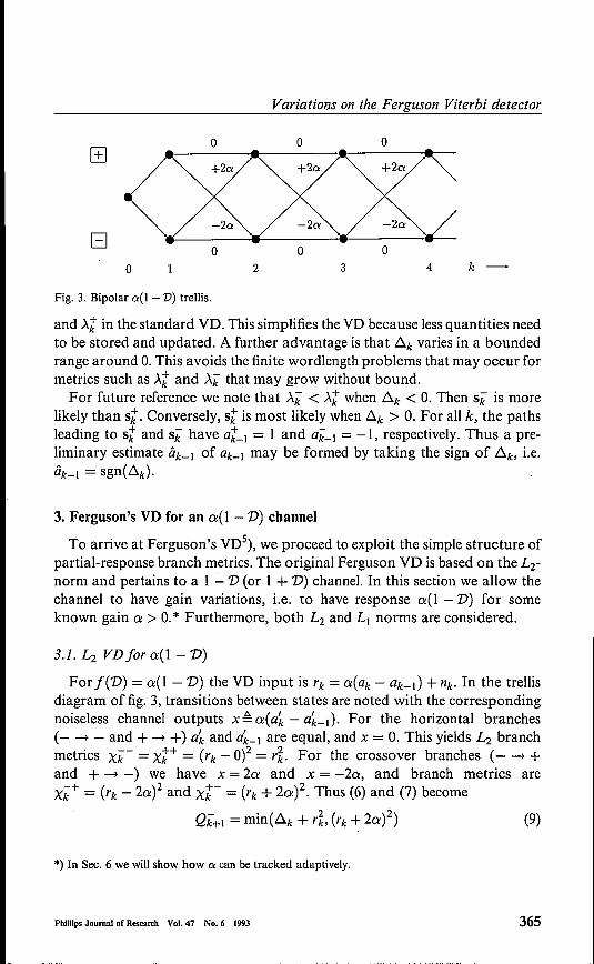
Variations on the Ferguson Viterbi detector
o o o
El o oo 1 2 3 4 k -
Fig. 3. Bipolar a(l - V) trellis.
and >..t in the standard VD. This simplifies the VD because lessquantities needto be stored and updated. A further advantage is that !:::ikvaries in a boundedrange around O.This avoids the finite wordlength problems that may occur formetrics such as >..t and Xi; that may grow without bound.
For future reference we note that >"i; < >..t when s, < O.Then si; is morelikely than st. Conversely, st is most likely when !:::ik> O.For all k, the pathsleading to st and sI; have at-I = 1 and al;_1 = -1, respectively. Thus a pre-liminary estimate éik_1 of ak_1 may be formed by taking the sign of !:::ik, i.e.éik-I = sgn(!:::ik)·
3. Ferguson's VD for an a( 1 - 1)) channel
To arrive at Ferguson's VD5), we proceed to exploit the simple structure ofpartial-response branch metrics. The original Ferguson VD is based on the Lrnorm and pertains to a 1 - 1) (or 1+ 'D) channel. In this section we allow thechannel to have gain variations, i.e. to have response a(l -1)) for someknown gain a > O.* Furthermore, both L2 and LI norms are considered.
(9)
3.1. L2 VD for a(l -1))
For f(1)) = a(l - 'D) the VD input is rk = a(ak - ak-I) + ni, In the trellisdiagram of fig. 3, transitions between states are noted with the correspondingnoiseless channel outputs x~a(ak - al.-I). For the horizontal branches(- ~ - and + ~ +) al. and al.-I are equal, and x = O.This yields L2 branchmetrics xl;- = xt+ = (rk - 0)2 = rr For the crossover branches (- ~ +and +~ -) we have x = 2a and x = -2a, and branch metrics areX;;+ = (rk - 2a)2 and »: = (rk + 2a)2. Thus (6) and (7) become
*) In Sec. 6 we will show how a can be tracked adaptively.
Phillips Journni of Research Vol. 47 No. 6 1993 365

Qk+l = min(b.k +h- 2a)2, r~).
We can distinguish four types of path extension (fig. 4):
Negative merge (m"): Here the - ~ - and - ~ + branches survive. From (9)and (10), this occurs when b.k + r~ < h+ 2a)2 and 6.k+h- 2a)2 < a,i.e. when b.k < h + 2a)2 - r~ = 4a(rk + a) and b.k < r~ - (rk - 2a)2 =4ah - a). The latter condition is strongest and the former one does notcome into play. The new difference metric amounts to
(10)
J.W.M. Bergmans, K.D. Fisher and H. W. Wong-Lam
s+ :/. • •~ X• •s
negative no positivemerge merge merge l'fOSS-
(m") (rn'') (m+)over
Fig. 4. Path extensions come in 4 types, ofwhich the crossover is impossible for Oi( 1 - D) channels.
and
b.k+l = Qk+l - Qk+l = (b.k + r~) - (6.k+ (rk - 2a)2) = 4ah - a). (11)
No merge (m"): Both horizontal branches survive when 6.k+ r~ < (rk + 2a)2and r~ < b.k + (rk - 2a)2, i.e. when 6.k < 4a(rk + a) and b.k > 4a(rk - a).The new difference metric is b.k+1 = Qk+l - Qk+l = (6.k + r~) - (r~) = 6.bi.e. b. does not change.
Positive merge (m"): By analogy to the negative merge, the + ----;+ and + ----;-branches survive when b.k > 4a(rk + a), and the new difference metric isb.k+1 = 4a(rk + a).
Crossover: This is impossible for the channel at hand.
TABLE IExtension of Ferguson's algorithm to a(I - 1)) channel, L2-norm. Positivemerge, no merge and negative merge are indicated by m+, m'' and m",
respectively.
Survivor6.~ 6.~+1 update
> rk+a rk +a m+
Eh -a,rk+a] 6.' mOk.< rk-a rk - a m
366 Phillips Journalof Research Vol.47 No.6 1993

Variations on the Ferguson Viterbi detector
It is obviously convenient to record and update ~~ ~ ~d(40'.) instead of ~k'The required actions are summarized in Table I.An implementation is shownin fig. 5.
The surviving paths Pk = [ak-o,· .. , ak-2J and pt = rato, ... , at2J arestored in two cross-coupled shift registers. The bits ak-) = -1 andat) = +1 that correspond to states '-' and '+' are hardwired. At any instantk, both registers perform either a Shift (S) or Load Parallel (LP) operation un-der the control ofthe signals m", m" and m- that are formed by controllogic.This logic distinguishes which of the three regions of table I rk is in. To thisend, ~~ is compared with rk - 0'. and rk + 0'.. In the event of a merge(m- jm+), the new value ~~+) is saturated at the lower or upper comparisonvalue. Otherwise it remains unchanged. Provided that the detection delay 8is large enough (e.g. 8 ~ 20 - 30), the oldest digits of both shift registers willvirtually always coincide, and either of them can be used as a near-maxi-mum-likelihood decision (Ik-o on ak-o' For small 8, it is necessary to takeGk-o = at-o according as Sf is most likely, as indicated by the polarity of ~~(see Sec. 2).
Figure 6 illustrates the operation of the Ferguson VD for an example input rand a channel with gain 0'. = 1. The actual transmitted data signal isak = ... + + - + + + - ... ; corresponding noiseless channel outputs Xk areindicated with closed circles. The detector input rk is a noisy version of Xk(rk = Xk + nk); samples of t« are indicated by open circles. These samplesdefine an uncertainty band [r - 1, r + IJ whose upper and lower edges aredepicted in the form of continuous-time waveforms (dashed). The differencemetric ~' is constrained to remain within this band. In principle ~' is not chan-ged, i.e. the graph of ~' (solid) is a horizontal line. However, whenever ~'bumps into a band edge it must trace that edge until the edge changes direc-tion. In that case there is a positive or negative merge (m+/m-), depending
controllogic
ak_1 ==-1
Fig. 5. Possible implementation of a(l - V) VD with L2 norm.
Phlllips Journalof Research, Vol. 47 No. 6 1993 367

J.W.M. Bergmans, K.D. Fisher and H.W. Wong-Lam
Uk + +
2
0
-1
-2
+ + + +........ '.. . . .o -,
o .-,
................... 0
'....................................... ~
-,
s :+ + + + +
Fig. 6. Illustration of the operation of Ferguson's Viterbi detector.
on which edge 6.' has bumped into. Conversely, there is no merge (m'') when6.' moves horizontally toward the end of a symbol interval. Except for a rota-tion of90°, this process is like water (6.') falling through a pipe that is bent inthe shape ofthe received signal. The diameter ofthe pipe reflects the gain ofthechannel.
The bottom of the picture depicts the paths through the trellis that corre-spond to the sequence of merges at hand. Two paths are extended in parallelas long as there is no merge (m"), A positive merge causes the path via st tosurvive to both st + 1 and Sk_+ 1. This means that all bits since the previousnegative merge up until ak - 1 are judged to be +1; the most recent bit ak
remains ambiguous until the next negative merge. A similar interpretation canbe given for a negative merge.All bits are detected correctly in spite of the fact that noise nk is so large that
Xk falls outside the band on two occasions. A bit-by-bit detector would havebeen in error here.
3.2. LI VD for (1 - 'D)
When noise nk is Gaussian, amplitudes of rk are, in principle, unbounded.This is unfavourable for some of the wordlengths in a digital implementationof the VD of fig. 5. Use of the LI-norm alleviates this problem. HereXk_- = Xt+ = Irkl, X;;+ = irk - 2al and xt- = irk + 2al. A rederivation forthese branch metrics leads to Table Il.
368 Phillips Journal of Research Vol.47 No.6 1993

Phillips Journal of Research Vol. 47 NO•.6 1993 369
Variations on the Ferguson Viterbi detector
TABLE 11Update table for a(l - V) VD, L( norm.
Survivorupdate
2:: sato:(rk + a)E [sato:h - a), sato:(rk + a)]
::; sato:(rk - a)
sato:(rk + a)~~
satQ(rk - a)
The only difference between Tables I and 11 pertains to the saturationoperator
satQ(x) = { ~-a
if x> a,if [x] ::; a, andif x < -a.
(12)
This operator restricts the amplitudes of rk + a and rk - a to a. In a digitalimplementation, this can be done by using adders in fig. 5 that saturate at±a. This tends to restrict required wordlengths as compared to the L2 receiver.
Bit error characteristics of the L( and L2 VDs are compared in fig. 7 for achannel with Gaussian white noise ni, Here and in following figures, thesignal-to-noise ratio of the channel is defined as SNR ~ Ebi No, where
1.0 ,----------------------,
BER
t
16
SNR IdBI
Fig. 7. Bit error rate (BER) versus signal-to-noise ratio (SNR) for Lt and L2 VD operating onI - V channel with additive white Gaussian noise.

J.W.M; Bergmans, K.D. Fisher and'H. W. Wong-Lam
Eb = E~-oo ff is the received data energy per transmitted bit and No is thevariance of ni:
Only for very poor SNRs does the L, VD lag marginally behind its L2
counterpart. The difference is too small to be visible in fig. 7. The curves offig. 7 do not change for gains a other than unity. Differences between L,and L2 are comparably small for VDs considered later, and correspondinggraphs will be omitted for the sake of brevity.It is worth noting that the L, VD has update ambiguities. Because
of the saturation operators, the events ~~ = sat(t(rk + a) = a and ~~ =sat(t(rk - a) = -a will have a strictly positive probability. This is unlike theL2 case, where the probability density function of ~~ has no discrete com-ponents. In the first event, both a positive merge (m+) and no merge (m")are allowable, while for the second event the choice is between m-and m".In Table Il, ~ and x (as opposed to > and <) comparisons have been adoptedin order to force merges at the earliest possible moment. This tends to restrictrequired detection delays 8 slightly. Simulations indicate that the savings arelargest at low signal-to-noise ratios and are even then only marginal.
The extreme simplicity of the detector of fig. 5 makes it attractive for appli-cations at high data rates. A disadvantage is that only a single class of channelimpulse responses, viz. a(l - 'D), can be handled. In practice the gain a maynot be the only channel parameter that varies. Even small mismatches be-tween the actual channel response f(V) and the response j('D) = a( I - 'D)assumed by the VD may lead to significant performance degradations. In thefollowing sections we expand the class of responses j'(D) that can be handledin two steps.
4. a - f3V channel
This channel also has a memory length M = I, i.e. a 2-state VD suffices formaximum-likelihood detection. For simplicity we take 13 > 0 (the case 13 < 0 isentirely similar). A derivation for the L2 norm along the lines of the previous
TABLE IIIVD for a - f3'D channel, Lrnorm; ,£ (a - (3)/a.
Survivor~~+ ,rk .6.~+t update
> rk + 13 rk + 13 m+
E [rk - 13, rk + f3l .6.~+ ,rk mO
< rk - 13 rk - 13 m
370 Phillips Journalof Research Vol.47 No. 6 1993

Variations on the Ferguson Viterbi detector
TABLEIVEquivalent VD for a - f3V channel, L2-norm; p~ (a - (3)jf3.
SurvivorD.k D.k+1 update
> rk+a rk + a + prk m+
E [rk - a, rk + al D.k + prk mO< rk-a rk - a + prk m
controllogic
Phillips Journul of Research Vol.47 No. 6 1993 371
{3
Fig. 8. Implementation of VD front-end according to Table III for Q - {31) channel.
controllogic
Fig. 9. Implementation of VD front-end according to Table IV for Q - f31J channel.

J.W.M. Bergmans, K.D. Fisher and H. W. Wong-Lam
section leads to Tables III and IV (see also figs. 8 and 9). In these and followingfigures, only the VD front-end, i.e. the logic that is needed to produce theindicators m", mO and m -, is shown; the cross-coupled shift registers of fig.5 are identical for all VDs and are omitted for the sake of brevity.The tables are cast in terms of scaled metrics .6." = .6.k/(4a) and
.6.k = .6.k/(4f3). Their equivalence is easily verified. For f3 = a we have"I = P = 0, and Table I re-emerges. For values f3/a ~ 1 that might typicallybe expected, 1"11, Ipl « 1.Multiplication of rk by "I or P amounts to a mere shiftoperation in digital hardware when either quantity is a power of 2. In practicethis will seldom be true. Nevertheless, the estimates ;Y and p of "I and p as usedby the VD may be restricted to a small set such as S = {O,1/8, 1/4, 1/2, I} inorder to avoid multiplications. The price of this simplification is that mis-matches between the actual values of these parameters and the correspondingVD estimates will induce a performance degradation. This effect is analyzed inthe appendix for the VD of Table IV. Within the interval °~ p ~ 1 (corre-sponding to 1 :?: f3/a :?: 0.5), the effective signal-to-noise ratio degradation islargest for p ~ 2/3 (f3 ~ 0.6a) and then amounts to some 0.5 dB (see fig. 14in the appendix). For Ipl « 1 the degradation is neglibible. A similar analysisis possible for the VD of Table III but is omitted for brevity. Here the interval1 :?: f3/ a :?: 0.5 is covered by only 4 'quantization levels' "I = 0, 1/8, 1/4, 1/2, asopposed to 5 (p = 0, 1/8, 1/4, 1/2, 1) for the VD of Table IV. This leads tosomewhat larger performance degradations. Losses are largest for f3 ~ 0.62a('Y ~ 1/3) and then amount to some 0.8 dB.As compared to the standard Ferguson VD (fig. 5 with a = 1), an extra shift
operation (for multiplication by "I or p) and some extra additions are needed.Depending on the implementation, the metric update in the intermediate (m")range may increase latency and lower attainable data rates. In Sec. 6wewill seehow "I and p can be determined adaptively.
Update tables for the L1 norm are comparatively complicated and do notseem to lead to attractive implementations. For this reason they are not in-cluded here.
4.1. Effect of precoding
Partial-response systems often employ a precoder at the transmitting end ofthe system. This precoder converts the original bit signal dk into a binary datasignal ak that is recorded or transmitted. For 1 - D the precoder is just amodulo-2 integrator, i.e. dk = 1 indicates a transition of ak (ak = -ak-l),while dk = -1 indicates no transition (ak = ak-l). The values dk may be deter-mined directly from the sequence ofmerges in the VD. Specifically, no merge
372 Phillips Journal of Research Vol.47 No.6 1993

Phillips Journol of Research Vol.47 No.6. 1993 373
Variations on the Eerguson Viterbi detector
(m") means that both surviving paths are extended 'horizontally', i.e. withouttransition (see fig. 6). Thus we can safely decide that dk = -1, even though thepolarity of the ongoing run of aks has not yet been decided upon. A positivemerge (m") indicates that a sequence of no merges has ended. In this eventthe previous merge of opposite polarity must have been a transition (comparefig. 6). This means that dp = +1, where p indicates the instant at which thismerge has occurred. In the event of a negative merge, we can similarly decidethat d = -1 at the instant p at which the previous positive merge occurred.
4.2. Alternative implementation
The foregoing observations pave the way to an alternative detector imple-mentation that is rooted in work of Wood and Petersen/). Let p :::;k - 1 bethe previous instant at which there was a merge (either positive or negative),and denote the polarity of this merge by €p E{-I, I}. Then for the VD ofTable Ill, .6.~+1 = rp + €p{J. Between the instants pand k - 1 there are nomerges, whence
(13)
where t.k ~ E~':pl+lri is a short-term measure of the DC-content of ri, Inbetween merges, t.k may be computed recursively according to t.k+l = t.k + rk.To this end, a single accumulator suffices. Since t.p+l = 0, this accumulatatormust be reset whenever a merge occurs. The factor "(t." in (13) causes theDC-content of rk to affect detection more strongly as 11'1 increases. This tendsto lower VD tolerance to DC-offsets and low-frequency interference.
Rather than keeping track of .6.k, we may store and update rp, ép and t.k'From Table Ill, a positive merge occurs when .6.k + "(rk = rp + êp{J+"((t.k + rk) > rk + {J, i.e. when Sk ~rp - rk + "((Çk + rk) > (J(I - ép). Apartfrom the current input rb this comparison indeed involves only rp, êp andt.k' Because of the merge, these variables must be updated according torp := rb êp := 1, and t.k+l := O. In hardware this amounts to hold, set andreset operations, respectively. The remaining two regions of Table III maybe recast in a similar way. The resulting algorithm for precoded data is sum-marized in Table V. An implementation is shown in fig. 10.
In fig. 10, the signal Sk is formed and compared with thresholds -2f3ép and O.Multiplication (exclusive or) of both outputs yields a merge indicator (m). Inthe event of a merge, the output of the left comparator is an indicator of thepolarity of the merge, and is latched into the êp register. At the same time rkis latched into the rk-register, and the accumulator that stores Çk is reset.The path register now takes the form of a random access memory (RAM).The locations k and p of this register are updated in accordance with Table V.

J.W.M. Bergmans, K.D. Fisher and H. W. Wong-Lam
TABLEVAlternative update table for a - (31) VD, L2 norm, precoded data; ,=(a - (3)/a.
Trellis VD UpdatesSk = rp - rk + ,(Çk + rk) extension output 'p := f:p := Çk+l.:= P'-.-
> (3(1- f:p) m+ Jp := -f:p rk 0 k
E [(3(-I-f:p),(3(I- f:p)] mO Jk :=-1 rp f:p Çk+ r» P< (3(-1 - f:p) m Jp := f:p rk -1 0 k
Fig. 10. Alternative detector implementation according to Table V for ei - f31J channel and pre-coded data.
The difference metric ~k of Table IV may be computed from rp, f:p and Çkaccording to (13). A sign operation on this result yields preliminary decisionsQk-l with respect to ak-l that are of interest for adaptation of (3 and, (seeSec. 6).
TABLE VIAlternative update table for a - (31) VD, L2 norm, precoded data; p =(a - (3)/(3.
Trellis VD UpdatesZk = rp - rk + P(k extension output r .- f:p := (k+l := P'-p .- .-
> a(1 - f:p) m+ Jp := -f:p rk rk k
E [a( -1 - f:p), (3(1- f:p)] mO Jk := -1 r f:p (k + rk Pp
<a(-l-f:p) m - Jp := f:p rk -1 rk k
374 Phlllips Journalof Research Vol.47 No. 6 1993

Phlllips Journni of Resenrch Vol.47 No. 6 1993 375
Variations on the Ferguson Viterbi detector
For the VD of Table IV, an alternative implementation may be derived in asimilar way. In Table VI, Zk £ rp - rk + P(k and (k £ 'f};:pl ri are the counter-parts of Sk and t,k, respectively. Implementation is analogous to fig. 10 andtherefore not shown. Preliminary decisions ak-l with respect to ak_1 can beproduced by taking the sign of 6.k = rp + P(k + O!.ép'
Implementation ofthe VDs of Tables V and VI may be simpler than that oftheir predecessors. A development along the above lines for the Lç VD doesnot seem to lead to attractive implementations.
5. Feedback
For channel memory lengths M > 1, more than two VD states are needed toretain optimality. However, in many instances close-to-optimum performanceis within reach withjust two states when use is made of feedback to truncate Minto a value MI = 1 that can be handled as discussed above'"), Optionsinclude:
1. Preliminary decisions ak-M, ... ,lÎk-2 extracted from the VD (as describedin the previous sections) can be applied to a feedback filter (FBF) that gen-erates a compensation signal for trailing ISI, which is subtracted from thereceived signal before it enters the VD (fig. 11). This is referred to as globalfeedback because only a single compensation signal is produced, whichaffects the updates of all survivors. When preliminary decisions are allcorrect, the effective channel impulse response as seen by the VD hasV-transform r (V) = fo +fl V, and a two-state VD suffices. Detection issuboptimum because data energy due to 12,'" JM is not exploited. The
~~fiäilliër---------- ---:: 11k :
: I~®~L: ,,
~k~ ~kJ.Lo kJ'
IOAF M -k -k
,,,l'k äk-ó,
L: VD, + /"1'= 1,--- -
äk_2 1-----1 ak_M
FBFh,···,JM
Fig. 11. Channel memory truncation by means of global feedback.

J.W.M. Bergmans, K.D. Fisher and H. W. Wang-Lam
consequential performance loss is, however, typically small. A further lossmay occur when any of the preliminary decisions is wrong. Then an erro-neous compensation signal will be produced, and errors may propagateto all of the survivor updates.
2. To lower this error propagation, a separate feedback path can be estab-lished for every survivor. The resulting compensation signals for trailingISI are used only for the update ofthe originating survivor. This is referredto as local feedback. We now elaborate this option in more detail.
5.1. Local feedback
In fig. 12, two compensation signals Uk£ L:::i!!2 ak-Ji and ut £ L:::i!!2 atdi fortrailing ISI are formed on the basis ofthe ,_, and '+'-survivors in the VD, andare subtracted from the received signal rk' The resulting signals rk and rt arefree from trailing ISI outside the span of the VD when ak-M,"" ak-2and atM"'" at2' respectively, coincide with the actual data symbolsak-M, ... ,ak-2' To minimize error propagation, rk and rt are only used forthe updates of the ,_, and '+'-survivors, respectively. For the baseline VDof Sec. 2 with L2 norm, this yields branch metrics xi" = (rk T fo + fl)2 andxt± = vt =FJo - fl)2. As in Sec. 3, only three regions need to be discrim-inated between when xt- _ Xk- > xt+ _ X;;+ for all k. A straightforwardderivation reveals that this is so for fo > 0 when rt - rk > 2fl' For fl < 0,this condition will hold for all k when L:::~2Ifkl < Ifll, i.e. when Ifll is nottoo small and trailing ISI due to 12, ... JM is not too severe. Since thedetectors developed here are meant to handle variations of the basic I _ Vresponse, it is reasonable to assume that this condition will hold.
FBFJ,,···,ht
1·+kI:+
1'k
Fig. 12. VD with local sequence feedback.
376 Phillips Journalof Research Vol.47 No.6 1993

Variations on the Ferguson Viterbi detector
TABLE VIIExtension of Table III to Cl!- {31)+121)2+ ... +fM1)Áf channel, Lrnorm,local feedback; 'Y = (Cl!- {3)/Cl!;'TI~~ ((1';;)2 - (rt)2)/(4Cl!).
+ -11.' + 'k+'k + 'uk 'Y 2 'TIk
Survivorupdate
> rt + {3
E h- {3,r, + {3l
< 1';; - {3
rt + {311.' + ,t+,; + 'uk 'Y 2 'TIk
1';; - {3 m
Extensions of Tables III and IV may be derived along the lines of theprevious sections (Tables VII and VIII).
In the absence of feedback one has 1';; = rt = rko 7iik = 0, 'TI~= r;k = 0, andTables III and IV re-emerge. Feedback involves contributions 'TI~ and 'ijkwhose computation involves squaring operations and is therefore compara-tively complicated. For the L, norm and Cl!= {3, the update table againinvolves saturation operators, and extra updates akin to 'TI~and r;ko both equalto 0.5(11';; I - IrtD. Computation ofthis quantity is comparatively simple. Evenfor Cl!~ {3, its use instead of 'TI~or r;k may not greatly lower performance.
To illustrate the performance of the above schemes we show in fig. 13 acollection of bit error characteristics for a 1 - 0.51) - OSV2 channel.
The VD with local feedback lags some 0.8 dB behind its fully fledged 4-statecounterpart. Replacement ofzj, = ((1';;)2 - (rt)2)/(4Cl!) by'TI~ = 0.5(lr;;I-lrtDresults in a marginal SNR loss of around 0.1 dB. Global rather than local feed-back costs another 0.2 to 0.3 dB. The considerably simpler DFE lags around1dB further behind. Omission of feedback, as in curve e, is clearly unadvisable.
TABLE VIIIExtension ofTable IV to Cl!- {3V +121)2 + ... +fM1)M channel, Lrnorm, localfeedback; 7iik ~ p(rt - 1';;)/2 with p = (Cl!- {3)/{3; r;k ~ ((1';;)2 - (rt)2)/(4f3).
Survivorupdate
> rt + Cl!+ 7iikE [rk - Cl!- 7iib rk + Cl!+ 7iikl
< 1';; - Cl!-7iik
rt + Cl!+ prt + 'ijk+ -
11. + 'k+'k +-uk P 2 'TIk1';; - Cl!+ pr;; + 'ijk
Phillips Journalof Research Vol. 47 No. 6 1993 377

SNR (dB(
J.W.M. Bergmans, K.D. Fisher and H.W. Wang-Lam
1.0 ....-------------------.,
BER
t
Fig. 13. Bit error rate (BER) versus signal-to-noise ratio (SNR) for various receiversoperating on aI - 0.51) - 0.51)2 channel. a. Fully fledged VD; b. VD according to Table VII; c. idem, but"Ik = 0.5(lrk"I-lrtD; d. VD with global feedback; e. VD for 1 - 0.51) channel, no feedback;f. decision feedback equalizer (DFE).
Global feedback is easily added to the alternative VD implementations ofSec.4.2. Incorporation of local feedback, on the other hand, is only possibleat a considerable expense to simplicity.
6. Adaptivity
6.1. a(l - 'D)-detector
Let a and &denote the actual gain of the channel and the gain assumed bythe detector, respectively. Under the control of an adaptation algorithm, &should be adjusted in small steps so as to approach a.With the help ofTables I and 1I,one easilyverifies that in the absence ofnoise
nb b.~= aak-l + (& - a )ak-2 whenever a merge has occurred at instant k - 1.Furthermore, rk = a(ak - ak-l) when nk = O. These facts allow the differencesignals d/ ~ b.~- rk - &and dk- ~ b.~ - rk +&,whose sign is determined bythe comparators in fig. 5, to be evaluated. One finds that dk+ = 2(a - ä) whenak = ak-l = -ak-2 = 1, while dk- = 2(& - a) when ak = ak-l = -ak-2 = -1.In the presence of noise ni, these misadjustment indicators become noisy aswell, but will remain a suitable control signal for update of &according to agradient-type algorithm. All that is needed whenever a merge occurs (as
378 Phillips Journal of Research Vol.47 No.6 1993

PhilJips Journal of Research Vol.47 No. 6 ,1993 379
Variations on the Ferguson Viterbi detector
indicated by the merge indicators m- and m") and Gk = Gk-l = -Gk-2 = ±I isan update of & according to & := & ± J.Lsgn(d/). Here J.L is a small positiveadaptation constant that will typically be a power of 2 for implementationalsimplicity. The preliminary decisions Gk> Gk-l and Gk-2 are determined asdescribed in Sec. 2. Provided that they are correct most of the time, & canbe made to approach a arbitrarily closely.
6.2. a - (31J detector
For the sake of brevity we restrict attention to the detector of Table Ill. Asimilar development is possible for the VD ofTable IV. Let a - {:J1Jcharacter-ize the channel impulse response assumed by the detector. Denote the corre-sponding estimate (& - (:J)/& of / by i. Under the control of an adaptationalgorithm, i and {:J are to be adapted towards / and (3, respectively. When iis a power of 2, multiplication of any quantity by I - i involves only a shiftoperation and an addition. Thus the error signal
(14)
may be determined without any digital multiplications. The preliminarydecisions Gk-l and Gk may be produced by taking the sign of ~~ and ~~+l(see Sec. 2). Whenever both decisions are correct, ek amounts to
ek = (a(I - i) - {:J)ak - (1 - i)((3 - {:J)ak-l + (1 - i)nk' (15)
Upon realizing that a(I - /) = (3, it follows that ek contains only a noise com-ponent when the estimates i and {:J are both correct. When nk is small, thissituation will be closely approached when the power of ek is minimized withrespect to i and {:J. To this end, {:J and i are changed iteratively away fromthe noisy gradients of e~ with respect to {:J and i, respectively. One easilyverifies that
(16)
This suggests that {:J may be updated according to the stochastic gradient(LMS) algorithm
(17)
where J.L is an adaptation constant that enables a tradeoff between rate of con-vergence and steady-state excess mean-square error. When both J.L and i areconstrained to be a power of 2, the correction term P,ek(Gk - (1 - i)Gk-l)

J.W.M. Bergmans, K.D. Fisher and H. W. Wang-Lam
may be computed with only shift and add operations. Often lil« 1. Then weobtain the simplified algorithm
(18)
Thus no correction takes place when Gk and Gk-l are equal. Conversely, anupdate of magnitude 2f1ek occurs when Gk =I- Gk-l. For maximum simplicity,only the sign of ek may be invoked in the update. This leads to the signalgorithm
when Gk '# Gk_[' and
when Gk= Gk-l·(19)
For y = 0 these algorithms degenerate into alternatives to the adaptation tech-nique of Sec. 6.
As to adaptation of i,one easily verifies that
ae~ -ai = -2ek(aak - ((3 - (3)ak-l) ~ -2aekak, (20)
where the approximation sign holds whenever {J does not differ too much from(3, as ensured by the adaptation algorithm for (J. This would suggest the sto-chastic gradient algorithm i := i + f1ekGk for some small adaptation fonstantu: Whenever i is constrained to be in a small set such as S, the update f1ekGkwill almost always move i outside this set. Then the stochastic gradientalgorithm is not applicable. A similar argument applies to the sign algorithm.
Among the viable options is one that is rooted in work of'Lucky':'), Here i isonly updated once every N symbol intervals, where N is typically fixed and onthe order of 100 to 1000. Updates are governed by the averaged stochasticgradient
(21)
or its sign-counterpart
1 k+N-1-6 '"cP = - ~ sgn(ek)Gk·
N i=k
More particularly, when cP or (ij exceeds some predefined positive threshold, iis increased to the next larger element of S. Below some negative threshold, i isdecreased one step, while in the intermediate range it is not changed. Of courseincreasing or decreasing of i is inhibited when the updated values would be
(22)
380 Phillips Journal of Research Vol. 47 No.6 1993

Variations on the Ferguson Viterbi detector
outside S. For the sake of brevity we refer to ref. 13 for a discussion on con-vergence behaviour, implementation issues and choice of thresholds.Provided that ak and ak-l are correct most of the time, {J and 7 can be made
to approach their ideal values closely by an appropriate selection of algorithmparameters.The above adaptation techniques are certainly not the only possible ones.
To illustrate this we describe one alternative technique for adaptation of {J.By a similar reasoning as in Sec. 6.1, one finds for the VD of Table III thatin the absence of noise nk> .6.~= aak_l + (/3 - f3)ak-2 when a merge hasoccurred at instant k - 1. Hence
.6.~+1-.6.~ = a(ak - ak-l) - ({J - f3)(ak-l - ak-2) (23)
when merges occur at instants k - 1 and k. This can be checked by observingthe current and previous merge indicators m- and m", and a preliminaryestimate (ak-2' ak-il ak) of the triplet (ak-2' ak-h ak) can be determined as inSec. 2. In particular when ak = ak-l = -ak-2 we find that
(24)
i.e. the metric increment .6.~+1- .6.~ is linearly proportional to the misadjust-ment of {J. In the presence of modest amounts of noise ni; .6.~+1- .6.~willremain a reasonable misadjustment indicator. Thus {J may be adjusted onthe basis of metric increments whenever two merges occur in succession,depending on the triplet (ak-2, ak-l, fIk)'
6.3. Feedback adaptivity
For the VD with global feedback, one easily verifies that the error signal ekof (14) becomes proportional to the misadjustment of the feedback filter, pro-vided that the preliminary decisions fIk-M" .. ,ak-2 are correct. Then the FBFcoefficients Ï2"",]M may be adjusted according to the stochastic gradientalgorithm
(25)
Replacement of ek by sgn(ek) results in the sign algorithm.Local feedback gives rise to two counterparts r;; and rt of rk> and conse-
quently to two error signals eJ; and et. From Sec. 2, we note that st is morelikely than sJ; when .6.k > 0 (i.e. when ak-l = 1), and vice versa when.6.k < 0 (i.e. when fIk-l = -1). Thus adaptation can proceed as for the VDwith global feedback, provided that it is based on et when ak-l = 1 and oneJ; when ak-l = -1.
Phillips Journalof Research Vol.47 No.6, 1993 381

(A.2)
J.W.M. Bergmans, K.D. Fisher and H. W. Wong-Lam
7. Final remarks
As regards implementational simplicity, the detectors derived here comparewell with their predecessors (ref 8, pp. 373-375 and refs 9-12). No squaringoperations or digital multiplications are needed. For channels with memorylength M> 1, use of local feedback avoids significant performance losseswith respect to the full-fledged VD. Adaptivity is easily added and comes ata modest hardware cost. We have not addressed any finite-wordlength issueshere. In this regard, one might anticipate that the L, VD will be slightlyfavourable to its L2 counterparts.
Generalization of the above results to metrics other than L, and L2 does notseem to lead to attractive solutions.
Appendix: Effect of quantization of pLetfCD) = a - (3V = a(1 - V/(1 + p)) andj(V) = &(1 - V/(l + p)) char-
acterize the actual channel and the one assumed by the VD, respectively. Inthis appendix we assume that cl has been adjusted properly, i.e. that & = a,while p may differ from p as a result of quantization. Since final results donot depend on a, we take a = 1 for simplicity. Then the actual channel outputrk is given by rk = ak - (3ak-' + ni, where ak E {-I, I} is the data sequence,(3 = 1/(1 + p), and nk is white Gaussian noise of variance No. The detectorbases its decisions on path metrics
where a~ is an arbitrary candidate data sequence, ek ~ ak - aL andiJ = 1/(1 + p). It chooses in favour of a sequence a~ =I- ak when Ja' < Ja, i.e.when Jd - Ja < o. One easily verifies that
The right hand side is a stochastic variable with mean
M(e, ~/) ~ L[(ek - (3ek-,f + 2(iJ - (3)(ek - (3ek-I)a~-d (A.3)k
382 Phillips Journalof Research Vol.47 No. 6 1993

Phlllips Journal of Research Vol.47. No.6 1993 383
Variations on the Ferguson Viterbi detector
and variance No V( e), where V( e) ~ 4 I::k( ek - ~ek-I )2. Hence
P,[Jr J,< O[ ~ Q ( d2~;d) ). (A.4)
where
d2( ') ~ M2(e, a')
e,a V(e). (A.5)
At high signal-to-noise ratios, performance is governed by the minimum valued2 of d2(e, a') across all allowable pairs (ek, a/Jo In the absence of a mismatch,d2(e, a') depends only on ei, and for 1,81~ 1 assumes a global minimumi;'in = 1 +,82 for the single bit error ek = ±28k> where 15k is the Kroneckerdelta function.
In the presence of a mismatch, a" comes into play as well. Here two errorsequences are of particular interest:
l. The single bit error ek = ±2Ók. Here V(e) = 16[1 + ~2] and M(e, a') =4[1 +,82 ± (~- ,8)(a'_l - ,8a~)]. Now aó = =fl when ek = ±28k. Thus
I 2 - I IM(e,a)=4[1+,8 +(,8-,8)(,8±a_I)]. In choosing a_I so as tominimize M(e, a'), the cases iJ > ,8 and ~ < ,8 must be distinguished.One finds that mind M( e, a') = 4( 1 + ,8(1 + iJ) - max(,8,~)). Thus thedistance dr ~ mind M2(e, a')/ V(e) for the single bit error amounts to
d2 _ (1 + ,8(1 + iJ) - max(,8,iJ))2I - 1+ ~2
(A.6)
2. The double bit error ek = ±2(Ók + 15k-I). Here V(e) = 32(1 _ iJ + iJ2),while M(e, a') = 8(1 -,8 + ,82) ± 4(~ - ,8)[a'_l + (1 - ,8)aó - ,8a;]. Nowaó = a'1 = =fl when ek = ±2(8k + 15k-I). Thus M(e, a') = 8(1 -,8 + ,82)+4(~ - ,8)[2,8 - 1 ± a'_I]. In selecting a'_l we must again distinguishbetween the cases ~ > ,8 and iJ <,8. One finds that mind M(e, a') =8(1 + max(,8, iJ) (min(,8, ~) - 1)). Thus the distance di ~ mind M2(e, a')/V(e) for the double bit error amounts to
d2 _ 2(1 +max(,8,iJ)(min(,8,~) - 1))22- 1_~+~2
(A.7)
For values of ,8 and ~ of practical interest, d2 = min(dr, di). Losses£. ~ d~in/d2 due to mismatch are depicted in fig. 14 as a function of,8 for var-ious values of p = (1 - iJ)/~.
Losses £. vanish whenever ~ = [3, i.e. when,8 = 1/(p + 1). For the standard

J.W.M. Bergmans, K.D. Fisher and H. W. Wong-Lam
3
.£ 2[dBI
t
o 0.5-p
Fig. 14. Loss C due to mismatch versus {3 for various values of p = (1 - /3)//3.
1.0 ~-----------------,
BER
t
5 10
SNR [dB I
1/4
1/8
1/16
o
Fig. IS. Bit error rate (BER) versus signal-to-noise ratio (SNR) for 1- 'D and 1 - O.5'DVDoperating on a 1 - O.5'Dchannel with additive white Gaussian noise.
384 Phillips Joumnl of Research Vol.47 No.6 1993

Phillips Journalor Research Vol.47 No. 6 1993 385
Variations on the Ferguson Viterbi detector
Ferguson VD (i.e. the p = 0 curve in fig. 14), losses of several dB are incurredin the presence of a considerable mismatch. By contrast, losses never exceed0.5 dB when p is selected to be an appropriate power of 2. In Sec. 6 we showhow this can be done adaptively.
By way of example we show in fig. 15 the bit error rates achieved by astandard (1 - 'D) VD and one with p = 1 for a 1 - 0.5'D channel.The 1 - 'D VD requires some 4 dB more SNR to achieve bit error rates
below 10-3 than its 1 - 0.5'D (p = 1) counterpart. This SNR difference is inagreement with fig. 14.
REFERENCESI) H. Kobayashi, Application of probabilistic decoding to digital magnetic recording systems,
IBM J. Res. Develop., 15, 64-74 (1971).2) R.W. Wood and D.A. Petersen, Viterbi detection of class IV partial response on a magnetic
recording channel, IEEE Trans. Commun., COM-34 (5), 454-461 (1986).3) Y. Eto, Signal processing for future home-use digital VTRs, IEEE J. Selected Areas in
Commun., SAC-10, (1) 73-79, (1992).4) R.D. Cideciyan, F. Dolivo, R. Hermann, W. Hirt and W. Schott, A PRML system for digital
magnetic recording, IEEE J. Selected Areas in Commun., SAC-10 (1) 38-56 (1992).5) M.J. Ferguson, Optimal reception for binary partial response channels, Bell Syst. Tech. J., 51
(2),493-505, (1972).6) K.A. Schouhamer Immink, Coding methods for high-density optical recording, Philips J. Res.,
41, (4), 410-430 (1986).7) J.W.M. Bergmans, Performance consequences of timing errors in digital magnetic recording,
Philips J. Res., 42 (3),281-307 (1987).8) G.D. Forney, Jr., Maximum-likelihood sequence estimation of digital sequences in the
presence ofintersymbol interference, IEEE Trans. Inform. Theory, IT-IS (3), 363-378 (1972).9) R.D. Gitlin and E.Y. Ho, A null-zone decision feedback equalizer incoroporating maximum-
likelihood bit detection, IEEE Trans. Commun., COM-23 (11), 1243-1250 (1975).10) G. Kawas-Kaleh, Double decision feedback equalizer, Frequenz, 33, (5), 146-149 (1979).11) E. Dahlman and B. Gudmundson, Performance improvement in decision feedback equalisers
by using 'soft decision', Electron. Lett., 24 (17) 1084-1085 (1988).12) J.W.M. Bergmans, S.A. Rajput and F.A.M. van de Laar, On the use of decision feedback for
simplifying the Viterbi detector, Philips J. Res., 42, (4), 399-428 (1987).13) R.W. Lucky, Automatic equalization for digital communications, Bell Syst. Tech. J., 44,547-
588 (1965).
Authors
Jan W. M. Bergmans: Ir. degree (Electrical Engineering), Eindhoven University of Technology,The Netherlands, 1981; Ph.D, Eindhoven University of Technology, 1987; Philips ResearchLaboratories, Eindhoven, 1982- . From 1981 to 1982, he was a manager for communicationprojects in the Royal Netherlands Navy. At Philips Research Laboratories, he is involved inresearch on signal processing for digital transmission and recording. In 1988 and 1989 he wasan exchange researcher in the digital video recording group of Hitachi Central ResearchLaboratories, Tokyo, Japan.
Kevin D. Fisher: B.Sc. (Computer Engineering), University of Illinois, Urbana, 1985; M.Sc.(Electrical Engineering), Stanford University, California, 1987; Ph.D., Stanford University,

J.W.M. Bergmans, K.D. Fisher and H.W. Wong-Lam
California, 1991; Philips Research Laboratories, Eindhoven, The Netherlands, 1991-1992;Quantum Corporation, Milpitas, California, 1993- . At Philips he was engaged in research onsignal processing for digital magnetic recording.
H.W. Wong-Larn: B.Sc. (ElectricalEngineering), University of Hong Kong, Hong Kong, 1985;M.Sc. (Electronic Engineering), Philips International Institute, Eindhoven, The Netherlands,1987; Philips Research Laboratories, Eindhoven, The Netherlands, November 1987- . Mrs.Wong's B.Sc. thesis was on medical signal processing. Her M.Sc. thesis was on strongly quantizedequalizer design. Since working with Philips, she has been involved in signal processing research inthe Magnetic Recording Systems group. From October 1991, she has been a member of a teaminvolved in analog channel IC design for recording applications.
386 Phillips Journal or Research Vol.47 Nó.6 1993

Philips Joumal of Research Vol.47 No.6 1993 387
Philips J. Res. 47 (1993) 387-423 R1285
THE DYNAMIC BEHAVIOR OFPARALLEL THINNING ALGORITHMS
by W.L.M. HOEKSPhilips Centrefor Manufacturing Teclmology, P.O. Box 218. 5600 MD Eindhoven,
The Netherlands
AbstractSkeleton extraction in digital image processing is the reduction of objects inthe image to a single pixel thin structure, while maintaining the topology ofthe object. A skeleton extraction method is thinning, which is the repeateddeletion of pixels on the object boundary until a single-pixel thin structureremains. If the computation of deletability of a pixel is done without usingthe result ofthe computation on neighboring pixels the method can be per-formed in parallel.The properties of the thinning paradigm are discussed from a theoretical
viewpoint. A thinning algorithm is defined by an edgemodel and a deletionfunction. A formal description of the thinning process for two edge modelsand some deletion functions is presented. The behavior of some implemen-tations of skeleton extraction algorithms based on parallel thinning is alsodiscussed. Some implementations not only miss or include non-skeletalpixels, but also have positional bias depending on implementation details.
Keywords: digital image processing, distance metric, morphological filter-ing, pattern recognition, skeleton extraction, thinning.
1. Introduetion
1.1. Skeleton extraction
In automated image interpretation, it is sometimes convenient to have a"stick-like" representation of the objects in the image representing the topo-logical structure of the objects. It is assumed that the stick-like representationis easier to analyze and can be coded more compactly in the computer. Anal-ogous to the skeleton in animals, the stick-like representation is called theskeleton. The topological relations between the parts of the object are pre-served in the stick-like representation; hence the restrietion that the skeletonmust be connected for any connected object (fig. 1 presents an example).

W.L.M. Hoeks
b
Fig. 1. a) A sample object and b) its skeleton.
In early machine vision research the skeleton was used as a compact butcomplete representation of the object. Since the representation had to beexact, the susceptibility of the skeleton to small perturbations of the objectboundary was a logical consequence'"). In image interpretation, skeletonextraction is not used for image coding, but is part of a recognition schemethat identifies the major features ofthe object. In such cases exactness ofrepre-sentation is contrary to the aim. In order to match the extracted skeleton to amodel it is necessary to drop the small details in favor of the overall structure.For image interpretation the effect of small boundary perturbations must beminimal.
Skeleton extraction can be implemented in various ways on a computer,though a common characteristic is that the input data are only defined at dis-crete grid points, also called pixels. Although there are skeleton extractionalgorithms for grey level images, we only consider binary input data here.One can start working directlyon the input data using the thinning methodor perform a distance transformation first. In this paper we concentrate onthe dynamics of the thinning method.We define the thinning operation using an edge model and a deletion func-
tion. The edge model describes which pixels are considered to belong to theboundary of the object. In the discrete rectangular grid the most commonedge models are the 4-neighborhood or the 8-neighborhood*. The deletionfunction describes the conditions for assigning the value "background" toedge pixels in a thinning step. The deletion of edge pixels not belonging tothe skeleton is repeated until only skeletal points remain. The deletion ofpixels not belonging to the skeleton can be done in either a parallel or a serialmanner.
If the computation of the deletability of an edge pixel does not depend onthe computation for a previous pixel, then all pixels can be checked for dele-tion in parallel, i.e. all deletable pixels may be removed in one operation onthe image. Most thinning 'algorithms in this class are implemented as Casequence of) morphological filters. If a 3 * 3 neighborhood is used as the sup-port of the filter, then the deletion must be performed in a number of passes 1).
* For definitions of the neighborhoods, see ref. 1.
388 Phillips Journalof Research Vol.47 No.6 1993

Phillips Journal of Research Vol. 47 No. 6 1993 389
Parallel thinning algorithms
The pixels on the object boundary are grouped in classes, and in each passpixels in one class are checked for deletion.
A thinning algorithm which checks one pixel after another for deletion is aserial algorithm. If a pixel is deleted before the next pixel is checked, the objectwill be deformed with each deletion, and the resulting thin structure will have astrong bias depending on the scan direction. Although there are variousmethods to reduce the bias, we will not consider serial thinning in this reportbecause the strong interaction between the processing of one pixel and the nextcomplicates the analysis of the thinning process.
In Sec. 2 the propagation properties of single-pass parallel thinning forvarious edge models and deletion functions are studied using artificial testimages. In the first subsection we introduce a formal method to describe thedynamics of the thinning process. In the three following subsections we willanalyze three edge models using that formalism. Although there are manymore options for deletion functions (see the, numerous articles cited inref. 2), it is not necessary to discuss all of them for a thorough understandingof the thinning process. We will not consider object shapes, where subtledifferences between algorithms are noticeable. In Sec. 3 we study the responseof some specific algorithms for the test images used in Sec. 2 and compare themwith the theoretical results of Sec. 2.
1.2. Several definitions of the skeleton
Usually the domain of the definition is a two-dimensional continuous spacewith the Euclidean distance metric. The choice of distance metric is sometimesimplicit, and linked to the way humans perceive distance. The choice of dis-tance metric cannot be neglected when the distance metric must be adaptedto the (square) grid for implementation of an algorithm. Therefore we discusssome definitions with respect to the distance metric, the definition domain andthe consequences for the discrete domain.
For reference purposes in this paper we say that a skeleton consists of seg-ments, branch points and endpoints. The segments are formed by the pixels inthe skeleton which have exactly 2 neighbors in the skeleton. The endpointshave only one neighbor in the skeleton. The branch points form the connec-tion between multiple segments.
Hilditch3) poses four constraints to the skeleton instead of giving an explicitdefinition. We will repeat these requirements here .
• ThinnessThe skeleton consists of single-pixel thin skeletons (minimal width) .
• Position

W.L.M. Hoeks
Each point of the skeleton should lie in the middle of the part of the objectthat corresponds to that point of the skeleton.
• ConnectivityThe connectivity of the object as well as the connectivity of the backgroundis preserved when the skeleton is extracted.
• StabilityThe parts of an object that are reduced to a curve in some stage of thealgorithm must remain as they are.
Hilditch refers to algorithms that extract the skeleton by thinning. The stab-ility criterion is sometimes referred to as the conservation of endpoints orabsence of excessive erosion. Stated otherwise, skeleton extraction is idem-potent, i.e. the result of skeleton extraction applied to a skeleton reproducesthe skeleton. Note that stability as defined here is not the same as in controltheory, where stability refers to the sensitivity of a system to small disturb-ances in the input. The above constraints leave some issues open. The mostobvious one is the definition of the "middle". The computation of the"middle" requires a means to compare distances, i.e. a metric. The constraintsof Hilditch are conflicting in the discrete domain. An elongated object parthaving an even numbered width cannot have a line of minimal width in itsmiddle, since the middle is between two grid points. If both grid points areassociated with the middle the line is not thin. If one of them is chosen theline is not in the middle. One of the two conditions will be violated.
• Maximal disk definition")Given a domain and a metric then the concept of a circle is defined as the setof points that are closer than a specified distance (radius) to a referencepoint (center). Now given an object, a maximal disk is a circle which is asubset of the object such that there is no larger circle which has the givencircle as subset and which is also a subset of the object. The skeleton isdefined as the set of centers of the maximal disks in the object.
Although this definition is independent of the domain, the connectivity con-straint of Hilditch is violated [ref. 4, p. 379, fig. XL3]. The existence of themetric is specified, but the choice of the metric is not specified.
Montanarr') lists several definitions, although the correctness of the defini-tions depends on the distance metric, or on the domain. The maximal disk defi-nition holds for all metrics and both domains, but does not guaranteeconnectness. The skeleton according to the maximal disk definition supple-mented with the pixels (points in the continuous domain) needed to maintainconnectness will be used as a reference in this report.
390 Phillips Journal or Resea rch Vol.47 No.6 1993

d4(P, Q) = Ixp - xQI + Iyp - YQI
dg(P, Q) = MAXIMUM(lxp - xQI, Iyp - YQI)
dE(P,Q) = V((Xp - XQ)2 + (yP - YQf)
(1)
(2)
(3)
Parallel thinning algorithms
1.3. Influence of the distance metric
Consider two points Pand Q in a two dimensional domain with coordinates(xp,Yp) and (xQ,YQ)' The distance metrics used in this paper are d4 represent-ing the cityblock distance, dg the chessboard distance, and dE the Euclideandistance. The definitions are given below, where [x]denotes the absolute valueof x.
Most theoretical results on the properties of the skeleton have been derivedfor the Euclidean metric in a continuous domain. The Euclidean metric has thenice property that a circular object remains the same when it is rotated aroundits center, i.e. there is no dependence on orientation. A square object may be a"circle" according to the chessboard distance if its sides are parallel to thecoordinate axes. When the object is rotated, it is no longer a circle accordingto the chessboard distance. For both the cityblock metric and the chessboardmetric the length of a line segment depends on the orientation with respect tothe coordinate axes.In many image processing tasks there is no or limited con trol over the orien-
tation of the objects in view. Under this condition general operations onimages such as skeleton extraction must be independent of orientation. Figure2 illustrates the effect of the metric on the skeletons according to the maximaldisk definition. In our opinion the skeletons in figs2b) and 2g) reflect the geo-metrical structure of the corresponding object. The other skeletons have extrasegments originating at the convex corners ofthe objects. The skeleton accord-ing to the chessboard distance has extra segments when the edges of the objectare not oriented horizontally or vertically. The skeleton according to the city-block distance has extra segments when the edges of the object do not rundiagonally. The skeleton according to the Euclidean distance has segmentsat every convex corner of the object. It has a more uniform response.The length of the extra segments depends on the actual width of the object.
If all objects have uniform width, such as handwritten characters, it is possibleto remove the segments before analysis of the skeleton. The removal of theextra segments can be viewed as extra work generated by an inappropriatedefinition of the skeleton. If the objects do not have uniform width theremoval of the extra segments may be a non-trivial task.Image analysis on a computer requires digitization and sampling of the
Phillips Journal of Research Vol. 47 No. 6 1993 391

W.L.M. Hoeks
::I- ~
, .- -', ,..a e
=t- b /'f f
:1-< c ~ g
:1-< d /'f h
Fig. 2. The selected distance function determines the result. The chessboard distance (b,J), thecityblock distance (c, g) and the Euclidean (d, h).
input images. Therefore, we study thinning only in the discrete domain.Skeleton extraction according to the EucIidean metric is difficult to implementusing the thinning paradigm without prior (EucIidean) distance transfor-mation of the sampled image"), Although the EucIidean metric is the mostappropriate one, on a discrete grid the chessboard or the cityblock metrichas advantages such as simple implementation. Therefore, we abandon theEucIidean distance metric and proceed with our analysis of the thinning pro-cess by choosing the edge model first, and study the consequences ofthe choiceof deletion function. The appropriate distance metric for the thinned struc-tures will be determined, and we compare these structures with the skeletonsas could be expected from the theoretical definition with the determined dis-tance metric.:
1.4. Object boundary conditions
On a discrete grid, straight object boundaries that are not parallel to one ofthe grid axes do not appear to be straight after visualization. Diagonal objectboundaries at least look like a regular staircase. For other orientations the
392 Phlllips Journalof Research Vol.47 No.6 1993

Parallel thinning algorithms
Fig. 3. Four squares at different orientations. The edges and corner shapes depend on the orien-tation of the square and its relative position with respect to the sampling grid.
object boundaries have irregular appearances (fig. 3). If only a small window(3 * 3 or 5 * 5 pixels) is considered, it is not possible to verify if a line is straightor to determine the orientation of the line with high accuracy"). The represen-tation of an object boundary on a discrete grid is more complicated if a corneris present. The actual appearance of the corner depends on the actual align-ment of the boundary of the object with the grid.
In the Euclidean plane the skeletons related to the object parts depicted infigs 4a) and 4b) are equal to the rotated skeletons of the object parts in figs4c) and 4d). When the objects are mapped onto the discrete grid andthinned, the skeletons of object parts in figs 4a) and 4b) should also looklike the rotated skeletons of the object parts in figs 4c) and 4d). As we haveseen in fig. 2 this is not likely. Therefore we expect that the examples in fig.4 uncover the influence of the global boundary orientation on the thinningprocess. We assume that the bulk ofthe object under study is sufficiently largethat no other parts of the boundary of the object interfere with the parts understudy. With very thick lines or large objects this condition generally holds.
For the analysis in Sec. 2, we will consider only horizontal. vertical anddiagonal boundaries (as shown in fig. 4) in order to avoid complicationswhich occur at other boundary orientations. The interaction of straight edgesand bumps on those straight edges is of particular interest. The interestingpoints are the points where the object boundary changes direction. They will
a b c d
Fig. 4. Various test patterns. Straight edges with a triangular bump (a and c) with a base B, andedges with a rectangular bump (b and d) with base B and height H. The black areas are assumedto cover a half plane in a straightforward way.
Phillips Journalof Research Vol. 47 No. 6 1993 393

e g h
W.L.M. Hoeks
a b c d
Fig. 5. The possible corner types for objects with only horizontal, vertical or diagonal boundaries.The convex corners are a) 180°, b) 135°, c and g) 90° and d) 45°. The concave corners are e) 45°,fand h) 90° and i) 135°.
be called corners. Since we have restricted the object boundary orientations tomultiples of 45°, only the corner types indicated in fig. 5 or rotated versions ofthese are possible. This classification of corner types will be used throughoutthis paper. We consider corners c) and g) as different types as well as!) andh), because the thinning process behaves differently for these corner types inthe discrete domain.
2. Propagation behavior of thinning algorithms in general
2.1. Propagation model
For the object boundary conditions set in Sec. 1.4, we derive propagationfunctions, describing the influence of each thinning step on the boundaryparts. This approach facilitates the understanding of the thinning processwithout actually performing the process for every example, and allows us todraw general conclusions. We introduce the concepts of propagation speed,and length of boundary parts.
The propagation speed of a thinning step on a part of the object boundary isdefined as the area removed per unit length of that edge. The object boundarytypes are horizontalor diagonal, where "horizontal" will denote any orien-tation aligned with the principal axes of the rectangular grid, i.e. horizontalor vertical. An object boundary part is any straight boundary between twocorners, or between a corner and a reference. The reference is a line ortho-gonal to the edge. The exact position of the reference is not crucial as longas it is fixed and sufficiently far from a corner, e.g. for the straight horizontalobject boundary in the example (fig. 6a) we may take the boundary of thefigure as the reference. The summed length of the horizontal edge parts understudy after thinning step iwill be denoted by Lh (i). The summed length of thediagonal edge parts under study after thinning step i will be denoted by Ld(i).
394 Phillips Journalof Research Vol. 47 NO.6 1993

Parallel thinning algorithms
a b
Fig. 6. Length change computation for a thinning step on a corner of type d. The horizontal edgehas no length change while the diagonal edge is half a pixel shorter after the thinning step. Thepixels deleted in this thinning step are shown in grey.
The length of these parts must be defined according to some distance metric.The only metric that gives results independent of the orientation is the Eucli-dean metric; therefore we use the Euclidean metric for length measurementthroughout this article. Let the distance between two neighboring pixels(discrete grid points) on a horizontal line be unity. The distance betweentwo indirect neighbor pixels, is then Vi.
The number of corners at time i is denoted by Nt(i), where t indicates thecorner type as shown in fig. 5, e.g. the number of 90° corners with sidesaligned to the grid axes is denoted by NcU). Corners rotated over multiplesof 90° or mirrored with respect to horizontal or vertical axes will not be con-sidered separately.
The analysis is based on the difference between object boundary lengthbefore and after a thinning step. The length change of the edge part is attri-buted to the presence of the corner. The horizontal edge has the same lengthbefore and after the thinning step. Therefore, the corner type d has no influ-ence on the length of the horizontalobject boundary parts. The straightdiagonal edge in the example (fig. 6b) is shorter after the thinning step. There-fore, each corner of type d causes half a pixel (times Vi) shortening of its diag-onal edge in a thinning step.
The corner type a is an endpoint of a skeleton segment, and may not bedeleted (see the condition on stability in ref. 3). In a 3 * 3 neighborhoodwith the corner pixel in the center, it is not possible to distinguish the cornertypes hand i. Therefore we will not consider the corner type i separately.An analysis as illustrated for corner type d in fig. 6 must be performed forall corner types. This allows us to describe the effect of a thinning step onan object part by the following recursive relations where the coefficients aht
and adt represent the effect of a corner type t on a horizontal edge and adiagonal edge respectively. These coefficients depend on the edge model and
Phillips Journalof Research Vol. 47 No. 6 1993 395

h
Ld(i + 1) = Ld(i) +L ad/N/(i)/=b
(4)
W.L.M. Hoeks .
the deletion function.
"L,,(i + 1) = L,,(i) +L a'IlN/(i)/=b
(5)
Some corner types are unstable, i.e. after a thinning step, they are decomposedinto two corners of a different type. Therefore, the following equations areneeded to complete the description of the effect of a single thinning step,where q is the unstable corner type and Nq is the number of corners of typeq. The corner type q decomposes into corner type t, and N/ indicates thenumber of corners of that type. The type of the unstable corners depends onthe edge model.
Nq(i + 1) = 0 i ~ 0
N/(i + 1) = N/(i) + b/q * N/(i)
(6)(7)
The boundary conditions for these recursive relations depend on the objectpart studied, i.e. for each example the values for Ld(O), L,,(O) and NlO)with t E {b ... h} must be found.
The formal description presented above is no longer valid when an objectpart is reduced to skeleton segment, i.e. if the distance between two cornersis reduced to zero.
2.2. Thinning in a 4-neighborhood
2.2.1. Deletion function options
Assume a 4-neighbor edge pixel model, i.e. one of the direct neighbors of anobject pixel is a background pixel. Along a straight horizontalobject bound-ary all pixels are deletable, A thinning step removes L pixels of a straight hori-zontalobject boundary of length L. Thus the propagation speed on ahorizontal boundary is Lj L = 1. Along a diagonal object boundary only thepixels that have a background pixel in their 4-neighborhood are deletable.On a straight diagonal edge of (Euclidean) length L * ....ti there will also beL pixels deleted. The propagation speed is therefore lj....ti. Any object havingboth horizontal and diagonal boundaries will be deformed during the thinningprocess owing to the unequal propagation speeds for the different boundaryorientations. This deformation shows that the distance metric for thinningin a 4-neighbor edge model is not Euclidean.
396 Phillips Journal or Research Vol.47 No.6 1993

PhiUips Journalof Research Vol. 47 No. 6 1993 397
Parallel thinning algorithms
a b
~ -,~ """"\.
c d
~ A .J
g he
Fig. 7. Corner types as they appear in a 3 * 3 neighborhood; a symbolic representation of thecorner type is shown along side the 3 * 3 neighborhood. The grey and black pixels belong to theobject. The central pixel (except c and g) is shown in grey if it is deletabIe.
The deletability of corner pixels is not so straightforward. The 3 * 3 neigh-borhood is not large enough to decide whether or not the central pixel in fig.7b) is deletable. It may represent an endpoint which is not deletabie. On theother hand, there are situations where the pixel must be considered as noiseand must be deleted. Either choice has its drawbacks. Therefore, we will notspecify whether or not this corner pixel is deletabie. This poses no problem,since the corner type b does not occur in our examples.
The most prominent corner types in our examples are types c and g. Therelevant options for the deletion function are:
• the center pixel of bath types are deletabie (c, g),• only one is deletabie ((--,c,g) or (c, -'g)),• neither is deletabie (--,c,--'g).
Although in fig. 7 the central pixels in the corner types c and g are not del et-able, we leave these options open for the moment, and discuss them in thefollowing subsections.
The central pixel of corner type h is not an edge pixel since there is no back-ground pixel in its 4-neighborhood. After the first thinning step (fig. 8b), thecorner type is destroyed and we do not have to worry about it any longer.After this step a short diagonal edge with length V2 is created as well astwo corners of type e. The horizontal and vertical edges have the same length
a b
Fig. 8. The result of a thinning step on a type h corner in a 4-neighborhood b). The pixels depictedin grey in a) and the deletabIe pixels.
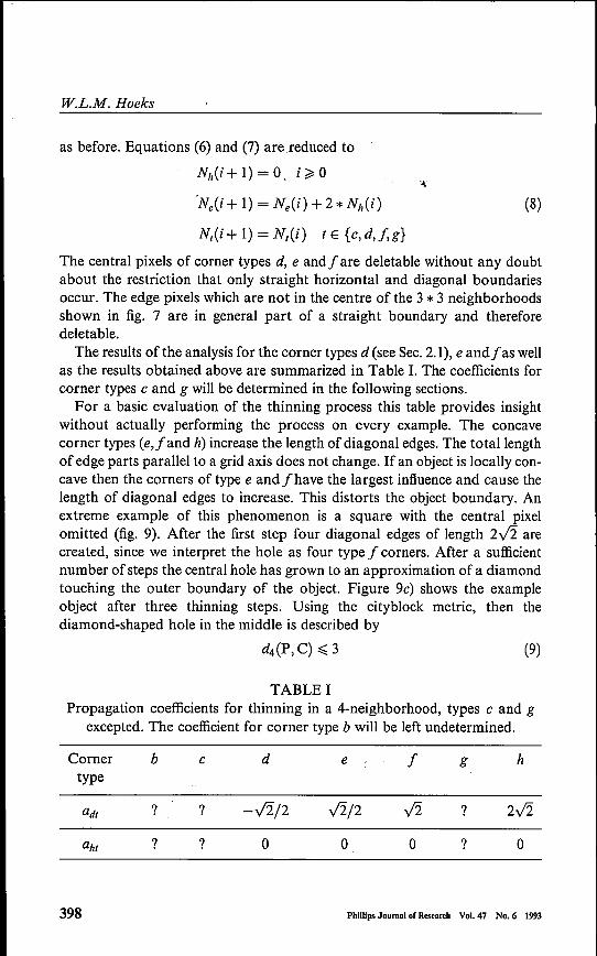
as before. Equations (6) and (7) are .reduced to
N,,(i+ 1) = O. i~ 0
'Ne(i + 1) = Ne(i) + 2 * N,,(i)N,(i+ 1) = N,(i) tE {e,d,j,g}
The central pixels of corner types d, e and fare deletable without any doubtabout the restrietion that only straight horizontal and diagonal boundariesoccur. The edge pixels which are not in the centre of the 3 * 3 neighborhoodsshown in fig. 7 are in general part of a straight boundary and thereforedeletable.
The results of the analysis for the corner types d (see Sec. 2.1), e andf as wellas the results obtained above are summarized in Table I. The coefficients forcorner types e and g will be determined in the following sections.
For a basic evaluation of the thinning process this table provides insightwithout actually performing the process on every example. The concavecorner types (e,J and h) increase the length of diagonal edges. The totallengthof edge parts parallel to a grid axis does not change. If an object is locally con-cave then the corners of type e andfhave the largest influence and cause thelength of diagonal edges to increase. This distorts the object boundary. Anextreme example of this phenomenon is a square with the central pixelomitted (fig. 9). After the first step four diagonal edges of length 2V2 arecreated, since we interpret the hole as four type f corners. After a sufficientnumber of steps the central hole has grown to an approximation of a diamondtouching the outer boundary of the object. Figure ge) shows the exampleobject after three thinning steps. Using the cityblock metric, then thediamond-shaped hole in the middle is described by
(8)
W.L.M. Hoeks
(9)
TABLEIPropagation coefficients for thinning in a 4-neighborhood, types e and g
excepted. The coefficient for corner type b will be left undetermined.
Corner btype
ad' ?
a", ?
e d e f g h
? V2j2 ?
? o o o ? o
398 Phlllips Journalof Research Vol.47 No.6 1993

Phillips Journalof Research Vol. 47 No.6 1993 399
Parallel thinning algorithms
aca b c
Fig. 9. a) The thinning of a square with a single pixel hole in the middle under the 4-neighbor edgemodel. b) After the first step the shape ofthe 4-neighborhood stands out in the center ofthe square.c) After 3 steps an approximation of a diamond on the inside touches the outside square.
where P is a pixel in the diamond shaped hole and C is the central pixel. The4-neighborhood for the definition of the edge pixels implies the cityblockdistance metric.
2.2.2. Corner types c nor g are deletabIe
Now we set the central pixels of corner types c and g to be not deletabIe,indicated as (--,c, ....,g). The central pixels of corner types d, e and fare delet-able as before. Although this option defines a valid deletion function for ourexamples, it does not allow a formal analysis as introduced in Sec. 2.1,because skeleton segments are created in the first thinning step. The effect ofthinning on object parts with a triangular bump is illustrated in fig. 10. Thisdigitization serves only as an example. After each thinning step the view onthe relevant object part is shifted such that the object boundary stays in view.
Superficially this deletion function seems to extract a Euclidean skeleton, sinceeach straight corner generates a segment as shown in figs 2d) and 2h). How-ever, we already concluded that the distance metric induced by the 4-neighboredge model was the cityblock metric. The sides of the triangular bump againshow the different propagation speeds for different orientations of the objectpart boundary. The triangular bump on a horizontal edge is not reduced insize, while the base of the triangular bump on a diagonal edge is reduced toa single pixel. The thinning results for this deletion function and edge modelare inconsistent with the formal definition of the skeleton presented in Sec. 1.
a b c d e f
Fig. 10. Thinning on a straight edge with a triangular bump. The global edge direction is either a)horizontalor d) diagonal. The pixels depicted in grey are the deietabie pixels, so b) is the result ofathinning step on a).

W.L.M. Hoeks
One must also consider the behavior of thinning with this deletion functionin the presence of boundary noise. A single noise pixel on a horizontalobjectboundary will not be deleted. A single noise pixel on a diagonal object bound-ary will not be deleted either. Therefore any extra object pixel will start a seg-ment of the skeleton. Such extreme noise sensitivity makes this scheme uselessin pattern recognition tasks.
2.2.3. Either corner type c or g is deletabie
Next we study the deletion function where the central pixel of either fig. 7cor fig. 7g) is deletabIe. We have noted already that the metric which fits bestwith the 4-neighborhood edge model is the cityblock distance. First considerthe deletion function with the central pixel of corner type g deIetabIe (-, c, g).
The effect of this deletion function is first studied using the triangular bumpin fig. 4a). The bump area is bounded by two corners of type e, and has onecorner of type g. The coefficients, which were left open in Table I, areahg = 0 and adg = -Vl. Inserting this information and the values from TableI in eqs (I) and (2) yields the following equations
Ld(i + I) = Ld(i)(10)
According to eqs (8) which describe the thinning process for the object part offig 4a), the diagonal edge parts and the horizontal edge parts have constantlength. The bump does not change shape or size. With each thinning step,the edge moves downward as shown in figs Ila), lIb), and lIe). The segmentof the skeleton related to this part of the object will depend on the shape of therest of the object. The relevant part of the skeleton is the center of the maximaldisk (a diamond shape according to the cityblock metric) that fits in the tri-angular bump. Therefore the object will be reduced to minimal width accord-ing to the maximal disk definition. For this example the 4-neighbor edge modelwith the deletion function (-, c, g) produces a skeleton according to the
a b c
Fig. 11. Thinning on a straight horizontal edge with a triangular bump. The pixels depicted in greyare the deIetabIe pixels, so b) is the result of a thinning step on a), and c) is the result of a thinningstep on b).
400 Phillips Journalof Research Vol.47 No.6 1993

Parallel thinning algorithms
maximal disk definition with the cityblock metric. A boundary shape whichdoes not change size such as the triangular bump on the horizontal edge iscalled a persistent shape.Next the triangular bump on a diagonal object boundary is analyzed
(fig.4c). The behavior ofthe thinning scheme where the central pixel in cornertype c is a skeletal pixel for the object part as shown in fig. 4c) is already illus-trated in Figs 10d), 10e) and lOf). The generation of a segment for the tri-angular bump is consistent with the conclusion that this deletion functionproduces a skeleton according to the cityblock metric. However, the gen-eration of segments for bumps as small as a single pixel on diagonal edges isan undesirable feature in the presence of noise.The deletion function (c, ...,g), where the central pixel in corner type g is not
deietabie instead of the central pixel in corner type c disturbs the behavior aspresented in the previous paragraphs. If the central pixel in corner type g is anendpoint, a segment will start at the top ofthe triangular bump as shown in fig.lOa). Such a deletion function produces skeletons as depicted in Figs 2b) and2f), which resembles a chessboard metric. This is inconsistent with the propa-gation speed on straight edges indicating a cityblock metric.The rectangular bump on a horizontalobject boundary (fig. 4b) has two
type c corners and two type h corners. This configuration does not lend itselffor a formal analysis as was done for the triangular bump on a horizontalobjectboundary, because it forms branch segments at the first thinning step owing tothe two type c corners. As illustrated in fig. 12, this behavior is consistent withthe earlier conclusion that the 4-neighborhood edge model along with thedeletion function (...,c, g) produces a skeleton according the cityblock metric.The rectangular bump on a horizontalobject boundary (fig. 4b) has two
type g corners in this object part, and there are two typef corners. The lengthof the diagonal object boundaries is L plus two times the height of the rect-angular bump. Horizontal (and vertical edges) are absent, so the thinning pro-cess is described by the following equation, which follows from Table I andadg = -V2:
(11)
The summed length of the straight edges of a rectangular bump on a diagonalobject boundary is constant. The shortening of an edge part due to the cornerof type f is compensated by the lengthening due to the corner of type g. Theparts of the edge that have length H at the start of the thinning process arebounded by a type f corner on one side and a type g corner on the otherside. Therefore their length remains the same during the thinning process(figs l2d-f).
PhiIlips Journalof Research Vol. 47 No. 6 1993 401

W.L.M. Hoeks
a b c d e
Fig. 12. Thinning on a straight edge with a rectangular bump. a-c) On a horizontal edge a lowbump is reduced to a triangular bump. d-f) On a diagonal edge, however, any rectangular bumpwill be reduced to a line of minimal width.
The edge part bounded by two corners of type g shortens until a segment ofminimal width remains. Customization of eq. (4) for the diagonal edgebetween the corners of type g yields
Ld(i + I) = Ld(i) - J2 (12)At the start of the thinning process the length of the diagonal edge partbetween the corners of type c is B. After imax thinning steps the length of thediagonal edge part at the top of the bump is reduced to zero*. Solving eg.(12) with this start and stop condition yields
imax = B/ V2 ( I 3 )The rectangular bump on a diagonal edge is reduced to a line of minimumwidth independent of the height H of the rectangular bump. These resultsdo not depend on the position of the object with respect to the samplinggrid. The actual digitization of a corner may be different from the examplespresented in this section, but it will not affect the recursive relations whichdescribe the process. For the examples of fig. 4, we conclude that thinningwith a 4-neighborhood edge model and the (-, c, g) deletion function prod ucesa skeleton according to the cityblock metric. This does not imply that such adeletion function is the best in the presence of noise. As already stated in theintroduction, the concept of the skeleton implies a high sensitivity to smalldeviations in the object boundary, i.e. boundary noise.
2.2.4. Both corner types c and gare deletable
Now we examine the deletion function (c, g), where the central pixels ofcorner types c and g are both deletabIe. The consequences of choosing cornertype g deIetabIe have been dealt with above. The results related to figs 4a) and4d) remain valid for the deletion function (c, g).
The triangular bump in fig. 4c) has one corner of type c and two corners of
• This length will be one pixel if BI v'2 was odd at the start. The provision that the distance betweenthe convex corner pixels ofthe rectangular bump is reduced to either zero or one pixel is applicableto similar computations in the remainder of this section.
402 Phillips Journalof Research Vol. 47 No.6 1993

Parallel thinning algorithms
a c
Fig. 13. Thinning on a straight diagonal edge with a triangular bump. The pixels depicted in greyare the deietabie pixels, so b) is the result of a thinning step on a).
type e. The length of the horizontal and vertical edge is V2 * B and the lengthof the diagonal edge is L-B at the start ofthe thinning process. The coefficientsfor corner type care adc = 0 and ahc = -2. Using this information and Table Ito customize eqs (4) and (5) for the triangular bump on a diagonal edge yields
Ld(i + I) = Ld(i) + V2( 14)
L,,(i + 1) = Lh(i) - 2
Equations (14) show that the length ofthe diagonal edge parts increases whilethe length of the horizontal edge parts decreases. The bump disappears veryrapidly in the thinning process. Solving eq. (14) with the start conditionL,,(O) = V2 * B, and setting the length of the horizontal edges 10 zero at thin-ning step imax, yields the number ofthinning steps it takes before the triangularbump has disappeared:
imax = B/V2 ( IS)
This is a significant difference from the result for a triangular bump on a hori-zontal edge (fig. 11) especially in the presence of noise. A horizontal edge willbe more sensitive to noise than a diagonal edge, because noisy bumps on ahorizontal edge "live" longer than on a diagonal edge. This problem is shownin fig. 14, where the noise pixel on the top of the rectangular structure is con-sidered to be a triangular bump. The formation of a segment of the skeletondepends on the exact definition of the deletion function. i.e. the deletabilityof corner type b.
The rectangular bump on a horizontalobject boundary depicted in fig. 4b)will be studied now. The first thinning step destroys the corner of type h.
a c
Fig. 14. Influence of persistent noise on the segment formation. The noise pixel in a) causes theformation of an extra skeleton segment in c) if the corner type b is not deletabie.
Phillips Journalof Research Vol.47 No.6 1993 403

imaxB = BI2 (19)
W.L.M. Hoeks,
Equations (16) describe the situation after the first step. Using the informationfrom Table I eqs (4) and (5) are simplified to the eqs (17), which describe thesubsequent steps in the thinning process: . ..
Ld(l) = Vi * 2(16)
L,,(I)=L'+2*H-4
Ld( i + 1) = Ld(i) +V2 * 2L,,(i + 1) = L,,(i) - 4
The top of the rectangular bump is bounded by two corners of type c. Thecorner of type c has a strong negative effect on the length of horizontal edges(a"e = -2). Therefore, the distance between the two c corners will be reducedto zero* after imaxB thinning steps, and hence the width of the rectangularbump is reduced to a segment of minimal width. Customization of eq. (5)for the horizontal edge part between the c corners yields eq. (18). At the startof the thinning process the length of the horizontal edge part between the typec corners is B. Solving eq. (18) with the start and stop conditions (L,,(O) = B,L,,(imaxB) = 0) yields eq. (19).
L,,(i + 1) = L,,(i) - 2 (18)
(17)
The number of steps until the distance between two corners is reduced to zerocan be limited by another event. The diagonal edges which were created in thefirst thinning step (eq. (16)) keep growing at the expense of the vertical edgeparts of the rectangular bump. Specialization of the equations to the verticalboundary part between a corner of type c and a corner of type e yields eq.(20). At i = 0 that boundary part is H long. After imaxH thinning steps thelength of that boundary part is reduced to zero. Using this start and stop con-dition in eq. (20) yields eq. (21)
L,,(i + 1) = L,,(i) - 1 (20)
imaxH = H (21)
If imaxH > imaxB, i.e. if the height of the rectangular bump ismore than half thewidth of the base, then the part of the bump more than BI2 away from thebulk of the object is thinned to a line of minimum width after imaxB steps.The line ofminimal width stands on top ofa triangular bump after imaxB thin-ning steps similar to the situation depicted in fig. lOc). '
* This distance will be I if B was odd at the start.
404 Phillips Journal of Research Vol.47 No, 6 1993

Phillips Journalof Research Vol. 47 No.6 1993 405
Parallel thinning algorithms
Çr;l~~ ~ ~
a b c
Fig. IS. Thinning of a low rectangular bump on a horizontal boundary.
If imaxH < imaxB the rectangular bump is reduced to a triangular bump or toa trapezoid as soon as the edges orthogonal to the global object boundary areconverted to diagonal edges (fig. ISe). Beyond this point in the thinning pro-cess, the bump configuration is stable as depicted in fig. 11.
The rectangular bump on a diagonal edge (fig. 4d) has been analyzed in theprevious section (see fig. 12).
2.3. Thinning in an 8-neighborhood
In this section, the edge pixels are defined by an 8-neighborhood. An objectpixel is an edge pixel if one ofits eight neighbors is part ofthe background. Wewill discuss the consequences of choosing the 8-neighbor edge model.
The thinning speed on a horizontal (vertical) edge is the same as in a4-neighborhood. On a diagonal object boundary, there are twice as many edgepixels in the 8-neighbor edge model as in the 4-neighbor model. Therefore, thethinning speed is also twice as large, i.e. the thinning speed on a diagonal edgeis Vl. In the 8-neighborhood, any object having both horizontal and diagonalboundaries will be defined by the thinning process because of the non-uniformthinning speed for diagonal and horizontal straight edge parts.
In the previous section we have already seen that choosing the central pixelin both corner types e and g as part of the skeleton is not a viable option. Itleads to inconsistent behavior and extreme noise sensitivity. The deletionfunction with the centre pixel in corner type edeletable and the centre pixelin corner type g not deietabie produces skeletons according to the chessboardmetric. However, such a thinning scheme is sensitive to noise pixels on a hori-zontalobject boundary. For each noise pixel on a horizontalobject boundarythere will be a segment of the skeleton. We will not repeat the analysis of Secs2.2.2 and 2.2.3 to support these assertions. Only the analysis of the deletionfunction with the central pixels in both corner types e and g deletabie (similarto Sec. 2.2.4) is performed here.
The main difference between 4-neighborhood and 8-neighborhood is thecorner type h. The central pixel of this corner type is an edge pixel in the8-neighborhood, and it is a deietabie pixel under the conditions stated in

W.L.M. Hoeks
e
~ 7 i3 -, ~ ~
b c d
lilV ~ A- il _j
g h
a
Fig. 16. The corner types in an 8-neighborhood. The grey and black pixels belong to the object.The deIetabIe pixels are depicted in grey. The edge pixels which are not in the center of the 3 * 3neighborhood can be deleted because of the restrictions on the objects, introduced in Sec. 1.4.
b
Fig. 17. a) A thinning step for a typejcorner. b) After this step the corner oftypejhas disappearedand two corners of type e and a horizontal edge of length 2 are formed.
the introduction. The central pixels in all corner types except a and baredeletabIe (fig. 16).
Detailed analysis of each corner type shows that in the 8-neighborhood thecorner type I is destroyed in the first thinning step. The corner type I is trans-formed into two corners type e, and horizontal boundary two pixels long(fig. 17).
Again we do not specify the deletability of the central pixel in corner type b,because this corner type is not present in our examples. The propagation coef-ficients of other corner types are summarized in Table 1I.
In this case only diagonal edges are shortened by the thinning process. Thelengthening of horizontal edges is limited to locally concave parts of the objectboundary. An extreme example is the square object with a single pixel hole in
TABLE IIPropagation coefficients for thinning in an 8-neighborhood.
Cornertype
b c d e I g h
? o o o o -2V2 o
? -2 -1 2 o 2
406 Phillips Journalof Research Vol. 47 NO.6 1993

Phillips Journalof Research Vol.47 No.6 1993 407
Parallel thinning algorithms
a oa b c
Fig. 18. al The thinning of a square with a single-pixel hole in the middle with the 8-neighbor edgemodel. bl After the first step the shape ofthe 8-neighborhood stands out in the center ofthe square.cl After 3 steps the inside square touches the outside square.
the middle (fig. l8a). The result after four thinning steps is the square hole inthe middle of fig. 18c), which is described by the formula for a circle accordingto the chessboard metric:
d8(P, C)!( 3 (22)
The distinction between this result and the result in the previous section(fig. 9c) is obvious.
We now return to the example of fig. 4a). The object boundary part withglobally horizontal orientation and a triangular bump has two corners oftype e, and one corner of type g. Initially the length of the diagonal edgesis V2 * B, and the length of the horizontal edges is L-B. The descriptionfor this situation is found by inserting the data from Table II in eqs (4)and (5):
Ld(i + I) = LdU) - V2 * 2
LhU + I) = LhU) + 2(23)
Equations (23) indicate that the bump is reduced in size fairly rapidly (seefigs 19a), 19b) and 19c). The length of the horizontal edge grows at theexpense of the diagonal edge. The triangular bump disappears without leavinga trace.
The thinning process of a diagonal edge with a triangular bump is describedby eqs (24). The difference in the start conditions is the straight corner which is
~~I.l---a b c d e
Fig. 19. The thinning process on a triangular bump on a straight edge in a 8-neighborhood. Theorientation of the edge has a major influence on the result.

W.L.M. Hoeks
type c instead of type g.
Lc/( i+ I) = Lc/( i)
L,,(i + I) = L,,(i)
As can be seen from eqs (24) the edges of the bump do not change length(shown in figs 19d), 1ge) and 19/), and the bump stays as it is. The propa-gation speed of a horizontal edge in the diagonal direction is the same asthe propagation speed of a diagonal edge. This causes the edge to shifttowards the lower right until it collides with another part of the boundaryof the object. Although this behavior can be expected for a skeleton accordingto the chessboard metric, the persistent bump on the diagonal edge is noisesensitive.
The thinning process of the rectangular bump on a straight object boundaryin fig. 4b) is described by the following equations:
(24)
NI (i) = 0 I E {d, e, I,g}
Nc(i) = 2 (25)
N,,(i) = 2
Lc/(i+ I) = L,,(i)(26)
Again the equations describing the length change indicate constant length.Local analysis of the top edge of the bump bounded by the two cornersof type c shows that this edge shortens during the thinning (eq. (27)). Thelocal shortening is compensated by the lengthening of other straightedge parts. This continues until imax, when the bump is reduced to a line ofminimum width and the thinning of the bump stops (fig. 20c). Solving therecursive relation (eq. (27)) and setting the width of the top to zero yields
a b c d e
Fig. 20. Thinning on a straight edge with a rectangular bump. a-c) On a horizontal edge a bumpwill be reduced to line of minimal width. d-f) On a diagonal edge, however, a low rectangularbump is reduced to a triangular bump.
408 Phillips Journalof Research Vol. 47 No. 6 1993

Phillips Journel of Research Vol.47 No.6 1993 409
Parallel thinning algorithms
eq. (28):
L,,(i + 1) = L,,(i) - 2
imax = BI2(27)
(28)
Now consider the last example: the straight diagonal edge with rectangularbump (fig. 4d). This object boundary part has two corners of type! and twocorners of type g. The corners of type! disappear in the first thinning step.Each! corner creates two corners of type e, and a horizontal edge of length 2:
Ld( 1) = L+ 2 * H - V2 * 2L,,(l) = 4
Ld(i + 1) = Ld(i) - V2 * 2L,,(i+ 1) =L,,(i)+4
Equations (30) show that the horizontal edges which were created in the firststep grow at the expense of the diagonal edges. This process stops as soon asthe edge bounded by the two g corners has minimal length (this conditionyields eq. (31)) or if the horizontal edge has replaced the diagonal edges ofthe bump completely (this condition yields eq. (32)).
(29)
(30)
imaxB = BIV2imaxH = H12V2
(31)
(32)
If imax H > imax B, i.e. if the bump is higher than half the base width, the excesslength is reduced to a line of minimum width. Otherwise, the rectangular bumpis reduced to a triangular or a trapezoidal bump and the thinning process pro-ceeds as described for a diagonal edge with a triangular bump.We note a duality in these results and the results for 4-neighborhood
thinning. On diagonal edges with bumps, 4-neighborhood thinning producesresults similar to an 8-neighborhood operation on horizontal edges withbumps, and the other way around. In either case the result of a thinningprocess depends strongly on the orientation of the edge.
2.4. Octagonal thinning
In order to decrease the influence of the edge orientation on the result ofthethinning process the 'previous two neighborhoods could be used alternately.This is called octagonal thinning. The choice of this name will be clear aftera look at the result of the thinning of a single-pixel hole in a large object(fig. 21).

W.L.M. Hoeks
IIlIaa b c
Fig. 21. a) Octagonal thinning of a square with a single-pixel hole in the middle. b) After the firststep the shape ofthe 4-neighborhood stands out in the center ofthe square. c) The second step usesthe 8-neighborhood. After this step a crude approximation of an octagon appears in the middle ofthe object.
The propagation speed on a horizontal edge is I for the 4-neighborhoodstep and 1 for the 8-neighborhood step. The average propagation speed on ahorizontalor vertical object boundary in the octagonal case is therefore equalto 1. On a diagonal edge the propagation speed is equal to 1/ V2 in the 4-neigh-borhood step and V2 in the 8-neighborhood step. This averages to!(V2 + 1/ V2) ::::::1.06. The propagation speeds for the horizontal and thediagonal object boundaries in the octagonal propagation model are notequal; they differ by 6%.
The choices to be made for the deletion function increase with octagonalthinning. Either one views octagonal thinning as a single operation or as acombination of 4- and 8-neighborhood thinning. The results of a combinationmay depend on the order of the 4- and the 8-neighborhood thinning steps.
If the deletion function is chosen such that the een tral pixels in corner types cand g are both skeletal pixels, all straight corners generate a skeletal segmentas shown in figs 2d) and 2h). This response is consistent with the expectationthat the octagonal distance metric is a closer approximation to the Euclideanmetric than the cityblock or the chessboard distance. Although the octagonalskeleton is a closer approximation to the Euclidean skeleton it still does notsolve the sensitivity to the unavoidable boundary noise. Choosing the centralpixels in corner types c and g as deletabIe will reduce the noise sensitivity to alarge extent. This option for octagonal thinning is analyzed.
Assume that all odd steps in the thinning process utilize the 4-neighborhoodand that the even steps utilize the 8-neighborhood. The results of the thinning
a b
Fig. 22. The result of octagonal thinning on the corner types a)fand b) h . The light grey representsthe pixels to be deleted in the 4-neighborhood step. The dark grey are the pixels that will be deletedin the 8-neighborhood step.
410 Phillil)S Journalof Research Vol. 47 No. 6 J 993

Phillips Journalof Research Vol. 47 No.6 1993 411
Parallel thinning algorithms
TABLE IIIPropagation coefficients for octagonal thinning
Cornertype
b c d e f g h
? o -V2/2 V2/2 -3 * V2
? -4 -I 2 o 2
process are only inspected after an even number of steps. The corners of typesfand h are both destroyed after the second step, and two corners of type e arecreated (fig. 22).The length change coefficients for this situation as well as theeffects of other corner types are listed in Table TIl. Again we omit corner type bfrom the table, since this corner type does not occur in the examples. Only theconcave corner type e increases the length of the edge parts (f and h disappearin the first thinning steps).
Customization of relations (4) and (5) to the triangular bump on a straighthorizontal edge (fig. 4a) yields
Ld(i + 2) = Ld(i) - V2(33)
The horizontal edge parts increase in length and the diagonal edge partsdecrease in length. The bump disappears (fig. 23). Insertion of the start condi-tions (bump base is B, there are two type e corners and one type g corner) ineqs. (33), and setting diagonal edge length to zero yields the number of stepsCimax") it takes to erode a triangular bump on a horizontal edge (eq. (34)).
. I BImax" = 2: * (34)
Performing the same exercise for the triangular bump on a straight diagonaledge (fig. 4c), example digitization in fig. 23d) yields imaxd, the number of steps
a b c d e
Fig. 23. Octagonal thinning on a straight edge with a triangular bump oriented a) horizonrally ord) diagonally. Although there are still some differences the general behavier is similar.

W.L.M. Hoeks
needed to erode a triangular bump on a diagonal edge:
imaxd =!* V?- * B (35)
The number of thinning steps to erode a bump on a diagonal edge is a factorV2 greater than on a horizontal edge. The orientation dependence is not asextreme as in the 4-neighborhood or 8-neighborhood thinning model, butthe time needed to remove a bump still depends on the orientation of theglobal edge. A triangular bump on a diagonal edge lives longer than a tri-angular bump on a horizontal edge by a factor of V2. This is also illustratedin fig. 23. The different number of steps needed to remove a triangular bumpon a horizontalobject boundary versus the number of steps needed to removea triangular bump on a diagonal object boundary is far worse than expectedfrom the propagation speed difference for straight object boundaries.
Finally, we examine the behavior of octagonal thinning for rectangularbumps on straight object boundary parts. On a horizontal edge, the bumphas two type c corners and two type h corners. In the first two thinning stepsthe two type h corners are destroyed and replaced by four type e corners. Thethinning process after the second step is described by the following equations:
Ld(i + 2) = Ld(i) + 2 *h(36)
L,,(i + 2) = L,,(i) - 4
The diagonal edge parts increase in length at the expense ofthe horizontal edgeparts. The base of the rectangular bump is transformed into a triangularshape. Customization of eq. (5) to the vertical edge bounded by a corner oftype e and a corner of type c yields
_L,,(i+ 2) = L,,(i) - 1 (37)
After a number of thinning steps the vertical part is reduced to zero, or a line ofminimal width has been formed. The number of steps necessary to consumethe vertical edge part is imaxH.
imaxH=H*2 (38)
The height ofthe bump determines whether or not a segment ofminimal widthappears. The rectangular bump is reduced to its minimal width after imaxBthinning steps, which follows from analysis of the top of the bump in isolation.
imaxB = BI2 (39)
If imaxH > imaxB, i.e. if the rectangular bump is higher than B14, a segment ofminimal width will appear (figs24a-c). A lower bump will first be reduced to atriangular bump or a trapezoid. The triangular bump will disappear as shown
412 Philllps Journal of Research Vol.47 No. 6 1993

PhiUips Journalor Research Vol. 47 No. 6 1993 413
Parallel thinning algorithms
a b c d e f
Fig. 24. Octagonal thinning of a rectangular bump. If the bump is high enough a line of minimalwidth is formed.
before. A rectangular bump on a diagonal edge shows similar behavior. Thetime to reach the critical event, which is either the creation of a minimal widthsegment (eg. (40» or the reduction of the rectangular bump to a trapezoid(eg. (41)), is the minimum of imaxH and imaxB:
imax B = v2 * BI 3 (40)
imaxH = v2 * H (41 )
If H is less than BI3 the bump is reduced to a trapezoid or a triangular bump.If H is larger, a segment of minimal width will appear (figs 24a-c). Again wesee timing differences depending on the orientation of the global edge. Thecritical height-to-width ratio ofthe bump is 33% higher for the diagonal orien-tation than for the horizontal orientation of the global edge. The differencesare substantially less than in the 4- or 8-neighborhood case, but they are stilllarge enough to note. The difference in the number of thinning steps to theformation of a segment of minimal width is v2 higher on a horizontalobjectboundary (eg. (38)) than on a diagonal object boundary.
2.5. Conclusions of the theoretical analysis
As long as the distance between corners is positive, the formal description ofthe thinning process using recurrent relations is useful to get quantitativeresults. The number of steps to a crucial event, e.g. the formation of a thinsegment, can be calculated without performing the actual experiments for dif-ferent test images.
The behavior of the thinning process with respect to the two edge models isdual. The artifacts occurring on horizontal edges with 4-neighborhood thin-ning will also be present on the diagonal edges with 8-neighborhood thin-ning. For each edge model there are edge shapes that will remain the sameas the thinning process proceeds. Such persistent shapes make the thinningalgorithms noise sensitive.
No persistent shapes occur with octagonal thinning, as the slow chinningspeed on diagonal edges in the 4-neighborhood thinning step is compensated

W.L.M. Hoeks
by the high speed in the 8-neighborhood thinning step. This compensation isnot perfect and therefore the octagonal thinning does not produce Euclideanskeletons as defined in Sec. 1.
With the correct deletion function and the 4-neighborliood edge modelit may be possible to define a thinning algorithm that produces a skeletonconforming to the cityblock distance. A thinning algorithm using the 8-neighborhood edge model can produce a skeleton conforming to the chess-board distance. However, the formation of skeletal segments for every noisepixel on an object boundary with a specific orientation and the persistentboundary shapes make such a skeleton extraction algorithm noise sensitive.The noise sensitivity can be reduced by choosing a different deletion func-tion, but the resulting thin structure is no longer the skeleton as specified bythe formal definitions in refs 4 and 5.
Comparing the results for a rectangular bump on a horizontalobject boundaryusing 4-neighborhood thinning, 8-neighborhood thinning, and octagonal thin-ning, we see that bumps higher than an orientation-dependent threshold causethe formation of a segment in octagonal thinning. However, using 4-neighbor-hood thinning, any rectangular bump on a diagonal edge will result in a seg-ment, and 8-neighborhood thinning will result in a segment for any rectangularbump on a horizontal edge. This dependence is interesting with respect to thenoise sensitivity of the algorithm. The removal of low and small structures bythe thinning process makes the result show the global aspects of the objectbetter. In this aspect the octagonal thinning has a more consistent behavior.
3. Behavior evaluation for existing thinning algorithms
3.1. Restrictions on the deletion function
In the previous sections we viewed corner types in a 3 * 3 kernel. As shownby Rosenfeld I), it is not possible to define a parallel thinning algorithm in a3 * 3 neighborhood. Note the two keywords here. One is parallelism, the otheris the neighborhood. Parallelism is necessary in order to get a clear view on theedge, without the distortion due to order selective deletion of pixels as noted ina serial algorithm. The algorithm must not only be parallel but it must accom-plish its task in a single pass over the image. The theory developed in Sec. 2deals only with single-pass parallel thinning. Therefore, it is to be expectedthat multi-pass parallel algorithms such as those designed by Arcelli et aI.8),Deutsch"), and Stefanelli and Rosenfeld 10) will not produce the results pre-dicted by the theory. However, we evaluate these algorithms, since they arewell known.
414 Phillips Journalof Research Vol.47 No.6 1993

Parallel thinning algorithms
a b c d
Fig. 25. 90° corners with different orientations (detail of fig. 3).
The window used by the thinning algorithm must be larger than a 3 * 3neighborhood of the edge pixel in order to make sure that a line two pixelsthick is not removed in one pass of the algorithm. Besides this theoreticalpoint there is another reason to use a larger neigh borhood. The size of theneighborhood determines the amount of information one can get on theglobal conditions of an edge"), e.g. it is not possible in a 3 * 3 neighborhoodto distinguish the noise from a corner of type g whenever castling noise ispresent. The size of the kernel depends on the desired accuracy. If we wantto recognize a 90° corner independent of the orientation even a 5 * 5 kernelmay be too small. Figure 3 serves as an example of this postulate (details infig. 25). In the presence of noise it may be difficult to distinguish 90° cornerscorrupted by noise from more acute or obtuse corners.
3.2. Multi-pass parallel thinning algorithm: Arcelli
The Arcelli algorithm checks the boundary pixels in a number of passes. Ineach pass a given (local) edge orientation is checked for deietabie pixels andthe dele tab Ie pixels are removed. In the subsequent pass another edge orien-tation is checked. In each pass a template (fig. 26) is used for the detectionof deietabie pixels on a specific edge. After detection, the deietabie pixels areremoved before the next template is applied. In the worst case it may happenthat a pixel whose presence allows the deletion of a pixel in a certain pass hasbeen deleted in the previous pass. It is also possible that the local edge orien-tation is affected by the deletion of some pixels in the previous pass. Thismakes the behavior of the algorithm dependent on the application order ofthe templates.
a b f g hdc e
Fig. 26. Templates as defined by Arcelli. The white pixels represent background, the black pixelsrepresent foreground, while the grey pixels represent either.
Phillips Journalof Research Vol. 47 No. 6 1993 415

W.L.M. Hoeks
Note that there is no template that can delete the centre pixel in the concavecorners (typesj, h, and i). This algorithm cannot produce the results offig. 9b)with fig. 9a) as input image. All templates require the presence of at least threebackground pixels. So, small holes (one or two pixels) yield a sm all loop in theresulting thin structure. This loop consists of the object pixels ha ving the pixelforming the hole as their neighbor. If single-pixel holes are considered to benoise then these small loops can be recognized and removed easily (or thesmall holes can be removed by the use of a closing operation") prior to thethinning operation). If the small holes are significant then the different behav-ior of the thinning algorithm for small and large holes poses a problem.
The templates of fig. 26 can be applied either one after the other (8-passes)or in groups (minimal 2 passes). The grouping must obey the restrietion asexplained in the introduction. A line that is two pixels wide should be pre-served. We will examine the beha vior of the 8-pass and the 2-pass implemen-tation of this algorithm for the examples as shown in fig. 4. Because of thenumber of passes in a cycle and the possible ordering of templates we willjust present the example, and omit the formal representation using the recur-rent relations.
The result ofthe 8-pass Arcelli algorithm is shown in figs 27 and 28. Note thesimilarity of figs 27d-I) to figs IOd-I). The corner type c generates a branchsegment (fig. 27f), in spite of the template in fig. 26h). One of the object pixelsspecified in template h is deleted in a pass preceding the application of templateh. The generated segment has a single pixel offset to the left, though the end-point of the segment is at the correct position. The behavior of this multi-passalgorithm is dependent on the edge orientation. Superficially it looks like askeleton based on the cityblock metric. In Sec. 2.2.3 we concluded that a thin-ning algorithm with the behavior as shown in fig. 27 is noise sensitive. Thisconclusion is confirmed by Hoeks 11), who reports on thinning experimentswith artificial images corrupted by boundary noise.
The 8-pass Arcelli algorithm generates two branch segments for a rectangu-lar bump on a straight horizontal edge, and one for a rectangular bump on adiagonal object boundary. From these examples we conclude that, though the
a b c d e f
Fig. 27. Eight-pass thinning with the Arcelli algorithm for the example objects in figs 4a) and 4c).All pixels deleted in a single cycle of eight passes are presented in grey.
416 Phillips Journalor Research Vol. 47 No.6 1993

Phillips Journalof Research Vol. 47 NO.6 1993 417
Parallel thinning algorithms
~. ~.................. . .,.... ,: .
a b c ct e f
Fig. 28. Eight-pass thinning with the Arcelli algorithm for the example objects in figs 4b) and 4d).All pixels deleted in a cycle of eight passes are presented in grey.
8-pass Arcelli algorithm produces skeletons according to the cityblock metricfor some examples, it does not do so for every object. For example, the branchsegment for the rectangular bump on a diagonal object boundary starts at thewrong position (fig. 28j). It should start in the middle of the maximal disk(diamond shape) that fits in the rectangular bump.
The 2-pass Arcelli algorithm uses four templates in parallel (first templatesa, b, c and d in parallel followed bye, f, g and h in parallel). The results areshown in figs 29 and 30. The behavior of this implementation is slightly differ-ent from that ofthe 8-pass implementation. Note the change ofthe edge orien-tation of the right diagonal edge in fig. 29c) and the left vertical edge in fig.29j) with respect to the corresponding results in fig. 27. Because of the group-ing of templates the type e corners are treated differently depending on theorientation. This influences the thinning speed and consequently the positionof the thin structure in the resultant image.
The right edge of the rectangular bump on a straight horizontal edge iseroded very fast, while the left edge barely moves. The position of the result-ing branch segment is far from the position of a skeleton branch according tothe maximal disk definition. This implementation behaves better than the pre-vious one with respect to bumps on straight diagonal object boundaries for theexamples analyzed here. The rectangular bump is eroded to a triangular bump(fig. 3lj), and the triangular bump will generate a segment (fig. 29j) where asegment should appear according to the maximal disk definition of the skeleton.
3.3. Multi-pass parallel thinning algorithm: Deutsch
Deutsch presented his algorithm as a single-pass algorithm. He noted,
a b c ct e
Fig. 29. Two-pass thinning with the Arcelli algorithm for the example objects in figs 4a) and 4c).All pixels deleted in a cycle of two passes are presented in grey.

W.L.M. Hoeks
~
... ... ". .
a b c d e f
Fig. 30. Two-pass thinning with the Arcelli algorithm for the example objects in figs 4b) and 4d).All pixels deleted in a cycle of two passes are presented in grey.
however, that the position of the resulting thin structure is biased to oneside of the object (anisotropy). In order to obtain a thin structure lying inthe middle of the object two passes are necessary. The deletion function ispresented as a function defined on a 3 * 3 neighborhood instead of a sequenceof templates. For an isotropic result the neighborhood indices must be rotatedover 1800 every pass (the indices in the 3 * 3 neighborhood are presented infig. 31). Object pixels have value I and background pixels have value O. Thevalues of the neighboring pixel are f(k), where k can take values from I to8. The deletion function is based on the crossing number X, which is defined as
8
X =L I f(k + I) -f(k)1 (42)k=1
If the following conditions hold for a pixel, the pixel is deletabIe:
X=O,2,or4 (43a)
(~f(k)) i= I (43b)
i.e. the pixel must have no or at least two neighbors in the object.
f(l) I\f(3) /\f(5) = 0
f(l) I\f(3) /\f(7) = 0
(43c)
(43d)
if X = 4, then either of the two templates shown in fig. 32 must fit (43e)
Note that this algorithm deletes isolated pixels (condition (43b)). Wheneversome object is reduced to a single pixel, it will be lost in the following thinningstep. The conditions (43c) and (43d) can be simplified to
f(l) = 0, or f(3) = 0, or f(5) /\f(7) = 0 (44)
Fig. 31. The indices used for the definition of the deletion function in Deutsch's algorithm.
418 Phillips Journal of Research Vol. 47 No.6 1993

Phillips Journalof Research Vol. 47 ~o. 6 1993 419
Parallel thinning algorithms
~~
ba
Fig. 32. Templates for condition (43e). In each of the templates at least one of the pixels shown ingrey must belong to the object. Object pixels are shown in black and background pixels are shownin white.
For X = 2 only conditions (43b) and (44) are relevant. This implies that thecentral pixel in corner type b is also deletabIe. The results for our examplesare shown in figs 33 and 34. Note that now each pass is shown instead ofthe combined result of all passes in a cycle.
In figs 33d-f) and figs 34a-c) the difference between the two passes is clear.The first pass mainly deletes pixels with an upper or a right background neigh-bor, while the second pass mainly deletes pixels with a left or a lower back-ground neighbor. Comparison of the objects after the second pass with theobjects in figs 19b), 1ge), 20b) and 20e) shows that this implementation ofthe Deutsch algorithm behaves as an algorithm with an 8-neighborhoodedge model. This contrasts with the definition, where only pixels with a back-ground pixel in its 4-neighborhood can be deleted. There are differences with atrue 8-neighborhood thinning algorithm (fig. 34c) but they are not crucial inthese examples. The conclusions of Sec. 2.3 may be valid for this algorithm,and the noise sensitivity is lower than for the Arcelli algorithm. The differentbehavior ofthe Oeutsch algorithm is due to the different classification of pixelsto be checked for deletion in a pass, which is less strict than in the Arcellialgorithm, i.e. a noise pixel probably fits in both classes and will be deleted
a b c d e f
Fig. 33. Two-pass thinning with the Deutsch algorithm for a triangular bump. All pixels deleted ina single pass are shown in grey.
t;;l!;l!;l---a b c ct e
Fig. 34. Two-pass thinning with the Deutsch algorithm for rectangular bump on a straight edge.

W.L.M. Hoeks
much quicker than in the Arcelli algorithm. This conclusion is supported bythe measurements of Hoeks!').
3.4. Multi-pass parallel thinning algorithm. Stefanelli
The algorithm published by Stefanelli and Rosenfeld 10) utilizes fourpasses. In each pass a specified type of edge pixel is considered. These types areupper (/(3) = 0), left (/(5) = 0), lower (/(7) = 0) and right (f( I) = 0). Apixel can belong to more than one type. In each pass all pixels of a giventype are deleted unless they belong to the "skeleton" as indicated by anumber of templates. The results are shown in figs 35 and 36. They areidentical to the example results of the theoretical analysis (figs 19 and 20).Again we see that a 4-neighbor edge model is specified for the algorithm,but this implementation behaves as 8-neighborhood thinning with thecentral pixels in both corner types c and g deletabIe. The conclusions ofSec. 2.3 are valid for this algorithm, especially the reduced noise sensitivitywith respect to a theoretically correct definition of a skeleton extractionalgorithm based on thinning. This conclusion is supported by the measure-ments of Hoeks 11).
In ref. 10 the com bina tion of two passes is suggested for faster execution ofthe algorithm. As we have seen for the Arcelli algorithm, such combinationsshow different behavior. Conclusions which hold for one implementation,may be invalid for another. The conclusions for the 4-pass implementationof the Stefanelli algorithm are invalid for the 2-pass implementation. A singleexample suffices to prove this conclusion (fig. 37). In the 4-pass implemen-
a b c d e f
Fig. 35. Four-pass thinning with the Stefanelli algorithm for a straight object boundary with atriangular bump. All pixels deleted in a cycle of four passes are shown in grey.
b c d e
Fig. 36. Four-pass thinning with the Stefanelli algorithm for a straight object boundary with arectangular bump. All pixels deleted in a cycle of four passes are shown in grey.
420 Phillips Journalof Research Vol. 47 No.6 1993

Paralfel thinning algorithms
a b c
Fig. 37. Two-pass thinning with the Stefanelli algorithm for a straight horizontalobject boundarywith a rectangular bump. All pixels deleted in a cycle of two passes are shown in grey.
ration a vertical segment is created, while no segment is created in the 2-passimplementation. The rectangular bump is reduced to a triangular bump,which will be eroded further in following cycles. The asymmetry of theresponse of the thinning operation (the orientation of the bump) depends onthe combination of passes.
3.5. Single-pass paralfel thinning algorithm: SP P
This algorithm performs parallel thinning in a single pass (SPP). Rosen-feld') has already shown that such an algorithm cannot be defined in a3 * 3 neighborhood. Therefore, a larger neighborhood is used. The 5 * 5 pixelslarge templates are used to identify the deietabie pixels (fig. 38). The tem-plates are applied to the image in parallel. This makes the algorithm lessnoise sensitive than the Arcelli algorithm. A further improvement is a modi-fication of the template for diagonal edges (fig. 38b versus fig. 26b). Thistemplate together with its rotated versions take care of the c type corners.Since they are less restrictive than the corresponding templates in theArcelli algorithm, they prevent the formation of segments for the straightcorners, e.g. the noise pixel in fig. 14 will not start a segment. The templatesc and d were added to ensure that the deletabie edge pixels at concave cornersare also deleted. With these templates the algorithm can produce fig. 9b)with fig. 9a) as input. This algorithm behaves as discussed in Sec. 2.2.4, sowe will not repeat the same figures here. However, it will not produce single-pixel thick skeletons. If an object has even width, the result of thinninguntil there are no deietabie pixels left will be two pixels thick. Postprocessingwith another thinning algorithm such as the Arcelli will produce single-pixel
a b c d
Fig. 38. Templates for the single-pass parallel thinning algorithm. The other templates can bederived from these four by rotation over 90°, 180° and 270°.
Phillips Journalof Research Vol. 47 No.6 1993 421

W.L.M. Hoeks
thick skeletons. The combined result will be less noise sensitive than the Arcellialgorithm.
4. Conclusions
In this article we have analyzed the dynamic behavior of thinningalgorithms from both a theoretical and a practical viewpoint. It has beenshown that the edge model induces a distance metric. If the deletion functiondoes not comply with this metric, the result of the thinning will not be askeleton as defined by Serra") and Montanarr').The set of test images depicted in fig. 4 provides a good basis for the evalu-
ation of thinning algorithms.If low noise sensitivity is a must, the best choice for the deletion function
is not the theoretically correct one, i.e. for low noise sensitivity the centralpixels in 90° corners (types c and g) must be deletable. The responseof a thinning algorithm strongly depends on the edge distribution in theinput image. Even with the optimal choice from the noise sensitivity view-point there are object boundary shapes that remain the same as thinningproceeds, while the rotated versions are eroded and vanish.According to the theory presented in Sec. 2, the behavior of a thinning
algorithm using the 4-neighborhood edge model is dual to the behavior of athinning algorithm using the 8-neighborhood edge model. The Arcelli andDeutsch algorithms do not show such dual behavior, owing to the differencesin the deletion functions. Stefanelli's algorithm and the SPP algorithm producedual results for the examples presented.
In a multi-pass parallel algorithm it is not clear from the specificationof the algorithm which edge model (distance metric) is applicable.Both the Stefanelli and the Deutsch algorithms identify edge pixels ina 4-neighborhood, while the results indicate an 8-neighbor edge model.The algorithms by Deutsch and Stefanelli produce a thin structure accord-ing to the chessboard metric (8-neighborhood). The corner types c andg are chosen as deletable, and as a consequence they will have a lownoise sensitivity.The SPP algorithm and Arcelli's algorithm produce a thin structure accord-
ing to the cityblock metric. The Arcelli algorithm resembles the skeleton basedon the cityblock metric. This implies a high noise sensitivity.In this report we have' presented a qualitative analysis of thinning
algorithms. A quantitative analysis of thinning algorithms with respect tonoise based on the insights presented in this paper can be found in ref. 11.
422 Phillips Journalof Research Vol.47 No.6 1993

Parallel thinning algorithms
REFERENCES
I) A. Rosenfeld, Connectivity in digital pictures, J. ACM, 17(1), 146-160 (1970).2) L. Lam, S.-W. Lee and C.Y. Suen, Thinning methodologies - A comprehensive study. IEEE
Trans. Pattern Anal. Machine IntelI., 14(9), 869-885 (1992).3) C.l. Hilditch, Linear skeletons from square cupboards, In B. MetzIer and D. Michie (eds.),
Machine Intelligence, Vol. 4, pp. 403-420, 1969.4) J. Serra, Image Analysis and Mathematical Morphology, Academic Press, London, 1982.5) U. Montanari, A method for obtaining skeletons using a quasi-Euc1idean distance, J. ACM,
15(4), 600-624 (1968).6) BJ.H. Verwer, Improved metrics in image processing applied to the Hilditch skeleton, ICPR 9,
Rome, 14-17 November 1988.7) L. Dorst, The accuracy ofthe digital representation ofa straight line, In R.A. Earnshaw (ed.),
Fundamental algorithms for computer graphics, NATO ASI series F, Vol. 17, Springer-Verlag, Berlin, pp. 141-152, 1985.
8) C. Arcelli, L.P. Cordella and S. Levialdi, Parallel thinning of binary pictures, Electron. Lett.,11(7), 148-149 (1975).
9) E.S. Deutsch, Thinning algorithms on rectangular, hexagonal and triangular arrays, Com-mun. ACM, 15(9) (1972).
10) R. Stefanelli and A. Rosenfeld, Some parallel thinning algorithms for digital pictures, J. ACM,18(2),255-264 (1971).
") W.L.M. Hoeks, Performance for thinning algorithms with respect to boundary noise. Proc.4th Int. Conf. on Image Processing and Its Applications, Maastricht, The Netherlands, April7-9 1992, pp. 250-253.
12) T. Pavlidis, Algorithms for Graphics and Image Processing, Computer Science Press, 1982,p.197.
Author
W.L.M. Hoeks: Ir. degree (Electrical Engineering), Technical University Eindhoven; Royal DutchNavy, 1984-1985; Philips Research Laboratories, Eindhoven, 1985-1991; Philips Centre forManufacturing Technology, 1991-. His thesis work presented coding schemes for maximuminformation transfer rates via multiple access channels with feedback. In the navy he worked onperformance evaluation of a sonar system. At Philips he has carried out research on algorithmsand machine learning in computer vision. His special interests are algorithms for automatedindustrial visual inspection and algorithm reliability. In 1991 he moved to the Philips Centre forManufacturing Technology, where he continued his research on performance evaluation ofmachine vision algorithms and systems.
Phillips Journalor Research Vol. 47 No.6 1993 423

Bergmans, J.W.M.Variations on the Ferguson Viterbi detector47,361-386 (1993); RI284Bergmans, J.W.M., Fisher, x.n., andWong-Lam, H.W.
Bouma, H.Human factors in technology47, 1-2 (1993); RI262Bouma, H.
Cillessen, J.F.M.TEM and XRD characterization ofepitaxially grown PbTi03 prepared bypulsed laser deposition47, 185-201 (1993); R1272De Vierman, A.E.M., Timmers, J.,Hakkens, F.J.G., Cillessen, J.F.M., andWolf, R.M.
Collier, R.Speech synthesis today and tomorrow47, 15-34 (1993); RI264Collier, R., van Leewen, H.C., andWillems, L.F.
Corno, J.Fast and accurate assessment of nanometerlayers using grazing X-ray reflectometry47,217-234 (1993); RI274Schiller, C., Martin, G.M.,van den Hoogenhof, W.W., and Corno, J.
de Boer, D.K.G.Elemental analysis of thin layers by X-rays47,247-262 (1993); RI276van de Weijer, P., and Boer, D.K.G.
De Vierman, A.Analytical study of the growth ofpolycrystalline titanate thin films47,263-285 (1993); R1277Klee, M., De Vierman, A., van de Weijer, P.,Mackens, U., and van Hal, H.
De Vierman, A.E.M.TEM and XRD characterization ofepitaxially grown PbTi03 prepared bypulsed laser deposition47, 185-201 (1993); R1272De Vierman, A.E.M., Timmers, J.,Hakkens, F.J.G., Cillessen, J.F.M., andWolf, R.M.
Philip. Journalof Research Vol.47 No.6 1993
Author index
Engel, F.L.Layered approach in user-systeminteraction47,63-80 (1993); RI266Engel, F.L., and Haakma, R.
Fewster, P.F.Structural characterization of materials bycombining X-ray diffraction space mappingand topography47,235-245 (1993); RI275Fewster, P.F.
Fisher, K.O.Variations on the Ferguson Viterbidetector47,361-386 (1993); RI284Bergmans, J.W.M., Fisher, K.O., andWong-Lam, H.W.
Gale, l.G.Quantitative AES analysis of amorphoussilicon carbide layers47,333-345 (1993); RI282Gale, l.G.
Grainger, F.Laser scan mass speetrometry - a novelmethod for impurity survey analysis47, 303-314 (1993); RI279Grainger, F.
Greidanus, F.J.A.M.Introduetion to the special issue oninorganic materials analysis47, 147-149 (1993); RI269
Greidanus, F.J.A.M., and Viegers, M.P.A.
Haakma, R.Layered approach in user-systeminteraction47,63-80 (1993); RI266Engel, F.L., and Haakma, R.
Hakkens, F.J.G.TEM and XRD characterization ofepitaxially grown PbTi03 prepared bypulsed laser deposition47, 185-201 (1993); R1272De Vierman, A.E.M., Timmers, J.,Hakkens, F.J.G., Cillessen, J.F.M., andWolf, R.M.
425

Author index
Roufs, J.A.J.Perceptual image quality: concept andmeasurement
. 47,36-62 (1993); R1265Roufs, J.A.J.
Rusinek, H.Three-dimensional registration ofmultimodality medical images using theprincipal axes technique47,81-97 (1993); RI267Moshfegi, M., and Rusinek, H.
Hoeks, W.L.M.The dynamic behaviour of parallel thinningalgorithms47, 387-423 (1993); R1285Hoeks, W.L.M.
Houtsma, A.J.M.Psychophysics and modern digital audiotechnology47,3-14 (1993); R1263Houtsma, A.J.M.
Jans, J.C.Non-destructive analysis by spectroscopieellipsometry47, 347-359 (1993); RI283Jans, J.C.
Janssen, A.J.E.M.An optimization problem in reflector design47,99-143 (1993); RI268Janssen, A.J.E.M., and Maes, M.J.J.J.B.
Klee, M.Analytical study of the growth ofpolycrystalline titanate thin films47,263-285 (1993); R1277Klee, M., De Vierman, A., van de Weijer, P.,Mackens, U., and van Hal, H.
Mackens, U.Analytical study of the growth ofpolycrystalline titanate thin films47,263-285 (1993); RI277Klee, M., De Vierman, A., van de Weijer, P.,Mackens, U., and van Hal, H.
Maes, M.J.J.J.B.An optimization problem in reflector design47,99-143 (1993); RI268Janssen, A.J.E.M., and Maes, M.J.J.J.B.
Martin, G.M.Fast and accurate assessment of nanometerlayers using grazing X-ray reflectrometry47,217-234 (1993); RI274Schiller, C., Martin, G.M.,van den Hoogenhof, W.W., and Corno, J.
Moshfeghi, M.Three-dimensional registration ofmultimodality medical images using theprincipal axes technique47,81-97 (1993); RI267Moshfegi, M., and Rusinek, H.
Oostra, D.J.RBS and ERD analysis in materialsresearch of thin films47,315-326 (1993); RI280Oostra, D.J.
426
Schiller, C.Fast and accurate assessment ofnanometer layers using grazing X-rayreflectometry47,217-234 (1993); R1274Schiller, C., Martin, G.M.,van den Hoogenhof, W.W., and Corno, J.
Sicignano, A.III situ differential scanning electronmicroscopy design and application47, 163-183 (1993); R1271Sicignano, A.
Timmers, J.TEM and XRD characterization ofepitaxially grown PbTi03 prepared bypulsed laser deposition47, 185-201 (1993); R1272De Vierman, A.E.M., Timmers, J.,Hakkens, F.J.G., Cillessen, J.F.M., andWolf, R.M.
Troost, K.Z.Sub-micron crystallography in the scanningelectron microscope47, 151-162 (1993); RI270Troost, K.Z.
Viegers, M.P.A.Introduetion to the special issue oninorganic materials analysis47, 147-149Greidanus, F.J.A.M., and Viegers, M.P.A.
van de Weijer, P.Analytical study of the growth ofpolycrystalline titanate thin films47,263-285 (1993); R1277Klee, M., De Vierman, A., van de Weijer,P., Mackens, U., and van Hal, H.Elemental analysis of thin layers by X-rays47,247-262 (1993); RI276van der Weijer, P., and Boer, D.K.G.
PhillipsJournalof Research Vol.44 No. 1 1993

Author index
van den Hoogenhof, W.W.Fast and accurate assessment of nanometerlayers using grazing X-ray reflectometry47,217-234 (1993); RI274Schiller, C., Martin, G.M., van denHoogenhof, W.W., and Corno, J.
van der Marel, C.Island model for angular resolve XPS47,327-331 (1993); RI281van der Marel, C.
van der Sluis, P.High-resolution X-ray diffraction of epitaxiallayers on vicinal semiconductor substrates47,203-215 (1993); RI273van der Sluis, P.
van Hal, H.Analytical study of the growth ofpolycrystalline titanate thin films47,263-285 (1993); R1277Klee, M., De Vierman, A., van de Weijer,P., Mackens, U., and van Hal, H.
van Leeuwen, H.C.Speech synthesis today and tomorrow47, 15-34 (1993); RI264Collier, R., van Leewen, H.C., andWillems, L.F.
Phillips Journalof Research Vol. 44 No. 1. 1993
Willems, L.F.Speech synthesis today and tomorrow47, 15-34 (1993); RI264Collier, R., van Leewen, H.C., andWillems, L.F.
Wolf, R.M.TEM and XRD characterization ofepitaxially grown PbTi03 prepared bypulsed laser deposition47, 185-201 (1993); R1272De Vierman, A.E.M., Timmers, J.,Hakkens, F.J.G., Cillessen, J.F.M., andWolf, R.M.
Wong-Lam, H.W.Variations on the Ferguson Viterbidetector47,361-386 (1993); RI284Bergmans, J.W.M., Fisher, K.O., andWong-Lam, H.W.
Zalm, P.C.The application of dynamic SIMS in siliconsemiconductor technology47,287-302 (1993); RI278Zalm, P.C.
427