PERFORMANCE COMPARISON OF SHUNT ACTIVE POWER ...
99
PERFORMANCE COMPARISON OF SHUNT ACTIVE POWER FILTER TOPOLOGIES A DISSERTATION Submitted in partial fulfillment of the requirements for the award of the degree of MASTER OF TECHNOLOGY in ELECTRICAL ENGINEERING (With Specialization in Electric Drives and Power Electronics) By SUDHAKAR BAKKI DEPARTMENT OF ELECTRICAL ENGINEERING INDIAN INSTITUTE OF TECHNOLOGY ROORKEE ROORKEE - 247 667 (INDIA) JUNE, 2010
-
Upload
khangminh22 -
Category
Documents
-
view
4 -
download
0
Transcript of PERFORMANCE COMPARISON OF SHUNT ACTIVE POWER ...

PERFORMANCE COMPARISON OF SHUNT ACTIVE POWER FILTER TOPOLOGIES
A DISSERTATION
Submitted in partial fulfillment of the requirements for the award of the degree
of MASTER OF TECHNOLOGY
in ELECTRICAL ENGINEERING
(With Specialization in Electric Drives and Power Electronics)
By
SUDHAKAR BAKKI
DEPARTMENT OF ELECTRICAL ENGINEERING INDIAN INSTITUTE OF TECHNOLOGY ROORKEE
ROORKEE - 247 667 (INDIA) JUNE, 2010

(Prof. Pramod Agarwal) Professor
This is to certify that the above statements made by the candidate are
o the best of my knowledge.
0 (Dr. S. P. Dubey)
Assistant Professor
INDIAN INSTITUTE OF TECHNOLOGY ROORKEE
Candidate's Declaration I hereby declare that the work which is being presented in the dissertation
thesis entitled "Performance Comparison of Shunt Active Power Filter
Topologies" in partial fulfillment of the requirements for the award of the degree
Master of Technology in Electrical Engineering with specialization in Electric
Drives and Power Electronics, submitted in the Department of Electrical
Engineering, Indian Institute of Technology, Roorkee, India-247667. This is
an authentic record of my own work carried out in the period of last two
semesters from July 2009 to June 2010, under the supervision of Prof. Pramod
Agarwal, professor, Department of Electrical Engineering, Indian Institute of
Technology, Roorkee and Dr. Satya Prakash Dubey, assistant professor,
Department of Electrical Engineering, Indian Institute of Technology, Roorkee,
India-247667.
The matter embodied in this dissertation thesis has not been submitted by
me for the award of any other degree or diploma.
Date:30-C3G-2010 Place: Roorkee (Sudhakar Bakki)
Department of Electrical Engineering, Indian Institute of Technology, Roorkee
Roorkee-247 667, India.

Acknowledgment
I wish to place on record my deep sense of gratitude and indebtedness to
my supervisors Prof. Pramod Agarwal, Professor, Department of Electrical
Engineering, Indian Institute of Technology, Roorkee and Dr. Satya Prakash
Dubey, Assistant Professor, Department of Electrical Engineering, Indian
Institute of Technology, Roorkee for their wholeheartedness and high dedication
with which they were involved in this work. I am grateful for the hours they spent
in discussing and explaining even the minute details of the work in spite of their
hectic schedule of work. They listened patiently and authoritatively as they
guided me and gave their valuable suggestions.
I am grateful to all my teachers of Electric Drives and Power Electronics
group for their suggestions and constant encouragements. I am also grateful to
the research scholars and the technical assistants of the group for their valuable
suggestions and constant encouragement.
I am grateful to my parents for their inspirational impetus and moral
support during the course of this work. I owe many things to them.
Finally, I would like to express my deepest gratitude to the Almighty God
and thank Him from the bottom of my heart.
Sudhakar Bakki
M.Tech II year (EDPE)
ii
Abstract
The alternating current circuits in electrical power system have been a
common practice. Nowadays solid state control of ac power using thyristors and
other semiconductor switches is widely employed to feed controlled electrical
power to electrical loads such as adjustable speed drives, furnaces, computer
power supplies, HVDC systems, etc. As non linear loads these solid state
converters draw harmonic and reactive power components of current from ac
mains and leads to power quality problems.
The problem of harmonic pollution in power distribution lines has raised a
significant interest over the last years. Special attention has been dedicated to
the proliferation of line current harmonics and their negative effects due to the
deformation of sine waveform characteristics. The recent development of power
electronic components and controlled processors allow the design of harmonic
current compensating structures, so-called Active Power Filters (APF). The
increasing use of power electronics based loads to improve system efficiency
and controllability is increasing the concern for harmonic distortion levels in end
use facilities and on the overall power system. Active power filters have been
widely used for harmonic eliminatiOn.
Simulation study and analysis of single phase VSI based active power
filter, single phase CSI based active power filter, three phase VSI based active
power filter, three phase CSI based active power filter, Multilevel Inverter based
active power filter, four switching-leg topology, and capacitor mid-point topology
is carried out for various conditions such as unbalanced load, unbalanced supply,
step change in load, harmonics in supply and their performance is compared.
Overview of FPGA and its application in active power filtering is discussed.
Development of FPGA controlled single phase VSI based shunt active power
filter is also discussed in detail.
iii

CONTENTS Title Page No.
Candidate's Declaration Acknowledgement ii
Abstract iii
Contents iv List of Figures vii List of Tables 1 Introduction and Literature Review 1
1.1 Overview 1
1.1.1 Causes of Harmonics 4
1.12 Effects of Harmonics 6
1.1.3 Classical Solutions 7
1.2 Literature Review 8
1.3 Author's Contribution 10
1.4 Dissertation Outline 10
2 Active Power Filters and Reactive Power Compensation 11
2.1 Active Power Filters 11
2.2 Active Power Filter Topologies 13
2.3 Multilevel Inverter Based Active Power Filters 19
2.4 Control Strategies 25
2.4.1 Signal Conditioning 25
2.4.2 Estimation of Compensating Signals 26
2.4.3 Generation of Firing Signals 28
2.4.4 Control Scheme for Active Power Filter 31
2.5 Conclusion 32
3Simulation Analysis of Shunt Active Power Filter Topologies 33
3.1 Introduction 33 3.2 Simulation study on 1- cD VSI based Shunt Active Power Filter 33
iv

3.2.1 Effect of sudden change in load 34 3.2.2 Effect of Supply Harmonics 35
3.3 Simulation study on 3- (1) VSI based Shunt Active Power Filter 36 3.3.1 Operation under unbalanced load conditions 38 3.3.2 Operation under unbalanced supply conditions 39 3.3.3 Effect of Supply Harmonics 40
3.3.4 Effect of sudden change in load 41 3.4 Simulation study on 3- CD CSI based Shunt Active Power Filter 42
3.4.1 Operation under unbalanced load conditions 43 3.4.2 Operation under unbalanced supply conditions 44
3.4.3 Effect of Supply Harmonics 45 3.4.4 Effect of sudden change in load 46
3.5 Simulation study on Multilevel inverter based Shunt APF 47
3.5.1 Operation under unbalanced load conditions 48
3.5.2 Operation under unbalanced supply conditions 49
3.5.3 Effect of Supply Harmonics 50
3.5.4 Effect of sudden change in load 51
3.6 Simulation study on Capacitor midpoint Shunt APF 52
3.7 Simulation Results and Discussions 53
3.8 Conclusion 54
4 Overview of FPGA and its Application in Active Power Filtering 55 4.1 Evolution Of FPGA 55
4.2 FPGA Architecture 57 4.2.1 Configurable Logic Blocks (CLBs) 57
4.2.2 Configurable I/O Block 58 4.2.3 Programmable Interconnect 58
4.3 Types of FPGAs 59 4.4 Features of FPGA 59 4.5 Basic FPGA Development Process 61 4.6 Commercially available FPGAs 62 4.7 Applications of FPGAs 63 4.8 FPGA based Control scheme for Active Power Filter 63 4.9 Active Power Filter topology using FPGA 66

4.10 Conclusion 67
5 Development of FPGA Based Single Phase Active Power Filter 68
5.1 Software Development 68
5.2 Hardware Development 68
5.2.1 Power Circuit 69
5.2.2 Pulse. Generation and Dead-Band Circuit 70
5.2.3 Snubber Circuit 70
5.2.4 Pulse Amplification and Isolation Circuit 71
5.2.5 Current Sensing Circuit 73
5.2.6 Voltage Sensor 73
5.2.7 Power Supplies 74
5.2.8 Spartan 3 FPGA Interface Circuit 74
5.2.9 ADC - DAC Interfacing 77
5.3 Conclusion 79
6 Conclusion and Future Scope 80
6.1 Conclusion 80
6.2 Future Scope 81
References 82
List of Publications 86
Appendix 87
vi

List of Figures Pg No
14 14 15 16 16 17 18 18 19 20 22 22 25 27 28 30 31 34 34 35
35
36
36 37 37 38
Fig. No Fig. 2.1 Fig. 2.2 Fig. 2.3 Fig.2.4 Fig.2.5 Fig. 2.6 Fig. 2.7
Fig. 2.8 Fig. 2.9 Fig. 2.10 Fig. 2.11 Fig. 2.12 Fig. 2.13 Fig.2.14 Fig.2.15 Fig.2.16 Fig.2.17 Fig. 3.1 Fig. 3.2 Fig. 3.3
Fig 3.4
Fig. 3.5
Fig. 3.6 Fig. 3.7 Fig. 3.8
Fig. 3.9
Legend CSI Based Active Filter VSI Based Active Filter Series Type Active Filter Hybrid Type Active Filter Single Phase Series Active Filter with CSI Single Phase Shunt Active Filter with CSI Capacitor Midpoint Four Wire Shunt Active Filter Four Pole Four Wire Shunt Active Filter Three Bridge Four Wire Shunt Active Filter Diode Clamped 5-Level Converter Circuit Diagram Phase and Line Voltage Waveforms of 5 Level Converter Flying Capacitor Based 5-Level Voltage Source Converter (a) Cascade H-Bridge Multilevel Inverter (b) Output Waveform Block Diagram of 'p-q' Theory Single Phase VSI and its HCC (a) Output Voltage Vector (b) Output line voltage in time domain
System Configuration for Shunt Active Filter Simulation results of Single Phase VSI Based Shunt APF FFT Analysis of Single Phase VSI Based Shunt APF Simulation results of Single Phase VSI Based Shunt APF with Sudden Change in Load FFT Analysis of Single Phase VSI APF with Sudden Change in Load Simulation results of Single Phase VSI Based Shunt APF with Supply Harmonics
FFT Analysis of Single Phase VSI APF with Supply Harmonics Simulation results of Three Phase VSI Based Shunt APF FFT Analysis of Three Phase VSI APF
Simulation results under Unbalanced Load Conditions
vii

Fig. 3.10 FFT Analysis of Three Phase VSI APF with Unbalanced Load 39
Fig. 3.11 Simulation results under Unbalanced Supply Conditions 39
Fig. 3.12 FFT Analysis of Three Phase VSI APF with Unbalanced Supply 40
Fig. 3.13 Simulation results with Supply Harmonics 40
Fig. 3.14 FFT Analysis of Three Phase VSI APF with Supply Harmonics 41
Fig. 3.15 Simulation results of Three Phase VSI Based Shunt Active 41
Power Filter with Sudden Change in Load
Fig. 3.16 FFT Analysis of Three Phase VSI APF with Sudden Change in 42
Load
Fig. 3.17 Simulation results of Three Phase CSI Based APF 42
Fig. 3.18 FFT Analysis of Three Phase CSI APF 43
Fig. 3.19 Simulation results under Unbalanced Load Conditions 43
Fig. 3.20 FFT Analysis of Three Phase CSI APF with Unbalanced Load 44
Fig. 3.21 Simulation results under Unbalanced Supply Conditions 44
Fig. 3.22 FFT Analysis of Three Phase CSI APF with Unbalanced Supply 45
Fig. 3.23 Simulation results with Supply Harmonics 45
Fig. 3.24 FFT Analysis of Three Phase CSI APF with Supply Harmonics 46
Fig. 3.25 Simulation results of Three Phase CSI Based Shunt Active 46
Power Filter with Sudden Change in Load
Fig. 326 FFT Analysis of Three Phase CSI APF with Sudden Change in 47
Load
Fig. 3.27 Simulation results of Multilevel Inverter Based Shunt APF 47
Fig. 3.28 FFT Analysis of Multilevel Inverter APF 48
Fig. 3.29 Simulation results under Unbalanced Load Conditions 48
Fig. 3.30 FFT Analysis of of Multilevel Inverter APF with Unbalanced 49
Load
Fig. 3.31 Simulation results under Unbalanced Supply Conditions 49
Fig. 3.32 FFT Analysis of of Multilevel Inverter APF with Unbalanced 50
Supply
Fig. 3.33 Simulation results with Supply Harmonics 50
Fig. 3.34 FFT Analysis of of Multilevel Inverter APF with Supply 51
Harmonics
viii

Fig. 3.35 Simulation results of Multilevel Inverter Based Shunt Active 51
Power Filter with Sudden Change in Load
Fig. 3.36 FFT Analysis of of Multilevel Inverter APF with Sudden Change 52
in Load
Fig. 3.37 Simulation results of Capacitor Mid-Point Shunt Active Power 52
Filter
Fig. 3.38 FFT Analysis of of Capacitor Mid-Point Shunt APF 53
Fig. 4.1 (a) Simple PLA 55
(b) PAL 56
Fig. 4.2 Time line of power electronics combined with time line of PLDs 56
Fig. 4.3 Generic FPGA architecture 57
Fig. 4.4 A 3-input LUT 57
Fig. 4.5 General Configurable Logic Block 58
Fig. 4.6 FPGA programmable inter-connect 59
Fig. 4.7 FPGA Development Process 62
Fig. 4.8 Current Distributions with an Active Power Filter 64
Fig. 4.9 System Configuration 65
Fig. 4.10 Fully Digital Controlled Shunt Active Filter 65
Fig. 4.11 Schematic of the Active Power Filter 66
Fig. 4.12 Control Systems Units 67
Fig. 5.1 Complete scheme of Single Phase Shunt Active power Filter 69
Fig. 5.2 Basic power circuit of Active Power Filter 69
Fig. 5.3 Pulse Generation and Dead-Band Circuit 70
Fig. 5.4 Snubber circuit for MOSFET protection 71
Fig. 5.5 Pulse Amplification and Isolation Circuit 72
Fig. 5.6 Current Sensing Circuit 73
Fig. 5.7 Voltage Sensing Circuit 73
Fig. 5.8 Block Diagram of Spartan 3 FPGA Kit 77 Fig. 5.9 FPGA — ADC DAC Interface 78 Fig. 5.10 Input Channels of ADC 78
Fig. 5.11 Anti- Aliasing Filter 78 Fig. 5.12 Reconstruction Filter 79
ix

List of Tables Table No Title Pg No
Diode Clamped 5-Level Converter Voltage Levels and 21
Their Switch States
A Possible Switch Combination for the Flying Capacitor 23
Based 5-Level Converter
Table 2.1
Table 2.2

Chapter 1 Introduction and Literature Review
1.1 OVERVIEW
The traditional approach to harmonic reduction is by means of passive
filters. Shunt passive filters, consists of tuned LC filter and/or high pass filter.
These filters are also used to improve the input power factor to suppress
harmonics. They have a low initial cost and high efficiency. However, shunt
passive filters have such problems as to discourage their applications. A shunt
passive filter (SPF) exhibits lower impedance at a tuned harmonic frequency
than the source impedance to reduce the harmonic currents flowing into the
source. In principle, filtering characteristics of the SPF are determined by the
impedance ratio of the source and the shunt passive filter. Therefore, the SPF
has the following problems.
a. The source impedance, which is not accurately known and varies with the
system configurations strongly influences filtering characteristics of the
shunt passive filter.
b. The shunt passive filter acts as a sink to the harmonic current flowing
from the source. In the worst case, the SPF falls in series resonance with
the source impedance.
c. At a specific frequency a parallel resonance occurs between the source
impedance and the SPF, which is called harmonic amplification.
The use of alternating current circuits in electrical power system has been
a common practice nearly since the very inception of the interconnected power
network. The most familiar loads on such a system were the constant power,
constant impedance and constant current loads or a linear combination of
thereof. In these cases, the voltage and current wave shapes are nearly pure
sinusoidal. But this is no longer the case with modern electric power system.
Massive use of the nonlinear and time varying devices has led to distortion of
voltage and current waveforms. As a consequence, recently the issue of power
quality has become important. Both electric utility and end users of electric
power are becoming increasingly concerned about the quality of electric power.
1

The term "power quality" has been used to describe the variation of the voltage, current and frequency on the power system beyond a limit.
Historically, most power system equipments have been able to operate successfully with relatively wide variations of these parameters. However, within the last few years a large amount of equipments have been added to the power system, controlled by electronics, and are not so tolerant of these variations. Some of the controls are directly through power conversion electronics, such as AC drives, DC drives, and switch mode power supplies, while some of the electronic equipments are in the peripheral controls, such as computers and programmable logic controllers (PLCs). With the availability of these sophisticated controls, much more precise control of the process have been developed which make the process even more susceptible to the effects of power system disturbances. System disturbances, which have been considered to be normal for many years, now may cause disruption to the industrial power
system with a resulting loss of production. In addition, new considerations must be taken into account for developing a reliable power system, which were not
previously considered significant. Any significant deviation in the magnitude of the voltage, current and
frequency, or their waveform purity may result in a potential power quality
problem. Power quality problems arise when these deviations are exceeded
beyond the tolerable limit, and can occur in three different ways: 1. Frequency events: Change of the supply frequency beyond the normal
range, which is mainly governed by the rotational speed of the power station
generators and occur very rarely. 2. Voltage events: Change of the voltage amplitude outside its normal range
These can be long-term variations, short-term variations, unbalance, continuous or_ random fluctuations (flickers) or complete interruption. Long-term variations sustain for more than one minute, and are called
undervoltages (if less than 90% of the nominal value) or overvoltages (if greater than 110% of nominal voltage). Overvoltages may cause loss of life
of the equipment due to over stressed insulation. While, due to under voltage, load would draw more current in an attempt to take the same power
2

from the source. This would increase the motor temperature and leads to the loss of service life.
3. Waveform events: Distortion of the voltage or current waveforms from the normal sinusoidal wave shape are considered as waveform events and can be identified as steady state distortions and transient distortions.
Steady State Distortions: 1. DC Offset: The presence of DC voltage or current in an AC system is
termed as DC offset. It causes additional heating and loss of transformer
life. 2. Harmonic Distortion: These are additional higher frequency component
in the mains voltage or current, which are integral multiples of the mains frequency. In case of harmonic distortion, each cycle is distorted but identical. Harmonic originates due to nonlinear characteristic of the
devices. 3. Notching: It is periodic voltage disturbance caused by normal operation
of power electronic devices, when current is commutated from one phase
to another. 4. Noise: It is a disturbance with a broad frequency distribution up to about
200KHZ Transient Distortions:
Transients are generally large, short duration voltage changes, usually resulting from lightning strikes or switching operations of power system devices and arcing of loose connections or intermittent faults. All these disturbances may originate problems to both utility and customers. Among them harmonic distortions are one of the most significant reasons for power quality problems. Harmonic distortions are mainly caused by the non-linear loads. Nowadays power converters utilizing switching devices are being increasingly used in industrial as well as in the domestic application. Some applications are, variable speed motor drives(ac and dc), switched mode power supplies, efficient control of heating and lighting, efficient interface for photovoltaic, modern domestic
applications, fuel cell and high voltage dc system, microcontrollers, UPS, Computers etc. Current harmonics generated by these non-linear loads are causes distortion to the ideal sinusoidal voltage waveforms. Voltage distortion is
3

the result of distorted currents passing through the linear, series impendence of
the system.
1.1.1 Causes of Harmonics: Harmonics in power systems have been known since the adoption of
alternating current as a means for electric energy transmission. They have, however, been magnified nowadays with the increased use of non-linear devices. A non-linear device produces non-sinusoidal current when supplied with
a sinusoidal voltage and vice versa. As sources of harmonics, non-linear devices can be classified as:
1) Traditional (Classical) types : • Transformers
• Rotating machines
• Arc furnaces 2) Modern (Power Electronic) types :
• Fluorescent lamps
• Electronic controls and switched mode power supplies (SMPS) widely
used these days in industry and modern office electronic equipment
• Thyristor-controlled devices which include Rectifiers, Inverters, Static VAR Compensators, Cycloconverters, HVDC transmission
Harmonic Sources - The Static Converter: According to the relative position of the firing instant from one valve to the
next on the steady state, four basically different control principles are in common use:
(i) Constant phase angle control produces consecutive valve firings equally spaced with reference to their respective commutating voltages.
(ii) Equidistant firing control produces consecutive firing, at equal intervals of
the supply frequency. (iii) Modulated phase-angle control produces time-varying phase-modulated
firings. (iv) Integral cycle control selects an integer number of complete cycles or half
cycles of the supply frequency. Phase angle control is by far the most extensively used technique. Forced
commutated converters, and in particular the inverter-fed AC drive are also
4

increasing in numbers and power ratings. Their power source is normally the AC power system through a line-commutated rectifier and therefore the harmonic currents injected into the AC network.
Constant phase angle is the type of control normally found in naturally commutated static converters and AC voltage regulators. AC Voltage regulator, using back-to-back thyristor pairs in each phase, produce varying levels of harmonic content which, in the case of inductive loads, can include even-ordered harmonics and direct current. Although the use of thyristor controlled AC voltage regulation is at present restricted to low power applications (such as light dimmers and small induction motors) with the growing interest in energy
conservation, their use is likely to increase and may well be a source of harmonic problem in the future.
The main sources of harmonic current are at present the phase angle controlled rectifiers and inverters. These can be conveniently grouped into the following three broad areas of different harmonic behavior:
• Large power converters such as those used in the metal reduction
industry and high voltage DC transmission;
• Medium size converters such as those used in the manufacturing industry for motor control and also in railway applications;
• Low power rectification from single-phase supplied such as television sets
and battery chargers. The waveforms in group (i) are the closest to the ideal and will be used as
a basis for the derivation of the characteristic harmonic content of the standard converter configurations. This information is often used as a reference in the harmonic assessment of less ideal waveforms. Imperfect System Conditions:
The harmonic effects caused by imperfect system conditions encountered in practice cannot be derived from the idealized models. In general each of the main three parts of the system is always in error to a lesser or greater extent:
• The AC system voltages are never perfectly balanced and undistorted nor do the system impedances, in particular the converter transformer, exactly equal in the three phases.
5

• The DC current may be modulated from another converter station in the
case of a rectifier-inverter link.
• The firing angles control systems often given rise to substantial errors in
their implementation. As a result the large static converters often produce harmonic orders and
magnitudes not predicted by the Fourier series of the idealized waveforms. The uncertain nature of these "uncharacteristic" harmonics makes it difficult to prevent them at all design stage. Filters are not normally provided for unch4acteristic harmonics and as a result their presence often causes more
problems than the characteristic harmonics. Other Harmonic Sources:
Prior to the development of static converter plant power system harmonic distortion was primarily associated with the design and operation of electric machines and transformers. Indeed the principal harmonic source present in the system in earlier days was the magnetizing current of the power generators provided the main secondary source since their practical economic design required that some departure from the ideal sinusoidal wave shape be accepted.
Modern transformers and rotating machines under normal steady state operating conditions do not of themselves cause significant distortion in the
network. However, during transient disturbances and when operating outside their normal state range they can considerably increase their harmonic
contribution. Besides the static converter there are two other non-linear loads that need to be considered because of their harmonic contribution, these are arc-
furnaces and fluorescent lighting.
1.1.2 Effects of Harmonics: Harmonics produced due to these nonlinear loads causes the following
effects: 1. Excessive losses and heating in motors, saturation in transformers. 2. Insulation failure due to the overheating and overvoltage. 3. Overloading and overheating of the neutral conductors. 4. Malfunctioning of sophisticated electronic equipments like relays etc. 5. Higher dielectric stress, harmonic resonance with the capacitors present
in the system and interference with the communication network.
6

1.1.3 Classical Sglutions:
Classically, shunt passive filters, consists of tuned LC filters or high filters
are used to suppress the harmonics. The shunt passive filters are tuned to a
particular harmonic frequency to be eliminated, so it exhibits low impedance at
the tuned frequency than the source impedance to reduce the harmonic current
flowing into the source. These shunt passive filters have problems such as
1. As passive filters are tuned to particular frequency, only that harmonic can
be eliminated.
2. Filtering characteristics depend on source impedance, which is not
accurately known and also varies with the system configuration.
3. The shunt passive filter acts as a sink to the harmonic current flowing from
the source.
4. At particular frequency resonance may occur between the source and
passive filter. The use of diode bridge and phase controlled converters in drives
applications, draw harmonic current and reactive power from AC Supply. With
the advanced, self commutating devices improved quality converters can be
used. This active power factor correction circuit refers to use of power electronic
converter switching at high frequencies to shape the input current to be
sinusoidal and in phase with the input utility voltage. They are classified on
commutation methods i.e. employing Line Commutations and converters
employing Forced commutations. In these methods appreciable harmonic
reduction is not possible under all conditions of load.
In recent years, more and more power semiconductor devices with high
switching frequency such as power MOSFETs and IGBTs are becoming more
popular. This makes possible ease use of PWM technique to improve the quality
of input current waveform and power factor in high power factor converters.
Broadly, Three-phase High Power Factor Converters have been classified on the
basis of the converter topology as Boost, Buck, Buck-Boost and Multilevel
converters with unidirectional and bi-directional power flow and the type of
converter used as unidirectional and bi-directional converters. But such
converters increases cost and control complexity, so use is limited.
7

1.2 LITERATURE REVIEW
Reactive power (var) compensation or control is an essential part in a
power system to minimize power transmission losses, to maximize power
transmission capability, to stabilize the power system, and to maintain the supply
voltage. Power capacitors are an inexpensive source of reactive power
compensation but are not easily controllable. They can provide undesirable
resonance conditions if not applied correctly [11,23]
Static VAR Compensators (SVCs) were developed in the late 1960s for
the compensation of large fluctuating industrial loads, such as electric arc
furnaces. These compensators use either Thyristor-Switched Capacitors (TSCs)
or Thyristor-Controlled Reactors (TCRs) with fixed power factor correcting
capacitors. They also provide harmonic filtering, when combined with
appropriate tuning reactors. But theey were large systems involing a number of
major components such transformers, capacitors, reactors, switchgears,
thyristors etc., resulting in considerable size and installation cost. [7, 11, 21]
In the late 1970s the need for the dynamic compensation of the electric
power transmission systems, had become increasingly evident to achieve better
utilization of existing generation and transmission facilities. The possibility of
generating or absorbing controllable reactive power with various power
electronics converters and without the use of capacitors and/or reactor banks
have been recognized and implemented in laboratory prototype [7]
Viability of these converter-based VAR compensators to provide
transmission line voltage support is ascertained in [15,22] However, it has been
considered that the compensators can eliminate only the fundamental reactive
power in steady state. Several other improved topologies and control algorithms
have been proposed to achieve precise and continuous reactive power control
with fast response times, significant reduction in the passive components values
and sizes, and are named as Advanced Static VAR Compensators (ASVC) [5],
Synchronous Solid-state VAR Compensators (SSVC) [13], PWM Inverter VAR
Compensator [9,14], STATCOM [5], etc. with the continuous proliferation of
nonlinear type of loads the requiredments of power compensation involved
avoidance of harmonic current generation also. When these techniques are used
for harmonic compensation in addition to var compensation are known as Active
8

Power Filters [3,4,6,8,10,12,16,18]. These filters have provided the required
harmonic filtering and control performance in comparison to conventional shunt
passive filters and static var compensators.
The basic principle of shunt active filter was originally presented by
Sasaki and Machida in 1971 [20]. The shunt active filter is controlled in such a
way as to actively shape the source current into sinusoid by injecting the
compensating current in phase opposition. This is considered the archetype of
shunt active filters. Since a linear amplifier was used to generate the
compensating current its realization was unreasonable due to its low efficiency.
In 1976, Gyugyi and Strycula presented a family of shunt and series filters, and
established the concept of active filters consisting of PWM inverters using power
transistors, but lacking on the part of control scheme for practical
implementation. In the beginning shunt active power filters were proposed to
suppress the harmonics generated by large rated thyristor converters and
inverters used in HVDC transmission systems. However, they could not be
realized in real power systems due to non-availability of high power, high speed
switching devices in the 1970s [17]
With remarkable development and advances in switching speed and
capacity of the power semiconductor devices in the 1980's shunt active power
filters using PWM inverters have been studied, with an attention to their practical
implementation in real power systems. However their practical uses were
delayed due to the lack of better control strategies, high losses in the main circuit
of active filter, higher initial cost and inferior efficiency [4,17,19]. Advancement in
power semiconductor and micro electronics technology have encouraged the
reasearchers to develop the control strategies taking into account transient
states as well as steady states, high efficiency and large capacity converters
required in power circuit of the active filter.
Today, remarkable progress in the capacity and switching speed of GTOs
and IGBTs, in conjunction with microcomputers and digital signal processors
(DSPs) have made it possible to realize APFs with complex control. It is
expected to realize high power converters of the capacity 1000MVA and 20MVA
using GTO and IGBT respectively [2].
9

1.3 AUTHORS CONTRIBUTION In this dissertation, simulation analysis of various shunt active power filter
topologies, i.e. single phase VSI based APF, three phase VSI and CSI based APF, multilevel inverter based APF, and four wire active power filter topology, i.e., capacitor midpoint topology are carried out and their performance analysis under unbalanced load and unbalanced supply is studied. The effect of sudden change in load and the effect of supply harmonics on these topologies are also
analysed.
1.4 DISSERTATION OUTLINE The dissertation report is organized in six chapters. Chapter 2 discusses active power filters in detail. It starts with the
definition of active power filter and discusses their compensation principle. Active Power Filter Topologies, their classification and different control strategies are
discussed in detail. In Chapter 3, simulation study and analysis of single phase VSI based
active power filter, three phase VSI and CSI based shunt active power filter, multilevel inverter based shunt active power filter, capacitor mid-point shunt active power filter is carried out in detail under various load and supply conditions.
Chapter 4 starts with the overview of FPGA. It describes the evolution, architecture, types, features, design, development process and applications of
FPGAs. FPGA based control scheme for active power filter is also discussed. Chapter 5 deals with the development of FPGA based single phase VSI
based shunt active power filter. The software and hardware requirements to develop FPGA based active power filter is described in detail.
Chapter 6 draws conclusion of the dissertation thesis and describes the future scope of work.
10

Chapter 2
Active Power Filters and Reactive Power Compensation
2.1 ACTIVE POWER FILTERS: Active power filters are seen as a viable alternative over the classical
passive filters and static compensators. Active filters provide harmonic compensation, reactive power compensation, power factor correction and voltage regulation. They can also provide harmonic isolation between the utility and its customers. Active filters can be installed for individual customers (near harmonic producing loads) and for electric utilities (in substations and distribution
feeders).The problem of harmonic pollution in power distribution lines has raised a significant interest over the last years. Special attention has been dedicated to the proliferation of line current harmonics and their negative effects due to the deformation of sine waveform characteristics.
During these days, the most common sources of harmonics are non-linear loads, such as switch mode power supplies and adjustable speed drives (ASDs). This type of power electronic equipment is usually used for power conversion purposes to provide a suitable voltage or current waveform to the load. AC to DC conversion is an example of a typical process that generates unwanted harmonics on the source current. Non-linear loads produce current harmonics. These harmonics interfere with sensitive electronic equipment and usually lead to additional power losses in electrical equipment. The recent development of power electronic components and controlled processors allow the design of harmonic current compensating structures, so-called Active Power Filters (APFs).
Active power filters produce a nearly sinusoidal supply current by measuring the harmonic currents and then injecting them into the power system
with a 180 degree phase shift. A controlled voltage source inverter is required to generate the compensating currents. The problem described has serious implications on the transmission of energy and the functioning of electronic and power equipment. One of the most negative impacts of non-sinusoidal line currents is the power factor degradation. The current waveform deformation may
lead to such degradation, affecting the cost of power transmission and
11
distribution, as well as the power charges implied for industrial consumers.
Additional consequences of harmonic pollution may be unexpected computer
network failures, premature motor burnouts, humming in telecommunication
lines, and transformer overheating. A solution to reduce the problem described is
the installation of a shunt Active Power Filter (APF). This type of filter attempts to
restore the sinusoidal characteristics of the line current by injecting the opposite
harmonics supplied by the load. In order to produce the harmonic cancellation
effect, the APF is connected in parallel with the load and the source at a Point of
Common Coupling (PCC). Ideally, the objective is to force the source current to
be sinusoidal and in phase with the source voltage, obtaining zero Total
Harmonic Distortion (THD) and unity power factor at the source line. In addition,
the APF shall adapt to changes in the load current waveform and power.
The alternating current circuits in electrical power system have been a
common practice. If load is linear, then the system voltage and current
waveforms will be pure sinusoidal and no harmonics are present in the system.
Nowadays solid state control of ac power using thyristors and other
semiconductor switches is widely employed to feed controlled electrical power to
electrical loads such as adjustable speed drives, furnaces, computer power
supplies, HVDC systems. As non linear loads these solid state converters draw
harmonic and reactive power components of current from ac mains and leads to
power quality problems. Power Quality phenomena include all possible situations in which the
waveform of supply voltage and load current deviate from the sinusoidal
waveform at rated frequency with amplitude corresponding to the rated RMS
value for all three phases of three phase system beyond to allowable limit. The
power quality disturbances cover sudden short duration deviations e.g. impulsive
and oscillatory transients, voltage dips, short interruptions. Another type of power
quality problem is distorted current drawn by load such as power electronic
converters. In this case current waveform will be deviated from required
sinusoidal waveform, means it include current harmonics.
Active power filters are used to compensate for reactive power, negative
sequence harmonics and/or flicker in industrial power systems. The basic
compensation principles were proposed in 1970. Over the last 15 years, due to
12

development in semiconductor technology and p-q theory it has become
possible to put them into practice. Compensation Principle:
Shunt active power filters compensate current harmonics by injecting equal but opposite harmonic compensating current. In this case, the shunt active power filter operates as a current source injecting the harmonic components generated by the load but phase shifted by 180 degrees. As a result, components of harmonic currents contained in the load current are cancelled by
the effect of the active filter, and the source current remains sinusoidal and in phase with the respective phase to neutral voltage. This principle is applicable to any type of load considered as an harmonic source. Moreover, with an appropriate control scheme, the active power filter can also compensate the load power factor. In this way, the power distribution system sees the non-linear load
and the active power filter as an ideal resistor. To put the shunt active conditioner into practical use, however the
following have to be solved:
1) Which voltage and/or current of V, Is and II should we detect?
2) How should we decide or calculate the command for the compensation from the detected voltage and/or current? It is difficult to do it, especially in
transient states or in such a case that II is always fluctuating
3) How should we realize a large capacity non-sinusoidal current source with rapid current response, which can follow its command?
2.2 ACTIVE POWER FILTER TOPOLOGIES: Classification of Active Filters:
Various types of APF have been proposed in technical literature.
Classification of APF is made from different point of view. Active filters are divided into ac and dc filters. Active dc filters have been designed to compensate
for current and/or voltage harmonics on the dc side of these converters for HVDC systems and on the dc link of a PWM rectifier/inverter for traction systems. However, emphasis is put on active ac filters.
13

1) Converter Based Classification: Depending on type of converter configuration used for active filters can be
classified as CSI based and VSI based active filters CSI Based Active Filters:
It consists of current fed pulse width modulated inverter bridge structure as shown in Figure 2.1. It behaves as a non sinusoidal current source to meet the harmonic current requirement of the non linear load a diode is used in series with the self —commutating device (IGBT) for reverse voltage blocking.
Figure 2.1 CSI Based Active Filter VSI Based Active Filters:
The other converter used as Active filter is voltage fed PWM inverter structure as shown in Figure 2.2. It has a self supporting dc voltage bus with a large dc capacitor. It has become more dominant, since it is lighter, cheaper and easily expandable to multilevel and multi step versions, to enhance the performance with lower switching frequencies. It is more popular in UPS based applications, because in the presence of mains, the same inverter bridge can be used as an APF to eliminate linear loads.
Figure 2.2 VSI Based Active Filter
14

2) Topology Based Classification: Active Filters can be classified based on the topology used as series and
shunt filters and combination of active filter and passive filter known as hybrid
filters. Active Shunt Filter:
It is connected across the load as shown in Figure 2.1 & 2.2 to eliminate current harmonic, reactive power compensation and balancing unbalanced currents. It is mainly used at load end, because current harmonics are injected by nonlinear loads. It injects equal compensating current opposite in phase, to cancel harmonics or reactive components of nonlinear load current at the point
of connection. It can be used as static VAR generator in power system network for stabilizing and improving the voltage profile.
Active Series Filter: It is connected before the load in series with mains, using a matching
transformer, to eliminate voltage harmonics and to balance and regulate the terminal voltage of the load Figure 2.3 shows block diagram of a standalone
active series filter.
Figure 2.3 Series Type Active Filter It has been used to reduce negative sequence voltage and regulate the
voltage on three phase system. It can be installed by electric utilities to compensate voltage harmonics and to damp out harmonic propagation caused by resonance with line impedances and passive shunt compensators.
15

Hybrid Filters :
It is a combination of an active series filter and passive shunt filters as
shown in Figure 2.4.
Staid A
Figure 2.4 Hybrid Type Active Filter
It is quite popular because the solid state devices used in the active series
part can be of reduced size and cost, the major part of the hybrid filter is made of
the passive shunt L-C filter used to eliminate lower order harmonics. It has
capability of reducing voltage and current harmonics at a reasonable cost.
3) Supply System Based Classification:
The Active Filters can be classified on the supply and /or the load system
as single phase and three phase systems.
Single Phase Active Filters: Single phase Active filters are connected in series
and shunt, Figure 2.5 and 2.6 show configurations of active series, active shunt
configuration using current source converter with current source brides, using
inductive storage elements.
Figure 2.5 Single Phase Series Active Filter with CSI
16

Figure 2.6 Single Phase Shunt Active Filter with CSI Similar configuration, based on VS1 Bridge may be obtained by
considering only two wires at each stage of Figure 2.2 and 2.3. In case of series AF with voltage fed converter, sometimes the transformer is removed and load is shunted with passive LC components. The series AF is normally used to
eliminate voltage harmonics, spikes sags, notches etc. while shunt AF is used to eliminate current harmonics and reactive power compensation.
Three Phase Three Wire Active Filters: Three phase three wire nonlinear loads, such as ASD's are major
applications of solid state power converters and lately ASD's incorporate AF's in
their front end design. All the configurations shown in Figure 2.1 to 2.6 can be developed, in three wire AF's with three wires on the ac side and two wires on the dc side. Active shunt AF's are developed in current fed type or voltage fed type with single stage or multi step/multilevel configurations Active shunt filters are also designed with three single phase AF's with isolation transformer for proper voltage matching, independent phase control, and reliable compensation
with unbalanced systems. Active series filters are developed for standalone mode or hybrid mode with passive shunt filters. The latter has become quite popular to reduce the size of power devices and cost of overall system. A combination of active series and shunt is used for unified power conditioners. Four Wire Active Filters:
A large number of single phase loads may be supplied from three phase mains with neutral conductor. They cause excessive neutral current, harmonic
17

and reactive power burden and unbalance. To reduce these problems, four wire
AF's are being used. They have been developed as active shunt mode with
current feed and voltage feed, active series mode and hybrid form with active
series and passive shunt mode. Figure 2.7 shows the typical capacitor mid-point
four wire shunt active filter connection. Here the entire neutral current flows
through DC bus capacitors which are of large value.
Figure 2.7 Capacitor Midpoint Four Wire Shunt Active Filter.
Figure 2.8 shows another configuration known as the four pole switch type, in
which the fourth pole is used to stabilize the neutral of AF.
Figure 2.8 Four Pole Four Wire Shunt Active Filter
18

The three single phase bridge configuration, shown in the Figure 2.9 is quite common and this version allows the proper voltage matching for solid state
devices and enhances the reliability of the AF system.
Figure 2.9 Three Bridge Four Wire Shunt Active Filter
2.3 MULTILEVEL INVERTER BASED ACTIVE POWER FILTERs Many technical papers related with active power filter have been
presented during last two decade, most of them dealt with their principles of operation, design of control schemes and presentation of different techniques to calculate the reference signals required by the control scheme and do not
address the limitations in medium and high voltage application. When active power filters are applied to medium voltage the main drawbacks are related with the semiconductor device rating requirements, the necessity of switching high
voltage and current in both in medium frequencies. In these conditions switching losses will be excessive, a high level of a dv/dt associated to the commutation
pattern appears in the system also generate EMI as well as insulating degradation in the electronic and electrical system. The commutation frequencies increase the losses directly affecting the efficiency in the active filter. High voltage inverters development based on multilevel inverters has attracted
the attention of power electronics community, especially for motor drive applications and reactive power compensation. The advantages of using
19

c,s,4-fRAL Lla 0- GI
z' ACC No ... . ...... . ... ..
Date
multilevel topology include reduction on power rating of power devices reducing
cost also reductions on voltage efforts and losses.
Multilevel inverters include an array of power semiconductors and
capacitors. The commutation of the switches permits the summation of
capacitor voltages, which reach high voltages at the output, while the power
semiconductors must withstand only reduced voltages. Following are different
multilevel inverter topologies
a. Diode clamped
b. Flying capacitor
c. Cascade H-bridge
d. Hybrid H-bridge
Diode Clamped Multilevel Converter:
Figure 2.10 Diode Clamped 5-Level Converter Circuit Diagram
20

Table 2.1
Diode Clamped 5 Level Converter Voltage Levels and Their Switch States
An m-level diode clamp converter typically consists of (m-1) capacitors on
the dc bus and produces m levels of phase voltage. Figure 2.10 shows a single
phase full bridge five level diode clamp converter in which the dc bus consists of
four capacitors C1, C2, C3 and C4. For a de bus voltage of Vdc, the voltage across each capacitor is Vdc/4, and each device voltage stress will be limited to one capacitor voltage level, Vdc/4, through clamping diodes, if negative rail 0 is
considered as the output phase voltage reference point.
Using 5-level converter shown in Figure 2.10, there are five switch
combinations to synthesize five level voltages across a and 0 1. For voltage level Vao= Vdc, turn on all upper switches Sal to Sa4-
2. For voltage level Va0=3Vdc4, turn on three upper switches Sae through Sa4
and one lower switch Sa'i
3. For voltage level Va0=Vdc2, turn on two upper switches Sa3 and Sa4 and two lower switches Sal and Sa'2.
4. For voltage level Va0=Vdcm, turn on one upper switches Sa4 and three lower switches Sal through Sa'3.
5. For voltage level Va0=0, turn on all lower switches Sal through Sa'4-
Table 2.1 lists the voltage levels and their corresponding switch states.
The state condition 1 means the switch is on and 0 means the switch is off. In
this each switch is only switched once per cycle. There exist four complimentary
switch pairs in each phase. The complimentary switch pair is defined such that
turning on one of the pair switches will exclude the other from being turn on. The
complimentary pairs are(Sai,Sal),(Sa2,Sa2),(Sa3,Sa,3)and (Sa4,Sar4)
21

Figure 2.11 Phase and Line Voltage Waveforms of 5 Level Converter In this configuration each switching device is required to block a voltage
level of Vdc/(m-1) but the clamping diodes need different voltage rating for reverse voltage blocking e.g. when all lower devices Sal to Sa'4 are turned on Dal needs to block 3Vdc/47 Da'2 needs to block 2Vdc/4. Similarly from Table 2.1 it can be seen that upper switch Sal conducts only during Va0=Vdc while Sa4
conducts over entire cycle. This unequal conduction duty requires different current ratings for switches. When the inverter design is to use average duty for all devices, the outer switches will be oversized and the inner switches will be undersized. If real power transfer is required then the charge or discharging time for each capacitor will be different and this result in unbalanced capacitor voltages between different levels. Flying-Capacitor Multilevel Converter:
Figure 2.12 Flying Capacitor Based 5-Level Voltage Source Converter
22

Figure 2.12 gives the fundamental building block of single phase full
bridge flying-capacitor based 5 level converter. Each phase-leg has identical
structure. Assuming that each capacitor has same voltage rating, the series
connection of capacitors in Figure 2.12 is to indicate the voltage level between
the clamping points. Three inner loop balancing capacitors for phase leg a Cal
Cat and Ca3 are independent from those for phase leg b. All phase legs share the same dc link capacitors C1-C4. Voltage level defined in the flying capacitor
converter is similar to that of diode clamp type converter. The phase voltage of
an m-level converter has m levels including the reference level and line voltage
has (2m-1) levels. Assuming that each capacitor has the same voltage rating as
that of switching device. The dc bus needs (m-1) capacitors for an m-level
converter. The voltage synthesis in a flying capacitor converter has more
flexibility than a diode clamp converter.
Table 2.2
A Possible Switch Combination for the Flying Capacitor Based 5 Level
Converter
Table 2.2 lists a possible combination of the voltage levels and their
corresponding switch states. Using such a switch combination, each device
needs to be switched only once per cycle. According to device turn on time
requirement, this converter also has unequal device duty problems.
In diode clamp needs a lot of clamping switches, diodes and capacitors
and also control required is complex. Similarly in flying capacitor inverter no of
capacitors required is large. For m-level converter will require a total of (m-1)*(m-
23

2)/2 auxiliary capacitors and (m-1) main dc bus capacitors and also inverter control will be very complicated. Cascaded Multilevel Converters:
For the same number of power devices, H-bridge multilevel topology significantly increase the level number of output • voltage waveforms and therefore these topologies become one of the most attractive approaches. Figure 2.13(a) shows a block diagram of a single phase leg for the cascade H —bridge multilevel inverter where symmetric dc voltage source is used for each cell. The terminal voltages of different level inverters are connected in series. Figure 2.13(b) shows the synthesized voltage waveforms of 7 level cascade inverter with three SDC's. The phase output voltage is synthesized by the sum of three inverter outputs i.e. Van=V1+V2+V3. Each single phase full bridge inverter can
generate three level outputs, +Vdc,Oand —Vdc. This is made possible by connecting the dc sources sequentially to the ac side via the four switching devices. Each level of the full bridge converter consists of four switches S1, S2,
S3, S4. Using the top level as an example, turning on S1 and S4 yields Vi=+Vcic-
Turning on S2 and S3 yields Vi=-Vdc. Turning off all switches yields V1=0. Similarly the ac output voltage can be obtained in the same manner. Harmonic distortion can be controlled by controlling the conducting angles at different inverter levels.
Output waveform consists of SVde where S=the number of stages and the associated number of level equals m=(2S+1). For S=3 the output waveform has seven levels +-3Vde , +-2Vdc,+-Vdc and 0. For three phase system, the output voltages of three cascaded inverters can be connected in either Y or A
configuration. As compared to other configuration such as diode clamp or flying
capacitor inverter this cascaded inverter needs least number of components. For this type of converter separate DC source is required.
24

2.4.2 Estimation of Compensating Signals: Estimation of compensating signal is the most important part of the active
filter control. It has great impact on compensation objectives rating of active filter and its transient as well as steady state performance. There are different approaches for extracting current or voltage harmonics from the corresponding
distorted current or voltage. A. Frequency Domain Approach
Fourier transform is applied to the captured current or voltage signal. Compensating harmonic components are separated by eliminating the
fundamental component and inverse Fourier Transform is applied to derive compensating reference signal in time domain. The main disadvantages of this
technique are the time delay for sampling and computation of Fourier coefficients. Most of the frequency domain technique depends on FFT for disturbance extraction and does not give any indication about time and needs at least one cycle to extract any disturbance. This makes it difficult for real time application with dynamically varying load.
B. Time Domain Approach: Time domain approach is based on instantaneous derivation of reference
signal in the form of either current or voltage signals from distorted signals.
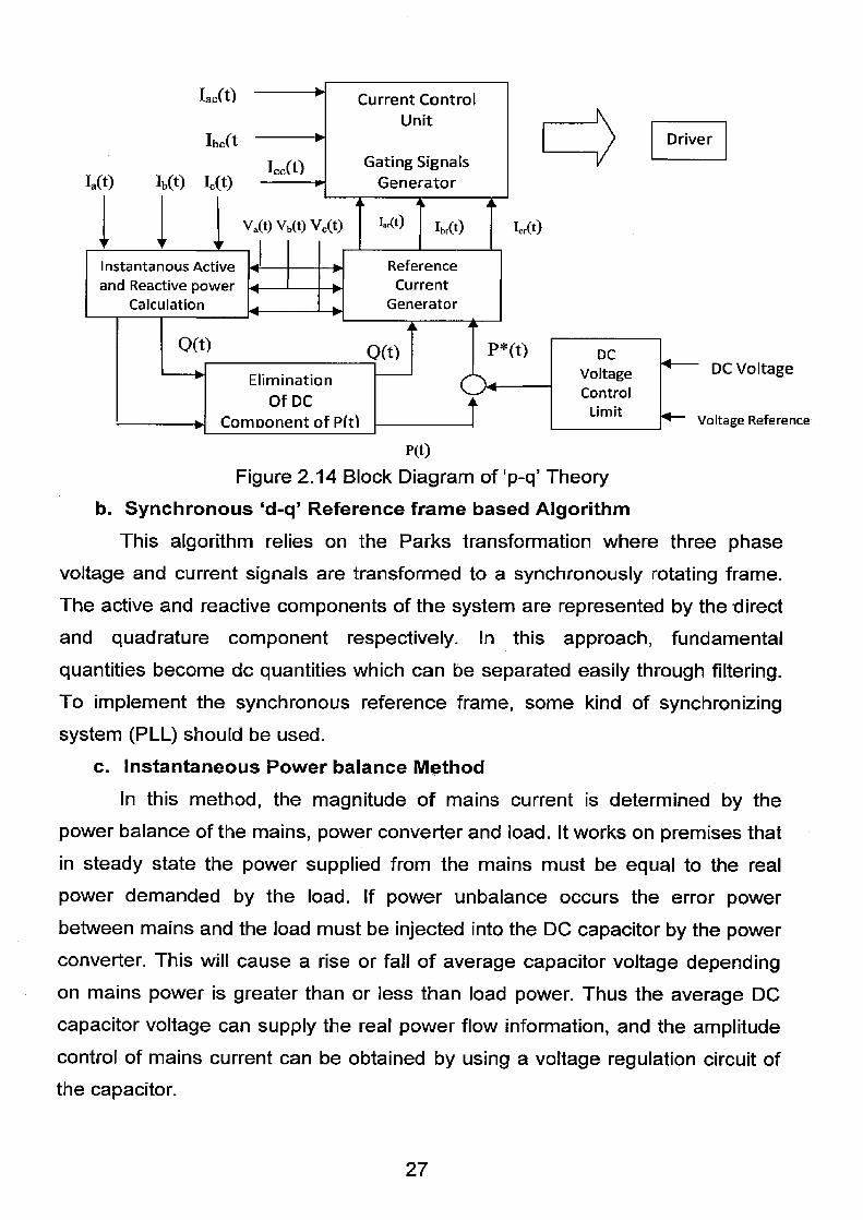
There is large number of techniques available in time domain: a. Instantaneous Reactive Power Theory or 'p-q' Theory
The 'p-q' theory is based on the aI3o transformation which transforms three phase voltages and currents into the aI3o stationary reference frame. From this transformed quantities, instantaneous real and reactive power of the load is calculated, which consists of DC component and an oscillating component. The oscillating component is extracted using high pass filter and taking inverse `a-13' transformation compensating command signals in terms of either currents or voltages are derived. This technique is suitable only for balanced three phase system with voltage waveforms purely sinusoidal. Diagram is shown in Figure 2.14
The original 'p-q' theory proposed by Akagi and revised by Marshal and Nabae is modified to make it applicable to eliminate neutral current of three
phase four wire systems.
26
Current Control Unit
Iac(t) Gating Signals
Generator
lnstantanous Active and Reactive power
Calculation
Va(t) Vb(t) Vat)
Ia(t) A 4
LA) Ibr(t)
Reference Current
Generator
Elimination Of DC
Component of P(t)
P*(t)
OA
Q(t) Q(t) 1— DC Voltage
411- Voltage Reference
DC Voltage Control Limit
=) Driver
P(t) Figure 2.14 Block Diagram of 'p-q' Theory
b. Synchronous 'd-q' Reference frame based Algorithm This algorithm relies on the Parks transformation where three phase
voltage and current signals are transformed to a synchronously rotating frame. The active and reactive components of the system are represented by the direct and quadrature component respectively. In this approach, fundamental
quantities become dc quantities which can be separated easily through filtering. To implement the synchronous reference frame, some kind of synchronizing system (PLL) should be used.
c. Instantaneous Power balance Method In this method, the magnitude of mains current is determined by the
power balance of the mains, power converter and load. It works on premises that in steady state the power supplied from the mains must be equal to the real
power demanded by the load. If power unbalance occurs the error power between mains and the load must be injected into the DC capacitor by the power converter. This will cause a rise or fall of average capacitor voltage depending on mains power is greater than or less than load power. Thus the average DC capacitor voltage can supply the real power flow information, and the amplitude control of mains current can be obtained by using a voltage regulation circuit of the capacitor.
27
d. Energy balanced Method This is based on the estimation of the active power required by load and
active filter the estimated reference supply command has two components. One is active power required by load and the other is the small component of active power required by the dc bus capacitor of the APF to maintain preset reference bus voltage. With the help of such estimated components instantaneous reference supply currents are obtained using instantaneously sensed supply voltage .subtracting load currents from these supply reference currents
compensating command currents for APF are derived. The energy controller
offers universal characteristics independent of load rating.
2.4.3 Generation of Firing Signals The switching signals are obtained by comparing the reference
compensating current signals with actual current in a current controller. There are different control techniques:
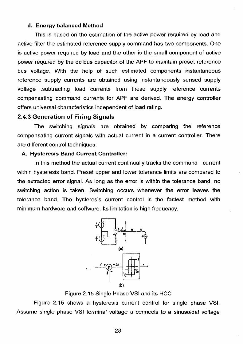
A. Hysteresis Band Current Controller: In this method the actual current continually tracks the command current
within hysteresis band. Preset upper and lower tolerance limits are compared to
the extracted error signal. As long as the error is within the tolerance band, no switching action is taken. Switching occurs whenever the error leaves the tolerance band. The hysteresis current control is the fastest method with minimum hardware and software. Its limitation is high frequency.
(b)
Figure 2.15 Single Phase VSI and its HCC
Figure 2.15 shows a hysteresis current control for single phase VSI. Assume single phase VSI terminal voltage u connects to a sinusoidal voltage
28

source e through an equivalent inductance L and resistance R. If we want to
control APF output current i to track a certain reference current i*, according to
Figure 2.15(a) the equation will be
Ldi/dt +Ri =u-e
When the APF output current is equal to reference current i* the corresponding
equation will be Ldi*/dt + Ri*= u*-e
Where u* is reference VSI terminal voltage corresponding to i*. If APF current
tracking error Ai=i-i*, when R=0 LdAi/dt=u-u*
Where VSI terminal voltage u is
U={ E/2 (s=1) - E/2 (s=0) }
Here E is the VSI dc voltage and s the solid state switch status.
WHEN Ai is greater than h, s is controlled to be at lower level s=0 and therefore
(u-u*)< 0 which makes Al to reduce . The corresponding HCC block is shown in
Figure 2.15(b)
B. Predictive Control Two popular approaches to prediction or forecasting problems are
statistical time series modeling method and the use of neural networks.
Estimation of reference signal at next sampling value is obtained by rotating the
present sampling value through an angle in ct-13 plane using the rotation matrix.
The first approach is rather complicated and amount of computation is large .On
the other hand ANN offer fast computation speed because parallel nature,
adaptability to changing parameters.
In spite of the superior performance the predictive controllers have
drawbacks that they require considerable calculations.
C. Space Vector Modulation:
SVM technique can be easily implemented for active power filter using
multilevel converters. The weakness of hysteresis controller can be overcome by
conjunction of the space vector modulation technique to the controller. SVM was
first introduced by German researcher in the mid of 1980s. This technique
showed several advantages over PWM technique. SVM technique can maximize
the output voltage and also reduce the switching number at the same carrier
29
frequency of the PWM method. The space vector modulation technique is a fixed
frequency approach.
The desired three phase voltages at the output of the inverter could be
represented by an equivalent vector V rotating in the counter clock wise direction
as shown in Figure 2.16(a). The magnitude of this vector is related to the
magnitude of the output voltage as in Figure 2.16(b) and the time this vector
takes to complete one revolution is the same as the fundamental time period of
the output voltage.
Figure 2.16(a) Output Voltage Vector.
144,
---,-.
.„--------, ''',---
_,'''''
--
- ----
_
-,----'- _...'
_.,,,`
5
6
Figure 2.16(b) Output line voltage in time domain.
When the desired line to line output voltage vector V is in sector 1,then
this vector can be synthesized by pulse width modulation(PWM) of the two
adjacent switching state Vectors(SSV) V1(pnn) and V2(ppn), the duty cycle of
each being dl and d2 respectively, and the zero vector(V7N8) of duty cycle dO:
d1V1+ d2V2=V=mVg e1' d1 + d2 + dO = 1
where 05.m 0.866 is modulation index. This would correspond to a
maximum line to line voltage of 1.0 Vg. All SVM schemes and most of other
PWM algorithms use above equations for output voltage synthesis. The
modulation algorithm that use non adjacent SSV's have shown to produce higher
THD or switching losses. The duty cycles dl, d2 and dO are uniquely determined
from Figure 2.16 and above equations.
30

dote-
rToWns tclge dole-t1 r
In SVM there are no of advantages as compared to other techniques
A. Very low values of output voltage TI-ID
B. Robust dynamic response
C. The efficiency of the inverter can be optimized, for each load condition.
D. SVM enables more efficient use of DC Voltage( 15% more than
conventional PWM techniques)
E. By applying special modulation techniques the peak current in IGBTs can
be reduced compared to similar inverters.
F. By changing the switching behavior of the inverter the audible noise can be
minimized.
2.4.4 Control Scheme for Active Power Filter: Mdi FIE;
Figure 2.17 System Configuration for Shunt Active Filter
In control block diagram three signals, the mains voltage, DC bus voltage
and mains current, are detected. The signal of mains voltage is used to generate
a reference sine wave, with unity amplitude and in phase with the mains voltage.
The DC bus voltage is used to supply the information of power balance. In
steady state power supplied from mains will be equal to load power and losses in
converter and in transient conditions caused by load. The DC capacitor must
supply the power difference between the mains and load. If real power supplied
from mains is smaller than demanded by load, the average voltage of DC
31
capacitor is reduced, at this instant magnitude of mains current must be enlarged
to increase the real power supplied from the mains. On the contrary, the average
voltage of capacitor rises and mains current must be decreased. The average
voltage of DC capacitor can supply the real power flow information and the
amplitude control of mains current can be obtained by using voltage regulation
circuit of DC capacitor.
The signal of the practical mains current is fed to the active current wave
shaping controller to supply the wave shape and phase information of the mains
current. The detected DC bus voltage is compared with reference DC voltage.
The compared result is fed to P-I controller. The output of P-I controller and the
reference sine wave are then fed to multiplier to generate the desired mains
current is* (t). The desired mains current and the detected actual mains current
are fed to the active current wave shaping controller i.e. Hysteresis based PWM
current controller, to generate the switching signals of power converter. These
signals are applied to converter through suitable gate drive circuit. Thus the
control circuit provides gate signals to devices in the converter to compensate
current harmonics in the load and source side will be harmonic free.
2.5 CONCLUSION
In recent days power quality is an important issue in power system.
Different types of filter are reported for mitigation of current harmonics. Active
power filters with VSI and CSI are suitable for Low and medium voltage levels.
But for high voltage levels these filters have limitations. In such cases multilevel
inverters are used for shunt active filter. In case of multilevel inverters, with same
device rating, inverter output voltage will be high. With the advancement of
digital technology and their advantages in time and accuracy, in deriving the
compensation quantity, digital based control algorithms are becoming more
popular. With appropriate control scheme current harmonics in high voltage high
power system can be compensated effectively. In this project FPGA based
Shunt Active Power Filter is developed to reduce the current harmonics.
32

Chapter 3
Simulation Analysis of Shunt Active Power Filter Topologies
Simulation results of single phase VSI based shunt active power filter, three phase VSI and CSI based shunt active power filter, multilevel inverter based active power filter and capacitor mid-point topologies with different conditions of loads and supply are shown. The performance of all the topologies is studied under conditions of unbalanced load, unbalanced supply, change in
load and with supply harmonics.
3.1 Introduction Extensive simulation study is carried out to investigate the performance of
single phase VSI based shunt active power filter, three phase VSI and CSI based shunt active power filter, multilevel inverter based active power filter and
capacitor mid-point topologies under conditions of unbalanced load, unbalanced supply, change in load and with supply harmonics. The simulation study is
developed using SimPowerSystems blockset of MATLAB Simulink. Simulation is done using instantaneous reactive power theory or `p-cf theory with diode rectifier as non-linear load. A comparative study of all the topologies is also done.
3.2 Simulation Study on Single Phase VSI Based Shunt Active Power Filter Simulation studies have been done with the following parameters: Source
230V (ph to neutral, rms), 50Hz, non-linear load as diode rectifier with Load resistance 50 and Load inductance 30mH, DC capacitor 4000pF, Reference DC Voltage of 350V. Figure 3.1 shows the waveforms of source voltage Vs (in V), load current IL (in A), source current I. (in A) and filter current IF (in A).
33

• w 200 • 101,
M 0 -•-• 0 0 co > -200
50
0 .0ow
= U_50
I .11111,1111.IIIIIIIIII 11.111112.11m.I..11.
0.05
0.1
0.15
0.2
0.25
03
0
0.05
0.1
0.15
0.2
0.25
03
CD "E-.
0 0 CO C-3
111 CD
LL =
U
Figure 3.1 Simulation Results of Single Phase VSI Based Shunt Active Power Filter
The filter is made to act at 0.1 sec in the simulation, hence from 0 to 0.1
sec the waveforms shown are without filtering action and from 0.1 sec filtering
action starts and source current becomes close to sinusoidal waveform. FFT
analysis of the source current is shown in Figure 3.2. As observed from the FFT
analysis, the THD of the source current is well less than 5% according to IEEE
519 standards.
Figure 3.2 FFT Analysis of Single Phase VSI Based Shunt Active Power Filter
3.2.1 Effect of Sudden Change in Load:
The effect of sudden change in load is incorporated by switching another
diode rectifier in parallel to the existing diode rectifier at 0.2 sec. The simulation
34

results obtained with this sudden change in load are as shown in Figure 3.3. FFT
analysis of the source current after this sudden change in load is shown in
Figure 3.4
0.05
0.1
0.15
0.2
0.25 03
0.05
0.1
0.15
0.2
0.25 03
0.05
0.1
0.15
0.2
0.25
0.3
0.05
0.1
0.15 0.2 0.25 0 3 Time
Figure 3.3 Simulation results of Single Phase VSI Based Shunt Active Power Filter with sudden change in load
Figure 3.4 FFT Analysis of Single Phase VSI APF with sudden change in load 3.2.2 Effect of Supply Harmonics:
The effect of supply harmonics on the performance of the active power
filter is shown in Figure 3.5. The corresponding FFT analysis is as shown in
Figure 3.6.
35

0.15 0.2 0.25 0.3
---
0.15 0.2 0.25 03
0.1 0.05
0.1 0.05
50 -o 0 e
C-3 -50 =
0
50
0
-50
0.05 0.1 0.15 0.2 0.25 03
0.15 0.2 0.25 0 3 Time
0.1
Figure 3.5 Simulation results of Single Phase VSI Based Shunt Active Power Filter with
supply harmonics
Figure 3.6 FFT Analysis of Single Phase VSI APF with Supply Harmonics
3.3 Simulation Study on Three Phase VSI Based Shunt Active Power Filter
Simulation studies have been done with the following parameters: Source
230V (ph to neutral, rms), 50Hz, non-linear load as diode rectifier with Load
resistance 15n and Load inductance 25mH, DC capacitor 2000pF, Reference
DC Voltage of 350V. Figure 3.7 shows the waveforms of source voltage Vs (in
V), load current IL (in A), source current Is (in A) and filter current IF (in A).
36

0.1 0.2 03 0.15 0.05 0.25
O. 0.1 0.2 0.15 0.05 0.25
0.1 0.2 0.3 0.05 0.15 0.25
20
Or
Q>
7
200
0
-200
20
,3 23- 0 o6- _, =
20 C.) n
v co c.' -20
Figure 3/ Simulation results of Three Phase VSI Based Shunt Active Power Filter
Figure 3.8 FFT Analysis of Three Phase VSI APF
The filter is made to act at 0.05 sec in the simulation, hence from 0 to 0.05
sec the waveforms shown are without filtering action and from 0.05 sec filtering
action starts and source current becomes close to sinusoidal waveform. FFT
analysis of the source current is shown in Figure 3.8. As observed from the FFT
analysis, the THD of the source current is well less than 5% according to IEEE
519 standards.
37

I
-50
50
H 0
500
20
0
-200
0.05 0.1 0.15 0.2 0.25 03
Figure 3.9 Simulation results under unbalanced load conditions
3.3.1 Operation under unbalanced load conditions:
In addition to the harmonics and reactive power compensation, APF is
also capable to maintain the compensated line currents balanced, irrespective of
the unbalance in load currents. To verify this, simulation results of a random
unbalancing loading conditions are presented here.
Figure 3.9 shows the simulation results after compensation, after
compensation source currents are found to be sinusoidal, almost balanced and
in phase with their respective source voltages. THD of the compensated source
currents are well below 5% limit according to IEEE 519 standards. Figure 3.10
shows the FFT analysis after compensation.
38

11111111101milfili I I iii..II..11111111iil
0.05 0.1 0.15 0.2 0.25
0.1 0.2 03 0.05 0.15 0.25 -500
20
-20
200
0
-200
50
Figure 3.10 FFT Analysis of Three Phase VSI APF with Unbalanced Load
3.3.2 Operation under unbalanced supply conditions: The APF also provides compensation under unbalanced supply
conditions. To verify this, the rms per phase voltage in each phase is slightly varied with each other. The rms per phase voltages of phase 'a', 'b', and 'c' are kept at 230V, 220V and 210V respectively. Figure 3.11 shows the simulation
results after compensation and the corresponding FFT analysis is shown in
Figure 3.12
0 0.05 0.1 0.15 0.2 0.25 0.3 Time
Figure 3.11 Simulation results under unbalanced supply conditions
39

Figure 3.12 FFT Analysis of Three Phase VSI APF with Unbalanced Supply
3.3.3 Effect of Supply Harmonics: The effect of 5th and 7th harmonic contents in supply voltages on the
performance of the APF is studied by incorporating the harmonics in the supply voltage. The simulation results obtained after compensation are shown in Figure
3.13. The corresponding FFT analysis is as shown in Figure 3.14
20
0
-20
Figure 3.13 Simulation results with supply harmonics
40

Figure 3.14 FFT Analysis of Three Phase VSI APF with Supply Harmonics
3.3.4 Effect of Sudden Change in Load:
The effect of sudden change in load is incorporated by switching another
diode rectifier in parallel to the existing diode rectifier at 0.2 sec. The simulation
results obtained with this sudden change in load are as shown in Figure 3.15.
FFT analysis of the source current after this sudden change in load is shown in
Figure 3.16 400
500 0.05
20
03
_ _
0.15 Time
0.2
0.25
0.3 0
0.05
0.1
Figure 3.15 Simulation results of Three Phase VSI Based Shunt Active Power Filter with
sudden change in load
41

Time
400 & 200 . 0
o 15 to > -200
-400 0 0.05 0.1 0.15 0.2 0.25 03
2
1 0
Figure 3.16 FFT Analysis of Three Phase VSI APF with Sudden Change in Load
3.4 Simulation Study on Three Phase CSI Based Shunt Active Power Filter
Simulation studies have been done with the following parameters: Source
230V (ph to neutral, rms), 50Hz, non-linear load as diode rectifier with Load
resistance 1500 and Load inductance 20mH, DC side inductance 160mH,
Reference DC current of 5A. Figure 3.17 shows the waveforms of source voltage
Vs (in V), load current IL (in A), source current Is (in A) and filter current IF (in A).
The FFT analysis is shown in Figure 3.18. It is observed from Figure 3.16 that
THD of source current after compensation is less than 5%
Time
— e 0 CO
5 0 0.05
0.1
0.15
0.2
0.25
03 Time
0
0.05
0.1
0.15
0.2
0.25
0.3 Time
Figure 3.17 Simulation results of Three Phase CSI Based Shunt Active Power Filter
42

§
-5
Figure 3.18 FFT Analysis of Three Phase CSI APF
3.4.1 Operation under unbalanced load conditions:
The APF effectively provides compensation under unbalanced loaded
conditions also. This can be verified by making the load unbalanced by switching
phases at different instances. Here phase 'a' load is switched at 0.2 sec whereas
phase 'b' and 'c' loads are switched at 0.1 sec. The simulation results obtained
under this condition of unbalance are as shown in Figure 3.19 and the
corresponding FFT analysis is shown in Figure 3.20
0.05
0.1
0.15
0.2
0.25
03 Time
0.05
0.1
0.15
0.2
0.25
03 Time
Time
Figure 3.19 Simulation results under unbalanced load conditions
43

0.05 0.1 0.15 0.2 0.25 0.3
200
0
0.05 0.1 0.15 0.2 0.25 03 Time 5
5
0
5
Ea) 0 o cn U 5 0 0.05 0.1 0.15 0.2 0.25 03
Figure 3.20 FFT Analysis of Three Phase CSI APF with Unbalanced Load
3.4.2 Operation under unbalanced supply conditions:
The compensation provided by the APF under unbalanced supply
conditions is shown in Figure 3.18. To verify this, the rms per phase voltage in
each phase is slightly varied with each other. The rms per phase voltages of
phase 'a', 'b', and 'c' are kept at 230V, 220V and 210V respectively. Figure 3.21
shows the simulation results after compensation and the corresponding FFT
analysis is shown in Figure 3.22
Time
Figure 3.21 Simulation results under unbalanced supply conditions
44

0.05 0.1 0.15 0.2 0.25 0.3 5
0
5 0.2 0.25 0.3
o
2
° -2
200
0 o. to > -200
Figure 3.22 FFT Analysis of Three Phase CSI APF with Unbalanced Supply
3.4.3 Effect of Supply Harmonics: The effect of 5th and 7th harmonic contents in supply voltages on the
performance of the APF is studied by incorporating the harmonics in the supply voltage. The simulation results obtained after compensation are shown in Figure 3.23. The corresponding FFT analysis is as shown in Figure 3.24.
0.05 0.1 0.15 0.2 0.25 0.3 Time
Figure 3.23 Simulation results with supply harmonics
45

Figure 3.24 FFT Analysis of Three Phase CSI APF with Supply Harmonics
3.4.4 Effect of Sudden Change in Load:
The effect of sudden change in load is incorporated by switching another
diode rectifier in parallel to the existing diode rectifier at 0.1 sec. The simulation
results obtained with this sudden change in load are as shown in Figure 3.25.
FFT analysis of the source current after this sudden change in load is shown in
Figure 3.26
0.05
0.1
0.15
0.2
0.25
0.3
Figure 3.25 Simulation results of Three Phase CSI Based Shunt Active Power Filter with
sudden change in load
46

0.05 0.1 0.15 0.2 0.25 03
O 0
U.5
Figure 3.26 FFT Analysis of Three Phase CSI APF with Sudden Change in Load
3.5 Simulation Study on Multilevel Inverter Based Shunt Active Power Filter
Simulation studies have been done with the following parameters: Source 230V (ph to neutral, rms), 50Hz, non-linear load as diode rectifier with Load resistance 15052 and Load inductance 100mH, DC capacitor 1000pF. The simulation analysis is carried out by considering six level cascaded H-bridge
inverter. Figure 3.27 shows the waveforms of source voltage Vs (in V), load
current IL (in A), source current Is (in A) and filter current IF (in A). The FFT
analysis of the source current is shown in Figure 3.28
0.05 0.1 0.15 0.2
0.25 03
Figure 3.27 Simulation results of Multilevel Inverter Based Shunt Active Power Filter
47

5 •E
2 2 0
Figure 3.28 FFT Analysis of Multilevel Inverter APF 3.5.1 Operation under unbalanced load conditions:
The APF effectively provides compensation under unbalanced loaded
conditions also. This can be verified by making the load unbalanced by switching
phases at different instances. Here phase 'a' load is switched at 0.2 sec whereas
phase 'b' and 'c' loads are switched at 0.1 sec. The simulation results obtained
under this condition of unbalance are as shown in Figure 3.29 and the
corresponding FFT analysis is shown in Figure 3.30
200
s• 0 > -200
0 0.05 0.1 0.15 0.2 0.25 0.3
0 0.05 0.1 0.15 0.2 0.25 0.3
10
0 03 0
-10 0 0.05
0.1
0.15
0.2
0.25
0.3
g 0
-5
0.05
0.1 0.15
0.2 0.25 Time
Figure 3.29 Simulation results under unbalanced load conditions
03
48

0.1 0.15 0.05 0
200
t .23 0
Y .1
0.2 0.25
0 -200
03
Figure 3.30 FFT Analysis of Multilevel Inverter APF with Unbalanced Load
3.5.2 Operation under unbalanced supply conditions:
The compensation provided by the multilevel invereter APF under
unbalanced supply conditions is shown in Figure 3.27. To verify this, the rms per
phase voltage in each phase is slightly varied with each other. The rms per
phase voltages of phase 'a', 'b', and 'c' are kept at 230V, 220V and 210V
respectively. Figure 3.31 shows the simulation results after compensation and
the corresponding FFT analysis is shown in Figure 3.32
0.05
0.1
0.15
0.2
0.25
03 Time
Figure- 3.31 Simulation results under unbalanced supply conditions
49

0.05 0.1 0.15 0.2 0.25 03
0.2 0.05 0.1 0.15 Time
Figure 3.33 Simulation results with supply harmonics
0.25 0.3
10
50
c5
LL=̀ C)
0
100
L 0
CO C.)
Figure 3.32 FFT Analysis of Multilevel Inverter APF with Unbalanced Supply
3.5.3 Effect of Supply Harmonics:
The effect of 5th and 7th harmonic contents in supply voltages on the
performance of the APF is studied by incorporating the harmonics in the supply
voltage. The simulation results obtained after compensation are shown in Figure
3.33. The corresponding FFT analysis is as shown in Figure 3.34.
-200 TTTTTTT TTTTTT G3 co GI 0
00

Time
200
I 0
-200
0 10
0
100
10
0
-10
O
10
0 L li
-100
0.05
0.05
0.05
0.05
0.1
0.1
0.1
0.1
0.15
0.15
0.15
0.15
0.2
0.2
0.2
0.2
0.25
0.25
0.25
0.25
0.3
03
03
03
Figure 3.34 FFT Analysis of Multilevel Inverter APF with Supply Harmonics
3.5.4 Effect of Sudden Change in Load:
The effect of sudden change in load is incorporated by switching another
diode rectifier in parallel to the existing diode rectifier at 0.1 sec. The simulation
results obtained with this sudden change in load are as shown in Figure 3.35.
FFT analysis of the source current after this sudden change in load is shown in
Figure 3.36
Figure 3.35 Simulation results of Multilevel Inverter Based Shunt Active Power Filter
with sudden change in load
51

200
# 0 -200
0 50
0
0.05 0.1 0.15 0.2 0.25 0
1 1
50 0
50
-500
0.05
0.05
0.1
0.1
0.15
.0.15
0.2
0.2
0.25
0.25
03
0 3
Figure 3.36 FFT Analysis of Multilevel Inverter APF with Sudden Change in Load
3.6 Simulation Study on Capacitor Mid-Point Shunt Active Power Filter
Simulation studies have been done with the following parameters: Source
230V (ph to neutral, rms), 50Hz, non-linear load as diode rectifier with Load
resistance 150 and Load inductance 25mH, DC capacitor 1000pF, Reference
DC Voltage of 350V. Figure 3.37 shows the waveforms of source voltage Vs (in
V), load current IL (in A), source current Is (in A) and filter current IF (in A) and the
corresponding FFT analysis of source current is shown in Figure 3.38
Figure 3.37 Simulation results of Capacitor Mid-Point Shunt Active Power Filter
52

Figure 3.38 FFT Analysis of Capacitor Mid-Point Shunt APF
3.7 Simulation Results and Discussions: In order to investigate the performance of different active power filter
topologies various simulation results are presented under different load and supply conditions. Rating of the active filter is a function of reactive power to be compensated. After compensation three-phase source currents become sinusoidal, balanced, and are in phase with their respective voltages. THD of the compensated source current is within 5% limit imposed by IEEE 519 standard.
Transient behavior of the active power filter with diode rectifier as nonlinear load is investigated by switching load. As observed from various simulation results, source current becomes sinusoidal soon after the switch on of the APF. Various waveforms for sudden increase in load are shown for all the topologies considered. The change in compensated source currents are found to be smooth. It is observed that DC link voltage changes to absorb/release the energy during load change. Power factor of the input current is also improved. Frequency spectrum of source current after compensation are also shown.
It is observed that the smoothing reactor reduces the slope of the rising and falling edges of load current, thereby helps in reducing the band width of the APF and bring down the THD below 5% limit. THD of the source currents are significantly improved by introducing a smoothing reactor in front of nonlinear loads as compared to the active filter used alone.
53

3.8 Conclusion: Simulation analysis of single phase VSI based shunt active power filter,
three phase VSI and CSI based shunt active power filter, multilevel inverter
based active power filter and capacitor mid-point topologies are shown. The
performance of all the topologies is studied under conditions of unbalanced load,
unbalanced supply, change in load and with supply harmonics. It is observed
that source current becomes sinusoidal just after the application of APF and its
THD is less than 5% within the limit of IEEE 519 standard. All the simulated
results for different topologies are shown for various system conditions and their
behavior is studied.
54

Chapter 4
Overview of FPGA and its Application in Active Power Filtering
Field Programmable means that FPGA's function is defined by user's
program rather than by manufacturer. Typical IC performs function defined at the
time of manufacture. In contrast, FPGA's function is defined by program written
by someone other than device manufacturer. FPGA is an integrated circuit that
contains many (64 to over 10,000) identical logic cells. Each logic cell can take
on any one of a limited set of personalities, independently. These cells are
interconnected by matrix of wires and programmable switches. A user's design is
implemented by specifying the simple logic function for each cell and selectively
closing the switches in the interconnect matrix. Thus, it is a regular structure of
logic cells and interconnect, which is completely under user control. This means
we can design, program, and make changes to circuit anytime. 4.1 EVOLUTION OF FPGA
Programmable Logic Array (PLA) was introduced by Philips in early
1970s. PLA has two levels of logic gate i.e_ programmable wired AND plane then
an OR plane (in Figure 4.1 (a)). But it was expensive & offered poor speed-
performance due to two levels of configurable logic. After PLA, Programmable
Array Logic (PAL) was introduced, only AND plane is programmable while OR is fixed (Figure 4.1(b)).
Figure 4.1 (a) Simple PLA
55

Figure 4.1 (b) PAL
FPGAs have a different background as coming from the development of
ASICs, where digital designs were realized by using gate arrays. FPGAs are
programmable version of gate arrays. Gate is 2-i/p NAND, which is implemented
as array to silicon chip, gate array is connected via routing matrix. Tasks or
functions to be implemented in FPGA are generated by routing these gates
together through routing matrix. FPGAs offer highest logic capacity in PLDs. In
Figure 4.2, some major events in the history of power electronics and
programmable devices are brought together. It is not a full historical overview of the development.
J.A. Fleming Thermoelectric vacuum diodes Sell Laboratories
C. L. Co First transistor Patent of ar E. F. Alexanderso weldingprs ess Magnetic amp&
anus J. W d irst electric
Thomas .A. son F" Thertxoni sio
1984 1999 1980 19851988 1995 20012006
Fig 4.2 Time line of power electronics combined with time line of PLDs
1900 1902 1912 18831890 1901
11 Laborat riesT i "pow r elec tjunctio c e into 'de istor ac lance
1947 1957 1969 1971 1951 1970
sGeneral Electric Silicon controlle
General Electric corporation First adjustable speed AC driv (using inverter)
Inverter power source in welding
Signetics 55 -time
orpora on rectifi
Altera First P
Xilinx First F
Altera First CPLD Altera (MAX serioFirst embedded
processors in FPGA
era us* FPG
D mbedded
Actel A First embedded A/D converter in FPGA
Xilinx First ay gate F
million
56

Logi c lock
Interconnection Resources
The gate count of today's FPGAs is over 10 million gates. The design
capacity of one design engineer is approximated to be 15 gates per year. To
design 10 million gates in a year, one hundred design engineers would be
required.
4.2 FPGA ARCHITECTURE Each FPGA vendor has its own architecture; in general they are all
variation of Figure 4.3
Figure 4.3 Generic FPGA architecture.
4.2.1 Configurable Logic Blocks (CLBs) They contain logic for the FPGA. In the large-grain architecture used
today, CLBs contain enough logic to create small state machine. The block has
RAM, known as lookup table (LUTs) for creating arbitrary combinatorial logic
functions. It also contains flip-flops for clocked storage elements, along with
CDC) multiplexers in order to route the logic within the
0
ot_Lio_ block and to or from external resources. LUTs
compute any function of N inputs (N is number of ps control signals for LUT's) by programming 2N
11 12 13- programming bits with truth table of the desired Figure 4.4 A 3-input function as in Figure 4.4. Thus, if all LUT
programming bits except the one corresponding
to the input pattern 111 were set to zero a 3-input LUT would act as a 3- input
57

Figure 2.13 (a) Cascade H-Bridge Multilevel Inverter (b) Output Waveform
2.4 CONTROL STRATEGIES: The control methodology of APF is key element for its successful
performance in mitigating the harmonics and is implemented through three
steps:
1. Signal Conditioning
2. Estimation of compensating signal
3. Generation of firing signals for switching devices
2.4.1 Signal Conditioning: In order to implement the control algorithm, on line measurement of
various voltage and current signals such as ac mains voltage, DC link voltage
load, source and filter currents are required. Available advanced sensors have
offered great ease of accurate signal conditioning.
25

AND gate, while programming it with all ones except in 000 would compute a
NAND.
A general configurable logic block with one 4-input LUT, an optional D flip-
flop (DFF), and some form of fast carry logic like multiplexer is shown below.
Inputs 4, 4- Input I UT
Clotck Liable Set/Reset
Figure 4.5 General Configurable Logic Block
4.2.2 Configurable I/O Block:
It's used to bring signals onto the chip & send them back again. It has an
input & output buffer with 3-state and open collector output controls. Typically
pull up resistors on the output & sometimes pull down that can be used to
terminate signals & buses. Polarity of the output can be programmed for active
high or low output. There are typically flip-flops on outputs and inputs so that
clocked signals don't encounter significant delay.
4.2.3 Programmable interconnect:
In Figure 4.6, there are long lines used to connect critical CLBs that are
physically far from each other on the chip without inducing much delay. They can
also be used as buses within the chip. There are also short lines that are used
to connect individual CLBs located physically close to each other. Transistors
are used to turn on or off connections between different lines. There are also
several programmable switch matrices in the FPGA to connect these long and
short lines together in specific, flexible combinations.
Clock
D-Flip Flop
Output Mux
58

Figure 4.6 FPGA programmable inter-connect
Additional logic resources such as ALUs, memory, and decoders may also be available.
4.3 TYPES OF FPGAs
There are three competing technologies for programming FPGAs. First,
SRAM involves a small static RAM bit for each programming element. Writing
the bit with a zero turns off the switch, while writing with a one turns it on. Next is an antifuse that consists of a microscopic structure that, unlike a regular fuse,
normally makes no connection. A large amount of current during programming of
the device causes the two sides of the antifuse to connect. A third and relatively
new method uses flash EPROM bits for each programming element. 1) SRAM Based FPGA
2) Antifuse
3) Flash FPGAs
4.4 FEATURES OF FPGA
Here some of the benefits that make FPGAs unique are highlighted. Top Five Benefits:
• Performance
• Time to Market
• Cost
• Reliability
• Long-Term Maintenance
59

At the highest level, FPGAs are reprogrammable silicon chips. Using
prebuilt logic blocks and programmable routing resources, we can configure
these chips to implement custom hardware functionality without ever having to
pick up a breadboard or soldering iron. In addition, FPGAs are completely
reconfigurable and instantly take on a brand new "personality" when recompiled
with a different configuration of circuitry. FPGA chip adoption across all industries is driven by fact that FPGAs
combine best parts of ASICs and processor-based systems. FPGAs provide
hardware-timed speed and reliability, but they don't require high volumes to
justify large upfront expense of custom ASIC design. Unlike processors, FPGAs
are truly parallel in nature so different processing operations do not compete for
same resources. Each independent processing task is assigned to dedicated
section of chip & function autonomously without any influence from other logic
blocks. So, performance of one part of application is not affected when additional
processing added. Parameters are difficult to update for fast tasks like control, protection &
signal processing using analog designs. Slower tasks, like monitoring, are
implemented in DSP, which are not as fast as analog but software-based, thus,
easily reprogrammable. Utilizing FPGAs in control hardware is to replace analog
parts to achieve digital & programmable implementation of the control part. Other
advantages of implementing analog functions in FPGA are temperature and
variation insensitivity of passive components and faster execution of tasks.
HDL designs have one advantage over processor design, namely the
technology independency. Different designs can be implemented to different
FPGAs almost directly without any code changes. Functions can be executed 10
times faster in FPGA than DSP, while reducing total cost of system. Another
interesting feature of FPGA is Run-Time Reconfiguration, which is major
advantage compared to other alternates. Frequently, areas of program that can
be accelerated through use of reconfigurable hardware are too numerous or
complex to be loaded simultaneously onto the available hardware. For these
cases, it is helpful to swap different configurations in and out of the
reconfigurable hardware as they are needed during program execution,
performing a run-time reconfiguration of the hardware. Because run-time
60

reconfiguration allows more sections of an application to be mapped into hardware than can be fit in a non run- time reconfigurable system, a greater portion of the program can be accelerated in the run-time reconfigurable systems. This can lead to an overall improvement in performance.
FPGAs that can be selectively programmed without a complete reconfiguration are partially reconfigurable. These are more suited to run-time reconfiguration than single-context, because small areas of array can be modified without requiring entire logic be reprogrammed. This allows configurations which occupy only a part of the total area to be configured onto array without removing all of configurations already present. These small reconfigurations require much less time than a full-chip reconfiguration due to reduced data traffic.
Serious problem is that the special features added in FPGAs cannot fulfil the needs of every application field. Thus, the extra features developed to other applications add extra costs to the FPGAs used to control power electronics. This problem is addressed by offering different family members of FPGAs for different applications. In this solution, the features of each application are added to the FPGA circuit offered to the current application field. To sum up, the future trend seems to be to move towards application-specific circuits.
4.5 BASIC FPGA DEVELOPMENT PROCESS FPGA based complex system designs has various interdependent
requirements such as maximizing device utilization, optimizing 10 placement, minimizing routing congestion and reaching timing goals. Though it is highly desired that all these requirements are automatically met by EDA tools in an automated flow, it is practically impossible. FPGA development stages are design, simulation, synthesis, & implementation, as Figure 4.7
61

Figure 4.7 FPGA Development Process
4.6 COMMERCIALLY AVAILABLE FPGAs Today, Xilinx and Altera dominate while Actel, Lattice, and Atmel each
share remainder of market with products aimed at specific application & needs.
SRAM is dominant technology. Actel has flash memory-based FPGAs that have
the speed, size, and non-volatility advantages of antifuse technology while using
a more standard process. Software tools for FPGA development have greatly
increased in functionality and further decreased in price over the years. Xilinx,
pressured by Altera, now offers a great tool set.
One great equalizer is that independent tool vendors have sprung up to
support all device families from all FPGA vendors. Synplicity was a pioneer in
this area. Previously, Synopsys, the original synthesis company, provided
synthesis tools for ASICs that could be "adjusted" for FPGAs. Synplicity,
however, focused their technology solely on FPGAs, fine-tuning their synthesis
algorithms for specific FPGA architectures from different vendors.
62

Examples of SRAM FPGA families include the following:
• Altera Stratix II and Cyclone II families • Atmel AT6000 and AT4OK families • Lattice LatticeEC and LatticeECP families • Xilinx Spartan-3 and Virtex-4 families
Examples of antifuse FPGA families include the following:
• Actel SX and Accelerator families • Quicklogic Eclipse II family
Examples of flash FPGA families include the following:
• Actel ProASIC family
4.7 APPLICATIONS OF FPGAs
FPGAs have gained rapid acceptance and growth over the past decade because they can be applied to a very wide range of applications. A list of typical applications includes: random logic, integrating multiple SPLDs, device controllers, communication encoding and filtering, small to medium sized systems with SRAM blocks. Other interesting applications of FPGAs are prototyping of designs later to be implemented in gate arrays, and also emulation of entire large hardware systems. Some of the Applications of FPGA are in these fields:
• Power Electronics • Image and Signal Processing • Medical Equipment • Wired and Wireless Telecommunications • Robotics & Automotive • Space and Aircraft Embedded Control Systems • Thermal Management and Packaging
4.8 FPGA BASED CONTROL SCHEME FOR ACTIVE POWER FILTER:
The line diagram in Figure 4.8 shows the current distribution of a power system composed by a sinusoidal voltage source, a nonlinear load, and a shunt APF. Various power line conditioning approaches have been explored using the
63

NONLINEAR LOAD
SOURCE
ACTIVE POWER FILTER
technology of active power filtering_ Series, shunt, and hybrid APF topologies
have been developed along with different control schemes. Different modeling,
simulation, and implementation approaches have been used in order to develop
APF control systems. A novel approach to the design of the APF controller is the
use of Simulink combined with Xilinx System Generator to produce a VHDL code
for hardware implementation in a FPGA. The design involves the measurements
of source voltage, source current, and filter current, allowing the filter to
compensate for multiple nonlinear loads connected to the same distribution bus,
since the load current is not directly measured. The generation of the source
reference current is based on the computation of average power.
Figure 4.8 Current Distributions with an Active Power Filter System configuration
Figure 4.9 shows the system configuration. This system is composed of a three-phase shunt active power filter, a source and non-linear load. The shunt
active power filter consists of a three-phase voltage source inverter using six
IGBTs, three identical series inductances Lf with resistances Rf and a DC
capacitor. The non-linear load is a three-phase diode rectifier with R- L load. The
output currents of the shunt active filter are controlled to provide harmonic
currents generated by the non-linear load to ensure filtering. In Figure 4.10 the
control scheme of the active filter is presented. The control scheme consists of an A/D unit and a digital controller.
64

Figure 4.9 System Configuration
Figure 4.10 Fully Digital Controlled Shunt Active Filter
65
4.9 ACTIVE POWER FILTER TOPOLOGY USING FPGA The topology of the active power filter considered for a single phase
power system is shown in Figure 4.11. A voltage source H-bridge inverter configuration is used in the power circuit including a DC capacitor, an inductor, and four controllable switches. Such circuit is connected in parallel with the source and the load at a PCC as shown in Figure 4.8. Ideally, with the proper switching control, the APF draws a current that forces the source current to be sinusoidal and in phase with the source voltage. The control system makes use of three physical measurements to generate the switching signals for the power circuit. These are the source voltage vs, the source current is, and the filter current if. The source current is measured with a current transformer at the source line. The source voltage and filter current are measured inside the APF with a potential transformer and current transformer respectively. It is also convenient to compensate for multiple nonlinear loads connected in parallel at the same distribution bus.
LOAM)
CONTROLLER
$w
ACTIVE POWER. FR-TER
Figure 4.11 Schematic of the Active Power Filter A general concept of the controller composition and data flow is shown in
Figure 4.12. The input signals are processed through an instrumentation interface unit responsible for some scaling operations and analog to digital conversion. Once the measured signals are in digital form, these are processed
66

ItistrtitrittTierteac
by the adaptive control unit using FPGA hardware technology with fixed-point
computation. The switching signals are generated, and finally provided to the
power inverter switches through a drivers interface unit.
CONTROLLER
Figure 4.12 Control Systems Units
4.10 CONCLUSION
With the advancement of digital technology and their advantages in time
and accuracy, in deriving the compensation quantity, digital based control
algorithms are becoming more popular. FPGAs offer better performance, lower
cost, and are highly reliable. FPGA based control scheme for active power filter
effectively compensates current harmonics in high voltage high power system
and obtains zero total harmonic distortion (THD) and unity power factor at the
source.
67

Chapter 5
Development of FPGA Based Single Phase Active Power Filter
5.1 SOFTWARE DEVELOPMENT The source voltage is sensed with the help of voltage sensor circuit. The
sensed source voltage is given as analog input to ADC of Spartan 3 FPGA kit. This is converted into digital form and then the reference source current is
generated. The generated reference current is converted back to analog using DAC of Spartan 3 FPGA kit. Now this reference current and the actual current sensed using current sensor is compared using Op-Amp and then the switching
signals are passed through Dead Band Circuit to provide delay and then finally the switching signals are given the devices through pulse amplification and isolation circuits. 5.2 HARDWARE DEVELOPMENT
The complete schematic of Single Phase Shunt Active Power Filter is as shown in Figure 5.1. The system has been developed for open loop control containing the following blocks:
> Power Circuit > Pulse Generation and Dead-Band Circuit > Snubber Circuit > Pulse Amplification and Isolation Circuit > Current Sensing Circuit
> Voltage Sensing Circuit > Power supplies > Spartan 3 FPGA interface circuit > ADC-DAC Interfacing
68

Active Power Filter 1-phase hwerter
Pulse Aroplication and Isolation Circuit
1-phase source Non-Linear Load (Diode Rectifier)
Current Sensor Voltage Sensor
SPARTAN 3 EIRGA, KIT if Differential Aiup]ifier and
Dead Band Circuit
Figure 5.1: Complete scheme of Single Phase Shunt Active power Filter
5.2.1 Power Circuit Figure 5.2 shows the power circuit of a Active Power Filter. The filter
requires a bidirectional switch capable of blocking voltage and current in both directions. Four bidirectional switches are required to form a bridge. MOSFET
switch used in the circuit consists of an inbuilt antiparallel freewheeling diode. No forced commutation circuits are required for the MOSFET as it is a self commutating device. These power devices are placed on heat sinks made of aluminum sheet to dissipate the excessive heat.
0
Fig 5.2: Basic power circuit of Active Power Filter
69
Specifications
• MOSFET-1RFP 460 (500V, 20A): 4 nos. Connetad to Drain
• Single phase diode bridge dc 602-9108 (1000V, 10A): 1nos.
• Heat sinks (2.5"x 2.5" top surface, 5mm sheet thickness): 4nos.
5.2.2 Pulse Generation and Dead-Band Circuit The reference current, ia* is generated by SPARTAN 3 FPGA kit. The
actual source current, is is sensed using current sensor circuit and these currents are given as inputs to the pulse generation and dead-band circuit which is shown in Figure 5.3
>--
lk
_ SAItill
Figure 5.3 Pulse Generation and Dead-Band Circuit
5.2.3 Snubber Circuit Since the power handled by the prototype bridge converter is less (upto
10A) an RC snubber circuit has been used for protection of the main switching
device. Switching high current in short time gives rise to voltage transients that
70

MOSFET IRFP 460 10uF
could exceed the rating of the MOSFET. Snubbers are therefore needed to protect the switch from transients. Snubber circuit for MOSFET is shown in Figure 5.4. The diode prevents the discharging of the capacitor via the switching device, which could damage the device due to large discharge current. An additional protective metal oxide varistor (MOV) is used across each device to protect against over voltages across the devices.
Fig 5.4: Snubber circuit for MOSFET protection
Components
• Snubber circuits: 4 nos.
• Dimensions of each PCB: 2.5" x 2.5"
• Capacitance: 10pF/450V
• MOV (metal oxide varistor): 510V
• Diodes IN5408 : 4nos
5.2.4 Pulse Amplification and Isolation Circuit The pulse amplification circuit for MOSFET is shown in Figure 5.5. The
opto-coupler MCT-2E provides necessary isolation between the low voltage isolation circuit and high voltage power circuit. The pulse amplification is provided by the output amplifier transistor 2N2222. When the input gating is +5V level, the transistor saturates, the LED conducts and the light emitted by it falls
on the base of the phototransistor, thus forming its base drive. The output transistor thus receives no base drive and remains in the cut-off state and a +15V pulse (amplified) appears at its collector terminal.
71

1.2k
Firing Pulse
10k
_EN2222
enner Diode 12V e Source
470k
+15V
1R3 Ok
2N2222
3.8k
Gate +5V
-F15V
Fig 5.5: Pulse Amplification and Isolation Circuit
When the input gating pulse reaches ground level, the input switching transistor goes to cut-off state and LED remains off, thus emitting no light and
therefore the photo-transistor remains off. The output transistor receives base drive and saturates, hence the output falls to ground level. Therefore, the circuit provides proper amplification and isolation.
Further, since slightest spike above 20 can damage the MOSFET, a 12V Zenner diode is connected across the output isolation circuit. This clamps the triggering voltage to 12V. Further to the +15V power supply was fabricated on the same PCB using 7815 chip. Components
• Opto-coupler MCT-2E: 4nos. SCHEMATIC
1. LED Anode 2. LED Cathode 3. N.C. 4. Emitter 5. Collector 6. Base
• Output amplifier transistor (2N2222) : 4nos • Resistance:- 10k: 8 nos., 1.2k: 4 nos., 470k: 4 nos., 3.8k: 4nos. • Zener diode (+12V): 4nos.
• Copper clad sheet (4" x 2") for making 4 PCBs.
72

5.2.5 Current Sensing Circuit The actual source current, is is sensed using the current sensing circuit
shown in Figure 5.6 and is given as input to the pulse generation and dead-band
circuit.
10k
+1W
-1W 6-
01)
100
Figure 5.6 Current Sensing Circuit
5.2.6 Voltage Sensor The source voltage is sensed using voltage sensing circuit which is
soldered on a PCB. The output of the voltage sensor circuit is given to the ADC
channel of SPARTAN 3 kit. Figure 5.7 shows the voltage sensing circuit, the
input to the voltage sensor, i.e., the input source voltage is first applied to a
potential divider arrangement. This reduces the voltage by a factor of 100. This
reduced voltage is applied to the input terminals of AD202 which is an isolator
/amplifier. The output of AD202 is fed to a buffer of IC741 and then to a gain
block again of IC741. The gain block has an adjustable POT. This POT is
adjusted to give an overall gain of 0.05 to the input voltage.
Figure 5.7 Voltage Sensing Circuit
73

Components
• AD202: 1 no.
• IC741: 2no.
• Resistors (0.25W):- 100k: 1 no., 1k: 3 no., 2.2k: 1 no., 10k: 1 no.
• Trim POTs: 1 nos.
• Capacitors (25V):- 10pF: 2 nos., 0.1pF: 2 nos.
• Connectors:- 2 pin: 8 nos.
5.2.7 Power Supplies DC regulated power supplies (+15V,+12V, -12V, +5V) are require for
providing biasing to various circuits like pulse amplification and isolation, voltage sensor circuits and analog inputs providing reference frequency and voltage
using ICs 7815,7812, 7912 and 7805 for +15V,+12V, -12V and +5V respectively. Primary side of 230V/12V single phase transformer is fed through a single
phase 230V, 50Hz supply, secondary side is connected to a diode bridge.
1000pF, 25V capacitor is connected at the input supply of the regulator. 1000pF, 25V capacitor is connected at the output of the IC voltae regulator of each supply for obtaining the constant ripple free DC voltage. Components
• +12V supply: 10 nos.
• -12V supply: 1 no.
• +5V supply: 1 nos.
• IC 7812: 10 nos.
• IC 7912: 1 no.
• IC 7805: 1 nos.
• Capacitors 1000pF/50V: 12 nos., 100pF/25V: 12 nos.
• Diodes: 48 nos.
• Single phase transformer 230V/12V: 12 nos.
5.2.8 Spartan 3 FPGA Interface Circuit SPARTAN-3 based Universal DSP ProtoBoard (MXS3FK-004-DSP)
provides easy to use development platform, useful to physically verify DSP algorithms or simple digital designs around SPARTAN -3 FPGA.
74

Features
Figure 5.8 shows the SPARTAN-3 ProtoBoard, which includes the
following components and features:
SPARTAN -3 FPGA : 400 k logic cell SPARTAN -3 FPGA in PQ208 Plastic
Quad Flat Package (MXS3FK-004-DSP)
❖ Three families Spartan 3 /Spartan 3L/Spartan 3 XA.
❖ Very low cost, high-performance logic solution for high-volume, consumer-
oriented applications.
1. Densities as high as 74,880 logic cells.
2. Three power rails for core (1.2V), 1/0's (1.2V to 3.3V) and Auxiliary
purposes (2.5V)
3. 326 MHz system clock rate.
4. 90 nm process technology.
+ Select IOTM Signaling.
1. Up to 784 1/0 pins.
2. 622 Mb/s data transfer rate per 10.
3. 18 single-ended signal standards.
4. 6 differential I/O standards including LVDS, RSDS.
5. Termination by Digitally Controlled Impedance.
6. Double data Rate (DDR) support. ❖ Logic Resources
1) Abundant Logic cells with shift register capability.
2) Wide Multiplexers.
3) Fast look-ahead carry logic.
4) Dedicated 18 x 18 Multipliers. ❖ SelectRAMTm Hierarchical Memory.
1) Up to 1,872 Kbits of total block RAM.
2) Up to 520 Kbits of Distributed RAM.
❖ Digital Clock Manager (up to 4DCMs) 1) Clock skew elimination.
2) Frequency synthesis
3) High resolution phase shifting.
75

• Eight global clock lines and abundant routing. ❖ Micro BlazeTM processor, PCI and other cores.
Analog Interface: — 12 bit AD7891 ADC and 12 bit AD7541 DAC. •• Analog Input Four channels using ADC using AD7891, (500Ksps, 12
bit). •:• Additional Stereo Jacks are provided for Audio Input and Audio Output. ❖ Thermister interface is given to ADC channel 5. ❖ Analog Output- Four channels using four DAC's-AD7541. (12 bit, 100 ns
conversion time) Function Generator (using IC 8038)
❖ Provides Sine, Square and Triangular waveforms outputs. ❖ Frequency variable from 60-200 KHz. ❖ One Anti-aliasing filter at the input of Analog to Digital converter. ❖ One Reconstruction filter at the output of Digital to Analog converter.
76

Centro
6/ 16 Output LEDs
16 Input DIP Switches with LED indication
2
Scan Lines •
FIRiettLines V• j 16-Key, Key pad
VGA
LCD Interface 16 Char by 2-Row
3 h_sync, V sync 4 /blue0-2
.41-427ire °-2 103 User lOs
FPGA Configtwation pi 10 Connector
Jtag
Control
on tail 'EIlIJlil1 I
Four tZgfrTeTTEDi splays Prom
SP-111 DSP Trainer Stereo
2 Jac
4 Channt
4
—
Stereo Jack
/ ►t Stepper Motor I
Extemal PUT
Connector
I
PUT d Relay Onboard
Connector
Stereo ack 2,
Analog / Audio Input
thannel ADC - AD7891
Function Generator
Serial Interface
RS232C Interface
FPGA
■ DAC - AD7541
Pole
AnalogfAudio or
Spartan-Ill XC3S400 6
USB interface
— DP+
oP- USB
INTERFACE
SO •
On Board Clock sources
Crysta' ,
Oscillator for FPGA
41V1l-li
Crystal Oscillator socket for
FPGA (optional)
External Supply -12 VA
gnd
+12 VA
+5 VD
on board Power
Supplies
1.2V
33v
2.5V
Figure 5.8: Block Diagram of Spartan 3 FPGA Kit
5.2.9 ADC - DAC Interfacing
SPARTAN-3 DSP ProtoBoard has a high speed, 12 bit ADC (AD 7891)
and DAC (AD 7541), surface mounted on top side of the board. A detailed
interface is as shown in Figure 5.9
ANALOG INPUT
Five analog input channels (In-Channel 1 to In-Channel 4 and In-Channel
5 for Thermister), as shown in Figure 5.10, are provided using ADC - AD7891,
with following specifications
77

CLIC. 4INN11-iz
Function Generator
Sampling Frequency
CPC
12131! Oatal-Ine
Control Linea
SPARTAN —3 FPGA
•se
OE
IDA,C
ANALOG OUTPUT
12 Bit [late Line
I
Figure 5.9: FPGA — ADC DAC Interface
• Input range - +10V to -10 Volts.
• In-Channel 1 and In-Channel 2 can take external analog inputs either
from the PUT terminal or audio inputs from the stereo jacks provided.
• In-Channel 3 takes an external analog input from the PUT terminal. Analog liP
Audio VP
Stereo Jack
.4 1
Therrnister
ADC
X.1 Antis as.
Filter CI-15 I ii:s
FPGA
Figure 5.10: Input Channels of ADC
Figure 5.11: Anti- Aliasing Filter
78
Analog Input

NFAnalog Output
PR3 SW9
jp7 PUT
• In-Channel 4 takes an external analog input from the PUT terminal, user
has the option of cascading the onboard Anti-Aliasing Filter to his input.
Figure 5.11 shows Anti Aliasing Filter
• Channel 5 takes input from Thermister.
• Note - AD7891 ADC has eight single ended channels out of which only
five channels are used as analog inputs.
Analog Output
Four analog output channels are provided on-board DAC — AD7541
• Output Range +10 V to -10 Volts, single ended
• Analog output on Out-Channel 1 and Out-Channel 2 can be routed either
to Stereo Jacks or PUT terminals.
• Out-Channel 3 is directly connected to PUT terminals.
• Out-Channel 4, user has the option of either connecting its output directly
to PUT terminal or through a "Reconstruction filter" (Low pass analog
filter), as shown in Figure 5.12.
Figure 5.12 Reconstruction Filter 5.3 CONCLUSION
Development of FPGA based single phase shunt active power filter is
discussed in detail. Software and hardware requirements for its development are
also discussed. FPGA offers better flexibility, reliability and offers better control
for the active power filter.
79
Chapter 6 Conclusion and Future Scope
6.1 CONCLUSION
Today, the end users are achieving high efficiency, energy savings,
improved performance, and compactness, with the increased use of power
electronic technology. The substantial proliferation of the power electronic
converters, leads to various power quality problems by injecting harmonics, and
reactive power requirements. It is becoming difficult for the utilities to maintain
the quality of power at the consumer end. Consumers are also paying penalities
indirectly in the form of under-utilization of their resources, increases losses,
malfunctioning of electronic equipments and relays, and plant down time etc.
This imposes the implementation of various guidelines and regulations for
harmonic mitigations to overcome the power quality disturbances.
Active power filters are seen as a viable alternative over the conventional
methods for power quality improvement. Various topologies of the APFs are
proposed and developed for the compensation of current and voltage harmonics,
reactive power, neutral current, unbalance, voltage flicker, etc. The use of a
voltage source PWM converter based shunt active power filters are researched
widely due to its high efficiency, lightweight, low cost and expandability to
multilevel and multi-step converters. It is recommended to install shunt active
power filter at the consumer's end, as current harmonics are injected by
nonlinear loads located on their own premises.
In this thesis, simulation analysis of various shunt active power filter
topologies, namely, single phase VSI based active power filter, three phase VSI
and CSI based active power filter,, multilevel inverter based active power filter
and capacitor mid-point topology is carried out. The performance of these
topologies is also studied under unbalanced load and unbalanced supply
conditions. The effect of supply harmonics and the effect of sudden change in
load is also investigated for these topologies. The design and development of
FPGA controlled active power filter is also presented in this thesis.
80

6.2 FUTURE SCOPE Following aspects are identified for future scope of work in this area:
1. Fuzzy controller offers better transient response and more freedom of design as compared to the PI controller. Fuzzy membership function and control rule designs are based on the general dynamic behavior of the process.
2. Genetic algorithm can be used to optimize the parameters to improve the performance further.
3. Determination of size and locations of the active power filter on the line can be investigated further.
4. A hybrid active filter can be investigated for high power applications.
81

References
[1] Afonso J., Conto C., and Martins J., "Active filters with control based on p-q
theory," IEEE Industrial Electronics Society Newsletter, Sep. 2000, pp. 5-11.
[2] Akagi H., "The state-of-the art of Power Electronics in Japan", IEEE Trans. on
Power Electronics, vol.13, no.2, Mar 1998, pp. 345-356. [3] Akagi H., Ksanazawa Y., and Nabae A., "Instantaneous reactive power
compensators comprising switching devices without energy storage
components", IEEE Trans. on Industry Applications, vol. IA-20, no.3,
May/June 1984, pp. 625-630.
[4] Akagi H., Nabae A., and Atoh S., "Control strategy of active power filters
using multiple voltage source PWM converters", IEEE Trans. on Industry
Applications, vol. IA-22, no.3, May/June 1986, pp. 460-465.
[5] Edwards C. W., Mattern K. E., Stacey E. J Nannery P. R., and Gubernic J.,
"Advanced static var generator employing GTO thyristors", IEEE Trans. on
Power Delivery, Oct. 1988, vol. 3, no.4, pp. 1622-1627.
[6] Grady W. M., Samotyj M. J., and Noyola A. H., "Survey of active power line
conditioning methodologies", IEEE Trans. on Power Delivery, vol. 5, no. 3,
July 1990, pp. 1536-1541.
[7] Gyugyi L., "Reactive power generation and control by thyristor circuits", IEEE
Trans. on Idustry Applications, vol. IA-15, no. 5, Sep./Oct. 1979, pp. 521-523 [8] Hsu C. Y., and Wu H. Y., "A new single-phase active power filter with reduced
energy storage capacity", IEEE Trans. on Industry Applications, Jan. 1996, vol. 32, no. 1, pp. 25-30.
[9] Joos G., Moran L., and Ziogas P., "Performance analysis of a PWM inverter
var compensator", IEEE Trans. on Power Electronics, July 1991, vol. 6, no. 3, pp. 380-391.
[10] Jou H. L., Wu J. C., and Chu H. Y., "New single phase active power filter",
IEEE Proc. On Electrical Power Applications, vol. 141, May 1994, pp. 129-134
[11] Miller T. J. E., "Reactive Power Control in Electrical Systems", John Wiley and Sons, 1982.
82

[12] Moran L. T., Dixon J. W., and Wallace R. R., " A three-phase active power
filter operating with fixed switching frequency for reactive power and current
harmonic compensation", IEEE Trans. on Industrial Electronics, Aug. 1995,
vol. 42, no. 4, pp. 402-408
[13] Moran L.T., Zlogas P.D., and Joos G., "Analysis and design of a three-
phase synchronous solid state var compensator", IEEE Trans. on Industry
Applications, vol. 25, no.4, july/aug. 1989,pp.598-608.
[14] Moran L., Zlogas P.D., and Joos G., "A solid-state high performance
reactive-power compensator", IEEE Trans. on Industry Applications,
vol.29,no.5,Sep/Oct. 1993,pp.969-978.
[15] Mori S.et, al., Development of a large static var generator using self-
commutated inverters for improving power system stability", IEEE Trans. on
power system, Feb. 1993, pp.vol. 8, no.1, pp.371-377.
[16] Nastran J., Cajhen R., Seliger M., and Jereb P., "Active Power Filter for
Nonlineart AC Loads", IEEE Trans. on power Electronics, vol.9, no.1, Jan.
1994, pp.92-96.
[17] Peng F.Z., Akagi H. and Nabae A., "A new approach to harmonic
compensation in power systems- A combined system of shunt passive and
series active filters", IEEE Trans. on Industry Applications, vol. 26, no.6,
Nov./Dec. 1990,pp.983-989.
[18] Peng F.Z., Akagi H., and Nabae A., "Forced-commutated reactive power
compensator", IEEE Trans. on power Electronics, vol.5, no.1, Jan. 1990,pp.9-
15
[19] Peng F.Z., Akagi H., and Nabae A., "A study of active power filters using
quad-series voltage-source PWM converters for harmonic compensation",
IEEE Trans. on power Electronics, vol.5, no.1, Jan. 1990, pp.9-15.
[20] Sasaki H., and Machida T., "A new method to eliminate ac harmonic
currents by magnetic compensation — considerations on basic design", IEEE
Trans. on power Appli. Syst., vol.90,no.5, 1971,p.2009.
[21] Steeper D.E., and Stratford R.P., "Reactive compensation and harmonic
suppression for industrial power systems using thyristor converters", IEEE
Trans. on Industrial Applications. Vol.12,no.3, May/June 1976, pp.232-244.
83

[22] Suml Y.et. al, "New static var control using forced-commutated inverters",
IEEE Trans. on power Apparatus and Systems, vol. PAS-100,
no.9,Sep.1981,pp.4216-4224.
[23] ThomasT., Haddad Kevork, Joos G., and Jaafarl A., "Design and
performance of active filters", IEEE Trans. on Industry Applicationsmagazine,
Sep./Oct. 1998,pp.38-46.
[24] J. Acosta, Student Member, IEEE, A. Gonz'alez, PhD, Member, IEEE and
Z.R.Marrinez, "FPGA Based Control Scheme for Active Power Filter", 2006
IEEE PES Transmission and Distribution Conference and Exposition Latin
America, Venezuela.
[25] Shahram Karimi, Philippe Poure and Shahrokh Saadate, "FPGA- based real
time current sensor failure diagnosis for shunt active power filters",
International Journal of Electronics Vol. 96, No. 3, March 2009, 249-265A.
[26] S. Karimi, P. Poure, S. Saadate and E. Gholipour, "FPGA-based fully digital
controller for three-phase shunt active filters", International Journal of
Electronics Vol. 95, No. 8, August 2008, 805-818
[27] Kimmo Rauma, "FPGA-Based Control Design for Power Electronic
Applications", PhD Thesis, pp. 15-32, Lappeenranta University of
Technology, Finland, 19 Dec, 2006.
[28] Wu Jian , He Na, Xu Dianguo, "A 10KV Shunt Hybrid Active Filter for a
Power Distribution System", Department of Electrical Engineering,Harbin
Institute of Technology, Harbin, 150001, CHINA
[29] W. Edward Reid , "Power Quality Issues —standards and Guidelines", IEEE
Transactions On Industry Applications. Vol.32 No. 3 may/June 1996
[30] Bhim Singh, Kamal Al-Haddad, "A Review Of Active Filters for Power
Quality Improvement", in IEEE Transactions on Industrial Electronics Vol.46,
no3, pp 960-971 october, 1999. [31] Norman Marium, A. Alam S.Mahmod, "A Review Of Control Strategies for
Power Quality Conditioners", in National Power and Energy Conference 2004 Proc.pp-109-
[32] E.W Gunther and H.Mehata, "A Survey of Distribution system power
Quality", IEEE transactions on power delivery ,vol 10 No 1 jan 1995, pp 322-329
84

[33] Akagi, "New Trends in Active Power filter for power conditioning", IEEE Transactions on Industrial Applications," Vol 32 No 6 Nov /Dec 1996,pp
1312-1322.
[34] Farrukh Kamron, "Combined dead beat control of series —parallel converter
combination used as universal power filter", IEEE PESC 1995 pp196-201 [35] M. Takade, K.Jkeda, "Harmonic current and reactive power compensation
with an active filter", IEEE PESC 1998,pp1174-1179
[36] Akagi H, "A shunt active power filter based on voltage detection for harmonic
termination of a radial power distribution line", IEEE Trans on Industrial
Application vol.35 no 3 may 1999 pp638-645
[37] Akagi H, Nabae A, "Instantaneous reactive power compensators comprising
switching devices without energy storage components", IEEE Trans. on
industry application, vol.IA 20.No 3 may/june 1984 pp-625-630 [38] Akagi H, nabae A, "Control strategy of active power filters using multiple
voltage source PWM converters", IEEE Trans on industry applications, vol IA 22 No 3 may/june 1986 pp460-465
[39] Jun Oyama, Xiaorong Xia, Tsuyoshi Higuchi, Koji Kuroki and Eiji Yamada,
"Variable Voltage Variable Frequency (VVVF) online control of matrix
converter," Scripta technical, Inc. Electr Eng Jpn, Vol-119, No. 2, pp. 81-90, 1997.
[40] Kimmo Rauma, "FPGA-Based Control Design for Power Electronic Applications", PhD Thesis, pp. 15-32, Lappeenranta University of Technology, Finland, 19 Dec, 2006.
85

List of Publications
[41] Sudhakar Bakki, Pramod Agarwal and S. P. Dubey, "Application of FPGA to
Active Power Filtering", accepted in International Conference on System
Dynamics and Control (ICSDC 2010), MIT Manipal, 19th to 22hd August, 2010
[42] Sudhakar Bakki, Pramod Agarwal and S. P. Dubey, "FPGA Based Active
Power Filter", accepted in International Conference on Electrical Power and
Energy Systems (ICEPES 2010), NIT Bhopal, 26th to 28th August, 2010
86
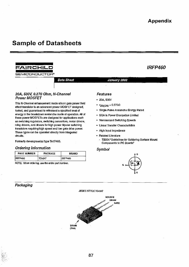
SOURCE DRAIN
GATE
Appendix
Sample of Datasheets
FAIRCHILD
IRFP4GO DNDUCTDR5
20A, 500V, 0.270 Ohm, N-Channel Power MOSFET This N-Channel enhancement mode silicon gate power field effect transistor is an advanced power MOSFET designed, tested, and guaranteed to withstand a specified level of energy in the breakdown avalanche mode of operation. All of these power MOSFETs are designed for applications such as switching regulators, switching convertors, motor drivers, relay drivers, and drivers for high power bipolar switching transistors requiring high speed and low gate drive power. These types can be operated directly from integrated circuits.
Formerly developmental type TA17465.
Ordering Information PART NUMBER PACKAGE BRAND
1RFP460 TO-247 I RFP460
NOTE: When ordering, use the entire part number.
Features • 20A, 500V
• rDS(ON) = 0.270i1
• Single Pulse Avalanche Energy Rated
• SOA is Power Dissipation Limited
• Nanosecond Switching Speeds
• Linear Transfer Characteristics
• High input Impedance
• Related Literature - TB334 "Guidelines for Soldering Surface Mount
Components to PC Boards"
Symbol #D
Packaging JEDEC STYLE TO-247
DRAIN (TAB)
87
C1._111?1'sfr - 10 Arrspe,r-e,.. 17-4."1 - 50 tio, lcola dolts. -Tr.C4-11\11.C..^1_ .01=0,EC'IFIC-..4777*CiiSi, (DV SIP.I.GLI__E-PHASES.:11_1-C-C3"4
C-7, C7C>titrir.PICAZNT,E7,1s1-77,S7 C4CP. Ft. SF3ECaALISTS
1611A-Xletu7llit4 ftia-rtat At isE3 ELECTRICAL CMAIRACTe.12iST7CS *tattoos at 2.5.12, ambient ternorprailtd. a toss oasaraiists spaolfaial_ Sartgle phew., hart wee.. 50 el., restativa srittualluis load For ...aerie.. toad_ dermae corr.". by 20%
Dorsal* ovaerloasel rating: aock aszystaiarois patina. Low Torianoct Yoltrioia dray
MECHANICAL. DATA Caws: ts.itoliaaa sato:4011a
. Epoxy: UL Ditki-O rata fl aroma riataratatit
.1 Latta: 20S gottratrataticl
. Polarity Dyrottols molded or rrietrIcacl on body hitatirstalg jaGialtiors7. Any Wasigtst: 6.121 Dramas
AC
-b2a(13.24 12.21
-62
▪
0 it
-
-i,2) .400 it2.29
-Tnar _tstri
BFI-a/10
05isnensions in berthas end arnallariat era)
SAW 13 et L i3R1005 Bf4121 0wi02 00 104 512105 ER108 BR lo lo untr-s Maximum Recuristat Prat vars. Voltage Loma so ICSO zoo- 400 005 500 r000 Woes Maximum RMS Voile.. Yaw. 35 70 140 200 .25 500 TOO Volts Maraltriern DO Blacking Varney,. Vac. 52- 152 239 400 COS 0000 Volts Meade-WM ...hag* Forward Mactified 001001. Correve al To. 501C la 10 Amps Peak Forward Sorg. Caerart g_3 Ins tingle loaf sine-.wave sepeitianpreedi on rate. load VEDEC Matticia
are. 200 Amps
tassianstim aoatasrd Voltage Drop per silennarn/ at 0. 300 Jr 1,E Vohs Istascanurn DC Revers. Currant at Ralad I gp-r=.= 25,2
an aitrraps CC Bloating VollaOe par starmara 43Yrc a 100.0 500 et Rating for Fesairg (eaft.gosal er 105 ..- .4 ire. Typical J.natica Capricatairicei ( 'Mote; } C4 200 Iss Typle.l lreirearrial staalattaaa tra.t. 2) Rai.* 21 112,10V Cape, 1n9 Terdtariabaas Range- To -55 to ..a 125 Stara.. leartparatiarie Range Terra -55 to 4 100 .0
NOTES 1.141atairal at 1 aaltana applied necesso votatia of 4,0 vats 2. Thertnet Raszstaesce bon I. Arabia,. and from ronction to dead rao.n.lact an P.0.13 .410 0.5 sc 0.5" 113,r13trari) ...pp., pans.
Voltage sensor Circuit
88