OTA (operational transconductance amp.) - Configuration
12
OTA (operational transconductance amp.) [grise, lecture14, AN6077.1, LM13700, (AN6668.2)]
-
Upload
khangminh22 -
Category
Documents
-
view
1 -
download
0
Transcript of OTA (operational transconductance amp.) - Configuration
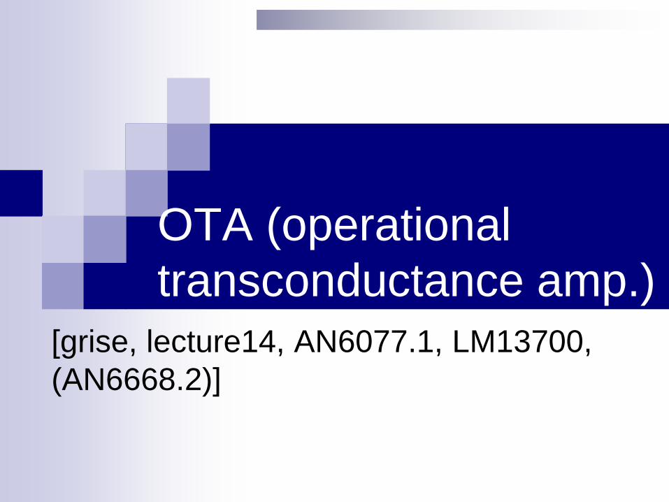
OTA (operational
transconductance amp.)
[grise, lecture14, AN6077.1, LM13700,
(AN6668.2)]
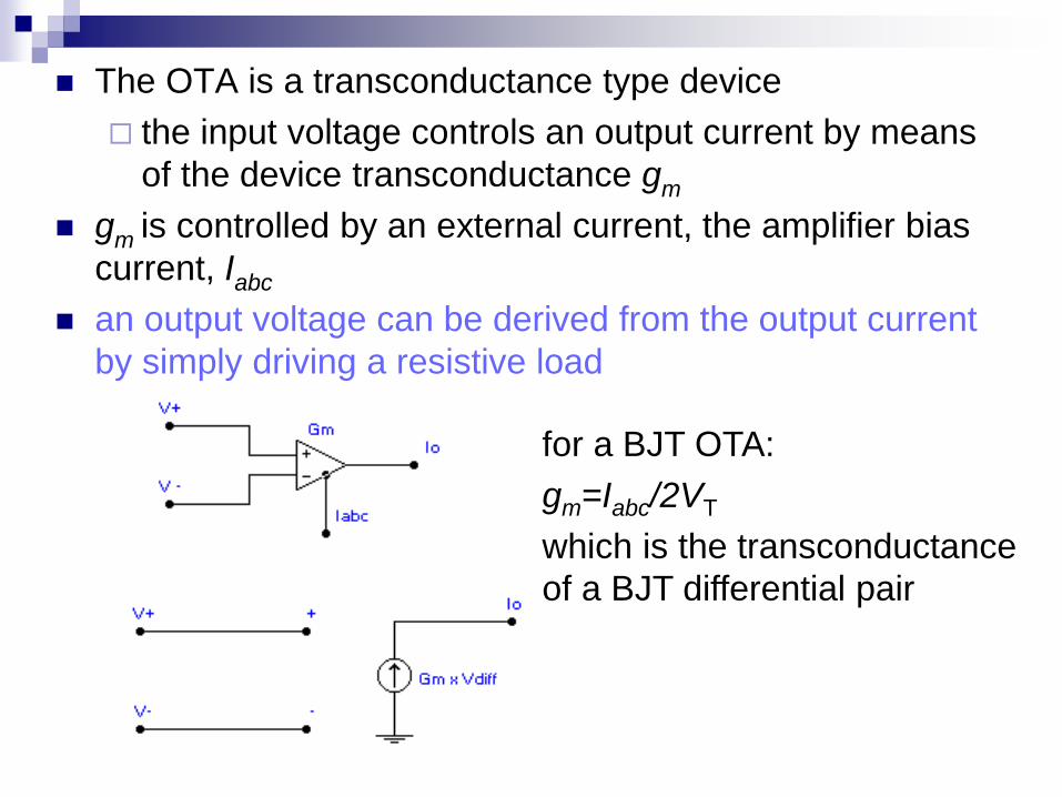
The OTA is a transconductance type device
the input voltage controls an output current by means
of the device transconductance gm
gm is controlled by an external current, the amplifier bias
current, Iabc
an output voltage can be derived from the output current
by simply driving a resistive load
for a BJT OTA:
gm=Iabc/2VT
which is the transconductance
of a BJT differential pair
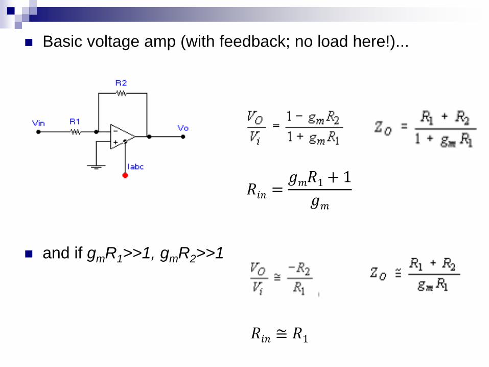
Basic voltage amp (with feedback; no load here!)...
and if gmR1>>1, gmR2>>1
𝑅𝑖𝑛 =𝑔𝑚𝑅1+ 1
𝑔𝑚
𝑅𝑖𝑛 ≅ 𝑅1

An all-OTA amplifier (note: the first OTA is without feedback!)
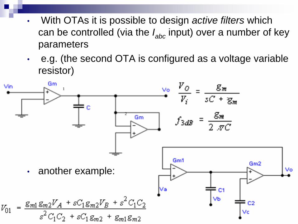
• With OTAs it is possible to design active filters which
can be controlled (via the Iabc input) over a number of key
parameters
• e.g. (the second OTA is configured as a voltage variable
resistor)
• another example:
1 1
2
2 2
V
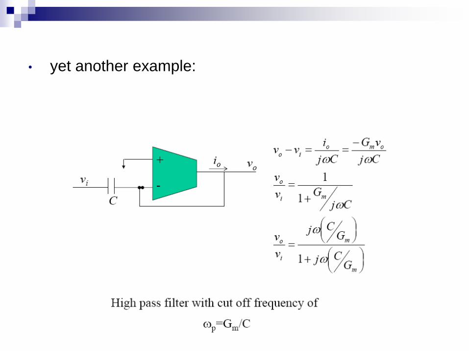
• yet another example:
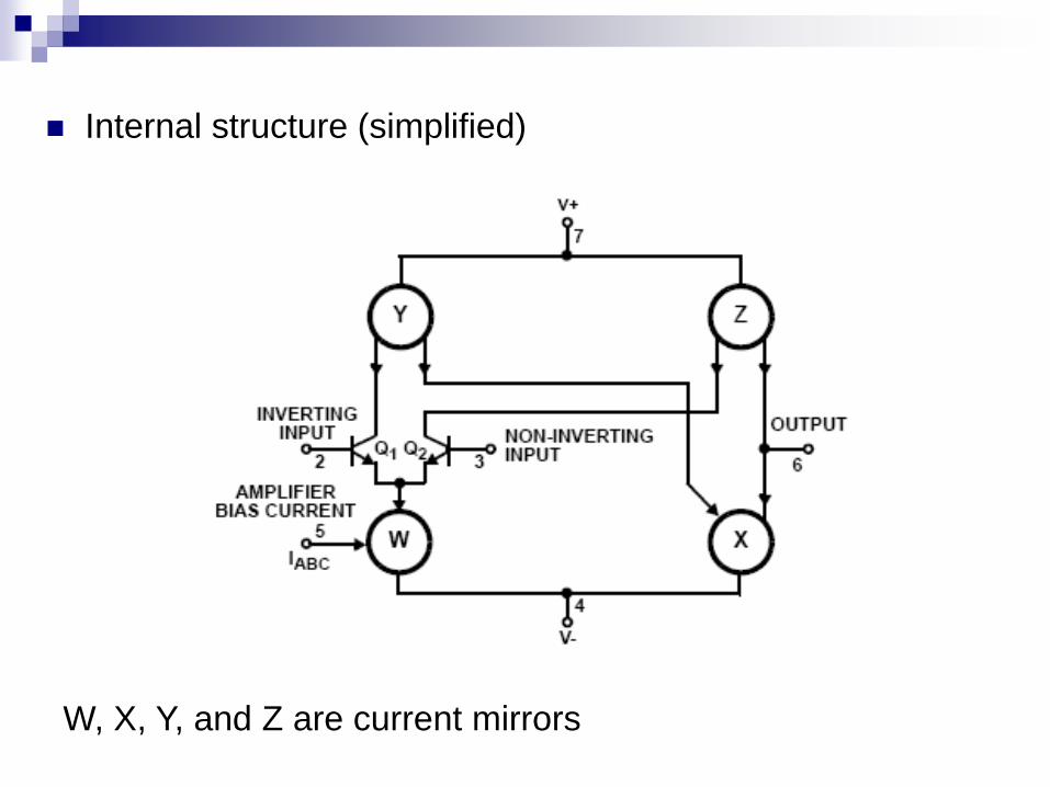
Internal structure (simplified)
W, X, Y, and Z are current mirrors
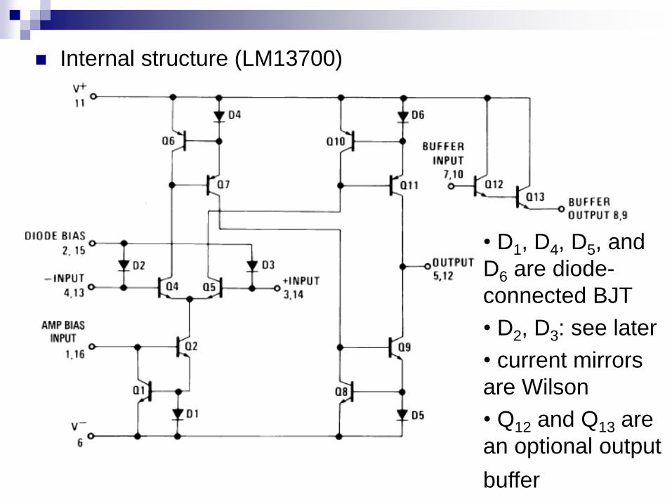
Internal structure (LM13700)
• D1, D4, D5, and
D6 are diode-
connected BJT
• D2, D3: see later
• current mirrors
are Wilson
• Q12 and Q13 are
an optional output
buffer
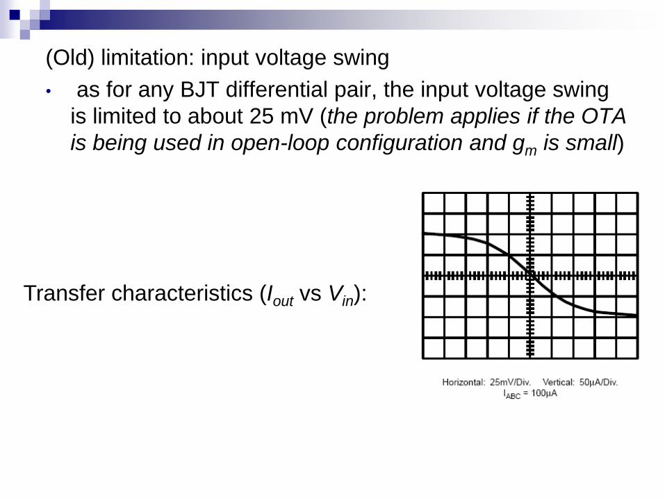
(Old) limitation: input voltage swing
• as for any BJT differential pair, the input voltage swing
is limited to about 25 mV (the problem applies if the OTA
is being used in open-loop configuration and gm is small)
Transfer characteristics (Iout vs Vin):
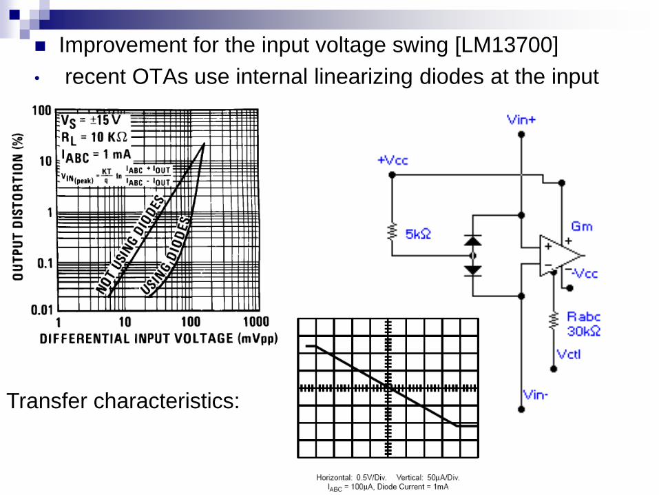
Transfer characteristics:
Improvement for the input voltage swing [LM13700]
• recent OTAs use internal linearizing diodes at the input
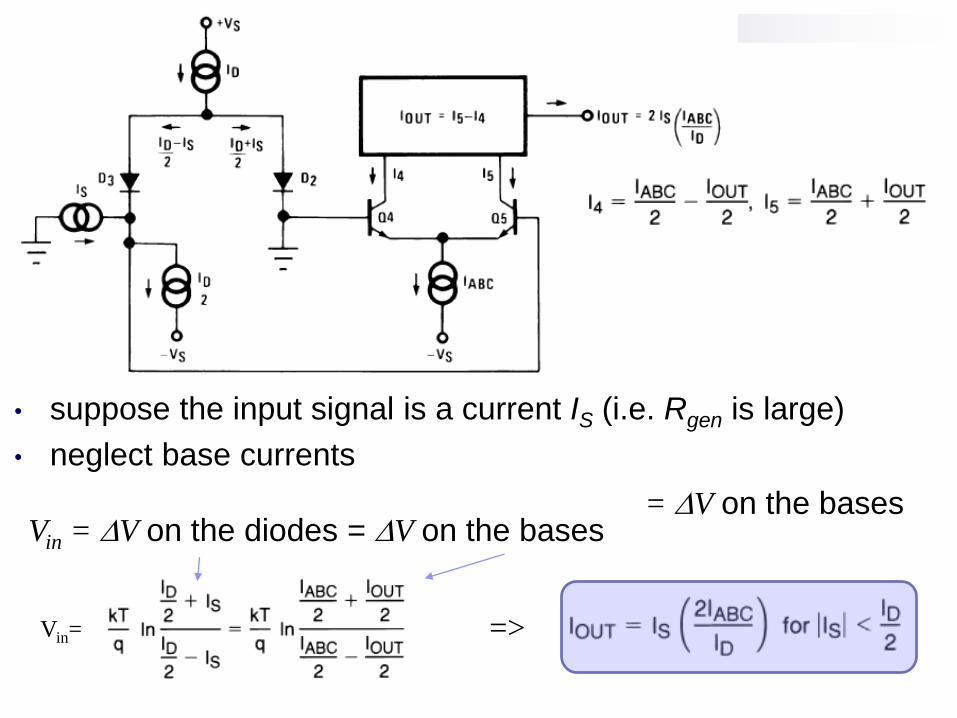
• suppose the input signal is a current IS (i.e. Rgen is large)
• neglect base currents
Vin=
= DV on the basesVin = DV on the diodes = DV on the bases
=>
Non-idealities (besides those of conventional op-amp)
• change in output offset with IABC
• change in output offset with Idiodes
• change in gain with Idiodes
• ...