
On the extraction of interface trap density in the Pt/La2O3/Ge gate stack and the determination of...
9
On the extraction of interface trap density in the Pt/La2O3/Ge gate stack and the determination of the charge neutrality level in Ge D. Bozyigit and C. Rossel Citation: J. Appl. Phys. 105, 124521 (2009); doi: 10.1063/1.3155830 View online: http://dx.doi.org/10.1063/1.3155830 View Table of Contents: http://jap.aip.org/resource/1/JAPIAU/v105/i12 Published by the American Institute of Physics. Related Articles Trapped charge dynamics in InAs nanowires J. Appl. Phys. 113, 024511 (2013) Figure of merit for and identification of sub-60mV/decade devices Appl. Phys. Lett. 102, 013510 (2013) Influence of stress on structural properties of AlGaN/GaN high electron mobility transistor layers grown on 150 mm diameter Si (111) substrate J. Appl. Phys. 113, 023510 (2013) Local potential profiling of operating carbon nanotube transistor using frequency-modulation high-frequency electrostatic force microscopy Appl. Phys. Lett. 102, 013115 (2013) One-shot current conserving quantum transport modeling of phonon scattering in n-type double-gate field-effect- transistors Appl. Phys. Lett. 102, 013508 (2013) Additional information on J. Appl. Phys. Journal Homepage: http://jap.aip.org/ Journal Information: http://jap.aip.org/about/about_the_journal Top downloads: http://jap.aip.org/features/most_downloaded Information for Authors: http://jap.aip.org/authors Downloaded 11 Jan 2013 to 129.132.202.35. Redistribution subject to AIP license or copyright; see http://jap.aip.org/about/rights_and_permissions
Transcript of On the extraction of interface trap density in the Pt/La2O3/Ge gate stack and the determination of...

On the extraction of interface trap density in the Pt/La2O3/Ge gate stackand the determination of the charge neutrality level in GeD. Bozyigit and C. Rossel Citation: J. Appl. Phys. 105, 124521 (2009); doi: 10.1063/1.3155830 View online: http://dx.doi.org/10.1063/1.3155830 View Table of Contents: http://jap.aip.org/resource/1/JAPIAU/v105/i12 Published by the American Institute of Physics. Related ArticlesTrapped charge dynamics in InAs nanowires J. Appl. Phys. 113, 024511 (2013) Figure of merit for and identification of sub-60mV/decade devices Appl. Phys. Lett. 102, 013510 (2013) Influence of stress on structural properties of AlGaN/GaN high electron mobility transistor layers grown on 150mm diameter Si (111) substrate J. Appl. Phys. 113, 023510 (2013) Local potential profiling of operating carbon nanotube transistor using frequency-modulation high-frequencyelectrostatic force microscopy Appl. Phys. Lett. 102, 013115 (2013) One-shot current conserving quantum transport modeling of phonon scattering in n-type double-gate field-effect-transistors Appl. Phys. Lett. 102, 013508 (2013) Additional information on J. Appl. Phys.Journal Homepage: http://jap.aip.org/ Journal Information: http://jap.aip.org/about/about_the_journal Top downloads: http://jap.aip.org/features/most_downloaded Information for Authors: http://jap.aip.org/authors
Downloaded 11 Jan 2013 to 129.132.202.35. Redistribution subject to AIP license or copyright; see http://jap.aip.org/about/rights_and_permissions

On the extraction of interface trap density in the Pt/La2O3/Ge gate stackand the determination of the charge neutrality level in Ge
D. Bozyigit and C. Rossela�
IBM Zurich Research GmbH, Zurich Research Laboratory, Säumerstrasse 4, 8803 Rüschlikon, Switzerland
�Received 26 March 2009; accepted 14 May 2009; published online 26 June 2009�
The study of trap densities at the oxide-semiconductor interface of the new generation of field-effecttransistors is essential for the optimization of their electrical performance. The conventionalconductance method, which was efficiently applied to Si, turns out to be less appropriate onalternative substrates, such as the lower band gap germanium �Ge�, because of the strong influenceof minority carrier processes. Recent investigations show that these restrictions might be severe andlead to incorrect conclusions. We identify here the appearance of such processes, compare theconventional conductance method with the full conductance method of Martens et al., IEEEElectron Device Lett. 27, 405 �2006�, and propose an extension of the latter. By applying a reversebias to source and drain with respect to the substrate, it becomes possible to separate, on the samedevice, the contribution of electron and hole trap distributions. Our approach allows us to determinethe position of the charge neutrality level at the surface of the semiconductor, which is found to beat 0.14 eV above the valence band. © 2009 American Institute of Physics.�DOI: 10.1063/1.3155830�
I. INTRODUCTION
Germanium-based metal-oxide-semiconductor field-effect transistors �MOSFETs� with high-k dielectrics are con-sidered promising candidates for future technology nodes.Indeed a variety of high-mobility p-channel Ge MOSFETshave been demonstrated using various oxides �HfO2, ZrO2,and Al2O3� as gate dielectrics1–3 and various ultrathin passi-vating interlayers �ILs� such as GeO2,4 GeONx,
5 or Si.6,7
Rare-earth oxide layers, for example, CeO2, Gd2O3,8,9 and inparticular La2O3 /LaGeOx,
10–12 have also been proposed. De-spite this progress, several issues remain unresolved, such asthe positive threshold shift in p-MOSFETs and the poor per-formance of n-MOSFETs, which still suffer from low chan-nel mobility and low on-state and large off-state currents.Thus a proper passivation of Ge remains a critical challengein achieving high-quality interfaces with low defect densitiesand good electrical properties.
A commonly adopted method for extracting the interfacetrap density �Dit� on MOS capacitors and optimizing thevarious passivation schemes is the conductance method asfully described by Nicollian and Brews.13 A demonstration ofthe interface quality in high-mobility semiconductors, suchas Ge or III-V materials, requires the reliable extraction ofDit�E� within the band gap. It was shown by Martens andco-workers14,15 and Batude et al.16 that a straight applicationof the conventional conductance method—only valid indepletion and weak inversion—on alternative substrates canlead to incorrect conclusions. Indeed these authors pointedout several pitfalls that can jeopardize the interpretation ofthe capacitance-voltage �C-V� and conductance-voltage�G-V� characteristics. These are caused by minority carrier
processes, which cannot be neglected in the case of Ge-baseddevices.
This problem was addressed by modeling measured C-Vand G-V characteristics16 and/or by experimentally control-ling the effects of the minority carriers.15 This can beachieved by the full conductance method proposed by Mar-tens et al.15 in the case of FETs, where source �S� and drain�D� are shorted to the substrate. Another advantage of thismethod is that Dit�E� can be measured across the entire bandgap with a single experimental configuration on a single n-or p-channel device.
In this work, we apply the conventional and the fullconductance methods and propose a new extension of thelatter, i.e., setting a reverse bias Vr between S/D and the bulk�Fig. 1�d��, to the specific case of La2O3–Ge ring FETs. Thecomparison of the respective data allows us to discriminateand identify the effects of minority carriers on the measure-ments and to understand the conditions necessary for a cor-rect extraction of the interface trap density Dit.
a�Author to whom correspondence should be addressed. Electronic mail:[email protected].
FIG. 1. �a� Equivalent circuit for a single interface trap proposed by Nicol-lian and Brews �Ref. 13�. �b� Simplified equivalent circuit valid for thedepletion and full conductance modes. �c� Proposed equivalent circuit forthe reverse bias method. �d� Connection scheme of the FET for reverse biasapplication.
JOURNAL OF APPLIED PHYSICS 105, 124521 �2009�
0021-8979/2009/105�12�/124521/8/$25.00 © 2009 American Institute of Physics105, 124521-1
Downloaded 11 Jan 2013 to 129.132.202.35. Redistribution subject to AIP license or copyright; see http://jap.aip.org/about/rights_and_permissions

By determining the hole and electron trap distributions,we show that access to the charge neutrality level �CNL� ofGe becomes possible with our approach. It was recently re-ported that the location of the CNL slightly above the va-lence band �VB� of Ge ��0.1 eV� is important for under-standing the asymmetry between n- and p-channel FETbehaviors.17,18 Indeed, when the Fermi level is forced abovethe CNL, the filling of acceptorlike states results in the gen-eration of a negative fixed charge at the Ge surface. This can,in principle, explain the positive threshold voltage shift inp-FETs and the difficulty in inverting the channel of n-FETs.
II. DEVICES
As a model case, we investigated p-channel ring FETswith the gate stack Pt /La2O3 /LaGeO on n-Ge�100�. A layerof 9 nm La2O3 was grown by molecular beam deposition ina molecular beam epitaxy �MBE� cluster. During growth, theLa2O3 layer transforms partially into La-germanate�LaGeOx� as verified by x-ray photoelectron spectroscopy19
and transmission electron microscopy.10,11 More details canbe found in Ref. 12. The ring structure was made by a self-aligned, gate-first process, with the gate length varying be-tween 20 and 160 �m. The gate metal deposited by electronbeam was 20 nm of Pt. In the earlier study, we reported adecrease in the average interface trap density Dit from themid-1012 to �2–4��1011 eV−1 cm−2 upon postannealing informing gas at 450 °C. Interestingly these devices exhibit anegative threshold voltage of VT�−1 V, resulting possiblyfrom a partial passivation of the negatively charged Ge dan-gling bonds by the LaGeOx IL.12
III. METHODOLOGY
Our goal is to compare variations in the conductancemethod used to extract Dit in MOS capacitors.13 Althoughthe original method proved to be very successful on Si de-vices in the past, its use for devices fabricated on high-mobility semiconductors, such Ge or the III-V GaAs or In-GaAs materials, must be done with care to avoidmisinterpretations and, in particular, an under- or overesti-mate of Dit.
The first alternative approach is the full conductancemethod15 on FETs, where source �S� and drain �D� are con-nected to the bulk �B� �Fig. 1�d��. We generalize this methodby introducing a reverse bias Vr between these contacts. Thefull conductance method thus reduces to the special casewhere Vr=0 V. For simplicity, we consider here only thecase of a p-MOSFET grown on n-Ge. Therefore electrons�holes� are referred to as majority �minority� carriers.
A. Conductance method
The original method13 allows a reliable extraction of Dit
from the admittance Y =Gm+ i�Cm measured as a function offrequency, f =� /2� �typically from 100 Hz to 1 MHz� es-sentially in depletion, where only the fast response of major-ity carriers comes into play. This measurement is performedwith an autobalancing LCR bridge �Agilent 4284A�, apply-ing an ac voltage that is sufficiently small ��50 mV� to
assume that the steady state of the system is not changed.Parasitic effects, in particular, the series resistance Rs, can becorrected for by well-known procedures.
For the admittance measurement with real and imaginarycomponents in parallel, the equivalent circuit in Fig. 1�a� iscommonly proposed for a single-level interface trap. Storedcharges are taken into account by the respective capacitancesof the oxide layer �Cox�, depletion layer �CD�, inversion layer�CI�, and interface traps �CT�. Charge carrier processes aremodeled by Gn �electron capture/emission�, Gp �holecapture/emission�, and Gd �inversion generation, such as mi-nority carrier diffusion from the bulk�. These processes leadto dissipation, which is measured in the conductance Gm.
Under depletion condition, where minority carrier pro-cesses are neglected, the equivalent circuit �Fig. 1�a�� is re-duced to the simplified circuit �Fig. 1�b�� with
Geff = Gn and Ceff = CD. �1a�
With this simplified circuit, a theory was developed to ex-tract the trap density correctly from the admittance data.13 Inthe simplest case, the quantity
�Gp��
=Dit
2��nln�1 + ���n�2� �
�Cox2 Gm
Gm2 + �2�Cox − Cm�2 �1b�
can be derived to link Dit to the measured capacitance Cm
and conductance Gm. Normally �Gp� /� features a character-istic peak at some frequency �peak, which is due to the inter-face traps. For a uniform trap distribution and neglectingsurface potential fluctuations, Dit and the trap relaxation time�n defined at the peak are given by
Dit =2.5
q �Gp�
�
max, �1c�
�n =1.98
�peak, �1d�
where q is the elementary charge. Since the equivalent cir-cuits in Fig. 1 do not include any conductance in parallel toCox, it is important to check during the measurement that thegate leakage current remains negligible.
Besides the density, the time constant � of interface trapscan provide valuable insight. It is normally assumed thattrapping processes are thermally activated. Thus for electron��n� and hole ��e� traps, one can write13
�n � e�ECB−EF�/kT and �p � e�EF−EVB�/kT, �1e�
where EF is the Fermi level, and ECB and EVB are the con-duction band �CB� and VB edges, respectively. Qualitativelyone can say that electron �hole� traps become faster whentheir position is closer to the conduction �valence� band.Through their respective time dependence, the two types oftraps can be differentiated.
B. Shortcomings of the conductance method
The restriction to the depletion case in the originalmethod is severe and is related to the difficulty of modeling/controlling minority carriers at the dielectric-semiconductorinterface of a MOS capacitor or MOSFET with floating
124521-2 D. Bozyigit and C. Rossel J. Appl. Phys. 105, 124521 �2009�
Downloaded 11 Jan 2013 to 129.132.202.35. Redistribution subject to AIP license or copyright; see http://jap.aip.org/about/rights_and_permissions

source and drain �called “open mode” below�. Neverthelessin Si, where the intrinsic carrier density is low �ni=1.45�1010 cm−3�, neglecting minority carriers is a reasonableand valid approximation. However, one drawback is thatboth n- and p-type devices are needed to measure the trapdensities through the entire band gap.
In Ge, where the intrinsic carrier density is substantiallyhigher �ni=2.4�1013 cm−3�, this approximation generallyfails, as evidenced by the appearance of the weak inversionresponse �typical bump in C-V curves� and the strong inver-sion response.9
The weak inversion response at the measurement fre-quencies is caused by the interaction of minority and major-ity carriers through interface traps, represented in the equiva-lent circuit by Gn and Gp, respectively,. On the other hand,the strong inversion response is due to the different mecha-nisms getting minority carriers to or from the inversion layer,i.e., by generation-recombination in the depletion layer or bydiffusion from the back contact through the bulk. These ef-fects, which are temperature dependent, are represented inthe circuit by the conductance Gd �Fig. 1�a��.
Both weak and strong inversion responses are ultimatelydue to the fact that the minority carrier density is uncon-trolled and responds to the measurement stimulus. To under-stand this fact from the circuit �Fig. 1�a��, we introduce thequasi-Fermi level for minority carriers �holes� in the channelEFp as a quantity for the minority carrier density �and,equivalently, EFn for electrons�. The circuit shows that EFp isnot controlled by the experiment, thus allowing weak andstrong inversion responses through Gp and Gd. This can leadto a second peak, which is often observed in the G /� versus� curves measured on Ge devices. This second peak mightbe falsely attributed to interface traps and thus lead to asignificant under-/overestimation of the Dit.
C. Full conductance method
A solution to these shortcomings is proposed in the fullconductance method15 by shorting both source and drain of aFET to the bulk. It is argued that this external control ofminority carriers in the channel eliminates the strong inver-sion response and includes the weak inversion response inthe model by combining minority and majority carrier ef-fects.
In the equivalent circuit �Fig. 1�a��, this corresponds to ashort of Gd and shunt of Gn and Gp so that EFp=EFn. Thisallows a reduction in the circuit shown in Fig. 1�b�, now with
Geff = Gn + Gp and Ceff = CD + CI. �2�
Since the equivalent circuit is the same as in the originalcase, the same analysis applies. The only difference is thatboth majority and minority carrier trapping are taken intoaccount indistinguishably because Gp and Gn are shunted. Inaddition, the entire band gap is accessible to measurementbecause the depletion condition becomes unnecessary.
D. Reverse bias method
Following these lines, we propose to apply a reverse biasvoltage Vr between source/drain and bulk. For Vr=0 V, this
coincides with the full conductance method. However at fi-nite Vr, minority and majority carrier concentrations can becontrolled independently. Thus the contributions to interfacetrapping of each carrier type can be determined.
The circuit shown in Fig. 1�c� models the reverse biasmethod, where Ur is the potential difference between thequasi-Fermi levels EFn �electrons� and EFp �holes� at the in-terface, so that
EFp = EFn + qUr. �3�
This is a valid assumption because source and drain are alarge reservoir of minority carriers. By providing or absorb-ing charges in the channel, an effective control over the mi-nority carrier quasi-Fermi level can be achieved
The potential difference Ur is a nontrivial function of Vr
and Vg and might be spatially decaying toward the channelcenter. For our measurements we shall present an approxi-mation of the quasi-Fermi levels during the discussion of theresults. In all cases, we assume a reverse bias and thereforealways EFp�EFn.
In order to apply the same analysis as in the two previ-ous methods, circuit �c� of Fig. 1 must be reduced to circuit�b�. To do so, we need to evaluate the different cases pos-sible, which depend on the surface potential and the reversebias.
The two following conditions at the interface help ussimplify the circuit:
�a� EFnEi→no mobile electrons→electron trappingcontribution negligible→Gn=0.
�b� EFp�Ei→no mobile holes→hole trapping contribu-tion negligible→Gp=0.
Here Ei is the intrinsic energy level. Together with the re-striction EFp�EFn, three combinations of conditions �a� and�b� are possible. The circuit can be simplified by finding Geff
and Ceff for the three different regions:
�I� Strong inversion: EFnEFpEi→Geff=Gp and Ceff
=Ci.�II� Deep depletion: EFnEiEFp→Geff=0 and Ceff
=Cd.�III� Depletion/midgap: EiEFnEFp→Geff=Gn and
Ceff=Cd.
The corresponding band schemes along the channel areshown in Fig. 2.
Regions I–III can be observed in a conductance mea-surement by sweeping the gate voltage from strong inversiontoward accumulation. First a contribution from hole trappingis measured, followed by a region with no conductance be-cause of the absence of mobile carriers at the interface, andfinally a contribution from electron trapping.
It is worth mentioning that the control of the minoritycarrier density in the full conductance and the reverse biascase has some limitations in very-long-channel devices. Theapplication of a reverse bias Vr establishes a steady statecondition in the channel—like in any reverse-biasedpn-junction—so that carrier concentrations and energy levels�EFn�EFp� are different from equilibrium. Though, far away
124521-3 D. Bozyigit and C. Rossel J. Appl. Phys. 105, 124521 �2009�
Downloaded 11 Jan 2013 to 129.132.202.35. Redistribution subject to AIP license or copyright; see http://jap.aip.org/about/rights_and_permissions

from the junction, the system might relax to an equilibriumstate through generation/recombination processes. Therefore,if the channel is longer than a typical excess-minority carrierrelaxation length, control of the desired nonequilibrium statecan be ineffective in its center.
IV. RESULTS
A first comparison of the different measurement methodscan be made by looking at their impact on the capacitance-voltage �C-V� �Fig. 3� and the conductance-voltage �G-V�characteristics �Fig. 4� of a La2O3 /LaGeO /Ge p-ring FET,as-deposited with a channel length of 20 �m. The data weremainly taken between 1 kHz and 1 MHz at room temperatureand in some cases between 230 and 350 K.
A. C-V characteristics and hysteresis
The C-V curve measured at 100 kHz in open mode, i.e.,with floating S and D �solid line in Fig. 3� is typical of Gestacks, with a partial inversion �Vg−0.5 V� and ratherlarge hysteresis �V�320 mV�. By now shorting S and D
and applying a reverse bias with respect to the back contact,the C-V curve does not change in accumulation, whereas theonset of the inversion shifts linearly with increasing Vr—awell-known threshold voltage shift Vth�Vr� for FETs underreverse bias.20 Furthermore the inversion is complete for allapplied Vr, which is the signature of the low-frequency �LF�behavior. This is in contrast to the high-frequency �HF� be-havior, where the minority carrier response is too slow tocreate an inversion layer in conventional C-V measurements.This indicates that the minority carrier response time is dras-tically reduced by their supply from source and drain, asexpected.
Another observation is the reduction in the hysteresiswith the reverse bias �inset in Fig. 3�. Starting at a value of320 mV in open mode or with Vr�0 V, the hysteresis de-creases linearly down to 160 mV at Vr=−1.0 V. A simpleexplanation might be the fact that the gate voltage sweep islimited to �2 V, thus preventing capacitance to reach fullsaturation at lower Vr.
B. G-V characteristics
The corresponding conductance data, G-V, taken at 100kHz are displayed in Fig. 4. The curve measured in openmode shows peak A in the depletion region �Vg�−0.5 V�and rises to a constant value in the strong inversion region.Under reverse bias condition, G-V does not change signifi-cantly in accumulation, whereas a sharp peak B appears inweak and strong inversion. Peak A hardly moves, and peak Bshifts linearly with the reverse bias according to
Vg,peak B � − 0.5 V + Vr with = 1.18. �4�
The origin of both peaks can be identified by looking at theVr=−0.6 V curve and considering the three gate voltage re-gions: I, II and III. In strong inversion �I, Vg−0.9 V�, weassume that only minority carriers are involved in the trap-ping process at the interface leading to the conductance peakB. In deep depletion �II, −0.9 VVg−0.3 V�, no mobilecarriers are available at the interface and therefore no con-
FIG. 2. �Color online� Schematic band diagrams in the channel for threeranges of the reverse bias Vr: �I� strong inversion, �II� deep depletion, and�III� depletion/midgap. In these schematics only the position of the band gapin the channel is shifted.
FIG. 3. �Color online� C-V characteristics �up and down Vg sweep� mea-sured at 100 kHz and 300 K on a La2O3–Ge ring FET with no postannealing�as-deposited stack�, in open mode, and for various reverse bias voltages Vr
applied between source/drain and bulk. The inset shows the linear decreasein the C-V hysteresis V as a function of Vr.
FIG. 4. �Color online� G-V characteristics measured at 100 kHz and 300 Kon the same La2O3–Ge ring FET as in Fig. 3 in open mode and for variousreverse biases Vr. Peak A appears at nearly the same gate voltage for allcases. Peak B, which appears only upon application of the reverse bias�including 0 V�, shifts its position in Vg linearly with Vr.
124521-4 D. Bozyigit and C. Rossel J. Appl. Phys. 105, 124521 �2009�
Downloaded 11 Jan 2013 to 129.132.202.35. Redistribution subject to AIP license or copyright; see http://jap.aip.org/about/rights_and_permissions

ductance is measured. In depletion toward midgap �III,−0.4 VVg�, majority carrier trapping becomes predomi-nant, causing peak A.
From the positions of the two peaks, information on thequasi-Fermi levels in the channel can be obtained. Peak A,which is controlled by EFn, barely shifts with Vr, indicatingthat EFn is only a function of Vg. In contrast, peak B stronglydepends on Vr. An approximation for both Fermi levels isderived below.
The important result here is that we are able to measureand distinguish the two types of carrier trapping by applica-tion of a reverse bias. Moreover, the large conductance con-tribution due to the weak and the strong inversion responsecan be avoided.
C. Comparison of Gp /� characteristics
Three sets of Gp��� /� data at various Vg are comparedusing either the conventional method �Fig. 5�a��, full conduc-tance Vr=0 V �Fig. 5�b��, or the finite reverse bias at Vr=−0.6 V �Figs. 5�c� and 5�d��. In the first case �Fig. 5�a��, twopeaks appear: one at LF ��1 kHz�, with increasing ampli-tude and frequency as Vg becomes more negative �i.e., EF
shift toward the valence band�, and a second one at higherfrequency ��30 kHz� with decreasing amplitude and in-creasing frequency as Vg becomes more positive �shift to-ward the CB�. In the depletion region �Vg�0 V�, both peaksare present simultaneously, making a simple interpretation interms of Dit difficult.
To explain the origin of the LF peak, we note the fol-lowing: the peak frequency �103–104 Hz� is much lowerthan expected for hole traps located very close to the valenceband. Second, it disappears in all measurements with reverse
bias. Therefore this peak is attributed to weak/strong inver-sion response, and its position in frequency relates to theminority carrier interface trap time constant.
The HF peak, however, is also found in measurementsunder reverse bias �Figs. 5�b� and 5�d�� for Vg between 0 and�0.30 V and is not influenced by the Vr value. This is whatis expected for electron trapping and is also supported by theincreasing frequency toward the CB �Vg→0.4 V�.
What is different if a reverse bias is applied? The LFpeak disappears �Fig. 5�b�� and a new HF peak appears for−0.28 V�Vg�−0.60 V related to carrier exchange be-tween the traps and the VB �hole trapping�. It moves tohigher frequency as the VB is approached and merges withthe electron-trapping peak at Vg�−0.28 V.
At Vr=−0.6 V, both peaks are still present. For clarity,the data have been splitted in two plots �Figs. 5�c� and 5�d��.In Fig. 5�c�, the hole-trapping peak is clearly evident downto smaller gate voltages Vg−0.80 V, shifting to higher fre-quency. In Fig. 5�d�, the electron-trapping peak appears forVg�−0.2 V as before. However, also another peak showsup at lower Vg with fixed frequency and decreasing ampli-tude. It is attributed to charge-carrier generation in the bulk,as will be discussed later.
To quantify the effect of the reverse bias, let us considerthe hole-trapping peaks located at the same frequency of 30kHz in both Fig. 5�b� �Vr=0 V and Vg=−0.28 V� and Fig.5�c� �Vr=−0.6 V and Vg=−1.0 V�. We find that Vg=−0.72 V�1.18Vr, which is the same relation as Eq. �4�.This indicates that by tuning the reverse bias Vr, the sameposition in the band gap can be seen for different Vg. Thiswill be considered in the determination of the EFp�Vg ,Vr�relationship. We conclude from these data that in bothreverse-biased cases �0 and �0.6 V� the behavior in Gp /� isequivalent �modulo the Vg shift�.
V. DISCUSSION
A. Interface charge-trapping distributions
To better understand the role of the reverse bias, let usconsider Fig. 6, where the interface trap densities Dit and traptime constant � versus the gate voltage Vg are plotted for
FIG. 5. Four sets of Gp /� vs � curves at 300 K: �a� in open mode, �b� withVr=0 V, and ��c� and �d�� Vr=−0.6 V. Vertical scales are adapted by mul-tiplying Gp /� by 2.5 /q to give an intuitive understanding of the correspond-ing Dit �cf. Eq. �1c��.
FIG. 6. �Color online� Interface trap density Dit�Vg� and trap time constant��Vg� extracted by the reverse bias method at Vr=0 V �dashed line� andVr=−0.6 V �solid line� at 300 K. The inset shows the Arrhenius plot � vs1 /kT used to extract the thermal activation energy in deep depletion �regionII�.
124521-5 D. Bozyigit and C. Rossel J. Appl. Phys. 105, 124521 �2009�
Downloaded 11 Jan 2013 to 129.132.202.35. Redistribution subject to AIP license or copyright; see http://jap.aip.org/about/rights_and_permissions

Vr=0 V �dashed line� and Vr=−0.6 V �solid line�, respec-tively. As introduced above, three regions, I–III, can be dis-tinguished for Vr=−0.6 V according to the specific behaviorof ��Vg� occurring from left to right.
In the leftmost region I �Vg−0.8 V�, the time constantincreases by almost two orders of magnitude with increasinggate voltage. This behavior indicates that here hole trappingis measured. The distribution of these traps will be denotedby Dit
+�Vg� or Dit+�EFp�.
Region II is deep depletion �−0.80 VVg−0.20 V�with low Dit�1�1011 eV−1 cm−2 and a constant relaxationtime of �0�1.4�10−5 s. In this region, no mobile chargecarriers and thus no interface charge-trapping effect are as-sumed. The residual peaks in the conductance measurementsare therefore due to dissipation effects in the bulk. In theabsence of mobile carriers in the depletion layer, thermallyactivated charge generation at the so-called crossover pointis expected to predominate.13 This can be verified by extract-ing the corresponding activation energy E0 from the Arrhen-ius plot ��1 /kT� in the inset of Fig. 6. The value of E0
=0.332 eV is exactly Eg /2, in excellent agreement withwhat is expected for the generation process in bulk traps.9,13
In region III �Vg�−0.2 V�, ��Vg� decreases again, anindication for the electron-trapping process. The correspond-ing trap density, denoted by Dit
−�EF�, agrees nicely with thevalue Dit�1.5�1012 eV−1 cm−2 measured via the full con-ductance at Vr=0 V.
To map the measured Dit�Vg� correctly to the band gapas Dit�E�, we have to consider that in the reverse-biased case,the hole and electron quasi-Fermi levels do not coincide. InFig. 7 the dependence of the quasi-Fermi levels EFn and EFp
is plotted as a function of the gate voltage Vg. EFn is equiva-lent to the surface potential �s, which is extracted by fittingthe C-V data with a program including quantum effectcorrection.21 EFp is approximated by the same curve shiftedin gate voltage by Vg=1.18Vr=1.18�0.6 V=0.71 V.
At fixed Vg, the contributions of the respective trap den-sities �Dit
+ ,Dit−� at different positions in the band gap—a
priori indistinguishable—contribute to the total Dit, so that
Dit�Vg� = Dit+�EFp�Vg,Vr�� + Dit
−�EFn�Vg�� . �5�
This can be simplified by realizing that in region I �regionIII� only Dit
+ �D� it−� contributes
Dit�Vg� = �Dit+�EFp� region I
0 region II
Dit−�EFn� region III.
�6�
To find the distribution Dit− within the band gap, the function
EFn�Vg� needs to be determined. As the bulk is a large reser-voir of majority carriers, we assume that EFn is not influ-enced by Vr, as evident from the almost fixed position ofpeak A in Fig. 4. Thus EFn has to be equal to the surfacepotential in the channel �s�Vg� �Fig. 7�, so that
EFn = q�s�Vg� ,
Dit−�EFn� = Dit
−�q�s�Vg�� . �7�
In the case of the hole trap distribution Dit+�EFp�, EFp de-
pends nontrivially on Vg and Vr. Using Eq. �4�, which de-scribes the linear shift of peak B versus Vr, one can writeEFp= f�Vg− Vr�.
For the case Vr=Ur=0 V, using Eq. �3�, we know thatEFp coincides with EFn, so that the following approximationcan be made:
EFp = q�s�Vg − Vr� ,
Dit+�EFp� = Dit
+�q�s�Vg − Vr�� . �8�
Here long channel effects are neglected and both quasi-Fermilevels are supposed to be constant over the entire channelarea. The value of coefficient is not universal as it mightdepend on several device parameters such as channel geom-etry, quality of the p-n junction at S and D, and substratedoping,
Both distributions Dit+�EFp� and Dit
−�EFn�, which werederived from the data at Vr=−0.6 V using Eqs. �7� and �8�,are plotted in Fig. 8, together with the respective time con-stants. One can clearly see that the sum of both Dit distribu-tions �dashed-dotted line� agrees nicely with the distributionobtained by the full conductance method �Vr=0 V� �dashedline�. Considering the differences in both methods and thetheoretical approximations that were made, this is a verysatisfactory validity proof.
The hole trap distribution close to the VB exhibits anexponential dependence as seen from the straight line inlog�Dit
+� versus �EFp−EVB�, indicating that the carrier ex-change from the VB to the traps is thermally activated. Wefind, in good approximation,
Dit+�E� = 9.4 � 1013e−�E−EVB�/kT �eV−1 cm−2� . �9�
In depletion and midgap, Dit− yields a constant value of
�1.5�1012 eV−1 cm−2. The upper half of the band gap wasnot investigated in more detail because lower temperaturesclose to 80 K would have been needed. In fact the VB half ismore relevant to p-channel device performance.
FIG. 7. �Color online� Calculated dependence of the quasi-Fermi levels�electrons� and EFp �holes� on the gate voltage Vg. EFn is equivalent to thesurface potential �s extracted from the fit of the experimental C-V curve inaccumulation at 300 K. EFp is approximated by the same curve shifted ingate voltage by 1.18�0.6 V=0.71 V.
124521-6 D. Bozyigit and C. Rossel J. Appl. Phys. 105, 124521 �2009�
Downloaded 11 Jan 2013 to 129.132.202.35. Redistribution subject to AIP license or copyright; see http://jap.aip.org/about/rights_and_permissions
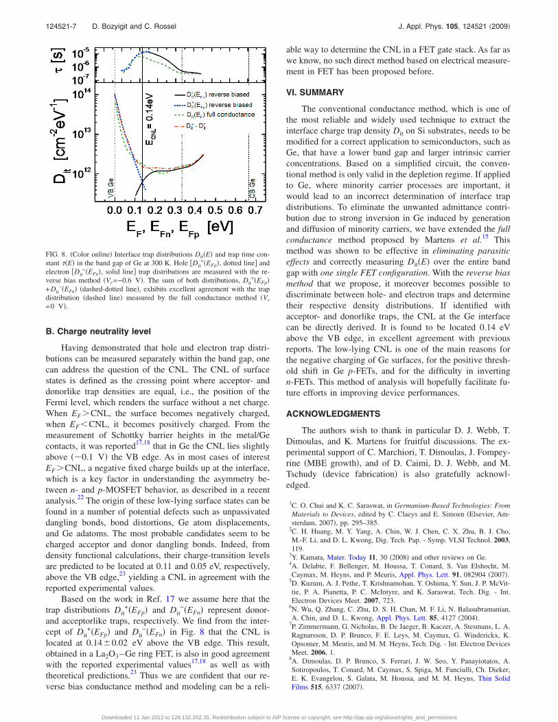
B. Charge neutrality level
Having demonstrated that hole and electron trap distri-butions can be measured separately within the band gap, onecan address the question of the CNL. The CNL of surfacestates is defined as the crossing point where acceptor- anddonorlike trap densities are equal, i.e., the position of theFermi level, which renders the surface without a net charge.When EF�CNL, the surface becomes negatively charged,when EFCNL, it becomes positively charged. From themeasurement of Schottky barrier heights in the metal/Gecontacts, it was reported17,18 that in Ge the CNL lies slightlyabove ��0.1 V� the VB edge. As in most cases of interestEF�CNL, a negative fixed charge builds up at the interface,which is a key factor in understanding the asymmetry be-tween n- and p-MOSFET behavior, as described in a recentanalysis.22 The origin of these low-lying surface states can befound in a number of potential defects such as unpassivateddangling bonds, bond distortions, Ge atom displacements,and Ge adatoms. The most probable candidates seem to becharged acceptor and donor dangling bonds. Indeed, fromdensity functional calculations, their charge-transition levelsare predicted to be located at 0.11 and 0.05 eV, respectively,above the VB edge,23 yielding a CNL in agreement with thereported experimental values.
Based on the work in Ref. 17 we assume here that thetrap distributions Dit
+�EFp� and Dit−�EFn� represent donor-
and acceptorlike traps, respectively. We find from the inter-cept of Dit
+�EFp� and Dit−�EFn� in Fig. 8 that the CNL is
located at 0.14�0.02 eV above the VB edge. This result,obtained in a La2O3–Ge ring FET, is also in good agreementwith the reported experimental values17,18 as well as withtheoretical predictions.23 Thus we are confident that our re-verse bias conductance method and modeling can be a reli-
able way to determine the CNL in a FET gate stack. As far aswe know, no such direct method based on electrical measure-ment in FET has been proposed before.
VI. SUMMARY
The conventional conductance method, which is one ofthe most reliable and widely used technique to extract theinterface charge trap density Dit on Si substrates, needs to bemodified for a correct application to semiconductors, such asGe, that have a lower band gap and larger intrinsic carrierconcentrations. Based on a simplified circuit, the conven-tional method is only valid in the depletion regime. If appliedto Ge, where minority carrier processes are important, itwould lead to an incorrect determination of interface trapdistributions. To eliminate the unwanted admittance contri-bution due to strong inversion in Ge induced by generationand diffusion of minority carriers, we have extended the fullconductance method proposed by Martens et al.15 Thismethod was shown to be effective in eliminating parasiticeffects and correctly measuring Dit�E� over the entire bandgap with one single FET configuration. With the reverse biasmethod that we propose, it moreover becomes possible todiscriminate between hole- and electron traps and determinetheir respective density distributions. If identified withacceptor- and donorlike traps, the CNL at the Ge interfacecan be directly derived. It is found to be located 0.14 eVabove the VB edge, in excellent agreement with previousreports. The low-lying CNL is one of the main reasons forthe negative charging of Ge surfaces, for the positive thresh-old shift in Ge p-FETs, and for the difficulty in invertingn-FETs. This method of analysis will hopefully facilitate fu-ture efforts in improving device performances.
ACKNOWLEDGMENTS
The authors wish to thank in particular D. J. Webb, T.Dimoulas, and K. Martens for fruitful discussions. The ex-perimental support of C. Marchiori, T. Dimoulas, J. Fompey-rine �MBE growth�, and of D. Caimi, D. J. Webb, and M.Tschudy �device fabrication� is also gratefully acknowl-edged.
1C. O. Chui and K. C. Saraswat, in Germanium-Based Technologies: FromMaterials to Devices, edited by C. Claeys and E. Simoen �Elsevier, Am-sterdam, 2007�, pp. 295–385.
2C. H. Huang, M. Y. Yang, A. Chin, W. J. Chen, C. X. Zhu, B. J. Cho,M.-F. Li, and D. L. Kwong, Dig. Tech. Pap. - Symp. VLSI Technol. 2003,119.
3Y. Kamata, Mater. Today 11, 30 �2008� and other reviews on Ge.4A. Delabie, F. Bellenger, M. Houssa, T. Conard, S. Van Elshocht, M.Caymax, M. Heyns, and P. Meuris, Appl. Phys. Lett. 91, 082904 �2007�.
5D. Kuzum, A. J. Pethe, T. Krishnamohan, Y. Oshima, Y. Sun, J. P. McVit-tie, P. A. Pianetta, P. C. McIntyre, and K. Saraswat, Tech. Dig. - Int.Electron Devices Meet. 2007, 723.
6N. Wu, Q. Zhang, C. Zhu, D. S. H. Chan, M. F. Li, N. Balasubramanian,A. Chin, and D. L. Kwong, Appl. Phys. Lett. 85, 4127 �2004�.
7P. Zimmermann, G. Nicholas, B. De Jaeger, B. Kaczer, A. Stesmans, L. A.Ragnarsson, D. P. Brunco, F. E. Leys, M. Caymax, G. Winderickx, K.Opsomer, M. Meuris, and M. M. Heyns, Tech. Dig. - Int. Electron DevicesMeet. 2006, 1.
8A. Dimoulas, D. P. Brunco, S. Ferrari, J. W. Seo, Y. Panayiotatos, A.Sotiropoulos, T. Conard, M. Caymax, S. Spiga, M. Fanciulli, Ch. Dieker,E. K. Evangelou, S. Galata, M. Houssa, and M. M. Heyns, Thin SolidFilms 515, 6337 �2007�.
FIG. 8. �Color online� Interface trap distributions Dit�E� and trap time con-stant ��E� in the band gap of Ge at 300 K. Hole �Dit
+�EFp�, dotted line� andelectron �Dit
−�EFn�, solid line� trap distributions are measured with the re-verse bias method �Vr=−0.6 V�. The sum of both distributions, Dit
+�EFp�+Dit
−�EFn� �dashed-dotted line�, exhibits excellent agreement with the trapdistribution �dashed line� measured by the full conductance method �Vr
=0 V�.
124521-7 D. Bozyigit and C. Rossel J. Appl. Phys. 105, 124521 �2009�
Downloaded 11 Jan 2013 to 129.132.202.35. Redistribution subject to AIP license or copyright; see http://jap.aip.org/about/rights_and_permissions

9A. Dimoulas, G. Vellianitis, G. Mavrou, E. K. Evangelou, and A. Sotirop-oulos, Appl. Phys. Lett. 86, 223507 �2005�.
10G. Mavrou, S. Galata, P. Tsipas, A. Sotiropoulos, Y. Panayiotatos, A.Dimoulas, E. K. Evangelou, J. W. Seo, and Ch. Dieker, J. Appl. Phys. 103,014506 �2008�.
11J. Song, K. Kakushima, P. Ahmet, K. Tsutsui, N. Sugii, T. Hattori, and H.Iwai, Microelectron. Eng. 84, 2336 �2007�.
12C. Rossel, A. Dimoulas, A. Tapponnier, D. Caimi, D. J. Webb, C. Ander-sson, M. Sousa, C. Marchiori, H. Siegwart, and R. Germann, Proceedingsof the 38th European Solid-State Device Research Conference “ESSDERC2008,” Edinburgh, UK, 15–19 September 2008 �IEEE, New York, 2008�,pp. 79–82.
13E. H. Nicollian and J. R. Brews, MOS (Metal Oxide Semiconductors)Physics and Technology �Wiley, New York, 1982�.
14K. Martens, B. De Jaeger, R. Bonzom, J. Van Steenbergen, M. Meuris, G.Groeseneken, and H. E. Maes, IEEE Electron Device Lett. 27, 405 �2006�.
15K. Martens, C. O. Chui G. Brammertz, B. De Jaeger, D. Kuzum, M.Meuris, M. M. Heyns, T. Krishnamohan, K. Saraswat, H. E. Maes, and G.
Groeseneken, IEEE Trans. Electron Devices 55, 547 �2008�.16P. Batude, X. Garros, L. Clavelier, C. Le Royer, J. M. Hermann, V. Loup,
P. Besson, L. Vandroux, Y. Campidelli, S. Deleonibus, and F. Boulanger, J.Appl. Phys. 102, 034514 �2007�.
17A. Dimoulas, P. Tsipas, A. Sotiropoulos, and E. K. Evangelou, Appl. Phys.Lett. 89, 252110 �2006�.
18T. Nishimura, K. Kita, and A. Toriumi, Appl. Phys. Lett. 91, 123123�2007�.
19G. Mavrou, P. Tsipas, A. Sotiropoulos, S. Galata, Y. Panayiotatos, A.Dimoulas, C. Marchiori, and J. Fompeyrine, Appl. Phys. Lett. 93, 212904�2008�.
20S. M. Sze, Physics of Semiconductor Devices, 2nd ed. �Wiley, New York,1981�.
21J. Hauser �private communication�.22P. Tsipas and A. Dimoulas, Appl. Phys. Lett. 94, 012114 �2009�.23P. Broqvist, A. Alkauskas, and A. Pasquarello, Phys. Rev. B 78, 075203
�2008�.
124521-8 D. Bozyigit and C. Rossel J. Appl. Phys. 105, 124521 �2009�
Downloaded 11 Jan 2013 to 129.132.202.35. Redistribution subject to AIP license or copyright; see http://jap.aip.org/about/rights_and_permissions