NOTICE Items to Check Before Unpacking
230
Thank you for choosing a SYSDRIVE 3G3RV/3G3PV/3G3FV Inverter and DeviceNet Communications Card. This manual describes the specifications and operating methods of the DeviceNet Communications Card used for exchanging data between an Inverter and a Programmable Controller. Specifically, it describes the operation methods, communications methods, and data setting methods of the 3G3FV -PDRT1-SINV1 DeviceNet Communications Card. Proper use and handling of the product will help ensure proper product performance, will length product life, and may prevent possible accidents. Please read this manual thoroughly and handle and operate the product with care. For details about the 3G3RV/3G3PV/3G3FV Inverter and DeviceNet communications system, refer to the following manuals. SYSDRIVE 3G3RV User’s Manual (I532) SYSDRIVE 3G3PV User’s Manual (I537) SYSDRIVE 3G3FV User’s Manual (I516) DeviceNet Unit Operation Manual (W380) DeviceNet (CompoBus/D) Operation Manual (W267) NOTICE 1. This manual describes the functions of the product and relations with other prod- ucts. Y ou should assume that anything not described in this manual is not possible. 2. The name “SYSMAC” in this manual refers to the SYSMAC CS/CJ-series, C200HX/HG/HE, and CV-series Programmable Controllers that can be connected to a DeviceNet System. (C200HS Programmable Controllers support only the re- mote I/O function.) 3. Although care has been given in documenting the product, please contact your OMRON representative if you have any suggestions on improving this manual. 4. The product contains potentially dangerous parts under the cover . Do not attempt to open the cover under any circumstances. Doing so may result in injury or death and may damage the product. Never attempt to repair or disassemble the product. 5. We recommend that you add the following precautions to any instruction manuals you prepare for the system into which the product is being installed. S Precautions on the dangers of high-voltage equipment. S Precautions on touching the terminals of the product even after power has been turned off. (These terminals are live even with the power turned off.) 6. Specifications and functions may be changed without notice in order to improve product performance. Items to Check Before Unpacking Check the following items before removing the product from the package: S Has the correct product been delivered (i.e., the correct model number and speci- fications)? S Has the product been damaged in shipping? S Are any screws or bolts loose? S Have all accessories been delivered together with or attached to the product?
-
Upload
khangminh22 -
Category
Documents
-
view
1 -
download
0
Transcript of NOTICE Items to Check Before Unpacking

Thank you for choosing a SYSDRIVE 3G3RV/3G3PV/3G3FV Inverter andDeviceNet Communications Card. This manual describes the specifications andoperating methods of the DeviceNet Communications Card used for exchangingdata between an Inverter and a Programmable Controller. Specifically, itdescribes the operation methods, communications methods, and data settingmethods of the 3G3FV-PDRT1-SINV1 DeviceNet Communications Card. Properuse and handling of the product will help ensure proper product performance, willlength product life, and may prevent possible accidents.Please read this manual thoroughly and handle and operate the product with care.For details about the 3G3RV/3G3PV/3G3FV Inverter and DeviceNetcommunications system, refer to the following manuals.
SYSDRIVE 3G3RV User’s Manual (I532)SYSDRIVE 3G3PV User’s Manual (I537)SYSDRIVE 3G3FV User’s Manual (I516)DeviceNet Unit Operation Manual (W380)DeviceNet (CompoBus/D) Operation Manual (W267)
NOTICE1. This manual describes the functions of the product and relations with other prod-
ucts. You should assume that anything not described in this manual is not possible.
2. The name “SYSMAC” in this manual refers to the SYSMAC CS/CJ-series,C200HX/HG/HE, and CV-series Programmable Controllers that can be connectedto a DeviceNet System. (C200HS Programmable Controllers support only the re-mote I/O function.)
3. Although care has been given in documenting the product, please contact yourOMRON representative if you have any suggestions on improving this manual.
4. The product contains potentially dangerous parts under the cover. Do not attemptto open the cover under any circumstances. Doing so may result in injury or deathand may damage the product. Never attempt to repair or disassemble the product.
5. We recommend that you add the following precautions to any instruction manualsyou prepare for the system into which the product is being installed.
Precautions on the dangers of high-voltage equipment.
Precautions on touching the terminals of the product even after power has beenturned off. (These terminals are live even with the power turned off.)
6. Specifications and functions may be changed without notice in order to improveproduct performance.
Items to Check Before UnpackingCheck the following items before removing the product from the package:
Has the correct product been delivered (i.e., the correct model number and speci-fications)?
Has the product been damaged in shipping?
Are any screws or bolts loose?
Have all accessories been delivered together with or attached to the product?

USER’S MANUAL
MODEL 3G3FV-PDRT1-SINV1(For SYSDRIVE 3G3RV, 3G3PV, and 3G3FV Inverters)
DeviceNet (CompoBus/D)Communications Card

!
!
!
Notice:OMRON products are manufactured for use according to proper procedures by a qualifiedoperator and only for the purposes described in this manual.
The following conventions are used to indicate and classify precautions in this manual. Al-ways heed the information provided with them. Failure to heed precautions can result in inju-ry to people or damage to property.
DANGER Indicates an imminently hazardous situation which, if not avoided, will result in deathor serious injury.
WARNING Indicates a potentially hazardous situation which, if not avoided, could result in deathor serious injury.
Caution Indicates a potentially hazardous situation which, if not avoided, may result in minoror moderate injury, or property damage.
OMRON Product ReferencesAll OMRON products are capitalized in this manual. The word “Unit” is also capitalized whenit refers to an OMRON product, regardless of whether or not it appears in the proper nameof the product.
The abbreviation “Ch,” which appears in some displays and on some OMRON products,often means “word” and is abbreviated “Wd” in documentation in this sense.
The abbreviation “PC” means Programmable Controller and is not used as an abbreviationfor anything else.
Visual AidsThe following headings appear in the left column of the manual to help you locate differenttypes of information.
Note Indicates information of particular interest for efficient and convenient operation of the product.
OMRON, 1998All rights reserved. No part of this publication may be reproduced, stored in a retrieval system, or transmitted,in any form, or by any means, mechanical, electronic, photocopying, recording, or otherwise, without the priorwritten permission of OMRON.
No patent liability is assumed with respect to the use of the information contained herein. Moreover, becauseOMRON is constantly striving to improve its high-quality products, the information contained in this manualis subject to change without notice. Every precaution has been taken in the preparation of this manual. Never-theless, OMRON assumes no responsibility for errors or omissions. Neither is any liability assumed for dam-ages resulting from the use of the information contained in this publication.

!
!
!
!
!
!
!
!
!
!
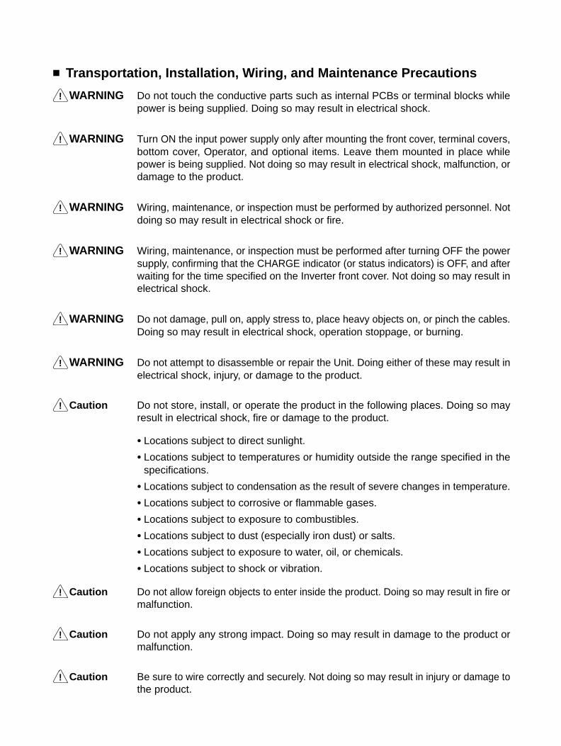
Transportation, Installation, Wiring, and Maintenance Precautions
WARNING Do not touch the conductive parts such as internal PCBs or terminal blocks whilepower is being supplied. Doing so may result in electrical shock.
WARNING Turn ON the input power supply only after mounting the front cover, terminal covers,bottom cover, Operator, and optional items. Leave them mounted in place whilepower is being supplied. Not doing so may result in electrical shock, malfunction, ordamage to the product.
WARNING Wiring, maintenance, or inspection must be performed by authorized personnel. Notdoing so may result in electrical shock or fire.
WARNING Wiring, maintenance, or inspection must be performed after turning OFF the powersupply, confirming that the CHARGE indicator (or status indicators) is OFF, and afterwaiting for the time specified on the Inverter front cover. Not doing so may result inelectrical shock.
WARNING Do not damage, pull on, apply stress to, place heavy objects on, or pinch the cables.Doing so may result in electrical shock, operation stoppage, or burning.
WARNING Do not attempt to disassemble or repair the Unit. Doing either of these may result inelectrical shock, injury, or damage to the product.
Caution Do not store, install, or operate the product in the following places. Doing so mayresult in electrical shock, fire or damage to the product.
Locations subject to direct sunlight.
Locations subject to temperatures or humidity outside the range specified in thespecifications.
Locations subject to condensation as the result of severe changes in temperature.
Locations subject to corrosive or flammable gases.
Locations subject to exposure to combustibles.
Locations subject to dust (especially iron dust) or salts.
Locations subject to exposure to water, oil, or chemicals.
Locations subject to shock or vibration.
Caution Do not allow foreign objects to enter inside the product. Doing so may result in fire ormalfunction.
Caution Do not apply any strong impact. Doing so may result in damage to the product ormalfunction.
Caution Be sure to wire correctly and securely. Not doing so may result in injury or damage tothe product.
!
!
!
!
!
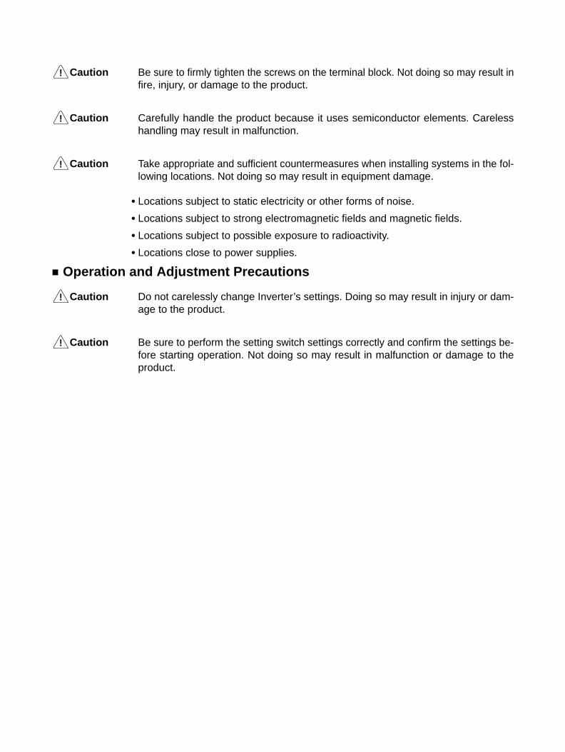
Caution Be sure to firmly tighten the screws on the terminal block. Not doing so may result infire, injury, or damage to the product.
Caution Carefully handle the product because it uses semiconductor elements. Carelesshandling may result in malfunction.
Caution Take appropriate and sufficient countermeasures when installing systems in the fol-lowing locations. Not doing so may result in equipment damage.
Locations subject to static electricity or other forms of noise.
Locations subject to strong electromagnetic fields and magnetic fields.
Locations subject to possible exposure to radioactivity.
Locations close to power supplies.
Operation and Adjustment Precautions
Caution Do not carelessly change Inverter’s settings. Doing so may result in injury or dam-age to the product.
Caution Be sure to perform the setting switch settings correctly and confirm the settings be-fore starting operation. Not doing so may result in malfunction or damage to theproduct.
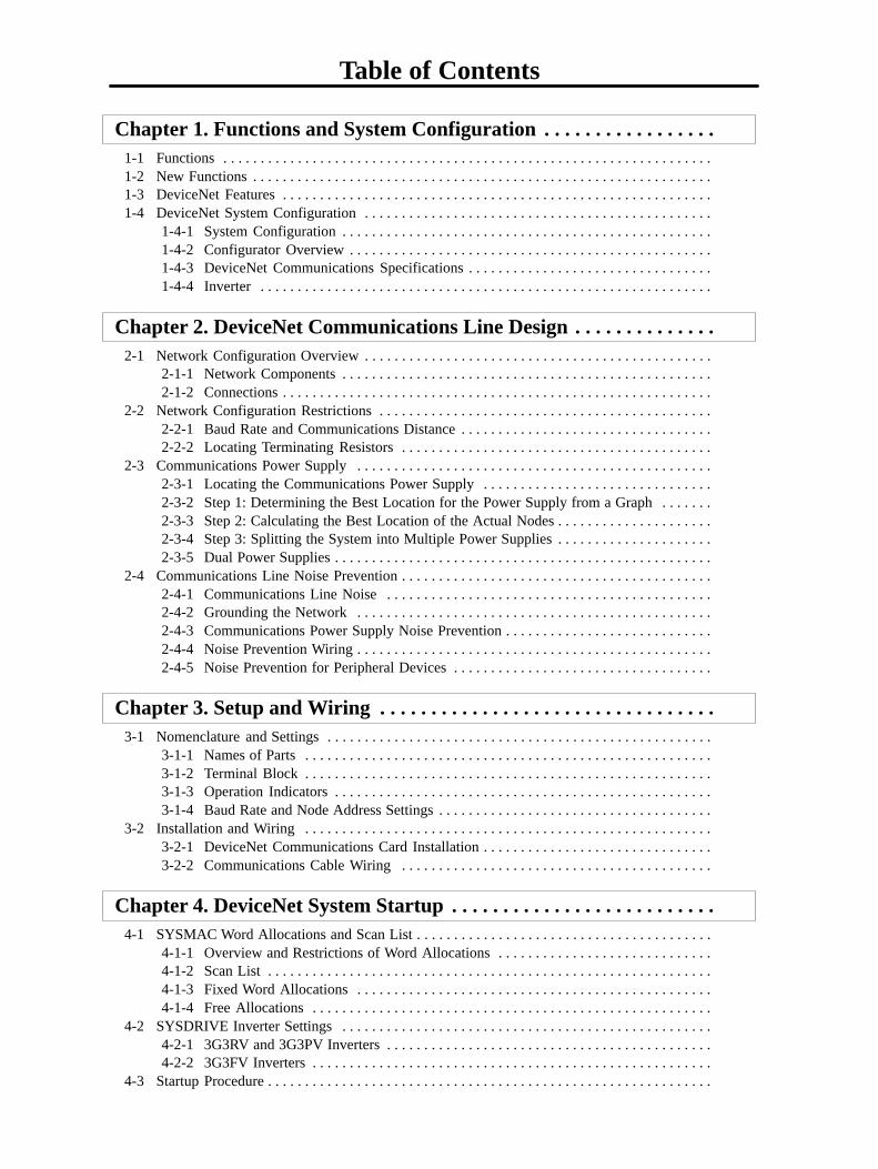
Table of Contents
Chapter 1. Functions and System Configuration . . . . . . . . . . . . . . . . . 1-1 Functions . . . . . . . . . . . . . . . . . . . . . . . . . . . . . . . . . . . . . . . . . . . . . . . . . . . . . . . . . . . . . . . . . . 1-2 New Functions . . . . . . . . . . . . . . . . . . . . . . . . . . . . . . . . . . . . . . . . . . . . . . . . . . . . . . . . . . . . . . 1-3 DeviceNet Features . . . . . . . . . . . . . . . . . . . . . . . . . . . . . . . . . . . . . . . . . . . . . . . . . . . . . . . . . . 1-4 DeviceNet System Configuration . . . . . . . . . . . . . . . . . . . . . . . . . . . . . . . . . . . . . . . . . . . . . . .
1-4-1 System Configuration . . . . . . . . . . . . . . . . . . . . . . . . . . . . . . . . . . . . . . . . . . . . . . . . . . 1-4-2 Configurator Overview . . . . . . . . . . . . . . . . . . . . . . . . . . . . . . . . . . . . . . . . . . . . . . . . . 1-4-3 DeviceNet Communications Specifications . . . . . . . . . . . . . . . . . . . . . . . . . . . . . . . . . 1-4-4 Inverter . . . . . . . . . . . . . . . . . . . . . . . . . . . . . . . . . . . . . . . . . . . . . . . . . . . . . . . . . . . . .
Chapter 2. DeviceNet Communications Line Design . . . . . . . . . . . . . . 2-1 Network Configuration Overview . . . . . . . . . . . . . . . . . . . . . . . . . . . . . . . . . . . . . . . . . . . . . . .
2-1-1 Network Components . . . . . . . . . . . . . . . . . . . . . . . . . . . . . . . . . . . . . . . . . . . . . . . . . . 2-1-2 Connections . . . . . . . . . . . . . . . . . . . . . . . . . . . . . . . . . . . . . . . . . . . . . . . . . . . . . . . . . .
2-2 Network Configuration Restrictions . . . . . . . . . . . . . . . . . . . . . . . . . . . . . . . . . . . . . . . . . . . . . 2-2-1 Baud Rate and Communications Distance . . . . . . . . . . . . . . . . . . . . . . . . . . . . . . . . . . 2-2-2 Locating Terminating Resistors . . . . . . . . . . . . . . . . . . . . . . . . . . . . . . . . . . . . . . . . . .
2-3 Communications Power Supply . . . . . . . . . . . . . . . . . . . . . . . . . . . . . . . . . . . . . . . . . . . . . . . . 2-3-1 Locating the Communications Power Supply . . . . . . . . . . . . . . . . . . . . . . . . . . . . . . . 2-3-2 Step 1: Determining the Best Location for the Power Supply from a Graph . . . . . . . 2-3-3 Step 2: Calculating the Best Location of the Actual Nodes . . . . . . . . . . . . . . . . . . . . . 2-3-4 Step 3: Splitting the System into Multiple Power Supplies . . . . . . . . . . . . . . . . . . . . . 2-3-5 Dual Power Supplies . . . . . . . . . . . . . . . . . . . . . . . . . . . . . . . . . . . . . . . . . . . . . . . . . . .
2-4 Communications Line Noise Prevention . . . . . . . . . . . . . . . . . . . . . . . . . . . . . . . . . . . . . . . . . . 2-4-1 Communications Line Noise . . . . . . . . . . . . . . . . . . . . . . . . . . . . . . . . . . . . . . . . . . . . 2-4-2 Grounding the Network . . . . . . . . . . . . . . . . . . . . . . . . . . . . . . . . . . . . . . . . . . . . . . . . 2-4-3 Communications Power Supply Noise Prevention . . . . . . . . . . . . . . . . . . . . . . . . . . . . 2-4-4 Noise Prevention Wiring . . . . . . . . . . . . . . . . . . . . . . . . . . . . . . . . . . . . . . . . . . . . . . . . 2-4-5 Noise Prevention for Peripheral Devices . . . . . . . . . . . . . . . . . . . . . . . . . . . . . . . . . . .
Chapter 3. Setup and Wiring . . . . . . . . . . . . . . . . . . . . . . . . . . . . . . . . . 3-1 Nomenclature and Settings . . . . . . . . . . . . . . . . . . . . . . . . . . . . . . . . . . . . . . . . . . . . . . . . . . . .
3-1-1 Names of Parts . . . . . . . . . . . . . . . . . . . . . . . . . . . . . . . . . . . . . . . . . . . . . . . . . . . . . . . 3-1-2 Terminal Block . . . . . . . . . . . . . . . . . . . . . . . . . . . . . . . . . . . . . . . . . . . . . . . . . . . . . . . 3-1-3 Operation Indicators . . . . . . . . . . . . . . . . . . . . . . . . . . . . . . . . . . . . . . . . . . . . . . . . . . . 3-1-4 Baud Rate and Node Address Settings . . . . . . . . . . . . . . . . . . . . . . . . . . . . . . . . . . . . .
3-2 Installation and Wiring . . . . . . . . . . . . . . . . . . . . . . . . . . . . . . . . . . . . . . . . . . . . . . . . . . . . . . . 3-2-1 DeviceNet Communications Card Installation . . . . . . . . . . . . . . . . . . . . . . . . . . . . . . . 3-2-2 Communications Cable Wiring . . . . . . . . . . . . . . . . . . . . . . . . . . . . . . . . . . . . . . . . . .
Chapter 4. DeviceNet System Startup . . . . . . . . . . . . . . . . . . . . . . . . . . 4-1 SYSMAC Word Allocations and Scan List . . . . . . . . . . . . . . . . . . . . . . . . . . . . . . . . . . . . . . . .
4-1-1 Overview and Restrictions of Word Allocations . . . . . . . . . . . . . . . . . . . . . . . . . . . . . 4-1-2 Scan List . . . . . . . . . . . . . . . . . . . . . . . . . . . . . . . . . . . . . . . . . . . . . . . . . . . . . . . . . . . . 4-1-3 Fixed Word Allocations . . . . . . . . . . . . . . . . . . . . . . . . . . . . . . . . . . . . . . . . . . . . . . . . 4-1-4 Free Allocations . . . . . . . . . . . . . . . . . . . . . . . . . . . . . . . . . . . . . . . . . . . . . . . . . . . . . .
4-2 SYSDRIVE Inverter Settings . . . . . . . . . . . . . . . . . . . . . . . . . . . . . . . . . . . . . . . . . . . . . . . . . . 4-2-1 3G3RV and 3G3PV Inverters . . . . . . . . . . . . . . . . . . . . . . . . . . . . . . . . . . . . . . . . . . . . 4-2-2 3G3FV Inverters . . . . . . . . . . . . . . . . . . . . . . . . . . . . . . . . . . . . . . . . . . . . . . . . . . . . . .
4-3 Startup Procedure . . . . . . . . . . . . . . . . . . . . . . . . . . . . . . . . . . . . . . . . . . . . . . . . . . . . . . . . . . . .
Table of Contents
Chapter 5. DeviceNet Communications Card Operations . . . . . . . . . 5-1 Remote I/O . . . . . . . . . . . . . . . . . . . . . . . . . . . . . . . . . . . . . . . . . . . . . . . . . . . . . . . . . . . . . . . . .
5-1-1 Standard Remote I/O (Initial Setting) . . . . . . . . . . . . . . . . . . . . . . . . . . . . . . . . . . . . . 5-1-2 Types of Remote I/O Operation . . . . . . . . . . . . . . . . . . . . . . . . . . . . . . . . . . . . . . . . . .
5-2 Switching Remote I/O Operation . . . . . . . . . . . . . . . . . . . . . . . . . . . . . . . . . . . . . . . . . . . . . . . 5-3 Special Remote I/O Operation . . . . . . . . . . . . . . . . . . . . . . . . . . . . . . . . . . . . . . . . . . . . . . . . .
5-3-1 Overview of Special Remote I/O . . . . . . . . . . . . . . . . . . . . . . . . . . . . . . . . . . . . . . . . . 5-3-2 Special Remote I/O Communications Timing . . . . . . . . . . . . . . . . . . . . . . . . . . . . . . . 5-3-3 Parameter Register Numbers for Each Function . . . . . . . . . . . . . . . . . . . . . . . . . . . . .
5-4 Control Remote I/O Operation . . . . . . . . . . . . . . . . . . . . . . . . . . . . . . . . . . . . . . . . . . . . . . . . . 5-5 Message Communications (DeviceNet Explicit Messages) . . . . . . . . . . . . . . . . . . . . . . . . . . .
5-5-1 Overview of Message Communications (Explicit Message Operations) . . . . . . . . . . . 5-5-2 Sending and Receiving Messages with a CS1W-DRM21 or CJ1W-DRM21
DeviceNet Unit . . . . . . . . . . . . . . . . . . . . . . . . . . . . . . . . . . . . . . . . . . . . . . . . . . . . . . . 5-5-3 Sending and Receiving Messages with C200HW-DRM21-V1 DeviceNet Master Unit 5-5-4 CVM1-DRM21-V1 DeviceNet Master Unit Message Transmission . . . . . . . . . . . . . . 5-5-5 Overview of Messages and Responses . . . . . . . . . . . . . . . . . . . . . . . . . . . . . . . . . . . . . 5-5-6 Motor Data Objects: Class 28 Hex . . . . . . . . . . . . . . . . . . . . . . . . . . . . . . . . . . . . . . . . 5-5-7 Control Supervisor Objects: Class 29 Hex . . . . . . . . . . . . . . . . . . . . . . . . . . . . . . . . . . 5-5-8 AC/DC Drive Objects: Class 2A Hex . . . . . . . . . . . . . . . . . . . . . . . . . . . . . . . . . . . . . 5-5-9 Reading and Writing Parameters: Class 64 Hex . . . . . . . . . . . . . . . . . . . . . . . . . . . . .
5-6 3G3RV Register Numbers, Classes, Instances, and Attributes . . . . . . . . . . . . . . . . . . . . . . . . . 5-6-1 Inputting Control/Frequency (Read/Write) . . . . . . . . . . . . . . . . . . . . . . . . . . . . . . . . . 5-6-2 Inverter Monitoring Functions (Read) . . . . . . . . . . . . . . . . . . . . . . . . . . . . . . . . . . . . . 5-6-3 Parameter Reading and Writing . . . . . . . . . . . . . . . . . . . . . . . . . . . . . . . . . . . . . . . . . .
5-7 3G3PV Register Numbers, Classes, Instances, and Attributes . . . . . . . . . . . . . . . . . . . . . . . . . 5-7-1 Inputting Control/Frequency (Read/Write) . . . . . . . . . . . . . . . . . . . . . . . . . . . . . . . . . 5-7-2 Inverter Monitoring Functions (Read) . . . . . . . . . . . . . . . . . . . . . . . . . . . . . . . . . . . . . 5-7-3 Parameter Reading and Writing . . . . . . . . . . . . . . . . . . . . . . . . . . . . . . . . . . . . . . . . . .
5-8 3G3FV Register Numbers, Classes, Instances, and Attributes . . . . . . . . . . . . . . . . . . . . . . . . . 5-8-1 Inputting Control/Frequency . . . . . . . . . . . . . . . . . . . . . . . . . . . . . . . . . . . . . . . . . . . . 5-8-2 Inverter Monitoring Functions . . . . . . . . . . . . . . . . . . . . . . . . . . . . . . . . . . . . . . . . . . . 5-8-3 Parameter Reading and Writing . . . . . . . . . . . . . . . . . . . . . . . . . . . . . . . . . . . . . . . . . .
Chapter 6. Communications Errors . . . . . . . . . . . . . . . . . . . . . . . . . . . 6-1 Communications Line Errors . . . . . . . . . . . . . . . . . . . . . . . . . . . . . . . . . . . . . . . . . . . . . . . . . . 6-2 Message Communications Errors . . . . . . . . . . . . . . . . . . . . . . . . . . . . . . . . . . . . . . . . . . . . . . . 6-3 Special Remote I/O Errors . . . . . . . . . . . . . . . . . . . . . . . . . . . . . . . . . . . . . . . . . . . . . . . . . . . . . 6-4 Inverter Faults . . . . . . . . . . . . . . . . . . . . . . . . . . . . . . . . . . . . . . . . . . . . . . . . . . . . . . . . . . . . . .
Chapter 7. Communications Programs (SYSMAC CS-series PCs) . . 7-1 Standard Remote I/O Programming . . . . . . . . . . . . . . . . . . . . . . . . . . . . . . . . . . . . . . . . . . . . . 7-2 Message Communications Programming . . . . . . . . . . . . . . . . . . . . . . . . . . . . . . . . . . . . . . . . .
7-2-1 Inverter Fault Processing . . . . . . . . . . . . . . . . . . . . . . . . . . . . . . . . . . . . . . . . . . . . . . . 7-2-2 Reading/Writing Data . . . . . . . . . . . . . . . . . . . . . . . . . . . . . . . . . . . . . . . . . . . . . . . . . .
7-3 Special Remote I/O Programs . . . . . . . . . . . . . . . . . . . . . . . . . . . . . . . . . . . . . . . . . . . . . . . . . . 7-3-1 Simple Operation Programs . . . . . . . . . . . . . . . . . . . . . . . . . . . . . . . . . . . . . . . . . . . . . 7-3-2 Reading Parameter Data . . . . . . . . . . . . . . . . . . . . . . . . . . . . . . . . . . . . . . . . . . . . . . . . 7-3-3 Writing Parameter Data . . . . . . . . . . . . . . . . . . . . . . . . . . . . . . . . . . . . . . . . . . . . . . . .

Table of Contents
Chapter 8. Appendices . . . . . . . . . . . . . . . . . . . . . . . . . . . . . . . . . . . . . . 8-1 Specifications . . . . . . . . . . . . . . . . . . . . . . . . . . . . . . . . . . . . . . . . . . . . . . . . . . . . . . . . . . . . . . . 8-2 Objects . . . . . . . . . . . . . . . . . . . . . . . . . . . . . . . . . . . . . . . . . . . . . . . . . . . . . . . . . . . . . . . . . . . .
8-2-1 Identify Objects (Identification Information): Class 01 Hex . . . . . . . . . . . . . . . . . . . . 8-2-2 Message Router Objects: Class 02 Hex . . . . . . . . . . . . . . . . . . . . . . . . . . . . . . . . . . . . 8-2-3 DeviceNet Objects: Class 03 Hex . . . . . . . . . . . . . . . . . . . . . . . . . . . . . . . . . . . . . . . . 8-2-4 Assembly Objects: Class 04 Hex . . . . . . . . . . . . . . . . . . . . . . . . . . . . . . . . . . . . . . . . . 8-2-5 DeviceNet Connection Objects: Class 05 Hex . . . . . . . . . . . . . . . . . . . . . . . . . . . . . . .
8-3 DeviceNet Communications Response Time . . . . . . . . . . . . . . . . . . . . . . . . . . . . . . . . . . . . . .
Index . . . . . . . . . . . . . . . . . . . . . . . . . . . . . . . . . . . . . . . . . . Revision History . . . . . . . . . . . . . . . . . . . . . . . . . . . . . . . . .

Chapter 1
Functions and SystemConfiguration
1-1 Functions
1-2 New Functions
1-3 DeviceNet Features
1-4 DeviceNet System Configuration
1
1-2
1-1 Functions
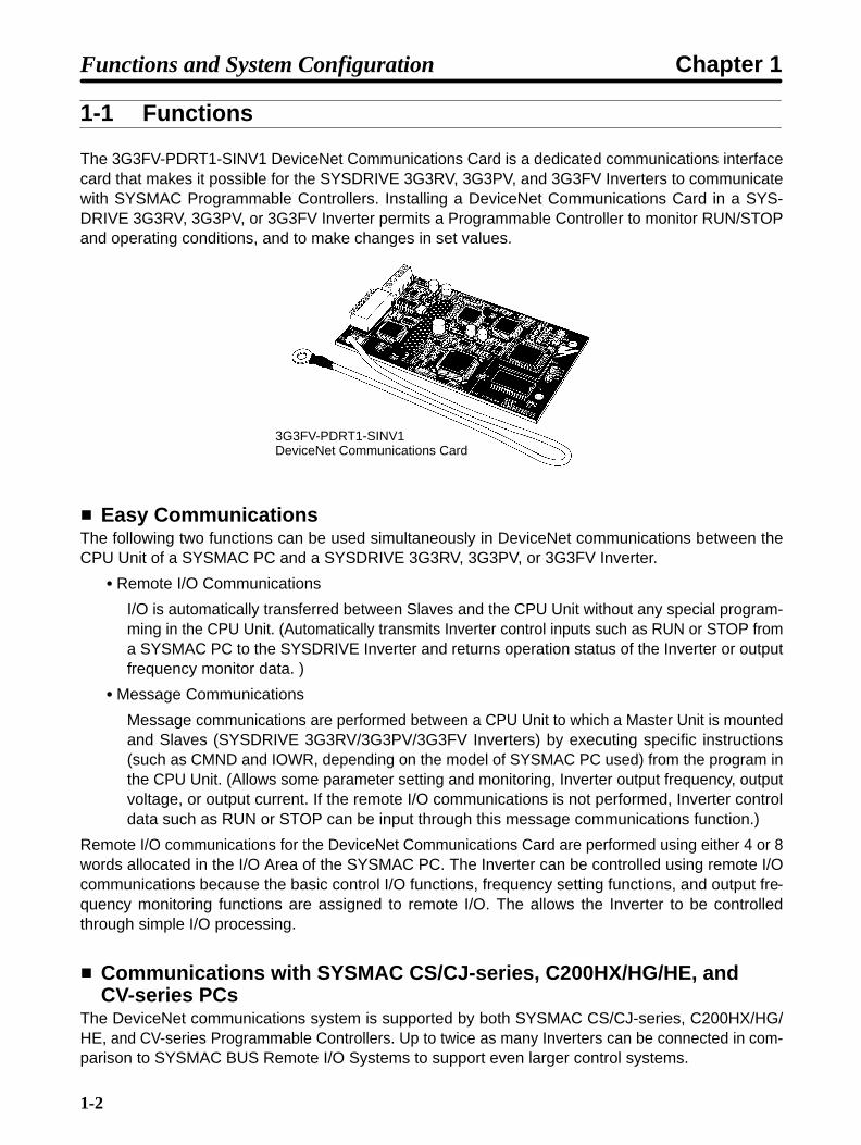
The 3G3FV-PDRT1-SINV1 DeviceNet Communications Card is a dedicated communications interfacecard that makes it possible for the SYSDRIVE 3G3RV, 3G3PV, and 3G3FV Inverters to communicatewith SYSMAC Programmable Controllers. Installing a DeviceNet Communications Card in a SYS-DRIVE 3G3RV, 3G3PV, or 3G3FV Inverter permits a Programmable Controller to monitor RUN/STOPand operating conditions, and to make changes in set values.
3G3FV-PDRT1-SINV1DeviceNet Communications Card
Easy CommunicationsThe following two functions can be used simultaneously in DeviceNet communications between theCPU Unit of a SYSMAC PC and a SYSDRIVE 3G3RV, 3G3PV, or 3G3FV Inverter.
Remote I/O Communications
I/O is automatically transferred between Slaves and the CPU Unit without any special program-ming in the CPU Unit. (Automatically transmits Inverter control inputs such as RUN or STOP froma SYSMAC PC to the SYSDRIVE Inverter and returns operation status of the Inverter or outputfrequency monitor data. )
Message Communications
Message communications are performed between a CPU Unit to which a Master Unit is mountedand Slaves (SYSDRIVE 3G3RV/3G3PV/3G3FV Inverters) by executing specific instructions(such as CMND and IOWR, depending on the model of SYSMAC PC used) from the program inthe CPU Unit. (Allows some parameter setting and monitoring, Inverter output frequency, outputvoltage, or output current. If the remote I/O communications is not performed, Inverter controldata such as RUN or STOP can be input through this message communications function.)
Remote I/O communications for the DeviceNet Communications Card are performed using either 4 or 8words allocated in the I/O Area of the SYSMAC PC. The Inverter can be controlled using remote I/Ocommunications because the basic control I/O functions, frequency setting functions, and output fre-quency monitoring functions are assigned to remote I/O. The allows the Inverter to be controlledthrough simple I/O processing.
Communications with SYSMAC CS/CJ-series, C200HX/HG/HE, andCV-series PCs
The DeviceNet communications system is supported by both SYSMAC CS/CJ-series, C200HX/HG/HE, and CV-series Programmable Controllers. Up to twice as many Inverters can be connected in com-parison to SYSMAC BUS Remote I/O Systems to support even larger control systems.
Functions and System Configuration Chapter 1

1-3
Note 1. The maximum number of nodes that can be connected to the system depends on the type ofMaster Unit used, whether the message function is used, and the number of words used byremote I/O communications. See 1-4 DeviceNet System Configuration for further details.
Note 2. The SYSMAC CS/CJ-series includes the CS1G, CS1H and CJ1G Programmable Control-lers. The SYSMAC CV Series includes the CV1000, CV2000, and CVM1 ProgrammableControllers. SYSMAC C200HS PCs support only remote I/O communications.
Multi-vendor NetworkDeviceNet conforms to the DeviceNet open field network specification, which means that devices (Mas-ters and Slaves) produced by other manufacturers can also be connected to the Network. The Device-Net Communications Card supports the DeviceNet AC/DC drive object.
Choice of Communications FunctionsThe DeviceNet Communications Card has various functions to choose from to suit the Inverter applica-tions.
Remote I/O Communications
Either basic remote I/O control or special remote I/O can be chosen for remote I/O allocation tosuit the application. Special I/O control can be used to control and set all functions for3G3RV/3G3PV/3G3FV-series Inverters.
Message Communications
Basic Inverter control and monitoring is possible with DeviceNet explicit messages, which aredefined for AC/DC driver objects. Remote I/O and message communications can be used simul-taneously, i.e., remote I/O control can be performed at the same time as other control using mes-sage communications.
Functions and System Configuration Chapter 1
1-4
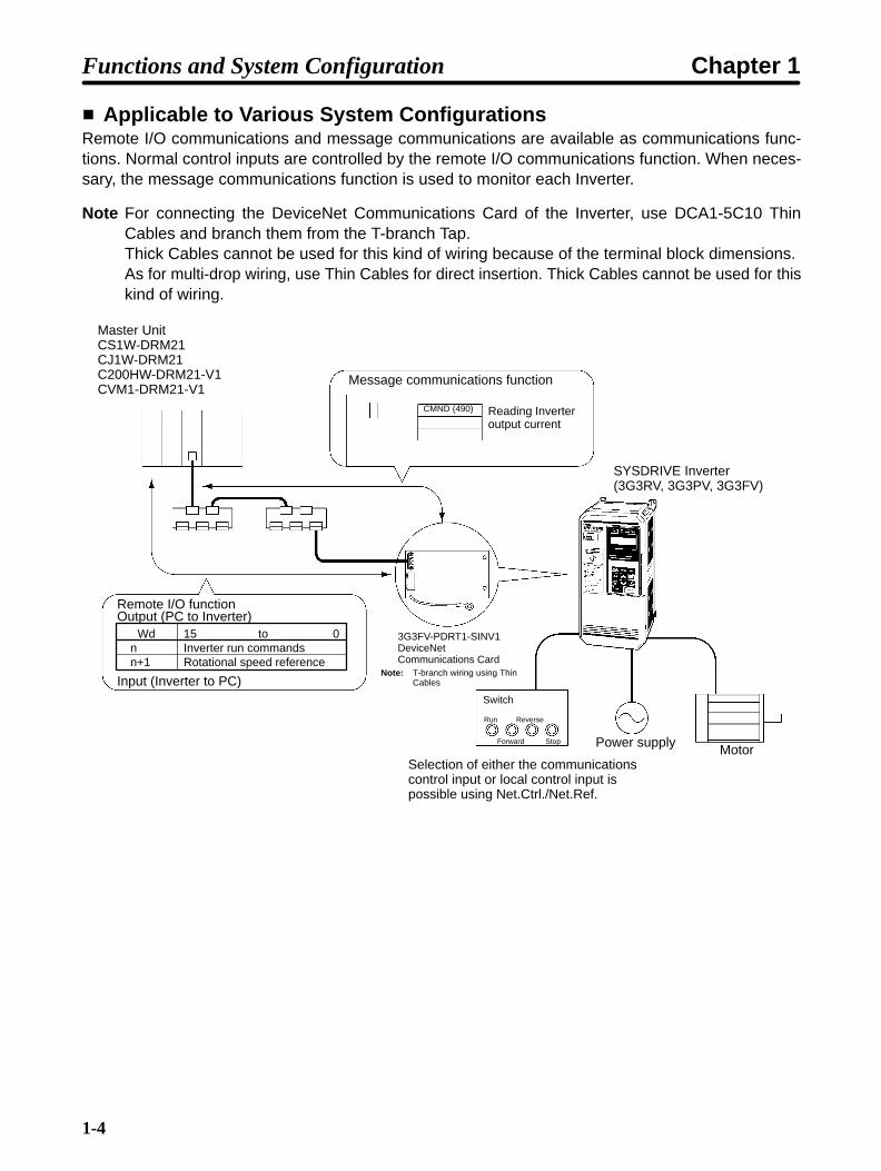
Applicable to Various System ConfigurationsRemote I/O communications and message communications are available as communications func-tions. Normal control inputs are controlled by the remote I/O communications function. When neces-sary, the message communications function is used to monitor each Inverter.
Note For connecting the DeviceNet Communications Card of the Inverter, use DCA1-5C10 ThinCables and branch them from the T-branch Tap.Thick Cables cannot be used for this kind of wiring because of the terminal block dimensions.As for multi-drop wiring, use Thin Cables for direct insertion. Thick Cables cannot be used for thiskind of wiring.
Master Unit CS1W-DRM21CJ1W-DRM21C200HW-DRM21-V1 CVM1-DRM21-V1
Message communications function
Reading Inverter output current
Remote I/O functionOutput (PC to Inverter)
Input (Inverter to PC)
SYSDRIVE Inverter (3G3RV, 3G3PV, 3G3FV)
3G3FV-PDRT1-SINV1DeviceNetCommunications Card
Power supply MotorSelection of either the communicationscontrol input or local control input is possible using Net.Ctrl./Net.Ref.
Note: T-branch wiring using ThinCables
Switch
Run
Forward
Reverse
Stop
Wd 15 to 0n Inverter run commandsn+1 Rotational speed reference
CMND (490)
Functions and System Configuration Chapter 1
1-5
1-2 New Functions
The software of the previous DeviceNet Communications Card (3G3FV-PDRT1-SIN) has beenupgraded with this model (3G3FV-PDRT1-SINV1), and new functions have been added.
Note The upgraded software used with this model is Ver. 2.0. The software version can be confirmedusing the Configurator.
New Remote I/O FunctionA new remote I/O function has been added to the three existing functions (basic remote I/O, standardremote I/O, and special remote I/O). The new remote I/O, called control remote I/O, contains functional-ity and arrays matching the Inverter control terminal I/O signals, and it provides easy-to-use specifica-tions for reduced wiring.
Note The control remote I/O function does not conform to the AC/DC drive profile, but is specially set forthis product.
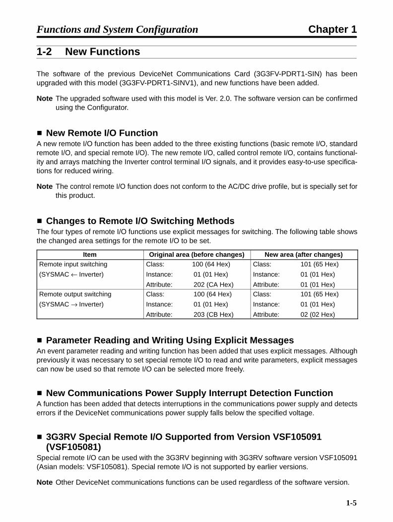
Changes to Remote I/O Switching MethodsThe four types of remote I/O functions use explicit messages for switching. The following table showsthe changed area settings for the remote I/O to be set.
Item Original area (before changes) New area (after changes)Remote input switching
(SYSMAC ← Inverter)
Class: 100 (64 Hex)
Instance: 01 (01 Hex)
Attribute: 202 (CA Hex)
Class: 101 (65 Hex)
Instance: 01 (01 Hex)
Attribute: 01 (01 Hex)
Remote output switching
(SYSMAC → Inverter)
Class: 100 (64 Hex)
Instance: 01 (01 Hex)
Attribute: 203 (CB Hex)
Class: 101 (65 Hex)
Instance: 01 (01 Hex)
Attribute: 02 (02 Hex)
Parameter Reading and Writing Using Explicit MessagesAn event parameter reading and writing function has been added that uses explicit messages. Althoughpreviously it was necessary to set special remote I/O to read and write parameters, explicit messagescan now be used so that remote I/O can be selected more freely.
New Communications Power Supply Interrupt Detection FunctionA function has been added that detects interruptions in the communications power supply and detectserrors if the DeviceNet communications power supply falls below the specified voltage.
3G3RV Special Remote I/O Supported from Version VSF105091(VSF105081)
Special remote I/O can be used with the 3G3RV beginning with 3G3RV software version VSF105091(Asian models: VSF105081). Special remote I/O is not supported by earlier versions.
Note Other DeviceNet communications functions can be used regardless of the software version.
Functions and System Configuration Chapter 1
1-6
1-3 DeviceNet Features
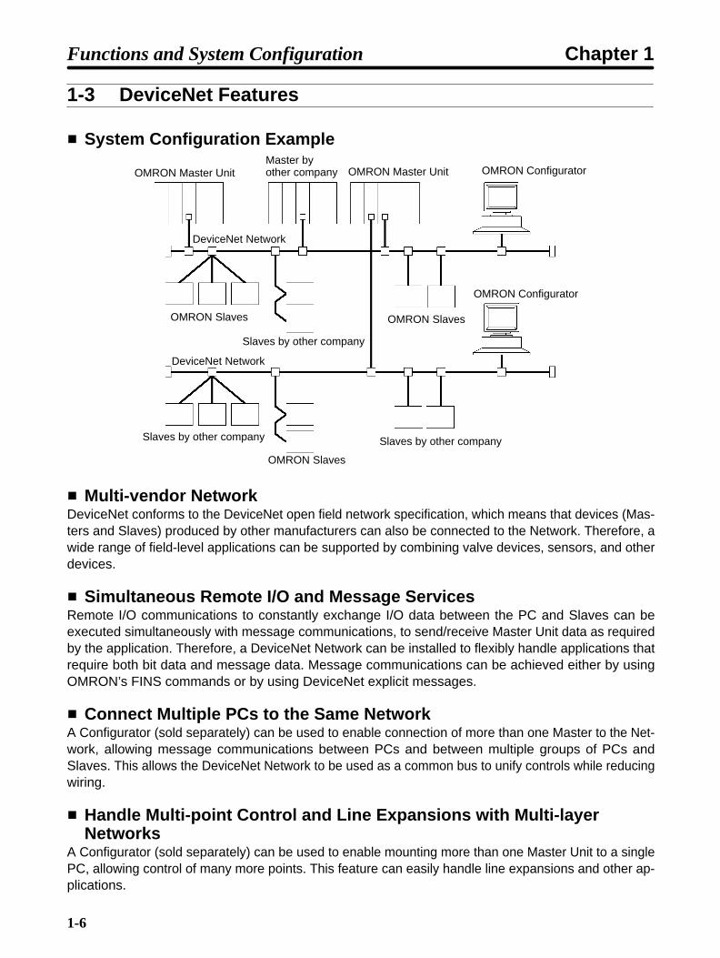
System Configuration Example
OMRON Master UnitMaster by other company OMRON Master Unit OMRON Configurator
OMRON Configurator
DeviceNet Network
OMRON Slaves
Slaves by other company
OMRON Slaves
Slaves by other company
OMRON Slaves
Slaves by other company
DeviceNet Network
Multi-vendor NetworkDeviceNet conforms to the DeviceNet open field network specification, which means that devices (Mas-ters and Slaves) produced by other manufacturers can also be connected to the Network. Therefore, awide range of field-level applications can be supported by combining valve devices, sensors, and otherdevices.
Simultaneous Remote I/O and Message ServicesRemote I/O communications to constantly exchange I/O data between the PC and Slaves can beexecuted simultaneously with message communications, to send/receive Master Unit data as requiredby the application. Therefore, a DeviceNet Network can be installed to flexibly handle applications thatrequire both bit data and message data. Message communications can be achieved either by usingOMRON’s FINS commands or by using DeviceNet explicit messages.
Connect Multiple PCs to the Same NetworkA Configurator (sold separately) can be used to enable connection of more than one Master to the Net-work, allowing message communications between PCs and between multiple groups of PCs andSlaves. This allows the DeviceNet Network to be used as a common bus to unify controls while reducingwiring.
Handle Multi-point Control and Line Expansions with Multi-layerNetworks
A Configurator (sold separately) can be used to enable mounting more than one Master Unit to a singlePC, allowing control of many more points. This feature can easily handle line expansions and other ap-plications.
Functions and System Configuration Chapter 1

1-7
Free Remote I/O AllocationA Configurator (sold separately) can be used to enable flexible allocation of I/O, i.e., in any area and inany order. This allows I/O allocations that suit the application to simplify programming and enable effec-tive usage of PC memory areas.
Handle Slaves with Different Response SpeedsA Configurator (sold separately) can be used to set the communications cycle time, enabling usage ofSlaves with slow response times.
Easily Expand or Change Lines with Various Connection MethodsUse a multi-drop trunk line, T-branch multi-drop lines, or daisy-chain drop lines. All three connectionmethods can be combined to flexibly construct a Network that meets the needs of the application.
Note For connecting the DeviceNet Communications Card of the Inverter, use DCA1-5C10 ThinCables and branch them from the T-branch Tap.
Functions and System Configuration Chapter 1

1-8
1-4 DeviceNet System Configuration
1-4-1 System ConfigurationOpen field network DeviceNet is a multi-bit, multi-vendor network that combines controls and data on amachine/line-control level.
Two types of communications are supported: 1) Remote I/O communications that automatically trans-fer I/O between Slaves and the CPU Unit of a SYSMAC PC without any special programming in the CPUUnit and 2) Message communications are performed between a CPU Unit to which a Master Unit ismounted and Slaves by executing specific instructions (such as CMND and IOWR, depending on themodel of SYSMAC PC used) from the program in the CPU Unit.
A Configurator (sold separately) can be used to enable following. This allows the support of an evenlarger control system.
I/O area words can be flexibly allocated for remote I/O communications.
More than one Master Unit can be mounted to a single PC.
More than one Master Unit can be connected in a single Network.
Fixed Allocation: Configuration without a Configurator
Slave SlaveSlave Slave
3G3FV-PDRT1-SINV1DeviceNet Communications Card
SYSDRIVE3G3RV/3G3PV/3G3FV Inverter
CS1W-DRM21, CJ1W-DRM21, C200HW-DRM21-V1, CVM1-DRM21-V1DeviceNet Master Unit
CS/CJ-series PCs: 64 nodes max. (including the Master Unit) CV-series PCs: 64 nodes max. (including the Master Unit)C200HX/HG/HE PCs: 64 nodes max. (including the Master Unit)C200HS PCs: 33 nodes max. (including the Master Unit)
Note 1. The Master Unit occupies one node of the DeviceNet Network.
Note 2. If C200HS PCs are used, only remote I/O communications are possible.
Note 3. If one node uses more than one word, the maximum number of nodes will be reduced by onenode for each extra word that is used.
Functions and System Configuration Chapter 1

1-9
Free Allocation: Configuration with a Configurator
Slave SlaveSlave
3G3FV-PDRT1-SINV1DeviceNet Communications Card
SYSDRIVE 3G3RV/3G3PV/3G3FV Inverter
CS1W-DRM21, CJ1W-DRM21, C200HW-DRM21-V1 or CVM1-DRM21-V1DeviceNet Master Unit 3G8F5-DRM21 (ISA Board)
orSG8E2-DRM21 (PC Card)Configurator
64 nodes max. (including the Master Unit)
ConfiguratorSlave SlaveSlave
64 nodes max. (including the Master Unit)
Note 1. The Master Unit and Configurator each occupy one node of the DeviceNet Network.
Note 2. If C200HS PCs are used, only remote I/O communications are possible.
Note 3. The maximum number of nodes that can be connected to the Network will be limited by themaximum number of control points of the PC used.
1-4-2 Configurator OverviewThe Configurator is a software application run on a computer and is used to support a DeviceNet com-munications system. The Configurator can be connected to the network via a serial communicationsport (using Peripheral Bus or Host Link), or it can be connected directly using an interface (hardware) forconnecting computers to the DeviceNet Network. The Configurator occupies one node on the Device-Net Network, but has no specific functions on the network itself. The Configurator provides the followingfunctions.
Free Allocation of Remote I/O
The remote I/O allocations in the PCs can be changed from the Configurator. I/O can be flexiblyallocated for each node within the specified I/O areas.
More than One Master Unit per Network
Functions and System Configuration Chapter 1

1-10
Slaves can be set for each Master Unit from the Configurator enabling communications betweenmultiple groups of PCs and Slaves. The maximum number of nodes connected to one Networkremains at 64. One Slave can be connected to no more than one Master Unit.
More than one Master Unit per PC
Remote I/O can be allocated for each Slave of the Master Unit from the Configurator, so morethan one Master Unit can be mounted to the same PC.
Note In allocating Remote I/O for each Master Unit, be careful not to allow any dual allocation.
Configurator SpecificationsItem WS02-CFDC1-E 3G8F5-DRM21 3G8E2-DRM21
Personal computer --- Desktop model Notebook model
Components Installation disk(software)
Installation disk (software)Dedicated ISA Board
Installation disk (software)Dedicated PCMCIA CardDeviceNet Interface Unit
Operatingenvironment
Hardware Computer: IBM PC/AT or compatible
CPU: Windows NT: 166 MHz Pentium min.
Memory: 32 MB min.
Hard disk: 15 MB min. free spaceOS Windows 95, 98, 2000, or NT 4.0
DeviceNetinterface
No accessories Dedicated ISA Board Dedicated PCMCIA Card
DeviceNet Interface UnitRelation to Network Operates as one node on the Network, requires one node address, and only
one Configurator can be connected to the Network. (The Configurator can bedisconnected from the Network after remote I/O has been allocated.)
Functions and System Configuration Chapter 1

1-11
1-4-3 DeviceNet Communications SpecificationsItem Specifications
Communications protocol DeviceNet
Supported connections (commu-nications)
Master-Slave: Remote I/O and explicit messagesPeer-to-peer: FINS messagesBoth conform to DeviceNet specifications.
Connection forms Combination of multi-drop and T-branch connections (for trunk and droplines)
Baud rate 500 Kbps, 250 Kbps, or 125 Kbps (switchable)
Communications media Special 5-wire cables (2 signal lines, 2 power lines, and 1 shield line)Thick Cable: DCA2-5C10 (100 m)Thin Cable: DCA1-5C10 (100 m)
Communicationsdistances
500 Kbps Network length: 100 m max.Drop line length: 6 m max.Total drop line length: 39 m max.
250 Kbps Network length: 250 m max.Drop line length: 6 m max.Total drop line length: 78 m max.
125 Kbps Network length: 500 m max.Drop line length: 6 m max.Total drop line length: 156 m max.
Communications power supply 24 VDC 1%, supplied externally(Slave power supply: 11 to 25 VDC)Recommended power supply: OMRON S82H Series or S82J Series
Max. number of nodes 64 nodes
Max. number of Masters Without Configurator: 1With Configurator: 63
Max. number of Slaves Without Configurator: 63With Configurator: 63
Error control CRC check
1-4-4 InverterThe maximum number of Inverters that can be connected to one Network depends on the PC modelthat is used, the remote I/O functions of the Inverter, and whether message communications are used ornot. (Use the message communications function for setting some parameters and for monitoring theoutput current.) The differences between models are provided in the following tables.
Functions and System Configuration Chapter 1

1-12
CS1W-DRM21 or CJ1W-DRM21 Master Units
Communications without Configurator: Fixed Allocations
Applicable PC CS Series CJ SeriesMaster Unit CS1W-DRM21 CJ1W-DRM21
Supported communications Remote I/O and messages
Maximum number of Slaves perMaster Unit
63
Maximum number of controlledpoints per Master Unit
2,048
Allocation areas Select one of the following settings, using the software switch (FixedArea Setting 1, 2, or 3 Switch) in the words allocated to the MasterUnit in the CIO Area:
1. OUT: CIO 3200 to CIO 3263; IN: CIO 3300 to CIO 3363 (default)
2. OUT: CIO 3400 to CIO 3463; IN: CIO 3500 to CIO 3563
3. OUT: CIO 3600 to CIO 3663; IN: CIO 3700 to CIO 3763
Allocation method Words are allocated for each node to the above data areas in nodeaddress order only.
8-point Slaves: Allocated 1 word (1 node address)
16-point Slaves: Allocated 1 word (1 node address)
Slaves with more than 16 points: Allocated multiple words (multiplenode addresses)
Maximumnumber ofInverters
Without explicitmessages
4 words remote I/O: 32
6 words remote I/O: 21
8 words remote I/O: 16With explicitmessages
4 words remote I/O: 32
6 words remote I/O: 21
8 words remote I/O: 16
Communications with Configurator: Free Allocations
Applicable PC CS Series CJ SeriesMaster Unit CS1W-DRM21 CJ1W-DRM21
Supported communications Remote I/O and messages
Maximum number of Slaves perMaster Unit
63
Maximum number of controlledpoints per Master Unit
Using Settings in Words Allocated in DM Area: 16,000 points (IN: 500words × 1 block; OUT: 500 words × 1 block
Using Configurator: 32,000 points (IN: 500 words × 2 blocks; OUT: 500words × 2 blocks
Allocation areas CIO 0000 to CIO 6143
WR: W000 to W511
HR: H000 to H511
DM: D00000 to D32767
EM: E00000 to E32767
Functions and System Configuration Chapter 1
1-13
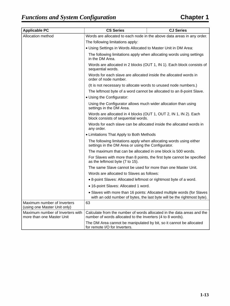
Applicable PC CJ SeriesCS SeriesAllocation method Words are allocated to each node in the above data areas in any order.
The following limitations apply:
• Using Settings in Words Allocated to Master Unit in DM Area:
The following limitations apply when allocating words using settingsin the DM Area.
Words are allocated in 2 blocks (OUT 1, IN 1). Each block consists ofsequential words.
Words for each slave are allocated inside the allocated words inorder of node number.
(It is not necessary to allocate words to unused node numbers.)
The leftmost byte of a word cannot be allocated to an 8-point Slave.
• Using the Configurator:
Using the Configurator allows much wider allocation than usingsettings in the DM Area.
Words are allocated in 4 blocks (OUT 1, OUT 2, IN 1, IN 2). Eachblock consists of sequential words.
Words for each slave can be allocated inside the allocated words inany order.
• Limitations That Apply to Both Methods
The following limitations apply when allocating words using eithersettings in the DM Area or using the Configurator.
The maximum that can be allocated in one block is 500 words.
For Slaves with more than 8 points, the first byte cannot be specifiedas the leftmost byte (7 to 15).
The same Slave cannot be used for more than one Master Unit.
Words are allocated to Slaves as follows:
• 8-point Slaves: Allocated leftmost or rightmost byte of a word.
• 16-point Slaves: Allocated 1 word.
• Slaves with more than 16 points: Allocated multiple words (for Slaveswith an odd number of bytes, the last byte will be the rightmost byte).
Maximum number of Inverters(using one Master Unit only)
63
Maximum number of Inverters withmore than one Master Unit
Calculate from the number of words allocated in the data areas and thenumber of words allocated to the Inverters (4 to 8 words).
The DM Area cannot be manipulated by bit, so it cannot be allocatedfor remote I/O for Inverters.
Functions and System Configuration Chapter 1

1-14
C200HW-DRM21-V1 or CVM1-DRM21-V1 Master Units
Communications without Configurator: Fixed AllocationApplicable PC CV Series CS Series/
C200HX/HG/HEC200HS
Master Unit CVM1-DRM21-V1 C200HW-DRM21-V1
Supported communica-tions
Remote I/O and messages Remote I/O and mes-sages
Remote I/O
Max. No. of Slaves perMaster Unit
63 50 32
Max. No. of controlledpoints per Master Unit
2,048 1,600 1,024
Allocation areas OUT: CIO 1900 to CIO 1963
IN: CIO 2000 to CIO 2063
OUT: IR 050 to IR 099
IN: IR 350 to IR 399
OUT: IR 50 to IR 81
IN: IR 350 to IR 381
Allocation method Words are allocated for each node to the above data areas in node address or-der only.
8-point Slaves: Allocated 1 word
16-point Slaves:Allocated 1 word
Slaves with more than 16 points: Allocated multiple words
Max. No.ofInverters
Without ex-plicit mes-sages
4 words remote I/O: 32
6 words remote I/O: 21
8 words remote I/O: 16
4 words remote I/O: 25
6 words remote I/O: 16
8 words remote I/O: 12
4 words remote I/O: 16
6 words remote I/O: 10
8 words remote I/O: 8With explicitmessages
4 words remote I/O: 32
6 words remote I/O: 21
8 words remote I/O: 16
4 words remote I/O: 25
6 words remote I/O: 16
8 words remote I/O: 12
–
Communications with Configurator: Free AllocationApplicable PC CV Series CS Series/
C200HX/HG/HEC200HS
Master Unit CVM1-DRM21-V1 C200HW-DRM21-V1
Supported communications Remote I/O andmessages
Remote I/O andmessages
Remote I/O
Max. No of Slaves perMaster Unit
63 63 63
Max. No. of controlled pointsper Master Unit
6,400 (100 words 4blocks)
Without messages:4,800
With messages: 1,600
1,280 (total of 4 blocks)
Functions and System Configuration Chapter 1

1-15
Applicable PC C200HSCS Series/C200HX/HG/HE
CV Series
Allocation areas Core I/O Area:CIO 0000 to CIO 2555
CIO 0000 toCIO 2427 forCV500/CVM1-CPU01(-V)
IR Area 1: IR 000 to IR 235IR Area 2: IR 300 to IR 511
CPU Bus Link Area:G008 to G255
HR Area: HR 00 to HR 99LR Area: LR 00 to LR 63
DM Area:D00000 to D24575
D00000 toD08191 forCV500/CVM1-CPU01(-V)
DM Area:DM 0000 to DM 5999
DM 0000 to DM 4095for C200HE-CPU11 (-Z)
DM Area:DM 0000 to DM 5999
Allocation method Words are allocated to each node in the above data areas in any order usingthe Configurator.
The following limitations apply:
The allocation areas are in 4 blocks (OUT 1, OUT 2, IN 1, and IN 2).Each block consists of sequential words.
100 words max. per block.
For Slaves with more than 8 points, the first byte cannot be specifiedin leftmost bits (7 to 15).
Words are allocated to Slaves as follows:
8-point Slaves: Allocated leftmost or rightmost byte of 1 word
16-point Slaves:Allocated 1 word
Slaves with more than 16-points: Allocated multiple words (For Slaves withan odd number of bytes, the last byte will be the rightmost byte)
Max. No. ofInverters(using one
Withoutexplicitmessages
63 4 remote I/O words: 636 remote I/O words: 508 remote I/O words: 37
4 words remote I/O: 20 6 words remote I/O: 138 remote I/O words: 10( g
Master Unitonly)
With explicitmessages
63 4 remote I/O words: 256 remote I/O words: 168 remote I/O words: 12
---
Max. No. Inverters with morethan one Master Unit
Calculate from the number of words allocated in the data areas and thenumber of words allocated to the Inverters (4 or 6 words).Note 1. The DM Area cannot be manipulated by bit, so it cannot be allocated
for remote I/O for Inverters.
Note 2. If the CPU Bus Link is used with a CV-series PC, the CPU Bus LinkArea will be used for the CPU Bus Link Therefore, the CPU Bus LinkArea cannot be allocated to Inverters if the CPU Bus Link is used.
Functions and System Configuration Chapter 1

Chapter 2
DeviceNetCommunications LineDesign
2-1 Network Configuration Overview
2-2 Network Configuration Restrictions
2-3 Communications Power Supply
2-4 Communications Line Noise Prevention
2

2-2
2-1 Network Configuration Overview
The following diagram shows the configuration of a DeviceNet Network.
DeviceNet
cables are used.
T: T-branch connection
M: Multi-drop connection
DeviceNet cables (5-wire cables) areused for the trunk lines and drop lines.
Node
Drop line
Drop line
Drop line
T-branch
TapDrop line
Drop line
Trunk line Trunk line Trunk lineTrunk
line Trunk line Trunk line
Node Node
Node
Node
Node
Node
Node
Node
Node
T T TT
M
M
T
M
M MT
Terminating Resistors
are connected at each
end of the trunk line.
Power Supply Tap
or T-branch Tap
24 VDC
Communications
power supply
DeviceNet
cables are used.
T-branch
Tap
T-branch
Tap
T-branch
Tap
Drop line Drop line
T-branch
Tap
T-branch Tap
Terminating Resistors
are connected at each
end of the trunk line.
2-1-1 Network Components
NodesThere are two kinds of nodes on a DeviceNet Network: The Master and Slaves. The Slaves connect toexternal I/O and the Master administers the Network and manages the external I/O of the Slaves. TheMaster and Slaves can be connected at any location in the Network, as shown in the preceding diagram.
Trunk/Drop LinesThe trunk line refers to the cable that has Terminating Resistors on both ends. Cables branching fromthe trunk line are known as drop lines. The trunk line length does not necessarily coincide with the maxi-mum length of the Network. DeviceNet communications are transmitted through 5-wire cables. Thecables come in thick and thin versions.
Connection MethodsTwo methods can be used to connect DeviceNet nodes: The T-branch method and the multi-drop meth-od. With the T-branch method, the node is connected to a drop line created with a T-branch Tap. With themulti-drop method, the node is directly connected to the trunk line or the drop line. Secondary branchescan be made from a drop line. Both of these connection methods can be used in the same Network.
Terminating ResistorsTerminating Resistors are connected at each end of the trunk line to reduce signal reflection and stabi-lize communications. There are two kinds of Terminating Resistors available: One that is provided witha T-branch Tap and a Terminal-block Terminating Resistor. Use a DeviceNet Cable when connecting aTerminal-block Terminating Resistor.
Communications Power SuppliesTo use DeviceNet, connect a communications power supply to the communications connector of eachnode with a 5-wire cable. Basically, a communications power supply, internal circuit power supply, andI/O power supply must be provided separately.
DeviceNet Communications Line Design Chapter 2

2-3
2-1-2 Connections
Trunk and Drop LinesThe trunk line is a cable to which Terminating Resistors are connected at the ends. Drop lines are cablesthat branch from the trunk lines. A special 5-wire cable is used for both the trunk lines and the drop lines.
Branching Patterns
Branching Patterns from Trunk Line
Drop line
T-branch Tap
Trunk line
Node
Trunk line
T-branch Tap
Trunk line
Node
T-branch Tap
NodeNode
Trunk lineMulti-drop
Trunk line
Node
Trunk line
1.One drop line fromtrunk line
2.Three drop lines (maximum)from trunk line
3.Node connected directly totrunk line
Branching Patterns from Drop Line
Drop line
T-branch Tap
Trunk line
Node
Trunk line
T-branch Tap
Trunk line
Node
T-branch Tap
NodeNode
Trunk lineMulti-drop
Trunk line
Node
Trunk line
4 One drop line fromdrop line
5.Three drop lines (maximum)from drop line
6.Node connected directly todrop line
Various forms of connection can be used on the same Network, as shown in thefollowing diagram. Any number of nodes up to 63 can be connected onto a singledrop line.
Note Design the Inverter wiring for T-branch wiring purposes using ThinCables.
Communications
power supply
Terminating
Resistor
Node Node
Drop line
NodeNode
Drop
line
Trunk line
24 VDC
Node
Node
NodeNode
Node
Node
Power Supply Tap
or T-branch Tap
Trunk line
Drop
line
Terminating
Resistor
DeviceNet Communications Line Design Chapter 2

2-4
2-2 Network Configuration Restrictions
DeviceNet communications are designed to meet a wide range of applications by providing a choice ofbaud rates and allowing different combinations of T-branch and multi-drop connections. The restric-tions of DeviceNet communications that are required to enable the various communications possibili-ties are described here.
2-2-1 Baud Rate and Communications DistanceThe maximum length of the DeviceNet communications cables is restricted by the baud rate and thetype of cable used. The three types of restrictions on DeviceNet communications cable length are asfollows:
Maximum network length
Drop line length
Total drop line length
Be sure to design and configure a Network that meets the conditions provided below to ensure reli-able communications.
Maximum Communications DistanceBaud rate Maximum network length Drop line length Total drop line
lengthThick Cable Thin Cable
length
500 kbps 100 m max. 100 m max. 6 m max. 39 m max.
250 kbps 250 m max. 100 m max. 6 m max. 78 m max.
125 kbps 500 m max. 100 m max. 6 m max. 156 m max.
Note Thick Cable (5-wire): DCA2-5C10 (100 m)Thin Cable (5-wire): DCA1-5C10 (100 m)
Maximum Network LengthThe length of the Network is longest at either the distance between the two most distant nodes or at thedistance between the Terminating Resistors.
There are two types of cables: Thick Cables and Thin Cables. The cable thickness affects signal deteri-oration. The maximum length of the Network therefore depends on the type of cable used as shown inthe previous table.
The following restrictions apply to Networks in which both Thick and Thin Cables are combined.
Baud rate Maximum Network length500 kbps Thick Cable length + Thin Cable length 100 m
250 kbps Thick Cable length + 2.5 Thin Cable length 250 m
125 kbps Thick Cable length + 5.0 Thin Cable length 500 m
Drop Line LengthThe length of the drop line is measured from the point in the trunk line where the original branch wasmade to the end of the branch. The maximum length of a drop line is 6 m. It is possible to make a second-ary branch from a drop line.
DeviceNet Communications Line Design Chapter 2

2-5
Total Drop Line LengthThe total drop line length is the total sum length of all the drop lines (but not including the trunk line). Donot exceed the maximum total drop line length (even when the length of each individual drop line is 6 mor less). The standard for the total drop line length varies with the baud rate as shown in the previoustable.
Configuration ExampleThe following configuration example shows the maximum length of the Network, the drop line lengths,and the total drop line length.
TerminatingResistor
Node
Node
2 m
Node
1 m
Node
2 m
Node
Node
TerminatingResistor
2 m
3 m
Node
Node
6 m2 m
2 m
1 m
1 m
Node Node Node
6 m 6 m 6 m
Trunk line10 m
Trunk line10 m
Trunk line20m
Drop line5 m
Drop line2m
Drop line6 m
Drop line6 m
The longest distance between nodes is 48 m, and the distance between the twoTerminating Resistors is 40 m. The maximum Network length is therefore 48 m.
There are four branch points in the trunk line. The length of each drop line isshown in the diagram. The maximum drop line length is 6 m.
The sum of all the drop lines is 40 m.
2-2-2 Locating Terminating ResistorsBe sure to connect the Terminating Resistors at both ends of the trunk line to reduce signal reflectionand stabilize communications.
When there is a T-branch Tap 6 m or less from the end of the trunk line (or the node):
A Terminating Resistor attached to a T-branch Tap can easily be mounted without taking up muchspace.
When there is not a T-branch Tap 6 meters or less from the end of the trunk line (or the node):
A Terminating Resistor must be connected before that point. Either a T-branch Tap mounted to aTerminating Resistor or a terminal block with Terminating Resistor can be used. In this case, be sureto make the cable length 1 m or less from the node to the Terminating Resistor.
Node at end of trunk line
Truck line
Node
T-branch Tap mounted to a Terminating Resistoror a terminal block with Terminating Resistor.
1 m or less
Maximum NetworkLength
Drop Line Length
Total Drop Line Length
DeviceNet Communications Line Design Chapter 2

2-6
2-3 Communications Power Supply
2-3-1 Locating the Communications Power Supply
Basic Concept• The communications power supply must be 24 VDC.
• Make sure that the power is supplied from the trunk line.
• When providing power to several nodes from one power supply, if possible try to locate the nodes inboth directions from the power supply.
• Provide power through Power Supply Taps. It is, however, possible to use T-branch Taps instead whenthere is one communications power supply in the system and the total current consumption is lessthan 5 A.
• The power supply capacity for cables is restricted to 8 A for Thick Cables and 3 A for Thin Cables.
• A single Network is usually supplied by one power supply. It is, however, possible to have more thanone power supply when power supply specifications cannot be met with a single power supply. (See2-3-4 Step 3: Splitting the System into Multiple Power Supplies.)
• Fully consider the power supply capacity allowance in the design.
• If the power supply is switched OFF during the operation of the Network, there may be a malfunction inthe nodes.
• The current capacity of the drop line varies according to its length. The longer the drop line, the lowerits maximum capacity becomes. This is the same whether the cable is thick or thin. Calculate the cur-rent capacity passing through the drop line I (the total current consumption at the drop line) using thefollowing formula.
I = 4.57/L I: Permissible current (A)L: Length of the drop line (m)
DeviceNet Communications Line Design Chapter 2

2-7
FlowchartUse the flowchart below to determine the communications power supply on the trunk line. Satisfy theconditions for each drop line on page 2-6.
Provisionally determine thelocation of the power supply.
Step 1
Are the power supplyspecifications met?
Step 2
Determine the best location of thepower supply from the graphs.
Are the power supplyspecifications met?
Calculate the best locationof the actual nodes.
Consider changing thelocation of the power supply.
Consider using Thick Cable.
Are the power supplyspecifications met?
Consider changing the location ofthe power supply.
Consider using Thick Cable.
Consider changing the location ofhigh current consumption nodes.
Set the location forthe power supply.
Split the power supplysystem by installing morethan two power supplies.
No
Yes
Yes
No
No
Are the power supplyspecifications met?
No
Step 3
Yes
Yes
Power Supply Location PatternsThe power supply can be located in the configurations shown below. Basically, select from the configu-rations 1 and 2.
Consider using configuration 3 when power supply specifications cannot be met by configurations 1and 2. It is possible to use configuration 4 for a duplex power supply.
DeviceNet Communications Line Design Chapter 2

2-8
1 Locating the Nodes on Both Sides of the Power SupplyPower Supply Tapor T-branch Tap
Communicationspower supplyNode Node Node Node Node
2 Locating the Nodes on One Side of the Power Supply
Note Configuration 1 is recommended for a single power supply to several nodes.
Power Supply Tapor T-branch Tap
Node Node Node Node NodeCommunicationspower supply
3 Splitting the Power Supply System with Multiple Power Supplies
Communicationspower supply
Communicationspower supply
System 1Special Power Supply Tap
Remove the fuseand split +V.
Make –V the same forSystems 1 and 2.
Special Power Supply Tap
System 2
Node Node Node Node Node
V+
V–
fuse
24 V 0 V
4 Duplex Power Supply with Multiple Power Supplies
Communicationspower supply
Communicationspower supply
Special PowerSupply Tap
Node Node Node NodeNode
Special PowerSupply Tap
Note 1. If power supply specifications cannot be met with a single power supply when the current ca-pacity of the Thick Cable exceeds 8 A even after the power supply location is modified, usemore than one communications power supply.
Note 2. In configuration 1, the power can be supplied in two directions to the trunk line as long as thecurrent capacity of each is 8 A or less when using Thick Cable, i.e., it is possible to have aconfiguration with a total maximum current capacity of up to 16 A.
DeviceNet Communications Line Design Chapter 2
2-9
Note 3. Consider changing to Thick Cable to meet specifications if the current capacity of the ThinCable exceeds 3 A when using Thin Cable for the trunk line.
Setting the Power Supply LocationDetermine whether or not the current can be supplied normally by finding the current capacity requiredby each node and the voltage drop in the cables to be used to provide power. Calculate the values belowin advance.
• The current capacity required by each node
• The distance between the power supply and each node
The current capacity of the 3G3FV-PDRT1-SINV1 DeviceNet Communications Card is approximately20 mA.
Calculating the Power Supply LocationThere are two methods to find the best location of the communications power supply on the trunk line.
• Simple calculation from a graph
• Calculation by formula (Calculating the voltage drop from resistance and current consumption of thecommunications cables).
Each drop line must satisfy the equation on page 2-6, which represents the relationship between thedrop line length and the current capacity for the drop line.
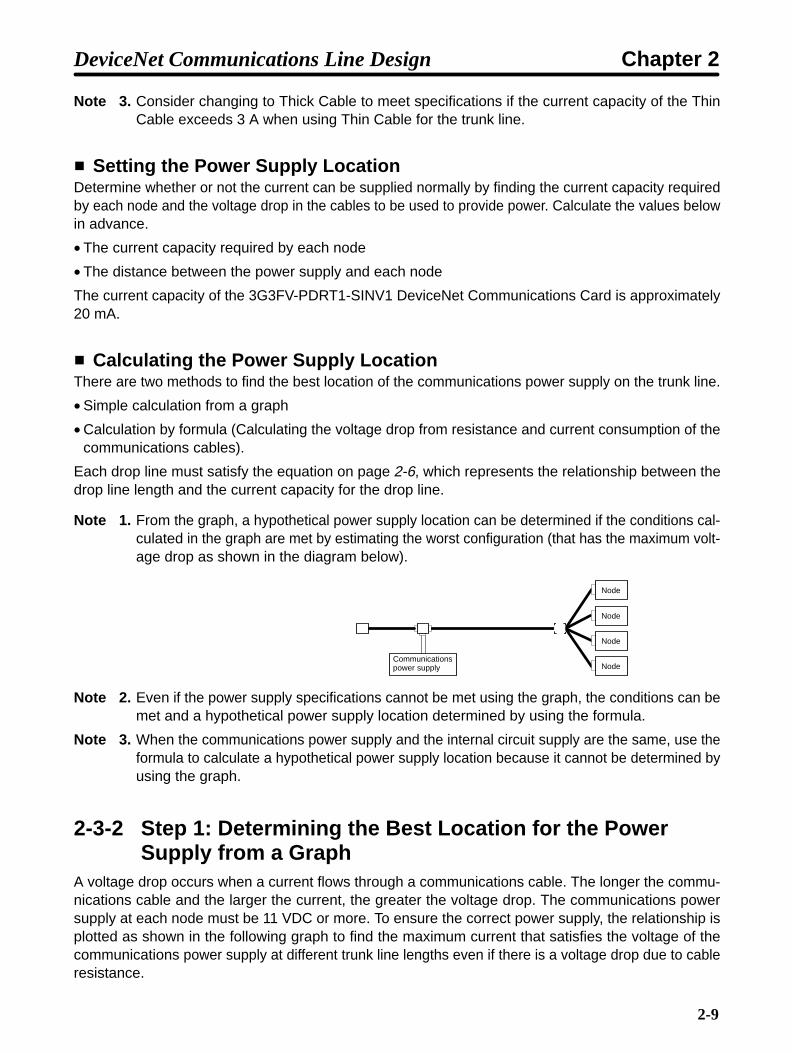
Note 1. From the graph, a hypothetical power supply location can be determined if the conditions cal-culated in the graph are met by estimating the worst configuration (that has the maximum volt-age drop as shown in the diagram below).
Communicationspower supply Node
Node
Node
Node
Note 2. Even if the power supply specifications cannot be met using the graph, the conditions can bemet and a hypothetical power supply location determined by using the formula.
Note 3. When the communications power supply and the internal circuit supply are the same, use theformula to calculate a hypothetical power supply location because it cannot be determined byusing the graph.
2-3-2 Step 1: Determining the Best Location for the PowerSupply from a Graph
A voltage drop occurs when a current flows through a communications cable. The longer the commu-nications cable and the larger the current, the greater the voltage drop. The communications powersupply at each node must be 11 VDC or more. To ensure the correct power supply, the relationship isplotted as shown in the following graph to find the maximum current that satisfies the voltage of thecommunications power supply at different trunk line lengths even if there is a voltage drop due to cableresistance.
DeviceNet Communications Line Design Chapter 2

2-10
Thick CableDistance (m) 0 25 50 100 150 200 250 300 350 400 450 500
Max. current (A) 8.00 8.00 5.42 2.93 2.01 1.53 1.23 1.03 0.89 0.78 0.69 0.63
Max. current (A)
Distance (m)
8
7
6
5
4
3
2
1
00
Thin CableDistance (m) 0 10 20 30 40 50 60 70 80 90 100
Max. current (A) 3.00 3.00 3.00 2.06 1.57 1.26 1.06 0.91 0.80 0.71 0.64
Max. current (A)
Distance (m)
3
2
1
00
Determining the Best Location of the Power Supply from a GraphVerify the Items 1 to 3 below for each node located in the same direction viewed from the power supply.Therefore, if nodes are located on both sides of the power supply, these items must be verified for allnodes located in each direction.
1 Find A, the total current consumption of all the nodes to which communications power is to be sup-plied.
2 Using the graph compute B, the maximum current flow in each cable from the power supply to theend of the trunk line according to the types of cables (Thick Cables or Thin Cables).
3 Compare the values found in steps 1 and 2, above. If the first value (A) is less than the second (B),this shows that power supply specifications are met and power can be supplied to all nodes at anypoint in the Network.
Note Be sure to refer to the correct graph as the maximum current flow is different for Thick and ThinCables.
DeviceNet Communications Line Design Chapter 2

2-11
CountermeasuresIf the second value (B) is less than the first (A), use the following procedure to locate the communica-tions power supply.
• Locate the communications power supply in the center of the Network and the nodes to both sides of it.
• If the nodes are already located at both sides of the power supply, move the power supply in the direc-tion that requires the larger current capacity.
• If Thin Cable is being used, replace it with Thick Cable.
Note If, after following the above procedure, B is still less than A, go to Step 2 and determine the actualposition of the nodes by the formula calculation method.
Calculation ExampleThe following example shows a Network that requires power to be supplied for 240 m on Thick Cable.The power supply is located in the center of the Network. Because the power supply is in the center, themaximum current will flow both to the left and to the right, enabling the supply of at least twice the maxi-mum current as when the power supply is placed on the end of the Network. The current consumptionfor individual nodes is as follows:
Communicationspower supply
120 m 120 m
3 m max.
0.25 A 0.2 A 0.15 A 0.25 A 0.15 A
Node Node Node Node Node
0.1 A
Node
Trunk line(5-wire cable)
Terminating Resistor
Trunk line
Power supply cable
Terminating Resistor Trunk line(5-wire cable)
Total power supply length on left = Total power supply length on right = 120 mTotal current consumption on left: 0.1 + 0.25 + 0.2 = 0.55 ATotal current consumption on right: 0.15 + 0.25 + 0.15 = 0.55 AMaximum current for the left side of the Thick Cable (see previous table) = approx. 2.5 AMaximum current for the right side of the Thick Cable (see previous table) = approx. 2.5 A(using straight line approximation between 100 to 150 m)
2-3-3 Step 2: Calculating the Best Location of the ActualNodes
Go to Step 2 if the best location for the power supply according to the specifications cannot be deter-mined from the graphs. The second method calculates the best location for each actual node and doesnot estimate the worst possible configuration for the power supply.
Basically, in the DeviceNet Network the permissible maximum voltage drop within the system can bespecified at 5 V for a power supply line (+V or –V), by calculating the specifications for the voltage of thecommunications power supply (24 VDC) and the input voltage of the communications power supply ofeach device (11 to 25 VDC).
Of the permissible 5-V maximum voltage drop within the system, the permissible voltage drop is 4.65 Vin the trunk lines and 0.35 V in the drop lines.
DeviceNet Communications Line Design Chapter 2

2-12
The following formulae are applicable when power is supplied independently for communicationsand the internal circuit. For details on voltage drop and formulae when the communications powersupply and internal circuit power supply are shared, refer to the DeviceNet Operation Manual.
FormulaeTry to calculate the best location for each node using the formula below. If the best location for eachnode can be determined using the formula, the specifications for the power supply to each node canalso be met. Do not exceed the maximum current capacity of the cable (Thick Cable: 8 A and ThinCable: 3 A).
(L1 × RC + N1 × 0.005) × l1 + (L2 × RC + N2 × 0.005) × l2 + ..... + (Ln × RC + Nn × 0.005) × ln 4.65 V
Li: The distance (m) of the trunk line between the power supply and node i.
Rc: Maximum cable resistance for approx. 1 m(Thick Cable: 0.015 Ω/m, Thin Cable: 0.069 Ω/m)
Ni: The number of T-branch Taps on the trunk line between the power supply and node i.
Ii: The consumption current required for the communications power supply for node i.
0.005 Ω = The contact resistance of the T-branch Taps.
Note 1. If there are nodes on both sides of the power supply, the formula is used to calculate the bestlocation in each direction, and if the conditions are satisfied, then the locations are valid. Theconditions are satisfied if the following equations are true.Voltage drop (V) on trunk line at left side 4.65 VVoltage drop (V) on trunk line at right side 4.65 V
Note 2. The above formulae are for the communications power supply. For Unit power supplies, per-form calculations according to the power supply specifications of the Units.
Calculation Example
Communicationspower supply
3 mmax.
0.25 A 0.2 A 0.15 A 0.25 A 0.15 A
Node Node Node Node Node
0.1 A
Node
Trunk line(5-wire cable)
Terminating ResistorTerminating Resistor Trunk line(5-wire cable)
40 m 40 m 40 m 40 m 40 m 40 m
Left Side EquationNode 1: (120 0.015 + 3 0.005) 0.1 = 0.1815 (V)Node 2: (80 0.015 + 2 0.005) 0.25 = 0.3025 (V)Node 3: (40 0.015 + 1 0.005) 0.2 = 0.121 (V)If 0.1815 + 0.3025 + 0.121 = 0.605 V 4.65 V, the conditions are satisfied.
Right Side CalculationNode 4: (40 0.015 + 1 0.005) 0.15 = 0.09075 (V)Node 5: (80 0.015 + 2 0.005) 0.25 = 0.3025 (V)Node 6: (120 0.015 + 3 0.005) 0.15 = 0.27225 (V)If 0.09075 + 0.3025 + 0.27225 = 0.6655 V 4.65 V, the conditions are satisfied.
DeviceNet Communications Line Design Chapter 2

2-13
2-3-4 Step 3: Splitting the System into Multiple Power SuppliesGo to Step 3 if the best location for the nodes cannot be calculated from the formulae. In the third step,there are multiple power supplies and the power supply system is split.
Splitting the Power Supply System• Be sure to use a Power Supply Tap for each power supply when the Network is supplied by two or more
power supplies.
• Remove the fuses in the Power Supply Tap to split the power supply system.
Once the power supply system is split, return to Step 1 or 2, and determine the best location of the nodesin each system.
Power Supply Tap ConfigurationModel 1485T-R2T5-T5
Specification Power supply tap(with a groundingterminal and reversecurrent preventionfunction )
Manufacturer Allen-Bradley
Internal Circuitry of the Power Supply Tap
V+
Power Supply Tap
5-wire cableson side B
Schottkydiode
Fuses used:Littel fuse 312008Rated amperage: 8 ARated voltage: 250 V6.35 Φ x 31.75 mm
Groundterminal
Power supply device on side C
V+
CAN H
Shield
CAN L
V–
V–
Fuse A Fuse BV+
CAN H
Shield
CAN L
V–
5-wire cableson side A
2-3-5 Dual Power SuppliesBecause diodes are contained in Power Supply Taps, these taps can be used to construct a dual powersupply system in the Network. Dual power supply differs from parallel operation of power supplies, sothe following restrictions apply.
DeviceNet Communications Line Design Chapter 2
Connector C
Fuse A
Cable A
Power supply cable
Fuse B
Connector B
Cable B
Connector A

2-14
RestrictionsDual power supply is basically used to ensure backup power supply, not parallel operation of powersupplies. Therefore, each power supply to be used must meet the power allocation specifications (i.e.,must satisfy steps 1 and 2).
DeviceNet Communications Line Design Chapter 2

2-15
2-4 Communications Line Noise Prevention
2-4-1 Communications Line NoiseThe communications line sends and receives high-speed pulse signals, and checks whether the data iscorrect by checking the sequence of the signals. If the amount of noise on the communications line is toogreat, the interference will alter the communications signal data, and communications will be impossi-ble. Communications lines are more sensitive and require higher speeds than normal I/O lines, so besure that noise does not interfere with communications. Use the preventative noise countermeasuresdescribed here when configuring the system to ensure smooth system start up.
2-4-2 Grounding the Network
Grounding the NetworkThe DeviceNet Network must be grounded at only one location so that a ground loop is not created. Theground should also be connected as close as possible to the center of the Network. Connect the cableshield to the ground terminal on the communications power supply and then connect to a ground of100 Ω max., as shown in the following diagram.
Power Supply Tap
V+
CAN H
CAN L
Shield
V+
CAN H
CAN L
Shield Communicationscable
V+
V+
V–
V–FGCommunicationspower supply
Groundterminal
V–V–
Ground (100 Ω max.)
If more than one communications power supply is connected to the same Network, ground only the onenearest the center of the Network. Do not connect the shield wire at the other power supplies.
Note 1. Always ground the communications cable shield at one and only one location in the Network.
Note 2. Always ground to 100 Ω or less.
Note 3. Always use a separate ground. Never use the same ground as for Inverters or other drivesystem devices.
Grounding the DeviceNet Communications CardThe DeviceNet Communications Card should be grounded according to DeviceNet recommendationsinstalling a noise filter as shown in the following diagram. The ground is normally wired to the groundterminal (12 (G)).
DeviceNet Communications Line Design Chapter 2

2-16
Note If the cable grounded to the Inverter is not sufficient and is receiving noise interference, discon-nect the grounding cable.
Shield
2-4-3 Communications Power Supply Noise PreventionThe communications power supply is the most important power supply in a DeviceNet Network. Thefollowing measures will prevent noise in the communications power supply.
• Use the recommended power supply (S82H/S82J) for communications.
• Use an independent power supply for communications.
• Make sure to install a noise filter on the primary AC input side of the communications power supply.
• Always use a control system power supply for the primary AC side of the communications power sup-ply that is not shared with power devices, such as Inverters or motors.
If noise interference remains in cables for which noise countermeasures have been implemented, thefollowing countermeasures may be effective.
Communications Cable ShieldingSuspend the communications cable shielding wire without grounding it. This will filter the noise thatflows from the ground to the communications cable and will filter the noise current that flows in theshielding wire.
Communications Power SupplySuspend the communications power supply without grounding it. This will also filter the noise that flowsfrom the communications power supply ground to the communications cable or the noise current thatflows in the shielding wire. The switching power supply is usually connected to the case and the capaci-tor as shown below. The ground (FG) terminal must be suspended and the control panel for the powersupply itself must be insulated.
Switching Power Supply Configuration
Switching power supply
AC power supply AC input
Casing
DC outputPowersupplycircuit
DeviceNet Communications Line Design Chapter 2

!
2-17
Suspending the Communications Power Supply
S82J power supply
S82Y-N (Mounting Tool)
When using S82J power supply
DC power supply
Insulating material (such asbaked board or acrylic board)
When using other power supplies
2-4-4 Noise Prevention WiringTo prevent inductive noise, do not wire the communications line, SYSMAC power lines, and other powerlines near to each other. Keep the power lines for Inverters, motors, regulators, and contactors, thecommunications lines, and the SYSMAC power lines separated from each other by at least 300 mm.Also, provide separate conduits or ducts for the communications lines and power lines.
Power line
Communications lineSYSMAC I/O Line
Suspended duct Floor duct
Control cable
SYSMAC Power LineGeneral control circuit line
Power cable
Power line
Shielding
Ground (100 Ω max.)
300 mmmax.
Low-voltage cableCommunications cable
300 mmmax.
Communications lineSYSMAC I/O Line
• Do not install communications lines and SYSMAC power lines onto the control panel on which high-voltage devices are mounted.
• Because noise currents flow through metallic equipment (such as casings), the communicationscables should be placed as far away from metallic equipment as possible.
• Ground the shielding wire on the communications cable at one point.
• If the same ground is used for the communications cables and communications power supply, there isa possibility that noise may be transmitted through the ground line to the communications line. In orderto avoid this, be sure that the power line ground and the grounds for the communications cables andthe communications power supply are located as far from each other as possible.
Caution Connect the communications signal lines (V+, CANH, shield, CANL, and V–) so thatthey do not come into contact with each other.
If noise is generated, check the wiring.
Communications may be performed even if the V+ and CANH, or V– and CANL, are in contactwith each other, but differential operation will not be performed, reducing resistance to noise.
If the shield wire comes into contact with any of the signal lines, a high level of noise will besuperimposed on the line, reducing resistance to noise.
DeviceNet Communications Line Design Chapter 2

2-18
2-4-5 Noise Prevention for Peripheral Devices• Install surge suppressors on devices that generate noise, particularly devices that have an inductive
component such as motors, transformers, solenoids, and magnetic coils.
Surge suppressor(Installed next to device)
DC input type Device(such as a motor)
AC input type
Surge suppressor(Installed next to device)
Device(such as a motor)
• If a surge suppressor does not fit on the device, installing a ferrite core directly next to the device’scontactors, such as a contactor may be effective.
Ferrite core 0443-1641151Nisshin Electric Co, Ltd.
Device(such as a motor)
• Insert a line filter on the primary side of the communications power supply.
• When there are two or more communications power supplies, the communications power cables canbe grounded by simply connecting a single Power Supply Tap near the center of the communicationscable. Do not ground shielding wire at more than one place.
Master
T-branch Tap or Power Supply Tapor Communications Connector
Slave
Ground at only one point
When there is only one power supply When there are two or more power supplies
PS PS PS PS
Master
Slave Slave Slave
Power Supply Tap Power Supply Tap
DeviceNet Communications Line Design Chapter 2

Chapter 3
Setup and Wiring
3-1 Nomenclature and Settings
3-2 Installation and Wiring
3

3-2
3-1 Nomenclature and Settings
3-1-1 Names of Parts
Terminal block (TC)
Node address andbaud rate settingpins
Operation indicators
PWR indicator
MS indicator
NS indicator
WD indicator
Shielded grounding cable
3-1-2 Terminal BlockThe following table provides details of the terminal block connected to the communications line.
Display Sticker color Code Cable color Details1 Black V– Black Communications power supply ground.
2 Blue CAN L Blue Communications data low side.
3 --- SG (Shield) Shield connection.
4 White CAN H White Communications data high side.
5 Red V+ Red Communications power supply, 24 VDC.
Black Blue White Red
Setup and Wiring Chapter 3

3-3
3-1-3 Operation IndicatorsThe DeviceNet Communications Card has 4 operation indicators that show the status of the power andcommunications as described in the following table.
Indicator Display MeaningColor Status
g
PWR Green Lit Power is being supplied from the Inverter to the Card.
--- Not lit Power is not being supplied from the Inverter.
The Card is not connected properly and power is not being supplied to it.MS Green Lit The Card is operating normally.
Flashing Initial settings or necessary preparations for communications are incom-plete.
Red Lit A fatal error (hardware error) has occurred in the Card.Flashing A non-fatal error, such as a switch setting error, has occurred.
--- Not lit Power is not being supplied from the Inverter.
The Card is not connected properly and power is not being to supplied to it.NS Green Lit The DeviceNet Network is operating normally.
(Communications connection established.)Flashing The Network is normal, but the communications connection with the Master
Unit is not established.Red Lit A fatal communications error has occurred.
A DeviceNet communications error was detected caused by node addressduplication or Bus OFF. (These errors make communications impossible.)
Flashing A non-fatal communications error has occurred due to communicationstimeout.
--- Not lit A DeviceNet Network error has occurred. For example, the Network doesnot exist, power is not supplied to the Card, or the baud rates do not match.
WD Green Flashing The CPU Unit of the Card is operating normally.
Red Lit The CPU Unit of the Card is not ready or the CPU Unit has malfunctioned.--- Not lit Power is not being supplied from the Inverter.
The Card is not connected properly and power is not being to supplied to it.
Note When both of the baud rate setting pins DR0 and DR1 are set to ON, both the MS and NS will be litin red.
Setup and Wiring Chapter 3

3-4
3-1-4 Baud Rate and Node Address SettingsIn a DeviceNet Network, the baud rate can be set to 500 Kbps, 250 Kbps, or 125 Kbps. To manageMaster/Slave communications, numbers are assigned as node addresses.
Baud rate setting pins
Node address setting pins
Note Default settings are all OFF.
Baud Rate Setting PinsPin 500 Kbps 250 Kbps 125 Kbps
DR1 ON OFF OFF
DR0 OFF ON OFF
Node Address Setting PinsPin Node Address
0 1 2 3 4 5 6 7 8 9 10 11 12 13 14 15 to 63
ADR5 OFF OFF OFF OFF OFF OFF OFF OFF OFF OFF OFF OFF OFF OFF OFF OFF to ON
ADR4 OFF OFF OFF OFF OFF OFF OFF OFF OFF OFF OFF OFF OFF OFF OFF OFF to ON
ADR3 OFF OFF OFF OFF OFF OFF OFF OFF ON ON ON ON ON ON ON ON to ON
ADR2 OFF OFF OFF OFF ON ON ON ON OFF OFF OFF OFF ON ON ON ON to ON
ADR1 OFF OFF ON ON OFF OFF ON ON OFF OFF ON ON OFF OFF ON ON to ON
ADR0 OFF ON OFF ON OFF ON OFF ON OFF ON OFF ON OFF ON OFF ON to ON
Note 1. The same node address cannot be used for more than one Slave connected to the commu-nications line.
Note 2. Remote I/O allocations in the CPU Unit are affected by the node addresses, so make sure thatthe remote I/O allocations do not overlap before setting a node address. Refer to Chapter 4DeviceNet System Startup.
Setup and Wiring Chapter 3

!
!
!
!
!
!
!
!
!
3-5
3-2 Installation and Wiring
WARNING Do not touch the conductive parts such as internal PCBs or terminal blocks whilepower is being supplied. Doing so may result in electrical shock.
WARNING Turn ON the input power supply only after mounting the front cover, terminal covers,bottom cover, Operator, and optional items. Leave them mounted in place whilepower is being supplied. Not doing so may result in electrical shock, malfunction, ordamage to the product.
WARNING Wiring, maintenance, or inspection must be performed by authorized personnel. Notdoing so may result in electrical shock or fire.
WARNING Wiring, maintenance, or inspection must be performed after turning OFF the powersupply, confirming that the CHARGE indicator (or status indicators) is OFF, and afterwaiting for the time specified on the Inverter front cover. Not doing so may result inelectrical shock.
WARNING Do not damage, pull on, apply stress to, place heavy objects on, or pinch the cables.Doing so may result in electrical shock, operation stoppage, or burning.
WARNING Do not attempt to disassemble or repair the Unit. Doing either of these may result inelectrical shock, injury, or damage to the product.
Caution Do not store, install, or operate the product in the following places. Doing so mayresult in electrical shock, fire or damage to the product.
Locations subject to direct sunlight.
Locations subject to temperatures or humidity outside the range specified in thespecifications.
Locations subject to condensation as the result of severe changes in temperature.
Locations subject to corrosive or flammable gases.
Locations subject to exposure to combustibles.
Locations subject to dust (especially iron dust) or salts.
Locations subject to exposure to water, oil, or chemicals.
Locations subject to shock or vibration.
Caution Do not allow foreign objects to enter inside the product. Doing so may result in fire ormalfunction.
Caution Do not apply any strong impact. Doing so may result in damage to the product ormalfunction.
Setup and Wiring Chapter 3

!
!
!
!
!
3-6
Caution Be sure to wire correctly and securely. Not doing so may result in injury or damage tothe product.
Caution Be sure to firmly tighten the screws on the terminal block. Not doing so may result infire, injury, or damage to the product.
Caution Carefully handle the product because it uses semiconductor elements. Carelesshandling may result in malfunction.
Caution Take appropriate and sufficient countermeasures when installing systems in the fol-lowing locations. Not doing so may result in equipment damage.
Locations subject to static electricity or other forms of noise.
Locations subject to strong electromagnetic fields and magnetic fields.
Locations subject to possible exposure to radioactivity.
Locations close to power supplies.
3-2-1 DeviceNet Communications Card Installation
Caution Before installing and wiring an Optional Card, always turn OFF the power to theSYSDRIVE 3G3RV/3G3PV/ 3G3FV Inverter and wait for the CHARGE indicator toturn OFF.
Mounting Procedure1. Turn OFF the Inverter, wait for at least 5 minutes, remove the front cover of the Inverter, and check
that the CHARGE indicator is not lit.
2. Mount the Optional Card to the option C area.
3. Insert the provided spacers into the spacer holes on the mounting base of the Inverter.
4. After properly engaging the connectors of the Optional Card and control circuit board, insert thespacers to the spacer holes of the Optional Card, and press the Optional Card until the spacersclick.
5. Connect the shielded ground cable of the Optional Card to FG terminal 12 (E) on the control circuitboard of the Inverter.
Setup and Wiring Chapter 3

3-7
6. Press the top of the connector 2CN and check that the apexes of the triangular marks on both sidesmatch.
Connector4CN for option A area
Connector2CN for option C area
Connector3CN for option D area
Make sure that theapexes of the blacktriangular marks match
Option A
Option C
ControlCircuitBoard
Front View Side View
Note When the DeviceNet Communications Card is mounted, other Optional Cards cannot bemounted in the C area.
3-2-2 Communications Cable Wiring
Connecting Communications CablesThis section explains how to prepare and connect the communications cables to connectors for theDeviceNet Network.
Use the following procedure to prepare and connect the communications cables to the connectors.
Note For connecting of the DeviceNet Communications Card of the Inverter, use DCA1-5C10 ThinCables.Thick Cables cannot be used for this kind of wiring because of the terminal block dimensions.
1. Remove about 30 mm of the cable covering, being careful not to damage the shield weaving under-neath. Do not remove more than about 30 mm; removing too much of the covering can result in shortcircuits.
About 30 mm
2. Carefully peel back the weaving to reveal the signal lines, power lines, and the shielding wire. Theshielding wire will be loose on the outside of the other lines, but it is harder than the weaving.
Shielding wire
Setup and Wiring Chapter 3

3-8
3. Remove the exposed weaving and the aluminum tape from the signal and power lines. Strip thecovering from the signal and power lines to the proper length for the crimp terminals. Twist togetherthe wires of each of the signal and power lines.
Strip to match the crimp terminals
Inverter Internal WiringKeep the DeviceNet wiring separated from the main circuit wiring as much as possible. Do not wire themtogether.
DeviceNetcommunicationsline wiring
Control wiring Main circuit wiring
OperatorDeviceNetCommunicationsCard
Side panel of Inverter
Pass the DeviceNetcommunications linewiring by breaking offthis portion.
3G3RV/3G3PV Inverters of 18.5 kW or Less3G3FV Inverters of 15 kW or Less
3G3RV/3G3PV Inverters of 22 kW or More3G3FV Inverters of 18.5 kW or More
Do not bundle the control wiring andmain circuit wiring together.
DeviceNet Communications Card Crimp TerminalTo further improve the reliability and ease of wiring, use the following straight crimp terminal when wiringthe communications cable to the terminal block of the DeviceNet Communications Card.
Unit: mm
Model: A1 0.5–8 WH (by Phoenix Contact)
1.0 dia.
2.6 dia.
DeviceNet Communications Card Terminal Block Wiring Procedure1. Loosen the terminal screws using a thin flat-blade screwdriver.
Setup and Wiring Chapter 3

3-9
2. Insert the wires from underneath the terminal block.
3. Tighten the terminal screws securely to a torque of 0.5 Nm.
Note 1. Separate the DeviceNet communications cables from the main circuit wiring and other powerlines.
Note 2. Do not solder the ends of the electric wires. Doing so may cause contact failure.
Note 3. If straight crimp terminals are not used, strip the electrical wires to a length of 5.5 mm.
Note 4. Do not tighten the screws to a torque exceeding 0.5 Nm. Doing so may damage the terminalblock. If the screws are too loose, however, malfunctions or short circuits may result.
Thin flat-blade screwdriver
Terminal block (TC)
Strip to 5.5 mm(if straight crimpterminal is notused).
Black Blue White Red
Straight crimp terminalor unsoldered cable
Wire
Connecting Communications Cables to T-branch TapsFor connecting the DeviceNet Communications Card, use DCA1-5C10 Thin Cables and branch themfrom the T-branch Tap. This is done for reasons of terminal block dimensions and easy maintenance.
Note 1. Thick Cables cannot be used for this wiring.
Note 2. As for multi-drop wiring, use Thin Cables for direct insertion.
This section shows how to connect a communications cable with a connector attached to a T-branchTap. There are two kinds of T-branch Taps, one makes a single branch and the other makes threebranches, but the cable connections are the same for both.
The connectors indicated by asterisks in the following diagrams have the least resistance and theseconnectors should be used for the trunk line connections. When using a T-branch Tap on a drop line,connect the longest drop line to these connectors.
Setup and Wiring Chapter 3

3-10
DCN1-1C T-branch Tap* Use for trunk line oflongest drop line.
DCN1-3C T-branch Tap* Use for trunk line oflongest drop line.
T-branch Tap ConnectorsThe required number of connectors (on cable side) for T-branch Taps are supplied with the product.
Name COMBICON Plug with Screw Flange
Model MSTBP 2515-STF-5.08 AB AU SO
Manufacturer Phoenix Contact
Align the cable connector with the socket on the T-branch Tap as shown in the following diagram andfully insert the connector into the socket. Tighten the set screws to secure the connection. Tighten thescrews to a torque of 0.3 Nm.
Note To avoid damaging the cable or breaking wires, do not pull on the cable or bend it too sharply whenconnecting it to the T-branch Tap. Also, never place heavy objects on top of the cable.
Setup and Wiring Chapter 3

3-11
Connecting Terminating ResistorsTerminating resistors must be connected at each end of the trunk line. Use the methods described hereto connect the Terminating Resistors.
T-branch Tap Terminating ResistorA Terminating Resistor is included with the T-branch Tap. Insert the Terminating Resistor into the T-branch Tap as shown in the following diagram. The Terminating Resistor can face in either direction.
Terminal-block Terminating Resistor
20
41 max. 20 max.
21 m
ax.
A Terminating Resistor is built into the Terminal-block Terminating Resistor. To connect the cable to theTerminating Resistor, attach standard M3 crimp terminals to the signal wires and securely screw theterminals to the Terminal-block Terminating Resistor. Tighten to a torque of 0.5 Nm.
6.0 mm max. 6.0 mm max.
Note To avoid damaging the cable or breaking wires, do not pull on the cable or bend it too sharply whenconnecting it to the terminal block. Also, never place heavy objects on top of the cable.
Setup and Wiring Chapter 3

Chapter 4
DeviceNet SystemStartup
4-1 SYSMAC Word Allocations and Scan List
4-2 SYSDRIVE Inverter Settings
4-3 Startup Procedure
4

4-2
4-1 SYSMAC Word Allocations and Scan List
In a DeviceNet Network, remote I/O and message communications can be used simultaneously. Thissection describes remote I/O communications, particularly the memory words allocated in the SYS-MAC PC that correspond to the remote I/O of the Slaves.
4-1-1 Overview and Restrictions of Word Allocations
Fixed Allocation: Without ConfiguratorIf a Configurator is not used, default word allocations are used in the DeviceNet Master Unit. The remoteI/O is allocated in the order of DeviceNet node addresses and the words are divided into output areasand input areas. The word allocation default settings of the Master Unit are set based on the assumptionthat one node should occupy one input word and one output word. Output words will be allocated evento Units that are used only for input.
For Units that require two input words or two output words, the node addresses to which the secondword is normally allocated cannot be set. If it is set, the word allocations will overlap.
Allocation Areas for CS1W-DRM21 or CJ1W-DRM21 Master Units
CIO 3200
CIO 3263
CIO 3300
CIO 3363
Outputarea
CIO 3200 Node 0CIO 3201 Node 1
CIO 3262 Node 62CIO 3263 Node 63
CIO 3300 Node 0CIO 3301 Node 1
CIO 3362 Node 62CIO 3363 Node 63
To Slaves
From Slaves
CS/CJ-series PC
Inputarea
CIO 3400
CIO 3463
CIO 3500
CIO 3563
Outputarea
CIO 3400 Node 0CIO 3401 Node 1
CIO 3462 Node 62CIO 3463 Node 63
CIO 3500 Node 0CIO 3501 Node 1
CIO 3562 Node 62CIO 3563 Node 63
To Slaves
From SlavesInputarea
CIO 3600
CIO 3663
CIO 3700
CIO 3763
Outputarea
CIO 3600 Node 0CIO 3601 Node 1
CIO 3662 Node 62CIO 3663 Node 63
CIO 3700 Node 0CIO 3701 Node 1
CIO 3762 Node 62CIO 3763 Node 63
To Slaves
From SlavesInputarea
Select one of these.
DeviceNet System Startup Chapter 4

4-3
Allocation Areas for CVM1-DRM21-V1 Master Unit
CIO 1900
CIO 1963
CIO 2000
CIO 2063
Outputarea
CIO 1900 Node 0CIO 1901 Node 1
CIO 1962 Node 62CIO 1963 Node 63
CIO 2000 Node 0CIO 2001 Node 1
CIO 2062 Node 62CIO 2063 Node 63
To Slaves
From Slaves
CVM1 or CV-series PC
Inputarea
Allocation Areas for C200HW-DRM21-V1 Master Unit
IR 50
IR 81
IR 350
IR 381
Outputarea
IR 50 Node 0IR 51 Node 1
IR 80 Node 30IR 81 Node 31
IR 350 Node 0IR 351 Node 1
IR 380 Node 30IR 381 Node 31
To Slaves
From Slaves
CIO/IR 50
CIO/IR 99
CIO/IR 350
CIO/IR 399
Outputarea
IR 50 Node 0IR 51 Node 1
IR 98 Node 48IR 99 Node 49
IR 350 Node 0IR 351 Node 1
IR 398 Node 48IR 399 Node 49
To Slaves
From Slaves
CS-series or C200HX/HG/HE PC
C200HS PC
Inputarea
Inputarea
Each node address is allocated one input and one output word starting from node 00. If a Slave requiresmore than one input or one output word, then it is assigned more than one node address. If a Slaverequires less than one word, it simply uses the rightmost bits in the word allocated to it.
Free Allocation: With Allocated DM Area WordsWhen using a CS/CJ-series Master Unit (CS1W-DRM21/CJ1W-DRM21), it is possible to allocate anyarea to slaves using the allocated DM Area words. Set the following data in the Master User AllocationsTable, and then turn ON the Master User Allocations Switch to execute allocation.
1. The area (i.e., CIO, DM, etc.) and first word of the OUT 1 block allocated to DeviceNet remote I/O
2. The area and first word of the IN 1 block allocated to DeviceNet remote I/O
3. The area and the first word of the Allocation Size Setup Table, which indicates the words allocated toeach DeviceNet slave.
Free allocation using the allocated DM Area words enables the following.
DeviceNet System Startup Chapter 4

4-4
Free allocation is possible without using a Configurator.
Output words do not need to be allocated to Input Units, only input words.
Slaves that require two words can be allocated two words using only one node address so that thenext node addresses can be set for another Slave.
Free allocation using the allocated DM Area words differs from free allocation using the Configurator inthe following ways.
Words can be allocated in order of node address only. Allocation is not possible in any other order.
Two blocks are used for setting, 1 OUT block and 1 IN block. Allocation is not possible using 4blocks. (Size of 1 block = 500 words max.)
The leftmost byte cannot be allocated to slaves with less than 16 points.
CPU Unit
Address
To Slaves
From Slaves
Addresses in ascendingorder starting from 0
Set with allocatedDM Area words
Output(OUT)block 1
Input(IN)
block 1
Address
Address Addresses in ascendingorder starting from 0
Address
At least one byte (rightmost) is allocated to each address.
For slaves with more than 16 inputs or outputs, more than one input or output word is allocated tothat slave’s node address.
The rightmost byte is allocated to slaves with less than 16 inputs or outputs.
Free Allocation: With ConfiguratorA Configurator can be used to allocate words in the DeviceNet Master Unit in any order by calling pa-rameters of the Master Unit and changing the word allocation of parameters. The following allocationsare possible when using a Configurator.
• Output words do not need to be allocated to Input Units, only input words.
• Slaves that require two words can be allocated two words using only one node address so that the nextnode addresses can be set for another Slave.
• Remote I/O words can be allocated in sequence regardless of the order of the node addresses.
Note The Configurator uses one node address. Therefore, the number of Slaves that can be connectedis reduced if the Network is to be operated with the Configurator still connected. The Configuratorcan be removed, however, after the words have been allocated, and then another Slave can be
DeviceNet System Startup Chapter 4
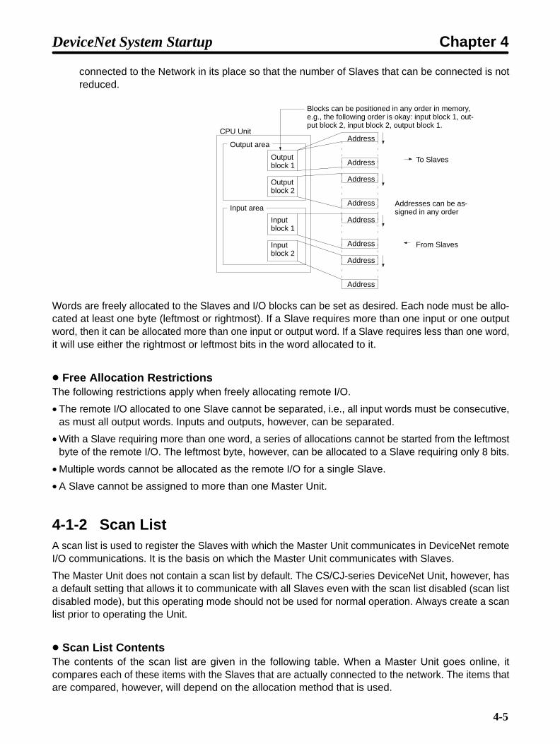
4-5
connected to the Network in its place so that the number of Slaves that can be connected is notreduced.
CPU Unit
Outputblock 1
Outputblock 2
Inputblock 1
Inputblock 2
Blocks can be positioned in any order in memory,e.g., the following order is okay: input block 1, out-put block 2, input block 2, output block 1.
Address
Address
Address
Address
Address
Address
Address
Address
To Slaves
From Slaves
Addresses can be as-signed in any order
Output area
Input area
Words are freely allocated to the Slaves and I/O blocks can be set as desired. Each node must be allo-cated at least one byte (leftmost or rightmost). If a Slave requires more than one input or one outputword, then it can be allocated more than one input or output word. If a Slave requires less than one word,it will use either the rightmost or leftmost bits in the word allocated to it.
Free Allocation RestrictionsThe following restrictions apply when freely allocating remote I/O.
• The remote I/O allocated to one Slave cannot be separated, i.e., all input words must be consecutive,as must all output words. Inputs and outputs, however, can be separated.
• With a Slave requiring more than one word, a series of allocations cannot be started from the leftmostbyte of the remote I/O. The leftmost byte, however, can be allocated to a Slave requiring only 8 bits.
• Multiple words cannot be allocated as the remote I/O for a single Slave.
• A Slave cannot be assigned to more than one Master Unit.
4-1-2 Scan ListA scan list is used to register the Slaves with which the Master Unit communicates in DeviceNet remoteI/O communications. It is the basis on which the Master Unit communicates with Slaves.
The Master Unit does not contain a scan list by default. The CS/CJ-series DeviceNet Unit, however, hasa default setting that allows it to communicate with all Slaves even with the scan list disabled (scan listdisabled mode), but this operating mode should not be used for normal operation. Always create a scanlist prior to operating the Unit.
Scan List ContentsThe contents of the scan list are given in the following table. When a Master Unit goes online, itcompares each of these items with the Slaves that are actually connected to the network. The items thatare compared, however, will depend on the allocation method that is used.
DeviceNet System Startup Chapter 4

4-6
Item Description Fixed allocations Free allocationsusing allocatedDM Area words
Free allocationsusing Configurator
Node address Node address forevery Slave
Compared Compared
Allocated IN/OUTsizes andallocation area
Settings for thenumber of bytesallocated to the MasterUnit and in which area
Compared Compared
Vendor Unique manufacturerID
Not compared Set using Configurator
Device type Unit product typevalue
Not compared Set using Configurator
Product code Unique product modelvalue
Not compared Set using Configurator
Connection type Applicable DeviceNetprotocol
Automatically set Automatically set orset using Configurator
Connection path Type of Slave I/O data Cannot be set Set using Configurator
Note With CVM1-DRM21-V1/C200HW-DRM21-V1 Master Units, only node addresses, allocated IN/OUT sizes, and allocated areas are registered in the scan list.
Creating the Scan ListThe way that a scan list is prepared varies with the allocation method as shown below.
Fixed allocations Free allocations using allocatedDM Area words
Free allocations using Configu-rator
With the CPU Unit in PROGRAMmode:
1. Turn ON a Master FixedAllocation Setting Switch (1 to3).
2. Turn ON the Scan List EnableSwitch.
With the CPU Unit in PROGRAMmode, turn ON the Master UserAllocations Setup Switch.
Create a list from the Configurator.(Obtain a list of online devices,use it to create a scan list, andthen register the scan list in theMaster Unit.)
Note 1. Be sure to create a scan list before starting actual system operation.
Note 2. With fixed allocations, it is possible to communicate with Slaves without creating a scan list(scan list disabled mode). Operating without a scan list, however, may result in faulty opera-tion because the Master Unit will communicate with Slaves even if they do not start up (due toequipment failure, for example).
Scan List Enabled Mode and Scan List Disabled ModeA scan list must be created. The scan list modes are explained below.
Scan List Enabled Mode (Used for Actual Operation)Remote I/O communications are performed according to the registered scan list and only with slavesthat are on the list. A verification error occurs if a slave registered on the scan list is not present on thenetwork, if a slave did not start up when remote I/O communications started, or is the number of I/Opoints did not match the number registered.
DeviceNet System Startup Chapter 4

4-7
Scan List Disabled Mode (Used When Changing the System Configuration)In this mode, remote I/O communications (fixed allocations) are performed without a scan list created(or with the scan list cleared). This mode is used when the scan list is temporarily cleared in order tochange the system configuration. Do not perform actual system operation without a scan list. Use thismode only to replace a Master Unit or change the system configuration (change a connected Slave ornode address).
Note 1. To enter Scan List Disabled Mode, turn ON the Scan List Clear Switch during remote I/O com-munications with the scan list enabled (with fixed allocations, free allocations using the allo-cated DM Area words, or free allocations using the Configurator). Remote I/O communica-tions will be executed using fixed allocations.
Note 2. In Scan List Disabled Mode, all Slaves are targeted for remote I/O communications. Slavesthat are connected to the network while communications are in progress are also targeted forcommunications. Errors cannot be confirmed, however, even if there are slaves present thatdid not start up (due to equipment failure, for example) because there is no scan list availableto check communications against. The communications cycle time will also be significantlylonger than the calculated value.
Note 3. The scan list is automatically enabled when free allocations are set using the allocated DMArea words or the Configurator. If the list is subsequently cleared using a software switch, thefixed allocations that were used when the list was disabled will be used for remote I/O commu-nications. Make sure the system has stopped before disabling the scan list with a Master Unitthat is set for free allocations. In particular, when multiple Master Units are connected to asingle network, communications will not be performed normally if one Master Unit on the net-work is operating with the scan list disabled. Also, once the list is disabled, the free allocationsdata registered in the Master Unit is lost.
4-1-3 Fixed Word Allocations
Allocation Areas for Different PCsIf fixed allocations are used, the node addresses and the words allocated to them are determined ac-cording to the PC or Master Unit used. The remote I/O allocation area consists of the input area thatreceives input from the Slaves, and the output area that writes output data to the Slaves.
DeviceNet System Startup Chapter 4

4-8
Allocations for CS1W-DRM21 and CJ1W-DRM21 Master UnitsNodedd
SYSMAC CS/CJ-series Programmable Controllersaddress Fixed allocation area 1 Fixed allocation area 2 Fixed allocation area 3
Output area
(CIO 3200 toCIO 3263)
Input area
(CIO 3300 toCIO 3363)
Output area
(CIO3400 toCIO 3463)
Input area
(CIO 3500 toCIO 3563)
Output area
(CIO 3600 toCIO 3663)
Input area
(CIO 3700 toCIO 3763)
0 CIO 3200 CIO 3300 CIO 3400 CIO 3500 CIO 3600 CIO 3700
1 CIO 3201 CIO 3301 CIO 3401 CIO 3501 CIO 3601 CIO 3701
2 CIO 3202 CIO 3302 CIO 3402 CIO 3502 CIO 3602 CIO 3702
... ... ... ... ... ... ...
30 CIO 3230 CIO 3330 CIO 3430 CIO 3530 CIO 3630 CIO 3730
31 CIO 3231 CIO 3331 CIO 3431 CIO 3531 CIO 3631 CIO 3731
32 CIO 3232 CIO 3332 CIO 3432 CIO 3532 CIO 3632 CIO 3732
... ... ... ... ... --- ---
48 CIO 3248 CIO 3348 CIO 3448 CIO 3548 CIO 3648 CIO 3748
49 CIO 3249 CIO 3349 CIO 3449 CIO 3549 CIO 3649 CIO 3749
50 CIO 3250 CIO 3350 CIO 3450 CIO 3550 CIO 3650 CIO 3750
... ... ... --- --- --- ---
62 CIO 3262 CIO 3362 CIO 3462 CIO 3562 CIO 3662 CIO 3762
63 CIO 3263 CIO 3363 CIO 3463 CIO 3563 CIO 3663 CIO 3763
Note 1. The fixed allocation area (1, 2, or 3) is selected using a software switch in the area allocated tothe Master Unit.
Note 2. The words corresponding to the node address of the Master Unit are not actually used by theMaster Unit, so they can be used by other Slaves. The actual node address of the Master Unit,however, cannot be the same as the node address of another Slave.
Note 3. When Slaves made by other companies are used that are for either output only or input only,both the output area and the input area may be used depending on the status information.Therefore, be sure to check the specifications of the Slave before using any word allocated toa Slave.
DeviceNet System Startup Chapter 4

4-9
Allocations for CVM1-DRM21-V1 and C200HW-DRM21-V1 Master UnitsNodedd
SYSMAC Programmable Controllersaddress CV-series PCs C200HX/HG/HE PCs C200HS PCs
Output area
(CIO 1900 toCIO 1963)
Input area
(CIO 2000 toCIO 2063)
Output area
(IR 50 to IR 99)
Input area
(IR 350 to IR 399)
Output area
(IR 50 to IR 81)
Input area
(IR 350 to IR 381)
0 CIO 1900 CIO 2000 IR 50 IR 350 IR 50 IR 350
1 CIO 1901 CIO 2001 IR 51 IR 351 IR 51 IR 351
2 CIO 1902 CIO 2002 IR 52 IR 352 IR 52 IR 352
... ... ... ... ... ... ...
30 CIO 1930 CIO 2030 IR 80 IR 380 IR 80 IR 380
31 CIO 1931 CIO 2031 IR 81 IR 381 IR 81 IR 381
32 CIO 1932 CIO 2032 IR 82 IR 382 --- ---
... ... ... ... ... --- ---
48 CIO 1948 CIO 2048 IR 98 IR 398 --- ---
49 CIO 1949 CIO 2049 IR 99 IR 399 --- ---
50 CIO 1950 CIO 2050 --- --- --- ---
... ... ... --- --- --- ---
62 CIO 1962 CIO 2062 --- --- --- ---
63 CIO 1963 CIO 2063 --- --- --- ---
Note 1. The words corresponding to the node address of the Master Unit are not actually used by theMaster Unit, so they can be used by other Slaves. The actual node address of the Master Unit,however, cannot be the same as the node address of another Slave.
Note 2. When Slaves made by other companies are used that are for either output only or input only,both the output area and the input area may be used depending on the status information.Therefore, be sure to check the specifications of the Slave before using any word allocated toa Slave.
Procedure
CS1W-DRM21 or CJ1W-DRM21 Master UnitsFixed allocation is executed using the software switches in the area allocated to the Master Unit,according to the following procedure.
1. Put the CPU Unit in PROGRAM mode.Allocation cannot be executed if the CPU Unit is not in PROGRAM mode. Be sure to put the CPUUnit in PROGRAM mode.
2. Turn ON the Master Enable Switch.It is possible to set CS1W-DRM21 or CJ1W-DRM21 Master Units to function as Slave Units. Enablethe Master Unit functionality by turning ON the Master Enable Switch.
3. Turn ON the Scan List Clear Switch.Disable any scan list that has been created. When the scan list is cleared, all scan list data is lost andso make a backup copy if required.
4. Select fixed allocation area.Select fixed allocation area 1, 2, or 3.
DeviceNet System Startup Chapter 4

4-10
5. Turn ON the Scan List Enable Switch.The Master Unit will create and store a scan list based on information from all the Slaves currentlyparticipating in the network and operate with this scan list enabled. Slaves that are not participatingin the network when this Switch is turned ON are not registered and so check that all the necessarySlaves are participating.
Note If the Master Enable Switch is turned ON when the master function is enabled, or Scan List ClearSwitch is turned ON when the scan list is disabled, a C2 error will be generated to indicate a soft-ware setting error.
CVM1-DRM21-V1 or C200HW-DRM21-V1 Master UnitsFixed allocation is executed using the software switches in the area allocated to the Master Unit,according to the following procedure.
1. Put the CPU Unit in PROGRAM mode.Allocation cannot be executed if the CPU Unit is not in PROGRAM mode. Be sure to put the CPUUnit in PROGRAM mode.
2. Turn ON the Scan List Clear Switch.Disable any scan list that has been created. When the scan list is cleared, all scan list data is lost andso make a backup copy if required.
3. Turn ON the Scan List Enable Switch.The Master Unit will create and store a scan list based on information from all the Slaves currentlyparticipating in the network and operate with this scan list enabled. Slaves that are not participatingin the network when this Switch is turned ON are not registered and so check that all the necessarySlaves are participating.
I/O Allocations and ErrorsA setup error may occur when the scan list is disabled or a verification error may occur when the scan listis enabled if I/O allocations are not correct.
Setup Error: I/O Area OverlapA setup error (I/O Area Overlap) will occur and it will not be possible to start DeviceNet communicationsif the same word is used by more than one Slave connected to a SYSMAC Master Unit. This error willoccur only when the scan list is disabled.To eliminate the I/O area overlap and clear this error, change the node address setting on one of theSlaves and restart the Master Unit by turning ON the power again or restarting.
Setup Error: I/O Area Range ViolationA setup error (I/O Area Range Violation) will occur and it will not be possible to start DeviceNet commu-nications if node addresses are set at values that exceed the specified range, or if Slaves that use multi-ple words are using more words than are specified in the I/O area. This error will occur only when thescan list is disabled.To eliminate the above problems and clear this error, change the node address setting on the Slavesand restart the Master Unit by turning ON the power again or restarting.
Verification Error: Slave I/O Size DiffersWith the scan list enabled, if there are differences between the information in the scan list and theinformation from Slaves actually participating in the network, a verification error will occur and it will not
DeviceNet System Startup Chapter 4

4-11
be possible to start DeviceNet communications. This error will occur only when the scan list is enabled.To eliminate and clear this error, either create the scan list again or restore the network configurationcorresponding to the scan list.
Fixed Allocation ExampleNodeaddress
Outputpoints
Inputpoints
Output area Input area
Allocation not possible
Allocation not possible
Allocationnot possible
Allocation not possible
Allocation possible
Allocated
Allocated
Allocated
Allocated
Allocated
Allocated
Not used
CIO 3200
CIO 3201
CIO 3202
CIO 3203
CIO 3204
CIO 3205
CIO 3206
CIO 3207
CIO 3208
CIO 3209
CIO 3210
CIO 3211
CIO 3212
8
0
16
16
0
8
48
(see note 3)
0
0
8
16
8
16
0
0
1
2
3
4
5
6
7
8
9
10
11
63 None None
Allocationnot possible
Allocationnot possible
Allocationnot possible
Allocated
Allocated
Allocated
Allocated
Allocated
Allocated
Allocated
Allocation possible
Not used
Allocation not possible
Allocation not possible
CIO 3300
CIO 3301
CIO 3302
CIO 3303
CIO 3304
CIO 3305
CIO 3306
CIO 3307
CIO 3308
CIO 3309
CIO 3310
CIO 3311
CIO 3312
Master Unit (see note 2)
. . .
. . .
. . .
12 NoneNone
3232 . . .
Not usedCIO 3263 Not usedCIO 3363
Allocated
Allocated
Allocated
Allocated
032 . . .
Note 1. The above example is for allocations in a CS/CJ-series PC.
Note 2. The Master Unit is not allocated any words, so any available node address can be used asnode address 7.
Note 3. Slaves can be allocated to the words labeled “Allocation possible” as long as the same wordsare not allocated to more than one Slave.
Basic Application Procedure1. Set the initial settings for the Master Unit:
CS1W-DRM21 or CJ1W-DRM21
Unit number (“UNIT No.” switch on front panel)Node address (node address switches on front panel)Baud rate (front panel DIP switch pins 1 and 2)Communications continue/stop setting for communications error (front panel DIP switch pin 3)Hold/clear remote output setting for communications error (front panel DIP switch pin 4)
CVM1-DRM21-V1
Unit number (“UNIT No.” switch on front panel)Node address (back panel DIP switch pins 1 to 6)Baud rate (front panel DIP switch pins 1 and 2)Communications continue/stop setting for communications error (front panel switch pin 3)
DeviceNet System Startup Chapter 4

4-12
C200HW-DRM21-V1
Unit number (“MACHINE No.” switch on front panel)Node address (back panel DIP switch pins 1 to 6)Baud rate (front panel DIP switch pins 1 and 2)Communications continue/stop setting for communications error (front panel switch pin 3)
2. Set the initial settings for the Slaves:
Node address (DIP switch)Baud rate (DIP switch)Etc.
3. Mount the Master Unit and wire the Network.
For CV-series PCs, Master Units can be mounted to the CPU Rack or Expansion CPU Rack. Onlyone Master Unit can be mounted.
For CS-series and C200HX/HG/HE PCs, Master Units can be mounted to the CPU Rack or Expan-sion I/O Rack. Only one Master Unit can be mounted.
For C200HS PCs, Master Units can be mounted to the CPU Rack or Expansion I/O Rack. Only oneMaster Unit can mounted.
4. Connect a Programming Device to the PC and turn ON the power supply to the PC.
5. Generate the I/O table.
6. Turn ON the power supply to the Slaves and turn ON the communications power supply.
7. Switch the PC to PROGRAM mode. (See note 1.)
8. Perform the following and go to step 11. if the scan list was disabled at startup. Otherwise, go to step9.
a) Turn ON a Fixed Allocation Switch (1 to 3). (See note 2.)
b) Confirm that communications are possible with the registered slaves by monitoring the Regis-tered Slave Data Area.
c) From a Programming Device connected to the PC, turn ON the Scan List Enable Bit in the soft-ware switches (bit 0).
Remote I/O communications will start with the scan list enabled. The software switches can be usedto start and stop remote I/O communications.
9. Perform the following from the Programming Device connected to the PC and go to step 11. if thescan list was enabled at startup and you want to re-register the scan list. Otherwise, go to step 10.
a) Turn ON the Scan List Clear Bit in the software switches (bit 1).
b) Turn ON a Fixed Allocation Switch (1 to 3). (See note 2.)
c) Confirm that communications are possible with the registered slaves by monitoring the Regis-tered Slave Data Area.
d) Turn ON the Scan List Enable Bit in the software switches (bit 0).
Remote I/O communications will start with the scan list enabled. The software switches can be usedto start and stop remote I/O communications.
10. Do nothing if the scan list was enabled at startup and the scan list does not need to be changed.
Remote I/O communications will start with the scan list enabled. The software switches can be usedto start and stop remote I/O communications. Go to step 11.
DeviceNet System Startup Chapter 4

4-13
11. Confirm that the MS and NS indicators on all Master Units and Slaves are lit.
12. Switch the PC to RUN mode.
Note 1. With the CS1W-DRM21 or CJ1W-DRM21, if the slave function is being used, switch to themaster function by turning ON the Master Enable Switch.
Note 2. This operation is not required with the CVM1-DRM21-V1 or C200HW-DRM21-V1 becausethere is only one fixed allocation area.
4-1-4 Free Allocations
Allocation Areas and Maximum Words for Different PCs and MasterUnits
When free allocations are used, the remote I/O areas consist of IN blocks, which input Slave data to thePC, and OUT blocks, which output data from the PC to the Slaves. These blocks can be allocated asdesired using the following words. Each block, however, must consist of continuous words within onedata area.
CS1W-DRM21 and CJ1W-DRM21 Master UnitsPC CS/CJ Series (all models)Setting method Set using allocated DM Area
words (See note 1.)Set using Configurator
Words that can be allocated CIO: 0000 to 6143WR: W000 to W511HR: HR000 to HR511DM: D00000 to D32767EM: E00000 to E32767 (Banks 0 to C)
Maximum number of words 1 block: 500 words max.
OUT 1 and IN 1 can be createdanywhere in the above areas.
(Maximum: 1,000 words)
1 block: 500 words max.
OUT 1, IN 1, OUT 2, and IN 2 canbe created anywhere in the aboveareas.
(Maximum: 2,000 words)
Note 1. Free allocation using allocated DM Area words is only possible with the CS1W-DRM21 orCJ1W-DRM21. To perform free allocation with other Master Units, use the Configurator.
Note 2. The Data Memory (DM) Area cannot manipulated by bit, so it is not suitable as the remote I/Oallocation area for the Inverter.
DeviceNet System Startup Chapter 4

4-14
CVM1-DRM21-V1 and C200HW-DRM21-V1 Master Units
PC SYSMAC Programmable Controllers
CV-series PCs CS1-seriesPC
C200HX/HG/HE PCs C200HS PCs( ll d l )CV500/
CVM1-CPU01-E
All othermodels
PCs(all models)
C200HE-CPU11-E
All othermodels
(all models)
Wordsthat canbeallocated
CIO 0000 toCIO 2427
CIO 0000toCIO 2555
CIO 000 toCIO 235,CIO 300 toCIO 511
IR 000 to IR 235, IR 300 to IR 511
IR 000 toIR 235, IR 300to IR 511
G008 to G255 HR 000 toH099,CIO 1000 toCIO 1063
HR 00 to HR 99LR 00 to LR 63
HR 00 to HR99LR 00 to LR63
D00000 toD08191
D00000 toD24575
D00000 toD05999
DM 0000 toDM 4095
DM 0000toDM 5999
DM 0000 toDM 5999
Max. No.of words
Each block can be up to100 words (including unusedareas).
The total number of words inall four blocks must be 400words or less.
Each block can be up to 100 words (includingunused areas).
The total number of words in all four blocksmust be 300 words or less (including unusedareas).
If message communications are used, thetotal number of words in all four blocks mustbe 100 words or less.
The totalnumber ofwords in allfour blocksmust be 80words or less(includingunusedareas).
Note 1. The Data Memory (DM) Area cannot manipulated by bit, so it is not suitable as the remote I/Oallocation area for the Inverter.
Note 2. If a CPU Bus Link is used with a CV-series PC, the G Area is used for the CPU Bus Link, mak-ing it impossible to use this area for DeviceNet communications.
Output block 1
Output block 2
Start word
No. of wordsallocated (“oc-cupied”)
Start word
No. of wordsallocated (“oc-cupied”)
Input block 1
Input block 2
Start word
No. of wordsallocated (“oc-cupied”)
Start word
Output area Input area
No. of wordsallocated (“oc-cupied”)
Note 1. OUT 1 and IN 1 can be set using the allocated DM Area words. For each block, set the area,the start word, and the number of words allocated to each Slave.
Note 2. OUT 1, IN 1, OUT 2, and IN 2 can be set using a Configurator. For each block, set the area, thestart word, the number of words allocated to the block, and the number of words allocated toeach Slave.
DeviceNet System Startup Chapter 4

4-15
Free Allocation Restrictions• Each node address can be set only once in the output blocks and once in the input blocks.
The same node ad-dress cannot be settwice. Output block 1
Node 02
Output block 2
Node 02WRONG
• If a Configurator is used to freely allocate words or bytes to each Slave, only a Slave using only onebyte (8 bits) can be set in the leftmost byte of the allocated word. Slaves with more than 8 bits cannot beset for the leftmost bit of the allocated word.
Only one byte can be setif the first byte is a left-most byte.
Start byte
WRONG
15 0
• The same Slave cannot be allocated words in more than one Master.
Master Master
Slave
Words must be allocated to aSlave from one Master only.
WRONG
Note The master parameter file duplication check from the Configurator can be used to check for nodeaddresses that have been set more than once in the scan list, which shows the I/O allocations thathave been made.
• Always use the Configurator when there is more than one Master and enable the scan lists. A Bus OFFerror can occur if there is more than one Master with the scan list disabled on the same Network.
Free Allocation Restrictions When Using Allocated DM Area Words• Allocation in Order of Node Address
When using allocated DM Area words, words are allocated in order of node address. It is possible notto allocated words to a node address but the order cannot be changed.
• Only OUT 1 and IN 1 Can Be UsedWhen using allocated DM Area words, only two blocks (OUT 1 and IN 1) can be allocated. Four blockscan be allocated using the Configurator.
• Slaves of 1 Byte or Less Can Not Be Allocated to the Leftmost ByteWith the Configurator, Slaves requiring one byte or less can be allocated the leftmost byte of a word,but this is not possible when using allocated DM Area words.
DeviceNet System Startup Chapter 4
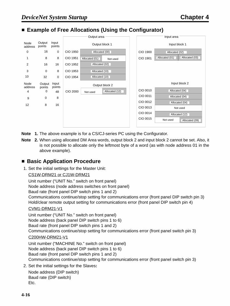
4-16
Example of Free Allocations (Using the Configurator)Output area
CIO 1950
CIO 1951
CIO 1952
CIO 1953
CIO 1954
CIO 2000
Allocated (01) Not used
Not used Allocated (12)
Allocated (02)
Allocated (10)
Allocated (10)
Allocated (02)
Allocated (01)
Allocated (00) CIO 1900
CIO 1901 Allocated (03)
Allocated (04)
Allocated (04)
Allocated (04)
Allocated (12)
Allocated (09)Not used
Not used
Input area
Output block 1
Input block 2Output block 2
Input block 1Nodeaddress
Outputpoints
Inputpoints
0
1
2
3
10
16
8
16
0
32
0
8
16
8
0
Nodeaddress
4
9
12
0
0
8
48
8
16
Inputpoints
Outputpoints
CIO 0010
CIO 0011
CIO 0012
CIO 0013
CIO 0014
CIO 0015
Note 1. The above example is for a CS/CJ-series PC using the Configurator.
Note 2. When using allocated DM Area words, output block 2 and input block 2 cannot be set. Also, itis not possible to allocate only the leftmost byte of a word (as with node address 01 in theabove example).
Basic Application Procedure1. Set the initial settings for the Master Unit:
CS1W-DRM21 or CJ1W-DRM21
Unit number (“UNIT No.” switch on front panel)Node address (node address switches on front panel)Baud rate (front panel DIP switch pins 1 and 2)Communications continue/stop setting for communications error (front panel DIP switch pin 3)Hold/clear remote output setting for communications error (front panel DIP switch pin 4)
CVM1-DRM21-V1
Unit number (“UNIT No.” switch on front panel)Node address (back panel DIP switch pins 1 to 6)Baud rate (front panel DIP switch pins 1 and 2)Communications continue/stop setting for communications error (front panel switch pin 3)
C200HW-DRM21-V1
Unit number (“MACHINE No.” switch on front panel)Node address (back panel DIP switch pins 1 to 6)Baud rate (front panel DIP switch pins 1 and 2)Communications continue/stop setting for communications error (front panel switch pin 3)
2. Set the initial settings for the Slaves:
Node address (DIP switch)Baud rate (DIP switch)Etc.
DeviceNet System Startup Chapter 4

4-17
3. Mount the Master Unit and wire the Network.
For CV-series PCs, Master Units can be mounted to the CPU Rack or Expansion CPU Rack. Up to16 Master Units can be mounted.
For C200HX/HG/HE PCs, Master Units can be mounted to the CPU Rack or Expansion I/O Rack.Up to 10 or 16 Master Units can be mounted.
For C200HS PCs, Master Units can be mounted to the CPU Rack or Expansion I/O Rack. Up to 10Master Units can be mounted.
4. Connect a Programming Device to the PC and turn ON the power supply to the PC.
5. Generate the I/O table.
6. Turn OFF the power to the PC.
7. Go to step 8. if only one Master Unit is being used. Go to step 15. if more than one Master Unit isbeing used in the same Network. Go to step 29. if allocated DM Area words are used for allocations.
8. Connect a Configurator to the Network.
9. Turn ON the power supply to all nodes.
10. Switch the PC to PROGRAM mode. (See note.)
11. Get the device list and create the master parameters with the Configurator.
12. If more than one Master Unit is mounted to the same PC, use the Configurator to check for duplica-tion in the master parameter settings.
13. Register the master parameters in the Master Unit(s).
14. Go to step 32.
15. Connect a Configurator to the Network.
16. Turn ON the power supply to all the Slaves.
17. Read the Network configuration from the Configurator. (See note.)
18. Turn OFF the power supply to all the Slaves.
19. Create the master parameters for each Master Unit and save the parameters in files.
20. Turn ON the power supply to one PC (i.e., to one of the Master Units).
21. Switch the PC to PROGRAM mode.
22. Read the Network configuration from the Configurator.
23. Read the master parameter file for the Master Unit that has been turned ON from the master param-eter editing screen.
24. Write the master parameters created in the above step 19.
25. Turn OFF the power supply to the PC (i.e., the Master Unit) and the Slaves.
26. Repeat the above steps beginning at step 20. for all Master Units.
27. Turn ON the power supply to all Masters and Slaves.
28. Go to step 32.
29. Switch the PC to PROGRAM mode. (See note.)
30. Set the Master User Allocations Tables for the allocated DM Area words in each Master Unit.
31. Turn ON the Master User Allocations Switch for each Master Unit.
32. Remote I/O communications will start with the scan list enabled. (Communications will not start ifthey have been set to be stopped at startup from the Configurator.) Use the software switches orConfigurator to start and stop remote I/O communications.
DeviceNet System Startup Chapter 4

4-18
33. Confirm that the MS and NS indicators on all Master Units and Slaves are lit.
34. Read the Network configuration from the Configurator.
35. Save the Network configuration in a file from the Configurator.
36. Switch the PC to RUN mode.
Note With the CS1W-DRM21 or CJ1W-DRM21, if the slave function is being used, switch to the masterfunction by turning ON the Master Enable Switch.
DeviceNet System Startup Chapter 4
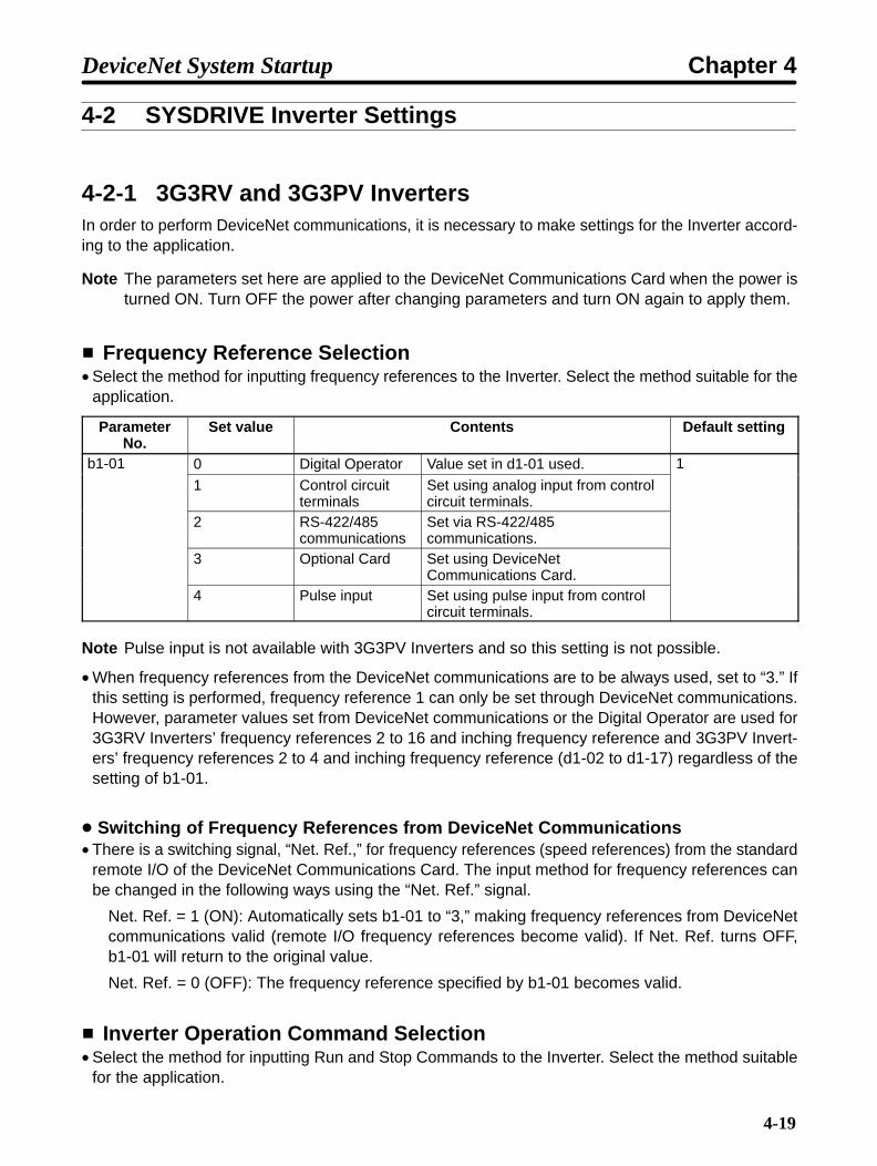
4-19
4-2 SYSDRIVE Inverter Settings
4-2-1 3G3RV and 3G3PV InvertersIn order to perform DeviceNet communications, it is necessary to make settings for the Inverter accord-ing to the application.
Note The parameters set here are applied to the DeviceNet Communications Card when the power isturned ON. Turn OFF the power after changing parameters and turn ON again to apply them.
Frequency Reference Selection• Select the method for inputting frequency references to the Inverter. Select the method suitable for the
application.
ParameterNo.
Set value Contents Default setting
b1-01 0 Digital Operator Value set in d1-01 used. 1
1 Control circuitterminals
Set using analog input from controlcircuit terminals.
2 RS-422/485communications
Set via RS-422/485communications.
3 Optional Card Set using DeviceNetCommunications Card.
4 Pulse input Set using pulse input from controlcircuit terminals.
Note Pulse input is not available with 3G3PV Inverters and so this setting is not possible.
• When frequency references from the DeviceNet communications are to be always used, set to “3.” Ifthis setting is performed, frequency reference 1 can only be set through DeviceNet communications.However, parameter values set from DeviceNet communications or the Digital Operator are used for3G3RV Inverters’ frequency references 2 to 16 and inching frequency reference and 3G3PV Invert-ers’ frequency references 2 to 4 and inching frequency reference (d1-02 to d1-17) regardless of thesetting of b1-01.
Switching of Frequency References from DeviceNet Communications• There is a switching signal, “Net. Ref.,” for frequency references (speed references) from the standard
remote I/O of the DeviceNet Communications Card. The input method for frequency references canbe changed in the following ways using the “Net. Ref.” signal.
Net. Ref. = 1 (ON): Automatically sets b1-01 to “3,” making frequency references from DeviceNetcommunications valid (remote I/O frequency references become valid). If Net. Ref. turns OFF,b1-01 will return to the original value.
Net. Ref. = 0 (OFF): The frequency reference specified by b1-01 becomes valid.
Inverter Operation Command Selection• Select the method for inputting Run and Stop Commands to the Inverter. Select the method suitable
for the application.
DeviceNet System Startup Chapter 4
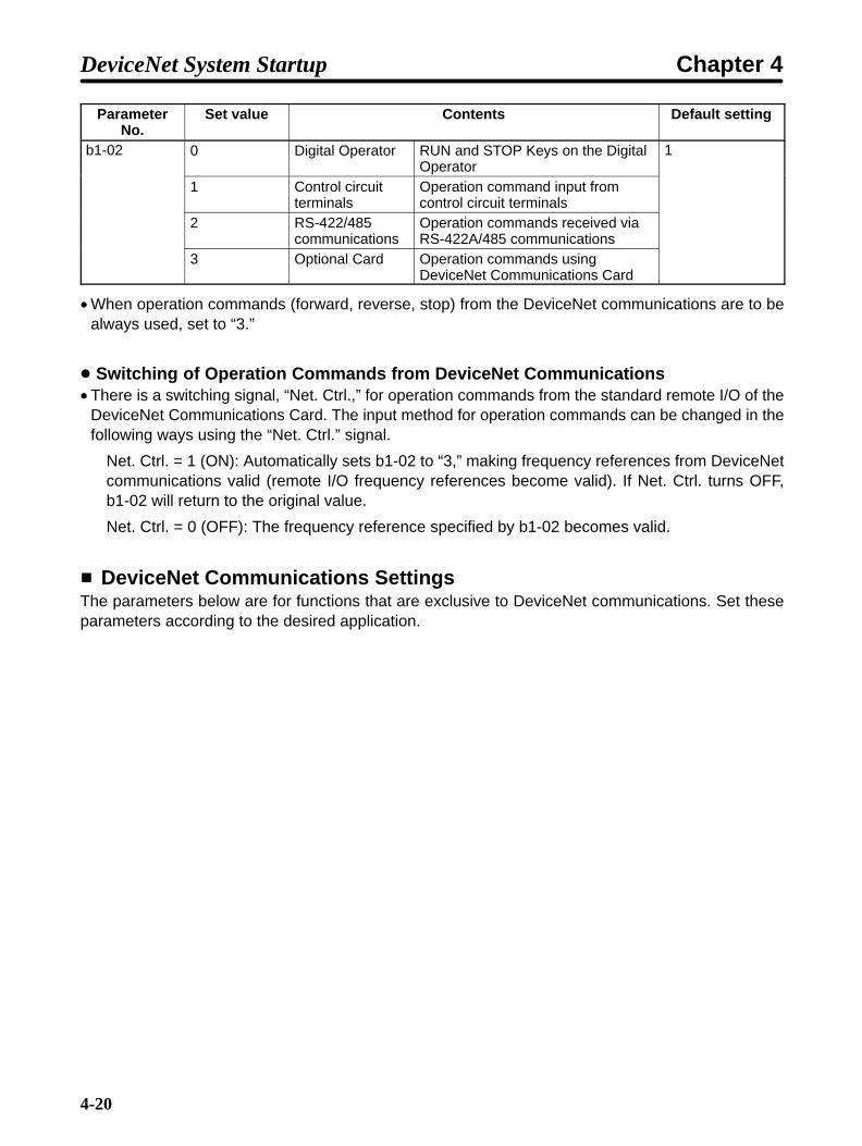
4-20
ParameterNo.
Set value Contents Default setting
b1-02 0 Digital Operator RUN and STOP Keys on the DigitalOperator
1
1 Control circuitterminals
Operation command input fromcontrol circuit terminals
2 RS-422/485communications
Operation commands received viaRS-422A/485 communications
3 Optional Card Operation commands usingDeviceNet Communications Card
• When operation commands (forward, reverse, stop) from the DeviceNet communications are to bealways used, set to “3.”
Switching of Operation Commands from DeviceNet Communications• There is a switching signal, “Net. Ctrl.,” for operation commands from the standard remote I/O of the
DeviceNet Communications Card. The input method for operation commands can be changed in thefollowing ways using the “Net. Ctrl.” signal.
Net. Ctrl. = 1 (ON): Automatically sets b1-02 to “3,” making frequency references from DeviceNetcommunications valid (remote I/O frequency references become valid). If Net. Ctrl. turns OFF,b1-02 will return to the original value.
Net. Ctrl. = 0 (OFF): The frequency reference specified by b1-02 becomes valid.
DeviceNet Communications SettingsThe parameters below are for functions that are exclusive to DeviceNet communications. Set theseparameters according to the desired application.
DeviceNet System Startup Chapter 4

4-21
ParameterN
Name Contents Setting DefaultiNo. Operator display
grange setting
F6-01 Communications fault operation Select the Inverter operationperformed when a communicationsfault is detected.
0: Decelerates to a stop usingC1-02 deceleration time/faultdetection
0 to 3 1
Comm Bus Flt Sel 1: Coasts to a stop/fault detection
2: Decelerates to a stop using theC1-09 emergency stop time/faultdetection
3: Continues operating/alarmdetection (See note 1.)
F6-02 Communications external faultinput: detection method
Select the detection method usedfor the communications externalfault input from communications(DeviceNet CommunicationsCard).
0, 1 0
EF0 Detection 0: Faults always detected.
1: Faults detected only whilerunning (i.e., when RunCommands are input)
F6-03 Communications external faultinput: operation
Select the Inverter operationperformed when there is acommunications external fault(EF0) input from communications(DeviceNet CommunicationsCard).
0: Decelerates to a stop usingC1-02 deceleration time/faultdetection
0 to 3 1
EF0 Fault Actiondetection
1: Coats to a stop/fault detection
2: Decelerates to a stop using theC1-09 emergency stop time/faultdetection
3: Continues operating/alarmdetection
F6-04 Not used Do not set.(3G3PV Inverters do not have this
--- 0
Trace Sample Tim(3G3PV Inverters do not have thisparameter.)
F6-05 Current monitor display unitselection
Select the display unit formonitoring the current. Always setthis parameter to 0 when using aDeviceNet Communications Card.
0, 1 0
Current Unit SelDeviceNet Communications Card.
0: A (ampere) display
1: 100%/8192
Note If F6-01 is set to 3 (continues operating), the Inverter will continue operating when a communica-tions fault occurs according to the contents of settings immediately before. Be sure to take anysteps necessary to ensure safety, such as installing a limit switch or an emergency stop switch.
DeviceNet System Startup Chapter 4

4-22
Frequency Reference Settings and Display Units• Perform the following settings to specify units for data related to frequencies (speeds) used in Device-
Net communications.
• The standard unit used with DeviceNet is r/min, so always set the number of motor poles.
ParameterNo.
Set value Contents Default setting
o1-o3 0 0.01 Hz 0
1 0.01% (max. frequency is 100%)2 to 39 r/min (Set the number of motor poles.)40 to 3,999 Specifies the value used to set and display the
maximum frequency.
Set a 4-digit value without thedecimal point.Set the position of the digit wherethe decimal point is to be displayedstarting from the rightmost digit.
Example: To display the maximum frequency as “200.0”specify “12000.”
4-2-2 3G3FV InvertersIn order to perform DeviceNet communications, it is necessary to make settings for the Inverter accord-ing to the application.
Note The parameters set here are applied to the DeviceNet Communications Card when the power isturned ON. Turn OFF the power after changing parameters and turn ON again to apply them.
Frequency Reference Selection• Select the method for inputting frequency references to the Inverter. Select the method suitable for the
application.
ParameterNo.
Set value Contents Default setting
b1-01 0 d1-01 Value set in d1-01 used. 1
1 Externalterminals
Set using analog input from controlcircuit terminals.
2 Not used (Do not set.)3 Optional Card Set using DeviceNet
Communications Card.
• When frequency references from the DeviceNet communications are to be always used, set to “3.” Ifthis setting is performed, frequency reference 1 can only be set through DeviceNet communications.However, parameter values set from DeviceNet communications or the Digital Operator are used forfrequency references 2 to 8 and the inching frequency reference (d1-02 to d1-09) regardless of thesetting of b1-01.
DeviceNet System Startup Chapter 4

4-23
Switching of Frequency References from DeviceNet Communications• There is a switching signal, “Net. Ref.,” for frequency references (speed references) from the standard
remote I/O of the DeviceNet Communications Card. The input method for frequency references canbe changed in the following ways using the “Net. Ref.” signal.
Net. Ref. = 1 (ON): Automatically sets b1-01 to “3,” making frequency references from DeviceNetcommunications valid (remote I/O frequency references become valid). If Net. Ref. turns OFF,b1-01 will return to the original value.
Net. Ref. = 0 (OFF): The frequency reference specified by b1-01 becomes valid.
Inverter Operation Command Selection• Select the method for inputting Run and Stop Commands to the Inverter. Select the method suitable
for the application.
ParameterNo.
Set value Contents Default setting
b1-02 0 Operator Operation commands from theDigital Operator
1
1 Externalterminals
Control circuit terminals (sequenceinput)
2 Not used (Do not set.)3 Optional Card Operation commands using
DeviceNet Communications Card
• When operation commands (forward, reverse, stop) from the DeviceNet communications are to bealways used, set to “3.”
Switching of Operation Commands from DeviceNet Communications• There is a switching signal, “Net. Ctrl.,” for operation commands from the standard remote I/O of the
DeviceNet Communications Card. The input method for operation commands can be changed in thefollowing ways using the “Net. Ctrl.” signal.
Net. Ctrl. = 1 (ON): Automatically sets b1-02 to “3,” making frequency references from DeviceNetcommunications valid (remote I/O frequency references become valid). If Net. Ctrl. turns OFF,b1-02 will return to the original value.
Net. Ctrl. = 0 (OFF): The frequency reference specified by b1-02 becomes valid.
DeviceNet Communications SettingsThe parameters below are for functions that are exclusive to DeviceNet communications. Set theseparameters according to the desired application.
ParameterN
Name Contents Setting DefaultiNo. Operator display
grange setting
F9-01 Communications external faultinput: input type
Select the type of input used forthe communications external faultinput from communications(DeviceNet CommunicationsCard).
0, 1 1
EF0 Selection 0: N.O. input (external faultdetected when 1)
1: N.C. input (external faultdetected when 0)
DeviceNet System Startup Chapter 4

4-24
ParameterNo.
Defaultsetting
Settingrange
ContentsNameParameterNo.
Defaultsetting
Settingrange
ContentsOperator display
F9-02 Communications external faultinput: detection method
Select the detection method usedfor the communications externalfault input from communications(DeviceNet CommunicationsCard).
0, 1 0
EF0 Detection 0: Always detect.
1: Detect during operation (i.e.,when operation commands areinput).
F9-03 Communications external faultinput: operation
Select the Inverter operationperformed when there is acommunications external faultinput from communications(DeviceNet CommunicationsCard).
0: Decelerates to a stop usingC1-02 deceleration time/faultdetection
0 to 3 1
EF0 Fault Actiondetection
1: Coats to a stop/fault detection
2: Decelerates to a stop using theC1-09 emergency stop time/faultdetection
3: Continues operating/alarmdetection
F9-04 Not used Do not set. --- 0
Trace Sample Tim
F9-05 Torque reference/torque limitselection from communications
When operating in flux vectorcontrol mode, this setting enablesor disables torque reference andtorque limit values input fromcommunications (DeviceNetCommunications Card).(See note 1 )
0, 1 1
Torq Ref/Lmt Sel(See note 1.)
0: Torque reference/torque limitfrom communications disabled.
1: Torque reference/torque limitfrom communications enabled.
F9-06 Communications fault operation Select the Inverter operationperformed when a communicationsfault is detected.
0: Decelerates to a stop usingC1-02 deceleration time/faultdetection
0 to 3 1
BUS Fault Sel 1: Coats to a stop/fault detection
2: Decelerates to a stop using theC1-09 emergency stop time/faultdetection
3: Continues operating/alarmdetection
DeviceNet System Startup Chapter 4

4-25
Note 1. Be sure to set F9-05 when using flux vector control. If used with the default setting (1), unlessthere is a torque reference/torque limit from control remote I/O, 0 will be taken as the torquereference/torque limit, and there will be no torque output.
Note 2. If F9-06 is set to 3 (continues operating), the Inverter will continue operating when a commu-nications fault occurs according to the contents of settings immediately before. Be sure totake any steps necessary to ensure safety, such as installing a limit switch or an emergencystop switch.
Frequency Reference Settings and Display Units• Perform the following settings to specify units for data related to frequencies (speeds) used in Device-
Net communications.
• The standard unit used with DeviceNet is r/min, so always set the number of motor poles.
ParameterNo.
Set value Contents Default setting
o1-o3 0 0.01 Hz 0
1 0.01% (max. frequency is 100%)2 to 39 r/min (Set the number of motor poles.)40 to 3,999 Specifies the value used to set and display the
maximum frequency.
Set a 4-digit value without thedecimal point.Set the position of the digit wherethe decimal point is to be displayedstarting from the rightmost digit.
Example: To display the maximum frequency as “200.0”specify “12000.”
DeviceNet System Startup Chapter 4

4-26
4-3 Startup Procedure
The communications system can be started from any of the nodes on the Network. The following proce-dure gives the startup process after turning ON the power to the Inverter’s DeviceNet CommunicationsCard. If the startup process shown below is interrupted or stops before being completed, an error willoccur. Correct errors that occur, referring to Chapter 6 Communications Errors.
1. Turn ON the power.
2. The PWR indicator will turn ON: Power is being supplied.
3. The MS indicator will be lit red and then green: Confirming MS indicator status.
4. The NS indicator will be lit red and then green: Confirming MS indicator status.
5. The MS indicator will flash: Shows Optional Card startup processing status.
6. The MS indicator will be lit: The Optional Card is ready.
7. The NS indicator will flash: The Optional Card is connected to the Network and startup processing isbeing performed.
8. The NS indicator will be lit: The Network is started.
DeviceNet System Startup Chapter 4

Chapter 5
DeviceNetCommunications CardOperations
5-1 Remote I/O
5-2 Switching Remote I/O Operation
5-3 Special Remote I/O Operation
5-4 Control Remote I/O Operation
5-5 Message Communications (DeviceNet Explicit Messages)
5-6 3G3RV Register Numbers, Classes, Instances,and Attributes
5-7 3G3PV Register Numbers, Classes, Instances,and Attributes
5-8 3G3FV Register Numbers, Classes, Instances,and Attributes
5

!
!
5-2
Caution Do not carelessly change Inverter’s settings. Doing so may result in injury or dam-age to the product.
Caution Be sure to perform the setting switch settings correctly and confirm the settings be-fore starting operation. Not doing so may result in malfunction or damage to theproduct.
5-1 Remote I/O
There are two types of DeviceNet communications: Remote I/O and message communications. Thereare 4 types of remote I/O operation: Basic remote I/O, standard remote I/O, special remote I/O, andcontrol remote I/O. This section explains standard remote I/O operations and the types of remote I/O.
Note To use special remote I/O or control remote I/O, it is necessary to switch the remote I/O operation.Switching the remote I/O operation involves the use of message communications, so refer to 5-2Switching Remote I/O Operation and 5-5 Message Communications. Also, for details regardingspecial remote I/O, refer to 5-3 Special Remote I/O.
DeviceNet Communications Card Operations Chapter 5

5-3
5-1-1 Standard Remote I/O (Initial Setting)The type of remote I/O operation pre-set as the initial setting for the Inverter’s DeviceNet Communica-tions Card is standard remote I/O. This remote I/O can be used for general Inverter control.
CS1W-DRM21, CJ1W-DRM21, C200HW-DRM21-V1 orCVM1-DRM21-V1 (Master Unit)
Remote I/O functionOutput (PC to 3G3FV)
Input (3G3FV to PC)
SYSDRIVE Inverter (3G3RV/3G3PV/3G3FV)
3G3FV-PDRT1-SINV1DeviceNet CommunicationsCard
Power supplyMotorSelection of either the communications
control input or local control input ispossible using Net.Ctrl./Net.Ref.
Note: T-branch wiring usingThin Cables
Switch
Run
Forward
Reverse
Stop
Wd 15 to 0n Inverter run commandsn+1 Rotational speed reference
DeviceNet Communications Card Operations Chapter 5

5-4
Words Allocated to SYSDRIVE 3G3RV/3G3PV/3G3FV InvertersA SYSDRIVE 3G3RV/3G3PV/3G3FV Inverter is allocated a total of four SYSMAC I/O words (two inputand two output) via a DeviceNet Communications Card.
I/O classification Word address Bits
15 to 8 7 to 0Output(SYSMAC PC
n Not used. Inverter run commands(SYSMAC PC toInverter)
n+1 Rotational speed reference(leftmost bits)
Rotational speed reference(rightmost bits)
Input(I
m Not used. Inverter status(Inverter toSYSMAC PC)
m+1 Rotational speed monitor(leftmost bits)
Rotational speed monitor(rightmost bits)
Inverter Run CommandsWord n
Bit Bit 7 Bit 6 Bit 5 Bit 4 Bit 3 Bit 2 Bit 1 Bit 0
Signalname
Not used. Net Reference Net Control Not used. Not used. Fault Reset Reverse/stop
Forward/stop
Content --- 0: b1-011: DeviceNet(See note 1.)
0: b1-021: DeviceNet(See note 2.)
--- --- 0: ---1: FaultReset
0: Stop1: Reverse
0: Stop1: Forward
Note 1. Net Reference is used to specify the frequency reference as follows (cannot be changed dur-ing running):0: The frequency reference input method specified by the frequency reference source selec-tion (b1-01) is used.1: Set b1-01 to “3” and operate via DeviceNet. (Operate with rotational speed reference inword n+1.)
Note 2. Net Control is used to change the run command as follows (cannot be changed during run-ning):0: The run command input method specified by the run command source selection (b1-02) isused.1: Set b1-02 to “3” and operate via DeviceNet. (Follow run command in word n, bits 0 and 1.)
Inverter StatusWord m
Bit Bit 7 Bit 6 Bit 5 Bit 4 Bit 3 Bit 2 Bit 1 Bit 0
Signalname
At Reference ReferenceFrom Net
Control FromNet
InverterReady
Duringreverse run
Duringforward run
Warning(MinorFault)
Fault
Content 0: AcceleratingorDecelerating1: At reference
0: b1-011: DeviceNet(See note 1.)
0: b1-021: DeviceNet(See note 2.)
0:Preparing1: Ready
0: Stop/forward1: Duringreverse run(See note 4.)
0: Stop/reverse1: Duringforward run(See note 5.)
0: Normal1: Alarm(MinorFault)
0: Normal1: Fault
Note 1. Reference From Net shows the input status of word n, bit 6 (Net Reference) for DeviceNetcommunications.
Note 2. Control From Net shows the input status of word n, bit 5 (Net Control) for DeviceNet commu-nications.
Note 3. Reverse Operation indicates reverse output status. This bit does not turn ON for DC braking(DC injection).
DeviceNet Communications Card Operations Chapter 5

5-5
Note 4. Forward Operation indicates either forward run status or DC braking (DC injection) status.This bit turns ON even for DC braking (DC injection) during reverse run.
Rotational Speed Reference DataWord address n+1
Bit 15 14 13 12 11 10 9 8 7 6 5 4 3 2 1 0
Signal name Rotational speed reference data
Content Communications data = Rotational speed reference x 2a
a: Speed scale value of Class 2A, Instance 01, Attribute 16 (Initial value: 0)
• The speed scale is assigned to the message function. For instructions on how to change it, refer to 5-5 Mes-
sage Communications.
• The unit for the rotational speed reference is set in o1-03 (frequency reference setting and display units)
• Setting example (providing reference of 1,800 r/min):
When the speed scale value is “0” and the number of motor poles is set in 01-03 (so unit is r/min):
1,800 r/min → 1,800 x20 → 1,800 → 0708 Hex
Note 1. Under the DeviceNet protocol, the unit for the speed reference is fixed as r/min. The numberof motor poles (2 to 39) must be set in parameter o1-03 (frequency reference setting and dis-play units) when using DeviceNet (open network).
Note 2. If the setting in not within the proper range, the previous data will be retained and the desig-nated rotational speed will not be entered.
Rotational Speed Monitor DataWord address m+1
Bit 15 14 13 12 11 10 9 8 7 6 5 4 3 2 1 0
Signal name Rotational speed monitor data
Content Communications data = Rotational speed monitor x 2a
a: Speed scale value of Class 2A, Instance 01, Attribute 16 (Initial value: 0)
• The speed scale is assigned to the message function. For instructions on how to change it, refer to 5-5 Mes-
sage Communications.
• The unit for the rotational speed monitor is set in o1-03 (frequency reference setting and display units)
• Data conversion example:
When the speed scale value is “0” and the number of motor poles is set in 01-03, and the read data is 03E8 Hex:
03E8 Hex → 1,000 → 1,000/20 → 1,000 r/min
Note Under the DeviceNet protocol, the unit for the speed reference is fixed as r/min. The number ofmotor poles (2 to 39) must be set in parameter o1-03 (frequency reference setting and displayunits) when using DeviceNet (open network).
5-1-2 Types of Remote I/O OperationThere are 4 types of DeviceNet Communications Card remote I/O operation:
• Basic remote I/O: Remote I/O operation for the standard DeviceNet configuration.
• Standard remote I/O: Remote I/O operation (DeviceNet-compatible) that is the default setting for theDeviceNet Communications Card.
• Special remote I/O: Remote I/O operations that enable using all the functions of3G3RV/3G3PV/3G3FV Inverters, and accessing/setting for all parameters. (Special remote I/O op-eration is a special function of this product; it is not compatible with DeviceNet.)
DeviceNet Communications Card Operations Chapter 5

5-6
• Control remote I/O: Remote I/O operation according to the control terminal input/output signals of3G3RV/3G3PV/3G3FV Inverters. (Control remote I/O operation is a special function of this product; itis not compatible with DeviceNet.)
The default setting is for standard remote I/O operation, so it will be necessary to switch to either of theother types of remote I/O operation if desired. Switching the remote I/O operation involves the use ofmessage communications. Refer to 5-5 Message Communications and 5-2 Switching Remote I/O Op-eration.
Basic Remote I/OBasic remote I/O is used for the standard DeviceNet configuration.
Outputs (SYSMAC PC to Inverter) Instance ID: 20 Dec (14 Hex)Byte number Bit 7 Bit 6 Bit 5 Bit 4 Bit 3 Bit 2 Bit 1 Bit 0
Wd n Rightmost 0 FaultReset
Forward/stop
Leftmost 1
Wd n+1 Rightmost 2 Rotational speed reference (rightmost data)
Leftmost 3 Rotational speed reference (leftmost data)
Inputs (Inverter to SYSMAC PC) Instance ID: 70 Dec (46 Hex)Byte number Bit 7 Bit 6 Bit 5 Bit 4 Bit 3 Bit 2 Bit 1 Bit 0
Wd m Rightmost 0 Duringforwardrun
Fault
Leftmost 1
Wd m+1 Rightmost 2 Rotational speed reference (rightmost data)
Leftmost 3 Rotational speed reference (leftmost data)
Note 1. A shaded box indicates that the bit is not used.
Note 2. The basic remote I/O operation is the same as those explained for standard remote I/O. (Ba-sic remote I/O restricts the operation of standard remote I/O.)
Standard Remote I/OStandard remote I/O is the default setting for the DeviceNet Communications Card.
Outputs (SYSMAC PC to Inverter) Instance ID: 21 Dec (15 Hex)Byte number Bit 7 Bit 6 Bit 5 Bit 4 Bit 3 Bit 2 Bit 1 Bit 0
Wd n Rightmost 0 NetReference
NetControl
FaultReset
Reverse/stop
Forward/stop
Leftmost 1
Wd n+1 Rightmost 2 Rotational speed reference (rightmost data)
Leftmost 3 Rotational speed reference (leftmost data)
Inputs (Inverter to SYSMAC PC) Instance ID: 71 Dec (47 Hex)Byte number Bit 7 Bit 6 Bit 5 Bit 4 Bit 3 Bit 2 Bit 1 Bit 0
Wd m Rightmost 0 AtReference
ReferenceFrom Net
ControlFrom Net
InverterReady
Duringreverserun
Duringforwardrun
Warning(minorfault)
Fault
Leftmost 1
Wd m+1 Rightmost 2 Rotational speed monitor (rightmost data)
Leftmost 3 Rotational speed monitor (leftmost data)
DeviceNet Communications Card Operations Chapter 5

5-7
Note A shaded box indicates that the bit is not used.
Special Remote I/OSpecial remote I/O enables using all the functions of 3G3RV/3G3PV/3G3FV Inverters, and accessing/setting all parameters.
Outputs (SYSMAC PC to Inverter) Instance ID: 100 Dec (64 Hex)Byte number Bit 7 Bit 6 Bit 5 Bit 4 Bit 3 Bit 2 Bit 1 Bit 0
Wd n Rightmost 0 Function code (write/read code)
Leftmost 1 Register number, leftmost byte (register number assigned to various parameters, etc.)
Wd n+1 Rightmost 2 Register number, rightmost byte (register number assigned to various parameters, etc.)
Leftmost 3 Register data, leftmost byte (data to write to specified register)
Wd n+2 Rightmost 4 Register data, rightmost byte (data to write to specified register)
Inputs (Inverter to SYSMAC PC) Instance ID: 150 Dec (96 Hex)Byte number Bit 7 Bit 6 Bit 5 Bit 4 Bit 3 Bit 2 Bit 1 Bit 0
Wd m Rightmost 0 Function code (returns transmitted code)
Leftmost 1 Register number, leftmost byte (returns transmitted register number)
Wd m+1 Rightmost 2 Register number, rightmost byte (returns transmitted register number)
Leftmost 3 Register data, leftmost byte (return transfer data amount or read data)
Wd m+2 Rightmost 4 Register data, rightmost byte (return transfer data amount or read data)
Note 1. Special remote I/O outputs and inputs are paired. When using special remote I/O, be sure toset them together.
Note 2. Special remote I/O objects do not conform to the AC/DC drive profile, but are specially set forthis product.
Note 3. The 16-bit data (register number and register data) is set using two words for each setting.
Note 4. Be careful of the order of the leftmost and rightmost bytes of the 16-bit data. The order is re-versed from that of basic and standard remote I/O.
Note 5. For details on special remote I/O operation, refer to 5-3 Special Remote I/O.
Note 6. 3G3RV Inverters support special remote I/O from version VSF105091 (Asian models: Ver-sion VSF105081).
Control Remote I/OControl remote I/O enables using the functions and arrays of the Inverter control terminal I/O signals.The Inverter’s multi-function I/O functions can be used during communications.
• Outputs (SYSMAC PC to Inverter) Instance ID: 101 Dec (65 Hex)
Byte number Bit 7 Bit 6 Bit 5 Bit 4 Bit 3 Bit 2 Bit 1 Bit 0
Wd n Rightmost 0 Multi-func-tion input 6
Multi-func-tion input 5
Multi-func-tion input 4
Multi-func-tion input 3
Multi-func-tion input 2
Multi-func-tion input 1
Stop/re-verse
Stop/for-ward
Leftmost 1 Multi-func-tion output2
Multi-func-tion output1
Multi-func-tion con-tact output
Fault reset Externalfault input
Wd n+1 Rightmost 2 Frequency reference, rightmost byte
Leftmost 3 Frequency reference, leftmost byte
Wd n+2 Rightmost 4 Torque reference/torque limit, rightmost byte
Leftmost 5 Torque reference/torque limit, leftmost byte
Wd n+3 Rightmost 6 Torque compensation bias, rightmost byte
Leftmost 7 Torque compensation bias, leftmost byte
DeviceNet Communications Card Operations Chapter 5

5-8
• Inputs (Inverter to SYSMAC PC) Instance ID: 151 Dec (97 Hex)
Byte number Bit 7 Bit 6 Bit 5 Bit 4 Bit 3 Bit 2 Bit 1 Bit 0
Wd m Rightmost 0 Fault Alarm (mi-nor fault)
Inverterready
At refer-ence
During re-set input
During re-verse run
Zerospeed
During run
Leftmost 1 P-lockcompletion
Multi-func-tion output2
Multi-func-tion output1
Multi-func-tion con-tact output
Local/re-mote
Undervol-tage
Operationfault
Wd m+1 Rightmost 2 Output frequency monitor, rightmost byte
Leftmost 3 Output frequency monitor, leftmost byte
Wd m+2 Rightmost 4 Torque reference monitor, rightmost byte
Leftmost 5 Torque reference monitor, leftmost byte
Wd m+3 Rightmost 6 Output current monitor, rightmost byte
Leftmost 7 Output current monitor, leftmost byte
Note 1. A shaded box indicates that the bit is not used.
Note 2. Control remote I/O inputs and outputs are paired. When using control remote I/O, be sure toset them together.
Note 3. Control remote I/O objects do not conform to the AC/DC drive profile, but are specially set forthis product.
Note 4. For details of control remote I/O functions, refer to 5-4 Control Remote I/O Operation.
DeviceNet Communications Card Operations Chapter 5

5-9
5-2 Switching Remote I/O Operation
To use remote I/O operations other than the standard remote I/O operation it is necessary to switch theremote I/O operation. There are two ways to switch:
• Set the remote I/O instance IDs for parameter objects.
• Set the remote I/O instance IDs for connection objects.
When using an OMRON Master Unit, set the remote I/O instance IDs for parameter objects, using theMaster Unit’s message functions or the Configurator. When using a CS1W-DRM21 or CJ1W-DRM21Master Unit, the connection object at communications startup can be specified using the Configurator.Set the connection path from the Configurator.
Switching via Parameter Objects (Using the Configurator)To switch remote I/O operations using parameter objects, the appropriate instance IDs must be set forthe following parameter objects.
• Switching remote I/O inputs (Inverter to SYSMAC PC):Class 101 Dec (65 Hex), Instance 01 Dec (01 Hex), Attribute 01 Dec (01 Hex)
• Switching remote I/O outputs (SYSMAC PC to Inverter)Class 101 Dec (65 Hex), Instance 01 Dec (01 Hex), Attribute 02 Dec (02 Hex)
The instances to be set are shown in the following table.
Remote I/O type Instance IDypInputs (Inverter to PC) Outputs (PC to Inverter)
Basic remote I/O 70 Dec (46 Hex) 20 Dec (14 Hex)
Standard remote I/O 71 Dec (47 Hex) 21 Dec (15 Hex)
Special remote I/O 150 Dec (96 Hex) 100 Dec (64 Hex)
Control remote I/O 151 Dec (97 Hex) 101 Dec (65 Hex)
The procedure for switching remote I/O operations by means of parameter objects using the Configura-tor is as follows:
1. Connect the Inverter and a Configurator to the DeviceNet communications network. At least a Devi-ceNet Communications Card and a Configurator must be connected.
2. Set up the explicit message connection
Turn ON the power to the Configurator and all Units participating in communications and press theConfigurator’s online button. This will put the system into online status.
Click the Device List button at the upper left corner of the Configurator screen. With this, the explic-it message connection will be set up.
3. Connect the remote I/O to be used for the parameter objects.
Select Tool (T) and then Device Parameter Setting (P) from the Configurator tool bar to display theparameter setting tool.
Set the node address, and then set the remote I/O instance IDs for the parameter objects de-scribed above (attributes 01 and 02 Hex of class 65 Hex, instance 01 Hex).
4. Change the Master Unit and Inverter connection to the set connection.
Reset the power to the Master Unit and Inverter. The remote I/O connection will then start up withthe specified remote I/O operation.
DeviceNet Communications Card Operations Chapter 5

5-10
When creating scan lists, set the scan list to disable mode once and then create scan lists orchange the settings as follows for the Inverter I/O allocation byte number from the Configurator.
Basic/Standard remote I/O: 4 bytes (both for OUT and IN)
Special remote I/O: 4 bytes (both for OUT and IN)
Control remote I/O: 8 bytes (both for OUT and IN)
Switching via Connection ObjectsThis method is defined by ODVA AC/DC drive objects. Switching via connection objects is possible onlywhen using a CS1W-DRM21 or CJ1W-DRM21 Master Unit. Set the remote I/O connection path usedfor the scan list with the Configurator. At communications startup, Slave communications are startedfrom the Master Unit with the connection path set in the scan list.
Connection Objects for Switching Remote I/O OperationsTo switch remote I/O operations by this method, the appropriate instance IDs must be set for the con-nection path in the following connection objects.
• Switching remote I/O inputs (Inverter to SYSMAC PC):Produced connection path (Class 05 Hex, Instance 02 Hex, Attribute 14 Hex)
• Switching remote I/O outputs (SYSMAC PC to Inverter)Consumed connection path (Class 05 Hex, Instance 02 Hex, Attribute 16 Hex)
Remote I/O Instance IDThe instances to be set are shown in the following table.
Remote I/O type Instance IDypInputs (Inverter to PC) Outputs (PC to Inverter)
Basic remote I/O 70 Dec (46 Hex) 20 Dec (14 Hex)
Standard remote I/O 71 Dec (47 Hex) 21 Dec (15 Hex)
Special remote I/O 150 Dec (96 Hex) 100 Dec (64 Hex)
Control remote I/O 151 Dec (97 Hex) 101 Dec (65 Hex)
Restrictions on Switching Remote I/OTo switch remote I/O operations, maintain either of the following conditions and send an explicit mes-sage.
• Remote I/O communications stopped after the remote I/O connection and explicit message connec-tion have been established.
• Remote I/O connection allocated after explicit message connection has been established.
Note 1. With CS1W-DRM21 and CJ1W-DRM21 Master Units, the connection path is automaticallyset at communications startup.
Note 2. This setting is not possible with CVM1-DRM21-V1 and C200HW-DRM21-V1 Master Units.
DeviceNet Communications Card Operations Chapter 5

5-11
Data Setting ExampleThe set data must be converted to signal segments as defined by DeviceNet and then transferred. Forexample, when remote I/O inputs are converted to special remote I/O inputs (instance ID: 96 Hex), theset data is as follows:
Instance ID set as ASCII code
“9” in ASCII code “6” in ASCII code
Number of subsequent bytes (2 bytes)
Header showing signal segment (011)
0 1 1 0 0 0 1 0 0 0 1 1 1 0 0 1 0 0 1 1 0 1 1 0
7 7 7 000=62 39 36 Hex
Note For details on using message communications, refer to 5-5 Message Communications (Device-Net Explicit Messages and the operation manual for the Master Unit being used.
DeviceNet Communications Card Operations Chapter 5

5-12
5-3 Special Remote I/O Operation
There are four kinds of DeviceNet remote I/O operation: Basic remote I/O, standard remote I/O (thedefault setting), special remote I/O, and control remote I/O. This section explains special remote I/O.
Special remote I/O operation enables using all the functions of 3G3RV/3G3PV/3G3FV Inverters, andsetting and reading all parameters. These operations have been developed independently, and are notpart of the DeviceNet standard.
Note 3G3RV Inverters support special remote I/O from version VSF105091 (Asian models: VersionVSF105081).
5-3-1 Overview of Special Remote I/OSpecial remote I/O operations utilize DeviceNet remote I/O, and can directly write to and read from in-ternal Inverter registers. Basically, the register numbers for the various functions shown on this and sub-sequent pages are specified for writing or reading. Once data has been written, it is retained until it ischanged by the next write operation.
Words Used for Special Remote I/O
Outputs (SYSMAC PC to Inverter) Instance ID: 100 Dec (64 Hex)Byte number Bit 7 Bit 6 Bit 5 Bit 4 Bit 3 Bit 2 Bit 1 Bit 0
Wd n Rightmost 0 Function code (write/read code)
Leftmost 1 Register number leftmost byte (register number allocated to each parameter, etc.)
Wd n+1 Rightmost 2 Register number rightmost byte (register number allocated to each parameter, etc.)
Leftmost 3 Register data leftmost byte (data to write to specified register)
Wd n+2 Rightmost 4 Register data rightmost byte (data to write to specified register)
Outputs (Inverter to SYSMAC PC) Instance ID: 150 Dec (96 Hex)Bit 7 Bit 6 Bit 5 Bit 4 Bit 3 Bit 2 Bit 1 Bit 0
Wd m Rightmost 0 Function code (returns transmitted code)
Leftmost 1 Register number leftmost byte (returns transmitted register number)
Wd m+1 Rightmost 2 Register number rightmost byte (returns transmitted register number)
Leftmost 3 Register data leftmost byte (returns transmitted data amount or reads data)
Wd m+2 Rightmost 4 Register data rightmost byte (returns transmitted data amount or reads data)
Note 1. Special remote I/O outputs and inputs are paired. When using special remote I/O, be sure toset them together.
Note 2. Special remote I/O objects do not conform to the AC/DC drive profile, but are specially set forthis product.
Note 3. The 16-bit data (register number and register data) is set in two words for each setting.
Function CodesThe special remote I/O function codes are shown in the following table. Note that they are different fromthe explicit message service codes.
Function code (hex) Content10 Data writing
03 Data reading
00 No execution (data wrapping only; no internalprocessing takes place.)
DeviceNet Communications Card Operations Chapter 5

5-13
Setting Data for Operations and ParameterRead data and write data to be set for operations and parameters are calculated as shown below andthen transmitted in hexadecimal.
• Convert to hexadecimal values with the operation/parameter minimum setting value as 1.
• Negative numbers are expressed as two’s complements.
• If the original data is already displayed in hexadecimal, it is transmitted as is.
• Set bits that are not used to “0.”
• Do not set data for unused registers.
Example 1In this example, the frequency reference is 60 Hz, and the minimum setting unit is 0.01 Hz.60/0.01 = 6000 → 1770 hex
Example 2In this example, –50% (minimum setting unit: 0.1%) is set for the frequency reference (voltage) terminal13 input bias.50/0.1 = 500 → 01F4 hex
Bit reversal
= FE0C hex+1
Example 3In this example, “1F (hex)” is set for multi-function inputs.“1F” is transmitted.
Enabling Parameter Setting Data by Enter CommandWhen setting (writing) data in parameters, be sure to send an enter command. After receiving the entercommand, the Inverter will enable the data newly set in the parameters as operation data.
When setting (writing) data in more than one parameter, send an enter command once after completingall the settings. All the parameters newly set before the enter command is sent will be enabled.
Data type Transmission Inverter operation RemarksEnter command written inEEPROM
Function code: 10 hex
Register No.: FFFD hex
Send data: 0000 hex
When receiving an entercommand, a series ofparameter setting datawill be stored inEEPROM and enabledas operation data.
Applicable to all theInverter software.
Enter command notwritten in EEPROM
Function code: 10 hex
Register No.: FFDD hex
Send data: 0000 hex
When receiving an entercommand, a series ofparameter setting datawill be enabled withoutstoring them inEEPROM.
All the set data will becleared to the initial datawhen the power is turnedOFF.
Applicable to Inverterswith software version ofS1042 or later.
DeviceNet Communications Card Operations Chapter 5
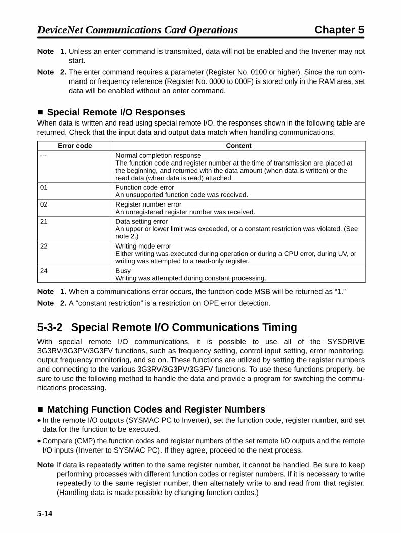
5-14
Note 1. Unless an enter command is transmitted, data will not be enabled and the Inverter may notstart.
Note 2. The enter command requires a parameter (Register No. 0100 or higher). Since the run com-mand or frequency reference (Register No. 0000 to 000F) is stored only in the RAM area, setdata will be enabled without an enter command.
Special Remote I/O ResponsesWhen data is written and read using special remote I/O, the responses shown in the following table arereturned. Check that the input data and output data match when handling communications.
Error code Content--- Normal completion response
The function code and register number at the time of transmission are placed atthe beginning, and returned with the data amount (when data is written) or theread data (when data is read) attached.
01 Function code errorAn unsupported function code was received.
02 Register number errorAn unregistered register number was received.
21 Data setting errorAn upper or lower limit was exceeded, or a constant restriction was violated. (Seenote 2.)
22 Writing mode errorEither writing was executed during operation or during a CPU error, during UV, orwriting was attempted to a read-only register.
24 BusyWriting was attempted during constant processing.
Note 1. When a communications error occurs, the function code MSB will be returned as “1.”
Note 2. A “constant restriction” is a restriction on OPE error detection.
5-3-2 Special Remote I/O Communications TimingWith special remote I/O communications, it is possible to use all of the SYSDRIVE3G3RV/3G3PV/3G3FV functions, such as frequency setting, control input setting, error monitoring,output frequency monitoring, and so on. These functions are utilized by setting the register numbersand connecting to the various 3G3RV/3G3PV/3G3FV functions. To use these functions properly, besure to use the following method to handle the data and provide a program for switching the commu-nications processing.
Matching Function Codes and Register Numbers• In the remote I/O outputs (SYSMAC PC to Inverter), set the function code, register number, and set
data for the function to be executed.
• Compare (CMP) the function codes and register numbers of the set remote I/O outputs and the remoteI/O inputs (Inverter to SYSMAC PC). If they agree, proceed to the next process.
Note If data is repeatedly written to the same register number, it cannot be handled. Be sure to keepperforming processes with different function codes or register numbers. If it is necessary to writerepeatedly to the same register number, then alternately write to and read from that register.(Handling data is made possible by changing function codes.)
DeviceNet Communications Card Operations Chapter 5

5-15
Handling Illustration (for 3G3RV)
Function coderegister number
Processingcontents
10 hex0002 hex
10 hex0001 hex
03 hex0024 hex
03 hex002C hex
Frequency reference writing Inverter run command writing Output frequency monitoring Inverter status reading
Transmissioncompleted signal
Function code-response number comparison (CMP)
5-3-3 Parameter Register Numbers for Each FunctionRefer to 5-6 3G3RV Register Numbers, Classes, Instances, and Attributes, 5-7 3G3PV Register Num-bers, Classes, Instances, and Attributes, and 5-8 3G3FV Register Numbers, Classes, Instances, andAttributes.
DeviceNet Communications Card Operations Chapter 5

5-16
5-4 Control Remote I/O Operation
There are four kinds of DeviceNet remote I/O operation: Basic remote I/O, standard remote I/O (thedefault setting), special remote I/O, and control remote I/O. This section explains control remote I/O.
Control remote I/O enables using the functions and arrays of the Inverter control terminal I/O signals.The Inverter’s multi-function I/O functions can be used during communications. These operations havebeen developed independently, and are not part of the DeviceNet standard.
Words Used for Control Remote I/O• Outputs (SYSMAC PC to Inverter) Instance ID: 101 Dec (65 Hex)
Byte number Bit 7 Bit 6 Bit 5 Bit 4 Bit 3 Bit 2 Bit 1 Bit 0
Wd n Rightmost 0 Multi-func-tion input 6
Multi-func-tion input 5
Multi-func-tion input 4
Multi-func-tion input 3
Multi-func-tion input 2
Multi-func-tion input 1
Stop/re-verse
Stop/for-ward
Leftmost 1 Multi-func-tion output2
Multi-func-tion output1
Multi-func-tion con-tact output
Fault reset Externalfault input
Wd n+1 Rightmost 2 Frequency reference, rightmost byte
Leftmost 3 Frequency reference, leftmost byte
Wd n+2 Rightmost 4 Torque reference/torque limit, rightmost byte
Leftmost 5 Torque reference/torque limit, leftmost byte
Wd n+3 Rightmost 6 Torque compensation bias, rightmost byte
Leftmost 7 Torque compensation bias, leftmost byte
• Inputs (Inverter to SYSMAC PC) Instance ID: 151 Dec (97 Hex)
Byte number Bit 7 Bit 6 Bit 5 Bit 4 Bit 3 Bit 2 Bit 1 Bit 0
Wd m Rightmost 0 Fault Alarm (mi-nor fault)
Inverterready
At refer-ence
During re-set input
During re-verse run
Zerospeed
During run
Leftmost 1 P lock/completion
Multi-func-tion output2
Multi-func-tion output1
Multi-func-tion con-tact output
Local/re-mote
Undervol-tage
Operationfault
Wd m+1 Rightmost 2 Output frequency monitor, rightmost byte
Leftmost 3 Output frequency monitor, leftmost byte
Wd m+2 Rightmost 4 Torque reference monitor, rightmost byte
Leftmost 5 Torque reference monitor, leftmost byte
Wd m+3 Rightmost 6 Output current monitor, rightmost byte
Leftmost 7 Output current monitor, leftmost byte
Note 1. A shaded box indicates that the bit is not used.
Note 2. Control remote I/O inputs and outputs are paired. When using control remote I/O, be sure toset them together.
Note 3. Control remote I/O objects do not conform to the AC/DC drive profile, but are specially set forthis product.
DeviceNet Communications Card Operations Chapter 5

5-17
Word n (Inverter Operation Commands)Word Bit Signal name Contents
n 0 Stop/forward 0: Stop1: Forward
1 Stop/reverse 0: Stop1: Reverse
2 Multi-function input 1 (See note 1.) 0: ---1: Function set for multi-function input 1
3 Multi-function input 2 (See note 1.) 0: ---1: Function set for multi-function input 2
4 Multi-function input 3 (See note 1.) 0: ---1: Function set for multi-function input 3
5 Multi-function input 4 (See note 1.) 0: ---1: Function set for multi-function input 4
6 Multi-function input 5 (See note 1.) 0: ---1: Function set for multi-function input 5
7 Multi-function input 6 (See notes 1 and 2.) 0: ---1: Function set for multi-function input 6
8 External fault input 0: ---1: External fault (EFO)
9 Fault reset 0: ---1: Reset
10 Not used. ---11 Not used. ---
12 Not used. ---13 Multi-function contact output (See note 3.) 0: OFF (open)
1: ON (closed)14 Multi-function output 1 (See note 3.) 0: OFF (open)
1: ON (closed)15 Multi-function output 2 (See note 3.) 0: OFF (open)
1: ON (closed)
Note 1. The functions set with parameters H1-01 to H1-05 (multi-function inputs 1 to 5) for3G3RV/3G3PV Inverters and H1-01 to H1-06 (multi-function inputs 1 to 6) for 3G3FV Invert-ers can be controlled with these bits.
Note 2. This bit is not used with 3G3RV/3G3PV Inverters. (These Inverters have only 5 multi-functioninputs.)
Note 3. The settings of these bits are enabled when parameters H2-01 to H2-03 (multi-function con-tact output and multi-function outputs 1 and 2) are set to F. (Same for 3G3RV, 3G3PV, and3G3FV Inverters.) Output from the control terminal block of the Inverter can be controlled viacommunications.
DeviceNet Communications Card Operations Chapter 5

5-18
Word m (Inverter Status)Word Bit Signal name Contents
m 0 During run 0: ---1: During run
1 Zero speed 0: ---1: Zero speed
2 During reverse run 0: ---1: During reverse run
3 During reset input 0: ---1: During reset input
4 At reference 0: ---1: At reference
5 Inverter ready 0: ---1: Inverter ready
6 Alarm (minor fault) 0: ---1: Alarm
7 Fault 0: ---1: Fault
8 Operation error 0: ---1: Operation error
9 Undervoltage 0: ---1: Undervoltage
10 Run command selection status 0: ---1: Communications
11 Multi-function contact output (See note 1.) 0: ---1: Function set in H2-01
12 Multi-function output 1 (See note 1.) 0: ---1: Function set in H2-02
13 Multi-function output 2 (See note 1 and 2.) 0: ---1: Function set in H2-03
14 Not used. ---
15 P lock/completion (See note 3.) 0: ---1: During P lock
Note 1. The functions set with parameters H2-01 to H2-03 (multi-function contact output and multi-function contact outputs 1 and 2) for 3G3RV/3G3FV Inverters, and with parameters H2-01and H2-02 (multi-function contact output and multi-function output 1) for 3G3PV, are enabledwith these bits.
Note 2. This bit is not used with 3G3PV Inverters. (These Inverters have only 2 multi-function out-puts.)
Note 3. The P lock function is only available with 3G3FV Inverters used in flux vector control mode. Itcannot be used with any other Inverter series or control mode.
DeviceNet Communications Card Operations Chapter 5

5-19
Reference DataWord Signal name Content
n+1 Frequency reference Specifies the Inverter output frequency from communications.
• Setting unit: 0.01 Hz (See note 1.)
• Setting range: 0 to maximum frequency in Hz (See note 2.)
Example: To set the frequency reference to 60.00 Hz:60.00 Hz/(0.01 Hz) = 6000 Dec = 1770 Hex ⇒ Set as 1770 Hex.
n+2 Torquereference/torque limit
Specifies the torque reference or torque limit for the Inverter output. (See notes 3 and 4.)The torque limit/torque reference is only enabled when flux vector control is set.
• Whether torque reference or torque limit is specified depends on the Inverter’s control mode.Speed control: torque limit Torque control: torque reference
• Setting unit: 0.1% (100% = motor rated torque)
• Setting range: –300.0% to 300.0% (See note 5.)
Example: To set the torque reference to 10%:10%/(0.1%) = 100 Dec = 64 Hex ⇒ Set as 64 Hex.
n+3 Torque compensationbias
Specifies the torque compensation bias when using torque control. (See note 3.)Torque compensation bias is only available when performing torque control in flux vector controlmode. It is used separately from torque control to compensate for mechanical torque loss.
• Setting unit: 0.1% (100% = motor rated torque)
• Setting range: –300.0% to 300.0% (See note 5.)
Example: To set the torque compensation bias to 100%:100.0%/(0.1%) = 1000 Dec = 3E8 Hex ⇒ Set as 3E8 Hex.
Note 1. The data setting unit can be changed with o1-03 (frequency reference setting/display unit).
Note 2. Data that exceeds the upper or lower setting range limits will be considered faulty and ignoredby the Inverter, and the previous data will be maintained.
Note 3. This function is only available with 3G3FV Inverters, which are equipped with flux vector con-trol mode. Do not use with 3G3RV/3G3PV Inverters.
Note 4. When not using either the torque limit of the torque reference, set F9-05 (torque reference/torque limit selection from communications) to 0 (disabled). If this setting is not disabled and“0” is sent as data, the torque limit/torque reference will be set to 0, and there will be no torqueoutput (i.e., the motor will not operate).
Note 5. Although the setting range for torque reference/torque limit is –300.0% to 300.0%, the torqueactually output depends on the motor characteristics. For a general-purpose motor, take therange to be –200.0% to 200.0%.
DeviceNet Communications Card Operations Chapter 5

5-20
Monitor DataWord Signal name Content
m+1 Output frequencymonitor
Gives the frequency being output by the Inverter.
• Monitor unit: 0.01 Hz (See note 1.)
Example: Output frequency when the monitor value is 1388 Hex:1388 Hex = 5000 Dec × (0.01 Hz) = 50.00 Hz
m+2 Torque referencemonitor
Gives the torque reference value inside the Inverter (See note 2.)
• Monitor unit: 0.1% (100% is motor rated torque)
Example: Torque reference for monitor value of 1F4 Hex:1F4 Hex = 500 Dec × (0.1%) = 50% (relative to motor rated torque)
m+3 Output currentmonitor
Gives the value of the current being output by the Inverter (See note 3.)
• Monitor unit:0.01 A (for Inverters with maximum motor capacity of 7.5 kW)0.1 A (for Inverters with maximum motor capacity of 11 kW)
Example: Output current for 0.4-kW 3G3RV Inverter with monitor value of C8 Hex:C8 Hex = 200 Dec × (0.01 A) = 2.00 A
Note 1. The data setting unit can be changed with o1-03 (frequency reference setting/display unit).(Same for 3G3RV, 3G3PV, and 3G3FV Inverters.)
Note 2. The torque reference monitor is valid only if open-loop vector control (sensorless vector con-trol) or flux vector control is set.
Note 3. With 3G3RV/3G3PV Inverters, do not set F6-05 (current monitor display unit selection) to 1(% units).
DeviceNet Communications Card Operations Chapter 5

5-21
5-5 Message Communications (DeviceNet Explicit Messages)
There are two types of DeviceNet communications: Remote I/O and message communications. Thissections explains DeviceNet Communications Card message communications. With message com-munications, specific instructions (SEND, RECV, CMND, and IOWR) are used for reading and writingdata between Master and Slave Units.
5-5-1 Overview of Message Communications (Explicit MessageOperations)
Message Communications OperationsMessage communications enable data to be exchanged as required between nodes (i.e., betweenMasters or between Masters and Slaves) on a DeviceNet Network. For example, the accumulated datafrom a given PC can be read from another PC, and constants from various Slaves can be changed froma PC. To use message communications, however, both nodes involved in the data exchange must sup-port message communications.
C200HW-DRM21-V1 or CVM1-DRM21-V1 (Master Unit)
Message communications function
Reading Inverter output current
3G3FV Inverter
3G3FV-PDRT1-SINV1 DeviceNet Communications CardNote: T-branch wiring using Thin Cables
CMND (490)
Types of Message CommunicationsDeviceNet message communications are broadly divided into the two categories described below. Ofthese two categories, the Inverter’s DeviceNet Communications Card supports explicit messages.
• Explicit MessagesExplicit messages are defined by DeviceNet. The class, instance, and attribute are specified forexecuting message communications. The messages are the same for all Inverter products, so mes-sages can be exchanged in the same way with masters made by other manufacturers.
• FINS MessagesMessages can be exchanged using FINS commands between DeviceNet nodes (Masters andSlaves) that support FINS messages. (FINS commands are actually sent and received using Device-Net explicit messages.)
DeviceNet Communications Card Operations Chapter 5

5-22
Note Message communications are supported by CS/CJ-series, CV-series and C200HX/HG/HE PCs,but not by C200HS PCs.
Overview of Explicit MessagesExplicit messages are sent and received as described below. Basically explicit message communica-tions are executed in 1-byte (8-bit) units.
Header Node address Service code Class Instance Attribute Data Footer
Item ContentHeader The header indicates the beginning of an explicit message and that the frame is an
explicit message request/response. It is set automatically for DeviceNet, so there isno particular need to be concerned with it.
Node address Request: Set the node address of the Slave/Master to be requested.Response: The node address of the responding Slave/Master is set.
Service code Request: Set the code of the requested service (read/write, etc.).Response: The MSB (most significant bit) of the requested service code ischanged to “1” and returned.
Class Function classification (majorclassification)
Indicates the classification of a functiondefined by DeviceNet. To specify a function,
Instance Instance classification (minorclassification)
de ed by e ce et o s ec y a u ct o ,specify these three codes.
Attribute Attribute (Set values are assignedfor each function.)
Data Request: Set the data to be written.Response: Read-requested data or fault message are attached.
Footer This is the part that indicates the end of the explicit message and executes theCRC check. It is set automatically for DeviceNet, so there is no particular need tobe concerned with it.
5-5-2 Sending and Receiving Messages with a CS1W-DRM21or CJ1W-DRM21 DeviceNet Unit
Using CMND(194)With a CS1W-DRM21 or CJ1W-DRM21 DeviceNet Unit, CMND(490) is used to send explicit mes-sages. To send an explicit message, it is necessary to place FINS command “2801” in front and to sendthe command to the Master Unit. The Master Unit that receives the command converts the commanddata to an explicit message and transfers it to the destination node. When sending an explicit message,it is not possible to directly specify the destination node with CMND(490).
(↑)CMND(490)
S
D
C
DeviceNet Communications Card Operations Chapter 5

5-23
S: Beginning Command Storage WordSpecify the beginning word address for the command data transferred to the DeviceNet Master Unit.Preset the data to be transferred in consecutive words as shown in the following table.
Word address Bits
15 to 8 7 to 0S Command data (Set explicit message FINS command “2801.”)
S+1 Node of Slave or Master for transmissionAddress: 0 to 3F Hex (0 to 63)
Explicit message service codeWrite: 10 Read: 0E
S+2 Class ID code (Set DeviceNet class code for relevant function.)Set within 0001 to 002A, or 0064 (Hex) with Inverter’s DeviceNet CommunicationsCard.
S+3 Instance ID code (Set DeviceNet instance code for relevant function.)
S+4 Attribute ID code(Set DeviceNet attribute code for relevantfunction.)
Attached data (for writing)
--- Attached data (for writing)
D: Beginning Response Storage WordSpecify the beginning word address of the area for storing responses to messages.
C: Beginning Control Code WordSpecify the beginning word address of the area for storing the required control codes for message com-munications. The control codes shown in the following table are required by DeviceNet Master Units.Preset the data in consecutive words.
Word address Bits
15 14 to 8 7 to 0C Number of command data bytes: 0000 to 00A0 Hex (0 to 160 bytes)
Set the amount of data from the beginning S word.C+1 Number of response data bytes: 0000 to 00A0 Hex (0 to 160 bytes)
Set the size of the data storage area from the beginning D word.C+2 Network address: 0001 to 007F Hex (1 to 127)
When using CMND(490) with the CS/CJ Series, a network address must be set for eachDeviceNet Master Unit. The network address is edited using the routing table edit functionof a Peripheral Device (except for the Programming Console).
C+3 Command destination node address: 00 to3F Hex (0 to 63)Node address of the Master Unit
Command destination Unit addressSet Master Unit (FE) or Master Unit’s unitnumber, 10 to 1F Hex (0 to 15).
C+4 Response Communications port number: 0to 7Set the communications portused for DeviceNet.
Number of retries: 00 to 0F Hex (0 to 15)Set the number of times to resend for errorresponse.
C+5 Response monitor time:0000 Hex → 2 s0001 to FFFF Hex → 0.1 to 6553.5 s (unit: 0.1 s)
Set at least 2 seconds for explicit messages.
Note Set “0” in word C+4 bit 15 to require a response or “1” to not require a response. Responses arerequired for explicit messages, so set “0.”
DeviceNet Communications Card Operations Chapter 5

5-24
Message TimingWhen executing CMND(490), an AND condition must be set that requires both the PC’s Network Com-munications Enabled Flag and the Master Unit’s Message Communications Enabled Flag to be ON.
Network CommunicationsEnabled Flag
Online status(or Message
CommunicationsEnabled Flag)
Executioncondition
(↑)CMND(490)
S
D
C
Message Response Read TimingHave messages read with the rising edge of the Network Communications Enabled Flag for each com-munications port.
Enabled FlagNetwork Communications
Read responseprocessing
Communications FlagsType Name Address Contentyp
Word BitSYSMACPC flags
Network CommunicationsEnabled Flag
A202 7: Port 76: Port 65: Port 54: Port 43: Port 32: Port 21: Port 10: Port 0
0: Execution disabled (executing)
1: Execution enabled (not executing)
Network CommunicationsError Flag
A219 15: Port 714: Port 613: Port 512: Port 411: Port 310: Port 29: Port 18: Port 0
0: Normal end
1: Abnormal end
Master Unitstatus flags
Online Flag 25 x Unitnumber +1511
00 0: Offline
1: Online
Message CommunicationsEnabled Flag
25 x Unitnumber +1524
12 Indicates the same status as theOnline Flag.
0: Offline
1: Online
This function is compatible withC200HW-DRM21-V1.
DeviceNet Communications Card Operations Chapter 5

5-25
5-5-3 Sending and Receiving Messages withC200HW-DRM21-V1 DeviceNet Master Unit
IOWR for CS1 SeriesWith a C200HW-DRM21-V1 DeviceNet Master Unit, explicit messages are sent using IOWR. To sendan explicit message, it is necessary to place FINS command “2801” in front and to send the command tothe Master Unit. The Master Unit that receives the command converts the command data to an explicitmessage and transfers it to the destination node. (When sending an explicit message, it is not possibleto directly specify the destination node with IOWR.)
(@)IOWR
C
S
W
C: Control CodeThe control code is set as shown below for DeviceNet Master Units.
Response setting:ON: No response.OFF: Response required.Must be OFF (response required) for explicit messages.
Destination node address: 0 to 3F Hex (0 to 63)The Master Unit node address must be set for explicit messages.
Destination unit address: FE (Master Unit)Master Unit must be set for explicit messages.
C:
DeviceNet Communications Card Operations Chapter 5

5-26
S: Beginning Source WordSpecify the beginning word address for the command data transferred to the DeviceNet Master Unit.Preset the data to be transferred in consecutive words as shown in the following table.
Word ad-d
Bitsdress 15 to 8 7 to 0
S Beginning response storage wordSet with the PC’s variable area designation method.
S+1
g
Example: DM 100082 (DM area) 03E8 (1000 in hexadecimal) 00 (fixed at 00 for DM area)
S+2 Response monitor time:0000 Hex → 2 s0001 to 028F Hex → 0.1 to 65.5 s (unit: 0.1 s)
S+3 Number of command data bytes (Set in hexadecimal.)Note: Command data is the data set in words S+4 onwards.
S+4 Command data (Set explicit message FINS command “2801.”)
S+5 Node of Slave or Master for transmissionAddress: 0 to 3F Hex (0 to 63)
Explicit message service codeWrite: 10 Read: 0E
S+6 Class ID code (Set DeviceNet class code for relevant function.)Set within 0001 to 002A, 0064 (Hex) with Inverter’s DeviceNet Communications Card.
S+7 Instance ID code (Set DeviceNet instance code for relevant function.)
S+8 Attribute ID code(Set DeviceNet attribute code for relevantfunction.)
Attached data (for writing)
--- Attached data (for writing)
W: Number of Words to Transfer/Destination Unit Number
W:
W + 1 W
Destination unit number (00000 to 000F Hex, 0 to 15)Set the unit number of the Master Unit.
Number of words to transfer (0001 to 0080 Hex, 1 to 128)Set the total number of words to be transferred, includingleading word S.
Example: 000A0001 (sends 10 words to Master Unit withunit number 1)
IOWR for C200HX/HG/HEWith C200HW-DRM21-V1 DeviceNet Master Unit C200HX/HG/HE PCs, explicit messages are sentusing IOWR. To send an explicit message, it is necessary to place FINS command “2801” in front and tosend the command to the Master Unit. The Master Unit that receives the command converts the com-
DeviceNet Communications Card Operations Chapter 5

5-27
mand data to an explicit message and transfers it to the destination node. (When sending an explicitmessage, it is not possible to directly specify the destination node with IOWR.)
(@)IOWR
C
S
D
C: Control CodeThe control code is set as shown below for DeviceNet Master Units.
Response setting:ON: No response.OFF: Response required.Must be OFF (response required) for explicit messages.
Destination node address: 0 to 3F hex (0 to 63)The Master Unit node address must be set for explicit messages.
Destination unit address: FE (Master Unit)Master Unit must be set for explicit messages.
C:
S: Beginning Source WordSpecify the beginning word address for the command data transferred to the DeviceNet Master Unit.Preset the data to be transferred in consecutive words as shown in the following table.
Word address Bits
15 to 8 7 to 0S Beginning response storage word
Set with the PC’s variable area designation method.
S+1
g
Example: DM 100082 (DM area) 03E8 (1000 in hexadecimal) 00 (fixed at 00 for DM area)
S+2 Response monitor time:0000 hex → 2 s0001 to 028F hex → 0.1 to 65.5 s (unit: 0.1 s)
S+3 Number of command data bytes (Set in hexadecimal.)Note: Command data is the data set in words S+4 onwards.
S+4 Command data (Set explicit message FINS command “2801.”)
S+5 Node of Slave or Master for transmissionAddress: 0 to 3F hex (0 to 63)
Explicit message service codeWrite: 10 Read: 0E
S+6 Class ID code (Set DeviceNet class code for relevant function.)Set within 0001 to 002A or 0064 (hex) with Inverter’s DeviceNet CommunicationsCard.
S+7 Instance ID code (Set DeviceNet instance code for relevant function.)
S+8 Attribute ID code(Set DeviceNet attribute code for relevantfunction.)
Attached data (for writing)
--- Attached data (for writing)
DeviceNet Communications Card Operations Chapter 5

5-28
D: Destination Information
Digits 2 to 4: Number of words to transfer (001 to 128 BCD)Set total number of words to transfer, including leading word S.
Digit 1: Destination unit number of the Special Unit (0 to F hex, 0 to 15)Set the unit number of the Master Unit.
D:
Message TimingThe Message Communications Enabled Flag must be used as an execution condition for the Masterwhen IOWR is used. Be sure this flag is ON before executing IOWR. If IOWR is executed when this flagis OFF, a Special I/O Unit error may be generated for the Master.
Executioncondition
MessageCommunicationsEnabled Flag
(@) IOWR
C
S
D
B
A
25506Equals Flag
B
A
1. IOWR is executed when the execution condition is met and the Message Communications EnabledFlag is ON.
2. When IOWR is executed, it is self-held by bit B.
3. When IOWR is completed, the Equals Flag turns ON and the self-holding bit is cleared.
Note 1. If IOWR ends in an error, the Equals Flag will not turn ON, so the self-holding bit will remainON.
Note 2. The Equals Flag is also affected by the execution of other instructions, so be careful not to useany other such instructions between IOWR and the Equals Flag.
DeviceNet Communications Card Operations Chapter 5

5-29
Timing of Message Response ReadingResponses are read when the Message Communications Enabled Flag turns ON in the next cycle. TheMessage Communications Enabled Flag will turn OFF when a Master Unit is executing message com-munications. If the message response is faster than the PC ladder program cycle time, the MessageCommunications Enabled Flag will remain ON and response processing will not be possible. Executethe read response processing before IOWR, as shown in the following diagram, and produce a Mes-sage Communications Status Flag (d) using bit A.
Read responseprocessing
Executioncondition
MessageCommunicationsEnabled Flag
B
B
A
25506
DIFU C
A
SET D
C
RSET D
D
MessageCommunicationsEnabled Flag
Equals Flag
(@) IOWR
C
S
D
A
Note If the read response processing is executed after IOWR, there can be no Message Communica-tions Enabled Flag response by means of IOWR, so an attempt could be made to read the re-sponse even though the message communications have not been completed.
Communications Flags For CS1 SeriesFlag Functions
Equals Flag The Equals Flag turns OFF when an error occurs in writing a commandfrom the CPU Unit to the Master Unit.
This Flag turns ON after a command has been written normally from theCPU Unit to the Master Unit.
Error Flag The Error Flag is OFF when all operands and the control code are legal.
This Flag turns ON when an illegal operand or control code is set orwhen there is an error in instruction execution.
Message CommunicationsEnabled Flag in the Master Unitstatus area (bit 12 in CIO 2001 +10 x unit number)
The Communications Enabled Flag turns OFF during messagescommunications or when message communications are not possible.
This Flag is ON when message communications are possible.
DeviceNet Communications Card Operations Chapter 5

5-30
Communications FlagsFlag Functions
Equals Flag (SR 25506) The Equals Flag turns OFF when an error occurs in writing a commandfrom the CPU Unit to the Master Unit.
This Flag turns ON after a command has been written normally from theCPU Unit to the Master Unit.
Error Flag (SR25503) The Error Flag is OFF when all operands and the control code are legal.
This Flag turns ON when an illegal operand or control code is set orwhen there is an error in instruction execution.
Message CommunicationsEnabled Flag in the Master Unitstatus area (bit 12 in IR 101 + 10 x unit No.)
The Communications Enabled Flag turns OFF during messagescommunications or when message communications are not possible.
This Flag is ON when message communications are possible.
5-5-4 CVM1-DRM21-V1 DeviceNet Master Unit MessageTransmission
Using CMND(194)With CVM1-DRM21-V1 DeviceNet Master Unit, CMND(194) is used to send explicit messages. Tosend an explicit message, it is necessary to place FINS command “2801” in front and to send the com-mand to the Master Unit. The Master Unit that receives the command converts the command data to anexplicit message and transfers it to the destination node. When sending an explicit message, it is notpossible to directly specify the destination node with CMND(194).
(194)CMND S D C
S: Beginning Command Storage WordSpecify the beginning word address for the command data transferred to the DeviceNet Master Unit.Preset the data to be transferred in consecutive words as shown in the following table.
Word address Bits
15 to 8 7 to 0S Command data (Set explicit message FINS command “2801.”)
S+1 Node of Slave or Master for transmissionAddress: 0 to 3F hex (0 to 63)
Explicit message service codeWrite: 10 Read: 0E
S+2 Class ID code (Set DeviceNet class code for relevant function.)Set within 0001 to 002A, 0064 (hex) with Inverter’s DeviceNet Communications Card.
S+3 Instance ID code (Set DeviceNet instance code for relevant function.)
S+4 Attribute ID code(Set DeviceNet attribute code for relevantfunction.)
Attached data (for writing)
--- Attached data (for writing)
D: Beginning Response Storage WordSpecify the beginning word address of the area for storing responses to messages.
DeviceNet Communications Card Operations Chapter 5

5-31
C: Beginning Control Code WordSpecify the beginning word address of the area for storing the required control codes for message com-munications. The control codes shown in the following table are required by DeviceNet Master Units.Preset the data in consecutive words.
Word address Bits
15 14 to 8 7 to 0C Number of command data bytes: 0000 to 00A0 hex (0 to 160 bytes)
Set the amount of data from the beginning S word.C+1 Number of response data bytes: 0001 to 00A0 hex (0 to 160 bytes)
Set the size of the data storage area from the beginning D word.C+2 Network address: 0001 to 007F hex (1 to 127)
When using CMND(194) with the CV Series, a network address must be set for eachDeviceNet Master Unit. The network address is edited using the routing table edit functionof a Peripheral Device (except for the Programming Console).
C+3 Command destination node address: 00 to3F hex (0 to 63)Node address of the Master Unit
Command destination Unit addressSet Master Unit (FE) or Master Unit’s unitnumber, 10 to 1F hex (0 to 15).
C+4 Response Communications port no.: 0 to 7 Number of retries: 00 to 0F hex (0 to 15)Set the number of times to resend for errorresponse.
C+5 Response monitor time:0000 hex → 2 s0001 to 028F hex → 0.1 to 65.5 s (unit: 0.1 s)
Set at least 2 seconds for explicit messages.
Note Set “0” in word C+4 bit 15 to require a response or “1” to not require a response. Responses arerequired for explicit messages, so set “0.”
Message TimingWhen executing CMND(194), an AND condition must be set that requires both the PC’s Network Com-munications Enabled Flag and the Master Unit’s Message Communications Enabled Flag to be ON.
(194)CMND S D C
Execution condition
Network CommunicationsEnabled Flag
Message CommunicationsEnabled Flag
Message Response Read TimingHave messages read with the rising edge of the Network Communications Enabled Flag for each com-munications port.
Response readprocessing
Enabled FlagNetwork Communications
DeviceNet Communications Card Operations Chapter 5

5-32
Communications FlagsType Name Address Contentyp
Word BitSYSMACPC flags
Network CommunicationsEnabled Flag
A502 7: Port 76: Port 65: Port 54: Port 43: Port 32: Port 21: Port 10: Port 0
0: Execution disabled (executing)
1: Execution enabled (not executing)
Network CommunicationsError Flag
A502 15: Port 714: Port 613: Port 512: Port 411: Port 310: Port 29: Port 18: Port 0
0: Normal end
1: Abnormal end
Master Unitstatus flag
Message CommunicationsEnabled Flag
25 x Unitnumber +1501
12 0: Communications error detected;Master Unit message communica-tions not possible.
1: Master Unit communications pos-sible.
5-5-5 Overview of Messages and ResponsesWhen message communications are used, the Inverter’s DeviceNet Communications Card returns re-sponses as explained below.
Basically, DeviceNet communications are executed in 1-byte (8-bit) units. In the case of single-worddata (16 bits), the rightmost bits (least significant) and the leftmost bits (most significant) are reversed inorder due to the following reasons:
• Data on communications line is transmitted in the order of rightmost bits and leftmost bits.
• Data that is internally processed by PC for issuing commands is transmitted in the order of leftmost bitsand rightmost bits.
Therefore, reverse the order for attributes where “Word” is written in the “Size” column in the tables onsubsequent pages and create attached data or read response data.
Note There is no need to take this into consideration for remote I/O because the rightmost bits andleftmost bits are automatically reversed.
Command Format
Command code(FINS command for PC)
Destinationnode address
Service data (attribute No. or at-tribute No. and write data)
32 bytes max.
Servicecode
Class ID Instance ID
28 01
DeviceNet Communications Card Operations Chapter 5

5-33
Response Format
Normal Response
Command code(FINS command for PC)
Destinationnode address
32 bytes max.
Completion code Number of bytes transmitted
Service data (read data)Service code
28 01 00 00
Error Response
Command code(FINS command for PC)
Destinationnode address
Completion code Number of bytes transmitted
Servicecode
Error code
2 bytes28 01 00 00 94
Failure or Timeout During Transmission
Command code(FINS command for PC)
Completion code(FINS error code)
28 01
5-5-6 Motor Data Objects: Class 28 HexThis and subsequent sections provide details on objects. There are eight types of :
• Identify objects (identification information): Class 01 hex
• Message router objects: Class 02 hex
• DeviceNet objects: Class 03 hex
• Assembly objects: Class 04 hex
• DeviceNet connection objects: Class 05 hex
• Motor data objects: Class 28
• Control supervisor objects: Class 29 hex
• AC/DC drive objects: Class 2A hex
The three types of objects related to Inverters are the motor data, control supervisor, and AC/DC driveobjects. These are explained below and in subsequent sections. The other types of objects are usedless frequently, and covered in 8-2 Objects.
Motor data objects are data and functions related to motors connected to Inverters. The motors that canbe connected to Inverters are squirrel-cage inductive motors, so the “Motor Type” is always “7.” Themotor’s rated current and rated voltage can be set and read.
Support Service CodeService Code No. (Hex) Service
0E Get attribute single
10 Set attribute single
DeviceNet Communications Card Operations Chapter 5

5-34
Object DetailsInstance Attribute Name Content Setting range Default Read Write Size
00 01 Object SoftwareRevision
Indicates class 28 softwarerevisions. The revision value isadvanced whenever there is achange.
--- 0001 Yes No Word
01 03 Motor Type Indicates the type of motor to beused. The setting for asquirrel-cage inductive motor is 7.
--- 07 Yes No Byte
06 Motor RatedCurrent
The motor’s rated current can beset and read. The setting unit is0.1 A. (The setting unit can bechanged using the current scalein Class 2A, Instance 1, Attribute17.)
Inverter ratedoutput current10% to 120%
Seenote 1.
Yes Yes Word
07 Motor RatedVoltage
The motor’s rated voltage can beset and read. The setting unit is 1V. (The setting unit can bechanged using the voltage scalein Class 2A, Instance 1, Attribute1B.)
0 to 255 V(0 to 510 V)
See note 2.
00C8(0190)
Seenote 2.
Yes Yes Word
Note 1. The default setting for the motor’s rated current depends on the Inverter model.Example: 1.90A (0013 hex) for 200-V class, 0.4 kW
Note 2. The figures enclosed in parentheses in the “Setting range” and “Default” columns are the val-ues for 400-V class Inverters.
5-5-7 Control Supervisor Objects: Class 29 HexControl supervisor objects are objects that have Inverter control I/O-related functions. They are as-signed according to their particular control I/O functions, such as forward operation, reverse operation,error detection, and so on. Be careful when setting up a remote I/O communications connection. Thesefunctions are shared with similar functions used for remote I/O, so even if they have been set for mes-sage operations they may get rewritten for remote I/O.
Support Service CodesService Code No. (Hex) Service
0E Get attribute single
10 Set attribute single
05 Reset attribute
Turns OFF the Forward Operation and Reverse Operation inputs and turnsON the Fault Reset. Then turns OFF the Fault Reset when Inverter Readyis output.
DeviceNet Communications Card Operations Chapter 5

5-35
Object DetailsInstance Attribute Name Content Setting
rangeDefault Read Write Size
00 01 Object SoftwareRevision
Indicates class 29 softwarerevisions. The revision value isadvanced whenever there is achange.
--- 0001 Yes No Word
01 03 Forward/Stop 00: Stop01: Forward operation
00, 01 00 Yes Yes Byte
04 Reverse/Stop 00: Stop01: Reverse operation
00, 01 00 Yes Yes Byte
05 Net ControlLocal/remote switch
Set note 1.
00: Operate by b1-02 setting.01: Operate by DeviceNet withb1-02 set to “3.”
00, 01 00 Yes Yes Byte
06 StateInverter status
03 hex: Inverter ready --- 03 Yes No Byte
07 During forward run 00: No Inverter output or operatingin reverse.01: Forward operation or DCbraking
Turns ON even for DC brakingduring reverse operation.
--- 00 Yes No Byte
08 During reverse run 00: No Inverter output or operatingin forward.01: Operating in reverse (reverseoperation output status)
Becomes “00” with DC braking.
--- 00 Yes No Byte
09 Inverter Ready 00: PreparingInitial processing/ not drive mode/fault01: Inverter readyInverter can receive runcommand.
--- 00 Yes No Byte
0A Fault 00: Normal01: Fault
--- 00 Yes No Byte
0B Warning (minor fault) 00: Normal01: Warning (minor fault)
--- 00 Yes No Byte
0C Fault Reset 00: Normal status01: Fault reset
00, 01 00 Yes Yes Byte
0D Fault code Indicates the contents of fault thatoccur. (See the fault code list onthe following page.)
--- 0000 Yes No Word
0F Control From NetRun signal inputstatus
See note 1.
00: Operating by b1-02 setting.01: Operating by DeviceNet.
--- 00 Yes No Byte
10 DeviceNet Faultmode
See note 2.
02: Maker’s specifications --- 02 Yes No Byte
11 Force Fault/Trip
Communicationsexternal fault input
00: Normal operation01: Communications external faultinput (according to parameter F9 )
00, 01 00 Yes Yes Byte
12 Force Status
Communicationsexternal fault inputstatus
00: Normal status01: Communications external faultdetected. (Inverter stopped withfault detection.)
--- 00 Yes No Byte
Note 1. The Net Control and Control From Net functions cannot be changed during running.
Note 2. A DeviceNet Fault mode cannot be set from communications. Use the Inverter’s parameters.
DeviceNet Communications Card Operations Chapter 5

5-36
Fault CodesDeviceNet error code Operator display Meaning
0000 --- Inverter normal
2120 GF Ground fault
2130 SC Short circuit
2200 OL2 Inverter overload
2220 OL1 Motor overload
2221 OL3 Overtorque detection 1
2222 OL4 Overtorque detection 2
2300 OC Overcurrent3130 PF Input phase loss
LF Output phase loss
3210 OV Main circuit overvoltage
3220 UV1 Undervoltage (main)
3222 UV3 Undervoltage (MC)
4200 OH Overheat
4210 OH1 Overheat
5110 UV2 Control power supply fault
5120 PUF Fuse open
5300 OPR Operator disconnection
6320 ERR EEPROM write failure
7110 RR Braking transistor failure
7112 RH Braking resistor overheating
7301 PGO PG is disconnected7310 OS Overspeed
DEV Speed deviation7500 BUS Communications error9000 EF3 External fault (Terminal 3)
EF4 External fault (Terminal 4)EF5 External fault (Terminal 5)EF6 External fault (Terminal 6)EF7 External fault (Terminal 7)EF8 External fault (Terminal 8)
FF0 Communications external fault
DeviceNet Communications Card Operations Chapter 5

5-37
5-5-8 AC/DC Drive Objects: Class 2A HexAC/DC drive objects are assigned to command-related functions for drive devices such as Invertersand Servomotors. Command-related data reading and writing, monitor data reading, set data scalechanges, and so on, are all enabled. These functions are shared with similar functions used for remoteI/O, so even if they have been set for message operations they may get rewritten for remote I/O.
Support Service CodesService Code No. (Hex) Service
0E Get attribute single
10 Set attribute single
Object DetailsInstance Attribute Name Content Setting
rangeDefault Read Write Size
00 01 Object SoftwareRevision
Indicates class 2A software revisions. Therevision value is advanced whenever thereis a change.
--- 0001 Yes No Word
01 03 At Reference 00: Stopped, accelerating or decelerating01: At reference 1
--- 00 Yes No Byte
04 Net Reference
(See note 1.)
00: Operate at B1-01 setting.01: Set B1-01 to “3” and operate withDeviceNet.
00, 01 00 Yes Yes Byte
06 Drive Mode 00: Open loop vector (A1-02 = 2)01: V/f control (A1-02 = 0)02: V/f control with PG (A1-02 = 1)03: Flux vector (A1-02 = 3)
00 to 03 00 Yes Yes Byte
07 Speed Actual
Rotational SpeedMonitor
(See note 1.)
Can be referenced in hexadecimal with theoutput frequency monitor (U1-02) minimumunit as 1.
The output frequency monitor minimumunit can be set by the frequency referencesetting and display units (o1-03).o1-03= 0: 0.01 Hzo1-03= 1: 0.01% (100%: Max. frequency.)o1-03= 2 to 39: 1 r/min (Set number ofpoles.)o1-03= 40 to 39999: Follow individual setvalues.
Setting the attribute 16 speed scaleenables a further multiplication factor to beset for o1-03= 2 to 39: 1 r/min.
--- 0000 Yes No Word
08 Speed Reference
Rotational SpeedReference
(See note 1.)
Can be set and read in hexadecimal withthe frequency reference minimum unit as1.
The frequency reference minimum unit canbe set by the frequency reference settingand display units (o1-03).o1-03= 0: 0.01 Hzo1-03= 1: 0.01% (100%: Max. frequency.)o1-03= 2 to 39: 1 r/min (Set number ofpoles.)o1-03= 40 to 39999: Follow individual setvalues.
Setting the attribute 16 speed scaleenables a further multiplication factor to beset for o1-03= 2 to 39: 1 r/min.
0 to max.frequency
0000 Yes Yes Word
DeviceNet Communications Card Operations Chapter 5

5-38
Instance SizeWriteReadDefaultSettingrange
ContentNameAttribute
01 09 Current Actual Can be referenced in hexadecimal with theoutput current monitor (U1-03) minimumunit as 0.1 A.
Setting the attribute 17 current scaleenables a multiplication factor to be set.
--- 0000 Yes No Word
0F Power Actual Can be referenced in hexadecimal with theoutput power monitor (U1-08) minimumunit as 1 W.
Setting the attribute 1A power scaleenables a multiplication factor to be set.
--- 0000 Yes No Word
10 Input Voltage Can be referenced in hexadecimal with theinput voltage setting (E1-01) minimum unitas 1 V.
Setting the attribute 1B voltage scaleenables a multiplication factor to be set.
--- 0000 Yes No Word
11 Output Voltage Can be referenced in hexadecimal with theoutput voltage monitor (U1-06) minimumunit as 1 V.
Setting the attribute 1B voltage scaleenables a multiplication factor to be set.
--- 0000 Yes No Word
12 Accel Time Can be set and read in hexadecimal withthe acceleration time 1 (C1-01) anddeceleration time 1 (C1-02) minimum unitas 1 ms.
Depending on the acceleration/
0.0 to6,000.0 ×103 ms(0.00 to600.00 ×103 ms)
2710Hex(10.0 s)
Yes Yes Word
13 Decel TimeDe ending on the acceleration/deceleration time unit (C1-01) setting,numbers below 100 ms or 10 ms aretruncated.
Setting the attribute 1C time scale enablesa multiplication factor to be set.
103 ms)2710Hex(10.0 s)
Yes Yes Word
14 Low Speed Limit
(See note 1 and3.)
Can be set and read in hexadecimal withthe frequency reference lower limit (d2-02)and the frequency reference upper limit(d2-01) minimum unit as 1 ms.
The minimum unit can be set by thefrequency reference setting and displayunits (o1-03).
0 to109% ofmaximumfrequency
0000 Yes Yes Word
15 High Speed Limit
(See note 1 and3.)
units (o1-03).
o1-03= 2 to 39: 1 r/mino1-03= Other than above: 0.1% (Maximumfrequency: 100%)
Setting the attribute 16 speed scaleenables a multiplication factor to be set foro1-03= 2 to 39: 1 r/min.
0 to 110%ofmaximumfrequency
0708Hex(1,800r/min)
Yes Yes Word
16 Speed scale Speed data unit selection can be set andread. The speed data unit value iscalculated as follows:
Unit = 1 [r/min] x 1/2a
a: Speed scale set value
Set a negative value as its 2’scomplement.
–15 to 15(F1 to 0Fhex)
00 Yes Yes Byte
17 Current scale Current data unit selection can be set andread. The current data unit value iscalculated as follows:
Unit = 0.1 [A] x 1/2b
b: Current scale set value
Set a negative value as its 2’scomplement.
–15 to 15(F1 to 0Fhex)
00 Yes Yes Byte
DeviceNet Communications Card Operations Chapter 5

5-39
Instance SizeWriteReadDefaultSettingrange
ContentNameAttribute
01 1A Power scale Power data unit selection can be set andread. The power data unit value iscalculated as follows:
Unit = 0.1 [W] x 1/2c
c: Power scale set value
Set a negative value as its 2’scomplement.
–15 to 15(F1 to 0Fhex)
00 Yes Yes Byte
1B Voltage scale Voltage data unit selection can be set andread. The voltage data unit value iscalculated as follows:
Unit = 0.1 [V] x 1/2d
d: Voltage scale set value
Set a negative value as its 2’scomplement.
–15 to 15(F1 to 0Fhex)
00 Yes Yes Byte
1C Time scale Time data unit selection can be set andread. The time data unit value is calculatedas follows:
Unit = 0.1 [V] x 1/2e
e: Voltage scale set value
Set a negative value as its 2’scomplement.
–15 to 15(F1 to 0Fhex)
00 Yes Yes Byte
1D Reference FromNet
00: Operate at B1-01 setting.01: Set B1-01 to “3” and operate withDeviceNet.
--- 00 Yes No Byte
Note 1. The Net Reference and Reference From Net functions cannot be changed during running.
Note 2. Under the DeviceNet protocol, the unit for the speed reference is always r/min. The number ofmotor poles (2 to 39) must be set in parameter o1-03 (frequency reference setting and displayunits) when using DeviceNet (open network).
Note 3. Cannot be changed during running.
Communications Data Setting ExamplesExample 1: Finding the communications data for outputting a frequency of 60 Hz with the followingconditions set.
Number of poles (o1-03): 4Speed scale (attribute 16): 0
• Converting frequency to rotational speed:Frequency x 120 / number of poles = 60 x 120/4 = 1,800 r/min
• Converting rotational speed to minimum unit:Rotational speed / unit = 1,800 / (1 r/min x 1/20) = 1,800
• Converting communications data to hexadecimal: 1,800 (dec) = 708 (hex)
Example 2: Finding the communications data for outputting a frequency of 60 Hz with the followingcondition set.
Frequency setting (o1-03): 0 (Cannot be set with DeviceNet protocol.)
• Converting frequency to minimum setting unit:Frequency / minimum unit = 60 / 0.01 = 6,000
• Converting communications data to hexadecimal: 6,000 (dec) = 1,770 (hex)
Note With frequency, the speed scale has no effect.
DeviceNet Communications Card Operations Chapter 5

5-40
Example 3: Finding the communications data for setting a one-minute acceleration time with the follow-ing condition set.
Time scale (attribute 1C): –3
• Matching the acceleration time unit: 1 minute = 60 seconds = 60,000 ms
• Converting acceleration time to minimum unit:Acceleration time / unit = 60,000 / (1 ms x 1/2–3) = 7,500
• Converting communications data to hexadecimal: 7,500 (dec) = 1D4C (hex)
Communications Data Reference ExampleIn this example, the hexadecimal value BB8 that has been read is converted to frequency with the fol-lowing conditions set.
Number of poles (o1-03): 4Speed scale (attribute 16): 1
• Converting communications data to decimal: BB8 (hex) = 3,000 (dec)
• Converting from minimum unit to r/min:Communications data x unit = 3,000 x (1 r/min x 1/21) = 1,500 (r/min)
5-5-9 Reading and Writing Parameters: Class 64 HexInverter parameters can be read and written using explicit messages. Class 100 Dec (64 Hex) has beenprovided with instances and attributes corresponding to each parameter in the Inverter. Send an explicitmessage to the class, instance, or attribute of the parameter to be set as described below.
Parameter DatabaseAll parameters in the parameter database have been unified to 1-word (16-bit) data. Even settings of 0and 1 will be treated as 1-word (16-bit) data in explicit messages.
Note When sending or receiving 1-word (16-bit) data in an explicit message, the leftmost and rightmostbytes will be reversed. Accordingly, when reading or writing data, the attribute value will be in theupper byte, the lower byte will contain the lower byte of the data, and the upper byte of the data willbe in the upper byte of the next word.
Communications line data is sent and received in the order of lower byte, then upper byte.
PLC internal processing data, such as when sending commands, are sent and received in the or-der of upper byte, then lower byte.
Parameter Read and Write DataRead data and write data for parameters is calculated as shown below and then transmitted in hexade-cimal.
• Convert to hexadecimal values with the function/parameter minimum setting unit taken as 1.Example: To set a frequency reference of 60 Hz when the minimum setting unit is 0.01 Hz.60/0.01 = 6000 → 1770 Hex
DeviceNet Communications Card Operations Chapter 5

5-41
• Negative numbers are expressed as two’s complements.Example: To set a frequency reference bias (n061) of –100% when the minimum setting unit is 1%:100/1 = 100 Dec = 0064 Hex, –100% → FF9C Hex
Bit reversal0064 Hex=
FF9B Hex=
FF9C Hex=
0 0 0 0 0 0 0 0 0 1 1 0 0 1 0 0
1 1 1 1 1 1 1 1 1 0 0 1 1 0 1 1
1 1 1 1 1 1 1 1 1 0 0 1 1 1 0 0+1
• If the original data is already in hexadecimal, it is transmitted as is.
• Set bits that are not used to “0.”
• Do not set data for unused registers.
Enabling Parameter Data Using the ENTER CommandTo enable parameter data that has been received, send an ENTER command as shown in the followingtable to either store or not store the parameters in EEPROM. To enable a series of data for more thanone transmission, send only one ENTER command after sending all of the data.
Data type Transmission Inverter Operation RemarksENTERcommand thatwritesparameters toEEPROM
Write 0000 as follows:
Class: 100 Dec (64 Hex)Instance: 255 Dec (FF Hex)Attribute: 253 Hex (FD Hex)
Previously receivedparameter setting data isstored in EEPROM.
Note: The maximumnumber of write operationsthat can be performed toEEPROM is 100,000.
Used to store data evenafter a power interruption.
ENTERcommand thatdoes not writeparameters toEEPROM
Write 0000 as follows:
Class: 100 Dec (64 Hex)Instance: 255 Dec (FF Hex)Attribute: 221 Hex (DD Hex)
Previously receivedparameter setting data isenabled as operating datawithout storing it toEEPROM.
If there is frequent rewritingof data, do not sendENTER commands eachtime because of the limit tothe number of timesEEPROM can be written.Be sure to send an ENTERcommand that writes datato EEPROM once beforethe power supply isinterrupted.
Parameter Classes, Instances, and AttributesRefer to 5-6 3G3RV Register Numbers, Classes, Instances, and Attributes, 5-7 3G3PV Register Num-bers, Classes, Instances, and Attributes, and 5-8 3G3FV Register Numbers, Classes, Instances, andAttributes.
DeviceNet Communications Card Operations Chapter 5

5-42
5-6 3G3RV Register Numbers, Classes, Instances, andAttributes
5-6-1 Inputting Control/Frequency (Read/Write)Register No.
(Hex)Contents
0000 Reserved0001 Frequency reference
Bit 0 Run/stop command 1: Run 0: Stop
Bit 1 Reverse/stop command 1: Reverse 0: StopBit 2 Multi-function input command 3Bit 3 Multi-function input command 4Bit 4 Multi-function input command 5Bit 5 Multi-function input command 6Bit 6 Multi-function input command 7Bit 7 Not used.
Bit 8 External error 1: Error (EFO)Bit 9 Error reset 1: Reset commandBits 10 to 15 Not used.
0002 Frequency reference (Set units using parameter o1-03.)
0003 to 0005 Not used.
0006 PID target value
0007 Analog output 1 setting (–11 V/–726 Dec to 11 V/726 Dec)
0008 Analog output 2 setting (–11 V/–726 Dec to 11 V/726 Dec)0009 Multi-function contact output setting
Bit 0 Contact output (terminal M1-M2) 1: ON 0: OFFBit 1 Contact output (terminals M3-M4 or P1-PC) 1: ON 0: OFFBit 2 Contact output (terminals M5-M6 or P2-PC) 1: ON 0: OFF
Bits 3 to 5 Not used.Bit 6 Set error contact (terminal MA-MC) output using bit 7. 1: ON 0: OFFBit 7 Error contact (terminal MA-MC) 1: ON 0: OFFBits 8 to 15 Not used.
000A to 000E Not used.000F Reference selection settings
Bit 0 Not used.Bit 1 PID target value (register 0006H) 1: Enabled 0: DisabledBits 2 to 15 Not used.
Note Set all unused bits to 0.
DeviceNet Communications Card Operations Chapter 5

5-43
5-6-2 Inverter Monitoring Functions (Read)
Register No.(Hex)
Contents
0020 Inverter statusBit 0 Operation 1: Operating 0: StoppedBit 1 Reverse operation 1: Reverse operation 0: Forward operation or
stopped
Bit 2 Inverter startup complete 1: Completed 2: Not completedBit 3 Error 1: ErrorBit 4 Data setting error 1: ErrorBit 5 Multi-function contact output (terminals M1-M2) 1: ON 0: OFFBit 6 Multi-function contact output (terminals M3-M4 or P1-PC) 1: ON 0:
OFF
Bit 7 Multi-function contact output (terminals M5-M6 or P2-PC) 1: ON 0:OFF
Bits 8 to 15 Not used.
0021 Error detailsBit 0 Overcurrent (OC), ground fault (GF)Bit 1 Main circuit overvoltage (OV)Bit 2 Inverter overload (OL2)Bit 3 Inverter overheat (OH1, OH2)Bit 4 Injection brake transistor resistance overheat (rr, rH)
Bit 5 Fuse blown (PUF)Bit 6 PID feedback reference lost (FbL)Bit 7 External error (EF, EFO)Bit 8 Hardware error (CPF)Bit 9 Motor overload (OL1) or overtorque 1 (OL3) detectedBit 10 PG broken wire detected (PGO), overspeed (OS), speed deviation
(DEV)
Bit 11 Main circuit undervoltage (UV) detectedBit 12 Main circuit undervoltage (UV1), control power supply error (UV2),
inrush prevention circuit error (UV3)
Bit 13 Missing output phase (LF)Bit 14 RS-422A/485 communications error (CE)
Bit 15 Operator disconnected (OPR)
0022 Data link statusBit 0 Writing dataBits 1 and 2 Not used.Bit 3 Upper and lower limit errorsBit 4 Data integrity error
Bits 5 to 15 Not used.
0023 Frequency reference Monitors U1-01 (Unit set with o1-03.)
0024 Output frequency Monitors U1-02 (Unit set with o1-03.)
0025 Output voltagereference
Monitors U1-06 (0.1-V units)
DeviceNet Communications Card Operations Chapter 5

5-44
Register No.(Hex)
Contents
0026 Output current Monitors U1-03 (Inverters of 7.5 kW or less: 0.01-A units, Invertersof 11 kW or more: 0.1-A units)
0027 Output power Monitors U1-08 (0.1-kW units)
0028 Torque reference Monitors U1-09 (0.1 units, 100% = motor’s rated torque)
Note Only enabled for vector control.
0029 to 002A Not used.
002A Not used.
002B Sequence input statusBit 0 Multi-function input terminal S1 1: ON 0: OFFBit 1 Multi-function input terminal S2 1: ON 0: OFFBit 2 Multi-function input terminal S3 1: ON 0: OFFBit 3 Multi-function input terminal S4 1: ON 0: OFF
Bit 4 Multi-function input terminal S5 1: ON 0: OFFBit 5 Multi-function input terminal S6 1: ON 0: OFFBit 6 Multi-function input terminal S7 1: ON 0: OFFBits 7 to 15 Not used.
002C Inverter statusBit 0 Operation 1: OperatingBit 1 Zero speed 1: Zero speedBit 2 Frequency matching 1: MatchedBit 3 User-defined speed matching 1: MatchedBit 4 Frequency detection 1 1: Output frequency ≤ L4-01Bit 5 Frequency detection 2 1: Output frequency ≥ L4-01
Bit 6 Inverter startup completed 1: Startup completedBit 7 Low voltage detection 1: DetectedBit 8 Baseblock 1: Inverter output baseblockBit 9 Frequency reference mode 1: Not communications
0: Communications
Bit 10 Run command mode 1: Not communications 0: Communications
Bit 11 Overtorque detection 1: DetectedBit 12 Frequency reference lost 1: LostBit 13 Retrying error 1: RetryingBit 14 Fault. (including RS-422A/485 communications time-out) 1: fault
occurred
Bit 15 Communications time-out 1: Timed out
002D Multi-function output statusBit 0 Multi-function contact output (terminals M1-M2) 1: ON 0: OFFBit 1 Multi-function contact output (terminals M3-M4 or P1-PC): 1: ON 0:
OFF
Bit 2 Multi-function contact output (terminals M5-M6 or P2-PC): 1: ON 0:OFF
Bits 3 to 15 Not used.
002E to 0030 Not used.
0031 Main circuit DCvoltage
Monitors U1-07 (1-V units)
DeviceNet Communications Card Operations Chapter 5

5-45
Register No.(Hex)
Contents
0032 to 0037 Not used.
0038 PID feedbackquantity
1% = 10; 100% = Input corresponding to max. output frequency;without sign
0039 PID input quantity 1% = 10; 100% = Max. output frequency; without sign
003A PID output quantity 1% = 10; 100% = Max. output frequency; without sign
003B CPU software number
003C Flash software number003D Communications error details
Bit 0 CRC errorBit 1 Invalid data lengthBit 2 Not used.
Bit 3 Parity errorBit 4 Overrun errorBit 5 Framing errorBit 6 Time-outBits 7 to 15 Not used.
003E kVA setting
003F Control method
0040 Frequency reference Monitors U1-01; 0.01-Hz units (units set in o1-03; with sign)
0041 Output frequency Monitors U1-02; 0.01-Hz units (units set in o1-03; with sign)
0042 Output current Monitors U1-03; Inverters of 7.5 kW or less: 0.01-A units,Inverters of 11 kW or more: 0.1-A units
0043 Control method Monitors U1-04; set in A1-02
0044 Motor speed Monitors U1-05; 0.01-Hz units (units set in o1-03; with sign)
0045 Output voltage Monitors U1-06; 0.1-V units
0046 Main circuit DC voltage Monitors U1-07; 1-V units
0047 Output power Monitors U1-08; 0.1-kW units (with sign)
0048 Torque reference Monitors U1-09; 0.1%-kW units (100% = motor’s ratedtorque; with sign)
0049 Input terminal status Monitors U1-10; 1: ON. Bits 0 to 6 correspond to terminalsS1 to S7.
004A Output terminal status Monitors U1-11Bit 0 Terminals M1 and M2; 1: ONBit 1 Terminals M3 (P1) and M4 (PC); 1: ON
Bit 2 Terminals M5 (P2) and M6 (PC); 1: ONBits 3 to 6 Not used.Bit 7 Terminals MA and MC; 1: ONBits 8 to 15 Not used.
DeviceNet Communications Card Operations Chapter 5
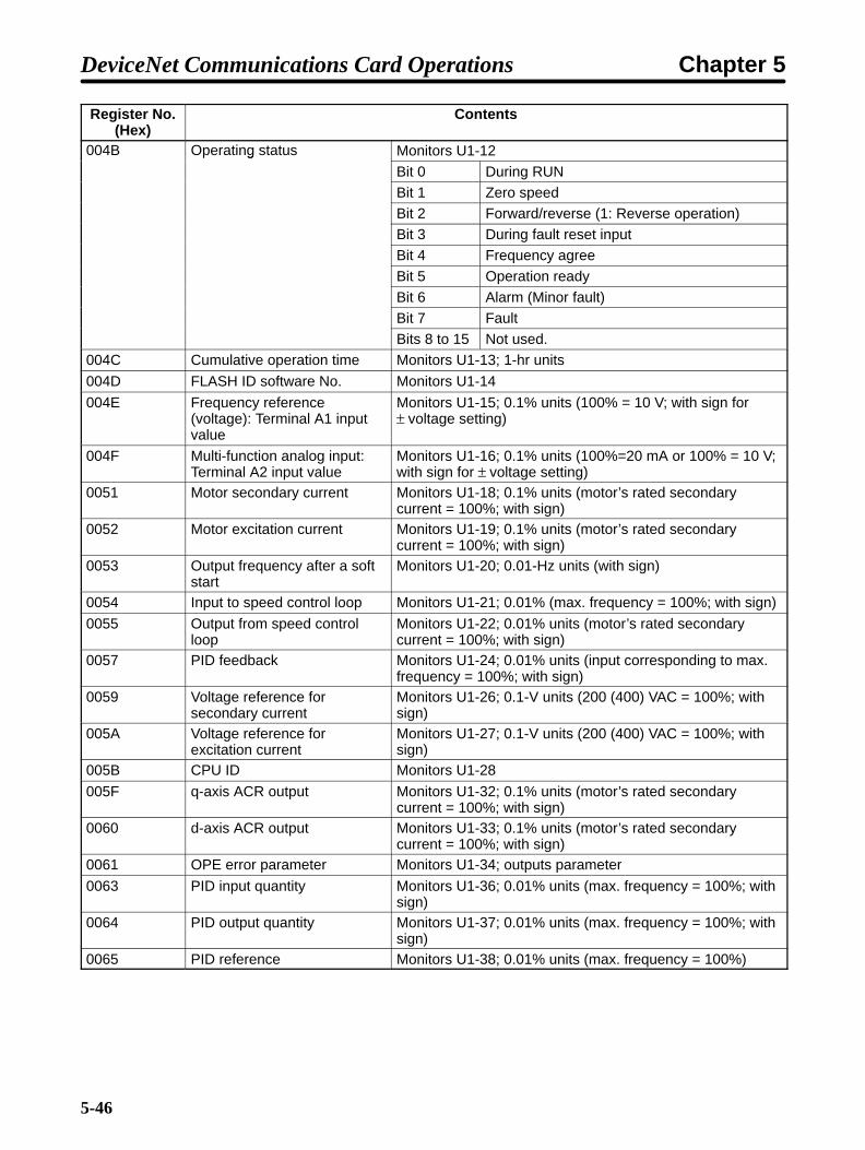
5-46
Register No.(Hex)
Contents
004B Operating status Monitors U1-12g
Bit 0 During RUNBit 1 Zero speedBit 2 Forward/reverse (1: Reverse operation)Bit 3 During fault reset inputBit 4 Frequency agreeBit 5 Operation ready
Bit 6 Alarm (Minor fault)Bit 7 FaultBits 8 to 15 Not used.
004C Cumulative operation time Monitors U1-13; 1-hr units
004D FLASH ID software No. Monitors U1-14
004E Frequency reference(voltage): Terminal A1 inputvalue
Monitors U1-15; 0.1% units (100% = 10 V; with sign for± voltage setting)
004F Multi-function analog input:Terminal A2 input value
Monitors U1-16; 0.1% units (100%=20 mA or 100% = 10 V;with sign for ± voltage setting)
0051 Motor secondary current Monitors U1-18; 0.1% units (motor’s rated secondarycurrent = 100%; with sign)
0052 Motor excitation current Monitors U1-19; 0.1% units (motor’s rated secondarycurrent = 100%; with sign)
0053 Output frequency after a softstart
Monitors U1-20; 0.01-Hz units (with sign)
0054 Input to speed control loop Monitors U1-21; 0.01% (max. frequency = 100%; with sign)
0055 Output from speed controlloop
Monitors U1-22; 0.01% units (motor’s rated secondarycurrent = 100%; with sign)
0057 PID feedback Monitors U1-24; 0.01% units (input corresponding to max.frequency = 100%; with sign)
0059 Voltage reference forsecondary current
Monitors U1-26; 0.1-V units (200 (400) VAC = 100%; withsign)
005A Voltage reference forexcitation current
Monitors U1-27; 0.1-V units (200 (400) VAC = 100%; withsign)
005B CPU ID Monitors U1-28
005F q-axis ACR output Monitors U1-32; 0.1% units (motor’s rated secondarycurrent = 100%; with sign)
0060 d-axis ACR output Monitors U1-33; 0.1% units (motor’s rated secondarycurrent = 100%; with sign)
0061 OPE error parameter Monitors U1-34; outputs parameter
0063 PID input quantity Monitors U1-36; 0.01% units (max. frequency = 100%; withsign)
0064 PID output quantity Monitors U1-37; 0.01% units (max. frequency = 100%; withsign)
0065 PID reference Monitors U1-38; 0.01% units (max. frequency = 100%)
DeviceNet Communications Card Operations Chapter 5

5-47
Register No.(Hex)
Contents
0066 RS-422A/485i i
Monitors U1-39communications error Bit 0 CRC error
Bit 1 Invalid data lengthBit 2 Not used.Bit 3 Parity errorBit 4 Overrun errorBit 5 Framing error
Bit 6 Time-outBits 7 to 15 Not used.
0068 Fan operating time Monitors U1-40; 1-hr units
0080 Current fault Monitors U2-01Code Error
displayCode Error
displayCode Error
display01 PUF 0E OL4 1C LF
02 UV1 0F RR 1D OH303 UV2 10 RH 1E OPR04 UV3 11 EF3 1F ERR06 GF 12 EF4 20 OH407 OC 13 EF5 22 BUS08 OV 14 EF6 25 CF09 OH 15 EF7 27 EF0
0A OH1 18 OS 28 FBL0B OL1 19 DEV 29 UL30C OL2 1A PGO 2A UL40D OL3 1B PF 2B OL7
0081 Last fault Monitors U2-02 (same codes as U2-01)
0082 Fault frequency reference Monitors U2-03; 0.01-Hz units (units set in o1-03; with sign)
0083 Fault output reference Monitors U2-04; 0.01-Hz units (units set in o1-03; with sign)
0084 Fault output current Monitors U2-05; Inverters of 7.5 kW or less: 0.01-A units,Inverters of 11 kW or more: 0.1-A units
0085 Fault motor speed Monitors U2-06; 0.01-Hz units (units set in o1-03; with sign)
0086 Fault output voltage reference Monitors U2-07; 0.1-V units
0087 Fault main circuit DC voltage Monitors U2-08; 1-V units
0088 Fault output power Monitors U2-09; 0.1-kW units (with sign)
0089 Fault torque reference Monitors U2-10; 0.1% units (100% = motor’s rated torque;with sign)
008A Fault input terminal status Monitors U2-11 (same contents as U1-10)
008B Fault output terminal status Monitors U2-12 (same contents as U1-11)
008C Fault operating status Monitors U2-13 (same contents as U1-12)
008D Fault cumulative operationtime
Monitors U2-14; 1-hr units
0090 (0800) Content of last fault Monitors U3-01 (same codes as U2-01)
0091 (0801) Content of 2nd prior fault Monitors U3-02 (same codes as U2-01)
0092 (0802) Content of 3rd prior fault Monitors U3-03 (same codes as U2-01)
0093 (0803) Content of 4th prior fault Monitors U3-04 (same codes as U2-01)
DeviceNet Communications Card Operations Chapter 5

5-48
Register No.(Hex)
Contents
0094 (080A) Cumulative operation timesince last fault
Monitors U3-05; 1-hr units
0095 (080B) Cumulative operation timesince 2nd prior fault
Monitors U3-06; 1-hr units
0096 (080C) Cumulative operation timesince 3rd prior fault
Monitors U3-07; 1-hr units
0097 (080D) Cumulative operation timesince 4th prior fault
Monitors U3-08; 1-hr units
0804 Content of 5th prior fault Monitors U3-09 (same codes as U2-01) (See note.)
0805 Content of 6th prior fault Monitors U3-10 (same codes as U2-01) (See note.)
0806 Content of 7th prior fault Monitors U3-11 (same codes as U2-01) (See note.)
0807 Content of 8th prior fault Monitors U3-12 (same codes as U2-01) (See note.)
0808 Content of 9th prior fault Monitors U3-13 (same codes as U2-01) (See note.)
0809 Content of 10th prior fault Monitors U3-14 (same codes as U2-01) (See note.)
080E Cumulative operation timesince 5th prior fault
Monitors U3-15; 1-hr units (See note.)
080F Cumulative operation timesince 6th prior fault
Monitors U3-16; 1-hr units (See note.)
0810 Cumulative operation timesince 7th prior fault
Monitors U3-17; 1-hr units (See note.)
0811 Cumulative operation timesince 8th prior fault
Monitors U3-18; 1-hr units (See note.)
0812 Cumulative operation timesince 9th prior fault
Monitors U3-19; 1-hr units (See note.)
0813 Cumulative operation timesince 10th prior fault
Monitors U3-20; 1-hr units (See note.)
Note U3-09 to U3-20 are not supported for Asian models. Register No. 0800 Hex to 0813 Hex are notsupported for Asian models.
5-6-3 Parameter Reading and WritingThe following tables show the SYSDRIVE 3G3RV Inverter parameters and the corresponding registernumbers. Write and read the various parameters with “1” as the minimum setting unit. Negative num-bers are expressed as two’s complement. If the setting unit is in hexadecimal, there is no need to con-vert it.
When writing data in parameters, be sure to send an enter command to enable the written data. Unlessthe enter command is transmitted, the data will not be enabled and the Inverter may not start.
DeviceNet Communications Card Operations Chapter 5

5-49
Parameters for Initialize ModeÁÁÁÁÁÁÁÁParameter
ÁÁÁÁÁÁÁÁRegister
No (Hex)
ÁÁÁÁÁÁÁÁÁÁÁÁÁÁ
Class 64 (Hex)ÁÁÁÁÁÁÁÁÁÁÁÁÁÁName
ÁÁÁÁÁÁÁÁÁÁSetting
range
ÁÁÁÁÁÁÁÁSetting
nit
ÁÁÁÁÁÁÁÁDefault
setting
ÁÁÁÁÁÁÁÁÁÁChanges
d ringÁÁÁÁÁÁÁÁ
ÁÁÁÁÁÁÁÁ
No. (Hex)Instance Attribute
ÁÁÁÁÁÁÁÁÁÁÁÁÁÁ
ÁÁÁÁÁÁÁÁÁÁ
range ÁÁÁÁÁÁÁÁ
unit ÁÁÁÁÁÁÁÁ
settingÁÁÁÁÁÁÁÁÁÁ
duringoperationÁÁÁÁ
ÁÁÁÁÁÁÁÁ
A1-00ÁÁÁÁÁÁÁÁÁÁÁÁ
0100ÁÁÁÁÁÁÁÁÁÁÁÁ
01ÁÁÁÁÁÁÁÁÁÁÁÁ
00ÁÁÁÁÁÁÁÁÁÁÁÁÁÁÁÁÁÁÁÁÁ
Language selection forDigital Operator display
ÁÁÁÁÁÁÁÁÁÁÁÁÁÁÁ
0 to 6ÁÁÁÁÁÁÁÁÁÁÁÁ
1ÁÁÁÁÁÁÁÁÁÁÁÁ
1ÁÁÁÁÁÁÁÁÁÁÁÁÁÁÁ
Yes
ÁÁÁÁÁÁÁÁ
A1-01 ÁÁÁÁÁÁÁÁ
0101 ÁÁÁÁÁÁÁÁ
01 ÁÁÁÁÁÁÁÁ
01 ÁÁÁÁÁÁÁÁÁÁÁÁÁÁ
Parameter access levelÁÁÁÁÁÁÁÁÁÁ
0 to 2 ÁÁÁÁÁÁÁÁ
1 ÁÁÁÁÁÁÁÁ
2 ÁÁÁÁÁÁÁÁÁÁ
Yes
ÁÁÁÁÁÁÁÁ
A1-02 ÁÁÁÁÁÁÁÁ
0102 ÁÁÁÁÁÁÁÁ
01 ÁÁÁÁÁÁÁÁ
02 ÁÁÁÁÁÁÁÁÁÁÁÁÁÁ
Control method selectionÁÁÁÁÁÁÁÁÁÁ
0 to 2 ÁÁÁÁÁÁÁÁ
1 ÁÁÁÁÁÁÁÁ
0 ÁÁÁÁÁÁÁÁÁÁ
No
ÁÁÁÁA1-03 ÁÁÁÁ0103 ÁÁÁÁ01 ÁÁÁÁ03 ÁÁÁÁÁÁÁInitialize ÁÁÁÁÁ0 to 3,330 ÁÁÁÁ1 ÁÁÁÁ0 ÁÁÁÁÁNoÁÁÁÁÁÁÁÁ
A1-04ÁÁÁÁÁÁÁÁ
0104ÁÁÁÁÁÁÁÁ
01ÁÁÁÁÁÁÁÁ
04ÁÁÁÁÁÁÁÁÁÁÁÁÁÁ
PasswordÁÁÁÁÁÁÁÁÁÁ
0 to 9,999ÁÁÁÁÁÁÁÁ
1ÁÁÁÁÁÁÁÁ
0ÁÁÁÁÁÁÁÁÁÁ
NoÁÁÁÁÁÁÁÁ
A1-05 ÁÁÁÁÁÁÁÁ
0105 ÁÁÁÁÁÁÁÁ
01 ÁÁÁÁÁÁÁÁ
05 ÁÁÁÁÁÁÁÁÁÁÁÁÁÁ
Password setting ÁÁÁÁÁÁÁÁÁÁ
0 to 9,999 ÁÁÁÁÁÁÁÁ
1 ÁÁÁÁÁÁÁÁ
0 ÁÁÁÁÁÁÁÁÁÁ
No
A2-01 toA2-32
0106 to0125
01 06 to 25 User-parameter settings 0180 to0510
Set theregisternumbers forb1-01 too2-11.
1 --- No
Application ParametersÁÁÁÁÁÁÁÁ
ParameterÁÁÁÁÁÁÁÁ
RegisterNo (Hex)ÁÁÁÁÁÁÁÁÁÁÁÁÁÁ
Class 64 (Hex) ÁÁÁÁÁÁÁÁÁÁÁÁÁÁ
Name ÁÁÁÁÁÁÁÁÁÁ
Settingrange
ÁÁÁÁÁÁÁÁ
SettingnitÁÁÁÁÁÁÁÁ
DefaultsettingÁÁÁÁÁÁÁÁÁÁ
Changed ringÁÁÁÁ
ÁÁÁÁÁÁÁÁÁÁÁÁ
No. (Hex)Instance AttributeÁÁÁÁÁÁÁ
ÁÁÁÁÁÁÁÁÁÁÁÁÁÁÁÁÁ
range ÁÁÁÁÁÁÁÁ
unit ÁÁÁÁÁÁÁÁ
settingÁÁÁÁÁÁÁÁÁÁ
duringoperation
ÁÁÁÁÁÁÁÁ
b1-01 ÁÁÁÁÁÁÁÁ
0180 ÁÁÁÁÁÁÁÁ
01 ÁÁÁÁÁÁÁÁ
80 ÁÁÁÁÁÁÁÁÁÁÁÁÁÁ
Reference selection ÁÁÁÁÁÁÁÁÁÁ
0 to 4 ÁÁÁÁÁÁÁÁ
1 ÁÁÁÁÁÁÁÁ
1 ÁÁÁÁÁÁÁÁÁÁ
No
ÁÁÁÁÁÁÁÁ
b1-02 ÁÁÁÁÁÁÁÁ
0181 ÁÁÁÁÁÁÁÁ
01 ÁÁÁÁÁÁÁÁ
81 ÁÁÁÁÁÁÁÁÁÁÁÁÁÁ
Operation methodselection
ÁÁÁÁÁÁÁÁÁÁ
0 to 3 ÁÁÁÁÁÁÁÁ
1 ÁÁÁÁÁÁÁÁ
1 ÁÁÁÁÁÁÁÁÁÁ
No
ÁÁÁÁÁÁÁÁÁÁÁÁ
b1-03ÁÁÁÁÁÁÁÁÁÁÁÁ
0182ÁÁÁÁÁÁÁÁÁÁÁÁ
01ÁÁÁÁÁÁÁÁÁÁÁÁ
82ÁÁÁÁÁÁÁÁÁÁÁÁÁÁÁÁÁÁÁÁÁ
Stopping methodselection
ÁÁÁÁÁÁÁÁÁÁÁÁÁÁÁ
0 to 3ÁÁÁÁÁÁÁÁÁÁÁÁ
1ÁÁÁÁÁÁÁÁÁÁÁÁ
0ÁÁÁÁÁÁÁÁÁÁÁÁÁÁÁ
No
ÁÁÁÁÁÁÁÁ
b1-04 ÁÁÁÁÁÁÁÁ
0183 ÁÁÁÁÁÁÁÁ
01 ÁÁÁÁÁÁÁÁ
83 ÁÁÁÁÁÁÁÁÁÁÁÁÁÁ
Prohibition of reverseoperation
ÁÁÁÁÁÁÁÁÁÁ
0 or 2 (Seenote 6.)
ÁÁÁÁÁÁÁÁ
1 ÁÁÁÁÁÁÁÁ
0 ÁÁÁÁÁÁÁÁÁÁ
No
ÁÁÁÁÁÁÁÁÁÁÁÁ
b1-06ÁÁÁÁÁÁÁÁÁÁÁÁ
0185ÁÁÁÁÁÁÁÁÁÁÁÁ
01ÁÁÁÁÁÁÁÁÁÁÁÁ
85ÁÁÁÁÁÁÁÁÁÁÁÁÁÁÁÁÁÁÁÁÁ
Read sequence inputtwice
ÁÁÁÁÁÁÁÁÁÁÁÁÁÁÁ
0 or 1ÁÁÁÁÁÁÁÁÁÁÁÁ
1ÁÁÁÁÁÁÁÁÁÁÁÁ
1ÁÁÁÁÁÁÁÁÁÁÁÁÁÁÁ
No
ÁÁÁÁÁÁÁÁÁÁÁÁ
b1-07 ÁÁÁÁÁÁÁÁÁÁÁÁ
0186 ÁÁÁÁÁÁÁÁÁÁÁÁ
01 ÁÁÁÁÁÁÁÁÁÁÁÁ
86 ÁÁÁÁÁÁÁÁÁÁÁÁÁÁÁÁÁÁÁÁÁ
Operation selection afterswitching to remotemode
ÁÁÁÁÁÁÁÁÁÁÁÁÁÁÁ
0 or 1 ÁÁÁÁÁÁÁÁÁÁÁÁ
1 ÁÁÁÁÁÁÁÁÁÁÁÁ
0 ÁÁÁÁÁÁÁÁÁÁÁÁÁÁÁ
No
ÁÁÁÁÁÁÁÁ
b1-08 ÁÁÁÁÁÁÁÁ
0187 ÁÁÁÁÁÁÁÁ
01 ÁÁÁÁÁÁÁÁ
87 ÁÁÁÁÁÁÁÁÁÁÁÁÁÁ
Run command selectionin programming modes
ÁÁÁÁÁÁÁÁÁÁ
0 or 1 ÁÁÁÁÁÁÁÁ
1 ÁÁÁÁÁÁÁÁ
0 ÁÁÁÁÁÁÁÁÁÁ
No
ÁÁÁÁÁÁÁÁÁÁÁÁ
b2-01 ÁÁÁÁÁÁÁÁÁÁÁÁ
0189 ÁÁÁÁÁÁÁÁÁÁÁÁ
01 ÁÁÁÁÁÁÁÁÁÁÁÁ
89 ÁÁÁÁÁÁÁÁÁÁÁÁÁÁÁÁÁÁÁÁÁ
Zero speed level (DCinjection braking startingfrequency)
ÁÁÁÁÁÁÁÁÁÁÁÁÁÁÁ
0.0 to 10.0 ÁÁÁÁÁÁÁÁÁÁÁÁ
0.1 Hz ÁÁÁÁÁÁÁÁÁÁÁÁ
0.5 ÁÁÁÁÁÁÁÁÁÁÁÁÁÁÁ
No
ÁÁÁÁÁÁÁÁÁÁÁÁ
b2-02 ÁÁÁÁÁÁÁÁÁÁÁÁ
018A ÁÁÁÁÁÁÁÁÁÁÁÁ
01 ÁÁÁÁÁÁÁÁÁÁÁÁ
8A ÁÁÁÁÁÁÁÁÁÁÁÁÁÁÁÁÁÁÁÁÁ
DC injection brakingcurrent
ÁÁÁÁÁÁÁÁÁÁÁÁÁÁÁ
0 to 100 ÁÁÁÁÁÁÁÁÁÁÁÁ
1% ÁÁÁÁÁÁÁÁÁÁÁÁ
50 ÁÁÁÁÁÁÁÁÁÁÁÁÁÁÁ
No
ÁÁÁÁÁÁÁÁ
b2-03 ÁÁÁÁÁÁÁÁ
018B ÁÁÁÁÁÁÁÁ
01 ÁÁÁÁÁÁÁÁ
8B ÁÁÁÁÁÁÁÁÁÁÁÁÁÁ
DC injection braking timeat start ÁÁÁÁÁ
ÁÁÁÁÁ
0.00 to10.00 ÁÁÁÁ
ÁÁÁÁ
0.01 s ÁÁÁÁÁÁÁÁ
0.00 ÁÁÁÁÁÁÁÁÁÁ
No
ÁÁÁÁÁÁÁÁ
b2-04 ÁÁÁÁÁÁÁÁ
018C ÁÁÁÁÁÁÁÁ
01 ÁÁÁÁÁÁÁÁ
8C ÁÁÁÁÁÁÁÁÁÁÁÁÁÁ
DC Injection braking timeat stop
ÁÁÁÁÁÁÁÁÁÁ
0.00 to10.00
ÁÁÁÁÁÁÁÁ
0.01 s ÁÁÁÁÁÁÁÁ
0.50 ÁÁÁÁÁÁÁÁÁÁ
No
ÁÁÁÁÁÁÁÁÁÁÁÁÁÁÁÁ
b3-01ÁÁÁÁÁÁÁÁÁÁÁÁÁÁÁÁ
0191ÁÁÁÁÁÁÁÁÁÁÁÁÁÁÁÁ
01ÁÁÁÁÁÁÁÁÁÁÁÁÁÁÁÁ
91ÁÁÁÁÁÁÁÁÁÁÁÁÁÁÁÁÁÁÁÁÁÁÁÁÁÁÁÁ
Speed search selection(current detection orspeed calculation)
ÁÁÁÁÁÁÁÁÁÁÁÁÁÁÁÁÁÁÁÁ
0 to 3ÁÁÁÁÁÁÁÁÁÁÁÁÁÁÁÁ
1ÁÁÁÁÁÁÁÁÁÁÁÁÁÁÁÁ
2 (Seenote 1.)
ÁÁÁÁÁÁÁÁÁÁÁÁÁÁÁÁÁÁÁÁ
No
ÁÁÁÁÁÁÁÁÁÁÁÁ
b3-02 ÁÁÁÁÁÁÁÁÁÁÁÁ
0192 ÁÁÁÁÁÁÁÁÁÁÁÁ
01 ÁÁÁÁÁÁÁÁÁÁÁÁ
92 ÁÁÁÁÁÁÁÁÁÁÁÁÁÁÁÁÁÁÁÁÁ
Speed search operatingcurrent (currentdetection)
ÁÁÁÁÁÁÁÁÁÁÁÁÁÁÁ
0 to 200 ÁÁÁÁÁÁÁÁÁÁÁÁ
1% ÁÁÁÁÁÁÁÁÁÁÁÁ
120 (Seenote 1.) ÁÁÁÁÁ
ÁÁÁÁÁÁÁÁÁÁ
No
ÁÁÁÁÁÁÁÁÁÁÁÁ
b3-03 ÁÁÁÁÁÁÁÁÁÁÁÁ
0193 ÁÁÁÁÁÁÁÁÁÁÁÁ
01 ÁÁÁÁÁÁÁÁÁÁÁÁ
93 ÁÁÁÁÁÁÁÁÁÁÁÁÁÁÁÁÁÁÁÁÁ
Speed searchdeceleration time(current detection)
ÁÁÁÁÁÁÁÁÁÁÁÁÁÁÁ
0.1 to 10.0 ÁÁÁÁÁÁÁÁÁÁÁÁ
0.1 s ÁÁÁÁÁÁÁÁÁÁÁÁ
2.0 ÁÁÁÁÁÁÁÁÁÁÁÁÁÁÁ
No
ÁÁÁÁÁÁÁÁÁÁÁÁ
b3-05 ÁÁÁÁÁÁÁÁÁÁÁÁ
0195 ÁÁÁÁÁÁÁÁÁÁÁÁ
01 ÁÁÁÁÁÁÁÁÁÁÁÁ
95 ÁÁÁÁÁÁÁÁÁÁÁÁÁÁÁÁÁÁÁÁÁ
Speed search wait time(current detection orspeed calculation)
ÁÁÁÁÁÁÁÁÁÁÁÁÁÁÁ
0.0 to20.0
ÁÁÁÁÁÁÁÁÁÁÁÁ
0.1 s ÁÁÁÁÁÁÁÁÁÁÁÁ
0.2 ÁÁÁÁÁÁÁÁÁÁÁÁÁÁÁ
No
DeviceNet Communications Card Operations Chapter 5

5-50
ÁÁÁÁÁÁÁÁÁÁ
Changeduring
operation
ÁÁÁÁÁÁÁÁ
Defaultsetting
ÁÁÁÁÁÁÁÁ
Settingunit
ÁÁÁÁÁÁÁÁÁÁ
Settingrange
ÁÁÁÁÁÁÁÁÁÁÁÁÁÁ
NameÁÁÁÁÁÁÁÁÁÁÁÁÁÁ
Class 64 (Hex)ÁÁÁÁÁÁÁÁ
RegisterNo. (Hex)
ÁÁÁÁÁÁÁÁ
ParameterÁÁÁÁÁÁÁÁÁÁ
Changeduring
operationÁÁÁÁÁÁÁÁ
DefaultsettingÁÁÁÁ
ÁÁÁÁ
SettingunitÁÁÁÁÁ
ÁÁÁÁÁ
SettingrangeÁÁÁÁÁÁÁ
ÁÁÁÁÁÁÁInstance
Name
AttributeÁÁÁÁÁÁÁÁ
RegisterNo. (Hex)ÁÁÁÁ
ÁÁÁÁ
Parameter
ÁÁÁÁÁÁÁÁÁÁÁÁÁÁÁÁ
b4-01ÁÁÁÁÁÁÁÁÁÁÁÁÁÁÁÁ
01A3ÁÁÁÁÁÁÁÁÁÁÁÁÁÁÁÁ
01ÁÁÁÁÁÁÁÁÁÁÁÁÁÁÁÁ
A3ÁÁÁÁÁÁÁÁÁÁÁÁÁÁÁÁÁÁÁÁÁÁÁÁÁÁÁÁ
Timer function ON-delaytime
ÁÁÁÁÁÁÁÁÁÁÁÁÁÁÁÁÁÁÁÁ
0.0 to3000.0(See note5.)
ÁÁÁÁÁÁÁÁÁÁÁÁÁÁÁÁ
0.1 sÁÁÁÁÁÁÁÁÁÁÁÁÁÁÁÁ
0.0ÁÁÁÁÁÁÁÁÁÁÁÁÁÁÁÁÁÁÁÁ
No
ÁÁÁÁÁÁÁÁÁÁÁÁ
b4-02 ÁÁÁÁÁÁÁÁÁÁÁÁ
01A4 ÁÁÁÁÁÁÁÁÁÁÁÁ
01 ÁÁÁÁÁÁÁÁÁÁÁÁ
A4 ÁÁÁÁÁÁÁÁÁÁÁÁÁÁÁÁÁÁÁÁÁ
Timer function OFF-delaytime
ÁÁÁÁÁÁÁÁÁÁÁÁÁÁÁ
0.0 to3000.0(See note5.)
ÁÁÁÁÁÁÁÁÁÁÁÁ
0.1 s ÁÁÁÁÁÁÁÁÁÁÁÁ
0.0 ÁÁÁÁÁÁÁÁÁÁÁÁÁÁÁ
No
ÁÁÁÁÁÁÁÁÁÁÁÁ
b5-01ÁÁÁÁÁÁÁÁÁÁÁÁ
01A5ÁÁÁÁÁÁÁÁÁÁÁÁ
01ÁÁÁÁÁÁÁÁÁÁÁÁ
A5ÁÁÁÁÁÁÁÁÁÁÁÁÁÁÁÁÁÁÁÁÁ
PID control modeselection
ÁÁÁÁÁÁÁÁÁÁÁÁÁÁÁ
0 to 4ÁÁÁÁÁÁÁÁÁÁÁÁ
1ÁÁÁÁÁÁÁÁÁÁÁÁ
0ÁÁÁÁÁÁÁÁÁÁÁÁÁÁÁ
No
ÁÁÁÁÁÁÁÁ
b5-02 ÁÁÁÁÁÁÁÁ
01A6 ÁÁÁÁÁÁÁÁ
01 ÁÁÁÁÁÁÁÁ
A6 ÁÁÁÁÁÁÁÁÁÁÁÁÁÁ
Proportional gain (P) ÁÁÁÁÁÁÁÁÁÁ
0.00 to25.00
ÁÁÁÁÁÁÁÁ
0.01 ÁÁÁÁÁÁÁÁ
1.00 ÁÁÁÁÁÁÁÁÁÁ
Yes
ÁÁÁÁÁÁÁÁÁÁÁÁ
b5-03ÁÁÁÁÁÁÁÁÁÁÁÁ
01A7ÁÁÁÁÁÁÁÁÁÁÁÁ
01ÁÁÁÁÁÁÁÁÁÁÁÁ
A7ÁÁÁÁÁÁÁÁÁÁÁÁÁÁÁÁÁÁÁÁÁ
Integral (I) timeÁÁÁÁÁÁÁÁÁÁÁÁÁÁÁ
0.0 to360.0
ÁÁÁÁÁÁÁÁÁÁÁÁ
0.1 sÁÁÁÁÁÁÁÁÁÁÁÁ
1.0ÁÁÁÁÁÁÁÁÁÁÁÁÁÁÁ
Yes
ÁÁÁÁÁÁÁÁ
b5-04 ÁÁÁÁÁÁÁÁ
01A8 ÁÁÁÁÁÁÁÁ
01 ÁÁÁÁÁÁÁÁ
A8 ÁÁÁÁÁÁÁÁÁÁÁÁÁÁ
Integral (I) limit ÁÁÁÁÁÁÁÁÁÁ
0.0 to100.0
ÁÁÁÁÁÁÁÁ
0.1% ÁÁÁÁÁÁÁÁ
100.0 ÁÁÁÁÁÁÁÁÁÁ
Yes
ÁÁÁÁÁÁÁÁÁÁÁÁ
b5-05ÁÁÁÁÁÁÁÁÁÁÁÁ
01A9ÁÁÁÁÁÁÁÁÁÁÁÁ
01ÁÁÁÁÁÁÁÁÁÁÁÁ
A9ÁÁÁÁÁÁÁÁÁÁÁÁÁÁÁÁÁÁÁÁÁ
Derivative (D) timeÁÁÁÁÁÁÁÁÁÁÁÁÁÁÁ
0.00 to10.00
ÁÁÁÁÁÁÁÁÁÁÁÁ
0.01 sÁÁÁÁÁÁÁÁÁÁÁÁ
0.00ÁÁÁÁÁÁÁÁÁÁÁÁÁÁÁ
Yes
ÁÁÁÁÁÁÁÁ
b5-06 ÁÁÁÁÁÁÁÁ
01AA ÁÁÁÁÁÁÁÁ
01 ÁÁÁÁÁÁÁÁ
AA ÁÁÁÁÁÁÁÁÁÁÁÁÁÁ
PID limit ÁÁÁÁÁÁÁÁÁÁ
0.0 to100.0
ÁÁÁÁÁÁÁÁ
0.1% ÁÁÁÁÁÁÁÁ
100.0 ÁÁÁÁÁÁÁÁÁÁ
Yes
ÁÁÁÁÁÁÁÁÁÁÁÁ
b5-07ÁÁÁÁÁÁÁÁÁÁÁÁ
01ABÁÁÁÁÁÁÁÁÁÁÁÁ
01ÁÁÁÁÁÁÁÁÁÁÁÁ
ABÁÁÁÁÁÁÁÁÁÁÁÁÁÁÁÁÁÁÁÁÁ
PID offset adjustmentÁÁÁÁÁÁÁÁÁÁÁÁÁÁÁ
–100.0 to100.0
ÁÁÁÁÁÁÁÁÁÁÁÁ
0.1%ÁÁÁÁÁÁÁÁÁÁÁÁ
0.0ÁÁÁÁÁÁÁÁÁÁÁÁÁÁÁ
Yes
ÁÁÁÁÁÁÁÁ
b5-08 ÁÁÁÁÁÁÁÁ
01AC ÁÁÁÁÁÁÁÁ
01 ÁÁÁÁÁÁÁÁ
AC ÁÁÁÁÁÁÁÁÁÁÁÁÁÁ
PID primary delay timeconstant
ÁÁÁÁÁÁÁÁÁÁ
0.00 to10.00
ÁÁÁÁÁÁÁÁ
0.01 s ÁÁÁÁÁÁÁÁ
0.00 ÁÁÁÁÁÁÁÁÁÁ
Yes
ÁÁÁÁÁÁÁÁÁÁÁÁ
b5-09ÁÁÁÁÁÁÁÁÁÁÁÁ
01ADÁÁÁÁÁÁÁÁÁÁÁÁ
01ÁÁÁÁÁÁÁÁÁÁÁÁ
ADÁÁÁÁÁÁÁÁÁÁÁÁÁÁÁÁÁÁÁÁÁ
PID outputcharacteristics selection
ÁÁÁÁÁÁÁÁÁÁÁÁÁÁÁ
0 or 1ÁÁÁÁÁÁÁÁÁÁÁÁ
1ÁÁÁÁÁÁÁÁÁÁÁÁ
0ÁÁÁÁÁÁÁÁÁÁÁÁÁÁÁ
No
ÁÁÁÁÁÁÁÁ
b5-10 ÁÁÁÁÁÁÁÁ
01AE ÁÁÁÁÁÁÁÁ
01 ÁÁÁÁÁÁÁÁ
AE ÁÁÁÁÁÁÁÁÁÁÁÁÁÁ
PID output gain ÁÁÁÁÁÁÁÁÁÁ
0.0 to 25.0 ÁÁÁÁÁÁÁÁ
0.1 ÁÁÁÁÁÁÁÁ
1.0 ÁÁÁÁÁÁÁÁÁÁ
No
ÁÁÁÁÁÁÁÁ
b5-11 ÁÁÁÁÁÁÁÁ
01AF ÁÁÁÁÁÁÁÁ
01 ÁÁÁÁÁÁÁÁ
AF ÁÁÁÁÁÁÁÁÁÁÁÁÁÁ
PID reverse outputselection
ÁÁÁÁÁÁÁÁÁÁ
0 or 1 ÁÁÁÁÁÁÁÁ
1 ÁÁÁÁÁÁÁÁ
0 ÁÁÁÁÁÁÁÁÁÁ
No
ÁÁÁÁÁÁÁÁÁÁÁÁ
b5-12ÁÁÁÁÁÁÁÁÁÁÁÁ
01B0ÁÁÁÁÁÁÁÁÁÁÁÁ
01ÁÁÁÁÁÁÁÁÁÁÁÁ
B0ÁÁÁÁÁÁÁÁÁÁÁÁÁÁÁÁÁÁÁÁÁ
Selection of PIDfeedback command lossdetection
ÁÁÁÁÁÁÁÁÁÁÁÁÁÁÁ
0 to 2ÁÁÁÁÁÁÁÁÁÁÁÁ
1ÁÁÁÁÁÁÁÁÁÁÁÁ
0ÁÁÁÁÁÁÁÁÁÁÁÁÁÁÁ
No
ÁÁÁÁÁÁÁÁÁÁÁÁ
b5-13ÁÁÁÁÁÁÁÁÁÁÁÁ
01B1ÁÁÁÁÁÁÁÁÁÁÁÁ
01ÁÁÁÁÁÁÁÁÁÁÁÁ
B1ÁÁÁÁÁÁÁÁÁÁÁÁÁÁÁÁÁÁÁÁÁ
PID feedback commandloss detection level
ÁÁÁÁÁÁÁÁÁÁÁÁÁÁÁ
0 to 100ÁÁÁÁÁÁÁÁÁÁÁÁ
1%ÁÁÁÁÁÁÁÁÁÁÁÁ
0ÁÁÁÁÁÁÁÁÁÁÁÁÁÁÁ
No
ÁÁÁÁÁÁÁÁ
b5-14 ÁÁÁÁÁÁÁÁ
01B2 ÁÁÁÁÁÁÁÁ
01 ÁÁÁÁÁÁÁÁ
B2 ÁÁÁÁÁÁÁÁÁÁÁÁÁÁ
PID feedback commandloss detection time
ÁÁÁÁÁÁÁÁÁÁ
0.0 to 25.5 ÁÁÁÁÁÁÁÁ
0.1 s ÁÁÁÁÁÁÁÁ
1.0 ÁÁÁÁÁÁÁÁÁÁ
No
ÁÁÁÁÁÁÁÁÁÁÁÁ
b5-15ÁÁÁÁÁÁÁÁÁÁÁÁ
01B3ÁÁÁÁÁÁÁÁÁÁÁÁ
01ÁÁÁÁÁÁÁÁÁÁÁÁ
B3ÁÁÁÁÁÁÁÁÁÁÁÁÁÁÁÁÁÁÁÁÁ
PID sleep functionoperation level
ÁÁÁÁÁÁÁÁÁÁÁÁÁÁÁ
0.0 to400.0
ÁÁÁÁÁÁÁÁÁÁÁÁ
0.1 HzÁÁÁÁÁÁÁÁÁÁÁÁ
0.0ÁÁÁÁÁÁÁÁÁÁÁÁÁÁÁ
No
ÁÁÁÁÁÁÁÁ
b5-16 ÁÁÁÁÁÁÁÁ
01B4 ÁÁÁÁÁÁÁÁ
01 ÁÁÁÁÁÁÁÁ
B4 ÁÁÁÁÁÁÁÁÁÁÁÁÁÁ
PID sleep operationdelay time
ÁÁÁÁÁÁÁÁÁÁ
0.0 to 25.5 ÁÁÁÁÁÁÁÁ
0.1 s ÁÁÁÁÁÁÁÁ
0.0 ÁÁÁÁÁÁÁÁÁÁ
No
ÁÁÁÁÁÁÁÁÁÁÁÁ
b5-17ÁÁÁÁÁÁÁÁÁÁÁÁ
01B5ÁÁÁÁÁÁÁÁÁÁÁÁ
01ÁÁÁÁÁÁÁÁÁÁÁÁ
B5ÁÁÁÁÁÁÁÁÁÁÁÁÁÁÁÁÁÁÁÁÁ
Accel/decel time for PIDreference
ÁÁÁÁÁÁÁÁÁÁÁÁÁÁÁ
0.0 to 25.5ÁÁÁÁÁÁÁÁÁÁÁÁ
0.1 sÁÁÁÁÁÁÁÁÁÁÁÁ
0.0ÁÁÁÁÁÁÁÁÁÁÁÁÁÁÁ
No
ÁÁÁÁÁÁÁÁ
b5-18 ÁÁÁÁÁÁÁÁ
01DC ÁÁÁÁÁÁÁÁ
01 ÁÁÁÁÁÁÁÁ
DC ÁÁÁÁÁÁÁÁÁÁÁÁÁÁ
PID set point selection(See note 5.)
ÁÁÁÁÁÁÁÁÁÁ
0 or 1 ÁÁÁÁÁÁÁÁ
1 ÁÁÁÁÁÁÁÁ
0 ÁÁÁÁÁÁÁÁÁÁ
No
ÁÁÁÁÁÁÁÁÁÁÁÁ
b5-19ÁÁÁÁÁÁÁÁÁÁÁÁ
01DDÁÁÁÁÁÁÁÁÁÁÁÁ
01ÁÁÁÁÁÁÁÁÁÁÁÁ
DDÁÁÁÁÁÁÁÁÁÁÁÁÁÁÁÁÁÁÁÁÁ
PID set point (See note5.)
ÁÁÁÁÁÁÁÁÁÁÁÁÁÁÁ
0.0 to100.0
ÁÁÁÁÁÁÁÁÁÁÁÁ
0.1%ÁÁÁÁÁÁÁÁÁÁÁÁ
0.0ÁÁÁÁÁÁÁÁÁÁÁÁÁÁÁ
No
ÁÁÁÁÁÁÁÁ
b6-01 ÁÁÁÁÁÁÁÁ
01B6 ÁÁÁÁÁÁÁÁ
01 ÁÁÁÁÁÁÁÁ
B6 ÁÁÁÁÁÁÁÁÁÁÁÁÁÁ
Dwell frequency at startÁÁÁÁÁÁÁÁÁÁ
0.0 to400.0
ÁÁÁÁÁÁÁÁ
0.1 Hz ÁÁÁÁÁÁÁÁ
0.0 ÁÁÁÁÁÁÁÁÁÁ
No
ÁÁÁÁÁÁÁÁ
b6-02ÁÁÁÁÁÁÁÁ
01B7ÁÁÁÁÁÁÁÁ
01ÁÁÁÁÁÁÁÁ
B7ÁÁÁÁÁÁÁÁÁÁÁÁÁÁ
Dwell time at startÁÁÁÁÁÁÁÁÁÁ
0.0 to 10.0ÁÁÁÁÁÁÁÁ
0.1 sÁÁÁÁÁÁÁÁ
0.0ÁÁÁÁÁÁÁÁÁÁ
NoÁÁÁÁÁÁÁÁÁÁÁÁ
b6-03ÁÁÁÁÁÁÁÁÁÁÁÁ
01B8ÁÁÁÁÁÁÁÁÁÁÁÁ
01ÁÁÁÁÁÁÁÁÁÁÁÁ
B8ÁÁÁÁÁÁÁÁÁÁÁÁÁÁÁÁÁÁÁÁÁ
Dwell frequency at stopÁÁÁÁÁÁÁÁÁÁÁÁÁÁÁ
0.0 to400.0
ÁÁÁÁÁÁÁÁÁÁÁÁ
0.1 HzÁÁÁÁÁÁÁÁÁÁÁÁ
0.0ÁÁÁÁÁÁÁÁÁÁÁÁÁÁÁ
No
ÁÁÁÁÁÁÁÁ
b6-04 ÁÁÁÁÁÁÁÁ
01B9 ÁÁÁÁÁÁÁÁ
01 ÁÁÁÁÁÁÁÁ
B9 ÁÁÁÁÁÁÁÁÁÁÁÁÁÁ
Dwell time at stop ÁÁÁÁÁÁÁÁÁÁ
0.0 to 10.0 ÁÁÁÁÁÁÁÁ
0.1 s ÁÁÁÁÁÁÁÁ
0.0 ÁÁÁÁÁÁÁÁÁÁ
No
ÁÁÁÁÁÁÁÁ
b8-01 ÁÁÁÁÁÁÁÁ
01CC ÁÁÁÁÁÁÁÁ
01 ÁÁÁÁÁÁÁÁ
CC ÁÁÁÁÁÁÁÁÁÁÁÁÁÁ
Energy-saving modeselection ÁÁÁÁÁ
ÁÁÁÁÁ
0 or 1 ÁÁÁÁÁÁÁÁ
1 ÁÁÁÁÁÁÁÁ
0 ÁÁÁÁÁÁÁÁÁÁ
No
ÁÁÁÁÁÁÁÁÁÁÁÁ
b8-02 ÁÁÁÁÁÁÁÁÁÁÁÁ
01CD ÁÁÁÁÁÁÁÁÁÁÁÁ
01 ÁÁÁÁÁÁÁÁÁÁÁÁ
CD ÁÁÁÁÁÁÁÁÁÁÁÁÁÁÁÁÁÁÁÁÁ
Energy-saving gain ÁÁÁÁÁÁÁÁÁÁÁÁÁÁÁ
0.0 to 10.0 ÁÁÁÁÁÁÁÁÁÁÁÁ
0.1 ÁÁÁÁÁÁÁÁÁÁÁÁ
0.7 (Seenote 2.)
ÁÁÁÁÁÁÁÁÁÁÁÁÁÁÁ
Yes
DeviceNet Communications Card Operations Chapter 5

5-51
ÁÁÁÁÁÁÁÁÁÁ
Changeduring
operation
ÁÁÁÁÁÁÁÁ
Defaultsetting
ÁÁÁÁÁÁÁÁ
Settingunit
ÁÁÁÁÁÁÁÁÁÁ
Settingrange
ÁÁÁÁÁÁÁÁÁÁÁÁÁÁ
NameÁÁÁÁÁÁÁÁÁÁÁÁÁÁ
Class 64 (Hex)ÁÁÁÁÁÁÁÁ
RegisterNo. (Hex)
ÁÁÁÁÁÁÁÁ
ParameterÁÁÁÁÁÁÁÁÁÁ
Changeduring
operationÁÁÁÁÁÁÁÁ
DefaultsettingÁÁÁÁ
ÁÁÁÁ
SettingunitÁÁÁÁÁ
ÁÁÁÁÁ
SettingrangeÁÁÁÁÁÁÁ
ÁÁÁÁÁÁÁInstance
Name
AttributeÁÁÁÁÁÁÁÁ
RegisterNo. (Hex)ÁÁÁÁ
ÁÁÁÁ
Parameter
ÁÁÁÁÁÁÁÁÁÁÁÁ
b8-03ÁÁÁÁÁÁÁÁÁÁÁÁ
01CEÁÁÁÁÁÁÁÁÁÁÁÁ
01ÁÁÁÁÁÁÁÁÁÁÁÁ
CEÁÁÁÁÁÁÁÁÁÁÁÁÁÁÁÁÁÁÁÁÁ
Energy-saving filter timeconstant
ÁÁÁÁÁÁÁÁÁÁÁÁÁÁÁ
0.00 to10.0
ÁÁÁÁÁÁÁÁÁÁÁÁ
0.01 sÁÁÁÁÁÁÁÁÁÁÁÁ
0.50 (Seenote 3.)
ÁÁÁÁÁÁÁÁÁÁÁÁÁÁÁ
Yes
ÁÁÁÁÁÁÁÁÁÁÁÁ
b8-04 ÁÁÁÁÁÁÁÁÁÁÁÁ
01CF ÁÁÁÁÁÁÁÁÁÁÁÁ
01 ÁÁÁÁÁÁÁÁÁÁÁÁ
CF ÁÁÁÁÁÁÁÁÁÁÁÁÁÁÁÁÁÁÁÁÁ
Energy-saving coefficientÁÁÁÁÁÁÁÁÁÁÁÁÁÁÁ
0.00 to655.00(See note4.)
ÁÁÁÁÁÁÁÁÁÁÁÁ
0.01 ÁÁÁÁÁÁÁÁÁÁÁÁ
Dependsoncapacity.
ÁÁÁÁÁÁÁÁÁÁÁÁÁÁÁ
No
ÁÁÁÁÁÁÁÁÁÁÁÁ
b8-05ÁÁÁÁÁÁÁÁÁÁÁÁ
01D0ÁÁÁÁÁÁÁÁÁÁÁÁ
01ÁÁÁÁÁÁÁÁÁÁÁÁ
D0ÁÁÁÁÁÁÁÁÁÁÁÁÁÁÁÁÁÁÁÁÁ
Power detection filtertime constant
ÁÁÁÁÁÁÁÁÁÁÁÁÁÁÁ
0 to 2000ÁÁÁÁÁÁÁÁÁÁÁÁ
1 msÁÁÁÁÁÁÁÁÁÁÁÁ
20ÁÁÁÁÁÁÁÁÁÁÁÁÁÁÁ
No
ÁÁÁÁÁÁÁÁ
b8-06 ÁÁÁÁÁÁÁÁ
01D1 ÁÁÁÁÁÁÁÁ
01 ÁÁÁÁÁÁÁÁ
D1 ÁÁÁÁÁÁÁÁÁÁÁÁÁÁ
Search operation voltagelimiter
ÁÁÁÁÁÁÁÁÁÁ
0 to 100 ÁÁÁÁÁÁÁÁ
1% ÁÁÁÁÁÁÁÁ
0 ÁÁÁÁÁÁÁÁÁÁ
No
Note 1. When the control mode is changed, the Inverter will revert to default settings. (The V/F controldefault setting is given above.)
Note 2. The default setting is 0.1 for V/f control with PG.
Note 3. The default setting is 2.00 s for Inverters with a capacity of 55 kW or more.
Note 4. The same capacity as the Inverter can be set by initializing this parameter.
Note 5. The setting range for Asian models is 0.0 to 300.0.
Note 6. The setting range for Asian models is 0 to 1.
Tuning ParametersÁÁÁÁÁÁÁÁ
ParameterÁÁÁÁÁÁÁÁ
RegisterNo (Hex)ÁÁÁÁÁÁÁÁÁÁÁÁÁÁ
Class 64 (Hex) ÁÁÁÁÁÁÁÁÁÁÁÁÁÁ
Name ÁÁÁÁÁÁÁÁÁÁ
Settingrange
ÁÁÁÁÁÁÁÁ
SettingnitÁÁÁÁÁÁÁÁ
DefaultsettingÁÁÁÁÁÁÁÁÁÁ
Changed ring
ÁÁÁÁÁÁÁÁ
ÁÁÁÁÁÁÁÁ
No. (Hex)Instance AttributeÁÁÁÁÁÁÁ
ÁÁÁÁÁÁÁÁÁÁÁÁÁÁÁÁÁ
rangeÁÁÁÁÁÁÁÁ
unitÁÁÁÁÁÁÁÁ
settingÁÁÁÁÁÁÁÁÁÁ
duringoperation
ÁÁÁÁÁÁÁÁ
C1-01 ÁÁÁÁÁÁÁÁ
0200 ÁÁÁÁÁÁÁÁ
02 ÁÁÁÁÁÁÁÁ
00 ÁÁÁÁÁÁÁÁÁÁÁÁÁÁ
Acceleration time 1 ÁÁÁÁÁÁÁÁÁÁ
0.0 to6000 0
ÁÁÁÁÁÁÁÁ
0.1 s (S t ith
ÁÁÁÁÁÁÁÁ
10.0 ÁÁÁÁÁÁÁÁÁÁ
Yes
ÁÁÁÁC1-02 ÁÁÁÁ0201 ÁÁÁÁ02 ÁÁÁÁ01 ÁÁÁÁÁÁÁDeceleration time 1 ÁÁÁÁÁ6000.0(Set with ÁÁÁÁ
(Set withC1-10 ) ÁÁÁÁÁÁÁÁÁYesÁÁÁÁ
ÁÁÁÁC1-03ÁÁÁÁÁÁÁÁ0202
ÁÁÁÁÁÁÁÁ02
ÁÁÁÁÁÁÁÁ02
ÁÁÁÁÁÁÁÁÁÁÁÁÁÁAcceleration time 2
ÁÁÁÁÁÁÁÁÁÁ
(Set withC1-10.)
ÁÁÁÁÁÁÁÁ
C1-10.) ÁÁÁÁÁÁÁÁ
ÁÁÁÁÁÁÁÁÁÁYesÁÁÁÁ
ÁÁÁÁC1-04
ÁÁÁÁÁÁÁÁ
0203ÁÁÁÁÁÁÁÁ
02ÁÁÁÁÁÁÁÁ
03ÁÁÁÁÁÁÁÁÁÁÁÁÁÁ
Deceleration time 2ÁÁÁÁÁÁÁÁÁÁ
C1 10.) ÁÁÁÁÁÁÁÁ
ÁÁÁÁÁÁÁÁ
ÁÁÁÁÁÁÁÁÁÁ
YesÁÁÁÁÁÁÁÁ
C1-05 ÁÁÁÁÁÁÁÁ
0204 ÁÁÁÁÁÁÁÁ
02 ÁÁÁÁÁÁÁÁ
04 ÁÁÁÁÁÁÁÁÁÁÁÁÁÁ
Acceleration time 3 ÁÁÁÁÁÁÁÁÁÁ
ÁÁÁÁÁÁÁÁ
ÁÁÁÁÁÁÁÁ
ÁÁÁÁÁÁÁÁÁÁ
No
ÁÁÁÁÁÁÁÁ
C1-06 ÁÁÁÁÁÁÁÁ
0205 ÁÁÁÁÁÁÁÁ
02 ÁÁÁÁÁÁÁÁ
05 ÁÁÁÁÁÁÁÁÁÁÁÁÁÁ
Deceleration time 3 ÁÁÁÁÁÁÁÁÁÁ
ÁÁÁÁÁÁÁÁ
ÁÁÁÁÁÁÁÁ
ÁÁÁÁÁÁÁÁÁÁ
No
ÁÁÁÁC1-07 ÁÁÁÁ0206 ÁÁÁÁ02 ÁÁÁÁ06 ÁÁÁÁÁÁÁAcceleration time 4 ÁÁÁÁÁÁÁÁÁÁÁÁÁÁÁÁÁÁNoÁÁÁÁÁÁÁÁC1-08
ÁÁÁÁÁÁÁÁ0207
ÁÁÁÁÁÁÁÁ02
ÁÁÁÁÁÁÁÁ07
ÁÁÁÁÁÁÁÁÁÁÁÁÁÁDeceleration time 4
ÁÁÁÁÁÁÁÁÁÁ
ÁÁÁÁÁÁÁÁ
ÁÁÁÁÁÁÁÁ
ÁÁÁÁÁÁÁÁÁÁNoÁÁÁÁ
ÁÁÁÁC1-09
ÁÁÁÁÁÁÁÁ
0208ÁÁÁÁÁÁÁÁ
02ÁÁÁÁÁÁÁÁ
08ÁÁÁÁÁÁÁÁÁÁÁÁÁÁ
Deceleration Stop TimeÁÁÁÁÁÁÁÁÁÁ
ÁÁÁÁÁÁÁÁ
ÁÁÁÁÁÁÁÁ
ÁÁÁÁÁÁÁÁÁÁ
NoÁÁÁÁÁÁÁÁÁÁÁÁ
C1-10 ÁÁÁÁÁÁÁÁÁÁÁÁ
0209 ÁÁÁÁÁÁÁÁÁÁÁÁ
02 ÁÁÁÁÁÁÁÁÁÁÁÁ
09 ÁÁÁÁÁÁÁÁÁÁÁÁÁÁÁÁÁÁÁÁÁ
Accel/decel time settingunit
ÁÁÁÁÁÁÁÁÁÁÁÁÁÁÁ
0 or 1 ÁÁÁÁÁÁÁÁÁÁÁÁ
1 ÁÁÁÁÁÁÁÁÁÁÁÁ
1 ÁÁÁÁÁÁÁÁÁÁÁÁÁÁÁ
No
ÁÁÁÁÁÁÁÁ
C1-11 ÁÁÁÁÁÁÁÁ
020A ÁÁÁÁÁÁÁÁ
02 ÁÁÁÁÁÁÁÁ
0A ÁÁÁÁÁÁÁÁÁÁÁÁÁÁ
Accel/decel timeswitching frequency ÁÁÁÁÁ
ÁÁÁÁÁ
0.0 to400.0 ÁÁÁÁ
ÁÁÁÁ
0.1 Hz ÁÁÁÁÁÁÁÁ
0.0 ÁÁÁÁÁÁÁÁÁÁ
No
ÁÁÁÁÁÁÁÁ
C2-01 ÁÁÁÁÁÁÁÁ
020B ÁÁÁÁÁÁÁÁ
02 ÁÁÁÁÁÁÁÁ
0B ÁÁÁÁÁÁÁÁÁÁÁÁÁÁ
S-curve characteristictime at acceleration start
ÁÁÁÁÁÁÁÁÁÁ
0.00 to2.50
ÁÁÁÁÁÁÁÁ
0.01 s ÁÁÁÁÁÁÁÁ
0.20 ÁÁÁÁÁÁÁÁÁÁ
No
ÁÁÁÁÁÁÁÁÁÁÁÁ
C2-02ÁÁÁÁÁÁÁÁÁÁÁÁ
020CÁÁÁÁÁÁÁÁÁÁÁÁ
02ÁÁÁÁÁÁÁÁÁÁÁÁ
0CÁÁÁÁÁÁÁÁÁÁÁÁÁÁÁÁÁÁÁÁÁ
S-curve characteristictime at acceleration end
ÁÁÁÁÁÁÁÁÁÁÁÁÁÁÁ
0.00 to2.50
ÁÁÁÁÁÁÁÁÁÁÁÁ
0.01 sÁÁÁÁÁÁÁÁÁÁÁÁ
0.20ÁÁÁÁÁÁÁÁÁÁÁÁÁÁÁ
No
ÁÁÁÁÁÁÁÁ
C2-03 ÁÁÁÁÁÁÁÁ
020D ÁÁÁÁÁÁÁÁ
02 ÁÁÁÁÁÁÁÁ
0D ÁÁÁÁÁÁÁÁÁÁÁÁÁÁ
S-curve characteristictime at deceleration start
ÁÁÁÁÁÁÁÁÁÁ
0.00 to2.50
ÁÁÁÁÁÁÁÁ
0.01 s ÁÁÁÁÁÁÁÁ
0.20 ÁÁÁÁÁÁÁÁÁÁ
No
ÁÁÁÁÁÁÁÁÁÁÁÁ
C2-04ÁÁÁÁÁÁÁÁÁÁÁÁ
020EÁÁÁÁÁÁÁÁÁÁÁÁ
02ÁÁÁÁÁÁÁÁÁÁÁÁ
0EÁÁÁÁÁÁÁÁÁÁÁÁÁÁÁÁÁÁÁÁÁ
S-curve characteristictime at deceleration end
ÁÁÁÁÁÁÁÁÁÁÁÁÁÁÁ
0.00 to2.50
ÁÁÁÁÁÁÁÁÁÁÁÁ
0.01 sÁÁÁÁÁÁÁÁÁÁÁÁ
0.00ÁÁÁÁÁÁÁÁÁÁÁÁÁÁÁ
No
ÁÁÁÁÁÁÁÁ
C3-01 ÁÁÁÁÁÁÁÁ
020F ÁÁÁÁÁÁÁÁ
02 ÁÁÁÁÁÁÁÁ
0F ÁÁÁÁÁÁÁÁÁÁÁÁÁÁ
Slip compensation gainÁÁÁÁÁÁÁÁÁÁ
0.0 to 2.5 ÁÁÁÁÁÁÁÁ
0.1 ÁÁÁÁÁÁÁÁ
0.0 (Seenote 1.)
ÁÁÁÁÁÁÁÁÁÁ
Yes
ÁÁÁÁÁÁÁÁÁÁÁÁ
C3-02ÁÁÁÁÁÁÁÁÁÁÁÁ
0210ÁÁÁÁÁÁÁÁÁÁÁÁ
02ÁÁÁÁÁÁÁÁÁÁÁÁ
10ÁÁÁÁÁÁÁÁÁÁÁÁÁÁÁÁÁÁÁÁÁ
Slip compensationprimary delay time
ÁÁÁÁÁÁÁÁÁÁÁÁÁÁÁ
0 to 10000ÁÁÁÁÁÁÁÁÁÁÁÁ
1 msÁÁÁÁÁÁÁÁÁÁÁÁ
2000 (Seenote 1.)
ÁÁÁÁÁÁÁÁÁÁÁÁÁÁÁ
No
ÁÁÁÁÁÁÁÁ
C3-03 ÁÁÁÁÁÁÁÁ
0211 ÁÁÁÁÁÁÁÁ
02 ÁÁÁÁÁÁÁÁ
11 ÁÁÁÁÁÁÁÁÁÁÁÁÁÁ
Slip compensation limitÁÁÁÁÁÁÁÁÁÁ
0 to 250 ÁÁÁÁÁÁÁÁ
1% ÁÁÁÁÁÁÁÁ
200 ÁÁÁÁÁÁÁÁÁÁ
No
DeviceNet Communications Card Operations Chapter 5

5-52
ÁÁÁÁÁÁÁÁÁÁ
Changeduring
operation
ÁÁÁÁÁÁÁÁ
Defaultsetting
ÁÁÁÁÁÁÁÁ
Settingunit
ÁÁÁÁÁÁÁÁÁÁ
Settingrange
ÁÁÁÁÁÁÁÁÁÁÁÁÁÁ
NameÁÁÁÁÁÁÁÁÁÁÁÁÁÁ
Class 64 (Hex)ÁÁÁÁÁÁÁÁ
RegisterNo. (Hex)
ÁÁÁÁÁÁÁÁ
ParameterÁÁÁÁÁÁÁÁÁÁ
Changeduring
operationÁÁÁÁÁÁÁÁ
DefaultsettingÁÁÁÁ
ÁÁÁÁ
SettingunitÁÁÁÁÁ
ÁÁÁÁÁ
SettingrangeÁÁÁÁÁÁÁ
ÁÁÁÁÁÁÁInstance
Name
AttributeÁÁÁÁÁÁÁÁ
RegisterNo. (Hex)ÁÁÁÁ
ÁÁÁÁ
Parameter
ÁÁÁÁÁÁÁÁÁÁÁÁ
C3-04ÁÁÁÁÁÁÁÁÁÁÁÁ
0212ÁÁÁÁÁÁÁÁÁÁÁÁ
02ÁÁÁÁÁÁÁÁÁÁÁÁ
12ÁÁÁÁÁÁÁÁÁÁÁÁÁÁÁÁÁÁÁÁÁ
Slip compensationselection duringregeneration
ÁÁÁÁÁÁÁÁÁÁÁÁÁÁÁ
0 or 1ÁÁÁÁÁÁÁÁÁÁÁÁ
1ÁÁÁÁÁÁÁÁÁÁÁÁ
0ÁÁÁÁÁÁÁÁÁÁÁÁÁÁÁ
No
ÁÁÁÁÁÁÁÁÁÁÁÁ
C3-05ÁÁÁÁÁÁÁÁÁÁÁÁ
0213ÁÁÁÁÁÁÁÁÁÁÁÁ
02ÁÁÁÁÁÁÁÁÁÁÁÁ
13ÁÁÁÁÁÁÁÁÁÁÁÁÁÁÁÁÁÁÁÁÁ
Output voltage limitoperation selection
ÁÁÁÁÁÁÁÁÁÁÁÁÁÁÁ
0 or 1ÁÁÁÁÁÁÁÁÁÁÁÁ
1ÁÁÁÁÁÁÁÁÁÁÁÁ
0ÁÁÁÁÁÁÁÁÁÁÁÁÁÁÁ
No
ÁÁÁÁÁÁÁÁ
C4-01 ÁÁÁÁÁÁÁÁ
0215 ÁÁÁÁÁÁÁÁ
02 ÁÁÁÁÁÁÁÁ
15 ÁÁÁÁÁÁÁÁÁÁÁÁÁÁ
Torque compensationgain
ÁÁÁÁÁÁÁÁÁÁ
0.00 to2.50
ÁÁÁÁÁÁÁÁ
0.01 ÁÁÁÁÁÁÁÁ
1.00 ÁÁÁÁÁÁÁÁÁÁ
Yes
ÁÁÁÁÁÁÁÁÁÁÁÁ
C4-02 ÁÁÁÁÁÁÁÁÁÁÁÁ
0216 ÁÁÁÁÁÁÁÁÁÁÁÁ
02 ÁÁÁÁÁÁÁÁÁÁÁÁ
16 ÁÁÁÁÁÁÁÁÁÁÁÁÁÁÁÁÁÁÁÁÁ
Torque compensationprimary delay timeconstant
ÁÁÁÁÁÁÁÁÁÁÁÁÁÁÁ
0 to 10000 ÁÁÁÁÁÁÁÁÁÁÁÁ
1 ms ÁÁÁÁÁÁÁÁÁÁÁÁ
200 (Seenote 1.)
ÁÁÁÁÁÁÁÁÁÁÁÁÁÁÁ
No
C4-03 0217 02 17 Starting torque value(forward) (See note 4.)
0.0 to 200.0 0.1% 0.0 No
C4-04 0218 02 18 Starting torque value(reverse) (See note 4.)
–200.0 to0.0
0.1% 0.0 No
C4-05 0219 02 19 Starting torque timeconstant (See note 4.)
0 to 200 1 ms 10 No
ÁÁÁÁÁÁÁÁ
C5-01 ÁÁÁÁÁÁÁÁ
021B ÁÁÁÁÁÁÁÁ
02 ÁÁÁÁÁÁÁÁ
1B ÁÁÁÁÁÁÁÁÁÁÁÁÁÁ
ASR proportional (P)gain 1 ÁÁÁÁÁ
ÁÁÁÁÁ
0.00 to300.00 ÁÁÁÁ
ÁÁÁÁ
0.01 ÁÁÁÁÁÁÁÁ
0.20 ÁÁÁÁÁÁÁÁÁÁ
Yes
ÁÁÁÁÁÁÁÁ
C5-02 ÁÁÁÁÁÁÁÁ
021C ÁÁÁÁÁÁÁÁ
02 ÁÁÁÁÁÁÁÁ
1C ÁÁÁÁÁÁÁÁÁÁÁÁÁÁ
ASR integral (I) time 1 ÁÁÁÁÁÁÁÁÁÁ
0.000 to10.000
ÁÁÁÁÁÁÁÁ
0.001 s ÁÁÁÁÁÁÁÁ
0.200 ÁÁÁÁÁÁÁÁÁÁ
Yes
ÁÁÁÁÁÁÁÁÁÁÁÁ
C5-03ÁÁÁÁÁÁÁÁÁÁÁÁ
021DÁÁÁÁÁÁÁÁÁÁÁÁ
02ÁÁÁÁÁÁÁÁÁÁÁÁ
1DÁÁÁÁÁÁÁÁÁÁÁÁÁÁÁÁÁÁÁÁÁ
ASR proportional (P)gain 2
ÁÁÁÁÁÁÁÁÁÁÁÁÁÁÁ
0.00 to300.00
ÁÁÁÁÁÁÁÁÁÁÁÁ
0.01ÁÁÁÁÁÁÁÁÁÁÁÁ
0.02ÁÁÁÁÁÁÁÁÁÁÁÁÁÁÁ
Yes
ÁÁÁÁÁÁÁÁ
C5-04 ÁÁÁÁÁÁÁÁ
021E ÁÁÁÁÁÁÁÁ
02 ÁÁÁÁÁÁÁÁ
1E ÁÁÁÁÁÁÁÁÁÁÁÁÁÁ
ASR integral (I) time 2 ÁÁÁÁÁÁÁÁÁÁ
0.000 to10.000
ÁÁÁÁÁÁÁÁ
0.001 s ÁÁÁÁÁÁÁÁ
0.050 ÁÁÁÁÁÁÁÁÁÁ
Yes
ÁÁÁÁÁÁÁÁ
C5-05ÁÁÁÁÁÁÁÁ
021FÁÁÁÁÁÁÁÁ
02ÁÁÁÁÁÁÁÁ
1FÁÁÁÁÁÁÁÁÁÁÁÁÁÁ
ASR limitÁÁÁÁÁÁÁÁÁÁ
0.0 to 20.0ÁÁÁÁÁÁÁÁ
0.1%ÁÁÁÁÁÁÁÁ
5.0ÁÁÁÁÁÁÁÁÁÁ
NoÁÁÁÁÁÁÁÁ
C6-01 ÁÁÁÁÁÁÁÁ
0223 ÁÁÁÁÁÁÁÁ
02 ÁÁÁÁÁÁÁÁ
23 ÁÁÁÁÁÁÁÁÁÁÁÁÁÁ
CT/VT selection ÁÁÁÁÁÁÁÁÁÁ
0 or 1 ÁÁÁÁÁÁÁÁ
1 ÁÁÁÁÁÁÁÁ
1 ÁÁÁÁÁÁÁÁÁÁ
NoÁÁÁÁÁÁÁÁÁÁÁÁ
C6-02 ÁÁÁÁÁÁÁÁÁÁÁÁ
0224 ÁÁÁÁÁÁÁÁÁÁÁÁ
02 ÁÁÁÁÁÁÁÁÁÁÁÁ
24 ÁÁÁÁÁÁÁÁÁÁÁÁÁÁÁÁÁÁÁÁÁ
Carrier frequencyselection
ÁÁÁÁÁÁÁÁÁÁÁÁÁÁÁ
0 to F ÁÁÁÁÁÁÁÁÁÁÁÁ
1 ÁÁÁÁÁÁÁÁÁÁÁÁ
Dependson capac-ity.
ÁÁÁÁÁÁÁÁÁÁÁÁÁÁÁ
No
ÁÁÁÁÁÁÁÁÁÁÁÁ
C6-03 ÁÁÁÁÁÁÁÁÁÁÁÁ
0225 ÁÁÁÁÁÁÁÁÁÁÁÁ
02 ÁÁÁÁÁÁÁÁÁÁÁÁ
25 ÁÁÁÁÁÁÁÁÁÁÁÁÁÁÁÁÁÁÁÁÁ
Carrier frequency upperlimit
ÁÁÁÁÁÁÁÁÁÁÁÁÁÁÁ
2.0 to 15.0(See notes2 and 3.)
ÁÁÁÁÁÁÁÁÁÁÁÁ
0.1 kHz ÁÁÁÁÁÁÁÁÁÁÁÁ
Dependson capac-ity.
ÁÁÁÁÁÁÁÁÁÁÁÁÁÁÁ
No
ÁÁÁÁÁÁÁÁÁÁÁÁ
C6-04 ÁÁÁÁÁÁÁÁÁÁÁÁ
0226 ÁÁÁÁÁÁÁÁÁÁÁÁ
02 ÁÁÁÁÁÁÁÁÁÁÁÁ
26 ÁÁÁÁÁÁÁÁÁÁÁÁÁÁÁÁÁÁÁÁÁ
Carrier frequency lowerlimit
ÁÁÁÁÁÁÁÁÁÁÁÁÁÁÁ
0.4 to 15.0(See notes2 and 3.)
ÁÁÁÁÁÁÁÁÁÁÁÁ
0.1 kHz ÁÁÁÁÁÁÁÁÁÁÁÁ
Dependson capac-ity.
ÁÁÁÁÁÁÁÁÁÁÁÁÁÁÁ
No
ÁÁÁÁÁÁÁÁÁÁÁÁ
C6-05 ÁÁÁÁÁÁÁÁÁÁÁÁ
0227 ÁÁÁÁÁÁÁÁÁÁÁÁ
02 ÁÁÁÁÁÁÁÁÁÁÁÁ
27 ÁÁÁÁÁÁÁÁÁÁÁÁÁÁÁÁÁÁÁÁÁ
Carrier frequencyproportional gain
ÁÁÁÁÁÁÁÁÁÁÁÁÁÁÁ
00 to 99(See note3.)
ÁÁÁÁÁÁÁÁÁÁÁÁ
1 ÁÁÁÁÁÁÁÁÁÁÁÁ
00 ÁÁÁÁÁÁÁÁÁÁÁÁÁÁÁ
No
Note 1. When the control mode is changed, the Inverter will revert to default settings. (The V/f controldefault setting is given above.)
Note 2. The setting range depends on the capacity of the Inverter.
Note 3. These parameters can be monitored or set only when 1 is set for C6-01 and F is set for C6-02.
Note 4. These parameters are not supported by the Asian models.
DeviceNet Communications Card Operations Chapter 5

5-53
Reference ParametersÁÁÁÁÁÁÁÁParameter
ÁÁÁÁÁÁÁÁRegister
No (Hex)
ÁÁÁÁÁÁÁÁÁÁÁÁÁÁClass 64 (Hex)
ÁÁÁÁÁÁÁÁÁÁÁÁÁÁName
ÁÁÁÁÁÁÁÁÁÁSetting
range
ÁÁÁÁÁÁÁÁSetting
nit
ÁÁÁÁÁÁÁÁDefault
setting
ÁÁÁÁÁÁÁÁÁÁChange
d ringÁÁÁÁÁÁÁÁ
ÁÁÁÁÁÁÁÁ
No. (Hex)Instance Attribute
ÁÁÁÁÁÁÁÁÁÁÁÁÁÁ
ÁÁÁÁÁÁÁÁÁÁ
range ÁÁÁÁÁÁÁÁ
unit ÁÁÁÁÁÁÁÁ
settingÁÁÁÁÁÁÁÁÁÁ
duringoperationÁÁÁÁ
ÁÁÁÁd1-01ÁÁÁÁÁÁÁÁ0280
ÁÁÁÁÁÁÁÁ02
ÁÁÁÁÁÁÁÁ80
ÁÁÁÁÁÁÁÁÁÁÁÁÁÁÁÁFrequency reference 1
ÁÁÁÁÁÁÁÁÁÁ0 to max.
t t f
ÁÁÁÁÁÁÁÁ0.01 Hz
(S t ith
ÁÁÁÁÁÁÁÁ0.00
ÁÁÁÁÁÁÁÁÁÁYesÁÁÁÁ
ÁÁÁÁd1-02
ÁÁÁÁÁÁÁÁ
0281ÁÁÁÁÁÁÁÁ
02ÁÁÁÁÁÁÁÁ
81ÁÁÁÁÁÁÁÁÁÁÁÁÁÁÁÁ
Frequency reference 2ÁÁÁÁÁÁÁÁÁÁ
output fre-quency
ÁÁÁÁÁÁÁÁ
(Set witho1-03 )
ÁÁÁÁÁÁÁÁ
0.00ÁÁÁÁÁÁÁÁÁÁ
YesÁÁÁÁÁÁÁÁ
d1-03 ÁÁÁÁÁÁÁÁ
0282 ÁÁÁÁÁÁÁÁ
02 ÁÁÁÁÁÁÁÁ
82 ÁÁÁÁÁÁÁÁÁÁÁÁÁÁÁÁ
Frequency reference 3 ÁÁÁÁÁÁÁÁÁÁ
quency(See note ÁÁÁÁ
ÁÁÁÁ
o1-03.) ÁÁÁÁÁÁÁÁ
0.00 ÁÁÁÁÁÁÁÁÁÁ
Yes
ÁÁÁÁÁÁÁÁ
d1-04 ÁÁÁÁÁÁÁÁ
0283 ÁÁÁÁÁÁÁÁ
02 ÁÁÁÁÁÁÁÁ
83 ÁÁÁÁÁÁÁÁÁÁÁÁÁÁÁÁ
Frequency reference 4 ÁÁÁÁÁÁÁÁÁÁ
(See note1.) ÁÁÁÁ
ÁÁÁÁÁÁÁÁÁÁÁÁ
0.00 ÁÁÁÁÁÁÁÁÁÁ
Yes
ÁÁÁÁÁÁÁÁ
d1-05 ÁÁÁÁÁÁÁÁ
0284 ÁÁÁÁÁÁÁÁ
02 ÁÁÁÁÁÁÁÁ
84 ÁÁÁÁÁÁÁÁÁÁÁÁÁÁÁÁ
Frequency reference 5 ÁÁÁÁÁÁÁÁÁÁ
ÁÁÁÁÁÁÁÁ
ÁÁÁÁÁÁÁÁ
0.00 ÁÁÁÁÁÁÁÁÁÁ
Yes
ÁÁÁÁd1-06 ÁÁÁÁ0285 ÁÁÁÁ02 ÁÁÁÁ85 ÁÁÁÁÁÁÁÁFrequency reference 6 ÁÁÁÁÁÁÁÁÁÁÁÁÁ0.00 ÁÁÁÁÁYesÁÁÁÁÁÁÁÁ
d1-07ÁÁÁÁÁÁÁÁ
0286ÁÁÁÁÁÁÁÁ
02ÁÁÁÁÁÁÁÁ
86ÁÁÁÁÁÁÁÁÁÁÁÁÁÁÁÁ
Frequency reference 7ÁÁÁÁÁÁÁÁÁÁ
ÁÁÁÁÁÁÁÁ
ÁÁÁÁÁÁÁÁ
0.00ÁÁÁÁÁÁÁÁÁÁ
YesÁÁÁÁÁÁÁÁ
d1-08 ÁÁÁÁÁÁÁÁ
0287 ÁÁÁÁÁÁÁÁ
02 ÁÁÁÁÁÁÁÁ
87 ÁÁÁÁÁÁÁÁÁÁÁÁÁÁÁÁ
Frequency reference 8 ÁÁÁÁÁÁÁÁÁÁ
ÁÁÁÁÁÁÁÁ
ÁÁÁÁÁÁÁÁ
0.00 ÁÁÁÁÁÁÁÁÁÁ
Yes
ÁÁÁÁÁÁÁÁ
d1-09 ÁÁÁÁÁÁÁÁ
0288 ÁÁÁÁÁÁÁÁ
02 ÁÁÁÁÁÁÁÁ
88 ÁÁÁÁÁÁÁÁÁÁÁÁÁÁÁÁ
Frequency reference 9 ÁÁÁÁÁÁÁÁÁÁ
ÁÁÁÁÁÁÁÁ
ÁÁÁÁÁÁÁÁ
0.00 ÁÁÁÁÁÁÁÁÁÁ
Yes
ÁÁÁÁÁÁÁÁ
d1-10 ÁÁÁÁÁÁÁÁ
028B ÁÁÁÁÁÁÁÁ
02 ÁÁÁÁÁÁÁÁ
8B ÁÁÁÁÁÁÁÁÁÁÁÁÁÁÁÁ
Frequency reference 10ÁÁÁÁÁÁÁÁÁÁ
ÁÁÁÁÁÁÁÁ
ÁÁÁÁÁÁÁÁ
0.00 ÁÁÁÁÁÁÁÁÁÁ
Yes
ÁÁÁÁd1-11 ÁÁÁÁ028C ÁÁÁÁ02 ÁÁÁÁ8C ÁÁÁÁÁÁÁÁFrequency reference 11ÁÁÁÁÁÁÁÁÁÁÁÁÁ0.00 ÁÁÁÁÁYesÁÁÁÁÁÁÁÁ
d1-12ÁÁÁÁÁÁÁÁ
028DÁÁÁÁÁÁÁÁ
02ÁÁÁÁÁÁÁÁ
8DÁÁÁÁÁÁÁÁÁÁÁÁÁÁÁÁ
Frequency reference 12ÁÁÁÁÁÁÁÁÁÁ
ÁÁÁÁÁÁÁÁ
ÁÁÁÁÁÁÁÁ
0.00ÁÁÁÁÁÁÁÁÁÁ
YesÁÁÁÁÁÁÁÁ
d1-13ÁÁÁÁÁÁÁÁ
028EÁÁÁÁÁÁÁÁ
02ÁÁÁÁÁÁÁÁ
8EÁÁÁÁÁÁÁÁÁÁÁÁÁÁÁÁ
Frequency reference 13ÁÁÁÁÁÁÁÁÁÁ
ÁÁÁÁÁÁÁÁ
ÁÁÁÁÁÁÁÁ
0.00ÁÁÁÁÁÁÁÁÁÁ
YesÁÁÁÁÁÁÁÁ
d1-14 ÁÁÁÁÁÁÁÁ
028F ÁÁÁÁÁÁÁÁ
02 ÁÁÁÁÁÁÁÁ
8F ÁÁÁÁÁÁÁÁÁÁÁÁÁÁÁÁ
Frequency reference 14ÁÁÁÁÁÁÁÁÁÁ
ÁÁÁÁÁÁÁÁ
ÁÁÁÁÁÁÁÁ
0.00 ÁÁÁÁÁÁÁÁÁÁ
Yes
ÁÁÁÁÁÁÁÁ
d1-15 ÁÁÁÁÁÁÁÁ
0290 ÁÁÁÁÁÁÁÁ
02 ÁÁÁÁÁÁÁÁ
90 ÁÁÁÁÁÁÁÁÁÁÁÁÁÁÁÁ
Frequency reference 15ÁÁÁÁÁÁÁÁÁÁ
ÁÁÁÁÁÁÁÁ
ÁÁÁÁÁÁÁÁ
0.00 ÁÁÁÁÁÁÁÁÁÁ
Yes
ÁÁÁÁd1-16 ÁÁÁÁ0291 ÁÁÁÁ02 ÁÁÁÁ91 ÁÁÁÁÁÁÁÁFrequency reference 16ÁÁÁÁÁÁÁÁÁÁÁÁÁ0.00 ÁÁÁÁÁYesÁÁÁÁÁÁÁÁd1-17
ÁÁÁÁÁÁÁÁ0292
ÁÁÁÁÁÁÁÁ02
ÁÁÁÁÁÁÁÁ92
ÁÁÁÁÁÁÁÁÁÁÁÁÁÁÁÁJog frequency reference
ÁÁÁÁÁÁÁÁÁÁ
ÁÁÁÁÁÁÁÁ
ÁÁÁÁÁÁÁÁ6.00
ÁÁÁÁÁÁÁÁÁÁYesÁÁÁÁ
ÁÁÁÁÁÁÁÁ
d2-01ÁÁÁÁÁÁÁÁÁÁÁÁ
0289ÁÁÁÁÁÁÁÁÁÁÁÁ
02ÁÁÁÁÁÁÁÁÁÁÁÁ
89ÁÁÁ
ÁÁÁÁÁÁÁÁÁÁÁÁÁÁÁÁÁÁÁÁÁ
Frequency reference up-per limit
ÁÁÁÁÁÁÁÁÁÁÁÁÁÁÁ
0.0 to110.0
ÁÁÁÁÁÁÁÁÁÁÁÁ
0.1%ÁÁÁÁÁÁÁÁÁÁÁÁ
100.0ÁÁÁÁÁÁÁÁÁÁÁÁÁÁÁ
No
ÁÁÁÁÁÁÁÁ
d2-02 ÁÁÁÁÁÁÁÁ
028A ÁÁÁÁÁÁÁÁ
02 ÁÁÁÁÁÁÁÁ
8A ÁÁÁÁÁÁÁÁÁÁÁÁÁÁÁÁ
Frequency referencelower limit
ÁÁÁÁÁÁÁÁÁÁ
0.0 to110.0
ÁÁÁÁÁÁÁÁ
0.1% ÁÁÁÁÁÁÁÁ
0.0 ÁÁÁÁÁÁÁÁÁÁ
No
ÁÁÁÁÁÁÁÁÁÁÁÁ
d2-03 ÁÁÁÁÁÁÁÁÁÁÁÁ
0293 ÁÁÁÁÁÁÁÁÁÁÁÁ
02 ÁÁÁÁÁÁÁÁÁÁÁÁ
93 ÁÁÁ
ÁÁÁÁÁÁÁÁÁÁÁÁÁÁÁÁÁÁÁÁÁ
Master speed referencelower limit
ÁÁÁÁÁÁÁÁÁÁÁÁÁÁÁ
0.0 to110.0
ÁÁÁÁÁÁÁÁÁÁÁÁ
0.1% ÁÁÁÁÁÁÁÁÁÁÁÁ
0.0 ÁÁÁÁÁÁÁÁÁÁÁÁÁÁÁ
No
ÁÁÁÁd3-01 ÁÁÁÁ0294 ÁÁÁÁ02 ÁÁÁÁ94 ÁÁÁÁÁÁÁÁJump frequency 1 ÁÁÁÁÁ0.0 to400 0 ÁÁÁÁ0.1 Hz ÁÁÁÁ0.0 ÁÁÁÁÁNoÁÁÁÁ
ÁÁÁÁd3-02ÁÁÁÁÁÁÁÁ0295
ÁÁÁÁÁÁÁÁ02
ÁÁÁÁÁÁÁÁ95
ÁÁÁÁÁÁÁÁÁÁÁÁÁÁÁÁJump frequency 2
ÁÁÁÁÁÁÁÁÁÁ
400.0 ÁÁÁÁÁÁÁÁ0.1 Hz
ÁÁÁÁÁÁÁÁ0.0
ÁÁÁÁÁÁÁÁÁÁNoÁÁÁÁ
ÁÁÁÁd3-03
ÁÁÁÁÁÁÁÁ
0296ÁÁÁÁÁÁÁÁ
02ÁÁÁÁÁÁÁÁ
96ÁÁÁÁÁÁÁÁÁÁÁÁÁÁÁÁ
Jump frequency 3ÁÁÁÁÁÁÁÁÁÁ
ÁÁÁÁÁÁÁÁ
0.1 HzÁÁÁÁÁÁÁÁ
0.0ÁÁÁÁÁÁÁÁÁÁ
NoÁÁÁÁÁÁÁÁ
d3-04 ÁÁÁÁÁÁÁÁ
0297 ÁÁÁÁÁÁÁÁ
02 ÁÁÁÁÁÁÁÁ
97 ÁÁÁÁÁÁÁÁÁÁÁÁÁÁÁÁ
Jump frequency width ÁÁÁÁÁÁÁÁÁÁ
0.0 to 20.0 ÁÁÁÁÁÁÁÁ
0.1 Hz ÁÁÁÁÁÁÁÁ
1.0 ÁÁÁÁÁÁÁÁÁÁ
No
ÁÁÁÁÁÁÁÁ
d4-01 ÁÁÁÁÁÁÁÁ
0298 ÁÁÁÁÁÁÁÁ
02 ÁÁÁÁÁÁÁÁ
98 ÁÁÁÁÁÁÁÁÁÁÁÁÁÁÁÁ
Frequency referencehold function selection
ÁÁÁÁÁÁÁÁÁÁ
0 or 1 ÁÁÁÁÁÁÁÁ
1 ÁÁÁÁÁÁÁÁ
0 ÁÁÁÁÁÁÁÁÁÁ
No
ÁÁÁÁÁÁÁÁ
d4-02ÁÁÁÁÁÁÁÁ
0299ÁÁÁÁÁÁÁÁ
02ÁÁÁÁÁÁÁÁ
99ÁÁÁÁÁÁÁÁÁÁÁÁÁÁÁÁ
+ – Speed limitsÁÁÁÁÁÁÁÁÁÁ
0 to 100ÁÁÁÁÁÁÁÁ
1%ÁÁÁÁÁÁÁÁ
10ÁÁÁÁÁÁÁÁÁÁ
NoÁÁÁÁÁÁÁÁ
d6-01 ÁÁÁÁÁÁÁÁ
02A0 ÁÁÁÁÁÁÁÁ
02 ÁÁÁÁÁÁÁÁ
A0 ÁÁÁÁÁÁÁÁÁÁÁÁÁÁÁÁ
Field weakening level ÁÁÁÁÁÁÁÁÁÁ
0 to 100 ÁÁÁÁÁÁÁÁ
1% ÁÁÁÁÁÁÁÁ
80 ÁÁÁÁÁÁÁÁÁÁ
NoÁÁÁÁÁÁÁÁ
d6-02 ÁÁÁÁÁÁÁÁ
02A1 ÁÁÁÁÁÁÁÁ
02 ÁÁÁÁÁÁÁÁ
A1 ÁÁÁÁÁÁÁÁÁÁÁÁÁÁÁÁ
Field frequency ÁÁÁÁÁÁÁÁÁÁ
0.0 to400.0
ÁÁÁÁÁÁÁÁ
0.1 Hz ÁÁÁÁÁÁÁÁ
0.0 ÁÁÁÁÁÁÁÁÁÁ
No
Note Values exceeding the max. output frequency (E1-04 and E3-02) cannot be set. Set the motor con-stant parameters first.
Motor Constant ParametersÁÁÁÁÁÁÁÁ
ParameterÁÁÁÁÁÁÁÁ
RegisterNo (Hex)
ÁÁÁÁÁÁÁÁÁÁÁÁÁÁ
Class 64 (Hex) ÁÁÁÁÁÁÁÁÁÁÁÁÁÁ
Name ÁÁÁÁÁÁÁÁÁÁ
Settingrange
ÁÁÁÁÁÁÁÁ
Settingnit
ÁÁÁÁÁÁÁÁ
Defaultsetting
ÁÁÁÁÁÁÁÁÁÁ
Changed ringÁÁÁÁ
ÁÁÁÁÁÁÁÁÁÁÁÁ
No. (Hex)Instance AttributeÁÁÁÁÁÁÁ
ÁÁÁÁÁÁÁÁÁÁÁÁÁÁÁÁÁ
range ÁÁÁÁÁÁÁÁ
unit ÁÁÁÁÁÁÁÁ
settingÁÁÁÁÁÁÁÁÁÁ
duringoperation
ÁÁÁÁÁÁÁÁÁÁÁÁÁÁÁÁ
E1-01 ÁÁÁÁÁÁÁÁÁÁÁÁÁÁÁÁ
0300 ÁÁÁÁÁÁÁÁÁÁÁÁÁÁÁÁ
03 ÁÁÁÁÁÁÁÁÁÁÁÁÁÁÁÁ
00 ÁÁÁÁÁÁÁÁÁÁÁÁÁÁÁÁÁÁÁÁÁÁÁÁÁÁÁÁ
Input voltage setting ÁÁÁÁÁÁÁÁÁÁÁÁÁÁÁÁÁÁÁÁ
155 to 255(155 to510) (Seenote 1.)
ÁÁÁÁÁÁÁÁÁÁÁÁÁÁÁÁ
1 V ÁÁÁÁÁÁÁÁÁÁÁÁÁÁÁÁ
200 (400)(See note1.)
ÁÁÁÁÁÁÁÁÁÁÁÁÁÁÁÁÁÁÁÁ
No
ÁÁÁÁÁÁÁÁ
E1-03 ÁÁÁÁÁÁÁÁ
0302 ÁÁÁÁÁÁÁÁ
03 ÁÁÁÁÁÁÁÁ
02 ÁÁÁÁÁÁÁÁÁÁÁÁÁÁ
V/f pattern selection ÁÁÁÁÁÁÁÁÁÁ
0 to F ÁÁÁÁÁÁÁÁ
1 ÁÁÁÁÁÁÁÁ
F ÁÁÁÁÁÁÁÁÁÁ
No
ÁÁÁÁÁÁÁÁÁÁÁÁ
E1-04 ÁÁÁÁÁÁÁÁÁÁÁÁ
0303 ÁÁÁÁÁÁÁÁÁÁÁÁ
03 ÁÁÁÁÁÁÁÁÁÁÁÁ
03 ÁÁÁÁÁÁÁÁÁÁÁÁÁÁÁÁÁÁÁÁÁ
Max. output frequency ÁÁÁÁÁÁÁÁÁÁÁÁÁÁÁ
40.0 to400.0 (Seenote 5.)
ÁÁÁÁÁÁÁÁÁÁÁÁ
0.1 Hz ÁÁÁÁÁÁÁÁÁÁÁÁ
50.0 (60.0)(See note8.)
ÁÁÁÁÁÁÁÁÁÁÁÁÁÁÁ
No
DeviceNet Communications Card Operations Chapter 5
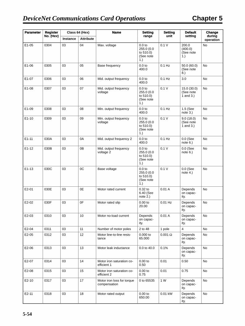
5-54
ÁÁÁÁÁÁÁÁÁÁ
Changeduring
operation
ÁÁÁÁÁÁÁÁ
Defaultsetting
ÁÁÁÁÁÁÁÁ
Settingunit
ÁÁÁÁÁÁÁÁÁÁ
Settingrange
ÁÁÁÁÁÁÁÁÁÁÁÁÁÁ
NameÁÁÁÁÁÁÁÁÁÁÁÁÁÁ
Class 64 (Hex)ÁÁÁÁÁÁÁÁ
RegisterNo. (Hex)
ÁÁÁÁÁÁÁÁ
ParameterÁÁÁÁÁÁÁÁÁÁ
Changeduring
operationÁÁÁÁÁÁÁÁ
DefaultsettingÁÁÁÁ
ÁÁÁÁ
SettingunitÁÁÁÁÁ
ÁÁÁÁÁ
SettingrangeÁÁÁÁÁÁÁ
ÁÁÁÁÁÁÁInstance
Name
AttributeÁÁÁÁÁÁÁÁ
RegisterNo. (Hex)ÁÁÁÁ
ÁÁÁÁ
Parameter
ÁÁÁÁÁÁÁÁÁÁÁÁÁÁÁÁ
E1-05ÁÁÁÁÁÁÁÁÁÁÁÁÁÁÁÁ
0304ÁÁÁÁÁÁÁÁÁÁÁÁÁÁÁÁ
03ÁÁÁÁÁÁÁÁÁÁÁÁÁÁÁÁ
04ÁÁÁÁÁÁÁÁÁÁÁÁÁÁÁÁÁÁÁÁÁÁÁÁÁÁÁÁ
Max. voltageÁÁÁÁÁÁÁÁÁÁÁÁÁÁÁÁÁÁÁÁ
0.0 to255.0 (0.0to 510.0)(See note1.)
ÁÁÁÁÁÁÁÁÁÁÁÁÁÁÁÁ
0.1 VÁÁÁÁÁÁÁÁÁÁÁÁÁÁÁÁ
200.0(400.0)(See note1.)
ÁÁÁÁÁÁÁÁÁÁÁÁÁÁÁÁÁÁÁÁ
No
ÁÁÁÁÁÁÁÁÁÁÁÁÁÁÁÁ
E1-06ÁÁÁÁÁÁÁÁÁÁÁÁÁÁÁÁ
0305ÁÁÁÁÁÁÁÁÁÁÁÁÁÁÁÁ
03ÁÁÁÁÁÁÁÁÁÁÁÁÁÁÁÁ
05ÁÁÁÁÁÁÁÁÁÁÁÁÁÁÁÁÁÁÁÁÁÁÁÁÁÁÁÁ
Base frequencyÁÁÁÁÁÁÁÁÁÁÁÁÁÁÁÁÁÁÁÁ
0.0 to400.0
ÁÁÁÁÁÁÁÁÁÁÁÁÁÁÁÁ
0.1 HzÁÁÁÁÁÁÁÁÁÁÁÁÁÁÁÁ
50.0 (60.0)(See note8.)
ÁÁÁÁÁÁÁÁÁÁÁÁÁÁÁÁÁÁÁÁ
No
ÁÁÁÁÁÁÁÁ
E1-07 ÁÁÁÁÁÁÁÁ
0306 ÁÁÁÁÁÁÁÁ
03 ÁÁÁÁÁÁÁÁ
06 ÁÁÁÁÁÁÁÁÁÁÁÁÁÁ
Mid. output frequency ÁÁÁÁÁÁÁÁÁÁ
0.0 to400.0 ÁÁÁÁ
ÁÁÁÁ
0.1 Hz ÁÁÁÁÁÁÁÁ
3.0 ÁÁÁÁÁÁÁÁÁÁ
No
ÁÁÁÁÁÁÁÁÁÁÁÁÁÁÁÁ
E1-08 ÁÁÁÁÁÁÁÁÁÁÁÁÁÁÁÁ
0307 ÁÁÁÁÁÁÁÁÁÁÁÁÁÁÁÁ
03 ÁÁÁÁÁÁÁÁÁÁÁÁÁÁÁÁ
07 ÁÁÁÁÁÁÁÁÁÁÁÁÁÁÁÁÁÁÁÁÁÁÁÁÁÁÁÁ
Mid. output frequencyvoltage
ÁÁÁÁÁÁÁÁÁÁÁÁÁÁÁÁÁÁÁÁ
0.0 to255.0 (0.0to 510.0)(See note1.)
ÁÁÁÁÁÁÁÁÁÁÁÁÁÁÁÁ
0.1 V ÁÁÁÁÁÁÁÁÁÁÁÁÁÁÁÁ
15.0 (30.0)(See note1 and 3.)
ÁÁÁÁÁÁÁÁÁÁÁÁÁÁÁÁÁÁÁÁ
No
ÁÁÁÁÁÁÁÁÁÁÁÁ
E1-09ÁÁÁÁÁÁÁÁÁÁÁÁ
0308ÁÁÁÁÁÁÁÁÁÁÁÁ
03ÁÁÁÁÁÁÁÁÁÁÁÁ
08ÁÁÁÁÁÁÁÁÁÁÁÁÁÁÁÁÁÁÁÁÁ
Min. output frequencyÁÁÁÁÁÁÁÁÁÁÁÁÁÁÁ
0.0 to400.0
ÁÁÁÁÁÁÁÁÁÁÁÁ
0.1 HzÁÁÁÁÁÁÁÁÁÁÁÁ
1.5 (Seenote 3.)
ÁÁÁÁÁÁÁÁÁÁÁÁÁÁÁ
No
ÁÁÁÁÁÁÁÁÁÁÁÁÁÁÁÁ
E1-10 ÁÁÁÁÁÁÁÁÁÁÁÁÁÁÁÁ
0309 ÁÁÁÁÁÁÁÁÁÁÁÁÁÁÁÁ
03 ÁÁÁÁÁÁÁÁÁÁÁÁÁÁÁÁ
09 ÁÁÁÁÁÁÁÁÁÁÁÁÁÁÁÁÁÁÁÁÁÁÁÁÁÁÁÁ
Min. output frequencyvoltage
ÁÁÁÁÁÁÁÁÁÁÁÁÁÁÁÁÁÁÁÁ
0.0 to255.0 (0.0to 510.0)(See note1.)
ÁÁÁÁÁÁÁÁÁÁÁÁÁÁÁÁ
0.1 V ÁÁÁÁÁÁÁÁÁÁÁÁÁÁÁÁ
9.0 (18.0)(See note1 and 3.)
ÁÁÁÁÁÁÁÁÁÁÁÁÁÁÁÁÁÁÁÁ
No
ÁÁÁÁÁÁÁÁÁÁÁÁ
E1-11 ÁÁÁÁÁÁÁÁÁÁÁÁ
030A ÁÁÁÁÁÁÁÁÁÁÁÁ
03 ÁÁÁÁÁÁÁÁÁÁÁÁ
0A ÁÁÁÁÁÁÁÁÁÁÁÁÁÁÁÁÁÁÁÁÁ
Mid. output frequency 2ÁÁÁÁÁÁÁÁÁÁÁÁÁÁÁ
0.0 to400.0
ÁÁÁÁÁÁÁÁÁÁÁÁ
0.1 Hz ÁÁÁÁÁÁÁÁÁÁÁÁ
0.0 (Seenote 6.)
ÁÁÁÁÁÁÁÁÁÁÁÁÁÁÁ
No
ÁÁÁÁÁÁÁÁÁÁÁÁÁÁÁÁ
E1-12 ÁÁÁÁÁÁÁÁÁÁÁÁÁÁÁÁ
030B ÁÁÁÁÁÁÁÁÁÁÁÁÁÁÁÁ
03 ÁÁÁÁÁÁÁÁÁÁÁÁÁÁÁÁ
0B ÁÁÁÁÁÁÁÁÁÁÁÁÁÁÁÁÁÁÁÁÁÁÁÁÁÁÁÁ
Mid. output frequencyvoltage 2 ÁÁÁÁÁ
ÁÁÁÁÁÁÁÁÁÁÁÁÁÁÁ
0.0 to255.0 (0.0to 510.0)(See note1.)
ÁÁÁÁÁÁÁÁÁÁÁÁÁÁÁÁ
0.1 V ÁÁÁÁÁÁÁÁÁÁÁÁÁÁÁÁ
0.0 (Seenote 6.) ÁÁÁÁÁ
ÁÁÁÁÁÁÁÁÁÁÁÁÁÁÁ
No
ÁÁÁÁÁÁÁÁÁÁÁÁÁÁÁÁ
E1-13 ÁÁÁÁÁÁÁÁÁÁÁÁÁÁÁÁ
030C ÁÁÁÁÁÁÁÁÁÁÁÁÁÁÁÁ
03 ÁÁÁÁÁÁÁÁÁÁÁÁÁÁÁÁ
0C ÁÁÁÁÁÁÁÁÁÁÁÁÁÁÁÁÁÁÁÁÁÁÁÁÁÁÁÁ
Base voltage ÁÁÁÁÁÁÁÁÁÁÁÁÁÁÁÁÁÁÁÁ
0.0 to255.0 (0.0to 510.0)(See note1.)
ÁÁÁÁÁÁÁÁÁÁÁÁÁÁÁÁ
0.1 V ÁÁÁÁÁÁÁÁÁÁÁÁÁÁÁÁ
0.0 (Seenote 4.)
ÁÁÁÁÁÁÁÁÁÁÁÁÁÁÁÁÁÁÁÁ
No
ÁÁÁÁÁÁÁÁÁÁÁÁ
E2-01 ÁÁÁÁÁÁÁÁÁÁÁÁ
030E ÁÁÁÁÁÁÁÁÁÁÁÁ
03 ÁÁÁÁÁÁÁÁÁÁÁÁ
0E ÁÁÁÁÁÁÁÁÁÁÁÁÁÁÁÁÁÁÁÁÁ
Motor rated current ÁÁÁÁÁÁÁÁÁÁÁÁÁÁÁ
0.32 to6.40 (Seenote 2.)
ÁÁÁÁÁÁÁÁÁÁÁÁ
0.01 A ÁÁÁÁÁÁÁÁÁÁÁÁ
Dependson capac-ity.
ÁÁÁÁÁÁÁÁÁÁÁÁÁÁÁ
No
ÁÁÁÁÁÁÁÁÁÁÁÁ
E2-02 ÁÁÁÁÁÁÁÁÁÁÁÁ
030F ÁÁÁÁÁÁÁÁÁÁÁÁ
03 ÁÁÁÁÁÁÁÁÁÁÁÁ
0F ÁÁÁÁÁÁÁÁÁÁÁÁÁÁÁÁÁÁÁÁÁ
Motor rated slip ÁÁÁÁÁÁÁÁÁÁÁÁÁÁÁ
0.00 to20.00
ÁÁÁÁÁÁÁÁÁÁÁÁ
0.01 Hz ÁÁÁÁÁÁÁÁÁÁÁÁ
Dependson capac-ity.
ÁÁÁÁÁÁÁÁÁÁÁÁÁÁÁ
No
ÁÁÁÁÁÁÁÁÁÁÁÁ
E2-03ÁÁÁÁÁÁÁÁÁÁÁÁ
0310ÁÁÁÁÁÁÁÁÁÁÁÁ
03ÁÁÁÁÁÁÁÁÁÁÁÁ
10ÁÁÁÁÁÁÁÁÁÁÁÁÁÁÁÁÁÁÁÁÁ
Motor no-load currentÁÁÁÁÁÁÁÁÁÁÁÁÁÁÁ
Dependson capac-ity.
ÁÁÁÁÁÁÁÁÁÁÁÁ
0.01 AÁÁÁÁÁÁÁÁÁÁÁÁ
Dependson capac-ity.
ÁÁÁÁÁÁÁÁÁÁÁÁÁÁÁ
No
ÁÁÁÁÁÁÁÁ
E2-04ÁÁÁÁÁÁÁÁ
0311ÁÁÁÁÁÁÁÁ
03ÁÁÁÁÁÁÁÁ
11ÁÁÁÁÁÁÁÁÁÁÁÁÁÁ
Number of motor polesÁÁÁÁÁÁÁÁÁÁ
2 to 48ÁÁÁÁÁÁÁÁ
1 poleÁÁÁÁÁÁÁÁ
4ÁÁÁÁÁÁÁÁÁÁ
NoÁÁÁÁÁÁÁÁÁÁÁÁ
E2-05ÁÁÁÁÁÁÁÁÁÁÁÁ
0312ÁÁÁÁÁÁÁÁÁÁÁÁ
03ÁÁÁÁÁÁÁÁÁÁÁÁ
12ÁÁÁÁÁÁÁÁÁÁÁÁÁÁÁÁÁÁÁÁÁ
Motor line-to-line resis-tance
ÁÁÁÁÁÁÁÁÁÁÁÁÁÁÁ
0.000 to65.000
ÁÁÁÁÁÁÁÁÁÁÁÁ
0.001 Ω ÁÁÁÁÁÁÁÁÁÁÁÁ
Dependson capac-ity.
ÁÁÁÁÁÁÁÁÁÁÁÁÁÁÁ
No
ÁÁÁÁÁÁÁÁÁÁÁÁ
E2-06ÁÁÁÁÁÁÁÁÁÁÁÁ
0313ÁÁÁÁÁÁÁÁÁÁÁÁ
03ÁÁÁÁÁÁÁÁÁÁÁÁ
13ÁÁÁÁÁÁÁÁÁÁÁÁÁÁÁÁÁÁÁÁÁ
Motor leak inductanceÁÁÁÁÁÁÁÁÁÁÁÁÁÁÁ
0.0 to 40.0ÁÁÁÁÁÁÁÁÁÁÁÁ
0.1%ÁÁÁÁÁÁÁÁÁÁÁÁ
Dependson capac-ity.
ÁÁÁÁÁÁÁÁÁÁÁÁÁÁÁ
No
ÁÁÁÁÁÁÁÁÁÁÁÁ
E2-07ÁÁÁÁÁÁÁÁÁÁÁÁ
0314ÁÁÁÁÁÁÁÁÁÁÁÁ
03ÁÁÁÁÁÁÁÁÁÁÁÁ
14ÁÁÁÁÁÁÁÁÁÁÁÁÁÁÁÁÁÁÁÁÁ
Motor iron saturation co-efficient 1
ÁÁÁÁÁÁÁÁÁÁÁÁÁÁÁ
0.00 to0.50
ÁÁÁÁÁÁÁÁÁÁÁÁ
0.01ÁÁÁÁÁÁÁÁÁÁÁÁ
0.50ÁÁÁÁÁÁÁÁÁÁÁÁÁÁÁ
No
ÁÁÁÁÁÁÁÁ
E2-08 ÁÁÁÁÁÁÁÁ
0315 ÁÁÁÁÁÁÁÁ
03 ÁÁÁÁÁÁÁÁ
15 ÁÁÁÁÁÁÁÁÁÁÁÁÁÁ
Motor iron saturation co-efficient 2
ÁÁÁÁÁÁÁÁÁÁ
0.00 to0.75
ÁÁÁÁÁÁÁÁ
0.01 ÁÁÁÁÁÁÁÁ
0.75 ÁÁÁÁÁÁÁÁÁÁ
No
ÁÁÁÁÁÁÁÁÁÁÁÁÁÁÁÁ
E2-10ÁÁÁÁÁÁÁÁÁÁÁÁÁÁÁÁ
0317ÁÁÁÁÁÁÁÁÁÁÁÁÁÁÁÁ
03ÁÁÁÁÁÁÁÁÁÁÁÁÁÁÁÁ
17ÁÁÁÁÁÁÁÁÁÁÁÁÁÁÁÁÁÁÁÁÁÁÁÁÁÁÁÁ
Motor iron loss for torquecompensation
ÁÁÁÁÁÁÁÁÁÁÁÁÁÁÁÁÁÁÁÁ
0 to 65535ÁÁÁÁÁÁÁÁÁÁÁÁÁÁÁÁ
1 WÁÁÁÁÁÁÁÁÁÁÁÁÁÁÁÁ
Dependson capac-ity.
ÁÁÁÁÁÁÁÁÁÁÁÁÁÁÁÁÁÁÁÁ
No
ÁÁÁÁÁÁÁÁÁÁÁÁ
E2-11 ÁÁÁÁÁÁÁÁÁÁÁÁ
0318 ÁÁÁÁÁÁÁÁÁÁÁÁ
03 ÁÁÁÁÁÁÁÁÁÁÁÁ
18 ÁÁÁÁÁÁÁÁÁÁÁÁÁÁÁÁÁÁÁÁÁ
Motor rated output ÁÁÁÁÁÁÁÁÁÁÁÁÁÁÁ
0.00 to650.00 ÁÁÁÁ
ÁÁÁÁÁÁÁÁ
0.01 kW ÁÁÁÁÁÁÁÁÁÁÁÁ
Dependson capac-ity.
ÁÁÁÁÁÁÁÁÁÁÁÁÁÁÁ
No
DeviceNet Communications Card Operations Chapter 5

5-55
ÁÁÁÁÁÁÁÁÁÁ
Changeduring
operation
ÁÁÁÁÁÁÁÁ
Defaultsetting
ÁÁÁÁÁÁÁÁ
Settingunit
ÁÁÁÁÁÁÁÁÁÁ
Settingrange
ÁÁÁÁÁÁÁÁÁÁÁÁÁÁ
NameÁÁÁÁÁÁÁÁÁÁÁÁÁÁ
Class 64 (Hex)ÁÁÁÁÁÁÁÁ
RegisterNo. (Hex)
ÁÁÁÁÁÁÁÁ
ParameterÁÁÁÁÁÁÁÁÁÁ
Changeduring
operationÁÁÁÁÁÁÁÁ
DefaultsettingÁÁÁÁ
ÁÁÁÁ
SettingunitÁÁÁÁÁ
ÁÁÁÁÁ
SettingrangeÁÁÁÁÁÁÁ
ÁÁÁÁÁÁÁInstance
Name
AttributeÁÁÁÁÁÁÁÁ
RegisterNo. (Hex)ÁÁÁÁ
ÁÁÁÁ
Parameter
ÁÁÁÁÁÁÁÁÁÁÁÁ
E3-01ÁÁÁÁÁÁÁÁÁÁÁÁ
0319ÁÁÁÁÁÁÁÁÁÁÁÁ
03ÁÁÁÁÁÁÁÁÁÁÁÁ
19ÁÁÁÁÁÁÁÁÁÁÁÁÁÁÁÁÁÁÁÁÁ
Motor 2 control methodselection
ÁÁÁÁÁÁÁÁÁÁÁÁÁÁÁ
0 to 2ÁÁÁÁÁÁÁÁÁÁÁÁ
1ÁÁÁÁÁÁÁÁÁÁÁÁ
0ÁÁÁÁÁÁÁÁÁÁÁÁÁÁÁ
No
ÁÁÁÁÁÁÁÁÁÁÁÁ
E3-02 ÁÁÁÁÁÁÁÁÁÁÁÁ
031A ÁÁÁÁÁÁÁÁÁÁÁÁ
03 ÁÁÁÁÁÁÁÁÁÁÁÁ
1A ÁÁÁÁÁÁÁÁÁÁÁÁÁÁÁÁÁÁÁÁÁ
Motor 2 max. output fre-quency (FMAX)
ÁÁÁÁÁÁÁÁÁÁÁÁÁÁÁ
40.0 to400.0 (Seenote 5.)
ÁÁÁÁÁÁÁÁÁÁÁÁ
0.1 Hz ÁÁÁÁÁÁÁÁÁÁÁÁ
50.0 (60.0)(See note8.)
ÁÁÁÁÁÁÁÁÁÁÁÁÁÁÁ
No
ÁÁÁÁÁÁÁÁÁÁÁÁÁÁÁÁ
E3-03 ÁÁÁÁÁÁÁÁÁÁÁÁÁÁÁÁ
031B ÁÁÁÁÁÁÁÁÁÁÁÁÁÁÁÁ
03 ÁÁÁÁÁÁÁÁÁÁÁÁÁÁÁÁ
1B ÁÁÁÁÁÁÁÁÁÁÁÁÁÁÁÁÁÁÁÁÁÁÁÁÁÁÁÁ
Motor 2 max. voltage(VMAX)
ÁÁÁÁÁÁÁÁÁÁÁÁÁÁÁÁÁÁÁÁ
0.0 to255.0 (0.0to 510.0)(See note1.)
ÁÁÁÁÁÁÁÁÁÁÁÁÁÁÁÁ
0.1 V ÁÁÁÁÁÁÁÁÁÁÁÁÁÁÁÁ
200.0(400.0)(See note1.)
ÁÁÁÁÁÁÁÁÁÁÁÁÁÁÁÁÁÁÁÁ
No
ÁÁÁÁÁÁÁÁÁÁÁÁ
E3-04 ÁÁÁÁÁÁÁÁÁÁÁÁ
031C ÁÁÁÁÁÁÁÁÁÁÁÁ
03 ÁÁÁÁÁÁÁÁÁÁÁÁ
1C ÁÁÁÁÁÁÁÁÁÁÁÁÁÁÁÁÁÁÁÁÁ
Motor 2 max. voltage fre-quency (FA)
ÁÁÁÁÁÁÁÁÁÁÁÁÁÁÁ
0.0 to400.0
ÁÁÁÁÁÁÁÁÁÁÁÁ
0.1 Hz ÁÁÁÁÁÁÁÁÁÁÁÁ
50.0 (60.0)(See note8.)
ÁÁÁÁÁÁÁÁÁÁÁÁÁÁÁ
No
ÁÁÁÁÁÁÁÁ
E3-05 ÁÁÁÁÁÁÁÁ
031D ÁÁÁÁÁÁÁÁ
03 ÁÁÁÁÁÁÁÁ
1D ÁÁÁÁÁÁÁÁÁÁÁÁÁÁ
Motor 2 mid. output fre-quency 1 (FB)
ÁÁÁÁÁÁÁÁÁÁ
0.0 to400.0
ÁÁÁÁÁÁÁÁ
0.1 Hz ÁÁÁÁÁÁÁÁ
3.0 ÁÁÁÁÁÁÁÁÁÁ
No
ÁÁÁÁÁÁÁÁÁÁÁÁÁÁÁÁ
E3-06ÁÁÁÁÁÁÁÁÁÁÁÁÁÁÁÁ
031EÁÁÁÁÁÁÁÁÁÁÁÁÁÁÁÁ
03ÁÁÁÁÁÁÁÁÁÁÁÁÁÁÁÁ
1EÁÁÁÁÁÁÁÁÁÁÁÁÁÁÁÁÁÁÁÁÁÁÁÁÁÁÁÁ
Motor 2 mid. output fre-quency voltage 1 (VC)
ÁÁÁÁÁÁÁÁÁÁÁÁÁÁÁÁÁÁÁÁ
0.0 to255.0 (0.0to 510.0)(See note1.)
ÁÁÁÁÁÁÁÁÁÁÁÁÁÁÁÁ
0.1 VÁÁÁÁÁÁÁÁÁÁÁÁÁÁÁÁ
15.0 (30.0)(See note1 and 3.)
ÁÁÁÁÁÁÁÁÁÁÁÁÁÁÁÁÁÁÁÁ
No
ÁÁÁÁÁÁÁÁÁÁÁÁ
E3-07ÁÁÁÁÁÁÁÁÁÁÁÁ
031FÁÁÁÁÁÁÁÁÁÁÁÁ
03ÁÁÁÁÁÁÁÁÁÁÁÁ
1FÁÁÁÁÁÁÁÁÁÁÁÁÁÁÁÁÁÁÁÁÁ
Motor 2 min. output fre-quency (FMIN)
ÁÁÁÁÁÁÁÁÁÁÁÁÁÁÁ
0.0 to400.0
ÁÁÁÁÁÁÁÁÁÁÁÁ
0.1 HzÁÁÁÁÁÁÁÁÁÁÁÁ
1.5 (Seenote 3.)
ÁÁÁÁÁÁÁÁÁÁÁÁÁÁÁ
No
ÁÁÁÁÁÁÁÁÁÁÁÁÁÁÁÁ
E3-08 ÁÁÁÁÁÁÁÁÁÁÁÁÁÁÁÁ
0320 ÁÁÁÁÁÁÁÁÁÁÁÁÁÁÁÁ
03 ÁÁÁÁÁÁÁÁÁÁÁÁÁÁÁÁ
20 ÁÁÁÁÁÁÁÁÁÁÁÁÁÁÁÁÁÁÁÁÁÁÁÁÁÁÁÁ
Motor 2 min. output fre-quency voltage (VMIN)
ÁÁÁÁÁÁÁÁÁÁÁÁÁÁÁÁÁÁÁÁ
0.0 to255.0 (0.0to 510.0)(See note1.)
ÁÁÁÁÁÁÁÁÁÁÁÁÁÁÁÁ
0.1 V ÁÁÁÁÁÁÁÁÁÁÁÁÁÁÁÁ
9.0 (18.0)(See note1 and 3.)
ÁÁÁÁÁÁÁÁÁÁÁÁÁÁÁÁÁÁÁÁ
No
ÁÁÁÁÁÁÁÁÁÁÁÁ
E4-01 ÁÁÁÁÁÁÁÁÁÁÁÁ
0321 ÁÁÁÁÁÁÁÁÁÁÁÁ
03 ÁÁÁÁÁÁÁÁÁÁÁÁ
21 ÁÁÁÁÁÁÁÁÁÁÁÁÁÁÁÁÁÁÁÁÁ
Motor 2 rated current ÁÁÁÁÁÁÁÁÁÁÁÁÁÁÁ
0.32 to6.40 (Seenote 2.)
ÁÁÁÁÁÁÁÁÁÁÁÁ
0.01 A ÁÁÁÁÁÁÁÁÁÁÁÁ
Dependson capac-ity.
ÁÁÁÁÁÁÁÁÁÁÁÁÁÁÁ
No
ÁÁÁÁÁÁÁÁÁÁÁÁ
E4-02 ÁÁÁÁÁÁÁÁÁÁÁÁ
0322 ÁÁÁÁÁÁÁÁÁÁÁÁ
03 ÁÁÁÁÁÁÁÁÁÁÁÁ
22 ÁÁÁÁÁÁÁÁÁÁÁÁÁÁÁÁÁÁÁÁÁ
Motor 2 rated slip ÁÁÁÁÁÁÁÁÁÁÁÁÁÁÁ
0.00 to20.00
ÁÁÁÁÁÁÁÁÁÁÁÁ
0.01 Hz ÁÁÁÁÁÁÁÁÁÁÁÁ
Dependson capac-ity.
ÁÁÁÁÁÁÁÁÁÁÁÁÁÁÁ
No
ÁÁÁÁÁÁÁÁÁÁÁÁ
E4-03 ÁÁÁÁÁÁÁÁÁÁÁÁ
0323 ÁÁÁÁÁÁÁÁÁÁÁÁ
03 ÁÁÁÁÁÁÁÁÁÁÁÁ
23 ÁÁÁÁÁÁÁÁÁÁÁÁÁÁÁÁÁÁÁÁÁ
Motor 2 no-load currentÁÁÁÁÁÁÁÁÁÁÁÁÁÁÁ
0.00 to1.89 (Seenote 7.)
ÁÁÁÁÁÁÁÁÁÁÁÁ
0.01 A ÁÁÁÁÁÁÁÁÁÁÁÁ
Dependson capac-ity.
ÁÁÁÁÁÁÁÁÁÁÁÁÁÁÁ
No
ÁÁÁÁÁÁÁÁÁÁÁÁ
E4-04 ÁÁÁÁÁÁÁÁÁÁÁÁ
0324 ÁÁÁÁÁÁÁÁÁÁÁÁ
03 ÁÁÁÁÁÁÁÁÁÁÁÁ
24 ÁÁÁÁÁÁÁÁÁÁÁÁÁÁÁÁÁÁÁÁÁ
Motor 2 number of poles(number of poles)
ÁÁÁÁÁÁÁÁÁÁÁÁÁÁÁ
2 to 48 ÁÁÁÁÁÁÁÁÁÁÁÁ
1 pole ÁÁÁÁÁÁÁÁÁÁÁÁ
4 ÁÁÁÁÁÁÁÁÁÁÁÁÁÁÁ
No
ÁÁÁÁÁÁÁÁÁÁÁÁ
E4-05 ÁÁÁÁÁÁÁÁÁÁÁÁ
0325 ÁÁÁÁÁÁÁÁÁÁÁÁ
03 ÁÁÁÁÁÁÁÁÁÁÁÁ
25 ÁÁÁÁÁÁÁÁÁÁÁÁÁÁÁÁÁÁÁÁÁ
Motor 2 line-to-line resis-tance ÁÁÁÁÁ
ÁÁÁÁÁÁÁÁÁÁ
0.000 to65.000 ÁÁÁÁ
ÁÁÁÁÁÁÁÁ
0.001 Ω ÁÁÁÁÁÁÁÁÁÁÁÁ
Dependson capac-ity.
ÁÁÁÁÁÁÁÁÁÁÁÁÁÁÁ
No
ÁÁÁÁÁÁÁÁÁÁÁÁ
E4-06 ÁÁÁÁÁÁÁÁÁÁÁÁ
0326 ÁÁÁÁÁÁÁÁÁÁÁÁ
03 ÁÁÁÁÁÁÁÁÁÁÁÁ
26 ÁÁÁÁÁÁÁÁÁÁÁÁÁÁÁÁÁÁÁÁÁ
Motor 2 leak inductanceÁÁÁÁÁÁÁÁÁÁÁÁÁÁÁ
0.0 to 40.0 ÁÁÁÁÁÁÁÁÁÁÁÁ
0.1% ÁÁÁÁÁÁÁÁÁÁÁÁ
Dependson capac-ity.
ÁÁÁÁÁÁÁÁÁÁÁÁÁÁÁ
No
ÁÁÁÁÁÁÁÁÁÁÁÁ
E4-07 ÁÁÁÁÁÁÁÁÁÁÁÁ
0327 ÁÁÁÁÁÁÁÁÁÁÁÁ
03 ÁÁÁÁÁÁÁÁÁÁÁÁ
27 ÁÁÁÁÁÁÁÁÁÁÁÁÁÁÁÁÁÁÁÁÁ
Motor 2 rated capacity ÁÁÁÁÁÁÁÁÁÁÁÁÁÁÁ
0.40 to650.00 ÁÁÁÁ
ÁÁÁÁÁÁÁÁ
0.01 kW ÁÁÁÁÁÁÁÁÁÁÁÁ
Dependson capac-ity.
ÁÁÁÁÁÁÁÁÁÁÁÁÁÁÁ
No
Note 1. Values in parentheses are for 400-V-class Inverters.
Note 2. The setting range is 10% to 200% of the Inverter’s rated output current. The values for a200-V-class 0.4-kW Inverter are given above.
Note 3. When the control mode is changed, the Inverter will revert to default settings. (The V/f controldefault settings are given above.)
Note 4. E1-13 will be the same value as E1-05 after autotuning.
Note 5. The upper setting limit will be 150.0 Hz when C6-01 is set to 0.
Note 6. The settings of E1-11 and E1-12 are ignored if set to 0.0.
DeviceNet Communications Card Operations Chapter 5
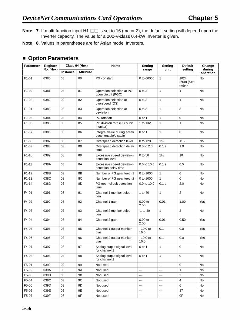
5-56
Note 7. If multi-function input H1- is set to 16 (motor 2), the default setting will depend upon theInverter capacity. The value for a 200-V-class 0.4-kW Inverter is given.
Note 8. Values in parentheses are for Asian model Inverters.
Option ParametersÁÁÁÁÁÁÁÁ
ParameterÁÁÁÁÁÁÁÁ
RegisterNo (Hex)ÁÁÁÁÁÁÁÁÁÁÁÁÁÁ
Class 64 (Hex) ÁÁÁÁÁÁÁÁÁÁÁÁÁÁÁÁ
Name ÁÁÁÁÁÁÁÁ
SettingrangeÁÁÁÁÁÁÁÁ
SettingnitÁÁÁÁÁÁÁÁ
DefaultsettingÁÁÁÁÁÁÁÁÁÁ
Changed ring
ÁÁÁÁÁÁÁÁ
ÁÁÁÁÁÁÁÁ
No. (Hex)Instance AttributeÁÁÁÁÁÁÁÁ
ÁÁÁÁÁÁÁÁÁÁÁÁÁÁÁÁ
rangeÁÁÁÁÁÁÁÁ
unitÁÁÁÁÁÁÁÁ
settingÁÁÁÁÁÁÁÁÁÁ
duringoperation
ÁÁÁÁÁÁÁÁÁÁÁÁ
F1-01 ÁÁÁÁÁÁÁÁÁÁÁÁ
0380 ÁÁÁÁÁÁÁÁÁÁÁÁ
03 ÁÁÁÁÁÁÁÁÁÁÁÁ
80 ÁÁÁÁÁÁÁÁÁÁÁÁÁÁÁÁÁÁÁÁÁÁÁÁ
PG constant ÁÁÁÁÁÁÁÁÁÁÁÁ
0 to 60000ÁÁÁÁÁÁÁÁÁÁÁÁ
1 ÁÁÁÁÁÁÁÁÁÁÁÁ
1024(600) (Seenote.)
ÁÁÁÁÁÁÁÁÁÁÁÁÁÁÁ
No
ÁÁÁÁÁÁÁÁ
F1-02 ÁÁÁÁÁÁÁÁ
0381 ÁÁÁÁÁÁÁÁ
03 ÁÁÁÁÁÁÁÁ
81 ÁÁÁÁÁÁÁÁÁÁÁÁÁÁÁÁ
Operation selection at PGopen circuit (PGO)
ÁÁÁÁÁÁÁÁ
0 to 3 ÁÁÁÁÁÁÁÁ
1 ÁÁÁÁÁÁÁÁ
1 ÁÁÁÁÁÁÁÁÁÁ
No
ÁÁÁÁÁÁÁÁÁÁÁÁ
F1-03 ÁÁÁÁÁÁÁÁÁÁÁÁ
0382 ÁÁÁÁÁÁÁÁÁÁÁÁ
03 ÁÁÁÁÁÁÁÁÁÁÁÁ
82 ÁÁÁÁÁÁÁÁÁÁÁÁÁÁÁÁÁÁÁÁÁÁÁÁ
Operation selection atoverspeed (OS)
ÁÁÁÁÁÁÁÁÁÁÁÁ
0 to 3 ÁÁÁÁÁÁÁÁÁÁÁÁ
1 ÁÁÁÁÁÁÁÁÁÁÁÁ
1 ÁÁÁÁÁÁÁÁÁÁÁÁÁÁÁ
No
ÁÁÁÁÁÁÁÁ
F1-04 ÁÁÁÁÁÁÁÁ
0383 ÁÁÁÁÁÁÁÁ
03 ÁÁÁÁÁÁÁÁ
83 ÁÁÁÁÁÁÁÁÁÁÁÁÁÁÁÁ
Operation selection atdeviation
ÁÁÁÁÁÁÁÁ
0 to 3 ÁÁÁÁÁÁÁÁ
1 ÁÁÁÁÁÁÁÁ
3 ÁÁÁÁÁÁÁÁÁÁ
No
ÁÁÁÁÁÁÁÁ
F1-05 ÁÁÁÁÁÁÁÁ
0384 ÁÁÁÁÁÁÁÁ
03 ÁÁÁÁÁÁÁÁ
84 ÁÁÁÁÁÁÁÁÁÁÁÁÁÁÁÁ
PG rotation ÁÁÁÁÁÁÁÁ
0 or 1 ÁÁÁÁÁÁÁÁ
1 ÁÁÁÁÁÁÁÁ
0 ÁÁÁÁÁÁÁÁÁÁ
No
ÁÁÁÁÁÁÁÁ
F1-06 ÁÁÁÁÁÁÁÁ
0385 ÁÁÁÁÁÁÁÁ
03 ÁÁÁÁÁÁÁÁ
85 ÁÁÁÁÁÁÁÁÁÁÁÁÁÁÁÁ
PG division rate (PG pulsemonitor)
ÁÁÁÁÁÁÁÁ
1 to 132 ÁÁÁÁÁÁÁÁ
1 ÁÁÁÁÁÁÁÁ
1 ÁÁÁÁÁÁÁÁÁÁ
No
ÁÁÁÁÁÁÁÁÁÁÁÁ
F1-07ÁÁÁÁÁÁÁÁÁÁÁÁ
0386ÁÁÁÁÁÁÁÁÁÁÁÁ
03ÁÁÁÁÁÁÁÁÁÁÁÁ
86ÁÁÁÁÁÁÁÁÁÁÁÁÁÁÁÁÁÁÁÁÁÁÁÁ
Integral value during accel/decel enable/disable
ÁÁÁÁÁÁÁÁÁÁÁÁ
0 or 1ÁÁÁÁÁÁÁÁÁÁÁÁ
1ÁÁÁÁÁÁÁÁÁÁÁÁ
0ÁÁÁÁÁÁÁÁÁÁÁÁÁÁÁ
No
ÁÁÁÁÁÁÁÁ
F1-08 ÁÁÁÁÁÁÁÁ
0387 ÁÁÁÁÁÁÁÁ
03 ÁÁÁÁÁÁÁÁ
87 ÁÁÁÁÁÁÁÁÁÁÁÁÁÁÁÁ
Overspeed detection level ÁÁÁÁÁÁÁÁ
0 to 120 ÁÁÁÁÁÁÁÁ
1% ÁÁÁÁÁÁÁÁ
115 ÁÁÁÁÁÁÁÁÁÁ
No
ÁÁÁÁÁÁÁÁ
F1-09 ÁÁÁÁÁÁÁÁ
0388 ÁÁÁÁÁÁÁÁ
03 ÁÁÁÁÁÁÁÁ
88 ÁÁÁÁÁÁÁÁÁÁÁÁÁÁÁÁ
Overspeed detection delaytime
ÁÁÁÁÁÁÁÁ
0.0 to 2.0 ÁÁÁÁÁÁÁÁ
0.1 s ÁÁÁÁÁÁÁÁ
1.0 ÁÁÁÁÁÁÁÁÁÁ
No
ÁÁÁÁÁÁÁÁÁÁÁÁ
F1-10 ÁÁÁÁÁÁÁÁÁÁÁÁ
0389 ÁÁÁÁÁÁÁÁÁÁÁÁ
03 ÁÁÁÁÁÁÁÁÁÁÁÁ
89 ÁÁÁÁÁÁÁÁÁÁÁÁÁÁÁÁÁÁÁÁÁÁÁÁ
Excessive speed deviationdetection level
ÁÁÁÁÁÁÁÁÁÁÁÁ
0 to 50 ÁÁÁÁÁÁÁÁÁÁÁÁ
1% ÁÁÁÁÁÁÁÁÁÁÁÁ
10 ÁÁÁÁÁÁÁÁÁÁÁÁÁÁÁ
No
ÁÁÁÁÁÁÁÁ
F1-11 ÁÁÁÁÁÁÁÁ
038A ÁÁÁÁÁÁÁÁ
03 ÁÁÁÁÁÁÁÁ
8A ÁÁÁÁÁÁÁÁÁÁÁÁÁÁÁÁ
Excessive speed deviationdetection delay time ÁÁÁÁ
ÁÁÁÁ
0.0 to 10.0ÁÁÁÁÁÁÁÁ
0.1 s ÁÁÁÁÁÁÁÁ
0.5 ÁÁÁÁÁÁÁÁÁÁ
No
ÁÁÁÁÁÁÁÁ
F1-12 ÁÁÁÁÁÁÁÁ
038B ÁÁÁÁÁÁÁÁ
03 ÁÁÁÁÁÁÁÁ
8B ÁÁÁÁÁÁÁÁÁÁÁÁÁÁÁÁ
Number of PG gear teeth 1 ÁÁÁÁÁÁÁÁ
0 to 1000 ÁÁÁÁÁÁÁÁ
1 ÁÁÁÁÁÁÁÁ
0 ÁÁÁÁÁÁÁÁÁÁ
No
ÁÁÁÁÁÁÁÁ
F1-13 ÁÁÁÁÁÁÁÁ
038C ÁÁÁÁÁÁÁÁ
03 ÁÁÁÁÁÁÁÁ
8C ÁÁÁÁÁÁÁÁÁÁÁÁÁÁÁÁ
Number of PG gear teeth 2 ÁÁÁÁÁÁÁÁ
0 to 1000 ÁÁÁÁÁÁÁÁ
1 ÁÁÁÁÁÁÁÁ
0 ÁÁÁÁÁÁÁÁÁÁ
No
ÁÁÁÁÁÁÁÁ
F1-14 ÁÁÁÁÁÁÁÁ
038D ÁÁÁÁÁÁÁÁ
03 ÁÁÁÁÁÁÁÁ
8D ÁÁÁÁÁÁÁÁÁÁÁÁÁÁÁÁ
PG open-circuit detectiontime
ÁÁÁÁÁÁÁÁ
0.0 to 10.0ÁÁÁÁÁÁÁÁ
0.1 s ÁÁÁÁÁÁÁÁ
2.0 ÁÁÁÁÁÁÁÁÁÁ
No
ÁÁÁÁÁÁÁÁÁÁÁÁ
F4-01 ÁÁÁÁÁÁÁÁÁÁÁÁ
0391 ÁÁÁÁÁÁÁÁÁÁÁÁ
03 ÁÁÁÁÁÁÁÁÁÁÁÁ
91 ÁÁÁÁÁÁÁÁÁÁÁÁÁÁÁÁÁÁÁÁÁÁÁÁ
Channel 1 monitor selec-tion
ÁÁÁÁÁÁÁÁÁÁÁÁ
1 to 40 ÁÁÁÁÁÁÁÁÁÁÁÁ
1 ÁÁÁÁÁÁÁÁÁÁÁÁ
2 ÁÁÁÁÁÁÁÁÁÁÁÁÁÁÁ
No
ÁÁÁÁÁÁÁÁ
F4-02 ÁÁÁÁÁÁÁÁ
0392 ÁÁÁÁÁÁÁÁ
03 ÁÁÁÁÁÁÁÁ
92 ÁÁÁÁÁÁÁÁÁÁÁÁÁÁÁÁ
Channel 1 gain ÁÁÁÁÁÁÁÁ
0.00 to2.50 ÁÁÁÁ
ÁÁÁÁ
0.01 ÁÁÁÁÁÁÁÁ
1.00 ÁÁÁÁÁÁÁÁÁÁ
Yes
ÁÁÁÁÁÁÁÁ
F4-03 ÁÁÁÁÁÁÁÁ
0393 ÁÁÁÁÁÁÁÁ
03 ÁÁÁÁÁÁÁÁ
93 ÁÁÁÁÁÁÁÁÁÁÁÁÁÁÁÁ
Channel 2 monitor selec-tion
ÁÁÁÁÁÁÁÁ
1 to 40 ÁÁÁÁÁÁÁÁ
1 ÁÁÁÁÁÁÁÁ
3 ÁÁÁÁÁÁÁÁÁÁ
No
ÁÁÁÁÁÁÁÁÁÁÁÁ
F4-04ÁÁÁÁÁÁÁÁÁÁÁÁ
0394ÁÁÁÁÁÁÁÁÁÁÁÁ
03ÁÁÁÁÁÁÁÁÁÁÁÁ
94ÁÁÁÁÁÁÁÁÁÁÁÁÁÁÁÁÁÁÁÁÁÁÁÁ
Channel 2 gainÁÁÁÁÁÁÁÁÁÁÁÁ
0.00 to2.50
ÁÁÁÁÁÁÁÁÁÁÁÁ
0.01ÁÁÁÁÁÁÁÁÁÁÁÁ
0.50ÁÁÁÁÁÁÁÁÁÁÁÁÁÁÁ
Yes
ÁÁÁÁÁÁÁÁ
F4-05 ÁÁÁÁÁÁÁÁ
0395 ÁÁÁÁÁÁÁÁ
03 ÁÁÁÁÁÁÁÁ
95 ÁÁÁÁÁÁÁÁÁÁÁÁÁÁÁÁ
Channel 1 output monitorbias
ÁÁÁÁÁÁÁÁ
–10.0 to10.0
ÁÁÁÁÁÁÁÁ
0.1 ÁÁÁÁÁÁÁÁ
0.0 ÁÁÁÁÁÁÁÁÁÁ
Yes
ÁÁÁÁÁÁÁÁÁÁÁÁ
F4-06ÁÁÁÁÁÁÁÁÁÁÁÁ
0396ÁÁÁÁÁÁÁÁÁÁÁÁ
03ÁÁÁÁÁÁÁÁÁÁÁÁ
96ÁÁÁÁÁÁÁÁÁÁÁÁÁÁÁÁÁÁÁÁÁÁÁÁ
Channel 2 output monitorbias
ÁÁÁÁÁÁÁÁÁÁÁÁ
–10.0 to10.0
ÁÁÁÁÁÁÁÁÁÁÁÁ
0.1ÁÁÁÁÁÁÁÁÁÁÁÁ
0.0ÁÁÁÁÁÁÁÁÁÁÁÁÁÁÁ
Yes
ÁÁÁÁÁÁÁÁ
F4-07 ÁÁÁÁÁÁÁÁ
0397 ÁÁÁÁÁÁÁÁ
03 ÁÁÁÁÁÁÁÁ
97 ÁÁÁÁÁÁÁÁÁÁÁÁÁÁÁÁ
Analog output signal levelfor channel 1
ÁÁÁÁÁÁÁÁ
0 or 1 ÁÁÁÁÁÁÁÁ
1 ÁÁÁÁÁÁÁÁ
0 ÁÁÁÁÁÁÁÁÁÁ
No
ÁÁÁÁÁÁÁÁÁÁÁÁ
F4-08ÁÁÁÁÁÁÁÁÁÁÁÁ
0398ÁÁÁÁÁÁÁÁÁÁÁÁ
03ÁÁÁÁÁÁÁÁÁÁÁÁ
98ÁÁÁÁÁÁÁÁÁÁÁÁÁÁÁÁÁÁÁÁÁÁÁÁ
Analog output signal levelfor channel 2
ÁÁÁÁÁÁÁÁÁÁÁÁ
0 or 1ÁÁÁÁÁÁÁÁÁÁÁÁ
1ÁÁÁÁÁÁÁÁÁÁÁÁ
0ÁÁÁÁÁÁÁÁÁÁÁÁÁÁÁ
No
ÁÁÁÁÁÁÁÁ
F5-01 ÁÁÁÁÁÁÁÁ
0399 ÁÁÁÁÁÁÁÁ
03 ÁÁÁÁÁÁÁÁ
99 ÁÁÁÁÁÁÁÁÁÁÁÁÁÁÁÁ
Not used. ÁÁÁÁÁÁÁÁ
--- ÁÁÁÁÁÁÁÁ
--- ÁÁÁÁÁÁÁÁ
0 ÁÁÁÁÁÁÁÁÁÁ
No
ÁÁÁÁF5-02 ÁÁÁÁ039A ÁÁÁÁ03 ÁÁÁÁ9A ÁÁÁÁÁÁÁÁNot used. ÁÁÁÁ--- ÁÁÁÁ--- ÁÁÁÁ1 ÁÁÁÁÁNoÁÁÁÁÁÁÁÁF5-03
ÁÁÁÁÁÁÁÁ039B
ÁÁÁÁÁÁÁÁ03
ÁÁÁÁÁÁÁÁ9B
ÁÁÁÁÁÁÁÁÁÁÁÁÁÁÁÁNot used.
ÁÁÁÁÁÁÁÁ---
ÁÁÁÁÁÁÁÁ---
ÁÁÁÁÁÁÁÁ2
ÁÁÁÁÁÁÁÁÁÁNoÁÁÁÁ
ÁÁÁÁF5-04
ÁÁÁÁÁÁÁÁ
039CÁÁÁÁÁÁÁÁ
03ÁÁÁÁÁÁÁÁ
9CÁÁÁÁÁÁÁÁÁÁÁÁÁÁÁÁ
Not used.ÁÁÁÁÁÁÁÁ
---ÁÁÁÁÁÁÁÁ
---ÁÁÁÁÁÁÁÁ
4ÁÁÁÁÁÁÁÁÁÁ
NoÁÁÁÁÁÁÁÁ
F5-05 ÁÁÁÁÁÁÁÁ
039D ÁÁÁÁÁÁÁÁ
03 ÁÁÁÁÁÁÁÁ
9D ÁÁÁÁÁÁÁÁÁÁÁÁÁÁÁÁ
Not used. ÁÁÁÁÁÁÁÁ
--- ÁÁÁÁÁÁÁÁ
--- ÁÁÁÁÁÁÁÁ
6 ÁÁÁÁÁÁÁÁÁÁ
No
ÁÁÁÁÁÁÁÁ
F5-06 ÁÁÁÁÁÁÁÁ
039E ÁÁÁÁÁÁÁÁ
03 ÁÁÁÁÁÁÁÁ
9E ÁÁÁÁÁÁÁÁÁÁÁÁÁÁÁÁ
Not used. ÁÁÁÁÁÁÁÁ
--- ÁÁÁÁÁÁÁÁ
--- ÁÁÁÁÁÁÁÁ
37 ÁÁÁÁÁÁÁÁÁÁ
No
ÁÁÁÁÁÁÁÁ
F5-07 ÁÁÁÁÁÁÁÁ
039F ÁÁÁÁÁÁÁÁ
03 ÁÁÁÁÁÁÁÁ
9F ÁÁÁÁÁÁÁÁÁÁÁÁÁÁÁÁ
Not used. ÁÁÁÁÁÁÁÁ
--- ÁÁÁÁÁÁÁÁ
--- ÁÁÁÁÁÁÁÁ
0F ÁÁÁÁÁÁÁÁÁÁ
No
DeviceNet Communications Card Operations Chapter 5

5-57
ÁÁÁÁÁÁÁÁÁÁ
Changeduring
operation
ÁÁÁÁÁÁÁÁ
Defaultsetting
ÁÁÁÁÁÁÁÁ
Settingunit
ÁÁÁÁÁÁÁÁ
Settingrange
ÁÁÁÁÁÁÁÁÁÁÁÁÁÁÁÁ
NameÁÁÁÁÁÁÁÁÁÁÁÁÁÁ
Class 64 (Hex)ÁÁÁÁÁÁÁÁ
RegisterNo. (Hex)
ÁÁÁÁÁÁÁÁ
ParameterÁÁÁÁÁÁÁÁÁÁ
Changeduring
operationÁÁÁÁÁÁÁÁ
DefaultsettingÁÁÁÁ
ÁÁÁÁ
SettingunitÁÁÁÁ
ÁÁÁÁ
SettingrangeÁÁÁÁÁÁÁÁ
ÁÁÁÁÁÁÁÁInstance
Name
AttributeÁÁÁÁÁÁÁÁ
RegisterNo. (Hex)ÁÁÁÁ
ÁÁÁÁ
Parameter
ÁÁÁÁÁÁÁÁ
F5-08ÁÁÁÁÁÁÁÁ
03A0ÁÁÁÁÁÁÁÁ
03ÁÁÁÁÁÁÁÁ
A0ÁÁÁÁÁÁÁÁÁÁÁÁÁÁÁÁ
Not used.ÁÁÁÁÁÁÁÁ
---ÁÁÁÁÁÁÁÁ
---ÁÁÁÁÁÁÁÁ
0FÁÁÁÁÁÁÁÁÁÁ
NoÁÁÁÁÁÁÁÁ
F5-09 ÁÁÁÁÁÁÁÁ
03A1 ÁÁÁÁÁÁÁÁ
03 ÁÁÁÁÁÁÁÁ
A1 ÁÁÁÁÁÁÁÁÁÁÁÁÁÁÁÁ
Not used. ÁÁÁÁÁÁÁÁ
--- ÁÁÁÁÁÁÁÁ
--- ÁÁÁÁÁÁÁÁ
0 ÁÁÁÁÁÁÁÁÁÁ
No
ÁÁÁÁÁÁÁÁ
F6-01 ÁÁÁÁÁÁÁÁ
03A2 ÁÁÁÁÁÁÁÁ
03 ÁÁÁÁÁÁÁÁ
A2 ÁÁÁÁÁÁÁÁÁÁÁÁÁÁÁÁ
DeviceNet fault operationselection
ÁÁÁÁÁÁÁÁ
0 to 3 ÁÁÁÁÁÁÁÁ
1 ÁÁÁÁÁÁÁÁ
1 ÁÁÁÁÁÁÁÁÁÁ
No
ÁÁÁÁÁÁÁÁÁÁÁÁ
F6-02ÁÁÁÁÁÁÁÁÁÁÁÁ
03A3ÁÁÁÁÁÁÁÁÁÁÁÁ
03ÁÁÁÁÁÁÁÁÁÁÁÁ
A3ÁÁÁÁÁÁÁÁÁÁÁÁÁÁÁÁÁÁÁÁÁÁÁÁ
Communications externalfault input detection meth-od selection
ÁÁÁÁÁÁÁÁÁÁÁÁ
0 or 1ÁÁÁÁÁÁÁÁÁÁÁÁ
1ÁÁÁÁÁÁÁÁÁÁÁÁ
0ÁÁÁÁÁÁÁÁÁÁÁÁÁÁÁ
No
ÁÁÁÁÁÁÁÁÁÁÁÁ
F6-03ÁÁÁÁÁÁÁÁÁÁÁÁ
03A4ÁÁÁÁÁÁÁÁÁÁÁÁ
03ÁÁÁÁÁÁÁÁÁÁÁÁ
A4ÁÁÁÁÁÁÁÁÁÁÁÁÁÁÁÁÁÁÁÁÁÁÁÁ
Communications externalfault input operation selec-tion
ÁÁÁÁÁÁÁÁÁÁÁÁ
0 to 3ÁÁÁÁÁÁÁÁÁÁÁÁ
1ÁÁÁÁÁÁÁÁÁÁÁÁ
1ÁÁÁÁÁÁÁÁÁÁÁÁÁÁÁ
No
ÁÁÁÁÁÁÁÁ
F6-04ÁÁÁÁÁÁÁÁ
03A5ÁÁÁÁÁÁÁÁ
03ÁÁÁÁÁÁÁÁ
A5ÁÁÁÁÁÁÁÁÁÁÁÁÁÁÁÁ
Not used.ÁÁÁÁÁÁÁÁ
---ÁÁÁÁÁÁÁÁ
---ÁÁÁÁÁÁÁÁ
0ÁÁÁÁÁÁÁÁÁÁ
NoÁÁÁÁÁÁÁÁÁÁÁÁ
F6-05ÁÁÁÁÁÁÁÁÁÁÁÁ
03A6ÁÁÁÁÁÁÁÁÁÁÁÁ
03ÁÁÁÁÁÁÁÁÁÁÁÁ
A6ÁÁÁÁÁÁÁÁÁÁÁÁÁÁÁÁÁÁÁÁÁÁÁÁ
Display unit selection forcurrent monitor
ÁÁÁÁÁÁÁÁÁÁÁÁ
0 or 1ÁÁÁÁÁÁÁÁÁÁÁÁ
1ÁÁÁÁÁÁÁÁÁÁÁÁ
0ÁÁÁÁÁÁÁÁÁÁÁÁÁÁÁ
No
Note Values in parentheses are for Asian model Inverters.
External Terminal Function ParametersÁÁÁÁÁÁÁÁ
ParameterÁÁÁÁÁÁÁÁ
RegisterNo (Hex)ÁÁÁÁÁÁÁÁÁÁÁÁÁÁ
Class 64 (Hex) ÁÁÁÁÁÁÁÁÁÁÁÁÁÁ
Name ÁÁÁÁÁÁÁÁÁÁ
Settingrange
ÁÁÁÁÁÁÁÁ
SettingnitÁÁÁÁÁÁÁÁ
DefaultsettingÁÁÁÁÁÁÁÁÁÁ
Changed ringÁÁÁÁ
ÁÁÁÁÁÁÁÁÁÁÁÁ
No. (Hex)Instance AttributeÁÁÁÁÁÁÁ
ÁÁÁÁÁÁÁÁÁÁÁÁÁÁÁÁÁ
range ÁÁÁÁÁÁÁÁ
unit ÁÁÁÁÁÁÁÁ
settingÁÁÁÁÁÁÁÁÁÁ
duringoperation
ÁÁÁÁÁÁÁÁ
H1-01 ÁÁÁÁÁÁÁÁ
0400 ÁÁÁÁÁÁÁÁ
04 ÁÁÁÁÁÁÁÁ
00 ÁÁÁÁÁÁÁÁÁÁÁÁÁÁ
Terminal S3 functionselection
ÁÁÁÁÁÁÁÁÁÁ
0 to 68 ÁÁÁÁÁÁÁÁ
1 ÁÁÁÁÁÁÁÁ
24 ÁÁÁÁÁÁÁÁÁÁ
No
ÁÁÁÁÁÁÁÁÁÁÁÁ
H1-02ÁÁÁÁÁÁÁÁÁÁÁÁ
0401ÁÁÁÁÁÁÁÁÁÁÁÁ
04ÁÁÁÁÁÁÁÁÁÁÁÁ
01ÁÁÁÁÁÁÁÁÁÁÁÁÁÁÁÁÁÁÁÁÁ
Terminal S4 functionselection
ÁÁÁÁÁÁÁÁÁÁÁÁÁÁÁ
0 to 68ÁÁÁÁÁÁÁÁÁÁÁÁ
1ÁÁÁÁÁÁÁÁÁÁÁÁ
14ÁÁÁÁÁÁÁÁÁÁÁÁÁÁÁ
No
ÁÁÁÁÁÁÁÁ
H1-03 ÁÁÁÁÁÁÁÁ
0402 ÁÁÁÁÁÁÁÁ
04 ÁÁÁÁÁÁÁÁ
02 ÁÁÁÁÁÁÁÁÁÁÁÁÁÁ
Terminal S5 functionselection
ÁÁÁÁÁÁÁÁÁÁ
0 to 68 ÁÁÁÁÁÁÁÁ
1 ÁÁÁÁÁÁÁÁ
3 (0) (Seenote 1.)
ÁÁÁÁÁÁÁÁÁÁ
No
ÁÁÁÁÁÁÁÁÁÁÁÁ
H1-04ÁÁÁÁÁÁÁÁÁÁÁÁ
0403ÁÁÁÁÁÁÁÁÁÁÁÁ
04ÁÁÁÁÁÁÁÁÁÁÁÁ
03ÁÁÁÁÁÁÁÁÁÁÁÁÁÁÁÁÁÁÁÁÁ
Terminal S6 functionselection
ÁÁÁÁÁÁÁÁÁÁÁÁÁÁÁ
0 to 68ÁÁÁÁÁÁÁÁÁÁÁÁ
1ÁÁÁÁÁÁÁÁÁÁÁÁ
4 (3) (Seenote 1.)
ÁÁÁÁÁÁÁÁÁÁÁÁÁÁÁ
No
ÁÁÁÁÁÁÁÁ
H1-05 ÁÁÁÁÁÁÁÁ
0404 ÁÁÁÁÁÁÁÁ
04 ÁÁÁÁÁÁÁÁ
04 ÁÁÁÁÁÁÁÁÁÁÁÁÁÁ
Terminal S7 functionselection
ÁÁÁÁÁÁÁÁÁÁ
0 to 68 ÁÁÁÁÁÁÁÁ
1 ÁÁÁÁÁÁÁÁ
6 (4) (Seenote 1.)
ÁÁÁÁÁÁÁÁÁÁ
No
ÁÁÁÁÁÁÁÁ
H2-01ÁÁÁÁÁÁÁÁ
040BÁÁÁÁÁÁÁÁ
04ÁÁÁÁÁÁÁÁ
0BÁÁÁÁÁÁÁÁÁÁÁÁÁÁ
Terminal M1-M2 SelectÁÁÁÁÁÁÁÁÁÁ
0 to 38ÁÁÁÁÁÁÁÁ
1ÁÁÁÁÁÁÁÁ
0ÁÁÁÁÁÁÁÁÁÁ
NoÁÁÁÁÁÁÁÁÁÁÁÁ
H2-02 ÁÁÁÁÁÁÁÁÁÁÁÁ
040C ÁÁÁÁÁÁÁÁÁÁÁÁ
04 ÁÁÁÁÁÁÁÁÁÁÁÁ
0C ÁÁÁÁÁÁÁÁÁÁÁÁÁÁÁÁÁÁÁÁÁ
Terminal M3-M4 (P1)function select
ÁÁÁÁÁÁÁÁÁÁÁÁÁÁÁ
0 to 38 ÁÁÁÁÁÁÁÁÁÁÁÁ
1 ÁÁÁÁÁÁÁÁÁÁÁÁ
1 ÁÁÁÁÁÁÁÁÁÁÁÁÁÁÁ
No
ÁÁÁÁÁÁÁÁ
H2-03 ÁÁÁÁÁÁÁÁ
040D ÁÁÁÁÁÁÁÁ
04 ÁÁÁÁÁÁÁÁ
0D ÁÁÁÁÁÁÁÁÁÁÁÁÁÁ
Terminal M5-M6 (P2)function select ÁÁÁÁÁ
ÁÁÁÁÁ
0 to 38 ÁÁÁÁÁÁÁÁ
1 ÁÁÁÁÁÁÁÁ
2 ÁÁÁÁÁÁÁÁÁÁ
No
H3-01 0410 04 10 Signal select terminal A1(voltage) (See note 4.)
0 or 1 1 0 No
ÁÁÁÁÁÁÁÁÁÁÁÁ
H3-02ÁÁÁÁÁÁÁÁÁÁÁÁ
0411ÁÁÁÁÁÁÁÁÁÁÁÁ
04ÁÁÁÁÁÁÁÁÁÁÁÁ
11ÁÁÁÁÁÁÁÁÁÁÁÁÁÁÁÁÁÁÁÁÁ
Gain (terminal A1)ÁÁÁÁÁÁÁÁÁÁÁÁÁÁÁ
0.0 to1000.0
ÁÁÁÁÁÁÁÁÁÁÁÁ
0.1%ÁÁÁÁÁÁÁÁÁÁÁÁ
100.0ÁÁÁÁÁÁÁÁÁÁÁÁÁÁÁ
Yes
ÁÁÁÁÁÁÁÁ
H3-03 ÁÁÁÁÁÁÁÁ
0412 ÁÁÁÁÁÁÁÁ
04 ÁÁÁÁÁÁÁÁ
12 ÁÁÁÁÁÁÁÁÁÁÁÁÁÁ
Bias (terminal A1) ÁÁÁÁÁÁÁÁÁÁ
–100.0 to100.0
ÁÁÁÁÁÁÁÁ
0.1% ÁÁÁÁÁÁÁÁ
0.0 ÁÁÁÁÁÁÁÁÁÁ
Yes
ÁÁÁÁÁÁÁÁÁÁÁÁ
H3-08ÁÁÁÁÁÁÁÁÁÁÁÁ
0417ÁÁÁÁÁÁÁÁÁÁÁÁ
04ÁÁÁÁÁÁÁÁÁÁÁÁ
17ÁÁÁÁÁÁÁÁÁÁÁÁÁÁÁÁÁÁÁÁÁ
Multi-function analoginput terminal A2 signallevel selection
ÁÁÁÁÁÁÁÁÁÁÁÁÁÁÁ
0 to 2ÁÁÁÁÁÁÁÁÁÁÁÁ
1ÁÁÁÁÁÁÁÁÁÁÁÁ
2ÁÁÁÁÁÁÁÁÁÁÁÁÁÁÁ
No
ÁÁÁÁÁÁÁÁÁÁÁÁ
H3-09ÁÁÁÁÁÁÁÁÁÁÁÁ
0418ÁÁÁÁÁÁÁÁÁÁÁÁ
04ÁÁÁÁÁÁÁÁÁÁÁÁ
18ÁÁÁÁÁÁÁÁÁÁÁÁÁÁÁÁÁÁÁÁÁ
Multi-function analoginput terminal A2 functionselection
ÁÁÁÁÁÁÁÁÁÁÁÁÁÁÁ
0 to 1FÁÁÁÁÁÁÁÁÁÁÁÁ
1ÁÁÁÁÁÁÁÁÁÁÁÁ
0ÁÁÁÁÁÁÁÁÁÁÁÁÁÁÁ
No
ÁÁÁÁÁÁÁÁÁÁÁÁ
H3-10ÁÁÁÁÁÁÁÁÁÁÁÁ
0419ÁÁÁÁÁÁÁÁÁÁÁÁ
04ÁÁÁÁÁÁÁÁÁÁÁÁ
19ÁÁÁÁÁÁÁÁÁÁÁÁÁÁÁÁÁÁÁÁÁ
Gain (terminal A2)ÁÁÁÁÁÁÁÁÁÁÁÁÁÁÁ
0.0 to1000.0
ÁÁÁÁÁÁÁÁÁÁÁÁ
0.1%ÁÁÁÁÁÁÁÁÁÁÁÁ
100.0ÁÁÁÁÁÁÁÁÁÁÁÁÁÁÁ
Yes
ÁÁÁÁÁÁÁÁ
H3-11 ÁÁÁÁÁÁÁÁ
041A ÁÁÁÁÁÁÁÁ
04 ÁÁÁÁÁÁÁÁ
1A ÁÁÁÁÁÁÁÁÁÁÁÁÁÁ
Bias (terminal A2) ÁÁÁÁÁÁÁÁÁÁ
–100.0 to100.0
ÁÁÁÁÁÁÁÁ
0.1% ÁÁÁÁÁÁÁÁ
0.0 ÁÁÁÁÁÁÁÁÁÁ
Yes
ÁÁÁÁÁÁÁÁÁÁÁÁ
H3-12ÁÁÁÁÁÁÁÁÁÁÁÁ
041BÁÁÁÁÁÁÁÁÁÁÁÁ
04ÁÁÁÁÁÁÁÁÁÁÁÁ
1BÁÁÁÁÁÁÁÁÁÁÁÁÁÁÁÁÁÁÁÁÁ
Analog input filter timeconstant
ÁÁÁÁÁÁÁÁÁÁÁÁÁÁÁ
0.00 to2.00
ÁÁÁÁÁÁÁÁÁÁÁÁ
0.01 sÁÁÁÁÁÁÁÁÁÁÁÁ
0.00ÁÁÁÁÁÁÁÁÁÁÁÁÁÁÁ
No
ÁÁÁÁÁÁÁÁ
H3-13 ÁÁÁÁÁÁÁÁ
041C ÁÁÁÁÁÁÁÁ
04 ÁÁÁÁÁÁÁÁ
1C ÁÁÁÁÁÁÁÁÁÁÁÁÁÁ
Terminal A1/A2 switchingÁÁÁÁÁÁÁÁÁÁ
0 or 1 ÁÁÁÁÁÁÁÁ
1 ÁÁÁÁÁÁÁÁ
0 ÁÁÁÁÁÁÁÁÁÁ
No
DeviceNet Communications Card Operations Chapter 5

5-58
ÁÁÁÁÁÁÁÁÁÁ
Changeduring
operation
ÁÁÁÁÁÁÁÁ
Defaultsetting
ÁÁÁÁÁÁÁÁ
Settingunit
ÁÁÁÁÁÁÁÁÁÁ
Settingrange
ÁÁÁÁÁÁÁÁÁÁÁÁÁÁ
NameÁÁÁÁÁÁÁÁÁÁÁÁÁÁ
Class 64 (Hex)ÁÁÁÁÁÁÁÁ
RegisterNo. (Hex)
ÁÁÁÁÁÁÁÁ
ParameterÁÁÁÁÁÁÁÁÁÁ
Changeduring
operationÁÁÁÁÁÁÁÁ
DefaultsettingÁÁÁÁ
ÁÁÁÁ
SettingunitÁÁÁÁÁ
ÁÁÁÁÁ
SettingrangeÁÁÁÁÁÁÁ
ÁÁÁÁÁÁÁInstance
Name
AttributeÁÁÁÁÁÁÁÁ
RegisterNo. (Hex)ÁÁÁÁ
ÁÁÁÁ
Parameter
ÁÁÁÁÁÁÁÁÁÁÁÁ
H4-01ÁÁÁÁÁÁÁÁÁÁÁÁ
041DÁÁÁÁÁÁÁÁÁÁÁÁ
04ÁÁÁÁÁÁÁÁÁÁÁÁ
1DÁÁÁÁÁÁÁÁÁÁÁÁÁÁÁÁÁÁÁÁÁ
Monitor selection(terminal FM)
ÁÁÁÁÁÁÁÁÁÁÁÁÁÁÁ
1 to 40ÁÁÁÁÁÁÁÁÁÁÁÁ
1ÁÁÁÁÁÁÁÁÁÁÁÁ
2ÁÁÁÁÁÁÁÁÁÁÁÁÁÁÁ
No
ÁÁÁÁÁÁÁÁÁÁÁÁÁÁÁÁ
H4-02 ÁÁÁÁÁÁÁÁÁÁÁÁÁÁÁÁ
041E ÁÁÁÁÁÁÁÁÁÁÁÁÁÁÁÁ
04 ÁÁÁÁÁÁÁÁÁÁÁÁÁÁÁÁ
1E ÁÁÁÁÁÁÁÁÁÁÁÁÁÁÁÁÁÁÁÁÁÁÁÁÁÁÁÁ
Gain (terminal FM) ÁÁÁÁÁÁÁÁÁÁÁÁÁÁÁÁÁÁÁÁ
0.0 to1000.0(0.00 to2.5) (Seenote 3.)
ÁÁÁÁÁÁÁÁÁÁÁÁÁÁÁÁ
0.1%(0.01) (Seenote 3.)
ÁÁÁÁÁÁÁÁÁÁÁÁÁÁÁÁ
100.0(1.00) (Seenote 3.)
ÁÁÁÁÁÁÁÁÁÁÁÁÁÁÁÁÁÁÁÁ
Yes
ÁÁÁÁÁÁÁÁÁÁÁÁÁÁÁÁ
H4-03 ÁÁÁÁÁÁÁÁÁÁÁÁÁÁÁÁ
041F ÁÁÁÁÁÁÁÁÁÁÁÁÁÁÁÁ
04 ÁÁÁÁÁÁÁÁÁÁÁÁÁÁÁÁ
1F ÁÁÁÁÁÁÁÁÁÁÁÁÁÁÁÁÁÁÁÁÁÁÁÁÁÁÁÁ
Bias (terminal FM) ÁÁÁÁÁÁÁÁÁÁÁÁÁÁÁÁÁÁÁÁ
–110.0 to+110.0(–10.0 to10.0) (Seenote 3.)
ÁÁÁÁÁÁÁÁÁÁÁÁÁÁÁÁ
0.1% ÁÁÁÁÁÁÁÁÁÁÁÁÁÁÁÁ
0.0 ÁÁÁÁÁÁÁÁÁÁÁÁÁÁÁÁÁÁÁÁ
Yes
ÁÁÁÁÁÁÁÁ
H4-04 ÁÁÁÁÁÁÁÁ
0420 ÁÁÁÁÁÁÁÁ
04 ÁÁÁÁÁÁÁÁ
20 ÁÁÁÁÁÁÁÁÁÁÁÁÁÁ
Monitor selection(terminal AM)
ÁÁÁÁÁÁÁÁÁÁ
1 to 40 ÁÁÁÁÁÁÁÁ
1 ÁÁÁÁÁÁÁÁ
3 ÁÁÁÁÁÁÁÁÁÁ
No
ÁÁÁÁÁÁÁÁÁÁÁÁÁÁÁÁÁÁÁÁ
H4-05ÁÁÁÁÁÁÁÁÁÁÁÁÁÁÁÁÁÁÁÁ
0421ÁÁÁÁÁÁÁÁÁÁÁÁÁÁÁÁÁÁÁÁ
04ÁÁÁÁÁÁÁÁÁÁÁÁÁÁÁÁÁÁÁÁ
21ÁÁÁÁÁÁÁÁÁÁÁÁÁÁÁÁÁÁÁÁÁÁÁÁÁÁÁÁÁÁÁÁÁÁÁ
Gain (terminal AM)ÁÁÁÁÁÁÁÁÁÁÁÁÁÁÁÁÁÁÁÁÁÁÁÁÁ
0.0 to1000.0(0.00 to2.5) (Seenote 3.)
ÁÁÁÁÁÁÁÁÁÁÁÁÁÁÁÁÁÁÁÁ
0.1%(0.01) (Seenote 3.)
ÁÁÁÁÁÁÁÁÁÁÁÁÁÁÁÁÁÁÁÁ
50.0 (0.50)(See note3.)
ÁÁÁÁÁÁÁÁÁÁÁÁÁÁÁÁÁÁÁÁÁÁÁÁÁ
Yes
ÁÁÁÁÁÁÁÁÁÁÁÁÁÁÁÁ
H4-06 ÁÁÁÁÁÁÁÁÁÁÁÁÁÁÁÁ
0422 ÁÁÁÁÁÁÁÁÁÁÁÁÁÁÁÁ
04 ÁÁÁÁÁÁÁÁÁÁÁÁÁÁÁÁ
22 ÁÁÁÁÁÁÁÁÁÁÁÁÁÁÁÁÁÁÁÁÁÁÁÁÁÁÁÁ
Bias (terminal AM) ÁÁÁÁÁÁÁÁÁÁÁÁÁÁÁÁÁÁÁÁ
–110.0 to+110.0(–10.0 to10.0) (Seenote 3.)
ÁÁÁÁÁÁÁÁÁÁÁÁÁÁÁÁ
0.1% ÁÁÁÁÁÁÁÁÁÁÁÁÁÁÁÁ
0.0 ÁÁÁÁÁÁÁÁÁÁÁÁÁÁÁÁÁÁÁÁ
Yes
ÁÁÁÁÁÁÁÁÁÁÁÁ
H4-07 ÁÁÁÁÁÁÁÁÁÁÁÁ
0423 ÁÁÁÁÁÁÁÁÁÁÁÁ
04 ÁÁÁÁÁÁÁÁÁÁÁÁ
23 ÁÁÁÁÁÁÁÁÁÁÁÁÁÁÁÁÁÁÁÁÁ
Analog output 1 signallevel selection
ÁÁÁÁÁÁÁÁÁÁÁÁÁÁÁ
0 to 2 (0 or1) (Seenote 3.)
ÁÁÁÁÁÁÁÁÁÁÁÁ
1 ÁÁÁÁÁÁÁÁÁÁÁÁ
0 ÁÁÁÁÁÁÁÁÁÁÁÁÁÁÁ
No
ÁÁÁÁÁÁÁÁÁÁÁÁ
H4-08 ÁÁÁÁÁÁÁÁÁÁÁÁ
0424 ÁÁÁÁÁÁÁÁÁÁÁÁ
04 ÁÁÁÁÁÁÁÁÁÁÁÁ
24 ÁÁÁÁÁÁÁÁÁÁÁÁÁÁÁÁÁÁÁÁÁ
Analog output 2 signallevel selection
ÁÁÁÁÁÁÁÁÁÁÁÁÁÁÁ
0 to 2 (0 or1) (Seenote 3.)
ÁÁÁÁÁÁÁÁÁÁÁÁ
1 ÁÁÁÁÁÁÁÁÁÁÁÁ
0 ÁÁÁÁÁÁÁÁÁÁÁÁÁÁÁ
No
ÁÁÁÁÁÁÁÁÁÁÁÁ
H5-01 ÁÁÁÁÁÁÁÁÁÁÁÁ
0425 ÁÁÁÁÁÁÁÁÁÁÁÁ
04 ÁÁÁÁÁÁÁÁÁÁÁÁ
25 ÁÁÁÁÁÁÁÁÁÁÁÁÁÁÁÁÁÁÁÁÁ
Slave address ÁÁÁÁÁÁÁÁÁÁÁÁÁÁÁ
0 to 20(See note2.)
ÁÁÁÁÁÁÁÁÁÁÁÁ
1 ÁÁÁÁÁÁÁÁÁÁÁÁ
1F ÁÁÁÁÁÁÁÁÁÁÁÁÁÁÁ
No
ÁÁÁÁÁÁÁÁ
H5-02 ÁÁÁÁÁÁÁÁ
0426 ÁÁÁÁÁÁÁÁ
04 ÁÁÁÁÁÁÁÁ
26 ÁÁÁÁÁÁÁÁÁÁÁÁÁÁ
Communication speedselection
ÁÁÁÁÁÁÁÁÁÁ
0 to 4 ÁÁÁÁÁÁÁÁ
1 ÁÁÁÁÁÁÁÁ
3 ÁÁÁÁÁÁÁÁÁÁ
No
ÁÁÁÁÁÁÁÁÁÁÁÁ
H5-03ÁÁÁÁÁÁÁÁÁÁÁÁ
0427ÁÁÁÁÁÁÁÁÁÁÁÁ
04ÁÁÁÁÁÁÁÁÁÁÁÁ
27ÁÁÁÁÁÁÁÁÁÁÁÁÁÁÁÁÁÁÁÁÁ
Communication parityselection
ÁÁÁÁÁÁÁÁÁÁÁÁÁÁÁ
0 to 2ÁÁÁÁÁÁÁÁÁÁÁÁ
1ÁÁÁÁÁÁÁÁÁÁÁÁ
0ÁÁÁÁÁÁÁÁÁÁÁÁÁÁÁ
No
ÁÁÁÁÁÁÁÁ
H5-04 ÁÁÁÁÁÁÁÁ
0428 ÁÁÁÁÁÁÁÁ
04 ÁÁÁÁÁÁÁÁ
28 ÁÁÁÁÁÁÁÁÁÁÁÁÁÁ
Stopping method aftercommunication error
ÁÁÁÁÁÁÁÁÁÁ
0 to 3 ÁÁÁÁÁÁÁÁ
1 ÁÁÁÁÁÁÁÁ
3 ÁÁÁÁÁÁÁÁÁÁ
No
ÁÁÁÁÁÁÁÁÁÁÁÁ
H5-05 ÁÁÁÁÁÁÁÁÁÁÁÁ
0429 ÁÁÁÁÁÁÁÁÁÁÁÁ
04 ÁÁÁÁÁÁÁÁÁÁÁÁ
29 ÁÁÁÁÁÁÁÁÁÁÁÁÁÁÁÁÁÁÁÁÁ
Communication errordetection selection
ÁÁÁÁÁÁÁÁÁÁÁÁÁÁÁ
0 or 1 ÁÁÁÁÁÁÁÁÁÁÁÁ
1 ÁÁÁÁÁÁÁÁÁÁÁÁ
1 ÁÁÁÁÁÁÁÁÁÁÁÁÁÁÁ
No
ÁÁÁÁH5-06 ÁÁÁÁ042A ÁÁÁÁ04 ÁÁÁÁ2A ÁÁÁÁÁÁÁSend wait time ÁÁÁÁÁ5 to 65 ÁÁÁÁ1 ms ÁÁÁÁ5 ÁÁÁÁÁNoÁÁÁÁÁÁÁÁH5-07
ÁÁÁÁÁÁÁÁ042B
ÁÁÁÁÁÁÁÁ04
ÁÁÁÁÁÁÁÁ2B
ÁÁÁÁÁÁÁÁÁÁÁÁÁÁRTS control ON/OFF
ÁÁÁÁÁÁÁÁÁÁ0 or 1
ÁÁÁÁÁÁÁÁ1
ÁÁÁÁÁÁÁÁ1
ÁÁÁÁÁÁÁÁÁÁNoÁÁÁÁ
ÁÁÁÁÁÁÁÁ
H6-01ÁÁÁÁÁÁÁÁÁÁÁÁ
042CÁÁÁÁÁÁÁÁÁÁÁÁ
04ÁÁÁÁÁÁÁÁÁÁÁÁ
2CÁÁÁÁÁÁÁÁÁÁÁÁÁÁÁÁÁÁÁÁÁ
Pulse train input functionselection
ÁÁÁÁÁÁÁÁÁÁÁÁÁÁÁ
0 to 2ÁÁÁÁÁÁÁÁÁÁÁÁ
1ÁÁÁÁÁÁÁÁÁÁÁÁ
0ÁÁÁÁÁÁÁÁÁÁÁÁÁÁÁ
No
ÁÁÁÁÁÁÁÁ
H6-02 ÁÁÁÁÁÁÁÁ
042D ÁÁÁÁÁÁÁÁ
04 ÁÁÁÁÁÁÁÁ
2D ÁÁÁÁÁÁÁÁÁÁÁÁÁÁ
Pulse train input scalingÁÁÁÁÁÁÁÁÁÁ
1000 to32000
ÁÁÁÁÁÁÁÁ
1 Hz ÁÁÁÁÁÁÁÁ
1440 ÁÁÁÁÁÁÁÁÁÁ
Yes
ÁÁÁÁÁÁÁÁÁÁÁÁ
H6-03 ÁÁÁÁÁÁÁÁÁÁÁÁ
042E ÁÁÁÁÁÁÁÁÁÁÁÁ
04 ÁÁÁÁÁÁÁÁÁÁÁÁ
2E ÁÁÁÁÁÁÁÁÁÁÁÁÁÁÁÁÁÁÁÁÁ
Pulse train input gain ÁÁÁÁÁÁÁÁÁÁÁÁÁÁÁ
0.0 to1000.0
ÁÁÁÁÁÁÁÁÁÁÁÁ
0.1% ÁÁÁÁÁÁÁÁÁÁÁÁ
100.0 ÁÁÁÁÁÁÁÁÁÁÁÁÁÁÁ
Yes
ÁÁÁÁÁÁÁÁ
H6-04 ÁÁÁÁÁÁÁÁ
042F ÁÁÁÁÁÁÁÁ
04 ÁÁÁÁÁÁÁÁ
2F ÁÁÁÁÁÁÁÁÁÁÁÁÁÁ
Pulse train input bias ÁÁÁÁÁÁÁÁÁÁ
–100.0 to100.0 ÁÁÁÁ
ÁÁÁÁ
0.1% ÁÁÁÁÁÁÁÁ
0.0 ÁÁÁÁÁÁÁÁÁÁ
Yes
ÁÁÁÁÁÁÁÁÁÁÁÁ
H6-05 ÁÁÁÁÁÁÁÁÁÁÁÁ
0430 ÁÁÁÁÁÁÁÁÁÁÁÁ
04 ÁÁÁÁÁÁÁÁÁÁÁÁ
30 ÁÁÁÁÁÁÁÁÁÁÁÁÁÁÁÁÁÁÁÁÁ
Pulse train input filtertime
ÁÁÁÁÁÁÁÁÁÁÁÁÁÁÁ
0.00 to2.00
ÁÁÁÁÁÁÁÁÁÁÁÁ
0.01 s ÁÁÁÁÁÁÁÁÁÁÁÁ
0.10 ÁÁÁÁÁÁÁÁÁÁÁÁÁÁÁ
Yes
ÁÁÁÁÁÁÁÁ
H6-06 ÁÁÁÁÁÁÁÁ
0431 ÁÁÁÁÁÁÁÁ
04 ÁÁÁÁÁÁÁÁ
31 ÁÁÁÁÁÁÁÁÁÁÁÁÁÁ
Pulse train monitorselection ÁÁÁÁÁ
ÁÁÁÁÁ
1, 2, 5, 20,24, 36 ÁÁÁÁ
ÁÁÁÁ
1 ÁÁÁÁÁÁÁÁ
2 ÁÁÁÁÁÁÁÁÁÁ
Yes
ÁÁÁÁÁÁÁÁ
H6-07 ÁÁÁÁÁÁÁÁ
0432 ÁÁÁÁÁÁÁÁ
04 ÁÁÁÁÁÁÁÁ
32 ÁÁÁÁÁÁÁÁÁÁÁÁÁÁ
Pulse train monitorscaling
ÁÁÁÁÁÁÁÁÁÁ
0 to 32000 ÁÁÁÁÁÁÁÁ
1 Hz ÁÁÁÁÁÁÁÁ
1440 ÁÁÁÁÁÁÁÁÁÁ
Yes
Note 1. The values in parentheses indicate initial values when initialized in 3-wire sequence.
DeviceNet Communications Card Operations Chapter 5

5-59
Note 2. Set H5-01 to 0 to disable Inverter responses to RS-422A/485 communications.
Note 3. Values in parentheses are for Asian model Inverters.
DeviceNet Communications Card Operations Chapter 5

5-60
Protective Function Parameters
ÁÁÁÁÁÁÁÁ
ParameterÁÁÁÁÁÁÁÁ
RegisterNo (Hex)ÁÁÁÁÁÁÁÁÁÁÁÁÁÁ
Class 64 (Hex) ÁÁÁÁÁÁÁÁÁÁÁÁÁÁ
Name ÁÁÁÁÁÁÁÁÁÁ
Settingrange
ÁÁÁÁÁÁÁÁ
SettingnitÁÁÁÁÁÁÁÁ
DefaultsettingÁÁÁÁÁÁÁÁÁÁ
Changed ring
ÁÁÁÁÁÁÁÁ
ÁÁÁÁÁÁÁÁ
No. (Hex)Instance AttributeÁÁÁÁÁÁÁ
ÁÁÁÁÁÁÁÁÁÁÁÁÁÁÁÁÁ
rangeÁÁÁÁÁÁÁÁ
unitÁÁÁÁÁÁÁÁ
settingÁÁÁÁÁÁÁÁÁÁ
duringoperation
ÁÁÁÁÁÁÁÁ
L1-01 ÁÁÁÁÁÁÁÁ
0480 ÁÁÁÁÁÁÁÁ
04 ÁÁÁÁÁÁÁÁ
80 ÁÁÁÁÁÁÁÁÁÁÁÁÁÁ
Motor protectionselection
ÁÁÁÁÁÁÁÁÁÁ
0 to 3 ÁÁÁÁÁÁÁÁ
1 ÁÁÁÁÁÁÁÁ
1 ÁÁÁÁÁÁÁÁÁÁ
No
ÁÁÁÁÁÁÁÁÁÁÁÁ
L1-02ÁÁÁÁÁÁÁÁÁÁÁÁ
0481ÁÁÁÁÁÁÁÁÁÁÁÁ
04ÁÁÁÁÁÁÁÁÁÁÁÁ
81ÁÁÁÁÁÁÁÁÁÁÁÁÁÁÁÁÁÁÁÁÁ
Motor protection timeconstant
ÁÁÁÁÁÁÁÁÁÁÁÁÁÁÁ
0.1 to 5.0ÁÁÁÁÁÁÁÁÁÁÁÁ
0.1 minÁÁÁÁÁÁÁÁÁÁÁÁ
1.0ÁÁÁÁÁÁÁÁÁÁÁÁÁÁÁ
No
ÁÁÁÁÁÁÁÁ
L1-03 ÁÁÁÁÁÁÁÁ
0482 ÁÁÁÁÁÁÁÁ
04 ÁÁÁÁÁÁÁÁ
82 ÁÁÁÁÁÁÁÁÁÁÁÁÁÁ
Alarm operation selectionduring motor overheating
ÁÁÁÁÁÁÁÁÁÁ
0 to 3 ÁÁÁÁÁÁÁÁ
1 ÁÁÁÁÁÁÁÁ
3 ÁÁÁÁÁÁÁÁÁÁ
No
ÁÁÁÁÁÁÁÁÁÁÁÁ
L1-04ÁÁÁÁÁÁÁÁÁÁÁÁ
0483ÁÁÁÁÁÁÁÁÁÁÁÁ
04ÁÁÁÁÁÁÁÁÁÁÁÁ
83ÁÁÁÁÁÁÁÁÁÁÁÁÁÁÁÁÁÁÁÁÁ
Motor overheatingoperation selection
ÁÁÁÁÁÁÁÁÁÁÁÁÁÁÁ
0 to 2ÁÁÁÁÁÁÁÁÁÁÁÁ
1ÁÁÁÁÁÁÁÁÁÁÁÁ
1ÁÁÁÁÁÁÁÁÁÁÁÁÁÁÁ
No
ÁÁÁÁÁÁÁÁ
L1-05 ÁÁÁÁÁÁÁÁ
0484 ÁÁÁÁÁÁÁÁ
04 ÁÁÁÁÁÁÁÁ
84 ÁÁÁÁÁÁÁÁÁÁÁÁÁÁ
Motor temperature inputfilter time constant
ÁÁÁÁÁÁÁÁÁÁ
0.00 to10.00
ÁÁÁÁÁÁÁÁ
0.01 s ÁÁÁÁÁÁÁÁ
0.20 ÁÁÁÁÁÁÁÁÁÁ
No
ÁÁÁÁÁÁÁÁÁÁÁÁ
L2-01ÁÁÁÁÁÁÁÁÁÁÁÁ
0485ÁÁÁÁÁÁÁÁÁÁÁÁ
04ÁÁÁÁÁÁÁÁÁÁÁÁ
85ÁÁÁÁÁÁÁÁÁÁÁÁÁÁÁÁÁÁÁÁÁ
Momentary power lossdetection
ÁÁÁÁÁÁÁÁÁÁÁÁÁÁÁ
0 to 2ÁÁÁÁÁÁÁÁÁÁÁÁ
1ÁÁÁÁÁÁÁÁÁÁÁÁ
0ÁÁÁÁÁÁÁÁÁÁÁÁÁÁÁ
No
ÁÁÁÁÁÁÁÁÁÁÁÁ
L2-02 ÁÁÁÁÁÁÁÁÁÁÁÁ
0486 ÁÁÁÁÁÁÁÁÁÁÁÁ
04 ÁÁÁÁÁÁÁÁÁÁÁÁ
86 ÁÁÁÁÁÁÁÁÁÁÁÁÁÁÁÁÁÁÁÁÁ
Momentary power lossridethru time
ÁÁÁÁÁÁÁÁÁÁÁÁÁÁÁ
0 to 2.0 ÁÁÁÁÁÁÁÁÁÁÁÁ
0.1 s ÁÁÁÁÁÁÁÁÁÁÁÁ
Dependsoncapacity.
ÁÁÁÁÁÁÁÁÁÁÁÁÁÁÁ
No
ÁÁÁÁÁÁÁÁÁÁÁÁ
L2-03 ÁÁÁÁÁÁÁÁÁÁÁÁ
0487 ÁÁÁÁÁÁÁÁÁÁÁÁ
04 ÁÁÁÁÁÁÁÁÁÁÁÁ
87 ÁÁÁÁÁÁÁÁÁÁÁÁÁÁÁÁÁÁÁÁÁ
Min. baseblock time ÁÁÁÁÁÁÁÁÁÁÁÁÁÁÁ
0.1 to 5.0 ÁÁÁÁÁÁÁÁÁÁÁÁ
0.1 s ÁÁÁÁÁÁÁÁÁÁÁÁ
Dependsoncapacity.
ÁÁÁÁÁÁÁÁÁÁÁÁÁÁÁ
No
ÁÁÁÁÁÁÁÁÁÁÁÁ
L2-04 ÁÁÁÁÁÁÁÁÁÁÁÁ
0488 ÁÁÁÁÁÁÁÁÁÁÁÁ
04 ÁÁÁÁÁÁÁÁÁÁÁÁ
88 ÁÁÁÁÁÁÁÁÁÁÁÁÁÁÁÁÁÁÁÁÁ
Voltage recovery time ÁÁÁÁÁÁÁÁÁÁÁÁÁÁÁ
0.0 to 5.0 ÁÁÁÁÁÁÁÁÁÁÁÁ
0.1 s ÁÁÁÁÁÁÁÁÁÁÁÁ
Dependsoncapacity.
ÁÁÁÁÁÁÁÁÁÁÁÁÁÁÁ
No
ÁÁÁÁÁÁÁÁÁÁÁÁÁÁÁÁ
L2-05 ÁÁÁÁÁÁÁÁÁÁÁÁÁÁÁÁ
0489 ÁÁÁÁÁÁÁÁÁÁÁÁÁÁÁÁ
04 ÁÁÁÁÁÁÁÁÁÁÁÁÁÁÁÁ
89 ÁÁÁÁÁÁÁÁÁÁÁÁÁÁÁÁÁÁÁÁÁÁÁÁÁÁÁÁ
Undervoltage detectionlevel
ÁÁÁÁÁÁÁÁÁÁÁÁÁÁÁÁÁÁÁÁ
150 to 210(150 to420) (Seenote 1.)
ÁÁÁÁÁÁÁÁÁÁÁÁÁÁÁÁ
1 V ÁÁÁÁÁÁÁÁÁÁÁÁÁÁÁÁ
190 (380)(See note1.)
ÁÁÁÁÁÁÁÁÁÁÁÁÁÁÁÁÁÁÁÁ
No
ÁÁÁÁÁÁÁÁ
L2-06 ÁÁÁÁÁÁÁÁ
048A ÁÁÁÁÁÁÁÁ
04 ÁÁÁÁÁÁÁÁ
8A ÁÁÁÁÁÁÁÁÁÁÁÁÁÁ
KEB deceleration time ÁÁÁÁÁÁÁÁÁÁ
0.0 to200.0
ÁÁÁÁÁÁÁÁ
0.1 s ÁÁÁÁÁÁÁÁ
0.0 ÁÁÁÁÁÁÁÁÁÁ
No
ÁÁÁÁÁÁÁÁÁÁÁÁ
L2-07ÁÁÁÁÁÁÁÁÁÁÁÁ
048BÁÁÁÁÁÁÁÁÁÁÁÁ
04ÁÁÁÁÁÁÁÁÁÁÁÁ
8BÁÁÁÁÁÁÁÁÁÁÁÁÁÁÁÁÁÁÁÁÁ
Momentary recovery timeÁÁÁÁÁÁÁÁÁÁÁÁÁÁÁ
0.0 to 25.5ÁÁÁÁÁÁÁÁÁÁÁÁ
0.1 sÁÁÁÁÁÁÁÁÁÁÁÁ
0.0 (Seenote 2.)
ÁÁÁÁÁÁÁÁÁÁÁÁÁÁÁ
No
ÁÁÁÁÁÁÁÁ
L2-08 ÁÁÁÁÁÁÁÁ
048C ÁÁÁÁÁÁÁÁ
04 ÁÁÁÁÁÁÁÁ
8C ÁÁÁÁÁÁÁÁÁÁÁÁÁÁ
Frequency reduction gainat KEB start
ÁÁÁÁÁÁÁÁÁÁ
0 to 300 ÁÁÁÁÁÁÁÁ
1 ÁÁÁÁÁÁÁÁ
100 ÁÁÁÁÁÁÁÁÁÁ
No
ÁÁÁÁÁÁÁÁÁÁÁÁ
L3-01ÁÁÁÁÁÁÁÁÁÁÁÁ
048FÁÁÁÁÁÁÁÁÁÁÁÁ
04ÁÁÁÁÁÁÁÁÁÁÁÁ
8FÁÁÁÁÁÁÁÁÁÁÁÁÁÁÁÁÁÁÁÁÁ
Stall prevention selectionduring accel
ÁÁÁÁÁÁÁÁÁÁÁÁÁÁÁ
0 to 2ÁÁÁÁÁÁÁÁÁÁÁÁ
1ÁÁÁÁÁÁÁÁÁÁÁÁ
1ÁÁÁÁÁÁÁÁÁÁÁÁÁÁÁ
No
ÁÁÁÁÁÁÁÁ
L3-02 ÁÁÁÁÁÁÁÁ
0490 ÁÁÁÁÁÁÁÁ
04 ÁÁÁÁÁÁÁÁ
90 ÁÁÁÁÁÁÁÁÁÁÁÁÁÁ
Stall prevention levelduring accel
ÁÁÁÁÁÁÁÁÁÁ
0 to 200 ÁÁÁÁÁÁÁÁ
1% ÁÁÁÁÁÁÁÁ
120 (Seenote 3.)
ÁÁÁÁÁÁÁÁÁÁ
No
ÁÁÁÁÁÁÁÁÁÁÁÁ
L3-03ÁÁÁÁÁÁÁÁÁÁÁÁ
0491ÁÁÁÁÁÁÁÁÁÁÁÁ
04ÁÁÁÁÁÁÁÁÁÁÁÁ
91ÁÁÁÁÁÁÁÁÁÁÁÁÁÁÁÁÁÁÁÁÁ
Stall prevention limitduring accel
ÁÁÁÁÁÁÁÁÁÁÁÁÁÁÁ
0 to 100ÁÁÁÁÁÁÁÁÁÁÁÁ
1%ÁÁÁÁÁÁÁÁÁÁÁÁ
50ÁÁÁÁÁÁÁÁÁÁÁÁÁÁÁ
No
ÁÁÁÁÁÁÁÁ
L3-04 ÁÁÁÁÁÁÁÁ
0492 ÁÁÁÁÁÁÁÁ
04 ÁÁÁÁÁÁÁÁ
92 ÁÁÁÁÁÁÁÁÁÁÁÁÁÁ
Stall prevention selectionduring decel
ÁÁÁÁÁÁÁÁÁÁ
0 to 3 ÁÁÁÁÁÁÁÁ
1 ÁÁÁÁÁÁÁÁ
1 ÁÁÁÁÁÁÁÁÁÁ
No
ÁÁÁÁÁÁÁÁÁÁÁÁ
L3-05ÁÁÁÁÁÁÁÁÁÁÁÁ
0493ÁÁÁÁÁÁÁÁÁÁÁÁ
04ÁÁÁÁÁÁÁÁÁÁÁÁ
93ÁÁÁÁÁÁÁÁÁÁÁÁÁÁÁÁÁÁÁÁÁ
Stall prevention selectionduring running
ÁÁÁÁÁÁÁÁÁÁÁÁÁÁÁ
0 to 2ÁÁÁÁÁÁÁÁÁÁÁÁ
1ÁÁÁÁÁÁÁÁÁÁÁÁ
1ÁÁÁÁÁÁÁÁÁÁÁÁÁÁÁ
No
ÁÁÁÁÁÁÁÁ
L3-06 ÁÁÁÁÁÁÁÁ
0494 ÁÁÁÁÁÁÁÁ
04 ÁÁÁÁÁÁÁÁ
94 ÁÁÁÁÁÁÁÁÁÁÁÁÁÁ
Stall prevention levelduring running
ÁÁÁÁÁÁÁÁÁÁ
30 to 200 ÁÁÁÁÁÁÁÁ
1% ÁÁÁÁÁÁÁÁ
120 (Seenote 3.)
ÁÁÁÁÁÁÁÁÁÁ
No
ÁÁÁÁÁÁÁÁÁÁÁÁ
L4-01ÁÁÁÁÁÁÁÁÁÁÁÁ
0499ÁÁÁÁÁÁÁÁÁÁÁÁ
04ÁÁÁÁÁÁÁÁÁÁÁÁ
99ÁÁÁÁÁÁÁÁÁÁÁÁÁÁÁÁÁÁÁÁÁ
Speed agreementdetection level
ÁÁÁÁÁÁÁÁÁÁÁÁÁÁÁ
0.0 to400.0
ÁÁÁÁÁÁÁÁÁÁÁÁ
0.1 HzÁÁÁÁÁÁÁÁÁÁÁÁ
0.0ÁÁÁÁÁÁÁÁÁÁÁÁÁÁÁ
No
ÁÁÁÁÁÁÁÁÁÁÁÁ
L4-02 ÁÁÁÁÁÁÁÁÁÁÁÁ
049A ÁÁÁÁÁÁÁÁÁÁÁÁ
04 ÁÁÁÁÁÁÁÁÁÁÁÁ
9A ÁÁÁÁÁÁÁÁÁÁÁÁÁÁÁÁÁÁÁÁÁ
Speed agreementdetection width
ÁÁÁÁÁÁÁÁÁÁÁÁÁÁÁ
0.0 to 20.0 ÁÁÁÁÁÁÁÁÁÁÁÁ
0.1 Hz ÁÁÁÁÁÁÁÁÁÁÁÁ
2.0 ÁÁÁÁÁÁÁÁÁÁÁÁÁÁÁ
No
ÁÁÁÁÁÁÁÁ
L4-03 ÁÁÁÁÁÁÁÁ
049B ÁÁÁÁÁÁÁÁ
04 ÁÁÁÁÁÁÁÁ
9B ÁÁÁÁÁÁÁÁÁÁÁÁÁÁ
Speed agreementdetection level (+/–) ÁÁÁÁÁ
ÁÁÁÁÁ
–400.0 to400.0 ÁÁÁÁ
ÁÁÁÁ
0.1 Hz ÁÁÁÁÁÁÁÁ
0.0 ÁÁÁÁÁÁÁÁÁÁ
No
ÁÁÁÁÁÁÁÁÁÁÁÁ
L4-04 ÁÁÁÁÁÁÁÁÁÁÁÁ
049C ÁÁÁÁÁÁÁÁÁÁÁÁ
04 ÁÁÁÁÁÁÁÁÁÁÁÁ
9C ÁÁÁÁÁÁÁÁÁÁÁÁÁÁÁÁÁÁÁÁÁ
Speed agreementdetection width (+/–)
ÁÁÁÁÁÁÁÁÁÁÁÁÁÁÁ
0.0 to 20.0 ÁÁÁÁÁÁÁÁÁÁÁÁ
0.1 Hz ÁÁÁÁÁÁÁÁÁÁÁÁ
2.0 ÁÁÁÁÁÁÁÁÁÁÁÁÁÁÁ
No
ÁÁÁÁÁÁÁÁÁÁÁÁ
L4-05 ÁÁÁÁÁÁÁÁÁÁÁÁ
049D ÁÁÁÁÁÁÁÁÁÁÁÁ
04 ÁÁÁÁÁÁÁÁÁÁÁÁ
9D ÁÁÁÁÁÁÁÁÁÁÁÁÁÁÁÁÁÁÁÁÁ
Operation whenfrequency reference islost
ÁÁÁÁÁÁÁÁÁÁÁÁÁÁÁ
0 or 1 ÁÁÁÁÁÁÁÁÁÁÁÁ
1 ÁÁÁÁÁÁÁÁÁÁÁÁ
0 ÁÁÁÁÁÁÁÁÁÁÁÁÁÁÁ
No
DeviceNet Communications Card Operations Chapter 5

5-61
ÁÁÁÁÁÁÁÁÁÁ
Changeduring
operation
ÁÁÁÁÁÁÁÁ
Defaultsetting
ÁÁÁÁÁÁÁÁ
Settingunit
ÁÁÁÁÁÁÁÁÁÁ
Settingrange
ÁÁÁÁÁÁÁÁÁÁÁÁÁÁ
NameÁÁÁÁÁÁÁÁÁÁÁÁÁÁ
Class 64 (Hex)ÁÁÁÁÁÁÁÁ
RegisterNo. (Hex)
ÁÁÁÁÁÁÁÁ
ParameterÁÁÁÁÁÁÁÁÁÁ
Changeduring
operationÁÁÁÁÁÁÁÁ
DefaultsettingÁÁÁÁ
ÁÁÁÁ
SettingunitÁÁÁÁÁ
ÁÁÁÁÁ
SettingrangeÁÁÁÁÁÁÁ
ÁÁÁÁÁÁÁInstance
Name
AttributeÁÁÁÁÁÁÁÁ
RegisterNo. (Hex)ÁÁÁÁ
ÁÁÁÁ
Parameter
ÁÁÁÁÁÁÁÁÁÁÁÁ
L4-06ÁÁÁÁÁÁÁÁÁÁÁÁ
04C2ÁÁÁÁÁÁÁÁÁÁÁÁ
04ÁÁÁÁÁÁÁÁÁÁÁÁ
C2ÁÁÁÁÁÁÁÁÁÁÁÁÁÁÁÁÁÁÁÁÁ
Frequency reference forloss of frequencyreference
ÁÁÁÁÁÁÁÁÁÁÁÁÁÁÁ
0.0 to100.0
ÁÁÁÁÁÁÁÁÁÁÁÁ
0.1%ÁÁÁÁÁÁÁÁÁÁÁÁ
80.0ÁÁÁÁÁÁÁÁÁÁÁÁÁÁÁ
No
ÁÁÁÁÁÁÁÁÁÁÁÁ
L5-01ÁÁÁÁÁÁÁÁÁÁÁÁ
049EÁÁÁÁÁÁÁÁÁÁÁÁ
04ÁÁÁÁÁÁÁÁÁÁÁÁ
9EÁÁÁÁÁÁÁÁÁÁÁÁÁÁÁÁÁÁÁÁÁ
Number of auto restartattempts
ÁÁÁÁÁÁÁÁÁÁÁÁÁÁÁ
0 to 10ÁÁÁÁÁÁÁÁÁÁÁÁ
1ÁÁÁÁÁÁÁÁÁÁÁÁ
0ÁÁÁÁÁÁÁÁÁÁÁÁÁÁÁ
No
ÁÁÁÁÁÁÁÁ
L5-02 ÁÁÁÁÁÁÁÁ
049F ÁÁÁÁÁÁÁÁ
04 ÁÁÁÁÁÁÁÁ
9F ÁÁÁÁÁÁÁÁÁÁÁÁÁÁ
Auto restart operationselection
ÁÁÁÁÁÁÁÁÁÁ
0 or 1 ÁÁÁÁÁÁÁÁ
1 ÁÁÁÁÁÁÁÁ
0 ÁÁÁÁÁÁÁÁÁÁ
No
ÁÁÁÁÁÁÁÁÁÁÁÁ
L6-01 ÁÁÁÁÁÁÁÁÁÁÁÁ
04A1 ÁÁÁÁÁÁÁÁÁÁÁÁ
04 ÁÁÁÁÁÁÁÁÁÁÁÁ
A1 ÁÁÁÁÁÁÁÁÁÁÁÁÁÁÁÁÁÁÁÁÁ
Torque detectionselection 1
ÁÁÁÁÁÁÁÁÁÁÁÁÁÁÁ
0 to 8 ÁÁÁÁÁÁÁÁÁÁÁÁ
1 ÁÁÁÁÁÁÁÁÁÁÁÁ
0 ÁÁÁÁÁÁÁÁÁÁÁÁÁÁÁ
No
ÁÁÁÁL6-02 ÁÁÁÁ04A2 ÁÁÁÁ04 ÁÁÁÁA2 ÁÁÁÁÁÁÁTorque detection level 1ÁÁÁÁÁ0 to 300 ÁÁÁÁ1% ÁÁÁÁ150 ÁÁÁÁÁNoÁÁÁÁÁÁÁÁL6-03
ÁÁÁÁÁÁÁÁ04A3
ÁÁÁÁÁÁÁÁ04
ÁÁÁÁÁÁÁÁA3
ÁÁÁÁÁÁÁÁÁÁÁÁÁÁTorque detection time 1
ÁÁÁÁÁÁÁÁÁÁ0.0 to 10.0
ÁÁÁÁÁÁÁÁ0.1 s
ÁÁÁÁÁÁÁÁ0.1
ÁÁÁÁÁÁÁÁÁÁNoÁÁÁÁ
ÁÁÁÁÁÁÁÁ
L6-04ÁÁÁÁÁÁÁÁÁÁÁÁ
04A4ÁÁÁÁÁÁÁÁÁÁÁÁ
04ÁÁÁÁÁÁÁÁÁÁÁÁ
A4ÁÁÁÁÁÁÁÁÁÁÁÁÁÁÁÁÁÁÁÁÁ
Torque detectionselection 2
ÁÁÁÁÁÁÁÁÁÁÁÁÁÁÁ
0 to 8ÁÁÁÁÁÁÁÁÁÁÁÁ
1ÁÁÁÁÁÁÁÁÁÁÁÁ
0ÁÁÁÁÁÁÁÁÁÁÁÁÁÁÁ
No
ÁÁÁÁÁÁÁÁ
L6-05 ÁÁÁÁÁÁÁÁ
04A5 ÁÁÁÁÁÁÁÁ
04 ÁÁÁÁÁÁÁÁ
A5 ÁÁÁÁÁÁÁÁÁÁÁÁÁÁ
Torque detection level 2ÁÁÁÁÁÁÁÁÁÁ
0 to 300 ÁÁÁÁÁÁÁÁ
1% ÁÁÁÁÁÁÁÁ
150 ÁÁÁÁÁÁÁÁÁÁ
No
ÁÁÁÁL6-06 ÁÁÁÁ04A6 ÁÁÁÁ04 ÁÁÁÁA6 ÁÁÁÁÁÁÁTorque detection time 2ÁÁÁÁÁ0.0 to 10.0 ÁÁÁÁ0.1 s ÁÁÁÁ0.1 ÁÁÁÁÁNoÁÁÁÁÁÁÁÁ
L7-01ÁÁÁÁÁÁÁÁ
04A7ÁÁÁÁÁÁÁÁ
04ÁÁÁÁÁÁÁÁ
A7ÁÁÁÁÁÁÁÁÁÁÁÁÁÁ
Forward drive torque limitÁÁÁÁÁÁÁÁÁÁ
0 to 300ÁÁÁÁÁÁÁÁ
1%ÁÁÁÁÁÁÁÁ
200ÁÁÁÁÁÁÁÁÁÁ
NoÁÁÁÁÁÁÁÁÁÁÁÁ
L7-02ÁÁÁÁÁÁÁÁÁÁÁÁ
04A8ÁÁÁÁÁÁÁÁÁÁÁÁ
04ÁÁÁÁÁÁÁÁÁÁÁÁ
A8ÁÁÁÁÁÁÁÁÁÁÁÁÁÁÁÁÁÁÁÁÁ
Reverse drive torquelimit
ÁÁÁÁÁÁÁÁÁÁÁÁÁÁÁ
0 to 300ÁÁÁÁÁÁÁÁÁÁÁÁ
1%ÁÁÁÁÁÁÁÁÁÁÁÁ
200ÁÁÁÁÁÁÁÁÁÁÁÁÁÁÁ
No
ÁÁÁÁÁÁÁÁ
L7-03 ÁÁÁÁÁÁÁÁ
04A9 ÁÁÁÁÁÁÁÁ
04 ÁÁÁÁÁÁÁÁ
A9 ÁÁÁÁÁÁÁÁÁÁÁÁÁÁ
Forward regenerativetorque limit
ÁÁÁÁÁÁÁÁÁÁ
0 to 300 ÁÁÁÁÁÁÁÁ
1% ÁÁÁÁÁÁÁÁ
200 ÁÁÁÁÁÁÁÁÁÁ
No
ÁÁÁÁÁÁÁÁÁÁÁÁ
L7-04 ÁÁÁÁÁÁÁÁÁÁÁÁ
04AA ÁÁÁÁÁÁÁÁÁÁÁÁ
04 ÁÁÁÁÁÁÁÁÁÁÁÁ
AA ÁÁÁÁÁÁÁÁÁÁÁÁÁÁÁÁÁÁÁÁÁ
Reverse regenerativetorque limit
ÁÁÁÁÁÁÁÁÁÁÁÁÁÁÁ
0 to 300 ÁÁÁÁÁÁÁÁÁÁÁÁ
1% ÁÁÁÁÁÁÁÁÁÁÁÁ
200 ÁÁÁÁÁÁÁÁÁÁÁÁÁÁÁ
No
ÁÁÁÁÁÁÁÁ
L8-01 ÁÁÁÁÁÁÁÁ
04AD ÁÁÁÁÁÁÁÁ
04 ÁÁÁÁÁÁÁÁ
AD ÁÁÁÁÁÁÁÁÁÁÁÁÁÁ
Protect selection forinternal DB resistor ÁÁÁÁÁ
ÁÁÁÁÁ
0 or 1 ÁÁÁÁÁÁÁÁ
1 ÁÁÁÁÁÁÁÁ
0 ÁÁÁÁÁÁÁÁÁÁ
No
ÁÁÁÁÁÁÁÁÁÁÁÁ
L8-02 ÁÁÁÁÁÁÁÁÁÁÁÁ
04AE ÁÁÁÁÁÁÁÁÁÁÁÁ
04 ÁÁÁÁÁÁÁÁÁÁÁÁ
AE ÁÁÁÁÁÁÁÁÁÁÁÁÁÁÁÁÁÁÁÁÁ
Overheat pre-alarm levelÁÁÁÁÁÁÁÁÁÁÁÁÁÁÁ
50 to 130 ÁÁÁÁÁÁÁÁÁÁÁÁ
1°C ÁÁÁÁÁÁÁÁÁÁÁÁ
Dependsoncapacity.
ÁÁÁÁÁÁÁÁÁÁÁÁÁÁÁ
No
ÁÁÁÁÁÁÁÁÁÁÁÁ
L8-03 ÁÁÁÁÁÁÁÁÁÁÁÁ
04AF ÁÁÁÁÁÁÁÁÁÁÁÁ
04 ÁÁÁÁÁÁÁÁÁÁÁÁ
AF ÁÁÁÁÁÁÁÁÁÁÁÁÁÁÁÁÁÁÁÁÁ
Operation selection afteroverheat pre-alarm
ÁÁÁÁÁÁÁÁÁÁÁÁÁÁÁ
0 to 3 ÁÁÁÁÁÁÁÁÁÁÁÁ
1 ÁÁÁÁÁÁÁÁÁÁÁÁ
3 ÁÁÁÁÁÁÁÁÁÁÁÁÁÁÁ
No
ÁÁÁÁÁÁÁÁ
L8-05 ÁÁÁÁÁÁÁÁ
04B1 ÁÁÁÁÁÁÁÁ
04 ÁÁÁÁÁÁÁÁ
B1 ÁÁÁÁÁÁÁÁÁÁÁÁÁÁ
Input open-phaseprotection selection ÁÁÁÁÁ
ÁÁÁÁÁ
0 or 1 ÁÁÁÁÁÁÁÁ
1 ÁÁÁÁÁÁÁÁ
1 (0) (Seenote 4.) ÁÁÁÁÁ
ÁÁÁÁÁ
No
ÁÁÁÁÁÁÁÁ
L8-07 ÁÁÁÁÁÁÁÁ
04B3 ÁÁÁÁÁÁÁÁ
04 ÁÁÁÁÁÁÁÁ
B3 ÁÁÁÁÁÁÁÁÁÁÁÁÁÁ
Output open-phaseprotection selection
ÁÁÁÁÁÁÁÁÁÁ
0 or 1 ÁÁÁÁÁÁÁÁ
1 ÁÁÁÁÁÁÁÁ
0 ÁÁÁÁÁÁÁÁÁÁ
No
ÁÁÁÁÁÁÁÁÁÁÁÁ
L8-09ÁÁÁÁÁÁÁÁÁÁÁÁ
04B5ÁÁÁÁÁÁÁÁÁÁÁÁ
04ÁÁÁÁÁÁÁÁÁÁÁÁ
B5ÁÁÁÁÁÁÁÁÁÁÁÁÁÁÁÁÁÁÁÁÁ
Ground protectionselection
ÁÁÁÁÁÁÁÁÁÁÁÁÁÁÁ
0 or 1ÁÁÁÁÁÁÁÁÁÁÁÁ
1ÁÁÁÁÁÁÁÁÁÁÁÁ
1ÁÁÁÁÁÁÁÁÁÁÁÁÁÁÁ
No
ÁÁÁÁÁÁÁÁ
L8-10 ÁÁÁÁÁÁÁÁ
04B6 ÁÁÁÁÁÁÁÁ
04 ÁÁÁÁÁÁÁÁ
B6 ÁÁÁÁÁÁÁÁÁÁÁÁÁÁ
Cooling fan controlselection
ÁÁÁÁÁÁÁÁÁÁ
0 or 1 ÁÁÁÁÁÁÁÁ
1 ÁÁÁÁÁÁÁÁ
0 ÁÁÁÁÁÁÁÁÁÁ
No
ÁÁÁÁÁÁÁÁÁÁÁÁ
L8-11ÁÁÁÁÁÁÁÁÁÁÁÁ
04B7ÁÁÁÁÁÁÁÁÁÁÁÁ
04ÁÁÁÁÁÁÁÁÁÁÁÁ
B7ÁÁÁÁÁÁÁÁÁÁÁÁÁÁÁÁÁÁÁÁÁ
Cooling fan control delaytime
ÁÁÁÁÁÁÁÁÁÁÁÁÁÁÁ
0 to 300ÁÁÁÁÁÁÁÁÁÁÁÁ
1 sÁÁÁÁÁÁÁÁÁÁÁÁ
60ÁÁÁÁÁÁÁÁÁÁÁÁÁÁÁ
No
ÁÁÁÁÁÁÁÁ
L8-12 ÁÁÁÁÁÁÁÁ
04B8 ÁÁÁÁÁÁÁÁ
04 ÁÁÁÁÁÁÁÁ
B8 ÁÁÁÁÁÁÁÁÁÁÁÁÁÁ
Ambient temperature ÁÁÁÁÁÁÁÁÁÁ
45 to 60 ÁÁÁÁÁÁÁÁ
1°C ÁÁÁÁÁÁÁÁ
45 ÁÁÁÁÁÁÁÁÁÁ
No
ÁÁÁÁÁÁÁÁ
L8-15 ÁÁÁÁÁÁÁÁ
04BB ÁÁÁÁÁÁÁÁ
04 ÁÁÁÁÁÁÁÁ
BB ÁÁÁÁÁÁÁÁÁÁÁÁÁÁ
OL2 characteristicsselection at low speedsÁÁÁÁÁ
ÁÁÁÁÁ
0 or 1 ÁÁÁÁÁÁÁÁ
1 ÁÁÁÁÁÁÁÁ
1 ÁÁÁÁÁÁÁÁÁÁ
No
ÁÁÁÁÁÁÁÁ
L8-18 ÁÁÁÁÁÁÁÁ
04BE ÁÁÁÁÁÁÁÁ
04 ÁÁÁÁÁÁÁÁ
BE ÁÁÁÁÁÁÁÁÁÁÁÁÁÁ
Soft CLA selection ÁÁÁÁÁÁÁÁÁÁ
0 or 1 ÁÁÁÁÁÁÁÁ
1 ÁÁÁÁÁÁÁÁ
1 ÁÁÁÁÁÁÁÁÁÁ
No
Note 1. Values in parentheses are for 400-V-class Inverters.
Note 2. If the setting is 0, the axis will accelerate to the specified speed over the specified accelerationtime (C1-01 to C1-08).
Note 3. The initial value when C6-01 is set to 1 is given. If C6-01 is set to 0, the initial value will be150%.
Note 4. Values in parentheses are for Asian model Inverters.
DeviceNet Communications Card Operations Chapter 5

5-62
Special Adjustment ParametersÁÁÁÁÁÁÁÁParameter
ÁÁÁÁÁÁÁÁRegister
No (Hex)
ÁÁÁÁÁÁÁÁÁÁÁÁÁÁ
Class 64 (Hex)ÁÁÁÁÁÁÁÁÁÁÁÁÁÁName
ÁÁÁÁÁÁÁÁÁÁSetting
range
ÁÁÁÁÁÁÁÁSetting
nit
ÁÁÁÁÁÁÁÁDefault
setting
ÁÁÁÁÁÁÁÁÁÁChange
d ringÁÁÁÁÁÁÁÁ
ÁÁÁÁÁÁÁÁ
No. (Hex)Instance Attribute
ÁÁÁÁÁÁÁÁÁÁÁÁÁÁ
ÁÁÁÁÁÁÁÁÁÁ
range ÁÁÁÁÁÁÁÁ
unit ÁÁÁÁÁÁÁÁ
settingÁÁÁÁÁÁÁÁÁÁ
duringoperationÁÁÁÁ
ÁÁÁÁÁÁÁÁ
N1-01ÁÁÁÁÁÁÁÁÁÁÁÁ
0580ÁÁÁÁÁÁÁÁÁÁÁÁ
05ÁÁÁÁÁÁÁÁÁÁÁÁ
80ÁÁÁÁÁÁÁÁÁÁÁÁÁÁÁÁÁÁÁÁÁ
Hunting-prevention func-tion selection
ÁÁÁÁÁÁÁÁÁÁÁÁÁÁÁ
0 or 1ÁÁÁÁÁÁÁÁÁÁÁÁ
1ÁÁÁÁÁÁÁÁÁÁÁÁ
1ÁÁÁÁÁÁÁÁÁÁÁÁÁÁÁ
No
ÁÁÁÁÁÁÁÁ
N1-02 ÁÁÁÁÁÁÁÁ
0581 ÁÁÁÁÁÁÁÁ
05 ÁÁÁÁÁÁÁÁ
81 ÁÁÁÁÁÁÁÁÁÁÁÁÁÁ
Hunting-prevention gainÁÁÁÁÁÁÁÁÁÁ
0.00 to2.50
ÁÁÁÁÁÁÁÁ
0.01 ÁÁÁÁÁÁÁÁ
1.00 ÁÁÁÁÁÁÁÁÁÁ
No
ÁÁÁÁÁÁÁÁÁÁÁÁ
N2-01ÁÁÁÁÁÁÁÁÁÁÁÁ
0584ÁÁÁÁÁÁÁÁÁÁÁÁ
05ÁÁÁÁÁÁÁÁÁÁÁÁ
84ÁÁÁÁÁÁÁÁÁÁÁÁÁÁÁÁÁÁÁÁÁ
Speed feedback detec-tion control (AFR) gain
ÁÁÁÁÁÁÁÁÁÁÁÁÁÁÁ
0.00 to10.00
ÁÁÁÁÁÁÁÁÁÁÁÁ
0.01ÁÁÁÁÁÁÁÁÁÁÁÁ
1.00ÁÁÁÁÁÁÁÁÁÁÁÁÁÁÁ
No
ÁÁÁÁÁÁÁÁÁÁÁÁ
N2-02 ÁÁÁÁÁÁÁÁÁÁÁÁ
0585 ÁÁÁÁÁÁÁÁÁÁÁÁ
05 ÁÁÁÁÁÁÁÁÁÁÁÁ
85 ÁÁÁÁÁÁÁÁÁÁÁÁÁÁÁÁÁÁÁÁÁ
Speed feedback detec-tion control (AFR) timeconstant
ÁÁÁÁÁÁÁÁÁÁÁÁÁÁÁ
0 to 2000 ÁÁÁÁÁÁÁÁÁÁÁÁ
1 ms ÁÁÁÁÁÁÁÁÁÁÁÁ
50 ÁÁÁÁÁÁÁÁÁÁÁÁÁÁÁ
No
ÁÁÁÁÁÁÁÁÁÁÁÁ
N2-03 ÁÁÁÁÁÁÁÁÁÁÁÁ
0586 ÁÁÁÁÁÁÁÁÁÁÁÁ
05 ÁÁÁÁÁÁÁÁÁÁÁÁ
86 ÁÁÁÁÁÁÁÁÁÁÁÁÁÁÁÁÁÁÁÁÁ
Speed feedback detec-tion control (AFR) timeconstant 2
ÁÁÁÁÁÁÁÁÁÁÁÁÁÁÁ
0 to 2000 ÁÁÁÁÁÁÁÁÁÁÁÁ
1 ms ÁÁÁÁÁÁÁÁÁÁÁÁ
750 ÁÁÁÁÁÁÁÁÁÁÁÁÁÁÁ
No
ÁÁÁÁÁÁÁÁ
N3-01 ÁÁÁÁÁÁÁÁ
0588 ÁÁÁÁÁÁÁÁ
05 ÁÁÁÁÁÁÁÁ
88 ÁÁÁÁÁÁÁÁÁÁÁÁÁÁ
High-slip braking decel-eration frequency width
ÁÁÁÁÁÁÁÁÁÁ
1 to 20 ÁÁÁÁÁÁÁÁ
1% ÁÁÁÁÁÁÁÁ
5 ÁÁÁÁÁÁÁÁÁÁ
No
ÁÁÁÁÁÁÁÁÁÁÁÁ
N3-02ÁÁÁÁÁÁÁÁÁÁÁÁ
0589ÁÁÁÁÁÁÁÁÁÁÁÁ
05ÁÁÁÁÁÁÁÁÁÁÁÁ
89ÁÁÁÁÁÁÁÁÁÁÁÁÁÁÁÁÁÁÁÁÁ
High-slip braking currentlimit
ÁÁÁÁÁÁÁÁÁÁÁÁÁÁÁ
100 to 200ÁÁÁÁÁÁÁÁÁÁÁÁ
1%ÁÁÁÁÁÁÁÁÁÁÁÁ
150ÁÁÁÁÁÁÁÁÁÁÁÁÁÁÁ
No
ÁÁÁÁÁÁÁÁ
N3-03 ÁÁÁÁÁÁÁÁ
058A ÁÁÁÁÁÁÁÁ
05 ÁÁÁÁÁÁÁÁ
8A ÁÁÁÁÁÁÁÁÁÁÁÁÁÁ
High-slip braking stopdwell time
ÁÁÁÁÁÁÁÁÁÁ
0.1 to 10.0 ÁÁÁÁÁÁÁÁ
0.1 s ÁÁÁÁÁÁÁÁ
1.0 ÁÁÁÁÁÁÁÁÁÁ
No
ÁÁÁÁÁÁÁÁ
N3-04 ÁÁÁÁÁÁÁÁ
058B ÁÁÁÁÁÁÁÁ
05 ÁÁÁÁÁÁÁÁ
8B ÁÁÁÁÁÁÁÁÁÁÁÁÁÁ
High-slip braking OL timeÁÁÁÁÁÁÁÁÁÁ
30 to 1200 ÁÁÁÁÁÁÁÁ
1 s ÁÁÁÁÁÁÁÁ
40 ÁÁÁÁÁÁÁÁÁÁ
No
Operator Parameters
ÁÁÁÁÁÁÁÁ
ParameterÁÁÁÁÁÁÁÁ
RegisterNo (Hex)ÁÁÁÁÁÁÁÁÁÁÁÁÁÁ
Class 64 (Hex) ÁÁÁÁÁÁÁÁÁÁÁÁÁÁ
Name ÁÁÁÁÁÁÁÁÁÁ
Settingrange ÁÁÁÁ
ÁÁÁÁ
Settingnit ÁÁÁÁÁÁÁÁ
DefaultsettingÁÁÁÁÁÁÁÁÁÁ
Changed ring
ÁÁÁÁÁÁÁÁ
ÁÁÁÁÁÁÁÁ
No. (Hex)Instance AttributeÁÁÁÁÁÁÁ
ÁÁÁÁÁÁÁÁÁÁÁÁÁÁÁÁÁ
rangeÁÁÁÁÁÁÁÁ
unitÁÁÁÁÁÁÁÁ
settingÁÁÁÁÁÁÁÁÁÁ
duringoperation
ÁÁÁÁo1-01 ÁÁÁÁ0500 ÁÁÁÁ05 ÁÁÁÁ00 ÁÁÁÁÁÁÁMonitor selection ÁÁÁÁÁ4 to 40 ÁÁÁÁ1 ÁÁÁÁ6 ÁÁÁÁÁYesÁÁÁÁÁÁÁÁÁÁÁÁ
o1-02ÁÁÁÁÁÁÁÁÁÁÁÁ
0501ÁÁÁÁÁÁÁÁÁÁÁÁ
05ÁÁÁÁÁÁÁÁÁÁÁÁ
01ÁÁÁÁÁÁÁÁÁÁÁÁÁÁÁÁÁÁÁÁÁ
Monitor selection afterpower up
ÁÁÁÁÁÁÁÁÁÁÁÁÁÁÁ
1 to 4ÁÁÁÁÁÁÁÁÁÁÁÁ
1ÁÁÁÁÁÁÁÁÁÁÁÁ
1ÁÁÁÁÁÁÁÁÁÁÁÁÁÁÁ
Yes
ÁÁÁÁÁÁÁÁÁÁÁÁ
o1-03 ÁÁÁÁÁÁÁÁÁÁÁÁ
0502 ÁÁÁÁÁÁÁÁÁÁÁÁ
05 ÁÁÁÁÁÁÁÁÁÁÁÁ
02 ÁÁÁÁÁÁÁÁÁÁÁÁÁÁÁÁÁÁÁÁÁ
Frequency units ofreference setting andmonitor
ÁÁÁÁÁÁÁÁÁÁÁÁÁÁÁ
0 to 39999 ÁÁÁÁÁÁÁÁÁÁÁÁ
1 ÁÁÁÁÁÁÁÁÁÁÁÁ
0 ÁÁÁÁÁÁÁÁÁÁÁÁÁÁÁ
No
ÁÁÁÁÁÁÁÁ
o1-05 ÁÁÁÁÁÁÁÁ
0504 ÁÁÁÁÁÁÁÁ
05 ÁÁÁÁÁÁÁÁ
04 ÁÁÁÁÁÁÁÁÁÁÁÁÁÁ
LCD brightness ÁÁÁÁÁÁÁÁÁÁ
0 to 5 ÁÁÁÁÁÁÁÁ
1 ÁÁÁÁÁÁÁÁ
3 ÁÁÁÁÁÁÁÁÁÁ
Yes
ÁÁÁÁÁÁÁÁ
o2-01 ÁÁÁÁÁÁÁÁ
0505 ÁÁÁÁÁÁÁÁ
05 ÁÁÁÁÁÁÁÁ
05 ÁÁÁÁÁÁÁÁÁÁÁÁÁÁ
LOCAL/REMOTE keyenable/disable
ÁÁÁÁÁÁÁÁÁÁ
0 or 1 ÁÁÁÁÁÁÁÁ
1 ÁÁÁÁÁÁÁÁ
1 ÁÁÁÁÁÁÁÁÁÁ
No
ÁÁÁÁÁÁÁÁÁÁÁÁ
o2-02 ÁÁÁÁÁÁÁÁÁÁÁÁ
0506 ÁÁÁÁÁÁÁÁÁÁÁÁ
05 ÁÁÁÁÁÁÁÁÁÁÁÁ
06 ÁÁÁÁÁÁÁÁÁÁÁÁÁÁÁÁÁÁÁÁÁ
STOP key during controlcircuit terminal operation
ÁÁÁÁÁÁÁÁÁÁÁÁÁÁÁ
0 or 1 ÁÁÁÁÁÁÁÁÁÁÁÁ
1 ÁÁÁÁÁÁÁÁÁÁÁÁ
1 ÁÁÁÁÁÁÁÁÁÁÁÁÁÁÁ
No
ÁÁÁÁo2-03 ÁÁÁÁ0507 ÁÁÁÁ05 ÁÁÁÁ07 ÁÁÁÁÁÁÁParameter initial value ÁÁÁÁÁ0 to 2 ÁÁÁÁ1 ÁÁÁÁ0 ÁÁÁÁÁNoÁÁÁÁÁÁÁÁÁÁÁÁ
o2-04ÁÁÁÁÁÁÁÁÁÁÁÁ
0508ÁÁÁÁÁÁÁÁÁÁÁÁ
05ÁÁÁÁÁÁÁÁÁÁÁÁ
08ÁÁÁÁÁÁÁÁÁÁÁÁÁÁÁÁÁÁÁÁÁ
kVA selectionÁÁÁÁÁÁÁÁÁÁÁÁÁÁÁ
0 to FFÁÁÁÁÁÁÁÁÁÁÁÁ
1ÁÁÁÁÁÁÁÁÁÁÁÁ
Dependsoncapacity.
ÁÁÁÁÁÁÁÁÁÁÁÁÁÁÁ
No
ÁÁÁÁÁÁÁÁÁÁÁÁ
o2-05ÁÁÁÁÁÁÁÁÁÁÁÁ
0509ÁÁÁÁÁÁÁÁÁÁÁÁ
05ÁÁÁÁÁÁÁÁÁÁÁÁ
09ÁÁÁÁÁÁÁÁÁÁÁÁÁÁÁÁÁÁÁÁÁ
Frequency referencesetting method selection
ÁÁÁÁÁÁÁÁÁÁÁÁÁÁÁ
0 or 1ÁÁÁÁÁÁÁÁÁÁÁÁ
1ÁÁÁÁÁÁÁÁÁÁÁÁ
0ÁÁÁÁÁÁÁÁÁÁÁÁÁÁÁ
No
ÁÁÁÁÁÁÁÁÁÁÁÁ
o2-06 ÁÁÁÁÁÁÁÁÁÁÁÁ
050A ÁÁÁÁÁÁÁÁÁÁÁÁ
05 ÁÁÁÁÁÁÁÁÁÁÁÁ
0A ÁÁÁÁÁÁÁÁÁÁÁÁÁÁÁÁÁÁÁÁÁ
Operation selection whendigital operator isdisconnected
ÁÁÁÁÁÁÁÁÁÁÁÁÁÁÁ
0 or 1 ÁÁÁÁÁÁÁÁÁÁÁÁ
1 ÁÁÁÁÁÁÁÁÁÁÁÁ
0 ÁÁÁÁÁÁÁÁÁÁÁÁÁÁÁ
No
ÁÁÁÁÁÁÁÁ
o2-07 ÁÁÁÁÁÁÁÁ
050B ÁÁÁÁÁÁÁÁ
05 ÁÁÁÁÁÁÁÁ
0B ÁÁÁÁÁÁÁÁÁÁÁÁÁÁ
Cumulative operationtime setting
ÁÁÁÁÁÁÁÁÁÁ
0 to 65535 ÁÁÁÁÁÁÁÁ
1 hr ÁÁÁÁÁÁÁÁ
0 ÁÁÁÁÁÁÁÁÁÁ
No
ÁÁÁÁÁÁÁÁÁÁÁÁ
o2-08ÁÁÁÁÁÁÁÁÁÁÁÁ
050CÁÁÁÁÁÁÁÁÁÁÁÁ
05ÁÁÁÁÁÁÁÁÁÁÁÁ
0CÁÁÁÁÁÁÁÁÁÁÁÁÁÁÁÁÁÁÁÁÁ
Cumulative operationtime selection
ÁÁÁÁÁÁÁÁÁÁÁÁÁÁÁ
0 or 1ÁÁÁÁÁÁÁÁÁÁÁÁ
1ÁÁÁÁÁÁÁÁÁÁÁÁ
1 (0) (Seenote.)
ÁÁÁÁÁÁÁÁÁÁÁÁÁÁÁ
No
ÁÁÁÁÁÁÁÁ
o2-09 ÁÁÁÁÁÁÁÁ
050D ÁÁÁÁÁÁÁÁ
05 ÁÁÁÁÁÁÁÁ
0D ÁÁÁÁÁÁÁÁÁÁÁÁÁÁ
Initialize mode ÁÁÁÁÁÁÁÁÁÁ
--- ÁÁÁÁÁÁÁÁ
--- ÁÁÁÁÁÁÁÁ
--- ÁÁÁÁÁÁÁÁÁÁ
No
ÁÁÁÁÁÁÁÁ
o2-10 ÁÁÁÁÁÁÁÁ
050E ÁÁÁÁÁÁÁÁ
05 ÁÁÁÁÁÁÁÁ
0E ÁÁÁÁÁÁÁÁÁÁÁÁÁÁ
Fan operation timesetting
ÁÁÁÁÁÁÁÁÁÁ
0 to 65535 ÁÁÁÁÁÁÁÁ
1 hr ÁÁÁÁÁÁÁÁ
0 ÁÁÁÁÁÁÁÁÁÁ
No
ÁÁÁÁÁÁÁÁÁÁÁÁ
o2-11 ÁÁÁÁÁÁÁÁÁÁÁÁ
0510 ÁÁÁÁÁÁÁÁÁÁÁÁ
05 ÁÁÁÁÁÁÁÁÁÁÁÁ
10 ÁÁÁÁÁÁÁÁÁÁÁÁÁÁÁÁÁÁÁÁÁ
Fault trace/fault historyinitialization
ÁÁÁÁÁÁÁÁÁÁÁÁÁÁÁ
0 or 1 ÁÁÁÁÁÁÁÁÁÁÁÁ
1 ÁÁÁÁÁÁÁÁÁÁÁÁ
0 ÁÁÁÁÁÁÁÁÁÁÁÁÁÁÁ
No
DeviceNet Communications Card Operations Chapter 5

5-63
Note Values in parentheses are for Asian model Inverters.
Motor Autotuning ParametersÁÁÁÁÁÁÁÁ
ParameterÁÁÁÁÁÁÁÁ
RegisterNo (Hex)ÁÁÁÁÁÁÁÁÁÁÁÁÁÁ
Class 64 (Hex) ÁÁÁÁÁÁÁÁÁÁÁÁÁÁ
Name ÁÁÁÁÁÁÁÁÁÁ
Settingrange
ÁÁÁÁÁÁÁÁ
SettingnitÁÁÁÁÁÁÁÁ
DefaultsettingÁÁÁÁÁÁÁÁÁÁ
Changed ring
ÁÁÁÁÁÁÁÁ
ÁÁÁÁÁÁÁÁ
No. (Hex)Instance AttributeÁÁÁÁÁÁÁ
ÁÁÁÁÁÁÁÁÁÁÁÁÁÁÁÁÁ
rangeÁÁÁÁÁÁÁÁ
unitÁÁÁÁÁÁÁÁ
settingÁÁÁÁÁÁÁÁÁÁ
duringoperation
ÁÁÁÁÁÁÁÁ
T1-00 ÁÁÁÁÁÁÁÁ
0700 ÁÁÁÁÁÁÁÁ
07 ÁÁÁÁÁÁÁÁ
00 ÁÁÁÁÁÁÁÁÁÁÁÁÁÁ
Motor 1/2 selection ÁÁÁÁÁÁÁÁÁÁ
1 or 2 ÁÁÁÁÁÁÁÁ
1 ÁÁÁÁÁÁÁÁ
1 ÁÁÁÁÁÁÁÁÁÁ
No
ÁÁÁÁÁÁÁÁ
T1-01 ÁÁÁÁÁÁÁÁ
0701 ÁÁÁÁÁÁÁÁ
07 ÁÁÁÁÁÁÁÁ
01 ÁÁÁÁÁÁÁÁÁÁÁÁÁÁ
Autotuning modeselection ÁÁÁÁÁ
ÁÁÁÁÁ
0 to 2 (Seenote 2.) ÁÁÁÁ
ÁÁÁÁ
1 ÁÁÁÁÁÁÁÁ
0 ÁÁÁÁÁÁÁÁÁÁ
No
ÁÁÁÁÁÁÁÁ
T1-02 ÁÁÁÁÁÁÁÁ
0702 ÁÁÁÁÁÁÁÁ
07 ÁÁÁÁÁÁÁÁ
02 ÁÁÁÁÁÁÁÁÁÁÁÁÁÁ
Motor output power ÁÁÁÁÁÁÁÁÁÁ
0.00 to650.00
ÁÁÁÁÁÁÁÁ
0.01 kW ÁÁÁÁÁÁÁÁ
0.40 ÁÁÁÁÁÁÁÁÁÁ
No
ÁÁÁÁÁÁÁÁÁÁÁÁÁÁÁÁÁÁÁÁ
T1-03ÁÁÁÁÁÁÁÁÁÁÁÁÁÁÁÁÁÁÁÁ
0703ÁÁÁÁÁÁÁÁÁÁÁÁÁÁÁÁÁÁÁÁ
07ÁÁÁÁÁÁÁÁÁÁÁÁÁÁÁÁÁÁÁÁ
03ÁÁÁÁÁÁÁÁÁÁÁÁÁÁÁÁÁÁÁÁÁÁÁÁÁÁÁÁÁÁÁÁÁÁÁ
Motor rated voltageÁÁÁÁÁÁÁÁÁÁÁÁÁÁÁÁÁÁÁÁÁÁÁÁÁ
0 to 255.0(0.0 to510.0)(See note1.)
ÁÁÁÁÁÁÁÁÁÁÁÁÁÁÁÁÁÁÁÁ
0.1 VÁÁÁÁÁÁÁÁÁÁÁÁÁÁÁÁÁÁÁÁ
200.0(400.0)(See note1.)
ÁÁÁÁÁÁÁÁÁÁÁÁÁÁÁÁÁÁÁÁÁÁÁÁÁ
No
ÁÁÁÁÁÁÁÁÁÁÁÁ
T1-04 ÁÁÁÁÁÁÁÁÁÁÁÁ
0704 ÁÁÁÁÁÁÁÁÁÁÁÁ
07 ÁÁÁÁÁÁÁÁÁÁÁÁ
04 ÁÁÁÁÁÁÁÁÁÁÁÁÁÁÁÁÁÁÁÁÁ
Motor rated current ÁÁÁÁÁÁÁÁÁÁÁÁÁÁÁ
0.32 to6.40 (Seenote 3.)
ÁÁÁÁÁÁÁÁÁÁÁÁ
0.01 A ÁÁÁÁÁÁÁÁÁÁÁÁ
Dependsoncapacity.
ÁÁÁÁÁÁÁÁÁÁÁÁÁÁÁ
No
ÁÁÁÁÁÁÁÁÁÁÁÁ
T1-05 ÁÁÁÁÁÁÁÁÁÁÁÁ
0705 ÁÁÁÁÁÁÁÁÁÁÁÁ
07 ÁÁÁÁÁÁÁÁÁÁÁÁ
05 ÁÁÁÁÁÁÁÁÁÁÁÁÁÁÁÁÁÁÁÁÁ
Motor base frequency ÁÁÁÁÁÁÁÁÁÁÁÁÁÁÁ
0 to 400.0(See note4.)
ÁÁÁÁÁÁÁÁÁÁÁÁ
0.01 Hz ÁÁÁÁÁÁÁÁÁÁÁÁ
60.0 ÁÁÁÁÁÁÁÁÁÁÁÁÁÁÁ
No
ÁÁÁÁT1-06 ÁÁÁÁ0706 ÁÁÁÁ07 ÁÁÁÁ06 ÁÁÁÁÁÁÁNumber of motor polesÁÁÁÁÁ2 to 48 ÁÁÁÁ1 pole ÁÁÁÁ4 ÁÁÁÁÁNoÁÁÁÁÁÁÁÁT1-07
ÁÁÁÁÁÁÁÁ0707
ÁÁÁÁÁÁÁÁ07
ÁÁÁÁÁÁÁÁ07
ÁÁÁÁÁÁÁÁÁÁÁÁÁÁMotor base speed
ÁÁÁÁÁÁÁÁÁÁ0 to 24000
ÁÁÁÁÁÁÁÁ1 r/min
ÁÁÁÁÁÁÁÁ1750
ÁÁÁÁÁÁÁÁÁÁNo
Note 1. Values in parentheses are for 400-V-class Inverters.
Note 2. Set T1-02 and T1-04 when T1-01 is set to 2. This setting (2) is only possible for V/f control orV/f control with PG.
Note 3. The setting range is from 10% to 200% of the Inverter rated output current. (The value for a200-V-class 0.4-kW Inverter is given.)
Note 4. The upper setting limit will be 150.0 Hz when C6-01 is set to 0.
DeviceNet Communications Card Operations Chapter 5

5-64
5-7 3G3PV Register Numbers, Classes, Instances, andAttributes
5-7-1 Inputting Control/Frequency (Read/Write)Register No.
(Hex)Contents
0000 Reserved0001 Frequency reference
Bit 0 Run/stop command 1: Run 0: Stop
Bit 1 Reverse/stop command 1: Reverse 0: StopBit 2 Multi-function input command 3Bit 3 Multi-function input command 4Bit 4 Multi-function input command 5Bit 5 Multi-function input command 6Bit 6 Multi-function input command 7Bit 7 Not used.
Bit 8 External error 1: Error (EFO)Bit 9 Error reset 1: Reset commandBits 10 to 15 Not used.
0002 Frequency reference (Set units using parameter o1-03.)
0003 to 0005 Not used.
0006 PID target value
0007 Analog output 1 setting (–11 V/–726 Dec. to 11 V/726 Dec.)
0008 Not used.0009 Multi-function contact output setting
Bit 0 Contact output (terminal M1-M2) 1: ON 0: OFFBit 1 Contact output (terminal M3-M4) 1: ON 0: OFFBits 2 to 5 Not used.
Bit 6 Set error contact (terminal MA-MC) output using bit 7. 1: ON 0: OFFBit 7 Error contact (terminal MA-MC) 1: ON 0: OFFBits 8 to 15 Not used.
000A to 000E Not used.000F Reference selection settings
Bit 0 Not used.
Bit 1 PID target value (register 0006H) 1: Enabled 0: DisabledBits 2 to 15 Not used.
Note Set all unused bits to 0.
DeviceNet Communications Card Operations Chapter 5

5-65
5-7-2 Inverter Monitoring Functions (Read)
Register No.(Hex)
Contents
0020 Inverter status
Bit 0 Operation 1: Operating 0: StoppedBit 1 Reverse operation 1: Reverse operation 0: Forward operation or stoppedBit 2 Inverter startup complete 1: Completed 2: Not completedBit 3 Error 1: ErrorBit 4 Data setting error 1: ErrorBit 5 Multi-function contact output (terminal M1-M2) 1: ON 0: OFF
Bit 6 Multi-function contact output (terminal M3-M4) 1: ON 0: OFFBits 7 to 15 Not used.
0021 Error detailsBit 0 Overcurrent (OC), ground fault (GF)Bit 1 Main circuit overvoltage (OV)Bit 2 Inverter overload (OL2)Bit 3 Inverter overheat (OH1)
Bit 4 Not used.Bit 5 Fuse blown (PUF)Bit 6 PID feedback reference lost (FbL)Bit 7 External error (EF, EFO)Bit 8 Hardware error (CPF)Bit 9 Motor overload (OL1) or overtorque 1 (OL3) detectedBit 10 Not used.
Bit 11 Main circuit undervoltage (UV) detectedBit 12 Main circuit undervoltage (UV1), control power supply error (UV2), inrush
prevention circuit error (UV3)
Bit 13 Not used.Bit 14 RS-422A/485 communications error (CE)Bit 15 Operator disconnected (OPR)
0022 Data link statusBit 0 Writing dataBits 1 and 2 Not used.Bit 3 Upper and lower limit errorsBit 4 Data integrity errorBits 5 to 15 Not used.
0023 Frequencyreference
Monitors U1-01 (Unit set with o1-03.)
0024 Output fre-quency
Monitors U1-02 (Unit set with o1-03.)
0025 Output volt-age reference
Monitors U1-06 (0.1-V units)
0026 Output current Monitors U1-03 (Inverters of 7.5 kW or less: 0.01-A units, Inverters of 11kW or more: 0.1-A units)
0027 Output power Monitors U1-08 (0.1-kW units)
0028 to 002A Not used.
DeviceNet Communications Card Operations Chapter 5
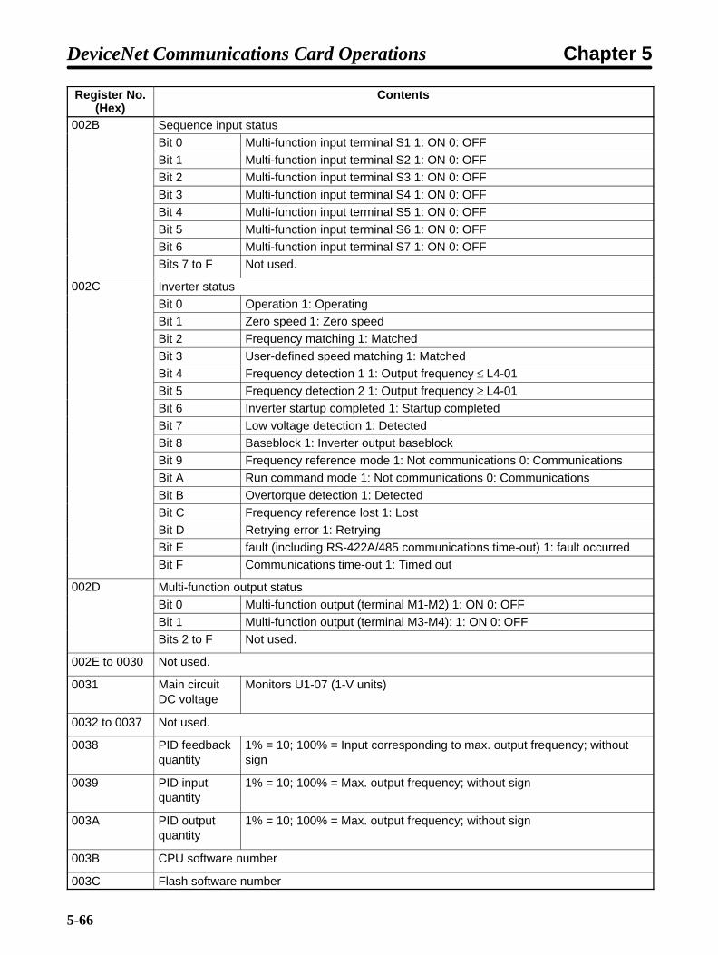
5-66
Register No.(Hex)
Contents
002B Sequence input status
Bit 0 Multi-function input terminal S1 1: ON 0: OFFBit 1 Multi-function input terminal S2 1: ON 0: OFFBit 2 Multi-function input terminal S3 1: ON 0: OFFBit 3 Multi-function input terminal S4 1: ON 0: OFFBit 4 Multi-function input terminal S5 1: ON 0: OFFBit 5 Multi-function input terminal S6 1: ON 0: OFF
Bit 6 Multi-function input terminal S7 1: ON 0: OFFBits 7 to F Not used.
002C Inverter statusBit 0 Operation 1: OperatingBit 1 Zero speed 1: Zero speedBit 2 Frequency matching 1: Matched
Bit 3 User-defined speed matching 1: MatchedBit 4 Frequency detection 1 1: Output frequency ≤ L4-01Bit 5 Frequency detection 2 1: Output frequency ≥ L4-01Bit 6 Inverter startup completed 1: Startup completedBit 7 Low voltage detection 1: DetectedBit 8 Baseblock 1: Inverter output baseblockBit 9 Frequency reference mode 1: Not communications 0: Communications
Bit A Run command mode 1: Not communications 0: CommunicationsBit B Overtorque detection 1: DetectedBit C Frequency reference lost 1: LostBit D Retrying error 1: RetryingBit E fault (including RS-422A/485 communications time-out) 1: fault occurredBit F Communications time-out 1: Timed out
002D Multi-function output statusBit 0 Multi-function output (terminal M1-M2) 1: ON 0: OFFBit 1 Multi-function output (terminal M3-M4): 1: ON 0: OFFBits 2 to F Not used.
002E to 0030 Not used.
0031 Main circuitDC voltage
Monitors U1-07 (1-V units)
0032 to 0037 Not used.
0038 PID feedbackquantity
1% = 10; 100% = Input corresponding to max. output frequency; withoutsign
0039 PID inputquantity
1% = 10; 100% = Max. output frequency; without sign
003A PID outputquantity
1% = 10; 100% = Max. output frequency; without sign
003B CPU software number
003C Flash software number
DeviceNet Communications Card Operations Chapter 5

5-67
Register No.(Hex)
Contents
003D Communications error details
Bit 0 CRC errorBit 1 Invalid data lengthBit 2 Not used.Bit 3 Parity errorBit 4 Overrun errorBit 5 Framing error
Bit 6 Time-outBits 7 to F Not used.
003E kVA setting
003F Control method
0040 Frequency reference Monitors U1-01; 0.01-Hz units (units set in o1-03; with sign)
0041 Output frequency Monitors U1-02; 0.01-Hz units (units set in o1-03; with sign)
0042 Output current Monitors U1-03; Inverters of 7.5 kW or less: 0.01-A units,Inverters of 11 kW or more: 0.1-A units
0043 and0044
Not used.
0045 Output voltage Monitors U1-06; 0.1-V units
0046 Main circuit DC voltage Monitors U1-07; 1-V units
0047 Output power Monitors U1-08; 0.1-kW units (with sign)
0048 Not used.
0049 Input terminal status Monitors U1-10; 1: ON. Bits 0 to 6 correspond to terminals S1 toS7.
004A Output terminal status Monitors U1-11Bit 0 Terminals M1 and M2; 1: ONBit 1 Terminals M3 and M4; 1: ONBits 2 to 6 Not used.Bit 7 Terminals MA and MC; 1: ON
Bits 8 to F Not used.
004B Operating status Monitors U1-12g
Bit 0 During RUNBit 1 Zero speedBit 2 Forward/reverse (1: Reverse operation)Bit 3 During fault reset inputBit 4 Frequency agree
Bit 5 Operation readyBit 6 Alarm (minor fault)Bit 7 FaultBits 8 to F Not used.
004C Cumulative operationtime
Monitors U1-13; 1-hr units
004D FLASH ID software No. Monitors U1-14
004E Frequency reference(voltage): Terminal A1input value
Monitors U1-15; 0.1% units (100% = 10 V; with sign for ± voltagesetting)
DeviceNet Communications Card Operations Chapter 5

5-68
Register No.(Hex)
Contents
004F Multi-function analoginput: Terminal A2 inputvalue
Monitors U1-16; 0.1% units (100%=20 mA or 100% = 10 V; withsign for ± voltage setting)
0051 and0052
Not used.
0053 Output frequency after asoft start
Monitors U1-20; 0.01-Hz units (with sign)
0054 and0055
Not used.
0057 PID feedback Monitors U1-24; 0.01% units (input corresponding to max.frequency = 100%; with sign)
0059 and005A
Not used.
005B CPU ID Monitors U1-28
005F and0060
Not used.
0061 OPE error parameter Monitors U1-34; outputs parameter
0063 PID input quantity Monitors U1-36; 0.01% units (max. frequency = 100%; with sign)
0064 PID output quantity Monitors U1-37; 0.01% units (max. frequency = 100%; with sign)
0065 PID reference Monitors U1-38; 0.01% units (max. frequency = 100%)
0066 RS-422A/485i i
Monitors U1-39communications error Bit 0 CRC error
Bit 1 Invalid data lengthBit 2 Not used.Bit 3 Parity errorBit 4 Overrun errorBit 5 Framing errorBit 6 Time-out
Bits 7 to F Not used.
0068 Fan operating time Monitors U1-40; 1-hr units
0080 Current fault Monitors U2-01Code Error
displayCode Error
displayCode Error
display01 PUF 0E --- 1C ---02 UV1 0F --- 1D OH303 UV2 10 --- 1E OPR04 UV3 11 EF3 1F ERR06 GF 12 EF4 20 OH407 OC 13 EF5 22 BUS
08 OV 14 EF6 25 CF09 OH 15 EF7 27 EF00A OH1 18 --- 28 FBL0B OL1 19 --- 29 UL30C OL2 1A --- 2A ---0D OL3 1B --- 2B OL7
0081 Last fault Monitors U2-02 (same codes as U2-01)
DeviceNet Communications Card Operations Chapter 5

5-69
Register No.(Hex)
Contents
0082 Fault frequencyreference
Monitors U2-03; 0.01-Hz units (units set in o1-03; with sign)
0083 Fault output reference Monitors U2-04; 0.01-Hz units (units set in o1-03; with sign)
0084 Fault output current Monitors U2-05; Inverters of 7.5 kW or less: 0.01-A units,Inverters of 11 kW or more: 0.1-A units
0085 Not used.
0086 Fault output voltagereference
Monitors U2-07; 0.1-V units
0087 Fault main circuit DCvoltage
Monitors U2-08; 1-V units
0088 Fault output power Monitors U2-09; 0.1-kW units (with sign)
0089 Not used.
008A Fault input terminalstatus
Monitors U2-11 (same contents as U1-10)
008B Fault output terminalstatus
Monitors U2-12 (same contents as U1-11)
008C Fault operating status Monitors U2-13 (same contents as U1-12)
008D Fault cumulativeoperation time
Monitors U2-14; 1-hr units
0090 (0800) Content of last fault Monitors U3-01 (same codes as U2-01)
0091 (0801) Content of 2nd prior fault Monitors U3-02 (same codes as U2-01)
0092 (0802) Content of 3rd prior fault Monitors U3-03 (same codes as U2-01)
0093 (0803) Content of 4th prior fault Monitors U3-04 (same codes as U2-01)
0094 (080A) Cumulative operationtime since last fault
Monitors U3-05; 1-hr units
0095 (080B) Cumulative operationtime since 2nd prior fault
Monitors U3-06; 1-hr units
0096 (080C) Cumulative operationtime since 3rd prior fault
Monitors U3-07; 1-hr units
0097 (080D) Cumulative operationtime since 4th prior fault
Monitors U3-08; 1-hr units
0804 Content of 5th prior fault Monitors U3-09 (same codes as U2-01) (See note.)
0805 Content of 6th prior fault Monitors U3-10 (same codes as U2-01) (See note.)
0806 Content of 7th prior fault Monitors U3-11 (same codes as U2-01) (See note.)
0807 Content of 8th prior fault Monitors U3-12 (same codes as U2-01) (See note.)
0808 Content of 9th prior fault Monitors U3-13 (same codes as U2-01) (See note.)
0809 Content of 10th priorfault
Monitors U3-14 (same codes as U2-01) (See note.)
080E Cumulative operationtime since 5th prior fault
Monitors U3-15; 1-hr units (See note.)
080F Cumulative operationtime since 6th prior fault
Monitors U3-16; 1-hr units (See note.)
0810 Cumulative operationtime since 7th prior fault
Monitors U3-17; 1-hr units (See note.)
0811 Cumulative operationtime since 8th prior fault
Monitors U3-18; 1-hr units (See note.)
DeviceNet Communications Card Operations Chapter 5
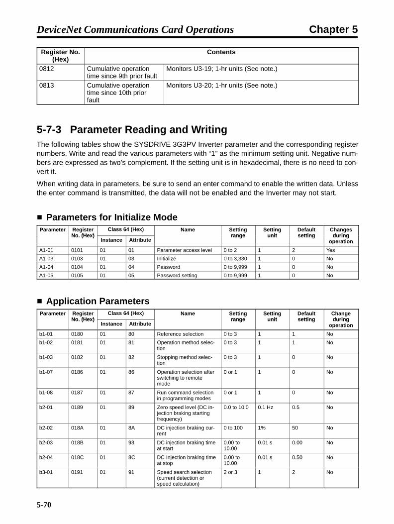
5-70
Register No.(Hex)
Contents
0812 Cumulative operationtime since 9th prior fault
Monitors U3-19; 1-hr units (See note.)
0813 Cumulative operationtime since 10th priorfault
Monitors U3-20; 1-hr units (See note.)
5-7-3 Parameter Reading and WritingThe following tables show the SYSDRIVE 3G3PV Inverter parameter and the corresponding registernumbers. Write and read the various parameters with “1” as the minimum setting unit. Negative num-bers are expressed as two’s complement. If the setting unit is in hexadecimal, there is no need to con-vert it.
When writing data in parameters, be sure to send an enter command to enable the written data. Unlessthe enter command is transmitted, the data will not be enabled and the Inverter may not start.
Parameters for Initialize ModeÁÁÁÁÁÁÁÁ
ParameterÁÁÁÁÁÁÁÁ
RegisterNo (Hex)ÁÁÁÁÁÁÁÁÁÁÁÁÁÁ
Class 64 (Hex) ÁÁÁÁÁÁÁÁÁÁÁÁÁÁ
Name ÁÁÁÁÁÁÁÁÁÁ
Settingrange
ÁÁÁÁÁÁÁÁ
SettingnitÁÁÁÁÁÁÁÁ
DefaultsettingÁÁÁÁÁÁÁÁÁÁ
Changesd ring
ÁÁÁÁÁÁÁÁ
ÁÁÁÁÁÁÁÁ
No. (Hex)Instance AttributeÁÁÁÁÁÁÁ
ÁÁÁÁÁÁÁÁÁÁÁÁÁÁÁÁÁ
rangeÁÁÁÁÁÁÁÁ
unitÁÁÁÁÁÁÁÁ
settingÁÁÁÁÁÁÁÁÁÁ
duringoperation
ÁÁÁÁÁÁÁÁ
A1-01 ÁÁÁÁÁÁÁÁ
0101 ÁÁÁÁÁÁÁÁ
01 ÁÁÁÁÁÁÁÁ
01 ÁÁÁÁÁÁÁÁÁÁÁÁÁÁ
Parameter access levelÁÁÁÁÁÁÁÁÁÁ
0 to 2 ÁÁÁÁÁÁÁÁ
1 ÁÁÁÁÁÁÁÁ
2 ÁÁÁÁÁÁÁÁÁÁ
Yes
ÁÁÁÁA1-03 ÁÁÁÁ0103 ÁÁÁÁ01 ÁÁÁÁ03 ÁÁÁÁÁÁÁInitialize ÁÁÁÁÁ0 to 3,330 ÁÁÁÁ1 ÁÁÁÁ0 ÁÁÁÁÁNoÁÁÁÁÁÁÁÁ
A1-04ÁÁÁÁÁÁÁÁ
0104ÁÁÁÁÁÁÁÁ
01ÁÁÁÁÁÁÁÁ
04ÁÁÁÁÁÁÁÁÁÁÁÁÁÁ
PasswordÁÁÁÁÁÁÁÁÁÁ
0 to 9,999ÁÁÁÁÁÁÁÁ
1ÁÁÁÁÁÁÁÁ
0ÁÁÁÁÁÁÁÁÁÁ
NoÁÁÁÁÁÁÁÁ
A1-05ÁÁÁÁÁÁÁÁ
0105ÁÁÁÁÁÁÁÁ
01ÁÁÁÁÁÁÁÁ
05ÁÁÁÁÁÁÁÁÁÁÁÁÁÁ
Password settingÁÁÁÁÁÁÁÁÁÁ
0 to 9,999ÁÁÁÁÁÁÁÁ
1ÁÁÁÁÁÁÁÁ
0ÁÁÁÁÁÁÁÁÁÁ
No
Application ParametersÁÁÁÁÁÁÁÁ
ParameterÁÁÁÁÁÁÁÁ
RegisterNo (Hex)ÁÁÁÁÁÁÁÁÁÁÁÁÁÁ
Class 64 (Hex) ÁÁÁÁÁÁÁÁÁÁÁÁÁÁ
Name ÁÁÁÁÁÁÁÁÁÁ
Settingrange
ÁÁÁÁÁÁÁÁ
SettingnitÁÁÁÁÁÁÁÁ
DefaultsettingÁÁÁÁÁÁÁÁÁÁ
Changed ringÁÁÁÁ
ÁÁÁÁÁÁÁÁÁÁÁÁ
No. (Hex)Instance AttributeÁÁÁÁÁÁÁ
ÁÁÁÁÁÁÁÁÁÁÁÁÁÁÁÁÁ
range ÁÁÁÁÁÁÁÁ
unit ÁÁÁÁÁÁÁÁ
settingÁÁÁÁÁÁÁÁÁÁ
duringoperation
ÁÁÁÁÁÁÁÁ
b1-01 ÁÁÁÁÁÁÁÁ
0180 ÁÁÁÁÁÁÁÁ
01 ÁÁÁÁÁÁÁÁ
80 ÁÁÁÁÁÁÁÁÁÁÁÁÁÁ
Reference selection ÁÁÁÁÁÁÁÁÁÁ
0 to 3 ÁÁÁÁÁÁÁÁ
1 ÁÁÁÁÁÁÁÁ
1 ÁÁÁÁÁÁÁÁÁÁ
No
ÁÁÁÁÁÁÁÁ
b1-02 ÁÁÁÁÁÁÁÁ
0181 ÁÁÁÁÁÁÁÁ
01 ÁÁÁÁÁÁÁÁ
81 ÁÁÁÁÁÁÁÁÁÁÁÁÁÁ
Operation method selec-tion
ÁÁÁÁÁÁÁÁÁÁ
0 to 3 ÁÁÁÁÁÁÁÁ
1 ÁÁÁÁÁÁÁÁ
1 ÁÁÁÁÁÁÁÁÁÁ
No
ÁÁÁÁÁÁÁÁÁÁÁÁ
b1-03ÁÁÁÁÁÁÁÁÁÁÁÁ
0182ÁÁÁÁÁÁÁÁÁÁÁÁ
01ÁÁÁÁÁÁÁÁÁÁÁÁ
82ÁÁÁÁÁÁÁÁÁÁÁÁÁÁÁÁÁÁÁÁÁ
Stopping method selec-tion
ÁÁÁÁÁÁÁÁÁÁÁÁÁÁÁ
0 to 3ÁÁÁÁÁÁÁÁÁÁÁÁ
1ÁÁÁÁÁÁÁÁÁÁÁÁ
0ÁÁÁÁÁÁÁÁÁÁÁÁÁÁÁ
No
ÁÁÁÁÁÁÁÁÁÁÁÁ
b1-07 ÁÁÁÁÁÁÁÁÁÁÁÁ
0186 ÁÁÁÁÁÁÁÁÁÁÁÁ
01 ÁÁÁÁÁÁÁÁÁÁÁÁ
86 ÁÁÁÁÁÁÁÁÁÁÁÁÁÁÁÁÁÁÁÁÁ
Operation selection afterswitching to remotemode
ÁÁÁÁÁÁÁÁÁÁÁÁÁÁÁ
0 or 1 ÁÁÁÁÁÁÁÁÁÁÁÁ
1 ÁÁÁÁÁÁÁÁÁÁÁÁ
0 ÁÁÁÁÁÁÁÁÁÁÁÁÁÁÁ
No
ÁÁÁÁÁÁÁÁ
b1-08 ÁÁÁÁÁÁÁÁ
0187 ÁÁÁÁÁÁÁÁ
01 ÁÁÁÁÁÁÁÁ
87 ÁÁÁÁÁÁÁÁÁÁÁÁÁÁ
Run command selectionin programming modes
ÁÁÁÁÁÁÁÁÁÁ
0 or 1 ÁÁÁÁÁÁÁÁ
1 ÁÁÁÁÁÁÁÁ
0 ÁÁÁÁÁÁÁÁÁÁ
No
ÁÁÁÁÁÁÁÁÁÁÁÁ
b2-01 ÁÁÁÁÁÁÁÁÁÁÁÁ
0189 ÁÁÁÁÁÁÁÁÁÁÁÁ
01 ÁÁÁÁÁÁÁÁÁÁÁÁ
89 ÁÁÁÁÁÁÁÁÁÁÁÁÁÁÁÁÁÁÁÁÁ
Zero speed level (DC in-jection braking startingfrequency)
ÁÁÁÁÁÁÁÁÁÁÁÁÁÁÁ
0.0 to 10.0 ÁÁÁÁÁÁÁÁÁÁÁÁ
0.1 Hz ÁÁÁÁÁÁÁÁÁÁÁÁ
0.5 ÁÁÁÁÁÁÁÁÁÁÁÁÁÁÁ
No
ÁÁÁÁÁÁÁÁÁÁÁÁ
b2-02 ÁÁÁÁÁÁÁÁÁÁÁÁ
018A ÁÁÁÁÁÁÁÁÁÁÁÁ
01 ÁÁÁÁÁÁÁÁÁÁÁÁ
8A ÁÁÁÁÁÁÁÁÁÁÁÁÁÁÁÁÁÁÁÁÁ
DC injection braking cur-rent
ÁÁÁÁÁÁÁÁÁÁÁÁÁÁÁ
0 to 100 ÁÁÁÁÁÁÁÁÁÁÁÁ
1% ÁÁÁÁÁÁÁÁÁÁÁÁ
50 ÁÁÁÁÁÁÁÁÁÁÁÁÁÁÁ
No
ÁÁÁÁÁÁÁÁ
b2-03 ÁÁÁÁÁÁÁÁ
018B ÁÁÁÁÁÁÁÁ
01 ÁÁÁÁÁÁÁÁ
93 ÁÁÁÁÁÁÁÁÁÁÁÁÁÁ
DC injection braking timeat start
ÁÁÁÁÁÁÁÁÁÁ
0.00 to10.00
ÁÁÁÁÁÁÁÁ
0.01 s ÁÁÁÁÁÁÁÁ
0.00 ÁÁÁÁÁÁÁÁÁÁ
No
ÁÁÁÁÁÁÁÁÁÁÁÁ
b2-04 ÁÁÁÁÁÁÁÁÁÁÁÁ
018C ÁÁÁÁÁÁÁÁÁÁÁÁ
01 ÁÁÁÁÁÁÁÁÁÁÁÁ
8C ÁÁÁÁÁÁÁÁÁÁÁÁÁÁÁÁÁÁÁÁÁ
DC Injection braking timeat stop
ÁÁÁÁÁÁÁÁÁÁÁÁÁÁÁ
0.00 to10.00
ÁÁÁÁÁÁÁÁÁÁÁÁ
0.01 s ÁÁÁÁÁÁÁÁÁÁÁÁ
0.50 ÁÁÁÁÁÁÁÁÁÁÁÁÁÁÁ
No
ÁÁÁÁÁÁÁÁÁÁÁÁ
b3-01 ÁÁÁÁÁÁÁÁÁÁÁÁ
0191 ÁÁÁÁÁÁÁÁÁÁÁÁ
01 ÁÁÁÁÁÁÁÁÁÁÁÁ
91 ÁÁÁÁÁÁÁÁÁÁÁÁÁÁÁÁÁÁÁÁÁ
Speed search selection(current detection orspeed calculation)
ÁÁÁÁÁÁÁÁÁÁÁÁÁÁÁ
2 or 3 ÁÁÁÁÁÁÁÁÁÁÁÁ
1 ÁÁÁÁÁÁÁÁÁÁÁÁ
2 ÁÁÁÁÁÁÁÁÁÁÁÁÁÁÁ
No
DeviceNet Communications Card Operations Chapter 5

5-71
ÁÁÁÁÁÁÁÁÁÁ
Changeduring
operation
ÁÁÁÁÁÁÁÁ
Defaultsetting
ÁÁÁÁÁÁÁÁ
Settingunit
ÁÁÁÁÁÁÁÁÁÁ
Settingrange
ÁÁÁÁÁÁÁÁÁÁÁÁÁÁ
NameÁÁÁÁÁÁÁÁÁÁÁÁÁÁ
Class 64 (Hex)ÁÁÁÁÁÁÁÁ
RegisterNo. (Hex)
ÁÁÁÁÁÁÁÁ
ParameterÁÁÁÁÁÁÁÁÁÁ
Changeduring
operationÁÁÁÁÁÁÁÁ
DefaultsettingÁÁÁÁ
ÁÁÁÁ
SettingunitÁÁÁÁÁ
ÁÁÁÁÁ
SettingrangeÁÁÁÁÁÁÁ
ÁÁÁÁÁÁÁInstance
Name
AttributeÁÁÁÁÁÁÁÁ
RegisterNo. (Hex)ÁÁÁÁ
ÁÁÁÁ
Parameter
ÁÁÁÁÁÁÁÁÁÁÁÁ
b3-02ÁÁÁÁÁÁÁÁÁÁÁÁ
0192ÁÁÁÁÁÁÁÁÁÁÁÁ
01ÁÁÁÁÁÁÁÁÁÁÁÁ
92ÁÁÁÁÁÁÁÁÁÁÁÁÁÁÁÁÁÁÁÁÁ
Speed search operatingcurrent (current detec-tion)
ÁÁÁÁÁÁÁÁÁÁÁÁÁÁÁ
0 to 200ÁÁÁÁÁÁÁÁÁÁÁÁ
1%ÁÁÁÁÁÁÁÁÁÁÁÁ
120ÁÁÁÁÁÁÁÁÁÁÁÁÁÁÁ
No
ÁÁÁÁÁÁÁÁÁÁÁÁ
b3-03ÁÁÁÁÁÁÁÁÁÁÁÁ
0193ÁÁÁÁÁÁÁÁÁÁÁÁ
01ÁÁÁÁÁÁÁÁÁÁÁÁ
93ÁÁÁÁÁÁÁÁÁÁÁÁÁÁÁÁÁÁÁÁÁ
Speed search decelera-tion time (current detec-tion)
ÁÁÁÁÁÁÁÁÁÁÁÁÁÁÁ
0.1 to 10.0ÁÁÁÁÁÁÁÁÁÁÁÁ
0.1 sÁÁÁÁÁÁÁÁÁÁÁÁ
2.0ÁÁÁÁÁÁÁÁÁÁÁÁÁÁÁ
No
ÁÁÁÁÁÁÁÁÁÁÁÁ
b3-05ÁÁÁÁÁÁÁÁÁÁÁÁ
0195ÁÁÁÁÁÁÁÁÁÁÁÁ
01ÁÁÁÁÁÁÁÁÁÁÁÁ
95ÁÁÁÁÁÁÁÁÁÁÁÁÁÁÁÁÁÁÁÁÁ
Speed search wait time(current detection orspeed calculation)
ÁÁÁÁÁÁÁÁÁÁÁÁÁÁÁ
0.0 to 20.0ÁÁÁÁÁÁÁÁÁÁÁÁ
0.1 sÁÁÁÁÁÁÁÁÁÁÁÁ
0.2ÁÁÁÁÁÁÁÁÁÁÁÁÁÁÁ
No
ÁÁÁÁÁÁÁÁÁÁÁÁ
b5-01ÁÁÁÁÁÁÁÁÁÁÁÁ
01A5ÁÁÁÁÁÁÁÁÁÁÁÁ
01ÁÁÁÁÁÁÁÁÁÁÁÁ
A5ÁÁÁÁÁÁÁÁÁÁÁÁÁÁÁÁÁÁÁÁÁ
PID control mode selec-tion
ÁÁÁÁÁÁÁÁÁÁÁÁÁÁÁ
0 or 1ÁÁÁÁÁÁÁÁÁÁÁÁ
1ÁÁÁÁÁÁÁÁÁÁÁÁ
0ÁÁÁÁÁÁÁÁÁÁÁÁÁÁÁ
No
ÁÁÁÁÁÁÁÁ
b5-02 ÁÁÁÁÁÁÁÁ
01A6 ÁÁÁÁÁÁÁÁ
01 ÁÁÁÁÁÁÁÁ
A6 ÁÁÁÁÁÁÁÁÁÁÁÁÁÁ
Proportional gain (P) ÁÁÁÁÁÁÁÁÁÁ
0.00 to25.00
ÁÁÁÁÁÁÁÁ
0.01 ÁÁÁÁÁÁÁÁ
1.00 ÁÁÁÁÁÁÁÁÁÁ
Yes
ÁÁÁÁÁÁÁÁÁÁÁÁ
b5-03ÁÁÁÁÁÁÁÁÁÁÁÁ
01A7ÁÁÁÁÁÁÁÁÁÁÁÁ
01ÁÁÁÁÁÁÁÁÁÁÁÁ
A7ÁÁÁÁÁÁÁÁÁÁÁÁÁÁÁÁÁÁÁÁÁ
Integral (I) timeÁÁÁÁÁÁÁÁÁÁÁÁÁÁÁ
0.0 to360.0
ÁÁÁÁÁÁÁÁÁÁÁÁ
0.1 sÁÁÁÁÁÁÁÁÁÁÁÁ
1.0ÁÁÁÁÁÁÁÁÁÁÁÁÁÁÁ
Yes
ÁÁÁÁÁÁÁÁ
b5-04 ÁÁÁÁÁÁÁÁ
01A8 ÁÁÁÁÁÁÁÁ
01 ÁÁÁÁÁÁÁÁ
A8 ÁÁÁÁÁÁÁÁÁÁÁÁÁÁ
Integral (I) limit ÁÁÁÁÁÁÁÁÁÁ
0.0 to100.0
ÁÁÁÁÁÁÁÁ
0.1% ÁÁÁÁÁÁÁÁ
100.0 ÁÁÁÁÁÁÁÁÁÁ
Yes
ÁÁÁÁÁÁÁÁÁÁÁÁ
b5-06 ÁÁÁÁÁÁÁÁÁÁÁÁ
01AA ÁÁÁÁÁÁÁÁÁÁÁÁ
01 ÁÁÁÁÁÁÁÁÁÁÁÁ
AA ÁÁÁÁÁÁÁÁÁÁÁÁÁÁÁÁÁÁÁÁÁ
PID limit ÁÁÁÁÁÁÁÁÁÁÁÁÁÁÁ
0.0 to100.0
ÁÁÁÁÁÁÁÁÁÁÁÁ
0.1% ÁÁÁÁÁÁÁÁÁÁÁÁ
100.0 ÁÁÁÁÁÁÁÁÁÁÁÁÁÁÁ
Yes
ÁÁÁÁÁÁÁÁ
b5-07 ÁÁÁÁÁÁÁÁ
01AB ÁÁÁÁÁÁÁÁ
01 ÁÁÁÁÁÁÁÁ
AB ÁÁÁÁÁÁÁÁÁÁÁÁÁÁ
PID offset adjustment ÁÁÁÁÁÁÁÁÁÁ
–100.0 to100.0 ÁÁÁÁ
ÁÁÁÁ
0.1% ÁÁÁÁÁÁÁÁ
0.0 ÁÁÁÁÁÁÁÁÁÁ
Yes
ÁÁÁÁÁÁÁÁ
b5-08 ÁÁÁÁÁÁÁÁ
01AC ÁÁÁÁÁÁÁÁ
01 ÁÁÁÁÁÁÁÁ
AC ÁÁÁÁÁÁÁÁÁÁÁÁÁÁ
PID primary delay timeconstant
ÁÁÁÁÁÁÁÁÁÁ
0.00 to10.00
ÁÁÁÁÁÁÁÁ
0.01 s ÁÁÁÁÁÁÁÁ
0.00 ÁÁÁÁÁÁÁÁÁÁ
Yes
ÁÁÁÁÁÁÁÁÁÁÁÁ
b5-12ÁÁÁÁÁÁÁÁÁÁÁÁ
01B0ÁÁÁÁÁÁÁÁÁÁÁÁ
01ÁÁÁÁÁÁÁÁÁÁÁÁ
B0ÁÁÁÁÁÁÁÁÁÁÁÁÁÁÁÁÁÁÁÁÁ
Selection of PID feed-back command lossdetection
ÁÁÁÁÁÁÁÁÁÁÁÁÁÁÁ
0 to 2ÁÁÁÁÁÁÁÁÁÁÁÁ
1ÁÁÁÁÁÁÁÁÁÁÁÁ
0ÁÁÁÁÁÁÁÁÁÁÁÁÁÁÁ
No
ÁÁÁÁÁÁÁÁÁÁÁÁ
b5-13ÁÁÁÁÁÁÁÁÁÁÁÁ
01B1ÁÁÁÁÁÁÁÁÁÁÁÁ
01ÁÁÁÁÁÁÁÁÁÁÁÁ
B1ÁÁÁÁÁÁÁÁÁÁÁÁÁÁÁÁÁÁÁÁÁ
PID feedback commandloss detection level
ÁÁÁÁÁÁÁÁÁÁÁÁÁÁÁ
0 to 100ÁÁÁÁÁÁÁÁÁÁÁÁ
1%ÁÁÁÁÁÁÁÁÁÁÁÁ
0ÁÁÁÁÁÁÁÁÁÁÁÁÁÁÁ
No
ÁÁÁÁÁÁÁÁ
b5-14 ÁÁÁÁÁÁÁÁ
01B2 ÁÁÁÁÁÁÁÁ
01 ÁÁÁÁÁÁÁÁ
B2 ÁÁÁÁÁÁÁÁÁÁÁÁÁÁ
PID feedback commandloss detection time
ÁÁÁÁÁÁÁÁÁÁ
0.0 to 25.5 ÁÁÁÁÁÁÁÁ
0.1 s ÁÁÁÁÁÁÁÁ
1.0 ÁÁÁÁÁÁÁÁÁÁ
No
ÁÁÁÁÁÁÁÁÁÁÁÁ
b5-15ÁÁÁÁÁÁÁÁÁÁÁÁ
01B3ÁÁÁÁÁÁÁÁÁÁÁÁ
01ÁÁÁÁÁÁÁÁÁÁÁÁ
B3ÁÁÁÁÁÁÁÁÁÁÁÁÁÁÁÁÁÁÁÁÁ
PID sleep function opera-tion level
ÁÁÁÁÁÁÁÁÁÁÁÁÁÁÁ
0.0 to400.0
ÁÁÁÁÁÁÁÁÁÁÁÁ
0.1 HzÁÁÁÁÁÁÁÁÁÁÁÁ
0.0ÁÁÁÁÁÁÁÁÁÁÁÁÁÁÁ
No
ÁÁÁÁÁÁÁÁ
b5-16 ÁÁÁÁÁÁÁÁ
01B4 ÁÁÁÁÁÁÁÁ
01 ÁÁÁÁÁÁÁÁ
B4 ÁÁÁÁÁÁÁÁÁÁÁÁÁÁ
PID sleep operationdelay time
ÁÁÁÁÁÁÁÁÁÁ
0.0 to 25.5 ÁÁÁÁÁÁÁÁ
0.1 s ÁÁÁÁÁÁÁÁ
0.0 ÁÁÁÁÁÁÁÁÁÁ
No
ÁÁÁÁÁÁÁÁÁÁÁÁ
b5-17ÁÁÁÁÁÁÁÁÁÁÁÁ
01B5ÁÁÁÁÁÁÁÁÁÁÁÁ
01ÁÁÁÁÁÁÁÁÁÁÁÁ
B5ÁÁÁÁÁÁÁÁÁÁÁÁÁÁÁÁÁÁÁÁÁ
Accel/decel time for PIDreference
ÁÁÁÁÁÁÁÁÁÁÁÁÁÁÁ
0.0 to 25.5ÁÁÁÁÁÁÁÁÁÁÁÁ
0.1 sÁÁÁÁÁÁÁÁÁÁÁÁ
0.0ÁÁÁÁÁÁÁÁÁÁÁÁÁÁÁ
No
ÁÁÁÁÁÁÁÁ
b8-01 ÁÁÁÁÁÁÁÁ
01CC ÁÁÁÁÁÁÁÁ
01 ÁÁÁÁÁÁÁÁ
CC ÁÁÁÁÁÁÁÁÁÁÁÁÁÁ
Energy-saving modeselection
ÁÁÁÁÁÁÁÁÁÁ
0 or 1 ÁÁÁÁÁÁÁÁ
1 ÁÁÁÁÁÁÁÁ
0 ÁÁÁÁÁÁÁÁÁÁ
No
ÁÁÁÁÁÁÁÁÁÁÁÁ
b8-04ÁÁÁÁÁÁÁÁÁÁÁÁ
01CFÁÁÁÁÁÁÁÁÁÁÁÁ
01ÁÁÁÁÁÁÁÁÁÁÁÁ
CFÁÁÁÁÁÁÁÁÁÁÁÁÁÁÁÁÁÁÁÁÁ
Energy-saving coefficientÁÁÁÁÁÁÁÁÁÁÁÁÁÁÁ
0.00 to655.00(See note.)
ÁÁÁÁÁÁÁÁÁÁÁÁ
0.01ÁÁÁÁÁÁÁÁÁÁÁÁ
Dependsoncapacity.
ÁÁÁÁÁÁÁÁÁÁÁÁÁÁÁ
No
ÁÁÁÁÁÁÁÁÁÁÁÁ
b8-05ÁÁÁÁÁÁÁÁÁÁÁÁ
01D0ÁÁÁÁÁÁÁÁÁÁÁÁ
01ÁÁÁÁÁÁÁÁÁÁÁÁ
D0ÁÁÁÁÁÁÁÁÁÁÁÁÁÁÁÁÁÁÁÁÁ
Power detection filtertime constant
ÁÁÁÁÁÁÁÁÁÁÁÁÁÁÁ
0 to 2,000ÁÁÁÁÁÁÁÁÁÁÁÁ
1 msÁÁÁÁÁÁÁÁÁÁÁÁ
20ÁÁÁÁÁÁÁÁÁÁÁÁÁÁÁ
No
ÁÁÁÁÁÁÁÁ
b8-06 ÁÁÁÁÁÁÁÁ
01D1 ÁÁÁÁÁÁÁÁ
01 ÁÁÁÁÁÁÁÁ
D1 ÁÁÁÁÁÁÁÁÁÁÁÁÁÁ
Search operation voltagelimiter
ÁÁÁÁÁÁÁÁÁÁ
0 to 100 ÁÁÁÁÁÁÁÁ
1% ÁÁÁÁÁÁÁÁ
0 ÁÁÁÁÁÁÁÁÁÁ
No
Note The same capacity as the Inverter can be set by initializing this parameter.
DeviceNet Communications Card Operations Chapter 5

5-72
Tuning ParametersÁÁÁÁÁÁÁÁ
ParameterÁÁÁÁÁÁÁÁ
RegisterNo (Hex)
ÁÁÁÁÁÁÁÁÁÁÁÁÁÁ
Class 64 (Hex)ÁÁÁÁÁÁÁÁÁÁÁÁÁÁ
NameÁÁÁÁÁÁÁÁÁÁ
Settingrange
ÁÁÁÁÁÁÁÁ
Settingnit
ÁÁÁÁÁÁÁÁ
Defaultsetting
ÁÁÁÁÁÁÁÁÁÁ
Changed ringÁÁÁÁ
ÁÁÁÁÁÁÁÁÁÁÁÁ
No. (Hex)Instance Attribute
ÁÁÁÁÁÁÁÁÁÁÁÁÁÁ
ÁÁÁÁÁÁÁÁÁÁ
range ÁÁÁÁÁÁÁÁ
unit ÁÁÁÁÁÁÁÁ
settingÁÁÁÁÁÁÁÁÁÁ
duringoperationÁÁÁÁ
ÁÁÁÁC1-01
ÁÁÁÁÁÁÁÁ
0200ÁÁÁÁÁÁÁÁ
02ÁÁÁÁÁÁÁÁ
00ÁÁÁÁÁÁÁÁÁÁÁÁÁÁ
Acceleration time 1ÁÁÁÁÁÁÁÁÁÁ
0.0 to600 0
ÁÁÁÁÁÁÁÁ
0.1 sÁÁÁÁÁÁÁÁ
10.0ÁÁÁÁÁÁÁÁÁÁ
YesÁÁÁÁÁÁÁÁ
C1-02 ÁÁÁÁÁÁÁÁ
0201 ÁÁÁÁÁÁÁÁ
02 ÁÁÁÁÁÁÁÁ
01 ÁÁÁÁÁÁÁÁÁÁÁÁÁÁ
Deceleration time 1 ÁÁÁÁÁÁÁÁÁÁ
600.0 ÁÁÁÁÁÁÁÁ
ÁÁÁÁÁÁÁÁ
ÁÁÁÁÁÁÁÁÁÁ
YesÁÁÁÁÁÁÁÁ
C1-03 ÁÁÁÁÁÁÁÁ
0202 ÁÁÁÁÁÁÁÁ
02 ÁÁÁÁÁÁÁÁ
02 ÁÁÁÁÁÁÁÁÁÁÁÁÁÁ
Acceleration time 2 ÁÁÁÁÁÁÁÁÁÁ
ÁÁÁÁÁÁÁÁ
ÁÁÁÁÁÁÁÁ
ÁÁÁÁÁÁÁÁÁÁ
Yes
ÁÁÁÁÁÁÁÁ
C1-04 ÁÁÁÁÁÁÁÁ
0203 ÁÁÁÁÁÁÁÁ
02 ÁÁÁÁÁÁÁÁ
03 ÁÁÁÁÁÁÁÁÁÁÁÁÁÁ
Deceleration time 2 ÁÁÁÁÁÁÁÁÁÁ
ÁÁÁÁÁÁÁÁ
ÁÁÁÁÁÁÁÁ
ÁÁÁÁÁÁÁÁÁÁ
Yes
ÁÁÁÁC1-09 ÁÁÁÁ0208 ÁÁÁÁ02 ÁÁÁÁ08 ÁÁÁÁÁÁÁDeceleration Stop TimeÁÁÁÁÁÁÁÁÁÁÁÁÁÁÁÁÁÁNoÁÁÁÁÁÁÁÁÁÁÁÁ
C1-11ÁÁÁÁÁÁÁÁÁÁÁÁ
020AÁÁÁÁÁÁÁÁÁÁÁÁ
02ÁÁÁÁÁÁÁÁÁÁÁÁ
0AÁÁÁÁÁÁÁÁÁÁÁÁÁÁÁÁÁÁÁÁÁ
Accel/decel timeswitching frequency
ÁÁÁÁÁÁÁÁÁÁÁÁÁÁÁ
0.0 to400.0
ÁÁÁÁÁÁÁÁÁÁÁÁ
0.1 HzÁÁÁÁÁÁÁÁÁÁÁÁ
0.0ÁÁÁÁÁÁÁÁÁÁÁÁÁÁÁ
No
ÁÁÁÁÁÁÁÁ
C2-01 ÁÁÁÁÁÁÁÁ
020B ÁÁÁÁÁÁÁÁ
02 ÁÁÁÁÁÁÁÁ
0B ÁÁÁÁÁÁÁÁÁÁÁÁÁÁ
S-curve characteristictime at acceleration start
ÁÁÁÁÁÁÁÁÁÁ
0.00 to2.50
ÁÁÁÁÁÁÁÁ
0.01 s ÁÁÁÁÁÁÁÁ
0.20 ÁÁÁÁÁÁÁÁÁÁ
No
ÁÁÁÁÁÁÁÁÁÁÁÁ
C2-02ÁÁÁÁÁÁÁÁÁÁÁÁ
020CÁÁÁÁÁÁÁÁÁÁÁÁ
02ÁÁÁÁÁÁÁÁÁÁÁÁ
0CÁÁÁÁÁÁÁÁÁÁÁÁÁÁÁÁÁÁÁÁÁ
S-curve characteristictime at acceleration end
ÁÁÁÁÁÁÁÁÁÁÁÁÁÁÁ
0.00 to2.50
ÁÁÁÁÁÁÁÁÁÁÁÁ
0.01 sÁÁÁÁÁÁÁÁÁÁÁÁ
0.20ÁÁÁÁÁÁÁÁÁÁÁÁÁÁÁ
No
ÁÁÁÁÁÁÁÁ
C4-01 ÁÁÁÁÁÁÁÁ
0215 ÁÁÁÁÁÁÁÁ
02 ÁÁÁÁÁÁÁÁ
15 ÁÁÁÁÁÁÁÁÁÁÁÁÁÁ
Torque compensationgain
ÁÁÁÁÁÁÁÁÁÁ
0.00 to2.50
ÁÁÁÁÁÁÁÁ
0.01 ÁÁÁÁÁÁÁÁ
1.00 ÁÁÁÁÁÁÁÁÁÁ
Yes
ÁÁÁÁÁÁÁÁÁÁÁÁ
C4-02ÁÁÁÁÁÁÁÁÁÁÁÁ
0216ÁÁÁÁÁÁÁÁÁÁÁÁ
02ÁÁÁÁÁÁÁÁÁÁÁÁ
16ÁÁÁÁÁÁÁÁÁÁÁÁÁÁÁÁÁÁÁÁÁ
Torque compensationprimary delay timeconstant
ÁÁÁÁÁÁÁÁÁÁÁÁÁÁÁ
0 to 10,000ÁÁÁÁÁÁÁÁÁÁÁÁ
1 msÁÁÁÁÁÁÁÁÁÁÁÁ
200 (Seenote 1.)
ÁÁÁÁÁÁÁÁÁÁÁÁÁÁÁ
No
ÁÁÁÁÁÁÁÁÁÁÁÁ
C6-02ÁÁÁÁÁÁÁÁÁÁÁÁ
0224ÁÁÁÁÁÁÁÁÁÁÁÁ
02ÁÁÁÁÁÁÁÁÁÁÁÁ
24ÁÁÁÁÁÁÁÁÁÁÁÁÁÁÁÁÁÁÁÁÁ
Carrier frequencyselection
ÁÁÁÁÁÁÁÁÁÁÁÁÁÁÁ
1 to FÁÁÁÁÁÁÁÁÁÁÁÁ
1ÁÁÁÁÁÁÁÁÁÁÁÁ
Dependsoncapacity.
ÁÁÁÁÁÁÁÁÁÁÁÁÁÁÁ
No
ÁÁÁÁÁÁÁÁÁÁÁÁ
C6-03ÁÁÁÁÁÁÁÁÁÁÁÁ
0225ÁÁÁÁÁÁÁÁÁÁÁÁ
02ÁÁÁÁÁÁÁÁÁÁÁÁ
25ÁÁÁÁÁÁÁÁÁÁÁÁÁÁÁÁÁÁÁÁÁ
Carrier frequency upperlimit
ÁÁÁÁÁÁÁÁÁÁÁÁÁÁÁ
2.0 to 15.0(See notes2 and 3.)
ÁÁÁÁÁÁÁÁÁÁÁÁ
0.1 kHzÁÁÁÁÁÁÁÁÁÁÁÁ
Dependsoncapacity.
ÁÁÁÁÁÁÁÁÁÁÁÁÁÁÁ
No
ÁÁÁÁÁÁÁÁÁÁÁÁ
C6-04ÁÁÁÁÁÁÁÁÁÁÁÁ
0226ÁÁÁÁÁÁÁÁÁÁÁÁ
02ÁÁÁÁÁÁÁÁÁÁÁÁ
26ÁÁÁÁÁÁÁÁÁÁÁÁÁÁÁÁÁÁÁÁÁ
Carrier frequency lowerlimit
ÁÁÁÁÁÁÁÁÁÁÁÁÁÁÁ
0.4 to 15.0(See notes2 and 3.)
ÁÁÁÁÁÁÁÁÁÁÁÁ
0.1 kHzÁÁÁÁÁÁÁÁÁÁÁÁ
Dependsoncapacity.
ÁÁÁÁÁÁÁÁÁÁÁÁÁÁÁ
No
ÁÁÁÁÁÁÁÁÁÁÁÁ
C6-05ÁÁÁÁÁÁÁÁÁÁÁÁ
0227ÁÁÁÁÁÁÁÁÁÁÁÁ
02ÁÁÁÁÁÁÁÁÁÁÁÁ
27ÁÁÁÁÁÁÁÁÁÁÁÁÁÁÁÁÁÁÁÁÁ
Carrier frequencyproportional gain
ÁÁÁÁÁÁÁÁÁÁÁÁÁÁÁ
00 to 99(See note3.)
ÁÁÁÁÁÁÁÁÁÁÁÁ
1ÁÁÁÁÁÁÁÁÁÁÁÁ
00ÁÁÁÁÁÁÁÁÁÁÁÁÁÁÁ
No
Note 1. When the control mode is changed, the Inverter will revert to default settings. (The V/f controldefault setting is given above.)
Note 2. The setting range depends on the capacity of the Inverter.
Note 3. These parameters can be monitored or set only when F is set for C6-02.
DeviceNet Communications Card Operations Chapter 5

5-73
Reference ParametersÁÁÁÁÁÁÁÁ
ParameterÁÁÁÁÁÁÁÁ
RegisterNo (Hex)
ÁÁÁÁÁÁÁÁÁÁÁÁÁÁ
Class 64 (Hex)ÁÁÁÁÁÁÁÁÁÁÁÁÁÁ
NameÁÁÁÁÁÁÁÁÁÁ
Settingrange
ÁÁÁÁÁÁÁÁ
Settingnit
ÁÁÁÁÁÁÁÁ
Defaultsetting
ÁÁÁÁÁÁÁÁÁÁ
Changed ringÁÁÁÁ
ÁÁÁÁÁÁÁÁÁÁÁÁ
No. (Hex)Instance Attribute
ÁÁÁÁÁÁÁÁÁÁÁÁÁÁ
ÁÁÁÁÁÁÁÁÁÁ
range ÁÁÁÁÁÁÁÁ
unit ÁÁÁÁÁÁÁÁ
settingÁÁÁÁÁÁÁÁÁÁ
duringoperationÁÁÁÁ
ÁÁÁÁd1-01
ÁÁÁÁÁÁÁÁ
0280ÁÁÁÁÁÁÁÁ
02ÁÁÁÁÁÁÁÁ
80ÁÁÁÁÁÁÁÁÁÁÁÁÁÁÁÁ
Frequency reference 1ÁÁÁÁÁÁÁÁÁÁ
0 to max.t t f
ÁÁÁÁÁÁÁÁ
0.01 Hz(S t ith
ÁÁÁÁÁÁÁÁ
0.00ÁÁÁÁÁÁÁÁÁÁ
YesÁÁÁÁÁÁÁÁ
d1-02 ÁÁÁÁÁÁÁÁ
0281 ÁÁÁÁÁÁÁÁ
02 ÁÁÁÁÁÁÁÁ
81 ÁÁÁÁÁÁÁÁÁÁÁÁÁÁÁÁ
Frequency reference 2 ÁÁÁÁÁÁÁÁÁÁ
output fre-quency
ÁÁÁÁÁÁÁÁ
(Set witho1-03 )
ÁÁÁÁÁÁÁÁ
0.00 ÁÁÁÁÁÁÁÁÁÁ
YesÁÁÁÁÁÁÁÁ
d1-03 ÁÁÁÁÁÁÁÁ
0282 ÁÁÁÁÁÁÁÁ
02 ÁÁÁÁÁÁÁÁ
82 ÁÁÁÁÁÁÁÁÁÁÁÁÁÁÁÁ
Frequency reference 3 ÁÁÁÁÁÁÁÁÁÁ
quency ÁÁÁÁÁÁÁÁ
o1-03.) ÁÁÁÁÁÁÁÁ
0.00 ÁÁÁÁÁÁÁÁÁÁ
Yes
ÁÁÁÁÁÁÁÁ
d1-04 ÁÁÁÁÁÁÁÁ
0283 ÁÁÁÁÁÁÁÁ
02 ÁÁÁÁÁÁÁÁ
83 ÁÁÁÁÁÁÁÁÁÁÁÁÁÁÁÁ
Frequency reference 4 ÁÁÁÁÁÁÁÁÁÁ
ÁÁÁÁÁÁÁÁ
ÁÁÁÁÁÁÁÁ
0.00 ÁÁÁÁÁÁÁÁÁÁ
Yes
ÁÁÁÁd1-17 ÁÁÁÁ0292 ÁÁÁÁ02 ÁÁÁÁ92 ÁÁÁÁÁÁÁÁJog frequency referenceÁÁÁÁÁÁÁÁÁÁÁÁÁ6.00 ÁÁÁÁÁYesÁÁÁÁÁÁÁÁÁÁÁÁ
d2-01ÁÁÁÁÁÁÁÁÁÁÁÁ
0289ÁÁÁÁÁÁÁÁÁÁÁÁ
02ÁÁÁÁÁÁÁÁÁÁÁÁ
89ÁÁÁ
ÁÁÁÁÁÁÁÁÁÁÁÁÁÁÁÁÁÁÁÁÁ
Frequency reference up-per limit
ÁÁÁÁÁÁÁÁÁÁÁÁÁÁÁ
0.0 to110.0
ÁÁÁÁÁÁÁÁÁÁÁÁ
0.1%ÁÁÁÁÁÁÁÁÁÁÁÁ
100.0ÁÁÁÁÁÁÁÁÁÁÁÁÁÁÁ
No
ÁÁÁÁÁÁÁÁ
d2-02 ÁÁÁÁÁÁÁÁ
028A ÁÁÁÁÁÁÁÁ
02 ÁÁÁÁÁÁÁÁ
8A ÁÁÁÁÁÁÁÁÁÁÁÁÁÁÁÁ
Frequency referencelower limit
ÁÁÁÁÁÁÁÁÁÁ
0.0 to110.0
ÁÁÁÁÁÁÁÁ
0.1% ÁÁÁÁÁÁÁÁ
0.0 ÁÁÁÁÁÁÁÁÁÁ
No
ÁÁÁÁÁÁÁÁÁÁÁÁ
d2-03ÁÁÁÁÁÁÁÁÁÁÁÁ
0293ÁÁÁÁÁÁÁÁÁÁÁÁ
02ÁÁÁÁÁÁÁÁÁÁÁÁ
93ÁÁÁ
ÁÁÁÁÁÁÁÁÁÁÁÁÁÁÁÁÁÁÁÁÁ
Master speed referencelower limit
ÁÁÁÁÁÁÁÁÁÁÁÁÁÁÁ
0.0 to110.0
ÁÁÁÁÁÁÁÁÁÁÁÁ
0.1%ÁÁÁÁÁÁÁÁÁÁÁÁ
0.0ÁÁÁÁÁÁÁÁÁÁÁÁÁÁÁ
No
ÁÁÁÁÁÁÁÁ
d3-01 ÁÁÁÁÁÁÁÁ
0294 ÁÁÁÁÁÁÁÁ
02 ÁÁÁÁÁÁÁÁ
94 ÁÁÁÁÁÁÁÁÁÁÁÁÁÁÁÁ
Jump frequency 1 ÁÁÁÁÁÁÁÁÁÁ
0.0 to400 0
ÁÁÁÁÁÁÁÁ
0.1 Hz ÁÁÁÁÁÁÁÁ
0.0 ÁÁÁÁÁÁÁÁÁÁ
No
ÁÁÁÁd3-02 ÁÁÁÁ0295 ÁÁÁÁ02 ÁÁÁÁ95 ÁÁÁÁÁÁÁÁJump frequency 2 ÁÁÁÁÁ400.0
ÁÁÁÁ0.1 Hz ÁÁÁÁ0.0 ÁÁÁÁÁNoÁÁÁÁÁÁÁÁd3-03
ÁÁÁÁÁÁÁÁ0296
ÁÁÁÁÁÁÁÁ02
ÁÁÁÁÁÁÁÁ96
ÁÁÁÁÁÁÁÁÁÁÁÁÁÁÁÁJump frequency 3
ÁÁÁÁÁÁÁÁÁÁ
ÁÁÁÁÁÁÁÁ0.1 Hz
ÁÁÁÁÁÁÁÁ0.0
ÁÁÁÁÁÁÁÁÁÁNoÁÁÁÁ
ÁÁÁÁd3-04
ÁÁÁÁÁÁÁÁ
0297ÁÁÁÁÁÁÁÁ
02ÁÁÁÁÁÁÁÁ
97ÁÁÁÁÁÁÁÁÁÁÁÁÁÁÁÁ
Jump frequency widthÁÁÁÁÁÁÁÁÁÁ
0.0 to 20.0ÁÁÁÁÁÁÁÁ
0.1 HzÁÁÁÁÁÁÁÁ
1.0ÁÁÁÁÁÁÁÁÁÁ
NoÁÁÁÁÁÁÁÁ
d6-01 ÁÁÁÁÁÁÁÁ
02A0 ÁÁÁÁÁÁÁÁ
02 ÁÁÁÁÁÁÁÁ
A0 ÁÁÁÁÁÁÁÁÁÁÁÁÁÁÁÁ
Field weakening level ÁÁÁÁÁÁÁÁÁÁ
0 to 100 ÁÁÁÁÁÁÁÁ
1% ÁÁÁÁÁÁÁÁ
80 ÁÁÁÁÁÁÁÁÁÁ
No
ÁÁÁÁÁÁÁÁ
d6-02 ÁÁÁÁÁÁÁÁ
02A1 ÁÁÁÁÁÁÁÁ
02 ÁÁÁÁÁÁÁÁ
A1 ÁÁÁÁÁÁÁÁÁÁÁÁÁÁÁÁ
Field frequency ÁÁÁÁÁÁÁÁÁÁ
0.0 to400.0
ÁÁÁÁÁÁÁÁ
0.1 Hz ÁÁÁÁÁÁÁÁ
0.0 ÁÁÁÁÁÁÁÁÁÁ
No
DeviceNet Communications Card Operations Chapter 5

5-74
Motor Constant Parameters
ÁÁÁÁÁÁÁÁ
ParameterÁÁÁÁÁÁÁÁ
RegisterNo (Hex)ÁÁÁÁÁÁÁÁÁÁÁÁÁÁ
Class 64 (Hex) ÁÁÁÁÁÁÁÁÁÁÁÁÁÁ
Name ÁÁÁÁÁÁÁÁÁÁ
Settingrange ÁÁÁÁ
ÁÁÁÁ
Settingnit ÁÁÁÁÁÁÁÁ
DefaultsettingÁÁÁÁÁÁÁÁÁÁ
Changed ring
ÁÁÁÁÁÁÁÁ
ÁÁÁÁÁÁÁÁ
No. (Hex)Instance AttributeÁÁÁÁÁÁÁ
ÁÁÁÁÁÁÁÁÁÁÁÁÁÁÁÁÁ
rangeÁÁÁÁÁÁÁÁ
unitÁÁÁÁÁÁÁÁ
settingÁÁÁÁÁÁÁÁÁÁ
duringoperation
ÁÁÁÁÁÁÁÁÁÁÁÁ
E1-01 ÁÁÁÁÁÁÁÁÁÁÁÁ
0300 ÁÁÁÁÁÁÁÁÁÁÁÁ
03 ÁÁÁÁÁÁÁÁÁÁÁÁ
00 ÁÁÁÁÁÁÁÁÁÁÁÁÁÁÁÁÁÁÁÁÁ
Input voltage setting ÁÁÁÁÁÁÁÁÁÁÁÁÁÁÁ
155 to 255(155 to510) (Seenote 1.)
ÁÁÁÁÁÁÁÁÁÁÁÁ
1 V ÁÁÁÁÁÁÁÁÁÁÁÁ
200 (400)(See note1.)
ÁÁÁÁÁÁÁÁÁÁÁÁÁÁÁ
No
ÁÁÁÁÁÁÁÁÁÁÁÁ
E1-03 ÁÁÁÁÁÁÁÁÁÁÁÁ
0302 ÁÁÁÁÁÁÁÁÁÁÁÁ
03 ÁÁÁÁÁÁÁÁÁÁÁÁ
02 ÁÁÁÁÁÁÁÁÁÁÁÁÁÁÁÁÁÁÁÁÁ
V/f pattern selection ÁÁÁÁÁÁÁÁÁÁÁÁÁÁÁ
0 to FE cannotbe set.
ÁÁÁÁÁÁÁÁÁÁÁÁ
1 ÁÁÁÁÁÁÁÁÁÁÁÁ
F ÁÁÁÁÁÁÁÁÁÁÁÁÁÁÁ
No
ÁÁÁÁÁÁÁÁÁÁÁÁ
E1-04 ÁÁÁÁÁÁÁÁÁÁÁÁ
0303 ÁÁÁÁÁÁÁÁÁÁÁÁ
03 ÁÁÁÁÁÁÁÁÁÁÁÁ
03 ÁÁÁÁÁÁÁÁÁÁÁÁÁÁÁÁÁÁÁÁÁ
Max. output frequency ÁÁÁÁÁÁÁÁÁÁÁÁÁÁÁ
0.0 to120.0
ÁÁÁÁÁÁÁÁÁÁÁÁ
0.1 Hz ÁÁÁÁÁÁÁÁÁÁÁÁ
50.0 ÁÁÁÁÁÁÁÁÁÁÁÁÁÁÁ
No
ÁÁÁÁÁÁÁÁÁÁÁÁÁÁÁÁ
E1-05 ÁÁÁÁÁÁÁÁÁÁÁÁÁÁÁÁ
0304 ÁÁÁÁÁÁÁÁÁÁÁÁÁÁÁÁ
03 ÁÁÁÁÁÁÁÁÁÁÁÁÁÁÁÁ
04 ÁÁÁÁÁÁÁÁÁÁÁÁÁÁÁÁÁÁÁÁÁÁÁÁÁÁÁÁ
Max. voltage ÁÁÁÁÁÁÁÁÁÁÁÁÁÁÁÁÁÁÁÁ
0.0 to255.0 (0.0to 510.0)(See note1.)
ÁÁÁÁÁÁÁÁÁÁÁÁÁÁÁÁ
0.1 V ÁÁÁÁÁÁÁÁÁÁÁÁÁÁÁÁ
200.0(400.0)(See note1.)
ÁÁÁÁÁÁÁÁÁÁÁÁÁÁÁÁÁÁÁÁ
No
ÁÁÁÁÁÁÁÁ
E1-06 ÁÁÁÁÁÁÁÁ
0305 ÁÁÁÁÁÁÁÁ
03 ÁÁÁÁÁÁÁÁ
05 ÁÁÁÁÁÁÁÁÁÁÁÁÁÁ
Base frequency ÁÁÁÁÁÁÁÁÁÁ
0.0 to120.0
ÁÁÁÁÁÁÁÁ
0.1 Hz ÁÁÁÁÁÁÁÁ
50.0 ÁÁÁÁÁÁÁÁÁÁ
No
ÁÁÁÁÁÁÁÁÁÁÁÁ
E1-07ÁÁÁÁÁÁÁÁÁÁÁÁ
0306ÁÁÁÁÁÁÁÁÁÁÁÁ
03ÁÁÁÁÁÁÁÁÁÁÁÁ
06ÁÁÁÁÁÁÁÁÁÁÁÁÁÁÁÁÁÁÁÁÁ
Mid. output frequencyÁÁÁÁÁÁÁÁÁÁÁÁÁÁÁ
0.0 to120.0
ÁÁÁÁÁÁÁÁÁÁÁÁ
0.1 HzÁÁÁÁÁÁÁÁÁÁÁÁ
3.0ÁÁÁÁÁÁÁÁÁÁÁÁÁÁÁ
No
ÁÁÁÁÁÁÁÁÁÁÁÁÁÁÁÁ
E1-08 ÁÁÁÁÁÁÁÁÁÁÁÁÁÁÁÁ
0307 ÁÁÁÁÁÁÁÁÁÁÁÁÁÁÁÁ
03 ÁÁÁÁÁÁÁÁÁÁÁÁÁÁÁÁ
07 ÁÁÁÁÁÁÁÁÁÁÁÁÁÁÁÁÁÁÁÁÁÁÁÁÁÁÁÁ
Mid. output frequencyvoltage
ÁÁÁÁÁÁÁÁÁÁÁÁÁÁÁÁÁÁÁÁ
0.0 to 255(0.0 to510.0)(See note1.)
ÁÁÁÁÁÁÁÁÁÁÁÁÁÁÁÁ
0.1 V ÁÁÁÁÁÁÁÁÁÁÁÁÁÁÁÁ
15.0 (30.0)(See note1.)
ÁÁÁÁÁÁÁÁÁÁÁÁÁÁÁÁÁÁÁÁ
No
ÁÁÁÁÁÁÁÁ
E1-09 ÁÁÁÁÁÁÁÁ
0308 ÁÁÁÁÁÁÁÁ
03 ÁÁÁÁÁÁÁÁ
08 ÁÁÁÁÁÁÁÁÁÁÁÁÁÁ
Min. output frequency ÁÁÁÁÁÁÁÁÁÁ
0.0 to120.0
ÁÁÁÁÁÁÁÁ
0.1 Hz ÁÁÁÁÁÁÁÁ
1.5 ÁÁÁÁÁÁÁÁÁÁ
No
ÁÁÁÁÁÁÁÁÁÁÁÁÁÁÁÁ
E1-10ÁÁÁÁÁÁÁÁÁÁÁÁÁÁÁÁ
0309ÁÁÁÁÁÁÁÁÁÁÁÁÁÁÁÁ
03ÁÁÁÁÁÁÁÁÁÁÁÁÁÁÁÁ
09ÁÁÁÁÁÁÁÁÁÁÁÁÁÁÁÁÁÁÁÁÁÁÁÁÁÁÁÁ
Min. output frequencyvoltage
ÁÁÁÁÁÁÁÁÁÁÁÁÁÁÁÁÁÁÁÁ
0.0 to255.0 (0.0to 510.0)(See note1.)
ÁÁÁÁÁÁÁÁÁÁÁÁÁÁÁÁ
0.1 VÁÁÁÁÁÁÁÁÁÁÁÁÁÁÁÁ
9.0 (18.0)(See note1.)
ÁÁÁÁÁÁÁÁÁÁÁÁÁÁÁÁÁÁÁÁ
No
ÁÁÁÁÁÁÁÁÁÁÁÁ
E1-11ÁÁÁÁÁÁÁÁÁÁÁÁ
030AÁÁÁÁÁÁÁÁÁÁÁÁ
03ÁÁÁÁÁÁÁÁÁÁÁÁ
0AÁÁÁÁÁÁÁÁÁÁÁÁÁÁÁÁÁÁÁÁÁ
Mid. output frequency 2ÁÁÁÁÁÁÁÁÁÁÁÁÁÁÁ
0.0 to120.0
ÁÁÁÁÁÁÁÁÁÁÁÁ
0.1 HzÁÁÁÁÁÁÁÁÁÁÁÁ
0.0 (Seenote 2.)
ÁÁÁÁÁÁÁÁÁÁÁÁÁÁÁ
No
ÁÁÁÁÁÁÁÁÁÁÁÁÁÁÁÁ
E1-12 ÁÁÁÁÁÁÁÁÁÁÁÁÁÁÁÁ
030B ÁÁÁÁÁÁÁÁÁÁÁÁÁÁÁÁ
03 ÁÁÁÁÁÁÁÁÁÁÁÁÁÁÁÁ
0B ÁÁÁÁÁÁÁÁÁÁÁÁÁÁÁÁÁÁÁÁÁÁÁÁÁÁÁÁ
Mid. output frequencyvoltage 2
ÁÁÁÁÁÁÁÁÁÁÁÁÁÁÁÁÁÁÁÁ
0.0 to255.0 (0.0to 510.0)(See note1.)
ÁÁÁÁÁÁÁÁÁÁÁÁÁÁÁÁ
0.1 V ÁÁÁÁÁÁÁÁÁÁÁÁÁÁÁÁ
0.0 (Seenote 2.)
ÁÁÁÁÁÁÁÁÁÁÁÁÁÁÁÁÁÁÁÁ
No
ÁÁÁÁÁÁÁÁÁÁÁÁÁÁÁÁ
E1-13 ÁÁÁÁÁÁÁÁÁÁÁÁÁÁÁÁ
030C ÁÁÁÁÁÁÁÁÁÁÁÁÁÁÁÁ
03 ÁÁÁÁÁÁÁÁÁÁÁÁÁÁÁÁ
0C ÁÁÁÁÁÁÁÁÁÁÁÁÁÁÁÁÁÁÁÁÁÁÁÁÁÁÁÁ
Base voltage ÁÁÁÁÁÁÁÁÁÁÁÁÁÁÁÁÁÁÁÁ
0.0 to255.0 (0.0to 510.0)(See note1.)
ÁÁÁÁÁÁÁÁÁÁÁÁÁÁÁÁ
0.1 V ÁÁÁÁÁÁÁÁÁÁÁÁÁÁÁÁ
0.0 (Seenote 3.)
ÁÁÁÁÁÁÁÁÁÁÁÁÁÁÁÁÁÁÁÁ
No
ÁÁÁÁÁÁÁÁÁÁÁÁ
E2-01 ÁÁÁÁÁÁÁÁÁÁÁÁ
030E ÁÁÁÁÁÁÁÁÁÁÁÁ
03 ÁÁÁÁÁÁÁÁÁÁÁÁ
0E ÁÁÁÁÁÁÁÁÁÁÁÁÁÁÁÁÁÁÁÁÁ
Motor rated current ÁÁÁÁÁÁÁÁÁÁÁÁÁÁÁ
0.32 to6.40 (Seenote 4.)
ÁÁÁÁÁÁÁÁÁÁÁÁ
0.01 A ÁÁÁÁÁÁÁÁÁÁÁÁ
Dependsoncapacity.
ÁÁÁÁÁÁÁÁÁÁÁÁÁÁÁ
No
ÁÁÁÁÁÁÁÁÁÁÁÁ
E2-05 ÁÁÁÁÁÁÁÁÁÁÁÁ
0312 ÁÁÁÁÁÁÁÁÁÁÁÁ
03 ÁÁÁÁÁÁÁÁÁÁÁÁ
12 ÁÁÁÁÁÁÁÁÁÁÁÁÁÁÁÁÁÁÁÁÁ
Motor line-to-lineresistance
ÁÁÁÁÁÁÁÁÁÁÁÁÁÁÁ
0.000 to65.000
ÁÁÁÁÁÁÁÁÁÁÁÁ
0.001 Ω ÁÁÁÁÁÁÁÁÁÁÁÁ
Dependsoncapacity.
ÁÁÁÁÁÁÁÁÁÁÁÁÁÁÁ
No
Note 1. Values in parentheses are for 400-V-class Inverters.
Note 2. The settings of E1-11 and E1-12 are ignored if set to 0.0.
Note 3. E1-13 will be the same value as E1-05 after autotuning.
Note 4. The setting range is 10% to 200% of the Inverter’s rated output current. The values for a200-V-class 0.4-kW Inverter are given above.
DeviceNet Communications Card Operations Chapter 5

5-75
Option ParametersÁÁÁÁÁÁÁÁ
ParameterÁÁÁÁÁÁÁÁ
RegisterNo (Hex)
ÁÁÁÁÁÁÁÁÁÁÁÁÁÁ
Class 64 (Hex)ÁÁÁÁÁÁÁÁÁÁÁÁÁÁ
NameÁÁÁÁÁÁÁÁÁÁ
Settingrange
ÁÁÁÁÁÁÁÁ
Settingnit
ÁÁÁÁÁÁÁÁ
Defaultsetting
ÁÁÁÁÁÁÁÁÁÁ
Changed ringÁÁÁÁ
ÁÁÁÁÁÁÁÁÁÁÁÁ
No. (Hex)Instance Attribute
ÁÁÁÁÁÁÁÁÁÁÁÁÁÁ
ÁÁÁÁÁÁÁÁÁÁ
range ÁÁÁÁÁÁÁÁ
unit ÁÁÁÁÁÁÁÁ
settingÁÁÁÁÁÁÁÁÁÁ
duringoperationÁÁÁÁ
ÁÁÁÁÁÁÁÁ
F6-01ÁÁÁÁÁÁÁÁÁÁÁÁ
03A2ÁÁÁÁÁÁÁÁÁÁÁÁ
03ÁÁÁÁÁÁÁÁÁÁÁÁ
A2ÁÁÁÁÁÁÁÁÁÁÁÁÁÁÁÁÁÁÁÁÁ
DeviceNet fault operationselection
ÁÁÁÁÁÁÁÁÁÁÁÁÁÁÁ
0 to 3ÁÁÁÁÁÁÁÁÁÁÁÁ
1ÁÁÁÁÁÁÁÁÁÁÁÁ
1ÁÁÁÁÁÁÁÁÁÁÁÁÁÁÁ
No
ÁÁÁÁÁÁÁÁÁÁÁÁ
F6-02 ÁÁÁÁÁÁÁÁÁÁÁÁ
03A3 ÁÁÁÁÁÁÁÁÁÁÁÁ
03 ÁÁÁÁÁÁÁÁÁÁÁÁ
A3 ÁÁÁÁÁÁÁÁÁÁÁÁÁÁÁÁÁÁÁÁÁ
Communications externalfault input detectionmethod selection
ÁÁÁÁÁÁÁÁÁÁÁÁÁÁÁ
0 or 1 ÁÁÁÁÁÁÁÁÁÁÁÁ
1 ÁÁÁÁÁÁÁÁÁÁÁÁ
0 ÁÁÁÁÁÁÁÁÁÁÁÁÁÁÁ
No
ÁÁÁÁÁÁÁÁÁÁÁÁ
F6-03 ÁÁÁÁÁÁÁÁÁÁÁÁ
03A4 ÁÁÁÁÁÁÁÁÁÁÁÁ
03 ÁÁÁÁÁÁÁÁÁÁÁÁ
A4 ÁÁÁÁÁÁÁÁÁÁÁÁÁÁÁÁÁÁÁÁÁ
Communications externalfault input operationselection
ÁÁÁÁÁÁÁÁÁÁÁÁÁÁÁ
0 to 3 ÁÁÁÁÁÁÁÁÁÁÁÁ
1 ÁÁÁÁÁÁÁÁÁÁÁÁ
1 ÁÁÁÁÁÁÁÁÁÁÁÁÁÁÁ
No
ÁÁÁÁÁÁÁÁ
F6-05 ÁÁÁÁÁÁÁÁ
03A6 ÁÁÁÁÁÁÁÁ
03 ÁÁÁÁÁÁÁÁ
A6 ÁÁÁÁÁÁÁÁÁÁÁÁÁÁ
Display unit selection forcurrent monitor
ÁÁÁÁÁÁÁÁÁÁ
0 or 1 ÁÁÁÁÁÁÁÁ
1 ÁÁÁÁÁÁÁÁ
0 ÁÁÁÁÁÁÁÁÁÁ
No
External Terminal Function ParametersÁÁÁÁÁÁÁÁÁÁÁÁ
ParameterÁÁÁÁÁÁÁÁÁÁÁÁ
RegisterNo. (Hex)
Instance AttributeÁÁÁÁÁÁÁÁÁÁÁÁÁÁÁÁÁÁÁÁÁ
NameÁÁÁÁÁÁÁÁÁÁÁÁÁÁÁ
Settingrange
ÁÁÁÁÁÁÁÁÁÁÁÁ
Settingunit
ÁÁÁÁÁÁÁÁÁÁÁÁ
Defaultsetting
ÁÁÁÁÁÁÁÁÁÁÁÁÁÁÁ
Changeduring
operationÁÁÁÁÁÁÁÁÁÁÁÁ
H1-01ÁÁÁÁÁÁÁÁÁÁÁÁ
0400ÁÁÁÁÁÁÁÁÁÁÁÁ
04ÁÁÁÁÁÁÁÁÁÁÁÁ
00ÁÁÁÁÁÁÁÁÁÁÁÁÁÁÁÁÁÁÁÁÁ
Terminal S3 functionselection
ÁÁÁÁÁÁÁÁÁÁÁÁÁÁÁ
0 to 6AÁÁÁÁÁÁÁÁÁÁÁÁ
1ÁÁÁÁÁÁÁÁÁÁÁÁ
24ÁÁÁÁÁÁÁÁÁÁÁÁÁÁÁ
No
ÁÁÁÁÁÁÁÁ
H1-02 ÁÁÁÁÁÁÁÁ
0401 ÁÁÁÁÁÁÁÁ
04 ÁÁÁÁÁÁÁÁ
01 ÁÁÁÁÁÁÁÁÁÁÁÁÁÁ
Terminal S4 functionselection
ÁÁÁÁÁÁÁÁÁÁ
0 to 6A ÁÁÁÁÁÁÁÁ
1 ÁÁÁÁÁÁÁÁ
14 ÁÁÁÁÁÁÁÁÁÁ
No
ÁÁÁÁÁÁÁÁÁÁÁÁ
H1-03 ÁÁÁÁÁÁÁÁÁÁÁÁ
0402 ÁÁÁÁÁÁÁÁÁÁÁÁ
04 ÁÁÁÁÁÁÁÁÁÁÁÁ
02 ÁÁÁÁÁÁÁÁÁÁÁÁÁÁÁÁÁÁÁÁÁ
Terminal S5 functionselection
ÁÁÁÁÁÁÁÁÁÁÁÁÁÁÁ
0 to 6A ÁÁÁÁÁÁÁÁÁÁÁÁ
1 ÁÁÁÁÁÁÁÁÁÁÁÁ
3 (0) (Seenote1.)
ÁÁÁÁÁÁÁÁÁÁÁÁÁÁÁ
No
ÁÁÁÁÁÁÁÁ
H1-04 ÁÁÁÁÁÁÁÁ
0403 ÁÁÁÁÁÁÁÁ
04 ÁÁÁÁÁÁÁÁ
03 ÁÁÁÁÁÁÁÁÁÁÁÁÁÁ
Terminal S6 functionselection ÁÁÁÁÁ
ÁÁÁÁÁ
0 to 6A ÁÁÁÁÁÁÁÁ
1 ÁÁÁÁÁÁÁÁ
4 (3) (Seenote1.) ÁÁÁÁÁ
ÁÁÁÁÁ
No
ÁÁÁÁÁÁÁÁÁÁÁÁ
H1-05 ÁÁÁÁÁÁÁÁÁÁÁÁ
0404 ÁÁÁÁÁÁÁÁÁÁÁÁ
04 ÁÁÁÁÁÁÁÁÁÁÁÁ
04 ÁÁÁÁÁÁÁÁÁÁÁÁÁÁÁÁÁÁÁÁÁ
Terminal S7 functionselection
ÁÁÁÁÁÁÁÁÁÁÁÁÁÁÁ
0 to 6A ÁÁÁÁÁÁÁÁÁÁÁÁ
1 ÁÁÁÁÁÁÁÁÁÁÁÁ
6 (4) (Seenote1.)
ÁÁÁÁÁÁÁÁÁÁÁÁÁÁÁ
No
ÁÁÁÁH2-01 ÁÁÁÁ040B ÁÁÁÁ04 ÁÁÁÁ0B ÁÁÁÁÁÁÁTerminal M1-M2 SelectÁÁÁÁÁ0 to 38 ÁÁÁÁ1 ÁÁÁÁ0 ÁÁÁÁÁNoÁÁÁÁÁÁÁÁ
H2-02ÁÁÁÁÁÁÁÁ
040CÁÁÁÁÁÁÁÁ
04ÁÁÁÁÁÁÁÁ
0CÁÁÁÁÁÁÁÁÁÁÁÁÁÁ
Terminal M3-M4 selectÁÁÁÁÁÁÁÁÁÁ
0 to 38ÁÁÁÁÁÁÁÁ
1ÁÁÁÁÁÁÁÁ
1ÁÁÁÁÁÁÁÁÁÁ
NoÁÁÁÁÁÁÁÁÁÁÁÁ
H3-02 ÁÁÁÁÁÁÁÁÁÁÁÁ
0411 ÁÁÁÁÁÁÁÁÁÁÁÁ
04 ÁÁÁÁÁÁÁÁÁÁÁÁ
11 ÁÁÁÁÁÁÁÁÁÁÁÁÁÁÁÁÁÁÁÁÁ
Gain (terminal A1) ÁÁÁÁÁÁÁÁÁÁÁÁÁÁÁ
0.0 to1,000.0
ÁÁÁÁÁÁÁÁÁÁÁÁ
0.1% ÁÁÁÁÁÁÁÁÁÁÁÁ
100.0 ÁÁÁÁÁÁÁÁÁÁÁÁÁÁÁ
Yes
ÁÁÁÁÁÁÁÁ
H3-03 ÁÁÁÁÁÁÁÁ
0412 ÁÁÁÁÁÁÁÁ
04 ÁÁÁÁÁÁÁÁ
12 ÁÁÁÁÁÁÁÁÁÁÁÁÁÁ
Bias (terminal A1) ÁÁÁÁÁÁÁÁÁÁ
–100.0 to100.0 ÁÁÁÁ
ÁÁÁÁ
0.1% ÁÁÁÁÁÁÁÁ
0.0 ÁÁÁÁÁÁÁÁÁÁ
Yes
ÁÁÁÁÁÁÁÁÁÁÁÁ
H3-08 ÁÁÁÁÁÁÁÁÁÁÁÁ
0417 ÁÁÁÁÁÁÁÁÁÁÁÁ
04 ÁÁÁÁÁÁÁÁÁÁÁÁ
17 ÁÁÁÁÁÁÁÁÁÁÁÁÁÁÁÁÁÁÁÁÁ
Multi-function analoginput terminal A2 signallevel selection
ÁÁÁÁÁÁÁÁÁÁÁÁÁÁÁ
0 or 2 ÁÁÁÁÁÁÁÁÁÁÁÁ
1 ÁÁÁÁÁÁÁÁÁÁÁÁ
2 ÁÁÁÁÁÁÁÁÁÁÁÁÁÁÁ
No
ÁÁÁÁÁÁÁÁÁÁÁÁ
H3-09 ÁÁÁÁÁÁÁÁÁÁÁÁ
0418 ÁÁÁÁÁÁÁÁÁÁÁÁ
04 ÁÁÁÁÁÁÁÁÁÁÁÁ
18 ÁÁÁÁÁÁÁÁÁÁÁÁÁÁÁÁÁÁÁÁÁ
Multi-function analoginput terminal A2 functionselection
ÁÁÁÁÁÁÁÁÁÁÁÁÁÁÁ
0 to 1F ÁÁÁÁÁÁÁÁÁÁÁÁ
1 ÁÁÁÁÁÁÁÁÁÁÁÁ
0 ÁÁÁÁÁÁÁÁÁÁÁÁÁÁÁ
No
ÁÁÁÁÁÁÁÁÁÁÁÁ
H3-10 ÁÁÁÁÁÁÁÁÁÁÁÁ
0419 ÁÁÁÁÁÁÁÁÁÁÁÁ
04 ÁÁÁÁÁÁÁÁÁÁÁÁ
19 ÁÁÁÁÁÁÁÁÁÁÁÁÁÁÁÁÁÁÁÁÁ
Gain (terminal A2) ÁÁÁÁÁÁÁÁÁÁÁÁÁÁÁ
0.0 to1,000.0
ÁÁÁÁÁÁÁÁÁÁÁÁ
0.1% ÁÁÁÁÁÁÁÁÁÁÁÁ
100.0 ÁÁÁÁÁÁÁÁÁÁÁÁÁÁÁ
Yes
ÁÁÁÁÁÁÁÁ
H3-11 ÁÁÁÁÁÁÁÁ
041A ÁÁÁÁÁÁÁÁ
04 ÁÁÁÁÁÁÁÁ
1A ÁÁÁÁÁÁÁÁÁÁÁÁÁÁ
Bias (terminal A2) ÁÁÁÁÁÁÁÁÁÁ
–100.0 to100.0 ÁÁÁÁ
ÁÁÁÁ
0.1% ÁÁÁÁÁÁÁÁ
0.0 ÁÁÁÁÁÁÁÁÁÁ
Yes
ÁÁÁÁÁÁÁÁ
H3-13 ÁÁÁÁÁÁÁÁ
041C ÁÁÁÁÁÁÁÁ
04 ÁÁÁÁÁÁÁÁ
1C ÁÁÁÁÁÁÁÁÁÁÁÁÁÁ
Terminal A1/A2 switchingÁÁÁÁÁÁÁÁÁÁ
0 or 1 ÁÁÁÁÁÁÁÁ
1 ÁÁÁÁÁÁÁÁ
0 ÁÁÁÁÁÁÁÁÁÁ
No
ÁÁÁÁÁÁÁÁ
H4-01 ÁÁÁÁÁÁÁÁ
041D ÁÁÁÁÁÁÁÁ
04 ÁÁÁÁÁÁÁÁ
1D ÁÁÁÁÁÁÁÁÁÁÁÁÁÁ
Monitor selection(terminal FM)
ÁÁÁÁÁÁÁÁÁÁ
1 to 40 ÁÁÁÁÁÁÁÁ
1 ÁÁÁÁÁÁÁÁ
2 ÁÁÁÁÁÁÁÁÁÁ
No
ÁÁÁÁÁÁÁÁÁÁÁÁ
H4-02ÁÁÁÁÁÁÁÁÁÁÁÁ
041EÁÁÁÁÁÁÁÁÁÁÁÁ
04ÁÁÁÁÁÁÁÁÁÁÁÁ
1EÁÁÁÁÁÁÁÁÁÁÁÁÁÁÁÁÁÁÁÁÁ
Gain (terminal FM)ÁÁÁÁÁÁÁÁÁÁÁÁÁÁÁ
0.0 to1,000.0
ÁÁÁÁÁÁÁÁÁÁÁÁ
0.1%ÁÁÁÁÁÁÁÁÁÁÁÁ
100.0ÁÁÁÁÁÁÁÁÁÁÁÁÁÁÁ
Yes
ÁÁÁÁÁÁÁÁ
H4-03 ÁÁÁÁÁÁÁÁ
041F ÁÁÁÁÁÁÁÁ
04 ÁÁÁÁÁÁÁÁ
1F ÁÁÁÁÁÁÁÁÁÁÁÁÁÁ
Bias (terminal FM) ÁÁÁÁÁÁÁÁÁÁ
–110.0 to110.0
ÁÁÁÁÁÁÁÁ
0.1% ÁÁÁÁÁÁÁÁ
0.0 ÁÁÁÁÁÁÁÁÁÁ
Yes
ÁÁÁÁÁÁÁÁÁÁÁÁ
H4-04ÁÁÁÁÁÁÁÁÁÁÁÁ
0420ÁÁÁÁÁÁÁÁÁÁÁÁ
04ÁÁÁÁÁÁÁÁÁÁÁÁ
20ÁÁÁÁÁÁÁÁÁÁÁÁÁÁÁÁÁÁÁÁÁ
Monitor selection(terminal AM)
ÁÁÁÁÁÁÁÁÁÁÁÁÁÁÁ
1 to 40ÁÁÁÁÁÁÁÁÁÁÁÁ
1ÁÁÁÁÁÁÁÁÁÁÁÁ
3ÁÁÁÁÁÁÁÁÁÁÁÁÁÁÁ
No
ÁÁÁÁÁÁÁÁ
H4-05 ÁÁÁÁÁÁÁÁ
0421 ÁÁÁÁÁÁÁÁ
04 ÁÁÁÁÁÁÁÁ
21 ÁÁÁÁÁÁÁÁÁÁÁÁÁÁ
Gain (terminal AM) ÁÁÁÁÁÁÁÁÁÁ
0.0 to1,000.0
ÁÁÁÁÁÁÁÁ
0.1% ÁÁÁÁÁÁÁÁ
50.0 ÁÁÁÁÁÁÁÁÁÁ
Yes
ÁÁÁÁÁÁÁÁÁÁÁÁ
H4-06 ÁÁÁÁÁÁÁÁÁÁÁÁ
0422 ÁÁÁÁÁÁÁÁÁÁÁÁ
04 ÁÁÁÁÁÁÁÁÁÁÁÁ
22 ÁÁÁÁÁÁÁÁÁÁÁÁÁÁÁÁÁÁÁÁÁ
Bias (terminal AM) ÁÁÁÁÁÁÁÁÁÁÁÁÁÁÁ
–110.0 to110.0
ÁÁÁÁÁÁÁÁÁÁÁÁ
0.1% ÁÁÁÁÁÁÁÁÁÁÁÁ
0.0 ÁÁÁÁÁÁÁÁÁÁÁÁÁÁÁ
Yes
DeviceNet Communications Card Operations Chapter 5

5-76
ÁÁÁÁÁÁÁÁÁÁÁÁÁÁÁ
Changeduring
operation
ÁÁÁÁÁÁÁÁÁÁÁÁ
Defaultsetting
ÁÁÁÁÁÁÁÁÁÁÁÁ
Settingunit
ÁÁÁÁÁÁÁÁÁÁÁÁÁÁÁ
Settingrange
ÁÁÁÁÁÁÁÁÁÁÁÁÁÁÁÁÁÁÁÁÁ
Instance NameAttributeÁÁÁÁÁÁÁÁÁÁÁÁ
RegisterNo. (Hex)
ÁÁÁÁÁÁÁÁÁÁÁÁ
Parameter
ÁÁÁÁÁÁÁÁÁÁÁÁ
H4-07 ÁÁÁÁÁÁÁÁÁÁÁÁ
0423 ÁÁÁÁÁÁÁÁÁÁÁÁ
04 ÁÁÁÁÁÁÁÁÁÁÁÁ
23 ÁÁÁÁÁÁÁÁÁÁÁÁÁÁÁÁÁÁÁÁÁ
Analog output 1 signallevel selection
ÁÁÁÁÁÁÁÁÁÁÁÁÁÁÁ
0 or 2 ÁÁÁÁÁÁÁÁÁÁÁÁ
1 ÁÁÁÁÁÁÁÁÁÁÁÁ
0 ÁÁÁÁÁÁÁÁÁÁÁÁÁÁÁ
No
ÁÁÁÁÁÁÁÁ
H4-08 ÁÁÁÁÁÁÁÁ
0424 ÁÁÁÁÁÁÁÁ
04 ÁÁÁÁÁÁÁÁ
24 ÁÁÁÁÁÁÁÁÁÁÁÁÁÁ
Analog output 2 signallevel selection
ÁÁÁÁÁÁÁÁÁÁ
0 or 2 ÁÁÁÁÁÁÁÁ
1 ÁÁÁÁÁÁÁÁ
0 ÁÁÁÁÁÁÁÁÁÁ
No
ÁÁÁÁÁÁÁÁÁÁÁÁ
H5-01 ÁÁÁÁÁÁÁÁÁÁÁÁ
0425 ÁÁÁÁÁÁÁÁÁÁÁÁ
04 ÁÁÁÁÁÁÁÁÁÁÁÁ
25 ÁÁÁÁÁÁÁÁÁÁÁÁÁÁÁÁÁÁÁÁÁ
Slave address ÁÁÁÁÁÁÁÁÁÁÁÁÁÁÁ
0 to 20(See note2.)
ÁÁÁÁÁÁÁÁÁÁÁÁ
1 ÁÁÁÁÁÁÁÁÁÁÁÁ
1F ÁÁÁÁÁÁÁÁÁÁÁÁÁÁÁ
No
ÁÁÁÁÁÁÁÁÁÁÁÁ
H5-02 ÁÁÁÁÁÁÁÁÁÁÁÁ
0426 ÁÁÁÁÁÁÁÁÁÁÁÁ
04 ÁÁÁÁÁÁÁÁÁÁÁÁ
26 ÁÁÁÁÁÁÁÁÁÁÁÁÁÁÁÁÁÁÁÁÁ
Communication speedselection
ÁÁÁÁÁÁÁÁÁÁÁÁÁÁÁ
0 to 4 ÁÁÁÁÁÁÁÁÁÁÁÁ
1 ÁÁÁÁÁÁÁÁÁÁÁÁ
3 ÁÁÁÁÁÁÁÁÁÁÁÁÁÁÁ
No
ÁÁÁÁÁÁÁÁ
H5-03 ÁÁÁÁÁÁÁÁ
0427 ÁÁÁÁÁÁÁÁ
04 ÁÁÁÁÁÁÁÁ
27 ÁÁÁÁÁÁÁÁÁÁÁÁÁÁ
Communication parityselection ÁÁÁÁÁ
ÁÁÁÁÁ
0 to 2 ÁÁÁÁÁÁÁÁ
1 ÁÁÁÁÁÁÁÁ
0 ÁÁÁÁÁÁÁÁÁÁ
No
ÁÁÁÁÁÁÁÁ
H5-04 ÁÁÁÁÁÁÁÁ
0428 ÁÁÁÁÁÁÁÁ
04 ÁÁÁÁÁÁÁÁ
28 ÁÁÁÁÁÁÁÁÁÁÁÁÁÁ
Stopping method aftercommunication error
ÁÁÁÁÁÁÁÁÁÁ
0 to 3 ÁÁÁÁÁÁÁÁ
1 ÁÁÁÁÁÁÁÁ
3 ÁÁÁÁÁÁÁÁÁÁ
No
ÁÁÁÁÁÁÁÁÁÁÁÁ
H5-05ÁÁÁÁÁÁÁÁÁÁÁÁ
0429ÁÁÁÁÁÁÁÁÁÁÁÁ
04ÁÁÁÁÁÁÁÁÁÁÁÁ
29ÁÁÁÁÁÁÁÁÁÁÁÁÁÁÁÁÁÁÁÁÁ
Communication errordetection selection
ÁÁÁÁÁÁÁÁÁÁÁÁÁÁÁ
0 or 1ÁÁÁÁÁÁÁÁÁÁÁÁ
1ÁÁÁÁÁÁÁÁÁÁÁÁ
1ÁÁÁÁÁÁÁÁÁÁÁÁÁÁÁ
No
ÁÁÁÁÁÁÁÁ
H5-06 ÁÁÁÁÁÁÁÁ
042A ÁÁÁÁÁÁÁÁ
04 ÁÁÁÁÁÁÁÁ
2A ÁÁÁÁÁÁÁÁÁÁÁÁÁÁ
Send wait time ÁÁÁÁÁÁÁÁÁÁ
5 to 65 ÁÁÁÁÁÁÁÁ
1 ms ÁÁÁÁÁÁÁÁ
5 ÁÁÁÁÁÁÁÁÁÁ
No
ÁÁÁÁÁÁÁÁ
H5-07 ÁÁÁÁÁÁÁÁ
042B ÁÁÁÁÁÁÁÁ
04 ÁÁÁÁÁÁÁÁ
2B ÁÁÁÁÁÁÁÁÁÁÁÁÁÁ
RTS control ON/OFF ÁÁÁÁÁÁÁÁÁÁ
0 or 1 ÁÁÁÁÁÁÁÁ
1 ÁÁÁÁÁÁÁÁ
1 ÁÁÁÁÁÁÁÁÁÁ
No
Note 1. The values in parentheses indicate initial values when initialized in 3-wire sequence.
Note 2. Set H5-01 to 0 to disable Inverter responses to RS-422A/485 communications.
Protective Function ParametersÁÁÁÁÁÁÁÁ
ParameterÁÁÁÁÁÁÁÁ
RegisterNo (Hex)
ÁÁÁÁÁÁÁÁÁÁÁÁÁÁ
Class 64 (Hex)ÁÁÁÁÁÁÁÁÁÁÁÁÁÁ
NameÁÁÁÁÁÁÁÁÁÁ
Settingrange
ÁÁÁÁÁÁÁÁ
Settingnit
ÁÁÁÁÁÁÁÁ
Defaultsetting
ÁÁÁÁÁÁÁÁÁÁ
Changed ringÁÁÁÁ
ÁÁÁÁÁÁÁÁÁÁÁÁ
No. (Hex)Instance Attribute
ÁÁÁÁÁÁÁÁÁÁÁÁÁÁ
ÁÁÁÁÁÁÁÁÁÁ
range ÁÁÁÁÁÁÁÁ
unit ÁÁÁÁÁÁÁÁ
settingÁÁÁÁÁÁÁÁÁÁ
duringoperationÁÁÁÁ
ÁÁÁÁÁÁÁÁ
L1-01ÁÁÁÁÁÁÁÁÁÁÁÁ
0480ÁÁÁÁÁÁÁÁÁÁÁÁ
04ÁÁÁÁÁÁÁÁÁÁÁÁ
80ÁÁÁÁÁÁÁÁÁÁÁÁÁÁÁÁÁÁÁÁÁ
Motor protectionselection
ÁÁÁÁÁÁÁÁÁÁÁÁÁÁÁ
0 or 1ÁÁÁÁÁÁÁÁÁÁÁÁ
1ÁÁÁÁÁÁÁÁÁÁÁÁ
1ÁÁÁÁÁÁÁÁÁÁÁÁÁÁÁ
No
ÁÁÁÁÁÁÁÁ
L1-02 ÁÁÁÁÁÁÁÁ
0481 ÁÁÁÁÁÁÁÁ
04 ÁÁÁÁÁÁÁÁ
81 ÁÁÁÁÁÁÁÁÁÁÁÁÁÁ
Motor protection timeconstant
ÁÁÁÁÁÁÁÁÁÁ
0.1 to 5.0 ÁÁÁÁÁÁÁÁ
0.1 min ÁÁÁÁÁÁÁÁ
1.0 ÁÁÁÁÁÁÁÁÁÁ
No
ÁÁÁÁÁÁÁÁÁÁÁÁ
L1-03ÁÁÁÁÁÁÁÁÁÁÁÁ
0482ÁÁÁÁÁÁÁÁÁÁÁÁ
04ÁÁÁÁÁÁÁÁÁÁÁÁ
82ÁÁÁÁÁÁÁÁÁÁÁÁÁÁÁÁÁÁÁÁÁ
Alarm operation selectionduring motor overheating
ÁÁÁÁÁÁÁÁÁÁÁÁÁÁÁ
0 to 3ÁÁÁÁÁÁÁÁÁÁÁÁ
1ÁÁÁÁÁÁÁÁÁÁÁÁ
3ÁÁÁÁÁÁÁÁÁÁÁÁÁÁÁ
No
ÁÁÁÁÁÁÁÁ
L1-04 ÁÁÁÁÁÁÁÁ
0483 ÁÁÁÁÁÁÁÁ
04 ÁÁÁÁÁÁÁÁ
83 ÁÁÁÁÁÁÁÁÁÁÁÁÁÁ
Motor overheatingoperation selection
ÁÁÁÁÁÁÁÁÁÁ
0 to 2 ÁÁÁÁÁÁÁÁ
1 ÁÁÁÁÁÁÁÁ
1 ÁÁÁÁÁÁÁÁÁÁ
No
ÁÁÁÁÁÁÁÁÁÁÁÁ
L1-05 ÁÁÁÁÁÁÁÁÁÁÁÁ
0484 ÁÁÁÁÁÁÁÁÁÁÁÁ
04 ÁÁÁÁÁÁÁÁÁÁÁÁ
84 ÁÁÁÁÁÁÁÁÁÁÁÁÁÁÁÁÁÁÁÁÁ
Motor temperature inputfilter time constant
ÁÁÁÁÁÁÁÁÁÁÁÁÁÁÁ
0.00 to10.00
ÁÁÁÁÁÁÁÁÁÁÁÁ
0.01 s ÁÁÁÁÁÁÁÁÁÁÁÁ
0.20 ÁÁÁÁÁÁÁÁÁÁÁÁÁÁÁ
No
ÁÁÁÁÁÁÁÁ
L2-01 ÁÁÁÁÁÁÁÁ
0485 ÁÁÁÁÁÁÁÁ
04 ÁÁÁÁÁÁÁÁ
85 ÁÁÁÁÁÁÁÁÁÁÁÁÁÁ
Momentary power lossdetection ÁÁÁÁÁ
ÁÁÁÁÁ
0 to 2 ÁÁÁÁÁÁÁÁ
1 ÁÁÁÁÁÁÁÁ
0 ÁÁÁÁÁÁÁÁÁÁ
No
ÁÁÁÁÁÁÁÁÁÁÁÁ
L2-02 ÁÁÁÁÁÁÁÁÁÁÁÁ
0486 ÁÁÁÁÁÁÁÁÁÁÁÁ
04 ÁÁÁÁÁÁÁÁÁÁÁÁ
86 ÁÁÁÁÁÁÁÁÁÁÁÁÁÁÁÁÁÁÁÁÁ
Momentary power lossridethru time
ÁÁÁÁÁÁÁÁÁÁÁÁÁÁÁ
0 to 2.0 ÁÁÁÁÁÁÁÁÁÁÁÁ
0.1 s ÁÁÁÁÁÁÁÁÁÁÁÁ
Dependsoncapacity.
ÁÁÁÁÁÁÁÁÁÁÁÁÁÁÁ
No
ÁÁÁÁÁÁÁÁÁÁÁÁ
L2-03 ÁÁÁÁÁÁÁÁÁÁÁÁ
0487 ÁÁÁÁÁÁÁÁÁÁÁÁ
04 ÁÁÁÁÁÁÁÁÁÁÁÁ
87 ÁÁÁÁÁÁÁÁÁÁÁÁÁÁÁÁÁÁÁÁÁ
Min. baseblock time ÁÁÁÁÁÁÁÁÁÁÁÁÁÁÁ
0.1 to 5.0 ÁÁÁÁÁÁÁÁÁÁÁÁ
0.1 s ÁÁÁÁÁÁÁÁÁÁÁÁ
Dependsoncapacity.
ÁÁÁÁÁÁÁÁÁÁÁÁÁÁÁ
No
ÁÁÁÁÁÁÁÁÁÁÁÁ
L2-04 ÁÁÁÁÁÁÁÁÁÁÁÁ
0488 ÁÁÁÁÁÁÁÁÁÁÁÁ
04 ÁÁÁÁÁÁÁÁÁÁÁÁ
88 ÁÁÁÁÁÁÁÁÁÁÁÁÁÁÁÁÁÁÁÁÁ
Voltage recovery time ÁÁÁÁÁÁÁÁÁÁÁÁÁÁÁ
0.0 to 5.0 ÁÁÁÁÁÁÁÁÁÁÁÁ
0.1 s ÁÁÁÁÁÁÁÁÁÁÁÁ
Dependsoncapacity.
ÁÁÁÁÁÁÁÁÁÁÁÁÁÁÁ
No
ÁÁÁÁÁÁÁÁÁÁÁÁÁÁÁÁ
L2-05 ÁÁÁÁÁÁÁÁÁÁÁÁÁÁÁÁ
0489 ÁÁÁÁÁÁÁÁÁÁÁÁÁÁÁÁ
04 ÁÁÁÁÁÁÁÁÁÁÁÁÁÁÁÁ
89 ÁÁÁÁÁÁÁÁÁÁÁÁÁÁÁÁÁÁÁÁÁÁÁÁÁÁÁÁ
Undervoltage detectionlevel
ÁÁÁÁÁÁÁÁÁÁÁÁÁÁÁÁÁÁÁÁ
150 to 210(150 to420) (Seenote.)
ÁÁÁÁÁÁÁÁÁÁÁÁÁÁÁÁ
1 V ÁÁÁÁÁÁÁÁÁÁÁÁÁÁÁÁ
190 (380)(See note.)
ÁÁÁÁÁÁÁÁÁÁÁÁÁÁÁÁÁÁÁÁ
No
ÁÁÁÁÁÁÁÁ
L3-01 ÁÁÁÁÁÁÁÁ
048F ÁÁÁÁÁÁÁÁ
04 ÁÁÁÁÁÁÁÁ
8F ÁÁÁÁÁÁÁÁÁÁÁÁÁÁ
Stall prevention selectionduring accel
ÁÁÁÁÁÁÁÁÁÁ
0 to 2 ÁÁÁÁÁÁÁÁ
1 ÁÁÁÁÁÁÁÁ
1 ÁÁÁÁÁÁÁÁÁÁ
No
ÁÁÁÁÁÁÁÁÁÁÁÁ
L3-02 ÁÁÁÁÁÁÁÁÁÁÁÁ
0490 ÁÁÁÁÁÁÁÁÁÁÁÁ
04 ÁÁÁÁÁÁÁÁÁÁÁÁ
90 ÁÁÁÁÁÁÁÁÁÁÁÁÁÁÁÁÁÁÁÁÁ
Stall prevention levelduring accel
ÁÁÁÁÁÁÁÁÁÁÁÁÁÁÁ
0 to 200 ÁÁÁÁÁÁÁÁÁÁÁÁ
1% ÁÁÁÁÁÁÁÁÁÁÁÁ
120 ÁÁÁÁÁÁÁÁÁÁÁÁÁÁÁ
No
DeviceNet Communications Card Operations Chapter 5

5-77
ÁÁÁÁÁÁÁÁÁÁ
Changeduring
operation
ÁÁÁÁÁÁÁÁ
Defaultsetting
ÁÁÁÁÁÁÁÁ
Settingunit
ÁÁÁÁÁÁÁÁÁÁ
Settingrange
ÁÁÁÁÁÁÁÁÁÁÁÁÁÁ
NameÁÁÁÁÁÁÁÁÁÁÁÁÁÁ
Class 64 (Hex)ÁÁÁÁÁÁÁÁ
RegisterNo. (Hex)
ÁÁÁÁÁÁÁÁ
ParameterÁÁÁÁÁÁÁÁÁÁ
Changeduring
operationÁÁÁÁÁÁÁÁ
DefaultsettingÁÁÁÁ
ÁÁÁÁ
SettingunitÁÁÁÁÁ
ÁÁÁÁÁ
SettingrangeÁÁÁÁÁÁÁ
ÁÁÁÁÁÁÁInstance
Name
AttributeÁÁÁÁÁÁÁÁ
RegisterNo. (Hex)ÁÁÁÁ
ÁÁÁÁ
Parameter
ÁÁÁÁÁÁÁÁÁÁÁÁ
L3-04ÁÁÁÁÁÁÁÁÁÁÁÁ
0492ÁÁÁÁÁÁÁÁÁÁÁÁ
04ÁÁÁÁÁÁÁÁÁÁÁÁ
92ÁÁÁÁÁÁÁÁÁÁÁÁÁÁÁÁÁÁÁÁÁ
Stall prevention selectionduring decel
ÁÁÁÁÁÁÁÁÁÁÁÁÁÁÁ
0 to 2ÁÁÁÁÁÁÁÁÁÁÁÁ
1ÁÁÁÁÁÁÁÁÁÁÁÁ
1ÁÁÁÁÁÁÁÁÁÁÁÁÁÁÁ
No
ÁÁÁÁÁÁÁÁ
L3-05 ÁÁÁÁÁÁÁÁ
0493 ÁÁÁÁÁÁÁÁ
04 ÁÁÁÁÁÁÁÁ
93 ÁÁÁÁÁÁÁÁÁÁÁÁÁÁ
Stall prevention selectionduring running
ÁÁÁÁÁÁÁÁÁÁ
0 to 2 ÁÁÁÁÁÁÁÁ
1 ÁÁÁÁÁÁÁÁ
1 ÁÁÁÁÁÁÁÁÁÁ
No
ÁÁÁÁÁÁÁÁÁÁÁÁ
L3-06 ÁÁÁÁÁÁÁÁÁÁÁÁ
0494 ÁÁÁÁÁÁÁÁÁÁÁÁ
04 ÁÁÁÁÁÁÁÁÁÁÁÁ
94 ÁÁÁÁÁÁÁÁÁÁÁÁÁÁÁÁÁÁÁÁÁ
Stall prevention levelduring running
ÁÁÁÁÁÁÁÁÁÁÁÁÁÁÁ
30 to 200 ÁÁÁÁÁÁÁÁÁÁÁÁ
1% ÁÁÁÁÁÁÁÁÁÁÁÁ
120 ÁÁÁÁÁÁÁÁÁÁÁÁÁÁÁ
No
ÁÁÁÁÁÁÁÁ
L4-01 ÁÁÁÁÁÁÁÁ
0499 ÁÁÁÁÁÁÁÁ
04 ÁÁÁÁÁÁÁÁ
99 ÁÁÁÁÁÁÁÁÁÁÁÁÁÁ
Speed agreementdetection level ÁÁÁÁÁ
ÁÁÁÁÁ
0.0 to400.0 ÁÁÁÁ
ÁÁÁÁ
0.1 Hz ÁÁÁÁÁÁÁÁ
0.0 ÁÁÁÁÁÁÁÁÁÁ
No
ÁÁÁÁÁÁÁÁÁÁÁÁ
L4-02 ÁÁÁÁÁÁÁÁÁÁÁÁ
049A ÁÁÁÁÁÁÁÁÁÁÁÁ
04 ÁÁÁÁÁÁÁÁÁÁÁÁ
9A ÁÁÁÁÁÁÁÁÁÁÁÁÁÁÁÁÁÁÁÁÁ
Speed agreementdetection width
ÁÁÁÁÁÁÁÁÁÁÁÁÁÁÁ
0.0 to 20.0 ÁÁÁÁÁÁÁÁÁÁÁÁ
0.1 Hz ÁÁÁÁÁÁÁÁÁÁÁÁ
2.0 ÁÁÁÁÁÁÁÁÁÁÁÁÁÁÁ
No
ÁÁÁÁÁÁÁÁÁÁÁÁ
L4-05 ÁÁÁÁÁÁÁÁÁÁÁÁ
049D ÁÁÁÁÁÁÁÁÁÁÁÁ
04 ÁÁÁÁÁÁÁÁÁÁÁÁ
9D ÁÁÁÁÁÁÁÁÁÁÁÁÁÁÁÁÁÁÁÁÁ
Operation whenfrequency reference islost
ÁÁÁÁÁÁÁÁÁÁÁÁÁÁÁ
0 or 1 ÁÁÁÁÁÁÁÁÁÁÁÁ
1 ÁÁÁÁÁÁÁÁÁÁÁÁ
0 ÁÁÁÁÁÁÁÁÁÁÁÁÁÁÁ
No
ÁÁÁÁÁÁÁÁÁÁÁÁ
L4-06 ÁÁÁÁÁÁÁÁÁÁÁÁ
04C2 ÁÁÁÁÁÁÁÁÁÁÁÁ
04 ÁÁÁÁÁÁÁÁÁÁÁÁ
C2 ÁÁÁÁÁÁÁÁÁÁÁÁÁÁÁÁÁÁÁÁÁ
Frequency reference forloss of frequencyreference
ÁÁÁÁÁÁÁÁÁÁÁÁÁÁÁ
0.0 to100.0 ÁÁÁÁ
ÁÁÁÁÁÁÁÁ
0.1% ÁÁÁÁÁÁÁÁÁÁÁÁ
80.0 ÁÁÁÁÁÁÁÁÁÁÁÁÁÁÁ
No
ÁÁÁÁÁÁÁÁ
L5-01 ÁÁÁÁÁÁÁÁ
049E ÁÁÁÁÁÁÁÁ
04 ÁÁÁÁÁÁÁÁ
9E ÁÁÁÁÁÁÁÁÁÁÁÁÁÁ
Number of auto restartattempts ÁÁÁÁÁ
ÁÁÁÁÁ
0 to 10 ÁÁÁÁÁÁÁÁ
1 ÁÁÁÁÁÁÁÁ
0 ÁÁÁÁÁÁÁÁÁÁ
No
ÁÁÁÁÁÁÁÁ
L5-02 ÁÁÁÁÁÁÁÁ
049F ÁÁÁÁÁÁÁÁ
04 ÁÁÁÁÁÁÁÁ
9F ÁÁÁÁÁÁÁÁÁÁÁÁÁÁ
Auto restart operationselection
ÁÁÁÁÁÁÁÁÁÁ
0 or 1 ÁÁÁÁÁÁÁÁ
1 ÁÁÁÁÁÁÁÁ
0 ÁÁÁÁÁÁÁÁÁÁ
No
ÁÁÁÁÁÁÁÁÁÁÁÁ
L6-01ÁÁÁÁÁÁÁÁÁÁÁÁ
04A1ÁÁÁÁÁÁÁÁÁÁÁÁ
04ÁÁÁÁÁÁÁÁÁÁÁÁ
A1ÁÁÁÁÁÁÁÁÁÁÁÁÁÁÁÁÁÁÁÁÁ
Torque detectionselection 1
ÁÁÁÁÁÁÁÁÁÁÁÁÁÁÁ
0 to 8ÁÁÁÁÁÁÁÁÁÁÁÁ
1ÁÁÁÁÁÁÁÁÁÁÁÁ
0ÁÁÁÁÁÁÁÁÁÁÁÁÁÁÁ
No
ÁÁÁÁÁÁÁÁ
L6-02 ÁÁÁÁÁÁÁÁ
04A2 ÁÁÁÁÁÁÁÁ
04 ÁÁÁÁÁÁÁÁ
A2 ÁÁÁÁÁÁÁÁÁÁÁÁÁÁ
Torque detection level 1ÁÁÁÁÁÁÁÁÁÁ
0 to 300 ÁÁÁÁÁÁÁÁ
1% ÁÁÁÁÁÁÁÁ
150 ÁÁÁÁÁÁÁÁÁÁ
No
ÁÁÁÁÁÁÁÁ
L6-03 ÁÁÁÁÁÁÁÁ
04A3 ÁÁÁÁÁÁÁÁ
04 ÁÁÁÁÁÁÁÁ
A3 ÁÁÁÁÁÁÁÁÁÁÁÁÁÁ
Torque detection time 1ÁÁÁÁÁÁÁÁÁÁ
0.0 to 10.0 ÁÁÁÁÁÁÁÁ
0.1 s ÁÁÁÁÁÁÁÁ
0.1 ÁÁÁÁÁÁÁÁÁÁ
No
ÁÁÁÁÁÁÁÁÁÁÁÁ
L8-02 ÁÁÁÁÁÁÁÁÁÁÁÁ
04AE ÁÁÁÁÁÁÁÁÁÁÁÁ
04 ÁÁÁÁÁÁÁÁÁÁÁÁ
AE ÁÁÁÁÁÁÁÁÁÁÁÁÁÁÁÁÁÁÁÁÁ
Overheat pre-alarm levelÁÁÁÁÁÁÁÁÁÁÁÁÁÁÁ
50 to 130 ÁÁÁÁÁÁÁÁÁÁÁÁ
1°C ÁÁÁÁÁÁÁÁÁÁÁÁ
Dependsoncapacity.
ÁÁÁÁÁÁÁÁÁÁÁÁÁÁÁ
No
ÁÁÁÁÁÁÁÁ
L8-03 ÁÁÁÁÁÁÁÁ
04AF ÁÁÁÁÁÁÁÁ
04 ÁÁÁÁÁÁÁÁ
AF ÁÁÁÁÁÁÁÁÁÁÁÁÁÁ
Operation selection afteroverheat pre-alarm ÁÁÁÁÁ
ÁÁÁÁÁ
0 to 3 ÁÁÁÁÁÁÁÁ
1 ÁÁÁÁÁÁÁÁ
3 ÁÁÁÁÁÁÁÁÁÁ
No
ÁÁÁÁÁÁÁÁ
L8-09 ÁÁÁÁÁÁÁÁ
04B5 ÁÁÁÁÁÁÁÁ
04 ÁÁÁÁÁÁÁÁ
B5 ÁÁÁÁÁÁÁÁÁÁÁÁÁÁ
Ground protectionselection
ÁÁÁÁÁÁÁÁÁÁ
0 or 1 ÁÁÁÁÁÁÁÁ
1 ÁÁÁÁÁÁÁÁ
1 ÁÁÁÁÁÁÁÁÁÁ
No
ÁÁÁÁÁÁÁÁÁÁÁÁ
L8-11ÁÁÁÁÁÁÁÁÁÁÁÁ
04B7ÁÁÁÁÁÁÁÁÁÁÁÁ
04ÁÁÁÁÁÁÁÁÁÁÁÁ
B7ÁÁÁÁÁÁÁÁÁÁÁÁÁÁÁÁÁÁÁÁÁ
Cooling fan control delaytime
ÁÁÁÁÁÁÁÁÁÁÁÁÁÁÁ
0 to 300ÁÁÁÁÁÁÁÁÁÁÁÁ
1 sÁÁÁÁÁÁÁÁÁÁÁÁ
60ÁÁÁÁÁÁÁÁÁÁÁÁÁÁÁ
No
ÁÁÁÁÁÁÁÁ
L8-12 ÁÁÁÁÁÁÁÁ
04B8 ÁÁÁÁÁÁÁÁ
04 ÁÁÁÁÁÁÁÁ
B8 ÁÁÁÁÁÁÁÁÁÁÁÁÁÁ
Ambient temperature ÁÁÁÁÁÁÁÁÁÁ
45 to 60 ÁÁÁÁÁÁÁÁ
1°C ÁÁÁÁÁÁÁÁ
45 ÁÁÁÁÁÁÁÁÁÁ
No
ÁÁÁÁÁÁÁÁ
L8-15 ÁÁÁÁÁÁÁÁ
04BB ÁÁÁÁÁÁÁÁ
04 ÁÁÁÁÁÁÁÁ
BB ÁÁÁÁÁÁÁÁÁÁÁÁÁÁ
OL2 characteristicsselection at low speeds
ÁÁÁÁÁÁÁÁÁÁ
0 or 1 ÁÁÁÁÁÁÁÁ
1 ÁÁÁÁÁÁÁÁ
1 ÁÁÁÁÁÁÁÁÁÁ
No
Note Values in parentheses are for 400-V-class Inverters.
Special Adjustment ParametersÁÁÁÁÁÁÁÁ
ParameterÁÁÁÁÁÁÁÁ
RegisterNo (Hex)ÁÁÁÁÁÁÁÁÁÁÁÁÁÁ
Class 64 (Hex) ÁÁÁÁÁÁÁÁÁÁÁÁÁÁ
Name ÁÁÁÁÁÁÁÁÁÁ
Settingrange
ÁÁÁÁÁÁÁÁ
SettingnitÁÁÁÁÁÁÁÁ
DefaultsettingÁÁÁÁÁÁÁÁÁÁ
Changed ringÁÁÁÁ
ÁÁÁÁÁÁÁÁÁÁÁÁ
No. (Hex)Instance AttributeÁÁÁÁÁÁÁ
ÁÁÁÁÁÁÁÁÁÁÁÁÁÁÁÁÁ
range ÁÁÁÁÁÁÁÁ
unit ÁÁÁÁÁÁÁÁ
settingÁÁÁÁÁÁÁÁÁÁ
duringoperation
ÁÁÁÁÁÁÁÁ
N1-01 ÁÁÁÁÁÁÁÁ
0580 ÁÁÁÁÁÁÁÁ
05 ÁÁÁÁÁÁÁÁ
80 ÁÁÁÁÁÁÁÁÁÁÁÁÁÁ
Hunting-prevention func-tion selection
ÁÁÁÁÁÁÁÁÁÁ
0 or 1 ÁÁÁÁÁÁÁÁ
1 ÁÁÁÁÁÁÁÁ
1 ÁÁÁÁÁÁÁÁÁÁ
No
ÁÁÁÁÁÁÁÁÁÁÁÁ
N1-02ÁÁÁÁÁÁÁÁÁÁÁÁ
0581ÁÁÁÁÁÁÁÁÁÁÁÁ
05ÁÁÁÁÁÁÁÁÁÁÁÁ
81ÁÁÁÁÁÁÁÁÁÁÁÁÁÁÁÁÁÁÁÁÁ
Hunting-prevention gainÁÁÁÁÁÁÁÁÁÁÁÁÁÁÁ
0.00 to2.50
ÁÁÁÁÁÁÁÁÁÁÁÁ
0.01ÁÁÁÁÁÁÁÁÁÁÁÁ
1.00ÁÁÁÁÁÁÁÁÁÁÁÁÁÁÁ
No
ÁÁÁÁÁÁÁÁÁÁÁÁ
N3-01 ÁÁÁÁÁÁÁÁÁÁÁÁ
0588 ÁÁÁÁÁÁÁÁÁÁÁÁ
05 ÁÁÁÁÁÁÁÁÁÁÁÁ
88 ÁÁÁÁÁÁÁÁÁÁÁÁÁÁÁÁÁÁÁÁÁ
High-slip brakingdeceleration frequencywidth
ÁÁÁÁÁÁÁÁÁÁÁÁÁÁÁ
1 to 20 ÁÁÁÁÁÁÁÁÁÁÁÁ
1% ÁÁÁÁÁÁÁÁÁÁÁÁ
5 ÁÁÁÁÁÁÁÁÁÁÁÁÁÁÁ
No
ÁÁÁÁÁÁÁÁ
N3-02 ÁÁÁÁÁÁÁÁ
0589 ÁÁÁÁÁÁÁÁ
05 ÁÁÁÁÁÁÁÁ
89 ÁÁÁÁÁÁÁÁÁÁÁÁÁÁ
High-slip braking currentlimit
ÁÁÁÁÁÁÁÁÁÁ
100 to 200 ÁÁÁÁÁÁÁÁ
1% ÁÁÁÁÁÁÁÁ
150 ÁÁÁÁÁÁÁÁÁÁ
No
ÁÁÁÁÁÁÁÁÁÁÁÁ
N3-03ÁÁÁÁÁÁÁÁÁÁÁÁ
058AÁÁÁÁÁÁÁÁÁÁÁÁ
05ÁÁÁÁÁÁÁÁÁÁÁÁ
8AÁÁÁÁÁÁÁÁÁÁÁÁÁÁÁÁÁÁÁÁÁ
High-slip braking stopdwell time
ÁÁÁÁÁÁÁÁÁÁÁÁÁÁÁ
0.1 to 10.0ÁÁÁÁÁÁÁÁÁÁÁÁ
0.1 sÁÁÁÁÁÁÁÁÁÁÁÁ
1.0ÁÁÁÁÁÁÁÁÁÁÁÁÁÁÁ
No
ÁÁÁÁÁÁÁÁ
N3-04 ÁÁÁÁÁÁÁÁ
058B ÁÁÁÁÁÁÁÁ
05 ÁÁÁÁÁÁÁÁ
8B ÁÁÁÁÁÁÁÁÁÁÁÁÁÁ
High-slip braking OL timeÁÁÁÁÁÁÁÁÁÁ
30 to 1200 ÁÁÁÁÁÁÁÁ
1 s ÁÁÁÁÁÁÁÁ
40 ÁÁÁÁÁÁÁÁÁÁ
No
DeviceNet Communications Card Operations Chapter 5

5-78
Operator ParametersÁÁÁÁÁÁÁÁ
ParameterÁÁÁÁÁÁÁÁ
RegisterNo (Hex)
ÁÁÁÁÁÁÁÁÁÁÁÁÁÁ
Class 64 (Hex)ÁÁÁÁÁÁÁÁÁÁÁÁÁÁ
NameÁÁÁÁÁÁÁÁÁÁ
Settingrange
ÁÁÁÁÁÁÁÁ
Settingnit
ÁÁÁÁÁÁÁÁ
Defaultsetting
ÁÁÁÁÁÁÁÁÁÁ
Changed ringÁÁÁÁ
ÁÁÁÁÁÁÁÁÁÁÁÁ
No. (Hex)Instance Attribute
ÁÁÁÁÁÁÁÁÁÁÁÁÁÁ
ÁÁÁÁÁÁÁÁÁÁ
range ÁÁÁÁÁÁÁÁ
unit ÁÁÁÁÁÁÁÁ
settingÁÁÁÁÁÁÁÁÁÁ
duringoperationÁÁÁÁ
ÁÁÁÁo1-01
ÁÁÁÁÁÁÁÁ
0500ÁÁÁÁÁÁÁÁ
05ÁÁÁÁÁÁÁÁ
00ÁÁÁÁÁÁÁÁÁÁÁÁÁÁ
Monitor selectionÁÁÁÁÁÁÁÁÁÁ
4 to 40ÁÁÁÁÁÁÁÁ
1ÁÁÁÁÁÁÁÁ
6ÁÁÁÁÁÁÁÁÁÁ
YesÁÁÁÁÁÁÁÁÁÁÁÁ
o1-02ÁÁÁÁÁÁÁÁÁÁÁÁ
0501ÁÁÁÁÁÁÁÁÁÁÁÁ
05ÁÁÁÁÁÁÁÁÁÁÁÁ
01ÁÁÁÁÁÁÁÁÁÁÁÁÁÁÁÁÁÁÁÁÁ
Monitor selection afterpower up
ÁÁÁÁÁÁÁÁÁÁÁÁÁÁÁ
1 to 4ÁÁÁÁÁÁÁÁÁÁÁÁ
1ÁÁÁÁÁÁÁÁÁÁÁÁ
1ÁÁÁÁÁÁÁÁÁÁÁÁÁÁÁ
Yes
ÁÁÁÁÁÁÁÁÁÁÁÁ
o1-03 ÁÁÁÁÁÁÁÁÁÁÁÁ
0502 ÁÁÁÁÁÁÁÁÁÁÁÁ
05 ÁÁÁÁÁÁÁÁÁÁÁÁ
02 ÁÁÁÁÁÁÁÁÁÁÁÁÁÁÁÁÁÁÁÁÁ
Frequency units ofreference setting andmonitor
ÁÁÁÁÁÁÁÁÁÁÁÁÁÁÁ
0 to 39,999 ÁÁÁÁÁÁÁÁÁÁÁÁ
1 ÁÁÁÁÁÁÁÁÁÁÁÁ
0 ÁÁÁÁÁÁÁÁÁÁÁÁÁÁÁ
No
ÁÁÁÁÁÁÁÁ
o1-05 ÁÁÁÁÁÁÁÁ
0504 ÁÁÁÁÁÁÁÁ
05 ÁÁÁÁÁÁÁÁ
04 ÁÁÁÁÁÁÁÁÁÁÁÁÁÁ
LCD brightness ÁÁÁÁÁÁÁÁÁÁ
0 to 5 ÁÁÁÁÁÁÁÁ
1 ÁÁÁÁÁÁÁÁ
3 ÁÁÁÁÁÁÁÁÁÁ
Yes
ÁÁÁÁÁÁÁÁ
o2-01 ÁÁÁÁÁÁÁÁ
0505 ÁÁÁÁÁÁÁÁ
05 ÁÁÁÁÁÁÁÁ
05 ÁÁÁÁÁÁÁÁÁÁÁÁÁÁ
LOCAL/REMOTE keyenable/disable ÁÁÁÁÁ
ÁÁÁÁÁ
0 or 1 ÁÁÁÁÁÁÁÁ
1 ÁÁÁÁÁÁÁÁ
1 ÁÁÁÁÁÁÁÁÁÁ
No
ÁÁÁÁÁÁÁÁ
o2-02 ÁÁÁÁÁÁÁÁ
0506 ÁÁÁÁÁÁÁÁ
05 ÁÁÁÁÁÁÁÁ
06 ÁÁÁÁÁÁÁÁÁÁÁÁÁÁ
STOP key during controlcircuit terminal operation
ÁÁÁÁÁÁÁÁÁÁ
0 or 1 ÁÁÁÁÁÁÁÁ
1 ÁÁÁÁÁÁÁÁ
1 ÁÁÁÁÁÁÁÁÁÁ
No
ÁÁÁÁÁÁÁÁo2-03
ÁÁÁÁÁÁÁÁ0507
ÁÁÁÁÁÁÁÁ05
ÁÁÁÁÁÁÁÁ07
ÁÁÁÁÁÁÁÁÁÁÁÁÁÁParameter initial value
ÁÁÁÁÁÁÁÁÁÁ0 to 2
ÁÁÁÁÁÁÁÁ1
ÁÁÁÁÁÁÁÁ0
ÁÁÁÁÁÁÁÁÁÁNoÁÁÁÁ
ÁÁÁÁÁÁÁÁ
o2-04ÁÁÁÁÁÁÁÁÁÁÁÁ
0508ÁÁÁÁÁÁÁÁÁÁÁÁ
05ÁÁÁÁÁÁÁÁÁÁÁÁ
08ÁÁÁÁÁÁÁÁÁÁÁÁÁÁÁÁÁÁÁÁÁ
kVA selectionÁÁÁÁÁÁÁÁÁÁÁÁÁÁÁ
0 to FFÁÁÁÁÁÁÁÁÁÁÁÁ
1ÁÁÁÁÁÁÁÁÁÁÁÁ
Dependsoncapacity.
ÁÁÁÁÁÁÁÁÁÁÁÁÁÁÁ
No
ÁÁÁÁÁÁÁÁÁÁÁÁ
o2-05ÁÁÁÁÁÁÁÁÁÁÁÁ
0509ÁÁÁÁÁÁÁÁÁÁÁÁ
05ÁÁÁÁÁÁÁÁÁÁÁÁ
09ÁÁÁÁÁÁÁÁÁÁÁÁÁÁÁÁÁÁÁÁÁ
Frequency referencesetting method selection
ÁÁÁÁÁÁÁÁÁÁÁÁÁÁÁ
0 or 1ÁÁÁÁÁÁÁÁÁÁÁÁ
1ÁÁÁÁÁÁÁÁÁÁÁÁ
0ÁÁÁÁÁÁÁÁÁÁÁÁÁÁÁ
No
ÁÁÁÁÁÁÁÁÁÁÁÁ
o2-06 ÁÁÁÁÁÁÁÁÁÁÁÁ
050A ÁÁÁÁÁÁÁÁÁÁÁÁ
05 ÁÁÁÁÁÁÁÁÁÁÁÁ
0A ÁÁÁÁÁÁÁÁÁÁÁÁÁÁÁÁÁÁÁÁÁ
Operation selection whendigital operator isdisconnected
ÁÁÁÁÁÁÁÁÁÁÁÁÁÁÁ
0 or 1 ÁÁÁÁÁÁÁÁÁÁÁÁ
1 ÁÁÁÁÁÁÁÁÁÁÁÁ
0 ÁÁÁÁÁÁÁÁÁÁÁÁÁÁÁ
No
ÁÁÁÁÁÁÁÁ
o2-07 ÁÁÁÁÁÁÁÁ
050B ÁÁÁÁÁÁÁÁ
05 ÁÁÁÁÁÁÁÁ
0B ÁÁÁÁÁÁÁÁÁÁÁÁÁÁ
Cumulative operationtime setting
ÁÁÁÁÁÁÁÁÁÁ
0 to 65,535 ÁÁÁÁÁÁÁÁ
1 hr ÁÁÁÁÁÁÁÁ
0 ÁÁÁÁÁÁÁÁÁÁ
No
ÁÁÁÁÁÁÁÁÁÁÁÁ
o2-08 ÁÁÁÁÁÁÁÁÁÁÁÁ
050C ÁÁÁÁÁÁÁÁÁÁÁÁ
05 ÁÁÁÁÁÁÁÁÁÁÁÁ
0C ÁÁÁÁÁÁÁÁÁÁÁÁÁÁÁÁÁÁÁÁÁ
Cumulative operationtime selection
ÁÁÁÁÁÁÁÁÁÁÁÁÁÁÁ
0 or 1 ÁÁÁÁÁÁÁÁÁÁÁÁ
1 ÁÁÁÁÁÁÁÁÁÁÁÁ
1 ÁÁÁÁÁÁÁÁÁÁÁÁÁÁÁ
No
ÁÁÁÁo2-09 ÁÁÁÁ050D ÁÁÁÁ05 ÁÁÁÁ0D ÁÁÁÁÁÁÁInitialize mode ÁÁÁÁÁ--- ÁÁÁÁ--- ÁÁÁÁ--- ÁÁÁÁÁNoÁÁÁÁÁÁÁÁÁÁÁÁ
o2-10ÁÁÁÁÁÁÁÁÁÁÁÁ
050EÁÁÁÁÁÁÁÁÁÁÁÁ
05ÁÁÁÁÁÁÁÁÁÁÁÁ
0EÁÁÁÁÁÁÁÁÁÁÁÁÁÁÁÁÁÁÁÁÁ
Fan operation timesetting
ÁÁÁÁÁÁÁÁÁÁÁÁÁÁÁ
0 to 65,535ÁÁÁÁÁÁÁÁÁÁÁÁ
1 hrÁÁÁÁÁÁÁÁÁÁÁÁ
0ÁÁÁÁÁÁÁÁÁÁÁÁÁÁÁ
No
ÁÁÁÁÁÁÁÁ
o2-12 ÁÁÁÁÁÁÁÁ
0510 ÁÁÁÁÁÁÁÁ
05 ÁÁÁÁÁÁÁÁ
10 ÁÁÁÁÁÁÁÁÁÁÁÁÁÁ
Fault history initializationÁÁÁÁÁÁÁÁÁÁ
0 or 1 ÁÁÁÁÁÁÁÁ
1 ÁÁÁÁÁÁÁÁ
0 ÁÁÁÁÁÁÁÁÁÁ
No
DeviceNet Communications Card Operations Chapter 5

5-79
5-8 3G3FV Register Numbers, Classes, Instances, andAttributes
5-8-1 Inputting Control/FrequencyThe Inverter’s various control inputs are allocated to the registers shown in the following table. For ex-ample, to set the frequency reference and begin operation, first set the reference value to the frequencyreference register “0001,” and then write the run command to the Inverter’s run command register“0000.”
Note 1. Set values are retained until changed by the next writing operation.
Note 2. The following registers are in RAM, so they are all cleared to zero when the Inverter’s powersupply is turned OFF.
Register No. (Hex) Function Content Read Write0000 Inverter run command (Refer to table below.) Yes Yes
0001 Frequency reference Sets frequency referencevalue. (See note 1.)
Yes Yes
0002 Not used. --- --- ---
000300040005
00060007 Multi-function analog
output 1 (See note 2.)+11 V = 02D6 hex Yes Yes
0008 Multi-function analogoutput 2 (See note 2.)
+11 V = 02D6 hex Yes Yes
0009 Inverter output (See note3.)
(Refer to table below.) Yes Yes
000A Not used. --- --- ---
000B000C000D
000E000F
Inverter Run Commands: Register Number 0000 HexBit Content
0 Forward/stop (1: Forward operation)
1 Reverse/stop (1: Reverse operation)
2 Multi-function input 1
3 Multi-function input 2
4 Multi-function input 3
5 Multi-function input 4
6 Multi-function input 5
7 Multi-function input 6
8 to 15 Not used.
DeviceNet Communications Card Operations Chapter 5

5-80
Inverter Outputs: Register Number 0009 HexBit Content
0 Multi-function contact output (1: ON)
1 Multi-function output 1 (1: ON)
2 Multi-function output 2 (1: ON)
3 to 15 Not used.
Note 1. The setting unit of the frequency reference can be changed in o1-03 (frequency referencesetting and display units). The default setting is 0.01 Hz.
Note 2. The multi-function analog output 1 and 2 registers can be used to set the Inverter’s analogoutputs by means of communications. To do that, set “31 (1F hex)” for H4-01 (multi-functionanalog output terminal 21 monitor selection) and H4-04 (multi-function analog output terminal23 monitor selection).
Note 3. The Inverter’s multi-function outputs can be turned from ON to OFF by means of communica-tions. To do that, set “F” for multi-function output parameters H2-01 (multi-function contactoutput: terminals 9-10 function selection), H2-01 (multi-function output 1: terminal 25 functionselection), and H2-03 (multi-function output 2: terminal 25 function selection).
5-8-2 Inverter Monitoring FunctionsAll Inverter monitoring can be accessed. To read Inverter status, fault monitoring, alarm monitoring, I/Ostatus monitoring, error log, etc., specify the register number from the following table and read the data.
Register number (hex) Function Content Read Write0010 Inverter status (Refer to table below.) Yes No
0011 Operator status (Refer to table below.) Yes No
0012 Operator setting errornumber
OPE error number Yes No
0013 Not used. --- --- ---
0014 Fault 1 (Refer to table below.) Yes No
0015 Fault 2 (Refer to table below.) Yes No
0016 Fault 3 Not used. Yes No
0017 CPF error 1 (Refer to table below.) Yes No
0018 CPF error 2 (Refer to table below.) Yes No
0019 Alarm 1 (Refer to table below.) Yes No
001A Alarm 2 (Refer to table below.) Yes No
001B to 001F Not used. --- --- ---
DeviceNet Communications Card Operations Chapter 5

5-81
Inverter Status: Register Number 0010 Hex
Bit Content0 During RUN
1 Zero speed
2 Forward/reverse (1: Reverse operation)
3 During Fault Reset input
4 Frequency agree 1
5 Inverter operation ready
6 Alarm
7 Fault
8 to 15 Not used.
Operator Status: Register Number 0011 Hex
Bit Content0 1: Operation fault
1 1: EEPROM error
2 1: Program mode
3 00: Operator connectingO di i4
g11: Operator disconnecting
5 to 15 Not used.
Fault 1: Register Number 0014 Hex
Bit Display Content0 PUF Fuse open
1 UV1 Undervoltage (main)
2 UV2 Undervoltage (CTL)
3 UV3 Undervoltage (MC)
4 SC Short-circuit
5 GF Ground fault
6 OC Overcurrent
7 OV Overvoltage
8 OH Overheat (See note 1.)
9 OH1 Overheat (See note 2.)
10 OL1 Motor overload
11 OL2 Inverter overload
12 OL3 Overtorque detection 1
13 OL4 Overtorque detection 2
14 RR Braking transistor
15 RH Braking resistor
Note 1. Maximum (upper limit) temperature was exceeded.
Note 2. Set temperature was exceeded.
DeviceNet Communications Card Operations Chapter 5

5-82
Fault 2: Register Number 0015 HexBit Display Content
0 EF3 External fault (3)
1 EF4 External fault (4)
2 EF5 External fault (5)
3 EF6 External fault (6)
4 EF7 External fault (7)
5 EF8 External fault (8)
6 --- Not used.
7 OS Overspeed
8 DEV Speed deviation
9 PGO PG is disconnected
10 PF Input phase loss
11 LF Output phase loss
12 --- Not used.
13 OPR OPR disconnected
14 ERR EEPROM error
15 --- Not used.
Fault 3: Register Number 0016 HexBit Display Content
0 --- Not used.
1 BUS Communications error
CPF Error 1: Register Number 0017Bit Display Content
0 --- Not used.
1 ---2 CPF02 Baseblock circuit error
3 CPF03 EEPROM error
4 CPF04 Internal A/D error (See note 1.)
5 CPF05 External A/D error (See note 2.)
6 CPF06 Option connect error
7 to 15 --- Not used.
Note 1. CPU internal A/D converter error
Note 2. CPU external A/D converter error
CPF Error 2: Register Number 0018 HexBit Display Content
0 CPF20 Optional Card A/D error
1 to 15 --- Not used.
DeviceNet Communications Card Operations Chapter 5

5-83
Alarm 1: Register Number 0019 HexBit Display Content
0 UV Undervoltage (main)
1 OV Overvoltage
2 OH Overheat
3 OH2 External overheat 2
4 OL3 Overtorque detection 1
5 OL4 Overtorque detection 2
6 EF Forward/reverse simultaneous input
7 BB Baseblock
8 EF3 External fault (3)
9 EF4 External fault (4)
10 EF5 External fault (5)
11 EF6 External fault (6)
12 EF7 External fault (7)
13 EF8 External fault (8)
14 --- Not used.
15 OS Overspeed
Alarm 2: Register Number 001A HexBit Display Content
0 DEV Speed deviation
1 PGO PG is disconnected
2 to 15 --- Not used.
DeviceNet Communications Card Operations Chapter 5

5-84
Inverter Monitoring: U1-
Registernumber
Monitornumber
Monitored item Output unit Read Write
0020 U1-01 Frequency reference Set in o1-03 Yes No
0021 U1-02 Output frequency Set in o1-03 Yes No
0022 U1-03 Output current 8192 dec = Inverter ratedcurrent
Yes No
0023 U1-04 Control method Set in A1-02 Yes No
0024 U1-05 Motor speed Set in o1-03 Yes No
0025 U1-06 Output voltage 0.1 V Yes No
0026 U1-07 Main circuit DC voltage 1 V Yes No
0027 U1-08 Output power 0.1 kW Yes No
0028 U1-09 Torque reference 0.1% Yes No
0029 U1-10 Input terminal status Bits 0 to 7 = terminals 1 to 8 Yes No
002A U1-11 Output terminal status (Refer to table below.) Yes No
002B U1-12 Operating status (Refer to table below.) Yes No
002C U1-13 Elapsed time 1 hour Yes No
002D U1-14 FLASH ID software No. --- Yes No
002E U1-15 Terminal 13 level 0.1% (100% = 10 V) Yes No
002F U1-16 Terminal 14 level 0.1% (100% = 20 mA) Yes No
0030 U1-17 Terminal 16 level 0.1% (100% = 10 V) Yes No
0031 U1-18 Motor secondary current 0.1% (100%: Motor ratedcurrent)
Yes No
0032 U1-19 Motor excitation current 0.1% (100%: Motor ratedcurrent)
Yes No
0033 U1-20 Output frequency after asoft start
Set in o1-03 Yes No
0034 U1-21 Input to speed control loop 0.01% (100%: Maximumfrequency)
Yes No
0035 U1-22 Output from speed controlloop
0.1% (100%: Motor ratedcurrent)
Yes No
0036 U1-23 Speed deviation 0.01% (100%: Maximumfrequency)
Yes No
0037 U1-24 PID feedback 0.01% (100%: Maximumfrequency)
Yes No
0039 U1-26 Voltage reference forsecondary current
0.1 V Yes No
003A U1-27 Voltage reference forexcitation current
0.1 V Yes No
003B U1-28 CPU ID --- Yes No
DeviceNet Communications Card Operations Chapter 5
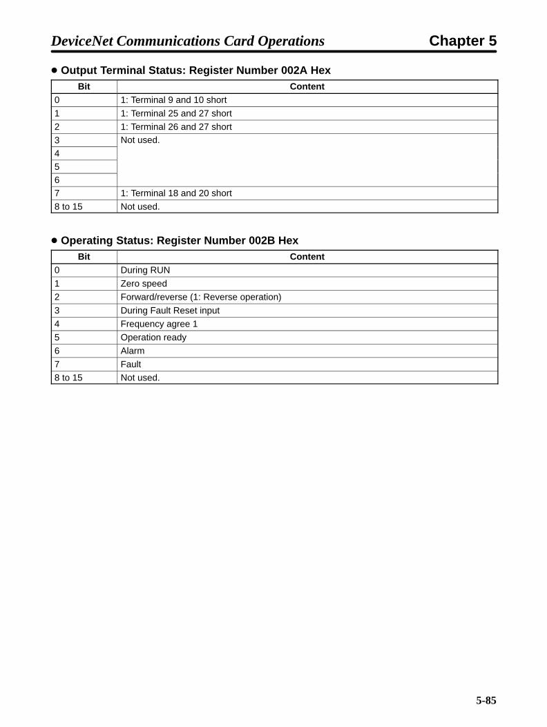
5-85
Output Terminal Status: Register Number 002A HexBit Content
0 1: Terminal 9 and 10 short
1 1: Terminal 25 and 27 short
2 1: Terminal 26 and 27 short
3 Not used.
4
567 1: Terminal 18 and 20 short
8 to 15 Not used.
Operating Status: Register Number 002B HexBit Content
0 During RUN
1 Zero speed
2 Forward/reverse (1: Reverse operation)
3 During Fault Reset input
4 Frequency agree 1
5 Operation ready
6 Alarm
7 Fault
8 to 15 Not used.
DeviceNet Communications Card Operations Chapter 5

5-86
Inverter Monitoring: U2-, U3-
Registernumber
Monitornumber
Monitored item Output unit Read Write
0080 U2-01 Current fault (Refer to table below.) Yes No
0081 U2-02 Last fault (Refer to table below.) Yes No
0082 U2-03 Fault frequency reference Set in o1-03. Yes No
0083 U2-04 Fault output reference Set in o1-03. Yes No
0084 U2-05 Fault output current 8192 dec = Inverter ratedcurrent
Yes No
0085 U2-06 Fault motor speed Set in o1-03. Yes No
0086 U2-07 Fault output voltagereference
0.1 V Yes No
0087 U2-08 Fault main circuit DCvoltage
1 V Yes No
0088 U2-09 Fault output power 0.1 kW Yes No
0089 U2-10 Fault torque reference 0.1% Yes No
008A U2-11 Fault input terminal status Bits 0 to 7 = terminals 1 to8
Yes No
008B U2-12 Fault output terminal status (Same as for U1-11 onprevious page.)
Yes No
008C U2-13 Fault operating status (Same as for U1-12 onprevious page.)
Yes No
008D U2-14 Fault elapsed time 1 hour Yes No
0090 U3-01 Content of last fault (Refer to table below.) Yes No
0091 U3-02 Content of 2nd prior fault (Refer to table below.) Yes No
0092 U3-03 Content of 3rd prior fault (Refer to table below.) Yes No
0093 U3-04 Content of 4th prior fault (Refer to table below.) Yes No
0094 U3-05 Elapsed time since lastfault
1 hour Yes No
0095 U3-06 Elapsed time since 2ndprior fault
1 hour Yes No
0096 U3-07 Elapsed time since 3rdprior fault
1 hour Yes No
0097 U3-08 Elapsed time since 4thprior fault
1 hour Yes No
DeviceNet Communications Card Operations Chapter 5

5-87
Error CodesCode Display Content
01 PUF Fuse open
02 UV1 Undervoltage (main)
03 UV2 Undervoltage (CTL)
04 UV3 Undervoltage (MC)
05 SC Short-circuit
06 GF Ground fault
07 OC Overcurrent
08 OV Overvoltage
09 OH Overheat (See note 1.)
0A OH1 Overheat (See note 2.)
0B OL1 Motor overload
0C OL2 Inverter overload
0D OL3 Overtorque detection 1
0E OL4 Overtorque detection 2
0F RR Braking transistor
10 RH Braking resistor
11 EF3 External fault (Terminal 3)
12 EF4 External fault (Terminal 4)
13 EF5 External fault (Terminal 5)
14 EF6 External fault (Terminal 6)
15 EF7 External fault (Terminal 7)
16 EF8 External fault (Terminal 8)
17 --- Not used.
18 OS Overspeed
19 DEV Speed deviation
1A PGO PG is disconnected
1B PF Input phase loss
1C LF Output phase loss
1D --- Not used.
1E OPR OPR disconnected
1F ERR EEPROM error
21 to FF --- Not used.
Note 1. Maximum (upper limit) temperature was exceeded.
Note 2. Set temperature was exceeded.
DeviceNet Communications Card Operations Chapter 5

5-88
5-8-3 Parameter Reading and WritingThe following tables show the SYSDRIVE 3G3FV Inverter parameters and the corresponding registernumbers. Write and read the various parameters with “1” as the minimum setting unit. Negative num-bers are expressed as two’s complement. If the setting unit is in hexadecimal, there is no need to con-vert it.
When writing data in parameters, be sure to send an enter command to enable the written data. Unlessthe enter command is transmitted, the data will not be enabled and the Inverter may not start.
Parameters for Initialize ModeParameter Register
No (Hex)Class 64 (Hex) Name Setting range Setting unit Default
settingChangesd ringNo. (Hex)
Instance Attributesetting during
operation
A1-00 0100 --- --- Display Language 0 to 6 1 1 Yes
A1-01 0101 01 01 Access Level 0 to 4 1 2 Yes
A1-02 0102 01 02 Select ControlMethod
0 to 3 1 2 No
A1-03 0103 --- --- Initialize 0 to 3,330 1 0 No
A1-04 0104 --- --- Password 0 to 9,999 1 0 No
A1-05 0105 --- --- Setting the Password 0 to 9,999 1 0 No
A2-01 toA2-32
0106 to0125
--- --- User-parametersettings
0180 to 050C
Set theregisternumbers forb1-01 too2-08.
--- --- No
Application ParametersParameter Register
No (Hex)Class 64 (Hex) Name Setting range Setting
nitDefaultsetting
Changesd ringNo. (Hex)
Instance Attributeunit setting during
operation
b1-01 0180 01 03 Frequency referenceselection
0 to 3 1 1 No
b1-02 0181 01 04 Run source selection 0 to 3 1 1 No
b1-03 0182 01 05 Stopping methodselection
0 to 3 1 0 No
b1-04 0183 01 06 Disabling reverseoperation
0 or 1 1 0 No
b1-05 0184 01 07 Operation selectionfor minimumfrequency (E1-09 orless)
0 to 3 1 0 No
b1-06 0185 --- --- Setting control inputresponsiveness
0 or 1 1 1 No
b1-07 0186 --- --- Operation selectionafter switching toremote mode
0 or 1 1 0 No
b1-08 01A6 --- --- Run source selectionwhen not in drivemode
0 or 1 1 0 No
b2-01 0187 01 08 Excitation level (DCinjection startingfrequency)
0.0 to 10.0 0.1 Hz 0.5 No
b2-02 0188 01 09 DC injection brakingcurrent
0 to 100 1% 50 No
DeviceNet Communications Card Operations Chapter 5

5-89
Parameter Changesduring
operation
Defaultsetting
Settingunit
Setting rangeNameClass 64 (Hex)RegisterNo. (Hex)
Parameter Changesduring
operation
Defaultsetting
Settingunit
Setting rangeName
AttributeInstance
RegisterNo. (Hex)
b2-03 0189 01 0A DC injection brakingtime at start
0.00 to 10.00 0.01 s 0.00 No
b2-04 018A 01 0B DC injection brakingtime at stop
0.00 to 10.00 0.01 s 0.50 No
b2-08 01AB --- --- Magnetic fluxcompensation amount
0 to 500 1% 0 No
b3-01 018E 01 0C Speed searchselection at start
0 or 1 1 0 (Seenote.)
No
b3-02 018F 01 0D Speed searchoperation current
0 to 200 1% 100 No
b3-03 0190 01 0E Speed searchdeceleration time
0.1 to 10.0 0.1 s 2.0 No
b4-01 0192 --- --- Timer functionON-delay time
0.0 to 300.0 0.1 s 0.0 No
b4-02 0193 --- --- Timer functionOFF-delay time
0.0 to 300.0 0.1 s 0.0 No
b5-01 0194 01 0F PID control selection 0 to 4 1 0 No
b5-02 0195 01 10 Proportional gain (P) 0.00 to 25.00 0.01 1.00 Yes
b5-03 0196 01 11 Integral time (I) 0.0 to 360.0 0.1 s 1.0 Yes
b5-04 0197 01 12 Integral limit (I) 0.0 to 100.0 0.1% 100.0 Yes
b5-05 0198 01 13 Differential time (D) 0.00 to 10.00 0.01 s 0.00 Yes
b5-06 0199 01 14 PID limit 0.0 to 100.0 0.1% 100.0 Yes
b5-07 019A 01 15 PID offset adjustment –100.0 to 100.0 0.1% 0.0 Yes
b5-08 019B 01 16 PID primary delaytime constant
0.00 to 10.00 0.01 s 0.00 Yes
b5-09 01A7 --- --- PID outputcharacteristicselection
0 or 1 1 0 No
b5-10 01A8 --- --- PID output gain 0.0 to 25.0 0.1 1.0 No
b5-11 01A9 --- --- PID output reverseselection
0 or 1 1 0 No
b5-12 01AF --- --- Feedback lossdetection selection
0 to 2 1 0 No
b5-13 01B0 --- --- Feedback lossdetection level
0 to 100 1% 0 No
b5-14 01B1 --- --- Feedback lossdetection time
0.0 to 25.0 0.1 s 1.0 No
b6-01 019C 01 17 Dwell frequency atstart
0.0 to 400.0 0.1 Hz 0.0 No
b6-02 019D 01 18 Dwell time at start 0.0 to 10.0 0.1 s 0.0 No
b6-03 019E 01 19 Dwell frequency atstop
0.0 to 400.0 0.1 Hz 0.0 No
b6-04 019F 01 1A Dwell time at stop 0.0 to 10.0 0.1 s 0.0 No
b7-01 01A0 01 1B Droop control gain 0.0 to 100.0 0.1 Hz 0.0 Yes
b7-02 01A1 01 1C Droop control delaytime
0.03 to 2.00 0.01 s 0.05 Yes
b8-01 01A2 01 1D Energy-saving gain 0 to 100 1% 80 No
b8-02 01A3 01 1E Energy-savingfrequency
0.0 to 400.0 0.1 Hz 0.0 No
b9-01 01A4 01 1F Zero-servo gain 0 to 100 1 5 No
b9-02 01A5 01 20 Zero-servocompletion width
0 to 16,383 1 pulse 10 No
Note When the control mode is changed, the Inverter will revert to default settings. (The open loop vec-tor control default setting is given above.)
DeviceNet Communications Card Operations Chapter 5

5-90
Tuning ParametersParameter Register
No (Hex)Class 64 (Hex) Name Setting range Setting
nitDefaultsetting
Changesd ring op-No. (Hex)
Instance Attributeunit setting during op-
eration
C1-01 0200 01 21 Acceleration time 1 0.0 to 6,000.0(S 1 )
0.1 10.0 Yes
C1-02 0201 01 22 Deceleration time 1
,(See note 1.) Yes
C1-03 0202 01 23 Acceleration time 2 Yes
C1-04 0203 01 24 Deceleration time 2 Yes
C1-05 0204 01 25 Acceleration time 3 No
C1-06 0205 01 26 Deceleration time 3 No
C1-07 0206 01 27 Acceleration time 4 No
C1-08 0207 01 28 Deceleration time 4 No
C1-09 0208 01 29 Emergency stop time No
C1-10 0209 --- --- Acceleration/deceleration time units
0 or 1 1 1 No
C1-11 020A --- --- Acceleration/deceleration switching frequency
0.0 to 400.0 0.1 Hz 0.0 No
C2-01 020B 01 2A S-curve characteristictime at accelerationstart.
0.00 to 2.50 0.01 s 0.20 No
C2-02 020C 01 2B S-curve characteristictime at accelerationend.
0.00 to 2.50 0.01 s 0.20 No
C2-03 020D 01 2C S-curve characteristictime at decelerationstart.
0.00 to 2.50 0.01 s 0.20 No
C2-04 020E 01 2D S-curve characteristictime at decelerationend.
0.00 to 2.50 0.01 s 0.00 No
C3-01 020F 01 2E Slip compensationgain.
0.0 to 2.5 0.1 1.0 (Seenote 2.)
Yes
C3-02 0210 01 2F Slip compensationprimary delay time.
0 to 10,000 1 ms 200 (Seenote 2.)
No
C3-03 0211 01 30 Slip compensationlimit.
0 to 250 1% 200 No
C3-04 0212 01 31 Slip compensationduring regeneration.
0 or 1 1 0 No
C3-05 0242 01 32 Flux CalculationMethod
0 or 1 1 0 No
C3-06 0243 --- --- Output voltage limitingaction selection
0 or 1 1 0 No
C4-01 0213 01 33 Torque compensationgain.
0.00 to 2.50 0.01 1.00 Yes
C4-02 0214 01 34 Torque compensationdelay time.
0 to 10,000 1 ms 20 (Seenote 2.)
No
C4-03 0244 --- --- Startup torque(forward operation)
0.0 to 200.0 0.1% 0.0 No
C4-04 0245 --- --- Startup torque(reverse operation)
–200.0 to 0 0.1% 0.0 No
C4-05 0246 --- --- Startup torquecompensation time
0 to 200 1 ms 10 No
C5-01 0215 01 35 ASR Proportional (P)gain 1
0.00 to 300.00 0.01 20.0 (Seenote 2.)
Yes
C5-02 0216 01 36 ASR Integral (I) time 1 0.000 to10.000
0.001 s 0.500 (Seenote 2.)
Yes
C5-03 0217 01 37 ASR Proportional Gain(P) 2
0.00 to 300.00 0.01 20.0 (Seenote 2.)
Yes
C5-04 0218 01 38 ASR Integral (I) time 2 0.000 to10.000
0.001 s 0.500 (Seenote 2.)
Yes
DeviceNet Communications Card Operations Chapter 5

5-91
Parameter Changesduring op-
eration
Defaultsetting
Settingunit
Setting rangeNameClass 64 (Hex)RegisterNo. (Hex)
Parameter Changesduring op-
eration
Defaultsetting
Settingunit
Setting rangeName
AttributeInstance
RegisterNo. (Hex)
C5-05 0219 01 39 ASR Limit 0.0 to 20.0 0.1% 5.0 No
C5-06 021A 01 3A ASR Primary delaytime
0.000 to 0.500 0.001 s 0.004 No
C5-07 021B 01 3B ASR Switchingfrequency
0.0 to 400.0 0.1 Hz 0.0 No
C5-08 0241 01 3C ASR Integral (I) Limit 0 to 400 1% 400 No
C6-01 021C 01 3D Carrier frequencyupper limit.
2.0 to 15.0(See note 4.)
0.1 kHz 15.0 (Seenote 3.)
No
C6-02 021D 01 3E Carrier frequencylower limit.
0.4 to 15.0 0.1 kHz 15.0 (Seenote 3.)
No
C6-03 021E 01 3F Carrier frequencyproportional gain.
0 to 99 1 0 No
C7-01 021F 01 40 Hunting preventionselection
0 or 1 1 1 No
C7-02 0220 01 41 Hunting preventiongain
0.00 to 2.50 0.01 1.00 No
C8-08 022A 01 42 AFR Gain 0.00 to 10.00 0.01 1.00 No
C8-09 022B --- --- AFR primary delaytime
0 to 2,000 1 ms 50 No
C8-30 0240 --- --- Carrier FrequencySelection DuringAuto-tuning
1 or 2 1 2 No
Note 1. The setting range and setting unit for acceleration/deceleration times will differ according tothe setting for C1-10 (the unit for acceleration/deceleration time). If C1-10 is set to 0, the set-ting range for acceleration/deceleration times is 0.00 to 600.00 (s).
Note 2. When the control mode is changed, the Inverter will revert to default settings. (The open loopvector control default settings are given above.)
Note 3. The default setting of the Inverter will differ depending on its capacity. (The value for the200-V-class 0.4-kW Inverter is given above.)
Note 4. When the control mode is changed, the Inverter will revert to the setting range. (The open loopvector control setting range is given above.)
DeviceNet Communications Card Operations Chapter 5
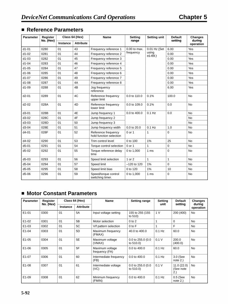
5-92
Reference ParametersParameter Register
No (Hex)Class 64 (Hex) Name Setting
rangeSetting unit Default
settingChangesd ringNo. (Hex)
Instance Attributerange setting during
operation
d1-01 0280 01 43 Frequency reference 1 0.00 to max.f
0.01 Hz (Seti
6.00 Yes
d1-02 0281 01 44 Frequency reference 2 frequency(
usingo1-03 )
0.00 Yes
d1-03 0282 01 45 Frequency reference 3o1-03.)
0.00 Yes
d1-04 0283 01 46 Frequency reference 4 0.00 Yes
d1-05 0284 01 47 Frequency reference 5 0.00 Yes
d1-06 0285 01 48 Frequency reference 6 0.00 Yes
d1-07 0286 01 49 Frequency reference 7 0.00 Yes
d1-08 0287 01 4A Frequency reference 8 0.00 Yes
d1-09 0288 01 4B Jog frequencyreference
6.00 Yes
d2-01 0289 01 4C Reference frequencyupper limit
0.0 to 110.0 0.1% 100.0 No
d2-02 028A 01 4D Reference frequencylower limit
0.0 to 109.0 0.1% 0.0 No
d3-01 028B 01 4E Jump frequency 1 0.0 to 400.0 0.1 Hz 0.0 No
d3-02 028C 01 4F Jump frequency 2 No
d3-03 028D 01 50 Jump frequency 3 No
d3-04 028E 01 51 Jump frequency width 0.0 to 20.0 0.1 Hz 1.0 No
d4-01 028F 01 52 Reference frequencyhold function selection
0 or 1 1 0 No
d4-02 0290 01 53 Trim control level 0 to 100 1% 25 No
d5-01 0291 01 54 Torque control selection 0 or 1 1 0 No
d5-02 0292 01 55 Torque reference delaytime
0 to 1,000 1 ms 0 No
d5-03 0293 01 56 Speed limit selection 1 or 2 1 1 No
d5-04 0294 01 57 Speed limit –120 to 120 1% 0 No
d5-05 0295 01 58 Speed limit bias 0 to 120 1% 10 No
d5-06 0296 01 59 Speed/torque controlswitching timer.
0 to 1,000 1 ms 0 No
Motor Constant ParametersParameter Register
No (Hex)Class 64 (Hex) Name Setting range Setting
nitDefaultsetting
Changesd ringNo. (Hex)
Instance Attributeunit setting during
operation
E1-01 0300 01 5A Input voltage setting 155 to 255 (155to 510)
1 V 200 (400) No
E1-02 0301 01 5B Motor selection 0 to 2 1 0 No
E1-03 0302 01 5C V/f pattern selection 0 to F 1 F No
E1-04 0303 01 5D Maximum frequency(FMAX)
40.0 to 400.0 0.1 Hz 60.0 No
E1-05 0304 01 5E Maximum voltage(VMAX)
0.0 to 255.0 (0.0to 510.0)
0.1 V 200.0(400.0)
No
E1-06 0305 01 5F Maximum voltagefrequency (FA)
0.0 to 400.0 0.1 Hz 60.0 No
E1-07 0306 01 60 Intermediate frequency(FB)
0.0 to 400.0 0.1 Hz 3.0 (Seenote 2.)
No
E1-08 0307 01 61 Intermediate voltage(VC)
0.0 to 255.0 (0.0to 510.0)
0.1 V 11.0 (22.0)(See note2.)
No
E1-09 0308 01 62 Minimum frequency(FMIN)
0.0 to 400.0 0.1 Hz 0.5 (Seenote 2.)
No
DeviceNet Communications Card Operations Chapter 5

5-93
Parameter Changesduring
operation
Defaultsetting
Settingunit
Setting rangeNameClass 64 (Hex)RegisterNo. (Hex)
Parameter Changesduring
operation
Defaultsetting
Settingunit
Setting rangeName
AttributeInstance
RegisterNo. (Hex)
E1-10 0309 01 63 Minimum voltage(VMIN)
0.0 to 255.0 (0.0to 510.0)
0.1 V 2.0 (4.0)(See note2.)
No
E1-11 030A 01 64 Mid. output frequency B 0.0 to 400.0 0.1 Hz 0.0 No
E1-12 030B 01 65 Mid. output frequencyvoltage B
0.0 to 255.0 (0.0to 510.0)
0.1 V 0.0 No
E1-13 030C 01 66 Base voltage 0.0 to 255.0 (0.0to 510.0)
0.1 V 0.0 No
E2-01 030E 01 67 Motor rated current 0.32 to 6.40 (Seenote 4.)
0.01 A 1.90 (Seenote 3.)
No
E2-02 030F 01 68 Motor rated slip 0.00 to 20.00 0.01 Hz 2.90 (Seenote 3.)
No
E2-03 0310 01 69 Motor no-load current 0.00 to 2.90 (Seenote 5.)
0.01 A 1.20 (Seenote 3.)
No
E2-04 0311 01 6A Number of motor poles 2 to 48 1 4 No
E2-05 0312 01 6B Motor phase-to-phaseresistance
0.000 to 65.000 0.001 Ω 9.842(See note3.)
No
E2-06 0313 01 6C Motor leakageinductance
0.0 to 40.0 0.1% 18.2 (Seenote 3.)
No
E2-07 0314 01 6D Motor iron-coresaturation coefficient 1
0.00 to 0.50 0.01 0.50 No
E2-08 0315 01 6E Motor iron-coresaturation coefficient 2
0.00 to 0.75 0.01 0.75 No
E2-09 0316 01 6F Mechanical loss 0.0 to 10.0 0.1% 0.0 No
E2-10 0325 --- --- Torque compensationmotor iron loss
0 to 65,535 1 W 14 (Seenote 3.)
No
E3-01 0317 --- --- Select control methodof motor 2
0 to 3 1 2 No
E4-01 0318 --- --- Motor 2 maximumfrequency
40.0 to 400.0 0.1 Hz 60.0 No
E4-02 0319 --- --- Motor 2 maximumvoltage
0.0 to 255.0 (0.0to 510.0)
0.1 V 200.0(400.0)
No
E4-03 031A --- --- Motor 2 maximumvoltage frequency
0.0 to 400.0 0.1 Hz 60.0 No
E4-04 031B --- --- Motor 2 intermediatefrequency
0.0 to 400.0 0.1 Hz 3.0 (Seenote 2.)
No
E4-05 031C --- --- Motor 2 intermediatevoltage
0.0 to 255.0 (0.0to 510.0)
0.1 V 11.0 (22.0)(See note2.)
No
E4-06 031D --- --- Motor 2 minimumfrequency
0.0 to 400.0 0.1 Hz 0.5 (Seenote 2.)
No
E4-07 031E --- --- Motor 2 minimumvoltage
0.0 to 255.0 (0.0to 510.0)
0.1 V 2.0 (4.0)(See note2.)
No
E5-01 031F --- --- Motor 2 rated current 0.32 to 6.40 (Seenote 4.)
0.01 A 1.90 (Seenote 3.)
No
E5-02 0320 --- --- Motor 2 rated slip 0.00 to 20.00 0.01 Hz 2.90 (Seenote 3.)
No
E5-03 0321 --- --- Motor 2 no-load current 0.00 to 2.90 (Seenote 5.)
0.01 A 1.20 (Seenote 3.)
No
E5-04 0322 --- --- Motor 2 number ofmotor poles
2 to 48 1 pole 4 No
E5-05 0323 --- --- Motor 2 phase-to-phaseresistance
0.000 to 65.000 0.001 Ω 9.842(See note3.)
No
DeviceNet Communications Card Operations Chapter 5

5-94
Parameter Changesduring
operation
Defaultsetting
Settingunit
Setting rangeNameClass 64 (Hex)RegisterNo. (Hex)
Parameter Changesduring
operation
Defaultsetting
Settingunit
Setting rangeName
AttributeInstance
RegisterNo. (Hex)
E5-06 0324 --- --- Motor 2 leakageinductance
0.0 to 40.0 0.1% 18.2 (Seenote 3.)
No
Note 1. Values in parentheses are for 400-V-class Inverters.
Note 2. When the control mode is changed, the Inverter will revert to default settings. (The open loopvector control default settings are given above.)
Note 3. The default setting depends upon the type of Inverter. The value for a 200-V-class 0.4-kWInverter is given above.
Note 4. The setting range is 10% to 200% of the Inverter’s rated output current. The values for a200-V-class 0.4-kW Inverter are given above.
Note 5. The setting range is 0.00 to (motor’s rated current –0.1 A). The value for a 200-V-class 0.4-kWInverter is given above.
Option ParametersParameter Register
No (Hex)Class 64 (Hex) Name Setting range Setting
nitDefaultsetting
Changesd ring op-No. (Hex)
Instance Attributeunit setting during op-
eration
F1-01 0380 01 70 Number of PG pulses 0 to 60,000 1 p/r 1,000 No
F1-02 0381 01 71 PG disconnectionstopping method(PGO)
0 to 3 1 1 No
F1-03 0382 01 72 PG overspeedstopping method
0 to 3 1 1 No
F1-04 0383 01 73 PG speed deviationstopping method
0 to 3 1 3 No
F1-05 0384 01 74 PG rotation setting 0 or 1 1 0 No
F1-06 0385 01 75 PG output ratio 1 to 132 1 1 No
F1-07 0386 01 76 Selecting integralcontrol duringaccel/decel.
0 or 1 1 0 No
F1-08 0387 01 77 Overspeed (OS)detection level.
0 to 120 1% 115 No
F1-09 0388 01 78 Overspeed (OS)detection time
0.0 to 2.0 0.1 s 0.0 (Seenote 1.)
No
F1-10 0389 01 79 PG speed deviationdetection level (DEV)
0 to 50 1% 10 No
F1-11 038A 01 7A PG speed deviationdetection time (DEV)
0.0 to 10.0 0.1 s 0.5 No
F1-12 038B 01 7B Number of PG gearteeth 1
0 to 1,000 1 0 No
F1-13 038C 01 7C Number of PG gearteeth 2
No
F1-14 0397 01 7D PG disconnectiondetection time
0.0 to 10.0 0.1 s 2.0 No
F2-01 038D --- --- Analog ReferenceCard selection
0 or 1 1 0 No
F3-01 038E --- --- Digital ReferenceCard input selection
0 to 7 1 0 No
F4-01 038F --- --- Channel 1 outputmonitor selection
1 to 38 (See note2.)
1 2 No
F4-02 0390 --- --- Channel 1 gain 0.00 to 2.50 0.01 1.00 Yes
DeviceNet Communications Card Operations Chapter 5

5-95
Parameter Changesduring op-
eration
Defaultsetting
Settingunit
Setting rangeNameClass 64 (Hex)RegisterNo. (Hex)
Parameter Changesduring op-
eration
Defaultsetting
Settingunit
Setting rangeName
AttributeInstance
RegisterNo. (Hex)
F4-03 0391 --- --- Channel 2 outputmonitor selection
1 to 38 (See note2.)
1 3 No
F4-04 0392 --- --- Channel 2 gain 0.00 to 2.50 0.01 0.50 Yes
F4-05 03A0 --- --- Channel 1 bias –10.0 to 10.0 0.1% 0.0 Yes
F4-06 03A1 --- --- Channel 2 bias –10.0 to 10.0 0.1% 0.0 Yes
F5-01 0393 --- --- Not used. --- --- 0 ---
F5-02 0394 --- --- Not used. --- --- 1 ---
F6-01 0395 --- --- Not used. --- --- 0 ---
F7-01 0396 --- --- Output pulse multipleselection
0 to 4 1 1 No
F8-01 0398 --- --- Operation detectioncommunications error(SYSMAC BUS)
0 to 3 1 1 No
F9-01 0399 --- --- Communicationsexternal fault inputselection
0 or 1 1 0 No
F9-02 039A --- --- Communicationsexternal fault inputdetection selection
0 or 1 1 0 No
F9-03 039B --- --- Communicationsexternal fault inputoperation selection
0 to 3 1 1 No
F9-04 039C --- --- Not used. --- 1 0 ---
F9-05 039E --- --- Not used. 0 or 1 1 1 ---
F9-06 039F --- --- DeviceNet operationselection
0 to 3 1 1 No
Note 1. When the control mode is changed, the Inverter will revert to default settings. (The open loopvector control default settings are given above.)
Note 2. Within the setting range (1 to 38), 4, 10, 11, 12, 13, 14, 25, 28, 34, and 35 cannot be set, and 29to 31 are not used.
External Terminal Function ParametersParameter Register
No (Hex)Class 64 (Hex) Name Setting range Setting
nitDefaultsetting
Changesd ringNo. (Hex)
Instance Attributeunit setting during
operation
H1-01 0400 01 7E Multi-function input 1:terminal 3 selection
0 to 77 Hex 24 No
H1-02 0401 01 7F Multi-function input 2:terminal 4 selection
14 No
H1-03 0402 01 80 Multi-function input 3:terminal 5 selection
3 (0) (Seenote 1.)
No
H1-04 0403 01 81 Multi-function input 4:terminal 6 selection
4 (3) (Seenote 1.)
No
H1-05 0404 01 82 Multi-function input 5:terminal 7 selection
6 (4) (Seenote 1.)
No
H1-06 0405 01 83 Multi-function input 6:terminal 8 selection
8 (6) (Seenote 1.)
No
H2-01 0406 01 84 Multi-function contactoutput: terminal 9 to10.
0 to 37 Hex 0 No
H2-02 0407 01 85 Multi-function output1: terminal 25.
1 No
H2-03 0408 01 86 Multi-function output2: terminal 26.
2 No
DeviceNet Communications Card Operations Chapter 5

5-96
Parameter Changesduring
operation
Defaultsetting
Settingunit
Setting rangeNameClass 64 (Hex)RegisterNo. (Hex)
Parameter Changesduring
operation
Defaultsetting
Settingunit
Setting rangeName
AttributeInstance
RegisterNo. (Hex)
H3-01 0409 01 87 Signal selection:terminal 13 (Voltage)
0 or 1 1 0 No
H3-02 040A 01 88 Gain: terminal 13 0.0 to 1,000.0 0.1% 100.0 Yes
H3-03 040B 01 89 Bias: terminal 13 –100.0 to 100.0 0.1% 0.0 Yes
H3-04 040C 01 8A Multi-function analoginput signal selection:terminal 16
0 or 1 1 0 No
H3-05 040D 01 8B Selection: terminal 16 0 to 1F 1 1F No
H3-06 040E 01 8C Gain: terminal 16 0.0 to 1,000.0 0.1% 100.0 Yes
H3-07 040F 01 8D Bias: terminal 16 –100.0 to 100.0 0.1% 0.0 Yes
H3-08 0410 01 8E Signal selection:terminal 14
0 to 2 1 2 No
H3-09 0411 01 8F Selection: terminal 14 1 to 1F 1 1F No
H3-10 0412 01 90 Gain: terminal 14 0.0 to 1,000.0 0.1% 100.0 Yes
H3-11 0413 01 91 Bias: terminal 14 –100.0 to 100.0 0.1% 0.0 Yes
H3-12 0414 01 92 Analog input filter timeconstant
0.00 to 2.00 0.01 s 0.00 No
H4-01 0415 01 93 Multi-function analogoutput 1 selection:terminal 21
1 to 38 (See note2.)
1 2 No
H4-02 0416 01 94 Gain terminal 21 0.00 to 2.50 0.01% 1.00 Yes
H4-03 0417 01 95 Bias terminal 21 –10.0 to 10.0 0.1 0.0 Yes
H4-04 0418 01 96 Multi-function analogoutput 2 selection:terminal 23
1 to 38 (See note2.)
1 3 No
H4-05 0419 01 97 Gain terminal 23 0.00 to 2.50 0.01 0.50 Yes
H4-06 041A 01 98 Bias terminal 23 –10.0 to 10.0 0.1% 0.0 Yes
H4-07 041B 01 99 Analog output signallevel selection
0 or 1 1 0 No
H5-01 041C --- --- Not used. --- --- 1F ---
H5-02 041D --- --- Not used. --- --- 3 ---
H5-03 041E --- --- Not used. --- --- 0 ---
H5-04 041F --- --- Not used. --- --- 3 ---
H5-05 0420 --- --- Not used. --- --- 1 ---
Note 1. The values in parentheses indicate initial values when initialized in 3-wire sequence.
Note 2. Within the setting range (1 to 38), 4, 10, 11, 12, 13, 14, 25, 28, 34, and 35 cannot be set, and 29to 31 are not used.
DeviceNet Communications Card Operations Chapter 5

5-97
Protective Function ParametersParameter Register
No (Hex)Class 64 (Hex) Name Setting range Setting
nitDefaultsetting
Changesd ringNo. (Hex)
Instance Attributeunit setting during
operation
L1-01 0480 01 9A Motor protectionselection
0 or 1 1 1 No
L1-02 0481 01 9B Motor protection timeconstant
0.1 to 5.0 0.1 min 1.0 No
L2-01 0482 04 9C Momentary power lossselection
0 to 2 1 0 No
L2-02 0483 01 9D Momentary power lossridethru
0.0 to 2.0 0.1 s 0.7 (Seenote 2.)
No
L2-03 0484 01 9E Minimum baseblocktime (BB)
0.1 to 5.0 0.1 s 0.5 (Seenote 2.)
No
L2-04 0485 01 9F Voltage restart time 0.0 to 5.0 0.1 s 0.3 No
L2-05 0486 01 A0 Under voltage detectionlevel (UV)
150 to 210 (150to 420)
1 V 190 (380) No
L2-06 0487 01 A1 Not used. --- --- 0.0 ---
L3-01 0488 01 A2 Stall prevention duringacceleration
0 to 2 1 1 No
L3-02 0489 01 A3 Stall prevention levelduring acceleration
0 to 200 1% 150 No
L3-03 048A 01 A4 Stall prevention limitduring acceleration
0 to 100 1% 50 No
L3-04 048B 01 A5 Stall prevention duringdeceleration
0 to 2 1 1 No
L3-05 048C 01 A6 Stall prevention duringrun
0 to 2 1 1 No
L3-06 048D 01 A7 Stall prevention levelduring run
30 to 200 1% 160 No
L4-01 0490 01 A8 Frequency detectionlevel
0.0 to 400.0 0.1 Hz 0.0 No
L4-02 0491 01 A9 Frequency detectionwidth
0.0 to 20.0 0.1 Hz 2.0 No
L4-03 0492 01 AA Frequency detectionlevel (+/–)
–400.0 to 400.0 0.1 Hz 0.0 No
L4-04 0493 01 AB Frequency detectionwidth (+/–)
0.0 to 20.0 0.1 Hz 2.0 No
L4-05 0494 01 AC Operation whenfrequency reference islost
0 or 1 1 0 No
L5-01 0495 01 AD Number of auto restartattempts
0 to 10 1 0 No
L5-02 0496 01 AE Auto restart operationselection
0 or 1 1 0 No
L6-01 0498 01 AF Torque detectionselection 1
0 to 4 1 0 No
L6-02 0499 01 B0 Torque detection level 1 0 to 300 1% 150 No
L6-03 049A 01 B1 Torque detection time 1 0.0 to 10.0 0.1 s 0.1 No
L6-04 049B 01 B2 Torque detectionselection 2
0 to 4 1 0 No
L6-05 049C 01 B3 Torque detection level 2 0 to 300 1% 150 No
L6-06 049D 01 B4 Torque detection time 2 0.0 to 10.0 0.1 s 0.1 No
DeviceNet Communications Card Operations Chapter 5

5-98
Parameter Changesduring
operation
Defaultsetting
Settingunit
Setting rangeNameClass 64 (Hex)RegisterNo. (Hex)
Parameter Changesduring
operation
Defaultsetting
Settingunit
Setting rangeName
AttributeInstance
RegisterNo. (Hex)
L7-01 049E 01 B5 Forward torque limit 0 to 300 1% 200 No
L7-02 049F 01 B6 Reverse torque limit No
L7-03 04A0 01 B7 Forward regenerativetorque limit
No
L7-04 04A1 01 B8 Reverse regenerativetorque limit
No
L8-01 04A4 01 B9 DB resistor protection 0 or 1 1 0 No
L8-02 04A5 01 BA Inverter overheatdetection pre-alarmlevel
50 to 130 1°C 95 No
L8-03 04A6 01 BB Operation after Inverteroverheat pre-alarm
0 to 3 1 3 No
L8-05 04A8 01 BC Input open-phaseprotection selection
0 or 1 1 0 No
L8-07 04AA 01 BD Output open-phaseprotection selection
0 or 1 1 0 No
L8-10 04AD 01 BE Ground fault protectionoperation selection
0 or 1 1 1 No
L8-17 04B4 --- --- Low-speed carrierfrequency reductionselection (2)
0 to 3 1 1 No
L8-19 04B6 --- --- Low-speed Inverteroverload (OL2)characteristic selection
0 or 1 1 0 No
Note 1. Values in parentheses are for 400-V-class Inverters.
Note 2. The default setting depends upon the type of Inverter. The value for a 200-V-class 0.4-kWInverter is given above.
DeviceNet Communications Card Operations Chapter 5

5-99
Operator ParametersParameter Register
No (Hex)Class 64 (Hex) Name Setting range Setting
nitDefaultsetting
Changesd ring op-No. (Hex)
Instance Attributeunit setting during op-
eration
o1-01 0500 01 BF Monitor selection 4 to 38 1 6 Yes
o1-02 0501 01 C0 Monitor selection afterpower-on
1 to 4 1 1 Yes
o1-03 0502 01 C1 Frequency referencesetting and displayunits
0 to 39,999 1 0 No
o1-04 0503 01 C2 V/f pattern settingunits
0 or 1 1 0 No
o1-05 0504 01 C3 Not used. --- --- 0 ---
o2-01 0505 01 C4 Local/Remote Key 0 or 1 1 1 No
o2-02 0506 01 C5 Stop Key 0 or 1 1 1 No
o2-03 0507 --- --- User constant initialvalues
0 to 2 1 0 No
o2-04 0508 01 C6 Inverter capacityselection
0 to FF (Seenote.)
1 0 (Seenote.)
No
o2-05 0509 01 C7 Frequency referencesetting method
0 or 1 1 0 No
o2-06 050A 01 C8 Operation selectionwhen Digital Operatoris disconnected
0 or 1 1 0 No
o2-07 050B --- --- Cumulative operationtime setting
0 to 65,535 1 hr 0 No
o2-08 050C --- --- Cumulative operationtime selection
0 or 1 1 0 No
o2-09 050D 01 C9 Factory use --- --- 0 ---
Note The default setting depends upon the type of Inverter. The value for a 200-V-class 0.4-kW Inverteris given above.
DeviceNet Communications Card Operations Chapter 5

Chapter 6
Communications Errors
6-1 Communications Line Errors
6-2 Message Communications Errors
6-3 Special Remote I/O Errors
6-4 Inverter Faults
6

6-2
6-1 Communications Line Errors
Malfunctions in DeviceNet communications that are a result of broken wires, short circuits, reversedwiring, duplicate node address assignments, or noise interference are detected as transmission (BUS)errors. When a transmission error is detected, the Inverter’s Fault Bit will turn ON and the motor willcoast to a stop. (For Inverters with a software version of 1042 or later, the operation when a communica-tions error occurs can be set using constant F9-06.)
When an error is detected, perform error processing according to the indicator display of the DeviceNetCommunications Card.
Operation IndicatorsThe DeviceNet Communications Card has 4 operation indicators that show the status of the power andcommunications.
Indicator Display Meaning CountermeasuresColor Status
g
PWR Green Lit Power is being supplied from the Inverterto the Card.
---
--- Not lit Power is not being supplied from the In-verter.
The Card is not connected properly andpower is not being supplied to it.
Check the Option Card con-nector and turn ON the Invert-er power supply.
Replace the Option Card.MS Green Lit The Card is operating normally. ---
Flashing Initial settings or necessary preparationsfor communications are incomplete.
Turn ON the Inverter powersupply again.
Replace the Option Card.
Red Lit A fatal error (hardware error) has occurredin the Card.
Turn ON the Inverter powersupply again.
Replace the Option Card.
Flashing A non-fatal error, such as a switch settingerror, has occurred.
Check the baud rate setting.
Turn ON the Inverter powersupply again.
Replace the Option Card.
--- Not lit Power is not being supplied from the In-verter.
The Card is not connected properly andpower is not being to supplied to it.
Check the Option Card con-nector and turn ON the Invert-er power supply.
Replace the Option Card.
Communications Errors Chapter 6

6-3
Indicator CountermeasuresMeaningDisplayIndicator CountermeasuresMeaningStatusColor
NS Green Lit The DeviceNet Network is operating nor-mally.
(Communications connections estab-lished.)
---
Flashing The Network is normal, but the commu-nications connection with the Master Unitis not established.
Turn ON the power supplyagain after the following steps.
• Register in the scan list.
• Turn ON the power supply tothe Master Unit.
Red Lit A fatal communications error has oc-curred.
A DeviceNet communications error wasdetected caused by node address duplica-tion or Bus OFF. (These errors make com-munications impossible.)
Turn ON the power supplyagain after the following steps.
• Correct node address du-plication.
• Connect termination resis-tance to both ends of the com-munications line.
• Correct the Master Unit errorsthat occur when the MasterUnit stops after communica-tions is once established.
• Correct environmental condi-tions such as noise.
Flashing A non-fatal communications error has oc-curred due to communications timeout.
Turn ON the power supplyagain after the following pro-cessing.
• Connect termination resis-tance to both ends of the com-munications line.
• Correct defective connec-tions in the communicationsline.
• Correct environmental condi-tions such as noise.
--- Not lit A DeviceNet Network error has occurred.For example, the Network does not exist,power is not supplied to the Card, or thebaud rates do not match.
Check the baud rate setting.
Check the Option Card con-nector and turn ON the Invert-er power supply.
Replace the Option Card.
Communications Errors Chapter 6

6-4
Indicator CountermeasuresMeaningDisplayIndicator CountermeasuresMeaningStatusColor
WD Green Flashing The CPU Unit of the Card is operating nor-mally.
---
Red Lit The CPU Unit of the Card is not ready orthe CPU Unit has malfunctioned.
Check the Option Card con-nector and turn ON the Invert-er power supply.
Replace the Option Card.--- Not lit Power is not being supplied from the In-
verter.
The Card is not connected properly andpower is not being to supplied to it.
Check the Option Card con-nector and turn ON the Invert-er power supply.
Replace the Option Card.
Note 1. When both of the baud rate setting pins DR0 and DR1 are set to ON, both the MS and NS willbe lit in red.
Note 2. For communications line problems, detailed error codes will be displayed on the indicators ofthe Master Unit. Check the error code and take appropriate countermeasures according tothe descriptions in Chapter 15 Troubleshooting and Maintenance of DeviceNet (Compo-Bus/D) Operation Manual (W267).
Communications Errors Chapter 6

6-5
6-2 Message Communications Errors
Explicit Message ErrorsIf an explicit message is sent, but communications do not end normally, one of the following error codeswill be returned with service code 94. Check the meaning of the error message, and either correct themessage or adjust the timing of the message.
ErrorCode
Meaning Countermeasures
0000 Normal end response. ---
08FF The requested service does not exist. Correct the service code and send the dataagain.
09FF An invalid attribute was detected. Check and correct the attribute values, andsend the data again.
0CFF The requested service cannot be executed inthe current object mode or status.
Stop the Inverter and send the data again.
0EFF A request has been sent to change an attributethat cannot be changed.
Check and correct the service code andattribute values, and send the data again.
13FF There is insufficient data to execute the service. Correct the data size and send the data again.
14FF The attribute for the service does not exist. Check and correct the service code andattribute values, and send the data again.
15FF These is too much data to execute the service. Correct the data size and send the data again.
16FF The specified object does not exist. Check and correct the class and instancevalues, and send the data again.
20FF The parameters are invalid or the data isoutside the range for the requested service.
Check and correct the data setting range, sendthe data again.
1FFF Manufacturer fault code. Stop the Inverter and send the data again.
Check and correct the data setting range, sendthe data again.
Communications Errors Chapter 6

6-6
6-3 Special Remote I/O Errors
Special Remote I/O ErrorsIf each function is not set properly using the special remote I/O, the MSB of the function code will bechanged to 1 and one of the following error codes will be returned. Check the meaning of the error mes-sage, and either correct the message or adjust the timing of the message.
Error Code Meaning--- Normal operation response.
When sending data, the code will be returned with the function code and register numberfollowed by the amount of data being written or read data.
01 Function code error: A function code that is not supported has been received.
02 Invalid register number: A register number that is not registered has been received.
21 Data setting error: The data is outside the specified range or does not comply with theconstant restrictions.
22 Write mode error: Attempted write during operation, during UV, or while there was a CPUUnit error, or attempted write to a read-only register.
24 Attempted write during constant processing (busy status).
Note The MSB of the function code will be returned as 1 when there is a communications failure.
Enter CommandWhen entering data in the parameter constant (register No. 0100 or higher), be sure to send an entercommand. If the enter command is not transmitted after writing data, the following situation will occur.
• Written data will not be enabled.Written data will be enabled only after an enter command is sent.
• Inverter will not start.The Inverter will determine the state as being under programming until it receives an enter commandand will ignore the start or run command.After sending an enter command, input the start or run command again.
Communications Errors Chapter 6

6-7
6-4 Inverter Faults
Detecting Inverter FaultsWhen a fault is detected in the Inverter itself, the status will change as shown in the following table.
Function Inverter Fault StatusRemote I/O The fault output allocated in the remote I/O will turn ON.
If the fault output is ON, turn OFF all related inputs controlling the Inverter,and program a sequence to stop the program.
Explicit messages Read the fault output for Class 29, Instance 1, Attribute 0A using messagecommunications. If there is a fault in the Inverter, the fault output will be ON,so turn OFF all related inputs controlling the Inverter, and program asequence to stop the program.
Special remote I/O Read register 0010, and check whether bit 07 (fault output) is ON (seriousfault). If bit 07 is ON, turn OFF all related inputs controlling the Inverter, andprogram a sequence to stop the program.
Confirming Inverter Fault StatusThe fault information for the Inverter can be checked by using the following methods. Perform trouble-shooting based on the information corresponding to the fault and refer to maintenance information inthe Inverter User’s Manual (3G3RV: I532, 3G3PV: I537, 3G3FV: I516).
Function Inverter Error StatusOperation indicators onInverter
When there is an Inverter fault, the details will be displayed on the DigitalOperator of the Inverter. The fault log can be checked using the monitorfunction (U3).
Explicit messages Read the fault code for Class 29, Instance 1, Attribute 0D using messagecommunications. The code corresponding to the Inverter fault is specified.
Special remote I/O Read registers 0014 to 0018. Check the fault status from the bit signals thatare output for an Inverter fault. The fault log can be checked using themonitor function (U3) in registers 0090 to 0093.
Memory Data BackupThe SYSDRIVE 3G3RV/3G3PV/3G3FV Inverter uses EEPROM for the data backup. Data is written toEEPROM when the parameters change or the power is turned OFF.
• Data can be written to EEPROM up to 100,000 times.
• Parameters are always written to EEPROM when they are changed using DeviceNet communica-tions, so limit the times that parameters are written to EEPROM as much as possible.(With the special I/O, data will be written to EEPROM when an enter command is received.)
• Frequency reference and control command (register numbers 0000 to 000F for the special I/O) andthe Net Control Bit and Net Reference Bit are not written to RAM or EEPROM. When the power isturned OFF, any specified values are cleared.
Communications Errors Chapter 6

Chapter 7
CommunicationsPrograms (SYSMAC CS-series PCs)
7-1 Standard Remote I/O Programming
7-2 Message Communications Programming
7-3 Special Remote I/O Programs
7

7-2
Note In this chapter, the bits, words, and data memory used in the ladder pro-grams are selected at random. When creating actual programs, modify thecontents so that they do not overlap with other areas.
7-1 Standard Remote I/O Programming
When the following standard remote I/O programming is executed, the rotational speed reference dataspecified in the DM (Data Memory) Area of the PC is written to the 3G3RV/3G3PV/3G3FV Inverter andforward or reverse operation is performed at the specified frequency when the Frequency ReferenceInput Bit is turned ON and the Forward Input Bit or Reverse Input Bit is turned ON.
AllocationsBit
Bit
Bit
Bit
Bit
Bit
Frequency Reference Input Bit
Forward Input Bit
Reverse Input Bit
Fault Reset Input Bit
Local/Network selection Bit
Fault Flag
Rotational speed reference data
000000
000001
000002
000003
001000
003000
D00000
Remote I/O: Outputs from PC to 3G3MV Inverter Words n and n + 1Byte Bit 7 Bit 6 Bit 5 Bit 4 Bit 3 Bit 2 Bit 1 Bit 0
n Rightmost 0 --- NetReference
NetControl
--- --- FaultReset
Reverse/Stop
Forward/Stop
Leftmost 1 --- --- --- --- --- --- --- ---
n+1 Rightmost 2 Rotational speed reference dataLeftmost 3 Rotational speed reference data
Remote I/O: Inputs from 3G3MV Inverter to PC Words m and m + 1Byte Bit 7 Bit 6 Bit 5 Bit 4 Bit 3 Bit 2 Bit 1 Bit 0
m Rightmost 0 AtFrequency
ReferenceFrom Net
ControlFrom Net
InverterReady
DuringReverseRun
DuringForwardRun
Alarm Fault
Leftmost 1 --- --- --- --- --- --- --- ---
m+1 Rightmost 2 Rotational speed reference dataLeftmost 3 Rotational speed reference data
Communications Programs (SYSMAC CS-series PCs) Chapter 7

7-3
Timing Chart000000(Frequency Reference Input Bit)
000001(Forward Input Bit)
000002(Reverse Input Bit)
Word m bit 2(During Forward Run)
Word m bit 3(During Reverse Run)
Rotational speed reference data D00000 (rotational speed reference data transmitted to words n + 1)
003000 (Fault Flag)
000003 (Fault Reset Input Bit)
1. 2. 3. 4. 5. 6. 7.
Operation1. When the Frequency Reference Input Bit turns ON, the rotational speed reference data specified in
D00000 is moved to remote I/O output word n + 1.
2. When the Forward Input Bit turns ON, remote I/O word n bit 0 (Forward/Stop) will turn ON, and for-ward operation will start. During forward operation, remote I/O word m bit 2 (During Forward Run)will be ON.
3. When the Forward Input Bit turns OFF, remote I/O word m bit 2 (During Forward Run) will turn OFFafter operation will decelerate to a stop.
4. When the Reverse Input Bit turns ON, remote I/O word n bit 1 (Reverse/Stop) will turn ON, and re-verse operation will start. During reverse operation, remote I/O word m bit 3 (During Reverse Run)will be ON.
5. When the Reverse Input Bit turns OFF, remote I/O word m bit 3 (During Reverse Run) will turn OFFafter operation decelerates to a stop.
6. When the remote I/O Fault Bit (word m bit 0) turns ON, the Fault Flag will turn ON.
7. When the Fault Reset Input Bit turns ON, remote I/O word n bit 2 (Fault Reset Input Bit) will turn ON,and the fault will be cleared. When the fault is reset, the Fault Flag will turn OFF simultaneously.
Communications Programs (SYSMAC CS-series PCs) Chapter 7

7-4
Ladder Program
Forward/Stop Bit(word n bit 0)
Reverse/Stop Bit(word n bit 1)
Fault Flag(003000)
Fault Reset Input Bit(word n bit 2)
Reverse Operation 000001 003000(word m bit 3)
Forward Operation000002 003000(word m bit 2)
000003Fault Bit
(word m bit 0)
003000
000003
001003
001004
Net control(word n bit 5)
During forward run001001 (word m bit 2)
001003
001004
001004
During reverse run(word m bit 3)
001002
Net reference(word n bit 6)
See note
DIFU (013)
001001
001000
DIFD (014)
001002
Speed reference setting000000
MOV (021)
D00000
n+1
Note This program is not required if the b1-01 (Frequency Reference Selection) is set to “3” and b1-02(Inverter Operation Command Selection) is set to “3.”
Communications Programs (SYSMAC CS-series PCs) Chapter 7

7-5
7-2 Message Communications Programming
7-2-1 Inverter Fault ProcessingThe message communications programming example given here reads and stores the fault data usingexplicit messages for fault outputs from the Inverter. If the Inverter has a fault, the remote I/O input’sFault Bit (word m bit 0) will turn ON. Be sure to turn OFF the Run Command Bits (word n bits 0 and 1). Inthis program example, the fault code is stored in D00200.
If commands are interrupted by faults, store the completion code in the DM Area and re-execute thecommand. When a fault occurs, check the contents of the fault and take countermeasures referring toinformation provided in the SYSDRIVE Inverter User’s Manual (3G3RV: I532, 3G3PV: I537, 3G3FV:I516).
AllocationsBit
Bit
Bit
Bit
Bit
Bit
Bit
003000
000000
000001
000002
003003
003002
000100
Fault Flag
Fault Code Read Flag
IOWR Write Completed Flag
Response Flag
Sending Message Flag
Message Sent Flag
Reset Input Bit
Slave node address (3G3MV Inverter)D00000
Response Storage Words
Command Code: 2801
Completion Code
Number of Received Bytes
Node Address, Service Code (8E: Normal read, 94: Error)
Read Data or Error Code
Error Code for Error Response
Error Code for Inverter Error
D03000
D03001
D03002
D03003
D03004
D00100
D00200
Communications Programs (SYSMAC CS-series PCs) Chapter 7

7-6
Timing ChartWord m bit 0 (Fault Bit)
000000(Fault Read Flag)
003003(Sending Message Flag)003002(Message Sent Flag)
CMND instruction execution
000001(CMND Write Completed Flag)
000002(Response Flag)
A20200 (Message Communica-tions Enabled Flag)
003000 (Fault Flag)
000100 (Reset Input Bit)
D00200 (Fault code storage) Fault code
1. 2. 3.
Operation1. When the Inverter has a fault, bit 0 of word m (Fault Bit) will be turned ON. Until the fault is cleared,
the Fault Flag will be turn ON, and this will cause the Fault Read Flag to be turned ON, and the com-mand specified in the DM Area will be sent using the CMND instruction.
2. When the Message Communications Enabled Flag is turned ON, the completion code (D03001) willbe examined. If an error is found, the error code will be stored in D00100 and re-send message. Ifnormally completed, the fault code will be stored in D00200 and the Message Sent Flag will beturned ON, and the Sending Message Flag will be turned OFF.
3. When the Reset Input Bit is turned ON, bit 2 of word n (Fault Reset Input Bit) will turn ON. When thefault is cleared, the Fault Flag will turn OFF.
Network ConfigurationThis program is based on the following conditions.
Master unit number: 0Master node address: 63Fixed allocation area setting: 1Network Communications Enabled Flag: A20200Online Flag: 151100Network Communications Error Flag: A21900
Communications Programs (SYSMAC CS-series PCs) Chapter 7

7-7
Ladder ProgramFault (Wd m, bit 00)
Fault Flag
Fault resetWd n, bit 02
Sets the node addressof the Slave for reading.
Clears the storage area, andsets 1 in word 0000 (used forshift register).
No. of send data bytes
Sets CMND data.
Fault (Wd m, bit 00)
No. of received bytes
Network address
Send destination node address: 63
Send destination unit number: FE
Response requiredCommunications port No. 0
Number of resends: 0
Response monitor time:10 s
Explicit messagecommand
Slave node address andservice code: OE Hex
Class ID
Attribute ID
Instance ID
Communications Programs (SYSMAC CS-series PCs) Chapter 7

7-8
A20200(Network Com-
municationsEnabled Flag)
151100(Online Flag)
The completion code examined. Ifan error is found, the command isre-executed. If the command isexecuted normally, the data isstored in D00200.
Equals Flag(P_EQ)
Equals Flag(P_EQ)
A20200(Network Com-
municationsEnabled Flag)
151100(Online Flag)
Executes CMND instruction.
Confirms execution of CMND instruction.
#00000000
A20200(NetworkCommu-nicationsEnabledFlag)
A21900 (Network Com-munications Error Flag)
A21900 (Network Com-munications Error Flag)
Communications Programs (SYSMAC CS-series PCs) Chapter 7

7-9
7-2-2 Reading/Writing DataThis programming example writes and reads data using explicit messages. Explicit messages can beexecuted by specifying FINS commands in the DM Area allocated to the PC, and sending them usingthe CMND or IOWR instructions.
If there is an error in the command, the completion code is stored in the DM Area and the command isre-executed.
Allocations
Bit
Bit
Bit
Bit
Bit
Bit
001000
000000
000001
000002
003000
003001
Program Start Input Bit
Message Execution Flag
Command Write Flag
Response Flag
Sending Message Flag
Message Sent Flag
D00000
D00001
D00002
D00003
D00004
D00005
D00006 Write data (Hex) (See note)to D00009
Slave node address (3G3MV Inverter)
Service code; 0E: Read, 10: Write
Number of command data bytes (Hex)
Class ID (Hex)
Instance ID (Hex)
Attribute ID (Hex)
Note If the written data size is “Word,” set in the order of the rightmost bits and leftmost bits.
Response Storage Words
Command Code: 2801
Completion CodeNumber of Received BytesNode Address, Service Code (8E: Normal read, 90: Normal write, 94: Error)
Read Data or Error Code
Storage Area for Communications Error Completion Codes
D03000
D03001
D03002
D03003
D03004
D00100
to D00009
Communications Programs (SYSMAC CS-series PCs) Chapter 7

7-10
Timing Chart001000(Program Start Input Bit)
001001(Start Switch ON)
000000(Message Execution Flag)003000(Sending Message Flag)003001(Message Sent Flag)
CMND instruction execution
000001 CMND Write Completed Flag000002 Response Flag
Message Communications Enabled FlagCompletion code errorD00100(Completion code storage)
1. 2. 3.
Operation1. When the Program Start Input Bit is turned ON, the Message Execution Flag will turn ON, and the
command specified in the DM Area will be sent using the IOWR instruction.
2. When the Message Communications Enabled Flag is turned ON, the completion code (D03001) isexamined. If an error is found, the completion code is stored in D00100, and the command is re-executed.
3. If the completion code of the response is normal, the Message Sent Flag will be turned ON, and theSending Message Flag will be turned OFF.
Network ConfigurationThis program is based on the following conditions.
Master unit number: 0Master node address: 63Fixed allocation area setting: 1Network Communications Enabled Flag: A20200Online Flag: 151100Network Communications Error Flag: A21900
Communications Programs (SYSMAC CS-series PCs) Chapter 7

7-11
Ladder Program
Equals Flag (P_EQ)
Converts command specifiedin DM Area to CMND data.
Converts command specifiedin DM Area to CMND data.
/ (430)
+C (402)
+C (402)
Communications Programs (SYSMAC CS-series PCs) Chapter 7
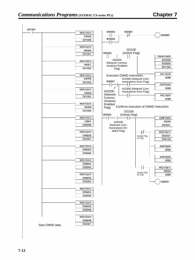
7-12
Sets CMND data.
A20200(Network Com-munications En-
abled Flag)
151100(Online Flag)
Equals Flag(P_EQ)
Equals Flag(P_EQ)
A20200(Network Commu-nications Enabled
Flag)
151100(Online Flag)
Executes CMND instruction.
Confirms execution of CMND instruction.
A20200(NetworkCommu-nicationsEnabledFlag)
A21900 (Network Com-munications Error Flag)
A21900 (Network Com-munications Error Flag)
Communications Programs (SYSMAC CS-series PCs) Chapter 7

7-13
7-3 Special Remote I/O Programs
7-3-1 Simple Operation ProgramsThis section describes examples of simple operation programming using special remote I/O for a3G3RV Inverter. To use special remote I/O, it is necessary to switch the remote I/O operation. Refer to5-2 Switching Remote I/O Operation and change to the special remote I/O operation.
Once the Program Start Input Bit is turned ON, Inverter operations will continue until the Program EndInput is turned ON. The frequency (speed) reference specified in the DM Area (D01000) of the PC isrepeatedly set in the Inverter. The output frequency value will be repeatedly read and stored in the DMArea (D02000). The Inverter status will also be read repeatedly and stored in words (0020**) allocatedin the PC.
If any communications error occurs, the program will stop and a stop command will be sent to theInverter. This state will continue until the Communications Fault Reset Input Bit is turned ON.
Note 3G3RV Inverters support special remote I/O from version VSF105091 (Asian models: VersionVSF105081).
Note Write the program so that the Inverter operation commands (001000 and 001001) will be turnedOFF when the Fault Bit (002014) of the Inverter status turns ON, and also take appropriate coun-termeasures according to maintenance information in the SYSDRIVE Inverter User’s Manual.(3G3RV: I532, 3G3PV: I537, 3G3FV: I516)
Allocations
Inverter Control Input Word AllocationWord Function
001000 Forward/Stop (1: forward) Bit
001001 Reverse/Stop (1: reverse) Bit
001002 Multi-function Input 3 Bit
001003 Multi-function Input 4 Bit
001004 Multi-function Input 5 Bit (Reset input)
001005 Multi-function Input 6 Bit
001006 Multi-function Input 7 Bit
001007 Not used.
001008 External Fault Input (1: EFO) Bit
001009 Fault Reset (1: reset) Bit
Communications Programs (SYSMAC CS-series PCs) Chapter 7

7-14
Inverter Status Word AllocationWord Function
002000 Operation 1: Operating
002001 Zero speed 1: Zero speed
002002 Frequency matching 1: Matched
002003 User-defined speed matching 1: Matched
002004 Frequency detection 1 1: Output frequency ≤L4-01
002005 Frequency detection 2 1: Output frequency ≥L4-01
002006 Inverter startup completed 1: Startupcompleted
002007 Low voltage detection 1: Detected
002008 Baseblock 1: Inverter output baseblock
002009 Frequency reference mode 1: Notcommunications 0: Communications
002010 Run command mode 1: Not communications0: Communications
002011 Overtorque detection 1: Detected
002012 Frequency reference lost 1: Lost
002013 Retrying error 1: Retrying
002014 Fault (including RS-422A/485 communicationstime-out) 1: fault occurred
002015 Communications time-out 1: Timed out
Program-related Bits UsedWord Function
000000 Program Start Input Bit
000001 Program End Input Bit
000002 Program Execution Flag
000003 Communications Error Reset Input Bit
000004 Inverter Stop Command Flag
000100 Frequency Reference Write Flag
000101 Control Input Write Flag
000102 Output Frequency Read Flag
000103 Inverter Status Read Flag
000300 Frequency Reference Write Completed Flag
000301 Control Input Write Completed Flag
000302 Output Frequency Read Completed Flag
000303 Inverter Status Read Completed Flag
003110 Communications Error Flag
Inverter Control InputWord Function
D01000 Reference frequency setting
D02000 Output frequency monitor
Communications Programs (SYSMAC CS-series PCs) Chapter 7

7-15
Remote I/O Allocation AreasI/O classification Word address 15 to 8 7 to 0Output(PC to Inverter)
n Register number (leftmost bits) Function code (10: Write, 03:Read)( C to e te )
n+1 Register data (leftmost bits) Register number (rightmostbits)
n+2 Not used Register data (rightmost bits)Input(Inverter to PC)
m Register number (leftmost bits) Function code (10: Write, 03:Read)( e te to C)
m+1 Register data (leftmost bits) Register number (rightmostbits)
m+2 Not used Register data (rightmost bits)
Timing Chart
000000 (Program Start Input Bit)
000001 (Program End Input Bit) or003110 (Communications Error Flag)
000002 (Program Execution Flag)
000100 (Frequency Reference Write Flag)
000101 (Control Input Write Flag)
000102 (Output Frequency Read Flag)
000103 (Inverter Status Read Flag)
000300 (Control Input Write Completed Flag)
000301 (Frequency Reference Write Completed Flag)
000302 (Output Frequency Read Completed Flag)
000303 (Inverter Status Read Completed Flag)
000004 (Inverter Stop Command Flag)
1. 2. 3. 4. 5.
Communications Programs (SYSMAC CS-series PCs) Chapter 7

7-16
Operation1. When the Program Start Input Bit is turned ON, the Program Execution Input Bit will be set to self-
holding and the Frequency Reference Write Flag will be turned ON. When the Frequency Refer-ence Write Flag is ON, the frequency reference data in D01000 will be transferred to the Inverter.When the Frequency Reference Write Completed Flag is turned ON, the Frequency ReferenceWrite Flag will be turned OFF and the Control Input Write Flag will be turned ON. (Bits are shifted toachieve this.)
2. When the Control Input Write Flag is turned ON, the Inverter control input specified in word 0010 willbe transferred to the Inverter. When the Control Input Write Completed Flag is turned ON, the Con-trol Input Write Flag will be turned OFF and the Output Frequency Reference Read Flag will beturned ON. (Bits are shifted to achieve this.)
3. When the Output Frequency Read Flag is turned ON, the output frequency of the Inverter will beread. When the Output Frequency Read Completed Flag is turned ON, the read output frequencywill be stored in D02000, the Output Frequency Read Flag will be turned OFF, and the Inverter Sta-tus Read Flag will be turned ON. (Bits are shifted to achieve this.)
4. When the Inverter Status Read Flag is turned ON, the Inverter status will be read. When the InverterStatus Read Completed Flag is turned ON, the read Inverter status will be transferred to word 0020,the Inverter Status Read Flag will be turned OFF, and the Frequency Reference Write Flag will beturned ON. Setting the Frequency Reference Write Flag to ON will repeat the above steps 1 to 4.
5. When the Program End Input Bit is turned ON, the Inverter stop command will be written in theInverter. (When word m bit 7 turns ON, communications errors will be detected and the Communica-tions Error Flag will be turned ON and will be self-holding. While this flag remains ON, the system willperform the same processing as when the Program End Input Bit is turned ON. When the Commu-nications Error Reset Input Bit is turned ON, the self-holding state will be cleared.)
Communications Programs (SYSMAC CS-series PCs) Chapter 7

7-17
Ladder Program
000000DIFU (013)
003000
MOV (021)
#0010
D00100
MOV (021)
#0001
0001
ORW (035)
#0001
D00101
MOV (021)
#0003
D00100
MOV (021)
#0024
D00101
000100
003100
Equals Flag (P_EQ)
000002
000004
000004003000
003000
ANDW (034)
D01000
#FF00
D00101
ORW (035)
D00101
#0002
D00101
ANDW (034)
D01000
#00FF
D00102
MOV (021)
#0010
D00100
ANDW (034)
0010
#00FF
D00102
000100
000101
000102
MOV (021)
#0003
D00100
MOV (021)
#002C
D00101
000103
000002
000101
000102
000103
003002
CMP (020)
#0010
m
000100
XFER (070)
#0002
D00100
n
ANDW (034)
m+1
#00FF
D01002
CMP (020)
#0002
D01002
003101
003100ASL (025)
0001
003101
000300
003002
MOVD (083)
D00102
#0010
n+2Sets frequency reference.
Sets control input.
Reads output frequency.
Reads Inverter status.
ANDW (034)
0010
#FF00
D00101
Equals Flag (P_EQ)
Communications Programs (SYSMAC CS-series PCs) Chapter 7

7-18
003103
003105
CMP (020)
#0003
m
000102
ANDW (034)
m+1
#00FF
D01002
CMP (020)
#0024
D01002
003106
ASL (025)
0001
000302
000301
003104
003105 003106ANDW (034)
m+1
#FF00
D01003
ANDW (034)
m+2
#00FF
D01004
ORW (035)
D01003
D01004
D02000
ASL (025)
0001
003107
MOV (021)
#0001
0001
000303
003108
003109
000002ANDW (034)
m
#0080
D01005
CMP (020)
#0080
D01005
003109
000003
003110
003110
003110
000001
000004
CMP (020)
#0010
m
000101
003103
Equals Flag (P_EQ)
ANDW (034)
m+1
#00FF
D01002
CMP (020)
#0001
D01002
003104
CMP (020)
#0003
m
000103
003107
ANDW (034)
m+1
#00FF
D01002
CMP (020)
#002C
D01002
003108
ANDW (034)
m+1
#FF00
D01003
ANDW (034)
m+2
#00FF
D01004
ORW (035)
D01003
D01004
0020
Equals Flag (P_EQ)
Equals Flag (P_EQ)
Equals Flag (P_EQ)
Equals Flag (P_EQ)
Equals Flag (P_EQ)
Equals Flag (P_EQ)
Communications Programs (SYSMAC CS-series PCs) Chapter 7

7-19
MOV (021)
#0000
0001
000004
MOV (021)
#0010
D00100
MOV (021)
#0001
D00101
MOV (021)
#0000
D00102
XFER (070)
#0002
D00100
n
MOVD (083)
D00102
#0010
n+2
Executes stop command.
7-3-2 Reading Parameter DataThis programming example is designed to read the parameter data specified in the3G3RV/3G3PV/3G3FV Inverter. To use special remote I/O, it is necessary to switch the remote I/O op-eration. Refer to 5-2 Switching Remote I/O Operation and change to the special remote I/O operation.
Allocation
Read Parameter Input Bit
Faulty Data Reset Input Bit
Data Read FlagFaulty Data Flag
Register number of the parameter to be read
Read data
Bit
Bit
Bit
Bit
Bit
000000
000002
003000
003001
003005 Data Read Completed Flag
D00000
D00001
Communications Programs (SYSMAC CS-series PCs) Chapter 7

7-20
Remote I/O Allocation AreasI/O classification Word 15 to 8 7 to 0Output(PC to Inverter)
n Register number (leftmostbyte)
Function code (10: Write, 03:Read)( C to e te )
n+1 Register data (leftmost byte) Register number (rightmostbyte)
n+2 Not used. Register data (rightmost byte)Input(Inverter to PC)
m Register number (leftmostbyte)
Function code (10: Write, 03:Read)( e te to C)
m+1 Register data (leftmost byte) Register number (rightmostbyte)
m+2 Not used. Register data (rightmost byte)
Timing Chart
Receive Data (Read)
1. 2.
Send Data (Read)
003000 (Data Read Flag)
Word n to n+2 (Send Data)
Word m to m+2 (Receive Data)
000000 (Read Parameter Input Bit)
003005 (Data Read Completed Flag)
Operation1. Set the register number of the parameter to be read in D00000. When the Read Parameter Input Bit
is turned ON, the Data Read Flag will be turned ON and parameter reading processing will beexecuted.
2. If the data is normally read, the read parameter register number and data will be returned by theInverter. When the register number that was sent agrees with the received register number, the pa-rameter data will be stored in D00001, the Data Read Completed Flag will be turned ON and theData Read Flag will be turned OFF.
Note If the send data is faulty, word m bit 7 will be turned ON, which will turn ON the Faulty Data Flagand the program will be stopped until the Faulty Data Reset Input Bit (000002) is turned ON.
Communications Programs (SYSMAC CS-series PCs) Chapter 7

7-21
Ladder Program
000000 (Read Parameter Input Bit)
DIFU (013)
000001
CMP (020)
D00205
m
CMP (020)
D00206
D00208
003000
003001000001
ANDW (034)
D00000
#FF00
D00200
ORW (035)
D00200
#0003
D00205
ANDW (034)
D00000
#00FF
D00206
000001
003000
003000 MOV (021)
m+1
D00201
003005
ANDW (034)
D00201
#FF00
D00203
003001
003001
003005
BSET (071)
#0000
D00200
D00209
XFER (070)
#0002
D00205
n
003002
003003
003005
MOV (021)
m+2
D00202
ANDW (034)
D00202
#00FF
D00204
ORW (035)
D00203
D00204
D00001
003001
Word m bit 7
Equals Flag (P_EQ)
Equals Flag (P_EQ)
003002 003003
MOVD (083)
#0000
#0010
n+2
ANDW (034)
m+1
#00FF
D00208
000002
Sets the function code to beread and register number.
Confirms the completion of reading.
Transfers read data toD00001.
Detects data errors.
Communications Programs (SYSMAC CS-series PCs) Chapter 7

7-22
7-3-3 Writing Parameter DataThis programming example is designed to write the parameter data in the 3G3RV/3G3PV/3G3FVInverter. After writing has been completed, be sure to send an enter command to enable the written dataas the Inverter operation data.
To use special remote I/O, it will be necessary to switch the remote I/O operation. Refer to 5-2 SwitchingRemote I/O Operation and change to the special remote I/O operation.
Allocations
Bit
Bit
Bit
Bit
Bit
Bit
Bit
Bit
Bit
Write Parameter Input Bit
Faulty Data Reset Input Bit
Data Write Flag
Sending Enter Command FlagSetting “00” Function Code Flag
Data Write Completed Flag
Data Agree Flag (Function Code and Register No.)
Sending Written Data Flag
000000
000002
003000
003005
000100
000101
000102
000103
003010
Register number of the parameter to be written
Written data
Faulty Data Flag
D00000
D00001
Remote I/O Allocation AreasI/O classification Word 15 to 8 7 to 0
Output(PC I )
n Register number (leftmost byte) Function code (10: Write, 03: Read)(PC to Inverter) n+1 Register data (leftmost byte) Register number (rightmost byte)
n+2 Not used Register data (rightmost byte)Input(I PC)
m Register number (leftmost byte) Function code (10: Write, 03: Read)(Inverter to PC) m+1 Register data (leftmost byte) Register number (rightmost byte)
m+2 Not used Register data (rightmost byte)
Communications Programs (SYSMAC CS-series PCs) Chapter 7

7-23
Timing Chart
1. 2. 3. 4.
00000 (Write Parameter Input Bit)
03000 (Data Write Flag)
03005 (Data Agree Flag)
Word n to n+2 (Send Data)
Word m to m+2 (Receive Data)
00101 (Sending Enter Command Flag)
00102 (Sending “00” Function Flag)
00103 (Data Write Completed Flag)
00100 (Sending Written Data Flag)
Send Data (Write) Enter Command “00” Function
Send Data (Write) Enter Command “00” Function
Operation
1. Set the register number of the parameter and the data to be written in D00000 and D00001 respec-tively. When the Write Parameter Input Bit is turned ON, the Data Write Flag will be turned ON andparameter writing processing will be executed.
2. If the data is properly written, the written parameter register number and the function code will bereturned from the Inverter. When the sent register number and the function code agree with the re-ceived data contents, the Data Agree Flag will be turned ON to send the enter command.
3. If the enter command is normally received, the register number and function code that agree withthe enter command will be returned from the Inverter. When the sent register number and functioncode agree with the received contents, the Data Agree Flag will be turned ON to send the functioncode “00” (both the register number and function code are 0000).
4. In the same manner, if the function code “00” is normally received, the Data Agree Flag will be turnedON and the Data Write Completed Flag will be turned ON. When the Data Write Completed Flagturns ON, the Data Write Flag will turn OFF and the program will stop.
Note 1. If the enter command remains set, data will be repeatedly written to EEPROM. Therefore, setthe function code to “00” (both the register number and function code are 0000), which per-forms no processing, to disable the enter command.
Note 2. If the sent data is faulty, word m bit 7 will be turned ON, which will turn ON the Faulty Data Flagand the program will be stopped until the Faulty Data Reset Input Bit (000002) is turned ON.
Communications Programs (SYSMAC CS-series PCs) Chapter 7

7-24
Ladder Program000000 (Write Parameter Input Bit)
DIFU (013)
000001
MOV (021)
#FF10
D00205
MOV (021)
#0000
D00207
003000
003010000001
ANDW (034)
D00000
#FF00
D00200
ORW (035)
D00200
#0010
D00205
ANDW (034)
D00000
#00FF
D00201
000001
000101
003000
003010
000103
BSET (071)
#0000
D00200
D00209
ANDW (034)
D00001
#FF00
D00202
ORW (035)
D00201
D00202
D00206
ANDW (034)
D00001
#00FF
D00207
MOV ()21)
#0001
0001
000100
MOV (021)
#00FD
D00206MOV (021)
#0000
0001
000103
Sets write data.
Sets enter command.
003001000100
BSET (071)
#0000
D00205
D00207
000102
000101
000102
Sets “00” function.
003001
MOVD (083)
D00207
#0010
n+2
XFER (070)
#0002
D00205
n
(Continued on the next page.)
Communications Programs (SYSMAC CS-series PCs) Chapter 7

7-25
CMP (020)
D00205
m
003002
ANDW (034)
D00206
#00FF
D00209
CMP (020)
D00208
D00209
003005
003010Word m bit 7 000002
Equals Flag (P_EQ)
003001
003002 003003
003003
Equals Flag (P_EQ)
ASL (025)
0001
003010MOV (021)
#0000
0001
BSET (071)
#0000
D00205
D00207
ANDW (034)
m+1
#00FF
D00208
XFER (070)
#0002
D00205
n
MOVD (083)
D00207
#0010
n+2
(From previous page.)
Data error processing.
Communications Programs (SYSMAC CS-series PCs) Chapter 7

Chapter 8
Appendices
8-1 Specifications
8-2 Objects
8-3 DeviceNet Communications Response Time
8

8-2
8-1 Specifications
Item SpecificationsModel 3G3FV-PDRT1-SINV1
Remote I/O • Basic remote I/O: Allocated 2 input and 2 output words.
• Standard remote I/O (default setting): Allocated 2 input and 2 outputwords.
• Special remote I/O: Allocated 3 input and 3 output words.
• Control remote I/O: Allocated 4 input and 4 output words.
Note 1. The user can select from among these four types of remote I/O.
Note 2. Basic and standard remote I/O are compatible with DeviceNet.Special remote I/O and control remote I/O are applicable onlyto this product and is not compatible with DeviceNet.
Explicit messages A maximum of 32 bytes of data can be sent or received.Note Explicit messages are applicable to the AC/DC drive profile.
Communications power supplyspecifications
11 to 25 VDC (20 mA max.)
Internal circuit power supply Provided from Inverter.
Operating location Indoors (with no corrosive gases, oil mist, metallic particles, etc.)
Operating ambient temperature –10 to 45°COperating ambient humidity 90% RH max. (with no condensation)
Storage temperature –20 to 60°CArea 1,000 m max.
Weight 150 g max.
Appendices Chapter 8

8-3
8-2 Objects
There are eight types of object:
• Identify objects (identification information): Class 01 hex
• Message router objects: Class 02 hex
• DeviceNet objects: Class 03 hex
• Assembly objects: Class 04 hex
• DeviceNet connection objects: Class 05 hex
• Motor data objects: Class 28
• Control supervisor objects: Class 29 hex
• AC/DC drive objects: Class 2A hex
For details on motor data objects, control supervisor objects, and AC/DC drive objects, refer to 5-5-6Motor Data Objects: Class 28 Hex through 5-5-8 AC/DC Drive Objects: Class 2A Hex.
8-2-1 Identify Objects (Identification Information): Class 01 HexIdentify objects are objects that provide DeviceNet product information. All of this information is read-only.
Support Service CodesService Code No. (Hex) Service
0E Get attribute single
05 Reset (return to initial status)
Appendices Chapter 8

8-4
Object DetailsInstance Attribute Name Content Setting
rangeDefault(Hex)
Read Write Size
00 01 Object SoftwareRevision
Indicates class 01 softwarerevisions. The revisionvalue is advancedwhenever there is achange.
--- 0001 Yes No Word
01 01 Vender ID Indicates the maker’s code.
OMRON: 47 (2F hex)
--- 002F Yes No Word
02 Device Type Indicates the DeviceNetprofile classification. TheInverter corresponds to theAC/DC Drive.
• Master Unit: 0
• AC/DC Drive: 2
--- 0002 Yes No Word
03 Product Code Assigned to each series byeach maker.
DeviceNet CommunicationsCard: 52 (34 hex) or 57 (39hex) or 58 (34 hex)
--- 0034 Yes No Word
04 Revision Indicates overall softwarerevisions for the DeviceNetCommunications Card.
--- 02.01 Yes No Byte × 2
05 Status Indicates thecommunications status ofthe DeviceNetCommunications Card.(See details below.)
--- 0000 Yes No Word
06 Serial Number Indicates the product serialnumber of the DeviceNetCommunications Card.(60000000 hex onwards)
--- Dependsonproduct.
Yes No Long
07 Product Number Indicates product modelnumber.
3G3FV-PDRT1-SIN/3G3RV–PDRT1-SIN/3G3PV-PDRT1-SIN
--- Numbershown atleft.
Yes No String
08 State Indicates Inverter status.
• 3 hex: Inverter ready
--- 03 Yes No Byte
Status DetailsBit Item Content
0 Connection 0: Not connected.1: Master/Slave connected.
1 Not used. ---
2 Configuration 0: Data never changed.1: Data other than default.
3 to 15 Not used. ---
Note Bits that are not used are all zeros.
8-2-2 Message Router Objects: Class 02 HexMessage router objects have the function of distributing DeviceNet communications data. Messageand remote I/O operations, and so on, must pass through these objects to be distributed. Message rout-er objects themselves are involved in internal processing only and do not have data to be exchangedexternally.
Appendices Chapter 8

8-5
Support Service CodeService Code No. (Hex) Service
0E Get attribute single
Object DetailsInstance Attribute Name Content Setting
rangeDefault(Hex)
Read Write Size
00 01 Object SoftwareRevision
Indicates class 02 softwarerevisions. The revisionvalue is advancedwhenever there is achange.
--- 0001 Yes No Word
8-2-3 DeviceNet Objects: Class 03 HexDeviceNet objects are objects related to DeviceNet communications information and operations.
Support Service CodeService Code No. (Hex) Service
0E Get attribute single
10 Set attribute single
Object DetailsInstance Attribute Name Content Setting
rangeDefault(Hex)
Read Write Size
00 01 Object SoftwareRevision
Indicates class 03 softwarerevisions. The revisionvalue is advancedwhenever there is achange.
--- 0001 Yes No Word
01 01 MAC ID Indicates the set value ofthe communications nodeaddress. It is read-onlybecause the setting ismade by the externalsetting switch.
--- 00 Yes No Byte
02 Baud Rate Indicates the baud rate. It iswrite-protected because thesetting is made by theexternal setting switch.
00: 125 Kbps01: 250 Kbps02: 500 Kbps
--- 00 Yes No Byte
05 Allocation Information Indicates DeviceNetcommunications connectioninformation. Used to checkwhether connection isalready made.
• See details below.
• Cannot be written for ex-plicit messages. (Error isreturned.)
--- 0000 Yes No Byte × 2
Appendices Chapter 8

8-6
Allocation Information DetailsByte Bit 7 Bit 6 Bit 5 Bit 4 Bit 3 Bit 2 Bit 1 Bit 0
0 0 0 0 0 0 0 1: Remote I/Oconnectionstatus
1: Explicitmessageconnectionstatus
1 0 0 Node address (MAC ID) of Master connected for DeviceNet communications.
Note The Master Unit automatically writes allocation information when the communications connec-tion is completed. After the Master Unit has written the information, writing is prohibited.
8-2-4 Assembly Objects: Class 04 HexAssembly objects are objects related to remote I/O operations. Remote I/O operations are configuredwith these objects for communications.
Support Service CodesService Code No. (Hex) Service
0E Get attribute single
10 Set attribute single
Object DetailsInstance Attribute Name Content Setting
rangeDefault(Hex)
Read Write Size
00 01 Object SoftwareRevision
Indicates class 04 softwarerevisions. The revisionvalue is advancedwhenever there is achange.
--- 0001 Yes No Word
14 03 Remote I/O data Operation is the same asfor basic remote I/O(output).
Seenote 1.
00. 00.00. 00
Yes Yes Byte × 4
15 03 Remote I/O data Operation is the same asfor standard remote I/O(output).
Seenote 1.
00. 00.00. 00
Yes Yes Byte × 4
46 03 Remote I/O data Operation is the same asfor basic remote I/O (input).
--- 00. 00.00. 00
Yes No Byte × 4
47 03 Remote I/O data Operation is the same asfor standard remote I/O(input).
--- 00. 00.00. 00
Yes No Byte × 4
64 03 Remote I/O data Operation is the same asfor special remote I/O(output).
Seenote 1.
00. 00.00. 00.00
Yes Yes Byte × 5
65 03 Remote I/O data Operation is the same asfor control remote I/O(output).
Seenote 1.
00. 00.00. 00.00. 00.00. 00.
Yes Yes Byte × 8
96 03 Remote I/O data Operation is the same asfor special remote I/O(input).
--- 00. 00.00. 00.00
Yes No Byte × 5
97 03 Remote I/O data Operation is the same asfor control remote I/O(input).
--- 00. 00.00. 00.00. 00.00. 00.
Yes No Byte × 8
Note 1. The setting ranges are the same as the respective remote I/O setting ranges.
Appendices Chapter 8

8-7
Note 2. The remote I/O operations are the same as those explained in 5-1 Remote I/O and 5-3 SpecialRemote I/O Operation.
Note 3. Remote I/O can be performed by means of message communications. When a normal re-mote I/O communications connection is established, however, the message communicationscannot be used for that purpose. Even if an attempt is made to use message communications,they will be overwritten by remote I/O inputs.
Appendices Chapter 8

8-8
8-2-5 DeviceNet Connection Objects: Class 05 HexDeviceNet connection objects are objects related to information and operations involving DeviceNetcommunications connections. The Master Unit uses the information and operations of these objects toexecute the initial processing for communications.
Support Service CodesService Code No. (Hex) Service
0E Get attribute single
10 Set attribute single
Object DetailsInstance Attribute Name Content Setting
rangeDefault(Hex)
Read Write Size
00 01 Object SoftwareRevision
Indicates class 05 softwarerevisions. The revisionvalue is advancedwhenever there is achange.
--- 0001 Yes No Word
01Explicitmessage
01 State Indicates the status of thisobject (instance).
00: Does not exist innetwork, or is not ready.01: In network state, waitingfor connection event fromMaster Unit.02: Waiting for connectionID (attribute) writing.03: Connection completed.04: Timeout
--- Must be“03”whencommu-nicationsare es-tab-lished.
Yes No Byte
02 Instance type Indicates the type of object(instance).
00: Explicit message01: Remote I/O
--- 00 Yes No Byte
03 Transport class trigger Indicates thecommunicationsconfiguration for theDeviceNet CommunicationsCard.
--- 83 Yes No Byte
04 Produced connection ID Indicates the label used forthe communications headerfor the DeviceNetC i ti C d
--- --- Yes No Word
05 Consumed connectionID
Communications Card.
Note: These are set whenthe communicationsconnection is made.
--- --- Yes No Word
06 Initial commcharacteristics
Indicates thecommunicationsconfiguration for theDeviceNet CommunicationsCard.
--- 21 Yes No Byte
07 Produced connectionsize
Indicates the maximumnumber of bytes fortransmission.
--- 0020 Yes No Word
08 Consumed connectionsize
Indicates the maximumnumber of bytes forreception.
--- 0020 Yes No Word
Appendices Chapter 8

8-9
Instance SizeWriteReadDefault(Hex)
Settingrange
ContentNameAttribute
01Explicitmessage
09 Expected packet rate Indicates the length of theinternal processing timeoutwhen a communicationsrequest is received.Incremented by 10-msunits.
0 to65,535(ms)
09C4(2,500ms)
Yes Yes Word
0C Watchdog time-outaction
Indicates the action forinternal processing timeoutrelated to communications.
00: Retain timeout status(until reset or cleared).01: Cut connectionautomatically.02: Operate again withsame connection as is.
--- 01 Yes No Byte
0D Produced connectionpath length
Indicates number of bytesof data for producedconnection path. (No datafor explicit messages.)
--- 0000 Yes No Word
0E Produced connectionpath
Indicates the data fordefining the applicationobject for sending thisobject (instance). (No datafor explicit messages.)
--- --- Yes No Array
0F Consumed connectionpath length
Indicates the number ofbytes of data for theconsumed connection path.(No data for explicitmessages.)
--- 0000 Yes No Word
10 Consumed connectionpath
Indicates the data fordefining the applicationobject for receiving thisobject (instance). (No datafor explicit messages.)
--- --- Yes No Array
Appendices Chapter 8

8-10
Instance SizeWriteReadDefault(Hex)
Settingrange
ContentNameAttribute
02RemoteI/O
01 State Indicates the status of thisobject (instance).
00: Does not exist innetwork, or is not ready.01: In network state, waitingfor connection event fromMaster Unit.02: Waiting for connectionID (attribute) writing.03: Connection completed.04: Timeout
--- Must be“03”whencommu-nicationsare es-tab-lished.
Yes No Byte
02 Instance type Indicates the type of object(instance).
00: Explicit message01: Remote I/O
--- 01 Yes No Byte
03 Transport class trigger Indicates thecommunicationsconfiguration for theDeviceNet CommunicationsCard.
--- 82 Yes No Byte
04 Produced connection ID Indicates the label used forthe communications headerfor the DeviceNetC i ti C d
--- --- Yes No Word
05 Consumed connectionID
Communications Card.
Note: These are set whenthe communicationsconnection is made.
--- --- Yes No Word
06 Initial commcharacteristics
Indicates thecommunicationsconfiguration for theDeviceNet CommunicationsCard.
--- 01 Yes No Byte
Appendices Chapter 8

8-11
Instance SizeWriteReadDefault(Hex)
Settingrange
ContentNameAttribute
02RemoteI/O
07 Produced connectionsize
Indicates the maximumnumber of bytes fortransmission.
--- 0004 Yes No Word
08 Consumed connectionsize
Indicates the maximumnumber of bytes forreception.
--- 0004 Yes No Word
09 Expected packet rate Indicates the length of theinternal processing timeoutwhen a communicationsrequest is received.
0 to65,535(ms)
0000(0 ms)
Yes Yes Word
0C Watchdog time-outaction
Indicates the action forinternal processing timeoutrelated to communications.
00: Retain timeout status(until reset or cleared).01: Cut connectionautomatically.02: Operate again withsame connection as is.
--- 01 Yes No Byte
0D Produced connectionpath length
Indicates number of bytesof data for producedconnection path.
--- 0003 Yes No Word
0E Produced connectionpath
Indicates the data fordefining the applicationobject for sending thisobject (instance).
Note: Has a function forswitching the DeviceNetCommunication Card’sremote I/O operation.
--- 62 34 37 Yes No Array
0F Consumed connectionpath length
Indicates the number ofbytes of data for theconsumed connection path.
--- 0003 Yes No Word
10 Consumed connectionpath
Indicates the data fordefining the applicationobject for receiving thisobject (instance).
Note: Has a function forswitching the DeviceNetCommunication Card’sremote I/O operation.
--- 62 31 35 Yes No Array
Note “Reception” means output (Inverter to SYSMAC PC), and “transmission” means input (SYSMACPC to Inverter).
Appendices Chapter 8
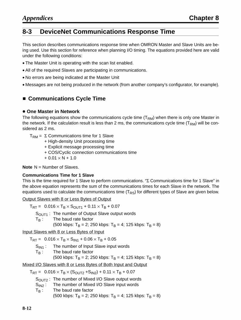
8-12
8-3 DeviceNet Communications Response Time
This section describes communications response time when OMRON Master and Slave Units are be-ing used. Use this section for reference when planning I/O timing. The equations provided here are validunder the following conditions:
• The Master Unit is operating with the scan list enabled.
• All of the required Slaves are participating in communications.
• No errors are being indicated at the Master Unit
• Messages are not being produced in the network (from another company’s configurator, for example).
Communications Cycle Time
One Master in NetworkThe following equations show the communications cycle time (TRM) when there is only one Master inthe network. If the calculation result is less than 2 ms, the communications cycle time (TRM) will be con-sidered as 2 ms.
TRM = Σ Communications time for 1 Slave+ High-density Unit processing time+ Explicit message processing time+ COS/Cyclic connection communications time+ 0.01 × N + 1.0
Note N = Number of Slaves.
Communications Time for 1 SlaveThis is the time required for 1 Slave to perform communications. “Σ Communications time for 1 Slave” inthe above equation represents the sum of the communications times for each Slave in the network. Theequations used to calculate the communications time (TRS) for different types of Slave are given below.
Output Slaves with 8 or Less Bytes of Output
TRT = 0.016 × TB × SOUT1 + 0.11 × TB + 0.07
SOUT1 : The number of Output Slave output wordsTB : The baud rate factor
(500 kbps: TB = 2; 250 kbps: TB = 4; 125 kbps: TB = 8)
Input Slaves with 8 or Less Bytes of Input
TRT = 0.016 × TB × SIN1 + 0.06 × TB + 0.05
SIN1 : The number of Input Slave input wordsTB : The baud rate factor
(500 kbps: TB = 2; 250 kbps: TB = 4; 125 kbps: TB = 8)
Mixed I/O Slaves with 8 or Less Bytes of Both Input and Output
TRT = 0.016 × TB × (SOUT2 +SIN2) + 0.11 × TB + 0.07
SOUT2 : The number of Mixed I/O Slave output wordsSIN2 : The number of Mixed I/O Slave input wordsTB : The baud rate factor
(500 kbps: TB = 2; 250 kbps: TB = 4; 125 kbps: TB = 8)
Appendices Chapter 8

8-13
Slaves with More than 8 Bytes of Input or Output (or Both)
TRT = TOH × TBYTE-IN × BIN × TBYTE-OUT × BOUT
TOH : Protocol overheadTBYTE-IN : Input byte transmission timeBIN : Number of input bytesTBYTE-OUT : Output byte transmission timeBOUT : Number of output bytes
Baud rate TOH TBYTE-IN TBYTE-OUT
500 kbps 0.306 ms 0.040 ms 0.036 ms
250 kbps 0.542 ms 0.073 ms 0.069 ms
125 kbps 1.014 ms 0.139 ms 0.135 ms
Note Calculate with BOUT = 0 for Slaves with inputs only and BIN = 0 for Slaves with outputs only.
High-density Unit Processing TimeAdd 3.5 ms if there is at least 1 Slave with more than 8 bytes of input or output (or both).
Explicit Message Processing TimeAdd the following explicit message processing time when performing explicit message communications(sending or receiving).
Explicit message processing time = 0.11 × TB n
n : The number of explicit messages that are sent or received within 1 cycle of the CPU UnitTB : The baud rate factor
(500 kbps: TB = 2; 250 kbps: TB = 4; 125 kbps: TB = 8)
COS/Cyclic Connection Communications TimeAdd the following COS/cyclic connection communications time.
COS/cyclic connection communications time = (0.05 + 0.008 × S) × TB × n
S : The total number of input and output bytes for COS/cycle connectionsTB : The baud rate factor
(500 kbps: TB = 2; 250 kbps: TB = 4; 125 kbps: TB = 8)n : The number of nodes for which COS/cyclic connections occur within 1 cycle of the CPU
Unit
More than One Master in NetworkCalculate the communications cycle time according to the above equation for the Slaves of each MasterUnit. The communications cycle time for the entire network is the sum of communications cycle timesfor each Master Unit.
Appendices Chapter 8

8-14
I/O Response Time of InverterThe following shows processing time between the Inverter and the DeviceNet Communications Card.
• DP-RAM processing time between the Inverter and DeviceNet Communications Card: 5 ms
• Inverter input scanning: 5 ms (read twice)
• Inverter output scanning: 5 ms
• Inverter parameters scanning: 20 ms
Inverter I/O response time
Ladder program cycle time
Communications cycle time
DP-RAM processing time: 5 ms
Inverter I/O scanning
Inverter internal processing
Maximum input response Maximum output response
5 ms15 ms
Note 1. The internal processing time varies depending on the controls to be executed.
Note 2. Input scanning for parameter reading or writing requires 20 ms.
Appendices Chapter 8

I-1
Index
AAC/DC drive objects, ,
details,
alarms,
allocation areas,fixed allocation,free allocation,
assembly objects,details,service codes,
At Frequency Bit,
Bbasic remote I/O
inputs,outputs,
baud rate,restrictions,settings,
Ccommunications
cable shielding,distance,explicit messages,fault processing,flags,functions,line noise,power supply, , ,
noise prevention,suspension,
specifications,with Configurator,with SYSMAC PCs, ,without Configurator,
communications datareference examples,setting examples,
Communications Error Flag,
Communications Error Reset Input Bit,
Communications Fault Reset Input Bit,
communications flags, ,
communications line errors, operation indicators,
Configurator, ,3G8E2-DRM21,3G8F5-DRM21,communications,
overview,specifications,
connection objects,
connections, methods,
Control From Net Bit,
Control Input Write Completed Flag,
Control Input Write Flag,
control monitor objects, details,
control remote I/Oallocated words,outputs,
control supervisor objects, ,
CPF errors,
CRC check,
crimp terminals,
current capacity,
Ddaisy-chain drop lines,
DeviceNet connection objects,details,service codes,
DeviceNet objects,allocations,details,service codes,
drop lines, ,branching patterns,daisy-chain,maximum length, ,
During Forward Run Input Bit,
During Reverse Run Input Bit,
EEEPROM,
Equals Flag,CS1 Series,
error codes,
Error Flag,CS1 Series,
errorscommunications line,explicit messages,setup
I/O Area Overlap,I/O Area Range Violation,

Index
I-2
special remote I/O,verification,
Slave I/O Size Differs,
explicit messages, ,errors,overview,transmission,
External Fault Input Bit,
Ffault, Inverter,
Fault Bit, ,
fault codes,
Fault Flag, ,
Fault Read Flag,
Fault Reset Bit,
Fault Reset Input Bit,
faults,
FINS commands, ,
fixed allocation,allocation areas,application procedure,communications,example,without Configurator,
Forward Input Bit,
Forward/Stop Bit, ,
free allocation, ,allocation areas,application procedure,communications,example,restrictions, ,with allocated DM Area words,with Configurator,
frequency referenceladder program,settings,
Frequency Reference Input Bit,
Frequency Reference Write Completed Flag,
Frequency Reference Write Flag,
functions,
Ggrounding,
Communications Card,network,
II/O Area Overlap,
I/O Area Range Violation,
I/O power supply,
identify objects,details,service codes,status,
installationCommunications Card,precautions,T-branch Tap,T-branch Tap Terminating Resistor,Terminating Resistor,
instruction setCMND,CMND(194), ,IOWR,
C200HX/HG/HE,CS1 Series,
Interface Unit,
internal circuit power supply,
Inverter,allocated words,control input,
word allocation,fault detection,fault processing,fault status,memory data backup,monitoring,monitoring function,monitoring functions, , ,outputs,run commands, ,settings,status,
word allocation,wiring,
Inverter Ready Bit,
Inverter Status Read Completed Flag,
Inverter Status Read Flag,
Inverter Stop Command Flag,
ISA Board,
Mmemory data backup,
message communications, , , ,command format,explicit messages,FINS messages,operations,overview,programming,response format,

Index
I-3
response read timing, ,responses,timing, , , ,
Message Communications Enabled Flag, , , ,CS1 Series,
Message Communications Status Flag,
Message Execution Flag,
message router objects,details,service codes,
Message Sent Flag,
message transmission,
motor constant objects, details,
motor data objects,
mounting procedure,
multi-drop trunk lines,
multi-layer network,
multi-vendor network, , ,
Multi-function Input Bits,
NNet Control,
Net Control Bit,
Net Reference,
Net Reference Bit,
Network Communications Enabled Flag, ,
Network Communications Error Flag, ,
network configuration,components,node location,overview,power supply location,restrictions,
node addresses,setting pins,
noise preventioncommunications power supply,peripheral devices,wiring,
nomenclature,
Oobjects, types,
operation indicators, ,
Operator, status,
output frequency monitor,
Output Frequency Read Completed Flag,
Output Frequency Read Flag,
Pparameter constants,
reading/writing3G3FV Inverters,3G3PV Inverters,3G3RV Inverters,
parameter objects,
parametersapplication
3G3FV Inverters,3G3PV Inverters,3G3RV Inverters,
external terminal functions3G3FV Inverters,3G3PV Inverters,3G3RV Inverters,
initialize mode3G3FV Inverters,3G3PV Inverters,3G3RV Inverters,
motor autotuning, 3G3RV Inverters,motor constants
3G3FV Inverters,3G3PV Inverters,3G3RV Inverters,
operators3G3FV Inverters,3G3PV Inverters,3G3RV Inverters,
options3G3FV Inverters,3G3PV Inverters,3G3RV Inverters,
protective functions3G3FV Inverters,3G3PV Inverters,3G3RV Inverters,
reference3G3FV Inverters,3G3PV Inverters,3G3RV Inverters,
special adjustments3G3PV Inverters,3G3RV Inverters,
tuning3G3FV Inverters,3G3PV Inverters,3G3RV Inverters,
PMCIA Card,
power supplycalculating location,dual,location,multiple,noise prevention,
Power Supply Tap,configuration,

Index
I-4
internal circuitry,
Program End Input,
Program End Input Bit,
Program Execution Flag,
Program Start Input Bit, , ,
Programmable ControllerC200HS,CV Series,
programmingbits,reading data,reading parameter data,writing data,writing parameter data,
RReference From Net Bit,
register allocation,
remote I/Oallocation areas, , ,basic,communications, , , ,free allocation, ,initial settings,special, ,
errors,programming,
standard, ,programming,
switching operations,restrictions,
Reset Input Bit,
Reverse Input Bit,
Reverse/Stop Bit, ,
rotational speed monitor data,
rotational speed reference data, ,
Sscan lists,
Sending Message Flag, ,
Slave I/O Size Differs,
special 5-wire cables,
special remote I/Oallocated words,communications timing,errors,function codes,inputs,outputs,overview,programming,responses,
specificationscommunications,Configurator,DeviceNet, ,
speed reference,
standard remote I/Oinputs,outputs,programming,
startup procedure,
statusalarms,CPF errors,faults,Inverter,operation,Operator,output terminal,
system configuration,example,fixed allocation,free allocation,with Configurator,without Configurator,
T
T-branch multi-drop lines,
T-branch Tap,DCN1-1C,DCN1-3C,installation,
T-branch Tap Terminating Resistor,
Terminal Block,wiring,
Terminal-block Terminating Resistor,
Terminating Resistor,connection,connections,
Thick Cable, ,maximum length,
Thin Cable, ,maximum length,
trunk lines, ,branching patterns,

Index
I-5
Wwiring
communications cables,Inverter,precautions,preparations,Terminal Block,
word allocationsoverview,SYSDRIVE 3G3RV/3G3PV/3G3FV Inverters,

R-1
Revision History
A manual revision code appears as a suffix to the catalog number on the front cover of the manual.
Cat. No. I525-E1-02
Revision code
The following table outlines the changes made to the manual during each revision. Page numbers refer to theprevious version.
Revisioncode
Date Revised content
01 June 1998 Original production
02 September 2001 The following changes were made throughout the manual: Information related to 3G3RV and 3G3PVInverters was added (and specific model numbers changed to “Inverter”); “V1” was added to the modelnumber; “CompoBus/D” was removed or changed to “DeviceNet” where appropriate; “CS1 Series” waschanged to “CS Series” or “CS/CJ Series” where appropriate; information related to CS/CJ-series Devi-ceNet Units and CJ-series PCs was added; and IOWR changed to CMND where applicable.
In addition, the following changes were made.
Preliminary Pages: The order of the preliminary pages was changed and precautionary informationwas added.
Page 1-2: “6” changed to “8” in last paragraph under “Easy Communications.”
Page 1-4: Last sentence removed from first paragraph. Information on new functions added.
Page 1-7: Wording of first paragraph changed.
Page 1-8: Changes made to first paragraph under “Configurator Review.”
Page 1-9: Information added to table.
Page 2-3: Last paragraph removed.
Pages 2-12, 5-7, 5-27, : Note added.
Page 2-17: Precaution added.
Page 3-5: Changes made to precautionary information. First step of mounting procedure changed.
Page 4-2: Information on free allocation added.
Page 4-3: Information on scan lists changed in several places.
Page 4-5: Minor change made to last paragraph.
Page 4-6: Information on procedures for word allocation added.
Page 4-7: Changes made to information on verification error. Minor changes made to allocationexample. Changes made to procedure in several places.
Page 4-9: First paragraph changed. Minor change made to table. Note changed.
Page 4-10: Information on allocation restrictions added.
Page 4-11: Note changed. Changes made to procedure in several places.
Chapter 5: Order changed and information on control remote I/O added in several places. In addi-tion, the following changes were made.
Page 5-2: Changes made to precautionary information.
Page 5-3: Minor change made to captions.
Page 5-4: Last note removed.
Page 5-5: Note 3 removed and number of poles corrected in notes.
Page 5-24: Information on switching remote I/O operation changed in several places.
Page 5-30: Information on reading and writing parameters added, and graphic corrected.
Page 6-7: Catalog number corrected.
Chapter 7: Extensive changes made throughout the chapter to provide examples for CS-series PCs.
Page 8-2: Minor changes made to table and “three” changed to “four.”
Page 8-6: Information added to table.
Page 8-11: Equations added.