NIELIT Aurangabad-Admission Broucher-converted (1).pdf
84
-
Upload
khangminh22 -
Category
Documents
-
view
1 -
download
0
Transcript of NIELIT Aurangabad-Admission Broucher-converted (1).pdf

Technology has made giant strides and today India is sitting on the cusp of digital revolution,
which is going to reshape the social, economical, political and the cultural landscape of the
country. Indian IT and IT enabled companies have done remarkably well, all over the world, in
terms of services and innovations.
The Government has embarked upon the ambitious ‘Digital India’ program, which is based on
three fundamental pillars – to create digital architecture as a utility for citizens of India; to ensure
digital delivery of services; and to digitally empower the citizens of India.
Digital empowerment refers to digital literacy and essentially means that people, who may not be
literate, are trained to handle digital devices so as to take advantage of e-Governance and digital
services and make a meaningful transformation in their livelihood. In this context, the role of
NIELIT assumes greater significance. With its growing network of centres, including private
training partners in the PPP framework, NIELIT is suitably poised to take forward the National
Digital Literacy Mission (also known as DISHA) that aims to bridge the digital divide.
With the launch of ‘Make-In-India’, there is a need to ensure the availability of skilled manpower
in the area of Electronic System Design and Manufacturing (ESDM). In Ministry of Electronics
and Information Technology (MeitY)’s Scheme for Skill Development in ESDM which envisages
the skilling of more than four lakh candidates over a period of 4 years, the role rendered by
NIELIT in implementing the said scheme is appreciated. I am also happy to note that NIELIT has
launched digital marketing courses for small and medium sellers, such as artisans and weavers,
which would enable them to widen their business prospect by learning the nuances of using e-
Commerce to market and sell their products.
In addition to the training programs, both in Formal and Non Formal sectors, NIELIT has taken up
sponsored projects and consultancy work on behalf of Government departments and I appreciate
the efforts of NIELIT in training youth including women, especially in mofussil and remote areas.
I congratulate NIELIT for its all-round growth and I wish the organization greater success in its
endeavors.
Message from Hon'ble Minister
Electronics & IT, Law & Justice

The Government of India has taken a number of landmark initiatives. The ‘Digital India’ program
is committed to take the cause of good governance forward, in both letter and spirit. Digital India is
viewed as a ‘game changer’, from the perspective of delivery of pro-citizen good governance, with
the synchronized and coordinated engagement of the entire Government.
As one of the most sustainable and dependable arm of MeitY, NIELIT has endeavored to lead by
example through institutionalization of policies and best practices. It has emerged as a key player
in training related services. NIELIT courses are already known throughout India for its high
standards of quality and these courses are also supported by an unfaltering and holistic system of
examination at the national level.
I am happy to note that through proactive use of technology, capacity building and process re-
engineering initiatives, NIELIT has made efforts to leverage its capacity and create synergy in the
area of training and support services. Also, in tune with the changing times, NIELIT has
diversified and spread its wing by expanding its repertoire of activities. Recently, NIELIT has also
taken up new capacity building initiatives in the areas of e-Governance, Digital Marketing, Cloud
Computing, Big Data, IoT etc. e-Contents are being developed to usher in a new paradigm of
learning.
I would also like to compliment NIELIT for its efforts to standardize its Short Term Courses across
all NIELIT Centres. The Student Support Services have been also upgraded with the introduction
of web based services and a Placement Portal has been institutionalized by NIELIT, which would
facilitate the students to seek suitable employment. Such proactive measures are the need of the
time and I am happy that NIELIT is introducing such features with the required sensitivity and
vibrancy.
I congratulate NIELIT for its endeavor to spread IT literacy and education across the country. The
efforts made by NIELIT in implementing various government schemes by scaling up its operations
and leveraging its capacities, are praiseworthy.
The integrated NIELIT Website is a welcome step towards uniformity, dynamism and improved
services for stakeholders and I wish NIELIT success in its future efforts..
Message from Secretary Ministry of
Electronics & Information Technology
The National Institute of Electronics and Information Technology (NIELIT), a body under the
administrative control of the Ministry of Electronics and Information Technology (MeitY),
Government of India, a distinct identity and character in the panorama of Skill Development and
Capacity Building in India. With presence at 42 locations across the country and a network of
around 1000 Accreditation Centres, NIELIT is uniquely positioned in terms of its outreach to all
corners of the country and all segments of the society.
NIELIT has made efforts to establish standards in the areas of IECT (Information, Electronics and
Communication Technology) in both formal and non-formal mode of education. As the education
system in this country is undergoing a paradigm shift to improve upon the employability factor,
NIELIT is offering a rich repertoire of market-oriented courses in the emerging areas viz Cyber
Security, IoT, ESDM, GIS, Cloud Computing, Hardware, Electronics Design Technology, VLSI
Design, Embedded Systems, e-Waste, Big Data as per needs of the IT and the electronic industry.
NIELIT Aurangabad is one of the prominent centre of NIELIT, that was setup in the year 1987 in
order to bring an innovative, entrepreneurial spirit and to maintain close links with Industries,
R&D and Academic Institutions to promote electronics, IT and industrial design culture. Owing to
its quality and solution-oriented skilling approach, the centre has produced many prominent
entrepreneurs, experts and designers.
As per the aegis of Make-in-India, the Centre is providing Quality Technical Education though
B. Tech. (Electronics System Engineering), M. Tech. (Electronics Design and Technology)
and Diploma in Electronics Production and Maintenance leading to Academic Excellence,
Creativity and Innovation in the areas of IECT that helps to develop employable workforce and
shape entrepreneurs. It is also a Research Centre of the Dr. Babasaheb Ambedkar Marathwada
University, Aurangabad for conducting research leading to award of Ph.D. Degree in Engineering
and Technology.
I am confident that by taking admission at Aurangabad centre of NIELIT, the students would be
greatly benefitted by some of the best facilities in the country like Industrial R&D Infrastructure,
state-of-the-art Labs, well equipped Library, NKN, rich repertoire of e-journals, Hostel,
Gymnasium, Sport Facility.
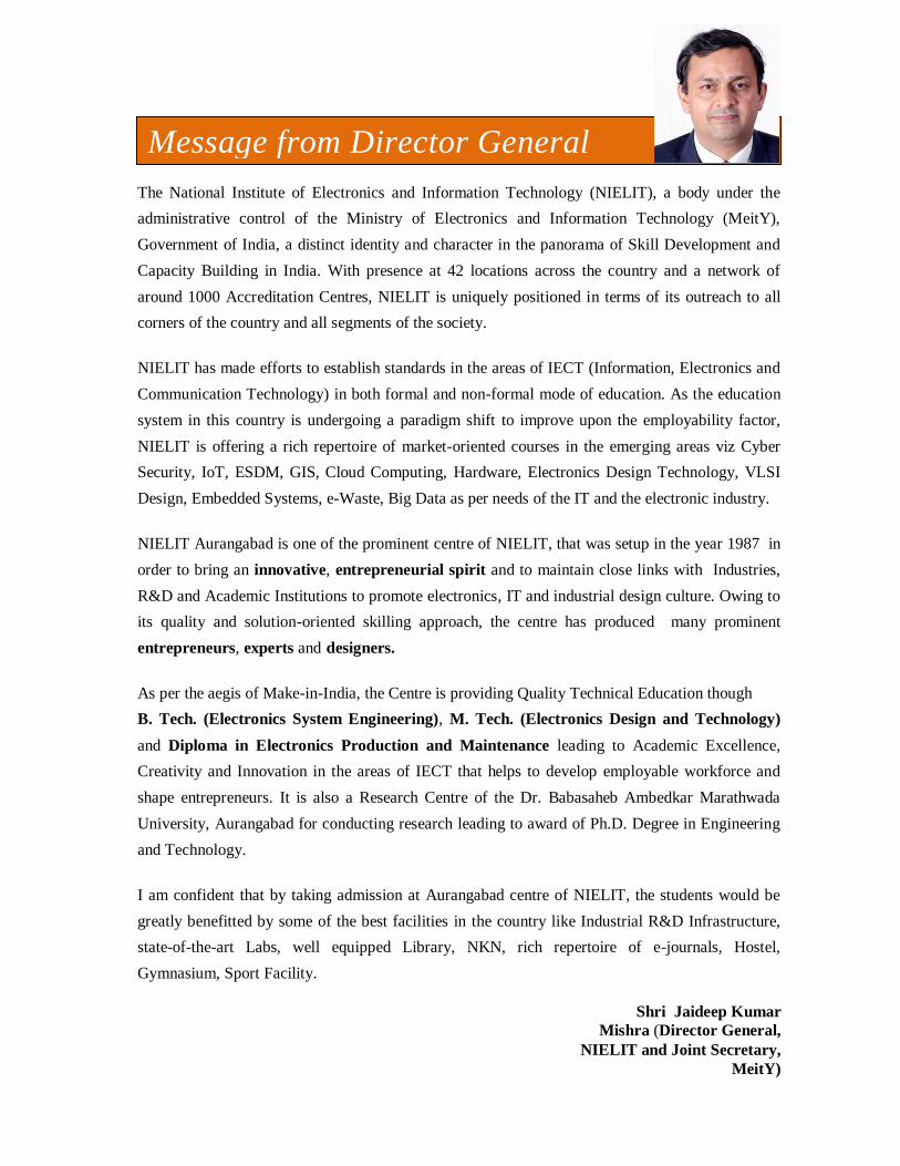
Shri Jaideep Kumar
Mishra (Director General,
NIELIT and Joint Secretary,
MeitY)
Message from Director General

The NIELIT Aurangabad Centre (erstwhile CEDTI) is one of the prominent Centres of NIELIT
that was established in the year 1987 to bring an innovative, entrepreneurial spirit along with
excellence in teaching, learning and research to develop leaders in IT and Electronics. It is co-
located in Dr. Babasaheb Ambedkar Marathwada University (BAMU) campus and possesses state-
of-the-art 14 well equipped laboratories and Mechanical workshop besides a rich Library, NKN,
Gymnasium for students, Auditorium, Hostel, Canteen, Sports facility spread over more than 18
acres.
The Centre is offering AICTE approved B. Tech (Electronics System Engineering), M. Tech
(Electronics Design and Technology), Diploma in Electronics Production & Maintenance and
is also a Research Centre of the Dr. Babasaheb Ambedkar Marathwada University, Aurangabad for
conducting research leading to award of Ph.D. Degree in Engineering and Technology.
Based on project-based teaching methodology, these courses provide practical skills in in the areas
of Electronics Design & Technology and includes interdisciplinary field issues such as
requirements engineering, industrial design, product engineering, ergonomics, aesthetics, System-
level packaging, thermal design, reliability, EMI&EMC, testing & evaluation, maintainability,
Serviceability necessary for successful system development, design, implementation and ultimate
disposal after decommission. These courses take into account latest industrial trends &
requirements and trains students to become entrepreneurs, experts & designers, carry out R&D
and provide Industrial Consultancy in IECT.
NIELIT Aurangabad Centre is promoting Industry Oriented Projects, R & D and consultancy to
raise the overall standards. The Centre reckoned on the ideology that identifying the needs of
modern engineering & technology education for modern age students supplemented with a vision
& mission will lead to a greater education system which is outcome oriented, transparent,
accountable & accessible and is also effective in keeping ourselves abreast and keep us way ahead
of our competitors.
All the faculty members and scientists working at Centre are striving hard to impart professional
education, combined with fostering innovative thinking, application of knowledge, inculcating
professional ethics and consciousness to social responsibilities. Our core values of excellence,
integrity, transparency, quality, team work, execution with passion, trust, continuous and student
centric learning are all closely integrated into our academic programs.
I encourage you to explore all that NIELIT Aurangabad Centre has to offer and I am confident that
each one of you graduating from the Centre will leave your indelible mark of success in whichever
sphere of life you choose to be.
Dr. Sanjeev Kumar Gupta
(Executive Director)
NIELIT Aurangabad
Message from Executive Director

Shri. Ravi Shankar Prasad
Chairperson
Hon'ble Minister of Electronics
& IT and Law & Justice
Shri S .S. Ahluwalia Deputy Chairperson
Hon'ble MoS Electronics &
IT
Shri Ajay Prakash
Sawhney
Executive Vice Chairperson
Secretary, Ministry of Electronics and IT
Shri R. Subrahmanyam
Member
Secretary, Department of
higher EducationMinistry of
Human Resources
Development
Prof. Dhirendra Pal Singh
Member
Chairman, UGC
Prof. Anil D.
Sahasrabudhe
Member Chairman, AICTE
Ms. Anuradha Mitra
Member Additional Secretary &
Financial Adviser, MEITY
Shri Jaideep Kumar Mishra
Member
Joint Secretary, HRD,
MEITY
Shri Rajiv Kumar
Member Joint Secretary, MEITY
Shri Rajesh Aggarwal Member, Director General (Training), DGET Ministry
of Skill Development & Entrepreneurship
Mrs. Debjani Ghosh Member
President, NASSCOM
Prof (Dr) K T V Reddy Member
President, IETE
Prof. Pushpak Bhattacharya, Member, Director, Department
of Comp. Sci. & Engg., IIT Patna
Shri Hariom Rai
Member
Chairman, Lava International
Limited
Shri. T.V. Mohandas Pai
Member, Chairman Manipal
Global Education Services pvt.
ltd.
Shri. Vineet Nayar
Member, Founder Sampark
Foundation
Shri Jaideep Kumar Mishra Member Secretary, Director General, NIELIT and Joint Secretary, MeitY
Governing Council of NIELIT
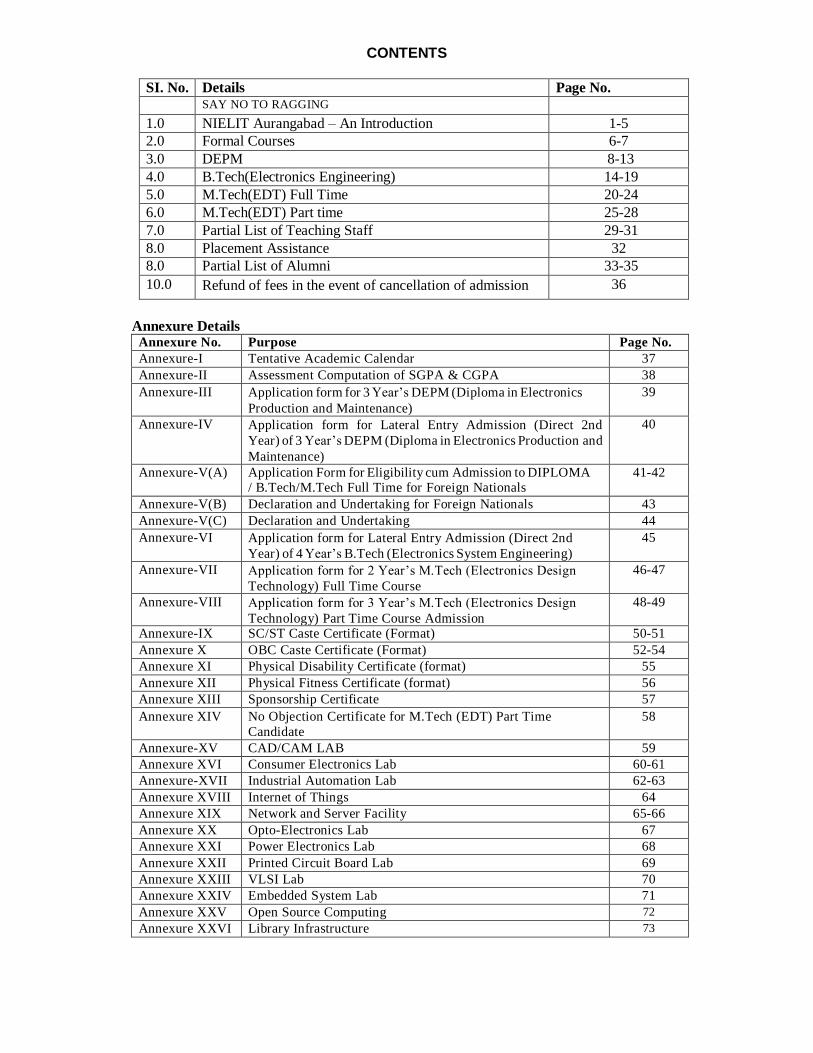
CONTENTS
SI. No. Details Page No. SAY NO TO RAGGING
1.0 NIELIT Aurangabad – An Introduction 1-5
2.0 Formal Courses 6-7
3.0 DEPM 8-13
4.0 B.Tech(Electronics Engineering) 14-19
5.0 M.Tech(EDT) Full Time 20-24
6.0 M.Tech(EDT) Part time 25-28
7.0 Partial List of Teaching Staff 29-31
8.0 Placement Assistance 32
8.0 Partial List of Alumni 33-35
10.0 Refund of fees in the event of cancellation of admission 36
Annexure Details Annexure No. Purpose Page No.
Annexure-I Tentative Academic Calendar 37
Annexure-II Assessment Computation of SGPA & CGPA 38
Annexure-III Application form for 3 Year’s DEPM (Diploma in Electronics
Production and Maintenance)
39
Annexure-IV Application form for Lateral Entry Admission (Direct 2nd
Year) of 3 Year’s DEPM (Diploma in Electronics Production and
Maintenance)
40
Annexure-V(A) Application Form for Eligibility cum Admission to DIPLOMA / B.Tech/M.Tech Full Time for Foreign Nationals
41-42
Annexure-V(B) Declaration and Undertaking for Foreign Nationals 43
Annexure-V(C) Declaration and Undertaking 44
Annexure-VI Application form for Lateral Entry Admission (Direct 2nd
Year) of 4 Year’s B.Tech (Electronics System Engineering)
45
Annexure-VII Application form for 2 Year’s M.Tech (Electronics Design
Technology) Full Time Course
46-47
Annexure-VIII Application form for 3 Year’s M.Tech (Electronics Design
Technology) Part Time Course Admission
48-49
Annexure-IX SC/ST Caste Certificate (Format) 50-51
Annexure X OBC Caste Certificate (Format) 52-54
Annexure XI Physical Disability Certificate (format) 55
Annexure XII Physical Fitness Certificate (format) 56
Annexure XIII Sponsorship Certificate 57
Annexure XIV No Objection Certificate for M.Tech (EDT) Part Time
Candidate
58
Annexure-XV CAD/CAM LAB 59
Annexure XVI Consumer Electronics Lab 60-61
Annexure-XVII Industrial Automation Lab 62-63
Annexure XVIII Internet of Things 64
Annexure XIX Network and Server Facility 65-66
Annexure XX Opto-Electronics Lab 67
Annexure XXI Power Electronics Lab 68
Annexure XXII Printed Circuit Board Lab 69
Annexure XXIII VLSI Lab 70
Annexure XXIV Embedded System Lab 71
Annexure XXV Open Source Computing 72
Annexure XXVI Library Infrastructure 73

SAY NO TO RAGGING According to UGC guidelines, the definition of ragging states that any conduct whether by words spoken or
written or by an act which has the effect of teasing, treating of handling with rudeness any other student,
indulging in rowdy or undisciplined activities which causes or is likely to cause annoyance, hardship or
psychological harm or to raise fear or apprehension thereof in a fresher or a junior student or asking the student
to do any act or perform something which such student will not in the ordinary course and which has the effect
of causing or generating a sense of sham or embarrassment so as to adversely affect physique or psyche of a
fresher or a junior student.
IMPORTANT INSTRUCTIONS FOR THE STUDENTS 1. As per the directions of the Hon’ble Supreme Court in SLP No. 24295 of 2006 dated 16 -05-2007 and in
Civil Appeal number 887 of 2009, dated 08-05-2009, ragging is strictly prohibited and banned.
2. All students of the institute have to study and fill affidavit online
http://antiragging.in/site/affidavits_registration_form.aspx.
3. Ragging is a Cognizable Offence. Students are advised not to indulge in Ragging.
4. Ragging entails heavy fines and/or suspension/expulsion.
5. In case the applicant for admission in the institute is found to have indulged in ragging in the past or if it is
noticed later that he has indulged in ragging, admission may be refused or he/she shall be expelled from the
institution.
6. It is mandatory for the parents to report immediately to the Authorities of the Institute in case their wards
inform them about ragging.
PUNISHABLE INGREDIENTS OF RAGGING 1. Abetment to ragging or Criminal conspiracy to rag
2. Unlawful assembly and rioting while ragging
3. Public nuisance created during ragging
4. Violation of decency and morals through ragging
5. Injury to body, causing hurt or grievous hurt
6. Wrongful restraint or Wrongful confinement
7. Use of criminal force
8. Assault as well as sexual offences or unnatural offences
9. Extortion or Criminal intimidation
10. Criminal trespass or Offences against property
11. Attempts to commit any or all of the above mentioned offences against the victim(s)
12. Physical or psychological humiliation
13. All other offences following from the definition of "Ragging"
PUNISHMENT Depending upon the nature and gravity of the offence as established by the Anti -Ragging Committee of the
institution, the possible punishment for those found guilty of Ragging at the Institution level shaped any one or
any combination of the following:
1. Suspension from attending classes and academic privileges
2. Withholding/ Withdrawing scholarship/ fellowship and other benefits
3. Debarring from appearing in any test/ examination or other evaluation process
4. Withholding results
5. Debarring from representing the institution in any regional, national or international meet, tournament,
youth festival etc.
6. Suspension expulsion from the hostel
7. Rustication from the institution for period ranging from 1 to 4 semesters
8. Expulsion from the institution and consequent debarring from admission to any other institution for a
specified period
9. Fine ranging between Rupees 25,000/- and Rupees 1 Lakh
10. Collective punishment: When the persons committing or abetting the crime of ragging are not identified,
the institution shall resort to collective punishment
11. Fresher who do not report the incidents of ragging either as victims or as witnesses shall also be punished
suitably.
As per the directions of the Hon'ble Supreme Court of India, if any incident of ragging comes to the notice of
authority, the concerned student shall be given liberty to explain and if his/her explanation is not found
satisfactory, the authority would expel him/her from the Institute"
1
1.0 NIELIT Aurangabad –An Introduction
1.1 Genesis The history of NIELIT dates back to 1974 when the Department of Electronics (DoE) now Ministry
of Electronics and Information Technology (MeitY), Govt. of India and the University Grants
Commission (UGC) set up the first CEDT within the premises of Indian Institute of Science
(IISc.), Bangalore with assistance from Swiss Development Corporation.
A decade after the successful running of CEDT, Bangalore, DoE (now MeitY) set up similar
centres at Aurangabad, Imphal and Srinagar in 1987, Calicut, Mohali and Gorakhpur in 1989,
with an objective to develop human resources at different levels and in different specialized areas of
Electronics Design. Aim was to bridge the gap between the academic institutions and industries.
The CEDT centres based at Aurangabad, Calicut, Gorakhpur, Imphal and Srinagar were merged
with DOEACC (a scientific society of MeitY) in 2001. In order for its metamorphism into an
Institute of National Importance the Society was renamed as ‘National Institute of Electronics
and Information Technology (NIELIT) on October 10, 2011.
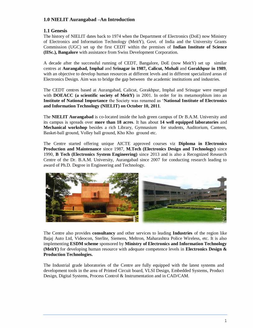
The NIELIT Aurangabad is co-located inside the lush green campus of Dr B.A.M. University and
its campus is spreads over more than 18 acres. It has about 14 well equipped laboratories and
Mechanical workshop besides a rich Library, Gymnasium for students, Auditorium, Canteen,
Basket-ball ground, Volley ball ground, Kho Kho ground etc.
The Centre started offering unique AICTE approved courses viz Diploma in Electronics
Production and Maintenance since 1987, M.Tech (Electronics Design and Technology) since
1990, B Tech (Electronics System Engineering) since 2013 and is also a Recognized Research
Centre of the Dr. B.A.M. University, Aurangabad since 2007 for conducting research leading to
award of Ph.D. Degree in Engineering and Technology.
The Centre also provides consultancy and other services to leading Industries of the region like
Bajaj Auto Ltd, Videocon, Sterlite, Siemens, Meltron, Maharashtra Police Wireless, etc. It is also
implementing ESDM scheme sponsored by Ministry of Electronics and Information Technology
(MeitY) for developing human resource with adequate competence levels in Electronics Design &
Production Technologies.
The Industrial grade laboratories of the Centre are fully equipped with the latest systems and
development tools in the area of Printed Circuit board, VLSI Design, Embedded Systems, Product
Design, Digital Systems, Process Control & Instrumentation and in CAD/CAM.

2
Besides numerous reference books, Journals, magazines; the students of the Centre have access to
MeitY Library Consortium (rich collection of latest e-Journals including IEEE and books) and
National Knowledge Network (NKN) a strong a network with multi-gigabit capability connected
to all universities, research institutions, libraries, laboratories, healthcare and agricultural
institutions across the country.
All the labs, library and office are connected through the central network and students can retrieve
information from their terminals itself and through well connected Wi-Fi system. The Centre
organizes National Level Seminars/Workshops in areas like Agri- Electronics, Electronics
Product Design, Intellectual Property Rights(IPR), Neural Networks, e-learning regularly.
Trained to become R&D engineers students of the centre are working in leading and reputed
organizations like C.G Coral. Lucent India, Texas, L&T, HCL, Wipro Technologies, BITS, IIT,
BEL, HAL, ISRO, DRDO, BARC, ECIL, Messung, Thermax, Honeywell Cyrus logic L&T
EMSYS to name a few.
The Centre has become a solution-oriented model organization and knowledge-based enterprise
and is tirelessly working for creating a pool of R&D engineers and Entrepreneurs.
1.2 Objectives of Centre 1. To bring an innovative, entrepreneurial spirit along with excellence in teaching, learning and
research to develop leaders in IT and Electronics.
2. To generate and keep update Industry-ready quality professionals with knowledge-based
skill set in IECT and allied fields through formal and informal education system.
3. To establish a Quality system of examination and certification that is globally recognized and
provides a fair assessment of the competency of students
4. To maintain close links with Industries, R&D and Academic Institutions to promote
electronics, IT and industrial design culture
5. To develop entrepreneurs, experts and designers, carry out R&D and provide
Industrial Consultancy in IECT
6. To offer e-Training in Electronics, Information Technology and Industrial Design methodology
and production technique
Mission Identifying the needs of modern engineering & technology education and providing Quality
Technical Education leading to Academic Excellence, creativity and innovation in the areas of
Electronics and Information Technology
3
Vision To impart professional education that is outcome oriented, combined with fostering innovative
thinking, application of knowledge, inculcating professional ethics and consciousness to social
responsibilities.
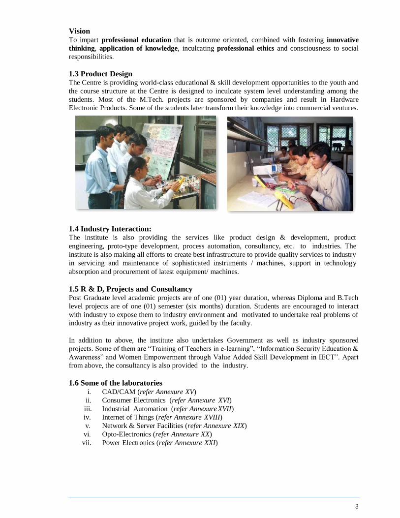
1.3 Product Design The Centre is providing world-class educational & skill development opportunities to the youth and
the course structure at the Centre is designed to inculcate system level understanding among the
students. Most of the M.Tech. projects are sponsored by companies and result in Hardware
Electronic Products. Some of the students later transform their knowledge into commercial ventures.
1.4 Industry Interaction: The institute is also providing the services like product design & development, product
engineering, proto-type development, process automation, consultancy, etc. to industries. The
institute is also making all efforts to create best infrastructure to provide quality services to industry
in servicing and maintenance of sophisticated instruments / machines, support in technology
absorption and procurement of latest equipment/ machines.
1.5 R & D, Projects and Consultancy Post Graduate level academic projects are of one (01) year duration, whereas Diploma and B.Tech
level projects are of one (01) semester (six months) duration. Students are encouraged to interact
with industry to expose them to industry environment and motivated to undertake real problems of
industry as their innovative project work, guided by the faculty.
In addition to above, the institute also undertakes Government as well as industry sponsored
projects. Some of them are “Training of Teachers in e-learning”, “Information Security Education &
Awareness” and Women Empowerment through Value Added Skill Development in IECT”. Apart
from above, the consultancy is also provided to the industry.
1.6 Some of the laboratories i. CAD/CAM (refer Annexure XV)
ii. Consumer Electronics (refer Annexure XVI)
iii. Industrial Automation (refer Annexure XVII)
iv. Internet of Things (refer Annexure XVIII)
v. Network & Server Facilities (refer Annexure XIX)
vi. Opto-Electronics (refer Annexure XX)
vii. Power Electronics (refer Annexure XXI)
4
viii. Printed Circuit Board (refer Annexure XXII)
ix. VLSI Design (refer Annexure XXIII)
x. Embedded System Design (refer Annexure XXIV)
xi. Open Source Computing (refer Annexure XXV)
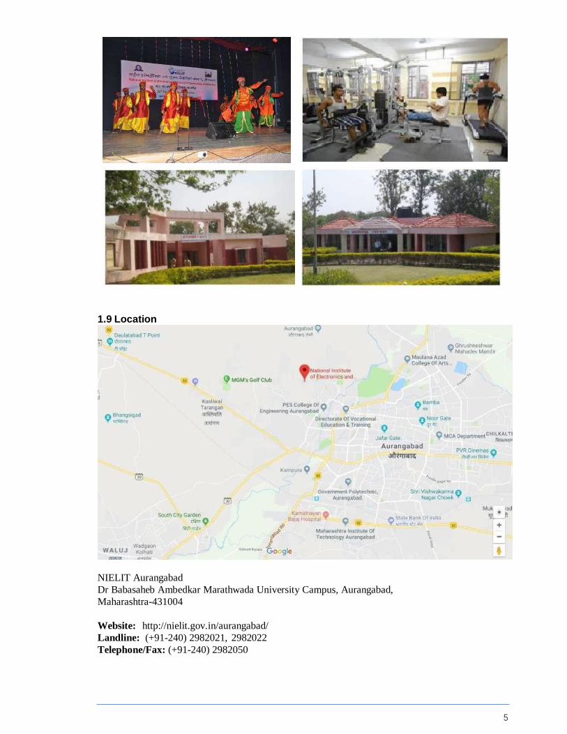
1.7 Other Amenities / Facilities:
Lecture Halls Uninterrupted Power (63 KVA DG Set)
Seminar Hall Cafeteria
Conference Hall Boy’s Hostel
Auditorium PG Boy’s Hostel
Local Area Network with 225 (100 Mbps)
Nodes.
Warden Quarters
Leased line internet connectivity Guest House
Library with NKN, MeitY Library Consortium
and National Digital library of MHRD, India
besides rich collection of Books, Journals and
Magazines (refer Annexure XXVI)
Vehicle Parking
Virtual Smart Class-Room facility Open Theatre
Placement Cell and Model Career Centre Record Room (143 Sqm)
Gymnasiums(Separate for Boys & Girls) Sports Facilities
Dramatics, dance and Extra-Curricular Jogging Track
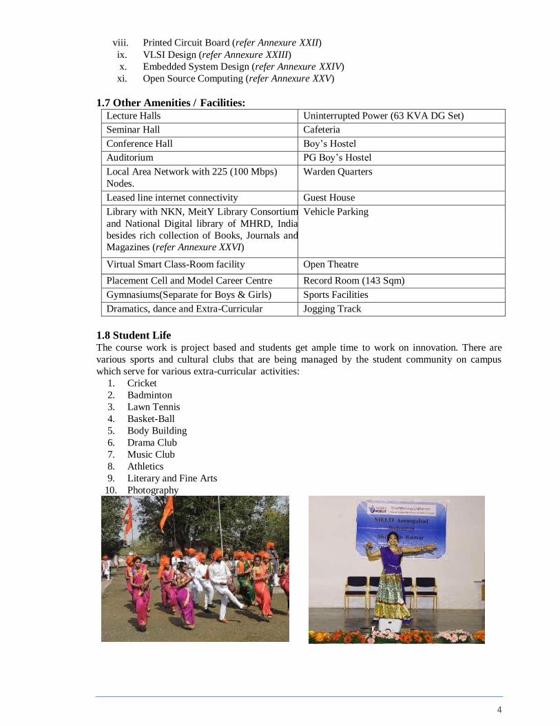
1.8 Student Life The course work is project based and students get ample time to work on innovation. There are
various sports and cultural clubs that are being managed by the student community on campus
which serve for various extra-curricular activities:
1. Cricket
2. Badminton
3. Lawn Tennis
4. Basket-Ball
5. Body Building
6. Drama Club
7. Music Club
8. Athletics
9. Literary and Fine Arts
10. Photography
5
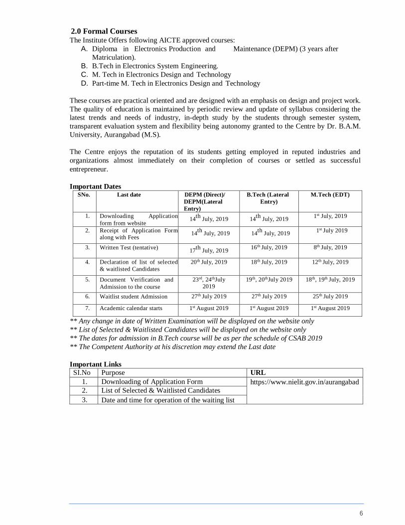
1.9 Location
NIELIT Aurangabad
Dr Babasaheb Ambedkar Marathwada University Campus, Aurangabad,
Maharashtra-431004
Website: http://nielit.gov.in/aurangabad/
Landline: (+91-240) 2982021, 2982022
Telephone/Fax: (+91-240) 2982050
6
2.0 Formal Courses The Institute Offers following AICTE approved courses:
A. Diploma in Electronics Production and Maintenance (DEPM) (3 years after
Matriculation).
B. B.Tech in Electronics System Engineering.
C. M. Tech in Electronics Design and Technology
D. Part-time M. Tech in Electronics Design and Technology
These courses are practical oriented and are designed with an emphasis on design and project work.
The quality of education is maintained by periodic review and update of syllabus considering the
latest trends and needs of industry, in-depth study by the students through semester system,
transparent evaluation system and flexibility being autonomy granted to the Centre by Dr. B.A.M.
University, Aurangabad (M.S).
The Centre enjoys the reputation of its students getting employed in reputed industries and
organizations almost immediately on their completion of courses or settled as successful
entrepreneur.
Important Dates SNo. Last date DEPM (Direct)/
DEPM(Lateral
Entry)
B.Tech (Lateral
Entry)
M.Tech (EDT)
1. Downloading Application
form from website 14
th July, 2019 14
th July, 2019
1st July, 2019
2. Receipt of Application Form along with Fees
14th
July, 2019 14th
July, 2019 1st July 2019
3. Written Test (tentative) 17
th July, 2019
16th July, 2019 8th July, 2019
4. Declaration of list of selected
& waitlisted Candidates
20th July, 2019 18th July, 2019 12th July, 2019
5. Document Verification and
Admission to the course
23rd, 24thJuly 2019
19th, 20thJuly 2019 18th, 19th July, 2019
6. Waitlist student Admission 27th July 2019 27th July 2019 25th July 2019
7. Academic calendar starts 1st August 2019 1st August 2019 1st August 2019
** Any change in date of Written Examination will be displayed on the website only
** List of Selected & Waitlisted Candidates will be displayed on the website only
** The dates for admission in B.Tech course will be as per the schedule of CSAB 2019
** The Competent Authority at his discretion may extend the Last date
Important Links
SI.No Purpose URL
1. Downloading of Application Form https://www.nielit.gov.in/aurangabad
2. List of Selected & Waitlisted Candidates
3. Date and time for operation of the waiting list
7
Process for Payment for Fees
Name of the Institute/Beneficiary National Institute of Electronics and Information
Technology(NIELIT)
Name of the Bank State Bank of India
Branch Samarth Nagar Aurangabad Maharashtra
Saving Bank Account Number 32078399585
IFSC/RTGS NO SBIN 0007919
Mode of Electronic Transfer NEFT, SBI Collect, Website: www.onlinesbi.com
Syllabus of Written test
Sno Purpose Syllabus Subjects
1. DEPM (Direct) X standard of CBSE Board Science, Mathematics & English
2. DEPM(Lateral Entry) XII standard of CBSE Board Physics, Chemistry and Mathematics & English
3. B.Tech (Lateral Entry) Diploma (Electronics) of Maharashtra State Board of
Technical Education
4. M.Tech (EDT) for both full time and part time
Gate 2019 Syllabus for (Common Subject of Electronics and Communication/Instrumentation Engg./Electrical Engg.)
Written Test for Admission 1. The written entrance test will be of 1½ hours duration
2. The question be of objective type, wherein the candidate is provided, multiple choice
answers
3. The candidate is required to mark the correct answer in the same sheet, provided to him/her.
4. The candidates are required to bring Pen, HB Pencil, Sharpner and Eraser.
5. Candidates are not allowed to take the Question/Answer booklet outside the exam hall.
6. Test will be in English Medium only.
7. Calculators, Mobile, Digital Diary, Logbooks, Pocket PCs are not allowed in the Exam Hall.
Important Information a. The student is required to submit the undertaking to agree to abide by the terms and
conditions of the institute and AICTE New Delhi at the time of admission in the
prescribed format as per Annexure V(C) and counter signed by parent / guardian.
b. The students are encouraged to interact with industry for getting familiar to industry
environment and to study & undertake real problems being faced by them as their project
work.
c. All the students (boarders as well as day scholars) are required to strictly abide by the rules
of the Institute / Centre, failing which disciplinary action may be taken against them.
d. The mess is attached to the hostel.
e. Mess–Canteen facility is compulsory for the students who reside in NIELIT Hostel.
10
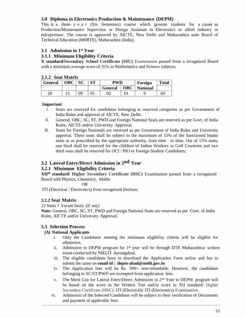
3.0 Diploma in Electronics Production & Maintenance (DEPM) This is a three- y e a r (Six Semesters) course which grooms students for a career as
Production/Maintenance Supervisor or Design Assistant in Electronics or allied industry or
entrepreneur. The course is approved by AICTE, New Delhi and Maharashtra state Board of
Technical Education (MSBTE), Maharashtra (India).
3.1 Admission in 1st Year
3.1.1 Minimum Eligibility Criteria X standard/Secondary School Certificate (SSC) Examination passed from a recognized Board
with a minimum average score of 35% in Mathematics and Science subjects.
3.1.2 Seat Matrix General OBC SC ST PWD Foreign
National
Total General OBC
28 15 09 05 02 01 9 69
Important
i. Seats are reserved for candidates belonging to reserved categories as per Government of
India Rules and approval of AICTE, New Delhi.
ii. General, OBC, SC, ST, PWD and Foreign National Seats are reserved as per Govt. of India
Rules, AICTE and/or University Approval.
iii. Seats for Foreign Nationals are reserved as per Government of India Rules and University
approval. These seats shall be subject to the maximum of 15% of the Sanctioned Intake
seats or as prescribed by the appropriate authority, from time to time. Out of 15% seats,
one third shall be reserved for the children of Indian Workers in Gulf Countries and two
third seats shall be reserved for OCI / PIO or Foreign Student Candidates;
3.2 Lateral Entry/Direct Admission in 2nd Year
3.2.1 Minimum Eligibility Criteria XIIth standard/ Higher Secondary Certificate (HSC) Examination passed from a recognized
Board with Physics, Chemistry, Maths
OR
ITI (Electrical / Electronics) from recognized Institute.
3.2.2 Seat Matrix
12 Seats + Vacant Seats (if any)
Note: General, OBC, SC, ST, PWD and Foreign National Seats are reserved as per Govt. of India
Rules, AICTE and/or University Approval.
3.3 Selection Process
(A) National Applicants
i. Only the Candidates meeting the minimum eligibility criteria will be eligible for
admission.
ii. Admission to DEPM program for 1st year will be through DTE Maharashtra/ written
exam conducted by NIELIT Aurangabad.
iii. The eligible candidates have to download the Application Form online and has to
submit the same on email id : [email protected]
iv. The Application fees will be Rs. 500/- non-refundable. However, the candidates
belonging to SC/ST/PWD are exempted from application fees.
v. The Merit List for Lateral Entry/Direct Admission in 2nd Year to DEPM program will
be based on the score in the Written Test and/or score in XII standard/ Higher
Secondary Certificate (HSC)/ ITI (Electrical)/ ITI (Electronics) Examination.
vi. Admission of the Selected Candidates will be subject to their verification of Documents
and payment of applicable fees.

11
vii. The category-wise Main List (selected) and Waiting List of the candidates for
admission to (year 2019-20) of DEPM Course will be displayed on the website and
Notice Board of this Institute.
viii. The date and time for operation of the waiting list shall also be declared along with the
list of selected candidates. All the waitlisted candidates should make themselves
available at the time of operation of the waiting list, otherwise their claim shall be
forfeited.
ix. The waitlisted candidates, available at the time of operation of the waiting list, shall be
provisionally admitted as per the merit of the category-wise waiting list.
x. The selected main and waiting list candidates are required to register on the day as
notified along with the list displayed by making payment as mentioned in Section 3.12
for admission in 1st year and Section 3.13 for Lateral Entry/Direct Admission in 2nd
Year, otherwise their claim shall be forfeited.
xi. Admission process of the DEPM Course is completed when the approved intake of
candidates as per Seat Matrix are provisionally admitted and registered or a time limit
decided by the competent authority is over, which- ever is earlier.
B) International Applicants for admission for 1st year
i. Admission of Foreign Nationals is subject to guidelines, laid down by Government of
India from time to time.
ii. Persons of Indian Origin (PIO) is an individual with foreign citizenship, except Pakistan
and Bangladesh, without “NRI” status, holding a Foreign Passport at the time of
applying for admission as well as during the study period and is himself/herself or
anyone/both of his/her parents or anyone/both of his/her grandparents is/was/were
Indian citizens.
iii. Children of Indian workers in the Gulf Countries (CIWG) are children of an Indian who
is working in Gulf Countries under relevant working visa.
iv. Non-Resident Indian (NRI) Candidate are Child/ward of the person having ‘NRI status’
as defined under section 6 of the Income Tax Act.
v. Foreign nationals may apply for admission to M.Tech (EDT) Full time course subject to
fulfilling the minimum eligibility requirements through proper channel.
vi. Their application will, however, be considered separately on first cum first serve basis
as per the procedure, mentioned in ANNEXURE-V(A)
vii. Foreign nationals are required to download and submit the application form for
eligibility cum admission (Annexure-V(A)) and declaration & undertaking format
(Annexure-V(B)) along with payment of Rs.5000/- or equivalent foreign currency (non-
refundable).
3.4 Cancellation of Secured Admissions
If any vacancy arises after completion of admission process, the vacancy may be filled on case
to case basis at the discretion of the Competent Authority as per below mentioned procedure:
i. Preference shall be given as per the ranking in common merit list.
ii. The Selected Students as per ranking in Merit List, who could not reach the Centre for
admission on the pre-intimated day because of legal and/or genuine reason(s) and
approaching/contacting the institute are first considered for filling the said vacancy.
iii. After (i) & (ii), the candidates, who have not been offered the admission and
approaching, may be considered.
3.5 Academic Calendar – Refer ANNEXURE – I
3.6 Scheme of Instruction:
Every student has to register for all the subjects of a Semester as mentioned below. A four weeks
mandatory vocational training is arranged for DEPM students during the summer vacation at the
end of IV Semester.
12
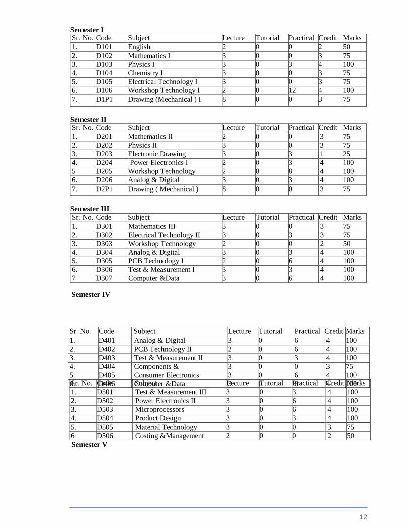
Semester I Sr. No. Code Subject Lecture Tutorial Practical Credit Marks
1. D101 English 2 0 0 2 50
2. D102 Mathematics I 3 0 0 3 75
3. D103 Physics I 3 0 3 4 100
4. D104 Chemistry I 3 0 0 3 75
5. D105 Electrical Technology I 3 0 0 3 75
6. D106 Workshop Technology I 2 0 12 4 100
7. D1P1 Drawing (Mechanical ) I 8 0 0 3 75
Semester II Sr. No. Code Subject Lecture Tutorial Practical Credit Marks
1. D201 Mathematics II 2 0 0 3 75
2. D202 Physics II 3 0 0 3 75
3. D203 Electronic Drawing 3 0 3 1 25
4. D204 Power Electronics I 2 0 3 4 100
5 D205 Workshop Technology 2 0 8 4 100
6. D206 Analog & Digital 3 0 3 4 100
7. D2P1 Drawing ( Mechanical ) 8 0 0 3 75
Semester III Sr. No. Code Subject Lecture Tutorial Practical Credit Marks
1. D301 Mathematics III 3 0 0 3 75
2. D302 Electrical Technology II 3 0 3 3 75
3. D303 Workshop Technology 2 0 0 2 50
4. D304 Analog & Digital 3 0 3 4 100
5. D305 PCB Technology I 2 0 6 4 100
6. D306 Test & Measurement I 3 0 3 4 100
7 D307 Computer &Data 3 0 6 4 100
Semester IV
Semester V
Sr. No. Code Subject Lecture Tutorial Practical Credit Marks
1. D401 Analog & Digital 3 0 6 4 100
2. D402 PCB Technology II 2 0 6 4 100
3. D403 Test & Measurement II 3 0 3 4 100
4. D404 Components & 3 0 0 3 75
5. D405 Consumer Electronics 3 0 6 4 100
6. D406 Computer &Data 3 0 6 4 100 Sr. No. Code Subject Lecture Tutorial Practical Credit Marks
1. D501 Test & Measurement III 3 0 3 4 100
2. D502 Power Electronics II 3 0 6 4 100
3. D503 Microprocessors 3 0 6 4 100
4. D504 Product Design 3 0 3 4 100
5. D505 Material Technology 3 0 0 3 75
6 D506 Costing &Management 2 0 0 2 50

13
Semester VI sr. Code Subject Lecture Tutorial Practical Credit Marks
1. D601 Microcontroller 3 0 6 4 100
2. D602 Maintenance & 2 0 6 4 100
3. D603 Project 0 0 0 10 250
3.7 Term Course Load:
i. In each semester, subject load varies from 22 to 28 credits per semester.
ii. During the course period, student has to pass certain number of subjects and complete
satisfactorily the assigned project work of 10 (ten) credits in the sixth semester.
iii. On valid grounds, the authority may advise a student, who is unable to complete the course
requirements in the normal period, to continue for an extra term
iv. Diploma should be completed within Six years
3.8 Assessment:
i. The overall performance of a student is evaluated by assigning equal weightage to all the
six semesters in order to maintain the quality of education.
ii. A student is permitted to appear for the semester examination subject to he or she has a
minimum attendance of 70% in theory and practical classes, completes all his/her sessional
assignments and clears all his/her dues.
iii. Non-appearance in any examination is treated as the student having secured zero mark in
that subject examination.
iv. The evaluation is based on an average weightage system. Every subject has credit points
based on the hours of study required.
v. Every student is assessed in a subject with equal weightage to sessional work and semester
examination, thereby making the students study regularly.
vi. Every student is awarded Grade points out of maximum 10 points in each subject. (based
on 10 Points Scale).
vii. Based on the Grade points obtained in each subject, Semester Grade Point Average (SGPA)
and then Cumulative Grade Point Average (CGPA) are computed as per ANNEXURE- II.
3.9 Award of Diploma:
i. A student must complete the minimum requirement of credits in maximum period of six
(6) years and must obtain a minimum CGPA of 3.3 in the course to qualify for award of
Diploma.
ii. The Diploma is awarded by Dr. Babasaheb Ambedkar Marathwada University,
Aurangabad
iii. It is also recognized by Directorate of Technical Education, Government of Maharashtra.
3.10 Scholarship
The institute encourages and provides assistance to all the students, particularly the reserved
category, to apply for the Central / State Govt. scholarship for reimbursement of tuition fee and
maintenance allowance as per State Govt. rules.
3.11 Assistance in Placement / Pursuing Higher Studies:
The Placement Cell of the Centre offers all assistance to the students for employment / self-
employment. Most of the students passing out from the Centre have good opportunities to build
their career.

14
3.12 DEPM Fee-Structure for 1st year admission for Academic year (2019-20)
SI. No. Particulars 1st Sem Fees (Rs.) 2nd Sem Fees (Rs.)
1. Tuition Fee 21000 21000
2. Caution Money Deposit* 1250 -- Sub total 22250 21000
Boy's Hostel Accommodation
3. Hostel Fee per Semester
(5 months)
9100 9100
4. Hostel Deposit* 2500 -- Sub total 11600 9100
Other Fees Particulars Fees
5. Backlog Exam Fee per semester (along with
junior batch regular exam settings)
300.00
6. Backlog Exam Fee separate exam setting)
per paper (with 1000.00
* Caution Money Deposits are onetime payment and returnable on completion of the course subject to
NIELIT rules.
*Mess charges are to be paid directly to mess manager on monthly basis.
Important:
i. SC/ST students are exempted from Tuition Fee(SCST/TSP Scheme), only Caution Money deposit
and hostel fee and deposit is to be paid
ii. Back log Exam Fee is applicable to all students appearing Back log Exams.
iii. There shall be an increase up to 10% in (Sl. No 1 & 3) in every academic year.
3.13 DEPM Lateral Entry Fee-Structure for Academic year (2019-20)
SI. No. Particulars 1st Sem Fees (Rs.) 2nd Sem Fees (Rs.)
1. Tuition Fee 21000 21000
2. Caution Money Deposit* 1250 -- Sub total 22250 21000
Boy's Hostel Accommodation
3. Hostel Fee per
Semester (5 months)
9100 9100
4. Hostel Deposit* 2500 -- Sub total 11600 9100
Other Fees Particulars Fees
5. Backlog Exam Fee per semester (along with
junior batch regular exam settings)
300.00
6. Backlog Exam Fee separate exam setting)
per paper (with 1000.00
* Caution Money Deposits are onetime payment and returnable on completion of the course subject to
NIELIT rules.
*Mess charges are to be paid directly to mess manager on monthly basis.
Important:
i. SC/ST students are exempted from Tuition Fee(SCST/TSP Scheme), only Caution Money deposit and hostel fee and deposit is to be paid.
ii. Back log Exam Fee is applicable to all students appearing Back log Exams.
iii. There shall be an increase up to 10% in (SI. No 1 & 3) in every academic year.

15
4.0 B.Tech.(Electronics System Engineering) This is four years (Eight Semesters) course approved by AICTE, New Delhi. This course is
designed to produces Qualified and skilled engineers capable of doing Innovative Design and
Development of Electronic Products. The prospective Engineers are groomed to adopt to changing
professional and societal needs through the project-oriented teaching approach. They will become
qualified to work in multiple sectors viz Public Sector, Telecom Industry, IT Industry, Automation
& Instrumentation Industry.
4.1 Eligibility for Admission in 1st Year Admission to B.Tech.(Electronics System Engineering) being offered by NIELIT Aurangabad will
be made on the basis of JEE (Main) conducted by Central Board of Secondary Education (CBSE)
on behalf of the Govt. of India. The Joint Seat Allocation (JoSAA) / Central Seat Allocation Board
(CSAB) will conduct centralized admissions for this course. For further details candidate are
advised to please visit http://josaa.nic.in/ and http://csab.nic.in/
About Joint Seat Allocation Authority (JoSAA)
The Joint Seat Allocation Authority (JoSAA) has been set up by the Ministry of Human
Resources Development (MHRD) to manage and regulate the joint seat allocation for admissions to
IITs, ISM, NITs, IIITs and Other-Government Funded Technical Institutes (Other-GFTIs).
Admission to all the academic programs offered by these Institutes will be made through a single
platform.
a. The Eligible candidate has to register and fill choices for academic program under JoSAA.
b. Document verification will be done for acceptance of and admitting to Institute of the
candidates selected by JoSAA.
c. Special vacant seat filling round (Special round) will be conducted by Central Seat
Allocation Board . For further details please visit : http://csab.nic.in
d. The selected candidate NIELIT Aurangabad should report to this Institute along with the all
original certificates & Xerox copy of each documents which the candidate had verified at
the reporting canter in the stipulated duration and time.
e. The candidate has to deposit the difference amount (if any) through NEFT / RTGS
f. The fee structure is given in Section 4.11.
4.1.1 Seat Matrix
General OBC SC ST PWD Student Studying
Abroad
Total General OBC
28 15 09 05 02 01 9 69
There is a separate quota of 9 seats for Student studying abroad. The interested candidates will
have to take admission through DASA (https://www.dasanit.org/).
4.2 Lateral Entry (Direct Second Year) in B.Tech.(Electronics System Engineering)
4.2.1 Minimum Eligibility Criteria Three Year Diploma Passed candidate of Electronics & allied streams with minimum 45% marks
(40 percent for SC/ST candidates) are eligible for Lateral Entry (Direct Second Year) in B.Tech.
4.2.2 Seat Matrix 12 Seats + Vacant Seats (if any)
Note: General, OBC, SC, ST and PWD are reserved as per Govt. of India Rules, AICTE and/or
University Approval.
4.2.3 Selection Process for Lateral Entry i. Only the Candidates meeting the minimum eligibility criteria will be eligible for
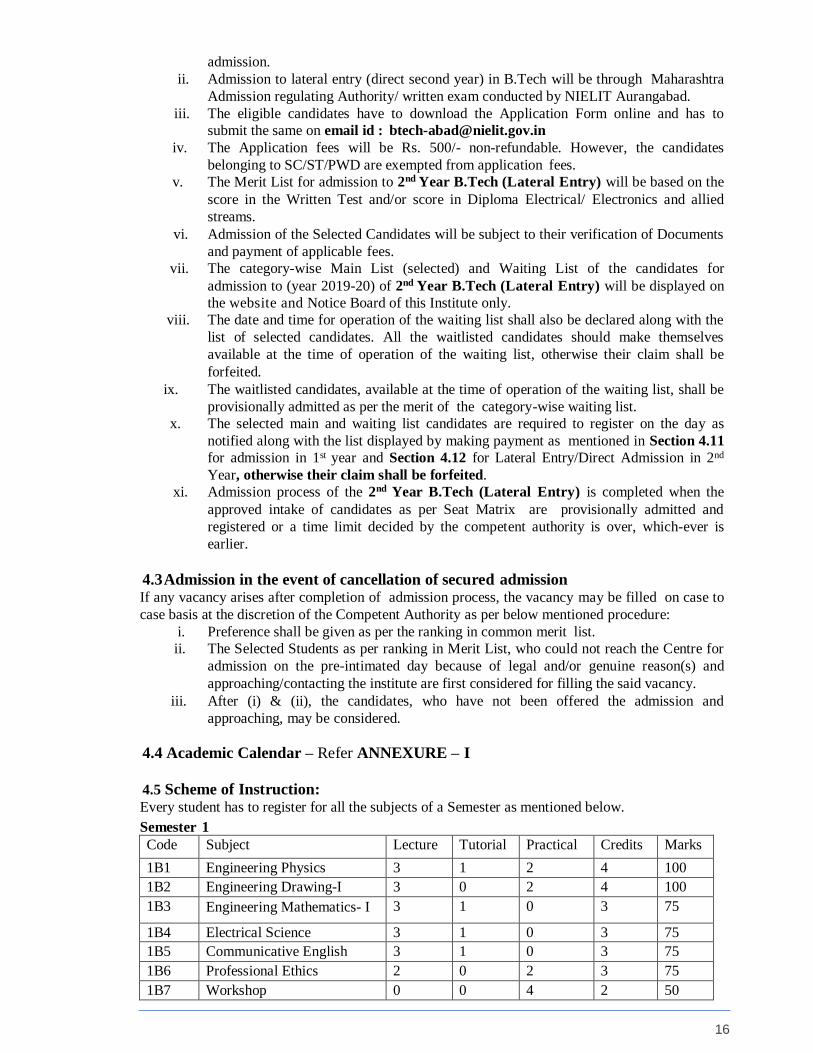
16
admission.
ii. Admission to lateral entry (direct second year) in B.Tech will be through Maharashtra
Admission regulating Authority/ written exam conducted by NIELIT Aurangabad.
iii. The eligible candidates have to download the Application Form online and has to
submit the same on email id : [email protected]
iv. The Application fees will be Rs. 500/- non-refundable. However, the candidates
belonging to SC/ST/PWD are exempted from application fees.
v. The Merit List for admission to 2nd Year B.Tech (Lateral Entry) will be based on the
score in the Written Test and/or score in Diploma Electrical/ Electronics and allied
streams.
vi. Admission of the Selected Candidates will be subject to their verification of Documents
and payment of applicable fees.
vii. The category-wise Main List (selected) and Waiting List of the candidates for
admission to (year 2019-20) of 2nd Year B.Tech (Lateral Entry) will be displayed on
the website and Notice Board of this Institute only.
viii. The date and time for operation of the waiting list shall also be declared along with the
list of selected candidates. All the waitlisted candidates should make themselves
available at the time of operation of the waiting list, otherwise their claim shall be
forfeited.
ix. The waitlisted candidates, available at the time of operation of the waiting list, shall be
provisionally admitted as per the merit of the category-wise waiting list.
x. The selected main and waiting list candidates are required to register on the day as
notified along with the list displayed by making payment as mentioned in Section 4.11
for admission in 1st year and Section 4.12 for Lateral Entry/Direct Admission in 2nd
Year, otherwise their claim shall be forfeited.
xi. Admission process of the 2nd Year B.Tech (Lateral Entry) is completed when the
approved intake of candidates as per Seat Matrix are provisionally admitted and
registered or a time limit decided by the competent authority is over, which-ever is
earlier.
4.3 Admission in the event of cancellation of secured admission If any vacancy arises after completion of admission process, the vacancy may be filled on case to
case basis at the discretion of the Competent Authority as per below mentioned procedure:
i. Preference shall be given as per the ranking in common merit list.
ii. The Selected Students as per ranking in Merit List, who could not reach the Centre for
admission on the pre-intimated day because of legal and/or genuine reason(s) and
approaching/contacting the institute are first considered for filling the said vacancy.
iii. After (i) & (ii), the candidates, who have not been offered the admission and
approaching, may be considered.
4.4 Academic Calendar – Refer ANNEXURE – I
4.5 Scheme of Instruction: Every student has to register for all the subjects of a Semester as mentioned below.
Semester 1
Code Subject Lecture Tutorial Practical Credits Marks
1B1 Engineering Physics 3 1 2 4 100
1B2 Engineering Drawing-I 3 0 2 4 100
1B3 Engineering Mathematics- I 3 1 0 3 75
1B4 Electrical Science 3 1 0 3 75
1B5 Communicative English 3 1 0 3 75
1B6 Professional Ethics 2 0 2 3 75
1B7 Workshop 0 0 4 2 50

17
17 4 10 22 550
Semester II
Code Subject Lecture Tutorial Practical Credits Marks
2B1 Digital Electronic Circuits 3 1 2 4 100
2B2 Electrical Networks 3 1 2 4 100
2B3 Analog Electronic Circuits 3 1 2 4 100
2B4 Engineering Mathematics-II 3 1 0 3 75
2B5 Engineering Chemistry 3 0 0 3 75
2B6 Engineering Mechanics 2 1 0 2 75
2B7 Engineering drawing II 0 0 4 2 50
17 5 10 22 575
Semester III
Code Subject Lecture Tutorial Practical Credits Marks
3B1 Power Electronics-I 3 1 2 4 100
3B2 Measurement
&Instrumentation
3 1 2 4 100
3B3 Computer programming
C, C++
3 1 2 4 100
3B4 Electronics Systems Engineering
3 1 2 4 100
3B5 Engineering
Mathematics-III
3 1 0 3 75
3B61
/3B62
General Elective-I
(Commerce/Management )
3 0 0 3 75
18 5 8 22 550
Semester IV
Code Subject Lecture Tutorial Practical Credits Marks
4B1 Product Design 3 1 2 4 100
4B2 Power Electronics-II 3 1 2 4 100
4B3 Microprocessor 3 1 2 4 100
4B4 Integrated Circuits and
Applications
3 0 2 4 100
4B5 Control System Engineering 3 1 0 3 75
4B6 Electronics Design Technology 3 1 0 3 75
18 5 8 22 550
Semester V
Code Subject Lecture Tutorial Practical Credits Marks
5B1 Industrial Design of Electronic
Equipment
3 1 2 4 100
5B2 Microcontroller &Peripherals 3 0 2 4 100
5B3 Digital System Design 3 0 2 4 100
5B4 Printed Circuit Board Technology-I 3 0 2 4 100
5B5 Signal and Systems 3 1 0 3 75
5B61/
5B62
Elective-II (Obj C++ Programming
/ Imbedded C)
3 1 0 3 75
5B7 Industrial training/visit/internship 0 0 2 1
18 3 10 23 550
18
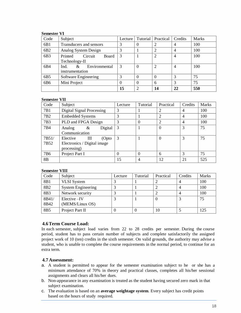
Semester VI
Code Subject Lecture Tutorial Practical Credits Marks
6B1 Transducers and sensors 3 0 2 4 100
6B2 Analog System Design 3 1 2 4 100
6B3 Printed Circuit Board
Technology-II
3 1 2 4 100
6B4 Ind. & Environmental instrumentation
3 0 2 4 100
6B5 Software Engineering 3 0 0 3 75
6B6 Mini Project 0 0 6 3 75
15 2 14 22 550
Semester VII
Code Subject Lecture Tutorial Practical Credits Marks
7B1 Digital Signal Processing 3 1 2 4 100
7B2 Embedded Systems 3 1 2 4 100
7B3 PLD and FPGA Design 3 0 2 4 100
7B4 Analog & Digital
Communication
3 1 0 3 75
7B51/
7B52
Elective III (Opto
Electronics / Digital image
processing)
3 1 0 3 75
7B6 Project Part I 0 0 6 3 75
8B 15 4 12 21 525
Semester VIII
Code Subject Lecture Tutorial Practical Credits Marks
8B1 VLSI System 3 1 2 4 100
8B2 System Engineering 3 1 2 4 100
8B3 Network security 3 1 2 4 100
8B41/
8B42
Elective –IV
(MEMS/Linux OS)
3 1 0 3 75
8B5 Project Part II 0 0 10 5 125
4.6 Term Course Load: In each semester, subject load varies from 22 to 28 credits per semester. During the course
period, student has to pass certain number of subjects and complete satisfactorily the assigned
project work of 10 (ten) credits in the sixth semester. On valid grounds, the authority may advise a
student, who is unable to complete the course requirements in the normal period, to continue for an
extra term.
4.7 Assessment: a. A student is permitted to appear for the semester examination subject to he or she has a
minimum attendance of 70% in theory and practical classes, completes all his/her sessional
assignments and clears all his/her dues.
b. Non-appearance in any examination is treated as the student having secured zero mark in that
subject examination.
c. The evaluation is based on an average weightage system. Every subject has credit points
based on the hours of study required.

19
d. Every student is assessed in a subject with equal weightage to sessional work and semester
examination, thereby making the students study regularly.
e. Every student is awarded Grade points out of maximum 10 points in each subject. (based on 10
Points Scale).
f. Based on the Grade points obtained in each subject, Semester Grade Point Average (SGPA)
and then Cumulative Grade Point Average (CGPA) are computed.
Note: For computation of SGPA CGPA, refer ANNEXURE- II.
4.8 Award of Degree: A student must complete the minimum requirement of credits in maximum period of eight
(8) years and must obtain a minimum CGPA of 3.3 in the course to qualify for award of
Degree. The Degree is awarded by Dr. Babasaheb Ambedkar Marathwada University, Aurangabad.
4.9 Scholarship The institute encourages and provides assistance to all the students, particularly the reserved
category, to apply for the Central / State Govt. scholarship for reimbursement of tuition fee and
maintenance allowance as per State Govt. rules. The tuition fee is exempted for SC/ST candidates
only, subject to his/her applying for the same and fulfilling the conditions.
4.10 Assistance in Placement / Pursuing Higher Studies: The Placement Cell of the Centre offers all assistance to the students for employment / self-
employment. Most of the students passing out from the Centre have good opportunities to build
their career.
4.11 B.Tech Fee-Structure for 1st year admission for Academic year (2019-19)
Sr. No.
Particulars
1st Sem. Fees &
Deposit (Rs.)
2nd Sem.
Fees (Rs.)
1 Tuition Fee 38000 38000
2 Caution Money Deposit * 1250 -
Sub Total 39250 38000
Boy's Hostel Accommodation
3 Hostel rent per Sem. ( 5 months) 9100 9100
4 Hostel Deposit* 2500 -
Sub Total 11600 9100
Other Fees
Particulars Fees (Rs.)
5
Backlog Exam Fee per semester (along with junior batch regular
exam settings)
400
6 Backlog Exam Fee per paper (with separate exam setting) 1000
*Caution Money Deposits are onetime payment and returnable on completion of the course subject to
NIELIT rules.
*Mess charges are to be paid directly to mess manager on monthly basis.
Important:
i. SC/ST students are exempted from Tuition Fee(SCST/TSP Scheme), only Caution Money deposit
and hostel fee and deposit is to be paid.
ii. Back log Exam Fee is applicable to all students appearing Back log Exams.
iii. There shall be an increase up to 10% in (SI. No 1 & 3) in every academic year.
20
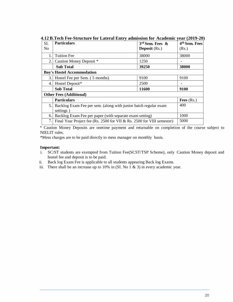
4.12 B.Tech Fee-Structure for Lateral Entry admission for Academic year (2019-20)
SI.
No
Particulars 3rd Sem. Fees &
Deposit (Rs.)
4th Sem. Fees
(Rs.)
1. Tuition Fee 38000 38000
2. Caution Money Deposit * 1250 -
Sub Total 39250 38000
Boy's Hostel Accommodation
3. Hostel Fee per Sem. ( 5 months) 9100 9100
4. Hostel Deposit* 2500 -
Sub Total 11600 9100
Other Fees (Additional)
Particulars Fees (Rs.)
5.
Backlog Exam Fee per sem. (along with junior batch regular exam
settings )
400
6. Backlog Exam Fee per paper (with separate exam setting) 1000
7. Final Year Project fee (Rs. 2500 for VII & Rs. 2500 for VIII semester) 5000
* Caution Money Deposits are onetime payment and returnable on completion of the course subject to
NIELIT rules.
*Mess charges are to be paid directly to mess manager on monthly basis.
Important:
i. SC/ST students are exempted from Tuition Fee(SCST/TSP Scheme), only Caution Money deposit and
hostel fee and deposit is to be paid.
ii. Back log Exam Fee is applicable to all students appearing Back log Exams.
iii. There shall be an increase up to 10% in (SI. No 1 & 3) in every academic year.

20
5.0 MASTER OF TECHNOLOGY (ELECTRONICS DESIGN AND TECHNOLOGY)
[M.Tech (EDT)] Full Time Course This is four semesters (2 years) AICTE approved Postgraduate course with the Degree awarded by
Dr. Babasaheb Ambedkar Marathwada University, Aurangabad (MS).
5.1 Eligibility a. Admission to M. Tech. degree courses are made on the basis of candidate's score in the
GATE examination.
b. Seats are first filled by admitting GATE qualified candidates and Remaining vacant seats are
offered to Non-GATE* candidates, both GATE qualified and Non- GATE candidates must
have minimum of 55 percent marks (50 percent for SC/ST candidates) in their B.E. /
B.Tech Degree or equivalent in Electronics / Electrical /Telecommunication /
Instrumentation engineering etc. from a recognized University.
c. Only GATE qualified candidates are eligible for scholarship.
d. The Industry Sponsored Candidates should have been serving in Academic Institution/
Industry/ R&D organization engaged in electronic product or system development for at
least two years after completion of B.E. /B. Tech. in relevant area. He/ She should produce
necessary sponsorship certificate along with application in the prescribed form given in
Annexure XIII *Non-GATE candidates: Candidates who have not appeared for GATE exam
5.2 Intake (28 Seats) Five seats are reserved for Industry Sponsored Candidates and three seats are reserved for Non-
Resident Indian (NRI) / Persons of Indian Origin (PIO) / Children of Indian workers in the Gulf
Countries (CIWG) quota. Distribution of remaining seats is as under:
Non-Sponsored category
General 10
OBC 5
SC 3
ST 2
Total 20
Important
a. Seats are reserved as per Govt. of India Rules, AICTE and/or University Approval.
b. A quota of 15 % is reserved for the SC candidates, 7.5% for ST candidates, and 27% for
Other Backward Classes.
c. Candidates selected against the quota for persons with disabilities (3%) as per PWD Act
1995 are placed in the appropriate category viz.SC/ST/OBC/General candidates depending
upon the category to which they belong in the roster meant for reservation of
SCs/STs/OBCs.
5.3 Selection Process for Admission for 1st year M. Tech (EDT) Full time
(A) National Applicants
i. Only the Candidates meeting the minimum eligibility criteria will be eligible for admission.
ii. The eligible candidates have to download the Application Form from website and has to
submit the same on email id : [email protected]
iii. The selection for admission to M.Tech (EDT) Full Time Course, will be based on GATE
marks out of 100 for the current year/ valid GATE score (out of 1000) and/or score in the
written test. List of Shortlisted Candidates will be displayed on the institute website.
iv. Admission of the Selected Candidates will be subject to their verification of Documents and
payment of applicable fees.
v. The date and time for operation of the waiting list shall also be declared along
21
with the list of selected candidates. All the waitlisted candidates should make themselves
available at the time of operation of the waiting list, otherwise their claim shall be forfeited.
vi. The waitlisted candidates, available at the time of operation of the waiting list, shall be
provisionally admitted as per the merit of the category-wise waiting list.
vii. The selected main and waiting list candidates are required to register on the day as notified
along with the list displayed by making payment as mentioned in Section 5.13 for
admission.
viii. The decision of Executive Director, NIELIT, Aurangabad in respect of selection and closing
of admission will be final. Canvassing in any form will lead to disqualification.
B) International Applicants
i. Admission of Foreign Nationals is subject to guidelines, laid down by Government of India
from time to time.
ii. Persons of Indian Origin (PIO) is an individual with foreign citizenship, except Pakistan
and Bangladesh, without “NRI” status, holding a Foreign Passport at the time of applying
for admission as well as during the study period and is himself/herself or anyone/both of
his/her parents or anyone/both of his/her grandparents is/was/were Indian citizens.
iii. Children of Indian workers in the Gulf Countries (CIWG) are children of an Indian who is
working in Gulf Countries under relevant working visa.
iv. Non-Resident Indian (NRI) Candidate are Child/ward of the person having ‘NRI status’ as
defined under section 6 of the Income Tax Act.
v. Foreign nationals may apply for admission to M.Tech (EDT) Full time course subject to
fulfilling the minimum eligibility requirements through proper channel.
vi. Their application will, however, be considered separately on first cum first serve basis as
per the procedure, mentioned in ANNEXURE-V(A)
vii. Foreign nationals are required to download and submit the application form for eligibility
cum admission (Annexure-V(A)) and declaration & undertaking format (Annexure-V(B))
along with payment of Rs.5000/- or equivalent foreign currency (non-refundable).
5.4 Cancellation of Secured Admissions If any vacancy arises after completion of admission process, the vacancy may be filled on case to
case basis at the discretion of the Competent Authority as per below mentioned procedure:
i. Preference shall be given as per the ranking in common merit list.
ii. The Selected Students as per ranking in Merit List, who could not reach the Centre for
admission on the pre-intimated day because of legal and/or genuine reason(s) and
approaching/contacting the institute are first considered for filling the said vacancy.
iii. After (i) & (ii), the candidates, who have not been offered the admission and
approaching, may be considered.
5.5 Academic Calendar – Refer ANNEXURE – I
5.6 Scheme of Instruction: Every student has to register for all the subjects of a Semester as mentioned below.
22
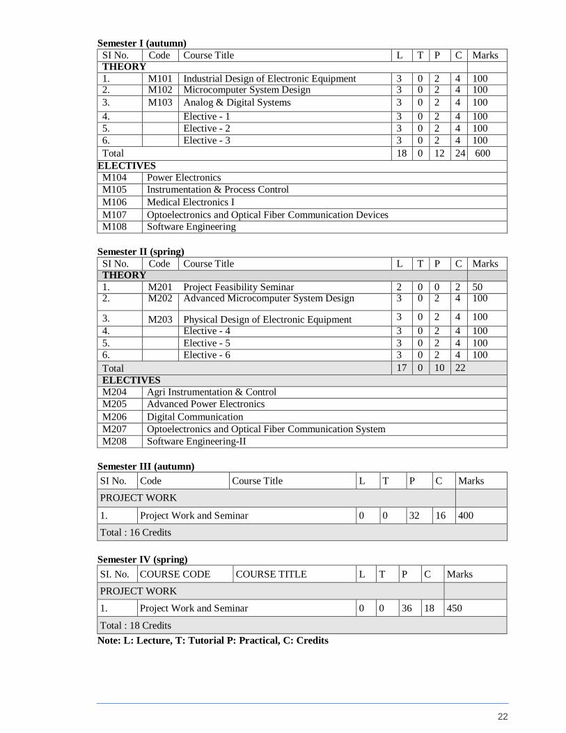
Semester I (autumn)
SI No. Code Course Title L T P C Marks THEORY
1. M101 Industrial Design of Electronic Equipment 3 0 2 4 100 2. M102 Microcomputer System Design 3 0 2 4 100
3. M103 Analog & Digital Systems 3 0 2 4 100
4. Elective - 1 3 0 2 4 100
5. Elective - 2 3 0 2 4 100
6. Elective - 3 3 0 2 4 100
Total 18 0 12 24 600
ELECTIVES
M104 Power Electronics
M105 Instrumentation & Process Control
M106 Medical Electronics I
M107 Optoelectronics and Optical Fiber Communication Devices
M108 Software Engineering
Semester II (spring)
SI No. Code Course Title L T P C Marks THEORY
1. M201 Project Feasibility Seminar 2 0 0 2 50 2. M202 Advanced Microcomputer System Design 3 0 2 4 100
3. M203 Physical Design of Electronic Equipment 3 0 2 4 100
4. Elective - 4 3 0 2 4 100
5. Elective - 5 3 0 2 4 100
6. Elective - 6 3 0 2 4 100
Total 17 0 10 22
ELECTIVES
M204 Agri Instrumentation & Control
M205 Advanced Power Electronics
M206 Digital Communication
M207 Optoelectronics and Optical Fiber Communication System
M208 Software Engineering-II
Semester III (autumn)
SI No. Code Course Title L T P C Marks
PROJECT WORK
1. Project Work and Seminar 0 0 32 16 400
Total : 16 Credits
Semester IV (spring)
SI. No. COURSE CODE COURSE TITLE L T P C Marks
PROJECT WORK
1. Project Work and Seminar 0 0 36 18 450
Total : 18 Credits
Note: L: Lecture, T: Tutorial P: Practical, C: Credits
23
5.7 Term Course Load: i. In each semester, subject load varies from 16 to 24 credits per semester.
ii. On valid grounds, the authority may advise a student, who is unable to complete the course
requirements in the normal period, to continue for an extra term
5.8 Assessment: i. The overall performance of a student is evaluated by assigning equal weightage to all the
four semesters in order to maintain the quality of education.
ii. A student is permitted to appear for the semester examination subject to he or she has a
minimum attendance of 70% in theory and practical classes, completes all his/her sessional
assignments and clears all his/her dues.
iii. Non-appearance in any examination is treated as the student having secured zero mark in
that subject examination.
iv. The evaluation is based on an average weightage system. Every subject has credit points
based on the hours of study required.
v. Every student is assessed in a subject with equal weightage to sessional work and semester
examination, thereby making the students study regularly.
vi. Every student is awarded Grade points out of maximum 10 points in each subject. (based
on 10 Points Scale).
vii. Based on the Grade points obtained in each subject, Semester Grade Point Average (SGPA)
and then Cumulative Grade Point Average (CGPA) are computed as per ANNEXURE- II.
5.9 Award of PG Degree: A student must complete the minimum requirement of credits in maximum period of four
(04) years and must obtain a minimum CGPA of 3.3 in the course to qualify for award of
Degree. The PG Degree is awarded by Dr. Babasaheb Ambedkar Marathwada University,
Aurangabad (MS).
5.10 Scholarship i. Non-sponsored students, admitted to the M Tech (EDT) course, provided they have a valid
GATE SCORE, are eligible for the scholarship of Rs. 12400/- * per month, subject to
sanction and receipt of the said amount from AICTE New Delhi. Disbursement of PG-
Scholarships is through direct cash transfer scheme through AICTE portal subject to his/her
applying for the same and fulfilling the conditions. The award of scholarship and its
continuation is subject to regular attendance, satisfactory progress, good conduct and
abiding by the rules of the Institute.
ii. Sponsored students, or students not having a valid GATE SCORE are not entitled for the
said scholarship.
iii. The tuition fee is exempted for SC/ST candidates only, subject to his/her applying for the
same and fulfilling the conditions.
iv. It is obligatory for every student, granted admission to M. Tech (EDT) and awarded
scholarship, to undertake work related to teaching and research activities as assigned to him
/ her.
* Subject to the policies of GOI
5.11 Assistance in Placement / Pursuing Higher Studies: The Placement Cell of the Centre offers all assistance to the students for employment / self-
employment. Most of the students passing out from the Centre have good opportunities to build
their career.

24
5.12 Refund of fees in the event of cancellation of admission a. There will be no refund
i. If admission is cancelled after the 1st Semester is over.
ii. If admission is cancelled in 1st Semester and the vacancy is not filled.
b. However, if admission is cancelled in 1st Semester and the vacancy is filled, then Refund
of fees will be as under: -
i. Student leaving before start of the course – Entire fee minus Rs1000/- (Rupees One
Thousand only) as processing fee.
ii. Student leaving after start of the course but before closing of admissions- Entire fee
minus Rs1000/- or (Semester fee/6), whichever is higher.
iii. Student leaving after start of the course and closing of admissions-Entire fee minus
[Rs1000/- + (Semester fee/6) x Registered Period in number of months)]
iv. For students staying in hostel, [(Hostel Rent/6) x Registered Period in number of
Months] will be deducted from Semester hostel fee paid by the student.
v. All the deposits will be refunded after adjusting student dues, if any.
vi. Fraction of month will be treated as full month.
5.13 M.Tech. Fee-Structure, Academic year (2019-20) Admission
Sr. No.
Particulars
1st Semester Fees
&Deposit (₹)
2nd Sem
Fees (₹)
1. Tuition Fee 46000/- 46000/-
2. Caution Money Deposit * 1250 -
Sub Total 47250/- 46000/-
Boy's Hostel Accommodation
3. Hostel Fee per Semester ( 5 months) 9100 9100
4. Hostel Deposit* 2500 -
5. Sub Total 11600 9100
Other Fees
Particulars Fees (₹)
6. Backlog Exam Fee per semester per paper (along with junior batch
regular exam settings)
500
7. Backlog Exam Fee per semester per paper (with separate exam setting) 1000
8. Project fee payable only in III &IV semester separately 5000
* Caution Money Deposits are onetime payment and returnable on completion of the course subject
to NIELIT rules.
*Mess charges are to be paid directly to mess manager on monthly basis.
Important:
i. SC/ST students are exempted from Tuition Fee(SCST/TSP Scheme), only Caution Money deposit
and hostel fee and deposit is to be paid.
ii. Back log Exam Fee is applicable to all students appearing Back log Exams.
iii. There shall be an increase up to 10% in (Sl. No 1 & 3) in every academic year.

25
6.0 MASTER OF TECHNOLOGY (ELECTRONICS DESIGN AND
TECHNOLOGY) [M.Tech (EDT)] PART TIME COURSE This is six semesters (3 years) AICTE approved course for working professionals with the Degree
awarded by Dr. Babasaheb Ambedkar Marathwada University, Aurangabad (MS).
6.1 Eligibility a. B.E. / B.Tech Degree or equivalent in Electronics / Electrical /Telecommunication
/Instrumentation engineering etc from a recognized University with at least 55% of marks.
b. The candidate should have been serving in Academic Institution/ Industry/ R&D
organization engaged in electronic product or system development for at least two years
after completion of B.E./ B. Tech. degree
c. The candidate should be sponsored by the employer.
d. His/ Her working place should be within 60 km distance from the institute.
e. He should produce necessary sponsorship certificate along with application in the
prescribed form given in Annexure XIII.
6.2 Intake: 24 Seats
6.3 Selection Process i. Only the Candidates meeting the eligibility criteria will be eligible for admission.
ii. The eligible candidates have to download the Application Form from website and has to submit the
same on email id : [email protected]
iii. The selection for admission to M.Tech (EDT) part Time Course, will be based on score in
the written test. List of Shortlisted Candidates will be displayed on the institute website.
iv. Admission of the Selected Candidates will be subject to their verification of Documents and
payment of applicable fees.
v. The date and time for operation of the waiting list shall also be declared along with the list
of selected candidates. All the waitlisted candidates should make themselves available at
the time of operation of the waiting list, otherwise their claim shall be forfeited.
vi. The waitlisted candidates, available at the time of operation of the waiting list, shall be
provisionally admitted as per the merit of the category-wise waiting list.
vii. The selected main and waiting list candidates are required to register on the day as notified
along with the list displayed by making payment as mentioned in
Section 4.2.13 for admission.
viii. The decision of Executive Director, NIELIT, Aurangabad in respect of selection and closing
of admission will be final. Canvassing in any form will lead to disqualification.
6.4 Admission in the event of cancellation of secured admission If any vacancy arises due to leaving the course by a registered student after completion of
admission process, the vacancy may be filled on case to case basis at the discretion of the
Executive Director as the admission process is completed, by following below mentioned
procedure:
i. Preference shall be given as per the ranking in common merit list.
ii. The Selected Students as per ranking in Merit List, who could not reach the Centre for
admission on the pre-intimated day because of legal and/or genuine reason(s) and
approaching/contacting the institute are first considered for filling the said vacancy.
iii. After (i) & (ii), the candidates, who have not been offered the admission and
approaching, may be considered.
26
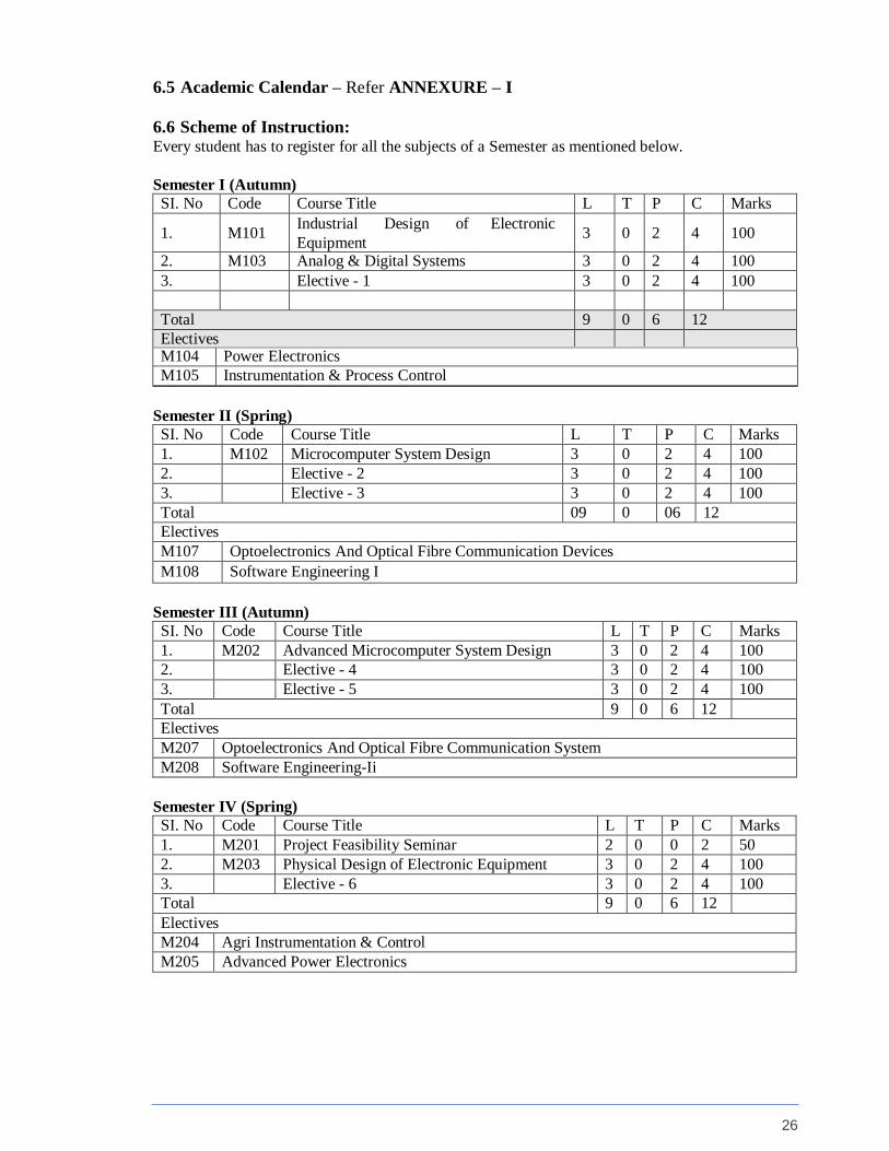
6.5 Academic Calendar – Refer ANNEXURE – I
6.6 Scheme of Instruction: Every student has to register for all the subjects of a Semester as mentioned below.
Semester I (Autumn)
SI. No Code Course Title L T P C Marks
1. M101 Industrial Design of Electronic
Equipment 3 0 2 4 100
2. M103 Analog & Digital Systems 3 0 2 4 100
3. Elective - 1 3 0 2 4 100
Total 9 0 6 12
Electives
M104 Power Electronics
M105 Instrumentation & Process Control
Semester II (Spring)
SI. No Code Course Title L T P C Marks
1. M102 Microcomputer System Design 3 0 2 4 100
2. Elective - 2 3 0 2 4 100
3. Elective - 3 3 0 2 4 100
Total 09 0 06 12
Electives
M107 Optoelectronics And Optical Fibre Communication Devices
M108 Software Engineering I
Semester III (Autumn)
SI. No Code Course Title L T P C Marks
1. M202 Advanced Microcomputer System Design 3 0 2 4 100
2. Elective - 4 3 0 2 4 100
3. Elective - 5 3 0 2 4 100
Total 9 0 6 12
Electives
M207 Optoelectronics And Optical Fibre Communication System
M208 Software Engineering-Ii
Semester IV (Spring)
SI. No Code Course Title L T P C Marks
1. M201 Project Feasibility Seminar 2 0 0 2 50
2. M203 Physical Design of Electronic Equipment 3 0 2 4 100
3. Elective - 6 3 0 2 4 100
Total 9 0 6 12
Electives
M204 Agri Instrumentation & Control
M205 Advanced Power Electronics

27
Semester V (Autumn)
SI. No Code Course Title L T P C Marks
Project Work
1. Project Work and Seminar 0 0 32 16 400
Total : 16 Credits
Semester VI (Spring)
SI. No Course Code Course Title L T P C Marks
Project Work
1. Project Work and Seminar 0 0 36 18 450
Total : 18 Credits
Note: L: Lecture, T: Tutorial P: Practical, C: Credits
6.7 Term Course Load: i. In each semester, subject load varies from 16 to 24 credits per semester.
ii. On valid grounds, the authority may advise a student, who is unable to complete the course
requirements in the normal period, to continue for an extra term
6.8 Assessment: i. The overall performance of a student is evaluated by assigning equal weightage to all the
four semesters in order to maintain the quality of education.
ii. A student is permitted to appear for the semester examination subject to he or she has a
minimum attendance of 70% in theory and practical classes, completes all his/her sessional
assignments and clears all his/her dues.
iii. Non-appearance in any examination is treated as the student having secured zero mark in
that subject examination.
iv. The evaluation is based on an average weightage system. Every subject has credit points
based on the hours of study required.
v. Every student is assessed in a subject with equal weightage to sessional work and semester
examination, thereby making the students study regularly.
vi. Every student is awarded Grade points out of maximum 10 points in each subject. (based
on 10 Points Scale).
vii. Based on the Grade points obtained in each subject, Semester Grade Point Average (SGPA)
and then Cumulative Grade Point Average (CGPA) are computed as per ANNEXURE- II.
6.9 Award of PG Degree: A student must complete the minimum requirement of credits in maximum period of seven
(07) years and must obtain a minimum CGPA of 3.3 in the course to qualify for award of Degree.
The PG Degree is awarded by Dr. Babasaheb Ambedkar Marathwada University, Aurangabad
(MS).
6.10 Refund of fees in the event of cancellation of admission: a. There will be no refund
i. If admission is cancelled after the 1st Semester is over.
ii. If admission is cancelled in 1st Semester and the vacancy is not filled.
b. However, if admission is cancelled in 1st Semester and the vacancy is filled, then Refund
of fees will be as under: -
i. Student leaving before start of the course – Entire fee minus Rs1000/- (Rupees One
Thousand only) as processing fee.

28
ii. Student leaving after start of the course but before closing of admissions- Entire fee
minus Rs1000/- or (Semester fee/6), whichever is higher.
iii. Student leaving after start of the course and closing of admissions-Entire fee minus
[Rs1000/- + (Semester fee/6) x Registered Period in number of months)]
iv. For students staying in hostel, [(Hostel Rent/6) x Registered Period in number of
Months] will be deducted from Semester hostel fee paid by the student.
v. All the deposits will be refunded after adjusting student dues, if any.
vi. Fraction of month will be treated as full month.
6.11 M.Tech. Fee-Structure, Academic year (2019-20) Admission
SI. No.
Particulars
1st Semester Fees
&Deposit (₹)
2nd Sem
Fees (₹)
1. Tuition Fee 46000/- 46000/-
2. Caution Deposit * 1250 -
Sub Total 47250/- 46000/-
Boy's Hostel Accommodation
3. Hostel Fee per Semester (5 months) 9100 9100
4. Hostel Deposit* 2500 -
Sub Total 11600 9100
Other Fees
Particulars Fees (₹)
5. Backlog Exam Fee per semester per paper (along with junior batch
regular exam settings)
500
6. Backlog Exam Fee per semester per paper (with separate exam
setting)
1000
7. Project fee payable only in III &IV semester separately 5000
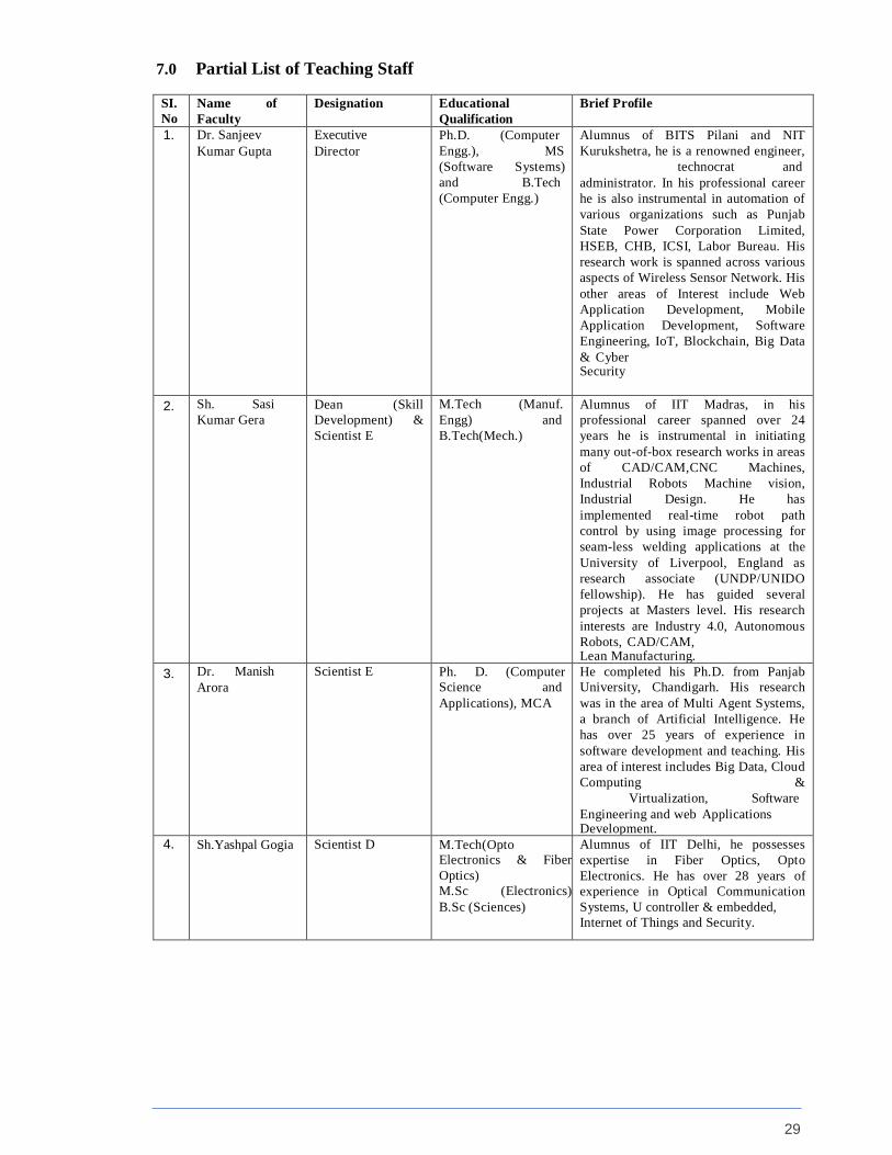
29
7.0 Partial List of Teaching Staff
SI.
No
Name of
Faculty
Designation Educational
Qualification
Brief Profile
1. Dr. Sanjeev
Kumar Gupta
Executive
Director
Ph.D. (Computer
Engg.), MS
(Software Systems)
and B.Tech
(Computer Engg.)
Alumnus of BITS Pilani and NIT
Kurukshetra, he is a renowned engineer,
technocrat and
administrator. In his professional career
he is also instrumental in automation of
various organizations such as Punjab
State Power Corporation Limited,
HSEB, CHB, ICSI, Labor Bureau. His
research work is spanned across various
aspects of Wireless Sensor Network. His
other areas of Interest include Web
Application Development, Mobile
Application Development, Software
Engineering, IoT, Blockchain, Big Data
& Cyber Security
2. Sh. Sasi
Kumar Gera
Dean (Skill
Development) &
Scientist E
M.Tech (Manuf.
Engg) and
B.Tech(Mech.)
Alumnus of IIT Madras, in his
professional career spanned over 24
years he is instrumental in initiating
many out-of-box research works in areas
of CAD/CAM,CNC Machines,
Industrial Robots Machine vision,
Industrial Design. He has
implemented real-time robot path
control by using image processing for
seam-less welding applications at the
University of Liverpool, England as
research associate (UNDP/UNIDO
fellowship). He has guided several
projects at Masters level. His research
interests are Industry 4.0, Autonomous
Robots, CAD/CAM, Lean Manufacturing.
3. Dr. Manish
Arora
Scientist E Ph. D. (Computer
Science and
Applications), MCA
He completed his Ph.D. from Panjab
University, Chandigarh. His research
was in the area of Multi Agent Systems,
a branch of Artificial Intelligence. He
has over 25 years of experience in
software development and teaching. His
area of interest includes Big Data, Cloud
Computing &
Virtualization, Software
Engineering and web Applications Development.
4. Sh.Yashpal Gogia Scientist D M.Tech(Opto Electronics & Fiber
Optics)
M.Sc (Electronics)
B.Sc (Sciences)
Alumnus of IIT Delhi, he possesses
expertise in Fiber Optics, Opto
Electronics. He has over 28 years of
experience in Optical Communication
Systems, U controller & embedded,
Internet of Things and Security.
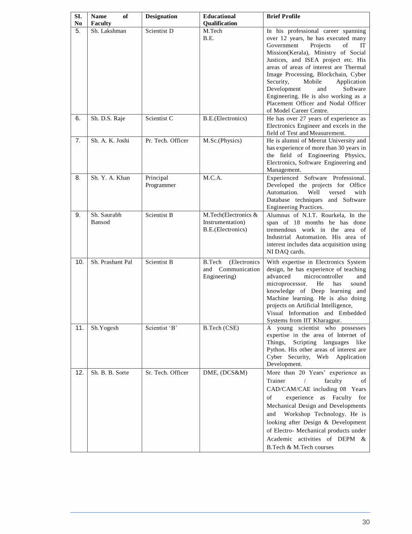
30
SI.
No
Name of
Faculty
Designation Educational
Qualification
Brief Profile
5. Sh. Lakshman Scientist D M.Tech
B.E.
In his professional career spanning
over 12 years, he has executed many
Government Projects of IT
Mission(Kerala), Ministry of Social
Justices, and ISEA project etc. His
areas of areas of interest are Thermal
Image Processing, Blockchain, Cyber
Security, Mobile Application
Development and Software
Engineering. He is also working as a
Placement Officer and Nodal Officer
of Model Career Centre.
6. Sh. D.S. Raje Scientist C B.E.(Electronics) He has over 27 years of experience as
Electronics Engineer and excels in the
field of Test and Measurement.
7. Sh. A. K. Joshi Pr. Tech. Officer M.Sc.(Physics) He is alumni of Meerut University and
has experience of more than 30 years in
the field of Engineering Physics,
Electronics, Software Engineering and
Management.
8. Sh. Y. A. Khan Principal
Programmer
M.C.A. Experienced Software Professional.
Developed the projects for Office
Automation. Well versed with
Database techniques and Software
Engineering Practices.
9. Sh. Saurabh
Bansod
Scientist B M.Tech(Electronics &
Instrumentation)
B.E.(Electronics)
Alumnus of N.I.T. Rourkela, In the
span of 18 months he has done
tremendous work in the area of
Industrial Automation. His area of
interest includes data acquisition using
NI DAQ cards.
10. Sh. Prashant Pal Scientist B B.Tech (Electronics
and Communication
Engineering)
With expertise in Electronics System
design, he has experience of teaching
advanced microcontroller and
microprocessor. He has sound
knowledge of Deep learning and
Machine learning. He is also doing
projects on Artificial Intelligence,
Visual Information and Embedded
Systems from IIT Kharagpur.
11. Sh.Yogesh Scientist ‘B’ B.Tech (CSE) A young scientist who possesses
expertise in the area of Internet of
Things, Scripting languages like
Python. His other areas of interest are
Cyber Security, Web Application
Development.
12. Sh. B. B. Sorte Sr. Tech. Officer DME, (DCS&M) More than 20 Years’ experience as
Trainer / faculty of
CAD/CAM/CAE including 08 Years
of experience as Faculty for
Mechanical Design and Developments
and Workshop Technology. He is
looking after Design & Development
of Electro- Mechanical products under
Academic activities of DEPM &
B.Tech & M.Tech courses
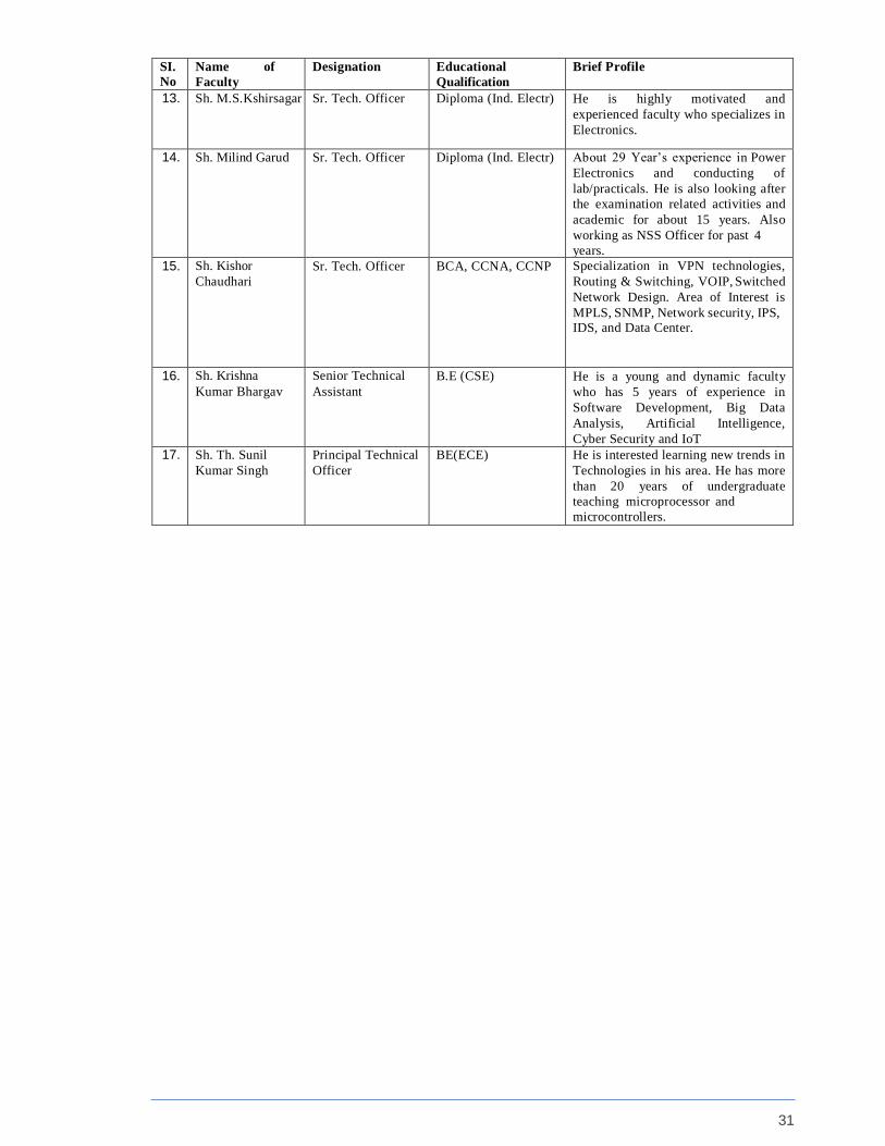
31
SI.
No
Name of
Faculty
Designation Educational
Qualification
Brief Profile
13. Sh. M.S.Kshirsagar Sr. Tech. Officer Diploma (Ind. Electr) He is highly motivated and
experienced faculty who specializes in
Electronics.
14. Sh. Milind Garud Sr. Tech. Officer Diploma (Ind. Electr) About 29 Year’s experience in Power
Electronics and conducting of
lab/practicals. He is also looking after
the examination related activities and
academic for about 15 years. Also
working as NSS Officer for past 4
years.
15. Sh. Kishor
Chaudhari
Sr. Tech. Officer BCA, CCNA, CCNP Specialization in VPN technologies,
Routing & Switching, VOIP, Switched
Network Design. Area of Interest is
MPLS, SNMP, Network security, IPS, IDS, and Data Center.
16. Sh. Krishna
Kumar Bhargav
Senior Technical
Assistant
B.E (CSE) He is a young and dynamic faculty
who has 5 years of experience in
Software Development, Big Data
Analysis, Artificial Intelligence,
Cyber Security and IoT
17. Sh. Th. Sunil
Kumar Singh
Principal Technical
Officer
BE(ECE) He is interested learning new trends in
Technologies in his area. He has more
than 20 years of undergraduate
teaching microprocessor and
microcontrollers.

32
8.0 Placement Assistance and Support Students of the Centre are trained to become
R&D engineers. In Course curriculum there is
emphasize on Innovation,
Design and Development of Electronic Product.
The Centre has also sign an MoU with Chamber
of Marathwada Industries and Agriculture
(CMIA) to platform to Startup Aspirants
students. In association with Directorate of
Employment, Ministry of Labour &
Employment (MoLE), a Model Career Centre is
also functioning to provide a variety of
employment related services. Apart from this an
independent Placement Cell is providing
Placement support and assistance to all the
students. Almost all the students of the Institute
gets career opportunities of their choice.
1. MoU with CMIA
CMIA is a group organization representing
around 650 small scale / medium scale / large
scale industries including the Multinational
Companies (MNC's) of the Maharashtra. An
MoU was signed with CMIA in November, 2017
for referral of Students Projects which have
potential of developing into scalable business
models and also adoption of their business
startup ideas. The support for internship and
employment to our students in member
companies of CMIA was another goal of the
MoU.
2. Model Career Centre
In association with Directorate of Employment,
Ministry of Labour and Employment(MoLE),
NIELIT is providing a variety of employment
related services to students of the region. The
students of the institute are by default members
of National
Career Services (NCS) of Government of India.
The Model career Centre apart from organizing
multiple Job Fairs every year is also conducting
counseling sessions to improve Soft Skills and
presentation skills of the students. Leading
Experts and Industrialists are invited for these
counseling sessions to share their views.
3. Industrial Tie-up
Multiple visits of the students are arranged in
leading Industries of the region so that they can
get well versed with current Industrial trends.
The students also get a chance to take up real
Industrial issues as their project work. The
bright students are also provided with mentoring
support for establishment of their own start-up
by Industrialists.
4. Some of Companies who have come
from Campus Placement

33
9.0 Some of the Alumni of the Centre
NIELIT Aurangabad believes in developing and maintaining a strong alumni association
for its growth and progress
1. Dr. Suresh D. Shirbahadurkar
Professor Zeal College of
Engineering, Narhe, Pune
2. Dr. Radhakrishna Naik
Vice Principal G S Mandals
Maharashtra Institute of
Technology Aurangabad
3. Dr Varsha Ratnaparkhe
“Progress Seminars Conducted by NIELIT Aurangabad
research centre and attended by fellow researches, M.Tech
Students & eminent guides provided me a forum to present
and discuss my research. All the IEEE publications were
available for reference. The state of art lab facilities were
available for simulation & experimentation.”
“The industrial Design & Product Design subjects helped
me to compliment my class room learning with in-depth
project work. Guest lectures arranged at NIELIT exposed
us to latest trends in industry & real life problems.
Industrial visits helped us to understand & relate our
subject to industrial environment”
Assistant Professor & Dean (Quality Assurance),
Department of Electronics & Telecommunication
Engineering, Government College of Engineering,
Aurangabad
“Skills that I acquired and honed while in NIELIT
Aurangabad, are benefiting me continuously in my
professional career. NIELIT has helped me shape my
character and strengthened attitude required to
deliver strong results in academia.”
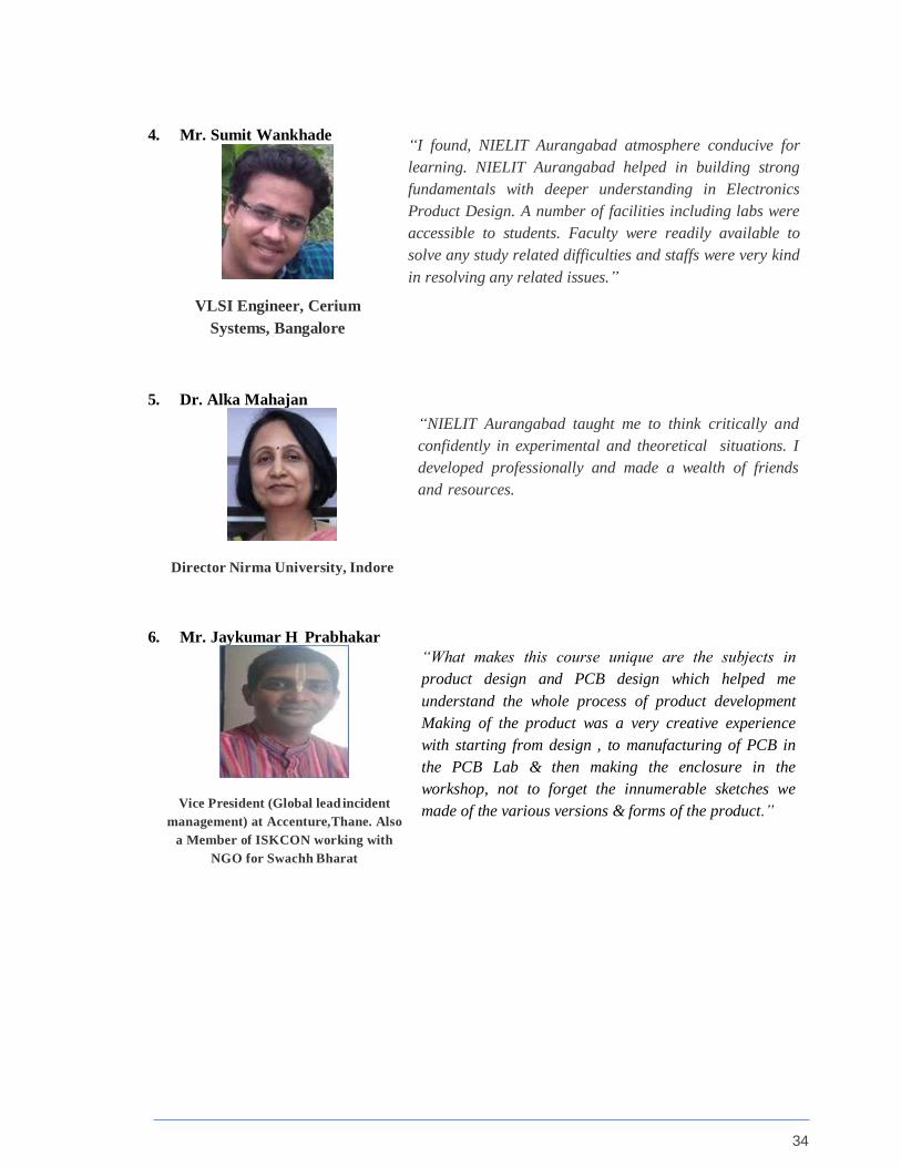
34
4. Mr. Sumit Wankhade
VLSI Engineer, Cerium
Systems, Bangalore
5. Dr. Alka Mahajan
Director Nirma University, Indore
6. Mr. Jaykumar H Prabhakar
Vice President (Global lead incident
management) at Accenture,Thane. Also
a Member of ISKCON working with
NGO for Swachh Bharat
“I found, NIELIT Aurangabad atmosphere conducive for
learning. NIELIT Aurangabad helped in building strong
fundamentals with deeper understanding in Electronics
Product Design. A number of facilities including labs were
accessible to students. Faculty were readily available to
solve any study related difficulties and staffs were very kind
in resolving any related issues.”
“NIELIT Aurangabad taught me to think critically and
confidently in experimental and theoretical situations. I
developed professionally and made a wealth of friends
and resources.
“What makes this course unique are the subjects in
product design and PCB design which helped me
understand the whole process of product development
Making of the product was a very creative experience
with starting from design , to manufacturing of PCB in
the PCB Lab & then making the enclosure in the
workshop, not to forget the innumerable sketches we
made of the various versions & forms of the product.”

35
7. Arvind B Nyayadhish
Director Enman Automation
Pvt.Ltd, Aurangabad
8. Mr. MahendraPadalkar
Principal Technical Architect (Cloud)
at Tech Mahindra Ltd, Pune
9. Mr. Pradeep Kizhiseeri
Senior Consultant Presently into
Hatstand, Singapore
10. Mr. Sandeep K Patni
“To shine in today's competitive world it is very essential to
have the nurturing that helps you go the extra mile. NIELIT
Aurangabad equipped me for the world outside with the
best skill set. Those amazing years gave me much more than
bookish knowledge; I met probably the best people in my life
and some inspiring personalities Proud to be an alumnus of
NIELIT Aurangabad.”
“In NIELIT Aurangabad, I acquired and honed not only
technical skills but also management and people skills that
are assisting me immensely in my career. I’m thankful to
NIELIT Aurangabad for providing such a strong foundation
towards my career.”
“NIELIT Aurangabad is where the students are molded to
Perfect Industry Professionals & Entrepreneurs. The
reputation and brand equity associated with the institute
makes one feel proud. Thanks to college management and
faculty for engineering my career in right direction.”
Co-Founder and VP of Systems and
Engineering at CumuLogicInc,
NewJersey, USA
“NIELIT Aurangabad taught me that education can be
the most challenging, extremely rewarding, exciting,
and fun. I learned that passion for learning really is the
driver of finding new knowledge, and that passion is
honestly contagious.”

36
10.0 Refund of fees in the event of cancellation of admission:
10.1 No Refund
There will be no refund
i. If admission is cancelled after the 1st Semester is over.
ii. If admission is cancelled in 1st Semester and the vacancy is not filled.
10.2 Refund
However, if admission is cancelled in 1st Semester and the vacancy is filled, then Refund
of fees will be as under: -
i. Student leaving before start of the course – Entire fee minus Rs1000/- (Rupees One
Thousand only) as processing fee.
ii. Student leaving after start of the course but before closing of admissions- Entire fee
minus Rs1000/- or (Semester fee/6), whichever is higher.
iii. Student leaving after start of the course and closing of admissions-Entire fee minus
[Rs1000/- + (Semester fee/6) x Registered Period in number of months)]
iv. For students staying in hostel, [(Hostel Rent/6) x Registered Period in number of Months]
will be deducted from Semester hostel fee paid by the student.
v. All the deposits will be refunded after adjusting student dues, if any.
vi. Fraction of month will be treated as full month.

37
ANNEXURE I
Tentative Academic Calendar for M.Tech (EDT),B.Tech(ESE) and DEPM Programs
Academic Year 2019-2020 (Semester I)
Sr. No. Semester-I (Spring)
1 Start of On line application 1st May 2019
2 Last date of On line application 1st July 2019
3 Instruction Begins 01st Aug 2019
4 Class Test-1 10th Sept to 14th Sept 2019
5 Class Test-2 12th to 16th Nov 2019
6 Instruction Ends 23rd Nov. 2019
7 Semester (Practical) Examination 26th to 30th Nov 2019
8 Semester (Theory) Examination 3rd to 24th Dec 2019
9 Project Assessment 10th Dec. to 24th Dec 2019
Project Feasibility Seminar
10 Semester Break (DEPM and B.Tech) 25th Dec to 14thJan 2020
11 Declaration of Results 12th Jan 2020
--

38
ANNEXURE – II
Assessment Computation of SGPA & CGPA
1. Semester Grade Point Average (SGPA) is the weighted average of Grade Points obtained by
a student in a semester and is computed as follows:
U1 X M1+U2 X M2+⋯+Un X Mn
SGPA= U1+U2+⋯Un
Where U1, U2,.... are subject credit of respective course and M1, M2,..... are the marks
Obtained in the respective subject aout of 8 (grade point)
Note: The semester grade point average (SGPA) for all the six semester is also mentioned at
the end of every semester.
2. The Cumulative Grade Point Average (CGPA) is used to describe the overall performance
of a student in the Diploma / Degree course and is computed as under:
6 / 4
ΣSGPA (n) Cn
n=1
CGPA =
6 / 4
ΣCn
n=1
Where SGPA (n) is the nth Semester SGPA of the student and Cn is the nth Semester total
credit. The maximum value of n is as under
a. Six (6) in case of DEPM Program
b. Eight (8) in case of B.Tech Program
c. Four (4) in case of Full-time M. Tech Program.
d. Six (6) in case of Part-time M. Tech Program.
Note: The Semester and Cumulative GPA are rounded off to the second place of decimal
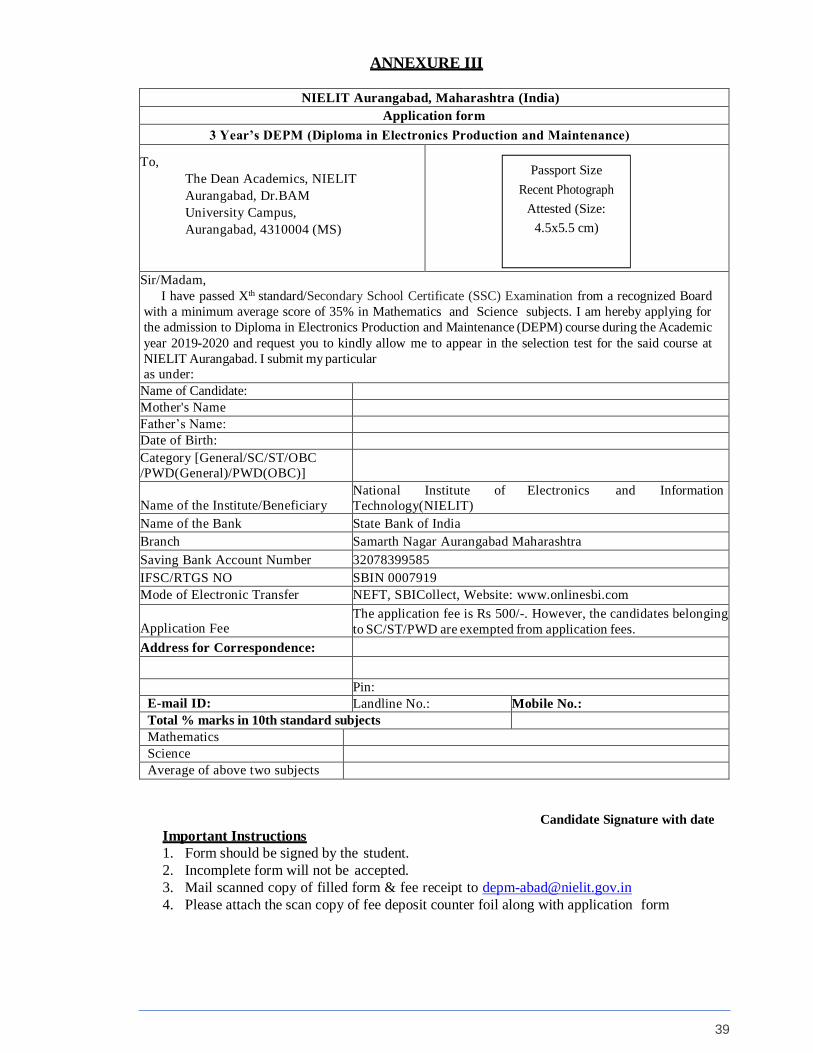
39
ANNEXURE III
NIELIT Aurangabad, Maharashtra (India)
Application form
3 Year’s DEPM (Diploma in Electronics Production and Maintenance)
To,
The Dean Academics, NIELIT
Aurangabad, Dr.BAM
University Campus,
Aurangabad, 4310004 (MS)
Passport Size
Recent Photograph
Attested (Size:
4.5x5.5 cm)
Sir/Madam,
I have passed Xth standard/Secondary School Certificate (SSC) Examination from a recognized Board
with a minimum average score of 35% in Mathematics and Science subjects. I am hereby applying for
the admission to Diploma in Electronics Production and Maintenance (DEPM) course during the Academic
year 2019-2020 and request you to kindly allow me to appear in the selection test for the said course at
NIELIT Aurangabad. I submit my particular
as under:
Name of Candidate:
Mother's Name
Father’s Name:
Date of Birth:
Category [General/SC/ST/OBC
/PWD(General)/PWD(OBC)]
Name of the Institute/Beneficiary
National Institute of Electronics and Information
Technology(NIELIT)
Name of the Bank State Bank of India
Branch Samarth Nagar Aurangabad Maharashtra
Saving Bank Account Number 32078399585
IFSC/RTGS NO SBIN 0007919
Mode of Electronic Transfer NEFT, SBICollect, Website: www.onlinesbi.com
Application Fee
The application fee is Rs 500/-. However, the candidates belonging
to SC/ST/PWD are exempted from application fees.
Address for Correspondence:
Pin:
E-mail ID: Landline No.: Mobile No.:
Total % marks in 10th standard subjects
Mathematics
Science
Average of above two subjects
Candidate Signature with date
Important Instructions
1. Form should be signed by the student.
2. Incomplete form will not be accepted.
3. Mail scanned copy of filled form & fee receipt to [email protected]
4. Please attach the scan copy of fee deposit counter foil along with application form
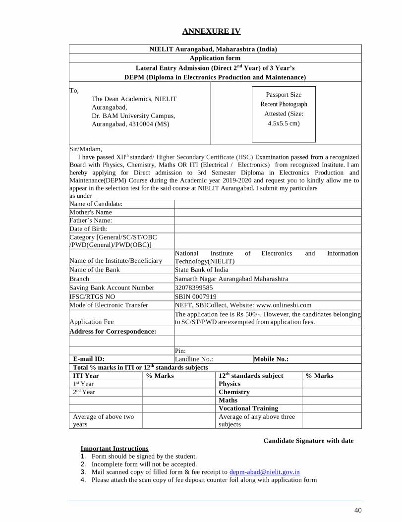
40
ANNEXURE IV
NIELIT Aurangabad, Maharashtra (India)
Application form
Lateral Entry Admission (Direct 2nd Year) of 3 Year’s
DEPM (Diploma in Electronics Production and Maintenance)
To,
The Dean Academics, NIELIT
Aurangabad,
Dr. BAM University Campus,
Aurangabad, 4310004 (MS)
Passport Size
Recent Photograph
Attested (Size:
4.5x5.5 cm)
Sir/Madam,
I have passed XIIth standard/ Higher Secondary Certificate (HSC) Examination passed from a recognized
Board with Physics, Chemistry, Maths OR ITI (Electrical / Electronics) from recognized Institute. I am
hereby applying for Direct admission to 3rd Semester Diploma in Electronics Production and
Maintenance(DEPM) Course during the Academic year 2019-2020 and request you to kindly allow me to
appear in the selection test for the said course at NIELIT Aurangabad. I submit my particulars
as under
Name of Candidate:
Mother's Name
Father’s Name:
Date of Birth:
Category [General/SC/ST/OBC
/PWD(General)/PWD(OBC)]
Name of the Institute/Beneficiary
National Institute of Electronics and Information
Technology(NIELIT)
Name of the Bank State Bank of India
Branch Samarth Nagar Aurangabad Maharashtra
Saving Bank Account Number 32078399585
IFSC/RTGS NO SBIN 0007919
Mode of Electronic Transfer NEFT, SBICollect, Website: www.onlinesbi.com
Application Fee
The application fee is Rs 500/-. However, the candidates belonging
to SC/ST/PWD are exempted from application fees.
Address for Correspondence:
Pin:
E-mail ID: Landline No.: Mobile No.:
Total % marks in ITI or 12th standards subjects
ITI Year % Marks 12th standards subject % Marks
1st Year Physics
2nd Year Chemistry
Maths
Vocational Training
Average of above two
years
Average of any above three
subjects
Candidate Signature with date
Important Instructions
1. Form should be signed by the student.
2. Incomplete form will not be accepted.
3. Mail scanned copy of filled form & fee receipt to [email protected]
4. Please attach the scan copy of fee deposit counter foil along with application form
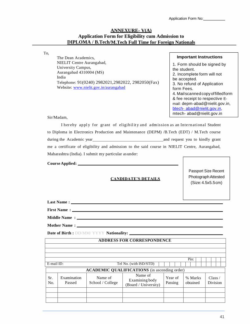
41
Passport Size Recent
Photograph Attested
(Size: 4.5x5.5 cm)
Application Form No:
ANNEXURE- V(A)
Application Form for Eligibility cum Admission to
DIPLOMA / B.Tech/M.Tech Full Time for Foreign Nationals
To, The Dean Academics,
NIELIT Centre Aurangabad,
University Campus,
Aurangabad 4310004 (MS)
India
Telephone: 91(0240) 2982021,2982022, 2982050(Fax) Website: www.nielit.gov.in/aurangabad
Sir/Madam,
I h er e by ap pl y f or gr ant of e ligib il it y and a dm is s io n a s an Inte rn at ional Student
to Diploma in Electronics Production and Maintenance (DEPM) /B.Tech (EDT) / M.Tech course
during the Academic year and request you to kindly grant
me a certificate of eligibility and admission to the said course in NIELIT Centre, Aurangabad,
Maharashtra (India). I submit my particular as under:
Course Applied:
CANDIDATE’S DETAILS
Last Name :
First Name :
Middle Name :
Mother Name :
Date of Birth : DD/MM/ YYYY Nationality:
ADDRESS FOR CORRESPONDENCE
Pin:
E-mail ID: Tel No. (with ISD/STD)
ACADEMIC QUALIFICATIONS (in ascending order)
Sr.
No.
Examination
Passed
Name of
School / College
Name of
Examining body (Board / University)
Year of
Passing
% Marks
obtained
Class /
Division
Important Instructions
1. Form should be signed by
the student. 2. Incomplete form will not be accepted. 3. No refund of Application form Fees.
4. Mail scanned copy of filled form
& fee receipt to respective E-
mail: [email protected],
btech- [email protected],
mtech- [email protected]

42
QUALIFYING EXAMINATION DETAILS
10th Std. Marks / Grade (For DEPM only) GATE or Equivalent Score Details (if applicable) (For M.Tech (EDT) / Ph.D)
Subject Science Mathematics Total
Marks
Year Discipline Percentile
Marks / Grade
Obtained
Maximum Marks
WORKING EXPERIENCE
Name of Industry / Institution
Type of W ork / Experience
Experience in years
Passed Xth std. or higher level Examination with English as one of the passing subjects
Name and address of the School / College / Institution last attended: _ _ _ _ (Tick Approporiate)
_ _ _ _
Details for online fee payment for DIPLOMA/ B.Tech/ M.Tech Full Time for Foreign Nationals
Students are as given below.
Bank Account No 20060526862
Account Type Current a/c
Account Name National Institute of Electronics and Information Technology
(NIELIT), Aurangabad
Bank Name& Address Bank of Maharashtra, Dr. B.A.M.University branch Aurangabad
(MS)
IFSC Code MAHB0000152
Mode of Electronic
Transfer
NEFT, RTGS
Check List (Please attach Attested photocopies of all the Certificates for Sr. No. 2 to 6 below)
01. Two Passport Size Photograph pasted & attested YES NO
02 Date of Birth proof, copy attached (Xth Mark-sheet / Certificate) YES NO
03 Caste (OBC/SC/ST) Certificate, copy attach YES NO
04 Disability Certificate for PD, copy attached YES NO
05 12th /Graduation Passing Certificate, copy attached YES NO
06 Studentship Letter, Original attached YES NO
07 Qualifying Degree Certificate ,copy attached YES NO
08 GATE Score Card, copy attached (M.Tech Full Time) YES NO
09 Sponsorship letter Original / Experience letter attached YES NO
10 Payment receipt in the form of RTGS/NEFT Enclosed YES NO
Note: The application form is liable to be rejected if found incomplete or if the necessary & appropriate documents & Payment are not enclosed along with.
CANDIDATE SIGNATURE:
FOR OFFICE USE ONLY:
Registration No Application Form No
Checked By:
Academic Section I/C M.Tech Coordinator Dean Academics B.Tech Coordinator Diploma Coordinator
Date: DD /MM /YYYY
No Yes

43
ANNEXURE-V (B)
(To be typed on Rs. 100/- Stamp Paper) Declaration and Undertaking
1. I hereby declare that I have carefully read this application form for eligibility and admission
and have noted the instructions / requirements thereby.
2. I have also carefully noted the rules of eligibility & conduct and discipline, laid down by the
NIELIT Centre, Aurangabad and I agree to abide by them.
3. I understand and declare that I shall be responsible for any discrepancies, error, wrong or
incorrect information, supplied by me in this application form and for cancellation of admission
thereby or otherwise found ineligible.
4. I undertake to furnish the necessary certificate(s)/ document(s)/ paper(s) in original along with
a true copy of each of them as and when asked for, failing which I understand that my
eligibility and admission stands automatically cancelled and that the NIELIT Centre,
Aurangabad is not responsible for the same.
I hereby declare that the information furnished by me in this form is true and correct to the best of
my knowledge. I am liable to be disqualified if the competent authority notices that I have
furnished any false information.
Yours Faithfully,
(Name & Signature of Foreign National)
Date: dd/mm/yyyy
Place:
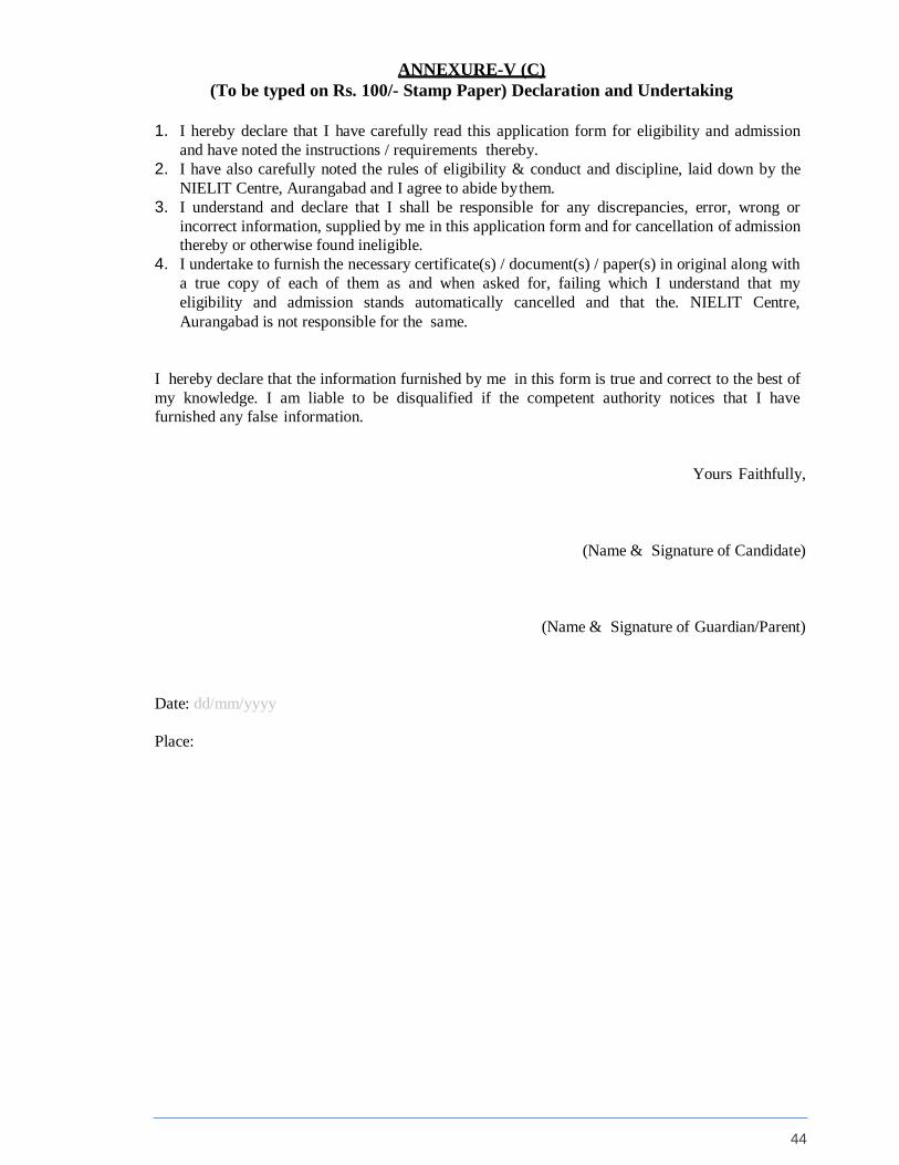
44
ANNEXURE-V (C)
(To be typed on Rs. 100/- Stamp Paper) Declaration and Undertaking
1. I hereby declare that I have carefully read this application form for eligibility and admission
and have noted the instructions / requirements thereby.
2. I have also carefully noted the rules of eligibility & conduct and discipline, laid down by the
NIELIT Centre, Aurangabad and I agree to abide by them.
3. I understand and declare that I shall be responsible for any discrepancies, error, wrong or
incorrect information, supplied by me in this application form and for cancellation of admission
thereby or otherwise found ineligible.
4. I undertake to furnish the necessary certificate(s) / document(s) / paper(s) in original along with
a true copy of each of them as and when asked for, failing which I understand that my
eligibility and admission stands automatically cancelled and that the. NIELIT Centre,
Aurangabad is not responsible for the same.
I hereby declare that the information furnished by me in this form is true and correct to the best of
my knowledge. I am liable to be disqualified if the competent authority notices that I have
furnished any false information.
Yours Faithfully,
(Name & Signature of Candidate)
(Name & Signature of Guardian/Parent)
Date: dd/mm/yyyy
Place:

45
ANNEXURE VI
NIELIT Aurangabad, Maharashtra (India)
Application form
Lateral Entry Admission (Direct 2nd Year) of 4 Year’s
B.TECH (Electronics System Engineering)
To,
The Dean Academics,
NIELIT Aurangabad,
Dr. BAM University Campus,
Aurangabad, 4310004 (MS)
Passport Size
Recent Photograph
Attested (Size:
4.5x5.5 cm)
Sir/Madam,
I have passed 3 year diploma course in Electronics & allied streams with minimum 45% marks (40
percent for SC/ST candidates) approved by AICTE. I hereby register for admission to 3rd Semester
B.Tech (Electronics System Engineering) Course through Lateral Entry during the Academic year 2019-
20 and request you to kindly grant me admission to the said course at NIELIT Aurangabad. I submit my
particular as under:
Name of Candidate:
Mother's Name
Father’s Name:
Date of Birth:
Category [General/SC/ST/OBC
/PWD(General)/PWD(OBC)]
Name of the Institute/Beneficiary
National Institute of Electronics and Information
Technology(NIELIT)
Name of the Bank State Bank of India
Branch Samarth Nagar Aurangabad Maharashtra
Saving Bank Account Number 32078399585
IFSC/RTGS NO SBIN 0007919
Application Fee
The application fee is Rs 500/-. However, the candidates belonging
to SC/ST/PWD are exempted from application fees.
Mode of Electronic Transfer NEFT, SBICollect, Website: www.onlinesbi.com
Address for Correspondence:
Pin:
E-mail ID: Landline No.: Mobile No.:
Total % marks in Diploma Course in Engineering and Technology
Branch/Discipline 1st Year % 2nd Year % 3rd Year % Avg. %
Candidate Signature with date
Important Instructions
1. Form should be signed by the student.
2. Incomplete form will not be accepted.
3. Mail scanned copy of filled form & fee receipt to [email protected]
4. Please attach the scan copy of fee deposit counter foil along with application form
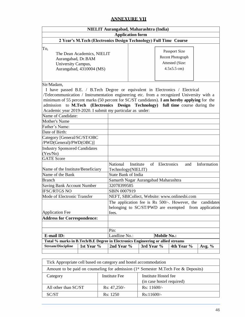
46
ANNEXURE VII
NIELIT Aurangabad, Maharashtra (India)
Application form
2 Year’s M.Tech (Electronics Design Technology) Full Time Course
To,
The Dean Academics, NIELIT
Aurangabad, Dr.BAM
University Campus, Aurangabad, 4310004 (MS)
Passport Size
Recent Photograph
Attested (Size:
4.5x5.5 cm)
Sir/Madam,
I have passed B.E. / B.Tech Degree or equivalent in Electronics / Electrical
/Telecommunication / Instrumentation engineering etc. from a recognized University with a
minimum of 55 percent marks (50 percent for SC/ST candidates). I am hereby applying for the
admission to M.Tech (Electronics Design Technology) full time course during the
Academic year 2019-2020. I submit my particular as under:
Name of Candidate:
Mother's Name
Father’s Name:
Date of Birth:
Category [General/SC/ST/OBC /PWD(General)/PWD(OBC)]
Industry Sponsored Candidates
(Yes/No)
GATE Score
Name of the Institute/Beneficiary
National Institute of Electronics and Information
Technology(NIELIT)
Name of the Bank State Bank of India
Branch Samarth Nagar Aurangabad Maharashtra
Saving Bank Account Number 32078399585
IFSC/RTGS NO SBIN 0007919
Mode of Electronic Transfer NEFT, SBICollect, Website: www.onlinesbi.com
Application Fee
The application fee is Rs 500/-. However, the candidates
belonging to SC/ST/PWD are exempted from application
fees.
Address for Correspondence:
Pin:
E-mail ID: Landline No.: Mobile No.:
Total % marks in B.Tech/B.E Degree in Electronics Engineering or allied streams
Stream/Discipline 1st Year % 2nd Year % 3rd Year % 4th Year % Avg. %
Tick Appropriate cell based on category and hostel accommodation
Amount to be paid on counseling for admission (1st Semester M.Tech Fee & Deposits)
Category Institute Fee Institute Hostel fee
(in case hostel required)
All other than SC/ST Rs: 47,250/- Rs: 11600/-
SC/ST Rs: 1250 Rs:11600/-
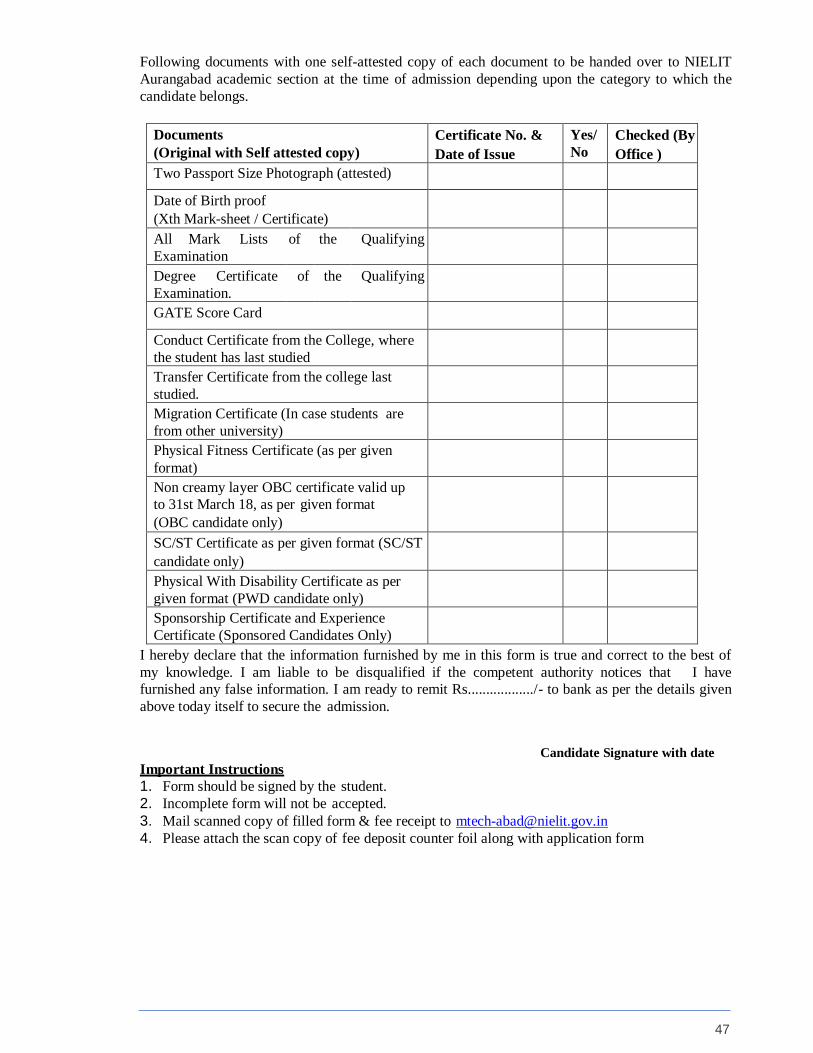
47
Following documents with one self-attested copy of each document to be handed over to NIELIT
Aurangabad academic section at the time of admission depending upon the category to which the
candidate belongs.
Documents
(Original with Self attested copy)
Certificate No. &
Date of Issue
Yes/
No
Checked (By
Office )
Two Passport Size Photograph (attested)
Date of Birth proof
(Xth Mark-sheet / Certificate)
All Mark Lists
Examination
of the Qualifying
Degree Certificate
Examination.
of the Qualifying
GATE Score Card
Conduct Certificate from the College, where
the student has last studied
Transfer Certificate from the college last
studied.
Migration Certificate (In case students are
from other university)
Physical Fitness Certificate (as per given
format)
Non creamy layer OBC certificate valid up
to 31st March 18, as per given format
(OBC candidate only)
SC/ST Certificate as per given format (SC/ST
candidate only)
Physical With Disability Certificate as per
given format (PWD candidate only)
Sponsorship Certificate and Experience
Certificate (Sponsored Candidates Only)
I hereby declare that the information furnished by me in this form is true and correct to the best of
my knowledge. I am liable to be disqualified if the competent authority notices that I have
furnished any false information. I am ready to remit Rs................../- to bank as per the details given
above today itself to secure the admission.
Candidate Signature with date
Important Instructions
1. Form should be signed by the student.
2. Incomplete form will not be accepted.
3. Mail scanned copy of filled form & fee receipt to [email protected]
4. Please attach the scan copy of fee deposit counter foil along with application form

48
ANNEXURE VIII
NIELIT Aurangabad, Maharashtra (India)
Application form
3 Year’s M.Tech (Electronics Design Technology) Part Time Course Admission
To,
The Dean Academics, NIELIT
Aurangabad, Dr.BAM
University Campus, Aurangabad, 4310004 (MS)
Passport Size
Recent Photograph
Attested (Size:
4.5x5.5 cm)
Sir/Madam,
I have passed B.E. / B.Tech Degree or equivalent in Electronics / Electrical /Telecommunication / Instrumentation engineering etc. from a recognized University with a
minimum of 55 percent marks (50 percent for SC/ST candidates). I am hereby applying for the
admission to M.Tech (Electronics Design Technology) Part time course during the Academic year 2019-2020. I submit my particular as under:
Name of Candidate:
Mother's Name
Father’s Name:
Date of Birth:
Category [General/SC/ST/OBC /PWD(General)/PWD(OBC)]
Sponsorship by Academic
Institute/Industry
Working Experience
Approximate Distance of Working
place from the Institute (Kms)
Name of the Institute/Beneficiary
National Institute of Electronics and Information
Technology(NIELIT) Name of the Bank State Bank of India
Branch Samarth Nagar Aurangabad Maharashtra
Saving Bank Account Number 32078399585
IFSC/RTGS NO SBIN 0007919
Mode of Electronic Transfer NEFT, SBICollect, Website: www.onlinesbi.com
Application Fee
The application fee is Rs 500/-. However, the candidates
belonging to SC/ST/PWD are exempted from application
fees.
Address for Correspondence:
Pin:
E-mail ID: Landline No.: Mobile No.:
Total % marks in B.Tech/B.E Degree in Electronics Engineering or allied streams
Stream/Discipline 1st Year % 2nd Year % 3rd Year % 4th Year % Avg. %
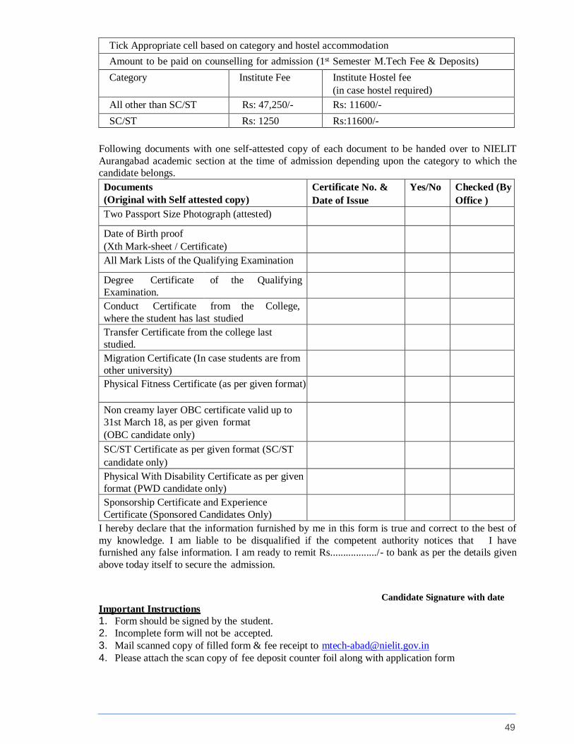
49
Tick Appropriate cell based on category and hostel accommodation
Amount to be paid on counselling for admission (1st Semester M.Tech Fee & Deposits)
Category Institute Fee Institute Hostel fee
(in case hostel required)
All other than SC/ST Rs: 47,250/- Rs: 11600/-
SC/ST Rs: 1250 Rs:11600/-
Following documents with one self-attested copy of each document to be handed over to NIELIT
Aurangabad academic section at the time of admission depending upon the category to which the
candidate belongs.
Documents
(Original with Self attested copy)
Certificate No. &
Date of Issue
Yes/No Checked (By
Office )
Two Passport Size Photograph (attested)
Date of Birth proof
(Xth Mark-sheet / Certificate)
All Mark Lists of the Qualifying Examination
Degree Certificate
Examination.
of the Qualifying
Conduct Certificate from the College,
where the student has last studied
Transfer Certificate from the college last
studied.
Migration Certificate (In case students are from
other university)
Physical Fitness Certificate (as per given format)
Non creamy layer OBC certificate valid up to
31st March 18, as per given format
(OBC candidate only)
SC/ST Certificate as per given format (SC/ST
candidate only)
Physical With Disability Certificate as per given
format (PWD candidate only)
Sponsorship Certificate and Experience
Certificate (Sponsored Candidates Only)
I hereby declare that the information furnished by me in this form is true and correct to the best of
my knowledge. I am liable to be disqualified if the competent authority notices that I have
furnished any false information. I am ready to remit Rs................../- to bank as per the details given
above today itself to secure the admission.
Candidate Signature with date
Important Instructions
1. Form should be signed by the student.
2. Incomplete form will not be accepted.
3. Mail scanned copy of filled form & fee receipt to [email protected]
4. Please attach the scan copy of fee deposit counter foil along with application form
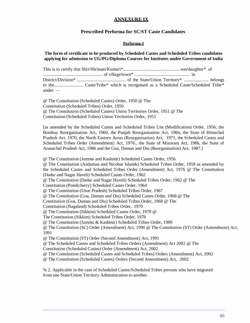
50
ANNEXURE IX
Prescribed Performa for SC/ST Caste Candidates
Performa-I
The form of certificate to be produced by Scheduled Castes and Scheduled Tribes candidates
applying for admission to UG/PG/Diploma Courses for Institutes under Government of India
This is to certify that Shri/Shrimati/Kumari*.................................................. son/daughter* of
..................................................... of village/town* ................................................. in
District/Division* ........................................... of the State/Union Territory* ...................... belongs
to the.......................... Caste/Tribe* which is recognised as a Scheduled Caste/Scheduled Tribe*
under: —
@ The Constitution (Scheduled Castes) Order, 1950 @ The
Constitution (Scheduled Tribes) Order, 1950
@ The Constitution (Scheduled Castes) Union Territories Order, 1951 @ The
Constitution (Scheduled Tribes) Union Territories Order, 1951
[as amended by the Scheduled Castes and Scheduled Tribes List (Modification) Order, 1956; the
Bombay Reorganisation Act, 1960, the Punjab Reorganisation Act, 1966, the State of Himachal
Pradesh Act, 1970, the North Eastern Areas (Reorganisation) Act, 1971, the Scheduled Castes and
Scheduled Tribes Order (Amendment) Act, 1976., the State of Mizoram Act, 1986, the State of
Arunachal Pradesh Act, 1986 and the Goa, Daman and Diu (Reorganisation) Act, 1987.]
@ The Constitution (Jammu and Kashmir) Scheduled Castes Order, 1956
@ The Constitution (Andaman and Nicobar Islands) Scheduled Tribes Order, 1959 as amended by
the Scheduled Castes and Scheduled Tribes Order (Amendment) Act, 1976 @ The Constitution
(Dadar and Nagar Haveli) Scheduled Castes Order, 1962
@ The Constitution (Dadar and Nagar Haveli) Scheduled Tribes Order, 1962 @ The
Constitution (Pondicherry) Scheduled Castes Order, 1964
@ The Constitution (Uttar Pradesh) Scheduled Tribes Order, 1967
@ The Constitution (Goa, Daman and Diu) Scheduled Castes Order, 1968 @ The
Constitution (Goa, Daman and Diu) Scheduled Tribes Order, 1968 @ The
Constitution (Nagaland) Scheduled Tribes Order, 1970
@ The Constitution (Sikkim) Scheduled Castes Order, 1978 @
The Constitution (Sikkim) Scheduled Tribes Order, 1978
@ The Constitution (Jammu & Kashmir) Scheduled Tribes Order, 1989
@ The Constitution (SC) Order (Amendment) Act, 1990 @ The Constitution (ST) Order (Amendment) Act,
1991
@ The Constitution (ST) Order (Second Amendment) Act, 1991
@ The Scheduled Castes and Scheduled Tribes Orders (Amendment) Act 2002 @ The
Constitution (Scheduled Castes) Order (Amendment) Act, 2002
@ The Constitution (Scheduled Castes and Scheduled Tribes) Orders (Amendment) Act, 2002
@ The Constitution (Scheduled Castes) Orders (Second Amendment) Act, 2002
% 2. Applicable in the case of Scheduled Castes/Scheduled Tribes persons who have migrated
from one State/Union Territory Administration to another.
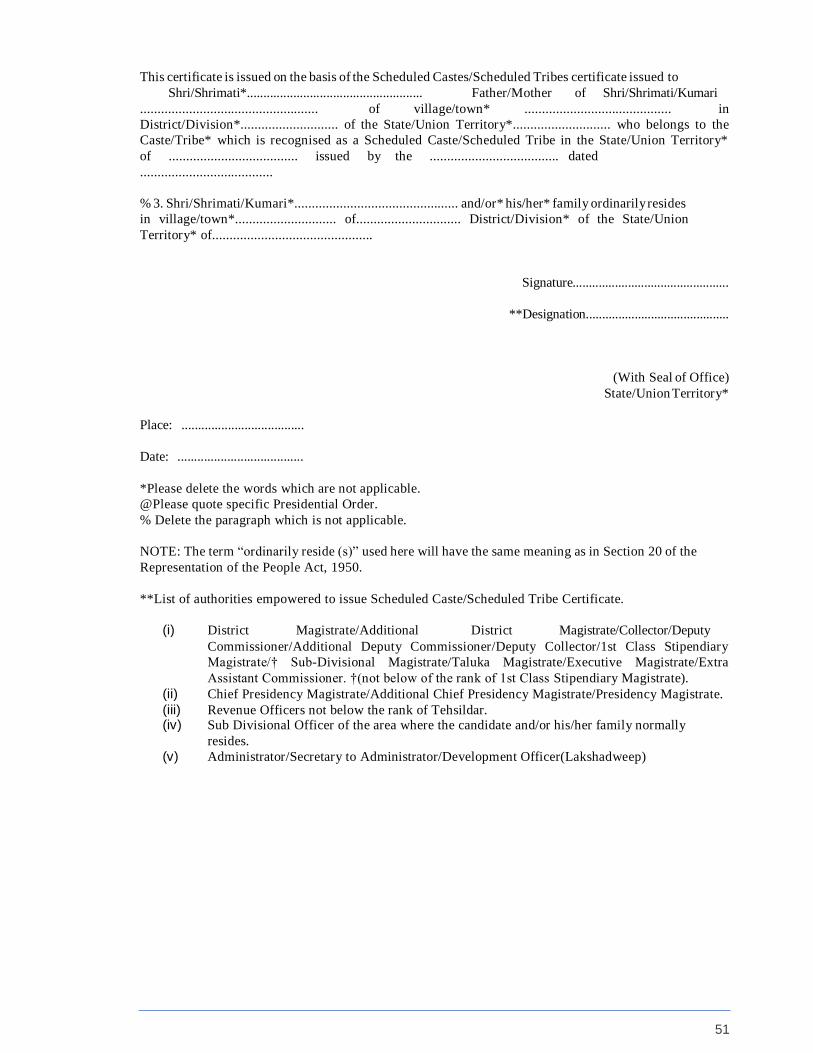
51
This certificate is issued on the basis of the Scheduled Castes/Scheduled Tribes certificate issued to
Shri/Shrimati*..................................................... Father/Mother of Shri/Shrimati/Kumari
................................................... of village/town* .......................................... in
District/Division*............................ of the State/Union Territory*............................ who belongs to the
Caste/Tribe* which is recognised as a Scheduled Caste/Scheduled Tribe in the State/Union Territory*
of ..................................... issued by the ..................................... dated
......................................
% 3. Shri/Shrimati/Kumari*............................................... and/or* his/her* family ordinarily resides
in village/town*............................. of.............................. District/Division* of the State/Union
Territory* of..............................................
Signature................................................
**Designation............................................
(With Seal of Office)
State/Union Territory*
Place: .....................................
Date: ......................................
*Please delete the words which are not applicable.
@Please quote specific Presidential Order.
% Delete the paragraph which is not applicable.
NOTE: The term “ordinarily reside (s)” used here will have the same meaning as in Section 20 of the
Representation of the People Act, 1950.
**List of authorities empowered to issue Scheduled Caste/Scheduled Tribe Certificate.
(i) District Magistrate/Additional District Magistrate/Collector/Deputy
Commissioner/Additional Deputy Commissioner/Deputy Collector/1st Class Stipendiary
Magistrate/† Sub-Divisional Magistrate/Taluka Magistrate/Executive Magistrate/Extra
Assistant Commissioner. †(not below of the rank of 1st Class Stipendiary Magistrate).
(ii) Chief Presidency Magistrate/Additional Chief Presidency Magistrate/Presidency Magistrate.
(iii) Revenue Officers not below the rank of Tehsildar. (iv) Sub Divisional Officer of the area where the candidate and/or his/her family normally
resides.
(v) Administrator/Secretary to Administrator/Development Officer(Lakshadweep)
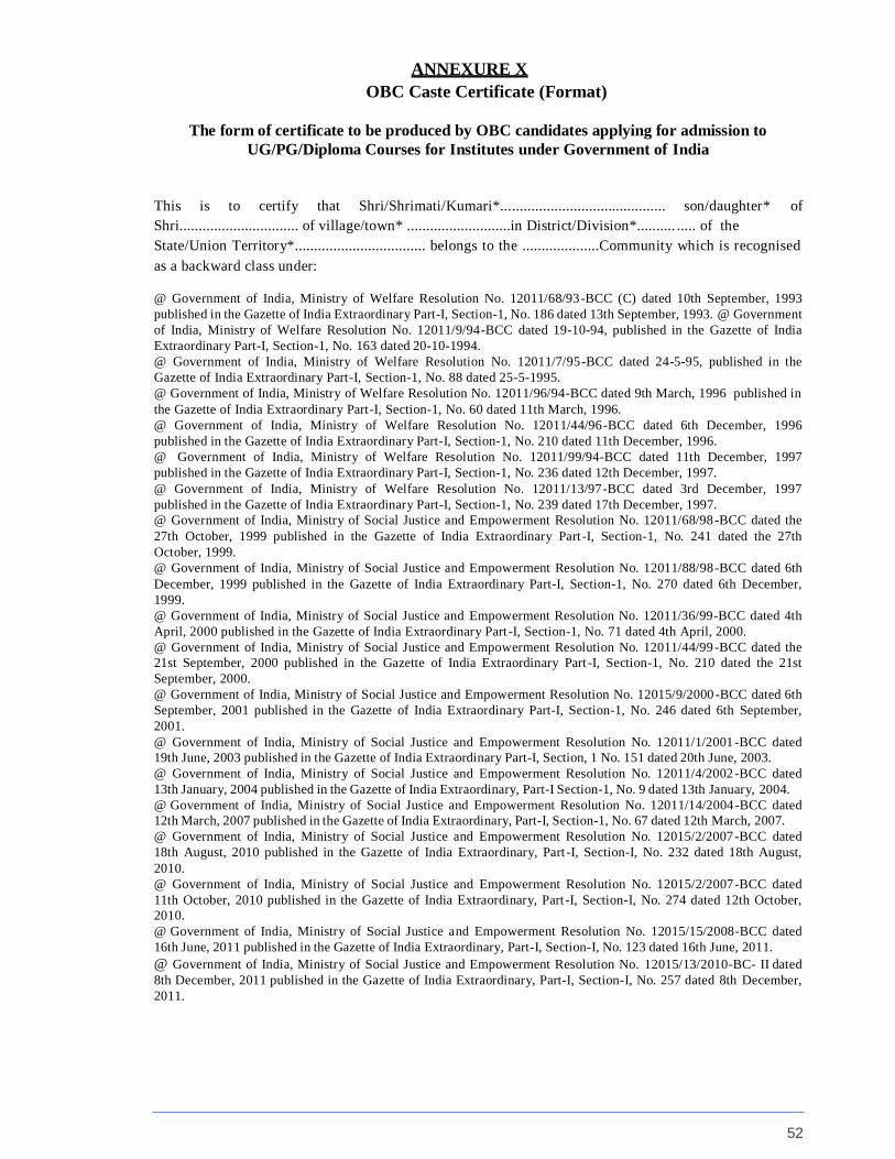
52
ANNEXURE X
OBC Caste Certificate (Format)
The form of certificate to be produced by OBC candidates applying for admission to
UG/PG/Diploma Courses for Institutes under Government of India
This is to certify that Shri/Shrimati/Kumari*........................................... son/daughter* of
Shri............................... of village/town* ...........................in District/Division*.......... ..... of the
State/Union Territory*.................................. belongs to the ....................Community which is recognised
as a backward class under:
@ Government of India, Ministry of Welfare Resolution No. 12011/68/93-BCC (C) dated 10th September, 1993
published in the Gazette of India Extraordinary Part-I, Section-1, No. 186 dated 13th September, 1993. @ Government
of India, Ministry of Welfare Resolution No. 12011/9/94-BCC dated 19-10-94, published in the Gazette of India
Extraordinary Part-I, Section-1, No. 163 dated 20-10-1994.
@ Government of India, Ministry of Welfare Resolution No. 12011/7/95-BCC dated 24-5-95, published in the
Gazette of India Extraordinary Part-I, Section-1, No. 88 dated 25-5-1995.
@ Government of India, Ministry of Welfare Resolution No. 12011/96/94-BCC dated 9th March, 1996 published in
the Gazette of India Extraordinary Part-I, Section-1, No. 60 dated 11th March, 1996.
@ Government of India, Ministry of Welfare Resolution No. 12011/44/96-BCC dated 6th December, 1996
published in the Gazette of India Extraordinary Part-I, Section-1, No. 210 dated 11th December, 1996.
@ Government of India, Ministry of Welfare Resolution No. 12011/99/94-BCC dated 11th December, 1997
published in the Gazette of India Extraordinary Part-I, Section-1, No. 236 dated 12th December, 1997.
@ Government of India, Ministry of Welfare Resolution No. 12011/13/97-BCC dated 3rd December, 1997
published in the Gazette of India Extraordinary Part-I, Section-1, No. 239 dated 17th December, 1997.
@ Government of India, Ministry of Social Justice and Empowerment Resolution No. 12011/68/98-BCC dated the
27th October, 1999 published in the Gazette of India Extraordinary Part -I, Section-1, No. 241 dated the 27th
October, 1999.
@ Government of India, Ministry of Social Justice and Empowerment Resolution No. 12011/88/98-BCC dated 6th
December, 1999 published in the Gazette of India Extraordinary Part-I, Section-1, No. 270 dated 6th December,
1999.
@ Government of India, Ministry of Social Justice and Empowerment Resolution No. 12011/36/99-BCC dated 4th
April, 2000 published in the Gazette of India Extraordinary Part -I, Section-1, No. 71 dated 4th April, 2000.
@ Government of India, Ministry of Social Justice and Empowerment Resolution No. 12011/44/99-BCC dated the
21st September, 2000 published in the Gazette of India Extraordinary Part -I, Section-1, No. 210 dated the 21st
September, 2000.
@ Government of India, Ministry of Social Justice and Empowerment Resolution No. 12015/9/2000-BCC dated 6th
September, 2001 published in the Gazette of India Extraordinary Part-I, Section-1, No. 246 dated 6th September,
2001.
@ Government of India, Ministry of Social Justice and Empowerment Resolution No. 12011/1/2001-BCC dated
19th June, 2003 published in the Gazette of India Extraordinary Part-I, Section, 1 No. 151 dated 20th June, 2003.
@ Government of India, Ministry of Social Justice and Empowerment Resolution No. 12011/4/2002-BCC dated
13th January, 2004 published in the Gazette of India Extraordinary, Part-I Section-1, No. 9 dated 13th January, 2004.
@ Government of India, Ministry of Social Justice and Empowerment Resolution No. 12011/14/2004-BCC dated
12th March, 2007 published in the Gazette of India Extraordinary, Part-I, Section-1, No. 67 dated 12th March, 2007.
@ Government of India, Ministry of Social Justice and Empowerment Resolution No. 12015/2/2007-BCC dated
18th August, 2010 published in the Gazette of India Extraordinary, Part -I, Section-I, No. 232 dated 18th August,
2010.
@ Government of India, Ministry of Social Justice and Empowerment Resolution No. 12015/2/2007-BCC dated
11th October, 2010 published in the Gazette of India Extraordinary, Part -I, Section-I, No. 274 dated 12th October,
2010.
@ Government of India, Ministry of Social Justice and Empowerment Resolution No. 12015/15/2008-BCC dated
16th June, 2011 published in the Gazette of India Extraordinary, Part-I, Section-I, No. 123 dated 16th June, 2011.
@ Government of India, Ministry of Social Justice and Empowerment Resolution No. 12015/13/2010-BC- II dated
8th December, 2011 published in the Gazette of India Extraordinary, Part-I, Section-I, No. 257 dated 8th December,
2011.

53
Shri/Shrimati/Kumari*................................and/or* his/her* family ordinarily resides in
village/town*................................ of...................... District/Division* of the State/ Union Territory*
of............................... This is also to certify that he/she* does not belong to the persons/sections* (Creamy
Layer) mentioned in column 3 of the Schedule to the Government of India, Department of Personnel &
Training O.M. No. 36012/22/93-Estt. (SCT) dated 8-9-1993 O.M. No. 36033/3/2004-Estt. (Res.) dated
9th March, 2004 and further modified vide OM No. 36033/3/2004- Estt. (Res.) dated 14th October, 2008 or
the latest notification of the Government of India.
.
Signature................................
**Designation............................
(With seal of Office)
State/Union Territory
Place....................................................
Date.....................................................
*Please delete the words which are not applicable. @
Strike out whichever is not applicable.
NOTE: The term ‘Ordinarily’ used here will have the same meaning as in Section 20 of the
Representation of the People Act, 1950.
**List of authorities empowered to issue OBC Certificate
i. District Magistrate/Additional District Magistrate/Collector/Deputy Commissioner / Additional
Deputy Commissioner/Deputy Collector/1st Class Stipendiary Magistrate/† Sub- Divisional
Magistrate/Taluka Magistrate/Executive Magistrate/Extra Assistant Commissioner.
†(not below of the rank of 1st Class Stipendiary Magistrate).
ii. Chief Presidency Magistrate/Additional Chief Presidency Magistrate/Presidency
Magistrate.
iii. Revenue Officers not below the rank of Tehsildar.
iv. Sub Divisional Officer of the area where the candidate and/or his/her family normally resides.
v. Administrator/Secretary to Administrator/Development Officer(Lakshadweep)
Note 1: Candidates claiming to belong to OBCs should note that the name of their Caste (including its
spellings) as indicated in their certificates, should be exactly the same as published in the lists notified by
the Central Government from time to time. A certificate containing any variation in the Caste name will
not be accepted.
Note 2: The OBC claim of a candidate will be determined in relation to the State (or part of the State) to
which his/her father originally belongs. A candidate who has migrated from one State (or part of the State)
to another should, therefore, produce an OBC certificate which should have been issued to him/her based
on his/her father’s OBC certificate from the State to which he (father) originally belongs.
Note 3: No change in the community status already indicated by a candidate in his/her simplified
application form for this examination will ordinarily be allowed by the Commission.

54
Declaration/Undertaking for OBC (Non-creamy Layer) Candidates only
I, son / daughter of Shri
resident of village/town/city
district State
hereby declare that I belong to the community
which is recognised as a backward class by the Government of India for the purpose of reservation in
services as per orders contained in Department of Personnel and Training Office Memorandum
No.36012/22/93- Estt. (SCT), dated 8/9/1993. It is also declared that I do not belong to persons/sections
(Creamy Layer) mentioned in Column 3 of the Schedule to the above referred Office Memorandum, dated
8/9/1993, which is modified vide Department of Personnel and Training Office Memorandum
No.36033/3/2004 Estt.(Res.) dated 9/3/2004 and further modified vide OM No 36033/3/2004-
Estt.(Res.) dated 14/10/2008 or the latest notification of the Government of India.
I also declare that the condition of status/annual income for ‘Creamy Layer’ of my parents is within
prescribed limits as on financial year ending on March 31, 2019.
Signature of the Candidate
Place: Date:
Note: Declaration / undertaking not signed by Candidate will be rejected .
NOTE: “The admission is provisional and is subject to the community certificate being verified
through the proper channels. If the verification reveals that the claim of the candidate to belong to Other
Backward Classes or not to belong to the creamy layer is false, his/her admission will be terminated
forthwith without assigning any further reasons and without prejudice to such further action as may be
taken under the provisions of the Indian Penal Code for production of false certificates.”
Creamy Layer Definition
OBC Creamy layer is defined comprehensively at http://ncbc.nic.in/html/creamylayer.html. All
candidates for the OBC reserved seats should make sure that they do not satisfy any of the creamy layer
criteria as listed in the website. Some general exclusion for quick reference (no way comprehensive)
are as follows.
i. Any one of the parents holds a constitutional position in Govt. of India.
ii. Any one of the parents is a class I officer.
iii. Both the parents are class II officers.
iv. Any one of the parents is employed in an equivalent rank to class I officer or both parents
equivalent to class II officer in a public sector, insurance companies, banks, universities or in
other organizations.
v. Land holding on irrigated land is 85% or more of the statutory ceiling area
vi. Parents income is more than Rs. 8 Lakhs per year
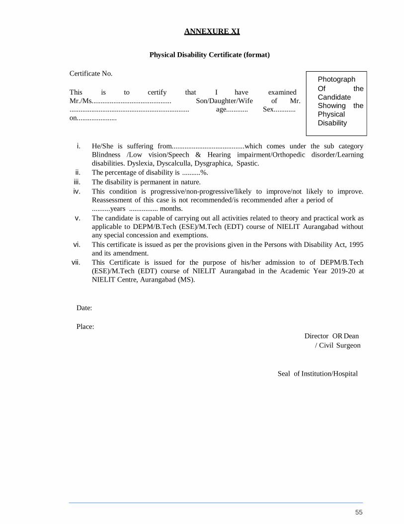
55
ANNEXURE XI
Physical Disability Certificate (format)
Certificate No.
This is to certify that I have examined
Mr./Ms............................................ Son/Daughter/Wife of Mr.
.................................................................. age............ Sex............
on......................
i. He/She is suffering from........................................which comes under the sub category
Blindness /Low vision/Speech & Hearing impairment/Orthopedic disorder/Learning
disabilities. Dyslexia, Dyscalculla, Dysgraphica, Spastic.
ii. The percentage of disability is ..........%.
iii. The disability is permanent in nature.
iv. This condition is progressive/non-progressive/likely to improve/not likely to improve.
Reassessment of this case is not recommended/is recommended after a period of
..........years ................ months.
v. The candidate is capable of carrying out all activities related to theory and practical work as
applicable to DEPM/B.Tech (ESE)/M.Tech (EDT) course of NIELIT Aurangabad without
any special concession and exemptions.
vi. This certificate is issued as per the provisions given in the Persons with Disability Act, 1995
and its amendment.
vii. This Certificate is issued for the purpose of his/her admission to of DEPM/B.Tech
(ESE)/M.Tech (EDT) course of NIELIT Aurangabad in the Academic Year 2019-20 at
NIELIT Centre, Aurangabad (MS).
Date:
Place: Director OR Dean
/ Civil Surgeon
Seal of Institution/Hospital
Photograph
Of the
Candidate Showing the
Physical
Disability
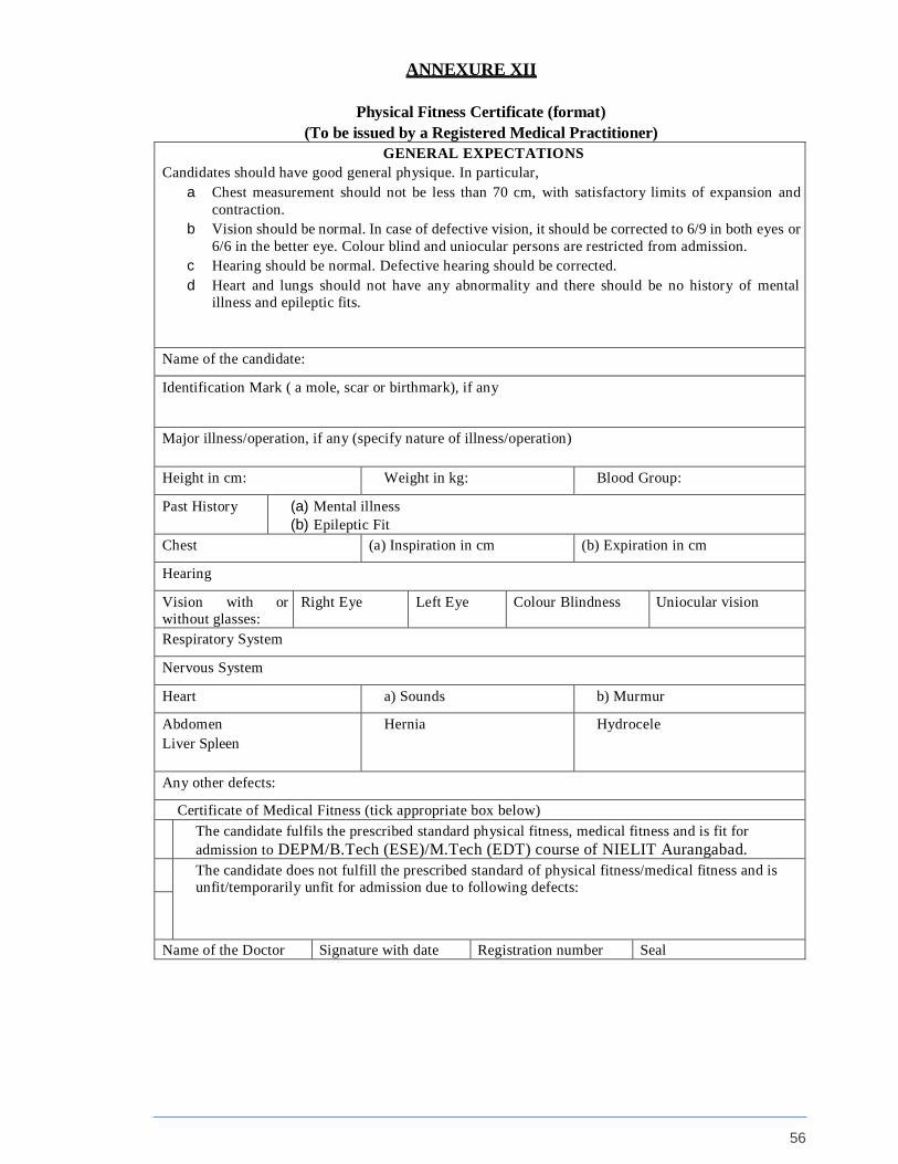
56
ANNEXURE XII
Physical Fitness Certificate (format)
(To be issued by a Registered Medical Practitioner)
GENERAL EXPECTATIONS
Candidates should have good general physique. In particular,
a Chest measurement should not be less than 70 cm, with satisfactory limits of expansion and
contraction.
b Vision should be normal. In case of defective vision, it should be corrected to 6/9 in both eyes or
6/6 in the better eye. Colour blind and uniocular persons are restricted from admission.
c Hearing should be normal. Defective hearing should be corrected.
d Heart and lungs should not have any abnormality and there should be no history of mental
illness and epileptic fits.
Name of the candidate:
Identification Mark ( a mole, scar or birthmark), if any
Major illness/operation, if any (specify nature of illness/operation)
Height in cm: Weight in kg: Blood Group:
Past History (a) Mental illness
(b) Epileptic Fit
Chest (a) Inspiration in cm (b) Expiration in cm
Hearing
Vision with or
without glasses:
Right Eye Left Eye Colour Blindness Uniocular vision
Respiratory System
Nervous System
Heart a) Sounds b) Murmur
Abdomen
Liver Spleen
Hernia Hydrocele
Any other defects:
Certificate of Medical Fitness (tick appropriate box below)
The candidate fulfils the prescribed standard physical fitness, medical fitness and is fit for
admission to DEPM/B.Tech (ESE)/M.Tech (EDT) course of NIELIT Aurangabad. The candidate does not fulfill the prescribed standard of physical fitness/medical fitness and is
unfit/temporarily unfit for admission due to following defects:
Name of the Doctor Signature with date Registration number Seal

57
ANNEXURE XIII
Sponsorship Certificate
(On letterhead of the Institute /Organization)
Outward No.: Date : _
To, The Dean Academics, NIELIT
Aurangabad
Dr B A M University Campus, Aurangabad
431 004
This is to certify that Mr. / Ms ...........................................................................is serving in
our Organization / Institution as...................................................since………..................
The Organization / Institution has no objection for the mentioned candidate to join the M.Tech(EDT)
at NIELIT, Aurangabad and will permit the candidate to attend lectures as per the institute
timetable.
The Organization / Institution will render all possible help to him / her in persuasion of studies.
He / She will be relieved for a requisite period, if selected for the course.
Signature of Competent Authority
Name: Designation:
Seal of Sponsoring Organization
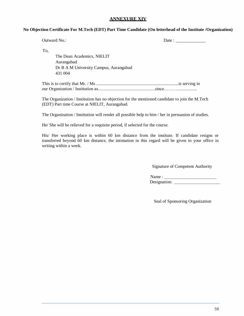
58
ANNEXURE XIV
No Objection Certificate For M.Tech (EDT) Part Time Candidate (On letterhead of the Institute /Organization)
Outward No.: Date : _
To, The Dean Academics, NIELIT
Aurangabad
Dr B A M University Campus, Aurangabad
431 004
This is to certify that Mr. / Ms ...........................................................................is serving in
our Organization / Institution as....................................................since………..................
The Organization / Institution has no objection for the mentioned candidate to join the M.Tech
(EDT) Part time Course at NIELIT, Aurangabad.
The Organization / Institution will render all possible help to him / her in persuasion of studies.
He/ She will be relieved for a requisite period, if selected for the course.
His/ Her working place is within 60 km distance from the institute. If candidate resigns or
transferred beyond 60 km distance, the intimation in this regard will be given to your office in
writing within a week.
Signature of Competent Authority
Name :
Designation:
Seal of Sponsoring Organization
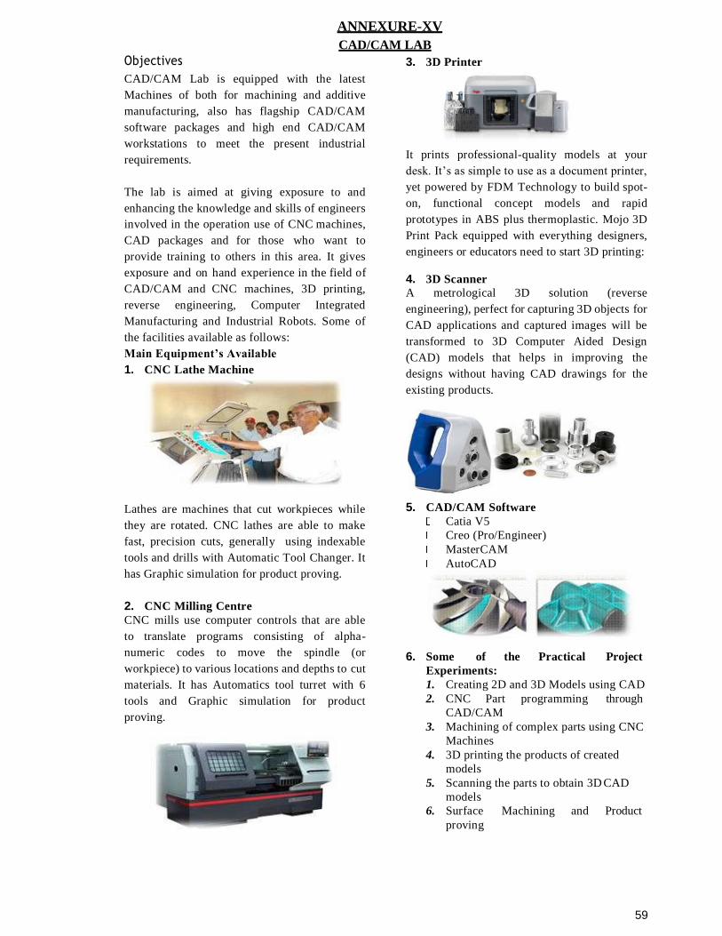
59
Objectives
ANNEXURE-XV
CAD/CAM LAB
3. 3D Printer
CAD/CAM Lab is equipped with the latest
Machines of both for machining and additive
manufacturing, also has flagship CAD/CAM
software packages and high end CAD/CAM
workstations to meet the present industrial
requirements.
The lab is aimed at giving exposure to and
enhancing the knowledge and skills of engineers
involved in the operation use of CNC machines,
CAD packages and for those who want to
provide training to others in this area. It gives
exposure and on hand experience in the field of
CAD/CAM and CNC machines, 3D printing,
reverse engineering, Computer Integrated
Manufacturing and Industrial Robots. Some of
the facilities available as follows:
Main Equipment’s Available
1. CNC Lathe Machine
Lathes are machines that cut workpieces while
they are rotated. CNC lathes are able to make
fast, precision cuts, generally using indexable
tools and drills with Automatic Tool Changer. It
has Graphic simulation for product proving.
2. CNC Milling Centre
CNC mills use computer controls that are able
to translate programs consisting of alpha-
numeric codes to move the spindle (or
workpiece) to various locations and depths to cut
materials. It has Automatics tool turret with 6
tools and Graphic simulation for product
proving.
It prints professional-quality models at your
desk. It’s as simple to use as a document printer,
yet powered by FDM Technology to build spot-
on, functional concept models and rapid
prototypes in ABS plus thermoplastic. Mojo 3D
Print Pack equipped with everything designers,
engineers or educators need to start 3D printing:
4. 3D Scanner
A metrological 3D solution (reverse
engineering), perfect for capturing 3D objects for
CAD applications and captured images will be
transformed to 3D Computer Aided Design
(CAD) models that helps in improving the
designs without having CAD drawings for the
existing products.
5. CAD/CAM Software
Catia V5
Creo (Pro/Engineer)
MasterCAM
AutoCAD
6. Some of the Practical Project
Experiments:
1. Creating 2D and 3D Models using CAD
2. CNC Part programming through
CAD/CAM
3. Machining of complex parts using CNC
Machines
4. 3D printing the products of created
models
5. Scanning the parts to obtain 3D CAD
models
6. Surface Machining and Product
proving
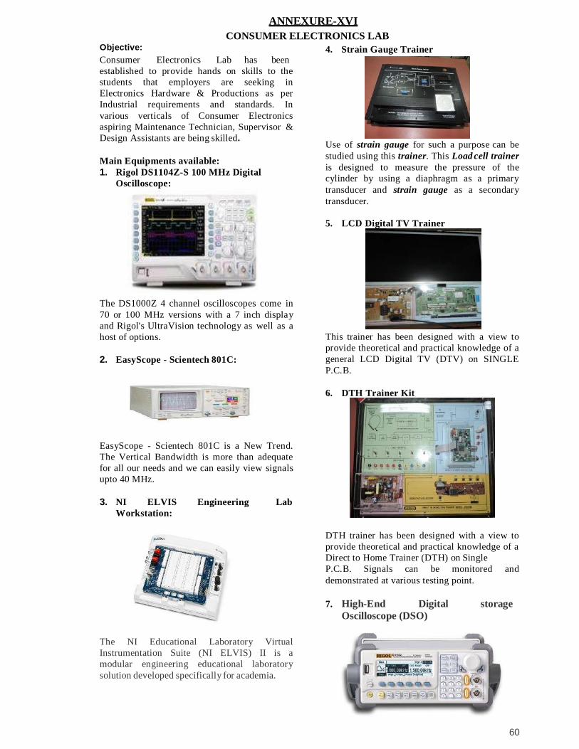
60
Objective:
ANNEXURE-XVI
CONSUMER ELECTRONICS LAB
4. Strain Gauge Trainer Consumer Electronics Lab has been
established to provide hands on skills to the
students that employers are seeking in
Electronics Hardware & Productions as per
Industrial requirements and standards. In
various verticals of Consumer Electronics
aspiring Maintenance Technician, Supervisor &
Design Assistants are being skilled.
Main Equipments available:
1. Rigol DS1104Z-S 100 MHz Digital
Oscilloscope:
The DS1000Z 4 channel oscilloscopes come in
70 or 100 MHz versions with a 7 inch display
and Rigol's UltraVision technology as well as a
host of options.
2. EasyScope - Scientech 801C:
EasyScope - Scientech 801C is a New Trend.
The Vertical Bandwidth is more than adequate
for all our needs and we can easily view signals
upto 40 MHz.
3. NI ELVIS Engineering Lab
Workstation:
The NI Educational Laboratory Virtual
Instrumentation Suite (NI ELVIS) II is a
modular engineering educational laboratory
solution developed specifically for academia.
Use of strain gauge for such a purpose can be
studied using this trainer. This Load cell trainer
is designed to measure the pressure of the
cylinder by using a diaphragm as a primary
transducer and strain gauge as a secondary
transducer.
5. LCD Digital TV Trainer
This trainer has been designed with a view to
provide theoretical and practical knowledge of a
general LCD Digital TV (DTV) on SINGLE
P.C.B.
6. DTH Trainer Kit
DTH trainer has been designed with a view to
provide theoretical and practical knowledge of a
Direct to Home Trainer (DTH) on Single
P.C.B. Signals can be monitored and
demonstrated at various testing point.
7. High-End Digital storage
Oscilloscope (DSO)

61
ANNEXURE XVI
CONSUMER ELECTRONICS LAB
High-End Digital storage Oscilloscope (DSO)
can ensure the proper functioning of the device
or design flaws allowing for a more intuitive
visual diagnosis of the source of unexpected
voltage.
It allows probing of individual components and
connections within electronic devices, acting as
a simple signal tracer to determine the specific
malfunctioning part besides providing alert
regarding replacement need or fine tuning of
electronic component.
Some of the Practical / Project
Experiments:
1. Testing of Passive and Active
components -
2. Characteristics diode: Transistor
3. Rectifying circuits
4. Filter circuits
5. Oscillator: Design of different type of
biasing and their comparison
6. Study of Amplifiers
7. Verification of Thevenins, theorem for a
two port network
8. Verification of Norton’s theorem for a two
port network
9. Maximum Power Transfer theorem
10. Series resonance - BW and Q factor
11. Parallel resonance –B.W. and Q- factor
12. To learn LCD Digital TV working and
repairing using Trainer kit
13. To learn DTH working and repairing using
Trainer Kit
14. To learn Dvd player working and
repairing using Trainer Kit
PTH Mechanical assembly
Electroless plating is “plating without the use of
electrical energy” a chemical reduction process
which depends upon the catalytic reduction
process of metal ions in an aqueous solution
(containing a chemical reducing agent) and the
subsequent deposition of the metal. Typical
choice for irregularly shaped, highly detailed
part shapes because of completely uniform
deposit thickness and high precision. By using
this process and principle, PTH process has
been completed shapes because of completely
uniform deposit thickness and high precision.
By using this process and principle, PTH process
has been completed.
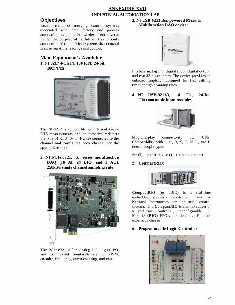
62
Objectives
ANNEXURE-XVII
INDUSTRIAL AUTOMATION LAB
3. NI USB-6211 Bus-powered M series
Recent trend of merging control systems
associated with both factory and process
automation demands knowledge from diverse
fields. The purpose of the lab work is to study
automation of time critical systems that demand
precise real-time readings and control.
Main Equipment’s Available 1. NI 9217 4-Ch PT 100 RTD 24-bit,
100S/s/ch
The NI-9217 is compatible with 3- and 4-wire
RTD measurements, and it automatically detects
the type of RTD (3- or 4-wire) connected to the
channel and configures each channel for the
appropriate mode
2. NI PCIe-6321, X series multifunction
DAQ (16 AI, 24 DIO, and 2 AO),
250kS/s single channel sampling rate:
The PCIe-6321 offers analog I/O, digital I/O,
and four 32-bit counters/timers for PWM,
encoder, frequency, event counting, and more.
Multifunction DAQ device:
It offers analog I/O, digital input, digital output,
and two 32-bit counters. The device provides an
onboard amplifier designed for fast settling
times at high scanning rates.
4. NI USB-9211A, 4 Ch., 24-Bit
Thermocouple input module:
Plug-and-play connectivity via USB.
Compatibility with J, K, R, S, T, N, E, and B
thermocouple types
Small, portable device (12.1 x 8.6 x 2.5 cm)
5. CompactRIO:
CompactRIO (or cRIO) is a real-time
embedded industrial controller made by
National Instruments for industrial control
systems. The CompactRIO is a combination of
a real-time controller, reconfigurable IO
Modules (RIO), FPGA module and an Ethernet
expansion chassis.
6. Programmable Logic Controller

63
ANNEXURE XVII
INDUSTRIAL AUTOMATION LAB
PLC is used for control applications as in
special purpose machines for milling, drilling,
packaging etc. PLC senses inputs from field
(using its input cards), for example from a level
sensor, a proximity switch, pushbutton etc.
PLC’s have been programmed in a language
called as ladder language.
7. Electro-Pneumatic Trainer Kit
Electro-pneumatic control consists of electrical
control systems and operating pneumatic power
systems. In this solenoid valves are used as
interface between the electrical and pneumatic
systems. Devices like limit switches and
proximity sensors are used as feedback
elements.
8. Level Measurement
Capacitive Level Sensors also referred as Radio
Frequency (RF) level sensors, are used for
measuring process level at a specific point,
multiple points or continuously over the entire
vessel height. Level change results in a
variation of capacitance value around the probe,
depending upon the degree of immersion.
Some of the practical project experiment: 1. Optimized Operation of Induction Generator
for Small-scale Wind Power.
2. High Precision Stepper Motor Controller
Implementation on FPGA with GUI on
LabVIEW.
3. Real Time Data Monitoring of PV Solar
Cell Using LabVIEW and DAQ.
4. Forest Fire Detection Using Optimized
Solar-Power Zigbee Network
5. Optical Character Recognition Based
Speech Synthesis System Using LabVIEW
6. LabVIEW and Web-Server Based Human
Body Monitoring System
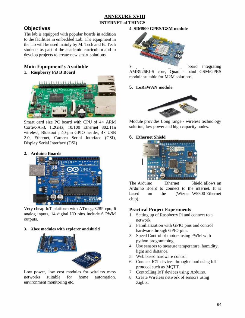
64
Objectives
ANNEXURE XVIII
INTERNET of THINGS
4. SIM900 GPRS/GSM module
The lab is equipped with popular boards in addition
to the facilities in embedded Lab. The equipment in
the lab will be used mainly by M. Tech and B. Tech
students as part of the academic curriculum and to
develop projects to create new smart solutions.
Main Equipment’s Available 1. Raspberry Pi3 B Board
Smart card size PC board with CPU of 4× ARM
Cortex-A53, 1.2GHz, 10/100 Ethernet 802.11n
wireless, Bluetooth, 40-pin GPIO header, 4× USB
2.0, Ethernet, Camera Serial Interface (CSI),
Display Serial Interface (DSI)
2. Arduino Boards
Very cheap IoT platform with ATmega328P cpu, 6
analog inputs, 14 digital I/O pins include 6 PWM
outputs.
3. Xbee modules with explorer and shield
Low power, low cost modules for wireless mess
networks suitable for home automation,
environment monitoring etc.
Very powerful single-chip board integrating
AMR926EJ-S core, Quad - band GSM/GPRS
module suitable for M2M solutions.
5. LoRaWAN module
Module provides Long range - wireless technology
solution, low power and high capacity nodes.
6. Ethernet Shield
The Arduino Ethernet Shield allows an
Arduino Board to connect to the internet. It is
based on the (Wiznet W5500 Ethernet
chip).
Practical Project Experiments 1. Setting up of Raspberry Pi and connect to a
network
2. Familiarization with GPIO pins and control
hardware through GPIO pins.
3. Speed Control of motors using PWM with
python programming.
4. Use sensors to measure temperature, humidity,
light and distance.
5. Web based hardware control
6. Connect IOT devices through cloud using IoT
protocol such as MQTT.
7. Controlling IoT devices using Arduino.
8. Create Wireless network of sensors using
Zigbee.
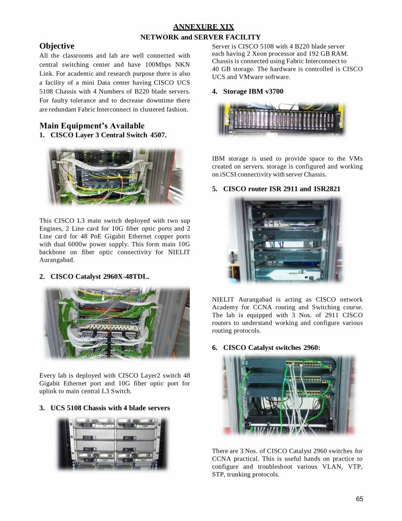
65
Objective
ANNEXURE XIX
NETWORK and SERVER FACILITY
Server is CISCO 5108 with 4 B220 blade server
All the classrooms and lab are well connected with
central switching center and have 100Mbps NKN
Link. For academic and research purpose there is also
a facility of a mini Data center having CISCO UCS
5108 Chassis with 4 Numbers of B220 blade servers.
For faulty tolerance and to decrease downtime there
are redundant Fabric Interconnect in clustered fashion.
Main Equipment’s Available 1. CISCO Layer 3 Central Switch 4507.
This CISCO L3 main switch deployed with two sup
Engines, 2 Line card for 10G fiber optic ports and 2
Line card for 48 PoE Gigabit Ethernet copper ports
with dual 6000w power supply. This form main 10G
backbone on fiber optic connectivity for NIELIT
Aurangabad.
2. CISCO Catalyst 2960X-48TDL.
Every lab is deployed with CISCO Layer2 switch 48
Gigabit Ethernet port and 10G fiber optic port for
uplink to main central L3 Switch.
3. UCS 5108 Chassis with 4 blade servers
each having 2 Xeon processor and 192 GB RAM. Chassis is connected using Fabric Interconnect to
40 GB storage. The hardware is controlled is CISCO
UCS and VMware software.
4. Storage IBM v3700
IBM storage is used to provide space to the VMs
created on servers. storage is configured and working
on iSCSI connectivity with server Chassis.
5. CISCO router ISR 2911 and ISR2821
NIELIT Aurangabad is acting as CISCO network
Academy for CCNA routing and Switching course.
The lab is equipped with 3 Nos. of 2911 CISCO
routers to understand working and configure various
routing protocols.
6. CISCO Catalyst switches 2960:
There are 3 Nos. of CISCO Catalyst 2960 switches for
CCNA practical. This is useful hands on practice to
configure and troubleshoot various VLAN, VTP,
STP, trunking protocols.
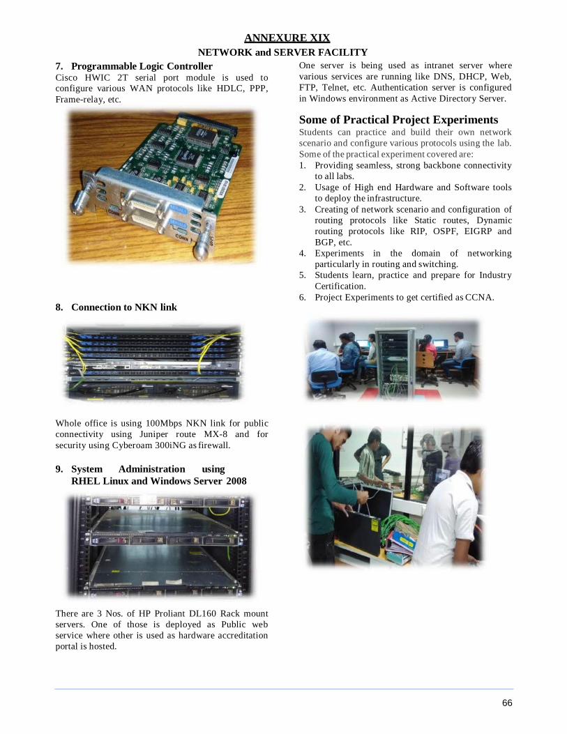
66
ANNEXURE XIX
NETWORK and SERVER FACILITY
7. Programmable Logic Controller Cisco HWIC 2T serial port module is used to
configure various WAN protocols like HDLC, PPP,
Frame-relay, etc.
8. Connection to NKN link
Whole office is using 100Mbps NKN link for public
connectivity using Juniper route MX-8 and for
security using Cyberoam 300iNG as firewall.
9. System Administration using
RHEL Linux and Windows Server 2008
There are 3 Nos. of HP Proliant DL160 Rack mount
servers. One of those is deployed as Public web
service where other is used as hardware accreditation
portal is hosted.
One server is being used as intranet server where
various services are running like DNS, DHCP, Web,
FTP, Telnet, etc. Authentication server is configured
in Windows environment as Active Directory Server.
Some of Practical Project Experiments Students can practice and build their own network
scenario and configure various protocols using the lab.
Some of the practical experiment covered are:
1. Providing seamless, strong backbone connectivity
to all labs.
2. Usage of High end Hardware and Software tools
to deploy the infrastructure.
3. Creating of network scenario and configuration of
routing protocols like Static routes, Dynamic
routing protocols like RIP, OSPF, EIGRP and
BGP, etc.
4. Experiments in the domain of networking
particularly in routing and switching.
5. Students learn, practice and prepare for Industry
Certification.
6. Project Experiments to get certified as CCNA.
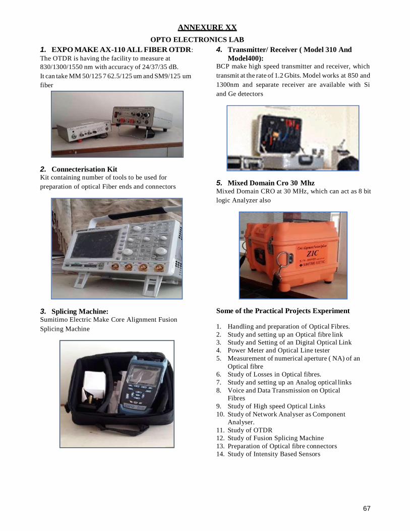
67
ANNEXURE XX
OPTO ELECTRONICS LAB
1. EXPO MAKE AX-110 ALL FIBER OTDR:
The OTDR is having the facility to measure at
830/1300/1550 nm with accuracy of 24/37/35 dB.
It can take MM 50/125 7 62.5/125 um and SM9/125 um
fiber
2. Connecterisation Kit Kit containing number of tools to be used for
preparation of optical Fiber ends and connectors
3. Splicing Machine: Sumitimo Electric Make Core Alignment Fusion
Splicing Machine
4. Transmitter/ Receiver ( Model 310 And
Model400): BCP make high speed transmitter and receiver, which
transmit at the rate of 1.2 Gbits. Model works at 850 and
1300nm and separate receiver are available with Si
and Ge detectors
5. Mixed Domain Cro 30 Mhz Mixed Domain CRO at 30 MHz, which can act as 8 bit
logic Analyzer also
Some of the Practical Projects Experiment
1. Handling and preparation of Optical Fibres.
2. Study and setting up an Optical fibre link
3. Study and Setting of an Digital Optical Link
4. Power Meter and Optical Line tester
5. Measurement of numerical aperture ( NA) of an
Optical fibre
6. Study of Losses in Optical fibres.
7. Study and setting up an Analog optical links
8. Voice and Data Transmission on Optical
Fibres
9. Study of High speed Optical Links
10. Study of Network Analyser as Component
Analyser.
11. Study of OTDR
12. Study of Fusion Splicing Machine
13. Preparation of Optical fibre connectors
14. Study of Intensity Based Sensors

68
Objectives
ANNEXURE XXI
POWER ELECTRONICS LAB
2. Electronic Heater Temperature control.
The lab aims at imparting practical knowledge of
Power Electronics to the students at various levels
i.e. DEPM, B.Tech and M.Tech. It is accordingly well
equipped with equipment’s and trainer kits to teach
practical from fundamentals to high level concepts to
the students.
Main Equipment’s Available
1. Triac AC Phase Control
All Components are terminated with a connector for
the study of Students. One potentiometer is provided
to vary the firing angle of SCR. Another
potentiometer is provided to vary the firing angle of
TRIAC.
2. Single Phase Converter
Power circuit with a DC shunt motor 2SCRs/4SCRs
and 2 power diodes. A circuit breaker, a bridge
rectifier for field supply.1 phase converter firing
circuit. SCR converter with open/close loop with
motor rpm indication, mech. Loading load regulation
= 1% with tacho F/B
3. SCR Lamp Flasher
Scientech PE40 SCR Lamp Flasher is compact, ready
to use experiment board for lamp flasher using SCR
circuit. This board is useful for students to study and
understand operation of SCR controlled lamp flasher
circuit and measurement of frequency, time, and
voltage.
Some of the Practical project experiments.
1. Triac based speed control of small single
Phase Induction Motor.
3. Operation of SCR flasher.
4. Lamp brightness control using single Phase
SCR Converter.
4. DC Chopper
DC Chopper Using SCR Trainer is very much useful
for the students, to understand the principle of working
and operation of the chopper. Output voltage can be
controlled electronically by variation of Duty Cycle.
5. DC to AC Inverter
Power Electronic Training Board has been designed
specifically for the study of working of inverter. A
Battery 12V 80AH (Any car battery) is required to
operate this apparatus. Different test points have been
provided to check wave shape and amplitude of pulses
how DC supply is changed to AC supply.
6. SCR Triggering Trainer
SCR trigger trainer system. UJT triggering
circuit24Volt 10W Lamp load24 Volt ac supply for
Circuit inputs LED indication for supply R-trigger
circuit with phase angle control 5 degrees to 90
degrees R-trigger circuit half wave with phase angle
control up to 180 degree maximum. UJT is an
excellent triggering device which provides narrow
gate pulses. Control is very accurate and from 0 Deg.
to 180 Degree.
Practical project experiments.
1. DC Chopper based speed control of small DC
Motor.
2. Lamp brightness control using inverter.
3. Inverter driven small induction motor.
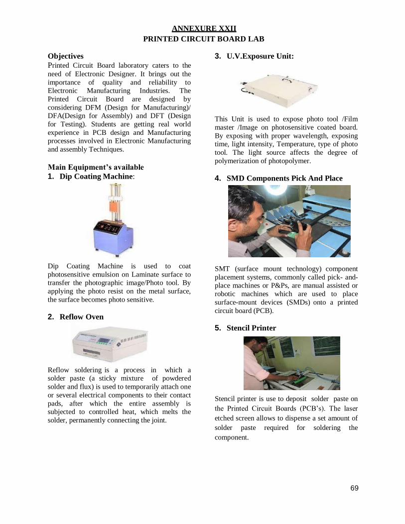
69
ANNEXURE XXII
PRINTED CIRCUIT BOARD LAB
Objectives
Printed Circuit Board laboratory caters to the
need of Electronic Designer. It brings out the
importance of quality and reliability to Electronic Manufacturing Industries. The
Printed Circuit Board are designed by
considering DFM (Design for Manufacturing)/ DFA(Design for Assembly) and DFT (Design
for Testing). Students are getting real world
experience in PCB design and Manufacturing processes involved in Electronic Manufacturing
and assembly Techniques.
Main Equipment’s available
1. Dip Coating Machine:
Dip Coating Machine is used to coat
photosensitive emulsion on Laminate surface to transfer the photographic image/Photo tool. By
applying the photo resist on the metal surface,
the surface becomes photo sensitive.
2. Reflow Oven
Reflow soldering is a process in which a solder paste (a sticky mixture of powdered
solder and flux) is used to temporarily attach one
or several electrical components to their contact
pads, after which the entire assembly is subjected to controlled heat, which melts the
solder, permanently connecting the joint.
3. U.V.Exposure Unit:
This Unit is used to expose photo tool /Film
master /Image on photosensitive coated board.
By exposing with proper wavelength, exposing time, light intensity, Temperature, type of photo
tool. The light source affects the degree of
polymerization of photopolymer.
4. SMD Components Pick And Place
SMT (surface mount technology) component
placement systems, commonly called pick- and-place machines or P&Ps, are manual assisted or
robotic machines which are used to place
surface-mount devices (SMDs) onto a printed
circuit board (PCB).
5. Stencil Printer
Stencil printer is use to deposit solder paste on
the Printed Circuit Boards (PCB’s). The laser
etched screen allows to dispense a set amount of
solder paste required for soldering the
component.
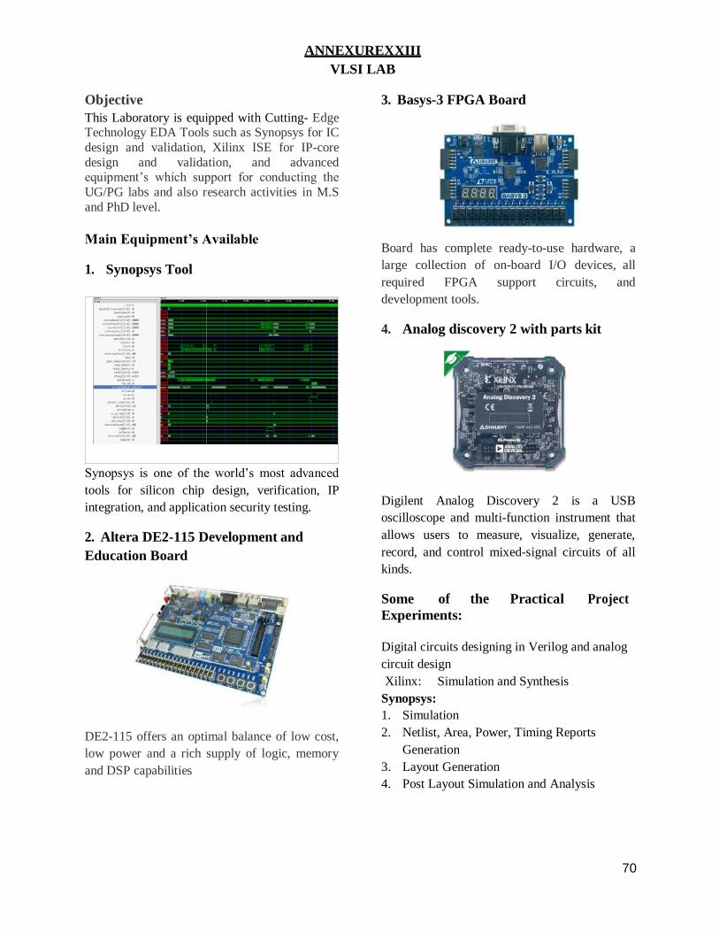
70
ANNEXUREXXIII
VLSI LAB
Objective
This Laboratory is equipped with Cutting- Edge Technology EDA Tools such as Synopsys for IC
design and validation, Xilinx ISE for IP-core
design and validation, and advanced equipment’s which support for conducting the
UG/PG labs and also research activities in M.S
and PhD level.
Main Equipment’s Available
1. Synopsys Tool
Synopsys is one of the world’s most advanced
tools for silicon chip design, verification, IP
integration, and application security testing.
2. Altera DE2-115 Development and
Education Board
DE2-115 offers an optimal balance of low cost,
low power and a rich supply of logic, memory
and DSP capabilities
3. Basys-3 FPGA Board
Board has complete ready-to-use hardware, a
large collection of on-board I/O devices, all
required FPGA support circuits, and
development tools.
4. Analog discovery 2 with parts kit
Digilent Analog Discovery 2 is a USB
oscilloscope and multi-function instrument that
allows users to measure, visualize, generate,
record, and control mixed-signal circuits of all
kinds.
Some of the Practical Project
Experiments:
Digital circuits designing in Verilog and analog
circuit design
Xilinx: Simulation and Synthesis
Synopsys:
1. Simulation
2. Netlist, Area, Power, Timing Reports
Generation
3. Layout Generation
4. Post Layout Simulation and Analysis
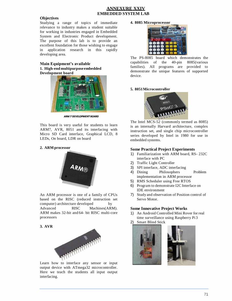
71
Objectives
ANNEXURE XXIV EMBEDDED SYSTEM LAB
Studying a range of topics of immediate
relevance to industry makes a student suitable
for working in industries engaged in Embedded
System and Electronic Product development.
The purpose of this lab is to provide an
excellent foundation for those wishing to engage
in application research in this rapidly
developing area.
Main Equipment’s available 1. High-end multipurpose embedded
Development board
This board is very useful for students to learn
ARM7, AVR, 8051 and its interfacing with
Micro SD Card interface, Graphical LCD, 8
LEDs, On board, LDR on board
2. ARM processor
An ARM processor is one of a family of CPUs
based on the RISC (reduced instruction set
computer) architecture developed by
Advanced RISC Machines(ARM).
ARM makes 32-bit and 64- bit RISC multi-core
processors
3. AVR
Learn how to interface any sensor or input
output device with ATmega32 microcontroller.
Here we teach the students all input output
interfacing.
4. 8085 Microprocessor
The PS-8085 board which demonstrates the
capabilities of the 40-pin 8085(various
families). All programs are provided to
demonstrate the unique features of supported
device.
5. 8051 Microcontroller
The Intel MCS-52 (commonly termed as 8085)
is an internally Harvard architecture, complex
instruction set, and single chip microcontroller
series developed by Intel in 1980 for use in
embedded systems.
Some Practical Project Experiments 1) Familiarization with ARM board, RS- 232C
interface with PC
2) Traffic Light Controller
3) SPI interface, ADC interfacing
4) Dining Philosophers Problem
implementation in ARM processor
5) RMS Scheduler using Free RTOS
6) Program to demonstrate I2C Interface on
IDE environment
7) Study and observation of Position control of
Servo Motor.
Some Innovative Project Works 1) An Android Controlled Mini Rover for real
time surveillance using Raspberry Pi 3
2) Smart Blind Stick
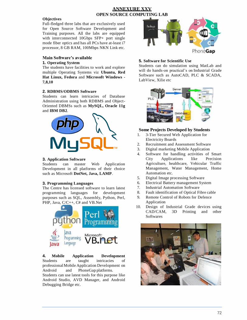
72
Objectives
ANNEXURE XXV
OPEN SOURCE COMPUTING LAB
Full-fledged three labs that are exclusively used
for Open Source Software Development and
Training purposes. All the labs are equipped
with interconnected 10Gbps SFP+ port single
mode fiber optics and has all PCs have at-least i7
processor, 8 GB RAM, 100Mbps NKN Link etc.
Main Software’s available 1. Operating System
The students have facilities to work and explore
multiple Operating Systems viz Ubuntu, Red
Hat Linux, Fedora and Microsoft Windows -
7,8,10
2. RDBMS/ODBMS Software
Students can learn intricacies of Database
Administration using both RDBMS and Object-
Oriented DBMSs such as MySQL, Oracle 11g
and IBM DB2.
3. Application Software
Students can master Web Application
Development in all platforms of their choice
such as Microsoft DotNet, Java, LAMP.
3. Programming Languages
The Centre has licensed software to learn latest
programming languages for development
purposes such as SQL, Assembly, Python, Perl,
PHP, Java, C/C++, C# and VB.Net
4. Mobile Application Development
Students are taught intricacies of
professional Mobile Application Development on
Android and PhoneGap platforms.
Students can use latest tools for this purpose like
Android Studio, AVD Manager, and Android
Debugging Bridge etc.
5. Software for Scientific Use
Students can do simulation using MatLab and
will do hands-on practical’s on Industrial Grade
Software such as AutoCAD, PLC & SCADA,
LabView, Xilie etc
Some Projects Developed by Students 1. 3-Tier Secured Web Application for
Electricity Boards
2. Recruitment and Assessment Software
3. Digital marketing Mobile Application
4. Software for handling activities of Smart
City Applications like Precision
Agriculture, healthcare, Vehicular Traffic
Management, Water Management, Home
Automation etc.
5. Digital Image processing Software
6. Electrical Battery management System
7. Industrial Automation Software
8. Fault identification of Optical Fibre cable
9. Remote Control of Robots for Defence
Application
10. Design of Industrial Grade devices using
CAD/CAM, 3D Printing and other
Softwares

73
ANNEXURE XXVI LIBRARY INFRASTRUCTURE
Rich library caters to the information needs of the
students, researchers and scientists with its well
managed information resources housed in two
floors spread over an area of 331 Sq.Mtr.
The library has a huge collection of books,
reference books, periodicals, and electronic
resources. The mission to facilitate creation of
new knowledge through acquisition,
organization and dissemination of knowledge
resources.
Major Library Resources
1. MeitY Library Consortium
The Centre is part of MeitY Library Consortium
and has access to an inventory of latest e-Books,
Research Papers and e- Journals including
IEEEXPLORE among others.
2. National Knowledge Network
The purpose of NKN goes
to the very core of the
country’s quest for
building quality
institutions.
The Centre is part of NKN and can seamlessly
connect at gigabit speed and enables students,
scientists, researchers to work together for
accessing information to stimulate research and
create next generation applications & services in
critical and emerging areas.
3. National Digital Library
The Centre is also part of
National Digital library of
MHRD, India. The
students and staff can
access and download
6.5 million books in
vernacular languages of
multiple national and
international digital
libraries.
4. Rich Collection of Books
The library possesses rich collection of more
than 14000 latest books covering subjects such
as Electronics, Computer Science,
Microcontrollers, Embedded systems, Internet of
things, Bioinformatics, Information Security,
Precision-Agriculture, Bio technology,
Control Engineering,
Instrumentation, Networking,
Communication, Robotics.
5. Journals, Theses and Periodicals More
than 20 National Journals/Magazines of repute
are being subscribed by the library.
6. Magazines and Newspapers
Library is subscribing to all leading
newspapers in English, Hindi and Marathi.
Facilities to Students
1. Book Bank
Six books are given to each student per
Semester.
2. Book Request
Students can give recommendation for
procurement of any Books, Journals and
Magazines (Foreign as well as National). The
requests are examined and procurement of the
same is done.
3. Open Access
Students have unrestricted access to all shelf of
books and Journals.
4. Facility for Downloading
There is adequate seating facility besides stack
of computers for downloading research papers, e-
Journals, e-Books and other reading material.
5. Miscellaneous Services
Reprographic service, Circulation, Curriculum
Support for training programs and other User
awareness services.