Characterization and investigation of molybdenum carbides ...
Journal Name
Cite this: DOI: 10.1039/c0xx00000x
www.rsc.org/xxxxxx
Dynamic Article Links ►
ARTICLE TYPE
This journal is © The Royal Society of Chemistry [year] [journal], [year], [vol], 00–00 | 1
Molybdenum disulfide/pyrolytic carbon hybrid electrodes for scalable
hydrogen evolution
Hugo Nolan,a,b
Niall McEvoy,*a Maria O’Brien,
a,b Nina C. Berner,
a Chanyoung Yim,
a,b Toby Hallam,
a
Aidan R. McDonaldb and Georg S. Duesberg*
a,b
Received (in XXX, XXX) Xth XXXXXXXXX 20XX, Accepted Xth XXXXXXXXX 20XX 5
DOI: 10.1039/b000000x
The electrochemical generation of hydrogen fuel via the proton reduction in the Hydrogen Evolution Reaction
(HER) in aqueous media is currently dependent on the use expensive noble metal catalysts for which alternatives
must be sought. Molybdenum disulfide (MoS2) has shown great promise as a suitable electrocatalyst in this regard.
While many lab-scale experiments on the HER activity of this material have demonstrated its viability and explored 10
some fundamental mechanistic features of HER at MoS2, these experimental techniques are often ill-suited to large
scale production of such electrodes. In this study we present work on the fabrication of MoS2/pyrolytic carbon (PyC)
electrodes via vapour phase sulfurization of Mo thin films. These hybrid electrodes combine the catalytic activity of
MoS2 with the conductivity and stability of PyC, whilst using industrially compatible processing techniques.
Structural defects in the sulfur lattice were found to be key catalytically active sites for HER and thinner MoS2 films 15
displayed a higher quantity of these defects and, hence, an improved HER activity. The observed Tafel slope of
95 mV/dec is comparable to previous literature works on MoS2 HER performance.
Introduction
Efficient and sustainable production of hydrogen is essential for a
hydrogen based economy to reduce our dependence on fossil fuel 20
energy sources.1 The electrochemical splitting of water via proton
reduction in the Hydrogen Evolution Reaction (HER) provides a
feasible route towards this without dependence on consumable
resources. However, to date, the best HER performance has been
achieved using prohibitively expensive platinum electrodes, 25
severely limiting the practical applications of this technology. If
the HER is to be exploited as a viable energy source, alternative
electrocatalysts to Pt must be sought.
Recent years have seen ever increasing focus placed on the
synthesis and characterisation of layered 2D materials, based 30
principally on their novel properties.2 Much work in the literature
at present is concerned with layered Transition Metal
Dichalcogenides (TMDs).2,3 This group of materials has been
proposed for a plethora of next generation uses with potential
applications in 2D electronics,4–6 gas sensing7–9
and, most 35
significantly for this study, catalysis of the HER,10–12
having
been demonstrated in recent years.
Thus far, molybdenum disulfide (MoS2) has been the most
heavily studied material in the context of catalysis, although
studies on the HER behaviour of other materials such as MoSe2, 40
WS2 and WSe2 have recently emerged.13–15
Depending on the
synthesis route undertaken, HER activity has been attributed to
different features of TMD layers. Where MoS2 flakes have been
exfoliated from bulk MoS2 via intercalation of Li-ions, it has
been demonstrated that the HER activity is related to the presence 45
of the so-called 1T polymorph.16,17
This is not found in bulk
MoS2, which consists solely of the 2H polymorph. Many other
studies have attributed HER activity of MoS2 to the presence of
unsaturated sulfur atoms along molybdenum edges of the MoS2
structure.18,19
Furthermore, theoretical studies have shown that 50
sulfur vacancies catalyse various reactions at the MoS2 surface.20
These defects, in the otherwise catalytically inactive basal plane
of the sulfur sub-lattice, act as catalytically active sites.
The majority of studies on HER by TMDs deal with dispersions
of TMD flakes or nanoparticles which are then immobilised on an 55
electrode surface for HER measurements. Often these same
studies incorporate further processing conditions or stages to
enhance the HER activity of these films by establishing active
sites on the material. Li et al. used a solvothermal process to
synthesise MoS2 flakes and found that incorporating Reduced 60
Graphene Oxide (rGO) to create an MoS2/rGO hybrid improved
performance for HER.10
Xie et al. reported a synthetic chemical
route where the reaction precursors were controlled to create
defective MoS2 nanoflakes which exhibit favourable HER
activity.21
Wang et al. isolated MoS2 flakes exfoliated from 65
bulk22 and subsequently attributed increased HER performance of
smaller nanoparticles to an increase in available unsaturated
sulfur sites.23 Yu et al. found that the HER activity of MoS2
grown via Chemical Vapour Deposition (CVD) from an MoCl5
precursor improved with a reduction in the number of MoS2 70
layers.24 They correlated the activity to the hopping of electrons
between these layers. Typically characterisation of the HER
activity of such materials is carried out by depositing very small
amounts of the material on conductive substrates such as glassy
carbon. Merki et al. developed a technique whereby MoS2 flakes 75
can be electrochemically deposited on conductive substrates via

2 | Journal Name, [year], [vol], 00–00 This journal is © The Royal Society of Chemistry [year]
repeated cyclic voltammetry in an electrolyte of (NH4)2[MoS4].25
Such direct deposition/synthesis techniques could conceivably
allow the large-scale fabrication of MoS2 electrodes for energy
applications.
Nonetheless, many techniques employed in literature studies on 5
HER at MoS2, while useful for lab-scale experiments, offer poor
scalability. Ultimately, if the implementation of TMDs as HER
catalysts is to be successful, large scale production of such
electrocatalysts for industrial applications must be viable. Here,
we propose an electrode fabrication process that involves the 10
deposition of thin films of metallic Mo directly on conductive
substrates followed by vapour phase sulfurisation. The poor
conductivity of MoS2 precludes the use of electrodes fabricated
entirely from the material. Mo films were evaporated on to
Pyrolytic Carbon (PyC) films grown via CVD. Our previous 15
experience with PyC has shown that this material is highly
suitable as an electrode material given its chemical, thermal and
mechanical durability with many reported electrochemical
applications.26–29
This investigation aims to show that such thin layers of MoS2, 20
grown via vapour phase sulfurisation directly on a substrate of
conductive PyC, present a suitable electrode for HER with few
limits to up-scaling production in an industrially compatible
process. In addition, details of the reaction mechanism are
discussed and correlated to spectroscopic and microscopic 25
characterisation of the MoS2/PyC films.
Results and Discussion
Electrodes were fabricated on SiO2/Si substrates with an initial
step of CVD growth of PyC. Subsequent deposition of Mo was
performed in a defined region of the sample to control the area of 30
the resultant electrode. Finally, vapour phase sulfurisation was
carried out to form MoS2 on the PyC coated substrate. All further
material characterisation and electrochemical measurements were
performed on such samples.
Material Characterisation 35
Raman Spectroscopy
MoS2 samples 4.5, 10 and 53 nm thick were investigated and
spectral features of both PyC and MoS2 are evident. The broad D
and G bands (~1353 and ~1583 cm-1, respectively) coupled with
the highly suppressed 2D band at 2700 cm-1 are indicative of a 40
disordered graphitic system such as PyC. The peaks observed at
~383 and ~408 cm-1 are characteristic of MoS2 and are denoted
the E12g and A1g peaks and arise due to in plane and out of plane
vibrations, respectively.30,31 Fig.1 (a) shows a comparison of the
Raman spectra of each sample, normalised to the intensity of the 45
A1g peak, with the D and G band region of PyC highlighted in
grey and the MoS2 peaks highlighted in cyan. It is immediately
apparent that the relative PyC characteristic signal is much
reduced as the MoS2 layer thickness increases. The greater
quantity of MoS2 present atop of the PyC surface causes a 50
decreased penetration of the Raman laser into the PyC substrate.
Fig 1: (a) Raman spectra for MoS2 films on PyC substrates. Also
included is the spectrum of the bare substrate. The cyan region marks
MoS2 characteristic peaks while the grey region marks PyC characteristic 55
peaks. (b) High spectral resolution scan of the MoS2 peaks with the
reduced peak separation of the thinner films indicated.
Analysis of the MoS2 characteristic peaks divulges information
regarding the nature of the MoS2 films. Fig.1 (b) shows that the
spectral region of interest for MoS2 is rather similar for all 60
samples. However, closer inspection shows a shift in peak
position which is dependent on MoS2 thickness. The coupling
between electronic transitions and phonons is modified as the
MoS2 thickness is decreased, causing a narrowing of peak
separation between the E12g and A1g modes. This behaviour is 65
reflected here with the dotted lines highlighting a reduction in
peak separation of ~2 cm-1 on going from 53 nm to 4.5 nm thick
MoS2. From this it is apparent that the 4.5 nm film can be
considered distinct from bulk MoS2.
X-Ray Photoelectron Spectroscopy 70
XPS analysis of the MoS2/PyC films revealed a wealth of
chemical information. Survey spectra of each MoS2 film and the
bare PyC substrate are shown in Fig.2 (a) with characteristic
photoemission peaks corresponding to C, S and Mo highlighted
in grey, yellow and cyan, respectively. It is apparent, as with the 75
Raman spectroscopy, that the spectral contributions from the PyC
substrate diminish as the MoS2 layer thickness increases.

This journal is © The Royal Society of Chemistry [year] Journal Name, [year], [vol], 00–00 | 3
Fig 2: (a) XPS survey scans of the MoS2/PyC electrodes investigated in
this study. Carbon characteristic core level peaks marked by grey, Mo
peaks by cyan and the S peaks by yellow. (b) S2p core level peak for
4.5 nm MoS2 film with spectral contributions fitted. 5
To gain a greater insight into the chemical nature of the film,
higher resolution scans of the S2p and Mo3d spectral regions
were recorded and spectral contributions were fitted to the
measured data. Fig.2 (b) shows the S2p region for the 4.5 nm film
including peak contributions, which are consistent with the 10
binding energy values found by Eda et al.32 The two key features
are the doublet peak which corresponds to sulfur in bulk MoS2
(marked in blue) and a smaller doublet peak at a slightly higher
binding energy which is associated with unsaturated sulfur in
edge crystallographic states (marked in green). It was found that 15
this “edge-sulfur” contribution was appreciably smaller for
thicker MoS2 films. The concentration of edge sulfur as
determined by XPS was found to increase from approximately
7.6% in the thickest film to approximately 13.6% in the thinnest
film. A detailed discussion of the S2p fitting and a comparison of 20
all three MoS2 film thicknesses is included in the ESI in Fig.S1.
From analysis of the Mo3d spectral region it was found that low
levels of oxides in the form of MoO2 and MoO3 are present in the
MoS2. However, these quantities remain invariant with MoS2 film
thickness and, as such, do not influence any trends in HER 25
activity of the MoS2/PyC electrodes (see ESI for detailed
discussion, Fig.S2).
Electron Microscopy
Fig.3 (a) displays a cross-sectional TEM image of the 53 nm
MoS2/PyC film. The indicated Au/Pd and Pt are part of a 30
protective capping layer involved in the fabrication of the TEM
lamella. A uniform thickness is observed throughout the film as
shown. The polycrystalline nature of the MoS2 layer is evident in
the higher magnification image in Fig.3 (b) where randomly
oriented crystallites can be discerned by virtue of the crystalline 35
planes. Further analysis of MoS2/PyC cross sections is included
in the ESI where an MoS2 interlayer spacing of approximately
6.6 Å was found, consistent with previously reported values.33
Further TEM analysis was carried out on MoS2 grown on SiO2
using an identical technique as used for that grown on PyC. This 40
substrate allowed the MoS2 film to be transferred to TEM grids
via a polymer supported transfer method.
A top-down image of such a MoS2 film is shown in Fig.3 (c).
Hexagonal symmetry is clearly visible in the lattice. Inset in this
panel is a Fast Fourier Transform (FFT) corresponding to this 45
image. The clear hexagonal pattern further confirms the structure
of the film with the presence of multiple MoS2 layers evidenced
by the outer ring in the FFT spot pattern.
Fig 3: (a) Cross sectional TEM image showing uniformity of the 53 nm 50
MoS2/PyC hybrid electrode. (b) HR-TEM of the PyC/MoS2 interface.
Crystalline planes are visible in the MoS2 layer. (c) High resolution top-
4 | Journal Name, [year], [vol], 00–00 This journal is © The Royal Society of Chemistry [year]
down image of MoS2 film on TEM grid with evident hexagonal
symmetry. Inset: Corresponding FFT image.
HER Catalysis
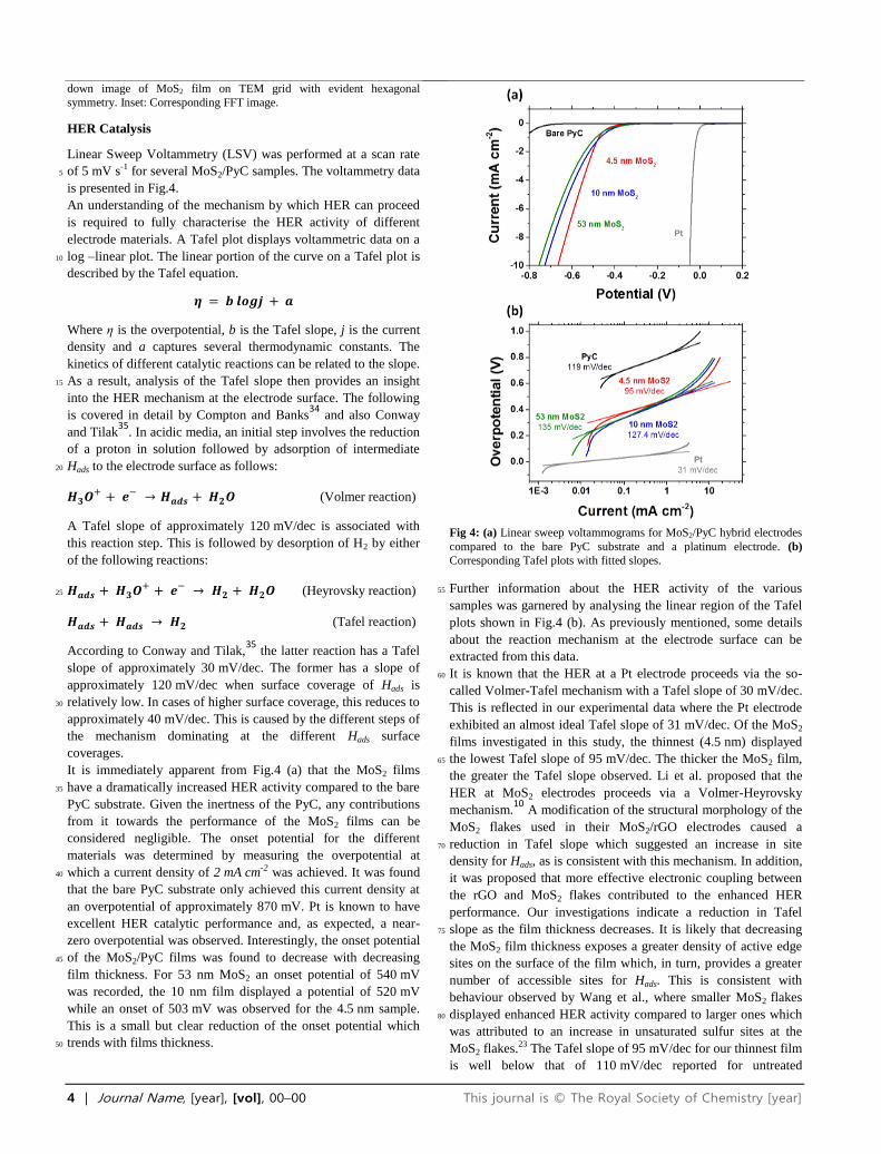
Linear Sweep Voltammetry (LSV) was performed at a scan rate
of 5 mV s-1 for several MoS2/PyC samples. The voltammetry data 5
is presented in Fig.4.
An understanding of the mechanism by which HER can proceed
is required to fully characterise the HER activity of different
electrode materials. A Tafel plot displays voltammetric data on a
log –linear plot. The linear portion of the curve on a Tafel plot is 10
described by the Tafel equation.
Where η is the overpotential, b is the Tafel slope, j is the current
density and a captures several thermodynamic constants. The
kinetics of different catalytic reactions can be related to the slope.
As a result, analysis of the Tafel slope then provides an insight 15
into the HER mechanism at the electrode surface. The following
is covered in detail by Compton and Banks34
and also Conway
and Tilak35
. In acidic media, an initial step involves the reduction
of a proton in solution followed by adsorption of intermediate
Hads to the electrode surface as follows: 20
(Volmer reaction)
A Tafel slope of approximately 120 mV/dec is associated with
this reaction step. This is followed by desorption of H2 by either
of the following reactions:
(Heyrovsky reaction) 25
(Tafel reaction)
According to Conway and Tilak,35
the latter reaction has a Tafel
slope of approximately 30 mV/dec. The former has a slope of
approximately 120 mV/dec when surface coverage of Hads is
relatively low. In cases of higher surface coverage, this reduces to 30
approximately 40 mV/dec. This is caused by the different steps of
the mechanism dominating at the different Hads surface
coverages.
It is immediately apparent from Fig.4 (a) that the MoS2 films
have a dramatically increased HER activity compared to the bare 35
PyC substrate. Given the inertness of the PyC, any contributions
from it towards the performance of the MoS2 films can be
considered negligible. The onset potential for the different
materials was determined by measuring the overpotential at
which a current density of 2 mA cm-2 was achieved. It was found 40
that the bare PyC substrate only achieved this current density at
an overpotential of approximately 870 mV. Pt is known to have
excellent HER catalytic performance and, as expected, a near-
zero overpotential was observed. Interestingly, the onset potential
of the MoS2/PyC films was found to decrease with decreasing 45
film thickness. For 53 nm MoS2 an onset potential of 540 mV
was recorded, the 10 nm film displayed a potential of 520 mV
while an onset of 503 mV was observed for the 4.5 nm sample.
This is a small but clear reduction of the onset potential which
trends with films thickness. 50
Fig 4: (a) Linear sweep voltammograms for MoS2/PyC hybrid electrodes
compared to the bare PyC substrate and a platinum electrode. (b)
Corresponding Tafel plots with fitted slopes.
Further information about the HER activity of the various 55
samples was garnered by analysing the linear region of the Tafel
plots shown in Fig.4 (b). As previously mentioned, some details
about the reaction mechanism at the electrode surface can be
extracted from this data.
It is known that the HER at a Pt electrode proceeds via the so-60
called Volmer-Tafel mechanism with a Tafel slope of 30 mV/dec.
This is reflected in our experimental data where the Pt electrode
exhibited an almost ideal Tafel slope of 31 mV/dec. Of the MoS2
films investigated in this study, the thinnest (4.5 nm) displayed
the lowest Tafel slope of 95 mV/dec. The thicker the MoS2 film, 65
the greater the Tafel slope observed. Li et al. proposed that the
HER at MoS2 electrodes proceeds via a Volmer-Heyrovsky
mechanism.10
A modification of the structural morphology of the
MoS2 flakes used in their MoS2/rGO electrodes caused a
reduction in Tafel slope which suggested an increase in site 70
density for Hads, as is consistent with this mechanism. In addition,
it was proposed that more effective electronic coupling between
the rGO and MoS2 flakes contributed to the enhanced HER
performance. Our investigations indicate a reduction in Tafel
slope as the film thickness decreases. It is likely that decreasing 75
the MoS2 film thickness exposes a greater density of active edge
sites on the surface of the film which, in turn, provides a greater
number of accessible sites for Hads. This is consistent with
behaviour observed by Wang et al., where smaller MoS2 flakes
displayed enhanced HER activity compared to larger ones which 80
was attributed to an increase in unsaturated sulfur sites at the
MoS2 flakes.23 The Tafel slope of 95 mV/dec for our thinnest film
is well below that of 110 mV/dec reported for untreated

This journal is © The Royal Society of Chemistry [year] Journal Name, [year], [vol], 00–00 | 5
exfoliated MoS2 flakes16 and comparable to that observed by Xie
et al. for calcined synthetic MoS2 nanosheets36
and by Li et al. for
synthetic MoS2 particles.10
The MoS2/rGO hybrid material of Ma
et al. exhibits an identical Tafel slope.37 It should be noted that a
secondary phenomenon may contribute to the improved HER 5
performance of the thinner MoS2 films in this study whereby the
thinner films facilitate electron migration to the MoS2 surface.
While the results presented here do not match the best
performance of MoS2 materials for HER available in the
literature, a greater understanding of the mechanism by which the 10
reaction proceeds has been achieved. Sufficiently thin MoS2
layers exhibit behaviour distinct from bulk and a greater number
of defects in the sulfur lattice is seen. Importantly, our electrodes
display both good reproducibility and stability as shown in Fig.S6
of the supplementary information. It is envisaged that further 15
modification of the MoS2/PyC hybrid stack, by chemical or
physical means, could result in additional enhancement of HER
catalysis. In addition, the facile fabrication of MoS2 electrodes on
conductive substrates renders this process highly applicable for
large scale production. 20
Conclusions
In conclusion, we have developed a robust method of fabricating
electrodes of MoS2 on conductive PyC substrates and
demonstrated encouraging results when this is employed as a
HER catalyst. This combination of materials leads to a 25
mechanically durable electrode assembly which can easily be
manufactured on a large scale, unlike many techniques which are
used in the literature to investigate HER at TMDs. Spectroscopic
techniques confirm the stoichiometry of the MoS2 film and also
indicate that our thinnest films behave in a manner distinct from 30
bulk MoS2. The improved performance of the thinner MoS2 films
over thicker ones is correlated to an apparent increase in sulfur
defects in the thinner sample. We propose that this increase in
crystalline defects allows for an increased surface coverage of
adsorbed H (Hads) on the electrode surface. Controlling the 35
thickness of the starting Mo layer is sufficient to enhance the
HER performance of the resultant electrode. The performance of
the MoS2 catalyst is comparable to other published results for
untreated MoS2 materials. Further engineering of the MoS2/PyC
electrode presented here to increase surface roughness and defect 40
levels could further enhance the HER performance. Additionally,
our methods could readily be extended to synthesise electrodes
from other members of the TMD family (WS2, MoSe2 etc.),
potentially improving their catalytic performance.
Experimental 45
Electrode Fabrication
All chemicals used throughout the synthesis and characterisation
were purchased from Sigma-Aldrich and used as-received. PyC
films were grown by CVD of acetylene at 950° C for 30 minutes
to a thickness of 300-400 nm on 300 nm thermal SiO2 on Si 50
substrates in a hot wall quartz tube furnace as previously
reported.26
Following CVD of PyC, the samples were cooled
under Ar atmosphere to room temperature. Subsequently,
electron beam evaporation was carried out in a Temescal FC-
2000 to deposit Mo to thicknesses of approximately 2 nm, 4 nm 55
and 20 nm. Areas of the PyC substrates were physically masked
so that only a 1 cm2 area of the PyC sample was exposed to the
Mo flux. This ensured a reproducible electrode area from sample
to sample. Sulfurisation was then performed as previously
reported.9,33
Briefly, the Mo/PyC samples were placed in a two 60
zone hot wall quartz tube furnace and heated to 750° C under Ar
flow (150 sccm). Sulfur powder was thermally sublimed
upstream of the samples at a temperature of 120° C and
sulfurisation of the Mo took place in the higher temperature
region. Samples were then cooled to room temperature under Ar 65
flow.
Electrochemical Measurements
Electrochemical measurements were carried out to evaluate the
performance of MoS2/PyC films as electrodes for HER. Sulfuric
acid (0.5 M) was used as the electrolyte. A three electrode 70
configuration was employed with MoS2 as the working electrode,
a graphite counter electrode and a Reference Hydrogen Electrode
(RHE) as the reference electrode. A Gamry Reference 600
potentiostat was used for all electrochemical measurements.
Spectroscopy 75
Raman spectroscopy was performed using a Witec Alpha 300 R
confocal Raman microscope with a laser wavelength of 532 nm at
a power of ~ 0.5 mW. For wide spectral scans a grating with 600
lines/mm was used. Higher spectral resolution measurements
required the use of a 1800 lines/mm grating. 80
XPS was carried out on a VG Scientific ESCAlab MKII system,
using Al Kα X-rays (1486.7 eV) as incident light. An analyser
pass energy of 50 eV was used for survey scans while a pass
energy of 20 eV was used to obtain high resolution spectra of
characteristic core levels. 85
Thickness measurements of as-deposited Mo and sulfurised MoS2
films were performed by spectroscopic ellipsometry as described
in a previous work.38 Bare SiO2 substrates were included in the
same deposition runs as the PyC samples of each thickness and
these samples were used to calibrate the actual film thicknesses 90
for each sample set. Mo films of 2, 4 and 20 nm were found to
increase in thickness by a factor of approximately 2.5 after
sulfurisation. The resultant MoS2 films were found to be
approximately 4.5, 10 and 53 nm thick, respectively. Detailed
discussion of these measurements is included in the ESI. 95
Microscopy
Cross sections of the MoS2 on PyC were fabricated by Focussed
Ion Beam (FIB) milling of lamellar cross sections followed by
TEM imaging. A PMMA polymer support layer was spun on 100
before the SiO2 substrate was etched using 2M NaOH. The
resultant films were transferred to a TEM grid and the PMMA
layer dissolved in acetone. A Carl Zeiss Auriga FIB was used for
lamella fabrication and TEM images were recorded using an FEI
Titan TEM at an accelerating voltage of 300 kV. Scanning 105
Electron Microscopy (SEM) was performed with a Carl Zeiss
Ultra FE SEM at low accelerating voltages with a secondary
electron detector.
Atomic Force Microscopy (AFM) images were obtained using a

6 | Journal Name, [year], [vol], 00–00 This journal is © The Royal Society of Chemistry [year]
Veeco Dimension 3100 atomic force microscope in tapping mode
with 300 kHz resonant Si Tips.
Acknowledgements
This work is supported by the SFI under Contract No.
12/RC/2278 and PI_10/IN.1/I3030. NM acknowledges the EU 5
under FP7-2010-PPP Green Cars (Electrograph No. 266391) and
MO is supported by the Irish Research Council under the
Enterprise Partnership Scheme, Project #201517, Award #12508.
The authors thank Mr. Davide Betto for his assistance with
electron beam evaporation. Mr. Dermot Daly and Mr. Clive 10
Downing, of the Advanced Microscopy Laboratory, are thanked
for their assistance with FIB and TEM techniques, respectively.
References
1. J. A. Turner, Science, 2004, 305, 972–974.
2. S. Z. Butler, S. M. Hollen, L. Cao, Y. Cui, J. A. Gupta, H. R. 15
Gutierrez, T. F. Heinz, S. S. Hong, J. Huang, A. F. Ismach, E.
Johnston-Halperin, M. Kuno, V. V. Plashnitsa, R. D. Robinson, R. S.
Ruoff, S. Salahuddin, J. Shan, L. Shi, M. G. Spencer, M. Terrones,
W. Windl, and J. E. Goldberger, ACS Nano, 2013.
3. M. Chhowalla, H. S. Shin, G. Eda, L.-J. Li, K. P. Loh, and H. Zhang, 20
Nat. Chem., 2013, 5, 263–275.
4. B. Radisavljevic, M. B. Whitwick, and A. Kis, ACS Nano, 2011, 5,
9934–9938.
5. K. Lee, H. Kim, M. Lotya, J. N. Coleman, G. Kim, and G. S.
Duesberg, Adv. Mater., 2011, 23, 4178–4182. 25
6. B. Radisavljevic, A. Radenovic, J. Brivio, V. Giacometti, and A. Kis,
Nat. Nanotechnol., 2011, 6, 147–150.
7. Q. He, Z. Zeng, Z. Yin, H. Li, S. Wu, X. Huang, and H. Zhang,
Small, 2012, 8, 2994–2999.
8. H. Li, Z. Yin, Q. He, H. Li, X. Huang, G. Lu, D. W. H. Fam, A. I. Y. 30
Tok, Q. Zhang, and H. Zhang, Small, 2012, 8, 63–67.
9. K. Lee, R. Gatensby, N. McEvoy, T. Hallam, and G. S. Duesberg,
Adv. Mater., 2013, 25, 6699–6702.
10. Y. Li, H. Wang, L. Xie, Y. Liang, G. Hong, and H. Dai, J. Am.
Chem. Soc., 2011, 133, 7296–7299. 35
11. D. Merki and X. Hu, Energy Environ. Sci., 2011, 4, 3878–3888.
12. Y. Zhao, Y. Zhang, Z. Yang, Y. Yan, and K. Sun, Sci. Technol. Adv.
Mater., 2013, 14, 043501.
13. D. Kong, H. Wang, J. J. Cha, M. Pasta, K. J. Koski, J. Yao, and Y.
Cui, Nano Lett., 2013, 13, 1341–1347. 40
14. H. Wang, D. Kong, P. Johanes, J. J. Cha, G. Zheng, K. Yan, N. Liu,
and Y. Cui, Nano Lett., 2013, 13, 3426–3433.
15. D. Voiry, H. Yamaguchi, J. Li, R. Silva, D. C. B. Alves, T. Fujita, M.
Chen, T. Asefa, V. B. Shenoy, G. Eda, and M. Chhowalla, Nat.
Mater., 2013, 12, 850–855. 45
16. M. A. Lukowski, A. S. Daniel, F. Meng, A. Forticaux, L. Li, and S.
Jin, J. Am. Chem. Soc., 2013, 135, 10274–10277.
17. D. Voiry, M. Salehi, R. Silva, T. Fujita, M. Chen, T. Asefa, V. B.
Shenoy, G. Eda, and M. Chhowalla, Nano Lett., 2013, 13, 6222–
6227. 50
18. B. Hinnemann, P. G. Moses, J. Bonde, K. P. Jørgensen, J. H. Nielsen,
S. Horch, I. Chorkendorff, and J. K. Nørskov, J. Am. Chem. Soc.,
2005, 127, 5308–5309.
19. T. F. Jaramillo, K. P. Jørgensen, J. Bonde, J. H. Nielsen, S. Horch,
and I. Chorkendorff, Science, 2007, 317, 100–102. 55
20. D. Le, T. B. Rawal, and T. S. Rahman, J. Phys. Chem. C, 2014.
21. J. Xie, H. Zhang, S. Li, R. Wang, X. Sun, M. Zhou, J. Zhou, X. W.
(David) Lou, and Y. Xie, Adv. Mater., 2013, 25, 5807–5813.
22. T. Wang, L. Liu, Z. Zhu, P. Papakonstantinou, J. Hu, H. Liu, and M.
Li, Energy Environ. Sci., 2013, 6, 625–633. 60
23. T. Wang, D. Gao, J. Zhuo, Z. Zhu, P. Papakonstantinou, Y. Li, and
M. Li, Chem. – Eur. J., 2013, 19, 11939–11948.
24. Y. Yu, S.-Y. Huang, Y. Li, S. N. Steinmann, W. Yang, and L. Cao,
Nano Lett., 2014, 14, 553–558.
25. D. Merki, S. Fierro, H. Vrubel, and X. Hu, Chem. Sci., 2011, 2, 65
1262–1267.
26. N. McEvoy, N. Peltekis, S. Kumar, E. Rezvani, H. Nolan, G. P.
Keeley, W. J. Blau, and G. S. Duesberg, Carbon, 2012, 50, 1216–
1226.
27. G. Keeley, N. McEvoy, S. Kumar, N. Peltekis, M. Mausser, and G. 70
Duesberg, Electrochem. Commun., 2010, 12, 1034–1036.
28. G. P. Keeley, N. McEvoy, H. Nolan, S. Kumar, E. Rezvani, M.
Holzinger, S. Cosnier, and G. S. Duesberg, Anal. Methods, 2012, 4,
2048–2053.
29. H. Nolan, N. McEvoy, G. P. Keeley, S. D. Callaghan, C. 75
McGuinness, and G. S. Duesberg, Phys. Chem. Chem. Phys., 2013.
30. C. Lee, H. Yan, L. E. Brus, T. F. Heinz, J. Hone, and S. Ryu, ACS
Nano, 2010, 4, 2695–2700.
31. H. Li, Q. Zhang, C. C. R. Yap, B. K. Tay, T. H. T. Edwin, A. Olivier,
and D. Baillargeat, Adv. Funct. Mater., 2012, 22, 1385–1390. 80
32. G. Eda, H. Yamaguchi, D. Voiry, T. Fujita, M. Chen, and M.
Chhowalla, Nano Lett., 2011, 11, 5111–5116.
33. Y. Zhan, Z. Liu, S. Najmaei, P. M. Ajayan, and J. Lou, Small, 2012,
8, 966–971.
34. R. G. Compton and C. E. Banks, Understanding Voltammetry, World 85
Scientific, 2011.
35. B. E. Conway and B. V. Tilak, Electrochimica Acta, 2002, 47, 3571–
3594.
36. J. Xie, H. Zhang, S. Li, R. Wang, X. Sun, M. Zhou, J. Zhou, X. W.
(David) Lou, and Y. Xie, Adv. Mater., 2013, n/a–n/a. 90
37. C.-B. Ma, X. Qi, B. Chen, S. Bao, Z. Yin, X.-J. Wu, Z. Luo, J. Wei,
H. Zhang, and H. Zhang, Nanoscale, 2014.
38. C. Yim, M. O’Brien, N. McEvoy, S. Winters, I. Mirza, J. G. Lunney,
and G. S. Duesberg, Appl. Phys. Lett., 2014, 104, 103114.
Notes 95
a Centre for Research on Adaptive Nanostructures and Nanodevices
(CRANN) & Advanced Materials Bio-Engineering Research Centre
(AMBER),Trinity College Dublin, Dublin 2, Ireland.
E-mail: [email protected], [email protected] b School of Chemistry, Trinity College Dublin, Dublin 2, Ireland. 100
† Electronic Supplementary Information (ESI) available: [Detailed XPS
analysis, further TEM, ellipsometry measurements, AFM]. See
DOI: 10.1039/b000000x/
Copyright © 2022 FDOKUMEN