Modal analysis for a bounded-wave EMP Simulator - part II: radiation leakage and mode suppression
12
IEEE TRANSACTIONS ON ELECTROMAGNETIC COMPATIBILITY, VOL. 47, NO. 1, FEBRUARY 2005 171 Modal Analysis for a Bounded-Wave EMP Simulator—Part I: Effect of Test Object Shahid Ahmed, Daniel Raju, Shashank Chaturvedi, and Ratneshwar Jha Abstract—We have analyzed the electromagnetic-mode struc- ture inside a bounded-wave electromagnetic pulse (EMP) sim- ulator. This has been done by the application of the singular value decomposition method to time-domain data generated by self-consistent, three-dimensional finite-difference time-domain simulations. This combination of two powerful techniques yields a wealth of information about the internal mode structure which cannot be otherwise obtained. To our knowledge, this is the first time such a comprehensive study has been done. In the absence of a test object, the transverse electromagnetic (TEM) mode is domi- nant throughout the simulator length. TM dominates over other transverse electromagnetic (TM) modes over most of the length. Close to the termination, the TEM mode weakens marginally, while higher order TM modes become stronger. The enhance- ment of TM , and the weakening of TEM near the termination, have been explained in physical terms. Placement of a perfectly conducting test object in the parallel-plate section increases the strength of higher order TM modes, at the cost of TEM. Hence, the object is subjected to electromagnetic fields that deviate sig- nificantly from the desired TEM form. A physical interpretation has been provided for this phenomenon. The enhancement of electromagnetic fields near the top and bottom faces of the object are explained in terms of the Poynting flux distribution. Index Terms—Electromagnetic interference (EMI), electromag- netic pulse (EMP), finite-difference time domain (FDTD), mode, singular value decomposition (SVD), transverse electromagnetic (TEM), transverse magnetic (TM). I. INTRODUCTION E LECTROMAGNETIC pulse (EMP) simulators are widely used for studying the susceptibility of test objects to broad- band electromagnetic fields. These test objects can come in a variety of shapes and sizes and consist of a range of conducting and dielectric materials [1], [2]. Details of various types of EMP simulators are available in [2]. A bounded-wave EMP simulator, in its simplest form, con- sists of two electrically conducting triangular plates separated by a parallel-plate region [3], [4]. A pulse-power driver (pulser), which is typically a capacitor bank charged to a high voltage, is discharged through a fast closing switch into the front triangular plate (wave-launcher). The current flows through the structure to the rear triangular plate (wave-receptor), through a matching ter- mination, and back through a conducting ground plane. The front plate, which displays a near-constant impedance over a wide fre- quency range, plays a significant role in determining the EMP Manuscript received December 5, 2003; revised July 1, 2004. S. Ahmed is with the Institute of Electrical, Communications and Information Technology (ECIT), Queen’s University, Belfast, BT7 1NN, U.K. D. Raju, S. Chaturvedi, and R. Jha are with the Institute for Plasma Research, Gandhinagar 382428, India (e-mail: [email protected]). Digital Object Identifier 10.1109/TEMC.2004.842098 waveform, while the middle and rear plates serve to guide the signal [4]. The object to be tested is mounted in the bounded volume of the parallel-plate region. The discharging capacitor produces an intense, rapidly varying electromagnetic field, cov- ering a wide frequency range, in the vicinity of the test object [1]. In earlier work [5], we have reported the results of a three-di- mensional (3-D) finite-difference time-domain (FDTD) analysis of a bounded-wave EMP simulator. That analysis revealed the temporal variation of the 3-D electromagnetic field structure within the bounded volume, the test object, and in its imme- diate vicinity. The analysis also gave physical insight into the dependence of electric field risetime upon the closing time for the switch and provided a physical interpretation for the pre- pulse. It was also found that placement of a test object within the test section significantly modifies the electric field “seen” by the object. Ideally, a nuclear-EMP (NEMP) simulator should subject a test object to an electric field waveform similar to that it would have experienced in free-space illumination [3]. Amongst other things, this means that the pulse incident on the test object should be a “pure” transverse electromagnetic (TEM) wave with a near-planar/spherical wavefront, as in free-space propagation. However, multiple scattering off the simulator structure and test object, and reflections from the termination, produce features in the simulated waveform that are markedly different from the free-space case. Such simulator–object interaction has been studied by several workers [6]–[9] for the case of canonical test objects, e.g., cylinder or cube, and a parallel-plate simulator. These studies show that the maximum permissible size of the test object must be less than 60% of the height between the simulator plates [7]–[9]. This criterion is obtained by requiring that cur- rents induced on the object in the simulator do not deviate from their free-space counterpart by more than 20%. In terms of the electromagnetic mode structure, these modifi- cations correspond to the excitation of higher order transverse- electric (TE) and transverse-magnetic (TM) modes [3]. These modes arise from small, but nonzero, electric field components and inside the simulator shown in Fig. 1. Interpretation of test results from a simulator should thus take into account the strength of these higher order modes. A. Scope of Our Work The degree to which the TEM mode is “polluted” by higher order modes depends strongly upon the design of the simulator, the frequency spectrum of interest, and the geometry and mate- rial of the test object. Given the number of variables, a detailed analysis often becomes necessary. This is the topic of the present paper. 0018-9375/$20.00 © 2005 IEEE
-
Upload
independent -
Category
Documents
-
view
4 -
download
0
Transcript of Modal analysis for a bounded-wave EMP Simulator - part II: radiation leakage and mode suppression
IEEE TRANSACTIONS ON ELECTROMAGNETIC COMPATIBILITY, VOL. 47, NO. 1, FEBRUARY 2005 171
Modal Analysis for a Bounded-Wave EMPSimulator—Part I: Effect of Test Object
Shahid Ahmed, Daniel Raju, Shashank Chaturvedi, and Ratneshwar Jha
Abstract—We have analyzed the electromagnetic-mode struc-ture inside a bounded-wave electromagnetic pulse (EMP) sim-ulator. This has been done by the application of the singularvalue decomposition method to time-domain data generated byself-consistent, three-dimensional finite-difference time-domainsimulations. This combination of two powerful techniques yieldsa wealth of information about the internal mode structure whichcannot be otherwise obtained. To our knowledge, this is the firsttime such a comprehensive study has been done. In the absence ofa test object, the transverse electromagnetic (TEM) mode is domi-nant throughout the simulator length. TM1 dominates over othertransverse electromagnetic (TM) modes over most of the length.Close to the termination, the TEM mode weakens marginally,while higher order TM modes become stronger. The enhance-ment of TM2, and the weakening of TEM near the termination,have been explained in physical terms. Placement of a perfectlyconducting test object in the parallel-plate section increases thestrength of higher order TM modes, at the cost of TEM. Hence,the object is subjected to electromagnetic fields that deviate sig-nificantly from the desired TEM form. A physical interpretationhas been provided for this phenomenon. The enhancement ofelectromagnetic fields near the top and bottom faces of the objectare explained in terms of the Poynting flux distribution.
Index Terms—Electromagnetic interference (EMI), electromag-netic pulse (EMP), finite-difference time domain (FDTD), mode,singular value decomposition (SVD), transverse electromagnetic(TEM), transverse magnetic (TM).
I. INTRODUCTION
E LECTROMAGNETIC pulse (EMP) simulators are widelyused for studying the susceptibility of test objects to broad-
band electromagnetic fields. These test objects can come in avariety of shapes and sizes and consist of a range of conductingand dielectric materials [1], [2]. Details of various types of EMPsimulators are available in [2].
A bounded-wave EMP simulator, in its simplest form, con-sists of two electrically conducting triangular plates separatedby a parallel-plate region [3], [4]. A pulse-power driver (pulser),which is typically a capacitor bank charged to a high voltage, isdischarged through a fast closing switch into the front triangularplate (wave-launcher). The current flows through the structure tothe rear triangular plate (wave-receptor), through a matching ter-mination, and back through a conducting ground plane. The frontplate, which displays a near-constant impedance over a wide fre-quency range, plays a significant role in determining the EMP
Manuscript received December 5, 2003; revised July 1, 2004.S. Ahmed is with the Institute of Electrical, Communications and Information
Technology (ECIT), Queen’s University, Belfast, BT7 1NN, U.K.D. Raju, S. Chaturvedi, and R. Jha are with the Institute for Plasma Research,
Gandhinagar 382428, India (e-mail: [email protected]).Digital Object Identifier 10.1109/TEMC.2004.842098
waveform, while the middle and rear plates serve to guide thesignal [4]. The object to be tested is mounted in the boundedvolume of the parallel-plate region. The discharging capacitorproduces an intense, rapidly varying electromagnetic field, cov-ering a wide frequency range, in the vicinity of the test object [1].
In earlier work [5], we have reported the results of a three-di-mensional (3-D) finite-difference time-domain (FDTD) analysisof a bounded-wave EMP simulator. That analysis revealed thetemporal variation of the 3-D electromagnetic field structurewithin the bounded volume, the test object, and in its imme-diate vicinity. The analysis also gave physical insight into thedependence of electric field risetime upon the closing time forthe switch and provided a physical interpretation for the pre-pulse. It was also found that placement of a test object withinthe test section significantly modifies the electric field “seen”by the object.
Ideally, a nuclear-EMP (NEMP) simulator should subject atest object to an electric field waveform similar to that it wouldhave experienced in free-space illumination [3]. Amongst otherthings, this means that the pulse incident on the test object shouldbe a “pure” transverse electromagnetic (TEM) wave with anear-planar/spherical wavefront, as in free-space propagation.However, multiple scattering off the simulator structure and testobject, and reflections from the termination, produce featuresin the simulated waveform that are markedly different from thefree-space case. Such simulator–object interaction has beenstudied by several workers [6]–[9] for the case of canonical testobjects, e.g., cylinder or cube, and a parallel-plate simulator.These studies show that the maximum permissible size of the testobject must be less than 60% of the height between the simulatorplates [7]–[9]. This criterion is obtained by requiring that cur-rents induced on the object in the simulator do not deviate fromtheir free-space counterpart by more than 20%.
In terms of the electromagnetic mode structure, these modifi-cations correspond to the excitation of higher order transverse-electric (TE) and transverse-magnetic (TM) modes [3]. Thesemodes arise from small, but nonzero, electric field components
and inside the simulator shown in Fig. 1. Interpretationof test results from a simulator should thus take into account thestrength of these higher order modes.
A. Scope of Our Work
The degree to which the TEM mode is “polluted” by higherorder modes depends strongly upon the design of the simulator,the frequency spectrum of interest, and the geometry and mate-rial of the test object. Given the number of variables, a detailedanalysis often becomes necessary. This is the topic of the presentpaper.
0018-9375/$20.00 © 2005 IEEE

172 IEEE TRANSACTIONS ON ELECTROMAGNETIC COMPATIBILITY, VOL. 47, NO. 1, FEBRUARY 2005
Fig. 1. Schematic of a bounded-wave EMP simulator.
Apart from polluting the TEM mode, higher order modes canenhance radiation leakage from the simulator. A detailed studyof radiation leakage from such simulators, and their relation tothe mode structure, will be reported separately [10].
B. Choice of Method for Modal Analysis
Modal analysis of bounded-wave devices has been performedby other researchers using waveguide theory and the methodof conformal mapping [11], [12]. However, such analyses havebeen limited to single-frequency excitation (instead of broad-band) and to parallel-plate waveguides (instead of a TEM-horn)and do not account for the test object. We have generalizedthe study to a real-life EMP simulator, having broad-band ex-citation in the presence of an arbitrary test object. This is ac-complished by performing singular value decomposition (SVD)analysis [13] of 3-D FDTD results.
Modal analysis could also be done by other spectral tech-niques, such as Fourier spectral analysis and Hilbert spectralanalysis [14]. Fourier analysis, with respect to space, of FDTD-computed and inside the simulator, would yieldthe spatial modes at a particular time. The analysis would thenhave to be repeated at each time point in order to determine thetemporal evolution of these modes. The method would naturallybe computationally expensive.
The use of SVD offers the following advantages [13]. First,this method is based on the diagonalization of a rectangular ma-trix. Therefore, one can easily analyze the data collected by asmany channels as desired. Second, in a single analysis, SVDgives complete spatial as well as temporal mode information.We have, therefore, opted for the SVD technique to analyzeFDTD results.
C. Organization of This Paper
Section II describes the computational model used in thisstudy, including the FDTD model as well as the SVD methodand its application to modal analysis. Section III examines the
mode structure inside the simulator in the absence of a test ob-ject, and Section IV reports on the results with a test objectpresent. A physical explanation for electric field enhancementin the neighborhood of a test object is given in Section V. Majorlimitations of the study are summarized in Section VI, and theconclusions in Section VII.
II. DETAILS OF THE MODEL
A detailed description of the FDTD analysis of a bounded-wave simulator is reported in [5]. Since the present work fo-cuses on the modal analysis of FDTD results, we present onlythe salient features of the FDTD model in this section. Some in-formation about the SVD calculations is reported next, followedby results on the mode structure within the bounded volume.
A. FDTD Model
For the purposes of illustration, the parameters of the pulserand the TEM structure are chosen to be similar to those of theEMP simulator described in [1] and schematically illustrated inFig. 1. The TEM structure of [1] has a characteristic impedanceof 90 and a matching resistive termination at the aperture. Itis driven by an 82-pF peaking capacitor charged to 1 MV.
Only limited data is available about that simulator. To facil-itate the analysis, and in some cases due to lack of data, wehave made certain simplifying assumptions, details of which areavailable from [5]. This is because the objective of this study isto illustrate the utility of FDTD-SVD calculations for such sim-ulators, rather than an exact match with experiment. The methodcan readily be adapted to handle more realistic designs.
We have used a 3-D FDTD code [15] for this work. Fig. 2shows a cross-sectional elevation of the FDTD mesh. Since thetest volume of the simulator is not shown in [1], we have as-sumed a small test volume as shown in Fig. 1. The peaking ca-pacitor, which consists of a set of water capacitors in [1], is ide-alized as a single parallel-plate air-gap capacitor in our model.Both plates of the capacitor and the simulator are assumed to

AHMED et al.: MODAL ANALYSIS FOR BOUNDED-WAVE EMP SIMULATOR—PART I 173
Fig. 2. Side view of FDTD mesh of the EMP simulator, showing locations(channels) for field measurement. Channels lie in the x–z plane and are centeredwith respect to the plate width in the y direction. “Junction” refers to the junctionof the tapered and parallel-plate sections.
be made of perfect electrical conductor (PEC). Our simulationstarts with an uncharged capacitor, and charging to 1 MV is ac-complished by the application of a voltage waveform followinga half Gaussian in time. Details of this procedure are given in[5] and [16].
The charged capacitor is then discharged into the TEM “cell”through a closing switch. The actual temporal variation ofswitch resistance would depend upon the physics of the break-down process. Since detailed modeling of the switch is beyondthe scope of this paper, we have chosen an approximate modelthat is physically justifiable. This consists of two resistivestrips, each with a length of one computational cell, separatingthe upper and lower capacitor plates from the correspondingplates of the TEM structure, as shown in Figs. 1 and 2. Thestrip material has a time-dependent resistivity, which is initiallykept infinite during capacitor charging. This variation of switchconductivity from the fully open to the fully closed state isgiven by the half-Gaussian [5]
(1)
where is a characteristic time for closure, is the time whenswitching starts, , and is the conductivity inthe fully closed state. is chosen such that the switch resis-tance becomes very small in comparison with the characteristicimpedance of the TEM cell. is chosen so as to avoid the gen-eration of frequencies higher than those that can be handled bythe FDTD mesh [15]. Our earlier work [5] showed that the rise-time of the electromagnetic fields inside the TEM cell typ-ically lies in the range 0.2–0.3 . For example, 4.3 nsfor 19.7 ns. This is because the field inside the TEM cellis dictated by the flow of charge from the capacitor, which onlybecomes significant when is high enough, e.g., for .A detailed discussion of the capacitor-switch model, and a phys-ical interpretation for the relationship, is available in [5]and [16].
Setting up of the capacitor, switch, and simulator in the FDTDdomain allows a fully self-consistent analysis of the system, in-cluding details of capacitor charging and discharging throughthe closing switch.
Fig. 2 shows the FDTD mesh and the locations used for fieldmeasurement. Hereafter, we will interchangeably use the words
Fig. 3. Typical level of electric field components at an arbitrary location insidethe tapered section of the simulator.
“location” and “channel” for consistency with the terminologyused in experimental data analysis. These channels lie in theplane and are located at the mid-point of the simulator in thedirection (plate width). We have used a uniform computationalmesh throughout the computational domain. We have also con-firmed that the results are insensitive to mesh size, thereby en-suring that “staircasing” errors due to the Cartesian mesh arenot significant. The computational mesh changes according tothe needs of each problem. A typical mesh consists of 27070 244 cells in the , , and directions, with uniform cellsizes and of 7.4 cm and of 0.9 cm. This correspondsto a constant time-step of 28.7 ps according to the Courant crite-rion [15]. The active region, consisting of the capacitor, switch,TEM structure, and the test volume, is placed within this do-main with a uniform spacing of at least 20 cells to the domainboundaries.
Fig. 3 shows the temporal variation of the three electric fieldcomponents at an arbitrary location inside the tapered section(TEM cell) of the simulator. The purpose of this figure is onlyto illustrate their relative magnitudes. Since is, by far, thedominant component within the capacitor plates, we would ex-pect it to dominate within the bounded volume as well. This canbe seen from Fig. 3. There is a small, but still significant, lon-gitudinal component , while the transverse component isnegligibly small.
It is desirable to check if the pulse propagating in the taperedsection satisfies a basic requirement of a spherical TEM wave,i.e., the radial component of the electric field . Now,
, where subscripts, , and on the right-hand side denote the components of the
electric field in Cartesian coordinates and , andare the coordinates of the observation point measured
with respect to the source of the spherical wave, i.e., the vertexof the horn structure. is the distance between this origin andthe observation point. Now, the location corresponding to Figs. 3and 4 has , and 0.036, 0.0, and1.70 m, respectively. At this point, at the time corresponding tothe main peak in , we have 1.429 MV/m,and 30.69 kV/m, yielding 0.428 kV/m, which

174 IEEE TRANSACTIONS ON ELECTROMAGNETIC COMPATIBILITY, VOL. 47, NO. 1, FEBRUARY 2005
Fig. 4. Typical level of magnetic field components inside the tapered sectionof the simulator, at the same location as in Fig. 3.
is much smaller than both and . Hence, , for allpractical purposes.
Fig. 4 shows the temporal variation of the three magnetic fieldcomponents at the same location. The dominant component is
, while and are negligibly small. This is what wewould expect from the geometrical structure of the simulator,where the -directed “sheet” currents in the two plates wouldmainly set up .
B. Qualitative Discussion of Mode Structure
The simulator shown in Fig. 2 has conducting plates at twolocations and is open in the direction. Hence we expect
periodicity only in the direction, i.e., mode analysis need onlybe performed with respect to the direction.
Before we start analyzing FDTD results, it is important toidentify the modes that are likely to exist within this system.In a parallel-plate waveguide, with the wave propagating in thelongitudinal ( ) direction, the TE modes can have nonzero ,but not . TM modes, on the other hand, would have nonzero
[17]. Now, we have already seen in Fig. 3 that there is a sig-nificant inside the simulator, while is negligible. and
are also negligible. Hence, it is reasonable to suppose that,apart from TEM, mainly TM modes exist within the simulator.In a parallel-plate waveguide, the TM eigenmode exhibits thefollowing field variation with height “ ” [17]:
(2)
where is the mode number and is the interplate separation.The TEM and TM modes support several electromagnetic
field components, apart from the dominant . The mode struc-ture would, of course, be expected to show up in more than onecomponent. At the outset, it is necessary to decide which com-ponent should be considered for SVD. Now, exists in theTEM as well as the TM modes. Since we are interested in therelative importance of these modes, is the natural choice. Wehave, therefore, performed SVD analysis using throughoutthis study.
C. Application of SVD for Modal Analysis
SVD is a powerful technique for solving sets of equationsinvolving matrices that are either singular or numerically closeto singular, where methods such as Gaussian-elimination orlower–upper (LU) decomposition fail to give satisfactory re-sults. This method can readily be applied to problems wherethe number of equations is either more or less than the numberof unknowns. It is also the method of choice for solving linearleast-squares problems [18]. Details of the SVD method areavailable in [18]. Its application to the determination of modestructures in fusion plasma devices, including important fea-tures and limitations, is described in [13]. In this subsection,we present a brief description of the method and its applicationto the modal analysis of FDTD simulation results.
Let us consider a physical quantity simultaneously mea-sured at different positions (channels) and sampled at dif-ferent times with a sampling interval . The matrix represen-tation of the above observation can be generally expressed bya rectangular array , where the row indexrefers to time and the column index to the channel. The SVDof the matrix is expressed as
(3)
where superscript refers to the transpose of a vector. Here,is a matrix and is a square matrix, both of whichhave orthogonal columns so that (identitymatrix). is a diagonal matrix, i.e., , the quantities
being called “singular values.” The SVD is an analog ofthe similarity transformation which diagonalizes a square ma-trix. The products are analogs of eigenvalues, while thecolumns are the analogs of the eigenvectors. There-fore, (3) is equivalent to the representation .
The vectors , called the principal axes, form an or-thonormal basis on which the signal is decomposed. Since thisbasis diagonalizes the covariance matrix, it can be expected thatit describes better the features of the whole signal, comparedto other possible bases chosen a priori, such as the Fourierbasis [13]. This is confirmed by the fact that, in practice, mostof the s are very small compared to a few dominant ones.This explains why SVD is well known in the context of signalprocessing as a noise-filtering technique [13].
The projections of along (i.e., the product ) are theprincipal components (PCs) of . They give the time evolutionof the signal along the corresponding principal axes. This meansthat the original time series is now described as a sum oftime series , each along the new co-ordinate axis . It is also possible to disregard as noise thecomponents with below a given level [13]. Since corre-sponds to singular values, it is justifiable to assume that is arepresentative of time bases.
Only the singular value represents the amplitude of a mode.This has been confirmed by performing the following exercise.Consider an artificially generated signal having the form [13]
(4)

AHMED et al.: MODAL ANALYSIS FOR BOUNDED-WAVE EMP SIMULATOR—PART I 175
This is a superposition of cosinusoids of mode number ,having the frequencies with amplitudes , respectively, sam-pled at M equispaced channels with a timestep . The indicesand have their usual meaning. We have performed SVD for asuperposition of three cosinusoids having the same but dif-ferent and . We find that doubling the amplitudes doublesthe singular values, leaving the basis vectors unchanged.
Now the matrix has been decomposed into three parts—time , amplitude , and space . We have already seenthat and are simply the basis functions and only the sin-gular value represents the amplitude. Hence, in the rest of thispaper, we treat the variation of -values of different modes asrepresentative of their respective strengths.
D. Validation of SVD Results
Before SVD is applied to data for the simulator, it is neces-sary to verify the calculations against known solutions in simplecases. We have verified the consistency of the SVD method intwo ways. First, we have reconstructed the original signal fromthe decomposed components, using the relation .Second, we have performed SVD analysis of FDTD output forsingle-frequency excitation of a simple parallel-plate waveguidewith a matching termination. This analysis yields the theoreti-cally expected shapes of the eigenmodes as well as the temporalwaveforms . Third, with multifrequency excitation, i.e., a sumof sinusoids at different frequencies, the appropriate is recov-ered. Finally, we observe the expected excitation of modes withprogressively higher mode numbers as the applied frequency isincreased.
E. Sample Calculation
Our first calculation of the mode structure has been done forthe case where the switching time is 19.7 ns, correspondingto a 4.3-ns electric-field risetime in the simulator. SVD is per-formed on measured at 25 channels lying between thetop and bottom plates inside the test volume. These locationslie at a distance of 1.5 m in the direction, measured fromthe junction—see Fig. 2. Each channel has 11 000 timepoints with a sampling time of 28.7 ps.
We have applied SVD to the matrix formed by thesemeasurements. The 25 singular values of the decomposedcomponents are shown in Fig. 5. Note that the SVD procedureyields singular values arranged in descending order Here “i”is merely a serial number and should not be confused withthe mode number, which must be determined by inspection ofthe eigenvectors corresponding to each . Fig. 5 shows thatthere are three dominant modes (eigenmodes). Here, the word“dominant” is used in an approximate sense to describe modeswhose singular values lie within three orders of magnitude ofthe strongest mode. We have not used a specific quantitativecriterion to define the dominant mode in the rest of this paper.
Fig. 6(a)–(c) shows the eigenvectors corresponding to thesemodes, in descending order of -value. The eigenvector inFig. 6(a) is almost constant, showing a maximum of 1.2%variation across the height of the test volume ( direction). This
Fig. 5. Log of singular value S shown as a function of serial number i.“i” should not be confused with the mode number.
Fig. 6. Eigenvectors of the three dominant modes indicated in Fig. 5.(a)–(c) TEM, TM , and TM modes, respectively. Each curve represents thevariation of mode strength in the x direction. Abscissa “i” represents the x
location of the ith channel.
clearly corresponds to the TEM mode. Since the -value ofthis mode is more than two orders of magnitude higher than itsclosest mode, we conclude that the TEM mode is dominant, byfar, at this particular location “z.” This is just what we wouldexpect from a TEM cell. Fig. 6(b) corresponds to the second
-value of Fig. 5. This eigenvector is symmetric about zeroand has only one zero crossing, consistent with the TM mode.An important point may be noted here. Since SVD has beenperformed on data, we should not expect it to fall to zeroat the top and bottom plates. Only would fall to zero at theplates. This is why we are using the number of zero-crossings inthe eigenvector for identification of the mode number. Fig. 6(c)shows two zero-crossings and matches the structure of the TMmode.
The temporal evolution of the TEM, TM , and TM modes isshown in Fig. 7(a)–(c). As expected, the dominant TEM mode is

176 IEEE TRANSACTIONS ON ELECTROMAGNETIC COMPATIBILITY, VOL. 47, NO. 1, FEBRUARY 2005
Fig. 7. Temporal evolution of the three dominant modes. Cases (a)–(c) corre-spond to TEM, TM , and TM modes, respectively.
Fig. 8. Fourier spectrum of vertical (dominant) component of the E-field (E )near the feed of the TEM structure.
similar to the original electric field waveform . However,the higher order modes have entirely different waveforms.
III. MODAL ANALYSIS OF THE SIMULATOR
WITHOUT A TEST OBJECT
In this section, we examine the mode structure inside the sim-ulator in the absence of a test object. The discharge of the ca-pacitor through the switch launches a broad range of frequenciesinto the simulator, as shown in Fig. 8 for a position very close tothe feed. The Fourier spectrum is rapidly decaying, having sig-nificant energy content only up to 240 MHz. Now, the cutofffrequency for the TM mode is given bywhere is the speed of light in free space and is the heightbetween the plates, which is a function of . In the region of thesimulator near the feed, is rather small, hence is highnear the feed and decreases as we move toward the test section.This means that the strength of a given TM mode should gen-erally increase as we move from the feed toward the test section.Also, since the Fourier spectrum is more or less fixed, it is more
Fig. 9. Longitudinal (z) variation of m = 2 eigenmode inside the simulator,over the range z = 5.4-14 m. The numbers next to the curves denote the zlocation in meters.
difficult to excite higher order modes at a given location dueto their higher cutoff frequencies.
SVD analysis has been performed on 3-D, time-dependentdata obtained from the FDTD analysis for the simulator
without a test object.A word of caution is necessary before we present the results
of this analysis. The expression given for of the TMeigenmode in (2) is, strictly speaking, valid only for an infin-itely long parallel-plate waveguide. In the simulator examinedhere, this condition is violated in two ways. First, in the taperedsection, the top plate is inclined with respect to the bottom one,so it is not a parallel-plate arrangement. The bottom plate would“short-out” , as in a parallel-plate geometry, but the top platewould exactly short-out neither nor . This means thatwe should expect the actual eigenmode shape to deviate fromthe simple cosinusoidal form, especially in the tapered section.Second, even the parallel-plate section is not infinite, being ter-minated by a resistive sheet. Hence, even in the parallel-platesection, we would expect some deviation near the termination.
Given these two points, we expect the following generaltrend. There should be significant deviations in eigenmodeshape all through the tapered section. Moving in the longitu-dinal ( ) direction within the parallel-plate section, we expectthe eigenmode to progressively approach the “ideal” form.Near the termination, the deviation should increase once again.However, given that the termination is a matched one, we expectthe point of “best” match to lie closer to the termination thanto the junction. These trends are indeed seen in our analysis.Due to space constraints, only a sample result is shown inFig. 9, which illustrates the evolution of the eigenmode as afunction of longitudinal position “ .”
In the case of the mode, we find increasing eigenmodedistortion as we approach the junction, probably due to the dis-continuity. There is significant improvement over a small lengthsoon after entering the parallel-plate section, followed by a re-gion of near-constant eigenmode shape.
In the remainder of this paper, whenever we refer to aparticular mode , it actually refers to the mode that most

AHMED et al.: MODAL ANALYSIS FOR BOUNDED-WAVE EMP SIMULATOR—PART I 177
Fig. 10. Longitudinal (z) variation of singular values of dominant modesinside the simulator. Cases (a)–(c) correspond to TEM, TM , and TM modes,respectively.
closely resembles that particular mode number. For example,would refer to a mode which is nearly a constant in the
direction.Fig. 10(a)–(c) shows the longitudinal ( ) variation of the sin-
gular values , , and of the three strongest modes, viz.,TEM, TM , and TM , respectively. Two points are noteworthy.First, is between one and two orders of magnitude strongerthan the others throughout the bounded volume. Second, in-creases monotonically between 2 m and 4 m. These twopoints can be understood as follows.
The height between the plates increases linearly withbetween the feed and the junction, as shown in Fig. 2. Betweenthe junction and the aperture, remains constant. Hence thecutoff frequency for any given mode steadily falls as we movefrom the feed to the junction. Given the Fourier spectrum ofFig. 8, we expect that the TEM mode, which propagates at allfrequencies, must be the dominant mode. At small values of ,
is high for , so that only a small part of the launchedenergy can exist in the TM mode. As and increase, aprogressively larger fraction of the energy can exist in the TMmode, leading to an increase in . For 2 and 3 m, is
0.65 and 0.9 m, respectively, yielding values of 230 and170 MHz for TM . It is clear from Fig. 8 that a decrease in
from 230 to 170 MHz allows access to a significantly largerfraction of the power, strengthening TM .
The TM mode is not well formed in the tapered section,because its cutoff frequency is far too high.
The singular values show a rapid decrease (increase)near the junction. This is probably due to a sudden change in thegeometry, which produces a discontinuity in . A small reflec-tion at the junction has also been observed in a computationalanalysis [19] and predicted in [3].
All three singular values are fairly constant throughout thetest volume, with the exception of a small region near the termi-nation. There is a significant decrease in near the termination,which is explained below.
Fig. 11 shows the spatio-temporal variation of inside thetest volume near the termination. There is a progressive reduc-tion in the peak amplitude of the pulse as we approach the ter-
Fig. 11. Spatio-temporal variation of E inside the test volume near the sheettermination.
Fig. 12. Instantaneous x-directed current through the sheet termination as afunction of its height, from the bottom to the top end. Case with switching time� = 19.7 ns.
mination, a consequence of reflections from the termination.Note that the reflection has a negative amplitude. At locationsfar from the termination, the first pulse of the forward-travelingwave completes its rise and fall well before the reflected wavefrom the termination reaches that location. Hence the rise andfall of the main peak is unaffected. As we move closer to thetermination, the reflections arising out the “rising” part of themain pulse reach the location earlier. This means that the mainpeak remains unaltered, but there is a faster decay following thispeak. Very close to the termination, the reflected pulse arriveseven before the main peak is reached, leading to a reduction inthe primary peak itself. Since is the dominant electric fieldcomponent, and TEM is the dominant mode, the same trend isobserved in the singular value .
Fig. 10 also shows that increases rapidly near the termi-nation. This increase in the magnitude of can be ex-plained in terms of the variation of current along the heightof the termination and the magnetic field produced by thiscurrent. Fig. 12 shows the variation of instantaneous currentflowing through the sheet termination, as a function of heightfrom the bottom to the top end, for the case with switching time
19.7 ns. At any given location, the current is calculatedthrough the line integral , the integral being taken along
178 IEEE TRANSACTIONS ON ELECTROMAGNETIC COMPATIBILITY, VOL. 47, NO. 1, FEBRUARY 2005
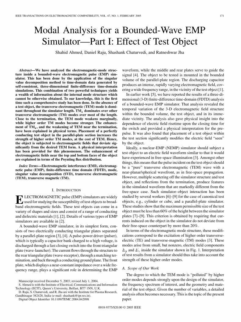
Fig. 13. Instantaneous magnetic field H (x) between the parallel plates.Curves are shown at different z locations near the sheet termination. Case withswitching time � = 19.7 ns.
a loop enclosing the sheet termination. The integral is calculatedat a time when the current through the sheet is close to its max-imum. We see that the current is maximum at both ends, with aminimum lying near the middle of the sheet. The asymmetry inthe current is probably due to the difference between the top andbottom plates. This -directed current produces a correspondingvariation in , which is shown in Fig. 13. In Fig. 13, at each
location, is recorded at the time when the magnetic fieldreaches its peak value at the center of the plane. This is nec-essary to allow for the time delay in pulse propagation betweendifferent locations. We see that the waveform resemblesa constant function with a superimposed variation. Fur-thermore, the curvature of the variation, and hence the ampli-tude of the change in , becomes stronger as we move towardthe termination. This corresponds to a progressively increasing
mode as we approach the termination.A simple quantitative check will be in order at this point.
From Fig. 13, we see that varies between 1560 and1480 A/m at 14 m. This corresponds to an
mode of amplitude 40 A/m, superimposed on anmode of strength 1520 A/m. This implies a ratio of ampli-tudes of 40/1520 2.6%, matching fairly well with the ratio
at 14 m.The foregoing analysis has only been done for the case of
a resistive termination. It is worth mentioning here that distor-tion due to the termination can be reduced or even eliminated inmodern designs, e.g., by the use of distributed terminations [3].
IV. MODAL ANALYSIS OF A SIMULATOR WITH A TEST OBJECT
In an EMP simulator, the presence of the test object itselfmodifies the fields to which it is subjected. The extent of modi-fication depends upon the dimensions and material compositionof the object. Such simulator–object interaction has been studiedextensively in the literature. For example, simple estimates showthat if the local height of the simulator is more than 1.6 timesthe height of the test object, their interaction becomes tolerable[6]–[9]. We have earlier reported on FDTD simulations of thedistortion produced by test objects of different sizes in [5]. In
Fig. 14. Variation of instantaneous electric field E with x, with (y; z)coordinates located at the center of the test object.
particular, we found that the simulator examined here could beused for testing perfectly conducting cube-shaped objects with amaximum dimension of 0.5 m, without introducing significantdistortion. We also found that the frequency spectrum “seen” bythe object changes with object size. This appears to be consis-tent with the above-mentioned estimate.
These changes in the spatial and temporal structure of thefield imply a corresponding change in the mode structure, whichis examined in this section. For the purposes of illustration, wehave performed modal analysis in the presence of a perfectlyconducting solid cube of side 0.5 m.
A. Qualitative Analysis
Before starting the modal analysis, it is instructive to take alook at the variation of the two major electric field components,
and , through the bounded volume. We focus our attentionon the region of the simulator close to the test object.
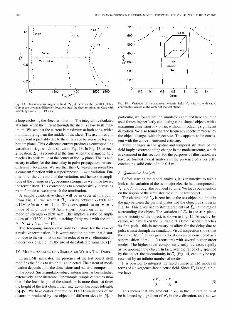
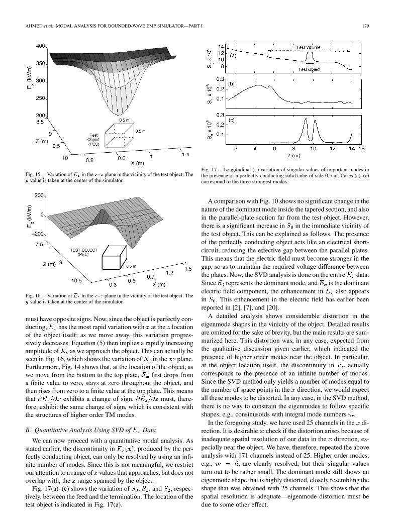
The electric field is zero inside the test object but finite inthe gap between the parallel plates and the object, as shown inFig. 14. This gives rise to strong gradients of in the regionsurrounding the object. The variation of in the – plane,in the vicinity of the object, is shown in Fig. 15. At each lo-cation, we have taken the value at a time when it reachesits first peak—this is necessary to allow for the delay due topulse transit through the simulator. Visual inspection shows thatthe curve at any given location can be considered as asuperposition of (constant) with several higher ordermodes. The higher order component clearly increases rapidlyas we approach the object. In fact, over the range of spannedby the object, the discontinuity in (Fig. 14) can only be rep-resented by an infinite number of modes.
It is possible to interpret the rapid change in TM modes interms of a divergence-free electric field. Since is negligible,we have
(5)
This means that any gradient in in the direction mustbe balanced by a gradient of in the direction, and the two
AHMED et al.: MODAL ANALYSIS FOR BOUNDED-WAVE EMP SIMULATOR—PART I 179
Fig. 15. Variation of E in the x–z plane in the vicinity of the test object. They value is taken at the center of the simulator.
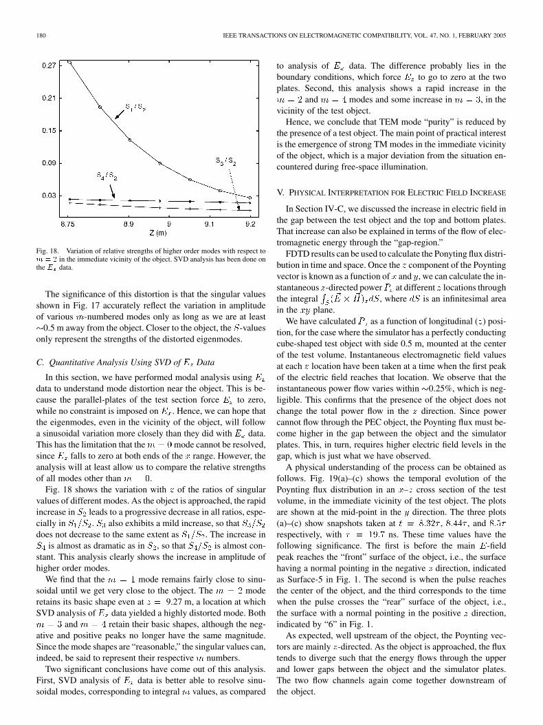
Fig. 16. Variation of E in the x–z plane in the vicinity of the test object. They value is taken at the center of the simulator.
must have opposite signs. Now, since the object is perfectly con-ducting, has the most rapid variation with at the locationof the object itself; as we move away, this variation progres-sively decreases. Equation (5) then implies a rapidly increasingamplitude of as we approach the object. This can actually beseen in Fig. 16, which shows the variation of in the plane.Furthermore, Fig. 14 shows that, at the location of the object, aswe move from the bottom to the top plate, first drops froma finite value to zero, stays at zero throughout the object, andthen rises from zero to a finite value at the top plate. This meansthat exhibits a change of sign. must, there-fore, exhibit the same change of sign, which is consistent withthe structures of higher order TM modes.
B. Quantitative Analysis Using SVD of Data
We can now proceed with a quantitative modal analysis. Asstated earlier, the discontinuity in , produced by the per-fectly conducting object, can only be resolved by using an infi-nite number of modes. Since this is not meaningful, we restrictour attention to a range of values that approaches, but does notoverlap with, the range spanned by the object.
Fig. 17(a)–(c) shows the variation of , , and , respec-tively, between the feed and the termination. The location of thetest object is indicated in Fig. 17(a).
Fig. 17. Longitudinal (z) variation of singular values of important modes inthe presence of a perfectly conducting solid cube of side 0.5 m. Cases (a)–(c)correspond to the three strongest modes.
A comparison with Fig. 10 shows no significant change in thenature of the dominant mode inside the tapered section, and alsoin the parallel-plate section far from the test object. However,there is a significant increase in in the immediate vicinity ofthe test object. This can be explained as follows. The presenceof the perfectly conducting object acts like an electrical short-circuit, reducing the effective gap between the parallel plates.This means that the electric field must become stronger in thegap, so as to maintain the required voltage difference betweenthe plates. Now, the SVD analysis is done on the entire data.Since represents the dominant mode, and is the dominantelectric field component, the enhancement in also appearsin . This enhancement in the electric field has earlier beenreported in [2], [7], and [20].
A detailed analysis shows considerable distortion in theeigenmode shapes in the vinicity of the object. Detailed resultsare omitted for the sake of brevity, but the main results are sum-marized here. This distortion was, in any case, expected fromthe qualitative discussion given earlier, which indicated thepresence of higher order modes near the object. In particular,at the object location itself, the discontinuity in actuallycorresponds to the presence of an infinite number of modes.Since the SVD method only yields a number of modes equal tothe number of space points in the direction, we would expectall these modes to be distorted. In any case, in the SVD method,there is no way to constrain the eigenmodes to follow specificshapes, e.g., consinusoids with integral mode numbers .
In the foregoing study, we have used 25 channels in the di-rection. It is desirable to check if the distortion arises because ofinadequate spatial resolution of our data in the direction, es-pecially near the object. We have, therefore, repeated the aboveanalysis with 171 channels instead of 25. Higher order modes,e.g., , are clearly resolved, but their singular valuesturn out to be rather small. The dominant mode still shows aneigenmode shape that is highly distorted, closely resembling theshape that was obtained with 25 channels. This shows that thespatial resolution is adequate—eigenmode distortion must bedue to some other effect.
180 IEEE TRANSACTIONS ON ELECTROMAGNETIC COMPATIBILITY, VOL. 47, NO. 1, FEBRUARY 2005
Fig. 18. Variation of relative strengths of higher order modes with respect tom = 2 in the immediate vicinity of the object. SVD analysis has been done onthe E data.
The significance of this distortion is that the singular valuesshown in Fig. 17 accurately reflect the variation in amplitudeof various -numbered modes only as long as we are at least
0.5 m away from the object. Closer to the object, the -valuesonly represent the strengths of the distorted eigenmodes.
C. Quantitative Analysis Using SVD of Data
In this section, we have performed modal analysis usingdata to understand mode distortion near the object. This is be-cause the parallel-plates of the test section force to zero,while no constraint is imposed on . Hence, we can hope thatthe eigenmodes, even in the vicinity of the object, will followa sinusoidal variation more closely than they did with data.This has the limitation that the mode cannot be resolved,since falls to zero at both ends of the range. However, theanalysis will at least allow us to compare the relative strengthsof all modes other than .
Fig. 18 shows the variation with of the ratios of singularvalues of different modes. As the object is approached, the rapidincrease in leads to a progressive decrease in all ratios, espe-cially in . also exhibits a mild increase, so thatdoes not decrease to the same extent as . The increase in
is almost as dramatic as in , so that is almost con-stant. This analysis clearly shows the increase in amplitude ofhigher order modes.
We find that the mode remains fairly close to sinu-soidal until we get very close to the object. The moderetains its basic shape even at 9.27 m, a location at whichSVD analysis of data yielded a highly distorted mode. Both
and retain their basic shapes, although the neg-ative and positive peaks no longer have the same magnitude.Since the mode shapes are “reasonable,” the singular values can,indeed, be said to represent their respective numbers.
Two significant conclusions have come out of this analysis.First, SVD analysis of data is better able to resolve sinu-soidal modes, corresponding to integral values, as compared
to analysis of data. The difference probably lies in theboundary conditions, which force to go to zero at the twoplates. Second, this analysis shows a rapid increase in the
and modes and some increase in , in thevicinity of the test object.
Hence, we conclude that TEM mode “purity” is reduced bythe presence of a test object. The main point of practical interestis the emergence of strong TM modes in the immediate vicinityof the object, which is a major deviation from the situation en-countered during free-space illumination.
V. PHYSICAL INTERPRETATION FOR ELECTRIC FIELD INCREASE
In Section IV-C, we discussed the increase in electric field inthe gap between the test object and the top and bottom plates.That increase can also be explained in terms of the flow of elec-tromagnetic energy through the “gap-region.”
FDTD results can be used to calculate the Ponyting flux distri-bution in time and space. Once the component of the Poyntingvector is known as a function of and , we can calculate the in-stantaneous -directed power at different locations throughthe integral , where is an infinitesimal areain the plane.
We have calculated as a function of longitudinal ( ) posi-tion, for the case where the simulator has a perfectly conductingcube-shaped test object with side 0.5 m, mounted at the centerof the test volume. Instantaneous electromagnetic field valuesat each location have been taken at a time when the first peakof the electric field reaches that location. We observe that theinstantaneous power flow varies within 0.25%, which is neg-ligible. This confirms that the presence of the object does notchange the total power flow in the direction. Since powercannot flow through the PEC object, the Poynting flux must be-come higher in the gap between the object and the simulatorplates. This, in turn, requires higher electric field levels in thegap, which is just what we have observed.
A physical understanding of the process can be obtained asfollows. Fig. 19(a)–(c) shows the temporal evolution of thePoynting flux distribution in an – cross section of the testvolume, in the immediate vicinity of the test object. The plotsare shown at the mid-point in the direction. The three plots(a)–(c) show snapshots taken at , , andrespectively, with ns. These time values have thefollowing significance. The first is before the main -fieldpeak reaches the “front” surface of the object, i.e., the surfacehaving a normal pointing in the negative direction, indicatedas Surface-5 in Fig. 1. The second is when the pulse reachesthe center of the object, and the third corresponds to the timewhen the pulse crosses the “rear” surface of the object, i.e.,the surface with a normal pointing in the positive direction,indicated by “6” in Fig. 1.
As expected, well upstream of the object, the Poynting vec-tors are mainly -directed. As the object is approached, the fluxtends to diverge such that the energy flows through the upperand lower gaps between the object and the simulator plates.The two flow channels again come together downstream ofthe object.

AHMED et al.: MODAL ANALYSIS FOR BOUNDED-WAVE EMP SIMULATOR—PART I 181
Fig. 19. Snapshots of Poynting flux distribution in the xz plane in theimmediate vicinity of a solid PEC cubic object of side length 0.5 m insidethe test volume. The plots are shown at the mid-point in the y direction. Plots(a)–(c) correspond to t = 8:32� , 8:44� , and 8:5� , respectively, with � =
19:7 ns. x and z correspond to the height and length of simulator, as shown inFig. 2.
VI. MAJOR LIMITATIONS OF THIS STUDY
The test object is assumed to be made of perfect electricalconductor. A realistic test object could consist of multiple ma-terials, including both conductors and lossy dielectrics, whichwould significantly affect the mode structure. That effect hasnot been examined in the present study.
Some of the important features and limitations of the SVDmethod are discussed in [13]. One important limitation observedhere is that, in regions where mode strength changes rapidly, theeigenmodes can get considerably distorted. In such regions, it isnecessary to check for distortion. If distortion is considerable,some other method may be more suitable, e.g., a combinationof SVD with fast Fourier transform.
VII. CONCLUSION
We have performed an analysis of the electromagnetic modestructure inside a bounded-wave EMP simulator, both with andwithout a test object. This has been done by the applicationof the SVD method to time-domain data generated by self-consistent, 3-D FDTD simulations. This combination of twopowerful techniques yields a wealth of information about theinternal mode structure which cannot be otherwise obtained.This is particularly important, given that a real-life simulator,with a realistic test object, has a complex geometry and consistsof a range of materials from good conductors to dielectrics;this is further complicated by the existence of broad-bandexcitation. To our knowledge, this is the first time such acomprehensive study has been done.
and are the dominant field components in the absenceof the object. We also find a significant in the vicinity of thetest object or the resistive termination. This shows that TEMand TM modes exist, while TE modes are not present to anysignificant extent.
The conclusions given below are for the case with a switchclosure time of 19.7 ns, corresponding to an electric field rise-time of 4.3 ns. However, the analysis can easily be repeated forany other value of the switching time.
In the absence of the object, the TEM mode is dominantthroughout the simulator length. TM dominates over other TMmodes over most of the length. Within the tapered section, inparticular, TM and higher modes do not exist, since their cutofffrequencies are far too high for the frequency spectrum excitedby the above-mentioned switching time. Close to the termina-tion, however, the TEM mode weakens marginally, while higherorder TM modes become stronger. The enhancement of TMnear the termination has been explained in terms of the inducedcurrent distribution in the resistive sheet and the resulting mag-netic field in the vicinity of the termination. The weakening ofTEM near the termination has been explained in terms of reflec-tions from the termination.
Placement of a reasonably sized, perfectly conducting test ob-ject in the parallel-plate section produces major changes in themode structure in the vicinity of the object. Higher order TMmodes become stronger, at the cost of the mode. Thisfinding has considerable practical significance, since it impliesthat the object would be subjected to electromagnetic fields thatdeviate significantly from the desired form. Also, the ob-ject is entirely to be blamed for this deviation. We have provideda physical explanation for the deviation in terms of induced cur-rents on the object.
The presence of such deviations from the ideal TEM formmust be kept in mind while interpreting test results from EMPsimulators.
182 IEEE TRANSACTIONS ON ELECTROMAGNETIC COMPATIBILITY, VOL. 47, NO. 1, FEBRUARY 2005
Another interesting observation is that the eigenmodes com-puted using SVD analysis of data get considerably distortednear the object, such that the dominant eigenmode consists ofa superposition of and several higher order modes. Wehave ruled out inadequate spatial resolution as the cause of thisdistortion. SVD analysis of data is better able to resolve si-nusoidal modes, corresponding to integral values, as com-pared to analysis of data. The difference probably lies inthe boundary conditions, which force to go to zero at thetwo plates. Second, this analysis shows a rapid increase in the
and modes, and some increase in , in thevicinity of the test object.
ACKNOWLEDGMENT
The authors would like to acknowledge valuable discussionswith S. V. Kulkarni, K. K. Jain, Prof. P. I. John, and G. Singh.
REFERENCES
[1] H. Schilling, J. Schluter, M. Peters, K. Neilsen, J. T. Naff, and H. G.Hammon, “High voltage generator with fast risetime for EMP simula-tion,” in Proc. 10th IEEE Int. Pulsed Power Conf., Albuquerque, NM,1995, pp. 1359–1364.
[2] C. E. Baum, “EMP simulators for various types of nuclear EMP environ-ments: an interim categorization,” IEEE Trans. Antennas Propag., vol.AP-26, no. 1, pp. 35–53, Jan. 1978.
[3] D. V. Giri and C. E. Baum, “Design guidelines for flat-plate conicalguided-wave EMP simulators with distributed terminations,” SensorSimulation Notes, vol. SSN-402, pp. 1–37, Oct. 1996.
[4] H. M. Shen, R. W. P. King, and T. T. Wu, “The exciting mechanism ofthe parallel-plate EMP simulator,” IEEE Trans. Electromagn. Compat.,vol. EMC-29, no. 1, pp. 32–39, Feb. 1987.
[5] S. Ahmed, D. Sharma, and S. Chaturvedi, “Modeling of an EMP simu-lator using a 3-D FDTD code,” IEEE Trans. Plasma Sci., vol. 31, no. 2,pp. 207–215, Apr. 2003.
[6] R. W. Latham, “Interaction between a cylindrical test body and a parallelplate simulator,” Sensor Simulation Notes, vol. SSN-55, pp. 1–39, May1968.
[7] C. D. Taylor and G. A. Steigerwald, “On the pulse excitation in aparallel-plate waveguide,” Sensor Simulation Notes, vol. SSN-99, pp.1–121, Mar. 1970.
[8] R. W. Latham and K. S. H. Lee, “Electromagnetic interaction between acylindrical post and a two-parallel-plate simulator, I,” Sensor SimulationNotes, vol. SSN-111, pp. 1–30, July 1970.
[9] C. E. Baum, D. V. Giri, and R. D. Gonzalez, “Electromagnetic field dis-tribution of the TEM mode in a symmetrical two-parallel-plate transmia-sion line,” Sensor Simulation Notes, vol. SSN-219, pp. 1–87, Apr. 1976.
[10] S. Ahmed, D. Raju, S. Chaturvedi, and R. Jha, “Modal analysis for abounded-wave EMP simulator—Part II: Radiation leakage and modesuppression,” IEEE Trans. Electromagn. Compat., vol. 47, no. 1, pp.183–191, Feb. 2005.
[11] A. M. Rushdi, R. C. Menendez, R. Mittra, and S.-W. Lee, “Leaky modesin parallel-plate EMP simulators,” IEEE Trans. Electromagn. Compat.,vol. EMC-20, no. 3, pp. 444–451, Aug. 1978.
[12] D. V. Giri, C. E. Baum, and H. Schilling, “Electromagnetic consider-ations of a spatial modal filter for suppression of non-TEM modes inthe transmission-line type of EMP simulators,” Sensor Simulation Notes,vol. SSN-247, pp. 1–34, Dec. 29, 1978.
[13] C. Nardone, “Multichannel fluctuation data analysis by the singularvalue decomposition method. Application to MHD modes in JET,”Plasma Phys. Controlled Fusion, vol. 34, no. 9, pp. 1447–1465, 1992.
[14] N. E. Huang, Z. Shen, S. R. Long, M. G. Wu, H. H. Shish, Q. Zheng,N. C. Yen, C. C. Tung, and H. H. Liu, “The empirical mode decomposi-tion and the Hilbert spectrum for nonlinear and nonstationary time seriesanalysis,” Proc. R. Soc. Lond. A, pp. 903–995, 1998.
[15] K. S. Kunz and R. J. Luebbers, The Finite-Difference Time-DomainMethod for Electromagnetics. Boca Raton, FL: CRC Press, 1993.
[16] S. Ahmed, D. Sharma, and S. Chaturvedi, “Finite-difference time-do-main analysis of parallel-plate capacitors,” Int. J. Computat. Sci.Methods Eng. Sci. Mech., vol. 6, no. 2, Dec. 2004.
[17] S. L. Gupta and V. Kumar, Handbook of Electronics. Meerut, India:Pragati Prakashan, 1994.
[18] W. H. Press et al., Numerical Recipes in Fortran. Cambridge, U.K.:Cambridge Univ. Press, 1998.
[19] K. L. Shlager, “The analysis and optimization of bow-tie and TEM-horn antennas for pulse radiation using the finite-difference time-do-main method,” Ph.D. dissertation, Georgia Inst. of Technol., Atlanta,Feb. 1995.
[20] C. E. Baum, “From the electromagnetic pulse to high-power electromag-netics,” Proc. IEEE, vol. 80, no. 6, pp. 789–817, Jun. 1992.
Shahid Ahmed received the M.Sc. degree in physicsfrom Ranchi University, Ranchi, India, in 1995,and the Ph.D. degree from the Institute for PlasmaResearch, Gandhinagar, India, in 2003. His doctoralwork involved the computational study of electro-magnetic pulse simulators.
From August 2003 to October 2004, he was a Re-search Fellow with the Institute of High PerformanceComputing, Singapore, where he was involved inthe simulation of high-speed microstrip circuits. Heis presently with the Institute of Electronics, Com-
munications and Information Technology (ECIT), Queen’s University, Belfast,U.K., as a Research Fellow, where he is involved in the study of chip deviceshielding and packaging. His research interest is the computer simulation ofpulsed power systems, especially ultrawideband antennas, microstrip circuits,electromagnetic compatibility, and electromagnetic interference. He is alsointerested in photonic crystals and nano electronics.
Daniel Raju was born in India in 1967. He receivedthe M.Sc. degree in physics from Ravishankar Uni-versity, Raipur, India, in 1989, and the Ph.D. degreefrom Devi Ahilya Vishwavidyalaya, Indore, India, in2004.
He joined the Institute for Plasma Research, Gand-hinagar, India, in 1995 and is currently working onmagnetic diagnostics for tokamaks and on tokamakcontrol. His research interests include magnetic diag-nostics, plasma feedback control, data analysis, andneural networks.
Shashank Chaturvedi received the B.Tech. degreein chemical enginering from the Indian Instiute ofTechnology, Delhi, in 1985, and the Ph.D. degreein chemical engineering from Princeton University,Princeton, NJ, in 1989.
He has since been with the Institute for PlasmaResearch, Gandhinagar, India. For several years, heworked on computer modeling of different fusionreactor configurations, including tokamaks. Overthe past ten years, he has been involved in themodeling of pulsed-power systems, including pulsed
electromagnetics, radiation-hydrodynamics, and magneto-hydro-dynamics(MHD) simulations as well as shockwave studies.
Ratneshwar Jha was born in 1954. He received theM.Sc. degree in physics from Jawaharlal Nehru Uni-versity, New Delhi, India, in 1978 and the Ph.D. de-gree from Gujarat University, Gujarat, India.
He worked in the area of geocosmophysics atthe Physical Research Laboratory, Ahmedabad,India. Since 1986, he has been involved with plasmadiagnostics at the Institute for Plasma Research,Gandhinagar, India, where he is a Senior AssociateProfessor. His current interests are plasma instabilityand turbulence, plasma diagnostics, tokamak plasma
research, and data analysis.