Mass-Market Designed-for-Cellular MMICs Can be Gainfully Adapted for Use in Niche Applications on...
13
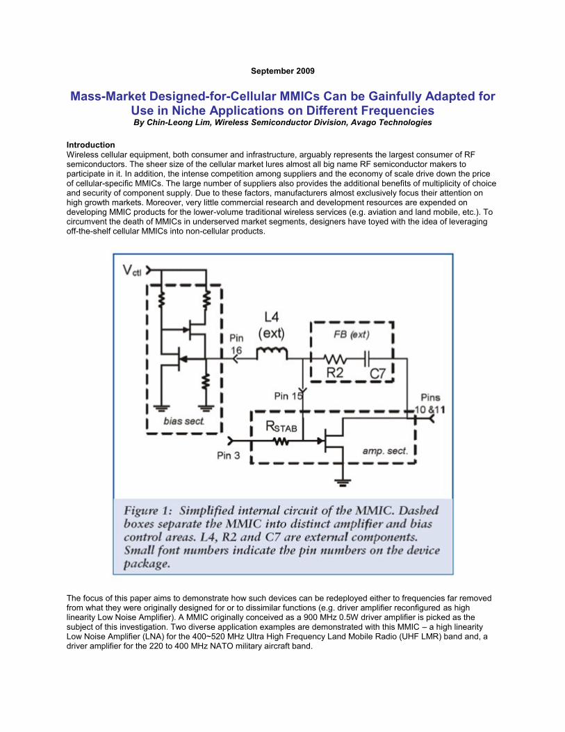
September 2009 Mass-Market Designed-for-Cellular MMICs Can be Gainfully Adapted for Use in Niche Applications on Different Frequencies By Chin-Leong Lim, Wireless Semiconductor Division, Avago Technologies Introduction Wireless cellular equipment, both consumer and infrastructure, arguably represents the largest consumer of RF semiconductors. The sheer size of the cellular market lures almost all big name RF semiconductor makers to participate in it. In addition, the intense competition among suppliers and the economy of scale drive down the price of cellular-specific MMICs. The large number of suppliers also provides the additional benefits of multiplicity of choice and security of component supply. Due to these factors, manufacturers almost exclusively focus their attention on high growth markets. Moreover, very little commercial research and development resources are expended on developing MMIC products for the lower-volume traditional wireless services (e.g. aviation and land mobile, etc.). To circumvent the death of MMICs in underserved market segments, designers have toyed with the idea of leveraging off-the-shelf cellular MMICs into non-cellular products. The focus of this paper aims to demonstrate how such devices can be redeployed either to frequencies far removed from what they were originally designed for or to dissimilar functions (e.g. driver amplifier reconfigured as high linearity Low Noise Amplifier). A MMIC originally conceived as a 900 MHz 0.5W driver amplifier is picked as the subject of this investigation. Two diverse application examples are demonstrated with this MMIC – a high linearity Low Noise Amplifier (LNA) for the 400~520 MHz Ultra High Frequency Land Mobile Radio (UHF LMR) band and, a driver amplifier for the 220 to 400 MHz NATO military aircraft band.
Transcript of Mass-Market Designed-for-Cellular MMICs Can be Gainfully Adapted for Use in Niche Applications on...
September 2009
Mass-Market Designed-for-Cellular MMICs Can be Gainfully Adapted for Use in Niche Applications on Different Frequencies By Chin-Leong Lim, Wireless Semiconductor Division, Avago Technologies
Introduction
Wireless cellular equipment, both consumer and infrastructure, arguably represents the largest consumer of RF semiconductors. The sheer size of the cellular market lures almost all big name RF semiconductor makers to participate in it. In addition, the intense competition among suppliers and the economy of scale drive down the price of cellular-specific MMICs. The large number of suppliers also provides the additional benefits of multiplicity of choice and security of component supply. Due to these factors, manufacturers almost exclusively focus their attention on high growth markets. Moreover, very little commercial research and development resources are expended on developing MMIC products for the lower-volume traditional wireless services (e.g. aviation and land mobile, etc.). To circumvent the death of MMICs in underserved market segments, designers have toyed with the idea of leveraging off-the-shelf cellular MMICs into non-cellular products.
The focus of this paper aims to demonstrate how such devices can be redeployed either to frequencies far removed from what they were originally designed for or to dissimilar functions (e.g. driver amplifier reconfigured as high linearity Low Noise Amplifier). A MMIC originally conceived as a 900 MHz 0.5W driver amplifier is picked as the subject of this investigation. Two diverse application examples are demonstrated with this MMIC – a high linearity Low Noise Amplifier (LNA) for the 400~520 MHz Ultra High Frequency Land Mobile Radio (UHF LMR) band and, a driver amplifier for the 220 to 400 MHz NATO military aircraft band.
Rationale for Selecting a MMIC Device
To make the process of retuning a MMIC device to a different frequency as generic as possible, we deliberately chose the most common topology – a single-stage amplifier. For example, the MGA-30116 MMIC from Avago Technologies consists of a microwave FET with an on-chip bias generator (Figure 1). The FET is meant to be
externally matched. Generally, MMICs with impedance matching networks outside the package lend themselves more readily for conversion to another frequency. For an “off-label” application such as this, a simpler device offers the advantage of having its internal circuits accessible from outside the package. As demonstrated in the examples below, the facility for connecting external feedback circuits to the amplifying device is helpful – especially when it is necessary to modify the original behavior.
Device Characteristics and Suitability for Use in Cellular Infrastructure Applications
The MGA-30116 was originally conceived as a 0.5W high linearity driver amplifier for cellular infrastructure service in the 900 MHz frequency range. As a result, the datasheet primarily provides design information that is pertinent to this band. Internally, the RF section consists of a single FET fabricated on a proprietary GaAs Enhancement mode pHEMT process [1] with a 0.25um gate length (the gate length representing a trade-off between improved performance conferred by a smaller “feature size” versus the corresponding higher fabrication cost and poorer yield [2]). This process is noted for its industry-leading linearity and efficiency performance when compared to competing PA semiconductor technologies [3, 4, 5]. As the PAs in cellular handsets are powered from low voltage (~3V) batteries, the pHEMT’s low knee voltage (~0.5V) offers a clear advantage as it provides more operating headroom [6]. Additionally, this process also makes the PAs more reliable because its drain to source resistance (RDSon) automatically rises to prevent self-destruction from thermal runaway, whereas competing technologies such as Bipolar Junction Transistor (BJT) and Hetero-junction Bipolar Transistor (HBT) require ballast resistors which sacrifice gain and output power – precious commodities at high frequency [7,8]. The pHEMT, like all FET devices, can survive even worse load mismatches than BJT and HBT because of its higher breakdown voltage [8] and can operate without protection circuitry [9]. Additionally, the process is also advantageous for Low Noise Amplifiers (LNA) realization because it has a lower noise figure (NF) than equivalent MESFET and HBT [10]. The enhancement mode allows DC grounding of the FET source while using a single polarity supply, to eliminate the depletion FET’s requirement for a source bypass capacitor [11] and the inevitable gain and efficiency degradation due to the capacitor’s parasitic inductance [12,13].
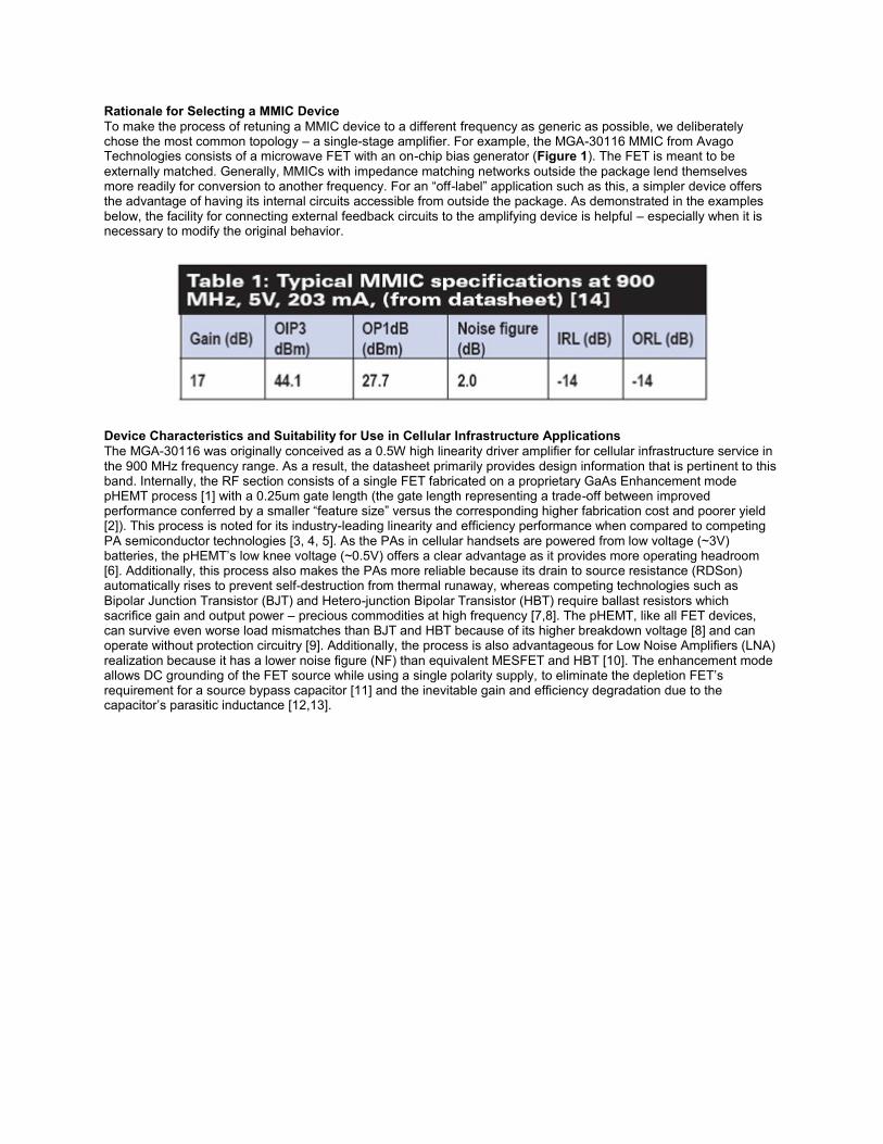
Circuit Changes
Internally, a series resistor “RSTAB” connects the MMIC input (“pin 3” in Figure 1) to the FET gate – this simple stabilization measure is sufficient to ensure unconditional stability at the original 900 MHz design frequency. However, when the MMIC is used at a lower frequency, the gain will increase above the value specified in the datasheet (17 dB typical at 900 MHz). A useful rule of thumb is to estimate an additional 6 dB gain as the frequency is lowered by an octave (i.e. halved). Unfortunately, the higher gain can change an unconditionally stable (Rollett stability factor, k >=1) amplifier to one that is potentially unstable (k <1). The Maximum Stable Gain (MSG) and Maximum Available Gain (MAG), which are calculated from the device s-parameters, demarcate the frequency ranges where k is less than 1 and greater than 1, respectively. As the transition between MSG and MAG occurs at ~700 MHz, it predicts when this device will become potentionally unstable if retuned to a new application frequency that is lower than 700 MHz. Subsequently, the simulation shows k < 1, negative resistance in the input plane and non-realizable values of source and load reflection coefficient (GS and GL) when attempting to simultaneously conjugate match the MMIC at middle frequencies of 460 MHz and 300 MHz. Taken together, these symptoms indicate that additional stabilization is required.
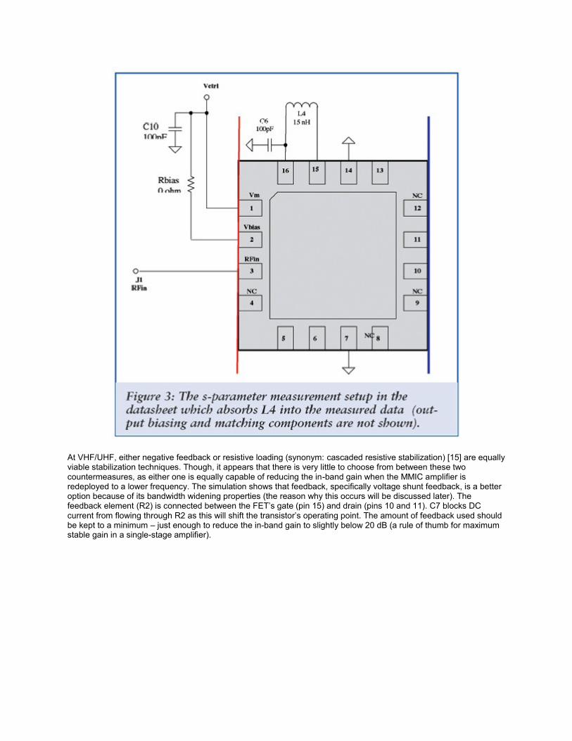
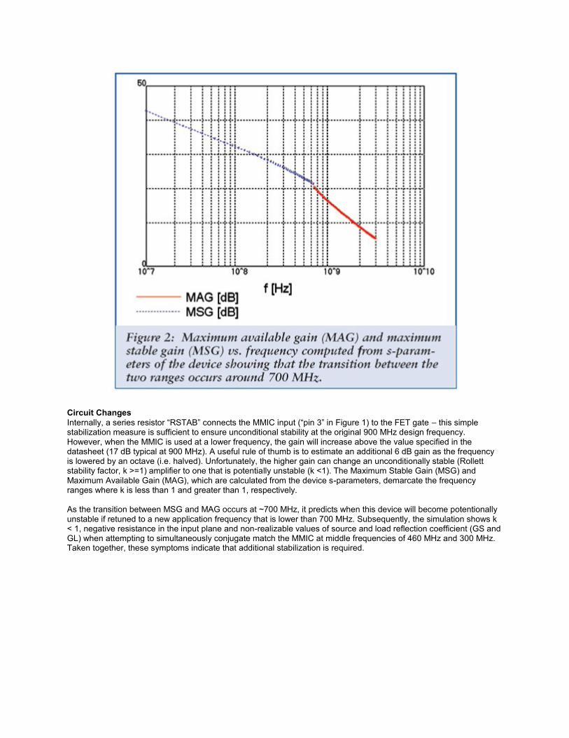
At VHF/UHF, either negative feedback or resistive loading (synonym: cascaded resistive stabilization) [15] are equally viable stabilization techniques. Though, it appears that there is very little to choose from between these two countermeasures, as either one is equally capable of reducing the in-band gain when the MMIC amplifier is redeployed to a lower frequency. The simulation shows that feedback, specifically voltage shunt feedback, is a better option because of its bandwidth widening properties (the reason why this occurs will be discussed later). The feedback element (R2) is connected between the FET’s gate (pin 15) and drain (pins 10 and 11). C7 blocks DC current from flowing through R2 as this will shift the transistor’s operating point. The amount of feedback used should be kept to a minimum – just enough to reduce the in-band gain to slightly below 20 dB (a rule of thumb for maximum stable gain in a single-stage amplifier).
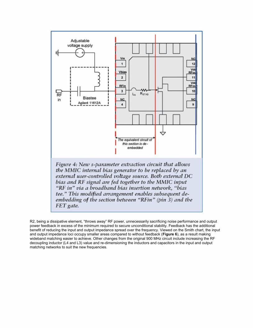
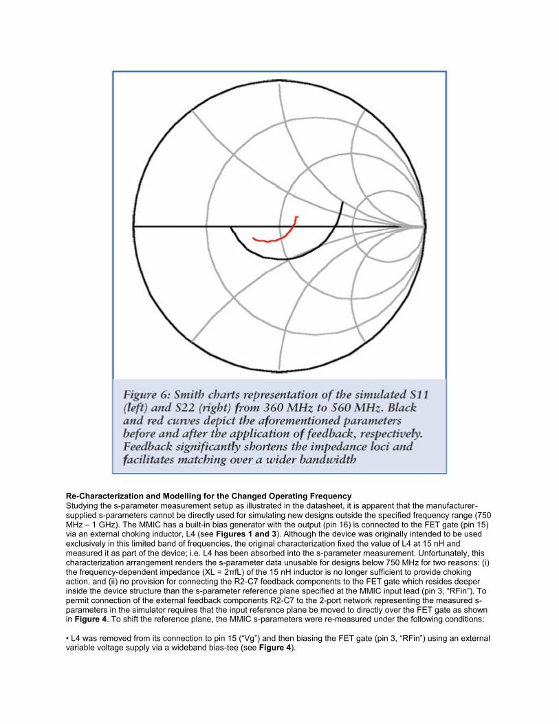
R2, being a dissipative element, “throws away” RF power, unnecessarily sacrificing noise performance and output power feedback in excess of the minimum required to secure unconditional stability. Feedback has the additional benefit of reducing the input and output impedance spread over the frequency. Viewed on the Smith chart, the input and output impedance loci occupy smaller areas compared to without feedback (Figure 6), as a result making
wideband matching easier to achieve. Other changes from the original 900 MHz circuit include increasing the RF decoupling inductor (L4 and L3) value and re-dimensioning the inductors and capacitors in the input and output matching networks to suit the new frequencies.
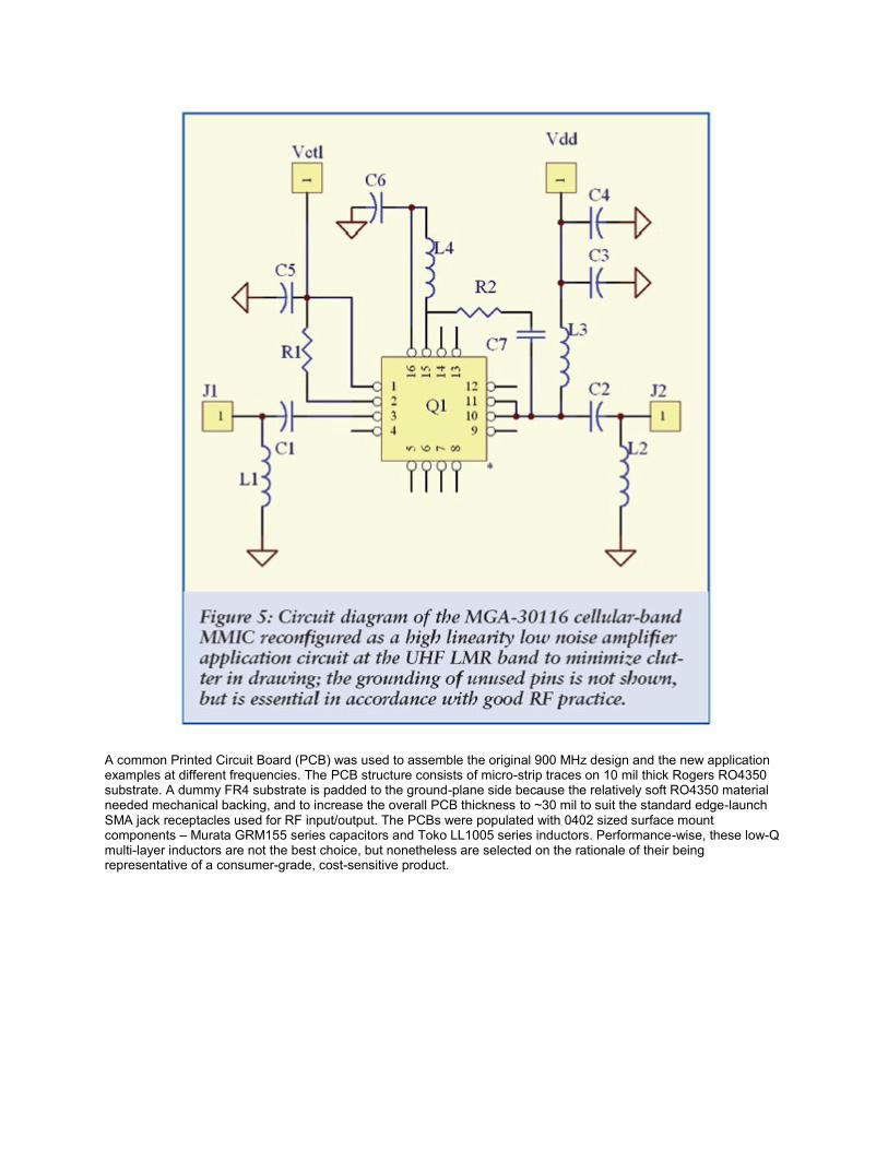
A common Printed Circuit Board (PCB) was used to assemble the original 900 MHz design and the new application examples at different frequencies. The PCB structure consists of micro-strip traces on 10 mil thick Rogers RO4350 substrate. A dummy FR4 substrate is padded to the ground-plane side because the relatively soft RO4350 material needed mechanical backing, and to increase the overall PCB thickness to ~30 mil to suit the standard edge-launch SMA jack receptacles used for RF input/output. The PCBs were populated with 0402 sized surface mount components – Murata GRM155 series capacitors and Toko LL1005 series inductors. Performance-wise, these low-Q multi-layer inductors are not the best choice, but nonetheless are selected on the rationale of their being representative of a consumer-grade, cost-sensitive product.
Re-Characterization and Modelling for the Changed Operating Frequency
Studying the s-parameter measurement setup as illustrated in the datasheet, it is apparent that the manufacturer-supplied s-parameters cannot be directly used for simulating new designs outside the specified frequency range (750 MHz – 1 GHz). The MMIC has a built-in bias generator with the output (pin 16) is connected to the FET gate (pin 15) via an external choking inductor, L4 (see Figures 1 and 3). Although the device was originally intended to be used
exclusively in this limited band of frequencies, the original characterization fixed the value of L4 at 15 nH and measured it as part of the device; i.e. L4 has been absorbed into the s-parameter measurement. Unfortunately, this characterization arrangement renders the s-parameter data unusable for designs below 750 MHz for two reasons: (i) the frequency-dependent impedance (XL = 2πfL) of the 15 nH inductor is no longer sufficient to provide choking action, and (ii) no provision for connecting the R2-C7 feedback components to the FET gate which resides deeper inside the device structure than the s-parameter reference plane specified at the MMIC input lead (pin 3, “RFin”). To permit connection of the external feedback components R2-C7 to the 2-port network representing the measured s-parameters in the simulator requires that the input reference plane be moved to directly over the FET gate as shown in Figure 4. To shift the reference plane, the MMIC s-parameters were re-measured under the following conditions:
• L4 was removed from its connection to pin 15 (“Vg”) and then biasing the FET gate (pin 3, “RFin”) using an external variable voltage supply via a wideband bias-tee (see Figure 4).
• Shift the input reference plane from the initial location (package edge abutting pin 3) to the new location (FET gate inside the package) by de-embedding the gate stabilizing resistor RSTAB, and the package parasitic associated with pin 3 (e.g. bond-wire inductance “Lb” and pad capacitance) from the measured s-parameters. With the new set of s-parameters has its input plane referenced to the FET gate, it can now be used in the simulation of designs incorporating external feedback.
Application Example 1: High linearity LNA for the UHF LMR Bands
In this example, a customer who makes LMR radios requested an application demonstration of a second stage LNA that has very high-linearity (OIP3 > 35 dBm), wide bandwidth and low noise. The LNA must be able to cover 403 to 524 MHz because this customer wanted one design that can cover the UHF LMR band-plan variations that exist in different parts of the world. The target specifications provided by the customer versus the achieved specifications are summarized in Table 2.
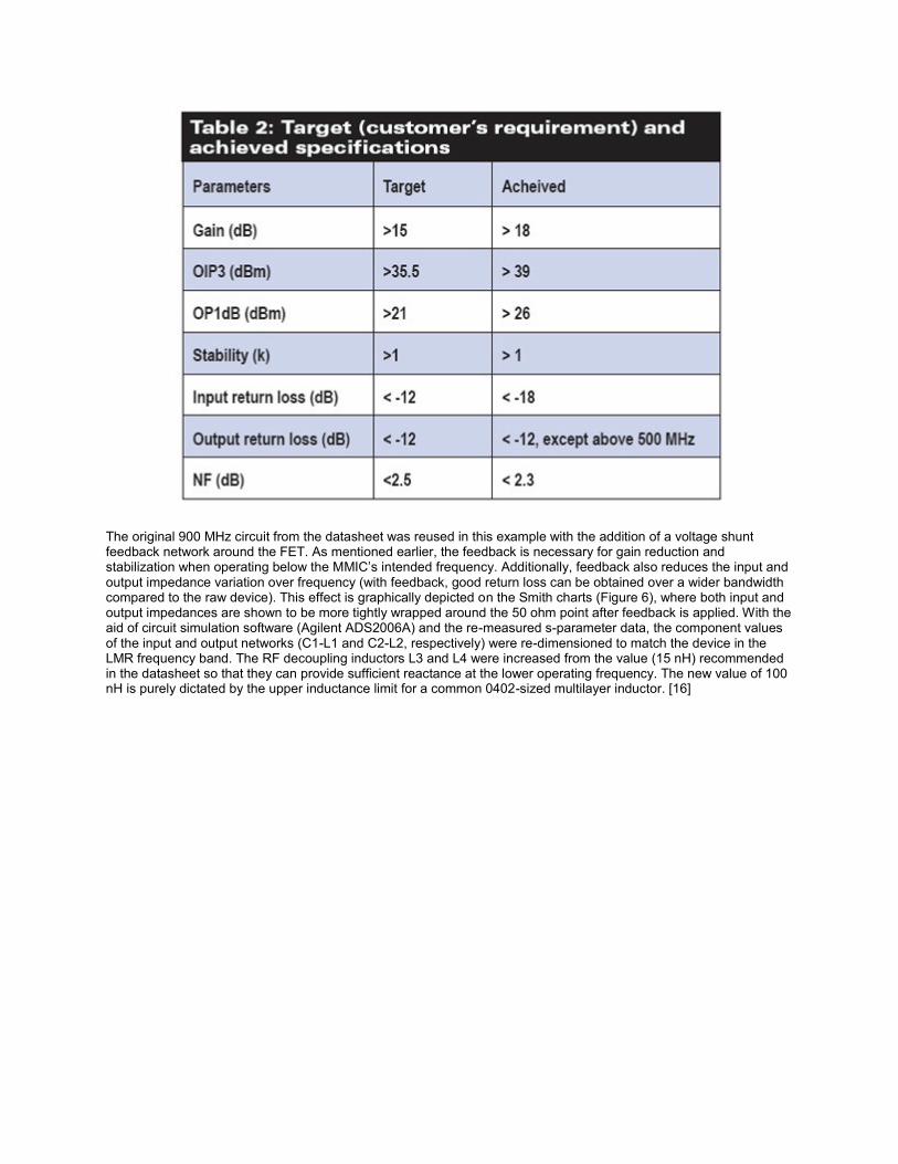
The original 900 MHz circuit from the datasheet was reused in this example with the addition of a voltage shunt feedback network around the FET. As mentioned earlier, the feedback is necessary for gain reduction and stabilization when operating below the MMIC’s intended frequency. Additionally, feedback also reduces the input and output impedance variation over frequency (with feedback, good return loss can be obtained over a wider bandwidth compared to the raw device). This effect is graphically depicted on the Smith charts (Figure 6), where both input and output impedances are shown to be more tightly wrapped around the 50 ohm point after feedback is applied. With the aid of circuit simulation software (Agilent ADS2006A) and the re-measured s-parameter data, the component values of the input and output networks (C1-L1 and C2-L2, respectively) were re-dimensioned to match the device in the LMR frequency band. The RF decoupling inductors L3 and L4 were increased from the value (15 nH) recommended in the datasheet so that they can provide sufficient reactance at the lower operating frequency. The new value of 100 nH is purely dictated by the upper inductance limit for a common 0402-sized multilayer inductor. [16]
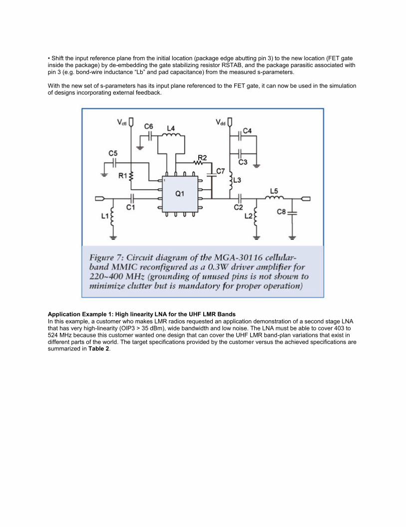
Application Example 2: 0.3W Driver Amplifier for 220 to 400 MHz
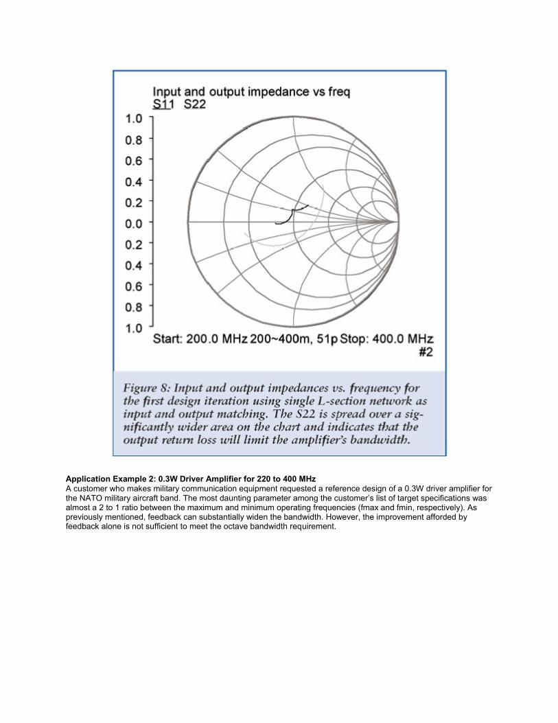
A customer who makes military communication equipment requested a reference design of a 0.3W driver amplifier for the NATO military aircraft band. The most daunting parameter among the customer’s list of target specifications was almost a 2 to 1 ratio between the maximum and minimum operating frequencies (fmax and fmin, respectively). As previously mentioned, feedback can substantially widen the bandwidth. However, the improvement afforded by feedback alone is not sufficient to meet the octave bandwidth requirement.
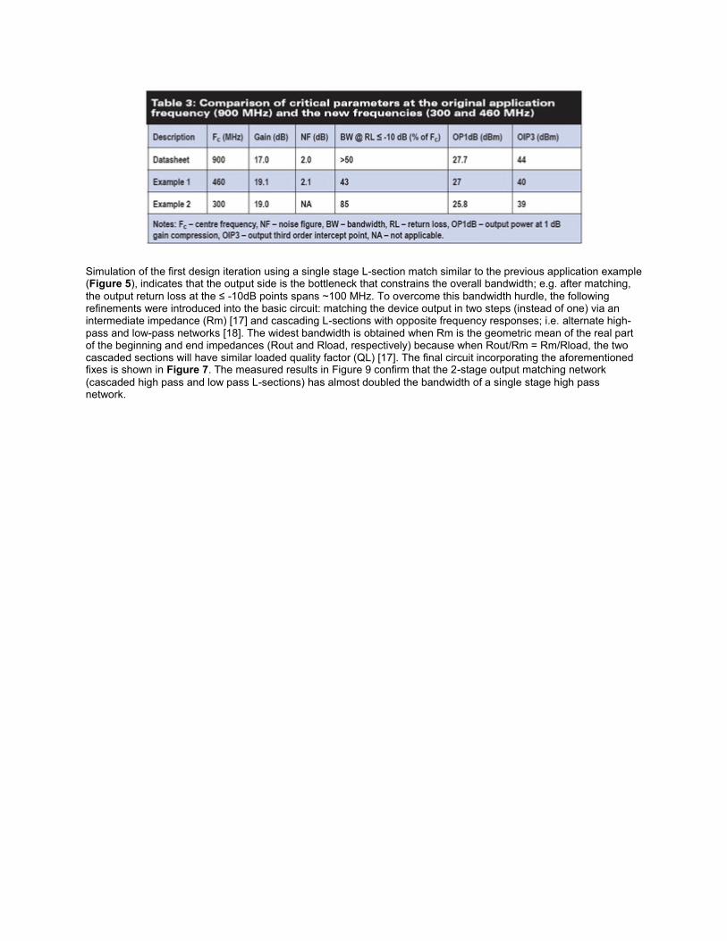
Simulation of the first design iteration using a single stage L-section match similar to the previous application example (Figure 5), indicates that the output side is the bottleneck that constrains the overall bandwidth; e.g. after matching,
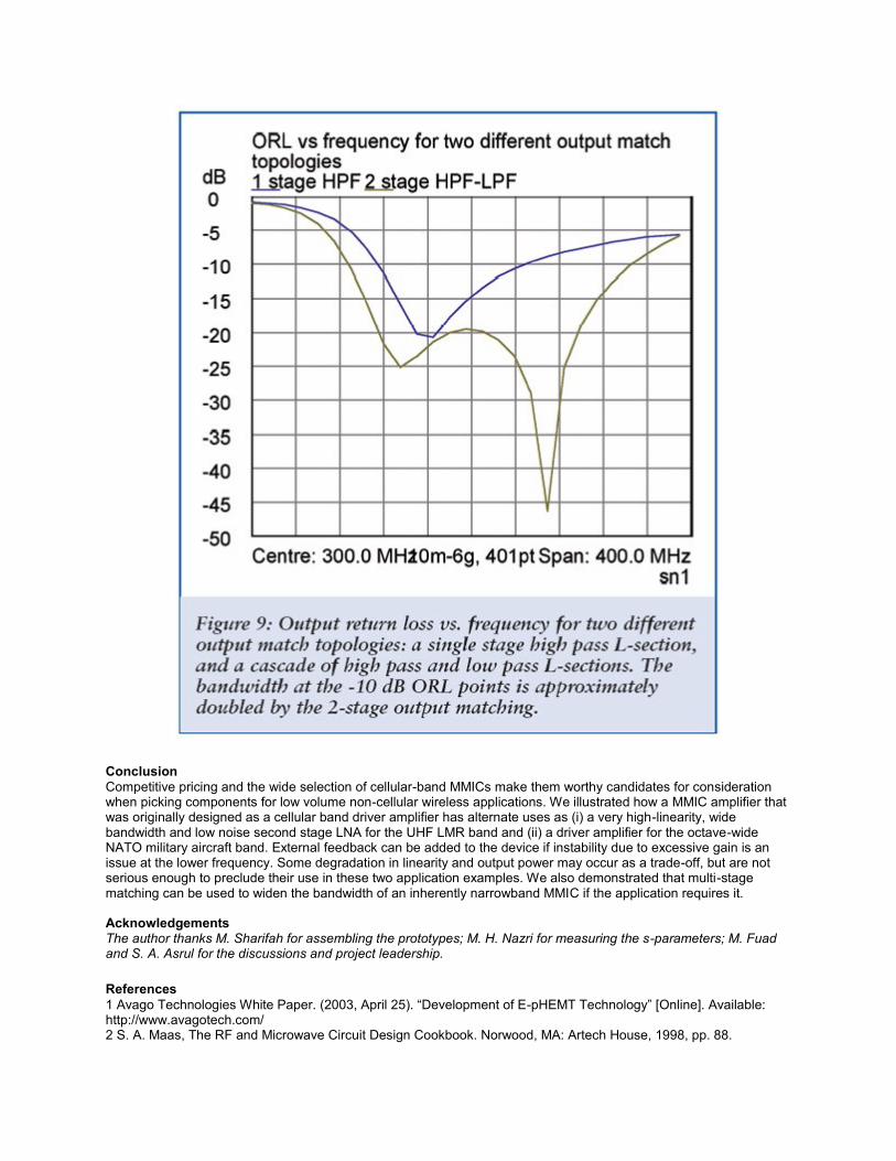
the output return loss at the ≤ -10dB points spans ~100 MHz. To overcome this bandwidth hurdle, the following refinements were introduced into the basic circuit: matching the device output in two steps (instead of one) via an intermediate impedance (Rm) [17] and cascading L-sections with opposite frequency responses; i.e. alternate high-pass and low-pass networks [18]. The widest bandwidth is obtained when Rm is the geometric mean of the real part of the beginning and end impedances (Rout and Rload, respectively) because when Rout/Rm = Rm/Rload, the two cascaded sections will have similar loaded quality factor (QL) [17]. The final circuit incorporating the aforementioned fixes is shown in Figure 7. The measured results in Figure 9 confirm that the 2-stage output matching network
(cascaded high pass and low pass L-sections) has almost doubled the bandwidth of a single stage high pass network.
Conclusion
Competitive pricing and the wide selection of cellular-band MMICs make them worthy candidates for consideration when picking components for low volume non-cellular wireless applications. We illustrated how a MMIC amplifier that was originally designed as a cellular band driver amplifier has alternate uses as (i) a very high-linearity, wide bandwidth and low noise second stage LNA for the UHF LMR band and (ii) a driver amplifier for the octave-wide NATO military aircraft band. External feedback can be added to the device if instability due to excessive gain is an issue at the lower frequency. Some degradation in linearity and output power may occur as a trade-off, but are not serious enough to preclude their use in these two application examples. We also demonstrated that multi-stage matching can be used to widen the bandwidth of an inherently narrowband MMIC if the application requires it. Acknowledgements The author thanks M. Sharifah for assembling the prototypes; M. H. Nazri for measuring the s-parameters; M. Fuad and S. A. Asrul for the discussions and project leadership.
References
1 Avago Technologies White Paper. (2003, April 25). “Development of E-pHEMT Technology” [Online]. Available: http://www.avagotech.com/ 2 S. A. Maas, The RF and Microwave Circuit Design Cookbook. Norwood, MA: Artech House, 1998, pp. 88.
3 C. L. Lim, “0.5 W High Linearity Power Amplifier for Broadband Wireless (3.3 ~ 3.9 GHz),” Proceeding of Korean Japan Microwave Conference, 15 Nov 2007, Okinawa, Japan. 4 R. S. Pengelly, “Improving the Linearity and Efficiency of RF Power Amplifiers,” High Frequency Electronics, September 2002, pp. 26. 5 S. C. Cripps, “RF Power 2005,” Microwave Journal, Apr. 2005. 6 Prashant Chavarkar, and Umesh Mishra, “High Electron Mobility Transistors” in The RF and Microwave Handbook, M. Golio, Ed. CRC Press, 2001, chap. 7.2.5. 7 T. Johansson, “Inside the RF Power Transistor,” Applied Microwave & Wireless, Oct. 1997. 8 Avago Technologies White Paper. (2003, April). “Characteristics of E-pHEMT vs. HBTs for PA Applications,” pp. 3. [Online]. Available: http://www.avagotech.com/assets/downloadDocument.do?id=2001. 9 C. Weitzel, “Will GaAs Survive for Wireless PA?” 2005 Int. Conf. Compound Semiconductor Manufacturing Technology. 10 O. Berger, “GaAs MESFET, HEMT and HBT Competition with Advanced Si RF Technologies,” 1999 Int. Conf. on Compound Semiconductor Manufacturing Technology, GaAs Mantech. 11 California Eastern Laboratories Application Note, “AN82901-1: Applications of Microwave GaAs FETs,” 1982, pp. 3. 12 N. Dye, and H. Granberg, Radio Frequency Transistors: Principles and Practical Applications, Newton, MA: Butterworth-Heinemann, 1993, pp. 89-92. 13 C. Baringer, and C. Hull, “Amplifiers for Wireless Communications” in RF and Microwave Circuit Design for Wireless Communications, L. E. Larson, Ed. Boston: Artech House, 1997, pp. 384-388. 14 Avago Technologies datasheet. (2008, June 17). “MGA-30116 750 MHz-1 GHz ½ Watt High Linearity Amplifier” [Online]. Available: http://www.avagotech.com 15 L. Besser, “Avoiding RF Oscillation,” Applied Microwave & Wireless, Spring 1995, pp46. 16 Toko Inc. product specification, “Type LL1005FHL Multilayer Chip Inductors” [Online]. Available: http:/www.tokoam.com 17 A. V. Grebennikov, “A Simplified CAD Approach to Analyzing Lumped Elements,” RF Design, Jun. 2000, pp. 34-38. 18 S. C. Cripps, “Chasing Chebyshev,” IEEE Microwave Magazine, Dec. 2007, pp 36.