LT5500 - 1.8GHz to 2.7GHz Receiver Front End - Analog ...
12
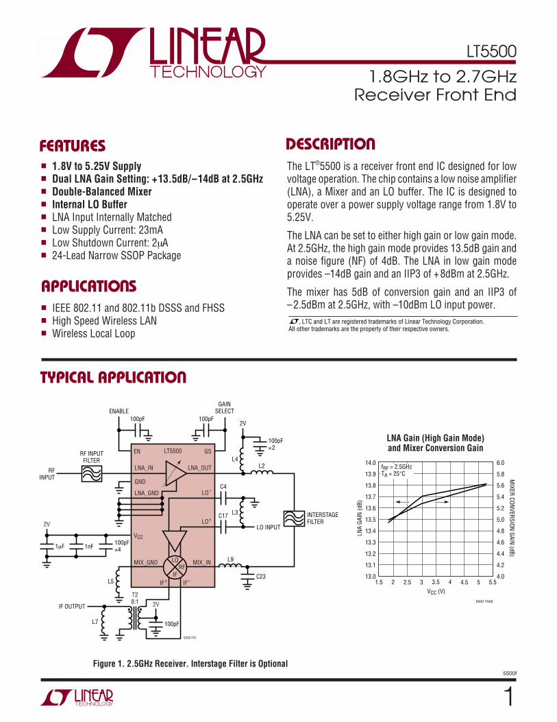
1 LT5500 5500f TYPICAL APPLICATIO U FEATURES DESCRIPTIO U APPLICATIO S U 1.8GHz to 2.7GHz Receiver Front End ■ 1.8V to 5.25V Supply ■ Dual LNA Gain Setting: +13.5dB/–14dB at 2.5GHz ■ Double-Balanced Mixer ■ Internal LO Buffer ■ LNA Input Internally Matched ■ Low Supply Current: 23mA ■ Low Shutdown Current: 2 A ■ 24-Lead Narrow SSOP Package The LT ® 5500 is a receiver front end IC designed for low voltage operation. The chip contains a low noise amplifier (LNA), a Mixer and an LO buffer. The IC is designed to operate over a power supply voltage range from 1.8V to 5.25V. The LNA can be set to either high gain or low gain mode. At 2.5GHz, the high gain mode provides 13.5dB gain and a noise figure (NF) of 4dB. The LNA in low gain mode provides –14dB gain and an IIP3 of + 8dBm at 2.5GHz. The mixer has 5dB of conversion gain and an IIP3 of – 2.5dBm at 2.5GHz, with –10dBm LO input power. ■ IEEE 802.11 and 802.11b DSSS and FHSS ■ High Speed Wireless LAN ■ Wireless Local Loop Figure 1. 2.5GHz Receiver. Interstage Filter is Optional LO MIX_IN LO + LO – LNA_OUT LNA_IN LNA_GND GND GS EN LT5500 MIX_GND V CC 2V IF – 5500 F01 IF + 2V • • T2 8:1 IF RF C4 C17 C23 L3 L5 L7 IF OUTPUT RF INPUT L4 100pF 2 L2 2V GAIN SELECT RF INPUT FILTER ENABLE 100pF 100pF L9 LO INPUT INTERSTAGE FILTER 100pF 4 1nF 100pF 1F LNA Gain (High Gain Mode) and Mixer Conversion Gain V CC (V) 1.5 LNA GAIN (dB) MIXER CONVERSION GAIN (dB) 13.4 13.6 13.7 5.5 5500 TA02 13.2 13.0 2.5 3.5 4.5 2 3 4 5 14.0 13.3 13.5 13.1 13.8 13.9 4.8 5.2 5.4 4.4 4.0 6.0 4.6 5.0 4.2 5.6 5.8 f RF = 2.5GHz T A = 25C , LTC and LT are registered trademarks of Linear Technology Corporation. All other trademarks are the property of their respective owners.
-
Upload
khangminh22 -
Category
Documents
-
view
3 -
download
0
Transcript of LT5500 - 1.8GHz to 2.7GHz Receiver Front End - Analog ...
1
LT5500
5500f
TYPICAL APPLICATIO
U
FEATURES DESCRIPTIO
U
APPLICATIO SU
1.8GHz to 2.7GHzReceiver Front End
1.8V to 5.25V Supply Dual LNA Gain Setting: +13.5dB/–14dB at 2.5GHz Double-Balanced Mixer Internal LO Buffer LNA Input Internally Matched Low Supply Current: 23mA Low Shutdown Current: 2µA 24-Lead Narrow SSOP Package
The LT®5500 is a receiver front end IC designed for lowvoltage operation. The chip contains a low noise amplifier(LNA), a Mixer and an LO buffer. The IC is designed tooperate over a power supply voltage range from 1.8V to5.25V.
The LNA can be set to either high gain or low gain mode.At 2.5GHz, the high gain mode provides 13.5dB gain anda noise figure (NF) of 4dB. The LNA in low gain modeprovides –14dB gain and an IIP3 of +8dBm at 2.5GHz.
The mixer has 5dB of conversion gain and an IIP3 of–2.5dBm at 2.5GHz, with –10dBm LO input power. IEEE 802.11 and 802.11b DSSS and FHSS
High Speed Wireless LAN Wireless Local Loop
Figure 1. 2.5GHz Receiver. Interstage Filter is Optional
LO MIX_IN
LO+
LO–
LNA_OUTLNA_IN
LNA_GND
GND
GSEN LT5500
MIX_GND
VCC
2V
IF–
5500 F01
IF+
2V• •
T28:1
IFRF
C4
C17
C23
L3
L5
L7
IF OUTPUT
RFINPUT
L4
100pF×2
L2
2V
GAINSELECT
RF INPUTFILTER
ENABLE100pF 100pF
L9
LO INPUT
INTERSTAGEFILTER
100pF×41nF
100pF
1µF
LNA Gain (High Gain Mode)and Mixer Conversion Gain
VCC (V)1.5
LNA
GAIN
(dB)
MIXER CONVERSION GAIN (dB)
13.4
13.6
13.7
5.5
5500 TA02
13.2
13.02.5 3.5 4.52 3 4 5
14.0
13.3
13.5
13.1
13.8
13.9
4.8
5.2
5.4
4.4
4.0
6.0
4.6
5.0
4.2
5.6
5.8fRF = 2.5GHzTA = 25°C
, LTC and LT are registered trademarks of Linear Technology Corporation. All other trademarks are the property of their respective owners.
2
LT5500
5500f
WU U
PACKAGE/ORDER I FOR ATIO
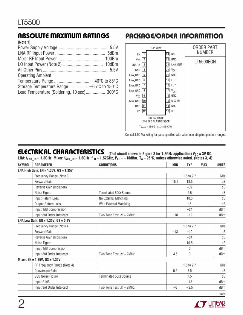
LT5500EGN
TJMAX = 150°C, θJA = 85°C/W
ORDER PARTNUMBER
ABSOLUTE MAXIMUM RATINGS
W WW U
(Note 1)Power Supply Voltage ........................................... 5.5VLNA RF Input Power ............................................ 5dBmMixer RF Input Power ........................................ 10dBmLO Input Power (Note 2) ................................... 10dBmAll Other Pins ......................................................... 5.5VOperating AmbientTemperature Range ............................... –40°C to 85°CStorage Temperature Range ................ – 65°C to 150°CLead Temperature (Soldering, 10 sec)................. 300°C
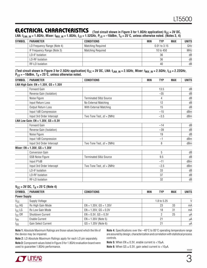
(Test circuit shown in Figure 3 for 1.8GHz application) VCC = 3V DC,LNA: fLNA_IN = 1.8GHz, Mixer: fMIX_IN = 1.8GHz, fLO = 1.52GHz, PLO = –10dBm, TA = 25°C, unless otherwise noted. (Notes 3, 4)
1
2
3
4
5
6
7
8
9
10
11
12
TOP VIEW
GN PACKAGE24-LEAD PLASTIC SSOP
24
23
22
21
20
19
18
17
16
15
14
13
EN
VCC
LNA_IN
GND
LNA_GND
LNA_GND
LNA_GND
LNA_GND
VCC
MIX_GND
GND
IF+
GS
GND
LNA_OUT
VCC
GND
LO–
LO+
VCC
GND
MIX_IN
GND
IF–
Consult LTC Marketing for parts specified with wider operating temperature ranges.
ELECTRICAL CHARACTERISTICS
SYMBOL PARAMETER CONDITIONS MIN TYP MAX UNITSLNA High Gain: EN = 1.35V, GS = 1.35V
Frequency Range (Note 3) 1.8 to 2.7 GHz
Forward Gain 15.5 18.5 dBReverse Gain (Isolation) –39 dB
Noise Figure Terminated 50Ω Source 2.5 dB
Input Return Loss No External Matching 10.5 dBOutput Return Loss With External Matching 15 dB
Input 1dB Compression –24 dBm
Input 3rd Order Intercept Two Tone Test, ∆f = 2MHz –18 –12 dBmLNA Low Gain: EN = 1.35V, GS = 0.3V
Frequency Range (Note 4) 1.8 to 2.7 GHz
Forward Gain –13 –10 dBReverse Gain (Isolation) –34 dB
Noise Figure 16.5 dB
Input 1dB Compression 0 dBmInput 3rd Order Intercept Two Tone Test, ∆f = 2MHz 4.5 9 dBm
Mixer: EN = 1.35V, GS = 1.35V
RF Frequency Range (Note 4) 1.8 to 2.7 GHzConversion Gain 5.5 8.5 dB
SSB Noise Figure Terminated 50Ω Source 7.5 dB
Input P1dB –13 dBmInput 3rd Order Intercept Two Tone Test, ∆f = 2MHz –6 –2.5 dBm
3
LT5500
5500f
(Test circuit shown in Figure 3 for 1.8GHz application) VCC = 3V DC,LNA: fLNA_IN = 1.8GHz, Mixer: fMIX_IN = 1.8GHz, fLO = 1.52GHz, PLO = –10dBm, TA = 25°C, unless otherwise noted. (Notes 3, 4)ELECTRICAL CHARACTERISTICS
(Test circuit shown in Figure 3 for 2.5GHz application) VCC = 3V DC, LNA: fLNA_IN = 2.5GHz, Mixer: fMIX_IN = 2.5GHz, fLO = 2.22GHz,PLO = –10dBm, TA = 25°C, unless otherwise noted.
SYMBOL PARAMETER CONDITIONS MIN TYP MAX UNITSLO Frequency Range (Note 4) Matching Required 0.01 to 3.15 GHzIF Frequency Range (Note 3) Matching Required 10 to 450 MHzLO-IF Isolation 36 dBLO-RF Isolation 36 dBRF-LO Isolation 40 dB
SYMBOL PARAMETER CONDITIONS MIN TYP MAX UNITSLNA High Gain: EN = 1.35V, GS = 1.35V
Forward Gain 13.5 dBReverse Gain (Isolation) –35 dBNoise Figure Terminated 50Ω Source 4 dBInput Return Loss No External Matching 12 dBOutput Return Loss With External Matching 15 dBInput 1dB Compression –15 dBmInput 3rd Order Intercept Two Tone Test, ∆f = 2MHz –3.5 dBm
LNA Low Gain: EN = 1.35V, GS = 0.3VForward Gain –14 dBReverse Gain (Isolation) –39 dBNoise Figure 19 dBInput 1dB Compression –1 dBmInput 3rd Order Intercept Two Tone Test, ∆f = 2MHz 8 dBm
Mixer: EN = 1.35V, GS = 1.35VConversion Gain 5 dBSSB Noise Figure Terminated 50Ω Source 9.5 dBInput P1dB –11 dBmInput 3rd Order Intercept Two Tone Test, ∆f = 2MHz –2.5 dBmLO-IF Isolation 33 dBLO-RF Isolation 37 dBRF-LO Isolation 32 dB
VCC = 3V DC, TA = 25°C (Note 4)
Note 1: Absolute Maximum Ratings are those values beyond which the life ofthe device may be impaired.Note 2: LO Absolute Maximum Ratings apply for each LO pin separately.Note 3: Component values listed in Figure 3 for 1.8GHz evaluation board wereused to guarantee 1.8GHz performance.
Note 4: Specifications over the –40°C to 85°C operating temperature rangeare assured by design, characterization and correlation with statistical processcontrols.Note 5: When EN ≤ 0.3V, enable current is <10µA.Note 6: When GS ≤ 0.3V, gain select current is <10µA.
SYMBOL PARAMETER CONDITIONS MIN TYP MAX UNITSPower SupplyVCC Supply Voltage 1.8 to 5.25 VICC HG Rx High Gain Mode EN = 1.35V, GS = 1.35V 23 33 mAICC LG Rx Low Gain Mode EN = 1.35V, GS = 0.3V 18 31 mAICC Off Shutdown Current EN = 0.3V, GS = 0.3V 2 25 µAIEN Enable Current EN = 1.35V (Note 5) 21 µAIGS Gain Select Current GS = 1.35V (Note 6) 21 µA
4
LT5500
5500f
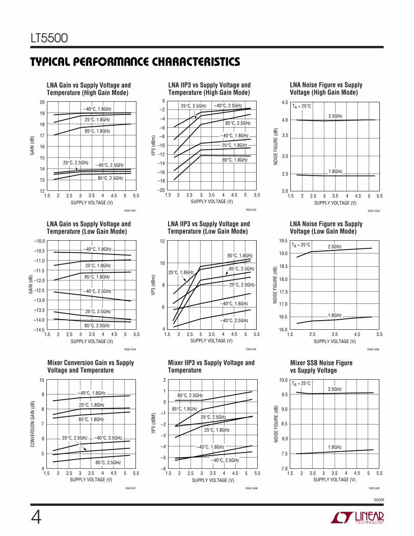
TYPICAL PERFOR A CE CHARACTERISTICS
UW
LNA IIP3 vs Supply Voltage andTemperature (High Gain Mode)
LNA Noise Figure vs SupplyVoltage (High Gain Mode)
LNA IIP3 vs Supply Voltage andTemperature (Low Gain Mode)
LNA Noise Figure vs SupplyVoltage (Low Gain Mode)
LNA Gain vs Supply Voltage andTemperature (High Gain Mode)
SUPPLY VOLTAGE (V)1.5
GAIN
(dB)
16
18
5.5
5500 G01
14
122.5 3.5 4.52 3 4 5
20
15
17
13
19–40°C, 1.8GHz
–40°C, 2.5GHz
25°C, 1.8GHz
85°C, 1.8GHz
85°C, 2.5GHz
25°C, 2.5GHz
SUPPLY VOLTAGE (V)1.5
–20
IIP3
(dBm
)
–18
–14
–12
–10
0
–6
2.5 3.5 4
5500 G02
–16
–4
–2
–8
2 3 4.5 5 5.5
–40°C, 1.8GHz
–40°C, 2.5GHz
25°C, 1.8GHz
85°C, 1.8GHz
85°C, 2.5GHz
25°C, 2.5GHz
SUPPLY VOLTAGE (V)1.5
NOIS
E FI
GURE
(dB)
3.5
4.0
4.5
3 4 5.5
5500 G03
3.0
2.5
2.02 2.5 3.5 4.5 5
2.5GHz
TA = 25°C
1.8GHz
LNA Gain vs Supply Voltage andTemperature (Low Gain Mode)
SUPPLY VOLTAGE (V)1.5
GAIN
(dB)
–12.0
–11.5
–11.0
5.5
5500 G04
–12.5
–13.0
–14.5
–14.0
2 2.5 3 3.5 4 4.5 5
–13.5
–10.0
–10.5 –40°C, 1.8GHz
–40°C, 2.5GHz
25°C, 1.8GHz
25°C, 2.5GHz
85°C, 1.8GHz
85°C, 2.5GHz
SUPPLY VOLTAGE (V)1.5
IIP3
(dBm
)
4
6
8
2.5 3.5 4.5 5.5
5500 G05
10
12
2 3 4 5
–40°C, 1.8GHz
–40°C, 2.5GHz
25°C, 2.5GHz
85°C, 1.8GHz
85°C, 2.5GHz25°C, 1.8GHz
SUPPLY VOLTAGE (V)1.5
18.0
18.5
19.5
4.5
5500 G06
17.5
17.0
2.5 3.5 5.5
16.5
16.0
19.0
NOIS
E FI
GURE
(dB)
2.5GHz
1.8GHz
TA = 25°C
Mixer Conversion Gain vs SupplyVoltage and Temperature
Mixer IIP3 vs Supply Voltage andTemperature
Mixer SSB Noise Figurevs Supply Voltage
SUPPLY VOLTAGE (V)1.5
4
CONV
ERSI
ON G
AIN
(dB)
5
6
7
8
2.5 3.5 4.5 5.5
5500 G07
9
10
2 3 4 5
–40°C, 1.8GHz
–40°C, 2.5GHz
85°C, 1.8GHz
25°C, 1.8GHz
85°C, 2.5GHz
25°C, 2.5GHz
SUPPLY VOLTAGE (V)1.5
IIP3
(dBM
)
–2
0
5.5
5500 G08
–4
–62.5 3.5 4.52 3 4 5
2
–3
–1
–5
1
–40°C, 1.8GHz
–40°C, 2.5GHz
25°C, 1.8GHz
85°C, 1.8GHz
85°C, 2.5GHz
25°C, 2.5GHz
SUPPLY VOLTAGE (V)1.5
7.0
NOIS
E FI
GURE
(dB)
7.5
8.0
8.5
9.0
2.5 3.5 4.5 5.5
5500 G09
9.5
10.0
2 3 4 5
2.5GHz
1.8GHz
TA = 25°C
5
LT5500
5500f
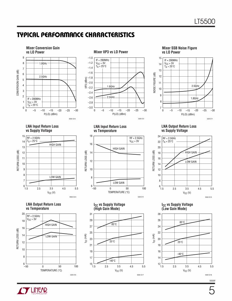
TYPICAL PERFOR A CE CHARACTERISTICS
UW
Mixer Conversion Gainvs LO Power Mixer IIP3 vs LO Power
P(LO) (dBm)0
0
CONV
ERSI
ON G
AIN
(dB)
1
3
4
5
–20
9
5500 G10
2
–10–5 –25–15 –30
6
7
8
2.5GHz
1.8GHz
IF = 280MHzVCC = 3VTA = 25°C
LNA Input Return Lossvs Supply Voltage
Mixer SSB Noise Figurevs LO Power
P(LO) (dBm)0
NOIS
E FI
GURE
(dB)
10
11
12
–15 –25
5500 G11
9
8
7–5 –10 –20
13
14
15
–30
2.5GHz
1.8GHz
IF = 280MHzVCC = 3VTA = 25°C
P(LO) (dBm)0
–3.0
IIP3
(dBm
)
–2.6
–2.2
–1.8
–5 –10 –15 –20
5500 G12
–25
–1.4
–1.0
–2.8
–2.4
–2.0
–1.6
–1.2
–30
2.5GHz
1.8GHz
IF = 280MHzVCC = 3VTA = 25°C
LNA Input Return Lossvs Temperature
LNA Output Return Lossvs Supply Voltage
VCC (V)1.5
RETU
RN L
OSS
(dB)
11
12
13
5.5
5500 G13
10
9
6
7
2.5 3.5 4.5
8
15
14
LOW GAIN
HIGH GAIN
RF = 2.5GHzTA = 25°C
TEMPERATURE (°C)–50
6
RETU
RN L
OSS
(dB)
8
10
12
14
18
0 50
HIGH GAIN
LOW GAIN
5500 G14
100
16
RF = 2.5GHzVCC = 3V
VCC (V)1.5
RETU
RN L
OSS
(dB)
16
18
20
5.5
5500 G15
14
12
6
8
2.5 3.5 4.5
10
24
22
LOW GAIN
HIGH GAIN
RF = 2.5GHzTA = 25°C
LNA Output Return Lossvs Temperature
ICC vs Supply Voltage(High Gain Mode)
ICC vs Supply Voltage(Low Gain Mode)
TEMPERATURE (°C)–50
20
18
16
14
12
10
8
6
5500 G16
0 50
HIGH GAIN
100
RETU
RN L
OSS
(dB)
LOW GAIN
RF = 2.5GHzVCC = 3V
VCC (V)1.5
I CC
(mA)
23
25
27
5.5
5500 G17
21
19
152.5 3.5 4.5
17
31
85°C
25°C
–40°C
29
VCC (V)1.5
I CC
(mA)
20
22
24
5.5
5500 G18
18
16
122.5 3.5 4.5
14
28
85°C
25°C
–40°C
26
6
LT5500
5500f
PIN FUNCTIONS
UUU
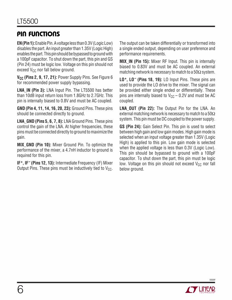
EN (Pin 1): Enable Pin. A voltage less than 0.3V (Logic Low)disables the part. An input greater than 1.35V (Logic High)enables the part. This pin should be bypassed to ground witha 100pF capacitor. To shut down the part, this pin and GS(Pin 24) must be logic low. Voltage on this pin should notexceed VCC nor fall below ground.
VCC (Pins 2, 9, 17, 21): Power Supply Pins. See Figure 6for recommended power supply bypassing.
LNA_IN (Pin 3): LNA Input Pin. The LT5500 has betterthan 10dB input return loss from 1.8GHz to 2.7GHz. Thispin is internally biased to 0.8V and must be AC coupled.
GND (Pin 4, 11, 14, 16, 20, 23): Ground Pins. These pinsshould be connected directly to ground.
LNA_GND (Pins 5, 6, 7, 8): LNA Ground Pins. These pinscontrol the gain of the LNA. At higher frequencies, thesepins must be connected directly to ground to maximize thegain.
MIX_GND (Pin 10): Mixer Ground Pin. To optimize theperformance of the mixer, a 4.7nH inductor to ground isrequired for this pin.
IF+, IF– (Pins 12, 13): Intermediate Frequency (IF) MixerOutput Pins. These pins must be inductively tied to VCC.
The output can be taken differentially or transformed intoa single ended output, depending on user preference andperformance requirements.
MIX_IN (Pin 15): Mixer RF Input. This pin is internallybiased to 0.83V and must be AC coupled. An externalmatching network is necessary to match to a 50Ω system.
LO+, LO– (Pins 18, 19): LO Input Pins. These pins areused to provide the LO drive to the mixer. The signal canbe provided either single ended or differentially. Thesepins are internally biased to VCC – 0.2V and must be ACcoupled.
LNA_OUT (Pin 22): The Output Pin for the LNA. Anexternal matching network is necessary to match to a 50Ωsystem. This pin must be DC coupled to the power supply.
GS (Pin 24): Gain Select Pin. This pin is used to selectbetween high gain and low gain modes. High gain mode isselected when an input voltage greater than 1.35V (LogicHigh) is applied to this pin. Low gain mode is selectedwhen the applied voltage is less than 0.3V (Logic Low).This pin should be bypassed to ground with a 100pFcapacitor. To shut down the part, this pin must be logiclow. Voltage on this pin should not exceed VCC nor fallbelow ground.
7
LT5500
5500f
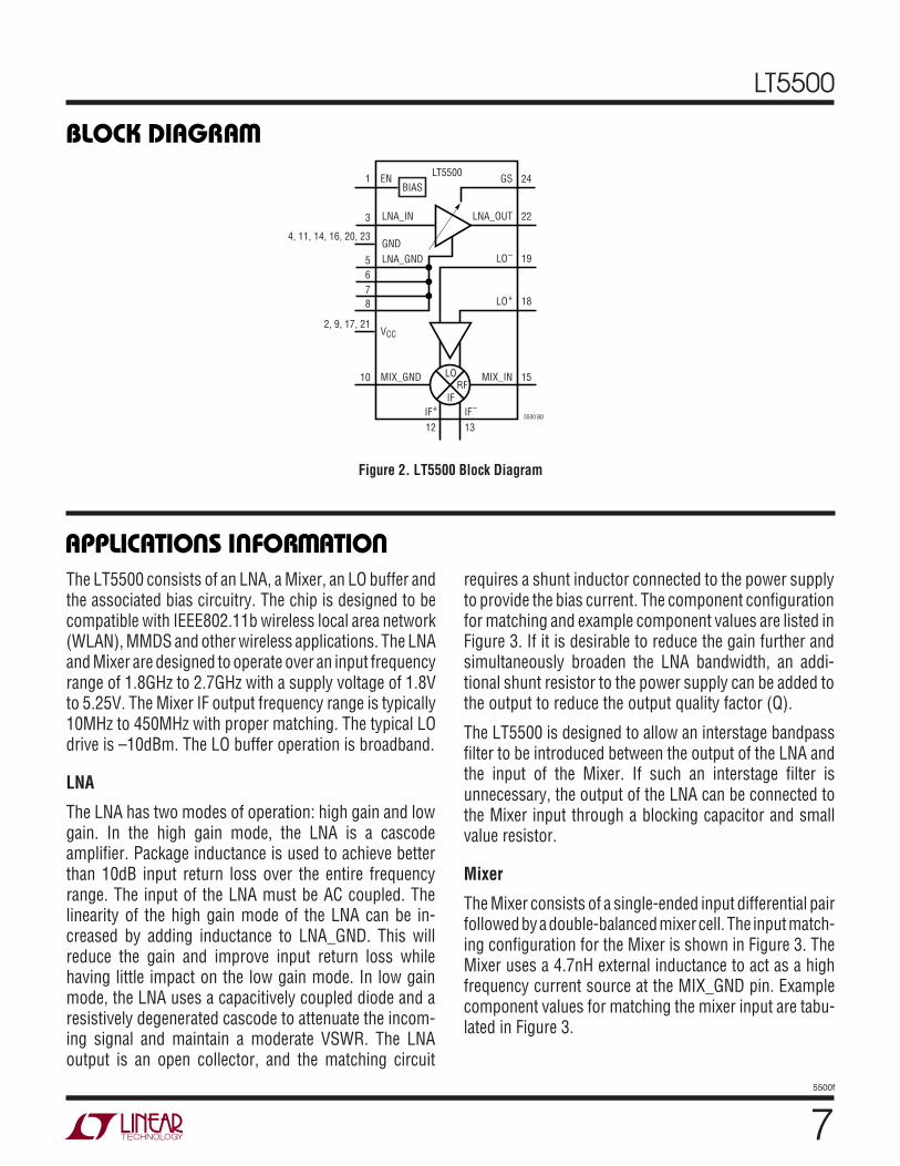
BLOCK DIAGRA
W
Figure 2. LT5500 Block Diagram
LO MIX_IN
LO+
LO–
LNA_OUTLNA_IN
LNA_GNDGND
GSEN1
3
5678
2, 9, 17, 21
10
12 135500 BD
15
18
19
22
24
4, 11, 14, 16, 20, 23
LT5500
MIX_GND
VCC
IF–IF+IF
RF
BIAS
APPLICATIONS INFORMATION
WU UU
The LT5500 consists of an LNA, a Mixer, an LO buffer andthe associated bias circuitry. The chip is designed to becompatible with IEEE802.11b wireless local area network(WLAN), MMDS and other wireless applications. The LNAand Mixer are designed to operate over an input frequencyrange of 1.8GHz to 2.7GHz with a supply voltage of 1.8Vto 5.25V. The Mixer IF output frequency range is typically10MHz to 450MHz with proper matching. The typical LOdrive is –10dBm. The LO buffer operation is broadband.
LNA
The LNA has two modes of operation: high gain and lowgain. In the high gain mode, the LNA is a cascodeamplifier. Package inductance is used to achieve betterthan 10dB input return loss over the entire frequencyrange. The input of the LNA must be AC coupled. Thelinearity of the high gain mode of the LNA can be in-creased by adding inductance to LNA_GND. This willreduce the gain and improve input return loss whilehaving little impact on the low gain mode. In low gainmode, the LNA uses a capacitively coupled diode and aresistively degenerated cascode to attenuate the incom-ing signal and maintain a moderate VSWR. The LNAoutput is an open collector, and the matching circuit
requires a shunt inductor connected to the power supplyto provide the bias current. The component configurationfor matching and example component values are listed inFigure 3. If it is desirable to reduce the gain further andsimultaneously broaden the LNA bandwidth, an addi-tional shunt resistor to the power supply can be added tothe output to reduce the output quality factor (Q).
The LT5500 is designed to allow an interstage bandpassfilter to be introduced between the output of the LNA andthe input of the Mixer. If such an interstage filter isunnecessary, the output of the LNA can be connected tothe Mixer input through a blocking capacitor and smallvalue resistor.
Mixer
The Mixer consists of a single-ended input differential pairfollowed by a double-balanced mixer cell. The input match-ing configuration for the Mixer is shown in Figure 3. TheMixer uses a 4.7nH external inductance to act as a highfrequency current source at the MIX_GND pin. Examplecomponent values for matching the mixer input are tabu-lated in Figure 3.
8
LT5500
5500f
APPLICATIONS INFORMATION
WU UU
LO MIX_IN
LO+
LO–
LNA_OUTLNA_INRF OUT
LNA_GND
GND
GSEN LT5500
MIX_GND
VCC
*REFER TO FIGURE 6 FOR POWER SUPPLY PINS BYPASSING RECOMMENDATION
VCC
IF–
5500 F03
IF+
VCC• •
T1
IFRF
C4
100pF 100pF
C17 L3
L54.7nH
L7
IF OUTPUT
RF INPUT
L4
100pF100pF
L2
GAINSELECTENABLE
LO INPUT
MIXER RFINPUT
C2100pF
APPLICATION DEPENDENTCOMPONENT VALUESRF INPUT
L4L2L3C4C17L9
C23
L7T1
1.8GHz4.7nH12nH4.7nH220pF10pF5.6nH1.8pF
280MHz IF OUTPUT
2.5GHz2.7nH4.7nH1.8nH220pF10pF2.7nH1.5pF
BIAS
C23
L9
VCC
15nHTC8-1 MINI-CIRCUITS
*
Figure 3. Simplified Test Schematic for 1.8GHz and 2.5GHz Applications
An IF transformer can be used to create a single-endedoutput. The additional discrete components necessary toachieve a 50Ω match are tabulated in Figure 3. Alterna-tively, the discrete solution shown in Figure 4 can be usedto perform differential to single-ended conversion. Forbest LO and RF signal suppression at the IF output, atransformer should be used. If it is desirable to reduce thegain of the mixer, a resistor between the IF outputs can beused.
LO Buffer
The LO inputs can be driven either differentially or singleended. A single-ended configuration is shown along withexample component values in Figure 3. Optionally, the LOcan be driven differentially as shown in Figure 5.
C14 C12
L10
VCC
L11
100pF
5500 F04
1312
50ΩIF OUTPUT
LT5500IF+ IF–
IF OUTPUTL10, L11
C12C14
280MHz27nH3.3pF2.2pF
Figure 4. Alternative Mixer IF Output Matching Figure 5. Optional Transformer-Based Differential LO Drive
L3
5500 F05
TX14:1
LO INPUTL3
TX1
2.22GHz3.3nH
TOKO-BF4
LO INPUT19
18LT5500
LO–
LO+
9
LT5500
5500f
APPLICATIONS INFORMATION
WU UU
Modes of Operation
The LT5500 has three operating modes:
1. Shutdown
2. LNA High Gain
3. LNA Low Gain
For shutdown, the EN pin and the GS pin must be at logicLow. Logic Low is defined as a control voltage below 0.3V.LNA High gain mode requires that both EN and GS pins beat logic High. Logic High is defined as a control voltageabove 1.35V. LNA Low gain mode requires that the EN pinbe at logic High and that the GS pin be at logic Low. Mixeroperation is independent of the GS pin. The Mixer isenabled when the EN pin is at logic High.Table 1: Mode Selection
EN GS LNA MIXER
High High High Gain On
High Low Low Gain On
Low Low Shutdown Shutdown
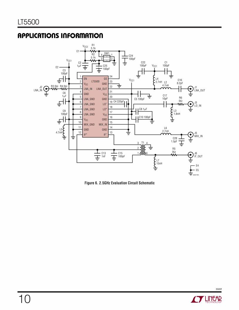
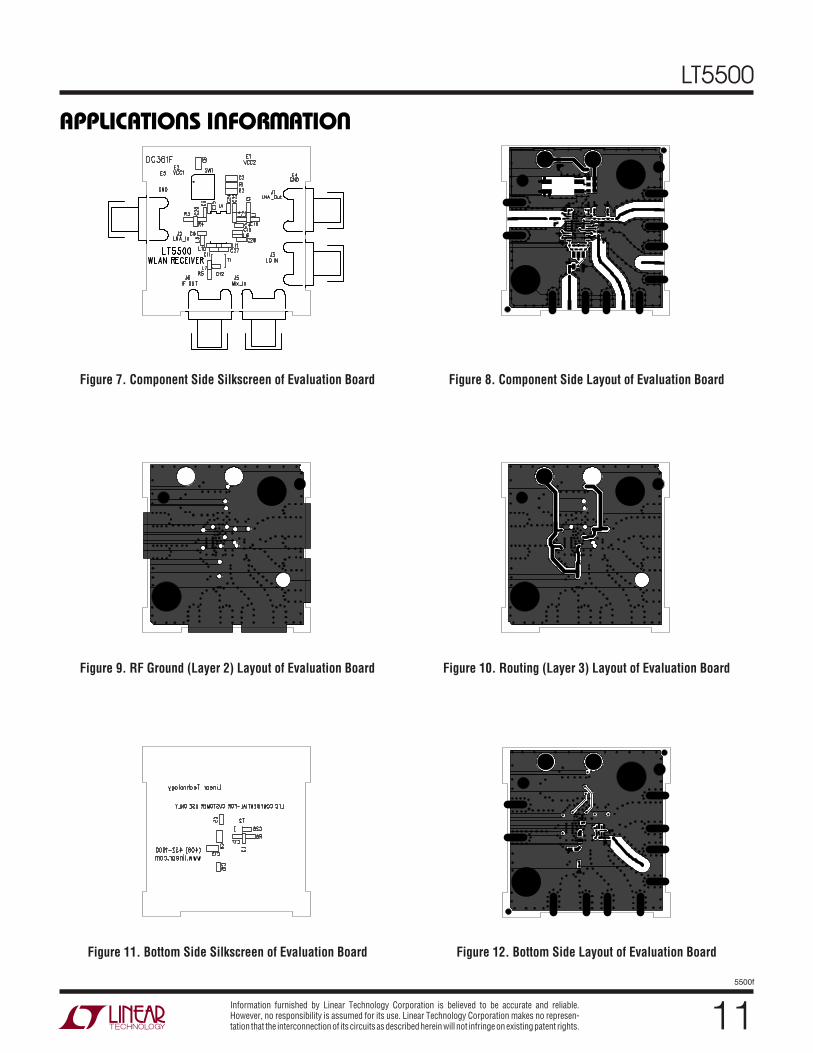
Evaluation Board
Figure 6 shows the circuit schematic of the evaluationboard. Each signal terminal of the evaluation board hasprovisions for three matching components in a T-forma-tion. In practice, two or fewer components are needed toachieve the match. In the case of the LNA input, no externalcomponents are necessary if the band select filter pro-vides the necessary AC coupling. Otherwise AC couplingmust be provided. A similar consideration applies to theMixer input pin. The LO terminal of the evaluation boardwas designed to permit evaluation of both single endedand differential matching configurations. The differentialconfiguration anticipates the use of a transformer. Simi-larly, the IF output board layout was designed to permit
evaluation of both transformer based and discrete compo-nent based matching.
The evaluation board employs primarily 0402 surfacemount components, particularly near the signal paths. Allsurface mount inductors must have a high self-resonancefrequency. The component values necessary for 1.8GHzand 2.5GHz applications are tabulated in Figure 3.
RF Layout Tips
• Use 50Ω impedance transmission lines up to the match-ing networks. Use of ground planes is a must, particu-larly beneath the IC.
• Keep the matching networks as close to the pins aspossible.
• Surface mount 0402 outline (or smaller) parts arerecommended to minimize parasitic capacitances andinductances.
• Improve LO isolation and maximize component densityby putting the LO signal trace on the bottom of theboard. This permits either the matching components oran interstage filter to be placed directly between theLNA output and the Mixer input.
• Place bypass capacitors to ground in close proximity tothe pull-up inductors on the LNA and Mixer outputs toimprove component behavior and assure a good small-signal ground.
• VCC lines must be decoupled with low impedance,broadband capacitors to prevent instability. The capaci-tors should be placed as close as possible to the VCCpins.
• Avoid use of long traces whenever possible. Long RFtraces in particular lead to signal radiation, degradedisolation and higher losses.
10
LT5500
5500f
APPLICATIONS INFORMATION
WU UU
GS
GND
LNA_OUT
VCC
GND
LO–
LO+
VCC
GND
MIX_IN
GND
IF–
EN
VCC
LNA_IN
GND
LNA_GND
LNA_GND
LNA_GND
LNA_GND
VCC
MIX_GND
GND
IF+
24
23
22
21
20
19
18
17
16
15
14
13
1
2
3
4
5
6
7
8
9
10
11
12
LT5500
C3100pF
C21µF
J2LNA_IN
C25100pF
C24100pF
C61µF
C4 220pF
C8 1µF
C1710pF
C22100pF
L42.7nH
L31.8nH
L24.7nH
C5 100pF
C10 100pF
C9100pF
C131nF
L54.7nH
E2
VCC1
VCC2
E1
VCC1
VCC1
R4 0ΩR3 0Ω
R15.1k
SW143
12
R25.1k
C1100pF
C168.2pF
R60Ω
C281.5pF
L62.7nH
J1LNA_OUT
J3LO_IN
J5MIX_IN
J6IF_OUT
E4
E5
5500 F06
C15100pF
T13
2
1
4
6••
L715nH
R50Ω
Figure 6. 2.5GHz Evaluation Circuit Schematic
11
LT5500
5500f
APPLICATIONS INFORMATION
WU UU
Figure 7. Component Side Silkscreen of Evaluation Board Figure 8. Component Side Layout of Evaluation Board
Figure 9. RF Ground (Layer 2) Layout of Evaluation Board Figure 10. Routing (Layer 3) Layout of Evaluation Board
Figure 11. Bottom Side Silkscreen of Evaluation Board Figure 12. Bottom Side Layout of Evaluation Board
Information furnished by Linear Technology Corporation is believed to be accurate and reliable.However, no responsibility is assumed for its use. Linear Technology Corporation makes no represen-tation that the interconnection of its circuits as described herein will not infringe on existing patent rights.
12
LT5500
5500f
PART NUMBER DESCRIPTION COMMENTS
LT5502 400MHz Quadrature Demodulator with RSSI 1.8V to 5.25V Supply, 70MHz to 400MHz IF, 84dB Limiting Gain,90dB RSSI Range
LT5503 1.2GHz to 2.7GHz Direct IQ Modulator and 1.8V to 5.25V Supply, Four-Step RF Power Control,Upconverting Mixer 120MHz Modulation Bandwidth
LT5504 800MHz to 2.7GHz RF Measuring Receiver 80dB Dynamic Range, Temperature Compensated, 2.7V to 5.5V Supply
LTC5505 300MHz to 3.5GHz RF Power Detector >40dB Dynamic Range, Temperature Compensated, 2.7V to 6V Supply
LT5506/LTC5446 500MHz Quadrature IF Demodulator with VGA 1.8V to 5.25V Supply, 40MHz to 500MHz IF, Linear Power Gain
LTC5507 100kHz to 1GHz RF Power Detector 48dB Dynamic Range, Temperature Compensated, 2.7V to 6V Supply
LTC5508 300MHz to 7GHz RF Power Detector SC70 Package
LTC5509 300MHz to 3GHz RF Power Detector 36dB Dynamic Range, SC70 Package
LT5511 High Signal Level Upconverting Mixer RF Output to 3GHz, 17dBm IIP3, Integrated LO Buffer
LT5512 High Signal Level Downconverting Mixer DC-3GHz, 20dBm IIP3, Integrated LO Buffer
LT5515 1.5GHz to 2.5GHz Direct Conversion Quadrature Demodulator 20dBm IIP3,Integrated LO Quadrature Generator
LT5516 0.8GHz to 1.5GHz Direct Conversion Quadrature Demodulator 21.5dBm IIP3,Integrated LO Quadrature Generator
LT5522 600MHz to 2.7GHz High Signal Level Mixer 25dBm IIP3 at 900MHz, 21.5dBm IIP3 at 1.9GHz, Single-Ended 50ΩMatched RF and LO Ports, Integrated LO Buffer
LTC5532 300MHz to 7GHz Precision RF Power Detector Precision VOUT Offset Control, Adjustable Gain and Offset Voltage
ThinSOT is a trademark of Linear Technology Corporation.
© LINEAR TECHNOLOGY CORPORATION 2005
LT/TP 0305 1K PRINTED IN USA
RELATED PARTS
Linear Technology Corporation1630 McCarthy Blvd., Milpitas, CA 95035-7417(408) 432-1900 FAX: (408) 434-0507 www.linear.com
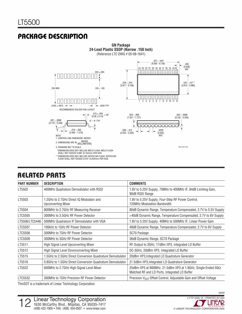
PACKAGE DESCRIPTION
U
GN Package24-Lead Plastic SSOP (Narrow .150 Inch)
(Reference LTC DWG # 05-08-1641)
.337 – .344*(8.560 – 8.738)
GN24 (SSOP) 0502
1 2 3 4 5 6 7 8 9 10 11 12
.229 – .244(5.817 – 6.198)
.150 – .157**(3.810 – 3.988)
161718192021222324 15 1413
.016 – .050(0.406 – 1.270)
.015 ± .004(0.38 ± 0.10)
× 45°
0° – 8° TYP.007 – .0098(0.178 – 0.249)
.053 – .068(1.351 – 1.727)
.008 – .012(0.203 – 0.305)
.004 – .0098(0.102 – 0.249)
.0250(0.635)
BSC
.033(0.838)
REF
.254 MIN
RECOMMENDED SOLDER PAD LAYOUT
.150 – .165
.0250 TYP.0165 ± .0015
.045 ±.005
*DIMENSION DOES NOT INCLUDE MOLD FLASH. MOLD FLASH SHALL NOT EXCEED 0.006" (0.152mm) PER SIDE**DIMENSION DOES NOT INCLUDE INTERLEAD FLASH. INTERLEAD FLASH SHALL NOT EXCEED 0.010" (0.254mm) PER SIDE
INCHES(MILLIMETERS)
NOTE:1. CONTROLLING DIMENSION: INCHES
2. DIMENSIONS ARE IN
3. DRAWING NOT TO SCALE