
Unit-3 Transformer Transformer Voltage regulation, losses ...
Upload
khangminh22Category
view
1download
0
Application Note Please read the Important Notice and Warnings at the end of this document V 1.1 www.infineon.com page 1 of 69 2020-03-03
AN_1910_PL15_1910_001345
Low frequency transformer based SOHO UPS design Application Note
Author: Peter B. Green
About this document
Scope and purpose
The purpose of this document is to provide a comprehensive functional description and guide to the Uninterruptible Power Supply (UPS) demonstration board based on the offline bi-directional full-bridge topology and including a 50/60 Hz laminated iron-cored power transformer. The circuit functionality is discussed in detail during both back-up and charging modes of operation. System implementation including converter architecture, control algorithms and firmware is described in detail. Waveforms are shown under all operating conditions and test measurement data is presented.
Intended audience
Design engineers, applications engineers and students.
Infineon components featured
IRFS7440 40 V N-channel IR MOSFETTM in a D2PAK
2EDL8114 level-shift high-side, low-side half-bridge gate driver (EiceDRIVERTM)
XMC1301-TO16F0032 32-bit microcontroller with ARM® Cortex-M0 (XMCTM)
Table of contents
About this document ....................................................................................................................... 1 Table of contents ............................................................................................................................ 1
1 Introduction .......................................................................................................................... 3 1.1 UPS types ................................................................................................................................................. 3 1.2 Evaluation board description ................................................................................................................. 5 2 Evaluation board specifications ............................................................................................... 7 2.1 Evaluation board connections ................................................................................................................ 8 3 Schematics ............................................................................................................................ 9 4 Functional description ........................................................................................................... 11 4.1 UPS system operation ........................................................................................................................... 11 4.1.1 Back-up (inverter) mode power conversion ................................................................................... 12 4.1.2 Battery charging operation .............................................................................................................. 14 4.2 Supervisory functions ........................................................................................................................... 16
Application Note 2 of 69 V 1.1 2020-03-03
Low frequency transformer based SOHO UPS design Application Note Introduction
4.2.1 AC input voltage sensing .................................................................................................................. 16 4.2.2 AC output voltage sensing ............................................................................................................... 16 4.2.3 Current Sense (CS) amplifiers .......................................................................................................... 17 4.2.4 Thermal protection .......................................................................................................................... 17 4.2.5 Alarm buzzer and LED indicators ..................................................................................................... 18 5 Firmware ............................................................................................................................. 19 5.1 XMCTM microcontroller .......................................................................................................................... 19 5.2 DAVETM IDE ............................................................................................................................................. 20 5.3 I/O pin configuration ............................................................................................................................. 22 5.4 Flowcharts ............................................................................................................................................. 23 5.5 In-circuit debugging with Micrium μC probe ....................................................................................... 29 6 Bill of Materials (BOM) ........................................................................................................... 30 6.1 Power board .......................................................................................................................................... 30 6.2 Daughter card ........................................................................................................................................ 33 7 Transformer specifications..................................................................................................... 35 8 PCB layout ............................................................................................................................ 36 8.1 Main power board layout and heatsinking........................................................................................... 36
9 Test results ........................................................................................................................... 38 9.1 Back-up mode ....................................................................................................................................... 38 9.1.1 Operating waveforms ...................................................................................................................... 41 9.2 Charging mode ...................................................................................................................................... 51 9.2.1 Operating waveforms ...................................................................................................................... 52 9.3 Thermal performance (back-up mode) ................................................................................................ 54 10 Conclusion ........................................................................................................................... 56 11 Appendix .............................................................................................................................. 57 11.1 Firmware listings ................................................................................................................................... 57
References .................................................................................................................................... 68 Register your Infineon evaluation board, reference design or demo kit board ...................................... 68 Revision history............................................................................................................................. 68
Application Note 3 of 69 V 1.1 2020-03-03
Low frequency transformer based SOHO UPS design Application Note Introduction
1 Introduction
1.1 UPS types
UPSs for use in Small Office or Home Office (SOHO) environments typically include MOSFET-based inverters that operate from 12 V or 24 V lead-acid batteries (24 V systems are comprised of two series-connected 12 V batteries). Higher battery voltages are required to limit operating currents in higher power-rated systems. 42 V and 72 V systems also exist for the same reason; however, since these are somewhat less common, this reference design is based on a 12 V battery. Batteries may be external or internal to the UPS; car batteries are used externally and sealed lead-acid batteries internally.
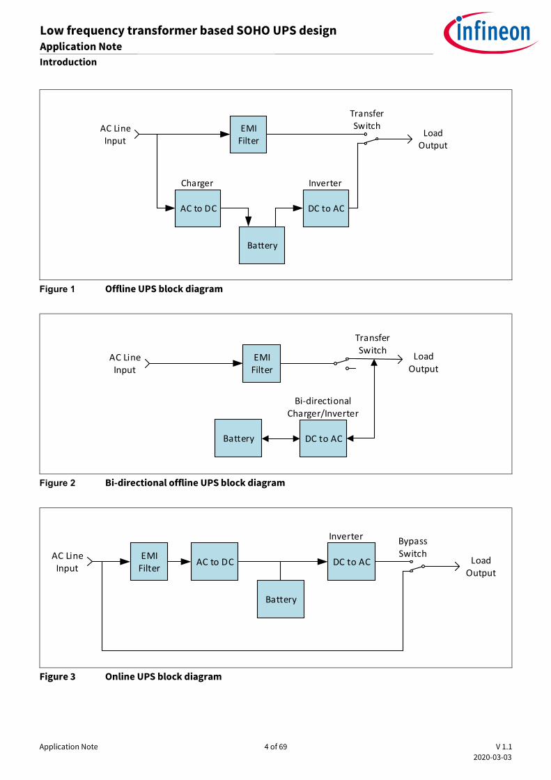
UPS systems can be classified into three main categories (see Figures 1, 2 and 3):
1. Offline/standby When AC-line voltage is present a relay bypasses the inverter, which remains off. The battery charger operates to maintain full charge. If the AC power fails the relay switches the UPS output over to the inverter, which starts up after a short interruption of 10 to 20 ms to supply back-up power.
2. Line-interactive Similar to the offline UPS but includes some AC-line conditioning function to regulate the AC output to compensate for low- and high-line input voltage conditions and provide a more stable output voltage. The system is a line conditioner and offline UPS combined.
3. On-line/double-conversion The AC input is converted to DC at the battery charge level and then converted back to AC so that in the event of an AC-line failure the system will switch seamlessly to battery back-up and the output will continue to run without interruption. Such systems provide a stable and clean AC output under all conditions, but there is an inherent efficiency loss with stages of conversion. More sophisticated systems are able to mitigate this by partially bypassing the two conversion stages during AC-line operation so that only a small amount of power passes through them. If AC input fails, the inverter stage is able to take the full load without interruption of the output.
SOHO UPS systems are mainly of the offline and line-interactive types. These can be broadly categorized into systems based on Low Frequency (LF) iron lamination-type transformers and High Frequency (HF) transformers based on ferrite cores. The most basic UPS types produce an unregulated 50 to 60 Hz square-wave output. Sine wave output inverters are preferred, however, since they offer better power quality with regulated output voltage to avoid any potential stress that may occur with some types of appliance. Systems also exist that produce an approximate sine wave output with high distortion. The evaluation board discussed here is based on a LF transformer and produces a low distortion sine wave output waveform.
Application Note 4 of 69 V 1.1 2020-03-03
Low frequency transformer based SOHO UPS design Application Note Introduction
EMIFilter
AC to DC
Battery
DC to AC
TransferSwitch
Charger Inverter
AC LineInput
LoadOutput
Figure 1 Offline UPS block diagram
EMIFilter
Battery DC to AC
TransferSwitch
Bi-directionalCharger/Inverter
AC LineInput
LoadOutput
Figure 2 Bi-directional offline UPS block diagram
EMIFilter
AC to DC
Battery
DC to AC
Inverter
AC LineInput
BypassSwitch
LoadOutput
Figure 3 Online UPS block diagram
Application Note 5 of 69 V 1.1 2020-03-03
Low frequency transformer based SOHO UPS design Application Note Introduction
1.2 Evaluation board description
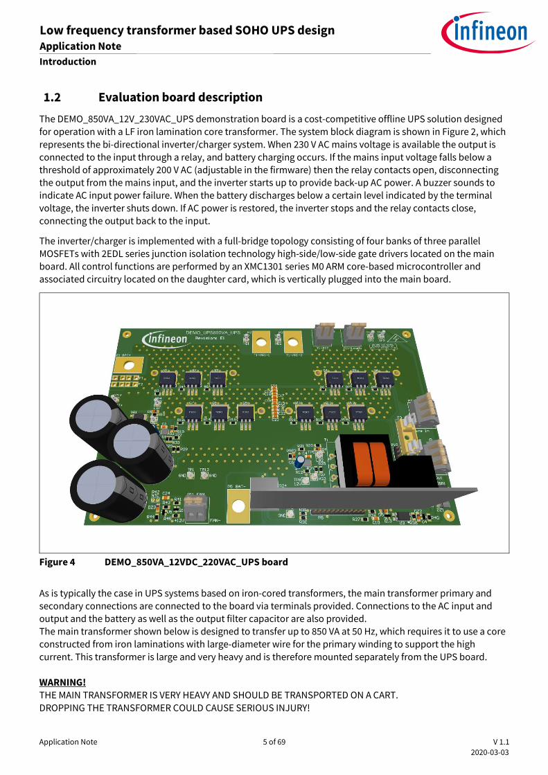
The DEMO_850VA_12V_230VAC_UPS demonstration board is a cost-competitive offline UPS solution designed for operation with a LF iron lamination core transformer. The system block diagram is shown in Figure 2, which represents the bi-directional inverter/charger system. When 230 V AC mains voltage is available the output is connected to the input through a relay, and battery charging occurs. If the mains input voltage falls below a threshold of approximately 200 V AC (adjustable in the firmware) then the relay contacts open, disconnecting the output from the mains input, and the inverter starts up to provide back-up AC power. A buzzer sounds to indicate AC input power failure. When the battery discharges below a certain level indicated by the terminal voltage, the inverter shuts down. If AC power is restored, the inverter stops and the relay contacts close, connecting the output back to the input.
The inverter/charger is implemented with a full-bridge topology consisting of four banks of three parallel MOSFETs with 2EDL series junction isolation technology high-side/low-side gate drivers located on the main board. All control functions are performed by an XMC1301 series M0 ARM core-based microcontroller and associated circuitry located on the daughter card, which is vertically plugged into the main board.
Figure 4 DEMO_850VA_12VDC_220VAC_UPS board
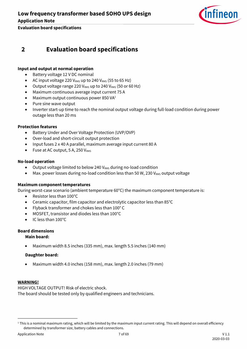
As is typically the case in UPS systems based on iron-cored transformers, the main transformer primary and secondary connections are connected to the board via terminals provided. Connections to the AC input and output and the battery as well as the output filter capacitor are also provided. The main transformer shown below is designed to transfer up to 850 VA at 50 Hz, which requires it to use a core constructed from iron laminations with large-diameter wire for the primary winding to support the high current. This transformer is large and very heavy and is therefore mounted separately from the UPS board. WARNING! THE MAIN TRANSFORMER IS VERY HEAVY AND SHOULD BE TRANSPORTED ON A CART. DROPPING THE TRANSFORMER COULD CAUSE SERIOUS INJURY!
Application Note 6 of 69 V 1.1 2020-03-03
Low frequency transformer based SOHO UPS design Application Note Introduction
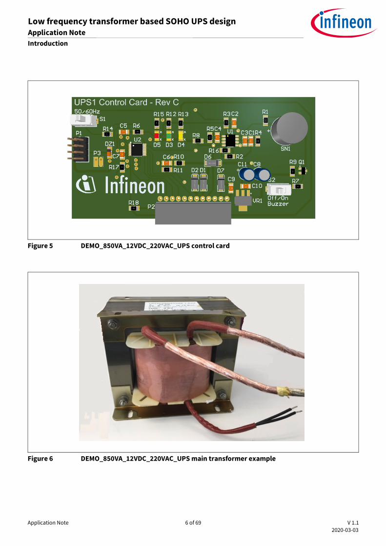
Figure 5 DEMO_850VA_12VDC_220VAC_UPS control card
Figure 6 DEMO_850VA_12VDC_220VAC_UPS main transformer example
Application Note 7 of 69 V 1.1 2020-03-03
Low frequency transformer based SOHO UPS design Application Note Evaluation board specifications
2 Evaluation board specifications
Input and output at normal operation Battery voltage 12 V DC nominal AC input voltage 220 VRMS up to 240 VRMS (55 to 65 Hz) Output voltage range 220 VRMS up to 240 VRMS (50 or 60 Hz) Maximum continuous average input current 75 A Maximum output continuous power 850 VA1 Pure sine wave output Inverter start-up time to reach the nominal output voltage during full-load condition during power
outage less than 20 ms Protection features
Battery Under and Over Voltage Protection (UVP/OVP) Over-load and short-circuit output protection Input fuses 2 x 40 A parallel, maximum average input current 80 A Fuse at AC output, 5 A, 250 VRMS
No-load operation
Output voltage limited to below 240 VRMS during no-load condition Max. power losses during no-load condition less than 50 W, 230 VRMS output voltage
Maximum component temperatures During worst-case scenario (ambient temperature 60°C) the maximum component temperature is:
Resistor less than 100°C Ceramic capacitor, film capacitor and electrolytic capacitor less than 85°C Flyback transformer and chokes less than 100° C MOSFET, transistor and diodes less than 100°C IC less than 100°C
Board dimensions
Main board:
Maximum width 8.5 inches (335 mm), max. length 5.5 inches (140 mm)
Daughter board:
Maximum width 4.0 inches (158 mm), max. length 2.0 inches (79 mm)
WARNING! HIGH VOLTAGE OUTPUT! Risk of electric shock. The board should be tested only by qualified engineers and technicians.
1 This is a nominal maximum rating, which will be limited by the maximum input current rating. This will depend on overall efficiency
determined by transformer size, battery cables and connections.
Application Note 8 of 69 V 1.1 2020-03-03
Low frequency transformer based SOHO UPS design Application Note Evaluation board specifications
2.1 Evaluation board connections
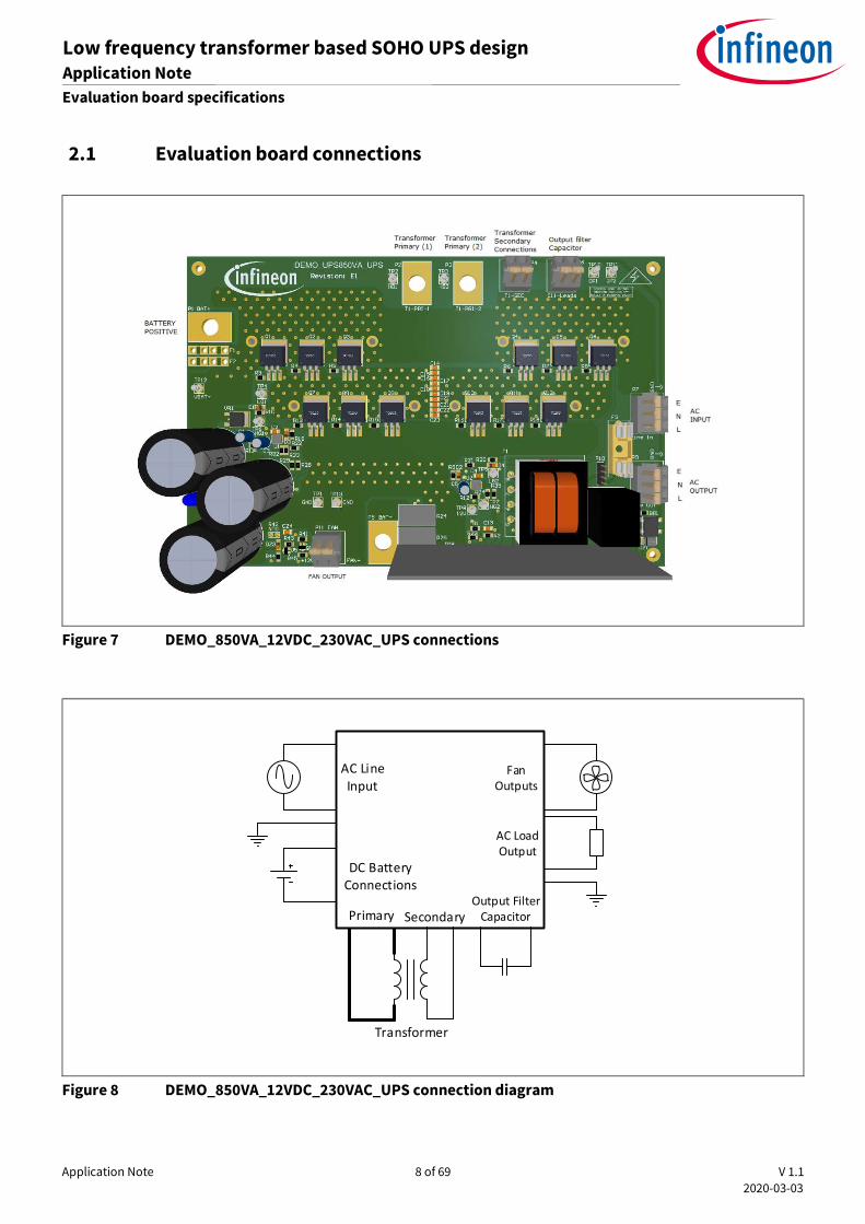
Figure 7 DEMO_850VA_12VDC_230VAC_UPS connections
AC LineInput
DC BatteryConnections
AC LoadOutput
Output FilterCapacitor
Transformer
Primary Secondary
FanOutputs
Figure 8 DEMO_850VA_12VDC_230VAC_UPS connection diagram
Application Note 9 of 69 V 1.1 2020-03-03
Low frequency transformer based SOHO UPS design Application Note Schematics
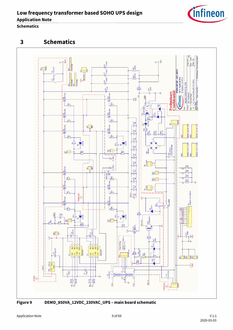
3 Schematics
Figure 9 DEMO_850VA_12VDC_230VAC_UPS – main board schematic
Application Note 10 of 69 V 1.1 2020-03-03
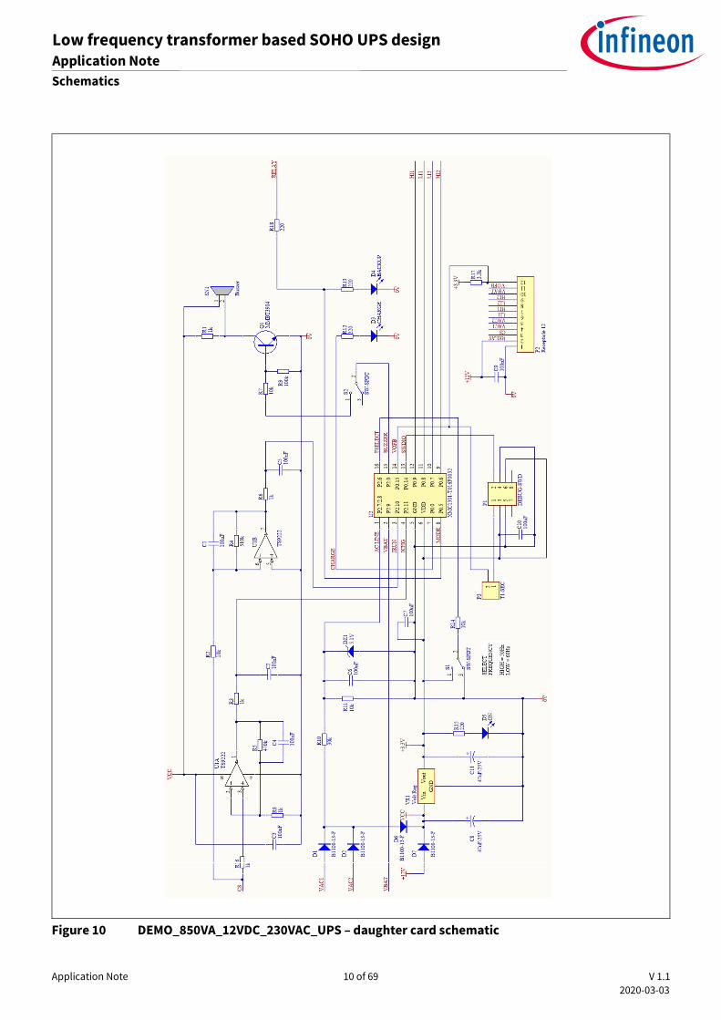
Low frequency transformer based SOHO UPS design Application Note Schematics
Figure 10 DEMO_850VA_12VDC_230VAC_UPS – daughter card schematic
Application Note 11 of 69 V 1.1 2020-03-03
Low frequency transformer based SOHO UPS design Application Note Functional description
4 Functional description
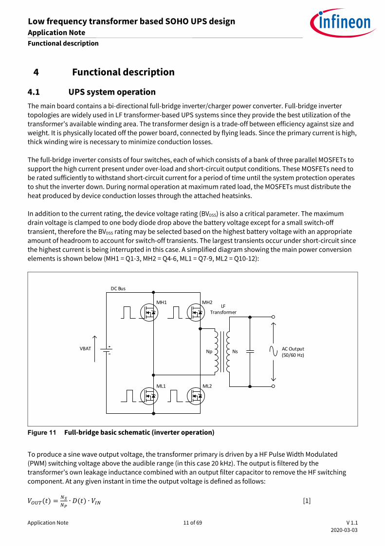
4.1 UPS system operation The main board contains a bi-directional full-bridge inverter/charger power converter. Full-bridge inverter topologies are widely used in LF transformer-based UPS systems since they provide the best utilization of the transformer’s available winding area. The transformer design is a trade-off between efficiency against size and weight. It is physically located off the power board, connected by flying leads. Since the primary current is high, thick winding wire is necessary to minimize conduction losses. The full-bridge inverter consists of four switches, each of which consists of a bank of three parallel MOSFETs to support the high current present under over-load and short-circuit output conditions. These MOSFETs need to be rated sufficiently to withstand short-circuit current for a period of time until the system protection operates to shut the inverter down. During normal operation at maximum rated load, the MOSFETs must distribute the heat produced by device conduction losses through the attached heatsinks. In addition to the current rating, the device voltage rating (BVDSS) is also a critical parameter. The maximum drain voltage is clamped to one body diode drop above the battery voltage except for a small switch-off transient, therefore the BVDSS rating may be selected based on the highest battery voltage with an appropriate amount of headroom to account for switch-off transients. The largest transients occur under short-circuit since the highest current is being interrupted in this case. A simplified diagram showing the main power conversion elements is shown below (MH1 = Q1-3, MH2 = Q4-6, ML1 = Q7-9, ML2 = Q10-12):
DC Bus
AC Output(50/60 Hz)
VBAT
LFTransformer
Np Ns
MH1 MH2
ML1 ML2
Figure 11 Full-bridge basic schematic (inverter operation)
To produce a sine wave output voltage, the transformer primary is driven by a HF Pulse Width Modulated (PWM) switching voltage above the audible range (in this case 20 kHz). The output is filtered by the transformer’s own leakage inductance combined with an output filter capacitor to remove the HF switching component. At any given instant in time the output voltage is defined as follows: 𝑉 (𝑡) = ∙ 𝐷(𝑡) ∙ 𝑉 [1]
Application Note 12 of 69 V 1.1 2020-03-03
Low frequency transformer based SOHO UPS design Application Note Functional description
Where VIN is equal to the DC bus voltage, NS/NP is the transformer turns ratio (voltage drops on the switches are negligible) and D(t) is the duty cycle of the PWM primary voltage at that instant. The switching frequency is kept low to minimize MOSFET switching losses since this is a hard-switching topology. A variable-time PWM duty-cycle function D(t) is used to periodically adjust the integrated output voltage VOUT(t) to construct a sinusoidal voltage: 𝐷(𝑡) = 𝑚 ∙ |sin (2𝜋𝑓𝑡)| [2] Where “f” is the AC output frequency. In equations [1] and [2], “D” refers to the PWM command duty cycle, which can vary between zero and one. This is divided into two alternating gate drive pulses such that each switch is operated every other pulse and therefore the actual gate drive maximum duty cycle DG(MAX) is 0.5. The duty cycle granularity is limited by microcontroller clock speed, therefore a lower PWM frequency just above the audio range at around 20 kHz provides the best resolution. The modulation index (m) determines the amount by which the duty cycle is modulated and is controlled to provide regulation of the RMS AC output voltage. The UPS relay RL1 is also located on the main board with its coil voltage switched on and off by the microcontroller U2, which is located on the daughter board. The micro-controller is programmed with firmware, which provides all of the MOSFET gate-drive signals and supervisory functions for the UPS. When AC mains power is present the contacts are closed so that the output is connected to the AC input. This is the default state of the relay when the coil is not energized. If the AC mains supply fails then U2 energizes the relay coil to open the contacts, thus disconnecting the output from the input. This is essential before the inverter starts up so that when running it will power loads connected to the UPS output only. From the time the AC-line input voltage drops below the minimum threshold, the system takes approximately 10 ms to open the relay contacts and start up the inverter for back-up mode operation. Loads connected to the output such as power supplies or LED lights can maintain operation through this short power interruption from internal storage capacitors. When AC power is restored the inverter shuts off and the relay contacts close, connecting the output back to the input for charging mode operation, which takes a similar amount of time. These interruptions are short enough that equipment connected to the output is able to continue operating seamlessly. Battery charging operation commences shortly after the relay contacts are closed. A soft-start is included so that charge current rises gradually to the charging level defined in the firmware.
4.1.1 Back-up (inverter) mode power conversion During inverter operation, each half-bridge of the full-bridge (MH1 with ML1, MH2 with ML2) operates as a synchronous buck converter in Continuous Conduction Mode (CCM), connected to one side of the transformer primary. The other side is connected to the battery positive through the opposite high-side MOSFET, which switches at LF. A high-side/low-side driver IC is used to supply the gate-drive pulses to each of the half-bridges. The bootstrap capacitors have to be large enough to operate at LF and supply gate charge for several MOSFETs connected in parallel. The reason for making the low-side MOSFETs the buck main switching elements is because these are hard-switched while the upper MOSFETs operating synchronously are soft-switched. Floating high-side gate-drive outputs from half-bridge driver ICs are more sensitive to potential latch-up, dv/dt or negative voltage transitions when driving hard-switched MOSFETs, which is not normally an issue with soft-switching. Since the low-side gate driver is not floating it is better suited to driving hard-switched MOSFETs. A fixed dead-time is
Application Note 13 of 69 V 1.1 2020-03-03
Low frequency transformer based SOHO UPS design Application Note Functional description
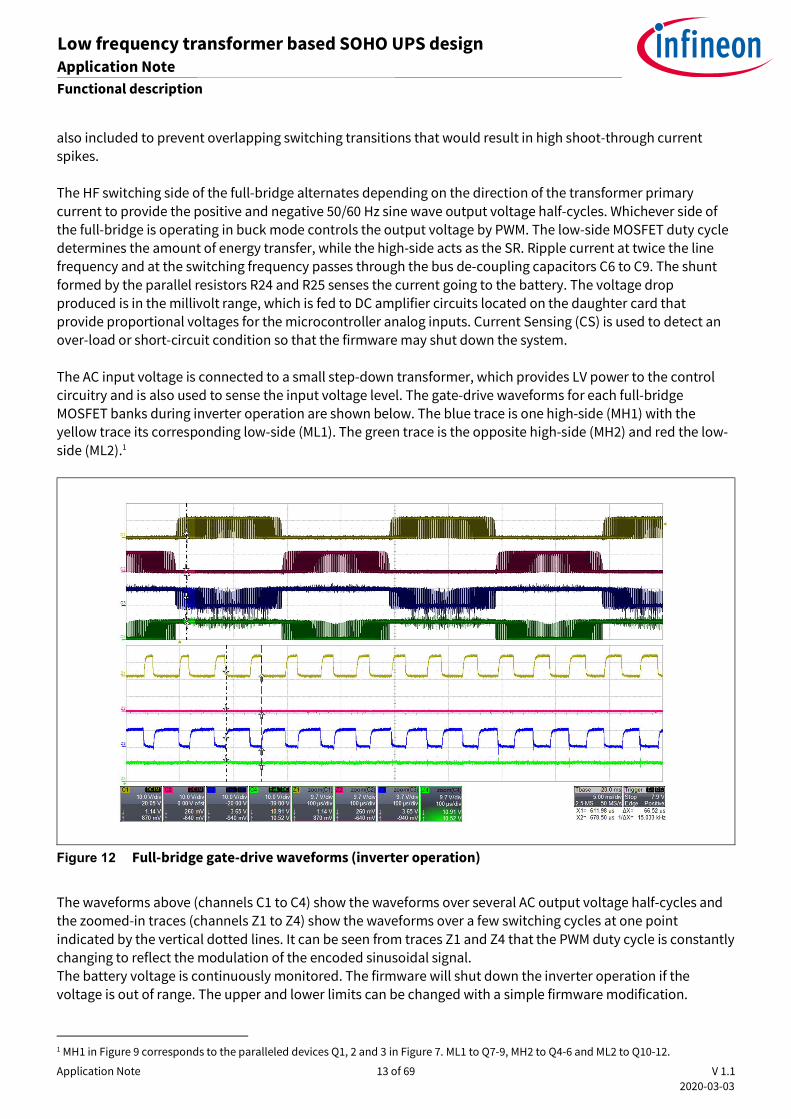
also included to prevent overlapping switching transitions that would result in high shoot-through current spikes. The HF switching side of the full-bridge alternates depending on the direction of the transformer primary current to provide the positive and negative 50/60 Hz sine wave output voltage half-cycles. Whichever side of the full-bridge is operating in buck mode controls the output voltage by PWM. The low-side MOSFET duty cycle determines the amount of energy transfer, while the high-side acts as the SR. Ripple current at twice the line frequency and at the switching frequency passes through the bus de-coupling capacitors C6 to C9. The shunt formed by the parallel resistors R24 and R25 senses the current going to the battery. The voltage drop produced is in the millivolt range, which is fed to DC amplifier circuits located on the daughter card that provide proportional voltages for the microcontroller analog inputs. Current Sensing (CS) is used to detect an over-load or short-circuit condition so that the firmware may shut down the system. The AC input voltage is connected to a small step-down transformer, which provides LV power to the control circuitry and is also used to sense the input voltage level. The gate-drive waveforms for each full-bridge MOSFET banks during inverter operation are shown below. The blue trace is one high-side (MH1) with the yellow trace its corresponding low-side (ML1). The green trace is the opposite high-side (MH2) and red the low-side (ML2).1
Figure 12 Full-bridge gate-drive waveforms (inverter operation)
The waveforms above (channels C1 to C4) show the waveforms over several AC output voltage half-cycles and the zoomed-in traces (channels Z1 to Z4) show the waveforms over a few switching cycles at one point indicated by the vertical dotted lines. It can be seen from traces Z1 and Z4 that the PWM duty cycle is constantly changing to reflect the modulation of the encoded sinusoidal signal. The battery voltage is continuously monitored. The firmware will shut down the inverter operation if the voltage is out of range. The upper and lower limits can be changed with a simple firmware modification. 1 MH1 in Figure 9 corresponds to the paralleled devices Q1, 2 and 3 in Figure 7. ML1 to Q7-9, MH2 to Q4-6 and ML2 to Q10-12.
Application Note 14 of 69 V 1.1 2020-03-03
Low frequency transformer based SOHO UPS design Application Note Functional description
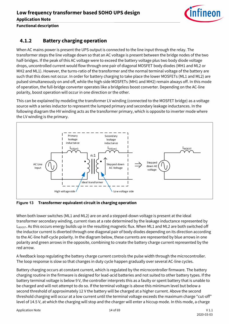
4.1.2 Battery charging operation
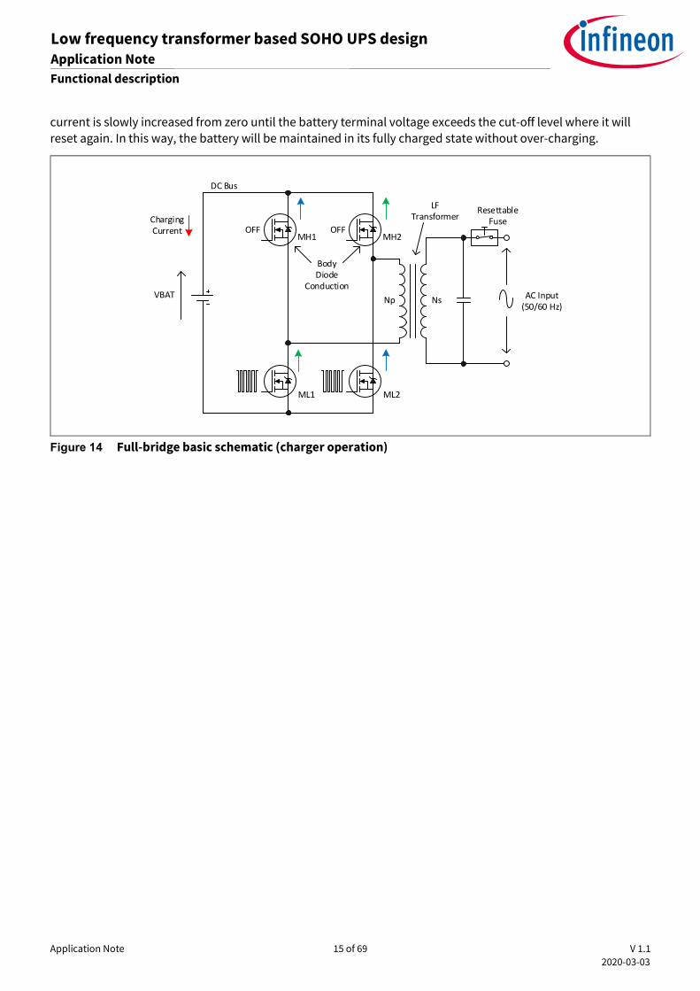
When AC mains power is present the UPS output is connected to the line input through the relay. The transformer steps the line voltage down so that an AC voltage is present between the bridge nodes of the two half-bridges. If the peak of this AC voltage were to exceed the battery voltage plus two body diode voltage drops, uncontrolled current would flow through one pair of diagonal MOSFET body diodes (MH1 and ML2 or MH2 and ML1). However, the turns-ratio of the transformer and the normal terminal voltage of the battery are such that this does not occur. In order for battery charging to take place the lower MOSFETs (ML1 and ML2) are pulsed simultaneously on and off, while the high-side MOSFETs (MH1 and MH2) remain always off. In this mode of operation, the full-bridge converter operates like a bridgeless boost converter. Depending on the AC-line polarity, boost operation will occur in one direction or the other.
This can be explained by modeling the transformer LV winding (connected to the MOSFET bridge) as a voltage source with a series inductor to represent the lumped primary and secondary leakage inductances. In the following diagram the HV winding acts as the transformer primary, which is opposite to inverter mode where the LV winding is the primary.
AC Line Input
LLK(pri) LLK(sec)
n:1
LBOOST
Stepped down AC voltage
Ideal transformer
Primary leakage
inductance
Secondary leakage
inductance
Stepped down AC Voltage
Low voltage sideHigh voltage side
Figure 13 Transformer equivalent circuit in charging operation
When both lower switches (ML1 and ML2) are on and a stepped-down voltage is present at the ideal transformer secondary winding, current rises at a rate determined by the leakage inductance represented by LBOOST. As this occurs energy builds up in the resulting magnetic flux. When ML1 and ML2 are both switched off the inductor current is diverted through one diagonal pair of body diodes depending on its direction according to the AC-line half-cycle polarity. In the diagram below, these currents are represented by blue arrows in one polarity and green arrows in the opposite, combining to create the battery charge current represented by the red arrow.
A feedback loop regulating the battery charge current controls the pulse width through the microcontroller. The loop response is slow so that changes in duty cycle happen gradually over several AC-line cycles.
Battery charging occurs at constant current, which is regulated by the microcontroller firmware. The battery charging routine in the firmware is designed for lead-acid batteries and not suited to other battery types. If the battery terminal voltage is below 9 V, the controller interprets this as a faulty or spent battery that is unable to be charged and will not attempt to do so. If the terminal voltage is above this minimum level but below a second threshold of approximately 12 V the battery will be charged at a higher current. Above the second threshold charging will occur at a low current until the terminal voltage exceeds the maximum charge “cut-off” level of 14.5 V, at which the charging will stop and the charger will enter a hiccup mode. In this mode, a charge
Application Note 15 of 69 V 1.1 2020-03-03
Low frequency transformer based SOHO UPS design Application Note Functional description
current is slowly increased from zero until the battery terminal voltage exceeds the cut-off level where it will reset again. In this way, the battery will be maintained in its fully charged state without over-charging.
DC Bus
AC Input(50/60 Hz)
VBAT
LFTransformer
Np Ns
OFF OFF
BodyDiode
Conduction
MH1 MH2
ML1 ML2
ResettableFuseCharging
Current
Figure 14 Full-bridge basic schematic (charger operation)
Application Note 16 of 69 V 1.1 2020-03-03
Low frequency transformer based SOHO UPS design Application Note Functional description
4.2 Supervisory functions
4.2.1 AC input voltage sensing
In order for the micro-controller (U2) to be able to switch between charging and back-up (inverter) modes of operation, it requires a constant monitoring of the AC-line input voltage to the UPS. This is done through the step-down transformer (T1) located on the main power board, which also provides the LV supply to the board when AC-line voltage is present. T1 is always connected to the AC-line input and isolated from the output during back-up operation. During AC-line input failure the LV circuitry in the system is supplied from the battery. Jumpers (P10) are provided so that T1 may be configured for 120 V AC or 230 V AC operation if required.
The secondary side of T1 is connected to the daughter card via the header P8 (VAC1 and VAC2 pins), which corresponds to P2 on the daughter card. This AC voltage is then rectified by Schottky diodes D1 and D2 to provide a full-wave rectified DC voltage, which is then divided down through R10 and R11 with C6 providing noise filtering but not smoothing of the LF ripple. This signal is supplied to an analog input of U2 and sampled periodically then converted to digital input information to be monitored by the firmware.
The rectified voltage from T1 is ORed with the battery voltage through D6 and D7 to provide a supply voltage of 12 to 15 V, which is present in both operating modes. This supplies the gate driver ICs and relay coil, the alarm buzzer SN1 and the dual operational amplifier IC U1. A linear regulator (VR1) provides a 3.3 V logic supply for U2.
4.2.2 AC output voltage sensing
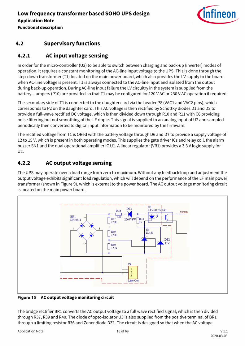
The UPS may operate over a load range from zero to maximum. Without any feedback loop and adjustment the output voltage exhibits significant load regulation, which will depend on the performance of the LF main power transformer (shown in Figure 9), which is external to the power board. The AC output voltage monitoring circuit is located on the main power board.
Figure 15 AC output voltage monitoring circuit
The bridge rectifier BR1 converts the AC output voltage to a full wave rectified signal, which is then divided through R37, R39 and R40. The diode of opto-isolator U3 is also supplied from the positive terminal of BR1 through a limiting resistor R36 and Zener diode DZ1. The circuit is designed so that when the AC voltage
Application Note 17 of 69 V 1.1 2020-03-03
Low frequency transformer based SOHO UPS design Application Note Functional description
exceeds 230 VRMS, the divided voltage at the REF input of U4 exceeds the 2.5 V threshold, causing current to flow through the diode of U3. This causes the voltage at VOFB, which is fed to a digital input of U2, to be pulled down. A minimum current of 1 mA is required to bias U4, which is supplied via R38 over the portions of the AC cycle where there is sufficient voltage available. For the remainder of the cycle U4 is not required. DZ2 is added to clamp the cathode voltage of U4 so that it never exceeds the absolute maximum rating of the device.
Whenever the firmware detects VOFB as a logic low level, this indicates that the output voltage exceeds 230 VRMS and should be adjusted down by reducing the modulation index (m). During normal operation “m” will be slowly increased until a low level is detected at VOFB and then kept close to this point to maintain an output of approximately 230 VRMS. This enables output voltage control without adding another small transformer like T1 or an additional winding on the output transformer.
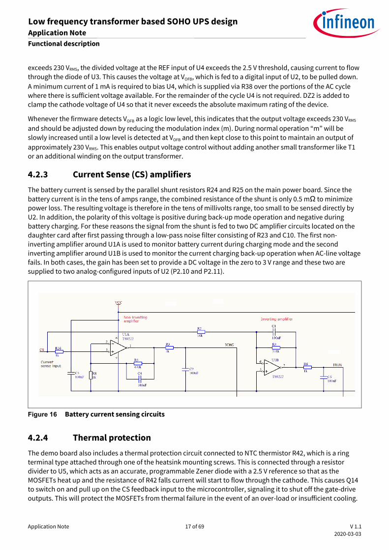
4.2.3 Current Sense (CS) amplifiers
The battery current is sensed by the parallel shunt resistors R24 and R25 on the main power board. Since the battery current is in the tens of amps range, the combined resistance of the shunt is only 0.5 mΩ to minimize power loss. The resulting voltage is therefore in the tens of millivolts range, too small to be sensed directly by U2. In addition, the polarity of this voltage is positive during back-up mode operation and negative during battery charging. For these reasons the signal from the shunt is fed to two DC amplifier circuits located on the daughter card after first passing through a low-pass noise filter consisting of R23 and C10. The first non-inverting amplifier around U1A is used to monitor battery current during charging mode and the second inverting amplifier around U1B is used to monitor the current charging back-up operation when AC-line voltage fails. In both cases, the gain has been set to provide a DC voltage in the zero to 3 V range and these two are supplied to two analog-configured inputs of U2 (P2.10 and P2.11).
Figure 16 Battery current sensing circuits
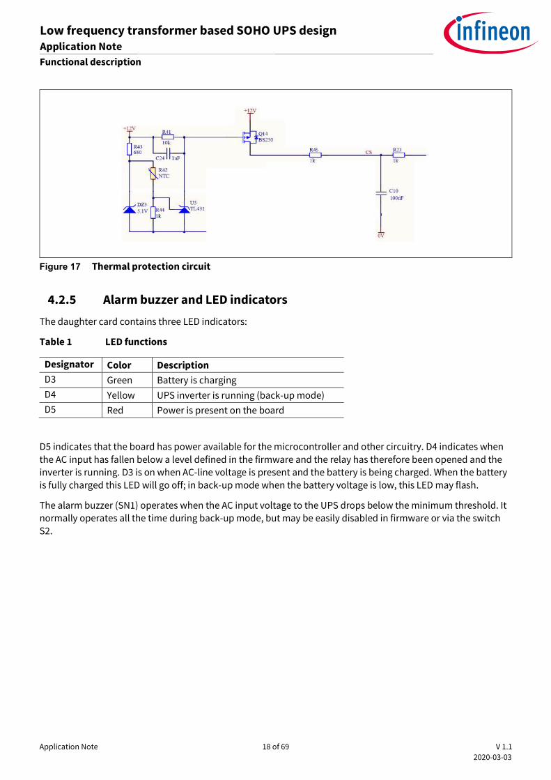
4.2.4 Thermal protection
The demo board also includes a thermal protection circuit connected to NTC thermistor R42, which is a ring terminal type attached through one of the heatsink mounting screws. This is connected through a resistor divider to U5, which acts as an accurate, programmable Zener diode with a 2.5 V reference so that as the MOSFETs heat up and the resistance of R42 falls current will start to flow through the cathode. This causes Q14 to switch on and pull up on the CS feedback input to the microcontroller, signaling it to shut off the gate-drive outputs. This will protect the MOSFETs from thermal failure in the event of an over-load or insufficient cooling.
Application Note 18 of 69 V 1.1 2020-03-03
Low frequency transformer based SOHO UPS design Application Note Functional description
Figure 17 Thermal protection circuit
4.2.5 Alarm buzzer and LED indicators
The daughter card contains three LED indicators:
Table 1 LED functions
Designator Color Description D3 Green Battery is charging D4 Yellow UPS inverter is running (back-up mode) D5 Red Power is present on the board
D5 indicates that the board has power available for the microcontroller and other circuitry. D4 indicates when the AC input has fallen below a level defined in the firmware and the relay has therefore been opened and the inverter is running. D3 is on when AC-line voltage is present and the battery is being charged. When the battery is fully charged this LED will go off; in back-up mode when the battery voltage is low, this LED may flash.
The alarm buzzer (SN1) operates when the AC input voltage to the UPS drops below the minimum threshold. It normally operates all the time during back-up mode, but may be easily disabled in firmware or via the switch S2.
Application Note 19 of 69 V 1.1 2020-03-03
Low frequency transformer based SOHO UPS design Application Note Firmware
5 Firmware
5.1 XMCTM microcontroller
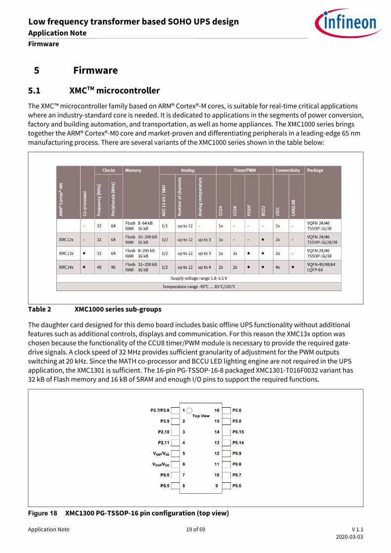
The XMC™ microcontroller family based on ARM® Cortex®-M cores, is suitable for real-time critical applications where an industry-standard core is needed. It is dedicated to applications in the segments of power conversion, factory and building automation, and transportation, as well as home appliances. The XMC1000 series brings together the ARM® Cortex®-M0 core and market-proven and differentiating peripherals in a leading-edge 65 nm manufacturing process. There are several variants of the XMC1000 series shown in the table below:
Table 2 XMC1000 series sub-groups
The daughter card designed for this demo board includes basic offline UPS functionality without additional features such as additional controls, displays and communication. For this reason the XMC13x option was chosen because the functionality of the CCU8 timer/PWM module is necessary to provide the required gate-drive signals. A clock speed of 32 MHz provides sufficient granularity of adjustment for the PWM outputs switching at 20 kHz. Since the MATH co-processor and BCCU LED lighting engine are not required in the UPS application, the XMC1301 is sufficient. The 16-pin PG-TSSOP-16-8 packaged XMC1301-T016F0032 variant has 32 kB of Flash memory and 16 kB of SRAM and enough I/O pins to support the required functions.
Figure 18 XMC1300 PG-TSSOP-16 pin configuration (top view)
Application Note 20 of 69 V 1.1 2020-03-03
Low frequency transformer based SOHO UPS design Application Note Firmware
5.2 DAVETM IDE
The firmware controlling this demo board was developed using the DAVETM IDE, which can be downloaded free of charge from the Infineon website. Programming and debugging was carried out via the XMCTM Link isolated debug probe, which is connected to the daughter card through the larger ribbon cable to header P1 and to a computer via a USB cable (the smaller ribbon cable is not used).
Figure 19 XMCTM Link isolated debugger probe
A project was created within DAVETM IDE containing the device definition, settings and source files required to compile and build the executable code, which can be downloaded into the Flash program memory of the XMCTM controller. There are several programming/debugging protocols available. The SPD0 option is chosen in this case because it only required one pin (P0.14). This mode has to be selected when first setting up the DAVETM IDE to connect the daughter card before programming. When programming a blank XMCTM device for the first time the BMI (boot mode index) must be initially set by clicking the “Set BMI” button. In-circuit debugging should be carried out with great care, since pausing the program could cause the power board MOSFETs to over-heat when the system is connected to a DC power supply or battery.
Figure 20 Configuration of the programming/debugging mode SPD0
The I/O ports are configured for analog or digital input or output and mapped to the peripherals required by selecting the required DAVETM apps, and configuring these to provide the functions required for the application. These include analog inputs, digital inputs and outputs, and functions such as the PWM generators and timers.
Application Note 21 of 69 V 1.1 2020-03-03
Low frequency transformer based SOHO UPS design Application Note Firmware
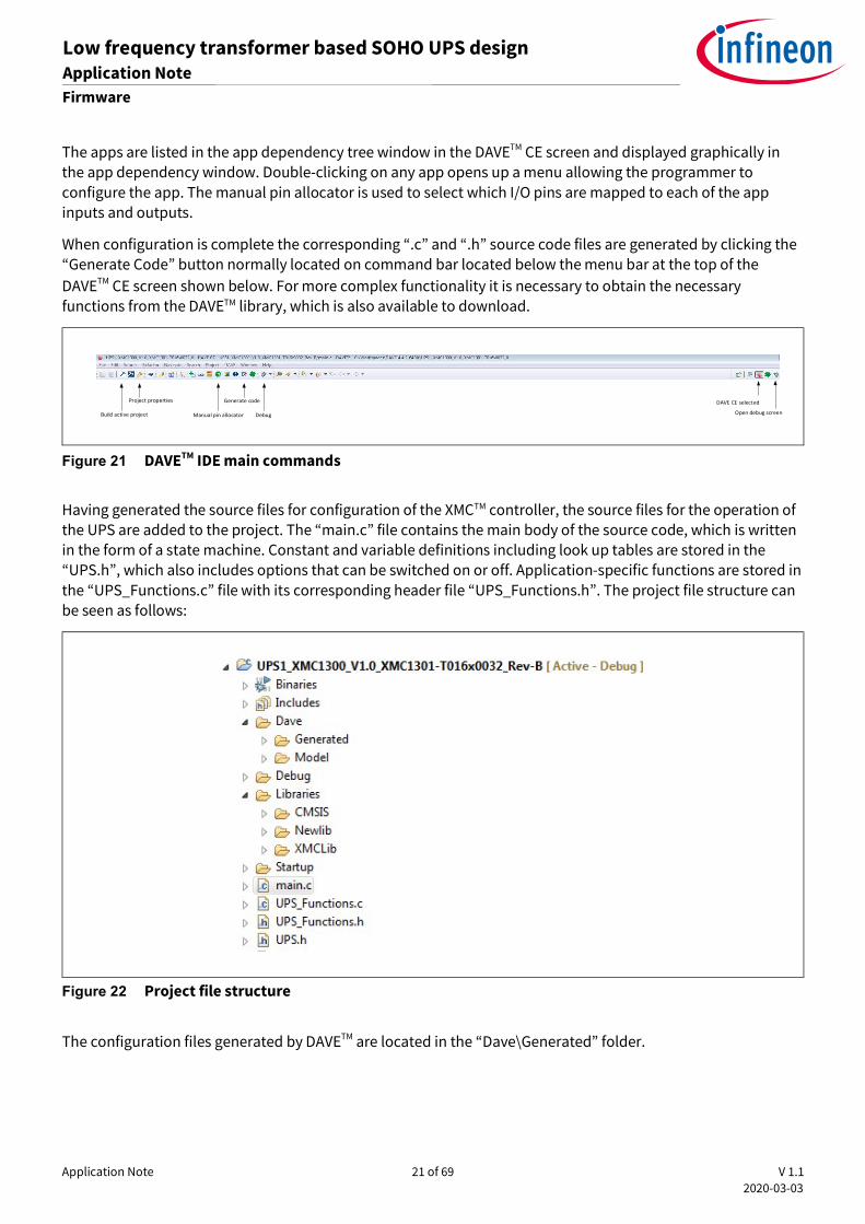
The apps are listed in the app dependency tree window in the DAVETM CE screen and displayed graphically in the app dependency window. Double-clicking on any app opens up a menu allowing the programmer to configure the app. The manual pin allocator is used to select which I/O pins are mapped to each of the app inputs and outputs.
When configuration is complete the corresponding “.c” and “.h” source code files are generated by clicking the “Generate Code” button normally located on command bar located below the menu bar at the top of the DAVETM CE screen shown below. For more complex functionality it is necessary to obtain the necessary functions from the DAVETM library, which is also available to download.
Generate code
Manual pin allocatorBuild active project
Project properties
Debug Open debug screen
DAVE CE selected
Figure 21 DAVETM IDE main commands
Having generated the source files for configuration of the XMCTM controller, the source files for the operation of the UPS are added to the project. The “main.c” file contains the main body of the source code, which is written in the form of a state machine. Constant and variable definitions including look up tables are stored in the “UPS.h”, which also includes options that can be switched on or off. Application-specific functions are stored in the “UPS_Functions.c” file with its corresponding header file “UPS_Functions.h”. The project file structure can be seen as follows:
Figure 22 Project file structure
The configuration files generated by DAVETM are located in the “Dave\Generated” folder.
Application Note 22 of 69 V 1.1 2020-03-03
Low frequency transformer based SOHO UPS design Application Note Firmware
5.3 I/O pin configuration
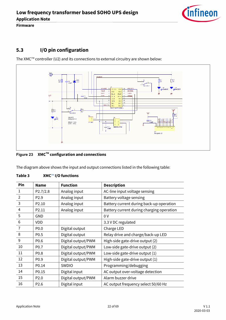
The XMCTM controller (U2) and its connections to external circuitry are shown below:
Figure 23 XMCTM configuration and connections
The diagram above shows the input and output connections listed in the following table:
Table 3 XMCTM I/O functions
Pin Name Function Description 1 P2.7/2.8 Analog input AC-line input voltage sensing 2 P2.9 Analog input Battery voltage sensing 3 P2.10 Analog input Battery current during back-up operation 4 P2.11 Analog input Battery current during charging operation 5 GND 0 V 6 VDD 3.3 V DC regulated 7 P0.0 Digital output Charge LED 8 P0.5 Digital output Relay drive and charge/back-up LED 9 P0.6 Digital output/PWM High-side gate-drive output (2) 10 P0.7 Digital output/PWM Low-side gate-drive output (2) 11 P0.8 Digital output/PWM Low-side gate-drive output (1) 12 P0.9 Digital output/PWM High-side gate-drive output (1) 13 P0.14 SWDIO Programming/debugging 14 P0.15 Digital input AC output over-voltage detection 15 P2.0 Digital output/PWM Alarm buzzer drive 16 P2.6 Digital input AC output frequency select 50/60 Hz
Application Note 23 of 69 V 1.1 2020-03-03
Low frequency transformer based SOHO UPS design Application Note Firmware
5.4 Flowcharts
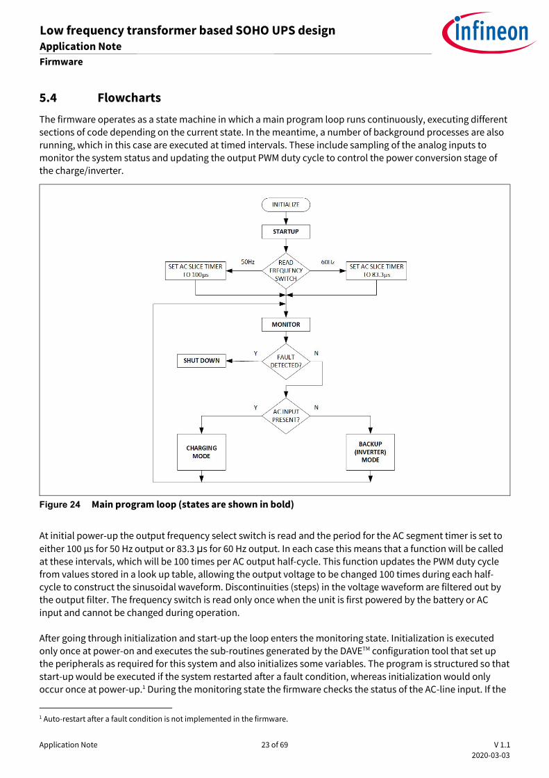
The firmware operates as a state machine in which a main program loop runs continuously, executing different sections of code depending on the current state. In the meantime, a number of background processes are also running, which in this case are executed at timed intervals. These include sampling of the analog inputs to monitor the system status and updating the output PWM duty cycle to control the power conversion stage of the charge/inverter.
Figure 24 Main program loop (states are shown in bold)
At initial power-up the output frequency select switch is read and the period for the AC segment timer is set to either 100 μs for 50 Hz output or 83.3 μs for 60 Hz output. In each case this means that a function will be called at these intervals, which will be 100 times per AC output half-cycle. This function updates the PWM duty cycle from values stored in a look up table, allowing the output voltage to be changed 100 times during each half-cycle to construct the sinusoidal waveform. Discontinuities (steps) in the voltage waveform are filtered out by the output filter. The frequency switch is read only once when the unit is first powered by the battery or AC input and cannot be changed during operation. After going through initialization and start-up the loop enters the monitoring state. Initialization is executed only once at power-on and executes the sub-routines generated by the DAVETM configuration tool that set up the peripherals as required for this system and also initializes some variables. The program is structured so that start-up would be executed if the system restarted after a fault condition, whereas initialization would only occur once at power-up.1 During the monitoring state the firmware checks the status of the AC-line input. If the
1 Auto-restart after a fault condition is not implemented in the firmware.
Application Note 24 of 69 V 1.1 2020-03-03
Low frequency transformer based SOHO UPS design Application Note Firmware
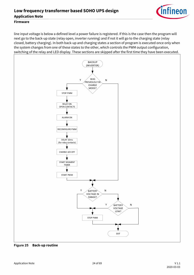
line input voltage is below a defined level a power failure is registered. If this is the case then the program will next go to the back-up state (relay open, inverter running) and if not it will go to the charging state (relay closed, battery charging). In both back-up and charging states a section of program is executed once only when the system changes from one of these states to the other, which controls the PWM output configuration, switching of the relay and LED display. These sections are skipped after the first time they have been executed.
BACKUP
(INVERTER)
WAS PREVIOUSLY IN
CHARGE MODE?
Y N
STOP PWM
RELAY ONOPEN CONTACTS
ALARM ON
DELAY 10ms(for relay contacts)
CHARGE LED OFF
RECONFIGURE PWM
START SEGMENT TIMER
BATTERY VOLTAGE IN
RANGE?
Y N
BATTERY VOLTAGE
LOW?
Y N
STOP PWM
EXIT
START PWM
Figure 25 Back-up routine
Application Note 25 of 69 V 1.1 2020-03-03
Low frequency transformer based SOHO UPS design Application Note Firmware
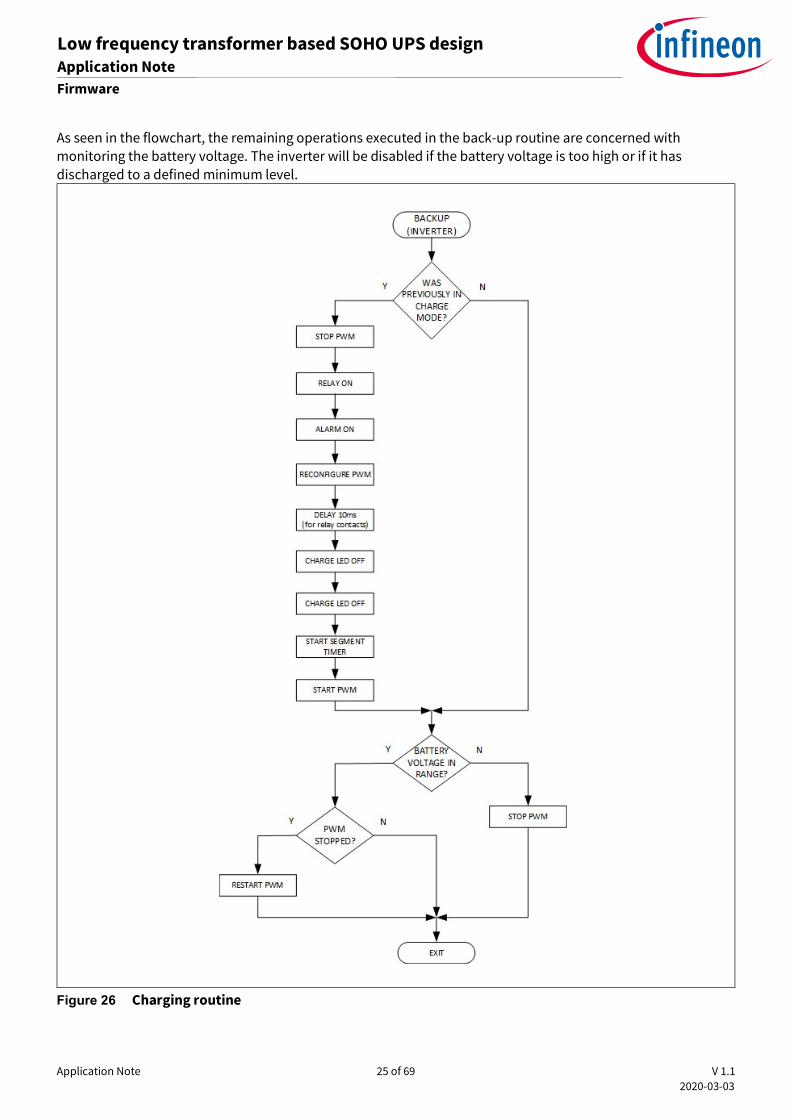
As seen in the flowchart, the remaining operations executed in the back-up routine are concerned with monitoring the battery voltage. The inverter will be disabled if the battery voltage is too high or if it has discharged to a defined minimum level.
Figure 26 Charging routine
Application Note 26 of 69 V 1.1 2020-03-03
Low frequency transformer based SOHO UPS design Application Note Firmware
The charging routine operates in a similar way, where the battery voltage is monitored such that when it is low a larger fast-charging current is supplied, and when it has charged sufficiently for the terminal voltage to rise to another defined level the system is adjusted to provide a smaller slow-charging current. In the event of a fault occurring in either the back-up or charging states, the program will enter the fault state. During this state the outputs are deactivated to shut down the system, for example in the case of an over-load or short-circuit at the output. Fault monitoring is carried out during the timed background processes executed every AC half-cycle (83.3 μs and 100 μs).
UPDATE PWM
(SEGMENT TIMER)
INCREMENT PWM COUNTER
PWM COUNTER =
101?
Y N
PWM COUNTER = 1
TOGGLE POLARITY
OPERATING MODE?
BACKUP CHARGING
READ SINE VALUE FROM LOOKUP
TABLE
VOUTTOO HIGH?
Y N
REDUCE MODULATION
INDEX
EXIT
INCREASE MODULATION
INDEX
MULTIPLY BYMODULATION
INDEX
UPDATE PWM
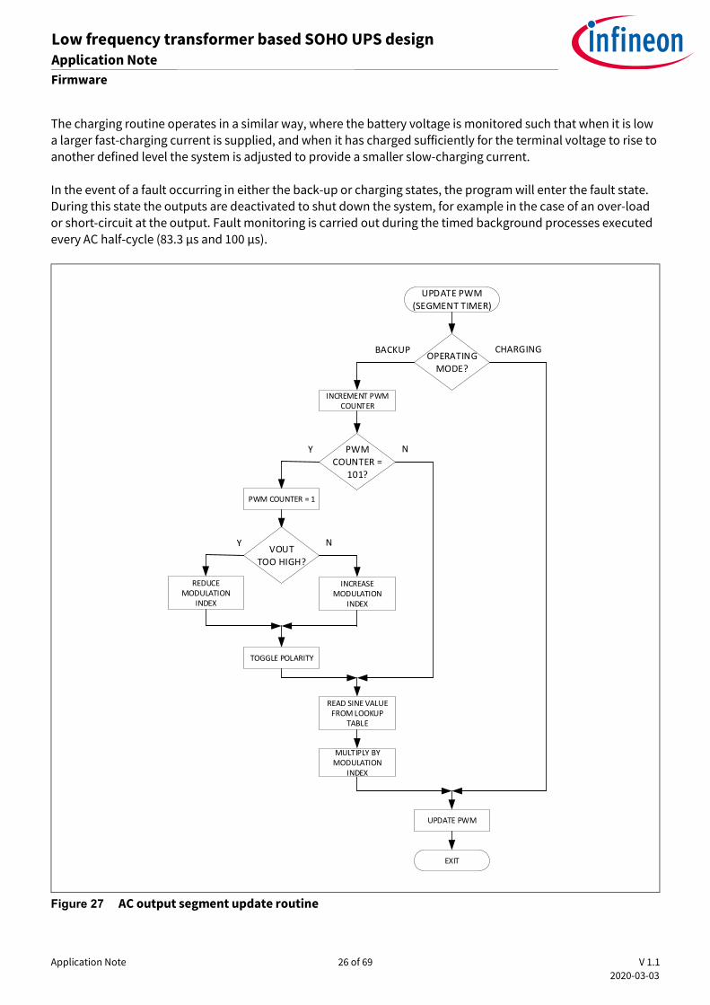
Figure 27 AC output segment update routine
Application Note 27 of 69 V 1.1 2020-03-03
Low frequency transformer based SOHO UPS design Application Note Firmware
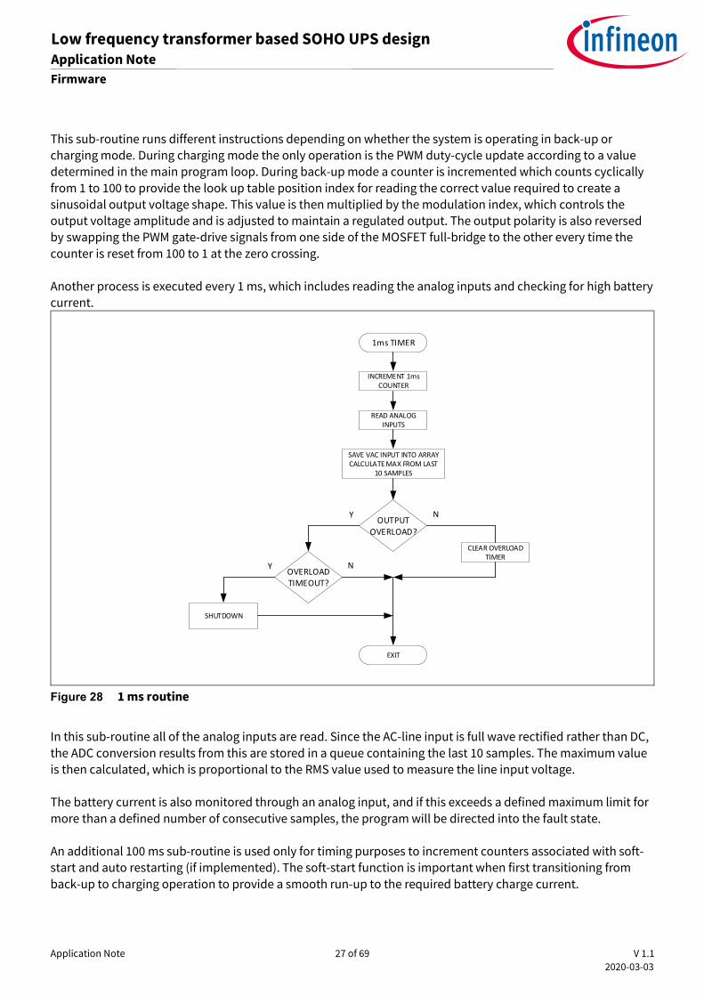
This sub-routine runs different instructions depending on whether the system is operating in back-up or charging mode. During charging mode the only operation is the PWM duty-cycle update according to a value determined in the main program loop. During back-up mode a counter is incremented which counts cyclically from 1 to 100 to provide the look up table position index for reading the correct value required to create a sinusoidal output voltage shape. This value is then multiplied by the modulation index, which controls the output voltage amplitude and is adjusted to maintain a regulated output. The output polarity is also reversed by swapping the PWM gate-drive signals from one side of the MOSFET full-bridge to the other every time the counter is reset from 100 to 1 at the zero crossing. Another process is executed every 1 ms, which includes reading the analog inputs and checking for high battery current.
1ms TIMER
INCREMENT 1ms COUNTER
READ ANALOG INPUTS
SAVE VAC INPUT INTO ARRAY CALCULATE MAX FROM LAST
10 SAMPLES
OUTPUTOVERLOAD?
Y N
OVERLOADTIMEOUT?
Y N
CLEAR OVERLOADTIMER
EXIT
SHUTDOWN
Figure 28 1 ms routine
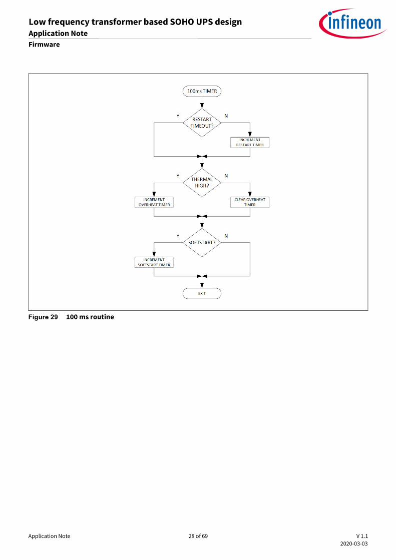
In this sub-routine all of the analog inputs are read. Since the AC-line input is full wave rectified rather than DC, the ADC conversion results from this are stored in a queue containing the last 10 samples. The maximum value is then calculated, which is proportional to the RMS value used to measure the line input voltage. The battery current is also monitored through an analog input, and if this exceeds a defined maximum limit for more than a defined number of consecutive samples, the program will be directed into the fault state. An additional 100 ms sub-routine is used only for timing purposes to increment counters associated with soft-start and auto restarting (if implemented). The soft-start function is important when first transitioning from back-up to charging operation to provide a smooth run-up to the required battery charge current.
Application Note 28 of 69 V 1.1 2020-03-03
Low frequency transformer based SOHO UPS design Application Note Firmware
Figure 29 100 ms routine
Application Note 29 of 69 V 1.1 2020-03-03
Low frequency transformer based SOHO UPS design Application Note Firmware
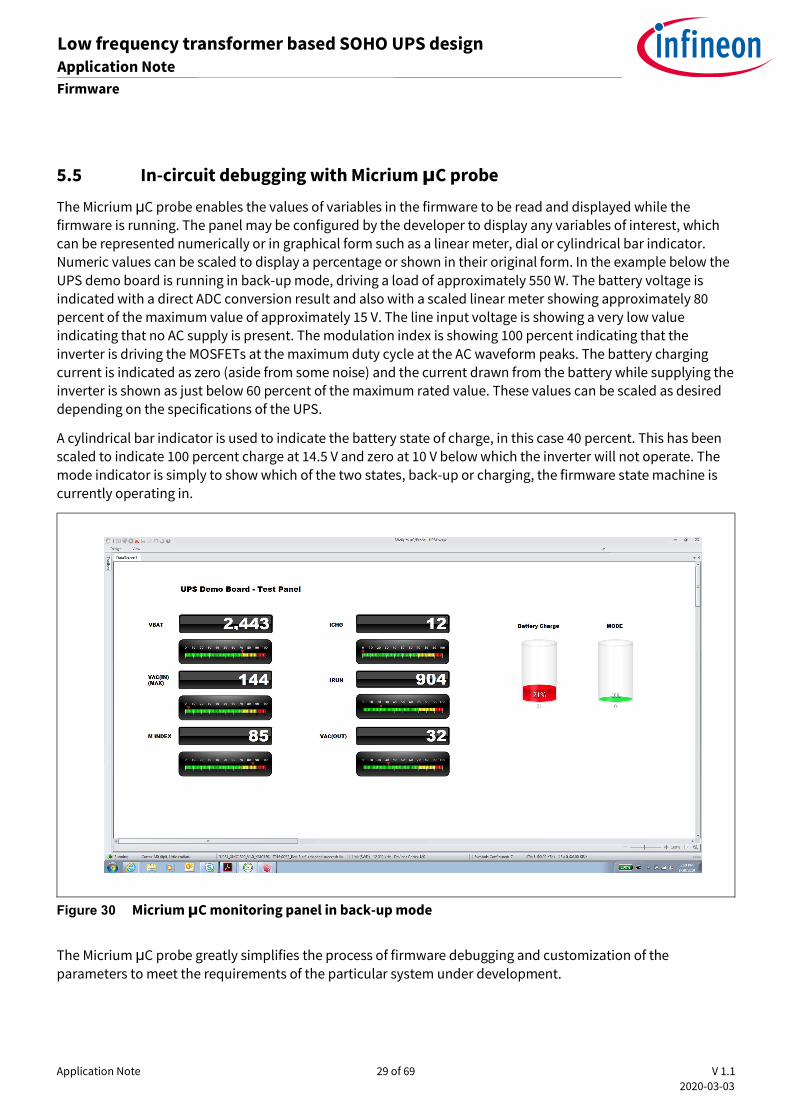
5.5 In-circuit debugging with Micrium μC probe
The Micrium μC probe enables the values of variables in the firmware to be read and displayed while the firmware is running. The panel may be configured by the developer to display any variables of interest, which can be represented numerically or in graphical form such as a linear meter, dial or cylindrical bar indicator. Numeric values can be scaled to display a percentage or shown in their original form. In the example below the UPS demo board is running in back-up mode, driving a load of approximately 550 W. The battery voltage is indicated with a direct ADC conversion result and also with a scaled linear meter showing approximately 80 percent of the maximum value of approximately 15 V. The line input voltage is showing a very low value indicating that no AC supply is present. The modulation index is showing 100 percent indicating that the inverter is driving the MOSFETs at the maximum duty cycle at the AC waveform peaks. The battery charging current is indicated as zero (aside from some noise) and the current drawn from the battery while supplying the inverter is shown as just below 60 percent of the maximum rated value. These values can be scaled as desired depending on the specifications of the UPS.
A cylindrical bar indicator is used to indicate the battery state of charge, in this case 40 percent. This has been scaled to indicate 100 percent charge at 14.5 V and zero at 10 V below which the inverter will not operate. The mode indicator is simply to show which of the two states, back-up or charging, the firmware state machine is currently operating in.
Figure 30 Micrium μC monitoring panel in back-up mode
The Micrium μC probe greatly simplifies the process of firmware debugging and customization of the parameters to meet the requirements of the particular system under development.
Application Note 30 of 69 V 1.1 2020-03-03
Low frequency transformer based SOHO UPS design Application Note Bill of Materials (BOM)
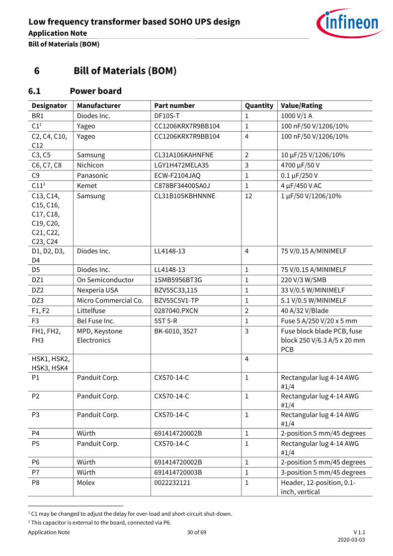
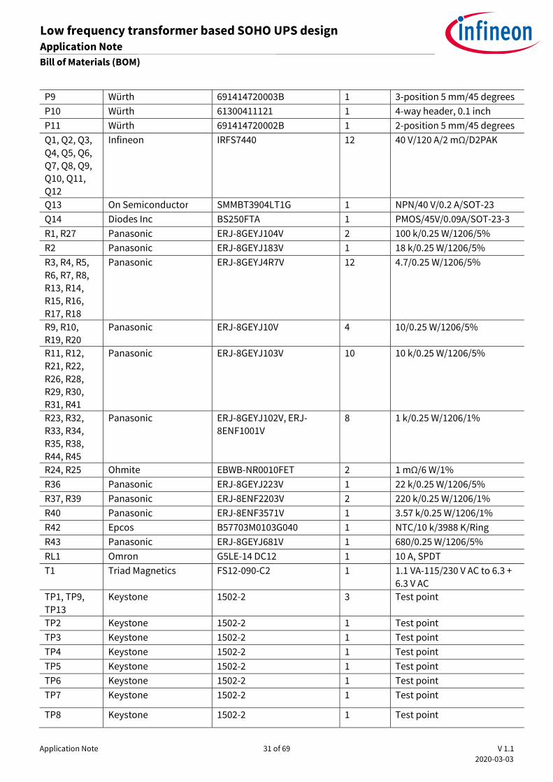
6 Bill of Materials (BOM)
6.1 Power board Designator Manufacturer Part number Quantity Value/Rating BR1 Diodes Inc. DF10S-T 1 1000 V/1 A C11 Yageo CC1206KRX7R9BB104 1 100 nF/50 V/1206/10% C2, C4, C10, C12
Yageo CC1206KRX7R9BB104 4 100 nF/50 V/1206/10%
C3, C5 Samsung CL31A106KAHNFNE 2 10 μF/25 V/1206/10% C6, C7, C8 Nichicon LGY1H472MELA35 3 4700 μF/50 V C9 Panasonic ECW-F2104JAQ 1 0.1 μF/250 V C112 Kemet C878BF34400SA0J 1 4 μF/450 V AC C13, C14, C15, C16, C17, C18, C19, C20, C21, C22, C23, C24
Samsung CL31B105KBHNNNE 12 1 μF/50 V/1206/10%
D1, D2, D3, D4
Diodes Inc. LL4148-13 4 75 V/0.15 A/MINIMELF
D5 Diodes Inc. LL4148-13 1 75 V/0.15 A/MINIMELF DZ1 On Semiconductor 1SMB5956BT3G 1 220 V/3 W/SMB DZ2 Nexperia USA BZV55C33,115 1 33 V/0.5 W/MINIMELF DZ3 Micro Commercial Co. BZV55C5V1-TP 1 5.1 V/0.5 W/MINIMELF F1, F2 Littelfuse 0287040.PXCN 2 40 A/32 V/Blade F3 Bel Fuse Inc. 5ST 5-R 1 Fuse 5 A/250 V/20 x 5 mm FH1, FH2, FH3
MPD, Keystone Electronics
BK-6010, 3527 3 Fuse block blade PCB, fuse block 250 V/6.3 A/5 x 20 mm PCB
HSK1, HSK2, HSK3, HSK4
4
P1 Panduit Corp. CXS70-14-C 1 Rectangular lug 4-14 AWG #1/4
P2 Panduit Corp. CXS70-14-C 1 Rectangular lug 4-14 AWG #1/4
P3 Panduit Corp. CXS70-14-C 1 Rectangular lug 4-14 AWG #1/4
P4 Würth 691414720002B 1 2-position 5 mm/45 degrees P5 Panduit Corp. CXS70-14-C 1 Rectangular lug 4-14 AWG
#1/4 P6 Würth 691414720002B 1 2-position 5 mm/45 degrees P7 Würth 691414720003B 1 3-position 5 mm/45 degrees P8 Molex 0022232121 1 Header, 12-position, 0.1-
inch, vertical
1 C1 may be changed to adjust the delay for over-load and short-circuit shut-down. 2 This capacitor is external to the board, connected via P6.
Application Note 31 of 69 V 1.1 2020-03-03
Low frequency transformer based SOHO UPS design Application Note Bill of Materials (BOM)
P9 Würth 691414720003B 1 3-position 5 mm/45 degrees P10 Würth 61300411121 1 4-way header, 0.1 inch P11 Würth 691414720002B 1 2-position 5 mm/45 degrees Q1, Q2, Q3, Q4, Q5, Q6, Q7, Q8, Q9, Q10, Q11, Q12
Infineon IRFS7440 12 40 V/120 A/2 mΩ/D2PAK
Q13 On Semiconductor SMMBT3904LT1G 1 NPN/40 V/0.2 A/SOT-23 Q14 Diodes Inc BS250FTA 1 PMOS/45V/0.09A/SOT-23-3 R1, R27 Panasonic ERJ-8GEYJ104V 2 100 k/0.25 W/1206/5% R2 Panasonic ERJ-8GEYJ183V 1 18 k/0.25 W/1206/5% R3, R4, R5, R6, R7, R8, R13, R14, R15, R16, R17, R18
Panasonic ERJ-8GEYJ4R7V 12 4.7/0.25 W/1206/5%
R9, R10, R19, R20
Panasonic ERJ-8GEYJ10V 4 10/0.25 W/1206/5%
R11, R12, R21, R22, R26, R28, R29, R30, R31, R41
Panasonic ERJ-8GEYJ103V 10 10 k/0.25 W/1206/5%
R23, R32, R33, R34, R35, R38, R44, R45
Panasonic ERJ-8GEYJ102V, ERJ-8ENF1001V
8 1 k/0.25 W/1206/1%
R24, R25 Ohmite EBWB-NR0010FET 2 1 mΩ/6 W/1% R36 Panasonic ERJ-8GEYJ223V 1 22 k/0.25 W/1206/5% R37, R39 Panasonic ERJ-8ENF2203V 2 220 k/0.25 W/1206/1% R40 Panasonic ERJ-8ENF3571V 1 3.57 k/0.25 W/1206/1% R42 Epcos B57703M0103G040 1 NTC/10 k/3988 K/Ring R43 Panasonic ERJ-8GEYJ681V 1 680/0.25 W/1206/5% RL1 Omron G5LE-14 DC12 1 10 A, SPDT T1 Triad Magnetics FS12-090-C2 1 1.1 VA-115/230 V AC to 6.3 +
6.3 V AC TP1, TP9, TP13
Keystone 1502-2 3 Test point
TP2 Keystone 1502-2 1 Test point TP3 Keystone 1502-2 1 Test point TP4 Keystone 1502-2 1 Test point TP5 Keystone 1502-2 1 Test point TP6 Keystone 1502-2 1 Test point TP7 Keystone 1502-2 1 Test point
TP8 Keystone 1502-2 1 Test point
Application Note 32 of 69 V 1.1 2020-03-03
Low frequency transformer based SOHO UPS design Application Note Bill of Materials (BOM)
TP10 Keystone 1502-2 1 Test point TP11 Keystone 1502-2 1 Test point TP12 Keystone 1502-2 1 Test point U1, U2 Infineon 2EDL8114 2 Gate-driver IC U3 Lite-On Inc. LTV-817S-TA1 1 5 kV/4-SMD U4, U5 Diodes Inc. ZTL431 2 IC, voltage reference, SOT23-
3 VR1 Diodes Inc. AS7815ADTR-G1 1 12 V/1 A/TO252-2
Application Note 33 of 69 V 1.1 2020-03-03
Low frequency transformer based SOHO UPS design Application Note Bill of Materials (BOM)
6.2 Daughter card
Designator Manufacturer Part number Quantity Value/Rating C2, C3, C4, C5, C6, C7, C9, C10
Yageo CC1206KRX7R9BB104 8 100 nF/50 V/1206/10%
C1 Samsung CL31A475KAHNNNE 1 4.7 μF/25 V/1206/10% C8, C11 Panasonic EEU-EB1E470SH 2 47 μF/25 V/20% D1, D2, D6, D7
Diodes Inc. B1100-13-F 4 Schottky/1 V/1 A/SMA
D3 Dialight 5988270107F 1 Green/2 V/1206 D4 Dialight 5988240107F 1 Yellow/2 V/1206 D5 Dialight 5988210107F 1 Red/2 V/1206 DZ1 Micro Commercial Co. BZV55C5V1-TP 1 5.1 V/0.5 W/MINIMELF P1 Amphenol FCI 67996-408HLF 1 Header 2 x 4, 0.1 inch, male
pins P2 Sullins Connector
Solutions PPTC121LGBN-RC 1 12-way header receptacle
P3 Würth 691414720002B 1 2-position 5 mm/45 degrees Q1 On Semiconductor SMMBT3904LT1G 1 NPN/40 V/0.2 A/SOT-23 R1, R3, R6, R8, R16
Panasonic ERJ-8GEYJ102V, ERJ-8ENF1001V
5 1 k/0.25 W/1206/1%
R2, R7, R11, R14
Panasonic ERJ-8ENF1002V 4 10 k/0.25 W/1206/1%
R4 Panasonic ERJ-8ENF5103V 1 510 k/0.25 W/1206/1% R5 Panasonic ERJ-8ENF5603V 1 560 k/0.25 W/1206/1% R9 Panasonic ERJ-8GEYJ104V 1 100 k/0.25 W/1206/5% R10 Panasonic ERJ-8ENF3002V 1 30 k/0.25 W/1206/1% R12, R13, R15, R18
Panasonic ERJ-8GEYJ221V 4 220/0.25 W/1206/5%
R17 Panasonic ERJ-8ENF3301V 1 3.3 k/0.25 W/1206/1% S1, S2 C&K Switches OS102011MS2QN1 2 SPDT/12 V/100 mA SN1 TDK PS1240P02BT 1 Piezoelectric buzzer
2 kHz/3 V/100 mA U1 ST Microelectronics TS9222IYDT 1 IC, dual op-amp, SO8 U2 Infineon XMC1301T016F0032ABXUMA1 1 8 kB Flash ROM/16 kB RAM VR1 Diodes Inc. AZ1117EH-3.3TRG1 1 3.3 V/1 A/SOT-223 C1, C2, C4 C6, C7, C9, C10
Yageo CC1206KRX7R9BB104 7 100 nF/50 V/1206/10%
C3, C5, C8, C11
Panasonic EEU-EB1E470SH 4 47 μF/25 V/20%
D1, D2, D6, D7
Diodes Inc. B1100-13-F 4 Schottky/1 V/1 A/SMA
D3 Dialight 5988270107F 1 Green/2 V/1206 D4 Dialight 5988240107F 1 Yellow/2 V/1206
Application Note 34 of 69 V 1.1 2020-03-03
Low frequency transformer based SOHO UPS design Application Note Bill of Materials (BOM)
D5 Dialight 5988210107F 1 Red/2 V/1206 DZ1 Micro Commercial Co. BZV55C5V1-TP 1 5.1 V/0.5 W/MINIMELF P1 Amphenol FCI 67996-408HLF 1 Header 2 x 4, 0.1 inch, male
pins P2 Sullins Connector
Solutions PPTC121LGBN-RC 1 12-way header receptacle
P3 Würth 691414720002B 1 2-position 5 mm/45 degrees Q1 On Semiconductor SMMBT3904LT1G 1 NPN/40 V/0.2 A/SOT-23 R1, R3, R6, R8, R16
Panasonic ERJ-8GEYJ102V, ERJ-8ENF1001V
5 1 k/0.25 W/1206/1%
R2, R7, R11, R14
Panasonic ERJ-8ENF1002V 4 10 k/0.25 W/1206/1%
R4 Panasonic ERJ-8ENF5103V 1 510 k/0.25 W/1206/1% R5 Panasonic ERJ-8ENF5603V 1 560 k/0.25 W/1206/1% R9 Panasonic ERJ-8GEYJ104V 1 100 k/0.25 W/1206/5% R10 Panasonic ERJ-8ENF3002V 1 30 k/0.25 W/1206/1%
Application Note 35 of 69 V 1.1 2020-03-03
Low frequency transformer based SOHO UPS design Application Note Transformer specifications
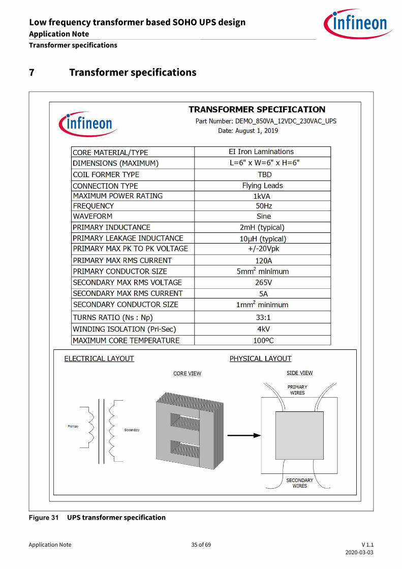
7 Transformer specifications
Figure 31 UPS transformer specification
Application Note 36 of 69 V 1.1 2020-03-03
Low frequency transformer based SOHO UPS design Application Note PCB layout
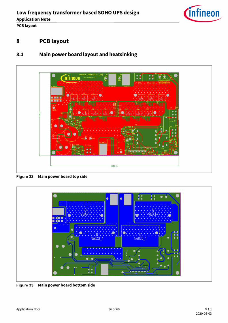
8 PCB layout
8.1 Main power board layout and heatsinking
Figure 32 Main power board top side
Figure 33 Main power board bottom side
Application Note 37 of 69 V 1.1 2020-03-03
Low frequency transformer based SOHO UPS design Application Note PCB layout
Since the board is required to conduct average currents up to 90 A, the copper conductor on both sides needs to be at least 2 oz. per square ft. thick, which corresponds to a thickness of 70 μm (2.8 mils). These high currents pass from the battery positive terminal P1 through the full-bridge MOSFETs through the transformer primary via P2 and P3 then through the CS shunts R24 and R25 and finally back to the battery negative via P5. Traces carrying these currents are kept as wide as possible. The MOSFET drains are connected from the top side to the bottom side through multiple vias, which transfer heat through to the heatsinks mounted underneath the PCB. The rectangular areas shown on the bottom-side PCB image above represent the outlines of the heatsinks, whose fins face downward. There is no solder resist covering the bottom side copper in these regions to allow a direct metal-to-metal contact with the heatsinks.
All other components, including gate drivers, output voltage sensing and thermal protection circuitry as well as the relay, the AC input transformer, fuses and connectors, are located on the top side of the PCB. The layout is a trade-off between correct SMPS layout practices such as minimizing distances from gate drivers to MOSFETs to reduce the effect of parasitic inductances against thermal management by using large areas of copper with the shortest practical trace lengths.
Supervisory circuitry does not contribute to EMI and does not carry critical HF signals, therefore it can be placed in any convenient location not already populated.
Application Note 38 of 69 V 1.1 2020-03-03
Low frequency transformer based SOHO UPS design Application Note Test results
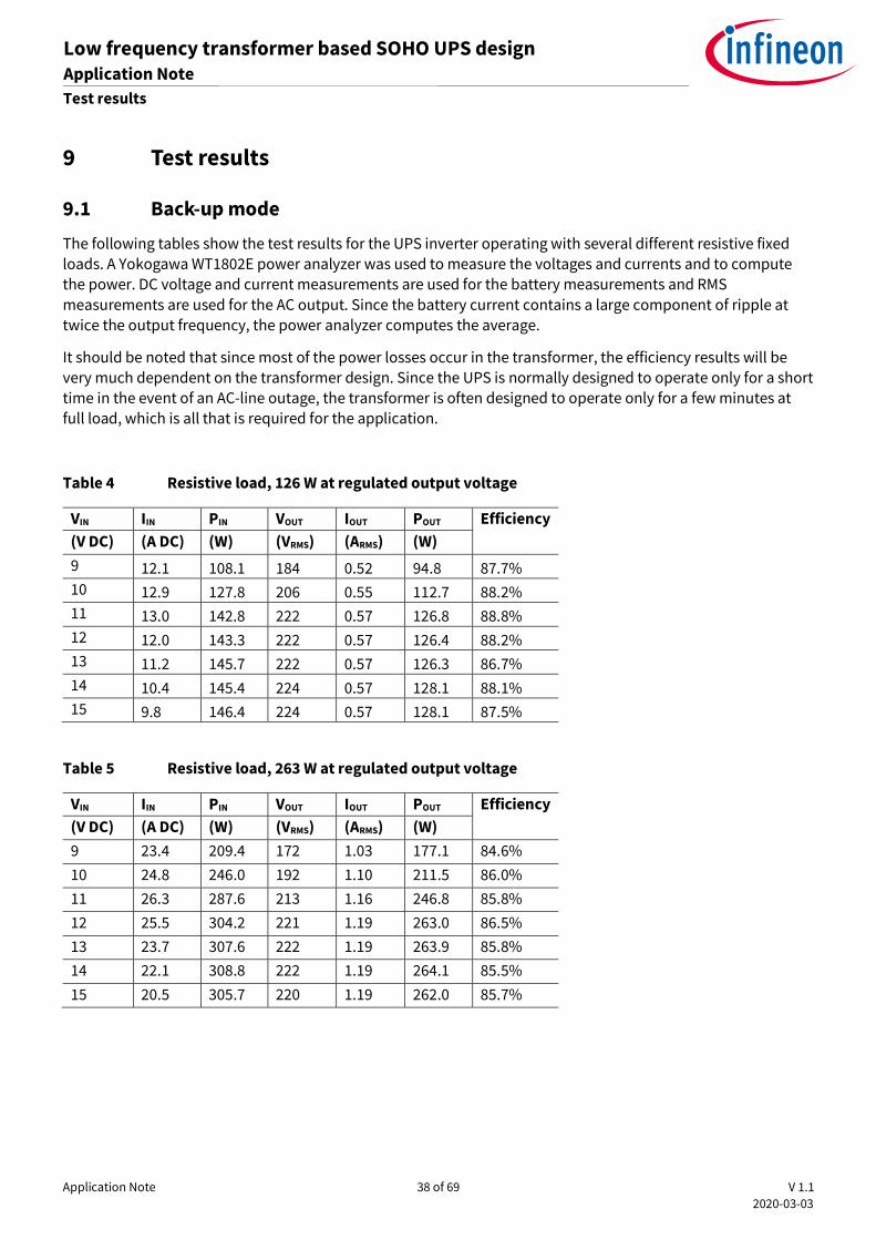
9 Test results
9.1 Back-up mode
The following tables show the test results for the UPS inverter operating with several different resistive fixed loads. A Yokogawa WT1802E power analyzer was used to measure the voltages and currents and to compute the power. DC voltage and current measurements are used for the battery measurements and RMS measurements are used for the AC output. Since the battery current contains a large component of ripple at twice the output frequency, the power analyzer computes the average.
It should be noted that since most of the power losses occur in the transformer, the efficiency results will be very much dependent on the transformer design. Since the UPS is normally designed to operate only for a short time in the event of an AC-line outage, the transformer is often designed to operate only for a few minutes at full load, which is all that is required for the application.
Table 4 Resistive load, 126 W at regulated output voltage
VIN IIN PIN VOUT IOUT POUT Efficiency (V DC) (A DC) (W) (VRMS) (ARMS) (W) 9 12.1 108.1 184 0.52 94.8 87.7% 10 12.9 127.8 206 0.55 112.7 88.2% 11 13.0 142.8 222 0.57 126.8 88.8% 12 12.0 143.3 222 0.57 126.4 88.2% 13 11.2 145.7 222 0.57 126.3 86.7% 14 10.4 145.4 224 0.57 128.1 88.1% 15 9.8 146.4 224 0.57 128.1 87.5%
Table 5 Resistive load, 263 W at regulated output voltage
VIN IIN PIN VOUT IOUT POUT Efficiency (V DC) (A DC) (W) (VRMS) (ARMS) (W) 9 23.4 209.4 172 1.03 177.1 84.6% 10 24.8 246.0 192 1.10 211.5 86.0% 11 26.3 287.6 213 1.16 246.8 85.8% 12 25.5 304.2 221 1.19 263.0 86.5% 13 23.7 307.6 222 1.19 263.9 85.8% 14 22.1 308.8 222 1.19 264.1 85.5% 15 20.5 305.7 220 1.19 262.0 85.7%
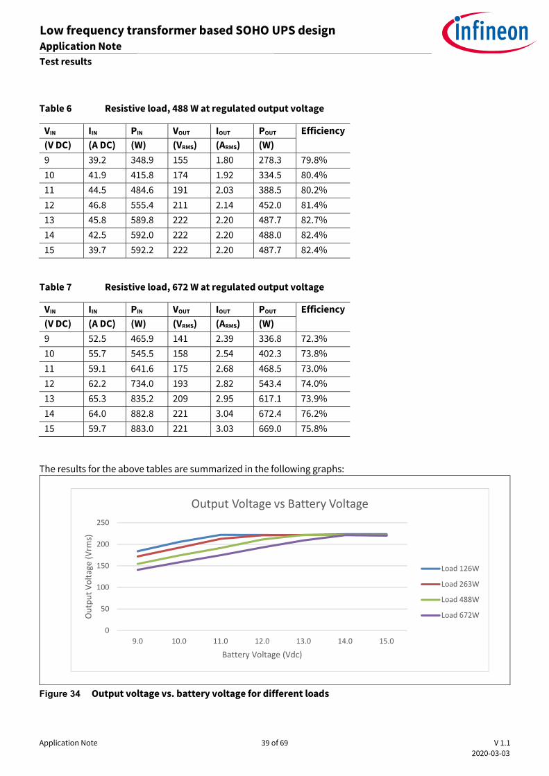
Application Note 39 of 69 V 1.1 2020-03-03
Low frequency transformer based SOHO UPS design Application Note Test results
Table 6 Resistive load, 488 W at regulated output voltage
VIN IIN PIN VOUT IOUT POUT Efficiency (V DC) (A DC) (W) (VRMS) (ARMS) (W) 9 39.2 348.9 155 1.80 278.3 79.8% 10 41.9 415.8 174 1.92 334.5 80.4% 11 44.5 484.6 191 2.03 388.5 80.2% 12 46.8 555.4 211 2.14 452.0 81.4% 13 45.8 589.8 222 2.20 487.7 82.7% 14 42.5 592.0 222 2.20 488.0 82.4% 15 39.7 592.2 222 2.20 487.7 82.4%
Table 7 Resistive load, 672 W at regulated output voltage
VIN IIN PIN VOUT IOUT POUT Efficiency (V DC) (A DC) (W) (VRMS) (ARMS) (W) 9 52.5 465.9 141 2.39 336.8 72.3% 10 55.7 545.5 158 2.54 402.3 73.8% 11 59.1 641.6 175 2.68 468.5 73.0% 12 62.2 734.0 193 2.82 543.4 74.0% 13 65.3 835.2 209 2.95 617.1 73.9% 14 64.0 882.8 221 3.04 672.4 76.2% 15 59.7 883.0 221 3.03 669.0 75.8%
The results for the above tables are summarized in the following graphs:
Figure 34 Output voltage vs. battery voltage for different loads
0
50
100
150
200
250
9.0 10.0 11.0 12.0 13.0 14.0 15.0
Out
put V
olta
ge (V
rms)
Battery Voltage (Vdc)
Output Voltage vs Battery Voltage
Load 126W
Load 263W
Load 488W
Load 672W
Application Note 40 of 69 V 1.1 2020-03-03
Low frequency transformer based SOHO UPS design Application Note Test results
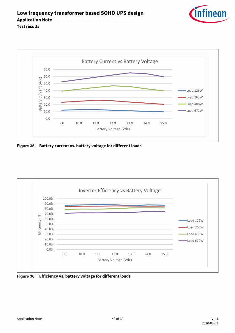
Figure 35 Battery current vs. battery voltage for different loads
Figure 36 Efficiency vs. battery voltage for different loads
0.0
10.0
20.0
30.0
40.0
50.0
60.0
70.0
9.0 10.0 11.0 12.0 13.0 14.0 15.0
Batt
ery
Curr
ent (
Adc)
Battery Voltage (Vdc)
Battery Current vs Battery Voltage
Load 126W
Load 263W
Load 488W
Load 672W
0.0%10.0%20.0%30.0%40.0%50.0%60.0%70.0%80.0%90.0%
100.0%
9.0 10.0 11.0 12.0 13.0 14.0 15.0
Effic
ienc
y (%
)
Battery Voltage (Vdc)
Inverter Efficiency vs Battery Voltage
Load 126W
Load 263W
Load 488W
Load 672W
Application Note 41 of 69 V 1.1 2020-03-03
Low frequency transformer based SOHO UPS design Application Note Test results
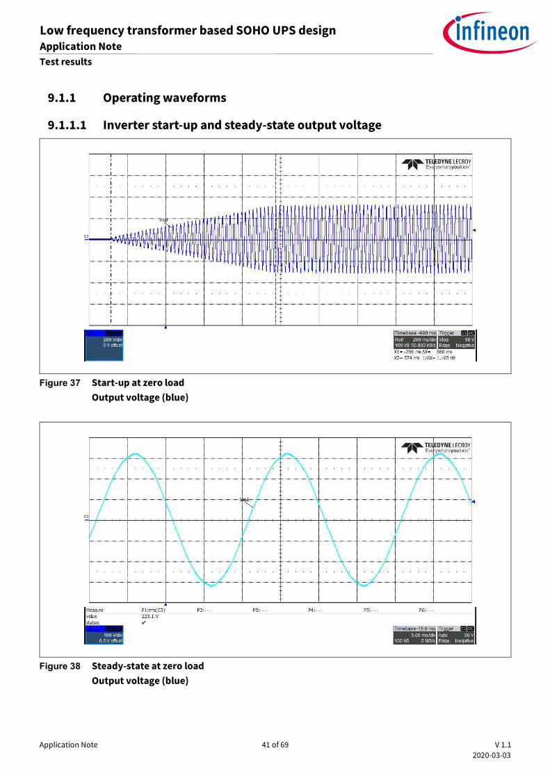
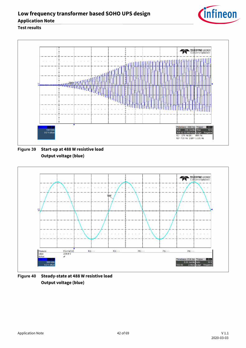
9.1.1 Operating waveforms
9.1.1.1 Inverter start-up and steady-state output voltage
Figure 37 Start-up at zero load Output voltage (blue)
Figure 38 Steady-state at zero load Output voltage (blue)
Application Note 42 of 69 V 1.1 2020-03-03
Low frequency transformer based SOHO UPS design Application Note Test results
Figure 39 Start-up at 488 W resistive load Output voltage (blue)
Figure 40 Steady-state at 488 W resistive load Output voltage (blue)
Application Note 43 of 69 V 1.1 2020-03-03
Low frequency transformer based SOHO UPS design Application Note Test results
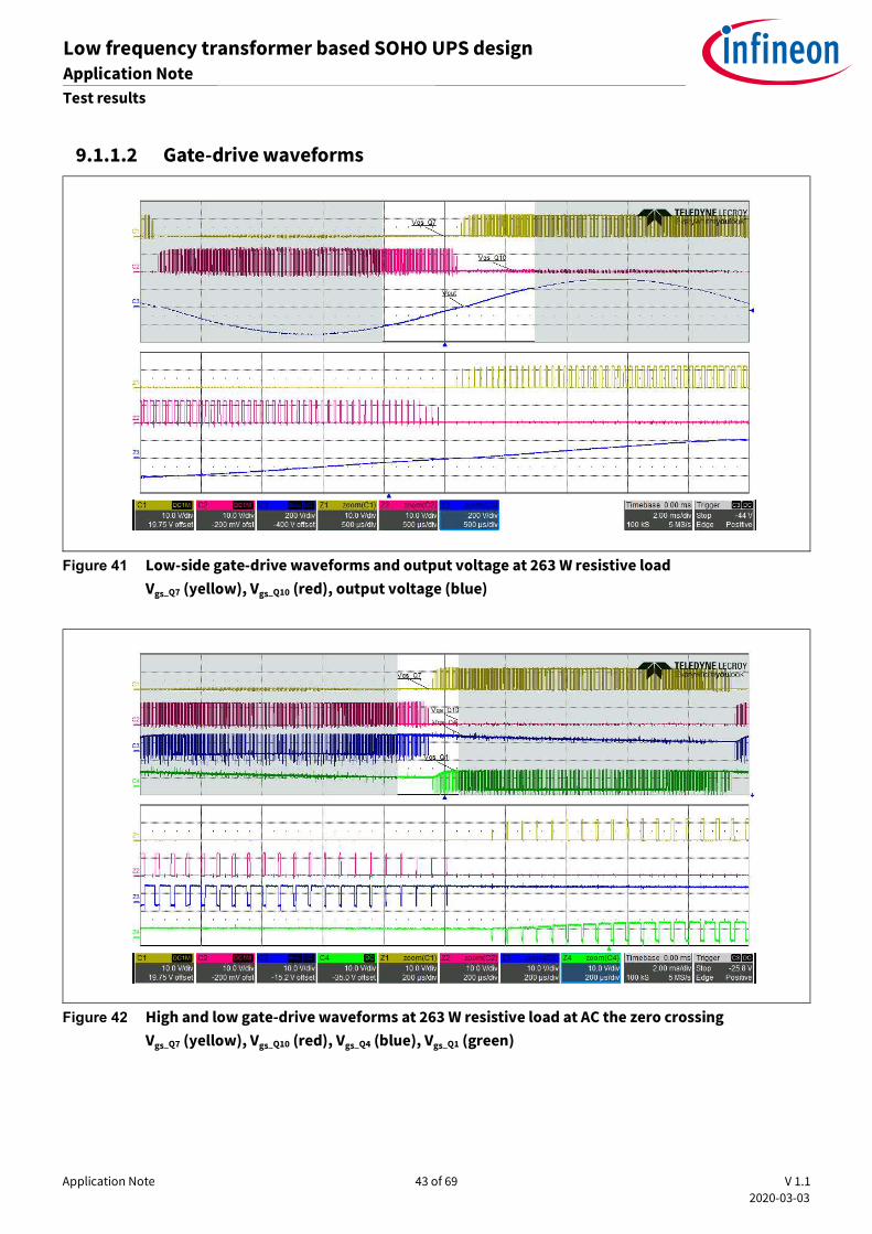
9.1.1.2 Gate-drive waveforms
Figure 41 Low-side gate-drive waveforms and output voltage at 263 W resistive load Vgs_Q7 (yellow), Vgs_Q10 (red), output voltage (blue)
Figure 42 High and low gate-drive waveforms at 263 W resistive load at AC the zero crossing Vgs_Q7 (yellow), Vgs_Q10 (red), Vgs_Q4 (blue), Vgs_Q1 (green)
Application Note 44 of 69 V 1.1 2020-03-03
Low frequency transformer based SOHO UPS design Application Note Test results
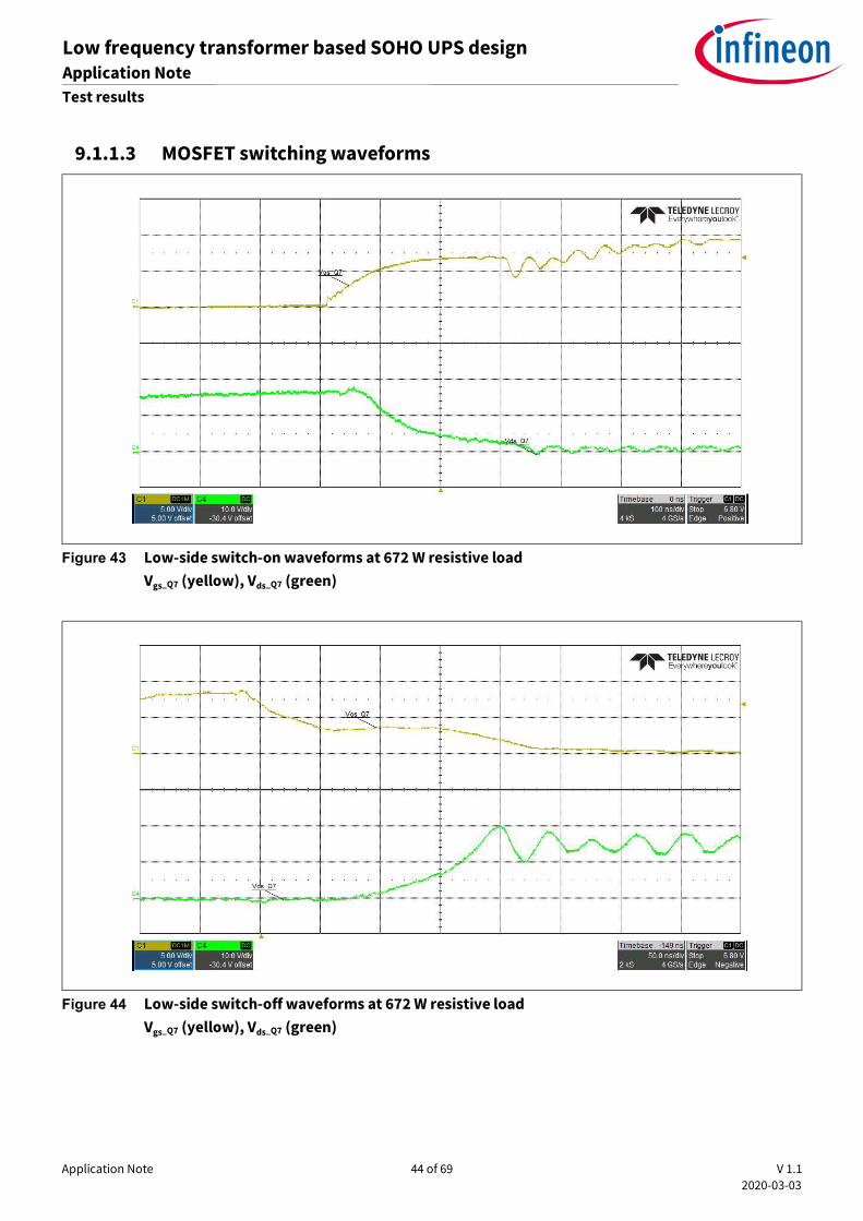
9.1.1.3 MOSFET switching waveforms
Figure 43 Low-side switch-on waveforms at 672 W resistive load Vgs_Q7 (yellow), Vds_Q7 (green)
Figure 44 Low-side switch-off waveforms at 672 W resistive load Vgs_Q7 (yellow), Vds_Q7 (green)
Application Note 45 of 69 V 1.1 2020-03-03
Low frequency transformer based SOHO UPS design Application Note Test results
9.1.1.4 Primary voltage and current waveforms
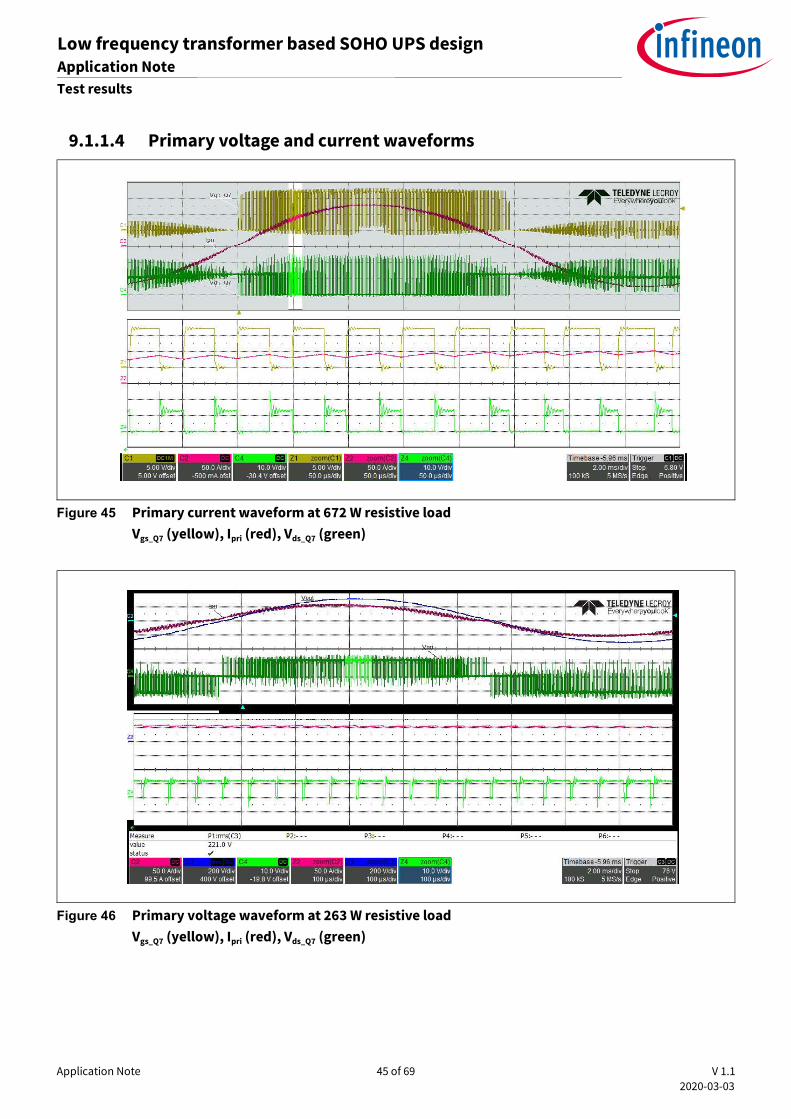
Figure 45 Primary current waveform at 672 W resistive load Vgs_Q7 (yellow), Ipri (red), Vds_Q7 (green)
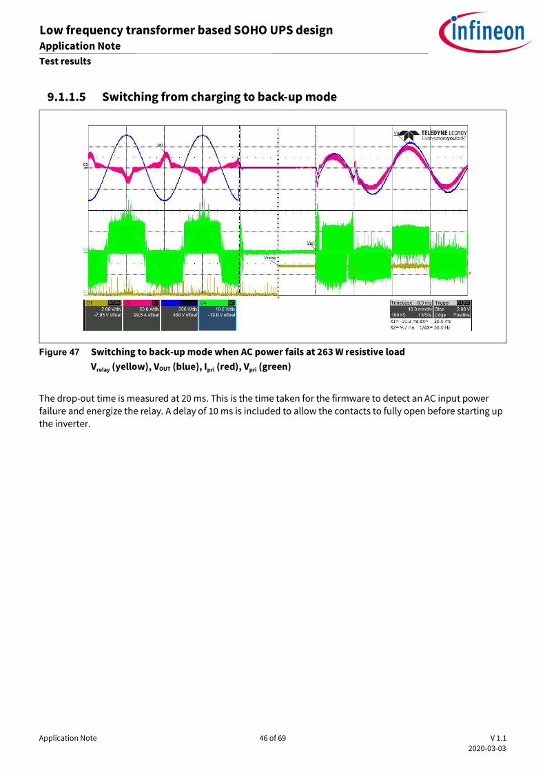
Figure 46 Primary voltage waveform at 263 W resistive load Vgs_Q7 (yellow), Ipri (red), Vds_Q7 (green)
Application Note 46 of 69 V 1.1 2020-03-03
Low frequency transformer based SOHO UPS design Application Note Test results
9.1.1.5 Switching from charging to back-up mode
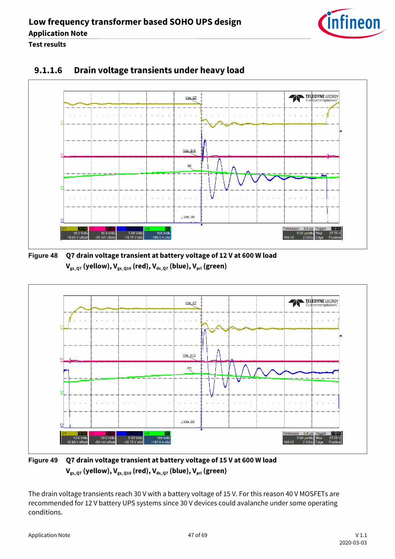
Figure 47 Switching to back-up mode when AC power fails at 263 W resistive load Vrelay (yellow), VOUT (blue), Ipri (red), Vpri (green)
The drop-out time is measured at 20 ms. This is the time taken for the firmware to detect an AC input power failure and energize the relay. A delay of 10 ms is included to allow the contacts to fully open before starting up the inverter.
Application Note 47 of 69 V 1.1 2020-03-03
Low frequency transformer based SOHO UPS design Application Note Test results
9.1.1.6 Drain voltage transients under heavy load
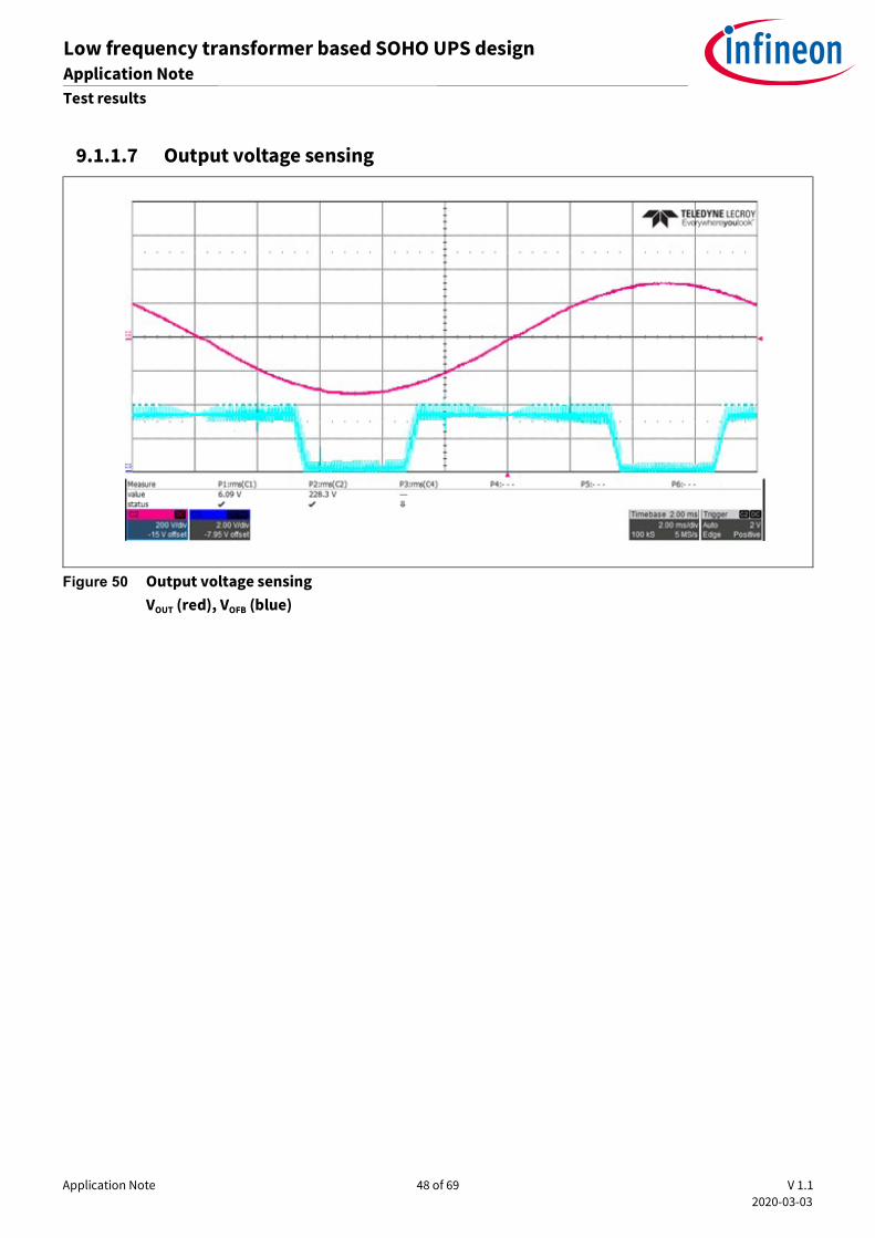
Figure 48 Q7 drain voltage transient at battery voltage of 12 V at 600 W load Vgs_Q7 (yellow), Vgs_Q10 (red), Vds_Q7 (blue), Vpri (green)
Figure 49 Q7 drain voltage transient at battery voltage of 15 V at 600 W load Vgs_Q7 (yellow), Vgs_Q10 (red), Vds_Q7 (blue), Vpri (green)
The drain voltage transients reach 30 V with a battery voltage of 15 V. For this reason 40 V MOSFETs are recommended for 12 V battery UPS systems since 30 V devices could avalanche under some operating conditions.
Application Note 48 of 69 V 1.1 2020-03-03
Low frequency transformer based SOHO UPS design Application Note Test results
9.1.1.7 Output voltage sensing
Figure 50 Output voltage sensing VOUT (red), VOFB (blue)
Application Note 49 of 69 V 1.1 2020-03-03
Low frequency transformer based SOHO UPS design Application Note Test results
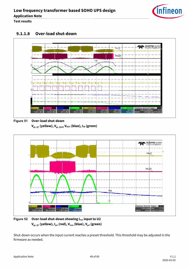
9.1.1.8 Over-load shut-down
Figure 51 Over-load shut-down Vgs_Q7 (yellow), Vgs_Q10, VOUT (blue), IIN (green)
Figure 52 Over-load shut-down showing Irun input to U2 Vgs_Q7 (yellow), Ipri (red), Virun (blue), Vpri (green)
Shut-down occurs when the input current reaches a preset threshold. This threshold may be adjusted in the firmware as needed.
Application Note 50 of 69 V 1.1 2020-03-03
Low frequency transformer based SOHO UPS design Application Note Test results
9.1.1.9 Short-circuit output shut-down
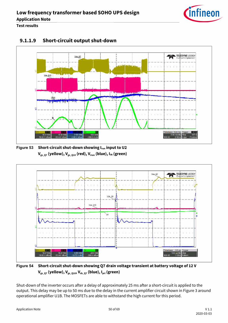
Figure 53 Short-circuit shut-down showing Irun input to U2 Vgs_Q7 (yellow), Vgs_Q10 (red), Virun (blue), IIN (green)
Figure 54 Short-circuit shut-down showing Q7 drain voltage transient at battery voltage of 12 V Vgs_Q7 (yellow), Vgs_Q10, Vds_Q7 (blue), Ipri (green)
Shut-down of the inverter occurs after a delay of approximately 25 ms after a short-circuit is applied to the output. This delay may be up to 50 ms due to the delay in the current amplifier circuit shown in Figure 3 around operational amplifier U1B. The MOSFETs are able to withstand the high current for this period.
Application Note 51 of 69 V 1.1 2020-03-03
Low frequency transformer based SOHO UPS design Application Note Test results
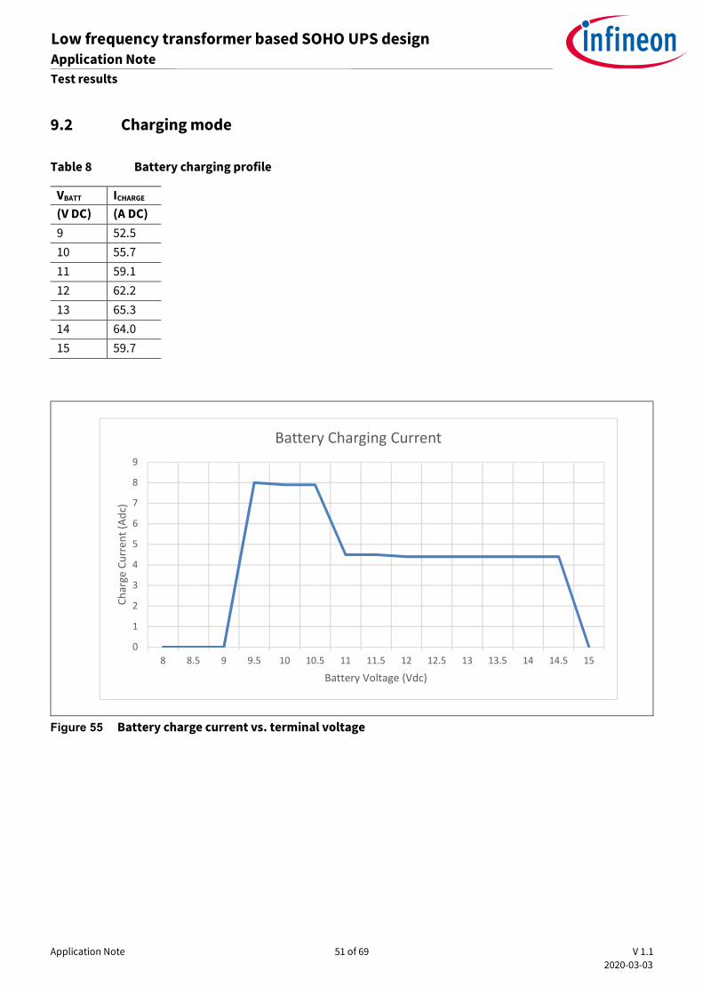
9.2 Charging mode Table 8 Battery charging profile
VBATT ICHARGE (V DC) (A DC) 9 52.5 10 55.7 11 59.1 12 62.2 13 65.3 14 64.0 15 59.7
Figure 55 Battery charge current vs. terminal voltage
0
1
2
3
4
5
6
7
8
9
8 8.5 9 9.5 10 10.5 11 11.5 12 12.5 13 13.5 14 14.5 15
Char
ge C
urre
nt (A
dc)
Battery Voltage (Vdc)
Battery Charging Current
Application Note 52 of 69 V 1.1 2020-03-03
Low frequency transformer based SOHO UPS design Application Note Test results
9.2.1 Operating waveforms
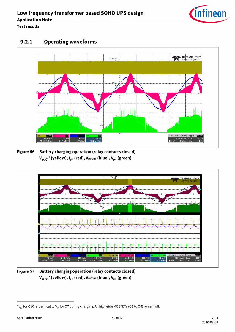
Figure 56 Battery charging operation (relay contacts closed) Vgs_Q7
1 (yellow), Ipri (red), VIN/OUT (blue), Vpri (green)
Figure 57 Battery charging operation (relay contacts closed) Vgs_Q7
2 (yellow), Ipri (red), VIN/OUT (blue), Vpri (green)
1 Vgs for Q10 is identical to Vgs for Q7 during charging. All high-side MOSFETs (Q1 to Q6) remain off.
Application Note 53 of 69 V 1.1 2020-03-03
Low frequency transformer based SOHO UPS design Application Note Test results
The previous figure shows the boost operation during charging where the transformer current indicates continuous conduction mode.
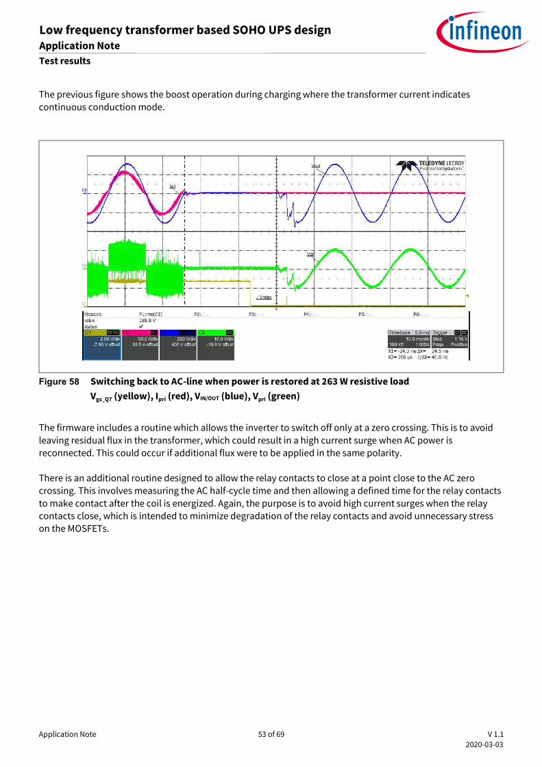
Figure 58 Switching back to AC-line when power is restored at 263 W resistive load Vgs_Q7 (yellow), Ipri (red), VIN/OUT (blue), Vpri (green)
The firmware includes a routine which allows the inverter to switch off only at a zero crossing. This is to avoid leaving residual flux in the transformer, which could result in a high current surge when AC power is reconnected. This could occur if additional flux were to be applied in the same polarity. There is an additional routine designed to allow the relay contacts to close at a point close to the AC zero crossing. This involves measuring the AC half-cycle time and then allowing a defined time for the relay contacts to make contact after the coil is energized. Again, the purpose is to avoid high current surges when the relay contacts close, which is intended to minimize degradation of the relay contacts and avoid unnecessary stress on the MOSFETs.
Application Note 54 of 69 V 1.1 2020-03-03
Low frequency transformer based SOHO UPS design Application Note Test results
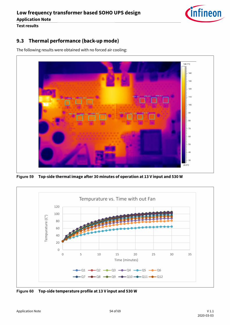
9.3 Thermal performance (back-up mode)
The following results were obtained with no forced air cooling:
Figure 59 Top-side thermal image after 30 minutes of operation at 13 V input and 530 W
Figure 60 Top-side temperature profile at 13 V input and 530 W
0
20
40
60
80
100
120
0 5 10 15 20 25 30 35
Tem
pura
ture
(C°)
Time (minutes)
Tempurature vs. Time with out Fan
Q1 Q2 Q3 Q4 Q5 Q6
Q7 Q8 Q9 Q10 Q11 Q12
Application Note 55 of 69 V 1.1 2020-03-03
Low frequency transformer based SOHO UPS design Application Note Test results
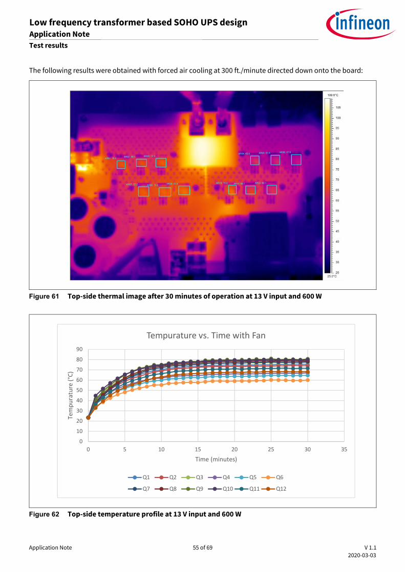
The following results were obtained with forced air cooling at 300 ft./minute directed down onto the board:
Figure 61 Top-side thermal image after 30 minutes of operation at 13 V input and 600 W
Figure 62 Top-side temperature profile at 13 V input and 600 W
0
10
20
30
40
50
60
70
80
90
0 5 10 15 20 25 30 35
Tem
pura
ture
(°C)
Time (minutes)
Tempurature vs. Time with Fan
Q1 Q2 Q3 Q4 Q5 Q6
Q7 Q8 Q9 Q10 Q11 Q12
Application Note 56 of 69 V 1.1 2020-03-03
Low frequency transformer based SOHO UPS design Application Note Conclusion
10 Conclusion The results demonstrate the functionality of the UPS demonstration board under all operating conditions. The output waveform is close to a pure sine wave under all load conditions. Conversion efficiency drops at higher loads mainly due to high conduction losses in the transformer, battery cables and PCB traces. This demonstrates why UPS systems rated at above around 600 W generally use 24 V batteries rather than 12 V. Modification of the DEMO_850VA_12VDC_230VAC_UPS demonstration board for operation with a 24 V battery can be performed by replacing the MOSFETs with devices rated for higher BVDSS in the same package and also replacing the transformer with one having twice the number of turns on the primary winding using a smaller wire size. A small number of component value changes as well as adjustment of some of the firmware parameters defined in the UPS.h header file would also be necessary.
Additional power losses arise due to the hard-switching operation of the inverter. Switch-off losses are typically much higher than switch-on losses in this type of UPS because the switch-off time is deliberately not designed to be very fast to reduce di/dt and thereby limit drain transient voltage peaks. This is especially relevant under a short-circuit condition where the primary current is very high for a short time until the inverter shuts down. Test waveforms indicate that the switch-off transient voltage may exceed 30 V at high battery voltage but that it remains well under 40 V. It should be noted that the gate-drive circuitry could be modified to provide faster turn-off, which would reduce switch-off loss and improve efficiency. However, by doing this the switch-off transient voltage would increase. It is also evident that 30 V MOSFETs could be used provided the designer pays particular attention to ensuring that the switch-off transient remains below this level, which can be achieved by limiting the switch-off time and thus the di/dt.
The full functionality of the offline UPS system has been demonstrated with a low-cost XMCTM M0 core-based
microcontroller. This includes generation of all gate-drive signals, monitoring of input and output voltages, regulation of the output voltage and charging current, and safe transition between charging and back-up modes of operation with approximately 20 ms drop-out time. This could be reduced to around 10 ms; however, the firmware includes functionality to ensure the relay contacts remain close to an AC zero-crossing, which introduces up to one half-cycle of delay.
A heatsinking arrangement has been implemented, which utilizes four individual heatsinks mounted on the underside of the PCB where the paralleled bridge D2PAK MOSFETs are mounted on the top side. Vias are used to transfer the heat from the drains to the heatsinks, which are mounted directly to exposed metal areas on the underside of the PCB without the need for any insulators. The thermal images indicate that without forced air cooling using this heatsinking arrangement the case temperature of the hottest MOSFETs exceed 100°C after 30 minutes of operation in open air at 530 W load; however, with forced air cooling the device temperatures stabilize at around 80°C. This indicates that forced air cooling would be required for a UPS based on this topology and rated for power levels above 500 W. The temperature rise would be greater with the electronics housed within an enclosure if the UPS were designed to operate continuously at full load. In a design using a 24 V battery the primary-side currents would be approximately halved, which could reduce conduction losses in the MOSFETs, PCB traces and transformer.
Protection functions have also been demonstrated. It is noted that the short-circuit protection includes a delay in the range of tens of milliseconds. Since the current passing through the MOSFETs is limited by the transformer, the average drain current passing through each device does not exceed the maximum continuous ID rating, which for these LV devices is package limited at 120 A. This delay is therefore acceptable and also desirable in preventing false triggering of the protection, which could otherwise occur due to inrush current or sudden increase in load.
Application Note 57 of 69 V 1.1 2020-03-03
Low frequency transformer based SOHO UPS design Application Note Appendix
11 Appendix
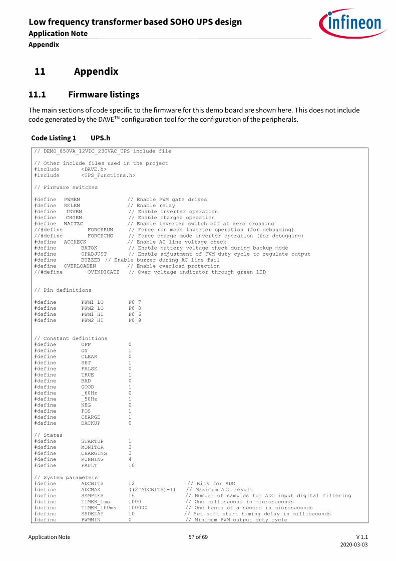
11.1 Firmware listings
The main sections of code specific to the firmware for this demo board are shown here. This does not include code generated by the DAVETM configuration tool for the configuration of the peripherals.
Code Listing 1 UPS.h
// DEMO_850VA_12VDC_230VAC_UPS include file // Other include files used in the project #include <DAVE.h> #include <UPS_Functions.h> // Firmware switches #define PWMEN // Enable PWM gate drives #define RELEN // Enable relay #define INVEN // Enable inverter operation #define CHGEN // Enable charger operation #define WAITZC // Enable inverter switch off at zero crossing //#define FORCERUN // Force run mode inverter operation (for debugging) //#define FORCECHG // Force charge mode inverter operation (for debugging) #define ACCHECK // Enable AC line voltage check #define BATOK // Enable battery voltage check during backup mode #define OPADJUST // Enable adjustment of PWM duty cycle to regulate output #define BUZZER // Enable buzzer during AC line fail #define OVERLOADEN // Enable overload protection //#define OVINDICATE // Over voltage indicator through green LED // Pin definitions #define PWM1_LO P0_7 #define PWM2_LO P0_8 #define PWM1_HI P0_6 #define PWM2_HI P0_9 // Constant definitions #define OFF 0 #define ON 1 #define CLEAR 0 #define SET 1 #define FALSE 0 #define TRUE 1 #define BAD 0 #define GOOD 1 #define _60Hz 0 #define _50Hz 1 #define NEG 0 #define POS 1 #define CHARGE 1 #define BACKUP 0 // States #define STARTUP 1 #define MONITOR 2 #define CHARGING 3 #define RUNNING 4 #define FAULT 10 // System parameters #define ADCBITS 12 // Bits for ADC #define ADCMAX ((2^ADCBITS)-1) // Maximum ADC result #define SAMPLES 16 // Number of samples for ADC input digital filtering #define TIMER_1ms 1000 // One millisecond in microseconds #define TIMER_100ms 100000 // One tenth of a second in microseconds #define SSDELAY 10 // Set soft start timing delay in milliseconds #define PWMMIN 0 // Minimum PWM output duty cycle
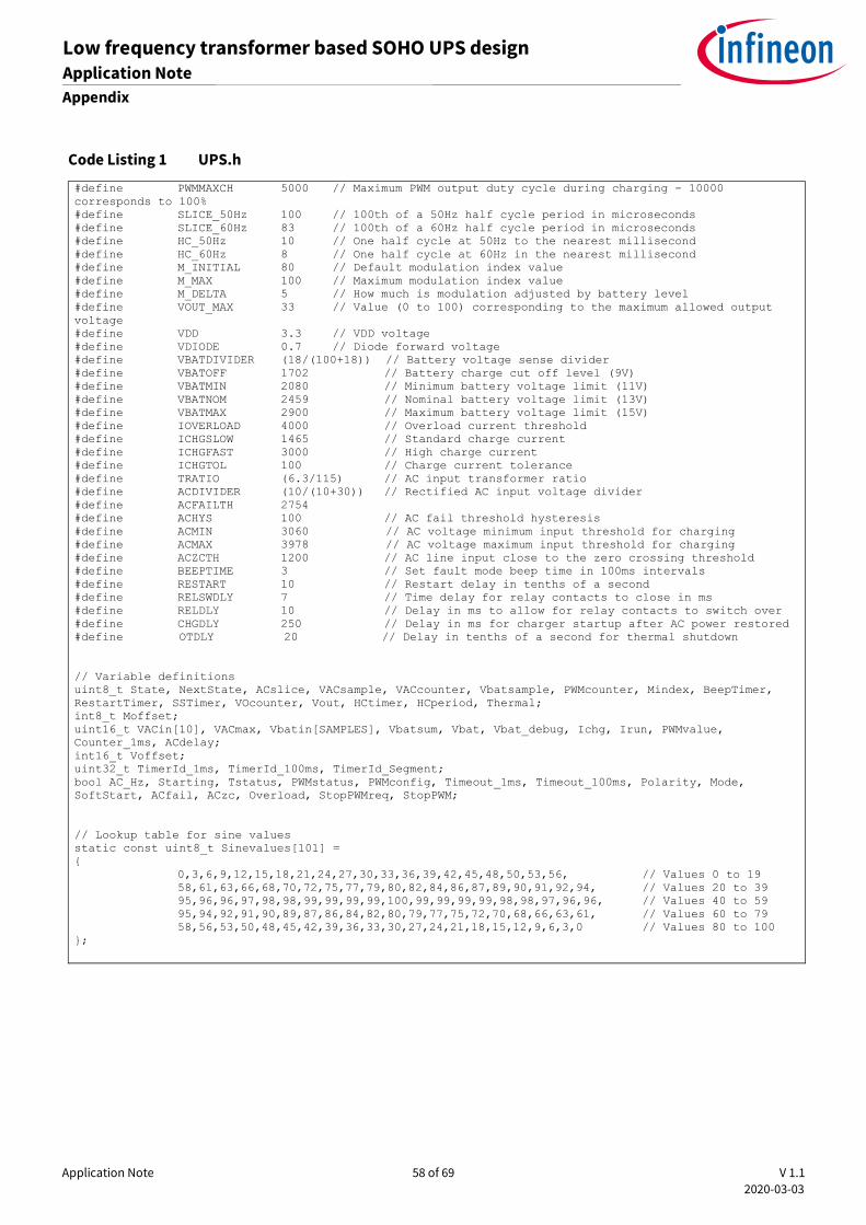
Application Note 58 of 69 V 1.1 2020-03-03
Low frequency transformer based SOHO UPS design Application Note Appendix
Code Listing 1 UPS.h
#define PWMMAXCH 5000 // Maximum PWM output duty cycle during charging - 10000 corresponds to 100% #define SLICE_50Hz 100 // 100th of a 50Hz half cycle period in microseconds #define SLICE_60Hz 83 // 100th of a 60Hz half cycle period in microseconds #define HC_50Hz 10 // One half cycle at 50Hz to the nearest millisecond #define HC_60Hz 8 // One half cycle at 60Hz in the nearest millisecond #define M_INITIAL 80 // Default modulation index value #define M_MAX 100 // Maximum modulation index value #define M_DELTA 5 // How much is modulation adjusted by battery level #define VOUT_MAX 33 // Value (0 to 100) corresponding to the maximum allowed output voltage #define VDD 3.3 // VDD voltage #define VDIODE 0.7 // Diode forward voltage #define VBATDIVIDER (18/(100+18)) // Battery voltage sense divider #define VBATOFF 1702 // Battery charge cut off level (9V) #define VBATMIN 2080 // Minimum battery voltage limit (11V) #define VBATNOM 2459 // Nominal battery voltage limit (13V) #define VBATMAX 2900 // Maximum battery voltage limit (15V) #define IOVERLOAD 4000 // Overload current threshold #define ICHGSLOW 1465 // Standard charge current #define ICHGFAST 3000 // High charge current #define ICHGTOL 100 // Charge current tolerance #define TRATIO (6.3/115) // AC input transformer ratio #define ACDIVIDER (10/(10+30)) // Rectified AC input voltage divider #define ACFAILTH 2754 #define ACHYS 100 // AC fail threshold hysteresis #define ACMIN 3060 // AC voltage minimum input threshold for charging #define ACMAX 3978 // AC voltage maximum input threshold for charging #define ACZCTH 1200 // AC line input close to the zero crossing threshold #define BEEPTIME 3 // Set fault mode beep time in 100ms intervals #define RESTART 10 // Restart delay in tenths of a second #define RELSWDLY 7 // Time delay for relay contacts to close in ms #define RELDLY 10 // Delay in ms to allow for relay contacts to switch over #define CHGDLY 250 // Delay in ms for charger startup after AC power restored #define OTDLY 20 // Delay in tenths of a second for thermal shutdown // Variable definitions uint8_t State, NextState, ACslice, VACsample, VACcounter, Vbatsample, PWMcounter, Mindex, BeepTimer, RestartTimer, SSTimer, VOcounter, Vout, HCtimer, HCperiod, Thermal; int8_t Moffset; uint16_t VACin[10], VACmax, Vbatin[SAMPLES], Vbatsum, Vbat, Vbat_debug, Ichg, Irun, PWMvalue, Counter_1ms, ACdelay; int16_t Voffset; uint32_t TimerId_1ms, TimerId_100ms, TimerId_Segment; bool AC_Hz, Starting, Tstatus, PWMstatus, PWMconfig, Timeout_1ms, Timeout_100ms, Polarity, Mode, SoftStart, ACfail, ACzc, Overload, StopPWMreq, StopPWM; // Lookup table for sine values static const uint8_t Sinevalues[101] = { 0,3,6,9,12,15,18,21,24,27,30,33,36,39,42,45,48,50,53,56, // Values 0 to 19 58,61,63,66,68,70,72,75,77,79,80,82,84,86,87,89,90,91,92,94, // Values 20 to 39 95,96,96,97,98,98,99,99,99,99,100,99,99,99,99,98,98,97,96,96, // Values 40 to 59 95,94,92,91,90,89,87,86,84,82,80,79,77,75,72,70,68,66,63,61, // Values 60 to 79 58,56,53,50,48,45,42,39,36,33,30,27,24,21,18,15,12,9,6,3,0 // Values 80 to 100 };
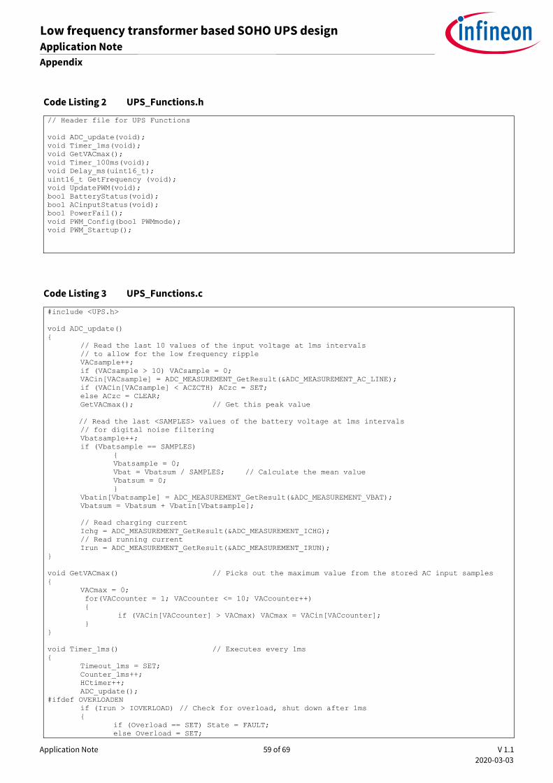
Application Note 59 of 69 V 1.1 2020-03-03
Low frequency transformer based SOHO UPS design Application Note Appendix
Code Listing 2 UPS_Functions.h
// Header file for UPS Functions void ADC_update(void); void Timer_1ms(void); void GetVACmax(); void Timer_100ms(void); void Delay_ms(uint16_t); uint16_t GetFrequency (void); void UpdatePWM(void); bool BatteryStatus(void); bool ACinputStatus(void); bool PowerFail(); void PWM_Config(bool PWMmode); void PWM_Startup();
Code Listing 3 UPS_Functions.c
#include <UPS.h> void ADC_update() { // Read the last 10 values of the input voltage at 1ms intervals // to allow for the low frequency ripple VACsample++; if (VACsample > 10) VACsample = 0; VACin[VACsample] = ADC_MEASUREMENT_GetResult(&ADC_MEASUREMENT_AC_LINE); if (VACin[VACsample] < ACZCTH) ACzc = SET; else ACzc = CLEAR; GetVACmax(); // Get this peak value // Read the last <SAMPLES> values of the battery voltage at 1ms intervals // for digital noise filtering Vbatsample++; if (Vbatsample == SAMPLES) { Vbatsample = 0; Vbat = Vbatsum / SAMPLES; // Calculate the mean value Vbatsum = 0; } Vbatin[Vbatsample] = ADC_MEASUREMENT_GetResult(&ADC_MEASUREMENT_VBAT); Vbatsum = Vbatsum + Vbatin[Vbatsample]; // Read charging current Ichg = ADC_MEASUREMENT_GetResult(&ADC_MEASUREMENT_ICHG); // Read running current Irun = ADC_MEASUREMENT_GetResult(&ADC_MEASUREMENT_IRUN); } void GetVACmax() // Picks out the maximum value from the stored AC input samples { VACmax = 0; for(VACcounter = 1; VACcounter <= 10; VACcounter++) { if (VACin[VACcounter] > VACmax) VACmax = VACin[VACcounter]; } } void Timer_1ms() // Executes every 1ms { Timeout_1ms = SET; Counter_1ms++; HCtimer++; ADC_update(); #ifdef OVERLOADEN if (Irun > IOVERLOAD) // Check for overload, shut down after 1ms { if (Overload == SET) State = FAULT; else Overload = SET;
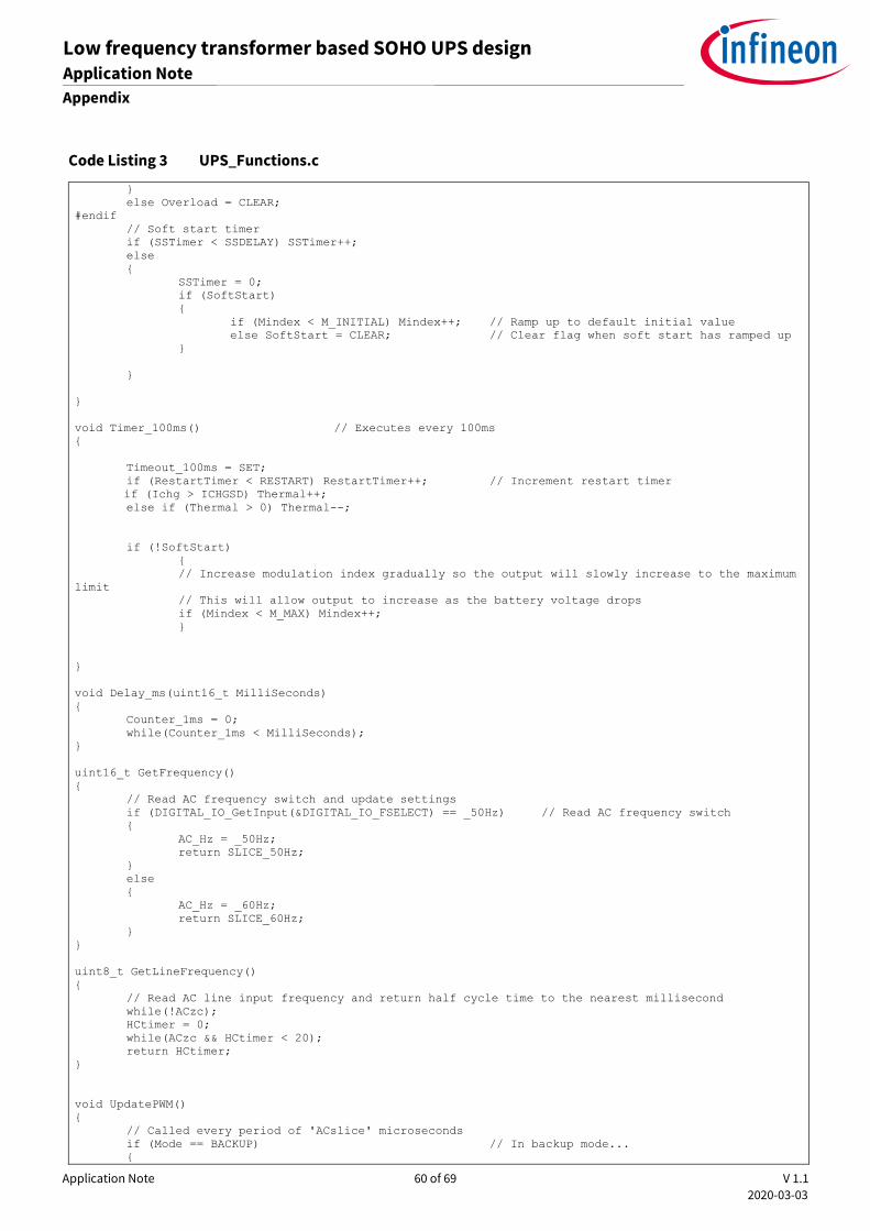
Application Note 60 of 69 V 1.1 2020-03-03
Low frequency transformer based SOHO UPS design Application Note Appendix
Code Listing 3 UPS_Functions.c
} else Overload = CLEAR; #endif // Soft start timer if (SSTimer < SSDELAY) SSTimer++; else { SSTimer = 0; if (SoftStart) { if (Mindex < M_INITIAL) Mindex++; // Ramp up to default initial value else SoftStart = CLEAR; // Clear flag when soft start has ramped up } } } void Timer_100ms() // Executes every 100ms { Timeout_100ms = SET; if (RestartTimer < RESTART) RestartTimer++; // Increment restart timer if (Ichg > ICHGSD) Thermal++; else if (Thermal > 0) Thermal--; if (!SoftStart) { // Increase modulation index gradually so the output will slowly increase to the maximum limit // This will allow output to increase as the battery voltage drops if (Mindex < M_MAX) Mindex++; } } void Delay_ms(uint16_t MilliSeconds) { Counter_1ms = 0; while(Counter_1ms < MilliSeconds); } uint16_t GetFrequency() { // Read AC frequency switch and update settings if (DIGITAL_IO_GetInput(&DIGITAL_IO_FSELECT) == _50Hz) // Read AC frequency switch { AC_Hz = _50Hz; return SLICE_50Hz; } else { AC_Hz = _60Hz; return SLICE_60Hz; } } uint8_t GetLineFrequency() { // Read AC line input frequency and return half cycle time to the nearest millisecond while(!ACzc); HCtimer = 0; while(ACzc && HCtimer < 20); return HCtimer; } void UpdatePWM() { // Called every period of 'ACslice' microseconds if (Mode == BACKUP) // In backup mode... {
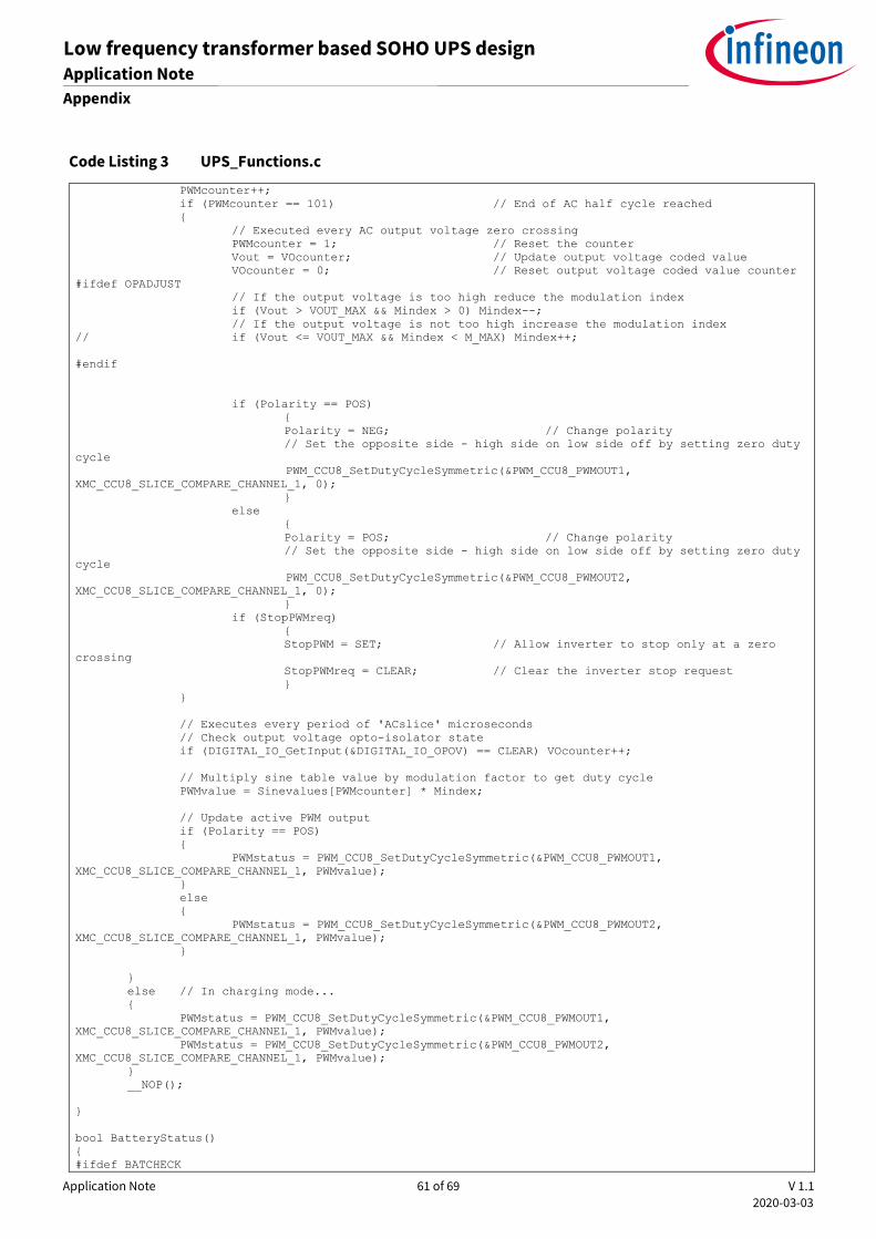
Application Note 61 of 69 V 1.1 2020-03-03
Low frequency transformer based SOHO UPS design Application Note Appendix
Code Listing 3 UPS_Functions.c
PWMcounter++; if (PWMcounter == 101) // End of AC half cycle reached { // Executed every AC output voltage zero crossing PWMcounter = 1; // Reset the counter Vout = VOcounter; // Update output voltage coded value VOcounter = 0; // Reset output voltage coded value counter #ifdef OPADJUST // If the output voltage is too high reduce the modulation index if (Vout > VOUT_MAX && Mindex > 0) Mindex--; // If the output voltage is not too high increase the modulation index // if (Vout <= VOUT_MAX && Mindex < M_MAX) Mindex++; #endif if (Polarity == POS) { Polarity = NEG; // Change polarity // Set the opposite side - high side on low side off by setting zero duty cycle PWM_CCU8_SetDutyCycleSymmetric(&PWM_CCU8_PWMOUT1, XMC_CCU8_SLICE_COMPARE_CHANNEL_1, 0); } else { Polarity = POS; // Change polarity // Set the opposite side - high side on low side off by setting zero duty cycle PWM_CCU8_SetDutyCycleSymmetric(&PWM_CCU8_PWMOUT2, XMC_CCU8_SLICE_COMPARE_CHANNEL_1, 0); } if (StopPWMreq) { StopPWM = SET; // Allow inverter to stop only at a zero crossing StopPWMreq = CLEAR; // Clear the inverter stop request } } // Executes every period of 'ACslice' microseconds // Check output voltage opto-isolator state if (DIGITAL_IO_GetInput(&DIGITAL_IO_OPOV) == CLEAR) VOcounter++; // Multiply sine table value by modulation factor to get duty cycle PWMvalue = Sinevalues[PWMcounter] * Mindex; // Update active PWM output if (Polarity == POS) { PWMstatus = PWM_CCU8_SetDutyCycleSymmetric(&PWM_CCU8_PWMOUT1, XMC_CCU8_SLICE_COMPARE_CHANNEL_1, PWMvalue); } else { PWMstatus = PWM_CCU8_SetDutyCycleSymmetric(&PWM_CCU8_PWMOUT2, XMC_CCU8_SLICE_COMPARE_CHANNEL_1, PWMvalue); } } else // In charging mode... { PWMstatus = PWM_CCU8_SetDutyCycleSymmetric(&PWM_CCU8_PWMOUT1, XMC_CCU8_SLICE_COMPARE_CHANNEL_1, PWMvalue); PWMstatus = PWM_CCU8_SetDutyCycleSymmetric(&PWM_CCU8_PWMOUT2, XMC_CCU8_SLICE_COMPARE_CHANNEL_1, PWMvalue); } __NOP(); } bool BatteryStatus() { #ifdef BATCHECK
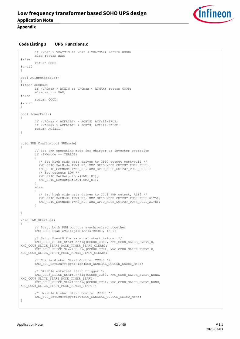
Application Note 62 of 69 V 1.1 2020-03-03
Low frequency transformer based SOHO UPS design Application Note Appendix
Code Listing 3 UPS_Functions.c
if (Vbat > VBATMIN && Vbat < VBATMAX) return GOOD; else return BAD; #else return GOOD; #endif } bool ACinputStatus() { #ifdef ACCHECK if (VACmax > ACMIN && VACmax < ACMAX) return GOOD; else return BAD; #else return GOOD; #endif } bool PowerFail() { if (VACmax < ACFAILTH - ACHYS) ACfail=TRUE; if (VACmax > ACFAILTH + ACHYS) ACfail=FALSE; return ACfail; } void PWM_Config(bool PWMmode) { // Set PWM operating mode for charger or inverter operation if (PWMmode == CHARGE) { /* Set high side gate drives to GPIO output push-pull */ XMC_GPIO_SetMode(PWM1_HI, XMC_GPIO_MODE_OUTPUT_PUSH_PULL); XMC_GPIO_SetMode(PWM2_HI, XMC_GPIO_MODE_OUTPUT_PUSH_PULL); /* Set outputs LOW */ XMC_GPIO_SetOutputLow(PWM1_HI); XMC_GPIO_SetOutputLow(PWM2_HI); } else { /* Set high side gate drives to CCU8 PWM output, ALT5 */ XMC_GPIO_SetMode(PWM1_HI, XMC_GPIO_MODE_OUTPUT_PUSH_PULL_ALT5); XMC_GPIO_SetMode(PWM2_HI, XMC_GPIO_MODE_OUTPUT_PUSH_PULL_ALT5); } } void PWM_Startup() { // Start both PWM outputs synchronized together XMC_CCU8_EnableMultipleClocks(CCU80, 15U); /* Setup Event0 for external start trigger */ XMC_CCU8_SLICE_StartConfig(CCU80_CC82, XMC_CCU8_SLICE_EVENT_0, XMC_CCU8_SLICE_START_MODE_TIMER_START_CLEAR); XMC_CCU8_SLICE_StartConfig(CCU80_CC81, XMC_CCU8_SLICE_EVENT_0, XMC_CCU8_SLICE_START_MODE_TIMER_START_CLEAR); /* Enable Global Start Control CCU80 */ XMC_SCU_SetCcuTriggerHigh(SCU_GENERAL_CCUCON_GSC80_Msk); /* Disable external start trigger */ XMC_CCU8_SLICE_StartConfig(CCU80_CC82, XMC_CCU8_SLICE_EVENT_NONE, XMC_CCU8_SLICE_START_MODE_TIMER_START); XMC_CCU8_SLICE_StartConfig(CCU80_CC81, XMC_CCU8_SLICE_EVENT_NONE, XMC_CCU8_SLICE_START_MODE_TIMER_START); /* Disable Global Start Control CCU80 */ XMC_SCU_SetCcuTriggerLow(SCU_GENERAL_CCUCON_GSC80_Msk); }
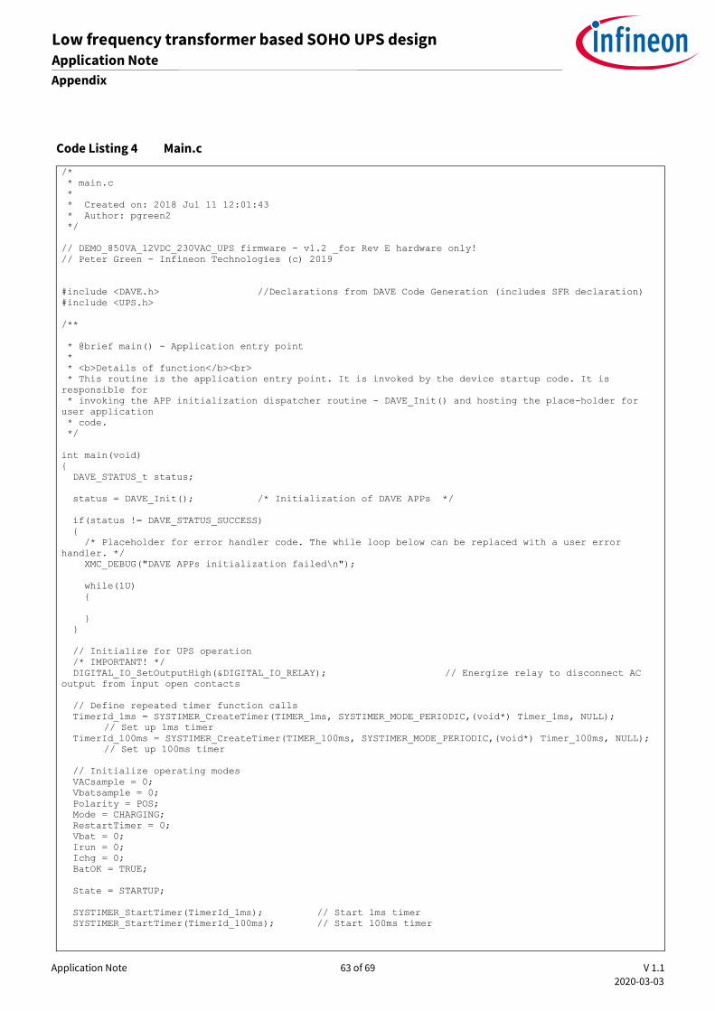
Application Note 63 of 69 V 1.1 2020-03-03
Low frequency transformer based SOHO UPS design Application Note Appendix
Code Listing 4 Main.c
/* * main.c * * Created on: 2018 Jul 11 12:01:43 * Author: pgreen2 */ // DEMO_850VA_12VDC_230VAC_UPS firmware - v1.2 _for Rev E hardware only! // Peter Green - Infineon Technologies (c) 2019 #include <DAVE.h> //Declarations from DAVE Code Generation (includes SFR declaration) #include <UPS.h> /** * @brief main() - Application entry point * * <b>Details of function</b><br> * This routine is the application entry point. It is invoked by the device startup code. It is responsible for * invoking the APP initialization dispatcher routine - DAVE_Init() and hosting the place-holder for user application * code. */ int main(void) { DAVE_STATUS_t status; status = DAVE_Init(); /* Initialization of DAVE APPs */ if(status != DAVE_STATUS_SUCCESS) { /* Placeholder for error handler code. The while loop below can be replaced with a user error handler. */ XMC_DEBUG("DAVE APPs initialization failed\n"); while(1U) { } } // Initialize for UPS operation /* IMPORTANT! */ DIGITAL_IO_SetOutputHigh(&DIGITAL_IO_RELAY); // Energize relay to disconnect AC output from input open contacts // Define repeated timer function calls TimerId_1ms = SYSTIMER_CreateTimer(TIMER_1ms, SYSTIMER_MODE_PERIODIC,(void*) Timer_1ms, NULL); // Set up 1ms timer TimerId_100ms = SYSTIMER_CreateTimer(TIMER_100ms, SYSTIMER_MODE_PERIODIC,(void*) Timer_100ms, NULL); // Set up 100ms timer // Initialize operating modes VACsample = 0; Vbatsample = 0; Polarity = POS; Mode = CHARGING; RestartTimer = 0; Vbat = 0; Irun = 0; Ichg = 0; BatOK = TRUE; State = STARTUP; SYSTIMER_StartTimer(TimerId_1ms); // Start 1ms timer SYSTIMER_StartTimer(TimerId_100ms); // Start 100ms timer
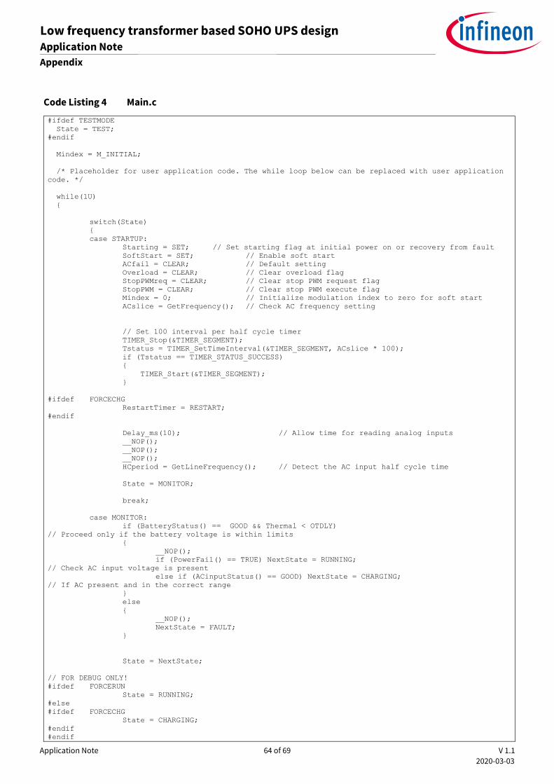
Application Note 64 of 69 V 1.1 2020-03-03
Low frequency transformer based SOHO UPS design Application Note Appendix
Code Listing 4 Main.c
#ifdef TESTMODE State = TEST; #endif Mindex = M_INITIAL; /* Placeholder for user application code. The while loop below can be replaced with user application code. */ while(1U) { switch(State) { case STARTUP: Starting = SET; // Set starting flag at initial power on or recovery from fault SoftStart = SET; // Enable soft start ACfail = CLEAR; // Default setting Overload = CLEAR; // Clear overload flag StopPWMreq = CLEAR; // Clear stop PWM request flag StopPWM = CLEAR; // Clear stop PWM execute flag Mindex = 0; // Initialize modulation index to zero for soft start ACslice = GetFrequency(); // Check AC frequency setting // Set 100 interval per half cycle timer TIMER_Stop(&TIMER_SEGMENT); Tstatus = TIMER_SetTimeInterval(&TIMER_SEGMENT, ACslice * 100); if (Tstatus == TIMER_STATUS_SUCCESS) { TIMER_Start(&TIMER_SEGMENT); } #ifdef FORCECHG RestartTimer = RESTART; #endif Delay_ms(10); // Allow time for reading analog inputs __NOP(); __NOP(); __NOP(); HCperiod = GetLineFrequency(); // Detect the AC input half cycle time State = MONITOR; break; case MONITOR: if (BatteryStatus() == GOOD && Thermal < OTDLY) // Proceed only if the battery voltage is within limits { __NOP(); if (PowerFail() == TRUE) NextState = RUNNING; // Check AC input voltage is present else if (ACinputStatus() == GOOD) NextState = CHARGING; // If AC present and in the correct range } else { __NOP(); NextState = FAULT; } State = NextState; // FOR DEBUG ONLY! #ifdef FORCERUN State = RUNNING; #else #ifdef FORCECHG State = CHARGING; #endif #endif
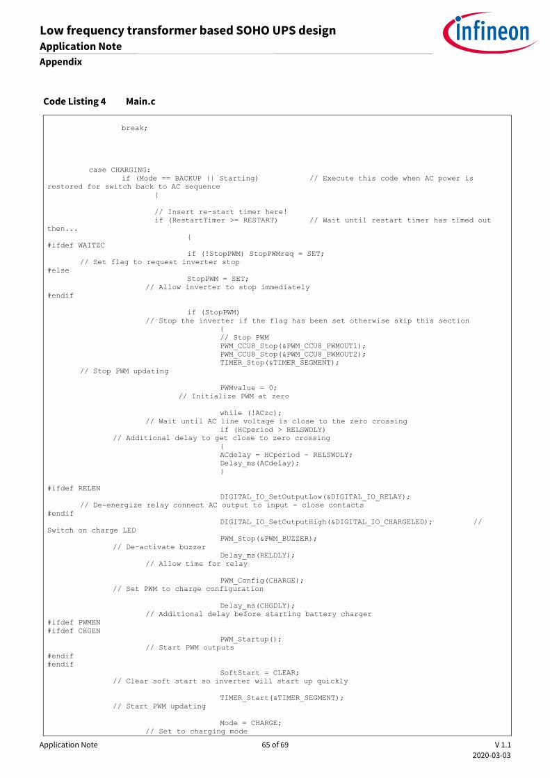
Application Note 65 of 69 V 1.1 2020-03-03
Low frequency transformer based SOHO UPS design Application Note Appendix
Code Listing 4 Main.c
break; case CHARGING: if (Mode == BACKUP || Starting) // Execute this code when AC power is restored for switch back to AC sequence { // Insert re-start timer here! if (RestartTimer >= RESTART) // Wait until restart timer has timed out then... { #ifdef WAITZC if (!StopPWM) StopPWMreq = SET; // Set flag to request inverter stop #else StopPWM = SET; // Allow inverter to stop immediately #endif if (StopPWM) // Stop the inverter if the flag has been set otherwise skip this section { // Stop PWM PWM_CCU8_Stop(&PWM_CCU8_PWMOUT1); PWM_CCU8_Stop(&PWM_CCU8_PWMOUT2); TIMER_Stop(&TIMER_SEGMENT); // Stop PWM updating PWMvalue = 0; // Initialize PWM at zero while (!ACzc); // Wait until AC line voltage is close to the zero crossing if (HCperiod > RELSWDLY) // Additional delay to get close to zero crossing { ACdelay = HCperiod - RELSWDLY; Delay_ms(ACdelay); } #ifdef RELEN DIGITAL_IO_SetOutputLow(&DIGITAL_IO_RELAY); // De-energize relay connect AC output to input - close contacts #endif DIGITAL_IO_SetOutputHigh(&DIGITAL_IO_CHARGELED); // Switch on charge LED PWM_Stop(&PWM_BUZZER); // De-activate buzzer Delay_ms(RELDLY); // Allow time for relay PWM_Config(CHARGE); // Set PWM to charge configuration Delay_ms(CHGDLY); // Additional delay before starting battery charger #ifdef PWMEN #ifdef CHGEN PWM_Startup(); // Start PWM outputs #endif #endif SoftStart = CLEAR; // Clear soft start so inverter will start up quickly TIMER_Start(&TIMER_SEGMENT); // Start PWM updating Mode = CHARGE; // Set to charging mode
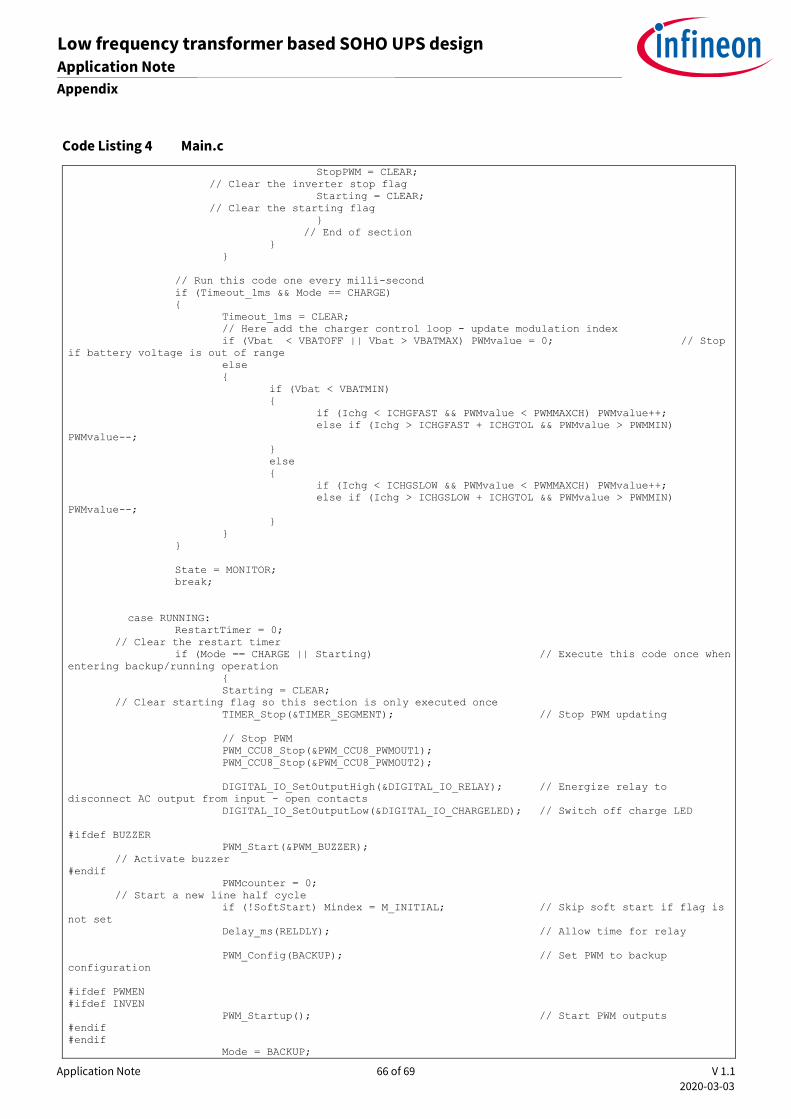
Application Note 66 of 69 V 1.1 2020-03-03
Low frequency transformer based SOHO UPS design Application Note Appendix
Code Listing 4 Main.c
StopPWM = CLEAR; // Clear the inverter stop flag Starting = CLEAR; // Clear the starting flag } // End of section } } // Run this code one every milli-second if (Timeout_1ms && Mode == CHARGE) { Timeout_1ms = CLEAR; // Here add the charger control loop - update modulation index if (Vbat < VBATOFF || Vbat > VBATMAX) PWMvalue = 0; // Stop if battery voltage is out of range else { if (Vbat < VBATMIN) { if (Ichg < ICHGFAST && PWMvalue < PWMMAXCH) PWMvalue++; else if (Ichg > ICHGFAST + ICHGTOL && PWMvalue > PWMMIN) PWMvalue--; } else { if (Ichg < ICHGSLOW && PWMvalue < PWMMAXCH) PWMvalue++; else if (Ichg > ICHGSLOW + ICHGTOL && PWMvalue > PWMMIN) PWMvalue--; } } } State = MONITOR; break; case RUNNING: RestartTimer = 0; // Clear the restart timer if (Mode == CHARGE || Starting) // Execute this code once when entering backup/running operation { Starting = CLEAR; // Clear starting flag so this section is only executed once TIMER_Stop(&TIMER_SEGMENT); // Stop PWM updating // Stop PWM PWM_CCU8_Stop(&PWM_CCU8_PWMOUT1); PWM_CCU8_Stop(&PWM_CCU8_PWMOUT2); DIGITAL_IO_SetOutputHigh(&DIGITAL_IO_RELAY); // Energize relay to disconnect AC output from input - open contacts DIGITAL_IO_SetOutputLow(&DIGITAL_IO_CHARGELED); // Switch off charge LED #ifdef BUZZER PWM_Start(&PWM_BUZZER); // Activate buzzer #endif PWMcounter = 0; // Start a new line half cycle if (!SoftStart) Mindex = M_INITIAL; // Skip soft start if flag is not set Delay_ms(RELDLY); // Allow time for relay PWM_Config(BACKUP); // Set PWM to backup configuration #ifdef PWMEN #ifdef INVEN PWM_Startup(); // Start PWM outputs #endif #endif Mode = BACKUP;
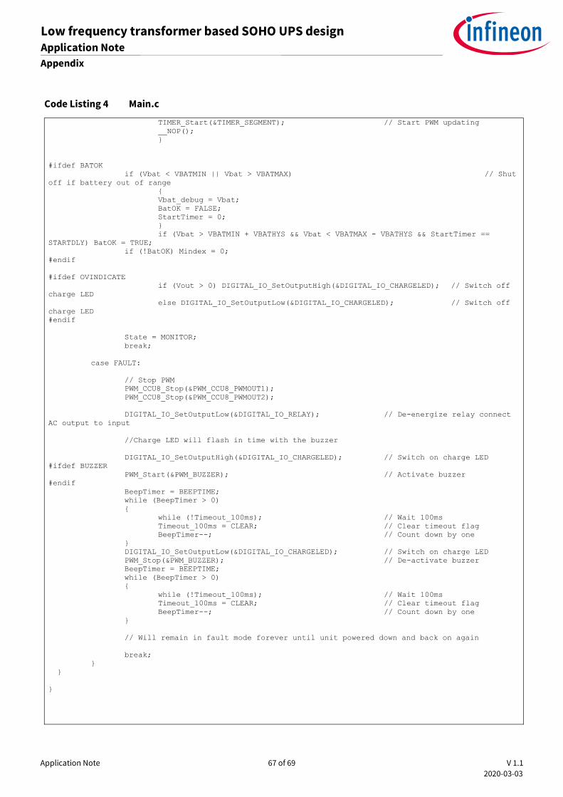
Application Note 67 of 69 V 1.1 2020-03-03
Low frequency transformer based SOHO UPS design Application Note Appendix
Code Listing 4 Main.c
TIMER_Start(&TIMER_SEGMENT); // Start PWM updating __NOP(); } #ifdef BATOK if (Vbat < VBATMIN || Vbat > VBATMAX) // Shut off if battery out of range { Vbat_debug = Vbat; BatOK = FALSE; StartTimer = 0; } if (Vbat > VBATMIN + VBATHYS && Vbat < VBATMAX - VBATHYS && StartTimer == STARTDLY) BatOK = TRUE; if (!BatOK) Mindex = 0; #endif #ifdef OVINDICATE if (Vout > 0) DIGITAL_IO_SetOutputHigh(&DIGITAL_IO_CHARGELED); // Switch off charge LED else DIGITAL_IO_SetOutputLow(&DIGITAL_IO_CHARGELED); // Switch off charge LED #endif State = MONITOR; break; case FAULT: // Stop PWM PWM_CCU8_Stop(&PWM_CCU8_PWMOUT1); PWM_CCU8_Stop(&PWM_CCU8_PWMOUT2); DIGITAL_IO_SetOutputLow(&DIGITAL_IO_RELAY); // De-energize relay connect AC output to input //Charge LED will flash in time with the buzzer DIGITAL_IO_SetOutputHigh(&DIGITAL_IO_CHARGELED); // Switch on charge LED #ifdef BUZZER PWM_Start(&PWM_BUZZER); // Activate buzzer #endif BeepTimer = BEEPTIME; while (BeepTimer > 0) { while (!Timeout_100ms); // Wait 100ms Timeout_100ms = CLEAR; // Clear timeout flag BeepTimer--; // Count down by one } DIGITAL_IO_SetOutputLow(&DIGITAL_IO_CHARGELED); // Switch on charge LED PWM_Stop(&PWM_BUZZER); // De-activate buzzer BeepTimer = BEEPTIME; while (BeepTimer > 0) { while (!Timeout_100ms); // Wait 100ms Timeout_100ms = CLEAR; // Clear timeout flag BeepTimer--; // Count down by one } // Will remain in fault mode forever until unit powered down and back on again break; } } }
Application Note 68 of 69 V 1.1 2020-03-03
Low frequency transformer based SOHO UPS design Application Note Appendix
References
[1] Infineon Technologies – XMC1300 AB-Step, XMC1000 family
[2] International Rectifier AN-941 – Paralleling power MOSFETs
[3] International Rectifier AN-967A – Using HEXFET III in PWM inverters for motor drives and UPS systems, Duncan Grant
[4] Infineon Technologies – Linear mode operation and safe operating diagram of power MOSFETs Johannes Schoiswohl (May 2017)
[5] Infineon Technologies – MOSFET selection for low-voltage UPS, Peter B. Green
Register your Infineon evaluation board, reference design or demo kit board
When receiving your order you are only three steps away from unlocking what our application engineers prepared for you - the new owner of a very specific Infineon evaluation board, reference design or demo kit:
https://www.infineon.com/cms/en/product/promopages/productregistration/
Revision history
Document version
Date of release Description of changes
1.0 August 27, 2019 Initial release 1.1 March 3, 2020 Firmware updated with improved battery voltage sensing, minor
corrections

Trademarks All referenced product or service names and trademarks are the property of their respective owners.
Edition 2020-03-03
AN_1910_PL15_1910_001345
Published by
Infineon Technologies AG
81726 Munich, Germany
© 2020 Infineon Technologies AG. All Rights Reserved. Do you have a question about this document?
Email: [email protected]
Document reference
IMPORTANT NOTICE The information contained in this application note is given as a hint for the implementation of the product only and shall in no event be regarded as a description or warranty of a certain functionality, condition or quality of the product. Before implementation of the product, the recipient of this application note must verify any function and other technical information given herein in the real application. Infineon Technologies hereby disclaims any and all warranties and liabilities of any kind (including without limitation warranties of non-infringement of intellectual property rights of any third party) with respect to any and all information given in this application note. The data contained in this document is exclusively intended for technically trained staff. It is the responsibility of customer’s technical departments to evaluate the suitability of the product for the intended application and the completeness of the product information given in this document with respect to such application.
For further information on the product, technology, delivery terms and conditions and prices please contact your nearest Infineon Technologies office (www.infineon.com).
WARNINGS Due to technical requirements products may contain dangerous substances. For information on the types in question please contact your nearest Infineon Technologies office. Except as otherwise explicitly approved by Infineon Technologies in a written document signed by authorized representatives of Infineon Technologies, Infineon Technologies’ products may not be used in any applications where a failure of the product or any consequences of the use thereof can reasonably be expected to result in personal injury.
Copyright © 2022 FDOKUMEN