LM555 General-purpose single bipolar timers - All Products
15
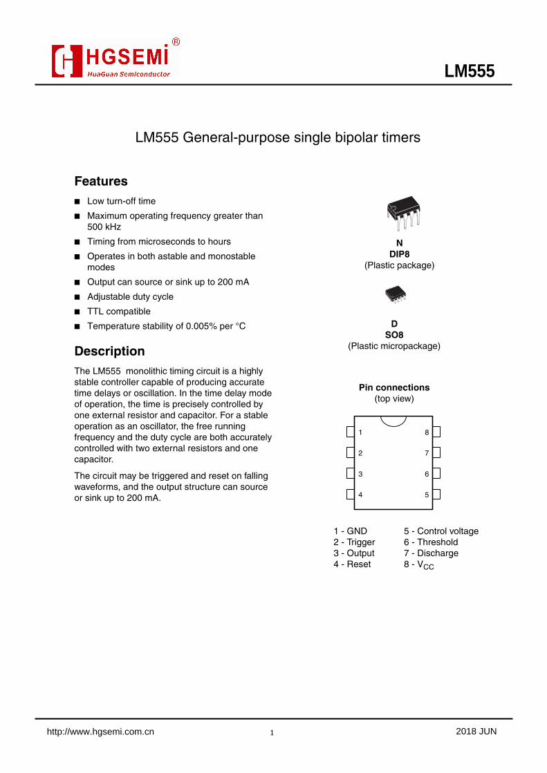
LM555 General-purpose single bipolar timers Features ■ Low turn-off time ■ Maximum operating frequency greater than 500 kHz ■ Timing from microseconds to hours ■ Operates in both astable and monostable modes ■ Output can source or sink up to 200 mA ■ Adjustable duty cycle ■ TTL compatible ■ Temperature stability of 0.005% per °C Description The LM555 monolithic timing circuit is a highly stable controller capable of producing accurate time delays or oscillation. In the time delay mode of operation, the time is precisely controlled by one external resistor and capacitor. For a stable operation as an oscillator, the free running frequency and the duty cycle are both accurately controlled with two external resistors and one capacitor. The circuit may be triggered and reset on falling waveforms, and the output structure can source or sink up to 200 mA. N DIP8 (Plastic package) D SO8 (Plastic micropackage) 1 2 3 4 5 6 7 8 1 - GND 2 - Trigger 3 - Output 4 - Reset 5 - Control voltage 6 - Threshold 7 - Discharge 8 - V CC Pin connections (top view) LM555 1 http://www.hgsemi.com.cn 2018 JUN
-
Upload
khangminh22 -
Category
Documents
-
view
0 -
download
0
Transcript of LM555 General-purpose single bipolar timers - All Products
LM555 General-purpose single bipolar timers
Features■ Low turn-off time
■ Maximum operating frequency greater than 500 kHz
■ Timing from microseconds to hours
■ Operates in both astable and monostable modes
■ Output can source or sink up to 200 mA
■ Adjustable duty cycle
■ TTL compatible
■ Temperature stability of 0.005% per °C
DescriptionThe LM555 monolithic timing circuit is a highly stable controller capable of producing accurate time delays or oscillation. In the time delay mode of operation, the time is precisely controlled by one external resistor and capacitor. For a stable operation as an oscillator, the free running frequency and the duty cycle are both accurately controlled with two external resistors and one capacitor.
The circuit may be triggered and reset on falling waveforms, and the output structure can source or sink up to 200 mA.
NDIP8
(Plastic package)
DSO8
(Plastic micropackage)
1
2
3
4 5
6
7
8
1 - GND2 - Trigger3 - Output4 - Reset
5 - Control voltage6 - Threshold7 - Discharge8 - VCC
Pin connections(top view)
LM555
1 http://www.hgsemi.com.cn 2018 JUN
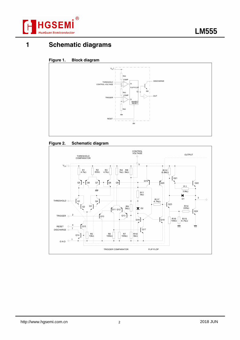
1 Schematic diagrams
Figure 1. Block diagram
Figure 2. Schematic diagram
THRESHOLD
COMP
5kΩ
5kΩ
5kΩ
TRIGGER
R
FLIP-FLOP
S
Q
DISCHARGE
OUT
INHIBIT/
RESET
RESET
COMP
S - 8086
S
+
CONTROL VOLTAGE
VCC
������
����������
��� ��������������
��
�������
������
�� �� �� �� ��
�������
�����
�����
��
�� ��
��
���
��� ���
���
��� ����
����� �
� � �
��������
� � �
�
�
�
�
���
���
������
�������
�������
������
���
��� ���
����� ��
�������
��������
�������
���
���
��������
�
���
���
��
������
���
��������
�
����� � ���������� !�� !��
������
�����
LM555
2 http://www.hgsemi.com.cn 2018 JUN
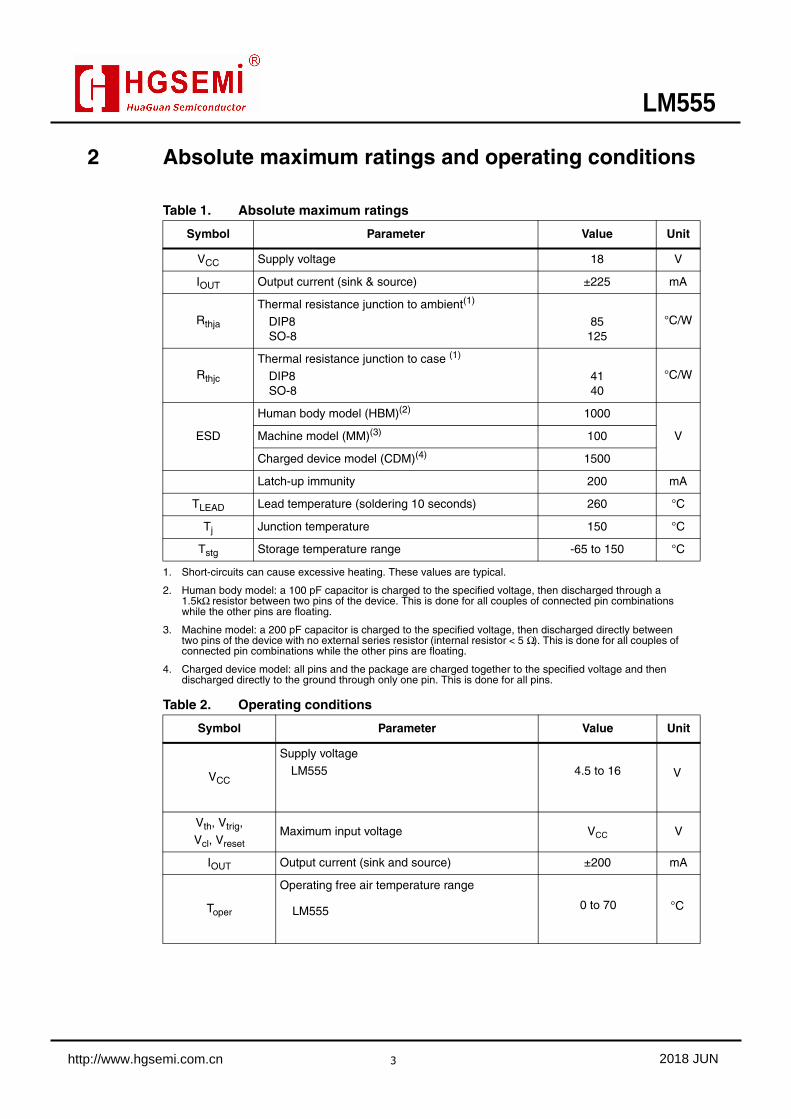
2 Absolute maximum ratings and operating conditions
Table 1. Absolute maximum ratings
Symbol Parameter Value Unit
VCC Supply voltage 18 V
IOUT Output current (sink & source) ±225 mA
Rthja
Thermal resistance junction to ambient(1)
DIP8SO-8
1. Short-circuits can cause excessive heating. These values are typical.
85125
°C/W
Rthjc
Thermal resistance junction to case (1)
DIP8SO-8
4140
°C/W
ESD
Human body model (HBM)(2)
2. Human body model: a 100 pF capacitor is charged to the specified voltage, then discharged through a 1.5kΩ resistor between two pins of the device. This is done for all couples of connected pin combinations while the other pins are floating.
1000
VMachine model (MM)(3)
3. Machine model: a 200 pF capacitor is charged to the specified voltage, then discharged directly between two pins of the device with no external series resistor (internal resistor < 5 Ω). This is done for all couples of connected pin combinations while the other pins are floating.
100
Charged device model (CDM)(4)
4. Charged device model: all pins and the package are charged together to the specified voltage and then discharged directly to the ground through only one pin. This is done for all pins.
1500
Latch-up immunity 200 mA
TLEAD Lead temperature (soldering 10 seconds) 260 °C
Tj Junction temperature 150 °C
Tstg Storage temperature range -65 to 150 °C
Table 2. Operating conditions
Symbol Parameter Value Unit
VCC
Supply voltage
LM555 4.5 to 16 V
Vth, Vtrig,
Vcl, VresetMaximum input voltage VCC V
IOUT Output current (sink and source) ±200 mA
Toper
Operating free air temperature range
LM555 0 to 70 °C
LM555
3 http://www.hgsemi.com.cn 2018 JUN
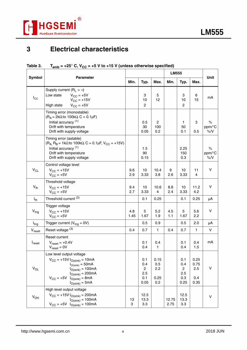
3 Electrical characteristics
Table 3. Tamb = +25° C, VCC = +5 V to +15 V (unless otherwise specified)
Symbol Parameter UnitMin. Typ. Max. Min. Typ. Max.
ICC
Supply current (RL = ∝)
Low state VCC = +5VVCC = +15V
High state VCC = +5V
310
2
512
310
2
615
mA
Timing error (monostable)(RA = 2kΩ to 100kΩ, C = 0.1μF)
Initial accuracy (1)
Drift with temperatureDrift with supply voltage
0.530
0.05
21000.2
1500.1
3
0.5
%ppm/°C
%/V
Timing error (astable)(RA, RB = 1kΩ to 100kΩ, C = 0.1μF, VCC = +15V)
Initial accuracy (1)
Drift with temperatureDrift with supply voltage
1.590
0.15
2.251500.3
%ppm/°C
%/V
VCL
Control voltage levelVCC = +15VVCC = +5V
9.62.9
103.33
10.43.8
92.6
103.33
114
V
Vth
Threshold voltage
VCC = +15VVCC = +5V
9.42.7
103.33
10.64
8.82.4
103.33
11.24.2
V
Ith Threshold current (2) 0.1 0.25 0.1 0.25 µA
Vtrig
Trigger voltageVCC = +15VVCC = +5V
4.81.45
51.67
5.21.9
4.51.1
51.67
5.62.2
V
Itrig Trigger current (Vtrig = 0V) 0.5 0.9 0.5 2.0 µA
Vreset Reset voltage (3) 0.4 0.7 1 0.4 0.7 1 V
Ireset
Reset currentVreset = +0.4VVreset = 0V
0.10.4
0.41
0.10.4
0.41.5
mA
VOL
Low level output voltage
VCC = +15V IO(sink) = 10mAIO(sink) = 50mAIO(sink) = 100mAIO(sink) = 200mA
VCC = +5V IO(sink) = 8mAIO(sink) = 5mA
0.10.42
2.50.1
0.05
0.150.52.2
0.250.2
0.10.42
2.50.30.25
0.250.752.5
0.40.35
V
VOH
High level output voltageVCC = +15V IO(sink) = 200mA
IO(sink) = 100mAVCC = +5V IO(sink) = 100mA
133
12.513.33.3
12.752.75
12.513.33.3
V
LM555
LM555
4 http://www.hgsemi.com.cn 2018 JUN
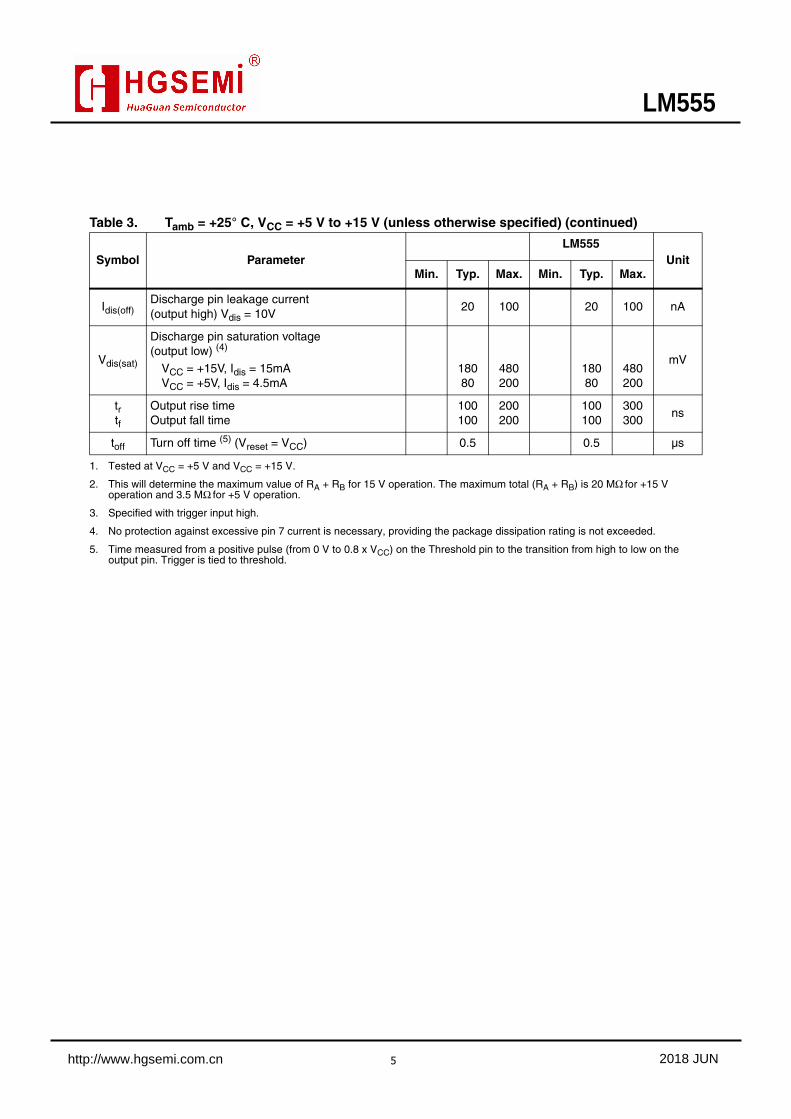
Idis(off)Discharge pin leakage current(output high) Vdis = 10V
20 100 20 100 nA
Vdis(sat)
Discharge pin saturation voltage(output low) (4)
VCC = +15V, Idis = 15mAVCC = +5V, Idis = 4.5mA
18080
480200
18080
480200
mV
trtf
Output rise timeOutput fall time
100100
200200
100100
300300
ns
toff Turn off time (5) (Vreset = VCC) 0.5 0.5 µs
1. Tested at VCC = +5 V and VCC = +15 V.
2. This will determine the maximum value of RA + RB for 15 V operation. The maximum total (RA + RB) is 20 MΩ for +15 V operation and 3.5 MΩ for +5 V operation.
3. Specified with trigger input high.
4. No protection against excessive pin 7 current is necessary, providing the package dissipation rating is not exceeded.
5. Time measured from a positive pulse (from 0 V to 0.8 x VCC) on the Threshold pin to the transition from high to low on the output pin. Trigger is tied to threshold.
Table 3. Tamb = +25° C, VCC = +5 V to +15 V (unless otherwise specified) (continued)
Symbol Parameter UnitMin. Typ. Max. Min. Typ. Max.
LM555
LM555
5 http://www.hgsemi.com.cn 2018 JUN
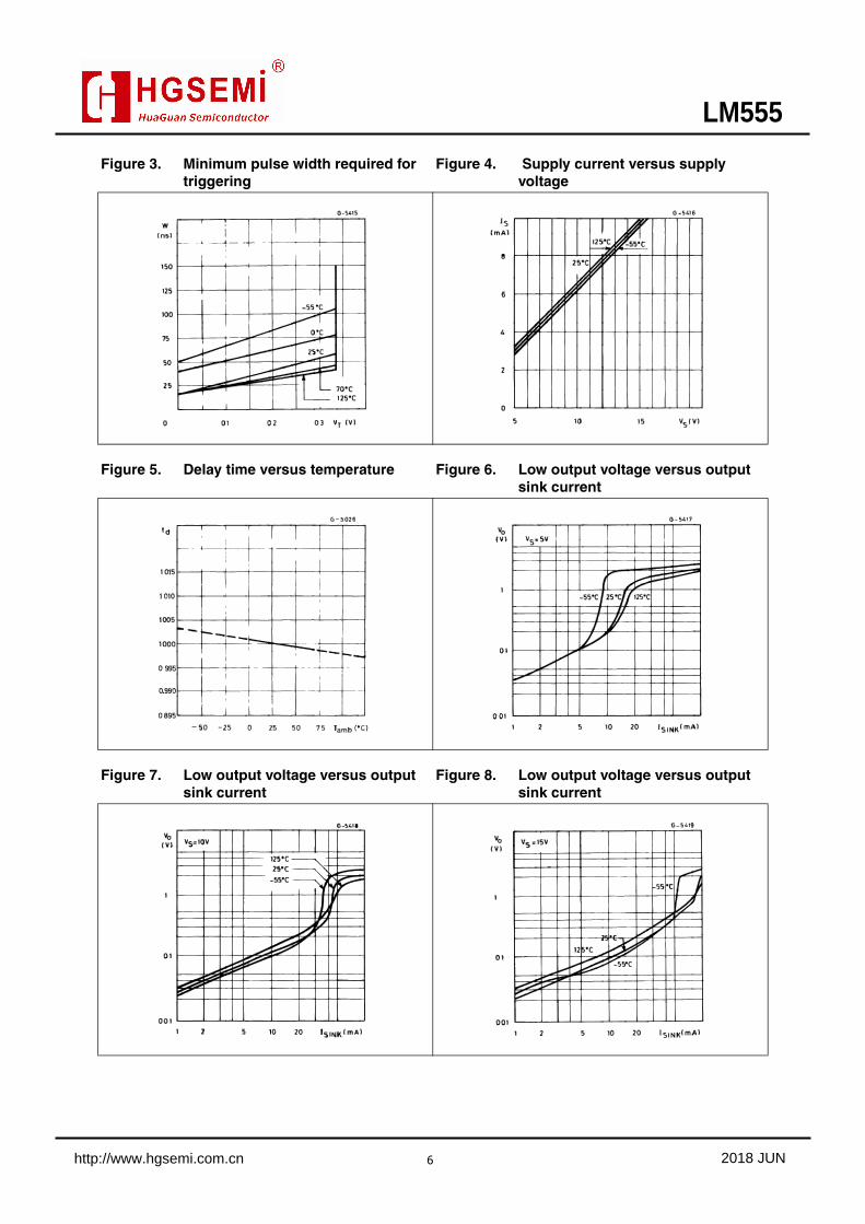
Figure 3. Minimum pulse width required for triggering
Figure 4. Supply current versus supply voltage
Figure 5. Delay time versus temperature Figure 6. Low output voltage versus output sink current
Figure 7. Low output voltage versus output sink current
Figure 8. Low output voltage versus output sink current
LM555
6 http://www.hgsemi.com.cn 2018 JUN
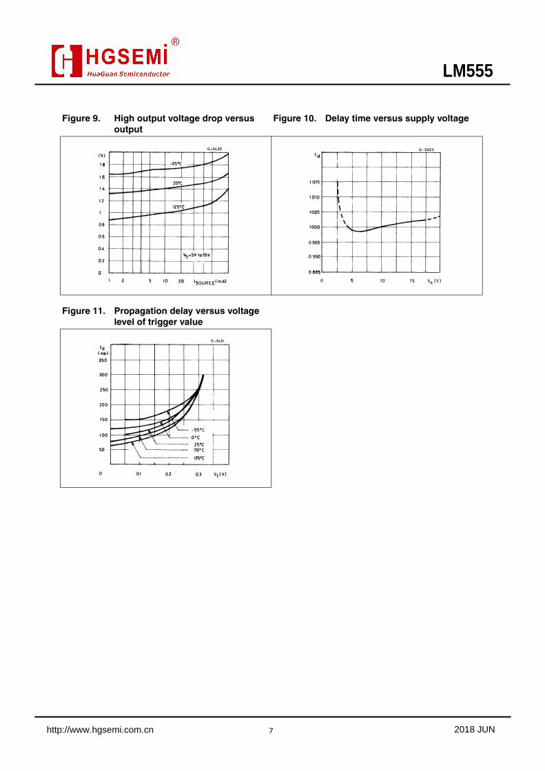
Figure 9. High output voltage drop versus output
Figure 10. Delay time versus supply voltage
Figure 11. Propagation delay versus voltage level of trigger value
LM555
7 http://www.hgsemi.com.cn 2018 JUN
4 Application information
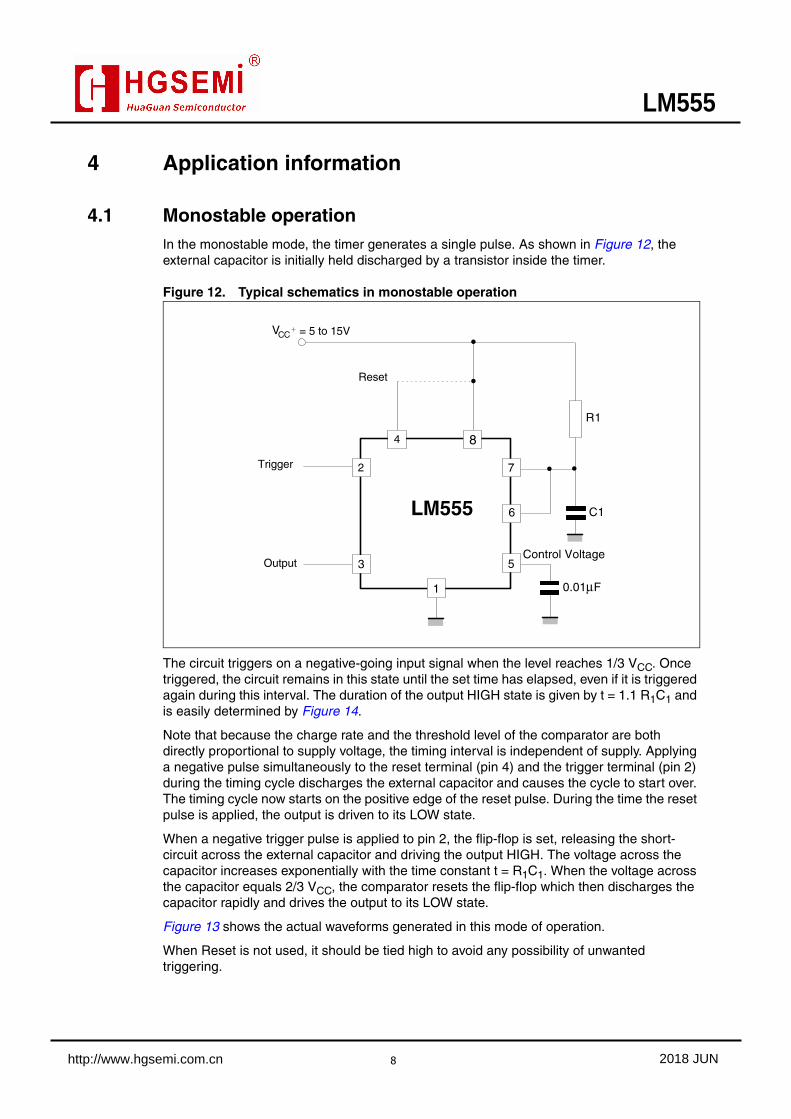
4.1 Monostable operationIn the monostable mode, the timer generates a single pulse. As shown in Figure 12, the external capacitor is initially held discharged by a transistor inside the timer.
Figure 12. Typical schematics in monostable operation
The circuit triggers on a negative-going input signal when the level reaches 1/3 VCC. Once triggered, the circuit remains in this state until the set time has elapsed, even if it is triggered again during this interval. The duration of the output HIGH state is given by t = 1.1 R1C1 and is easily determined by Figure 14.
Note that because the charge rate and the threshold level of the comparator are both directly proportional to supply voltage, the timing interval is independent of supply. Applying a negative pulse simultaneously to the reset terminal (pin 4) and the trigger terminal (pin 2) during the timing cycle discharges the external capacitor and causes the cycle to start over. The timing cycle now starts on the positive edge of the reset pulse. During the time the reset pulse is applied, the output is driven to its LOW state.
When a negative trigger pulse is applied to pin 2, the flip-flop is set, releasing the short-circuit across the external capacitor and driving the output HIGH. The voltage across the capacitor increases exponentially with the time constant t = R1C1. When the voltage across the capacitor equals 2/3 VCC, the comparator resets the flip-flop which then discharges the capacitor rapidly and drives the output to its LOW state.
Figure 13 shows the actual waveforms generated in this mode of operation.
When Reset is not used, it should be tied high to avoid any possibility of unwanted triggering.
Reset
Trigger
Output
R1
C1
Control Voltage
0.01μF
LM555
= 5 to 15VVCC
4
2
3
1
5
6
7
8
LM555
8 http://www.hgsemi.com.cn 2018 JUN
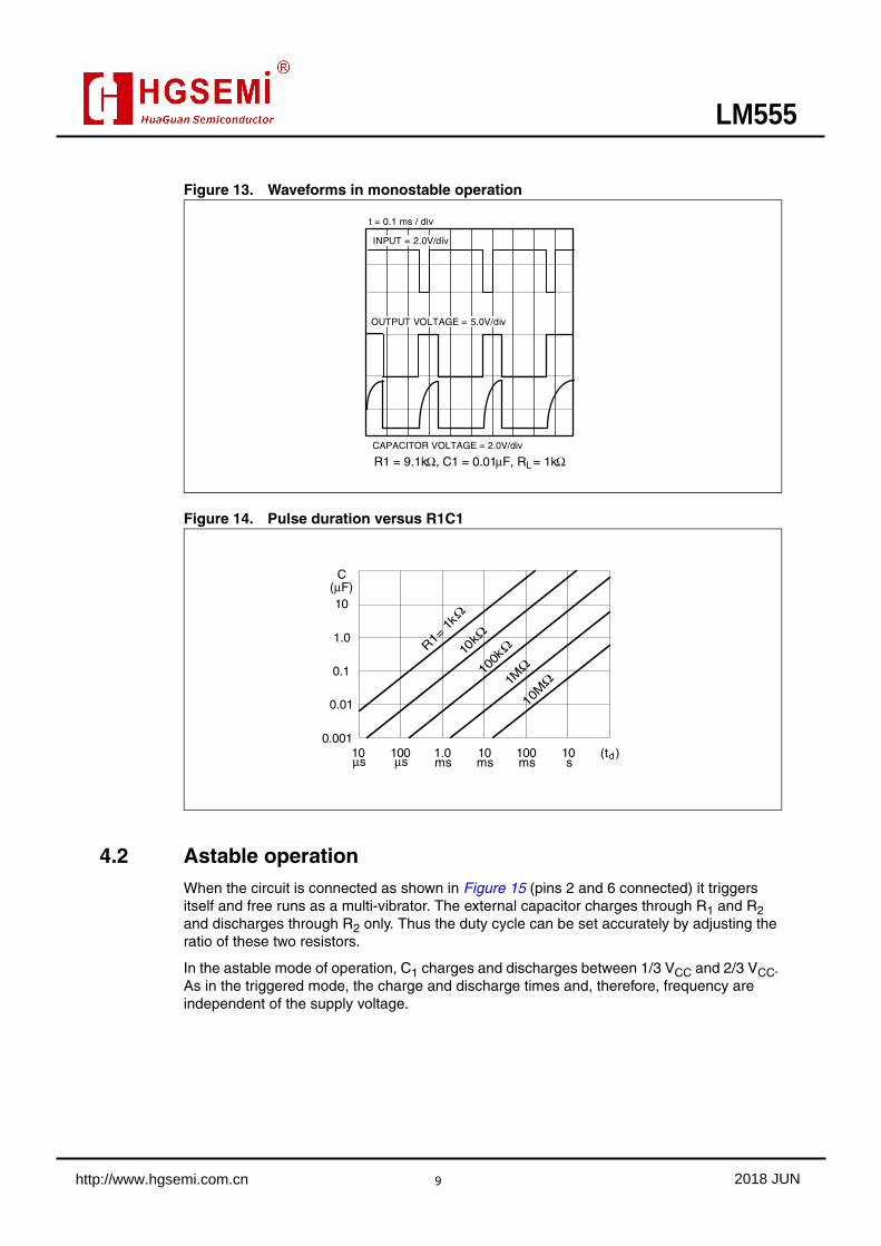
Figure 13. Waveforms in monostable operation
Figure 14. Pulse duration versus R1C1
4.2 Astable operationWhen the circuit is connected as shown in Figure 15 (pins 2 and 6 connected) it triggers itself and free runs as a multi-vibrator. The external capacitor charges through R1 and R2 and discharges through R2 only. Thus the duty cycle can be set accurately by adjusting the ratio of these two resistors.
In the astable mode of operation, C1 charges and discharges between 1/3 VCC and 2/3 VCC. As in the triggered mode, the charge and discharge times and, therefore, frequency are independent of the supply voltage.
CAPACITOR VOLTAGE = 2.0V/div
t = 0.1 ms / div
INPUT = 2.0V/div
OUTPUT VOLTAGE = 5.0V/div
R1 = 9.1kΩ, C1 = 0.01μF, R = 1kΩL
C(μF)10
1.0
0.1
0.01
0.00110 100 1.0 10 100 10 (t )dμs μs ms ms ms s
10M
Ω1MΩ10
0kΩ10
kΩR1= 1
kΩ
LM555
9 http://www.hgsemi.com.cn 2018 JUN
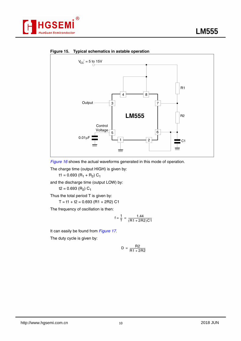
Figure 15. Typical schematics in astable operation
Figure 16 shows the actual waveforms generated in this mode of operation.
The charge time (output HIGH) is given by:
t1 = 0.693 (R1 + R2) C1
and the discharge time (output LOW) by:
t2 = 0.693 (R2) C1
Thus the total period T is given by:
T = t1 + t2 = 0.693 (R1 + 2R2) C1
The frequency of oscillation is then:
It can easily be found from Figure 17.
The duty cycle is given by:
Output 3
4 8
7
5
1
R1
C12
6
R2
ControlVoltage
LM555
VCC = 5 to 15V
0.01μF
f = 1T--- 1.44
R1 2R2+( )C1---------------------------------------=
D R2R1 2R2+--------------------------=
LM555
10 http://www.hgsemi.com.cn 2018 JUN
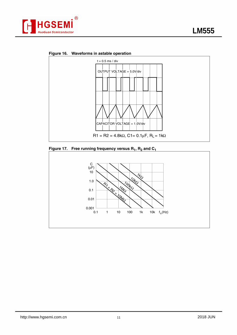
Figure 16. Waveforms in astable operation
Figure 17. Free running frequency versus R1, R2 and C1
t = 0.5 ms / div
OUTPUT VOLTAGE = 5.0V/div
CAPACITOR VOLTAGE = 1.0V/div
R1 = R2 = 4.8kΩ, C1= 0.1μF, R = 1kΩL
C(μF)10
1.0
0.1
0.01
0.0010.1 1 10 100 1k 10k f (Hz)o
1MΩ
R1 + R2 = 10MΩ
100kΩ
10kΩ
1kΩ
LM555
11 http://www.hgsemi.com.cn 2018 JUN
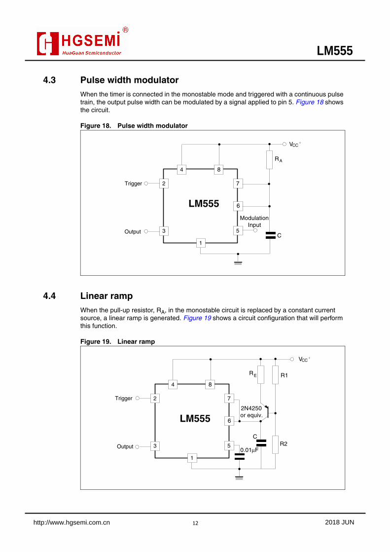
4.3 Pulse width modulatorWhen the timer is connected in the monostable mode and triggered with a continuous pulse train, the output pulse width can be modulated by a signal applied to pin 5. Figure 18 shows the circuit.
Figure 18. Pulse width modulator
4.4 Linear rampWhen the pull-up resistor, RA, in the monostable circuit is replaced by a constant current source, a linear ramp is generated. Figure 19 shows a circuit configuration that will perform this function.
Figure 19. Linear ramp
Trigger
Output
R
C
LM555
2
4
3
1
5
6
7
ModulationInput
8
A
VCC
Trigger
Output
C
LM555
2
4
3
1
5
6
7
8
E
VCC
0.01μFR2
R1R
2N4250or equiv.
LM555
12 http://www.hgsemi.com.cn 2018 JUN
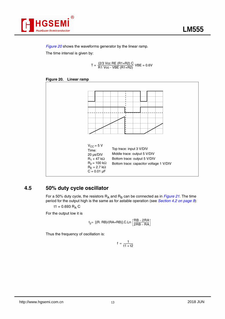
Figure 20 shows the waveforms generator by the linear ramp.
The time interval is given by:
Figure 20. Linear ramp
4.5 50% duty cycle oscillatorFor a 50% duty cycle, the resistors RA and RB can be connected as in Figure 21. The time period for the output high is the same as for astable operation (see Section 4.2 on page 9):
t1 = 0.693 RA C
For the output low it is
Thus the frequency of oscillation is:
T = (2/3 Vcc RE (R1+R2) CR1 Vcc - VBE (R1+R2)---------------------------------------------------------------- VBE = 0.6V
VCC = 5 VTime: 20 µs/DIVR1 + 47 kΩR2 = 100 kΩRE = 2.7 kΩC = 0.01 µF
Top trace: input 3 V/DIV
Middle trace: output 5 V/DIVBottom trace: output 5 V/DIV
Bottom trace: capacitor voltage 1 V/DIV
t2 [(R. RB)/(RA+RB)].C.Ln RB 2RA–2RB RA–---------------------------=
f 1t1 t2+-----------------=
LM555
13 http://www.hgsemi.com.cn 2018 JUN
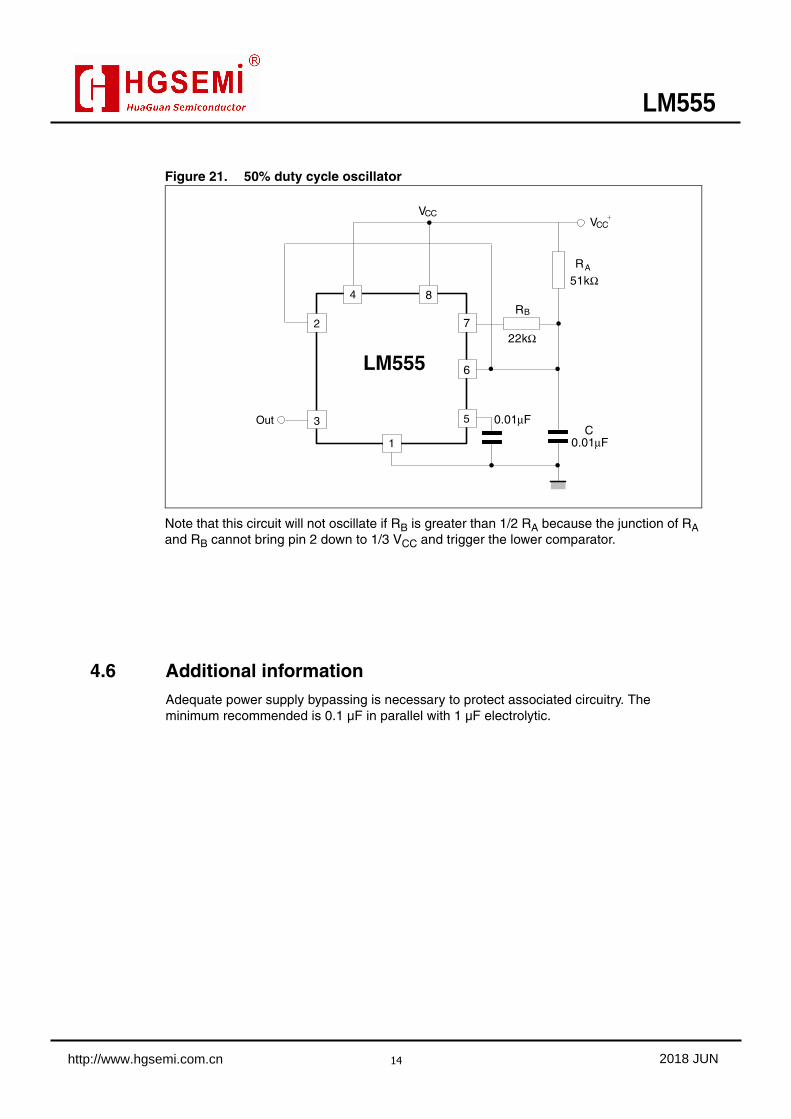
Figure 21. 50% duty cycle oscillator
Note that this circuit will not oscillate if RB is greater than 1/2 RA because the junction of RA and RB cannot bring pin 2 down to 1/3 VCC and trigger the lower comparator.
4.6 Additional informationAdequate power supply bypassing is necessary to protect associated circuitry. The minimum recommended is 0.1 µF in parallel with 1 µF electrolytic.
Out
RA
C
LM555
2
4
3
1
5
6
7
8
VCC
51kΩ
RB
22kΩ
0.01μF
VCC
0.01μF
LM555
14 http://www.hgsemi.com.cn 2018 JUN
LM555
15 http://www.hgsemi.com.cn 2018 JUN
Important statement:
Huaguan Semiconductor Co,Ltd. reserves the right to changethe products and services provided without notice. Customersshould obtain the latest relevant information before ordering,and verify the timeliness and accuracy of this information.
Customers are responsible for complying with safetystandards and taking safety measures when using ourproducts for system design and machine manufacturing toavoid potential risks that may result in personal injury orproperty damage.
Our products are not licensed for applications in life support,military, aerospace, etc., so we do not bear the consequencesof the application of these products in these fields.
Our documentation is only permitted to be copied withoutany tampering with the content, so we do not accept anyresponsibility or liability for the altered documents.