Leonardo Synthesis and Technology Guide - CS - Huji
348
Leonardo Synthesis and Technology Guide Release 4.2
-
Upload
khangminh22 -
Category
Documents
-
view
0 -
download
0
Transcript of Leonardo Synthesis and Technology Guide - CS - Huji

Leonardo Synthesis andTechnology Guide
Release 4.2
Copyright
Copyright © 1991-1998 Exemplar Logic, Inc.
All Rights Reserved
ium
Trademarks
Exemplar Logic® and its Logo are registered trademarks of Exemplar Logic, Inc.; Galileo™, Galileo Extreme™, Leonardo™, Galileo FS™ and MODGEN™ are trademarks of Exemplar Logic, Inc.; Extreme Technology, FAST Synthesis and Synthesizing the next Millennare servicemarks of Exemplar Logic, Inc. V-System/VHDL™ and V-System/Verilog™ are trademarks of Model Technology, Inc.Verilog® and Verilog-XL® are registered trademarks of Cadence Design Systems, Inc. All other trademarks remain the property of their respective owners.
Disclaimer
Although Exemplar Logic, Inc. has tested the software and reviewed the documentation, Exemplar Logic, Inc. makes no warranty or representation, either express or implied, with respect to this soft-ware and documentation, its quality, performance, merchantability, or fitness for a particular purpose.
Exemplar Logic, Inc.6503 Dumbarton CircleFremont, CA 94555Telephone: 800-632-3742email: [email protected]
Part No: EL-60015-R

1-1
1-2
1-2
1-2
1-3
1-3
1-3
1-3
1-3
1-3
1-3
1-4
1-4
1-4
2-1
2-2
2-2
2-2
2-2
2
2-7
2-8
2-8
2-9
3-1
3-1
3-1
3-2
3-5
3-5
3-7
Contents
1. Introduction . . . . . . . . . . . . . . . . . . . . . . . . . . . . . . . . . . . . . . . . . . . . . . .About Leonardo’s Manuals . . . . . . . . . . . . . . . . . . . . . . . . . . . . . . . . . . . . . . . . . . . . .
Installation Guide . . . . . . . . . . . . . . . . . . . . . . . . . . . . . . . . . . . . . . . . . . . . . . .
User’s Guide . . . . . . . . . . . . . . . . . . . . . . . . . . . . . . . . . . . . . . . . . . . . . . . . . . .
Synthesis and Technology Guide . . . . . . . . . . . . . . . . . . . . . . . . . . . . . . . . . . .
Command Reference Guide . . . . . . . . . . . . . . . . . . . . . . . . . . . . . . . . . . . . . . .
HDL Synthesis Guide . . . . . . . . . . . . . . . . . . . . . . . . . . . . . . . . . . . . . . . . . . . .
More About Leonardo . . . . . . . . . . . . . . . . . . . . . . . . . . . . . . . . . . . . . . . . . . . . . . . . .
Available Online . . . . . . . . . . . . . . . . . . . . . . . . . . . . . . . . . . . . . . . . . . . . . . . .
Available Help . . . . . . . . . . . . . . . . . . . . . . . . . . . . . . . . . . . . . . . . . . . . . . . . .
Available Libraries . . . . . . . . . . . . . . . . . . . . . . . . . . . . . . . . . . . . . . . . . . . . . .
Screen Shots, Reports, and Filenames. . . . . . . . . . . . . . . . . . . . . . . . . . . . . . . .
Time Module License . . . . . . . . . . . . . . . . . . . . . . . . . . . . . . . . . . . . . . . . . . . .
System Requirements and Runtime . . . . . . . . . . . . . . . . . . . . . . . . . . . . . . . . . . . . . . .
2. Technology Mapping . . . . . . . . . . . . . . . . . . . . . . . . . . . . . . . . . . . . . . . .
Before Beginning . . . . . . . . . . . . . . . . . . . . . . . . . . . . . . . . . . . . . . . . . . . . . . . . . . . . .
Boolean Mapping . . . . . . . . . . . . . . . . . . . . . . . . . . . . . . . . . . . . . . . . . . . . . . . . . . . . .
Lookup Table Mapping . . . . . . . . . . . . . . . . . . . . . . . . . . . . . . . . . . . . . . . . . . . . . . . .
Command Line and GUI Options . . . . . . . . . . . . . . . . . . . . . . . . . . . . . . . . . .
I/O Mapping . . . . . . . . . . . . . . . . . . . . . . . . . . . . . . . . . . . . . . . . . . . . . . . . . . . . . . . . . -7
Command Line and GUI Options . . . . . . . . . . . . . . . . . . . . . . . . . . . . . . . . . . .
Manual I/O Mapping . . . . . . . . . . . . . . . . . . . . . . . . . . . . . . . . . . . . . . . . . . . . . . . . . .
Setting Timing Constraints with GUI Constraint Editor . . . . . . . . . . . . . . . . . .
PAD and BUFFER_SIG Commands . . . . . . . . . . . . . . . . . . . . . . . . . . . . . . . . .
3. Timing Analysis . . . . . . . . . . . . . . . . . . . . . . . . . . . . . . . . . . . . . . . . . . . .
Before Beginning . . . . . . . . . . . . . . . . . . . . . . . . . . . . . . . . . . . . . . . . . . . . . . . . . . . . .
Static Timing Analysis . . . . . . . . . . . . . . . . . . . . . . . . . . . . . . . . . . . . . . . . . . . . . . . . .
Delay Models . . . . . . . . . . . . . . . . . . . . . . . . . . . . . . . . . . . . . . . . . . . . . . . . . .
Timing Analysis Before and After Place-and-Route . . . . . . . . . . . . . . . . . . . . .
Defining Process, Temperature, and Voltage Values . . . . . . . . . . . . . . . . . . . . .
Critical Path Report . . . . . . . . . . . . . . . . . . . . . . . . . . . . . . . . . . . . . . . . . . . . .
iii
3-7
3-8
3-8
3-9
3-11
3-11
-12
3-12
4-1
4-1
4-1
4-2
4-2
4-3
4-6
4-8
4-9
4-9
4-9
-1
5-1
5-1
5-2
5-3
5-5
5
5-14
6-1
6-1
6-1
6-4
6-5
Back-Annotation. . . . . . . . . . . . . . . . . . . . . . . . . . . . . . . . . . . . . . . . . . . . . . . . . . . . . .
SDF (Standard Delay Format) Writer . . . . . . . . . . . . . . . . . . . . . . . . . . . . . . . .
Design Flow . . . . . . . . . . . . . . . . . . . . . . . . . . . . . . . . . . . . . . . . . . . . . . . . . . .
VITAL Libraries . . . . . . . . . . . . . . . . . . . . . . . . . . . . . . . . . . . . . . . . . . . . . . . .
Standard Delay Format (SDF) for Transporting Delays . . . . . . . . . . . . . . . . . .
Post Synthesis RTL (Register Transfer Level) Simulation . . . . . . . . . . . . . . . . . . . . .
First Application . . . . . . . . . . . . . . . . . . . . . . . . . . . . . . . . . . . . . . . . . . . . . . . . 3
Second Application . . . . . . . . . . . . . . . . . . . . . . . . . . . . . . . . . . . . . . . . . . . . . .
4. Timing Constraints . . . . . . . . . . . . . . . . . . . . . . . . . . . . . . . . . . . . . . . . . .
Before Beginning . . . . . . . . . . . . . . . . . . . . . . . . . . . . . . . . . . . . . . . . . . . . . . . . . . . . .
Setting Global Constraints . . . . . . . . . . . . . . . . . . . . . . . . . . . . . . . . . . . . . . . . . . . . . .
Setting Constraints on Individual Signals. . . . . . . . . . . . . . . . . . . . . . . . . . . . . . . . . . .
Load and Drive Specifications . . . . . . . . . . . . . . . . . . . . . . . . . . . . . . . . . . . . .
Timing Specifications . . . . . . . . . . . . . . . . . . . . . . . . . . . . . . . . . . . . . . . . . . . .
Usage of Timing Constraints in Leonardo . . . . . . . . . . . . . . . . . . . . . . . . . . . . . . . . . .
New Constraint Features. . . . . . . . . . . . . . . . . . . . . . . . . . . . . . . . . . . . . . . . . . . . . . . .
Constraint Driven Timing Optimization . . . . . . . . . . . . . . . . . . . . . . . . . . . . . .
Support for Maximum Frequency . . . . . . . . . . . . . . . . . . . . . . . . . . . . . . . . . . .
Support for Multicycle Path . . . . . . . . . . . . . . . . . . . . . . . . . . . . . . . . . . . . . . .
5. Timing Optimization . . . . . . . . . . . . . . . . . . . . . . . . . . . . . . . . . . . . . . . . 5
Before Beginning . . . . . . . . . . . . . . . . . . . . . . . . . . . . . . . . . . . . . . . . . . . . . . . . . . . . .
Optimization Flow . . . . . . . . . . . . . . . . . . . . . . . . . . . . . . . . . . . . . . . . . . . . . . . . . . . .
Delay Optimization. . . . . . . . . . . . . . . . . . . . . . . . . . . . . . . . . . . . . . . . . . . . . . . . . . . .
Setting Timing Constraints . . . . . . . . . . . . . . . . . . . . . . . . . . . . . . . . . . . . . . . .
User Control . . . . . . . . . . . . . . . . . . . . . . . . . . . . . . . . . . . . . . . . . . . . . . . . . . .
Statistics Report . . . . . . . . . . . . . . . . . . . . . . . . . . . . . . . . . . . . . . . . . . . . . . . . . . . . . . -6
Automatic Constraining of Designs . . . . . . . . . . . . . . . . . . . . . . . . . . . . . . . . . . . . . . .
6. Reports . . . . . . . . . . . . . . . . . . . . . . . . . . . . . . . . . . . . . . . . . . . . . . . . . . .
Xilinx Area/Delay Example Reports . . . . . . . . . . . . . . . . . . . . . . . . . . . . . . . . . . . . . .
Area Reporting . . . . . . . . . . . . . . . . . . . . . . . . . . . . . . . . . . . . . . . . . . . . . . . . .
Delay Estimates . . . . . . . . . . . . . . . . . . . . . . . . . . . . . . . . . . . . . . . . . . . . . . . .
Altera FLEX Area/Delay Example Reports . . . . . . . . . . . . . . . . . . . . . . . . . . . . . . . . .
iv Leonardo Synthesis and Technology Guide

6-6
6-9
7-1
7-1
7-
7-4
7-4
7-5
7-5
7-5
7-7
7-8
7-8
7-9
7-1
7-12
7-13
7-14
7-14
7-18
8-1
8-2
8-2
8-2
8-2
8-
8-5
8-5
8-5
8-5
8-5
Area Reporting . . . . . . . . . . . . . . . . . . . . . . . . . . . . . . . . . . . . . . . . . . . . . . . . .
Delay Estimates . . . . . . . . . . . . . . . . . . . . . . . . . . . . . . . . . . . . . . . . . . . . . . . .
7. Synthesis for ASIC Technologies . . . . . . . . . . . . . . . . . . . . . . . . . . . . . . .
Before Beginning . . . . . . . . . . . . . . . . . . . . . . . . . . . . . . . . . . . . . . . . . . . . . . . . . . . . .
Design Flows . . . . . . . . . . . . . . . . . . . . . . . . . . . . . . . . . . . . . . . . . . . . . . . . . . . . . . . . 1
Hierarchy . . . . . . . . . . . . . . . . . . . . . . . . . . . . . . . . . . . . . . . . . . . . . . . . . . . . .
Design Partitioning . . . . . . . . . . . . . . . . . . . . . . . . . . . . . . . . . . . . . . . . . . . . . .
Optimization Features. . . . . . . . . . . . . . . . . . . . . . . . . . . . . . . . . . . . . . . . . . . . . . . . . .
Data-Path Synthesis . . . . . . . . . . . . . . . . . . . . . . . . . . . . . . . . . . . . . . . . . . . . .
New ASIC Modgen . . . . . . . . . . . . . . . . . . . . . . . . . . . . . . . . . . . . . . . . . . . . . . . . . . .
Technology Mapping . . . . . . . . . . . . . . . . . . . . . . . . . . . . . . . . . . . . . . . . . . . .
Constraint-Driven Timing Optimization . . . . . . . . . . . . . . . . . . . . . . . . . . . . . .
Gate Sizing . . . . . . . . . . . . . . . . . . . . . . . . . . . . . . . . . . . . . . . . . . . . . . . . . . . .
Design Rule Constraints . . . . . . . . . . . . . . . . . . . . . . . . . . . . . . . . . . . . . . . . . .
Timing Analysis . . . . . . . . . . . . . . . . . . . . . . . . . . . . . . . . . . . . . . . . . . . . . . . . . . . . . . 2
Issues in Delay Modeling . . . . . . . . . . . . . . . . . . . . . . . . . . . . . . . . . . . . . . . . .
Modeling Interconnects. . . . . . . . . . . . . . . . . . . . . . . . . . . . . . . . . . . . . . . . . . .
Area and Delay Reporting . . . . . . . . . . . . . . . . . . . . . . . . . . . . . . . . . . . . . . . . . . . . . .
Area Report. . . . . . . . . . . . . . . . . . . . . . . . . . . . . . . . . . . . . . . . . . . . . . . . . . . .
Delay Report . . . . . . . . . . . . . . . . . . . . . . . . . . . . . . . . . . . . . . . . . . . . . . . . . . .
8. Actel Synthesis . . . . . . . . . . . . . . . . . . . . . . . . . . . . . . . . . . . . . . . . . . . . .
Before Beginning . . . . . . . . . . . . . . . . . . . . . . . . . . . . . . . . . . . . . . . . . . . . . . . . . . . . .
Actel FPGA Architecture . . . . . . . . . . . . . . . . . . . . . . . . . . . . . . . . . . . . . . . . . . . . . . .
Actel Logic Module . . . . . . . . . . . . . . . . . . . . . . . . . . . . . . . . . . . . . . . . . . . . .
I/O Buffers . . . . . . . . . . . . . . . . . . . . . . . . . . . . . . . . . . . . . . . . . . . . . . . . . . . .
Design Flows . . . . . . . . . . . . . . . . . . . . . . . . . . . . . . . . . . . . . . . . . . . . . . . . . . . . . . . . 2
New Features for Actel . . . . . . . . . . . . . . . . . . . . . . . . . . . . . . . . . . . . . . . . . . . . . . . . .
New Operators . . . . . . . . . . . . . . . . . . . . . . . . . . . . . . . . . . . . . . . . . . . . . . . . .
Improvements to Mapper . . . . . . . . . . . . . . . . . . . . . . . . . . . . . . . . . . . . . . . . .
Accurate Delay Estimations . . . . . . . . . . . . . . . . . . . . . . . . . . . . . . . . . . . . . . .
Logic Replication and Buffering. . . . . . . . . . . . . . . . . . . . . . . . . . . . . . . . . . . .
v
8-5
8-5
8-6
8-6
8-6
8-7
8-7
8-7
8-11
-11
8-14
-14
8-15
8-15
8-18
-18
8-21
8-25
9-1
9-1
9-2
9
9-5
9-5
9-7
9-9
-11
9-20
-22
9-24
Fanout Violations and Load Violations . . . . . . . . . . . . . . . . . . . . . . . . . . . . . . .
Reduced Memory Consumption . . . . . . . . . . . . . . . . . . . . . . . . . . . . . . . . . . . .
Enhancements to Actel Technologies . . . . . . . . . . . . . . . . . . . . . . . . . . . . . . . .
Modgen Enhancements . . . . . . . . . . . . . . . . . . . . . . . . . . . . . . . . . . . . . . . . . . .
Synthesis and Optimization Features . . . . . . . . . . . . . . . . . . . . . . . . . . . . . . . . . . . . . .
Technology Mapping . . . . . . . . . . . . . . . . . . . . . . . . . . . . . . . . . . . . . . . . . . . .
Data Path Synthesis . . . . . . . . . . . . . . . . . . . . . . . . . . . . . . . . . . . . . . . . . . . . . . . . . . .
Modgen . . . . . . . . . . . . . . . . . . . . . . . . . . . . . . . . . . . . . . . . . . . . . . . . . . . . . . .
Constraint-Driven Timing Optimization . . . . . . . . . . . . . . . . . . . . . . . . . . . . . . . . . . .
Interfacing with Actel’s ACTGen . . . . . . . . . . . . . . . . . . . . . . . . . . . . . . . . . . . 8
Additional Synthesis Features . . . . . . . . . . . . . . . . . . . . . . . . . . . . . . . . . . . . . . . . . . .
Logic Combinability . . . . . . . . . . . . . . . . . . . . . . . . . . . . . . . . . . . . . . . . . . . . . 8
Fanout and Load Violations . . . . . . . . . . . . . . . . . . . . . . . . . . . . . . . . . . . . . . .
Using Global Clock Buffers . . . . . . . . . . . . . . . . . . . . . . . . . . . . . . . . . . . . . . .
Design I/O. . . . . . . . . . . . . . . . . . . . . . . . . . . . . . . . . . . . . . . . . . . . . . . . . . . . . . . . . . . 8-18
I/O Mapping . . . . . . . . . . . . . . . . . . . . . . . . . . . . . . . . . . . . . . . . . . . . . . . . . . .
Complex I/O Design Rule Checker and Modifier . . . . . . . . . . . . . . . . . . . . . . . 8
Assigning Device Pin Numbers . . . . . . . . . . . . . . . . . . . . . . . . . . . . . . . . . . . .
Reporting . . . . . . . . . . . . . . . . . . . . . . . . . . . . . . . . . . . . . . . . . . . . . . . . . . . . . . . . . . . 8-24
Process Derating Factors . . . . . . . . . . . . . . . . . . . . . . . . . . . . . . . . . . . . . . . . . . . . . . .
9. Altera FLEX Synthesis . . . . . . . . . . . . . . . . . . . . . . . . . . . . . . . . . . . . . . .
Before Beginning . . . . . . . . . . . . . . . . . . . . . . . . . . . . . . . . . . . . . . . . . . . . . . . . . . . . .
Altera FLEX Architecture . . . . . . . . . . . . . . . . . . . . . . . . . . . . . . . . . . . . . . . . . . . . . .
Design Flow . . . . . . . . . . . . . . . . . . . . . . . . . . . . . . . . . . . . . . . . . . . . . . . . . . . . . . . . . -2
Synthesis and Optimization Features . . . . . . . . . . . . . . . . . . . . . . . . . . . . . . . . . . . . . .
Fanin Limited Optimization . . . . . . . . . . . . . . . . . . . . . . . . . . . . . . . . . . . . . . .
Lookup Table Mapping . . . . . . . . . . . . . . . . . . . . . . . . . . . . . . . . . . . . . . . . . . .
Data Path Synthesis and Modgen Implementation . . . . . . . . . . . . . . . . . . . . . .
LPM Support for FLEX 10K . . . . . . . . . . . . . . . . . . . . . . . . . . . . . . . . . . . . . . 9
Genmem Support . . . . . . . . . . . . . . . . . . . . . . . . . . . . . . . . . . . . . . . . . . . . . . .
Embedded Array Block (EAB) Support for FLEX 10K. . . . . . . . . . . . . . . . . . . . . . . . 9
Additional Optimization Features. . . . . . . . . . . . . . . . . . . . . . . . . . . . . . . . . . . . . . . . .
vi Leonardo Synthesis and Technology Guide
9-24
9-24
9-25
9-25
9-27
9-28
9-28
-29
9-29
-30
-30
31
9-32
9-33
33
9-33
9-34
9-35
9-35
9-38
9-38
9-39
9-41
0-1
10-1
10-1
1
0-5
10-7
10-8
0-8
Sequential Optimization . . . . . . . . . . . . . . . . . . . . . . . . . . . . . . . . . . . . . . . . . .
Altera FLEX Reports . . . . . . . . . . . . . . . . . . . . . . . . . . . . . . . . . . . . . . . . . . . . . . . . . .
Design I/O. . . . . . . . . . . . . . . . . . . . . . . . . . . . . . . . . . . . . . . . . . . . . . . . . . . . . . . . . . . 9-25
Global Signals. . . . . . . . . . . . . . . . . . . . . . . . . . . . . . . . . . . . . . . . . . . . . . . . . .
Pin Location . . . . . . . . . . . . . . . . . . . . . . . . . . . . . . . . . . . . . . . . . . . . . . . . . . .
Writing EDIF Output . . . . . . . . . . . . . . . . . . . . . . . . . . . . . . . . . . . . . . . . . . . . . . . . . .
Using FLEX Designs as Input to Leonardo . . . . . . . . . . . . . . . . . . . . . . . . . . . . . . . . .
EDIF Input . . . . . . . . . . . . . . . . . . . . . . . . . . . . . . . . . . . . . . . . . . . . . . . . . . . .
How to Get Best Results with MAX+PLUS II. . . . . . . . . . . . . . . . . . . . . . . . . . . . . . . 9
Altera Synthesis with Leonardo . . . . . . . . . . . . . . . . . . . . . . . . . . . . . . . . . . . .
Place-and-Route using MAX+PLUS II . . . . . . . . . . . . . . . . . . . . . . . . . . . . . . . 9
Flow 1: Altera Primitives are Mapped by Leonardo . . . . . . . . . . . . . . . . . . . . . 9
Flow 2: Altera Primitives are Mapped by MAX+PLUS II . . . . . . . . . . . . . . . . 9-
Additional Settings to Get Faster Designs . . . . . . . . . . . . . . . . . . . . . . . . . . . .
New Features for Altera FLEX. . . . . . . . . . . . . . . . . . . . . . . . . . . . . . . . . . . . . . . . . . .
MAX+PLUS II Integration and Generation of ACF File . . . . . . . . . . . . . . . . . 9-
New Command Line Switches . . . . . . . . . . . . . . . . . . . . . . . . . . . . . . . . . . . . .
ACF File Generation. . . . . . . . . . . . . . . . . . . . . . . . . . . . . . . . . . . . . . . . . . . . .
ACF Example . . . . . . . . . . . . . . . . . . . . . . . . . . . . . . . . . . . . . . . . . . . . . . . . . .
User Options . . . . . . . . . . . . . . . . . . . . . . . . . . . . . . . . . . . . . . . . . . . . . . . . . . .
New Features for Altera FLEX. . . . . . . . . . . . . . . . . . . . . . . . . . . . . . . . . . . . . . . . . . .
Enhancements to Modgen . . . . . . . . . . . . . . . . . . . . . . . . . . . . . . . . . . . . . . . . .
Quality of Area and Delay Results . . . . . . . . . . . . . . . . . . . . . . . . . . . . . . . . . .
Altera FLEX Family Supported Devices . . . . . . . . . . . . . . . . . . . . . . . . . . . . . . . . . . .
10. Altera MAX Synthesis . . . . . . . . . . . . . . . . . . . . . . . . . . . . . . . . . . . . . . . 1
Before Beginning . . . . . . . . . . . . . . . . . . . . . . . . . . . . . . . . . . . . . . . . . . . . . . . . . . . . .
Altera MAX Architecture . . . . . . . . . . . . . . . . . . . . . . . . . . . . . . . . . . . . . . . . . . . . . . .
Design Flow . . . . . . . . . . . . . . . . . . . . . . . . . . . . . . . . . . . . . . . . . . . . . . . . . . . . . . . . . 0-2
Library Mapping File (LMF) . . . . . . . . . . . . . . . . . . . . . . . . . . . . . . . . . . . . . . 1
Synthesis and Optimization Features . . . . . . . . . . . . . . . . . . . . . . . . . . . . . . . . . . . . . .
Optimization Style Points . . . . . . . . . . . . . . . . . . . . . . . . . . . . . . . . . . . . . . . . . . . . . . .
Quality of Optimization . . . . . . . . . . . . . . . . . . . . . . . . . . . . . . . . . . . . . . . . . . 1
vii
10-8
10-8
10-9
10-9
0-10
0-10
1-1
11-1
11-2
11-5
1-5
1-5
1-6
1-8
-10
11-10
1-11
11-28
1-28
1-28
1-29
1-29
1-31
11-31
1-31
11-32
11-32
11-37
1-37
Sequential Optimization . . . . . . . . . . . . . . . . . . . . . . . . . . . . . . . . . . . . . . . . . .
Reporting . . . . . . . . . . . . . . . . . . . . . . . . . . . . . . . . . . . . . . . . . . . . . . . . . . . . . . . . . . . 10-8
Design I/O. . . . . . . . . . . . . . . . . . . . . . . . . . . . . . . . . . . . . . . . . . . . . . . . . . . . . . . . . . . 10-8
Global Signals. . . . . . . . . . . . . . . . . . . . . . . . . . . . . . . . . . . . . . . . . . . . . . . . . .
Additional Options . . . . . . . . . . . . . . . . . . . . . . . . . . . . . . . . . . . . . . . . . . . . . . . . . . . .
Max Fanin and Max Cubes . . . . . . . . . . . . . . . . . . . . . . . . . . . . . . . . . . . . . . . .
Using MAX Designs as Input to Leonardo . . . . . . . . . . . . . . . . . . . . . . . . . . . . . . . . . 1
EDIF Input . . . . . . . . . . . . . . . . . . . . . . . . . . . . . . . . . . . . . . . . . . . . . . . . . . . . 1
11. Lucent ORCA Synthesis. . . . . . . . . . . . . . . . . . . . . . . . . . . . . . . . . . . . . . 1
Before Beginning . . . . . . . . . . . . . . . . . . . . . . . . . . . . . . . . . . . . . . . . . . . . . . . . . . . . .
FPGA Architecture . . . . . . . . . . . . . . . . . . . . . . . . . . . . . . . . . . . . . . . . . . . . . . . . . . . .
Synthesis and Optimization Features . . . . . . . . . . . . . . . . . . . . . . . . . . . . . . . . . . . . . .
Optimization Algorithms . . . . . . . . . . . . . . . . . . . . . . . . . . . . . . . . . . . . . . . . . 1
Fanin Limited Optimization . . . . . . . . . . . . . . . . . . . . . . . . . . . . . . . . . . . . . . . 1
Lookup Table (LUT) Mapping . . . . . . . . . . . . . . . . . . . . . . . . . . . . . . . . . . . . . 1
Leonardo Variables to Control Optimization and Mapping. . . . . . . . . . . . . . . . 1
Constraint-Driven Timing Optimization . . . . . . . . . . . . . . . . . . . . . . . . . . . . . . 11
Data Path Synthesis (Modgen) . . . . . . . . . . . . . . . . . . . . . . . . . . . . . . . . . . . . .
Using ORCA Architectural Features. . . . . . . . . . . . . . . . . . . . . . . . . . . . . . . . . 1
ORCA Reporting . . . . . . . . . . . . . . . . . . . . . . . . . . . . . . . . . . . . . . . . . . . . . . . . . . . . .
Generation of ORCA Foundry Properties from Leonardo . . . . . . . . . . . . . . . . . . . . . . 1
Pin Number Property - LOC . . . . . . . . . . . . . . . . . . . . . . . . . . . . . . . . . . . . . . 1
Slew Property . . . . . . . . . . . . . . . . . . . . . . . . . . . . . . . . . . . . . . . . . . . . . . . . . . 1
ORCA DIN/DOUT Attributes . . . . . . . . . . . . . . . . . . . . . . . . . . . . . . . . . . . . . . . . . . . 1
Part Number - PICSPEC . . . . . . . . . . . . . . . . . . . . . . . . . . . . . . . . . . . . . . . . . . 1
Speed Grade - PICSPEED . . . . . . . . . . . . . . . . . . . . . . . . . . . . . . . . . . . . . . . .
ORCA Foundry Properties on IOBs . . . . . . . . . . . . . . . . . . . . . . . . . . . . . . . . . 1
Other Foundry Properties . . . . . . . . . . . . . . . . . . . . . . . . . . . . . . . . . . . . . . . . .
ORCA Preference File Writer. . . . . . . . . . . . . . . . . . . . . . . . . . . . . . . . . . . . . . . . . . . .
Preference File . . . . . . . . . . . . . . . . . . . . . . . . . . . . . . . . . . . . . . . . . . . . . . . . .
Additional Writing Preference File Features. . . . . . . . . . . . . . . . . . . . . . . . . . . 1
viii Leonardo Synthesis and Technology Guide
1-39
11-42
1-42
-43
-44
2-1
12-1
12-2
12-2
12-2
12-2
1
12-3
2-3
12-4
12-4
12-4
12-4
12-4
2-5
12-7
3-1
13-1
13-2
1
13-3
13-3
13-4
13-4
13-4
13-4
Devices Supported for Lucent ORCA FPGA Families . . . . . . . . . . . . . . . . . . . . . . . . 1
New Features for ORCA. . . . . . . . . . . . . . . . . . . . . . . . . . . . . . . . . . . . . . . . . . . . . . . .
ORCA Preference File . . . . . . . . . . . . . . . . . . . . . . . . . . . . . . . . . . . . . . . . . . . 1
ORCA3C and ORCA3T Multicycle Support . . . . . . . . . . . . . . . . . . . . . . . . . . 11
Mapping to ORCALUTs . . . . . . . . . . . . . . . . . . . . . . . . . . . . . . . . . . . . . . . . . . 11
12. QuickLogic Synthesis . . . . . . . . . . . . . . . . . . . . . . . . . . . . . . . . . . . . . . . . 1
Before Beginning . . . . . . . . . . . . . . . . . . . . . . . . . . . . . . . . . . . . . . . . . . . . . . . . . . . . .
FPGA Architecture . . . . . . . . . . . . . . . . . . . . . . . . . . . . . . . . . . . . . . . . . . . . . . . . . . . .
The pASIC Logic Cell . . . . . . . . . . . . . . . . . . . . . . . . . . . . . . . . . . . . . . . . . . .
I/O Buffers . . . . . . . . . . . . . . . . . . . . . . . . . . . . . . . . . . . . . . . . . . . . . . . . . . . .
New Features for QuickLogic. . . . . . . . . . . . . . . . . . . . . . . . . . . . . . . . . . . . . . . . . . . .
Design Flow . . . . . . . . . . . . . . . . . . . . . . . . . . . . . . . . . . . . . . . . . . . . . . . . . . . . . . . . . 2-2
Optimization Style Points . . . . . . . . . . . . . . . . . . . . . . . . . . . . . . . . . . . . . . . . . . . . . . .
Quality of Optimization . . . . . . . . . . . . . . . . . . . . . . . . . . . . . . . . . . . . . . . . . . 1
Combinational Logic Loops . . . . . . . . . . . . . . . . . . . . . . . . . . . . . . . . . . . . . . .
Sequential Optimization . . . . . . . . . . . . . . . . . . . . . . . . . . . . . . . . . . . . . . . . . .
Internal Tristates . . . . . . . . . . . . . . . . . . . . . . . . . . . . . . . . . . . . . . . . . . . . . . . .
QuickLogic Reports . . . . . . . . . . . . . . . . . . . . . . . . . . . . . . . . . . . . . . . . . . . . . . . . . . .
Process Derating Factors . . . . . . . . . . . . . . . . . . . . . . . . . . . . . . . . . . . . . . . . . . . . . . .
Design I/O. . . . . . . . . . . . . . . . . . . . . . . . . . . . . . . . . . . . . . . . . . . . . . . . . . . . . . . . . . . 12-5
Manual Assignment of I/O Buffers . . . . . . . . . . . . . . . . . . . . . . . . . . . . . . . . . . 1
Assigning Pin Locations . . . . . . . . . . . . . . . . . . . . . . . . . . . . . . . . . . . . . . . . . .
13. Xilinx CPLDs Synthesis . . . . . . . . . . . . . . . . . . . . . . . . . . . . . . . . . . . . . . 1
Before Beginning . . . . . . . . . . . . . . . . . . . . . . . . . . . . . . . . . . . . . . . . . . . . . . . . . . . . .
Xilinx CPLD Architecture . . . . . . . . . . . . . . . . . . . . . . . . . . . . . . . . . . . . . . . . . . . . . .
Design Flow . . . . . . . . . . . . . . . . . . . . . . . . . . . . . . . . . . . . . . . . . . . . . . . . . . . . . . . . . 3-2
Synthesis and Optimization Features . . . . . . . . . . . . . . . . . . . . . . . . . . . . . . . . . . . . . .
Special Synthesis Feature . . . . . . . . . . . . . . . . . . . . . . . . . . . . . . . . . . . . . . . . .
Other Synthesis Features . . . . . . . . . . . . . . . . . . . . . . . . . . . . . . . . . . . . . . . . . . . . . . .
Device Selection . . . . . . . . . . . . . . . . . . . . . . . . . . . . . . . . . . . . . . . . . . . . . . . .
I/O Buffers and Pads . . . . . . . . . . . . . . . . . . . . . . . . . . . . . . . . . . . . . . . . . . . . .
Pin (LOC) Assignment . . . . . . . . . . . . . . . . . . . . . . . . . . . . . . . . . . . . . . . . . . .
ix
13-4
3-5
13-7
4-1
14-2
4-2
4-2
14-2
14-2
14-5
14-7
4-7
-10
-11
-12
14-17
-20
4-51
4-54
14-5
4-57
4-58
4-65
-67
4-67
4-67
4-68
4
4-71
Module Generation . . . . . . . . . . . . . . . . . . . . . . . . . . . . . . . . . . . . . . . . . . . . . . . . . . . .
User Options for XC9500 Families Only . . . . . . . . . . . . . . . . . . . . . . . . . . . . . 1
Reporting . . . . . . . . . . . . . . . . . . . . . . . . . . . . . . . . . . . . . . . . . . . . . . . . . . . . . . . . . . . 13-6
Xilinx CPLD Family Supported Devices . . . . . . . . . . . . . . . . . . . . . . . . . . . . . . . . . . .
14. Xilinx LCA Synthesis . . . . . . . . . . . . . . . . . . . . . . . . . . . . . . . . . . . . . . . . 1
Before Beginning . . . . . . . . . . . . . . . . . . . . . . . . . . . . . . . . . . . . . . . . . . . . . . . . . . . . .
Xilinx LCA Architecture . . . . . . . . . . . . . . . . . . . . . . . . . . . . . . . . . . . . . . . . . . . . . . . 1
Configurable Logic Block. . . . . . . . . . . . . . . . . . . . . . . . . . . . . . . . . . . . . . . . . 1
Input/Output Block . . . . . . . . . . . . . . . . . . . . . . . . . . . . . . . . . . . . . . . . . . . . . .
Synthesis Design Flows . . . . . . . . . . . . . . . . . . . . . . . . . . . . . . . . . . . . . . . . . . . . . . . .
Design Flow Guidelines . . . . . . . . . . . . . . . . . . . . . . . . . . . . . . . . . . . . . . . . . .
Synthesis and Optimization Features . . . . . . . . . . . . . . . . . . . . . . . . . . . . . . . . . . . . . .
Fanin Limited Optimization . . . . . . . . . . . . . . . . . . . . . . . . . . . . . . . . . . . . . . . 1
Lookup Table (LUT) Mapping . . . . . . . . . . . . . . . . . . . . . . . . . . . . . . . . . . . . . 14
Constraint-Driven Timing Optimization . . . . . . . . . . . . . . . . . . . . . . . . . . . . . . 14
CLB Packing for Xilinx XC4000 Technology . . . . . . . . . . . . . . . . . . . . . . . . . 14
Data Path Synthesis (Modgen) . . . . . . . . . . . . . . . . . . . . . . . . . . . . . . . . . . . . .
Using Xilinx Architectural Features . . . . . . . . . . . . . . . . . . . . . . . . . . . . . . . . . 14
Design I/O. . . . . . . . . . . . . . . . . . . . . . . . . . . . . . . . . . . . . . . . . . . . . . . . . . . . . . . . . . . 14-50
Complex I/O Mapping . . . . . . . . . . . . . . . . . . . . . . . . . . . . . . . . . . . . . . . . . . . 1
Pin Location Assignment . . . . . . . . . . . . . . . . . . . . . . . . . . . . . . . . . . . . . . . . . 1
Reporting . . . . . . . . . . . . . . . . . . . . . . . . . . . . . . . . . . . . . . . . . . . . . . . . . . . . . . . . . . . 14-56
UsingTimespecs . . . . . . . . . . . . . . . . . . . . . . . . . . . . . . . . . . . . . . . . . . . . . . . . . . . . . . 6
User Interaction. . . . . . . . . . . . . . . . . . . . . . . . . . . . . . . . . . . . . . . . . . . . . . . . . 1
TIMESPECs . . . . . . . . . . . . . . . . . . . . . . . . . . . . . . . . . . . . . . . . . . . . . . . . . . . 1
Using Xilinx Attributes. . . . . . . . . . . . . . . . . . . . . . . . . . . . . . . . . . . . . . . . . . . . . . . . . 1
Additional Xilinx-Specific Options . . . . . . . . . . . . . . . . . . . . . . . . . . . . . . . . . . . . . . . 14
Using Enabled D Type Flip-Flops. . . . . . . . . . . . . . . . . . . . . . . . . . . . . . . . . . . 1
Use of Registered Logic in IOBs . . . . . . . . . . . . . . . . . . . . . . . . . . . . . . . . . . . 1
Part Number . . . . . . . . . . . . . . . . . . . . . . . . . . . . . . . . . . . . . . . . . . . . . . . . . . . 1
Writing XNF. . . . . . . . . . . . . . . . . . . . . . . . . . . . . . . . . . . . . . . . . . . . . . . . . . . . . . . . . 1-68
Using Xilinx Designs as Input to Leonardo . . . . . . . . . . . . . . . . . . . . . . . . . . . . . . . . . 1
x Leonardo Synthesis and Technology Guide
4-71
4-71
4-71
4-73
4-75
4-78
4-78
4-79
14-79
4-80
4-80
4-81
4-83
4-83
4-84
-85
4-90
15-1
15-1
15-2
Design Restrictions . . . . . . . . . . . . . . . . . . . . . . . . . . . . . . . . . . . . . . . . . . . . . . 1
XNF File Constructs Readable by Leonardo. . . . . . . . . . . . . . . . . . . . . . . . . . . 1
Preserving Logic in an XNF Netlist . . . . . . . . . . . . . . . . . . . . . . . . . . . . . . . . . 1
Global Set/Reset/Tristate . . . . . . . . . . . . . . . . . . . . . . . . . . . . . . . . . . . . . . . . . 1
I/Os in XNF . . . . . . . . . . . . . . . . . . . . . . . . . . . . . . . . . . . . . . . . . . . . . . . . . . . 1
External Signals . . . . . . . . . . . . . . . . . . . . . . . . . . . . . . . . . . . . . . . . . . . . . . . . 1
Interfacing with XBLOX . . . . . . . . . . . . . . . . . . . . . . . . . . . . . . . . . . . . . . . . . . . . . . . 1
New Xilinx Architecture Features . . . . . . . . . . . . . . . . . . . . . . . . . . . . . . . . . . . . . . . . 1
Modgen Enhancements . . . . . . . . . . . . . . . . . . . . . . . . . . . . . . . . . . . . . . . . . . .
Fast I/O Buffers . . . . . . . . . . . . . . . . . . . . . . . . . . . . . . . . . . . . . . . . . . . . . . . . 1
Quality of Area and Delay Results . . . . . . . . . . . . . . . . . . . . . . . . . . . . . . . . . . 1
Fast Xilinx Outputs . . . . . . . . . . . . . . . . . . . . . . . . . . . . . . . . . . . . . . . . . . . . . . 1
M1 Back Annotation Flow . . . . . . . . . . . . . . . . . . . . . . . . . . . . . . . . . . . . . . . . 1
SDF (Standard Delay Format) Writer . . . . . . . . . . . . . . . . . . . . . . . . . . . . . . . . 1
M1 Support . . . . . . . . . . . . . . . . . . . . . . . . . . . . . . . . . . . . . . . . . . . . . . . . . . . . 1
Implementing Boundary Scan for Xilinx 4000 FPGAs. . . . . . . . . . . . . . . . . . . 14
Xilinx FPGA Devices Supported . . . . . . . . . . . . . . . . . . . . . . . . . . . . . . . . . . . . . . . . . 1
15. New Technologies . . . . . . . . . . . . . . . . . . . . . . . . . . . . . . . . . . . . . . . . . . .
Vantis . . . . . . . . . . . . . . . . . . . . . . . . . . . . . . . . . . . . . . . . . . . . . . . . . . . . . . . . . . . . . . 15-1
Cypress . . . . . . . . . . . . . . . . . . . . . . . . . . . . . . . . . . . . . . . . . . . . . . . . . . . . . . . . . . . . . 15-1
Motorola MPA 1000. . . . . . . . . . . . . . . . . . . . . . . . . . . . . . . . . . . . . . . . . . . . . . . . . . .
Philips PS Cool Runner . . . . . . . . . . . . . . . . . . . . . . . . . . . . . . . . . . . . . . . . . . . . . . . .
xi

xii Leonardo Synthesis and Technology Guide
Introduction 1
ctive
erve ed to
the
fully can
Welcome to Leonardo with extreme technology. Leonardo is a versatile and interalogic synthesis, optimization, and analysis tool developed to allow the use of technology-independent design methods for Field Programmable Gate Arrays (FPGAs), Complex Programmable Logic Devices (CPLDs) and ASICs. You can efficiently and economically consolidate multiple designs into one design and presand manipulate the design hierarchy. The hardware description languages are usimplement the design.
Leonardo utilizes the most powerful state-of-the-art optimization technology to guarantee high-quality results for any targeted FPGA technology. Leonardo offersfollowing distinct features:
• Certified FPGA flows: Netlists and directives generated by Leonardo successpass through the back-end tools; and post place and route timing informationbe read and back-annotated by Leonardo's Time Module for timing and logicverification purposes.
• FPGA architecture specific module generation
• FPGA architecture specific optimization
• Accurate architecture specific timing analysis
• RTL and gate-level post-synthesis verification
• Timing back annotation
• Platform independence
• ASIC specific module generation
1-1
1
list or
s - line to DL
s
nd
and
Leonardo optimizes your designs for area and speed, and accepts designs in netVHDL and Verilog formats. Leonardo produces vendor specific netlists and designreports which estimate the performance of your design.
You can invoke Leonardo through a graphical user interface (GUI) on all platformUnix, Linux, and Windows 95 and NT. You can use Leonardo from the command and in batch mode and script files. Leonardo is designed to give you easy accessthree modules: Leonardo, Time Module, and Model Technology V-System/QuickHsimulator.
Leonardo provides a top-down verification flow through VHDL or Verilog with an SDF timing file. A VITAL or Verilog simulation library is also provided. Leonardo ifully integrated with Model Technology, Inc. (MTI) simulation environment.
About Leonardo’s Manuals
The following four guides are available in print and online:
• Installation Guide
• User’s Guide
• Synthesis and Technology Guide• Command Reference Guide
• HDL Synthesis Guide
Installation Guide
The Installation Guide provides you with the steps for multi-platform installation aFLEXlm License Administration.
User’s Guide
The User’s Guide allows you to start designing right away. Clear instructions are provided for the graphical user interface (GUI). In addition, GUI-managed options switches are listed, and examples of reports and message logs are provided. Theconstraint file commands are documented.
1-2 Leonardo Synthesis and Technology Guide
1
A
les.
eets f the
fter tion,
is
r.
A b
Synthesis and Technology Guide
This Synthesis and Technology Guide provides you with details on synthesis andoptimization. This guide explains the various design flows for synthesizing to FPGtechnologies.
Command Reference Guide
The Command Reference Guide presents a list of commands and a list of variab
HDL Synthesis Guide
The HDL Synthesis Guide presents you with “cookbook” information. This guide provides you with the design guidelines to achieve a circuit implementation that mthe timing and area constraints of a target, while using the high level abstraction oVHDL or Verilog source code.
More About Leonardo
Available Online
The four guides are available for viewing online with the Adobe Acrobat Reader aLeonardo and the Adobe Acrobat Reader are installed from the CD-ROM. In addithe guides can be viewed and printed with desktop utilities.
Available Help
When you run Leonardo, balloon help will automatically display when your cursorpositioned on certain fields. Most fields also offer context-sensitive help, which isaccessed by tabbing to the field and pressing F1. The online manuals are also accessible from the Help menu after you have installed the Adobe Acrobat Reade
Available Libraries
The Leonardo license automatically enables the synthesis libraries for most FPGtechnologies. The VITAL libraries for FPGAs are available. Check Exemplar’s wesite at www.exemplar.com for more information.
Introduction 1-3
1
gy
d for
k-
for pend
e to
were
Screen Shots, Reports, and Filenames
The screen shots, reports, and filename examples in this Synthesis and TechnoloGuide may differ slightly from the actual or most current screens and examples. Moreover, some screen shots may have options selected and filenames displayeillustration purposes only.
Time Module License
You must purchase a Time Module license from Exemplar Logic, Inc., to use bacannotation flows with Leonardo. Back-annotation is supported through VITAL libraries for the following technologies:
• Xilinx XC4000/E/EX/X/XL/XV (through M1 software only) and XC5200
• Altera FLEX 6K, FLEX 8K, FLEX 10K
• Actel Act1/2/3, 3200DX, 1200XL
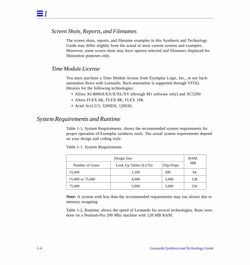
System Requirements and Runtime
Table 1-1, System Requirements, shows the recommended system requirementsproper operation of Exemplar synthesis tools. The actual system requirements deon your design and coding style.
Table 1-1. System Requirements
Note: A system with less than the recommended requirements may run slower dumemory swapping.
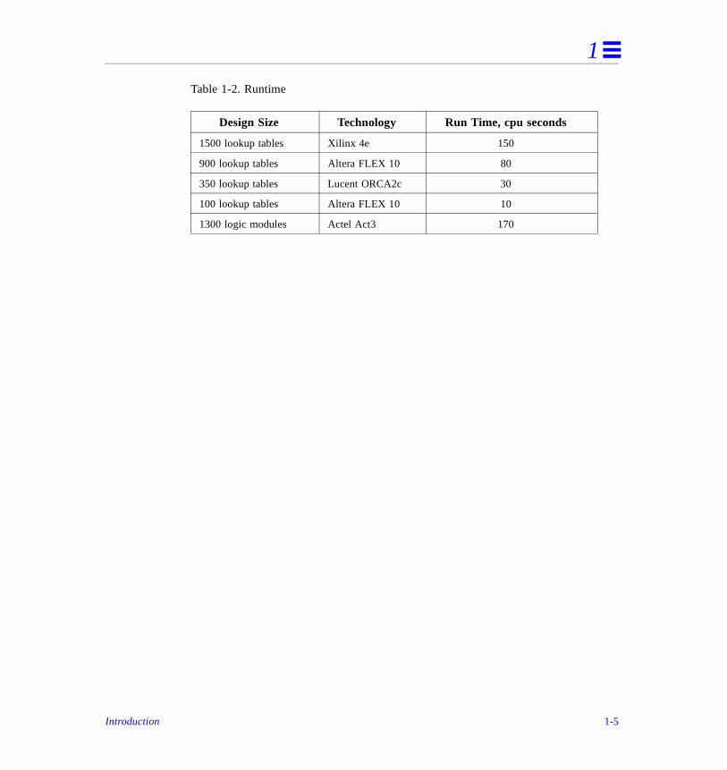
Table 1-2, Runtime, shows the speed of Leonardo for several technologies. Runsdone on a Pentium-Pro 200 Mhz machine with 128 MB RAM.
Design Size RAM, MB
Number of Gates Look Up Tables (LUTs) Flip-Flops
15,000 1,100 500 64
15,000 to 75,000 4,000 3,000 128
75,000 5,000 5,000 256
1-4 Leonardo Synthesis and Technology Guide
1
Table 1-2. Runtime
Design Size Technology Run Time, cpu seconds
1500 lookup tables Xilinx 4e 150
900 lookup tables Altera FLEX 10 80
350 lookup tables Lucent ORCA2c 30
100 lookup tables Altera FLEX 10 10
1300 logic modules Actel Act3 170
Introduction 1-5
1
1-6 Leonardo Synthesis and Technology Guide
Technology Mapping 2
tional he d
he y ooses rs in
ly, and are atic ctively
This chapter describes the mapping techniques used in Leonardo to map combinaand sequential logic. Also, I/O pad assignments and setting constraints through tconstraint file are described. The mapping algorithm is determined by the targetetechnology library. Boolean mapping is used for all Actel FPGA devices, while Lookup table mapping is used for Lookup table based FPGA devices.
When running Leonardo in the default mode, all I/O signals are assigned pads. Tpads are selected from the target technology library during Leonardo’s technologmapping phase. If more than one size of the same pad is available, Leonardo chthe smallest pad size. If the target library contains complex I/Os - I/Os with registethe I/O cell - then Leonardo maps these complex I/Os as required.
Each architecture has different constraints on the usage of complex I/Os. CurrentLeonardo checks for design rule violations during usage of complex I/Os for Act3 Xilinx architectures. For other architectures and for manually assigned I/Os, you responsible for the validity of the output design. You can also override the automassignments done by Leonardo and assign pads manually. This can be done seleon each pad.
This chapter is divided as follows:
• Before Beginning
• Boolean Mapping
• Look Up Table Mapping
• I/O Mapping
• Manual I/O Mapping
2-1
2
ogy . The
ctel rated
ible
tion ing
is ns.
Before Beginning
The synthesis information presented in this chapter introduces you to the technolchapters in this guide. This chapter assumes that you have read the User’s GuideHDL Synthesis and Command Reference guides provide additional information.
Boolean Mapping
Boolean mapping is a technology mapping technique that Leonardo applies to all AFPGAs to utilize the underlying Actel architecture. The technology gates are geneautomatically from Actel’s CM8s. This is accomplished by tying CM8s inputs to VCC/GND, and by bridging inputs. This allows the Boolean mapper to use all posscells that can be derived from the target technology logic cell.
Lookup Table Mapping
Leonardo uses lookup table mapping for the following LUT-based FPGAs.
• Xilinx XC3000, XC4000/E/EX/XL/XV and XC5200
• Altera FLEX 6K, FLEX 8K, and FLEX 10K
• Lucent ORCA 1C, 2C, 2CA, 2TA and 3C/3T
The listed FPGA technologies have logic cells based on LUTs. During the optimizaprocess, combination logic is decomposed to individual logic functions. LUT mappfits these logic functions into a minimal number of LUTs while meeting timing requirements. For each of the LUT based technologies, a different LUT mapping performed. LUT mapping finds an optimal coverage that maps these logic functio
Command Line and GUI Options
The following choices are available on the GUI to control mapping.
• Map Look Up Tables, Screen 2-1, Table 2-1
• Map Cascades, Screen 2-1, Table 2-1
• Use F5 Map Symbols, Screen 2-2, Table 2-1
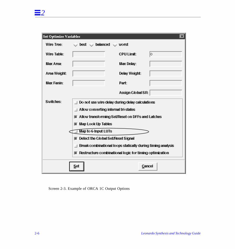
• Map 6-Input LUT, Screen 2-3, Table 2-1
2-2 Leonardo Synthesis and Technology Guide
2
Table 2-1. Mapping Options
*GUI default options**variables, options, constraint attributes, commands
GUI Option Optionon/off
Command Line** Available inTechnologies
Results
■ Map Look Up Tables
on* default (true) All Listed LUT-based FPGAs
Controls LUT mapping.
off lut_map
■ Map to CASCADEs during LUT mapping
on* default (true)t Altera FLEX6K Controls mapping logic to cascade gates for Altera FLEX.
off flex_use_cascades
❏ Use F5MAP Symbols
on use_f5map XilinxXC5200
Controls mapping to F5MAP Symbols.
off* default (false)
❏ Map to 6-input LUTs
on use_f6_lut ORCA1C Controls mapping to 6-Input LUTs.
off* default (false)
Technology Mapping 2-3
2
Screen 2-1. Example of Altera FLEX 6K Output Options
2-4 Leonardo Synthesis and Technology Guide
2
Screen 2-2. Example of Xilinx 5200 Output Options
Technology Mapping 2-5
2
Screen 2-3. Example of ORCA 1C Output Options
2-6 Leonardo Synthesis and Technology Guide

2
n. ers,
rdo’s idual
ble s in
I/O Mapping
During I/O mapping, Leonardo assigns PADs to all I/Os in the top level of a desigLeonardo can map input buffers, output buffers, tri-state buffers, bi-directional buffand complex I/O cells. Leonardo also maps global buffers for clock lines and highfanout input pads.
Command Line and GUI Options
There are several technology independent options in the GUI which control LeonaI/O pad assignments. These GUI options affect the complete design, not just indivI/Os.
Add IO Pads
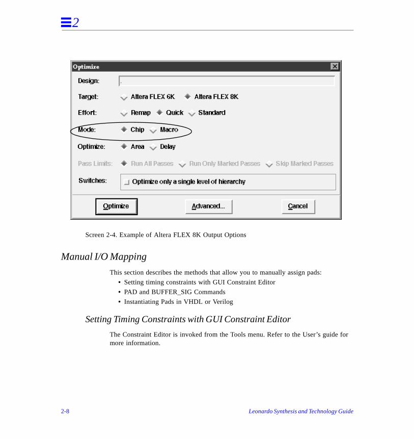
The ◆ chip and ◆ macro options are available for all technologies. As shown in Ta2-2 and Screen 2-4, the selection of these options enable all I/O Pad assignmentLeonardo.
Table 2-2. Results of Command Line and GUI I/O Mapping Options
*GUI default options**variables, options, constraint attributes, commands
GUI Option Option on/off
Command Line** Available inTechnologies
Results
◆ chip on* -chip default (true) All Assigns I/O pads around perimeter of thedesign.
off
◆ macro on -macro Output design is only a part of a design. I/O buffers are not added around the perimeter of design.
off*
n/a default (false) Actel, Xilinx, ORCA
This variable controls use of complex I/Os.
complex_ios
Technology Mapping 2-7
2
for
Screen 2-4. Example of Altera FLEX 8K Output Options
Manual I/O Mapping
This section describes the methods that allow you to manually assign pads:
• Setting timing constraints with GUI Constraint Editor
• PAD and BUFFER_SIG Commands
• Instantiating Pads in VHDL or Verilog
Setting Timing Constraints with GUI Constraint Editor
The Constraint Editor is invoked from the Tools menu. Refer to the User’s guide more information.
dontlockflex
2-8 Leonardo Synthesis and Technology Guide
2
, and
d on
ardo l I/O re n, as
ed
te The
ign’s
gy.
PAD and BUFFER_SIG Commands
There are two commands that can be used to manually assign I/O pads: PAD and BUFFER_SIG. These commands can be used as attributes from VHDL or as commands from the Leonardo shell. The PAD command is the recommended way to assign pads, since it is the most general and can be used to assign any pad thatLeonardo is able to map. In addition, connections between the pins on the PAD and the design signals do not need to be specified. The PAD command is limited, howeveronly works on inputs and outputs.
The BUFFER_SIG command can be used to assign buffers only, but it can be useinternal signals (internal clock buffers) as well. The PAD and BUFFER_SIG commands can only assign mappable cells. A mappable cell is any cell that Leonis able to automatically instantiate in the output netlist. For FPGA technologies, alcells are mappable. For ASIC technologies, typically only the simplest I/O cells amappable. However, other cells can be instantiated through component instantiatiodiscussed in the above in section.
PAD Command
This is the recommended way to manually assign pads. The command can be usfrom the Leonardo shell or from VHDL.
When using this command from the Leonardo shell, the syntax is:
Signal 1 ... signal n are the names of I/O signals on which you want to instantiathe above I/O pad. The I/O pad must be a mappable gate from the target library. PAD command will not work on non-mappable gates. To instantiate the I/O pad, Leonardo will automatically make connections between the gate’s pins and the dessignals.
In the example below, the ACTEL Act3 FPGA device family is the target technolo
PAD gate_name signal 1 .... signal n
PAD HCLKBUF hclk
Technology Mapping 2-9
2
y
his
y.
This command will connect the input signal hclk to the input pin of the array registers clock buffer (HCLKBUF), and connect all the elements which were originalldriven by hclk to the output pin of hclkbuf .When using this command from VHDL, you should set the PAD attribute on the specific I/O signal. The syntax is:
signal-name is the I/O on which you want to assign the pad with name pad-name.
BUFFER_SIG Command
This command will only work for I/O buffers (one input, one output). When using tcommand from Leonardo’s shell, the syntax is:
In the examples below, the Actel Act2 FPGA device family is the target technolog
Connect signal clk1 to the input pin of the external clock buffer (clkbuf ), and all the elements which were originally driven by clk1 will be driven by the output pin of the clock buffer (clkbuf ).
Connect signal rstn (reset signal) to the input of the internal clock buffer (clkint ), and all the elements which were originally driven by rstn will be driven by the output pin of the clock buffer (clkint ). When using this command from VHDL, thesyntax is:
signal-name is the I/O on which you want to assign buffer with name buffer_name.
attribute PAD of signal-name: signal is pad-name
BUFFER_SIG buffer_name signal_name
BUFFER_SIG clkbuf clk1
BUFFER_SIG clkint rstn
attribute BUFFER_SIG of signal-name:signal is buffer_name;
2-10 Leonardo Synthesis and Technology Guide
2
is ads
O ually,
The following example is a design using the Actel Act3 architecture. The examplewritten in VHDL and the I/O pads are assigned automatically, except for two I/O pwhich are assigned manually, using attributes.
The following example is a VHDL design using the Actel Act3 architecture. The I/pads are assigned automatically, except for two I/O pads which are assigned manusing attributes.
Technology Mapping 2-11
2
,
The VHDL file:
As shown above, the signal pad has automatically been assigned to the ORECTL complex I/O. Since the register is not using the enable signal in the VHDL designLeonardo ties the register’s enable to GND. The PAD and BUFFER_SIG attributes are also used to instantiate the IOCLKBUF (for the clock signal) and the IOPCLBUF (for the reset signal).
-- Example for mapping of orectl in Act3 library ieee ;
use ieee.std_logic_1164.all;library exemplar ;use exemplar.exemplar.all;entity orectl is
port ( a, b, clk, iopcl, e: in std_logic; pad : out std_logic ); -- Instantiate hard wired I/O clock buffer and -- I/O clear buffer attribute pad of iopcl:signal is “IOPCLBUF”; attribute buffer_sig of clk:signal is “IOCLKBUF”; end orectl;
architecture exemplar of orectl is signal sig1, o: std_logic;
beginprocess (clk, sig1, iopcl)begin
if (iopcl = ’0’) theno <= ’0’;
elsif (clk’event and clk = ’1’) theno <= sig1;
end if ;end process ;sig1 <= a and b;pad <= o when (e = ’1’) else ’Z’;end exemplar;
2-12 Leonardo Synthesis and Technology Guide
2
rs on
The following VHDL example is for targeting Xilinx XC4000 technology:
The complex I/O OUTFFT registers the intern_out signal and is connected to theinoutp output pad. You must follow these rules:
• In the port section of the component declaration, you should utilize the sameformal names which appear in Exemplar’s target technology library.
• Also, you must specify an input technology library. If an input library is not loaded, then Leonardo cannot find the instantiated component and treats thecomponent as a black box. This causes Leonardo to add additional I/O buffethe I/O pins of the component.
architecture exemplar of example is component OUTFFT port ( c, d, t: in std_logic; o: out std_logic ); end component ; b1: OUTFFT port map (c=>clk, d=>intern_out, t=>io_control, o=>inoutp);
end exemplar;
Technology Mapping 2-13

2
2-14 Leonardo Synthesis and Technology Guide
Timing Analysis 3
rs in to the
gn. y
aths . In
This chapter describes:
• Before Beginning
• Static Timing Analysis
• Back Annotation
• Post Synthesis RTL (Register Transfer Level) Simulation
Before Beginning
The information presented in this chapter introduces you to the technology chaptethis guide. This chapter assumes that you have read the User’s Guide. Refer alsoHDL Synthesis and Command Reference Guides for information.
Static Timing Analysis
Static timing analysis allows for efficient evaluation of timing hot spots in the desiThe static timing analyzer enables Leonardo to make a decision on area and delatrade-off during synthesis and optimization.
Leonardo can also generate a critical path report showing a specific set of critical pin the design. These critical paths can also be received in the schematic browseraddition, Leonardo provides a path to the HDL simulator for post place-and-routefunction and timing simulation using Standard Delay Format (SDF).
3-1
3
y the ires
logy ath.
A the e
te to nout lay
rary el, or
Timing analysis helps verify the timing performance and correctness of a circuit. Timing analysis traces the clocks to the registers in the circuit, computes the delaalong various instances in the circuit, and helps to identify timing critical section ofdesign. This type of analysis does not require generation of circuit stimuli and requless time than simulation. However, timing analysis does not provide the comprehensive functional and dynamic simulation capabilities of a simulator.
Timing analysis is used in synthesis tools to guide timing optimization and technomapping. Critical paths in the circuit are reported by checking the slack along the pSlack is the difference between the required time and the arrival time of a signal.critical path has a negative slack value. The path with the most negative slack ismost critical path in the circuit. The longest path in the circuit is not necessarily thmost critical path, since a long path may have a very late required time.
Arrival times are propagated along the circuit by adding the delay across each gathe arrival times of its inputs. Delay across a gate not only depends on the delaythrough the gate (the intrinsic delay) but also upon the loading of the gate, the faconnections, the interconnect load, and the slew of the inputs of the gate. The deinformation can be expressed in a variety of delay models.
Delay Models
Timing Analysis uses the delay information from a technical library to propagate arrival times (required times) to the end points (start points). The delays in the libcan be modeled using a simple linear delay model, a piece-wise linear delay moda nonlinear delay model.
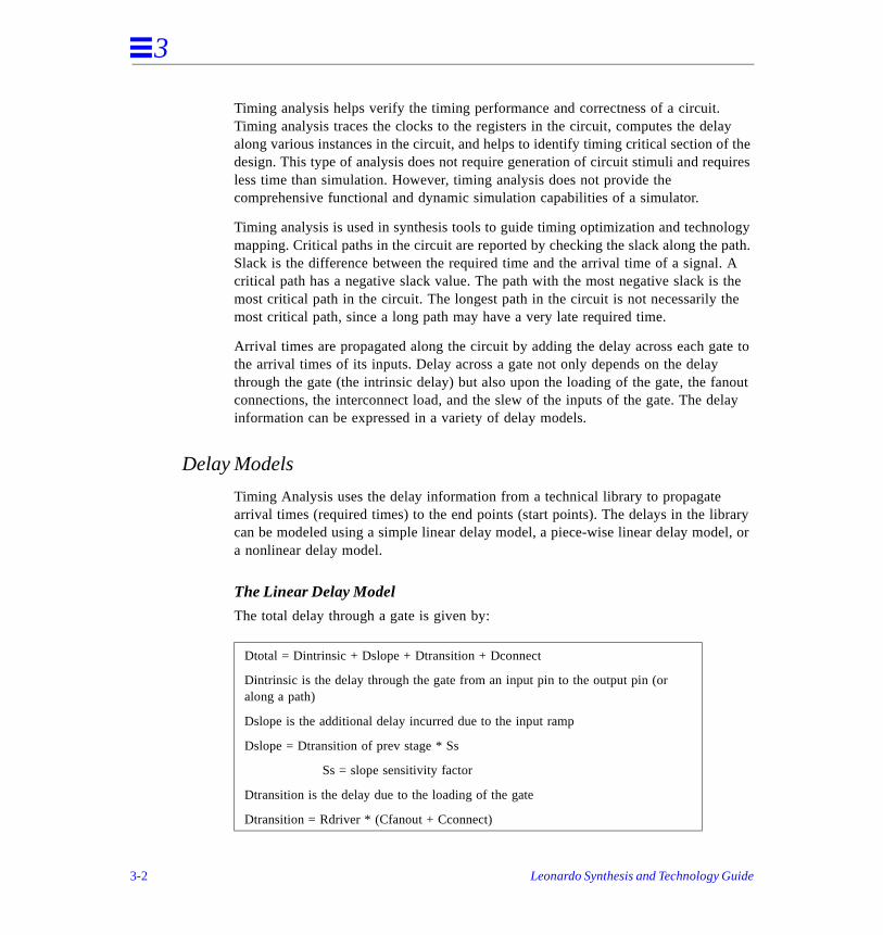
The Linear Delay Model
The total delay through a gate is given by:
Dtotal = Dintrinsic + Dslope + Dtransition + Dconnect
Dintrinsic is the delay through the gate from an input pin to the output pin (or along a path)
Dslope is the additional delay incurred due to the input ramp
Dslope = Dtransition of prev stage * Ss
Ss = slope sensitivity factor
Dtransition is the delay due to the loading of the gate
Dtransition = Rdriver * (Cfanout + Cconnect)
3-2 Leonardo Synthesis and Technology Guide
3
onnect nout, tive ls of
.
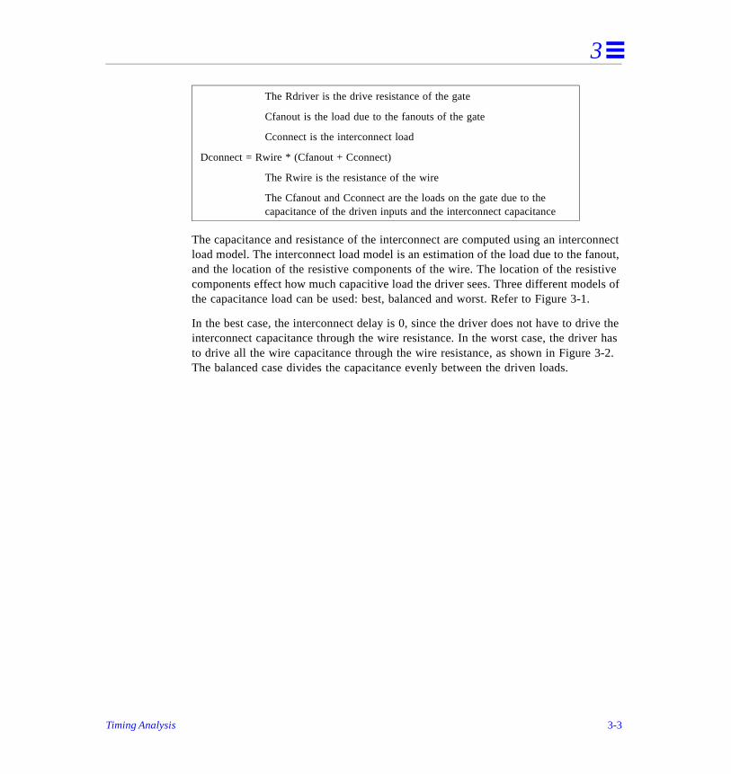
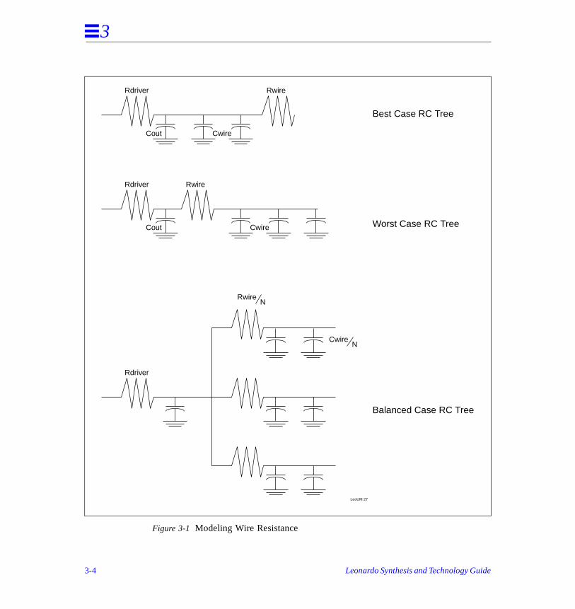
ve the r has 3-2.
The capacitance and resistance of the interconnect are computed using an intercload model. The interconnect load model is an estimation of the load due to the faand the location of the resistive components of the wire. The location of the resiscomponents effect how much capacitive load the driver sees. Three different modethe capacitance load can be used: best, balanced and worst. Refer to Figure 3-1
In the best case, the interconnect delay is 0, since the driver does not have to driinterconnect capacitance through the wire resistance. In the worst case, the driveto drive all the wire capacitance through the wire resistance, as shown in Figure The balanced case divides the capacitance evenly between the driven loads.
The Rdriver is the drive resistance of the gate
Cfanout is the load due to the fanouts of the gate
Cconnect is the interconnect load
Dconnect = Rwire * (Cfanout + Cconnect)
The Rwire is the resistance of the wire
The Cfanout and Cconnect are the loads on the gate due to the capacitance of the driven inputs and the interconnect capacitance
Timing Analysis 3-3
3
Figure 3-1 Modeling Wire Resistance
Cout Cwire
Rdriver Rwire
Cout Cwire
Rdriver Rwire
Cwire
Rwire
Rdriver
N
N
LeoUM 27
Best Case RC Tree
Worst Case RC Tree
Balanced Case RC Tree
3-4 Leonardo Synthesis and Technology Guide

3
r et elay
to
to to e.
in a
Figure 3-2 Components of Total Path Delay
Timing Analysis Before and After Place-and-Route
Timing analysis can occur before or after place-and-route.
• Before place-and-route: only estimated routing delay numbers are available fotiming analysis. The accuracy of the estimates varies, depending on the targtechnology. For many FPGA technologies, the variance between predicted dand actual delay can be up to 20%.
• After place-and-route: actual routing delay numbers can be back annotated inLeonardo using an SDF file.
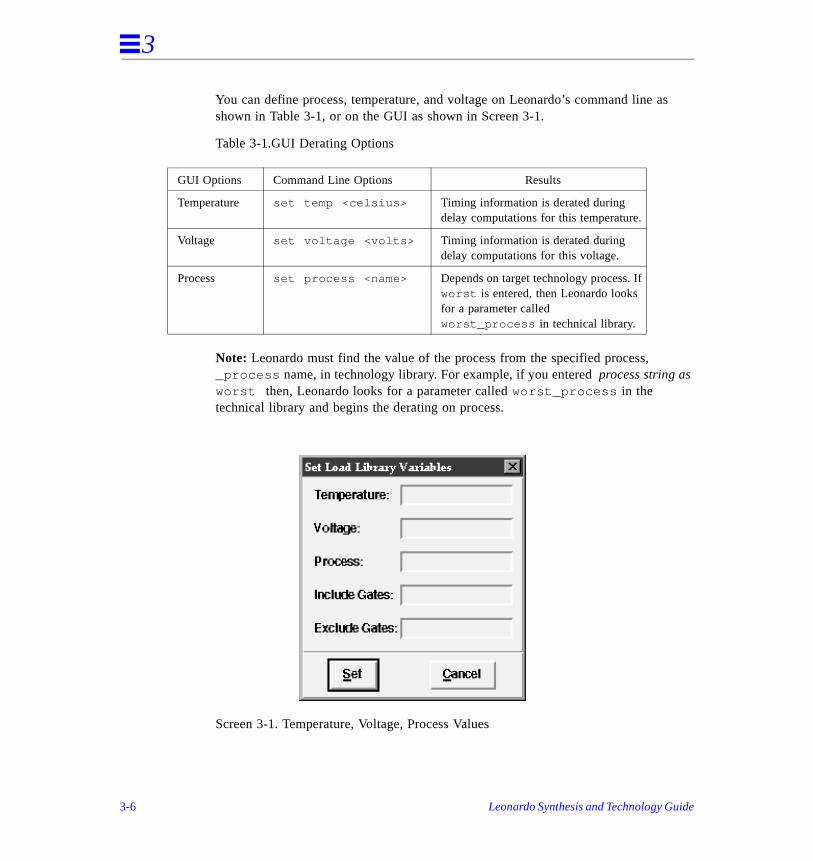
Defining Process, Temperature, and Voltage Values
Derating models the variations in total delay based on your specified process, temperature, and voltage. Leonardo derates or scales each deratable parameter compute the total delay of a path. You can define global parameters in the librarymodel these effects with respect to the nominal process, temperature, and voltag
Nominal Parameter in Library
Leonardo recognizes the nominal process, temperature, and voltage parameters technology library with the following names.
• Process - nominal_process : string
• Temperature - nominal_temp : float
• Voltage - nominal_volt : float
LeoUM 28
Ds
Dc
DtDi
Timing Analysis 3-5
3
s
You can define process, temperature, and voltage on Leonardo’s command line ashown in Table 3-1, or on the GUI as shown in Screen 3-1.Table 3-1.GUI Derating Options
Note: Leonardo must find the value of the process from the specified process, _process name, in technology library. For example, if you entered process string as worst then, Leonardo looks for a parameter called worst_process in the technical library and begins the derating on process.
Screen 3-1. Temperature, Voltage, Process Values
GUI Options Command Line Options Results
Temperature set temp <celsius> Timing information is derated during delay computations for this temperature.
Voltage set voltage <volts> Timing information is derated during delay computations for this voltage.
Process set process <name> Depends on target technology process. If worst is entered, then Leonardo looks for a parameter called worst_process in technical library.
3-6 Leonardo Synthesis and Technology Guide

3
r ur
path t is is h
ths
t,
fall
fer to bles
after
ndard the
Critical Path Report
A critical path is defined as a path that has negative slack, or slack less than youspecified slack threshold. A path, however long, may not be critical if it meets yoconstraints.
In the delay report, the header of the path gives the path number, followed by theslack. All paths are reported from the start point to the end point. If the start pointhe output of a flip flop, the rising or falling edge and the arrival time of the clock reported. The clock at the end point is also reported where appropriate, along witsetup information.
The critical path report is sorted by most critical path first. If there are no critical pain the design, then the longest path is reported.
The following definitions describe the headings in the critical path report:
NAME The instance name is reported followed by the pin name. By defaulonly output pins are reported.
ARRIVAL The arrival time at this node is specified. The latest of the rise and times is reported followed by up or down indicating rise time or fall time.
LOAD The load being driven by the driver (output pin), is specified.
Nodes which are on combinational loops are identified by the string (loop) next to the arrival time. For example:
When an option is set to report nets, the fanout is reported instead of the load. Rethe Leonardo Command Reference for more details of different options and variathat affect critical path reporting.
Back-Annotation
Back-annotation is the process of inserting actual delay numbers into the networkplace-and-route. Leonardo Time Module provides a mechanism for timing back-annotation from the place-and-route tools. For most technologies, a separate StaDelay Format (SDF) file is written by the place-and-route tool. The SDF format is
i1305/O AND3 13.0 dn (loop) 0.0
Timing Analysis 3-7
3
nd-
.
The h
for
ute),
t
cal
industry standard way to represent delay information. For Xilinx, the post place-aroute delay numbers are annotated in the XNF netlist. Leonardo XACT flow TimeModule can read a timing annotated XNF netlist and write out a Verilog or VHDL structural netlist along with an SDF file with the back-annotated delay information
SDF (Standard Delay Format) Writer
An SDF writer for pre place-and-route delays has been added. The SDF writer calculates delays as used by the timing analyzer and timing optimization routines.SDF writer writes this information in an SDF format. The SDF format together witthe flat VHDL netlist can be read into MTI V-System or any RTL simulator for preplace-and-route timing simulation.
The SDF writer is controlled by the sdf_write_flat_netlist Tcl variable. Set this variable to TRUE. An example set of Leonardo commands may be:
set sdf_write_flat_netlist TRUE
ungroup -all /*need to flatten the netlist*/
write design.vhd /*write out flat VHDL or Verilog*/
write design.sdf /*write out SDF*/
Design Flow
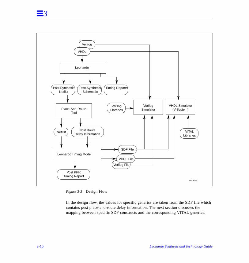
As shown in Figure 3-3, the timing back annotation flow consists of the following steps:
1. Exemplar’s Leonardo is used to synthesize a behavioral VHDL or Verilog netlista particular target technology.
2. The synthesized netlist is input to a place- and-route tool.
3. The place-and-route tool produces a timing annotated netlist (post place-and-roor an SDF file, along with the post place-and-route netlist.
4. Leonardo’s timing analyzer uses these actual delay numbers to determine posplace-and-route critical paths.
5. Leonardo’s schematic viewer is used for graphical analysis of the design. Critipaths can also be highlighted in the schematic.
3-8 Leonardo Synthesis and Technology Guide
3
duce
g
ck-ing tity
ay ch
and s AL
pin p s lock
6. Leonardo can read the netlist provided by the place-and-route tool, and can proa structural VHDL or Verilog netlist along with an SDF file with post place-and-route delays.
7. This structural netlist, along with the SDF file can be input to a VHDL or Verilosimulator.
VITAL Libraries
The timing simulation is only as accurate and fast as the libraries that support baannotation of delay information. VITAL provides for a mechanism for back-annotatdelay information to circuit elements through interface constants, called generics,which are declared in the cells in the VITAL library. Generics are declared in the ensection of a cell and are relayed to the port names of the cell and the type of delinformation being communicated. Libraries that allow back-annotation through sugenerics are called VITAL level 0 compliant.
For fast and accurate simulation, functionality and delay propagation need to be expressed efficiently. VITAL specifies a method for developing simulation models also specifies a set of primitives to efficiently evaluate the functionality. Simulatorthat take advantage of this can show significant improvement in performance. VITlibraries that adhere to this specification are considered level 1 compliant.
For delay propagation in VITAL, path delays between an input pin and an output tpd_in_out are annotated in the tpd_ in_out generic. The interconnect delay leading uto an input pin is annotated in the tipd_ in generic. The setup and hold timing checkare with respect to a clock edge and are annotated in generics that identify the cedge, for instance, tsetup_ data_clk_POSEDGE or thold_ data_clk_NEGEDGE. A generic, TimingChecksOn, also allows such timing checks to be turned off for increased performance.
Timing Analysis 3-9
3
ich
.
Figure 3-3 Design Flow
In the design flow, the values for specific generics are taken from the SDF file whcontains post place-and-route delay information. The next section discusses the mapping between specific SDF constructs and the corresponding VITAL generics
LeoUM 25
VHDL Simulator(V-System)
VerilogSimulator
Leonardo
Verilog
Post SynthesisNetlist
Place-And-RouteTool
Leonardo Timing Model
Post RouteDelay Information
Netlist
VHDL
Verilog File
SDF File
Post PPRTiming Report
VITALLibraries
VHDL File
Post SynthesisSchematic
Timing Reports
VerilogLibraries
3-10 Leonardo Synthesis and Technology Guide
3
s for eters into
ct).
tween
nect at the OLD TAL tion
:6:))
a
sly, in a d
L
Standard Delay Format (SDF) for Transporting Delays
SDF provides a means for transporting delays from one tool to another. SDF allowspecification of computed delays such as pin-to-pin delays, instead of delay paramsuch as drive resistance, capacitive load, etc. SDF Delay information is grouped path specific cell delays and interconnect delays. Path specific delays include:
• The intrinsic delay from the input pin of the gate to the output pin.
• The delay due to the input ramp.
• The delay due to the output loading (including the load due to the interconne
The interconnect delay is the delay due to the wire resistance and capacitance bethe driver of the net and the input pins it drives.
The path specific delays are modeled as IOPATH constructs in SDF. The intercondelays are represented by PORT or INTERCONNECT constructs and are lumped input pin of the gate. The setup and hold checks are modeled with the SETUP, Hor SETUPHOLD constructs. The SDF constructs correspond to generics in the VIlibrary into which the delay numbers are to be annotated. Following is and explanaof how various SDF constructs are mapped to corresponding VITAL generics.
• The PORT construct maps to the tipd_ generic. This generic is identified by theport names associated with the SDF construct. For example, (PORT A (:5:) (would annotate the tipd_A generic with rise and fall delays of 5 and 6.
• The IOPATH construct maps to the tpd_ generic. For example, (IOPATH A Y (:5:) (:6:)) would annotate the tpd_A_Y generic with rise and fall delays of 5 and 6.
• The SDF constructs SETUP and HOLD map to timing check generics tsetup_ and thold_ depending if the cell being annotated is a rising edge flip-flop orfalling edge flip-flop.
Post Synthesis RTL (Register Transfer Level) Simulation
Leonardo now supports writing simulatable models for gate level designs. Previouif the design contained technology cells, Leonardo could not write the design out(simulatable) RTL description (VHDL or Verilog). Technology cells were considereblack-boxes in the Leonardo design data base.
Technology cells are now filled with functional (RTL) information. This enables RToutput from technology netlists to write behavior for technology cells.
Timing Analysis 3-11
3
ces lows
, ze
ce.
es
ce,
e able
del
A new command, unmap was added. This command removes technology cell instanfrom a design, and replaces the instances with the primitives underneath. This alVHDL and Verilog writer to write RTL descriptions for the design. The command unmap is available in the Leonardo Hierarchy menu.
The -downto option on the write command is provided to write descriptions with technology cells downto primitives (RTL).
First Application
Leonardo can now write RTL VHDL or Verilog for a mapped design. For exampleyour back-annotated design or a design that has already gone through the optimicommand contains technology cells. You can now write the design(s) out in RTL VHDL or Verilog with one of the following two methods:
(1) Run command unmap first, then write.
This removes the technology cells from the design. Primitives are put in their plaThe design can now be written out in VHDL or Verilog and will be simulatable without a technology library.
Note: After unmap, the design can contain redundant logic, and may be large. Runpre_optimize -common -unused to reduce the size. This cleans the design, removconstants, shared and unused logic, and does not change the functionality of thedesign.
(2) Run write -downto PRIMITIVES.
The design does not change with this method, the technology cells are still in plabut the VHDL or Verilog writer will write the behavioral contents for the used technology cells. Thus, the design is still fully simulatable.
Note: optimize maps the design to a technology and unmap unmaps the design back toprimitives. After unmap , the structure of the design may not be the same as beforoptimize. If you run another optimize after unmap, the result may be more undesirthan the result of the first optimize run.
Second Application
Leonardo can now write simulatable models for technology cells. To write one moof one library cell, change present_design to the NETLIST view of the technology cell of choice, and issue a write -downto PRIMITIVES command.
3-12 Leonardo Synthesis and Technology Guide
3
be
y in
Use the following Tcl script to write all library cell models to separate VHDL files:
# Set library name here:
set lib lsi300
load_library $lib
foreach i [list_design -short .$lib] {
present_design .$lib.$i.NETLIST
write -downto PRIMITIVES $i.vhd
}
If you want all models in a single, large, VHDL file try IO redirection:
load_library $lib
foreach i [list_design -short .$lib] {
present_design .$lib.$i.NETLIST
write -downto PRIMITIVES -format VHDL - >> total.vhd
}
Note: write without the downto option still writes the design downto technology cells. unmap always flattens out ALL technology cell instances in a design or ALL technology cell instances in one level of hierarchy (-single_level ).
ungroup does not flatten out technology cell instances. The option (-force ) is added to the ungroup command, so that specific technology cell instances (by name) canflattened out to primitives.
Limitations:
Look Up Table (LUTs) are not unmapped with the unmap command. LUTs (for example after optimize for xi4) are written out as simulatable RTL equations alreadVHDL or Verilog.
If desired, run decompose_luts command then run unmap command to remove all technology cells, including LUTs.
Timing Analysis 3-13
3
3-14 Leonardo Synthesis and Technology Guide
Timing Constraints 4
ser’s
the
This chapter describes:
• Before Beginning
• Setting Global Constraints
• Setting Constraints on Individual Signals
• Usage of Timing Constraints in Leonardo
• New Constraint Features
Before Beginning
The information presented in this chapter is intended to introduce you to the technology chapters in this guide. This chapter assumes that you have read the UGuide. Refer also to the HDL Synthesis and Command Reference Guides for information.
Setting Global Constraints
Global constraints are imposed to assist in optimizing the timing of the design. Usemaxdly variable to set global timing constraints.:
set maxdly <n>
4-1
4
pped
s.
shell
r on
an s ty is the lt
The maxdly variable specifies the maximum delay acceptable for any path in the optimized circuit. Leonardo is directed to search for the smallest circuit implementation which meets the specified timing constraint. The maxdly variable is used with -area option for optimize command.
If a specific pass does not meet the constraint, then the optimized circuit is remain a effort to meet the constraint. If the constraint is not met after remapping, thenLeonardo performs the next pass and continues the optimization/mapping proces
Setting Constraints on Individual Signals
You can set constraints on individual signals with the Constraint File Editor as explained in the User’s Guide. Constraints can also be imposed from Leonardo’s or as properties in VHDL.
Load and Drive Specifications
Output load and input drive can be specified for Leonardo in the Command File othe Constraint File Editor. All load numbers are in number of unit loads.
The OUTPUT_LOAD attribute tells the program the amount of external loading on output of the design. The value is the number of unit loads driven by the output. Thinumber is used to calculate delays and to make sure that sufficient drive capabiliavailable at the output. This can result in buffering, or in replicating logic to meet load and drive requirements. If no value is specified for an output, then the defauoutput load for the particular technology is used.
optimize -area
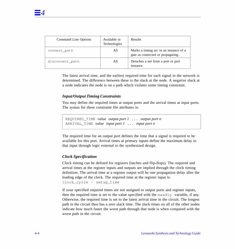
OUTPUT_LOAD value output signal 1 ... output signal n
OUTPUT_FANOUT value output signal 1 ... output signal n
4-2 Leonardo Synthesis and Technology Guide
4
n ut.
will he
uce
ut sed sents efault
y
for at er lt.
The OUTPUT_FANOUT attribute tells the program the amount of external loading oan output of the design. Value is the total number of fanout loads driven by the outp
The INPUT_MAX_LOAD attribute defines the maximum load that the synthesizedcircuit may present at an input to the design. The value is the maximum number of unit loads allowed. If the synthesized circuit exceeds this amount of loading, Leonardobuffer to reduce the load. In the macro mode, Leonardo will add buffers to meet tload constraint unless the input pins have NOBUFF attribute.
The INPUT_MAX_FANOUT attribute defines the maximum fanout load that the synthesized circuit may present at an input to the design. Value is the maximum number of total fanout loads allowed. During synthesis, Leonardo will buffer to redthe load.
The INPUT_DRIVE attribute specifies the additional delay per unit load for an inpport. The value is the additional delay in nanoseconds per unit load. This value is uwhen calculating delays so that the effects of the load the synthesized circuit preto the gate driving the input can be accurately modeled. Each technology has a ddrive defined for inputs, usually the drive of a single inverter gate.
Timing Specifications
Leonardo includes timing analysis routines to decide where to make an area/delatradeoff in the logic design.
These routines use your specified timing constraints along with delay informationthe library elements and do a path analysis of the synthesized circuit. Paths startprimary inputs and at register outputs. Paths end at primary outputs and at registinputs. Paths to the asynchronous set and reset of flip-flops are ignored by defauHowever, they can be connected and analyzed with the connect_path and disconnect_path commands.
INPUT_MAX_LOAD value input signal 1 ... input signal n
INPUT_MAX_FANOUT value input signal 1 ... input signal n
INPUT_DRIVE value input signal 1 ... input signal n
Timing Constraints 4-3
4
rk is ack at
orts.
e
d g the
ts,
gest odes h the
The latest arrival time, and the earliest required time for each signal in the netwodetermined. The difference between these is the slack at the node. A negative sla node indicates the node is on a path which violates some timing constraint.
Input/Output Timing Constraints
You may define the required times at output ports and the arrival times at input pThe syntax for these constraint file attributes is:
The required time for an output port defines the time that a signal is required to bavailable for this port. Arrival times at primary inputs define the maximum delay tothat input through logic external to the synthesized design.
Clock Specification
Clock timing can be defined for registers (latches and flip-flops). The required anarrival times at the register inputs and outputs are implied through the clock timindefinition. The arrival time at a register output will be one propagation delay afterleading edge of the clock. The required time at the register input is: clock_cycle - setup_time
If your specified required times are not assigned to output ports and register inputhen the required time is set to the value specified with the maxdly variable, if any. Otherwise, the required time is set to the latest arrival time in the circuit. The lonpath in the circuit then has a zero slack time. The slack times on all of the other nindicate how much faster the worst path through that node is when compared witworst path in the circuit.
Command Line Options Available inTechnologies
Results
connect_path All Marks a timing arc in an instance of a gate as connected or propagating.
disconnect_path All Detaches a net from a port or port instance.
REQUIRED_TIME value output port 1 ... output port nARRIVAL_TIME value input port 1 ... input port n
4-4 Leonardo Synthesis and Technology Guide
4
the
le
hat y be c
d ined
You may specify the times from Leonardo’s shell, and/or in a VHDL source file, if input is a VHDL file. The parameters which may be specified are:
These parameters define a clock’s behavior. All clock behaviors assume one singcommon zero reference. CLOCK_OFFSET defines the offset of the leading edge fromthe common zero. CLOCK_CYCLE defines the length of the clock. PULSE_WIDTH defines the length of the clock pulse.
For both flip-flops and latches, the leading edge occurs at time CLOCK_OFFSET. The arrival time at the register outputs is set to the propagation delay after this time.
The required time at the input to the flip-flops and latches is CLOCK_OFFSET + CLOCK_CYCLE - setup_time . At this point Leonardo does not handle transparent latches.
Clock timing parameters are specified for the actual clock signal (i.e., the signal tconnects to the clock pin of the register). This signal may be an input port or it mathe output of another register, or it may be the output of some combinational logi(although this is not a recommended method for generating clocks).
Clock timing is not derived automatically for any signals. Timing must be specifieexplicitly for each clock. For example, a clock which is a divided down version ofanother clock must have defined timing specifications. The timing is not be determfrom the source clock’s timing.
VHDL Attributes
VHDL attributes may be used to specify timing parameters in VHDL designs. Thenames of the attributes are the command names as defined above.
CLOCK_OFFSET value clock_signal_1 ... clock_signal_nCLOCK_CYCLE value clock_signal_1 ... clock_signal_nPULSE_WIDTH value clock_signal_1 ... clock_signal_n
arrival time at register output = CLOCK_OFFSET + CLK->Q delay
Timing Constraints 4-5
4
tes
ve to
An example of the syntax of an attribute is:
Usage of Timing Constraints in Leonardo
Timing constraints are defined as constraints that affect Leonardo's timing estimaand thus the quality of optimization, mapping and other features.
Table 4-1, Technology Constraints, summarizes what constraints can be used fordifferent technologies. The table also provides a list of applications that are sensitithe corresponding constraints.
ATTRIBUTE REQUIRED_TIME OF out:SIGNAL IS 10ns;
4-6 Leonardo Synthesis and Technology Guide
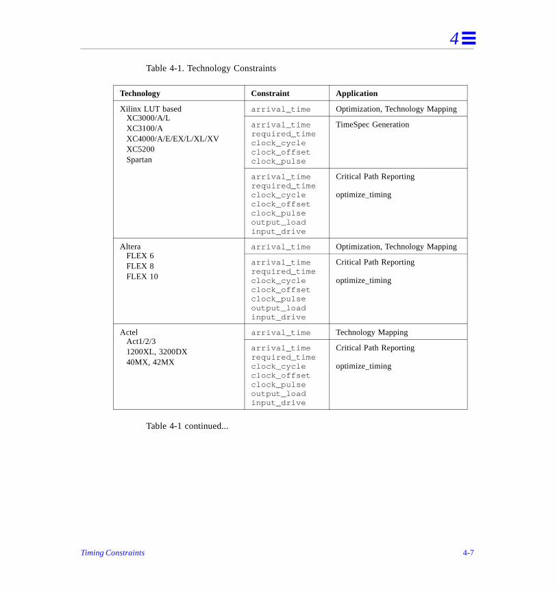
4
Table 4-1. Technology Constraints
Table 4-1 continued...
Technology Constraint Application
Xilinx LUT basedXC3000/A/LXC3100/A XC4000/A/E/EX/L/XL/XVXC5200Spartan
arrival_time Optimization, Technology Mapping
arrival_timerequired_timeclock_cycleclock_offsetclock_pulse
TimeSpec Generation
arrival_timerequired_timeclock_cycleclock_offsetclock_pulseoutput_loadinput_drive
Critical Path Reporting
optimize_timing
AlteraFLEX 6FLEX 8FLEX 10
arrival_time Optimization, Technology Mapping
arrival_timerequired_timeclock_cycleclock_offsetclock_pulseoutput_loadinput_drive
Critical Path Reporting
optimize_timing
ActelAct1/2/31200XL, 3200DX40MX, 42MX
arrival_time Technology Mapping
arrival_timerequired_timeclock_cycleclock_offsetclock_pulseoutput_loadinput_drive
Critical Path Reporting
optimize_timing
Timing Constraints 4-7
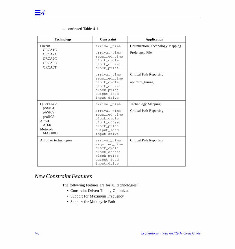
4
... continued Table 4-1
New Constraint Features
The following features are for all technologies:
• Constraint Driven Timing Optimization
• Support for Maximum Frequency
• Support for Multicycle Path
Technology Constraint Application
LucentORCA1CORCA2AORCA2CORCA3CORCA3T
arrival_time Optimization, Technology Mapping
arrival_timerequired_timeclock_cycleclock_offsetclock_pulse
Preference File
arrival_timerequired_timeclock_cycleclock_offsetclock_pulseoutput_loadinput_drive
Critical Path Reporting
optimize_timing
QuickLogicpASIC1pASIC2pASIC3
AtmelAT6K
MotorolaMAP1000
arrival_time Technology Mapping
arrival_timerequired_timeclock_cycleclock_offsetclock_pulseoutput_loadinput_drive
Critical Path Reporting
All other technologies arrival_timerequired_timeclock_cycleclock_offsetclock_pulseoutput_loadinput_drive
Critical Path Reporting
4-8 Leonardo Synthesis and Technology Guide
4
at
.
on
en
t e an
Constraint Driven Timing Optimization
The constraint driven timing optimization has significant run time improvements (least 10 times faster), and the quality of results are improved significantly.
You can set global timing constraints by setting clock frequency. You do this by running the clock_frequency <value> command, while <value> is in terms of MHzThe clock_frequency constraint will apply to all clocks in the design.
Note: clock_cycle is set on a particular clock, while clock_frequency is set globallyall clocks.
Support for Maximum Frequency
You can set a global timing constraint for maximum clock frequency in a design. Leonardo will set this constraint on all global clocks in the design. Constraint drivtiming optimization will try to meet the global clock frequency constraint.
You can set the maximum global frequency constraint in Leonardo by running seclock_frequency <value> on the Leonardo command line. The frequency should binteger greater than 0 and entered in Mhz.
Leonardo can report clock frequency of the clocks after synthesis by running report_delay -clock command.
Support for Multicycle Path
Use the following syntax to specify multicycle path constraints to Leonardo:
set a multicycle path:
set_multicycle_path -from <> -to <> -value <value> ->
delete a multicycle path:
set_multicycle_path -from <> -to <> -unset ->
options for multicycle path:
set_multicycle_path [options] <from> <to> <value>
Timing Constraints 4-9
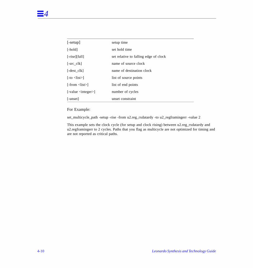
4
nd and
For Example:
set_multicycle_path -setup -rise -from u2.reg_rxdatardy -to u2_regframingerr -value 2
This example sets the clock cycle (for setup and clock rising) between u2.reg_rxdatardy au2.regframingerr to 2 cycles. Paths that you flag as multicycle are not optimized for timingare not reported as critical paths.
[-setup] setup time
[-hold] set hold time
[-rise][fall] set relative to falling edge of clock
[-src_clk] name of source clock
[-dest_clk] name of destination clock
[-to <list>] list of source points
[-from <list>] list of end points
[-value <integer>] number of cycles
[-unset] unset constraint
4-10 Leonardo Synthesis and Technology Guide
Timing Optimization 5
rs in to the
nd
target
the
This chapter describes:
• Before Beginning
• Optimization Flow
• Delay Optimization
• Statistics Report
• Automatic Constraining of Designs
Before Beginning
The information presented in this chapter introduces you to the technology chaptethis guide. This chapter assumes that you have read the User’s Guide. Refer alsoHDL Synthesis and Command Reference guides for information.
Optimization Flow
This is a brief review of Leonardo's optimization flow. First, Leonardo reads in thedesign and translates the design into internal data structures. Next, optimization amapping are run, and then the design is mapped into technology gates from the library.
Timing optimization is performed and can be controlled at various levels within Leonardo. By choosing the optimization mode to be “delay mode” you can direct tool to optimize for delay instead of area. Different optimization algorithms are
5-1
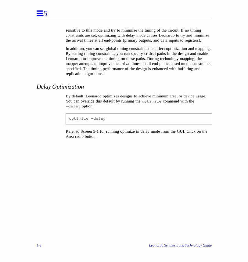
5
ize
ing. ble
raints
e.
e
sensitive to this mode and try to minimize the timing of the circuit. If no timing constraints are set, optimizing with delay mode causes Leonardo to try and minimthe arrival times at all end-points (primary outputs, and data inputs to registers).
In addition, you can set global timing constraints that affect optimization and mappBy setting timing constraints, you can specify critical paths in the design and enaLeonardo to improve the timing on these paths. During technology mapping, the mapper attempts to improve the arrival times on all end-points based on the constspecified. The timing performance of the design is enhanced with buffering and replication algorithms.
Delay Optimization
By default, Leonardo optimizes designs to achieve minimum area, or device usagYou can override this default by running the optimize command with the-delay option.
Refer to Screen 5-1 for running optimize in delay mode from the GUI. Click on thArea radio button.
optimize -delay
5-2 Leonardo Synthesis and Technology Guide
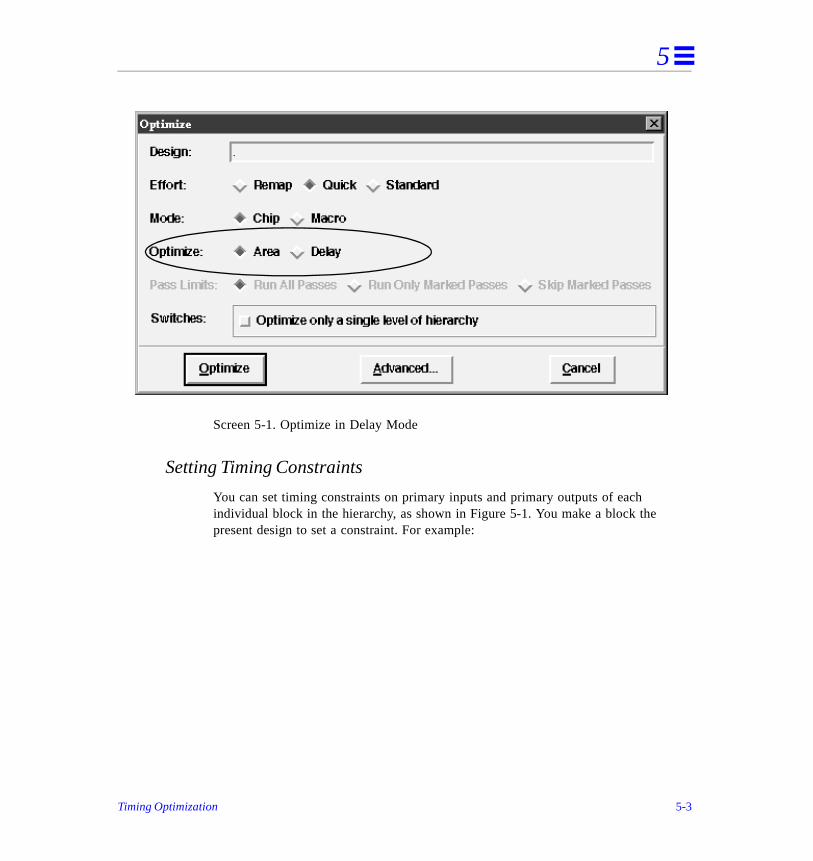
5
Screen 5-1. Optimize in Delay Mode
Setting Timing Constraints
You can set timing constraints on primary inputs and primary outputs of each individual block in the hierarchy, as shown in Figure 5-1. You make a block the present design to set a constraint. For example:
Timing Optimization 5-3
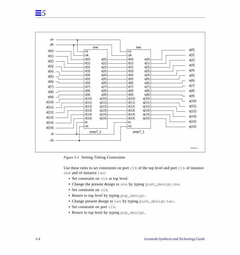
5
Figure 5-1 Setting Timing Constraints
Use these rules to set constraints on port clk of the top level and port clk of instance one and of instance two :
• Set constraint on clk at top level.
• Change the present design to one by typing push_design one .
• Set constraint on clk .
• Return to top level by typing pop_design.
• Change present design to two by typing push_design two.
• Set constraint on port clk .
• Return to top level by typing pop_design.
ceclkd(0)d(1)d(2)d(3)d(4)d(5)d(6)d(7)d(8)d(9)d(10)d(11)d(12)d(13)d(14)d(15)
q(0)q(1)q(2)q(3)q(4)q(5)q(6)q(7)q(8)q(9)
q(10)q(11)q(12)q(13)q(14)q(15)
ldrst
ce
clk
d(0)
d(1)
d(2)
d(3)
d(4)
d(5)
d(6)
d(7)
d(8)
d(9)
d(10)
d(11)
d(12)
d(13)
d(14)
d(15)
ld
rst
ceclkd(0)d(1)d(2)d(3)d(4)d(5)d(6)d(7)d(8)d(9)d(10)d(11)d(12)d(13)d(14)d(15)
q(0)q(1)q(2)q(3)q(4)q(5)q(6)q(7)q(8)q(9)
q(10)q(11)q(12)q(13)q(14)q(15)
q(0)
q(1)
q(2)
q(3)
q(4)
q(5)
q(6)
q(7)
q(8)
q(9)
q(10)
q(11)
q(12)
q(13)
q(14)
q(15)ldrst
prep7_1 prep7_1
one two
LeoRG 01
5-4 Leonardo Synthesis and Technology Guide
5
rt of
g
g the
by
Constraints can be specified for a design by using the constraint editor that is pathe GUI, or by typing one of the following commands:
You can specify the timing constraints in a script for future use.
This command sets the required time at the port port_name. Similarly, arrival_time, output_load, clock_cycle , etc. can be specified.
User Control
Timing optimization works on all levels of hierarchy. It runs on each instance separately and tries to minimize the critical path in each instance. However, optimize_timing can be limited to only one level of hierarchy by specifying the-single_level option. When limited to one level of hierarchy, the optimize timinruns only on instances in the current level of hierarchy (as pointed by present_design ).
If the design does not have timing constraints, the -force option can be used to forceconstraints. This option computes the longest path for a given view and uses thelongest path as the constraint at all the end points. This has the effect of optimizinlongest path.
Timing optimization can also be directed to work only on some of the end points specifying a list of end points with the -through option. The -through option can also be used to optimize the timing performance at any instance in the design byoptimizing the paths through it. Use the following syntax for optimize_timing .
set_attribute -name REQUIRED_TIME -value n -port port_name
REQUIRED_TIME port_name value
optimize_timing -through < node_list >optimize_timing -forceoptimize_timing -single_level
Timing Optimization 5-5
5
l
in
d
of
Statistics Report
Timing optimization reports statistics while evaluating the critical paths. The initiastatistics before the view was optimized is reported first.
Most critical slack: This is the biggest negative slack on all critical pathsthe optimized view.
Sum of negative slacks: This is the sum of all the negative slacks, at the enpoints and the start points in the optimized view.
Longest path: This is the delay along the longest path in the view.
Area: Is the area of the view.
As timing optimization evaluates the critical paths, it constantly updates the sum negative slacks. After completion, it prints the final values of these statistics.
5-6 Leonardo Synthesis and Technology Guide
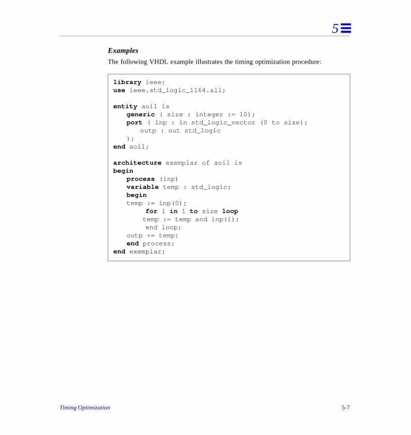
5
Examples
The following VHDL example illustrates the timing optimization procedure:
library ieee;use ieee.std_logic_1164.all;
entity aoi1 isgeneric ( size : integer := 10);port ( inp : in std_logic_vector (0 to size);
outp : out std_logic);
end aoi1;
architecture exemplar of aoi1 isbegin
process (inp)variable temp : std_logic;begintemp := inp(0);
for i in 1 to size loop temp := temp and inp(i);
end loop;outp <= temp;end process;
end exemplar;
Timing Optimization 5-7
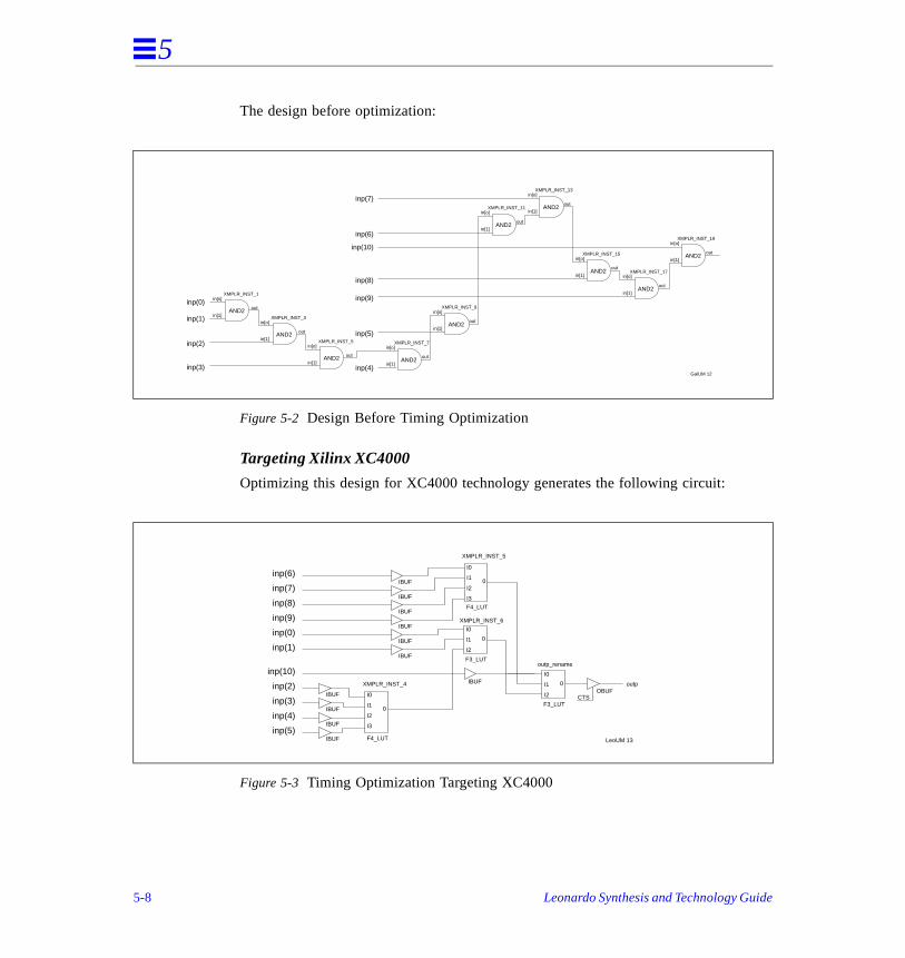
5
The design before optimization:
Figure 5-2 Design Before Timing Optimization
Targeting Xilinx XC4000
Optimizing this design for XC4000 technology generates the following circuit:
Figure 5-3 Timing Optimization Targeting XC4000
GalUM 12
AND2
XMPLR_INST_1
AND2
AND2 AND2
AND2
AND2
AND2
AND2
AND2
AND2
inp(0)
inp(2)
inp(3)
inp(1)
inp(4)
inp(5)
inp(9)
inp(8)
inp(10)
inp(6)
inp(7)
in[o]
in[1]
out
XMPLR_INST_3in[o]
in[1]
out
XMPLR_INST_5in[o]
in[1]
out
XMPLR_INST_7in[o]
in[1]
out
XMPLR_INST_9in[o]
in[1]
out
XMPLR_INST_11in[o]
in[1]
out
XMPLR_INST_13in[o]
in[1]
out
XMPLR_INST_15in[o]
in[1]
outXMPLR_INST_17
in[o]
in[1]
out
XMPLR_INST_19in[o]
in[1]
out
inp(5)
XMPLR_INST_4
inp(4)
inp(3)
inp(2)
inp(10)
inp(1)
inp(0)
inp(9)
inp(8)
inp(7)
inp(6)
XMPLR_INST_6
CTS
XMPLR_INST_5
outp_rename
outp
LeoUM 13
I0
I1
I2
I3
0
IBUF
IBUF
IBUF
IBUF
IBUF
OBUF
IBUF
IBUF
IBUF
IBUF
IBUF
IBUF
F4_LUT
I0
I1
I2
I3
0
F4_LUT
I0
I1
I2
0
F3_LUT
I0
I1
I2
0
F3_LUT
5-8 Leonardo Synthesis and Technology Guide
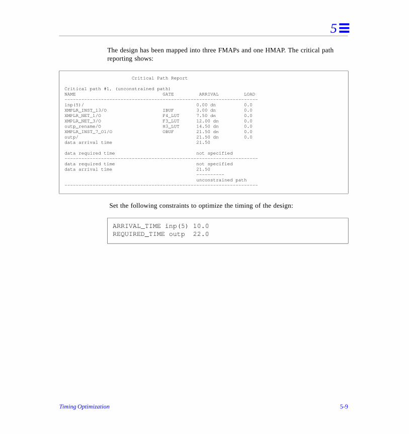
5
The design has been mapped into three FMAPs and one HMAP. The critical pathreporting shows:Set the following constraints to optimize the timing of the design:
Critical Path Report Critical path #1, (unconstrained path)NAME GATE ARRIVAL LOAD---------------------------------------------------------------------inp(5)/ 0.00 dn 0.0XMPLR_INST_13/O IBUF 3.00 dn 0.0XMPLR_NET_1/O F4_LUT 7.50 dn 0.0XMPLR_NET_3/O F3_LUT 12.00 dn 0.0outp_rename/O H3_LUT 14.50 dn 0.0XMPLR_INST_7_O1/O OBUF 21.50 dn 0.0outp/ 21.50 dn 0.0data arrival time 21.50
data required time not specified---------------------------------------------------------------------data required time not specifieddata arrival time 21.50 ---------- unconstrained path---------------------------------------------------------------------
ARRIVAL_TIME inp(5) 10.0REQUIRED_TIME outp 22.0
Timing Optimization 5-9
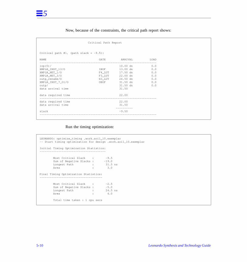
5
Now, because of the constraints, the critical path report shows:
Run the timing optimization:
Critical Path Report
Critical path #1, (path slack = -9.5):
NAME GATE ARRIVAL LOAD---------------------------------------------------------------------inp(5)/ 10.00 dn 0.0XMPLR_INST_13/O IBUF 13.00 dn 0.0XMPLR_NET_1/O F4_LUT 17.50 dn 0.0XMPLR_NET_3/O F3_LUT 22.00 dn 0.0outp_rename/O H3_LUT 24.50 dn 0.0XMPLR_INST_7_O1/O OBUF 31.50 dn 0.0outp/ 31.50 dn 0.0data arrival time 31.50
data required time 22.00---------------------------------------------------------------------data required time 22.00data arrival time 31.50 ----------slack -9.50---------------------------------------------------------------------
LEONARDO: optimize_timing .work.aoi1_10.exemplar-- Start timing optimization for design .work.aoi1_10.exemplar Initial Timing Optimization Statistics:--------------------------------------- Most Critical Slack : -9.5 Sum of Negative Slacks : -19.0 Longest Path : 31.5 ns Area : 3.0 Final Timing Optimization Statistics:------------------------------------- Most Critical Slack : -2.5 Sum of Negative Slacks : -5.0 Longest Path : 24.5 ns Area : 4.0 Total time taken : 1 cpu secs
5-10 Leonardo Synthesis and Technology Guide
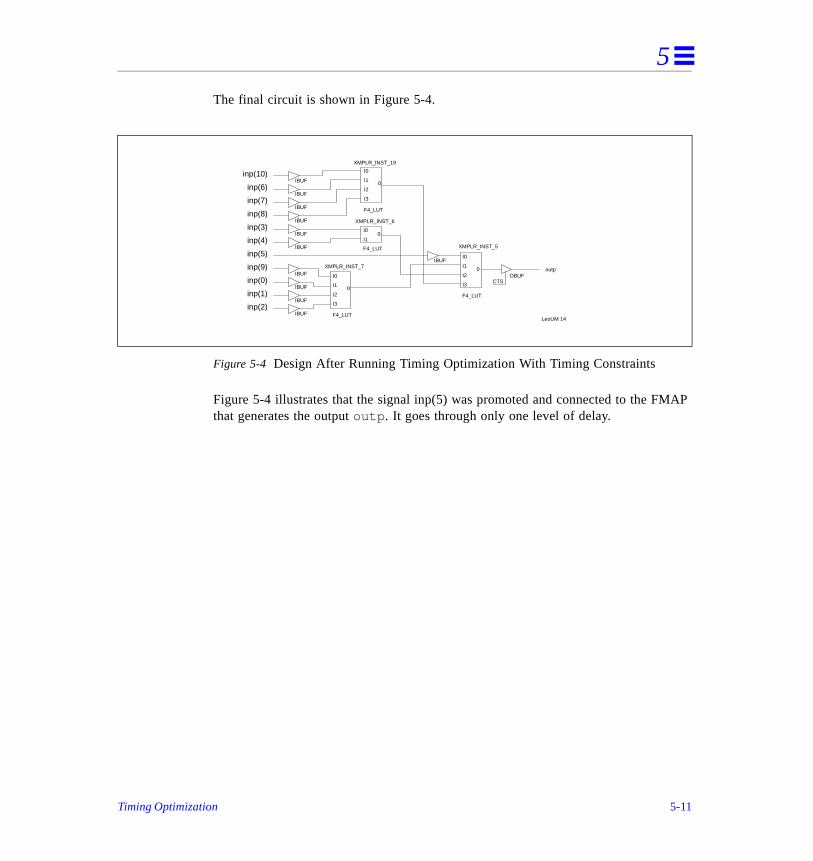
5
AP
The final circuit is shown in Figure 5-4.
Figure 5-4 Design After Running Timing Optimization With Timing Constraints
Figure 5-4 illustrates that the signal inp(5) was promoted and connected to the FMthat generates the output outp . It goes through only one level of delay.
inp(2)
XMPLR_INST_7
inp(1)
inp(0)
inp(9)
inp(5)
inp(4)
inp(3)
inp(8)
inp(7)
inp(10)
inp(6)
XMPLR_INST_6
XMPLR_INST_19
XMPLR_INST_5
outp
LeoUM 14IBUF
IBUF
IBUF
IBUF
IBUF
IBUF
IBUF
IBUF
IBUF
IBUF
IBUF
I0
I1
I2
I3
0
F4_LUT
I0
I1
I2
I3
0
F4_LUT
I0
I1
I2
I3
0
F4_LUT
I0
I10
F4_LUT
CTSOBUF
Timing Optimization 5-11

5
ct3
Targeting Actel Act3
Figure 5-5 shows the design after optimization that has been targeting for Actel Atechnology and before timing optimization has been done.
Figure 5-5 Design Before Timing Optimization
After setting the following constraints:
ARRIVAL_TIME inp(1) 10.0REQUIRED_TIME outp 25.0
inp(1)
XMPLR_INST_17IBUF
inp(0)
XMPLR_INST_18IBUF
IBUF
inp(2)
XMPLR_INST_16
inp(4)
XMPLR_INST_14IBUF
IBUF
IBUF
IBUF
IBUF
IBUF
inp(3)
XMPLR_INST_15
inp(5)
XMPLR_INST_13
inp(10)
XMPLR_INST_3IBUF
IBUF
inp(9)
XMPLR_INST_2
inp(7)
XMPLR_INST_11
inp(6)
XMPLR_INST_12
inp(8)
XMPLR_INST_10
PAD
PAD
PAD
PAD
PAD
PAD
PAD
PAD
PAD
PAD
PAD
Y
Y
Y
Y
Y
Y
Y
Y
Y
Y
Y
XMPLR_INST_5
Y
A
B
C
D
XMPLR_INST_4
Y
A
B
C
XMPLR_INST_6
Y
A
B
C
outp_rename
Y
A
B
C
D
AND4
AND4
AND3
AND3
XMPLR_INST_7OUTBUF
PAD outp
LeoUM 15
5-12 Leonardo Synthesis and Technology Guide
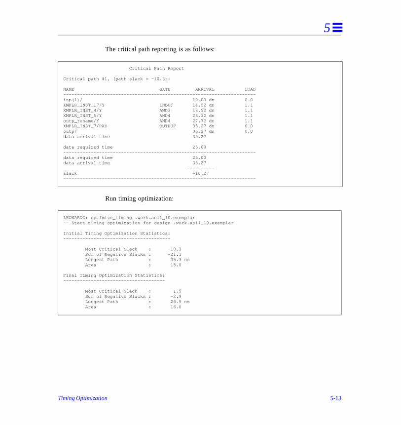
5
The critical path reporting is as follows:
Run timing optimization:
Critical Path Report
Critical path #1, (path slack = -10.3):
NAME GATE ARRIVAL LOAD----------------------------------------------------------------------inp(1)/ 10.00 dn 0.0XMPLR_INST_17/Y INBUF 14.52 dn 1.1XMPLR_INST_4/Y AND3 18.92 dn 1.1XMPLR_INST_5/Y AND4 23.32 dn 1.1outp_rename/Y AND4 27.72 dn 1.1XMPLR_INST_7/PAD OUTBUF 35.27 dn 0.0outp/ 35.27 dn 0.0data arrival time 35.27 data required time 25.00----------------------------------------------------------------------data required time 25.00data arrival time 35.27 ----------slack -10.27----------------------------------------------------------------------
LEONARDO: optimize_timing .work.aoi1_10.exemplar-- Start timing optimization for design .work.aoi1_10.exemplar
Initial Timing Optimization Statistics:---------------------------------------
Most Critical Slack : -10.3 Sum of Negative Slacks : -21.1 Longest Path : 35.3 ns Area : 15.0
Final Timing Optimization Statistics:-------------------------------------
Most Critical Slack : -1.5 Sum of Negative Slacks : -2.9 Longest Path : 26.5 ns Area : 16.0
Timing Optimization 5-13
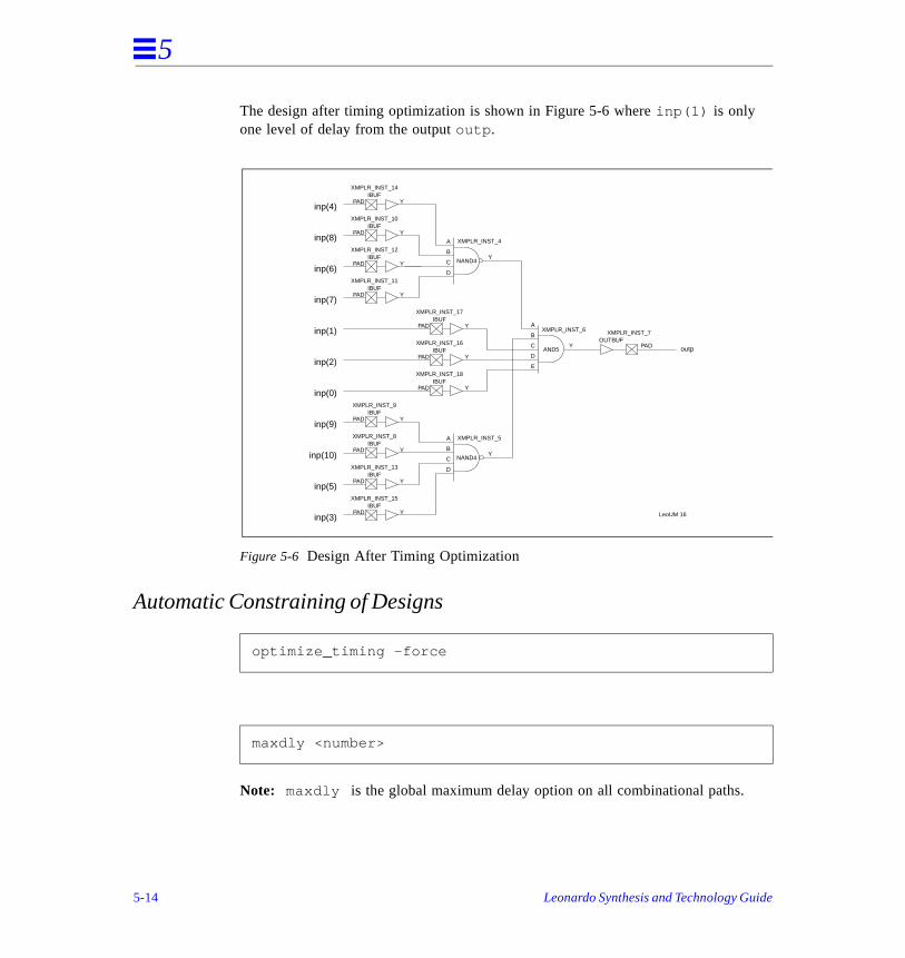
5
The design after timing optimization is shown in Figure 5-6 where inp(1) is only one level of delay from the output outp .
Figure 5-6 Design After Timing Optimization
Automatic Constraining of Designs
Note: maxdly is the global maximum delay option on all combinational paths.
optimize_timing -force
maxdly <number>
inp(5)
XMPLR_INST_13IBUF
inp(10)
XMPLR_INST_8IBUF
IBUF
inp(9)
XMPLR_INST_9
inp(0)
XMPLR_INST_18IBUF
IBUF
IBUF
inp(2)
XMPLR_INST_16
inp(1)
XMPLR_INST_17
inp(7)
inp(6)
inp(8)
inp(4)
PAD
PAD
PAD
PAD
PAD
PAD
Y
Y
Y
Y
Y
Y
inp(3)
XMPLR_INST_15IBUF
PAD Y
XMPLR_INST_12IBUF
XMPLR_INST_10IBUF
IBUFXMPLR_INST_14
PAD
PAD
PAD
Y
Y
Y
XMPLR_INST_11IBUF
PAD Y
XMPLR_INST_7OUTBUF
PAD outp
LeoUM 16
XMPLR_INST_5
Y
A
B
C
D
NAND4
XMPLR_INST_4
Y
A
B
C
D
NAND4
XMPLR_INST_6
Y
A
B
C
D
E
AND5
5-14 Leonardo Synthesis and Technology Guide
5
gative ber, re
p the
aths
Slack is a path that terminates in a register where a clock has been specified. Neslack indicates that there is a timing violation. However, if the slack is a valid numthen you have specified a required time and/or clock constraint. The constraints adefined as follows:
• Arrival time only is specified: The path is unconstrained.
• Clock only is specified: The output ports are unconstrained. However, paths ending in register inputs are constrained and optimize_timing ignores the -force option and attempts to improve the paths with slack.
• Clock is not specified: but some is specified on an output port, optimize_timing ignores the -force option and works only on output ports where the required time is specified. There is negative slack.
• Clocks and required times on outputs are not specified: In addition, no maxdly is specified. optimize_timing -force then attempts to improve the path that is most critical or the longest path. The command then cleans uartificial constraint that was applied and returns the circuit without any constraints.
In addition to restructuring paths for all technologies, buffering and replication forActel and ASICs have been added to the optimize_timing command. Leonardo attempts to buffer and replicate logic for timing, and then restructures if there are pthat violate timing.
Note: Buffering and replication for timing is not available for lookup table (LUT) FPGA technologies: Xilinx, Lucent ORCA, and Altera FLEX.
The -force option attempts to improve the circuit if you have not specified any constraints: required time and/or clock.
Timing Optimization 5-15

5
5-16 Leonardo Synthesis and Technology Guide
Reports 6
e s
d tions
d
This chapter presents examples of reports for Xilinx and Altera FLEX. Reports aravailable to all the technologies presented in this guide. This chapter is divided afollows:
• Xilinx Area/Delay Example Reports
• Altera FLEX Area/Delay Example Reports
Xilinx Area/Delay Example Reports
Leonardo provides estimates of the area and critical path delay for the synthesizedesigns. These estimates are provided for comparing different design implementaand for getting a quantitative estimate of design performance.
Area Reporting
Area for Xilinx LCA architectures is measured in terms of Function Generators anConfigurable Logic Blocks (CLBs). There are two different types of area reports:
6-1
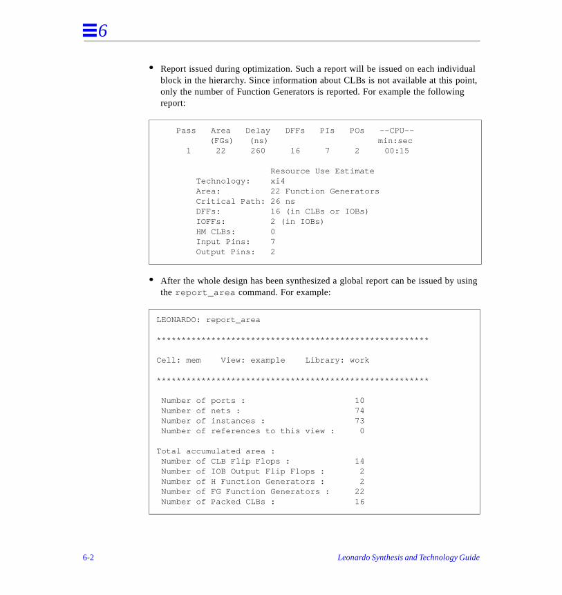
6
ual int,
using
• Report issued during optimization. Such a report will be issued on each individblock in the hierarchy. Since information about CLBs is not available at this poonly the number of Function Generators is reported. For example the followingreport:
• After the whole design has been synthesized a global report can be issued by the report_area command. For example:
Pass Area Delay DFFs PIs POs --CPU-- (FGs) (ns) min:sec
1 22 260 16 7 2 00:15
Resource Use Estimate Technology: xi4 Area: 22 Function Generators Critical Path: 26 ns DFFs: 16 (in CLBs or IOBs) IOFFs: 2 (in IOBs) HM CLBs: 0 Input Pins: 7 Output Pins: 2
LEONARDO: report_area
*******************************************************
Cell: mem View: example Library: work
******************************************************* Number of ports : 10 Number of nets : 74 Number of instances : 73 Number of references to this view : 0 Total accumulated area : Number of CLB Flip Flops : 14 Number of IOB Output Flip Flops : 2 Number of H Function Generators : 2 Number of FG Function Generators : 22 Number of Packed CLBs : 16
6-2 Leonardo Synthesis and Technology Guide
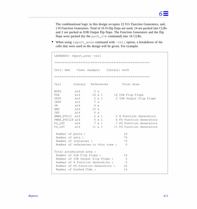
6
nd, LBs ip
The combinational logic in this design occupies 22 F,G Function Generators, a2 H Function Generators. Total of 16 D-flip flops are used, 14 are packed into Cand 2 are packed as IOB Output flip flops. The Function Generators and the flflops were packed (by the pack_clb command) into 16 CLBs.
• When using report_area command with -cell option, a breakdown of the cells that were used in the design will be given. For example:
LEONARDO: report_area -cell
*******************************************************
Cell: mem View: example Library: work
*******************************************************
Cell Library References Total Area
BUFG xi4 2 xFDE xi4 14 x 1 14 CLB Flip FlopsOFDT xi4 2 x 1 2 IOB Output Flip FlopsIBUF xi4 7 xOR xi4 6 xAND xi4 12 xINV xi4 6 xHMAP_PUC12 xi4 2 x 1 2 H Function GeneratorsFMAP_PUC124 xi4 4 x 1 4 FG Function GeneratorsF2_LUT xi4 7 x 1 7 FG Function GeneratorsF4_LUT xi4 11 x 1 11 FG Function Generators Number of ports : 10 Number of nets : 74 Number of instances : 73 Number of references to this view : 0 Total accumulated area : Number of CLB Flip Flops : 14 Number of IOB Output Flip Flops : 2 Number of H Function Generators : 2 Number of FG Function Generators : 22 Number of Packed CLBs : 16
Reports 6-3
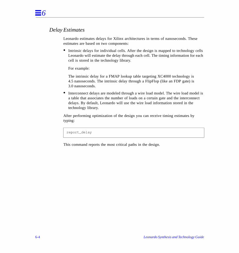
6
e
lls ach
el is nect
Delay Estimates
Leonardo estimates delays for Xilinx architectures in terms of nanoseconds. Thesestimates are based on two components:
• Intrinsic delays for individual cells. After the design is mapped to technology ceLeonardo will estimate the delay through each cell. The timing information for ecell is stored in the technology library.
For example:
The intrinsic delay for a FMAP lookup table targeting XC4000 technology is 4.5 nanoseconds. The intrinsic delay through a FlipFlop (like an FDP gate) is 3.0 nanoseconds.
• Interconnect delays are modeled through a wire load model. The wire load moda table that associates the number of loads on a certain gate and the intercondelays. By default, Leonardo will use the wire load information stored in the technology library.
After performing optimization of the design you can receive timing estimates by typing:
This command reports the most critical paths in the design.
report_delay
6-4 Leonardo Synthesis and Technology Guide
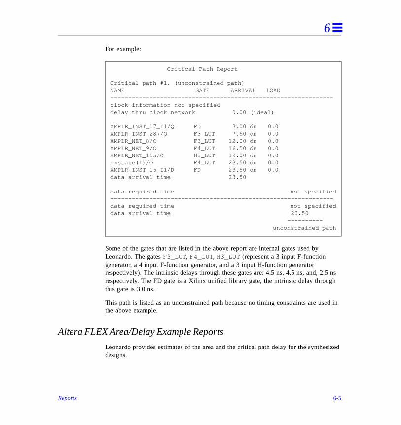
6
.5 ns h
ed in
sized
For example:
Some of the gates that are listed in the above report are internal gates used by Leonardo. The gates F3_LUT, F4_LUT, H3_LUT (represent a 3 input F-function generator, a 4 input F-function generator, and a 3 input H-function generator respectively). The intrinsic delays through these gates are: 4.5 ns, 4.5 ns, and, 2respectively. The FD gate is a Xilinx unified library gate, the intrinsic delay througthis gate is 3.0 ns.
This path is listed as an unconstrained path because no timing constraints are usthe above example.
Altera FLEX Area/Delay Example Reports
Leonardo provides estimates of the area and the critical path delay for the synthedesigns.
Critical Path Report
Critical path #1, (unconstrained path)NAME GATE ARRIVAL LOAD---------------------------------------------------------------clock information not specifieddelay thru clock network 0.00 (ideal)
XMPLR_INST_17_I1/Q FD 3.00 dn 0.0XMPLR_INST_287/O F3_LUT 7.50 dn 0.0XMPLR_NET_8/O F3_LUT 12.00 dn 0.0XMPLR_NET_9/O F4_LUT 16.50 dn 0.0XMPLR_NET_155/O H3_LUT 19.00 dn 0.0nxstate(1)/O F4_LUT 23.50 dn 0.0XMPLR_INST_15_I1/D FD 23.50 dn 0.0data arrival time 23.50
data required time not specified---------------------------------------------------------------data required time not specifieddata arrival time 23.50 ---------- unconstrained path
Reports 6-5
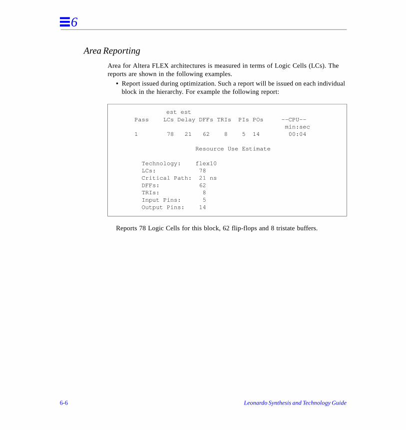
6
e
ual
Area Reporting
Area for Altera FLEX architectures is measured in terms of Logic Cells (LCs). Threports are shown in the following examples.
• Report issued during optimization. Such a report will be issued on each individblock in the hierarchy. For example the following report:
Reports 78 Logic Cells for this block, 62 flip-flops and 8 tristate buffers.
est est Pass LCs Delay DFFs TRIs PIs POs --CPU-- min:sec 1 78 21 62 8 5 14 00:04
Resource Use Estimate
Technology: flex10 LCs: 78 Critical Path: 21 ns DFFs: 62 TRIs: 8 Input Pins: 5 Output Pins: 14
6-6 Leonardo Synthesis and Technology Guide
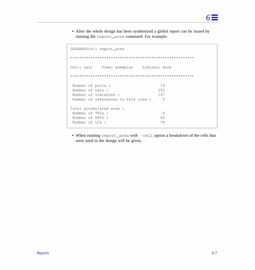
6
y
• After the whole design has been synthesized a global report can be issued brunning the report_area command. For example:
• When running report_area with -cell option a breakdown of the cells thatwere used in the design will be given.
LEONARDO{4}: report_area
*******************************************************
Cell: uart View: exemplar Library: work
*******************************************************
Number of ports : 19 Number of nets : 152 Number of instances : 147 Number of references to this view : 0 Total accumulated area : Number of TRIs : 8 Number of DFFs : 62 Number of LCs : 78
Reports 6-7
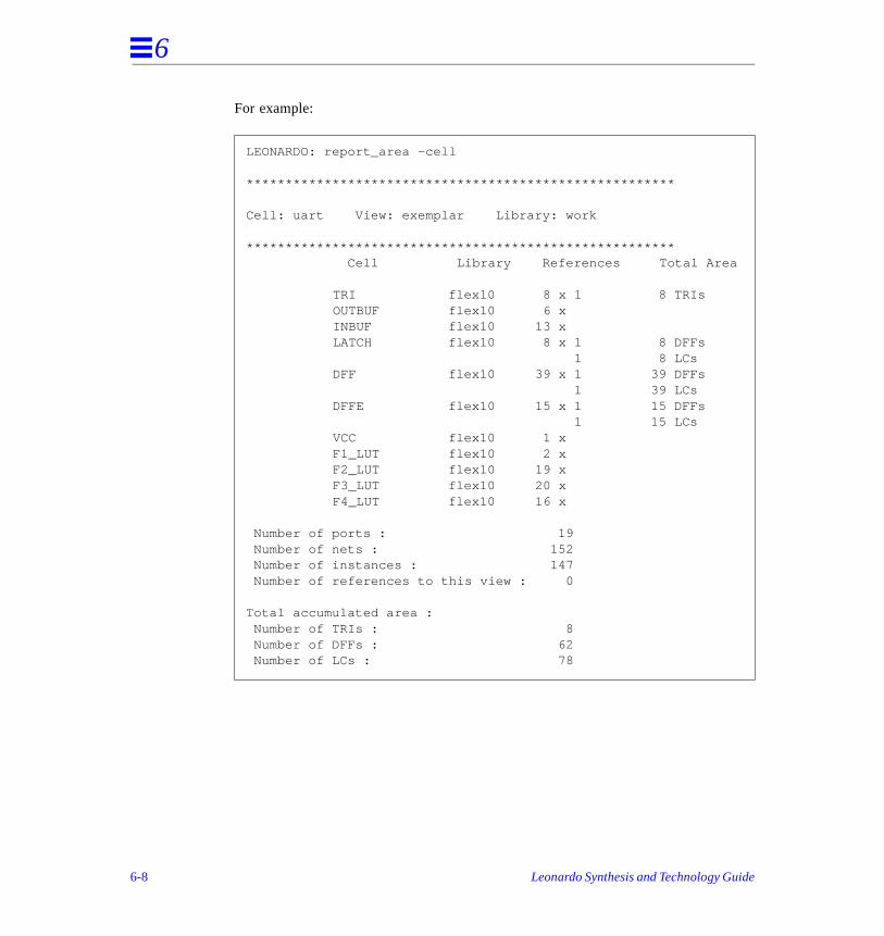
6
For example:
LEONARDO: report_area -cell
******************************************************* Cell: uart View: exemplar Library: work ******************************************************* Cell Library References Total Area
TRI flex10 8 x 1 8 TRIsOUTBUF flex10 6 xINBUF flex10 13 xLATCH flex10 8 x 1 8 DFFs
1 8 LCsDFF flex10 39 x 1 39 DFFs
1 39 LCsDFFE flex10 15 x 1 15 DFFs
1 15 LCsVCC flex10 1 xF1_LUT flex10 2 xF2_LUT flex10 19 xF3_LUT flex10 20 xF4_LUT flex10 16 x
Number of ports : 19 Number of nets : 152 Number of instances : 147 Number of references to this view : 0 Total accumulated area : Number of TRIs : 8 Number of DFFs : 62 Number of LCs : 78
6-8 Leonardo Synthesis and Technology Guide

6
The cells F1_LUT, F2_LUT, F3_LUT, F4_LUT are used internally by Leonardofor optimization and mapping. When writing out the output netlist these cells are replaced by Altera primitives (i.e., LCELL).Delay Estimates
LEONARDO{6}: report_delay -num 1 Critical Path Report Critical path #1, (unconstrained path)NAME GATE ARRIVAL LOAD---------------------------------------------------------clock information not specifieddelay thru clock network 0.00 (ideal) xmplr_inst_146/Q DFF 0.30 dn 0.0xmplr_net_155/O DF4_LUT 4.40 dn 0.0xmplr_net_161/O DF4_LUT 8.50 dn 0.0~xmplr_net_185/O DF4_LUT 12.60 dn 0.0xmplr_net_95/O DF2_LUT 16.70 dn 0.0xmplr_net_107/O DF2_LUT 20.80 dn 0.0xmplr_inst_146/D DDFF 20.80 dn 0.0data arrival time 20.80
data required time not specified---------------------------------------------------------data required time not specifieddata arrival time 20.80 ---------- unconstrained path---------------------------------------------------------
Reports 6-9

6
6-10 Leonardo Synthesis and Technology Guide
Synthesis for ASIC Technologies 7
nt our
d the
ter a
n and
ing evel
Leonardo provides a complete synthesis, optimization, and verification environmefor ASIC technologies. You can control and customize the synthesis process for ydesign. In addition, you can verify timing and functionality after place-and-route iscompleted. This chapter is divided as follows:
• Before Beginning
• Design Flows
• Optimization Features
• Timing Analysis
• Area and Delay Reporting
Before Beginning
The technology information presented in this chapter assumes that you have reaintroductory chapters in this guide.
Design Flows
As shown in Figure 7-1 Leonardo focuses on top-down design flows. You can endesign in VHDL or Verilog and synthesize it to the target ASIC technology. The behavioral design needs to be simulated first, then optimized and synthesized. AEDIF netlist is generated as an output. In addition, pre-place and pre-route timinganalysis can be run and critical path reporting received. Scan insertions for testinglayout are done next. The post-place and post-route netlist can be read to do timanalysis. Gate level simulation is then applied. Leonardo allows you to use gate lVHDL or Verilog with an SDF timing file to verify timing and functionality.
7-1
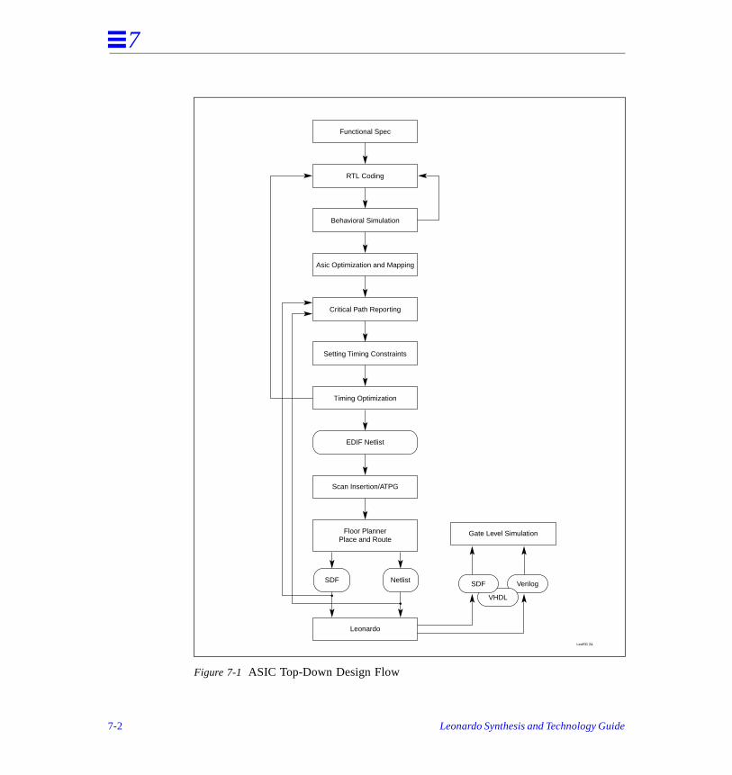
7
Figure 7-1 ASIC Top-Down Design Flow
Timing Optimization
Behavioral Simulation
Asic Optimization and Mapping
Critical Path Reporting
Setting Timing Constraints
RTL Coding
Functional Spec
EDIF Netlist
Scan Insertion/ATPG
Floor PlannerPlace and Route
Leonardo
LeoRG 24
VerilogSDF Netlist
VHDL
Gate Level Simulation
SDF
7-2 Leonardo Synthesis and Technology Guide
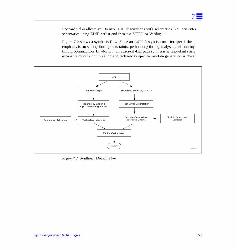
7
r
.
Leonardo also allows you to mix HDL descriptions with schematics. You can enteschematics using EDIF netlist and then use VHDL or Verilog.
Figure 7-2 shows a synthesis flow. Since an ASIC design is tuned for speed, theemphasis is on setting timing constraints, performing timing analysis, and runningtiming optimization. In addition, an efficient data path synthesis is important sinceextensive module optimization and technology specific module generation is done
Figure 7-2 Synthesis Design Flow
Technology-SpecificOptimization Algorithms
Technology MappingTechnology Libraries
Timing Optimization
Random Logic
High-Level Optimization
Module GenerationInference Engine
Module GenerationLibraries
Structured Logic (+,*,=,>,...)
HDL
LeoRG 25
Netlist
Synthesis for ASIC Technologies 7-3
7
ior)
ay hine
uld
e h
e on , bus
or plify
s for
on
is
om
Hierarchy
You can do the following:
• preserve the hierarchy as it was described in the input design (default behav
• flatten certain instances (using the ungroup command)
• create new levels of hierarchy (using the group command)
Since the tool is interactive (or script driven), different modules in the hierarchy mbe optimized with different parameters and constraints. For example, a state macmight be optimized for minimal gate count, while an ALU or data-path function cobe optimized for minimal delay.
In some designs, you can merge several instances together to optimize across thboundaries. This is useful when trying to speed up a critical path that goes througseveral instances.
Design Partitioning
ASIC designs are usually large. The way the design is partitioned has an influencsynthesis results. You can partition the design based on functionality. For exampleinterface unit is one block, while ALU is another block.
Some partitioning can be done for synthesis purposes. The goals of partitioning fsynthesis are: produce best synthesis results, speed up optimization time, and simthe synthesis process. Consider the following guidelines:
• Block size should not exceed 5000 gates. Run-time of synthesis algorithms inonlinear. Therefore, if the synthesized block is too large synthesis might runa long time.
• Try to register all inputs and outputs of a block. This is a good practice that simplifies the synthesis process. There is no need to specify required times outputs since all outputs are registered. Also, all logic is synchronous, whichavoids glitches.
• Do not use glue logic between hierarchical blocks. If you preserve hierarchyboundaries, then glue logic is not merged with hierarchical blocks. Glue logicthen optimized separately, which may be detrimental to synthesis results.
• The best results are when the critical paths lies in one hierarchical block as opposed to traversing multiple hierarchical blocks. You can group the logic frseveral blocks together to ensure that the critical path is in one block.
• Separate sub-designs with different goals.
7-4 Leonardo Synthesis and Technology Guide
7
/or s are
-plier
• Logic with similar characteristics should be grouped together to improve synthesis quality. Timing critical logic in one block with area critical logic in another.
Optimization Features
Specific optimization algorithms are targeted towards ASIC architectures:
• Data path synthesis
• Technology mapping
• Timing optimization
• Gate sizing for timing
• Resolution of design rule constraints
Data-Path Synthesis
Leonardo supports various types of implementations of arithmetic and relational operators used in VHDL or Verilog. Since these implementations are designed specifically for the ASIC technology, the synthesis results are usually smaller andfaster and take less time to compile. For the following operators, module generatorused to provide a technology-specific implementation:
Logical Operators and or nand nor xor xnor
Relational Operators = /= < <= > >=
Arithmetic Operators + - *
Misc. Functions incrementer, +1
decrementer, -1
absolute value, ABS
unary minus, unary -
New ASIC Modgen
Leonardo supports a variety of new module generator architectures for efficient implementation of data path modules. Supported are ripple-carry/carry-save/carrylookahead adders, subtractors, incrementers, decrementers, Baugh-Wooley multi
Synthesis for ASIC Technologies 7-5
7
or
e in
a r
cific te of
.03,
ic.vhd
is
re
age
with ripple-carry or carry-lookahead final adder stage, etc. These module generatarchitectures give far superior results in terms of area, delay and cpu time when compared to 'default' modgen (without a module generator primitives library) usagLeonardo, or any previous technology independent module generator technique.
To be able to use the new modgen architectures, you need a library of modgen primitives for the ASIC technology that you are using. This library of primitives is vhdl description of technology specific implementation of full-adder cells, and othebasic cells needed for efficient module generation.
The library is included with the ASIC package. The package can be obtained fromyour ASIC vendor. The Exemplar ftp site also provides a large number of ASIC packages for various technologies.
If you are currently using an ASIC technology, but don't have the technology spemodgen primitives library, please contact your ASIC vendor, and ask for an updathe ASIC package for the technology you are using.
If you have been using the new ASIC module generators with Leonardo release 4then you will be accustomed to loading the technology independent architecture generator file (asic.vhd) separately. Also, you needed to download a separate asarchitecture generator file from the Exemplar ftp site.
This generator file is not needed in Leonardo 4.1. Now you only need to load thetechnology specific modgen primitives library file. The architecture generator file loaded automatically, from the Leonardo 4.1 installation area.
The ASIC package consists of a Leonardo library (<tech>.syn file), a Leonardo modgen primitives library (<tech>.vhd file) plus documentation. Presently, there aapproximately 60 different ASIC technologies available for Leonardo.
Once you obtain the ASIC package, follow the instructions that come with the packto install the files: store the <tech>.syn file in the $EXEMPLAR/lib directory, and install the <tech>.vhd file in the $EXEMPLAR/data/modgen directory.
Next, run Leonardo and load both the technology and the modgen architectures
load_library <tech>[.syn] <-- Load the technology fileload_modgen <tech>[.vhd] <-- Load the modgen architectures
You are now ready to load in any design. Leonardo will use the new, efficient, technology specific implementations for all data path modules in your design.
7-6 Leonardo Synthesis and Technology Guide
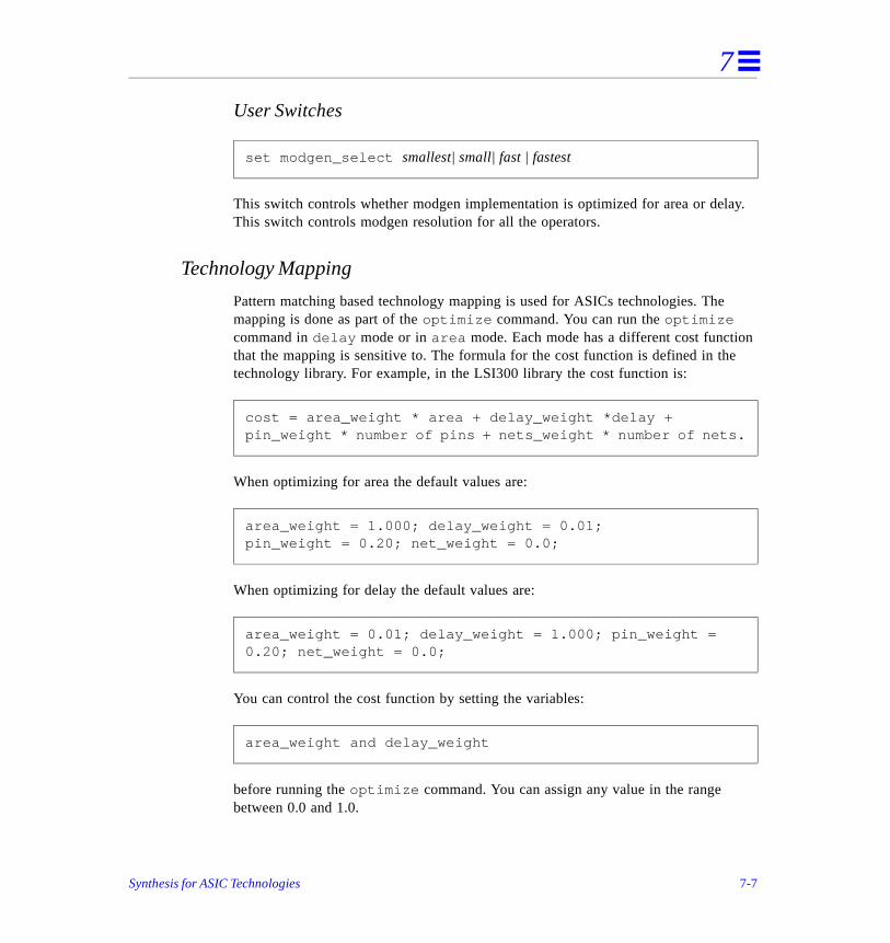
7
ay.
n e
User Switches
This switch controls whether modgen implementation is optimized for area or delThis switch controls modgen resolution for all the operators.
Technology Mapping
Pattern matching based technology mapping is used for ASICs technologies. Themapping is done as part of the optimize command. You can run the optimize command in delay mode or in area mode. Each mode has a different cost functiothat the mapping is sensitive to. The formula for the cost function is defined in thtechnology library. For example, in the LSI300 library the cost function is:
When optimizing for area the default values are:
When optimizing for delay the default values are:
You can control the cost function by setting the variables:
before running the optimize command. You can assign any value in the range between 0.0 and 1.0.
set modgen_select smallest| small| fast | fastest
cost = area_weight * area + delay_weight *delay + pin_weight * number of pins + nets_weight * number of nets.
area_weight = 1.000; delay_weight = 0.01; pin_weight = 0.20; net_weight = 0.0;
area_weight = 0.01; delay_weight = 1.000; pin_weight = 0.20; net_weight = 0.0;
area_weight and delay_weight
Synthesis for ASIC Technologies 7-7
7
t to
ry cost te
Constraint-Driven Timing Optimization
The optimize_timing command can be used after optimization is done to improve the timing quality of the design. The optimize_timing command works most effectively when timing constraints are specified. If timing constraints are nospecified the -force option can be used to force timing constraints, in an attemptimprove the longest path.
You can set timing constraints to direct the timing optimization to optimize certainpaths. For example: OUTPUT_LOAD, INPUT_DRIVE, ARRIVAL_TIME, and REQUIRED_TIME.
The optimize_timing command restructures combinational logic to reduce thelevels of logic between the critical signal and the output.
The optimize_timing may be invoked repeatedly for added improvements if possible.
A specific end point or instance to improve can be specified to the optimize_timing command with the -through option.
Gate Sizing
Leonardo performs gate sizing to improve the timing quality of the design. It will tto find the optimal size of a gate so that the cost of the gate will be minimal. The is controlled by the global cost function that is set from the technology library. Gasizing is performed as part of the optimize and optimize_timing commands. You can disable gate sizing by setting the variable gate_sizing to FALSE. By default this variable is set to TRUE. You can experiment with this variable to get optimal results. For example, running the sequence:
will perform gate sizing during mapping but not during timing optimization.
Leonardo does not perform gate sizing for I/O cells and sequential cells.
set gate_sizing TRUEoptimize -ta lsi300 -delayset gate_sizing FALSEoptimize_timing
7-8 Leonardo Synthesis and Technology Guide
7
pF). does the
. the ce,
input
in in an be
ll by
Design Rule Constraints
Leonardo checks for the following design rule constraints load violations, fanout violations, and transition time violations.
Load Violations
The load driven by a particular gate is expressed in terms of capacitance (usuallyLeonardo checks that every output pin in a given design has an actual load that not exceed the allowed (maximum) load. Maximum load for an output pin is set bymax_cap_load property in the technology library. Some libraries may define a default load value to be used for output pins which do not have a max_cap_load value set.
The default is specified in the library by using the default_max_cap_load property. From Leonardo’s shell you can overwrite the default value by setting thevariable max_cap_load . This must be done before reading the technology libraryRecommended: set the load values on all primary outputs of each sub-design usingoutput_load command. The actual computed load includes wire load capacitanif information is available in the technology library.
Fanout Violations
In the technology library each gate may have a fanout_load value for input pins, and a max_fanout_load value for output pins. fanout_load is expressed in terms of integer numbers and represents the number of fanouts that a particular pin is loading to the fanout output driver. The max_fanout_load specifies how many fanouts a particular output pin can drive. Leonardo checks that each output pa design does not drive more than the allowed number of fanouts. Default value cspecified in the library by using the default_max_fanout_load property. If specified, the default_max_fanout_load assigns max_fanout_load values to all unassigned gates. You can overwrite the default value from Leonardo’s shesetting the max_fanout_load variable before reading the technology library.
Synthesis for ASIC Technologies 7-9
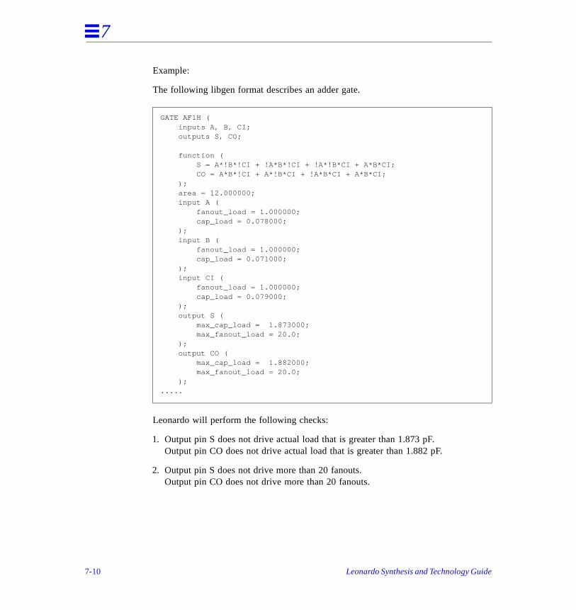
7
Example:
The following libgen format describes an adder gate.
Leonardo will perform the following checks:
1. Output pin S does not drive actual load that is greater than 1.873 pF. Output pin CO does not drive actual load that is greater than 1.882 pF.
2. Output pin S does not drive more than 20 fanouts.Output pin CO does not drive more than 20 fanouts.
GATE AF1H ( inputs A, B, CI; outputs S, CO;
function ( S = A*!B*!CI + !A*B*!CI + !A*!B*CI + A*B*CI; CO = A*B*!CI + A*!B*CI + !A*B*CI + A*B*CI; ); area = 12.000000; input A ( fanout_load = 1.000000; cap_load = 0.078000; ); input B ( fanout_load = 1.000000; cap_load = 0.071000; ); input CI ( fanout_load = 1.000000; cap_load = 0.079000; ); output S ( max_cap_load = 1.873000; max_fanout_load = 20.0; ); output CO ( max_cap_load = 1.882000; max_fanout_load = 20.0; );.....
7-10 Leonardo Synthesis and Technology Guide
7
ates ition has
by
d
e
Transition Time Violations
This violation is applicable for nonlinear timing modeling only. You can specify maximum transition time for input and output pins of gates. Leonardo then calculthe actual transition time for input and output pins in the design. If the actual transtime exceeds the maximum transition time, as specified in the library, a violation occurred.
This computation is more complex than load and fanout violations because the transition time of a particular output pin is dependent on the transition time of its inputs. You can define a default maximum transition time in the technology librarysetting the default_max_transition property, and can overwrite the default transition time from Leonardo’s shell by setting the max_transition variable before reading the technology library.
Resolving Load Violations
Leonardo resolves load violations by doing one of the following operations:
• Gate sizing If possible, Leonardo upsizes the gate on which a load violation has occurred. This is applicable for resolving loaand fanout violations only.
• Logic replication Logic is replicated and the actual load is split between threplicated logic. This is applicable for resolving load violations only.
• Buffering Building a buffer tree to resolve the violation. This technique is used to resolve transition time violations.
Synthesis for ASIC Technologies 7-11
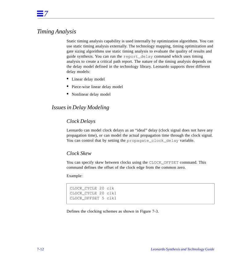
7
an and and
s on nt
any nal.
Timing Analysis
Static timing analysis capability is used internally by optimization algorithms. You cuse static timing analysis externally. The technology mapping, timing optimization gate sizing algorithms use static timing analysis to evaluate the quality of results guide synthesis. You can run the report_delay command which uses timing analysis to create a critical path report. The nature of the timing analysis dependthe delay model defined in the technology library. Leonardo supports three differedelay models:
• Linear delay model
• Piece-wise linear delay model
• Nonlinear delay model
Issues in Delay Modeling
Clock Delays
Leonardo can model clock delays as an “ideal” delay (clock signal does not havepropagation time), or can model the actual propagation time through the clock sigYou can control that by setting the propagate_clock_delay variable.
Clock Skew
You can specify skew between clocks using the CLOCK_OFFSET command. This command defines the offset of the clock edge from the common zero.
Example:
Defines the clocking schemes as shown in Figure 7-3.
CLOCK_CYCLE 20 clkCLOCK_CYCLE 20 clk1CLOCK_OFFSET 5 clk1
7-12 Leonardo Synthesis and Technology Guide
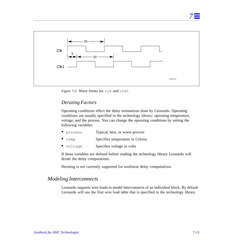
7
ault y.
Figure 7-3 Wave forms for clk and clk1
Derating Factors
Operating conditions effect the delay estimations done by Leonardo. Operating conditions are usually specified in the technology library: operating temperature, voltage, and the process. You can change the operating conditions by setting thefollowing variables:
• process Typical, best, or worst process
• temp Specifies temperature in Celsius
• voltage Specifies voltage in volts
If these variables are defined before reading the technology library Leonardo willderate the delay computations.
Derating is not currently supported for nonlinear delay computations.
Modeling Interconnects
Leonardo supports wire loads to model interconnects of an individual block. By defLeonardo will use the first wire load table that is specified in the technology librar
LeoRG 26
520
20
Clk
Clk1
Synthesis for ASIC Technologies 7-13
7
ct a
nnect nout, tive
nd to
, the ivides d by
sized
rary.
You can define many wire load tables in the technology library and then can selewire load table by using the wire_table variable. For example, the sequence of commands:
Uses wire load table table1 for the sub-design called design1 and wire load table table2 for the sub-design called design2 .
You can direct Leonardo not to use wire load tables by setting the variable nowire_table to TRUE.
The capacitance and resistance of the interconnect are computed using an intercoload model. The interconnect load model is an estimation of the load due to the faand the location of the resistive components of the wire. The location of the resiscomponents effect how much capacitive load the driver see.
The three different models of the capacitance load can be used: best, balanced aworst. In the best case the interconnect delay is 0, since the driver does not havedrive the interconnect capacitance through the wire resistance. In the worst casedriver has to drive the wire cap through the wire resistance. The balanced case dthe capacitance evenly between the driven loads. This modeling can be controllesetting the wire_tree variable to either best, balanced, or worst value.
Area and Delay Reporting
Leonardo provides estimates of the area and the critical path delay for the synthedesign.
Area Report
Area for ASIC designs is measured in units that are defined in the technology lib
present_design design1set wire_table table1optimizereport_delaypresent_design design2set wire_table table2optimizereport_delay
7-14 Leonardo Synthesis and Technology Guide
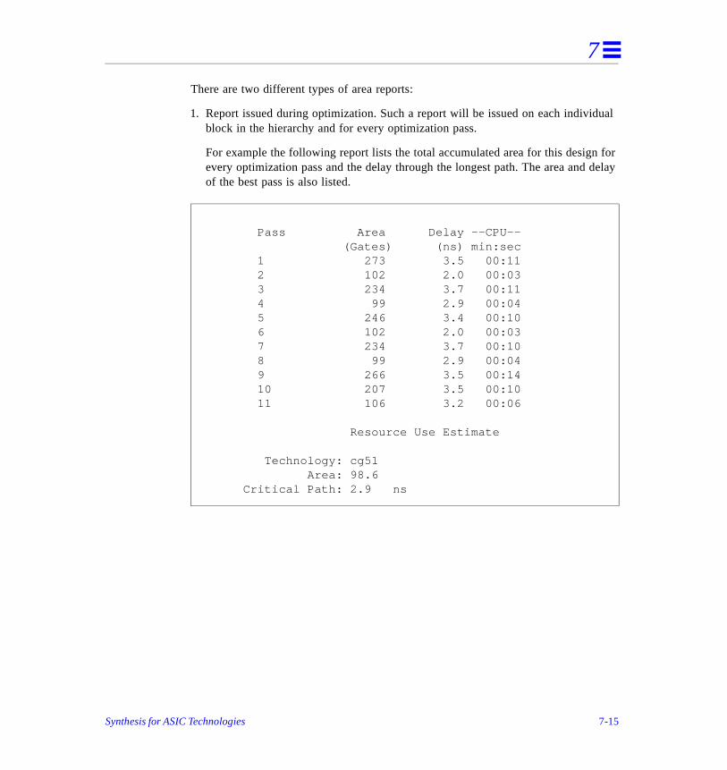
7
ual
for delay
There are two different types of area reports:
1. Report issued during optimization. Such a report will be issued on each individblock in the hierarchy and for every optimization pass.
For example the following report lists the total accumulated area for this designevery optimization pass and the delay through the longest path. The area and of the best pass is also listed.
Pass Area Delay --CPU-- (Gates) (ns) min:sec 1 273 3.5 00:11 2 102 2.0 00:03 3 234 3.7 00:11 4 99 2.9 00:04 5 246 3.4 00:10 6 102 2.0 00:03 7 234 3.7 00:10 8 99 2.9 00:04 9 266 3.5 00:14 10 207 3.5 00:10 11 106 3.2 00:06 Resource Use Estimate Technology: cg51 Area: 98.6 Critical Path: 2.9 ns
Synthesis for ASIC Technologies 7-15
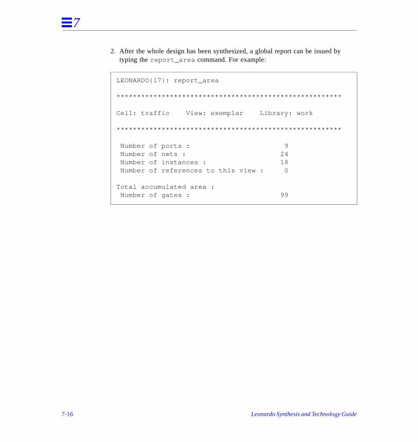
7
2. After the whole design has been synthesized, a global report can be issued bytyping the report_area command. For example:LEONARDO{17}: report_area ******************************************************* Cell: traffic View: exemplar Library: work ******************************************************* Number of ports : 9 Number of nets : 24 Number of instances : 18 Number of references to this view : 0 Total accumulated area : Number of gates : 99
7-16 Leonardo Synthesis and Technology Guide
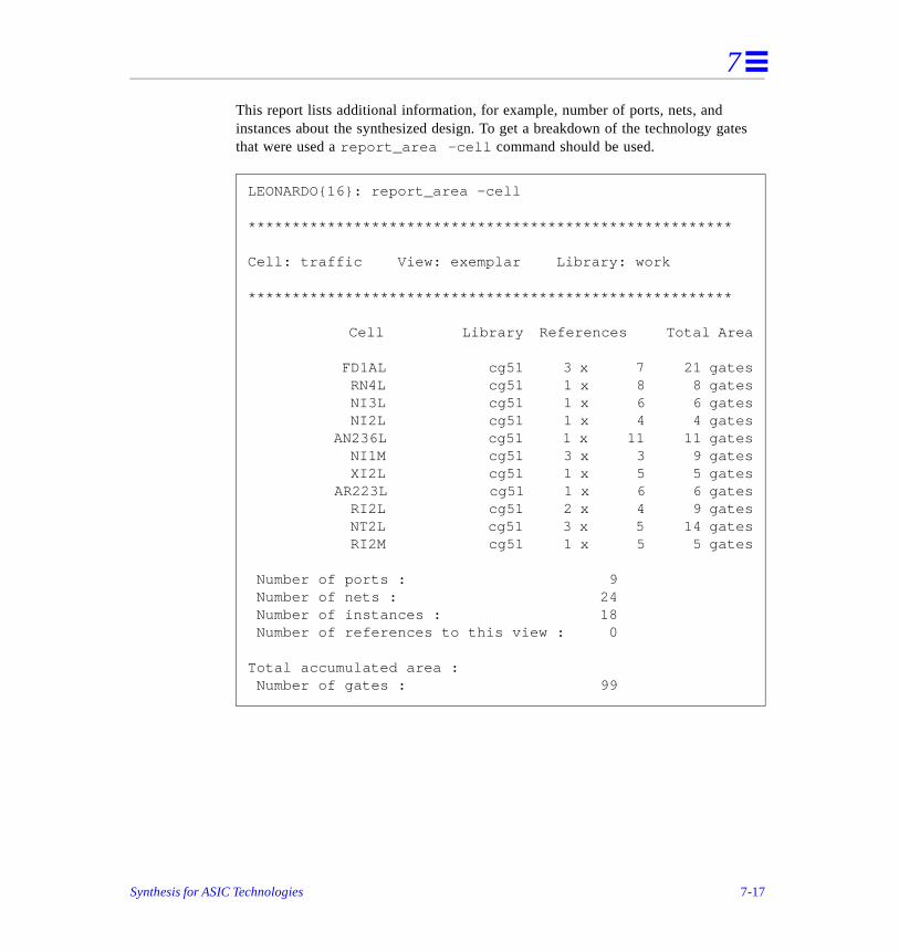
7
ates
This report lists additional information, for example, number of ports, nets, and instances about the synthesized design. To get a breakdown of the technology gthat were used a report_area -cell command should be used.LEONARDO{16}: report_area -cell
*******************************************************
Cell: traffic View: exemplar Library: work
*******************************************************
Cell Library References Total Area
FD1AL cg51 3 x 7 21 gates RN4L cg51 1 x 8 8 gates NI3L cg51 1 x 6 6 gates NI2L cg51 1 x 4 4 gates AN236L cg51 1 x 11 11 gates NI1M cg51 3 x 3 9 gates XI2L cg51 1 x 5 5 gates AR223L cg51 1 x 6 6 gates RI2L cg51 2 x 4 9 gates NT2L cg51 3 x 5 14 gates RI2M cg51 1 x 5 5 gates
Number of ports : 9 Number of nets : 24 Number of instances : 18 Number of references to this view : 0
Total accumulated area : Number of gates : 99
Synthesis for ASIC Technologies 7-17
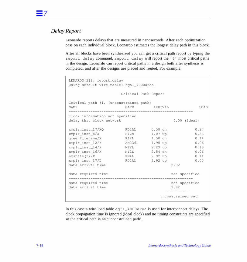
7
ion lock.
the
is
ified
Delay Report
Leonardo reports delays that are measured in nanoseconds. After each optimizatpass on each individual block, Leonardo estimates the longest delay path in this b
After all blocks have been synthesized you can get a critical path report by typingreport_delay command. report_delay will report the ’6’ most critical paths in the design. Leonardo can report critical paths in a design both after synthesis completed, and after the designs are placed and routed. For example:
In this case a wire load table cg51_4000area is used for interconnect delays. The clock propagation time is ignored (ideal clock) and no timing constraints are specso the critical path is an ‘unconstrained path’.
LENARDO{21}: report_delayUsing default wire table: cg51_4000area
Critical Path Report Critical path #1, (unconstrained path)NAME GATE ARRIVAL LOAD---------------------------------------------------------clock information not specifieddelay thru clock network 0.00 (ideal) xmplr_inst_17/XQ FD1AL 0.58 dn 0.27xmplr_inst_8/X RI2M 1.07 up 0.33green2_rename/X RI2L 1.50 dn 0.14xmplr_inst_12/X AN236L 1.95 up 0.06xmplr_inst_14/X NT2L 2.29 up 0.19xmplr_inst_16/X NI2L 2.54 dn 0.06nxstate(2)/X RN4L 2.92 up 0.11xmplr_inst_17/D FD1AL 2.92 up 0.00data arrival time 2.92
data required time not specified---------------------------------------------------------data required time not specifieddata arrival time 2.92 ---------- unconstrained path
7-18 Leonardo Synthesis and Technology Guide
Actel Synthesis 8
. pter
Leonardo provides synthesis support for the following Actel architectures:
• Act1/2/3
• 1200XL
• 3200DX
• 40MX and 42MX
Designs can be entered using VHDL or Verilog HDL descriptions or EDIF netlistsGate array and other FPGA designs can be retargeted for Actel devices. This chapresents information on how to use Leonardo for Actel devices.
This chapter is divided as follows:
• Before Beginning
• Actel FPGA Architecture
• Design Flows
• New Features for Actel
• Synthesis and Optimization Features
• Data Path Synthesis
• Additional Synthesis Features
• I/O Mapping
• Complex I/O Design Rule Checker and Modifier
• Actel Reports
• Process Derating Factors
8-1
8
d the d
is t one
ble of
e
with
as
e fer.
ized tlist
Before Beginning
The technology information presented in this chapter assumes that you have reaintroductory chapters in this guide. Refer also to the HDL Synthesis and CommanReference guides for information.
Actel FPGA Architecture
Actel Logic Module
The basic logic element of the Actel FPGAs is the Logic Module. A logic module built from three, 2-input multiplexers. The Act1 logic module is an 8-input,1-outpulogic circuit, which consists of three 2-to-1 multiplexers, one 2-input OR gate, and 2-input AND gate. The Act2 architecture creates two different module structures. These structures are the C-Modules and the S-Modules. The C-Modules are capaimplementing only combinational logic, while the S-Modules can implement both combinational and sequential logic. The 1200XL and 3200DX are variations of thAct2 architecture. The 3200DX has on-chip dual port RAMs available.
The Act3 family has basically the same architecture as the Act2 devices, with theexception that the sequential gate in the S-Module does not share the reset logicthe combinational logic. It has speed improvements and additional clock lines.
Since logic modules are created from multiplexers, the multiplexer can be viewedthe most cost effective function, where cost is measured in area and speed
I/O Buffers
Each I/O pin is configurable as an input, output, tristate, or bidirectional buffer. ThAct3 family adds complex I/Os that combine registered logic with the basic I/O bufComplex I/Os are absorbed automatically when using Leonardo.
Design Flows
A simplified design flow is shown in Figure 8-1 to illustrate how Leonardo is usedwith the Actel tools. Designs are entered using standard methods, and are optimand mapped to the target Actel technology by Leonardo. The result is an EDIF nethat is used by Actel place-and-route tools.
8-2 Leonardo Synthesis and Technology Guide
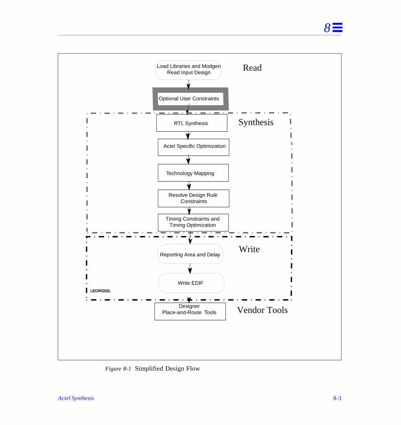
8
Figure 8-1 Simplified Design Flow
Actel Specific Optimization
Optional User Constraints
Write EDIF
Synthesis
Write
Read
Vendor ToolsDesignerPlace-and-Route Tools
Reporting Area and Delay
Resolve Design Rule Constraints
Timing Constraints andTiming Optimization
RTL Synthesis
Technology Mapping
LEORG02L
Load Libraries and ModgenRead Input Design
Actel Synthesis 8-3
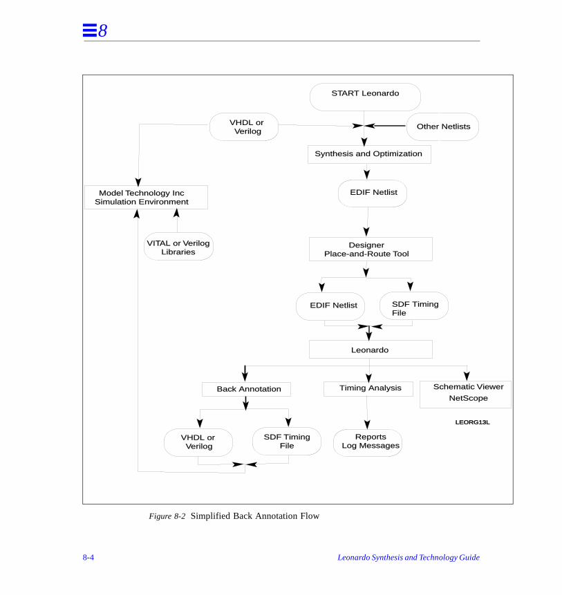
8
wer
Figure 8-2 Simplified Back Annotation Flow
START Leonardo
VHDL or Verilog
Other Netlists
Synthesis and Optimization
Model Technology IncSimulation Environment
VITAL or VerilogLibraries
LEORG13L
NetScopeTiming Analysis
Leonardo
Back Annotation Schematic Vie
VHDL or Verilog
SDF TimingFile
ReportsLog Messages
EDIF Netlist SDF TimingFile
EDIF Netlist
DesignerPlace-and-Route Tool
8-4 Leonardo Synthesis and Technology Guide
8
ns.
also
New Features for Actel
New Operators
The following operators were added:
• Act 1: fast incrementer, reduce_and
• All families: reduce_nand , reduce_or
Improvements to Mapper
• Boolean mapper is faster. Only Boolean mapper is being used for Actel.
• Mapping to CM7s: Increases the combinability for Act2, 1200xl, 3200dx desig
• Automatic mapping to available clock buffers.
Accurate Delay Estimations
All Actel libraries were modified with delay information that is compatible with Designer.
Logic Replication and Buffering
Logic replication and buffering resolves timing violations.
Fanout Violations and Load Violations
When resolving design rule violations, Leonardo considers fanout violations and load violations. You can disable either fanout or load violations from the GUI.
Reduced Memory Consumption
The Actel technology libraries are smaller.
Actel Synthesis 8-5
8
es.
at s
nal es).
alid.
the
Enhancements to Actel Technologies
Actel mapping and optimization were enhanced to map to DFM7 and DFM7A gatThis will make area and delay estimates more accurate. When targeting Act2 or 3200DX technologies, the mapper will map to CM7 gates. It is a known problem ththe CM7 gate was not included in Designer's simulation libraries. This problem habeen fixed and you can get the new simulation libraries from Actel.
Note: These libraries are available on Actel's Web site. Beginning with the R1/98 release, CM7 simulation models will be part of Actel's release.
Modgen Enhancements
New Modgen Libraries
A32DX: Actel 3200DX Modgen Library (Act2 modgen plus RAMs)
Existing Library Improvement
All RAMs: support for arbitrary size RAMs
New Components
Act1/2/3/32DX: small/fast non-loadable down counters.
Synthesis and Optimization Features• Mux-based optimization that understands and utilizes the multiplexer based
structure of the Actel Logic Module. The concept is to restructure combinatiologic to be represented in terms of multiplexers (instead of AND and OR gat
• Boolean mapping maps directly to the Actel Logic Module.
• Leonardo resolves load violations to ensure that the generated designs are v
• Leonardo assigns clock buffers automatically. You can also assign the clock buffers manually.
• Replication and buffering to resolve timing violations.
• Constraint driven timing optimization can be used to speed up critical paths indesign.
8-6 Leonardo Synthesis and Technology Guide
8
o
al d d/or
• Additional features are Support for Logic Combinability, Automatic Mapping tComplex I/Os, and Design Rule Checker.
Technology Mapping
Leonardo offers a powerful Boolean Mapping algorithm that maps logic directly toLogic Cells. The following libraries are available:
Act1 For the Act1 technology
Act2 For the Act2 technology
Act3 For the Act3 technology
a12x1 For the 1200XL technology
a32dx For the 3200DX technology
Data Path Synthesis
Modgen
Leonardo supports technology specific implementations of arithmetic and relationoperators used in VHDL or Verilog RTL. Since these implementations are designeoptimally for the Actel technologies, the synthesis results are in general smaller anfaster and take less time to compile. The following operators and miscellaneous functions have technology specific architectures in the modgen libraries:
• Logical Operators and or nand nor xor xnor
• Relational Operators = /= < <= > >=
• Shift Operators sll srl sla sra rol ror
• Arithmetic Operators + - *
• Misc. Functions incrementerdecrementerabsolute valueunary minuscountersmultiplexer
Actel Synthesis 8-7
8
a
hese
ation Both
AMs:
a
a
Using RAMs
Types of Inferencing RAMs
Leonardo supports two types of RAMs:
• RAM_DQ. RAM_DQ is a single-port RAM with separate input and output datlines.
• RAM_IO. RAM_IO is a single-port RAM with bidirectional data lines.
Both of these RAM types support synchronous or asynchronous read and write. TRAMs are automatically inferred by Leonardo from HDL code (VHDL or Verilog). The inferencing process distinguishes between RAMs that perform the read operwith an address clocked or not clocked by the write clock (read address clocked). of the following VHDL examples perform synchronous writes (inclock) and synchronous reads (outclock); Leonardo recognizes these VHDL processes as R
• The first, entity ram_example1 , is when the read operation does not haveclocked address.
• The second entity ram_example2 , is when the read operation does have clocked address.
Disable RAM Inferencing
set extract_RAM true (default)
set extract_RAM false to disable.
8-8 Leonardo Synthesis and Technology Guide
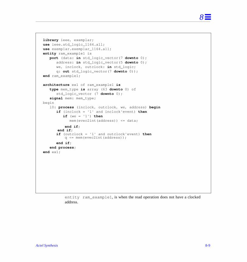
8
entity ram_example1 , is when the read operation does not have a clocked address.
library ieee, exemplar;use ieee.std_logic_1164.all;use exemplar.exemplar_1164.all;entity ram_example1 is port (data: in std_logic_vector(7 downto 0); address: in std_logic_vector(5 downto 0); we, inclock, outclock: in std_logic; q: out std_logic_vector(7 downto 0));end ram_example1;
architecture ex1 of ram_example1 is type mem_type is array (63 downto 0) of std_logic_vector (7 downto 0); signal mem: mem_type;begin l0: process (inclock, outclock, we, address) begin if (inclock = '1' and inclock'event) then if (we = '1') then mem(evec2int(address)) <= data;
if (outclock = '1' and outclock'event) then
end if ; end process ;end ex1;
q <= mem(evec2int(address));
end if ;end if ;
Actel Synthesis 8-9
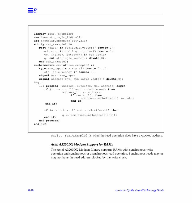
8
ss.
ay or
entity ram_example2 , is when the read operation does have a clocked addre
Actel A3200DX Modgen Support for RAMs
The Actel A3200DX Modgen Library supports RAMs with synchronous write operation and synchronous or asynchronous read operation. Synchronous reads mmay not have the read address clocked by the write clock.
library ieee, exemplar;use ieee.std_logic_1164.all;use exemplar.exemplar_1164.all;entity ram_example2 is port (data: in std_logic_vector(7 downto 0); address: in std_logic_vector(5 downto 0); we, inclock, outclock: in std_logic; q: out std_logic_vector(7 downto 0)); end ram_example2;architecture ex2 of ram_example2 is type mem_type is array (63 downto 0) of std_logic_vector (7 downto 0); signal mem: mem_type; signal address_int: std_logic_vector(5 downto 0);begin l0: process (inclock, outclock, we, address) begin if (inclock = '1' and inclock'event) then
if (outclock = '1' and outclock'event) then
end if ; end process ;end ex2;
address_int <= address;if (we = '1') then
mem(evec2int(address)) <= data;end if ;
end if ;
q <= mem(evec2int(address_int));
8-10 Leonardo Synthesis and Technology Guide
8
th.
s the
u a
L
pin
,
be
Constraint-Driven Timing Optimization
The optimize_timing command can be used after optimization to improve thetiming performance of the design. optimize_timing command works most effectively when timing constraints are specified. However, the -force option can be used to force timing constraints, in which case it will try to improve the longest pa
A specific end point or instance to improve can be specified to the optimize_timing command with the -through option.
The optimize_timing command restructures combinational logic to reduce thelevels of logic between the critical signal and the output. This command also maprestructured portion of the logic effectively to the Actel technologies. optimize_timing may be invoked repeatedly for added improvements.
Interfacing with Actel’s ACTGen
Modgen implementations are fully compatible with Actel’s ACTGen. This gives yovery high quality of results. You may also interface from Leonardo with ACTGen directly. The following steps describe how to interface with ACTGen through VHDand Verilog.
1. Create your ACTGen modules and generate an EDIF output for each module.
2. Instantiate the ACTGen modules in your design. Be sure to keep the cell and names consistent with ACTGen naming convention. Refer to Figure 8-3.
3. Set the Leonardo variable hdl_array_name_style to the format %s(%d) . This will ensure that Leonardo will expand bus names by the format bus_name bit_number. For Example if a 32 bit bus is named A, it will be expanded as: A0A1, A2, ..., A31. This matches the way ACTGen generates bus names.
4. Optimize your design and generate EDIF output. All the ACTGen modules willtreated as black boxes.
optimize_timing -force
optimize_timing -through <node_list>
Actel Synthesis 8-11
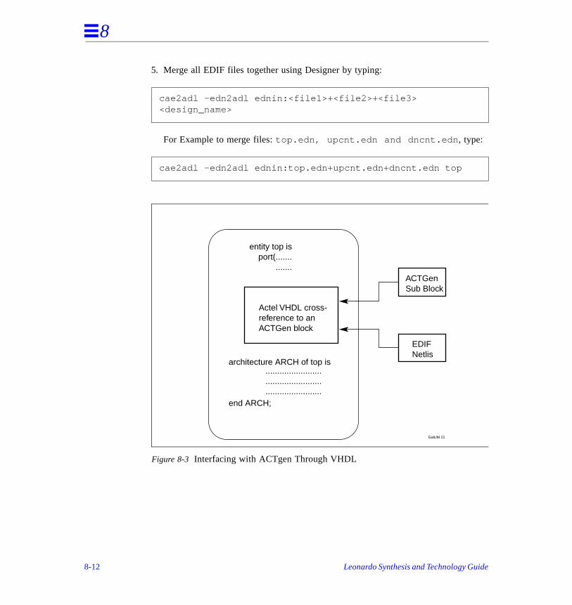
8
5. Merge all EDIF files together using Designer by typing:
For Example to merge files: top.edn, upcnt.edn and dncnt.edn , type:
Figure 8-3 Interfacing with ACTgen Through VHDL
cae2adl -edn2adl ednin:<file1>+<file2>+<file3> <design_name>
cae2adl -edn2adl ednin:top.edn+upcnt.edn+dncnt.edn top
GalUM 21
entity top isport(.......
.......
Actel VHDL cross-reference to anACTGen block
architecture ARCH of top is
end ARCH;
........................
........................
........................
ACTGenSub Block
EDIFNetlis
8-12 Leonardo Synthesis and Technology Guide
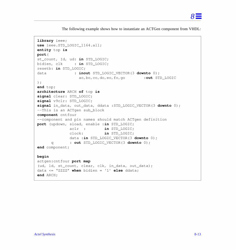
8
DL:
The following example shows how to instantiate an ACTGen component from VHlibrary ieee;use ieee.STD_LOGIC_1164.all;entity top isport (st_count, Id, ud: in STD_LOGIC;bidien, clk : in STD_LOGIC;resetb: in STD_LOGIC;data : inout STD_LOGIC_VECTOR(3 downto 0); ao,bo,co,do,eo,fo,go : out STD_LOGIC);end top;architecture ARCH of top is signal clear: STD_LOGIC;signal v9clr: STD_LOGIC;signal in_data, out_data, ddata :STD_LOGIC_VECTOR(3 downto 0);--This is an ACTgen sub_blockcomponent cntfour--component and pin names should match ACTgen definitionport (updown, sload, enable : in STD_LOGIC; aclr : in STD_LOGIC; clock: in STD_LOGIC; data : in STD_LOGIC_VECTOR(3 downto 0); q : out STD_LOGIC_VECTOR(3 downto 0);end component;
beginactgen:cntfour port map(ud, ld, st_count, clear, clk, in_data, out_data);data <= “ZZZZ” when bidien = ‘1’ else ddata;end ARCH;
Actel Synthesis 8-13
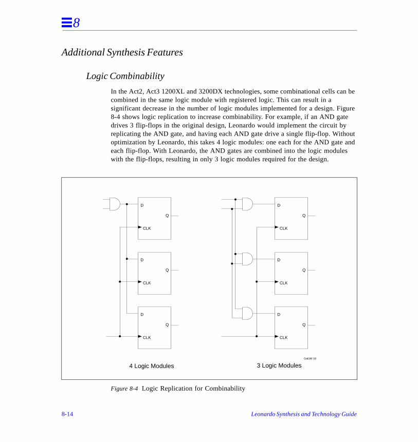
8
be
gure
ut and s
Additional Synthesis Features
Logic Combinability
In the Act2, Act3 1200XL and 3200DX technologies, some combinational cells cancombined in the same logic module with registered logic. This can result in a significant decrease in the number of logic modules implemented for a design. Fi8-4 shows logic replication to increase combinability. For example, if an AND gatedrives 3 flip-flops in the original design, Leonardo would implement the circuit by replicating the AND gate, and having each AND gate drive a single flip-flop. Withooptimization by Leonardo, this takes 4 logic modules: one each for the AND gateeach flip-flop. With Leonardo, the AND gates are combined into the logic modulewith the flip-flops, resulting in only 3 logic modules required for the design.
Figure 8-4 Logic Replication for Combinability
GalUM 18
D
CLK
Q
D
CLK
Q
D
CLK
Q
D
CLK
Q
D
CLK
Q
D
CLK
Q
4 Logic Modules 3 Logic Modules
8-14 Leonardo Synthesis and Technology Guide
8
ess
et.
ll as
Fanout and Load Violations
A fanout violation occurs when a cell drives a higher number of fanouts than the allowed number of fanouts. Actel’s Designer Software allows a technology cell todrive up to 24 fanouts. The recommended number of fanouts a cell can drive is lthan 10. If a cell drives between 10 and 24 fanouts, Designer will issue a warningmessage.
The default number for maximum fanout allowed by Leonardo is set from the technology library and is as follows
Act1, Act2, 1200XL, 3200DX 10 fanouts
Act 3 16 fanouts
You can overwrite this number by setting the variable from Leonardo’s shell.
To resolve fanout violations Leonardo will replicate logic whenever possible. Otherwise Leonardo will buffer the relevant signals so that fanout violations are mYou can disable logic replication by setting the variable nologic_rep to TRUE.
Using Global Clock Buffers
Leonardo supports both automatic mapping of clock signals to clock buffers as wemanual mapping of clocks. Both automatic and manual mapping are discussed.
Automatic Mapping of Clocks
Leonardo automatically maps primary clocks and primary set/reset signals to clock/global buffers available in the target Actel architecture.
Following architectural constrains are taken into account:
• For Act1 only one CLKBUF is available.
• For Act2/1200XL two CLKBUFs are available.
set max_fanout_load <n>
set nologic_rep TRUE
Actel Synthesis 8-15
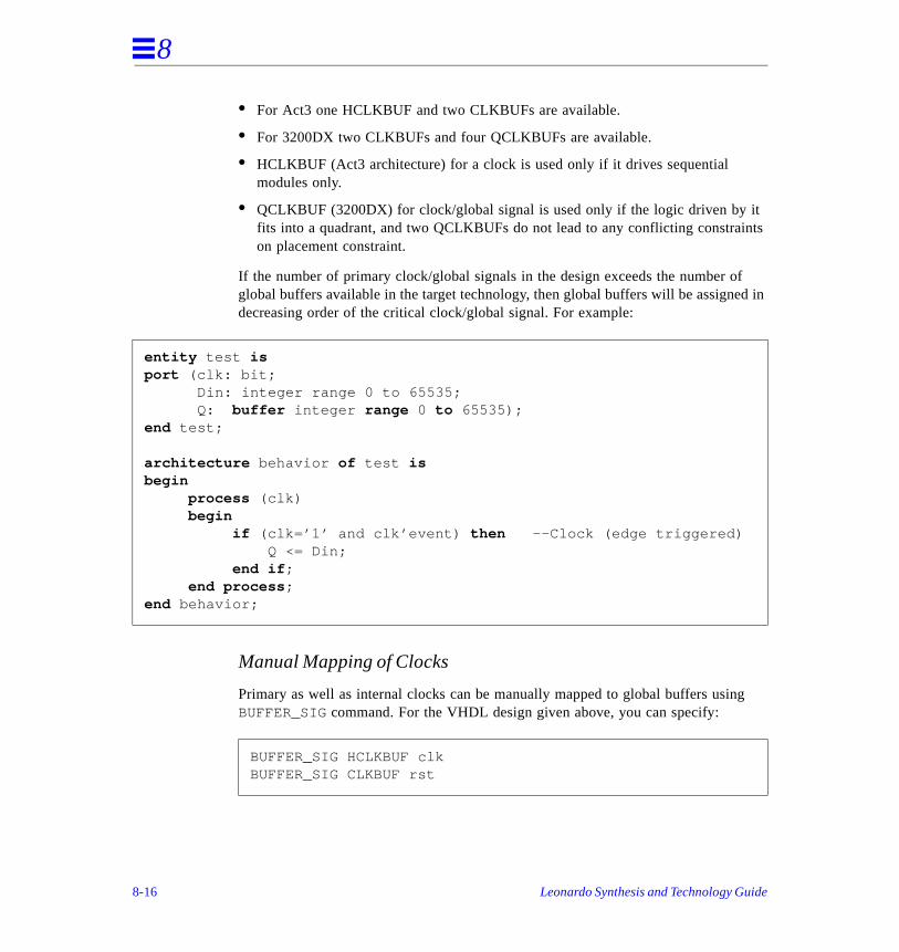
8
t nts
f d in
g
• For Act3 one HCLKBUF and two CLKBUFs are available.
• For 3200DX two CLKBUFs and four QCLKBUFs are available.
• HCLKBUF (Act3 architecture) for a clock is used only if it drives sequential modules only.
• QCLKBUF (3200DX) for clock/global signal is used only if the logic driven by ifits into a quadrant, and two QCLKBUFs do not lead to any conflicting constraion placement constraint.
If the number of primary clock/global signals in the design exceeds the number oglobal buffers available in the target technology, then global buffers will be assignedecreasing order of the critical clock/global signal. For example:
Manual Mapping of Clocks
Primary as well as internal clocks can be manually mapped to global buffers usinBUFFER_SIG command. For the VHDL design given above, you can specify:
entity test isport (clk: bit; Din: integer range 0 to 65535; Q: buffer integer range 0 to 65535);end test;
architecture behavior of test is begin process (clk) begin if (clk=’1’ and clk’event) then --Clock (edge triggered) Q <= Din; end if ; end process ;end behavior;
BUFFER_SIG HCLKBUF clkBUFFER_SIG CLKBUF rst
8-16 Leonardo Synthesis and Technology Guide
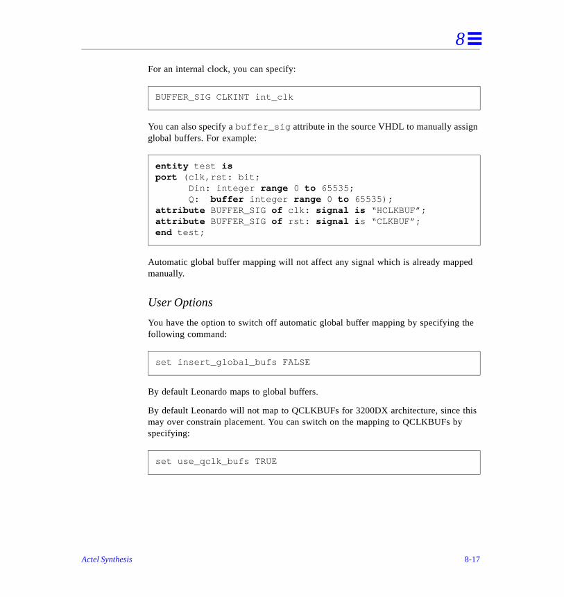
8
d
he
is
For an internal clock, you can specify:
You can also specify a buffer_sig attribute in the source VHDL to manually assignglobal buffers. For example:
Automatic global buffer mapping will not affect any signal which is already mappemanually.
User Options
You have the option to switch off automatic global buffer mapping by specifying tfollowing command:
By default Leonardo maps to global buffers.
By default Leonardo will not map to QCLKBUFs for 3200DX architecture, since thmay over constrain placement. You can switch on the mapping to QCLKBUFs byspecifying:
BUFFER_SIG CLKINT int_clk
entity test is port (clk,rst: bit; Din: integer range 0 to 65535; Q: buffer integer range 0 to 65535);attribute BUFFER_SIG of clk: signal is “HCLKBUF”;attribute BUFFER_SIG of rst: signal i s “CLKBUF”;end test;
set insert_global_bufs FALSE
set use_qclk_bufs TRUE
Actel Synthesis 8-17
8
tion cells or
:
ed
not tries ng an
Design I/O
I/O Mapping
Leonardo maps I/O cells and registered I/O cells automatically. If the input descripimplies a use of a certain I/O cell, then Leonardo maps to it. You can assign I/O manually by either instantiating them from the (RTL description) VHDL or Verilog, using the PAD or BUFFER_SIG commands from Leonardo’s shell.
Complex I/O Design Rule Checker and Modifier
Act3 architecture enables you to use registered I/Os with the following restrictions
• All registered I/Os are controlled by one hardwired clock line: IOCLK.
• All registered I/Os should use either clear or preset. There is only one hardwirclear/preset line to be used (IOPCL).
Leonardo verifies that a design (after optimization and technology mapping) doesviolate any of these restrictions. If the design violates some constraints, Leonardoto modify the design and to use as many registered I/Os as possible without creatiillegal design.
8-18 Leonardo Synthesis and Technology Guide

8
Example of a VHDL File Containing a Design Rule Violation
library exemplar ;use work.exemplar.all;entity sample is port ( a, b, d, clr, clk: in bit; o, o1 : out bit );end sample;architecture exemplar of sample is signal sig1, sig2, sig3: bit;beginprocess (clk, clr)begin if (clr = ’0’) then sig2 <= ’0’; sig1 <= ’0’; elsif (clk’event and clk = ’1’) then sig2 <= b; sig1 <= sig3; end if ;end process ;o <= a and sig2;o1 <= a and sig1;sig3 <= a and d;end exemplar;
Actel Synthesis 8-19
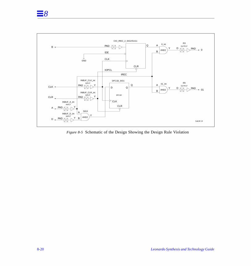
8
Figure 8-5 Schematic of the Design Showing the Design Rule Violation
Q
CLR
PAD A
IDE
GND
D
CLK
Q
CLR
PAD
DFC1B_SIG1
PAD
Q
GalUM 19
PAD
PAD
AND2
AND2
PAD
PAD
CIO_IREC_2_SIG2/S1I11
B
A
B
B
DFC1B
INBUF_CLK_int
CLK
IOPCL
IREC
INBUF_CLR_int
INPUT
INPUT
INBUF_A_intINPUT
INBUF_D_intINPUT AND2
CLK
CLR
A
B
A
D
Y
Y
Y
Y
Y
OUTPUT
Y
Y
D
D
01
0
i53
SIG3
OUTPUT
i55
0_int
01_int
8-20 Leonardo Synthesis and Technology Guide
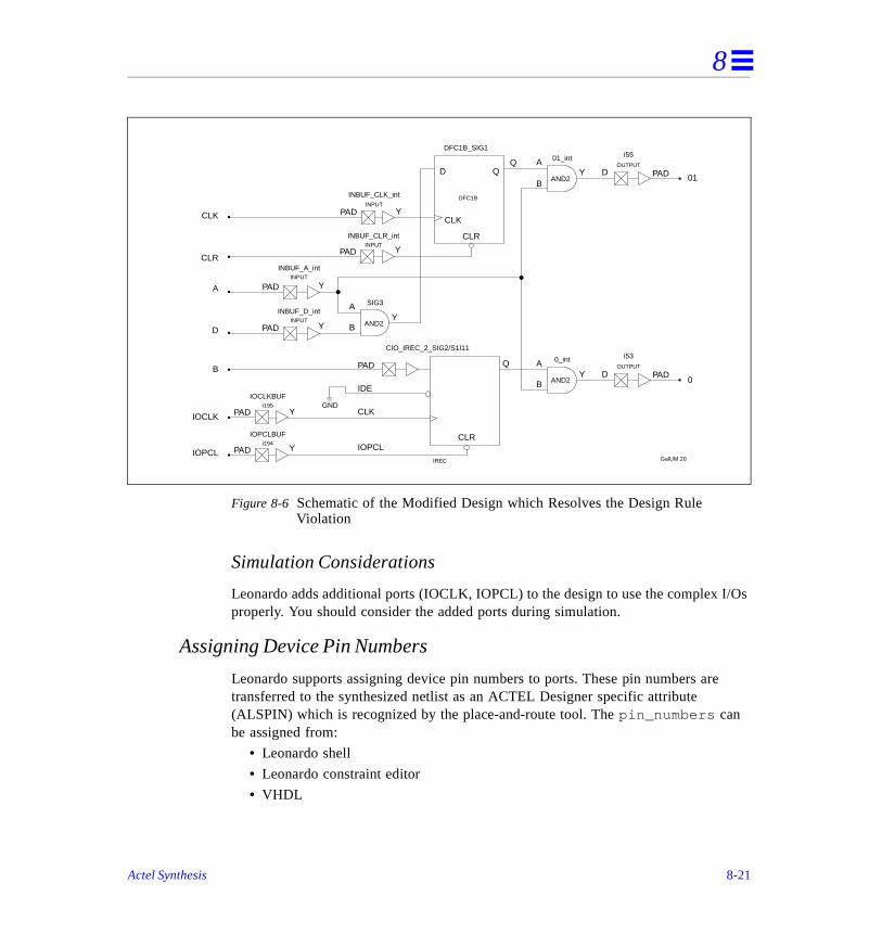
8
I/Os
e
Figure 8-6 Schematic of the Modified Design which Resolves the Design Rule Violation
Simulation Considerations
Leonardo adds additional ports (IOCLK, IOPCL) to the design to use the complex properly. You should consider the added ports during simulation.
Assigning Device Pin Numbers
Leonardo supports assigning device pin numbers to ports. These pin numbers artransferred to the synthesized netlist as an ACTEL Designer specific attribute (ALSPIN) which is recognized by the place-and-route tool. The pin_numbers can be assigned from:
• Leonardo shell
• Leonardo constraint editor
• VHDL
GalUM 20
D
CLK
Q
CLR
DFC1B_SIG1
Q
DFC1B
PAD
PAD
INBUF_A_intINPUT
INBUF_D_intINPUT AND2
A
B
A
D
Y
Y
Y
SIG3
PAD
PAD
INBUF_CLK_int
INBUF_CLR_int
INPUT
INPUT
Y
Y
APAD
PAD
AND2
AND2
A
B
B
OUTPUT
Y
Y
D
D
0
01
i55
OUTPUT
i53
01_int
0_intQ
CLR
PAD
IDE
GND
CIO_IREC_2_SIG2/S1I11
B
CLK
IOPCL
PAD
PAD
IOPCLBUFi194
IOCLKBUFi195
IOPCL
Y
Y
IOCLK
CLK
CLR
IREC
Actel Synthesis 8-21
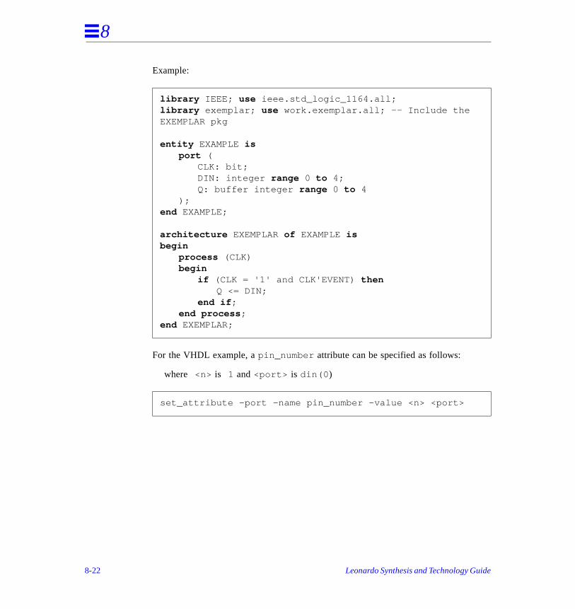
8
Example:
For the VHDL example, a pin_number attribute can be specified as follows:
where <n> is 1 and <port> is din(0 )
library IEEE; use ieee.std_logic_1164.all;library exemplar; use work.exemplar.all; -- Include the EXEMPLAR pkg
entity EXAMPLE isport (
CLK: bit;DIN: integer range 0 to 4;Q: buffer integer range 0 to 4
);end EXAMPLE;
architecture EXEMPLAR of EXAMPLE isbegin
process (CLK)begin
if (CLK = '1' and CLK'EVENT) thenQ <= DIN;
end if ;end process ;
end EXEMPLAR;
set_attribute -port -name pin_number -value <n> <port>
8-22 Leonardo Synthesis and Technology Guide
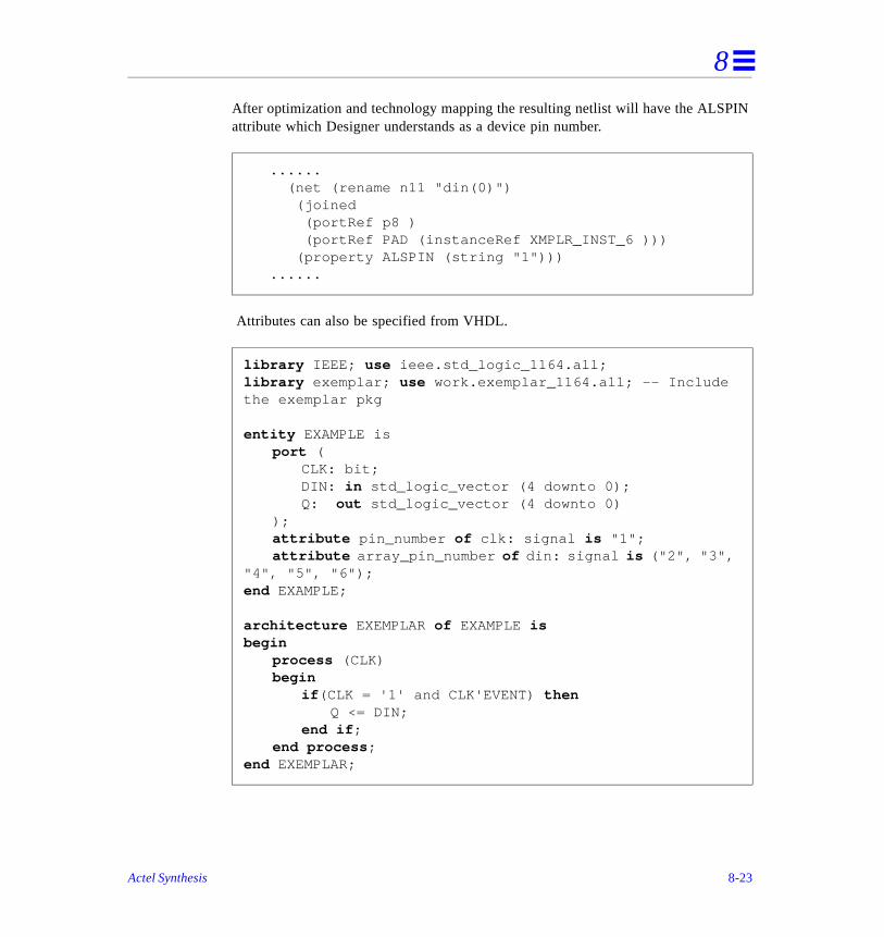
8
IN
After optimization and technology mapping the resulting netlist will have the ALSPattribute which Designer understands as a device pin number.Attributes can also be specified from VHDL.
...... (net (rename n11 "din(0)") (joined (portRef p8 ) (portRef PAD (instanceRef XMPLR_INST_6 ))) (property ALSPIN (string "1"))) ......
library IEEE; use ieee.std_logic_1164.all;library exemplar; use work.exemplar_1164.all; -- Include the exemplar pkg
entity EXAMPLE isport (
CLK: bit;DIN: in std_logic_vector (4 downto 0);Q: out std_logic_vector (4 downto 0)
);attribute pin_number of clk: signal is "1";attribute array_pin_number of din: signal is ("2", "3",
"4", "5", "6");end EXAMPLE;
architecture EXEMPLAR of EXAMPLE isbegin
process (CLK)begin
if (CLK = '1' and CLK'EVENT) thenQ <= DIN;
end if ;end process ;
end EXEMPLAR;
Actel Synthesis 8-23
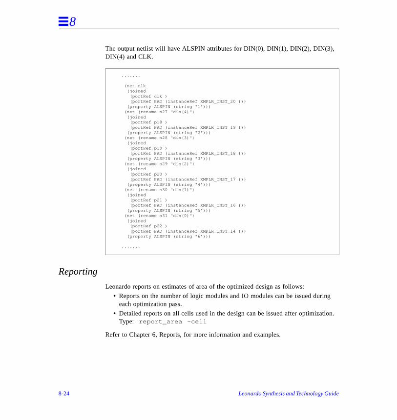
8
ng
ion.
The output netlist will have ALSPIN attributes for DIN(0), DIN(1), DIN(2), DIN(3), DIN(4) and CLK.
Reporting
Leonardo reports on estimates of area of the optimized design as follows:
• Reports on the number of logic modules and IO modules can be issued durieach optimization pass.
• Detailed reports on all cells used in the design can be issued after optimizatType: report_area -cell
Refer to Chapter 6, Reports, for more information and examples.
.......
(net clk (joined (portRef clk ) (portRef PAD (instanceRef XMPLR_INST_20 ))) (property ALSPIN (string "1"))) (net (rename n27 "din(4)") (joined (portRef p18 ) (portRef PAD (instanceRef XMPLR_INST_19 ))) (property ALSPIN (string "2"))) (net (rename n28 "din(3)") (joined (portRef p19 ) (portRef PAD (instanceRef XMPLR_INST_18 ))) (property ALSPIN (string "3"))) (net (rename n29 "din(2)") (joined (portRef p20 ) (portRef PAD (instanceRef XMPLR_INST_17 ))) (property ALSPIN (string "4"))) (net (rename n30 "din(1)") (joined (portRef p21 ) (portRef PAD (instanceRef XMPLR_INST_16 ))) (property ALSPIN (string "5"))) (net (rename n31 "din(0)") (joined (portRef p22 ) (portRef PAD (instanceRef XMPLR_INST_14 ))) (property ALSPIN (string "6")))
.......
8-24 Leonardo Synthesis and Technology Guide
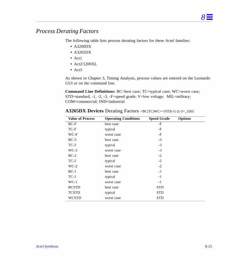
8
ardo
Process Derating Factors
The following table lists process derating factors for these Actel families:
• A3200DX
• A3265DX
• Act1
• Act2/1200XL
• Act3
As shown in Chapter 3, Timing Analysis, process values are entered on the LeonGUI or on the command line.
Command Line Definitions: BC=best case; TC=typical case; WC=worst case; STD=standard, -1, -2, -3, -F=speed grade; V=low voltage; MIL=military; COM=commercial; IND=industrial
A3265DX Devices Derating Factors <BC|TC|WC><STD|-1|-2|-3>_3265
Value of Process Operating Conditions Speed Grade Options
BC-F best case -F
TC-F typical -F
WC-F worst case -F
BC-3 best case -3
TC-3 typical -3
WC-3 worst case -3
BC-2 best case -2
TC-2 typical -2
WC-2 worst case -2
BC-1 best case -1
TC-1 typical -1
WC-1 worst case -1
BCSTD best case STD
TCSTD typical STD
WCSTD worst case STD
Actel Synthesis 8-25
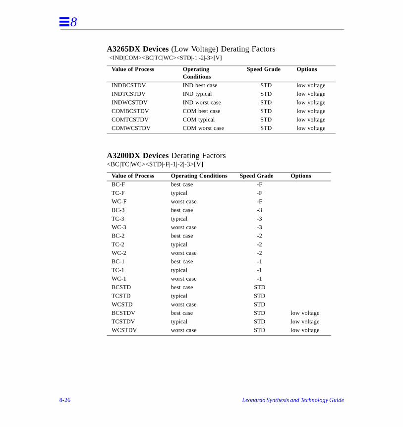
8
A3265DX Devices (Low Voltage) Derating Factors <IND|COM><BC|TC|WC><STD|-1|-2|-3>[V]
A3200DX Devices Derating Factors<BC|TC|WC><STD|-F|-1|-2|-3>[V]
Value of Process Operating Conditions
Speed Grade Options
INDBCSTDV IND best case STD low voltage
INDTCSTDV IND typical STD low voltage
INDWCSTDV IND worst case STD low voltage
COMBCSTDV COM best case STD low voltage
COMTCSTDV COM typical STD low voltage
COMWCSTDV COM worst case STD low voltage
Value of Process Operating Conditions Speed Grade OptionsBC-F best case -F
TC-F typical -F
WC-F worst case -F
BC-3 best case -3
TC-3 typical -3
WC-3 worst case -3
BC-2 best case -2
TC-2 typical -2
WC-2 worst case -2
BC-1 best case -1
TC-1 typical -1
WC-1 worst case -1
BCSTD best case STD
TCSTD typical STD
WCSTD worst case STD
BCSTDV best case STD low voltage
TCSTDV typical STD low voltage
WCSTDV worst case STD low voltage
8-26 Leonardo Synthesis and Technology Guide
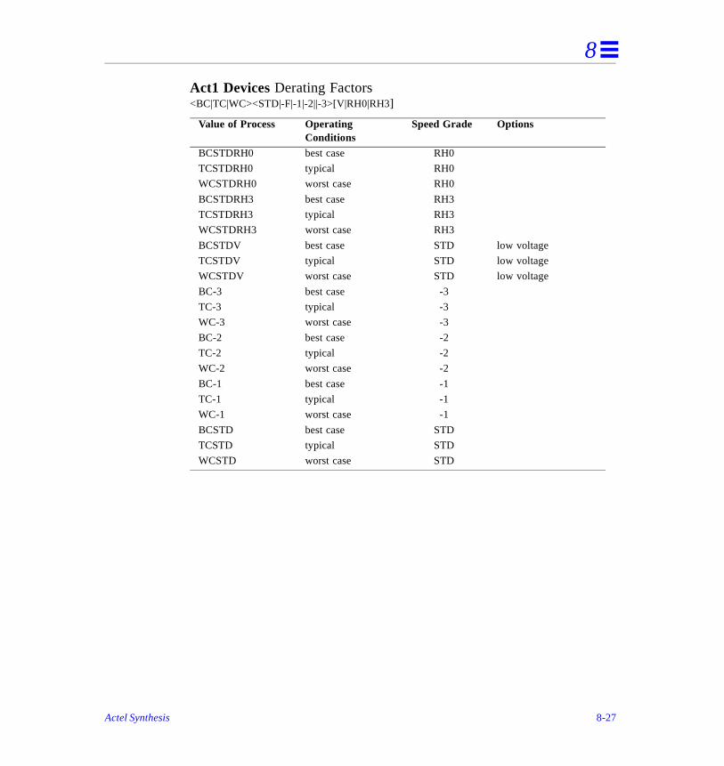
8
Act1 Devices Derating Factors<BC|TC|WC><STD|-F|-1|-2||-3>[V|RH0|RH3]
Value of Process Operating Conditions
Speed Grade Options
BCSTDRH0 best case RH0
TCSTDRH0 typical RH0
WCSTDRH0 worst case RH0
BCSTDRH3 best case RH3
TCSTDRH3 typical RH3
WCSTDRH3 worst case RH3
BCSTDV best case STD low voltage
TCSTDV typical STD low voltage
WCSTDV worst case STD low voltage
BC-3 best case -3
TC-3 typical -3
WC-3 worst case -3
BC-2 best case -2
TC-2 typical -2
WC-2 worst case -2
BC-1 best case -1
TC-1 typical -1
WC-1 worst case -1
BCSTD best case STD
TCSTD typical STD
WCSTD worst case STD
Actel Synthesis 8-27
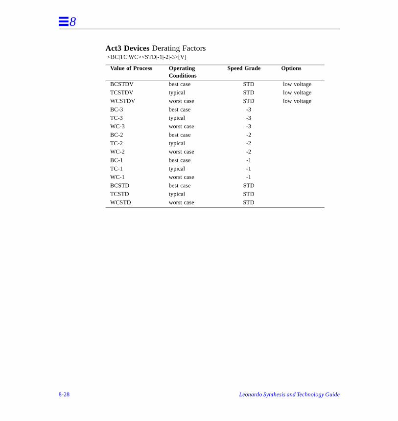
8
Act3 Devices Derating Factors <BC|TC|WC><STD|-1|-2|-3>[V]
Value of Process Operating Conditions
Speed Grade Options
BCSTDV best case STD low voltage
TCSTDV typical STD low voltage
WCSTDV worst case STD low voltage
BC-3 best case -3
TC-3 typical -3
WC-3 worst case -3
BC-2 best case -2
TC-2 typical -2
WC-2 worst case -2
BC-1 best case -1
TC-1 typical -1
WC-1 worst case -1
BCSTD best case STD
TCSTD typical STD
WCSTD worst case STD
8-28 Leonardo Synthesis and Technology Guide
Altera FLEX Synthesis 9
or
d the d
This chapter presents information specific to the use of Altera FLEX as a source target technology. Leonardo supports the following architectures:
• FLEX 6K
• FLEX 8K
• FLEX 10K
This chapter is divided as follows:
• Before Beginning
• Altera FLEX Architecture
• Design Flow
• Synthesis and Optimization Features
• Reporting
• Design I/Os
• Writing EDIF Output
• Using EDIF from MAX+PLUS II
• How to Get Best Results with MAX+PLUS II
• New Features for Altera FLEX
Before Beginning
The technology information presented in this chapter assumes that you have reaintroductory chapters in this guide. Refer also to the HDL Synthesis and CommanReference guides for information.
9-1
9
is e ited LE. E in
es
s o 9-1
ees his
ost rdo n be
Altera FLEX Architecture
Logic Elements (LEs)
LEs are also known as Logic Cells (LCells). The combinational logic part of an LEoften called a look up table (LUT). LEs are at the core of Altera FLEX architecturand contain both combinational logic and registers. The combinational logic is limby the number of inputs; functions of up to four inputs can be implemented in oneFunctions with more inputs must be separated into multiple levels of LEs. Each Lalso contains a register with clear and preset inputs. In addition, LEs are groupedLABs. All LEs in an LAB share control signals and connect to each other throughspecial cascade routing resources.
Input Output Elements (IOEs)
IOEs in Altera FLEX can be configured as inputs, outputs, tristate outputs, or bi-directional pins, with a register in either input or output path.
Embedded Array Blocks (EABs)
EABs are for FLEX 10K only and implement memory functions. Each EAB provid2048 bits which can create a RAM, ROM, FIFO, or dual-port RAM.
Design Flow
Leonardo accepts hierarchical HDL descriptions in VHDL or Verilog. Input designcan be optimized and mapped to any Altera FLEX architecture. Leonardo can alstarget designs from other FPGA vendors to Altera architectures. Refer to Figuresand 9-2.
During reading, the input design is translated into Leonardo's intermediate data structures. FLEX-specific optimization is then performed. This optimization guarantthat combinational functions do not have more than a limited number of inputs. Tprocess is called fanin limited optimization. The next step is to map the design into lookup tables (LUTs) using LUT mapping. Before writing the design, Leonardo attaches an equation string, lut_function, to each lookup table to represent the combinational logic function. A hierarchical EDIF netlist in a single file is then written.
After MAX+PLUS II is run for place-and-route, Leonardo can back-annotate the pplace-and-route timing and generate an SDF timing file and a VHDL netlist. Leonagenerates the VHDL and SDF files simultaneously for consistency. These files caused to simulate the design with post place-and-route timing for functional verification.
9-2 Leonardo Synthesis and Technology Guide
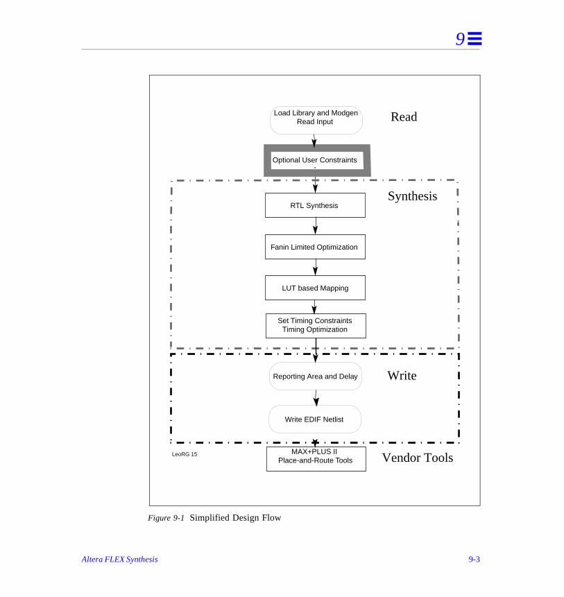
9
Figure 9-1 Simplified Design Flow
Fanin Limited Optimization
LUT based Mapping
RTL Synthesis
Optional User Constraints
LeoRG 15
Synthesis
Write
Load Library and ModgenRead Input Read
Vendor ToolsMAX+PLUS II
Place-and-Route Tools
Write EDIF Netlist
Set Timing ConstraintsTiming Optimization
Reporting Area and Delay
Altera FLEX Synthesis 9-3
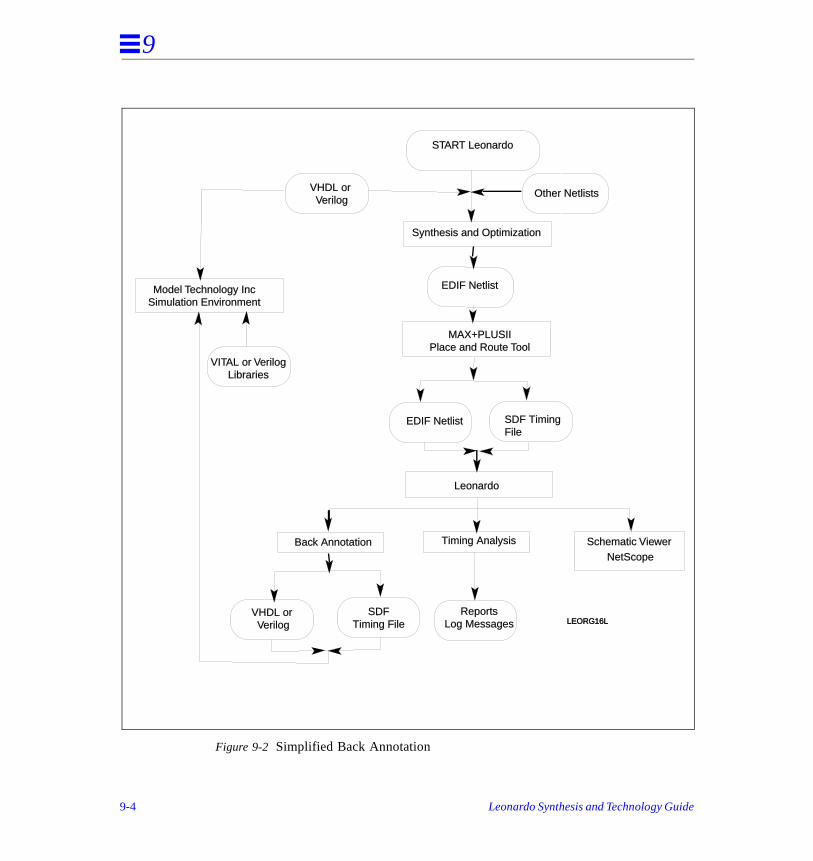
9
Figure 9-2 Simplified Back Annotation
START Leonardo
VHDL or Verilog
Other Netlists
Synthesis and Optimization
Model Technology IncSimulation Environment
VITAL or VerilogLibraries
MAX+PLUSIIPlace and Route Tool
LEORG16L
NetScopeSchematic ViewerTiming Analysis
Leonardo
Back Annotation
VHDL or Verilog
SDFTiming File
ReportsLog Messages
EDIF Netlist SDF TimingFile
EDIF Netlist
9-4 Leonardo Synthesis and Technology Guide

9
ion
les
re EX-
ers
n of ate.
s (1)
Synthesis and Optimization Features
This section is divided as follows:
• Fanin Limited Optimization
• Look Up Table (LUT) Mapping
• Data Path Synthesis
• LPM Support for FLEX 10K
• Genmen Support
• EAB Support
To take advantage of the Altera FLEX architecture, Altera FLEX-specific optimizatalgorithms and features are offered by Leonardo.
• A fanin limited optimization algorithm is performed. This algorithm utilizes the limited number of inputs of the Altera FLEX logic element.
• A lookup table mapping algorithm (LUT mapping) is then performed. This algorithm tries to find an optimal mapping of combinational logic into lookup taband cascade gates.
• Data Path Synthesis: RAM components can be instantiated through LPM conventions or inferenced and implemented through Modgen. Also, counters aautomatically inferred and implemented to fit the FLEX architecture. Data pathelements are implemented using Modgen to take advantage of the following FLspecific features: carry chains and cascade chains.
• Clock Enable Detection: Clock Enable logic is automatically detected for regist
• Constraint driven timing optimization. This algorithm understands the FLEX architecture and speeds up critical paths in the design.
Fanin Limited Optimization
The key architectural feature of the FLEX FPGA is that the LE can be any functiofour inputs. A 4-input XOR uses the same area and is as fast as a 4-input AND gThe function shown in Equation E-1 can be solved in two ways. Here are Solutionand (2):
Altera FLEX Synthesis 9-5

9
and
and X
Solution (1)
You can decompose a function into its simpler AND/OR equivalent representation,then split the gates with large fan-in into multiple gates. For example:
Represented in AND and OR gates, X is decomposed as:
Because T3 has more than four inputs, further decomposition is required:
After fully decomposing the design, you can use the Altera FLEX MAX+PLUS II place-and-route software to place the design into physical LEs. In this example, T3T5 cannot be merged because of fan-in limitations. Next, combine T1 with T4 andwith T2. This gives the following partitioning to four LEs:
Note – The critical path is LE_4 → LE_3 → LE_1, resulting in three levels of LEs forthe delay.
X = (A*(B+C))+(B*D)+(E*F*G*H*I) (E-1)
X = T1+T2+T3T1 = A*T4T2 = B*D (E-2)T3 = E*F*G*H*IT4 = B+C.
T3 = E*F*G*T5T5 = H*I (E-3)
LE_1: X = T1+(B*D)+T3LE_2: T1 = A*(B+C)LE_3: T3 = E*F*G*T5 (E-4)LE_4: T5 = H*I
9-6 Leonardo Synthesis and Technology Guide
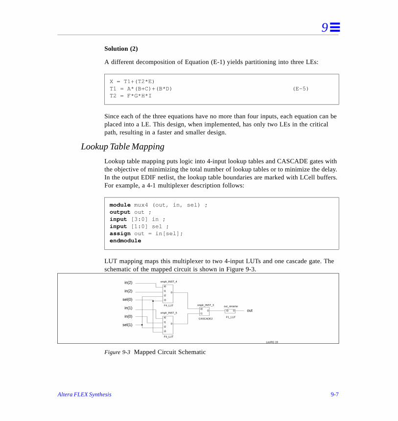
9
an be l
ith lay. ers.
he
Solution (2)
A different decomposition of Equation (E-1) yields partitioning into three LEs:
Since each of the three equations have no more than four inputs, each equation cplaced into a LE. This design, when implemented, has only two LEs in the criticapath, resulting in a faster and smaller design.
Lookup Table Mapping
Lookup table mapping puts logic into 4-input lookup tables and CASCADE gates wthe objective of minimizing the total number of lookup tables or to minimize the deIn the output EDIF netlist, the lookup table boundaries are marked with LCell buffFor example, a 4-1 multiplexer description follows:
LUT mapping maps this multiplexer to two 4-input LUTs and one cascade gate. Tschematic of the mapped circuit is shown in Figure 9-3.
Figure 9-3 Mapped Circuit Schematic
X = T1+(T2*E)T1 = A*(B+C)+(B*D) (E-5)T2 = F*G*H*I
module mux4 (out, in, sel) ;output out ;input [3:0] in ;input [1:0] sel ;assign out = in[sel];endmodule
in(0)
xmplr_INST_4
in(1)
sel(0)
in(2)
in(2)
xmplr_INST_3
LeoRG 19
I0
I1
I2
I3
0
F4_LUT
xmplr_INST_5
sel(1)
I0
I1
I2
I3
0
F4_LUT
CASCADE2
I0
I10
out_rename
I0 0
F1_LUT
out
Altera FLEX Synthesis 9-7
9
do cally
t ge
n
Before writing an EDIF netlist that can be read by MAX+PLUS II software, Leonarattaches a lut_function property to each lookup table. This step is done automatiwhen using the auto_write command. This is necessary to describe the LUTs functionality.
User Options to Control LUT Mapping
Use these rules and refer to Table 9-1 and Screen 9-1.
• dont_lock_lcells - Default value is set to FALSE. If this variable is seto TRUE, then Leonardo does not force LCell boundaries in the output EDIFnetlist. Instead, it writes them as SOFT. In this case, MAX+PLUS II can chanthe LCell boundaries.
• flex_use_cascades - If set flex_use_cascades is set to FALSE, dont_lock_lcells should also be set to TRUE. This way MAX+PLUS II castill map to cascades wherever appropriate.
• lut_map - If this variable is set to FALSE, LUT mapping is off.
Table 9-1. Mapping Options
*GUI default options**variables, options, constraint attributes, commands
GUI Option Optionon/off
Command Line** Results
■ Map Look Up Tables
on* default (true) Controls LUT mapping. If lut_map is false, set dont_lock_lcells to true.
off lut_map
■ Map to CASCADEs during LUT mapping
on* default (true) Controls mapping logic to cascade gates for Altera FLEX.
off flex_use_cascades
❏ Do not lock LCells
on dont_lock_lcells Controls locking of LCells.
off* default (false)
9-8 Leonardo Synthesis and Technology Guide
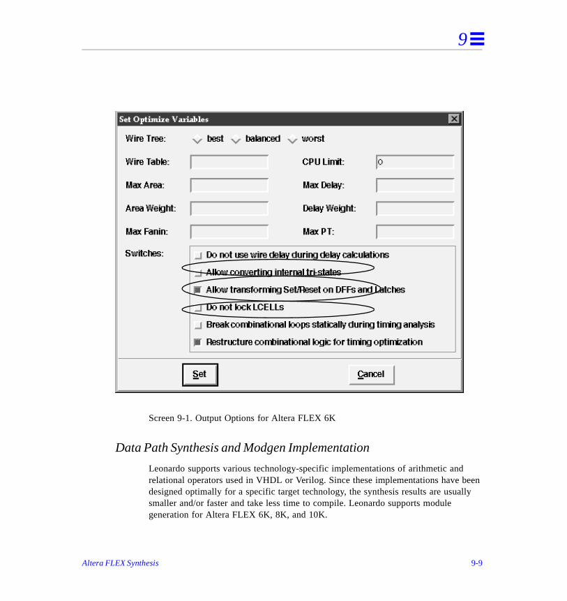
9
een lly
Screen 9-1. Output Options for Altera FLEX 6K
Data Path Synthesis and Modgen Implementation
Leonardo supports various technology-specific implementations of arithmetic andrelational operators used in VHDL or Verilog. Since these implementations have bdesigned optimally for a specific target technology, the synthesis results are usuasmaller and/or faster and take less time to compile. Leonardo supports module generation for Altera FLEX 6K, 8K, and 10K.
Altera FLEX Synthesis 9-9
9
ition, n
ble fast
n dgen
The following operators are supported for Altera FLEX technologies:
• Relational Operators = /= < <= > >=
• Arithmetic Operators + - *
• Misc. Functions counters (up/down, loadable etc.)RAMsincrementerdecrementerabsolute valueunary minus
The module generator for each technology uses dedicated hardware resources whenever possible. Therefore, modgen implementation of operators, such as addsubtraction, counters, relational operators is generally smaller in area and faster idelay.
Examples:
• Adder in FLEX modgen is implemented using dedicated CARRY chain availain FLEX architectures to implement the adder carry logic. This leads to very carry propagation and results in excellent timing performance.
• Counters in FLEX modgen make use of counter modes available in FLEX architectures which results in faster and smaller designs.
• RAMs in FLEX 10K modgen use dedicated RAMs available in FLEX 10K architecture.
User-Defined Switches
You can control modgen implementation that is optimized for area or for delay byusing this switch. This switch controls modgen resolution for all operators. You caalso use the GUI as explained in Table 9-2 and shown in Screen 9-2 to control moimplementation.
set modgen_select= sma llest | small | fast | fastest
9-10 Leonardo Synthesis and Technology Guide
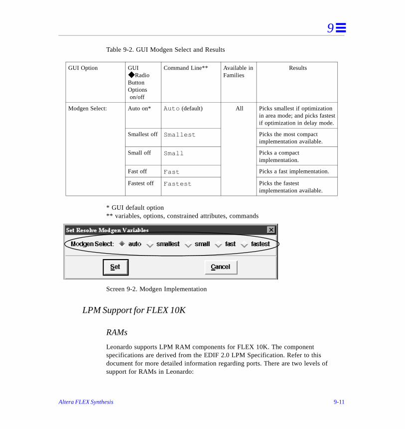
9
Table 9-2. GUI Modgen Select and Results
* GUI default option** variables, options, constrained attributes, commands
Screen 9-2. Modgen Implementation
LPM Support for FLEX 10K
RAMs
Leonardo supports LPM RAM components for FLEX 10K. The component specifications are derived from the EDIF 2.0 LPM Specification. Refer to this document for more detailed information regarding ports. There are two levels of support for RAMs in Leonardo:
GUI Option GUI ◆ Radio Button Options on/off
Command Line** Available in Families
Results
Modgen Select: Auto on* Auto (default) All Picks smallest if optimization in area mode; and picks fastest if optimization in delay mode.
Smallest off Smallest Picks the most compact implementation available.
Small off Small Picks a compact implementation.
Fast off Fast Picks a fast implementation.
Fastest off Fastest Picks the fastest implementation available.
Altera FLEX Synthesis 9-11
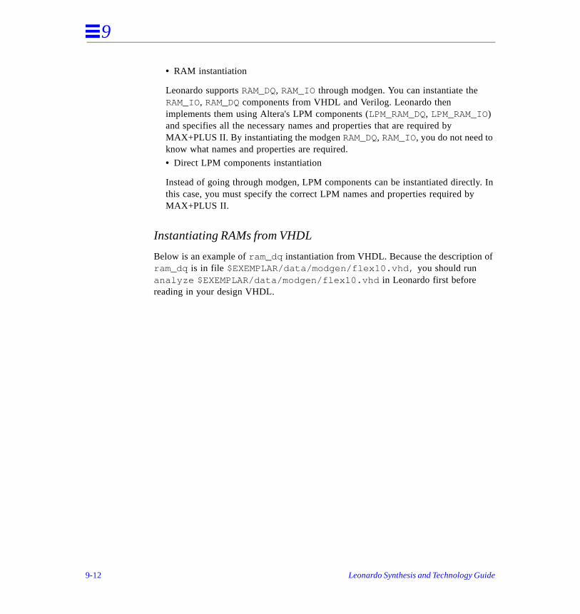
9
y. In
f
• RAM instantiation
Leonardo supports RAM_DQ, RAM_IO through modgen. You can instantiate the RAM_IO, RAM_DQ components from VHDL and Verilog. Leonardo then implements them using Altera's LPM components (LPM_RAM_DQ, LPM_RAM_IO) and specifies all the necessary names and properties that are required by MAX+PLUS II. By instantiating the modgen RAM_DQ, RAM_IO, you do not need to know what names and properties are required.
• Direct LPM components instantiation
Instead of going through modgen, LPM components can be instantiated directlthis case, you must specify the correct LPM names and properties required byMAX+PLUS II.
Instantiating RAMs from VHDL
Below is an example of ram_dq instantiation from VHDL. Because the description oram_dq is in file $EXEMPLAR/data/modgen/flex10.vhd, you should run analyze $EXEMPLAR/data/modgen/flex10.vhd in Leonardo first before reading in your design VHDL.
9-12 Leonardo Synthesis and Technology Guide
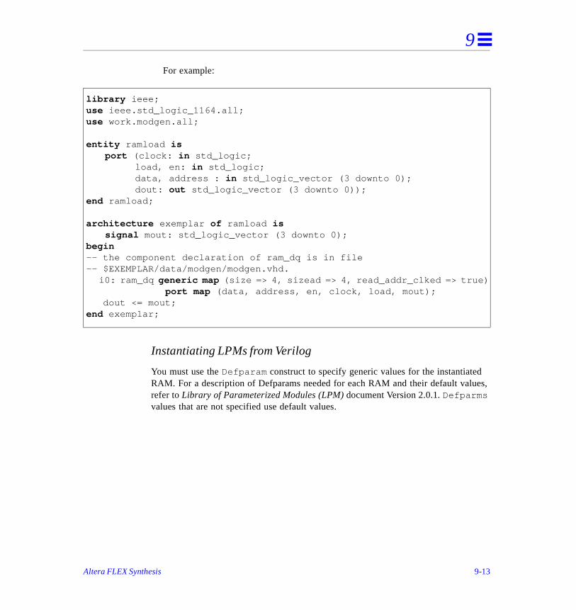
9
ues,
For example:
Instantiating LPMs from Verilog
You must use the Defparam construct to specify generic values for the instantiatedRAM. For a description of Defparams needed for each RAM and their default valrefer to Library of Parameterized Modules (LPM) document Version 2.0.1. Defparms values that are not specified use default values.
library ieee;use ieee.std_logic_1164.all;use work.modgen.all;
entity ramload isport (clock: in std_logic;
load, en: in std_logic; data, address : in std_logic_vector (3 downto 0); dout: out std_logic_vector (3 downto 0));
end ramload;
architecture exemplar of ramload issignal mout: std_logic_vector (3 downto 0);
begin-- the component declaration of ram_dq is in file-- $EXEMPLAR/data/modgen/modgen.vhd. i0: ram_dq generic map (size => 4, sizead => 4, read_addr_clked => true) port map (data, address, en, clock, load, mout); dout <= mout;end exemplar;
Altera FLEX Synthesis 9-13
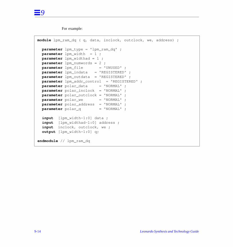
9
For example:
module lpm_ram_dq ( q, data, inclock, outclock, we, address) ;
parameter lpm_type = "lpm_ram_dq" ; parameter lpm_width = 1 ; parameter lpm_widthad = 1 ; parameter lpm_numwords = 2 ; parameter lpm_file = "UNUSED" ; parameter lpm_indata = "REGISTERED" ; parameter lpm_outdata = "REGISTERED" ; parameter lpm_addr_control = "REGISTERED" ; parameter polar_data = "NORMAL" ; parameter polar_inclock = "NORMAL" ; parameter polar_outclock = "NORMAL" ; parameter polar_we = "NORMAL" ; parameter polar_address = "NORMAL" ; parameter polar_q = "NORMAL" ;
input [lpm_width-1:0] data ; input [lpm_widthad-1:0] address ; input inclock, outclock, we ; output [lpm_width-1:0] q;
endmodule // lpm_ram_dq
9-14 Leonardo Synthesis and Technology Guide
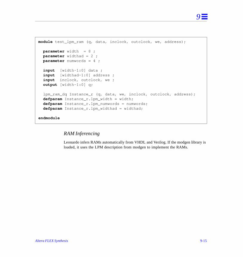
9
is
RAM Inferencing
Leonardo infers RAMs automatically from VHDL and Verilog. If the modgen library loaded, it uses the LPM description from modgen to implement the RAMs.
module test_lpm_ram (q, data, inclock, outclock, we, address);
parameter width = 8 ; parameter widthad = 2 ; parameter numwords = 4 ;
input [width-1:0] data ; input [widthad-1:0] address ; input inclock, outclock, we ; output [width-1:0] q;
lpm_ram_dq Instance_r (q, data, we, inclock, outclock, address); defparam Instance_r.lpm_width = width; defparam Instance_r.lpm_numwords = numwords; defparam Instance_r.lpm_widthad = widthad;
endmodule
Altera FLEX Synthesis 9-15
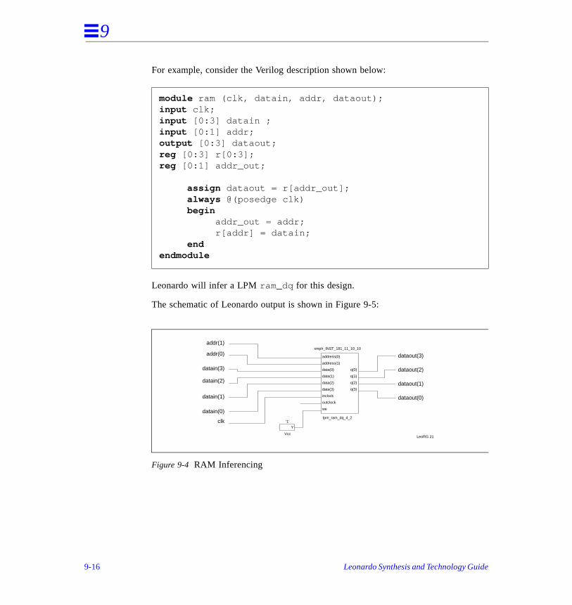
9
For example, consider the Verilog description shown below:
Leonardo will infer a LPM ram_dq for this design.
The schematic of Leonardo output is shown in Figure 9-5:
Figure 9-4 RAM Inferencing
module ram (clk, datain, addr, dataout);input clk;input [0:3] datain ;input [0:1] addr;output [0:3] dataout;reg [0:3] r[0:3];reg [0:1] addr_out;
assign dataout = r[addr_out]; always @(posedge clk) begin addr_out = addr; r[addr] = datain; endendmodule
datain(1)
xmplr_INST_181_11_10_10
datain(2)
datain(3)
addr(1)
addr(0)
LeoRG 21
address(0)
address(1)
data(0)
data(1)
data(2)
data(3)
inclock
outclock
wedatain(0)
clklpm_ram_dq_4_2
q(0)
q(1)
q(2)
q(3)
Y
Vcc
'1'
dataout(3)
dataout(2)
dataout(1)
dataout(0)
9-16 Leonardo Synthesis and Technology Guide
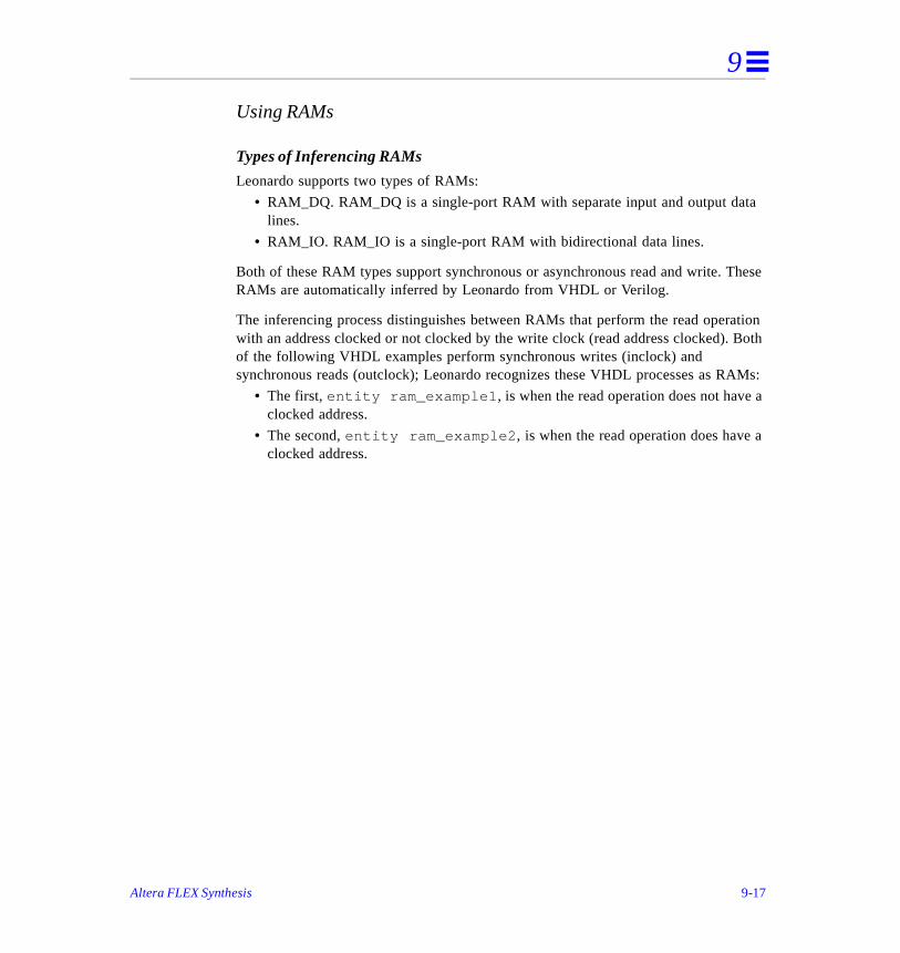
9
a
hese
ation Both
AMs:
a
a
Using RAMs
Types of Inferencing RAMs
Leonardo supports two types of RAMs:
• RAM_DQ. RAM_DQ is a single-port RAM with separate input and output datlines.
• RAM_IO. RAM_IO is a single-port RAM with bidirectional data lines.
Both of these RAM types support synchronous or asynchronous read and write. TRAMs are automatically inferred by Leonardo from VHDL or Verilog.
The inferencing process distinguishes between RAMs that perform the read operwith an address clocked or not clocked by the write clock (read address clocked). of the following VHDL examples perform synchronous writes (inclock) and synchronous reads (outclock); Leonardo recognizes these VHDL processes as R
• The first, entity ram_example1 , is when the read operation does not haveclocked address.
• The second, entity ram_example2 , is when the read operation does haveclocked address.
Altera FLEX Synthesis 9-17
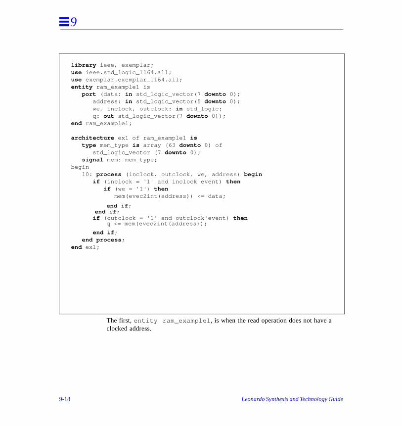
9
The first, entity ram_example1 , is when the read operation does not have a clocked address.
library ieee, exemplar;use ieee.std_logic_1164.all;use exemplar.exemplar_1164.all;entity ram_example1 is port (data: in std_logic_vector(7 downto 0); address: in std_logic_vector(5 downto 0); we, inclock, outclock: in std_logic; q: out std_logic_vector(7 downto 0));end ram_example1;
architecture ex1 of ram_example1 is type mem_type is array (63 downto 0) of std_logic_vector (7 downto 0); signal mem: mem_type;begin l0: process (inclock, outclock, we, address) begin if (inclock = '1' and inclock'event) then if (we = '1') then mem(evec2int(address)) <= data;
if (outclock = '1' and outclock'event) then
end if ; end process ;end ex1;
q <= mem(evec2int(address));
end if ;end if ;
9-18 Leonardo Synthesis and Technology Guide
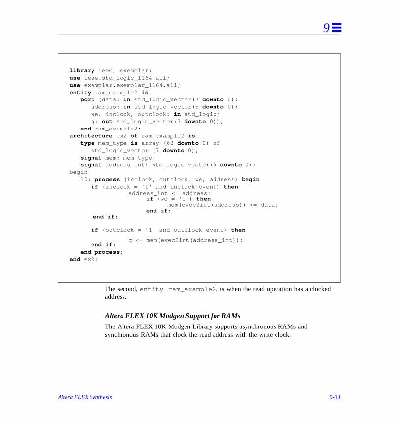
9
The second, entity ram_example2 , is when the read operation has a clocked address.
Altera FLEX 10K Modgen Support for RAMs
The Altera FLEX 10K Modgen Library supports asynchronous RAMs and synchronous RAMs that clock the read address with the write clock.
library ieee, exemplar;use ieee.std_logic_1164.all;use exemplar.exemplar_1164.all;entity ram_example2 is port (data: in std_logic_vector(7 downto 0); address: in std_logic_vector(5 downto 0); we, inclock, outclock: in std_logic; q: out std_logic_vector(7 downto 0)); end ram_example2;architecture ex2 of ram_example2 is type mem_type is array (63 downto 0) of std_logic_vector (7 downto 0); signal mem: mem_type; signal address_int: std_logic_vector(5 downto 0);begin l0: process (inclock, outclock, we, address) begin if (inclock = '1' and inclock'event) then
if (outclock = '1' and outclock'event) then
end if ; end process ;end ex2;
address_int <= address;if (we = '1') then
mem(evec2int(address)) <= data;end if ;
end if ;
q <= mem(evec2int(address_int));
Altera FLEX Synthesis 9-19
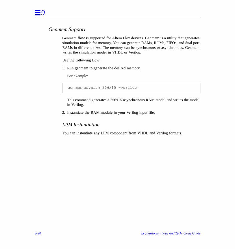
9
ates port mem
odel
Genmem Support
Genmem flow is supported for Altera Flex devices. Genmem is a utility that genersimulation models for memory. You can generate RAMs, ROMs, FIFOs, and dual RAMs in different sizes. The memory can be synchronous or asynchronous. Genwrites the simulation model in VHDL or Verilog.
Use the following flow:
1. Run genmem to generate the desired memory.
For example:
This command generates a 256x15 asynchronous RAM model and writes the min Verilog.
2. Instantiate the RAM module in your Verilog input file.
LPM Instantiation
You can instantiate any LPM component from VHDL and Verilog formats.
genmem asynram 256x15 -verilog
9-20 Leonardo Synthesis and Technology Guide
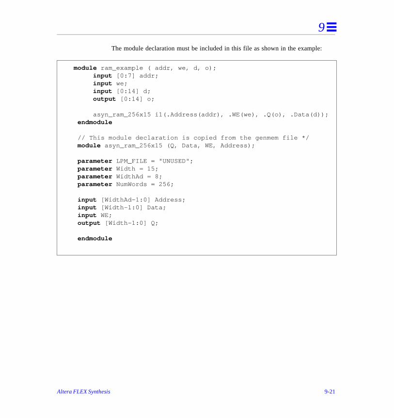
9
The module declaration must be included in this file as shown in the example:
module ram_example ( addr, we, d, o); input [0:7] addr; input we; input [0:14] d; output [0:14] o;
asyn_ram_256x15 i1(.Address(addr), .WE(we), .Q(o), .Data(d)); endmodule
// This module declaration is copied from the genmem file */ module asyn_ram_256x15 (Q, Data, WE, Address); parameter LPM_FILE = "UNUSED"; parameter Width = 15; parameter WidthAd = 8; parameter NumWords = 256; input [WidthAd-1:0] Address; input [Width-1:0] Data; input WE; output [Width-1:0] Q;
endmodule
Altera FLEX Synthesis 9-21
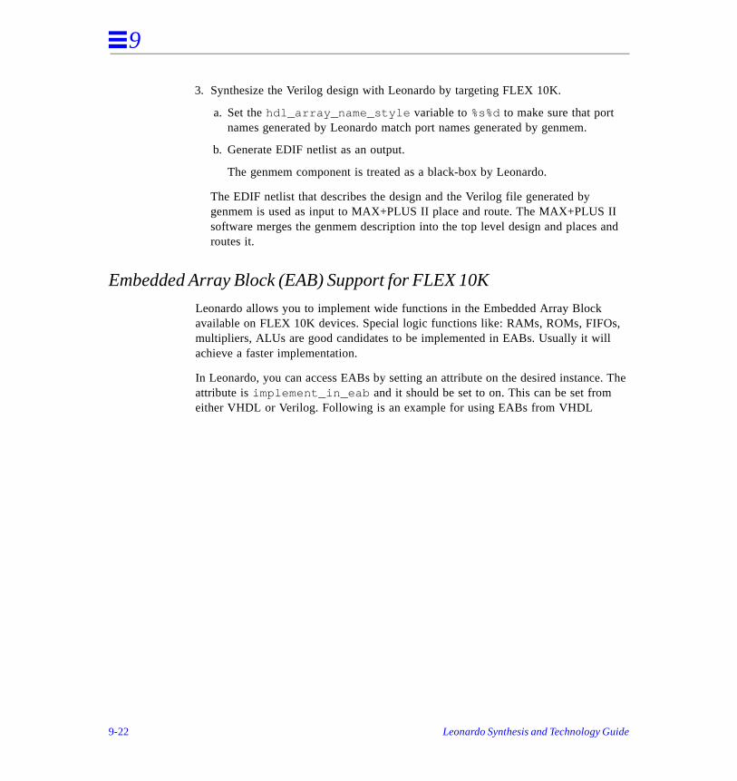
9
I and
,
. The
3. Synthesize the Verilog design with Leonardo by targeting FLEX 10K.
a. Set the hdl_array_name_style variable to %s%d to make sure that port names generated by Leonardo match port names generated by genmem.
b. Generate EDIF netlist as an output.
The genmem component is treated as a black-box by Leonardo.
The EDIF netlist that describes the design and the Verilog file generated by genmem is used as input to MAX+PLUS II place and route. The MAX+PLUS Isoftware merges the genmem description into the top level design and places routes it.
Embedded Array Block (EAB) Support for FLEX 10K
Leonardo allows you to implement wide functions in the Embedded Array Block available on FLEX 10K devices. Special logic functions like: RAMs, ROMs, FIFOsmultipliers, ALUs are good candidates to be implemented in EABs. Usually it will achieve a faster implementation.
In Leonardo, you can access EABs by setting an attribute on the desired instanceattribute is implement_in_eab and it should be set to on. This can be set from either VHDL or Verilog. Following is an example for using EABs from VHDL
9-22 Leonardo Synthesis and Technology Guide
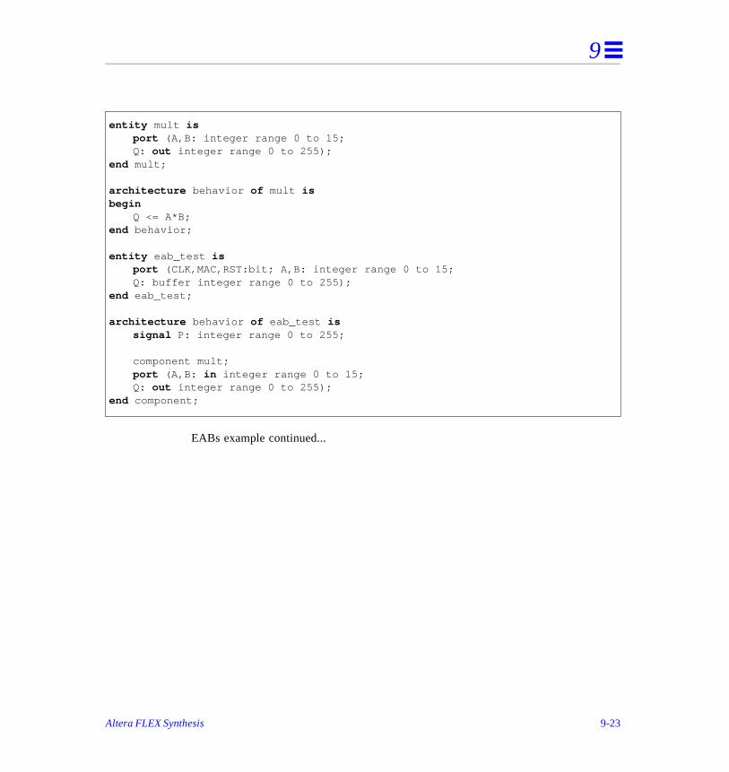
9
EABs example continued...
entity mult isport (A,B: integer range 0 to 15;Q: out integer range 0 to 255);
end mult;
architecture behavior of mult isbegin
Q <= A*B;end behavior;
entity eab_test isport (CLK,MAC,RST:bit; A,B: integer range 0 to 15;Q: buffer integer range 0 to 255);
end eab_test;
architecture behavior of eab_test issignal P: integer range 0 to 255;
component mult;port (A,B: in integer range 0 to 15;Q: out integer range 0 to 255);
end component;
Altera FLEX Synthesis 9-23
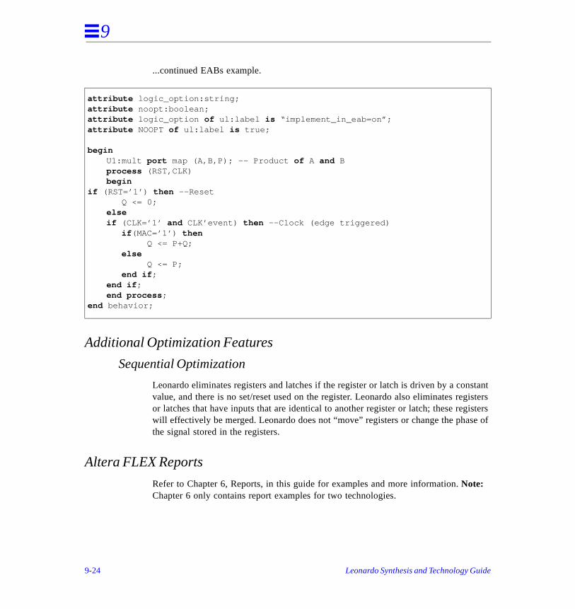
9
stant gisters isters e of
...continued EABs example.
Additional Optimization Features
Sequential Optimization
Leonardo eliminates registers and latches if the register or latch is driven by a convalue, and there is no set/reset used on the register. Leonardo also eliminates reor latches that have inputs that are identical to another register or latch; these regwill effectively be merged. Leonardo does not “move” registers or change the phasthe signal stored in the registers.
Altera FLEX Reports
Refer to Chapter 6, Reports, in this guide for examples and more information. Note: Chapter 6 only contains report examples for two technologies.
attribute logic_option:string;attribute noopt:boolean;attribute logic_option of ul:label is “implement_in_eab=on”;attribute NOOPT of ul:label is true;
beginU1:mult port map (A,B,P); -- Product of A and Bprocess (RST,CLK)begin
if (RST=’1’) then --Reset Q <= 0;elseif (CLK=’1’ and CLK’event) then --Clock (edge triggered) if (MAC=’1’) then Q <= P+Q; else Q <= P; end if ;end if ;end process ;
end behavior;
9-24 Leonardo Synthesis and Technology Guide
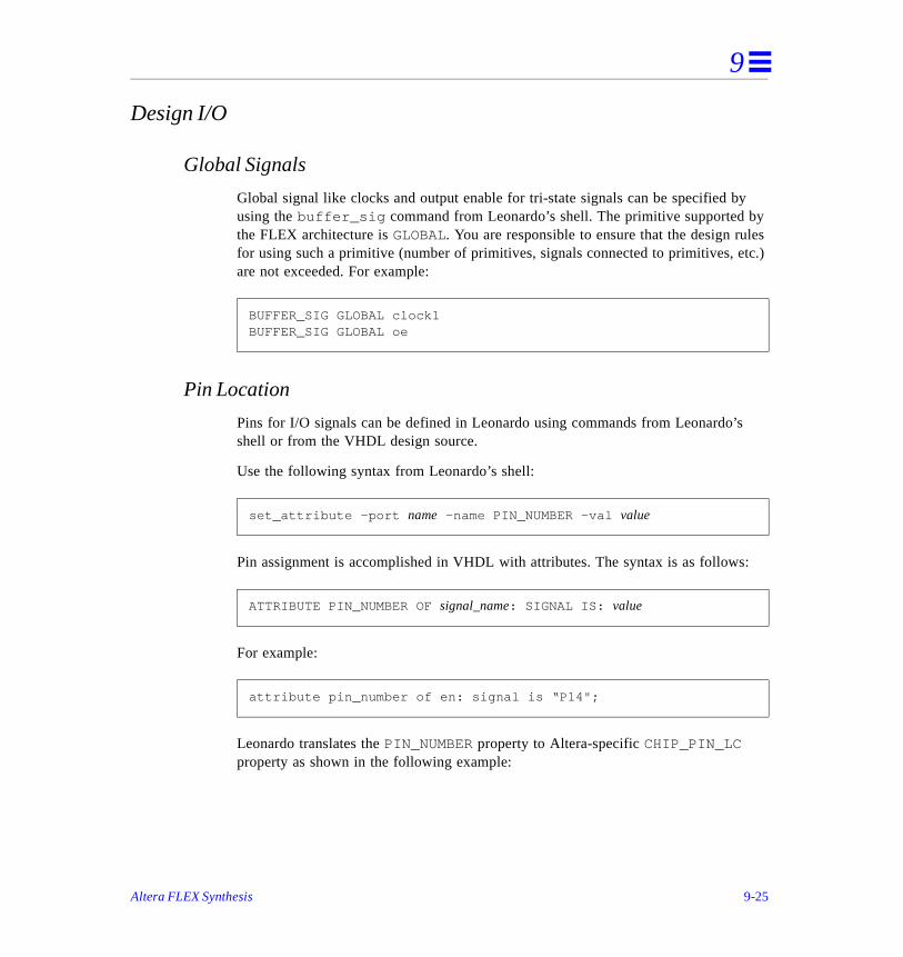
9
y y
les tc.)
s
:
Design I/O
Global Signals
Global signal like clocks and output enable for tri-state signals can be specified busing the buffer_sig command from Leonardo’s shell. The primitive supported bthe FLEX architecture is GLOBAL. You are responsible to ensure that the design rufor using such a primitive (number of primitives, signals connected to primitives, eare not exceeded. For example:
Pin Location
Pins for I/O signals can be defined in Leonardo using commands from Leonardo’shell or from the VHDL design source.
Use the following syntax from Leonardo’s shell:
Pin assignment is accomplished in VHDL with attributes. The syntax is as follows
For example:
Leonardo translates the PIN_NUMBER property to Altera-specific CHIP_PIN_LC property as shown in the following example:
BUFFER_SIG GLOBAL clock1 BUFFER_SIG GLOBAL oe
set_attribute -port name -name PIN_NUMBER -val value
ATTRIBUTE PIN_NUMBER OF signal_name: SIGNAL IS: value
attribute pin_number of en: signal is “P14";
Altera FLEX Synthesis 9-25
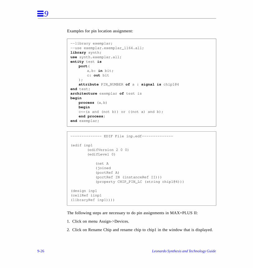
9
ed.
Examples for pin location assignment:
The following steps are necessary to do pin assignments in MAX+PLUS II:
1. Click on menu Assign->Devices.
2. Click on Rename Chip and rename chip to chip1 in the window that is display
--library exemplar;--use exemplar.exemplar_1164.all;library synth;use synth.exemplar.all;entity test is
port (a,b: in bit;c: out bit
);attribute PIN_NUMBER of a : signal is chip1@4
end test;architecture exemplar of test isbegin
process (a,b)beginc<=(a and (not b)) or ((not a) and b);end process ;
end exemplar;
-------------- EDIF File inp.edf--------------
(edif inp1(edifVersion 2 0 0)(edifLevel 0)
(net A(joined(portRef A)(portRef IN (instanceRef II)))(property CHIP_PIN_LC (string chip1@4)))
(design inp1(cellRef iinp1(libraryRef inp1))))
9-26 Leonardo Synthesis and Technology Guide
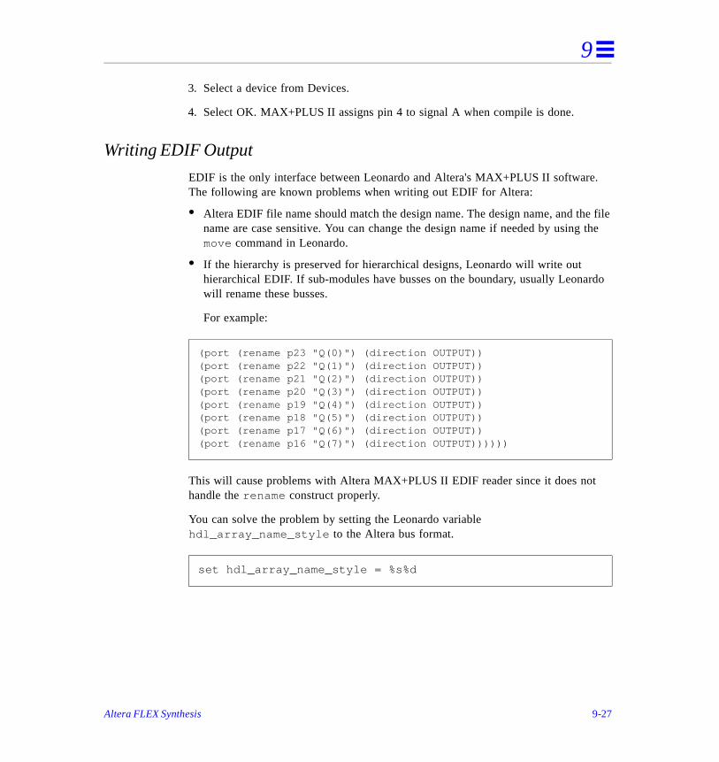
9
.
e file the
rdo
3. Select a device from Devices.
4. Select OK. MAX+PLUS II assigns pin 4 to signal A when compile is done.
Writing EDIF Output
EDIF is the only interface between Leonardo and Altera's MAX+PLUS II softwareThe following are known problems when writing out EDIF for Altera:
• Altera EDIF file name should match the design name. The design name, and thname are case sensitive. You can change the design name if needed by usingmove command in Leonardo.
• If the hierarchy is preserved for hierarchical designs, Leonardo will write out hierarchical EDIF. If sub-modules have busses on the boundary, usually Leonawill rename these busses.
For example:
This will cause problems with Altera MAX+PLUS II EDIF reader since it does nothandle the rename construct properly.
You can solve the problem by setting the Leonardo variable hdl_array_name_style to the Altera bus format.
(port (rename p23 "Q(0)") (direction OUTPUT))(port (rename p22 "Q(1)") (direction OUTPUT))(port (rename p21 "Q(2)") (direction OUTPUT))(port (rename p20 "Q(3)") (direction OUTPUT))(port (rename p19 "Q(4)") (direction OUTPUT))(port (rename p18 "Q(5)") (direction OUTPUT))(port (rename p17 "Q(6)") (direction OUTPUT))(port (rename p16 "Q(7)") (direction OUTPUT))))))
set hdl_array_name_style = %s%d
Altera FLEX Synthesis 9-27
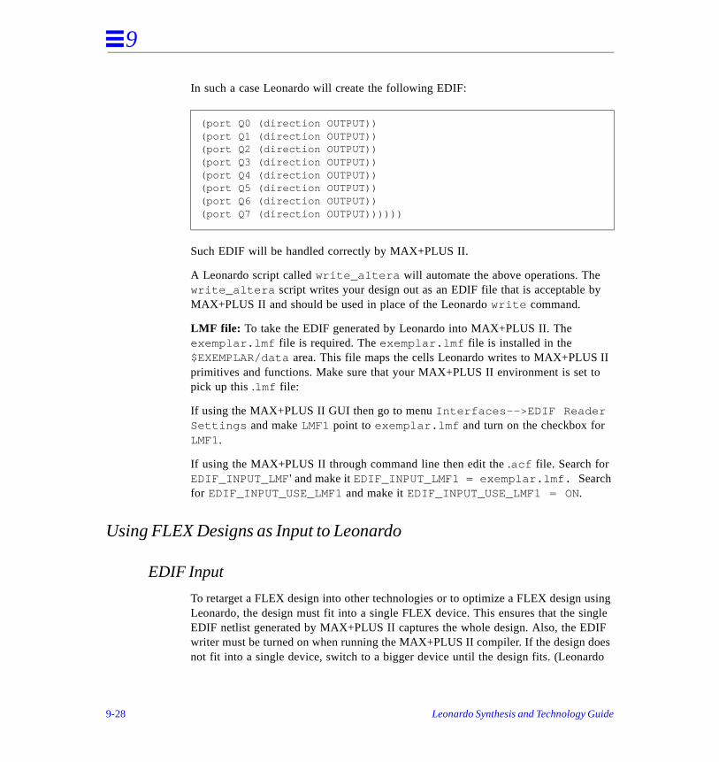
9
y
I
sing gle
IF es
do
In such a case Leonardo will create the following EDIF:
Such EDIF will be handled correctly by MAX+PLUS II.
A Leonardo script called write_altera will automate the above operations. The write_altera script writes your design out as an EDIF file that is acceptable bMAX+PLUS II and should be used in place of the Leonardo write command.
LMF file: To take the EDIF generated by Leonardo into MAX+PLUS II. The exemplar.lmf file is required. The exemplar.lmf file is installed in the $EXEMPLAR/data area. This file maps the cells Leonardo writes to MAX+PLUS Iprimitives and functions. Make sure that your MAX+PLUS II environment is set topick up this .lmf file:
If using the MAX+PLUS II GUI then go to menu Interfaces-->EDIF Reader Settings and make LMF1 point to exemplar.lmf and turn on the checkbox for LMF1.
If using the MAX+PLUS II through command line then edit the .acf file. Search for EDIF_INPUT_LMF' and make it EDIF_INPUT_LMF1 = exemplar.lmf. Search for EDIF_INPUT_USE_LMF1 and make it EDIF_INPUT_USE_LMF1 = ON .
Using FLEX Designs as Input to Leonardo
EDIF Input
To retarget a FLEX design into other technologies or to optimize a FLEX design uLeonardo, the design must fit into a single FLEX device. This ensures that the sinEDIF netlist generated by MAX+PLUS II captures the whole design. Also, the EDwriter must be turned on when running the MAX+PLUS II compiler. If the design donot fit into a single device, switch to a bigger device until the design fits. (Leonar
(port Q0 (direction OUTPUT))(port Q1 (direction OUTPUT))(port Q2 (direction OUTPUT))(port Q3 (direction OUTPUT))(port Q4 (direction OUTPUT))(port Q5 (direction OUTPUT))(port Q6 (direction OUTPUT))(port Q7 (direction OUTPUT))))))
9-28 Leonardo Synthesis and Technology Guide
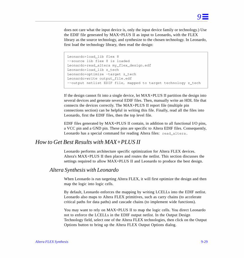
9
Use
ardo,
to that
o
s, ntly,
the n.
en
st. te
o
tput
does not care what the input device is, only the input device family or technology.)the EDIF file generated by MAX+PLUS II as input to Leonardo, with the FLEX library as the source technology, and synthesize to the chosen technology. In Leonfirst load the technology library, then read the design:
If the design cannot fit into a single device, let MAX+PLUS II partition the design inseveral devices and generate several EDIF files. Then, manually write an HDL fileconnects the devices correctly. The MAX+PLUS II report file (multiple pin connections section) can be helpful in writing this file. Finally, read all the files intLeonardo, first the EDIF files, then the top level file.
EDIF files generated by MAX+PLUS II contain, in addition to all functional I/O pina VCC pin and a GND pin. These pins are specific to Altera EDIF files. ConsequeLeonardo has a special command for reading Altera files: read_altera.
How to Get Best Results with MAX+PLUS II
Leonardo performs architecture specific optimization for Altera FLEX devices. Altera's MAX+PLUS II then places and routes the netlist. This section discusses settings required to allow MAX+PLUS II and Leonardo to produce the best desig
Altera Synthesis with Leonardo
When Leonardo is run targeting Altera FLEX, it will first optimize the design and thmap the logic into logic cells.
By default, Leonardo enforces the mapping by writing LCELLs into the EDIF netliLeonardo also maps to Altera FLEX primitives, such as carry chains (to acceleracritical paths for data paths) and cascade chains (to implement wide functions).
You may want to rely on MAX+PLUS II to map the logic cells. You direct Leonardnot to enforce the LCELLs in the EDIF output netlist. In the Output Design Technology field, select one of the Altera FLEX technologies, then click on the OuOptions button to bring up the Altera FLEX Output Options dialog.
Leonardo>load_lib flex 8--source lib flex 8 is loadedLeonardo>read_altera my_flex_design.edfLeonardo>load_lib z_techLeonardo>optimize -target z_techLeonardo>write output_file.edf--output netlist EDIF file, mapped to target technology z_tech
Altera FLEX Synthesis 9-29

9
r ed in e
and
The ■ Lock LCells option is selected by default. Click to clear this option. The command line option -dont_lock_lcells can also be used for this option. Refeagain to Table 9-1 and Screen 9-1. Leonardo will produce an EDIF netlist expressterms of AND-OR primitives only. Mapping to LCELLs, Carry, and Cascade will bdone by MAX+PLUS II.
Note: For FLEX 6K, refer to the Writing EDIF Output section in this chapter. The Library Mapping File (LMF) discussion provides information for using the data/exemplar.lmf file with MAX+PLUS II to configure the EDIF reader.
Place-and-Route using MAX+PLUS II
You can either use Leonardo to map to FLEX primitives or MAX+PLUS II. The following settings are recommended by Exemplar:
Use MAX+PLUS II to place-and-route the netlist. DO NOT use the default MAX+PLUS II settings for FLEX. With default settings, MAX+PLUS II will not usethe carries or cascades that Leonardo writes.
Flow 1: Altera Primitives are Mapped by Leonardo
Place-and-route is done by MAX+PLUS II:
1. Load MAX+PLUS II with the EDIF netlist from Exemplar. Ensure that any .xnf,.vhd or .tdf files do not have the same name as the EDIF netlist (e.g. design.edf design.vhd), otherwise MAX+PLUS II may use one of these files instead of theEDIF netlist.
2. Start the MAX+PLUS II compiler.
MAX+PLUS II -> Compiler
3. Set the device.
Assign -> Device
4. Configure the EDIF reader.
FLEX 8K or FLEX 10K
5. Launch the EDIF Netlist Reader Settings dialog box.
Interfaces -> EDIF Netlist Reader Settings...
9-30 Leonardo Synthesis and Technology Guide
9
log
EX
it nd
e
h n hurt
.
.
nd
6. Set Vendor to Exemplar.
FLEX 6K, FLEX 8K, and FLEX 10K
7. Make the Global logic settings. Launch the Global Project Logic Synthesis diabox.
Assign -> Global Project Logic Synthesis.
8. Set Global Project Synthesis Style to WYSIWYG. The default is NORMAL. NORMAL will remove cascade and carry chains and will generally degrade FLresults.
Consider the following options:• Automatic FAST I/O can be helpful, improving area and clock to out delays. But
can reduce the maximum clock frequency, add input hold time for FLEX 8K aincrease input setup time for FLEX 10K.
• Automatic Register packing can improve area and delay. However, if it makes thdesign fail to fit or route, then turn it off.
• Automatic implement in EAB. This option, which only applies to FLEX 6K andFLEX 10K, is often helpful in moving random logic into available EABs, whicimproves area, and often improves delay. There are some cases where it cadelay. For example, an 8 input AND gate is faster in LEs than in EABS.
9. Start the compile run.
Flow 2: Altera Primitives are Mapped by MAX+PLUS II
If you are not satisfied with the results from Leonardo's mapper, then this is an alternative flow. In some cases, mapping in MAX+PLUS II will yield better results
Use the following steps to map, place-and-route for the netlist with MAX+PLUS II
1. Load MAX+PLUS II with the EDIF netlist from Exemplar. Ensure that any .xnf,.vhd or .tdf files do not have the same name as the EDIF netlist (e.g. design.edf adesign.vhd), otherwise MAX+PLUS II may use one of these files instead of theEDIF netlist.
2. Start the MAX+PLUS II compiler.
MAX+PLUS II -> Compiler
Altera FLEX Synthesis 9-31
9
log
L
a
ds
uld
3. Set the device.
Assign -> Device
4. Configure the EDIF reader.
FLEX 8K or FLEX 10K
5. Launch the EDIF Netlist Reader Settings dialog box.
Interfaces -> EDIF Netlist Reader Settings...
6. Set Vendor to Exemplar.
FLEX 6K, FLEX 8K, FLEX 10K
7. Make the Global logic settings. Launch the Global Project Logic Synthesis diabox.
Assign -> Global Project Logic Synthesis.
8. Set Global Project Synthesis Style to FAST. The default is NORMAL. NORMAwill remove cascade and carry chains, and generally degrades FLEX results.
Consider the Following Options:• Automatic FAST I/O may improve area and clock to out delays. But it can
reduce the maximum clock frequency, add input hold time for FLEX 8K, and increase input setup time for FLEX 10K. So it improves area, but can imposedelay penalty.
• Automatic Register Packing can improve area and delay. Exemplar recommenthis option. If it makes the design fail to fit or route, then turn it off.
9. Start the compile run.
Additional Settings to Get Faster Designs
You can direct MAX+PLUS II to speed up clock frequency, and use a Leonardo timing report to find out the estimated clock frequency. The following settings shobe made:
1. Launch the Global Project Logic Synthesis dialog box.
Assign -> Global Project Timing Requirements
9-32 Leonardo Synthesis and Technology Guide
9
ardo. S II
II rol e
h
2. Assign fmax to be 10% to 15% faster than the frequency as estimated by LeonFrom the experiments completed at Exemplar, this setting improves MAX+PLUresults by an average of 10%.
New Features for Altera FLEX
MAX+PLUS II Integration and Generation of ACF File
Leonardo can automatically setup the ACF (Altera constraint file for MAX+PLUS and launch MAX+PLUS II from Leonardo's GUI. MAX+PLUS II will be launched ina batch mode, and its output will be directed to a Leonardo screen. You can contMAX+PLUS II functionality from Altera's Technology specific dialog box. You havthe following options:
• Generate Altera constraint file (*.ACF) file for MAX+PLUS II (default: on)
• Run MAX+PLUS II after optimization step (default: off)
• Run MAX+PLUS II in batch mode or separately (bring up GUI) (default: batcmode)
• Set MAX+PLUS II compiler options -auto_fast_io and -auto_register_packing
• Option to launch MAX+PLUS II Timing Analysis. This allows you to get the Setup/Hold or Register Performance reports.
Note: If you are using a PC then specify a MAX+PLUS II location by setting the MAX+PLUS II field in the Preferences menu. The default location is:
C:\maxplus2
New Command Line Switches
If running Leonardo in batch mode MAX+PLUS II functionality will be available through the following new command line switches:
-maxplus2 launch MAX+PLUS II in batch mode
-no_acf suppress generation of ACF file
-max_ta_reg analyze register performance
-auto_fast_io enable auto fast IO
-auto_register_packing enable auto register packing
-max_exe<executable> provide full path name of MAX+PLUS II executable file if MAX+PLUS II is not in search path.
Altera FLEX Synthesis 9-33
9
tings. ED en
ACF File Generation
Leonardo generates Altera constraint file with all necessary and recommended setNote: Leonardo cannot process the existing ACF files. These files will be REMOVwhen generating a new ACF file. If you are experienced with ACF file settings, thyou have the option to suppress ACF file generation.
9-34 Leonardo Synthesis and Technology Guide
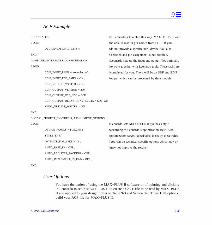
9
g S
ons
y
re
s.
ACF Example
User Options
You have the option of using the MAX+PLUS II software or of pointing and clickinin Leonardo to setup MAX+PLUS II to create an ACF file to be read by MAX+PLUII and applied to your design. Refer to Table 9-3 and Screen 9-3. These GUI optibuild your ACF file for MAX+PLUS II.
CHIP TRAFFIC #If Leonardo sets a chip this way, MAX+PLUS II will
BEGIN #be able to read in pin names from EDIF. If you
DEVICE=EPF10K10TC144-4; #do not provide a specific part, device AUTO is
END; # selected and pin assignment is not possible.
COMPILER_INTERFACES_CONFIGURATION #Leonardo sets up the input and output files optimall
BEGIN #to work together with Leonardo tools. These tasks a
EDIF_INPUT_LMF1 = exemplar.lmf ; #completed for you. There will be an SDF and EDIF
EDIF_INPUT_USE_LMF1 = ON ; #output which can be processed by time module.
EDIF_NETLIST_WRITER = ON ;
EDIF_OUTPUT_VERSION = 200 ;
EDIF_OUTPUT_USE_EDC = OFF;
EDIF_OUTPUT_DELAY_CONSTRUCTS = SDF_2.1;
VHDL_NETLIST_WRITER = ON ;
END;
GLOBAL_PROJECT_SYNTHESIS_ASSIGNMENT_OPTIONS
BEGIN #Leonardo sets MAX+PLUS II synthesis style
DEVICE_FAMILY = FLEX10k ; #according to Leonardo’s optimization style. Also
STYLE=FAST #optimization target (speed/area) is set by these rule
OPTIMIZE_FOR_SPEED = 1 ; #You can do technical specific options which may or
AUTO_FAST_IO = OFF ; #may not improve the results.
AUTO_REGISTER_PACKING = OFF ;
AUTO_IMPLEMENT_IN_EAB = OFF ;
END;
Altera FLEX Synthesis 9-35

9
Table 9-3. GUI Options and Results
*GUI Default Options
GUI Options Option on/off Comments Results
❏ Lock LCellssee Screen 9-1
on* click to clear default Allows MAX+PLUS II to map logic cells
off command line option-dont_lock_lcells
Input EDIF File EDIF file that is output from optimization. Part of the ACF file.
Input Target Target technology Part of the ACF file
Input Part Part number for target technology Part of the ACF file
Input Speed Grade Speed grade for target technology Part of the ACF file
RUN (Select ◆ radio button)
◆ Setup (ACF File) Sets up ACF File. Generates ACF file.
◆ Batch Mode Use Batch Mode to setup ACF file. Runs MAX+PLUS II in batch mode.
◆ GUI Use GUI. Runs MAX+PLUS II GUI.
❏ Auto Fast IO off* option disabled Compiles MAX+PLUS II
on enable auto fast io
❏ Auto Register Packing
off* option disabled Compiles MAX+PLUS II
on enable auto register packing
OPTIMIZE (Select ◆ radio button)
◆ Area Minimize design area in MAX+PLUS II Run Area again to improve results
◆ Delay Minimize design delay in MAX+PLUS II Run Delay again to improve results
TIMING ANALYSIS (Select ◆ radio button)
◆ None Select None if timing analysis is not needed. Timing analysis is disabled.
◆Setup/Hold Report Select a report if desired. Enables timing analysis reports
◆Register Performance Report
9-36 Leonardo Synthesis and Technology Guide
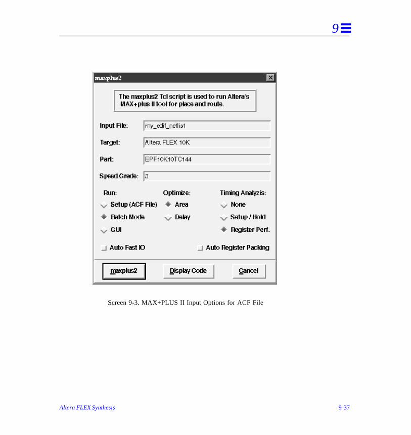
9
Screen 9-3. MAX+PLUS II Input Options for ACF File
Altera FLEX Synthesis 9-37
9
to -
he
EX
New Features for Altera FLEX
Altera FLEX 6K
Leonardo has support for the new FLEX 6K technology. It uses a modgen librarysupport the data path. This includes support for all flavors of counters available inFLEX 6K architecture. You must run MAX+PLUS II version 8.0 or higher for placeand-route. To support FLEX 6K, Leonardo uses an Exemplar library mapping file (LMF). Note: You cannot use the Exemplar LMF file that is shipped with MAX+PLUS II. You must use the LMF file shipped by Exemplar under the data directory.
Enhancements to Modgen
Existing Libraries
FLEX 10K: adjusted cascade chain lengths for eq and reduction operators to fit tsmaller LAB input counts of some FLEX 10K devices.
All RAMs: Support for arbitrary size RAMs.
Non-Square Multipliers
Non-square multipliers were implemented for the following Altera technologies: FL6K, FLEX 8K, FLEX 10K
LPM (Library of Parameterized Modules) Multiplier
The LPM multiplier provides better results. Note: Timing and area estimates will not be accurate.
Inferencing of LPM RAMs and Counters
Leonardo infers RAMs and Counters from the HDL description and uses LPM components to implement them.
9-38 Leonardo Synthesis and Technology Guide
9
lue by
utes,
ven
I
e
ogic
Instantiate LPM components
You can instantiate Altera LPM simulation models directly in VHDL and Verilog designs. The different parameters of the LPM instances are set to the required vadoing generic or parameter mapping. A special algorithm looks into a generic/parameter 'lpm_type' and moves all the generic/parameter values to attribin the final EDIF netlist for Altera.
You can simulate, as well as synthesize the same design without any change - ewith instances of technology specific RAMs, counters etc.
Lookup Table Functionality
Functionality of lookup table is written in terms of lut_function . For example:
.
.(cellref LUT
(libraryRef FLEX10K)
)..
(property lut_function
(string “(IN1 In2)”
)
This makes EDIF netlists generated by Leonardo much smaller and MAX+PLUSIprocessing time is faster.
Quality of Area and Delay Results
Quality of results were improved by 10%-20% for Altera FLEX area and delay. Thmost significant improvements are for targeting Altera FLEX technologies. The improvements are due to the following features:
• Clock Enable detection was improved to detect more complex clock enable l
• Multipliers are implemented more efficiently
• Improvements in LUT based Optimization algorithms
Altera FLEX Synthesis 9-39
9
• Improvements in the method Leonardo uses to represent and optimize wide functions, like ROMs.
You can expect significant improvements for both area and delay on designs thatcontain multipliers, clock enable logic, and ROMs.
9-40 Leonardo Synthesis and Technology Guide
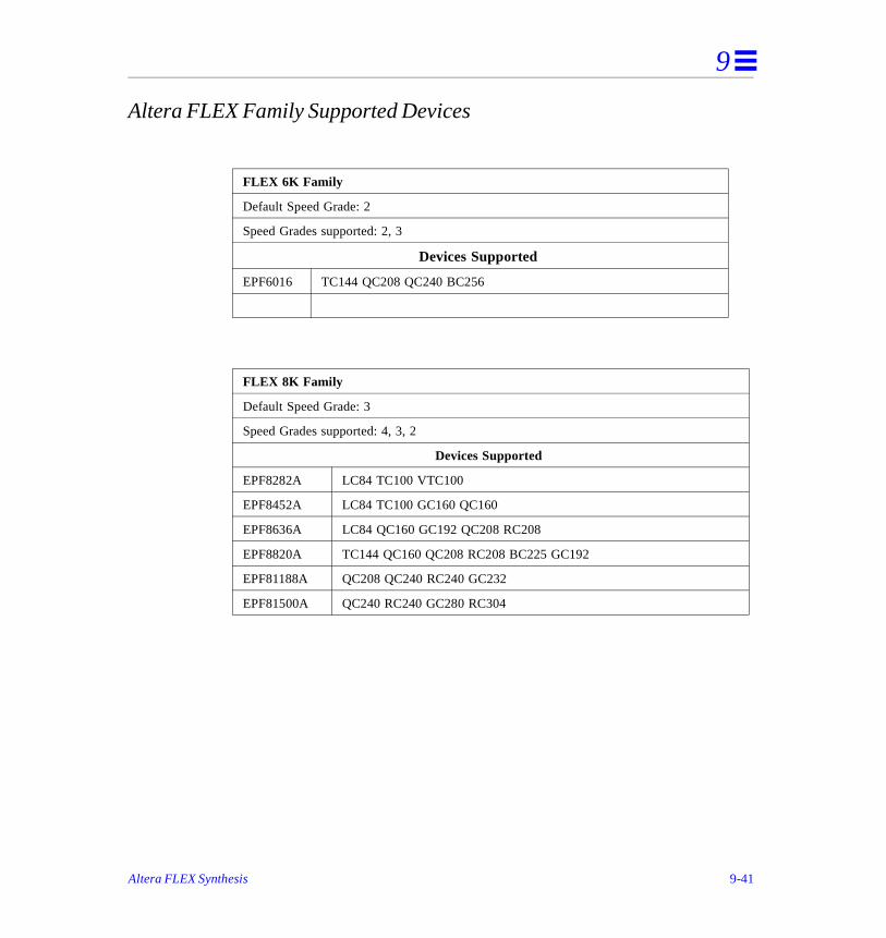
9
Altera FLEX Family Supported Devices
FLEX 6K Family
Default Speed Grade: 2
Speed Grades supported: 2, 3
Devices Supported
EPF6016 TC144 QC208 QC240 BC256
FLEX 8K Family
Default Speed Grade: 3
Speed Grades supported: 4, 3, 2
Devices Supported
EPF8282A LC84 TC100 VTC100
EPF8452A LC84 TC100 GC160 QC160
EPF8636A LC84 QC160 GC192 QC208 RC208
EPF8820A TC144 QC160 QC208 RC208 BC225 GC192
EPF81188A QC208 QC240 RC240 GC232
EPF81500A QC240 RC240 GC280 RC304
Altera FLEX Synthesis 9-41
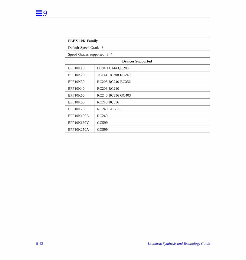
9
FLEX 10K Family
Default Speed Grade: 3
Speed Grades supported: 3, 4
Devices Supported
EPF10K10 LC84 TC144 QC208
EPF10K20 TC144 RC208 RC240
EPF10K30 RC208 RC240 BC356
EPF10K40 RC208 RC240
EPF10K50 RC240 BC356 GC403
EPF10K50 RC240 BC356
EPF10K70 RC240 GC503
EPF10K100A RC240
EPF10K130V GC599
EPF10K250A GC599
9-42 Leonardo Synthesis and Technology Guide
Altera MAX Synthesis 10
s her
d the d
Leonardo provides synthesis for Altera MAX5000, MAX7000, and MAX9000 familieof high density PLDs, and provides synthesis for these families into any of the otsupported technologies. This chapter presents the following information:
• Before Beginning
• Altera MAX Architecture
• Design Flow
• Library Mapping File (LMF)
• Synthesis and Optimization Features
• Optimization Style Points
• Altera MAX Reports
• Design I/O
• Additional Options
• Using MAX Designs as Input to Leonardo
Before Beginning
The technology information presented in this chapter assumes that you have reaintroductory chapters in this guide. Refer also to the HDL Synthesis and CommanReference guides for information.
Altera MAX Architecture
The basic Altera MAX structures are:
10-1
10
rs. is
of
vels be a rs ose
or
. X
s
of se
• Macrocells
• Expanders
• I/O cells
Macrocells, at the core of the Altera MAX, contain combinational logic and registeMacrocells can also be referred to as Logic Cells (LCELLs). Combinational logic limited by the number of product terms. Functions of up to four (MAX5000) or five(MAX7000, MAX9000) product terms can be implemented on one macro cell. Efficient use of the XOR gate resident in the Macrocell can increase the number product terms.
Functions of more product terms must use Expanders, or be broken into multiple leof Macrocells. Each Macrocell also contains a register that can be programmed toflip-flop or latch with clear and preset inputs. In addition, Macrocells and Expandeare grouped in LABs, which are fanin limited. The Macrocells and Expanders impa fanin limitation on the product term limitation.
I/O cells in Altera MAX can be configured as inputs, outputs, tri-statable outputs, bi-directional pins.
Design Flow
Figure 10-1 shows a simplified design flow that illustrates the use of Leonardo together with the Altera MAX+PLUS II tools to provide a complete design solutionDesigns are entered using standard methods and are optimized to the target MAdevice. The result is a hierarchical EDIF netlist file which is processed by MAX+PLUS II to produce final fitting.
When targeting the MAX 5000, 7000, or 9000 devices, optimization in Leonardo iused with -target=max5, -target=max7 or -target=max9. Output is written using write -format EDIF outputfile_name or using a .edf extension for output file name. Output is EDIF file which is for MAX+PLUS II.
If you do not want Leonardo to lock LCELLs, set the variable dont_lock_lcells to TRUE before running optimization. Leonardo will write out SOFT buffers insteadLCELL buffers. By default Leonardo locks LCELLS by using LCELL buffers becauin most cases it gives better results after MAX+PLUS II place and route. Refer toTable 10-1 and Screen 10-1.
10-2 Leonardo Synthesis and Technology Guide
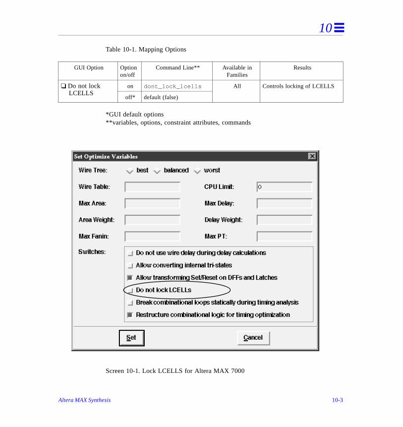
10
Table 10-1. Mapping Options
*GUI default options**variables, options, constraint attributes, commands
Screen 10-1. Lock LCELLS for Altera MAX 7000
GUI Option Optionon/off
Command Line** Available inFamilies
Results
❏ Do not lock LCELLS
on dont_lock_lcells All Controls locking of LCELLS
off* default (false)
Altera MAX Synthesis 10-3
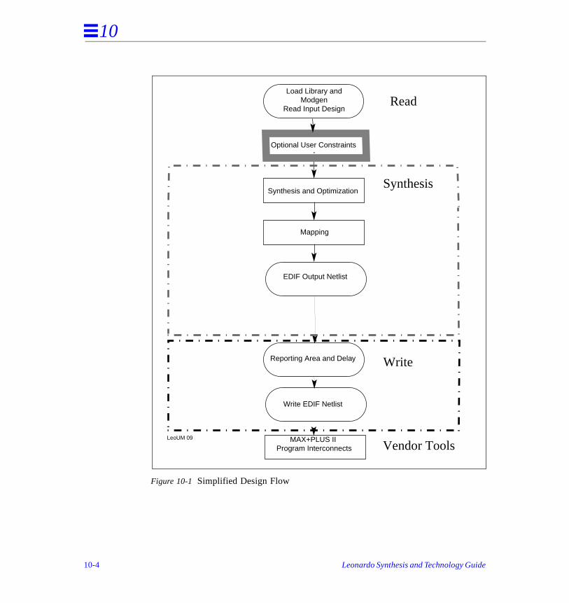
10
Figure 10-1 Simplified Design Flow
LeoUM 09
EDIF Output Netlist
Mapping
Synthesis and Optimization
Optional User Constraints
Reporting Area and Delay
Synthesis
Write
Load Library andModgen
Read Input DesignRead
Vendor ToolsMAX+PLUS II
Program Interconnects
Write EDIF Netlist
10-4 Leonardo Synthesis and Technology Guide
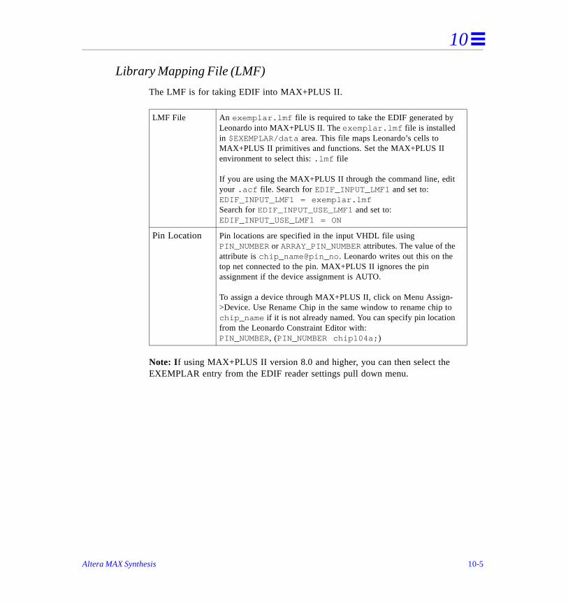
10
Library Mapping File (LMF)
The LMF is for taking EDIF into MAX+PLUS II.
Note: If using MAX+PLUS II version 8.0 and higher, you can then select the EXEMPLAR entry from the EDIF reader settings pull down menu.
LMF File An exemplar.lmf file is required to take the EDIF generated by Leonardo into MAX+PLUS II. The exemplar.lmf file is installed in $EXEMPLAR/data area. This file maps Leonardo’s cells to MAX+PLUS II primitives and functions. Set the MAX+PLUS II environment to select this: .lmf file
If you are using the MAX+PLUS II through the command line, edit your .acf file. Search for EDIF_INPUT_LMF1 and set to:EDIF_INPUT_LMF1 = exemplar.lmf Search for EDIF_INPUT_USE_LMF1 and set to: EDIF_INPUT_USE_LMF1 = ON
Pin Location Pin locations are specified in the input VHDL file using PIN_NUMBER or ARRAY_PIN_NUMBER attributes. The value of the attribute is chip_name@pin_no . Leonardo writes out this on the top net connected to the pin. MAX+PLUS II ignores the pin assignment if the device assignment is AUTO.
To assign a device through MAX+PLUS II, click on Menu Assign->Device. Use Rename Chip in the same window to rename chip to chip_name if it is not already named. You can specify pin location from the Leonardo Constraint Editor with:PIN_NUMBER, (PIN_NUMBER chip104a; )
Altera MAX Synthesis 10-5
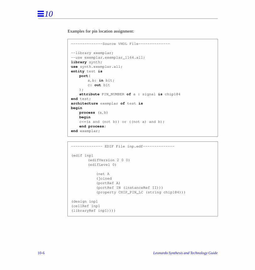
10
Examples for pin location assignment:
--------------Source VHDL File--------------
--library exemplar;--use exemplar.exemplar_1164.all;library synth;use synth.exemplar.all;entity test is
port (a,b: in bit;c: out bit
);attribute PIN_NUMBER of a : signal is chip1@4
end test;architecture exemplar of test isbegin
process (a,b)beginc<=(a and (not b)) or ((not a) and b);end process ;
end exemplar;
-------------- EDIF File inp.edf--------------
(edif inp1(edifVersion 2 0 0)(edifLevel 0)
(net A(joined(portRef A)(portRef IN (instanceRef II)))(property CHIP_PIN_LC (string chip1@4)))
(design inp1(cellRef inp1(libraryRef inp1))))
10-6 Leonardo Synthesis and Technology Guide
10
the
This
d
.
ted. can r
. rst
Pin Assignments
The following are the steps necessary to do pin assignments in MAX+PLUS II:
1. Click on menu Assign->Devices.
2. Click on Rename Chip and rename chip to chip1 in the display window.
3. Select a device from Devices.
4. Select OK. MAX+PLUS II assigns pin 4 to signal A when you compile.
Synthesis and Optimization Features
Leonardo uses dedicated algorithms to optimize logic for the MAX devices given product term and fanin limitations of the architecture. The optimization takes advantage of all MAX resources such as Expanders, XORs and enabled flip-flops.enables significant reductions in area and delay for the MAX devices.
Currently, four different, independent optimization passes are used, that may yieldifferent results:
• Pass 3 - One level implementation. This is the fastest performing result if it fits
• Passes 1, 2, and 4 - Multi-level implementations. These are slower but may takeless resources than pass 3.
Currently, the number of Macrocells as well as the number of Expanders is reporThe number of Macrocells and Expanders is only an estimate. The exact numberonly be determined during fitting, because MAX+PLUS II trades off Macrocells foExpanders, to achieve maximum utilization of resources.
If too many Expanders are used, MAX+PLUS II converts some Expanders into Macrocells, and consequently may use too many Macrocells for the target deviceTherefore, it is recommended to try and fit the other results as well, even if the fipass seems to be the smallest one.
Altera MAX Synthesis 10-7
10
acro.
or d as
the
r
he
sing y
Optimization Style Points
Quality of Optimization
Certain types of logic are optimized better than others: arithmetic circuits such asadders and multipliers are not as optimal as the best hand design or predefined mThese constructs are better synthesized using module generation if using VHDL Verilog as the input format. General control logic and state machines are optimizewell as or better than the best hand designs.
Module generation includes support for MAX7000 and MAX9000 architectures. Module generation support for MAX7000 can also be used by designers targetingMAX5000 architecture, although usually with less optimal results.
Sequential Optimization
Leonardo eliminates registers and latches when it is determined that the register olatch is always latching a constant value and there is no set or reset used on theregister. Leonardo also eliminates registers or latches that are identical in input toanother register or latch; these registers are effectively merged together.
Leonardo does not “move” registers or change the phase of the signal stored in tregisters.
Reporting
Refer to Chapter 6, Reports, in this guide for examples and more information.
Design I/O
Global Signals
Global signals like clocks and output enables for tri-state signals are specified by uthe BUFFER_SIG command. The two global signal primitives that are supported bthe MAX architecture are GLOBAL and SCLK.
10-8 Leonardo Synthesis and Technology Guide
10
o
em
he
For example:
Design rules for using these primitives (number of primitives, signals connected tprimitives, etc.) will not be violated by Leonardo.
Additional Options
Max Fanin and Max Cubes
There are two important variables that control the optimization. You can adjust thand re-optimize if a fit cannot be achieved for any of the passes.
This variable controls the maximum fanin into a function. If MAX+PLUS II issues tmessage:
Use this parameter to reduce fanin. The defaults values for max_fanin are:
max5 technology:80
max7 technology:36
max9 technology:49
This option controls the maximum number of product terms in a function. If MAX+PLUS II issues the message:
BUFFER_SIG SCLK clock1 BUFFER_SIG GLOBAL oe
set max_fanin <n>
Logic Array Block ... requires too many inputs
Logic Array Block ... requires too many expanders or Design requires too many macrocells/expanders
Altera MAX Synthesis 10-9
10
evels
e e be
F
g
Use this parameter to reduce the number of product terms. This results in more lof logic. The defaults values for max_pt are:
max5 technology:30
max7 technology:20
max9 technology:20
Appropriate defaults are picked when max_fanin/max_pt is set to 0.
Using MAX Designs as Input to Leonardo
EDIF Input
To retarget a MAX design into other technologies or to optimize a MAX design, thdesign must fit into a single MAX device. This ensures that MAX+PLUS II will writa single EDIF netlist that captures the whole design. The EDIF writer option mustenabled when running the MAX+PLUS II compiler. If the design does not fit into asingle device, switch to a bigger device until the design fits.
Use the EDIF file generated by MAX+PLUS II as input to Leonardo, with the MAX library as the source technology. If the design cannot fit into a single device, let MAX+PLUS II partition the design into several devices and generate several EDIfiles. Then, manually write an HDL file that connects the devices correctly. The MAX+PLUS II report file (multiple pin connections section) can be helpful in writinthis file.
10-10 Leonardo Synthesis and Technology Guide
Lucent ORCA Synthesis 11
d the d
This chapter provides guidelines for the synthesize of Lucent ORCA field programmable gate arrays (FPGAs). This chapter is divided as follows:
• Before Beginning
• FPGA Architecture
• Design Flow
• Synthesis and Optimization Features
• Using ORCA Architectural Features
• Reporting
• Generation of ORCA Foundry Properties
• ORCA DIN/DOUT Attributes
• ORCA Preference File Writer
• Devices Supported for Lucent ORCA FPGA Families
• More New Features for ORCA
Before Beginning
The technology information presented in this chapter assumes that you have reaintroductory chapters in this guide. Refer also to the HDL Synthesis and CommanReference Guides for information.
11-1
11
ic
igh-e or the ut, or
nt
le in d bufs.
ure
FPGA Architecture
ORCA FPGA consists of the following two basic elements:
• Programmable logic cells (PLCs)
• Programmable input/output cells (PICs)
The array of PLCs is surrounded by PICs. Each PLC contains a programmable function unit (PFU). All combinational logic is performed in Lookup Tables (LUTs)located in the PFU. The PFU can be used in different modes to meet different logrequirements. A PFU can be configured to implement from one to six input combinatorial logic functions:
• Four functions of 4-input variables, some inputs shared (QLUTs)
• Two functions of 5-input variables (HLUTs)
• One function of 6-input variables
The lookup tables in a PFU can also implement nibble-wide ripple functions with hspeed carry logic. Finally, you can also configure the lookup tables as a read/writread-only memory. The programmable input/output cells (PICs) are located alongperimeter of the device. Each I/O can be configured to be either an input, an outpa bidirectional I/O. Leonardo supports the following families of ORCA devices:
• ORCA-1C (ORCA-1c)
• ORCA-2C (ORCA-2c)
• ORCA-2CA (ORCA-2a)
• ORCA-2TA (ORCA-2a)
• ORCA-3C (ORCA-3c)
• ORCA-3T (ORCA-3t)
When targeting ORCA 2CA or ORCA 2TA, Leonardo selects the technology LuceORCA-2A from the Load Library menu. The ORCA3C modgen library is used by ORCA3. ORCA3C modgen library is similar to ORCA2C except for the following differences:
(1) Only synchronous RAMs are supported. Asynchronous RAMS are not availabORCA3C modgen library. Lucent recommends using SLIC (supplemental logic aninterconnect cell), to build RAMs greater than 32, instead of using a decoder and tSCUBA version 9.2a does not support RAM generation for ORCA 3C.
(2) ORCA3C modgen library does not use PFU gates.
The flow and interface between Leonardo and the ORCA Foundry is shown in Fig11-1. Figure 11-2 is the back annotation flow.
11-2 Leonardo Synthesis and Technology Guide

11
Figure 11-1 Simplified Design Flow
LeoUM 07L
Timing Constraints andTiming Optimization
Fanin Limited Optimization
LUT based Mapping
RTL Synthesis
Optional User Constraints
Reporting
Preference File orWrite EDIF
Synthesis
Write
Load Library and ModgenRead Input Design
Read
Vendor ToolsORCA Foundry
Place-and-Route tools
Lucent ORCA Synthesis 11-3
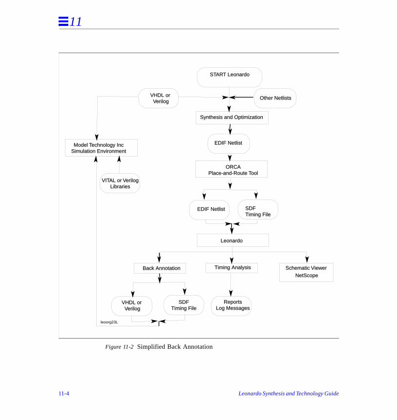
11
Figure 11-2 Simplified Back Annotation
START Leonardo
VHDL or Verilog
Other Netlists
Synthesis and Optimization
Model Technology IncSimulation Environment
VITAL or VerilogLibraries
ORCAPlace-and-Route Tool
NetScopeSchematic ViewerTiming Analysis
Leonardo
Back Annotation
VHDL or Verilog
SDFTiming File
ReportsLog Messages
EDIF Netlist SDFTiming File
EDIF Netlist
leoorg23L
11-4 Leonardo Synthesis and Technology Guide
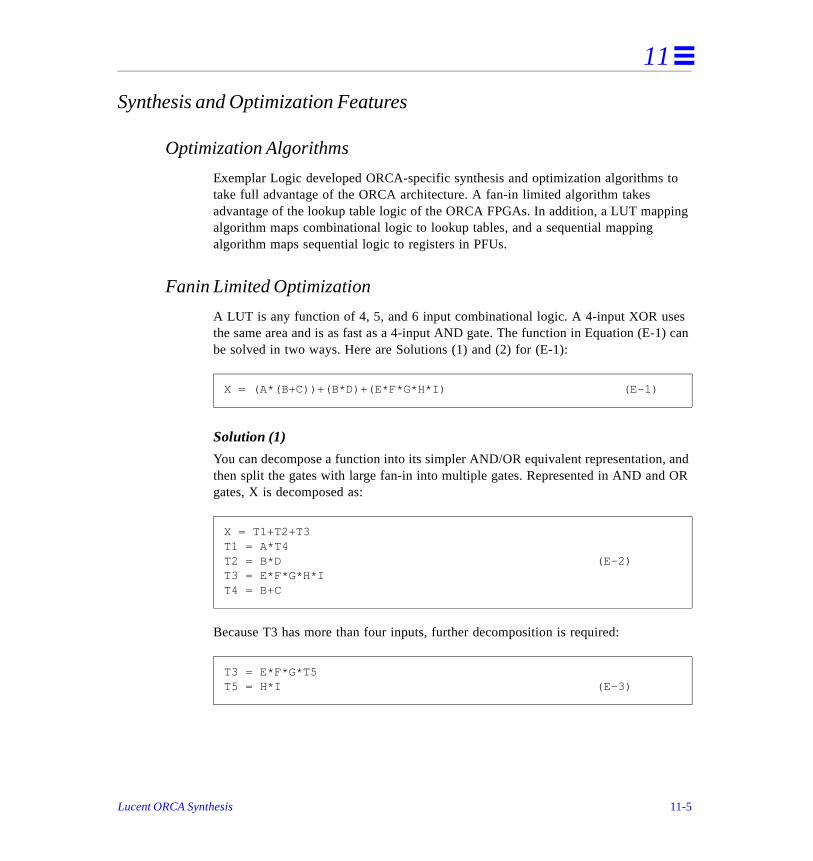
11
to
ing
s ) can
and OR
Synthesis and Optimization Features
Optimization Algorithms
Exemplar Logic developed ORCA-specific synthesis and optimization algorithms take full advantage of the ORCA architecture. A fan-in limited algorithm takes advantage of the lookup table logic of the ORCA FPGAs. In addition, a LUT mappalgorithm maps combinational logic to lookup tables, and a sequential mapping algorithm maps sequential logic to registers in PFUs.
Fanin Limited Optimization
A LUT is any function of 4, 5, and 6 input combinational logic. A 4-input XOR usethe same area and is as fast as a 4-input AND gate. The function in Equation (E-1be solved in two ways. Here are Solutions (1) and (2) for (E-1):
Solution (1)
You can decompose a function into its simpler AND/OR equivalent representation,then split the gates with large fan-in into multiple gates. Represented in AND andgates, X is decomposed as:
Because T3 has more than four inputs, further decomposition is required:
X = (A*(B+C))+(B*D)+(E*F*G*H*I) (E-1)
X = T1+T2+T3T1 = A*T4T2 = B*D (E-2)T3 = E*F*G*H*IT4 = B+C
T3 = E*F*G*T5T5 = H*I (E-3)
Lucent ORCA Synthesis 11-5
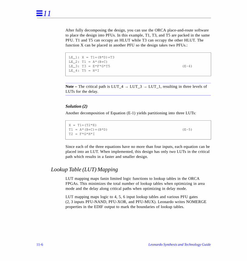
11
are same
an be ical
After fully decomposing the design, you can use the ORCA place-and-route softwto place the design into PFUs. In this example, T1, T3, and T5 are packed in the PFU. T1 and T5 can occupy an HLUT while T3 can occupy the other HLUT. The function X can be placed in another PFU so the design takes two PFUs.:
Note – The critical path is LUT_4 → LUT_3 → LUT_1, resulting in three levels of LUTs for the delay.
Solution (2)
Another decomposition of Equation (E-1) yields partitioning into three LUTs:
Since each of the three equations have no more than four inputs, each equation cplaced into an LUT. When implemented, this design has only two LUTs in the critpath which results in a faster and smaller design.
Lookup Table (LUT) Mapping
LUT mapping maps fanin limited logic functions to lookup tables in the ORCA FPGAs. This minimizes the total number of lookup tables when optimizing in areamode and the delay along critical paths when optimizing in delay mode.
LUT mapping maps logic to 4, 5, 6 input lookup tables and various PFU gates (2, 3 inputs PFU-NAND, PFU-XOR, and PFU-MUX). Leonardo writes NOMERGEproperties in the EDIF output to mark the boundaries of lookup tables.
LE_1: X = T1+(B*D)+T3LE_2: T1 = A*(B+C)LE_3: T3 = E*F*G*T5 (E-4)LE_4: T5 = H*I
X = T1+(T2*E)T1 = A*(B+C)+(B*D) (E-5)T2 = F*G*H*I
11-6 Leonardo Synthesis and Technology Guide
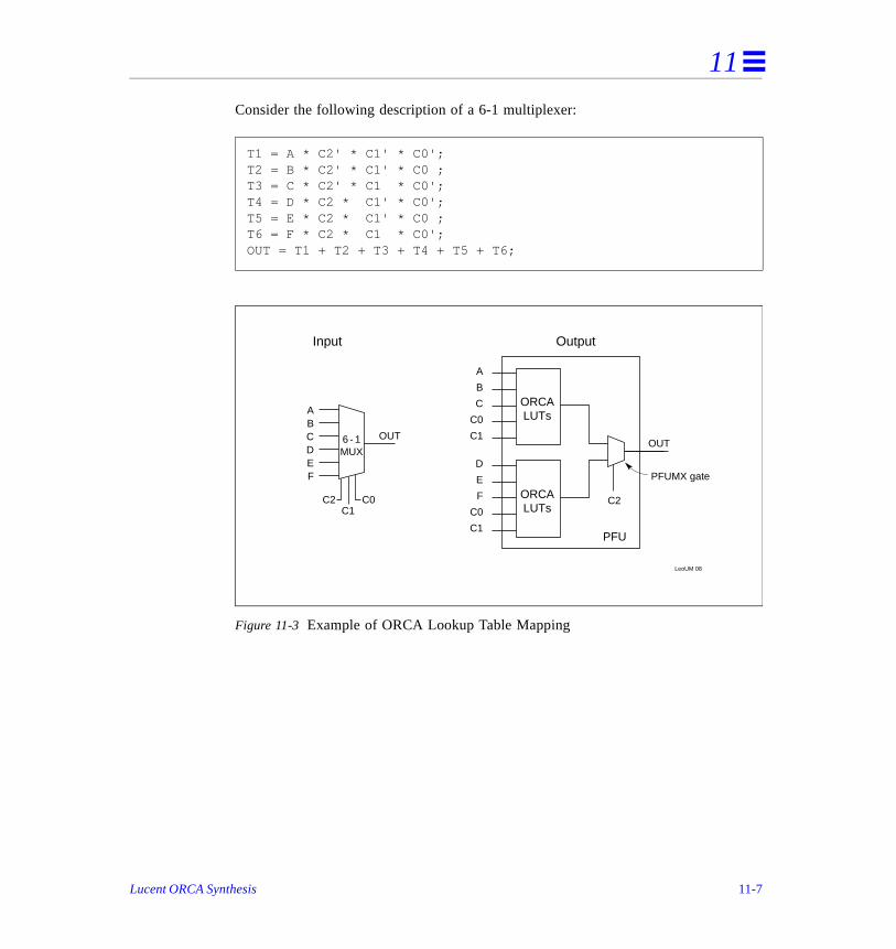
11
Consider the following description of a 6-1 multiplexer:
Figure 11-3 Example of ORCA Lookup Table Mapping
T1 = A * C2' * C1' * C0';T2 = B * C2' * C1' * C0 ;T3 = C * C2' * C1 * C0';T4 = D * C2 * C1' * C0';T5 = E * C2 * C1' * C0 ;T6 = F * C2 * C1 * C0';OUT = T1 + T2 + T3 + T4 + T5 + T6;
ORCALUTs
ORCALUTs
A
B
C
C0
C1
D
E
F
C0
C1
PFUMX gate
OUT
LeoUM 08
C2
OUT
C2C1
C0
FEDCBA
6 - 1MUX
Input Output
PFU
Lucent ORCA Synthesis 11-7
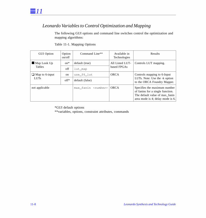
11
d
.
Leonardo Variables to Control Optimization and Mapping
The following GUI options and command line switches control the optimization anmapping algorithms:
Table 11-1. Mapping Options
*GUI default options**variables, options, constraint attributes, commands
GUI Option Optionon/off
Command Line** Available inTechnologies
Results
■ Map Look Up Tables
on* default (true) All Listed LUT-based FPGAs
Controls LUT mapping.
off lut_map
❏ Map to 6-input LUTs
on use_f6_lut ORCA Controls mapping to 6-Input LUTs. Note: Use the -k option to the ORCA Foundry Mapper.
off* default (false)
not applicable max_fanin < number> ORCA Specifies the maximum number of fanins for a single function. The default value of max_fanin area mode is 4; delay mode is 6
11-8 Leonardo Synthesis and Technology Guide
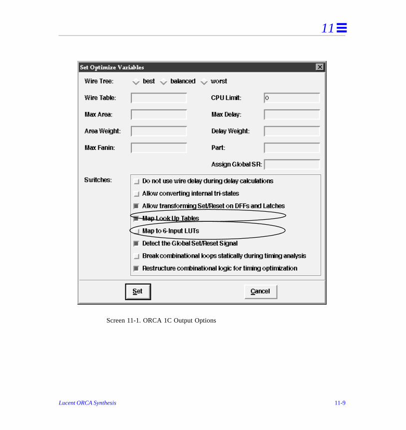
11
Screen 11-1. ORCA 1C Output Options
Lucent ORCA Synthesis 11-9
11
FU
ave neral
Constraint-Driven Timing Optimization
optimize_timing command can be used after optimize to improve the timing performance of the design. optimize_timing command works most effectively when timing constraints are specified. The -force option can be used to force timingconstraints, in which case it will try to improve the longest path.
The optimize_timing command restructures combinational logic to reduce thelevels of logic between the critical signal and the output. It also tries to map the restructured portion of the logic effectively to the ORCA architecture. Using the Pgate, it tries to map a critical signal directly to the input of the PFU-MUX gate, bypassing the LUTs in the PFU. However, this may not always be feasible.
Also the specific end point or instance to improve can be specified to the optimize_timing command with the -through option.
Data Path Synthesis (Modgen)
Leonardo supports various technology-specific implementations of arithmetic andrelational operators used in VHDL or Verilog RTL. Since these implementations hbeen designed optimally for the ORCA technology, the synthesis results are in gesmaller and/or faster and take less time to compile.
optimize_timing -force
optimize_timing -through
11-10 Leonardo Synthesis and Technology Guide
11
n.
y in
al ot
eset
The following operators are supported for ORCA technology for families 2C, 1C, 2CA, and 2TA:
• Logical Operators and or nand nor xor xnor
• Relational Operators = /= < <= > >=
• Arithmetic Operators + - *
• Misc. Functions incrementerdecrementerabsolute valueunary minuscountersRAMs (synchronous and asynchronous for 2A only)multiplexers
Using ORCA Architectural Features
Use of Enabled D-Type Flip-Flops
Mapping to enabled D-type flip-flops can be controlled with the use_dffenable
variable. This variable allows Leonardo to infer clock enable from HDL descriptioThe default is TRUE.
When reading HDL designs with use_dffenable value set to TRUE, Leonardo infers clock enable logic while parsing HDL code. Detecting the clock enable earlthe synthesis flow achieves better results.
GSR Usage and Startup Blocks
ORCA flip-flops feature set/reset inputs that can be driven from a dedicated GlobSet/Reset (GSR) signal. The GSR is implicit set/reset for all registers, and does nrequire any routing resources. A STARTUP block is instantiated automatically if global_sr is set to a signal name (my_signal ) in the design, or if infer_gsr variables are set to TRUE. The purpose of the STARTUP block is to accept the rsignal and to distribute the reset implicitly through the dedicated GSR signal.
use_dffenable true
set global_sr <my_signal>
Lucent ORCA Synthesis 11-11
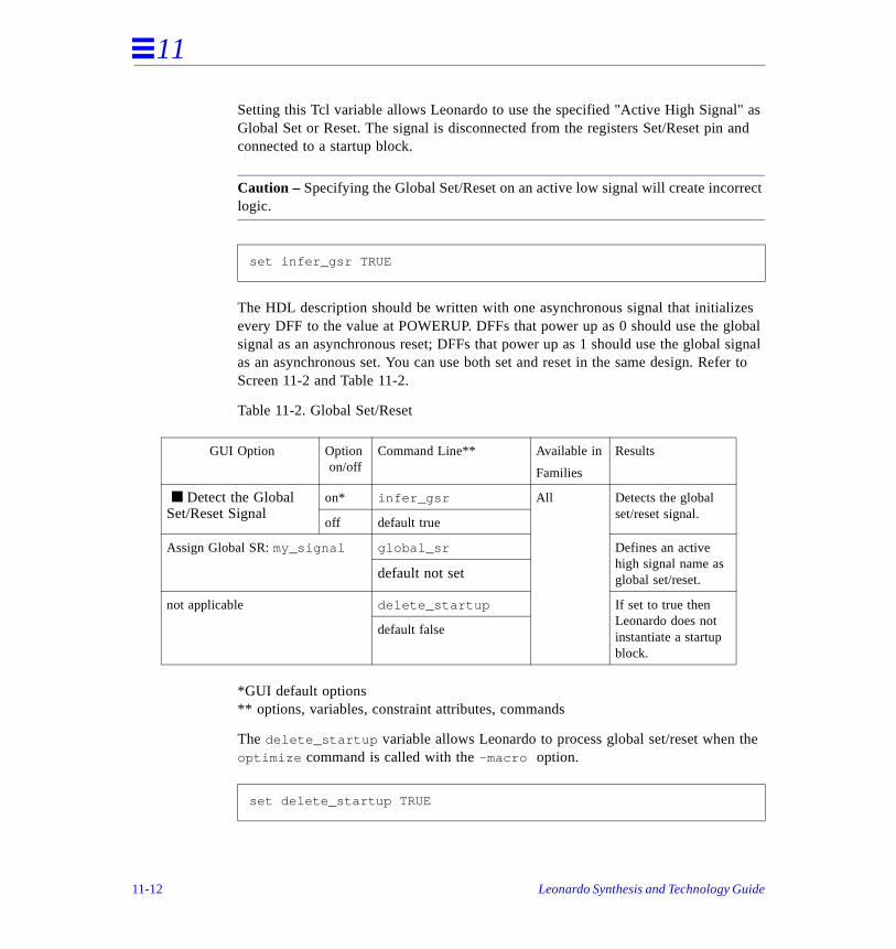
11
as and
ect
es lobal signal fer to
he
Setting this Tcl variable allows Leonardo to use the specified "Active High Signal"Global Set or Reset. The signal is disconnected from the registers Set/Reset pin connected to a startup block.
Caution – Specifying the Global Set/Reset on an active low signal will create incorrlogic.
The HDL description should be written with one asynchronous signal that initializevery DFF to the value at POWERUP. DFFs that power up as 0 should use the gsignal as an asynchronous reset; DFFs that power up as 1 should use the globalas an asynchronous set. You can use both set and reset in the same design. ReScreen 11-2 and Table 11-2.
Table 11-2. Global Set/Reset
*GUI default options** options, variables, constraint attributes, commands
The delete_startup variable allows Leonardo to process global set/reset when toptimize command is called with the -macro option.
set infer_gsr TRUE
GUI Option Option on/off
Command Line** Available in
Families
Results
■ Detect the Global Set/Reset Signal
on* infer_gsr All Detects the global set/reset signal.
off default true
Assign Global SR: my_signal global_sr Defines an active high signal name as global set/reset.default not set
not applicable delete_startup If set to true then Leonardo does not instantiate a startup block.
default false
set delete_startup TRUE
11-12 Leonardo Synthesis and Technology Guide
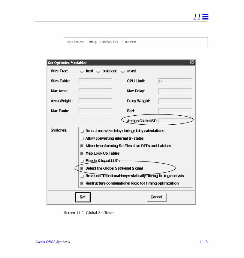
11
Screen 11-2. Global Set/Reset
optimize -chip (default) | macro
Lucent ORCA Synthesis 11-13
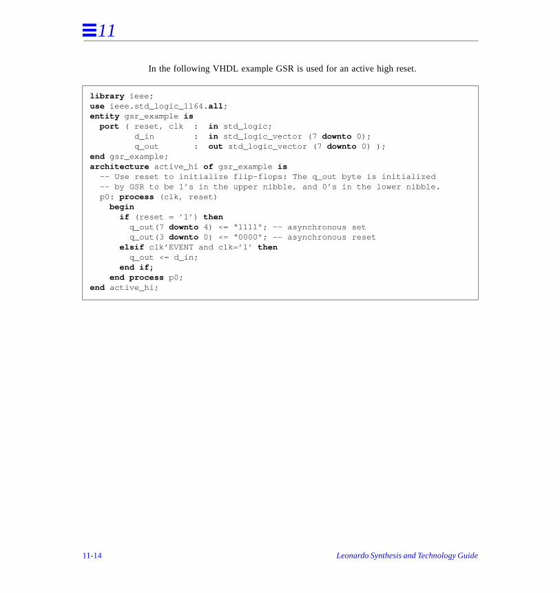
11
In the following VHDL example GSR is used for an active high reset.
library ieee;use ieee.std_logic_1164. all ;entity gsr_example is port ( reset, clk : in std_logic; d_in : in std_logic_vector (7 downto 0); q_out : out std_logic_vector (7 downto 0) );end gsr_example;architecture active_hi of gsr_example is -- Use reset to initialize flip-flops: The q_out byte is initialized -- by GSR to be 1’s in the upper nibble, and 0’s in the lower nibble. p0: process (clk, reset) begin if (reset = ’1’) then q_out(7 downto 4) <= “1111"; -- asynchronous set q_out(3 downto 0) <= “0000"; -- asynchronous reset elsif clk’EVENT and clk=’1’ then q_out <= d_in; end if; end process p0;end active_hi;
11-14 Leonardo Synthesis and Technology Guide
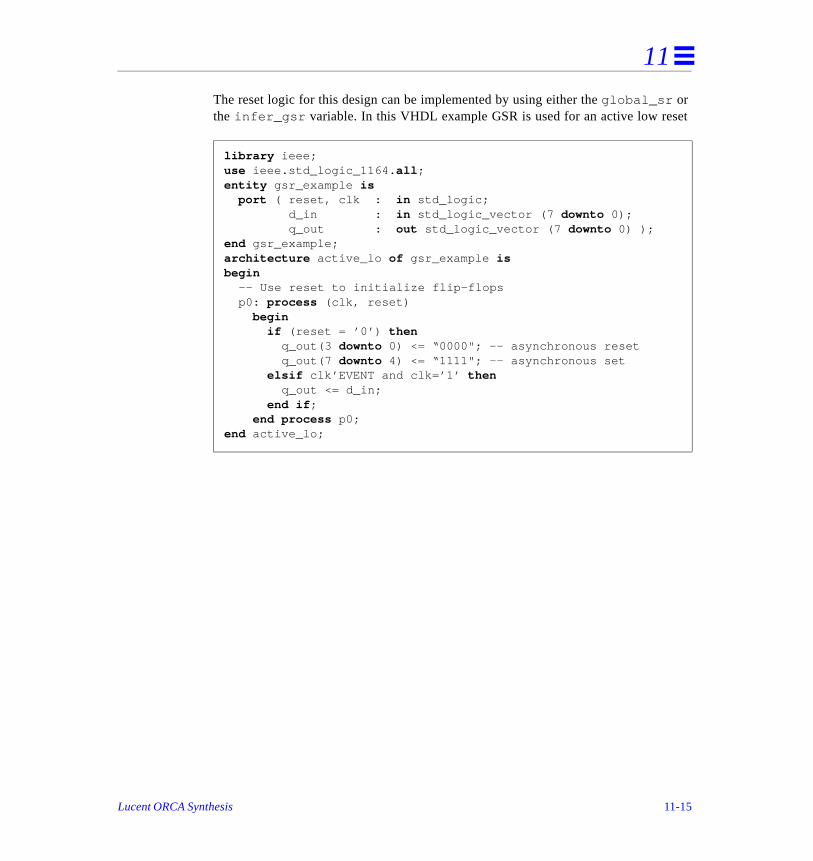
11
et
The reset logic for this design can be implemented by using either the global_sr or the infer_gsr variable. In this VHDL example GSR is used for an active low reslibrary ieee;use ieee.std_logic_1164. all ;entity gsr_example is port ( reset, clk : in std_logic; d_in : in std_logic_vector (7 downto 0); q_out : out std_logic_vector (7 downto 0) );end gsr_example;architecture active_lo of gsr_example isbegin -- Use reset to initialize flip-flops p0: process (clk, reset) begin if (reset = ’0’) then q_out(3 downto 0) <= “0000"; -- asynchronous reset q_out(7 downto 4) <= “1111"; -- asynchronous set elsif clk’EVENT and clk=’1’ then q_out <= d_in; end if ; end process p0;end active_lo;
Lucent ORCA Synthesis 11-15
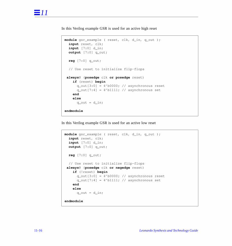
11
In this Verilog example GSR is used for an active high reset
In this Verilog example GSR is used for an active low reset
module gsr_example ( reset, clk, d_in, q_out ); input reset, clk; input [7:0] d_in; output [7:0] q_out; reg [7:0] q_out;
// Use reset to initialize flip-flops always @ ( posedge clk or posedge reset) if (reset) begin q_out[3:0] = 4’b0000; // asynchronous reset q_out[7:4] = 4’b1111; // asynchronous set end else q_out = d_in;
endmodule
module gsr_example ( reset, clk, d_in, q_out ); input reset, clk; input [7:0] d_in; output [7:0] q_out; reg [7:0] q_out;
// Use reset to initialize flip-flops always @ ( posedge clk or negedge reset) if (!reset) begin q_out[3:0] = 4’b0000; // asynchronous reset q_out[7:4] = 4’b1111; // asynchronous set end else q_out = d_in;
endmodule
11-16 Leonardo Synthesis and Technology Guide
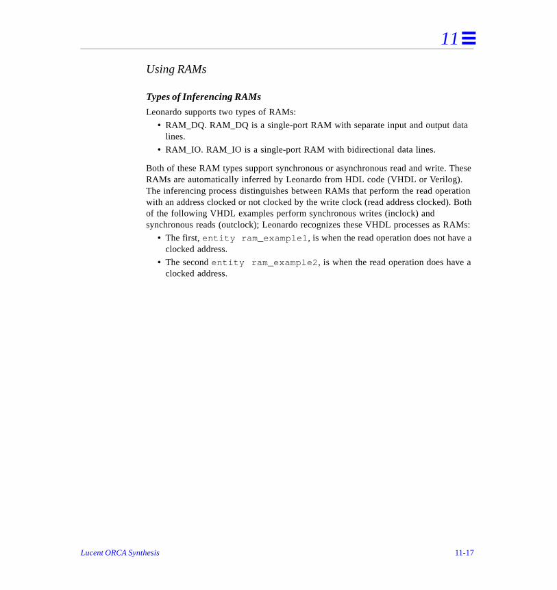
11
a
hese ation Both
AMs:
a
a
Using RAMs
Types of Inferencing RAMs
Leonardo supports two types of RAMs:
• RAM_DQ. RAM_DQ is a single-port RAM with separate input and output datlines.
• RAM_IO. RAM_IO is a single-port RAM with bidirectional data lines.
Both of these RAM types support synchronous or asynchronous read and write. TRAMs are automatically inferred by Leonardo from HDL code (VHDL or Verilog). The inferencing process distinguishes between RAMs that perform the read operwith an address clocked or not clocked by the write clock (read address clocked). of the following VHDL examples perform synchronous writes (inclock) and synchronous reads (outclock); Leonardo recognizes these VHDL processes as R
• The first, entity ram_example1 , is when the read operation does not haveclocked address.
• The second entity ram_example2 , is when the read operation does have clocked address.
Lucent ORCA Synthesis 11-17
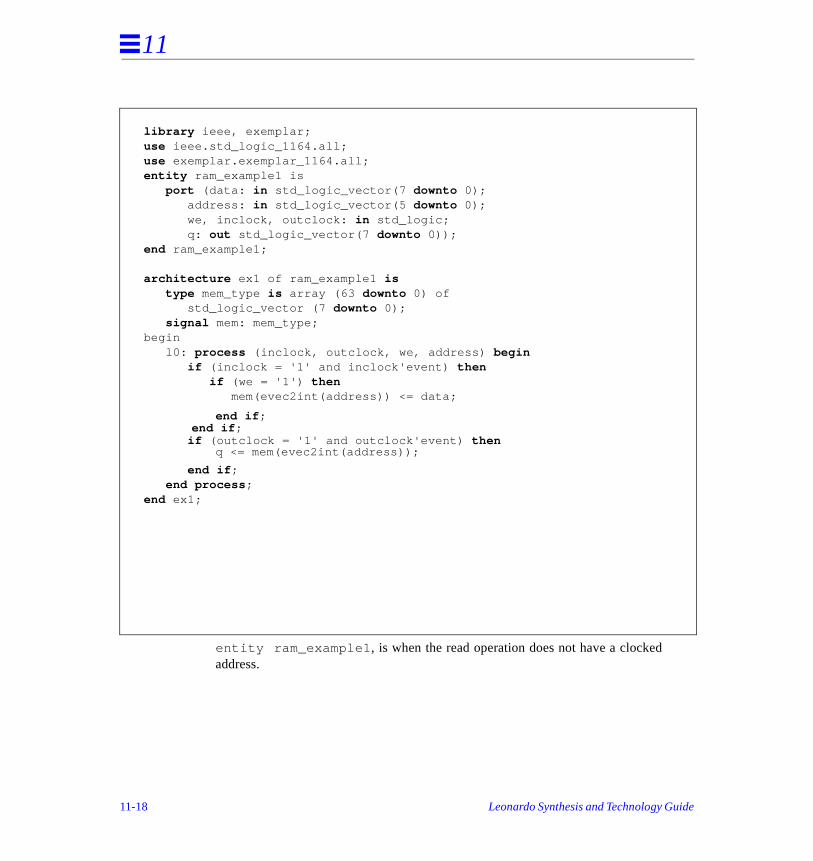
11
entity ram_example1 , is when the read operation does not have a clocked address.
library ieee, exemplar;use ieee.std_logic_1164.all;use exemplar.exemplar_1164.all;entity ram_example1 is port (data: in std_logic_vector(7 downto 0); address: in std_logic_vector(5 downto 0); we, inclock, outclock: in std_logic; q: out std_logic_vector(7 downto 0));end ram_example1;
architecture ex1 of ram_example1 is type mem_type is array (63 downto 0) of std_logic_vector (7 downto 0); signal mem: mem_type;begin l0: process (inclock, outclock, we, address) begin if (inclock = '1' and inclock'event) then if (we = '1') then mem(evec2int(address)) <= data;
if (outclock = '1' and outclock'event) then
end if ; end process ;end ex1;
q <= mem(evec2int(address));
end if ;end if ;
11-18 Leonardo Synthesis and Technology Guide

11
ss.
e Ms
entity ram_example2 , is when the read operation does have a clocked addre
ORCA 1C/2C/2A Modgen Support for RAMs
The ORCA 1C and ORCA 2C Modgen Libraries support asynchronous RAMs. ThORCA2A Modgen Library supports both asynchronous RAMs and synchronous RAthat do not clock the read address with the write clock.
library ieee, exemplar;use ieee.std_logic_1164.all;use exemplar.exemplar_1164.all;entity ram_example2 is port (data: in std_logic_vector(7 downto 0); address: in std_logic_vector(5 downto 0); we, inclock, outclock: in std_logic; q: out std_logic_vector(7 downto 0)); end ram_example2;architecture ex2 of ram_example2 is type mem_type is array (63 downto 0) of std_logic_vector (7 downto 0); signal mem: mem_type; signal address_int: std_logic_vector(5 downto 0);begin l0: process (inclock, outclock, we, address) begin if (inclock = '1' and inclock'event) then
if (outclock = '1' and outclock'event) then
end if ; end process ;end ex2;
address_int <= address;if (we = '1') then
mem(evec2int(address)) <= data;end if ;
end if ;
q <= mem(evec2int(address_int));
Lucent ORCA Synthesis 11-19
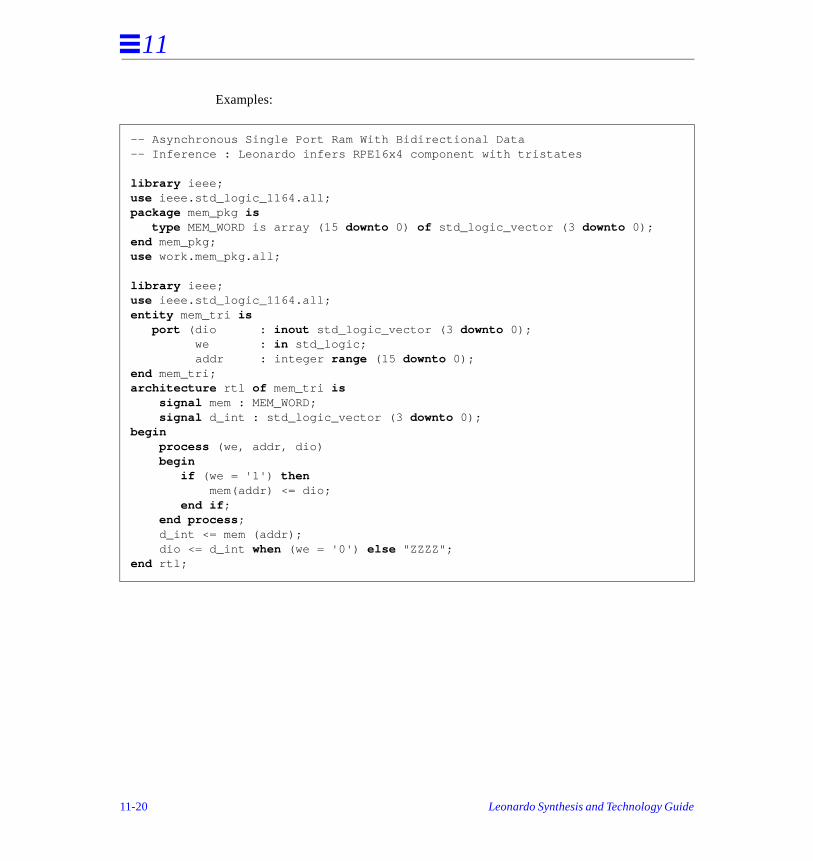
11
Examples:
-- Asynchronous Single Port Ram With Bidirectional Data-- Inference : Leonardo infers RPE16x4 component with tristates
library ieee;use ieee.std_logic_1164.all;package mem_pkg is type MEM_WORD is array (15 downto 0) of std_logic_vector (3 downto 0);end mem_pkg;use work.mem_pkg.all;
library ieee;use ieee.std_logic_1164.all;entity mem_tri is port (dio : inout std_logic_vector (3 downto 0); we : in std_logic; addr : integer range (15 downto 0);end mem_tri;architecture rtl of mem_tri is signal mem : MEM_WORD; signal d_int : std_logic_vector (3 downto 0);begin process (we, addr, dio) begin if (we = '1') then mem(addr) <= dio; end if ; end process ; d_int <= mem (addr); dio <= d_int when (we = '0') else "ZZZZ";end rtl;
11-20 Leonardo Synthesis and Technology Guide
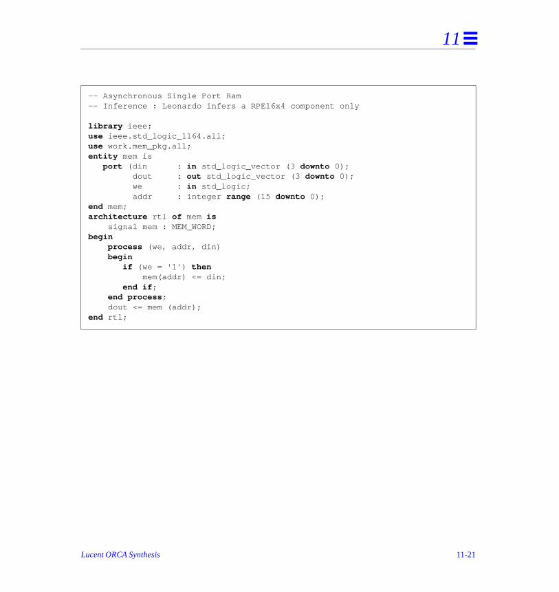
11
-- Asynchronous Single Port Ram-- Inference : Leonardo infers a RPE16x4 component only
library ieee;use ieee.std_logic_1164.all;use work.mem_pkg.all;entity mem is port (din : in std_logic_vector (3 downto 0); dout : out std_logic_vector (3 downto 0); we : in std_logic; addr : integer range (15 downto 0);end mem;architecture rtl of mem is signal mem : MEM_WORD;begin process (we, addr, din) begin if (we = '1') then mem(addr) <= din; end if ; end process ; dout <= mem (addr);end rtl;
Lucent ORCA Synthesis 11-21
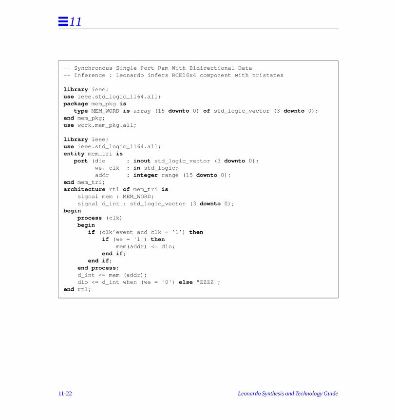
11
-- Synchronous Single Port Ram With Bidirectional Data-- Inference : Leonardo infers RCE16x4 component with tristates
library ieee;use ieee.std_logic_1164.all;package mem_pkg is type MEM_WORD is array (15 downto 0) of std_logic_vector (3 downto 0);end mem_pkg;use work.mem_pkg.all;
library ieee;use ieee.std_logic_1164.all;entity mem_tri is port (dio : inout std_logic_vector (3 downto 0); we, clk : in std_logic; addr : integer range (15 downto 0);end mem_tri;architecture rtl of mem_tri is signal mem : MEM_WORD; signal d_int : std_logic_vector (3 downto 0);begin process (clk) begin if (clk’event and clk = ‘1’) then if (we = '1') then mem(addr) <= dio; end if ; end if ; end process ; d_int <= mem (addr); dio <= d_int when (we = '0') else "ZZZZ";end rtl;
11-22 Leonardo Synthesis and Technology Guide
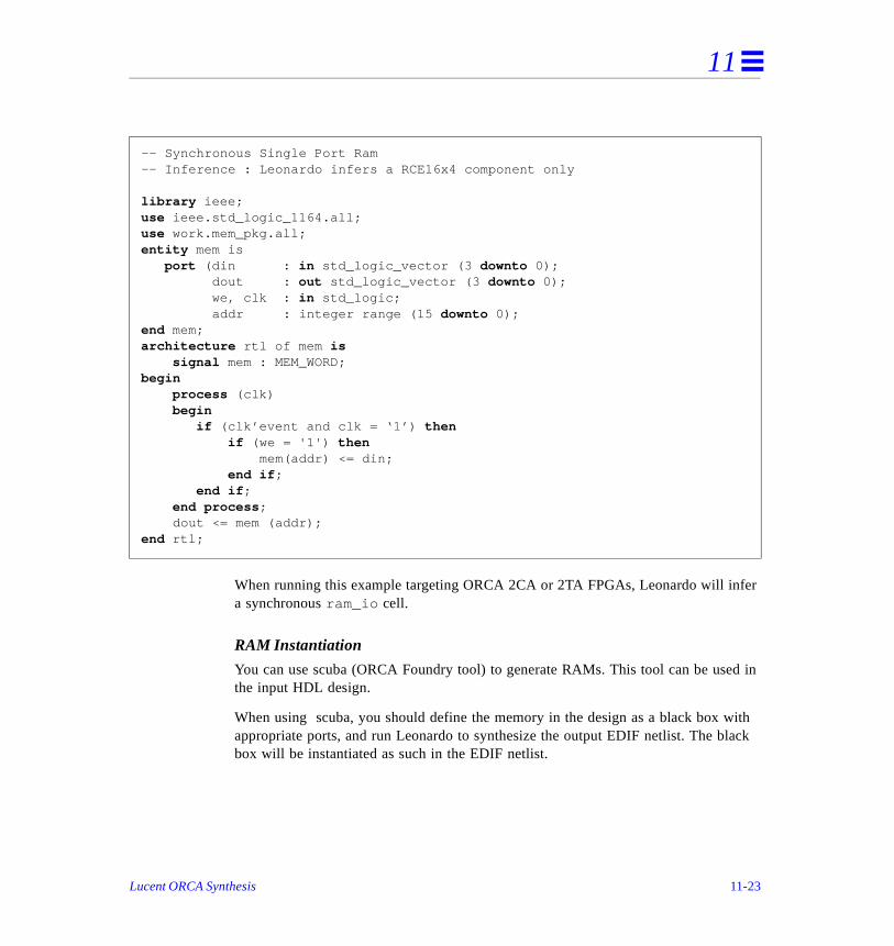
11
fer
d in
with ack
When running this example targeting ORCA 2CA or 2TA FPGAs, Leonardo will ina synchronous ram_io cell.
RAM Instantiation
You can use scuba (ORCA Foundry tool) to generate RAMs. This tool can be usethe input HDL design.
When using scuba, you should define the memory in the design as a black box appropriate ports, and run Leonardo to synthesize the output EDIF netlist. The blbox will be instantiated as such in the EDIF netlist.
-- Synchronous Single Port Ram-- Inference : Leonardo infers a RCE16x4 component only
library ieee;use ieee.std_logic_1164.all;use work.mem_pkg.all;entity mem is port (din : in std_logic_vector (3 downto 0); dout : out std_logic_vector (3 downto 0); we, clk : in std_logic; addr : integer range (15 downto 0);end mem;architecture rtl of mem is signal mem : MEM_WORD;begin process (clk) begin if (clk’event and clk = ‘1’) then if (we = '1') then mem(addr) <= din; end if ; end if ; end process ; dout <= mem (addr);end rtl;
Lucent ORCA Synthesis 11-23
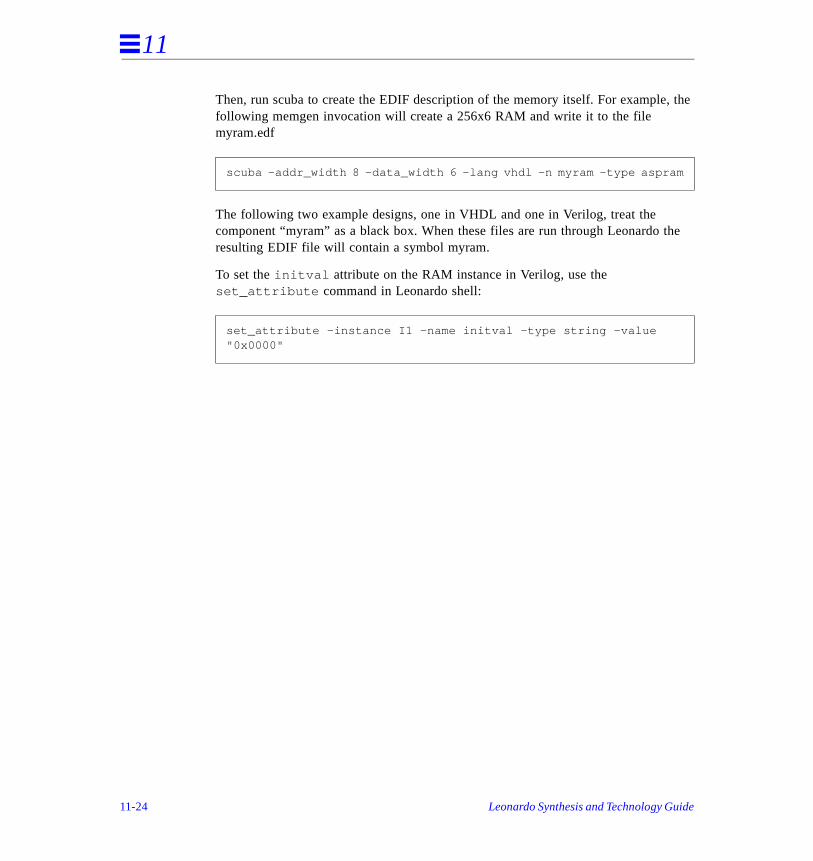
11
, the
he
Then, run scuba to create the EDIF description of the memory itself. For examplefollowing memgen invocation will create a 256x6 RAM and write it to the file myram.edf
The following two example designs, one in VHDL and one in Verilog, treat the component “myram” as a black box. When these files are run through Leonardo tresulting EDIF file will contain a symbol myram.
To set the initval attribute on the RAM instance in Verilog, use the set_attribute command in Leonardo shell:
scuba -addr_width 8 -data_width 6 -lang vhdl -n myram -type aspram
set_attribute -instance I1 -name initval -type string -value "0x0000"
11-24 Leonardo Synthesis and Technology Guide
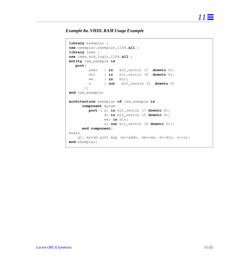
11
Example 8a. VHDL RAM Usage Example
library exemplar ;use exemplar.exemplar_1164. all ;library ieee ;use ieee.std_logic_1164. all ;entity ram_example is port ( addr : in bit_vector (7 downto 0); din : in bit_vector (5 downto 0); we : in bit; o : out bit_vector (5 downto 0) );end ram_example; architecture exemplar of ram_example is component myram port ( a: in bit_vector (7 downto 0); d: in bit_vector (5 downto 0); we: in bit; o: out bit_vector (5 downto 0)); end component ;begin g1: myram port map (a=>addr, we=>we, d=>din, o=>o);end eXemplar;
Lucent ORCA Synthesis 11-25
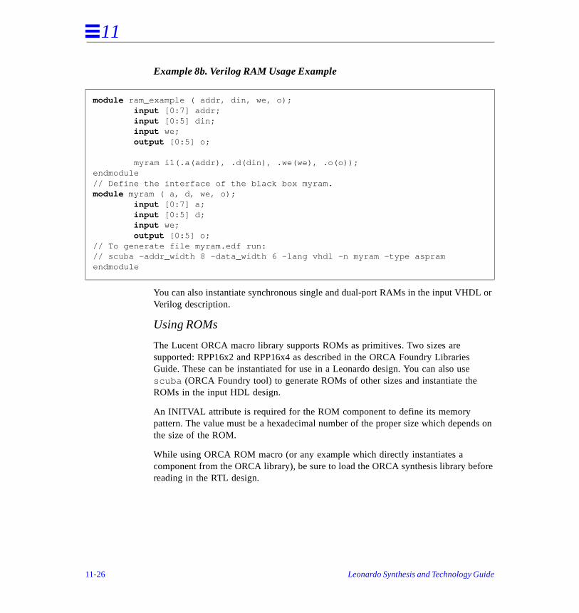
11
or
ds on
fore
Example 8b. Verilog RAM Usage Example
You can also instantiate synchronous single and dual-port RAMs in the input VHDLVerilog description.
Using ROMs
The Lucent ORCA macro library supports ROMs as primitives. Two sizes are supported: RPP16x2 and RPP16x4 as described in the ORCA Foundry Libraries Guide. These can be instantiated for use in a Leonardo design. You can also usescuba (ORCA Foundry tool) to generate ROMs of other sizes and instantiate theROMs in the input HDL design.
An INITVAL attribute is required for the ROM component to define its memory pattern. The value must be a hexadecimal number of the proper size which depenthe size of the ROM.
While using ORCA ROM macro (or any example which directly instantiates a component from the ORCA library), be sure to load the ORCA synthesis library bereading in the RTL design.
module ram_example ( addr, din, we, o); input [0:7] addr; input [0:5] din; input we; output [0:5] o; myram i1(.a(addr), .d(din), .we(we), .o(o));endmodule// Define the interface of the black box myram.module myram ( a, d, we, o); input [0:7] a; input [0:5] d; input we; output [0:5] o;// To generate file myram.edf run:// scuba -addr_width 8 -data_width 6 -lang vhdl -n myram -type aspramendmodule
11-26 Leonardo Synthesis and Technology Guide
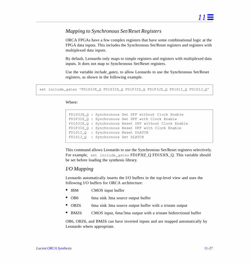
11
t the s with
data
t
tively.
y
Mapping to Synchronous Set/Reset Registers
ORCA FPGAs have a few complex registers that have some combinational logic aFPGA data inputs. This includes the Synchronous Set/Reset registers and registermultiplexed data inputs.
By default, Leonardo only maps to simple registers and registers with multiplexed inputs. It does not map to Synchronous Set/Reset registers.
Use the variable include_gates, to allow Leonardo to use the Synchronous Set/Reseregisters, as shown in the following example.
Where:
This command allows Leonardo to use the Synchronous Set/Reset registers selecFor example, set include_gates FD1P3IZ_Q FD1S3IX_Q. This variable shouldbe set before loading the synthesis library.
I/O Mapping
Leonardo automatically inserts the I/O buffers in the top-level view and uses the following I/O buffers for ORCA architecture:
• IBM CMOS input buffer
• OB6 6ma sink 3ma source output buffer
• OBZ6 6ma sink 3ma source output buffer with a tristate output
• BMZ6 CMOS input, 6ma/3ma output with a tristate bidirectional buffer
OB6, OBZ6, and BMZ6 can have inverted inputs and are mapped automatically bLeonardo where appropriate.
set include_gates "FD1S3JX_Q FD1S3IX_Q FD1P3IZ_Q FD1P3JZ_Q FD1S1I_Q FD1S1J_Q"
FD1S3JX_Q : Synchronous Set DFF without Clock EnableFD1P3IZ_Q : Synchronous Set DFF with Clock EnableFD1S3IX_Q : Synchronous Reset DFF without Clock EnableFD1P3IZ_Q : Synchronous Reset DFF with Clock EnableFD1S1I_Q : Synchronous Reset DLATCHFD1S1J_Q : Synchronous Set DLATCH
Lucent ORCA Synthesis 11-27
11
rdo
ou
put
s by s.
o
All other I/O buffers, as described in the ORCA Library section of the ORCA Foundry Manual, can be inserted from the Leonardo shell using the PAD command or instantiated by component instantiation in VHDL or Verilog HDL.
ORCA Reporting
Refer to Chapter 6, Reports, in this guide for examples and information on Leonareporting.
Generation of ORCA Foundry Properties from Leonardo
Pin Number Property - LOC
You can specify IOB locations for external pins of a design. If using VHDL input, ycan use pin_number for individual signals and array_pin_number for buses. These attributes are translated into LOC property on the IOB instances in the outEDIF file for further processing by ORCA Foundry place and route tools.
The VHDL attributes pin_number and array_pin_number are declared in the EXEMPLAR and EXEMPLAR_1164 packages. You gain access to these packagemaking a package visible with these context clauses before the entity declaration
If you are not using the EXEMPLAR or EXEMPLAR_1164 package, the attributespin_number , array_pin_number, and the type string_array must be defined.
For Verilog designs or any other netlist formats, you can use predefined Leonardprocedures or set_attribute command to set pin_number constraints on design ports.
library exemplar; use EXEMPLAR.EXEMPLAR_1164.all;
11-28 Leonardo Synthesis and Technology Guide
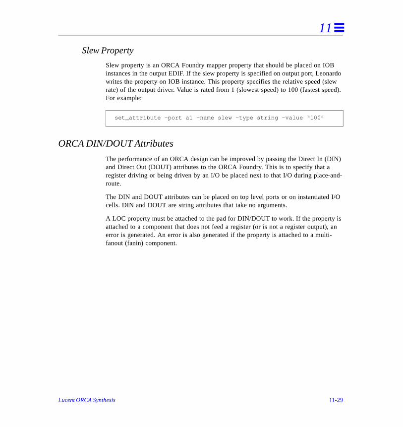
11
B ardo ew eed).
IN)
and-
I/O
is ), an i-
Slew Property
Slew property is an ORCA Foundry mapper property that should be placed on IOinstances in the output EDIF. If the slew property is specified on output port, Leonwrites the property on IOB instance. This property specifies the relative speed (slrate) of the output driver. Value is rated from 1 (slowest speed) to 100 (fastest spFor example:
ORCA DIN/DOUT Attributes
The performance of an ORCA design can be improved by passing the Direct In (Dand Direct Out (DOUT) attributes to the ORCA Foundry. This is to specify that a register driving or being driven by an I/O be placed next to that I/O during place-route.
The DIN and DOUT attributes can be placed on top level ports or on instantiatedcells. DIN and DOUT are string attributes that take no arguments.
A LOC property must be attached to the pad for DIN/DOUT to work. If the propertyattached to a component that does not feed a register (or is not a register outputerror is generated. An error is also generated if the property is attached to a multfanout (fanin) component.
set_attribute -port a1 -name slew -type string -value “100”
Lucent ORCA Synthesis 11-29
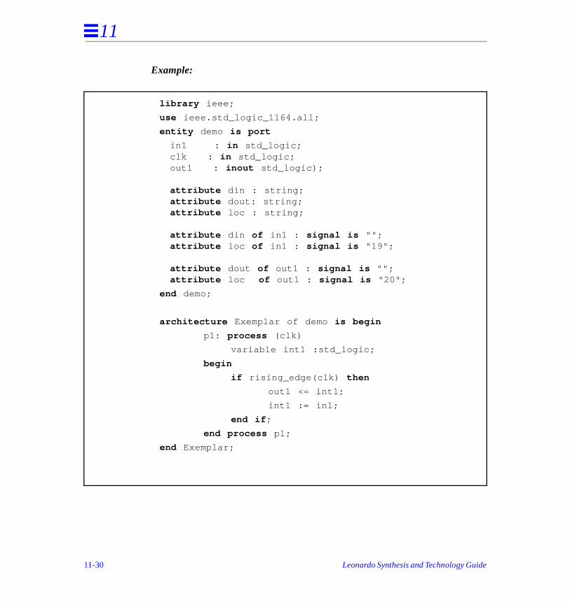
11
Example:
library ieee;
use ieee.std_logic_1164.all;
entity demo is port
in1 : in std_logic; clk : in std_logic; out1 : inout std_logic);
attribute din : string; attribute dout: string; attribute loc : string;
attribute din of in1 : signal is ""; attribute loc of in1 : signal is "19";
attribute dout of out1 : signal is ""; attribute loc of out1 : signal is "20";
end demo;
architecture Exemplar of demo is begin
p1: process (clk)
variable int1 :std_logic;
begin
if rising_edge(clk) then
out1 <= int1;
int1 := in1;
end if ;
end process p1;
end Exemplar;
11-30 Leonardo Synthesis and Technology Guide
11
o a tes ties
is
n
rdo
Part Number - PICSPEC
PICSPEC specifies the ORCA (1C, 2C, 2CA, 2TA) part number for the device intwhich the design is programmed. Specify the part number in Leonardo by settingvariable called part (e.g., in the Leonardo shell set part att2c04M84). Leonardo wriout the specified Part number as PICSPEC property in output EDIF in the propersection of top-level view.
Speed Grade - PICSPEED
PICSPEED specifies the speed of the target ORCA device into which the device programmed. Specify the Speed Grade in Leonardo by setting a variable called process (e.g., in the Leonardo shell set process 2 ).
ORCA Foundry Properties on IOBs
In addition to LOC and SLEW, ORCA Foundry supports the following properties oIOB instances:
• DELAYMODE (input buffer, specifies whether the input delay mode is enabled/disabled)
• DRIVE (output buffer, specifies output drive current in milliamps)
• IBUFLEVEL (input buffer, specifies the input voltage level)
• LOAD (output buffer, load values used by timing analysis)
• OBUFLEVEL (output buffer, specifies the output voltage level)
Specify these properties on ports of a design specified in VHDL, or from the Leonashell by using the set_attribute command.
part att2c04M84
process 2
Lucent ORCA Synthesis 11-31
11
CA
ritten
nets.
Other Foundry Properties
Other ORCA Foundry properties that can be set on nets or internal logic for the ORFoundry tool are written out in the EDIF file if the net or internal logic can be identified clearly. For example, the attributes set on instantiated component are wout in output EDIF.
ORCA Preference File Writer
The ORCA preference file writer translates timing constraints into an ORCA preference file.
Description
Timing constraints are written to the ORCA preference file. Your specified arrival_time , required_time , clock_cycle , clock_offset , and pulse_width are converted to ORCA preferences.
The absolute time constraints used by Leonardo are translated into the relative constraints used by Foundry, as illustrated in the following examples:
Note: Relative delays are between I/O ports, while periods are written for internal
11-32 Leonardo Synthesis and Technology Guide
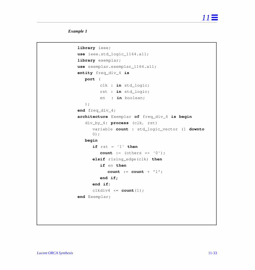
11
Example 1
library ieee;
use ieee.std_logic_1164.all;
library exemplar;
use exemplar.exemplar_1164.all;
entity freq_div_4 is
port (
clk : in std_logic;
rst : in std_logic;
en : in boolean;
);
end freq_div_4;
architecture Exemplar of freq_div_4 is begin
div_by_4: process (clk, rst)
variable count : std_logic_vector (1 downto 0);
begin
if rst = '1' then
count := (others => '0');
elsif rising_edge(clk) then
if en then
count := count + "1";
end if;
end if ;
clkdiv4 <= count (1);
end Exemplar;
Lucent ORCA Synthesis 11-33
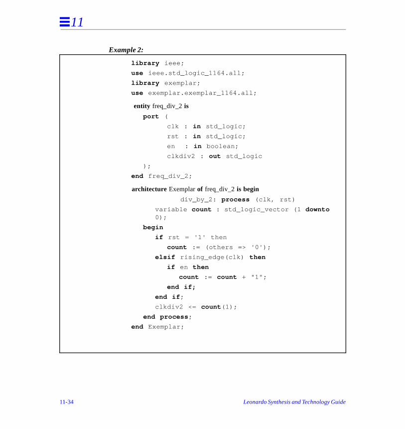
11
Example 2:
library ieee;
use ieee.std_logic_1164.all;
library exemplar;
use exemplar.exemplar_1164.all;
entity freq_div_2 is
port (
clk : in std_logic;
rst : in std_logic;
en : in boolean;
clkdiv2 : out std_logic
);
end freq_div_2;
architecture Exemplar of freq_div_2 is begin
div_by_2: process (clk, rst)
variable count : std_logic_vector (1 downto 0);
begin
if rst = '1' then
count := (others => '0');
elsif rising_edge(clk) then
if en then
count := count + "1";
end if;
end if ;
clkdiv2 <= count (1);
end process ;
end Exemplar;
11-34 Leonardo Synthesis and Technology Guide
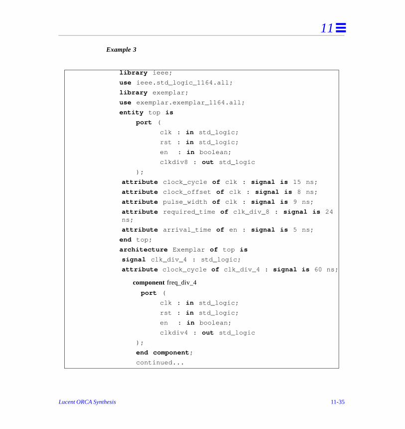
11
Example 3
library ieee;
use ieee.std_logic_1164.all;
library exemplar;
use exemplar.exemplar_1164.all;
entity top is
port (
clk : in std_logic;
rst : in std_logic;
en : in boolean;
clkdiv8 : out std_logic
);
attribute clock_cycle of clk : signal is 15 ns;
attribute clock_offset of clk : signal is 8 ns;
attribute pulse_width of clk : signal is 9 ns;
attribute required_time of clk_div_8 : signal is 24 ns;
attribute arrival_time of en : signal is 5 ns;
end top;
architecture Exemplar of top is
signal clk_div_4 : std_logic;
attribute clock_cycle of clk_div_4 : signal is 60 ns;
component freq_div_4
port (
clk : in std_logic;
rst : in std_logic;
en : in boolean;
clkdiv4 : out std_logic
);
end component ;
continued...
Lucent ORCA Synthesis 11-35
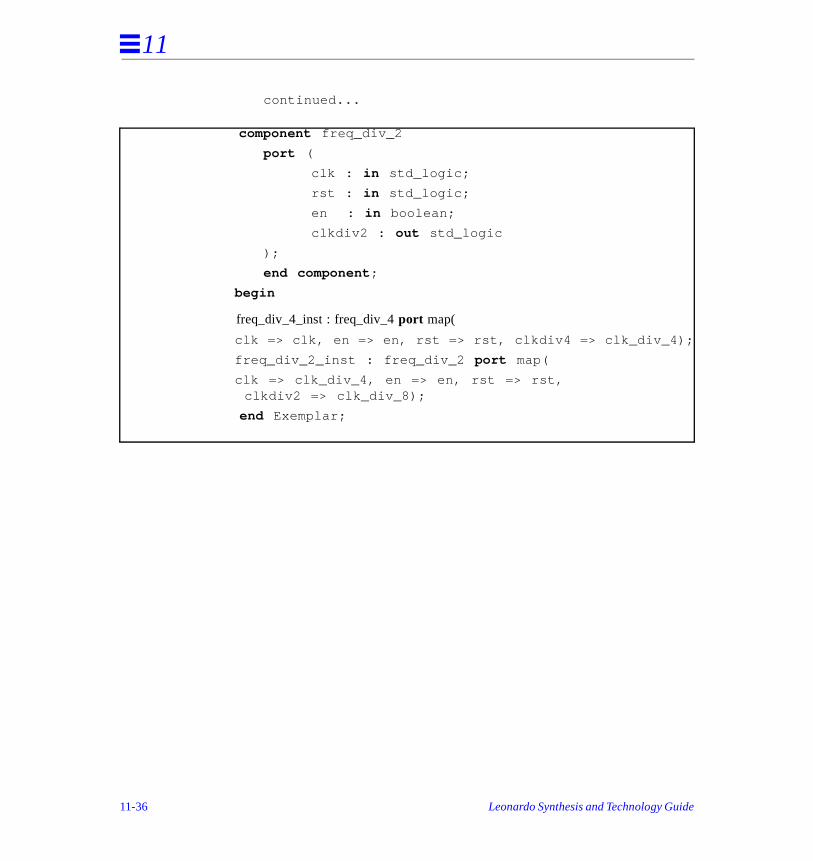
11
continued...
component freq_div_2
port (
clk : in std_logic;
rst : in std_logic;
en : in boolean;
clkdiv2 : out std_logic
);
end component ;
begin
freq_div_4_inst : freq_div_4 port map(
clk => clk, en => en, rst => rst, clkdiv4 => clk_div_4);
freq_div_2_inst : freq_div_2 port map(
clk => clk_div_4, en => en, rst => rst, clkdiv2 => clk_div_8);
end Exemplar;
11-36 Leonardo Synthesis and Technology Guide
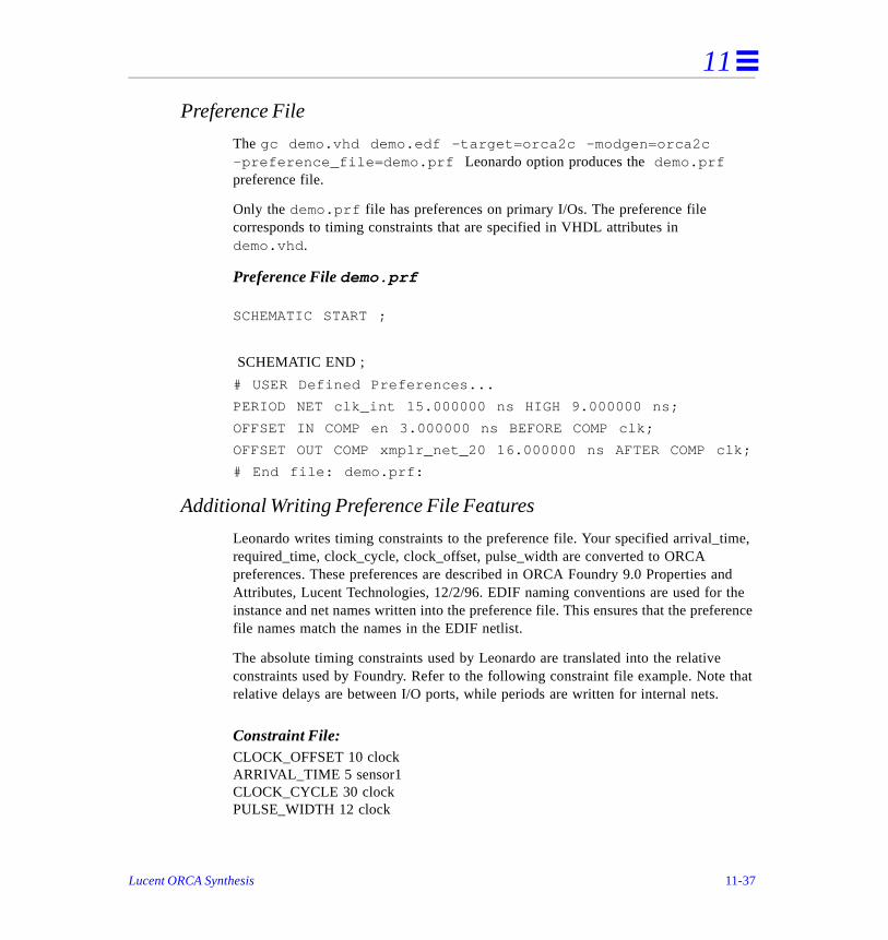
11
e,
nd the rence
that
Preference File
The gc demo.vhd demo.edf -target=orca2c -modgen=orca2c -preference_file=demo.prf Leonardo option produces the demo.prf preference file.
Only the demo.prf file has preferences on primary I/Os. The preference file corresponds to timing constraints that are specified in VHDL attributes in demo.vhd .
Preference File demo.prf
SCHEMATIC START ;
SCHEMATIC END ;
# USER Defined Preferences...
PERIOD NET clk_int 15.000000 ns HIGH 9.000000 ns;
OFFSET IN COMP en 3.000000 ns BEFORE COMP clk;
OFFSET OUT COMP xmplr_net_20 16.000000 ns AFTER COMP clk;
# End file: demo.prf:
Additional Writing Preference File Features
Leonardo writes timing constraints to the preference file. Your specified arrival_timrequired_time, clock_cycle, clock_offset, pulse_width are converted to ORCA preferences. These preferences are described in ORCA Foundry 9.0 Properties aAttributes, Lucent Technologies, 12/2/96. EDIF naming conventions are used for instance and net names written into the preference file. This ensures that the prefefile names match the names in the EDIF netlist.
The absolute timing constraints used by Leonardo are translated into the relativeconstraints used by Foundry. Refer to the following constraint file example. Note relative delays are between I/O ports, while periods are written for internal nets.
Constraint File:CLOCK_OFFSET 10 clockARRIVAL_TIME 5 sensor1CLOCK_CYCLE 30 clockPULSE_WIDTH 12 clock
Lucent ORCA Synthesis 11-37
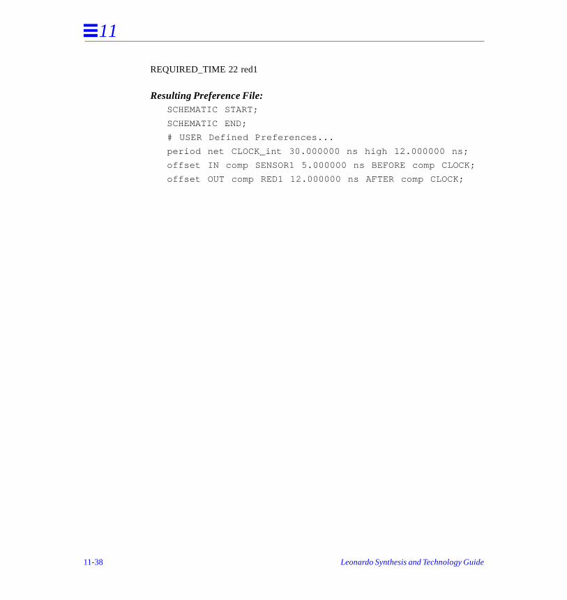
11
REQUIRED_TIME 22 red1
Resulting Preference File:SCHEMATIC START;
SCHEMATIC END;
# USER Defined Preferences...
period net CLOCK_int 30.000000 ns high 12.000000 ns;
offset IN comp SENSOR1 5.000000 ns BEFORE comp CLOCK;
offset OUT comp RED1 12.000000 ns AFTER comp CLOCK;
11-38 Leonardo Synthesis and Technology Guide
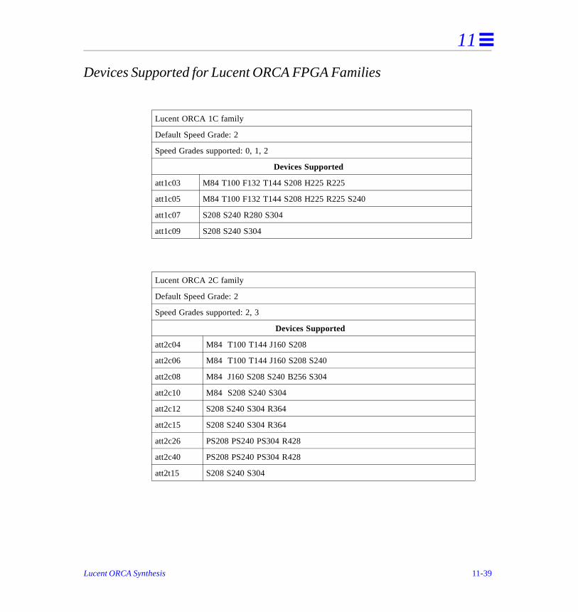
11
Devices Supported for Lucent ORCA FPGA Families
Lucent ORCA 1C family
Default Speed Grade: 2
Speed Grades supported: 0, 1, 2
Devices Supported
att1c03 M84 T100 F132 T144 S208 H225 R225
att1c05 M84 T100 F132 T144 S208 H225 R225 S240
att1c07 S208 S240 R280 S304
att1c09 S208 S240 S304
Lucent ORCA 2C family
Default Speed Grade: 2
Speed Grades supported: 2, 3
Devices Supported
att2c04 M84 T100 T144 J160 S208
att2c06 M84 T100 T144 J160 S208 S240
att2c08 M84 J160 S208 S240 B256 S304
att2c10 M84 S208 S240 S304
att2c12 S208 S240 S304 R364
att2c15 S208 S240 S304 R364
att2c26 PS208 PS240 PS304 R428
att2c40 PS208 PS240 PS304 R428
att2t15 S208 S240 S304
Lucent ORCA Synthesis 11-39
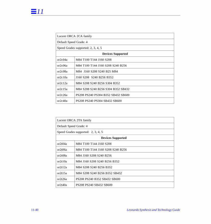
11
Lucent ORCA 2CA family
Default Speed Grade: 4
Speed Grades supported: 2, 3, 4, 5
Devices Supported
or2c04a M84 T100 T144 J160 S208
or2c06a M84 T100 T144 J160 S208 S240 B256
or2c08a M84 J160 S208 S240 B25 M84
or2c10a J160 S208 S240 B256 B352
or2c12a M84 S208 S240 B256 S304 B352
or2c15a M84 S208 S240 B256 S304 B352 SB432
or2c26a PS208 PS240 PS304 B352 SB432 SB600
or2c40a PS208 PS240 PS304 SB432 SB600
Lucent ORCA 2TA family
Default Speed Grade: 4
Speed Grades supported: 2, 3, 4, 5
Devices Supported
or2t04a M84 T100 T144 J160 S208
or2t06a M84 T100 T144 J160 S208 S240 B256
or2t08a M84 J160 S208 S240 B256
or2t10a M84 J160 S208 S240 B256 B352
or2t12a M84 S208 S240 B256 B352
or2t15a M84 S208 S240 B256 B352 SB432
or2t26a PS208 PS240 B352 SB432 SB600
or2t40a PS208 PS240 SB432 SB600
11-40 Leonardo Synthesis and Technology Guide
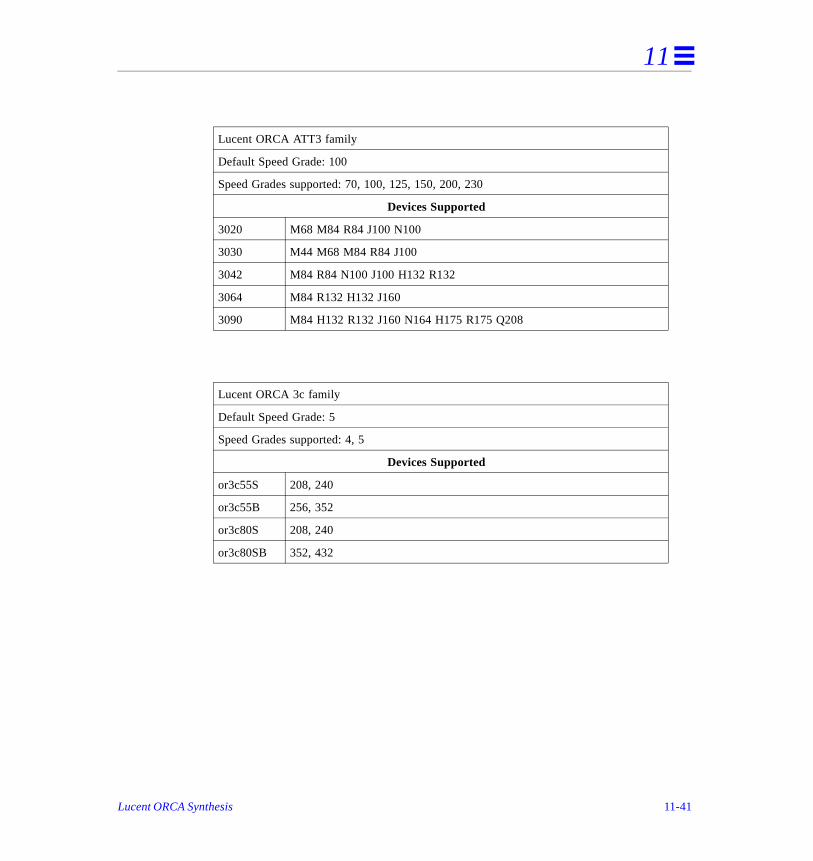
11
Lucent ORCA ATT3 family
Default Speed Grade: 100
Speed Grades supported: 70, 100, 125, 150, 200, 230
Devices Supported
3020 M68 M84 R84 J100 N100
3030 M44 M68 M84 R84 J100
3042 M84 R84 N100 J100 H132 R132
3064 M84 R132 H132 J160
3090 M84 H132 R132 J160 N164 H175 R175 Q208
Lucent ORCA 3c family
Default Speed Grade: 5
Speed Grades supported: 4, 5
Devices Supported
or3c55S 208, 240
or3c55B 256, 352
or3c80S 208, 240
or3c80SB 352, 432
Lucent ORCA Synthesis 11-41
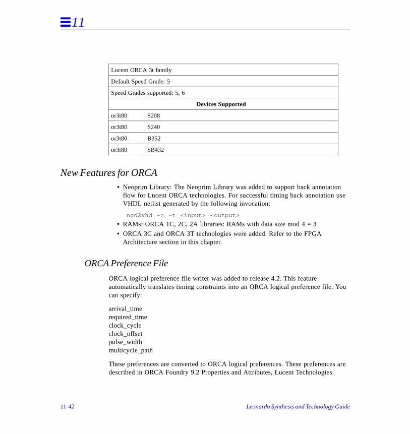
11
se
ou
s are
New Features for ORCA• Neoprim Library: The Neoprim Library was added to support back annotation
flow for Lucent ORCA technologies. For successful timing back annotation uVHDL netlist generated by the following invocation:
ngd2vhd -n -t <input> <output>
• RAMs: ORCA 1C, 2C, 2A libraries: RAMs with data size mod 4 = 3
• ORCA 3C and ORCA 3T technologies were added. Refer to the FPGA Architecture section in this chapter.
ORCA Preference File
ORCA logical preference file writer was added to release 4.2. This feature automatically translates timing constraints into an ORCA logical preference file. Ycan specify:
arrival_timerequired_timeclock_cycleclock_offsetpulse_widthmulticycle_path
These preferences are converted to ORCA logical preferences. These preferencedescribed in ORCA Foundry 9.2 Properties and Attributes, Lucent Technologies.
Lucent ORCA 3t family
Default Speed Grade: 5
Speed Grades supported: 5, 6
Devices Supported
or3t80 S208
or3t80 S240
or3t80 B352
or3t80 SB432
11-42 Leonardo Synthesis and Technology Guide
11
file
ing
Translation from logical to physical preference file:
Note: You must use Foundry version 9.2 or higher.
• Run Leonardo targeting ORCA. Leonardo will automaticaly generate an .lprf (logical preference file).
• Generate the .ngo from EDIF using EDIF2NGD.
• Build the .ngd file from the .ngo file using NGDBUILD.
• Generate .mrp file using MAP.
• Now use LP2PRF to translate the logical preference file into the physical preference file.
Usage:
LP2PRF -e <edif_file> -m <mrp_file> -l <logical> -p <physical>
Example Constraint file:
CLOCK_OFFSET 10 clockARRIVAL_TIME 5 sensor1CLOCK_CYCLE 30 clockPULSE_WIDTH 12 clock REQUIRED_TIME 22 red1
Resulting logical preference file:
PERIOD PIN ix418/O 30.000000 ns HIGH 12.000000 ns; INPUT_SETUP sensor1 5.000000 ns CLKNET=clock_int; CLOCK_TO_OUT red1 12.000000 ns CLKNET=clock_int;
ORCA3C and ORCA3T Multicycle Support
Multicycle path support is added for ORCA. You can set the Multicycle path in theconstraint file and Leonardo will pass it to the ORCA perference file. Leonardo timoptimization and delay reporting are sensitive to multicycle paths.
Example:
set_multicycle_path -setup -rise -from u2.reg_rxdatardy -to u2.reg_framingerr -value 2
Lucent ORCA Synthesis 11-43
11
CLOCK_OFFSET 13 clkx16 CLOCK_CYCLE 30 clkx16 PULSE_WIDTH 23 clkx16 REQUIRED_TIME 31 rxrdy
Logical Preference File
PERIOD PIN ix635/O 30.000000 ns HIGH 23.000000 ns;CLOCK_TO_OUT rxrdy 18.000000 ns CLKNET=clkx16_int;MULTICYCLE FROM CELL u2/reg_rxdatardy TO CELL u2/reg_framingerr 2 X;
Mapping to ORCALUTs
Leonardo maps directly to ORCA Foundry’s ORCALUTs. This improves design results.
11-44 Leonardo Synthesis and Technology Guide
QuickLogic Synthesis 12
ogic
d the d
Leonardo provides synthesis support for the QuickLogic pASIC 1, pASIC 2 and pASIC3 devices. Designs may be entered using VHDL or Verilog description. Additionally, gate array and other FPGA designs may be retargeted to the QuickLdevices using EDIF netlist. This chapter is divided as follows:
• Before Beginning
• FPGA Architecture
• New Features for QuickLogic
• Design Flow
• Optimization Style Points
• QuickLogic Reports
• Process Derating Factors
• Design I/O
• Assigning Pin Locations
Before Beginning
The technology information presented in this chapter assumes that you have reaintroductory chapters in this guide. Refer also to the HDL Synthesis and CommanReference guides for information.
12-1

12
ists D
ic
ffers
ugh 6.3
-
th d SIC
FPGA Architecture
The pASIC Logic Cell
The basic logic element of the QuickLogic pASIC FPGAs is the Logic Cell. A multiplexer-based structure is the central part of the logic cell. The logic cell consof two 6-input AND gates, four 2-input AND gates, three 2-to-1 multiplexers and aflip-flop. In addition to the dedicated flip-flop, logic gates in each cell can be configured to provide two latches. Multiple outputs are also available from the logcell.
I/O Buffers
In addition to the standard I/O buffers, the pASIC devices have dedicated clock buand high drive input buffers.
New Features for QuickLogic• Support for pASIC1 and pASIC2 is added. These libraries are supported thro
EDIF output into SPDE back-end tool. You must use SPDE software, versionor higher.
• Support for process and speed grades is available. The following values areavailable: WC-2, TYP-2, BC-2, WC-1, TYP-1, BC-1, WC-0, TYP-0, BC-0, WCX, TYP-X, BC-X
Design Flow
Figure 12-1 shows a simplified design flow that illustrates the use of Leonardo withe QuickLogic SpDE tools. Designs can be flat or hierarchical and can be entereusing standard methods. The designs are optimized and mapped to the target pAtechnology by Leonardo. The result is an EDIF netlist that is used by downstreamSpDE tools.
12-2 Leonardo Synthesis and Technology Guide
12
in
as d
Figure 12-1 Leonardo Interface with QuickLogic SpDE Tools
Leonardo currently does not accept QDIF files as input. However, pASIC designsEDIF netlist are accepted. The EDIF netlist can be hierarchical as long as all themodules are described in a single EDIF file.
Optimization Style Points
Quality of Optimization
Certain types of logic will be optimized better than others: arithmetic circuits suchadders and multipliers will not be as optimal as the best hand design or predefinemacro. These constructs are better synthesized using module generation, if usingVHDL or Verilog as the input format.
Language-based design:VHDL, Verilog HDL
Netlists: from otherFPGAs and gate arrays
LeonardoQuickLogic
specific synthesis and optimization
EDIF Netlist
QuickLogicSpDE
LeoRG 27
QuickLogic Synthesis 12-3
12
n the
ing
hing tively
he
be
s.
General control logic and state machines will be optimized as well as or better thabest hand designs.
Combinational Logic Loops
By default, Leonardo attempts to replace combinational loops with latches. Alternatives to consider include removing the loop prior to optimization (but includthe loop in the final design), or replacing the loop with a sequential element.
Sequential Optimization
Leonardo eliminates registers and latches if the register or latch will always be latca constant value, and there is no set or reset used on the register. Leonardo alsoeliminates registers or latches that have identical inputs; these registers are effecmerged.
Leonardo does not “move” registers or change the phase of the signal stored in tregisters.
Internal Tristates
The pASIC architecture has no internal tristate gate. Thus, all tristate gates mustconnected to a pad. If your design has tristates, Leonardo issues the message:
The internal tristates must be converted to combinational logic (by setting the tristate_map variable to TRUE) or to a tristate or bidirectional pad (using the -chip option).
QuickLogic Reports
Refer to Chapter 6, Reports, in this guide for examples and information.
Process Derating Factors
The following table for pASIC1 and pASIC2, list derating factors for these librarieThese values are entered on the Leonardo command line.
Internal tristates not available in this technology .
12-4 Leonardo Synthesis and Technology Guide
12
riate rs.
ny pad orks s,
pASIC1 and pASIC2 Derating Factors
Design I/O
Leonardo maps I/O cells automatically. Based on the input description the appropI/O cells from the pASIC technology library will be used. Leonardo does not mapautomatically to High Drive Input Buffers, Dual Port Input Buffers and Clock BuffeYou can map to these buffers manually using the PAD and BUFFER_SIG command.
Manual Assignment of I/O Buffers
There are two commands that can be used to manually assign I/O pads: PAD and BUFFER_SIG. These commands can be used as attributes from VHDL, or as commands from the Leonardo shell. The PAD command is the recommended way to assign pads since it is the most general, and because it can be used to assign athat Leonardo is able to map. The PAD command is limited, however, and only won inputs and outputs. The BUFFER_SIG command can only be used to assign bufferbut it can be used on internal signals (internal clock buffers) as well.
Value of Process Operating Conditions Speed Grade
WC-2 worst case -2
TYP-2 typical -2
BC-2 best case -2
WC-1 worst case -1
TYP-1 typical -1
BC-1 best case -1
WC-0 worst case 0
TYP-0 typical 0
BC-0 best case 0
WC-X worst case -X
TYP-X typical -X
BC-X best case -X
QuickLogic Synthesis 12-5
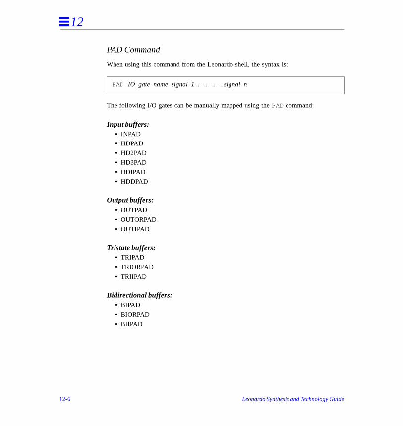
12
PAD Command
When using this command from the Leonardo shell, the syntax is:
The following I/O gates can be manually mapped using the PAD command:
Input buffers:• INPAD
• HDPAD
• HD2PAD
• HD3PAD
• HDIPAD
• HDDPAD
Output buffers:• OUTPAD
• OUTORPAD
• OUTIPAD
Tristate buffers:• TRIPAD
• TRIORPAD
• TRIIPAD
Bidirectional buffers:• BIPAD
• BIORPAD
• BIIPAD
PAD IO_gate_name_signal_1 . . . . signal_n
12-6 Leonardo Synthesis and Technology Guide
12
done
BUFFER_SIG Command
It is useful to manually assign clock buffers. For example:
The following clock buffers are available:
• CKPAD
• CKDPAD
• CKTPAD
Assigning Pin Locations
Pin numbers can be assigned to designs targeted to pASIC devices. This can befrom VHDL using PIN_NUMBER and PIN_ARRAY_NUMBER attributes or from Leonardo’s shell using the PIN_NUMBER procedure or set-attribute commands on I/Oports.
BUFFER_SIG clk CKPAD
QuickLogic Synthesis 12-7
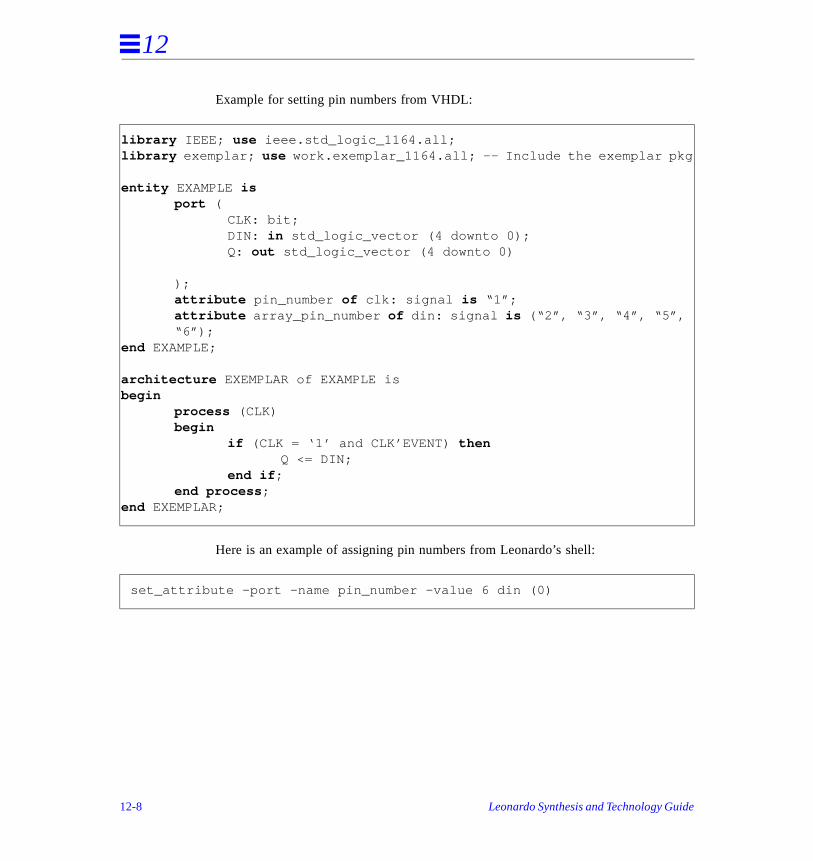
12
Example for setting pin numbers from VHDL:
Here is an example of assigning pin numbers from Leonardo’s shell:
library IEEE; use ieee.std_logic_1164.all;library exemplar; use work.exemplar_1164.all; -- Include the exemplar pkg
entity EXAMPLE isport (
CLK: bit;DIN: in std_logic_vector (4 downto 0);Q: out std_logic_vector (4 downto 0)
);attribute pin_number of clk: signal is “1”;attribute array_pin_number of din: signal is (“2”, “3”, “4”, “5”, “6”);
end EXAMPLE;
architecture EXEMPLAR of EXAMPLE isbegin
process (CLK)begin
if (CLK = ‘1’ and CLK’EVENT) thenQ <= DIN;
end if ;end process ;
end EXEMPLAR;
set_attribute -port -name pin_number -value 6 din (0)
12-8 Leonardo Synthesis and Technology Guide
Xilinx CPLDs Synthesis 13
and
or
d the d
Leonardo provides synthesis for all families of Xilinx CPLDs, which includes XC7200A, XC7300, and XC9500. Designs may be entered using standard VHDLVerilog descriptions or EDIF netlist. Leonardo also provides synthesis for these families into any of the other technologies supported by Leonardo. This chapter presents information specific to the use of the Xilinx CPLDs families as a source target technology.
This chapter is divided as follows:
• Before Beginning
• Xilinx CPLD Architecture
• Design Flow
• Synthesis and Optimization Features
• Other Synthesis Features
• Reporting
• Xilinx CPLD Family Supported Devices
Before Beginning
The technology information presented in this chapter assumes that you have reaintroductory chapters in this guide. Refer also to the HDL Synthesis and CommanReference guides for information.
13-1
13
has Each s.
duct to ell and
on
es d
bi-ut
d red
9500 tible
Xilinx CPLD Architecture
The basic Xilinx CPLD structures consists of:
• Function Blocks (FBs)
• I/O Blocks (IOBs)
Each function block is comprised of a set of macrocells which are capable of implementing a combinational or registered function. In XC9500, a function block a programmable AND-array and product term allocator that feeds the macrocells. macrocell can implement a combinational logic function of up to five product term
An XOR gate is available in each macrocell which can increase the number of proterms. The product term allocator can reassign other product terms within the FBincrease the logic capacity of a macrocell beyond five direct terms. Each macrocalso contains a register that can be programmed to be a D or T flip-flop with clearpreset inputs.
These function blocks impose a fanin limitation on top of the product term limitatiper macrocell.
The XC7200A/XC7300 family also supports carry lookahead generator that reducthe ripple-carry delay of wide arithmetic functions such as adders, subtractors, anmagnitude comparators.
I/O cells in Xilinx CPLDs can be configured as inputs, outputs, tristate outputs or directional pins. Leonardo automatically inserts the default I/O buffers in the outpnetlists.
Design Flow
A simplified design flow is shown in Figure 13-1 to illustrate how Leonardo is usewith the XACT-CPLD tools to provide a complete design solution. Designs are enteusing standard methods and are optimized to the target XC7200A, XC7300 or XCdevices. The output design can be written either as an EDIF netlist that is compawith M1-CPLD software or as an XNF netlist that is compatible with Xilinx XEPLDsoftware.
13-2 Leonardo Synthesis and Technology Guide
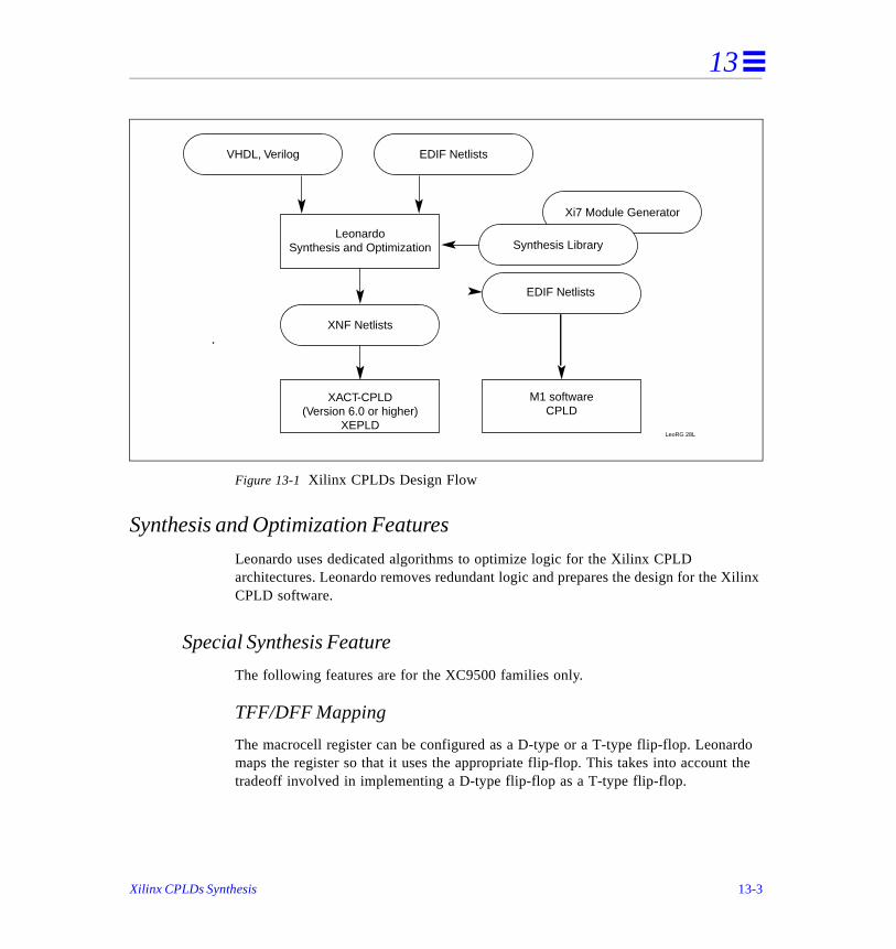
13
Xilinx
rdo the
Figure 13-1 Xilinx CPLDs Design Flow
Synthesis and Optimization Features
Leonardo uses dedicated algorithms to optimize logic for the Xilinx CPLD architectures. Leonardo removes redundant logic and prepares the design for the CPLD software.
Special Synthesis Feature
The following features are for the XC9500 families only.
TFF/DFF Mapping
The macrocell register can be configured as a D-type or a T-type flip-flop. Leonamaps the register so that it uses the appropriate flip-flop. This takes into accounttradeoff involved in implementing a D-type flip-flop as a T-type flip-flop.
VHDL, Verilog EDIF Netlists
LeonardoSynthesis and Optimization
XACT-CPLD(Version 6.0 or higher)
XEPLDLeoRG 28L
XNF Netlists
Xi7 Module Generator
Synthesis Library
M1 softwareCPLD
EDIF Netlists
Xilinx CPLDs Synthesis 13-3
13
ion
re
ice e or
re
h
ns r as
ave re
XOR Optimization
XOR optimization looks for tradeoffs in implementing a macrocell as an XOR functas opposed to an OR gate.
Other Synthesis Features
The device selection, I/O buffers and pads, and pin (LOC) assignment features aavailable for both XC7200A/XC7300 and XC9500 Xilinx CPLD families.
Device Selection
By default, the Xilinx CPLD software will automatically select the appropriate devthat fits your design. Optionally, you can specify the part number and speed gradprocess of the target device from either the GUI or command line arguments.
I/O Buffers and Pads
Leonardo automatically inserts the default I/O buffers in the output netlist. They aIBUF, OBUF, OBUFE (for tristated output ports) and IOBUFE (for bidirectional ports). For Xilinx M1 EDIF, Leonardo also inserts I/O PADs in the EDIF netlist.
The other I/O Buffers like OBUF_S, IBUF_S, OBUFE_S etc. are available througcomponent instantiation.
Pin (LOC) Assignment
Leonardo supports pin assignment from vhdl/verilog or control file. The pin locatioare generated in the output netlists as LOC parameters on EXT records in XNF oEDIF properties on I/O buffer instances in EDIF.
Module Generation
Leonardo supports module generation for XC7200A and XC7300 families only.
Leonardo supports various technology specific implementations of arithmetic andrelational operators used in VHDL or Verilog RTL. Since these implementations hbeen designed optimally for the specific target technology, the synthesis results asmaller and/or faster and take less time to compile.
13-4 Leonardo Synthesis and Technology Guide
13
t and
a in
n
The following operators and miscellaneous functions have technology specific architectures in the modgen libraries:
• Relational Operators = /= < <= > >=
• Arithmetic Operators + -
• Misc. Functions incrementerdecrementer
User Options for XC9500 Families Only
These options are available on the Output Options dialog for XC9500. Options noavailable on the GUI are entered in the Special Options field. Refer to Table 13-1Screen 13-1.
Table 13-1. GUI and Command Line Options
*variables, options, constraint attributes, commands
GUI Option Command Line* Results
Max PT set max_pt <integer> Determines the maximum number of product terms in macrocell. Default values are 15 in area mode and 25 delay mode. The higher product terms may result in afaster but bigger implementation.
Max Fanin set max_fanin <integer> Determines the maximum number of inputs to a functioblock. Default value is 36.
Xilinx CPLDs Synthesis 13-5
13
tion
ion.
Screen 13-1. Example - Xilinx 9500 Output Options
Reporting
Leonardo reports on estimates of area of the optimized design as follows:
• Reports on the number of AND-OR gates can be issued during each optimizapass.
• Detailed reports on all cells used in the design can be issued after optimizatType: report_area -cell
Refer to Reports, Chapter 6, in this guide for more information.
13-6 Leonardo Synthesis and Technology Guide
13
Xilinx CPLD Family Supported Devices
Xilinx CPLD Family - Xilinx XC7200A
Default Speed Grade: 20
Speed Grades supported: 16, 20, 25
Devices Supported
7236 APC44 AWC44
7272 APC68 AWC68 APC84 AWC84 APG84
Xilinx CPLD Family - Xilinx XC7300
Default Speed Grade: 10
Speed Grades supported: 5, 7, 10, 12, 15, 20
Devices Supported
7336 PC44 WC44 PQ44 QPC44 QWC44 QPQ44 QVQ44
7354 PC68 WC68 WC44 PC44
7372 PC68 WC68 PC84 WC84 PQ100
7310 8PC84 8WC84 8PQ100 8PG144 8PQ160 8BG225
7344 PQ160
7314 4BG225
Xilinx CPLDs Synthesis 13-7
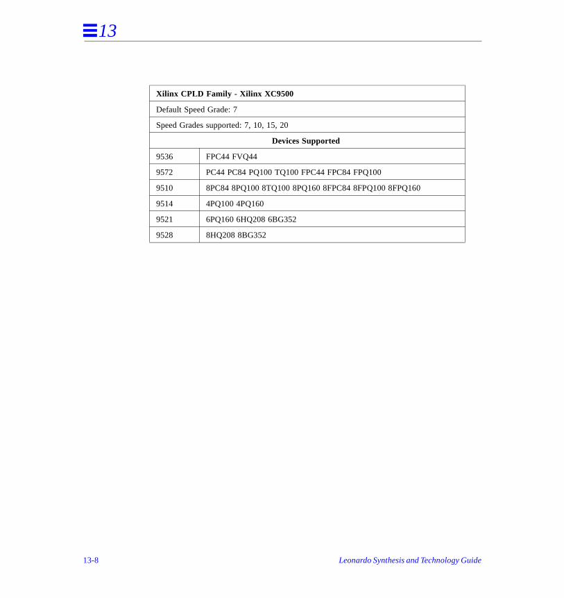
13
Xilinx CPLD Family - Xilinx XC9500
Default Speed Grade: 7
Speed Grades supported: 7, 10, 15, 20
Devices Supported
9536 FPC44 FVQ44
9572 PC44 PC84 PQ100 TQ100 FPC44 FPC84 FPQ100
9510 8PC84 8PQ100 8TQ100 8PQ160 8FPC84 8FPQ100 8FPQ160
9514 4PQ100 4PQ160
9521 6PQ160 6HQ208 6BG352
9528 8HQ208 8BG352
13-8 Leonardo Synthesis and Technology Guide
Xilinx LCA Synthesis 14
F ilinx
Leonardo provides full synthesis support for the following Xilinx LCA based architectures:
• XC3000/A/L, XC3100/A
• XC4000/A/E/EX/H/L/XL/XV, XC5200
• CPLD Family: XC7200A, XC7300, XC9500
• Spartan
Designs may be entered using VHDL or Verilog HDL descriptions or EDIF and XNnetlists. In addition, gate array and other FPGA designs may be retargeted to the Xdevices.
This chapter is divided as follows:
• Before Beginning• Xilinx LCA Architecture• Synthesis Design Flows• Synthesis and Optimization Features• Design I/O• Using TimeSpecs• Using Xilinx Attributes• Additional Xilinx Specific Options• EDIF and XNF• Interfacing with XBLOX• Additional Xilinx Architecture Features• Xilinx FPGA Devices Supported
14-1
14
d the d
nd
onal
le in
an
the
Before Beginning
The technology information presented in this chapter assumes that you have reaintroductory chapters in this guide. Refer also to the HDL Synthesis and CommanReference guides for information.
Xilinx LCA Architecture
Configurable Logic Block
The Xilinx FPGAs have two basic structures: the configurable logic block (CLB) athe input/output block (IOB). The CLBs are at the core of the Xilinx FPGA architecture. Each CLB contains combinational logic and registers. The combinatilogic section of the CLB is limited in the number of inputs.
Input/Output Block
The IOBs in the Xilinx FPGAs can be configured as input, tristate output, or bidirectional pins. Flip-flops and input latches may be used in IOBs. Leonardo recognizes these gates when targeting a Xilinx device and utilizes the logic availabthe IOBs.
Synthesis Design Flows
A simplified design flow is shown in Figure 14-1. LUT mapping and CLB packing cbe enabled/disabled on the GUI. Figure 14-2 shows a simplified back annotation.
Note: The output netlist may either be for XACT (XNF) flow or EDIF M1 flow. Youmay also use XNF as an input to M1 software. This flow will not be supported in future by Xilinx.
14-2 Leonardo Synthesis and Technology Guide
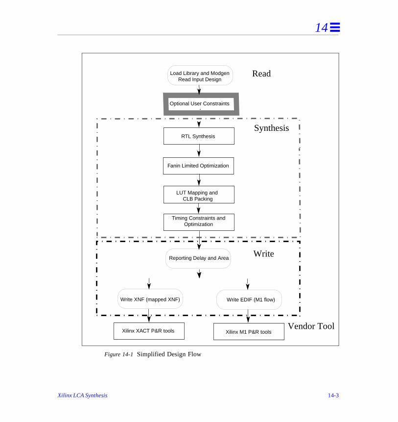
14
Figure 14-1 Simplified Design Flow
Fanin Limited Optimization
LUT Mapping and CLB Packing
RTL Synthesis
Timing Constraints andOptimization
Xilinx XACT P&R tools
Write XNF (mapped XNF) Write EDIF (M1 flow)
Synthesis
Write
Load Library and ModgenRead Input Design
Read
Vendor ToolXilinx M1 P&R tools
Reporting Delay and Area
Optional User Constraints
Xilinx LCA Synthesis 14-3
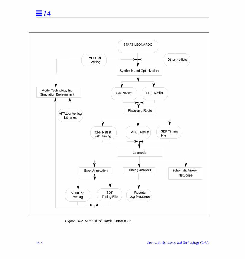
14
Figure 14-2 Simplified Back Annotation
START LEONARDO
VHDL or Verilog
Synthesis and Optimization
Model Technology IncSimulation Environment
VITAL or VerilogLibraries
NetScopeSchematic Viewer
Leonardo
Timing AnalysisBack Annotation
VHDL or Verilog
SDFTiming File
ReportsLog Messages
VHDL Netlist SDF TimingFile
Other Netlists
EDIF Netlist
Place-and-Route
XNF Netlist
XNF Netlistwith Timing
14-4 Leonardo Synthesis and Technology Guide

14
er is to
000
Design Flow Guidelines
During Xilinx synthesis, the output options are available on the GUI and can be entered on the command line. Refer to Table 14-1 and Screen 14-1.
User-Defined Variables
Table 14-1. Results of Output Options
*GUI default options** options, variables, constraint attributes, commands
Notes:• If the variable write_lut_binding is set to FALSE the XNF output will not be in
terms of MAP (FMAP/HMAP) symbols. • CLB packing should be used carefully. It will pack the CLBs tightly and will not consid
routing resources, which may cause routing problems in some cases. The other optionlet XACT do the CLB packing. However, in some cases Leonardo CLB packing gavesuperior results over XACT. Also, by packing to CLBs, Leonardo can estimate interconnect delays more accurately. Currently, CLB packing is available for the XC4architecture only.
set lut_map falseset write_lut_binding falseset write_clb_packing true
GUI Option Option on/off
Command Line** Available in
Families
Results
■ Map Look Up Tables on* default TRUE All except XC7200A, XC7300, XC9500
Controls LUT mapping for accurate reports.
off lut_map
not applicable default TRUE Controls packing of LUTs into CLBs.
write_lut_binding
not applicable write_clb_packing Controls printing of CLB packing (HBLKNM) information in the output netlist, as required.
default FALSE
Xilinx LCA Synthesis 14-5
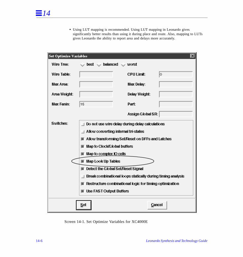
14
s
• Using LUT mapping is recommended. Using LUT mapping in Leonardo givessignificantly better results than using it during place and route. Also, mapping to LUTgives Leonardo the ability to report area and delays more accurately.
Screen 14-1. Set Optimize Variables for XC4000E
14-6 Leonardo Synthesis and Technology Guide
14
put
is s.
ps,
ign
nd
p into one AND
in
Synthesis and Optimization Features
Leonardo has several optimization features for the Xilinx architectures.
• To take full advantage of the Xilinx architecture, Xilinx-specific optimization techniques have been developed by Exemplar Logic. These include a “fanin limited” optimization algorithm that understands and takes advantage of the inlimitations of the Xilinx CLB.
• An important feature is the ability to map logic functions into lookup tables. Thmapping is available for XC3000, XC4000, XC4000E, and XC5200 technologie
• You can set timing constraints (arrival_time on inputs, required_time on outputs and clocking schemes) and apply timing optimization to speed up the design.
• After the logic is mapped to lookup tables, the lookup tables can be packed toCLBs. CLB packing is optional.
• In the output XNF netlist you have control of whether Leonardo writes out FMaHMaps, and CLBs information.
• Module generation is available for implementing data path logic from HDL dessource.
• In addition to optimization for the CLB architecture of the Xilinx LCA devices, Leonardo recognizes other Xilinx features such as the global set/reset signal awide edge decoders.
Fanin Limited Optimization
For the purposes of this example, the Xilinx 4000 architecture is used. In this technology any function with up to four inputs can be mapped into a FMAP lookutable. Any function with up to three inputs (with some restrictions) can be mappeda HMAP. Two FMAPs and one HMAP (with some restrictions) can be packed into CLB. In summary, a 4-input XOR uses the same area and is as fast as a 4-input gate.
One approach to designing in this architecture is to decompose a function into itssimpler AND/OR equivalent representation, and then split the gates with large faninto multiple gates. Consider this example:
X = (A*(B+C))+(B*D)+(E*F*G*H*I)
Xilinx LCA Synthesis 14-7
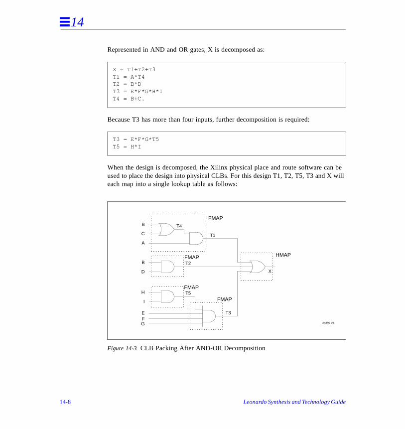
14
n be will
Represented in AND and OR gates, X is decomposed as:
Because T3 has more than four inputs, further decomposition is required:
When the design is decomposed, the Xilinx physical place and route software caused to place the design into physical CLBs. For this design T1, T2, T5, T3 and Xeach map into a single lookup table as follows:
Figure 14-3 CLB Packing After AND-OR Decomposition
X = T1+T2+T3T1 = A*T4T2 = B*DT3 = E*F*G*H*IT4 = B+C.
T3 = E*F*G*T5T5 = H*I
LeoRG 06
B
C
B
D
A
T4
T1
T2
H
I
T5
EFG
T3
X
FMAP
FMAP
FMAP
FMAP
HMAP
14-8 Leonardo Synthesis and Technology Guide
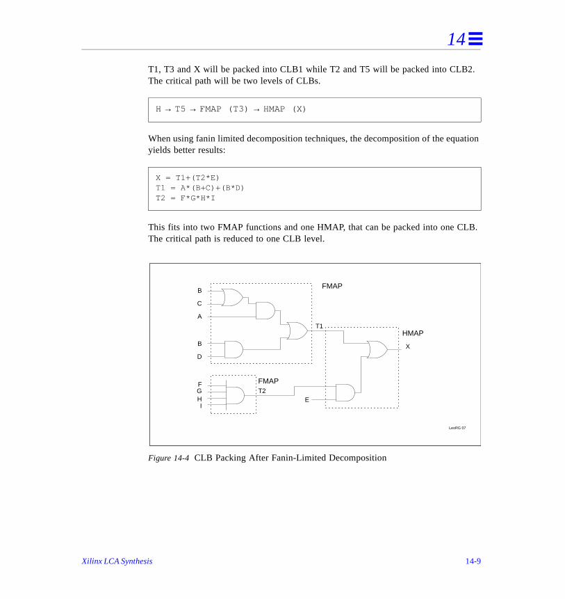
14
.
ation
B.
T1, T3 and X will be packed into CLB1 while T2 and T5 will be packed into CLB2The critical path will be two levels of CLBs.
When using fanin limited decomposition techniques, the decomposition of the equyields better results:
This fits into two FMAP functions and one HMAP, that can be packed into one CLThe critical path is reduced to one CLB level.
Figure 14-4 CLB Packing After Fanin-Limited Decomposition
H → T5 → FMAP (T3) → HMAP (X)
X = T1+(T2*E)T1 = A*(B+C)+(B*D)T2 = F*G*H*I
LeoRG 07
B
C
B
D
A
T1
T2E
GHI
F
X
FMAP
FMAP
HMAP
Xilinx LCA Synthesis 14-9
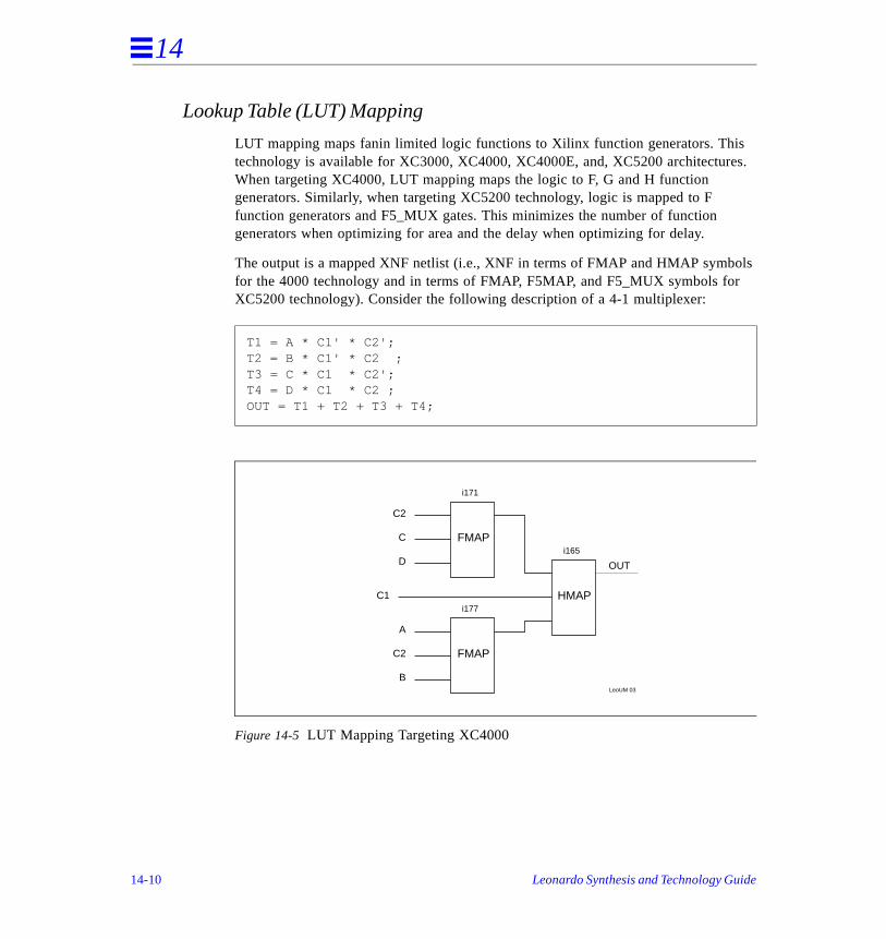
14
es.
ols r
Lookup Table (LUT) Mapping
LUT mapping maps fanin limited logic functions to Xilinx function generators. Thistechnology is available for XC3000, XC4000, XC4000E, and, XC5200 architecturWhen targeting XC4000, LUT mapping maps the logic to F, G and H function generators. Similarly, when targeting XC5200 technology, logic is mapped to F function generators and F5_MUX gates. This minimizes the number of function generators when optimizing for area and the delay when optimizing for delay.
The output is a mapped XNF netlist (i.e., XNF in terms of FMAP and HMAP symbfor the 4000 technology and in terms of FMAP, F5MAP, and F5_MUX symbols foXC5200 technology). Consider the following description of a 4-1 multiplexer:
Figure 14-5 LUT Mapping Targeting XC4000
T1 = A * C1' * C2';T2 = B * C1' * C2 ;T3 = C * C1 * C2';T4 = D * C1 * C2 ;OUT = T1 + T2 + T3 + T4;
FMAP
FMAP
C2
A
C
C1
C2
D
B
HMAP
OUT
i165
i171
i177
LeoUM 03
14-10 Leonardo Synthesis and Technology Guide
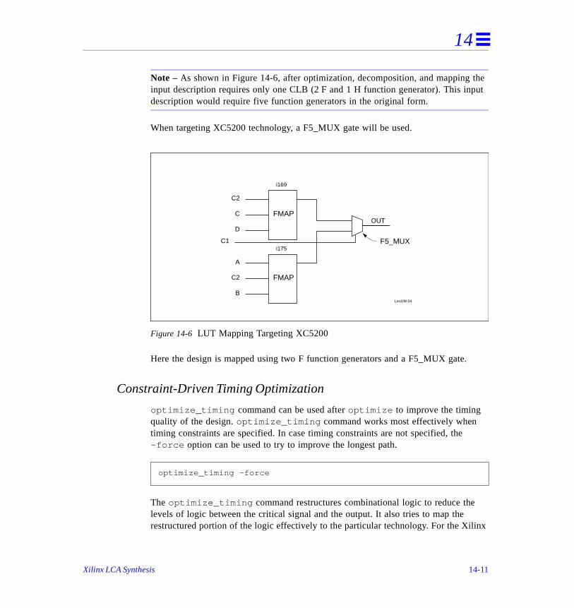
14
the ut
inx
Note – As shown in Figure 14-6, after optimization, decomposition, and mapping input description requires only one CLB (2 F and 1 H function generator). This inpdescription would require five function generators in the original form.
When targeting XC5200 technology, a F5_MUX gate will be used.
Figure 14-6 LUT Mapping Targeting XC5200
Here the design is mapped using two F function generators and a F5_MUX gate.
Constraint-Driven Timing Optimization
optimize_timing command can be used after optimize to improve the timing quality of the design. optimize_timing command works most effectively when timing constraints are specified. In case timing constraints are not specified, the -force option can be used to try to improve the longest path.
The optimize_timing command restructures combinational logic to reduce thelevels of logic between the critical signal and the output. It also tries to map the restructured portion of the logic effectively to the particular technology. For the Xil
optimize_timing -force
FMAP
FMAP
C2
A
C
C1
C2
D
B
F5_MUX
OUT
i169
i175
LeoUM 04
Xilinx LCA Synthesis 14-11
14
e
very
M
utside
4000 design, it tries to map the critical signal to the direct input of the HMAP in thCLB. optimize_timing may be invoked repeatedly for added improvements if possible.
The specific end point or instance to improve can be specified to the optimize_timing command with the -through option.
CLB Packing for Xilinx XC4000 Technology
The CLB Packing algorithm can be run on a design that is mapped to FMAPs/HMAPs function generators to generate block (CLB) level information.
The CLB packing operation is useful for two reasons:
1. You can get an accurate estimate of the design in terms of occupied CLBs.
2. The delay estimate on a post synthesized design (but pre place and route) is accurate, typically within 5 percent of the post place and route design.
CLB packing should be invoked after running the optimize command on a design from Leonardo's interactive shell.
CLB packing function generates the CLB information on a design using the HBLKNparameter on FMAPs, HMAPs, and sequential gates.
XC4000 CLB Architecture Constraints
Due to architectural constraints of a CLB in XC4000, a CLB can pack up to a maximum of two FMAPs, one HMAP, and two DFFs. But these functional blocks (FMAP/HMAP) are not independent entities because of their connectivity. These blocks have some requirements on the fanouts and number of outputs required othe CLB, which are handled during the CLB packing operation.
optimize_timing -through
pack_clbs
14-12 Leonardo Synthesis and Technology Guide
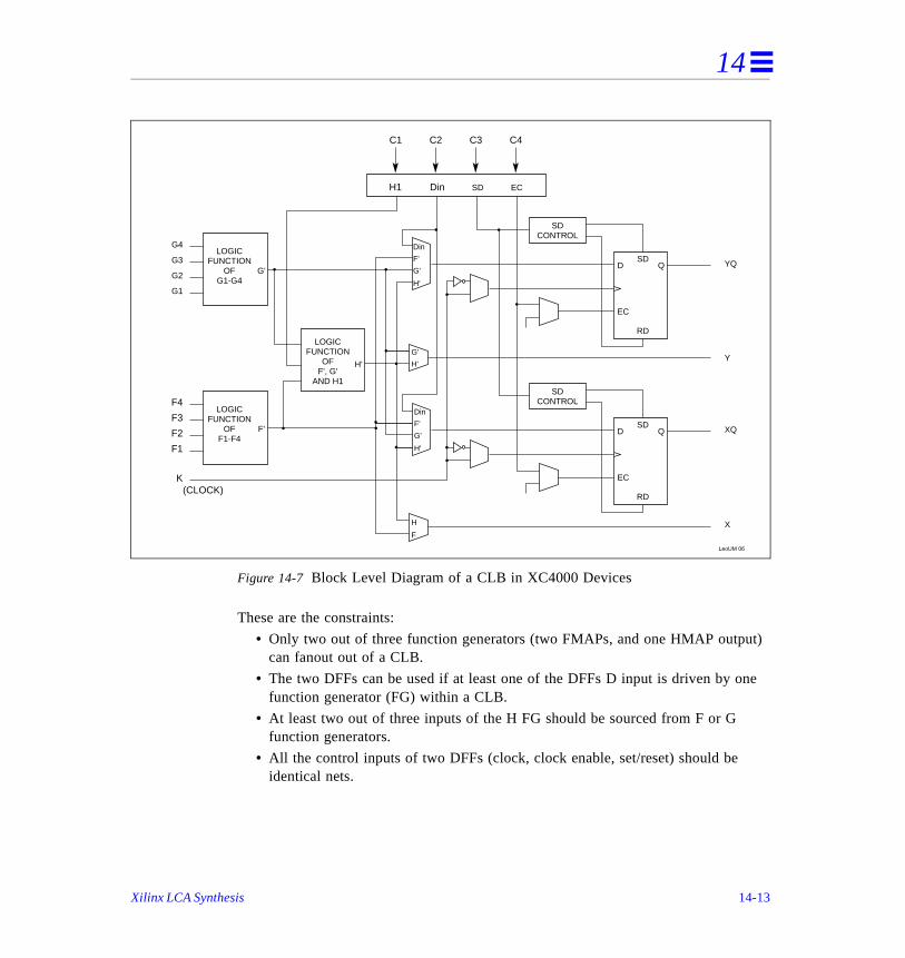
14
t)
ne
Figure 14-7 Block Level Diagram of a CLB in XC4000 Devices
These are the constraints:
• Only two out of three function generators (two FMAPs, and one HMAP outpucan fanout out of a CLB.
• The two DFFs can be used if at least one of the DFFs D input is driven by ofunction generator (FG) within a CLB.
• At least two out of three inputs of the H FG should be sourced from F or G function generators.
• All the control inputs of two DFFs (clock, clock enable, set/reset) should be identical nets.
C4
G4
F4
G3
F3
G2
F2
G1
F1
H1
K(CLOCK)
LeoUM 06
XQ
YQ
RD
SDD
EC
Q
ECSDDin
X
Y
LOGICFUNCTION
OFG1-G4
LOGICFUNCTION
OFF1-F4
G'
F'
LOGICFUNCTION
OFF', G'
AND H1
H'
SDCONTROL
RD
SDD
EC
Q
SDCONTROL
C3C2C1
Din
F'
G'
H'
Din
F'
G'
H'
G'
H'
H
F
Xilinx LCA Synthesis 14-13
14
An example of CLB packing is shown for the following test case:.
library ieee;use ieee.std_logic_1164. all;library exemplar;use exemplar.exemplar_1164.all;entity test isport (
CLK : in std_logic; RST : in std_logic; i1, i2, i3, i4 : in std_logic; i5, i6, i7, i8 : in std_logic; i9 : in std_logic; H : out std_logic; qG : inout std_logic; Q : inout std_logic_vector(1 downto 0)); end test; architecture instance of test is signal F : std_logic; signal G : std_logic; procedure dffc( signal input : IN std_logic; signal clr, clk: IN std_logic; signal output : INOUT std_logic) begin if (clr='1') then output <= '0'; elsif (clk'event and clk='1') then output <= input; else output <= output; end if; end dffc; begin F <= i1 and i2 and i3 and i4; G <= i5 and i6 and i7 and i8; H <= F and G and i9; dffc (G, RST, CLK, qG); dffs: for i in 0 to 1 generate dffc (F, RST, CLK, Q(i)); end generate dffs; end ;
14-14 Leonardo Synthesis and Technology Guide
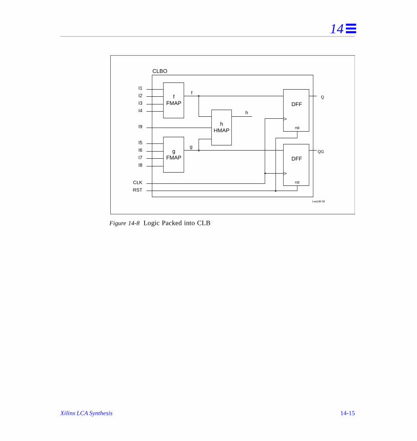
14
Figure 14-8 Logic Packed into CLB
fFMAP
gFMAP
I1
I5
I2
I6
I3
I7
I4
I8
I9
RST
CLK
hHMAP
h
LeoUM 05
Q
QG
rst
g
f
DFF
rst
DFF
CLBO
Xilinx LCA Synthesis 14-15
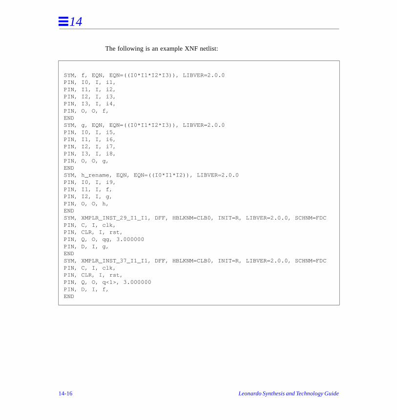
14
The following is an example XNF netlist:
SYM, f, EQN, EQN=((I0*I1*I2*I3)), LIBVER=2.0.0PIN, I0, I, i1, PIN, I1, I, i2, PIN, I2, I, i3, PIN, I3, I, i4, PIN, O, O, f, ENDSYM, g, EQN, EQN=((I0*I1*I2*I3)), LIBVER=2.0.0PIN, I0, I, i5, PIN, I1, I, i6, PIN, I2, I, i7, PIN, I3, I, i8, PIN, O, O, g, ENDSYM, h_rename, EQN, EQN=((I0*I1*I2)), LIBVER=2.0.0PIN, I0, I, i9, PIN, I1, I, f, PIN, I2, I, g, PIN, O, O, h, ENDSYM, XMPLR_INST_29_I1_I1, DFF, HBLKNM=CLB0, INIT=R, LIBVER=2.0.0, SCHNM=FDCPIN, C, I, clk,PIN, CLR, I, rst,PIN, Q, O, qg, 3.000000PIN, D, I, g,ENDSYM, XMPLR_INST_37_I1_I1, DFF, HBLKNM=CLB0, INIT=R, LIBVER=2.0.0, SCHNM=FDCPIN, C, I, clk,PIN, CLR, I, rst,PIN, Q, O, q<1>, 3.000000PIN, D, I, f,END
14-16 Leonardo Synthesis and Technology Guide
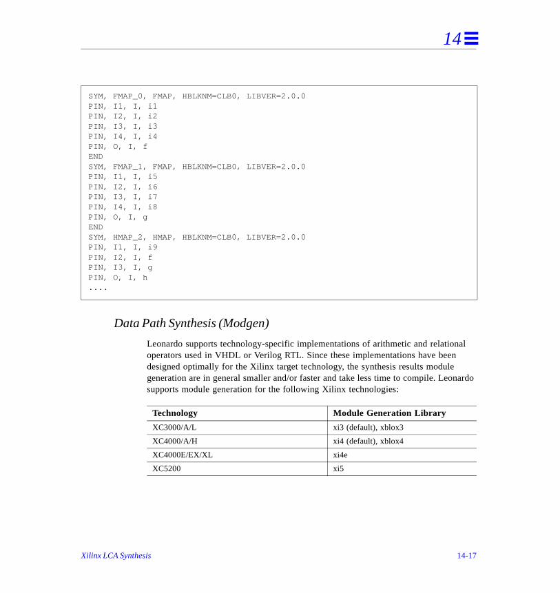
14
al
nardo
Data Path Synthesis (Modgen)
Leonardo supports technology-specific implementations of arithmetic and relationoperators used in VHDL or Verilog RTL. Since these implementations have been designed optimally for the Xilinx target technology, the synthesis results module generation are in general smaller and/or faster and take less time to compile. Leosupports module generation for the following Xilinx technologies:
SYM, FMAP_0, FMAP, HBLKNM=CLB0, LIBVER=2.0.0PIN, I1, I, i1PIN, I2, I, i2PIN, I3, I, i3PIN, I4, I, i4PIN, O, I, fENDSYM, FMAP_1, FMAP, HBLKNM=CLB0, LIBVER=2.0.0PIN, I1, I, i5PIN, I2, I, i6PIN, I3, I, i7PIN, I4, I, i8PIN, O, I, gENDSYM, HMAP_2, HMAP, HBLKNM=CLB0, LIBVER=2.0.0PIN, I1, I, i9PIN, I2, I, fPIN, I3, I, gPIN, O, I, h....
Technology Module Generation Library
XC3000/A/L xi3 (default), xblox3
XC4000/A/H xi4 (default), xblox4
XC4000E/EX/XL xi4e
XC5200 xi5
Xilinx LCA Synthesis 14-17

14
ble. .
000
r for
rry n.
Supported Operators
The following operators are supported for Xilinx technologies:
Logical Operators and or nand nor xor xnor
Relational Operators = /= < <= > >=
Arithmetic Operators + - *
Misc Functions counters (up/down, loadable, etc.)RAMsincrementerdecrementerabsolute valueunary minusdecoders
Modgen Implementation
Module generators attempt to use dedicated hardware resources whenever possiConsequently, the modgen implementation of operators like addition, subtraction,counters, and relational operators is in general smaller in area and faster in delay
For example:
• Adder in xi4 modgen is implemented using the dedicated carry chain in the XC4architecture to implement the adder carry logic. This leads to very fast carry propagation and good timing performance. Modgen implementation of an addeXC5200 technology uses the CY_MUXs to implement the adder carry logic.
• Relational operators <, <=, >, and >= are implemented using the dedicated calogic in the XC4000 architecture leading to a small and very fast implementatio
• xblox3 and xblox4 modgen use X-BLOX components to implement data path elements.
14-18 Leonardo Synthesis and Technology Guide
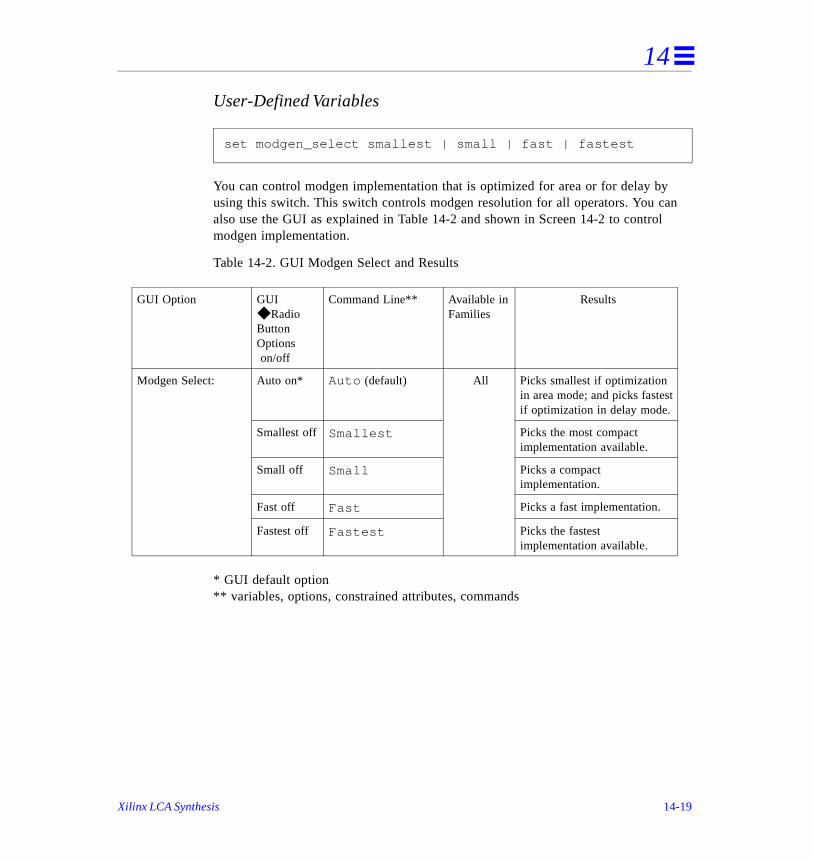
14
n
l
User-Defined Variables
You can control modgen implementation that is optimized for area or for delay byusing this switch. This switch controls modgen resolution for all operators. You caalso use the GUI as explained in Table 14-2 and shown in Screen 14-2 to contromodgen implementation.
Table 14-2. GUI Modgen Select and Results
* GUI default option** variables, options, constrained attributes, commands
set modgen_select sma llest | small | fast | fastest
GUI Option GUI ◆ Radio Button Options on/off
Command Line** Available in Families
Results
Modgen Select: Auto on* Auto (default) All Picks smallest if optimization in area mode; and picks fastest if optimization in delay mode.
Smallest off Smallest Picks the most compact implementation available.
Small off Small Picks a compact implementation.
Fast off Fast Picks a fast implementation.
Fastest off Fastest Picks the fastest implementation available.
Xilinx LCA Synthesis 14-19

14
l ot R ost flat
e citly
s d
ect
Screen 14-2. Modgen Implementation
Using Xilinx Architectural Features
GSR Usage and Startup Blocks
Xilinx flip-flops feature set/reset inputs that can be driven from a dedicated GlobaSet/Reset (GSR) signal. The GSR is implicit set/reset for all registers and does nrequire any routing resources. Leonardo GSR support is enhanced to handle GSprocessing across hierarchy. Global set/reset and local set/reset is detected on mor hierarchical designs.
A STARTUP block is instantiated automatically if global_sr is set to a signal name (my_signal ) in the design, or if infer_gsr variables are set to TRUE. The purposof the STARTUP block is to accept the reset signal and to distribute the reset implithrough the dedicated GSR signal.
Setting this Tcl variable allows Leonardo to use the specified Active High Signal aGlobal Set/Reset. The signal is disconnected from the registers Set/Reset pin anconnected to a startup block.
Caution – Specifying the Global Set/Reset on an active low signal will create incorrlogic.
set global_sr <my_signal>
14-20 Leonardo Synthesis and Technology Guide
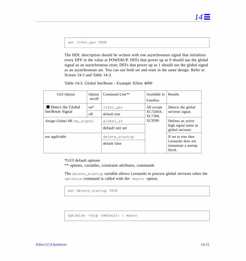
14
es lobal signal fer to
he
The HDL description should be written with one asynchronous signal that initializevery DFF to the value at POWERUP. DFFs that power up as 0 should use the gsignal as an asynchronous reset; DFFs that power up as 1 should use the globalas an asynchronous set. You can use both set and reset in the same design. ReScreen 14-3 and Table 14-3.
Table 14-3. Global Set/Reset - Example Xilinx 4000
*GUI default options** options, variables, constraint attributes, commands
The delete_startup variable allows Leonardo to process global set/reset when toptimize command is called with the -macro option.
set infer_gsr TRUE
GUI Option Option on/off
Command Line** Available in
Families
Results
■ Detect the Global Set/Reset Signal
on* infer_gsr All except XC7200A, XC7300, XC9500
Detects the global set/reset signal.
off default true
Assign Global SR: my_signal global_sr Defines an active high signal name as global set/reset.default not set
not applicable delete_startup If set to true then Leonardo does not instantiate a startup block.
default false
set delete_startup TRUE
optimize -chip (default) | macro
Xilinx LCA Synthesis 14-21
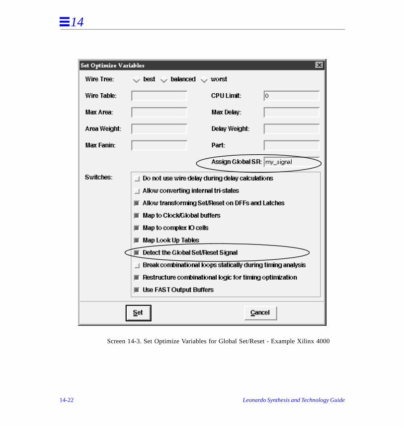
14
Screen 14-3. Set Optimize Variables for Global Set/Reset - Example Xilinx 4000
14-22 Leonardo Synthesis and Technology Guide
14
on of set
The xlx_preserve_gsr and xlx_preserve_gts are XNF reader specific only. The purpose of these variables is to preserve the Xilinx chip GSR, GTS behaviorthe retargeted chip. The S/R of each register in the output technology is not OR local and global S/R. You can only Set/Reset with local S/R. Preserve the global signal:.
Preserve the global tristate signal:
set xlx_preserve_gsr (default FALSE)
xlx_preserve_gts (default FALSE)
Xilinx LCA Synthesis 14-23
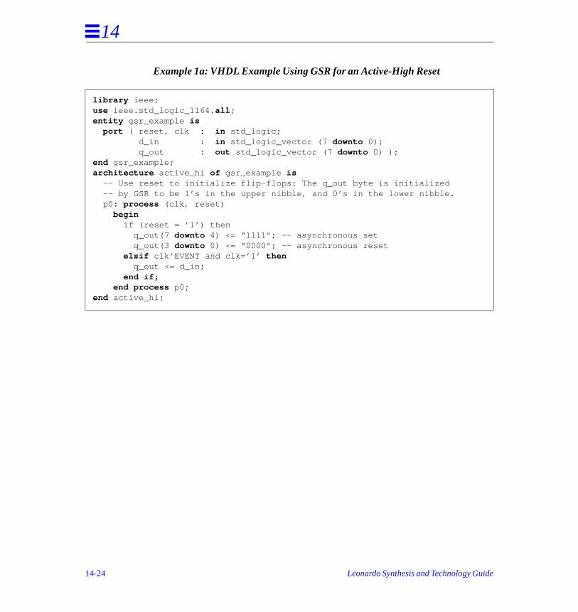
14
Example 1a: VHDL Example Using GSR for an Active-High Reset
library ieee;use ieee.std_logic_1164. all ;entity gsr_example is port ( reset, clk : in std_logic; d_in : in std_logic_vector (7 downto 0); q_out : out std_logic_vector (7 downto 0) );end gsr_example;architecture active_hi of gsr_example is -- Use reset to initialize flip-flops: The q_out byte is initialized -- by GSR to be 1’s in the upper nibble, and 0’s in the lower nibble. p0: process (clk, reset) begin if (reset = ’1’) then q_out(7 downto 4) <= “1111"; -- asynchronous set q_out(3 downto 0) <= “0000"; -- asynchronous reset elsif clk’EVENT and clk=’1’ then q_out <= d_in; end if; end process p0;end active_hi;
14-24 Leonardo Synthesis and Technology Guide

14
Example 1b. VHDL Example using GSR for an Active Low Reset
library ieee;use ieee.std_logic_1164. all ;entity gsr_example is port ( reset_b, clk : in std_logic; d_in : in std_logic_vector (7 downto 0); q_out : out std_logic_vector (7 downto 0) );end gsr_example;architecture active_lo of gsr_example isbegin-- Use reset to initialize flip-flops p0: process (clk, reset_b) begin if (reset_b = ’0’) then q_out(3 downto 0) <= “0000"; -- asynchronous reset q_out(7 downto 4) <= “1111"; -- asynchronous set elsif clk’EVENT and clk=’1’ then q_out <= d_in; end if ; end process p0;end active_lo;
Xilinx LCA Synthesis 14-25
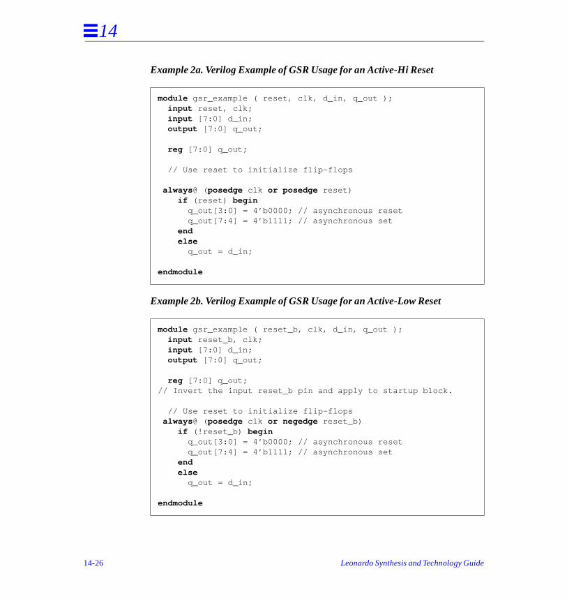
14
Example 2a. Verilog Example of GSR Usage for an Active-Hi Reset
Example 2b. Verilog Example of GSR Usage for an Active-Low Reset
module gsr_example ( reset, clk, d_in, q_out ); input reset, clk; input [7:0] d_in; output [7:0] q_out; reg [7:0] q_out;
// Use reset to initialize flip-flops always @ ( posedge clk or posedge reset) if (reset) begin q_out[3:0] = 4’b0000; // asynchronous reset q_out[7:4] = 4’b1111; // asynchronous set end else q_out = d_in;
endmodule
module gsr_example ( reset_b, clk, d_in, q_out ); input reset_b, clk; input [7:0] d_in; output [7:0] q_out; reg [7:0] q_out;// Invert the input reset_b pin and apply to startup block.
// Use reset to initialize flip-flops always @ ( posedge clk or negedge reset_b) if (!reset_b) begin q_out[3:0] = 4’b0000; // asynchronous reset q_out[7:4] = 4’b1111; // asynchronous set end else q_out = d_in;
endmodule
14-26 Leonardo Synthesis and Technology Guide
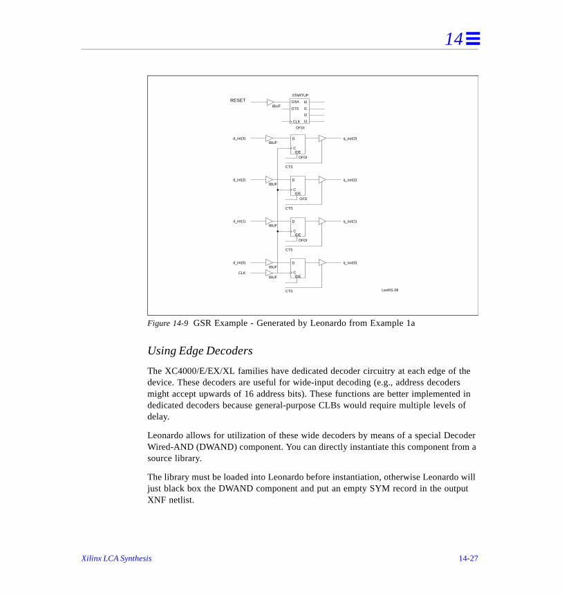
14
he rs d in of
oder a
will t
Figure 14-9 GSR Example - Generated by Leonardo from Example 1a
Using Edge Decoders
The XC4000/E/EX/XL families have dedicated decoder circuitry at each edge of tdevice. These decoders are useful for wide-input decoding (e.g., address decodemight accept upwards of 16 address bits). These functions are better implementededicated decoders because general-purpose CLBs would require multiple levelsdelay.
Leonardo allows for utilization of these wide decoders by means of a special DecWired-AND (DWAND) component. You can directly instantiate this component fromsource library.
The library must be loaded into Leonardo before instantiation, otherwise Leonardojust black box the DWAND component and put an empty SYM record in the outpuXNF netlist.
RESET
LeoRG 08
IBUFI0
I1
I2
I3
STARTUP
OFDI
CLK
GTS
GSA
CTS
q_out(3)D
OFDI
IBUF
IDEC
d_int(3)
CTS
q_out(2)D
OFD
IBUF
IDEC
d_int(2)
CTS
q_out(1)D
OFDI
IBUF
IDEC
d_int(1)
CTS
q_out(0)DIBUF
IDEC
d_int(0)
IBUFCLK
Xilinx LCA Synthesis 14-27
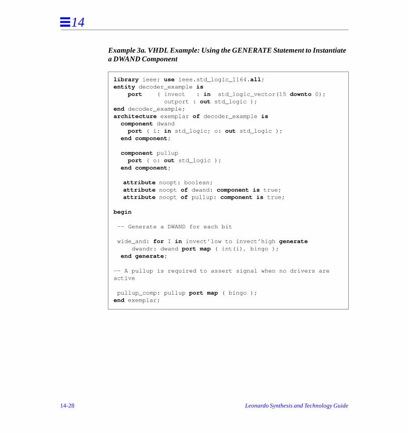
14
Example 3a. VHDL Example: Using the GENERATE Statement to Instantiatea DWAND Componentlibrary ieee; use ieee.std_logic_1164. all ;entity decoder_example is port ( invect : in std_logic_vector(15 downto 0); outport : out std_logic );end decoder_example;architecture exemplar of decoder_example is component dwand port ( i: in std_logic; o: out std_logic ); end component ; component pullup port ( o: out std_logic ); end component ;
attribute noopt: boolean;attribute noopt of dwand: component is true;attribute noopt of pullup: component is true;
begin
-- Generate a DWAND for each bit wide_and: for I in invect’low to invect’high generate dwandr: dwand port map ( int(i), bingo ); end generate ; -- A pullup is required to assert signal when no drivers are active pullup_comp: pullup port map ( bingo );end exemplar;
14-28 Leonardo Synthesis and Technology Guide
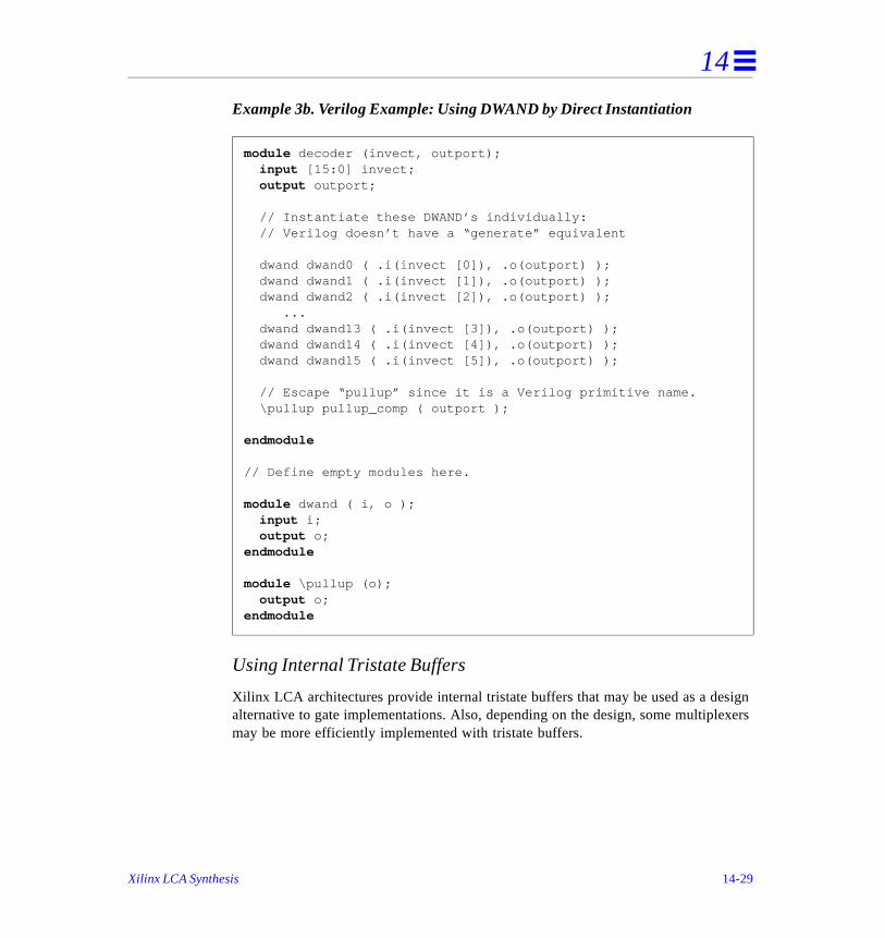
14
sign xers
Example 3b. Verilog Example: Using DWAND by Direct Instantiation
Using Internal Tristate Buffers
Xilinx LCA architectures provide internal tristate buffers that may be used as a dealternative to gate implementations. Also, depending on the design, some multiplemay be more efficiently implemented with tristate buffers.
module decoder (invect, outport); input [15:0] invect; output outport;
// Instantiate these DWAND’s individually: // Verilog doesn’t have a “generate” equivalent dwand dwand0 ( .i(invect [0]), .o(outport) ); dwand dwand1 ( .i(invect [1]), .o(outport) ); dwand dwand2 ( .i(invect [2]), .o(outport) ); ... dwand dwand13 ( .i(invect [3]), .o(outport) ); dwand dwand14 ( .i(invect [4]), .o(outport) ); dwand dwand15 ( .i(invect [5]), .o(outport) ); // Escape “pullup” since it is a Verilog primitive name. \pullup pullup_comp ( outport );
endmodule
// Define empty modules here.
module dwand ( i, o ); input i; output o;endmodule module \pullup (o); output o;endmodule
Xilinx LCA Synthesis 14-29
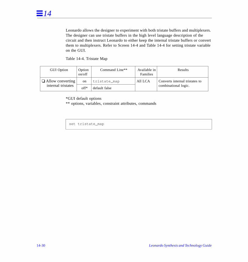
14
ers. vert able
Leonardo allows the designer to experiment with both tristate buffers and multiplexThe designer can use tristate buffers in the high level language description of thecircuit and then instruct Leonardo to either keep the internal tristate buffers or conthem to multiplexers. Refer to Screen 14-4 and Table 14-4 for setting tristate varion the GUI.
Table 14-4. Tristate Map
*GUI default options** options, variables, constraint attributes, commands
GUI Option Optionon/off
Command Line** Available inFamilies
Results
❏ Allow converting internal tristates
on tristate_map All LCA Converts internal tristates to combinational logic.
off* default false
set tristate_map
14-30 Leonardo Synthesis and Technology Guide
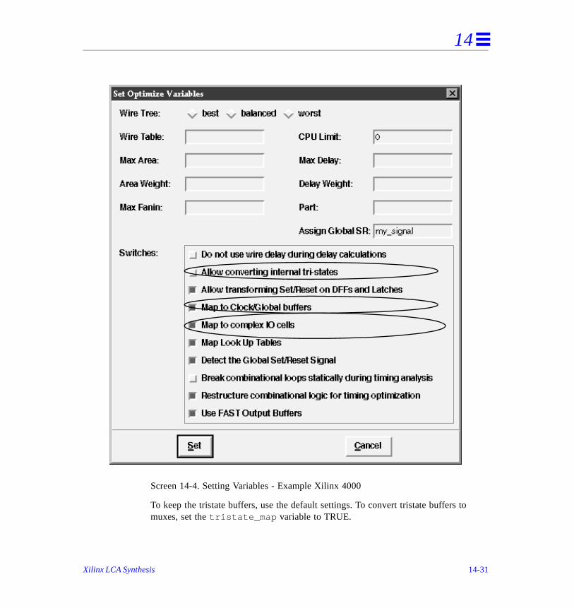
14
Screen 14-4. Setting Variables - Example Xilinx 4000
To keep the tristate buffers, use the default settings. To convert tristate buffers tomuxes, set the tristate_map variable to TRUE.
Xilinx LCA Synthesis 14-31
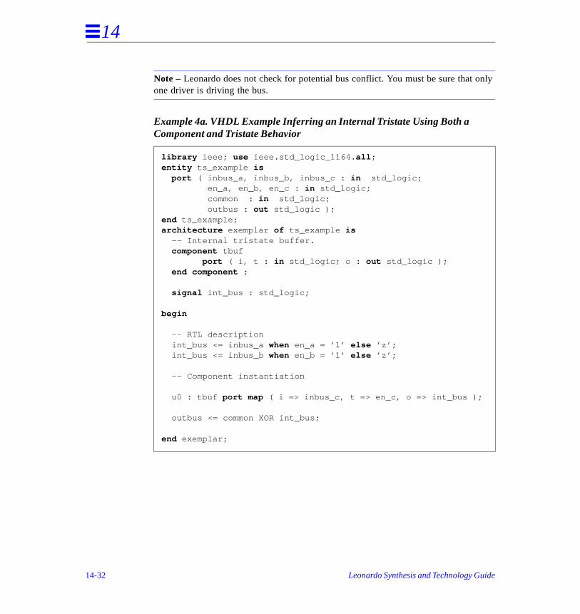
14
nly
Note – Leonardo does not check for potential bus conflict. You must be sure that oone driver is driving the bus.Example 4a. VHDL Example Inferring an Internal Tristate Using Both a Component and Tristate Behavior
library ieee; use ieee.std_logic_1164. all ;entity ts_example is port ( inbus_a, inbus_b, inbus_c : in std_logic; en_a, en_b, en_c : in std_logic; common : in std_logic; outbus : out std_logic );end ts_example;architecture exemplar of ts_example is -- Internal tristate buffer. component tbuf port ( i, t : in std_logic; o : out std_logic ); end component ;
signal int_bus : std_logic;
begin
-- RTL description int_bus <= inbus_a when en_a = ’1’ else ’z’; int_bus <= inbus_b when en_b = ’1’ else ’z’;
-- Component instantiation
u0 : tbuf port map ( i => inbus_c, t => en_c, o => int_bus );
outbus <= common XOR int_bus;
end exemplar;
14-32 Leonardo Synthesis and Technology Guide
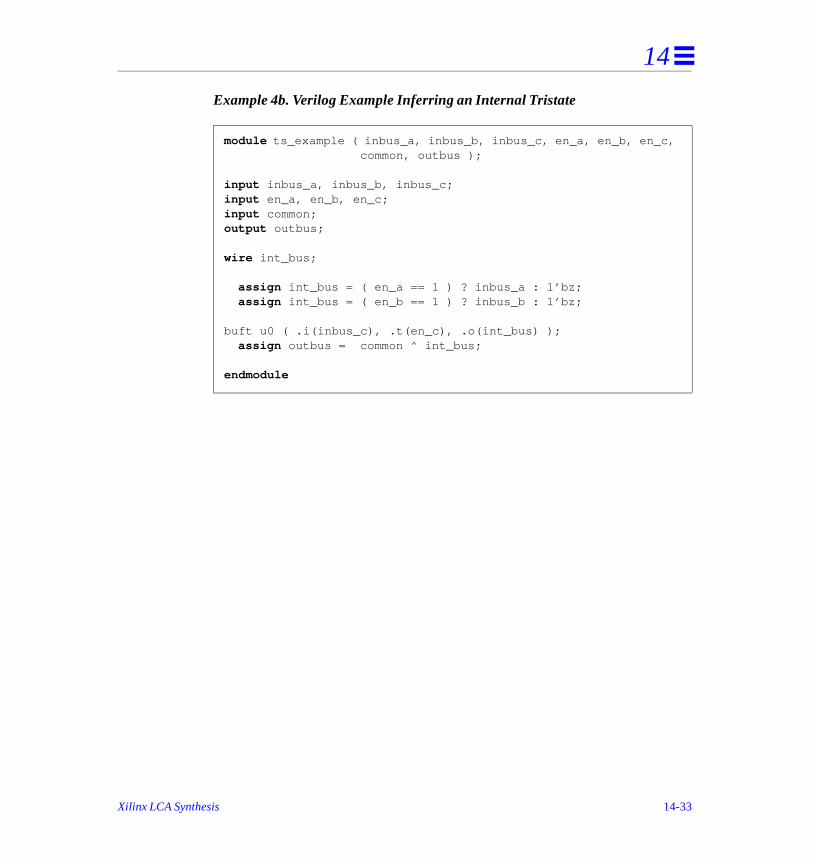
14
Example 4b. Verilog Example Inferring an Internal Tristate
module ts_example ( inbus_a, inbus_b, inbus_c, en_a, en_b, en_c, common, outbus ); input inbus_a, inbus_b, inbus_c;input en_a, en_b, en_c; input common; output outbus; wire int_bus; assign int_bus = ( en_a == 1 ) ? inbus_a : 1’bz; assign int_bus = ( en_b == 1 ) ? inbus_b : 1’bz; buft u0 ( .i(inbus_c), .t(en_c), .o(int_bus) ); assign outbus = common ^ int_bus; endmodule
Xilinx LCA Synthesis 14-33
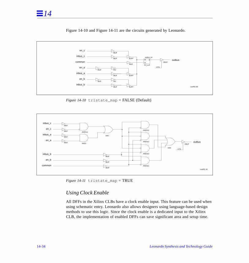
14
hen ign
x e.
Figure 14-10 and Figure 14-11 are the circuits generated by Leonardo.
Figure 14-10 tristate_map = FALSE (Default)
Figure 14-11 tristate_map = TRUE
Using Clock Enable
All DFFs in the Xilinx CLBs have a clock enable input. This feature can be used wusing schematic entry. Leonardo also allows designers using language-based desmethods to use this logic. Since the clock enable is a dedicated input to the XilinCLB, the implementation of enabled DFFs can save significant area and setup tim
LeoRG 09
outbus_int
I0
I1
F2_LUT
inbus_aIBUF
en_aINV
commonIBUF
BUFF
BUFF
inbus_cIBUF
en_cIBUF
IBUF
inbus_bIBUF
en_bINV
BUFF
IBUF
D
CTS
outbusOBUF
LeoRG 10
CTS
outbusOBUF
inbus_cIBUF
en_cIBUF
inbus_aIBUF
en_aIBUF
inbus_bIBUF
en_bIBUF
commonIBUF
AND2u1
AND2
OA2
AND2u1
AND3u2
AND3u2
AND3u1
OA4
14-34 Leonardo Synthesis and Technology Guide
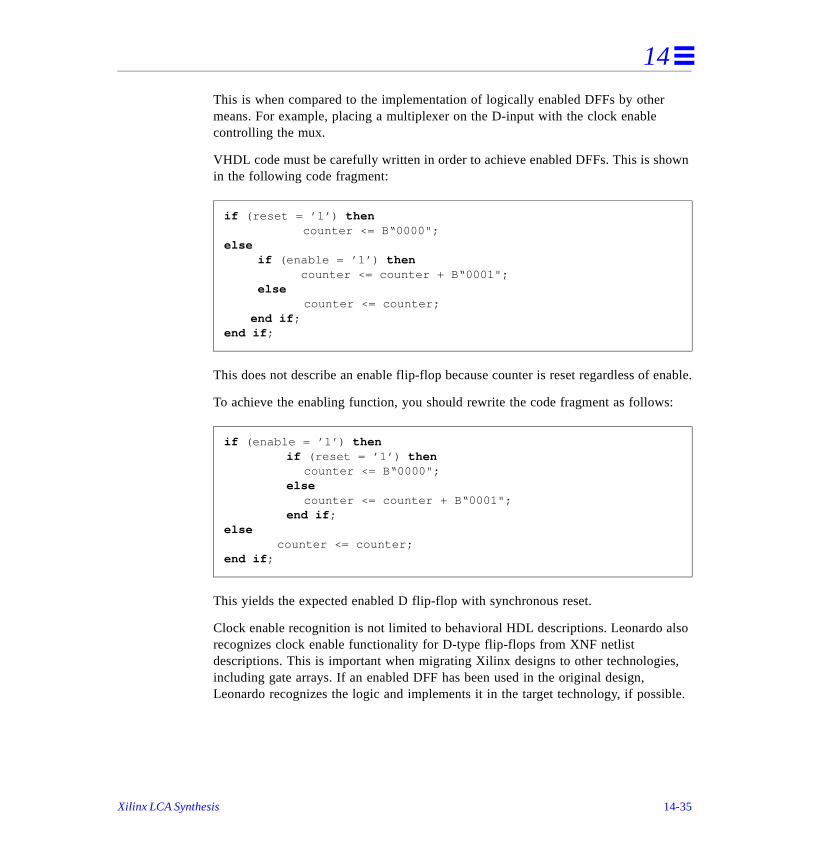
14
own
nable.
s:
lso
s,
ible.
This is when compared to the implementation of logically enabled DFFs by othermeans. For example, placing a multiplexer on the D-input with the clock enable controlling the mux.
VHDL code must be carefully written in order to achieve enabled DFFs. This is shin the following code fragment:
This does not describe an enable flip-flop because counter is reset regardless of e
To achieve the enabling function, you should rewrite the code fragment as follow
This yields the expected enabled D flip-flop with synchronous reset.
Clock enable recognition is not limited to behavioral HDL descriptions. Leonardo arecognizes clock enable functionality for D-type flip-flops from XNF netlist descriptions. This is important when migrating Xilinx designs to other technologieincluding gate arrays. If an enabled DFF has been used in the original design, Leonardo recognizes the logic and implements it in the target technology, if poss
if (reset = ’1’) then counter <= B“0000";else
if (enable = ’1’) then counter <= counter + B“0001"; else counter <= counter;end if ;
end if ;
if (enable = ’1’) then if (reset = ’1’) then
counter <= B“0000"; else counter <= counter + B“0001"; end if ;
else counter <= counter;
end if ;
Xilinx LCA Synthesis 14-35
14
a
hese ation Both
AMs:
a
a
Using RAMs
Types of Inferencing RAMs
Leonardo supports two types of RAMs:
• RAM_DQ. RAM_DQ is a single-port RAM with separate input and output datlines.
• RAM_IO. RAM_IO is a single-port RAM with bidirectional data lines.
Both of these RAM types support synchronous or asynchronous read and write. TRAMs are automatically inferred by Leonardo from HDL code (VHDL or Verilog). The inferencing process distinguishes between RAMs that perform the read operwith an address clocked or not clocked by the write clock (read address clocked). of the following VHDL examples perform synchronous writes (inclock) and synchronous reads (outclock); Leonardo recognizes these VHDL processes as R
• The first, entity ram_example1 , is when the read operation does not haveclocked address.
• The second entity ram_example2 , is when the read operation does have clocked address.
14-36 Leonardo Synthesis and Technology Guide
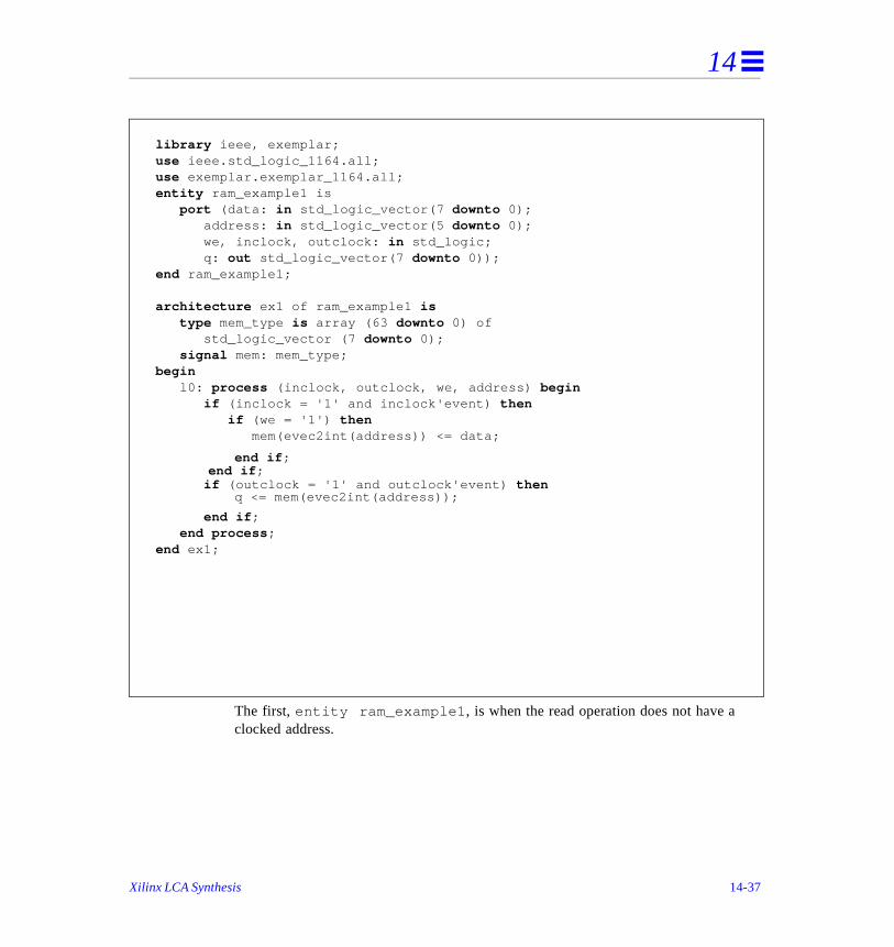
14
The first, entity ram_example1 , is when the read operation does not have a clocked address.
library ieee, exemplar;use ieee.std_logic_1164.all;use exemplar.exemplar_1164.all;entity ram_example1 is port (data: in std_logic_vector(7 downto 0); address: in std_logic_vector(5 downto 0); we, inclock, outclock: in std_logic; q: out std_logic_vector(7 downto 0));end ram_example1;
architecture ex1 of ram_example1 is type mem_type is array (63 downto 0) of std_logic_vector (7 downto 0); signal mem: mem_type;begin l0: process (inclock, outclock, we, address) begin if (inclock = '1' and inclock'event) then if (we = '1') then mem(evec2int(address)) <= data;
if (outclock = '1' and outclock'event) then
end if ; end process ;end ex1;
q <= mem(evec2int(address));
end if ;end if ;
Xilinx LCA Synthesis 14-37
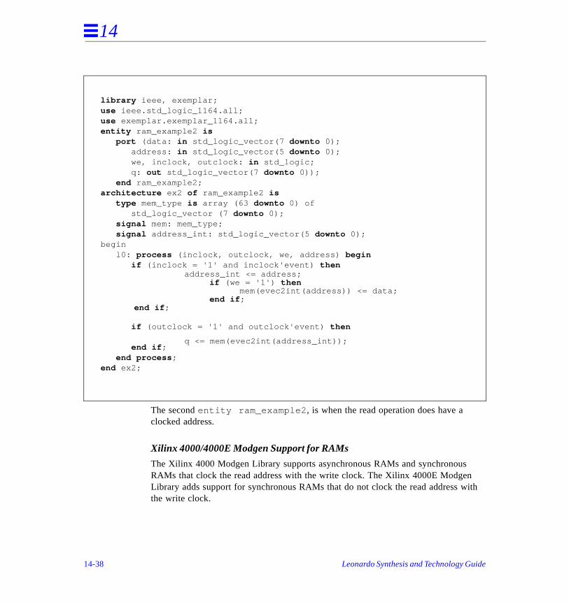
14
ith
The second entity ram_example2 , is when the read operation does have a clocked address.
Xilinx 4000/4000E Modgen Support for RAMs
The Xilinx 4000 Modgen Library supports asynchronous RAMs and synchronous RAMs that clock the read address with the write clock. The Xilinx 4000E ModgenLibrary adds support for synchronous RAMs that do not clock the read address wthe write clock.
library ieee, exemplar;use ieee.std_logic_1164.all;use exemplar.exemplar_1164.all;entity ram_example2 is port (data: in std_logic_vector(7 downto 0); address: in std_logic_vector(5 downto 0); we, inclock, outclock: in std_logic; q: out std_logic_vector(7 downto 0)); end ram_example2;architecture ex2 of ram_example2 is type mem_type is array (63 downto 0) of std_logic_vector (7 downto 0); signal mem: mem_type; signal address_int: std_logic_vector(5 downto 0);begin l0: process (inclock, outclock, we, address) begin if (inclock = '1' and inclock'event) then
if (outclock = '1' and outclock'event) then
end if ; end process ;end ex2;
address_int <= address;if (we = '1') then
mem(evec2int(address)) <= data;end if ;
end if ;
q <= mem(evec2int(address_int));
14-38 Leonardo Synthesis and Technology Guide
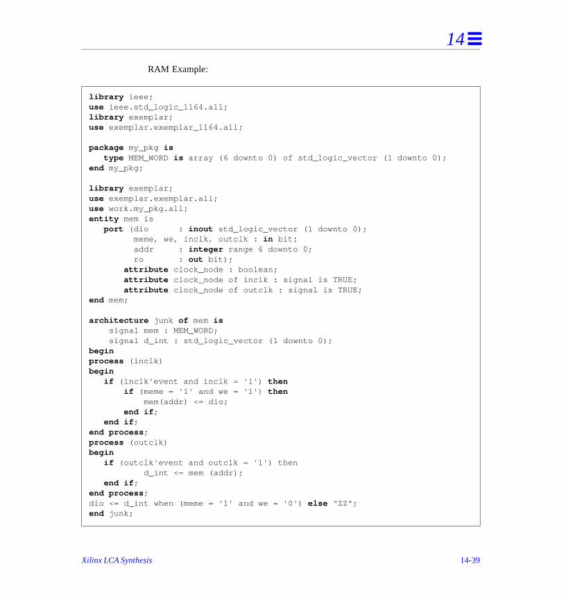
14
RAM Example:
library ieee;use ieee.std_logic_1164.all;library exemplar;use exemplar.exemplar_1164.all;
package my_pkg is type MEM_WORD is array (6 downto 0) of std_logic_vector (1 downto 0);end my_pkg; library exemplar;use exemplar.exemplar.all;use work.my_pkg.all;entity mem is port (dio : inout std_logic_vector (1 downto 0); meme, we, inclk, outclk : in bit; addr : integer range 6 downto 0; ro : out bit); attribute clock_node : boolean; attribute clock_node of inclk : signal is TRUE; attribute clock_node of outclk : signal is TRUE;end mem;
architecture junk of mem is signal mem : MEM_WORD; signal d_int : std_logic_vector (1 downto 0);beginprocess (inclk)begin if (inclk'event and inclk = '1') then if (meme = '1' and we = '1') then mem(addr) <= dio; end if ; end if ;end process ;process (outclk)begin if (outclk'event and outclk = '1') then d_int <= mem (addr); end if ;end process ;dio <= d_int when (meme = '1' and we = '0') else "ZZ";end junk;
Xilinx LCA Synthesis 14-39

14
the
black The
le,
When running this example targeting XC4000, XC4000E, Leonardo will infer a synchronous ram_io cell.
RAM Instantiation
You can also use Xilinx memgen utility to generate RAMs and instantiate them ininput HDL design.
To take advantage of memgen, you should define the memory in your design as a box with appropriate ports, and run Leonardo to synthesize the output XNF netlist.XNF netlist will include the black box for the RAM.
Next, run memgen to create the XNF description of the memory itself. For exampthe following memgen invocation will create a 256x6 RAM and write it to a file myram.xnf
The Xilinx PPR and XNFMERGE tools will look in their default search path (including the current directory) to find the file myram.xnf and link it into the original design.
The following two example designs in VHDL and Verilog treat the component myram
as a black box.
% memgen type=ram memory_depth=256 word_width=6 file_name=myram
14-40 Leonardo Synthesis and Technology Guide
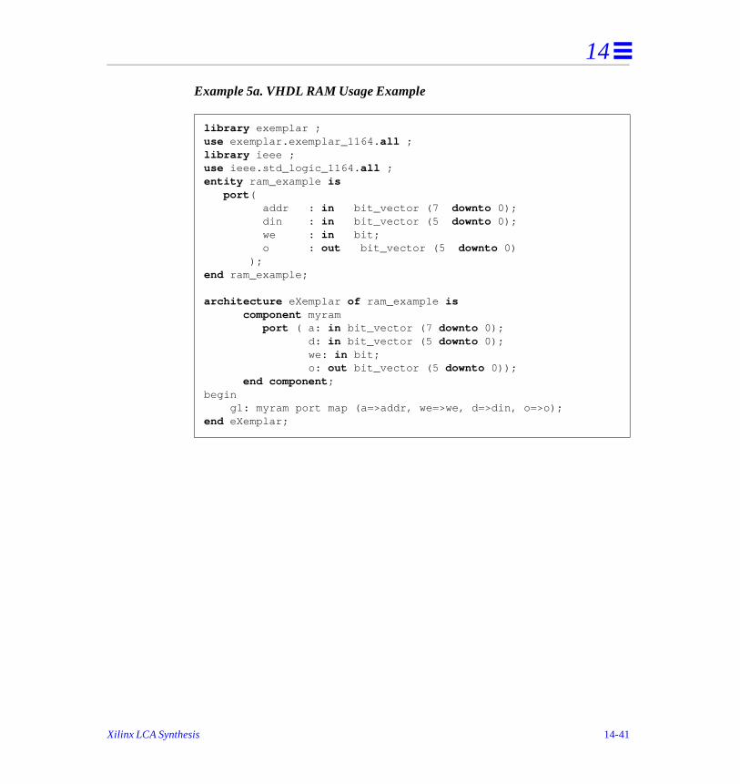
14
Example 5a. VHDL RAM Usage Example
library exemplar ;use exemplar.exemplar_1164. all ;library ieee ;use ieee.std_logic_1164. all ;entity ram_example is port ( addr : in bit_vector (7 downto 0); din : in bit_vector (5 downto 0); we : in bit; o : out bit_vector (5 downto 0) );end ram_example; architecture eXemplar of ram_example is component myram port ( a: in bit_vector (7 downto 0); d: in bit_vector (5 downto 0); we: in bit; o: out bit_vector (5 downto 0)); end component ;begin g1: myram port map (a=>addr, we=>we, d=>din, o=>o);end eXemplar;
Xilinx LCA Synthesis 14-41
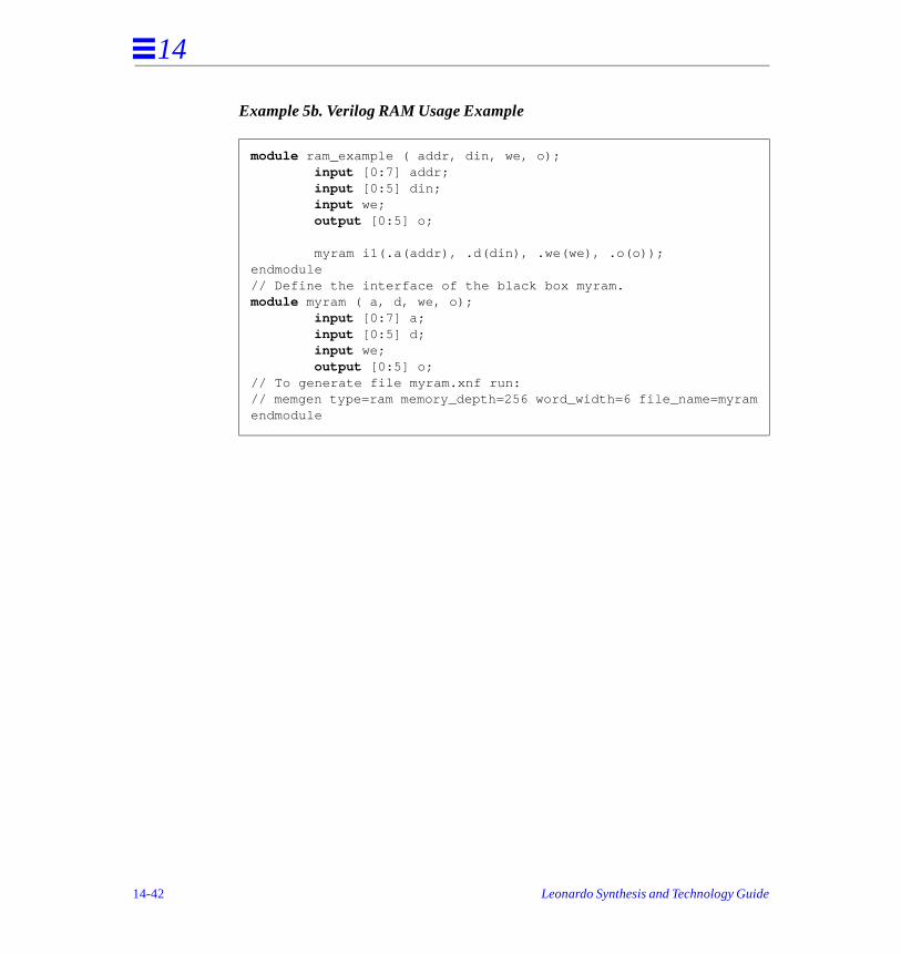
14
Example 5b. Verilog RAM Usage Example
module ram_example ( addr, din, we, o); input [0:7] addr; input [0:5] din; input we; output [0:5] o; myram i1(.a(addr), .d(din), .we(we), .o(o));endmodule// Define the interface of the black box myram.module myram ( a, d, we, o); input [0:7] a; input [0:5] d; input we; output [0:5] o;// To generate file myram.xnf run:// memgen type=ram memory_depth=256 word_width=6 file_name=myramendmodule
14-42 Leonardo Synthesis and Technology Guide
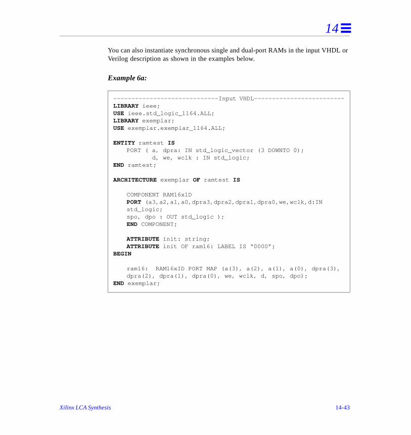
14
L or
You can also instantiate synchronous single and dual-port RAMs in the input VHDVerilog description as shown in the examples below.Example 6a:
-----------------------------Input VHDL-------------------------LIBRARY ieee;USE ieee.std_logic_1164.ALL;LIBRARY exemplar;USE exemplar.exemplar_1164.ALL;
ENTITY ramtest ISPORT ( a, dpra: IN std_logic_vector (3 DOWNTO 0); d, we, wclk : IN std_logic;
END ramtest;
ARCHITECTURE exemplar OF ramtest IS
COMPONENT RAM16x1DPORT (a3,a2,a1,a0,dpra3,dpra2,dpra1,dpra0,we,wclk,d:IN std_logic;spo, dpo : OUT std_logic );END COMPONENT;
ATTRIBUTE init: string;ATTRIBUTE init OF ram16: LABEL IS “0000”;
BEGIN
ram16: RAM16xID PORT MAP (a(3), a(2), a(1), a(0), dpra(3), dpra(2), dpra(1), dpra(0), we, wclk, d, spo, dpo);
END exemplar;
Xilinx LCA Synthesis 14-43
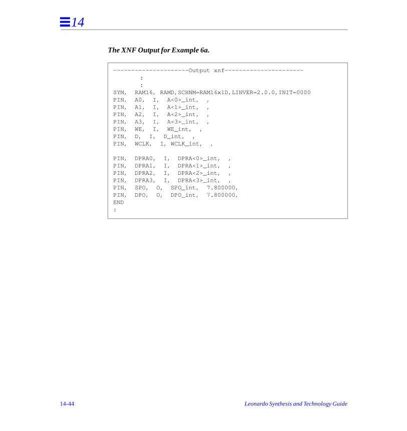
14
The XNF Output for Example 6a.
---------------------Output xnf----------------------::
SYM, RAM16, RAMD,SCHNM=RAM16x1D,LINVER=2.0.0,INIT=0000PIN, A0, I, A<0>_int, ,PIN, A1, I, A<1>_int, ,PIN, A2, I, A<2>_int, ,PIN, A3, I, A<3>_int, ,PIN, WE, I, WE_int, ,PIN, D, I, D_int, ,PIN, WCLK, I, WCLK_int, ,
PIN, DPRA0, I, DPRA<0>_int, ,PIN, DPRA1, I, DPRA<1>_int, ,PIN, DPRA2, I, DPRA<2>_int, ,PIN, DPRA3, I, DPRA<3>_int, ,PIN, SPO, O, SPO_int, 7.800000,PIN, DPO, O, DPO_int, 7.800000,END:
14-44 Leonardo Synthesis and Technology Guide
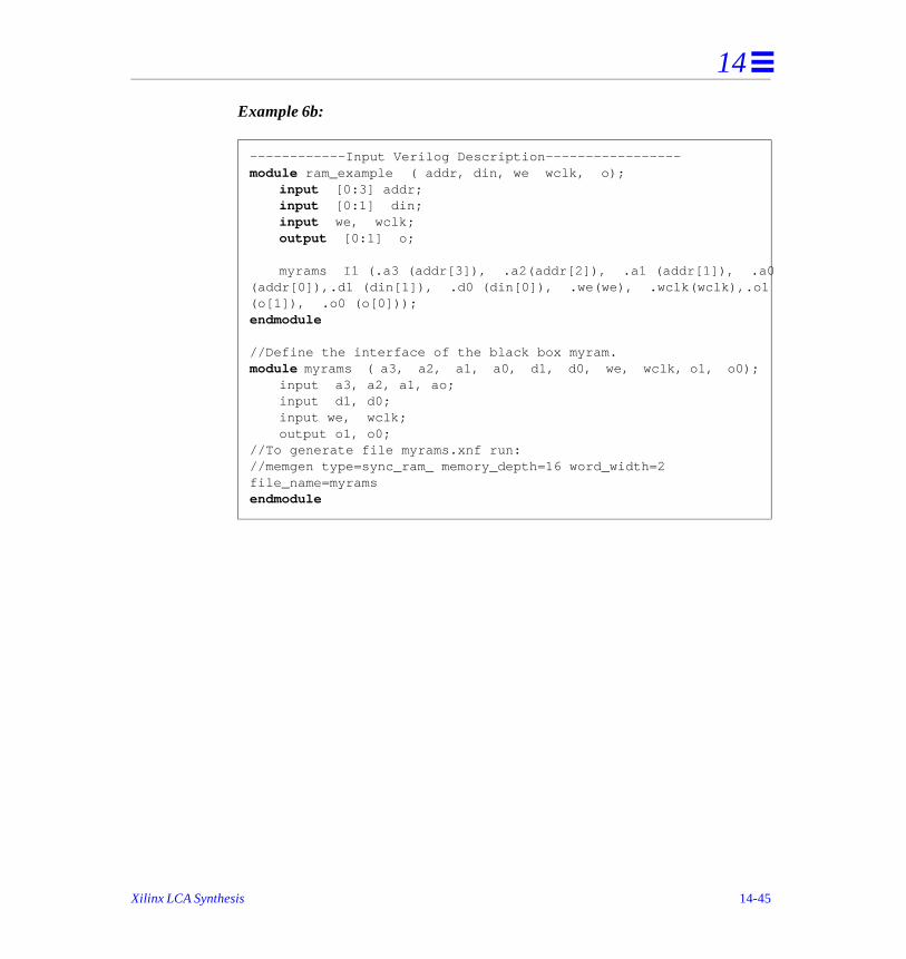
14
Example 6b:
------------Input Verilog Description-----------------module ram_example ( addr, din, we wclk, o);
input [0:3] addr;input [0:1] din;input we, wclk;output [0:1] o;
myrams I1 (.a3 (addr[3]), .a2(addr[2]), .a1 (addr[1]), .a0 (addr[0]),.d1 (din[1]), .d0 (din[0]), .we(we), .wclk(wclk),.o1 (o[1]), .o0 (o[0]));endmodule
//Define the interface of the black box myram.module myrams ( a3, a2, a1, a0, d1, d0, we, wclk, o1, o0);
input a3, a2, a1, ao;input d1, d0;input we, wclk;output o1, o0;
//To generate file myrams.xnf run://memgen type=sync_ram_ memory_depth=16 word_width=2 file_name=myramsendmodule
Xilinx LCA Synthesis 14-45
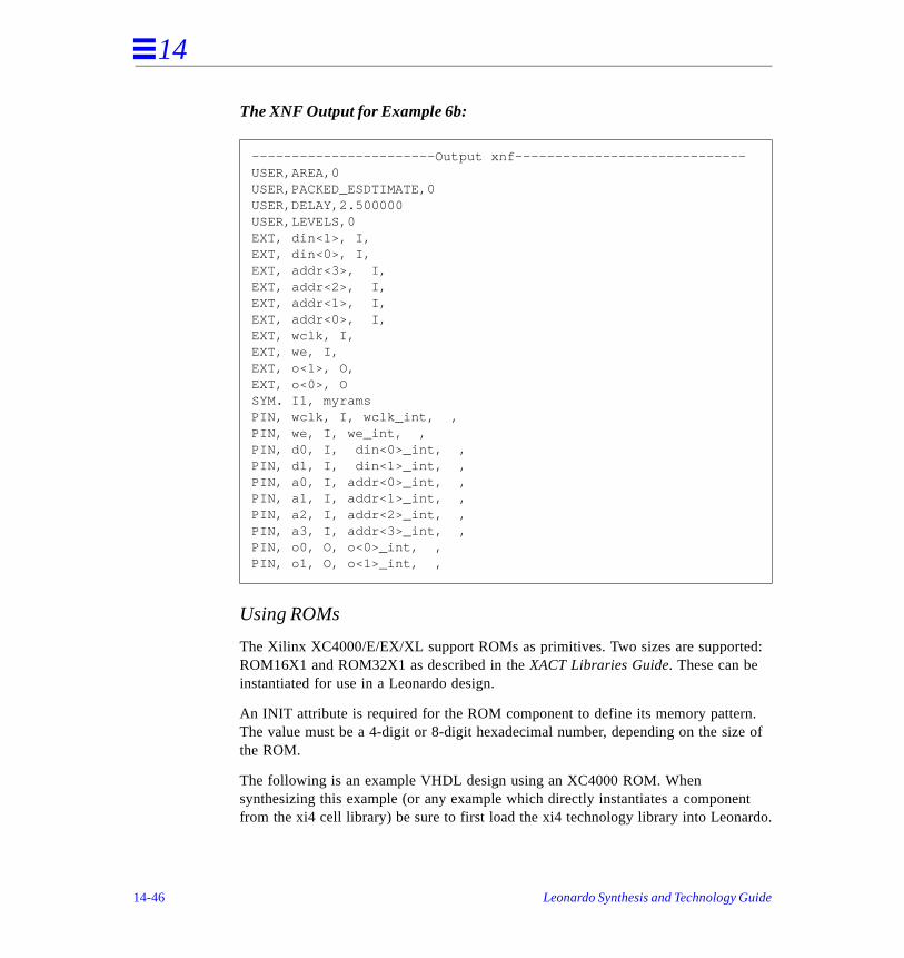
14
d:
. e of
nt do.
The XNF Output for Example 6b:
Using ROMs
The Xilinx XC4000/E/EX/XL support ROMs as primitives. Two sizes are supporteROM16X1 and ROM32X1 as described in the XACT Libraries Guide. These can be instantiated for use in a Leonardo design.
An INIT attribute is required for the ROM component to define its memory patternThe value must be a 4-digit or 8-digit hexadecimal number, depending on the sizthe ROM.
The following is an example VHDL design using an XC4000 ROM. When synthesizing this example (or any example which directly instantiates a componefrom the xi4 cell library) be sure to first load the xi4 technology library into Leonar
-----------------------Output xnf-----------------------------USER,AREA,0USER,PACKED_ESDTIMATE,0USER,DELAY,2.500000USER,LEVELS,0EXT, din<1>, I,EXT, din<0>, I,EXT, addr<3>, I,EXT, addr<2>, I,EXT, addr<1>, I,EXT, addr<0>, I,EXT, wclk, I,EXT, we, I,EXT, o<1>, O,EXT, o<0>, OSYM. I1, myramsPIN, wclk, I, wclk_int, ,PIN, we, I, we_int, ,PIN, d0, I, din<0>_int, ,PIN, d1, I, din<1>_int, ,PIN, a0, I, addr<0>_int, ,PIN, a1, I, addr<1>_int, ,PIN, a2, I, addr<2>_int, ,PIN, a3, I, addr<3>_int, ,PIN, o0, O, o<0>_int, ,PIN, o1, O, o<1>_int, ,
14-46 Leonardo Synthesis and Technology Guide
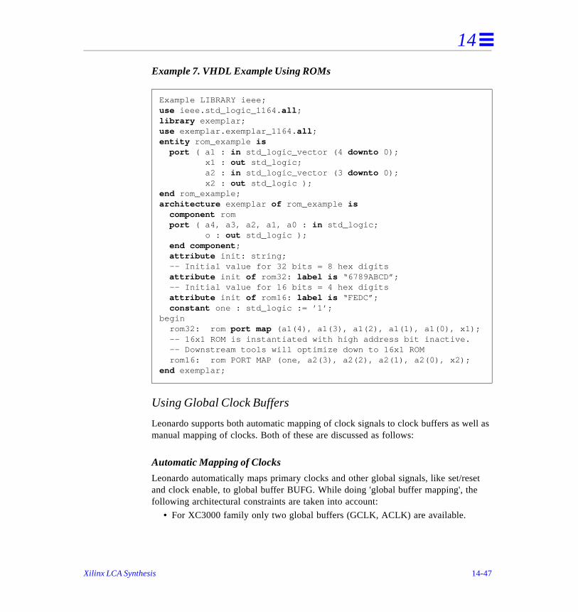
14
ll as
et
Example 7. VHDL Example Using ROMs
Using Global Clock Buffers
Leonardo supports both automatic mapping of clock signals to clock buffers as wemanual mapping of clocks. Both of these are discussed as follows:
Automatic Mapping of Clocks
Leonardo automatically maps primary clocks and other global signals, like set/resand clock enable, to global buffer BUFG. While doing 'global buffer mapping', thefollowing architectural constraints are taken into account:
• For XC3000 family only two global buffers (GCLK, ACLK) are available.
Example LIBRARY ieee;use ieee.std_logic_1164. all ;library exemplar;use exemplar.exemplar_1164. all ;entity rom_example is port ( a1 : in std_logic_vector (4 downto 0); x1 : out std_logic; a2 : in std_logic_vector (3 downto 0); x2 : out std_logic );end rom_example;architecture exemplar of rom_example is component rom port ( a4, a3, a2, a1, a0 : in std_logic; o : out std_logic ); end component ; attribute init: string; -- Initial value for 32 bits = 8 hex digits attribute init of rom32: label is “6789ABCD”; -- Initial value for 16 bits = 4 hex digits attribute init of rom16: label is “FEDC”; constant one : std_logic := ’1’;begin rom32: rom port map (a1(4), a1(3), a1(2), a1(1), a1(0), x1); -- 16x1 ROM is instantiated with high address bit inactive. -- Downstream tools will optimize down to 16x1 ROM rom16: rom PORT MAP (one, a2(3), a2(2), a2(1), a2(0), x2);end exemplar;
Xilinx LCA Synthesis 14-47
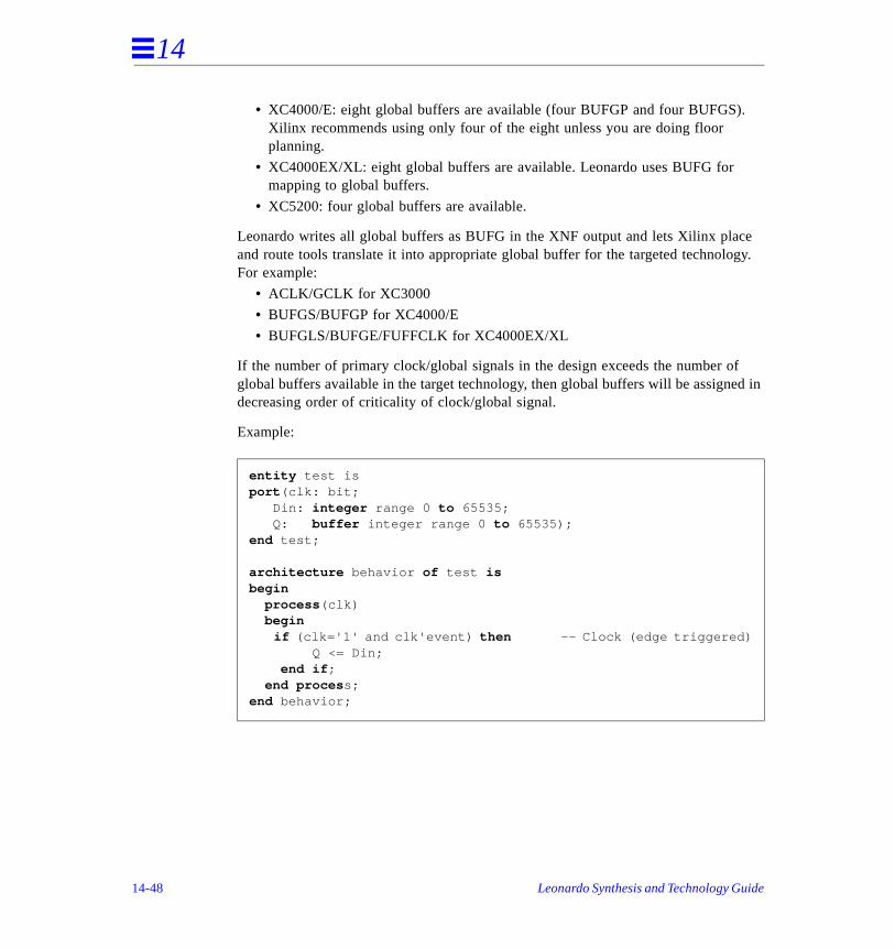
14
.
e gy.
f d in
• XC4000/E: eight global buffers are available (four BUFGP and four BUFGS)Xilinx recommends using only four of the eight unless you are doing floor planning.
• XC4000EX/XL: eight global buffers are available. Leonardo uses BUFG for mapping to global buffers.
• XC5200: four global buffers are available.
Leonardo writes all global buffers as BUFG in the XNF output and lets Xilinx placand route tools translate it into appropriate global buffer for the targeted technoloFor example:
• ACLK/GCLK for XC3000
• BUFGS/BUFGP for XC4000/E
• BUFGLS/BUFGE/FUFFCLK for XC4000EX/XL
If the number of primary clock/global signals in the design exceeds the number oglobal buffers available in the target technology, then global buffers will be assignedecreasing order of criticality of clock/global signal.
Example:
entity test isport (clk: bit; Din: integer range 0 to 65535; Q: buffer integer range 0 to 65535);end test;
architecture behavior of test isbegin process (clk) begin if (clk='1' and clk'event) then -- Clock (edge triggered) Q <= Din; end if ; end proces s;end behavior;
14-48 Leonardo Synthesis and Technology Guide
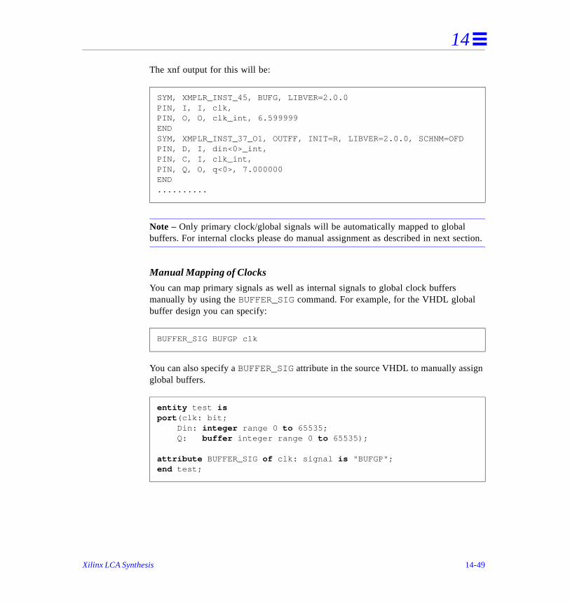
14
ction.
The xnf output for this will be:
Note – Only primary clock/global signals will be automatically mapped to global buffers. For internal clocks please do manual assignment as described in next se
Manual Mapping of Clocks
You can map primary signals as well as internal signals to global clock buffers manually by using the BUFFER_SIG command. For example, for the VHDL global buffer design you can specify:
You can also specify a BUFFER_SIG attribute in the source VHDL to manually assignglobal buffers.
SYM, XMPLR_INST_45, BUFG, LIBVER=2.0.0PIN, I, I, clk,PIN, O, O, clk_int, 6.599999ENDSYM, XMPLR_INST_37_O1, OUTFF, INIT=R, LIBVER=2.0.0, SCHNM=OFDPIN, D, I, din<0>_int,PIN, C, I, clk_int,PIN, Q, O, q<0>, 7.000000END..........
BUFFER_SIG BUFGP clk
entity test isport (clk: bit; Din: integer range 0 to 65535; Q: buffer integer range 0 to 65535);
attribute BUFFER_SIG of clk: signal is "BUFGP"; end test;
Xilinx LCA Synthesis 14-49
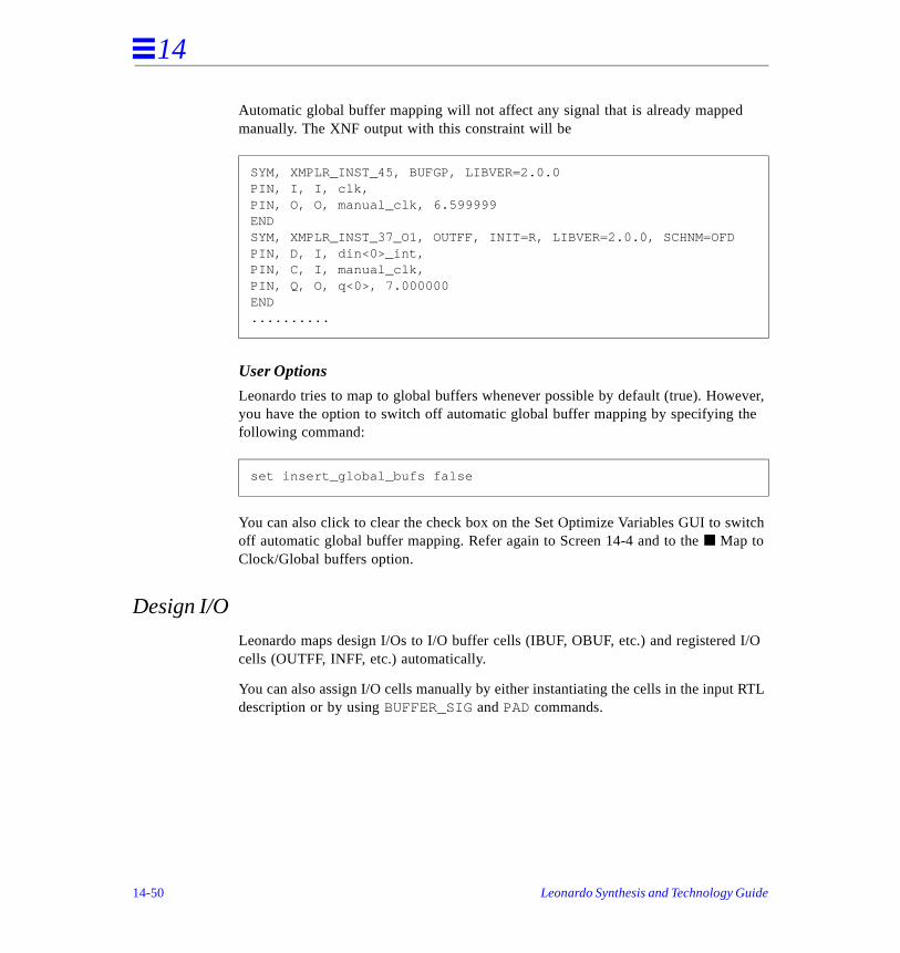
14
ver, e
itch
I/O
RTL
Automatic global buffer mapping will not affect any signal that is already mappedmanually. The XNF output with this constraint will be
User Options
Leonardo tries to map to global buffers whenever possible by default (true). Howeyou have the option to switch off automatic global buffer mapping by specifying thfollowing command:
You can also click to clear the check box on the Set Optimize Variables GUI to swoff automatic global buffer mapping. Refer again to Screen 14-4 and to the ■ Map to Clock/Global buffers option.
Design I/O
Leonardo maps design I/Os to I/O buffer cells (IBUF, OBUF, etc.) and registered cells (OUTFF, INFF, etc.) automatically.
You can also assign I/O cells manually by either instantiating the cells in the input description or by using BUFFER_SIG and PAD commands.
SYM, XMPLR_INST_45, BUFGP, LIBVER=2.0.0PIN, I, I, clk,PIN, O, O, manual_clk, 6.599999ENDSYM, XMPLR_INST_37_O1, OUTFF, INIT=R, LIBVER=2.0.0, SCHNM=OFDPIN, D, I, din<0>_int,PIN, C, I, manual_clk,PIN, Q, O, q<0>, 7.000000END..........
set insert_global_bufs false
14-50 Leonardo Synthesis and Technology Guide
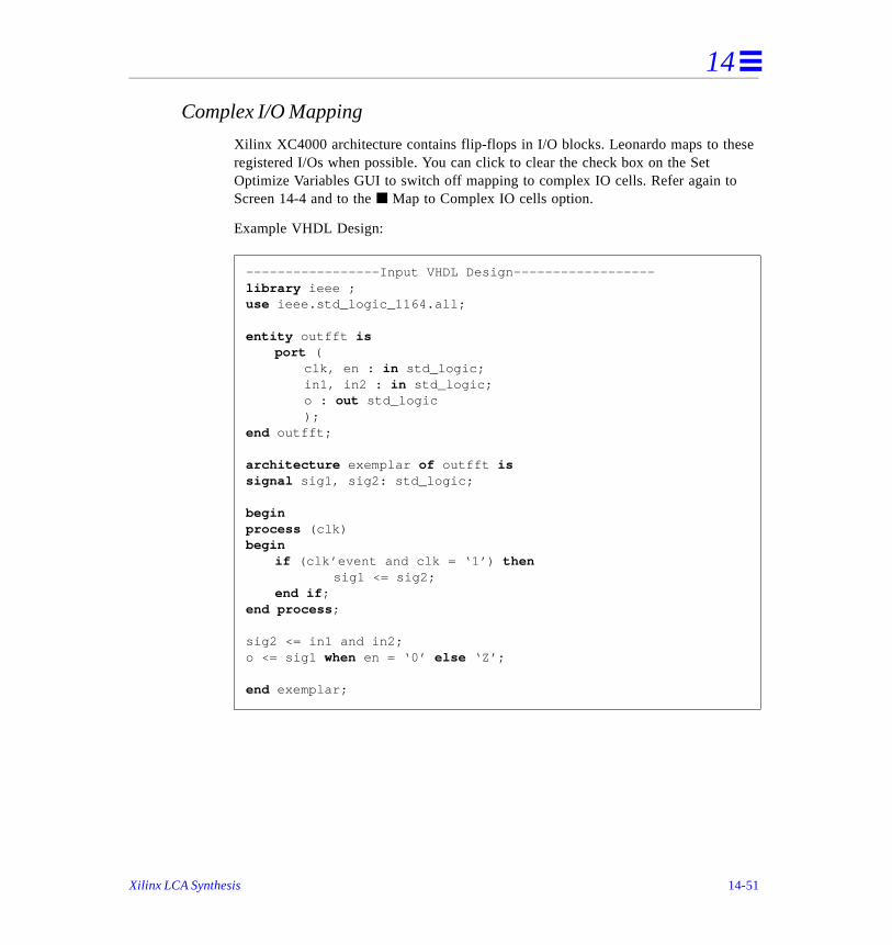
14
se
Complex I/O Mapping
Xilinx XC4000 architecture contains flip-flops in I/O blocks. Leonardo maps to theregistered I/Os when possible. You can click to clear the check box on the Set Optimize Variables GUI to switch off mapping to complex IO cells. Refer again toScreen 14-4 and to the ■ Map to Complex IO cells option.
Example VHDL Design:
-----------------Input VHDL Design------------------library ieee ;use ieee.std_logic_1164.all;
entity outfft isport (
clk, en : in std_logic;in1, in2 : in std_logic;o : out std_logic);
end outfft;
architecture exemplar of outfft issignal sig1, sig2: std_logic;
beginprocess (clk)begin
if (clk’event and clk = ‘1’) thensig1 <= sig2;
end if ;end process ;
sig2 <= in1 and in2;o <= sig1 when en = ‘0’ else ‘Z’;
end exemplar;
Xilinx LCA Synthesis 14-51
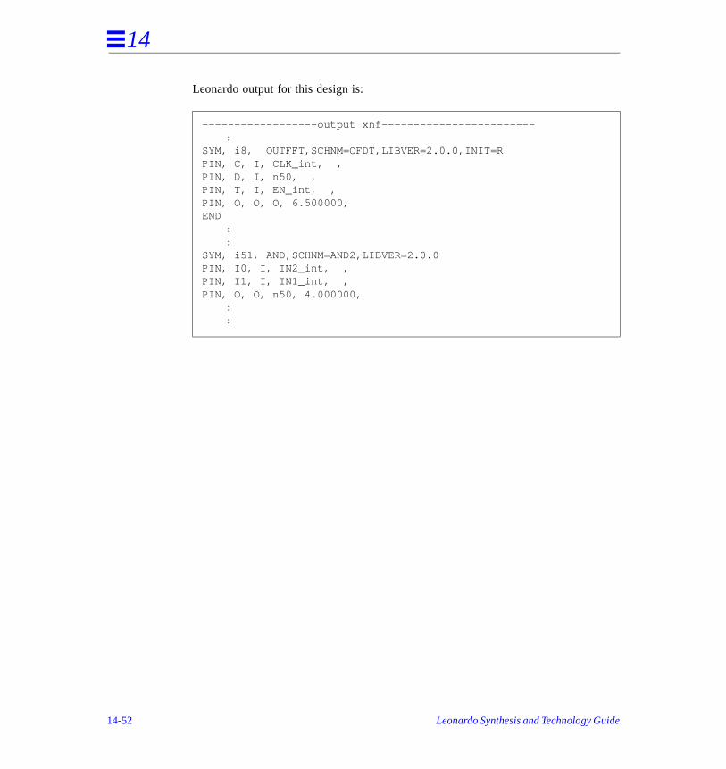
14
Leonardo output for this design is:
------------------output xnf------------------------:
SYM, i8, OUTFFT,SCHNM=OFDT,LIBVER=2.0.0,INIT=RPIN, C, I, CLK_int, ,PIN, D, I, n50, ,PIN, T, I, EN_int, ,PIN, O, O, O, 6.500000,END
::
SYM, i51, AND,SCHNM=AND2,LIBVER=2.0.0PIN, I0, I, IN2_int, ,PIN, I1, I, IN1_int, ,PIN, O, O, n50, 4.000000,
::
14-52 Leonardo Synthesis and Technology Guide
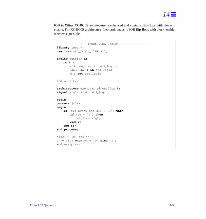
14
-ble
IOB in Xilinx XC4000E architecture is enhanced and contains flip-flops with clockenable. For XC4000E architecture, Leonardo maps to IOB flip-flops with clock-enawhenever possible.
-----------------Input VHDL Design------------------library ieee ;use ieee.std_logic_1164.all;
entity outfftx isport (
clk, en, ce: in std_logic;in1, in2 : in std_logic;o : out std_logic);
end outfftx;
architecture exemplar of outfftx issignal sig1, sig2: std_logic;
beginprocess (clk)begin
if (clk’event and clk = ‘1’) thenif (ce = ‘1’) then
sig1 <= sig2;end if ;
end if ;end process ;
sig2 <= in1 and in2;o <= sig1 when en = ‘0’ else ‘Z’;end exemplar;
Xilinx LCA Synthesis 14-53
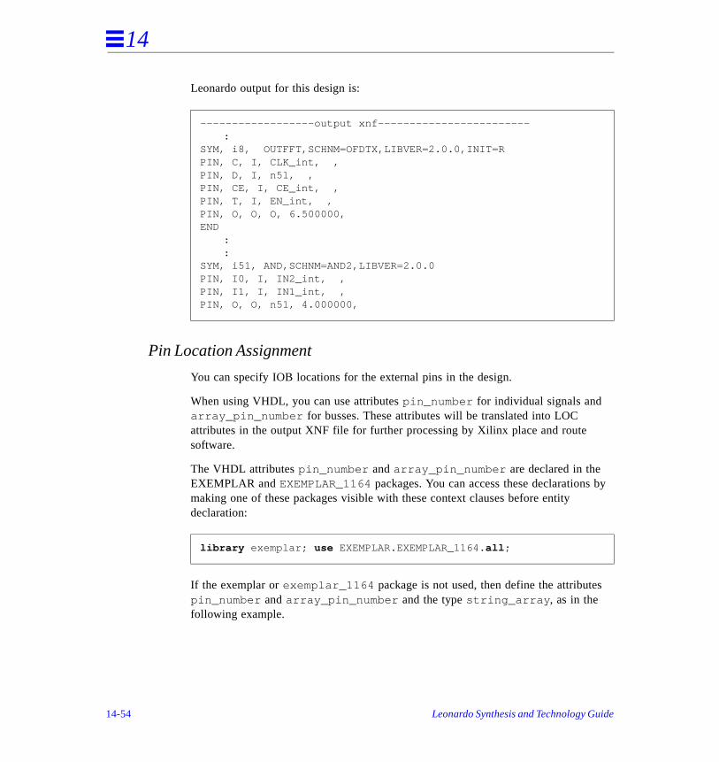
14
by
Leonardo output for this design is:
Pin Location Assignment
You can specify IOB locations for the external pins in the design.
When using VHDL, you can use attributes pin_number for individual signals and array_pin_number for busses. These attributes will be translated into LOC attributes in the output XNF file for further processing by Xilinx place and route software.
The VHDL attributes pin_number and array_pin_number are declared in the EXEMPLAR and EXEMPLAR_1164 packages. You can access these declarations making one of these packages visible with these context clauses before entity declaration:
If the exemplar or exemplar_1164 package is not used, then define the attributespin_number and array_pin_number and the type string_array , as in the following example.
------------------output xnf------------------------:
SYM, i8, OUTFFT,SCHNM=OFDTX,LIBVER=2.0.0,INIT=RPIN, C, I, CLK_int, ,PIN, D, I, n51, ,PIN, CE, I, CE_int, ,PIN, T, I, EN_int, ,PIN, O, O, O, 6.500000,END
::
SYM, i51, AND,SCHNM=AND2,LIBVER=2.0.0PIN, I0, I, IN2_int, ,PIN, I1, I, IN1_int, ,PIN, O, O, n51, 4.000000,
library exemplar; use EXEMPLAR.EXEMPLAR_1164.all ;
14-54 Leonardo Synthesis and Technology Guide
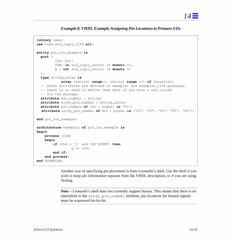
14
you ing
is no
Example 8. VHDL Example Assigning Pin Locations to Primary I/Os
Another way of specifying pin placement is from Leonardo’s shell. Use the shell if wish to keep pin information separate from the VHDL description, or if you are usVerilog.
Note – Leonardo’s shell does not currently support busses. This means that there equivalent to the array_pin_number attribute; pin locations for bussed signals must be expressed bit-by-bit.
library ieee;use ieee.std_logic_1164. all ;
entity pin_loc_example is port ( CLK: bit; DIN: in std_logic_vector (4 downto 3); Q : out std_logic_vector (4 downto 3) ); type string_array is array (natural range <>, natural range <>) of character; -- these attributes are defined in exemplar and exemplar_1164 packages. -- there is no need to define them here if you have a use clause -- for the package. attribute pin_number : string; attribute array_pin_number : string_array; attribute pin_number of clk : signal is “P1"; attribute array_pin_number of din : signal is (“P2", ”P3", “P4", ”P5", "P6");
end pin_loc_example;
architecture exemplar of pin_loc_example isbegin process (CLK) begin if (CLK = ’1’ and CLK’EVENT) then q <= DIN; end if ; end process ;end EXEMPLAR;
Xilinx LCA Synthesis 14-55
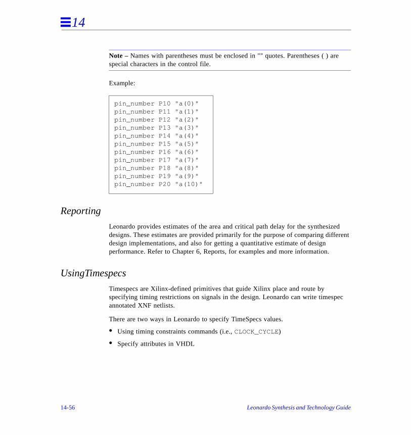
14
re
d rent
c
Note – Names with parentheses must be enclosed in "" quotes. Parentheses ( ) aspecial characters in the control file.
Example:
Reporting
Leonardo provides estimates of the area and critical path delay for the synthesizedesigns. These estimates are provided primarily for the purpose of comparing diffedesign implementations, and also for getting a quantitative estimate of design performance. Refer to Chapter 6, Reports, for examples and more information.
UsingTimespecs
Timespecs are Xilinx-defined primitives that guide Xilinx place and route by specifying timing restrictions on signals in the design. Leonardo can write timespeannotated XNF netlists.
There are two ways in Leonardo to specify TimeSpecs values.
• Using timing constraints commands (i.e., CLOCK_CYCLE)
• Specify attributes in VHDL
pin_number P10 "a(0)" pin_number P11 "a(1)" pin_number P12 "a(2)" pin_number P13 "a(3)" pin_number P14 "a(4)" pin_number P15 "a(5)" pin_number P16 "a(6)" pin_number P17 "a(7)" pin_number P18 "a(8)" pin_number P19 "a(9)" pin_number P20 "a(10)"
14-56 Leonardo Synthesis and Technology Guide
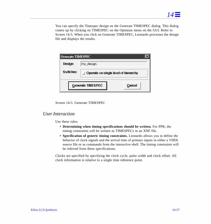
14
ialog
esign
L will
ll
You can specify the Timespec design on the Generate TIMESPEC dialog. This dcomes up by clicking on TIMESPEC on the Optimize menu on the GUI. Refer to Screen 14-5. When you click on Generate TIMESPEC, Leonardo processes the dfile and displays the results.
Screen 14-5. Generate TIMESPEC
User Interaction
Use these rules:
• Determining when timing specifications should be written. For PPR, the timing constraints will be written as TIMESPECs in an XNF file.
• Specification of generic timing constraints. Leonardo allows you to define the behavior of clock signals and the arrival time of primary inputs in either a VHDsource file or as commands from the interactive shell. The timing constraints be inferred from these specifications.
Clocks are specified by specifying the clock cycle, pulse width and clock offset. Aclock information is relative to a single time reference point.
Xilinx LCA Synthesis 14-57
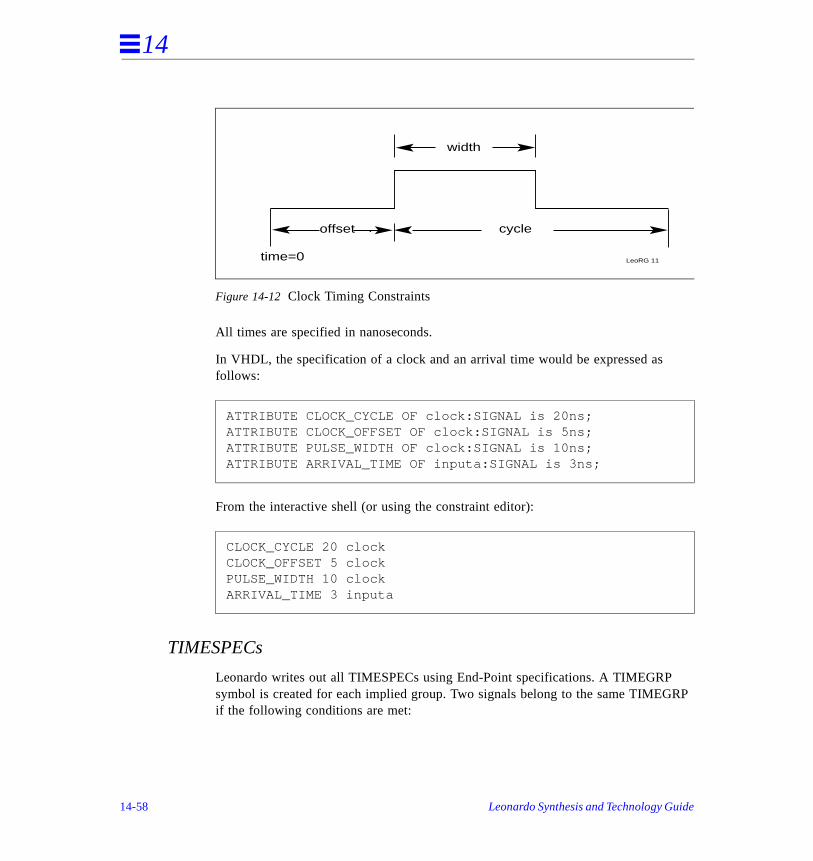
14
RP
Figure 14-12 Clock Timing Constraints
All times are specified in nanoseconds.
In VHDL, the specification of a clock and an arrival time would be expressed as follows:
From the interactive shell (or using the constraint editor):
TIMESPECs
Leonardo writes out all TIMESPECs using End-Point specifications. A TIMEGRP symbol is created for each implied group. Two signals belong to the same TIMEGif the following conditions are met:
ATTRIBUTE CLOCK_CYCLE OF clock:SIGNAL is 20ns;ATTRIBUTE CLOCK_OFFSET OF clock:SIGNAL is 5ns;ATTRIBUTE PULSE_WIDTH OF clock:SIGNAL is 10ns;ATTRIBUTE ARRIVAL_TIME OF inputa:SIGNAL is 3ns;
CLOCK_CYCLE 20 clockCLOCK_OFFSET 5 clockPULSE_WIDTH 10 clockARRIVAL_TIME 3 inputa
LeoRG 11
offset cycle
width
time=0
14-58 Leonardo Synthesis and Technology Guide
14
he p
aths;
nd
to
• (Group 1, a) Both signals are input pins with the same arrival time and are tstart points of a set of paths which are identical to the Xilinx predefined grouPADS; or
• (Group 2, b) Both signals are D inputs of D flip-flops which share a commonCLK and are the endpoints of a set of paths; or
• (Group 2, c) Both signals are output pins and are the endpoints of a set of por
• (Group 1, d) Both signals are Q outputs of D flip-flops with a common CLK aare the start points of a set of paths.
If you specify no arrival times for any inputs in the design, all inputs are assumedarrive at time 0. For each pair of TIMEGRP symbols for which a connecting pathexists, Leonardo writes out a TIMESPEC of the form
If group_2 represents a set of D-inputs clocked by CLK, the value of constraint is determined by the formula:
TSnn=FROM:group1:TO: group_2=constraint
constraint = (CLK.period + CLK.offset - group_d.setup) - group1.arrival
Xilinx LCA Synthesis 14-59
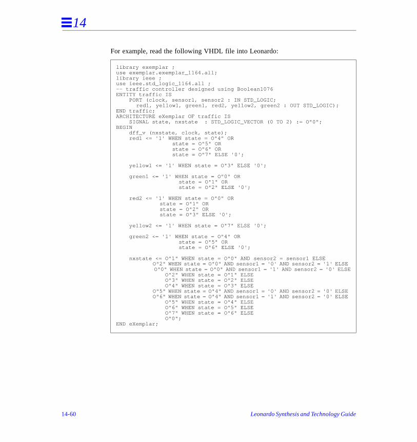
14
For example, read the following VHDL file into Leonardo:
library exemplar ;use exemplar.exemplar_1164.all;library ieee ;use ieee.std_logic_1164.all ;-- traffic controller designed using Boolean1076 ENTITY traffic IS PORT (clock, sensor1, sensor2 : IN STD_LOGIC;
red1, yellow1, green1, red2, yellow2, green2 : OUT STD_LOGIC);END traffic;ARCHITECTURE eXemplar OF traffic IS SIGNAL state, nxstate : STD_LOGIC_VECTOR (0 TO 2) := O"0";BEGIN dff_v (nxstate, clock, state); red1 <= '1' WHEN state = O"4" OR
state = O"5" OR state = O"6" OR state = O"7" ELSE '0';
yellow1 <= '1' WHEN state = O"3" ELSE '0';
green1 <= '1' WHEN state = O"0" OR state = O"1" OR state = O"2" ELSE '0';
red2 <= '1' WHEN state = O"0" OR state = O"1" OR state = O"2" OR state = O"3" ELSE '0';
yellow2 <= '1' WHEN state = O"7" ELSE '0';
green2 <= '1' WHEN state = O"4" OR
state = O"5" OR state = O"6" ELSE '0';
nxstate <= O"1" WHEN state = O"0" AND sensor2 = sensor1 ELSE O"2" WHEN state = O"0" AND sensor1 = '0' AND sensor2 = '1' ELSE O"0" WHEN state = O"0" AND sensor1 = '1' AND sensor2 = '0' ELSE O"2" WHEN state = O"1" ELSE O"3" WHEN state = O"2" ELSE O"4" WHEN state = O"3" ELSE O"5" WHEN state = O"4" AND sensor1 = '0' AND sensor2 = '0' ELSE O"6" WHEN state = O"4" AND sensor1 = '1' AND sensor2 = '0' ELSE O"5" WHEN state = O"4" ELSE O"6" WHEN state = O"5" ELSE O"7" WHEN state = O"6" ELSE O"0";END eXemplar;
14-60 Leonardo Synthesis and Technology Guide
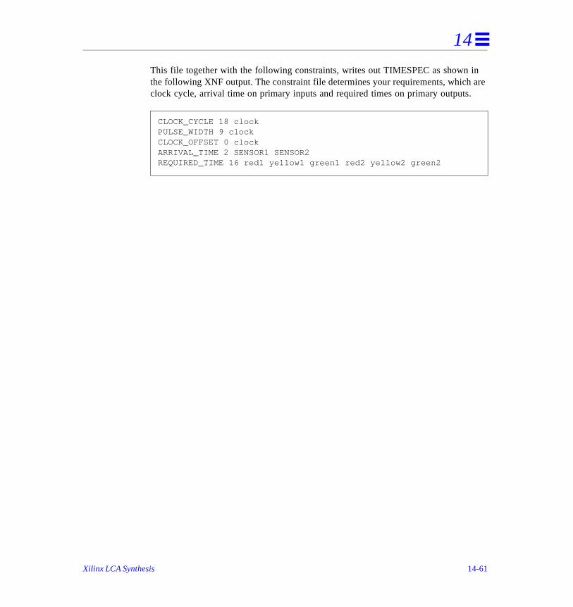
14
n are
This file together with the following constraints, writes out TIMESPEC as shown ithe following XNF output. The constraint file determines your requirements, which clock cycle, arrival time on primary inputs and required times on primary outputs.
CLOCK_CYCLE 18 clockPULSE_WIDTH 9 clockCLOCK_OFFSET 0 clockARRIVAL_TIME 2 SENSOR1 SENSOR2REQUIRED_TIME 16 red1 yellow1 green1 red2 yellow2 green2
Xilinx LCA Synthesis 14-61
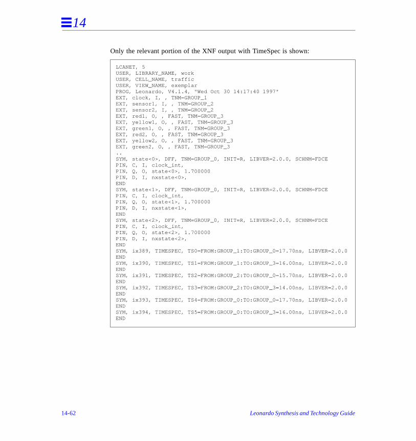
14
Only the relevant portion of the XNF output with TimeSpec is shown:
LCANET, 5USER, LIBRARY_NAME, workUSER, CELL_NAME, trafficUSER, VIEW_NAME, exemplarPROG, Leonardo, V4.1.4, "Wed Oct 30 14:17:40 1997"EXT, clock, I, , TNM=GROUP_1EXT, sensor1, I, , TNM=GROUP_2EXT, sensor2, I, , TNM=GROUP_2EXT, red1, O, , FAST, TNM=GROUP_3EXT, yellow1, O, , FAST, TNM=GROUP_3EXT, green1, O, , FAST, TNM=GROUP_3EXT, red2, O, , FAST, TNM=GROUP_3EXT, yellow2, O, , FAST, TNM=GROUP_3EXT, green2, O, , FAST, TNM=GROUP_3..SYM, state<0>, DFF, TNM=GROUP_0, INIT=R, LIBVER=2.0.0, SCHNM=FDCEPIN, C, I, clock_int,PIN, Q, O, state<0>, 1.700000PIN, D, I, nxstate<0>,ENDSYM, state<1>, DFF, TNM=GROUP_0, INIT=R, LIBVER=2.0.0, SCHNM=FDCEPIN, C, I, clock_int,PIN, Q, O, state<1>, 1.700000PIN, D, I, nxstate<1>,ENDSYM, state<2>, DFF, TNM=GROUP_0, INIT=R, LIBVER=2.0.0, SCHNM=FDCEPIN, C, I, clock_int,PIN, Q, O, state<2>, 1.700000PIN, D, I, nxstate<2>,ENDSYM, ix389, TIMESPEC, TS0=FROM:GROUP_1:TO:GROUP_0=17.70ns, LIBVER=2.0.0ENDSYM, ix390, TIMESPEC, TS1=FROM:GROUP_1:TO:GROUP_3=16.00ns, LIBVER=2.0.0ENDSYM, ix391, TIMESPEC, TS2=FROM:GROUP_2:TO:GROUP_0=15.70ns, LIBVER=2.0.0ENDSYM, ix392, TIMESPEC, TS3=FROM:GROUP_2:TO:GROUP_3=14.00ns, LIBVER=2.0.0ENDSYM, ix393, TIMESPEC, TS4=FROM:GROUP_0:TO:GROUP_0=17.70ns, LIBVER=2.0.0ENDSYM, ix394, TIMESPEC, TS5=FROM:GROUP_0:TO:GROUP_3=16.00ns, LIBVER=2.0.0END
14-62 Leonardo Synthesis and Technology Guide
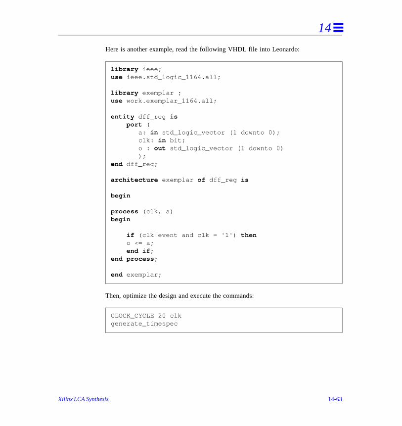
14
Here is another example, read the following VHDL file into Leonardo:
Then, optimize the design and execute the commands:
library ieee;use ieee.std_logic_1164.all;
library exemplar ;use work.exemplar_1164.all;
entity dff_reg is port ( a: in std_logic_vector (1 downto 0); clk: in bit; o : out std_logic_vector (1 downto 0) );end dff_reg;
architecture exemplar of dff_reg is
begin
process (clk, a)begin
if (clk'event and clk = '1') then o <= a; end if ;end process ;
end exemplar;
CLOCK_CYCLE 20 clkgenerate_timespec
Xilinx LCA Synthesis 14-63
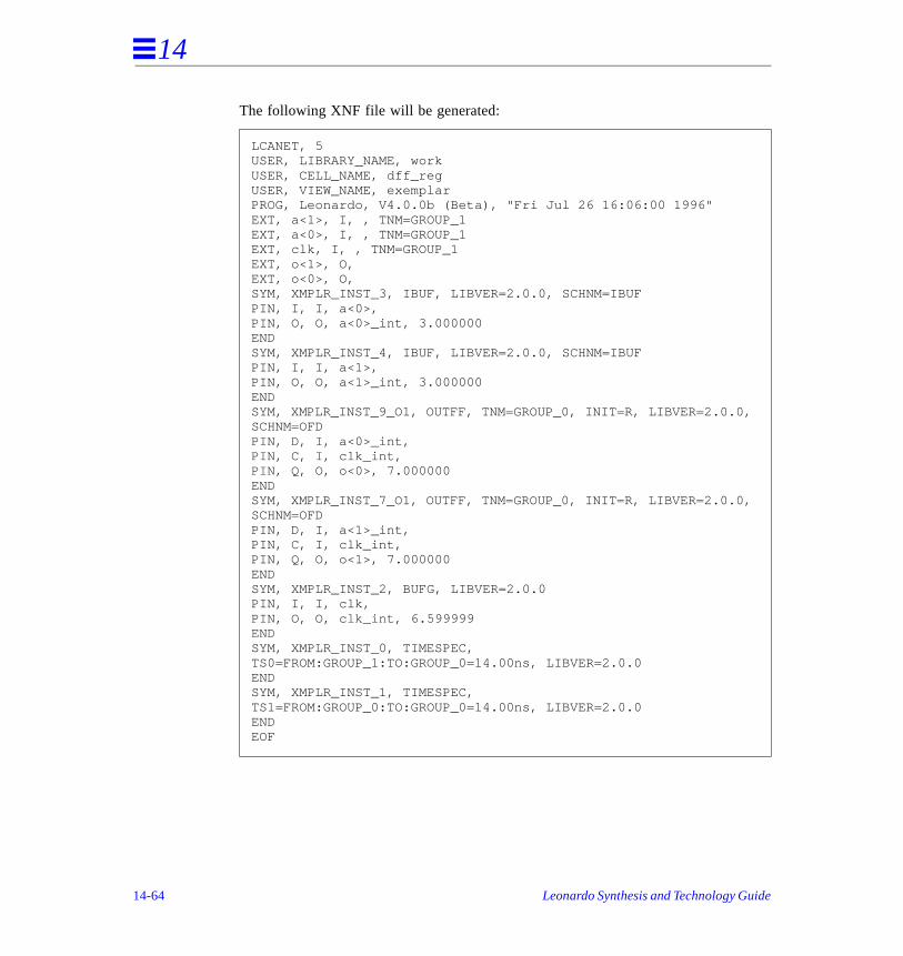
14
The following XNF file will be generated:
LCANET, 5USER, LIBRARY_NAME, workUSER, CELL_NAME, dff_regUSER, VIEW_NAME, exemplarPROG, Leonardo, V4.0.0b (Beta), "Fri Jul 26 16:06:00 1996"EXT, a<1>, I, , TNM=GROUP_1EXT, a<0>, I, , TNM=GROUP_1EXT, clk, I, , TNM=GROUP_1EXT, o<1>, O, EXT, o<0>, O, SYM, XMPLR_INST_3, IBUF, LIBVER=2.0.0, SCHNM=IBUFPIN, I, I, a<0>,PIN, O, O, a<0>_int, 3.000000ENDSYM, XMPLR_INST_4, IBUF, LIBVER=2.0.0, SCHNM=IBUFPIN, I, I, a<1>,PIN, O, O, a<1>_int, 3.000000ENDSYM, XMPLR_INST_9_O1, OUTFF, TNM=GROUP_0, INIT=R, LIBVER=2.0.0, SCHNM=OFDPIN, D, I, a<0>_int,PIN, C, I, clk_int,PIN, Q, O, o<0>, 7.000000ENDSYM, XMPLR_INST_7_O1, OUTFF, TNM=GROUP_0, INIT=R, LIBVER=2.0.0, SCHNM=OFDPIN, D, I, a<1>_int,PIN, C, I, clk_int,PIN, Q, O, o<1>, 7.000000ENDSYM, XMPLR_INST_2, BUFG, LIBVER=2.0.0PIN, I, I, clk,PIN, O, O, clk_int, 6.599999ENDSYM, XMPLR_INST_0, TIMESPEC, TS0=FROM:GROUP_1:TO:GROUP_0=14.00ns, LIBVER=2.0.0ENDSYM, XMPLR_INST_1, TIMESPEC, TS1=FROM:GROUP_0:TO:GROUP_0=14.00ns, LIBVER=2.0.0ENDEOF
14-64 Leonardo Synthesis and Technology Guide

14
and
rom
Using Xilinx Attributes
Xilinx documentation describes various attributes and constraints which can be attached to signals or instances in an XNF netlist to guide implementation by placeroute tools.
These attributes can be attached from VHDL with the use of VHDL attributes, or, fthe Leonardo’s shell.
An example in VHDL, attaching the FAST attribute to an output net RED1:
An example for setting attributes from Leonardo’s shell:
Some examples of attributes of I/O ports at the top level of design:
attribute fast: boolean;attribute fast of red1: SIGNAL is true;
set attribute -port red1 -name fast -value TRUE
LOC MEDFASTBLKNM MEDSLOWHBLKNM NODELAYINTERNAL RESFAST CAPSLOW FREQPERIOD THITLO
Xilinx LCA Synthesis 14-65
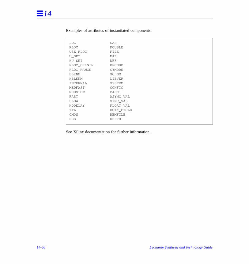
14
Examples of attributes of instantiated components:
See Xilinx documentation for further information.
LOC CAPRLOC DOUBLEUSE_RLOC FILEU_SET MAPHU_SET DEFRLOC_ORIGIN DECODERLOC_RANGE CYMODEBLKNM SCHNMHBLKNM LIBVERINTERNAL SYSTEMMEDFAST CONFIGMEDSLOW BASEFAST ASYNC_VALSLOW SYNC_VALNODELAY FLOAT_VALTTL DUTY_CYCLECMOS MEMFILERES DEPTH
14-66 Leonardo Synthesis and Technology Guide
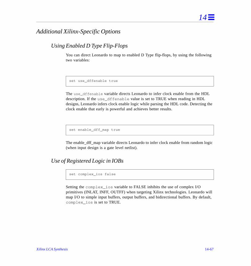
14
ng
the
ogic
ll lt,
Additional Xilinx-Specific Options
Using Enabled D Type Flip-Flops
You can direct Leonardo to map to enabled D Type flip-flops, by using the followitwo variables:
The use_dffenable variable directs Leonardo to infer clock enable from the HDLdescription. If the use_dffenable value is set to TRUE when reading in HDL designs, Leonardo infers clock enable logic while parsing the HDL code. Detectingclock enable that early is powerful and achieves better results.
The enable_dff_map variable directs Leonardo to infer clock enable from random l(when input design is a gate level netlist).
Use of Registered Logic in IOBs
Setting the complex_ios variable to FALSE inhibits the use of complex I/O primitives (INLAT, INFF, OUTFF) when targeting Xilinx technologies. Leonardo wimap I/O to simple input buffers, output buffers, and bidirectional buffers. By defaucomplex_ios is set to TRUE.
set use_dffenable true
set enable_dff_map true
set complex_ios false
Xilinx LCA Synthesis 14-67
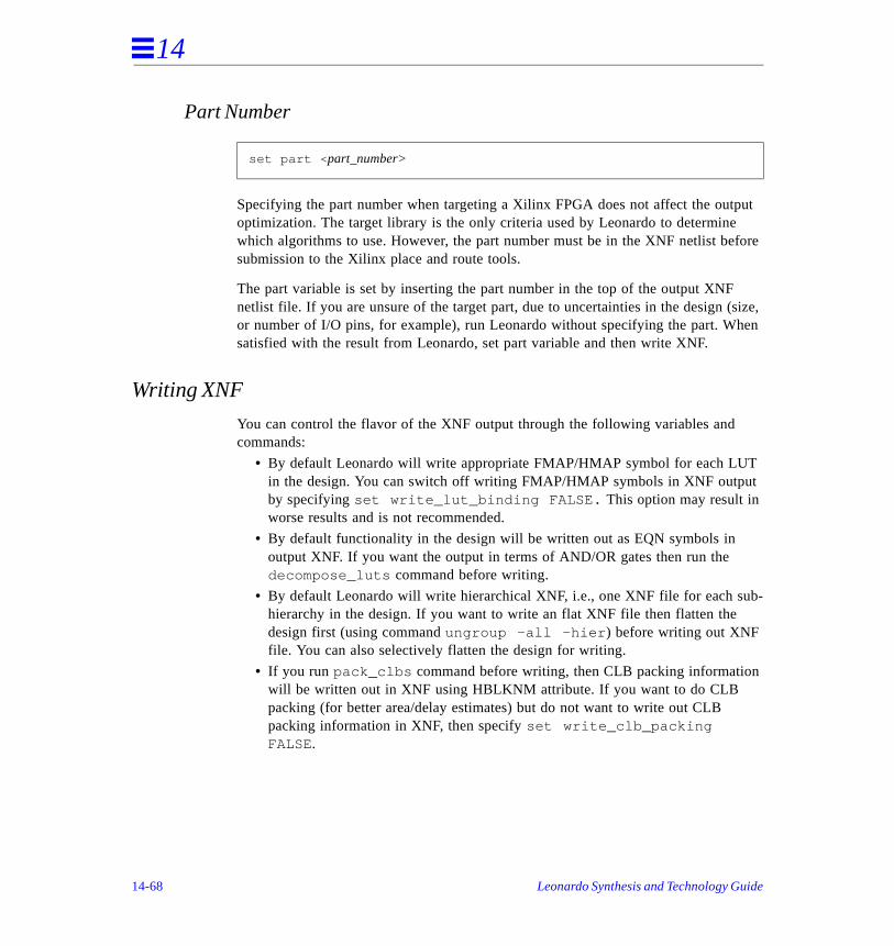
14
ut fore
size, en
t
b-
Part Number
Specifying the part number when targeting a Xilinx FPGA does not affect the outpoptimization. The target library is the only criteria used by Leonardo to determinewhich algorithms to use. However, the part number must be in the XNF netlist besubmission to the Xilinx place and route tools.
The part variable is set by inserting the part number in the top of the output XNFnetlist file. If you are unsure of the target part, due to uncertainties in the design (or number of I/O pins, for example), run Leonardo without specifying the part. Whsatisfied with the result from Leonardo, set part variable and then write XNF.
Writing XNF
You can control the flavor of the XNF output through the following variables and commands:
• By default Leonardo will write appropriate FMAP/HMAP symbol for each LUTin the design. You can switch off writing FMAP/HMAP symbols in XNF outpuby specifying set write_lut_binding FALSE. This option may result in worse results and is not recommended.
• By default functionality in the design will be written out as EQN symbols in output XNF. If you want the output in terms of AND/OR gates then run the decompose_luts command before writing.
• By default Leonardo will write hierarchical XNF, i.e., one XNF file for each suhierarchy in the design. If you want to write an flat XNF file then flatten the design first (using command ungroup -all -hier ) before writing out XNF file. You can also selectively flatten the design for writing.
• If you run pack_clbs command before writing, then CLB packing informationwill be written out in XNF using HBLKNM attribute. If you want to do CLB packing (for better area/delay estimates) but do not want to write out CLB packing information in XNF, then specify set write_clb_packing FALSE.
set part < part_number>
14-68 Leonardo Synthesis and Technology Guide
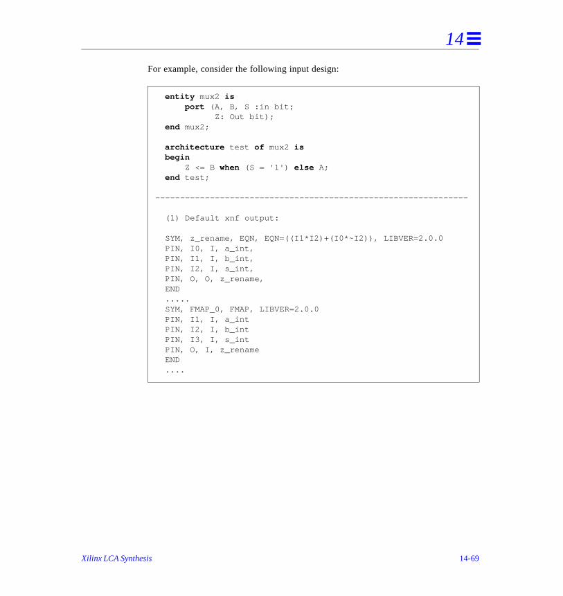
14
For example, consider the following input design:
entity mux2 is port (A, B, S :in bit; Z: Out bit); end mux2;
architecture test of mux2 is begin Z <= B when (S = '1') else A; end test;
---------------------------------------------------------------
(1) Default xnf output:
SYM, z_rename, EQN, EQN=((I1*I2)+(I0*~I2)), LIBVER=2.0.0 PIN, I0, I, a_int, PIN, I1, I, b_int, PIN, I2, I, s_int, PIN, O, O, z_rename, END ..... SYM, FMAP_0, FMAP, LIBVER=2.0.0 PIN, I1, I, a_int PIN, I2, I, b_int PIN, I3, I, s_int PIN, O, I, z_rename END ....
Xilinx LCA Synthesis 14-69
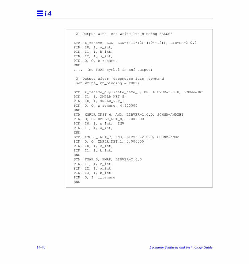
14
(2) Output with 'set write_lut_binding FALSE' SYM, z_rename, EQN, EQN=((I1*I2)+(I0*~I2)), LIBVER=2.0.0 PIN, I0, I, a_int, PIN, I1, I, b_int, PIN, I2, I, s_int, PIN, O, O, z_rename, END .... (no FMAP symbol in xnf output)
(3) Output after 'decompose_luts' command (set write_lut_binding = TRUE). SYM, z_rename_duplicate_name_0, OR, LIBVER=2.0.0, SCHNM=OR2 PIN, I1, I, XMPLR_NET_8, PIN, I0, I, XMPLR_NET_1, PIN, O, O, z_rename, 4.500000 END SYM, XMPLR_INST_6, AND, LIBVER=2.0.0, SCHNM=AND2B1 PIN, O, O, XMPLR_NET_8, 0.000000 PIN, I0, I, s_int,, INV PIN, I1, I, a_int, END SYM, XMPLR_INST_7, AND, LIBVER=2.0.0, SCHNM=AND2 PIN, O, O, XMPLR_NET_1, 0.000000 PIN, I0, I, s_int, PIN, I1, I, b_int, END SYM, FMAP_0, FMAP, LIBVER=2.0.0 PIN, I1, I, s_int PIN, I2, I, a_int PIN, I3, I, b_int PIN, O, I, z_rename END
14-70 Leonardo Synthesis and Technology Guide
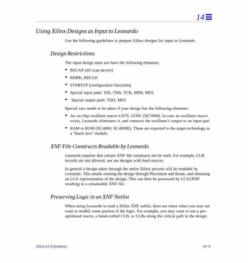
14
o pad.
y as
ining
not e-n.
Using Xilinx Designs as Input to Leonardo
Use the following guidelines to prepare Xilinx designs for input to Leonardo.
Design Restrictions
The input design must not have the following elements:
• BSCAN (IO scan device)
• RDBK, RDCLK
• STARTUP (configuration functions)
• Special input pads: TDI, TMS, TCK, MD0, MD2
• Special output pads: TDO, MD1
Special care needs to be taken if your design has the following elements:
• An on-chip oscillator macro GXTL GOSC (XC3000). In case an oscillator macrexists, Leonardo eliminates it, and connects the oscillator’s output to an input
• RAM or ROM (XC4000, XC4000E). These are exported to the target technologa “black box” module.
XNF File Constructs Readable by Leonardo
Leonardo requires that certain XNF file constructs not be used. For example, CLBrecords are not allowed, nor are designs with hard macros.
In general a design taken through the entire Xilinx process will be readable by Leonardo. This entails running the design through Placement and Route, and obtaan LCA representation of the design. This can then be processed by LCA2XNF resulting in a simulatable XNF file.
Preserving Logic in an XNF Netlist
When using Leonardo to read a Xilinx XNF netlist, there are times when you maywant to modify some portion of the logic. For example, you may want to use a proptimized macro, a hand-crafted CLB, or CLBs along the critical path in the desig
Xilinx LCA Synthesis 14-71
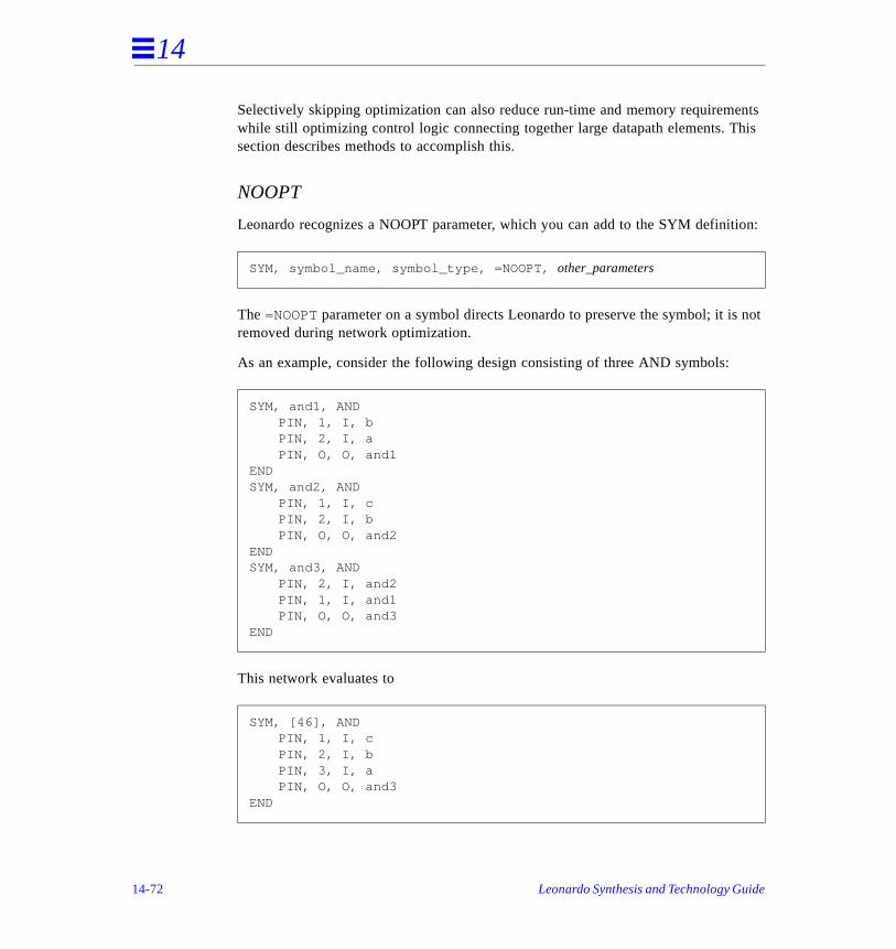
14
ents his
ion:
not
Selectively skipping optimization can also reduce run-time and memory requiremwhile still optimizing control logic connecting together large datapath elements. Tsection describes methods to accomplish this.
NOOPT
Leonardo recognizes a NOOPT parameter, which you can add to the SYM definit
The =NOOPT parameter on a symbol directs Leonardo to preserve the symbol; it isremoved during network optimization.
As an example, consider the following design consisting of three AND symbols:
This network evaluates to
SYM, symbol_name, symbol_type, =NOOPT, other_parameters
SYM, and1, ANDPIN, 1, I, bPIN, 2, I, a PIN, O, O, and1
ENDSYM, and2, AND
PIN, 1, I, cPIN, 2, I, bPIN, O, O, and2
ENDSYM, and3, AND
PIN, 2, I, and2PIN, 1, I, and1PIN, O, O, and3
END
SYM, [46], ANDPIN, 1, I, cPIN, 2, I, bPIN, 3, I, aPIN, O, O, and3
END
14-72 Leonardo Synthesis and Technology Guide

14
r
non-
If there is an annotated symbol and2 with the parameter NOOPT,
then the network evaluates to
Global Set/Reset/Tristate
XNF netlists, after placement and routing, will have primitives with explicit pins foGlobal Set/Reset (GSR) and Global Tristate (GTS). The xlx_preserve_gsr and xlx_preserve_gts variables used to preserve global signals when targeting a Xilinx technology. The variables are ignored when targeting a Xilinx technology.
SYM, and2, AND, =NOOPT PIN, 1, I, c PIN, 2, I, b PIN, O, O, and2END
SYM, [59], AND PIN, 1, I, and2 PIN, 2, I, b PIN, 3, I, a PIN, O, O, and3ENDSYM, and2, AND, =NOOPT PIN, 1, I, c PIN, 2, I, b PIN, O, O, and2END
set xlx_preserve_gsr (default is FALSE)set xlx_preserve_gts (default is FALSE)
Xilinx LCA Synthesis 14-73
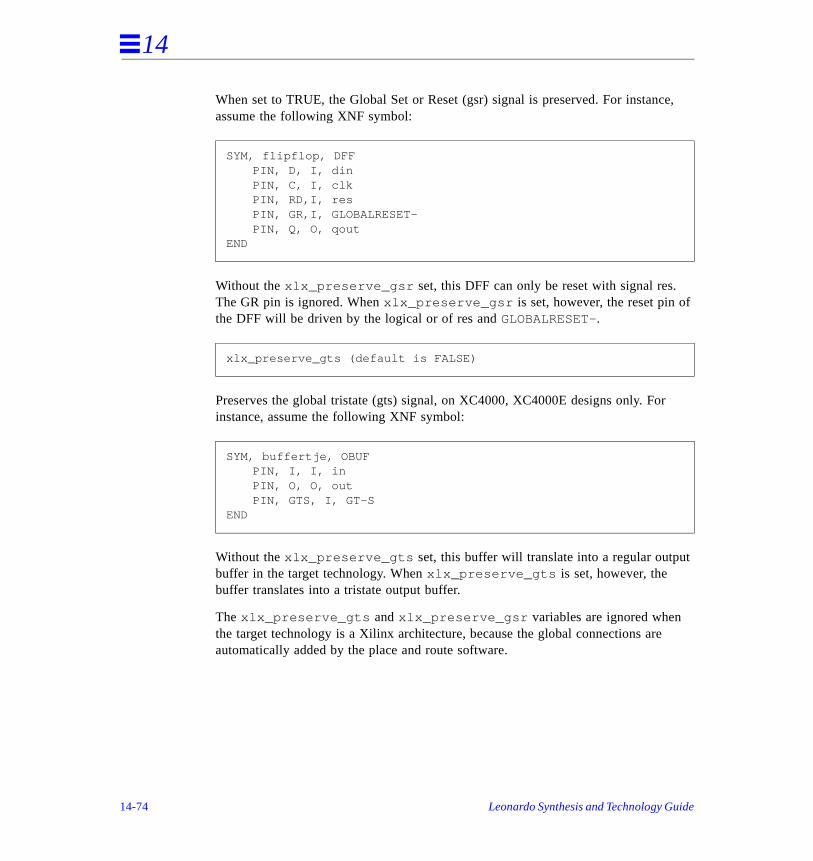
14
e,
t
When set to TRUE, the Global Set or Reset (gsr) signal is preserved. For instancassume the following XNF symbol:
Without the xlx_preserve_gsr set, this DFF can only be reset with signal res. The GR pin is ignored. When xlx_preserve_gsr is set, however, the reset pin ofthe DFF will be driven by the logical or of res and GLOBALRESET-.
Preserves the global tristate (gts) signal, on XC4000, XC4000E designs only. Forinstance, assume the following XNF symbol:
Without the xlx_preserve_gts set, this buffer will translate into a regular outpubuffer in the target technology. When xlx_preserve_gts is set, however, the buffer translates into a tristate output buffer.
The xlx_preserve_gts and xlx_preserve_gsr variables are ignored when the target technology is a Xilinx architecture, because the global connections areautomatically added by the place and route software.
SYM, flipflop, DFF PIN, D, I, din PIN, C, I, clk PIN, RD,I, res PIN, GR,I, GLOBALRESET- PIN, Q, O, qout
END
xlx_preserve_gts (default is FALSE)
SYM, buffertje, OBUF PIN, I, I, in PIN, O, O, out PIN, GTS, I, GT-S
END
14-74 Leonardo Synthesis and Technology Guide
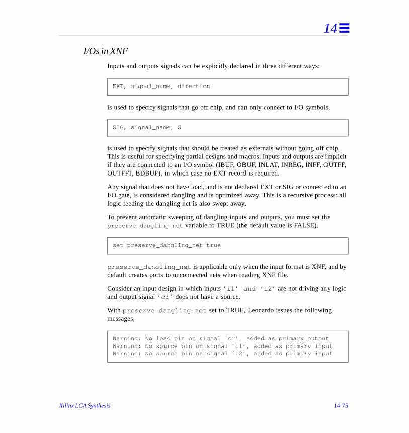
14
ip. plicit F,
to an s: all
y
I/Os in XNF
Inputs and outputs signals can be explicitly declared in three different ways:
is used to specify signals that go off chip, and can only connect to I/O symbols.
is used to specify signals that should be treated as externals without going off chThis is useful for specifying partial designs and macros. Inputs and outputs are imif they are connected to an I/O symbol (IBUF, OBUF, INLAT, INREG, INFF, OUTFOUTFFT, BDBUF), in which case no EXT record is required.
Any signal that does not have load, and is not declared EXT or SIG or connected I/O gate, is considered dangling and is optimized away. This is a recursive proceslogic feeding the dangling net is also swept away.
To prevent automatic sweeping of dangling inputs and outputs, you must set the preserve_dangling_net variable to TRUE (the default value is FALSE).
preserve_dangling_net is applicable only when the input format is XNF, and bdefault creates ports to unconnected nets when reading XNF file.
Consider an input design in which inputs ’i1’ and ’i2’ are not driving any logic and output signal ’or’ does not have a source.
With preserve_dangling_net set to TRUE, Leonardo issues the following messages,
EXT, signal_name, direction
SIG, signal_name, S
set preserve_dangling_net true
Warning: No load pin on signal ’or’, added as primary output Warning: No source pin on signal ’i1’, added as primary input Warning: No source pin on signal ’i2’, added as primary input
Xilinx LCA Synthesis 14-75
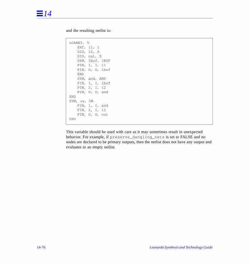
14
ut and
and the resulting netlist is:
This variable should be used with care as it may sometimes result in unexpectedbehavior. For example, if preserve_dangling_nets is set to FALSE and no nodes are declared to be primary outputs, then the netlist does not have any outpevaluates to an empty netlist.
LCANET, 5EXT, i1, I SIG, i2, SSIG, out, SSYM, ibuf, IBUFPIN, I, I, i1PIN, O, O, ibufENDSYM, and, ANDPIN, 1, I, ibuf PIN, 2, I, i2PIN, O, O, and
ENDSYM, or, OR
PIN, 1, I, andPIN, 2, I, i2PIN, O, O, out
END
14-76 Leonardo Synthesis and Technology Guide
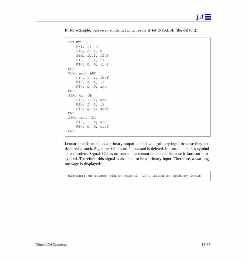
14
ol
nto ning
If, for example, preserve_dangling_nets is set to FALSE (the default):
Leonardo adds out1 as a primary output and i1 as a primary input because they aredeclared as such. Signal out2 has no fanout and is deleted. In turn, this makes symbinv obsolete. Signal i2 has no source but cannot be deleted because it fans out isymbol. Therefore, this signal is assumed to be a primary input. Therefore, a warmessage is displayed:
LCANET, 5EXT, i1, ISIG, out1, SSYM, ibuf, IBUFPIN, I, I, i1PIN, O, O, ibuf
END SYM, and, AND
PIN, 1, I, ibuf PIN, 2, I, i2PIN, O, O, and
ENDSYM, or, OR
PIN, 1, I, andPIN, 2, I, i2 PIN, O, O, out1
ENDSYM, inv, INV
PIN, I, I, andPIN, O, O, out2
END
Warning: No source pin on signal ’i2’, added as primary input
Xilinx LCA Synthesis 14-77
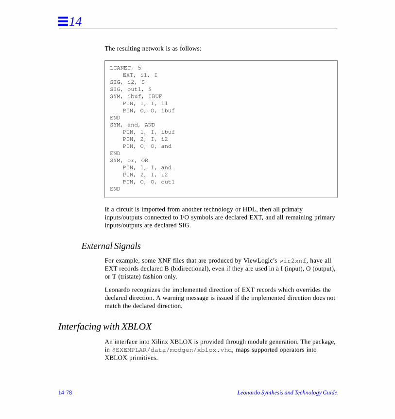
14
ary
ut),
he s not
e,
The resulting network is as follows:
If a circuit is imported from another technology or HDL, then all primary inputs/outputs connected to I/O symbols are declared EXT, and all remaining priminputs/outputs are declared SIG.
External Signals
For example, some XNF files that are produced by ViewLogic’s wir2xnf , have all EXT records declared B (bidirectional), even if they are used in a I (input), O (outpor T (tristate) fashion only.
Leonardo recognizes the implemented direction of EXT records which overrides tdeclared direction. A warning message is issued if the implemented direction doematch the declared direction.
Interfacing with XBLOX
An interface into Xilinx XBLOX is provided through module generation. The packagin $EXEMPLAR/data/modgen/xblox.vhd , maps supported operators into XBLOX primitives.
LCANET, 5EXT, i1, I
SIG, i2, SSIG, out1, SSYM, ibuf, IBUF
PIN, I, I, i1PIN, O, O, ibuf
ENDSYM, and, AND
PIN, 1, I, ibuf PIN, 2, I, i2PIN, O, O, and
ENDSYM, or, OR
PIN, 1, I, andPIN, 2, I, i2PIN, O, O, out1
END
14-78 Leonardo Synthesis and Technology Guide
14
r so
. e t to
To use XBLOX primitives for arithmetic and relational operators in a VHDL file, specify load-modgen xblox3 or xblox4 or enable XBLOX as the module generatolibrary in the Graphical User Interface. Specify the source technology to be xi4hmLeonardo can find and preserve the special macros that are needed for a correctXBLOX netlist.
The output format is XNF. The XNF file is used as input to the XBLOX program, which produces an expanded XNF file (.XG file), and hard macro files (.HM files)(Most XBLOX modules generate only an .XG file. Some implementations may us.HM files.) .XG and .HM files are subsequently used in the PPR program for inpupartitioning, placement and routing.
Note: XBLOX3 and XBLOX4: reduction operators now use XBLOX components.
New Xilinx Architecture Features
These features include:
• Modgen Enhancements
• Fast I/O Buffers
• Quality of Area and Delay Results
• Fast Xilinx Outputs
• M1 Back Annotation Flow
• M1 Support
• Implementing Boundary Scan for Xilinx 4000 FPGAs
Modgen Enhancements
Non-Square Multipliers
Non-square multipliers were implemented for the following technologies:
XC4000/E/L/EX/XL/XV and XC5200
Xilinx Libraries
Support for Xilinx M1 release
Xilinx LCA Synthesis 14-79
14
.
eeds
e
ogic
RAMs
All RAMs: support for arbitrary size RAMs.
XBLOX3/XBLOX4
Reduction operators now use XBLOX components.
New Modgen Libraries
• XI4E: XC4000E/EX modgen library is adding support for synchronous RAMs
Existing Modgen Library Improvement
• XI5: counter area and delay improvements.
• XI3: reductions in area and delay for adders and subtractors.
New Components for Modgen Libraries
• XI4/XI4E: pre-setable, non-loadable up counters
• XI4E: RAMs
• XI5: up/down counters
Fast I/O Buffers
Leonardo sets xi4 and xi5 slew rate to Fast for all input and output buffers. This spup the design.
Quality of Area and Delay Results
Area and Delay
Quality of results were improved by 10%-20% for Altera FLEX area and delay. Thmost significant improvements are for targeting Xilinx LUT technologies. The improvements are due to the following features:
• Clock Enable detection was improved to detect more complex clock enable l
• Multipliers are implemented more efficiently
14-80 Leonardo Synthesis and Technology Guide
14
to
to
DL
• Improvements in LUT based Optimization algorithms
• Improvements in the method Leonardo uses to represent and optimize wide functions, like ROMs.
You can expect significant improvements for both area and delay on designs thatcontain multipliers, clock enable logic, and ROMs.
Fast Xilinx Outputs
The following Xilinx Technologies are able to use this feature:
• XC4000/A/E/EX/XL
• XC5200
Leonardo can set slew rate on output buffers to FAST. This directs Xilinx softwareuse output buffers with a fast slew rate and with faster output propagation delay.
Description
Xilinx outputs are set to FAST by default. You can disable this option by clicking clear the check box for ■ Use FAST Output Buffers. Refer to Screen 14-6.
You can also override the default setting. Your directive can be an input design H(Verilog or VHDL) or in the Constraint File Editor to set slew rate attributes on individual outputs. These attributes can have one of the following values: FAST, MEDFAST, MEDSLOW, SLOW.
Xilinx LCA Synthesis 14-81
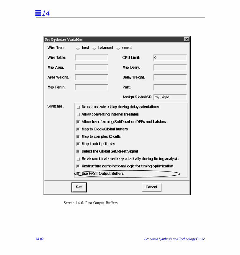
14
Screen 14-6. Fast Output Buffers
14-82 Leonardo Synthesis and Technology Guide
14
kes
.
e
1. ical
le.
th
The h
ble
M1 Back Annotation Flow
1. You can generate XNF netlist or EDIF netlist on an output from Leonardo and tait to M1 software.
2. After place and route, M1 software generates VHDL netlist and SDF timing fileThe VHDL netlist is simulatable.
3. To read in the VHDL file generated by M1 into Time Module, copy the simprim_VCOMPONENTS.vhd package into your current working directory. Thsimprim_VCOMPONENTS.vhd package is shipped by Xilinx.
4. Time Module back annotates the timing data from the SDF file generated by MYou can run timing analysis, review the critical paths report, and look at the critpaths in the schematic viewer.
5. If desired, you can generate a new VHDL netlist and SDF file from Time ModuYou have to manually add a usage clause for the simprim library (simprim_VCOMPONENTS.vhd) in the VHDL file. The VHDL and SDF files canbe read into Model Technology simulator for functional verification.
Note: You must purchase a Time Module license to use back annotation flows wiLeonardo. Back annotation is supported through VITAL libraries for the following Xilinx families: XC4000/E/EX/XL (through M1 software only), and XC5200.
SDF (Standard Delay Format) Writer
An SDF writer for pre place-and-route delays has been added. The SDF writer calculates delays as used by the timing analyzer and timing optimization routines.SDF writer writes this information in an SDF format. The SDF format together witthe flat VHDL netlist can be read into MTI V-System or any RTL simulator for preplace-and-route timing simulation.
The SDF writer is controlled by the sdf_write_flat_netlist Tcl variable. Set this variato TRUE. An example set of Leonardo commands may be:
set sdf_write_flat_netlist TRUE
ungroup -all /*need to flatten the netlist*/
write design.vhd /*write out flat VHDL or Verilog*/
write design.sdf /*write out SDF*/
Xilinx LCA Synthesis 14-83
14
es
L
g
M1 Support
M1 flow is supported through both EDIF and XNF formats. In EDIF, Leonardo writout Unified library cells, while in XNF it writes out XNF primitives.
EDIF flow includes:
• writing out FMAPs/HMAPs
• writing CLB information
• writing Timespecs
XNF flow is similar to XACT. In addition, Leonardo supports functional verificationand timing back-annotation using SimPrims.
Accurate Delay Estimations
Wire load models are added for the following Xilinx technologies: XC4000/E/EX/Xand XC5200. These models allow Leonardo to accurately predict routing delays. Leonardo's estimates are within 5%-10% of xdelay estimates.
Sophisticated CLB packing
CLB packing is added for XC4000E, XC4000EX technologies. By default, CLB packing is used for area and delay estimation only. If you want to write CLB information in the output EDIF or XNF netlists, set the variable write_clb_packing to TRUE.
Lookup Table
Functionality of lookup table is written in terms of EQN. For example:
.
.(instance ix372 (viewRef NETLIST (cellRef EQN (libraryRef xi4e )))
(property EQN (string "((~I0*~I11)+(~I0*~I2))""))
.This makes EDIF netlists generated by Leonardo much smaller and M1 processintime is faster.
set write_clb_packing true
14-84 Leonardo Synthesis and Technology Guide
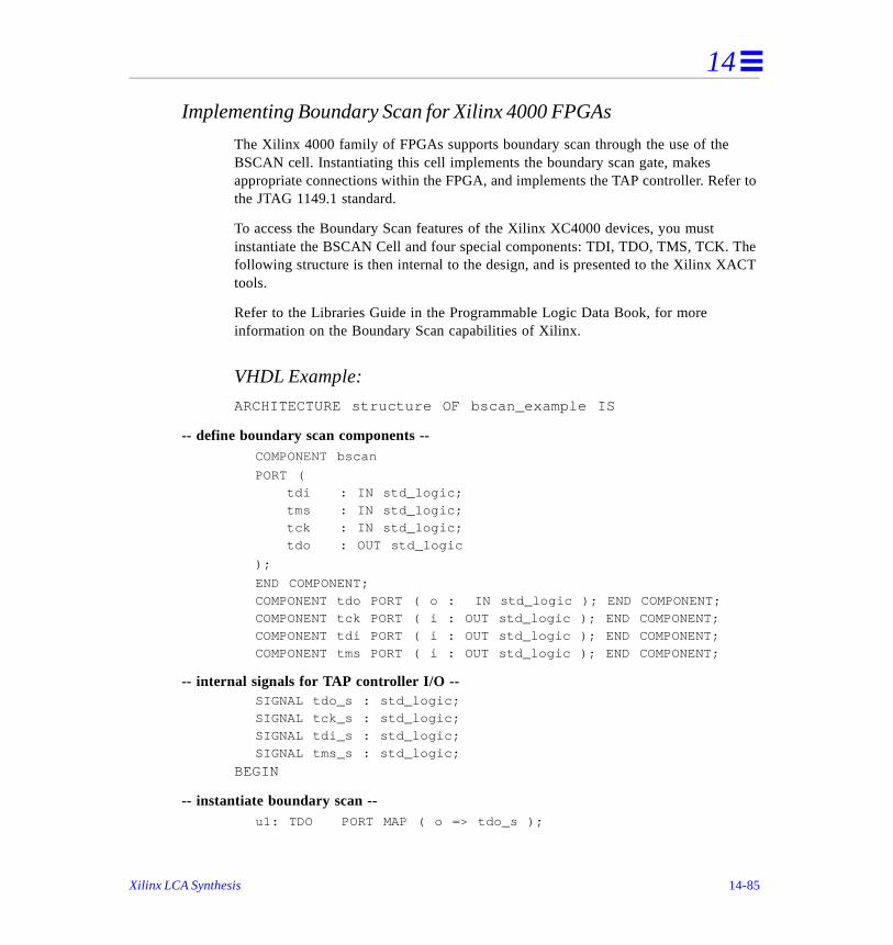
14
r to
he CT
Implementing Boundary Scan for Xilinx 4000 FPGAs
The Xilinx 4000 family of FPGAs supports boundary scan through the use of the BSCAN cell. Instantiating this cell implements the boundary scan gate, makes appropriate connections within the FPGA, and implements the TAP controller. Refethe JTAG 1149.1 standard.
To access the Boundary Scan features of the Xilinx XC4000 devices, you must instantiate the BSCAN Cell and four special components: TDI, TDO, TMS, TCK. Tfollowing structure is then internal to the design, and is presented to the Xilinx XAtools.
Refer to the Libraries Guide in the Programmable Logic Data Book, for more information on the Boundary Scan capabilities of Xilinx.
VHDL Example:
ARCHITECTURE structure OF bscan_example IS
-- define boundary scan components --COMPONENT bscan
PORT (
tdi : IN std_logic;
tms : IN std_logic;
tck : IN std_logic;
tdo : OUT std_logic
);
END COMPONENT;
COMPONENT tdo PORT ( o : IN std_logic ); END COMPONENT;
COMPONENT tck PORT ( i : OUT std_logic ); END COMPONENT;
COMPONENT tdi PORT ( i : OUT std_logic ); END COMPONENT;
COMPONENT tms PORT ( i : OUT std_logic ); END COMPONENT;
-- internal signals for TAP controller I/O --SIGNAL tdo_s : std_logic;
SIGNAL tck_s : std_logic;
SIGNAL tdi_s : std_logic;
SIGNAL tms_s : std_logic;
BEGIN
-- instantiate boundary scan --u1: TDO PORT MAP ( o => tdo_s );
Xilinx LCA Synthesis 14-85
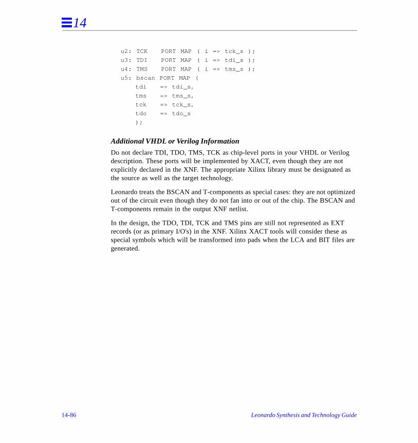
14
s
mized and
are
u2: TCK PORT MAP ( i => tck_s );
u3: TDI PORT MAP ( i => tdi_s );
u4: TMS PORT MAP ( i => tms_s );
u5: bscan PORT MAP (
tdi => tdi_s,
tms => tms_s,
tck => tck_s,
tdo => tdo_s
);
Additional VHDL or Verilog Information
Do not declare TDI, TDO, TMS, TCK as chip-level ports in your VHDL or Verilog description. These ports will be implemented by XACT, even though they are notexplicitly declared in the XNF. The appropriate Xilinx library must be designated athe source as well as the target technology.
Leonardo treats the BSCAN and T-components as special cases: they are not optiout of the circuit even though they do not fan into or out of the chip. The BSCAN T-components remain in the output XNF netlist.
In the design, the TDO, TDI, TCK and TMS pins are still not represented as EXTrecords (or as primary I/O's) in the XNF. Xilinx XACT tools will consider these as special symbols which will be transformed into pads when the LCA and BIT files generated.
14-86 Leonardo Synthesis and Technology Guide
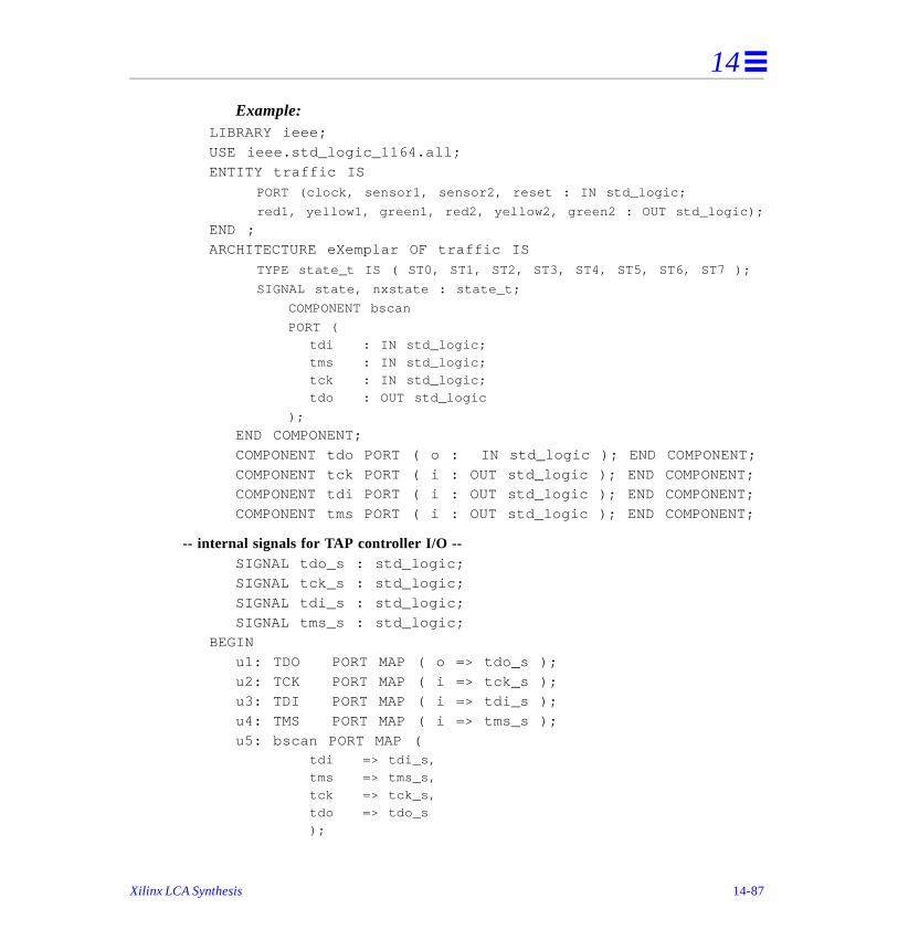
14
Example:LIBRARY ieee;
USE ieee.std_logic_1164.all;
ENTITY traffic IS
PORT (clock, sensor1, sensor2, reset : IN std_logic;
red1, yellow1, green1, red2, yellow2, green2 : OUT std_logic);
END ;
ARCHITECTURE eXemplar OF traffic IS
TYPE state_t IS ( ST0, ST1, ST2, ST3, ST4, ST5, ST6, ST7 );
SIGNAL state, nxstate : state_t;
COMPONENT bscan
PORT (
tdi : IN std_logic;
tms : IN std_logic;
tck : IN std_logic;
tdo : OUT std_logic
);
END COMPONENT;
COMPONENT tdo PORT ( o : IN std_logic ); END COMPONENT;
COMPONENT tck PORT ( i : OUT std_logic ); END COMPONENT;
COMPONENT tdi PORT ( i : OUT std_logic ); END COMPONENT;
COMPONENT tms PORT ( i : OUT std_logic ); END COMPONENT;
-- internal signals for TAP controller I/O --SIGNAL tdo_s : std_logic;
SIGNAL tck_s : std_logic;
SIGNAL tdi_s : std_logic;
SIGNAL tms_s : std_logic;
BEGIN
u1: TDO PORT MAP ( o => tdo_s );
u2: TCK PORT MAP ( i => tck_s );
u3: TDI PORT MAP ( i => tdi_s );
u4: TMS PORT MAP ( i => tms_s );
u5: bscan PORT MAP (tdi => tdi_s,
tms => tms_s,
tck => tck_s,
tdo => tdo_s
);
Xilinx LCA Synthesis 14-87
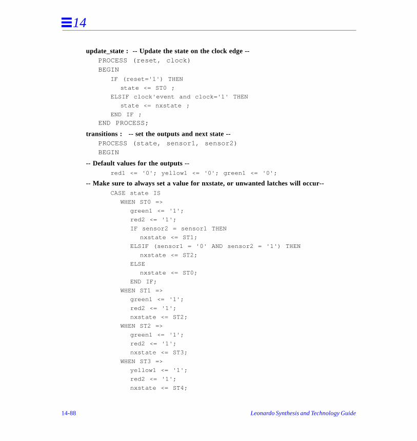
14
update_state : -- Update the state on the clock edge --PROCESS (reset, clock)
BEGIN
IF (reset='1') THEN
state <= ST0 ;
ELSIF clock'event and clock='1' THEN
state <= nxstate ;
END IF ;
END PROCESS;
transitions : -- set the outputs and next state --PROCESS (state, sensor1, sensor2)
BEGIN
-- Default values for the outputs --red1 <= '0'; yellow1 <= '0'; green1 <= '0';
-- Make sure to always set a value for nxstate, or unwanted latches will occur--CASE state IS
WHEN ST0 =>
green1 <= '1';
red2 <= '1';
IF sensor2 = sensor1 THEN
nxstate <= ST1;
ELSIF (sensor1 = '0' AND sensor2 = '1') THEN
nxstate <= ST2;
ELSE
nxstate <= ST0;
END IF;
WHEN ST1 =>
green1 <= '1';
red2 <= '1';
nxstate <= ST2;
WHEN ST2 =>
green1 <= '1';
red2 <= '1';
nxstate <= ST3;
WHEN ST3 =>
yellow1 <= '1';
red2 <= '1';
nxstate <= ST4;
14-88 Leonardo Synthesis and Technology Guide
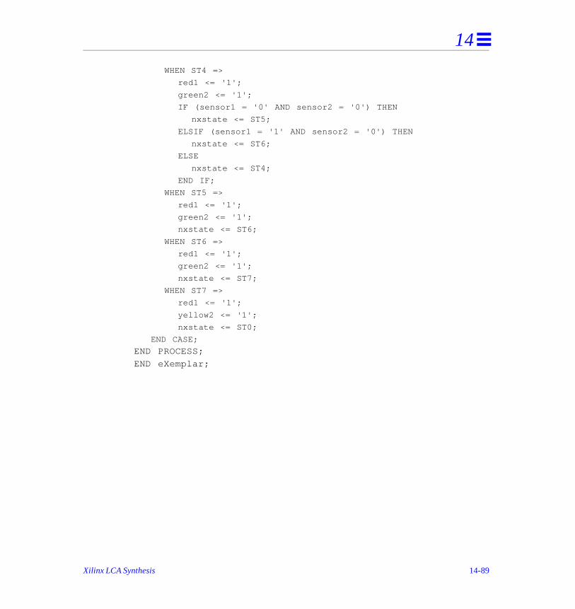
14
WHEN ST4 =>
red1 <= '1';
green2 <= '1';
IF (sensor1 = '0' AND sensor2 = '0') THEN
nxstate <= ST5;
ELSIF (sensor1 = '1' AND sensor2 = '0') THEN
nxstate <= ST6;
ELSE
nxstate <= ST4;
END IF;
WHEN ST5 =>
red1 <= '1';
green2 <= '1';
nxstate <= ST6;
WHEN ST6 =>
red1 <= '1';
green2 <= '1';
nxstate <= ST7;
WHEN ST7 =>
red1 <= '1';
yellow2 <= '1';
nxstate <= ST0;
END CASE;
END PROCESS;
END eXemplar;
Xilinx LCA Synthesis 14-89
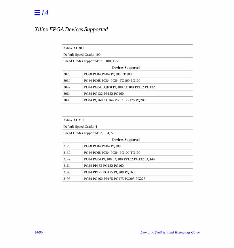
14
Xilinx FPGA Devices Supported
Xilinx XC3000
Default Speed Grade: 100
Speed Grades supported: 70, 100, 125
Devices Supported
3020 PC68 PC84 PG84 PQ100 CB100
3030 PC44 PC68 PC84 PG84 TQ100 PQ100
3042 PC84 PG84 TQ100 PQ100 CB100 PP132 PG132
3064 PC84 PG132 PP132 PQ160
3090 PC84 PQ160 CB164 PG175 PP175 PQ208
Xilinx XC3100
Default Speed Grade: 4
Speed Grades supported: 2, 3, 4, 5
Devices Supported
3120 PC68 PC84 PG84 PQ100
3130 PC44 PC68 PC84 PG84 PQ100 TQ100
3142 PC84 PG84 PQ100 TQ100 PP132 PG132 TQ144
3164 PC84 PP132 PG132 PQ160
3190 PC84 PP175 PG175 PQ208 PQ160
3195 PC84 PQ160 PP175 PG175 PQ208 PG223
14-90 Leonardo Synthesis and Technology Guide
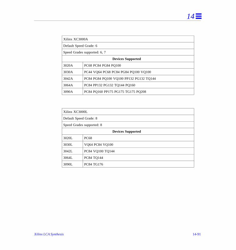
14
Xilinx XC3000A
Default Speed Grade: 6
Speed Grades supported: 6, 7
Devices Supported
3020A PC68 PC84 PG84 PQ100
3030A PC44 VQ64 PC68 PC84 PG84 PQ100 VQ100
3042A PC84 PG84 PQ100 VQ100 PP132 PG132 TQ144
3064A PC84 PP132 PG132 TQ144 PQ160
3090A PC84 PQ160 PP175 PG175 TG175 PQ208
Xilinx XC3000L
Default Speed Grade: 8
Speed Grades supported: 8
Devices Supported
3020L PC68
3030L VQ64 PC84 VQ100
3042L PC84 VQ100 TQ144
3064L PC84 TQ144
3090L PC84 TG176
Xilinx LCA Synthesis 14-91
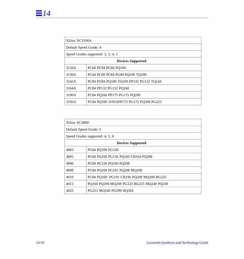
14
Xilinx XC3100A
Default Speed Grade: 4
Speed Grades supported: 2, 3, 4, 5
Devices Supported
3120A PC68 PC84 PG84 PQ100
3130A PC44 PC68 PC84 PG84 PQ100 TQ100
3142A PC84 PG84 PQ100 TQ100 PP132 PG132 TQ144
3164A PC84 PP132 PG132 PQ160
3190A PC84 PQ160 PP175 PG175 PQ208
3195A PC84 PQ160 3195APP175 PG175 PQ208 PG223
Xilinx XC4000
Default Speed Grade: 5
Speed Grades supported: 4, 5, 6
Devices Supported
4003 PC84 PQ100 PG120
4005 PC84 PQ100 PG156 PQ160 CB164 PQ208
4006 PC84 PG156 PQ160 PQ208
4008 PC84 PQ160 PG191 PQ208 MQ208
4010 PC84 PQ160 PG191 CB196 PQ208 MQ208 BG225
4013 PQ160 PQ208 MQ208 PG223 BG225 MQ240 PQ240
4025 PG223 MQ240 PG299 HQ304
14-92 Leonardo Synthesis and Technology Guide
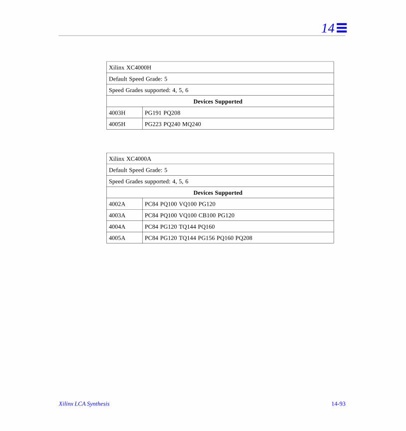
14
Xilinx XC4000H
Default Speed Grade: 5
Speed Grades supported: 4, 5, 6
Devices Supported
4003H PG191 PQ208
4005H PG223 PQ240 MQ240
Xilinx XC4000A
Default Speed Grade: 5
Speed Grades supported: 4, 5, 6
Devices Supported
4002A PC84 PQ100 VQ100 PG120
4003A PC84 PQ100 VQ100 CB100 PG120
4004A PC84 PG120 TQ144 PQ160
4005A PC84 PG120 TQ144 PG156 PQ160 PQ208
Xilinx LCA Synthesis 14-93
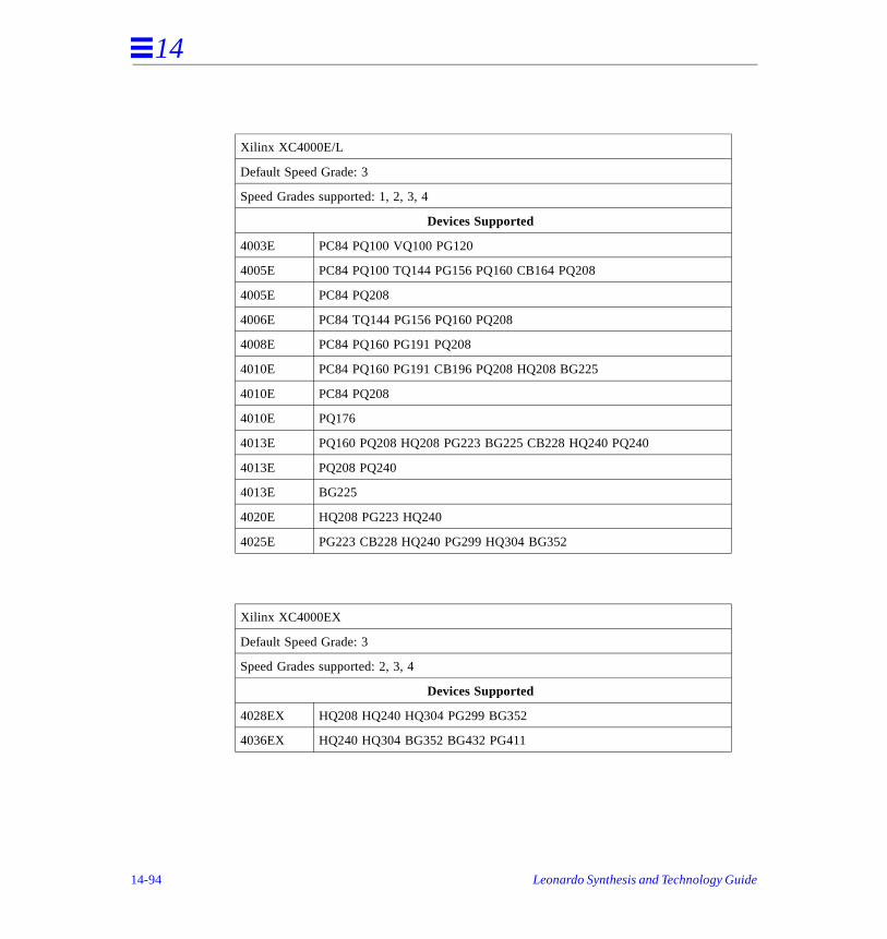
14
Xilinx XC4000E/L
Default Speed Grade: 3
Speed Grades supported: 1, 2, 3, 4
Devices Supported
4003E PC84 PQ100 VQ100 PG120
4005E PC84 PQ100 TQ144 PG156 PQ160 CB164 PQ208
4005E PC84 PQ208
4006E PC84 TQ144 PG156 PQ160 PQ208
4008E PC84 PQ160 PG191 PQ208
4010E PC84 PQ160 PG191 CB196 PQ208 HQ208 BG225
4010E PC84 PQ208
4010E PQ176
4013E PQ160 PQ208 HQ208 PG223 BG225 CB228 HQ240 PQ240
4013E PQ208 PQ240
4013E BG225
4020E HQ208 PG223 HQ240
4025E PG223 CB228 HQ240 PG299 HQ304 BG352
Xilinx XC4000EX
Default Speed Grade: 3
Speed Grades supported: 2, 3, 4
Devices Supported
4028EX HQ208 HQ240 HQ304 PG299 BG352
4036EX HQ240 HQ304 BG352 BG432 PG411
14-94 Leonardo Synthesis and Technology Guide
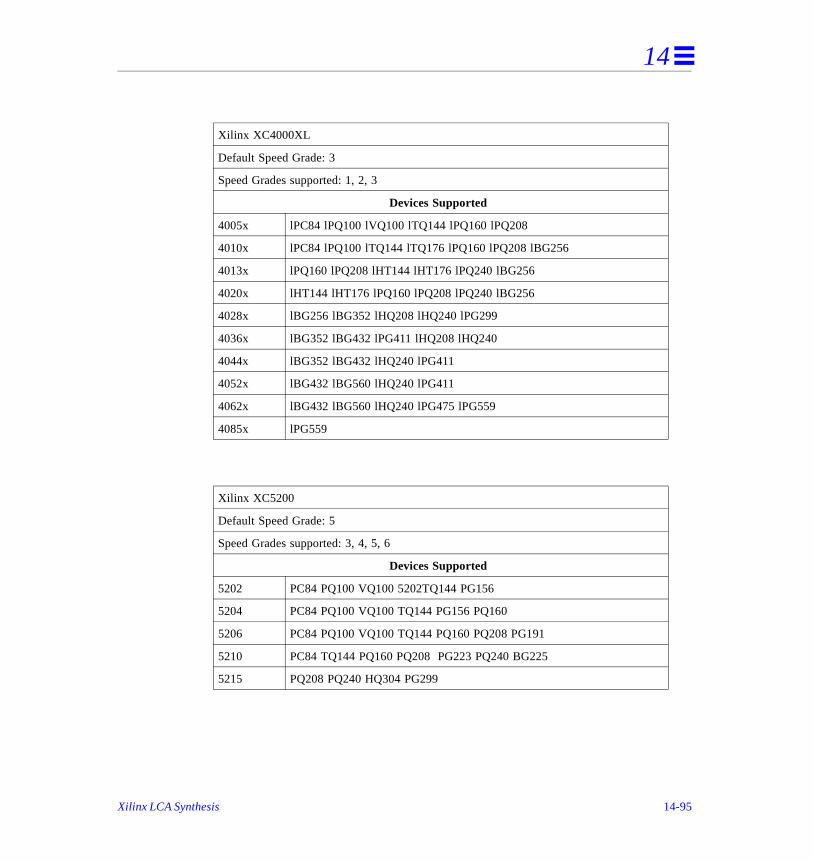
14
Xilinx XC4000XL
Default Speed Grade: 3
Speed Grades supported: 1, 2, 3
Devices Supported
4005x lPC84 lPQ100 lVQ100 lTQ144 lPQ160 lPQ208
4010x lPC84 lPQ100 lTQ144 lTQ176 lPQ160 lPQ208 lBG256
4013x lPQ160 lPQ208 lHT144 lHT176 lPQ240 lBG256
4020x lHT144 lHT176 lPQ160 lPQ208 lPQ240 lBG256
4028x lBG256 lBG352 lHQ208 lHQ240 lPG299
4036x lBG352 lBG432 lPG411 lHQ208 lHQ240
4044x lBG352 lBG432 lHQ240 lPG411
4052x lBG432 lBG560 lHQ240 lPG411
4062x lBG432 lBG560 lHQ240 lPG475 lPG559
4085x lPG559
Xilinx XC5200
Default Speed Grade: 5
Speed Grades supported: 3, 4, 5, 6
Devices Supported
5202 PC84 PQ100 VQ100 5202TQ144 PG156
5204 PC84 PQ100 VQ100 TQ144 PG156 PQ160
5206 PC84 PQ100 VQ100 TQ144 PQ160 PQ208 PG191
5210 PC84 TQ144 PQ160 PQ208 PG223 PQ240 BG225
5215 PQ208 PQ240 HQ304 PG299
Xilinx LCA Synthesis 14-95
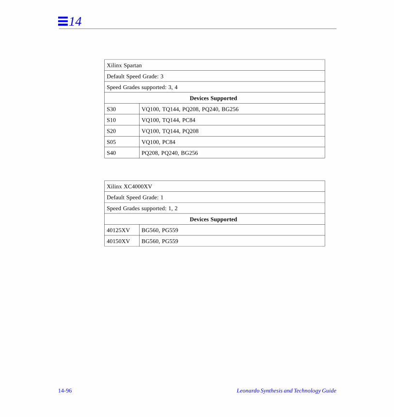
14
Xilinx Spartan
Default Speed Grade: 3
Speed Grades supported: 3, 4
Devices Supported
S30 VQ100, TQ144, PQ208, PQ240, BG256
S10 VQ100, TQ144, PC84
S20 VQ100, TQ144, PQ208
S05 VQ100, PC84
S40 PQ208, PQ240, BG256
Xilinx XC4000XV
Default Speed Grade: 1
Speed Grades supported: 1, 2
Devices Supported
40125XV BG560, PG559
40150XV BG560, PG559
14-96 Leonardo Synthesis and Technology Guide
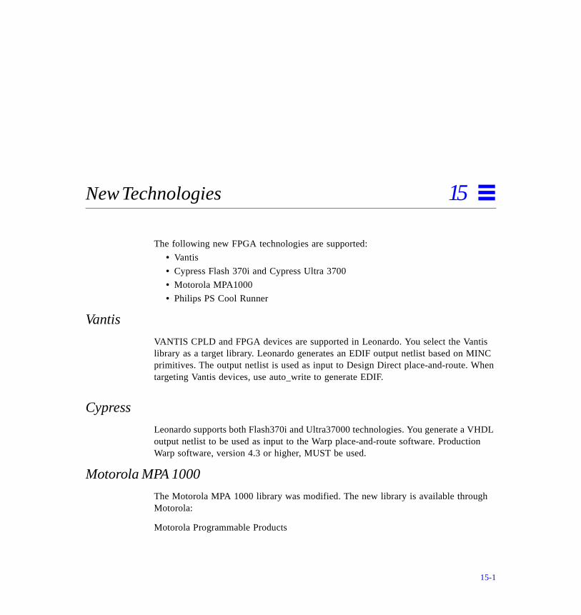
New Technologies 15
tis INC hen
HDL n
h
The following new FPGA technologies are supported:
• Vantis
• Cypress Flash 370i and Cypress Ultra 3700
• Motorola MPA1000
• Philips PS Cool Runner
Vantis
VANTIS CPLD and FPGA devices are supported in Leonardo. You select the Vanlibrary as a target library. Leonardo generates an EDIF output netlist based on Mprimitives. The output netlist is used as input to Design Direct place-and-route. Wtargeting Vantis devices, use auto_write to generate EDIF.
Cypress
Leonardo supports both Flash370i and Ultra37000 technologies. You generate a Voutput netlist to be used as input to the Warp place-and-route software. ProductioWarp software, version 4.3 or higher, MUST be used.
Motorola MPA 1000
The Motorola MPA 1000 library was modified. The new library is available througMotorola:
Motorola Programmable Products
15-1
15
from line
Telephone: 1-8-449-3742Web Site: http://sps.motorola.com/fpga
Philips PS Cool Runner
Philips cool runner is supported. Select Philips technology as a target technology the GUI. When running in batch mode, you should use -target=ps as a commandoption. When targeting Philips devices, use auto_write to generate EDIF.
15-2 Leonardo Synthesis and Technology Guide
Index
-
Aacf file, 10-5ACTGen, 8-11Adobe Acrobat Reader, 1-3ALSPIN, Actel, 8-21, 8-24AND/OR representation, 14-7
areaestimation for ASICs, 7-14reporting, Altera FLEX, 6-5reporting, Xilinx, 6-1
arithmetic operator, 8-7, 9-10, 11-11, 13-5, 14-17
array_pin_number, attribute, 10-5, 11-28, 1454
ARRIVAL_TIME, 4-4, 14-58
ASICdesign flow, 7-1
ASYNC_VAL, attribute, Xilinx, 14-66
attributeBUFFER_SIG, 14-49
automatic constraining of designs, 5-14
Bback-annotation, 3-7
Altera, 9-2hold checks, 3-9
-
setup checks, 3-9TimingChecksOn, 3-9tipd_in, 3-9tpd_in_out, 3-9
balloon help, 1-3BASE, attribute, Xilinx, 14-66BDBUF, Xilinx, 14-75
BIIPAD, QuickLogic, 12-6BIORPAD, QuickLogic, 12-6BIPAD, QuickLogic, 12-6black box, 9-22, 11-23, 14-27BLKNM, attribute, Xilinx, 14-65, 14-66
Boolean mappingalgorithm, 2-2, 8-6, 8-7
boundary scan, 14-85
BSCAN, Xilinx, 14-71, 14-85BUFFER_SIG, 2-9, 2-10, 8-16, 8-18, 9-25, 10
8, 12-5, 14-49, 14-50
buffering of logic, 4-3, 7-11, 8-15
Ccae2adl, Actel, 8-12CAP, attribute, Xilinx, 14-65, 14-66capacitance interconnect, 3-3carry
chain, Altera FLEX, 9-5, 9-10
Index-1

Index-2
chain, Xilinx, 14-18logic, ORCA, 11-2lookahead generator, Xilinx, 13-2propagation through, 14-18
cascadechain, Altera FLEX, 9-5gate, Altera FLEX, 9-7routing resource, 9-2
CHIP_PIN_LC, Altera FLEX, 9-25CKDPAD, QuickLogic, 12-7
CKPAD, QuickLogic, 12-7CKTPAD, QuickLogic, 12-7CLB
architecture, 14-2, 14-12occupied, 14-12packing, 14-5, 14-7, 14-9, 14-12, 14-68
CLB packing, 14-84CLKBUF, Actel, 8-15clock
common zero, 7-12cycle, 14-57delay, 7-12edge, 7-12enable, 14-13enable detection, Altera FLEX, 9-5enable logic, 14-34enable recognition, 14-35ideal, 7-12leading edge, 4-5manual mapping, Xilinx, 14-49offset, 14-57pulse, 4-5pulse width, 14-57reference, 4-5setup time, 4-5, 14-34
clock buffer, 2-10
clock buffer, Actel, 8-6, 8-15clock buffer, QuickLogic, 12-5clock buffer, Xilinx
ACLK, 14-47BUFG, 14-47BUFGP, 14-48BUFGS, 14-48GCLK, 14-47
clock timing constraints, 14-58CLOCK_CYCLE, 4-5, 14-58CLOCK_OFFSET, 4-5, 7-12, 14-58CMOS, attribute, Xilinx, 14-66
combinational logic loops, 12-4combinational module, Actel, 8-2command line
connect_path, 4-3disconnect_path, 4-3optimize, 14-21optimize_timing, 14-11pack_clbs, 14-12
command line options-area, 4-2-auto, 9-11, 14-19-chip, 2-7, 14-21-delay, 5-2-fast, 9-11, 14-19-fastest, 9-11, 14-19-force, 5-5, 5-14, 8-11, 11-10-macro, 2-7, 14-21-nolut_map, 9-36-small, 9-11, 14-19-smallest, 9-11, 14-19-through, 14-12
complex I/OsActel, 8-2checker, 8-18
complex_ios, variable, 14-67CONFIG, attribute, Xilinx, 14-66
configurable logic block, 14-2counter
Altera FLEX, 9-10ORCA, 11-11Xilinx, 14-18
CPLD Architecture, 13-2CPLD Family Supported Devices, 13-7critical path
delay, Xilinx, 6-1, 14-56critical path report, 3-1critical path reporting, 3-2, 5-10, 7-12
formatting, 3-7CYMODE, attribute, Xilinx, 14-66
Leonardo Synthesis and Technology Guide
Index
Ddata path synthesis
Actel, 8-7Altera FLEX, 9-9ORCA, 11-10Xilinx, 14-17
DECODE, attribute, Xilinx, 14-66
decompose_luts, command, 14-68decrementer, 8-7
Altera FLEX, 9-10ORCA, 11-11Xilinx, 13-5
DEF, attribute, Xilinx, 14-66default_max_transition, attribute, 7-11Defparms, Verilog, 9-13delay
estimate, ASICs, 7-18reporting, Altera FLEX, 6-5
delay modelconnect, 3-2input ramp, 3-2intrinsic, 3-2linear, 3-2, 7-12nonlinear, 3-2, 7-12piece wise linear, 3-2transition, 3-2
DELAYMODE, ORCA, 11-31DEPTH, attribute, Xilinx, 14-66derating factors, 7-13design
present, 5-3rule checker, 8-7rule violation, Actel, 8-18
designer, Actel, 8-15Devices Supported for Lucent ORCA, 11-39DFF, gate, 14-13DIN/DOUT Attributes, 11-29dont_lock_lcells, variable, 10-2DOUBLE, attribute, Xilinx, 14-66
drivecapability, 4-2default, 4-3
input, 4-3requirement, 4-2resistance, 3-3
DRIVE, ORCA, 11-31
DUTY_CYCLE, attribute, Xilinx, 14-66DWAND, component, 14-27
Eedf extension, 10-2edge decoders, Xilinx, 14-27EDIF
2.0 specification, 9-11bus, 9-27file, MAX+PLUS II, 10-10format, QuickLogic, 12-3netlist, 9-2, 9-27, 10-2, 11-23output, 8-11
EDIF Input, 9-28EDIF M1 flow, 14-2
EDIF netlist, 14-1EDIF_INPUT_LMF1, altera, 10-5EDIF_INPUT_USE_LMF1, Altera, 10-5Embedded Array Block (EAB), 9-22embedded array block, Altera, 9-2
exempler.lmf file, 9-28expander, Altera, 10-2, 10-7
FF1_LUT, Altera, 6-9F2_LUT, Altera, 6-9F3_LUT
Altera, 6-9F4_LUT
Altera, 6-9fanin limit, Altera MAX, 10-9fanin limited optimization, 9-2, 14-7fanout violations, 7-9, 8-15fast Xilinx outputs, 14-81FAST, attribute, Xilinx, 14-65, 14-66
FIFO, Altera FLEX, 9-2FILE, attribute, Xilinx, 14-66
Index-3
Index-4
FLEX architecture, 9-5flex_use_cascades, variable, 9-8flip-flop
D-type, 14-67enable, Altera, 10-7
FLOAT_VAL, attribute, Xilinx, 14-66FMAP, 5-9, 6-4, 14-5, 14-7, 14-13, 14-68foundry
ORCA, 11-23, 11-26FREQ, attribute, Xilinx, 14-65function generator, 14-10, 14-13functional block, 14-12
Ggate sizing, 7-8, 7-11generate_timespec, command, 14-63
genmemAltera, 9-20support, 9-20
global signals, 9-25GLOBAL, Altera, 9-25, 10-8
global_sr, variable, 11-11GLOBALRESET, Xilinx, 14-74GND, pin, 9-29GSR
Xilinx, 11-11, 14-20GTS
Xilinx, 14-74GUI options
assign global SR, 11-12, 14-21chip, 2-7detect the global set/reset signal, 11-12,
14-21do not lock LCells, 9-8macro, 2-7map cascades, 9-36map look up tables, 2-3, 9-8, 9-36, 11-8map to 6-input LUTs, 2-3, 11-8map to CASCADEs during LUT
mapping, 2-3, 9-8max fanin, 13-5max PT, 13-5
modgen select, 9-11, 14-19process, 3-6temperature, 3-6use F5MAP symbols, 2-3use FAST output buffers, 14-81write look up tables, 14-5
guidesCommand Reference, 1-3HDL Synthesis Guide, 1-3Installation Guide, 1-2Synthesis and Technology Guide, 1-3User’s Guide, 1-2
Hhard macro, file (.HM), 14-79HBLKNM, attribute, Xilinx, 14-12, 14-16, 14-
65, 14-66, 14-68HCLKBUF, Actel, 8-16HD2PAD, QuickLogic, 12-6HD3PAD, QuickLogic, 12-6HDDPAD, QuickLogic, 12-6HDIPAD, QuickLogic, 12-6
hdl_array_name_style, variable, 9-22, 9-27HDPAD, QuickLogic, 12-6Help, 1-3HMAP, 5-9, 14-5, 14-7, 14-12, 14-13, 14-68HU_SET, attribute, Xilinx, 14-66
II/O
assign automatically, 2-1, 14-50assign manually, 2-1, 2-11, 12-5, 14-50buffers, Actel, 8-2buffers, ORCA, 11-27cell, Altera, 10-2cells, 8-18cells, Xilinx, 14-50complex, 2-1port, 4-4registered, 8-18, 14-50set/reset, 8-15size of, 2-1
Leonardo Synthesis and Technology Guide
Index
I/O Mapping, 2-8, 8-18ORCA, 11-27
IBUF, Xilinx, 14-75IBUFLEVEL, ORCA, 11-31implementation
multi-level, 10-7one level, 10-7
include_gates, variable, 11-27incrementer, 8-7
Altera FLEX, 9-10ORCA, 11-11Xilinx, 13-5
infer_gsr, variable, 11-12INFF, Xilinx, 14-67, 14-75INIT, attribute, Xilinx, 14-16, 14-46initval, attribute, ORCA, 11-24, 11-26
INLAT, Xilinx, 14-67, 14-75INPAD, QuickLogic, 12-6input/output block, 14-2INPUT_DRIVE, 4-3INPUT_MAX_FANOUT, 4-3INPUT_MAX_LOAD, 4-3
inputsprimary, 4-3register, 4-3
INREG, Xilinx, 14-75insert_global_bufs, variable, 8-17
interconnectdelay, Xilinx, 6-4load, 3-3modeling, 7-13resistance, 3-3, 7-14
INTERNAL, attribute, Xilinx, 14-65, 14-66
intrinsic delayXilinx, 6-4
IOCLK, 8-21Actel, 8-18
IOPCL, 8-21
LLABs, Altera, 10-2
latchidentical, 10-8
LCA architecture, 14-1, 14-2LCA2XNF, Xilinx, 14-71LCELL
Altera, 10-2primitive, 9-7
Leonardo’s manuals, 1-2libraries
synthesis, 1-3VITAL, 1-3
Library Mapping File, 10-1Library Mapping File (LMF), 10-5
LIBVER, attribute, Xilinx, 14-16, 14-66LMF file, 10-5load
capacitive, 3-3, 7-14external, 4-2fanout, 4-3interconnect, 3-2, 3-3maximum, 4-3maximum fanout, 4-3output, 4-2requirements, 4-2unit, 4-2violation, 7-9, 7-11, 8-6
LOAD, ORCA, 11-31LOC, attribute, Xilinx, 14-65, 14-66LOC, ORCA, 11-28logic
array block, Altera, 9-2, 10-9buffering, 4-3, 7-11, 8-15cell, pASIC, 12-2combinability, Actel, 8-14element, Altera, 9-2module, Actel, 8-2replication, 4-2, 7-11
logical operator, 8-7, 11-11lookup table, 14-84
Altera FLEX, 9-7ORCA, 11-2
lookup table mapping, 2-2Altera, 2-2, 9-2, 9-7
Index-5
Index-6
F3_LUT, gate, 6-5F4_LUT, gate, 6-5F5_MUX, gate, 14-11H3_LUT, gate, 6-5ORCA, 2-2, 11-6Xilinx, 2-2, 14-6, 14-10
LPMconventions, 9-5instantiation, 9-13
LPM Support for FLEX 10K, 9-11LPM_RAM_DQ, component, 9-12LPM_RAM_IO, component, 9-12
MM1 back annotation flow, 14-83M1 support, 14-84
macrocell, 10-7Altera, 10-2
MAP, attribute, Xilinx, 14-66
MAX architecture, Altera, 10-1, 10-8max cubes, Altera MAX, 10-9max fanin, Altera MAX, 10-9MAX+PLUS II, 9-29MAX+PLUS II, Altera, 10-2, 10-5, 10-9
max_fanin, variable, 10-9max_transition, variable, 7-11MD0, input port, Xilinx, 14-71MD1, output port, Xilinx, 14-71MD2, input port, Xilinx, 14-71MEDFAST, attribute, Xilinx, 14-65, 14-66
MEDSLOW, attribute, Xilinx, 14-65, 14-66MEMFILE, attribute, Xilinx, 14-66memgen, Xilinx, 14-40module generator
Altera, 10-8library, 14-17Xilinx, 13-4
modulesLeonardo, 1-2Model Technology V-System/QuickHDL
simulator, 1-2Time Explorer, 1-2
move command, 9-27multiplexer
ORCA, 11-11mux-based, optimization, 8-6
Nnegative slack, 5-6Neoprim library, 11-42New Features for Altera FLEX, 9-35New Features for QuickLogic, 12-2
NOBUFF, 4-3NODELAY, attribute, Xilinx, 14-65, 14-66nologic_rep, variable, 8-15NOMERGE, ORCA, 11-6NOOPT, Xilinx, 14-72nowire_table, variable, 7-14
OOBUF, Xilinx, 14-75
OBUFLEVEL, ORCA, 11-31online guides, 1-3operating conditions, 7-13operator
arithmetic, 14-18logical, 14-18relational, 14-18
optimizationflow, 5-1passes, Altera MAX, 10-7sequential, 9-24, 10-8, 12-4
optimize command-target option, 10-2
optimize_timing command, 5-5, 8-11, 11-10-force option, 5-5, 8-11, 14-11-through option, 5-5
optimize_timing -force, 8-11oscillator, Xilinx, 14-71OUTFF, Xilinx, 14-67, 14-75OUTFFT, Xilinx, 14-75
OUTIPAD, QuickLogic, 12-6OUTORPAD, QuickLogic, 12-6
Leonardo Synthesis and Technology Guide
Index
-
OUTPAD, QuickLogic, 12-6OUTPUT_FANOUT, 4-2OUTPUT_LOAD, 4-2
Ppack_clbs, command, 6-3, 14-14PAD, 2-9, 8-18, 14-50
PAD Command, 12-6part number, ORCA, 11-31part, variable, 14-68pASIC architecture, QuickLogic, 12-2pASIC1 and pASIC2 Derating Factors, 12-5path analysis, 4-3
PERIOD, attribute, Xilinx, 14-65PFU-MUX, ORCA, 11-6PFU-NAND, ORCA, 11-6PFU-XOR, ORCA, 11-6PICSPEC, ORCA, 11-31PICSPEED, ORCA, 11-31
pin assignment, Actel, 8-21pin location
Altera, 9-25, 10-5, 10-6ORCA, 11-28QuickLogic, 12-7Xilinx, 14-54
PIN_NUMBER, 10-5pin_number, attribute, 8-22, 9-25, 11-28, 14-
54place-and-route
Altera, 10-2
PLDs architecture, Altera, 10-1pop_design, command, 5-4POWERUP, 11-12, 14-21PPR, Xilinx, 14-40preference file writer, 11-32preserve_dangling_nets, variable, 14-75, 14-
77primary inputs, 4-4Process Derating Factors, 8-25
process, variable, 7-13, 11-31product terms, 10-2, 10-10
programmablefunction unit, ORCA, 11-2input/output cells, ORCA, 11-2logic cells, ORCA, 11-2
propagate_clock_delay, variable, 7-12propagation delay, 4-4PULSE_WIDTH, 4-5, 14-58
push_design, command, 5-4
QQCLKBUF, Actel, 8-16QDIF format, 12-3
RRAM
Altera FLEX, 9-2, 9-10dual-port, 9-2, 14-43dual-port, ORCA, 11-26inferencing, RTL, 9-15instantiation, Altera FLEX, 9-5, 9-12instantiation, ORCA, 11-23instantiation, Xilinx, 14-40ORCA, 11-11Xilinx, 14-71
RAM_DQcomponent, 9-12
ram_example1, 8-9, 9-18, 11-18, 14-37ram_example2, 8-10, 9-19, 11-19, 14-38RAM_IO
component, 9-12RDBK, Xilinx, 14-71RDCLK, Xilinx, 14-71registers, 4-4
identical, 10-8relational operator, 8-7, 9-10, 11-11, 13-5, 14
17replicate logic, 8-15report_area command, 6-2, 6-7, 7-16
-cell option, 7-17report_delay command, 6-4, 7-12, 7-18reports
Altera FLEX area/delay example, 6-1
Index-7

Index-8
Xilinx area/delay example, 6-1REQUIRED_TIME, 4-4, 4-6RES, attribute, Xilinx, 14-65, 14-66reset
active high, 11-14, 14-24active low, 11-15, 14-25signal, 14-13
RLOC, attribute, in Xilinx, 14-66RLOC_ORIGIN, attribute, Xilinx, 14-66RLOC_RANGE, attribute, Xilinx, 14-66ROM
Altera FLEX, 9-2ORCA, 11-26Xilinx, 14-46, 14-71
rule constraints, 7-9runtime requirements, 1-5
Sschematic
viewer, 3-8SCHNM, attribute, Xilinx, 14-16, 14-66
SCLK, Altera, 10-8scuba, ORCA, 11-23, 11-26SDF
file, 3-7, 3-9HOLD, 3-11INTERCONNECT delays, 3-11IOPATH delays, 3-11PORT, 3-11SETUP, 3-11
sequentialmodule, Actel, 8-2, 8-16
set, 9-10, 14-5, 14-19set modgen_select, 9-10, 14-5, 14-19set, signal, 14-13shift operator, 8-7
simulationActel, 8-21functionality, 3-9timing, 3-9
slew input, 3-2slew property, ORCA, 11-29
SLOW, attribute, Xilinx, 14-65, 14-66SpDE, QuickLogic, 12-2speed grade, 11-31STARTUP, Xilinx, 11-11, 14-20
static timing analysis, 3-1SYNC_VAL, attribute, Xilinx, 14-66system requirements, 1-4SYSTEM, attribute, Xilinx, 14-66
TTCK, input port, Xilinx, 14-71TDI, input port, Xilinx, 14-71TDO, output port, Xilinx, 14-71
temperature, variable, 7-13THI, attribute, Xilinx, 14-65time
arrival, 3-2required, 3-2
Time Module, 3-7
Time Module license, 14-83TIMEGRP, 14-58, 14-59TIMESPEC, 14-57, 14-58, 14-59timing
constraints, 6-5required, 4-4
timing analysis, 3-2, 7-12annotated XNF netlist, 3-8arrival time, 4-4, 5-2constraint, 4-4, 5-2critical path, 5-2end point, 5-2, 5-6longest path, 3-2negative slack, 3-2path analysis, 4-3post place-and-route, 3-5routing delay, 3-5start point, 4-3
timing optimizationconstraint-driven, 11-10
timing optimization, reportingarea, 5-6longest path, 5-6
Leonardo Synthesis and Technology Guide
Index
most critical slack, 5-6sum of negative slacks, 5-6
TLO, attribute, Xilinx, 14-65TMS, input port, Xilinx, 14-71transition time
violations, 7-11TRIORPAD, QuickLogic, 12-6tristatable output, 10-2tristate, internal
QuickLogic, 12-4Xilinx, 14-29, 14-74
tristate_map, variable, 14-31TTL, attribute, Xilinx, 14-66
UU_SET, attribute, Xilinx, 14-66unconstrained path, 6-5ungroup command
-all option, 14-68-hier option, 14-68
unified library, Xilinx, 6-5use_qclk_bufs, variable, 8-17USE_RLOC, attribute, in Xilinx, 14-66
Vvariables
complex_ios, 2-7delete_startup, 11-12, 14-21dont_lock_lcells, 9-8enable_dff_map, 14-67flex_use_cascades, 2-3, 9-8global_sr, 11-12, 14-20hdl_array_name_style, 8-11infer_gsr, 11-12, 14-20insert_global_bufs, 14-50lut_map, 2-3, 9-8, 11-8, 14-5max_fanin, 11-8max_fanin <integer>, 13-5max_fanout_load, 8-15max_pt <integer>, 13-5maxdly, 4-1modgen_select, 14-19
nologic_rep, 8-15tristate_map, 14-30use_dffenable, 14-67use_f5map, 2-3use_f6_lut, 2-3, 11-8write_clb_packing, 14-5write_lut_binding, 14-5xlx_preserve_gsr, 14-23xlx_preserve_gts, 14-23
VCC, pin, 9-29
Verilog, 14-17Verilog HDL designs, 14-1VHDL, 14-17VHDL attributes, 4-5VHDL designs, 14-1VITAL library, 3-9
level 0 compliant, 3-9level 1 compliant, 3-9
voltage, variable, 7-13
Wweb site, 1-3wir2xnf, 14-78wire load models, 14-84
wire resistancebalanced case, 3-3, 7-14best case, 3-3, 7-14worst case, 3-3, 7-14
wire_table, variable, 7-14wire_tree, variable, 7-14wireload
model, 6-4table, 7-14, 7-18
write command, 10-2write_altera, script, 9-28write_clb_packing, variable, 14-68write_lut_binding, variable, 14-68
XXACT (XNF) flow, 14-2XACT, software, 14-5
Index-9
Index-10
XACT-CPLD tools, 13-2XBLOX, 14-78, 14-79
components, 14-18output file (.XG), 14-79xblox3 library, 14-79xblox4 library, 14-79
XBLOX program, 14-79xlx_preserve_gsr, variable, 14-23, 14-73xlx_preserve_gts, variable, 14-23, 14-73XNF, 14-54, 14-57
EXT record, 14-78hierarchical, 14-68mapped, 14-10NOOPT, 14-72output netlist, 14-68output, EQN symbols, 14-69preserving logic, 14-71reader, 14-23SIG record, 14-78simulatable, 14-71
XNFMERGE, Xilinx, 14-40XOR
optimization, Xilinx, 13-4
synthesis, Altera, 10-2
Leonardo Synthesis and Technology Guide