lecture 5.pdf
30
OTHER B IAS METHODS ◆ 241 Use Equation 5–7 to determine I E . From I E , you can determine I C and V CE as follows: Related Problem What value of is required in this example in order to neglect R IN(BASE) in keeping with the basic ten-times rule for a stiff voltage divider? b DC V CE = V C - V E =- 3.79 V + 2.71 V = 1.08 V V E =- I E R E =- (1.23 mA)(2.2 kÆ) =- 2.71 V V C =- V CC + I C R C =- 6 V + (1.23 mA)(1.8 kÆ) =- 3.79 V I C = I E = 1.23 mA = 3.15 V 2.57 kÆ = 1.23 mA I E = - V TH + V BE R E + R TH > b DC = 2.45 V + 0.7 V 2.2 kÆ+ 371 Æ R TH = R 1 R 2 R 1 + R 2 = (68 kÆ)(47 kÆ) (68 kÆ+ 47 kÆ) = 27.8 kÆ 1. If the voltage at the base of a transistor is 5 V and the base current is A, what is the dc input resistance at the base? 2. If a transistor has a dc beta of 190, V B 2 V, and I E 2 mA, what is the dc input resistance at the base? 3. What bias voltage is developed at the base of a transistor if both resistors in a stiff voltage divider are equal and 4. What are two advantages of voltage-divider bias? V CC 10 V? 5 m SECTION 5–2 CHECKUP 5–3 O THER B IAS M ETHODS In this section, four additional methods for dc biasing a transistor circuit are discussed. Although these methods are not as common as voltage-divider bias, you should be able to recognize them when you see them and understand the basic differences. After completing this section, you should be able to ❏ Analyze four more types of bias circuits ❏ Discuss emitter bias ◆ Analyze an emitter-biased circuit ❏ Discuss base bias ◆ Analyze a base-biased circuit ◆ Explain Q-point stability of base bias ❏ Discuss emitter-feedback bias ◆ Define negative feedback ◆ Analyze an emitter-feedback biased circuit ❏ Discuss collector-feedback bias ◆ Analyze a collector-feedback biased circuit ◆ Discuss Q-point stability over temperature Emitter Bias Emitter bias provides excellent bias stability in spite of changes in or temperature. It uses both a positive and a negative supply voltage. To obtain a reasonable estimate of the key dc values in an emitter-biased circuit, analysis is quite easy. In an npn circuit, such as shown b
-
Upload
khangminh22 -
Category
Documents
-
view
0 -
download
0
Transcript of lecture 5.pdf

OTHER BIAS METHODS ◆ 241
Use Equation 5–7 to determine IE.
From IE, you can determine IC and VCE as follows:
Related Problem What value of is required in this example in order to neglect RIN(BASE) in keepingwith the basic ten-times rule for a stiff voltage divider?
bDC
VCE = VC - VE = -3.79 V + 2.71 V = �1.08 V
VE = -IERE = -(1.23 mA)(2.2 kÆ) = -2.71 V
VC = -VCC + ICRC = -6 V + (1.23 mA)(1.8 kÆ) = -3.79 V
IC = IE = 1.23 mA
=3.15 V
2.57 kÆ= 1.23 mA
IE =-VTH + VBE
RE + RTH>bDC=
2.45 V + 0.7 V
2.2 kÆ + 371 Æ
RTH =R1R2
R1 + R2=
(68 kÆ)(47 kÆ)
(68 kÆ + 47 kÆ)= 27.8 kÆ
1. If the voltage at the base of a transistor is 5 V and the base current is A, what is thedc input resistance at the base?
2. If a transistor has a dc beta of 190, VB 2 V, and IE 2 mA, what is the dc inputresistance at the base?
3. What bias voltage is developed at the base of a transistor if both resistors in a stiffvoltage divider are equal and
4. What are two advantages of voltage-divider bias?
VCC � �10 V?
��
5 mSECTION 5–2 CHECKUP
5–3 OTHER BIAS METHODS
In this section, four additional methods for dc biasing a transistor circuit are discussed.Although these methods are not as common as voltage-divider bias, you should be ableto recognize them when you see them and understand the basic differences.
After completing this section, you should be able to
❏ Analyze four more types of bias circuits❏ Discuss emitter bias
◆ Analyze an emitter-biased circuit❏ Discuss base bias
◆ Analyze a base-biased circuit ◆ Explain Q-point stability of base bias❏ Discuss emitter-feedback bias
◆ Define negative feedback ◆ Analyze an emitter-feedback biased circuit❏ Discuss collector-feedback bias
◆ Analyze a collector-feedback biased circuit ◆ Discuss Q-point stability overtemperature
Emitter Bias
Emitter bias provides excellent bias stability in spite of changes in or temperature. It usesboth a positive and a negative supply voltage. To obtain a reasonable estimate of the key dcvalues in an emitter-biased circuit, analysis is quite easy. In an npn circuit, such as shown
b

242 ◆ TRANSISTOR BIAS CIRCUITS
in Figure 5–17, the small base current causes the base voltage to be slightly below ground.The emitter voltage is one diode drop less than this. The combination of this small dropacross RB and VBE forces the emitter to be at approximately Using this approxima-tion, you can obtain the emitter current as
VEE is entered as a negative value in this equation.You can apply the approximation that to calculate the collector voltage.
The approximation that is useful for troubleshooting because you won’t needto perform any detailed calculations. As in the case of voltage-divider bias, there is a morerigorous calculation for cases where you need a more exact result.
VE � -1 V
VC = VCC - ICRC
IC � IE
IE =-VEE - 1 V
RE
-1 V.
Calculate IE and VCE for the circuit in Figure 5–16 using the approximationsVE � -1 V and IC � IE.
EXAMPLE 5–6
Solution
Related Problem If VEE is changed to what is the new value of VCE?-12 V,
VCE = 8.4 V - (-1) = 9.4 V
VC = VCC - ICRC = +15 V - (1.4 mA)(4.7 kÆ) = 8.4 V
IE =-VEE - 1 V
RE=
-(-15 V) - 1 V
10 kÆ=
14 V
10 kÆ= 1.4 mA
VE � -1 V
RE10 k�
VCC+15 V
RC4.7 k�
RB
47 k�
VEE–15 V
� FIGURE 5–16
The approximation that and the neglect of may not be accurateenough for design work or detailed analysis. In this case, Kirchhoff’s voltage law can beapplied as follows to develop a more detailed formula for IE. Kirchhoff’s voltage law ap-plied around the base-emitter circuit in Figure 5–17(a), which has been redrawn in part (b)for analysis, gives the following equation:
Substituting, using Ohm’s law,
VEE + IBRB + VBE + IERE = 0
VEE + VRB+ VBE + VRE
= 0
bDCVE � -1 V

OTHER BIAS METHODS ◆ 243
Substituting for and transposing
Factoring out IE and solving for IE,
IE ��VEE � VBE
RE � RB/BDC
a IE
bDCbRB + IERE + VBE = -VEE
VEE,IB � IE>bDC
Equation 5–9
Voltages with respect to ground are indicated by a single subscript. The emitter voltagewith respect to ground is
The base voltage with respect to ground is
The collector voltage with respect to ground is
VC = VCC - ICRC
VB = VE + VBE
VE = VEE + IERE
VEE
VCC
RC
RB
REVB
VE VC
RCIC
+
–
RE
+
–
+–VBE
RB
IB
VEE
IE
+ –
(a) (b)
VCC� FIGURE 5–17
An npn transistor with emitter bias.Polarities are reversed for a pnp tran-sistor. Single subscripts indicate volt-ages with respect to ground.
Determine how much the Q-point (IC, VCE) for the circuit in Figure 5–18 will changeif increases from 100 to 200 when one transistor is replaced by another.bDC
EXAMPLE 5–7
RE10 k�
VCC+15 V
RC4.7 k�
RB
47 k�
VEE–15 V
� FIGURE 5–18
244 ◆ TRANSISTOR BIAS CIRCUITS
Solution For
Therefore,
For
Therefore,
The percent change in IC as changes from 100 to 200 is
The percent change in is
Related Problem Determine the Q-point in Figure 5–18 if increases to 300.bDC
%¢VCE = aVCE(2) - VCE(1)
VCE(1)b100% = a9.71 V - 9.83 V
9.83 Vb100% = �1.22%
VCE
%¢IC = a IC(2) - IC(1)
IC(1)b100% = a1.38 mA - 1.37 mA
1.37 mAb100% = 0.730%
bDC
VCE(2) = VC - VE = 8.51 V - (-1.2 V) = 9.71 V
VE = VEE + IERE = -15 V + (1.38 mA)(10 kÆ) = -1.2 V
VC = VCC - IC(2)RC = 15 V - (1.38 mA)(4.7 kÆ) = 8.51 V
IC(2) � IE =-VEE - VBE
RE + RB>bDC=
-(-15 V) - 0.7 V
10 kÆ + 47 kÆ>200= 1.38 mA
bDC = 200,
VCE(1) = VC - VE = 8.56 V - (-1.3 V) = 9.83 V
VE = VEE + IERE = -15 V + (1.37 mA)(10 kÆ) = -1.3 V
VC = VCC - IC(1)RC = 15 V - (1.37 mA)(4.7 kÆ) = 8.56 V
IC(1) � IE =-VEE - VBE
RE + RB>bDC=
-(-15 V) - 0.7 V
10 kÆ + 47 kÆ>100= 1.37 mA
bDC = 100,
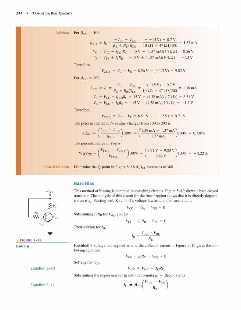
Base Bias
This method of biasing is common in switching circuits. Figure 5–19 shows a base-biasedtransistor. The analysis of this circuit for the linear region shows that it is directly depend-ent on Starting with Kirchhoff’s voltage law around the base circuit,
Substituting IBRB for you get
Then solving for IB,
Kirchhoff’s voltage law applied around the collector circuit in Figure 5–19 gives the fol-lowing equation:
Solving for VCE,
VCE � VCC � ICRC
VCC - ICRC - VCE = 0
IB =VCC - VBE
RB
VCC - IBRB - VBE = 0
VRB,
VCC - VRB- VBE = 0
bDC.
Equation 5–10
Substituting the expression for IB into the formula yields
IC � BDCaVCC � VBE
RBb
IC = bDCIB
Equation 5–11
RC
RB
VBE
+
+VCC
VCE
+
––
� FIGURE 5–19
Base bias.

OTHER BIAS METHODS ◆ 245
Q-Point Stability of Base Bias Notice that Equation 5–11 shows that IC is dependenton The disadvantage of this is that a variation in causes IC and, as a result, VCEto change, thus changing the Q-point of the transistor. This makes the base bias circuitextremely beta-dependent and unpredictable.
Recall that varies with temperature and collector current. In addition, there is alarge spread of values from one transistor to another of the same type due to manu-facturing variations. For these reasons, base bias is rarely used in linear circuits but is dis-cussed here so you will be familiar with it.
bDC
bDC
bDCbDC.
Determine how much the Q-point (IC, VCE) for the circuit in Figure 5–20 will changeover a temperature range where increases from 100 to 200.bDC
EXAMPLE 5–8
RC560 �
RB
VCC+12 V
330 k�
� FIGURE 5–20
Solution For
The percent change in IC as changes from 100 to 200 is
The percent change in VCE is
As you can see, the Q-point is very dependent on in this circuit and thereforemakes the base bias arrangement very unreliable. Consequently, base bias is not nor-mally used if linear operation is required. However, it can be used in switchingapplications.
Related Problem Determine IC if increases to 300.bDC
bDC
= a8.17 V - 10.1 V
10.1 Vb100% = �19.1% (a decrease)
%¢VCE = aVCE(2) - VCE(1)
VCE(1)b100%
= a6.84 mA - 3.42 mA
3.42 mAb100% = 100% (an increase)
%¢IC = a IC(2) - IC(1)
IC(1)b100%
bDC
VCE(2) = VCC - IC(2) RC = 12 V - (6.84 mA)(560 Æ) = 8.17 V
IC(2) = bDCaVCC - VBE
RBb = 200a12 V - 0.7 V
330 kÆb = 6.84 mA
For bDC = 200,
VCE(1) = VCC - IC(1)RC = 12 V - (3.42 mA)(560 Æ) = 10.1 V
IC(1) = bDCaVCC - VBE
RBb = 100a12 V - 0.7 V
330 kÆb = 3.42 mA
bDC = 100,
246 ◆ TRANSISTOR BIAS CIRCUITS
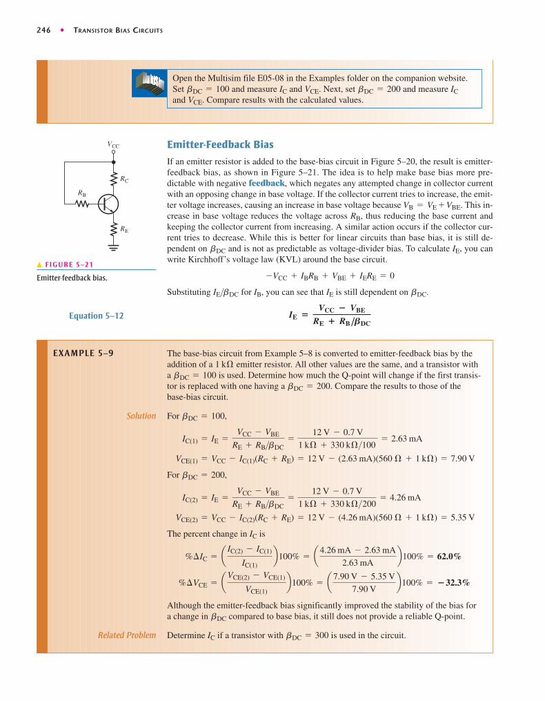
Emitter-Feedback Bias
If an emitter resistor is added to the base-bias circuit in Figure 5–20, the result is emitter-feedback bias, as shown in Figure 5–21. The idea is to help make base bias more pre-dictable with negative feedback, which negates any attempted change in collector currentwith an opposing change in base voltage. If the collector current tries to increase, the emit-ter voltage increases, causing an increase in base voltage because VB VE + VBE. This in-crease in base voltage reduces the voltage across RB, thus reducing the base current andkeeping the collector current from increasing. A similar action occurs if the collector cur-rent tries to decrease. While this is better for linear circuits than base bias, it is still de-pendent on and is not as predictable as voltage-divider bias. To calculate IE, you canwrite Kirchhoff’s voltage law (KVL) around the base circuit.
Substituting for IB, you can see that IE is still dependent on
IE �VCC � VBE
RE � RB/BDC
bDC.IE>bDC
-VCC + IBRB + VBE + IERE = 0
bDC
=
Open the Multisim file E05-08 in the Examples folder on the companion website.Set and measure IC and VCE. Next, set and measure ICand VCE. Compare results with the calculated values.
bDC = 200bDC = 100
RC
RE
RB
VCC
� FIGURE 5–21
Emitter-feedback bias.
Equation 5–12
The base-bias circuit from Example 5–8 is converted to emitter-feedback bias by theaddition of a emitter resistor. All other values are the same, and a transistor witha is used. Determine how much the Q-point will change if the first transis-tor is replaced with one having a Compare the results to those of thebase-bias circuit.
Solution For
For
The percent change in IC is
Although the emitter-feedback bias significantly improved the stability of the bias fora change in compared to base bias, it still does not provide a reliable Q-point.
Related Problem Determine IC if a transistor with is used in the circuit.bDC = 300
bDC
%¢VCE = aVCE(2) - VCE(1)
VCE(1)b100% = a7.90 V - 5.35 V
7.90 Vb100% = �32.3%
%¢IC = a IC(2) - IC(1)
IC(1)b100% = a4.26 mA - 2.63 mA
2.63 mAb100% = 62.0%
VCE(2) = VCC - IC(2)(RC + RE) = 12 V - (4.26 mA)(560 Æ + 1 kÆ) = 5.35 V
IC(2) = IE =VCC - VBE
RE + RB>bDC=
12 V - 0.7 V
1 kÆ + 330 kÆ>200= 4.26 mA
bDC = 200,
VCE(1) = VCC - IC(1)(RC + RE) = 12 V - (2.63 mA)(560 Æ + 1 kÆ) = 7.90 V
IC(1) = IE =VCC - VBE
RE + RB>bDC=
12 V - 0.7 V
1 kÆ + 330 kÆ>100 = 2.63 mA
bDC = 100,
bDC = 200.bDC = 100
1 kÆEXAMPLE 5–9
OTHER BIAS METHODS ◆ 247
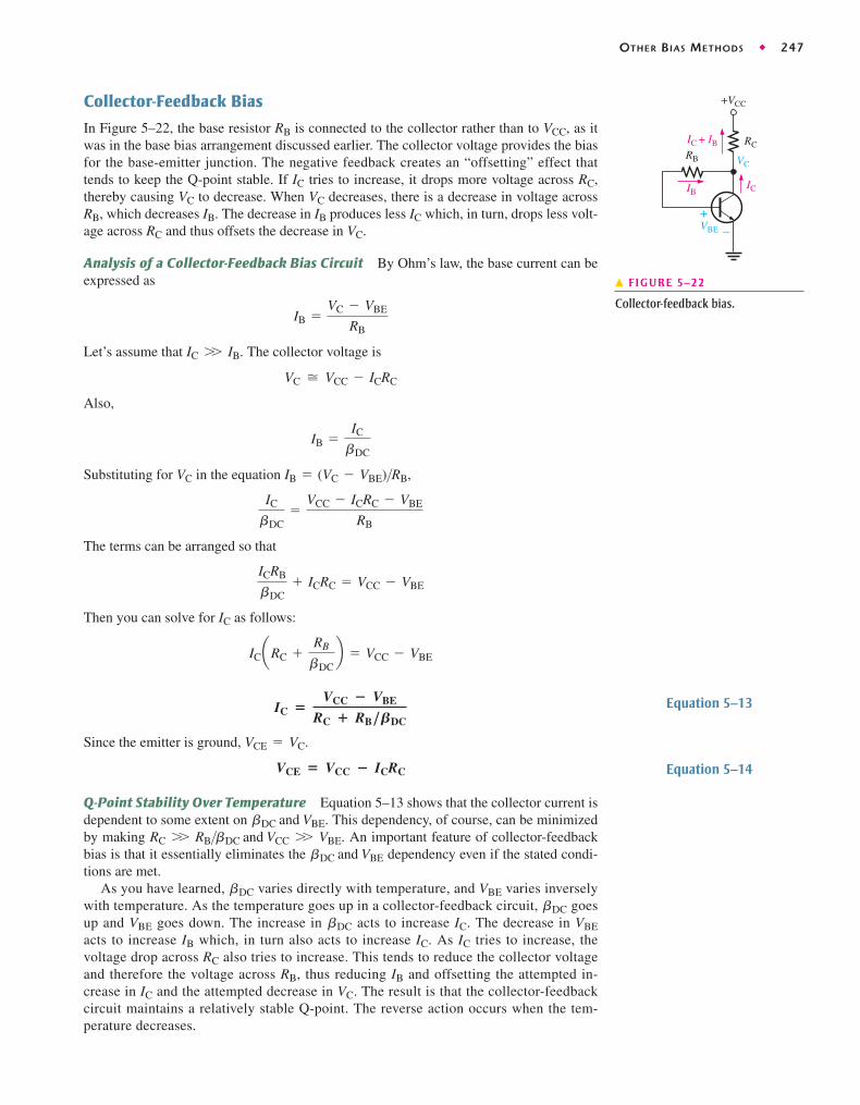
Collector-Feedback Bias
In Figure 5–22, the base resistor RB is connected to the collector rather than to VCC, as itwas in the base bias arrangement discussed earlier. The collector voltage provides the biasfor the base-emitter junction. The negative feedback creates an “offsetting” effect thattends to keep the Q-point stable. If IC tries to increase, it drops more voltage across RC,thereby causing VC to decrease. When VC decreases, there is a decrease in voltage acrossRB, which decreases IB. The decrease in IB produces less IC which, in turn, drops less volt-age across RC and thus offsets the decrease in VC.
Analysis of a Collector-Feedback Bias Circuit By Ohm’s law, the base current can beexpressed as
Let’s assume that The collector voltage is
Also,
Substituting for VC in the equation
The terms can be arranged so that
Then you can solve for IC as follows:
IC �VCC � VBE
RC � RB/BDC
ICaRC +RB
bDCb = VCC - VBE
ICRB
bDC+ ICRC = VCC - VBE
IC
bDC=
VCC - ICRC - VBE
RB
IB = (VC - VBE)>RB,
IB =IC
bDC
VC � VCC - ICRC
IC W IB.
IB =VC - VBE
RB
Equation 5–13
Since the emitter is ground, VCE VC.
VCE � VCC � ICRC
=
Equation 5–14
Q-Point Stability Over Temperature Equation 5–13 shows that the collector current isdependent to some extent on This dependency, of course, can be minimizedby making An important feature of collector-feedbackbias is that it essentially eliminates the dependency even if the stated condi-tions are met.
As you have learned, varies directly with temperature, and VBE varies inverselywith temperature. As the temperature goes up in a collector-feedback circuit, goesup and VBE goes down. The increase in acts to increase IC. The decrease in VBEacts to increase IB which, in turn also acts to increase IC. As IC tries to increase, thevoltage drop across RC also tries to increase. This tends to reduce the collector voltageand therefore the voltage across RB, thus reducing IB and offsetting the attempted in-crease in IC and the attempted decrease in VC. The result is that the collector-feedbackcircuit maintains a relatively stable Q-point. The reverse action occurs when the tem-perature decreases.
bDC
bDC
bDC
bDC and VBE
RC W RB>bDC and VCC W VBE.bDC and VBE.
RC
+VCC
+–VBE
IC + IB
IC
VCRB
IB
� FIGURE 5–22
Collector-feedback bias.

248 ◆ TRANSISTOR BIAS CIRCUITS
Calculate the Q-point values (IC and VCE) for the circuit in Figure 5–23.EXAMPLE 5–10
RC10 k�
VCC+10 V
RB
180 k�
+–0.7 V
βDC = 100
� FIGURE 5–23
Solution Using Equation 5–13, the collector current is
Using Equation 5–14, the collector-to-emitter voltage is
Related Problem Calculate the Q-point values in Figure 5–23 for and determine the percentchange in the Q-point from
Open the Multisim file E05-10 in the Examples folder on the companion website.Measure IC and VCE. Compare with the calculated values.
bDC = 100 to bDC = 200.bDC = 200
VCE = VCC - ICRC = 10 V - (788 mA)(10 kÆ) = 2.12 V
IC =VCC - VBE
RC + RB>bDC=
10 V - 0.7 V
10 kÆ + 180 kÆ>100= 788 MA
1. Why is emitter bias more stable than base bias?
2. What is the main disadvantage of emitter bias?
3. Explain how an increase in causes a reduction in base current in a collector-feed-back circuit.
4. What is the main disadvantage of the base bias method?
5. Explain why the base bias Q-point changes with temperature.
6. How does emitter-feedback bias improve on base bias?
bDC
SECTION 5–3 CHECKUP
5–4 TROUBLESHOOTING
In a biased transistor circuit, the transistor can fail or a resistor in the bias circuit canfail. We will examine several possibilities in this section using the voltage-divider biasarrangement. Many circuit failures result from open resistors, internally open transistorleads and junctions, or shorted junctions. Often, these failures can produce an apparentcutoff or saturation condition when voltage is measured at the collector.
After completing this section, you should be able to
❏ Troubleshoot faults in transistor bias circuits❏ Troubleshoot a voltage-divider biased transistor circuit
◆ Troubleshoot the circuit for several common faults ◆ Use voltage measurementto isolate a fault
TROUBLESHOOTING ◆ 249
Troubleshooting a Voltage-Divider Biased Transistor
An example of a transistor with voltage-divider bias is shown in Figure 5–24. For the spe-cific component values shown, you should get the voltage readings approximately as indi-cated when the circuit is operating properly.
For this type of bias circuit, a particular group of faults will cause the transistor collec-tor to be at VCC when measured with respect to ground. Five faults are indicated for the cir-cuit in Figure 5–25(a). The collector voltage is equal to 10 V with respect to ground foreach of the faults as indicated in the table in part (b). Also, for each of the faults, the basevoltage and the emitter voltage with respect to ground are given.
Fault 1: Resistor R1 Open This fault removes the bias voltage from the base, thus connect-ing the base to ground through R2 and forcing the transistor into cutoff because VB 0 V andIB 0 A. The transistor is nonconducting so there is no IC and, therefore, no voltage dropacross RC. This makes the collector voltage equal to VCC (10 V). Since there is no base cur-rent or collector current, there is also no emitter current and VE 0 V.
Fault 2: Resistor RE Open This fault prevents base current, emitter current, and collec-tor current except for a very small ICBO that can be neglected. Since IC 0 A, there is no=
=
==
V–+
V–+
V–
R110 k�
RC1.0 k�
R24.7 k�
RE470 �
VCC+10 V
� = 300
+
� FIGURE 5–24
A voltage-divider biased transistorwith correct voltages.
V–+
R110 k�
RC1.0 k�
R24.7 k�
RE470 �
VCC+10 V
(a) Faulty circuit (b) Possible faults for circuit in part (a)
FAULT DESCRIPTION VC VE VB
10 V10 V10 V10 V10 V
0 V2.50 V0 V0 V0.41 V
0 V3.20 V3.20 V3.20 V1.11 V
12345
R1 openRE openBase internally openEmitter internally openCollector internally open
� FIGURE 5–25
Faults for which VC � VCC.
Chapter 18: Basic Programming Concepts for Automated TestingSelected sections from Chapter 18 may be introduced as part of this troubleshootingcoverage or, optionally, the entire Chapter 18 may be covered later or not at all.

250 ◆ TRANSISTOR BIAS CIRCUITS
voltage drop across RC and, therefore, VC = VCC = 10 V. The voltage divider produces avoltage at the base with respect to ground as follows:
When a voltmeter is connected to the emitter, it provides a current path through its highinternal impedance, resulting in a forward-biased base-emitter junction. Therefore, theemitter voltage is The amount of the forward voltage drop across the BEjunction depends on the current. VBE = 0.7 V is assumed for purposes of illustration, but itmay be much less. The result is an emitter voltage as follows:
Fault 3: Base Internally Open An internal transistor fault is more likely to happen thanan open resistor. Again, the transistor is nonconducting so IC � 0 A and VC � VCC � 10 V.Just as for the case of the open RE, the voltage divider produces 3.2 V at the external baseconnection. The voltage at the external emitter connection is 0 V because there is no emit-ter current through RE and, thus, no voltage drop.
Fault 4: Emitter Internally Open Again, the transistor is nonconducting, so IC � 0 Aand VC � VCC � 10 V. Just as for the case of the open RE and the internally open base, thevoltage divider produces 3.2 V at the base. The voltage at the external emitter lead is 0 Vbecause that point is open and connected to ground through RE. Notice that Faults 3 and 4produce identical symptoms.
Fault 5: Collector Internally Open Since there is an internal open in the transistor col-lector, there is no IC and, therefore, VC � VCC � 10 V. In this situation, the voltage divider isloaded by RE through the forward-biased BE junction, as shown by the approximate equiva-lent circuit in Figure 5–26. The base voltage and emitter voltage are determined as follows:
VE = VB - VBE = 1.11 V - 0.7 V = 0.41 V
= a 427 Æ10.427 kÆ
b10 V + 0.7 V = 0.41 V + 0.7 V = 1.11 V
VB � a R2 7RE
R1 + R2 7REbVCC + 0.7 V
VE = VB - VBE = 3.2 V - 0.7 V = 2.5 V
VE = VB - VBE.
VB = a R2
R1 + R2bVCC = a 4.7 kÆ
14.7 kÆb10 V = 3.20 V
VCC+10 V
R110 k�
RE470 �
R24.7 k�
VB VE
Diode equivalent of BE junction
� FIGURE 5–26
Equivalent bias circuit for an inter-nally open collector.
There are two possible additional faults for which the transistor is conducting or appears to be conducting, based on the collector voltage measurement. These are indicatedin Figure 5–27.
Fault 6: Resistor RC Open For this fault, which is illustrated in Figure 5–27(a), the col-lector voltage may lead you to think that the transistor is in saturation, but actually it is

TROUBLESHOOTING ◆ 251
nonconducting. Obviously, if RC is open, there can be no collector current. In this situation,the equivalent bias circuit is the same as for Fault 5, as illustrated in Figure 5–26.Therefore, VB � 1.11 V and since the BE junction is forward-biased,
When a voltmeter is connected to the collector to measure VC, a current path is providedthrough the internal impedance of the meter and the BC junction is forward-biased by VB.Therefore,
Again the forward drops across the internal transistor junctions depend on the current.We are using 0.7 V for illustration, but the forward drops may be much less.
Fault 7: Resistor R2 Open When R2 opens as shown in Figure 5–27(b), the base voltageand base current increase from their normal values because the voltage divider is nowformed by and In this case, the base voltage is determined by the emittervoltage
First, verify whether the transistor is in saturation or not. The collector saturation cur-rent and the base current required to produce saturation are determined as follows (assum-ing VCE(sat) � 0.2 V):
Assuming the transistor is saturated, the maximum base current is determined.
Since this amount of base current is more than enough to produce saturation, the transistoris definitely saturated. Therefore, VE, VB, and VC are as follows:
VC = VCC - IC(sat)RC = 10 V - (6.67 mA)(1.0 kÆ) = 3.33 V
VB = 3.83 V
VE = 3.13 V
IB =VCC
R1 + RIN(BASE)=
10 V
182 kÆ= 54.9 mA
RIN(BASE) =BDCVB
IE=
(300)(3.83 V)
6.67 mA= 172 kÆ
VB = VE + VBE = 3.83 V
VE = IE(sat)RE = 3.13 V
IE(sat) � 6.67 mA
IB(sat) =IC(sat)
bDC=
6.67 mA
300= 22.2 mA
IC(sat) =VCC - VCE(sat)
RC + RE=
9.8 V
1.47 kÆ= 6.67 mA
(VB = VE + VBE).RIN(BASE).R1
VC = VB - VBC = 1.11 V - 0.7 V = 0.41 V
VE = VB - VBE = 1.11 V - 0.7 V = 0.41 V
−+
−+
− +
R110 k�
RC1.0 k�
R24.7 k�
RE470 �
VCC+10 V
� = 300
(a) RC open
R110 k�
RC1.0 k�
R24.7 k�
RE470 �
VCC+10 V
� = 300
(b) R2 open
− +
−+
−+
mV
mV
V V
V
V
� FIGURE 5–27
Faults for which the transistor is con-ducting or appears to be conducting.
252 ◆ TRANSISTOR BIAS CIRCUITS
Multisim Troubleshooting Exercises
These file circuits are in the Troubleshooting Exercises folder on the companion website.Open each file and determine if the circuit is working properly. If it is not workingproperly, determine the fault.
1. Multisim file TSE05-01
2. Multisim file TSE05-02
3. Multisim file TSE05-03
4. Multisim file TSE05-04
5. Multisim file TSE05-05
1. How do you determine when a transistor is saturated? When a transistor is in cutoff?
2. In a voltage-divider biased npn transistor circuit, you measure VCC at the collector andan emitter voltage 0.7 V less than the base voltage. Is the transistor functioning in cut-off, or is RE open?
3. What symptoms does an open RC produce?
SECTION 5–4 CHECKUP
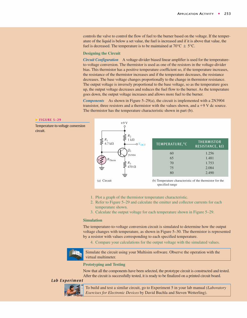
Application Activity: Temperature to Voltage Conversion
The focus of this Application Activity is a temperature-sensing circuit that converts the tem-perature of a liquid to a proportional voltage for the purpose of maintaining the temperatureof the liquid within a specified range. Figure 5–28 illustrates the temperature-control system.The temperature sensor is a thermistor, which is a device whose resistance changes withtemperature. The thermistor is connected to a transistor circuit that is biased for linear opera-tion. The output voltage of the circuit is proportional to the thermistor resistance and thus tothe temperature of the liquid in the tank. The output voltage goes to an interface circuit that
Valveinterface
Temperature-to-voltageconversioncircuit
DC powersupply
Thermistor
Continuouslyvariable valve
Fuel flow
� FIGURE 5–28
Temperature-control system.
APPLICATION ACTIVIT Y ◆ 253
controls the valve to control the flow of fuel to the burner based on the voltage. If the temper-ature of the liquid is below a set value, the fuel is increased and if it is above that value, thefuel is decreased. The temperature is to be maintained at
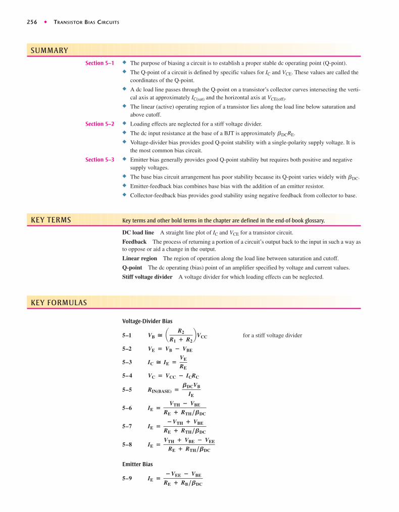
Designing the Circuit
Circuit Configuration A voltage-divider biased linear amplifier is used for the temperature-to-voltage conversion. The thermistor is used as one of the resistors in the voltage-dividerbias. This thermistor has a positive temperature coefficient so, if the temperature increases,the resistance of the thermistor increases and if the temperature decreases, the resistance decreases. The base voltage changes proportionally to the change in thermistor resistance.The output voltage is inversely proportional to the base voltage, so as the temperature goesup, the output voltage decreases and reduces the fuel flow to the burner. As the temperaturegoes down, the output voltage increases and allows more fuel to the burner.
Components As shown in Figure 5–29(a), the circuit is implemented with a 2N3904transistor, three resistors and a thermistor with the values shown, and a +9 V dc source.The thermistor has the temperature characteristic shown in part (b).
70°C ; 5°C.
R3
RTherm
VOUT
470 �
Q1
2N3904
+9 V
R21 k�
(a) Circuit
R14.7 k�
(b) Temperature characteristic of the thermistor for the specified range
T
TEMPERATURE,�CTHERMISTOR
RESISTANCE, k�
1.2561.4811.7532.0842.490
6065707580
� FIGURE 5–29
Temperature-to-voltage conversioncircuit.
1. Plot a graph of the thermistor temperature characteristic.2. Refer to Figure 5–29 and calculate the emitter and collector currents for each
temperature shown.3. Calculate the output voltage for each temperature shown in Figure 5–29.
Simulation
The temperature-to-voltage conversion circuit is simulated to determine how the outputvoltage changes with temperature, as shown in Figure 5–30. The thermistor is representedby a resistor with values corresponding to each specified temperature.
4. Compare your calculations for the output voltage with the simulated values.
Simulate the circuit using your Multisim software. Observe the operation with thevirtual multimeter.
Prototyping and Testing
Now that all the components have been selected, the prototype circuit is constructed and tested.After the circuit is successfully tested, it is ready to be finalized on a printed circuit board.
To build and test a similar circuit, go to Experiment 5 in your lab manual (LaboratoryExercises for Electronic Devices by David Buchla and Steven Wetterling).
Lab Experiment

254 ◆ TRANSISTOR BIAS CIRCUITS
(a) Circuit output voltage at 60° C
(b) Circuit output voltages at 65°, 70°, 75°, and 80°
Rtherm = 1.481 k� Rtherm = 1.753 k� Rtherm = 2.084 k� Rtherm = 2.490 k�
� FIGURE 5–30
Operation of the temperature-to-voltage conversion circuit over temperature.
The Printed Circuit Board
A partially completed printed circuit board is shown in Figure 5–31. Indicate how you wouldadd conductive traces to complete the circuit and show the input/output terminal functions.
E B C
� FIGURE 5–31
Partially complete temperature con-version circuit PC board.

SUMMARY OF TRANSISTOR BIAS CIRCUITS ◆ 255
SUMMARY OF TRANSISTOR BIAS CIRCUITS
npn transistors are shown. Supply voltage polarities are reversed for pnp transistors.
VOLTAGE-DIVIDER BIAS EMITTER BIAS
COLLECTOR-FEEDBACK BIAS BASE BIAS
EMITTER-FEEDBACK BIAS
RC
IC ≅ IE
VC = VCC − ICRC
VTH − VBE
RE + RTH/βDC
VE = IE RE
VCC
R1
RER2
VB = VE + VBE
IE =
IB ≅VB
RIN(BASE)
VCC
RC
RB
IE ≅ IC
VC = VCC − ICRC
VB = VBE
VE = 0 V
IB =VC − VBE
RB
IC ≅VCC − VBE
RC
RC
RB
VCC
IE ≅ IC
VC = VCC − ICRC
VB = VBE
VE = 0 V
IC = βDCVCC − VBB
RB
IB =VCC − VBE
RB
RC
RE
RB
VCC
IC ≅ IE
VC = VCC − ICRC
VE = VB − VBE
VB = IERE + VBE
IE =VCC − VBE
RE + RB/βDC
IB =VCC − VB
RB
RC
RB
VCC
RE
VEE
IC ≅ IE
VC = VCC − ICRC
VB = VE + VBE
VE = VEE + IERE
IB =VBRB
IE ≅−VEE − VBE
RE
256 ◆ TRANSISTOR BIAS CIRCUITS
SUMMARY
Section 5–1 ◆ The purpose of biasing a circuit is to establish a proper stable dc operating point (Q-point).
◆ The Q-point of a circuit is defined by specific values for IC and VCE. These values are called thecoordinates of the Q-point.
◆ A dc load line passes through the Q-point on a transistor’s collector curves intersecting the verti-cal axis at approximately IC(sat) and the horizontal axis at VCE(off).
◆ The linear (active) operating region of a transistor lies along the load line below saturation andabove cutoff.
Section 5–2 ◆ Loading effects are neglected for a stiff voltage divider.
◆ The dc input resistance at the base of a BJT is approximately
◆ Voltage-divider bias provides good Q-point stability with a single-polarity supply voltage. It isthe most common bias circuit.
Section 5–3 ◆ Emitter bias generally provides good Q-point stability but requires both positive and negativesupply voltages.
◆ The base bias circuit arrangement has poor stability because its Q-point varies widely with
◆ Emitter-feedback bias combines base bias with the addition of an emitter resistor.
◆ Collector-feedback bias provides good stability using negative feedback from collector to base.
KEY TERMS Key terms and other bold terms in the chapter are defined in the end-of-book glossary.
DC load line A straight line plot of IC and VCE for a transistor circuit.
Feedback The process of returning a portion of a circuit’s output back to the input in such a way asto oppose or aid a change in the output.
Linear region The region of operation along the load line between saturation and cutoff.
Q-point The dc operating (bias) point of an amplifier specified by voltage and current values.
Stiff voltage divider A voltage divider for which loading effects can be neglected.
KEY FORMULAS
Voltage-Divider Bias
5–1 for a stiff voltage divider
5–2
5–3
5–4
5–5
5–6
5–7
5–8
Emitter Bias
5–9 IE ��VEE � VBE
RE � RB/BDC
IE �VTH � VBE � VEE
RE � RTH/BDC
IE ��VTH � VBE
RE � RTH/BDC
IE �VTH � VBE
RE � RTH/BDC
RIN(BASE) �BDCVB
IE
VC � VCC � ICRC
IC � IE �VE
RE
VE � VB � VBE
VB � a R2
R1 � R2bVCC
bDC.
bDCRE.

CIRCUIT-ACTION QUIZ ◆ 257
Base Bias
5–10
5–11
Emitter-Feedback Bias
5–12
Collector-Feedback Bias
5–13
5–14
TRUE/FALSE QUIZ Answers can be found at www.pearsonhighered.com/floyd.
1. DC bias establishes the dc operating point for an amplifier.
2. Q-point is the quadratic point in a bias circuit.
3. The dc load line intersects the horizontal axis of a transistor characteristic curve at VCE � VCC.
4. The dc load line intersects the vertical axis of a transistor characteristic curve at IC � 0.
5. The linear region of a transistor’s operation lies between saturation and cutoff.
6. Voltage-divider bias is rarely used.
7. Input resistance at the base of the transistor can affect voltage-divider bias.
8. Stiff voltage-divider bias is essentially independent of base loading.
9. Emitter bias uses one dc supply voltage.
10. Negative feedback is employed in collector-feedback bias.
11. Base bias is less stable than voltage-divider bias.
12. A pnp transistor requires bias voltage polarities opposite to an npn transistor.
CIRCUIT-ACTION QUIZ Answers can be found at www.pearsonhighered.com/floyd.
1. If VBB in Figure 5–7 is increased, the Q-point value of collector current will
(a) increase (b) decrease (c) not change
2. If VBB in Figure 5–7 is increased, the Q-point value of VCE will
(a) increase (b) decrease (c) not change
3. If the value of R2 in Figure 5–10 is reduced, the base voltage will
(a) increase (b) decrease (c) not change
4. If the value of R1 in Figure 5–10 is increased, the emitter current will
(a) increase (b) decrease (c) not change
5. If RE in Figure 5–15 is decreased, the collector current will
(a) increase (b) decrease (c) not change
6. If RB in Figure 5–18 is reduced, the base-to-emitter voltage will
(a) increase (b) decrease (c) not change
7. If VCC in Figure 5–20 is increased, the base-to-emitter voltage will
(a) increase (b) decrease (c) not change
8. If R1 in Figure 5–24 opens, the collector voltage will
(a) increase (b) decrease (c) not change
9. If R2 in Figure 5–24 opens, the collector voltage will
(a) increase (b) decrease (c) not change
10. If R2 in Figure 5–24 is increased, the emitter current will
(a) increase (b) decrease (c) not change
VCE � VCC � ICRC
IC �VCC � VBE
RC � RB/BDC
IE �VCC � VBE
RE � RB/BDC
IC � BDC aVCC � VBE
RBb
VCE � VCC � ICRC

258 ◆ TRANSISTOR BIAS CIRCUITS
SELF-TEST Answers can be found at www.pearsonhighered.com/floyd.
Section 5–1 1. The maximum value of collector current in a biased transistor is
(a) (b) IC(sat) (c) greater than IE (d)
2. Ideally, a dc load line is a straight line drawn on the collector characteristic curves between
(a) the Q-point and cutoff (b) the Q-point and saturation
(c) VCE(cutoff) and IC(sat) (d)
3. If a sinusoidal voltage is applied to the base of a biased npn transistor and the resulting sinu-soidal collector voltage is clipped near zero volts, the transistor is
(a) being driven into saturation (b) being driven into cutoff
(c) operating nonlinearly (d) answers (a) and (c)
(e) answers (b) and (c)
Section 5–2 4. The input resistance at the base of a biased transistor depends mainly on
(a) (b) RB (c) RE (d)
5. In a voltage-divider biased transistor circuit such as in Figure 5–13, RIN(BASE) can generally beneglected in calculations when
(a) (b) (c) (d)
6. In a certain voltage-divider biased npn transistor, VB is 2.95 V. The dc emitter voltage is ap-proximately
(a) 2.25 V (b) 2.95 V (c) 3.65 V (d) 0.7 V
7. Voltage-divider bias
(a) cannot be independent of (b) can be essentially independent of
(c) is not widely used (d) requires fewer components than all the other methods
Section 5–3 8. Emitter bias is
(a) essentially independent of (b) very dependent on
(c) provides a stable bias point (d) answers (a) and (c)
9. In an emitter bias circuit, The emitter current
(a) is 5.3 mA (b) is 2.7 mA
(c) is 180 mA (d) cannot be determined
10. The disadvantage of base bias is that
(a) it is very complex (b) it produces low gain
(c) it is too beta dependent (d) it produces high leakage current
11. Collector-feedback bias is
(a) based on the principle of positive feedback (b) based on beta multiplication
(c) based on the principle of negative feedback (d) not very stable
Section 5–4 12. In a voltage-divider biased npn transistor, if the upper voltage-divider resistor (the one con-nected to VCC) opens,
(a) the transistor goes into cutoff (b) the transistor goes into saturation
(c) the transistor burns out (d) the supply voltage is too high
13. In a voltage-divider biased npn transistor, if the lower voltage-divider resistor (the one con-nected to ground) opens,
(a) the transistor is not affected (b) the transistor may be driven into cutoff
(c) the transistor may be driven into saturation (d) the collector current will decrease
14. In a voltage-divider biased pnp transistor, there is no base current, but the base voltage is ap-proximately correct. The most likely problem(s) is
(a) a bias resistor is open (b) the collector resistor is open
(c) the base-emitter junction is open (d) the emitter resistor is open
(e) answers (a) and (c) (f) answers (c) and (d)
RE = 2.7 kÆ and VEE = 15 V.
bDCbDC
bDCbDC
R1 V R2RIN(BASE) 7 10R2R2 7 10RIN(BASE)RIN(BASE) 7 R2
bDC and REbDC
IB = 0 and IB = IC>bDC
IE - IBbDCIB
PROBLEMS ◆ 259
15. If R1 in Figure 5–25 is open, the base voltage is
(a) +10 V (b) 0 V (c) 3.13 V (d) 0.7 V
16. If R1 is open, the collector current in Figure 5–25 is
(a) 5.17 mA (b) 10 mA (c) 4.83 mA (d) 0 mA
PROBLEMS Answers to all odd-numbered problems are at the end of the book.
BASIC PROBLEMSSection 5–1 The DC Operating Point
1. The output (collector voltage) of a biased transistor amplifier is shown in Figure 5–32. Is thetransistor biased too close to cutoff or too close to saturation?
� FIGURE 5–32
≈ 0 V
2. What is the Q-point for a biased transistor as in Figure 5–2 with
3. What is the saturation value of collector current in Problem 2?
4. What is the cutoff value of VCE in Problem 2?
5. Determine the intercept points of the dc load line on the vertical and horizontal axes of the collector-characteristic curves for the circuit in Figure 5–33.
VCC = 18 V, and RC = 1.0 kÆ?IB = 150 mA, bDC = 75,
� FIGURE 5–33
Multisim file circuits are identifiedwith a logo and are in the Problemsfolder on the companion website.Filenames correspond to figure num-bers (e.g., F05-33).
6. Assume that you wish to bias the transistor in Figure 5–33 with To what voltagemust you change the VBB supply? What are IC and VCE at the Q-point, given that
7. Design a biased-transistor circuit using VBB = VCC = 10 V for a Q-point of IC � 5 mA and VCE� 4 V. Assume The design involves finding RB, RC, and the minimum power ratingof the transistor. (The actual power rating should be greater.) Sketch the circuit.
8. Determine whether the transistor in Figure 5–34 is biased in cutoff, saturation, or the linear region. Remember that is valid only in the linear region.IC = bDCIB
bDC = 100.
bDC = 50?IB = 20 mA.
RC10 k�
RB
–
+VBB10 V
1.0 M� –
+VCC20 V
RC390 �
RB
VCC+8 V
10 k�
VBB1.5 V
βDC = 75
� FIGURE 5–34
260 ◆ TRANSISTOR BIAS CIRCUITS
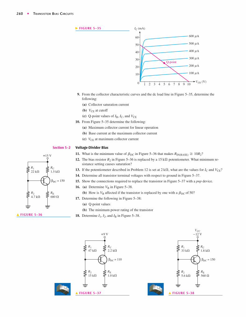
� FIGURE 5–35
20
30
40
50
60
1 2 3 4 5 6 7 8 9
Q-point
10VCE (V)
100 A
200 A
300 A
400 A
500 A
600 A
IC (mA)
0
10 μ
μ
μ
μ
μ
μ
9. From the collector characteristic curves and the dc load line in Figure 5–35, determine the following:
(a) Collector saturation current
(b) VCE at cutoff
(c) Q-point values of IB, IC, and VCE
10. From Figure 5–35 determine the following:
(a) Maximum collector current for linear operation
(b) Base current at the maximum collector current
(c) VCE at maximum collector current
Section 5–2 Voltage-Divider Bias
11. What is the minimum value of in Figure 5–36 that makes
12. The bias resistor R2 in Figure 5–36 is replaced by a potentiometer. What minimum re-sistance setting causes saturation?
13. If the potentiometer described in Problem 12 is set at what are the values for IC and VCE?
14. Determine all transistor terminal voltages with respect to ground in Figure 5–37.
15. Show the connections required to replace the transistor in Figure 5–37 with a pnp device.
16. (a) Determine VB in Figure 5–38.
(b) How is VB affected if the transistor is replaced by one with a
17. Determine the following in Figure 5–38:
(a) Q-point values
(b) The minimum power rating of the transistor
18. Determine I1, I2, and IB in Figure 5–38.
bDC of 50?
2 kÆ,
15 kÆRIN(BASE) G 10R2?bDC
RC1.5 k�
+15 V
βDC = 150
RE680 �
R24.7 k�
R122 k�
RC2.2 k�
+9 V
βDC = 110
RE1.0 k�
R215 k�
R147 k�
� FIGURE 5–36
� FIGURE 5–37
RC1.8 k�
VCC–12 V
βDC = 150
RE560 �
R25.6 k�
R133 k�
� FIGURE 5–38
25. What value of RC can be used to decrease IC in Problem 24 by 25 percent?
26. What is the minimum power rating for the transistor in Problem 25?
27. A collector-feedback circuit uses an npn transistor with Determine the collector current and the collector voltage if
28. Determine IB, IC, and VCE for a base-biased transistor circuit with the following values:VCC = 12 V,
29. If in Problem 28 doubles over temperature, what are the Q-point values?
30. You have two base bias circuits connected for testing. They are identical except that one is biased with a separate VBB source and the other is biased with the base resistor connected to VCC.Ammeters are connected to measure collector current in each circuit. You vary the VCC supplyvoltage and observe that the collector current varies in one circuit, but not in the other. In whichcircuit does the collector current change? Explain your observation.
31. The datasheet for a particular transistor specifies a minimum of 50 and a maximum of 125. What range of Q-point values can be expected if an attempt is made to mass-producethe circuit in Figure 5–42? Is this range acceptable if the Q-point must remain in the transis-tor’s linear region?
32. The base bias circuit in Figure 5–42 is subjected to a temperature variation from The decreases by 50 percent at and increases by 75 percent at from its nominalvalue of 110 at What are the changes in IC and VCE over the temperature range of0°C to 70°C?
25°C.70°C0°CbDC
0°C to 70°C.
bDCbDC
bDC
RB = 22 kÆ, and RC = 100 Æ.bDC = 90,
bDC = 200.RB = 47 kÆ.VCC = 12 V, RC = 1.2 kÆ, and
PROBLEMS ◆ 261
Section 5–3 Other Bias Methods
19. Analyze the circuit in Figure 5–39 to determine the correct voltages at the transistor terminalswith respect to ground. Assume
20. To what value can RE in Figure 5–39 be reduced without the transistor going into saturation?
21. Taking VBE into account in Figure 5–39, how much will IE change with a temperature increasefrom The VBE is 0.7 V at and decreases 2.5 mV per degree Celsius.Neglect any change in
22. When can the effect of a change in be neglected in the emitter bias circuit?
23. Determine IC and VCE in the pnp emitter bias circuit of Figure 5–40. Assume
24. Determine VB, VC, and IC in Figure 5–41.
bDC = 100.
bDC
bDC.25°C25°C to 100°C?
bDC = 100.
RE470 �
RB
VEE+10 V
10 k�
RC330 �
–10 VVCC
RC1.8 k�
VCC+3 V
RB
33 k�βDC = 90
VCC
+5 V
RC1.0 k�
RB
10 k�
RE2.2 k�
–5 VVEE
� FIGURE 5–39
� FIGURE 5–40 � FIGURE 5–41
� FIGURE 5–42
RC100 �
VCC+9 V
RB15 k�
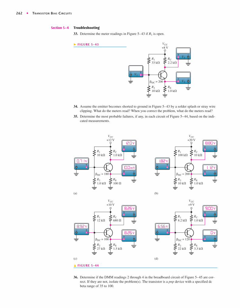
262 ◆ TRANSISTOR BIAS CIRCUITS
Section 5–4 Troubleshooting
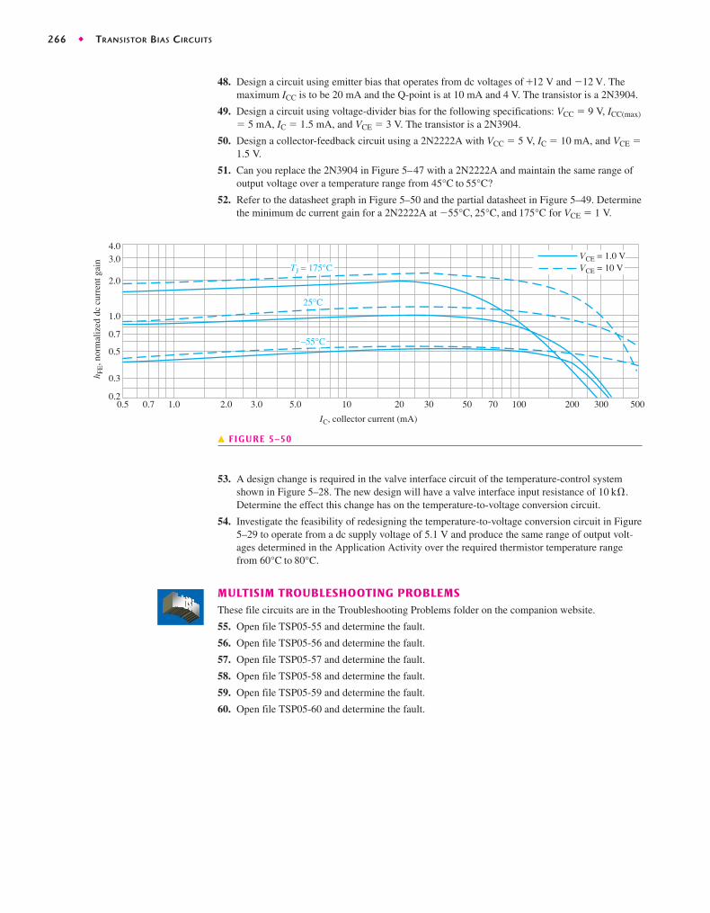
33. Determine the meter readings in Figure 5–43 if R1 is open.
− +
−+
−+
R1
V1
V2
V3
33 k�RC2.2 k�
R210 k�
RE1.0 k�
VCC+8 V
�DC = 200
� FIGURE 5–43
� FIGURE 5–44
− +
−+
−+
− +
−+
−+
− +
−+
−+
− +
−+
−+
R110 k�
RC1.0 k�
R21.0 k�
RE100 �
VCC+12 V
�DC = 180
(a)
R1100 k�
RC10 k�
R210 k�
RE1.0 k�
VCC+20 V
�DC = 200
(b)
R112 k�
RC680 �
R227 k�
RE1.5 k�
VCC+10 V
�DC = 100
(c)
R18.2 k�
RC1.0 k�
R222 k�
RE3.3 k�
VCC+9 V
�DC = 120
(d)
V
V
mV
V
V
V
V
V
V
V
VV
34. Assume the emitter becomes shorted to ground in Figure 5–43 by a solder splash or stray wireclipping. What do the meters read? When you correct the problem, what do the meters read?
35. Determine the most probable failures, if any, in each circuit of Figure 5–44, based on the indi-cated measurements.
36. Determine if the DMM readings 2 through 4 in the breadboard circuit of Figure 5–45 are cor-rect. If they are not, isolate the problem(s). The transistor is a pnp device with a specified dcbeta range of 35 to 100.

PROBLEMS ◆ 263
37. Determine each meter reading in Figure 5–45 for each of the following faults:
(a) the resistor open (b) the resistor open
(c) the resistor open (d) the resistor open
(e) a short from emitter to ground (f) an open base-emitter junction
APPLICATION ACTIVITY PROBLEMS38. Determine VB, VE, and VC in the temperature-to-voltage conversion circuit in Figure 5–29(a) if
R1 fails open.
39. What faults will cause the transistor in the temperature-to-voltage conversion circuit to go intocutoff?
40. A thermistor with the characteristic curve shown in Figure 5–46 is used in the circuit of Figure5–29(a). Calculate the output voltage for temperatures of Assume a stiffvoltage divider.
41. Explain how you would identify an open collector-base junction in the transistor in Figure 5–29(a).
45°C, 48°C, and 53°C.
1.0 kÆ10 kÆ5.6 kÆ680 Æ
4
DCV
V �COM
5 1
3
DCV
V �COM
4 1
2
DCV
V �COM
3 1
1
DCV
V �COM
2 1
E B C
2
3 5
1
4
V V V V
� FIGURE 5–45
2.6
2.4
2.2
2.0
1.8
1.6
1.4
45 46 47 48 49 50 51 52 53 54 55T (°C)
R (k�)� FIGURE 5–46

264 ◆ TRANSISTOR BIAS CIRCUITS
DATASHEET PROBLEMS42. Analyze the temperature-to-voltage conversion circuit in Figure 5–47 at the temperature ex-
tremes indicated on the graph in Figure 5–46 for both minimum and maximum specifieddatasheet values of hFE. Refer to the partial datasheet in Figure 5–48.
43. Verify that no maximum ratings are exceeded in the temperature-to-voltage conversion circuitin Figure 5–47. Refer to the partial datasheet in Figure 5–48.
44. Refer to the partial datasheet in Figure 5–49.
(a) What is the maximum collector current for a 2N2222A?
(b) What is the maximum reverse base-emitter voltage for a 2N2218A?
45. Determine the maximum power dissipation for a 2N2222A at
46. When you increase the collector current in a 2N2219A from 1 mA to 500 mA, how much doesthe minimum (hFE) change?
ADVANCED PROBLEMS47. Design a circuit using base bias that operates from a 15 V dc voltage and draws a maximum
current from the dc source (ICC(max)) of 10 mA. The Q-point values are to be IC � 5 mA andVCE � 5 V. The transistor is a 2N3904. Assume a midpoint value for bDC.
bDC
100°C.
RC1.0 k�
VCC+9.1 V
R15.6 k�
RE470 �
2N3904
T R2
Output
Absolute Maximum Ratings* TA = 25°C unless otherwise noted
*These ratings are limiting values above which the serviceability of any semiconductor device may be impaired.
NOTES:1) These ratings are based on a maximum junction temperature of 150 degrees C.2) These are steady state limits. The factory should be consulted on applications involving pulsed or low duty cycle operations.
Symbol Parameter Value Units
VCEO Collector-Emitter Voltage 40 V
VCBO Collector-Base Voltage 60 V
VEBO Emitter-Base Voltage 6.0 V
IC Collector Current - Continuous 200 mA
TJ, Tstg Operating and Storage Junction Temperature Range -55 to +150 °C
ON CHARACTERISTICS*hFE DC Current Gain IC = 0.1 mA, VCE = 1.0 V
IC = 1.0 mA, VCE = 1.0 VIC = 10 mA, VCE = 1.0 VIC = 50 mA, VCE = 1.0 VIC = 100 mA, VCE = 1.0 V
40701006030
300
VCE(sat) Collector-Emitter Saturation Voltage IC = 10 mA, IB = 1.0 mAIC = 50 mA, IB = 5.0 mA
0.20.3
VV
VBE(sat) Base-Emitter Saturation Voltage IC = 10 mA, IB = 1.0 mAIC = 50 mA, IB = 5.0 mA
0.65 0.850.95
VV
� FIGURE 5–47
� FIGURE 5–48
Partial datasheet for the 2N3904transistor. Copyright FairchildSemiconductor Corporation. Used by permission.

PROBLEMS ◆ 265
Maximum Ratings
Rating
Collector-Emitter voltageCollector-Base voltageEmitter-Base voltageCollector current — continuous
Total device dissipation @ TA = 25°C Derate above 25°CTotal device dissipation @ TC = 25°C Derate above 25°COperating and storage junction Temperature range
SymbolVCEO
VCBO
VEBO
IC
PD
PD
2N22182N22192N22212N2222
30605.0800
Unit
WattmW/°C
0.84.57
3.017.1
TJ, Tstg
2N2218,A2N2219,A
2N2218A2N2219A2N2221A2N2222A
40756.0800
0.52.28
1.26.85
2N2221,A2N2222,A
2N55812N5582
40756.0800
0.63.33
2.011.43
2N55812N5582
WattmW/°C
°C–65 to +200
V dcV dcV dc
mA dc
Electrical Characteristics (TA = 25°C unless otherwise noted.)
Characteristic Symbol Max UnitMin
Off CharacteristicsCollector-Emitter breakdown voltage (IC = 10 mA dc, IB = 0)
Collector-Base breakdown voltage (IC = 10 A dc, IE = 0)
Emitter-Base breakdown voltage (IE = 10 A dc, IC = 0)
Collector cutoff current (VCE = 60 V dc, VEB(off) = 3.0 V dcCollector cutoff current (VCB = 50 V dc, IE = 0) (VCB = 60 V dc, IE = 0) (VCB = 50 V dc, IE = 0, TA = 150°C) (VCB = 60 V dc, IE = 0, TA = 150°C)Emitter cutoff current (VEB = 3.0 V dc, IC = 0)Base cutoff current (VCE = 60 V dc, VEB(off) = 3.0 V dc)
V(BR)CEO
V(BR)CBO
V(BR)EBO
ICEX
ICBO
IEBO
IBL
V dc
V dc
V dc
nA dc
A dc
nA dc
nA dc
3040
6075
5.06.0
—
————
—
—
——
——
——
10
0.010.01101010
20
Non-A SuffixA-Suffix, 2N5581, 2N5582
Non-A SuffixA-Suffix, 2N5581, 2N5582
Non-A SuffixA-Suffix, 2N5581, 2N5582
A-Suffix, 2N5581, 2N5582
Non-A SuffixA-Suffix, 2N5581, 2N5582Non-A SuffixA-Suffix, 2N5581, 2N5582
A-Suffix, 2N5581, 2N5582
A-Suffix
On CharacteristicsDC current gain (IC = 0.1 mA dc, VCE = 10 V dc)
(IC = 1.0 mA dc, VCE = 10 V dc)
(IC = 10 mA dc, VCE = 10 V dc)
(IC = 10 mA dc, VCE = 10 V dc, TA = – 55°C)
(IC = 150 mA dc, VCE = 10 V dc)
(IC = 150 mA dc, VCE = 1.0 V dc)
(IC = 500 mA dc, VCE = 10 V dc)
Collector-Emitter saturation voltage (IC = 150 mA dc, IB = 15 mA dc)
(IC = 500 mA dc, IB = 50 mA dc)
Base-Emitter saturation voltage (IC = 150 mA dc, IB = 15 mA dc)
(IC = 500 mA dc, IB = 50 mA dc)
hFE
VCE(sat)
VBE(sat)
—
V dc
V dc
2035
2550
3575
1535
40100
2050
20302540
——
——
0.60.6
——
——
——
——
——
120300
——
————
2N2218,A, 2N2221,A, 2N5581(1)2N2219,A, 2N2222,A, 2N5582(1)
2N2218,A, 2N2221,A, 2N55812N2219,A, 2N2222,A, 2N5582
2N2218,A, 2N2221,A, 2N5581(1)2N2219,A, 2N2222,A, 2N5582(1)
2N2218,A, 2N2221,A, 2N55812N2219,A, 2N2222,A, 2N5582
2N2218,A, 2N2221,A, 2N55812N2219,A, 2N2222,A, 2N5582
2N2218,A, 2N2221,A, 2N55812N2219,A, 2N2222,A, 2N5582
2N2218, 2N22212N2219, 2N22222N2218A, 2N2221A, 2N55812N2219A, 2N2222A, 2N5582
Non-A SuffixA-Suffix, 2N5581, 2N5582
Non-A SuffixA-Suffix, 2N5581, 2N5582
Non-A SuffixA-Suffix, 2N5581, 2N5582
Non-A SuffixA-Suffix, 2N5581, 2N5582
0.40.3
1.61.0
1.31.2
2.62.0
μ
μ
μ
� FIGURE 5–49
Partial datasheet for 2N2218A–2N2222A.
266 ◆ TRANSISTOR BIAS CIRCUITS
48. Design a circuit using emitter bias that operates from dc voltages of +12 V and Themaximum ICC is to be 20 mA and the Q-point is at 10 mA and 4 V. The transistor is a 2N3904.
49. Design a circuit using voltage-divider bias for the following specifications: VCC � 9 V, ICC(max)� 5 mA, IC � 1.5 mA, and VCE � 3 V. The transistor is a 2N3904.
50. Design a collector-feedback circuit using a 2N2222A with VCC � 5 V, IC � 10 mA, and VCE �1.5 V.
51. Can you replace the 2N3904 in Figure 5–47 with a 2N2222A and maintain the same range ofoutput voltage over a temperature range from
52. Refer to the datasheet graph in Figure 5–50 and the partial datasheet in Figure 5–49. Determinethe minimum dc current gain for a 2N2222A at for VCE � 1 V.-55°C, 25°C, and 175°C
45°C to 55°C?
-12 V.
� FIGURE 5–50
4.03.0
2.0
1.0
0.2
0.3
0.5
0.7
0.5 0.7 1.0 2.0 3.0 5.0 10 20 30 50 70 100 200 300 500
h FE, n
orm
aliz
ed d
c cu
rren
t gai
n
IC, collector current (mA)
TJ = 175°C
25°C
–55°C
VCE = 1.0 VVCE = 10 V
53. A design change is required in the valve interface circuit of the temperature-control systemshown in Figure 5–28. The new design will have a valve interface input resistance of Determine the effect this change has on the temperature-to-voltage conversion circuit.
54. Investigate the feasibility of redesigning the temperature-to-voltage conversion circuit in Figure5–29 to operate from a dc supply voltage of 5.1 V and produce the same range of output volt-ages determined in the Application Activity over the required thermistor temperature rangefrom
MULTISIM TROUBLESHOOTING PROBLEMSThese file circuits are in the Troubleshooting Problems folder on the companion website.
55. Open file TSP05-55 and determine the fault.
56. Open file TSP05-56 and determine the fault.
57. Open file TSP05-57 and determine the fault.
58. Open file TSP05-58 and determine the fault.
59. Open file TSP05-59 and determine the fault.
60. Open file TSP05-60 and determine the fault.
60°C to 80°C.
10 kÆ.
Wind energy, like solar energy, is a major renewable resource. Wind is actually a productof solar energy because differences in earth temperatures result in the movement of air.Wind turbines harvest energy from the wind and may be used as small single units tosupply an individual home or wind farms where tens to hundreds of large units harvestwind energy and convert it to electricity.
Two key elements in a wind turbine are the blades and the ac generator. In many windturbines, electronic circuits sense the wind direction and speed and adjust the orientationand pitch of the blades to maximize the energy collected from the wind. The generatorproduces a varying ac voltage that depends on the rotational speed of the blades due tothe wind. Since the frequency and amplitude of a generator output varies with windspeed, the ac output is converted to dc and then back to 60 Hz ac with an inverter. Like asolar power system, the energy can be stored in batteries using a charge controller forsmaller applications, or the energy can be connected directly to the grid for large-scaleapplications.
Figure GA5–1 shows a basic diagram of a horizontal-axis wind turbine (HAWT) forsmall power applications, such as home use. A typical wind turbine has three blades andis mounted on a very high support tower. Wind energy is converted to mechanical energyby the rotating blades. As shown in Figure GA5–1, the blade rotation is applied to a shaft,which is geared up to turn the ac generator shaft at a higher rate than the blades are rotat-ing. The generator rotation produces an ac voltage output with a frequency that dependson the rate of rotation. Since it is a variable frequency and amplitude output, as previ-ously mentioned, the ac is converted to dc by the ac-to-dc converter. The dc is sent to acharge controller that charges the storage batteries. The battery output is applied to aninverter where it is converted to a 120 V, 60 Hz ac voltage for individual consumer use.The wind vane and yaw bearing assembly are used on small turbines to keep the bladespointed into the wind. An anemometer senses the wind speed in order to brake the bladeswhen the wind reaches a specified speed. This prevents mechanical damage if the windspeed is too high.
GreenTech Application 5: Wind Power
GREENTECH APPLICATION 5 ◆ 267
AC generator
Rotator blades
Brake Gears
Support poleYaw bearings
DC to external chargecontroller, batteries,and inverter
AC-to-DCconverter
Control electronics
Anemometer
Wind vane
� FIGURE GA5–1
Basic small HAWT system operation.
The AC-to-DC Converter
Because of the variable frequency of the ac from the generator, it must first be convertedto dc for the charge controller. A rectifier and regulator are used for the conversion, as illustrated in Figure GA5–2. The ac voltage from the generator varies in amplitude andfrequency as a function of wind speed. The ac-to-dc converter changes the varying ac to a varying dc voltage, which is then applied to a voltage regulator to produce a specifiedconstant dc voltage, as shown.
Large-Scale Wind Turbines
Figure GA5–3 is a horizontal axis grid-tie turbine, which is the most common configura-tion for commercial wind farm applications. The wind direction sensor sends a signal tothe control electronics so the yaw motor can keep the turbine pointing into the wind. Thewind speed sensor sends a signal to the control electronics so the pitch of the blades canbe adjusted for maximum efficiency. Also, when the wind exceeds a specified speed, thecontrol electronics activates the brakes to reduce or stop rotation of the blades, preventingdamage to the unit.
Full-wave rectifierwith filter
From ac generator
Voltage regulatorTo chargecontroller
� FIGURE GA5–2
AC-to-DC converter block diagram.
Rotator blades
Brake Gears
Yaw motor
Tower
3-phase60 Hz acto grid step-up transformer
AC-to-DCconverter
3-phaseinverter
Control electronics
Wind sensors
AC generator
� FIGURE GA5–3
Large horizontal-axis wind turbine (HAWT).
268 ◆ TRANSISTOR BIAS CIRCUITS
GREENTECH APPLICATION 5 ◆ 269
v = wind velocityρ = air density
r = radius = length of blade
A = πr2 = area through whichthe blades sweep
� FIGURE GA5–4
Factor determining the available power in the wind.
For large wind turbines (above 100 kW–150 kW) the voltage generated is usually 690 Vthree-phase ac. The output goes to a transformer usually located in the tower or near itsbase and is stepped up to thousands of volts depending on the requirements of the localelectrical grid.
Power in the Wind
The amount of power available in the wind can be calculated using the following formula:
In the formula, is the density of the air, A is the area swept by the blades, and v is thevelocity (speed) of the wind. Note that the power is dependent on the length of the blades,r, and the cube of the wind speed, v3. Since A � if the length of the blades is doubled,pr2,
r
P =rAv3
2
Betz Law This law states that the theoretical limit of the amount of power that can beextracted from the wind is 59% if all conditions are perfect. This limiting factor was de-veloped by Albert Betz in 1926. In practice, 20% to 40% can normally be expected.
Wind Power Curve
A wind power curve shows the amount of power that can be extracted over a range ofwind speeds (velocities) for specific turbines. Wind power curves will vary from one typeof turbine to another. Figure GA5–5 shows a typical curve. The cut-in speed is the windspeed at which the blades begin to turn. The start-up speed is the wind speed at which theblades are moving fast enough to cause the generator to produce electricity. The start-upspeed is slightly higher than the cut-in speed. The maximum power output is the peakpower that the turbine can produce. For this example curve, the maximum power outputis approximately 200 kW at a wind speed of approximately 28 mph.
To limit the rotational speed of the blades above the maximum power output (MPO) point inorder to prevent damage to the machine, a process called furling is used. Ideally, the curve iskept as level as possible as shown by the dashed portion of the curve in Figure GA5–5.However, in practice, the power decreases above that point, once the furling process is acti-vated. Furling can be accomplished by changing the pitch of the blades or turning the entireturbine away from the wind direction slightly under direction of the control electronics. Also,when the wind reaches a predetermined maximum, the turbine can be completely shut down.For example, the curve shows this turbine being shut down at 45 mph.
the available power in the wind will be increased by four times (22 � 4). If the wind velocity doubles, the available power in the wind is increased by eight times (23 � 8). Ofcourse, a turbine cannot convert all of the available wind power into mechanical power toturn the generator. In fact, most practical turbines can convert less than 50% of the windpower. Figure GA5–4 illustrates the factors that affect the amount of power that can beextracted from the wind.

270 ◆ TRANSISTOR BIAS CIRCUITS
20018016014012010080604020
00 5 10 15 20 25 30 35 40 45
Wind speed (mph)
Power (kW)
Shut down
Maximum power output
Cut in Start up
Furling
� FIGURE GA5–5
Example of a wind power curve for a wind turbine.
Questions
Some questions may require research beyond the content of this coverage. Answers are atthe end of the book.
1. What does HAWT stand for?
2. Why does the input voltage to the ac-to-dc converter vary in amplitude andfrequency?
3. What are the physical factors that determine the amount of power available in thewind that strikes the blades of a turbine?
4. What is the Betz limit?
5. In wind farms, how close together should the turbines generally be placed?
The following websites are recommended for viewing HAWTs in action.Many other websites are also available.
http://www.youtube.com/watch?v=eXejxcW-XGo
http://www.youtube.com/watch?v=RFPj9frhKuo
http://www.youtube.com/watch?v=7PLvr-lpADM&NR=1
http://www.youtube.com/watch?v=7rlVMJgPRc4
http://www.youtube.com/watch?v=NeVClBaQI_Q
http://www.youtube.com/watch?v=PEEAl9laoUg
http://www.youtube.com/watch?v=N9_FKGxD27g
http://www.youtube.com/watch?v=v05MuBseBQE
http://www.youtube.com/watch?v=hBRfboAscww