LCD TV Technical Training Manual
26
LCD TV Technical Training Manual 1/22 ఐ ఐ ఐ ML-038C Chassis 37,42 inch LCD TV - RZ-37LZ30 (Market:EU) - RZ-42LZ30 (Market:EU)
-
Upload
khangminh22 -
Category
Documents
-
view
1 -
download
0
Transcript of LCD TV Technical Training Manual
LCD TV Technical Training Manual
� 1/22
���� ML-038C Chassis 37,42 inch LCD TV
- RZ-37LZ30(Market:EU)
- RZ-42LZ30(Market:EU)

� 2/22
Contents
1. Circuit operation Description1.1 Block diagram1.2 Signal Input block1.3 Video Decoder Block 1.4 De-interlacer Block1.5 A/D converter Block1.6 Scalar input Block1.7 Scalar output Block1.8 Micro controller Block
1.9 Audio Circuits
2. Power Board block 2.1 Block diagram2.2 Circuit Description
Appendices 11. Software Upgrade Method 2. Composite Signal Description
2.1 NTSC Composite Signal2.2 PAL Composite Signal2.3 SECAM Composite Signal
Appendices 21. Pin Outs:1.1 DVI connector1.2 DSUB connector1.3 SCART connector1.4 S-video
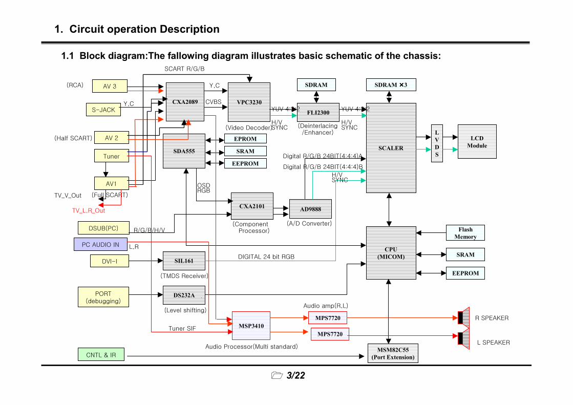
1.1 Block diagram:The fallowing diagram illustrates basic schematic of the chassis:
� 3/22
1. Circuit operation Description
��������
���������
�� ��
��������
MSM82C55(Port Extension)
���������
���
���
�����
�����
��������
CXA2089
� �!!�����
VPC3230
��"#�$��%$#���
FLI2300
���"����!&%"�'� �(&�%���
SCALER
)��*+�+�
,���)��
)��*+�+�
,���)��
SDRAM SDRAM ����3
AD9888
�����$�-������
SDA555
EPROM
SRAM
EEPROM
SIL161
DS232A
��.���%�"-���
���-�!/("0�"�'�
CPU(MICOM)
FlashMemory
SRAM
EEPROM
LVDS
LCDModule
����1�
�"'"�&!�����*����*+*+*��
�����,��
CXA2101
��$23$������$%�//$��
,���)��
MSP3410MPS7720
��#"$��$%�//$��.�!�"/�&�#&�#�
)��
�����
��������*4"���
�"'"�&!�����*����*+*+*��
�������
��#"$&23����
��
MPS7720��� ��
��5���)��
����#�4�''"�'�
����
�,&!0�����
��6����

� 4/22
This is a analog signal input circuit diagram:This block consist of three SCART and one S-Video inputs. *1) This is SCART Jack. Output signals from this jack are CVBS and R,G,B,FB.
Inputs are CVBS signal from tuner and audio inputs for R and L channels. *2) This is also SCART Jack. Input signal from this jack is CVBS only. And output signal is
video signal that currently is displayed on our LCD TV.*3) This is S-Video signal input port,the input to this port comes from Av board through S-jack. 82 ohm resistors on the Video Signal line are used for impedance matching.
*4) This is analog video Switching IC. Five video input signals(Three SCART , one S-Video, one CVBS fromTuner) are switched by this IC.
1. Circuit operation Description
1.2 Signal input Block
*2)
*1)
*4)
*3)

� 5/22
1. Circuit operation Description
1.2 Signal input Block
*1)
This is a analog Tuner and associated circuit diagram:This Tuner takes the input as the RF signal from cable or antenna and converts it into IF signal using Superheterodyning process. 1) This Tuner can tune for PAL and SECAM RF signal2) Power supply voltage for this tuner is 5V, 33V.3) The inputs to the tuner is TV RF signal from coaxial cable and output is TV video signal which processed by video decoder
to be displayed on screen.4) The most important functions associated are AGC(Automatic Gain Control) and AFT(Auto Frequency Tuning).5) The SIF i.e.Sound IF is also given out by tuner which is then fed to audio section.
� 6/22
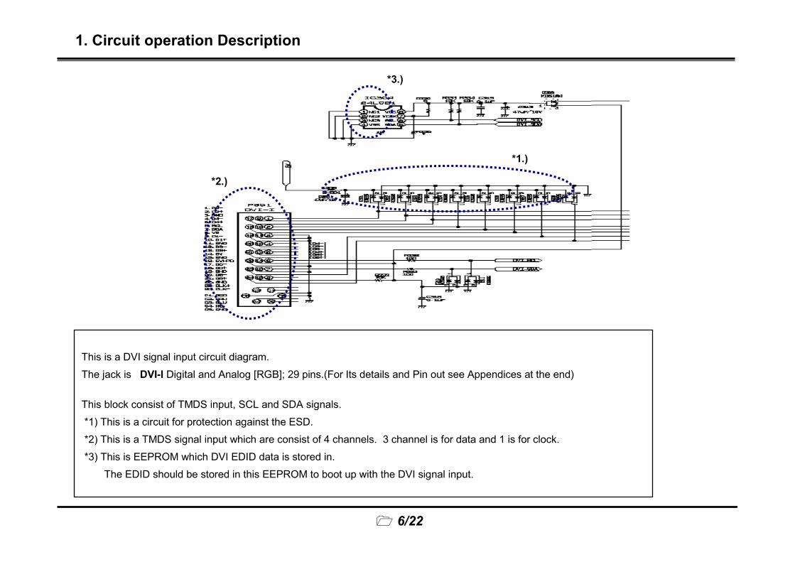
This is a DVI signal input circuit diagram.The jack is DVI-I Digital and Analog [RGB]; 29 pins.(For Its details and Pin out see Appendices at the end)
This block consist of TMDS input, SCL and SDA signals.*1) This is a circuit for protection against the ESD. *2) This is a TMDS signal input which are consist of 4 channels. 3 channel is for data and 1 is for clock.*3) This is EEPROM which DVI EDID data is stored in.
The EDID should be stored in this EEPROM to boot up with the DVI signal input.
1. Circuit operation Description
*3.)
*2.)
*1.)

� 7/22
This is Analog R,G,B signal and RS-232C port input Block.This block consist of 3.3V regulator, 2.5V regulator, panel Vcc voltage switching circuit.
*1) This is a circuit for protection against the ESD. *2) This is EEPROM which RGB EDID data is stored in.
The EDID should be stored in this EEPROM to boot up with the DVI signal input.*3) This is Level shifting IC. It is used to communicate between PC and our chassis’s CPU for debugging.*4) This is D-SUB jack.(For Its details and Pin out see Appendices at the end)
1. Circuit operation Description
*2.)
*4.)
*4.)
*1.) *3.)

� 8/22
* Input signal Format
*1) CVBS Signal
(Y Signal+C Signal+H,V Sync)
*2) S-Video Signal
(Separated Y,C Signal)
*3) Component Signal ,Only 480i
(Y, Pb, Pr)
The main Features of *1) VPC3230 are have functions are- high performance adaptive 4H Comb-Filter Y/C separator with adjustable vertical
peaking.- multi-standard color decoder PAL/NTSC/SECAM including all sub standards.- four CVBS, one S-Video input and one CVBS output- two RGB/YPbPr Component input, one Fast Blank input- peaking,contrast,brightness,color saturation,tint for RGB/YPbPr and CVBS,S-Video- IC Bus interface- one 20.25Mhz Crystal, few external components.- YUV 4:2:2 output format.
1. Circuit operation Description
1.3 Video decoder Block
*1)

� 9/22
This block consists of *1)FLI2200(Deinterlacer/Line doubler).*1) Removes artifacts produced by improper Y/C separation.
Supports 525/60(NTSC),625/50(PAL/SECAM).Accept up to 1100 pixels/lineYUV,RGB or YCbCr progressive output options.Supports 8 or 10 bit inputs and outputs.Our chassis use 10 bit YUV output format.
*2) 64M SDRAM,is Field memory which have 4MB capacity.This IC’s feature is a little different according to makers.160Mhz Memory clock is used.
1. Circuit operation Description
1.4 Deinterlacer Block
*1)*2)

� 10/22
1. Circuit operation Description
1.5 AD converter Block
*1)
This block consists of AD Converter,.*1) 140M MSPS Maximum conversion rate.
0.5 to 1V Analog input range.Component(480p,720p,1080i) /R,G,B signal pass through this IC.Output format is R,G,B 8:8:8 format .

� 11/22
1. Circuit operation Description
1.6 Scalar input Block
*1) Video port input Block.Input data format is YUV 4:2:2 plus H,V sync and data clock .Deinterlacer IC’s output pass through this.
*2) Graphic port input Block.AD Converter’s output and TMDS receiver IC ‘s output pass through this.AD Converter IC:AD9888, TMDS receiver:Sil161B.Input data format is RGB 8:8:8 digital data signal plus H,V sync and data clock.
*1)
*2)

� 12/22
1. Circuit operation Description
*1) is data output.Data output format is composed of RGB 8:8:8, H,V sync, data clock,data enable.Output sync and clock corresponds to LCD Module’s timing.
*2) is LVDS transmitter IC.Five pair signal data is transmitted to LCD Module’s T-con Board.
*3) is FET IC for 12V power supply.
*1)
1.7 Scalar output Block
*2)
*3)

� 13/22
1. Circuit operation Description
This block consists of CPU, Flash memory, SRAM, Port Expansion, etc ,.*1) is CPU IC.
Use 3.3V-standby Power and 25Mhz clock.It keep in communication with Flash memory,SRAM by 16bit parallel /Scaler IC by 8bit parallel. It keep in communication with EEPROM by I2C.
*2) is Port Expansion.It receive local key input. Output control signal is inv_on, sound_mute and lvds_enable,etc.
*3) is Flash memory that stored in System file and OSD file.*4) is SRAM that is loaded all kinds of variables.*5) is EEPROM that stored in adjustment data and user control data.
1.8 Micro controller Block(CPU)
*4)
*5)
*2
*1)*3)

� 14/22
1. Circuit operation Description
This block consists of Multi Standard Audio Processor and Audio amplifier ,.*1) This is the MSP audio processing IC,This IC performs processing of different standards.
It performs ASS (Automatic Standard Selection). *2)They are Audio Amplifiers IC for Right and Left Audio Channels. It is a 20W class-D amplifier IC which operateson 7.5 to 24 V Vcc The efficiency is very high.*3)The PC input jack is used to give Audio Inputs
1.9 Audio Block
*2)*1)
*3)
� 15/22
Appendices 1
1. Software Upgrade Method
2. Composite Signal Description
2.1 NTSC Composite Signal
2.2 PAL Composite Signal
2.3 SECAM Composite Signal

1. Software Upgrade Method
� 16/22
Software Upgrade Method for ML-038C(Model:RZ-37/42LZ30) Chassis
1) Connect Power Board(P/N:6871TPT283A) and Main Board(P/N:3313TP3001B)
2) Press the pin(SW001) that is located beside DVI Jack with sharp pin.
3) Connect RS-232C cable between PC and our set.The cable must be crossed Pin2 and Pin3.
4) Execute Flash Loader program. The program version must be 2.0
5) Supply AC power. Our set’s power input range is Wide Range(100~240V).Then, the Flash memory is identified.
6) Press “Browse” menu and find the file that must be upgraded.
7) Press “Program” in operation window. And Press “Start” button.Then, Software upgrade is executed.
8) Press the pin(SW001) that is located beside DVI Jack Originally. Must not be missed.If you miss this job, there is no image and no sound. Also, fail to power on.

� 17/22
���������� ���
�������������������� ��������
������������������ � ���
�������!�"�������� ���#��$�����������
�����%��&��' ����$��
!���� ������ ��$��
������������������������ ������������������������
*1)
*1)
*2)
*2)
2. Composite Signal Description
2.1 NTSC Composite Signal

� 18/22
NTSC(M) Composite Video Signal for 75% Color Bar
2. Composite Signal Description

� 19/22
�������� �� �� �� �� �� �� �� �� �� �� �� �� �� �� �� �� �� �� �� ��
�������������������� ���� ���� ����
��������� ��������� ��������� ��������� ���� ��� ��� ��� ��� ��
�������������� !��"#�������������� !��"#�������������� !��"#�������������� !��"# ��� ���� ���� ���� ���� ���
$����"������ !��"#$����"������ !��"#$����"������ !��"#$����"������ !��"# �� �� �� �� �� ��
%&'�%&'�%&'�%&'������!���!("�����������!���!("�����������!���!("�����������!���!("������
��� !��"#��� !��"#��� !��"#��� !��"# $�� �������( �������( �������( ��(� � ������
%)'�%)'�%)'�%)'�$���������*���+$���������*���+$���������*���+$���������*���+ $�� � $�� �$�� �� $�� ���$�� ���$��
��!������������!������������!������������!���������� $�� �$�� �� $�� ��$�� ��$�� ��$��
������������������������
*1)
*2)
2. Composite Signal Description
2.2 PAL Composite Signal

� 20/22
PAL(B,D,B,H,I) Composite Video Signal for 75% Color Bar
2. Composite Signal Description

� 21/22
���������������� ���������������� ����������������
��� ��� ��� ��� ��������������������������������
������������������������������������ ���� ����� �����
������������� !��"# ������������� !��"# ������������� !��"# ������������� !��"# �� ����� �����
$����"������ !��"#$����"������ !��"#$����"������ !��"#$����"������ !��"# �� ��� ���
�����!���!%"�����������!���!%"�����������!���!%"�����������!���!%"������ ���� ����
���� !��"#���� !��"#���� !��"#���� !��"# ��� ��� ���
$��������&���'$��������&���'$��������&���'$��������&���' ��� ����� �����
��!��������!��������!��������!������ ��� ������ ������
�(����(����(����(���
1) Like PAL, SECAM is a 625-line, 50 field-per-second, 2:1 interlaced system.
2) As with NTSC and PAL, the luminance signal occupy the entire video bandwidth.
3) The video signal has a bandwidth of 5.0 or 6.0 MHz, depending on specific SECAM standards.
4) SECAM uses FM modulation to transmit color difference information, with each component having its own
subcarrier.
2. Composite Signal Description
2.3 SECAM Composite Signal

� 22/22
Appendices 2
1. Pin Outs:1.1 DVI connector1.2 DSUB connector1.3 SCART connector1.4 S-video
� 23/22
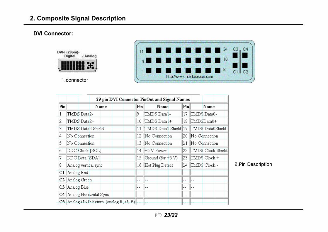
2. Composite Signal Description
DVI Connector:
��������������������������������������������
���� �������������� �������������� �������������� ����������

� 24/22
2. Composite Signal Description
2.3 SCART Connector:
Male front view
��������������������������������������������
���� �������������� �������������� �������������� ����������

� 25/22
2. Composite Signal Description
2.3 ����������������������������
������������������������������������������������������������������������������������������������������������������������������������������������������������������������������������������������������������������������������������������������������������� ����������������������������������������������� ����������������������������������������������� ����������������������������������������������� ����������������������������!"��������#��������������������������������$����� ��������������!"��������#��������������������������������$����� ��������������!"��������#��������������������������������$����� ��������������!"��������#��������������������������������$����� �������������%&����'�()(��������� ����������������%&����'�()(��������� ����������������%&����'�()(��������� ����������������%&����'�()(��������� ���������������%*����'�(*(��+����������������������������������������%*����'�(*(��+����������������������������������������%*����'�(*(��+����������������������������������������%*����'�(*(��+���������������������������� �������������������������������� �����,�����,�����,�����,��������-�������-�������-�������-������� ./��� ./��� ./��� ./��������������������������������������������0���0����������)1*�2*��������2��������0���0����������)1*�2*��������2��������0���0����������)1*�2*��������2��������0���0����������)1*�2*��������2�������2�2�2�2������������������������� ����� ������������������������������0�������������������������� ����� ������������������������������0�������������������������� ����� ������������������������������0�������������������������� ����� ������������������������������0������3�4������3�4������3�4������3�4�����������3�2��3�2��3�2��3�2�
��������������*���������*��������������*���������*��������������*���������*��������������*���������*�������� ��������������������

� 26/22
2. Composite Signal Description
2.3 DSUB 15p connector pin out
���� �������������� �������������� �������������� ����������
��������������������������������������������