
Large-signal SPICE model for depletion-type silicon ring ...
7
Large-signal SPICE model for depletion-type silicon ring modulators MINKYU KIM, 1 MYUNGJIN SHIN, 1,2 MIN-HYEONG KIM, 1,3 BYUNG-MIN YU, 1 YOUNGHYUN KIM, 1,4 YOOJIN BAN, 1,4 STEFAN LISCHKE, 5 CHRISTIAN MAI, 5 LARS ZIMMERMANN, 5 AND WOO-YOUNG CHOI 1, * 1 Department of Electrical and Electronic Engineering, Yonsei University, 03722 Seoul, South Korea 2 Now at University of Michigan, Ann Arbor, 48109 Michigan, USA 3 Now at Samsung Electronics, Hwasung, 18448 Gyeonggi-do, South Korea 4 Now at IMEC, Kapeldreef 75, 3001 Leuven, Belgium 5 IHP, Im Technologiepark 25, 15236 Frankfurt (Oder), Germany *Corresponding author: [email protected] Received 15 April 2019; revised 26 June 2019; accepted 26 June 2019; posted 28 June 2019 (Doc. ID 364895); published 7 August 2019 We present an accurate, easy-to-use large-signal SPICE circuit model for depletion-type silicon ring modulators (Si RMs). Our model includes both the electrical and optical characteristics of the Si RM and consists of circuit elements whose values change depending on modulation voltages. The accuracy of our model is confirmed by com- paring the SPICE simulation results of 25 Gb/s non-return-to-zero (NRZ) modulation with the measurement. The model is used for performance optimization of monolithically integrated Si photonic NRZ and pulse-amplitude- modulation 4 transmitters in the standard SPICE circuit design environment. © 2019 Chinese Laser Press https://doi.org/10.1364/PRJ.7.000948 1. INTRODUCTION Depletion-type silicon ring modulators (Si RMs) attract a great amount of research interests since they can provide advantages for optical interconnect (IC) applications such as large modu- lation bandwidth and small power consumption [1–4]. Furthermore, Si RMs are much smaller than the widely used Si Mach–Zehnder modulators (MZMs) and, consequently, al- low much easier monolithic integration with electronics. Such electronic–photonic integration is necessary for interconnec- tion solutions for future high-performance electronic systems in which photonic solutions must be as closely located to elec- tronics as possible for size and power consumption reduction [5]. To realize Si electronic–photonic ICs containing Si RMs, a Si RM equivalent circuit model that is accurate, easy-to-use, and compatible with the standard IC design environment is highly desirable. In addition, extracting numerical values for model parameters should be simple and straight-forward. Although there have been several published reports on depletion-type Si RM models, none satisfies the above require- ments. In Ref. [6], a precise analytical model for a Si RM was reported, but it requires more than 10 parameters and is not very compatible with the standard Si IC design environment. We reported a Verilog-A implementation of a coupled-mode description of the Si RM [7], which can be easily executed in the SPICE simulation environment. It, however, requires a substantial amount of computation time because Verilog-A is not optimized for numerically solving differential equations and, consequently, the simulation must use a very fine time resolution to accurately describe Si RM dynamics. In this paper, we present a large-signal equivalent circuit model based on the linear equivalent circuit of the Si RM [8], which contains only a few independent model parameters that can be easily extracted from the simple RM transmission measurement. Although model parameter values nonlinearly depend on the Si RM bias voltage, we demonstrate that, by using voltage-dependent circuit elements available within SPICE, large-signal transient modulation characteristics can be easily and accurately simulated at least 220 times faster than the approach used in Ref. [7]. Such a reduction in computation time should provide a great advantage for design optimization of optical interconnection solutions for high-performance elec- tronic systems that may contain numerous Si RMs as well as various electronic circuit blocks. An initial portion of this work was reported in Ref. [9]. In this paper, a more detailed descrip- tion of our model is presented. In addition, we provide how our model can be used for performance optimization of pulse-am- plitude modulation 4 (PAM-4) transmitters containing Si RMs and SiGe BiCMOS transistors. This paper is organized in four chapters. In Chapter 2, after a brief description of the Si RM device used for our investiga- tion, we give the details of our model and explain how model parameters are extracted from measurement results. The accu- racy of the model also is verified with a 25 Gb/s non-return-to- zero (NRZ) measurement. In Chapter 3, we demonstrate the 948 Vol. 7, No. 9 / September 2019 / Photonics Research Research Article 2327-9125/19/090948-07 Journal © 2019 Chinese Laser Press
-
Upload
khangminh22 -
Category
Documents
-
view
1 -
download
0
Transcript of Large-signal SPICE model for depletion-type silicon ring ...

Large-signal SPICE model for depletion-typesilicon ring modulatorsMINKYU KIM,1 MYUNGJIN SHIN,1,2 MIN-HYEONG KIM,1,3 BYUNG-MIN YU,1 YOUNGHYUN KIM,1,4
YOOJIN BAN,1,4 STEFAN LISCHKE,5 CHRISTIAN MAI,5 LARS ZIMMERMANN,5 AND WOO-YOUNG CHOI1,*1Department of Electrical and Electronic Engineering, Yonsei University, 03722 Seoul, South Korea2Now at University of Michigan, Ann Arbor, 48109 Michigan, USA3Now at Samsung Electronics, Hwasung, 18448 Gyeonggi-do, South Korea4Now at IMEC, Kapeldreef 75, 3001 Leuven, Belgium5IHP, Im Technologiepark 25, 15236 Frankfurt (Oder), Germany*Corresponding author: [email protected]
Received 15 April 2019; revised 26 June 2019; accepted 26 June 2019; posted 28 June 2019 (Doc. ID 364895); published 7 August 2019
We present an accurate, easy-to-use large-signal SPICE circuit model for depletion-type silicon ring modulators(Si RMs). Our model includes both the electrical and optical characteristics of the Si RM and consists of circuitelements whose values change depending onmodulation voltages. The accuracy of our model is confirmed by com-paring the SPICE simulation results of 25 Gb/s non-return-to-zero (NRZ) modulation with the measurement. Themodel is used for performance optimization of monolithically integrated Si photonic NRZ and pulse-amplitude-modulation 4 transmitters in the standard SPICE circuit design environment. © 2019 Chinese Laser Press
https://doi.org/10.1364/PRJ.7.000948
1. INTRODUCTION
Depletion-type silicon ring modulators (Si RMs) attract a greatamount of research interests since they can provide advantagesfor optical interconnect (IC) applications such as large modu-lation bandwidth and small power consumption [1–4].Furthermore, Si RMs are much smaller than the widely usedSi Mach–Zehnder modulators (MZMs) and, consequently, al-low much easier monolithic integration with electronics. Suchelectronic–photonic integration is necessary for interconnec-tion solutions for future high-performance electronic systemsin which photonic solutions must be as closely located to elec-tronics as possible for size and power consumption reduction[5]. To realize Si electronic–photonic ICs containing Si RMs, aSi RM equivalent circuit model that is accurate, easy-to-use,and compatible with the standard IC design environment ishighly desirable. In addition, extracting numerical values formodel parameters should be simple and straight-forward.
Although there have been several published reports ondepletion-type Si RM models, none satisfies the above require-ments. In Ref. [6], a precise analytical model for a Si RM wasreported, but it requires more than 10 parameters and is notvery compatible with the standard Si IC design environment.We reported a Verilog-A implementation of a coupled-modedescription of the Si RM [7], which can be easily executedin the SPICE simulation environment. It, however, requiresa substantial amount of computation time because Verilog-Ais not optimized for numerically solving differential equations
and, consequently, the simulation must use a very fine timeresolution to accurately describe Si RM dynamics.
In this paper, we present a large-signal equivalent circuitmodel based on the linear equivalent circuit of the Si RM[8], which contains only a few independent model parametersthat can be easily extracted from the simple RM transmissionmeasurement. Although model parameter values nonlinearlydepend on the Si RM bias voltage, we demonstrate that,by using voltage-dependent circuit elements available withinSPICE, large-signal transient modulation characteristics canbe easily and accurately simulated at least 220 times faster thanthe approach used in Ref. [7]. Such a reduction in computationtime should provide a great advantage for design optimizationof optical interconnection solutions for high-performance elec-tronic systems that may contain numerous Si RMs as well asvarious electronic circuit blocks. An initial portion of this workwas reported in Ref. [9]. In this paper, a more detailed descrip-tion of our model is presented. In addition, we provide how ourmodel can be used for performance optimization of pulse-am-plitude modulation 4 (PAM-4) transmitters containing Si RMsand SiGe BiCMOS transistors.
This paper is organized in four chapters. In Chapter 2, aftera brief description of the Si RM device used for our investiga-tion, we give the details of our model and explain how modelparameters are extracted from measurement results. The accu-racy of the model also is verified with a 25 Gb/s non-return-to-zero (NRZ) measurement. In Chapter 3, we demonstrate the
948 Vol. 7, No. 9 / September 2019 / Photonics Research Research Article
2327-9125/19/090948-07 Journal © 2019 Chinese Laser Press

advantage of our model by showing how it can be used for thedesign optimization of a monolithic Si photonic NRZ andPAM-4 transmitters in terms of power consumption minimi-zation and optical modulation amplitude (OMA) maximiza-tion. Chapter 4 concludes the paper.
2. LARGE-SIGNAL SPICE MODEL FOR Si RM
Figure 1(a) shows the structure of the depletion-type Si RMused for our investigation. It is fabricated by a Si photonicsfoundry service provided by IHP. The ring has an 8 μm radius,and there is a 290 nm separation between the bus and ringwaveguides, as can be seen in the TEM image of the cross-section of the coupling section given in Fig. 1(b). The lateralp-n junction diode for the ring waveguide has the nominal peakdoping concentration of 7 × 1017 cm−3 for the p-region and3 × 1018 cm−3 for the n-region. Figure 1(c) shows the normal-ized transmission characteristics measured at four different biasvoltages. For this and other measurements reported in thispaper, the device is placed on a stage whose temperature ismaintained at 25°C by a temperature controller.
The dynamic characteristics of an RM can be described bycoupled-mode equations as [10]
d
dta�t� �
�jωres −
1
τ
�a�t� − j
ffiffiffiffi2
τe
sE in�t�, (1)
Eout�t� � E in�t� − jffiffiffiffi2
τe
sa�t�, (2)
where a�t) represents the energy stored in the ringresonator, and τ is the decay time constant for a�t�. τ has
two components, τl and τe , which, respectively, represent thedecay time constants due to the ring resonator loss and thecoupling loss between the ring and bus waveguides. Theirrelationship is given as 1
τ � 1τl� 1
τe. ωres is the ring resonance
angular frequency given as ωres � 2πmcneffL
, where m is an integerrepresenting the resonance mode index, c is the velocity of lightin the vacuum, L is the ring circumference, and neff is theeffective index of the ring waveguide at the resonance.
The RM steady-state transmission characteristics can bederived from Eqs. (1) and (2) as
T ��Eout
E in
�2
�"j�ω − ωres� � 2
τl− 1
τ
j�ω − ωres� � 1τ
#2
: (3)
By fitting Eq. (3) to the measured transmission characteristicsshown in Fig. 1(c), numerical values for three key parameters(neff , τ, τl ) at different bias voltages can be determined. Theresults are given in Table 1. The quality factor of the RM isrelated to τ as Q � ωresτ
2, which indicates our RM has a Q of
about 8000.The normalized RM small-signal modulation frequency
response in the s-domain at a given bias voltage can be approxi-mated as [11]
s � 2τl
s2 � 2τ s � D2
ω � 1τ2, (4)
where Dω is the detuning parameter (Dω � jωin − ωresj) rep-resenting how much the input light frequency (ωin) is separatedfrom the RM resonance frequency (ωres). Figure 2(a) shows theblock diagram of the Si RM equivalent circuit. It consists ofthree blocks. Block A accounts for parasitic RLC componentsdue to bond pads and metal interconnects [8]. Block B shown
Fig. 1. (a) Structure of the Si RM used; (b) TEM image of the cross-section of the coupling section; and (c) measured transmission curves withdifferent bias voltages.
Research Article Vol. 7, No. 9 / September 2019 / Photonics Research 949

in Fig. 2(b) represents the RM’s electrical property due to aseries resistance and ring waveguide p-n junction. Block Cshown in Fig. 2(c) is an equivalent circuit emulating Eq. (4).Voltage-dependent resistors and capacitors are used in Blocks Band C, as the junction capacitance, and τ and τl depend on RMbias voltages. A scaling factor given as g � Pout
Pin· R1�R2
R2is used in
Block C, where P in and Pout are the input and output opticalpower used for the RM transmission measurement,respectively, so that Block C output voltage, V out, representsthe ratio of Pout and P in.
Numerical values for circuit elements in Blocks A and B canbe easily obtained from the electrical s-parameter measurementsat different bias voltages. Numerical values for Block Ccircuit elements are obtained by matching Eq. (4) with theBlock C transfer function given as
s � R2
L
s2 ��
1CR1
� R2
L
�s � 1
LC
�R2
R1� 1
� , (5)
using extracted numerical values for neff , τ, and τl at differentbias voltages and detuning values. Table 2 shows the extractednumerical values for Block C circuit elements for two differentcases of detuning wavelengths. The circuit models given inBlock B and Block C are small signal models whose parametervalues depend on bias voltages. With parameter values deter-mined at a few sample bias voltages, large-signal behaviormodeling can be easily done using the piece-wise linear simu-lation capability available in SPICE. Here, the detuning wave-length given as Dλ � 2πc
Dωis used because it is more convenient
to use in measurement. As can be seen in the table, Rs isindependent of the bias voltage and detuning, and Cj is inde-pendent of detuning. Since Eq. (4) has three independent var-iables (τl , τ,Dω) and Eq. (5) has four (R1,R2, L,C), wearbitrarily fix the value of R2 at a 0 bias voltage as 10,000 Ωand then determine other circuit parameter values at the samebias voltages. For other bias voltages, we fix the value of L at thevalue determined at 0 bias voltage and modify other resistor andcapacitor values since variable resistors and capacitors are mucheasier to use in SPICE than the variable inductor. R2 does notchange with Dλ since τl does not depend on Dλ. On the otherhand, R1 is proportional to Dλ, and R1C is proportional to τe ,which does not depend on Dλ. Consequently, C decreaseswith Dλ.
The voltage-dependent circuit elements in Fig. 2(b) can beeasily implemented with the piece-wise linear (PWL) elementsavailable in SPICE. Using this approach, the large-signal RMeye diagrams can be very easily simulated in SPICE. Althoughparameter values at only five different biases are specified forour investigation, the simulator automatically interpolatesthe values at other bias voltages, providing very accurate andefficient simulation results. Figure 3 shows both the measuredand simulated (red lines) 25 Gb/s Si RM eye diagrams for sev-eral detuning values. For both, modulating signals are 231 − 1PRBS having 4V peak−to−peak with −2 V common mode voltage.For simulation, Synopsys HSPICE, Version M 2017.03, isused. In addition, S21 responses of RF cables, the oscilloscope(Tektronix CSA8000B and 80E03), and the optical receiver(Optilab PR-23-M) [12] used in the measurement are includedto achieve an accurate comparison. As can be seen, thesimulation based on the RM equivalent circuit provides goodagreement with the measurement results. For a 1 μs long tran-sient simulation with a 0.1 ps time step, the approach reportedin Ref. [7] requires 980 s in computation with two octa-coreIntel processors (E5-2640 v3) and 32 GB RAM, whereas ournew approach needs only 4.43 s in the same computation envi-ronment, providing performance that is 220 times faster.
Table 1. Extracted Si RM Parameters at Different BiasVoltages
V Bias (V) neff τl (ps/rad) τ (ps/rad)
0 2.632166 22.7239 12.8595−1 2.632185 22.9560 12.9335−2 2.632216 23.5576 13.1224−3 2.632233 23.5578 13.1225−4 2.632250 23.5579 13.1225
Fig. 2. (a) Three blocks for the Si RM model; (b) circuit represent-ing RM electrical property; and (c) equivalent circuit representing RMoptical property.
Table 2. Values for Si RM Equivalent Circuit Model Parameters for the Case of Dλ � 40 and 70 pm
V Bias (V)
Rs (Ω) Cj (fF) R1 (kΩ) C (fF) R2(kΩ) L (nH)
Dλ � 40 and70 pm Dλ � 40 pm Dλ � 70 pm Dλ � 40 pm Dλ � 70 pm
Dλ � 40 and70 pm
Dλ � 40 and70 pm
0
249
14.26 0.35 2.07 42.15 7.14 10.00
114.41−1 10.95 0.75 3.15 19.65 4.70 9.96−2 9.47 1.77 5.15 8.37 2.87 9.71−3 8.55 3.01 7.19 4.92 2.06 9.71−4 7.90 4.20 8.99 3.52 1.65 9.71
950 Vol. 7, No. 9 / September 2019 / Photonics Research Research Article
As can be seen in Fig. 3, data with Dλ as 70 pm shows thelargest OMA.
3. CO-SIMULATION OF Si RM AND SiGeBiCMOS DRIVER
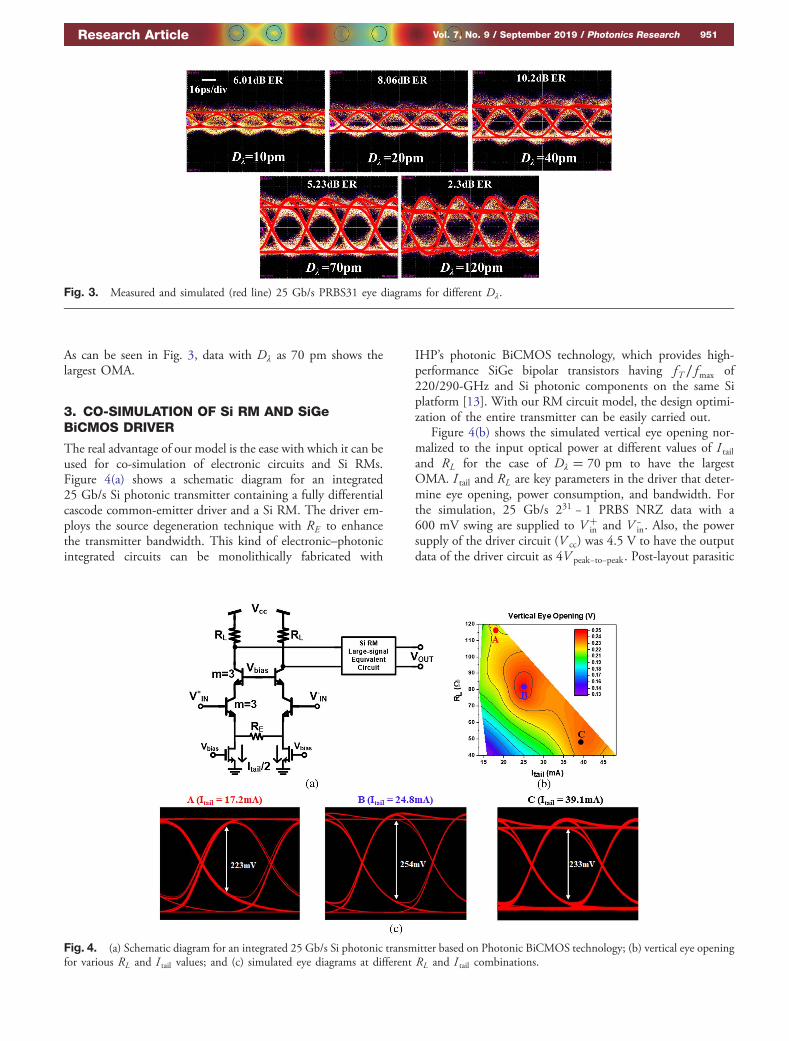
The real advantage of our model is the ease with which it can beused for co-simulation of electronic circuits and Si RMs.Figure 4(a) shows a schematic diagram for an integrated25 Gb/s Si photonic transmitter containing a fully differentialcascode common-emitter driver and a Si RM. The driver em-ploys the source degeneration technique with RE to enhancethe transmitter bandwidth. This kind of electronic–photonicintegrated circuits can be monolithically fabricated with
IHP’s photonic BiCMOS technology, which provides high-performance SiGe bipolar transistors having fT ∕fmax of220/290-GHz and Si photonic components on the same Siplatform [13]. With our RM circuit model, the design optimi-zation of the entire transmitter can be easily carried out.
Figure 4(b) shows the simulated vertical eye opening nor-malized to the input optical power at different values of I tailand RL for the case of Dλ � 70 pm to have the largestOMA. I tail and RL are key parameters in the driver that deter-mine eye opening, power consumption, and bandwidth. Forthe simulation, 25 Gb/s 231 − 1 PRBS NRZ data with a600 mV swing are supplied to V �
in and V −in. Also, the power
supply of the driver circuit (V cc) was 4.5 V to have the outputdata of the driver circuit as 4V peak−to−peak. Post-layout parasitic
Fig. 3. Measured and simulated (red line) 25 Gb/s PRBS31 eye diagrams for different Dλ.
Fig. 4. (a) Schematic diagram for an integrated 25 Gb/s Si photonic transmitter based on Photonic BiCMOS technology; (b) vertical eye openingfor various RL and I tail values; and (c) simulated eye diagrams at different RL and I tail combinations.
Research Article Vol. 7, No. 9 / September 2019 / Photonics Research 951

RC values for the driver are included in the simulation sincethey can significantly influence the driver performance. As canbe seen in Fig. 4(b), the vertical eye opening strongly dependson RL and I tail values. The optimal condition can be deter-mined that provides the largest modulator output eye openingwith the smallest I tail, or the smallest power consumption.With a fixed value for RL, larger I tail generates a larger outputvoltage swing but runs into the headroom problem if I tail is toolarge. Figure 4(c) shows simulated eye diagrams at three differ-ent conditions, whose I tail and RL values are represented byPoints A, B, and C in Fig. 4(b), having 4V peak−to−peak at thedriver output. Point A requires a small I tail for peak eyeopening but experiences degradation due to a large RC timeconstant, as shown in the simulated eye diagram. Points Band C show similar eye patterns in terms of rising and fallingtimes but Point C requires a larger I tail due to a smaller RL,which results in a larger power consumption. Consequently,Point B provides the largest eye opening with the smallestpower consumption.
Our RM circuit model can also be used to optimize the ratioof level mismatch (RLM), which is the key performance param-eter for a PAM-4 transmitter. RLM is defined as
RLM�%� � 100 ×min�ΔV upper,ΔV mid,ΔV lower�avg�ΔV upper,ΔV mid,ΔV lower�
, (6)
where ΔV upper, ΔV mid, and ΔV lower are defined in Fig. 5.PAM-4 allows a higher data rate transmission without requiringa higher transmitter bandwidth, and it is the standard formany important high-speed I/O applications [14,15]. There isgrowing interest in PAM-4 based on Si RMs [16–20], but itsperformance is greatly affected by Si RM nonlinearity, whichresults in degraded RLM [16–20]. This nonlinearity is dueto the Lorentzian shape of the RM resonance as well as thenonlinear dependence of the ring waveguide effective indexon the reverse bias [20]. This poses a great challenge to achieveSi PAM-4 transmitters because there is a rather tight require-ment on RLM. RLM higher than 94%, for example, is requiredfor IEEE802.3bs and CEI-56G [14,15]. One solution is to ap-ply different driving voltages for ΔV upper, ΔV mid, and ΔV lower,which can compensate for RM nonlinearity [20,21]. To use
Fig. 5. PAM-4 eye diagram and level representation.
Fig. 6. (a) Schematic diagram of the PAM-4 Si photonic transmitter including driver circuit and the RM and (b) simulated RLMRM values forvarious combinations of Dλ and RLMDRV values.
Point A(D =80pm)
VDRV Pout/Pin
Point B(D =90pm)
Point C(D =80pm)
Point D(D =80pm)
RLMRM = 96.9%
RLMRM = 88.5%
RLMDRV = 97.8%
RLMDRV = 78.9%
RLMRM = 75.5%
RLMDRV = 67.2% RLMRM = 82%
3.4dB ER
3.4dB ER
3.4dB ER
2.7dB ER
Fig. 7. Simulated 25 GBaud PAM-4 eye diagrams at different com-bination of RLMDRV and Dλ.
952 Vol. 7, No. 9 / September 2019 / Photonics Research Research Article

this approach, an accurate co-simulation of a driver circuit andRM is essential.
Figure 6(a) shows a schematic diagram for an integrated25 GBaud PAM-4 Si photonic transmitter containing a Si RMand a fully differential cascode BiCMOS common-emitterdriver with the emitter degeneration based on IHP photonicBiCMOS technology. To determine the optimum PAM-4modulation condition, SPICE simulation is performed forthe integrated transmitter for varying RM Dλ values and differ-ent RLM values for the driver output voltages measuredbetween V DRV (RLMDRV). For the simulation, RL � 80Ω isselected based on the optimization carried out for the above-mentioned NRZ transmitter. Data (25 Gb/s 231 − 1 PRBSNRZ) is supplied to both inputs of MSB and LSB ports.
The entire transmitter, including the driver and the Si RM,is simulated using the equivalent circuit for Si RM. Figure 6(b)shows the resulting RLM for the Si RM output, or RLMRM forvarying driver output voltage RLM, or RLMDRV, and detuning.Different RLMDRV values are achieved by changing ILSB andIMSB, while their sum is kept the same and V DRV has a4V peak−to−peak swing. As can be seen in the figure, RLMRM over94% can be achieved when Dλ is about 80 pm and theRLMDRV is between about 75% and 85%. Figure 7 shows thesimulated eye diagrams for the driver and RM outputs in differ-ent conditions represented by Points A, B, C, and D inFig. 6(b), and such conditions and results are described inTable 3. At Point A, RLMDRV is almost 100% but RLMRM issignificantly degraded due to Si RM nonlinearity. The RMnonlinearity is such that the middle eye opening is the largest.Consequently, by distorting driver output or making themiddle eye smaller, RLMRM can be improved, as shown bythe Points B and C eye diagrams. Too much driver output dis-tortion causes RLMRM degradation, as shown by the Point Deye diagram. With the optimum distortion of the driver output,we can carefully choose the detuning for the maximumRLMRM, as Point C shows an almost 97% RLM value.
4. CONCLUSION
We demonstrate a new large-signal SPICE circuit model for adepletion-type Si RM. The model is accurate, easy to use, andallows a significantly reduced simulation time compared to thepreviously reported approach. The accuracy of the model isconfirmed with measured 25 Gb/s NRZ modulation resultsat different detuning values. Furthermore, the model allowseasy co-simulation with electronic driver circuits. We demon-strate the design optimization based on such co-simulation forSi NRZ and PAM-4 transmitters containing SiGe BiCMOSdrivers and Si RMs.
Funding. Ministry of Trade, Industry and Energy(MOTIE) (10065666); Yonsei University (Research ScholarshipGrants); IC Design Education Center (IDEC).
Acknowledgment. We thank IC Design EducationCenter (IDEC) for EDA tool support.
REFERENCES1. G. Li, A. V. Krishnamoorthy, I. Shubin, J. Yao, Y. Luo, H. Thacker, X.
Zheng, K. Raj, and J. E. Cunningham, “Ring resonator modulators insilicon for interchip photonic links,” IEEE J. Sel. Top. QuantumElectron. 19, 95–113 (2013).
2. B. M. M. Milosevic, S. Stankovic, S. Reynolds, T. D. Bucio, K. Li, D. J.Thomson, F. Gardes, and G. T. Reed, “The emergence of silicon pho-tonics as a flexible technology platform,” Proc. IEEE 106, 2101–2116(2018).
3. J. Sun, R. Kumar, M. Sakib, J. B. Driscoll, H. Jayatilleka, and H. Rong,“A 128 Gb/s PAM-4 silicon microring modulator with integratedthermo-optic resonance tuning,” J. Lightwave Technol. 37, 110–115(2019).
4. Y. Kim, Y. Jo, M. Kim, B.-M. Yu, C. Mai, S. Lischke, L. Zimmermann,and W.-Y. Choi, “Parametric optimization of depletion-type Si micro-ring modulator performances,” Jpn. J. Appl. Phys. 58, 062006 (2019).
5. A. H. Atabaki, S. Moazeni, F. Pavanello, H. Gevorgyan, J. Notaros, L.Alloatti, M. T. Wade, C. Sun, S. A. Kruger, H. Meng, K. Al Qubaisi,I. Wang, B. Zhang, A. Khilo, C. V. Baiocco, M. A. Popović, V. M.Stojanović, and R. J. Ram, “Integrating photonics with silicon nano-electronics for the next generation of systems on a chip,” Nature556, 349–354 (2018).
6. R. Dube-Demers, J. St-Yves, A. Bois, Q. Zhong, M. Caverley, Y.Wang, L. Chrostowski, S. LaRochelle, D. V. Plant, and W. Shi,“Analytical modeling of silicon microring and microdisk modulatorswith electrical and optical dynamics,” J. Lightwave Technol. 33,4240–4252 (2015).
7. J. Rhim, Y. Ban, B.-M. Yu, J.-M. Lee, and W.-Y. Choi, “Verilog-Abehavioral model for resonance-modulated silicon micro-ringmodulator,” Opt. Express 23, 8762–8772 (2015).
8. M. Shin, Y. Ban, B. M. Yu, M. H. Kim, J. Rhim, L. Zimmermann, andW. Y. Choi, “A linear equivalent circuit model for depletion-type siliconmicroring modulators,” IEEE Trans. Electron Devices 64, 1140–1145(2017).
9. M. Kim, M. Shin, M.-H. Kim, B.-M. Yu, C. Mai, S. Lischke, L.Zimmermann, and W.-Y. Choi, “A large-signal equivalent circuitfor depletion-type silicon ring modulators,” in Optical FiberCommunication Conference (OSA, 2018), paper Th2A.13.
10. B. E. Little, S. T. Chu, H. A. Haus, J. Foresi, and J.-P. Laine, “Microringresonator channel dropping filters,” J. Lightwave Technol. 15, 998–1005 (1997).
11. Y. Ban, J. M. Lee, B. M. Yu, S. H. Cho, and W. Y. Choi, “Small-signalfrequency responses for Si micro-ring modulators,” in IEEE OpticalInterconnects Conference (OI’14) (2014), pp. 47–48.
12. Optilab PR-23-M, 23 GHz Linear Photoreceiver Module, 2018, https://www.oequest.com/getDatasheet/id/10580-10580.pdf.
13. D. Knoll, S. Lischke, A. Awny, and L. Zimmermann, “SiGe BiCMOS foroptoelectronics,” ECS Trans. 75, 121–139 (2016).
14. IEEE P802.3 bs 200 Gb/s and 400 Gb/s Ethernet Task Force. http://www.ieee802.org/3/bs/.
15. OIF CEI-56G Application Note. https://www.oiforum.com/.16. A. Roshan-Zamir, B. Wang, S. Telaprolu, K. Yu, C. Li, M. A. Seyedi,
M. Fiorentino, R. Beausoleil, and S. Palermo, “A 40 Gb/s PAM-4silicon microring resonator modulator transmitter in 65 nm CMOS,”in IEEE Optical Interconnects Conference (OI) (2016), pp. 8–9.
17. R. Li, D. Patel, A. Samani, E. El-Fiky, Z. Xing, M. Morsy-Osman, andD. V. Plant, “Silicon photonic ring-assisted MZI for 50 Gb/s DAC-lessand DSP-free PAM-4 transmission,” IEEE Photon. Technol. Lett. 29,1046–1049 (2017).
18. R. Li, D. Patel, E. El-Fiky, A. Samani, Z. Xing, M. Morsy-Osman, andD. V. Plant, “High-speed low-chirp PAM-4 transmission based on
Table 3. Operating Conditions and Simulated Results forDifferent Points in Fig. 6
RLMDRV Dλ RLMRM
Point A 97.8% 80 pm 75.5%Point B 78.9% 90 pm 88.5%Point C 78.9% 80 pm 96.9%Point D 67.2% 80 pm 82.0%
Research Article Vol. 7, No. 9 / September 2019 / Photonics Research 953

push-pull silicon photonic microring modulators,” Opt. Express 25,13222–13229 (2017).
19. S. Moazeni, S. Lin, M. Wade, L. Alloatti, R. J. Ram, M. Popovic, and V.Stojanovic, “A 40-Gb/s PAM-4 transmitter based on a ring-resonatoroptical DAC in 45-nm SOI CMOS,” IEEE J. Solid-State Circuits 52,3503–3516 (2017).
20. H. Li, G. Balamurugan, M. Sakib, J. Sun, J. Driscoll, R. Kumar, H.Jayatilleka, H. Rong, J. Jaussi, and B. Casper, “A 112 Gb/s PAM-4
transmitter with silicon photonics microring modulator and CMOSdriver,” in Optical Fiber Communication Conference (OSA, 2019),paper Th4A.4.
21. T. Kishi, M. Nagatani, S. Kanazawa, W. Kobayashi, H. Yamazaki, M.Ida, K. Kurishima, M. Nogawa, S. Kimura, and H. Nosaka, “56 Gb/soptical transmission performance of an InP HBT PAM-4 driver com-pensating for nonlinearity of extinction curve of EAM,” J. LightwaveTechnol. 35, 75–81 (2017).
954 Vol. 7, No. 9 / September 2019 / Photonics Research Research Article