LAMPIRAN - Repository WIMA
25
LAMPIRAN
-
Upload
khangminh22 -
Category
Documents
-
view
1 -
download
0
Transcript of LAMPIRAN - Repository WIMA

LAMPIRAN

uses newdelay,crt;
const pa=$300; {inisialisai PPI}
pb=$30l;
pc=$302;
pcw=$303;
cw=$98;
var data,status:byte; {identifikasi variabel}
s:integer;
busy:boolean;
suhu: real;
tegangan:real;
tom: char;
begin
clrscr;
TEXT COLOR (11) ;
GOTOXY(18,5);writeln('TERMOMETER DIGITAL DENGAN TAMPILAN
KOMPUTER' ) ;
gotoxy(18,6);writeln('-----------------------------------------');
gotoxy(20,8);write('Set suhu untuk mematikan pemanas=');readln(s);
port [pcw] :=cw; {set control word}
repeat
port [pc] :=$02;{set PCl untuk read='l' dan PCO untuk write='O'
pada ADC}
port [pc] :=$03;
repeat
{set PCl untuk read='l' dan PCO untuk write='l'
pada ADe}
status:=(port[pc] AND $lO);{mengecek interupt pada PC4}
busy:=(status=$Ol);
until not (busy);
port[pc]:=$Ol;{baca data pad port A}
data:=port[pa] ;
sUhu:= ( data*0.6973642l) +26; {konversi data ke 5uhu}

delay(2);
Port [pc) :=$03;{start konversi lagi}
text color (11) ;
textcolor(7);gotoxy(30,lO);writeln('DATA: ',DATA:3);
GOTOXY(30,13);writeln('TEMPERATUR:',suhu:3:0) ;
textcolor(ll) ;
gotoxy(19,17);writeln('--------------------------------------');
if s<=suhu then {jika input lebih kecil dari suhu maka port B
begin high}
port [pb) :=$1;
textcolor(4+blink);
gotoxy(20,20) ;writeln('pemanas mati');
end
else {jika tidak maka pemanas hidup}
port [pb) :=$0;
if keypressed then tom:=readkey;
until tom=#27;
end.

FDr an Ipplicauoo. wit.h a 12-bit NO convener with a IOV full $Ca!c to I 112lSB error muimum:
2-(11"'1) f.,.... - - 17_7kHz
,,(0.\ x 10-'1
Traclt..to-hClht offset is cauted by the transfer of chal'le to me boldin, C2pacitor via the Ilite capacilance of the switch wheD Iwitchina into hold. Since the a:ate capacitance couples the swltch,-control voUale applied to the late on to the bold c:apacilOr I rhe resultinllnck-to-hold offset is a funcuun of the loaic level Ipplied to the Jate and the ..:hansc in the late cap.citance ovcr len'lpentUrc.
HOLD MODE In the: hold mode there .ar~ two imponant specifications thlt must be con~idercd; f .. ~dthrough and the droop rat'. Ftcdthroulh error'S appear as an attenuaued venion of the input at the output wh.ilc in the hold mode. Hold-,\todc fcedthroulh vui~ with frequency, illcreasin, at hilher frcquencin. FC'l:dthroulh is an imP<ln:ult sp«ilic3tion when a track and hold fo\Jows an analol muhiplcxl:r ,h,:It swit.:he:. among ,many different chiUlnels.
Hold.moot: droop ratc is the chanle in outpUt vollalle per unit DC time ..... hile in the hl,ld roNe, Hold mode droop OriJinI'~ as ICilkage from the hold capacitor, of wruch the major lcable current conLCibuton arc switch lcaka,e current and bias current. The rate of \'oIt3IrC c:h,mg.: on the C3p3c:itor dV!..it is the fluio of Ih~ tou.1 lukJlt curtcnt It. 10 the hold capacitance C H·
Drl.)/)p R.ue ,. ~.I.YE!i! (\'ollSlSec) ,.. ~ dt CH(pF)
that a sampled dnil iyscem must sample, convett and acquire the Qext point It I rale at last twice the sl,na! frequency. Thus the maximum input frequency is equal 10
I I. .'AAX.- 2(TACQ + Tcosv + TAP)
Where T ACQ is the icqu.isitioQ time o( the samt>le.to-hoid . amplifier, T M is the maximum apcnure time (small cnou,h .to
be ianored) and TcoNY is the conve~ion time of the AiD cunvertcr.
DATA ACQUISITION SYSTEMS The Ca" acquisition time or the ADJ6S when usN "jth • hillh speed AiD convener allow. accurate Jigitizali"n o(hi,h frequency sirnals and hi,h throu,hput ntts in multichannel data acquisition systems. The AD36S can be used with a number of different AID cunvtners to achit:ve hilh throu,hput ntts. Figures 23 and Z4 show the usc of an AD36S with the ADS78 and AD\74A.
~_..! V
. ,
For the AD36S in panic:u1u;
Droop P.3h! - ~~~ -tV/sec m:Wmum
,. Figurt: 23. AD Convtlrsion Sysulm, t '7. 6kHz Throughput : 58. 8kHz M8x SigndllnptlC
Ad.J~lion'1l\y the Ieak,se current doubles (or every urc Increase in temperature ab.-we 2SoC; therefore, the holloi-mode droop rtte chJt',l..:terisuc .·ill also double in the same (ashion.
Since a track and hold is used typically in combination with an ArO ..:om'.:rter, thtn the lotal droop in the output volta,e hu to be ku 'han l!2LS8 during the period of a conversion. The
.Wtl\l!m allow:lb[e: signal chanle Oil the input of an NO cOllvencr
1:;:
~v Full Scalc Voltage max - 2LS~1) -
Oo..:e the in:t:dmum .1 V is dcf'!rmined then the coovenion time oflhe .\,0 ':t~n\'uter (tcOl'o-v) is requited to cah;ulue thc muimum all\lwabk ~';
dV rnJ,\ I;'~ d{'
dV rna The I~," : ::-.um --d-, -
the timi. not only II .25·C but at tcmperature range. Thc:rdore, 0\
range the following critcril mWI b• .IT .. !
~' ~X2IoJ"f:-S~
dt dl
·.he previous cquation is
~la:timum e:(~cd opcn.tin, \e opcratin. temperature ::.et (T orEMnON - 2S·q
HOLD.TQ.TRACK TRANSITION The NNUi:u theorem SU[,~S thac a band-til pmplcd It a r1te It Ie-.. st Iwice the maxim:; C:lO bt: ra:ul1suuc:ted without Inss or inI'amJ ..
:lJnal which is ,a.! frequency This means
Figure 24. 12·8;( A 0 Conv8rsion System, 26.3khz Tluoughput Rolle, 13.1kH.t MJ .. Signaf fnpur
~:
.'.
:\! , . '.','.!
;
~~ 1~ ,
(,
"i~' .. ~
~ ANALOG .. : .'~'. .. Integrated Circuit I4J DEVICES . Precision Instrumentation Amplffi'er
[ AD 5 ill FEATURES Programmable Gains from 0.1 to 1000 Dlff".ntlal Inputs High CMRR: I1000B mIn Law Drift: 2~VI'C m .. ILl Compllt. Input Protection, Power ON and POWlr OFF Functionally Compl.te with the Addition of Two R.sistors Int.rnalty Comptnsaud
ADltt PIN CONFIGURATION
rl, t====l 1'41~AIN
• SCALI
SINS. . .. Gain Bandwidth Product: 40MHz Output Curr.nt lImlt.d: 25mA V.ry Low Nol .. : O.s"V POP. O.1Hz to 10Hz, RTI • G • 1000 Chips a,. Avall,bl,
• SCALI tn, ,,' .F.
PRODUCT DESCRIPTION The ADn1 is Isccond Jener.tion,low COSt. monolithic Ie instNmentation amplirtcr developed by AnaiOJ Devices. As a rNC instrumentation amplifier, the AOS21 is Iitin block with diffcttntW inputs and an accurately propunmable inputl ourput Jlin telarionship.
the ADSlllC insmlmentatlon amplifier should not be contused with an operanonal amplifier. althouJh lC'Yerai manuf'~Nren Uncludin. Anillot Dnica) offer op amps which can be used IS buUdin, blocks in variable pin insttUmenu.tion amplifier circuia. Op un,s 1ft' lenen1-purposc camponena which, when used with precision-marched externa! resistors. can perfonn the instrumentation amplifier function.
Att instrumentation amplifier is a precision differential volt'Ie pin device optimized for operation in a re,l world environment, and is intended to be uscd wherever .cquisition or a ""sc!,,,1 sl,nal is difficult. It is c1uraeterized by hiah input impedance, baJaneed differendd inpuu,low bias currents and h;,h CMR.
AJ a complete instrumentation amplifier, the ADUt requires only two resuton to set its ,ain to In)' nlue between 0.1 .nd 1000. The ruio matehil1l of dane rninon docs not affect the tli~h CM.H.R (up to 120..18) or the hi.h input bnpedance (J X IO·f!) of the AOS21. Furthermore, unlike mon operationd "m,.\ificr-bud instrumentation amplifiers. the inputs arc prot"ted against oyervolt"tS up to tU yolu beyond the suppliCJ.
The ADJ21 IC instrumentarion amplifier is Iv.i),ble in four di((erent venions of accuracy and opendna tempenNtc rln,e . The economictl "J" ,"de. the low drift 'OK" JTlde, and the Illwer drift, hi,hcr linearity "L" pde are spedfied from 0 to
+70·C. The "s" ,ude paranrecs performance to specification over the extended temperatufC ranle: _"oC to +12S·C.
PRODUCT HIGHLIGHTS 1. The ADS21 is a mae instrumentation amplifier in inrerrtted
circvit form, offerin, the uler performance comparable to many modulat instrumentation amplifiers at a fraction of the cou.
1. The AOSl1 hu low part.nte::d, input offlC'& volt. drift (2IJVfC for L ,nde) a.nd low noise for prec"lon, hlp ,ain .pplieadons.
J. The ADS21 is functionally complete with the addition of twO resistors, Cain can be preset from 0.1 to more than 1000.
4. The ADS21 " fully protected for input levels up to I SV beyond the supply volra,es .nd lOV differential at the inPUts.
S. Internall), compensatd for aU pins, the AOS21 also offers the user the provision (or limitinl bandwidth.
6. Offset nullin, can be achieved with an optional trim pot.
7. The ADSll of (en Nperior dynamic performance with a pin-banJwidth product of ,*O~Uiz, full peak tesponse of 100kHz (independent of ,:lin) and a ,enlin, time of SjJs to 0.1% of a 10V step.

,/
.~:!:l .~I'~
, ,,-,~,
(typical tp VS' ±15V, RL • 2kn .nd TA' 25'C unl ... oth.rWiSlspe.ifiedl '\ ":'q¥~M . . .• ADUISD -.1r.
SPECIFICATIONS . . "DUIID ". L, _. •• "DUtKO -AOUlLa '. ~.,.. ,o""~ "'DU1SDI")',l;:.l·~
. ..'.l ~"" .: -"~ ;,;:r?~ MODlL
I h.IOoJII ".""IIC-VIV lIU,JI-G,0Q.4C)"
0.1' .....
'~i:I:' ::r, tnt t04C,WC ~
t.:D•
'~/"i~ ,,,,,.4Ift.. ..t." D,·.~,..\\tC kES'O,,,,,Sl " "~~::
>'_\\11' ,OIlUl. lllU'tll
C.IOOIJ .tI.l'". l",.U s, ... l, 1\ \1"Iro f\,Il~n'
Co\ 'Hlh c- 10 16k I" C.IDO "'111 ".IWI lUI,
full , .. , "'''''',''1<' J!O,,,' '1 1110\11, slo-.. Ih.r, I"'(;';H~" IIH' ... S<IIJ,,,, T".,~ (.ft)' 10V "'1' to .. "h,,, 10", II of hul v .1~~1
C. I ',,1 ColO ~
C·IOO ''''''' C_,(.OII(I II .. ,
[)ltfo,.",;>! 0.(.,.,." R«o .. ,I')" I'JOV Inp"t to ,*11"'\1\ ,OmV'" f,n>l V,I.UISOU H
C.I(I( .. I ,.,...
C<lMm->fl :.o...okSlt? lIu .... ry \~\' "''''\ .... '\hlft 10m\· .. f F,,,.01 \·"~.II""I' II
G.10\)\) lUll,
VtllTAI-'1 '" fifflmll be ft;"I~1 , .. ,..IOlf.nVoIu •• U·t)\.)
"_ T""9Cf,,,,",
". s..pply "".,w. 0 ..... '0'01"1' IVO\oI ... T"""""'I' ",.h"I,·\Sou')
1""t:lCU.JtE,'IoITS
J ... \' ..... 11m V I~,I
""Vre InU ""\'rC,,,1 h"o'," ~1"'\'",uUOOlrlV"rl ""',,\·,.C .... 11'0",\" C 1,,1 O.OO,\,O\r.'"
'ft'~1 ... , C"n'''' l.i'~11 i .. """ ,O .. A ...... ... T."" .... "".. '''A,·Cmu " Swtp1r Z,",V
1.'mV ..... IW 'm\' "Pi
!"vtc "' .. II ."v/c "pi
Jon",y IIIn fllItrIV ,,,,
!'U,. ... rC "' .. uo.,.VI"C'ypl
4011 ... ,., ....
!OIlp"'·Cm ..
ta,~, Of I .. , CKtUft' 10ft!....... 10llA ...... . ... T'''',.nNIf I!I)~"','C"". _JZ~l' ... tc",u
''''rl'T Dl(!.ufta..ol I",WI I,.,,,,,d.,,cr (l'oIOIt 11 (.,"''''0" 010<1. 1"~.llm,.J ... u l!'j"" II In,,,, \''''''1' II ..... 10. S, .. ifM.t hrforflu"u
I."'~ , .. p."." J'" ...... Mu,m ..... \·"Iu, ... uh,,". Olm'l'lo Vft,l, '0 ..... o~
01' OFf [j,'ICfCftuol \k.Jc '~ .. ,c t) volu, •• 1 "tlor.,np""S, ... ~I
Comrt.~ .. '010<1, 1I<;,cll~ftlll';o. DC 10 ~HI *i,l'IlkO _rco •• b •• ,"" , 0'
1.lo'On .,F "10)"0,1) 0)"
IlI,lV
JOV \',1IH'
70.1. ",.11 11441,,,1 '".1' ",.n (10.1'1),1
I OmV ..... IO ''''v .yp. "",VI'C,,,U
I_V", •• ",.vl"c",u
" (',-
,;~,t
·i:
':r~)' .- .' :'
. ;" ~
G'IO "'~. "".C'U' <,,1 'old' .... n fIOOJ' t~,' .. \ Co.IOO ,00J' ... ",. IO~J' '1,1 'd04JI ... ,~ C I"J' 'r" c.. II),),} \\II) ... m.ftl\\~J!ln) )\l)".",.~I"!lJl",) - ~ \,,,~~~ ~~~.I~~:,~: I'!!'III: CDH'CNoU 101 ~:~ ~~:: :;:~:;::\'
Ift'~1 ( .. ".n, .• m •. IIIU. t .. I,)UI, 11,_\ 1",",,1
mrrfStt T(I\.\\I).· ... .:.-'",C .. n~ft\ ,,..' "
, . I ....... 1.c, .. UfIC. 10\ln . :'~"<~' V"lu.tA ... ,< 11\1\' '.,' c.", 10 0..,.,_ I ' ";:
PO .... tASL·rn'· 1 .', Open" ... V<tIII.e k,o.... .Uv N iI.V . !:' QII._ •. , S .. ,ply C~ntnl tlllA "''''
nA,u ... n'lI[ ".\sC.1 S'uil .... J '.rllKrnan" (110 .10·C Openn"l : -U·Ct •• U·, SIOI'I" _,,'c It .11 ... ',
PACK.\Ct 0..,.10:-;) CrT."".II"'H AOI:IJO APfllkD "PUILD
NOT __
• kit k"io." Ic. ,.,\ ..... II_ .. 1-.... .. • ~.iI\ ... __ .. A/lllll0
.. ,..ri(, ... w. ........ A/lII\KD. ".,.,. .. " ............. , .. ~ ......... --... 'i~: ·t.~: t'~
\':::
~ .~'~'~~~
•. " C Applying the AD521 ," I , plOTES.
1. G.ins below l.nd abo\<c 1000 Ire realized by simply Id}IImfll the ,~n tettin, rc,\ltOft. 'Ot bclt resuh,. voltaiC at cilhcr input should be tesmeted to tl0V for lains equal to at lell than 1.
2. Nonlineltrity Is defined as the ndo of the deviation ftom the ''bcSt sttalaht linc" throulh a fun .cale ourput falllc of i9 yolts. With a combinadon of hilh pin and 1::10 yolt output twinl, distortion may increue to .. much &I O.J%.
J. Full Pcak Response is the frequenf:}' below which a rypical amplifier will produce fuU ourpUt swlnl.
... Diffcrend.l <nedoad Recovery is the. time it ta-tn the ampH--: fier to recover from a pulsed JOV differential input with 15V of common mode Yohare, to within 10mV of final.,.Jue. The Eelt input is a lOY, 10Jts pulse at a lkHl rate. (When'- dirfcrential silna! of ,reater chan 11 V is applied between the inputS, transistot clamp. arc activlu:d which drop the exCCS!' input YOItlle acrol$ internal input resiteon. If a continuous oYCrload .. maintained, power dissipated in these resistOR causes temper.Nrc ,",dienu and a corrcspOndinr change in offset Yoltale, .. well u added thennal dme Constant, but will not dantage the devicc.)
t. Common Modc Step Recovery is the timc it lakn the amplifier to tecover from a JOV common modc input with letO \'OIn of diffetentialsisnal to within 10mV of final nlue. The fCSt input is JOV, 1 OJ!, pulse at a lkHl flte. (When. com-
IlESIGN PRINCIPLE rip" 1 is a .implified schernatic of the AD521. A differential inpuIYoltare, V(N, appears ItTOU Rc causinlan imbalance in che cu.rrenn mroulh Qland QJ, AI-VIJ'o/IRC. That imbalance ;. fort-cd to now in k5 b«.~sc the coUectot auunu of Q,J and (4 are constrained to be equal by meir biasinl (current minor). These conditions can only be Sltisfied if the di(ferential voltaiC Icross RS (and hence die outpUt yoltalC or thc ADU1) is equal to AI X Rs. The fecdback amplificr. An
pmonns that fu~ction. Therefore, VOllT -~ X Rs or VOUT Rs YiN-Re'
mon .mode sirnal imter dian Vi -O.sv is"appUed .to'the .:;~ . 7 inputs, transistor clamps are activated which dt_op the cxcasivc input Yo1tqe acroll internal input rCliston. Power dissipated in these muton causes lempcraNrc sndierits' and a correspondin. chanp in offset vo1uae,'u welt u an 'added thcrina.l Dme constant, but will not dam.,e the device.)
6. Output Offset Voltlle venu. Power Supply ChanlC u a constant 0.00' times the unnuUcd output offs~ per percent chancc in eithet power supply. If the output offset is nulled, the OUtput offset ch.nlc venus supply chanre ls substantially reduced.
7. Differentia! Input Impedance is the impedance between. (he two inputs.
8. Common Mode Input Impedancc' is the impcdance ftom ~ilh~r input to the power supplies.
9. Maximum Input VoltaiC (differentia! or It either input) is JOV when u.inl 1::1SV supplies. A morc pneral specification is that neither input may exceed either supply (even when Vs .0) by marc than 15V and that the diffcrence bc[Wecn the two inpuu must not exceed 30V. (Sec also Notc. 4 and S.)
to, O.tHz. to 10Hl Pet.k-to-Peak Volu.ac NoiK is defined s.s the maximum peak·to-pcak yoltage noise observed durin, 2 . of J leperate 10 second periods with thc tC1t circuit of Fit-ure •.
I- "'
.::I , It· ....
on
, . 11 I'" ,~ ..
FiguIW 1. Simplified AD521 Schem,tic
n

'- 'z.
..,.,,- ~ r I"se theLM158/LM258/ NalionalSemlconduclor ~1 m~-,' :,",. .IZ' \::
'" , ,
I' i f. '
': \~
','
, , ,
,t. .'
z I.! Application Note t 16 ' • ;,:"', ltV 0 Q)
< LM358 Dual, Single Supply Jim Sherwin ',~,': ; ,," [0-I Op Amp ,ft j, [ I "'- Vo' I-IUV
.. If: CMV.- ':l~~ lM,SI •• w '''''', '
INTRODUCTION I i"'" , 0-Uw the LM1S8/LM258fLM358 duaJ op amp wilh • single In many applications the LM158/LM258/lM358 can llao ti .
" ~
supply In place 01 the lM 1458/ LM 1558 with spilt lupply and be used directly in place 01 LM 1558 for spill IUPPty opera· " 'eap the protilS In terms 01: \ion.
Llnput and output yottage rang. down to the negative SINGLISUPPlYOPERATION (ground) rail
b. Single supply operabOn C. Lowet standby powet diSSipation
d. Higher output voltage ovnng
•. Low8f' input offset current I. Genetalty -'mllar performance OthetWili
The main advantage, 01 course, II that you can Illm'nate the negative supply In many applications and IliII re'ain equiva· lent OP Imp performance. AddfUonalty. and in some cases more imponanlly. the inpul and output le"ell Ite permined 10 swing down to ground (negative tail) potential. Tab'e I Showl the relative performance of the two In Ilf'ms of guer. Inleed and/or typicallpecincation •.
The LM1458/LM1558 or limllar OP Imp' e.hibit "".11 1mportanl ltmltaHonI when operated from Ii tingle posItlv. (or negollYo) IUpply. ChIef omong lhelols Ihollnput .nd output lignal owing Is .everoly Imhed fOf a glvan oupply o.shown In FJgtn ,. For lin •• , operation. the Input voltage must not '.Ich within 3 volta 01 ground Of' of thl JUPPIY, and output rlngo Is oImHorly Umhed to w;1hIn 3-5 '101\0 of ground Of supply. TN. me.ns thllt operation wtth • + ltv auppty could be limited II low .1 2 vp·p output Iwtng. The LM358 how .... er. allows I 10.5 Vp.p output .w1ng fot the lime 12V supply. Admitledlv these are worst case speciflcalion lin'lits, but lhey serve to Illustrate the problem.
TABLE I. Comparflc;n of Dual Op Amp. LMI4$1 and LM351
Characterlsllc LM1458 LM358
V,O amVMax 7 mV Max
CMVI 24 Vp-p' 0-2B.5V·
110 200M 50M
los 500nA -5OOnA
CMAR eo dB Min. 100 Hz 85dB Typ. DC 90 dB Typ
in • 1 kHz. RGEN 10 kO 4$ nViltfiTyp 40 nV/Ji'iTyp'
Z'N 200 Mil Typ Typ'OO Mil
AVOL 20k Min lookTyp lOOk Typ ---
I, 1.1 MHtTyp 1 MHz Typ"
Paw IHHzTyp 11 kH1Typ"
dVo/dt O.8V/~a Typ 0.5V1p.1 Typ"
Vo S RL - 10k/2k 24120 Vp,p' 28.5 Vp,p
Isc 20 mA Typ Source 20mA Min (40 Typ) Sink 10 mA Min (20 Typ)
PSAR eDC 37 dB Min 100 dB Typ
90dBTyp
10 (Al - DO) BmAMax 2 mA Milt
IFIOI'II labcwa\ory mealU'emonI
"Ba'" on Vs - JOV on LM3S1 on/)'. CIt vs" :: 1'V
"F~ dala IIlMI *pical (;\.t'I ••
374
'::'
TVHl7424~t Tl/Hnd4~1
FIOURE 1. Wor.t C .. e Signel Levels wIth + 12V Supply
Yo-1,,'" ·m ~."~.
-:i:' Tl1H/hl"~' T\.JHl7U4-4
FIGURE 2. Operating with AC Signati
ACGAIN Few AC Ilgnals the Input can be capacitor coupled. The In· put common mode and quiescent OUlput voltages are fixed at on.hall lhe IUppty voltage by • resistive dMder al Ihe non-Invorting Input .a shown In ~ 2. ThIs quleacent out· put coutd btl Ht at I klweC voltage to mlnlmlte power dissi· pation In the lM358, K desired, 10 long .a Vo ~ V,N pk. For thllM1458 the quiescent output muat be higher, Vo > 3V + VIN pk thus. for Ima" tignall. power dissipation II much greilifwith Ih' LM14sa. Example: RequlredVo - Vo t IV pk VIto 2k. VSUPPL y - IS required. Ftnd quieseenl dissipa· tion In toad and amplifier for LM1458 and LM358.
LM351
vo- + tV VsupP\.y- +3.5V
PLOAO-~- ..!..-o.5mW RL 2k
PO-V.I" + (y.-VO)IL IV
-3.5VXO.7 mA+(3.5-I~
Po-2.4S+ 1.25-3.7 mW
PrOTAL ·3.7+0.5- •. 2 mW
·From typic.oI c:twact .... b
LMI451
VO-4V
VSIJI'P\. y - 8V
4' PLOAO-2i -BmW
Po-Pd+(Ys-VoIlL
-22mW+(B-4g 2k
PD- 22 + 1- 30 mW
PrOTAL -30+1-38 mW
-'rom fWIIcaI d'latlctertaliCl
The LM14S8 tequila. over twice the supply yoltage and nearly 10 lime. the supplV power of the lM358 In this appll·
calion.
INVERTING DC OAIN Connections and biastng tor DC kwerting gain ar. ""ntlel· ty the same 81 tor the AC coupled c.se. Note. 0' cours •• that thl output cannot swing negalive when operated from a single positive suppty. Figure 3 ShoWI the connections and
l;gnal 1i~II.tlonl.
375
NON.INVERTING DC GAIN The non.lnverting gain connection does not require thl Va biasing as betore; the inverting Input can be r.turned to ground inlhe usual manne' lor gainl gr •• ter Ihan unity. (se. F'l9ure 4). ,., \'Imendous ad.,ant.g_ ot lM lM3S6 \n ,h\t eooo_ Is Ihot Input lignall and OUlput may el<tend .11 the way to ground: therefore DC slgnall In Ihl Iow·mlllivoit range can be handled. The LMt .. S8 ltiM ,equires that VIN - 3-17V. Th.,elore maximum gain II Hmited to Av • (VO-3)/3. or Av max - 5." tor. 'lOV IUPPIy· Ther. II no similar limitation tor tn. LM358.

I j f; , t, .. i,
f ~ ,
i . (" ),
\ ~ t ~ •
\'\0
r1
I·" I •
i. t' \l • JI· 'tt ~.{;
:"\. , ~~I(f ,
/k.'" ~~).,' .. '"
1'r t:: i"· ;.. ,
'4.t: ·r· ,I' il,'
'i' ;' " r,
I'):
I', I r. I'" r-~ \ :""
~ERO T.C. INPUT alA.S CURRENT
An interesting and unusual Charact.nIUc II that 'IN has I zaro temperature coefficient Thil me.n, that matched r.Iistance II not required It the Input. allowing omission at one resistor per op Imp from the circuit In mosl caS8S,
V ... J.lrv~""·. ~ I ~Vo·'-t7l'
*tlV o--'V'>I'".' •
':'
flJHn.'4-S
BALANCED SUPPLY OPERATION TheLM358 will operate latfsfactoritv'n balanced IUppty oparation to long IS a load Is maintained from outPUI 10 Ihe negalive supply.
V .... ,.II.IY~
Vo ..... u .• v
.I'V~
r ':'
TlIH17"'-'
FIQURE 3, Typical DC Coupled Inv.rtlng Olin
"At· • lor Ay ... \ Av ~ 5 .• lew IOV LoPy
~VO·'·"V
, .. ......
TVH/1U'-'
Y .... ·,-lI.SV~
°AI ... fOr~ .... t
A"ftOtlirNtild
'"
FIOURE 4. Typlcil DC Couplod Non-Inverting Oaln
" .,
•• Ctouow .. (dI.\cW1Ion) OCCUI. a' Vo • VI -~
>-+--0 V,
"
V,-
FIGURE 5. Spill Supply Optrallon 01 LM3S1
318
TlIHI7"'.'
Vo ·1-lI.1V
'" n/HI1"'·1
The output load to nogotlve ouppJy _ tile ampJllI« to ....... lOme mtnIrnum curr.m at aM tIrnM, tI1ut1 ottminatlng """SOY_ dlltortlon. c.oosoy_ dllto<1Ion wllhout thII load _ be mota _a tIIan thai npoctad with tha normal op amp. SI_ the lingle ouppty dOtIgn .- notice of thII normal toad connection 10 ground. • eta •• AS output Itage wa. not Included. Whera ground ret ___ aok rOIl .. tors ".UIed al In Flgfn 5, tile required load to tile nega, IIY. ouppty dependl upon tile paak negallY. output IIgnat lev .. dOllred without oxI1IbItIng __ dlitottton. RL 10
lhe negative ... Ihoutd be chosen .."aR enough that tha voltage _or Iormed by Rf and RL win parmIt Vo to Iwing nogallYl to tha doslred point accordtng to till equation:
Vg-V RL·RF~'
RL COUld also be returned to til. polltlva ouppIy with tho advantaga that Vo max ..... 1d _ --!:Iff - 1.5V). Then with t 15V luppllel RL "'N _ be O. I 2 RF' The dllldvlnt_ge WOlIkt be tMllM LM3S1 Cln source IWlce II much current I. It can link, th .... for. Rl 10 negaltve supply can be one-heN til. yaw of ~ to pooltlve _Iy. Tho noed Jot lingt. or .,,111 _Iy ta based on 'Y.tom requirlments which may be other thin op Imp oriented. How· ..., N ilia only _ for balanced ouppIt<tlta to IimptIIy the biasing of op ampa, thera "0 many oyst_ which can ftnd a OOIt affoctlYe ben.1tt In opwaung LM358'1 &orn "ngla oupptIel rather tIIan Itandard op amps frorn batanced Iup. plio .. 01 the UIUOI op amp circuit .. Tabla II "'-' tI10sa fow which haya lmited _ with lingIo supply operation. Most ara bued on tile premi .. that to __ to frorn alingla ouppIy, a raf .. a".o Vo al about _haN ilia ouppJy be avan. Ible fot bll' Of (zero) "Dnl' refetence. The bllic cirCUftl "e thole Hlted In AN·20.
TABLE II. Conventional Op Amp Circuit' Sultabll for Single Supply Operation
Appncatlon Umttatlonl AC Coupled ampt VO· Invortlng amp Vo NorHnver1Ing amp OK' Unlly gain buffer OK Summing amp Vo ~ff •• ~.mp Vo DifferentialOf' Vo Integrator Vo LPFlltor Vo I·V Connector Va PECoIJAmp OK 15
I Sourc. 10 .. IN - R 1 I sink OK Volt Rol OK FW RectIfier Sine wave OSC
Trlangl. generator Thre.hold del ector Tracl<lng, rogutator PS Programmabl. PS Paak Delector
ts..AH20tor~clrc:ulla
Va or modiRed circuit Vo Vo OK NOI practical OK OKtoV,N-O
·Yo denoteot nMd far • merence von.o-, UM.Idy .t Ibout '!f OK II'IMnI no "'.ene. VOltage '*I!*1Cf
.... ""
~ ~
~
en

r-'"
"\' " .
I:' .;": I
" , r,';
l';'~ " i'
. -_. _ .. -- ---.-~.--
u: ZG5I'J, U; 35GfJ, :.1: 357N PCI1C;(In'J: Gpcrn~l r~~2cukan .JrCT (.JF~'f ji-!put Op[:radonllI Amp!ifiorsj
Tnrif Mnksimum Teaangan calu V'J Tcgangan masuk3n difcrcnsial V,o Lama hubungsinnkat kcluaran lm;c
~: 18 V :!:30 V
'"
PcngtJat-pcn\Jllul opfJrazi illi mcmiliki trnnsistor-twnslstor masukan JfET, dcngan arus·arus gclincir dan DrUS-
8rus masukan sangat keeil. Kcluarannya dirancang untuk beban bersifat kapasitas tinggi tanfl' sesuatu per· soalan stabilitas,
Jangkah suhu simpan T, -55 -125 ·C
Sifat·sifat tambahan: • Resistansi masukan sa
ngat linggi • Sedikit hanyut oleh per·
ubahan suhu • Lebarjalur lebar • Dibalehkan tegangan
.--- masukan . tinggi sempai +V,
• KonpcnsDsi frckuensi in·
Sl:Jhu pertemuan T, 100 ·C Resistansi termik antara sistem·udara lingkungan "">!,dlnt> 175 KNI
Konfigurasi pena
''''''''''''8' " 01",.., 1 1.v,
.h_,,,,, 1 -" 'O\II,u' .. "VI' -. - - - , Oft", "lut"
Ofh,' Cldlln,_"t
. --a.V,
. : I '-' . -
l ~I J
- I -':I "'.'
r.
.~
,t
J I J
!~ 1 I ~ " •••. , --_ ....... _- .
l{n rrJ, t" rl~ til~ --Vs • :.. 1 r-. V. T.mb - 25 ·C ~min II'P max
OPO:1 I.':'J:l ~uPt:tfi LF 35~ N Is 2 4 rnA C\llrCi'tt ccnsumption LF 356 f-l, LF 357 tJ Is 5 10 mil Input off!;et voltage (Rc· GO OJ V,a 3 10 mV Input clisot cu:rcnt ~o 3 50 pll ItlPUt C~lIrOI·.t I, 30 200 pA 1r.J'lut resistAnco RI 1012 0 Open loop voltage gain Aya 80 106 dB Rilte of rise
U' 355 N: Ay • 1 dvq 5 V/~. U' 356 N: Ay • 1 12 V1~. U' 357 N: Ay • 5 dlr
50 V/~. Performance U' 355 N I. 2.5 Mlil bandwidth U' 356 N I. 5 MH.
U' 357 N I. 20 MHz Translant tim. (for 0.01%1
U' 355 N t, 4 \.s U' 356 N, LF 357 N t, 1.5 ~s
Input noise voltage . 2~ Rs· 1 000;1-'00 H.: U' 355 N V'N nV/y"Rt
U' 356 N. LF 357 N V'N 15 nV/-IK'< Rs· 1000.1. 1000 Hz:U' 355 N V'N 20 nV/.f!l.
LF 356 N. LF 357 N Input noise current
. V1N 12 --- ilVIIHi---" ._-
1-100 Hz. or 1000Hz liN I om pNIRz Input capacitance C, 3 pF
Karakteristik Vs • ± 15 V; T _ • 0 to 70 ·C • unless otherwise specified
Input offset voltage Ra • 500 V,o 14 mV Temperature coefficient of VIC): Rs ~ 50 0 "VIO 5 ~v/K Chang. of Gvro after a chang. of VIC adjustmant 1\ ~/IVIO 0.5 per mV Input offset current Tj • 70 'C 1'0 2 nA Input currentl
' Tj • 70 'C I, 8 nA
Open loop voltage gain R, • 2 kO. VQp •• ±10 V Avo 63 dB Output voltage R,·'0kO Va.. 12 ~13 -12 V R,· 2 kO Va.. 10 ±12 -10 V Input common mode range VIC +11 t12 -11 V Common mode rejection IcCMR 80 100 dB Supply voltage rojection IcSVR 80 100 dB
Catatan: 1) Kaillu dibl'lndingkan drnga,.. '1.Il1ga asli yang tal:. dapal ditepatkan. koefi5ien luhu dAti legangen
gelincir, ma.ukln Y15119 lelah ditepllkan hanya berubah sedikil (lumrahnya 0.5 .. N.'K) untuk setiap mV dalarn jangkah stelan. Pcncpatan tcgangan gelincir tidaklah berpengaruh.kepada tinduan ragom lungg.' (common mode ,~!cctionl dan !tepad.! penguatan ikal terbuh.
2) Aru5 ma5ukan berlipat hampir dua-killi. kalau suhu penemuan naik 10 K.

pewaktu 555*
11, •• "." ... "." ... , .... ·"·"·"'·,,,, .. • ..... ·,,",,····,,· .. ,· .. • .. ••••• .. •••• .. , ................. .
appendiks 4
*Ijin dari Signetics Corporation, 811 East Arques, Sunnyvale, California, 94086,
hakcipta 1974.

URAIAN
Rangleaian Pe_letu monolitik NE/SE"555 _laII pengendeli .... gat ltabil yang berk&mampuan menghasilkan P8ftUndun WakN yang .liti, ataU osilasi. Bile diperlukan diberi· lean .nninal-terminll tambahan unNk memieu __ mereset. 011_ mode operlSi penundean waletu, waktunya dileandalikan secara 18pet oIeh saN till ...... luar dan klpasitor. Untuk operai lubil sebagai sebuall osiletor, beik frekuenli bergerak bebes dan liklul tugasnya dileandllilean secara taOti dangan due tall.... Iuar dan saN klpasitor. Rangleaiannya bisa cfopicu dan direset pede bentuk gelomllMg yang manurun. dan struktur lealllerannya dapat mengeiuarkan ataU menerime sampll 300mA __ menggeraklean rangkaienrangkIIan TTL.
KEISTIMEWAAN
-TIMING WAKTU DARI MIKRODETIK SAMPAI BEBERAPAJAM.
-BEKERJA BAlK PADA· MDDE STABIL MAUPUN ASTABIL.
_ SIKLUS TUGAS DAPAT DISETEL _KELUARAN ARUS TINGGI DAPAT ME-
NGELUARKAN ATAU MENERIMA 200mA
-KELUARANNYA DAPAT MENGGERAKKANTTL
_ KESTABILAN SUHU SEBESAR 0.005% PERoC
- KELUARANNYA HIDUP DAN MATI SECARA BIASA
PEMAKAIAN PENENTUAN-WAKTU PRESISI PEMBANGKITAN DENYUT PENENTUAN WAKTU BERURUTAN PEMBANGKITAN WAKTU PENUNOAAN MOOULASI LEBAR DENYUT MOOULASI KEDUDUKAN DENYUT DETEKTOR DENYUT HILANG
DIAGRAM BLOK
RANGKAIAN TERPADUUNIER
KONFIGURASI PASAK (Tampak Atasl
PAKETT
5. Tegangan
1. Ground Pengendalia
2. Pemieu 6. Ambeng
3. Keiuaran 7. Pembuangan
4. Raset 8. vee
Nomor ... omor _nan SESSST/NE55S/
PAKETV
Ground
Pemicu '
Kelu.,..n •
Pengosongan
Ambeng
Reset • T\I!IIIngan Pengendelien
Nomor..,omor Feunan SE5SSV/NE55SV
RATING MAKSIMUM MUTLAK Tegangan Suplei -UN Penyorapen Daye IOO .. W Jengkauan Suhu Operasi
N E555 o"C '0 -7O"c SE555 _HoC.o .,;zsOC
Jangkauan Suhu Penyimpanan -e5"c 10 ., 5O"c Suhu Timbal (Penyolderan, 60 detik) ·lOO"c
1---+"'-=.

369
CIRI-clRI LISTRIK TA 25"C. Vee. <5 ~ +15 kecuali ditontukan I.in
__ na _ .... ..... NI _ &AlVAN - .. -IIIAKS "N - IIIAKS T __ .. •• ... •• v -- vee·'" "L-- • , • • -Vcc· I" "L·- .o. Il .o. " -........ .......--. ............... ~ ......... c......,
""" •• "(0 __ 1001cn -- C· •. I"., _. o., • • .. """-- 30 '00 10 -'"c
Drift~T ......... "'" 0.00 a .• o..' ""' ... T __
'13 .13 xvec T __
vee -'IV ... • ... • v __ ,......... .... CMeIbiI) vcc· IV .... U, ''- ... ' v -- U o. .. ... T __
o..' o..' '.0 o..' o..' 1.0 v -- o..' 0.1. --- _. o..' .25 G.' .21 ... T.,., T ....... ~ epsii4llliue Vee -'IV ... '0. .... ... .o. n v
Vcc· IV •• .... ... .. .... • v T ....... ~~I VCC·'IV
IsiNc. 101M. 0.' 0.11 o..' ... v ..... K·- G.' ••• GA .75 V
"NK-'OOMA • .0 ... ... ... v ..... c·2OQIM ... ... vcc- IV ..... K· .... G.' ..25 v ..... K· .... .2S ..
.......... T ....... IC--...,....,.t flt"UftCl • :IGQIftA .... . ... vcc· 'IV -. .. -ycc·'w ".0 .... 12.'" .... v Vee· " ... ... '.75 ... v
...... Neik ...... ~ '00 '00 _.
"_TUNft~ '00 '00 --CATATAN 1. 1wvI ......... ...........,.df'IIi~I<M,_ ........ 2. IhIIdVcc-IV .. Vcc· 'IV. 1. 1ftI .................................. itA ..... Un_ ()pera11115V. R ... mebimoo.mnye. 20 ~
RANGKAIAN EKUIVALEN (oq,oniholkln ~ Sotu Sili Sajo,

--I •
I I ~
..
..
.. •
•
• 0
~ ~ ~
~
P /' ..... ,/ -_7 / :.:! ....
......-: .~ .::::: ..... ."""
&. .. .. ..
.. .. .. f • .,1 It
,- · .. · .. 0
l-
.. "
•
••
• . ~
... .. ..
.Le v 1... ~
I / ! .... -I--
"""cc" •
I I I .. . . . .. ----......................
..... -I..r P
II " ..... ....
...... ~ ~- .
.. • • • --- ..
, ,I
, , .1
-..
~ .. 0 ..
•
'0
· ... ..
•
0
•
... ..
...<I ~
.;
eo
.....
--....... --....... .l~ ~
~
~ -
~ --;C...<l
~
- -
·c·"
PI I ~F' "I lit
~
00 • • • ..
WK·'"
- ~ JA
~ ~ _c
~
• .. ---

t'
.' '" 1
'\
M \.\ t:; . ... ' : .~~.:,
~,"
<,
Ifl -i -i r-o ~ < n' ~ U>
2,76
w, T' ;~
"'~ , 'II I
• Operation from Very Slow Edg ••
• Improved lIne·Recelvlng Characte,t,~CI
• High Nol •• lmmunlty
description
Each circuit function ... In In .... "II. but becau .. 0' the Schmitt action. It ht' different Input threshold levell for
positive IVr + 'and 'Of 'Mgal"" going IVT ... llion.'s.
Th ... circuits ,r' .empet.tut.·compen .. ,ed and Cln be triggered from Ihl Stowe., 0' "'put rlmp. and Iti" gtw cl,'n, jin.,·"" outpul sign ....
The SNS4,4 end SN54lSt4 .r. chlrlcterind far oper· Ilion OVtl thl fun mlnte'Y temper""'f' ,.nge of ·5S·C to us-c. The SN7414 end the SN14lS14 .r. ch.r.c· terlzed ror oper.tion from O' C to 10' C.
logic Iymboll
" ,.
, TNI Iymbolll In .CCOfd.nc, ¥!til" ANSI/IEEE Std '1·1984 .nd IEC Publlutlon 117·U.
Pin numb"l Ihown "e IOf D, J, N •• nd W p.chge,.
logic diagram Ipolltlve logic'
'A~',(
2A~2V
l"'~3V
4A~4V
IA~I,(
.... -{9:>o--:--'V y ••
SN5414. SN54LSI4. SN7414. SN74LS14
HEX SCHMITT-TRIGGER INVERTERS OECEMBEA IIIl-REVISED ".ARCH 1t88
aN!41 •• SNS4LS.4 ••• J OR W PACkAGE IN'.' ..... N ,..,CKAO(
SN74LS14 ••• D OR N PACKAGE
ITOP VlEWI
"rr tV '2 I 8A 2A l , BY
2Y4 liSA 3.4 ~ 10 5V 3Y 6 9 4A
GNO I 8 4Y
SNS4lS14 ... 'K 'ACKAQE ITO' VIEW,
u >C(UUCC: __ Z > o,g
2A I. 6V
NC " NC 2Y I. SA NC " NC JA " 5Y
)-ou)-« M Z Z ....
" NC - No inle,n.' conneClion
'lOOUCT" ..... U ...... " "'''Ie "",.w.-,." •• , ., II ~ti ....... ',""-II .,.,., ••• ,,"/fit_t',,. ,., t~ t., .. " h ....... tt,_.tl
::::::!I1~'~:,:7i ~:~":r.r.':!t~::I!':' .~ TEXAS -l!}
INSTRUMENTS POSt O"ICI 101, IUOU • OAt~A" t .... ""'
I/) CI) U
os: Q)
o ...J
1=
2,77

~-
,
III -oj -oj r-o C1)
S, o C1) CIl
"N~q,q, SN~4LSI4, SN7414, SN74lSJ4 HEX SCHMITT-TRIGGER INVERTERS
$chematics '14
----1--,-T, V CC
y
I ,I I .00
'LS14 r--t vee
20 ItJI
I f .. } ,t OU':UT
"----+·----~ _____ !----~-~---ooo R."IIO' ~tI".1 '"0''''' ••• "0 .... ,,.,.1.
absolute maximum ratings over operating free·ai, temperature range (unless otherwise noted)
SWPly 'Ioltage. vee hee NOle II ..... Input \lollige: '14 •.....•...•.•.....•...........
'LSI' " "." """ ... Operating free·'lr lemperatwlI: SN54· ..
SN74· Storage lempe'lture r,nge •. , .
f'IIOTE 1. volt ••• ~'I"" ~ ••• ~,I" • .,,. .. , I" ".' ... <1" ~''''.''''' I •• ,,,."~I
. ........................ 7V
" , .. " " .. " , • " " " " " .. ... 5.5 V """"'"'''''' 7V
- SS"C 10 12SGC ........ rfc 10 70GC
_ 65°C to tSOGe
2·78 . TEXAS-lj)
INSTRUMENTS 'OSI -:.,;,u "JII'''OI2' O.o.u.o.,. !IU" '~JB
1Jti&f7"&WM'99S¥\i'P"'1.
,.' ':~·".f
I, t-.:
~ i .. ,
I
.1-"

~. ,.
t~ •
SN54LS14, SN74LS 14 HEX SCHMITT-TRIGGER INVERTERS
recommended operating conditions
SNS4LS'4 SN"'LI,. M,N NOM M •• M'N NOM MAX
UNIT
VCC Supply liIOll'9' 'S S S.S 4.75 S S.'" V
'OH Hieh·l.ve' O"lp ... , ,"","t -0." -0." m. 'OL Lo ... ·I .... ' O,""pul cu,rent , B m. '. QP""'"IiII, .. ,i, te"'Ptl,IUII - 'S m 0 ,0 e
electrical characteristics over recommended operating free·air temperature range (unless otherwise noted)
lEI -i -i r-o (I)
< (i' (I) C/I
TEST CONDITIO'"'st 5N54 .. I'4 SNULI,.
''''''AMETEA "'N TV" M •• M,N TV', MAX
V" Vcc -sv .. , ... ..• .., ..• '.1 V,_ Vee' 5 V O. o. • 05 o. •
Hylltr .... Vcc. 5 V 0.' 01 0.' •• ~=-VT.I
V'K Vee' MIN. ',- 18 inA -1.5 -u VOH Vee'" MIN, V, 'O.SY, IO~'" _0.4mA 2.S l.' 2.1 l.'
10l '''mA 0.25 0.' 0.25 0.' VOL VCC • MIN. '1,.'.9\1
tOL .... tnA 0.35 O.S
'" vCC· sv . V,. VT. - 0.14 -C.te
"- "CC, sv . ", ... "T- -0.18 - 0.'1
" VCC'" MAX, v,.1 V 0.' 0.'
"H vee ~ MAX, VIH" 2.1 v 20 20
'IL VCC'" MAX, VIL.o. 0." V -0.i11 - 0 .•
1051 Vee - MAX - 20 -'00 -2. -'00 ICCH Vee'" MAX B .• I. •• " ICCL Vee. MAX 12 21 " 21
t fa' ,o ... d,\,on, ' ... 0 ........ ' "'IN Of' MAX ... ,. HI' .0".00 ........... '0«.1.10 .. net ••• Of ........... OOd .... , ... ,., (ono"io",. I AI1I .. 0ic.I •• 1 ..... ,." '.ICC' ~Y. fA-l'·C. I No, "' ••• ,I",. 0'" 0 .. , ... , ." ... Id bO '''.'tld II • """.'...0 0 ...... 0" of '1'0, ,I'O."'("U"I ,1'00 ... _ no, Ou_ 0"' .. e .... O.
switching characteristics, Vee· 5 V, TA· 26 l1 C
FROM '0 TEST CONotTIONS 'AR ... METIR UNfUTI IOUTPUTI
M'N TV. .... IPlH
Y RL • 2 "II. Cl· IS "F .. 22
A lPHL .. 22
2-80 TEXAS 1JI INSTRUMENTS
.-on Of'1C1 IOJ .. WII t • DA~~I. 'IIIAI fun
UNIT
V
V
v
V
V
v
mA mA mA ,A mA mA mA mA
UNIT
"' "'
SN5414, SN54lS14, SN1414, SN14lS14 HEX SCHMITT-TRIGGER INVERTERS
PARAMETER MEASUREMENT INFORMATION tESt 'OINt
'.OM J OV"UT _ I ~ .I~ UNOIA i
TESt Cl T '_"'1 ... lOAO CIRCUIT
r----..,- - ... _ ... - --3V 1~,ut.J. V I • ." .HI \ VI .... ILl 0 V
~1I"Hl-; ""'LHotII '~VOH
OUtl"ut \. Vo •• 1 t 3 V --- VOL 1"''''"CI
VOL TAGE WAYlFORMS
NOtEI A. All d.ocI ...... lN306 •• , ............... . •. C1. ,nclt.d .. P'Obe ."d ... C..,M.un(o. C, G'"'_IIOf ' .... K .. """ .... O .. f, •• fIC' "01, ......
O_"ar Cftlf.' ..... tln It"HMUVoJUift
Z~I ,." " " VI,oIlH VI '''Ill VO"t SN~·/SN7.· .. " I MH, 10", 10ni 1.1Y 09 V 1.5 V
5N~lS'/5N14LS' SO" '''''"' IS "' h, 1.6V 0.' V 1.3 Y
TYPICAL CHARACTERISTICS OF '14 CIRCUITS ~SITIVE·GOING THRESHOLD VOLTAGE .. t-IEGATlVE·GOING THRESHOLD VOLTAGE ..
FREE·AIR TEMPERATURE > u, I 1.1
.. vCC·IV
I·" > "
,
I ." .A In
, , , ...
I" 1 u
, , I
'" ,
-;;
- l--t-
-+-
>, .. • 1:1
'
, .. >
J: , . i: •• ,
" .. " .. "
" "
FREE·AIR TEMPERATuRE
Vee-IV l "1
I:::::1 .,., ;;7
.- I i,...-
~I" _n_M_" , " M ~ ~ '"
~·-':n -M-n I. JIo 10 ".'00 In
'A - "M·A_ """,'IIUf' - C
. 'A - " .. ·Air '."",ntll,. _·c
FIGURE 1 HYSTERESIS FlQUAll
" FREE·AIR TEMPERATuRE
'" ,---.--... • > .t--I IJI , -! ...
t· -l-• ~ ... • •
~'" ~ 711
;;0'" ... '"
I-
I--
I Itcc-:', .,
bt---k -.~- I--
I--!.-+--I-'j:::-, ! "
F " ! H II ' .
I ,
! I I I I , I
!
_ n - to - non 50 " 100 In
' ...... " .... Air' ............... ·C FlOU"EJ
0 ... I •• 1."' .... 1 ..... Oil .... O·C.M 70'C .MI ....... y ... 1 ..... O'1,w •. 7~V.~ .., .... 1.21 V .It ,ppliue" fo, SNUI. ,"'Iy.
TEXAS 1JI INSTRUMENTS
1'011 OJ'ICI., •• nOI •• O"L~'. flU, 7Ult
III Q) CJ ':;
Q)
o ..J
I:
2-81
~

111 -4 -4 r o Q <: ;:; o '"
~·H
SN5414, SN7414 I SN54lS14, SN14lS14 HEX SCHMITHRUiGER INVERTERS HEX SCHMITHRIGGER INVERTERS
! j ,
I ! «
TYPICAL CHARACTERISTICS OF '14 CIRCUITS
DISTRISUTION OF UNITS FOR HYSTERESIS
Vcc' ~ 1/ fA' 2$"C
I
\ vV f'-6--___ ___ _ '-- --'-r---..
I.tO 160 JIO 800 120 '''0 no 110 too Yr. - YT_ -H.,II"'''I_mV
FIGURE '"
HYSTERESIS ., SUPPLY VOL fAGE
2.01 t"'2n~ II
> I , • I
i 1
• ! • J 0
•
• • • • , , I
, I
, I os
THRESHOLD VOL lAGES .. SUPPLY 'vOL TAGE
r". ,,·c I I I L
'."(1 .. -001"; r""I~" Vol ..... VT.
N~ .. I' ... ·Qoi'" Ttlllthol4 VO/I"". 11,_
--".1S .,. \I,. -VT_ - H.,n'''I'' -".V
FIGURE,
OUTPUT VOLTAGE .. INPUT VOL lAGE
VCC·,V
---
...
> • -J.. .IT fA. ,,"C
'M
! • i: 12
i , .! o. > ~ 0, ---f-- !-t-rl-+->" "f-I I I I I I I .. 4.15 ".
Vee - S"pply VDIUft _ \I
FtOUAE'
o.
> , ! >
i & , 0 >
I
,
I
, · - -••
- - -- -- -
U 1.2 Vee - SUNil, VOII~ - II
"GUR( 1
I.'
-
0.,. '0' 1~"'"I·.''''.1 01'0,," 0' C ."0 10' e .... '"00''' ""'UI" IItlo ..... 1$ \I ... a 100 •• !.2!11 Y t •• tOO" •• b!. 10' S"'!I.' '" onl,.
TEXAS lI} INSTRUMENTS
I'OS' O"'CI lOll InOIl • OAUAS. IfiAS 'nat
TYPICAL CHARACTERISTICS OF 'LS14 CIRCUITS
POSITIVE·GOING THRESHOLD VOLTAGE
" 1,70
~ t.' fu, J 1'·' .fu I
I
, • •
F .. 1" .u
• , I
I
fu , u ,
FREE·AIR TEMPERATURE
VCC·IV
./
-n-~_a ~ ~ n I~ 1~
no ... ~ 1:tO
i :~ , £ ... I ,
I .!.71O > , , ... t .. , I ...
".
Til. - " .. ·Air T.~"hI" _IC
F.GURI.
HYSTERESIS
" FREE·AIR TEMPERA-lURE
YCC-IY
t--............
........
-
I
·n -50 -25 2S SO 7S 100 121
Til. - ""·A,, Tt",,.,,, ... , -"C:
FlGUR( 10
NEGATIVE·GOING THRESHOLD VOl. TAGE
" .... > • 0.1' "
" I'" I" ! 0.11
" • ~ r U
~ 0.14
• • ! ..
," I
• ~Ol 1
" , -
FREE·AIR TEMPERATURE
YCC-IY
-y J...--'
-n-~-~ ~ ~ n 100 la TA - ', .. ·Air T ........ 'lhlII _ ~C
J ,
1 1
F.OURl t
DISTRIBUTION OF UNITS FOR HYSTERESIS
YC~-I! rTA· H~C:
1"\
"""ARI \ "'IOY(
~ / f'--no 140 760 710 100 120 140 110 110 VTt - YT_ - H,I'.,,,. - ",\I
IIGVPlE 11
0.1.10' ..... ,>1 •• ' .... 1 bllOW o·c '''<:1'1)0". JO'C '''0 I~PP' •• 0'119" '''''0.\ <1.'5 '\I ,,,,, 100., 5.25 Y ,., ."",,{.Ol. fo. SNS"L.$'" 0"1,.
TEXAS lI} INSTRUMENTS
100" O:IICllO_ Utoll • o .. u ..... flUS )un
CI) Q) CJ 'S: Q)
o .... 1=
2·83
:-,,~

''.
\!~ "./ ...
/"".
," .~.l
:.~
IJ ~ ~ r-0
"' < 1')'
"' (/I
2,84
SN54LS14, SN74LS14 HEX SCHMITT-TRIGGER INVERTERS
TYPICAL CHARACTERISTICS OF 'LSI4 CIRCUITS
THAESHOlO VOLTAGES ANO I1Y$TEF\ESIS
" SUPPLY VOL lAGE
g TA-H'cl I I I ~ I I .1
OUTPUT VOLTAGE .. INPUT VOLTAGE
~ ,. :- '01;1""·0.,,,. T'''''"MI' 1,1011 ... , Yr.
I I ~ ~ r··"·C t~Tttt~T'H .,11" " ,
f' > "
1· ~ .
• D r-- N"""~'GOi"! 'I'I,.! ..... t"I..!. y,~ == I
• H,,"fllIll, Yr. - YT-
• , '-'-.s 4.71 s.n
Vee - Sll~' 1,1011.,. - II
FIGUAE 12
.,
I
rll " 11111 "II 00 o • ... 1.2 1.1
v, - I,.,.., Yelu" _ V
FIOURE 13
0""0. I.'n •••• ' .... " u •• o .... D'C .,,1.1 .bO", Jo'e ,"d ... 1)111_ o"t.",t b.t' .... 4," V 1''':1 ,or.o". S.lS V., •• IU.hclb', , •• SNS'lSI .. '''''".
TEXAS -I.!,J INSTRUMENTS
.-0$1 O"tCl 10. UtoU • a.nAI. ItU.1 ,un
SN5414. SN54lS14. SN7414. SN74LS14
HEX SCHMITT-TRIGGER INVERTERS
TYPICAL APPLICATION DATA
, , .!
-1 CMOS ~M __
- - - _YTt
~ - - '\. - - - p- - -lir - - -VT_ , I I
INPUT
o o
T'LSVSTfMINTER'ACI 'OA SLOW IN"Vf WAVEFORMS
)30 n
MUL lIVIDA ... TOA
0",,,, ,eOI",,,u,,,
0 .. '£1 .. '
01MI,otOMHI
I I I
OUfPUT
r---' INII'UT I 17 OUTrUT ----1 r- 11 ----
I ) I I ~' I _.. I
:~ ..... u: I ~ I L __ 'J , ,
~
II'ULSE ST"UCHE"
TEXAS -I.!,J INSTRUMENTS
PUlS! SMA'!" .
THfUSHOLO OUEeTO"
~"OH:ClIO~ .. 10012 • OAU"'. f,U, 1U"
-Vr_
~ ...J
~
2,85
or, ~ 8 c < .... .... o CD o g
" ,: tL·" S ) CD ~ 0 . g , < f. . ........ ~. S " '" 1" 0 , g
< .t, ;' ;:: ct· 0 ~{,. CO ~ .. 0
~" g t < ~; •
.' ... '
., I..
" .~;
,/'" 'it'
1. :>: r
t ~.
i~··~ \'
,if . ;!1\ Ji".;
}.;;. '~'fI" ~' ".
r~~:(" 'i.,j"!l
i. i~
~NatiOnal . Semiconductor
Corporation
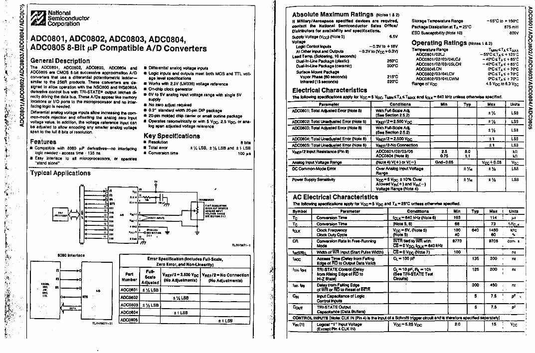
ADC0801, ADC0802, ADC0803, ADC0804, ADC0805 8-Blt p.P Compatible AID Converters
General Description Tho ADCOB01, ADCOB02, ADC0803, ADC0804 Ind • Differential analog voltage input. AOC0805 I" CMOS 8·bIt IUCC8SSfvoi lpp'oximaUon AID • Logic Inputl Ind outpull mill bolh MOS and TTL von, converter. that use • differential potentiometric Ildder- age leve' lpecIflcatlonl Ilmila, to the 256R product.. TheM convertera Ire de- .- Works with 2.SV (LM336) vonlge ref.rence '!gnad to allow operation with the NSC800 and INS8080A
• On-chlp clock 00..,.10. derlvallvl conlrol bus w~h TRI·STATE. CUIpu1la1oho1 dI, • OV 10 5V lnalog Inj>uI vonago rlngo wilh .Ingll 5V rectly drtvlng the data bus. Thesl A/Os appear like memory
Iupply kxations 01" 110 ports to the mlcroprocetlot and fk) Jnt.,~ • No zero adjust reqWed facing logic II needed. • 0.3" llandlld width 2O-pin DIP package Differential analog voftage Jnputl allow incre.sing the com-• 2O-pin molded cNp carrier 01 amen outtine package mon-moc1e rejection and offsetting the analog zero input • Operat •• ,atlometricahy Of with 5 Voc. 2.5 Voc. or Ina· vollag' value. In addilton, the voltage reference input can
b. 4!ldjullad to 4!lllow encoding any Imaller anatog voltage log 'Pan adjusted YOItage raference
span to the lull 8 bUs of resolution. Key Specifications
Features • Resolution 8 bill • Compatible with 8080 "p dertvatlv.a--no interfacfng • T olal error :t: If.. LSB, ± Va lSB and :t: 1 lSB
logic needed· .ccess time· 135 ns • Conversion time 100 "'S • Easy Interface to all microprocessors, or oper.t ••
",tand alone"
Typical Applications .. " q .. on •• I' .... l" ... II •• , .... " ... Ullil.
. II •• ........ ,," '"
'.l .... U ••• II .n 1('."10'1.4.1
1M II '11 II 'u 1/ OIl tI a ..
TL/H/S."·1
1080lnterl,ce Error Specification (InClude. Full-Scale,
Zero Error, .nd Non-Uneartfy)
R full-Plrt SCaI. VRIF/2- UOOVoc VAEF/2- No Connection
q Number AdJulled
(No AdJullm.nll) (No AdJullm.nll) .It ....
p
Nit. Il ADC0801 tY,LSB ' .. '" ..... "' "'" AOC0802 tv. LSB /~
A000803 t: Va lSB
AOC0804 1HSB
AOC0805 tllSB filHI54I1t.st
,' ..
Absolute Maximum Ratings (Nol.ll & 2)
" MlMtary/Aerolpace .pecffied device ..... requtred. stor.ge TemperatlKe A_nge - 65·C to + 150""<: contact the Nation.' Semiconductor S.les Offlcel Package Dissipation al TA - 2S"C 87SmW Distributors for .VllII.bnrly .nd speclflcatfons. ESD Suocep1lIlIUIy(No .. l0) 800>' Supply von.ga (Vcx;l (NOlO 3) S.SV Voltage Operating Ratings (NOI.' 1 & 2)
Logic Conlrollnput. -0.3V 10 + 18V AI 0Ihat Input and 0u1put0 -0.3V10 (VCC+0.3V) T""""""IuroRangl TMIN~TA~TM.Io.l
Laad Tomp. (SoIdtrIng, 10 oacondo) AOOO8OlI02U ·-SS·C$..T,.s + 12S':;
DuaI·ln·Una PlckagO (plasllc) 2WC AOC0801I02/03/04lCJ -'(O"CsoT,.S+8S"C
DuaI,In-Lint Packtge (ceramic) 300"C AOC0801102/0~/05LCN -.(O"C$.T,.:s: +8S"C
Surface Mount Pickage AOC0804LCN O"C~TA< +70"C AOC0802/03/04LCV crCS;;TAS +70'"C
Vapor PhI .. (80 IICOnds) 215'C AOC0802/03/04LCWM O"C$.T,.s +70"': Infrtrod (1511COnd1) 22O"C Ringe of Vcc 4.5 Vee 10 8.3 vo:
Electrical Characteristics Tho following opedfIcollonlllJllly to< VCC-S Vee T"'N~T.<T""" and fCl.-840 kHz untl" olhorwfoe opeeifIed.
'.rameter Condltlon. Min Typ lIox Un",
AD00801: Toill Adjusted Error (Hole S) WIth FuII,SCaIa Ad!-t:V .. LS9 (588_2.5.2)
AOOO802: ToIII Unadjusled Error (Nol. 8) V ••• /2 - 2.500 V .... tv. LS3 ADC0803: Total AdjuIIod Error (Nol. I) WIth Full-Scale Ad!-
:tVa LS3 (588 _ 2.5.2)
AOC0804: Tolal Unod)uslod Error (Noll 8) V •• F/2 - 2.500 V"" tl LS3 A000805: TOIalllnldjullod ErTo. (NOlI I) VR.F/2-No ConntcIIon tl LS3
VREF/2 Input R .......... (PIn 8) AOOO8OlI02/03/0S 2.5 8.0 kn ADC0804 (Nol. 8) 0.75 1.1 IUl
Anatoo Input Voltage R.nge (NoI.4)V(+) orV(-) Gnd-o.o5 VCC+ 0.05 Vr.: DC Commor>_ Error OYer Analog Input Vonoge :t:y,. .y, LS3
Rlnot .
P_ Supply SonsilMly VCC-5 Vee t 10% Over ±V" 1V. LS3 AI"':;: VIN( +) and VIN( -) Vono Rang. (Nolo 4)
AC Electrical Characteristics Tholollowlng opoc:tfIcollonl '1'I'iY lor Vcc- S Vee Ind TA - 25'C unI.I' olhorwlll opecIliad.
Symbol P.r.m.t.r Condlttone IIln Typ II .. I Un",
T~ eon-.ton TIme "" • - 840 kHz (NolO 8) 103 114 ", To. eon-.ton TIme (NoI.S,S) 88 73 We.< lClJ( Clock Frequency r,cc - :~' (NOlI 5) 100 840 1480 kt-.:
Clock NoteS 40 80 . .. CR eor-olon Ral.1n FrIO-Running IIl'm 1Iod 10 WIl wilh 8770 8708 CO", I
Mode !:!I-0 Voo. let.' - 840 kHz
"""""', Width of WIllnput (Slart PuI .. WId1h) !:!I-ov"" (Nole 7) 100 n.
IACC __ Timt (Doley lram Fining Ed;;; 01 RIllo 0u1pu1 Dlia Vllid)
Ct. -l00pF 135 200 OJ
1,",1otI TRI-STATE ConItoI WGey Ct. -10 pF, RL -10k 125 200 , ns !rom Rising Edge 01 10 (588 TRI-STATE Tell , Hl-ZSIaI.) CIrcuIts)
1wI. Iftl DoIWfI,ram Fining Edge 300 450 or of orRllIORI .. loIlRTl'I
Cot Input Copocllltnco 01 Logic 75 ' 5 p' • Conlrollnpull
. .
Cotn TRI·STATE 0u1pu1 5 7.5 p' Copoc:il.nco (D.1a BuIIora)
CONTROL INPUTS (NOlO: CU< IN (Pin 4) 10 tho Input 01. Sohmftt Irlgger clrCIA Ind .. IhtnIloro opecIIIad IIPIIIloly)
VIN(l) LogicII "I" Input Voflag. Vcc-5.25Vee 2.0 15 Vee (EKe.,,1 Pin 4 CLK Itl)
I
I I
I i i I I
I
i , i
» g CI) o -~ ~ » c
~ 1:: ...
I ... » c o g o UI

I ~
AC Electrical Characteristics (Continued)
The followtng specificaUonllpply for Va:; - 5VOC and TMIN " TA s; TMA)(. unless otherwise lpecffled.
Symbol T Parameter Condition. I Min Typ I M .. T Unit'
CONTROL INPUTS (Note: eLK IN (Pin "') is thelto4:M of. Schmin trigg8f dl'cuit and is therefore specified separately)
I I ~ ..
V'N(O) Loglcal'''O''lnput Vottage Vee· 4.75 Vee O.B Voc (E.capt Pin 4 ClK IN)
I'N (t) logical" I" Input Cunent V'N- 5VOC O.OOS t ,.AOC (All Inputs)
I'N(O) logical "0" Input Current V'N-OVOC -t -O.OOS ""OC (All Inputs)
CLOCK IN AND CLOCK R
Vl+ ClK IN (Pin 4) Positive Going 2.7 3.1 3.S Voc Threshold Voltage
Vr- elK IN (Pin oi) Negative I.S 1.8 2.1 Voc Going Thr.shold Voltage .
g VH elK IN (Pin "') HYSleresis 0.8 1.3 2.0 Voc
,,~ (Vl+)-(Vr-)
VOUT (0) lO!lical "0" ClK R Output 10- 380 "A 0.4 Voc Voltage Vee-OSVoc
VoUr (1) lO!lical "I" ClK R Output 10- -380 "A 2.4 Voc Voltage Vee- 4.7SVoc
DATA OUTPUTS AND IlI'fA Vour (0) Logical "0" Output Voltage
Data Outputs lOUT - 1.8 mA, Vee - OS Voc 0.4 Voc fN'm Output loUT - 1.0 mA, Vee - 4. 7S Voc 0.4 Voc
VOUl(l) Logical"'" Output Voltage 10- -380,.A. Vee-OSVoc 2.4 Voc
VOUT(I) Logical"'" Output Voltage 10- -10 "A, Vee-US Voc 4.S Voc
lour TAl-STATE Disabled Output VOUT-OVOC -3 "Aoc Leakage (All Data Bufters) VOUl-SVOC 3 ,.Aoc
'SOURCE VOUT Short 10 Gnd, TA-2S'C 4.S 8 mAoc
ISINK VOUT Short to Vee. TA - 2S'C 9.0 t8 mAoc
POWER SUPPLY
Icc Supply Current (Includes leLK - 640 kHz, Ladder Current) VREFI2 - NC, TA - 2S'C
and OS-SV ADCOB01/02/03/04lCJ/OS 1.1 1.8 mA ADC0804lCN/lCV/lCWM 1.9 2.5 mA
No .. 1: AblOlul. MulmlJrn Rllings "'111ImIII beyond M*fI damage to 1M 0evIc:e mil,. OCC\6. DC 1"11 AC eIKVkaf spedfiC.tion& do not IPPY wfWI oper.tng lhe ~ be,oneIlIs tpKifMKI opersling condIIioM.
No •• I: All 'tOI\Iges .,, IMfosured...,.. respect 10 Gnd, IdMI otMrwIH ~. TM ...,., •• It Ond point sI'IoIM ""1)'1 be Mted 10" D Gnd. No .. J: A zener diode .dals. 1nI:..-naIIr. from Yc:c 10 and ana his a ~ br •• kdOWn ¥OIIIp 01 7 Voc.
Not. 4: For YtN4-,~ Y..,(+ ''''' cIigbI 0I.ItIM coM .. be 0000 0001), T..o 0f\.ChIp cIodaiI .... tied 10 lach .... ~ I'" bIoc:t diagram) IIf*:ft dlOrwlrd c:onduCIlor INklQ Input wILl •• OM cIocHI ctop beIcMo Wound 01 OM diode drD9W .. ter """!he Yee 1l4'Pfy. Be ear ...... ~ ... ..,. at tow Vee ..... C4.5Y), .. high WveI.nalog ~'15V) can cauN WI '"""" diodIlO conduct-~ 1l....,.1Id IltITIC*aturl, •• nd causelfTOl'l lor analOg q,uu,...., ,..·tcaII. Thl S9IJC allows 50 mY 10tW1W bias of aIthIr cfioGI. Thit mMnI hi .. long II "" analog YIN don not ,.0Md IhlIUPPIr wn.va by mora INn 50 mY. IhI output c:odt wi! be COlT«=!. To ~ an ablolull 0 Yoc 10 I YOC" YOtWga range .. thlrlfora '~I • Iftin6rnum ~ volta. 014.150 YOC ~ tIrI'II*.u. vlriltionI, lrilill loI«ance and bKfnt. Not. I: Aecutlr:(" auarMlMd at Ic:u .. &40 kHz. At hIghaf docl ... ..,ande. toCUtc')'"n dIgr_. For lOw.- clock 1t1QWlndlol. the 6.Itf crc'- ...... CM f» • lCIandId to Ior'Ig at IN "**""'" c\ocl high .. ......., .. Of "**tun dod!. low .. In!IIY8I is 1'10 leu !han 275 ,... Not. I: WIlt! .n atynCtlronoua stilt PIM. up to • dod! ~ .... , be ,~td Mfart the 1nI.-rwI CIoCt pt\l ... are P'opIf 10 .twt !fie COft¥efIior'I ..,oceu.. Thl .tart request II ~1I!MIIy IlICh1d, ........ ' and Medon 2.0.
~, "
Nott 7: Tht C! Input ... aurnact 10 brac:kIt the vm *oM ... and '*-fore "'*'I" dIpandanI 01'1"" WA P"" wIdIh. All .rbInrty wIdI pufN IIIIcIIh wII hoed 1M oonv., ... 1n • raNt InocM and ..... ...,. 01 00I"I\I"nI0n" 1nIIIa ... ." .. IcJw 10 higtI I'IIIIhIon 0( '" '1m put.- (IMIIn*'O __ 11M'.
Nota t: Nona 01",", WDt reqW"' lIfO ..... IIMIICIIon U. '). To cbtU\ ZIl'O coda" od'wr '1'II1og Ir1M VOIla", ... IICtIon U and ~ I. Hotl I; TN YAEF/2 pin IIll'ii cent. PI*'II 01 a two ,..., cIMdIr com.c.ld from Vex: 10 WOI.RI. EICfI ""'lot 112.a. nc.pt few .. AOCOe04LCJ ...... -.eft ,nIIlor II 18k. TolII '-ddIrk1lUl r .. IInce .... un of 1M two ~ "'*tota.
Typical Performance Characteristics
E ..
I j:: I "
logic Input Th,"hold Vottlige n, Supply Voil_
-"·tS'A~"iHiC
~ " ... .n I. In I.M
! .a
Vee -111"'-' .ltIA" IVoel
I. ,. Clotl CA'AC."" It"
OUtput Current VI Temperaturl
v .' V
I ::::,:"''':-51 ~':'!I '
'.,,' AW"
i ~ ... ~
I LJ.J....L.I....:.!!.!===t.I -If -II • II If ,. I. 1ft
'A· AMI/II' U_UA,U"I rCl
.. .. J
~ -
! I j !
.. ,.
, , , , ,
,
Delay From Failing Edgl of 1115 to Outp,rt Dltl Vilid YO. Lood CapI_nee
o .... , .. llAI e'-'ACtU.I"",1
Full-SClle Error.1 Conve,..lon TIme
JJ~ 'c' 'JIIa.. I I I ~ Wec' UW
I Wet'UW
I'J I I N:::!.
.. • II ,. In lal
'"C.nu .... ' ... "'"
Powor Supply Currlnl Y1I TI.",.raturo (Note II
, $ *"" fO",.
"iI 1 It
i u
i U • OJ
I u , 11 0
AOC ... ,• ~IC rtf;.;! ~~"""A . "ff0!!!i
~'+ 'ctc· ... ·.. I
IT 1!fiw..r: T .. -ft ..... ,. •• Ul
'A-AllIlfI,n"''''''''.'NI
eLK IN Schmitt Tnp LlVII, VL Supply Voltagl
II
E ,
'T'
... ·e~' .. <.nl·c ; '.f
i IJ . .. . ~ , ,
1 'T_ ..l ..l
,.. UI I.. 1.11 ....
11'«. llIf'Pl' wal fAct Noel
Effect of UnadJultld Off.,t Error
! I i! a
va. Vln,/2 VoItllgl
I
"'
"'
" u Vlu/Ulleel
Unurtty Error ot Low VAE,/2 Vottllge.
". i • I I i I I I i
'f m-tt ......... ".j ., 'UU"MllnD, I ) II I ) _ OJ
I ..
1I1I.1I wou .... tvlel
tUI'I'56'I_'
,. g g o
I »
~ 8
~ I <II
EJ

''I' ~I ! ,Ill ..
, ,t.'
" I·
Ix;~: ..
. .I, ,I' iI.", ~ . , H
L;:! .~~ ;~!~.:, \ ~t). «I} ; v~ , i.I d' i
l'~;, : nl!f~~] , ... ~J~:i ,·11
',\, . :,1
:,1",
t.k . " ,,11 ;;: I ·i: J
" f ;
GENERAL OESCRIPTION 8192-word x 8-bit UV Erasable and Programmable Read Only Memory The 2764 is I 8192 word by 8 bil erasable and electri· cally programmable ROM. This device is packaged in a 28 pin dual-in· line package with transparent lid. The transparent lid on Ihe package allows the memory content to be erased with ultraviolet light.
MODE SELECTION
Pins U ~ Mode 1201 1221
Read VI( VI(
Stand·by VIn • Program VI( • Program Verify VI( VI(
Program Inhibit V'N · x = don't care
FEATURES • Single Power Supply .... , ..... ,... + 5V :t 5\ • Simple Programming Program Voltage: + 21 V D.C
. Program with one SOm. P~ • Stattc ........ , ............ No Clocks Requir_ • Inputl and Outputs TTL Compatible During Bot
Read and Program Mode. • Access Time ......... HN482164G·2 200n .....
HN482164G 250n ..... HN482764G·3' 3OOno ....
• High Per10fmance PtOOfammlng Avaitab\e • low Standby CUffent . . .. 35mA fTII,-
rsGM Vpp Vee OutputS
1271 111 1281 111-13, 15-191
Viti vee Vee Doul
• Vee Vee High Z
VI( Vpp vee Din
VIH V •• Vee Ooul
• Vpp Vee High Z
.... PIN CONNECTION BLOCK DIAGRAM
~ ... i'i:M "'_If u..-..,
.. ,.. I.,~oi:
a
,.u.c .. ,
.. I - '$$" ~,~
l·u.c., ..... ." NI''''
98
GENERAL DESCRIPTION t6384.wo,d " a·blt UV Erasable and programmable Read Only Memory TI!O 27128 Is I 16384 word by 8 bit orlsab'. Ind olec· .ncallv programmable ROM .. This devico is packaged in • dUal.in.line package whh transparent lid. The transptrtnt lid allows the user to expose the chip 10 ~r.viotet Itght to erase the bit pattern. whereby a new pauern un be written into the device.
MODE SELECTION
Pins ~ ~ I'lm MODE 1201 1221 1271
Read VI( VI( VIN Stand by V,N • • Program V" • V" Program Verify V" V" VIN Pr~gram Inhibit VIN • •
FEATURES, • Single Poworsupply ..... '.. .. .. .... + 5V ± 5% • Simple Programming Program Voltage: + 21 V DC
Program with One SOms Pulse • Static ............ , .••.. , .• No Clocks Required
Inputs and Outputs TIL Compatible During Both Read and Program Mode.
• Acco,s Time ................ 250ns/3OOns/45Ons • Absolute Max. Rating of VPfI Pin. , .• , , , ... 26.5V • low Stand·by Current ... , , ............. , 35mA • High Periormance Programming Available
V ... Vee Outputs 111 1281 111-13, 15-191
Vee Vee Oout
Vee Vee Hioh Z
V.,. Vee Din
Ii .. vee Oout
Vpp Vee High Z
PIN CONNECTION BLOCK DIAGRAM
1iq POW£ItOOWH. H PROCRAM LOGIC OUTPUI IUfFEU
('l
I~ Y DECOOEA Y GATING
I ·LJ~ A.
CfID 4 l\ Ck , Au I::J X DECODER
nl072 lUI M[MORY WATRIX
99

Ie Tn 54174(LS)46-47
48, 248 Penggerakldekoder BCO-7-segmen dengan jalankeluar kolektor terbuka (30 VI
101 1121319Islbnl8JCjld:::!PI$/E1 I • I • • • • • • • • • • • • • •
...... ICAL ........ T ... .-..... TMI' .-..aft 18-& _ .. g ... 248.~7.LS~7_LS4471
47, 247 dengan jalankeluar - - I_,
347, 447
kolektor terbuka .- -.. " lOll DC. A'
(tsV) dengan kolektor (7 VI
jalankeluar terbuka
-• "LL~ • .. L L ..
-+-r.. x L t : ~~ • t : ~ ~i • L .. M 1.1 , L .. M ,,1 i I~ ~ : L ~:.~ ~ .. .. L II L
" "!t" " ~ I~ : II-~-~ ~
:: I" x :: : ~ -" {it • • • • L L L L .. L
• •••• " ---...... ,A" ~4'.U'" • Ml.Jn.U.f.U""
• Ott -I: Ii 10;; -:" .-, .... .... .... ....
• • • .. .. .. 'Ott.!:- ;; .. Ott ---I: 1::- I: I:::' :: : I;' I;:: I; 10;; ;:: ;:: -.... .. .... .. I:'. .. Ott .... -.... • 10;; 10;; I! I;' 0;; 10;; -- I:::' :: I: .... I:' I::;; I:." I:: : I: I:: I:: I:. I:. :. I:. -----.... • --1::- -::- 1::- ! .... .... ....
CATATAN: 1. J ..... ""' ..... poIoun (II heru. t.rbub .... ditandI JI8cI8 .. ,., Ioglu
lInggi bi .. fungai-fungal ............ 0 hingge 1& dllnginUn. J8ie ......... k palaun dent (lUlIl herua t.rbub .... lInggi ....... pemoIoaan no! daaan lkI.k dlinginun.
2. Kalau .... t Iogiu ......." cIIkanaUn cIeng.n lenglung Upada . ............. kpoloan (1111 1NIfuo ....... I-Ian ........ _ ...... ada ... hofft8k perdu" .un .. ,., yang ada dI aebarang jat.n ......... lain.
3. Ii .. 1-.. .....- poIoaan _ (IUIII dan juga J-!anlNlouk-jatan"", .. k A. s.c.dan D berada dalamt8ref .............. ,....,,_1Inggi • ....u ........ _man ulu.ran off dan jat ........... poIoun _ (RlR)1 pergi u ..,., _h (kondlal "nggapl.
4. KaIau J-!anmaMlk poIoaanIJalanUl .... poIoaan _ (1IIiRBI)1 t8rbuu .... clibiarltan dnggi. dan J-!a .......... ,...." _ cIibuat _II. ....u .... u. ~men ulu ... n ada .. h on. t IIIiRBI) ada .. h 10gb AND _ yang berguna ae~aI ja"nma..k palaun (811 ....., ... u I ... n ......... poIoun dent (111m,
....., "".1aN tPt..H.... ...L ..... :; .. '00 -:148 ,.. . .... u,... • '00 -..... ..... , ....... .- ,-- -..... .... M ...
~.;... UN ... UN • -- L .. .... iiliiiO ..... M .. ,... UN
.",,10_ M u. -- L 10 -.... L • M • ..... - UN • .....
.IIMO .... L • M - L .. 189

o

1 , I , 1 , I 4
T :r ~ II 1 Vlnt·) , IP' VinH , ""080 ,.
~T 1 v· .
V;'(') 6 00'
I , .. Vin(+) ""' 0 D
DB3 2
YIo(,) • DB<
~~ A-<l1<D "'" * DB6 "",DB' VRef9
VNIn txiN. INTR ,
'iJ US oI:·R9 H-l!1' t-vee
~k.FI CU<·R C3 f- ,O!:. RD cI;,.p." cu<-n< WR ,
U, UIO ,,"- vi!' ":F
"""""'"
U17 ~
C C U'A P' P' 'J+
VRe(2 J_ v ...
POT' i1 ~1
LM'" = ~~, ''''
1-U' + f-27K
~
B B
f-- t-
A .-flANGKAlAN ADC 0804 A
.... 1- 1--A.
26-Fcb-2000 . , .. C:\WlN'N1\..\TA-ADC. Dmm , l~ 2 I , ...1_ • _._._--- -

DO jjj
~ 54
"
ill """"",r-"" I WR , A.
:=====~~~~.~ AI 35 RESET 6 M
." '(
MTl
IVHHJ
1.2 AJ A' A> A' A1 A. A9
8m
I
PAO .-PAl 3 PA2 2 PM 1
PA' PA> f--.;;.~L PM I-~..r;~ PA 1 r-'-'-!!!2~
('
I FI
Peo PAO
PAT
PA2
Jij
I"
PA$
PM
ill Pc'ii
PC!
PC2
'C)
.lV
PPI CARD
-

Nama
NRP
NlRM
BIODATA
: Astriyani Ekowati
: 5103095063
: 95.7.003.31073.51924
Tempat, Tanggal Lahir: Surabaya, 9 April 1977
Agama : Kristen
Alamat
Riwayat Pendidikan:
'3' Tahun 1989 Lulus SDK Petra 9 Surabaya.
,:;:" Tahun 1992 Lulus SMPK Petra 5 Surabaya.
C? Tahun 1995 Lulus SMAK Petra 5 Surabaya.
: JI. Rungkut Menanggal Harapan
W /19, Surabaya.
G"" Tahun 2000 Lulus Sarjana Fakultas Teknik Jurusan Teknik E1ektro Universitas
Katolik Widya Mandala Surabaya.