LAB MANUAL - VSMIT
79
Embedded Controller Lab [17ECL67] _____________________________________________________________________ Dept.of ECE VSM SRKIT NIPANI 1 VSM’s SOMASHEKHAR R KOTHIWALE INSTITUTE OF TECHNOLOGY, NIPANI DEPT. OF ELECTRONICS & COMMUNICATION ENGINEERING. EMBEDDED CONTROLLER LABORATORY [17ECL6] LAB MANUAL 2019-20 Faculty Incharge Prof. Mallikarjun G.Ganachari Asst. Prof. ECE. Dept.
-
Upload
khangminh22 -
Category
Documents
-
view
0 -
download
0
Transcript of LAB MANUAL - VSMIT

Embedded Controller Lab [17ECL67]
_____________________________________________________________________
Dept.of ECE VSM SRKIT NIPANI
1
VSM’s
SOMASHEKHAR R KOTHIWALE INSTITUTE OF
TECHNOLOGY, NIPANI
DEPT. OF ELECTRONICS & COMMUNICATION ENGINEERING.
EMBEDDED CONTROLLER LABORATORY [17ECL6] LAB MANUAL
2019-20
Faculty Incharge
Prof. Mallikarjun G.Ganachari
Asst. Prof. ECE. Dept.

Embedded Controller Lab [17ECL67]
_____________________________________________________________________
Dept.of ECE VSM SRKIT NIPANI
2
CONTENTS PAGE.NO
1. INTRODUCTIONTOARMCORTEXM3PROCESSOR 4 1.1 Introduction 4
1.2 Background ofARMarchitecture 5
1.3 Architectureversions 5
1.4 InstructionSetDevelopment 6
1.5 Advantages of CortexM3processors 7
1.6 Applications of ARM CortexM3processors 7
1.7 The Cortex-M3 Processorversus
Cortex-M3-BasedMicroControllers 8
2. INTRODUCTION TOMICROCONTROLLERLPC1768 9 2.1 ArchitecturalOverview 9
2.2 Block DiagramofLPC1768FBD100 10
2.3 A brief description oftheblocks 11
3. TECHNICALSPECIFICATIONS 15 3.1 SpecificationsofLPC1768 15
3.2 Specifications oftheALS-SDA-ARMCTXM3-06 17
4. PLACEMENTDIAGRAMS 18
5. SOFTWARE/FIRMWARE 19 5.1 Keil uvision4IDEInstallation 19
5.2 Settings to be done atConfigurationwizard 21
Of System_LPC17xx.c file
5.3 Flash magic6.01installations 23
5.4 Project Creation in Keiluvision4IDE 24
5.5 Settings to be done in KEILV4 forexecuting
Cprograms 28
6. TEST SET UP &TESTPROCEDURE 30 6.1 Test setuprequirements 30
6.2 Testsetup 30
6.3 Flashprogramming 30
7. HARDWAREDETAILS 31 7.1 ConnectorDetails 31
7.2 D-subConnectorDetails 33
7.3 PowermateDetails 33
7.4 JumperDetails 34
7.5 TestPoints 34
7.6 SwitchDetails 34
7.7 PotDetails 34
7.8 ICDetails 35
7.9 ReliamateDetails 35
8. CABLEDETAILS 36 8.1 Applyingpower 36
8.2 Serialcommunicatio 36

Embedded Controller Lab [17ECL67]
_____________________________________________________________________
Dept.of ECE VSM SRKIT NIPANI
3
9. ONBOARDINTERFACES 37
9.1 UART0interfaceBlock 37
9.2 AlphanumericLCD 38
9.3 Relay, Buzzer and MotorcontrolBlock 39
9.4 InternalADCinterface 40
9.5 ResetCircuit 41
9.6 ISPCircuit 41
9.7 Serialperipheralinterface 42
9.8 I2cNVROMinterface 42
9.9 4x4 KeyMatrixinterface 43
9.10 PWMinterface 44
9.11 Externalinterrupt 44
9.12 Seven segmentDisplayinterface 44
9.13 ExternalDAC 45
9.14 SpareConnector 46
10. DEMO PROGRAMS IN KEILUVISION4IDE 47
10.1 TestUART0Test 47
10.2 TestDCMotor 47
A) DC Motor Speed control using onchipPWM 47
B) DC MotordirectionControl 48
10.3 TestStepperMotor 48
10.4 TestInternalADC 48
10.5 TestDAC0800 48
A) Sinewave 48
B) Squarewave 48
C) Trianglewave 49
10.6 TestKeypad 49
10.7 Test PulseWidthModulation(PWM) 49
10.8 TestExternalInterrupt 49
10.9 Test 7segmentDisplay 49
10.10 To Control Relay\Buzzer\LEDthroughSwitch 50
10.11 SPITemperatureSensor 50
11. DEMOASSEMBLYPROGRAMS 50
11.1 ALP to multiply two 16 bitbinarynumbers 50
11.2 ALPtofindthesumoffirst10integernumbers 51
12. TROUBLESHOOTING 52
13. QUICKREFERENCE 52

Embedded Controller Lab [17ECL67]
_____________________________________________________________________
Dept.of ECE VSM SRKIT NIPANI
4
1. INTRODUCTION TO ARM Cortex M3PROCESSOR
1.1 Introduction
The ARM Cortex-M3 is a general purpose 32-bit microprocessor, which offers high performance
and very low power consumption. The Cortex-M3 offers many new features, including a Thumb-
2 instruction set, low interrupt latency, hardware divide, interruptible/continuable multiple load
and store instructions, automatic state save and restore for interrupts, tightly integrated
interrupt controller with Wake-up Interrupt Controller and multiple core buses capable of
simultaneous accesses.
Pipeline techniques are employed so that all parts of the processing and memory systems can
operate continuously. Typically, while one instruction is being executed, its successor is being
decoded, and a third instruction is being fetched from memory.
The processor has a Harvard architecture, which means that it has a separate instruction bus
and data bus. This allows instructions and data accesses to take place at the same time, and as
a result of this, the performance of the processor increases because data accesses do not affect
the instruction pipeline. This feature results in multiple bus interfaces on Cortex-M3, each with
optimized usage and the ability to be used simultaneously. However, the instruction and data
buses share the same memory space (a unified memory system). In other words, you cannot
get 8 GB of memory space just because you have separate bus interfaces.
A simplified block diagram of the Cortex-m3 architecture is shown below
It is worthwhile highlighting that the Cortex-M3 processor is not the first ARM processor to be
used to create generic micro controllers. The venerable ARM7 processor has been very
successful in this market, The Cortex-M3 processor builds on the success of the ARM7processor
to deliver devices that are significantly easier to program and debug and yet deliver a higher
processingcapability.
Embedded Controller Lab [17ECL67] _____________________________________________________________________
Dept.of ECE VSM SRKIT NIPANI
5
1.2 Background of ARMarchitecture
ARM was formed in 1990 as Advanced RISC Machines Ltd., a joint venture of Apple
Computer,Acorn Computer Group, and VLSI Technology. In 1991, ARM introduced the ARM6
processor family, and VLSI became the initial licensee. Subsequently, additional companies,
including Texas Instruments, NEC, Sharp, and ST Microelectronics, licensed the ARM processor
designs, extending the applications of ARM processors into mobile phones, computer hard
disks, personal digital assistants (PDAs), home entertainment systems, and many other
consumer products.
Nowadays, ARM partners ship in excess of 2 billion ARM processors each year. Unlike many
semiconductor companies, ARM does not manufacture processors or sell the chips directly.
Instead, ARM licenses the processor designs to business partners, including a majority of the
world‟s leading semiconductor companies. Based on the ARM low-cost and power-efficient
processor designs, these partners create their processors, micro controllers, and system-on-
chip solutions. This business model is commonly called intellectual property (IP) licensing.
1.3 Architectureversions
Overtheyears,ARMhascontinuedtodevelopnewprocessorsandsystemblocks.Theseinclude the
popular ARM7TDMI processor and, more recently, the ARM1176TZ (F)-S processor, which is
used in high-end applications such as smart phones. The evolution of features and
enhancements to the processors over time has led to successive versions of the ARM
architecture. Note that architecture version numbers are independent from processor names.
For example, the ARM7TDMI processor is based on the ARMv4T architecture (the T is forThumb
instruction modesupport).
The ARMv5E architecture was introduced with the ARM9E processor families, including the
ARM926E-S and ARM946E-S processors. This architecture added “Enhanced” Digital Signal
Processing (DSP) instructions for multimedia applications. With the arrival of the ARM11
processor family, the architecture was extended to the ARMv6. New features in this architecture
included memory system features and Single Instruction–Multiple Data (SIMD) instructions.
Processors based on the ARMv6 architecture include the ARM1136J (F)-S, the ARM1156T2 (F)-
S, and the ARM1176JZ (F)-S.
Over the past several years, ARM extended its product portfolio by diversifying its CPU
development,whichresultedinthearchitectureversion7orv7.Inthisversion,thearchitecture design
is divided into threeprofiles:
The A profile is designed for high-performance open applicationplatforms.
The R profile is designed for high-end embedded systems in which real-time
performance isneeded.
TheMprofileisdesignedfordeeplyembeddedmicrocontroller-typesystems. Bit
more details on theseprofiles
A Profile (ARMv7-A): Application processors which are designed to handle complex
applications such as high-end embedded operating systems (OSs) (e.g., Symbian, Linux, and
Windows Embedded). These processors requiring the highest processing power, virtual memory
system support with memory management units (MMUs), and, optionally, enhanced Java
support and a secure program execution environment. Example products include high-end
mobile phones and electronic wallets for financial transactions.
RProfile(ARMv7-R):Real-time,high-performanceprocessorstargetedprimarilyatthehigher end
of the real-time market, those applications, such as high-end breaking systems and hard drive
controllers.

Embedded Controller Lab [17ECL67]
_____________________________________________________________________
Dept.of ECE VSM SRKIT NIPANI
6
M Profile (ARMv7-M): Processors targeting low-cost applications in which processing
efficiency is important and cost, power consumption, low interrupt latency, and ease of use are
critical,aswellasindustrialcontrolapplications,includingreal-timecontrolsystems.TheCortex
processor families are the first products developed on architecture v7, and the Cortex- M3
processor is based on one profile of the v7 architecture, called ARM v7-M, an architecture
specification for micro controllerproducts.
Below figure shows the development stages of ARM versions
1.4 Instruction SetDevelopment
Enhancement and extension of instruction sets used by the ARM processors has been one ofthe
key driving forces of the architecture‟s evolution. Historically (since ARM7TDMI), two different
instruction sets are supported on the ARM processor: the ARM instructions that are 32 bits and
Thumb instructions that are 16 bits. During program execution, the processor can be
dynamically switched between the ARM state and the Thumb state to use either one of the
instructionsets.TheThumbinstructionsetprovidesonlyasubsetofthe ARMinstructions,butit can
provide higher code density. It is useful for products with tight memoryrequirements.
The Thumb-2 Technology and Instruction Set Architecture
The Thumb-2 technology extended the Thumb Instruction Set Architecture (ISA) into a highly
efficient and powerful instruction set that delivers significant benefits in terms of ease of use,
code size, and performance. The extended instruction set in Thumb-2 is a super set of the
previous 16-bit Thumb instruction set, with additional 16-bit instructions alongside 32-bit
instructions. It allows more complex operations to be carried out in the Thumb state, thus
allowing higher efficiency by reducing the number of states switching between ARM state and
Thumb state.
Focused on small memory system devices such as micro controllers and reducing the size ofthe
processor, the Cortex-M3 supports only the Thumb-2 (and traditional Thumb) instruction set.
Instead of using ARM instructions for some operations, as in traditional ARM processors, it uses
the Thumb-2 instruction set for all operations. As a result, the Cortex-M3 processor is not
backward compatible with traditional ARMprocessors.
Nevertheless, the Cortex-M3 processor can execute almost all the 16-bit Thumb instructions,
including all 16-bit Thumb instructions supported on ARM7 family processors, making
application porting easy. With support for both 16-bit and 32-bit instructions in the Thumb-2
instruction set, there is no need to switch the processor between Thumb state (16-bit
instructions) and ARM state (32-bit instructions). For example, in ARM7 or ARM9 family
processors, you might need to switchto ARM state if you want to carry out complex calculations
or a large number of conditional operations and good performance is needed, whereas in the
Cortex-M3 processor, you can mix 32-bit instructions with 16-bit instructions without switching
Embedded Controller Lab [17ECL67]
_____________________________________________________________________
Dept.of ECE VSM SRKIT NIPANI
7
state, getting high code density and high performance with no extracomplexity.The Thumb-2
instruction set is a very important feature of the ARMv7 architecture. Compared with the
instructions supported on ARM7 family processors (ARMv4T architecture), the Cortex- M3
processor instruction set has a large number of new features. For the first time, hardware
divide instruction is available on an ARM processor, and a number of multiply instructions are
also available on the Cortex-M3 processor to improve data-crunching performance. The Cortex-
M3 processor also supports unaligned data accesses, a feature previously available only inhigh-
end processors.
1.5 Advantages of Cortex M3processors
The Cortex-M3 addresses the requirements for the 32-bit embedded processor market in the
following ways:
Greater performance efficiency: allowing more work to be done without increasing the
frequency or power requirements
Low power consumption: enabling longer battery life, especially critical in portable products
including wireless networking applications
Enhanced determinism: guaranteeing that critical tasks and interrupts are serviced as quickly
as possible and in a known number of cycles
Improved code density: ensuring that code fits in even the smallest memory footprints
Easeofuse:providingeasierprogramminganddebuggingforthegrowingnumberof8-bitand 16-bit
users migrating to 32bits
Lower cost solutions: reducing 32-bit-based system costs close to those of legacy 8-bit and
16-bit devices and enabling low-end, 32-bit micro controllers to be priced at less than US$1 for
the first time
Wide choice of development tools: from low-cost or free compilers to full-featured
development suites from many development tool vendors
Cost savings can be achieved by improving the amount of code reuse across all systems.
Because Cortex-M3 processor-based micro controllers can be easily programmed using the C
language and are based on a well-established architecture, application code can be ported and
reused easily, and reducing development time and testing costs.
1.6 Applications of Cortex M3processors
Low-cost micro controllers: The Cortex-M3 processor is ideally suited for low-cost micro
controllers, which are commonly used in consumer products, from toys to electrical appliances.
It is a highly competitive market due to the many well-known 8-bit and 16-bit micro controller
products on the market. Its lower power, high performance, and ease-of-use advantages enable
embedded developers to migrate to 32-bit systems and develop products with the ARM
architecture.
Automotive: Another ideal application for the Cortex-M3 processor is in the automotive
industry. The Cortex-M3 processor has very high-performance efficiency and low interrupt
latency, allowing it to be used in real-time systems. The Cortex-M3 processor supports up to
240 external vectored interrupts, with a built-in interrupt controller with nested interrupt
supports and an optional MPU, making it ideal for highly integrated and cost-sensitive
automotive applications.
Data communications: The processor‟s low power and high efficiency, coupled with
instructions in Thumb-2 for bit-field manipulation, make the Cortex-M3 ideal for many
communications applications, such as Bluetooth and ZigBee.
Industrial control: In industrial control applications, simplicity, fast response, and reliability
are key factors. Again, the Cortex-M3 processors interrupt feature, low interrupt latency, and

Embedded Controller Lab [17ECL67]
_____________________________________________________________________
Dept.of ECE VSM SRKIT NIPANI
8
enhanced fault-handling features make it a strong candidate in this area.Consumer products:
In many consumer products, a high-performance microprocessor (or several of them) is used.
The Cortex-M3 processor, being a small processor, is highly efficient and low in power and
supports an MPU enabling complex software to execute while providing robust memory
protection.
1.7 TheCortex-M3ProcessorversusCortex-M3-BasedMicro
Controllers
The Cortex-M3 processor is the central processing unit (CPU) of a micro controller chip. In
addition, a number of other components are required for the whole Cortex-M3 processor-based
micro controller. After chip manufacturers license the Cortex-M3 processor, they can put the
Cortex-M3 processor in their silicon designs, adding memory, peripherals, input/output (I/O),
and other features. Cortex-M3 processor-based chips from different manufacturers will have
different memory sizes, types, peripherals, and features.
2. INTRODUCTION TO MICRO CONTROLLERLPC1768
2.1 ArchitecturalOverview
The LPC1768FBD100 is an ARM Cortex-M3 based micro controller for embedded applications
requiring a high level of integration and low power dissipation. The ARM Cortex-M3 is a next
generation core that offers system enhancements such as modernized debug features and a
higher level of support block integration. LPC1768 operate up to 100 MHz CPU frequency.
The peripheral complement of the LPC1768 includes up to 512 kilo bytes of flash memory, up to
64KB of data memory, Ethernet MAC, a USB interface that can be configured as either Host,
Device, or OTG, 8 channel general purpose DMA controller, 4 UARTs, 2 CAN channels, 2 SSP
controllers, SPI interface, 3 I2C interfaces, 2-input plus 2-output I2S interface, 8 channel 12-bit
ADC, 10-bit DAC, motor control PWM, Quadrature Encoder interface, 4 general purpose timers,
6-output general purpose PWM, ultra-low power RTC with separate battery supply, and up to 70
general purpose I/O pins.
The LPC1768 use a multi layer AHB(Advanced High Performance Bus) matrix to connect the
ARM Cortex-M3 buses and other bus masters to peripherals in a flexible manner that optimizes
performance by allowing peripherals that are on different slaves ports of the matrix to be
accessed simultaneously by different bus masters.
On-chip flash memory system
The LPC1768 contains up to 512 KB of on-chip flash memory. A flash memory accelerator
Embedded Controller Lab [17ECL67]
_____________________________________________________________________
Dept.of ECE VSM SRKIT NIPANI
9
maximizes performance for use with the two fast AHB Lite buses. This memory may be used for
both code and data storage. Programming of the flash memory may be accomplished in several
ways. It may be programmed In System via the serial port. The application program may also
erase and/or program the flash while the application is running, allowing a great degree of
flexibility for data storage field firmware upgrades, etc.
On-chip Static RAM
The LPC1768 contains up to 64 KB of on-chip static RAM memory. Up to 32 KB of SRAM,
accessible by the CPU and all three DMA controllers are on a higher-speed bus. Devices
containing more than 32 KB SRAM have two additional 16 KB SRAM blocks, each situated on
separate slave ports on the AHB multilayer matrix. This architecture allows the possibility for
CPU and DMA accesses to be separated in such a way that there are few or no delays for the
bus masters.

Embedded Controller Lab [17ECL67]
_____________________________________________________________________
Dept.of ECE VSM SRKIT NIPANI
10
2.2 Block Diagram ofLPC1768FBD10

Embedded Controller Lab [17ECL67]
_____________________________________________________________________
Dept.of ECE VSM SRKIT NIPANI
11
2.3 A brief description of theblocks:
Nested vector interrupt controller
The NVIC is an integral part of the Cortex-M3. The tight coupling to the CPU allows for low
interrupt latency and efficient processing of late arriving interrupts.
Features
Controls system exceptions and peripheralinterrupts
In the LPC1768, the NVIC supports 33 vectoredinterrupts
32 programmable interrupt priority levels, with hardware priority levelmasking Relocatable vectortable
Non-Maskable Interrupt(NMI)
Software interruptgeneration
Interrupt sources
Each peripheral device has one interrupt line connected to the NVIC but may have several
interrupt flags. Individual interrupt flags may also represent more than one interrupt source.
Any pin on Port 0 and Port 2 (total of 42 pins) regardless of the selected function, can be
programmed to generate an interrupt on a rising edge, a falling edge, or both.
General purpose DMA controller
The GPDMA (General Purpose Direct Memory Access) is an AMBA AHB (Advanced Micro
controller Bus Architecture Advance high performance bus) compliant peripheral allowing
selected peripherals to have DMA support.
TheGPDMAenablesperipheral-to-memory,memory-to-peripheral,peripheral-to-peripheral,and
memory-to-memory transactions. The source and destination areas can each be either a
memory region or a peripheral, and can be accessed through the AHB master. The GPDMA
controller allows data transfers between the USB and Ethernet controllers and the various on-
chip SRAM areas. The supported APB peripherals are SSP0/1, all UARTs, the I2S-bus interface,
theADC,andtheDAC.TwomatchsignalsforeachtimercanbeusedtotriggerDMAtransfers.
Function Configuration block
Theselectedpinsofthemicrocontrollertohavemorethanonefunction.Configurationregisters control
the multiplexers to allow connection between the pin and the on-chip peripherals.
Peripheralsshouldbeconnectedtotheappropriatepinspriortobeingactivatedandpriortoany related
interrupt(s) beingenabled.
Activity of any enabled peripheral function that is not mapped to a related pin should be
considered undefined. Most pins can also be configured as open-drain outputs or to have a pull-
up, pull-down, or no resistorenabled.
Fast general purpose parallelI/O
Device pins that are not connected to a specific peripheral function are controlled by the GPIO
registers. Pins may be dynamically configured as inputs or outputs. Separate registers allow
setting or clearing any number of outputs simultaneously. The value of the output register may
be read back as well as the current state of the port pins.
USB interface
TheUniversalSerialBus(USB)isa4-wirebusthatsupportscommunicationbetweenahostand
Embedded Controller Lab [17ECL67]
_____________________________________________________________________
Dept.of ECE VSM SRKIT NIPANI
12
oneormore(upto127)peripherals.ThehostcontrollerallocatestheUSBbandwidthto
attached devices through a token-based protocol. The bus supports hot plugging and dynamic
configuration of the devices. All transactions are initiated by the host controller.
The USB interface includes a device, Host, and OTG controller with on-chip PHY for device and
Host functions. The OTG switching protocol is supported through the use of an external
controller.
USB device controller enables 12 Mbit/s data exchange with a USB Host controller. It consists
of a register interface, serial interface engine, endpoint buffer memory, and a DMA controller.
The serial interface engine decodes the USB data stream and writes data to the appropriate
endpoint buffer. The status of a completed USB transfer or error condition is indicated viastatus
registers. An interrupt is also generated if enabled. When enabled, the DMA controller transfers
data between the endpoint buffer and the on-chipSRAM.
12-bit ADC
The LPC1768 contain a single 12-bit successive approximation ADC with eight channels and
DMA support.
10-bit DAC
The DAC allows to generate a variable analog output. The maximum output value of the DAC is
VREFP.
UART's
The LPC1768 contain four UART's. In addition to standard transmit and receive data lines,
UART1 also provides a full modem control handshake interface and support for RS-485/9-bit
mode allowing both software address detection and automatic address detection using 9-bit
mode.
The UART's include a fractional baud rate generator. Standard baud rates such as 115200 Baud
can be achieved with any crystal frequency above 2 MHz
SPI serial I/O controller
The LPC1768 contain one SPI controller. SPI is a full duplex serial interface designed to handle
multiple masters and slaves connected to a given bus. Only a single master and a single slave
can communicate on the interface during a given data transfer. During a data transfer the
master always sends 8 bits to 16 bits of data to the slave, and the slave always sends 8 bits to
16 bits of data to the master.
SSP serial I/O controller
The LPC1768 contain two SSP controllers. The SSP controller is capable of operation on a SPI,
4-wire SSI, or Micro wire bus. It can interact with multiple masters and slaves on the bus. Only
a single master and a single slave can communicate on the bus during a given data transfer.
The SSP supports full duplex transfers, with frames of 4 bits to 16 bits of data flowing from the
master to the slave and from the slave to the master. In practice, often only one of these data
flows carries meaningfuldata.
I2C-bus serial I/O controllers
The LPC1768 each contain three I2C-bus controllers. The I2C-bus is bidirectional for inter-IC
control using only two wires: a Serial Clock line (SCL) and a Serial DAta line (SDA). Each device
is recognized by a unique address and can operate as either a receiver-only device or a
transmitter with the capability to both receive and send information (such as memory).

Embedded Controller Lab [17ECL67]
_____________________________________________________________________
Dept.of ECE VSM SRKIT NIPANI
13
Transmitters and/or receivers can operate in either master or slave mode, depending on
whether the chip has to initiate a data transfer or is only addressed. The I2C is a multi-master
bus and can be controlled by more than one bus master connected to it.General purpose 32-bit
timers/external event counters
The LPC1768 include four 32-bit timer/counters. The timer/counter is designed to count cycles
of the system derived clock or an externally-supplied clock. It can optionally generate
interrupts, generate timed DMA requests, or perform other actions at specified timer values,
based on four match registers. Each timer/counter also includes two capture inputs to trap the
timer value when an input signal transitions, optionally generating an interrupt.
Pulse width modulator
The PWM is based on the standard Timer block and inherits all of its features, although only the
PWM function is pinned out on the LPC1768. The Timer is designed to count cycles of the
system derived clock and optionally switch pins, generate interrupts or perform other actions
when specified timer values occur, based on seven match registers. The PWM function is in
addition to these features, and is based on match register events.
Watchdog timer
The purpose of the watchdog is to reset the micro controller within a reasonable amount oftime
if it enters an erroneous state. When enabled, the watchdog will generate a system reset if the
userprogramfailsto„feed‟(orreload)thewatchdogwithinapredeterminedamountoftime.
RTC and backup registers
The RTC is a set of counters for measuring time when system power is on, and optionally when
it is off. The RTC on the LPC1768 is designed to have extremely low power consumption, i.e.
less than 1 uA. The RTC will typically run from the main chip power supply, conserving battery
power while the rest of the device is powered up. When operating from a battery, the RTC will
continue working down to 2.1 V. Battery power can be provided from a standard 3 V Lithium
button cell.
An ultra-low power 32 kHz oscillator will provide a 1 Hz clock to the time counting portion of the
RTC, moving most of the power consumption out of the time counting function.
Clocking and Power Control
Crystal oscillators
The LPC1768 include three independent oscillators. These are the main oscillator, the IRC
oscillator, and the RTC oscillator. Each oscillator can be used for more than one purpose as
required in a particular application. Any of the three clock sources can be chosen by software to
drive the main PLL and ultimately the CPU.
Following reset, the LPC1768 will operate from the Internal RC oscillator until switched by
software. This allows systems to operate without any external crystal and the boot loader code
to operate at a known frequency.
Power control
The LPC1768 support a variety of power control features. There are four special modes of
processor power reduction: Sleep mode, Deep-sleep mode, Power-down mode, and Deep
power-down mode. The CPU clock rate may also be controlled as needed by changing clock
sources, reconfiguring PLL values, and/or altering the CPU clock divider value. This allows a
trade-off of power versus processing speed based on application requirements. In addition,
Peripheral Power Control allows shutting down the clocks to individual on-chip peripherals,

Embedded Controller Lab [17ECL67]
_____________________________________________________________________
Dept.of ECE VSM SRKIT NIPANI
14
allowing fine tuning of power consumption by eliminating all dynamic power use in any
peripherals that are not required for the application. Each of the peripherals has its own clock
divider which provides even better power control.
Integrated PMU (Power Management Unit) automatically adjust internal regulators to minimize
power consumption during Sleep, Deep sleep, Power-down, and Deep power- down modes.The
LPC1768 also implement a separate power domain to allow turning off power to the bulk of the
device while maintaining operation of the RTC and a small set of registers for storing data during
any of the power-down modes.
Clock generation block diagram for LPC1768 is shown below
System Control
Reset
Reset has four sources on the LPC1768: the RESET pin, the Watchdog reset, power-on reset
(POR),andtheBrown-OutDetection(BOD)circuit.TheRESETpinisaSchmitttriggerinputpin. Assertion
of chip Reset by any source, once the operating voltage attains a usable level, causes the
RSTOUT pin to go LOW. Once reset is de-asserted, or, in case of a BOD- triggered reset, once
the voltage rises above the BOD threshold, the RSTOUT pin goes HIGH. In other words RSTOUT
is high when the controller is in its activestate.
Emulation and debugging
Debug and trace functions are integrated into the ARM Cortex-M3. Serial wire debug and trace
functions are supported in addition to a standard JTAG debug and parallel trace functions. The
ARM Cortex-M3 is configured to support up to eight breakpoints and four watch points.
Note: For further details on Controller blocks refer the User manual of LPC176x/5x – UM10360
available at www.nxp.com

Embedded Controller Lab [17ECL67]
_____________________________________________________________________
Dept.of ECE VSM SRKIT NIPANI
15
3. TECHNICAL SPECIFICATIONS ofLPC1768
3.1 Specifications ofLPC1768:
ARM Cortex-M3 processor runs up to 100 MHzfrequency.
ARM Cortex-M3 built-in Nested Vectored Interrupt Controller(NVIC).
Up to 512kB on-chip flash program memory with In-System Programming (ISP) and In-
Application Programming (IAP) capabilities. The combination of an enhanced flash
memory accelerator and location of the flash memory on the CPU local code/data bus
provides high code performance fromflash.
Up to 64kB on-chip SRAMincludes:
- Up to 32kB of SRAM on the CPU with local code/data bus for high-performance CPU
access.
- Up to two 16kB SRAM blocks with separate access paths for higher throughput. These
SRAM blocks may be used for Ethernet, USB, and DMA memory, as well as for general
purpose instruction and datastorage.
Eight channel General Purpose DMA controller (GPDMA) on the AHB multilayer matrix
that can be used with the SSP, I2S, UART, the Analog-to-Digital and Digital-to-Analog
converterperipherals,timermatchsignals,GPIO,andformemory-to-memorytransfers.
Serialinterfaces:
- Ethernet MAC with RMII interface and dedicated DMA controller.
- USB 2.0 full-speed controller that can be configured for either device, Host, or OTG
operation with an on-chip PHY for device and Host functions and a dedicated DMA
controller.
- Four UART's with fractional baud rate generation, internal FIFO, IrDA, and DMA
support. One UART has modem control I/O and RS-485/EIA-485support.
- Two-channel CANcontroller.
- Two SSP controllers with FIFO and multi-protocol capabilities. The SSP interfaces can
be used with the GPDMAcontroller.
- SPI controller with synchronous, serial, full duplex communication and programmable
data length. SPI is included as a legacy peripheral and can be used instead ofSSP0.
- Three enhanced I2C-bus interfaces, one with an open-drain output supporting the full
I2C specification and Fast mode plus with data rates of 1Mbit/s, two with standard port
pins. Enhancements include multiple address recognition and monitormode.
- I2S (Inter-IC Sound) interface for digital audio input or output, with fractional rate
control. The I2S interface can be used with the GPDMA. The I2S interface supports 3-
wire data transmit and receive or 4-wire combined transmit and receive connections,
as well as master clockoutput.
Otherperipherals:
- 70 General Purpose I/O (GPIO) pins with configurable pull-up/down resistors, open
drain mode, and repeater mode. All GPIOs are located on an AHB bus for fast access,
and support Cortex-M3 bit-banding. GPIOs can be accessed by the General Purpose DMA
Controller. Any pin of ports 0 and 2 can be used to generate aninterrupt.
- 12-bit Analog-to-Digital Converter (ADC) with input multiplexing among eight pins,
conversion rates up to 200 kHz, and multiple result registers. The 12-bit ADC can be
used with the GPDMAcontroller.
- 10-bit Digital-to-Analog Converter (DAC) with dedicated conversion timer and DMA
support.
- Four general purpose timers/counters, with a total of eight capture inputs and ten
compare outputs. Each timer block has an external count input. Specific timer events
can be selected to generate DMArequests.
- One motor control PWM with support for three-phase motorcontrol.
- Quadrature encoder interface that can monitor one external quadratureencoder.

Embedded Controller Lab [17ECL67]
_____________________________________________________________________
Dept.of ECE VSM SRKIT NIPANI
16
- One standard PWM/timer block with external countinput.
- Real-Time Clock (RTC) with a separate power domain. The RTC is clocked by a
dedicated RTC oscillator. The RTC block includes 20 bytes of battery-powered backup
registers, allowing system status to be stored when the rest of the chip is poweredoff.
Battery power can be supplied from a standard 3 V Lithium button cell. The RTC will
continue working when the battery voltage drops to as low as 2.1 V. An RTC interrupt
can wake up the CPU from any reduced powermode.
- Watchdog Timer (WDT). The WDT can be clocked from the internal RC oscillator, the
RTC oscillator, or the APBclock.
- Cortex-M3 system tick timer, including an external clock input option.
- Repetitive interrupt timer provides programmable and repeating timed interrupts.
Standard JTAG test/debug interface as well as Serial Wire Debug and Serial Wire Trace
Portoptions.
Emulation trace module supports real-timetrace.
Four reduced power modes: Sleep, Deep-sleep, Power-down, and Deeppower-down.
Single3.3Vpowersupply(2.4Vto3.6V).Temperaturerangeof-40°Cto85 °C.
Fourexternalinterruptinputsconfigurableasedge/levelsensitive.AllpinsonPORT0and PORT2
can be used as edge sensitive interruptsources.
Non Maskable Interrupt (NMI)input.
Clock output function that can reflect the main oscillator clock, IRC clock, RTC clock,CPU
clock, or the USBclock.
The Wake-up Interrupt Controller (WIC) allows the CPU to automatically wake up from
any priority interrupt that can occur while the clocks are stopped in deep sleep, Power-
down, and Deep power-downmodes
Processor wake-up from Power-down mode via any interrupt able to operate during
Power-down mode (includes external interrupts, RTC interrupt, USB activity, Ethernet
wake-up interrupt, CAN bus activity, PORT0/2 pin interrupt, andNMI).
Each peripheral has its own clock divider for further powersavings.
Brownout detect with separate threshold for interrupt and forcedreset.
On-chip Power-On Reset(POR).
On-chip crystal oscillator with an operating range of 1 MHz to 25MHz.
4 MHz internal RC oscillator trimmed to 1% accuracy that can optionally be used as a
systemclock.
Anon-chipPLLallows CPUoperationuptothemaximum CPUratewithouttheneedfora high-
frequency crystal. May be run from the main oscillator, the internal RC oscillator, or the
RTCoscillator.
A second, dedicated PLL may be used for the USB interface in order to allow added
flexibility for the Main PLLsettings.
Versatile pin function selection feature allows many possibilities for using on-chip
peripheralfunctions.

Embedded Controller Lab [17ECL67]
_____________________________________________________________________
Dept.of ECE VSM SRKIT NIPANI
17
3.2 SPECIFICATIONS OFALS-SDA-ARMCTXM3-06
LPC1768 is ARM Cortex M3 based micro controllerwith
512KB flash memory and 64KB SRAM In-System Programming (ISP) and In-
Application Programming (IAP)capabilities.
Single 3.3 V power supply (2.4 V to 3.6V).
70 General Purpose I/O (GPIO) pins with configurable pull-up/down resistors,
open drain mode, and repeatermode.
12-bit Analog-to-Digital Converter (ADC) and up to 8 analogchannels.
10-bit Digital-to-Analog Converter (DAC) with dedicated conversiontimer.
Four general purpose timers/counters, with a total of eight capture inputs andten
compareoutputs.
Four UART's with fractional baud rate generation, internal FIFO,IrDA.
SPI controller with synchronous, serial, full duplexcommunication.
Three enhanced I2C-businterfaces
Four reduced power modes: Sleep, Deep-sleep, Power-down, and Deep power-
down.
Real-Time Clock (RTC) with a separate powerdomain.
Standard JTAG test/debug interface as well as Serial WireDebug.
Four external interrupt inputs configurable as edge/levelsensitive.
12MHz Crystal allows easy communicationsetup
Oneonboardvoltageregulatorforgenerating3.3V.InputtothiswillbefromExternal
+5V DC Power supply through a 9-pin DSUB connector
Piggy Back module containing LPC1768controller
Standard JTAG connector with ARM 2×10 pin layout for programming/debugging with
ARM-JTAG
Reset push-button for resetting thecontroller
One RS232 interface circuit with 9 pin DSUB connector: this is used by the Boot loader
program, to program LPC1768 Flash memory without externalProgrammer
DC motor interface with direction and speedcontrol
Stepper motor interface with direction and speedcontrol
16×2 alphanumeric LCDDisplay
On chip ADC interface circuit usingAD0.5(P1.31)
8-bit DACinterface
4x4 Key-Matrix connected to the port lines of thecontroller
One External interrupt circuit with LEDindication
Two-digit multiplexed 7-segment displayinterface
Interface circuit for on board Buzzer, Relay and Led indication controlled through push
button.
SPI Interface: 2 channel ADC IC with POT and Temperaturesensor
I2C Interface: NVROMIC
Standard 26-pin FRC connectors to connect to on-board interface or some of ALS
standard ExternalInterfaces.
A number of software examples in „C-language‟ to illustrate the functioning of the
interfaces. The software examples are compiled using an evaluation version of KEIL4 „C‟
compiler forARM.
Compact elegant plasticenclosure
Optional USB to Serial interface (RS232)cable.

Embedded Controller Lab [17ECL67]
_____________________________________________________________________
Dept.of ECE VSM SRKIT NIPANI
18
4. PLACEMENTDIAGRAM

Embedded Controller Lab [17ECL67]
_____________________________________________________________________
Dept.of ECE VSM SRKIT NIPANI
19
5. SOFTWARE/FIRMWARE
5.1 Keil uvision4 IDEInstallation:
Installation of keiluVision4 asfollows.
Go to Software folder in the CD and run mdk474.exefile.
A welcome window will appear. Click next onit
A license window will appear. Clicknext
Embedded Controller Lab [17ECL67]
_____________________________________________________________________
Dept.of ECE VSM SRKIT NIPANI
20
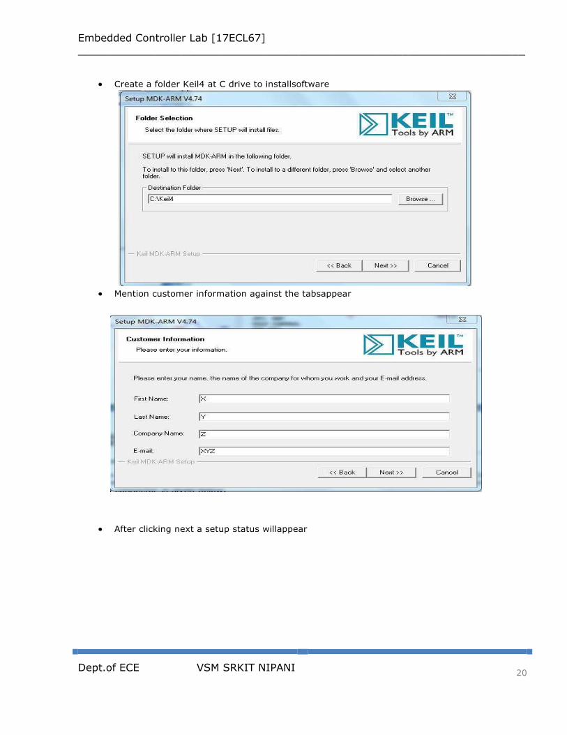
Create a folder Keil4 at C drive to installsoftware
Mention customer information against the tabsappear
After clicking next a setup status willappear

Embedded Controller Lab [17ECL67]
_____________________________________________________________________
Dept.of ECE VSM SRKIT NIPANI
21
Click next andfinish
5.2 Settings to be done at configuration wizard of system_LPC17xx.cfile
Beforeconfiguringtheclockregistersstudytheblockdiagramwhichisdescribedinthe
Clocking and power control in chapter2.
TherearethreeclocksourcesforCPU.SelectOscillatorclockoutofthree.Thisselection is done
by CLKSRCSELregister.
IfwedisablethePLL0SystemclockwillbebypasseddirectlyintoCPUclockdivider register.
UseCCLKCFGregisterforchoosingthedivisionfactorof4toget3MHzoutof12MHz
Oscillatorfrequency.
For any other peripherals use the PCLK same asCCLK.Follow the below mentioned

Embedded Controller Lab [17ECL67]
_____________________________________________________________________
Dept.of ECE VSM SRKIT NIPANI
22
procedure to do these settings. Open uVisoin4 under file tab open
C: Keil (4)\ARM\startup\NXP\LPC17xx\system_LPC17xx.c
Double click on system_LPC17xx.c file at projectwindow
Select the configuration wizard at thebottom
Expand theicons
Select Clockconfiguration
Under System controls and Statusregisters
OSCRANGE: Main Oscillatorrangeselect 1MHz to20MHz
OSCEN: Mainoscillatorenable √
Under Clock source select register(CLKSRCSEL)
CLKSRC: PLL clocksourceselection Main oscillator
Disable PLL0 configuration and PLL1configuration
Under CPU Clock Configurationregister(CCLKCFG)
CCLKSEL: Divide value for CPU clockforPLL0 4
Under USB Clock configuration register(USBCLKCFG)
USBSEL: Divide value for USB clockforPLL0 4
Under Peripheral clock selection register 0 (PCLKSEL0) and 1(PCLKSEL1)
Select Pclk = Cclk for all.
Under Power control for peripherals(PCONP)
Enable the power for requiredperipherals
IfCLKOUTtobestudiedconfiguretheClockoutputconfigurationregisterasbelow
CLKOUTSEL : MainOscillator
CLKOUTDIV 1
CLKOUT_EN :√
Call thefunctions
SystemInit ();
SystemCoreClockUpdate();
At the beginning of the main function without missing.These functions are defined
in system_LPC17xx.c where actual clock and other system control registers configuration takes
place.
NOTE: System core clock (Peripheral CLK)/Operating frequency is calculated as below
Main Oscillator = XTAL = 12MHZ and (CCLKCFG+1) = 4 then
System core clock = Main Oscillator/ (CCLKCFG+1) = 12MHZ / 4 = 3MHZ.

Embedded Controller Lab [17ECL67]
_____________________________________________________________________
Dept.of ECE VSM SRKIT NIPANI
23
5.3 Flash magic 6.01installations:
Go to Software folder in the CD and run FlashMagic.exe file.
Click next on Welcome wizard
Select the radio button I accept the agreement and click next
Choose a folder to install the files. Click next and choose the option create short cut icon
and click next. Displays the options we have selected

Embedded Controller Lab [17ECL67]
_____________________________________________________________________
Dept.of ECE VSM SRKIT NIPANI
24
Click on install and finish
5.4 Project Creation in Keil uvision4IDE:
Create a project folder before creating NEWproject.
Use separate folder for eachproject
Open Keil uVision4 IDE software by double clicking on “Keil Uvision4”icon.

Embedded Controller Lab [17ECL67]
_____________________________________________________________________
Dept.of ECE VSM SRKIT NIPANI
25
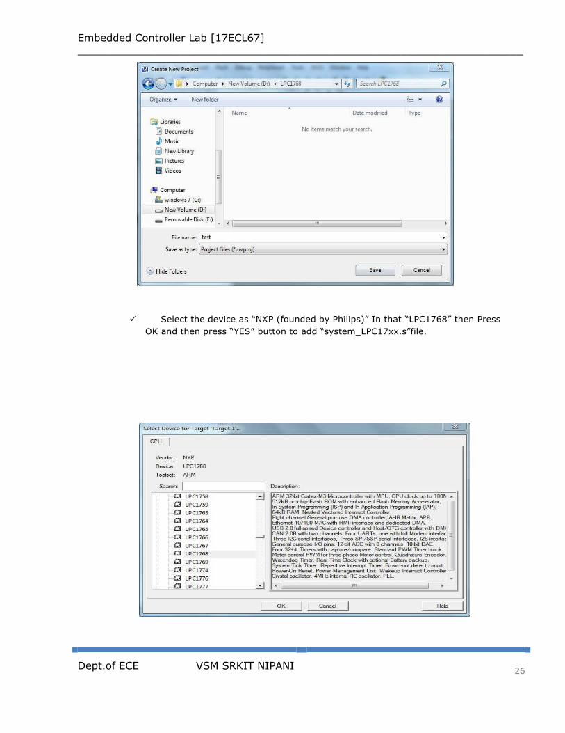
Go to “Project” then to “New Project” and save it with a name in the
Respective Project folder, already youcreated.
Embedded Controller Lab [17ECL67]
_____________________________________________________________________
Dept.of ECE VSM SRKIT NIPANI
26
Select the device as “NXP (founded by Philips)” In that “LPC1768” then Press
OK and then press “YES” button to add “system_LPC17xx.s”file.

Embedded Controller Lab [17ECL67]
_____________________________________________________________________
Dept.of ECE VSM SRKIT NIPANI
27
Go to “File” In that “New” to open an editor window. Create your source file And use the
header file “LPC17xx.h” in the source file and save the file. Color syntax highlighting will
be enabled once the file is saved with a Recognized extension such as “.C“.

Embedded Controller Lab [17ECL67]
_____________________________________________________________________
Dept.of ECE VSM SRKIT NIPANI
28
Rightclickon“SourceGroup1”andselecttheoption“Add FilestoGroup'SourceGroup 1' “add
the. C source file(s) to thegroup.
Again right click on Source Group 1 and select the option “Add Existing Files to Group
'Source Group 1' “add the file–C:
Keil4\ARM\startup\NXP\LPC17xx\system_LPC17xx.c
Any changes made to this file at current project will directly change the source
system_LPC17xx.c file. So that other project settings may get altered. So it is
recommended to copy thefile
C: Keil (4)\ARM\startup\NXP\LPC17xx\system_LPC17xx.c to the project folder and add
to the sourcegroup.
Important: This file should be added at each project creation.
Then go to “Project” in that “Translate” to compile the File(s).
Go to “Project” in that “Build Target” for building all source files such as “.C”,”.ASM”, “.h”,
files, etc…This will create the hex file if no warnings & noErrors.
5.5 Settings to be done in KEILUV4 for Executing Cprograms:
In Project Window Right click “TARGET1” and select “options for target„TARGET1‟
Then go to option “Target” inthat
1. Xtal 12.0MHz and UseMicroLIB
2. Select IROM1 (starting 0×0 size0×8000).
3. Select IRAM1 (starting 0×10000000 size0×8000).

Embedded Controller Lab [17ECL67]
_____________________________________________________________________
Dept.of ECE VSM SRKIT NIPANI
29
Then go to option“Output”
Select “Create Hexfile”.
Then go to option“Linker”
Select use memory layout from targetdialog
6. TEST SET UP & TESTPROCEDURE: 6.1 TEST SET UPREQUIREMENTS:
ALS-SDA-ARMCTXM3-06 : 1No.
Powersupply(+5V) : 1No.
USB-to-SERIAL cable for programming andserialcommunication : 1No.
Kiel uvision4 and flash magic6.01
OneworkingCOMportinthehostcomputersystemandPCfordownloadingthe
software.
1 numbers 26 core FRC cables of 2 inchlength
6.2 TEST SETUP:
Connect +5V power cable toDB1.
Do not insert the piggyback module into the board before testing the voltagelevels.
Remove JP5 and then switch on the powersupply.
Check+5VatTP1.IfvoltagesareatrightlevelthencheckifanyIC'sgettingwarm.
Insert JP5 and check +3.3V atTP3
Then switch off the power supply, insert the piggybackmodule.
Also make sure the regulator output which is flowing into the controller is3.3V
6.3 FLASH PROGRAMMING
Connect 9 pin DSUB USB-to-SERIAL cable from PC to DB2 at theboard.
On the 2 way dip switch SW3 and Short jumperJP7.
Open flash magic6.01.
Some Settings in FLASHMAGIC:
Step1. Communications:
Device :LPC1768
ComPort : COM1 (Check theCOM here .Computerright

Embedded Controller Lab [17ECL67]
_____________________________________________________________________
Dept.of ECE VSM SRKIT NIPANI
30
ClickManageDeviceManagerPorts)
Baud Rate 19200
Interface : None (ISP)
Oscillator :12MHz
Step2. ERASE:
Select “Erase Blocks Used By Hex File”.
Step3. Hex file:
Browse and select the Hex file which you want to download.
Step4. Options:
Select “Verify After Programming”.
Go to Options ->Advanced Options->communications
Do not select High Speed Communications
Keep baud rate 115200.
Options ->Advanced Options->Hardware config
Select Use DTR & RTS to control RST & ISP Pin.
Select Keep RTS asserted while COM Port open.
T1 = 50ms. T2 = 100ms.
Step5. Start:
Click Start to download the hex file to the controller.
After downloading the code the program starts executing in the hardware, then switch off
SW3 and remove the ISP jumper JP7.
7. HARDWAREDETAILS
7.1 CONNECTORDETAILS:
CN1CONNECTOR:28pin14X2HEADERisconnectedtothecontroller. Pin# DESCRIPTION PIN # DESCRIPTION
1 TDO-JTAG 2 TDI-JTAG
3 TMS-JTAG 4 TRST-JTAG
5 TCK-JTAG 6 PC3
7 PC2 8 PC1
9 PC0 10 3.3V
11 GND 12 3.3V
13 NC 14 NC
15 GND 16 RTCX1
17 RESET 18 RTCX2
19 VBAT 20 ADC
21 CP1.30 22 NC
23 NC 24 C_P0.28
25 C_P0.27 26 NC
27 NC 28 NC
CN2CONNECTOR:28pin14X2HEADERisconnectedtothecontroller.
Pin# DESCRIPTION PIN # DESCRIPTION
1 NC 2 NC
3 C_P2.12 4 PWM
5 3.3V 6 C_P0.29
7 C_P0.30 8 GND
9 C_P1.18 10 C_P1.19
11 ROW0 12 ROW1
13 ROW2 14 ROW3
15 C_P1.24 16 C_P1.25
17 NC 18 GND
19 3.3V 20 C_P1.27
21 C_P1.28 22 C_P1.29

Embedded Controller Lab [17ECL67]
_____________________________________________________________________
Dept.of ECE VSM SRKIT NIPANI
31
23 C_P0.0 24 C_P0.1
25 PB6 26 PB7
27 EINT 28 NC
CN3CONNECTOR:28pin14X2HEADERisconnectedtothecontroller.
PIN # DESCRIPTION PIN # DESCRIPTION
1 NC 2 NC
3 ILED 4 EINT1
5 ISP 6 3.3V
7 GND 8 PA7*
9 PA6 10 PA5
11 PA4 12 PA3
13 PA2 14 PA1
15 PA0 16 LD7/CON
17 LD6 18 LD5
19 LD4 20 LEN
21 LRS 22 PC7
23 3.3V 24 GND
25 PC6 26 PC5
27 PC4 28 NC

Embedded Controller Lab [17ECL67]
_____________________________________________________________________
Dept.of ECE VSM SRKIT NIPANI
32
CN4 CONNECTOR: 28 pin 14 X 2 HEADER is connected to thecontroller.
PIN # DESCRIPTION PIN # DESCRIPTION
1 PB5 2 PB4
3 PB3 4 PB2
5 PB1 6 PB0
7 C_P4.28 8 GND
9 3.3V 10 C_P4.29
11 C_P1.17 12 C_P1.16
13 C_P1.15 14 C_P1.14
15 C_P1.10 16 C_P1.4
17 C_P1.8 18 C_P1.9
19 C_P1.1 20 C_P1.0
21 3.3V 22 GND
23 TXD0 24 RXD0
25 RTCK-JTAG 26 NC
27 NC 28 NC
CN5 CONNECTOR: 2 pin MKDSN connector for RELAYinterface
PIN # DESCRIPTION
1 Connected to POL1 of Rly2
2 Connected to NO contact of Rly2
CN6 CONNECTOR: 20 pin FRC connected to the controller, Standard JTAG connector for
programming/debuggingwithARM-JTAGdebugger.SHORTjumperJP1for JTAGtowork.
PIN # DESCRIPTION PIN # DESCRIPTION
1 +3.3V 2 +3.3V
3 TRST 4 GND
5 TDI 6 GND
7 TMS 8 GND
9 TCK 10 GND
11 RTCK 12 GND
13 TDO 14 GND
15 RST 16 GND
17 R10 ONE END 18 GND
19 R11 ONE END 20 GND
CN7 CONNECTOR: 26 pin FRC connected to the controller, which is compatiblewith
ALS Standard External Interfaces. SHORT jumper JP4 to connect External Interfaces. PIN # DESCRIPTION PIN # DESCRIPTION
1 PC4(P2.0) 2 PC5(P2.1)
3 PC2(P0.25) 4 PC3(P0.26)
5 PC0(P0.23) 6 PC1(P0.24)
7 PB6(P0.10) 8 PB7(P0.11)
9 PB4(P0.8) 10 PB5(P0.9)
11 PB2(P0.6) 12 PB3(P0.7)
13 PB0(P0.4) 14 PB1(P0.5)
15 PA6(P0.21) 16 PA7(P0.22)
17 PA4(P0.19) 18 PA5(P0.20)
19 PA2(P0.17) 20 PA3(P0.18)
21 PA0(P0.15) 22 PA1(P0.16)
23 PC6*(P2.2 2nd PIN OF JP13) 24 PC7(P2.3)
25 +5V THROUGH JP4 26 GND
Embedded Controller Lab [17ECL67]
_____________________________________________________________________
Dept.of ECE VSM SRKIT NIPANI
33
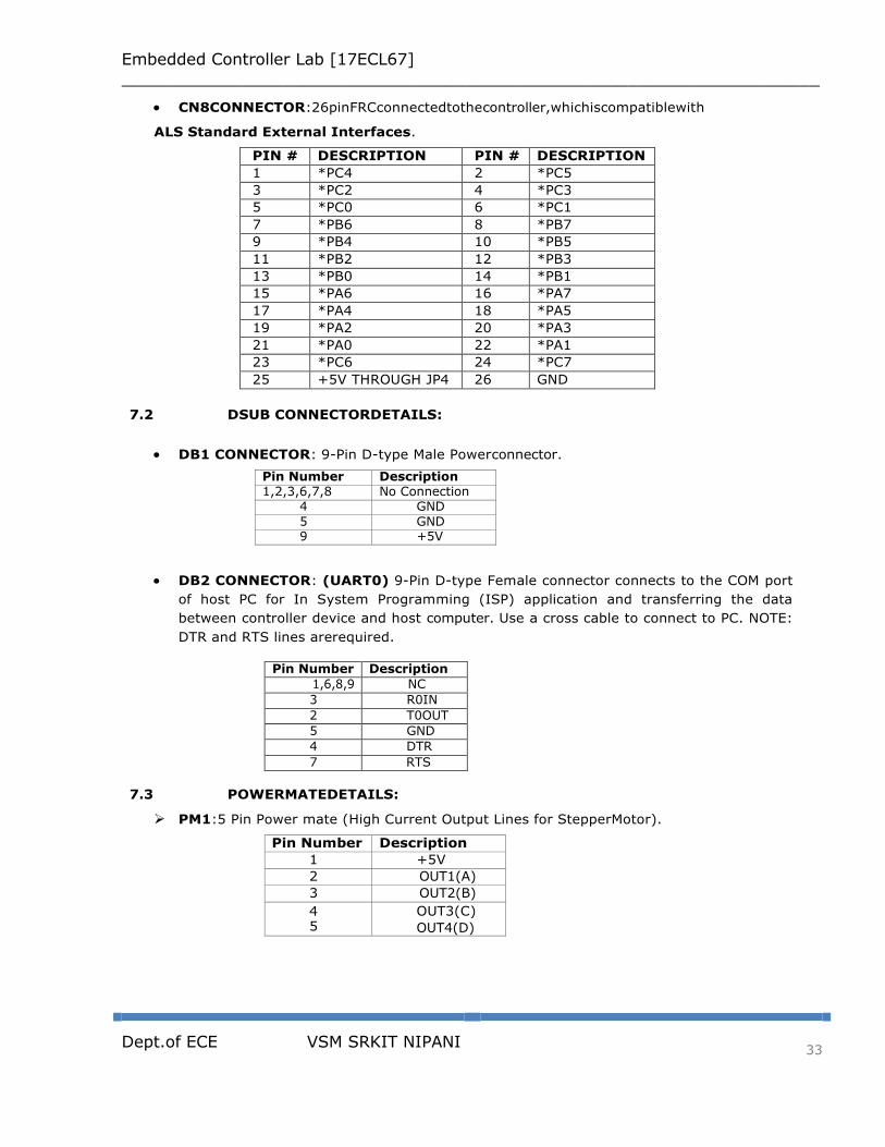
CN8CONNECTOR:26pinFRCconnectedtothecontroller,whichiscompatiblewith
ALS Standard External Interfaces.
PIN # DESCRIPTION PIN # DESCRIPTION
1 *PC4 2 *PC5
3 *PC2 4 *PC3
5 *PC0 6 *PC1
7 *PB6 8 *PB7
9 *PB4 10 *PB5
11 *PB2 12 *PB3
13 *PB0 14 *PB1
15 *PA6 16 *PA7
17 *PA4 18 *PA5
19 *PA2 20 *PA3
21 *PA0 22 *PA1
23 *PC6 24 *PC7
25 +5V THROUGH JP4 26 GND
7.2 DSUB CONNECTORDETAILS:
DB1 CONNECTOR: 9-Pin D-type Male Powerconnector.
Pin Number Description 1,2,3,6,7,8 No Connection
4 GND
5 GND 9 +5V
DB2 CONNECTOR: (UART0) 9-Pin D-type Female connector connects to the COM port
of host PC for In System Programming (ISP) application and transferring the data
between controller device and host computer. Use a cross cable to connect to PC. NOTE:
DTR and RTS lines arerequired.
Pin Number Description
1,6,8,9 NC
3 R0IN
2 T0OUT
5 GND
4 DTR
7 RTS
7.3 POWERMATEDETAILS:
PM1:5 Pin Power mate (High Current Output Lines for StepperMotor).
Pin Number Description
1 +5V
2 OUT1(A)
3 OUT2(B)
4 5
OUT3(C)
OUT4(D)
Embedded Controller Lab [17ECL67]
_____________________________________________________________________
Dept.of ECE VSM SRKIT NIPANI
34
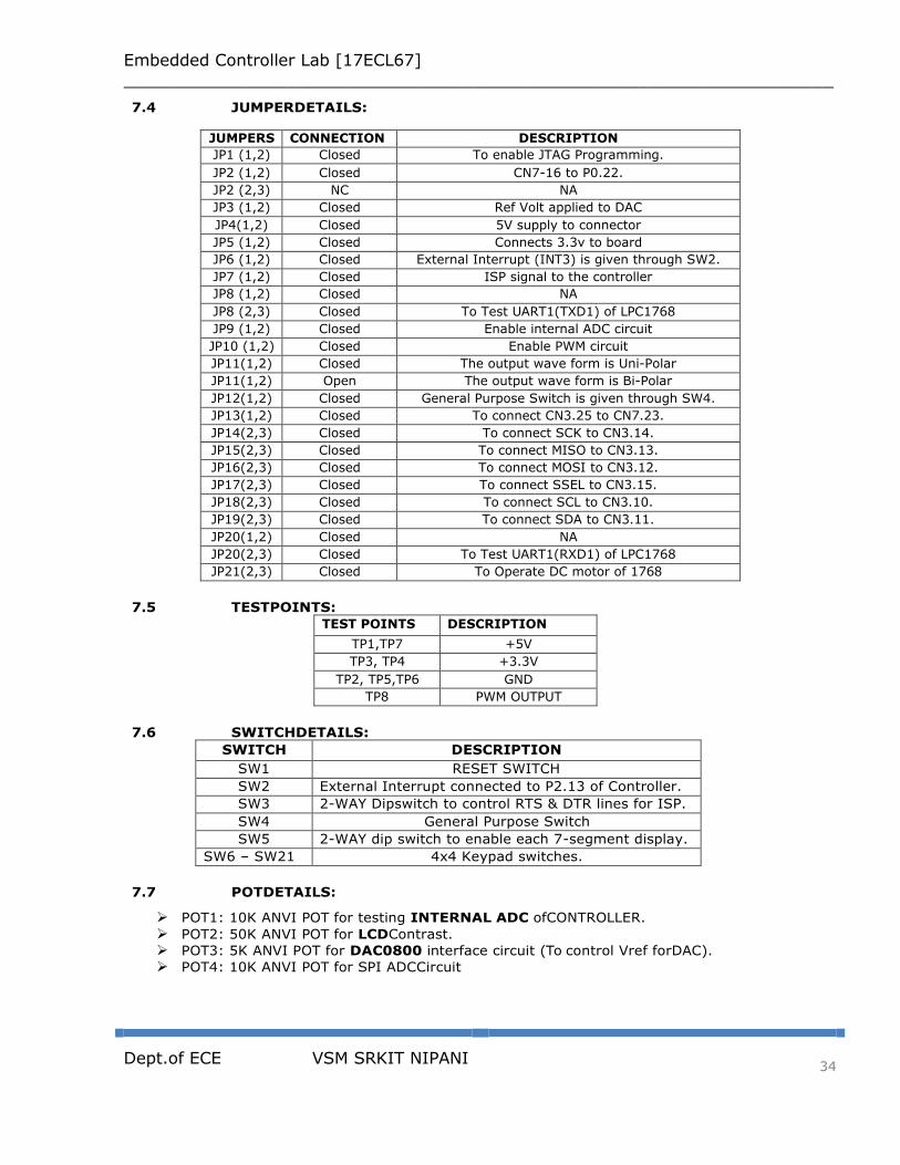
7.4 JUMPERDETAILS:
JUMPERS CONNECTION DESCRIPTION
JP1 (1,2) Closed To enable JTAG Programming.
JP2 (1,2) Closed CN7-16 to P0.22.
JP2 (2,3) NC NA
JP3 (1,2) Closed Ref Volt applied to DAC
JP4(1,2) Closed 5V supply to connector
JP5 (1,2) Closed Connects 3.3v to board
JP6 (1,2) Closed External Interrupt (INT3) is given through SW2.
JP7 (1,2) Closed ISP signal to the controller
JP8 (1,2) Closed NA
JP8 (2,3) Closed To Test UART1(TXD1) of LPC1768
JP9 (1,2) Closed Enable internal ADC circuit
JP10 (1,2) Closed Enable PWM circuit
JP11(1,2) Closed The output wave form is Uni-Polar
JP11(1,2) Open The output wave form is Bi-Polar
JP12(1,2) Closed General Purpose Switch is given through SW4.
JP13(1,2) Closed To connect CN3.25 to CN7.23.
JP14(2,3) Closed To connect SCK to CN3.14.
JP15(2,3) Closed To connect MISO to CN3.13.
JP16(2,3) Closed To connect MOSI to CN3.12.
JP17(2,3) Closed To connect SSEL to CN3.15.
JP18(2,3) Closed To connect SCL to CN3.10.
JP19(2,3) Closed To connect SDA to CN3.11.
JP20(1,2) Closed NA
JP20(2,3) Closed To Test UART1(RXD1) of LPC1768
JP21(2,3) Closed To Operate DC motor of 1768
7.5 TESTPOINTS:
TEST POINTS DESCRIPTION
TP1,TP7 +5V
TP3, TP4 +3.3V
TP2, TP5,TP6 GND
TP8 PWM OUTPUT
7.6 SWITCHDETAILS:
SWITCH DESCRIPTION
SW1 RESET SWITCH
SW2 External Interrupt connected to P2.13 of Controller.
SW3 2-WAY Dipswitch to control RTS & DTR lines for ISP.
SW4 General Purpose Switch
SW5 2-WAY dip switch to enable each 7-segment display.
SW6 – SW21 4x4 Keypad switches.
7.7 POTDETAILS:
POT1: 10K ANVI POT for testing INTERNAL ADC ofCONTROLLER.
POT2: 50K ANVI POT for LCDContrast.
POT3: 5K ANVI POT for DAC0800 interface circuit (To control Vref forDAC).
POT4: 10K ANVI POT for SPI ADCCircuit

Embedded Controller Lab [17ECL67]
_____________________________________________________________________
Dept.of ECE VSM SRKIT NIPANI
35
7.8 ICDETAILS: IC’s DESCRIPTION
U1 LM317 VOLTAGE REGULATOR (3 PIN)
U2 MAX3232 RS232 LINE DRIVER(16 PIN)
U3 ICL7660S SUPER VOLTAGE Converter (8 PIN)
U4 LM358 DUAL OP AMP (8 PIN)
U5 74HCT244 OCTAL BUFFER (20 PIN)
U6 ULN2803 DRIVER 8 Darlington array(18 PIN)
U7 MCP3202 SPI ADC(8 PIN)
U8,U9 LT543 SEVEN SEGMENT DISPLAY (10 PIN)
U10 AT24C16 I2C NVROM IC
U11 LM335 Temperature sensor
U12 DAC0800 Digital to Analog (16 PIN)
7.9 RELIAMATEDETAILS:
1. RM1: 16 pin Single female Berg for LCDInterface. PIN # DESCRIPTION PIN # DESCRIPTION
1 GND 9,10 NO CONNECTION
2 +5V 11 DATA LINE D4(P2.6)
3 50K ANVI POT (POT2) 12 DATA LINE D5(P2.7)
4 RS(P2.4) 13 DATA LINE D6(P2.8)
5 GND 14 DATA LINE D7(P2.9)
6 CSE(P2.5) 15 +5V(Backlight)
7,8 NO CONNECTION 16 GND
2. RM2: UART1Interface
Pin Number Description
1 TX
2 RX
3 GND
2. RM3: DAC 0800Interface
Pin Number Description
1 Connected to DAC O/P
2 GND
3. RM4: DCMOTOR
Pin Number Description
1 Connected to POLE1 of Rly1
2 Connected to POLE2 of Rly1

Embedded Controller Lab [17ECL67]
_____________________________________________________________________
Dept.of ECE VSM SRKIT NIPANI
36
8. CABLEDETAILS 8.1 APPLYINGPOWER:
Use the following procedure to apply power. Connect a 9-pin DSUB Female Connector to a 9-pin
DSUB Male connector DB1 provided on the Evaluation Board. The color code for the supply is
shown in table below:
PINNUMBERS POWER
9 +5V
4,5 GND
8.2 SERIAL COMMUNICATION:
TheRS232CrosscableconnectionsrequiredforestablishingcommunicationbetweenEvaluation Board
and a display terminal/host computer system is givenbelow (ON BOARD it is DB2).
Open the Hyper Terminal & set the host computer system baud rate to 9600, data length to 8
bit, parity bit to none and stop bits to 1.
DB2 PIN NO. (9 PIN MALE ) COMPUTER (COM PORT) PIN NO. (9-PIN FEMALE)
2-TXD 2-RXD
3-RXD 3-TXD
4-DTR 4-DTR
7-RTS 7-RTS
5-SIGNAL GND 5-SIGNAL GND
1,6,8,9 NC
Embedded Controller Lab [17ECL67]
_____________________________________________________________________
Dept.of ECE VSM SRKIT NIPANI
37
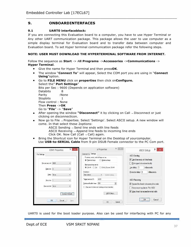
9. ONBOARDINTERFACES 9.1 UART0 interfaceblock:
If you are connecting this Evaluation board to a computer, you have to use Hyper Terminal or
Any other UART communication package. This package allows the user to use computer as a
simple display terminal for Evaluation board and to transfer data between computer and
Evaluation board. To set Hyper terminal communication package refer the following steps.
NOTE: USER MUST DOWNLOAD THE HYPERTERMINAL SOFTWARE FROM INTERNET.
Follow the sequence as Start -> All Programs ->Accessories ->Communications ->
Hyper Terminal.
Give the name for Hyper Terminal and then pressOK.
The window “Connect To” will appear, Select the COM port you are using in “Connect Using”option.
Go to FILE MENU click on properties then click onConfigure.
Select the” Port Settings”
Bits per Sec : 9600 (Depends on application software)
Databits 8
Parity :None
Stopbits 1
Flow control : None
Then Press ->OK
Go to “File” -> “Save”
After opening the window “Disconnect” it by clicking on Call → Disconnect or just clicking on disconnecticon.
Now go to File → Properties. Select 'Settings'. Select ASCII setup. A new window will come. In that select these 2options:
ASCII Sending → Send line ends with line feeds
ASCII Receiving → Append line feeds to incoming line ends Click OK. Now Call (Call → Call) again.
Bring the Shortcut icon for Hyper Terminal on the Desktop of yourcomputer.
Use USB-to-SERIAL Cable from 9-pin DSUB Female connector to the PC Com port.
UART0 is used for the boot loader purpose. Also can be used for interfacing with PC for any
Embedded Controller Lab [17ECL67]
_____________________________________________________________________
Dept.of ECE VSM SRKIT NIPANI
38
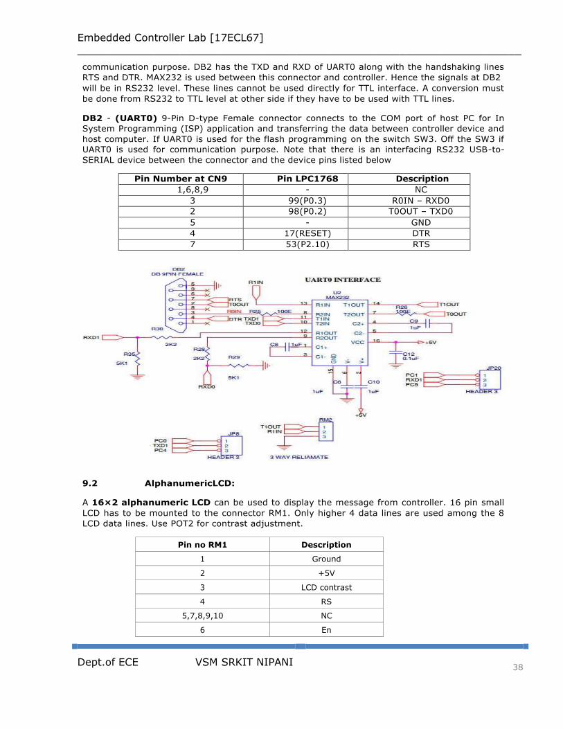
communication purpose. DB2 has the TXD and RXD of UART0 along with the handshaking lines
RTS and DTR. MAX232 is used between this connector and controller. Hence the signals at DB2
will be in RS232 level. These lines cannot be used directly for TTL interface. A conversion must
be done from RS232 to TTL level at other side if they have to be used with TTL lines.
DB2 - (UART0) 9-Pin D-type Female connector connects to the COM port of host PC for In
System Programming (ISP) application and transferring the data between controller device and
host computer. If UART0 is used for the flash programming on the switch SW3. Off the SW3 if
UART0 is used for communication purpose. Note that there is an interfacing RS232 USB-to-
SERIAL device between the connector and the device pins listed below
Pin Number at CN9 Pin LPC1768 Description
1,6,8,9 - NC
3 99(P0.3) R0IN – RXD0
2 98(P0.2) T0OUT – TXD0
5 - GND
4 17(RESET) DTR
7 53(P2.10) RTS
9.2 AlphanumericLCD:
A 16×2 alphanumeric LCD can be used to display the message from controller. 16 pin small
LCD has to be mounted to the connector RM1. Only higher 4 data lines are used among the 8
LCD data lines. Use POT2 for contrast adjustment.
Pin no RM1 Description
1 Ground
2 +5V
3 LCD contrast
4 RS
5,7,8,9,10 NC
6 En

Embedded Controller Lab [17ECL67]
_____________________________________________________________________
Dept.of ECE VSM SRKIT NIPANI
39
11 to 14 Data 4 to 7
15 Back light anode
16 Back light cathode
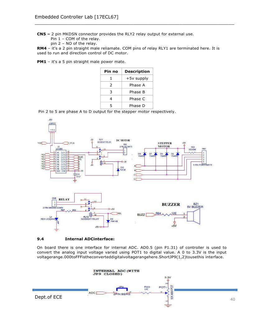
9.3 Relay buzzer and Motors controlblock:
It is a high Current applications block where a stepper motor, a Dc motor and a relay
are interfaced through the high current driver ULN2803 (U6). These lines will have high
current (max 300 mA) with low voltage level of 0.7V.
The Stepper motor can be interfaced to the board by connecting it to the Power Mate
PM1. The direction of the rotation can be changed through software. The DC Motor can also
beinterfacedtotheboardbyconnectingittotheReliamateRM4.Thedirectionoftherotation can be
changed throughsoftware.
The Relay RLY2 is switched between ON and OFF state. The LED L2 will toggle for
every relay switch over. The contact of NO & NC of the relay can be checked at the MKDSN
connector CN5 pins 1 & 2 using a Digital Multi meter – these contacts can be connected to
externaldevices.
By connecting 26 pin FRC cable from CN7 to CN8 this block can be interfaced and the port
lines details are given in the table.
CN8 Pin # Description
1, 2, 23, 24 Buffered from U6 used for stepper motor control
3 Buffered from U6 & connected to RLY2 coil. coil other end is connected to +5V
5 Connected to pin 1 of U6; corresponding output of U6 is taken to NO and NC
contacts of relay RLY1
4 One end of coil of relay RLY1
6 Controls the buzzer
Embedded Controller Lab [17ECL67]
_____________________________________________________________________
Dept.of ECE VSM SRKIT NIPANI
40
CN5 – 2 pin MKDSN connector provides the RLY2 relay output for external use.
Pin 1 – COM of the relay.
pin 2 – NO of the relay.
RM4 – it's a 2 pin straight male reliamate. COM pins of relay RLY1 are terminated here. It is
used to run and direction control of DC motor.
PM1 – it's a 5 pin straight male power mate.
Pin no Description
1 +5v supply
2 Phase A
3 Phase B
4 Phase C
5 Phase D
Pin 2 to 5 are phase A to D output for the stepper motor respectively.
9.4 Internal ADCinterface:
On board there is one interface for internal ADC. AD0.5 (pin P1.31) of controller is used to
convert the analog input voltage varied using POT1 to digital value. A 0 to 3.3V is the input
voltagerange.000toFFFistheconverteddigitalvoltagerangehere.ShortJP9(1,2)tousethis interface.
Embedded Controller Lab [17ECL67]
_____________________________________________________________________
Dept.of ECE VSM SRKIT NIPANI
41
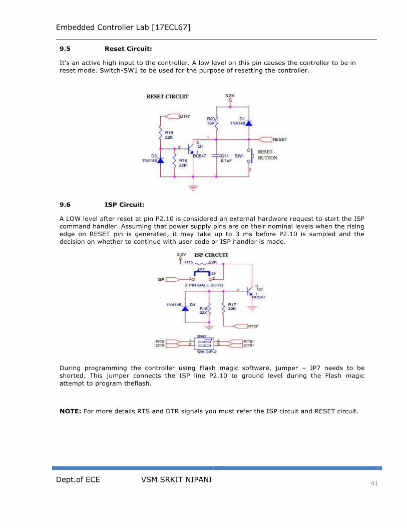
9.5 Reset Circuit:
It's an active high input to the controller. A low level on this pin causes the controller to be in
reset mode. Switch-SW1 to be used for the purpose of resetting the controller.
9.6 ISP Circuit:
A LOW level after reset at pin P2.10 is considered an external hardware request to start the ISP
command handler. Assuming that power supply pins are on their nominal levels when the rising
edge on RESET pin is generated, it may take up to 3 ms before P2.10 is sampled and the
decision on whether to continue with user code or ISP handler is made.
During programming the controller using Flash magic software, jumper – JP7 needs to be
shorted. This jumper connects the ISP line P2.10 to ground level during the Flash magic
attempt to program theflash.
NOTE: For more details RTS and DTR signals you must refer the ISP circuit and RESET circuit.

Embedded Controller Lab [17ECL67]
_____________________________________________________________________
Dept.of ECE VSM SRKIT NIPANI
42
ProgrammingMode: RunMode:
SW3 – is to isolate the hand shaking signals from board signals (RTS, DTR) and connector.
Keep this switch ON before programming the controller flash memory with the application code.
Keep it open to Run the loaded program and reset. Especially if UART0 is using for any
communication purpose, user must keep these switch open to execute UART0 relatedcode.
RTS – Controls the ISP line of the controllerP2.10
DTR – Used to interface controllerreset.
9.7 Serial peripheralInterface:
This block has a 2 channel SPI ADC. Channel 0 input is POT4 and channel 1 input is
Temperature sensor LM335. While interfacing this block do not connect 26 pin FRC cable from
CN7 to CN8 and short the Pins 2&3 at the jumpers JP14, JP15, JP16, JP17. Port lines used are
P0.15 – SCK, P0.16 – SSEL, P0.17 – MISO, P0.18 –MOSI.
9.8 I2C Interface:
This block has I2C NVROM IC. Can be communicated using I2C1. To interface this block short
pin2&3atthejumpersJP18andJP19.Donotconnect26pinFRCcablefromCN7 toCN8.Port lines used
are P0.19 – SDA1, P0.20 –SCL1.

Embedded Controller Lab [17ECL67]
_____________________________________________________________________
Dept.of ECE VSM SRKIT NIPANI
43
9.9 4×4 key matrixInterface:
The switches SW14 to SW29 are organized as 4 rows X 4 columns matrix. One end of all the
switches are configured as columns. The other end of the matrix configured as rows. A row
line will be always an output from the controller. Column lines are inputs. A low level sent
from the row will appear at column end if the switch ispressed.
Connect 26 pin FRC cable from CN7 to CN8 for interfacing this block with controller.

Embedded Controller Lab [17ECL67]
_____________________________________________________________________
Dept.of ECE VSM SRKIT NIPANI
44
9.10 PWM Interface:
A PWM output from the controller can be observed as an intensity variation of the LED L3.
Pulses on the CRO can be observed at TP8. Short JP10 to interface this block. Port line P3.25.
9.11 External interrupts:
An external interrupt EINT3 to the controller is generated using the switch SW2. Pressing the
switch generates edge triggered interrupt to the controller.
Short JP6 to use EINT3. Port lines EINT3 – P2.13.
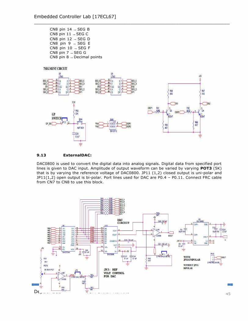
9.12 Seven segment display interface:
There are two multiplexed 7-segment display units (U8, U9) on the board. Each display has
8-inputs SEG_A (Pin-7), SEG_B (Pin-6), SEG_C (Pin-4), SEG_D (Pin-2), SEG_E (Pin-1),
SEG_F (Pin-9), SEG_G (Pin-10) and SEG_H (Pin-5) and the remaining pins pin-3 & pin-8 are
Common Cathode CC. These segments are common cathode type hence active high devices.
At power on enable of all the segments are pulled up. A two bits input through SW5 is used
for multiplexing operation. A high level on these lines enables the corresponding display.
Connection of these enable lines are shown below.
CN8 pin 17 → SW5 pin 1 → EN1 (U8)
CN8 pin 18 → SW5 pin 2 → EN2 (U9)
Data lines:
CN8 pin 13 → SEG A
Embedded Controller Lab [17ECL67]
_____________________________________________________________________
Dept.of ECE VSM SRKIT NIPANI
45
CN8 pin 14 → SEG B
CN8 pin 11 → SEG C
CN8 pin 12 → SEG D CN8 pin 9 → SEG E
CN8 pin 10 → SEG F
CN8 pin 7 → SEG G CN8 pin 8 → Decimal points
9.13 ExternalDAC:
DAC0800 is used to convert the digital data into analog signals. Digital data from specified port
lines is given to DAC input. Amplitude of output waveform can be varied by varying POT3 (5K)
that is by varying the reference voltage of DAC0800. JP11 (1,2) closed output is uni-polar and
JP11(1,2) open output is bi-polar. Port lines used for DAC are P0.4 – P0.11. Connect FRC cable
from CN7 to CN8 to use this block.

Embedded Controller Lab [17ECL67]
_____________________________________________________________________
Dept.of ECE VSM SRKIT NIPANI
46
9.14 Spareconnector:
Few unused lines of the board are terminated at a connector – CN9. It's a 30 pin 15×2 male
straight berg. These lines can be used for any external interface if required. A pin descriptionof
this connector is given below.
PIN # Description PIN # Description
1 P0.27/SDA0/USB_SDA 2 P0.28/SCL0/USB_SCL
3 P2.12//EINT2/I2STX_WS 4 P1.18/USB_UP_LED/PWM1.1/CAP1.0
5 P1.19/MCOA0/USB_PPWR/CAP1.1 6 P1.24/MCI2/PWM1.5/MOSI0
7 P1.25/MCOA1/MAT1.1 8 P1.27/CLKOUT/USB_OVRCR/CAP0.1
9 P1.28/MCOA2/PCAP1.0/MAT0.0 10 P1.29/MCOB2/PCAP1.1/MAT0.1
11 P0.0/RD1/TXD3/SDA1 12 P0.1/TD1/RXD3/SCL1
13 P4.28/RX_MCLK/MAT2.0/TXD3 14 P4.29/TX_MCLK/MAT2.1/RXD3
15 P1.0/ENET_TXD0 16 P1.1/ENET_TXD1
17 P1.4/ENET_TX_EN 18 P1.8/ENET_CRS
19 P1.9/ENET_RXD0 20 P1.10/ENET_RXD1
21 P1.14/ENET_RX_ER 22 P1.15/ENET_REF_CLK
23 P1.16/ENET_MDC 24 P1.17/ENET_MDIO
25 P0.29/USB_D+ 26 P0.30/USB_D
27 RTCX1 28 RTCX2
29 VBAT 30 Ground
10. DEMO PROGRAMS IN KEIL UVISION4IDE
For all the SYLLABUS or demo programs make sure that the corresponding settings have to be
made:
Both Switches of SW3 should be in ON position for ISPprogramming.
Short JP7 for ISPprogramming.
Short JP5 to connect +3.3v into thecircuit.
Short JP4 to connect +5v to InterfaceBoard.
Connect the 26 core FRC cable CN7 to CN8 to connect to On-boardinterfaces.
Connect CN7 for ExternalNIFC's.
DEMO PROGRAMS:
NOTE: Do not short any Jumpers JP14, JP15, JP16, JP17, JP18 and JP19 when 26 pin FRC cable is connected from CN7 to CN8. While using SPI and I2C do not connect 26 pin FRC cable from CN7 to CN8.
10.1 Test UART0test:
Download the file “UART0_test.hex” to trainer using Flash Magic 6.01 version.
Switch off SW3, Un-short JP7. Press the reset switch (SW1) to run the program.
Result:
Open the hyper terminal, the Constant string “Hello World” will be displayed on the hyper
terminal.

Embedded Controller Lab [17ECL67]
_____________________________________________________________________
Dept.of ECE VSM SRKIT NIPANI
47
10.2 Test DC Motor:
A) DC Motor Speed control using on chipPWM:
Download the file “dcm_speed_control.hex” to trainer using Flash Magic 6.01 version.
Connect the Female Reliamate of the DC motor to the male Reliamate RM4 present on the
board. Short JP21/2&3 ,Switch off SW3, Un-short JP7. Press the reset switch (SW1) to run the
program.
Result:
Observe the rotation of the dc motor (Controlled by On chip PWM) Varies from slow speed to
higher speed and Vice Versa. This rotation of the motor will be continuously in loop.
B) DC Motor directionControl:
Download the file “dcm_direction.hex” to trainer using Flash Magic 6.01 version.
Connect the Female Reliamate of the DC motor to the male Reliamate RM4 present on the
board. Short JP21/2&3 and Connect the 26pin FRC between CN7 and CN8. Switch off SW3, Un-
short JP7. Press the reset switch (SW1) to run the program.
Result:
Observe the Clockwise and Anti-Clockwise rotation of the dc motor with respect On/Off of Relay
RLY1. This rotation of the motor will be continuously in loop.
10.3 Test Stepper Motor
Download the file “steppermtr.hex” to trainer using Flash Magic 6.01 version.
Connect the Female Power mate of the stepper motor to the male Power mate PM1 present on
the board. Jumper JP13 (1, 2) should be shorted and all the other jumpers should be removed.
Switch off SW3, Un-short JP7. Press the reset switch (SW1) to run the program.
Result:
Observe the stepper motor rotation it should rotate Clockwise &Anti Clockwise direction.
This rotation of the motor will be continuously in loop.

Embedded Controller Lab [17ECL67]
_____________________________________________________________________
Dept.of ECE VSM SRKIT NIPANI
48
10.4 Test Internal ADC:
Download the file “Int_ADC.hex” to trainer using Flash Magic 6.01 version.
Jumper JP9 should be shorted and all the other jumpers should be removed. Switch off SW3,
Un-short JP7. Press the reset switch (SW1) to run the program.
Result:
This routine is used to study the internal Feature of the LPC1768 Microcontroller. Vary the POT1
(10K) and observe the corresponding analog (0-3.30V) & digital value (0-fff) on LCD.
10.5 TestDAC0800:
A) SineWave:
Download the file “SINE.hex” to trainer using Flash Magic 6.01 version.
Jumper JP3 should be shorted. Jumper JP11 should be open for bipolar mode. Jumper JP11
should be short for unipolar mode and all the other jumpers should be removed. Switch off
SW3, Un-short JP7. Press the reset switch (SW1) to run the program.
Result:
Observe the Analog output waveform at the Pin-1 of RM3 using Oscilloscope (CRO) with respect
to GND pin-2 of RM3.
NOTE: POT3 is provided to control the Reference voltage for DAC output (Vref).User will get
maximum 2.5V peak to peak for uni-polar and 5V peak to peak for Bipolar.
B) SquareWave:
Download the file “Square.hex” to trainer using Flash Magic 6.01 version.
Jumper setting are same as sine wave.
Result:
Observe the Analog output waveform at the Pin-1 of RM3 using Oscilloscope (CRO) with respect
to GND pin-2 of RM3.
NOTE: POT3 is provided to control the Reference voltage for DAC output (Vref).User will get
maximum 2.5V peak to peak for uni-polar and 5V peak to peak for Bipolar.
C) Triangle Wave:
Download the file “Triangle.hex” to trainer using Flash Magic 6.01 version.
Jumper setting are same as sine wave.
Result:
Observe the Analog output waveform at the Pin-1 of RM3 using Oscilloscope (CRO) with respect
to GND pin-2 of RM3.
NOTE: POT3 is provided to control the Reference voltage for DAC output (Vref).User will get
maximum 2.5V peak to peak for uni-polar and 5V peak to peak for Bipolar.
10.6 Test Keypad (4X4Matrix):
Download the file “KEY_LCD.hex” to trainer using Flash Magic 6.01 version. Switch off SW3, Un-
short JP7. Press the reset switch (SW1) to run the program.
Result:
Press the keys SW6 to SW21 and the Corresponding outputs „0 to F‟ will be displayed on the
LCD.
Embedded Controller Lab [17ECL67]
_____________________________________________________________________
Dept.of ECE VSM SRKIT NIPANI
49
10.7 Test Pulse Width Modulation(PWM):
Downloadthefile“PWM.hex”totrainerusingFlashMagic6.01version.
Jumper JP10 should be shorted all the other jumpers should be removed. Switch off SW3, Un-
short JP7. Press the reset switch (SW1) to run the program.
Result:
Observe the output on CRO at TP8 and also LED L3 (intensity of LED will vary).
10.9 Test ExternalInterrupt:
Download the file “EXINT.hex” to trainer using Flash Magic 6.01 version.
Jumper JP6 should be shorted, all the other jumpers should be removed. Switch off SW3, Un-
short JP7. Press the reset switch (SW1) to run the program.
Result:
When switch SW2 pressed the port line goes low & the external interrupt occurs at port line
P2.13. To show the external interrupt has been occurred LED L2 has been used (Toggle for each
Press).
10.10 TEST 7 SegmentDisplay:
Download the file “Seven_seg.hex” to trainer using Flash Magic 6.01 version.
Both pins of SW5 should be in ON position. Switch off SW3, Un-short JP7. Press the reset
switch (SW1) to run the program.
Result:
Observe display changing from 00 to FF. This process is continuously in loop
Control RELAY\BUZZER\LED ThroughSwitch:
Download the file “RELAY.hex” to trainer using Flash Magic 6.01 version.
Short jumper JP12.
Result:
Press SW4 on the buzzer section, see that Relay RLY2, Led L4 and Buzzer BZ1 are On and when
user releases the push button the Relay RLY2, L4 and Buzzer should be in Off condition. Relay
Common and NO are brought out to CN5 connector.
10.11 SPI TemperatureSensor
Download the file “SENSOR.hex” to trainer using Flash Magic 6.01 version.
Remove inter connected cable CN7 and CN8. Short JP14 JP15 JP16 JP17/2&3. Do the serial
communications set up with hyper terminal with baud rate of 9600. Switch off SW3, Un-short
JP7. Press the reset switch (SW1) to run the program.
NOTE: While doing this experiment user must measure the voltage of the Power Supply. That
measured voltage will be considered as your Vref for LM335 interface. In software you must
alter the defined value of Vref (for more details refer the description of the program).
Result:

Embedded Controller Lab [17ECL67]
_____________________________________________________________________
Dept.of ECE VSM SRKIT NIPANI
50
Temperature value will display on hyper terminal.
11. DEMO ASSEMBLYPROGRAMS
11.1 ALP to multiply two 16bit binarynumbers.
Download the file “16_bit_mul/mul.hex” to trainer using Flash Magic 6.01 version.
Here two 16 bit Numbers used for the multiplication are 0x706F and 0x7161.User can
change the inputs. Switch off SW3, Un-short JP7. Press the reset switch (SW1) to run the
program.
Result:
Multiplied result is displayed on the LCD.
11.2 ALP to find the sum of first 10 integernumbers.
Download the file “sum_of_1_to_10/sum.hex” to trainer using Flash Magic 6.01 version.
Here first 10 natural numbers are 01 to 10 so sum will be 55. Switch off SW3, Un-short
JP7. Press the reset switch (SW1) to run the program.
Result:
Added result is displayed on the LCD.
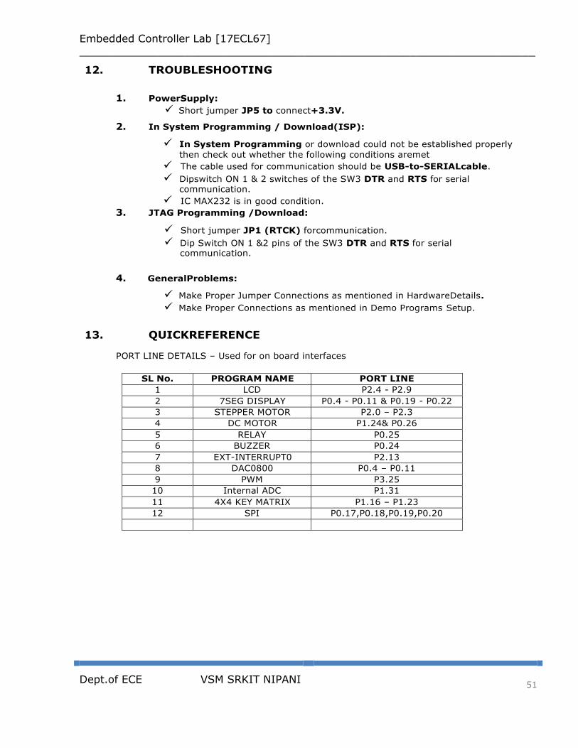
Embedded Controller Lab [17ECL67]
_____________________________________________________________________
Dept.of ECE VSM SRKIT NIPANI
51
12. TROUBLESHOOTING
1. PowerSupply:
Short jumper JP5 to connect+3.3V.
2. In System Programming / Download(ISP):
In System Programming or download could not be established properly
then check out whether the following conditions aremet
The cable used for communication should be USB-to-SERIALcable.
Dipswitch ON 1 & 2 switches of the SW3 DTR and RTS for serial communication.
IC MAX232 is in good condition.
3. JTAG Programming /Download:
Short jumper JP1 (RTCK) forcommunication.
Dip Switch ON 1 &2 pins of the SW3 DTR and RTS for serial communication.
4. GeneralProblems:
Make Proper Jumper Connections as mentioned in HardwareDetails.
Make Proper Connections as mentioned in Demo Programs Setup.
13. QUICKREFERENCE
PORT LINE DETAILS – Used for on board interfaces
SL No. PROGRAM NAME PORT LINE
1 LCD P2.4 - P2.9
2 7SEG DISPLAY P0.4 - P0.11 & P0.19 - P0.22
3 STEPPER MOTOR P2.0 – P2.3
4 DC MOTOR P1.24& P0.26
5 RELAY P0.25
6 BUZZER P0.24
7 EXT-INTERRUPT0 P2.13
8 DAC0800 P0.4 – P0.11
9 PWM P3.25
10 Internal ADC P1.31
11 4X4 KEY MATRIX P1.16 – P1.23
12 SPI P0.17,P0.18,P0.19,P0.20

Embedded Controller Lab [17ECL67]
_____________________________________________________________________
Dept.of ECE VSM SRKIT NIPANI
52
/***********************************************************
* EXP1 : UART0 test Demonstration(To display HELLO WORLD)
---------------------------------------------------------------------------- * Controller : LPC1768 * Description : In this example fixed string "HELLO WORLD" is displayed
* on the Hyperterminal using Uart0 Feature. ----------------------------------------------------------------------------
******************************************************************/ #include<LPC17xx.h>
void delay(unsigned int r1);
void UART0_Init(void); void UART0_IRQHandler(void);
unsigned long int r=0, i = 0; unsigned char tx0_flag=0;
unsigned char *ptr, arr[] = "Hello world\r"; int main(void)
{ SystemInit();
SystemCoreClockUpdate(); UART0_Init(); while(1)
{ ptr = arr;
while ( *ptr != '\0'){ LPC_UART0->THR = *ptr++; while(tx0_flag == 0x00);
tx0_flag = 0x00; for (i=0; i<200; i++);
} for (i=0; i<500; i++)
delay(625); } }
void UART0_Init(void)
{ LPC_SC->PCONP |= 0x00000008; //UART0 peripheral enable LPC_PINCON->PINSEL0 |= 0x00000050;
LPC_UART0->LCR = 0x00000083; //enable divisor latch, parity disable, 1 stop bit, 8bit word length
LPC_UART0->DLM = 0X00; LPC_UART0->DLL = 0x13; //select baud rate 9600 bps

Embedded Controller Lab [17ECL67]
_____________________________________________________________________
Dept.of ECE VSM SRKIT NIPANI
53
LPC_UART0->LCR = 0X00000003;
LPC_UART0->FCR = 0x07; LPC_UART0->IER = 0X03; //select Transmit and receive interrupt
NVIC_EnableIRQ(UART0_IRQn); //Assigning channel }
void UART0_IRQHandler(void)
{ unsigned long Int_Stat; Int_Stat = LPC_UART0->IIR; //reading the data from
interrupt identification register Int_Stat = Int_Stat & 0x06; //masking other than txmit
int & rcve data indicator if((Int_Stat & 0x02)== 0x02) //transmit interrupt
tx0_flag = 0xff; }
void delay(unsigned int r1) {
for(r=0;r<r1;r++); }

Embedded Controller Lab [17ECL67]
_____________________________________________________________________
Dept.of ECE VSM SRKIT NIPANI
54
/*******************************************************************
* EXP2A:DC MOTOR CONTROL USING ON CHIP PWM
---------------------------------------------------------------------------- * Controller : LPC1768 * Description : Port line P1.24 used for the PWM feature.When T0TC matches
* the MR0 counts interrupt is generated * and Duty cycle will be changed.Depends upon the Duty cycle Motor speed is also
changes. * PWM 1.5 is used. Match register 0 is used for count purpose. PWM 1 * match register 5 is increamented or decreamented at each interrupted.
----------------------------------------------------------------------------
********************************************************************/ #include <lpc17xx.h>
void pwm_init(void);
void PWM1_IRQHandler(void); unsigned long int i,j;
unsigned char flag,flag1,flag2;
int main(void) { SystemInit();
SystemCoreClockUpdate(); pwm_init();
while(1) {
for(i=0;i<=1000;i++); // delay
}//end of while }//end of main
void pwm_init(void) {
LPC_SC->PCONP |= (1<<6); //PWM1 is powered LPC_PINCON->PINSEL3 |= 0x00020000; //pwm1.5 is selected for the pin P1.24
LPC_PWM1->PR = 0x00000000; //Count frequency : Fpclk LPC_PWM1->PCR = 0x0002000; //select PWM5 single edge & PWM5 o/p is enb
LPC_PWM1->MCR = 0x00000003; //Reset and interrupt on PWMMR0 LPC_PWM1->MR0 = 30000; //setup match register 0 count
LPC_PWM1->MR5 = 0x00000100; //setup match register MR5 LPC_PWM1->LER = 0x000000FF; //enable shadow copy register

Embedded Controller Lab [17ECL67]
_____________________________________________________________________
Dept.of ECE VSM SRKIT NIPANI
55
LPC_PWM1->TCR = 0x00000002; //RESET COUNTER AND PRESCALER
LPC_PWM1->TCR = 0x00000009; //enable PWM and counter
NVIC_EnableIRQ(PWM1_IRQn); return; }
void PWM1_IRQHandler(void)
{ LPC_PWM1->IR = 0xff; //clear the interrupts
if(flag == 0x00) {
LPC_PWM1->MR5 += 100; LPC_PWM1->LER = 0x000000FF;
if(LPC_PWM1->MR5 >= 37000) { flag1 = 0xff;
flag = 0xff; LPC_PWM1->LER = 0x000000fF;
} for(i=0;i<8000;i++); }
else if(flag1 == 0xff)
{ LPC_PWM1->MR5 -= 100;
LPC_PWM1->LER = 0x000000fF;
if(LPC_PWM1->MR5 <= 0x500) {
flag = 0x00; flag1 = 0x00; LPC_PWM1->LER = 0X000000fF;
} for(i=0;i<8000;i++);
} }

Embedded Controller Lab [17ECL67]
_____________________________________________________________________
Dept.of ECE VSM SRKIT NIPANI
56
/********************************************************************
* EXP2B.DCM Direction Control *-------------------------------------------------------------------------------
* Controller : LPC1768 * Description :Direction of the DCM is cotrolled in this software by alternatively
inter- * changing the supply with the help Relay. Port lines: P1.24 and P0.26.
* Port line P1.24 used for the PWM feature.When T0TC matches * the MR0 counts interrupt is generated * and Duty cycle will be changed.Depends upon the Duty cycle Motor speed is also
changes. * PWM 1.5 is used. Match register 0 is used for count purpose. PWM 1
* match register 5 is increamented or decreamented at each interrupted. ----------------------------------------------------------------------------
********************************************************************/
#include <LPC17xx.H> void Clock_Wise(void);
void AClock_Wise(void);
unsigned long i; int main(void)
{ SystemInit();
LPC_PINCON->PINSEL1 &= 0xFFCFFFFF; //P0.26 GPIO, P0.26 controls dir LPC_PINCON->PINSEL3 &= 0xFFFFCFFF; //P1.24 GPIO LPC_GPIO0->FIODIR |= 0x04000000; //P0.26 output
LPC_GPIO1->FIODIR |= 0x01000000; //P1.24 output
while(1) {
Clock_Wise(); for(i=0;i<200000;i++); AClock_Wise();
for(i=0;i<200000;i++);
} //end while(1) } //end main
void Clock_Wise(void) {
LPC_GPIO1->FIOCLR = 0x01000000; //P0.23 Kept low to off DCM for(i=0;i<10000;i++); //delay to componsate inertia
Embedded Controller Lab [17ECL67]
_____________________________________________________________________
Dept.of ECE VSM SRKIT NIPANI
57
LPC_GPIO0->FIOSET = 0x04000000; //coil is on
LPC_GPIO1->FIOSET = 0x01000000; //motor in on return;
} //end void Clock_Wise(void) void AClock_Wise(void)
{ LPC_GPIO1->FIOCLR = 0x01000000; //P0.23 Kept low to off DCM
for(i=0;i<10000;i++); //delay to componsate inertia LPC_GPIO0->FIOCLR = 0x04000000; //coil is off LPC_GPIO1->FIOSET = 0x01000000; //Motor is on
return; } //end void AClock_Wise(void)
Embedded Controller Lab [17ECL67]
_____________________________________________________________________
Dept.of ECE VSM SRKIT NIPANI
58
/********************************************************************
* EXP3.Stepper motor Direction control *-------------------------------------------------------------------------------
* Controller : LPC1768 * Description:A stepper motor direction is controlled by shifting the voltage across * the coils. Port lines : P2.0 to P2.3.
*------------------------------------------------------------------------------- *******************************************************************/
#include <LPC17xx.H>
void clock_wise(void); void anti_clock_wise(void);
unsigned long int var1,var2; unsigned int i=0,j=0,k=0;
int main(void) {
SystemInit(); SystemCoreClockUpdate();
LPC_PINCON->PINSEL4 = 0x00000000; //P2.0 to P2.3 GPIO LPC_GPIO2->FIODIR = 0x0000000F; //P2.0 to P2.3 output
while(1) {
for(j=0;j<50;j++) //50 times in Clock wise Rotation clock_wise();
for(k=0;k<65000;k++); //Delay to show anti_clock Rotation
for(j=0;j<50;j++) //50 times in Anti Clock wise Rotation anti_clock_wise();
for(k=0;k<65000;k++); //Delay to show clock Rotation
} //End of while(1) } //End of main
void clock_wise(void) {
var1 = 0x00000001; //For Clockwise for(i=0;i<=3;i++) //for A B C D Stepping {
LPC_GPIO2->FIOCLR = 0X0000000F; LPC_GPIO2->FIOSET = var1;
var1 = var1<<1; //For Clockwise for(k=0;k<15000;k++); //for step speed variation

Embedded Controller Lab [17ECL67]
_____________________________________________________________________
Dept.of ECE VSM SRKIT NIPANI
59
}
}
void anti_clock_wise(void) { var1 = 0x0000008; //For Anticlockwise
for(i=0;i<=3;i++) //for A B C D Stepping {
LPC_GPIO2->FIOCLR = 0X0000000F; LPC_GPIO2->FIOSET = var1;
var1 = var1>>1; //For Anticlockwise for(k=0;k<15000;k++); //for step speed variation
} }

Embedded Controller Lab [17ECL67]
_____________________________________________________________________
Dept.of ECE VSM SRKIT NIPANI
60
/********************************************************************
* Alphanumeric LCD
*------------------------------------------------------------------------- * Controller : LPC1768 * Port lines used: Data1 to Data4 - P0.23 to P0.26
* En - P0.28. RS - P0.27, RW - Ground * Connection : CND to CNAB
********************************************************************/
#include <lpc17xx.h>
#include "AN_LCD.h" unsigned long int temp1=0, temp2=0 ;
//lcd initialization void lcd_init() {
/* Ports initialized as GPIO */ LPC_PINCON->PINSEL4 &= 0xFFF000FF; //P2.4 to P2.9
/* Setting the directions as output */ LPC_GPIO2->FIODIR |= DT_CTRL;
LPC_GPIO2->FIODIR |= RS_CTRL; LPC_GPIO2->FIODIR |= EN_CTRL;
clear_ports(); delay_lcd(3200);
temp2 = (0x30<<2);
wr_cn(); delay_lcd(30000);
temp2 = (0x30<<2); wr_cn();
delay_lcd(30000);
temp2 = (0x30<<2); wr_cn(); delay_lcd(30000);
temp2 = (0x20<<2);
wr_cn(); delay_lcd(30000);

Embedded Controller Lab [17ECL67]
_____________________________________________________________________
Dept.of ECE VSM SRKIT NIPANI
61
temp1 = 0x28; lcd_com();
delay_lcd(30000); temp1 = 0x0c;
lcd_com(); delay_lcd(800);
temp1 = 0x06; lcd_com();
delay_lcd(800);
temp1 = 0x01; lcd_com(); delay_lcd(10000);
temp1 = 0x80;
lcd_com(); delay_lcd(800); return;
}
void lcd_com(void) { temp2 = temp1 & 0xf0;//move data (26-8+1) times : 26 - HN place, 4 - Bits
temp2 = temp2 << 2;//data lines from 23 to 26 wr_cn();
temp2 = temp1 & 0x0f; //26-4+1 temp2 = temp2 << 6; wr_cn();
delay_lcd(1000); return;
}
// command nibble o/p routine void wr_cn(void) //write command reg {
clear_ports(); LPC_GPIO2->FIOPIN = temp2; // Assign the value to the data lines
LPC_GPIO2->FIOCLR = RS_CTRL; // clear bit RS LPC_GPIO2->FIOSET = EN_CTRL; // EN=1 delay_lcd(25);
LPC_GPIO2->FIOCLR = EN_CTRL; // EN =0 return;
}
Embedded Controller Lab [17ECL67]
_____________________________________________________________________
Dept.of ECE VSM SRKIT NIPANI
62
// data o/p routine which also outputs high nibble first // and lower nibble next
void lcd_data(void) { temp2 = temp1 & 0xf0;
temp2 = temp2 << 2; wr_dn();
temp2= temp1 & 0x0f; temp2= temp2 << 6; wr_dn();
delay_lcd(1000); return;
} // data nibble o/p routine
void wr_dn(void) {
clear_ports(); LPC_GPIO2->FIOPIN = temp2; // Assign the value to the data lines
LPC_GPIO2->FIOSET = RS_CTRL; // set bit RS LPC_GPIO2->FIOSET = EN_CTRL; // EN=1
delay_lcd(25); LPC_GPIO2->FIOCLR = EN_CTRL; // EN =0 return;
}
void delay_lcd(unsigned int r1) { unsigned int r;
for(r=0;r<r1;r++); return;
}
void clr_disp(void) { temp1 = 0x01;
lcd_com(); delay_lcd(10000);
return; } void clear_ports(void)
{ /* Clearing the lines at power on */
LPC_GPIO2->FIOCLR = DT_CTRL; //Clearing data lines LPC_GPIO2->FIOCLR = RS_CTRL; //Clearing RS line

Embedded Controller Lab [17ECL67]
_____________________________________________________________________
Dept.of ECE VSM SRKIT NIPANI
63
LPC_GPIO2->FIOCLR = EN_CTRL; //Clearing Enable line
return;
} void lcd_puts(unsigned char *buf1)
{ unsigned int i=0;
while(buf1[i]!='\0') {
temp1 = buf1[i]; lcd_data();
i++; if(i==16) {
temp1 = 0xc0; lcd_com();
} }
return; }

Embedded Controller Lab [17ECL67]
_____________________________________________________________________
Dept.of ECE VSM SRKIT NIPANI
64
// program to generate square wave with DAC interface
/********************************************* * EXP5:External DAC interface (Square Wave)
*-------------------------------------------------------------------- * Controller : LPC1768
* Description : This example explains about how Sqaure Wave is generated.P0.4
to P0.11 are used to get the Digital values.
0xff ________ | | |
| | | | | | | |
| 0x00 | |_________|
*********************************************************************
******/ #include <LPC17xx.H>
void delay(void);
int main () {
LPC_PINCON->PINSEL0 &= 0xFF0000FF ; // Configure P0.4 to P0.11 as GPIO LPC_GPIO0->FIODIR |= 0x00000FF0 ;
while(1)
{ LPC_GPIO0->FIOPIN = 0x00000FF0 ;
delay(); LPC_GPIO0->FIOCLR = 0x00000FF0 ; delay();
} }
void delay(void) {
unsigned int i=0; for(i=0;i<=9500;i++);
}

Embedded Controller Lab [17ECL67]
_____________________________________________________________________
Dept.of ECE VSM SRKIT NIPANI
65
// program to generate Triangular wave with DAC interface
/******************************************************************* * EXP5:External DAC interface (Triangle Wave)
*-------------------------------------------------------------------- * Controller : LPC1768 * Description : This example explains about how Triangular Wave is
generated.P0.4 to P0.11 are used to get the Digital values.
0xff /\ /\ / \ / \
/ \ / \ / \ / \
/ \ / \ 0x00 / \/ \
******************************************************************/ #include <LPC17xx.H>
int main () {
unsigned long int temp=0x00000000; unsigned int i=0;
LPC_PINCON->PINSEL0 &= 0xFF0000FF ; // Configure P0.4 to P0.11 as GPIO
LPC_GPIO0->FIODIR |= 0x00000FF0 ;
while(1) { //output 0 to FE
for(i=0;i!=0xFF;i++) {
temp=i; temp = temp << 4;
LPC_GPIO0->FIOPIN = temp; } // output FF to 1
for(i=0xFF; i!=0;i--) {
temp=i; temp = temp << 4; LPC_GPIO0->FIOPIN = temp;
} }//End of while(1)
}//End of main()

Embedded Controller Lab [17ECL67]
_____________________________________________________________________
Dept.of ECE VSM SRKIT NIPANI
66
/********************************************************************
* EXP5:External DAC interface (Sine Wave)
*-------------------------------------------------------------------- * Controller : LPC1768 * Description : This example explains about how Sine Wave is generated. Here Y
= Asin(@) since 48 samples are used to generate the sine wave so 360/48 = 7.5 degree/sample.
for example for 15deg Y = 1.25 + Asin(@) = 1.25 + 1.25sin(15) = 1.5735 for 2.5V -----------------> 0xff
then 1.5735V -----------------> 0xA1
|0xff . . --|2.5V
for Uni polar | . .
| | . 15 . |
| . . |
0x7f |------------------------------------------------- |1.25V | . . |
| . . |
| . . | ____|_________________________________.___._________________--|0V
|0x00
********************************************************************/
#include <LPC17xx.H> int count=0,sinevalue,value;
unsigned char sine_tab[49]= { 0x80,0x90,0xA1,0xB1,0xC0,0xCD,0xDA,0xE5,0xEE,0xF6,0xFB,0xFE,
0xFF,0xFE,0xFB,0xF6,0xEE,0xE5,0xDA,0xCD,0xC0,0xB1,0xA1,0x90, 0x80,0x70,0x5F,0x4F,0x40,0x33,0x26,0x1B,0x12,0x0A,0x05,0x02, 0x00,0x02,0x05,0x0A,0x12,0x1B,0x26,0x33,0x40,0x4F,0x5F,0x70,0x80};
int main(void)
{ LPC_PINCON->PINSEL0 &= 0xFF0000FF ; //

Embedded Controller Lab [17ECL67]
_____________________________________________________________________
Dept.of ECE VSM SRKIT NIPANI
67
Configure P0.0 to P0.15 as GPIO
LPC_GPIO0->FIODIR |= 0x00000FF0 ;
count = 0; while(1) {
for(count=0;count<48;count++) {
sinevalue = sine_tab[count];//+0X10 ; value= 0x00000FF0 & (sinevalue << 4); LPC_GPIO0->FIOPIN = value;
} }
}
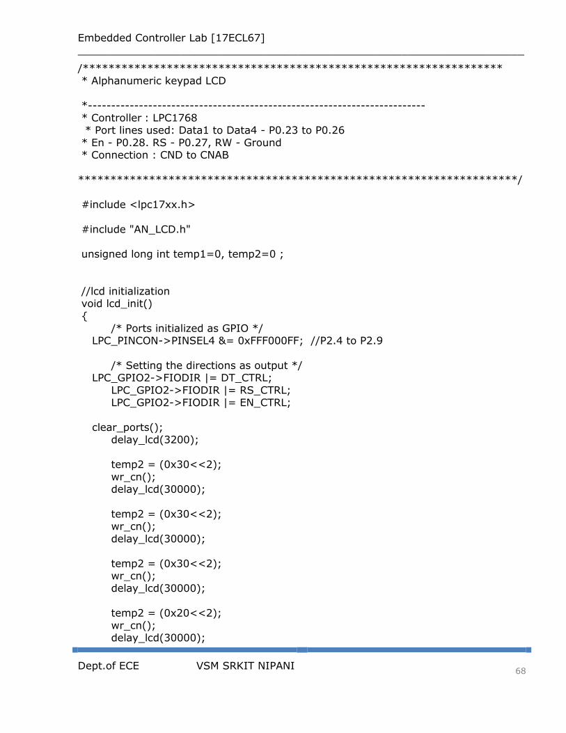
Embedded Controller Lab [17ECL67]
_____________________________________________________________________
Dept.of ECE VSM SRKIT NIPANI
68
/*****************************************************************
* Alphanumeric keypad LCD
*------------------------------------------------------------------------- * Controller : LPC1768 * Port lines used: Data1 to Data4 - P0.23 to P0.26
* En - P0.28. RS - P0.27, RW - Ground * Connection : CND to CNAB
********************************************************************/
#include <lpc17xx.h>
#include "AN_LCD.h" unsigned long int temp1=0, temp2=0 ;
//lcd initialization void lcd_init() {
/* Ports initialized as GPIO */ LPC_PINCON->PINSEL4 &= 0xFFF000FF; //P2.4 to P2.9
/* Setting the directions as output */ LPC_GPIO2->FIODIR |= DT_CTRL;
LPC_GPIO2->FIODIR |= RS_CTRL; LPC_GPIO2->FIODIR |= EN_CTRL;
clear_ports(); delay_lcd(3200);
temp2 = (0x30<<2);
wr_cn(); delay_lcd(30000);
temp2 = (0x30<<2); wr_cn();
delay_lcd(30000);
temp2 = (0x30<<2); wr_cn(); delay_lcd(30000);
temp2 = (0x20<<2);
wr_cn(); delay_lcd(30000);

Embedded Controller Lab [17ECL67]
_____________________________________________________________________
Dept.of ECE VSM SRKIT NIPANI
69
temp1 = 0x28; lcd_com();
delay_lcd(30000); temp1 = 0x0c;
lcd_com(); delay_lcd(800);
temp1 = 0x06; lcd_com();
delay_lcd(800);
temp1 = 0x01; lcd_com(); delay_lcd(10000);
temp1 = 0x80;
lcd_com(); delay_lcd(800); return;
}
void lcd_com(void) { temp2 = temp1 & 0xf0;//move data (26-8+1) times : 26 - HN place, 4 - Bits
temp2 = temp2 << 2;//data lines from 23 to 26 wr_cn();
temp2 = temp1 & 0x0f; //26-4+1 temp2 = temp2 << 6; wr_cn();
delay_lcd(1000); return;
}
// command nibble o/p routine void wr_cn(void) //write command reg {
clear_ports(); LPC_GPIO2->FIOPIN = temp2; // Assign the value to the data lines
LPC_GPIO2->FIOCLR = RS_CTRL; // clear bit RS LPC_GPIO2->FIOSET = EN_CTRL; // EN=1 delay_lcd(25);
LPC_GPIO2->FIOCLR = EN_CTRL; // EN =0 return;
}

Embedded Controller Lab [17ECL67]
_____________________________________________________________________
Dept.of ECE VSM SRKIT NIPANI
70
// data o/p routine which also outputs high nibble first // and lower nibble next
void lcd_data(void) { temp2 = temp1 & 0xf0;
temp2 = temp2 << 2; wr_dn();
temp2= temp1 & 0x0f; temp2= temp2 << 6; wr_dn();
delay_lcd(1000); return;
} // data nibble o/p routine
void wr_dn(void) {
clear_ports(); LPC_GPIO2->FIOPIN = temp2; // Assign the value to the data lines
LPC_GPIO2->FIOSET = RS_CTRL; // set bit RS LPC_GPIO2->FIOSET = EN_CTRL; // EN=1
delay_lcd(25); LPC_GPIO2->FIOCLR = EN_CTRL; // EN =0 return;
}
void delay_lcd(unsigned int r1) { unsigned int r;
for(r=0;r<r1;r++); return;
}
void clr_disp(void) { temp1 = 0x01;
lcd_com(); delay_lcd(10000);
return; } void clear_ports(void)
{ /* Clearing the lines at power on */
LPC_GPIO2->FIOCLR = DT_CTRL; //Clearing data lines LPC_GPIO2->FIOCLR = RS_CTRL; //Clearing RS line
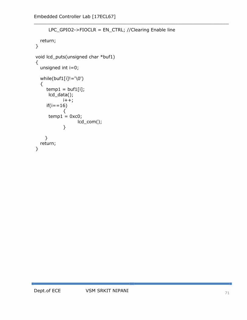
Embedded Controller Lab [17ECL67]
_____________________________________________________________________
Dept.of ECE VSM SRKIT NIPANI
71
LPC_GPIO2->FIOCLR = EN_CTRL; //Clearing Enable line
return;
} void lcd_puts(unsigned char *buf1)
{ unsigned int i=0;
while(buf1[i]!='\0') {
temp1 = buf1[i]; lcd_data();
i++; if(i==16) {
temp1 = 0xc0; lcd_com();
} }
return; }

Embedded Controller Lab [17ECL67]
_____________________________________________________________________
Dept.of ECE VSM SRKIT NIPANI
72
/********************************************************************
**** * EXP8 : Ext interrupt 3
* ---------------------------------------------------------------------- * Controller : LPC1768
* Project : ALS-SDA-ARMCTXM3-06
* Description :This example senses the extenal interrupt 3 through the pin P2.13 * caused through the switch SW10. Toggeles the LED L10 if there is an * interrupt. Port line: EX INT - P2.13 and LED - P2.13
*************************************************************************/
#include<LPC17xx.h>
void EINT3_IRQHandler(void);
unsigned char int3_flag=0; int main(void)
{ unsigned char flag=0;
SystemInit(); SystemCoreClockUpdate();
LPC_PINCON->PINSEL4 |= 0x04000000; //P2.13 as EINT3 LPC_PINCON->PINSEL4 &= 0xFCFFFFFF; //P2.12 GPIO for LED
LPC_GPIO2->FIODIR = 0x00001000; //P2.12 is assigned output
LPC_GPIO2->FIOSET = 0x00001000; //Initiall LED is kept on
LPC_SC->EXTINT = 0x00000008; //writing 1 cleares the interrupt, get set if there is interrupt
LPC_SC->EXTMODE = 0x00000008; //EINT3 is initiated as edge senitive, 0 for level sensitive
LPC_SC->EXTPOLAR = 0x00000000; //EINT3 is falling edge sensitive, 1 for rising edge //above
registers, bit0-EINT0, bit1-EINT1, bit2-EINT2,bit3-EINT3 NVIC_EnableIRQ(EINT3_IRQn); //core_cm3.h
while(1)

Embedded Controller Lab [17ECL67]
_____________________________________________________________________
Dept.of ECE VSM SRKIT NIPANI
73
{
while(int3_flag == 0x00); //wait till interrupt int3_flag = 0x00;
if(flag == 0x00) //when flag is '0' off the LED
{ LPC_GPIO2->FIOCLR = 0x00001000;
flag = 0xFF; } //when flag is FF on the LED
else {
LPC_GPIO2->FIOSET = 0x00001000; flag = 0x00; }
} }
void EINT3_IRQHandler(void) {
int3_flag = 0xff; LPC_SC->EXTINT = 0x00000008; //cleares the interrupt
}

Embedded Controller Lab [17ECL67]
_____________________________________________________________________
Dept.of ECE VSM SRKIT NIPANI
74
/********************************************************************************
* EXP9 : SEVEN SEGMENT DISPLAY *-------------------------------------------------------------------------------
* Controller : LPC1768 * Project : ALS-SDA-ARMCTXM3-06
* Description :\\\\\\\\\\\\\\\DISPLAY ARE CONNECTED IN COMMON CATHODE MODE\\\\\\\\\\\\\\\\\\\\\
Port0 Connected to data lines of all 7 segement displays a
---- f| g |b |----|
e| |c ---- . dot
d a = P0.04 b = P0.05
c = P0.06 d = P0.07
e = P0.08 f = P0.09 g = P0.10
dot = P0.11
Select lines for two 7 Segments DIS1 P0.19
DIS2 P0.20 */
#include <LPC17xx.h>
unsigned int delay, count=0, Switchcount=0,j; unsigned int Disp[16]={0x000003f0, 0x00000060, 0x000005b0, 0x000004f0,
0x00000660,0x000006d0, 0x000007d0, 0x00000070, 0x000007f0,
0x000006f0, 0x00000770,0x000007c0, 0x00000390, 0x000005e0, 0x00000790, 0x00000710 };
#define ALLDISP 0x00180000 //Select all display
#define DATAPORT 0x00000ff0 //P0.16 to P0.23 : Data lines connected to drive Seven Segments

Embedded Controller Lab [17ECL67]
_____________________________________________________________________
Dept.of ECE VSM SRKIT NIPANI
75
int main (void) {
LPC_PINCON->PINSEL0 = 0x00000000; LPC_PINCON->PINSEL1 = 0x00000000; LPC_GPIO0->FIODIR = 0x00180ff0;
while(1)
{ LPC_GPIO0->FIOSET |= ALLDISP; LPC_GPIO0->FIOCLR = 0x00000ff0; // clear the data lines to 7-
segment displays LPC_GPIO0->FIOSET = Disp[Switchcount]; // get the 7-segment
display value from the array for(j=0;j<3;j++)
for(delay=0;delay<30000;delay++); // 1s delay
Switchcount++; if(Switchcount == 0x10) // 0 to F has been displayed ? go back to 0
{ Switchcount = 0;
LPC_GPIO0->FIOCLR = 0x00180ff0; }
}
}
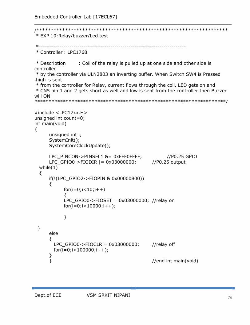
Embedded Controller Lab [17ECL67]
_____________________________________________________________________
Dept.of ECE VSM SRKIT NIPANI
76
/*******************************************************************
* EXP 10:Relay/buzzer/Led test
*------------------------------------------------------------------------ * Controller : LPC1768
* Description : Coil of the relay is pulled up at one side and other side is controlled
* by the controller via ULN2803 an inverting buffer. When Switch SW4 is Pressed ,high is sent * from the controller for Relay, current flows through the coil. LED gets on and
* CN5 pin 1 and 2 gets short as well and low is sent from the controller then Buzzer will ON
*******************************************************************/ #include <LPC17xx.H>
unsigned int count=0; int main(void)
{ unsigned int i; SystemInit();
SystemCoreClockUpdate();
LPC_PINCON->PINSEL1 &= 0xFFF0FFFF; //P0.25 GPIO LPC_GPIO0->FIODIR |= 0x03000000; //P0.25 output while(1)
{ if(!(LPC_GPIO2->FIOPIN & 0x00000800))
{ for(i=0;i<10;i++) {
LPC_GPIO0->FIOSET = 0x03000000; //relay on for(i=0;i<10000;i++);
}
} else
{ LPC_GPIO0->FIOCLR = 0x03000000; //relay off
for(i=0;i<100000;i++); } } //end int main(void)
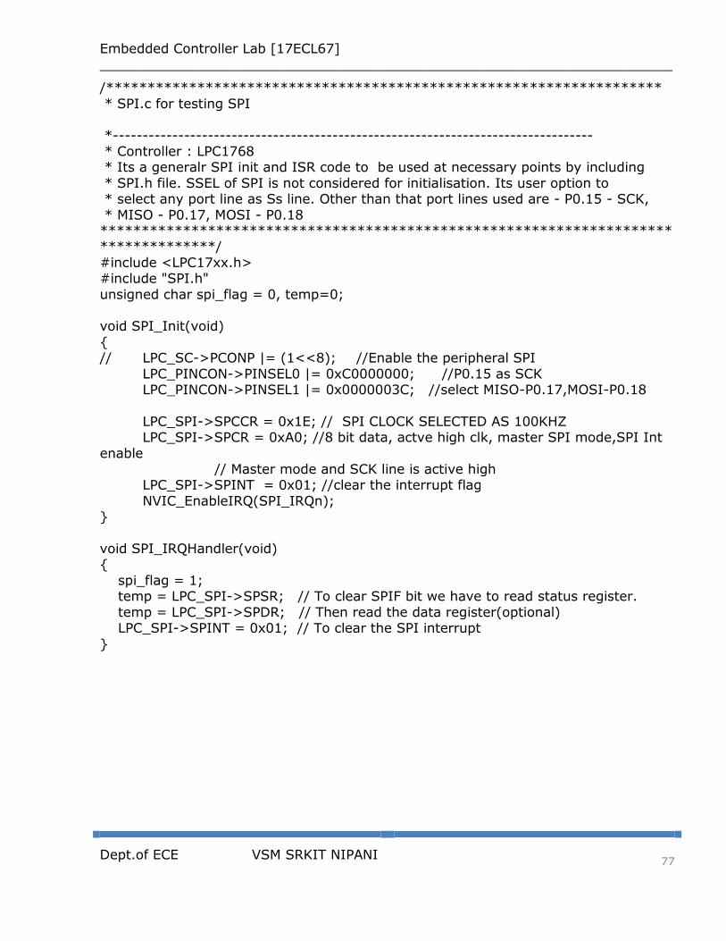
Embedded Controller Lab [17ECL67]
_____________________________________________________________________
Dept.of ECE VSM SRKIT NIPANI
77
/*******************************************************************
* SPI.c for testing SPI
*--------------------------------------------------------------------------------- * Controller : LPC1768 * Its a generalr SPI init and ISR code to be used at necessary points by including
* SPI.h file. SSEL of SPI is not considered for initialisation. Its user option to * select any port line as Ss line. Other than that port lines used are - P0.15 - SCK,
* MISO - P0.17, MOSI - P0.18 ***********************************************************************************/
#include <LPC17xx.h> #include "SPI.h"
unsigned char spi_flag = 0, temp=0; void SPI_Init(void)
{ // LPC_SC->PCONP |= (1<<8); //Enable the peripheral SPI
LPC_PINCON->PINSEL0 |= 0xC0000000; //P0.15 as SCK LPC_PINCON->PINSEL1 |= 0x0000003C; //select MISO-P0.17,MOSI-P0.18
LPC_SPI->SPCCR = 0x1E; // SPI CLOCK SELECTED AS 100KHZ LPC_SPI->SPCR = 0xA0; //8 bit data, actve high clk, master SPI mode,SPI Int
enable // Master mode and SCK line is active high LPC_SPI->SPINT = 0x01; //clear the interrupt flag
NVIC_EnableIRQ(SPI_IRQn); }
void SPI_IRQHandler(void) {
spi_flag = 1; temp = LPC_SPI->SPSR; // To clear SPIF bit we have to read status register.
temp = LPC_SPI->SPDR; // Then read the data register(optional) LPC_SPI->SPINT = 0x01; // To clear the SPI interrupt
}

Embedded Controller Lab [17ECL67]
_____________________________________________________________________
Dept.of ECE VSM SRKIT NIPANI
78
/******************************************************************* * EXP7 :PWM Test
* -------------------------------------------------------------------- * Controller : LPC1768
* Description : PWM 1.2 is used. Match register 0 is used for count purpose. PWM 1
* match register 2 is increamented or decreamented at each interrupted. * Port line P3.25. ****************************************************************/
#include <LPC17xx.H>
void pwm_init(void); void PWM1_IRQHandler(void);
unsigned long int i; unsigned char flag,flag1;
int main(void) {
SystemInit(); SystemCoreClockUpdate();
pwm_init(); while(1)
{ for(i=0;i<=1000;i++); // delay
}//end of while }//end of main
void pwm_init(void) {
LPC_SC->PCONP |= (1<<6); //PWM1 is powered LPC_PINCON->PINSEL7 |= 0x000C0000; //pwm1.2 is selected for the pin
P3.25 LPC_PWM1->PR = 0x00000000; //Count frequency : Fpclk
LPC_PWM1->PCR = 0x00000400; //select PWM2 single edge LPC_PWM1->MCR = 0x00000003; //Reset and interrupt on PWMMR0
LPC_PWM1->MR0 = 30000; //setup match register 0 count LPC_PWM1->MR2 = 0x00000100; //setup match register MR1 LPC_PWM1->LER = 0x000000FF; //enable shadow copy register
LPC_PWM1->TCR = 0x00000002; //RESET COUNTER AND PRESCALER LPC_PWM1->TCR = 0x00000009; //enable PWM and counter
NVIC_EnableIRQ(PWM1_IRQn);
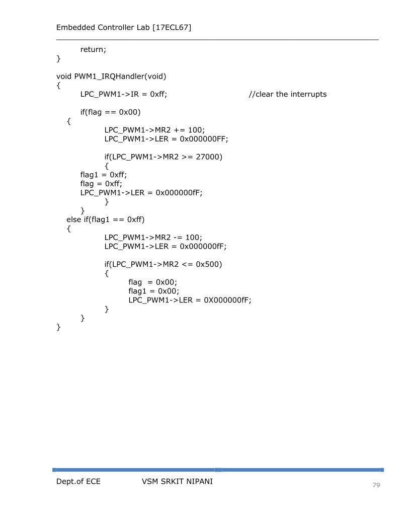
Embedded Controller Lab [17ECL67]
_____________________________________________________________________
Dept.of ECE VSM SRKIT NIPANI
79
return;
}
void PWM1_IRQHandler(void) { LPC_PWM1->IR = 0xff; //clear the interrupts
if(flag == 0x00)
{ LPC_PWM1->MR2 += 100; LPC_PWM1->LER = 0x000000FF;
if(LPC_PWM1->MR2 >= 27000)
{ flag1 = 0xff; flag = 0xff;
LPC_PWM1->LER = 0x000000fF; }
} else if(flag1 == 0xff) {
LPC_PWM1->MR2 -= 100; LPC_PWM1->LER = 0x000000fF;
if(LPC_PWM1->MR2 <= 0x500) {
flag = 0x00; flag1 = 0x00;
LPC_PWM1->LER = 0X000000fF; } }
}