SKDAV GOVT.POLYTECHNIC ROURKELA LAB MANUAL
67
SKDAV GOVT.POLYTECHNIC ROURKELA DEPARTMENT OF ELECTRONICS AND TELECOMMUNICATION ENGINEERING LAB MANUAL Year & Semester: 2 ND Year, IV Semester Subject Code/Name: Pr- 3, MICROPROCESSOR &MICROCONTROLLER
-
Upload
khangminh22 -
Category
Documents
-
view
1 -
download
0
Transcript of SKDAV GOVT.POLYTECHNIC ROURKELA LAB MANUAL

SKDAV GOVT.POLYTECHNIC
ROURKELA
DEPARTMENT OF ELECTRONICS
AND TELECOMMUNICATION ENGINEERING
LAB MANUAL
Year & Semester: 2ND Year, IV Semester
Subject Code/Name: Pr- 3, MICROPROCESSOR &MICROCONTROLLER
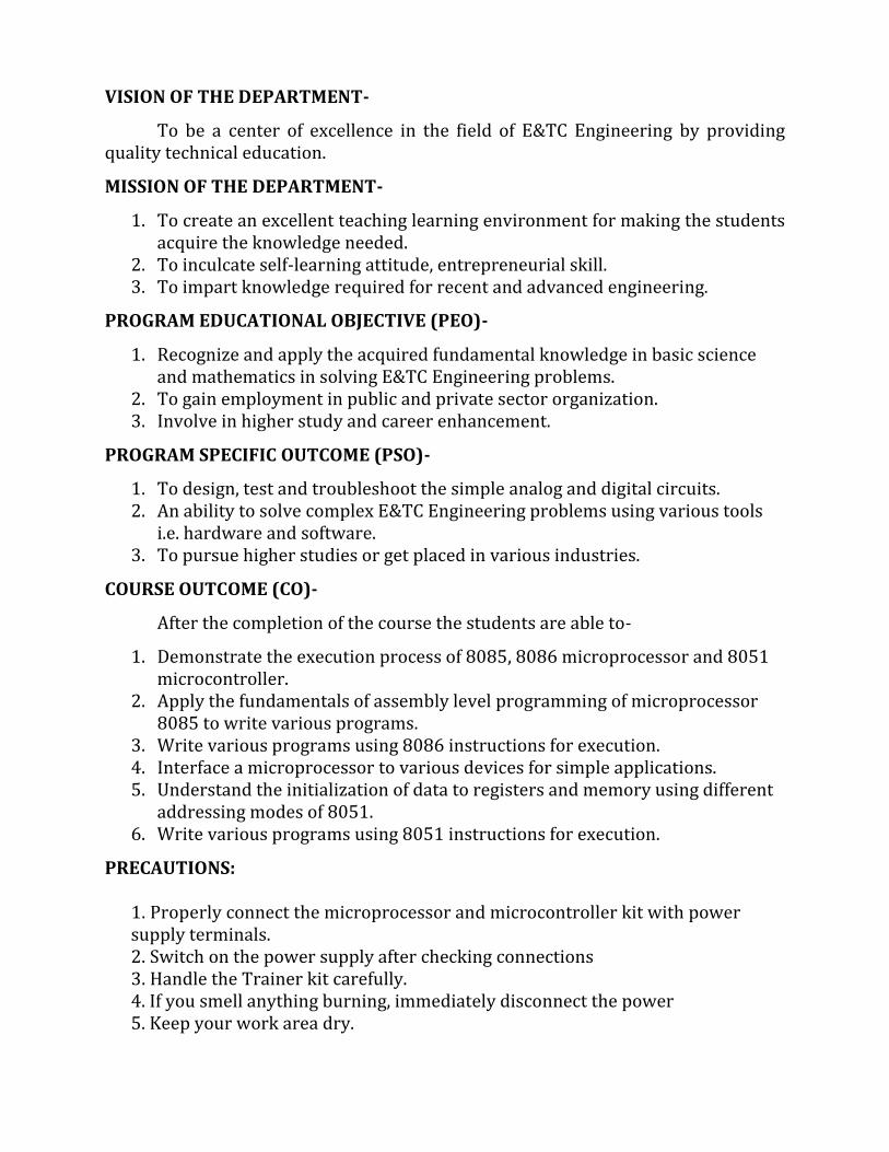
VISION OF THE DEPARTMENT-
To be a center of excellence in the field of E&TC Engineering by providing quality technical education.
MISSION OF THE DEPARTMENT-
1. To create an excellent teaching learning environment for making the students acquire the knowledge needed.
2. To inculcate self-learning attitude, entrepreneurial skill. 3. To impart knowledge required for recent and advanced engineering.
PROGRAM EDUCATIONAL OBJECTIVE (PEO)-
1. Recognize and apply the acquired fundamental knowledge in basic science and mathematics in solving E&TC Engineering problems.
2. To gain employment in public and private sector organization. 3. Involve in higher study and career enhancement.
PROGRAM SPECIFIC OUTCOME (PSO)-
1. To design, test and troubleshoot the simple analog and digital circuits. 2. An ability to solve complex E&TC Engineering problems using various tools
i.e. hardware and software. 3. To pursue higher studies or get placed in various industries.
COURSE OUTCOME (CO)-
After the completion of the course the students are able to-
1. Demonstrate the execution process of 8085, 8086 microprocessor and 8051 microcontroller.
2. Apply the fundamentals of assembly level programming of microprocessor 8085 to write various programs.
3. Write various programs using 8086 instructions for execution. 4. Interface a microprocessor to various devices for simple applications. 5. Understand the initialization of data to registers and memory using different
addressing modes of 8051. 6. Write various programs using 8051 instructions for execution.
PRECAUTIONS:
1. Properly connect the microprocessor and microcontroller kit with power supply terminals. 2. Switch on the power supply after checking connections 3. Handle the Trainer kit carefully. 4. If you smell anything burning, immediately disconnect the power 5. Keep your work area dry.

List of the Experiments-
SL.NO. NAME OF THE EXPERIMENT 1. To write a program to add two 8 bit number using 8085 microprocessor.
2. To write a program to add two 8-bit numbers & sum is 16-bit.
3. To write a program to subtract two 8 bit numbers using 8085 microprocessor
4. To write an assembly language program for multiplication of two 8-bit
numbers using 8085 instructions.
5. To write an assembly language program for division of two 8-bit numbers
using 8085 instructions.
6. To write an assembly language program for 1’s complement of an 8-bit
numbers using 8085 instructions.
7. To write an assembly language program for 2’s complement of an 8-bit
numbers using 8085 instructions.
8. Write a program to find larger of two numbers.
9. Write a program to find the largest value in a data array
10. Write a program to find smallest number in data array.
11. To write an assembly language program for addition of two 16-bit number
without carry using 8086 instruction.
12. To write an assembly language program for subtraction of two 16-bit number
without borrow using 8086 instruction.
13. To write an assembly language program for multiplication of two 16-bit
number using 8086 instructions.
14. To write an assembly language program for division of two 16-bit number
using 8086 instructions.
15. Write a program to largest number in data array using 8086 microprocessor.
16. Write a program for sorting an array of numbers in descending order.
17. Write a program for sorting an array of numbers in ascending order.
18. To write an assembly language program to generate square waves in all lines
of 8255 with different frequency.
19. To study the 8253 and its operation (Mode 0, Mode 2, Mode3)
20. To study the Mode 0, Mode 1, BSR mode operation of 8255.
21. To study the 8259 programmable interrupt controller.
22. To initialize data to registers and memory using immediate, register, direct
and indirect addressing mode of 8051.
23. To write a program for relay interface.
24. To write an assembly language program for character based LCD Interface.

CYCLE-1 1 To write a program to add two 8 bit number using 8085 microprocessor.
2 To write a program to subtract two 8 bit numbers using 8085
microprocessor 3 To write an assembly language program for addition of two 16-bit number
without carry using 8086 instruction. 4 To write an assembly language program for subtraction of two 16-bit number
without borrow using 8086 instruction. 5 To write an assembly language program to generate square waves in all lines
of 8255 with different frequency. 6 To study the Mode 0, Mode 1, BSR mode operation of 8255.
CYCLE-2 1 To write a program to add two 8-bit numbers & sum is 16-bit. 2 To write an assembly language program for division of two 8-bit numbers
using 8085 instructions. 3 To write an assembly language program for multiplication of two 16-bit
number using 8086 instructions. 4 To write an assembly language program for division of two 16-bit number
using 8086 instructions.
5 To study the 8253 and its operation (Mode 0, Mode 2, Mode3) 6 To initialize data to registers and memory using immediate, register, direct
and indirect addressing mode of 8051.
CYCLE-3 1 To write an assembly language program for multiplication of two 8-bit
numbers using 8085 instructions 2 To write an assembly language program for 1’s complement of an 8-bit
numbers using 8085 instructions. 3 To write an assembly language program for 2’s complement of an 8-bit
numbers using 8085 instructions.
4 To Write a program to largest number in data array using 8086 microprocessor
5 To study the 8259 programmable interrupt controller.
6 To write a program for relay interface.
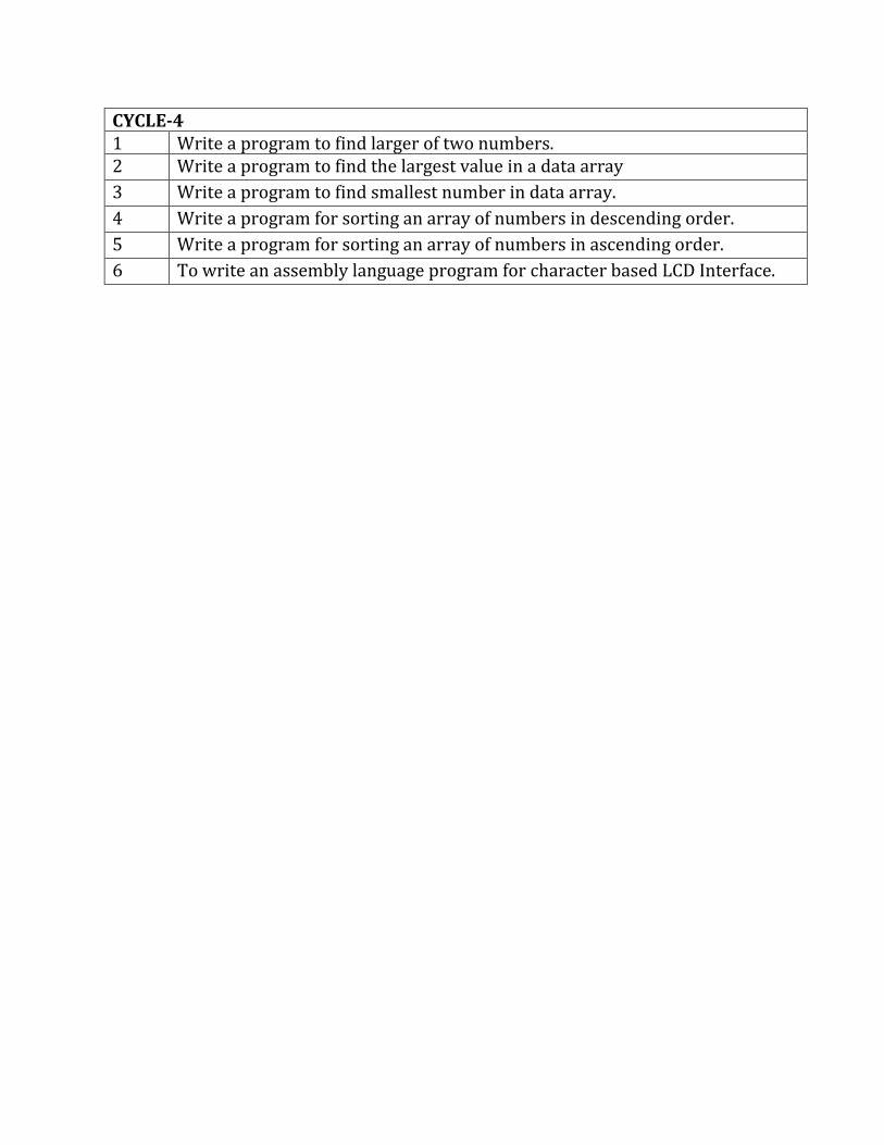
CYCLE-4 1 Write a program to find larger of two numbers. 2 Write a program to find the largest value in a data array
3 Write a program to find smallest number in data array.
4 Write a program for sorting an array of numbers in descending order.
5 Write a program for sorting an array of numbers in ascending order.
6 To write an assembly language program for character based LCD Interface.

AIM OF THE EXPERIMENT:
To write a program to add two 8 bit number using 8085 microprocessor.
EQUIPMENT REQUIRED:
8085microprocessor trainer kit.
THEORY:
The 1stnumber 49H is in the memory location 2501H.
The 2ndbinary number 56H is in the memory location 2502H.
The result is to be stored in the memory location 2503H.
PROCEDURE –
STEP 1- STORAGE OF PROGRAM MACHINE CODES: Machine codes of the program to be executed, should be stored in their memory available on 8085 trainer kit as RESET→REL EXMEM→starting address of program (2000) →NEXT→now enter all the machine codes, one after the other followed by the key ‘NEXT’. STEP 2-DECLARATION OF INPUTS: Input values to the program should be declared as RESET→REL EXMEM→input (data) address→NEXT→Now enter all the inputs values followed by the ‘NEXT’. STEP 3-EXECUTION OF PROGRAM: The program can be executed as RESET→GO→Starting address of the program (2000)→FILL STEP 4-VERIFICATION OF OUTPUT Output of the executed program can be verified as RESET→ REL EXMEM→output (data) address→NEXT
Exp. No.: 1
TO WRITE A PROGRAM TO ADD TWO 8 BIT
NUMBER USING 8085 MICROPROCESSOR
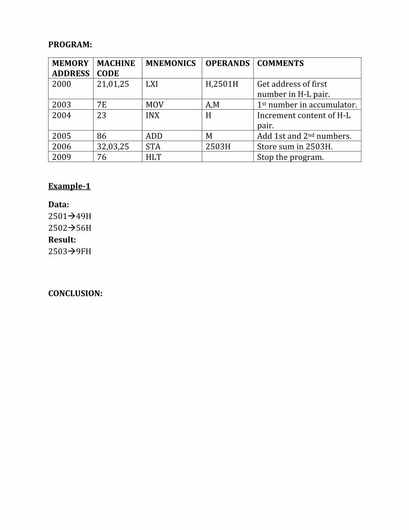
PROGRAM:
MEMORY ADDRESS
MACHINE CODE
MNEMONICS OPERANDS COMMENTS
2000 21,01,25 LXI H,2501H Get address of first number in H-L pair.
2003 7E MOV A,M 1st number in accumulator. 2004 23 INX H Increment content of H-L
pair. 2005 86 ADD M Add 1st and 2nd numbers. 2006 32,03,25 STA 2503H Store sum in 2503H. 2009 76 HLT Stop the program.
Example-1
Data:
2501→49H
2502→56H
Result:
2503→9FH
CONCLUSION:

Exp. No.: 2
TO WRITE A PROGRAM TO ADD TWO 8 BIT
NUMBER & SUM IS 16 BIT
AIM OF THE EXPERIMENT:
To write a program to add two 8-bit numbers & sum is 16-bit.
APPARATUS REQUIRED:
8085 microprocessor trainer kit.
THEORY:
➢ The 1st no. 98H is in the memory location 2501 H.
➢ The 2nd no. 9A H is in the memory location 2502H.
➢ The results are to be stored in 2503 and 2504 H.
➢ Numbers are represented in hexadecimal.
➢ In this case the sum is to be stored in two consecutive memory locations.
➢ The LSBs of the sum is 32 H and it will be stored in the memory location 2503
H.
➢ The MSB of the sum is 01 which will be stored in 2504 H.
PROCEDURE –
STEP 1- STORAGE OF PROGRAM MACHINE CODES: Machine codes of the program to be executed, should be stored in their memory available on 8085 trainer kit as RESET→REL EXMEM→starting address of program (2000) →NEXT→Now enter all the machine codes, one after the other followed by the key ‘NEXT’. STEP 2-DECLARATION OF INPUTS: Input values to the program should be declared as RESET→REL EXMEM→input (data) address→NEXT→Now enter all the inputs values followed by the ‘NEXT’. STEP 3-EXECUTION OF PROGRAM: The program can be executed as RESET→GO→Starting address of the program (2000)→FILL STEP 4-VERIFICATION OF OUTPUT Output of the executed program can be verified as RESET→ REL EXMEM→output (data) address→NEX

PROGRAM:
MEMORY ADDRESS
MACHINE CODES
LABELS MNEMONICS OPERANDS COMMENTS
2000 21,01,25 LXI H,2501H Address of 1st number in H-L pair.
2003 0E,00 MVI C,OO MSBs of sum in register C. initial value 00.
2005 7E MOV A,M 1st number in accumulator.
2006 23 INX H Address of 2nd number 2502 in H-L pair.
2007 86 ADD M 1st number+2nd number
2008 D2,0C,20 JNC AHEAD Is carry? No, go to the label AHEAD.
200B 0C INR C Yes ,increment C. 200C 32,03,25 AHEAD STA 2503H LSBs of sum in
2503H. 200F 79 MOV A,C MSBs of sum in
accumulator. 2010 32,04,25 STA 2504H MSBs of sum in
2504H. 2013 76 HLT Halt.
Example-1: Data
2501→98 H
2502→9A H
Result
2503→32 H, LSBs of sum.
2504→01 H, MSBs of sum.
Example-2: Data
2501→F5 H
2502→8A H
Result
2503→7F H, LSBs of sum.
2504→01 H, MSBs of sum.
CONCLUSION:

Exp. No.: 3
TO WRITE A PROGRAM TO SUBTRACT TWO 8
BIT NUMBERS
AIM OF THE EXPERIMENT:
To write a program to subtract two 8 bit numbers using 8085 microprocessor.
EQUIPMENT REQUIRED:
8085 microprocessor trainer kit.
THEORY:
➢ The 1st number 49 H in the memory location 2501 H.
➢ The 2nd binary number 32 H is stored in the memory location 2502 H.
➢ The result is to be stored in the memory location 2503 H.
PROCEDURE -
STEP 1- STORAGE OF PROGRAM MACHINE CODES: Machine codes of the program to be executed, should be stored in their memory available on 8085 trainer kit as RESET→REL EXMEM→starting address of program (2000) →NEXT→Now enter all the machine codes, one after the other followed by the key ‘NEXT’. STEP 2-DECLARATION OF INPUTS: Input values to the program should be declared as RESET→REL EXMEM→input (data) address→NEXT→Now enter all the inputs values followed by the ‘NEXT’. STEP 3-EXECUTION OF PROGRAM: The program can be executed as RESET→GO→Starting address of the program (2000)→FILL STEP 4-VERIFICATION OF OUTPUT Output of the executed program can be verified as RESET→ REL EXMEM→output (data) address→NEXT
PROGRAM:
MEMORY ADDRESS
MACHINE CODES
MNEMONICS OPERANDS
COMMENTS
2000 21,01,25 LXI H,2501 Get address of 1st in H-L pair. 2003 7E MOV A,M 1st number in accumulator.
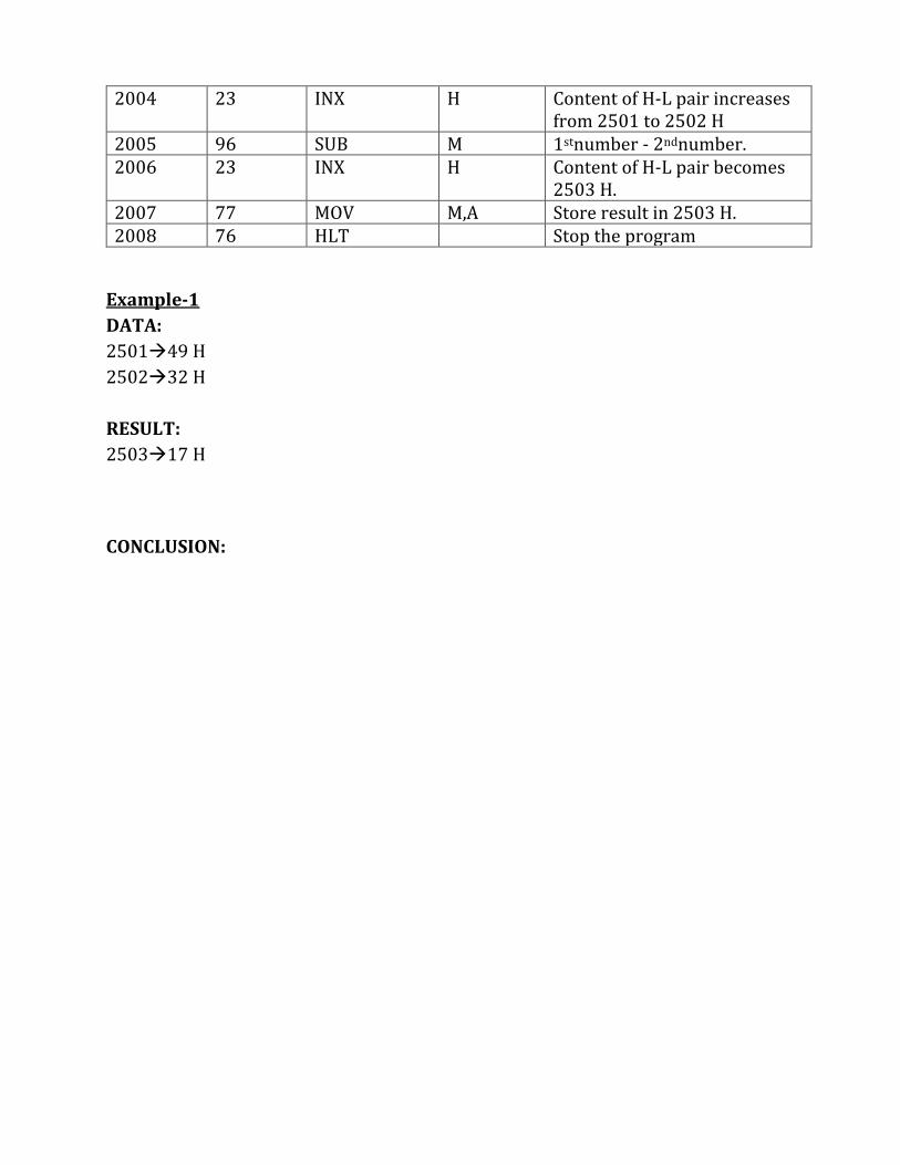
2004 23 INX H Content of H-L pair increases from 2501 to 2502 H
2005 96 SUB M 1stnumber - 2ndnumber. 2006 23 INX H Content of H-L pair becomes
2503 H. 2007 77 MOV M,A Store result in 2503 H. 2008 76 HLT Stop the program
Example-1
DATA:
2501→49 H
2502→32 H
RESULT:
2503→17 H
CONCLUSION:

Exp. No.: 4
TO WRITE A PROGRAM FOR MULTIPLICATION
OF TWO 8 BIT NUMBERS
AIM OF THE EXPERIMENT:
To write an assembly language program for multiplication of two 8-bit numbers
using 8085 instructions.
APPARATUS REQUIRED:
8085 trainer kit
THEORY:
The 8085 has no multiplication operation.to get the result of multiplication, we
should use the repetitive addition method. After multiplying two 8-bit numbers it
may generates 1-byte or 2- byte numbers, so we are using two registers to hold the
result. We are serving the data at location memory 8000H and 8001H.The result is to
be stored in the memory location 8050H and 8051H.
PROCEDURE -
STEP 1- STORAGE OF PROGRAM MACHINE CODES: Machine codes of the program to be executed, should be stored in their memory available on 8085 trainer kit as RESET→REL EXMEM→starting address of program (2000) →NEXT→Now enter all the machine codes, one after the other followed by the key ‘NEXT’. STEP 2-DECLARATION OF INPUTS: Input values to the program should be declared as RESET→REL EXMEM→input (data) address→NEXT→Now enter all the inputs values followed by the ‘NEXT’. STEP 3-EXECUTION OF PROGRAM: The program can be executed as RESET→GO→Starting address of the program (2000)→FILL STEP 4-VERIFICATION OF OUTPUT Output of the executed program can be verified as RESET→ REL EXMEM→output (data) address→NEXT
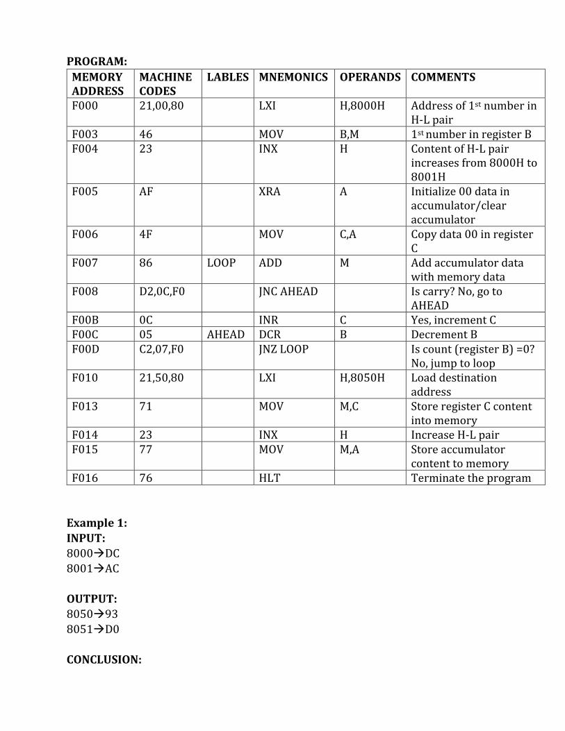
PROGRAM:
MEMORY ADDRESS
MACHINE CODES
LABLES MNEMONICS OPERANDS COMMENTS
F000 21,00,80 LXI H,8000H Address of 1st number in H-L pair
F003 46 MOV B,M 1st number in register B F004 23 INX H Content of H-L pair
increases from 8000H to 8001H
F005 AF XRA A Initialize 00 data in accumulator/clear accumulator
F006 4F MOV C,A Copy data 00 in register C
F007 86 LOOP ADD M Add accumulator data with memory data
F008 D2,0C,F0 JNC AHEAD Is carry? No, go to AHEAD
F00B 0C INR C Yes, increment C F00C 05 AHEAD DCR B Decrement B F00D C2,07,F0 JNZ LOOP Is count (register B) =0?
No, jump to loop F010 21,50,80 LXI H,8050H Load destination
address F013 71 MOV M,C Store register C content
into memory F014 23 INX H Increase H-L pair F015 77 MOV M,A Store accumulator
content to memory F016 76 HLT Terminate the program
Example 1:
INPUT:
8000→DC
8001→AC
OUTPUT:
8050→93
8051→D0
CONCLUSION:

Exp. No.: 5
TO WRITE A PROGRAM FOR DIVISION OF
TWO 8 BIT NUMBERS
AIM OF THE EXPERIMENT:
To write an assembly language program for division of two 8-bit numbers using
8085 instructions.
APPARATUS REQUIRED:
8085 trainer kit
THEORY:
The 8085 has no division operation to get the result of division, we should use the
repetitive subtraction method.
By using this program, we will get the quotient and the remainder.2504H will hold
the quotient, and 2505H will hold the remainder.
We save the data at memory location 2501H (LSBs of dividend), 2502H (MSBs of
dividend) and 2503H (divisor).The result is to be stored in the memory location
2504H (quotient) and 2505H (remainder).
PROCEDURE -
STEP 1- STORAGE OF PROGRAM MACHINE CODES: Machine codes of the program to be executed, should be stored in their memory available on 8085 trainer kit as RESET→REL EXMEM→starting address of program (2000) →NEXT→Now enter all the machine codes, one after the other followed by the key ‘NEXT’. STEP 2-DECLARATION OF INPUTS: Input values to the program should be declared as RESET→REL EXMEM→input (data) address→NEXT→Now enter all the inputs values followed by the ‘NEXT’. STEP 3-EXECUTION OF PROGRAM: The program can be executed as RESET→GO→Starting address of the program (2000)→FILL STEP 4-VERIFICATION OF OUTPUT Output of the executed program can be verified as RESET→ REL EXMEM→output (data) address→NEXT
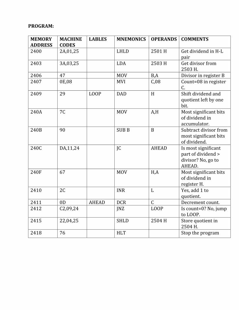
PROGRAM:
MEMORY ADDRESS
MACHINE CODES
LABLES MNEMONICS OPERANDS COMMENTS
2400 2A,01,25 LHLD 2501 H Get dividend in H-L pair
2403 3A,03,25 LDA 2503 H Get divisor from 2503 H.
2406 47 MOV B,A Divisor in register B 2407 0E,08 MVI C,08 Count=08 in register
C. 2409 29 LOOP DAD H Shift dividend and
quotient left by one bit.
240A 7C MOV A,H Most significant bits of dividend in accumulator.
240B 90 SUB B B Subtract divisor from most significant bits of dividend.
240C DA,11,24 JC AHEAD Is most significant part of dividend > divisor? No, go to AHEAD.
240F 67 MOV H,A Most significant bits of dividend in register H.
2410 2C INR L Yes, add 1 to quotient.
2411 0D AHEAD DCR C Decrement count. 2412 C2,09,24 JNZ LOOP Is count=0? No, jump
to LOOP. 2415 22,04,25 SHLD 2504 H Store quotient in
2504 H. 2418 76 HLT Stop the program
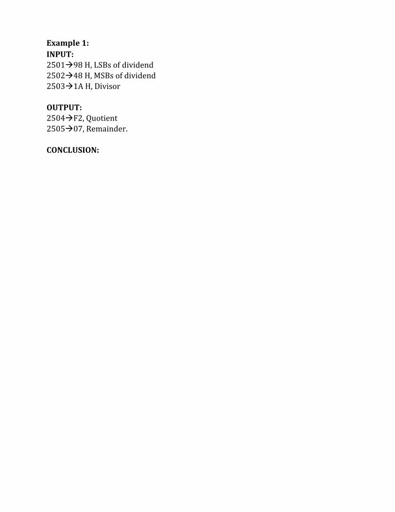
Example 1:
INPUT:
2501→98 H, LSBs of dividend
2502→48 H, MSBs of dividend
2503→1A H, Divisor
OUTPUT:
2504→F2, Quotient
2505→07, Remainder.
CONCLUSION:
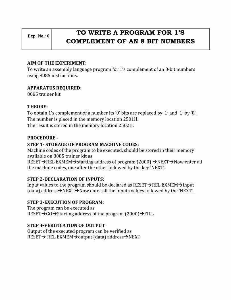
Exp. No.: 6 TO WRITE A PROGRAM FOR 1’S
COMPLEMENT OF AN 8 BIT NUMBERS
AIM OF THE EXPERIMENT:
To write an assembly language program for 1’s complement of an 8-bit numbers
using 8085 instructions.
APPARATUS REQUIRED:
8085 trainer kit
THEORY:
To obtain 1’s complement of a number its ‘0’ bits are replaced by ‘1’ and ‘1’ by ‘0’.
The number is placed in the memory location 2501H.
The result is stored in the memory location 2502H.
PROCEDURE -
STEP 1- STORAGE OF PROGRAM MACHINE CODES: Machine codes of the program to be executed, should be stored in their memory available on 8085 trainer kit as RESET→REL EXMEM→starting address of program (2000) →NEXT→Now enter all the machine codes, one after the other followed by the key ‘NEXT’. STEP 2-DECLARATION OF INPUTS: Input values to the program should be declared as RESET→REL EXMEM→input (data) address→NEXT→Now enter all the inputs values followed by the ‘NEXT’. STEP 3-EXECUTION OF PROGRAM: The program can be executed as RESET→GO→Starting address of the program (2000)→FILL STEP 4-VERIFICATION OF OUTPUT Output of the executed program can be verified as RESET→ REL EXMEM→output (data) address→NEXT

PROGRAM:
MEMORY ADDRESS
MACHINE CODES
MNEMONICS OPERANDS COMMENTS
2000 3A,01,25 LDA 2501 H Get data in accumulator. 2003 2F CMA Take its 1’s complement. 2007 32,02,25 STA 2502 H Store result in 2502 H. 2008 76 HLT Stop.
Example 1:
DATA:
2501→96 H
.
RESULT
2502→69 H
CONCLUSION:
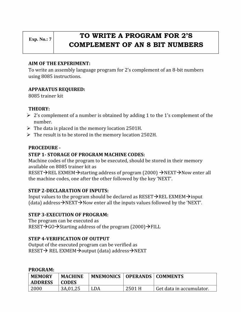
Exp. No.: 7 TO WRITE A PROGRAM FOR 2’S
COMPLEMENT OF AN 8 BIT NUMBERS
AIM OF THE EXPERIMENT:
To write an assembly language program for 2’s complement of an 8-bit numbers
using 8085 instructions.
APPARATUS REQUIRED:
8085 trainer kit
THEORY:
➢ 2’s complement of a number is obtained by adding 1 to the 1’s complement of the
number.
➢ The data is placed in the memory location 2501H.
➢ The result is to be stored in the memory location 2502H.
PROCEDURE -
STEP 1- STORAGE OF PROGRAM MACHINE CODES: Machine codes of the program to be executed, should be stored in their memory available on 8085 trainer kit as RESET→REL EXMEM→starting address of program (2000) →NEXT→Now enter all the machine codes, one after the other followed by the key ‘NEXT’. STEP 2-DECLARATION OF INPUTS: Input values to the program should be declared as RESET→REL EXMEM→input (data) address→NEXT→Now enter all the inputs values followed by the ‘NEXT’. STEP 3-EXECUTION OF PROGRAM: The program can be executed as RESET→GO→Starting address of the program (2000)→FILL STEP 4-VERIFICATION OF OUTPUT Output of the executed program can be verified as RESET→ REL EXMEM→output (data) address→NEXT
PROGRAM:
MEMORY ADDRESS
MACHINE CODES
MNEMONICS OPERANDS COMMENTS
2000 3A,01,25 LDA 2501 H Get data in accumulator.

2003 2F CMA Take its 1’s complement. 2004 3C INR A Take its 2’s complement. 2005 32,02,25 STA 2502 H Store result in 2502 H. 2008 76 HLT Stop.
Example 1:
DATA:
2501→96 H
RESULT
2502→ 6A H
CONCLUSION:

Exp. No.: 8 TO WRITE A PROGRAM TO FIND LARGE OF
TWO NUMBERS
AIM OF THE EXPERIMENT:
Write a program to find larger of two numbers.
APPARATUS REQUIRED:
8085 microprocessor trainer kit.
THEORY:
➢ The 1st number 98 H was placed in the memory location 2501 H.
➢ The 2nd number 87 H was placed in the memory location 2502 H.
➢ The result is stored in the memory location 2503 H.
➢ The numbers are represented in hexadecimal number system. The first no is moved
from its memory location to the accumulator.
➢ It is compared with second number.
➢ The largest of two is then placed in the accumulator.
➢ From the accumulator the larger number is moved to the desired memory location.
PROCEDURE -
STEP 1- STORAGE OF PROGRAM MACHINE CODES: Machine codes of the program to be executed, should be stored in their memory available on 8085 trainer kit as RESET→REL EXMEM→starting address of program (2000) →NEXT→now enter all the machine codes, one after the other followed by the key ‘NEXT’. STEP 2-DECLARATION OF INPUTS: Input values to the program should be declared as RESET→REL EXMEM→input (data) address→NEXT→Now enter all the inputs values followed by the ‘NEXT’. STEP 3-EXECUTION OF PROGRAM: The program can be executed as RESET→GO→Starting address of the program (2000)→FILL STEP 4-VERIFICATION OF OUTPUT Output of the executed program can be verified as RESET→ REL EXMEM→output (data) address→NEXT

PROGRAM:
MEMORY ADDRESS
MACHINE CODE
LABELS MNEMONICS OPERANDS COMMENTS
2000 21,01,25 LXI H,2501 H Address of 1st number in H-L pair.
2003 7E MOV A,M 1st number in accumulator.
2004 23 INX H Address of 2nd number in H-L pair.
2005 BE CMP M Compared 2nd number with 1st number. Is the 2nd number > 1st?
2006 D2,0A,20 JNC AHEAD No, larger number is in accumulator. Go to AHEAD
2009 7E MOV A,M Yes, get 2nd number in accumulator.
200A 32,03,25 AHEAD STA 2503H store larger number in 2503H
200D 76 HLT Stop the program.
Example-1:
Data:
2501→98 H
2502→87 H
Result:
2503→98 H and it is stored in the memory location 2503 H.
Example-2:
Data: 2501→A9 H
2502→EB H
Result:
2503→EB H
CONCLUSION:

Exp. No.: 9
TO WRITE A PROGRAM TO FIND LARGEST
VALUE IN A DATA ARRAY
AIM OF THE EXPERIMENT:
Write a program to find the largest value in a data array
EQUIPMENT REQUIRED:
8085 Microprocessor trainer kit
THEORY:
➢ The 1st number of the series is placed in the accumulator and it is compared with
the 2nd number which is in the memory.
➢ The larger of the two is placed in the accumulator.
➢ Again this number which is in the accumulator is compared with the 3rd number
of this series and larger number is placed in the accumulator.
➢ This process of comparison is repeated till all the numbers of the series are
compared and the largest number is stored in the desired memory location.
PROCEDURE -
STEP 1- STORAGE OF PROGRAM MACHINE CODES: Machine codes of the program to be executed, should be stored in their memory available on 8085 trainer kit as RESET→REL EXMEM→starting address of program (2000) →NEXT→now enter all the machine codes, one after the other followed by the key ‘NEXT’. STEP 2-DECLARATION OF INPUTS: Input values to the program should be declared as RESET→REL EXMEM→input (data) address→NEXT→Now enter all the inputs values followed by the ‘NEXT’. STEP 3-EXECUTION OF PROGRAM: The program can be executed as RESET→GO→Starting address of the program (2000)→FILL STEP 4-VERIFICATION OF OUTPUT Output of the executed program can be verified as RESET→ REL EXMEM→output (data) address→NEXT

PROGRAM:
MEMORY ADDRESS
MACHINE CODES
LABELS MNEMONICS OPERANDS COMMENTS
2000 21,00,25 LXI H, 2500H Address for count in H-L pair.
2003 4E MOV C,M Count in register C. 2004 23 INX H Address of the 1st
number in H-L pair. 2005 7E MOV A,M 1st number in
accumulator. 2006 OD DCR C Decrement count. 2007 23 INX H Address of next
number. 2008 BE CMP M Compare next
number with previous maximum. Is next number> previous maximum.
2009 D2,0D,20 JNC AHEAD NO, Larger number is in accumulator. GO to the label AHEAD.
200C 7E MOV A,M Yes, get larger number in accumulator.
200D 0D DCR C Decrement Count. 200E C2, 07, 20 JNZ LOOP 2011 32,04,25 STA 2504H Store result in 2504
H. 2014 76 HLT Stop the Program.
Example-1:
Data:
2500→03
2501→98
2502→75
2503→99
Result:
2504→99
CONCLUSION:
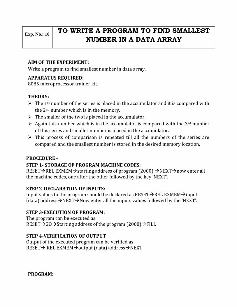
Exp. No.: 10
TO WRITE A PROGRAM TO FIND SMALLEST
NUMBER IN A DATA ARRAY
AIM OF THE EXPERIMENT:
Write a program to find smallest number in data array.
APPARATUS REQUIRED: 8085 microprocessor trainer kit.
THEORY:
➢ The 1st number of the series is placed in the accumulator and it is compared with
the 2nd number which is in the memory.
➢ The smaller of the two is placed in the accumulator.
➢ Again this number which is in the accumulator is compared with the 3rd number
of this series and smaller number is placed in the accumulator.
➢ This process of comparison is repeated till all the numbers of the series are
compared and the smallest number is stored in the desired memory location.
PROCEDURE -
STEP 1- STORAGE OF PROGRAM MACHINE CODES: RESET→REL EXMEM→starting address of program (2000) →NEXT→now enter all the machine codes, one after the other followed by the key ‘NEXT’. STEP 2-DECLARATION OF INPUTS: Input values to the program should be declared as RESET→REL EXMEM→input (data) address→NEXT→Now enter all the inputs values followed by the ‘NEXT’. STEP 3-EXECUTION OF PROGRAM: The program can be executed as RESET→GO→Starting address of the program (2000)→FILL STEP 4-VERIFICATION OF OUTPUT Output of the executed program can be verified as RESET→ REL EXMEM→output (data) address→NEXT
PROGRAM:
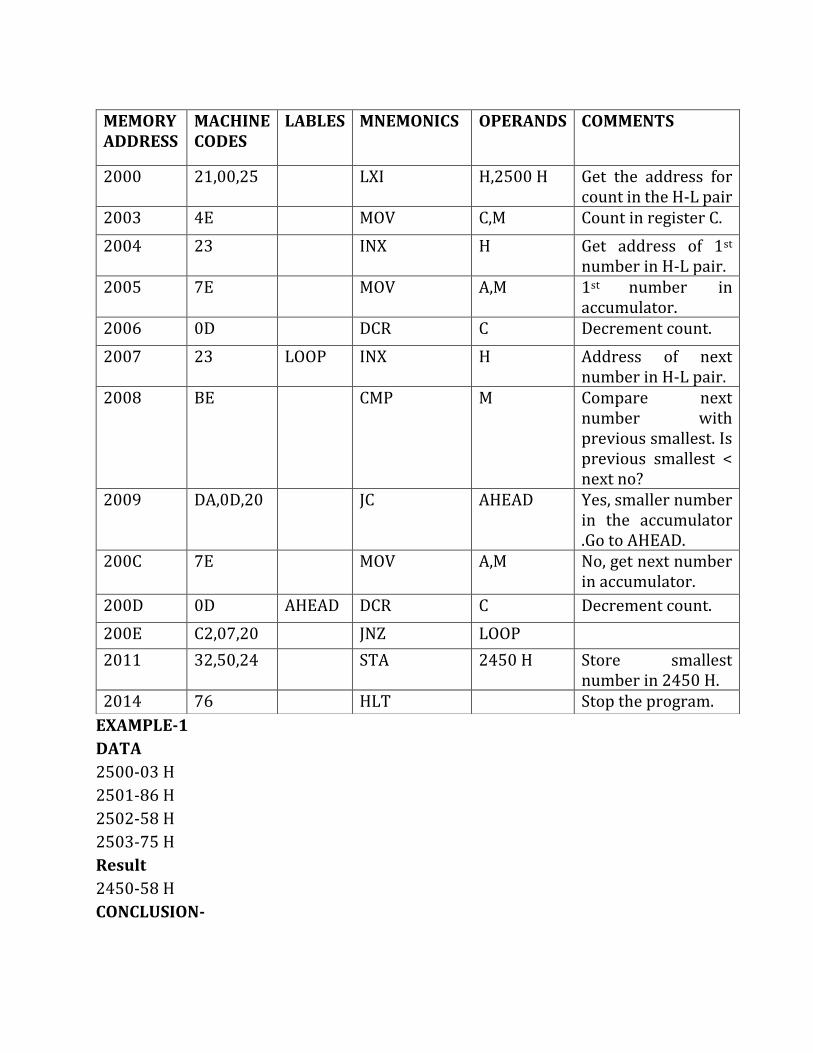
EXAMPLE-1
DATA
2500-03 H
2501-86 H
2502-58 H
2503-75 H
Result
2450-58 H
CONCLUSION-
MEMORY ADDRESS
MACHINE CODES
LABLES MNEMONICS OPERANDS COMMENTS
2000 21,00,25 LXI H,2500 H Get the address for count in the H-L pair
2003 4E MOV C,M Count in register C.
2004 23 INX H Get address of 1st number in H-L pair.
2005 7E MOV A,M 1st number in accumulator.
2006 0D DCR C Decrement count.
2007 23 LOOP INX H Address of next number in H-L pair.
2008 BE CMP M Compare next number with previous smallest. Is previous smallest < next no?
2009 DA,0D,20 JC AHEAD Yes, smaller number in the accumulator .Go to AHEAD.
200C 7E MOV A,M No, get next number in accumulator.
200D 0D AHEAD DCR C Decrement count.
200E C2,07,20 JNZ LOOP
2011 32,50,24 STA 2450 H Store smallest number in 2450 H.
2014 76 HLT Stop the program.

Exp. No.: 11
TO WRITE A PROGRAM FOR ADDITION OF
TWO 16 BIT NUMBER
AIM OF THE EXPERIMENT:
To write an assembly language program for addition of two 16-bit number without
carry using 8086 instruction.
APPARATUS REQUIRED:
8086 trainer kit
THEORY:
➢ We can simply take the numbers from memory to AX and BX register respectively,
then add them using ADD instruction.
➢ When the carry is present store carry into the memory, otherwise result moved to
the memory location.
PROCEDURE:
Assembly language programs for microprocessor 8086 can be executed on its trainer
kit as per the following steps
STEP 1- STORAGE OF PROGRAM MACHINE CODES:
RESET→EB/AX (Examine byte)→starting address of program
(2000)→NEXT→Now enter all the machine codes, one after the other followed by the
key ‘NEXT’.
STEP 2-DECLARATION OF INPUTS:
Input values to the program should be declared as →.TYY
STEP 3-EXECUTION OF PROGRAM:
The program can be executed as
GO→starting address of the program (2000)→.TYY
STEP 4-RESULT VERIFICATION OF REGISTERS:
Output of the executed program can be verified as
ER/BX (Register B)→ .TYY→ER/BX→EX/AX (To check the content of register A)
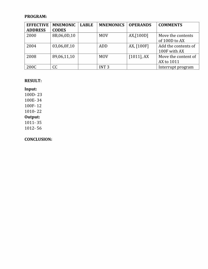
PROGRAM:
EFFECTIVE ADDRESS
MNEMONIC CODES
LABLE MNEMONICS OPERANDS COMMENTS
2000 8B,06,0D,10 MOV AX,[100D] Move the contents of 100D to AX
2004 03,06,0F,10 ADD AX, [100F] Add the contents of 100F with AX
2008 89,06,11,10 MOV [1011], AX Move the content of AX to 1011
200C CC INT 3 Interrupt program
RESULT:
Input:
100D- 23
100E- 34
100F- 12
1010- 22
Output:
1011- 35
1012- 56
CONCLUSION:

Exp. No.: 12
TO WRITE A PROGRAM FOR SUBTRACTION
OF TWO 16 BIT NUMBER
AIM OF THE EXPERIMENT:
To write an assembly language program for subtraction of two 16-bit number
without borrow using 8086 instruction.
APPARATUS REQUIRED:
8086 trainer kit
THEORY:
➢ We can simply take the numbers from memory to AX and BX register respectively,
then subtract them using SUB instruction.
➢ When the borrow is present, the CY flag will be 1, so we can store borrow into the
memory, otherwise result moved to the memory location.
PROCEDURE:
Assembly language programs for microprocessor 8086 can be executed on its trainer
kit as per the following steps
STEP 1- STORAGE OF PROGRAM MACHINE CODES:
RESET→EB/AX (Examine byte)→starting address of program
(2000)→NEXT→Now enter all the machine codes, one after the other followed by the
key ‘NEXT’.
STEP 2-DECLARATION OF INPUTS:
Input values to the program should be declared as →.TYY
STEP 3-EXECUTION OF PROGRAM:
The program can be executed as
GO→starting address of the program (2000)→.TYY
STEP 4-RESULT VERIFICATION OF REGISTERS:
Output of the executed program can be verified as
ER/BX (Register B)→ .TYY→ER/BX→EX/AX (To check the content of register A)

PROGRAM:
EFFECTIVE ADDRESS
MNEMONIC CODES
LABLE MNEMONICS OPERANDS COMMENTS
2000 8B,06,0D,10 MOV AX,[100D] Move the contents of 100D to AX
2004 03,06,0F,10 SUB AX, [100F] Add the contents of 100F with AX
2008 89,06,11,10 MOV [1011], AX Move the content of AX to 1011
200C CC INT 3 Interrupt program
RESULT:
Input:
100D- 34
100E- 56
100F- 12
1010- 34
Output:
1011- 22
1012- 22
CONCLUSION:

Exp. No.: 13
TO WRITE A PROGRAM FOR MULTIPLICATION
OF TWO 16 BIT NUMBER
AIM OF THE EXPERIMENT:
To write an assembly language program for multiplication of two 16-bit number
using 8086 instructions.
APPARATUS REQUIRED:
8086 trainer kit.
THEORY:
➢ Initialize the pointer to the memory for data and result. ➢ Load the multiplier value into AX register. ➢ Load multiplicand value in BX register. ➢ Multiply of these two data’s. ➢ Store the result into Memory address 1520.
PROCEDURE:
Assembly language programs for microprocessor 8086 can be executed on its trainer
kit as per the following steps
STEP 1- STORAGE OF PROGRAM MACHINE CODES:
RESET→EB/AX (Examine byte)→starting address of program
(2000)→NEXT→Now enter all the machine codes, one after the other followed by the
key ‘NEXT’.
STEP 2-DECLARATION OF INPUTS:
Input values to the program should be declared as →.TYY
STEP 3-EXECUTION OF PROGRAM:
The program can be executed as
GO→starting address of the program (2000)→.TYY
STEP 4-RESULT VERIFICATION OF REGISTERS:
Output of the executed program can be verified as
ER/BX (Register B)→ .TYY→ER/BX→EX/AX (To check the content of register A)

PROGRAM:
EFFECTIVE ADDRESS
OPCODES MNEMONICS OPERANDS COMMENTS
1100 BE 00 15 MOV SI,1500 Load 1500 into SI
1103 AD LOD SW Load the multiplicand value
1104 89 C3 MOV BX, AX Load AX value into BX
1106 AD LOD SW Load the multiplier value
1107 F7 E3 MUL BX Multiply two data
1109 BF 0 5 15 MOV DI, 1520 Load 1520 address into DI
110C 89 05 MOV [DI], AX Store AX value into DI
110E 47 INC DI
110F 47 INC DI Increment the DI
1110 89 15 MOV [DI], BX Store BX value into DI
1112 CC INT 3 Break point
Example 1:
INPUT:
1500→02
1501→00
1502→03
1503→00
OUTPUT:
1520→06
1521→00
CONCLUSION:

Exp. No.: 14
TO WRITE A PROGRAM FOR DIVISION OF
TWO 16 BIT NUMBER
AIM OF THE EXPERIMENT:
To write an assembly language program for division of two 16-bit number using
8086 instructions.
APPARATUS REQUIRED:
8086 trainer kit.
THEORY-
➢ Initialize the pointer to the memory for result. ➢ Load the dividend value into AX register. ➢ Load the divisor value into BX register. ➢ Divide these two data’s. ➢ Store the result into Memory address 1520.
PROCEDURE:
Assembly language programs for microprocessor 8086 can be executed on its trainer
kit as per the following steps
STEP 1- STORAGE OF PROGRAM MACHINE CODES:
RESET→EB/AX (Examine byte)→starting address of program
(2000)→NEXT→Now enter all the machine codes, one after the other followed by the
key ‘NEXT’.
STEP 2-DECLARATION OF INPUTS:
Input values to the program should be declared as →.TYY
STEP 3-EXECUTION OF PROGRAM:
The program can be executed as
GO→starting address of the program (2000)→.TYY
STEP 4-RESULT VERIFICATION OF REGISTERS:
Output of the executed program can be verified as
ER/BX (Register B)→ .TYY→ER/BX→EX/AX (To check the content of register A)

PROGRAM:
EFFECTIVE ADDRESS
OPCODES MNEMONICS OPERANDS COMMENTS
1100 BA 00 00 MOV DX, 0000 Clear DX registers
1103 B8 FD FF MOV AX, FFFD Load the dividend in AX
1106 B9 0F 00 MOV BX, 0F Load the divisor value in BX
1109 F7 F1 DIV BX Divide the two data’s
110B BF 00 15 MOV DI, 1520 Load 1520 address into DI
110E 88 05 MOV [DI], AL Load AL value into DI
1110 47 INC DI Increment DI
1111 88 25 MOV [DI], AH Load AH value into DI
1113 47 INC DI Increment DI
1114 89 15 MOV [DI], DX Load DX value into DI
1116 CC INT3 Break point
Example 1:
Input: AX (dividend) =0083 BX (divisor) =02 Output: 1522→41(quotient) 1523→01 (remainder) CONCLUSION-

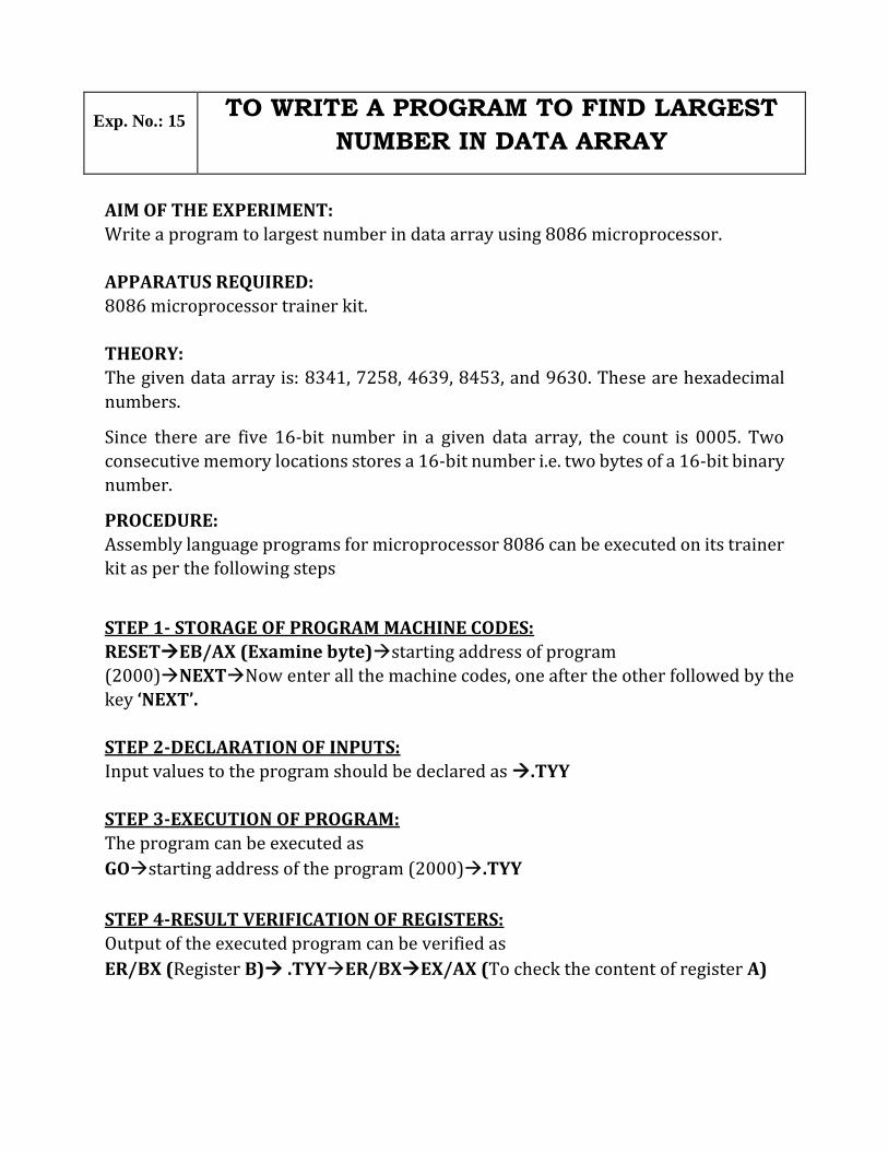
Exp. No.: 15
TO WRITE A PROGRAM TO FIND SMALLEST
NUMBER IN DATA ARRAY
AIM OF THE EXPERIMENT:
Write a program to find smallest number in data array using 8086 microprocessor.
APPARATUS REQUIRED:
8086 microprocessor trainer kit.
THEORY:
The given data array is 8341, 7258, 4639, 8453, 9630.These are hexadecimal
numbers.
As there are five 16-bit numbers in the given data array, the count is 0005.Two
consecutive memory locations store a 16-bit numbers i.e. two bytes of a 16-bit
number.
PROCEDURE:
Assembly language programs for microprocessor 8086 can be executed on its trainer
kit as per the following steps
STEP 1- STORAGE OF PROGRAM MACHINE CODES:
RESET→EB/AX (Examine byte)→starting address of program
(2000)→NEXT→Now enter all the machine codes, one after the other followed by the
key ‘NEXT’.
STEP 2-DECLARATION OF INPUTS:
Input values to the program should be declared as →.TYY
STEP 3-EXECUTION OF PROGRAM:
The program can be executed as
GO→starting address of the program (2000)→.TYY
STEP 4-RESULT VERIFICATION OF REGISTERS:
Output of the executed program can be verified as
ER/BX (Register B)→ .TYY→ER/BX→EX/AX (To check the content of register A)
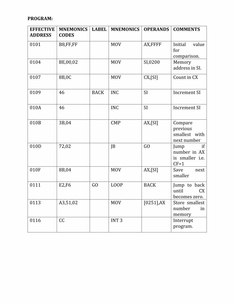
PROGRAM:
EFFECTIVE ADDRESS
MNEMONICS CODES
LABEL MNEMONICS OPERANDS COMMENTS
0101 B8,FF,FF MOV AX,FFFF Initial value for comparison.
0104 BE,00,02 MOV SI,0200 Memory address in SI.
0107 8B,0C MOV CX,[SI] Count in CX
0109 46 BACK INC SI Increment SI
010A 46 INC SI Increment SI
010B 3B,04 CMP AX,[SI] Compare previous smallest with next number
010D 72,02 JB GO Jump if number in AX is smaller i.e. CF=1
010F 8B,04 MOV AX,[SI] Save next smaller
0111 E2,F6 GO LOOP BACK Jump to back until CX becomes zero.
0113 A3,51,02 MOV [0251],AX Store smallest number in memory
0116 CC INT 3 Interrupt program.

DATA RESULT
0200-05 H 0251-39 H
0201-00 H 0252-46 H
0202-41 H
0203-83 H
0204-58 H
0205-72 H
0206-39 H
0207-46 H
0208-53 H
0209-84 H
020A-30 H
020B-96 H
CONCLUSION-
Exp. No.: 15
TO WRITE A PROGRAM TO FIND LARGEST
NUMBER IN DATA ARRAY
AIM OF THE EXPERIMENT:
Write a program to largest number in data array using 8086 microprocessor.
APPARATUS REQUIRED:
8086 microprocessor trainer kit.
THEORY:
The given data array is: 8341, 7258, 4639, 8453, and 9630. These are hexadecimal
numbers.
Since there are five 16-bit number in a given data array, the count is 0005. Two
consecutive memory locations stores a 16-bit number i.e. two bytes of a 16-bit binary
number.
PROCEDURE:
Assembly language programs for microprocessor 8086 can be executed on its trainer
kit as per the following steps
STEP 1- STORAGE OF PROGRAM MACHINE CODES:
RESET→EB/AX (Examine byte)→starting address of program
(2000)→NEXT→Now enter all the machine codes, one after the other followed by the
key ‘NEXT’.
STEP 2-DECLARATION OF INPUTS:
Input values to the program should be declared as →.TYY
STEP 3-EXECUTION OF PROGRAM:
The program can be executed as
GO→starting address of the program (2000)→.TYY
STEP 4-RESULT VERIFICATION OF REGISTERS:
Output of the executed program can be verified as
ER/BX (Register B)→ .TYY→ER/BX→EX/AX (To check the content of register A)
PROGRAM:
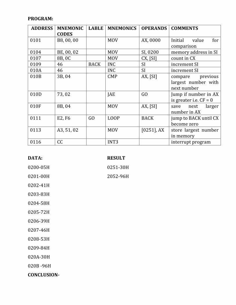
ADDRESS MNEMONIC CODES
LABLE MNEMONICS OPERANDS COMMENTS
0101 B8, 00, 00 MOV AX, 0000 Initial value for comparison
0104 BE, 00, 02 MOV SI, 0200 memory address in SI 0107 8B, 0C MOV CX, [SI] count in CX 0109 46 BACK INC SI increment SI 010A 46 INC SI increment SI 010B 3B, 04 CMP AX, [SI] compare previous
largest number with next number
010D 73, 02 JAE GO Jump if number in AX is greater i.e. CF = 0
010F 8B, 04 MOV AX, [SI] save next larger number in AX
0111 E2, F6 GO LOOP BACK jump to BACK until CX become zero
0113 A3, 51, 02 MOV [0251], AX store largest number in memory
0116 CC INT3 interrupt program
DATA: RESULT
0200-05H 0251-30H
0201-00H 2052-96H
0202-41H
0203-83H
0204-58H
0205-72H
0206-39H
0207-46H
0208-53H
0209-84H
020A-30H
020B -96H
CONCLUSION-

Exp. No.: 16
TO WRITE A PROGRAM FOR SHORTING AN
ARRAY OF NUMBERS IN DESCENDING ORDER
AIM OF THE EXPERIMENT:
Write a program for sorting an array of numbers in descending order.
APPARATUS REQUIRED:
8086 microprocessor trainer kit.
THEORY-
➢ Get the first data and compare with the second data. ➢ If the two data are in descending order then no swap. ➢ Else swap the data byte by descending order and then again compare the other
data bytes up to the count. ➢ Do the above the array is a ranged in descending order. ➢ Finally the array is arranged in ascending order.
PROCEDURE:
Assembly language programs for microprocessor 8086 can be executed on its trainer
kit as per the following steps
STEP 1- STORAGE OF PROGRAM MACHINE CODES:
RESET→EB/AX (Examine byte)→starting address of program
(2000)→NEXT→Now enter all the machine codes, one after the other followed by the
key ‘NEXT’.
STEP 2-DECLARATION OF INPUTS:
Input values to the program should be declared as →.TYY
STEP 3-EXECUTION OF PROGRAM:
The program can be executed as
GO→starting address of the program (2000)→.TYY
STEP 4-RESULT VERIFICATION OF REGISTERS:
Output of the executed program can be verified as
ER/BX (Register B)→ .TYY→ER/BX→EX/AX (To check the content of register A)

PROGRAM:
ADDRESS OPCODE MNEMONICS OPERANDS COMMENTS
1100 BE 00 90 MOV SI, 9001 Load 9000 into SI
1103 8A 0C MOV CL, [SI] Load SI value into CL
1105 BE 00 90 MOV SI, 9000 get the count
1108 8A 14 MOV DL, [SI] Load SI count value into DL
110A 46 INC SI Increment the pointer
110B 8A 04 MOV AL,[SI] first data in AL
110D FE CA DEC DL Decrement DL
110F 74 16 JZ 1127 If count is zero then jump into
1127
1111 46 INC SI Increment SI
1112 8A 1C MOV BL,[SI] Load SI count value into BL
1114 3A C3 CMP AL, BL if al > bl go to (jump1)
1116 72 07 JB 111F
1118 4E DEC SI Decrement SI
1119 88 04 MOV [SI],AL Load ACC value in SI
111B 88 D8 MOV AL, BL Store the greatest data
111D EB 03 JMP 1122 Jump into 1122
111F 4E DEC SI Decrement SI
1120 88 1C MOV [SI], BL Store the smallest data in memory
1122 46 INC SI Increment SI
1123 FE CA DEC DL Decrement DL

1125 75 EA JNZ 1111 If count is not zero then jump into
1111
1127 88 04 MOV [SI], AL Load AL value into SI
1129 FE C9 DEC CL Decrement CL
112B 75 D8 JNZ 1105 If count is not zero then jump into
1105
112D CC INT3 Break point
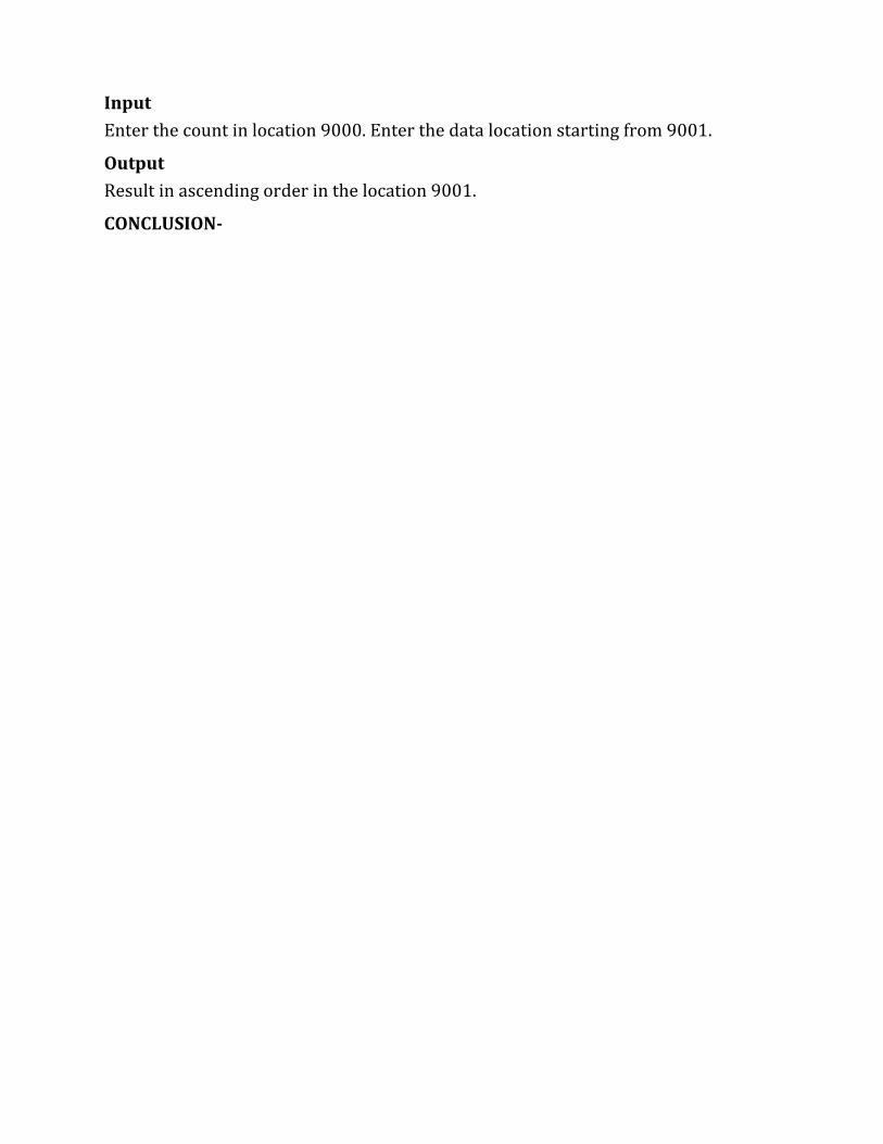
Input
Enter the count in location 9000. Enter the data location starting from 9001.
Output
Result in descending order in the location 9001.
CONCLUSION-

Exp. No.: 17
TO WRITE A PROGRAM FOR SHORTING AN
ARRAY OF NUMBERS IN ASCENDING ORDER
AIM OF THE EXPERIMENT:
Write a program for sorting an array of numbers in ascending order.
APPARATUS REQUIRED:
8086 microprocessor trainer kit.
Ascending Order
THEORY-
➢ Get the first data and compare with the second data. ➢ If the two data are in ascending order then no swap. ➢ Else swap the data byte by ascending order and then again compare the other
data bytes up to the count. ➢ Do the above the array is arranged in ascending order. ➢ Finally the array is arranged in ascending order.
PROCEDURE:
Assembly language programs for microprocessor 8086 can be executed on its trainer
kit as per the following steps
STEP 1- STORAGE OF PROGRAM MACHINE CODES:
RESET→EB/AX (Examine byte)→starting address of program
(2000)→NEXT→Now enter all the machine codes, one after the other followed by the
key ‘NEXT’.
STEP 2-DECLARATION OF INPUTS:
Input values to the program should be declared as →.TYY
STEP 3-EXECUTION OF PROGRAM:
The program can be executed as
GO→starting address of the program (2000)→.TYY
STEP 4-RESULT VERIFICATION OF REGISTERS:
Output of the executed program can be verified as
ER/BX (Register B)→ .TYY→ER/BX→EX/AX (To check the content of register A)

PROGRAM
ADDRESS OPCODE MNEMONICS OPERANDS COMMENTS
1100 BE 00 90 MOV SI, 9000 Load 9000 into SI
1103 8A 0C MOV CL, [SI] Load SI value into CL
1105 BE 00 90 MOV SI, 9000 Get second data
1108 8A 14 MOV DL, [SI] Load SI second data into DL
110A 46 INC SI Increment SI
110B 8A 04 MOV AL, [SI] Load SI value into AL
110D FE CA DEC DL Decrement DL
110F 74 16 JZ 1127 If count is zero then go to 1127
1111 46 INC SI Increment SI
1112 8A 1C MOV BL, [SI] Load SI value into BL
1114 38 D8 CMP AL, BL if AL > BL go to (jump1)
1116 72 07 JNB 111F
1118 4E DEC SI Decrement SI
1119 88 04 MOV [SI],AL Load AL value into SI
111B 88 D8 MOV AL, BL Load BL value into AL
111D EB 03 JMP 1122
111F 4E DEC SI Decrement SI
1120 88 1C MOV [SI], BL Load BL value into SI
1122 46 INC SI Increment SI
1123 FE CA DEC DL Decrement DL
1125 75 EA JNZ 1111 If count is not zero then go to 1111
1127 88 04 MOV [SI], AL Load AL value into SI
1129 FE C9 DEC CL Decrement CL
112B 75 D8 JNZ 1105 If count is not zero then go to 1105
112D CC INT3 Breakpoint
Input
Enter the count in location 9000. Enter the data location starting from 9001.
Output
Result in ascending order in the location 9001.
CONCLUSION-

Exp. No.: 18
TO WRITE A PROGRAM TO GEERATE SQUARE
WAVES IN ALL LINES OF 8255
AIM OF THE EXPERIMENT:
To write an assembly language program to generate square waves in all lines of
8255 with different frequency.
APPARATUS REQUIRED:
8085 trainer kit and 8255 interfacing kit, cables and CRO.
THEORY:
➢ Initialize a control word for 8255, for it to operate in I/O mode and for ports A, B
and C to operate in output mode.
➢ Delay 1 controls the time period for which the square wave remains LOW and HIGH
are to be kept equal, the count in register B and register C are made equal.
➢ For such case there is no need of two subroutines. Only one DELAY subroutine will
be called at two places, i.e. at 2408 and 240F memory addresses.
➢ There will be slight difference in timing of LOW and HIGH due to the instruction
JMP LOOP. If accuracy is desired this can be adjusted by suitable adjustment in the
counts of register B and register C.
➢ The difference can also be minimized by inserting two NOP instructions in DELAY
1 subroutine. The instruction JMP LOOP has been used at the end of the program
to repeat the whole process to generate square wave.
PROCEDURE -
STEP 1- STORAGE OF PROGRAM MACHINE CODES: Machine codes of the program to be executed, should be stored in their memory available on 8085 trainer kit as RESET→REL EXMEM→starting address of program (2000) →NEXT→Now enter all the machine codes, one after the other followed by the key ‘NEXT’. STEP 2-DECLARATION OF INPUTS: Input values to the program should be declared as RESET→REL EXMEM→input (data) address→NEXT→Now enter all the inputs values followed by the ‘NEXT’. STEP 3-EXECUTION OF PROGRAM: The program can be executed as RESET→GO→Starting address of the program (2000)→FILL

STEP 4-VERIFICATION OF OUTPUT Output of the executed program can be verified as
RESET→ REL EXMEM→output (data) address→NEXT
PROGRAM:
MEMORY ADDRESS
MACHINE CODES
LABLES MNEMONICS OPERANDS COMMENTS
2400 3E, 98 MVI A,98 H Get control word. 2402 D3, 0B OUT 08 Initialize ports. 2404 3E, 00 LOOP MVI A,00 Move ‘00’ into
accumulator 2406 D3,09 OUT 09 Make PB0 LOW 2408 CD, 00, 25 CALL DELAY 1 Call the DELAY 1
subroutine. 240B 3E, 01 MVI A,01 Move ‘01’ into
accumulator 240D D3, 09 OUT 09 Make PB0 HIGH 240F CD, 09, 25 CALL DELAY 2 Call the DELAY 2
subroutine. 2412 C3, 04, 24 JMP LOOP Jump to LOOP. SUBROUTINES DELAY 1
2500 06, 02 MVI B,02 Get count for delay. 2502 05 GO DCR B Decrement register
B by 1. 2503 C3, 02, 25 JNZ GO Is B=0? No, then
jump to GO. 2506 C9 RET DELAY 2
2509 0E, 02 MVI C,02 Get count for delay 250B 0D BACK DCR C Decrement register
C by 1. 250C C2, 0B, 25 JNZ BACK Is C=0? No, then go
to BACK. 250F C9 RET
CONCLUSION:

Exp. No.: 19
TO STUDY THE 8253 AND ITS OPERATION
(MODE 0, MODE 2, MODE 3)
AIM OF THE EXPERIMENT: To study the 8253 and its operation (Mode 0, Mode 2, Mode3) THEORY: The most prominent features of 8253/54 are as follows:
➢ It has three independent 16-bit down counters.
➢ It can handle inputs from DC to 10 MHz
➢ These three counters can be programmed for either binary or BCD count.
➢ It is compatible with almost all microprocessors.
➢ 8254 has a powerful command called READ BACK command, which allows the user to check the count value, the programmed mode, the current mode, and the current status of the counter.
8253 Architecture:

8253 Pin Description:
Here is the pin diagram of 8254 −
➢ In the above figure, there are three counters, a data bus buffer, Read/Write
control logic, and a control register. Each counter has two input signals - CLOCK & GATE, and one output signal - OUT.
Data Bus Buffer:
It is a tristate, bi-directional, 8-bit buffer, which is used to interface the 8253/54 to the system data bus. It has three basic functions −
• Programming the modes of 8253/54.
• Loading the count registers.
• Reading the count values.
Read/Write Logic:
It includes 5 signals, i.e. RD, WR, CS, and the address lines A0 & A1. In the peripheral I/O mode, the RD and WR signals are connected to IOR and IOW, respectively. In the memory mapped I/O mode, these are connected to MEMR and MEMW.
Address lines A0 & A1 of the CPU are connected to lines A0 and A1 of the 8253/54, and CS is tied to a decoded address. The control word register and counters are selected according to the signals on lines A0 & A1.
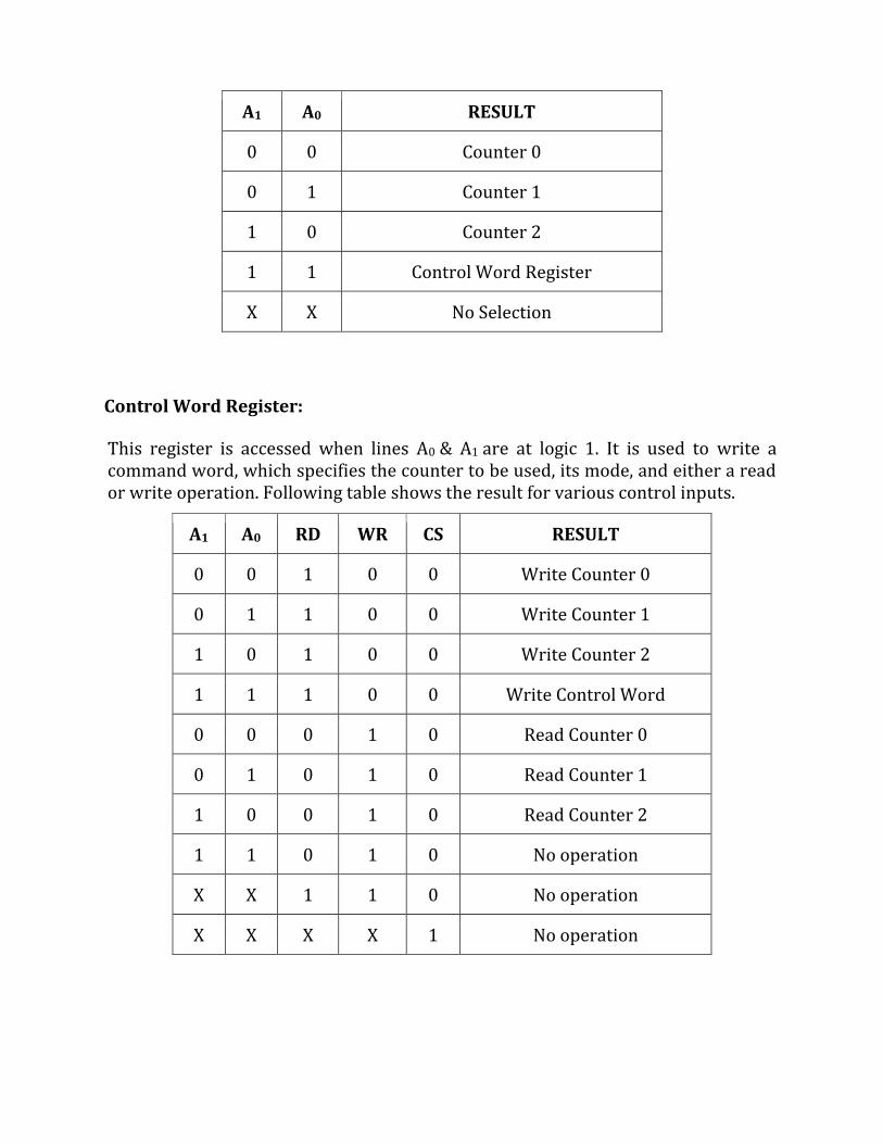
A1 A0 RESULT
0 0 Counter 0
0 1 Counter 1
1 0 Counter 2
1 1 Control Word Register
X X No Selection
Control Word Register:
This register is accessed when lines A0 & A1 are at logic 1. It is used to write a command word, which specifies the counter to be used, its mode, and either a read or write operation. Following table shows the result for various control inputs.
A1 A0 RD WR CS RESULT
0 0 1 0 0 Write Counter 0
0 1 1 0 0 Write Counter 1
1 0 1 0 0 Write Counter 2
1 1 1 0 0 Write Control Word
0 0 0 1 0 Read Counter 0
0 1 0 1 0 Read Counter 1
1 0 0 1 0 Read Counter 2
1 1 0 1 0 No operation
X X 1 1 0 No operation
X X X X 1 No operation

Counters:
Each counter consists of a single, 16 bit-down counter, which can be operated in either binary or BCD. Its input and output is configured by the selection of modes stored in the control word register. The programmer can read the contents of any of the three counters without disturbing the actual count in process.
❖ 8253/54 can be operated in 6 different modes. In this chapter, we will discuss these operational modes.
Mode 0 ─ Interrupt on Terminal Count
• It is used to generate an interrupt to the microprocessor after a certain interval.
• Initially the output is low after the mode is set. The output remains LOW after the count value is loaded into the counter.
• The process of decrementing the counter continues till the terminal count is reached, i.e., the count become zero and the output goes HIGH and will remain high until it reloads a new count.
• The GATE signal is high for normal counting. When GATE goes low, counting is terminated and the current count is latched till the GATE goes high again.
Mode 1 – Programmable One Shot
• It can be used as a mono stable multi-vibrator.
• The gate input is used as a trigger input in this mode.
• The output remains high until the count is loaded and a trigger is applied.
Mode 2 – Rate Generator
• The output is normally high after initialization.
• Whenever the count becomes zero, another low pulse is generated at the output and the counter will be reloaded.
Mode 3 – Square Wave Generator
• This mode is similar to Mode 2 except the output remains low for half of the timer period and high for the other half of the period.
Mode 4 − Software Triggered Mode
• In this mode, the output will remain high until the timer has counted to zero, at which point the output will pulse low and then go high again.
• The count is latched when the GATE signal goes LOW.

• On the terminal count, the output goes low for one clock cycle then goes HIGH. This low pulse can be used as a strobe.
Mode 5 – Hardware Triggered Mode
• This mode generates a strobe in response to an externally generated signal.
• This mode is similar to mode 4 except that the counting is initiated by a signal at the gate input, which means it is hardware triggered instead of software triggered.
• After it is initialized, the output goes high.
• When the terminal count is reached, the output goes low for one clock cycle.
CONCLUSION-
Exp. No.: 20
TO STUDY THE MODE 0, MODE 1, BSR MODE
OPERATION OF 8255
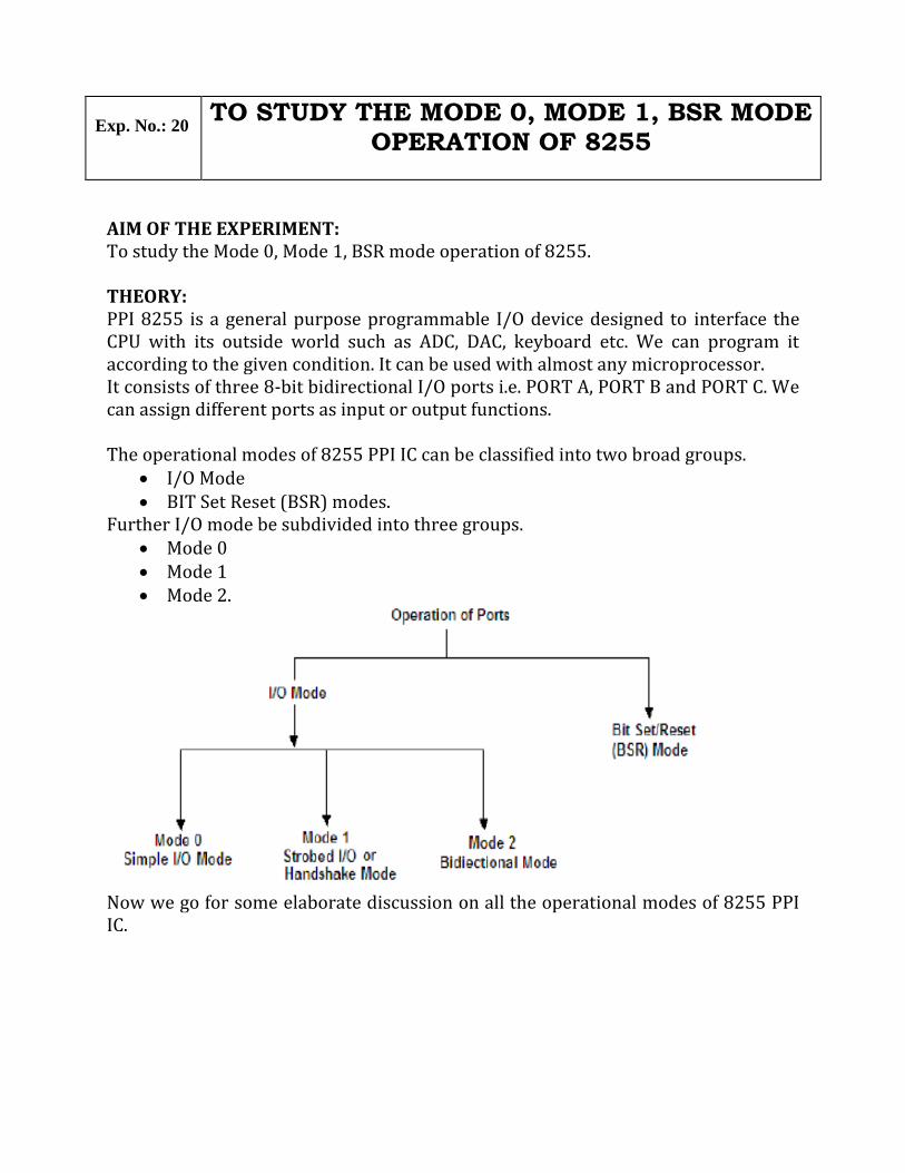
AIM OF THE EXPERIMENT: To study the Mode 0, Mode 1, BSR mode operation of 8255. THEORY: PPI 8255 is a general purpose programmable I/O device designed to interface the CPU with its outside world such as ADC, DAC, keyboard etc. We can program it according to the given condition. It can be used with almost any microprocessor. It consists of three 8-bit bidirectional I/O ports i.e. PORT A, PORT B and PORT C. We can assign different ports as input or output functions. The operational modes of 8255 PPI IC can be classified into two broad groups.
• I/O Mode • BIT Set Reset (BSR) modes.
Further I/O mode be subdivided into three groups. • Mode 0 • Mode 1 • Mode 2.
Now we go for some elaborate discussion on all the operational modes of 8255 PPI IC.

I/O MODE: I/O mode refer as input/output mode. So for any input/output operation of microprocessor this mode will activated. As we know the input/output mode can further be subdivided into three groups: Mode 0 – Simple Input/output mode: In this mode the 8 bit port A (PA0-PA7) of 8255 IC can be configured as input or output port. In the similar fashion port B (PB0-PB7) can also be configured as input or output operation. However there is flexibility for the port C. It can be divided into two 4 bit ports, the port C lower (PC0-PC3) and port C upper (PC4-PC7). Each of them can be set independently for input or output operation. In this way can say there are four ports (port-A, port-B, port C lower and port C upper) and each of them can be set either as an input port or an output port. Here these ports are simple input or output ports. That means these ports can work without handshaking. In this mode the outputs are latched whereas the inputs are not latched.
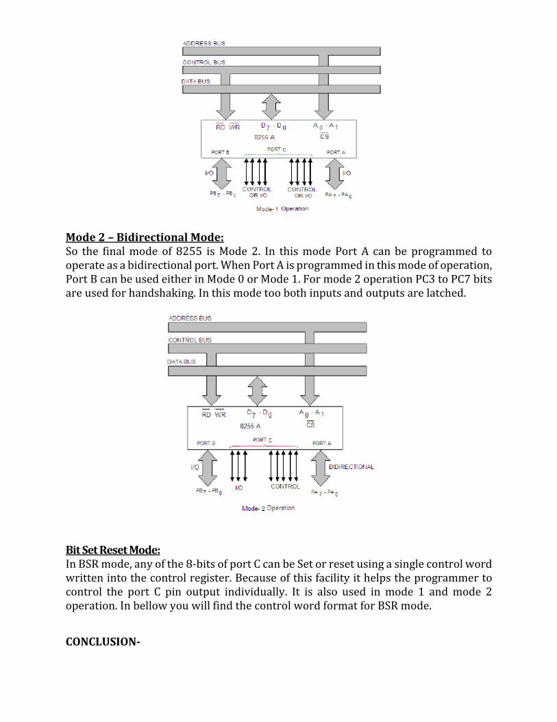
Mode 1 – Strobed Input/output or Handshake mode: Mode 1 is a second mode of 8255 I/O mode. In this mode of operation handshaking is used for the input or output data transfer. Another important think we have to remember that there are two groups in 8255 PPI, Group A and Group B. Both these groups have one 8-bit port and one 4-bit port. Group A consist Port-A and Port C upper. And group B consist Port-B and Port C lower. The 8-bit port of each group can be programmed for input or output operation with latched input and latched output facilities. The bits of Port C are used for handshaking.
Mode 2 – Bidirectional Mode: So the final mode of 8255 is Mode 2. In this mode Port A can be programmed to operate as a bidirectional port. When Port A is programmed in this mode of operation, Port B can be used either in Mode 0 or Mode 1. For mode 2 operation PC3 to PC7 bits are used for handshaking. In this mode too both inputs and outputs are latched.
Bit Set Reset Mode: In BSR mode, any of the 8-bits of port C can be Set or reset using a single control word written into the control register. Because of this facility it helps the programmer to control the port C pin output individually. It is also used in mode 1 and mode 2 operation. In bellow you will find the control word format for BSR mode.
CONCLUSION-

Exp. No.: 21
TO STUDY THE 8259 PROGRAMMABLE
INTERRUPT CONTROLLER
AIM OF THE EXPERIMENT: To study the 8259 programmable interrupt controller. THEORY:
The 8259 is known as the Programmable Interrupt Controller (PIC) microprocessor. In 8085 and 8086 there are five hardware interrupts and two hardware interrupts respectively. Bu adding 8259, we can increase the interrupt handling capability. This chip combines the multi-interrupt input source to single interrupt output. This provides 8-interrupts from IR0 to IR7. Let us see some features of this microprocessor.
• This chip is designed for 8085 and 8086.
• It can be programmed either in edge triggered, or in level triggered mode
• We can mask individual bits of Interrupt Request Register.
• By cascading 8259 chips, we can increase interrupts up to 64 interrupt lines
• Clock cycle is not needed.
Block Diagram of 8259 PIC microprocessor:

The Block Diagram consists of 8 blocks which are – Data Bus Buffer, Read/Write Logic, Cascade Buffer Comparator, Control Logic, Priority Resolver and 3 registers- ISR, IRR, IMR.
Data bus buffer: This Block is used as a mediator between 8259 and 8085/8086 microprocessor by acting as a buffer. It takes the control word from the 8085 (let say) microprocessor and transfer it to the control logic of 8259 microprocessor. Also, after selection of Interrupt by 8259 microprocessor, it transfer the opcode of the selected Interrupt and address of the Interrupt service sub routine to the other connected microprocessor. The data bus buffer consists of 8 bits represented as D0-D7 in the block diagram. Thus, shows that a maximum of 8 bits data can be transferred at a time.
Read/Write logic: This block works only when the value of pin CS is low (as this pin is active low). This block is responsible for the flow of data depending upon the inputs of RD and WR. These two pins are active low pins used for read and write operations. Control logic: It is the Centre of the microprocessor and controls the functioning of every block. It has pin INTR which is connected with other microprocessor for taking interrupt request and pin INT for giving the output. If 8259 is enabled, and the other microprocessor Interrupt flag is high then this causes the value of the output INT pin high and in this way 8259 responds to the request made by other microprocessor. Interrupt request register (IRR): It stores all the interrupt level which are requesting for Interrupt services. Interrupt service register (ISR): it stores the interrupt level which are currently being executed. Interrupt mask register (IMR): It stores the interrupt level which have to be masked by storing the masking bits of the interrupt level. Priority resolver: It examines all the three registers and set the priority of interrupts and according to the priority of the interrupts, interrupt with highest priority is set in ISR register. Also, it reset the interrupt level which is already been serviced in IRR. Cascade buffer: To increase the Interrupt handling capability, we can further cascade more number

of pins by using cascade buffer. So, during increment of interrupt capability, CSA lines are used to control multiple interrupt structure. SP/EN (Slave program/Enable buffer) pin is when set to high, works in master mode else in slave mode. In Non Buffered mode, SP/EN pin is used to specify whether 8259 work as master or slave and in Buffered mode, SP/EN pin is used as an output to enable data bus.
PIN DIAGRAM:
Vcc and GND:
It is the Power supply and ground pins. +5V power supply is used in this chip.
D7-0: For communication with the processor, there are Eight bi-directional data pins.
RD*: It is active low-input pin activated by the processor to read the information status from the 8259.
WR*: It is an active low-input pin which is activated by the processor to write the control information to 8259.
CS*: For selecting the chip it is used an active low input pin.
A0: An address input pin used along with RD* and WR* which is used to identify the various command words.

IR0-IR7: There are Eight asynchronous interrupt request inputs. These interrupt requests can be programmed for level-trigger or edge-triggered mode.
INT: A strong active high-output pin which interrupts the processor. Always connected to the INTR interrupt input of 8085. The INT output is only activated when all the given conditions are satisfied correctly.
INTA*: It is termed as an active low-input pin. The 8259 receives the signal from INTA* to the output of 8085. 8085 sends the three consecutive INTA* signals, the 8259sends a 3-byte CALL instruction to the 8085 via D7-0 pins. The two bytes termed as second and third bytes of the CALL instruction contains the ISS address which depends on the IR input of 8259 that is going to be serviced.
CAS:2-0 These are cascaded lines. Used only when there are multiple 8259s in the system. The interrupt control system might have a master 8259 and maximum eight Slave 8259s.
SP*/EN*: SP*/EN* stands for “slave program/enable buffer”. This pin serves dual function. When it is used as EN* pin it provides an active low-output pin that controls the buffer transceivers in the buffer mode.
CONCLUSION-

Exp. No.: 22
TO INITIALIZE DATA TO REGISTERS AND
MEMORY USING DIFFERENT ADDRESSING MODES OF 8051
AIM OF THE EXPERIMENT:
To initialize data to registers and memory using immediate, register, direct and
indirect addressing mode of 8051.
THEORY:
In 8051 there are 1-byte, 2-byte instructions and very few 3-byte instructions are present. The opcodes are 8-bit long. As the opcodes are 8-bit data, there are 256 possibilities. Among 256, 255 opcodes are implemented.
The clock frequency is 12MHz, so 64 instruction types are executed in just 1 µs, and rest are just 2 µs. The Multiplication and Division operations take 4 µs to execute.
In 8051 there are six types of addressing modes.
• Immediate Addressing mode
• Register Addressing mode
• Direct Addressing mode
• Register Indirect Addressing mode
• Indexed Addressing mode
• Implied Addressing mode
Immediate addressing mode:
In this Immediate Addressing Mode, the data is provided in the instruction itself. The data is provided immediately after the opcode. These are some examples of Immediate Addressing Mode.
MOV A, #0AFH;
MOV R3, #45H;
MOV DPTR, #FE00H;
In these instructions, the # symbol is used for immediate data. In the last instruction, there is DPTR. The DPTR stands for Data Pointer. Using this, it points the external data memory location. In the first instruction, the immediate data is AFH, but one 0 is
added at the beginning. So when the data is starting with A to F, the data should be preceded by 0.
Register addressing mode:
In the register addressing mode the source or destination data should be present in a register (R0 to R7). These are some examples of Register Addressing Mode.
MOV A, R5;
MOV R2, #45H;
MOV R0, A;
In 8051, there is no instruction like MOVR5, R7. But we can get the same result by using this instruction MOV R5, 07H, or by using MOV 05H, R7. But this two instruction will work when the selected register bank is RB0. To use another register bank and to get the same effect, we have to add the starting address of that register bank with the register number. For an example, if the RB2 is selected, and we want to access R5, then the address will be (10H + 05H = 15H), so the instruction will look like this MOV 15H, R7. Here 10H is the starting address of Register Bank 2.
Register indirect addressing mode:
In this mode, the source or destination address is given in the register. By using register indirect addressing mode, the internal or external addresses can be accessed. The R0 and R1 are used for 8-bit addresses, and DPTR is used for 16-bit addresses, no other registers can be used for addressing purposes. Let us see some examples of this mode.
MOV 0E5H, @R0;
MOV@R1, 80H
In the instructions, the @ symbol is used for register indirect addressing. In the first instruction, it is showing that theR0 register is used. If the content of R0 is 40H, then that instruction will take the data which is located at location 40H of the internal RAM. In the second one, if the content of R1 is 30H, then it indicates that the content of port P0 will be stored at location 30H in the internal RAM.
MOV XA, @R1;
MOV@DPTR, A;
In these two instructions, the X in MOVX indicates the external data memory. The external data memory can only be accessed in register indirect mode. In the first instruction if the R0 is holding 40H, then A will get the content of external RAM

location40H. And in the second one, the content of A is overwritten in the location pointed by DPTR.
Direct Addressing Mode:
In the Direct Addressing Mode, the source or destination address is specified by using 8-bit data in the instruction. Only the internal data memory can be used in this mode. Here some of the examples of direct Addressing Mode.
MOV 80H, R6;
MOV R2, 45H;
MOV R0, 05H;
The first instruction will send the content of registerR6 to port P0 (Address of Port 0 is 80H). The second one is forgetting content from 45H to R2. The third one is used to get data from Register R5 (When register bank RB0 is selected) to register R5.
Indexed addressing mode:
In the indexed addressing mode, the source memory can only be accessed from program memory only. The destination operand is always the register A. These are some examples of Indexed addressing mode.
MOVC A, @A+PC;
MOVC A, @A+DPTR;
The C in MOVC instruction refers to code byte. For the first instruction, let us consider A holds 30H. And the PC value is1125H. The contents of program memory location 1155H (30H + 1125H) are moved to register A.
Implied Addressing Mode:
In the implied addressing mode, there will be a single operand. These types of instruction can work on specific registers only. These types of instructions are also known as register specific instruction. Here are some examples of Implied Addressing Mode.
RLA;
SWAPA;
These are 1- byte instruction. The first one is used to rotate the A register content to the Left. The second one is used to swap the nibbles in A.
CONCLUSION-

Exp. No.: 23
TO WRITE A PROGRAM FOR RELAY INTERFACE
AIM OF THE EXPERIMENT:
To write a program for relay interface.
APPARATUS REQUIRED:
8051 Trainer Kit and Interfacing Kit.
THEORY:
An electromagnetic relay is a switch which is used to switch high voltage or current
using low power circuits.it magnetically isolates low power circuits from high power
circuits.it is activated by energizing a electromagnet, coil wounded on soft iron core.
A relay should not be directly connected to a microcontroller, it needs a driving circuit
due to the following reasons.
➢ A microcontroller will not able to supply current required for the proper
working of a relay .the maximum current that A89C51 microcontroller can
source or sink is 15mA while a relay needs about 50-100mA current.
➢ A relay is activated by energizing its coil. Microcontroller may stop working by
the negative voltages produced in the relay due to its back emf.
This program reads the status of switches and display on 8 outputs & seven segment
display of the kit.
PROCEDURE:
Assembly language programs for microprocessor 8051 can be executed on its trainer
kit as per the following steps
STEP 1- STORAGE OF PROGRAM MACHINE CODES:
Machine codes of the program to be executed, should be stored in their memory
available on 8051 trainer kit as
RESET→EXMEM→starting address of program (2000)→NEXT→Now enter all the
machine codes, one after the other followed by the key ‘NEXT’.
STEP 2-EXECUTION OF PROGRAM:
The program can be executed as
FILL→GO→Starting address of the program (2000)→FILL
STEP 3-VERIFICATION OF OUTPUT:
Output of the executed program can be verified as
RESET→ EXMEM→type the memory address where result will be stored →NEXT
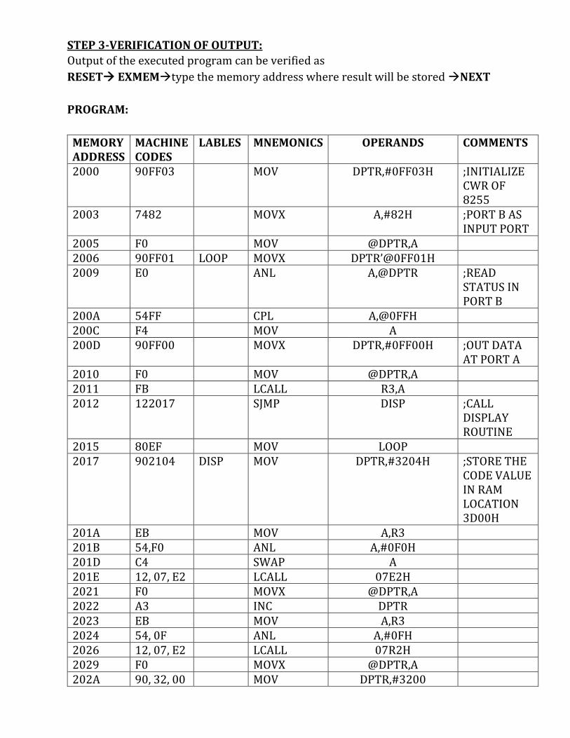
PROGRAM:
MEMORY ADDRESS
MACHINE CODES
LABLES MNEMONICS OPERANDS COMMENTS
2000 90FF03 MOV DPTR,#0FF03H ;INITIALIZE CWR OF 8255
2003 7482 MOVX A,#82H ;PORT B AS INPUT PORT
2005 F0 MOV @DPTR,A 2006 90FF01 LOOP MOVX DPTR’@0FF01H 2009 E0 ANL A,@DPTR ;READ
STATUS IN PORT B
200A 54FF CPL A,@0FFH 200C F4 MOV A 200D 90FF00 MOVX DPTR,#0FF00H ;OUT DATA
AT PORT A 2010 F0 MOV @DPTR,A 2011 FB LCALL R3,A 2012 122017 SJMP DISP ;CALL
DISPLAY ROUTINE
2015 80EF MOV LOOP 2017 902104 DISP MOV DPTR,#3204H ;STORE THE
CODE VALUE IN RAM LOCATION 3D00H
201A EB MOV A,R3 201B 54,F0 ANL A,#0F0H 201D C4 SWAP A 201E 12, 07, E2 LCALL 07E2H 2021 F0 MOVX @DPTR,A 2022 A3 INC DPTR 2023 EB MOV A,R3 2024 54, 0F ANL A,#0FH 2026 12, 07, E2 LCALL 07R2H 2029 F0 MOVX @DPTR,A 202A 90, 32, 00 MOV DPTR,#3200

202D 12, 06, F7 LCALL 06F7H ;Call display routine
2030 220 RET 3200 FF, FF, FF,
FF DFB 0FFH,0FFH,0FFH,0FFH
CONCLUSION:

Exp. No.: 24
TO WRITE A PROGRAM FOR CHARACTER BASED LCD INTERFACE
AIM OF THE EXPERIMENT:
To write an assembly language program for character based LCD Interface.
APPARATUS REQUIRED:
8051 trainer kit and interfacing kit.
THEORY:
➢ LCDs (Liquid Crystal Displays) are used for displaying status or parameters in
embedded systems.
➢ LCDs 16x2 is 16 pin device which has 8 data pins (D0-D7) and control pins (RS, RW,
EN).The remaining 5 pins are for supply and backlight for the LCD.
➢ The control pins help us configure the LCD in command mode or data mode. They
also help configure read mode or write mode also when to read or write.
➢ LCD 16x2 can be used in 4-bit mode or 8-bit mode depending on the requirement of
the application. In order to use it we need to send certain commands to the LCD in
command mode and once the LCD is configured according to our need, we can send
the required data in data mode.
Here we are flashing display of good 51 on seven segment display on executing this
program from address 2000H,”Good51” message flashes on the display of the kit.
PROCEDURE:
Assembly language programs for microprocessor 8051 can be executed on its trainer
kit as per the following steps
STEP 1- STORAGE OF PROGRAM MACHINE CODES:
Machine codes of the program to be executed, should be stored in their memory
available on 8051 trainer kit as
RESET→EXMEM→starting address of program (2000)→NEXT→Now enter all the
machine codes, one after the other followed by the key ‘NEXT’.
STEP 2-EXECUTION OF PROGRAM:
The program can be executed as
FILL→GO→Starting address of the program (2000)→FILL
STEP 3-VERIFICATION OF OUTPUT:
Output of the executed program can be verified as
RESET→ EXMEM→type the memory address where result will be stored →NEXT
PROGRAM:
CONCLUSION:
MEMORY ADDRESS
MACHINE CODES
LABLES MNEMONICS
OPERANDS COMMENTS
2000 90 20 2E HERE MOV DPTR,#202E ;Good 51 message 2003 12 06 F7 LCALL 06F7 ;display routine
2006 7B 00 MOV R3,#0
2008 7A 00 LOOP2: MOV R2,#0 200A DA FE LOOP1: DJNZ R2,200A ;delay code
200C DB FA DJNZ R3,2008 200E 90 20 34 MOV DPTR,#2034 ;blank message
2011 12 06 F7 LCALL 06F7 ;display routine
2014 7B 00 MOV R3,#0 2016 7A 00 LOOP4; MOV R2,#0 2018 DA FE LOOP3 DJNZ R2,2018 ;delay code 201A DB FA DJNZL R3,2016
201C 80 E2 SJMP 2000 202E 41 03 03 85
49 9F DFB 41,03,03,85,49,9
F Data Good 51
2034 FF FF FF FF FF FF
DFB ,FF,FF FF,FF,FF,FF
BLANK DISPLAY