KX-TCD445BXS KX-TCD445BXT KX-TCD445BXF ... - Index of
99
© 2004 Panasonic Communications Co., Ltd. All rights reserved. Unauthorized copying and distribution is a violation of law. KX-TCD445BXS KX-TCD445BXT KX-TCD445BXF KX-A144BXS KX-A144BXT KX-A144BXF Digital Cordless Answering System New Silver Version Titanium Black Version Metallic Blue Version (for Asia, Middle Near East and Other areas) Telephone Equipment ORDER NO. KM40406482C3
-
Upload
khangminh22 -
Category
Documents
-
view
0 -
download
0
Transcript of KX-TCD445BXS KX-TCD445BXT KX-TCD445BXF ... - Index of

© 2004 Panasonic Communications Co., Ltd. Allrights reserved. Unauthorized copying anddistribution is a violation of law.
KX-TCD445BXSKX-TCD445BXTKX-TCD445BXFKX-A144BXSKX-A144BXTKX-A144BXFDigital Cordless Answering SystemNew Silver VersionTitanium Black VersionMetallic Blue Version
(for Asia, Middle Near East and Other areas)
Telephone Equipment
ORDER NO. KM40406482C3

1 ABOUT LEAD FREE SOLDER (PbF: Pb free) 4 1.1. Suggested PbF Solder 4
1.2. How to recognize that Pb Free solder is used 5
2 FOR SERVICE TECHNICIANS 7 3 CAUTION 7 4 BATTERY 8
4.1. Battery Installation 8
4.2. Battery Charge 8
4.3. Battery Life 9
4.4. Replacing the Batteries 9
5 LOCATION OF CONTROLS 10 5.1. Base Unit 10
5.2. Handset 10
6 SETTINGS 11 6.1. Connections 11
6.2. Ringer Volume 12
6.3. PIN Code 13
6.4. Reset 14
6.5. Key Lock 15
6.6. R button to use the flash feature 15
6.7. Pause button for PBX (line/long distance service users) 15
6.8. Setting Call Restriction 16
6.9. Cancelling a Restricted Number 16
6.10. Setting Call BAR 16
6.11. Selecting the Display Language 17
6.12. Setting Dialling Mode (Tone/Pulse) 17
6.13. Setting Flash Time 17
7 DISPLAY 18 7.1. Handset Display 18
7.2. Caller ID Display 18
7.3. Before Requesting Help (Troubleshooting) 20
8 OPERATIONS 22 8.1. Turning the Power On/Off 22
8.2. Setting the Time and Date 22
8.3. Redialling 22
8.4. Phonebook 23
8.5. Registering a Handset to a Base Unit 25
8.6. Selecting a Base Unit 26
8.7. Answering System 27
9 DISASSEMBLY INSTRUCTIONS 30 9.1. Base Unit 30
9.2. Handset 31
9.3. Charger Unit 32
10 ASSEMBLY INSTRUCTIONS 33 10.1. Warning When Constructing the Base Unit 33
10.2. Processing of Ringer/Charge Terminal Lead 34
11 TROUBLESHOOTING GUIDE 35 11.1. Check Power 36
11.2. Check Battery Charge 37
11.3. Check Link 38
11.4. Check Handset Transmission 40
11.5. Check Handset Reception 40
11.6. Check Caller ID 40
11.7. TAM Voice Prompt Problems 41
11.8. Bell Reception 42
12 CHECK PROCEDURE (BASE UNIT) 43 12.1. Preparation 43
12.2. PC Setting 43
12.3. TAM Voice Prompt Download 44
13 CHECK PROCEDURE (HANDSET) 45 13.1. Preparation 45
13.2. PC Setting 45
14 ADJUSTMENTS (BASE UNIT AND CHARGER UNIT) 46 14.1. Adjustment (Base Unit) 46
14.2. Adjustment Standard (Base Unit) 49
14.3. Adjustment (Charger Unit) 51
14.4. Adjustment Standard (Charger Unit) 51
15 ADJUSTMENTS (HANDSET) 52 15.1. Adjustment (Handset) 52
15.2. Adjustment Standard (Handset) 55
16 RF SPECIFICATION 56 16.1. Base Unit 56
Note:Because CONTENTS 4 to 8 are the extracts from the Operating Instructions of this model, they are subject to change withoutnotice. Please refer to the original Operating Instructions for further information.
CONTENTS Page Page
2
KX-TCD445BXS / KX-TCD445BXT / KX-TCD445BXF / KX-A144BXS / KX-A144BXT / KX-A144BXF /

16.2. Handset 56
17 HOW TO CHECK THE HANDSET SPEAKER OR RECEIVER 56 18 FREQUENCY TABLE (MHz) 57 19 BLOCK DIAGRAM (BASE UNIT) 58 20 CIRCUIT OPERATION (BASE UNIT) 59
20.1. Outline 59
20.2. Power Supply Circuit 60
20.3. Telephone Line Interface 61
20.4. Transmitter/Receiver 61
20.5. Pulse Dialling 61
21 BLOCK DIAGRAM (HANDSET) 62 22 CIRCUIT OPERATION (HANDSET) 63
22.1. Outline 63
22.2. Power Supply Circuit/Reset Circuit 63
22.3. Charge Circuit 63
22.4. Battery Low/Power Down Detector 63
22.5. Speakerphone 63
23 CIRCUIT OPERATION (CHARGER UNIT) 64 23.1. Power Supply Circuit 64
24 SIGNAL ROUTE 65 25 CPU DATA (BASE UNIT) 66
25.1. IC8 (BBIC) 66
26 CPU DATA (HANDSET) 69 26.1. IC1 (BBIC) 69
27 EEPROM LAYOUT (BASE UNIT) 71 27.1. Scope 71
27.2. Introduction 71
27.3. EEPROM Layout 71
28 EEPROM LAYOUT (HANDSET) 75 28.1. Scope 75
28.2. Introduction 75
28.3. EEPROM contents 75
29 HOW TO REPLACE FLAT PACKAGE IC 78 29.1. Preparation 78
29.2. Procedure 78
29.3. Modification Procedure of Bridge 78
30 CABINET AND ELECTRICAL PARTS LOCATION (BASE UNIT) 79
31 CABINET AND ELECTRICAL PARTS LOCATION (HANDSET) 80 32 CABINET AND ELECTRICAL PARTS LOCATION (CHARGER
UNIT) 81 33 ACCESSORIES AND PACKING MATERIALS 82
33.1. KX-TCD445BXS/BXT/BXF 82
33.2. KX-A144BXS/BXT/BXF 83
34 TERMINAL GUIDE OF THE ICs, TRANSISTORS AND DIODES 84 34.1. Base Unit 84
34.2. Handset 84
34.3. Charger Unit 84
35 REPLACEMENT PARTS LIST 85 35.1. Base Unit 85
35.2. Handset 87
35.3. Charger Unit 88
35.4. Accessories and Packing Materials 88
35.5. Fixtures and Tools 88
36 FOR SCHEMATIC DIAGRAM 89 36.1. Base Unit (SCHEMATIC DIAGRAM (BASE UNIT)) 89
36.2. Handset (SCHEMATIC DIAGRAM (HANDSET)) 89
36.3. Charger Unit (SCHEMATIC DIAGRAM (CHARGER UNIT))
89
37 SCHEMATIC DIAGRAM (BASE UNIT) 90 38 SCHEMATIC DIAGRAM (HANDSET) 92 39 SCHEMATIC DIAGRAM (CHARGER UNIT) 94 40 CIRCUIT BOARD (BASE UNIT) 95
40.1. Component View 95
40.2. Flow Solder Side View 96
41 CIRCUIT BOARD (HANDSET) 97 41.1. Component View 97
41.2. Flow Solder Side View 98
42 CIRCUIT BOARD (CHARGER UNIT) 99 42.1. Component View 99
42.2. Flow Solder Side View 99
3
KX-TCD445BXS / KX-TCD445BXT / KX-TCD445BXF / KX-A144BXS / KX-A144BXT / KX-A144BXF /

1 ABOUT LEAD FREE SOLDER (PbF: Pb free)Note:
In the information below, Pb, the symbol for lead in the periodic table of elements, will refer to standard solder or solder thatcontains lead.We will use PbF solder when discussing the lead free solder used in our manufacturing process which is made from Tin (Sn),Silver (Ag), and Copper (Cu).This model, and others like it, manufactured using lead free solder will have PbF stamped on the PCB. For service and repairwork we suggest using the same type of solder although, with some precautions, standard Pb solder can also be used.
Caution • PbF solder has a melting point that is 50°F ~70°F (30°C ~ 40°C) higher than Pb solder. Please use a soldering iron with
temperature control and adjust it to 700°F ± 20°F (370°C ± 10°C). In case of using high temperature soldering iron, pleasebe careful not to heat too long.
• PbF solder will tend to splash if it is heated much higher than its melting point, approximately 1100°F (600°C). • If you must use Pb solder on a PCB manufactured using PbF solder, remove as much of the original PbF solder as possible
and be sure that any remaining is melted prior to applying the Pb solder. • When applying PbF solder to double layered boards, please check the component side for excess which may flow onto the
opposite side (See the figure below).
1.1. Suggested PbF SolderThere are several types of PbF solder available commercially. While this product is manufactured using Tin, Silver, and Copper(Sn+Ag+Cu), you can also use Tin and Copper (Sn+Cu) or Tin, Zinc, and Bismuth (Sn+Zn+Bi). Please check themanufacturer’s specific instructions for the melting points of their products and any precautions for using their product with othermaterials.The following lead free (PbF) solder wire sizes are recommended for service of this product: 0.3mm, 0.6mm and 1.0mm.
4
KX-TCD445BXS / KX-TCD445BXT / KX-TCD445BXF / KX-A144BXS / KX-A144BXT / KX-A144BXF /

1.2. How to recognize that Pb Free solder is used
1.2.1. Base Unit PCB
PbF
IC7
IC8
IC9
144
109108
1
16 17
32
1
11
3736
28
1873
72
Marked
IC41
45
8
(Component View)
TP13
TP15
TP8TP7
TP11
TP106
TP9
TP124
15
6TP4
TP2TP3
TP10
TP6
TP202
TP201
TP5
GNDMODESCLSDAVDD
J105J102J104J103J101
CHARGECHARGE
PbF
Marked(Flow Solder Side View)
Note:The locations of the “PbF” mark are subject to change without notice.
5
KX-TCD445BXS / KX-TCD445BXT / KX-TCD445BXF / KX-A144BXS / KX-A144BXT / KX-A144BXF /

1.2.3. Charger Unit PCB
1.2.2. Handset PCB
PbF
IC1
11 18
281
IC3
1001
808150
51
3130
Marked
IC25
8
4
1
(Component View)
Marked
1
PROG
Pb
F
BOOK
UP
POWERCAN
DOWN
RIGHT
REDIAL
LEFT
1
2
36
5
7
0
#
R4
9
8
INT
MIC
TALK 36
CN2
LE
D101
LED107
LED108SP_
LED104
LED106
LED105
LE
D102
LE
D103
(Flow Solder Side View)
Note:The locations of the “PbF” mark are subject to change without notice.
(Component View) (Flow Solder Side View)
PbF
D1
J1
Marked
PbF
R1
R2
TP4
TP1
TP2
TP3
Marked
Note:The locations of the “PbF” mark are subject to change without notice.
6
KX-TCD445BXS / KX-TCD445BXT / KX-TCD445BXF / KX-A144BXS / KX-A144BXT / KX-A144BXF /

2 FOR SERVICE TECHNICIANSICs and LSIs are vulnerable to static electricity.When repairing, the following precautions will help prevent recurring malfunctions.
1. Cover the plastic parts boxes with aluminum foil. 2. Ground the soldering irons. 3. Use a conductive mat on the worktable. 4. Do not touch IC or LSI pins with bare fingers.
3 CAUTIONDanger of explosion if battery is incorrectly replaced. Replace only with the same or equivalent type recommended by themanufacturer.Dispose of used batteries according to the manufacture’s Instructions.
7
KX-TCD445BXS / KX-TCD445BXT / KX-TCD445BXF / KX-A144BXS / KX-A144BXT / KX-A144BXF /

4 BATTERY4.1. Battery Installation
1. Insert the batteries negative (-) terminal first. 2. Close the battery cover.
Note: • Use only rechargeable HHR-4EPT (Ni-MH)/P-4NPT (Ni-Cd) batteries.
4.2. Battery ChargePlace the handset on the base unit for about 7 hours before initial use.When the batteries are fully charged, flashes. When charging, the battery icon is shown as follows.
Note: • Clean the charge contacts of the handset and base unit with a soft, dry cloth, otherwise the batteries may not charge
properly. Clean if the unit is exposed to grease, dust or high humidity. • If the handset is turned off, it will be turned on automatically when it is placed on the base unit.
Note for Service:The battery strength may not be indicated correctly if the battery is disconnected and connected again, even after it is fullycharged.In that case, by recharging the battery as mentioned above, you will get a correct indication of the battery strength.
8
KX-TCD445BXS / KX-TCD445BXT / KX-TCD445BXF / KX-A144BXS / KX-A144BXT / KX-A144BXF /

4.3. Battery LifeAfter your Panasonic batteries are fully charged, you can expect the following performance:
Note: • The included batteries are Ni-MH batteries. • Battery operating time may be shortened depending on usage conditions and ambient temperature.
4.4. Replacing the BatteriesIf flashes even when the handset batteries have been fully charged, both batteries must be replaced.
Important: • Please use only the Panasonic batteries HHR-4EPT (Ni-MH)/P-4NPT (Ni-Cd). • Use only rechargeable batteries. If you install non-rechargeable batteries and start charging, the batteries may leak
electrolyte. • Do not mix old and new batteries. • Use only 2 nickel metal hydride (Ni-MH) batteries or 2 nickel cadmium (Ni-Cd) batteries. Do not mix battery types. • Ensure that the correct battery type is selected.
1. Press the notch on the cover firmly and slide it in the direction of the arrow. 2. Remove the batteries positive (+) terminal first. Replace both batteries.
Note for Service: • When Ni-Cd batteries are fitted with the setting in , icon might disappear and stop
charging even if the handset is on the cradle for avoiding overcharge.
9
KX-TCD445BXS / KX-TCD445BXT / KX-TCD445BXF / KX-A144BXS / KX-A144BXT / KX-A144BXF /

5 LOCATION OF CONTROLS5.1. Base Unit
5.2. Handset
10
KX-TCD445BXS / KX-TCD445BXT / KX-TCD445BXF / KX-A144BXS / KX-A144BXT / KX-A144BXF /

6 SETTINGSImportant Information
General • Use only the power supply included with this product. • Do not connect the AC adaptor to any AC outlet other than a standard 220-240 V AC outlet. • This product is unable to make calls when:
− The portable handset batteries need recharging or have failed. − There is a power failure. − The key lock feature is turned on. − The call bar feature is turned on (only numbers stored as emergency numbers can be called).
• Do not open the base unit or handset (other than to change the batteries). • This product should not be used near emergency/intensive care medical equipment and should not be used by people
with pacemakers. • Care should be taken that objects do not fall onto, and liquids are not spilled into, the unit. Do not subject this product
to excessive smoke, dust, mechanical vibration or shock.Environment
• Do not use this product near water. • This product should be kept away from heat sources such as radiators, cookers, etc. It should also not be placed in
rooms where the temperature is less than 5°C or greater than 40°C. • The AC adaptor is used as the main disconnect device. Ensure that the AC outlet is located/installed near the unit and
is easily accessible.Warning:
• To prevent the risk of electrical shock, do not expose this product to rain or any other type of moisture.
LocationFor maximum distance and noise-free operation, place your base unit:- Away from electrical appliances such as TVs, radios, personal computers or other phones.- In a convenient, high and central location.
6.1. Connections6.1.1. Base Unit
Note: • If the handset is not charged, you cannot make or answer calls. • Never install telephone wiring during a lightning storm. • The AC adaptor must remain connected at all times. (It is normal for the adaptor to feel warm during use.) • Use only the AC adaptor PQLV19BXZ.
11
KX-TCD445BXS / KX-TCD445BXT / KX-TCD445BXF / KX-A144BXS / KX-A144BXT / KX-A144BXF /
6.1.2. Charger Unit
• The AC adaptor must remain connected at all times (It is normal for the adaptor to feel warm during use). • Use only the AC adaptor PQLV200BXZ.
6.2. Ringer Volume6.2.1. Base Unit
4 levels (high to off) are available.
6.2.2. Handset7 levels (high to off) are available.
12
KX-TCD445BXS / KX-TCD445BXT / KX-TCD445BXF / KX-A144BXS / KX-A144BXT / KX-A144BXF /

6.3. PIN Code6.3.1. Base Unit
For Service Hint:*: If the current 4-digit PIN is forgotten, press and you will be able to enter new PIN.
6.3.2. Handset
For Service Hint:*: If the current 4-digit PIN is forgotten, press and you will be able to enter new PIN.
13
KX-TCD445BXS / KX-TCD445BXT / KX-TCD445BXF / KX-A144BXS / KX-A144BXT / KX-A144BXF /

6.4. Reset
6.4.1. Base Unit
Note: • The emergency number and TAM setting will not be reset.
Base Unit Initial SettingsFunction Initial Setting Remarks (selectable options)
Base Unit Ringer Volume 2 1 to 3, OFFRinger Mode All Handsets All Handsets/Specific Handset No.Number of Rings (Ringer Mode) 3 Up to 6 ringsNumber of Rings (TAM) Auto 2 to 7, AutoDialling Mode Tone Tone/PulseFlash Time 600 msec 100 msec/600 msec/300 msecPause Length 3 seconds 3 seconds/5 secondsCall Restricted Handsets All Clear Each Handset can be set individually.Call Restriction Numbers All Clear Up to 10 numbers (up to 8 digits)4-Digit Base Unit PIN 0000 -Caller ID All Clear Up to 50 different callers.
6.4.2. Handset
Note: • Phonebook entries will not be erased. • The battery type setting will not be reset.
14
KX-TCD445BXS / KX-TCD445BXT / KX-TCD445BXF / KX-A144BXS / KX-A144BXT / KX-A144BXF /

Handset Initial SettingsFunction Initial Setting Remarks (selectable options)
Select Base Unit Auto -Time Alarm Mode OFF OFF/Once/DailyAlarm Time Clear -Handset Ringer Volume 6 1 to 6, OFFHandset External Ringer Pattern 1 20 patternsHandset Internal Ringer Pattern 1 20 patternsHandset Paging Tone Pattern 1 20 patternsHandset Alarm Tone Pattern 1 20 patternsKey Tone ON ON/OFFCall Waiting Tone ON ON/OFFRange Warning Alarm OFF OFF/ONBattery Low Alarm ON ON/OFFStandby Mode Display Clock Clock/OFF/Base No./Handset No.Talk Mode Display Talk Time Talk Time/Phone No.Display Language English 10 languagesCall BAR OFF OFF/ONDirect Call Mode OFF OFF/ONDirect Call Number Clear Up to 24 digits4-Digit Handset PIN 0000 -Auto Talk OFF OFF/ONRedial Memory All Clear Up to 10 numbers (Up to 24 digits)Handset Receiver Volume 2 1 to 3Handset Speaker Volume 3 1 to 6
6.5. Key LockThe dial keys can be locked so that no calls can be made. Only incoming calls will be accepted while key lock is on.
Note: • Emergency calls cannot be made until key lock is turned off. • Key lock is turned off when the handset is turned off.
6.6. R button to use the flash feature
6.7. Pause button for PBX (line/long distance service users)A pause is sometimes required when making calls using a PBX or long distance service.
15
KX-TCD445BXS / KX-TCD445BXT / KX-TCD445BXF / KX-A144BXS / KX-A144BXT / KX-A144BXF /

6.8. Setting Call RestrictionYou can restrict selected handsets from dialling certain phone numbers. You can assign up to 10 phone numbers (memorylocations 1-10) to be restricted per handset. If a restricted number is dialled, the call will not be connected and the restrictednumber will flash on the display. For example, storing an area code will prevent a handset from dialling a long distance call.
6.9. Cancelling a Restricted Number
6.10. Setting Call BARThis feature prohibits making outside calls. When call bar is turned on, only intercom calls and emergency calls can be made.
16
KX-TCD445BXS / KX-TCD445BXT / KX-TCD445BXF / KX-A144BXS / KX-A144BXT / KX-A144BXF /

6.11. Selecting the Display Language10 display languages are available.
Note: • If you select a language you cannot read, reset the handset to its default settings. Refer to Handset (P.14) in “Reset”.
6.12. Setting Dialling Mode (Tone/Pulse)
6.13. Setting Flash TimeChange the flash time if necessary to suit your PBX or service provider.
17
KX-TCD445BXS / KX-TCD445BXT / KX-TCD445BXF / KX-A144BXS / KX-A144BXT / KX-A144BXF /

7 DISPLAY7.1. Handset Display
For Service Hint:icon will be displayed if the unit took a signal from Telephone Company as a Voice Message signal.
In that case, press the left button of the Navigator Key for a while.
7.2. Caller ID DisplayImportant:
This unit is Caller ID compatible. To display the caller’s phone number, you must subscribe to Caller ID service. Aftersubscribing to Caller ID service, this unit will display caller information.
How Caller ID is displayedThe unit will display the calling party’s phone number after the first ring. You can view the caller information of the last 50different callers.When new calls have been received, the display will show the number of new calls.The number of new calls will be cleared after viewing all caller information.Example: 4 new calls have been received.
Note: • When you receive a call from the same phone number you stored with a name in the phonebook, the display will show the
stored name. • If the unit is connected to a PBX system, you may not receive the caller information. • When the caller dialled from an area which does not provide Caller ID service, will be displayed. • When the caller requested not to send caller information, either no information or will be displayed. • The display will not show caller information while using the handset for an intercom call. However, the caller information will
be stored. • Certain service providers send caller information between the first and second ring. If the display does not show caller
information after a few rings, follow these instructions to set DTMF mode.
18
KX-TCD445BXS / KX-TCD445BXT / KX-TCD445BXF / KX-A144BXS / KX-A144BXT / KX-A144BXF /

19
KX-TCD445BXS / KX-TCD445BXT / KX-TCD445BXF / KX-A144BXS / KX-A144BXT / KX-A144BXF /

7.3. Before Requesting Help (Troubleshooting)If you still have difficulties after following the instructions in this section, disconnect the AC adaptor and turn off the handset,then reconnect the AC adaptor and turn on the handset.
Cross Reference:(*1) Registering a Handset to a Base Unit (P.25)(*2) Setting Call BAR (P.16)(*3) Setting Call Restriction (P.16)(*4) Key Lock (P.15)(*5) Setting Dialling Mode (Tone/Pulse) (P.17)(*6) Ringer Volume (P.12)(*7) Turning the Power On/Off (P.22)(*8) Battery Installation (P.8)(*9) Battery Charge (P.8)
20
KX-TCD445BXS / KX-TCD445BXT / KX-TCD445BXF / KX-A144BXS / KX-A144BXT / KX-A144BXF /

Cross Reference:(*10) Battery Charge (P.8)(*11) Replacing the Batteries (P.9)(*12) Caller ID Display (P.18)(*13) Registering a Handset to a Base Unit (P.25)(*14) PIN Code (P.13)(*15) Erasing All Messages (P.27)(*16) Remote Operation (P.28)
21
KX-TCD445BXS / KX-TCD445BXT / KX-TCD445BXF / KX-A144BXS / KX-A144BXT / KX-A144BXF /

8 OPERATIONS8.1. Turning the Power On/Off
8.2. Setting the Time and DateImportant:
• Confirm that the AC adaptor is connected. • Ensure that is not flashing.
Note: • If a power failure occurs, set the time and date again.
8.3. Redialling
8.3.1. Making a Call Using the Redial ListThe last 10 phone numbers dialled are stored in the redial list.
8.3.2. Redialling the Last Number Dialled
22
KX-TCD445BXS / KX-TCD445BXT / KX-TCD445BXF / KX-A144BXS / KX-A144BXT / KX-A144BXF /

8.4. Phonebook8.4.1. Storing Phone Numbers and Names
23
KX-TCD445BXS / KX-TCD445BXT / KX-TCD445BXF / KX-A144BXS / KX-A144BXT / KX-A144BXF /

8.4.2. Storing a Number from the Caller ID List into the Phonebook
8.4.3. Storing a Number from the Redial List into the Phonebook
8.4.4. Hot Key (: Quick Dial)
Note: • The number erased from a hot key will not be deleted from the phonebook.
24
KX-TCD445BXS / KX-TCD445BXT / KX-TCD445BXF / KX-A144BXS / KX-A144BXT / KX-A144BXF /

8.5. Registering a Handset to a Base Unit
25
KX-TCD445BXS / KX-TCD445BXT / KX-TCD445BXF / KX-A144BXS / KX-A144BXT / KX-A144BXF /

8.6. Selecting a Base Unit
26
KX-TCD445BXS / KX-TCD445BXT / KX-TCD445BXF / KX-A144BXS / KX-A144BXT / KX-A144BXF /

8.7. Answering System
8.7.1. Listening to Messages
8.7.2. Erasing All Messages
27
KX-TCD445BXS / KX-TCD445BXT / KX-TCD445BXF / KX-A144BXS / KX-A144BXT / KX-A144BXF /

8.7.3. Remote OperationUsing a touch tone phone, you can call your phone number from outside and access the unit to listen to messages or changeanswering system settings. The unit’s voice guidance will prompt you to press certain dial keys to perform different operations.
Turning remote operation on/offA 3-digit remote access code must be entered when operating the answering system remotely. This code preventsunauthorised parties from listening to your messages remotely. After you store your remote access code, remote operationis possible.
Using the answering system remotely
28
KX-TCD445BXS / KX-TCD445BXT / KX-TCD445BXF / KX-A144BXS / KX-A144BXT / KX-A144BXF /

29
KX-TCD445BXS / KX-TCD445BXT / KX-TCD445BXF / KX-A144BXS / KX-A144BXT / KX-A144BXF /

9 DISASSEMBLY INSTRUCTIONS9.1. Base Unit
Shown in Fig.- To Remove Remove1 Lower Cabinet Screws (2.6 × 12)..........(A) × 22 Main P.C. Board Main P.C. Board
30
KX-TCD445BXS / KX-TCD445BXT / KX-TCD445BXF / KX-A144BXS / KX-A144BXT / KX-A144BXF /

9.2. Handset
Shown in Fig.- To Remove Remove3 Rear Cabinet Screws (2 × 10)..........(B) × 24 Follow the procedure.5 Main P.C. Board Screw (2 × 8)..............(C) × 1
Screws (2 × 8).............(D) × 2Main P.C. Board
31
KX-TCD445BXS / KX-TCD445BXT / KX-TCD445BXF / KX-A144BXS / KX-A144BXT / KX-A144BXF /
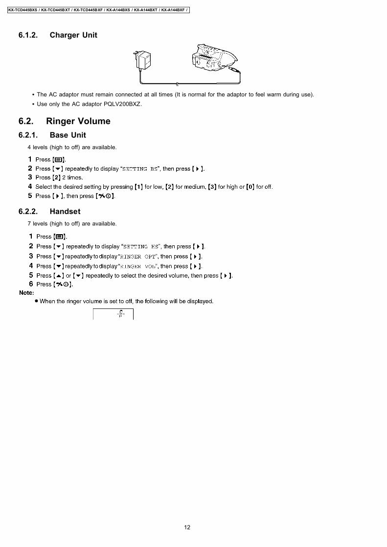
9.3. Charger Unit
Shown in Fig.- To Remove Remove6 Lower Cabinet Screws (2.6 × 14)..........(E) × 27 Main P.C. Board Tape and Solder
Main P.C. Board
32
KX-TCD445BXS / KX-TCD445BXT / KX-TCD445BXF / KX-A144BXS / KX-A144BXT / KX-A144BXF /

10 ASSEMBLY INSTRUCTIONS10.1. Warning When Constructing the Base Unit
OK
NGRib
CHG terminal is properly fit in the cabinet.
CHG terminal comes out of rib by pulling black lead wire when opening the cabinet and turning the PCB over. The terminal cannot have enough elastic force, cannot have good contact with handset, and it will result in charge problem.
33
KX-TCD445BXS / KX-TCD445BXT / KX-TCD445BXF / KX-A144BXS / KX-A144BXT / KX-A144BXF /

10.2. Processing of Ringer/Charge Terminal Lead
34
KX-TCD445BXS / KX-TCD445BXT / KX-TCD445BXF / KX-A144BXS / KX-A144BXT / KX-A144BXF /
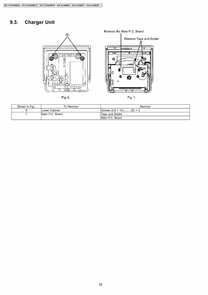
Flow Chart
Cross Reference:Check Power (P.36)Bell Reception (P.42)Check Battery Charge (P.37)Check Link (P.38)Check Handset Transmission (P.40)Check Handset Reception (P.40)SIGNAL ROUTE (P.65)TAM Voice Prompt Problems (P.41)
11 TROUBLESHOOTING GUIDE
35
KX-TCD445BXS / KX-TCD445BXT / KX-TCD445BXF / KX-A144BXS / KX-A144BXT / KX-A144BXF /

11.1.1. Base Unit
Cross ReferencePower Supply Circuit (P.60)
Cross ReferencePower Supply Circuit/Reset Circuit (P.63)
Note:BBIC is IC8.
Note:BBIC is IC1.
11.1. Check Power
Is the AC Adaptor inserted into AC outlet? (Check AC Adaptor’s specification.)
11.1.2. Handset
36
KX-TCD445BXS / KX-TCD445BXT / KX-TCD445BXF / KX-A144BXS / KX-A144BXT / KX-A144BXF /

11.2. Check Battery Charge
Cross Reference:Check Power (P.36)Charge Circuit (P.63)
Note:BBIC is IC1.
11.2.1. Base Unit
Cross Reference:Charge Circuit (P.63)
11.2.2. Handset
11.2.3. Charger Unit
Cross Reference:Power Supply Circuit (P.64)
37
KX-TCD445BXS / KX-TCD445BXT / KX-TCD445BXF / KX-A144BXS / KX-A144BXT / KX-A144BXF /

11.3. Check Link
Cross Reference:Power Supply Circuit (P.60)Adjustment (Base Unit) (P.46)
Note:RF module is IC9.
11.3.1. Base Unit
38
KX-TCD445BXS / KX-TCD445BXT / KX-TCD445BXF / KX-A144BXS / KX-A144BXT / KX-A144BXF /

11.3.2. Handset
Cross ReferencePower Supply Circuit/Reset Circuit (P.63)Adjustment (Handset) (P.52)
Note:RF module is IC3.
39
KX-TCD445BXS / KX-TCD445BXT / KX-TCD445BXF / KX-A144BXS / KX-A144BXT / KX-A144BXF /

11.4. Check Handset Transmission
Cross Reference:SIGNAL ROUTE (P.65)
11.5. Check Handset Reception
Cross Reference:HOW TO CHECK THE HANDSET SPEAKER ORRECEIVER (P.56).SIGNAL ROUTE (P.65)
11.6. Check Caller ID
Cross Reference:SIGNAL ROUTE (P.65)
40
KX-TCD445BXS / KX-TCD445BXT / KX-TCD445BXF / KX-A144BXS / KX-A144BXT / KX-A144BXF /
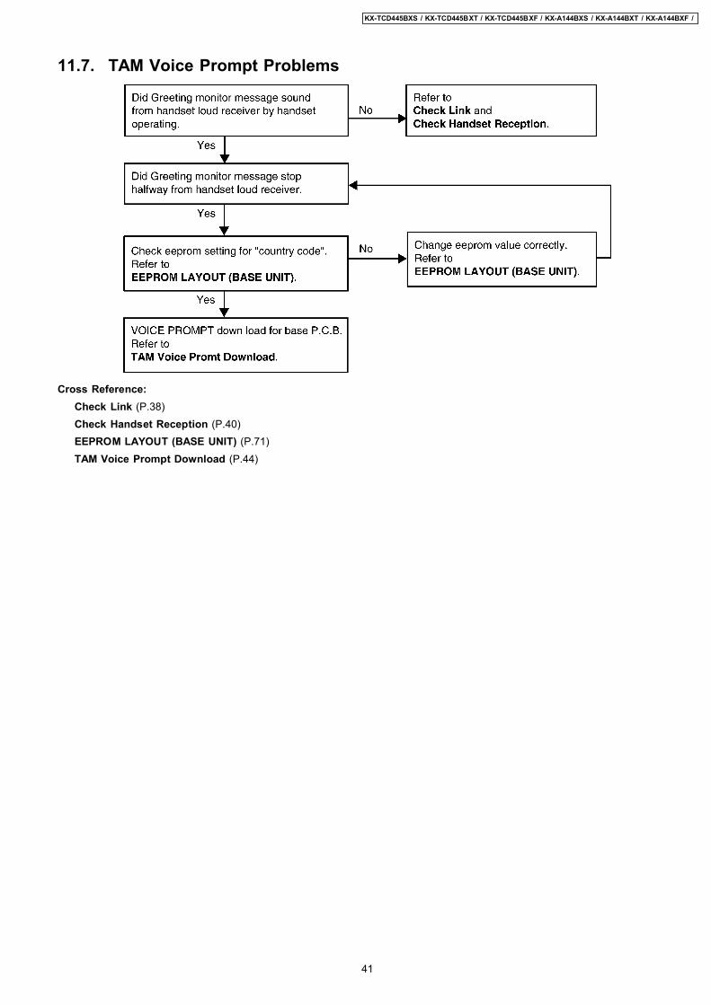
11.7. TAM Voice Prompt Problems
Cross Reference:Check Link (P.38)Check Handset Reception (P.40)EEPROM LAYOUT (BASE UNIT) (P.71)TAM Voice Prompt Download (P.44)
41
KX-TCD445BXS / KX-TCD445BXT / KX-TCD445BXF / KX-A144BXS / KX-A144BXT / KX-A144BXF /

11.8. Bell Reception
Cross Reference:Telephone Line Interface (P.61)Check Link (P.38)
Note:BBIC is IC1.
11.8.1. Base Unit
Note:BBIC is IC8.
11.8.2. Handset
42
KX-TCD445BXS / KX-TCD445BXT / KX-TCD445BXF / KX-A144BXS / KX-A144BXT / KX-A144BXF /

12 CHECK PROCEDURE (BASE UNIT)12.1. Preparation12.1.1. Equipment Required • DECT tester: Rohde & Schwarz, CMD 60 is recommended. • Frequency counter: it must be precise to be able to measure 1Hz (precision; ±4ppm).
Hewlett Packard, 53131A is recommended. • DC power: it must be able to output at least 1A current under 9V. • Digital multi-meter (DMM): it must be able to measure voltage and current. • Oscilloscope
12.1.2. JIGs and PC • EEPROM serial JIGs
1. I2C PCB: PQZZ1CD420BX 2. RS232C cable: PQZZ1CD705BX 3. Clip cable: PQZZ2CD705BX 4. DC cable: PQZZ3CD705BX
• PC which runs in DOS mode • Batch file for setting: PQZZTCD445BX
12.2. PC Setting12.2.1. Connections
12.2.2. PC Setting 1. Open a window of MS-DOS mode from the start-up menu. 2. Change a directory to the one with “RTX_COM” contained. 3. Type “SET RTX_COM=1” from the keyboard (when COM port 1 is used for the connection). 4. Type “doskey”.Note:
See the table below for frequently used commands.
Command name Function Examplerdeeprom Read the data of EEPROM Type “rdeeprom 00 00 FF”, and the data from
address “00 00” to “FF” is read out.readid Read ID (RFPI) Type “readid”, and the registered ID is read out.writeid Write ID (RFPI) Type “writeid 00 18 E0 0E 98”, and the ID “0018 E0 0E
98” is written.setfreq adjust Frequency of RFIC Type “setfreq nn nn”.hookoff off-hook mode on Base Type “hookoff”.hookon on-hook mode on Base Type “hookon”.Getchk Read checksum Type “getchk”.Wreeprom write eeprom Type "wreeprom 01 23 45". "01 23" is address and "45"
is data to be written.
43
KX-TCD445BXS / KX-TCD445BXT / KX-TCD445BXF / KX-A144BXS / KX-A144BXT / KX-A144BXF /
Command name Function ExampleInitBsPIN.bat Initial Base PIN to "0000" Type "initBsPIN"
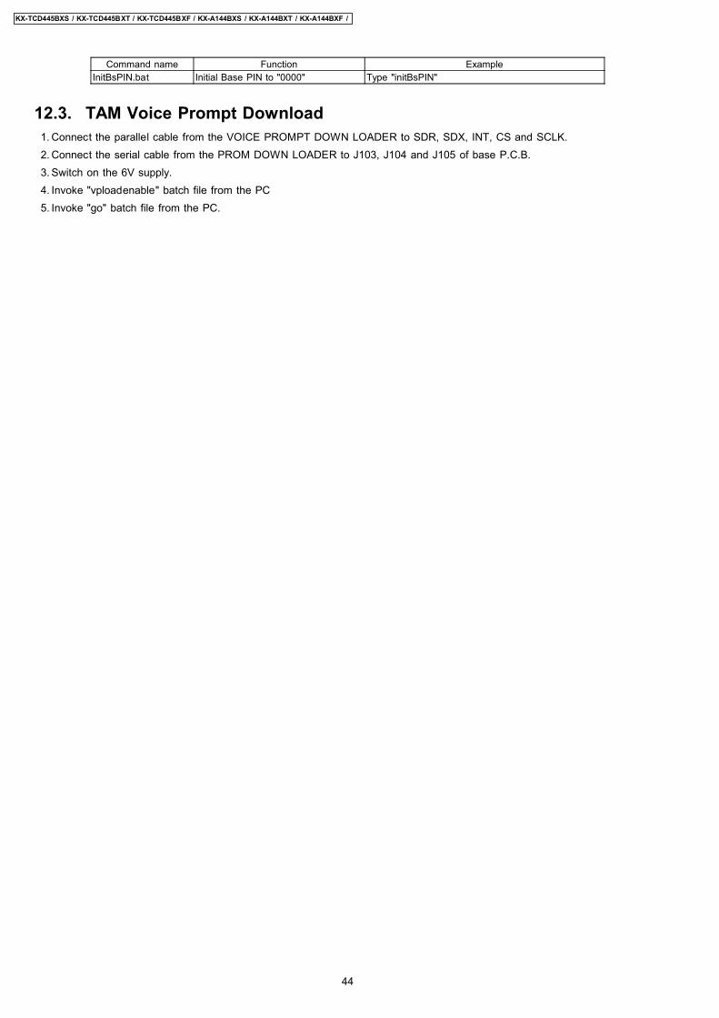
12.3. TAM Voice Prompt Download 1. Connect the parallel cable from the VOICE PROMPT DOWN LOADER to SDR, SDX, INT, CS and SCLK. 2. Connect the serial cable from the PROM DOWN LOADER to J103, J104 and J105 of base P.C.B. 3. Switch on the 6V supply. 4. Invoke "vploadenable" batch file from the PC 5. Invoke "go" batch file from the PC.
44
KX-TCD445BXS / KX-TCD445BXT / KX-TCD445BXF / KX-A144BXS / KX-A144BXT / KX-A144BXF /

13 CHECK PROCEDURE (HANDSET)13.1. Preparation13.1.1. Equipment Required • DECT tester: Rohde & Schwarz, CMD 60 is recommended. • Frequency counter: it must be precise to be able to measure 1Hz (precision; ±4ppm).
Hewlett Packard, 53131A is recommended. • DC power: it must be able to output at least 1A current under 2.4V for Handset, 9V for JIG. • Digital multi-meter (DMM): it must be able to measure voltage and current. • Oscilloscope
13.1.2. JIGs and PC • EEPROM serial JIGs
1. I2C PCB: PQZZ1CD420BX 2. RS232C cable: PQZZ1CD705BX 3. Clip cable: PQZZ2CD705BX 4. DC cable: PQZZ3CD705BX
• PC which runs in DOS mode. • Batch file for PC setting: PQZZTCD445BX
13.2. PC Setting13.2.1. Connections
13.2.2. PC Setting 1. Open a window of MS-DOS mode from the start-up menu. 2. Change a directory to the one with “RTX_COM” contained. 3. Type “SET RTX_COM=1” from the keyboard (when COM port 1 is used for the connection). 4. Type “doskey”.Note:
See the table below for frequently used commands.
Command name Function Examplerdeeprom Read the data of EEPROM Type “rdeeprom 00 00 FF”, and the data from
address “00 00” to “FF” is read out.readid Read ID (RFPI) Type “readid”, and the registered ID is read out.writeid Write ID (RFPI) Type “writeid 00 18 E0 0E 98”, and the ID “0018 E0 0E
98” is written.setfreq adjust Frequency of RFIC Type “setfreq nn nn”.Getchk Read checksum Type “getchk”.Wreeprom write eeprom Type "wreeprom 01 23 45". "01 23" is address and "45"
is data to be written.
45
KX-TCD445BXS / KX-TCD445BXT / KX-TCD445BXF / KX-A144BXS / KX-A144BXT / KX-A144BXF /

14 ADJUSTMENTS (BASE UNIT AND CHARGER UNIT)If your unit have below symptoms, adjust or confirm each item using remedy column from the table.
Symptom Remedy*The base unit does not respond to a call from handset. Make adjustments in item (A)~(F), (I)~(M)The base unit does not transmit or the transmit frequency is off. Make adjustments in item (A)~(E), (H)~(J), (L)The transmit frequency is off. Make confirmation in item (A)~(E), (H)~(J), (L)The transmit power output is low, and the operating distance between base unit and handset isless than normal.
Make confirmation in item (H), (K)
The reception sensitivity of base unit is low with noise. Make confirmation in item (K)The transmit level is high or low. Make adjustments in item (O)The reception level is high or low. Make adjustments in item (N)The unit does not link. Make confirmation in item (A)~(M)The unit cannot charge. Make confirmation in item (P)
*: Refer to Adjustment (Base Unit) (P.46)
14.1. Adjustment (Base Unit)Please follow the items below when BBIC or EEPROM is replaced.
Items Procedure Check orReplace Parts
(A) 2.65V SupplyConfirmation
1. Confirm that the voltage between J101 and GND is 2.65V ± 0.2V. C40,C41,C42,C43,C44,IC3,C32,C33,C36,
C37,C39(B) 4.0V Supply
Confirmation 1. Confirm that the voltage between TP11 and GND is 4.0V ± 0.2V. D4,C36,IC2,
R61,R62,C37,C72,D14,R74,
D9(C) VBACK Status
Confirmation 1. Confirm that the voltage between J102 and GND is 0V ± 0.4V. IC8,C53,C54,
C55,C56,X1,R78,R77,C52,R74,D9,R71,
Q12(D)* BBIC Confirmation 1. BBIC Confirmation (Execute the command "getchk").
2. Confirm the returned checksum value.
Connection of checksum value and program number is shown below.
IC8,C53,C54,C55,C56,X1,
R78
(E)* BBIC Clock Adjustment(Important)
1. Execute the command "deactmac".
2. Execute the command "conttx".
3. Input Command “rdeeprom 00 00 02”, then you can confirm the current value.
4. Adjust the frequency of TP15 executing the command "setfreq 00 xx (where xxis the value)" so that the reading of the frequency counter is 10.368000MHz ±10Hz.
IC8,C53,C54,C55,C56,X1,R78,L2,L60,
C95
(F)* Hookswitch Check withDC Characteristics
1. Connect J2 (Telephone Socket) to Tel-simulator which is connected with 600Ω.
2. Set line voltage to 48V at on hook condition and line current to 40mA.
3. Execute the command "hookoff"
4. Confirm that the line current is 40mA ± 5mA.
5. Execute the command "hookon".
6. Confirm that the line current is 0mA ~ + 2mA.
IC8,R12,R13,R14,R15,Q2,Q4,D6,C6,C7,
C11,JMP9
(G)* DTMF GeneratorConfirmation
1. Connect J2 (Telephone Socket) to DTMF tester.
2. Execute the command "hookoff" and "dtmf_up".
3. Confirm that the high frequency (1477.06Hz) group is -6 ± 2dBm.
4. Execute the command "dtmf_lo".
5. Confirm that the low frequency (852.05Hz) group is -8 ± 2dBm.
IC8,R55,C33,R30,C88,C19,R26,R25,Q9,R24,R27,C16,
R20
46
KX-TCD445BXS / KX-TCD445BXT / KX-TCD445BXF / KX-A144BXS / KX-A144BXT / KX-A144BXF /

Items Procedure Check orReplace Parts
(H)* Transmitted PowerConfirmation
Remove the Antenna before starting steps from 1 to 4. 1. Configure the DECT tester (CMD60) as follows;
<Setting> • Test mode: FP
• Traffic Channel: 5
• Traffic Slot: 4
• Mode: Loopback
• PMID: 00000
2. Execute the command "testmode".
3. Initiate connection from DECT tester. (“set up connect”)
4. Confirm that the NTP value at ANT is 20dBm ~ 25dBm.
IC6,IC4,L2,C57,C61,C75,C77,C78,C76,C68,C69,R79,R80,C63,C64,R83,R84,C65,L3,C79,C67,C66,D10,C62
(I) Modulation Check andAdjustment
Follow steps 1 to 3 of (H) above.4. Confirm that the B-Field Modulation is 340kHz/div ~ 402kHz/div using datatype Fig31.
5. Adjust the B-Field Modulation if required. (Execute the command "readmod"and "wrtmod xx", where xx is the value.)
IC6,IC4,L2,C57,C61,C75,C77,C78,C76,C68,C69,R79,R80,C63,C64,R83,R84,C65,L3,C79,C67,C66,D10,C62
(J) Frequency OffsetConfirmation
Follow steps 1 to 3 of (H) above.4. Confirm that the frequency offset is -50KHz ~ +50kHz.
IC6,IC4,L2,C57,C61,C75,C77,C78,C76,C68,C69,R79,R80,C63,C64,R83,R84,C65,L3,C79,C67,C66,D10,C62
(K) Sensitivity ReceiverConfirmation
Follow steps 1 to 3 of (H) above.4. Set DECT tester power to -88dBm.
5. Confirm that the BER is < 1000ppm.
IC6,IC4,L2,C57,C61,C75,C77,C78,C76,C68,C69,R79,R80,C63,C64,R83,R84,C65,L3,C79,C67,C66,D10,C62
(L) Timing Confirmation Follow steps 1 to 3 of (H) above.4. Confirm that the Timing accuracy is < ± 5.0ppm.
IC6,IC4,L2,C57,C61,C75,C77,C78,C76,C68,C69,R79,R80,C63,C64,R83,R84,C65,L3,C79,C67,C66,D10,C62
(M)* RSSI LevelConfirmation
Follow steps 1 to 3 of (H) above.4. Set DECT tester power to -70dBm.
5. Execute the command "readrssi".
6. Confirm: 59 returned value 77 (0x68 ± F (hex))
IC6,IC4,L2,C57,C61,C75,C77,C78,C76,C68,C69,R79,R80,C63,C64,R83,R84,C65,L3,C79,C67,C66,D10,C62
47
KX-TCD445BXS / KX-TCD445BXT / KX-TCD445BXF / KX-A144BXS / KX-A144BXT / KX-A144BXF /

Items Procedure Check orReplace Parts
(N)* Receive Audio Checkand Adjustment
1. Configure the DECT tester (CMD60) as follows;
<Setting> • Test mode: FP
• Mode: Normal
• PMID: 00000
2. Execute the command "testmode".
3. Initiate connection from DECT tester.
4. Execute the command "hookoff".
5. Execute the command "openau".
6. Connect J2 (Telephone Socket) to Tel-simulator which is connected with 600Ω.
7. Set line voltage to 48V and line current to 40mA.
8. Connect DECT tester to Tel-simulator.
9. Input audio signal (200mVrms/1kHz tone) to Tel-simulator.
<DECT tester setting> • Scramble: On
• AF Gen. to ADPCM: Off
• AF Meter Input: ADPCM
• AF Gen. Frequency: 1000Hz
• AF Gen. Level: 200mVrms
10. Confirm hearing tone: 300mVrms ± 100mVrms
11. Adjust audio level if required. (Make sure current value using "getmicgain". Andthen execute the command "setmicgain xx", where xx is the value.)
12. Confirm that the B-field audio distortion with DECT tester is < 5 %.
IC6,IC4,L2,C57,C61,C75,C77,C78,C76,C68,C69,R79,R80,C63,C64,R83,R84,C65,L3,C79,C67,
C66,D10,C62,R20,C14,D7,
R21,R22,R23,R85,C15,C30,R51,C92,R52,C32,Q2,R12,R13,Q4,R14,R15,D6,C6,
C7,JMP9
(O)* Transmit Audio Checkand Adjustment
1. Configure the DECT tester (CMD60) as follows;
<Setting> • Test mode: FP
• Mode: Normal
• PMID: 00000
2. Execute the command "testmode".
3. Initiate connection from DECT tester.
4. Execute the command "hookoff".
5. Execute the command "openau".
6. Connect J2 (Telephone Socket) to Tel-simulator which is connected with 600Ω.
7. Set line voltage to 48V and line current to 40mA.
8. Input audio signal (30mVrms/1kHz tone) to DECT tester.
<DECT tester setting> • Scramble: On
• AF Gen. to ADPCM: On
• AF Meter Input: AF Voltm
• AF Gen. Frequency: 1000Hz
• AF Gen. Level: 30mVrms
9. Confirm hearing tone: 330mVrms ± 100mVrms.
10. Adjust audio level if required. (Make sure current value using "getspkrgain".And then execute the command "setspkrgain xx", where xx is the value.)
11. Confirm that the audio distortion at 600R of Tel-simulator is < 5 %.
IC6,IC4,L2,C57,C61,C75,C77,C78,C76,C68,C69,R79,R80,C63,C64,R83,R84,C65,L3,C79,C67,
C66,D10,C62,R20,C14,D7,
R21,R22,R23,R85,C15,C30,R51,C92,R52,C32,Q2,R12,R13,Q4,R14,R15,D6,C6,
C7,JMP9
(P) Charging Check 1. Connect Charge Contact 12Ω/2W resistor between charge+ and charge-.
2. Measure and confirm voltage across the resistor is 2.3V ± 0.2V.
D4,R43,R44
Note:After the measuring, sock up the solder of TP.*: PC Setting (P.43) is required beforehand.The connection of adjustment equipment are as shown in Adjustment Standard (Base Unit) (P.49).
48
KX-TCD445BXS / KX-TCD445BXT / KX-TCD445BXF / KX-A144BXS / KX-A144BXT / KX-A144BXF /

14.2
. Ad
just
men
tSta
ndar
d(B
ase
Uni
t)W
hen
conn
ectin
gth
eSi
mul
ator
Equi
pmen
tsfo
rch
ecki
ng,p
leas
ere
fer
tobe
low
.
14.2
.1.
Com
pone
ntVi
ew
Q1
S1
R59
R66
R68
R60
R19
R18
L1
PbF
X1
IC7
IC4
IC8
IC9
IC6
IC3
IC5IC
1
IC2
JMP
6JM
P2
JMP
4
JMP
3
JMP
9
JMP
1JM
P5
1
1
JMP
8
JMP
7
J1
A1
A2
J2
D4
SA1
RLY1
C25
C24
C2
D1
D9
D12
R78
D11
D2
D3
D7
D6
D13
D8
D16
D5
D15
D14
R4
R5
R6
R7
R8 R
33 R37
R51
R30
R16
R31
R17
R23
R24
R35
R34
R25
R28
R75
R71
R77
R76
R72
R73
C50
C51
C52
C53
C56
C95
R74
R7014
4
10910
8
R69
R49
R27
R52
R12
R9
R10
R14
R15
R39 R40 R48
R45
C27
R46
R87
R67
R2
R36
R38R11
C88
R32
C21
C90
R20
R13
R56
R65C77
C43
C75C78
C101C102
C10
3
C33
C36
C87
C86
C37
C67
C76
C69
C83
C85
C96
C32
C94R50
Q8
Q12
Q9
B C E
R41
R43
R47
R57
R80
R64
R62
R57
R61
R83
R84
D10
R79
L3
Q3
Q4
Q7
Q5
Q11
Q13
Q10
Q6
Q2
R1 R
42R
44
R3
C1
C28
CS
141
1
1
1
45 8
161732
1 11
28 15
INT
SD
X
SD
R
SC
LK
C26
C91
C44
C63
C84
C64
C34
C61
C54
C55 R
86
C58
R82
C39
C99
C97
C10
0
C45
L2
3736
C72
C71
C60
C68
C80
C66
C62
C73
C79
C82
C81
C65
C74
28 18
AN
T
C6
C8
C3 C4
C9
C41
C40
73
72
C10
C7
C12
C70
C98
C14
C19
C18
C38 C23
C22
C16
C30
C29
C93
C92
C49
C89
R29
C17
C48
C42R54
R55
R26
R21
R85
C20
R22
C15
R53
C31
C46
C47
C35
C13
C5
C11
B
C
E
DE
CT
test
erC
MD
60
(H)
(I)
(J)
(K)
(L)
(M)
V.V
OS
C
Tel
Sim
ulat
o r
AF
Vol
t Met
er
AN
TG
ND
AF
Gen
erat
or
(N)
(O)
Not
e: (H)-
(O)i
sre
ferre
dto
Adju
stm
ent(
Bas
eU
nit)
(P.4
6)
KX-TCD445BXS / KX-TCD445BXT / KX-TCD445BXF / KX-A144BXS / KX-A144BXT / KX-A144BXF /
49

14.2
.2.
Flow
Sold
erSi
deVi
ew
TP13
TP15
TP8
TP7
TP11
TP10
6
TP9
TP1
24
156
TP4
TP2
TP3
TP10
TP6
TP20
2
TP20
1
TP5
GND
MODE
SCL
SDA
VDD
J105
J102
J104
J103
J101
CH
AR
GE
CH
AR
GE
Dig
ital
Vol
t Met
er
(A)
Dig
ital V
olt M
eter
(B)
Fre
quen
cyC
ount
er
(E)
DT
MF
test
er
Tel
Sim
ulat
or(F
) (N
) (O
)
(G)
Dig
ital
Vol
t Met
er
(C)
(P)
To
PC
(JI
G)
Dig
ital V
olt M
eter
(D)
(E)
(F)
(G)
(H)
(N)
(O)
12Ω
/2W
PbF
Not
e: (A)-
(P)i
sre
ferre
dto
Adju
stm
ent(
Bas
eU
nit)
(P.4
6)
KX-TCD445BXS / KX-TCD445BXT / KX-TCD445BXF / KX-A144BXS / KX-A144BXT / KX-A144BXF /
50

14.3. Adjustment (Charger Unit)Items Adjustment
PointProcedure Check or
Replace Parts(A) Charging Check - 1. Connect Charge Contact 12Ω/2W resistor between charge+ and charge-.
2. Measure and confirm voltage across the resistor is 2.7V ± 0.2V.
D1,R1,R2
Note:After the measuring, sock up the solder of TP.The connection of adjustment equipment are as shown in Adjustment Standard (Charger Unit) (P.51).
14.4. Adjustment Standard (Charger Unit)When connecting the Simulator Equipments for checking, please refer to below.
14.4.1. Flow Solder Side View
PbFR
1
R2
TP4
TP1
TP2
TP3
Digital Volt Meter 12Ω/2W
(A)
Note:(A) is referred to Adjustment (Charger Unit) (P.51)
51
KX-TCD445BXS / KX-TCD445BXT / KX-TCD445BXF / KX-A144BXS / KX-A144BXT / KX-A144BXF /

15 ADJUSTMENTS (HANDSET)If your unit have below symptoms, adjust or confirm each item using remedy column from the table.
Symptom Remedy*The movement of Battery Low indicator is wrong. Make confirmation in item (A)~(C), (F)~(G)The handset does not respond to a call from base unit. Make adjustments in item (A)~(C), (H), (J)~(N)The handset does not transmit or the transmit frequency is off. Make adjustments in item (A)~(C), (H)~(K), (M)The transmit frequency is off. Make confirmation in item (A)~(C), (H)~(K), (M)The transmit power output is low, and the operating distance between base unit and handset isless than normal.
Make confirmation in item (I), (L)
The reception sensitivity of base unit is low with noise. Make confirmation in item (L)Does not link between base unit and handset. Make confirmation in item (A)~(C), (H)~(N)The reception level is high or low. Make adjustments in item (O)The transmit level is high or low. Make adjustments in item (P)
*: Refer to Adjustment (Handset) (P.52)
15.1. Adjustment (Handset)Please follow the items below when BBIC or EEPROM is replaced.
Items Procedure Check orReplace Parts
(A) 4.0V SupplyConfirmation
1. Confirm that the consumption current is < 200mA, that is, there is no short circuit.
2. Confirm that the voltage between TP4V and GND is 3.9V ± 0.2V.
IC1,F1,R21,R4,C33,L2,D1,C15,C2,C14,Q1,R3,R2,D2,R22,C26,X1,C16,
C17(B) VBACK Status
Confirmation 1. Confirm that the voltage between TPVBACK and GND is 0V ± 0.4V. IC1,R11
(C) BBIC Confirmation 1. BBIC Confirmation (Execute the command "getchk").
2. Confirm the returned checksum value.
Connection of checksum value and program number is shown below.
IC1,X1,C16,C17
(D) Charge Control Check &Charge Current Monitor
Confirmation
1. Apply 6V between TPCHG(+) and TPCHG(-) with current limit of PSU to 250mA.
2. Confirm that the charge current is ON/OFF.
3. SW to decrease current limit of PSU to 100mA.
4. Confirm that the charge current is stable.
IC1,L4,L5,Q2,Q3,
R6,D2,R22,C26,F1,R21,
R4,C33
(E)* Charge Detection (OFF)Confirmation
1. Stop supplying 6V to TPCHG(+) and TPCHG(-).
2. Execute the command "charge".
3. Confirm that the returned value is 0x00 (hex).
IC1,L4,L5,Q2,Q3,
R6,D2,R22,C26,F1,R21,
R4,C33(F)* Battery Monitor
Confirmation &Adjustment (Important)
1. Apply 2.3V ± 0.005V between TPBATT(+) and TPBATT(-) with DC power.
2. Execute the command "deactmac" to stabilize the value.
3. Then, execute the command “readbatt“. The returned value is XX.
4. Confirm that XX is between 98 and A8
98 < XX < A8 (Hex)
(If XX is out of range, change BBIC)
IC1,L4,L5,Q2,Q3,
R6,D2,R22,C26,F1,R21,
R4,C33
(G) Battery low Confirmation(Important)
1. Apply 2.40V between TPBATT(+) and TPBATT(-).
2. Confirm that there is no Speaker sound (Battery low alarm).
3. Apply 2.20V between TPBATT(+) and TPBATT(-).
4. Confirm that there is Speaker sound (Battery low alarm).
IC1,F1,R21,R4,C33
(H)* BBIC Clock Adjustment(Important)
1. Apply 2.6V between TPBATT(+) and TPBATT(-) with DC power.
2. Execute the command "deactmac" .
3. Execute the command "conttx" .
4. Input Command “rdeepron 00 01 01“, then you can confirm the current value.
5. Adjust the frequency of TPMCLK executing the command.
“setfreq 00 xx (where xx is the value)”
so that the reading of the frequency counter is 10.368000MHz ± 10Hz.
IC1,L3,C57,IC3,X1,C16,
C17
52
KX-TCD445BXS / KX-TCD445BXT / KX-TCD445BXF / KX-A144BXS / KX-A144BXT / KX-A144BXF /

Items Procedure Check orReplace Parts
(I)* Transmitted PowerConfirmation
Remove the Antenna before starting steps from 1 to 5. 1. Configure the DECT tester(CMD60) as follows;
<Setting> • Test mode: PP
• RFPI: 0102030405
• Traffic Channel: 5
• Traffic Slot: 4
• Mode: Loopback
2. Execute the command "testmode".
3. Execute the command "regcmd60"
4. Initiate connection from DECT tester.
5. Confirm that the NTP value at ANT is 20dBm ~ 25dBm
IC1,IC3,C54,C66,C60,
L3,C57,C55,C56,C62,
R23,C63,C64,C65,R18,
L6,C67,C202,C208,C209
(J) Modulation Check andAdjustment
Follow steps 1 to 4 of (I) above.5. Confirm that the B-Field Modulation is 340kHz/div ~ 402kHz/div using data type Fig31.
6. Adjust the B-Field Modulation if required. (Execute the command "Readmod" and"Writemod xx", where xx is the value.)
IC1,IC3,C54,C66,C60,
L3,C57,C55,C56,C62,
R23,C63,C64,C65,R18,
L6,C67,C202,C208,C209
(K) Frequency OffsetConfirmation
Follow steps 1 to 4 of (I) above.5. Confirm that the frequency offset is -50kHz ~ +50kHz.
IC1,IC3,C54,C66,C60,
L3,C57,C55,C56,C62,
R23,C63,C64,C65,R18,
L6,C67,C202,C208,C209
(L) Sensitivity ReceiverConfirmation
Follow steps 1 to 4 of (I) above.5. Set DECT tester power to -88dBm.
6. Confirm that the BER is < 1000ppm.
IC1,IC3,C54,C66,C60,
L3,C57,C55,C56,C62,
R23,C63,C64,C65,R18,
L6,C67,C202,C208,C209
(M) Timing Confirmation Follow steps 1 to 4 of (I) above.5. Confirm that the Timing accuracy is < ± 10ppm.
IC1,IC3,C54,C66,C60,
L3,C57,C55,C56,C62,
R23,C63,C64,C65,R18,
L6,C67,C202,C208,C209
(N)* RSSI LevelConfirmation
Follow steps 1 to 4 of (I) above.5. Set DECT tester power to -70dBm.
6. Execute the command "readrssi"
7. Confirm: 52 returned value 72 (hex) (0x62 ± 0x10 (hex))
IC1,IC3,C54,C66,C60,
L3,C57,C55,C56,C62,
R23,C63,C64,C65,R18,
L6,C67,C202,C208,C209
53
KX-TCD445BXS / KX-TCD445BXT / KX-TCD445BXF / KX-A144BXS / KX-A144BXT / KX-A144BXF /

Items Procedure Check orReplace Parts
(O)* Receive Audio Check 1. Configure the DECT tester (CMD60) as follows;
<Setting> • Test mode: PP
• Mode: Nomal
• RFPI: 0102030405
2. Execute the command "testmode".
3. Execute the command "regcmd60"
4. Initiate connection from DECT tester.
5. Execute the command "openaudio".
6. Confirm that the value of EEPROM address "F3F" is "02". (If the value is not "02 (byUser)", set "02" and power off and power on, and return to clause 2.)
7. Input audio signal (50mVrms/1kHz tone) from DECT tester.
<DECT tester setting> • Scramble: On
• AF Gen to ADPCM: On
• AF Meter Input: AF Voltm
• AF Gen Frequency: 1000Hz
• AF Gen Level: 50mVrms
8. Confirm hearing tone: 300mV ± 250mV (Just check Audio path)
9. Confirm that the audio distortion with DECT tester is < 5 %.
IC1,R17,R20,D7,D6,
C12,C31,C115
(P) Transmit Audio Check 1. Configure the DECT tester (CMD60) as follows;
<Setting> • Test mode: FP
• Mode: Normal
• RFPI: 0102030405
2. Execute the command "testmode".
3. Execute the command "regcmd60".
4. Initiate connection from DECT tester.
5. Execute the command "openaudio".
6. Confirm that the value of EEPROM address "F3F" is "02". (If the value is not "02 (byUser)", set "02" and power off and power on, and return to clause 2.)
7. Input audio signal (30mVrms/1kHz tone) to DECT tester.
<DECT tester setting> • Scramble: On
• AF Gen to ADPCM: Off
• AF Meter Input: ADPCM
• AF Gen Frequency: 1000Hz
• AF Gen Level: 30mVrms
8. Confirm hearing tone: 300mV ± 250mV (Just check Audio path)
9. Confirm that the audio distortion with DECT tester is < 5 %.
IC1,C8,R7,R8,C6,
C7,C5,R5,R1,C4
Note:After the measuring, sock up the solder of TP.*: PC Setting (P.43) is required beforehand.The connections of the adjustment equipments are as shown in Adjustment Standard (Handset) (P.55).
54
KX-TCD445BXS / KX-TCD445BXT / KX-TCD445BXF / KX-A144BXS / KX-A144BXT / KX-A144BXF /

15.2
. Ad
just
men
tSta
ndar
d(H
ands
et)
Whe
nco
nnec
ting
the
Sim
ulat
orEq
uipm
ents
for
chec
king
,ple
ase
refe
rto
belo
w.
AF
OS
CA
F V
OLT
ME
TE
R
LOO
PS
imul
ator
Dum
my
Bas
eU
nit
600
OS
C
CH
AR
GE
+
Gen
erat
orM
IC+
+
MIC
-A
F
6.3V
47
F
DC
6V
Cur
rent
Pro
be
Osc
illos
cope
CH
AR
GE
-
DC
PO
WE
R2.
30 -
2.6
0V
BA
TT
ER
Y+
BA
TT
ER
Y-
PC
SD
AS
CL
GN
D
150
AF
Vol
t Met
er
Fre
quen
cyC
ount
er
RE
VG
ND
MC
LK
Osc
illos
cope
TP
17Pow
er K
ey TP
16
DE
CT
test
er
CM
D60
GN
DA
NT
EN
NA
(H)
Dig
ital
Vol
t Met
erGN
DT
P4V
8AF
Vol
t Met
er
SP
Osc
illos
cope
Dig
ital
Vol
t Met
erGN
DV
BA
CK
(F)
(G)
(A)
(I)
(J)
(K)
(L)
(M)
(N)
(O)
(P)
(B)
(C)
(E)
(F)
(H)
(I)
(O)
(P)
(D)
(D)
(D)
(E)
PbF
L2
D7D6
D3
D5
R11
VBACK
TP19
TP18TP3 TP4
R16
R104
Q102
D1
C22
C30
C8
C3
C24 C26 C28
C29
C6R8
D2
C16
R12 C17
SP/BUZ
Q3
Q2
C7
C4C5
C34
C33 C35
CHG+ CHG-MIC
R5R7R1
R4
R2R3
C11
0
C11
5
C31
R20
R10
7
R17
L3
L6
C57
MC
LK
C21
C25 R19
IC1
IC2
F1
58
41C
27Q
103
TP
1
TP
101
TP
102
R18
C56
TP
2
111
1828
C2
C20
C23
C18
RE
G
L5L4
R21
R22
R6
X1
Q1
BATT
TP
17T
P16
TP4V
R105
R106C101
D101
D102Q
101
R109C106
R110
R101
R102R103
C107C12
C116
C206
C207 C203
C202
C204
C201
C67
C60
C66
C63
C64C65
C54
C55
C62R23
C208
C209
C108C109
C102
R108
C103
C104
C111C105
IC1015
8 1
POWER
GND
SCL
SDA
TP21TP20
IC3
C15
C14
AN
T
100
1
8081
50 513130
Not
e: (A)-
(P)i
sre
ferre
dto
Adju
stm
ent(
Han
dset
)(P.
52)
KX-TCD445BXS / KX-TCD445BXT / KX-TCD445BXF / KX-A144BXS / KX-A144BXT / KX-A144BXF /
55

16 RF SPECIFICATION16.1. Base Unit
Item Value Refer to -. * RemarksTX Power More than 20 dBm ~ 25 dBm Adjustment (Base Unit) (H)Modulation 340 kHz/div ~ 402 kHz/div Adjustment (Base Unit) (I) Data type: Fig31Frequency Offset -50 kHz ~ +50 kHz Adjustment (Base Unit) (J)RX Sensitivity < 1000 ppm Adjustment (Base Unit) (K)Timing Accuracy < ± 5.0 ppm Adjustment (Base Unit) (L)RSSI Level 0x68 ± F (hex) Adjustment (Base Unit) (M)
*: Refer to Adjustment (Base Unit) (P.46)
16.2. HandsetItem Value Refer to -. ** Remarks
TX Power More than 20 dBm ~ 25 dBm Adjustment (Handset) (I)Modulation 340 kHz/div ~ 402 kHz/div Adjustment (Handset) (J) Data type: Fig31Frequency Offset -50 kHz ~ +50 kHz Adjustment (Handset) (K)RX Sensitivity < 1000 ppm Adjustment (Handset) (L)Timing Accuracy < ± 10 ppm Adjustment (Handset) (M)RSSI Level 0x62 ± 0x10 (hex) Adjustment (Handset) (N)
**: Refer to Adjustment (Handset) (P.52)
17 HOW TO CHECK THE HANDSET SPEAKER ORRECEIVER
1. Prepare the digital voltmeter, and set the selector knob to ohm meter. 2. Put the probes at the speaker terminals as shown below.
56
KX-TCD445BXS / KX-TCD445BXT / KX-TCD445BXF / KX-A144BXS / KX-A144BXT / KX-A144BXF /

18 FREQUENCY TABLE (MHz)BASE UNIT HANDSET
Channel No Transmit Frequency Receive Frequency Transmit Frequency Receive Frequency1 1897.344 1897.344 1897.344 1897.3442 1895.616 1895.616 1895.616 1895.6163 1893.888 1893.888 1893.888 1893.8884 1892.160 1892.160 1892.160 1892.1605 1890.432 1890.432 1890.432 1890.4326 1888.704 1888.704 1888.704 1888.7047 1886.976 1886.976 1886.976 1886.9768 1885.248 1885.248 1885.248 1885.2489 1883.520 1883.520 1883.520 1883.52010 1881.792 1881.792 1881.792 1881.792
Note:Channel No. 10: In the Test Mode on Base Unit and Handset.
57
KX-TCD445BXS / KX-TCD445BXT / KX-TCD445BXF / KX-A144BXS / KX-A144BXT / KX-A144BXF /

19 B
LOC
KD
IAG
RAM
(BAS
EU
NIT
)
KX
-TC
D44
5BX
S/B
XT
/BX
F B
LOC
K D
IAG
RA
M (
BA
SE
UN
IT)
Aud
ioH
ook
Sw
itch
Q2,
Q3
Brid
geR
ect
D2
A/D
D/A
Ana
log
Fro
nt E
nd
RIN
GE
R
CP
UB
BIC
HO
OK
RX
AF
TX
AF
DS
PB
MC
Spe
ech
Enc
odin
g
Spe
ech
Dec
odin
g
RF
In
terf
ace
Bur
st B
uild
ing
Bur
st D
ecod
ing
AD
PC
MC
odec
Filt
er
EE
PR
OM
IC4
SD
AS
CL
SY
RI
RS
SI
SY
EN
RX
DA
TX
DA
J1J2
IC8
IC9
4.0V
Reg
.
2.65
VR
eg.
4.0V
2.65
V
VU
NR
EG
2726133
123
63
12 20 139 5 22 25 18
56
4
RF
Mod
ule
20 5 10
33
7 5
XT
AL
10.3
68X
1
MH
z
DT
XA
F13
6B
ell/C
alle
r ID
Inte
rfac
e
AN
T1
AN
T2
to T
el_L
ine
A
B
to A
C A
dapt
or
RIN
G81
Rin
gD
et
76
(Clip
Der
.)
Fla
sh
IC7
D0-
D7
A0-
A17
PR
OM
30
AD
DR
ES
DA
TA
CT
RL
29
SCK1
1114
1312
103
104
106
105
107
SI
SO
CS
RD5/BUSY Ser
ial F
lash
RO
MIC
6
71P
age
Lim
itR
esis
tor
CH
AR
GE
CO
NT
AC
T
KX-TCD445BXS / KX-TCD445BXT / KX-TCD445BXF / KX-A144BXS / KX-A144BXT / KX-A144BXF /
58
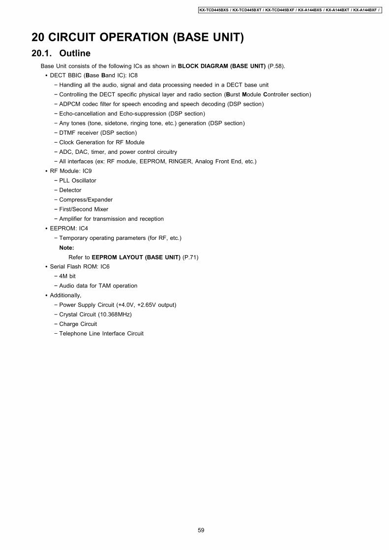
20 CIRCUIT OPERATION (BASE UNIT)20.1. Outline
Base Unit consists of the following ICs as shown in BLOCK DIAGRAM (BASE UNIT) (P.58). • DECT BBIC (Base Band IC): IC8
− Handling all the audio, signal and data processing needed in a DECT base unit − Controlling the DECT specific physical layer and radio section (Burst Module Controller section) − ADPCM codec filter for speech encoding and speech decoding (DSP section) − Echo-cancellation and Echo-suppression (DSP section) − Any tones (tone, sidetone, ringing tone, etc.) generation (DSP section) − DTMF receiver (DSP section) − Clock Generation for RF Module − ADC, DAC, timer, and power control circuitry − All interfaces (ex: RF module, EEPROM, RINGER, Analog Front End, etc.)
• RF Module: IC9 − PLL Oscillator − Detector − Compress/Expander − First/Second Mixer − Amplifier for transmission and reception
• EEPROM: IC4 − Temporary operating parameters (for RF, etc.)
Note:Refer to EEPROM LAYOUT (BASE UNIT) (P.71)
• Serial Flash ROM: IC6 − 4M bit − Audio data for TAM operation
• Additionally, − Power Supply Circuit (+4.0V, +2.65V output) − Crystal Circuit (10.368MHz) − Charge Circuit − Telephone Line Interface Circuit
59
KX-TCD445BXS / KX-TCD445BXT / KX-TCD445BXF / KX-A144BXS / KX-A144BXT / KX-A144BXF /

20.2. Power Supply CircuitThe power is supplied to the DECT BBIC, RF Module, EEPROM, Relay Coil, LED and Charge Contact from AC Adaptor (+6V)as shown in Fig.101. The power supply is as follows;
• DECT BBIC (IC8): J1(+6V) → D4 → IC2 → IC3 → IC8 → IC6 • RF Module (IC9): J1(+6V) → D4 → IC2 → IC9 • EEPROM (IC4): J1(+6V) → D4 → IC2 → IC3 → IC4 • LED (LED1): J1(+6V) → D4 → IC2 → R57 → LED1 • Charge Contact (TP13): J1(+6V) → D4 → R59, R60 → TP13
<Fig.101>
60
KX-TCD445BXS / KX-TCD445BXT / KX-TCD445BXF / KX-A144BXS / KX-A144BXT / KX-A144BXF /

20.3. Telephone Line Interface<Function>
• Bell signal detection • Clip signal detection • ON/OFF hook circuit • Audio circuits
Bell & Clip (: Calling Line Identification Presentation: Caller ID) signal detection:In the standby mode, Q2 is open to cut the DC loop current and decrease the ring load.When ring voltage appears at the TP3 (A) and TP40 (B) leads (when the telephone rings), the signal is transferred as follows; • A → C25 → R40 → R45 → IC5 → C28 → R47 → C29 → R49 → IC8 (136) [CLIP] • B → C24 → R39 → R44 → IC5 → C28 → R47 → C29 → R49 → IC8 (136) [CLIP] • A → C2 → IC1 → IC8 (81) [BELL] • B → D2 → D3 → R1 → IC1 → IC8 (81) [BELlL]
ON/OFF hook circuit:In the standby mode, Q2 is open, and connected as to cut the DC loop current and to cut the voice signal. The unit isconsequently in an off-hook condition.When IC8 detects a ring signal or press the TALK Key onto the handset, Q4 turns on and then Q2 turns on, thus providing anoff-hook condition (active DC current flow through the circuit) and the following signal flow is for the loop current. • A → JMP9 → D6 → Q2 → R13 → Q4 → D6→ B [OFF HOOK]
Audio Circuits:Refer to SIGNAL ROUTE (P.65).
20.4. Transmitter/ReceiverBase Unit and Handset mainly consist of RF Module and DECT BBIC.Base Unit and Handset transmit/receive voice signal and data signal through the antenna on carrier frequency.
Signal Pass:*Refer to SIGNAL ROUTE (P.65).
20.4.1. Transmitter BlockThe voice signal input from the TEL LINE interface goes to RF Module (IC9) through DECT BBIC (IC8) as shown in BLOCKDIAGRAM (BASE UNIT) (P.58)The voice signal passes through the analog part of IC8 where it is amplified and converted to a digital audio stream signal. Theburst switch controller processes this stream performing encryption and scrambling, adding the various other fields to producethe GAP (Generic Access Profile) standard DECT frame, assigning to a time slot and channel etc.In IC3, the carrier frequency is changing, and frequency modulated RF signal is generated and amplified, and radiated fromantenna. Handset detects the voice signal or data signal in the circuit same as the following explanation of Receiver Block.
20.4.2. Receiver BlockThe signal of 1.152 MHz band (1.881792 MHz ~ 1.897344 MHz) which is input from antenna is input to IC9 as shown in BLOCKDIAGRAM (BASE UNIT) (P.58).In IC3, the signal of 1.152 MHz band is downconverted to 864 kHz signal and demodulated, and goes to IC2 as GAP (GenericAccess Profile) standard DECT frames. It passes through the decoding section burst switch controller where it separates outthe frame information and performs de-encryption and de-scrambling as required. It then goes to the DSP section where it isturned back into analog audio. This is amplified by the analog front end, and goes to the TEL LINE Interface.
20.5. Pulse DiallingDuring pulse dialling the hookswitch (Q2, Q3) is used to generate the pulses using the HOOK control signal, which is set highduring pulses. To force the line impedance low during the “pause” intervals between dial pulses, the PULSE_DIAL signal turnson Q10.
61
KX-TCD445BXS / KX-TCD445BXT / KX-TCD445BXF / KX-A144BXS / KX-A144BXT / KX-A144BXF /

21 BLOCK DIAGRAM (HANDSET)
33
CPU
IC1
IC3
BBIC
A/D
D/A
AnalogFrontEnd
Speech Encoding
Speech Decoding
DSP
ADPCMCodecFilter
BMC
RFInterface
MIC
EEPROMIC2
IC101
AMP
SDA
SCL
66
67
5
6
SYRI
RSSI
SYEN
RXDA
TXDA16
12
48
23
13
RFModule
ANT
BATTERYTERMINAL
TP3
TP4
CHARGECIRCUIT
CHARGE
CHARGE DETECT
SWITCHEDSUPPLY
CHARGECONTACTS
TP5
4.0V
VDDBAT
VDDLR
SWITCH
31
XTAL
10.368MHz
LCD BACK LIGHTKEY BACK LIGNT
COLUMNS
ROWS
LCD14 SegDisplay
ON SWITCH
3827
26
36
37
28
pin 2, 5~9
COM 0~5segment 0~29
pin1, 90~100, 87, 78~84,72~76, 61, 62, 56~58
EARPIECE
SPEAKER
42
41
45
17~21
53~55, 59, 60
34
88
SP-Phone LED52
Burst Encoding
Burst Decoding
+
TP6
D3
KX-A144BXS/BXT/BXF BLOCK DIAGRAM (HANDSET)
46
20
4
5
13
10
62
KX-TCD445BXS / KX-TCD445BXT / KX-TCD445BXF / KX-A144BXS / KX-A144BXT / KX-A144BXF /

22 CIRCUIT OPERATION (HANDSET)22.1. Outline
Handset consists of the following ICs as shown in BLOCK DIAGRAM (HANDSET) (P.62). • DECT BBIC (Base Band IC): IC1
− All data signals (forming/analyzing ACK or CMD signal) − All interfaces (ex: Key, Detector Circuit, Charge, DC/DC Converter, EEPROM, LCD)
• RF Module: IC3 − PLL Oscillator − Detector − Compress/Expander − Amplifier for transmission and reception
• EEPROM: IC2 − Temporary operating parameters (for RF, etc.)
Note:Refer to EEPROM LAYOUT (HANDSET) (P.75).
22.2. Power Supply Circuit/Reset CircuitCircuit Operation:
When power on the Handset, the voltage is as follows;BATTERY(2.2 V ~ 2.6V: TP3) → TP14(4V) → IC3(6, 27), D3 → IC1(37) → IC1(39, 63) (2.65V)The Reset signal generates R19, C23 and 2.65V.
22.3. Charge CircuitCircuit Operation:
• When charging the handset on the Base Unit, the charge current is as follows;DC+(5.5V ~ 6V) → D4 → R43, R44 → CHARGE+(Base) → CHARGE+(Handset) → L4 → Q2→ F1 → BATTERY+ ... Battery... BATTERY- → R21 → GND → L5 → CHARGE-(Handset)→ CHARGE-(Base) → GND → DC-(GND)
• When charging the handset on the Charger Unit, the charge current is as follows;DC+(5.5V ~ 6V) → D1 → R1, R2 → CHARGE+(Charger Unit) → CHARGE+(Handset)→ F1 → BATTERY+ ... Battery ...BATTERY- → R21 → GND → CHARGE-(Handset)→ CHARGE-(Charger Unit) → GND → DC-(GND)
In this way, the BBIC on Handset detects the fact that the battery is charged.The charge current is controlled by switching Q2 of Handset.Refer to Fig.101 in Power Supply Circuit (P.60).
22.4. Battery Low/Power Down DetectorCircuit Operation:
"Battery Low" and "Power Down" are detected by BBIC which check the voltage from battery.The detected voltage is as follows; • Battery Low
Battery voltage: V(Batt) < 2.3VThe BBIC detects this level and " " starts flashing and "battery alarm" starts ringing.
• Power Down
Battery voltage: V(Batt) < 2.2VThe BBIC detects this level and power down.
Note:Refer to ADJUSTMENTS (HANDSET) (P.52).
22.5. SpeakerphoneThe hands-free loudspeaker at SP+ and SP- is used to generate the ring alarm. IC101 is used to switch off the telephoneloudspeaker and is used to ampligy the signal to drive the hands-free loudspeaker. They are selected using the SP_AMP linefrom pin 49 of the BBIC.
63
KX-TCD445BXS / KX-TCD445BXT / KX-TCD445BXF / KX-A144BXS / KX-A144BXT / KX-A144BXF /

23 CIRCUIT OPERATION (CHARGER UNIT)23.1. Power Supply CircuitThe power supply is as shown.
64
KX-TCD445BXS / KX-TCD445BXT / KX-TCD445BXF / KX-A144BXS / KX-A144BXT / KX-A144BXF /

24 SIGNAL ROUTE
65
KX-TCD445BXS / KX-TCD445BXT / KX-TCD445BXF / KX-A144BXS / KX-A144BXT / KX-A144BXF /
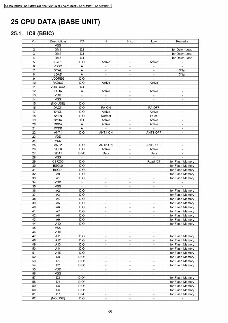
25 CPU DATA (BASE UNIT)25.1. IC8 (BBIC)
Pin Descriptiojn I/O Hi Hi-z Low Remarks1 VSS - - - -2 DM1 D.I - - - for Down Load3 DM2 D.I - - - for Down Load4 DM3 D.I - - - for Down Load5 SYRI D.O Active - Active -6 VSSO A - - - -7 XTAL A - - - X´tal8 LOAD A - - - X´tal9 VDDREG D.O - - - -10 RXDSG D.O Active - Active -11 VDDTXDA D.I - - -12 TXDA A Active - Active -13 VDD - - - - -14 VSS - - - - -15 (NO USE) D.O - - - -16 DAON D.O PA-ON - PA-OFF -17 SYCL D.O Active - Active -18 SYEN D.O Normal - Latch -19 SYDA D.I Active - Active -20 RXDA A Active - Active -21 RXDB A - - - -22 ANT1 D.O ANT1 ON - ANT1 OFF -23 VDD - - - - -24 VSS - - - - -25 ANT2 D.O ANT2 ON - ANT2 OFF -26 I2CLK D.O Active - Active -27 I2DAT D.I/O Data - Data -28 VSS - - - - -29 CSROQ D.O - - Read IC7 for Flash Memory30 BSCL0 D.O - - - for Flash Memory31 BSCL1 D.O - - - for Flash Memory32 A0 D.O - - - for Flash Memory33 A1 D.O - - - for Flash Memory34 VDD - - - - -35 VSS - - - - -36 A2 D.O - - - for Flash Memory37 A3 D.O - - - for Flash Memory38 A4 D.O - - - for Flash Memory39 A5 D.O - - - for Flash Memory40 A6 D.O - - - for Flash Memory41 A7 D.O - - - for Flash Memory42 A8 D.O - - - for Flash Memory43 A9 D.O - - - for Flash Memory44 A10 D.O - - - for Flash Memory45 VSS - - - - -46 VDD - - - - -47 A11 D.O - - - for Flash Memory48 A12 D.O - - - for Flash Memory49 A13 D.O - - - for Flash Memory50 A14 D.O - - - for Flash Memory51 A15 D.O - - - for Flash Memory52 D0 D.O/I - - - for Flash Memory53 D1 D.O/I - - - for Flash Memory54 D2 D.O/I - - - for Flash Memory55 VDD - - - - -56 VSS - - - - -57 D3 D.O/I - - - for Flash Memory58 D4 D.O/I - - - for Flash Memory59 D5 D.O/I - - - for Flash Memory60 D6 D.O/I - - - for Flash Memory61 D7 D.I/O - - - for Flash Memory62 (NO USE) D.O - - - -
66
KX-TCD445BXS / KX-TCD445BXT / KX-TCD445BXF / KX-A144BXS / KX-A144BXT / KX-A144BXF /

Pin Descriptiojn I/O Hi Hi-z Low Remarks63 P0.6 D.O Make Break -64 (NO USE) D.O - - - -65 (NO USE) D.O - - - -66 VDD - - - - -67 VSS - - - - -68 (NO USE) D.O - - - -69 PULSE_CTRL D.O Q7_ON - Q7_OFF -70 P0.1 D.O - - - for Flash Memory71 P0.0 D.O No Key - Key for Key72 PX.2 D.O - - Write IC4 for Flash Memory73 PX.1 D.O - - Read IC4 for Flash Memory74 (NO USE) D.O - - - -75 (NO USE) D.O - - - -76 R1 D.O RINGER ON - RINGER OFF -77 (NO USE) D.O - - - -78 VDD - - - - -79 VSS - - - - -80 (NO USE) D.O - - - -81 TONE D.I - - - Ring Det82 (NO USE) D.O - - - -83 (NO USE) D.O - - - -84 (NO USE) D.O - - - -85 (NO USE) D.O - - - -86 (NO USE) D.O - - - -87 (NO USE) D.O - - - -88 VDD - - - - -89 VSS - - - - -90 (NO USE) D.O - - - -91 (NO USE) D.O - - - -92 (NO USE) D.O - - - -93 (NO USE) D.O - - - -94 (NO USE) D.O - - - -95 MA5 D.O/I - - - for Voice Down Load96 (NO USE) D.O - - - -97 MA3 D.O/I - - - for Voice Down Load98 VDD - - - - -99 VSS - - - - -
100 MA2 D.O/I - - - for Voice Down Load101 MA1 D.O/I - - - for Voice Down Load102 MA0 D.O/I - - - for Voice Down Load103 FRDY D.O - - - for Flash Memory104 MD4 D.O - - - for Flash Memory105 MD2 D.O - - - for Flash Memory106 MD1 D.I - - - for Flash Memory107 MD0 D.O - - - for Flash Memory108 VDD - - - - -109 VSS - - - - -110 (NO USE) A - - - -111 (NO USE) A - - - -112 (NO USE) A - - - -113 (NO USE) A - - - -114 (NO USE) A - - - -115 (NO USE) A - - - -116 VSSA - - - - -117 VDDA - - - - -118 (NO USE) A - - - -119 (NO USE) A.I - - - -120 (NO USE) A.I - - - -121 (NO USE) A - - - -122 (NO USE) A - - - -123 SON A - - - -124 (NO USE) A - - - -125 (NO USE) A - - - -126 HOP A - - - -127 HOPI A - - - -128 (NO USE) A - - - -129 REFVH A - - - -
67
KX-TCD445BXS / KX-TCD445BXT / KX-TCD445BXF / KX-A144BXS / KX-A144BXT / KX-A144BXF /

Pin Descriptiojn I/O Hi Hi-z Low Remarks130 BREF A - - - -131 VSSA - - - - -132 VDDA - - - - -133 MIP A - - - -134 MFBN A - - - -135 MFBP A - - - -136 MIN A - - - -137 ADREFP A - - - -138 ADREFN A - - - -139 RSSI A - - - -140 AD3 A - - - -141 AD4 A - - - -142 MPCINP A - - - -143 RESETQ A Normal - Reset -144 VDD - - - - -
Note:I_PU; Internal Pull-Up, I_PD; Internal Pull-Down
68
KX-TCD445BXS / KX-TCD445BXT / KX-TCD445BXF / KX-A144BXS / KX-A144BXT / KX-A144BXF /

26 CPU DATA (HANDSET)26.1. IC1 (BBIC)
Pin Description I/O Hi Hi-z Remarks1 LCD_SEGMENT D.O Active - -2 LCD_COMMON D.O Active - -3 VDD - - - -4 VSS - - - -5 LCD_COMMON D.O Active - -6 LCD_COMMON D.O Active - -7 LCD_COMMON D.O Active - -8 LCD_COMMON D.O Active - -9 LCD_COMMON D.O Active - -10 PA_SW D.O PA ON - -11 T/R SW D.O Transmit - -12 RX_DATA D.I Active - -13 SYEN D.O Active - -14 SYDA D.O Active - -15 SYCL D.O Active - -16 TX_DATA A.O Active - -17 KEY_IN D.I No Key - -18 KEY_IN D.I No Key - -19 KEY_IN D.I No Key - -20 KEY_IN D.I No Key - -21 KEY_IN D.I No Key - -22 (NO USE) D.O - - -23 Reference clock D.O Active - -24 VDD - - - -25 VSS - - - -26 POWER_SW A.I No Key - -27 CHARGE_DET A.I Charge - -28 DCDCDRV D.O Active - -29 DCDCCMR A.I - - -30 RESET A.I Normal - -31 VSSO - - - -32 LOAD A.I - - -33 XTAL A.I - - -34 VDDPM A.O - - -35 VDDLO A.O - - -36 VDDBAT A.I - - -37 VDDLR - - - -38 CHARGE_START A.O - - for charge39 VDDA - - - -40 VSSA - - - -41 LSRN A.O - - -42 LSRP A.O - - -43 BANDGAP_REF A.O - - -44 MICS A.O - - -45 MICP A.I - - -46 MICN A.I - - -47 Reference Voltage A.O - - -48 RSSI A.I - - -49 P0.4 D.I - - -50 AD4N A.I - - -51 AD4P A.I - - -52 (NO USE) D.I - - -53 KEY_STRB D.O Active - -54 KEY_STRB D.O Active - -55 KEY_STRB D.O Active - -56 LCD_SEGMENT D.O Active - -57 LCD_SEGMENT D.O Active - -58 LCD_SEGMENT D.O Active - -59 KEY_STRB D.O Active - -60 KEY_STRB D.O Active - -61 LCD_SEGMENT D.O Active - -62 LCD_SEGMENT D.O Active - -
69
KX-TCD445BXS / KX-TCD445BXT / KX-TCD445BXF / KX-A144BXS / KX-A144BXT / KX-A144BXF /

Pin Description I/O Hi Hi-z Remarks63 VDD - - - -64 VSS - - - -65 VDD for EEPROM D.O - - -66 I2DAT D.I/O Active - -67 I2CLK D.I/O Active - -68 MODE D.I - - -69 R2 D.I - - -70 (NO USE) D.O - - -71 VBACK/P0.7 D.I - - -72 LCD_SEGMENT D.O Active - -73 LCD_SEGMENT D.O Active - -74 LCD_SEGMENT D.O Active - -75 LCD_SEGMENT D.O Active - -76 LCD_SEGMENT D.O Active - -77 VDDLI - - - -78 LCD_SEGMENT D.O Active - -79 LCD_SEGMENT D.O Active - -80 LCD_SEGMENT D.O Active - -81 LCD_SEGMENT D.O Active - -82 LCD_SEGMENT D.O Active - -83 LCD_SEGMENT D.O Active - -84 LCD_SEGMENT D.O Active - -85 VSS - - - -86 VDD - - - -87 LCD_SEGMENT D.O Active - -88 (NO USE) D.O - -89 Power Select D.O Low Power - -90 LCD_SEGMENT D.O Active - -91 LCD_SEGMENT D.O Active - -92 LCD_SEGMENT D.O Active - -93 LCD_SEGMENT D.O Active - -94 LCD_SEGMENT D.O Active - -95 LCD_SEGMENT D.O Active - -96 LCD_SEGMENT D.O Active - -97 LCD_SEGMENT D.O Active - -98 LCD_SEGMENT D.O Active - -99 LCD_SEGMENT D.O Active - -
100 LCD_SEGMENT D.O Active - -
70
KX-TCD445BXS / KX-TCD445BXT / KX-TCD445BXF / KX-A144BXS / KX-A144BXT / KX-A144BXF /

27 EEPROM LAYOUT (BASE UNIT)27.1. Scope
The purpose of this section is to describe the layout of the EEPROM (IC4) for the KX-TCD445 Base Unit.
The EEPROM contains hardware, software, and user specific parameters. Some parameters are set during production of thebase e.g. crystal frequency adjustment at address 0000 and 0001, some are set by the user configuration e.g. ringer volumeat address 0220, and some are set during normal use of the phone.
27.2. IntroductionThe base unit uses a 32K bit serial EEPROM (IC4) for storing volatile parameters. All parameters are set up before the baseleaves the factory. Some of these are vital for the operation of the hardware so a set of default parameters is programmedbefore the actual hardware fine-tuning can be initiated. This document lists all default settings with a short description.In the tables below values in a range that are similar are not repeated; i.e. Address 00 to 01 contains the value 00 simply meansthat the value 00 is repeated in all addresses in the range. All values in this document are in hexadecimal notation.
Type Name DescriptionD default The EEPROM location is preset to the Default value by the eeprom default loader.A adjust The EEPROM location is set during the production test and should not be overwritten. The value is set by the
eeprom default loader only if the location contains all 1’s (byte: 0xFF, word FFFFh), i, e. it has never been set.- EEPROM location which is not set at all.
CountrySetting
x Default - no specific country setting, so revert to default value
27.3. EEPROM Layout27.3.1. General Setup
Address Default Name CountrySetting
Type Description
0000-01 00 60 EepromOscillator x A Frequency adjustment0002 1B ModulationDeviation x A Modulation adjustment
0020-0024 - RFPI (ID for Base Unit) x A RFPI0025-0026 00 00 AC (Base PIN code) x D AC code
0028 00 TBR22Test x D TBR22 test0030-0034 FF .. FF IPUI_1 (ID for H/S 1) x D Ipui for handset 1. If set to FF .. FF (5bytes) the
handset is not enrolled.0035-0039 FF .. FF IPUI_2 (ID for H/S 2) x D Ipui for handset 2. If set to FF .. FF (5bytes) the
handset is not enrolled.003A-003E FF .. FF IPUI_3 (ID for H/S 3) x D Ipui for handset 3. If set to FF .. FF (5bytes) the
handset is not enrolled.003F-0043 FF .. FF IPUI_4 (ID for H/S 4) x D Ipui for handset 4. If set to FF .. FF (5bytes) the
handset is not enrolled.0044-0048 FF .. FF IPUI_5 (ID for H/S 5) x D Ipui for handset 5. If set to FF .. FF (5bytes) the
handset is not enrolled.0049-004D FF .. FF IPUI_6 (ID for H/S 6) x D Ipui for handset 6. If set to FF .. FF (5bytes) the
handset is not enrolled.004E-008F - Reserved x - Protocol data0090-009F - UAK_1 x - UAK for handset 1 (for factory use)00A0-00AF - UAK_2 x - UAK for handset 2 (for factory use)00B0-00BF - UAK_3 x - UAK for handset 3 (for factory use)00C0-00CF - UAK_4 x - UAK for handset 4 (for factory use)00D0-00DF - UAK_5 x - UAK for handset 5 (for factory use)00E0-00EF - UAK_6 x - UAK for handset 6 (for factory use)
27.3.2. Switch ControlAddress Default Name Country
SettingType Description
09F1 00 HsRegInfo.RegFlags x U Handset registration info - registration ON/OFF
1=reg, 0=no reg
71
KX-TCD445BXS / KX-TCD445BXT / KX-TCD445BXF / KX-A144BXS / KX-A144BXT / KX-A144BXF /
Address Default Name CountrySetting
Type Description
09F2 00 HsRegInfo.EmcFlags x U Handset registration info - EMC flagsBit6..7: not used0..5: handset 1..6 info, 1=known , 0=unknown
09F3 21 RingMode x D Ring mode. Modes used in KAMMA4 are 20h and 21h.Bit7..5: Mode (001=group)4: Not used3..0: Id (001= id of first group)
27.3.3. Flash Time settingAddress Default Name Country
SettingType Description
0F0B 08 CalibBreakTime[0] 0A D Calibrated loop-break time for short breakUnit: 10 ms, defaults to 80 ms
0F0C 14 CalibBreakTime[1] 3C D Calibrated loop-break time for long breakUnit: 10 ms, defaults to 200 ms
0F0D 46 CalibBreakTime[2] 1E D Calibrated loop-break time for Extra-long breakUnit: 10 ms, defaults to 700 ms
27.3.4. Clip (Caller ID) configurationAddress Default Name Country
SettingType Description
0F1C 70 Detect x D CLIP detect configurationBit0-2: Mode: 0: Learn mode, 1: DTMF only, 2: FSKonly 3: Generic mod, 4: Russian CLIP only3: Unused44: Onhook: 1=enable 0=disable5: Offhookk: 1=enable 0=disable6: Msgwaiting: 1=enable 0=disable7: Unused7
0F37..38 3D 01 Parse.Configuration 3D 08 D Clip parse set configurationBit0: Etsi: 1=enable 0=disable1: ForwardNumber: 1=enable 0=disable2: Danish: 1=enable 0=disable3: Dutch: 1=enable 0=disable4: Canadian: 1=enable 0=disable5: Swedish: 1=enable 0=disable6: UserDefined: 1=enable 0=disable7: KPN vmwi: 1=enable 0=disable8: ProtocolPriority:If 2 mutual exclusive parameters occurs, the 1st inthe protocol message has priority. 1=enable0=disable9: UseCallType:Verify the Call Type parameter, if available, whenreceiving Call Back CLIP at busy subscriber.1=enable 0=disable10:AddTop0IfNo0Automatic addition of 0 if top of Caller ID is not 0.1=enable 0=disable11: DtmfDigitsOnlyParse DTMF clip without start and/or stop code.1=enable 0=disable12..15: Reserved12..Reserved15
72
KX-TCD445BXS / KX-TCD445BXT / KX-TCD445BXF / KX-A144BXS / KX-A144BXT / KX-A144BXF /

27.3.5. TADTASKAddress Default Name Country
SettingType Description
0F40 00 CountryCode 03 D Country code0: Germany1: Greece2: Turkey3: England4: Switzerland5: Poland7: France8: DenmarkA: ItalyC: CzechD: NetherlandE: HungaryF: Spain12: Sweden13: South Afric14: Russia
0F41-0F60 FF TamTagInfo x D Message TAG informationBit 0-3 Odd number MSG, 4-7 Even number MSG0: Reserve1: 2WayInfo 0:Not 2WayRec/1:2WayRecMsg2: New Info 0:OLD/1:NEW3: OGM Info Not used4: Reserve5: 2WayInfo 0:Not 2WayRec/1:2WayRecMsg6: New Info 0:OLD/1:NEW7: OGM Info Not used
0F61 14 TamPrgInfo x D TAM Current Setting dataBit0: Answer ON/OFF 0:OFF/1:ON1: ICM Record Time Mode1 0:OFF/1:Greeting Only2: ICM Record Time Mode2 0:OFF/1:UnlimitedMode1=0&Mode2=0:ICM Record Time=1min3: CPC time selection 0:time A/1:time B4: Greeting Monitor mode ON/OFF 0:OFF/1:ON5: Reserve6: VOX sense selection 0: Normal /1: Low7: DSC time selection 0: immediately/1: 1.6sec
0F62 00 TamPrgRings x D Current number of rings for automatic answeringRange:0(Auto), 2-7
0F63-0F64 FF TamPrgRmtCode x D Current Remote codee.g. 123 Address 0x0F63 0xF1 Address 0x0F64 0x23
0F65 10 CountryData 18 D Each country dataBit0: Remote Turn on Beep 0: 500 ms/1: 2.5 sec1: Reserve2: Max time in Line Remote Not Used3: TimeData for voice prompt 0:24hour /1:12hour4: VicMenuData 0: No VoiceMenu/1: VoiceMenu5: LanguageInfo 0: Single Language/1: DualLanguages6: Reserve7: Reserve
0F66 08 DetData 18 D Detection dataBit0: Selection CPC A/B 0:OFF (A fixed)/1:ON(Select)1: Reserve2: Detect 1st Short Bell (300ms) for count3: Cyclic Detection of VOX 0: OFF/1: ON(Detect)4: Detection of DSC 0: OFF/1: ON(Detect)5: Reserve6: Reserve7: Reserve
73
KX-TCD445BXS / KX-TCD445BXT / KX-TCD445BXF / KX-A144BXS / KX-A144BXT / KX-A144BXF /

Address Default Name CountrySetting
Type Description
0F67 06 OptionData 25 D Each country dataBit0: 2 Way Beep ON/OFF 0:OFF/1:ON1: 2 Way Beep interval 0:15s per 400ms/1:20s per160ms2: 2 Way Rec ON/OFF 0:OFF/1:ON3: Switching of VOX Sense ON/OFF 0:OFF/1:ON4: Key Click Tone ON/OFF Not used5: Select Compression Rate Menu 0:Not Active/1:Active6: 2 Way Beep interval2*For UK (15s per 400ms 1khz)2wayBeepInterval=0 2wayBeepInterval2=0*For FR (20s per 160ms 1khz)2wayBeepInterval=1 2wayBeepInterval2=0*For AL (15s per 420ms 1.4khz)2wayBeepInterval=1 2wayBeepInterval2=17: Reserve
0F68 00 TamPrgWordMode x D Language select dataFor Switzerland 0:Germany/1:FrenchFor Czech 0:Chezh/1:Slovakian
0F69 27 TamRingsSetNum x D Number of rings select range for automatic answering0x25: 2 ~ 5 Rings0x27: 2 ~ 7 Rings
0F6A 00 TamRingsDefNum x D Number of rings default data0: Default is Automatically Turn on for Toll saver2-7: Default of the number of rings for Turn on.
27.3.6. BsUiTask settingsAddress Default Name Country
SettingType Description
0F6E 01 Config 03 D BsUiTask configuration (MSB)Bits 1=enable 0=disable0: AmPmClockSettingEnabled, enabled1: ClipDetectionSettingEnabled, disabled2: AkzMenuEnabled, disabled3: HakzMenuEnabled, disabled4: RussianClipSttingEnabled, disabled5: SmscSendNumberSettingEnabled, disabled6: SMSPabxSupportSettingEnabled, disabled7: ARSDisablePossible, disabled
0F6F F7 Config 07 D BsUiTask configuration (LSB)Bits 1=enable 0=disable0: FlashTime1Enabled, enabled1: FlashTime2Enabled, enabled2: FlashTime3Enabled, enabled3: KeyClicksEnable, disabled4: ARSCarrierMenuEnabled, enabled5: ARSIntDeletionMenuEnabled, enabled6: ARSMultipleCarrierMenuEnabled, enabled7: ARSMultipleAreaCodeMenuEnabled, enabled
0F70 00 Reserved x D Reserved0F71 FF Config2 EF D BsUiTask configuration 2
Bits 1=enable 0=disable0: RingerModeMenuEnabled, enabled1: CallRestrictionMenuEnabled, enabled2: CancelHandsetMenuEnabled, enabled3: BaseToneMenusEnabled, enabled4: ARSMenuEnabled, enabled5: CallCostMenuEnabled, enabled6: BasePINMenuEnabled, enabled7: DialModeMenuEnabled, enabled
74
KX-TCD445BXS / KX-TCD445BXT / KX-TCD445BXF / KX-A144BXS / KX-A144BXT / KX-A144BXF /

28 EEPROM LAYOUT (HANDSET)28.1. Scope
The purpose of this section is to describe “the layout of the EEPROM (IC2) for the KX-A144 Handset”.The EEPROM contains hardware, software, and user specific parameters. Some parameters are set during production of thehandset e.g. crystal oscillator adjustment at 0000..01, some are set by the user when configuring the handset e.g. ringer volumeat 0F3E, and some during normal use of the phone.
28.2. IntroductionThe handset uses a 32k bit serial EEPROM (IC2) for storing volatile parameters. All parameters are set up before the handsetthe factory. Some of these are vital for the operation of the hardware so a set of default parameters is programmed before theactual hardware fine-tuning can be initiated. This document lists all default settings with a short description.This document lists all default parameters with a short description.In the tables below values in a range that are similar are not repeated; i.e. Address 00 to 01 contains the value 00 simply meansthat the value 00 is repeated in all addressee in the range.
Type Name DescriptionD default The EEPROM location is preset to the Default value by the eeprom default loader.A adjust The EEPROM location is set during the production test and should not be overwritten. The value is set by
the eeprom default loader only if the location contains 0xFF, i, e. it has never been set.- EEPROM location which is not set at all.
CountrySetting
x Default - no specific country setting, so revert to default value
28.3. EEPROM contents
28.3.1. General SetupAddress Default Name Country
SettingType Description
0000-0001 00 60 EepromOscillator - A Frequency adjustment0002 0A ModulationDeviation - A Mudulation adjustment
0030-0034 00 IPEI (ID for Handset) - A IPEI0036-003A - PARK_1 (ID for Base 1) - - PARK for registration 1003B-003F - PARK_2 (ID for Base 2) - - PARK for registration 20040-0044 - PARK_3 (ID for Base 3) - - PARK for registration 30045-0049 - PARK_4 (ID for Base 4) - - PARK for registration 4004A-004D FF PLI_1-PLI_4 - D Pli for registration 1-4. If set to FF the registration is
deleted.0100-0104 - RFPI_1 (Base 1) - - RFPI for registration 1
0105 - SerClass_1 - - Service class for registration 10106 - LAL_1 - - Location area level for registration 10107 - IPUI_LEN_1 - - IPUI length for registration 1
0108-0114 - IPUI_1 - - IPUI for registration 10115 - ZAP_1 - - ZAP for registration 10116 - STATUS_1 - - Status for registration 1
0117-126 - UAK_1 - - UAK for registration 10130-134 - RFPI_2 (Base 2) - - RFPI for registration 2
0135 - SerClass_2 - - Service class for registration 20136 - LAL_2 - - Location area level for registration 20137 - IPUI_LEN_2 - - IPUI length for registration 2
0138-0144 - IPUI_2 - - IPUI for registration 20145 - ZAP_2 - - ZAP for registration 20146 - STATUS_2 - - Status for registration 2
0147-0156 - UAK_2 - - UAK for registration 20160-0164 - RFPI_3 (Base 3) - - RFPI for registration 3
0165 - SerClass_3 - - Service class for registration 30166 - LAL_3 - - Location area level for registration 30167 - IPUI_LEN_3 - - IPUI length for registration 3
0168-0174 - IPUI_3 - - IPUI for registration 30175 - ZAP_3 - - ZAP for registration 30176 - STATUS_3 - - status for registration 3
0177-0186 - UAK_3 - - UAK for registration 3
75
KX-TCD445BXS / KX-TCD445BXT / KX-TCD445BXF / KX-A144BXS / KX-A144BXT / KX-A144BXF /

Address Default Name CountrySetting
Type Description
0190-0194 - RFPI_4 (Base 4) - - RFPI for registration 40195 - SerClass_4 - - Service class for registration 40196 - LAL_4 - - Location area level for registration 40197 - IPUI_LEN_4 - - IPUI length for registration 4
0198-01A4 - IPUI_4 - - IPUI for registration 401A5 - ZAP_4 - - ZAP for registration 401A6 - STATUS_4 - - Status for registration 4
01A7-01B6 - UAK_4 - - UAK for registration 40450-0451 00 00 HSPinCode x D 4 BCD Digits
0462 00 Language x D 00 = English01 = Spanish02 = French03 = Italian04 = Dutch05 = Turkish06 = Hungarian07 = Portuguese08 = Polish09 = UnUsed0A = German
0467 00 FactoryLanguageSetting x D Factory setting for language:00 = English01 = Spanish02 = French03 = Italian04 = Dutch05 = Turkish06 = Hungarian07 = Portuguese08 = Polish09 = UnUsed0A = German
0469 07 MaxDigitsToMatch 06 D Valid values: 01 - FFDigits above this value will not be evaluated, whenmatching.
046A 05 MinDigitsToMatch x D Valid values: 01 - FF (-Must be lower thanMaxDigitsToMatch).-If all digits of one of the numbers match completely,-with at least this number of digits, we have a match.(-Or if they match completely with less digits, we also havematch.)
28.3.2. Battery ParametersAddress Default Name Type Description
0F04 9A LowVoltage A Voltage on which to start battery low-indication.The voltage has to be measured under this value for8 seconds before the handset start signaling low battery.LowVoltage[eeprom]=[ADC-steps]=LowVoltage[mV](14.35[mV/step])
28.3.3. Volume SettingsAddress Default Name Country
SettingType Description
474 03 EESpPhVolume x D Volume of the speakerphoneF29 60 RingVolumeLevel1 41 D Setting for RingerVolume 1 (lowest)F2A 50 RingVolumeLevel2 34 D Setting for RingerVolume 2:F2B 40 RingVolumeLevel3 31 D Setting for RingerVolume 3:F2C 30 RingVolumeLevel4 24 D Setting for RingerVolume 4:F2D 20 RingVolumeLevel5 21 D Setting for RingerVolume 5:F2E 10 RingVolumeLevel6 12 D Setting for RingerVolume 6:F35 1C GX-index x A Gain-transmit (values ranging from 0x00 to 0x30, each step
representing 1 dB)F36 46 GR-offset for volumestep 1 x D Bit7 : AOG
Bit6: AOG2Bit5 - bit0: Gain -receive offset to volumestep 2(valuesranging from 0x00 to 0x30, each step representing 1 dB)
76
KX-TCD445BXS / KX-TCD445BXT / KX-TCD445BXF / KX-A144BXS / KX-A144BXT / KX-A144BXF /

Address Default Name CountrySetting
Type Description
F37 5F GR-offset for volumestep 2 x A Bit7 : AOGBit6: AOG2Bit5 - bit0: Gain-receive (values ranging from 0x00 to 0x30,each step representing 1 dB)
F38 00 GR-offset for volumestep 3 x D Bit7 : AOGBit6: AOG2Bit5 - bit0: Gain-receive offset to volumestep 2(valuesranging from 0x00 to 0x30, each step representing 1 dB)
F3E 06 EERingerVolume x D Volume of the ringer (1 - 6)F3F 02 EEVoiceVolume x D Volume of the earpiece (1 - 3)F57 60 CadenceVolumeLevel1 41 D Setting for RingerVolume 1 (lowest)F58 50 CadenceVolumeLevel2 34 D Setting for RingerVolume 2F59 40 CadenceVolumeLevel3 31 D Setting for RingerVolume 3F5A 30 CadenceVolumeLevel4 24 D Setting for RingerVolume 4F5B 20 CadenceVolumeLevel5 21 D Setting for RingerVolume 5F5C 10 CadenceVolumeLevel6 12 D Setting for RingerVolume 6F5D 11 SpPhGX-index x A Gain -transmit for speakerphone (values ranging from 0x00
to 0x24, each step representing 1 dB). The index representvolumestep 3.
F5E 98 SpPhGR-index x D Bit7 - AOG when speakerphoneBit6 - AOG2 when speakerphoneGain -receive for speakerphone (values ranging from 0x00to 0x21, each step representing 1 dB). The indexrepresent volumestep 3.
28.3.4. Menu ConfigurationAddress Default Name Country
SettingType Description
0F53 FF Menu Config x D bit 0 - Registration menu on/off 1/0bit 1 - Select base menu on/off 1/0bit 2 - Internal ringer menu on/off 1/0bit 3 - Page ringer menu on/off 1/0bit 4 - Standby mode menu on/off 1/0bit 5 - Battery select menu on/off 1/0bit 6 - Call waiting menu on/off 1/0bit 7 - Clip list on/off 1/0
0F54 01 RecVolStoreEnabled x D 00: Receiver volume will be reset to default value whenhooking on.01: Receiver volume will be stored in eeprom when set inconversation.
77
KX-TCD445BXS / KX-TCD445BXT / KX-TCD445BXF / KX-A144BXS / KX-A144BXT / KX-A144BXF /

29.1. Preparation • PbF (: Pb free) Solder • Soldering Iron
Tip Temperature of 700°F ± 20°F (370°C ± 10°C)Note: We recommend a 30 to 40 Watt soldering iron. Anexpert may be able to use a 60 to 80 Watt iron wheresomeone with less experience could overheat and damagethe PCB foil.
• Flux
Recommended Flux: Specific Gravity → 0.82.Type → RMA (lower residue, non-cleaning type)Note: See ABOUT LEAD FREE SOLDER (PbF: Pb free)(P.4).
29.2. Procedure 1. Tack the flat pack IC to the PCB by temporarily soldering
two diagonally opposite pins in the correct positions on thePCB.
Be certain each pin is located over thecorrect pad on the PCB.
2. Apply flux to all of the pins on the IC.
3. Being careful to not unsolder the tack points, slide thesoldering iron along the tips of the pins while feedingenough solder to the tip so that it flows under the pins asthey are heated.
29.3. Modification Procedure ofBridge
1. Add a small amount of solder to the bridged pins. 2. With a hot iron, use a sweeping motion along the flat part of
the pin to draw the solder from between the adjacent pads.
29 HOW TO REPLACE FLAT PACKAGE IC
78
KX-TCD445BXS / KX-TCD445BXT / KX-TCD445BXF / KX-A144BXS / KX-A144BXT / KX-A144BXF /

30 CABINET AND ELECTRICAL PARTS LOCATION (BASEUNIT)
79
KX-TCD445BXS / KX-TCD445BXT / KX-TCD445BXF / KX-A144BXS / KX-A144BXT / KX-A144BXF /

31 CABINET AND ELECTRICAL PARTS LOCATION(HANDSET)
Note:(*1) The rechargeable Ni-MH battery HHR-4EPT and Ni-Cd battery P-4NPT are available through sales route of Panasonic.
80
KX-TCD445BXS / KX-TCD445BXT / KX-TCD445BXF / KX-A144BXS / KX-A144BXT / KX-A144BXF /
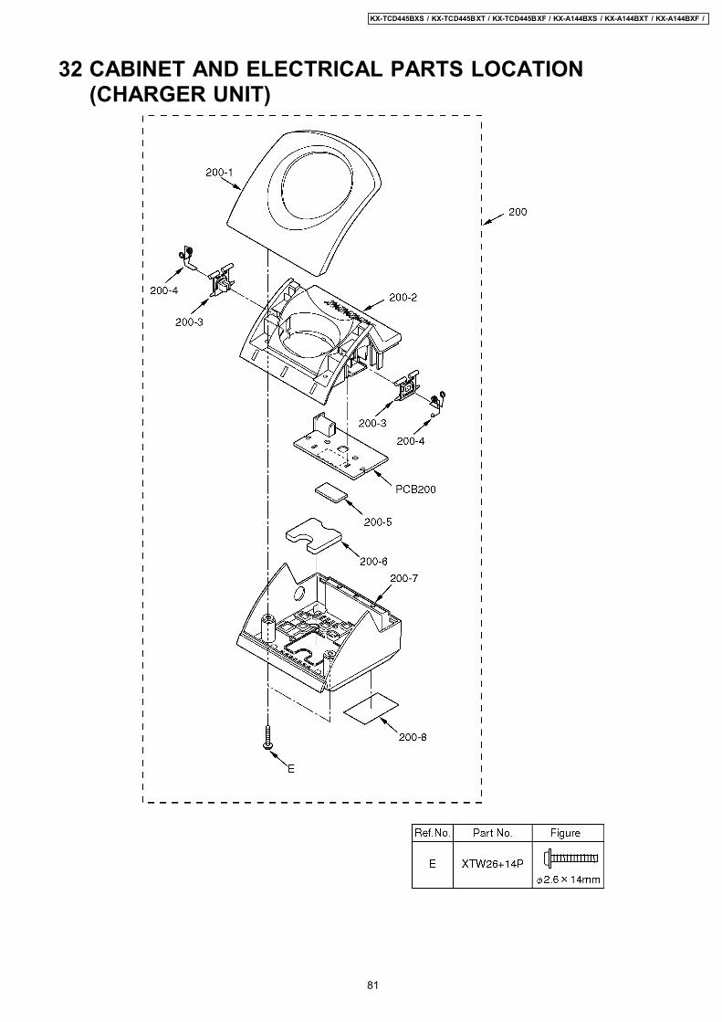
32 CABINET AND ELECTRICAL PARTS LOCATION(CHARGER UNIT)
81
KX-TCD445BXS / KX-TCD445BXT / KX-TCD445BXF / KX-A144BXS / KX-A144BXT / KX-A144BXF /
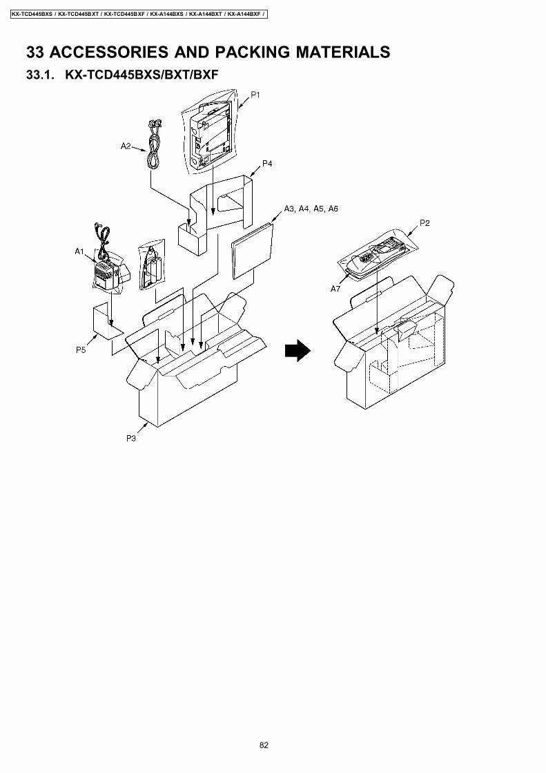
33 ACCESSORIES AND PACKING MATERIALS33.1. KX-TCD445BXS/BXT/BXF
82
KX-TCD445BXS / KX-TCD445BXT / KX-TCD445BXF / KX-A144BXS / KX-A144BXT / KX-A144BXF /

33.2. KX-A144BXS/BXT/BXF
83
KX-TCD445BXS / KX-TCD445BXT / KX-TCD445BXF / KX-A144BXS / KX-A144BXT / KX-A144BXF /

34 TERMINAL GUIDE OF THE ICs, TRANSISTORS ANDDIODES
34.1. Base Unit
34.2. Handset
34.3. Charger Unit
84
KX-TCD445BXS / KX-TCD445BXT / KX-TCD445BXF / KX-A144BXS / KX-A144BXT / KX-A144BXF /

Note: 1. RTL (Retention Time Limited)
Note:The marking (RTL) indicates that the Retention Time islimited for this item.After the discontinuation of this assembly in production,the item will continue to be available for a specific periodof time. The retention period of availability is dependanton the type of assembly, and in accordance with thelaws governing part and product retention. After the endof this period, the assembly will no longer be available.
2. Important safety noticeComponents identified by the mark indicates specialcharacteristics important for safety. When replacing any ofthese components, only use specified manufacture’s parts.
3. The S mark means the part is one of some identical parts.For that reason, it may be different from the installed part.
4. ISO code (Example: ABS-94HB) of the remarks columnshows quality of the material and a flame resisting gradeabout plastics.
5. RESISTORS & CAPACITORSUnless otherwise specified;All resistors are in ohms (Ω) K=1000Ω, M=1000kΩ
All capacitors are in MICRO FARADS (µF)P=µµF*Type & Wattage of Resistor
35.1. Base Unit35.1.1. Cabinet and Electrical PartsRef.No.
Part No. Part Name & Description Remarks
1 PQGG10154SA GRILLE (for KX-TCD445BXS) ABS-HB
1 PQGG10154SB GRILLE (for KX-TCD445BXT) ABS-HB
1 PQGG10154SC GRILLE (for KX-TCD445BXF) ABS-HB
2 PQKM10586WA CABINET BODY (for KX-TCD445BXS)
ABS-HB
2 PQKM10586WB CABINET BODY (for KX-TCD445BXT)
ABS-HB
Ref.No.
Part No. Part Name & Description Remarks
2 PQKM10586WC CABINET BODY (for KX-TCD445BXF)
ABS-HB
3 PQJT10203Z TERMINAL
4 PQKE10356Z1 GUIDE, CHARGE TERMINAL CASE POM-HB
5 PQSA10131Z ANTENNA, MAIN
6 PQSA10132Z ANTENNA, SUB
7 PQYF10560Z9 CABINET COVER (for KX-TCD445BXS)
ABS-HB
7 PQYF10560Z6 CABINET COVER (for KX-TCD445BXT)
ABS-HB
7 PQYF10560ZA CABINET COVER (for KX-TCD445BXF)
ABS-HB
8 PQGT16916Y NAME PLATE (for KX-TCD445BXS)
8 PQGT16918Y NAME PLATE (for KX-TCD445BXT)
8 PQGT16917Y NAME PLATE (for KX-TCD445BXF)
9 L0DACA000023 BUZZER
10 PQHG10690Z RUBBER PARTS, RINGER RUBBER
35.1.2. Main P.C.Board PartsNote:
(*1) When replacing IC4, data need to be written to it withPQZZTCD445BX.
Ref.No.
Part No. Part Name & Description Remarks
PCB1 PQWP1D445BXH MAIN P.C.BOARD ASS´Y (RTL)
(ICs)
IC1 PQVIPC357CN IC
IC2 PQVILM1117MP IC S
IC3 PSVIXC62FP27 IC
IC4 PQWI1D440EH IC (*1)
IC5 PQVILMV321M5 IC
IC6 PQWI2D445BXH IC
IC8 C2HBAK000014 IC
(TRANSISTORS)
Q2 2SA1625 TRANSISTOR(SI) S
Q4 PQVTBF822T7 TRANSISTOR(SI)
Q7 B1ABCE000009 TRANSISTOR(SI)
Q8 B1ABCE000009 TRANSISTOR(SI)
Q9 2SD1994A TRANSISTOR(SI)
Q10 B1ABCE000009 TRANSISTOR(SI)
Q11 B1ABCE000009 TRANSISTOR(SI)
Q13 B1ABGE000006 TRANSISTOR(SI)
(DIODES)
D2 PQVDBZV55C02 DIODE(SI)
D3 PQVDBZV55C02 DIODE(SI)
D4 B0JAME000085 DIODE(SI)
D5 MA111 DIODE(SI) S
D6 PQVDS1ZB60F1 DIODE(SI) S
D7 MA1Z300 DIODE(SI) S
D10 B0DDCM000001 DIODE(SI)
D11 MA8047 DIODE(SI) S
D12 MA8047 DIODE(SI) S
D13 MA8047 DIODE(SI) S
D14 PQVDBZV55C02 DIODE(SI)
D16 MA111 DIODE(SI) S
(COILS)
L2 PQLQR4D4R7K COIL
L3 PQLQR2M33NKT COIL S
(JACKS)
J1 PQJJ1B4Y JACK S
J2 PFJJ1T007Z JACK S
(RESISTORS)
R1 PQ4R18XJ472 4.7K S
R2 ERJ3GEYJ103 10K
R6 ERJ3GEYJ184 180K
R12 ERJ3GEYJ104 100K
R13 PQ4R10XJ562 5.6K S
R14 ERJ3GEYJ103 10K
R15 ERJ3GEYJ222 2.2K
35 REPLACEMENT PARTS LIST
85
KX-TCD445BXS / KX-TCD445BXT / KX-TCD445BXF / KX-A144BXS / KX-A144BXT / KX-A144BXF /
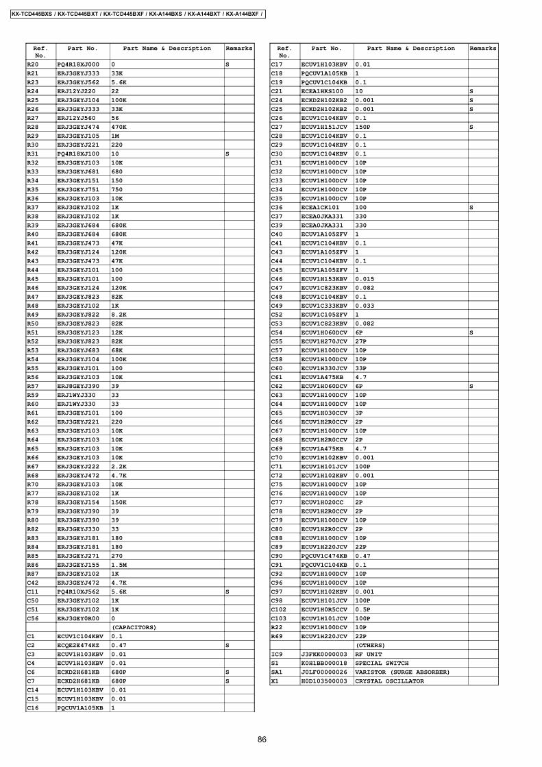
Ref.No.
Part No. Part Name & Description Remarks
R20 PQ4R18XJ000 0 S
R21 ERJ3GEYJ333 33K
R23 ERJ3GEYJ562 5.6K
R24 ERJ12YJ220 22
R25 ERJ3GEYJ104 100K
R26 ERJ3GEYJ333 33K
R27 ERJ12YJ560 56
R28 ERJ3GEYJ474 470K
R29 ERJ3GEYJ105 1M
R30 ERJ3GEYJ221 220
R31 PQ4R18XJ100 10 S
R32 ERJ3GEYJ103 10K
R33 ERJ3GEYJ681 680
R34 ERJ3GEYJ151 150
R35 ERJ3GEYJ751 750
R36 ERJ3GEYJ103 10K
R37 ERJ3GEYJ102 1K
R38 ERJ3GEYJ102 1K
R39 ERJ3GEYJ684 680K
R40 ERJ3GEYJ684 680K
R41 ERJ3GEYJ473 47K
R42 ERJ3GEYJ124 120K
R43 ERJ3GEYJ473 47K
R44 ERJ3GEYJ101 100
R45 ERJ3GEYJ101 100
R46 ERJ3GEYJ124 120K
R47 ERJ3GEYJ823 82K
R48 ERJ3GEYJ102 1K
R49 ERJ3GEYJ822 8.2K
R50 ERJ3GEYJ823 82K
R51 ERJ3GEYJ123 12K
R52 ERJ3GEYJ823 82K
R53 ERJ3GEYJ683 68K
R54 ERJ3GEYJ104 100K
R55 ERJ3GEYJ101 100
R56 ERJ3GEYJ103 10K
R57 ERJ8GEYJ390 39
R59 ERJ1WYJ330 33
R60 ERJ1WYJ330 33
R61 ERJ3GEYJ101 100
R62 ERJ3GEYJ221 220
R63 ERJ3GEYJ103 10K
R64 ERJ3GEYJ103 10K
R65 ERJ3GEYJ103 10K
R66 ERJ3GEYJ103 10K
R67 ERJ3GEYJ222 2.2K
R68 ERJ3GEYJ472 4.7K
R70 ERJ3GEYJ103 10K
R77 ERJ3GEYJ102 1K
R78 ERJ3GEYJ154 150K
R79 ERJ3GEYJ390 39
R80 ERJ3GEYJ390 39
R82 ERJ3GEYJ330 33
R83 ERJ3GEYJ181 180
R84 ERJ3GEYJ181 180
R85 ERJ3GEYJ271 270
R86 ERJ3GEYJ155 1.5M
R87 ERJ3GEYJ102 1K
C42 ERJ3GEYJ472 4.7K
C11 PQ4R10XJ562 5.6K S
C50 ERJ3GEYJ102 1K
C51 ERJ3GEYJ102 1K
C56 ERJ3GEY0R00 0
(CAPACITORS)
C1 ECUV1C104KBV 0.1
C2 ECQE2E474KZ 0.47 S
C3 ECUV1H103KBV 0.01
C4 ECUV1H103KBV 0.01
C6 ECKD2H681KB 680P S
C7 ECKD2H681KB 680P S
C14 ECUV1H103KBV 0.01
C15 ECUV1H103KBV 0.01
C16 PQCUV1A105KB 1
Ref.No.
Part No. Part Name & Description Remarks
C17 ECUV1H103KBV 0.01
C18 PQCUV1A105KB 1
C19 PQCUV1C104KB 0.1
C21 ECEA1HKS100 10 S
C24 ECKD2H102KB2 0.001 S
C25 ECKD2H102KB2 0.001 S
C26 ECUV1C104KBV 0.1
C27 ECUV1H151JCV 150P S
C28 ECUV1C104KBV 0.1
C29 ECUV1C104KBV 0.1
C30 ECUV1C104KBV 0.1
C31 ECUV1H100DCV 10P
C32 ECUV1H100DCV 10P
C33 ECUV1H100DCV 10P
C34 ECUV1H100DCV 10P
C35 ECUV1H100DCV 10P
C36 ECEA1CK101 100 S
C37 ECEA0JKA331 330
C39 ECEA0JKA331 330
C40 ECUV1A105ZFV 1
C41 ECUV1C104KBV 0.1
C43 ECUV1A105ZFV 1
C44 ECUV1C104KBV 0.1
C45 ECUV1A105ZFV 1
C46 ECUV1H153KBV 0.015
C47 ECUV1C823KBV 0.082
C48 ECUV1C104KBV 0.1
C49 ECUV1C333KBV 0.033
C52 ECUV1C105ZFV 1
C53 ECUV1C823KBV 0.082
C54 ECUV1H060DCV 6P S
C55 ECUV1H270JCV 27P
C57 ECUV1H100DCV 10P
C58 ECUV1H100DCV 10P
C60 ECUV1H330JCV 33P
C61 ECUV1A475KB 4.7
C62 ECUV1H060DCV 6P S
C63 ECUV1H100DCV 10P
C64 ECUV1H100DCV 10P
C65 ECUV1H030CCV 3P
C66 ECUV1H2R0CCV 2P
C67 ECUV1H100DCV 10P
C68 ECUV1H2R0CCV 2P
C69 ECUV1A475KB 4.7
C70 ECUV1H102KBV 0.001
C71 ECUV1H101JCV 100P
C72 ECUV1H102KBV 0.001
C75 ECUV1H100DCV 10P
C76 ECUV1H100DCV 10P
C77 ECUV1H020CC 2P
C78 ECUV1H2R0CCV 2P
C79 ECUV1H100DCV 10P
C80 ECUV1H2R0CCV 2P
C88 ECUV1H100DCV 10P
C89 ECUV1H220JCV 22P
C90 PQCUV1C474KB 0.47
C91 PQCUV1C104KB 0.1
C92 ECUV1H100DCV 10P
C96 ECUV1H100DCV 10P
C97 ECUV1H102KBV 0.001
C98 ECUV1H101JCV 100P
C102 ECUV1H0R5CCV 0.5P
C103 ECUV1H101JCV 100P
R22 ECUV1H100DCV 10P
R69 ECUV1H220JCV 22P
(OTHERS)
IC9 J3FKK0000003 RF UNIT
S1 K0H1BB000018 SPECIAL SWITCH
SA1 J0LF00000026 VARISTOR (SURGE ABSORBER)
X1 H0D103500003 CRYSTAL OSCILLATOR
86
KX-TCD445BXS / KX-TCD445BXT / KX-TCD445BXF / KX-A144BXS / KX-A144BXT / KX-A144BXF /

35.2. Handset35.2.1. Cabinet and Electrical PartsRef.No.
Part No. Part Name & Description Remarks
101 PQGP10226Y3 PANEL, LCD (for KX-A144BXS) AS-HB
101 PQGP10226Y4 PANEL, LCD (for KX-A144BXT) AS-HB
101 PQGP10226Y5 PANEL, LCD (for KX-A144BXF) AS-HB
102 PQHS10553Z TAPE, DOUBLE SIDED
103 PQKM10587VD CABINET BODY (for KX-A144BXS) ABS-HB
103 PQKM10587VE CABINET BODY (for KX-A144BXT) ABS-HB
103 PQKM10587VF CABINET BODY (for KX-A144BXF) ABS-HB
104 PQHS10554Z SPACER, LCD CUSHION
105 PQBC10375Z1 BUTTON, NAVI KEY
106 PQBC10376Z1 BUTTON, SP PHONE
107 PQSX10225X KEYBOARD SWITCH, 19 KEY
108 PQHS10467Z COVER, SP NET
109 L0AD02A00021 SPEAKER
110 PQSA10134Z ANTENNA
111 PQJT10204Z TERMINAL (L)
112 PQJT10205Z TERMINAL (R)
113 PQHX11202Z INSULATOR
114 PQHR10964Z GUIDE, SPEAKER
115 L0AD02A00010 SPEAKER
116 PQHG10693Z SPACER, SP RUBBER SHEET
117 PQHS10457Z COVER, SP NET
118 PQJC10058Z BATTERY TERMINAL (+)
119 PQJC10057Z BATTERY TERMINAL (-)
120 PQJC10056Z BATTERY TERMINAL
121 PQKF10626Z1 CABINET COVER (for KX-A144BXS)
ABS-HB
121 PQKF10626Z2 CABINET COVER (for KX-A144BXT)
ABS-HB
121 PQKF10626Z3 CABINET COVER (for KX-A144BXF)
ABS-HB
122 PQGT17145Z NAME PLATE (for KX-A144BXS)
122 PQGT17146Z NAME PLATE (for KX-A144BXT)
122 PQGT17147Z NAME PLATE (for KX-A144BXF)
123 PQHX11271Y PLASTIC PARTS, BATTERY COVERSHEET
124 PQHS10561Y SPACER, BATTERY COVER
125 PQKK10134ZG LID, BATTERY COVER (for KX-A144BXS)
ABS-HB
125 PQKK10134ZB LID, BATTERY COVER (for KX-A144BXT)
ABS-HB
125 PQKK10134ZH LID, BATTERY COVER (for KX-A144BXF)
ABS-HB
35.2.2. Main P.C.Board PartsNote:
(*2) When replacing IC2, data need to be written to it withPQZZTCD445BX.
Ref.No.
Part No. Part Name & Description Remarks
PCB100 PQWP1D445BXR MAIN P.C.BOARD ASS´Y (RTL)(for KX-TCD445BXS/BXT/BXF)
PCB100 PQWP1D144BXR MAIN P.C.BOARD ASS´Y (RTL)(for KX-A144BXS/BXT/BXF)
(ICs)
IC1 C2HBAK000013 IC
IC2 PQWI1D440ER IC (*2)
IC101 C1BB00000265 IC
(TRANSISTORS)
Q1 B1CFMC000006 TRANSISTOR(SI)
Q2 B1ADGE000004 TRANSISTOR(SI)
Q3 UN5216 TRANSISTOR(SI) S
Q101 UN521 TRANSISTOR(SI) S
Q102 UN521 TRANSISTOR(SI) S
Q103 UN521 TRANSISTOR(SI) S
(DIODES)
D1 B0JCME000035 DIODE(SI)
D3 MA2Z74800L DIODE(SI)
D6 MA8047 DIODE(SI) S
Ref.No.
Part No. Part Name & Description Remarks
D7 MA8047 DIODE(SI) S
D101 B0JCDD000002 DIODE(SI)
LED101 LNJ308G8JRA LED
LED102 LNJ308G8JRA LED
LED103 LNJ308G8JRA LED
LED104 PQVDSML310MT LED S
LED105 PQVDSML310MT LED S
LED106 PQVDSML310MT LED S
LED107 PQVDSML310MT LED S
LED108 PQVDBR1111C LED S
(COILS)
F1 PQLQR2M5N6K COIL S
L2 G1A470L00001 COIL
L3 PQLQR4D4R7K COIL
L4 G1C100MA0072 COIL
L5 G1C100MA0072 COIL
L6 G1C2N7Z00008 COIL
(RESISTORS)
R1 ERJ3GEYJ222 2.2K
R2 ERJ8BQJR30 0.3
R3 ERJ3GEYJ560 56
R4 ERJ3GEYJ103 10K
R5 ERJ3GEYJ471 470
R6 ERJ3GEYJ332 3.3K
R7 ERJ3GEYJ471 470
R8 ERJ3GEYJ471 470
R11 ERJ2GEY0R00 0
R17 ERJ2GEYJ560 56
R18 ERJ2GEYJ330 33
R19 ERJ3GEYJ153 15K
R20 ERJ2GEYJ560 56
R21 ERJ6RSJR10V 0.1
R22 ERJ3GEY0R00 0
R23 ERJ3GEYJ2R2 2.2
R101 ERJ3GEYJ820 82
R102 ERJ3GEYJ820 82
R103 ERJ3GEYJ820 82
R104 PQ4R10XJ680 68 S
R105 ERJ3GEYJ391 390
R107 ERJ3GEYJ563 56K
R108 ERJ3GEYJ683 68K
R109 ERJ2GEYJ103 10K
(CAPACITORS)
C2 ECUV1A475KB 4.7
C3 ECUV1C104KBV 0.1
C4 ECUV1C104KBV 0.1
C5 ECST0JY475 4.7
C6 ECUV1H100DCV 10P
C7 ECUV1C104KBV 0.1
C8 ECUV1H100DCV 10P
C12 ECUE1C100DCQ 10P
C14 ECEV0JA331 330
C15 ECEV0JA331 330
C16 ECUV1H1R0CCV 1P
C17 ECUV1H180JCV 18P
C18 ECUE1A104KBQ 0.1
C20 ECUE1A104KBQ 0.1
C21 ECUE1A104KBQ 0.1
C22 ECUE1A104KBQ 0.1
C23 ECUV1C104KBV 0.1
C24 ECUV1C104KBV 0.1
C26 ECUV1C104KBV 0.1
C27 ECUE1A104KBQ 0.1
C28 ECUV1C104KBV 0.1
C29 ECUV1C104KBV 0.1
C30 ECUV1C104KBV 0.1
C31 ECUE1C100DCQ 10P
C33 ECUV1A225KB 2.2
C54 ECUE1C100DCQ 10P
C55 ECUE1H2R0CCQ 2P
C56 ECUE1H2R0CCQ 2P
C57 ECUE1H330JCQ 33P
C60 ECST0JY475 4.7
87
KX-TCD445BXS / KX-TCD445BXT / KX-TCD445BXF / KX-A144BXS / KX-A144BXT / KX-A144BXF /

Ref.No.
Part No. Part Name & Description Remarks
C62 ECUV1A105KBV 1
C64 ECUV1A105KBV 1
C65 ECUE1C100DCQ 10P
C66 ECUE1C100DCQ 10P
C67 ECUE1H2R0CCQ 2P
C102 ECUV1H222KBV 0.0022
C103 ECUE1C100DCQ 10P
C105 ECUV1C104KBV 0.1
C106 ECUV1A105KBV 1
C107 ECUE1A104KBQ 0.1
C108 ECUV1H100DCV 10P
C109 ECUV1C104KBV 0.1
C110 ECUV1H100DCV 10P
C111 ECUV1H100DCV 10P
C115 ECUV1H100DCV 10P
C116 ECUV1H100DCV 10P
C202 ECUE1C0R5CCQ 0.5P
C206 ECUV1A475KB 4.7
C208 ECUE1C100DCQ 10P
C209 ECUV1H100DCV 10P
(OTHERS)
E101 PQWLA144EXR LCD ASSEMBLY
E102 PQHX11255Z SPACER, DIFFUSION SHEET
E103 PQHR11043Z TRANSPARENT PLATE, LCD
E104 PQHS10632Z TAPE, DOUBLE SIDED (LCD)
E105 PQHR11042Z GUIDE, LCD
E106 PQHS10486Z HEAT SHIELD PARTS
MIC L0CBAB000052 MICROPHONE
IC3 J3FKK0000003 RF UNIT
X1 H0D103500002 CRYSTAL OSCILLATOR
35.3. Charger Unit35.3.1. Cabinet and Electrical PartsRef.No.
Part No. Part Name & Description Remarks
200 PQLV30018ZS3 CHARGER UNIT (for KX-A144BXS)
200 PQLV30018ZT3 CHARGER UNIT (for KX-A144BXT)
200 PQLV30018ZF3 CHARGER UNIT (for KX-A144BXF)
200-1 PQGG10155YD GRILLE (for KX-A144BXS) ABS-HB
200-1 PQGG10155YE GRILLE (for KX-A144BXT) ABS-HB
200-1 PQGG10155YF GRILLE (for KX-A144BXF) ABS-HB
200-2 PQKM10591Y9 CABINET BODY (for KX-A144BXS) PS-HB
200-2 PQKM10591Y5 CABINET BODY (for KX-A144BXT) PS-HB
200-2 PQKM10591Y0 CABINET BODY (for KX-A144BXF) PS-HB
200-3 PQKE10356Z1 GUIDE, CHARGE TERMINAL CASE POM-HB
200-4 PQJT10206Z CHARGE TERMINAL
200-5 PQHX10991Z CUSHION, URETHANE FORM
200-6 PQMH10426Z WEIGHT
200-7 PQYF10563Z9 CABINET COVER (for KX-A144BXS)
PS-HB
200-7 PQYF10563Z5 CABINET COVER (for KX-A144BXT)
PS-HB
200-7 PQYF10563Z0 CABINET COVER (for KX-A144BXF)
PS-HB
200-8 PQGT17279Z NAME PLATE (for KX-A144BXS)
200-8 PQGT17280Z NAME PLATE (for KX-A144BXT)
200-8 PQGT17278Z NAME PLATE (for KX-A144BXF)
35.3.2. Main P.C.Board PartsRef.No.
Part No. Part Name & Description Remarks
PCB200 PQWPA142ESCH MAIN P.C.BOARD ASS´Y (RTL)
(DIODE)
D1 B0JAME000085 DIODE(SI)
(JACK)
J1 PQJJ1B4Y JACK S
(RESISTORS)
R1 ERJ1WYJ220 22
R2 ERJ1WYJ270 27
35.4. Accessories and PackingMaterials
35.4.1. KX-TCD445BXS/BXT/BXFRef.No.
Part No. Part Name & Description Remarks
A1 PQLV19BXZ AC ADAPTOR
A2 PQJA10075Z CORD, TELEPHONE
A3 PQQX14165Z INSTRUCTION BOOK
A4 PQQW13352Z QUICK GUIDE (for English)
A5 PQQW13328Z QUICK GUIDE (for Arabic)
A6 PQQW13468Z LEAFLET
A7 PQQW12846W LEAFLET, RECHARGE
P1 PQPP10100Z PROTECTION COVER (for BaseUnit)
P2 PQPP10084Z PROTECTION COVER (forHandset)
P3 PQPK14270Z GIFT BOX
P4 PQPD10603Z CUSHION
P5 PQPD10620Z CUSHION
35.4.2. KX-A144BXS/BXT/BXFRef.No.
Part No. Part Name & Description Remarks
A1 PQLV200BXZ AC ADAPTOR
A2 PQQX14190Z INSTRUCTION BOOK (forEnglish)
A3 PQQX14199Z INSTRUCTION BOOK (for Arabic)
A4 PQQW12846W LEAFLET, RECHARGE
P1 PQPP10086Z PROTECTION COVER (for ChargerUnit)
P2 PQPP10084Z PROTECTION COVER (forHandset)
P3 PQPK14279Z GIFT BOX
35.5. Fixtures and ToolsPart No. Part Name & Description Remarks
PQZZ1CD420BX I2C PCB
PQZZ1CD705BX RS232C CABLE
PQZZ2CD705BX CLIP CABLE
PQZZ3CD705BX DC CABLE
PQZZTCD445BX BATCH FILE
Note:See CHECK PROCEDURE (BASE UNIT) (P.43), andCHECK PROCEDURE (HANDSET) (P.45).
88
KX-TCD445BXS / KX-TCD445BXT / KX-TCD445BXF / KX-A144BXS / KX-A144BXT / KX-A144BXF /

36 FOR SCHEMATIC DIAGRAM36.1. Base Unit (SCHEMATIC DIAGRAM (BASE UNIT))Notes:
1. DC voltage measurements are taken with voltmeter from the negative voltage line.
2. This schematic diagram may be modified at any time with the development of new technology.
36.2. Handset (SCHEMATIC DIAGRAM (HANDSET))Notes:
1. DC voltage measurements are taken with an oscilloscope or a tester with a ground. 2. The schematic diagrams and circuit board may be modified at any time with the development of new technology.
36.3. Charger Unit (SCHEMATIC DIAGRAM (CHARGER UNIT))Notes:
1. DC voltage measurements are taken with voltmeter from the negative voltage line.
2. This schematic diagram may be modified at any time with the development of new technology.
89
KX-TCD445BXS / KX-TCD445BXT / KX-TCD445BXF / KX-A144BXS / KX-A144BXT / KX-A144BXF /

37 SCHEMATIC DIAGRAM (BASE UNIT)
20V
D3
120K
R42
+2.8V
3
5
14
2
D6
500V1000P
C24
+2.8V
+2.8V
SA
1
TP11
100K
R12
+2.8V
4.7KR1
680K
R40
10K
R2
Z1.
0C
45
J150P
C27
K0.1
C1
J2
1
2
3
4
5
6
250V
0.47
C2
220
R62
120KR46
6.3V
330
C37
680P
/500
V
C7
100
R61
680P
/500
V
C6
+2.8V
TP3
D5
TP4
20V
D2
2.2K
R15
NC1
A112
A93
A84
A135
A146
A177
WE8
VCC9
A1810
A1611
A1512
A1213
A714
A615
A516
A4 17A3
18A2
19A1
20A0
21D0
22D1
23D2
24GND
25D3
26D4
27D5
28D6
29D7
30CE
31A10
32OE
500V1000P
C25
Q4
C36
16V
100
10K
R14
TP9
214 3
TP10
5.6K
R13
K0.
1
C26
TP1
10K
R66
2.2K
R671RDY/BUSY2RESET
3WP
4NC
5NC
6VCC
7GND
8NC
9NC
10NC
11CS
12SCK
13SI
14SO
15NC
16NC
17NC
18NC
19NC
20NC
21NC
22NC
23NC
24NC
25NC
26NC
27NC
28NC
2VIN
3 VSS
1VOUT
47K
R41
47K
R43
680K
R39
100
R44
100
R45 K0.1
C28
82K
R47
TP2
33
R59
33
R60
TP5
+2.8V
K0.1
C44
10K
R65J102
1
J1031
J1041
J1011
J1051
+4.0V
TP13
10K
R64
10K
R63
RLY1NC
1
234
78
9
10
D4
4.7K
R68
M4.
7V
D11
M4.
7V
D12
J100P
C71
20V
D14
K10
00P
C72
K0.
01
C3
K0.
01
C4
180K
R6
K0.
1
C91
1 A02
A13
A24
GND5
SDA
6SCL
7WP
8VCC
3ADJ
2VOUT
1VIN
4VOUT
C11
5.6K
6.3V
330
C39
TP106
Q2
+2.8V
J1
1GND
2DC_PLUG
1 CHARGE-
2 CHARGE+
C8
NC
NC
C10C9
NC
NC
C5
NC
C87
NC
D15
NC
D1
JMP2
NC
NC
JMP
6
JMP4
NC
JMP3
NC
JMP
7
NC
JMP1
NC
NC
JMP9
JMP
5
NC
JMP
8
NC
NC
L1
R11 NC
NC
R5
R8
NC
NC
R7
NC
R4
R9
NC
NC
R3 R10 NC
Q3NC
Q1NC
DAB1
AD17
AD00
AD05
AD10
AD12
AD15
DAB0
DAB4
AD16 DAB2
AD09
AD03
AD14
AD01
DAB3
AD13
AD08
AD02
DAB7
DAB6
AD04
AD11
DAB5
AD06
AD07
V_CS
V_SI
V_SCK
V_SO
EARTH
CLIP_STATE
RIN
G
'SCL'
'SDA'
IC5
IC7
IC1
IC6
IC3
IC4
IC2
(8)
(7)
(4)
(5)(6)
(3)
(9)(10)(11)
(12)(13)
(2)
(1)
(14)
~
(19)
(20)
: No Components
0V: ON-HOOK +0.7V DC: OFF-HOOK
60vDC
LINE VOLTAGE 60V DC
Bell
+4.0V DC
+60V:DC ON-HOOK+10V:DC OFF-HOOK
ON-HOOK: 0VOFF-HOOK: about DC 9.8V
90
KX-TCD445BXS / KX-TCD445BXT / KX-TCD445BXF / KX-A144BXS / KX-A144BXT / KX-A144BXF /
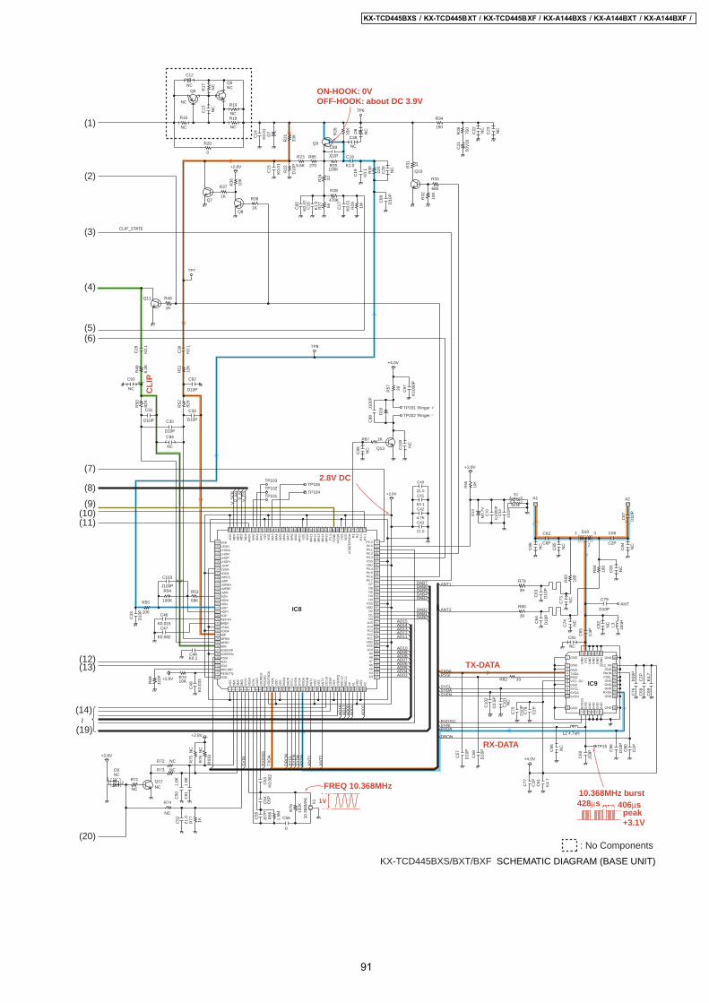
1V
SS
2D
M1
3D
M2
4D
M3
5S
YR
I6
VS
SO
7X
TAL
8LO
AD
9V
DD
RE
G10
RX
DS
G11
VD
DT
XD
A12
TX
DA
13V
DD
14V
SS
15PA
ON
16D
AO
N17
SY
CL
18S
YE
N19
SY
DA
20R
XD
A21
RX
DB
22A
NT
123
VD
D24
VS
S25
AN
T2
2612
CLK
2712
DAT
28V
SS
29C
SR
OQ
30B
SC
L031
BS
CL1
32A
033
A1
34V
DD
35V
SS
36A
2
37A338A439A540A641A742A843A944A1045VSS46VDD47A1148A1249A1350A1451A1552D053D154D255VDD56VSS57D358D459D560D661D762P0.763P0.664P0.565P0.466VDD67VSS68P0.369P0.270P0.171P0.072PX.2
73P
X.1
74P
X.0
75R
276
R1
77V
DD
EE
PR
OM
78V
DD
79V
SS
80K
HZ
9681
TON
E82
P1.
583
MA
1584
MA
1485
MA
1386
MA
1287
MA
1188
VD
D89
VS
S90
MA
1091
MA
992
MA
893
MA
794
MA
695
MA
596
MA
497
MA
398
VD
D99
VS
S10
0M
A2
101
MA
110
2M
A0
103
FR
DY
104
MD
410
5M
D2
106
MD
110
7M
D0
108
VD
D
109 VSS110 LSON111 LHONI112 LHON113 LHOP114 LHOPI115 LSOP116 VSSA117 VDDA118 LMICS119 LMIP120 LMFBN121 LMFBP122 LMIN123 SON124 HONI125 HON126 HOP127 HOPI128 SOP129 REFVH130 BREF131 VSSA132 VDDA133 MIP134 MFBN135 MFBP136 MIN137 ADREFP138 ADREFN139 RSSI140 AD3141 AD4142 MPCINP143 RESETQ144 VDD
K0.
01
C15
50V
10
C21Q9
33K
R21D
7
4.7K
C42K0.1
C41Z1.0
C40
Z1.0
C43
Q11
1K
R48
K0.
1
C30
12K
R51
82K
R52
D10P
C32
D10
P
R22
5.6K
R23
100KR25
33K
R26
K1.0
C18
K0.
1
C19 22
0
R30
22R24
K1.
0
C16 56R27
K0.
082
C53
K0.
1
C29
D10P
C31
82K
R50
8.2K
R49
C6P
C54
J27P
C55
K0.082
C47
NCR72
NCR73
NC
R71
NC
R74
100K
R54
100
R55
D10
P
C33
1KR77
NC
R75
NC
R76
+2.8V
K0.1C48
68K
R53
K0.
033
C49
TP7
TP8
+2.8V
R20
0
Q71K
R37 10K
R36
+2.8V
Q81K
R38
C56
0
R78
150K
TP105
TP104
TP103
TP102
TP101
C50
1.0K
C51
1.0K
C52
Z1.
0
D9NC
13 2
+2.8V
K0.015
C46
+4.0V C60
J33P
L2 4.7uH
5 RSSI6 VCC_OC7 GND8 SYCL9 SYDA
10 SYEN
11 GND
12R
XD
SG
13S
YR
I14
GN
D15
GN
D16
GN
D17
GN
D
18GND
19GND20RXDA21GND22GND23GND24PSEL25PAON26GND27VCC_PA
28GND
29G
ND
30G
ND
31G
ND
32G
ND
33R
F1
34G
NDGND1
GND2
GND3
TXDA4
R82 33
R69
J22P 10K
R70+2.8V
C65
C3P
R80
39
C64
D10
P
C63
D10
P
A2
1
C62
C6P
C66
C2P
R79
39
A1
1D101 3
2
R56
10K
D10
P
C34
+2.8V
TP6
S13421
X1
10.3
68M
Hz
TP15
M4.
7V
D13
K10
00P
C70
L3
33nH
R84
180
R83
180
C69
K4.
7
C68
C2P
C75
D10
P
C76
D10
P
ANTC79
D10P
C80
C2P
C17
K0.
01R
29 1M
R28
470K
C67
D10
P
D10P
C35
C14
K0.
01
D10
P
C88
J22P
C89
270
R85
K0.
47
C90
C92
D10P
D10
P
C96
C61
K4.
7Q12NC C
77
C2P
C78
C2P
R86
1.5M
C57
D10
P
C58
D10
P
+4.0V
TP202
R87 1K
Q13
C97
K10
00P
C98
J100
P
D16
R57 39
TP201
C23 NC
C93
NC
C94
NC
C95 NC
C73 NC
C85 NC
C20 NC
C82 NC
NC
C13
NC
C38
C86 NC
C10
0
NC
C83 NC
C99 NC
C84 NC
C74 NC
C81
NC
C12
NC
NC
D8
NC
R16NC
R19
NC
R17
NC
R18
Q5
NC
C10
1N
C
Q6NC
C103
J100P
C10
2
C0.
5P
Q10
10R31
680
R33
10K
R32
750
R35
150
R34
C22 NC
AD15AD14AD13AD12AD11
AD10AD09AD08AD07AD06AD05AD04AD03
AD
02
AD
01A
D00
DAB7DAB6DAB5DAB4DAB3
DAB2DAB1DAB0
V_S
CK
V_S
OV
_SI
V_C
S
AD
17A
D16
RS
SI
SY
RI
RX
DS
GT
XD
A
SY
CL
SY
EN
SY
DA
RX
DA
DR
ON
SYEN
RXDSG
CLIP_STATE
AN
T1
AN
T2
ANT2
ANT1
DRON
SYRI
TXDARSSI
RXDA
SYCLSYDA
'Ringer +'
'Ringer -'
IC8
IC9
(8)
(7)
(4)
(5)(6)
(3)
(9)(10)(11)
(12)(13)
(2)
(1)
(14)
~
(19)
(20): No Components
KX-TCD445BXS/BXT/BXF SCHEMATIC DIAGRAM (BASE UNIT)
10.368MHz burst 406 s
peak+3.1V
428 s
TX-DATA
RX-DATA
2.8V DC
1V
FREQ 10.368MHz
CL
IP
ON-HOOK: 0VOFF-HOOK: about DC 3.9V
91
KX-TCD445BXS / KX-TCD445BXT / KX-TCD445BXF / KX-A144BXS / KX-A144BXT / KX-A144BXF /
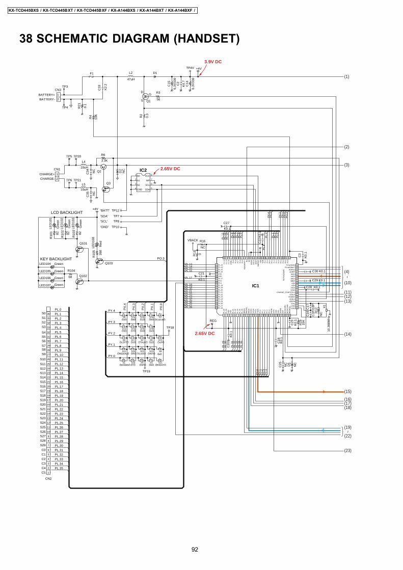
38 SCHEMATIC DIAGRAM (HANDSET)3.9V DC
2.65V DC
2.65V DC
C28 K0.1
Q3
TP5
C23
K0.
1
Q2C
15
6.3V
330
CN1
1CHARGE+2CHARGE-
C29 K0.1
L4
10uH
C3
K0.
1
VBACK
+4V
F1
C20
K0.
1
IC21 A0
2 A1
3 A2
4 GND 5SDA
6SCL
7WP
8VCC
C22
K0.
1
R2
0.3
R21 0.1
C33
K2.
2
L2
47uH
TP7
TP3CN3
1BATTERY+2BATTERY-
TP12
C2
K4.
7
C21
K0.1
R6
3.3K
R4
10K
TP8
C18
K0.
1
R19
15K
C27
K0.1
IC1
1P
L.29
2P
L.30
3V
DD
4V
SS
5P
L.31
6P
L.32
7P
L.33
8P
L.34
9P
L.35
10D
RO
N11
RX
DS
G12
RX
DA
13S
YE
N14
SY
DA
15S
YC
L16
TX
DA
17P
Y.0
18P
Y.1
19P
Y.2
20P
Y.3
21P
Y.4
22P
AO
N23
SY
RI
24V
DD
25V
SS
26O
NS
W27
CD
T28
DC
DC
DR
V29
DC
DC
CM
R30
RE
SE
TQ 31VSSO
32LOAD33XTAL34VDDPM35VDDLO36VDDBAT37VDDLR38CHARGE_START(P0.2)39VDDA40VSSA41HON42HOP43BREF44MICS45MICP46MICN47ADREF48ADRSSI49P0.4(ADBAT)50P0.5(AD4N)
51
51:P
0.6(
AD
4P)
52P
0.3
53P
X.0
54P
X.1
55P
X.2
56P
L.0
57P
L.1
58P
L.2
59P
X.3
60P
X.4
61P
L.3
62P
L.4
63V
DD
64V
SS
65S
UP
EE
P
66I2
DA
T
67IS
CLK
68M
OD
E
69R
2
70R
1
71V
BA
CK
/P0.
7
72P
L.5
73P
L.6
74P
L.7
75P
L.8
76P
L.9
77V
DD
LI
78P
L.10
79P
L.11
80P
L.12
81 PL.1382 PL.1483 PL.1584 PL.1685 VSS86 VDD87 PL.1788 P0.089 P0.190 PL.1891 PL.1992 PL.2093 PL.2194 PL.2295 PL.2396 PL.2497 PL.2598 PL.2699 PL.27100PL.28
D1
CN2
1C5
2C4
3C3
4C2
5C1
6C0
7S298S289S2710S26
11S25
12S24
13S23
14S22
15S21
16S20
17S19
18S18
19S17
20S16
21S15
22S14
23S13
24S12
25S11
26S10
27S928S829S7
30S631S5
32S4
33S334S235S136S0
R3
56Q1
G
S
D
TP4
TP10
C30 K0.1
TP4V
X1
10.3
68M
Hz
C17
J18P
C14
6.3V
330
L5
10uH
TP6
C16
C1P
Q102
Gre
en
LED
101
Q101
R10
1 82
Gre
en
LED
102
R10
2
82
Gre
en
LED
103
R10
3
82
GreenLED106
GreenLED105
GreenLED107
68
R104
GreenLED104
390
R10
5
Q103
Red
LED
108
+4V
S14
S9
S19
S17
S8 S24
S21
S20
S7
S11
S25S12
S18
S3
S22
S4S6
S15S13
S23
S2
S5S16S1
TP18
TP19
TP20
TP21
R11 0
C25 NC
C34 NC
C35 NC
D5
NC
D2
NC
R12
NC
R16
NC
REG
PL.14
PL.19
PL.23
PL.15
PL.18
PL.21
PL.16P
X.3
PX
.1
PL.22
PL.15
PL.17
PL.34
PL.27
PL.28
PL.29
PL.0
PL.
29
PL.31
PL.21
PL.19
PL.10
PL.1PL.2
PL.
30
PY
.2
PL.3
PY
.1
PL.
4
PL.28
PL.16
PL.
5
PX
.0P
X.1
PL.18
PX
.2
PL.13
PL.
32
PL.20
PL.22
PL.27
PL.
0
PX
.4
PY
.4
PL.4
PL.7
PL.
1
PL.8
PL.26
PY
.3
PL.
2
PL.9
PL.32
PL.11
PL.
3
PL.
6
PL.25
PL.
7
PL.23
PY
.0
PL.17
PL.
8
PL.12
PL.24
PL.5
PL.
9
PL.
10
PL.
31
PL.14
PL.24
PX
.4
PX
.0
PL.
11
PL.25
PL.33
PL.35
PL.
33
PL.
12
PL.26
PL.
34
PL.30
PL.
35
PL.13
PL.6
PL.20P
O.3
PO.3
PY.4
PY.1
PY.0
PY.3
PX
.3
PY.2
PX
.2
'GND'
'SCL'
'SDA'
'BATT'LCD BACKLIGHT
KEY BACKLIGHT
Õ8Õ
Õ->Õ
Õ5Õ
ÕRÕ
Õ0Õ
Õ6Õ
ÕREDIALÕ
Õ7Õ
ÕTEL BOOKÕ
Õ1Õ
Õ4Õ
Õ2Õ Õ9Õ
ÕUPÕ
ÕINTÕ
ÕCancelÕ
ÕRIGHTÕ
ÕLEFTÕ Õ3Õ
Õ#Õ
ÕTALKÕ
ÕSPÕÕ*ÕÕDOWNÕ
(1)
(14)
(10)
(11)(12)(13)
(4)
(3)
(2)
(15)
(16)(17)(18)
(22)
(23)
(19)~~
92
KX-TCD445BXS / KX-TCD445BXT / KX-TCD445BXF / KX-A144BXS / KX-A144BXT / KX-A144BXF /

TX-AF
RX-AF
SP-PhoneRX-AF
TX - DATA
RX - DATA
Frequency 10.368MHz
C8
D10
P
R22 0
C7
K0.1
TP1
R18 33
L3
4.7uH
R23 2.2
R1
2.2K
D3
C54
D10
P
TP2
A201
R7
470
MCLK
C5
6.3V
4.7
C66
D10
PMICC4
K0.1
C57
J33P
ANT
C6
D10
P
C26
K0.
1
IC3
ALPS_RF_UGSE6
5 RSSI6 VCC_OC7 GND8 SYCL9 SYDA10 SYEN
11 GND
12R
XD
SG
13S
YR
I14
GN
D15
GN
D16
GN
D17
GN
D
18GND
19GND20RXDA21GND22GND23GND24PSEL25PAON26GND27VCC_PA
28GND
29G
ND
30G
ND
31G
ND
32G
ND
33R
F1
34G
NDGND1
GND2
GND3
TXDA4
R5
470
R8
470
TP11
R17
56
R20
56
C31
D10
P
C12
D10
P
TP102IC1011
CD2
FC23
FC14
VIN5
VO1
6VCC
7GND
8VO2
56K
R107
K0.
1
C10
9
D101
68K
R108
TP101
K0.1
C105
10K
R10
9
D10
P
C11
0
D10
P
C11
1
D10
P
C10
8
D10
P
C10
3
K0.
1
C10
7
K2200P
C102
K1.
0
C10
6
C65
D10
PC
206
K4.
7
C20
9
D10
P
C62
K1.
0
C64
K1.
0C
56
C2P
C55
C2P
L6
2.7nH
C20
8
D10
PC
67
C2P
C11
6
D10
P
C11
5
D10
P
C20
2
C0.
5P
D7
M4.
7V
D6
M4.
7VC
207
NC
NC
C10
4NC
C101
C20
1
NC
C63 NC
C20
3
NC
C20
4
NC
D10
2N
C
NC
R106
R11
0
NC
C60
6.3V
4.7
- SPEAKER+ J101
J12RECIEVER-
+
S10
C24
K0.
1
TP16
TP17
'POWER'
(1)
(14)
(10)
(11)(12)(13)
(4)
(3)
(2)
(15)
(16)(17)(18)
(22)
(23)
(19)~~
KX-A144BXS/BXT/BXF SCHEMATIC DIAGRAM (HANDSET)
93
KX-TCD445BXS / KX-TCD445BXT / KX-TCD445BXF / KX-A144BXS / KX-A144BXT / KX-A144BXF /

39 SCHEMATIC DIAGRAM (CHARGER UNIT)TP3
R2
27
TP4D1
2
1
J1
pinL
DC_PLUG
22
Charge_minus
TP1
TP2
R1
Charge_plus
SCHEMATIC DIAGRAM (CHARGER UNIT)
94
KX-TCD445BXS / KX-TCD445BXT / KX-TCD445BXF / KX-A144BXS / KX-A144BXT / KX-A144BXF /

40 C
IRC
UIT
BO
ARD
(BAS
EU
NIT
)40
.1.
Com
pone
ntVi
ew
Q1
S1
R59
R66
R68
R60
R19
R18
L1
PbF
X1
IC7
IC4
IC8
IC9
IC6
IC3
IC5IC
1
IC2
JMP
6JM
P2
JMP
4
JMP
3
JMP
9
JMP
1JM
P5
1
1
JMP
8
JMP
7
J1
A1
A2
J2
D4
SA1
RLY
1
C25
C24
C2
D1
D9
D12
R78
D11
D2
D3
D7
D6
D13
D8
D16
D5
D15
D14
R4
R5
R6
R7
R8 R
33 R37
R51
R30
R16
R31
R17
R23
R24
R35
R34
R25
R28
R75
R71
R77
R76
R72
R73
C50
C51
C52
C53
C56
C95
R74
R7014
4
10910
8
R69
R49
R27
R52
R12
R9
R10
R14
R15
R39 R40 R48
R45
C27
R46
R87
R67
R2
R36
R38R11
C88
R32
C21
C90
R20
R13
R56
R65C77
C43
C75C78
C101C102
C10
3
C33
C36
C87
C86
C37
C67
C76
C69
C83
C85
C96
C32
C94R50
Q8
Q12
Q9
B C E
R41
R43
R47
R57
R80
R64
R62
R57
R61
R83
R84
D10
R79
L3
Q3
Q4
Q7
Q5
Q11
Q13
Q10
Q6
Q2
R1 R
42R
44
R3
C1
C28
CS
141
1
1
1
45 8
161732
1 11
28 15
INT
SD
X
SD
R
SC
LK
C26
C91
C44
C63
C84
C64
C34
C61
C54
C55 R
86
C58
R82
C39
C99
C10
0C
97
C45
L2
3736
C72
C71
C60
C68
C80
C66
C62
C73
C79 C82
C81
C65
C74
28 18
AN
T
C6
C8
C3 C4
C9
C41
C40
73
72
C10
C7
C12
C70
C98
C14
C19
C18
C38 C23
C22
C16
C30
C29
C93
C92
C49
C89
R29
C17
C48
C42R54
R55
R26
R21
R85
C20
R22
C15
R53
C31
C46
C47
C35
C13
C5
C11
B
C
E
RE
SE
T(B
BIC
: 143
)X
1(B
BIC
: 7
10.3
68 M
Hz)
BE
LL(B
BIC
: 81)
BE
LL L
ED
(BB
IC: 7
6)
KX
-TC
D44
5BX
S/B
XT
/BX
F C
IRC
UIT
BO
AR
D (
BA
SE
UN
IT)
Com
pone
nt V
iew
KX-TCD445BXS / KX-TCD445BXT / KX-TCD445BXF / KX-A144BXS / KX-A144BXT / KX-A144BXF /
95

40.2
. Fl
owSo
lder
Side
View
TP13
TP15
TP8
TP7
TP11
TP10
6
TP9
TP1
24
156
TP4
TP2
TP3
TP10
TP6
TP20
2
TP20
1
TP5
GND
MODE
SCL
SDA
VDD
J105
J102
J104
J103
J101
CH
AR
GE
CH
AR
GE
KX
-TC
D44
5BX
S/B
XT
/BX
F C
IRC
UIT
BO
AR
D (
BA
SE
UN
IT)
Flo
w S
olde
r S
ide
Vie
w
IC3
Out
put (
2.8V
)C
HA
RG
E+
CH
AR
GE
IC2
Inpu
t(5
.5V
)IC
2 O
utpu
t(4
.0V
)R
F C
lock
(10.
368M
HZ
)
PbF
KX-TCD445BXS / KX-TCD445BXT / KX-TCD445BXF / KX-A144BXS / KX-A144BXT / KX-A144BXF /
96

41 C
IRC
UIT
BO
ARD
(HAN
DSE
T)41
.1.
Com
pone
ntVi
ew
Bat
tery
(+
)T
P B
ATT
VD
D(+
2.65
V)
TP
4VR
F C
lock
(BB
IC: 2
3 10
.368
MH
z)G
ND
Bat
tery
(-)
SP
+ S
P-
(to
Spe
aker
)
RE
V+
RE
V-
(to
Rec
eive
r)
CD
T(B
BIC
: 27)
PbF
L2
D7D6
D3
D5
R11VBACK
TP19
TP18TP3 TP4
R16
R104
Q102
D1
C22
C30
C8
C3
C24 C26 C28
C29
C6R8
D2
C16
R12 C17
SP/BUZ
Q3
Q2
C7
C4C5
C34
C33C35
CHG+ CHG-MIC
R5R7R1
R4
R2R3
C11
0
C11
5
C31
R20
R10
7
R17
L3
L6
C57
MC
LK
C21
C25 R19
IC1
IC2
F1
58
41C
27Q
103
TP
1
TP
101
TP
102
R18
C56
TP
211
18281
C2
C20
C23
C18
RE
G
L5L4
R21
R22
R6
X1
Q1
BATT
TP17
TP16
TP4V
R105
R106C101
D101
D102
Q10
1
R109C106
R110
R101
R102R103
C107C12
C116
C206
C207C203
C202
C204
C201
C67
C60
C66
C63
C64C65
C54
C55
C62R23
C208
C209
C108C109
C102
R108
C103
C104
C111C105
IC1015
8 1
POWER
GND
SCL
SDA
TP21TP20
IC3
C15
C14
AN
T
100
1
8081
50 513130
KX
-A14
4BX
S/B
XT
/BX
F C
IRC
UIT
BO
AR
D (
HA
ND
SE
T)
Com
pone
nt V
iew
KX-TCD445BXS / KX-TCD445BXT / KX-TCD445BXF / KX-A144BXS / KX-A144BXT / KX-A144BXF /
97
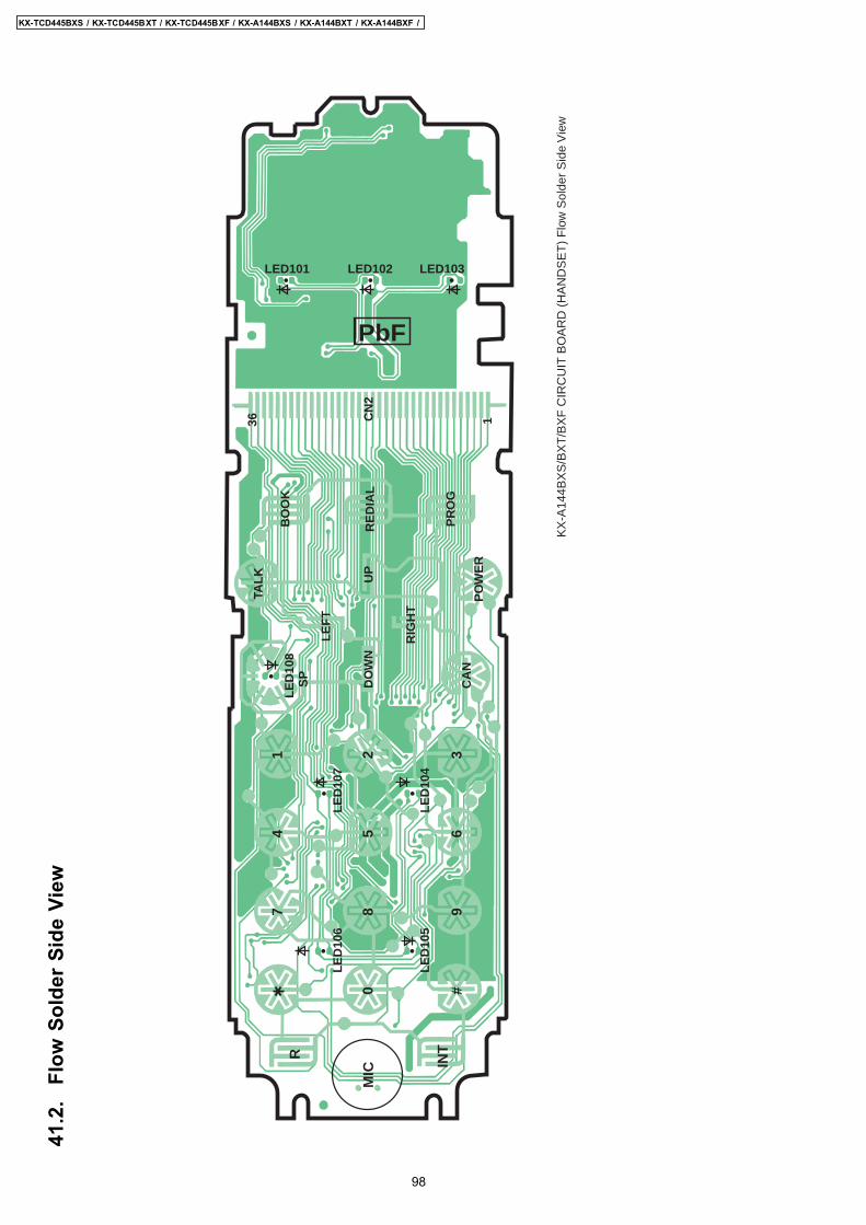
41.2
. Fl
owSo
lder
Side
View
KX
-A14
4BX
S/B
XT
/BX
F C
IRC
UIT
BO
AR
D (
HA
ND
SE
T)
Flo
w S
olde
r S
ide
Vie
w
1
PR
OG
PbF
BO
OK
UP
PO
WE
RC
AN
DO
WN
RIG
HT
RE
DIA
L
LE
FT
1 2 365
7
0 #
R4
98
INT
MIC
TAL
K36 C
N2
LED101
LE
D10
7
LE
D10
8S
P_
LE
D10
4
LE
D10
6
LE
D10
5
LED102 LED103
KX-TCD445BXS / KX-TCD445BXT / KX-TCD445BXF / KX-A144BXS / KX-A144BXT / KX-A144BXF /
98

42 CIRCUIT BOARD (CHARGER UNIT)42.1. Component View
PbF
D1
J1
CIRCUIT BOARD (CHARGER UNIT) Component View
42.2. Flow Solder Side View
PbF
R1
R2
TP4
TP1
TP2
TP3
CIRCUIT BOARD (CHARGER UNIT) Flow Solder Side View
99
KX-TCD445BXS / KX-TCD445BXT / KX-TCD445BXF / KX-A144BXS / KX-A144BXT / KX-A144BXF /
GKXTCD445BXSKXTCD445BXTKXTCD445BXFKXA144BXSKXA144BXTKXA144BXF