KSZ8692PB Register Description
275
KSZ8692PB Registration Description Integrated Networking and Communications Controller Micrel Inc. • 2180 Fortune Drive • San Jose, CA 95131 • USA • tel +1 (408) 944-0800 • fax + 1 (408) 474-1000 • http://www.micrel.com March 2010 M9999-031810-1.2 KSZ8692PB Register Description Revision 1.2 March 18, 2010
-
Upload
khangminh22 -
Category
Documents
-
view
2 -
download
0
Transcript of KSZ8692PB Register Description

KSZ8692PB Registration Description Integrated Networking and Communications Controller
Micrel Inc. • 2180 Fortune Drive • San Jose, CA 95131 • USA • tel +1 (408) 944-0800 • fax + 1 (408) 474-1000 • http://www.micrel.com
March 2010 M9999-031810-1.2
KSZ8692PB Register Description
Revision 1.2
March 18, 2010

KSZ8692PB Registration Description Integrated Networking and Communications Controller
March 2010 2 M9999-031810-1.2
General Description The KSZ8692PB is a highly-integrated System-on-Chip (SoC) containing an ARM 922T 32-bit processor and a rich set of peripherals to address the cost-sensitive, high-performance needs of a wide variety of high-bandwidth networking and communications applications.
Features ARM 922T High-Performance Processor Core • 250MHz ARM 922T RISC processor core • 8KB I-cache and 8KB D-cache • Configurable Memory Management Unit (MMU)
for Linux and WinCE
Memory Controller • 8/16-bit external bus interface for FLASH, ROM,
SRAM, and external I/O • NAND FLASH controller with boot option • 200MHz 32-bit DDR controller • Four JEDEC Specification JESD82-1-compliant
differential clock drivers for a glueless DDR interface solution
Ethernet Interfaces • Two Ethernet (10/100 Mbps) MACs • MII interface • Fully compliant with IEEE 802.3 Ethernet
standards
IP Security Engine • Hardware IPSec Engine guarantees 100Mbps
VPN • Secure Socket Layer Support • DES/3DES/AES/RC4 Cyphers • MD-5, SHA-1, SHA-256 Hashing Algorithms • HMAC • SSLMAC
PCI Interface • Version PCI 2.3 • 32-bit 33/66MHz • Integrated PCI Arbiter supports three external
masters • Configurable as Host bridge or Guest device • Glueless Support for mini-PCI or CardBus
devices
Dual High-Speed USB 2.0 Interfaces • Two USB2.0 ports with integrated PHY • Can be configured as 2-port host, or host +
device
SDIO/SD Host Controller • Meets SD Host Controller Standard Specification
Version 1.0 • Meets SDIO card specification Version 1.0
DMA Controllers • Dedicated DMA channels for PCI, USB, IPSec,
SDIO and Ethernet ports.
Peripherals • Four high-speed UART ports up to 5Mbps • Two programmable 32-bit timers with watchdog
timer capability • Interrupt Controller • Twenty GPIO ports • One shared SPI/I2C interface • One I2S port
Debugging • ARM9 JTAG debug interface • JTAG Boundary Scan Support
Power Management • CPU and system clock speed step-down options • Ethernet port Wake-on-LAN • DDR and PCI power-down
Operating Voltage • 1.2V power for core • 3.3V power for I/O • 2.5V power for DDR memory interface
Reference Hardware and Software Evaluation Kit • Hardware evaluation board • Board support package including firmware
source codes, Linux kernel, and software stacks • Complete hardware and software reference
designs available

KSZ8692PB Registration Description Integrated Networking and Communications Controller
March 2010 3 M9999-031810-1.2
Revision History Revision Date Summary of Changes 1.0 10/20/08 New Release 1.1 3/10/09 Added SPI Operation, Deleted AMBA bus 200MHz support 1.2 3/2/2010 Fix some typos

KSZ8692PB Registration Description Integrated Networking and Communications Controller
March 2010 4 M9999-031810-1.2
Contents 1.0 Memory Map ..........................................................................................................................................................5 2.0 Register Description .............................................................................................................................................6
2.1 Register Map Summary.................................................................................................................................6 2.2 System Register (0x0000-0x1fff)...................................................................................................................7 2.3 PCI-AHB Bridge Configuration Registers (PABCSR) (0x2000-0x3FFF) ....................................................11 2.4 AHB Internal Access to PCI Configuration Registers (Offsets 0x2000-0x20FC)........................................19 2.5 DDR Memory Controller Register (0x4000-0x4FFF) ..................................................................................33 2.6 Static Memory Controller Register (0x5000-0x5FFF) .................................................................................60 2.7 WAN DMA Registers (0x6000-0x7FFF)......................................................................................................68 2.8 LAN DMA Registers (0x8000-0x9FFF) .......................................................................................................88 2.9 SDIO Registers (0xA000-0xAFFF)............................................................................................................110 2.10 Relation between Transfer Complete and Data Timeout Error.................................................................129 2.11 Relation between Command Complete and Command Timeout Error ....................................................129 2.12 Relation between Command CRC Error and Command Timeout Error...................................................130 2.13 Error Interrupt Status Enable/Normal Interrupt Status Enable Register (offset 034h)..............................130 2.14 Relation between Auto CMD12 CRC Error and Auto CMD12 Timeout Error...........................................135 2.15 Capabilities Register (offset 040h) ............................................................................................................136 2.16 Maximum Current Value Definition Table .................................................................................................138 2.17 USB Registers (0xB000-0xDFFF).............................................................................................................139 2.18 Capability Registers ..................................................................................................................................154 2.19 Operational Registers ...............................................................................................................................154 2.20 UART Registers (0xE000-0xE1FF)...........................................................................................................183 2.21 Interrupt Controller Registers ....................................................................................................................190 2.22 Timer Registers .........................................................................................................................................220 2.23 GPIO Registers .........................................................................................................................................221 2.24 I2C Registers............................................................................................................................................226 2.25 SPI Registers ............................................................................................................................................230 2.26 Miscellaneous Registers ...........................................................................................................................229 2.27 I2S Registers.............................................................................................................................................231 2.28 STA Registers ...........................................................................................................................................233 2.29 MIB Counters ............................................................................................................................................237 2.30 Nand Flash Control Registers (0x 0000-0xFFFF).....................................................................................240 2.31 IPSec Registers (0x1FF8_0000 - 0x1FFB_FFFF) ....................................................................................248 2.32 AES .........................................................................................................................................................255 2.33 DES .........................................................................................................................................................257 2.34 RC4 .........................................................................................................................................................259
3.0 Host Communication ........................................................................................................................................263 3.1 Descriptor Lists and Data Buffers .............................................................................................................263 3.2 Receive Descriptors (RDES0-RDES3) .....................................................................................................263 3.3 Transmit Descriptors (TDES0-TDES3) .....................................................................................................265

KSZ8692PB Registration Description Integrated Networking and Communications Controller
March 2010 5 M9999-031810-1.2
1.0 Memory Map Upon power up, KSZ8692PB memory map is configured as shown below.
The default base address for the KSZ8692PB system configuration registers is 0x1FFF_0000. After power up, user is free to remap the memory for specific application by changing the corresponding base address.
NAND Flash memory bank 0 64KB
DDR 256MB
System Config. Registers 64KB
0x0FFF_FFFF | | | | 0x0000_0000
0x1FFE_FFFF | 0x1FFE 0000
0x1FFF_FFFF | 0x1FFF_0000
Total address space = 512MB IPSEC
256KB 0x1FFB_FFFF 0x1FF8_0000

KSZ8692PB Registration Description Integrated Networking and Communications Controller
March 2010 6 M9999-031810-1.2
2.0 Register Description This chapter describes the system configuration registers(SCRs) of the KSZ8692PB.
2.1 Register Map Summary
The KSZ8692PB SCRs are located in a block of 64KB in the host memory address space. After Power on reset, user can remap the SCR’s to a desired offset. The SCRs are word aligned, 32 bits long, and must be accessed using word instructions. Within the 64KB, the address range for different function blocks is summarized in the following.
2.1.1 AHB (Register Offset) Address Map 0x0000 – 0x1fff System Registers 0x2000 – 0x3fff PCI Bridge Registers 0x4000 – 0x4fff DDR memory Controller Registers 0x5000 – 0x5fff Static Memory Controller Registers 0x6000 – 0x7fff WAN DMA Registers 0x8000 – 0x9fff LAN DMA Registers 0xa000 – 0xafff SDIO Registers 0xb000 – 0xbfff USB Device Controller Registers 0xc000 – 0xcfff USB Host Controller EHCI Registers 0xd000 – 0xdfff USB Host Controller OHCI Register 0xe000 – 0xffff Peripheral Registers (see APB address mapping section for detailed mapping)
2.1.2 APB (Register Offset) Address Map 0xe000 – 0xe07f UART 1 0xe080 – 0xe0ff UART 2 0xe100 – 0xe17f UART 3 0xe180 – 0xe1ff UART 4 0xe200 – 0xe3ff Interrupt Controller Registers 0xe400 – 0xe5ff Timer Controller Registers 0xe600 – 0xe7ff GPIO Controller Registers 0xe800 – 0xe8ff I2C Registers 0xe900 – 0xe9ff SPI Registers 0xea00 – 0xeaff Miscellaneous Registers 0xeb00 – 0xebff I2S Registers 0xec00 – 0xecff MDIO Registers 0xed00 – 0xeeff MIB Registers 0xef00 – 0xefff Undefined

KSZ8692PB Registration Description Integrated Networking and Communications Controller
March 2010 7 M9999-031810-1.2
2.2 System Register (0x0000-0x1fff)
2.2.1 System Configuration Register (SYSCFG Offset 0x0000) This register determines the start address of all the system control registers. The total system control register space is fixed at 64Kbytes boundary.) The following Table shows the register bit fields.
BIT FIELD DEFAULT VALUE
READ/ WRITE
DESCRIPTION
31:29 0x0 RO Reserved
28:16 0x1FFF RW SPRBP System Configuration Register Bank Base Pointer The Base address of the system configuration register bank. The resolution of the address is 64Kbytes.
15:0 0x0 RO Reserved
2.2.2 System Clock and Bus Control Register (CLKCON Offset 0x0004) The CLKCON register is written by the CPU to configure the running frequency of the CPU clock, system clock and DDR memory clock.
The following Table shows the register bit fields.
BIT FIELD DEFAULT VALUE
READ/ WRITE
DESCRIPTION
31:11 0x0 Reserved 10:9 0x1 RW ipcs IPsec Clock Select
11 = 200 Mhz 10 = 166 Mhz 01 = 125 Mhz (Default) 00 = 50 Mhz
8 0 RW sfmode System Fast Mode for Simulation This bit is for simulation only. Software should never set this bit.
7 0x0 RW pci66msel PCI Bus Clock Select when set, PCI bus is running at 66 Mhz. When cleared, PCI bus is running at 33 Mhz.
6:4 0x4 RW armcs ARM9 Clock Select 100 = 250 011 = 200 010 = 166 (Default) 001 = 125 000 = 50
3:2 0x3 RW dmcs DDR Memory Clock Select 11 = 200 Mhz 10 = 166 Mhz 01 = 125 Mhz (Default) 00 = 100 Mhz
1:0 0x2 RW scdc AMBA System Clock (SYSCLK) Select 11 = Reserved 10 = 166 Mhz 01 = 125 Mhz (Default) 00 = 50 Mhz

KSZ8692PB Registration Description Integrated Networking and Communications Controller
March 2010 8 M9999-031810-1.2
2.2.3 NAND Flash Configuration Register (NFLCFG Offset 0x0008) This register determines NAND Flash write protection, Auto-Page enable, and the start address of NAND Flash bank The following Table shows the register bit fields.
BIT FIELD DEFAULT VALUE
READ/ WRITE
DESCRIPTION
31 1 RW WPE_N write protection enable When set, NAND flash memory write protect is off. When cleared, NAND flash memory write protect is on. The write protect input to NAND flash memory is controlled by this vaule
30 strapped by Power-on Reset
RW APOE Auto page open enable When set, auto page open function is enable When cleared, auto page open function is disable
29 0x0 RO Reserved
28:16 0x1FFE RW NANDFlBP Register Bank Base Pointer The Base address of the NAND Flash bank. The resolution of the address is 64Kbytes.
15:0 0x00 RO Reserved
2.2.4 IPSEC Configuration Register (IPSECCFG Offset 0x000C) This register determines the start address of IPSEC registers. The total IPSEC register space is fixed at 256Kbytes boundary.
The following Table shows the register bit fields.
BIT FIELD DEFAULT VALUE
READ/ WRITE
DESCRIPTION
31:29 0x0 RO Reserved
28:18 0x7FE RW IPSECBP Register Bank Base Pointer The Base address of the IPSEC configuration register bank. The resolution of the address is 256Kbytes.
17:1 0x0 RO Reserved
0 1 RW IPSEC Enable
2.2.5 (Factory Reserved Offset 0x0010)
2.2.6 DDR Delay Line and Combo I/O Pad Configuration Register (DDLCP Offset 0x0014) The register is for the DDR delay line configuration and i/o pad configuration.

KSZ8692PB Registration Description Integrated Networking and Communications Controller
March 2010 9 M9999-031810-1.2
The following Table shows the register bit fields.
BIT FIELD DEFAULT VALUE
READ/ WRITE
DESCRIPTION
31 0x0 RO byp_syspll Bypass system PLL enable: when set, the system PLL is disabled and the clock input from XI has to be either 250 Mhz or 200 Mhz. The following lists out the clock rate for each clock domain when the system PLL bypass is enabled. byp_syspll = 1 byp_syspll = 1 byp_clksel = 1 byp_clksel = 0 XI 250Mhz 200Mhz ARM9 250Mhz 200Mhz Denali 125Mhz 200Mhz PCI N/A 66Mhz RGMII 125Mhz N/A Sysclk 125Mhz 100Mhz Note: This bit is configured from power strapping only.
30 0x0 RO byp_clksel Bypass system PLL clock select: (power strapping) when this bit is set and system PLL is bypassed, the XI is expected to be 250 Mhz. when this bit is cleared and system PLL is bypassed, the XI is expected to be 200 Mhz. Note: This bit is configured from power strapping only.
29:20 0x0 RO Reserved
19:16 0xF RW ddrclken DDR memory clock output enable: When set, the corresponding DDR clock is enabled. When cleared, the corresponding DDR clock is forced at low. Ddrclken[0] configures DDCLKO0 Ddrclken[1] configures DDCLKO1 Ddrclken[2] configures DDCLKO2 Ddrclken[3] configures DDCLKO3
15:12 0x0 RO Reserved
11 0x0 RW byp_dspll Bypass deskew PLL enable: When set, deskew PLL is disabled in DDR clock adjustment. When cleared, deskew PLL is used in DDR clock adjustment.
10 0x0 RO Reserved
9:8 0x1 RW byp_dspll_dsel Bypass deskew PLL delay line select: 00: 1 MUX(CLKMX2X12) + 1 Delay Cell(DLY4X4) delay 01: 1 MUX(CLKMX2X12) + 2 Delay Cell(DLY4X4) delay 10: 1 MUX(CLKMX2X12) + 3 Delay Cell(DLY4X4) delay 11: 1 MUX(CLKMX2X12) + 4 Delay Cell(DLY4X4) delay
7:4 0x1 RW ddln_sel DDR Delay line configuration 0000: 2 MUX(CLKMX2X12) + 6 BUF(CLKBUFX16) delay 0001: 2 MUX(CLKMX2X12) + 8 BUF(CLKBUFX16) delay 0010: 4 MUX(CLKMX2X12) + 6 BUF(CLKBUFX16) delay 0011: 4 MUX(CLKMX2X12) + 11BUF(CLKBUFX16) delay 0100: 4 MUX(CLKMX2X12) + 12 BUF(CLKBUFX16) delay 0101: 4 MUX(CLKMX2X12) + 13 BUF(CLKBUFX16) delay 0110: 4 MUX(CLKMX2X12) + 14 BUF(CLKBUFX16) delay 0111: 4 MUX(CLKMX2X12) + 15 BUF(CLKBUFX16) delay 1000: 4 MUX(CLKMX2X12) + 16 BUF(CLKBUFX16) delay 1001: 4 MUX(CLKMX2X12) + 17 BUF(CLKBUFX16) delay 1010-1111: not valid
3 0x0 RO Reserved
2 0x0 RW Cmbo_pwd DDR pad (PWD) Receiver power down enable (active high)
1:0 0x0 RO Reserved

KSZ8692PB Registration Description Integrated Networking and Communications Controller
March 2010 10 M9999-031810-1.2
2.2.7 Feature Enable Control Registers (FEC Offset 0x0018) This register is for CPU to enable or disable the I/O channels. If the channel is disabled, then the clock to the corresponding functional block will be shut off for to save power. The following Table shows the register bit fields.
BIT FIELD DEFAULT VALUE
READ/ WRITE
DESCRIPTION
31:16 0x0 RO Reserved 17 0 RW lpsleep WAN Port disable 16 0 RW wpsleep WAN Port sleep 15 0x0 RW tmdis Timer interface disable 14 0x0 RW spidis SPI(I2C) interface disable 13 0x0 RW i2sdis I2S interface disable 12 0x0 RW uart4dis UART4 interface disable 11 0x0 RW uart3dis UART3 interface disable 10 0x0 RW uart2dis UART2 interface disable 9 0x0 RW uart1dis UART1 interface disable 8 0x0 RW norfmdis NOR flash memory disable 7 0x0 RW nandfmdis NAND flash memory disable 6 0x0 RW pcidis PCI interface disable 5 0x0 RW ipsdis IPSec disable 4 0x0 RW lpdis LAN Port disable 3 0x0 RW wpdis WAN Port disable 2 0x0 RW sdifdis SDIO interface disable 1 0x0 RW usbddis USB Device disable 0 0x0 RW usbhdis USB Host disable
2.2.8 NOR Flash / External I/O Base Address Register (NFEIOBA Offset 0x001C) This register determines the start address of static memory NOR FLASH/SRAM/ROM and Extrenal I/O banks. The following Table shows the register bit fields.
BIT FIELD DEFAULT VALUE
READ/ WRITE
DESCRIPTION
31:26 0x1FFF RW NFEIOBP NOR Flash – External I/O Bank Base Pointer The Base address of the static memory and Extrenal I/O banks
25:0 0x0 RO Reserved

KSZ8692PB Registration Description Integrated Networking and Communications Controller
March 2010 11 M9999-031810-1.2
2.3 PCI-AHB Bridge Configuration Registers (PABCSR) (0x2000-0x3FFF) The PCI-AHB Bridge (PAB) implements all configuration registers required by the PCI specification. These registers are described in the following subsections. Since the configuration registers can be accessed from both the PCI and AHB buses, they have two sets of addresses, one for each bus: PCI and AHB. The PCI bus configuration register address range is 0x0000-0x00FC, and the AHB bus configuration register address range is 0x2000-0x20FC. The PAB enables a full software-driven initialization and configuration when acting as a host bridge. This allows the software to identify and query the PAB. In the guest bridge mode, the CSID configuration register (subsystem ID and subsystem vendor ID) is programmed by the ARM9, and the remaining configuration registers are programmed by the host system. The PAB treats configuration space write operations to registers that are reserved as NO-OPs. That is, the access completes normally on the bus and the data is discarded. Read accesses, to reserved or unimplemented registers, complete normally and a data value of 0 is returned. Software reset has no effect on the configuration registers. Hardware reset sets the configuration registers to their default values. The configuration register CSID (subsystem ID and subsystem vendor ID) is programmed by the ARM9 during stage 1 initilization, thus eliminating the need for an EEPROM. Also, CBMA[3] (prefetchable bit) can be initialized in stage 1. Only internal access to these registers are done in stage 1 using offset range 0x2000-0x20FC; ie ARM9 accesses does not propagate out to the PCI bus. During Stage 2 initialization, the ARM9 programs the remaining configuration registers by using the indirect registers PBCA (address register at offset 0x2100) and PBCD (data register at offset 0x2104). The ARM9 programs the system control registers (CSRs) located at offsets 0x2200-0x2224. The PCI-AHB BRIDGE CSRs are located in the host memory address space. The PBCSRs are word aligned, 32 bits long, and must be accessed using word instructions with word-aligned addresses only. Note: Reserved bits should be written with 0. Failing to do this could cause incompatibility problems with a future version of the PCI-AHB BRIDGE. Reserved bits are undefined on read access. Retries on second data transactions occur in response to burst accesses. PBCSRs are physically located in the chip. The host uses a single instruction to access a CSR. The PCI-AHB BRIDGE implement the following configuraion registers and CSR registers. These registers are described below.
Configuration Register
Identifier PCI Bus Address Default Value
Identification CFID 0x0000 0x869216C6
Command and status CFCS 0x0004 0x04400000
Revision CFRV 0x0008 0x06**0000
Latency Timer CFLT 0x000C 0x00000000
Configuration Base Memory Address
CBMA 0x0010 0x00000000
Reserved 0x0014-28 0x00000000
Subsystem ID CSID 0x002C 0x********
Reserved 0x0030-38 0x00000000
Interrupt CFIT 0x003C 0x00000100
Reserved 0x0040-FC 0x00000000

KSZ8692PB Registration Description Integrated Networking and Communications Controller
March 2010 12 M9999-031810-1.2
Register Identifier AHB Bus Address Default Value
Configuration Register: Identification CRCFID 0x2000 0x869216C6
Configuration Register: Command and status CRCFCS 0x2004 0x04400000
Configuration Register: Revision CRCFRV 0x2008 0x06**0000
Configuration Register: Latency Timer CRCFLT 0x200C 0x00000000
Configuration Register: Configuration Base Memory Address
CRCBMA 0x2010 0x00000000
Reserved 0x2014-28 0x00000000
Configuration Register: Subsystem ID CRCSID 0x202C 0x********
Reserved 0x2030-38 0x00000000
Configuration Register: Interrupt CRCFIT 0x203C 0x00000100
Reserved 0x2040-FC 0x00000000
PCI-AHB Bridge Configuration Address PBCA 0x2100 0x00000000
PCI-AHB Bridge Configuration Data PBCD 0x2104 0x00000000
PCI-AHB Bridge Mode PBM 0x2200 0x00000000
PAB-AHB Bridge Control and Status PBCS 0x2204 0x00000000
PCI-AHB Bridge Memory Base Address PMBA 0x2208 0x00000000
PCI-AHB Bridge Memory Base Address Control PMBAC 0x220C 0x00000000
PCI-AHB Bridge Memory Base Address Mask PMBAM 0x2210 0x00000000
PCI-AHB Bridge Memory Base Address Translation
PMBAT 0x2214 0x00000000
PCI-AHB Bridge I/O Base Address PIOBA 0x2218 0x00000000
PCI-AHB Bridge I/O Base Address Control PIOBAC 0x221C 0x00000000
PCI-AHB Bridge I/O Base Address Mask PIOBAM 0x2220 0x00000000
PCI-AHB Bridge I/O Base Address Translation PIOBAT 0x2224 0x00000000
2.3.1 Configuration ID Register (CFID PCI Offset 0x0000) The CFID register identifies the PCI-AHB BRIDGE. The following Table shows the CFID register bit fields.
BIT FIELD
DEFAULT VALUE
READ/ WRITE
DESCRIPTION
31:16 0x8692 RO Device ID Provides the unique PCI-AHB BRIDGE ID number
15:0 0x16C6 RO Vendor ID Specifies the manufacturer of the PCI-AHB BRIDGE.

KSZ8692PB Registration Description Integrated Networking and Communications Controller
March 2010 13 M9999-031810-1.2
2.3.2 Command and Status Configuration Register (CFCS PCI Offset 0x0004) The CFCS register is divided into two sections: a command register (CFCS[15:0]) and a status register (CFCS[31:16]). The command register provides control of the PCI-AHB BRIDGE’s ability to generate and respond to PCI cycles. When 0 is written to this register, the PCI-AHB BRIDGE logically disconnects from the PCI bus for all accesses except configuration accesses. The status register records status information for the PCI bus-related events. The CFCS status bits are not cleared when they are read. Writing 1 to these bits clears them; writing 0 has no effect. The following Table describes the CFCS register bit fields.
BIT FIELD TYPE DEFAULT VALUE
READ/ WRITE
DESCRIPTION
31 Status 0 Read/ Clear
Detected Parity Error This bit is set when the bridge detects a parity error, even if parity error handling is disabled (as controlled by bit 6 in the command register).
30 Status 0 Read/ Clear
Signal System Error When set, indicates that the PCI-AHB BRIDGE asserted the system error SERR_N pin.
29 Status 0 Read/ Clear
Received Master Abort When set, indicates that the PCI-AHB BRIDGE terminated a master transaction (except for Special Cycle) with master abort.
28 Status 0 Read/ Clear
Received Target Abort When set, indicates that the PCI-AHB BRIDGE master transaction was terminated due to a target abort.
27 Status 0 Read/ Clear
Generated Target Abort When set, indicates that the PCI-AHB BRIDGE PCI target generated a target abort.
26:25 Status 10 RO Device Select Timing These bits encode the timing of DEVSEL#. Three allowable timings for assertion of DEVSEL#: 00 – fast 01 – medium 10 – slow
24 Status 0 Read/ Clear
Data Parity Report This bit is set when the following 3 conditions are met: 1) the bus agent asserted PERR# itself (on a read) or observed PERR# asserted (on a write) 2) the PCI-AHB BRIDGE operates as a bus master for the operation that caused the error. 3) the Parity Error Response bit (CFCS[6]) is set.
23:22 reserved 00 Reserved 21 Status 1 RO 66 MHz Capable
This read only bit indicates that the PCI-AHB BRIDGE is 66 MHz capable. Its value is always set to 1.
20 Status 1 RO New Capability New capabilities are not implemented.
19:16 Status 0x0 Reserved 15:11 Command 0x00 Reserved

KSZ8692PB Registration Description Integrated Networking and Communications Controller
March 2010 14 M9999-031810-1.2
10 Command 0 R/W Interrupt Disable
This bit disables the device/function from asserting INTx#. A value of 0 enables the assertion of its INTx# signal. A value of 1 disables the assertion of its INTx# signal. This bit’s state after RST# is 0.
9 Command 0 RO Master Fast Back-to-Back Capable Master cannot do fast back-to-back transactions to different devices.
8 Command 0 R/W System Error Enable Enable bit for SERR# driver. A value of 0 disables the SERR# driver. A value of 1 enables the SERR# driver. This bit’s state after RST# is 0. Address parity errors are reported only if this bit and bit 6 are 1.
7 Command 0 RO Address/Data stepping Bridge does not do address/data stepping.
6 Command 0 RW Parity Error Response When set, the bridge takes its normal action when a parity error is detected. When the bit is 0, the bridge sets its Detected Parity Error status bit (CFCS[31]) when an error is detected, but does not assert PERR# and continues normal operation. This bit’s state after RST# is 0.
5 Command 0 RO VGA palette access VGA palette snooping is disabled.
4 Command 0 RW Memory Write and Invalidate Enable When set, the PCI-AHB BRIDGE is allowed to generate the memory write and invalidate command. When reset, the PCI-AHB BRIDGE can only generate memory write command. This bit’s state after RST# is 0.
3 Command 0 RO Special Cycles Response Bridge ignores all special cycle operations.
2 Command 0 RW Master Operation When set, the PCI-AHB BRIDGE is capable of acting as a bus master. When reset, the PCI-AHB BRIDGE capability to generate PCI accesses is disabled. For normal operation, this bit must be set. This bit’s state after RST# is 0.
1 Command 0 RW Memory Space Access When set, the PCI-AHB BRIDGE responds to memory space accesses. When reset, the PCI-AHB BRIDGE does not respond to memory space accesses. This bit’s state after RST# is 0.
0 Command 0 RW I/O Space Access When set, the PCI-AHB BRIDGE responds to I/O space accesses. When reset, the PCI-AHB BRIDGE does not respond to I/O space accesses. This bit’s state after RST# is 0.

KSZ8692PB Registration Description Integrated Networking and Communications Controller
March 2010 15 M9999-031810-1.2
2.3.3 Configuration Revision Register (CFRV Offset PCI 0x0008) The CFRV register contains the PCI-AHB BRIDGE revision number. The following Table shows the CFRV register bit fields.
BIT FIELD
Default Value
READ/ WRITE
DESCRIPTION
31:24 0x06 RO Base Class Indicates device is a bridge, and is equal to 0x06.
23:16 - RO Subclass. Host/Guest mode determined by input pin PHGM. 0x00 – In Host bridge mode 0x80 – In Guest bridge mode
15:8 0X00 RO Reserved 7:4 0x0 RO Revision Number
Indicates the PCI-AHB BRIDGE revision number, and is equal to 0H. This number is incremented for subsequent revision.
3:0 0x0 RO Step Number Indicates the PCI-AHB BRIDGE step number, and is equal to 0H (chip revision A). This number is incremented for subsequent PCI-AHB BRIDGE steps within the current revision.
2.3.4 Configuration Latency Timer Register (CFLT PCI Offset 0x000C) This register configures the cache line size field and the latency timer. The following Table shows the CFLT register bit fields.
BIT FIELD
DEFAULT VALUE
READ/ WRITE
DESCRIPTION
31:16 0x0000 RO Reserved 15:8 0x00 R/W Configuration Latency Timer
Specifies, in units of PCI bus clocks, the value of the latency timer of the PCI-AHB BRIDGE. When the PCI-AHB BRIDGE asserts FRAME_N, it enables its latency timer to count. If the PCI-AHB BRIDGE deasserts FRAME_N prior to count expiration, the content of the latency timer is ignored. Otherwise, after the count expires, the PCI-AHB BRIDGE initiates transaction termination as soon as its GNT_N is deasserted.
7:0 0x00 R/W Cache Line Size Specifies, in unit of 32-bit words(Dword), the system cache line size. The PCI-AHB BRIDGE supports cache line sizes of 4, 8, and 16 Dwords. If an attempt is made to write an unsupported value to this register, the write is ignored and the PCI-AHB BRIDGE does not use the MWI command. If a value other than 8, 16 or 32 is written to the register, the PCI-AHB BRIDGE returns all zeros when the register is read. The driver should use the value of the cache line size to program the cache alignment bits (CSR0[15:14]). The PCI-AHB BRIDGE uses the cache alignment bits for PCI commands that are cache oriented, such as memory-read-line, memory-read-multiple and memory-write-and-invalidate.

KSZ8692PB Registration Description Integrated Networking and Communications Controller
March 2010 16 M9999-031810-1.2
2.3.5 Configuration Base Memory Address (CBMA PCI Offset 0x0010) The CBMA register specify the base memory address for accessing the devices on the AHB. This register must be initialized prior to accessing any AHB device with memory access. The following Table shows the CBMA register bit fields.
BIT FIELD DEFAULT VALUE
READ/ WRITE
DESCRIPTION
31:28 0xFC R/W Configuration Base Memory Address Defines the PCI memory base address used to access PAB and AHB resources. The resources reside in a 256MB address range.
27:4 0x0 Reserved 3 0 RO Prefetchable
1 – Indicates memory space is prefetchable. 0 – Indicates memory space is not prefetchable.
2:1 00 RO Type Locate anywhere in 32-bit address space.
0 0 RO Memory Space Indicator Determines that the register maps into the Memory space. The value in this field is 0.
2.3.6 Configuration Base Address (PCI Offsets 0x0014-0x0028) These configuration base address registers are reserved.
BIT FIELD DEFAULT VALUE
READ/ WRITE
DESCRIPTION
31:0 0x0 Reserved
2.3.7 Subsystem ID Register (CSID PCI Offset 0x002C) The CSID register is a read-only 32-bit register. The content of the CSID is loaded from the local CPU after a hardware reset. If the CSID is accessed by the PCI host before its content is loaded from the local CPU, the PCI-AHB BRIDGE responds with retry termination on the PCI bus. The following Table shows the CSID register bit fields.
BIT FIELD DEFAULT VALUE
READ/ WRITE
DESCRIPTION
31:16 - RO Subsystem ID Indicates a 16-bit field containing the subsystem ID.
15:0 - RO Subsystem Vendor ID Indicates a 16-bit field containing the subsystem vendor ID.

KSZ8692PB Registration Description Integrated Networking and Communications Controller
March 2010 17 M9999-031810-1.2
The following Table shows the access rules of the register.
Category Description
Value after hardware reset ARM9 CPU must program the value for Subsystem ID and Subsystem Vendor ID during stage 1 power up configuration.
Write access rules Only ARM9 CPU can program the Subsystem ID and Subsystem Vendor ID. This register is READ-ONLY on the PCI bus.
2.3.8 Capabilities Pointer Register (CCAP Offset 0x0034) The CCAP register points to the base address of the power management register block in the configuration address space. This pointer is valid only if the new capabilities bit in CFCS is set. The following Table shows the CCAP register bit fields. Read only.
BIT FIELD DEFAULT VALUE
DESCRIPTION
31:8 000000H Reserved. 7:0 50 Capabilities Pointer
Points to the location of the power management register block in the PCI configuration space. The value of this field is 50H.
2.3.9 Configuration Interrupt Register (CFIT PCI Offset 0x003C) The CFIT register is divided into two sections: the interrupt line and the interrupt pin. CFIT configures both the system’s interrupt and the PCI-AHB BRIDGE interrupt pin connection. The following Table shows the CFIT register bit fields.
BIT FIELD DEFAULT VALUE
READ/ WRITE
DESCRIPTION
31:24 0x00 RO MAX_LAT This field indicates how often the device needs to gain access to the PCI bus. Time unit is equal to 0.25 us, assuming a PCI clock frequency of 33 MHz. The value after a hardware reset is 28H (10 us).
23:16 0x00 RO MIN_GNT This field indicates the burst period length that the device needs. Time unit is equal to 0.25us, assuming a PCI clock frequency of 33 MHz. The value after a hardware reset is 14H (5 us).
15:8 0x01 RO Interrupt Pin Indicates which interrupt pin that the PCI-AHB BRIDGE uses. The PCI-AHB BRIDGE uses INTA# and the read value is 01H.
7:0 0x00 R/W Interrupt Line Provides interrupt line routing information. The basic I/O system (BIOS) writes the routing information into to this field when it initialized and configures the system. The value in this field indicates which I of the system interrupt controller is connected to the PCI-AHB BRIDGE’s interrupt pin. The driver can use this information to determine priority and vector information. Values in this field are system architecture specific.

KSZ8692PB Registration Description Integrated Networking and Communications Controller
March 2010 18 M9999-031810-1.2
2.3.10 Capabilities ID Register (CCID Offset 0x0050) The CCID register is a read-only register that provides information on the KSZ8692PBP power management capabilities. The following Table shows the CCID register bit fields. Read only.
BIT FIELD DEFAULT VALUE
DESCRIPTION
31 0 PME Support D3(cold) If this bit is set, the KSZ8692PBP asserts PME in D3(cold) power state. Otherwise, the KSZ8692PBP does not assert PME in D3(cold). Here this bit is set.
30 1 PME Support D3(hot) The value of this bit is 1, indicating that the KSZ8692PBP may assert PME in D3(hot) power state.
29 0 PME Support D2 KSZ8692PBP does not assert PME in D2 state.
28 0 PME Support D1 KSZ8692PBP does not assert PME in D1 state.
27 0 PME Support D0 The value of this bit is 0, indicating that the KSZ8692PBP does not assert PME in D0 power state.
26 1 D2 Support KSZ8692PBP support D2 power state.
25 1 D1 Support KSZ8692PBP support D1 power state.
24:22 000 Auxiliary Current This 3-bit field reports the 3.3Vaux auxiliary current requirements for the PCI function. If PME# generation from D3_cold is not supported by the function, this field must return a value of 000 when read.
21 0 Device Specific Initialization Indicates whether special initialization of this function is required (beyond the standard PCI configuration header) before the generic class device driver is able to use it. Note that this bit is not used by some operating systems. Microsoft Windows and Windows NT, for instance, do not use this bit to determine whether to use D3. Instead, they use the driver’s capabilities to determine this. A “1” indicates that the function requires a device specific initialization sequence following transition to the D0 uninitialization state.
20 0 Reserved, should be set to 0.
19 1 PME Clock When this bit is a “1”, it indicates that the function relies on the presence of the PCI clock for PME# operation. When this bit is a “0”, it indicates that no PCI clock is required for the function to generate PME#.
18:16 3H Power Management PCI Version(1.2) The value of this bit is 3’b011
15:8 00H Next Item Pointer Points to the location of the next block of the capabilities list in the PCI Configuration Space. The value of this field is 00H, indicating that this is the last item of the Capability linked list.
7:0 01H Capabilities ID PCI Power Management Registers ID. The value of this field is 01h, indicating that this is the power-management register block.

KSZ8692PB Registration Description Integrated Networking and Communications Controller
March 2010 19 M9999-031810-1.2
2.3.11 Power-Management Control and Status Register (CPMC Offset 0x0054) The CCID register is a read-only register that provides information on the K8842 power management capabilities. The following Table shows the CCID register bit fields.
BIT FIELD DEFAULT VALUE
DESCRIPTION
31:16 0000H Reserved. 15 0(RO, w1c) PME_Status
This bit indicates that the KSZ8692PBP has detected a power-management event. If bit PME_Enable is set, the KSZ8692PBP also asserts the PME_N pin. This bit is cleared on power-up reset or by write 1. It is not modified by either hardware or software reset. When this bit is cleared, the KSZ8692PBP deasserts the PME_N pin.
14:9 00H Reserved. 8 0(R/W) PME_Enable
If this bit is set, the KSZ8692PBP can assert the PME_N pin. Otherwise, assertion of the PME_N pin is disabled. This bit is cleared on power-up reset only and is not modified by either hardware or software reset.
7:4 0H Reserved. 3 1(RO) No Soft Reset
If this bit is set (“1”), the KSZ8692PBP does not perform an internal reset when transitioning from D3_hot to D0 because of PowerState commands. Configuration context is preserved. Upon transition from D3_hot to the D0 Initialized state, no additional operating system intervention is required to preserve configuration context beyond writing the PowerState bits.If this bit is cleared (“0”), the KSZ8692PBP does perform an internal reset when transitioning from D3_hot to D0 via software control of the PowerState bits. Configuration context is lost when performing the soft reset. Upon transition from D3_hot to the D0 state, full reinitialization sequence is needed to return the device to D0 Initialized. Regardless of this bit, devices that transition from D3_hot to D0 by a system or bus segment reset will return to the device state D0 Uninitialized with only PME context preserved if PME is supported and enabled.
2 0 Reserved. 1:0 00(RW) Power State
This field is used to set the current power state of the KSZ8692PBP and to determine its power state. The definitions of the field values are: 0: D0 1: D1 2: D2 3: D3(hot) This field gets a value of 0 after power up.
2.4 AHB Internal Access to PCI Configuration Registers (Offsets 0x2000-0x20FC)
The PCI configuration registers can be accessed internally by the ARM9 CPU using the address offsets 0x2000-20FC. They are physically the same registers as the PCI configuration registers, but accessing this address range will not generate PCI configuration cycles on the PCI bus. The only method ARM9 can generate PCI configuration cycles on the PCI bus is through the indirect registers, Configuration Address (PBCA) and Configuration Data (PBCD). During first stage initialization on power-up, the local CPU programs the Subsystem ID and Subsystem Vendor ID configuration registers normally programmed by the EEPROM. The following sections describe the PCI configuration registers described earlier with the difference being in the write access of the register bits. All register bits are READ-ONLY except for the Subsystem ID and Subsystem Vendor ID which are READ/WRITE.

KSZ8692PB Registration Description Integrated Networking and Communications Controller
March 2010 20 M9999-031810-1.2
2.4.1 Configuration ID Register (CRCFID Offset 0x2000) The CFID register identifies the PCI-AHB BRIDGE. The following Table shows the CFID register bit fields.
BIT FIELD
DEFAULT VALUE
READ/ WRITE
DESCRIPTION
31:16 0x8692 RO Device ID Provides the unique PCI-AHB BRIDGE ID number
15:0 0x16C6 RO Vendor ID Specifies the manufacturer of the PCI-AHB BRIDGE.
2.4.2 Command and Status Configuration Register (CRCFCS PCI Offset 0x2004) The CRCFCS register is divided into two sections: a command register (CRCFCS[15:0]) and a status register (CRCFCS[31:16]). The command register provides control of the PCI-AHB BRIDGE’s ability to generate and respond to PCI cycles. The status register records status information for the PCI bus-related events. The CRCFCS status bits are not cleared when they are read. The following Table describes the CRCFCS register bit fields.
BIT FIELD TYPE DEFAULT VALUE
READ/ WRITE
DESCRIPTION
31 Status 0 RO Detected Parity Error This bit is set when the bridge detects a parity error, even if parity error handling is disabled (as controlled by bit 6 in the command register).
30 Status 0 RO Signal System Error When set, indicates that the PCI-AHB BRIDGE asserted the system error SERR_N pin.
29 Status 0 RO Received Master Abort When set, indicates that the PCI-AHB BRIDGE terminated a master transaction (except for Special Cycle) with master abort.
28 Status 0 RO Received Target Abort When set, indicates that the PCI-AHB BRIDGE master transaction was terminated due to a target abort.
27 Status 0 RO Generated Target Abort When set, indicates that the PCI-AHB BRIDGE PCI target generated a target abort.
26:25 Status 10 RO Device Select Timing These bits encode the timing of DEVSEL#. Three allowable timings for assertion of DEVSEL#: 00 – fast 01 – medium 10 – slow
24 Status 0 RO Data Parity Report This bit is set when the following 3 conditions are met: 1) the bus agent asserted PERR# itself (on a read) or observed PERR# asserted (on a write) 2) the PCI-AHB BRIDGE operates as a bus master for the operation that caused the error. 3) the Parity Error Response bit (CFCS[6]) is set.

KSZ8692PB Registration Description Integrated Networking and Communications Controller
March 2010 21 M9999-031810-1.2
23:22 reserved 00 Reserved
21 Status 1 RO 66MHz Capable This read only bit indicates that the PCI-AHB BRIDGE is 66 MHz capable. Its value is always set to 1.
20 Status 1 RO New Capability New capabilities are not implemented.
19:10 Command 0x0 Reserved 9 Command 0 RO Master Fast Back-to-Back Capable
Master cannot do fast back-to-back transactions to different devices. 8 Command 0 RO System Error Enable
Enable bit for SERR# driver. A value of 0 disables the SERR# driver. A value of 1 enables the SERR# driver. This bit’s state after RST# is 0. Address parity errors are reported only if this bit and bit 6 are 1.
7 Command 0 RO Address/Data stepping Bridge does not do address/data stepping.
6 Command 0 RO Parity Error Response When set, the bridge takes its normal action when a parity error is detected. When the bit is 0, the bridge sets its Detected Parity Error status bit (CFCS[31]) when an error is detected, but does not assert PERR# and continues normal operation. This bit’s state after RST# is 0.
5 Command 0 RO VGA palette access VGA palette snooping is disabled.
4 Command 0 RO Memory Write and Invalidate Enable When set, the PCI-AHB BRIDGE is allowed to generate the memory write and invalidate command. When reset, the PCI-AHB BRIDGE can only generate memory write command. This bit’s state after RST# is 0.
3 Command 0 RO Special Cycles Response Bridge ignores all special cycle operations.
2 Command 0 RO Master Operation When set, the PCI-AHB BRIDGE is capable of acting as a bus master. When reset, the PCI-AHB BRIDGE capability to generate PCI accesses is disabled. For normal operation, this bit must be set. This bit’s state after RST# is 0.
1 Command 0 RO Memory Space Access When set, the PCI-AHB BRIDGE responds to memory space accesses. When reset, the PCI-AHB BRIDGE does not respond to memory space accesses. This bit’s state after RST# is 0.
0 Command 0 RO I/O Space Access When set, the PCI-AHB BRIDGE responds to I/O space accesses. When reset, the PCI-AHB BRIDGE does not respond to I/O space accesses. This bit’s state after RST# is 0.

KSZ8692PB Registration Description Integrated Networking and Communications Controller
March 2010 22 M9999-031810-1.2
2.4.3 Configuration Revision Register (CRCFRV Offset PCI 0x2008) The CRCFRV register contains the PCI-AHB BRIDGE revision number. The following Table shows the CRCFRV register bit fields. BIT FIELD DEFAUL
T VALUE READ/ WRITE
DESCRIPTION
31:24 0x06 RO Base Class Indicates device is a bridge, and is equal to 0x06.
23:16 - RO Subclass. Host/Guest mode determined by input pin PHGM. 0x00 – In Host bridge mode 0x80 – In Guest bridge mode
15:8 0X00 RO Reserved 7:4 0x0 RO Revision Number
Indicates the PCI-AHB BRIDGE revision number, and is equal to 0H. This number is incremented for subsequent revision.
3:0 0x0 RO Step Number Indicates the PCI-AHB BRIDGE step number, and is equal to 0H (chip revision A). This number is incremented for subsequent PCI-AHB BRIDGE steps within the current revision.
2.4.4 Configuration Latency Timer Register (CRCFLT PCI Offset 0x200C) This register configures the cache line size field and the latency timer. The following Table shows the CRCFLT register bit fields. BIT FIELD DEFAUL
T VALUE READ/ WRITE
DESCRIPTION
31:16 0x0000 RO Reserved 15:8 0x00 RO Configuration Latency Timer
Specifies, in units of PCI bus clocks, the value of the latency timer of the PCI-AHB BRIDGE. When the PCI-AHB BRIDGE asserts FRAME_N, it enables its latency timer to count. If the PCI-AHB BRIDGE deasserts FRAME_N prior to count expiration, the content of the latency timer is ignored. Otherwise, after the count expires, the PCI-AHB BRIDGE initiates transaction termination as soon as its GNT_N is deasserted.
7:0 0x00 RO Cache Line Size Specifies, in unit of 32-bit words(Dword), the system cache line size. The PCI-AHB BRIDGE supports cache line sizes of 4, 8, and 16 Dwords. If an attempt is made to write an unsupported value to this register, the write is ignored and the PCI-AHB BRIDGE does not use the MWI command. If a value other than 8, 16 or 32 is written to the register, the PCI-AHB BRIDGE returns all zeros when the register is read. The driver should use the value of the cache line size to program the cache alignment bits (CSR0[15:14]). The PCI-AHB BRIDGE uses the cache alignment bits for PCI commands that are cache oriented, such as memory-read-line, memory-read-multiple and memory-write-and-invalidate.

KSZ8692PB Registration Description Integrated Networking and Communications Controller
March 2010 23 M9999-031810-1.2
2.4.5 Configuration Base Memory Address (CRCBMA PCI Offset 0x2010) The CRCBMA register specify the base memory address for accessing the devices on the AHB. This register must be initialized prior to accessing any AHB device with memory access. The following Table shows the CRCBMA register bit fields.
BIT FIELD DEFAULT VALUE
READ/ WRITE
DESCRIPTION
31:28 - RO Configuration Base Memory Address Defines the PCI memory base address used to access PAB and AHB resources. The resources reside in a 64MB address range. The value read depends on CBMA.
27:4 0x000000 Reserved. 3 0 RW Prefetchable
1 – Indicates memory space is prefetchable. 0 – Indicates memory space is not prefetchable.
2:1 00 RO Type Locate anywhere in 32-bit address space.
0 0 RO Memory Space Indicator Determines that the register maps into the Memory space. The value in this field is 0.
2.4.6 Configuration Base Address (PCI Offsets 0x2014-0x2028) These configuration base address registers are reserved. BIT FIELD DEFAULT
VALUE READ/ WRITE
DESCRIPTION
31:0 0x0 Reserved
2.4.7 Subsystem ID Register (CRCSID PCI Offset 0x202C) The CRCSID register is a read-only 32-bit register. The content of the CRCSID is loaded from the local CPU after a hardware reset. If the CRCSID is accessed by the PCI host before its content is loaded from the local CPU, the PCI-AHB BRIDGE responds with retry termination on the PCI bus. The following Table shows the CRCSID register bit fields.
BIT FIELD DEFAULT VALUE
READ/ WRITE
DESCRIPTION
31:16 0x0 RW Subsystem ID Indicates a 16-bit field containing the subsystem ID.
15:0 0x0 RW Subsystem Vendor ID Indicates a 16-bit field containing the subsystem vendor ID.

KSZ8692PB Registration Description Integrated Networking and Communications Controller
March 2010 24 M9999-031810-1.2
The following Table shows the access rules of the register.
Category Description
Value after hardware reset ARM9 CPU must program the value for Subsystem ID and Subsystem Vendor ID during stage 1 power up configuration.
Write access rules Only ARM9 CPU can program the Subsystem ID and Subsystem Vendor ID. This register is READ-ONLY on the PCI bus.
2.4.8 Capabilities Pointer Register (CRCCAP Offset 2034H) The CCAP register points to the base address of the power management register block in the configuration address space. This pointer is valid only if the new capabilities bit in CFCS is set. The following Table shows the CRCCAP register bit fields. Read only.
BIT FIELD DEFAULT VALUE
DESCRIPTION
31:8 000000H Reserved. 7:0 50 Capabilities Pointer
Points to the location of the power management register block in the PCI configuration space. The value of this field is 50H.
2.4.9 Configuration Interrupt Register (CRCFIT PCI Offset 0x203CH) The CRCFIT register is divided into two sections: the interrupt line and the interrupt pin. CRCFIT configures both the system’s interrupt and the PCI-AHB BRIDGE interrupt pin connection. The following Table shows the CRCFIT register bit fields.
BIT FIELD DEFAULT VALUE
READ/ WRITE
DESCRIPTION
31:24 0x00 RO MAX_LAT This field indicates how often the device needs to gain access to the PCI bus. Time unit is equal to 0.25 us, assuming a PCI clock frequency of 33 MHz. The value after a hardware reset is 28H (10 us).
23:16 0x00 RO MIN_GNT This field indicates the burst period length that the device needs. Time unit is equal to 0.25us, assuming a PCI clock frequency of 33 MHz. The value after a hardware reset is 14H (5 us).
15:8 0x01 RO Interrupt Pin Indicates which interrupt pin that the PCI-AHB BRIDGE uses. The PCI-AHB BRIDGE uses INTA# and the read value is 01H.
7:0 0x00 RO Interrupt Line Provides interrupt line routing information. The basic I/O system (BIOS) writes the routing information into to this field when it initializes and configures the system. The value in this field indicates which I of the system interrupt controller is connected to the PCI-AHB BRIDGE’s interrupt pin. The driver can use this information to determine priority and vector information. Values in this field are system architecture specific.

KSZ8692PB Registration Description Integrated Networking and Communications Controller
March 2010 25 M9999-031810-1.2
2.4.10 Configuration Interrupt Register (CRCFIT PCI Offset 0x203CH) The CFIT register is divided into two sections: the interrupt line and the interrupt pin. CFIT configures both the system’s interrupt and the PCI-AHB BRIDGE interrupt pin connection. The following Table shows the CRCFIT register bit fields.
BIT FIELD DEFAULT VALUE
READ/ WRITE
DESCRIPTION
31:24 0x00 RO MAX_LAT This field indicates how often the device needs to gain access to the PCI bus. Time unit is equal to 0.25 us, assuming a PCI clock frequency of 33 MHz. The value after a hardware reset is 28H (10 us).
23:16 0x00 RO MIN_GNT This field indicates the burst period length that the device needs. Time unit is equal to 0.25us, assuming a PCI clock frequency of 33 MHz. The value after a hardware reset is 14H (5 us).
15:8 0x01 RO Interrupt Pin Indicates which interrupt pin that the PCI-AHB BRIDGE uses. The PCI-AHB BRIDGE uses INTA# and the read value is 01H.
7:0 0x00 R/W Interrupt Line Provides interrupt line routing information. The basic I/O system (BIOS) writes the routing information into to this field when it initialized and configures the system. The value in this field indicates which I of the system interrupt controller is connected to the PCI-AHB BRIDGE’s interrupt pin. The driver can use this information to determine priority and vector information. Values in this field are system architecture specific.
2.4.11 Capabilities ID Register (CRCCID Offset 2050H) The CCID register is a read-only register that provides information on the KSZ8692PBP power management capabilities. The following Table shows the CRCCID register bit fields. Read only .
BIT FIELD DEFAULT VALUE
DESCRIPTION
31 0 PME Support D3(cold) If this bit is set, the KSZ8692PBP asserts PME in D3(cold) power state. Otherwise, the KSZ8692PBP does not assert PME in D3(cold). Here this bit is set.
30 1 PME Support D3(hot) The value of this bit is 1, indicating that the KSZ8692PBP may assert PME in D3(hot) power state.
29 0 PME Support D2 KSZ8692PBP does not assert PME in D2 state.
28 0 PME Support D1 KSZ8692PBP does not assert PME in D1 state.
27 0 PME Support D0 The value of this bit is 0, indicating that the KSZ8692PBP does not assert PME in D0 power state.
26 1 D2 Support KSZ8692PBP support D2 power state.
25 1 D1 Support KSZ8692PBP support D1 power state.
24:22 000 Auxiliary Current This 3-bit field reports the 3.3Vaux auxiliary current requirements for the PCI function. If PME# generation from D3_cold is not supported by the function, this field must return a value of 000 when read.

KSZ8692PB Registration Description Integrated Networking and Communications Controller
March 2010 26 M9999-031810-1.2
21 0 Device Specific Initialization
Indicates whether special initialization of this function is required (beyond the standard PCI configuration header) before the generic class device driver is able to use it. Note that this bit is not used by some operating systems. Microsoft Windows and Windows NT, for instance, do not use this bit to determine whether to use D3. Instead, they use the driver’s capabilities to determine this. A “1” indicates that the function requires a device specific initialization sequence following transition to the D0 uninitialization state.
20 0 Reserved, should be set to 0.
19 0 PME Clock When this bit is a “1”, it indicates that the function relies on the presence of the PCI clock for PME# operation. When this bit is a “0”, it indicates that no PCI clock is required for the function to generate PME#.
18:16 3H Power Management PCI Version(1.2) The value of this bit is 3’b011
15:8 00H Next Item Pointer Points to the location of the next block of the capabilities list in the PCI Configuration Space. The value of this field is 00H, indicating that this is the last item of the Capability linked list.
7:0 01H Capabilities ID PCI Power Management Registers ID. The value of this field is 01h, indicating that this is the power-management register block.
2.4.12 Power-Management Control and Status Register (CRCPMC Offset 2054H) The CRCPMC register is a read-only register that provides information on the K8842 power management capabilities. The following Table shows the CRCPMC register bit fields.
BIT FIELD DEFAULT VALUE
DESCRIPTION
31:16 0000H Reserved.
15 0(RO, w1c) PME_Status This bit indicates that the KSZ8692PBP has detected a power-management event. If bit PME_Enable is set, the KSZ8692PBP also asserts the PME_N pin. This bit is cleared on power-up reset or by write 1. It is not modified by either hardware or software reset. When this bit is cleared, the KSZ8692PBP deasserts the PME_N pin.
14:9 00H Reserved.
8 0(R/W) PME_Enable If this bit is set, the KSZ8692PBP can assert the PME_N pin. Otherwise, assertion of the PME_N pin is disabled. This bit is cleared on power-up reset only and is not modified by either hardware or software reset.
7:4 0H Reserved.

KSZ8692PB Registration Description Integrated Networking and Communications Controller
March 2010 27 M9999-031810-1.2
3 1(RO) No Soft Reset
If this bit is set (“1”), the KSZ8692PBP does not perform an internal reset when transitioning from D3_hot to D0 because of PowerState commands. Configuration context is preserved. Upon transition from D3_hot to the D0 Initialized state, no additional operating system intervention is required to preserve configuration context beyond writing the PowerState bits. If this bit is cleared (“0”), the KSZ8692PBP does perform an internal reset when transitioning from D3_hot to D0 via software control of the PowerState bits. Configuration context is lost when performing the soft reset. Upon transition from D3_hot to the D0 state, full reinitialization sequence is needed to return the device to D0 Initialized. Regardless of this bit, devices that transition from D3_hot to D0 by a system or bus segment reset will return to the device state D0 Uninitialized with only PME context preserved if PME is supported and enabled.
2 0 Reserved.
1:0 00(RW) Power State This field is used to set the current power state of the KSZ8692PBP and to determine its power state. The definitions of the field values are: 0: D0 1: D1 2: D2 3: D3(hot) This field gets a value of 0 after power up.
2.4.13 PCI-AHB Bridge Configuration Address Register (PBCA Offset 0x2100) The PCA register sets the mechanism and address of PCI bus configuration cycle. To start a PCI configuration cycle, write PCA first then read/write PCD to complete the transaction.
When initiating a configuration access through PBCA and PBCD, the bridge checks the bus number and device number in PBCA. If the bus number and device number both equal “0”, the bridge assumes that its own configuration register is being accessed and the request will not be forwarded to the PCI interface. The bridge will process the configuration access locally.
The following Table shows the PCA register bit fields.
BIT FIELD
DEFAULT VALUE
READ/ WRITE
DESCRIPTION
31 0 WO Enable
30:24 0x00 - Reserved
23:16 0x00 WO Bus number, indicates whether configuration cycle is on local bus or on another PCI bus segment.
15:11 0x00 WO Device number, indicates which PCI device is accessed using IDSEL. AD[31:11] are used to connect to IDSEL.
10:8 0x0 WO Function number
7:2 0x00 WO Register number, indicates which configuration register is being accessed.
1:0 0x0 WO Type translation: 00 – PCI configuration cycle Type 00 01 – PCI configuration cycle Type 01

KSZ8692PB Registration Description Integrated Networking and Communications Controller
March 2010 28 M9999-031810-1.2
31 30 24 23 16 15 11 10 8 7 2 1 0
Enable Reserved Bus Number Device Number Function Number Register Number 00
One bit is “on”, connects to IDSEL PCI device Function Number Register Number 00
31 11 10 8 7 2 1 0 31 30 24 23 16 15 11 10 8 7 2 1 0
Enable Reserved Bus Number Device Number Function Number Register Number 01
Reserved Bus Number Device Number Function Number Register Number 01
31 24 23 16 15 11 10 8 7 2 1 0
2.4.14 PCI-AHB Bridge Configuration Data Register (PBCD Offset 0x2104) The PCD register provides the data interface for the PCI bus configuration cycle.
The following Table shows the PCD register bit fields.
BIT FIELD
DEFAULT VALUE
READ/ WRITE
DESCRIPTION
31:0 0x00000000 R/W PCI configuration register Read/Write data. Read data returned from the PCI configuration read cycle. AHB will be re-tried until the data is available to be read. Write data used in PCI configuration write cycles.
PCI configuration header type 00h Translation
PCI configuration header type 01h Translation

KSZ8692PB Registration Description Integrated Networking and Communications Controller
March 2010 29 M9999-031810-1.2
2.4.15 PCI-AHB Bridge Mode Register (PBM Offset 0x2200) The PBBM register sets the PCI-AHB Bridge operating mode. The following Table shows the PBBM register bit fields.
BIT FIELD
DEFAULT VALUE
READ/ WRITE
DESCRIPTION
31 1 RO PCI-AHB Bridge Function Mode. (READ-ONLY) Selected by power strap option. 1 – Host bridge mode 0 – Guest bridge mode
30:29 00 R/W PCI-AHB Bridge Bus Mode 00 : PCI Mode 01 : Mini PCI Mode 10 : Card Bus Mode 11 : Reserved
28:0 0x0 RO Reserved
2.4.16 PCI-AHB Bridge Control and Status Register (PBCS Offset 0x2204) The control register contains all the control bits for the PCI-AHB BRIDGE. In Host Bridge mode, PBCS indicates to the ARM when configuration cycles can be generated on the PCI bus. In Guest Bridge mode the PBCS register is read by the PCI host to determine when the bridge can be accessed. The following Table shows the PBC register bit fields.
BIT FIELD
DEFAULT VALUE
READ/ WRITE
DESCRIPTION
31 0 RW SWR Software Reset When set, the PCI-AHB BRIDGE resets all internal hardware with the exception of the PCI configuration area.
30:29 00 RW Prefetch Limit Allows the user to control the amount of data to be read by a PCI-to-AHB burst read. During PCI burst read with linear increment mode, the bridge prefetch data from the AHB bus up to the Prefetch Limit boundary. During PCI burst read with cache line wrap mode, the bridge prefetch data from the AHB bus up to the smaller value of Prefetch Limit boundary or the cacheline size boundary in the PCI configuration register. The encoding is as follows: 00 : Prefetch limit equals 4 words 01 : Prefetch limit equals 8 words 10 : Prefetch limit equals 16 words 11 : Reserved
28 1 RW PCI Configuration External Access Disable 1 : Disable PCI configuration register access on the PCI bus. The bridge will respond to PCI configuration cycles directed to it with a retry. 0 : The bridge will respond to PCI configuration cycles directed to it from an external PCI device.
28:0 0x0 RO Reserved

KSZ8692PB Registration Description Integrated Networking and Communications Controller
March 2010 30 M9999-031810-1.2
2.4.17 PCI-AHB Bridge Memory Base Address Register (PMBA Offset 0x2208) The PMBA register defines the AHB address range used to generate memory mapped cycles on the PCI bus. The following Table shows the PMBA register bit fields.
BIT FIELD
DEFAULT VALUE
READ/ WRITE
DESCRIPTION
31:12 0x6000_0 RW PCI memory mapped base address. For downstream accesses, this is the start of the AHB address range (range is determined by PMBAM) that will generate memory mapped cycles on the PCI bus. Note the following adress ranges are offlimits: 0x0 – 0x03FF_FFFF 0x4000_0000 – 0x5FFF_FFFF 0xC000_0000 – 0xDFFF_FFFF
11:0 0x000 RO Reserved.
2.4.18 PCI-AHB Bridge Memory Base Address Control Register (PMBAC Offset 0x220C) The PMBAC register is used for address translation control. The following Table shows the PMBAC register bit fields.
BIT FIELD
DEFAULT VALUE
READ/ WRITE
DESCRIPTION
31 0 RW Address Translation Enable If this bit is set, downstream address translation for the memory mapped range is enabled.
30:0 0x0000 RO Reserved
2.4.19 PCI-AHB Bridge Memory Base Address Mask (PMBAM Offset 0x2210) The PMBAM register specifies address masking for memory mapped cycles on the PCI bus. The following Table shows the PMBAM register bit fields.
BIT FIELD
DEFAULT VALUE
READ/ WRITE
DESCRIPTION
31:12 0xFC00_0 RW Address Unmask. For each bit: 1 – don’t mask the address bit 0 – mask the address bit Note: all the don’t mask bits must be contiguous. Also, this determines the address range (masked address bits) for downstream memory mapped operations.
11:0 0x000 RO Because the minimum block size is 4 KB, this field is always 0x000 (the 12 lower address lines are never compared with the PMBA register value).
2.4.20 PCI-AHB Bridge Memory Base Address Translation (PMBAT Offset 0x2214) The PMBAT register specifies the address translation for PCI I/O mapped bus cycles. The following Table shows the PMBAT register bit fields.
BIT FIELD
DEFAULT VALUE
READ/ WRITE
DESCRIPTION
31:12 - RW Translation Address This register value is used when address translation is enabled. Each value on address lines not masked by PMBAM register setting is replaced by the corresponding bit value of the PMBAT register for PCI bus accesses.
11:0 0x000 RO Because the minimum block size is 4 KB, this field is always 0x000 (the 12 lower address lines are never compared with the PMBA register value).

KSZ8692PB Registration Description Integrated Networking and Communications Controller
March 2010 31 M9999-031810-1.2

KSZ8692PB Registration Description Integrated Networking and Communications Controller
March 2010 32 M9999-031810-1.2
2.4.21 PCI-AHB Bridge I/O Base Address Register (PIOBA Offset 0x2218) The PIOBA register defines the AHB address range used to generate I/O mapped cycles on the PCI bus. The following Table shows the PIOBA register bit fields.
BIT FIELD
DEFAULT VALUE
READ/ WRITE
DESCRIPTION
31:12 0x8000_0 RW PCI I/O mapped base address. For downstream accesses, this is the start of the AHB address range (range is determined by PIOBAM) that will generate I/O cycles on the PCI bus. Note the following adress ranges are offlimits: 0x0 – 0x03FF_FFFF 0x4000_0000 – 0x5FFF_FFFF 0xC000_0000 – 0xDFFF_FFFF
11:0 0x000 RO Reserved.
2.4.22 PCI-AHB Bridge I/O Base Address Control Register (PIOBAC Offset 0x221C) The PIOBAC register is used for address translation control. The following Table shows the PIOBAC register bit fields.
BIT FIELD
DEFAULT VALUE
READ/ WRITE
DESCRIPTION
31 0 RW Address Translation Enable If this bit is set, downstream address translation for the I/O mapped range is enabled.
30:0 0x0 RO Reserved
2.4.23 PCI-AHB Bridge I/O Base Address Mask (PIOBAM Offset 0x2220) The PIOBAM register specifies address masking for PCI I/O mapped cycles. The following Table shows the PIOBAM register bit fields.
BIT FIELD
DEFAULT VALUE
READ/ WRITE
DESCRIPTION
31:12 0xFC00_0 RW Address Unmask. For each bit: 1 – don’t mask the address bit 0 – mask the address bit Note: all the don’t mask bits must be contiguous. Also, this determines the address range (masked address bits) for downstream I/O mapped operations.
11:0 0x000 RO Because the minimum block size is 4 KB, this field is always 0x000 (the 12 lower address lines are never compared with the PIOBAM register value).
2.4.24 PCI-AHB Bridge I/O Base Address Translation (PIOBAT Offset 0x2224) The PIOBAT register specifies the address translation for PCI I/O mapped bus cycles. The following Table shows the PIOBAT register bit fields.
BIT FIELD
DEFAULT VALUE
READ/ WRITE
DESCRIPTION
31:12 - RW Translation Address This register value is used when address translation is enabled. Each value on address lines not masked by PIOBAM register setting is replaced by the corresponding bit value of the PIOBAT register for PCI bus accesses.
11:0 0x000 RO Because the minimum block size is 4 KB, this field is always 0x000 (the 12 lower address lines are never compared with the PIOBAT register value).

KSZ8692PB Registration Description Integrated Networking and Communications Controller
March 2010 33 M9999-031810-1.2
2.5 DDR Memory Controller Register (0x4000-0x4FFF) A register may contain multiple parameters, a single parameter, or partial data for a parameter. As a result, a read of or a write to a particular parameter may require multiple read or write commands to different register addresses. While parameters can be of any size, each parameter is mapped to byte boundaries that will fit the entire parameter. Unused bits are considered reserved and indicated with a RESV tag. Reserved fields will return 0 on all register reads.
Parameter Size (in Bits) Mapping Size Starting Address 1 to 8 1 byte Byte Boundary
9 to 16 2 bytes 2 Byte Boundary
17 to 128 4 bytes 4 Byte Boundary
Parameter Size to Mapping Condition
Name AHB Register Address
Access Parameter(s)
DDR_CTL_00 0x00
RW RW RW RW
BANK_SPLIT_EN ADDR_CMP_EN COMMAND_AGE_COUNT AGE_COUNT
DDR_CTL_01 0x04
RW RW RW RW
FAST_WRITE RW_SAME_EN PRIORITY_EN PLACEMENT_EN
DDR_CTL_02 0x08
RD RW RW RW
INT_STATUS DLL_INCREMENT DLL_START_POINT Q_FULLNESS
DDR_CTL_03 0x0c
RW RD RW WR
AHB0_R_PRIORITY OUT_OF_RANGE_TYPE INT_MASK INT_ACK
DDR_CTL_04 0x10
RD RW RW RW
AHB0_CURRENT_BDW AHB0_BDW_OVFLOW AHB0_BDW AHB0_W_PRIORITY
DDR_CTL_05 0x14
RW RW RW RW
AHB1_BDW_OVFLOW AHB1_BDW AHB1_W_PRIORITY AHB1_R_PRIORITY
DDR_CTL_06 0x18
RW RW RW RD
AHB2_BDW AHB2_W_PRIORITY AHB2_R_PRIORITY AHB1_CURRENT_BDW
DDR_CTL_07 0x1c
RW RW RD RW
AHB3_W_PRIORITY AHB3_R_PRIORITY AHB2_CURRENT_BDW AHB2_BDW_OVFLOW
DDR_CTL_08 0x20
RW RD RW RW
AHB4_R_PRIORITY AHB3_CURRENT_BDW AHB3_BDW_OVFLOW AHB3_BDW

KSZ8692PB Registration Description Integrated Networking and Communications Controller
March 2010 34 M9999-031810-1.2
DDR_CTL_09 0x24
RD RW RW RW
AHB4_CURRENT_BDW AHB4_BDW_OVFLOW AHB4_BDW AHB4_W_PRIORITY
DDR_CTL_10 0x28
RW RW RW RW
AHB5_BDW_OVFLOW AHB5_BDW AHB5_W_PRIORITY AHB5_R_PRIORITY
DDR_CTL_11 0x2c
RW RW RW RD
AHB6_BDW AHB6_W_PRIORITY AHB6_R_PRIORITY AHB5_CURRENT_BDW
DDR_CTL_12 0x30
RW RW RD RW
AHB7_W_PRIORITY AHB7_R_PRIORITY AHB6_CURRENT_BDW AHB6_BDW_OVFLOW
DDR_CTL_13 0x34
RW RD RW RW
ARB_CMD_Q_THRESHOLD AHB7_CURRENT_BDW AHB7_BDW_OVFLOW AHB7_BDW
DDR_CTL_14 0x38
RD RD RD RW
MAX_CS_REG MAX_COL_REG MAX_ROW_REG START
DDR_CTL_15 0x3c
RW RW RW RW
CASLAT CASLAT_LIN_GATE CASLAT_LIN INITAREF
DDR_CTL_16 0x40
RW RW RW RW
TRC TPDEX TRRD BSTLEN
DDR_CTL_17 0x44
RW RW RW RW
TMRD TEMRS TRP TRAS_MIN
DDR_CTL_18 0x48 RW RW RW
WRITEINTERP TWTR TRFC
DDR_CTL_19 0x4c RW WR RW
WR_DQS_SHIFT AREFRESH AUTO_REFRESH_MODE
DDR_CTL_20 0x50
WR RW RW RW
WRITE_MODEREG CS_MAP NO_CMD_INIT WR_DQS_SHIFT_BYPASS
DDR_CTL_21 0x54 RW+ RW
SREFRESH POWER_DOWN
DDR_CTL_22 0x58
RW RW RW RW
CONCURRENTAP AP DRIVE_DQ_DQS TCKE
DDR_CTL_23 0x5c
RW RW RW RW
TRAS_LOCKOUT INTRPTAPBURST INTRPTWRITEA INTRPTREADA

KSZ8692PB Registration Description Integrated Networking and Communications Controller
March 2010 35 M9999-031810-1.2
DDR_CTL_24 0x60
RW RW RW RW
DLL_BYPASS_MODE TDAL TWR_INT TRCD_INT
DDR_CTL_25 0x64
RD RW RW RW
DLL_LOCK APREBIT COLUMN_SIZE ADDR_PINS
DDR_CTL_26 0x68
RW RW RW RW
DLL_DQS_DELAY_3 DLL_DQS_DELAY_2 DLL_DQS_DELAY_1 DLL_DQS_DELAY_0
DDR_CTL_27 0x6c
RW RW RW RW
DLL_DQS_DELAY_BYPASS_3 DLL_DQS_DELAY_BYPASS_2 DLL_DQS_DELAY_BYPASS_1 DLL_DQS_DELAY_BYPASS_0
DDR_CTL_28 0x70 RD RW RW
OUT_OF_RANGE_LENGTH DQS_OUT_SHIFT_BYPASS DQS_OUT_SHIFT
DDR_CTL_29 0x74 RW RW
AHB0_RDCNT AHB0_WRCNT
DDR_CTL_30 0x78 RW RW
AHB1_RDCNT AHB1_WRCNT
DDR_CTL_31 0x7c RW RW
AHB2_RDCNT AHB2_WRCNT
DDR_CTL_32 0x80 RW RW
AHB3_RDCNT AHB3_WRCNT
DDR_CTL_33 0x84 RW RW
AHB4_RDCNT AHB4_WRCNT
DDR_CTL_34 0x88 RW RW
AHB5_RDCNT AHB5_WRCNT
DDR_CTL_35 0x8c RW RW
AHB6_RDCNT AHB6_WRCNT
DDR_CTL_36 0x90 RW RW
AHB7_RDCNT AHB7_WRCNT
DDR_CTL_37 0x94 RW RD
TREF VERSION
DDR_CTL_38 0x98 RW TRAS_MAX DDR_CTL_39 0x9c RW EMRS_DATA DDR_CTL_40 0xa0 RD OUT_OF_RANGE_ADDR
DDR_CTL_41 0xa4
RD RW RW RD
OUT_OF_RANGE_SOURCE_ID REG_DIMM_ENABLE REDUC DLLLOCKREG
DDR_CTL_42 0xa8 RW RD
TDLL PORT_BUSY
DDR_CTL_43 0xac RW RW
TXSR TXSNR
DDR_CTL_44 0xb0 RW TINIT NOTE: Access refers to the writeability of the parameter. RW = Read/Write. RD = Read Only. WR = Write Only. RW+ = Read/Write, where one or more bits of the parameter have additional functionality and require special handling.

KSZ8692PB Registration Description Integrated Networking and Communications Controller
March 2010 36 M9999-031810-1.2
2.5.1 DDR_CTL_00 Register Parameters (DDR Offset 0x00) BIT FIELD DEFAULT
VALUE READ/ WRITE
DESCRIPTION
31:25 - - Reserved 24 0 RW BANK_SPLIT_EN
Enable bank splitting for cmd queue placement logic. 23:15 - - Reserved
16 0 RW ADDR_CMP_EN Enable address collision detection for cmd queue placement logic.
15:11 - - Reserved 10:8 0 RW COMMAND_AGE_COUNT
Initial value of individual cmd aging counters for cmd aging. 7:3 - - Reserved 2:0 0 RW AGE_COUNT
Initial value of master aging-rate counter for cmd aging.
2.5.2 DDR_CTL_01 Register Parameters (DDR Offset 0x04) BIT FIELD DEFAULT
VALUE READ/ WRITE
DESCRIPTION
31:25 - - Reserved 24 0 RW FAST_WRITE
Sets when write cmds are issued to DRAM devices. 23:15 - - Reserved
16 0 RW RW_SAME_EN Enable read/write grouping for cmd queue placement logic.
15:9 - - Reserved 8 0 RW PRIORITY_EN
Enable priority for cmd queue placement logic. 7:1 - - Reserved 0 0 RW PLACEMENT_EN
Enable placement logic for cmd queue.

KSZ8692PB Registration Description Integrated Networking and Communications Controller
March 2010 37 M9999-031810-1.2
2.5.3 DDR_CTL_02 Register Parameters (DDR Offset 0x08) BIT FIELD DEFAULT
VALUE READ/ WRITE
DESCRIPTION
31:30 - - Reserved 29:24 0 RO INT_STATUS
Status of Interrupt features in the controller. READ-ONLY 23 - - Reserved
22:16 0 RW DLL_INCREMENT Number of elements to add to DLL_START_POINT when searching for lock.
15 - - Reserved 14:8 0 RW DLL_START_POINT
Initial delay count when searching for lock in master DLL. 7:2 - - Reserved 1:0 0 RW Q_FULLNESS
Quantity that determines cmd queue full.
2.5.4 DDR_CTL_03 Register Parameters (DDR Offset 0x0C) BIT FIELD DEFAULT
VALUE READ/ WRITE
DESCRIPTION
31:27 - - Reserved 26:24 0 RW AHB0_R_PRIORITY
Priority of read cmds from port 0. 23:18 - - Reserved 17:16 0 RO OUT_OF_RANGE_TYPE
Type of cmd that caused an Out-of-Range interrupt 15:14 - - Reserved 13:8 0 RW INT_MASK
Mask for controller_int signals from the INT_STATUS parameter. 7:5 - - Reserved 4:0 0 WO INT_ACK
Clear mask of the INT_STATUS parameter.

KSZ8692PB Registration Description Integrated Networking and Communications Controller
March 2010 38 M9999-031810-1.2
2.5.5 DDR_CTL_04 Register Parameters (DDR Offset 0x10) BIT FIELD DEFAULT
VALUE READ/ WRITE
DESCRIPTION
31 - - Reserved 30:24 0 RO AHB0_CURRENT_BDW
Current bandwidth usage percentage for port 0. 23:17 - - Reserved
16 0 RW AHB0_BDW_OVFLOW Port 0 behavior when bandwidth maximized.
15 - - Reserved 14:8 0 RW AHB0_BDW
Maximum bandwidth percentage for port 0. 7:3 - - Reserved 2:0 0 RW AHB0_W_PRIORITY
Priority of write cmds from port 0.
2.5.6 DDR_CTL_05 Register Parameters (DDR Offset 0x14) BIT FIELD DEFAULT
VALUE READ/ WRITE
DESCRIPTION
31:25 - - Reserved 24 0 RW AHB1_BDW_OVFLOW
Port 1 behavior when bandwidth maximized. 23 - - Reserved
22:16 0 RW AHB1_BDW Maximum bandwidth percentage for port 1.
15:11 - - Reserved 10:8 0 RW AHB1_W_PRIORITY
Priority of write cmds from port 1. 7:3 - - Reserved 2:0 0 RW AHB1_R_PRIORITY
Priority of read cmds from port 1.

KSZ8692PB Registration Description Integrated Networking and Communications Controller
March 2010 39 M9999-031810-1.2
2.5.7 DDR_CTL_06 Register Parameters (DDR Offset 0x18) BIT FIELD DEFAULT
VALUE READ/ WRITE
DESCRIPTION
31 - - Reserved 30:24 0 RW AHB2_BDW
Maximum bandwidth percentage for port 2. 23:19 - - Reserved 18:16 0 RW AHB2_W_PRIORITY
Priority of write cmds from port 2. 15:11 - - Reserved 10:8 0 RW AHB2_R_PRIORITY
Priority of read cmds from port 2. 7 - - Reserved
6:0 0 RO AHB1_CURRENT_BDW Current bandwidth usage percentage for port 1.
2.5.8 DDR_CTL_07 Register Parameters (DDR Offset 0x1C) BIT FIELD DEFAULT
VALUE READ/ WRITE
DESCRIPTION
31:27 - - Reserved 26:24 0 RW AHB3_W_PRIORITY
Priority of write cmds from port 3. 23:19 - - Reserved 18:16 0 RW AHB3_R_PRIORITY
Priority of read cmds from port 3. 15 - - Reserved
14:8 0 RO AHB2_CURRENT_BDW Current bandwidth usage percentage for port 2.
7:1 - - Reserved 0 0 RO AHB2_BDW_OVFLOW
Port 2 behavior when bandwidth maximized.

KSZ8692PB Registration Description Integrated Networking and Communications Controller
March 2010 40 M9999-031810-1.2
2.5.9 DDR_CTL_08 Register Parameters (DDR Offset 0x20 BIT FIELD DEFAULT
VALUE READ/ WRITE
DESCRIPTION
31:27 - - Reserved 26:24 0 RW AHB4_R_PRIORITY
Priority of read cmds from port 4. 23 - - Reserved
22:16 0 RO AHB3_CURRENT_BDW Current bandwidth usage percentage for port 3.
15:9 - - Reserved 8 0 RO AHB3_BDW_OVFLOW
Port 3 behavior when bandwidth maximized. 7 - - Reserved
6:0 0 RW AHB3_BDW Maximum bandwidth percentage for port 3.
2.5.10 DDR_CTL_09 Register Parameters (DDR Offset 0x24) BIT FIELD DEFAULT
VALUE READ/ WRITE
DESCRIPTION
31 - - Reserved 30:24 0 RO AHB4_ CURRENT_BDW
Current bandwidth usage percentage for port 4. 23:17 - - Reserved
16 0 RW AHB4_BDW_OVFLOW Port 4 behavior when bandwidth maximized.
15 - - Reserved 14:8 0 RW AHB4_BDW
Maximum bandwidth percentage for port 4. 7:3 - - Reserved 2:0 0 RW AHB4_W_PRIORITY
Priority of write cmds from port 4.

KSZ8692PB Registration Description Integrated Networking and Communications Controller
March 2010 41 M9999-031810-1.2
2.5.11 DDR_CTL_10 Register Parameters (DDR Offset 0x28) BIT FIELD DEFAULT
VALUE READ/ WRITE
DESCRIPTION
31:25 - - Reserved 24 0 RW AHB5_BDW_OVFLOW
Port 5 behavior when bandwidth maximized. 23 - - Reserved
22:16 0 RW AHB5_BDW Maximum bandwidth percentage for port 5.
15:11 - - Reserved 10:8 0 RW AHB5_W_PRIORITY
Priority of write cmds from port 5. 7:3 - - Reserved 2:0 0 RW AHB5_R_PRIORITY
Priority of read cmds from port 5.
2.5.12 DDR_CTL_11 Register Parameters (DDR Offset 0x2C) BIT FIELD DEFAULT
VALUE READ/ WRITE
DESCRIPTION
31 - - Reserved 30:24 0 RW AHB6_BDW
Maximum bandwidth percentage for port 6. 23:19 - - Reserved 18:16 0 RW AHB6_W_PRIORITY
Priority of write cmds from port 6. 15:11 - - Reserved 10:8 0 RW AHB6_R_PRIORITY
Priority of read cmds from port 6. 7 - - Reserved
6:0 0 RO AHB5_CURRENT_BDW Current bandwidth usage percentage for port 5.

KSZ8692PB Registration Description Integrated Networking and Communications Controller
March 2010 42 M9999-031810-1.2
2.5.13 DDR_CTL_12 Register Parameters (DDR Offset 0x30) BIT FIELD DEFAULT
VALUE READ/ WRITE
DESCRIPTION
31:27 - - Reserved 26:24 0 RW AHB7_W_PRIORITY
Priority of write cmds from port 7. 23:19 - - Reserved 18:16 0 RW AHB7_R_PRIORITY
Priority of read cmds from port 7. 15 - - Reserved
14:8 0 RO AHB6_CURRENT_BDW Current bandwidth usage percentage for port 6.
7:1 - - Reserved 0 0 RO AHB6_BDW_OVFLOW
Port 6 behavior when bandwidth maximized.
2.5.14 DDR_CTL_13 Register Parameters (DDR Offset 0x34) BIT FIELD DEFAULT
VALUE READ/ WRITE
DESCRIPTION
31:26 - - Reserved 25:24 0 RW ARB_CMD_Q_THRESHOLD
Threshold for cmd queue fullness related to overflow. 23 - - Reserved
22:16 0 RO AHB7_CURRENT_BDW Current bandwidth usage percentage for port 7.
15:9 - - Reserved 8 0 RO AHB7_BDW_OVFLOW
Port 7 behavior when bandwidth maximized. 7 - - Reserved
6:0 0 RW AHB7_BDW Maximum bandwidth percentage for port 7.

KSZ8692PB Registration Description Integrated Networking and Communications Controller
March 2010 43 M9999-031810-1.2
2.5.15 DDR_CTL_14 Register Parameters (DDR Offset 0x38) BIT FIELD DEFAULT
VALUE READ/ WRITE
DESCRIPTION
31:26 - - Reserved 25:24 0 RO MAX_CS_REG
Maximum number of chip selects available. Default = 0x2
23:20 - - Reserved 19:16 0 RO MAX_COL_REG
Maximum width of column address in DRAMs. Default = 0xC
15:12 - - Reserved 11:8 0 RO MAX_ROW_REG
Maximum width of memory address bus. Default = 0xE
7:1 - - Reserved 0 0 RW START
Initiate cmd processing in the controller.
2.5.16 DDR_CTL_15 Register Parameters (DDR Offset 0x3C) BIT FIELD DEFAULT
VALUE READ/ WRITE
DESCRIPTION
31:27 - - Reserved 26:24 0 RW CASLAT
Encoded CAS latency sent to DRAMs during initialization. 23:21 - - Reserved 20:16 0 RW CASLAT_LIN_GATE
Adjusts data capture gate open by half cycles. 15:11 - - Reserved 12:8 0 RW CASLAT_LIN
Sets latency from read cmd send to data receive from/to controller. 7:4 - - Reserved 3:0 0 RW INITAREF
Number of auto-refresh cmds to execute during DRAM initialization.

KSZ8692PB Registration Description Integrated Networking and Communications Controller
March 2010 44 M9999-031810-1.2
2.5.17 DDR_CTL_16 Register Parameters (DDR Offset 0x40) BIT FIELD DEFAULT
VALUE READ/ WRITE
DESCRIPTION
31:29 - - Reserved 28:24 0 RW TRC
DRAM TRC parameter in cycles. 23:19 - - Reserved 18:16 0 RW TPDEX
DRAM TPDEX parameter in cycles. 15:11 - - Reserved 10:8 0 RW TRRD
DRAM TRRD parameter in cycles. 7:3 - - Reserved 2:0 0 RW BSTLEN
Encoded burst length sent to DRAMs during initialization.
2.5.18 DDR_CTL_17 Register Parameters (DDR Offset 0x44) BIT FIELD DEFAULT
VALUE READ/ WRITE
DESCRIPTION
31:29 - - Reserved 28:24 0 RW TMRD
DRAM TMRD parameter in cycles. 23:18 - - Reserved 17:16 0 RW TEMRS
DRAM TEMRS parameter in cycles. 15:12 - - Reserved 11:8 0 RW TRP
DRAM TRP parameter in cycles. 7:0 0 RW TRAS_MIN
DRAM TRAS_MIN parameter in cycles.
2.5.19 DDR_CTL_18 Register Parameters (DDR Offset 0x48) BIT FIELD DEFAULT
VALUE READ/ WRITE
DESCRIPTION
31:25 - - Reserved 24 0 RW WRITEINTERP
Allow controller to interrupt a write burst to the DRAMs with a read cmd. 23:19 - - Reserved 18:16 0 RW TWTR
DRAM TWTR parameter in cycles. 15:8 - - Reserved 7:0 0 RW TRFC
DRAM TRFC parameter in cycles.

KSZ8692PB Registration Description Integrated Networking and Communications Controller
March 2010 45 M9999-031810-1.2
2.5.20 DDR_CTL_19 Register Parameters (DDR Offset 0x4C) BIT FIELD DEFAULT
VALUE READ/ WRITE
DESCRIPTION
31 - - Reserved 30:24 0 RW WR_DQS_SHIFT
Fraction of a cycle to delay the clk_wr signal in the controller. 23:17 - - Reserved
16 0 WO AREFRESH Initiate auto-refresh when specified by AUTO_REFRESH_MODE
15:7 - - Reserved 8 0 RW AUTO_REFRESH_MODE
Sets if auto-refresh will be at next burst or next cmd boundary. 7:0 - - Reserved
2.5.21 DDR_CTL_20 Register Parameters (DDR Offset 0x50) BIT FIELD DEFAULT
VALUE READ/ WRITE
DESCRIPTION
31:25 - - Reserved 24 0 WO WRITE_MODEREG
Write EMRS data to the DRAMs 23:18 - - Reserved 17:16 0 RW CS_MAP
Number of active chip selects used in address decoding. 15:9 - - Reserved
8 0 RW NO_CMD_INIT Disable DRAM cmds until TDLL has expired during initialization.
7 - - Reserved 6:0 0 RW WR_DQS_SHIFT_BYPASS
Fraction of a cycle to delay the clk_wr signal in the controller when bypassed.
2.5.22 DDR_CTL_21 Register Parameters (DDR Offset 0x54) BIT FIELD DEFAULT
VALUE READ/ WRITE
DESCRIPTION
31:25 - - Reserved 24 0 RW SREFRESH
Place DRAMS in self-refresh mode. 23:1 - - Reserved
0 0 RW POWER_DOWN Disable clock enable and set DRAMs in power-down state.

KSZ8692PB Registration Description Integrated Networking and Communications Controller
March 2010 46 M9999-031810-1.2
2.5.23 DDR_CTL_22 Register Parameters (DDR Offset 0x58) BIT FIELD DEFAULT
VALUE READ/ WRITE
DESCRIPTION
31:25 - - Reserved 24 0 RW CONCURRENTAP
Allow controller to issue cmds to other banks while a bank is in auto pre-charge. 23:17 - - Reserved
16 0 RW AP Enable auto pre-charge mode of controller.
15:9 - - Reserved 8 0 RW DRIVE_DQ_DQS
Set DQ/DQS output enable behavior when controller is idle. 7:3 - - Reserved 2:0 0 RW TCKE
Minimum CKE pulse width.
2.5.24 DDR_CTL_23 Register Parameters (DDR Offset 0x5C) BIT FIELD DEFAULT
VALUE READ/ WRITE
DESCRIPTION
31:25 - - Reserved 24 0 RW TRAS_LOCKOUT
Allow the controller to execute auto pre-charge cmds before TRAS_MIN expires. 23:17 - - Reserved
16 0 RW INTRPTAPBURST Allow the controller to interrupt an auto pre-charge cmd with another cmd.
15:9 - - Reserved 8 0 RW INTRPTWRITEA
Allow the controller to interrupt a combined write with auto pre-charge cmd with another write cmd.
7:1 - - Reserved 0 0 RW INTRPTREADA
Allow the controller to interrupt a combined read with auto pre-charge cmd with another read cmd.

KSZ8692PB Registration Description Integrated Networking and Communications Controller
March 2010 47 M9999-031810-1.2
2.5.25 DDR_CTL_24 Register Parameters (DDR Offset 0x60) BIT FIELD DEFAULT
VALUE READ/ WRITE
DESCRIPTION
31:25 - - Reserved 24 0 RW DLL_BYPASS_MODE
Enable the DLL bypass feature of the controller. 23:20 - - Reserved 19:16 0 RW TDAL
DRAM TDAL parameter in cycles. 15:11 - - Reserved 10:8 0 RW TWR_INT
DRAM TWR_INT parameter in cycles. 7:0 0 RW TRCD_INT
DRAM TRCD_INT parameter in cycles.
2.5.26 DDR_CTL_25 Register Parameters (DDR Offset 0x64) BIT FIELD DEFAULT
VALUE READ/ WRITE
DESCRIPTION
31 - - Reserved 30:24 0 RO DLL_LOCK
Number of delay elements in master DLL lock. 23:20 - - Reserved 19:16 0 RW APREBIT
Location of the auto pre-charge bit in the DRAM address. 15:11 - - Reserved 10:8 0 RW COLUMN_SIZE
Difference between number of column pins available and number being used. 7:3 - - Reserved 2:0 0 RW ADDR_PINS
Difference between number of addr pins available and number being used.

KSZ8692PB Registration Description Integrated Networking and Communications Controller
March 2010 48 M9999-031810-1.2
2.5.27 DDR_CTL_26 Register Parameters (DDR Offset 0x68) BIT FIELD DEFAULT
VALUE READ/ WRITE
DESCRIPTION
31 - - Reserved 30:24 0 RW DLL_DQS_DELAY_3
Fraction of a cycle to delay the dqs signal from the DRAM for dll_rd_dqs_slice 3 during reads.
23 - - Reserved 22:16 0 RW DLL_DQS_DELAY_2
Fraction of a cycle to delay the dqs signal from the DRAM for dll_rd_dqs_slice 2 during reads.
15 - - Reserved 14:8 0 RW DLL_DQS_DELAY_1
Fraction of a cycle to delay the dqs signal from the DRAM for dll_rd_dqs_slice 1 during reads.
7 - - Reserved 6:0 0 RW DLL_DQS_DELAY_0
Fraction of a cycle to delay the dqs signal from the DRAM for dll_rd_dqs_slice 0 during reads.
2.5.28 DDR_CTL_27 Register Parameters (DDR Offset 0x6C) BIT FIELD DEFAULT
VALUE READ/ WRITE
DESCRIPTION
31 - - Reserved 30:24 0 RW DLL_DQS_DELAY_BYPASS_3
Fraction of a cycle to delay the dqs signal from the DRAM for dll_rd_dqs_slice 3 during reads when DLL is being bypassed.
23 - - Reserved 22:16 0 RW DLL_DQS_DELAY_BYPASS_2
Fraction of a cycle to delay the dqs signal from the DRAM for dll_rd_dqs_slice 2 during reads when DLL is being bypassed.
15 - - Reserved 14:8 0 RW DLL_DQS_DELAY_BYPASS_2
Fraction of a cycle to delay the dqs signal from the DRAM for dll_rd_dqs_slice 1 during reads when DLL is being bypassed.
7 - - Reserved 6:0 0 RW DLL_DQS_DELAY_BYPASS_0
Fraction of a cycle to delay the dqs signal from the DRAM for dll_rd_dqs_slice 0 during reads when DLL is being bypassed.

KSZ8692PB Registration Description Integrated Networking and Communications Controller
March 2010 49 M9999-031810-1.2
2.5.29 DDR_CTL_28 Register Parameters (DDR Offset 0x70) BIT FIELD DEFAULT
VALUE READ/ WRITE
DESCRIPTION
31:26 - - Reserved 25:16 0 RO OUT_OF_RANGE_LENGTH
Length of cmd that caused an Out-of-Range interrupt. 15 - - Reserved
14:8 0 RW DQS_OUT_SHIFT_BYPASS Fraction of a cycle to delay the write dqs signal to the DRAMs during writes when the DLL is being bypassed.
7 - - Reserved 6:0 0 RW DQS_OUT_SHIFT
Fraction of a cycle to delay the dqs signal to the DRAM during writes.
2.5.30 DDR_CTL_29 Register Parameters (DDR Offset 0x74) BIT FIELD DEFAULT
VALUE READ/ WRITE
DESCRIPTION
31:27 - - Reserved 26:16 0 RW AHB0_RDCNT
Number of bytes for an INCR READ cmd on port 0. 15:11 - - Reserved 10:0 0 RW AHB0_WRCNT
Number of bytes for an INCR WRITE cmd on port 0.
2.5.31 DDR_CTL_30 Register Parameters (DDR Offset 0x78) BIT FIELD DEFAULT
VALUE READ/ WRITE
DESCRIPTION
31:27 - - Reserved 26:16 0 RW AHB1_RDCNT
Number of bytes for an INCR READ cmd on port 1. 15:11 - - Reserved 10:0 0 RW AHB1_WRCNT
Number of bytes for an INCR WRITE cmd on port 1.
2.5.32 DDR_CTL_31 Register Parameters (DDR Offset 0x7C) BIT FIELD DEFAULT
VALUE READ/ WRITE
DESCRIPTION
31:27 - - Reserved 26:16 0 RW AHB2_RDCNT
Number of bytes for an INCR READ cmd on port 2. 15:11 - - Reserved 10:0 0 RW AHB2_WRCNT
Number of bytes for an INCR WRITE cmd on port 2.

KSZ8692PB Registration Description Integrated Networking and Communications Controller
March 2010 50 M9999-031810-1.2
2.5.33 DDR_CTL_32 Register Parameters (DDR Offset 0x80) BIT FIELD DEFAULT
VALUE READ/ WRITE
DESCRIPTION
31:27 - - Reserved 26:16 0 RW AHB3_RDCNT
Number of bytes for an INCR READ cmd on port 3. 15:11 - - Reserved 10:0 0 RW AHB3_WRCNT
Number of bytes for an INCR WRITE cmd on port 3.
2.5.34 DDR_CTL_32 Register Parameters (DDR Offset 0x84) BIT FIELD DEFAULT
VALUE READ/ WRITE
DESCRIPTION
31:27 - - Reserved 26:16 0 RW AHB4_RDCNT
Number of bytes for an INCR READ cmd on port 4. 15:11 - - Reserved 10:0 0 RW AHB4_WRCNT
Number of bytes for an INCR WRITE cmd on port 4.
2.5.35 DDR_CTL_33 Register Parameters (DDR Offset 0x88) BIT FIELD DEFAULT
VALUE READ/ WRITE
DESCRIPTION
31:27 - - Reserved 26:16 0 RW AHB5_RDCNT
Number of bytes for an INCR READ cmd on port 5. 15:11 - - Reserved 10:0 0 RW AHB5_WRCNT
Number of bytes for an INCR WRITE cmd on port 5.
2.5.36 DDR_CTL_34 Register Parameters (DDR Offset 0x8C) BIT FIELD DEFAULT
VALUE READ/ WRITE
DESCRIPTION
31:27 - - Reserved 26:16 0 RW AHB6_RDCNT
Number of bytes for an INCR READ cmd on port 6. 15:11 - - Reserved 10:0 0 RW AHB6_WRCNT
Number of bytes for an INCR WRITE cmd on port 6.

KSZ8692PB Registration Description Integrated Networking and Communications Controller
March 2010 51 M9999-031810-1.2
2.5.37 DDR_CTL_35 Register Parameters (DDR Offset 0x8C) BIT FIELD DEFAULT
VALUE READ/ WRITE
DESCRIPTION
31:27 - - Reserved 26:16 0 RW AHB6_RDCNT
Number of bytes for an INCR READ cmd on port 6. 15:11 - - Reserved 10:0 0 RW AHB6_WRCNT
Number of bytes for an INCR WRITE cmd on port 6.
2.5.38 DDR_CTL_36 Register Parameters (DDR Offset 0x90) BIT FIELD DEFAULT
VALUE READ/ WRITE
DESCRIPTION
31:27 - - Reserved 26:16 0 RW AHB7_RDCNT
Number of bytes for an INCR READ cmd on port 7. 15:11 - - Reserved 10:0 0 RW AHB7_WRCNT
Number of bytes for an INCR WRITE cmd on port 7.
2.5.39 DDR_CTL_37 Register Parameters (DDR Offset 0x94) BIT FIELD DEFAULT
VALUE READ/ WRITE
DESCRIPTION
31:28 - - Reserved 27:16 0 RW TREF
DRAM TREF parameter in cycles. 15:0 0 RO VERSION
Controller version number Default = 0x2042
2.5.40 DDR_CTL_38 Register Parameters (DDR Offset 0x98) BIT FIELD DEFAULT
VALUE READ/ WRITE
DESCRIPTION
31:16 - - Reserved 15:0 0 RW TRAS_MAX
DRAM TRAS_MAX parameter in cycles.
2.5.41 DDR_CTL_39 Register Parameters (DDR Offset 0x9C) BIT FIELD DEFAULT
VALUE READ/ WRITE
DESCRIPTION
31:14 - - Reserved 13:0 0 RW EMRS_DATA
Extended mode register data written during initialization or when WRITE_MODEREG set.

KSZ8692PB Registration Description Integrated Networking and Communications Controller
March 2010 52 M9999-031810-1.2
2.5.42 DDR_CTL_40 Register Parameters (DDR Offset 0xA0) BIT FIELD DEFAULT
VALUE READ/ WRITE
DESCRIPTION
31 - - Reserved 30:0 0 RO OUT_OF_RANGE_ADDR
Address of cmd that caused an Out-of-Range interrupt.
2.5.43 DDR_CTL_41 Register Parameters (DDR Offset 0xA4) BIT FIELD DEFAULT
VALUE READ/ WRITE
DESCRIPTION
31:27 - - Reserved 26:24 0 RO OUT_OF_RANGE_SOURCE_ID
Source ID of cmd that caused an Out-of-Range interrupt. 23:17 - - Reserved
16 0 RW REG_DIMM_ENABLE Enable registered DIMM operation of the controller.
15:9 - - Reserved 8 0 RW REDUC
Enable the half datapath feature of the controller. 7:1 - - Reserved 0 0 RO DLLLOCKREG
Status of DLL lock coming out of master delay.
2.5.44 DDR_CTL_42 Register Parameters (DDR Offset 0xA8) BIT FIELD DEFAULT
VALUE READ/ WRITE
DESCRIPTION
31:24 - - Reserved 23:8 0 RW TDLL
DRAM TDLL parameter in cycles. 7:0 0 RO PORT_BUSY
Per-port indicator that the controller is processing a cmd.
2.5.45 DDR_CTL_43 Register Parameters (DDR Offset 0xAC) BIT FIELD DEFAULT
VALUE READ/ WRITE
DESCRIPTION
31:16 0 RW TXSR DRAM TXSR parameter in cycles.
15:0 0 RW TXSNR DRAM TXSNR parameter in cycles.
2.5.46 DDR_CTL_44 Register Parameters (DDR Offset 0xB0) BIT FIELD DEFAULT
VALUE READ/ WRITE
DESCRIPTION
31:24 - - Reserved 23:0 0 RW TINIT
DRAM TINIT parameter in cycles.

KSZ8692PB Registration Description Integrated Networking and Communications Controller
March 2010 53 M9999-031810-1.2
2.5.47 DDR_CTL Parameter Descriptions Parameter Description addr_cmp_en [0] Enables address collision/data coherency detection as a condition when using the placement
logic to fill the command queue. 'b0 = Disabled 'b1 = Enabled
addr_pins [2:0] Defines the difference between the maximum number of address pins configured (14) and the actual number of pins being used. The user address is automatically shifted so that the user address space is mapped contiguously into the memory map based on the value of this parameter.
age_count [2:0] Holds the initial value of the master aging-rate counter. When using the placement logic to fill the command queue, the command aging counters will be decremented one each time the master aging-rate counter counts down age_count cycles.
ahbX_bdw [6:0] Sets the maximum bandwidth allocation percentage for AHB port X. The percentage must be specified as a hex value (0x01 - 0x64) representing a decimal percentage value from 1 - 100.
ahbX_bdw_ovflow [0] Determines the behavior of AHB port X when the maximum bandwidth has been reached. 'b0 = The port does not have access to the memory controller when its bandwidth allocation has been exceeded, even if the memory controller can accept the command. 'b1 = The port may exceed the bandwidth allocation if the command queue is less than half full and no other requestors (with available bandwidth) are requesting access.
ahbX_current_bdw [6:0] Holds the current bandwidth usage of AHB port X as calculated by the Arbiter. The percentage will be specified as a hex value (0x01 - 0x64) representing a decimal percentage value from 1 - 100. This parameter is read-only.
ahbX_r_priority [2:0] Sets the priority of read commands from AHB port X. A value of 0 is the highest priority. ahbX_rdcnt [10:0] Holds the number of bytes to return to AHB port X for an INCR READ AHB command. The
AHB logic will subdivide a request into bursts of the size of this parameter. A value of 0 indicates that 2 N+1 words will be returned. The logic will continue requesting bursts of this size as soon as the previous request has been received by the AHB port. If the INCR command is terminated on an unnatural boundary, the logic will discard the unnecessary words.
ahbX_w_priority [2:0] Sets the priority of write commands from AHB port X. A value of 0 is the highest priority. ahbX_wrcnt [10:0] Holds the number of bytes to send to the memory controller from AHB port X for an INCR
WRITE AHB command. The AHB logic will subdivide the request into bursts of the size of this parameter. A value of 0 indicates that 2 N+1 words will be sent in one burst. The logic will continue sending bursts of this size as soon as the previous request has been transmitted by the AHB port. If the INCR command is terminated on an unnatural boundary, the logic will mask out the unnecessary words.
ap [0] Enables auto pre-charge mode for DRAM devices. NOTE: This parameter may not be modified after the start parameter has been asserted. 'b0 = Auto pre-charge mode disabled. Memory banks will stay open until another request requires this bank, the maximum open time (tras_max) has elapsed, or a refresh command closes all the banks. 'b1 = Auto pre-charge mode enabled. All read and write transactions must be terminated by an auto pre-charge command. If a transaction consists of multiple read or write bursts, only the last command is issued with an auto pre-charge.
aprebit [3:0] Defines the location of the auto pre-charge bit in the DRAM address in decimal encoding. arb_cmd_q_threshold [1:0] Sets the command queue fullness that determines if ports will be allowed to overflow. This
parameter is used in conjunction with the ahbX_bdw_ovflow parameters.

KSZ8692PB Registration Description Integrated Networking and Communications Controller
March 2010 54 M9999-031810-1.2
arefresh [0] Initiates an automatic refresh to the DRAM devices based on the setting of the
auto_refresh_mode parameter. If there are any open banks when this parameter is set, the Databahn memory controller will automatically close these banks before issuing the auto-refresh command. This parameter will always read back "0". 'b0 = No action 'b1 = Issue refresh to the DRAM devices
auto_refresh_mode [0] Sets the mode for when the automatic refresh will occur. If auto_refresh_mode is set and a refresh is required to memory, the memory controller will delay this refresh until the end of the current transaction (if the transaction is fully contained inside a single page), or until the current transaction hits the end of the current page. 'b0 = Issue refresh on the next DRAM burst boundary, even if the current command is not complete. 'b1 = Issue refresh on the next command boundary.
bank_split_en [0] Enables bank splitting as a condition when using the placement logic to fill the command queue. 'b0 = Disabled 'b1 = Enabled
bstlen [2:0] Defines the burst length encoding that will be programmed into the DRAM devices at initialization. 'b001 = 2 words (This setting is reserved when the reduc parameter is set to 1 for half datapath mode.) 'b010 = 4 words 'b011 = 8 words All other settings are Reserved
caslat [2:0] Sets the CAS (Column Address Strobe) latency encoding that the memory uses. The binary value programmed into this parameter is dependent upon the memory device, since the same caslat value may have different meanings to different memories. This will be programmed into the DRAM devices at initialization. The CAS encoding will be specified in the DRAM spec sheet, and should correspond to the caslat_lin parameter.
caslat_lin [4:0] Sets the CAS latency linear value in 1/2 cycle increments. This sets an internal adjustment for the delay from when the read command is sent from the memory controller to when data will be received back. The window of time in which the data is captured is a fixed length. The caslat_lin parameter adjusts the start of this data capture window. Note: Not all linear values will be supported for the memory devices being used. Refer to the specification for the memory devices being used. 'b00000 - 'b00010 = Reserved 'b00011 = 1.5 cycles 'b00100 = 2 cycles 'b00101 = 2.5 cycles 'b00110 = 3 cycles 'b00111 = 3.5 cycles 'b01000 = 4 cycles 'b01001 = Reserved 'b01010 = 5 cycles All other settings Reserved

KSZ8692PB Registration Description Integrated Networking and Communications Controller
March 2010 55 M9999-031810-1.2
caslat_lin_gate [4:0] Adjusts the data capture gate open time by 1/2 cycle increments. This parameter is
programmed differently than caslat_lin when there are fixed offsets in the flight path between the memories and the memory controller for clock gating. When caslat_lin_gate is a larger value than caslat_lin, the data capture window will become shorter. A caslat_lin_gate value smaller than caslat_lin may have no effect on the data capture window, depending on the fixed offsets in the ASIC and the board. 'b00000 - 'b00010 = Reserved 'b00011 = 1.5 cycles 'b00100 = 2 cycles 'b00101 = 2.5 cycles 'b00110 = 3 cycles 'b00111 = 3.5 cycles 'b01000 = 4 cycles 'b01001 = Reserved 'b01010 = 5 cycles All other settings Reserved
column_size [2:0] Shows the difference between the maximum column width available (12) and the actual number of column pins being used. The user address is automatically shifted so that the user address space is mapped contiguously into the memory map based on the value of this parameter.
command_age_count [2:0] Holds the initial value of the command aging counters associated with each command in the command queue. When using the placement logic to fill the command queue, the command aging counters decrement one each time the master aging-rate counter counts down age_count cycles.
concurrentap [0] Enables concurrent auto pre-charge. Some DRAM devices do not allow one bank to be auto pre-charged while another bank is reading or writing. The JEDEC standard allows concurrent auto pre-charge. Set this parameter for the DRAM device being used. 'b0 = Concurrent auto pre-charge disabled. 'b1 = Concurrent auto pre-charge enabled.
cs_map [1:0] Sets the mask that determines which chip select pins are active. The user address chip select field will be mapped into the active chip selects indicated by this parameter in ascending order from lowest to highest. This allows the memory controller to map the entire contiguous user address into any group of chip selects. Bit 0 of this parameter corresponds to chip select [0]. Note that the number of chip selects, the number of bits set to 1 in this parameter, must be a power of 2 (2 0 , 2 1 , 2 2 , etc.)
dll_bypass_mode [0] Defines the behavior of the DLL bypass logic and establishes which set of delay parameters will be used. When dll_bypass_mode is set to 0, the values programmed in the dll_dqs_delay_X, dqs_out_shift, and wr_dqs_shift are used. These parameters add fractional increments of the clock to the specified lines. When dll_bypass_mode is set to 1, the values programmed into the dll_dqs_delay_bypass_X, dqs_out_shift_bypass, and wr_dqs_shift_bypass are used. These parameters specify the actual number of delay elements added to each of the lines. If the total delay time programmed into the delay parameters exceeds the number of delay elements in the delay chain, then the delay will be set to the maximum number of delay elements in the delay chain. 'b0 = Normal operational mode. 'b1 = Bypass the DLL master delay line.

KSZ8692PB Registration Description Integrated Networking and Communications Controller
March 2010 56 M9999-031810-1.2
dll_dqs_delay_X [6:0] Sets the delay for the read_dqs signal from the DDR SDRAM devices for dll_rd_dqs_slice X.
This delay is used center the edges of the read_dqs signal so that the read data will be captured in the middle of the valid window in the I/O logic. Each increment of this parameter adds a delay of 1/128 of the system clock. The same delay will be added to the read_dqs signal for each byte of the read data.
dll_dqs_delay_bypass_X [6:0] Sets the delay for the read_dqs signal from the DDR SDRAM devices for dll_rd_dqs_slice X for reads when the DLL is being bypassed. This delay is used center the edges of the read_dqs signal so that the read data will be captured in the middle of the valid window in the I/O logic. The value programmed into this parameter sets the actual number of delay elements in the read_dqs line. The same delay will be added to the read_dqs signal for each byte of the read data. If the total delay time programmed exceeds the number of delay elements in the delay chain, then the delay will be set internally to the maximum number of delay elements available.
dll_increment [6:0] Defines the number of delay elements to recursively increment the dll_start_point parameter with when searching for lock.
dll_lock [6:0] Defines the actual number of delay elements used to capture one full clock cycle. This parameter is automatically updated every time a refresh operation is performed. This parameter is read-only.
dll_start_point [6:0] Sets the number of delay elements to place in the master delay line to start searching for lock in master DLL.
dlllockreg [0] DLL lock/unlock. This parameter is read-only. dqs_out_shift [6:0] Sets the delay for the clk_dqs_out signal of the dll_wr_dqs_slice to ensure correct data capture
in the I/O logic. Each increment of this parameter adds a delay of 1/128 of the system clock. dqs_out_shift_bypass [6:0] Sets the delay for the clk_dqs_out signal of the dll_wr_dqs_slice when the DLL is being
bypassed. This is used to ensure correct data capture in the I/O logic. The value programmed into this parameter sets the actual number of delay elements in the clk_dqs_out line. If the total delay time programmed exceeds the number of delay elements in the delay chain, then the delay will be set internally to the maximum number of delay elements available.
drive_dq_dqs [0] Selects if the DQ output enables and DQS output enables will be driven active when the memory controller is in an idle state. 'b0 = Leave the output enables de-asserted when idle. 'b1 = Drive the output enables active when idle.
emrs_data [13:0] Holds the EMRS data written during DDRII initialization. The contents of this parameter will be programmed into the DRAM at initialization or when the write_modereg parameter is written with a "1". Consult the DRAM specification for the correct settings for this parameter.
fast_write [0] Controls when the write commands are issued to the DRAM devices. 'b0 = The memory controller will issue a write command to the DRAM devices when it has received enough data for one DRAM burst. In this mode, write data can be sent in any cycle relative to the write command. This mode also allows for multi-word write command data to arrive in non-sequential cycles. 'b1 = The memory controller will issue a write command to the DRAM devices after the first word of the write data is received by the memory controller. The first word can be sent at any time relative to the write command. In this mode, multi-word write command data must be available to the memory controller in sequential cycles.
initaref [3:0] Defines the number of auto-refresh commands needed by the DRAM devices to satisfy the initialization sequence.
int_ack [4:0] Controls the clearing of the int_status parameter. If any of the int_ack bits are set to a "1," the corresponding bit in the int_status parameter will be set to "0." Any int_ack bits written with a "0" will not alter the corresponding bit in the int_status parameter. This parameter will always read back as "0".

KSZ8692PB Registration Description Integrated Networking and Communications Controller
March 2010 57 M9999-031810-1.2
int_mask [5:0] Active-high mask bits that control the value of the memory controller_int signal on the ASIC
interface. This mask is inverted and then logically AND'ed with the outputs of the int_status parameter.
int_status [5:0] Shows the status of all possible interrupts generated by the memory controller. The MSB is the result of a logical OR of all the lower bits. This parameter is read-only. Note: Backwards compatibility is available for register parameters across configurations. However, even with this compatibility, the individual bits, their meaning and the size of the int_status parameter may change. The int_status bits correspond to these interrupts: 0 = A single access outside the defined PHYSICAL memory space detected. 1 = Multiple accesses outside the defined PHYSICAL memory space detected. 2 = DRAM initialization complete. 3 = Address cross page boundary detected. 4 = DLL unlock condition detected. 5 = Logical OR of all lower bits.
intrptapburst [0] Enables interrupting an auto pre-charge command with another command for a different bank. If enabled, the current operation will be interrupted. However, the bank will be pre-charged as if the current operation were allowed to continue. 'b0 = Disable interrupting an auto pre-charge operation on a different bank. 'b1 = Enable interrupting an auto pre-charge operation on a different bank.
intrptreada [0] Enables interrupting of a combined read with auto pre-charge command with another read command to the same bank before the first read command is completed. 'b0 = Disable interrupting the combined read with auto pre-charge command with another read command to the same bank. 'b1 = Enable interrupting the combined read with auto pre-charge command with another read command to the same bank.
intrptwritea [0] Enables interrupting of a combined write with auto pre-charge command with another read or write command to the same bank before the first write command is completed. 'b0 = Disable interrupting a combined write with auto pre-charge command with another read or write command to the same bank. 'b1 = Enable interrupting a combined write with auto pre-charge command with another read or write command to the same bank.
max_col_reg [3:0] Defines the maximum width of column address in the DRAM devices. This value can be used to set the column_size parameter. This parameter is read-only. column_size = max_col_reg - <number of column bits in memory device>.
max_cs_reg [1:0] Defines the maximum number of chip selects for the memory controller as the log2 of the number of chip selects.
max_row_reg [3:0] Defines the maximum width of the memory address bus (number of row bits) for the memory controller. This value can be used to set the addr_pins parameter. This parameter is read-only. addr_pins = max_row_reg - <number of row bits in memory device>.
no_cmd_init [0] Disables DRAM commands until DLL initialization is complete and tdll has expired. 'b0 = Issue only REF and PRE commands during DLL initialization of the DRAM devices. 'b1 = Do not issue any type of command during DLL initialization of the DRAM devices.
out_of_range_addr [30:0] Holds the address of the command that caused an out-of-range interrupt request to the memory devices. This parameter is read-only.
out_of_range_length [9:0] Holds the length of the command that caused an out-of-range interrupt request to the memory devices. This parameter is read-only.

KSZ8692PB Registration Description Integrated Networking and Communications Controller
March 2010 58 M9999-031810-1.2
out_of_range_source_id [2:0] Holds the Source ID of the command that caused an out-of-range interrupt request to the
memory devices. This parameter is read-only. out_of_range_type [1:0] Holds the type of command that caused an out-of-range interrupt request to the memory
devices. This parameter is read-only. placement_en [0] Enables using the placement logic to fill the command queue.
'b0 = Placement logic is disabled. The command queue is a straight FIFO. 'b1 = Placement logic is enabled. The command queue will be filled according to the placement logic factors.
port_busy [7:0] Indicates that a port is actively processing a command. Each bit controls the corresponding port. This parameter is read-only. 'b0 = Port is not busy. 'b1 = Port is busy.
Power_down [0] When this parameter is written with a "1", the memory controller will complete processing of the current burst for the current transaction (if any), issue a pre-charge all command and then disable the clock enable signal to the DRAM devices. Any subsequent commands in the command queue will be suspended until this parameter is written with a "0". 'b0 = Enable full power state. 'b1 = Disable the clock enable and power down the memory controller.
priority_en [0] Enables priority as a condition when using the placement logic to fill the command queue. 'b0 = Disabled 'b1 = Enabled
q_fullness [1:0] Defines quantity of data that will be considered full for the command queue. reduc [0] Controls the width of the memory datapath. When enabled, the upper half of the memory buses
(DQ, DQS and DM) are unused and relevant data only exists in the lower half of the buses. This parameter expands the Databahn memory controller for use with memory devices of the configured width or half of the configured width. Note: The entire user datapath is used regardless of this setting. When operating in half datapath mode, only bstlen values of 4 and 8 are supported. 'b0 = Standard operation using full memory bus. 'b1 = Memory datapath width is half of the maximum size.
reg_dimm_enable [0] Enables registered DIMM operations to control the address and command pipeline of the memory controller. 'b0 = Normal operation 'b1 = Enable registered DIMM operation
rw_same_en [0] Enables read/write grouping as a condition when using the placement logic to fill the command queue. 'b0 = Disabled 'b1 = Enabled

KSZ8692PB Registration Description Integrated Networking and Communications Controller
March 2010 59 M9999-031810-1.2
srefresh [0] When this parameter is written with a 'b1, the DRAM device(s) will be placed in self-refresh
mode. For this, the current burst for the current transaction (if any) will complete, all banks will be closed, the self-refresh command will be issued to the DRAM, and the clock enable signal will be de-asserted. The system will remain in self-refresh mode until this parameter is written with a 'b0. The DRAM devices will return to normal operating mode after the self-refresh exit time (txsr) of the device and any DLL initialization time for the DRAM is reached. The memory controller will resume processing of the commands from the interruption point. This parameter will be updated with an assertion of the srefresh_enter pin, regardless of the behavior on the register interface. To disable self-refresh again after a srefresh_enter pin assertion, the user will need to clear the parameter to 'b0. 'b0 = Disable self-refresh mode. 'b1 = Initiate self-refresh of the DRAM devices.
start [0] With this parameter set to 'b0, the memory controller will not issue any commands to the DRAM devices or respond to any signal activity except for reading and writing parameters. Once this parameter is set to 'b1, the memory controller will respond to inputs from the ASIC. When set, the memory controller begins its initialization routine. When the interrupt bit in the int_status parameter associated with completed initialization is set, the user may begin to submit transactions. 'b0 = Controller is not in active mode. 'b1 = Initiate active mode for the memory controller.
tcke [2:0] Defines the minimum CKE pulse width, in cycles. tdal [3:0] Defines the auto pre-charge write recovery time when auto pre-charge is enabled
(ap is set), in cycles. This is defined internally as tRP (pre-charge time) + auto pre-charge write recovery time. Note that not all memories use this parameter. If tDAL is defined in the memory specification, then program this parameter to the specified value. If the memory does not specify a tDAL time, then program this parameter to tWR + tRP. DO NOT program this parameter with a value of 0x0 or the memory controller will not function properly when auto pre-charge is enabled.
tdll [15:0] Defines the DRAM DLL lock time, in cycles. temrs [1:0] Defines the DRAM extended mode parameter set time, in cycles. tinit [23:0] Defines the DRAM initialization time, in cycles. tmrd [4:0] Defines the DRAM mode register set command time, in cycles. tpdex [2:0] Defines the DRAM power-down exit command period, in cycles. tras_lockout [0] Defines the tRAS lockout setting for the DRAM device. tRAS lockout allows the
memory controller to execute auto pre-charge commands before the tras_min parameter has expired. 'b0 = tRAS lockout not supported by memory device. 'b1 = tRAS lockout supported by memory device.
tras_max [15:0] Defines the DRAM maximum row active time, in cycles. tras_min [7:0] Defines the DRAM minimum row activate time, in cycles. trc [4:0] Defines the DRAM period between active commands for the same bank, in cycles. trcd_int [7:0] Defines the DRAM RAS to CAS delay, in cycles tref [11:0] Defines the DRAM cycles between refresh commands. trfc [7:0] Defines the DRAM refresh command time, in cycles. trp [3:0] Defines the DRAM pre-charge command time, in cycles. trrd [2:0] Defines the DRAM activate to activate delay for different banks, in cycles. twr_int [2:0] Defines the DRAM write recovery time, in cycles.

KSZ8692PB Registration Description Integrated Networking and Communications Controller
March 2010 60 M9999-031810-1.2
twtr [2:0] Sets the number of cycles needed to switch from a write to a read operation, as
dictated by the DDR SDRAM specification. txsnr [15:0] Defines the DRAM tXSNR parameter, in cycles. txsr [15:0] Defines the DRAM self-refresh exit time, in cycles. version [15:0] Holds the version number for this controller. This parameter is read-only. wr_dqs_shift [6:0] Sets the delay for the clk_wr signal to ensure correct data capture in the I/O logic.
Each increment of this parameter adds a delay of 1/128 of the system clock. The same delay will be added to the clk_dqs_out signal for each slice.
wr_dqs_shift_bypass [6:0] Sets the delay for the clk_wr signal when the DLL is being bypassed. This is used to ensure correct data capture in the I/O logic. The value programmed into this parameter sets the actual number of delay elements in the clk_wr line. If the total delay time programmed exceeds the number of delay elements in the delay chain, then the delay will be set internally to the maximum number of delay elements available.
write_modereg [0] Supplies the EMRS data for each chip select to allow individual chips to set masked refreshing. When this parameter is written with a 'b1, the mode parameter(s) [EMRS register] within the DRAM devices will be written. Each subsequent write_modereg setting will write the EMRS register of the next chip select. This parameter will always read back as 'b0. The mode registers are automatically written at initialization of the memory controller. There is no need to initiate a mode register write after setting the start parameter in the memory controller unless some value in these registers needs to be changed after initialization.
writeinterp [0] Defines whether the memory controller can interrupt a write burst with a read command. Some memory devices do not allow this functionality. 'b0 = The device does not support read commands interrupting write commands. 'b1 = The device does support read commands interrupting write commands.
2.6 Static Memory Controller Register (0x5000-0x5FFF)
2.6.1 External I/O Access Control Register 0(EXTACON0 Offset 0x5000) The system has three external I/O access control registers that control external I/O banks. These registers correspond to the three external I/O banks that are supported by the KSZ8692PB.
External I/O access cycles are controlled through these registers( EXTACON0, EXTACON1, EXTACON2), or through an external wait signals, EWAITN. The delay times of the control signals (OEN, WBEN, ECSN) can be programmed to obtain access cycles that are longer than those possible with a specified value.
The following Table shows the EXTACON0 register bit fields.
BIT FIELD DEFAULT VALUE
READ/ WRITE
DESCRIPTION
31:30 0 RO Reserved 29:22 - RW EB0NPTR External I/O Bank 0 Last Address Pointer
This value is the current bank end address. The last address is calculated as {EB0NPTR, 0xffff}.
21:20 0 RO Reserved 19:12 - RW EB0BPTR External I/O Bank 0 Base Pointer
This value is the start address of the External I/O Bank 0. The start address is calculated as EB0BPTR << 16.

KSZ8692PB Registration Description Integrated Networking and Communications Controller
March 2010 61 M9999-031810-1.2
11:9 - RW EB0TACT External I/O Bank 0 Write Enable/Output Enable Active Time
The access time for Bank 0 is defined in unit of system clock. TMULT = 0 000 = 1 cycle 001 = TMULT + 2 cycles 010 = 2 x TMULT + 3 cycles 011 = 3 x TMULT + 4 cycles 100 = 4 x TMULT + 5 cycles 101 = 5 x TMULT + 6 cycles 110 = 6 x TMULT + 7 cycles 111 = 7 x TMULT + 8 cycles TMULT > 0 000 = 2^(TMULT + 3) cycles 001 = 1 x 2^TMULT + 2^(TMULT + 3) cycles 010 = 2 x 2^TMULT + 2^(TMULT + 3) cycles 011 = 3 x 2^TMULT + 2^(TMULT + 3) cycles 100 = 4 x 2^TMULT + 2^(TMULT + 3) cycles 101 = 5 x 2^TMULT + 2^(TMULT + 3) cycles 110 = 6 x 2^TMULT + 2^(TMULT + 3) cycles 111 = 7 x 2^TMULT + 2^(TMULT + 3) cycles Note: see ERGCON register for TMULT definition.
8:6 - RW EB0TCOH External I/O Bank 0 Chip Select Hold Time The Chip Select Hold time for Bank 0 is defined in unit of system clock. 000 = 1 cycle 001 = TMULT + 2 cycles 010 = 2 x TMULT + 3 cycles 011 = 3 x TMULT + 4 cycles 100 = 4 x TMULT + 5 cycles 101 = 5 x TMULT + 6 cycles 110 = 6 x TMULT + 7 cycles 111 = 7 x TMULT + 8 cycles
5:3 - RW EB0TACS External I/O Bank 0 Address Setup Time before ECSN The address setup time for Bank 0 is defined in unit of system clock. 000 = 0 cycle 001 = TMULT + 1 cycles 010 = 2 x TMULT + 2 cycles 011 = 3 x TMULT + 3 cycles 100 = 4 x TMULT + 4 cycles 101 = 5 x TMULT + 5 cycles 110 = 6 x TMULT + 6 cycles 111 = 7 x TMULT + 7 cycles
2:0 - RW EB0TCOS External I/O Bank 0 Chip Select Setup Time before OEN The chip select setup time for Bank 0 is defined in unit of system clock. 000 = 1 cycle 001 = TMULT + 2 cycles 010 = 2 x TMULT + 3 cycles 011 = 3 x TMULT + 4 cycles 100 = 4 x TMULT + 5 cycles 101 = 5 x TMULT + 6 cycles 110 = 6 x TMULT + 7 cycles 111 = 7 x TMULT + 8 cycles

KSZ8692PB Registration Description Integrated Networking and Communications Controller
March 2010 62 M9999-031810-1.2
2.6.2 External I/O Access Control Register 1(EXTACON1 Offset 0x5004) BIT FIELD DEFAULT
VALUE READ/ WRITE
DESCRIPTION
31:30 00 RO Reserved 29:22 - RW EB1NPTR External I/O Bank 1 Last Address Pointer
This value is the current bank end address. The last address is calculated as {EB1NPTR, 0xffff}.
21:20 00 RO Reserved 19:12 - RW EB1BPTR External I/O Bank 1 Base Pointer
This value is the start address of the External I/O Bank 1. The start address is calculated as EB1BPTR << 16.
11:9 - RW EB1TACT External I/O Bank 1 Write Enable/Output Enable Active Time The access time for Bank 1 is defined in unit of system clock. TMULT = 0 000 = 1 cycle 001 = TMULT + 2 cycles 010 = 2 x TMULT + 3 cycles 011 = 3 x TMULT + 4 cycles 100 = 4 x TMULT + 5 cycles 101 = 5 x TMULT + 6 cycles 110 = 6 x TMULT + 7 cycles 111 = 7 x TMULT + 8 cycles TMULT > 0 000 = 2^(TMULT + 3) cycles 001 = 1 x 2^TMULT + 2^(TMULT + 3) cycles 010 = 2 x 2^TMULT + 2^(TMULT + 3) cycles 011 = 3 x 2^TMULT + 2^(TMULT + 3) cycles 100 = 4 x 2^TMULT + 2^(TMULT + 3) cycles 101 = 5 x 2^TMULT + 2^(TMULT + 3) cycles 110 = 6 x 2^TMULT + 2^(TMULT + 3) cycles 111 = 7 x 2^TMULT + 2^(TMULT + 3) cycles Note: see ERGCON register for TMULT definition.
8:6 - RW EB1TCOH External I/O Bank 1 Chip Select Hold Time The Chip Select Hold time for Bank 1 is defined in unit of system clock. 000 = 1 cycle 001 = TMULT + 2 cycles 010 = 2 x TMULT + 3 cycles 011 = 3 x TMULT + 4 cycles 100 = 4 x TMULT + 5 cycles 101 = 5 x TMULT + 6 cycles 110 = 6 x TMULT + 7 cycles 111 = 7 x TMULT + 8 cycles
5:3 - RW EB1TACS External I/O Bank 1 Address Setup Time before ECSN The address setup time for Bank 1 is defined in unit of system clock. 000 = 0 cycle 001 = TMULT + 1 cycles 010 = 2 x TMULT + 2 cycles 011 = 3 x TMULT + 3 cycles 100 = 4 x TMULT + 4 cycles 101 = 5 x TMULT + 5 cycles 110 = 6 x TMULT + 6 cycles 111 = 7 x TMULT + 7 cycles

KSZ8692PB Registration Description Integrated Networking and Communications Controller
March 2010 63 M9999-031810-1.2
2:0 - RW EB1TCOS External I/O Bank 1 Chip Select Setup Time before OEN The chip select setup time for Bank 1 is defined in unit of system clock. 000 = 1 cycle 001 = TMULT + 2 cycles 010 = 2 x TMULT + 3 cycles 011 = 3 x TMULT + 4 cycles 100 = 4 x TMULT + 5 cycles 101 = 5 x TMULT + 6 cycles 110 = 6 x TMULT + 7 cycles 111 = 7 x TMULT + 8 cycles
2.6.3 External I/O Access Control Register 2 (EXTACON2 Offset 0x5008) BIT FIELD DEFAULT
VALUE READ/ WRITE
DESCRIPTION
31:30 0 RO Reserved 29:22 - RW EB2NPTR External I/O Bank 2 Last Address Pointer
This value is the current bank end address. The last address is calculated as {EB2NPTR, 0xffff}.21:20 0 RO Reserved 19:12 - RW EB2BPTR External I/O Bank 2 Base Pointer
This value is the start address of the External I/O Bank 2. The start address is calculated as EB2BPTR << 16.
11:9 - RW EB2TACT External I/O Bank 2 Write Enable/Output Enable Active Time The access time for Bank 2 is defined in unit of system clock. TMULT = 0 000 = 1 cycle 001 = TMULT + 2 cycles 010 = 2 x TMULT + 3 cycles 011 = 3 x TMULT + 4 cycles 100 = 4 x TMULT + 5 cycles 101 = 5 x TMULT + 6 cycles 110 = 6 x TMULT + 7 cycles 111 = 7 x TMULT + 8 cycles TMULT > 0 000 = 2^(TMULT + 3) cycles 001 = 1 x 2^TMULT + 2^(TMULT + 3) cycles 010 = 2 x 2^TMULT + 2^(TMULT + 3) cycles 011 = 3 x 2^TMULT + 2^(TMULT + 3) cycles 100 = 4 x 2^TMULT + 2^(TMULT + 3) cycles 101 = 5 x 2^TMULT + 2^(TMULT + 3) cycles 110 = 6 x 2^TMULT + 2^(TMULT + 3) cycles 111 = 7 x 2^TMULT + 2^(TMULT + 3) cycles Note: see ERGCON register for TMULT definition.

KSZ8692PB Registration Description Integrated Networking and Communications Controller
March 2010 64 M9999-031810-1.2
8:6 - RW EB2TCOH External I/O Bank 2 Chip Select Hold Time The Chip Select Hold time for Bank 2 is defined in unit of system clock. 000 = 1 cycle 001 = TMULT + 2 cycles 010 = 2 x TMULT + 3 cycles 011 = 3 x TMULT + 4 cycles 100 = 4 x TMULT + 5 cycles 101 = 5 x TMULT + 6 cycles 110 = 6 x TMULT + 7 cycles 111 = 7 x TMULT + 8 cycles
5:3 - RW EB2TACS External I/O Bank 2 Address Setup Time before ECSN The address setup time for Bank 2 is defined in unit of system clock. 000 = 0 cycle 001 = TMULT + 1 cycles 010 = 2 x TMULT + 2 cycles 011 = 3 x TMULT + 3 cycles 100 = 4 x TMULT + 4 cycles 101 = 5 x TMULT + 5 cycles 110 = 6 x TMULT + 6 cycles 111 = 7 x TMULT + 7 cycles
2:0 - RW EB2TCOS External I/O Bank 2 Chip Select Setup Time before OEN The chip select setup time for Bank 2 is defined in unit of system clock. 000 = 1 cycle 001 = TMULT + 2 cycles 010 = 2 x TMULT + 3 cycles 011 = 3 x TMULT + 4 cycles 100 = 4 x TMULT + 5 cycles 101 = 5 x TMULT + 6 cycles 110 = 6 x TMULT + 7 cycles 111 = 7 x TMULT + 8 cycles
2.6.4 ROM/SRAM/FLASH Control Register 0(ROMCON0 Offset 0x5010) The KSZ8692PB has two control registers for ROM, SRAM, and FLASH memory. These registers correspond to the two ROM/SRAM/FLASH banks supported by the KSZ8692PB.
The following Table shows the register bit fields for bank0.
BIT FIELD DEFAULT VALUE
READ/ WRITE
DESCRIPTION
31:22 1FFH RW RB0NPTR ROM/SRAM/FLASH Bank 0 Next Pointer This value is the current bank end address. The last address is calculated as {RB0NPTR, 0xffff}.
21:12 0 RW RB0BPTR ROM/SRAM/FLASH Bank 0 Base Pointer This value is the start address of the ROM/SRAM/FLASH Bank 0. The start address is calculated as RB0BPTR << 16.
11:7 0 RO Reserved 6:4 111B RW RB0TACC ROM/SRAM/FLASH Bank 0 Access Cycle Time
The access cycle time is defined in unit of system clock. Note that the write cycle access time is at least 3 cycles.

KSZ8692PB Registration Description Integrated Networking and Communications Controller
March 2010 65 M9999-031810-1.2
000 = 3 cycles if TMULT = 0 for write cycles 000 = TMULT + 2 cycles if TMULT > 0 for write cycles 000 = TMULT + 2 cycles for read cycles 001 = 2 x TMULT + 3 cycles 010 = 3 x TMULT + 4 cycles 011 = 4 x TMULT + 5 cycles 100 = 5 x TMULT + 6 cycles 101 = 6 x TMULT + 7 cycles 110 = 7 x TMULT + 8 cycles 111 = 8 x TMULT + 9 cycles
3:2 11B RW RB0TPA ROM/SRAM/FLASH Bank 0 Page Address Access Time The access cycle time is specified in unit of system clock. 00 = TMULT + 2 cycles 01 = 2 x TMULT + 3 cycles 10 = 3 x TMULT + 4 cycles 11 = 4 x TMULT + 5 cycles
1:0 0 RW RB0PMC ROM/SRAM/FLASH Bank 0 Page Mode Configuration The RB0PMC configures the access size in page mode. 00 = Normal ROM 01 = 4-word page 10 = 8 word page 11 = 16 word page
2.6.5 ROM/SRAM/FLASH Control Register 1(ROMCON1 Offset 0x5014) The KSZ8692PB has two control registers for ROM, SRAM, and FLASH memory. These registers correspond to the two ROM/SRAM/FLASH banks supported by the KSZ8692PB.
The following Table shows the register bit fields for bank1.
BIT FIELD DEFAULT VALUE
READ/ WRITE
DESCRIPTION
31:22 - RW RB1NPTR ROM/SRAM/FLASH Bank 1 Next Pointer This value is the current bank end address. The last address is calculated as {RB1NPTR, 0xffff}.
21:12 - RW RB1BPTR ROM/SRAM/FLASH Bank 1 Base Pointer This value is the start address of the ROM/SRAM/FLASH Bank 1. The start address is calculated as RB1BPTR << 16.
11:7 0 RO Reserved

KSZ8692PB Registration Description Integrated Networking and Communications Controller
March 2010 66 M9999-031810-1.2
6:4 - RW RB1TACC ROM/SRAM/FLASH Bank 1 Access Cycle Time
The access cycle time is defined in unit of system clock. Note that the write cycle access time is at least 3 cycles. 000 = 3 cycles if TMULT = 0 for write cycles 000 = TMULT + 2 cycles if TMULT > 0 for write cycles 000 = TMULT + 2 cycles for read cycles 001 = 2 x TMULT + 3 cycles 010 = 3 x TMULT + 4 cycles 011 = 4 x TMULT + 5 cycles 100 = 5 x TMULT + 6 cycles 101 = 6 x TMULT + 7 cycles 110 = 7 x TMULT + 8 cycles 111 = 8 x TMULT + 9 cycles
3:2 - RW RB1TPA ROM/SRAM/FLASH Bank 1 Page Address Access Time The access cycle time is specified in unit of system clock. 00 = TMULT + 2 cycles 01 = 2 x TMULT + 3 cycles 10 = 3 x TMULT + 4 cycles 11 = 4 x TMULT + 5 cycles
1:0 - RW RB1PMC ROM/SRAM/FLASH Bank 1 Page Mode Configuration The RB1PMC configures the access size in page mode. 00 = Normal ROM 01 = 4-word page 10 = 8 word page 11 = 16 word page

KSZ8692PB Registration Description Integrated Networking and Communications Controller
March 2010 67 M9999-031810-1.2
2.6.6 External I/O and ROM/SRAM/FLASH General Register (ERGCON Offset 0x5020) The KSZ8692PB supports 8/16-bit external ROM/SRAM/FLASH memory and I/O interfaces. By programming this register, the data width of the ROM/SRAM/FLASH memory and I/O interfaces can be controlled. The following Table shows the register bit fields.
BIT FIELD DEFAULT VALUE
READ/ WRITE
DESCRIPTION
31:30 0 RO Reserved 29:28 3H RW TMULT External I/O and ROM/SRAM/FLASH Time Multiplier
00 = Multiply by 0 01 = Multiply by 1 10 = Multiply by 2 11 = Multiply by 3
27:24 0 RO Reserved 23:22 0 RW Reserved 21:20 0 RW DSX2 Data Width for External I/O Bank 2
00 = disabled 01 = Byte ( 8 bits ) 10 = Half-word (16 bits)
19:18 0 RW DSX1 Data Width for External I/O Bank 1 00 = disabled 01 = Byte ( 8 bits ) 10 = Half-word (16 bits)
17:16 0 RW DSX0 Data Width for External I/O Bank 0 00 = disabled 01 = Byte ( 8 bits ) 10 = Half-word (16 bits)
15:8 0 RO Reserved 7:6 0 RW Reserved 5:4 0 RW Reserved 3:2 0 RW DSR1 Data Width for ROM/SRAM/FLASH Bank 1
00 = disabled 01 = Byte ( 8 bits ) 10 = Half-word (16 bits)
1:0 - RW DSR0 Data Width for ROM/SRAM/FLASH Bank 0 00 = disabled 01 = Byte ( 8 bits ) 10 = Half-word (16 bits) Note: DSR0’s value is derived from B0SIZE[0] upon power on reset. After power on reset, it can be written with 00B to disable the bank or the value of B0SIZE[0] to enable the bank. Any other written values are ignored.

KSZ8692PB Registration Description Integrated Networking and Communications Controller
March 2010 68 M9999-031810-1.2
2.7 WAN DMA Registers (0x6000-0x7FFF)
2.7.1 WAN MAC DMA Transmit Control Register (WMDTXC Offset 0x6000) The WAN MAC DMA transmit control register establishes the transmit operating modes and commands for the WAN port. This register should be one of the last SCRs to be written as part of the transmit initialization. The following Table shows the register bit fields.
BIT FIELD DEFAULT VALUE
READ/ WRITE
DESCRIPTION
31 0 WO WMTRST WAN DMA Soft Reset When set, the WAN MAC DMA block is reset. All registers in the WAN MAC DMA block will be reset to the default values.
30 RO Reserved 29:24 0x00 RW WMTBS WAN DMA Transmit Burst Size
This field indicates the maximum number of words to be transferred in one DMA transaction. If reset, the WAN MAC DMA burst size is limited only by the amount of data stored in the transmit buffer before issuing a bus request. The WMTBS can be programmed with permissible values 0,1, 2, 4, 8, 16, or 32. After reset, the WMTBS default is 0, i.e., unlimited.
23:20 0x00 RO Reserved 19 0 RW Factory Test Only. Must be left as default 0 18 0 RW WMTUCG WAN MAC Transmit UDP Checksum Generate
When set, the KSZ8692PB will generate correct UDP checksum for outgoing UDP/IP frames at WAN port. When this bit is set, ADD CRC should also turn on.
17 0 RW WMTTCG WAN MAC Transmit TCP Checksum Generate When set, the KSZ8692PB will generate correct TCP checksum for outgoing TCP/IP frames at WAN port. When this bit is set, ADD CRC should also turn on.
16 0 RW WMTICG WAN MAC Transmit IP Checksum Generate When set, the KSZ8692PB will generate correct IP checksum for outgoing IP frames at WAN port. When this bit is set, ADD CRC should also turn on.
15:10 0x00 RO Reserved 9 0 RW WMTFCE WAN MAC Transmit Flow Control Enable
When this bit is set and the KSZ8692PB is in Full Duplex mode, flow control is enabled and the KSZ8692PB will transmit a PAUSE frame when the MAC DMA Receive Buffer capacity has reached a level that may cause the buffer to overflow. When this bit is set and the KSZ8692PB is in Half Duplex mode, back-pressure flow control is enabled. When this bit is cleared, no transmit flow control is enabled. The threshold is defined by the hi watermark of low priority packet in the WAN MAC Rx Watermark register.
8 0 RW WMTLB WAN MAC DMA Loop Back Mode Select the KSZ8692PB WAN port in loopback operation modes. When set, the packet to be sent will be returned at the MAC interface.
7:3 0x0 RO Reserved 2 0 RW WMTEP WAN MAC DMA Transmit Enable Padding
When set, the KSZ8692PB automatically adds a padding field to a packet shorter than 64 bytes. Note: Setting this bit automatically enables Add CRC feature.

KSZ8692PB Registration Description Integrated Networking and Communications Controller
March 2010 69 M9999-031810-1.2
1 0 RW WMTAC WAN MAC DMA Transmit Add CRC
When set, the KSZ8692PB appends the CRC to the end of the transmission frame. 0 0 RW WMTE WAN MAC DMA TX Enable
When the bit is set, the MDMA TX block is enabled and placed in a running state. When reset, the transmission process is placed in the stopped state after completing the transmission of the current frame. The stop transmission command is effective only when the transmission process is in the running state.
2.7.2 WAN MAC DMA Receive Control Register (WMDRXC Offset 0x6004) The WAN MAC DMA receive control register establishes the receive operating modes and commands for the WAN port. This register should be one of the last SCRs to be written as part of the receive initialization. The following Table shows the register bit fields.
BIT FIELD DEFAULT VALUE
READ/ WRITE
DESCRIPTION
31:30 00 RO Reserved 29:24 0x00 RW WMRBS WAN DMA Receive Burst Size
This field indicates the maximum number of words to be transferred in one DMA transaction. If reset, the WAN MAC DMA burst size is limited only by the amound of data stored in the receive buffer before issuing a bus request. The WMRBS can be programmed with permissible values 0,1, 2, 4, 8, 16, or 32. After reset, the WMRBS default is 0, i.e., unlimited.
23:20 0x00 RO Reserved 19 0 RW WIHAE WAN IP header alignment enable
When set, KSZ8692PB will align IP header at Dword boundary if it’s an IP Packet.
18 0 RW WMRUCC WAN MAC Receive UDP Checksum Check When set, KSZ8692PB will check for correct UDP checksum for incoming UDP/IP frames at WAN port. Packets received with incorrect UDP checksum will be discarded.
17 0 RW WMRTCG WAN MAC Receive TCP Checksum Check When set, the KSZ8692PB will check for correct TCP checksum for incoming TCP/IP frames at WAN port. Packets received with incorrect TCP checksum will be discarded.
16 0 RW WMRICG WAN MAC Receive IP Checksum Check When set, the KSZ8692PB will check for correct IP checksum for incoming IP frames at WAN port.Packets received with incorrect IP checksum will be discarded.
15 0 RW Factory Test Only. Must be left as default 0 14:11 0x00 RO Reserved

KSZ8692PB Registration Description Integrated Networking and Communications Controller
March 2010 70 M9999-031810-1.2
10 0x0 RW WDLPPDC WAN Drop Low Priority Packet during Congestion Enable
When this bit is set and the transmit flow control (bit9 of MAC DMA Transmit Control Register) is disabled, the low priority packet will be dropped if the high watermark of low priority packet defined in WAN MAC Rx Watermark Register is triggerred. KSZ8692PB will continue dropping the low priority packet until the rx buffer is back to the low watermark state. The following Table describes the action of KSZ8692PB in the corresponding setting:
Transmit flow control enable
Drop low priority packet during congestion enable
Action
0 0 Drop both hi and low priority packet when the hi watermark of low priority packet defined in MAC Rx watermark register is triggerred.
0 1 Drop low priority packet when the hi watermark of low priority defined in MAC Rx watermark register is triggerred. Drop both hi and low priority packet when the hi watermark of hi priority defined in MAC Rx watermark register is triggerred.
1 0 Transmit flow control packet (or backpressure) when the hi watermark of low priority packet defined in MAC Rx watermark register is triggerred.
1 1 Transmit flow control packet (or backpressure) when the hi watermark of low priority packet defined in MAC Rx watermark register is triggerred.
Note: The classification of the hi/low priority for each packet could be determined by DiffServ, 802.1Q or Access Control List rules.
9 0 RW WMRFCE WAN MAC Receive Flow Control Enable When this bit is set and the KSZ8692PB is in Full Duplex mode, flow control is enabled and the KSZ8692PB will acknowledge a PAUSE frame from the WAN port, i.e. the outgoing packets will be pending in the transmit buffer until the PAUSE control timer expires. This field has no meaning in half-duplex mode and should be programmed to 0. When this bit is cleared, no flow control is enabled.
8:7 00 RO Reserved 6 0 RW WMRB WAN MAC Receive Broadcast
When set, the WAN MAC receive all broadcast frames. 5 0 RW WMRM WAN MAC Receive Multicast
When set, the WAN MAC receive all multicast frames (including broadcast). 4 0 RW WMRU WAN MAC Receive Unicast
When set, the WAN MAC receive unicast frames that match the 48-bit Station Address of the WAN MAC.

KSZ8692PB Registration Description Integrated Networking and Communications Controller
March 2010 71 M9999-031810-1.2
3 0 RW WMRE WAN MAC DMA Receive Error Frame
When set, the KSZ8692PB will pass the errors frames received to the host. Error frames include runt frames, oversized frames, CRC errors. Note: maximum packet size the WAN port can receive is 2015 bytes. Any packet larger than 2015 is dropped.
2 0 RW WMRA WAN MAC DMA Receive All When set, the KSZ8692PB receives all incoming frames, regardless of its destination address.
1 0 RW WMCHE multicast hash filter enable When this bit is set, the multicast hash filtering function is enabled.
0 0 RW WMRE WAN MAC DMA RX Enable When the bit is set, the DMA RX block is enabled and placed in a running state. When reset, the receive process is placed in the stopped state after completing the reception of the current frame. The stop transmission command is effective only when the reception process is in the running state.
2.7.3 WAN MAC DMA Transmit Start Command Register (WMDTSC Offset 0x6008) This register is written by the the CPU when packets in the WAN data buffer need to be transmitted. The following Table shows the register bit fields.
BIT FIELD DEFAULT VALUE
READ/ WRITE
DESCRIPTION
31:0 0x0 WO WTSC WAN Transmit Start Command When written with any value, the WAN Transmit DMA checks for frames to be transmitted. If no descriptor is available, the transmit process returns to suspended state. If descriptiors are available, the transmit process starts or resumes. This bit is self-clearing.
2.7.4 WAN MAC DMA Receive Start Command Register (WMDRSC Offset 0x600C) This register is written by the the CPU when there are frame data in receive buffer to be processed. The following Table shows the register bit fields.
BIT FIELD DEFAULT VALUE
READ/ WRITE
DESCRIPTION
31:0 0x0 WO WRSC WAN Receive Start Command When written with any value, the WAN Receive DMA checks for descriptors to be acquired. If no descriptor is available, the receive process returns to suspended state and wait for the next receive restart command. If descriptiors are available, the receive process resumes. This bit is self-clearing.
2.7.5 WAN Transmit Descriptor List Base Address Register (WTDLB Offset 0x6010) This register is used for WAN Transmit descriptor list base address register. The register is used to point to the start of the appropriate descriptor list. Writing to this register is permitted only when its respective process is in the stopped state. When stopped, the register must be written before the respective START command is given. Note: The descriptor lists must be Word (32-bit) aligned. The KSZ8692PB behavior is unpredicTable when the lists are not word-aligned.

KSZ8692PB Registration Description Integrated Networking and Communications Controller
March 2010 72 M9999-031810-1.2
The following Table shows the register bit fields.
BIT FIELD DEFAULT VALUE
READ/ WRITE
DESCRIPTION
31:2 0x0 RW WSTL WAN Start of Transmit List Note: Write can only occur when the transmit process stopped.
1:0 00 RO Reserved
2.7.6 WAN Receive Descriptor List Base Address Register (WRDLB Offset 0x6014) This register is used for WAN Receive descriptor list base address register. The register is used to point to the start of the appropriate descriptor list. Writing to this register is permitted only when its respective process is in the stopped state. When stopped, the register must be written before the respective START command is given. Note: The descriptor lists must be Word (32-bit) aligned. The KSZ8692PB behavior is unpredicTable when the lists are not word-aligned. The following Table shows the register bit fields.
BIT FIELD DEFAULT VALUE
READ/ WRITE
DESCRIPTION
31:2 0x0 RW WSRL WAN Start of Receive List Note: Write can only occur when the transmit process stopped.
1:0 00 RO Reserved
2.7.7 WAN MAC Station Address Low Register (WMAL Offset 0x6018) Station Address is used to define the individual destination address the KSZ8692PB WAN port will respond to when receiving frames. Network addresses are generally expressed in the form of 01:23:45:67:89:AB, where the bytes are received left to right, and the bits within each byte are received right to left (LSB to MSB). The actual transmitted and received bits are in the order of 10000000 11000100 10100010 11100110 10010001 11010101. The following Table shows the register bit fields.
BIT FIELD DEFAULT VALUE
READ/ WRITE
DESCRIPTION
31:0 0x0 RW WMAL WAN MAC Station Address Low 4 bytes The least significant word of the WAN MAC station address.
2.7.8 WAN MAC Station Address High Register (WMAH Offset 0x601C) Station Address is used to define the individual destination address the KSZ8692PB WAN port will respond to when receiving frames. Network addresses are generally expressed in the form of 01:23:45:67:89:AB, where the bytes are received left to right, and the bits within each byte are received right to left (LSB to MSB). The actual transmitted and received bits are in the order of 10000000 11000100 10100010 11100110 10010001 11010101. The following Table shows the register bit fields.
BIT FIELD DEFAULT VALUE
READ/ WRITE
DESCRIPTION
31:16 0x0 RO Reserved 15:0 0x0 RW WMAL WAN MAC Station Address High 2 bytes
The most significant word of the WAN MAC station address.

KSZ8692PB Registration Description Integrated Networking and Communications Controller
March 2010 73 M9999-031810-1.2
2.7.9 WAN MAC Misc. Control Register (WEMC offset 0x6020) The KSZ8692PB Port 0 support 10/100 Mbps ethernet speed and some configuration modes are shown in the following Table
BIT FIELD DEFAULT VALUE
READ/ WRITE
DESCRIPTION
30:16 0x0 RO Reserved 15 0x1 RW Factory Reserved 14 0x1 RW Factory Reserved 13 0x0 RW Factory Test Only. Must be left as default 0 12 0x0 RW MAC/PHY MII Mode select
0: MAC MII Mode 1: PHY MII Mode
11 0x0 RW Mode Select 0: MII mode is select (Default) 1: Factory Reserved
10 0x0 RO Reserved 9 0x0 RW Frame length check 8 0x1 RW Excessive defer enable 7 0x1 RW Receive enable 6 0x0 RW Shortcut slot time counter 5 0x0 RW Transmit half duplex flow control mode 2 enable 4 0x0 RW No excessive collision 3 0x0 RW Transmit Collision Limit 4 (Super MAC enable)
When set, the KSZ8692PB collision back off algorithm will always limit the backoff timer to within 2^4
2:1 0x0 RW Port 0 speed select 00: 10Mbps 01: 100Mbps 10: Factory Reserved 11: reserved
0 0x 0 RW Duplex mode select 1: fullduplex mode, 0: half duplex mode. NOTE: When KSZ8692PB is at 1Gbps speed, only full-duplex mode is support. Both the full-duplex and half -duplex modes are supported at 100/10 Mbps speed.
2.7.10 Factory Reserved (WMIPGL offset 0x 6068)

KSZ8692PB Registration Description Integrated Networking and Communications Controller
March 2010 74 M9999-031810-1.2
2.7.11 WAN MAC Rx Watermark Register (WMWTR : Offset 0x6028) The KSZ8692PB supports 8KB receive buffer size at WAN port. The following Table shows the register bit fields.
BIT FIELD DEFAULT VALUE
READ/ WRITE
DESCRIPTION
31:27 0x0 RO Reserved 26:20 0x70 RW High watermark of high priority packet (7K), 64 byte is the base unit 19:17 0x0 RO Reserved 16:10 0x50 RW High watermark of low priority packet (5K), 64 byte is the base unit 9:7 0x0 RO Reserved 6:0 0x20 RW Low watermark (2K), 64 Byte is the base unit
2.7.10 WAN MAC multicast Table low register (WMTRL: offset 0x602C) The 64 bit multicast Table is used for group address filtering. The has value is defined as the six most significant bits of the CRC of the DA. The most significant bits select the register to be used, while the other determines the bit within the register. The following Table shows the register bit fields.
BIT FIELD DEFAULT VALUE
READ/ WRITE
DESCRIPTION
31:0 0 RW WMTRL Multicast Table low When appropriate bit is set, the packet received with DA matches the CRC hashing function is received without being filtered. Note: when the receive all (RXRA) or receive multicast (RXRM) bit is set in the RXCR then all multicast addresses are received regardless of the multicast Table value.
2.7.11 WAN MAC multicast Table high register (WMTRH: offset 0x6030) The 64 bit multicast Table is used for group address filtering. The has value is defined as the six most significant bits of the CRC of the DA. The most significant bits select the register to be used, while the other determines the bit within the register. The following Table shows the register bit fields.
BIT FIELD DEFAULT VALUE
READ/ WRITE
DESCRIPTION
31:0 0 RW WMTRH Multicast Table high When appropriate bit is set, the packet received with DA matches the CRC hashing function is received without being filtered. Note: when the receive all (RXRA) or receive multicast (RXRM) bit is set in the RXCR then all multicast addresses are received regardless of the multicast Table value.
2.7.12 WAN Wakeup Frame Control Register (WWFCR : Offset 0x6034) This register holds control information programmed by the CPU to control the transmit module function.
BIT FIELD DEFAULT VALUE
READ/ WRITE
DESCRIPTION
15:8 0x00 RO Reserved. 7 0 RW MPRXE

KSZ8692PB Registration Description Integrated Networking and Communications Controller
March 2010 75 M9999-031810-1.2
Magic Packet RX Enable When set, it enables the magic packet pattern detection. When reset, the magic packet pattern detection is disabled.
6:4 0x0 RO Reserved. 3 0 RW WF3E
Wake up Frame 3 Enable When set, it enables the wake up frame 3 pattern detection. When reset, the wake up frame pattern detection is disabled.
2 0 RW WF2E Wake up Frame 2 Enable When set, it enables the wake up frame 2 pattern detection. When reset, the wake up frame pattern detection is disabled.
1 0 RW WF1E Wake up Frame 1 Enable When set, it enables the wake up frame 1 pattern detection. When reset, the wake up frame pattern detection is disabled.
0 0 RW WF0E Wake up Frame 0 Enable When set, it enables the wake up frame 0 pattern detection. When reset, the wake up frame pattern detection is disabled.
2.7.13 WAN Wakeup Frame 0 CRC Register (WWF0CRC: Offset 0x6038) This register contains the expected CRC values of the 1st Wake up frame pattern.
The value of the CRC calculated is based on the IEEE 802.3 Ethernet standard, taken over the bytes specified in the wake up byte mask registers.
BIT FIELD DEFAULT VALUE
READ/ WRITE
DESCRIPTION
31:0 -- RW WWF0CRC Wake up Frame 0 CRC The expected CRC value of a wake up frame 0 pattern.
2.7.14 WAN Wakeup Frame 0 Mask 0 Register (WWF0MK0 : Offset 0x603C) This register contains the first 32 byte mask values of the 1st Wake up frame pattern. Bit 0 selects the first byte of the wake up frame, bit 31 selects the 32tth byte of the frame.
BIT FIELD DEFAULT VALUE
READ/ WRITE
DESCRIPTION
31:0 -- RW WWF0BM0 Wake up Frame 0 Mask 0 The first 32 byte mask of a wake up frame pattern.
2.7.15 WAN Wakeup Frame 0 Mask 1 Register (WWF0MK1: Offset 0x6040) This register contains the next 32 byte mask values of the 1st Wake up frame pattern. Bit 0 selects the 33th byte of the wake up frame, bit 31 selects the 64nd byte of the frame.
BIT FIELD DEFAULT VALUE
READ/ WRITE
DESCRIPTION
31:0 -- RW WWF0BM1 Wake up Frame 0 Mask 1 The next 32 byte mask covering bytes 32 to 64 of a wake up frame pattern.

KSZ8692PB Registration Description Integrated Networking and Communications Controller
March 2010 76 M9999-031810-1.2
2.7.16 WAN Wakeup Frame 1 CRC Register (WWF1CRC: Offset 0x6044) This register contains the expected CRC values of the 2nd Wake up frame pattern.
The value of the CRC calculated is based on the IEEE 802.3 Ethernet standard, taken over the bytes specified in the wake up byte mask registers.
BIT FIELD DEFAULT VALUE
READ/ WRITE
DESCRIPTION
31:0 -- RW WWF1CRC Wake up Frame 1 CRC The expected CRC value of a wake up frame 0 pattern.
2.7.17 WAN Wakeup Frame 1 Mask 0 Register (WWF1MK0 : Offset 0x6048) This register contains the first 32 byte mask values of the 2nd Wake up frame pattern. Bit 0 selects the first byte of the wake up frame, bit 31 selects the 32tth byte of the frame.
BIT FIELD DEFAULT VALUE
READ/ WRITE
DESCRIPTION
31:0 -- RW WWF1BM0 Wake up Frame 1 Mask 0 The first 32 byte mask of a wake up frame pattern.
2.7.18 WAN Wakeup Frame 1 Mask 1 Register (WWF1MK1: Offset 0x604C) This register contains the next 32 byte mask values of the 2nd Wake up frame pattern. Bit 0 selects the 33th byte of the wake up frame, bit 31 selects the 64nd byte of the frame.
BIT FIELD DEFAULT VALUE
READ/ WRITE
DESCRIPTION
31:0 -- RW WWF1BM1 Wake up Frame 1 Mask 1 The next 32 byte mask covering bytes 32 to 64 of a wake up frame pattern.
2.7.19 WAN Wakeup Frame 2 CRC Register (WWF2CRC: Offset 0x6050) This register contains the expected CRC values of the 3rd Wake up frame pattern.
The value of the CRC calculated is based on the IEEE 802.3 Ethernet standard, taken over the bytes specified in the wake up byte mask registers.
BIT FIELD DEFAULT VALUE
READ/ WRITE
DESCRIPTION
31:0 -- RW WWF2CRC Wake up Frame 2 CRC The expected CRC value of a wake up frame 0 pattern.
2.7.20 WAN Wakeup Frame 2 Mask 0 Register (WWF2MK0 : Offset 0x6054) This register contains the first 32 byte mask values of the 3rd Wake up frame pattern. Bit 0 selects the first byte of the wake up frame, bit 31 selects the 32tth byte of the frame.
BIT FIELD DEFAULT VALUE
READ/ WRITE
DESCRIPTION
31:0 -- RW WWF2BM0 Wake up Frame 2 Mask 0 The first 32 byte mask of a wake up frame pattern.

KSZ8692PB Registration Description Integrated Networking and Communications Controller
March 2010 77 M9999-031810-1.2
2.7.21 WAN Wakeup Frame 2 Mask 1 Register (WWF2MK1: Offset 0x6058) This register contains the next 32 byte mask values of the 3rd Wake up frame pattern. Bit 0 selects the 33th byte of the wake up frame, bit 31 selects the 64nd byte of the frame.
BIT FIELD DEFAULT VALUE
READ/ WRITE
DESCRIPTION
31:0 -- RW WWF2BM1 Wake up Frame 2 Mask 1 The next 32 byte mask covering bytes 32 to 64 of a wake up frame pattern.
2.7.22 WAN Wakeup Frame 3 CRC Register (WWF3CRC: Offset 0x605C) This register contains the expected CRC values of the 4th Wake up frame pattern.
The value of the CRC calculated is based on the IEEE 802.3 Ethernet standard, taken over the bytes specified in the wake up byte mask registers.
BIT FIELD DEFAULT VALUE
READ/ WRITE
DESCRIPTION
31:0 -- RW WWF3CRC Wake up Frame 3 CRC The expected CRC value of a wake up frame 0 pattern.
2.7.23 WAN Wakeup Frame 3 Mask 0 Register (WWF3MK0: Offset 0x6060) This register contains the first 32 byte mask values of the 4th Wake up frame pattern. Bit 0 selects the first byte of the wake up frame, bit 31 selects the 32tth byte of the frame.
BIT FIELD DEFAULT VALUE
READ/ WRITE
DESCRIPTION
31:0 -- RW WWF3BM0 Wake up Frame 3 Mask 0 The first 32 byte mask of a wake up frame pattern.
2.7.24 WAN Wakeup Frame 3 Mask 1 Register (WWF3MK1: Offset 0x6064) This register contains the next 32 byte mask values of the 4th Wake up frame pattern. Bit 0 selects the 33th byte of the wake up frame, bit 31 selects the 64nd byte of the frame.
BIT FIELD DEFAULT VALUE
READ/ WRITE
DESCRIPTION
31:0 -- RW WWF3BM1 Wake up Frame 3 Mask 1 The next 32 byte mask covering bytes 32 to 64 of a wake up frame pattern.
2.7.25 WAN Broadcast Traffic Control Register (WBTC: Offset 0x60E4) This register is used to regulate the broadcast traffic which could possibly overwhelm the maximum CPU bandwidth in absorbing the Ethernet traffic if no protection mechanism is provided. Bit31 is the control bit to enable this function if it’s configured to 1. Bit7-0 provides an 8-bit preload value to a decrement counter. When the incoming packet is a broadcast packet, the device will pass the packet if the current counter value is zero. If not zero, the broadcast packet will be dropped. No matter broadcast is passed or dropped the counter is decremented by 1. Therefore, if the preload value is 1, half of the broadcast packets will be passed. If the preload value is 2, one third of the broadcast packets will be passed. The default setting is zero, which means device will accept all the broadcast traffic after power-on.

KSZ8692PB Registration Description Integrated Networking and Communications Controller
March 2010 78 M9999-031810-1.2
The following Table shows the bit fields of WBTC register.
BIT FIELD DEFAULT VALUE
READ/ WRITE
DESCRIPTION
31 0 RW WBTCE WAN Broadcast Traffic Control Enable: 1: enable 0: disable
30-8 0x0 RO Reserved 7:0 0x0 RW WBTCPLV WAN Broadcast Traffic Control Preload Value
It’s value ranges from 0 to 255.
2.7.26 WAN Packet Dropped Count Register (WPDC: Offset 0x60E8) This register is used to record the number of packet dropped due to the following reasons:
1. WAN port receive buffer overrun 2. WAN port ACL filtering 3. WAN port broadcast traffic control
This register is cleared after read. The following Table shows the bit fields of WPDC register.
BIT FIELD DEFAULT VALUE
READ/ WRITE
DESCRIPTION
31-0 0 RW WPDCV WAN Packet Dropped Count Value
2.7.27 WAN Checksum Error Packet Dropped Count Register (WCEPDC: Offset 0x60EC) This register is used to record the number of packet dropped due to the following reasons:
1. IP header checksum error 2. TCP checksum error 3. UDP checksum error 4. ICMP checksum error
Note: This counter is recommended for IPv4 systems only. This register is cleared after read. The following Table shows the bit fields of WCEPDC register.
BIT FIELD DEFAULT VALUE
READ/ WRITE
DESCRIPTION
31-0 0 RW WCEPDCV WAN Checksum Error Packet Dropped Count Value
2.7.28 WAN Access Control List 1 Data Register (WACL1D: Offset 0x6100) WAN Access Control List 2 Data Register (WACL2D: Offset 0x6110) • • • • • • • • WAN Access Control List 16 Data Register (WACL16D: Offset 0x61F0) WAN Access Control List 17 Data Register (WACL17D: Offset 0x6104) WAN Access Control List 18 Data Register (WACL18D: Offset 0x6114) • • • • • • • • WAN Access Control List 32 Data Register (WACL32D: Offset 0x61F4) The ACL function includes 32 ACL Data Registers, 32 ACL Mask Registers, and 32 ACL Configuration Registers to make up 32 rules for MAC Address (SA only), 32 rules or IPv4 header, and 8 rules for IPv6 header. For ACL on MAC Address (SA) or Ipv4 header, each rule is made up of 1 ACL Data Register, 1 ACL Mask Register, and 1 ACL Configuration Register. Each rule can be programmed independently to support ACL on MAC or ACL on Ipv4 header.

KSZ8692PB Registration Description Integrated Networking and Communications Controller
March 2010 79 M9999-031810-1.2
For ACL on Ipv6, these each rule is supported by a group made up of 4 consecutive-address Data Registers, 4 consecutive-address Mask Registers, and 4 consecutive-address Configuration Registers. Each group can be programmed independently to support ACL on IPv6 header. The WAN Access Control List Data Register is used to configure the searched 32-bit or part of 128-bit data pattern in the ACL For MAC Address ACL, 48-bit Data Pattern [47:0] = {WACL1M[15:0], WACL1D} for rule 1, …, {WACL32M[15:0], WACL32D} for rule 32. No Mask registers for MAC Address ACL. For IPV4 rule, the 32-bit Data Pattern [31:0] = WACL1D for rule 1, …, WACL32D for rule 32. For IPV6 rule, the 128-bit Data Pattern [127:0] = {WACL4D, WACL3D, WACL2D, WACL1D} for rule 1, …, {WACL32D, WACL31D, WACL30D, WACL29D} for rule 8. The following Table shows the bit fields of WACL1D register.
BIT FIELD DEFAULT VALUE
READ/ WRITE
DESCRIPTION
31-0 0 RW WACL1D WAN Access Control List Data Pattern
2.7.29 WAN Access Control List 1 Mask Register (WACL1M: Offset 0x6108) WAN Access Control List 2 Mask Register (WACL2M: Offset 0x6118) • • • • • • • • WAN Access Control List 16 Mask Register (WACL16M: Offset 0x61F8) WAN Access Control List 17 Mask Register (WACL17M: Offset 0x610C) WAN Access Control List 18 Mask Register (WACL18M: Offset 0x611C) • • • • • • • • WAN Access Control List 32 Mask Register (WACL32M: Offset 0x61FC) This register is used to configure the mask value of the searched 32-bit or part of 128-bit data pattern in the access control list. For MAC Address ACL, 48-bit Data Pattern [47:0] = {WACL1M[15:0], WACL1D} for rule 1, …, {WACL32M[15:0], WACL32D} for rule 32. No Mask registers for MAC Address ACL. For IPV4 rule, the 32-bit Data Mask [31:0] = WACL1M for rule 1, …, WACL32M for rule 32. For IPV6 rule, the 128-bit Data Mask [127:0] = {WACL4M, WACL3M, WACL2M, WACL1M} for rule 1, …, {WACL32M, WACL31M, WACL30M, WACL29M} for rule 8. The following Table shows the bit fields of WACL1M register.
BIT FIELD DEFAULT VALUE
READ/ WRITE
DESCRIPTION
31-0 0 RW WACL1M WAN Access Control List Mask Value
2.7.30 WAN Access Control List 1 Configuration Register (WACL1C: Offset 0x6200) WAN Access Control List 2 Configuration Register (WACL2C: Offset 0x6210) • • • • • • • • WAN Access Control List 16 Configuration Register (WACL16C: Offset 0x62F0) WAN Access Control List 17 Configuration Register (WACL17C: Offset 0x6204) WAN Access Control List 18 Configuration Register (WACL18C: Offset 0x6214) • • • • • • • • WAN Access Control List 32 Configuration Register (WACL32C: Offset 0x62F4) This register is used to configure the access control list. For MAC Address ACL, WACL1C is for rule 1, …, WACL32C is for rule 32. For IPv4 rule, WACL1C is for rule 1, …, WACL32C is for rule 32.

KSZ8692PB Registration Description Integrated Networking and Communications Controller
March 2010 80 M9999-031810-1.2
For IPv6 rule, WACL1C, WACL5C, WACL9C, WACL13C, WACL17C, WACL21C, WACL25C, WACL29C are used for rule 1, 2, 3, 4, 5, 6, 7 ,8 respectively. Other WACL Configuration registers are not used. The following Table shows the bit fields of WACL1C register.
BIT FIELD DEFAULT VALUE
READ/ WRITE
DESCRIPTION
31 0 RW ACLON when this bit is set, the access control list 1 is enabled. 30 0 RW IPV6S. This bit tells the ACL is on Ipv4 or Ipv6. This bit is active only when MACS =
0. When this bit is cleared, the systems is Ipv4 systems, ALC has 32 rules. Each WACL Configuration Register can be programmed independently. When this bit is set, the systems is Ipv6 systems, ACL has 8 rules. Note that this bit can ONLY be set in registers WACL1C, WACL5C, WACL9C, WACL13C, WACL17C, WACL21C, WACL25C, WACL29C for rule 1, 2, 3, 4, 5, 6, 7 ,8 respectively for an Ipv6 ACL. For example, once the bit WACL1C[30] is set, then bit WACL2C[30], WACL3C[30], WACL4C[30] have no effect in order to avoid conflict on Ipv6 rule 1; …; Once the bit WACL29C[30] is set, then bit WACL30C[30], WACL31C[30], WACL32C[30] have no effect in order to avoid conflict on Ipv6 rule 8.
29 0 RW MACS. The MAC Address is SA only When this bit is cleared, the ACL is for Ipv4/Ipv6 Address. When this bit is set, the ACL is for MAC Address (SA only).
28:20 0 RO Reserved 19 0 RW FLTON. Enable filter on the packet that matches the configured data pattern.
18:17 0 RO Reserved 16 0 RW HIPRI When this bit is set, the packet that matches with the configured data pattern
will be marked as hi priority packet. 15 0 RW OFFSETS when this bit is set, the offset address scheme is used for data match.
The FSTBT_PTR defined in bit5:0 is used as the first byte pointer. This is only valid when ACL1ON (bit31) is set.
14 0 RW IPV6SIPS when this bit is set, the 128-bit source IP address matching is enabled. This bit is valid only when the valid IPV6S (bit30) is set. Note that this bit can ONLY be programmed in registers WACL1C, WACL5C, WACL9C, WACL13C, WACL17C, WACL21C, WACL25C, WACL29C for rule 1, 2, 3, 4, 5, 6, 7 ,8 respectively for an Ipv6 ACL. For example, once the bit WACL1C[14] is programmed, then bit WACL2C[14], WACL3C[14], WACL4C[14] have no effect in order to avoid conflict on Ipv6 rule 1; …; Once the bit WACL29C[14] is programmed, then bit WACL30C[14], WACL31C[14], WACL32C[14] have no effect in order to avoid conflict on Ipv6 rule 8.
13 0 RW IPV6DIPS when this bit is set, the 128-bit destination IP address matching is enabled. This bit is valid only when the valid IPV6S (bit30) is set. Note that this bit can ONLY be programmed in registers WACL1C, WACL5C, WACL9C, WACL13C, WACL17C, WACL21C, WACL25C, WACL29C for rule 1, 2, 3, 4, 5, 6, 7 ,8 respectively for an Ipv6 ACL. For example, once the bit WACL1C[13] is programmed, then bit WACL2C[13], WACL3C[13], WACL4C[13] have no effect in order to avoid conflict on Ipv6 rule 1; …; Once the bit WACL29C[13] is programmed, then bit WACL30C[13], WACL31C[13], WACL32C[13] have no effect in order to avoid conflict on Ipv6 rule 8.
12 0 RW PROCS when this bit is set, the 8-bit protocol field matching is enabled. Once PROCS is on, the other select bits should be off and only the bit7-0 of DATA and MASK registers are used.
11 0 RW SPTS when this bit is set, the 16-bit source port number matching is enabled. Once SPTS is on, the other select bits should be off except DPTS and only the bit15-0 of

KSZ8692PB Registration Description Integrated Networking and Communications Controller
March 2010 81 M9999-031810-1.2
DATA and MASK registers are used.

KSZ8692PB Registration Description Integrated Networking and Communications Controller
March 2010 82 M9999-031810-1.2
10 0 RW DPTS when this bit is set, the 16-bit destination port number matching is enabled.
Once DPTS is on, the other select bits should be off except SPTS and only the bit15-0 of DATA and MASK registers are used.
9 0 RW IPV4SIPS when this bit is set, the 32-bit source IP address matching is enabled. Once IPV4SIPS is on, the other select bits should be off except IPV4DIPS. This bit is valid only when IPV6S (bit30) is cleared.
8 0 RW IPV4DIPS when this bit is set, the 32-bit destination IP address matching is enabled. Once IPV4DIPS is on, the other select bits should be off except IPV4SIPS. This bit is valid only when IPV6S (bit30) is cleared.
7:6 0 RO Reserved 5:0 0 RW FSTBT_PTR This value indicates the first byte location in the packet for the 32-bit
data pattern maching. For instance, if the value is 0, the 1st/2nd/3rd/4th bytes of the packet will be used for comparision. If the value is 12, the 13th/14th/15th/16th bytes of the packet will be used for comparision.
2.7.31 WAN Diff-Serv Priority Control Register 0 (WDSPC0: Offset 0x6300) The Diff-Serv priority control registers implement a fully decoded 64-bit DSCP (Differentiated Service Code Point) to determine priority from the 6 bits of TOS field in the IPv4/IPv6 header. The most significant 6 bits of the TOS field are fully decoded into 64 possibilities, and the singular code that results is compared against the corresponding bit in the DSCP register. If the register bit is a 1, the priority is high; if it is a 0, the priority is low. The following Table shows the bit fields of WDSPC0 register.
BIT FIELD DEFAULT VALUE
READ/ WRITE
DESCRIPTION
31 0 RW Ipv4 and Ipv6 mapping The value in this field is used as the frame’s priority when the frame’s IP DiffServ value is 0x1F
30 0 RW Ipv4 and Ipv6 mapping The value in this field is used as the frame’s priority when the frame’s IP DiffServ value is 0x1E
29 0 RW Ipv4 and Ipv6 mapping The value in this field is used as the frame’s priority when the frame’s IP DiffServ value is 0x1D
28 0 RW Ipv4 and Ipv6 mapping The value in this field is used as the frame’s priority when the frame’s IP DiffServ value is 0x1C
27 0 RW Ipv4 and Ipv6 mapping The value in this field is used as the frame’s priority when the frame’s IP DiffServ value is 0x1B
26 0 RW Ipv4 and Ipv6 mapping The value in this field is used as the frame’s priority when the frame’s IP DiffServ value is 0x1A
25 0 RW Ipv4 and Ipv6 mapping The value in this field is used as the frame’s priority when the frame’s IP DiffServ value is 0x19
24 0 RW Ipv4 and Ipv6 mapping The value in this field is used as the frame’s priority when the frame’s IP DiffServ value is 0x18
23 0 RW Ipv4 and Ipv6 mapping The value in this field is used as the frame’s priority when the frame’s IP DiffServ value is 0x17

KSZ8692PB Registration Description Integrated Networking and Communications Controller
March 2010 83 M9999-031810-1.2
22 0 RW Ipv4 and Ipv6 mapping
The value in this field is used as the frame’s priority when the frame’s IP DiffServ value is 0x16
21 0 RW Ipv4 and Ipv6 mapping The value in this field is used as the frame’s priority when the frame’s IP DiffServ value is 0x15
20 0 RW Ipv4 and Ipv6 mapping The value in this field is used as the frame’s priority when the frame’s IP DiffServ value is 0x14
19 0 RW Ipv4 and Ipv6 mapping The value in this field is used as the frame’s priority when the frame’s IP DiffServ value is 0x13
18 0 RW Ipv4 and Ipv6 mapping The value in this field is used as the frame’s priority when the frame’s IP DiffServ value is 0x12
17 0 RW Ipv4 and Ipv6 mapping The value in this field is used as the frame’s priority when the frame’s IP DiffServ value is 0x11
16 0 RW Ipv4 and Ipv6 mapping The value in this field is used as the frame’s priority when the frame’s IP DiffServ value is 0x10
15 0 RW Ipv4 and Ipv6 mapping The value in this field is used as the frame’s priority when the frame’s IP DiffServ value is 0x0F
14 0 RW Ipv4 and Ipv6 mapping The value in this field is used as the frame’s priority when the frame’s IP DiffServ value is 0x0E
13 0 RW Ipv4 and Ipv6 mapping The value in this field is used as the frame’s priority when the frame’s IP DiffServ value is 0x0D
12 0 RW Ipv4 and Ipv6 mapping The value in this field is used as the frame’s priority when the frame’s IP DiffServ value is 0x0C
11 0 RW Ipv4 and Ipv6 mapping The value in this field is used as the frame’s priority when the frame’s IP DiffServ value is 0x0B
10 0 RW Ipv4 and Ipv6 mapping The value in this field is used as the frame’s priority when the frame’s IP DiffServ value is 0x0A
9 0 RW Ipv4 and Ipv6 mapping The value in this field is used as the frame’s priority when the frame’s IP DiffServ value is 0x09
8 0 RW Ipv4 and Ipv6 mapping The value in this field is used as the frame’s priority when the frame’s IP DiffServ value is 0x08
7 0 RW Ipv4 and Ipv6 mapping The value in this field is used as the frame’s priority when the frame’s IP DiffServ value is 0x07
6 0 RW Ipv4 and Ipv6 mapping The value in this field is used as the frame’s priority when the frame’s IP DiffServ

KSZ8692PB Registration Description Integrated Networking and Communications Controller
March 2010 84 M9999-031810-1.2
value is 0x06

KSZ8692PB Registration Description Integrated Networking and Communications Controller
March 2010 85 M9999-031810-1.2
5 0 RW Ipv4 and Ipv6 mapping
The value in this field is used as the frame’s priority when the frame’s IP DiffServ value is 0x05
4 0 RW Ipv4 and Ipv6 mapping The value in this field is used as the frame’s priority when the frame’s IP DiffServ value is 0x04
3 0 RW Ipv4 and Ipv6 mapping The value in this field is used as the frame’s priority when the frame’s IP DiffServ value is 0x03
2 0 RW Ipv4 and Ipv6 mapping The value in this field is used as the frame’s priority when the frame’s IP DiffServ value is 0x02
1 0 RW Ipv4 and Ipv6 mapping The value in this field is used as the frame’s priority when the frame’s IP DiffServ value is 0x01
0 0 RW Ipv4 and Ipv6 mapping The value in this field is used as the frame’s priority when the frame’s IP DiffServ value is 0x00
2.7.32 WAN Diff-Serv Priority Control Register 1 (WDSPC1: Offset 0x6304) The Diff-Serv priority control registers implement a fully decoded 64-bit DSCP (Differentiated Service Code Point) to determine priority from the 6 bits of TOS field in the IPv4/IPv6 header. The most significant 6 bits of the TOS field are fully decoded into 64 possibilities, and the singular code that results is compared against the corresponding bit in the DSCP register. If the register bit is a 1, the priority is high; if it is a 0, the priority is low. The following Table shows the bit fields of WDSPC1 register.
BIT FIELD DEFAULT VALUE
READ/ WRITE
DESCRIPTION
31 0 RW Ipv4 and Ipv6 mapping The value in this field is used as the frame’s priority when the frame’s IP DiffServ value is 0x3F
30 0 RW Ipv4 and Ipv6 mapping The value in this field is used as the frame’s priority when the frame’s IP DiffServ value is 0x3E
29 0 RW Ipv4 and Ipv6 mapping The value in this field is used as the frame’s priority when the frame’s IP DiffServ value is 0x3D
28 0 RW Ipv4 and Ipv6 mapping The value in this field is used as the frame’s priority when the frame’s IP DiffServ value is 0x3C
27 0 RW Ipv4 and Ipv6 mapping The value in this field is used as the frame’s priority when the frame’s IP DiffServ value is 0x3B
26 0 RW Ipv4 and Ipv6 mapping The value in this field is used as the frame’s priority when the frame’s IP DiffServ value is 0x3A
25 0 RW Ipv4 and Ipv6 mapping The value in this field is used as the frame’s priority when the frame’s IP DiffServ value is 0x39

KSZ8692PB Registration Description Integrated Networking and Communications Controller
March 2010 86 M9999-031810-1.2
24 0 RW Ipv4 and Ipv6 mapping The value in this field is used as the frame’s priority when the frame’s IP DiffServ value is 0x38
23 0 RW Ipv4 and Ipv6 mapping The value in this field is used as the frame’s priority when the frame’s IP DiffServ value is 0x37
22 0 RW Ipv4 and Ipv6 mapping The value in this field is used as the frame’s priority when the frame’s IP DiffServ value is 0x36
21 0 RW Ipv4 and Ipv6 mapping The value in this field is used as the frame’s priority when the frame’s IP DiffServ value is 0x35
20 0 RW Ipv4 and Ipv6 mapping The value in this field is used as the frame’s priority when the frame’s IP DiffServ value is 0x34
19 0 RW Ipv4 and Ipv6 mapping The value in this field is used as the frame’s priority when the frame’s IP DiffServ value is 0x33
18 0 RW Ipv4 and Ipv6 mapping The value in this field is used as the frame’s priority when the frame’s IP DiffServ value is 0x32
17 0 RW Ipv4 and Ipv6 mapping The value in this field is used as the frame’s priority when the frame’s IP DiffServ value is 0x31
16 0 RW Ipv4 and Ipv6 mapping The value in this field is used as the frame’s priority when the frame’s IP DiffServ value is 0x30
15 0 RW Ipv4 and Ipv6 mapping The value in this field is used as the frame’s priority when the frame’s IP DiffServ value is 0x2F
14 0 RW Ipv4 and Ipv6 mapping The value in this field is used as the frame’s priority when the frame’s IP DiffServ value is 0x2E
13 0 RW Ipv4 and Ipv6 mapping The value in this field is used as the frame’s priority when the frame’s IP DiffServ value is 0x2D
12 0 RW Ipv4 and Ipv6 mapping The value in this field is used as the frame’s priority when the frame’s IP DiffServ value is 0x2C
11 0 RW Ipv4 and Ipv6 mapping The value in this field is used as the frame’s priority when the frame’s IP DiffServ value is 0x2B
10 0 RW Ipv4 and Ipv6 mapping The value in this field is used as the frame’s priority when the frame’s IP DiffServ value is 0x2A
9 0 RW Ipv4 and Ipv6 mapping The value in this field is used as the frame’s priority when the frame’s IP DiffServ value is 0x29
8 0 RW Ipv4 and Ipv6 mapping The value in this field is used as the frame’s priority when the frame’s IP DiffServ value is 0x28

KSZ8692PB Registration Description Integrated Networking and Communications Controller
March 2010 87 M9999-031810-1.2
7 0 RW Ipv4 and Ipv6 mapping
The value in this field is used as the frame’s priority when the frame’s IP DiffServ value is 0x27
6 0 RW Ipv4 and Ipv6 mapping The value in this field is used as the frame’s priority when the frame’s IP DiffServ value is 0x26
5 0 RW Ipv4 and Ipv6 mapping The value in this field is used as the frame’s priority when the frame’s IP DiffServ value is 0x25
4 0 RW Ipv4 and Ipv6 mapping The value in this field is used as the frame’s priority when the frame’s IP DiffServ value is 0x24
3 0 RW Ipv4 and Ipv6 mapping The value in this field is used as the frame’s priority when the frame’s IP DiffServ value is 0x23
2 0 RW Ipv4 and Ipv6 mapping The value in this field is used as the frame’s priority when the frame’s IP DiffServ value is 0x22
1 0 RW Ipv4 and Ipv6 mapping The value in this field is used as the frame’s priority when the frame’s IP DiffServ value is 0x21
0 0 RW Ipv4 and Ipv6 mapping The value in this field is used as the frame’s priority when the frame’s IP DiffServ value is 0x20
2.7.33 WAN Diff-Serv Priority Control Register 2 (WDSPC2: Offset 0x6308) The following Table shows the bit fields of WDSPC2 register.
BIT FIELD DEFAULT VALUE
READ/ WRITE
DESCRIPTION
31:1 0x0 RO Reserved 0 0 RW IP Diff-Serv priority enable
When set, the priority of the incoming packet based on IP DiffServ is active. When cleared, no priority decision is based on IP DiffServ.
2.7.34 WAN TAG Priority Control Register (WTPC: Offset 0x630C) This register is used to map the 3-bit TAG priority value of a frame to a defined priority. If the register bit is a 1, the priority is high; if it is a 0, the priority is low The following Table shows the bit fields of WTPC register.
BIT FIELD DEFAULT VALUE
READ/ WRITE
DESCRIPTION
31:9 0x0 RO Reserved 8 0 RW IEEE 802.1p enable
When set, the priority of the incoming packet based on tag priority is active. When cleared, the tag priority function is disabled.
7 0 RW IEEE 802.1p mapping

KSZ8692PB Registration Description Integrated Networking and Communications Controller
March 2010 88 M9999-031810-1.2
The value in this field is used as the frame’s priority when its IEEE 802.1p tag has a value of 0x7
6 0 RW IEEE 802.1p mapping The value in this field is used as the frame’s priority when its IEEE 802.1p tag has a value of 0x6
5 0 RW IEEE 802.1p mapping The value in this field is used as the frame’s priority when its IEEE 802.1p tag has a value of 0x5
4 0 RW IEEE 802.1p mapping The value in this field is used as the frame’s priority when its IEEE 802.1p tag has a value of 0x4
3 0 RW IEEE 802.1p mapping The value in this field is used as the frame’s priority when its IEEE 802.1p tag has a value of 0x3
2 0 RW IEEE 802.1p mapping The value in this field is used as the frame’s priority when its IEEE 802.1p tag has a value of 0x2
1 0 RW IEEE 802.1p mapping The value in this field is used as the frame’s priority when its IEEE 802.1p tag has a value of 0x1
0 0 RW IEEE 802.1p mapping The value in this field is used as the frame’s priority when its IEEE 802.1p tag has a value of 0x0
2.8 LAN DMA Registers (0x8000-0x9FFF)
2.8.1 LAN MAC DMA Transmit Control Register (LMDTXC Offset 0x8000) The LAN MAC DMA transmit control register establishes the transmit operating modes and commands for the LAN port. This register should be one of the last SCRs to be written as part of the transmit initialization.
The following Table shows the register bit fields.
BIT FIELD DEFAULT VALUE
READ/ WRITE
DESCRIPTION
31 0 WO LMTRST LAN DMA Soft Reset When set, the LAN MAC DMA block is reset. All registers in the LAN MAC DMA block will be reset to the default values.
30 0 RO Reserved 29:24 0x00 RW LMTBS LAN DMA Transmit Burst Size
This field indicates the maximum number of words to be transferred in one DMA transaction. If reset, the LAN MAC DMA burst size is limited only by the amound of data stored in the transmit buffer before issuing a bus request. The LMTBS can be programmed with permissible values 0,1, 2, 4, 8, 16, or 32. After reset, the LMTBS default is 0, i.e. unlimited.
23:20 0x00 RO Reserved 19 0 RW Factory Test Only. Must be left as default 0 18 0 RW LMTUCG LAN MAC Transmit UDP Checksum Generate
When set, the KSZ8692PB will generate correct UDP checksum for outgoing UDP/IP frames at LAN port. When this bit is set, ADD CRC should also turn on.
17 0 RW LMTTCG LAN MAC Transmit TCP Checksum Generate

KSZ8692PB Registration Description Integrated Networking and Communications Controller
March 2010 89 M9999-031810-1.2
When set, the KSZ8692PB will generate correct TCP checksum for outgoing TCP/IP frames at LAN port. When this bit is set, ADD CRC should also turn on.
16 0 RW LMTICG LAN MAC Transmit IP Checksum Generate When set, the KSZ8692PB will generate correct IP checksum for outgoing IP frames at LAN port. When this bit is set, ADD CRC should also turn on.
15:10 0x00 RO Reserved 9 0 RW LMTFCE LAN MAC Transmit Flow Control Enable
When this bit is set and the KSZ8692PB is in Full Duplex mode, flow control is enabled and the KSZ8692PB will transmit a PAUSE frame when the MAC DMA Receive Buffer capacity has reached a level that may cause the buffer to overflow. When this bit is set and the KSZ8692PB is in Half Duplex mode, back-pressure flow control is enabled. When this bit is cleared, no transmit flow control is enabled. The threshold is defined by the hi watermark of low priority packet in the LAN MAC Rx Watermark register.
8 0 RW LMTLB LAN MAC DMA Loop Back Mode Select the KSZ8692PB LAN port in loopback operation modes. When set, the packet to be sent will be returned at the MAC interface.
7:3 0x0 RO Reserved 2 0 RW LMTEP LAN MAC DMA Transmit Enable Padding
When set, the KSZ8692PB automatically adds a padding field to a packet shorter than 64 bytes. Note: Setting this bit automatically enables Add CRC feature.
1 0 RW LMTAC LAN MAC DMA Transmit Add CRC When set, the KSZ8692PB appends the CRC to the end of the transmission frame.
0 0 RW LMTE LAN MAC DMA TX Enable When the bit is set, the DMA TX block is enabled and placed in a running state. When reset, the transmission process is placed in the stopped state after completing the transmission of the current frame. The stop transmission command is effective only when the transmission process is in the running state.
2.8.2 LAN MAC DMA Receive Control Register (LMDRXC Offset 0x8004) The LAN MAC DMA receive control register establishes the receive operating modes and commands for the LAN port. This register should be one of the last SCRs to be written as part of the receive initialization.
The following Table shows the register bit fields.
BIT FIELD DEFAULT VALUE
READ/ WRITE
DESCRIPTION
31:30 00 RO Reserved 29:24 0x00 RW LMRBS LAN DMA Receive Burst Size
This field indicates the maximum number of words to be transferred in one DMA transaction. If reset, the LAN MAC DMA burst size is limited only by the amound of data stored in the receive buffer before issuing a bus request. The LMRBS can be programmed with permissible values 0,1, 2, 4, 8, 16, or 32. After reset, the LMRBS default is 0, i.e. unlimited.
23:20 0x00 RO Reserved 19 0 RW LIHAE LAN IP header alignment enable
When set, KSZ8692PB will align IP header at Dword boundary if it’s an IP Packet.

KSZ8692PB Registration Description Integrated Networking and Communications Controller
March 2010 90 M9999-031810-1.2
18 0 RW LMRUCC LAN MAC Receive UDP Checksum Check When set, the KSZ8692PB will check for correct UDP checksum for incoming UDP/IP frames at LAN port. Packets received with incorrect UDP checksum will be discarded.

KSZ8692PB Registration Description Integrated Networking and Communications Controller
March 2010 91 M9999-031810-1.2
17 0 RW LMRTCG LAN MAC Receive TCP Checksum Check
When set, the KSZ8692PB will check for correct TCP checksum for incoming TCP/IP frames at LAN port. Packets received with incorrect TCP checksum will be discarded.
16 0 RW LMRICG LAN MAC Receive IP Checksum Check When set, the KSZ8692PB will check for correct IP checksum for incoming IP frames at LAN port.Packets received with incorrect IP checksum will be discarded.
15 0 RW Factory Test Only. Must be left as default 0 14:11 0x00 RO Reserved
10 0x0 RW LDLPPDC LAN Drop Low Priority Packet during Congestion Enable When this bit is set and the transmit flow control (bit9 of MAC DMA Transmit Control Register) is disabled, the low priority packet will be dropped if the high watermark of low priority packet defined in LAN MAC Rx Watermark Register is triggerred. KSZ8692PB will continue dropping the low priority packet till the rx buffer is back to the low watermark state. The following Table describes the action of KSZ8692PB in the corresponding setting:
Transmit flow control enable
Drop low priority packet during congestion enable
Action
0 0 Drop both hi and low priority packet when the hi watermark of low priority packet defined in MAC Rx watermark register is triggerred.
0 1 Drop low priority packet when the hi watermark of low priority defined in MAC Rx watermark register is triggerred. Drop both hi and low priority packet when the hi watermark of hi priority defined in MAC Rx watermark register is triggerred.
1 0 Transmit flow control packet (or backpressure) when the hi watermark of low priority packet defined in MAC Rx watermark register is triggerred.
1 1 Transmit flow control packet (or backpressure) when the hi watermark of low priority packet defined in MAC Rx watermark register is triggerred.
Note: The classification of the hi/low priority for each packet could be determined by DiffServ, 802.1Q or Access Control List rules.
9 0 RW LMRFCE LAN MAC Receive Flow Control Enable When this bit is set and the KSZ8692PB is in Full Duplex mode, flow control is enabled and the KSZ8692PB will acknowledge a PAUSE frame from the LAN port, i.e. the outgoing packets will be pending in the transmit buffer until the PAUSE control timer expires. This field has no meaning in half-duplex mode and should be programmed to 0. When this bit is cleared, no flow control is enabled.

KSZ8692PB Registration Description Integrated Networking and Communications Controller
March 2010 92 M9999-031810-1.2
8:7 00 RO Reserved 6 0 RW LMRB LAN MAC Receive Broadcast
When set, the LAN MAC receive all broadcast frames. 5 0 RW LMRM LAN MAC Receive Multicast
When set, the LAN MAC receive all multicast frames (including broadcast). 4 0 RW LMRU LAN MAC Receive Unicast
When set, the LAN MAC receive unicast frames that match the 48-bit Station Address of the LAN MAC.
3 0 RW LMRE LAN MAC DMA Receive Error Frame When set, the KSZ8692PB will pass the errors frames received to the host. Error frames include runt frames, oversized frames, CRC errors.
2 0 RW LMRA LAN MAC DMA Receive All When set, the KSZ8692PB receives all incoming frames, regardless of its destination address.
1 0 RW LMCHE multicast hash filter enable When this bit is set, the multicast hash filtering function is enabled.
0 0 RW LMRE LAN MAC DMA RX Enable When the bit is set, the DMA RX block is enabled and placed in a running state. When reset, the receive process is placed in the stopped state after completing the reception of the current frame. The stop transmission command is effective only when the reception process is in the running state.
2.8.3 LAN MAC DMA Transmit Start Command Register (LMDTSC Offset 0x8008) This register is written by the the CPU when packets in the LAN data buffer need to be transmitted.
The following Table shows the register bit fields.
BIT FIELD DEFAULT VALUE
READ/ WRITE
DESCRIPTION
31:0 0x0 WO LTSC LAN Transmit Start Command When written with any value, the LAN Transmit DMA checks for frames to be transmitted. If no descriptor is available, the transmit process returns to suspended state. If descriptiors are available, the transmit process starts or resumes. This bit is self-clearing.
2.8.4 LAN MAC DMA Receive Start Command Register (LMDRSC Offset 0x800C) This register is written by the the CPU when there are frame data in receive buffer to be processed.
The following Table shows the register bit fields.
BIT FIELD DEFAULT VALUE
READ/ WRITE
DESCRIPTION
31:0 0x0 WO LRSC LAN Receive Start Command When written with any value, the WLAN Receive DMA checks for descriptors to be acquired. If no descriptor is available, the receive process returns to suspended state and wait for the next receive restart command. If descriptiors are available, the receive process resumes. This bit is self-clearing.

KSZ8692PB Registration Description Integrated Networking and Communications Controller
March 2010 93 M9999-031810-1.2
2.8.5 LAN Transmit Descriptor List Base Address Register (LTDLB Offset 0x8010) This register is used for LAN Transmit descriptor list base address register. The register is used to point to the start of the appropriate descriptor list. Writing to this register is permitted only when its respective process is in the stopped state. When stopped, the register must be written before the respective START command is given.
Note: The descriptor lists must be Word (32-bit) aligned. The KSZ8692PB behavior is unpredictable when the lists are not word-aligned.
The following Table shows the register bit fields.
BIT FIELD DEFAULT VALUE
READ/ WRITE
DESCRIPTION
31:2 0x0 RW LSTL LAN Start of Transmit List Note: Write can only occur when the transmit process stopped.
1:0 00 RO Reserved
2.8.6 LAN Receive Descriptor List Base Address Register (LRDLB Offset 0x8014) This register is used for LAN Receive descriptor list base address register. The register is used to point to the start of the appropriate descriptor list. Writing to this register is permitted only when its respective process is in the stopped state. When stopped, the register must be written before the respective START command is given.
Note: The descriptor lists must be Word (32-bit) aligned. The KSZ8692PB behavior is unpredicable when the lists are not word-aligned.
The following Table shows the register bit fields.
BIT FIELD DEFAULT VALUE
READ/ WRITE
DESCRIPTION
31:2 0x0 RW LSRL LAN Start of Receive List Note: Write can only occur when the transmit process stopped.
1:0 00 RO Reserved
2.8.7 LAN MAC Station Address Low Register (LMAL Offset 0x8018) Station Address is used to define the individual destination address the KSZ8692PB LAN port will respond to when receiving frames. Network addresses are generally expressed in the form of 01:23:45:67:89:AB, where the bytes are received left to right, and the bits within each byte are received right to left (LSB to MSB). The actual transmitted and received bits are in the order of 10000000 11000100 10100010 11100110 10010001 11010101. The following Table shows the register bit fields.
BIT FIELD DEFAULT VALUE
READ/ WRITE
DESCRIPTION
31:0 0x0 RW LMAL LAN MAC Station Address Low 4 bytes The least significant word of the LAN MAC station address.
2.8.8 LAN MAC Station Address High Register (LMAH Offset 0x801C) Station Address is used to define the individual destination address the KSZ8692PB LAN port will respond to when receiving frames. Network addresses are generally expressed in the form of 01:23:45:67:89:AB, where the bytes are received left to right, and the bits within each byte are received right to left (LSB to MSB). The actual transmitted and received bits are in the order of 10000000 11000100 10100010 11100110 10010001 11010101. The following Table shows the register bit fields.

KSZ8692PB Registration Description Integrated Networking and Communications Controller
March 2010 94 M9999-031810-1.2
BIT FIELD DEFAULT VALUE
READ/ WRITE
DESCRIPTION
31:16 0x0 RO Reserved 15:0 0x0 RW LMAL LAN MAC Station Address High 2 bytes
The most significant word of the LAN MAC station address.
2.8.9 LAN MAC Misc. Control Register (LEMC offset 0x8020) The KSZ8692PB Port 1 support 10/100 Mbps ethernet speed and some configuration modes are shown in the following Table BIT FIELD DEFAULT
VALUE READ/ WRITE
DESCRIPTION
31:16 0x0 RO Reserved 15 0x1 RW Factory Reserved 14 0x1 RW Factory Reserved 13 0x0 RW Factory Test Only. Must be left as default 0 12 0x0 RW MAC/PHY MII Mode select
0: MAC MII Mode 1: PHY MII Mode
11 0x0 RW Mode Select 1: Factory Reserved 0: MII mode is select (Default)
10 0x0 RW Jumbo frame support enable When set, the 9KB jumbo frame support is enabled. When cleared, the 9KB jumbo frame support is disabled. Note: The 9KB jumbo frame is only supported at LAN port. WAN port can only supports up to 2000-byte packet size.
9 0x0 RW Frame length check 8 0x1 RW Excessive defer enable 7 0x1 RW Receive enable 6 0x0 RW Shortcut slot time counter 5 0x0 RW Transmit half duplex flow control mode 2 enable 4 0x0 RW No excessive collision 3 0x0 RW Transmit Collision Limit 4 (Super MAC enable)
When set, the KSZ8692PB collision back off algorithm will always limit the backoff timer to within 2^4
2:1 0x0 RW Port 1 speed select 00: 10Mbps 01: 100Mbps 10: Factory Reserved 11: reserved
0 0x 0 RW Duplex mode select 1: fullduplex mode, 0: half duplex mode. NOTE: When KSZ8692PB is at 1Gbps speed, only full-duplex mode is support. Both the full-duplex and half -duplex modes are supported at 100/10Mbps speed.
2.8.10 Factory reserved (LMIPGL offset 0x 8068)

KSZ8692PB Registration Description Integrated Networking and Communications Controller
March 2010 95 M9999-031810-1.2
LAN MAC Rx Watermark Register (LMWTR : Offset 0x8028) The KSZ8692PB supports 24KB receive buffer size at LAN port. The following Table shows the register bit fields.
BIT FIELD DEFAULT VALUE
READ/ WRITE
DESCRIPTION
31:29 0x0 RO Reserved 28:20 0x160 RW High watermark of high priority packet (22 K), 64 byte is the base unit
19 0x0 RO Reserved 18:10 0x130 RW High watermark of low priority packet (19K), 64 byte is the base unit
9 0x0 RO Reserved 8:0 0x80 RW Low watermark(8 K), 64 Byte is the base unit
2.8.11 LAN MAC multicast Table low register (LMTRL: offset 0x802C) The 64 bit multicast Table is used for group address filtering. The has value is defined as the six most significant bits of the CRC of the DA. The most significant bits select the register to be used, while the other determines the bit within the register. The following Table shows the register bit fields.
BIT FIELD DEFAULT VALUE
READ/ WRITE
DESCRIPTION
31:0 0 RW LMTRL Multicast Table low When appropriate bit is set, the packet received with DA matches the CRC hashing function is received without being filtered. Note: when the receive all (RXRA) or receive multicast (RXRM) bit is set in the RXCR then all multicast addresses are received regardless of the multicast Table value.
2.8.12 LAN MAC multicast Table high register (LMTRH: offset 0x8030) The 64 bit multicast Table is used for group address filtering. The has value is defined as the six most significant bits of the CRC of the DA. The most significant bits select the register to be used, while the other determines the bit within the register. The following Table shows the register bit fields.
BIT FIELD DEFAULT VALUE
READ/ WRITE
DESCRIPTION
31:0 0 RW LMTRH Multicast Table high When appropriate bit is set, the packet received with DA matches the CRC hashing function is received without being filtered. Note: when the receive all (RXRA) or receive multicast (RXRM) bit is set in the RXCR then all multicast addresses are received regardless of the multicast Table value.

KSZ8692PB Registration Description Integrated Networking and Communications Controller
March 2010 96 M9999-031810-1.2
2.8.13 LAN Wakeup Frame Control Register (LWFCR : Offset 0x8034) This register holds control information programmed by the CPU to control the transmit module function.
BIT FIELD DEFAULT VALUE
READ/ WRITE
DESCRIPTION
15:8 0x00 RO Reserved. 7 0 RW MPRXE
Magic Packet RX Enable When set, it enables the magic packet pattern detection. When reset, the magic packet pattern detection is disabled.
6:4 0x0 RO Reserved. 3 0 RW WF3E
Wake up Frame 3 Enable When set, it enables the wake up frame 3 pattern detection. When reset, the wake up frame pattern detection is disabled.
2 0 RW WF2E Wake up Frame 2 Enable When set, it enables the wake up frame 2 pattern detection. When reset, the wake up frame pattern detection is disabled.
1 0 RW WF1E Wake up Frame 1 Enable When set, it enables the wake up frame 1 pattern detection. When reset, the wake up frame pattern detection is disabled.
0 0 RW WF0E Wake up Frame 0 Enable When set, it enables the wake up frame 0 pattern detection. When reset, the wake up frame pattern detection is disabled.
2.8.14 LAN Wakeup Frame 0 CRC Register (LWF0CRC: Offset 0x8038) This register contains the expected CRC values of the 1st Wake up frame pattern.
The value of the CRC calculated is based on the IEEE 802.3 Ethernet standard, taken over the bytes specified in the wake up byte mask registers.
BIT FIELD DEFAULT VALUE
READ/ WRITE
DESCRIPTION
31:0 -- RW LWF0CRC Wake up Frame 0 CRC The expected CRC value of a wake up frame 0 pattern.
2.8.15 LAN Wakeup Frame 0 Mask 0 Register (LWF0MK0 : Offset 0x803C) This register contains the first 32 byte mask values of the 1st Wake up frame pattern. Bit 0 selects the first byte of the wake up frame, bit 31 selects the 32tth byte of the frame.
BIT FIELD DEFAULT VALUE
READ/ WRITE
DESCRIPTION
31:0 -- RW LWF0BM0 Wake up Frame 0 Mask 0 The first 32 byte mask of a wake up frame pattern.

KSZ8692PB Registration Description Integrated Networking and Communications Controller
March 2010 97 M9999-031810-1.2
2.8.16 LAN Wakeup Frame 0 Mask 1 Register (LWF0MK1: Offset 0x8040) This register contains the next 32 byte mask values of the 1st Wake up frame pattern. Bit 0 selects the 33th byte of the wake up frame, bit 31 selects the 64nd byte of the frame.
BIT FIELD DEFAULT VALUE
READ/ WRITE
DESCRIPTION
31:0 -- RW LWF0BM1 Wake up Frame 0 Mask 1 The next 32 byte mask covering bytes 32 to 64 of a wake up frame pattern.
2.8.17 LAN Wakeup Frame 1 CRC Register (LWF1CRC: Offset 0x8044) This register contains the expected CRC values of the 2nd Wake up frame pattern.
The value of the CRC calculated is based on the IEEE 802.3 Ethernet standard, taken over the bytes specified in the wake up byte mask registers.
BIT FIELD DEFAULT VALUE
READ/ WRITE
DESCRIPTION
31:0 -- RW LWF1CRC Wake up Frame 1 CRC The expected CRC value of a wake up frame 0 pattern.
2.8.18 LAN Wakeup Frame 1 Mask 0 Register (LWF1MK0 : Offset 0x8048) This register contains the first 32 byte mask values of the 2nd Wake up frame pattern. Bit 0 selects the first byte of the wake up frame, bit 31 selects the 32tth byte of the frame.
BIT FIELD DEFAULT VALUE
READ/ WRITE
DESCRIPTION
31:0 -- RW LWF1BM0 Wake up Frame 1 Mask 0 The first 32 byte mask of a wake up frame pattern.
2.8.19 LAN Wakeup Frame 1 Mask 1 Register (LWF1MK1: Offset 0x804C) This register contains the next 32 byte mask values of the 2nd Wake up frame pattern. Bit 0 selects the 33th byte of the wake up frame, bit 31 selects the 64nd byte of the frame.
BIT FIELD DEFAULT VALUE
READ/ WRITE
DESCRIPTION
31:0 -- RW LWF1BM1 Wake up Frame 1 Mask 1 The next 32 byte mask covering bytes 32 to 64 of a wake up frame pattern.
2.8.20 LAN Wakeup Frame 2 CRC Register (LWF2CRC: Offset 0x8050) This register contains the expected CRC values of the 3rd Wake up frame pattern. The value of the CRC calculated is based on the IEEE 802.3 Ethernet standard, taken over the bytes specified in the wake up byte mask registers.
BIT FIELD DEFAULT VALUE
READ/ WRITE
DESCRIPTION
31:0 -- RW LWF2CRC Wake up Frame 2 CRC The expected CRC value of a wake up frame 0 pattern.

KSZ8692PB Registration Description Integrated Networking and Communications Controller
March 2010 98 M9999-031810-1.2
2.8.21 LAN Wakeup Frame 2 Mask 0 Register (LWF2MK0 : Offset 0x8054) This register contains the first 32 byte mask values of the 3rd Wake up frame pattern. Bit 0 selects the first byte of the wake up frame, bit 31 selects the 32tth byte of the frame.
BIT FIELD DEFAULT VALUE
READ/ WRITE
DESCRIPTION
31:0 -- RW LWF2BM0 Wake up Frame 2 Mask 0 The first 32 byte mask of a wake up frame pattern.
2.8.22 LAN Wakeup Frame 2 Mask 1 Register (LWF2MK1: Offset 0x8058) This register contains the next 32 byte mask values of the 3rd Wake up frame pattern. Bit 0 selects the 33th byte of the wake up frame, bit 31 selects the 64nd byte of the frame.
BIT FIELD DEFAULT VALUE
READ/ WRITE
DESCRIPTION
31:0 -- RW LWF2BM1 Wake up Frame 2 Mask 1 The next 32 byte mask covering bytes 32 to 64 of a wake up frame pattern.
2.8.23 LAN Wakeup Frame 3 CRC Register (LWF3CRC: Offset 0x805C) This register contains the expected CRC values of the 4th Wake up frame pattern. The value of the CRC calculated is based on the IEEE 802.3 Ethernet standard, taken over the bytes specified in the wake up byte mask registers.
BIT FIELD DEFAULT VALUE
READ/ WRITE
DESCRIPTION
31:0 -- RW LWF3CRC Wake up Frame 3 CRC The expected CRC value of a wake up frame 0 pattern.
2.8.24 LAN Wakeup Frame 3 Mask 0 Register (LWF3MK0 : Offset 0x8060) This register contains the first 32 byte mask values of the 4th Wake up frame pattern. Bit 0 selects the first byte of the wake up frame, bit 31 selects the 32tth byte of the frame.
BIT FIELD DEFAULT VALUE
READ/ WRITE
DESCRIPTION
31:0 -- RW LWF3BM0 Wake up Frame 3 Mask 0 The first 32 byte mask of a wake up frame pattern.
2.8.25 LAN Wakeup Frame 3 Mask 1 Register (LWF3MK1: Offset 0x8064) This register contains the next 32 byte mask values of the 4th Wake up frame pattern. Bit 0 selects the 33th byte of the wake up frame, bit 31 selects the 64nd byte of the frame.
BIT FIELD DEFAULT VALUE
READ/ WRITE
DESCRIPTION
31:0 -- RW LWF3BM1 Wake up Frame 3 Mask 1 The next 32 byte mask covering bytes 32 to 64 of a wake up frame pattern.

KSZ8692PB Registration Description Integrated Networking and Communications Controller
March 2010 99 M9999-031810-1.2
2.8.26 LAN Broadcast Traffic Control Register (LBTC 0x80E4) This register is used to regulate the broadcast traffic which could possibly overwhelm the maximum CPU bandwidth in absorbing the Ethernet traffic if no protection mechanism is provided. Bit31 is the control bit to enable this function if it’s configured to 1. Bit7-0 provides an 8-bit preload value to a decrement counter. When the incoming packet is a broadcast packet, the device will pass the packet if the current counter value is zero. If not zero, the broadcast packet will be dropped. No matter broadcast is passed or dropped the counter is decremented by 1. Therefore, if the preload value is 1, half of the broadcast packets will be passed. If the preload value is 2, one third of the broadcast packets will be passed. The default setting is zero, which means device will accept all the broadcast traffic after power-on. The following Table shows the bit fields of LBTC register.
BIT FIELD DEFAULT VALUE
READ/ WRITE
DESCRIPTION
31 0 RW LBTCE LAN Broadcast Traffic Control Enable: 1: enable 0: disable
30-8 0x0 RO Reserved 7:0 0x0 RW LBTCPLV LAN Broadcast Traffic Control Preload Value
It’s value ranges from 0 to 255.
2.8.26 LAN Packet Dropped Count Register (LPDC 0x80E8) This register is used to record the number of packet dropped due to the following reasons:
1. LAN port receive buffer overrun 2. LAN port ACL filtering 3. LAN port broadcast traffic control
This register is cleared after read. The following Table shows the bit fields of LPDC register.
BIT FIELD DEFAULT VALUE
READ/ WRITE
DESCRIPTION
31-0 0 RW LPDCV LAN Packet Dropped Count Value
2.8.27 LAN Checksum Error Packet Dropped Count Register (LCEPDC: Offset 0x80EC) This register is used to record the number of packet dropped due to the following reasons:
5. IP header checksum error 6. TCP checksum error 7. UDP checksum error 8. ICMP checksum error
Note: This counter is recommended for IPv4 systems only. This register is cleared after read. The following Table shows the bit fields of LCEPDC register. BIT FIELD DEFAULT
VALUE READ/ WRITE
DESCRIPTION
31-0 0 RW LCEPDCV LAN Checksum Error Packet Dropped Count Value

KSZ8692PB Registration Description Integrated Networking and Communications Controller
March 2010 100 M9999-031810-1.2
2.8.28 LAN Access Control List 1 Data Register (LACL1D 0x8100) LAN Access Control List 2 Data Register (LACL2D 0x8110) • • • • • • • • LAN Access Control List 16 Data Register (LACL16D 0x81F0) LAN Access Control List 17 Data Register (LACL17D 0x8104) LAN Access Control List 18 Data Register (LACL18D 0x8114) • • • • • • • • LAN Access Control List 32 Data Register (LACL32D 0x81F4) The ACL function includes 32 ACL Data Registers, 32 ACL Mask Registers, and 32 ACL Configuration Registers to make up 32 rules for MAC Address (SA only), 32 rules or IPv4 header, and 8 rules for IPv6 header. For ACL on MAC Address (SA only) or Ipv4 header, each rule is made up of 1 ACL Data Register, 1 ACL Mask Register, and 1 ACL Configuration Register. Each rule can be programmed independently to support ACL on MAC or ACL on Ipv4 header. For ACL on Ipv6, these each rule is supported by a group made up of 4 consecutive-address Data Registers, 4 consecutive-address Mask Registers, and 4 consecutive-address Configuration Registers. Each group can be programmed independently to support ACL on IPv6 header. The LAN Access Control List Data Register is used to configure the searched 32-bit or part of 128-bit data pattern in the ACL For MAC Address ACL, 48-bit Data Pattern [47:0] = {LACL1M[15:0], LACL1D} for rule 1, …, {LACL32M[15:0], LACL32D} for rule 32. No Mask registers for MAC Address ACL. For IPV4 rule, the 32-bit Data Pattern [31:0] = LACL1D for rule 1, …, LACL32D for rule 32. For IPV6 rule, the 128-bit Data Pattern [127:0] = {LACL4D, LACL3D, LACL2D, LACL1D} for rule 1, …, {LACL32D, LACL31D, LACL30D, LACL29D} for rule 8. The following Table shows the bit fields of LACL1D register.
BIT FIELD DEFAULT VALUE
READ/ WRITE
DESCRIPTION
31-0 0 RW LACL1D LAN Access Control List Data Pattern
2.8.29 LAN Access Control List 1 Mask Register (LACL1M 0x8108) LAN Access Control List 2 Mask Register (LACL2M 0x8118) • • • • • • • • LAN Access Control List 16 Mask Register (LACL16M 0x81F8) LAN Access Control List 17 Mask Register (LACL17M 0x810C) LAN Access Control List 18 Mask Register (LACL18M 0x811C) • • • • • • • • LAN Access Control List 32 Mask Register (LACL32M 0x81FC) This register is used to configure the mask value of the searched 32-bit or part of 128-bit data pattern in the access control list. For MAC Address ACL, 48-bit Data Pattern [47:0] = {LACL1M[15:0], LACL1D} for rule 1, …, {LACL32M[15:0], LACL32D} for rule 32. No Mask registers for MAC Address ACL. For IPV4 rule, the 32-bit Data Mask [31:0] = LACL1M for rule 1, …, LACL32M for rule 32. For IPV6 rule, the 128-bit Data Mask [127:0] = {LACL4M, LACL3M, LACL2M, LACL1M} for rule 1, …, {LACL32M, LACL31M, LACL30M, LACL29M} for rule 8. The following Table shows the bit fields of LACL1M register.
BIT FIELD DEFAULT VALUE
READ/ WRITE
DESCRIPTION
31-0 0 RW LACL1M LAN Access Control List Mask Value

KSZ8692PB Registration Description Integrated Networking and Communications Controller
March 2010 101 M9999-031810-1.2
2.8.30 LAN Access Control List 1 Configuration Register (LACL1C 0x8200) LAN Access Control List 2 Configuration Register (LACL2C 0x8210) • • • • • • • • LAN Access Control List 16 Configuration Register (LACL16C 0x82F0) LAN Access Control List 17 Configuration Register (LACL17C 0x8204) LAN Access Control List 18 Configuration Register (LACL18C 0x8214) • • • • • • • • LAN Access Control List 32 Configuration Register (LACL32C 0x82F4) This register is used to configure the access control list. For MAC Address ACL, LACL1C is for rule 1, …, LACL32C is for rule 32. For IPv4 rule, LACL1C is for rule 1, …, LACL32C is for rule 32. For IPv6 rule, LACL1C, LACL5C, LACL9C, LACL13C, LACL17C, LACL21C, LACL25C, LACL29C are used for rule 1, 2, 3, 4, 5, 6, 7 ,8 respectively. Other LACL Configuration registers are not used. The following Table shows the bit fields of LACL1C register.
BIT FIELD DEFAULT VALUE
READ/ WRITE
DESCRIPTION
31 0 RW ACLON when this bit is set, the access control list 1 is enabled. 30 0 RW IPV6S. This bit tells the ACL is on Ipv4 or Ipv6. This bit is active only when MACS =
0. When this bit is cleared, the systems is Ipv4 systems, ALC has 32 rules. Each LACL Configuration register can be programmed independently. When this bit is set, the systems is Ipv6 systems, ACL has 8 rules. Note that this bit can ONLY be set in registers LACL1C, LACL5C, LACL9C, LACL13C, LACL17C, LACL21C, LACL25C, LACL29C for rule 1, 2, 3, 4, 5, 6, 7 ,8 respectively for an Ipv6 ACL. For example, once the bit LACL1C[30] is set, then bit LACL2C[30], LACL3C[30], LACL4C[30] have no effect in order to avoid conflict on Ipv6 rule 1; …; Once the bit LACL29C[30] is set, then bit LACL30C[30], LACL31C[30], LACL32C[30] have no effect in order to avoid conflict on Ipv6 rule 8.
29 0 RW MACS. This MAC Address is SA only. When this bit is cleared, the ACL is for Ipv4/Ipv6 Address. When this bit is set, the ACL is for MAC Address.
28:20 0 RO Reserved 19 0 RW FLTON. Enable filter on the packet that matches the configured data pattern.
18:17 0 RO Reserved 16 0 RW HIPRI When this bit is set, the packet that matches with the configured data pattern
will be marked as hi priority packet. 15 0 RW OFFSETS when this bit is set, the offset address scheme is used for data match.
The FSTBT_PTR defined in bit5:0 is used as the first byte pointer. This is only valid when ACL1ON (bit31) is set.
14 0 RW IPV6SIPS when this bit is set, the 128-bit source IP address matching is enabled. This bit is valid only when the valid IPV6S (bit30) is set. Note that this bit can ONLY be programmed in registers LACL1C, LACL5C, LACL9C, LACL13C, LACL17C, LACL21C, LACL25C, LACL29C for rule 1, 2, 3, 4, 5, 6, 7 ,8 respectively for an Ipv6 ACL. For example, once the bit LACL1C[14] is programmed, then bit LACL2C[14], LACL3C[14], LACL4C[14] have no effect in order to avoid conflict on Ipv6 rule 1; …; Once the bit LACL29C[14] is programmed, then bit LACL30C[14], LACL31C[14], LACL32C[14] have no effect in order to avoid conflict on Ipv6 rule 8.

KSZ8692PB Registration Description Integrated Networking and Communications Controller
March 2010 102 M9999-031810-1.2
13 0 RW IPV6DIPS when this bit is set, the 128-bit destination IP address matching is
enabled. This bit is valid only when the valid IPV6S (bit30) is set. Note that this bit can ONLY be programmed in registers LACL1C, LACL5C, LACL9C, LACL13C, LACL17C, LACL21C, LACL25C, LACL29C for rule 1, 2, 3, 4, 5, 6, 7 ,8 respectively for an Ipv6 ACL. For example, once the bit LACL1C[13] is programmed, then bit LACL2C[13], LACL3C[13], LACL4C[13] have no effect in order to avoid conflict on Ipv6 rule 1; …; Once the bit LACL29C[30] is programmed, then bit LACL30C[13], LACL31C[13], LACL32C[13] have no effect in order to avoid conflict on Ipv6 rule 8.
12 0 RW PROCS when this bit is set, the 8-bit protocol field matching is enabled. Once PROCS is on, the other select bits should be off and only the bit7-0 of DATA and MASK registers are used.
11 0 RW SPTS when this bit is set, the 16-bit source port number matching is enabled. Once SPTS is on, the other select bits should be off except DPTS and only the bit15-0 of DATA and MASK registers are used.
10 0 RW DPTS when this bit is set, the 16-bit destination port number matching is enabled. Once DPTS is on, the other select bits should be off except SPTS and only the bit15-0 of DATA and MASK registers are used.
9 0 RW IPV4SIPS when this bit is set, the 32-bit source IP address matching is enabled. Once IPV4SIPS is on, the other select bits should be off except IPV4DIPS. This bit is valid only when IPV6S (bit30) is cleared.
8 0 RW IPV4DIPS when this bit is set, the 32-bit destination IP address matching is enabled. Once IPV4DIPS is on, the other select bits should be off except IPV4SIPS. This bit is valid only when IPV6S (bit30) is cleared.
7:6 0 RO Reserved 5:0 0 RW FSTBT_PTR This value indicates the first byte location in the packet for the 32-bit
data pattern maching. For instance, if the value is 0, the 1st/2nd/3rd/4th bytes of the packet will be used for comparision. If the value is 12, the 13th/14th/15th/16th bytes of the packet will be used for comparision.
2.8.31 LAN Diff-Serv Priority Control Register 0 (LDSPC0: Offset 0x8300) The Diff-Serv priority control registers implement a fully decoded 64-bit DSCP (Differentiated Service Code Point) to determine priority from the 6 bits of TOS field in the IPv4/IPv6 header. The most significant 6 bits of the TOS field are fully decoded into 64 possibilities, and the singular code that results is compared against the corresponding bit in the DSCP register. If the register bit is a 1, the priority is high; if it is a 0, the priority is low. The following Table shows the bit fields of LDSPC0 register.
BIT FIELD DEFAULT VALUE
READ/ WRITE
DESCRIPTION
31 0 RW Ipv4 and Ipv6 mapping The value in this field is used as the frame’s priority when the frame’s IP DiffServ value is 0x1F
30 0 RW Ipv4 and Ipv6 mapping The value in this field is used as the frame’s priority when the frame’s IP DiffServ value is 0x1E
29 0 RW Ipv4 and Ipv6 mapping The value in this field is used as the frame’s priority when the frame’s IP DiffServ value is 0x1D
28 0 RW Ipv4 and Ipv6 mapping The value in this field is used as the frame’s priority when the frame’s IP DiffServ value is 0x1C

KSZ8692PB Registration Description Integrated Networking and Communications Controller
March 2010 103 M9999-031810-1.2
27 0 RW Ipv4 and Ipv6 mapping
The value in this field is used as the frame’s priority when the frame’s IP DiffServ value is 0x1B
26 0 RW Ipv4 and Ipv6 mapping The value in this field is used as the frame’s priority when the frame’s IP DiffServ value is 0x1A
25 0 RW Ipv4 and Ipv6 mapping The value in this field is used as the frame’s priority when the frame’s IP DiffServ value is 0x19
24 0 RW Ipv4 and Ipv6 mapping The value in this field is used as the frame’s priority when the frame’s IP DiffServ value is 0x18
23 0 RW Ipv4 and Ipv6 mapping The value in this field is used as the frame’s priority when the frame’s IP DiffServ value is 0x17
22 0 RW Ipv4 and Ipv6 mapping The value in this field is used as the frame’s priority when the frame’s IP DiffServ value is 0x16
21 0 RW Ipv4 and Ipv6 mapping The value in this field is used as the frame’s priority when the frame’s IP DiffServ value is 0x15
20 0 RW Ipv4 and Ipv6 mapping The value in this field is used as the frame’s priority when the frame’s IP DiffServ value is 0x14
19 0 RW Ipv4 and Ipv6 mapping The value in this field is used as the frame’s priority when the frame’s IP DiffServ value is 0x13
18 0 RW Ipv4 and Ipv6 mapping The value in this field is used as the frame’s priority when the frame’s IP DiffServ value is 0x12
17 0 RW Ipv4 and Ipv6 mapping The value in this field is used as the frame’s priority when the frame’s IP DiffServ value is 0x11
16 0 RW Ipv4 and Ipv6 mapping The value in this field is used as the frame’s priority when the frame’s IP DiffServ value is 0x10
15 0 RW Ipv4 and Ipv6 mapping The value in this field is used as the frame’s priority when the frame’s IP DiffServ value is 0x0F
14 0 RW Ipv4 and Ipv6 mapping The value in this field is used as the frame’s priority when the frame’s IP DiffServ value is 0x0E
13 0 RW Ipv4 and Ipv6 mapping The value in this field is used as the frame’s priority when the frame’s IP DiffServ value is 0x0D
12 0 RW Ipv4 and Ipv6 mapping The value in this field is used as the frame’s priority when the frame’s IP DiffServ value is 0x0C
11 0 RW Ipv4 and Ipv6 mapping The value in this field is used as the frame’s priority when the frame’s IP DiffServ

KSZ8692PB Registration Description Integrated Networking and Communications Controller
March 2010 104 M9999-031810-1.2
value is 0x0B
10 0 RW Ipv4 and Ipv6 mapping The value in this field is used as the frame’s priority when the frame’s IP DiffServ value is 0x0A
9 0 RW Ipv4 and Ipv6 mapping The value in this field is used as the frame’s priority when the frame’s IP DiffServ value is 0x09
8 0 RW Ipv4 and Ipv6 mapping The value in this field is used as the frame’s priority when the frame’s IP DiffServ value is 0x08
7 0 RW Ipv4 and Ipv6 mapping The value in this field is used as the frame’s priority when the frame’s IP DiffServ value is 0x07
6 0 RW Ipv4 and Ipv6 mapping The value in this field is used as the frame’s priority when the frame’s IP DiffServ value is 0x06
5 0 RW Ipv4 and Ipv6 mapping The value in this field is used as the frame’s priority when the frame’s IP DiffServ value is 0x05
4 0 RW Ipv4 and Ipv6 mapping The value in this field is used as the frame’s priority when the frame’s IP DiffServ value is 0x04
3 0 RW Ipv4 and Ipv6 mapping The value in this field is used as the frame’s priority when the frame’s IP DiffServ value is 0x03
2 0 RW Ipv4 and Ipv6 mapping The value in this field is used as the frame’s priority when the frame’s IP DiffServ value is 0x02
1 0 RW Ipv4 and Ipv6 mapping The value in this field is used as the frame’s priority when the frame’s IP DiffServ value is 0x01
0 0 RW Ipv4 and Ipv6 mapping The value in this field is used as the frame’s priority when the frame’s IP DiffServ value is 0x00

KSZ8692PB Registration Description Integrated Networking and Communications Controller
March 2010 105 M9999-031810-1.2
2.8.32 LAN Diff-Serv Priority Control Register 1 (LDSPC1: Offset 0x8304) The Diff-Serv priority control registers implement a fully decoded 64-bit DSCP (Differentiated Service Code Point) to determine priority from the 6 bits of TOS field in the IPv4/IPv6 header. The most significant 6 bits of the TOS field are fully decoded into 64 possibilities, and the singular code that results is compared against the corresponding bit in the DSCP register. If the register bit is a 1, the priority is high; if it is a 0, the priority is low. The following Table shows the bit fields of LDSPC1 register.
BIT FIELD DEFAULT VALUE
READ/ WRITE
DESCRIPTION
31 0 RW Ipv4 and Ipv6 mapping The value in this field is used as the frame’s priority when the frame’s IP DiffServ value is 0x3F
30 0 RW Ipv4 and Ipv6 mapping The value in this field is used as the frame’s priority when the frame’s IP DiffServ value is 0x3E
29 0 RW Ipv4 and Ipv6 mapping The value in this field is used as the frame’s priority when the frame’s IP DiffServ value is 0x3D
28 0 RW Ipv4 and Ipv6 mapping The value in this field is used as the frame’s priority when the frame’s IP DiffServ value is 0x3C
27 0 RW Ipv4 and Ipv6 mapping The value in this field is used as the frame’s priority when the frame’s IP DiffServ value is 0x3B
26 0 RW Ipv4 and Ipv6 mapping The value in this field is used as the frame’s priority when the frame’s IP DiffServ value is 0x3A
25 0 RW Ipv4 and Ipv6 mapping The value in this field is used as the frame’s priority when the frame’s IP DiffServ value is 0x39
24 0 RW Ipv4 and Ipv6 mapping The value in this field is used as the frame’s priority when the frame’s IP DiffServ value is 0x38
23 0 RW Ipv4 and Ipv6 mapping The value in this field is used as the frame’s priority when the frame’s IP DiffServ value is 0x37
22 0 RW Ipv4 and Ipv6 mapping The value in this field is used as the frame’s priority when the frame’s IP DiffServ value is 0x36
21 0 RW Ipv4 and Ipv6 mapping The value in this field is used as the frame’s priority when the frame’s IP DiffServ value is 0x35
20 0 RW Ipv4 and Ipv6 mapping The value in this field is used as the frame’s priority when the frame’s IP DiffServ value is 0x34
19 0 RW Ipv4 and Ipv6 mapping The value in this field is used as the frame’s priority when the frame’s IP DiffServ value is 0x33
18 0 RW Ipv4 and Ipv6 mapping The value in this field is used as the frame’s priority when the frame’s IP DiffServ value is 0x32

KSZ8692PB Registration Description Integrated Networking and Communications Controller
March 2010 106 M9999-031810-1.2
17 0 RW Ipv4 and Ipv6 mapping
The value in this field is used as the frame’s priority when the frame’s IP DiffServ value is 0x31
16 0 RW Ipv4 and Ipv6 mapping The value in this field is used as the frame’s priority when the frame’s IP DiffServ value is 0x30
15 0 RW Ipv4 and Ipv6 mapping The value in this field is used as the frame’s priority when the frame’s IP DiffServ value is 0x2F
14 0 RW Ipv4 and Ipv6 mapping The value in this field is used as the frame’s priority when the frame’s IP DiffServ value is 0x2E
13 0 RW Ipv4 and Ipv6 mapping The value in this field is used as the frame’s priority when the frame’s IP DiffServ value is 0x2D
12 0 RW Ipv4 and Ipv6 mapping The value in this field is used as the frame’s priority when the frame’s IP DiffServ value is 0x2C
11 0 RW Ipv4 and Ipv6 mapping The value in this field is used as the frame’s priority when the frame’s IP DiffServ value is 0x2B
10 0 RW Ipv4 and Ipv6 mapping The value in this field is used as the frame’s priority when the frame’s IP DiffServ value is 0x2A
9 0 RW Ipv4 and Ipv6 mapping The value in this field is used as the frame’s priority when the frame’s IP DiffServ value is 0x29
8 0 RW Ipv4 and Ipv6 mapping The value in this field is used as the frame’s priority when the frame’s IP DiffServ value is 0x28
7 0 RW Ipv4 and Ipv6 mapping The value in this field is used as the frame’s priority when the frame’s IP DiffServ value is 0x27
6 0 RW Ipv4 and Ipv6 mapping The value in this field is used as the frame’s priority when the frame’s IP DiffServ value is 0x26
5 0 RW Ipv4 and Ipv6 mapping The value in this field is used as the frame’s priority when the frame’s IP DiffServ value is 0x25
4 0 RW Ipv4 and Ipv6 mapping The value in this field is used as the frame’s priority when the frame’s IP DiffServ value is 0x24
3 0 RW Ipv4 and Ipv6 mapping The value in this field is used as the frame’s priority when the frame’s IP DiffServ value is 0x23
2 0 RW Ipv4 and Ipv6 mapping The value in this field is used as the frame’s priority when the frame’s IP DiffServ value is 0x22
1 0 RW Ipv4 and Ipv6 mapping The value in this field is used as the frame’s priority when the frame’s IP DiffServ

KSZ8692PB Registration Description Integrated Networking and Communications Controller
March 2010 107 M9999-031810-1.2
value is 0x21

KSZ8692PB Registration Description Integrated Networking and Communications Controller
March 2010 108 M9999-031810-1.2
0 0 RW Ipv4 and Ipv6 mapping
The value in this field is used as the frame’s priority when the frame’s IP DiffServ value is 0x20
2.8.33 LAN Diff-Serv Priority Control Register 2 (LDSPC2: Offset 0x8308) The following Table shows the bit fields of LDSPC2 register.
BIT FIELD DEFAULT VALUE
READ/ WRITE
DESCRIPTION
31:1 0x0 RO Reserved 0 0 RW IP Diff-Serv priority enable
When set, the priority of the incoming packet based on IP DiffServ is active. When cleared, no priority decision is based on IP DiffServ.
2.8.34 LAN TAG Priority Control Register (LTPC: Offset 0x830C) This register is used to map the 3-bit TAG priority value of a frame to a defined priority. If the register bit is a 1, the priority is high; if it is a 0, the priority is low The following Table shows the bit fields of LTPC register.
BIT FIELD DEFAULT VALUE
READ/ WRITE
DESCRIPTION
31:9 0x0 RO Reserved 8 0 RW IEEE 802.1p enable
When set, the priority of the incoming packet based on tag priority is active. When cleared, the tag priority function is disabled.
7 0 RW IEEE 802.1p mapping The value in this field is used as the frame’s priority when its IEEE 802.1p tag has a value of 0x7
6 0 RW IEEE 802.1p mapping The value in this field is used as the frame’s priority when its IEEE 802.1p tag has a value of 0x6
5 0 RW IEEE 802.1p mapping The value in this field is used as the frame’s priority when its IEEE 802.1p tag has a value of 0x5
4 0 RW IEEE 802.1p mapping The value in this field is used as the frame’s priority when its IEEE 802.1p tag has a value of 0x4
3 0 RW IEEE 802.1p mapping The value in this field is used as the frame’s priority when its IEEE 802.1p tag has a value of 0x3
2 0 RW IEEE 802.1p mapping The value in this field is used as the frame’s priority when its IEEE 802.1p tag has a value of 0x2
1 0 RW IEEE 802.1p mapping The value in this field is used as the frame’s priority when its IEEE 802.1p tag has a value of 0x1
0 0 RW IEEE 802.1p mapping The value in this field is used as the frame’s priority when its IEEE 802.1p tag has a

KSZ8692PB Registration Description Integrated Networking and Communications Controller
March 2010 109 M9999-031810-1.2
value of 0x0

KSZ8692PB Registration Description Integrated Networking and Communications Controller
March 2010 110 M9999-031810-1.2
2.9 SDIO Registers (0xA000-0xAFFF)
2.9.1 SD Host Controller Register Map
Offset 15-08 bit 07-00 bit Offset 15-08 bit 07-00 bit
002h System Address(High) 000h System Address (Low)
006h Block Count 004h Block Size
00Ah Argument1 008h Argument0
00Eh Command 00Ch Transfer Mode
012h Response1 010h Response0
016h Response3 014h Response2
01Ah Response5 018h Response4
01Eh Response7 01Ch Response6
022h Buffer Data Port1 020h Buffer Data Port 0
026h Present State 024h Present State
02Ah Walk-up Control Block Gap Control 028h Power Control Host Control
02Eh Software Reset Time-out Control 02Ch Clock Control
032h Error Interrupt Status 030h Normal Interrupt Status
036h Error Interrupt Status Enable 034h Normal Interrupt Status Enable
03Ah Error Interrupt Signal Enable 038h Normal Interrupt Signal Enable
03Eh --- 03Ch Auto CMD12 Error Status
042h Capabilities 040h Capabilities
046h Capabilities (Reserved) 044h Capabilities (Reserved)
04Ah Maximum Current Capabilities 048h Maximum Current Capabilities
04Eh Maximum Current Capabilities (Reserved)
04Ch Maximum Current Capabilities (Reserved)
--- --- --- ---
0F2h --- 0F0h ---
--- --- --- ---
0FEh Host Controller Version 0FCh Slot Interrupt Status

KSZ8692PB Registration Description Integrated Networking and Communications Controller
March 2010 111 M9999-031810-1.2
2.9.2 Classification of the Standard Register Map

KSZ8692PB Registration Description Integrated Networking and Communications Controller
March 2010 112 M9999-031810-1.2
2.9.3 Configuration Register Types Register Attribute Description RO Read Only Register: Register bits are read only and cannot be altered by software or any reset
operation. Write to these bits are ignored. ROC Read Only Status: These bits are initialized to zero at reset. Writes to these bits are ignored. RW Read-Write Register: Register bits are read-write and may be either set or cleared by software
to the desired state. RW1C Read Only Status, Write 1 to clear Status: Register bits indicate status when read, a set bit
indicating a status event may be cleared by writing a 1. Writing a 0 to RW1C bits has no effect. RWAC Read-Write, automatic clear register: The Host driver requests a Host Controller operation by
setting the bit. The Host Controller shall clear the bit automatically when the operation of complete. Writing a 0 to RWAC bits has no effect.
Hwinit Hardware Initialized: Register bits are freezed. Bits are read only after initialization, and writes to these bits are ignored.
Rsvd Reserved: These bits are initialized to zero, and writes to them are ignored.
2.9.4 System Address Register (offset 000h) BIT FIELD DEFAULT
VALUE READ/ WRITE
DESCRIPTION
31:0 0x0 RW DMA System Address This register contains the system memory address for a DMA transfer. When the Host Controller (HC) stops a DMA transfer, this register shall point to the system address of the next contiguous data position. It can be accessed only if no transaction is executing (i.e after a transaction has stopped). Read operations during transfer return an invalid value. The Host Driver (HD) shall initialize this register before starting a DMA transaction. After DMA has stopped, the next system address of the next contiguous data position can be read from this register. The DMA transfer waits at the every boundary specified by the Host DMA Buffer Size in the Block Size register. The Host Controller generates DMA Interrupt to request to update this register. The HD set the next system address of the next data position to this register. When most upper byte of this register (003h) is written, the HC restart the DMA transfer. When restarting DMA by the resume command or by setting Continue Request in the Block Gap Control register, the HC shall start at the next contiguous address stored here in the System Address register.

KSZ8692PB Registration Description Integrated Networking and Communications Controller
March 2010 113 M9999-031810-1.2
2.9.5 Block Count/Size Register (offset 004h) BIT FIELD DEFAULT
VALUE READ/ WRITE
DESCRIPTION
31:16 0x0 RW Blocks Count for Current Transfer This register is enabled when Block Count Enable in the Transfer Mode register is set to 1 and is valid only for multiple block transfers. The HC decrements the block count after each block transfer and stops when the count reaches zero. It can be accessed only if no transaction is executing (i.e after a transaction has stopped). Read operations during transfer return an invalid value and write operations shall be ignored. When saving transfer context as a result of Suspend command, the number of blocks yet to be transferred can be determined by reading this register. When restoring transfer context prior to issuing a Resume command, the HD shall restore the previously save block count. 0000h - Stop Count 0001h - 1 block 0002h - 2 blocks --- --- FFFFh - 65535 blocks
15 - - Reserved 14:12 0x0 RW Host DMA Buffer Size
To perform long DMA transfer, System Address register shall be updated at every system boundary during DMA transfer. These bits specify the size of contiguous buffer in the system memory. The DMA transfer shall wait at the every boundary specified by these fields and the HC generates the DMA Interrupt to request the HD to update the System Address register. These bits shall support when the DMA Support in the Capabilities register is set to 1 and this function is active when the DMA Enable in the Transfer Mode register is set to 1. 000b - 4KB(Detects A11 Carry out) 001b - 8KB(Detects A11 Carry out) 010b - 16KB(Detects A11 Carry out) 011b - 32KB(Detects A11 Carry out) 100b - 64KB(Detects A11 Carry out) 101b -128KB(Detects A11 Carry out) 110b - 256KB(Detects A11 Carry out) 111b - 512KB(Detects A11 Carry out)
11:0 0x0 RW Transfer Block Size This register specifies the block size for block data transfers for CMD17, CMD18, CMD24, CMD25, and CMD53. It can be accessed only if no transaction is executing (i.e after a transaction has stopped). Read operations during transfer return an invalid value and write operations shall be ignored. 0000h - No Data Transfer 0001h - 1 Byte 0002h - 2 Bytes 0003h - 3 Bytes 0004h - 4 Bytes --- --- 01FFh - 511 Bytes 0200h - 512 Bytes --- --- 0800h - 2048 Bytes
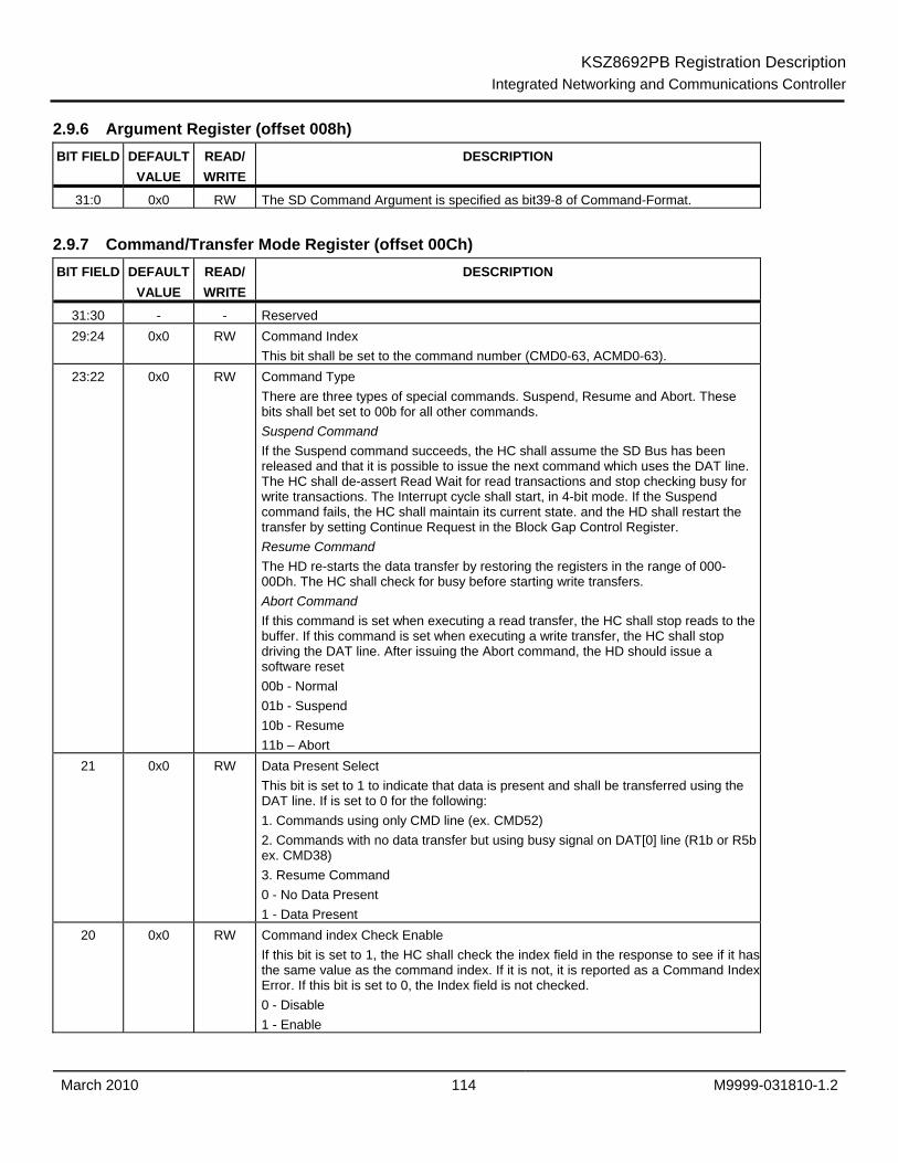
KSZ8692PB Registration Description Integrated Networking and Communications Controller
March 2010 114 M9999-031810-1.2
2.9.6 Argument Register (offset 008h) BIT FIELD DEFAULT
VALUE READ/ WRITE
DESCRIPTION
31:0 0x0 RW The SD Command Argument is specified as bit39-8 of Command-Format.
2.9.7 Command/Transfer Mode Register (offset 00Ch) BIT FIELD DEFAULT
VALUE READ/ WRITE
DESCRIPTION
31:30 - - Reserved 29:24 0x0 RW Command Index
This bit shall be set to the command number (CMD0-63, ACMD0-63). 23:22 0x0 RW Command Type
There are three types of special commands. Suspend, Resume and Abort. These bits shall bet set to 00b for all other commands. Suspend Command If the Suspend command succeeds, the HC shall assume the SD Bus has been released and that it is possible to issue the next command which uses the DAT line. The HC shall de-assert Read Wait for read transactions and stop checking busy for write transactions. The Interrupt cycle shall start, in 4-bit mode. If the Suspend command fails, the HC shall maintain its current state. and the HD shall restart the transfer by setting Continue Request in the Block Gap Control Register. Resume Command The HD re-starts the data transfer by restoring the registers in the range of 000-00Dh. The HC shall check for busy before starting write transfers. Abort Command If this command is set when executing a read transfer, the HC shall stop reads to the buffer. If this command is set when executing a write transfer, the HC shall stop driving the DAT line. After issuing the Abort command, the HD should issue a software reset 00b - Normal 01b - Suspend 10b - Resume 11b – Abort
21 0x0 RW Data Present Select This bit is set to 1 to indicate that data is present and shall be transferred using the DAT line. If is set to 0 for the following: 1. Commands using only CMD line (ex. CMD52) 2. Commands with no data transfer but using busy signal on DAT[0] line (R1b or R5b ex. CMD38) 3. Resume Command 0 - No Data Present 1 - Data Present
20 0x0 RW Command index Check Enable If this bit is set to 1, the HC shall check the index field in the response to see if it has the same value as the command index. If it is not, it is reported as a Command Index Error. If this bit is set to 0, the Index field is not checked. 0 - Disable 1 - Enable

KSZ8692PB Registration Description Integrated Networking and Communications Controller
March 2010 115 M9999-031810-1.2
19 0x0 RW Command CRC Check Enable
If this bit is set to 1, the HC shall check the CRC field in the response. If an error is detected, it is reported as a Command CRC Error. If this bit is set to 0, the CRC field is not checked. 0 - Disable 1 - Enable
18 - - Reserved 17:16 0x0 RW Response Type Select
00 - No Response 01 - Response length 136 10 - Response length 48 11 - Response length 48 check Busy after response
15:6 0x0 - Reserved 5 0x0 RW Multi/Single Block Select
This bit enables multiple block DAT line data transfers. 0 - Single Block 1 - Multiple Block
4 0x0 RW Data Transfer Direction Select This bit defines the direction of DAT line data transfers. 0 - Write (Host to Card) 1 - Read (Card to Host)
3 - - Reserved 2 0x0 RW Auto CMD12 Enable
Multiple block transfers for memory require CMD12 to stop the transaction. When this bit is set to 1, the HC shall issue CMD12 automatically when last block transfer is completed. The HD shall not set this bit to issue commands that do not require CMD12 to stop data transfer. 0 - Disable 1 – Enable
1 0x0 RW Block Count Enable This bit is used to enable the Block count register, which is only relevant for multiple block transfers. When this bit is 0, the Block Count register is disabled, which is useful in executing an infinite transfer. 0 - Disable 1 – Enable
0 0x0 RW DMA Enable DMA can be enabled only if DMA Support bit in the Capabilities register is set. If this bit is set to 1, a DMA operation shall begin when the HD writes to the upper byte of Command register (00Fh). 0 - Disable 1 – Enable

KSZ8692PB Registration Description Integrated Networking and Communications Controller
March 2010 116 M9999-031810-1.2
2.9.8 Determination of Transfer Type Multi / Single Block Select Block Count Enable Block Count Function
0 Don’t Care Don’t Care Single Transfer
1 0 Don’t Care Infinite Transfer
1 1 Not Zero Multiple Transfer
1 1 Zero Stop Multiple Transfer
2.9.9 Relation between Parameters and the Name of Response Type Response Type Index Check Enable CRC Check Enable Name of Response Type
00 0 0 No Response
01 0 1 R2
10 0 0 R3, R4
10 1 1 R1, R6, R5
11 1 1 R1b, R5b
2.9.10 Response Register (offset 010h) BIT FIELD DEFAULT
VALUE READ/ WRITE
DESCRIPTION
127:0 0x0 ROC Command Response The following Table describes the mapping of command responses from the SD Bus to this register for each response type. In the Table, R[] refers to a bit range within the response data as transmitted on the SD Bus, REP[] refers to a bit range within the Response register.
2.9.11 Response Bit Definition for Each Response Type Kind of Response Meaning of
Response Response Field Response Register
R1, R1b (normal response) Card Status R[39:8] REP[31:0] R1b (Auto CMD12 response) Card Status for Auto
CMD12 R[39:8] REP[127:96]
R2 (CID, CSD Register) CID or CSD reg. incl. R[127:8] REP[119:0] R3 (OCR Register) OCR Register for
memory R[39:8] REP[31:0]
R4 (OCR Register) OCR Register for I/O etc.
R[39:8] REP[31:0]
R5, R5b SDIO Response R[39:8] REP[31:0] R6 (Published RCA response)
New published RCA[31:16] etc.
R[39:8] REP[31:0]

KSZ8692PB Registration Description Integrated Networking and Communications Controller
March 2010 117 M9999-031810-1.2
2.9.12 Buffer Data Port Register (offset 020h) BIT FIELD DEFAULT
VALUE READ/ WRITE
DESCRIPTION
31:0 0x0 RW Buffer Data The Host Controller Buffer can be accessed through this 32-bit Data Port Register.
2.9.13 Present State Register (offset 024h) BIT FIELD DEFAULT
VALUE READ/ WRITE
DESCRIPTION
31:25 0x0 - Reserved 24 0x0 RO CMD Line Signal Level
This status is used to check CMD line level to recover from errors, and for debugging.
23:20 0x0 RO DAT[3:0] Line Signal Level This status is used to check DAT line level to recover from errors, and for debugging. This is especially useful in detecting the busy signal level from DAT[0]. D23 - DAT[3] D22 - DAT[2] D21 - DAT[1] D20 - DAT[0]
19 0x0 RO Write Protect Switch Pin Level The Write Protect Switch is supported for memory and combo cards. This bit reflects the SDWP# pin. 0 - Write protected (SDWP# = 1) 1 - Write enabled (SDWP# = 0)
18 0x0 RO Card Detect Pin Level This bit reflects the inverse value of the SDCD# pin. 0 - No Card present (SDCD# = 1) 1 - Card present (SDCD# = 0)
17 0x0 RO Card State STable This bit is used for testing. If it is 0, the Card Detect Pin Level is not sTable. If this bit is set to 1, it means the Card Detect Pin Level is sTable. The Software Reset For All in the Software Reset Register shall not affect this bit. 0 - Reset of Debouncing 1 - No Card or Inserted
16 0x0 RO Card Inserted This bit indicates whether a card has been inserted. Changing from 0 to 1 generates a Card Insertion interrupt in the Normal Interrupt Status register and changing from 1 to 0 generates a Card Removal Interrupt in the Normal Interrupt Status register. The Software Reset For All in the Software Reset register shall not affect this bit. If a Card is removed while its power is on and its clock is oscillating, the HC shall clear SD Bus Power in the Power Control register and SD Clock Enable in the Clock control register. In addition the HD should clear the HC by the Software Reset For All in Software register. The card detect is active regardless of the SD Bus Power. 0 - Reset or Debouncing or No Card 1 - Card Inserted
15:12 - - Reserved 11 0x0 ROC Buffer Read Enable

KSZ8692PB Registration Description Integrated Networking and Communications Controller
March 2010 118 M9999-031810-1.2
This status is used for non-DMA read transfers. This read only flag indicates that valid data exists in the host side buffer status. If this bit is 1, readable data exists in the buffer. A change of this bit from 1 to 0 occurs when all the block data is read from the buffer. A change of this bit from 0 to 1 occurs when all the block data is ready in the buffer and generates the Buffer Read Ready Interrupt. 0 - Read Disable 1 - Read Enable.
10 0x0 ROC Buffer Write Enable This status is used for non-DMA write transfers. This read only flag indicates if space is available for write data. If this bit is 1, data can be written to the buffer. A change of this bit from 1 to 0 occurs when all the block data is written to the buffer. A change of this bit from 0 to 1 occurs when top of block data can be written to the buffer and generates the Buffer Write Ready Interrupt. 0 - Write Disable 1 - Write Enable
9 0x0 ROC Read Transfer Active This status is used for detecting completion of a read transfer. This bit is set to 1 for either of the following conditions: 1) After the end bit of the read command 2) When writing a 1 to continue Request in the Block Gap Control register to restart a read transfer This bit is cleared to 0 for either of the following conditions: 1) When the last data block as specified by block length is transferred to the system.2) When all valid data blocks have been transferred to the system and no current block transfers are being sent as a result of the Stop At Block Gap Request set to 1. A transfer complete interrupt is generated when this bit changes to 0. 1 - Transferring data 0 - No valid data
8 0x0 ROC Write Transfer Active This status indicates a write transfer is active. If this bit is 0, it means no valid write data exists in the HC. This bit is set in either of the following cases: 1) After the end bit of the write command. 2) When writing a 1 to Continue Request in the Block Gap Control register to restart a write transfer. This bit is cleared in either of the following cases: 1) After getting the CRC status of the last data block as specified by the transfer count (Single or Multiple) 2) After getting a CRC status of any block where data transmission is about to be stopped by a Stop At Block Gap Request. During a write transaction, a Block Gap Event interrupt is generated when this bit is changed to 0, as a result of the Stop At Block Gap Request being set. This status is useful for the HD in determining when to issue commands during write busy. 1 - transferring data 0 - No valid data
7:3 - - Reserved

KSZ8692PB Registration Description Integrated Networking and Communications Controller
March 2010 119 M9999-031810-1.2
2 0x0 ROC DAT Line Active
This bit indicates whether one of the DAT line on SD bus is in use. 1 - DAT line active 0 - DAT line inactive
1 0x0 ROC Command Inhibit (DAT) This status bit is generated if either the DAT Line Active or the Read transfer Active is set to 1. If this bit is 0, it indicates the HC can issue the next SD command. Commands with busy signal belong to Command Inhibit (DAT) (ex. R1b, R5b type). Changing from 1 to 0 generates a Transfer Complete interrupt in the Normal interrupt status register. Note: The SD Host Driver can save registers in the range of 000-00Dh for a suspend transaction after this bit has changed from 1 to 0. 1 - cannot issue command which uses the DAT line 0 - Can issue command which uses the DAT line
0 0x0 ROC Command Inhibit (CMD) If this bit is 0, it indicates the CMD line is not in use and the HC can issue a SD command using the CMD line. This bit is set immediately after the Command register (00Fh) is written. This bit is cleared when the command response is received. Even if the Command Inhibit (DAT) is set to 1, Commands using only the CMD line can be issued if this bit is 0. Changing from 1 to 0 generates a Command complete interrupt in the Normal Interrupt Status register. If the HC cannot issue the command because of a command conflict error or because of Command Not Issued By Auto CMD12 Error, this bit shall remain 1 and the Command Complete is not set. Status issuing Auto CMD12 is not read from this bit.
This bit indicates whether one of the DAT line on SD bus is in use. Note: DAT line active indicates whether one of the DAT line is on SD bus is in use. a) In the case of read transactions This status indicates if a read transfer is executing on the SD bus. Changes in this value from 1 to 0 between data blocks generates a Block Gap Event interrupt in the Normal Interrupt Status register. This bit shall be set in either of the following cases: 1) After the end bit of the read command. 2) When writing a 1 to Continue Request in the Block Gap Control register to restart a read transfer. This bit shall be cleared in either of the following cases: 1) When the end bit of the last data block is sent from the SD bus to the HC. 2) When writing a 1 to Continue Request in the Block Gap Control register to restart a read transfer. This bit shall be cleared in either of the following cases: 1) When the end bit of the last data block is sent from the SD bus to the HC. 2) When beginning a wait read transfer at a stop at the block gap initiated by a Stop At Block Gap Request The HC shall wait at the next block gap by driving Read Wait at the start of the interrupt cycle. If the Read Wait signal is already driven (data buffer cannot receive data),the HC can wait for current block gap by continuing to drive the Read Wait signal. It is necessary to support Read Wait in order to use the suspend / resume function.

KSZ8692PB Registration Description Integrated Networking and Communications Controller
March 2010 120 M9999-031810-1.2
b) In the case of write transactions This status indicates that a write transfer is executing on the SD bus. Changing this value from 1 to 0 generate a Transfer complete interrupt in the Normal Interrupt status register. This bit shall be set in either of the following cases: 1) After the end of the write command. 2) When writing to 1 to Continue Request in the Block Gap Control register to continue a write transfer. This bit shall be cleared in either of the following cases: 1) When the SD card releases write busy of the last data block the HC shall also detect if output is not busy. If SD card does not drive busy signal for 8 SD clocks, the HC shall consider the card drive “Not Busy”. 2) When the SD card releases write busy prior to waiting for write transfer as a result of a Stop At block Gap Request. Implementation Note: The HD can issue cmd0, cmd12, cmd13 (for memory) and cmd52 (for SDIO) when the DAT lines are busy during data transfer. These commands can be issued when Command Inhibit (CMD) is set to zero. Other commands shall be issued when Command Inhibit (DAT) is set to zero.
2.9.14 Wake-up, Block Gap, Power and Host Control Register (offset 028h) The wakeup register portion is mandatory for the HC, but the wakeup functionality depends upon the HC system hardware and software. The HD shall maintain voltage on the SD Bus, by setting SD Bus power to 1 in the Power Control portion of the register, when wakeup event via card interrupt is desired. BIT FIELD DEFAULT
VALUE READ/ WRITE
DESCRIPTION
31:27 - - Reserved 26 0x0 RW Wakeup Even on SD Card Removal
This bit enables wakeup event via Card Removal assertion in the Normal Interrupt Status register. FN_WUS (Wake up Support) in CIS does not affect this bit. 1 - Enable 0 - Disable
25 0x0 RW Wakeup Event Enable On SD Card Insertion This bit enables wakeup event via Card Insertion assertion in the Normal Interrupt Status register. FN_WUS (Wake up Support) in CIS does not affect this bit. 1 - Enable 0 - Disable
24 0x0 RW Wakeup Event Enable On Card Interrupt This bit enables wakeup event via Card Interrupt assertion in the Normal Interrupt Status register. This bit can be set to 1 if FN_WUS (Wake Up Support) in CIS is set to 1. 1 - Enable 0 - Disable
23:20 - - Reserved 19 0x0 RW Interrupt At Block Gap
This bit is valid only in 4-bit mode of the SDIO card and selects a sample point in the interrupt cycle. Setting to 1 enables interrupt detection at the block gap for a multiple block transfer. If the SD card cannot signal an interrupt during a multiple block transfer, this bit should be set to 0. When the HD detects an SD card insertion, it shall set this bit according to the CCCR of the SDIO card.

KSZ8692PB Registration Description Integrated Networking and Communications Controller
March 2010 121 M9999-031810-1.2
18 0x0 RW Read Wait Control
The read wait function is optional for SDIO cards. If the card supports read wait, set this bit to enable use of the read wait protocol to stop read data using DAT[2] line. Otherwise the HC has to stop the SD clock to hold read data, which restricts commands generation. When the HD detects an SD card insertion, it shall set this bit according to the CCCR of the SDIO card. If the card does not support read wait, this bit shall never be set to 1 otherwise DAT line conflict may occur. If this bit is set to 0, Suspend / Resume cannot be supported 1 - Enable Read Wait Control 0 - Disable Read Wait Control
17 0x0 RWAC Continue Request This bit is used to restart a transaction which was stopped using the Stop At Block Gap Request. To cancel stop at the block gap, set Stop At block Gap Request to 0 and set this bit to restart the transfer. The HC automatically clears this bit in either of the following cases: 1) In the case of a read transaction, the DAT Line Active changes from 0 to 1 as a read transaction restarts. 2) In the case of a write transaction, the Write transfer active changes from 0 to 1 as the write transaction restarts. Therefore it is not necessary for Host driver to set this bit to 0. If Stop At Block Gap Request is set to 1, any write to this bit is ignored. 1 - Restart 0 - Ignored
16 0x0 RW Stop At Block Gap Request This bit is used to stop executing a transaction at the next block gap for both DMA and non- DMA transfers. Until the transfer complete is set to 1, indicating a transfer completion the HD shall leave this bit set to 1. Clearing both the Stop At Block Gap Request and Continue Request shall not cause the transaction to restart. Read Wait is used to stop the read transaction at the block gap. The HC shall honour Stop At Block Gap Request for write transfers, but for read transfers it requires that the SD card support Read Wait. Therefore the HD shall not set this bit during read transfers unless the SD card supports Read Wait and has set Read Wait Control to 1. In case of write transfers in which the HD writes data to the Buffer Data Port register, the HD shall set this bit after all block data is written. If this bit is set to 1, the HD shall not write data to Buffer data port register. This bit affects Read Transfer Active, Write Transfer Active, DAT line active and Command Inhibit (DAT) in the Present State register. 1 - Stop 0 - Transfer
15:12 - - Reserved 11:9 0x0 RW SD Bus Voltage Select
By setting these bits, the HD selects the voltage level for the SD card. Before setting this register, the HD shall check the voltage support bits in the capabilities register. If an unsupported voltage is selected, the Host System shall not supply SD bus voltage 111b - 3.3 V(Typ.) 110b - 3.0 V(Typ.) 101b - 1.8 V(Typ.) 100b - 000b - Reserved
8 0x0 RW SD Bus Power Before setting this bit, the SD host driver shall set SD Bus Voltage Select. If the HC detects the No Card State, this bit shall be cleared. 1 - Power on 0 - Power off

KSZ8692PB Registration Description Integrated Networking and Communications Controller
March 2010 122 M9999-031810-1.2
7:3 - - Reserved 2 0x0 RW High Speed Enable
This bit is optional. Before setting this bit, the HD shall check the High Speed Support in the capabilities register. If this bit is set to 0 (default), the HC outputs CMD line and DAT lines at the falling edge of the SD clock (up to 25 MHz). If this bit is set to 1, the HC outputs CMD line and DAT lines at the rising edge of the SD clock (up to 50 MHz) 1 - High Speed Mode 0 - Normal Speed Mode
1 0x0 RW Data Transfer Width (SD1 or SD4) This bit selects the data width of the HC. The HD shall select it to match the data width of the SD card. 1 - 4 bit mode 0 - 1 bit mode
0 0x0 RW LED Control This bit is used to caution the user not to remove the card while the SD card is being accessed. If the software is going to issue multiple SD commands, this bit can be set during all transactions. It is not necessary to change for each transaction. 1 - LED on 0 - LED off
There are three cases to restart the transfer after stop at the block gap. Which case is appropriate depends on whether the HC issues a Suspend command or the SD card accepts the Suspend command. 1) If the HD does not issue Suspend command, the Continue Request shall be used to restart the transfer. 2) If the HD issues a Suspend command and the SD card accepts it, a Resume Command shall be used to restart the transfer. 3) If the HD issues a Suspend command and the SD card does not accept it, the Continue Request shall be used to restart the transfer. Any time Stop At Block Gap Request stops the data transfer, the HD shall wait for Transfer Complete (in the Normal Interrupt Status register) before attempting to restart the transfer. When restarting the data transfer by Continue Request, the HD shall clear Stop At Block Gap Request before or simultaneously.
2.9.15 Software Reset/Time-out Control/Clock Control Register (offset 02Ch) At the initialization of the HC, the HD shall set the SDCLK Frequency Select according to the Capabilities register. At the initialization of the HC, the HD shall set the Data Timeout Counter Value according to the Capabilities register.

KSZ8692PB Registration Description Integrated Networking and Communications Controller
March 2010 123 M9999-031810-1.2
BIT FIELD DEFAULT VALUE
READ/ WRITE
DESCRIPTION
31:27 0x0 - Reserved 26 0x0 RWAC Software Reset for DAT Line
Only part of data circuit is reset. DMA circuit is also reset. The following registers and bits are cleared by this bit : Buffer Data Port Register Buffer is cleared and Initialized. Present State register Buffer read Enable Buffer write Enable Read Transfer Active Write Transfer Active DAT Line Active Command Inhibit (DAT) Block Gap Control register Continue Request Stop At Block Gap Request Normal Interrupt Status register Buffer Read Ready Buffer Write Ready Block Gap Event Transfer Complete 1 - Reset 0 - Work
25 0x0 RWAC Software Reset for CMD Line Only part of command circuit is reset. The following registers and bits are cleared by this bit : Present State register Command Inhibit (CMD) Normal Interrupt Status register Command Complete 1 - Reset 0 - Work
24 0x0 RWAC Software Reset for All This reset affects the entire HC except for the card detection circuit. Register bits of type ROC, RW, RW1C, RWAC are cleared to 0. During its initialization, the HD shall set this bit to 1 to reset the HC. The HC shall reset this bit to 0 when capabilities registers are valid and the HD can read them. Additional use of Software Reset For All may not affect the value of the Capabilities registers. If this bit is set to 1, the SD card shall reset itself and must be reinitialized by the HD. 1 - Reset 0 - Work
23:20 0x0 - Reserved

KSZ8692PB Registration Description Integrated Networking and Communications Controller
March 2010 124 M9999-031810-1.2
19:16 0x0 RW Data Timeout Counter Value
This value determines the interval by which DAT line timeouts are detected. Refer to the Data Timeout Error in the Error Interrupt Status register for information on factors that dictate timeout generation. Timeout clock frequency will be generated by dividing the base clock TMCLK by this value. When setting this register, prevent inadvertent timeout events by clearing the Data Timeout Error Status Enable (in the Error Interrupt Status Enable register) 1111b - Reserved 1110b - TMCLK * 2^ 27
------ - -------------------- 0001b - TMCLK * 2^ 14
0000b - TMCLK * 2^ 13 15:8 0x0 RW SDCLK Frequency Select
This register is used to select the frequency of the SDCLK pin. The frequency is not programmed directly; rather this register holds the divisor of the Base Clock Frequency For SD clock in the capabilities register. Only the following settings are allowed. 80h - base clock divided by 256 40h - base clock divided by 128 20h - base clock divided by 64 10h - base clock divided by 32 08h - base clock divided by 16 04h - base clock divided by 8 02h - base clock divided by 4 01h - base clock divided by 2 00h - base clock(10MHz-63MHz) Setting 00h specifies the highest frequency of the SD Clock. When setting multiple bits, the most significant bit is used as the divisor. But multiple bits should not be set. The two default divider values can be calculated by the frequency that is defined by the Base Clock Frequency For SD Clock in the Capabilities register. 1) 25 MHz divider value 2) 400 KHz divider value The frequency of the SDCLK is set by the following formula: Clock Frequency = (Baseclock) / divisor . Thus choose the smallest possible divisor which results in a clock frequency that is less than or equal to the target frequency.
7:3 - - Reserved 2 0x0 RW SD Clock Enable
The HC shall stop SDCLK when writing this bit to 0. SDCLK frequency Select can be changed when this bit is 0. Then, the HC shall maintain the same clock frequency until SDCLK is stopped (Stop at SDCLK = 0). If the HC detects the No Card state, this bit shall be cleared. 1 - Enable 0 - Disable
1 0x0 ROC Internal Clock STable This bit is set to 1 when SD clock is sTable after writing to Internal Clock Enable in this register to 1. The SD Host Driver shall wait to set SD Clock Enable until this bit is set to 1. Note : This is useful when using PLL for a clock oscillator that requires setup time. 1 - Ready

KSZ8692PB Registration Description Integrated Networking and Communications Controller
March 2010 125 M9999-031810-1.2
0 - Not Ready 0 0x0 RW Internal Clock Enable
This bit is set to 0 when the HD is not using the HC or the HC awaits a wakeup event. The HC should stop its internal clock to go very low power state. Still, registers shall be able to be read and written. Clock starts to oscillate when this bit is set to 1. When clock oscillation is sTable, the HC shall set Internal Clock STable in this register to 1. This bit shall not affect card detection. 1 - Oscillate 0 - Stop
A reset pulse is generated when writing 1 to each bit of the Software Reset portion of this register. After completing the reset, the HC shall clear each bit. Because it takes some time to complete software reset, the SD Host Driver shall confirm that these bits are 0.
2.9.16 Error Interrupt Status/Normal Interrupt Status Register (offset 030h) The Normal Interrupt Status Enable affects reads of the Normal Interupt Status portion of this register, but Normal Interrupt Signal does not affect these reads. An Interrupt is generated when the Normal Interrupt Signal Enable is enabled and atleast one of the status bits is set to 1. For all bits except Card Interrupt and Error Interrupt, writing 1 to a bit clears it. The Card Interrupt is cleared when the card stops asserting the interrupt: that is when the Card Driver services the Interrupt condition. Status defined in the Error Interrupt Status portion of this register can be enabled by the Error Interrupt Status Enable Register, but not by the Error Interrupt Signal Enable Register. The Interrupt is generated when the Error Interrupt Signal Enable is enabled and at least one of the statuses is set to 1. Writing to 1 clears the bit and writing to 0 keeps the bit unchanged. More than one status can be cleared at the one register write.
BIT FIELD DEFAULT VALUE
READ/ WRITE
DESCRIPTION
31:29 0x0 RW1C Vendor Specific Error Status Additional status bits can be defined in this register by the vendor.
28 0x0 RW1C Target Response Error Occurs when detecting ERROR in m_hresp 0 - No Error 1 - Error
27:25 - - Reserved 24 0x0 RW1C Auto CMD12 Error
Occurs when detecting that one of the bits in Auto CMD12 Error Status register has changed from 0 to 1. This bit is set to 1 also when Auto CMD12 is not executed due to the previous command error. 0 - No Error 1 - Error
23 0x0 RW1C Current Limit Error By setting the SD Bus Power bit in the Power Control Register, the HC is requested to supply power for the SD Bus. If the HC supports the Current Limit Function, it can be protected from an Illegal card by stopping power supply to the card in which case this bit indicates a failure status. Reading 1 means the HC is not supplying power to SD card due to some failure. Reading 0 means that the HC is supplying power and no error has occurred. This bit shall always set to be 0, if the HC does not support this function. 0 - No Error 1 - Power Fail
22 0x0 RW1C Data End Bit Error Occurs when detecting 0 at the end bit position of read data which uses the DAT line

KSZ8692PB Registration Description Integrated Networking and Communications Controller
March 2010 126 M9999-031810-1.2
or the end bit position of the CRC status. 0 - No Error 1 - Error

KSZ8692PB Registration Description Integrated Networking and Communications Controller
March 2010 127 M9999-031810-1.2
21 0x0 RW1C Data CRC Error
Occurs when detecting CRC error when transferring read data which uses the DAT line or when detecting the Write CRC Status having a value of other than “010”. 0 - No Error 1 - Error
20 0x0 RW1C Data Timeout Error Occurs when detecting one of following timeout conditions. 1) Busy Timeout for R1b, R5b type 2) Busy Timeout after Write CRC status 3) Write CRC status Timeout 4) Read Data Timeout 0 - No Error 1 - Timeout
19 0x0 RW1C Command Index Error Occurs if a Command Index error occurs in the Command Response. 0 - No Error 1 - Error
18 0x0 RW1C Command End Bit Error Occurs when detecting that the end bit of a command response is 0. 0 - No Error 1 - End Bit Error Generated
17 0x0 RW1C Command CRC Error Command CRC Error is generated in two cases. 1) If a response is returned and the Command Timeout Error is set to 0, this bit is set to 1 when detecting a crc error in the command response 2) The HC detects a CMD line conflict by monitoring the CMD line when a command is issued. If the HC drives the CMD line to 1 level, but detects 0 level on the CMD line at the next SDCLK edge, then the HC shall abort the command (Stop driving CMD line) and set this bit to 1. The Command Timeout Error shall also be set to 1 to distinguish CMD line conflict. 0 - No Error 1 - CRC Error Generated
16 0x0 RW1C Command Timeout Error Occurs only if the no response is returned within 64 SDCLK cycles from the end bit of the command. If the HC detects a CMD line conflict, in which case Command CRC Error shall also be set. This bit shall be set without waiting for 64 SDCLK cycles because the command will be aborted by the HC. 0 - No Error 1 - Timeout
15 0x0 ROC Error Interrupt If any of the bits in the Error Interrupt Status Register are set, then this bit is set. Therefore the HD can test for an error by checking this bit first. 0 - No Error. 1 - Error.
14:9 - - Reserved

KSZ8692PB Registration Description Integrated Networking and Communications Controller
March 2010 128 M9999-031810-1.2
8 0x0 ROC Card Interrupt
Writing this bit to 1 does not clear this bit. It is cleared by resetting the SD card interrupt factor. In 1-bit mode, the HC shall detect the Card Interrupt without SD Clock to support wakeup. In 4-bit mode, the card interrupt signal is sampled during the interrupt cycle, so there are some sample delays between the interrupt signal from the card and the interrupt to the Host system. when this status has been set and the HD needs to start this interrupt service, Card Interrupt Status Enable in the Normal Interrupt Status register shall be set to 0 inorder to clear the card interrupt statuses latched in the HC and stop driving the Host System. After completion of the card interrupt service (the reset factor in the SD card and the interrupt signal may not be asserted), set Card Interrupt Status Enable to 1 and start sampling the interrupt signal again. 0 - No Card Interrupt 1 - Generate Card Interrupt
7 0x0 RW1C Card Removal This status is set if the Card Inserted in the Present State register changes from 1 to 0. When the HD writes this bit to 1 to clear this status the status of the Card Inserted in the Present State register should be confirmed. Because the card detect may possibly be changed when the HD clear this bit an Interrupt event may not be generated. 0 - Card State Stable or Debouncing 1 - Card Removed
6 0x0 RW1C Card Insertion This status is set if the Card Inserted in the Present State register changes from 0 to 1. When the HD writes this bit to 1 to clear this status the status of the Card Inserted in the Present State register should be confirmed. Because the card detect may possibly be changed when the HD clear this bit an Interrupt event may not be generated. 0 - Card State Stable or Debouncing 1 - Card Inserted
5 0x0 RW1C Buffer Read Ready This status is set if the Buffer Read Enable changes from 0 to 1. 0 - Not Ready to read Buffer. 1 - Ready to read Buffer.
4 0x0 RW1C Buffer Write Ready This status is set if the Buffer Write Enable changes from 0 to 1. 0 - Not Ready to Write Buffer. 1 - Ready to Write Buffer.
3 0x0 RW1C DMA Interrupt This status is set if the HC detects the Host DMA Buffer Boundary in the Block Size regiser. 0 - No DMA Interrupt 1 - DMA Interrupt is Generated

KSZ8692PB Registration Description Integrated Networking and Communications Controller
March 2010 129 M9999-031810-1.2
2 0x0 RW1C Block Gap Event
If the Stop At Block Gap Request in the Block Gap Control Register is set, this bit is set. Read Transaction : This bit is set at the falling edge of the DAT Line Active Status (When the transaction is stopped at SD Bus timing. The Read Wait must be supported inorder to use this function). Write Transaction : This bit is set at the falling edge of Write Transfer Active Status ( After getting CRC status at SD Bus timing). 0 - No Block Gap Event 1 - Transaction stopped at Block Gap
1 0x0 RW1C Transfer Complete This bit is set when a read / write transaction is completed. Read Transaction : This bit is set at the falling edge of Read Transfer Active Status. There are two cases in which the Interrupt is generated. The first is when a data transfer is completed as specified by data length (After the last data has been read to the Host System). The second is when data has stopped at the block gap and completed the data transfer by setting the Stop At Block Gap Request in the Block Gap Control Register (After valid data has been read to the Host System). Write Transaction : This bit is set at the falling edge of the DAT Line Active Status. There are two cases in which the Interrupt is generated. The first is when the last data is written to the card as specified by data length and Busy signal is released. The second is when data transfers are stopped at the block gap by setting Stop At Block Gap Request in the Block Gap Control Register and data transfers completed. (After valid data is written to the SD card and the busy signal is released). Note : Transfer Complete has higher priority than Data Timeout Error. If both bits are set to 1, the data transfer can be considered complete 0 - No Data Transfer Complete 1 - Data Transfer Complete
0 0x0 RW1C Command Complete This bit is set when get the end bit of the command response (Except Auto CMD12). Note : Command Timeout Error has higher priority than Command Complete. If both are set to 1, it can be considered that the response was not received correctly. 0 - No Command Complete 1 - Command Complete
2.10 Relation between Transfer Complete and Data Timeout Error
Transfer Complete Data Timeout Error Meaning of the Status
0 0 Interrupted by Another Factor.
0 1 Timeout occur during transfer.
1 Don’t Care Data Transfer Complete 2.11 Relation between Command Complete and Command Timeout Error
Transfer Complete Data Timeout Error Meaning of the Status
0 0 Interrupted by Another Factor.
Don’t Care 1 Response not received within 64 SDCLK cycles.

KSZ8692PB Registration Description Integrated Networking and Communications Controller
March 2010 130 M9999-031810-1.2
1 0 Response Received 2.12 Relation between Command CRC Error and Command Timeout Error
Command CRC Error Command Time-out Error
Kinds of Error
0 0 Interrupted by Another Factor.
Don’t Care 1 Response not received within 64 SDCLK cycles.
1 0 Response Received
0 0 No Error
0 1 Response Timeout Error
1 0 Response CRC Error
1 1 CMD Line Conflict 2.13 Error Interrupt Status Enable/Normal Interrupt Status Enable Register (offset 034h)
BIT FIELD DEFAULT VALUE
READ/ WRITE
DESCRIPTION
31:29 0x0 RW Vendor Specific Error Status Enable 0 - Masked 1 – Enabled
28 0x0 RW Target Response Error Status Enable 0 - Masked 1 – Enabled
27:25 0x0 - Reserved
24 0x0 RW Auto CMD12 Error Status Enable 0 - Masked 1 – Enabled
23 0x0 RW Current Limit Error Status Enable 0 - Masked 1 – Enabled
22 0x0 RW Data End Bit Error Status Enable 0 - Masked 1 – Enabled
21 0x0 RW Data CRC Error Status Enable 0 - Masked 1 – Enabled
20 0x0 RW Data Timeout Error Status Enable 0 - Masked 1 – Enabled
19 0x0 RW Command Index Error Status Enable 0 - Masked 1 – Enabled
18 0x0 RW Command End Bit Error Status Enable 0 - Masked 1 – Enabled
17 0x0 RW Command CRC Error Status Enable 0 - Masked

KSZ8692PB Registration Description Integrated Networking and Communications Controller
March 2010 131 M9999-031810-1.2
1 – Enabled 16 0x0 RW Command Timeout Error Status Enable
0 - Masked 1 – Enabled
15 0x0 RO Fixed to 0 The HC shall control error Interrupts using the Error Interrupt Status Enable register.
14:9 0x0 - Reserved 8 0x0 RW Card Interrupt Status Enable
If this bit is set to 0, the HC shall clear Interrupt request to the System. The Card Interrupt detection is stopped when this bit is cleared and restarted when this bit is set to 1. The HD should clear the Card Interrupt Status Enable before servicing the Card Interrupt and should set this bit again after all Interrupt requests from the card are cleared to prevent inadvertent Interrupts. 0 - Masked 1 – Enabled
7 0x0 RW Card Removal Status Enable 0 - Masked 1 – Enabled
6 0x0 RW Card Insertion Status Enable 0 - Masked 1 – Enabled
5 0x0 RW Buffer Read Ready Status Enable 0 - Masked 1 – Enabled
4 0x0 RW Buffer Write Ready Status Enable 0 - Masked 1 – Enabled
3 0x0 RW DMA Interrupt Status Enable 0 - Masked 1 – Enabled
2 0x0 RW Block Gap Event Status Enable 0 - Masked 1 – Enabled
1 0x0 RW Transfer Complete Status Enable 0 - Masked 1 – Enabled
0 0x0 RW Command Complete Status Enable 0 - Masked 1 – Enabled
Setting to 1 enables Interrupt Status. Note: The HC may sample the card Interrupt signal during interrupt period and may hold its value in the flip-flop. If the Card Interrupt Status Enable is set to 0, the HC shall clear all internal signals regarding Card Interrupt. Note: To Detect CMD Line conflict, the HD must set both Command Time-out Error Status Enable and Command CRC Error Status Enable to 1.

KSZ8692PB Registration Description Integrated Networking and Communications Controller
March 2010 132 M9999-031810-1.2
2.13.1 Error Interrupt Signal Enable/Normal Interrupt Signal Enable Register (offset 038h) This register is used to select which interrupt status is indicated to the Host System as the Interrupt. These status bits all share the sample 1 bit interrupt line. Setting any of these bits to 1 enables Interrupt generation.
BIT FIELD DEFAULT VALUE
READ/ WRITE
DESCRIPTION
31:29 0x0 RW Vendor Specific Error Signal Enable 0 - Masked 1 – Enabled
28 0x0 RW Target Response Error Signal Enable 0 - Masked 1 – Enabled
27:25 0x0 - Reserved
24 0x0 RW Auto CMD12 Error Signal Enable 0 - Masked 1 – Enabled
23 0x0 RW Current Limit Error Signal Enable 0 - Masked 1 – Enabled
22 0x0 RW Data End Bit Error Signal Enable 0 - Masked 1 – Enabled
21 0x0 RW Data CRC Error Signal Enable 0 - Masked 1 – Enabled
20 0x0 RW Data Timeout Error Signal Enable 0 - Masked 1 – Enabled
19 0x0 RW Command Index Error Signal Enable 0 - Masked 1 – Enabled
18 0x0 RW Command End Bit Error Signal Enable 0 - Masked 1 – Enabled
17 0x0 RW Command CRC Error Signal Enable 0 - Masked 1 – Enabled
16 0x0 RW Command Timeout Error Signal Enable 0 - Masked 1 – Enabled
15 0x0 RO Fixed to 0 The HC shall control error Interrupts using the Error Interrupt Signal Enable register.
14:9 0x0 - Reserved
8 0x0 RW Card Interrupt Signal Enable 0 - Masked 1 – Enabled
7 0x0 RW Card Removal Signal Enable 0 - Masked 1 – Enabled

KSZ8692PB Registration Description Integrated Networking and Communications Controller
March 2010 133 M9999-031810-1.2
6 0x0 RW Card Insertion Signal Enable 0 - Masked 1 – Enabled
5 0x0 RW Buffer Read Ready Signal Enable 0 - Masked 1 – Enabled
4 0x0 RW Buffer Write Ready Signal Enable 0 - Masked 1 – Enabled
3 0x0 RW DMA Interrupt Signal Enable 0 - Masked 1 – Enabled
2 0x0 RW Block Gap Event Signal Enable 0 - Masked 1 – Enabled
1 0x0 RW Transfer Complete Signal Enable 0 - Masked 1 – Enabled
0 0x0 RW Command Complete Signal Enable 0 - Masked 1 – Enabled
The Error Interrupt Signal Enable portion of this register is used to select which interrupt status is notified to the Host System as the Interrupt. These status bits all share the same 1 bit interrupt line. Setting any of these bits to 1 enables Interrupt generation.
2.13.2 Auto CMD12 Error Status Register (offset 03Ch) When Auto CMD12 Error Status is set, the HD shall check this register to identify what kind of error Auto CMD12 indicated. This register is valid only when the Auto CMD12 Error is set.
BIT FIELD DEFAULT VALUE
READ/ WRITE
DESCRIPTION
31:8 0x0 - Reserved 7 0x0 ROC Command Not Issued by Auto CMD12 Error
Setting this bit to 1 means CMD_wo_DAT is not executed due to an Auto CMD12 error (D04 - D01) in this register. 0 - No Error 1 - Not Issued
6:5 0x0 - Reserved 4 0x0 ROC Auto CMD12 Index Error
Occurs if the Command Index error occurs in response to a command. 0 - No Error 1 - Error
3 0x0 ROC Auto CMD12 End Bit Error Occurs when detecting that the end bit of command response is 0. 0 - No Error 1 - End Bit Error Generated
2 0x0 ROC Auto CMD12 CRC Error Occurs when detecting a CRC error in the command response. 0 - No Error

KSZ8692PB Registration Description Integrated Networking and Communications Controller
March 2010 134 M9999-031810-1.2
1 - CRC Error Generated

KSZ8692PB Registration Description Integrated Networking and Communications Controller
March 2010 135 M9999-031810-1.2
1 0x0 ROC Auto CMD12 Timeout Error
Occurs if the no response is returned within 64 SDCLK cycles from the end bit of the command. If this bit is set to 1, the other error status bits (D04 - D02) are meaningless. 0 - No Error 1 - Timeout
0 0x0 ROC Auto CMD12 not Executed If memory multiple block data transfer is not started due to command error, this bit is not set because it is not necessary to issue Auto CMD12. Setting this bit to 1 means the HC cannot issue Auto CMD12 to stop memory multiple block transfer due to some error. If this bit is set to 1, other error status bits (D04 - D01) are meaningless. 0 - Executed 1 - Not Executed
2.14 Relation between Auto CMD12 CRC Error and Auto CMD12 Timeout Error
Auto Cmd12 CRC Error Auto CMD12 Timeout Error Kinds of Error
0 0 No Error
0 1 Response Timeout Error
1 0 Response CRC Error
1 1 CMD Line Conflict
The timing of changing Auto CMD12 Error Status can be classified in three scenarios: 1) When the HC is going to issue Auto CMD12. Set D00 to 1 if Auto CMD12 cannot be issued due to an error in the previous command. Set D00 to 0 if Auto CMD12 is issued.
2) At the end bit of Auto CMD12 response. Check received responses by checking the error bits D01, D02, D03, D04. Set to 1 if Error is Detected. Set to 0 if Error is Not Detected.
3) Before reading the Auto CMD12 Error Status bit D07 Set D07 to 1 if there is a command cannot be issued. Set D07 to 0 if there is no command to issue. Timing of generating the Auto CMD12 Error and writing to the Command register are Asynchronous. Then D07 shall be sampled when driver never writing to the Command register. So just before reading the Auto CMD12 Error Status register is good timing to set the D07 status bit.

KSZ8692PB Registration Description Integrated Networking and Communications Controller
March 2010 136 M9999-031810-1.2
2.15 Capabilities Register (offset 040h) This register provides the HD with information specific to the HC implementation. The HC may implement these values as fixed or loaded from flash memory during power on initialization.
BIT FIELD DEFAULT VALUE
READ/ WRITE
DESCRIPTION
31:27 0x0 - Reserved 26 0x1 HwInit Voltage Support 1.8V
0 - 1.8 V Not Supported 1 - 1.8 V Supported
25 0x1 HwInit Voltage Support 3.0V 0 – 3.0 V Not Supported 1 – 3.0 V Supported
24 0x1 HwInit Voltage Support 3.3V 0 - 3.3 V Not Supported 1 - 3.3 V Supported
23 0x1 HwInit Suspend/Resume Support This bit indicates whether the HC supports Suspend / Resume functionality. If this bit is 0, the Suspend and Resume mechanism are not supported and the HD shall not issue either Suspend / Resume commands. 0 - Not Supported 1 - Supported
22 0x1 HwInit DMA Support This bit indicates whether the HC is capable of using DMA to transfer data between system memory and the HC directly. 0 - DMA Not Supported 1 - DMA Supported.
21 0x1 HwInit High Speed Support This bit indicates whether the HC and the Host System support High Speed mode and they can supply SD Clock frequency from 25Mhz to 50 Mhz. 0 - High Speed Not Supported 1 - High Speed Supported
20:18 0x1 HwInit Reserved 17:16 0x1 HwInit Max Block Length
This value indicates the maximum block size that the HD can read and write to the buffer in the HC. The buffer shall transfer this block size without wait cycles. Three sizes can be defined as indicated below. 00 - 512 byte 01 - 1024 byte 10 - 2048 byte 11 – Reserved
15:14 0x0 - Reserved

KSZ8692PB Registration Description Integrated Networking and Communications Controller
March 2010 137 M9999-031810-1.2
13:8 110000b HwInit Base Clock Frequency for SD Clock
This value indicates the base (maximum) clock frequency for the SD clock. Unit values are 1Mhz. If the real frequency is 16.5 Mhz, the larger value shall be set 010001b (17 Mhz) because the HD uses this value to calculate the clock divider value and it shall not exceed the upper limit of the SD clock frequency. The supported range is 10Mhz to 63 Mhz. If these bits are all 0, the Host System has to get information via another method. Not 0 - 1 Mhz to 63 Mhz 000000b - Get information via another method (Registry Entry).
7 0x1 HwInit Timeout Clock Unit This bit shows the unit of base clock frequency used to detect Data Timeout Error. 0 - Khz 1 – Mhz
6 0x0 HwInit Reserved 5:0 110000b HwInit Timeout Clock Frequency
This bit shows the base clock frequency used to detect Data Timeout Error. Not 0 - 1Khz to 63Khz or 1Mhz to 63Mhz 000000b - Get Information via another method.
Note: The Host System shall support at least one of these voltages above. The HD sets the SD Bus Voltage Select in Power Control register according to these support bits. If multiple voltages are supported, select the usable lower voltage by comparing the OCR value from the card. These registers indicate maximum current capability for each voltage. The value is meaningful if Voltage Support is set in the Capabilities register.
2.15.1 Capabilities Register (Reserved) (offset 044h) BIT FIELD DEFAULT
VALUE READ/ WRITE
DESCRIPTION
31:0 0x0 - Reserved
2.15.2 Maximum Current Capabilities Register (offset 048h) BIT FIELD DEFAULT
VALUE READ/ WRITE
DESCRIPTION
31:24 0x0 - Reserved 23:16 0xFF HwInit Maximum Current for 1.8V 15:8 0xFF HwInit Maximum Current for 3.0V 7:0 0xFF HwInit Maximum Current for 3.3V

KSZ8692PB Registration Description Integrated Networking and Communications Controller
March 2010 138 M9999-031810-1.2
2.16 Maximum Current Value Definition Table
Register Value Current Value
0 Get Information via another method
1 4mA
2 8mA
3 12mA
------------------- ----------------------
255 1020mA
2.16.1 Maximum Current Capabilities (Reserved) (offset 04Ch) BIT FIELD DEFAULT
VALUE READ/ WRITE
DESCRIPTION
31:0 0x0 - Reserved
2.16.2 Host Controller Version/Slot Interrupt Status Register (offset 0FCh) BIT FIELD DEFAULT
VALUE READ/ WRITE
DESCRIPTION
31:24 0x0 HwInit Vendor Version Number This status is reserved for the vendor version number. The HD should not use this status.
23:16 0x0 HwInit Specification Version Number This Status indicates the Host Controller Spec Version. The Upper and Lower 4 bits indicate the version. 00 - SD Host Specification version 1.0 others - Reserved
15:8 0x0 - Reserved 7:0 0x0 ROC Interrupt Signal for Each Slot
These status bit indicate the logical OR of Interrupt signal and Wakeup signal for each slot. A maximum of 8 slots can be defined. If one interrupt signal is associated with multiple slots. the HD can know which interrupt is generated by reading these status bits. By a power on reset or by Software Reset For All, the Interrupt signal shall be deasserted and this status shall read 00h. Bit 00 - Slot 1 Bit 01 - Slot 2 Bit 02 - Slot 3 ----- ----- Bit 07 - Slot 8

KSZ8692PB Registration Description Integrated Networking and Communications Controller
March 2010 139 M9999-031810-1.2
2.17 USB Registers (0xB000-0xDFFF) The KSZ8692PB includes two USB 2.0 controllers that can support both EHCI or Enhanced Host Controller and OHCI or Open Host Controller specifications. For more information on the EHCI specification, please refer to USB 2.0 EHCI Host Controller Specification, Revision 1.0. For more information on the OHCI, please refer to the USB 2.0 OHCI Host Controller Specification, Rev.1.0a. The USB 2.0 Host Controller is designed with a USB 1.1 Host Controller interface at the Port Router, which allows the USB 2.0 Host Controller to communicate with high-, full- and low-speed devices connected at the UTMI PHY transceiver. The Port Router logic, which lies in the EHCI Host Controller and connects to the OHCI Host Controller, enables the host controllers to communicate with attached devices. The function of the Port Router logic is to route the attached device, depending upon the device speed, to the EHCI Host Controller or OHCI Host Controller. As the EHCI Host Controller is the default owner of each root port, when the attached device is not high-speed, the EHCI Host Controller releases ownership of the port and control of the device to the OHCI Host Controller. Otherwise, the EHCI Host Controller retains ownership of the port and the data flow of that port goes to the EHCI Host Controller. The OHCI Host Controller can be integrated with the EHCI Host Controller with no modification.
2.17.1 USB Device Configuration Register (0xB000 – 0xBFFF) BIT FIELD DEFAULT
VALUE READ/ WRITE
DESCRIPTION
31:20 - RW Reserved 19 1’b0 RW DDR
This bit indicates whether the ULPI PHY data bus interface is in DDR (double data rate) or SDR (single data rate) mode. Options are: - 1’b0: SDR mode. - 1’b1: DDR mode. Note: This bit is reserved if the UDC20-AHB Subsystem is configured to support the UTMI PHY interface. This bit is also reserved for the UDC11-AHB Subsystem.
18 1’b0 RW SET_DESC Indicates that the device supports Set Descriptor requests. Options are: - 1’b0: The UDC-AHB Subsystem returns a STALL handshake to the USB host. - 1’b1: The SETUP packet for the Set Descriptor request passes to the application.
17 1’b0 RW CSR_PRG The application can program the UDC registers dynamically whenever it has received an interrupt for either a Set Configuration or a Set Interface request. If this bit is enabled, the UDC-AHB Subsystem returns a NAK handshake during the status IN stage of both the Set Configuration and Set Interface requests until the application has written 1’b1 to the CSR_DONE bit 13 of the Device Control register.
16 1’b0 RW HALT STATUS This bit indicates whether the UDC-AHB Subystem must respond with a STALl or an ACK handshake when the USB host has issued a Clear_Feature (ENDPOINT_HALT) request for Endpoint 0. Options are: - 1’b0: ACK - 1’b1: STALL

KSZ8692PB Registration Description Integrated Networking and Communications Controller
March 2010 140 M9999-031810-1.2
15:13 3’b000 RW HS_TIMEOUT CALIB
These three bits indicate the number of PHY clocks to the UDC20-AHB Subsystem’s timeout counter. The application uses these bits to increase the timeout value (736 to 848 bit times in high-speed operation), which depends on the PHY’s delay in generating a line state condition. The default timeout value is 736 bit times. These bits are reserved for the UDC11-AHB Subsystem.
12:10 3’b000 RW FS_TIMEOUT CALIB These three bits indicate the number of PHY clocks to the UDC20-AHB Subsystem’s timeout counter. The application uses these bits to increase the timeout value (16 to 18 bit times in full-speed operation), which depends on the PHY’s delay in generating a line state condition. The default timeout value is 16 bit times. These bits are reserved for the UDC11-AHB Subsystem.
9 1’b0 RW PHY_ERROR DETECT If the application sets this bit, the device detects the phy_rxvalid or phy_rxactive input signal to be continuously asserted for 2 ms, indicating PHY error. This bit is reserved for the UDC11-AHB Subsystem.
8 - RW STATUS_1 This bit, together with STATUS Bit 7, provides an option for the UDC-AHB Subsystem to respond to the USB host with a STALL or ACK handshake if the USB host has issued a non-zero-length data packet during the STATUS-OUT stage of a CONTROL transfer.
7 - RW STATUS This bit, together with STATUS Bit 8, provides an option for the UDC-AHB Subsystem to respond to the USB host with a STALL or ACK handshake if the USB host has issued a non-zero-length data packet during the STATUS-OUT stage of a CONTROL transfer.
6 - RW DIR This bit indicates if the UTMI data bus interface has to support a unidirectional or bidirectional interface. Options are: - 1’b0: Unidirectional interface - 1’b1: Bidirectional interface
5 - RW PI PHY interface. Indicates if the UTMI PHY must support an 8-bit or 16-bit interface. Options are: - 1’b0: 16-bit - 1’b1: 8-bit
4 1’b0 RW SS Indicates that the device supports Sync Frame
3 1’b0 RW SP Indicates that the device is self-powered
2 1’b0 RW RWKP Indicates that the device is remote wake up capable.
1:0 2’b00 RW SPD Device Speed. This is the expected speed the application programs to the subsystem. The actual speed the subsystem operates depends on the enumeration speed (ENUM SPD) of the Device Status register. - 2’b00: HS (PHY clock = 30 or 60MHz) - 2’b01: FS (PHY clock = 30 or 60MHz) - 2’b10: LS (PHY clock = 6MHz) - 2’b11: FS (PHY clock = 48MHz) Note: the UDC11-AHB Subsystem uses only bit 0; bit 1 is a “don’t care” bit.

KSZ8692PB Registration Description Integrated Networking and Communications Controller
March 2010 141 M9999-031810-1.2
2.17.2 Device Control Register This register is set at runtime and controls the device after device configuration. BIT FIELD DEFAULT
VALUE READ/ WRITE
DESCRIPTION
31:24 8’d0 RW THLEN Threshold Length Indicates the number (THLEN +1) of 32-bit entries in the RxFIFO before the DMA can start data transfer.
23:16 8’d0 RW Burst Length Indicates the length, in 32-bit transfers, of a single burst on the AHB. The subsystem sends number of 32-bit transfers equal to (BRLEN +1).
15:14 - - Reserved 13 1’b0 W CSR_DONE
The application uses this bit to notify the UDC-AHB subsystem that the application has completed programming all required UDC registers, and the Subsystem can acknowledge the current Set Configuration or Set Interface command.
12 1’b0 RW DEVNAK When the application sets this bit, the Subsystem core returns a NAK handshake to all OUT endpoints. By writing 1’b1 to this bit, the application does not need to write 1’b1 to the SNAK bit 7 of each Endpoint Control register.
11 1’b0 RW SCALE Scale Down This bit reduces the timer values inside the UDC-AHB subsystem when running gate-level simulation only. When this bit is set to 1’b1, timer values are scaled down to reduce simulation time. Reset this bit to 1’b0 for normal operation.
10 1’b0 RW SD Soft Disconnect The application software uses this bit to signal the UDC20 to soft-disconnect. When set to 1’b1, this bit causes the device to enter the disconnected state.
9 1’b0 RW MODE Enables the application to dictate the subsystem’s operation in either DMA mode (1’b1) or Slave-Only mode (1’b0) operation.
8 1’b0 RW BREN Burst Enable When this bit is set, transfers on the AHB are split into bursts.
7 1’b0 RW THE Threshold Enable When this bit is set, a number of quadlets equivalent to the threshold value is transferred from the RxFIFO to the memory.
6 1’b0 RW BF The DMA is in Buffer Fill mode and transfers data into continguous locations pointed to by the buffer address.
5 1’b0 RW BE System Endianness Bit A value of 1’b1 indicates a big endian system.
4 1’b0 RW DU Descriptor Update When this bit is set, the DMA updates the descriptor at the end of each packet processed.
3 1’b0 RW TDE Transmit DMA is enabled.

KSZ8692PB Registration Description Integrated Networking and Communications Controller
March 2010 142 M9999-031810-1.2
2 1’b0 RW RDE Receive DMA is enabled. 1 - - Reserved 0 1’b0 RW RES Resuming Signaling on the USB
To perform a remote wakeup resume, the application sets this bit to 1’b1. The UDC-AHB Subsystem signals the USB host to resume the USB bus; however, the application must first set RWKP bit 2 in the Device Configuration register (indicating that the Subsystem supports the Remote Wakeup feature), and the USB host must already have issued a Set Feature request to enable the device’s Remote Wakeup feature.
2.17.3 Device Status Register This register reflects status information needed to service some of the interrupts. This is a read-only register. BIT FIELD DEFAULT
VALUE READ/ WRITE
DESCRIPTION
31:18 14’h0000 RO TS Frame number of the received SOF For high-speed operation: • [31:21]: Millesecond frame number • [20:18]: Microframe number For full-speed operation: • [31:29]: reserved • [28:18]: Millesecond frame number
17 - - Reserved 16 1’b0 RO PHY ERROR
Either the phy_rxvalid or phy_rxactive input signal is detected to be continuously asserted for 2 ms, indicating PHY error. The UDC20-AHB Subsystem goes to the Suspend state as a result. When the application serves the early suspend interrupt (ES bit 2 of the Device Interrupt register) it also must check this bit to determine if the early suspend interrupt was generated due to PHY error detection. This bit is reserved for the UDC11-AHB subsystem.
15 1’b0 RO RXFIFO EMPTY RXFIO emptiness • 1’b1 RXFIFO is empty • 1’b0 RXFIFO is not empty

KSZ8692PB Registration Description Integrated Networking and Communications Controller
March 2010 143 M9999-031810-1.2
14:13 2’b00 RO ENUM SPD
Enumerated Speed. These bits hold the speed at which the subsystem comes up after the speed enumeration. • If the expected speed (SPD of the Device Configuration register) is high speed and the subsystem connects to a 1.1 host controller, then after Speed Enumeration, these bits indicate that the subsystem is operating in full speed mode (2’b01 for SPD – 2b’00). * If the SPD is high speed and the subsystem connects to a 2.0 host controller, then after Speed Enumeration, these bits indicated that the subsystem is operating in high speed mode (2’b00 for SPD = 2’b00). * If the speed is low speed or full speed and the subsystem connects to either a 1.1 or a 2.0 host controller, then after Speed Enumeration, these bits indicated that the subsystem is operating in low speed mode (2’b10 for SPD = 2’b10) or full speed mode (2’b01 for SPD = 2’b01, and 2’b11 for SPD = 2’b11). Possible options are: • 2’b00 HS * 2’b01 FS • 2’b10 LS • 2’b11 FS Note: These bits are used only for the UDC20-AHB Subsystem.
12 1’b0 RO SUSP Suspend status. This bit is set as long as a Suspend condition is detected on the USB.
11:8 4’b0000 RO ALT This 4-bit field represents the alternate setting to which the above interface is switched.
7:4 4’b0000 RO INTF This 4-bit field reflects the interface set by the SetInterface command
3:0 4’b0000 RO CFG This f-bit field reflects the configuration set by the SetConfiguration command.
2.17.4 Device Interrupt Register Device interrupts are set when there are system-level events. Interrupts are used by the application to make system-level decisions. After checking the register, the application must clear the interrupt by writing a 1’b1 to the correct bit. BIT FIELD DEFAULT
VALUE READ/ WRITE
DESCRIPTION
31:7 - - Reserved (31:6 in UDCVCI) 6 1’b0 R/WC ENUM
Speed enumeration is complete. Note: This bit is only used for the UDC20-AHB Subystem.
5 1’b0 R/WC SOF An SOF token is detected on the USB.
4 1’b0 R/WC US A suspend is detected on the USB. Note: For the UDC20-AHB subsystem, there is no Suspend interrupt to the application if the PHY clock is suspended via the suspendm signal.
3 1’b0 R/WC UR

KSZ8692PB Registration Description Integrated Networking and Communications Controller
March 2010 144 M9999-031810-1.2
A reset is detected on the USB. Note: If the application has not served this interrupt, the UDC Subsystem returns a NAK handshake for all transactions except the 8 SETUP packet bytes from the USB host.
2 1’b0 R/WC ES An idle state has been detected on the USB for 3 milliseconds.
1 1’b0 R/WC SI The device has received a Set_Interface command. Note: If the application has not served this interrupt, the subsystem returns a NAK handshake to all transactions except the 8 SETUP packet bytes coming from the USB host.
0 1’b0 R/WC SC The device has received a Set_Configuration command. Note: If the application has not served this interrupt, the subsystem returns a NAK handshake to all transactions except the 8 SETUP packet bytes coming from the USB host.
2.17.5 Device Interrupt Mask Register The device interrupt mask can be set for system-level interrupts using this register. Programming 1’b1 in the appropriate bit position in the Interrupt Mask register maks the designated interrupt. Once masked, an interrupt signal will not reach the application, nor will its interrupt bit be set. BIT FIELD DEFAULT
VALUE READ/ WRITE
DESCRIPTION
31:7 - - Reserved (31:6 in UDCVCI) 6:0 1’b0
or 1’b1
R/WC MASK Mask equivalent device interrupt bit.
2.17.6 Endpoint Interrupt Register The Endpoint Interrupt register is used to set endpoint-level interrupts. Since all 16 endpoints can be bi-directional, each endpoint has two interrupt bits (one for each direction). The application needs to clear the interrupt by writing a 1’b1 to the correct bit after checking the register. BIT FIELD DEFAULT
VALUE READ/ WRITE
DESCRIPTION
31:16 1’b0 R/WC OUT EP One bit per OUT endpoint, set when there is an event on that endpoint.
15:0 1’b0 R/WC IN EP One bit per IN endpoint, set when there is an event on that endpoint.

KSZ8692PB Registration Description Integrated Networking and Communications Controller
March 2010 145 M9999-031810-1.2
2.17.7 Endpoint Interrupt Mask Register This register is used to mask endpoint interrupts. A write of 1’b1 to any bit of this register masks the corresponding endpoint for any possible interrupts. Once masked, an interrupt signal does not reach the application nor will its interrupt bit be set. BIT FIELD DEFAULT
VALUE READ/ WRITE
DESCRIPTION
31:16 1’b0 or 1’b1
RW OUT EP MASK Masks interrupts to the OUT endpoint equivalent to this value.
15:0 1’b0 or 1’b1
RW IN EP MASK Masks interrupts to the IN endpoint equivalent to this value.
2.17.8 Endpoint-Specific CSRs
2.17.9 Endpoint Control Register This register is used to program the endpoints as required by the application. If the endpoint is bi-directional, there will be two such endpoint registers. BIT FIELD DEFAULT
VALUE READ/ WRITE
DESCRIPTION
31:12 - - Reserved 11 1’b0
or 1’b1 RW CLOSE DESC
Close descriptor channel for this endpoint. This bit applies only to OUT endpoints and is available only when the Close Descriptor Channel option is selected through coreConsultant. The application sets this bit to close the descriptor channel, and the UDC Subsystem clears this bit after the channel is closed. This bit provides the application with a mechanism to close the descriptors in cases where the USB host does not indicate an end-of-transfer (by issuing a short packet to the USB device). To close the descriptor channel for a particular endpoint, the application sets the CLOSE DESC bit in the Endpoint Control Register. When the channel is closed, the UDC Subsystem clears this bit and ggenerates an interrupt. This bit must be used only for bulk and interrupt OUT endpoints. In addition, before closing the descriptor, software must ensure that the current descriptor reachable by the DMA is active (buffer status is Host Ready). When closed, the descriptor is marked with the Last bit set. When the descriptor is closed, it is assigned one of the following descriptor statuses: • Buffer Fill mode: Accumulated byte count is available in the Rx Bytes field. • Packet-Per-buffer With Descriptor Update mode: Current reachable descriptor is marked with the Last descriptor, and the Rx Bytes field is set to 0.
• Packet-Per-Buffer Without Descriptor Update mode: Current reachable descriptor is marked with the Last descriptor, and the accumulated byte count is available in the Rx Bytes field.
When this bit is available, you can enable or disable it using the strap signal, ss_close_desc_ena_i. Note: This bit is reserved for the UDC11-AHB Subsystem.

KSZ8692PB Registration Description Integrated Networking and Communications Controller
March 2010 146 M9999-031810-1.2
10 1’b0 RW SEND NULL
Send NULL packet This bit is available only when the Send NULL option is selected through coreConsultant. This bit provides the application with a mechanism to instruct the UDC Subsystem to send a NULL (zero-length) packet when no data is available in the p articular endpoint’s TxFIFO. If this bet is set, when no data is available in the endpoint’s TxFIFO, the UDC Subsystem sends a NULL packet. When this bit is available, you can enable or disable it using the strap signal, ss_send_null_ena_i. Note: This bit is reserved for the UDC11-AHB Subsystem.
9 1’b0 RW RRDY Receive Ready If this bit is set by the application, on receiving an OUT packet, the DMA sends the packet to system memory. This bit is deasserted at the end of packet if the Descriptor Update bit is set in the Device Control register. This bit is deasserted at the end of payload if the Descriptor Update is deasserted. This bit can be set by the application at any time. The application cannot clear this bit if the DMA is busy transferring the data. If multiple receive FIFO controllers is not implemented, this bit is reserved.
8 1’b0 WO CNAK Clear NAK Used by the application to clear the NAK bit (bit 6, below). After the subsystem sets bit 6 (NAK), the application must clear it with a write of 1 to the CNAK bit. (For example, after the application has decoded the SETUP packet and determined it is not an invalid command, the application must set the CNAK bit of the control endpoint to 1’b1 to clear the NAK bit.) The application also must clear the NAK bit whenever the subsystem sets it. (The subsystem sets it due to the application setting the Stall bit.) The application can only clear this bit when the RxFIFO is empty (for single RxFIFO implementation) or when the RxFIFO corresponding to the same logical endpoint is empty (Multiple RxFIFO implementation).
7 1’b0 WO SNAK Set NAK Used by the application to set the NAK bit (bit 6, below). The application must not set the NAK bit for an IN endpoint until it has received an IN token interrupt indicating that the TxFIFO is empty.
6 1’b0 RO NAK If set to 1, the endpoint responds to the USB host with a NAK handshake. If set to 0, the endpoint responds normally. A SETUP packet is sent to the application regardless of whether the NAK bit is set. On successful reception of a SETUP packet (decoded by the application), the subsystem sets both the IN and OUT NAK bits for the control endpoint. The subsystem also sets this bit because of the stall bit set by the application.
5:4 2’b00 RW ET Endpoint Type (2-bit) The possible options are: • 2’b00: Control endpoint • 2’b01: Isochronous endpoint • 2’b10: Bulk endpoint • 2’b11: Interrupt endpoint

KSZ8692PB Registration Description Integrated Networking and Communications Controller
March 2010 147 M9999-031810-1.2
3 1’b0 RW P
Poll demand from the application. Reserved for OUT endpoints. 2 1’bo RW SN
Configures the endpoint for Snoop mode. In this mode, the subsystem does not check the correctness of OUT packets before transferring them to application memory. Reserved for IN endpoints.
1 1’b0 RW F Flush the TxFIFO. Reserved for OUT endpoints.
0 1’b0 RW STALL Handshake On successful reception of a SETUP packet (decoded by the application), the subsystem clears both IN and OUT Stall bits, and sets both the IN and OUT NAK bits. The application must check for RxFIFO emptiness before setting the IN and OUT Stall bit. For non-SETUP packets, the subsystem clears either IN or out Stall bits only if a STALL handshake is returned to the USB host, then sets the corresponding NAK bit. The subsystem returns a STALL handshake for the subsequent transactions of the stalled endpoint until the USB host issues a Clear_Feature command to clear it.
2.17.10 Endpoint Status Register The Endpoint Status register indicates the endpoint status. BIT FIELD DEFAULT
VALUE READ/ WRITE
DESCRIPTION
31:24 - - Reserved 23 1’b0 RW ISO IN DONE
Isochronous IN transaction for the current microframe is complete. This bit indicates that the isochronous IN transaction for this endpoint is complete. The application can use this information to program the isochronous IN data for the next microframe. This bit is used only in Slave-Only mode. Note: This bit is reserved for the UDC11-AHB Subsystem.
22:11 12’h0000 RW RX PKT SIZE Receive Packet Size Indicates the number of bytes in the current receive packet the RxFIFO is receiving. Because the USB host always sends 8 bytes of SETUP data, these bits do not indicate the receipt of 8 bytes of SETUP data for a SETUP packet. Rather, these bits indicate the configuration status (Configuration number [22:19], Interface number [18:15], and Alternate Setting number [14:11]). This field is used in slave mode only. In DMA mode, the application must check the status from the endpoint data descriptor.
10 1’b0 R/WC TDC Transmit DMA Completion Indicates the transmit DMA has completed transferring a descriptor chain’s data to the Tx FIFO. After servicing the interrupt, the application must clear this bit.
9 1’b0 R/WC HE Error response on the host bus (AHB) when doing a data transfer, descriptor fetch, or descriptor update for this particular endpoint. After servicing the interrupt, the application must clear this bit.

KSZ8692PB Registration Description Integrated Networking and Communications Controller
March 2010 148 M9999-031810-1.2
8 - - Reserved 7 1’b0 R/WC BNA
Buffer Not Available The subsystem sets this bit when the descriptor’s status is either Host Busy or DMA Done to indicate that the descriptor was not ready at the time the DMA tried to access it. After servicing the interrupt, the application must clear this bit.
6 1’b0 R/WC IN An IN token has been received by this endpoint. After servicing the interrupt, the application must clear this bit. (Reserved for OUT endpoints.)
5:4 2’b00 R/WC OUT An OUT packet has been received by this endpoint. The encoding of these two bits indicates the type of data received. The possible options are: • 2’b00: None • 2’b01: Received data • 2’b10: Received SETUP data (8 bytes) • 2’b11: Reserved
3:0 - - Reserved
2.17.11 Endpoint Buffer Size IN/Receive Packet Frame Number OUT Register This dual-function register holds the endpoint buffer size when the endpoint is an IN endpoint. When the endpoint is an OUT endpoint, the register contains the frame number in which the packet is received, updated in bits 15:0. This frame number information is useful when handling isochronous traffic. BIT FIELD DEFAULT
VALUE READ/ WRITE
DESCRIPTION
31:18 - - Reserved 17:16 2’b00 RW ISO IN PID
Initial data PID to be sent for a high-bandwidth isochronous IN transaction This field is used only in Slave-Only mode. • 2’b00: DATA0 PID is sent • 2’b01: DATA0 PID is sent • 2’b10: DATA1 PID is sent • 2’b11: DATA2 PID is sent Note: These bits are reserved for the UDC11-AHB Subsystem.
17:16 2’b00 RO ISO OUT PID Data PID received for a high-bandwidth isochronous OUT transaction. This field indicates that the data PID for the current packet is available in the Receive FIFO. This field is used only in Slave-Only mode. • 2’b00: DATA0 PID is received • 2’b01: DATA1 PID is received • 2’b10: DATA2 PID is received • 2’b11: MDATA PID is received Note: These bits are reserved for the UDC11-AHB Subsystem.

KSZ8692PB Registration Description Integrated Networking and Communications Controller
March 2010 149 M9999-031810-1.2
15:0 16’h0000 RW BUFF SIZE
Buffer size required for this endpoint. The application can program this field to make each endpoint’s buffers adaptive, providing flexibility in buffer size when the interface or configuration is changed. This value is in 32-bit words, and indicates the number of 32-bit word entries in the Transmit FIFO. (IN only)
15:0 14’h0000 RO FRAME NUMBER Frame number in which the packet is received. For high-speed operation: • [15:14] Reserved • [13:3] Millisecond frame number • [2:0] Microframe number For full-speed operation: • [15;11] Reserved • [10:0] Millisecond frame number
2.17.12 Endpoint buffer Size OUT/Maximum Packet Size Register This register holds the endpoint buffer size when the endpoint is an OUT endpoint. If Multiple Receive FIFO Controllers is not implemented, these BUFF SIZE bits are reserved. This register also specifies the maximum packet size an endpoint should support. This maximum size is used to calculate whether the Receive FIFO has sufficient space to accept a packet. When changing the maximum packet size for a specific endpoint, the user must also program the UDC register space. BIT FIELD DEFAULT
VALUE READ/ WRITE
DESCRIPTION
31:16 16’h0000 RW BUFF SIZE Buffer size required for this endpoint. The application can program this field to make each endpoint’s buffers adaptive, providing flexibility in buffer size when the interface or configuration is changed. This value is in 32-bit words, and indicates the number of 32-bit word entries in the Receive FIFO. If Multiple Receive FIFO Controllers is not implemented, these bits are reserved.
15:0 16’h0000 RW MAX PKT SIZE Maximum packet size for the endpoint. This is the value in bytes.
2.17.13 Endpoint SETUP Buffer Pointer Register Endpoint SETUP buffer pointers are used for SETUP commands. The Endpoint SETUP Buffer register tracks control endpoint buffer registers: endpoint buffer registers for all other endpoint types are reserved. The Endpoint SETUP Buffer Pointer register is used only in DMA mode. This register is read- and write-capable, with a reset value of 32’h0000_0000. This is applicable only to control endpoints. For all other endpoints this is reserved. BIT FIELD DEFAULT
VALUE READ/ WRITE
DESCRIPTION
31:0 32’h0000 RW SUBPTR SETUP Buffer Pointer

KSZ8692PB Registration Description Integrated Networking and Communications Controller
March 2010 150 M9999-031810-1.2
2.17.14 Endpoint Data Descriptor Pointer Register This register contains data descriptor pointers. Both IN and OUT endpoints have one data descriptor pointer each. BIT FIELD DEFAULT
VALUE READ/ WRITE
DESCRIPTION
31:0 32’h0000 RW DESPTR Descriptor Pointer
2.17.15 CSR Memory Map The endpoint-specific CSRs occupy the first 512 bytes of the map. Each endpoint consumes 32 bytes of memory space in both the IN and OUT directions. All 16 endpoints are th us serviced by 512 bytes for each direction. The global CSRs, which serve the device, consume 32 bytes of memory space. The following Table shows the address allocation for the CSRs.
CSR Offset Address IN Endpoint-Specific Registers Endpoint 0 Control register 0x000 Endpoint 0 Status register 0x004 Endpoint 0 Buffer Size register 0x008 Endpoint 0 Maximum Packet Size register 0x00C Reserved 0x010 Endpoint 0 Data Descriptor Pointer register 0x014 Reserved 0x018 Endpoint 0 Write Confirmation register (for Slave-Only mode) 0x01C Endpoint 1 registers 0x020 – 0x03C Endpoint 2 registers 0x040 – 0x05C Endpoint 3 registers 0x060 – 0x07C Endpoint 4 registers 0x080 – 0x09C Endpoint 5 registers 0x0A0 – 0x0BC Endpoint 6 registers 0x0C0 – 0x0DC Endpoint 7 registers 0x0E0 – 0x0FC Endpoint 8 registers 0x100 – 0x11C Endpoint 9 registers 0x120 – 0x13C Endpoint 10 registers 0x140 – 0x15C Endpoint 11 registers 0x160 – 0x17C Endpoint 12 registers 0x180 – 0x19C Endpoint 13 registers 0x1A0 – 0x1BC Endpoint 14 registers 0x1C0 – 0x1DC Endpoint 15 registers 0x1E0 – 0x1FC
OUT Endpoint-Specific Registers Endpoint 0 Control register 0x200 Endpoint 0 Packet Frame Number register 0x208 Endpoint 0 Buffer Size OUT/Maximum Packet Size register 0x20C Endpoint 0 SETUP Buffer Pointer register 0x210

KSZ8692PB Registration Description Integrated Networking and Communications Controller
March 2010 151 M9999-031810-1.2
Endpoint 0 Data Descriptor Pointer register 0x214 Reserved 0x218 Endpoint 0 Read Confirmation register for zero-length OUT data (for Slave-Only mode) 0x21C Endpoint 1 registers 0x220 – 0x23C Endpoint 2 registers 0x240 – 0x25C Endpoint 3 registers 0x260 – 0x27C Endpoint 4 registers 0x280 – 0x29C Endpoint 5 registers 0x2A0 – 0x2BC Endpoint 6 registers 0x2C0 – 0x2DC Endpoint 7 registers 0x2E0 – 0x2FC Endpoint 8 registers 0x300 – 0x31C Endpoint 9 registers 0x320 – 0x33C Endpoint 10 registers 0x340 – 0x35C Endpoint 11 registers 0x360 – 0x37C Endpoint 12 registers 0x380 – 0x39C Endpoint 13 registers 0x3A0 – 0x3BC Endpoint 14 registers 0x3C0 – 0x3DC Endpoint 15 registers 0x3E0 – 0x3FC
Global Registers Device Configuration register 0x400 Device Control register 0x404 Device Status register 0x408 Device Interrupt register 0x40C Device Interrupt Mask register 0x410 Endpoint Interrupt register 0x414 Endpoint Interrupt Mask register 0x418 Test Mode register. Reserved if Test mode is not supported. 0x41C Reserved 0x420 – 0x4FC UDC registers 0x500 –0x7FC
Apart from the subsystem CSRs, the UDC contains CSRs that require 768 bytes of memory space. These CSRs are mapped to the 500h-7FCh address space. The SETUP command address pointer register (offset address 500h) is no longer writeable and returns 0 when read, because the SETUP command address pointer is already hardcoded to 16’hFFF0 in both the subsystem and the UDC core. The application must use an offset address, starting from 504h, then 508h, and so on, to program the UDC core’s endpoint buffers. The subsystem maps these offset addresses in turn with the UDC CSR addresses, starting from 4h, 8h, and so on. Writing to the offset address (offset 12’h01c + [endpoint number x 12’h020] (hexidecimal) confirms the IN data into the TxFIFO. This is applicable only in the Slave-Only mode of operation. The data in the RxFIFO is mapped from address 800h up to an address of the user’s design, which is followed by the address space of the TxFIFO.

KSZ8692PB Registration Description Integrated Networking and Communications Controller
March 2010 152 M9999-031810-1.2
Memory Map (from processor viewpoint)

KSZ8692PB Registration Description Integrated Networking and Communications Controller
March 2010 153 M9999-031810-1.2
2.17.16 UDCVCI Endpoint Register BIT FIELD DEFAULT
VALUE READ/ WRITE
DESCRIPTION
31:29 - - Reserved 28:19 10’h000 RW Maximum packet size 18:15 4’b0000 RW Alternate setting to which this endpoint belongs. 14:11 4’b0000 RW Interface number to which this endpoint belongs. 10:7 4’b0000 RW Configuration number to which this endpoint belongs. 6:5 2’b00 RW Endpoint type: The possible options are:
• 2’b00: Control • 2’b01: Isochronous • 2’b10: Bulk • 2’b11: Interrupt
4 1’b0 RW Endpoint direction. The possible options are: • 1’b0: OUT • 1’b1: IN
3:0 4’b0000 RW Logical Endpoint Number
2.17.17 UDC20 Endpoint Register BIT FIELD DEFAULT
VALUE READ/ WRITE
DESCRIPTION
31:30 - - Reserved 29:19 11’h000 RW Maximum packet size 18:15 4’b0000 RW Alternate setting to which this endpoint belongs. 14:11 4’b0000 RW Interface number to which this endpoint belongs. 10:7 4’b0000 RW Configuration number to which this endpoint belongs. 6:5 2’b00 RW Endpoint type: The possible options are:
• 2’b00: Control • 2’b01: Isochronous • 2’b10: Bulk • 2’b11: Interrupt
4 1’b0 RW Endpoint direction. The possible options are: • 1’b0: OUT • 1’b1: IN
3:0 4’b0000 RW Logical Endpoint Number

KSZ8692PB Registration Description Integrated Networking and Communications Controller
March 2010 154 M9999-031810-1.2
2.17.18 EHCI Capability and Operational Registers (0xC000 – 0xCFFF) The EHCI Capability and Operational registers are stored in this block of memory. 2.18 Capability Registers
Mnemonic Register Name Offset From EHCI AHB slave Start Address Default Value
HCCAPBASE Capability Register Fields include: CAPLENGTH1 (8 bits) RESERVED (8 bits) HCIVERSION2 (16 bits)
USBBASE + 00h USBBASE + 00h USBBASE + 01h USBBASE + 02h
32’h01000010
HCSPARAMS Structural Parameter USBBASE + 04h 32’h00001116 HCCPARAMS Capability Parameter USBBASE + 08h 32’h0000A010
Note: The Isochronous Scheduling Threshold value is set to 1 by default. If Descriptor/Data Prefetch is selected, the value is set 2.
HCSP-PORTROUTE Companion Port Route Description
USBBASE + 0Ch -
1 CAPLENGTH – Capability Registers Length is read only. This register is used as an offset to add to register base to find the beginning of the Operational Register space.
2 HCIVERSION – Host Controller Interface Version Number is read only with default value of 0100h. his is a two-byte register containing a BCD encoding of the EHCI revision number supported by this hostcontroller. The most significant byte of this register represents a major revision and the least significant byte is the minor revision.
2.19 Operational Registers
Mnemonic Register Name Offset From EHCI AHB slave Start Address1 Default Value
USBCMD USB Command USBOPBASE + 00h 32’h00080000 or 32’h00080B002
USBSTS USB Status USBOPBASE + 04h 32’h00001000 USBINTR USB Interrupt Enable USBOPBASE + 08h 32’h00000000 FRINDEX USB Frame Index USBOPBASE + 0ch 32’h00000000 CTRLDSSEGMENT 4G Segment Selector USBOPBASE + 10h 32’h00000000 PERIODICLISTBASE Periodic Frame List Base
Address Register USBOPBASE + 14h 32’h00000000
ASYNCLISTADDR Asynchronous List Address USBOPBASE + 18h 32’h00000000 CONFIGFLAG Configured Flag Register USBOPBASE + 40h 32’h00000000 PORTSC_1 to PORTSC_15
Port Status/Control USBOPBASE + 44h 32’h00002000
1 USBBASE is fixed to the EHCI slave start address (offset = 'h0) and USBOPBASE is fixed to the EHCI slave start address + `h10 (offset = `h10). 2 The default value depends on whether Async park capability is enabled. Disabled = 32'h0008_0000 and enabled = 32'h0008_0B00.
The default value is 32'h0008_0000 if Async park capability is disabled. It is 32'h0008_0B00 if Async park capability is enabled.

KSZ8692PB Registration Description Integrated Networking and Communications Controller
March 2010 155 M9999-031810-1.2
2.19.1 ECHI Capability Register – HCSPARAMS (USBBASE + 0x04) BIT FIELD READ/
WRITE DESCRIPTION
31:24 RW Reserved. These bits are reserved and should be set to zero.
23:20 RW Debug Port Number. Optional. This register identifies which of the host controller ports is the debug port. The value is the port number (one-based) of the debug port. A non-zero value in this field indicates the presence of a debug port. The value in this register must not be greater than N_PORTS (see below).
19:17 RW Reserved. These bits are reserved and should be set to zero.
16 RW Port Indicators (P_INDICATOR). This bit indicates whether the ports support port indicator control. When this bit is a one, the port status and control registers include a read/writeable field for controlling the state of the port indicator. See Section 2.3.9 for definition of the port indicator control field.
15:12 RW Number of Companion Controller (N_CC). This field indicates the number of companion controllers associated with this USB 2.0 host controller. A zero in this field indicates there are no companion host controllers. Port-ownership hand-off is not supported. Only high-speed devices are supported on the host controller root ports. A value larger than zero in this field indicates there are companion USB 1.1 host controller(s). Port-ownership hand-offs are supported. High, Full- and Low-speed devices are supported on the host controller root ports.
11:8
RW Number of Ports per Companion Controller (N_PCC). This field indicates the number of ports supported per companion host controller. It is used to indicate the port routing configuration to system software. For example, if N_PORTS has a value of 6 and N_CC has a value of 2 then N_PCC could have a value of 3. The convention is that the first N_PCC ports are assumed to be routed to companion controller 1, the next N_PCC ports to companion controller 2, etc. In the previous example, the N_PCC could have been 4, where the first 4 are routed to companion controller 1 and the last two are routed to companion controller 2. The number in this field must be consistent with N_PORTS and N_CC.
7
RW Port Routing Rules. This field indicates the method used by this implementation for how all ports are mapped to companion controllers. The value of this field has the following interpretation: Value Meaning 0 The first N_PCC ports are routed to the lowest numbered function companion host controller, the next N_PCC port are routed to the next lowest function companion controller, and so on. 1 The port routing is explicitly enumerated by the first N_PORTS elements of the HCSP-PORTROUTE array.
6:5 RW Port Power Control (PPC). This field indicates whether the host controller implementation includes port power control. A one in this bit indicates the ports have port power switches. A zero in this bit indicates the port do not have port power switches. The value of this field affects the functionality of the Port Power field in each port status and control register (see Section 2.3.8 of ECHI specification).

KSZ8692PB Registration Description Integrated Networking and Communications Controller
March 2010 156 M9999-031810-1.2
3:0 RW N_PORTS.
This field specifies the number of physical downstream ports implemented on this host controller. The value of this field determines how many port registers are addressable in the Operational Register Space. Valid values are in the range of 1H to FH. A zero in this field is undefined.
2.19.2 ECHI Capability Register – HCCPARMS (USBBASE + 0x08) BIT FIELD READ/
WRITE DESCRIPTION
31:16 RW Reserved 15:8 RW EHCI Extended Capabilities Pointer (EECP).
Default = Implementation Dependent. This optional field indicates the existence of a capabilities list. A value of 00h indicates no extended capabilities are implemented. A non-zero value in this register indicates the offset in PCI configuration space of the first EHCI extended capability. The pointer value must be 40h or greater if implemented to maintain the consistency of the PCI header defined for this class of device.
7:4 RW Isochronous Scheduling Threshold. Default = implementation dependent. This field indicates, relative to the current position of the executing host controller, where software can reliably update the isochronous schedule. When bit [7] is zero, the value of the least significant 3 bits indicates the number of micro-frames a host controller can hold a set of isochronous data structures (one or more) before flushing the state. When bit [7] is a one, then host software assumes the host controller may cache an isochronous data structure for an entire frame. Refer to Section 4.7.2.1 in the ECHI specification for details on how software uses this information for scheduling isochronous transfers.
3 RW Reserved. This bit is reserved and should be set to zero.
2 RW Asynchronous Schedule Park Capability. Default = Implementation dependent. If this bit is set to a one, then the host controller supports the park feature for high-speed queue heads in the Asynchronous Schedule. The feature can be disabled or enabled and set to a specific level by using the Asynchronous Schedule Park Mode Enable and Asynchronous Schedule Park Mode Count fields in the USBCMD register.
1 RW Programmable Frame List Flag. Default = Implementation dependent. If this bit is set to a zero, then system software must use a frame list length of 1024 elements with this host controller. The USBCMD register Frame List Size field is a read-only register and should be set to zero. If set to a one, then system software can specify and use a smaller frame list and configure the host controller via the USBCMD register Frame List Size field. The frame list must always be aligned on a 4K page boundary. This requirement ensures that the frame list is always physically contiguous.
0 RW 64-bit Addressing Capability1. This field documents the addressing range capability of this implementation. The value of this field determines whether software should use the data structures defined in Section 3 (32-bit) or those defined in Appendix B (64-bit). Values for this field have the following interpretation: 0b data structures using 32-bit address memory pointers 1b data structures using 64-bit address memory pointers

KSZ8692PB Registration Description Integrated Networking and Communications Controller
March 2010 157 M9999-031810-1.2
[1] This is not tightly coupled with the USBBASE address register mapping control. The 64-bit Addressing Capability bit indicates whether the host controller can generate 64-bit addresses as a master. The USBBASE register indicates the host controller only needs to decode 32-bit addresses as a slave.
2.19.3 EHCI Operational Register – USBCMD (USBOPBASE + 0x00) BIT FIELD READ/
WRITE DESCRIPTION
31:24 RW Reserved. These bits are reserved and should be set to zero.
23:16 RW Interrupt Threshold Control Default 08h. This field is used by system software to select the maximum rate at which the host controller will issue interrupts. The only valid values are defined below. If software writes an invalid value to this register, the results are undefined. Value Maximum Interrupt Interval 00h Reserved 01h 1 micro-frame 02h 2 micro-frames 04h 4 micro-frames 08h 8 micro-frames (default, equates to 1 ms) 10h 16 micro-frames (2 ms) 20h 32 micro-frames (4 ms) 40h 64 micro-frames (8 ms) Refer to Section 4.15 for interrupts affected by this register. Any other value in this register yields undefined results. Software modifications to this bit while HCHalted bit is equal to zero results in undefined behavior.
15:12 RW Reserved. These bits are reserved and should be set to zero.
11 RO or RW
Asynchronous Schedule Park Mode Enable (OPTIONAL) If the Asynchronous Park Capability bit in the HCCPARAMS register is a one, then this bit defaults to a 1h and is R/W. Otherwise the bit must be a zero and is RO. Software uses this bit to enable or disable Park mode. When this bit is one, Park mode is enabled. When this bit is a zero, Park mode is disabled.
10 RW Reserved. These bits are reserved and should be set to zero.
9:8
RO or RW
Asynchronous Schedule Park Mode Count (OPTIONAL) If the Asynchronous Park Capability bit in the HCCPARAMS register is a one, then this field defaults to 3h and is R/W. Otherwise it defaults to zero and is RO. It contains a count of the number of successive transactions the host controller is allowed to execute from a high-speed queue head on the Asynchronous schedule before continuing traversal of the Asynchronous schedule. See Section 4.10.3.2 of ECHI specification for full operational details. Valid values are 1h to 3h. Software must not write a zero to this bit when Park Mode Enable is a one as this will result in undefined behavior.
7
RW Light Host Controller Reset (OPTIONAL) This control bit is not required. If implemented, it allows the driver to reset the EHCI controller without affecting the state of the ports or the relationship to the companion host controllers. For example, the PORSTC registers should not be reset to their default values and the CF bit setting should not go to zero (retaining port ownership relationships). A host software read of this bit as zero indicates the Light Host Controller Reset has completed and it is safe for host software to re-initialize the host controller. A host software read of this bit as a one indicates the Light Host Controller Reset has not yet completed. If not implemented a read of this field will always return a zero.

KSZ8692PB Registration Description Integrated Networking and Communications Controller
March 2010 158 M9999-031810-1.2
6 RW Interrupt on Async Advance Doorbell
This bit is used as a doorbell by software to tell the host controller to issue an interrupt the next time it advances asynchronous schedule. Software must write a 1 to this bit to ring the doorbell. When the host controller has evicted all appropriate cached schedule state, it sets the Interrupt on Async Advance status bit in the USBSTS register. If the Interrupt on Async Advance Enable bit in the USBINTR register is a one then the host controller will assert an interrupt at the next interrupt threshold. See Section 4.8.2 of ECHI specification for operational details. The host controller sets this bit to a zero after it has set the Interrupt on Async Advance status bit in the USBSTS register to a one. Software should not write a one to this bit when the asynchronous schedule is disabled. Doing so will yield undefined results.
5 RW Asynchronous Schedule Enable Default 0b. This bit controls whether the host controller skips processing the Asynchronous Schedule. Values mean: 0b Do not process the Asynchronous Schedule 1b Use the ASYNCLISTADDR register to access the Asynchronous Schedule.
4 RW Periodic Schedule Enable Default 0b. This bit controls whether the host controller skips processing the Periodic Schedule. Values mean: 0b Do not process the Periodic Schedule 1b Use the PERIODICLISTBASE register to access the Periodic Schedule.
3:2 RW or RO
Frame List Size Default 00b. This field is R/W only if Programmable Frame List Flag in the HCCPARAMS registers is set to a one. This field specifies the size of the frame list. The size the frame list controls whichbits in the Frame Index Register should be used for the Frame List Current index. Values mean: 00b 1024 elements (4096 bytes) Default value 01b 512 elements (2048 bytes) 10b 256 elements (1024 bytes) – for resource-constrained environments 11b Reserved
1 RW Host Controller Reset (HCRESET) This control bit is used by software to reset the host controller. The effects of this on Root Hub registers are similar to a Chip Hardware Reset. When software writes a one to this bit, the Host Controller resets its internal pipelines, timers, counters, state machines, etc. to their initial value. Any transaction currently in progress on USB is immediately terminated. A USB reset is not driven on downstream ports. PCI Configuration registers are not affected by this reset. All operational registers, including port registers and port state machines are set to their initial values. Port ownership reverts to the companion host controller(s), with the side effects described in Section 4.2 fo the ECHI specification. Software must reinitialize the host controller as described in Section 4.1 in the ECHI specification in order to return the host controller to an operational state. This bit is set to zero by the Host Controller when the reset process is complete. Software cannot terminate the reset process early by writing a zero to this register. Software should not set this bit to a one when the HCHalted bit in the USBSTS register is a zero. Attempting to reset an actively running host controller will result in undefined behavior.

KSZ8692PB Registration Description Integrated Networking and Communications Controller
March 2010 159 M9999-031810-1.2
0 RW Run/Stop (RS)
Default 0b. 1=Run. 0=Stop. When set to a 1, the Host Controller proceeds with execution of the schedule. The Host Controller continues execution as long as this bit is set to a 1. When this bit is set to 0, the Host Controller completes the current and any actively pipelined transactions on the USB and then halts. The HostController must halt within 16 micro-frames after software clears the Run bit. The HC Halted bit in the status register indicates when the Host Controller has finished its pending pipelined transactions and has entered the stopped state. Software must not write a one to this field unless the host controller is in the Halted state (i.e. HCHalted in the USBSTS register is a one). Doing so will yield undefined results.
2.19.4 EHCI Operational Register – USBSTS (USBOPBASE 0x04) BIT FIELD READ/
WRITE DESCRIPTION
31:16 RW Reserved. These bits are reserved and should be set to zero.
15 RW Asynchronous Schedule Status 0=Default. The bit reports the current real status of the Asynchronous Schedule. If this bit is a zero then the status of the Asynchronous Schedule is disabled. If this bit is a one then the status of the Asynchronous Schedule is enabled. The Host Controller is not required to immediately disable or enable the Asynchronous Schedule when software transitions the Asynchronous Schedule Enable bit in the USBCMD register. When this bit and the Asynchronous Schedule Enable bit are the same value, the Asynchronous Schedule is either enabled (1) or disabled (0).
14 RW Periodic Schedule Status 0=Default. The bit reports the current real status of the Periodic Schedule. If this bit is a zero then the status of the Periodic Schedule is disabled. If this bit is a one then the status of the Periodic Schedule is enabled. The Host Controller is not required to immediately disable or enable the Periodic Schedule when software transitions the Periodic Schedule Enable bit in the USBCMD register. When this bit and the Periodic Schedule Enable bit are the same value, the Periodic Schedule is either enabled (1) or disabled (0).
13 RO Reclamation 0=Default. This is a read-only status bit, which is used to detect an empty asynchronous schedule. The operational model of empty schedule detection is described in Section 4.8.3 of the ECHI specification. The valid transitions for this bit are described in Section 4.8.6 of the ECHI specfication.
12 RW HCHalted 1=Default. This bit is a zero whenever the Run/Stop bit is a one. The Host Controller sets this bit to one after it has stopped executing as a result of the Run/Stop bit being set to 0, either by software or by the Host Controller hardware (e.g. internal error).
11:6
RW Reserved. These bits are reserved and should be set to zero.
5 R/WC Interrupt on Async Advance 0=Default. System software can force the host controller to issue an interrupt the next time the host controller advances the asynchronous schedule by writing a one to the Interrupt on Async Advance Doorbell bit in the USBCMD register. This status bit indicates the assertion of that interrupt source.
4 R/WC Host System Error The Host Controller sets this bit to 1 when a serious error occurs during a host system access involving the Host Controller module. In a PCI system, conditions that set this bit to 1 include PCI Parity error, PCI Master Abort, and PCI Target Abort. When this error occurs, the Host Controller clears the Run/Stop bit in the Command register to prevent further execution of the scheduled TDs.
3 R/WC Frame List Rollover The Host Controller sets this bit to a one when the Frame List Index (see Section 2.3.4 of the

KSZ8692PB Registration Description Integrated Networking and Communications Controller
March 2010 160 M9999-031810-1.2
ECHI specification) rolls over from its maximum value to zero. The exact value at which the rollover occurs depends on the frame list size. For example, if the frame list size (as programmed in the Frame List Size field of the USBCMD register) is 1024, the Frame Index Register rolls over every time FRINDEX[13] toggles. Similarly, if the size is 512, the Host Controller sets this bit to a one every time FRINDEX[12] toggles.
2 R/WC Port Change Detect The Host Controller sets this bit to a one when any port for which the Port Owner bit is set to zero (see Section 2.3.9) has a change bit transition from a zero to a one or a Force Port Resume bit transition from a zero to a one as a result of a J-K transition detected on a suspended port. This bit will also be set as a result of the Connect Status Change being set to a one after system software has relinquished ownership of a connected port by writing a one to a port's Port Owner bit (see Section 4.2.2 of the ECHI specification). This bit is allowed to be maintained in the Auxiliary power well. Alternatively, it is also acceptable that on a D3 to D0 transition of the EHCI HC device, this bit is loaded with the OR of all of the PORTSC change bits (including: Force port resume, over-current change, enable/disable change and connect status change).
1 R/WC USB Error Interrupt (USBERRINT) The Host Controller sets this bit to 1 when completion of a USB transaction results in an error condition (e.g., error counter underflow). If the TD on which the error interrupt occurred also had its IOC bit set, both this bit and USBINT bit are set. See Section 4.15.1 for a list of the USB errors that will result in this bit being set to a one.
0 R/WC USB Interrupt (USBINT) The Host Controller sets this bit to 1 on the completion of a USB transaction, which results in the retirement of a Transfer Descriptor that had its IOC bit set. The Host Controller also sets this bit to 1 when a short packet is detected (actual number of bytes received was less than the expected number of bytes).
2.19.5 ECHI Operational Register – USBINTR (USBOPBASE 0x08) BIT FIELD READ/
WRITE DESCRIPTION
31:6 RW Reserved. These bits are reserved and should be set to zero.
5 RW Interrupt on Async Advance Enable When this bit is a one, and the Interrupt on Async Advance bit in the USBSTS register is a one, the host controller will issue an interrupt at the next interrupt threshold. The interrupt is acknowledged by software clearing the Interrupt on Async Advance bit.
4 RW Host System Error Enable When this bit is a one, and the Host System Error Status bit in the USBSTS register is a one, the host controller will issue an interrupt. The interrupt is acknowledged by software clearing the Host System Error bit.
3 RW Frame List Rollover Enable When this bit is a one, and the Frame List Rollover bit in the USBSTS register is a one, the host controller will issue an interrupt. The interrupt is acknowledged by software clearing the Frame List Rollover bit.
2 RW Port Change Interrupt Enable When this bit is a one, and the Port Change Detect bit in the USBSTS register is a one, the host controller will issue an interrupt. The interrupt is acknowledged by software clearing the Port Change Detect bit.
1
RW USB Error Interrupt Enable When this bit is a one, and the USBERRINT bit in the USBSTS register is a one, the host controller will issue an interrupt at the next interrupt threshold. The interrupt is acknowledged by software clearing the USBERRINT bit.
0 RW USB Interrupt Enable When this bit is a one, and the USBINT bit in the USBSTS register is a one, the host controller will

KSZ8692PB Registration Description Integrated Networking and Communications Controller
March 2010 161 M9999-031810-1.2
issue an interrupt at the next interrupt threshold. The interrupt is acknowledged by software clearing the USBINT bit.
Note: for all enable register bits, 1= Enabled, 0= Disabled
2.19.6 ECHI Operational Register – FRINDEX (USBOPBASE 0x0C) BIT FIELD READ/
WRITE DESCRIPTION
31:14 RW Reserved. These bits are reserved and should be set to zero.
13:0 RW Reserved. 13:0 Frame Index. The value in this register increments at the end of each time frame (e.g. micro-frame). Bits [N:3] are used for the Frame List current index. This means that each location of the frame list is accessed 8 times (frames or micro-frames) before moving to the next index. The following illustrates values of N based on the value of the Frame List Size field in the USBCMD register. USBCMD[Frame List Size] Number Elements N 00b (1024) 12 01b (512) 11 10b (256) 10 11b Reserved
The SOF frame number value for the bus SOF token is derived or alternatively managed from this register. Please refer to Section 4.5 of the ECHI specification for a detailed explanation of the SOF value management requirements on the host controller. The value of FRINDEX must be 125 µsec (1 micro-frame) ahead of the SOF token value. The SOF value may be implemented as an 11-bit shadow register. For this discussion, this shadow register is 11 bits and is named SOFV. SOFV updates every 8 micro-frames. (1 millisecond). An example implementation to achieve this behavior is to increment SOFV each time the FRINDEX[2:0] increments from a zero to a one. Software must use the value of FRINDEX to derive the current micro-frame number, both for high-speed isochronous scheduling purposes and to provide the get micro-frame number function required for client drivers. Therefore, the value of FRINDEX and the value of SOFV must be kept consistent if chip is reset or software writes to FRINDEX. Writes to FRINDEX must also write-through FRINDEX[13:3] to SOFV[10:0]. In order to keep the update as simple as possible, software should never write a FRINDEX value where the three least significant bits are 111b or 000b. Please refer to Section 4.5 of the ECHI specification.

KSZ8692PB Registration Description Integrated Networking and Communications Controller
March 2010 162 M9999-031810-1.2
2.19.7 ECHI Operational Register – CTRLSSEGMENT (USBOPBASE 0x10) BIT FIELD READ/
WRITE DESCRIPTION
31:0 RW Writes must be DWord writes.
This 32-bit register corresponds to the most significant address bits [63:32] for all EHCI data structures. If the 64-bit Addressing Capability field in HCCPARAMS is a zero, then this register is not used. Software cannot write to it and a read from this register will return zeros. If the 64-bit Addressing Capability field in HCCPARAMS is a one, then this register is used with the link pointers to construct 64-bit addresses to EHCI control data structures. This register is concatenated with the link pointer from either the PERIODICLISTBASE, ASYNCLISTADDR, or any control data structure link field to construct a 64-bit address. This register allows the host software to locate all control data structures within the same 4 Gigabyte memory segment.
2.19.8 ECHI Operational Register – PERIODICLISTBASE (USBOPBASE 0x14) BIT FIELD READ/
WRITE DESCRIPTION
31:12 RW Base Address (Low). These bits correspond to memory address signals [31:12], respectively.
11:00 RW Reserved. Must be written as 0s. During runtime, the values of these bits are undefined.
This 32-bit register contains the beginning address of the Periodic Frame List in the system memory. If the host controller is in 64-bit mode (as indicated by a one in the 64-bit Addressing Capability field in the HCCSPARAMS register), then the most significant 32 bits of every control data structure address comes from the CTRLDSSEGMENT register (see Section 2.3.5). System software loads this register prior to starting the schedule execution by the Host Controller (see 4.1). The memory structure referenced by this physical memory pointer is assumed to be 4-Kbyte aligned. The contents of this register are combined with the Frame Index Register (FRINDEX) to enable the Host Controller to step through the Periodic Frame List in sequence.
2.19.9 ECHI Operational Register – ASYNCLISTADDR (USBOPBASE 0x18) BIT FIELD READ/
WRITE DESCRIPTION
31:12 RW Base Address (Low). These bits correspond to memory address signals [31:12], respectively.
11:00 RW Reserved. Must be written as 0s. During runtime, the values of these bits are undefined.
This 32-bit register contains the address of the next asynchronous queue head to be executed. If the host controller is in 64-bit mode (as indicated by a one in 64-bit Addressing Capability field in the HCCPARAMS register), then the most significant 32 bits of every control data structure address comes from the CTRLDSSEGMENT register (See Section 2.3.5 of ECHI specification). Bits [4:0] of this register cannot be modified by system software and will always return a zero when read. The memory structure referenced by this physical memory pointer is assumed to be 32-byte (cache line) aligned.

KSZ8692PB Registration Description Integrated Networking and Communications Controller
March 2010 163 M9999-031810-1.2
2.19.10 OHCI Operational Registers (0xD000 – 0xDFFF) The OHCI Operational registers are stored in this block of memory.
Register Name Offset From OHCI AHB slave Start Address (0xD000)
HcRevision USBOPBASE + 00h
HcControl USBOPBASE + 04h
HcCommandStatus USBOPBASE + 08h
HcInterruptStatus USBOPBASE + 0ch
HcInterruptEnable USBOPBASE + 10h
HcInterruptDisable USBOPBASE + 14h
HcHCCA USBOPBASE + 18h
HcPeriodCurrentED USBOPBASE + 1Ch
HcControlHeadED USBOPBASE + 20h
HcControlCurrentED USBOPBASE + 24ch
HcBulkHeadED USBOPBASE +280h
HcBulkCurrentED USBOPBASE + 2Ch
HcDoneHead USBOPBASE + 30h
HcFmInterval USBOPBASE + 34h
HcFmRemaining USBOPBASE + 38h
HcFmNumber USBOPBASE + 3Cch
HcPeriodicStart USBOPBASE + 40ch
HcLSThreshold USBOPBASE + 44h
HcRhDescriptorA USBOPBASE + 48h
HcRhDescriptorB USBOPBASE + 4Ch
HcRhStatus USBOPBASE + 50h
HcRhPortStatus[1] USBOPBASE + 54h
HcRhPortStatus[NDP] USBOPBASE + 54+4h *NDP

KSZ8692PB Registration Description Integrated Networking and Communications Controller
March 2010 164 M9999-031810-1.2
2.19.11 HcRevision Register (0xD000) BIT FIELD READ/
WRITE DESCRIPTION
31:8 RW Reserved. 7:0 RW REV - Revision
Default 10h HCD – Read HC – Read This read-only field contains the BCD representation of the version of the HCI specification that is implemented by this HC. For example, a value of 11h corresponds to version 1.1. All of the HC implementations that are compliant with this specification will have a value of 10h.
2.19.12 HcControl Register (0xD004) The HcControl register defines the operating modes for the Host Controller. Most of the fields in this register are modified only by the Host Controller Driver, except HostControllerFunctionalState and RemoteWakeupConnected. BIT FIELD READ/
WRITE DESCRIPTION
31:11 RW Reserved. 10 RW RWE - RemoteWakeupEnable
This bit is used by HCD to enable or disable the remote wakeup feature upon the detection of upstream resume signaling. When this bit is set and the ResumeDetected bit in HcInterruptStatus is set, a remote wakeup is signaled to the host system. Setting this bit has no impact on the generation of hardware interrupt.
9 RW RWC - RemoteWakeupConnected This bit indicates whether HC supports remote wakeup signaling. If remote wakeup is supported and used by the system it is the responsibility of system firmware to set this bit during POST. HC clears the bit upon a hardware reset but does not alter it upon a software reset. Remote wakeup signaling of the host system is host-bus-specific and is not described in this specification.
8 RW IR - InterruptRouting This bit determines the routing of interrupts generated by events registered in HcInterruptStatus. If clear, all interrupts are routed to the normal host bus interrupt mechanism. If set, interrupts are routed to the System Management Interrupt. HCD clears this bit upon a hardware reset, but it does not alter this bit upon a software reset. HCD uses this bit as a tag to indicate the ownership of HC
7:6 RW HCFS - HostControllerFunctionalState for USB 00b: USBRESET 01b: USBRESUME 10b: USBOPERATIONAL 11b: USBSUSPEND A transition to USBOPERATIONAL from another state causes SOF generation to begin 1 ms later. HCD may determine whether HC has begun sending SOFs by reading the StartofFrame field of HcInterruptStatus. This field may be changed by HC only when in the USBSUSPEND state. HC may move from the USBSUSPEND state to the USBRESUME state after detecting the resume signaling from a downstream port. HC enters USBSUSPEND after a software reset, whereas it enters USBRESET after a hardware reset. The latter also resets the Root Hub and asserts subsequent reset signaling to downstream ports.

KSZ8692PB Registration Description Integrated Networking and Communications Controller
March 2010 165 M9999-031810-1.2
5 RW BLE - BulkListEnable
This bit is set to enable the processing of the Bulk list in the next Frame. If cleared by HCD, processing of the Bulk list does not occur after the next SOF. HC checks this bit whenever it determines to process the list. When disabled, HCD may modify the list. If HcBulkCurrentED is pointing to an ED to be removed, HCD must advance the pointer by updating HcBulkCurrentED before re-enabling processing of the list.
4 RW CLE - ControlListEnable This bit is set to enable the processing of the Control list in the next Frame. If cleared by HCD, processing of the Control list does not occur after the next SOF. HC must check this bit whenever it determines to process the list. When disabled, HCD may modify the list. If HcControlCurrentEDis pointing to an ED to be removed, HCD must advance the pointer by updating HcControlCurrentED before re-enabling processing of the list.
3 RW IE - IsochronousEnable This bit is used by HCD to enable/disable processing of isochronous EDs. While processing the periodic list in a Frame, HC checks the status of this bit when it finds an Isochronous ED (F=1). If set (enabled), HC continues processing the EDs. If cleared (disabled), HC halts processing of the periodic list (which now contains only isochronous EDs) and begins processing the Bulk/Control lists. Setting this bit is guaranteed to take effect in the next Frame (not the current Frame).
2 RW PLE - PeriodicListEnable This bit is set to enable the processing of the periodic list in the next Frame. If cleared by HCD, processing of the periodic list does not occur after the next SOF. HC must check this bit before it starts processing the list.
1:0 RW CBSR - ControlBulkServiceRatio This specifies the service ratio between Control and Bulk EDs. Before processing any of the nonperiodic lists, HC must compare the ratio specified with its internal count on how many nonempty Control EDs have been processed, in determining whether to continue serving another Control ED or switching to Bulk EDs. The internal count will be retained when crossing the frame boundary. In case of reset, HCD is responsible for restoring this value.
CBSR No. of Control EDs Over Bulk EDs Served 0 1:1 1 2:1 2 3:1 3 4:1
2.19.13 HcCommandStatus Register (0xD008) BIT FIELD READ/
WRITE DESCRIPTION
31:18 RW Reserved. 17:16 RW SOC - SchedulingOverrunCount
These bits are incremented on each scheduling overrun error. It is initialized to 00b and wraps around at 11b. This will be incremented when a scheduling overrun is detected even if SchedulingOverrun in HcInterruptStatus has already been set. This is used by HCD to monitor any persistent scheduling problems.
15:4 RW Reserved 3 RW OCR - OwnershipChangeRequest
This bit is set by an OS HCD to request a change of control of the HC. When set HC will set the OwnershipChange field in HcInterruptStatus. After the changeover, this bit is cleared and remains so until the next request from OS HCD.

KSZ8692PB Registration Description Integrated Networking and Communications Controller
March 2010 166 M9999-031810-1.2
2 RW BLF - BulkListFilled
This bit is used to indicate whether there are any TDs on the Bulk list. It is set by HCD whenever it adds a TD to an ED in the Bulk list. When HC begins to process the head of the Bulk list, it checks BF. As long as BulkListFilled is 0, HC will not start processing the Bulk list. If BulkListFilled is 1, HC will start processing the Bulk list and will set BF to 0. If HC finds a TD on the list, then HC will set BulkListFilled to 1 causing the Bulk list processing to continue. If no TD is found on the Bulk list, and if HCD does not set BulkListFilled, then BulkListFilled will still be 0 when HC completes processing the Bulk list and Bulk list processing will stop.
1 RW CLF - ControlListFilled This bit is used to indicate whether there are any TDs on the Control list. It is set by HCD whenever it adds a TD to an ED in the Control list. When HC begins to process the head of the Control list, it checks CLF. As long as ControlListFilled is 0, HC will not start processing the Control list. If CF is 1, HC will start processing the Control list and will set ControlListFilled to 0. If HC finds a TD on the list, then HC will set ControlListFilled to 1 causing the Control list processing to continue. If no TD is found on the Control list, and if the HCD does not set ControlListFilled, then ControlListFilled will still be 0 when HC completes processing the Control list and Control list processing will stop.
0 RW HCR - HostControllerReset This bit is set by HCD to initiate a software reset of HC. Regardless of the functional state of HC, it moves to the USBSUSPEND state in which most of the operational registers are reset except those stated otherwise; e.g., the InterruptRouting field of HcControl, and no Host bus accesses are allowed. This bit is cleared by HC upon the completion of the reset operation. The reset operation must be completed within 10 μs. This bit, when set, should not cause a reset to the Root Hub and no subsequent reset signaling should be asserted to its downstream ports.
2.19.14 HcInterruptStatus Register (0xD00C) This register provides status on various events that cause hardware interrupts. When an event occurs, Host Controller sets the corresponding bit in this register. When a bit becomes set, a hardware interrupt is generated if the interrupt is enabled in the HcInterruptEnable register (see Section 7.1.5 of the OCHI specification) and the MasterInterruptEnable bit is set. The Host Controller Driver may clear specific bits in this register by writing ‘1’ to bit positions to be cleared. The Host Controller Driver may not set any of these bits. The Host Controller will never clear the bit. BIT FIELD READ/
WRITE DESCRIPTION
31 RW MIE – HCD – RW HC – R A ‘0’ written to this field is ignored by HC. A '1' written to this field enables interrupt generation due to events specified in the other bits of this register. This is used by HCD as a Master Interrupt Enable.
30 RW OC – OwnershipChange HCD – RW HC - RD 0 - Ignore 1 - Enable interrupt generation due to Ownership Change.
29:07 RW Reserved

KSZ8692PB Registration Description Integrated Networking and Communications Controller
March 2010 167 M9999-031810-1.2
6 RW RHSC – RootHubStatusChange
HCD – RW HC - R 0 - Ignore 1 - Enable interrupt generation due to Root Hub Status Change.
5 RW FNO – FrameNumberOverflow HCD – RW HC - R 0 - Ignore 1 - Enable interrupt generation due to Frame Number Overflow.
4 RW UE – UnrecoverableError HCD – RW HC - R 0 - Ignore 1 - Enable interrupt generation due to Unrecoverable Error.
3 RW RD – ResumeDetected HCD – RW HC - R 0 - Ignore 1 - Enable interrupt generation due to Resume Detect.
2 RW SF – StartofFrame HCD – RW HC - R 0 - Ignore 1 - Enable interrupt generation due to Start of Frame.
1 RW WDH – WritebackDoneHead HCD – RW HC - R 0 - Ignore 1 - Enable interrupt generation due to HcDoneHead Writeback.
0 RW SO – SchedulingOverrun HCD – RW HC - R 0 - Ignore 1 - Enable interrupt generation due to Scheduling Overrun.
2.19.15 HcInterrupt Enable Register (0xD010) Each enable bit in the HcInterruptEnable register corresponds to an associated interrupt bit in the HcInterruptStatus register. The HcInterruptEnable register is used to control which events generate a hardware interrupt. When a bit is set in the HcInterruptStatus register AND the corresponding bit in the HcInterruptEnable register is set AND the MasterInterruptEnable bit is set, then a hardware interrupt is requested on the host bus.

KSZ8692PB Registration Description Integrated Networking and Communications Controller
March 2010 168 M9999-031810-1.2
Writing a '1' to a bit in this register sets the corresponding bit, whereas writing a '0' to a bit in this register leaves the corresponding bit unchanged. On read, the current value of this register is returned. BIT FIELD READ/
WRITE DESCRIPTION
31 RW MIE – Default = 0b HCD – RW HC – R A ‘0’ written to this field is ignored by HC. A '1' written to this field enables interrupt generation due to events specified in the other bits of this register. This is used by HCD as a Master Interrupt Enable.
30 RW OC – OwnershipChange Default = 0b HCD – RW HC - RD 0 - Ignore 1 - Enable interrupt generation due to Ownership Change.
29:07 RW Reserved 6 RW RHSC – RootHubStatusChange
Default = 0b HCD – RW HC - R 0 - Ignore 1 - Enable interrupt generation due to Root Hub Status Change.
5 RW FNO – FrameNumberOverflow Default = 0b HCD – RW HC - R 0 - Ignore 1 - Enable interrupt generation due to Frame Number Overflow.
4 RW UE – UnrecoverableError Default = 0b HCD – RW HC - R 0 - Ignore 1 - Enable interrupt generation due to Unrecoverable Error.
3 RW RD – ResumeDetected Default = 0b HCD – RW HC - R 0 - Ignore 1 - Enable interrupt generation due to Resume Detect.
2 RW SF – StartofFrame Default = 0b HCD – RW HC - R 0 - Ignore 1 - Enable interrupt generation due to Start of Frame.

KSZ8692PB Registration Description Integrated Networking and Communications Controller
March 2010 169 M9999-031810-1.2
1 RW WDH – WritebackDoneHead
Default = 0b HCD – RW HC - R 0 - Ignore 1 - Enable interrupt generation due to HcDoneHead Writeback.
0 RW SO – SchedulingOverrun Default = 0b HCD – RW HC - R 0 - Ignore 1 - Enable interrupt generation due to Scheduling Overrun.
2.19.16 HcInterrupt Disable Register (0xD014) Each disable bit in the HcInterruptDisable register corresponds to an associated interrupt bit in the HcInterruptStatus register. The HcInterruptDisable register is coupled with the HcInterruptEnable register. Thus, writing a '1' to a bit in this register clears the corresponding bit in the HcInterruptEnable register, whereas writing a '0' to a bit in this register leaves the corresponding bit in the HcInterruptEnable register unchanged. On read, the current value of the HcInterruptEnable register is returned. BIT FIELD READ/
WRITE DESCRIPTION
31 RW MIE – Default = 0b HCD – RW HC – R A ‘0’ written to this field is ignored by HC. A '1' written to this field disables interrupt generationdue to events specified in the other bits of this register. This field is set after a hardware orsoftware reset.
30 RW OC – OwnershipChange Default = 0b HCD – RW HC - R 0 - Ignore 1 - Disable interrupt generation due to Ownership Change.
29:07 RW Reserved 6 RW RHSC – RootHubStatusChange
Default = 0b HCD – RW HC - R 0 - Ignore 1 - Disable interrupt generation due to Root Hub Status Change.
5 RW FNO – FrameNumberOverflow Default = 0b HCD – RW HC - R 0 - Ignore 1 - Disable interrupt generation due to Frame Number Overflow.

KSZ8692PB Registration Description Integrated Networking and Communications Controller
March 2010 170 M9999-031810-1.2
4 RW UE – UnrecoverableError
Default = 0b HCD – RW HC - R 0 - Ignore 1 - Disable interrupt generation due to Unrecoverable Error.
3 RW RD – ResumeDetected Default = 0b HCD – RW HC - R 0 - Ignore 1 - Disable interrupt generation due to Resume Detect.
2 RW SF – StartofFrame Default = 0b HCD – RW HC - R 0 - Ignore 1 - Disable interrupt generation due to Start of Frame.
1 RW WDH – WritebackDoneHead Default = 0b HCD – RW HC - R 0 - Ignore 1 - Disable interrupt generation due to HcDoneHead Writeback.
0 RW SO – SchedulingOverrun Default = 0b HCD – RW HC - R 0 - Ignore 1 - Disable interrupt generation due to Scheduling Overrun.
2.19.17 HcHCCA Register (0xD018) The HcHCCA register contains the physical address of the Host Controller Communication Area. The Host Controller Driver determines the alignment restrictions by writing all 1s to HcHCCA and reading the content of HcHCCA. The alignment is evaluated by examining the number of zeroes in the lower order bits. The minimum alignment is 256 bytes; therefore, bits 0 through 7 must always return '0' when read. Detailed description can be found in Chapter 4 of the OHCI specification. This area is used to hold the control structures and the Interrupt Table that are accessed by both the Host Controller and the Host Controller Driver. BIT FIELD READ/
WRITE DESCRIPTION
31:8 RW HCCA Host Controller Communications Area. Default 0h HCD – RW HC – R This is the base address of the Host Controller Communication Area.
7:0 - Default 0h

KSZ8692PB Registration Description Integrated Networking and Communications Controller
March 2010 171 M9999-031810-1.2
2.19.18 HcPeriodCurrentED Register (0xD01C) The HcPeriodCurrentED register contains the physical address of the current Isochronous or Interrupt Endpoint Descriptor. BIT FIELD READ/
WRITE DESCRIPTION
31:4 RW PCED PeriodCurrentED Default 0h HCD – R HC – RW This is used by HC to point to the head of one of the Periodic lists which will be processed in the current Frame. The content of this register is updated by HC after a periodic ED has been processed. HCD may read the content in determining which ED is currently being processed at the time of reading.
3:0 - Default 0h
2.19.19 HcControlHeadED Register (0xD020) The HcControlHeadED register contains the physical address of the first Endpoint Descriptor of the Control list. BIT FIELD READ/
WRITE DESCRIPTION
31:4 RW CHED ControlHeadED Default 0h HCD – RW HC – R HC traverses the Control list starting with the HcControlHeadED pointer. The content is loaded from HCCA during the initialization of HC.
3:0 - Default 0h
2.19.20 HcControlCurrentED Register (0xD024) The HcControlCurrentED register contains the physical address of the current Endpoint Descriptor of the Control list. BIT FIELD READ/
WRITE DESCRIPTION
31:4 RW CCED ControlCurrentED Default 0h HCD – RW HC – RW This pointer is advanced to the next ED after serving the present one. HC will continue processing the list from where it left off in the last Frame. When it reaches the end of the Control list, HC checks the ControlListFilled of in HcCommandStatus. If set, it copies the content of HcControlHeadED to HcControlCurrentED and clears the bit. If not set, it does nothing. HCD is allowed to modify this register only when the ControlListEnable of HcControl is cleared. When set, HCD only reads the instantaneous value of this register. Initially, this is set to zero to indicate the end of the Control list.
3:0 - Default 0h

KSZ8692PB Registration Description Integrated Networking and Communications Controller
March 2010 172 M9999-031810-1.2
2.19.21 HcBulkHeadED Register (0xD028) The HcBulkHeadED register contains the physical address of the first Endpoint Descriptor of the Bulk list. BIT FIELD READ/
WRITE DESCRIPTION
31:4 RW BHED BulkHeadED Default 0h HCD – RW HC – R HC traverses the Bulk list starting with the HcBulkHeadED pointer. The content is loaded from HCCA during the initialization of HC.
3:0 - Default 0h
2.19.22 HcBulkCurrentED Register (0xD02C) The HcBulkCurrentED register contains the physical address of the current endpoint of the Bulk list. As the Bulk list will be served in a round-robin fashion, the endpoints will be ordered according to their insertion to the list. BIT FIELD READ/
WRITE DESCRIPTION
31:4 RW BCED BulkCurrentED Default 0h HCD – RW HC – RW This is advanced to the next ED after the HC has served the present one. HC continues processing the list from where it left off in the last Frame. When it reaches the end of the Bulk list, HC checks the ControlListFilled of HcControl. If set, it copies the content of HcBulkHeadED to HcBulkCurrentED and clears the bit. If it is not set, it does nothing. HCD is only allowed to modify this register when the BulkListEnable of HcControl is cleared. When set, the HCD only reads the instantaneous value of this register. This is initially set to zero to indicate the end of the Bulk list.
3:0 - Default 0h
2.19.23 HcDoneHead Register (0xD030) The HcDoneHead register contains the physical address of the last completed Transfer Descriptor that was added to the Done queue. In normal operation, the Host Controller Driver should not need to read this register as its content is periodically written to the HCCA. BIT FIELD READ/
WRITE DESCRIPTION
31:4 RW DH DoneHead Default 0h HCD – R HC – RW When a TD is completed, HC writes the content of HcDoneHead to the NextTD field of the TD. HC then overwrites the content of HcDoneHead with the address of this TD. This is set to zero whenever HC writes the content of this register to HCCA. It also sets the WritebackDoneHead of HcInterruptStatus.
3:0 - Default 0h

KSZ8692PB Registration Description Integrated Networking and Communications Controller
March 2010 173 M9999-031810-1.2
2.19.24 HcFmInterval Register (0xD034) The HcFmInterval register contains a 14-bit value which indicates the bit time interval in a Frame, (i.e., between two consecutive SOFs), and a 15-bit value indicating the Full Speed maximum packet size that the Host Controller may transmit or receive without causing scheduling overrun. The Host Controller Driver may carry out minor adjustment on the FrameInterval by writing a new value over the present one at each SOF. This provides the programmability necessary for the Host Controller to synchronize with an external clocking resource and to adjust any unknown local clock offset. BIT FIELD READ/
WRITE DESCRIPTION
31 RW FIT FrameIntervalToggle Default = 0h HCD – RW HC – R HCD toggles this bit whenever it loads a new value to FrameInterval.
30:16 RW FSMPS FSLargestDataPacket Default = TBD This field specifies a value which is loaded into the Largest Data Packet Counter at the beginning of each frame. The counter value represents the largest amount of data in bits which can be sent or received by the HC in a single transaction at any given time without causing scheduling overrun. The field value is calculated by the HCD.
15:14 RW Reserved 13;0 RW FI
FrameInterval Default = 2EDFh This specifies the interval between two consecutive SOFs in bit times. The nominal value is set to be 11,999. HCD should store the current value of this field before resetting HC. By setting the HostControllerReset field of HcCommandStatus as this will cause the HC to reset this field to its nominal value. HCD may choose to restore the stored value upon the completion of the Reset sequence.
2.19.25 HcFmRemaining Register (0xD038) The HcFmRemaining register is a 14-bit down counter showing the bit time remaining in the current Frame. BIT FIELD READ/
WRITE DESCRIPTION
31 RW FRT FrameRemainingToggle Default = 0h HCD = R HC = R This bit is loaded from the FrameIntervalToggle field of HcFmInterval whenever FrameRemaining reaches 0. This bit is used by HCD for the synchronization between FrameInterval and FrameRemaining.
30:14 - Reserved 13:0 FrameRemaining
This counter is decremented at each bit time. When it reaches zero, it is reset by loading the FrameInterval value specified in HcFmInterval at the next bit time boundary. When entering the USBOPERATIONAL state, HC re-loads the content with the FrameInterval of HcFmInterval and uses the updated value from the next SOF.

KSZ8692PB Registration Description Integrated Networking and Communications Controller
March 2010 174 M9999-031810-1.2
2.19.26 HcFmNumber Register (0xD03C) The HcFmNumber register is a 16-bit counter. It provides a timing reference among events happening in the Host Controller and the Host Controller Driver. The Host Controller Driver may use the 16-bit value specified in this register and generate a 32-bit frame number without requiring frequent access to the register. BIT FIELD READ/
WRITE DESCRIPTION
31:16 RW Reserved 15:0 RW FN
FrameNumber Default = 0h HCD = R HC = RW This is incremented when HcFmRemaining is re-loaded. It will be rolled over to 0h after ffffh. When entering the USBOPERATIONAL state, this will be incremented automatically. The content will be written to HCCA after HC has incremented the FrameNumber at each frame boundary and sent a SOF but before HC reads the first ED in that Frame. After writing to HCCA, HC will set the StartofFrame in HcInterruptStatus.
2.19.27 HcPeriodicStart Register (0xD040) The HcPeriodicStart register has a 14-bit programmable value which determines when is the earliest time HC should start processing the periodic list. BIT FIELD READ/
WRITE DESCRIPTION
31:14 RW Reserved 13:0 RW PS
PeriodicStart Default = 0h HCD = RW HC = R After a hardware reset, this field is cleared. This is then set by HCD during the HC initialization. The value is calculated roughly as 10% off from HcFmInterval. A typical value will be 3E67h. When HcFmRemaining reaches the value specified, processing of the periodic lists will have priority over Control/Bulk processing. HC will therefore start processing the Interrupt list after completing the current Control or Bulk transaction that is in progress.
2.19.28 HcLSThreshold Register (0xD044) The HcLSThreshold register contains an 11-bit value used by the Host Controller to determine whether to commit to the transfer of a maximum of 8-byte LS packet before EOF. Neither the Host Controller nor the Host Controller Driver are allowed to change this value. BIT FIELD READ/
WRITE DESCRIPTION
31:12 RW Reserved 11:0 RW LST
LSThreshold Default = 0628h HCD = RW HC = R This field contains a value which is compared to the FrameRemaining field prior to initiating a Low Speed transaction. The transaction is started only if FrameRemaining ≥ this field. The value is calculated by HCD with the consideration of transmission and setup overhead.
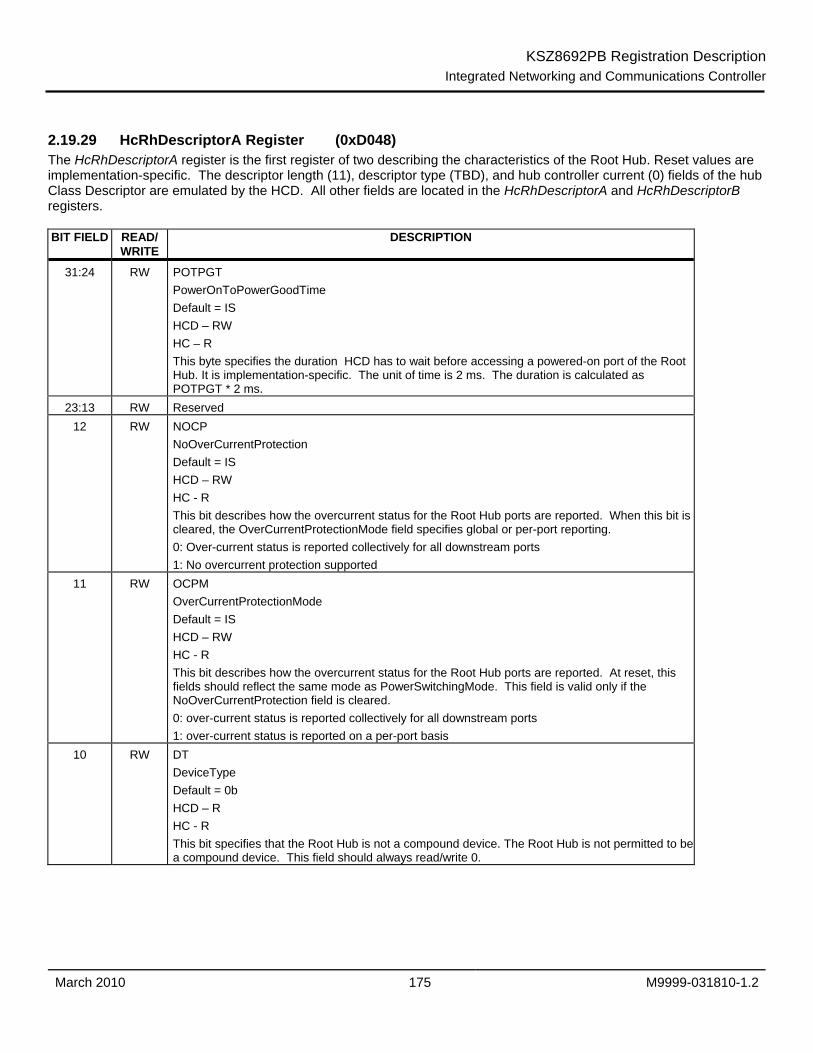
KSZ8692PB Registration Description Integrated Networking and Communications Controller
March 2010 175 M9999-031810-1.2
2.19.29 HcRhDescriptorA Register (0xD048) The HcRhDescriptorA register is the first register of two describing the characteristics of the Root Hub. Reset values are implementation-specific. The descriptor length (11), descriptor type (TBD), and hub controller current (0) fields of the hub Class Descriptor are emulated by the HCD. All other fields are located in the HcRhDescriptorA and HcRhDescriptorB registers. BIT FIELD READ/
WRITE DESCRIPTION
31:24 RW POTPGT PowerOnToPowerGoodTime Default = IS HCD – RW HC – R This byte specifies the duration HCD has to wait before accessing a powered-on port of the Root Hub. It is implementation-specific. The unit of time is 2 ms. The duration is calculated as POTPGT * 2 ms.
23:13 RW Reserved 12 RW NOCP
NoOverCurrentProtection Default = IS HCD – RW HC - R This bit describes how the overcurrent status for the Root Hub ports are reported. When this bit is cleared, the OverCurrentProtectionMode field specifies global or per-port reporting. 0: Over-current status is reported collectively for all downstream ports 1: No overcurrent protection supported
11 RW OCPM OverCurrentProtectionMode Default = IS HCD – RW HC - R This bit describes how the overcurrent status for the Root Hub ports are reported. At reset, this fields should reflect the same mode as PowerSwitchingMode. This field is valid only if the NoOverCurrentProtection field is cleared. 0: over-current status is reported collectively for all downstream ports 1: over-current status is reported on a per-port basis
10 RW DT DeviceType Default = 0b HCD – R HC - R This bit specifies that the Root Hub is not a compound device. The Root Hub is not permitted to be a compound device. This field should always read/write 0.

KSZ8692PB Registration Description Integrated Networking and Communications Controller
March 2010 176 M9999-031810-1.2
9 RW NPS
NoPowerSwitching Default = IS HCD – RW HC - R These bits are used to specify whether power switching is supported or port are always powered. It is implementation- specific. When this bit is cleared, the PowerSwitchingMode specifies global or per-port switching. 0: Ports are power switched 1: Ports are always powered on when the HC is powered on
8 RW PSM PowerSwitchingMode Default = IS HCD – RW HC - R This bit is used to specify how the power switching of the Root Hub ports is controlled. It is implementation-specific. This field is only valid if the NoPowerSwitching field is cleared. 0: all ports are powered at the same time. 1: each port is powered individually. This mode allows port power to be controlled by either the global switch or per-port switching. If the PortPowerControlMask bit is set, the port responds only to port power commands (Set/ClearPortPower). If the port mask is cleared, then the port is controlled only by the global power switch (Set/ClearGlobalPower).
7:0 RW NDP NumberDownstreamPorts Default = IS HCD – R HC - R These bits specify the number of downstream ports supported by the Root Hub. It is implementation-specific. The minimum number of ports is 1. The maximum number of ports supported by OpenHCI is 15.

KSZ8692PB Registration Description Integrated Networking and Communications Controller
March 2010 177 M9999-031810-1.2
2.19.30 HcRhDescriptorB Register (0xD04C) The HcRhDescriptorB register is the second register of two describing the characteristics of the Root Hub. These fields are written during initialization to correspond with the system implementation. Reset values are implementation-specific. BIT FIELD READ/
WRITE DESCRIPTION
31:16 RW PPCM PortPowerControlMask Default – IS HCD = RW HC = R Each bit indicates if a port is affected by a global power control command when PowerSwitchingMode is set. When set, the port's power state is only affected by per-port power control (Set/ClearPortPower). When cleared, the port is controlled by the global power switch (Set/ClearGlobalPower). If the device is configured to global switching mode (PowerSwitchingMode=0), this field is not valid. bit 0: Reserved bit 1: Ganged-power mask on Port #1 bit 2: Ganged-power mask on Port #2 ... bit15: Ganged-power mask on Port #15
15:0 RW DR DeviceRemovable Default = IS HCD = RW HC = R Each bit is dedicated to a port of the Root Hub. When cleared, the attached device is removable. When set, the attached device is not removable. bit 0: Reserved bit 1: Device attached to Port #1 bit 2: Device attached to Port #2 ... bit15: Device attached to Port #15
2.19.31 HcRhStatus Register (0xD050)
The HcRhStatus register is divided into two parts. The lower word of a Dword represents the Hub Status field and the upper word represents the Hub Status Change field. Reserved bits should always be written '0'.
BIT FIELD READ/ WRITE
DESCRIPTION
31 RW CRWE ClearRemoteWakeupEnable (Write Only) HCD = W HC = R Writing a '1' clears DeviceRemoveWakeupEnable. Writing a '0' has no effect.
30:18 - Reserved

KSZ8692PB Registration Description Integrated Networking and Communications Controller
March 2010 178 M9999-031810-1.2
17 RW OCIC
OverCurrentIndicatorChange Default = 0b HCD = RW HC = R Each bit is dedicated to a port of the Root Hub. When cleared, the attached device is removable.When set, the attached device is not removable. bit 0: Reserved bit 1: Device attached to Port #1 bit 2: Device attached to Port #2 ... bit15: Device attached to Port #15
16 RW LPSC (read) LocalPowerStatusChange Default = 0b HCD = RW HC = R The Root Hub does not support the local power status feature; thus, this bit is always read as ‘0’. (write) SetGlobalPower In global power mode (PowerSwitchingMode=0), This bit is written to ‘1’ to turn on power to all ports (clear PortPowerStatus). In per-port power mode, it sets PortPowerStatus only on ports whose PortPowerControlMask bit is not set. Writing a ‘0’ has no effect.
15 RW DRWE (read) DeviceRemoteWakeupEnable Default = 0b HCD = R HC = RW This bit enables a ConnectStatusChange bit as a resume event, causing a UsbSuspend to UsbResume state transition and setting the ResumeDetected interrupt. 0 = ConnectStatusChange is not a remote wakeup event. 1 = ConnectStatusChange is a remote wakeup event. (write) SetRemoteWakeupEnable Writing a '1' sets DeviceRemoveWakeupEnable. Writing a '0' has no effect.
14:2 - Reserved 1 RW OCI
OverCurrentIndicator Default = 0b HCD = R HC = RW This bit reports overcurrent conditions when the global reporting is implemented. When set, an overcurrent condition exists. When cleared, all power operations are normal. If per-port overcurrent protection is implemented this bit is always ‘0’

KSZ8692PB Registration Description Integrated Networking and Communications Controller
March 2010 179 M9999-031810-1.2
0 RW LPS
(read) LocalPowerStatus Default = 0b HCD = RW HC = R The Root Hub does not support the local power status feature; thus, this bit is always read as ‘0’. (write) ClearGlobalPower In global power mode (PowerSwitchingMode=0), This bit is written to ‘1’ to turn off power to all ports (clear PortPowerStatus). In per-port power mode, it clears PortPowerStatus only on ports whose PortPowerControlMask bit is not set. Writing a ‘0’ has no effect.
2.19.32 HcRhPortStatus[1:NDP] Register (0xD054)
The HcRhPortStatus[1:NDP] register is used to control and report port events on a per-port basis. NumberDownstreamPorts represents the number of HcRhPortStatus registers that are implemented in hardware. The lower word is used to reflect the port status, whereas the upper word reflects the status change bits. Some status bits are implemented with special write behavior (see below). If a transaction (token through handshake) is in progress when a write to change port status occurs, the resulting port status change must be postponed until the transaction completes. Reserved bits should always be written '0'.
BIT FIELD READ/ WRITE
DESCRIPTION
31:21 RW Reserved 20 RW PRSC
PortResetStatusChange Default = 0b HCD = RW HC = RW This bit is set at the end of the 10-ms port reset signal. The HCD writes a ‘1’ to clear this bit. Writing a ‘0’ has no effect. 0 = port reset is not complete 1 = port reset is complete
19 RW OCIC PortOverCurrentIndicatorChange Default = 0b HCD = RW HC = RW This bit is valid only if overcurrent conditions are reported on a per-port basis. This bit is set when Root Hub changes the PortOverCurrentIndicator bit. The HCD writes a ‘1’ to clear this bit. Writinga ‘0’ has no effect. 0 = no change in PortOverCurrentIndicator 1 = PortOverCurrentIndicator has changed

KSZ8692PB Registration Description Integrated Networking and Communications Controller
March 2010 180 M9999-031810-1.2
18 RW PSSC
PortSuspendStatusChange Default = 0b HCD = RW HC = RW This bit is set when the full resume sequence has been completed. This sequence includes the 20-s resume pulse, LS EOP, and 3-ms resychronization delay. The HCD writes a ‘1’ to clear this bit. Writing a ‘0’ has no effect. This bit is also cleared when ResetStatusChange is set. 0 = resume is not completed 1 = resume completed
17 RW PESC PortEnableStatusChange Default = 0b HCD = RW HC = RW This bit is set when hardware events cause the PortEnableStatus bit to be cleared. Changes from HCD writes do not set this bit. The HCD writes a ‘1’ to clear this bit. Writing a ‘0’ has no effect. 0 = no change in PortEnableStatus 1 = change in PortEnableStatus
16 RW CSC ConnectStatusChange Default =0b HCD = RW HC = RW This bit is set whenever a connect or disconnect event occurs. The HCD writes a ‘1’ to clear this bit. Writing a ‘0’ has no effect. If CurrentConnectStatus is cleared when a SetPortReset, SetPortEnable, or SetPortSuspend write occurs, this bit is set to force the driver to re-evaluate the connection status since these writes should not occur if the port is disconnected. 0 = no change in CurrentConnectStatus 1 = change in CurrentConnectStatus Note: If the DeviceRemovable[NDP] bit is set, this bit is set only after a Root Hub reset to inform the system that the device is attached.
15:10 - Reserved 9 RW LSDA
(read) LowSpeedDeviceAttached Default =Xb HCD = RW HC = RW This bit indicates the speed of the device attached to this port. When set, a Low Speed device is attached to this port. When clear, a Full Speed device is attached to this port. This field is valid only when the CurrentConnectStatus is set. 0 = full speed device attached 1 = low speed device attached (write) ClearPortPower The HCD clears the PortPowerStatus bit by writing a ‘1’ to this bit. Writing a ‘0’ has no effect.

KSZ8692PB Registration Description Integrated Networking and Communications Controller
March 2010 181 M9999-031810-1.2
8 RW PPS
(read) PortPowerStatus Default = 0b HCD = RW HC = RW This bit reflects the port’s power status, regardless of the type of power switching implemented. This bit is cleared if an overcurrent condition is detected. HCD sets this bit by writing SetPortPower or SetGlobalPower. HCD clears this bit by writing ClearPortPower or ClearGlobalPower. Which power control switches are enabled is determined by PowerSwitchingMode and PortPortControlMask[NDP]. In global switching mode (PowerSwitchingMode=0), only Set/ClearGlobalPower controls this bit. In per-port power switching (PowerSwitchingMode=1), if the PortPowerControlMask[NDP] bit for the port is set, only Set/ClearPortPower commands are enabled. If the mask is not set, only Set/ClearGlobalPower commands are enabled. When port power is disabled, CurrentConnectStatus, PortEnableStatus, PortSuspendStatus, and PortResetStatus should be reset. 0 = port power is off 1 = port power is on (write) SetPortPower The HCD writes a ‘1’ to set the PortPowerStatus bit. Writing a ‘0’ has no effect. Note: This bit is always reads ‘1b’ if power switching is not supported.
7:5 - Reserved 4 RW PRS
(read) PortResetStatus Default = 0b HCD = RW HC = RW When this bit is set by a write to SetPortReset, port reset signaling is asserted. When reset is completed, this bit is cleared when PortResetStatusChange is set. This bit cannot be set if CurrentConnectStatus is cleared. 0 = port reset signal is not active 1 = port reset signal is active (write) SetPortReset The HCD sets the port reset signaling by writing a ‘1’ to this bit. Writing a ‘0’ has no effect. If CurrentConnectStatus is cleared, this write does not set PortResetStatus, but instead sets ConnectStatusChange. This informs the driver that it attempted to reset a disconnected port.
3 RW POCI (read) PortOverCurrentIndicator Default = 0b HCD = RW HC = RW This bit is only valid when the Root Hub is configured in such a way that overcurrent conditions are reported on a per-port basis. If per-port overcurrent reporting is not supported, this bit is set to 0. If cleared, all power operations are normal for this port. If set, an overcurrent condition exists on this port. This bit always reflects the overcurrent input signal 0 = no overcurrent condition. 1 = overcurrent condition detected. (write) ClearSuspendStatus The HCD writes a ‘1’ to initiate a resume. Writing a ‘0’ has no effect. A resume is initiated only if PortSuspendStatus is set.

KSZ8692PB Registration Description Integrated Networking and Communications Controller
March 2010 182 M9999-031810-1.2
2 RW PSS
(read) PortSuspendStatus Default = 0b HCD = RW HC = RW This bit indicates the port is suspended or in the resume sequence. It is set by a SetSuspendState write and cleared when PortSuspendStatusChange is set at the end of the resume interval. This bit cannot be set if CurrentConnectStatus is cleared. This bit is also cleared when PortResetStatusChange is set at the end of the port reset or when the HC is placed in the UsbResume state. If an upstream resume is in progress, it should propagate to the HC. 0 = port is not suspended 1 = port is suspended (write) SetPortSuspend The HCD sets the PortSuspendStatus bit by writing a ‘1’ to this bit. Writing a ‘0’ has no effect. If CurrentConnectStatus is cleared, this write does not set PortSuspendStatus; instead it sets ConnectStatusChange. This informs the driver that it attempted to suspend a disconnected port.
1 RW PES (read) PortEnableStatus Default = 0b HCD = RW HC = RW This bit indicates whether the port is enabled or disabled. The Root Hub may clear this bit when an overcurrent condition, disconnect event, switched-off power, or operational bus error such as babble is detected. This change also causes PortEnabledStatusChange to be set. HCD sets this bit by writing SetPortEnable and clears it by writing ClearPortEnable. This bit cannot be set when CurrentConnectStatus is cleared. This bit is also set, if not already, at the completion of a port reset when ResetStatusChange is set or port suspend when SuspendStatusChange is set. 0 = port is disabled 1 = port is enabled (write) SetPortEnable The HCD sets PortEnableStatus by writing a ‘1’. Writing a ‘0’ has no effect. If CurrentConnectStatus is cleared, this write does not set PortEnableStatus, but instead sets ConnectStatusChange. This informs the driver that it attempted to enable a disconnected port.
0 RW CCS (read) CurentConnectStatus Default = 0b HCD = RW HC = RW This bit reflects the current state of the downstream port. 0 = no device connected 1 = device connected (write) ClearPortEnable The HCD writes a ‘1’ to this bit to clear the PortEnableStatus bit. Writing a ‘0’ has no effect. The CurrentConnectStatus is not affected by any write. Note: This bit is always read ‘1b’ when the attached device is non-removable (DeviceRemoveable[NDP]).

KSZ8692PB Registration Description Integrated Networking and Communications Controller
March 2010 183 M9999-031810-1.2
2.20 UART Registers (0xE000-0xE1FF) 2.20.1 UART 1 Receive Buffer Register (UR1RB Offset 0xE000) 2.20.2 UART 2 Receive Buffer Register (UR2RB Offset 0xE080) 2.20.3 UART 3 Receive Buffer Register (UR3RB Offset 0xE100) 2.20.4 UART 4 Receive Buffer Register (UR4RB Offset 0xE180) The UART Receive Buffer register contains an 8-bit data value received over the UART channel. The following Table shows the register bit fields.
BIT FIELD DEFAULT VALUE
READ/ WRITE
DESCRIPTION
31:8 0x0 RO Reserved 7:0 -- RO URRBD UART Receive Buffer Data
This field contains the data received over the single channel UART. When UART finishes receiving data frame, the Receive Data Ready bit in the Line Status Register will be set. Note: whenever the URRBD is read, the Receive Data Ready bit in the Line Status Register is automatically cleared.
2.20.5 UART 1 Transmit Holding Register (UR1TH Offset 0xE004) 2.20.6 UART 2 Transmit Holding Register (UR2TH Offset 0xE084) 2.20.7 UART 3 Transmit Holding Register (UR3TH Offset 0xE104) 2.20.8 UART 4 Transmit Holding Register (UR4TH Offset 0xE184) The UART Transmit Holding register contains an 8-bit data value to be transmitted over the UART channel. The following Table shows the register bit fields.
BIT FIELD DEFAULT VALUE
READ/ WRITE
DESCRIPTION
31:8 0x0 RO Reserved 7:0 -- WO URTHD UART Transmit Holding Data
This field contains the data to be transmitted over the single channel UART. Whenever the URTHD is written, the Transmit Holding Register Empty bit in the Line Status Register is automatically cleared to ‘0’ until the UART finishes transmitting the data. Note: software should ensure that the Transmit Holding Register Empty bit in the Line Status Register is ‘1’ before writing to this register to prevent from over-writting the current transmit data.
2.20.9 UART 1 FIFO Control Register (UR1FC Offset 0xE008) 2.20.10 UART 2 FIFO Control Register (UR2FC Offset 0xE088) 2.20.11 UART 3 FIFO Control Register (UR3FC Offset 0xE108) 2.20.12 UART 4 FIFO Control Register (UR4FC Offset 0xE188)

KSZ8692PB Registration Description Integrated Networking and Communications Controller
March 2010 184 M9999-031810-1.2
The UART FIFO Control register provides control over transmitter and receiver FIFOs. The following Table shows the register bit fields.
BIT FIELD DEFAULT VALUE
READ/ WRITE
DESCRIPTION
31:8 0x0 RO Reserved 7:6 00 RW URFRT UART Receive FIFO Trigger Level
This field controls the trigger level for the receive FIFO. 00 = 1 Byte 01 = 8 Bytes 10 = 16 Bytes 11 = 24 Bytes
5:3 000 RO Reserved 2 0 RW URTFR UART Transmit FIFO Reset
When set, the transmit state machine will be reset, and the transmit FIFO will be emptied. Writing ‘0’ has no effect. Note: This bit will be self-cleared to 0 after 1 is written.
1 0 RW URRFR UART Receive FIFO Reset When set, the receive FIFO state machine will be reset, and receive FIFO will be emptied. Writting ‘0’ has no effect. Note: This bit will be self-cleared to 0 after 1 is written.
0 0 RW URFE UART FIFO Enable When set, both the transmit and receive FIFOs are enabled. (UART is in 16550 mode) When reset, both the transmit and receive FIFOs are disabled. (UART is in 16450 mode) Note that when UART changes from FIFO to character mode or vice versa, data in the FIFOs are automatically cleared. This bit must be set when other control bits in this register are written to or they will not be programmed.
2.20.13 UART 1 Line Control Register (UR1LC Offset 0xE00C) 2.20.14 UART 2 Line Control Register (UR2LC Offset 0xE08C) 2.20.15 UART 3 Line Control Register (UR3LC Offset 0xE10C) 2.20.16 UART 4 Line Control Register (UR4LC Offset 0xE18C)

KSZ8692PB Registration Description Integrated Networking and Communications Controller
March 2010 185 M9999-031810-1.2
The UART Line Control register basically specifies the asynchronous data frame for transmitting and receiving as seen below.
Start Character Length (5, 6, 7 or 8 bits) Parity Stopbits
Idle Idle
Data transmitting direction
Fsample
Frclk
7,8,9
When the bus(one bit serial bus) is idle, it stays at high. The first high-to-low transition is detected as the Start bit. Start bit is Low and Stop bit is High. Due to the noise, a short glitch might happen on the bus. To avoid detecting the wrong Start bit, three samples at clock (Frclk) 7, 8, and 9 after high-to-low transition is taken on the bus. If at least two out of three samples are Low, then Start bit is detected; otherwise, the high-to-low transition is treated as a glitch. Frclk and Fsample will be defined at Baud Rate Divisor Register section. The following Table shows the register bit fields.
BIT FIELD DEFAULT VALUE
READ/ WRITE
DESCRIPTION
31:10 0x0 RO Reserved 9 0 RW CTS_N tx flow control enable
Whet set, the data transmission is halted when the corresponding CTS_N pin is high.When reset, no tx flow control is applied. [note: The CTS_N and RTS_N are shared with GPIO pins. The bit23:21 in GPIO Port Control Register has to be configured to indicate which application is used.]
8 0 RW RTS_N rx flow control enable When set, the corresponding RTS_N pin will be desserted when the rx buffer level is greater than or equal to HWM trigger level. Sending out a desserted value of RTS_N will make the link partner stop to send out data. When the rx buffer level is less than LWM trigger level, the corresponding RTS_N pin will be asserted. When reset, no rx flow control is applied. The following Table shows the HWM and LWM trigger level at different FIFO size mode.
FIFO Size HWM trigger level LWM trigger level
1 8 1 8 16 4
16 24 8 24 28 16
7 0 RO Reserved

KSZ8692PB Registration Description Integrated Networking and Communications Controller
March 2010 186 M9999-031810-1.2
6 0 RW URSBC UART Set Break Condition on UTXD
When set, a break condition will be asserted on the UTXD pin. A break condition is when the UTXD is driven low for more than one frame time ( including Start, Parity, and Stop bits) measured at a give baud rate.
5 0 RW URSPB UART Stick Parity Bit When set, the stick parity is enabled, ( stick parity has precedence over even/odd parity), i.e. if bit URPE, UREPB, and URSPB are all 1’s, parity is always 0. If bits URPE, and URSPB are 1’s, and bit UREPB is 0, parity is always 1. When reset, stick parity is disabled.
4 0 RW UREPB UART Even Parity Bit 0 = even parity. 0 = odd parity.
3 0 RW URPE UART Parity Enable (Even/Odd/Stick) When set, parity is enabled. When reset, parity is disabled.
2 0 RW URSB UART Stop Bits 0 = 1 Stop bit per data frame. 1 = 2 Stop bit per data frame.
1:0 11 RW URCL UART Character Length 00 = 5 data bits per frame. 01 = 6 data bits per frame. 10 = 7 data bits per frame. 11 = 8 data bits per frame. (Default)
2.20.17 UART 1 Modem Control Register (UR1MC Offset 0xE010) 2.20.18 UART 2 Modem Control Register (UR2MC Offset 0xE090) 2.20.19 UART 3 Modem Control Register (UR3MC Offset 0xE110) 2.20.20 UART 4 Modem Control Register (UR4MC Offset 0xE190) The UART 1 Modem Control register provides interface with the MODEM. All the UART and Modem communication uses software handshaing. The following Table shows the register bit fields.
BIT FIELD DEFAULT VALUE
READ/ WRITE
DESCRIPTION
31:8 0x0 RO Reserved 7 0 RW UREN UART enable
1 = enable this UART unit, clock and IO 0 = diable this UART unit, clock, and IO
6:5 0 RW URCLKSEL UART clock select 00 = 25MHz 01 = 62.5MHz 10 = 125MHz 11 = 166MHz

KSZ8692PB Registration Description Integrated Networking and Communications Controller
March 2010 187 M9999-031810-1.2
4 0 RW URLB UART Loop Back Mode
When set, the UART is in the local loopback mode. This feature is for software diagnostics/testing. When reset, the UART is in normal functional mode. Note: In the UART loopback mode, the interrupt mechanism is fully operational. The operation of the Modem in the loopback mode is similar to external Modem loopback with Null modem cable.
3 0 RW UROUT2 UART OUT2 When set, the internal UART OUT2 signal is asserted to 0. When reset, the internal UART OUT2 signal is deasserted.
2 0 RW UROUT1 UART OUT1 When set, the internal UART OUT1 signal is asserted to 0. When reset, the internal UART OUT1 signal is deasserted.
1 0 RW Reserved. 0 0 RW Reserved
2.20.21 UART 1 Line Status Register (UR1LS Offset 0xE014) 2.20.22 UART 2 Line Status Register (UR2LS Offset 0xE094) 2.20.23 UART 3 Line Status Register (UR3LS Offset 0xE114) 2.20.24 UART 4 Line Status Register (UR4LS Offset 0xE194) The UART Line Status register provides status information to the CPU regarding the received data. The receive FIFO has 16 entries, each of which includes one byte of data and three error bits (parity error, framing error,and break interrupt) associated to the data. The Line status register is read only; writing to this register has no effect. The following Table shows the register bit fields.
BIT FIELD DEFAULT VALUE
READ/ WRITE
DESCRIPTION
31:14 0x0 RO Reserved 13:8 0x0 RO NADRF Number of available data in Receive FIFO
7 0 RO URRFE UART Receive FIFO Error This bit is meaningful only in FIFO mode to indicate that the UART receive FIFO contains error(s). Reading of ‘1’ indicates there is at least one of the following errors: parity error, framing error, or break interrupt. This bit is cleared only when it is read by CPU and no subsequent errors in the FIFO.
6 1 RO URTE UART Transmit Empty This bit indicates that the UART Tranmit buffer is ready to accept new data for transmit. In character mode (16450): When set to ‘1’, it indicates that the Transmit Holding Register and Transmitter Shift Register are both empty. In FIFO mode (16550): When set to ‘1’, it indicates that both the Transmit FIFO and Transmit Shift Register are empty

KSZ8692PB Registration Description Integrated Networking and Communications Controller
March 2010 188 M9999-031810-1.2
5 1 RO URTHRE UART Transmit Holding Register Empty
This bit indicates that the UART Transmit Holding Register (THR) is empty. In character mode (16450): When set to ‘1’, it indicates the THR is empty. In FIFO mode (16550): When set to ‘1’, it indicates that the Transmit FIFO is empty.
4 0 RO URBI UART Break Interrupt Indicator In character mode (16450): When set, it indicates a “break” condition occurs on the URXD pin. A break condition is when the serial data is driven low for more than one frame time ( including Start, Parity, and Stop bits) measured at a give baud rate. In FIFO mode (16550): The break interrupt bit in the Receiver FIFO will be copied to this register bit when its associated character is at the top of the Receiver FIFO. This bit is reset to ‘0’ when read.
3 0 RO URFE UART Framing Error In character mode (16450): When set, the received character does not have the correct stop bit.( ‘0’ is sampled) In FIFO mode (16550): The framing error bit in the Receiver FIFO will be copied to this register bit when its associated character is at the top of the Receiver FIFO. This bit reset to ‘0’ when read.
2 0 RO URPE UART Parity Error In character mode (16450): When set, the received character does not have the correct even or odd parity (excluding stick parity), as selected by the parity select bit. In FIFO mode (16550): The parity error bit in the Receiver FIFO will be copied to this register bit when its associated character is at the top of the Receiver FIFO. This bit reset to ‘0’ when read.
1 0 RO URROE UART Receive Overrun Error In character mode (16450): When set, the Receive Buffer Register (RBR) has not been read by the CPU before the next character is ready to be transferred into RBR from the Receive Shift Register. In FIFO mode (16550): The Receiver FIFO is full and the next character is ready to be transferred into FIFO from the Receive Shift Register. This bit reset to ‘0’ when read.
0 0 RO URDR UART Receive Data Ready In character mode (16450): When set, data is valid in the Receive Buffer Register. In FIFO mode (16550): There is at least one character data ready in the Receive FIFO (not empty.) This bit will be cleared when no data in Receive Buffer Register or FIFO.

KSZ8692PB Registration Description Integrated Networking and Communications Controller
March 2010 189 M9999-031810-1.2
2.20.25 UART 1 Modem Status Register (UR1MS Offset 0xE018) 2.20.26 UART 2 Modem Status Register (UR2MS Offset 0xE098) 2.20.27 UART 3 Modem Status Register (UR3MS Offset 0xE118) 2.20.28 UART 4 Modem Status Register (UR4MS Offset 0xE198) This register provides the current state of the Modem input control lines to the CPU. In addition to the current-state information, four bits of the Modem status register provide state-changing information. These bits are set to logic ‘1’ whenever a control input from the remote Modem changes state. They are reset to ‘0’ whenever the CPU reads the register. When either one of the four bits URLS[3:0] is set to ‘1’, a Modem status interrupt is generated. The following Table shows the register bit fields.
BIT FIELD DEFAULT VALUE
READ/ WRITE
DESCRIPTION
31:8 0 RO Reserved 7 -- RO URDCD UART Data Carrier Detect
This bit indicates the logical (inverted) value of the UDCDN input. 6 -- RO URRI UART Ring Indicator
This bit indicates the logical (inverted) value of the URIN input pin. 5 -- RO URDSR UART Data Set Ready
This bit indicates the logical (inverted) value of the UDSRN input pin. 4 -- RO URCTS UART Clear To Send
This bit indicates the logical (inverted) value of the UCTSN input pin. 3 0 RO URDDCD UART Delta Data Carrier Detect
This bit is set when the UDCDN input pin has changed state. Cleared when read.
2 0 RO URTERI UART Trailing Edge Ring Indicator This bit is set when the URIN input pin has changed from Low to High. Cleared when read.
1 0 RO URDDST UART Delta Data Set Ready This bit is set when the UDSRN input pin has changed state. Cleared when read.
0 0 RO URDCTS UART Delta Clear To Send This bit is set when the UCTSN input pin has changed state. Cleared when read.
2.20.29 UART 1 Baud Rate Divisor Register (UR1BD Offset 0xE01C) 2.20.30 UART 2 Baud Rate Divisor Register (UR2BD Offset 0xE09C) 2.20.31 UART 3 Baud Rate Divisor Register (UR3BD Offset 0xE11C) 2.20.32 UART 4 Baud Rate Divisor Register (UR4BD Offset 0xE19C) The input clock to the baud rate generator is selected by URCLKSEL. This clock is divided by the value in the URBD register to generate the sample clock (Fsample), which is used to sample the incoming data or to drive the outgoing data. The frequency of Frclk is 16 times of Fsample.

KSZ8692PB Registration Description Integrated Networking and Communications Controller
March 2010 190 M9999-031810-1.2
The following Table shows the register bit fields.
BIT FIELD DEFAULT VALUE
READ/ WRITE
DESCRIPTION
31:27 0x0 RO Reserved 26:0 0x1BE RW URBDC UART Baud Rate Divisor Count
2.20.33 UART 1 Status Register (US1R Offset 0xE020) 2.20.34 UART 2 Status Register (US2R Offset 0xE0A0) 2.20.35 UART 3 Status Register (US3R Offset 0xE120) 2.20.36 UART 4 Status Register (US4R Offset 0xE1A0) This register currently holds the Timeout Indication bit. The Timeout and Receive Triggered-level Reach shares the same interrupt Status(INTST[9]) bit. To further distinguish these two interrupt sources, a Timeout Indication bit is introduced. The following Table shows the register bit fields.
BIT FIELD DEFAULT VALUE
READ/ WRITE
DESCRIPTION
31:1 0x0 RO Reserved 0 0 RO UTI UART Timeout Indication bit
If INTST[9] = 1 and USR[0] = 1, the interrupt source is from timeout. If INTST[9] = 1 and USR[0] = 0, the interrupt source is because the Receive FIFO has reached the trigger-level. Note that this bit will be automatically cleared when either a new coming frame has received or CPU reads Receive FIFO.
2.21 Interrupt Controller Registers KSZ8692PB supports multiple interrupt sources with reconfigurable priority. Interrupt requests can be generated by internal functional blocks as well as external pins. The ARM core recognizes two kinds of interrupts: a normal interrupt request (IRQ), and a fast interrupt request (FIQ). All interrupts can be categorized as either IRQ or FIQ. The KSZ8692PB interrupt controller has an interrupt status bit for each interrupt source. This register defines the interrupt source for each device interrupt. In general, four special registers are used to control interrupt generation and handling:
• Interrupt Mode Control Register: defines the interrupt source to the ARM core, IRQ or FIQ. • Interrupt Priority Register: the index number of each interrupt source is written to the pre-defined interrupt
priority register field to obtain the priority. The interrupt priorities are predefined from 0 to 15. • Interrupt Status Register: indicates the interrupt status. • Interrupt Enable Register: enables the interrupts.

KSZ8692PB Registration Description Integrated Networking and Communications Controller
March 2010 191 M9999-031810-1.2
2.21.1 Interrupt Mode Control Register (INTMC Offset 0xE200) The following Table shows the register bit fields.
BIT FIELD DEFAULT VALUE
READ/ WRITE
DESCRIPTION
31 0 RO Reserved 30 0 RW WMTIM WAN MAC Transmit Interrupt Mode
When set, the WAN MAC Transmit Interrupt corresponds to the FIQ (fast Interrupt). When reset, the WAN MAC Transmit Interrupt corresponds to the IRQ (normal interrupt).
29 0 RW WMRIM WAN MAC Receive Interrupt Mode When set, the WAN MAC Receive Interrupt corresponds to the FIQ (fast Interrupt). When reset, the WAN MAC Receive Interrupt corresponds to the IRQ (normal interrupt).
28 0 RW WMTBUIM WAN MAC Transmit Buffer Unavailable Interrupt Mode When set, the WAN MAC Transmit Buffer Unavailable Interrupt corresponds to the FIQ (fast Interrupt). When reset, the WAN MAC Transmit Buffer Unavailable Interrupt corresponds to the IRQ (normal interrupt).
27 0 RW WMRBUIM WAN MAC Receive Buffer Unavailable Interrupt Mode When set, the WAN MAC Receive Buffer Unavailable Interrupt corresponds to the FIQ (fast Interrupt). When reset, the WAN MAC Receive Buffer Unavailable Interrupt corresponds to the IRQ (normal interrupt).
26 0 RW WMTPSIM WAN MAC Transmit Process Stopped Interrupt Mode When set, the WAN MAC Transmit Process Stopped Interrupt corresponds to the FIQ (fast interrupt). When reset, the WAN MAC Transmit Process Stopped Interrupt corresponds to the IRQ (normal interrupt).
25 0 RW WMRPSIM WAN MAC Receive Process Stopped Interrupt Mode When set, the WAN MAC Receive Process Stopped Interrupt corresponds to the FIQ (fast interrupt). When reset, the WAN MAC Receive Process Stopped Interrupt corresponds to the IRQ (normal interrupt).
24 0 RW ABERIM AMBA Bus Error Response Interrupt Mode When set, the AMBA Bus Error Response Interrupt corresponds to the FIQ (fast interrupt). When reset, the AMBA Bus Error Response Interrupt corresponds to the IRQ (normal interrupt).
23:20 0x0 RO Reserved 19 0 RW WWUM WAN Wake-up Interrupt Mode
When set, the WAN Wake-up Interrupt corresponds to the FIQ (fast interrupt). When reset, the WAN Wake-up Interrupt corresponds to the IRQ (normal interrupt).
18 0 RW LWUM LAN Wake-up Interrupt Mode When set, the LAN Wake-up Interrupt corresponds to the FIQ (fast interrupt). When reset, the LAN Wake-up Interrupt corresponds to the IRQ (normal interrupt).

KSZ8692PB Registration Description Integrated Networking and Communications Controller
March 2010 192 M9999-031810-1.2
17 0 RW LMTIM LAN MAC Transmit Interrupt Mode
When set, the LAN MAC Transmit Interrupt corresponds to the FIQ (fast Interrupt). When reset, the LAN MAC Transmit Interrupt corresponds to the IRQ (normal interrupt).
16 0 RW LMRIM LAN MAC Receive Interrupt Mode When set, the LAN MAC Receive Interrupt corresponds to the FIQ (fast Interrupt).When reset, the LAN MAC Receive Interrupt corresponds to the IRQ (normal interrupt).
15 0 RW LMTBUIM LAN MAC Transmit Buffer Unavailable Interrupt Mode When set, the LAN MAC Transmit Buffer Unavailable Interrupt corresponds to the FIQ (fast Interrupt). When reset, the LAN MAC Transmit Buffer Unavailable Interrupt corresponds to the IRQ (normal interrupt).
14 0 RW LMRBUIM LAN MAC Receive Buffer Unavailable Interrupt Mode When set, the LAN MAC Receive Buffer Unavailable Interrupt corresponds to the FIQ (fast Interrupt). When reset, the LAN MAC Receive Buffer Unavailable Interrupt corresponds to the IRQ (normal interrupt).
13 0 RW LMTPSIM LAN MAC Transmit Process Stopped Interrupt Mode When set, the LAN MAC Transmit Process Stopped Interrupt corresponds to the FIQ (fast interrupt). When reset, the LAN MAC Transmit Process Stopped Interrupt corresponds to the IRQ (normal interrupt).
12 0 RW LMRPSIM LAN MAC Receive Process Stopped Interrupt Mode When set, the LAN MAC Receive Process Stopped Interrupt corresponds to the FIQ (fast interrupt). When reset, the LAN MAC Receive Process Stopped Interrupt corresponds to the IRQ (normal interrupt).
11 0 RO Reserved 10 0 RW UDIM USB Device Interrupt Mode
When set, the USB Device Interrupt corresponds to the FIQ (fast interrupt). When reset, the USB Device Interrupt corresponds to the IRQ (normal interrupt).
9 0 RW UHOIM USB Host OHCI Interrupt Mode When set, the USB Host OHCI Interrupt corresponds to the FIQ (fast interrupt). When reset, the USB Host OHCI Interrupt corresponds to the IRQ (normal interrupt).
8 0 RW UHEIM USB Host EHCI Interrupt Mode When set, the USB Host EHCI Interrupt corresponds to the FIQ (fast interrupt). When reset, the USB Host EHCI Interrupt corresponds to the IRQ (normal interrupt).
7 0 RW SDIOM SDIO Interrupt Mode When set, the SDIO Interrupt corresponds to the FIQ (fast interrupt). When reset, the SDIO Interrupt corresponds to the IRQ (normal interrupt).
6 0 RW IPSECIM IPSec interrupt Mode When set, the IPSec Interrupt corresponds to the FIQ (fast interrupt). When reset, the IPSec Interrupt corresponds to the IRQ (normal interrupt).

KSZ8692PB Registration Description Integrated Networking and Communications Controller
March 2010 193 M9999-031810-1.2
5 0 RO Reserved 4 0 RW DDRIM DDR Error Interrupt Mode
When set, the DDR Interrupt corresponds to the FIQ (fast interrupt). When reset, the DDR Interrupt corresponds to the IRQ (normal interrupt).
3:0 0 RO Reserved
2.21.2 Interrupt Mode Control Register2 (INTMC2 Offset 0xE204) The following Table shows the register bit fields.
BIT FIELD DEFAULT VALUE
READ/ WRITE
DESCRIPTION
31:26 0x000 RO Reserved 25 0 RW U4LSEIM UART4 Line Status Error Interrupt Mode
When set, the UART4 Line Status Error interrupt corresponds to the FIQ (fast interrupt). When reset, the UART4 Line Status Error interrupt corresponds to the IRQ (normal interrupt).
24 0 RW U4RTLRIM UART4 Receiver Trigger Level Reached Interrupt Mode When set, the UART4 Receiver Trigger Level Reached interrupt corresponds to the FIQ (fast interrupt). When reset, the UART4 Receiver Trigger Level Reached interrupt corresponds to the IRQ (normal interrupt).
23 0 RW U4TEIM UART4 Transmitter Empty Interrupt Mode When set, the UART4 Transmitter Empty interrupt corresponds to the FIQ (fastl interrupt). When reset, the UART4 Transmitter Empty interrupt corresponds to the IRQ (normal interrupt).
22 0 RW U3LSEIM UART3 Line Status Error Interrupt Mode When set, the UART3 Line Status Error interrupt corresponds to the FIQ (fast interrupt). When reset, the UART3 Line Status Error interrupt corresponds to the IRQ (normal interrupt).
21 0 RW U3RTLRIM UART3 Receiver Trigger Level Reached Interrupt Mode When set, the UART3 Receiver Trigger Level Reached interrupt corresponds to the FIQ (fast interrupt). When reset, the UART3 Receiver Trigger Level Reached interrupt corresponds to the IRQ (normal interrupt).
20 0 RW U3TEIM UART3 Transmitter Empty Interrupt Mode When set, the UART3 Transmitter Empty interrupt corresponds to the FIQ (fast interrupt). When reset, the UART3 Transmitter Empty interrupt corresponds to the IRQ (normal interrupt).
19 0 RW U2LSEIM UART2 Line Status Error Interrupt Mode When set, the UART2 Line Status Error interrupt corresponds to the FIQ (fast interrupt). When reset, the UART2 Line Status Error interrupt corresponds to the IRQ (normal interrupt).

KSZ8692PB Registration Description Integrated Networking and Communications Controller
March 2010 194 M9999-031810-1.2
18 0 RW U2RTLRIM UART2 Receiver Trigger Level Reached Interrupt Mode
When set, the UART2 Receiver Trigger Level Reached interrupt corresponds to the FIQ (fast interrupt). When reset, the UART2 Receiver Trigger Level Reached interrupt corresponds to the IRQ (normal interrupt).
17 0 RW U2TEIM UART2 Transmitter Empty Interrupt Mode When set, the UART2 Transmitter Empty interrupt corresponds to the FIQ (fast interrupt). When reset, the UART2 Transmitter Empty interrupt corresponds to the IRQ (normal interrupt).
16 0 RW U1MIM UART1 Modem Interrupt Mode When set, the UART Modem interrupt corresponds to the FIQ (fast interrupt). When reset, the UART Modem interrupt corresponds to the IRQ (normal interrupt).
15 0 RW U1LSEIM UART1 Line Status Error Interrupt Mode When set, the UART1 Line Status Error interrupt corresponds to the FIQ (fast interrupt). When reset, the UART1 Line Status Error interrupt corresponds to the IRQ (normal interrupt).
14 0 RW U1RTLRIM UART1 Receiver Trigger Level Reached Interrupt Mode When set, the UART1 Receiver Trigger Level Reached interrupt corresponds to the FIQ (fast interrupt). When reset, the UART1 Receiver Trigger Level Reached interrupt corresponds to the IRQ (normal interrupt).
13 0 RW U1TEIM UART1 Transmitter Empty Interrupt Mode When set, the UART1 Transmitter Empty interrupt corresponds to the FIQ (fast interrupt). When reset, the UART1 Transmitter Empty interrupt corresponds to the IRQ (normal interrupt).
12 0 RW MDIOM MDIO Interrupt Mode When set, the MDIO interrupt corresponds to the FIQ (fast interrupt). When reset, the MDIO interrupt corresponds to the IRQ (normal interrupt).
11 0 RW SPIM SPI Interrupt Mode When set, the SPI interrupt corresponds to the FIQ (fast interrupt). When reset, the SPI interrupt corresponds to the IRQ (normal interrupt).
10 0 RW I2STM I2S Transmit Interrupt Mode When set, the I2S Transmit interrupt corresponds to the FIQ (fast interrupt). When reset, the I2S Transmit interrupt corresponds to the IRQ (normal interrupt).
9 0 RW I2SRM I2S Receive Interrupt Mode When set, the I2S Receive interrupt corresponds to the FIQ (fast interrupt). When reset, the I2S Receive interrupt corresponds to the IRQ (normal interrupt).
8 0 RW I2CM I2C Interrupt Mode When set, the I2C interrupt corresponds to the FIQ (fast interrupt). When reset, the I2C interrupt corresponds to the IRQ (normal interrupt).
7 0 RW T1IM Timer 1 Interrupt Mode When set, the Timer 1 Interrupt corresponds to the FIQ (fast interrupt). When reset, the Timer 1 Interrupt corresponds to the IRQ (normal interrupt).

KSZ8692PB Registration Description Integrated Networking and Communications Controller
March 2010 195 M9999-031810-1.2
6 0 RW T0IM Timer 0 Interrupt Mode
When set, the Timer 0 Interrupt corresponds to the FIQ (fast interrupt). When reset, the Timer 0 Interrupt corresponds to the IRQ (normal interrupt).
5 0 RW EXTI3M External Interrupt 3 Mode When set, the external interrupt 3 corresponds to the FIQ (fast interrupt). When reset, the external interrupt 3 corresponds to the IRQ (normal interrupt).
4 0 RW EXTI2M External Interrupt 2 Mode When set, the external interrupt 2 corresponds to the FIQ (fast interrupt). When reset, the external interrupt 2 corresponds to the IRQ (normal interrupt).
3 0 RW EXTI1M External Interrupt 1 Mode When set, the external interrupt 1 corresponds to the FIQ (fast interrupt). When reset, the external interrupt 1 corresponds to the IRQ (normal interrupt).
2 0 RW EXTI0M External Interrupt 0 Mode When set, the external interrupt 0 corresponds to the FIQ (fast interrupt). When reset, the external interrupt 0 corresponds to the IRQ (normal interrupt).
1 0 RW CCTM Communications Channel Transmit Mode When set, the communications channel transmit corresponds to the FIQ (fast interrupt). When reset, the communications channel transmit corresponds to the IRQ (normal interrupt).
0 0 RW CCRM Communications Channel Receive Mode When set, the communications channel receive corresponds to the FIQ (fast interrupt). When reset, the communications channel receive corresponds to the IRQ (normal interrupt).
2.21.3 Interrupt Enable Register (INTEN Offset 0xE208) This register enables the interrupts from the internal or external sources. The following Table shows the register bit fields.
BIT FIELD DEFAULT VALUE
READ/ WRITE
DESCRIPTION
31 0 RO Reserved 30 0 RW WMTIE WAN MAC Transmit Interrupt Enable
When this bit is set, the WAN MAC Transmit Interrupt is enabled. When this bit is reset, the WAN MAC Transmit Interrupt is disabled.
29 0 RW WMRIE WAN MAC Receive Interrupt Enable When this bit is set, the WAN MAC Receive Interrupt is enabled. When this bit is reset, the WAN MAC Receive Interrupt is disabled.
28 0 RW WMTBUIE WAN MAC Transmit Buffer Unavailable Interrupt Enable When this bit is set, the WAN MAC Transmit Buffer Unavailable Interrupt is enabled. When this bit is reset, the WAN MAC Transmit Buffer Unavailable Interrupt is disabled.
27 0 RW WMRBUIE WAN MAC Receive Buffer Unavailable Interrupt Enable When this bit is set, the WAN MAC Receive Buffer Unavailable Interrupt is enabled. When this bit is reset, the WAN MAC Receive Buffer Unavailable Interrupt is disabled.

KSZ8692PB Registration Description Integrated Networking and Communications Controller
March 2010 196 M9999-031810-1.2
26 0 RW WMTPSIE WAN MAC Transmit Process Stopped Interrupt Enable
When this bit is set, the WAN MAC Transmit Process Stopped Interrupt is enabled. When this bit is reset, the WAN MAC Transmit Process Stopped Interrupt is disabled.
25 0 RW WMRPSIE WAN MAC Receive Process Stopped Interrupt Enable When this bit is set, the WAN MAC Receive Process Stopped Interrupt is enabled. When this bit is reset, the WAN MAC Receive Process Stopped Interrupt is disabled.
24 0 RW ABERIE AMBA Bus Error Response Interrupt Enable When this bit is set, the AMBA Bus Error Response Interrupt is enabled. When this bit is reset, the AMBA Bus Error Response Interrupt is disabled.
23:20 0x0 RO Reserved 19 0 RW WWUIE WAN Wake-up Interrupt Enable
When set, the WAN Wake-up Interrupt is enabled. When reset, the WAN Wake-up Interrupt is disabled.
18 0 RW LWUIE LAN Wake-up Interrupt Enable When set, the LAN Wake-up Interrupt is enabled. When reset, the LAN Wake-up Interrupt is disabled
17 0 RW LMTIE LAN MAC Transmit Interrupt Enable When set, the LAN MAC Transmit Interrupt is enabled. When reset, the LAN MAC Transmit Interrupt is disabled.
16 0 RW LMRIE LAN MAC Receive Interrupt Enable When set, the LAN MAC Receive Interrupt is enabled. When reset, the LAN MAC Receive Interrupt is disabled.
15 0 RW LMTBUIE LAN MAC Transmit Buffer Unavailable Interrupt Enable When set, the LAN MAC Transmit Buffer Unavailable Interrupt is enabled. When reset, the LAN MAC Transmit Buffer Unavailable Interrupt is disabled.
14 0 RW LMRBUIE LAN MAC Receive Buffer Unavailable Interrupt Enable When set, the LAN MAC Receive Buffer Unavailable Interrupt is enabled. When reset, the LAN MAC Receive Buffer Unavailable Interrupt is disabled.
13 0 RW LMTPSIE LAN MAC Transmit Process Stopped Interrupt Enable When set, the LAN MAC Transmit Process Stopped Interrupt is enabled. When reset, the LAN MAC Transmit Process Stopped Interrupt is disabled.
12 0 RW LMRPSIE LAN MAC Receive Process Stopped Interrupt Enable When set, the LAN MAC Receive Process Stopped Interrupt is enabled. When reset, the LAN MAC Receive Process Stopped Interrupt is disabled.
11 0 RO Reserved 10 0 RW UDIE USB Device Interrupt Enable
When set, the USB Device Interrupt is enabled. When reset, the USB Device Interrupt is disabled.
9 0 RW UHOIE USB Host OHCI Interrupt Enable When set, the USB Host OHCI Interrupt is enabled. When reset, the USB Host OHCI Interrupt is disabled.

KSZ8692PB Registration Description Integrated Networking and Communications Controller
March 2010 197 M9999-031810-1.2
8 0 RW UHEIE USB Host EHCI Interrupt Enable
When set, the USB Host EHCI Interrupt is enabled. When reset, the USB Host EHCI Interrupt is disabled.
7 0 RW SDIOIE SDIO Interrupt Enable When set, the SDIO Interrupt is enabled. When reset, the SDIO Interrupt is disabled.
6 0 RW IPSECIE IPSec interrupt Enable When set, the IPSec Interrupt is enabled. When reset, the IPSec Interrupt is disabled.
5 0 RO Reserved 4 0 RW DDRIE DDR Error Interrupt Enable
When set, the DDR Interrupt is enabled. When reset, the DDR Interrupt is disabled.
3:0 0 RO Reserved
2.21.4 Interrupt Enable Register2 (INTEN2 Offset 0xE20C) The following Table shows the register bit fields.
BIT FIELD DEFAULT VALUE
READ/ WRITE
DESCRIPTION
31:26 0x000 RO Reserved. 25 0 RW U4LSEE UART4 Line Status Error Enable
When set, the UART4 Line Status Error interrupt is enabled. When reset, the UART4 Line Status Error interrupt is disabled.
24 0 RW U4RTLRE UART4 Receiver Trigger Level Reached Enable When set, the UART4 Receiver Trigger Level Reached interrupt is enabled. When reset, the UART4 Receiver Trigger Level Reached interrupt is disabled.
23 0 RW U4TEE UART4 Transmitter Empty Enable When set, the UART4 Transmitter Empty interrupt corresponds to the FIQ (fastl interrupt). When reset, the UART4 Transmitter Empty interrupt is disabled.
22 0 RW U3LSEE UART3 Line Status Error Enable When set, the UART3 Line Status Error interrupt is enabled. When reset, the UART3 Line Status Error interrupt is disabled.
21 0 RW U3RTLRE UART3 Receiver Trigger Level Reached Enable When set, the UART3 Receiver Trigger Level Reached interrupt is enabled. When reset, the UART3 Receiver Trigger Level Reached interrupt is disabled.
20 0 RW U3TEE UART3 Transmitter Empty Enable When set, the UART3 Transmitter Empty interrupt is enabled. When reset, the UART3 Transmitter Empty interrupt is disabled.
19 0 RW U2LSEE UART2 Line Status Error Enable When set, the UART2 Line Status Error interrupt is enabled. When reset, the UART2 Line Status Error interrupt is disabled.
18 0 RW U2RTLRE UART2 Receiver Trigger Level Reached Enable When set, the UART2 Receiver Trigger Level Reached interrupt is enabled. When reset, the UART2 Receiver Trigger Level Reached interrupt is disabled.

KSZ8692PB Registration Description Integrated Networking and Communications Controller
March 2010 198 M9999-031810-1.2
17 0 RW U2TEE UART2 Transmitter Empty Enable
When set, the UART2 Transmitter Empty interrupt is enabled. When reset, the UART2 Transmitter Empty interrupt is disabled.
16 0 RW U1ME UART1 Modem Enable When set, the UART Modem interrupt is enabled. When reset, the UART Modem interrupt is disabled.
15 0 RW U1LSEE UART1 Line Status Error Enable When set, the UART1 Line Status Error interrupt is enabled. When reset, the UART1 Line Status Error interrupt is disabled.
14 0 RW U1RTLRE UART1 Receiver Trigger Level Reached Enable When set, the UART1 Receiver Trigger Level Reached interrupt is enabled. When reset, the UART1 Receiver Trigger Level Reached interrupt is disabled.
13 0 RW U1TEE UART1 Transmitter Empty Enable When set, the UART1 Transmitter Empty interrupt is enabled. When reset, the UART1 Transmitter Empty interrupt is disabled.
12 0 RW MDIOE MDIO Enable When set, the MDIO interrupt is enabled. When reset, the MDIO interrupt is disabled.
11 0 RW SPIE SPI Enable When set, the SPI interrupt is enabled. When reset, the SPI interrupt is disabled.
10 0 RW I2STE I2S Transmit Enable When set, the I2S Transmit interrupt is enabled. When reset, the I2S Transmit interrupt corresponds to the IRQ (normalt interrupt).
9 0 RW I2SRE I2S Receive Enable When set, the I2S Receive interrupt is enabled. When reset, the I2S Receive interrupt is disabled.
8 0 RW I2CE I2C Enable When set, the I2C interrupt is enabled. When reset, the I2C interrupt is disabled.
7 0 RW T1IE Timer 1 Enable When set, the Timer 1 Interrupt is enabled. When reset, the Timer 1 Interrupt is disabled.
6 0 RW T0IE Timer 0 Enable When set, the Timer 0 Interrupt is enabled. When reset, the Timer 0 Interrupt is disabled.
5 0 RW EXTI3E External Interrupt 3 Enable When set, the external interrupt 3 is enabled. When reset, the external interrupt 3 is disabled.
4 0 RW EXTI2E External Interrupt 2 Enable When set, the external interrupt 2 is enabled. When reset, the external interrupt 2 is disabled.
3 0 RW EXTI1E External Interrupt 1 Enable When set, the external interrupt 1 is enabled. When reset, the external interrupt 1 is disabled.

KSZ8692PB Registration Description Integrated Networking and Communications Controller
March 2010 199 M9999-031810-1.2
2 0 RW EXTI0E External Interrupt 0 Enable
When set, the external interrupt 0 is enabled. When reset, the external interrupt 0 is disabled.
1 0 RW CCTE Communications Channel Transmit Enable When set, the communications channel transmit is enabled. When reset, the communications channel transmit is disabled.
0 0 RW CCRE Communications Channel Receive Enable When set, the communications channel receive is enabled. When reset, the communications channel receive is disabled.
2.21.5 Interrupt Status Register (INTST Offset 0xE210) This register contains all the status bits for the ARM CPU. When corresponding enable bit is set, it cause the CPU to be interrupted. This register is usually read by the driver during interrupt service routine or polling. The register bits are not cleared when read. Each field can be masked. The following Table shows the register bit fields.
BIT FIELD DEFAULT VALUE
READ/ WRITE
DESCRIPTION
31 0 RO Reserved 30 0 RW WMTS WAN MAC Transmit Status
When this bit is set, it indicates that the WAN MAC has transmitted at least a frame on the WAN port and the MAC is ready for new frames from the host. This edge-triggered interrupt status is cleared by writing 1 to this bit.
29 0 RW WMRS WAN MAC Receive Status When this bit is set, it indicates that the WAN MAC has received a frame from the WAN port and it is ready for the host to process This edge-triggered interrupt status is cleared by writing 1 to this bit.
28 0 RW WMTBUS WAN MAC Transmit Buffer Unavailable Status When this bit is set, it indicates that the next descriptor on the transmit list is owned by the host and cannnot be acquired by the KSZ8692PB. The transmission process is suspended. To resume processing transmit descriptors, the host should change the ownership bit of the descriptor and then issue a transmit start command. This edge-triggered interrupt status is cleared by writing 1 to this bit.
27 0 RW WMRBUS WAN MAC Receive Buffer Unavailable Status When this bit is set, it indicates that the descriptor list is owned by the host and cannot be acquired by the KSZ8692PB. The receiving process is suspended. To resume processing receive descriptors, the host should change the ownership of the descriptor and may issue a receive start command. If no receive start command is issued, then the receiving process resumes when the next recognized incoming frame is received. After the first assertion, this bit is not asserted for any subsequent not owned receive descriptors fetches. This bit is asserted only when the previous receive descriptor was owned by the KSZ8692PB. This edge-triggered interrupt status is cleared by writing 1 to this bit.
26 0 RW WMTPSS WAN MAC Transmit Process Stopped Status Asserted when the WAN MAC transmit process enters the stopped state. This edge-triggered interrupt status is cleared by writing 1 to this bit.
25 0 RW WMRPSS WAN MAC Receive Process Stopped Status Asserted when the WAN MAC receive process enters the stopped state. This edge-triggered interrupt status is cleared by writing 1 to this bit.

KSZ8692PB Registration Description Integrated Networking and Communications Controller
March 2010 200 M9999-031810-1.2
24 0 RO ABERS AMBA Bus Error Response Status
When this bit is set, it indicates that either WAN or LAN AMBA master has received a bus error response from slave(memory controller). This level-triggered interrupt status is automatically cleared when interrupt source is cleared.
23:20 0x0 RO Reserved 19 0 RW WWUM WAN Wake-up status
When set, the WAN Wake-up Interrupt is enabled. When reset, the WAN Wake-up Interrupt is disabled. This status is cleared by writing 1 to this bit.
18 0 RW LWUM LAN Wake-up Interrupt Enable When set, the LAN Wake-up Interrupt is enabled. When reset, the LAN Wake-up Interrupt is disabled. This status is cleared by writing 1 to this bit.
17 0 RW LMTS LAN MAC Transmit Status When this bit is set, it indicates that the LAN MAC has transmitted at least a frame on the LAN port and the MAC is ready for new frames from the host. This edge-triggered interrupt status is cleared by writing 1 to this bit.
16 0 RW LMRS LAN MAC Receive Status When this bit is set, it indicates that the LAN MAC has received a frame from the LAN port and it is ready for the host to process This edge-triggered interrupt status is cleared by writing 1 to this bit.
15 0 RW LMTBUS LAN MAC Transmit Buffer Unavailable Status When this bit is set, it indicates that the next descriptor on the transmit list is owned by the host and cannnot be acquired by the KSZ8692PB. The transmission process is suspended. To resume processing transmit descriptors, the host should change the ownership bit of the descriptor and then issue a transmit start command. This edge-triggered interrupt status is cleared by writing 1 to this bit.
14 0 RW LMRBUS LAN MAC Receive Buffer Unavailable Status When this bit is set, it indicates that the descriptor list is owned by the host and cannot be acquired by the KSZ8692PB. The receiving process is suspended. To resume processing receive descriptors, the host should change the ownership of the descriptor and may issue a receive start command. If no receive start command is issued, the receiving process resumes when the next recognized incoming frame is received. After the first assertion, this bit is not asserted for any subsequent not owned receive descriptors fetches. This bit is asserted only when the previous receive descriptor was owned by the KSZ8692PB. This edge-triggered interrupt status is cleared by writing 1 to this bit.
13 0 RW LMTPSS LAN MAC Transmit Process Stopped Status Asserted when the LAN MAC transmit process enters the stopped state. This edge-triggered interrupt status is cleared by writing 1 to this bit.
12 0 RW LMRPSS LAN MAC Receive Process Stopped Status Asserted when the LAN MAC receive process enters the stopped state. This edge-triggered interrupt status is cleared by writing 1 to this bit.
11 0 RO Reserved 10 0 RW UDIS USB Device Interrupt Status
This level-triggered interrupt status is automatically cleared when interrupt source is cleared. Please refer USB register section.

KSZ8692PB Registration Description Integrated Networking and Communications Controller
March 2010 201 M9999-031810-1.2
9 0 RW UHOIS USB Host OHCI Interrupt Status
This level-triggered interrupt status is automatically cleared when interrupt source is cleared. Please refer USB register section.
8 0 RW UHEIS USB Host EHCI Interrupt Status This level-triggered interrupt status is automatically cleared when interrupt source is cleared. Please refer USB register section.
7 0 RO SDIOS SDIO Status When this bit is set, it indicates that SDIO module has detected an interrrupt event. This level-triggered interrupt status is automatically cleared when interrupt source is cleared. Please refer SDIO register section.
6 0 RO IPSECIS IPSec Interrupt Status When this bit is set, it indicates that IPSec module has detected an interrrupt event. This level-triggered interrupt status is automatically cleared when interrupt source is cleared. Please refer IPSec register section.
5 0 RO Reserved 4 0 RO DDRS DDR Error Interrupt Status
When this bit is set, it indicates that DDR controller has detected an error event. This level-triggered interrupt status is automatically cleared when interrupt source is cleared.
3:0 0x0 RO Reserved
2.21.6 Interrupt Status Register2 (INST2 Offset 0xE214) The following Table shows the register bit fields.
BIT FIELD DEFAULT VALUE
READ/ WRITE
DESCRIPTION
31:26 0x000 RO Reserved. 25 0 RW UART4 Line Status Error Interrupt Status 24 0 RW UART4 Receiver Trigger Level Reached Interrupt Status 23 0 RW UART4 Transmitter Empty Interrupt Status 22 0 RW UART3 Line Status Error Interrupt Status 21 0 RW UART3 Receiver Trigger Level Reached Interrupt Status 20 0 RW UART3 Transmitter Empty Interrupt Status 19 0 RW UART2 Line Status Error Interrupt Status 18 0 RW UART2 Receiver Trigger Level Reached Interrupt Status 17 0 RW UART2 Transmitter Empty Interrupt Status 16 0 RO UART1 Modem Interrupt Status
When this bit is set, it indicates that the UART modem status is set. UART modem status is defined as logic OR of Delta Data Carrier Detect, Trailing Edge Ring Indicator, Delta Data Set Ready and Delta Clear To Send. This level-triggered interrupt status is automatically cleared when UART Modem Status Register is read.

KSZ8692PB Registration Description Integrated Networking and Communications Controller
March 2010 202 M9999-031810-1.2
15 0 RO UART1 Line Status Error Interrupt Status
When this bit is set, it indicates that the UART line error status is set. UART line error status is defined as logic OR of the following line conditions: Overrun Error, parity error, framing error, break interrupt. This level-triggered interrupt status is automatically cleared when UART Line Status Register is read.
14 0 RO UART1 Receiver Trigger Level Reached Interrupt Status When this bit is set, it indicates that the UART receive status is set. UART receive status is defined as logic OR of received data available or character timeout indication. For received data available, it indicates Receive Buffer Register is full(character mode) or trigger-level reached(FIFO mode). This level-triggered interrupt status is automatically cleared when UART Receive Buffer Register is read or FIFO drops below trigger-level. For character timeout indication, it indicates timeout has occured in FIFO mode. This level-triggered interrupt status is automatically cleared when CPU reads a datum back. Note that UART Status Register can provide further information if this interrupt status is for received data available or timeout.
13 0 RW UART1 Transmitter Empty Interrupt Status When this bit is set, it indicates that the UART transmit status is set. UART transmit status is defined as the emptiness of Transmit Holding Register. This edge-triggered interrupt status is cleared by writing 1 to this bit.
12 0 RW MDIOIS MDIO Interrupt Status 11 0 RW SPIIS SPI Interrupt Status 10 0 RW I2STIS I2S Transmit Interrupt Status 9 0 RW I2SRIS I2S Receive Interrupt Status 8 0 RW I2CIS I2S Interrupt Status
Indicates one of the interrupt conditions have been triggered. Check the I2C status register to determine the cause of the interrupt.
7 0 RW T1MS Timer 1 Status When this bit is set, it indicates that the Timer 1 status is set as specified in the Timer 1 registers. This edge-triggered interrupt status is cleared by writing 1 to this bit.
6 0 RW T0MS Timer 0 Status When this bit is set, it indicates that the Timer 0 status is set as specified in the Timer 0 registers. This edge-triggered interrupt status is cleared by writing 1 to this bit.
5 0 RW EXTI3S External Interrupt 3 Status When this bit is set, it indicates that the external interrupt 3 pin is set. This interrupt status is cleared by writing 1 to this bit if edge-trigger is selected.
4 0 RW EXTI2S External Interrupt 2 Status When this bit is set, it indicates that the external interrupt 2 pin is set. This interrupt status is cleared by writing 1 to this bit if edge-trigger is selected.
3 0 RW EXTI1S External Interrupt 1 Status When this bit is set, it indicates that the external interrupt 1 pin is set. This interrupt status is cleared by writing 1 to this bit if edge-trigger is selected.

KSZ8692PB Registration Description Integrated Networking and Communications Controller
March 2010 203 M9999-031810-1.2
2 0 RW EXTI0S External Interrupt 0 Status
When this bit is set, it indicates that the external interrupt 0 pin is set. This interrupt status is cleared by writing 1 to this bit if edge-trigger is selected.
1 0 RO CCTS Communications Channel Transmit Status. When this bit is set, it indicates that the Communications Channel Transmit pin is set.When High, this signal denotes that the comms channel transmit buffer is empty. This level-triggered interrupt status is automatically cleared when interrupt source is cleared.
0 0 RO CCRS Communications Channel Receive Status. When this bit is set, it indicates that the Communications Channel Receive pin is set.When High, this signal denotes that the comms channel receive buffer contains data waiting to be read by the processor core. This level-triggered interrupt status is automatically cleared when interrupt source is cleared.
2.21.7 Interrupt Priority Register for WAN MAC (INTPW Offset 0xE218) This register configures the priority of the WAN DMA Interrupt sources. There are a total of 16 priority levels, 0xF has the highest priority; 0x0 has the lowest priority. Note that FIQ still has higher precedence over IRQ. The following Table shows the register bit fields.
BIT FIELD DEFAULT VALUE
READ/ WRITE
DESCRIPTION
31:28 0x0 RO Reserved 27:24 0x0 RW WMTIP WAN MAC Transmit Interrupt Priority Level
This field defines the priority level of the WAN MAC Transmit Interrupt if enabled. 23:20 0x0 RW WMRIP WAN MAC Receive Interrupt Priority Level
This field defines the priority level of the WAN MAC Receive Interrupt if enabled. 19:16 0x0 RW WMTBUIP WAN MAC Transmit Buffer Unavailable Interrupt Priority Level
This field defines the priority level of the WAN MAC Transmit Buffer Unavailable Interrupt if enabled.
15:12 0x0 RW WMTBUIP WAN MAC Receive Buffer Unavailable Interrupt Priority Level This field defines the priority level of the WAN MAC Receive Buffer Unavailable Interrupt if enabled.
11:8 0x0 RW WMTPSIP WAN MAC Transmit Process Stopped Interrupt Priority Level This field defines the priority level of the WAN MAC Transmit Process Stopped Interrupt if enabled.
7:4 0x0 RW WMRPSIP WAN MAC Receive Process Stopped Interrupt Priority Level This field defines the priority level of the WAN MAC Receive Process Stopped Interrupt if enabled.
3:0 0x0 RW WWIPL WAN Wake-Up Interrupt Priority Level This field defines the priority level of the WAN Wake-Up Interrupt if enabled.

KSZ8692PB Registration Description Integrated Networking and Communications Controller
March 2010 204 M9999-031810-1.2
2.21.8 Interrupt Priority Register for Bus Error Response (INTPBE Offset 0xE21C) The following Table shows the register bit fields.
BIT FIELD DEFAULT VALUE
READ/ WRITE
DESCRIPTION
31:4 0x0 RO Reserved 3:0 0x0 RW ABERP AMBA Bus Error Response Priority Level
This field defines the priority level of the Bus Error Response if enabled.
2.21.9 Interrupt Priority Register for LAN MAC (INTPL Offset 0xE220) This register configures the priority of the LAN DMA Interrupt sources. There are a total of 16 priority levels, 0xF has the highest priority; 0x0 has the lowest priority. Note that FIQ still has higher precedence over IRQ. The following Table shows the register bit fields.
BIT FIELD DEFAULT VALUE
READ/ WRITE
DESCRIPTION
31:28 0x0 RW Reserved. 27:24 0x0 RW LMTIP LAN MAC Transmit Interrupt Priority Level
This field defines the priority level of the LAN MAC Transmit Interrupt if enabled. 23:20 0x0 RW LMRIP LAN MAC Receive Interrupt Priority Level
This field defines the priority level of the LAN MAC Receive Interrupt if enabled. 19:16 0x0 RW LMTBUIP LAN MAC Transmit Buffer Unavailable Interrupt Priority Level
This field defines the priority level of the LAN MAC Transmit Buffer Unavailable Interrupt if enabled.
15:12 0x0 RW LMTBUIP LAN MAC Receive Buffer Unavailable Interrupt Priority Level This field defines the priority level of the LAN MAC Receive Buffer Unavailable Interrupt if enabled.
11:8 0x0 RW LMTPSIP LAN MAC Transmit Process Stopped Interrupt Priority Level This field defines the priority level of the LAN MAC Transmit Process Stopped Interrupt if enabled.
7:4 0x0 RW LMRPSIP LAN MAC Receive Process Stopped Interrupt Priority Level This field defines the priority level of the LAN MAC Receive Process Stopped Interrupt if enabled.
3:0 0x0 RW LWIPL LAN Wake-Up Interrupt Priority Level This field defines the priority level of the LAN Wake-Up Interrupt if enabled.
2.21.10 Interrupt Priority Register for USB (INTPUSB Offset 0xE224) This register configures the priority of the USB Interrupt source. There are a total of 16 priority levels, 0xF has the highest priority; 0x0 has the lowest priority. Note that FIQ still has higher precedence over IRQ.

KSZ8692PB Registration Description Integrated Networking and Communications Controller
March 2010 205 M9999-031810-1.2
The following Table shows the register bit fields.
BIT FIELD DEFAULT VALUE
READ/ WRITE
DESCRIPTION
31:12 0x0 RO Reserved. 11:8 0x0 RW USBHEP USB Host EHCI Interrupt Level 7:4 0x0 RW USBHOP USB Host OHCI Interrupt Level 3:0 0x0 RW USBDP USB Device Interrupt Priority Level
This field defines the priority level of the USB Device Interrupt if enabled.
2.21.11 Interrupt Priority Register for SDIO (INTPSDIO Offset 0xE228) This register configures the priority of the SDIO Interrupt source. There are a total of 16 priority levels, 0xF has the highest priority; 0x0 has the lowest priority. Note that FIQ still has higher precedence over IRQ. The following Table shows the register bit fields.
BIT FIELD DEFAULT VALUE
READ/ WRITE
DESCRIPTION
31:4 0x0 RO Reserved. 3:0 0x0 RW SDIOP SDIO Interrupt Priority Level
This field defines the priority level of the SDIO Interrupt if enabled.
2.21.12 Interrupt Priority Register for IPSec (INTPIPSEC Offset 0xE22C) This register configures the priority of the IPSec Interrupt source. There are a total of 16 priority levels, 0xF has the highest priority; 0x0 has the lowest priority. Note that FIQ still has higher precedence over IRQ. The following Table shows the register bit fields.
BIT FIELD DEFAULT VALUE
READ/ WRITE
DESCRIPTION
31:4 0x0 RO Reserved. 3:0 0x0 RW IPSECP IPSec Interrupt Priority Level
This field defines the priority level of the IPSec Interrupt if enabled.
2.21.13 Interrupt Priority Register for DDR (INTPDDR Offset 0xE230) This register configures the priority of the DDR Interrupt sources. There are a total of 16 priority levels, 0xF has the highest priority; 0x0 has the lowest priority. Note that FIQ still has higher precedence over IRQ. The following Table shows the register bit fields.
BIT FIELD DEFAULT VALUE
READ/ WRITE
DESCRIPTION
31:4 0x0 RO Reserved. 3:0 0x0 RW DDRP DDR Interrupt Priority Level
This field defines the priority level of the DDR Interrupt if enabled.

KSZ8692PB Registration Description Integrated Networking and Communications Controller
March 2010 206 M9999-031810-1.2
2.21.14 Interrupt Priority Register for UART (INTPU Offset 0xE234) This register configures the priority of the UART Interrupt sources. There are a total of 16 priority levels, 0xF has the highest priority; 0x0 has the lowest priority. Note that FIQ still has higher precedence over IRQ. The following Table shows the register bit fields.
BIT FIELD DEFAULT VALUE
READ/ WRITE
DESCRIPTION
31:16 0x0 RO Reserved 27:24 0x0 RW U2LESIP UART2 Line Error Status Interrupt Priority Level
This field defines the priority level of the Line Error Status Interrupt if enabled. 23:20 0x0 RW U2RIP UART2 Receive Interrupt Priority Level
This field defines the priority level of the UART Receive Interrupt if enabled. 19:16 0x0 RW U2TIP UART2 Transmit Interrupt Priority Level
This field defines the priority level of the UART Transmit Interrupt if enabled. 15:12 0x0 RW MSIP Modem Status Interrupt Priority Level
This field defines the priority level of the Modem Status Interrupt if enabled. 11:8 0x0 RW U1LESIP UART1 Line Error Status Interrupt Priority Level
This field defines the priority level of the Line Error Status Interrupt if enabled. 7:4 0x0 RW U1RIP UART1 Receive Interrupt Priority Level
This field defines the priority level of the UART Receive Interrupt if enabled. 3:0 0x0 RW U1TIP UART1 Transmit Interrupt Priority Level
This field defines the priority level of the UART Transmit Interrupt if enabled.
2.21.15 Interrupt Priority Register2 for UART (INTPU2 Offset 0xE238) This register configures the priority of the UART Interrupt sources. There are a total of 16 priority levels, 0xF has the highest priority; 0x0 has the lowest priority. Note that FIQ still has higher precedence over IRQ. The following Table shows the register bit fields.
BIT FIELD DEFAULT VALUE
READ/ WRITE
DESCRIPTION
31:24 0x0 RO Reserved 23:20 0x0 RW U4LESIP UART4 Line Error Status Interrupt Priority Level
This field defines the priority level of the Line Error Status Interrupt if enabled. 19:16 0x0 RW U4RIP UART4 Receive Interrupt Priority Level
This field defines the priority level of the UART Receive Interrupt if enabled. 15:12 0x0 RW U4TIP UART4 Transmit Interrupt Priority Level
This field defines the priority level of the UART Transmit Interrupt if enabled. 11:8 0x0 RW U3LESIP UART3 Line Error Status Interrupt Priority Level
This field defines the priority level of the Line Error Status Interrupt if enabled. 7:4 0x0 RW U3RIP UART3 Receive Interrupt Priority Level
This field defines the priority level of the UART Receive Interrupt if enabled. 3:0 0x0 RW U3TIP UART3 Transmit Interrupt Priority Level
This field defines the priority level of the UART Transmit Interrupt if enabled.

KSZ8692PB Registration Description Integrated Networking and Communications Controller
March 2010 207 M9999-031810-1.2
2.21.16 Interrupt Priority Register for MDIO (INTPMDIO Offset 0xE23C) This register configures the priority of the MDIO Interrupt source. There are a total of 16 priority levels, 0xF has the highest priority; 0x0 has the lowest priority. Note that FIQ still has higher precedence over IRQ. The following Table shows the register bit fields.
BIT FIELD DEFAULT VALUE
READ/ WRITE
DESCRIPTION
31:4 0x0 RW Reserved. 3:0 0x0 RW MDIOP MDIO Interrupt Priority Level
This field defines the priority level of the MDIO Interrupt if enabled.
2.21.17 Interrupt Priority Register for SPI (INTPSPI Offset 0xE240) This register configures the priority of the SPI Interrupt source. There are a total of 16 priority levels, 0xF has the highest priority; 0x0 has the lowest priority. Note that FIQ still has higher precedence over IRQ. The following Table shows the register bit fields.
BIT FIELD DEFAULT VALUE
READ/ WRITE
DESCRIPTION
31:4 0x0 RW Reserved. 3:0 0x0 RW SPIP SPI Interrupt Priority Level
This field defines the priority level of the SPI Interrupt if enabled.
2.21.18 Interrupt Priority Register for I2S (INTPI2S Offset 0xE244) This register configures the priority of the I2S Interrupt source. There are a total of 16 priority levels, 0xF has the highest priority; 0x0 has the lowest priority. Note that FIQ still has higher precedence over IRQ. The following Table shows the register bit fields.
BIT FIELD DEFAULT VALUE
READ/ WRITE
DESCRIPTION
31:8 0x0 RW Reserved. 7:4 0x0 RW I2STP I2S Transmit Interrupt Priority Level
This field defines the priority level of the I2S Transmit Interrupt if enabled. 3:0 0x0 RW I2SRP I2S Receive Interrupt Priority Level
This field defines the priority level of the I2S Receive Interrupt if enabled.
2.21.19 Interrupt Priority Register for I2C (INTPI2C Offset 0xE248) This register configures the priority of the I2C Interrupt source. There are a total of 16 priority levels, 0xF has the highest priority; 0x0 has the lowest priority. Note that FIQ still has higher precedence over IRQ. The following Table shows the register bit fields.
BIT FIELD DEFAULT VALUE
READ/ WRITE
DESCRIPTION
31:4 0x0 RW Reserved. 3:0 0x0 RW I2CP I2C Interrupt Priority Level
This field defines the priority level of the I2C Interrupt if enabled.

KSZ8692PB Registration Description Integrated Networking and Communications Controller
March 2010 208 M9999-031810-1.2
2.21.20 Interrupt Priority Register for Timer (INTPT Offset 0xE24C) This register configures the priority of the Timer Interrupt sources. There are a total of 16 priority levels, 0xF has the highest priority; 0x0 has the lowest priority. Note that FIQ still has higher precedence over IRQ. The following Table shows the register bit fields.
BIT FIELD DEFAULT VALUE
READ/ WRITE
DESCRIPTION
31:8 0x0 RO Reserved 7:4 0x0 RW T1IP Timer 1 Interrupt Priority Level
This field defines the priority level of the Timer 1 Interrupt if enabled. 3:0 0x0 RW T0IP Timer 0 Interrupt Priority Level
This field defines the priority level of the Timer 0 Interrupt in enabled.
2.21.21 Interrupt Priority Register for External Interrupt (INTPE Offset 0xE250) This register configures the priority of the External Interrupt sources. There are a total of 16 priority levels, 0xF has the highest priority; 0x0 has the lowest priority. Note that FIQ still has higher precedence over IRQ. The following Table shows the register bit fields.
BIT FIELD DEFAULT VALUE
READ/ WRITE
DESCRIPTION
31:16 0x0 RO Reserved 15:12 0x0 RW EXTI3P External Interrupt 3 Priority Level
This field defines the priority level of the External Interrupt 3 if enabled. 11:8 0x0 RW EXTI2P External Interrupt 2 Priority Level
This field defines the priority level of the External Interrupt 2 if enabled. 7:4 0x0 RW EXTI1P External Interrupt 1 Priority Level
This field defines the priority level of the External Interrupt 1 if enabled. 3:0 0x0 RW EXTI0P External Interrupt 0 Priority Level
This field defines the priority level of the External Interrupt 0 if enabled.
2.21.22 Interrupt Priority Register for Communications Channel (INTPC Offset 0xE254) The following Table shows the register bit fields.
BIT FIELD DEFAULT VALUE
READ/ WRITE
DESCRIPTION
31:8 0x0 RO Reserved 7:4 0x0 RW CCTP Communications Channel Transmit Priority Level
This field defines the priority level of the Communications Channel Transmit if enabled.
3:0 0x0 RW CCRP Communications Channel Receive Priority Level This field defines the priority level of the Communications Channel Receive if enabled.
2.21.23 Interrupt Mask Status Register (INTMS Offset 0xE258) This register is the logical AND of the Interrupt Enable Register and the Interrupt Status Register. This register is read only.

KSZ8692PB Registration Description Integrated Networking and Communications Controller
March 2010 209 M9999-031810-1.2
The following Table shows the register bit fields.
BIT FIELD DEFAULT VALUE
READ/ WRITE
DESCRIPTION
31 0 RO Reserved 30 0 RO WMTIMS WAN MAC Transmit Interrupt Mask Status
When this bit is set, it indicates that the WAN MAC Transmit Interrupt is enabled and its corresponding status bit is set.
29 0 RO WMRIMS WAN MAC Receive Interrupt Mask Status When this bit is set, it indicates that the WAN MAC Receive Interrupt is enabled and its corresponding status bit is set.
28 0 RO WMTBUMS WAN MAC Transmit Buffer Unavailable Interrupt Mask Status When this bit is set, it indicates that the WAN MAC Transmit Buffer Unavailable Interrupt is enabled and its corresponding status bit is set.
27 0 RO WMRBUMS WAN MAC Receive Buffer Unavailable Interrupt Mask Status When this bit is set, it indicates that the WAN MAC Receive Buffer Unavailable Interrupt is enabled and its corresponding status bit is set.
26 0 RO WMTPSMS WAN MAC Transmit Process Stopped Interrupt Mask Status When this bit is set, it indicates that the WAN MAC Transmit Process Stopped Interrupt is enabled and its corresponding status bit is set.
25 0 RO WMRPSMS WAN MAC Receive Process Stopped Interrupt Mask Status When this bit is set, it indicates that the WAN MAC Receive Process Stopped Interrupt is enabled and its corresponding status bit is set.
24 0 RO ABERMS AMBA Bus Error Response Interrupt Mask Status When this bit is set, it indicates that the AMBA Bus Error Response Interrupt is enabled and its corresponding status bit is set.
23:20 0x00 RO Reserved 19 0 RO WWUMS WAN Wake-up Mask Status
When set, the WAN Wake-up interrupt is enabled and its corresponding status bit is set.
18 0 RO LWUMS LAN Wake-up Mask Status When set, the LAN Wake-up interrupt is enabled and its corresponding status bit is set.
17 0 RO LMTIMS LAN MAC Transmit Interrupt Mask Status When this bit is set, it indicates that the LAN MAC Transmit Interrupt is enabled and its corresponding status bit is set.
16 0 RO LMRIMS LAN MAC Receive Interrupt Mask Status When this bit is set, it indicates that the LAN MAC Receive Interrupt is enabled and its corresponding status bit is set.
15 0 RO LMTBUMS LAN MAC Transmit Buffer Unavailable Interrupt Mask Status When this bit is set, it indicates that the LAN MAC Transmit Buffer Unavailable Interrupt is enabled and its corresponding status bit is set.
14 0 RO LMRBUMS LAN MAC Receive Buffer Unavailable Interrupt Mask Status When this bit is set, it indicates that the LAN MAC Receive Buffer Unavailable Interrupt is enabled and its corresponding status bit is set.
13 0 RO LMTPSMS LAN MAC Transmit Process Stopped Interrupt Mask Status When this bit is set, it indicates that the LAN MAC Transmit Process Stopped Interrupt is enabled and its corresponding status bit is set.

KSZ8692PB Registration Description Integrated Networking and Communications Controller
March 2010 210 M9999-031810-1.2
12 0 RO LMRPSMS LAN MAC Receive Process Stopped Interrupt Mask Status When this bit is set, it indicates that the LAN MAC Receive Process Stopped Interrupt is enabled and its corresponding status bit is set.
11 0 RO Reserved 10 0 RW UDMS USB Device Mask Status
When this bit is set, it indicates that USB Device interrrupt is enabled and its corresponding status bit is set.
9 0 RW UHOMS USB Host OHCI Mask Status When this bit is set, it indicates that USB Host OHCI interrrupt is enabled and its corresponding status bit is set.
8 0 RW UHEMS USB Host EHCI Mask Status When this bit is set, it indicates that USB Host EHCI interrrupt is enabled and its corresponding status bit is set.
7 0 RO SDIOMS SDIO Mask Status When this bit is set, it indicates that SDIO interrrupt is enabled and its corresponding status bit is set.
6 0 RO IPSECMS IPSec Mask Status When this bit is set, it indicates that IPSec interrrupt is enabled and its corresponding status bit is set.
5 0 RO Reserved 4 0 RO DDRMS DDR Mask Status
When this bit is set, it indicates that DDR interrrupt is enabled and its corresponding status bit is set.
3:0 0 RO Reserved
2.21.24 Interrupt Mask Register2 (INTMS2 Offset 0xE25C) The following Table shows the register bit fields.
BIT FIELD DEFAULT VALUE
READ/ WRITE
DESCRIPTION
31:26 0x000 RO Reserved 25 0 RW U4LSEMS UART4 Line Status Error Mask Status
When this bit is set, it indicates that the UART4 Line Status Error Interrupt is enabled and its corresponding status bit is set.
24 0 RW U4RTLRMS UART4 Receiver Trigger Level Reached Mask Status When this bit is set, it indicates that the UART4 Line Receiver Trigger Level Reached Interrupt is enabled and its corresponding status bit is set.
23 0 RW U4TEMS UART4 Transmitter Empty Mask Status When this bit is set, it indicates that the UART4 Transmitter Empty Interrupt is enabled and its corresponding status bit is set.
22 0 RW U3LSEMS UART3 Line Status Error Mask Status When this bit is set, it indicates that the UART3 Line Status Error Interrupt is enabled and its corresponding status bit is set.
21 0 RW U3RTLRMS UART3 Receiver Trigger Level Reached Mask Status When this bit is set, it indicates that the UART3 Receiver Trigger Level Reached Interrupt is enabled and its corresponding status bit is set.

KSZ8692PB Registration Description Integrated Networking and Communications Controller
March 2010 211 M9999-031810-1.2
20 0 RW U3TEMS UART3 Transmitter Empty Mask Status
When this bit is set, it indicates that the UART3 Transmitter Empty Interrupt is enabled and its corresponding status bit is set.
19 0 RW U2LSEMS UART2 Line Status Error Mask Status When this bit is set, it indicates that the UART2 Line Status Error Interrupt is enabled and its corresponding status bit is set.
18 0 RW U2RTLRMS UART2 Receiver Trigger Level Reached Mask Status When this bit is set, it indicates that the UART2 Receiver Trigger Level Reached Interrupt is enabled and its corresponding status bit is set.
17 0 RW U2TEMS UART2 Transmitter Empty Mask Status When this bit is set, it indicates that the UART2 Transmitter Empty Interrupt is enabled and its corresponding status bit is set.
16 0 RW UART1MMS UART Modem Mask Status When this bit is set, it indicates that the UART Modem Interrupt is enabled and its corresponding status bit is set.
15 0 RW U1LSEMS UART1 Line Status Error Mask Status When this bit is set, it indicates that the UART1 Line Status Error Interrupt is enabled and its corresponding status bit is set. UART line error status is defined as logic OR of the following line conditions: Overrun Error, parity error, framing error, break interrupt.
14 0 RW U1RTLRMS UART1 Receiver Trigger Level Reached Mask Status When this bit is set, it indicates that the UART1 Line Status Error Interrupt is enabled and its corresponding status bit is set.
13 0 RW U1TEMS UART1 Transmitter Empty Mask Status When this bit is set, it indicates that the UART1 Transmitter Empty Interrupt is enabled and its corresponding status bit is set.
12 0 RW MDIOMS MDIO Mask Status When this bit is set, it indicates that the MDIO Interrupt is enabled and its corresponding status bit is set.
11 0 RW SPIMS SPI Mask Status When this bit is set, it indicates that the SPI Interrupt is enabled and its corresponding status bit is set.
10 0 RW I2STMS I2S Transmit Mask Status When this bit is set, it indicates that the I2S Interrupt is enabled and its corresponding status bit is set.
9 0 RW I2SRMS I2S Receive Mask Status When this bit is set, it indicates that I2S Interrupt is enabled and its corresponding status bit is set.
8 0 RW I2CMS I2C Mask Status When this bit is set, it indicates that the I2C Interrupt is enabled and its corresponding status bit is set.
7 0 RO T1IMS Timer 1 Interrupt Mask Status When this bit is set, it indicates that the Timer 1 Interrupt is enabled and its corresponding status bit is set.
6 0 RO T0IMS Timer 0 Interrupt Mask Status When this bit is set, it indicates that the Timer 0 Interrupt is enabled and its corresponding status bit is set.
5 0 RO EXTI3MS External Interrupt 3 Mask Status When this bit is set, it indicates that the external interrupt 3 is enabled and its corresponding status bit is set.

KSZ8692PB Registration Description Integrated Networking and Communications Controller
March 2010 212 M9999-031810-1.2
4 0 RO EXTI2MS External Interrupt 2 Mask Status
When this bit is set, it indicates that the external interrupt 2 is enabled and its corresponding status bit is set.
3 0 RO EXTI1MS External Interrupt 1 Mask Status When this bit is set, it indicates that the external interrupt 1 is enabled and its corresponding status bit is set.
2 0 RO EXTI0MS External Interrupt 0 Mask Status When this bit is set, it indicates that the external interrupt 0 is enabled and its corresponding status bit is set.
1 0 RO CCTMS Communications Channel Transmit Mask Status When this bit is set, it indicates that the Communications Channel Transmit is enabled and its corresponding status bit is set.
0 0 RO CCRMS Communications Channel Receive Mask Status When this bit is set, it indicates that the Communications Channel Receive is enabled and its corresponding status bit is set.
2.21.25 Interrupt Pending Highest Priority Register for FIQ (INTHPF Offset 0xE260) This register provides the interrupt information for the host to identify the pending interrupts with highest priority for FIQ (fast interrupt) Note that it is possible to have more than one higest interrupts pending because of the same priority level. This register is provided to the host to quickly identify and service the FIQ interrupt with highest priority. This register is read only. The following Table shows the register bit fields.
BIT FIELD DEFAULT VALUE
READ/ WRITE
DESCRIPTION
31 0 RO Reserved 30 0 RO WMTIPF WAN MAC Transmit Interrupt Pending for FIQ
When this bit is set, it indicates that the WAN MAC Transmit Interrupt has the highest priority among all the FIQ interrupts pending currently.
29 0 RO WMRIPF WAN MAC Receive Interrupt Pending for FIQ When this bit is set, it indicates that the WAN MAC Receive Interrupt has the highest priority among all the FIQ interrupts pending currently.
28 0 RO WMTBUIPF WAN MAC Transmit Buffer Unavailable Interrupt Pending for FIQ When this bit is set, it indicates that the WAN MAC Transmit Buffer Unavailable Interrupt has the highest priority among all the FIQ interrupts pending currently.
27 0 RO WMRBUIPF WAN MAC Receivet Buffer Unavailable Interrupt Pending for FIQ When this bit is set, it indicates that the WAN MAC Receive Buffer Unavailable Interrupt has the highest priority among all the FIQ interrupts pending currently.
26 0 RO WMTPSIPF WAN MAC Transmit Process Stopped Interrupt Pending for FIQ When this bit is set, it indicates that the WAN MAC Transmit Process Stopped Interrupt has the highest priority among all the FIQ interrupts pending currently.
25 0 RO WMRPSIPF WAN MAC Receive Process Stopped Interrupt Pending for FIQ When this bit is set, it indicates that the WAN MAC Receive Process Stopped Interrupt has the highest priority among all the FIQ interrupts pending currently.
24 0 RO ABERPF AMBA Bus Error Response Interrupt Pending for FIQ When this bit is set, it indicates that the AMBA Bus Error Response Interrupt has the highest priority among all the FIQ interrupts pending currently.
23:20 0x00 RO Reserved

KSZ8692PB Registration Description Integrated Networking and Communications Controller
March 2010 213 M9999-031810-1.2
19 0 RO WWUPF WAN Wake-up Interrupt Pending for FIQ
When this bit is set, it indicates that the WAN Wake-Up Interrupt has the highest priority among all the FIQ interrupts pending currently.
18 0 RO LWUPF LAN Wake-up Interrupt Pending for FIQ When this bit is set, it indicates that the LAN Wake-Up Interrupt has the highest priority among all the FIQ interrupts pending currently.
17 0 RO LMTIPF LAN MAC Transmit Interrupt Pending for FIQ When this bit is set, it indicates that the LAN MAC Transmit Interrupt has the highest priority among all the FIQ interrupts pending currently.
16 0 RO LMRIPF LAN MAC Receive Interrupt Pending for FIQ When this bit is set, it indicates that the LAN MAC Receive Interrupt has the highest priority among all the FIQ interrupts pending currently.
15 0 RO LMTBUIPF LAN MAC Transmit Buffer Unavailable Interrupt Pending for FIQ When this bit is set, it indicates that the LAN MAC Transmit Buffer Unavailable Interrupt has the highest priority among all the FIQ interrupts pending currently.
14 0 RO LMRBUIPF LAN MAC Receivet Buffer Unavailable Interrupt Pending for FIQ When this bit is set, it indicates that the LAN MAC Receive Buffer Unavailable Interrupt has the highest priority among all the FIQ interrupts pending currently.
13 0 RO LMTPSIPF LAN MAC Transmit Process Stopped Interrupt Pending for FIQ When this bit is set, it indicates that the LAN MAC Transmit Process Stopped Interrupt has the highest priority among all the FIQ interrupts pending currently.
12 0 RO LMRPSIPF LAN MAC Receive Process Stopped Interrupt Pending for FIQ When this bit is set, it indicates that the LAN MAC Receive Process Stopped Interrupt has the highest priority among all the FIQ interrupts pending currently.
11 0x00 RO Reserved 10 0 RO UDPSIF USB Device Interrupt Pending for FIQ
When this bit is set, it indicates that USB Device interrrupt has the highest priority among all the FIQ interrupts pending currently.
9 0 RO UHOPSIF USB Host OHCI Interrupt Pending for FIQ When this bit is set, it indicates that USB Host OHCI interrrupt has the highest priority among all the FIQ interrupts pending currently.
8 0 RO UHEPSIF USB Host EHCI Interrupt Pending for FIQ When this bit is set, it indicates that USB Host EHCI interrrupt has the highest priority among all the FIQ interrupts pending currently.
7 0 RO SDIOPSIF SDIO Interrupt Pending for FIQ When this bit is set, it indicates that the SDIO Interrupt has the highest priority among all the FIQ interrupts pending currently.
6 0 RO IPSECPSIF IPSec Interrupt Pending for FIQ When this bit is set, it indicates that IPSec interrrupt has the highest priority among all the FIQ interrupts pending currently.
5 0x00 RO Reserved 4 0 RO DDRPF DDR Interrupt Pending for FIQ
When this bit is set, it indicates that the DDR Interrupt has the highest priority among all the FIQ interrupts pending currently.
3:0 0x00 RO Reserved

KSZ8692PB Registration Description Integrated Networking and Communications Controller
March 2010 214 M9999-031810-1.2
2.21.26 Interrupt Pending Highest Priority Register2 for FIQ (INTHPF2 Offset 0xE264) The following Table shows the register bit fields.
BIT FIELD DEFAULT VALUE
READ/ WRITE
DESCRIPTION
31:26 0x000 RO Reserved 25 0 RW U4LSEPF UART4 Line Status Error Interrupt Pending for FIQ
When this bit is set, it indicates that the UART4 Line Status Error Interrupt has the highest priority among all the FIQ interrupts pending currently.
24 0 RW U4RTLRPF UART4 Receiver Trigger Level Reached Interrupt Pending for FIQ When this bit is set, it indicates that the UART4 Line Receiver Trigger Level Reached Interrupt has the highest priority among all the FIQ interrupts pending currently.
23 0 RW U4TEPF UART4 Transmitter Empty Interrupt Pending for FIQ When this bit is set, it indicates that the UART4 Transmitter Empty Interrupt has the highest priority among all the FIQ interrupts pending currently.
22 0 RW U3 LSEPF UART3 Line Status Error Interrupt Pending for FIQ When this bit is set, it indicates that the UART3 Line Status Error Interrupt has the highest priority among all the FIQ interrupts pending currently.
21 0 RW U3RTLRPF UART3 Receiver Trigger Level Reached Interrupt Pending for FIQ When this bit is set, it indicates that the UART3 Receiver Trigger Level Reached Interrupt has the highest priority among all the FIQ interrupts pending currently.
20 0 RW U3TEPF UART3 Transmitter Empty Interrupt Pending for FIQ When this bit is set, it indicates that the UART3 Transmitter Empty Interrupt has the highest priority among all the FIQ interrupts pending currently.
19 0 RW U2LSEPF UART2 Line Status Error Interrupt Pending for FIQ When this bit is set, it indicates that the UART2 Line Status Error Interrupt has the highest priority among all the FIQ interrupts pending currently.
18 0 RW U2RTLRPF UART2 Receiver Trigger Level Reached Interrupt Pending for FIQ When this bit is set, it indicates that the UART2 Receiver Trigger Level Reached Interrupt has the highest priority among all the FIQ interrupts pending currently.
17 0 RW U2TEPF UART2 Transmitter Empty Interrupt Pending for FIQ When this bit is set, it indicates that the UART2 Transmitter Empty Interrupt has the highest priority among all the FIQ interrupts pending currently.
16 0 RW U1MPF UART Modem Interrupt Pending for FIQ When this bit is set, it indicates that the UART Modem Interrupt has the highest priority among all the FIQ interrupts pending currently.
15 0 RW U1LSEPF UART1 Line Status Error Interrupt Pending for FIQ When this bit is set, it indicates that the UART1 Line Status Error Interrupt has the highest priority among all the FIQ interrupts pending currently.
14 0 RW U1RTLRPF UART1 Receiver Trigger Level Reached Interrupt Pending for FIQ When this bit is set, it indicates that the UART1 Line Status Error Interrupt has the highest priority among all the FIQ interrupts pending currently.
13 0 RW U1TEPF UART1 Transmitter Empty Interrupt Pending for FIQ When this bit is set, it indicates that the UART1 Transmitter Empty Interrupt has the highest priority among all the FIQ interrupts pending currently.
12 0 RW MDIOPF MDIO Interrupt Pending for FIQ When this bit is set, it indicates that the MDIO Interrupt has the highest priority among all the FIQ interrupts pending currently.
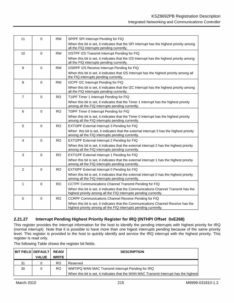
KSZ8692PB Registration Description Integrated Networking and Communications Controller
March 2010 215 M9999-031810-1.2
11 0 RW SPIPF SPI Interrupt Pending for FIQ
When this bit is set, it indicates that the SPI Interrupt has the highest priority among all the FIQ interrupts pending currently.
10 0 RW I2STPF I2S Transmit Interrupt Pending for FIQ When this bit is set, it indicates that the I2S Interrupt has the highest priority among all the FIQ interrupts pending currently.
9 0 RW I2SRPF I2S Receive Interrupt Pending for FIQ When this bit is set, it indicates that I2S Interrupt has the highest priority among all the FIQ interrupts pending currently.
8 0 RW I2CPF I2C Interrupt Pending for FIQ When this bit is set, it indicates that the I2C Interrupt has the highest priority among all the FIQ interrupts pending currently.
7 0 RO T1IPF Timer 1 Interrupt Pending for FIQ When this bit is set, it indicates that the Timer 1 Interrupt has the highest priority among all the FIQ interrupts pending currently.
6 0 RO T0IPF Timer 0 Interrupt Pending for FIQ When this bit is set, it indicates that the Timer 0 Interrupt has the highest priority among all the FIQ interrupts pending currently.
5 0 RO EXTI3PF External Interrupt 3 Pending for FIQ When this bit is set, it indicates that the external interrupt 3 has the highest priority among all the FIQ interrupts pending currently.
4 0 RO EXTI2PF External Interrupt 2 Pending for FIQ When this bit is set, it indicates that the external interrupt 2 has the highest priority among all the FIQ interrupts pending currently.
3 0 RO EXTI1PF External Interrupt 1 Pending for FIQ When this bit is set, it indicates that the external interrupt 1 has the highest priority among all the FIQ interrupts pending currently.
2 0 RO EXTI0PF External Interrupt 0 Pending for FIQ When this bit is set, it indicates that the external interrupt 0 has the highest priority among all the FIQ interrupts pending currently.
1 0 RO CCTPF Communications Channel Transmit Pending for FIQ When this bit is set, it indicates that the Communications Channel Transmit has the highest priority among all the FIQ interrupts pending currently.
0 0 RO CCRPF Communications Channel Receive Pending for FIQ When this bit is set, it indicates that the Communications Channel Receive has the highest priority among all the FIQ interrupts pending currently.
2.21.27 Interrupt Pending Highest Priority Register for IRQ (INTHPI Offset 0xE268) This register provides the interrupt information for the host to identify the pending interrupts with highest priority for IRQ (normal interrupt) Note that it is possible to have more than one higest interrupts pending because of the same priority level. This register is provided to the host to quickly identify and service the IRQ interrupt with the highest priority. This register is read only. The following Table shows the register bit fields.
BIT FIELD DEFAULT VALUE
READ/ WRITE
DESCRIPTION
31 0 RO Reserved 30 0 RO WMTIPQ WAN MAC Transmit Interrupt Pending for IRQ
When this bit is set, it indicates that the WAN MAC Transmit Interrupt has the highest

KSZ8692PB Registration Description Integrated Networking and Communications Controller
March 2010 216 M9999-031810-1.2
priority among all the IRQ interrupts pending currently. 29 0 RO WMRIPQ WAN MAC Receive Interrupt Pending for IRQ
When this bit is set, it indicates that the WAN MAC Receive Interrupt has the highest priority among all the IRQ interrupts pending currently.
28 0 RO WMTBUIPQ WAN MAC Transmit Buffer Unavailable Interrupt Pending for IRQ When this bit is set, it indicates that the WAN MAC Transmit Buffer Unavailable Interrupt has the highest priority among all the IRQ interrupts pending currently.
27 0 RO WMRBUIPQ WAN MAC Receivet Buffer Unavailable Interrupt Pending for IRQ When this bit is set, it indicates that the WAN MAC Receive Buffer Unavailable Interrupt has the highest priority among all the IRQ interrupts pending currently.
26 0 RO WMTPSIPQ WAN MAC Transmit Process Stopped Interrupt Pending for IRQ When this bit is set, it indicates that the WAN MAC Transmit Process Stopped Interrupt has the highest priority among all the IRQ interrupts pending currently.
25 0 RO WMRPSIPQ WAN MAC Receive Process Stopped Interrupt Pending for IRQ When this bit is set, it indicates that the WAN MAC Receive Process Stopped Interrupt has the highest priority among all the IRQ interrupts pending currently.
24 0 RO ABERPQ AMBA Bus Error Response Interrupt Pending for IRQ When this bit is set, it indicates that the AMBA Bus Error Response Interrupt has the highest priority among all the IRQ interrupts pending currently.
23:20 0x0 RO Reserved 19 0 RO LWUPFQ LAN Wake-up Interrupt Pending for IRQ
When this bit is set, it indicates that the LAN Wake-Up Interrupt has the highest priority among all the IRQ interrupts pending currently.
18 0 RO WWUPFQ WAN Wake-up Interrupt Pending for IRQ When this bit is set, it indicates that the WAN Wake-Up Interrupt has the highest priority among all the IRQ interrupts pending currently.
17 0 RO LMTIPQ LAN MAC Transmit Interrupt Pending for IRQ When this bit is set, it indicates that the LAN MAC Transmit Interrupt has the highest priority among all the IRQ interrupts pending currently.
16 0 RO LMRIPQ LAN MAC Receive Interrupt Pending for IRQ When this bit is set, it indicates that the LAN MAC Receive Interrupt has the highest priority among all the IRQ interrupts pending currently.
15 0 RO LMTBUIPQ LAN MAC Transmit Buffer Unavailable Interrupt Pending for IRQ When this bit is set, it indicates that the LAN MAC Transmit Buffer Unavailable Interrupt has the highest priority among all the IRQ interrupts pending currently.
14 0 RO LMRBUIPQ LAN MAC Receivet Buffer Unavailable Interrupt Pending for IRQ When this bit is set, it indicates that the LAN MAC Receive Buffer Unavailable Interrupt has the highest priority among all the IRQ interrupts pending currently.
13 0 RO LMTPSIPQ LAN MAC Transmit Process Stopped Interrupt Pending for IRQ When this bit is set, it indicates that the LAN MAC Transmit Process Stopped Interrupt has the highest priority among all the IRQ interrupts pending currently.
12 0 RO LMRPSIPQ LAN MAC Receive Process Stopped Interrupt Pending for IRQ When this bit is set, it indicates that the LAN MAC Receive Process Stopped Interrupt has the highest priority among all the IRQ interrupts pending currently.
11 0 RO Reserved 10 0 RO UDPSIPQ USB Device Interrupt Pending for IRQ
When this bit is set, it indicates that USB Device interrrupt has the highest priority among all the IRQ interrupts pending currently.
9 0 RO UHOPSIPQ USB Host OHCI Interrupt Pending for IRQ When this bit is set, it indicates that USB Host OHCI interrrupt has the highest priority among all the IRQ interrupts pending currently.

KSZ8692PB Registration Description Integrated Networking and Communications Controller
March 2010 217 M9999-031810-1.2
8 0 RO UHEPSIPQ USB Host EHCI Interrupt Pending for IRQ
When this bit is set, it indicates that USB Host EHCI interrrupt has the highest priority among all the IRQ interrupts pending currently.
7 0 RO SDIOPQ SDIO Interrupt Pending for IRQ When this bit is set, it indicates that the SDIO Interrupt has the highest priority among all the IRQ interrupts pending currently.
6 0 RO IPSECPSIPQ IPSec Interrupt Pending for IRQ When this bit is set, it indicates that IPSec interrrupt has the highest priority among all the IRQ interrupts pending currently.
5 0 RO Reserved 4 0 RO DDRPQ DDR Interrupt Pending for IRQ
When this bit is set, it indicates that the DDR Interrupt has the highest priority among all the IRQ interrupts pending currently.
3:0 0x0 RO Reserved
2.21.28 Interrupt Pending Highest Priority Register2 for IRQ (INTHPI2Offset 0xE26C) The following Table shows the register bit fields.
BIT FIELD DEFAULT VALUE
READ/ WRITE
DESCRIPTION
31:26 0x000 RO Reserved 25 0 RW UART4LSEPQ UART4 Line Status Error Interrupt Pending for IRQ
When this bit is set, it indicates that the UART4 Line Status Error Interrupt has the highest priority among all the IRQ interrupts pending currently.
24 0 RW U4RTLRPQ UART4 Receiver Trigger Level Reached Interrupt Pending for IRQ When this bit is set, it indicates that the UART4 Line Receiver Trigger Level Reached Interrupt has the highest priority among all the IRQ interrupts pending currently.
23 0 RW U4TEPQ UART4 Transmitter Empty Interrupt Pending for IRQ When this bit is set, it indicates that the UART4 Transmitter Empty Interrupt has the highest priority among all the IRQ interrupts pending currently.
22 0 RW U3LSEPQ UART3 Line Status Error Interrupt Pending for IRQ When this bit is set, it indicates that the UART3 Line Status Error Interrupt has the highest priority among all the IRQ interrupts pending currently.
21 0 RW U3RTLRPQ UART3 Receiver Trigger Level Reached Interrupt Pending for IRQ When this bit is set, it indicates that the UART3 Receiver Trigger Level Reached Interrupt has the highest priority among all the IRQ interrupts pending currently.
20 0 RW U3TEPQ UART3 Transmitter Empty Interrupt Pending for IRQ When this bit is set, it indicates that the UART3 Transmitter Empty Interrupt has the highest priority among all the IRQ interrupts pending currently.
19 0 RW U2LSEPQ UART2 Line Status Error Interrupt Pending for IRQ When this bit is set, it indicates that the UART2 Line Status Error Interrupt has the highest priority among all the IRQ interrupts pending currently.
18 0 RW U2RTLRPQ UART2 Receiver Trigger Level Reached Interrupt Pending for IRQ When this bit is set, it indicates that the UART2 Receiver Trigger Level Reached Interrupt has the highest priority among all the IRQ interrupts pending currently.
17 0 RW U2TEPQ UART2 Transmitter Empty Interrupt Pending for IRQ When this bit is set, it indicates that the UART2 Transmitter Empty Interrupt has the highest priority among all the IRQ interrupts pending currently.

KSZ8692PB Registration Description Integrated Networking and Communications Controller
March 2010 218 M9999-031810-1.2
16 0 RW U1MPQ UART Modem Interrupt Pending for IRQ
When this bit is set, it indicates that the UART Modem Interrupt has the highest priority among all the IRQ interrupts pending currently.
15 0 RW U1LSEPQ UART1 Line Status Error Interrupt Pending for IRQ When this bit is set, it indicates that the UART1 Line Status Error Interrupt has the highest priority among all the IRQ interrupts pending currently.
14 0 RW U1RTLRPQ UART1 Receiver Trigger Level Reached Interrupt Pending for IRQ When this bit is set, it indicates that the UART1 Line Status Error Interrupt has the highest priority among all the IRQ interrupts pending currently.
13 0 RW U1TEPQ UART1 Transmitter Empty Interrupt Pending for IRQ When this bit is set, it indicates that the UART1 Transmitter Empty Interrupt has the highest priority among all the IRQ interrupts pending currently.
12 0 RW MDIOPQ MDIO Interrupt Pending for IRQ When this bit is set, it indicates that the MDIO Interrupt has the highest priority among all the IRQ interrupts pending currently.
11 0 RW SPIPQ SPI Interrupt Pending for IRQ When this bit is set, it indicates that the SPI Interrupt has the highest priority among all the IRQ interrupts pending currently.
10 0 RW I2STPQ I2S Transmit Interrupt Pending for IRQ When this bit is set, it indicates that the I2S Interrupt has the highest priority among all the IRQ interrupts pending currently.
9 0 RW I2SRPQ I2S Receive Interrupt Pending for IRQ When this bit is set, it indicates that I2S Interrupt has the highest priority among all the IRQ interrupts pending currently.
8 0 RW I2CPQ I2C Interrupt Pending for IRQ When this bit is set, it indicates that the I2C Interrupt has the highest priority among all the IRQ interrupts pending currently.
7 0 RO T1IPQ Timer 1 Interrupt Pending for IRQ When this bit is set, it indicates that the Timer 1 Interrupt has the highest priority among all the IRQ interrupts pending currently.
6 0 RW T0IPQ Timer 0 Interrupt Pending for IRQ When this bit is set, it indicates that the Timer 0 Interrupt has the highest priority among all the IRQ interrupts pending currently.
5 0 RO EXTI3PQ External Interrupt 3 Pending for IRQ When this bit is set, it indicates that the external interrupt 3 has the highest priority among all the IRQ interrupts pending currently.
4 0 RO EXTI2PQ External Interrupt 2 Pending for IRQ When this bit is set, it indicates that the external interrupt 2 has the highest priority among all the IRQ interrupts pending currently.
3 0 RO EXTI1PQ External Interrupt 1 Pending for IRQ When this bit is set, it indicates that the external interrupt 1 has the highest priority among all the IRQ interrupts pending currently.
2 0 RO EXTI0PQ External Interrupt 0 Pending for IRQ When this bit is set, it indicates that the external interrupt 0 has the highest priority among all the IRQ interrupts pending currently.
1 0 RO CCTPQ Communications Channel Transmit Pending for IRQ When this bit is set, it indicates that the Communications Channel Transmit has the highest priority among all the IRQ interrupts pending currently.
0 0 RO CCRPQ Communications Channel Receive Pending for IRQ When this bit is set, it indicates that the Communications Channel Receive has the

KSZ8692PB Registration Description Integrated Networking and Communications Controller
March 2010 219 M9999-031810-1.2
highest priority among all the IRQ interrupts pending currently..

KSZ8692PB Registration Description Integrated Networking and Communications Controller
March 2010 220 M9999-031810-1.2
2.22 Timer Registers
2.22.1 Timer Control Register (TMCON Offset 0xE400) The KSZ8692PB has two 32-bit timers(Timer 0 and Timer 1). When the timer expires, it generates a pulse on the I/O pins. These timer can operate in a very flexible way. The host can control the timeout period as well as the pulse duration. The output signals are TOUT1 and TOUT0, respectively. These timers are enabled or disabled by this regsiter. Interrupt can be generated by setting the corresponding interrupt control registers. A timer generates a one-shot pulse with a preset timer clock duration whenever a timeout occurs. The duration of the one-shot pulse is also programmable by the host. This pulse consequently generates a time-out interrupt that is directly observable at the timers’s configured output pin. The timer frequency is calculated as follows: fTOUT = fMCLK / (Timer data value + Pulse data value) When the timer is enabled, it loads a data value to its count register and begins decrementing the count register value. When the timer expires, the corresponding TOUT pin is then asserted. Then it loads the pulse count value into the count register and starts decrementing. When the pulse data count reaches zero, the associated interrupt is asserted ( if enabled ), theTOUT pin is deasserted, and the timer data value is reloaded again for the next timeout. This process repeats until the timer is disabled. In our design, the frequency of MCLK is 25MHz. The following Table shows the register bit fields.
BIT FIELD DEFAULT VALUE
READ/ WRITE
DESCRIPTION
31:2 0x0 RO Reserved 1 0 RW TOUT1E Timer 1 Enable
When set, the timer 1 is enabled. Timer process starts as soon as this bit is set. Software should ensure correct timer count and pulse data values are preloaded before setting this bit.
0 0 RW TOUT0E Timer 0 Enable When set, the timer 0 is enabled. Timer process starts as soon as this bit is set. Software should ensure correct timer count and pulse data values are preloaded before setting this bit.
2.22.2 Timer 1 Timeout Count Register (T1TC Offset 0xE404) This register controls the timeout count value to be preloaded to the down-counting register for Timer 1. Writing a zero to this register may result in unpredictable timer behavior. The following Table shows the register bit fields.
BIT FIELD DEFAULT VALUE
READ/ WRITE
DESCRIPTION
31:0 -- RW TOUT1TC Timer 1 Timeout Count This field specifies the duration that the TOUT1 pin is Low in each timeout period. Writing zero to this register may cause unpredictalbe behavior.
2.22.3 Timer 0 Timeout Count Register (T0TC Offset 0xE408) This register controls the timeout count value to be preloaded to the down-counting register for Timer 0. Writing a zero to this register may result in unpredicTable timer behavior. Timer 0 can also be programmed as Watchdog timer when the Byte 0 of Timeout Count Register is programmed as 8’hFF. Once it has been programmed as a Watchdog timer, the value in Timeout Count Register can never be re-programmed unless the timer is disabled first. In normal system operation, the Watchdog timer will be periodically disabled by CPU before it expires. In case the Watchdog timer expires (indicating system gets hung and CPU can not

KSZ8692PB Registration Description Integrated Networking and Communications Controller
March 2010 221 M9999-031810-1.2
periodically come in to clear the timer by clearing the timer enable bit), a reset signal (active high) will be generated to reset the whole system. The following Table shows the register bit fields.
BIT FIELD
DEFAULT VALUE
READ/ WRITE
DESCRIPTION
31:0 0xFFFF_FF00 RW TOUT0TC Timer 0 Timeout Count This field specifies the duration that the TOUT0 pin is Low in each timeout period. Writing zero to this register may cuase unpredictalbe behavior. Note that if the lowest byte is configured as 8’hFF, Timer 0 becomes Watchdog Timer.
2.22.4 Timer 1 Pulse Count Register (T1PD Offset 0xE40C) This register controls the pulse data value to be preloaded to the down-counting register for Timer 1. The TOUT1 pin output remains asserted at ‘1’ until the pulse counter reaches zero. Writing a zero to this register may result in unpredicTable timer behavior. The following Table shows the register bit fields.
BIT FIELD DEFAULT VALUE
READ/ WRITE
DESCRIPTION
31:0 -- RW TOUT1PC Timer 1 Pulse Count This field specifies the duration that the TOUT1 pin is High in each timeout period. Writing zero to this register may cuase unpredictalbe behavior.
2.22.5 Timer 0 Pulse Count Register (T0PD Offset 0xE410) This register controls the pulse data value to be preloaded to the down-counting register for Timer 0. The TOUT0 pin output remains asserted at ‘1’ until the pulse counter reaches zero. Writing a zero to this register may result in unpredicTable timer behavior. The following Table shows the register bit fields.
BIT FIELD DEFAULT VALUE
READ/ WRITE
DESCRIPTION
31:0 -- RW TOUT0PC Timer 0 Pulse Count This field specifies the duration that the TOUT0 pin is High in each timeout period. Writing zero to this register may cuase unpredictalbe behavior.
2.23 GPIO Registers
2.23.1 I/O Port Mode Register (IOPM Offset 0xE600) This register controls the I/O pin input output mode. Each I/O pin can be configured as Input or Output. Note that some of the I/O pins are shared with the external interrupts and timer output. When these pins are configured for timer output, it overides the I/O Port Mode configuration. If the pins shared with External Interrupt(GPIO pins 3 to 0) are configured as output pins and are enabled for External/Soft Interrupt(e.g., Port Control Register bit 15 is set to 1 enable the External/Soft Interrupt 3), CPU can generate a soft interrupt by writing apporpriate data(based on Trigger Mode defined in Port Control Register) to the corresponding Port Data Register. The following Table shows the register bit fields.
BIT FIELD DEFAULT VALUE
READ/ WRITE
DESCRIPTION
31:20 0x0 RO Reserved

KSZ8692PB Registration Description Integrated Networking and Communications Controller
March 2010 222 M9999-031810-1.2
19 0 RW IOPM19 I/O Port Mode for GPIO Pin 19 When set, the port is configured as an output pin. When reset, the port is configured as an input pin.
18 0 RW IOPM18 I/O Port Mode for GPIO Pin 18 When set, the port is configured as an output pin. When reset, the port is configured as an input pin.
17 0 RW IOPM17 I/O Port Mode for GPIO Pin 17 When set, the port is configured as an output pin. When reset, the port is configured as an input pin.
16 0 RW IOPM16 I/O Port Mode for GPIO Pin 16 When set, the port is configured as an output pin. When reset, the port is configured as an input pin.
15 0 RW IOPM15 I/O Port Mode for GPIO Pin 15 When set, the port is configured as an output pin. When reset, the port is configured as an input pin.
14 0 RW IOPM14 I/O Port Mode for GPIO Pin 14 When set, the port is configured as an output pin. When reset, the port is configured as an input pin.
13 0 RW IOPM13 I/O Port Mode for GPIO Pin 13 When set, the port is configured as an output pin. When reset, the port is configured as an input pin.
12 0 RW IOPM12 I/O Port Mode for GPIO Pin 12 When set, the port is configured as an output pin. When reset, the port is configured as an input pin.
11 0 RW IOPM11 I/O Port Mode for GPIO Pin 11 When set, the port is configured as an output pin. When reset, the port is configured as an input pin.
10 0 RW IOPM10 I/O Port Mode for GPIO Pin 10 When set, the port is configured as an output pin. When reset, the port is configured as an input pin.
9 0 RW IOPM9 I/O Port Mode for GPIO Pin 9 When set, the port is configured as an output pin. When reset, the port is configured as an input pin.
8 0 RW IOPM8 I/O Port Mode for GPIO Pin 8 When set, the port is configured as an output pin. When reset, the port is configured as an input pin.
7 0 RW IOPM7 I/O Port Mode for GPIO Pin 7 When set, the port is configured as an output pin. When reset, the port is configured as an input pin.
6 0 RW IOPM6 I/O Port Mode for GPIO Pin 6 When set, the port is configured as an output pin. When reset, the port is configured as an input pin.
5 0 RW IOPM5 I/O Port Mode for GPIO Pin 5 When set, the port is configured as an output pin. When reset, the port is configured as an input pin. Note that GPIO Pin 5 is shared with Timer 1 output.
4 0 RW IOPM4 I/O Port Mode for GPIO Pin 4 When set, the port is configured as an output pin. When reset, the port is configured as an input pin. Note that GPIO Pin 4 is shared with Timer 0 output.
3 0 RW IOPM3 I/O Port Mode for GPIO Pin 3

KSZ8692PB Registration Description Integrated Networking and Communications Controller
March 2010 223 M9999-031810-1.2
When set, the port is configured as an output pin. When reset, the port is configured as an input pin. Note that GPIO Pin 3 is shared with External Interrupt 3 input.
2 0 RW IOPM2 I/O Port Mode for GPIO Pin 2
When set, the port is configured as an output pin. When reset, the port is configured as an input pin. Note that GPIO Pin 2 is shared with External Interrupt 2 input.
1 0 RW IOPM1 I/O Port Mode for GPIO Pin 1 When set, the port is configured as an output pin. When reset, the port is configured as an input pin. Note that GPIO Pin 1 is shared with External Interrupt 1 input.
0 0 RW IOPM0 I/O Port Mode for GPIO Pin 0 When set, the port is configured as an output pin. When reset, the port is configured as an input pin. Note that GPIO Pin 0 is shared with External Interrupt 0 input.
2.23.2 I/O Port Control Register (IOPC Offset 0xE604) This register controls the usage of the shared I/O pins. The following Table shows the register bit fields.
BIT FIELD DEFAULT VALUE
READ/ WRITE
DESCRIPTION
31:24 0x0 RO Reserved
23 0 RW When set, GPIO11 will be used for UART4 RTS_N and GPIO10 will be used for UART4 CTS_N for h/w flow control support. GPIO11 will be forced at output mode and GPIO10 will be forced at input mode in this case. When reset, the shared GPIO pin is used for normal GPIO purpose.
22 0 RW When set, GPIO9 will be used for UART3 RTS_N and GPIO8 will be used for UART3 CTS_N for h/w flow control support. GPIO9 will be forced at output mode and GPIO8 will be forced at input mode in this case. When reset, the shared GPIO pin is used for normal GPIO purpose.
21 0 RW When set, GPIO7 will be used for UART2 RTS_N and GPIO6 will be used for UART2 CTS_N for h/w flow control support. GPIO7 will be forced at output mode and GPIO6 will be forced at input mode in this case. When reset, the shared GPIO pin is used for normal GPIO purpose.
20 0 RW OUSBCKEN Enable of observe USB signals: 120 Mhz clock, PHY free clock, PHY Port 1 clock, PHY Port 2 clock, usb device clock, LSB of Port 2 transmit data, LSB of Port 1 transmit data, LSB of Port 2 receive data, LSB of Port 1 receuve data When set, the shared GPIO pins (GPIO[17:12], GPIO[3:1]) are used for USB signals observation. GPIO[17:12], GPIOI[3:1] will be forced at output mode. (Factory Reserved) When reset, the shared GPIO pins are used for normal GPIO purpose.
19 0 RW SLEDEN SDIO LED Enable When set, the shared GPIO pin (GPIO19) is used for SDIO LED. GPIO19 will be forced at output mode. When reset, the shared GPIO pin is used for normal GPIO purpose
18 0 RW OBINTEN Observe Internal Interrupt Enable When set, the shared GPIO pin (GPIO18) is used to monitor the internal interrupt (FIQ and IRQ) to CPU. GPIO18 will be forced at output mode. When reset, the shared GPIO pin is used for normal GPIO purpose.
17 0 RW IOTIM1EN GPIO Pin for Timer 1 Enable

KSZ8692PB Registration Description Integrated Networking and Communications Controller
March 2010 224 M9999-031810-1.2
When set, the shared GPIO pin (GPIO5) for Timer 1 is used for the timer. When reset, the shared GPIO pin for Timer 1 is used for normal GPIO purpose.
16 0 RW IOTIM0EN GPIO Pin for Timer 0 Enable When set, the shared GPIO pin (GPIO4) for Timer 0 is used for the timer. When reset, the shared GPIO pin for Timer 0 is used for normal GPIO operation.
15 0 RW IOEINT3EN GPIO[3] Pin for External/Soft Interrupt 3 Enable. This bit has higher
priority than bit[20] (OUSBCKEN) When set, the shared GPIO[3] pin (EXT3) for external interrupt request 3 is used for the interrupt. When reset, the shared GPIO[3] pin (EXT3) for external interrupt request 3 is used for normal GPIO operation.
14:12 000 RW IOEINT3TM GPIO[3] Pin for External/Soft Interrupt 3 Trigger Mode This field is used to configure the trigger mode for External Interrupt 3. 000= Level Detection (Active Low) 001= Level Detection (Active High) 01x= Rising Edge Detection 10x= Falling Edge Detection 11x= Both Edge Detection
11 0 RW IOEINT2EN GPIO[2] Pin for External/Soft Interrupt 2 Enable. This bit has higher priority than bit[20] (OUSBCKEN) When set, the shared GPIO[2] pin (EXT2) for external interrupt request 2 is used for the interrupt. When reset, the shared GPIO[2] pin (EXT2) for external interrupt request 2 is used for normal GPIO operation.
10:8 000 RW IOEINT2TM GPIO[2] Pin for External/Soft Interrupt 2 Trigger Mode This field is used to configure the trigger mode for External Interrupt 2. 000= Level Detection (Active Low) 001= Level Detection (Active High) 01x= Rising Edge Detection 10x= Falling Edge Detection 11x= Both Edge Detection
7 0 RW IOEINT1EN GPIO[1] Pin for External/Soft Interrupt 1 Enable. This bit has higher priority than bit[20] (OUSBCKEN) When set, the shared GPIO[1] pin (EXT1) for external interrupt request 1 is used for the interrupt. When reset, the shared GPIO[1] pin (EXT1) for external interrupt request 1 is used for normal GPIO operation.
6:4 000 RW IOEINT1TM GPIO Pin for External/Soft Interrupt 1 Trigger Mode This field is used to configure the trigger mode for External Interrupt 1. 000= Level Detection (Active Low) 001= Level Detection (Active High) 01x= Rising Edge Detection 10x= Falling Edge Detection 11x= Both Edge Detection
3 0 RW IOEINT0EN GPIO[0] Pin for External/Soft Interrupt 0 Enable When set, the shared GPIO[0] pin (EXT0) for external interrupt request 0 is used for the interrupt. When reset, the shared GPIO[0] pin (EXT0) for external interrupt request 0 is used for normal GPIO operation.
2:0 000 RW IOEINT0TM GPIO Pin for External/Soft Interrupt 0 Trigger Mode This field is used to configure the trigger mode for External Interrupt 0. 000= Level Detection (Active Low)

KSZ8692PB Registration Description Integrated Networking and Communications Controller
March 2010 225 M9999-031810-1.2
001= Level Detection (Active High) 01x= Rising Edge Detection 10x= Falling Edge Detection 11x= Both Edge Detection

KSZ8692PB Registration Description Integrated Networking and Communications Controller
March 2010 226 M9999-031810-1.2
2.23.3 I/O Port Data Register (IOPD Offset 0xE608) This register contains the one-bit read values for I/O ports that are configured as input port, and one-bit write value for I/O ports that are configured as output port. Bits[19:0] of the 20-bit I/O port register value correspond directly to the 20 I/O pins, GPIO[19:0]. The following Table shows the register bit fields.
BIT FIELD DEFAULT VALUE
READ/ WRITE
DESCRIPTION
31:20 0x0 RO Reserved
19:0 -- RW IOPD I/O Port Data Value The values reflect the signal level on the respective I/O port pins. When the ports are configured as output port, the bit reflects the port write value. When the port is configured as input port, the bit reflects the port read value.
2.24 I2C Registers 2.24.1 Global Control (Offset 0xE800): I2C_GCR BIT FIELD NAME READ/
WRITE DESCRIPTION DEFAULT
31:24 Reserved RO Reserved 0x00
23:16 Timeout RW Number of bit times allowed to complete transaction before aborting. 0x10
15 Enable I2C Stop
RW Enable stop bit generation after every data cycle, read or write. 1 : Enable Stop Bit generation 0 : Disable Stop Bit generation
0
14:10 Reserved RO Reserved 0x00
9:1 Bit Period RW Bit period in units of AHB clock period * 8. ie for AHB clock = 200MHz (5 ns period) bit period unit = 40ns Default: 166MHz AHB clock, 400KHz data rate actual data rate = 399.04KHz
0x033
0 I2C Enable
RW Enable I2C to perform data transfers. I2C must be disabled before changing the bit period.
0
2.24.2 I2C Address (Offset 0xE804): I2C_AR BIT FIELD NAME READ/
WRITE DESCRIPTION DEFAULT
31:24 Reserved RO Reserved 0x00 23:20 Number of
Bytes to Write
RW Number of bytes to read for each transaction (START/STOP pair). 0000 – Reserved 0001 – 1 Byte Write … 1000 – 8 Bytes Write 1001 – Reserved … 1111 – Reserved
0x1
19:16 Number of
Bytes to Read
RW Number of bytes to read for each transaction If it’s greater than 1, a sequential read is issued. (START/STOP pair). 0000 – Reserved 0001 – 1 Byte Read
0x1

KSZ8692PB Registration Description Integrated Networking and Communications Controller
March 2010 227 M9999-031810-1.2
… 1000 – 8 Bytes Read 1001 – Reserved … 1111 – Reserved
11 10-bit I2C Address
RW Use 10-bit Device Address for I2C transaction. 0
10:8 Address (Extended)
RW Write Device Address [9:7] used for 10-bit extended I2C addressing. -
7:1 Address (Standard)
RW Write Device Address [6:0] used for standard I2C addressing. -
0 Read/Write RW 1 = I2C read transaction 0 = I2C write transaction
0
2.24.3 I2C Start Command (Offset 0xE808): I2C_SCR BIT FIELD NAME READ/
WRITE DESCRIPTION DEFAULT
31:1 Reserved RO Reserved 0x0000_0000
0 Start/Done Command
RW Start/Done Command. Write a 1 to start I2C transaction. Cleared to 0 when I2C transaction is completed.
0
2.24.4 I2C Status (Offset 0xE80C): I2C_SR BIT FIELD NAME READ/
WRITE DESCRIPTION DEFAULT
31 SCL line status
RO The current value of the SCL signal -
30 SDA line status
RO The current value of the SDA signal -
29:17 Reserved RO Reserved 0x0000 16 Data
Transfer Done
RO 1 = burst Data Transfer was completed. All programmed burst data has be transferred. Can verify how many bytes has been transferred with this register’s bits [11:8] for read and [15:12] for writes. These values should match the programmed burst length value.
0
15:12 Number of
Bytes Written
RO Number of bytes that were written out from WDR1/0 registers. This field is valid when bit 16 is set, and bits[6:0] are not set in this register. This field specifies how many bytes has been written out when the burst transaction stopped. The burst transaction stops when the burst is done or when one of the timeout error conditions occurs. This field is cleared after reading. 0x0 = Reserved 0x1 = 1 byte valid: WDR0[7:0] 0x2 = 2 bytes valid: WDR0[15:0] … 0x7 = 7 bytes valid: {WDR1[23:0], WDR0[31:0]} 0x8 = 8 bytes valid: {WDR1, WDR0} 0x9 – 0xF = Reserved
15:12
11:8 Number of Bytes Read
RO Number of bytes available to be read out from RDR1/0 registers. This field is valid when any of the following bits in this register are set: [15] or [3:0]. This field specifies how many bytes has been read when the burst transaction stopped. The burst transaction stops when the burst is done or when one of the timeout error conditions occurs. This field is cleared
-

KSZ8692PB Registration Description Integrated Networking and Communications Controller
March 2010 228 M9999-031810-1.2
after reading. 0x0 = Reserved 0x1 = 1 byte valid: RDR0[7:0] 0x2 = 2 bytes valid: RDR0[15:0] … 0x7 = 7 bytes valid: {RDR1[23:0], RDR0[31:0]} 0x8 = 8 bytes valid: {RDR1, RDR0} 0x9 – 0xF = Reserved
7 Reserved RO Reserved 0 6 WR Data
Error RO 1 = WR data was corrupted by I2C slave driving SDA during data
transmission. This bit is cleared after reading.
5 Start Bit Timeout
RO 1 = SDA timeout error during the start bit caused by I2C slave pulling SDA low longer than the programmed time out value. This bit is cleared after reading.
0
4 Stop Bit Timeout
RO 1 = SDA timeout error during the stop bit caused by I2C slave pulling SDA low longer than the programmed time out value. This bit is cleared after reading.
0
3 Data Phase
Timeout
RO 1 = Data timeout error caused by I2C slave wait state exceeding programmed time out value during the data phase. This bit is cleared after reading.
0
2 Address Phase
Timeout
RO 1 = Address timeout error caused by I2C slave wait state exceeding programmed time out value during the address phase. This bit is cleared after reading.
0
1 No Data ACK Error
RO 1 = write data byte did not receive an ACK. This bit is valid only for write cycles. This bit is cleared after reading.
0
0 No Address
ACK Error
RO 1 = No ACK after address phase. This bit is cleared after reading. 0
2.24.5 Read Data0 (Offset 0xE810): I2C_RDR0 BIT FIELD NAME READ/
WRITE DESCRIPTION DEFAULT
31:24 Read Data Byte 3
RO Read 4th Data Byte -
23:16 Read Data Byte 2
RO Read 3rd Data Byte -
15:8 Read Data Byte 1
RO Read 2nd Data Byte -
7:0 Read Data Byte 0
RO Read 1st Data Byte -
2.24.6 Read Data1 (Offset 0xE814): I2C_RDR1
BIT FIELD NAME READ/
WRITE
DESCRIPTION DEFAULT
31:24 Read Data Byte 7
RO Read 8th Data Byte -
23:16 Read Data Byte 6
RO Read 7th Data Byte -
15:8 Read Data Byte 5
RO Read 6th Data Byte -
7:0 Read Data RO Read 5th Data Byte -

KSZ8692PB Registration Description Integrated Networking and Communications Controller
March 2010 229 M9999-031810-1.2
Byte 4
2.24.7 Write Data0 (Offset 0xE818): I2C_WDR0
BIT FIELD NAME READ/
WRITE
DESCRIPTION DEFAULT
31:24 Write Data Byte 3
RO Write 4th Data Byte -
23:16 Write Data Byte 2
RO Write 3rd Data Byte -
15:8 Write Data Byte 1
RO Write 2nd Data Byte -
7:0 Write Data Byte 0
RO Write 1st Data Byte -
2.24.8 Write Data1 (Offset 0E8x1C): I2C_WDR1
BIT FIELD NAME READ/
WRITE
DESCRIPTION DEFAULT
31:24 Write Data Byte 7
RO Write 8th Data Byte -
23:16 Write Data Byte 6
RO Write 7th Data Byte -
15:8 Write Data Byte 5
RO Write 6th Data Byte -
7:0 Write Data Byte 4
RO Write 5th Data Byte -

KSZ8692PB Registration Description Integrated Networking and Communications Controller
March 2010 230 M9999-031810-1.2
2.24.9 Debug (Offset 0xE820): I2C_DEBUG
BIT FIELD NAME READ/
WRITE
DESCRIPTION DEFAULT
31:3 Reserved RO Reserved 0x0000_0000 2 Enable
SCL / SDA outputs
RW = 1 Enable SCL and SDA output. Bits [1:0] can control SCL and SDA I/O directly. Use in conjunction with I2C_AR[31:30].
0
1 SCL Output
RW SCL output. When enabled (bit [2] = 1) directly drives the bit value onto SCL.
1
0 SDA Output
RW SDA output. When enabled (bit [2] = 1) directly drives the bit value onto SDA.
1
2.25 SPI Registers
2.25.1 SPI Operations The Master SPI controls data transfers to and from the slave. The SPI Master drives the chip select (CS) and the serial clock (SPCK) to the slave. After enabling the SPI the core writes data to the SPI_TDR (Transmit Data Register). A data transfer begins when the SPI_TDR writes to Transmit Buffer. When new data is available in the Transmit Buffer, the SPI continues to transfer data. The received data is written to Receive Buffer. When the Receive Buffer reaches its threshold or the timer is expired, the RDRDY flag is set. If the Receive Buffer is full, the Receive Data Buffer Full (RDBF) flag is set. Note: As long as RDBF flag is set, no new data is loaded to Receive Data Buffer. The user has to read the SPI_RDR (from Receive Buffer) and to read Interrupt Status Register (SPI_ISR) to clear RDBF flag. The delay between the active CS (DLYBCS) and the delay between each data transfer (DLYBCT) can be programmed. All data transfer characteristics are programmed in SPI_CSR (Chip Select Register). Figure 1 and Figure 2 show the operation of SPI. Chip Select The SPI Master device drives the Chip Select (CS) line. The value on the CS pin at the end of each transfer can be read in the SPI_RDR (Receive Data Register). The CS signal active state is programmable in SPI_CSR. If the CS active state is logic low (equal to zero), the CS signal is logic high (equal to one) before and after each transfer. Clock Generation and Transfer Delays The SPI Clock (SPCK) is generated by dividing the System Clock (SYSCLK) by a value between 16 and 65536. The divisor is defined in the Chip Select Registers (SPI_CSR). The SPI Baud rate is the rate of SPCK.
SPR[2:0] Divide CK By SYSCLK = 166MHz SYSCLK = 125MHz SYSCLK = 50MHz
000 16 10.375 MHz 7.813 MHz 3.125 MHz 001 32 5.188MHz 3.906MHz 1.5626MHz 010 64 2.594 MHz 1.953 MHz 781.25 KHz 011 128 1.297MHz 976.6KHz 390.625KHz 100 256 648 KHz 488 KHz 195.312 KHz 101 1024 162 KHz 122 KHz 48.828 KHz 110 8192 20.26KHz 15.26KHz 6.104KHz 111 65536 2.53KHz 1.907KHz 763Hz
Table 1. SPI Clock Rates

KSZ8692PB Registration Description Integrated Networking and Communications Controller
March 2010 231 M9999-031810-1.2
Figure 3 shows a chip select transfer change and consecutive transfers on the same CS. Three delays can be programmed to modify the transfer waveforms:
• DLYBCS: Delay between two CS enable is programmable by writing the field DLYBCS in the Chip Select Registers (SPI_CSR). Allows insertion of a delay between release of one chip select and before assertion of a new one.
• DLYBCT: Delay between consecutive transfers is programmable by writing the field DLYBCT in the SPI_CSR. Allows insertion of a delay between two transfers occurring on the same CS.
• DLYBS: Delay between CS active and 1st SPCK is programmable by writing the field DLYBS. Allows the start of SPCK to be delayed until after the chip select has been asserted.
These delays allow the SPI to be adapted to the interfaced peripherals and their speed and bus release time. Programmable Delays
Figure 3. Programmable Delays Data Transfer Four modes are used for SPI data transfers. These modes correspond to combinations of a pair of parameters called clock polarity (CPOL) and clock phase (CPHA) that determine the edges of the clock signal on which the data are driven and sampled. Each of the two parameters has two possible states, resulting in four possible combinations that are incompatible with one another. Thus a master/slave pair must use the same parameter pair values to communicate. Table 1 shows the four modes and corresponding parameter settings.
SPI Mode CPOL CPHA 0 0 0 1 0 1 2 1 0 3 1 1
Table 1. SPI Bus Protocol Mode
SPI
One Frame
… …
DLYBCT DLYBS DLYBCT
DLYBCS
CS
SPCK
DLYBCT

KSZ8692PB Registration Description Integrated Networking and Communications Controller
March 2010 232 M9999-031810-1.2
Figure 1 and Figure 2 show examples of data transfers:
Figure 1. SPI Transfer Format (CKPHA=1, 8 bits per transfer)
Figure 2. SPI Transfer Format (CKPHA=0, 8 bits per transfer)
x
x
SPCK Mode = 1
SPCK Mode = 3
MOSI
MISO
CS
SPCK Mode = 2
MISO
MOSI
CS
SPCK Mode=0
2 1 3 4 5 6 7 8
2 1 3 4 5 6 7 8
MSB
MSB

KSZ8692PB Registration Description Integrated Networking and Communications Controller
March 2010 222 M9999-031810-1.2
2.25.2 Control Register (SPI_CTR) (Offset 0xE900) Bit(s) Name Description Default R/W
31 Software Reset SWRST
0 = No effect. 1 = Reset the SPI.
0 R/W
30 SPI Enable SPIEN
0 = Disables the SPI. All pins are set in input mode and no data is received or transmitted. If a transfer is in progress, the transfer is finished before the SPI is disabled. 1 = Enables the SPI to transfer and receive data.
0 R/W
29:2 Reserved Ignore when read. 0 RO 1 Wait 1st RDY for
RX 0 = Disabled, does not check for 1st RDY before reading RX frame length byte. 1 = Enabled, checks RDY (from MICRF800) before reading RX frame length byte. Note SPI_TDR[12] must be a 1, Micrel Mode, for this feature to be enabled.
0 R/W
0 Wait 1st RDY for TX
0 = Disabled, does not check for 1st RDY before writing TX frame length byte. 1 = Enabled, checks RDY (from MICRF800) before writing TX frame length byte. Note SPI_TDR[12] must be a 1, Micrel Mode, for this feature to be enabled.
0 R/W
Note: MICRF800 is for interface to Micrel part number MICRF800. Bits designated as MICRF are applicable to this interface.
2.25.3 Receive Data Register (SPI_RDR) (Offset 0xE904) Bit(s) Name Description Default R/W 31:16 Received Data
RD[15:0] The Received Data is the data pointing to read pointer in Receive Buffer.
0 RO
15:0 Chip Select Value RD_CS
Normal mode (TDR.MICRF=0): [15] Indicates the value on the CS pin at the end of a transfer. [14:0] Reserved ignore when read. Micrel mode (TDR.MICRF=1): [15:0] Receive Data. The whole SPI_RDR becomes a 32-bit data registers.
0 RO

KSZ8692PB Registration Description Integrated Networking and Communications Controller
March 2010 223 M9999-031810-1.2
2.25.4 Transmit Data Register (SPI_TDR) (Offset 0xE908) Bit(s) Name Description Default R/W 31:16 TD[15:0] Transmit Data, written to Transmit BUFFER 0 R/W
15 CS_END 0 = After this transmission command, keep CS asserted. 1 = After this transmission command, de-assert the CS.
0 R/W
14 HiZ (1) MICRF=0 0 = There is output driving MOSI pin, and no data clock in to the Receive Data Buffer. 1 = Set high impedance in MOSI pin when process the first character in Transmit Buffer. There is no data output driving the MOSI. There is receive data clock in to the Receive Data Buffer. (2) MICRF=1 Reserved.
0 R/W
13 HiZ_EXT (1) MICRF=0 0 = There is output driving MOSI pin, and no data clock in to Receive Data Buffer. 1 = Set high impedance in MOSI pin when SPI goes to Character Extend State. This field is applied in Read Operation of a 3-wired SPI slave device. (2) MICRF=1 In Micrel mode, this bit indicates TX/RX mode. 0 = TX mode. 1 = RX mode.
0 R/W
12 MICRF 0 = Normal SPI Mode. 1 = Indicates the SPI changes to Micrel Mode to support MICRF interface after finishing this command.
0 R/W
11:8 BITS[3:0] (1) MICRF=0 Programmable Bits Per Transfer The BITS field determines the number of data bits transferred. Values greater than 8 should not be used. Bits Per Transfer = 8 + BITS[3:0] (2) MICRF=1 Reserved.
0 R/W
7:0 CEXT[7:0] (1) MICRF=0 Characters Extend. Indicate number characters of clocks to be generated after TD[15:0] transmission. If (CEXT==0), it is a Write Operation. Otherwise, a Read Operation will be applied after the TD[15:0] is transmitted. If (CEXT > 1), the Read Operation should be in Burst Read Mode (2) MICRF=1 if (HiZ_EXT==0) this field indicates TX frame length. If (HiZ_EXT==1) ignore this field
0 R/W

KSZ8692PB Registration Description Integrated Networking and Communications Controller
March 2010 224 M9999-031810-1.2
2.25.5 Micrel Mode Transmit Data Register (SPI_MCR) (Offset 0xE90c) Bit(s) Name Description Default R/W 31:0 MCTD[31:0] Transmit Data, written to Transmit BUFFER
This field is valid when SPI_TDR[12] is asserted. 0 R/W
2.25.6 Buffer Status Register (SPI_BFR) (Offset 0xE910) Bit(s) Name Description Default R/W 31:24 RX_LENGTH Micrel Mode RX Length.
Ignored when micrf=0; 0 RO
23:22 Reserved Ignore when read. 0 RO 21 RB_UDR Indicates a fatal error, when Receive Buffer empty
and APB keep reading data from buffer. 0 RO
20:16 RB_LVL[4:0] These bits indicate data left in Receive Buffer. 0 RO 15:6 Reserved Ignore when read. 0 RO
5 TB_OVR Indicates a fatal error, when Transmit Buffer full and APB keep writing data to buffer.
0 RO
4:0 TB_LVL[4:0] These bits indicate data left in Transmit Buffer. 0 RO
2.25.7 Interrupt Status Register (SPI_ISR) (Offset 0xE914)Bit(s) Name Description Default R/W
31 RB_Full Receive Data Buff Full. 0 = No full has been detected since the last read of ISR. 1 = Buffer Full has occurred since the last read of ISR.
0 RO
30 RDRDY Receive Data Ready. 0 = No data ready in RBUF since last read of ISR. 1 = RBUF reaches its threshold or the timer is expired.
0 RO
29 XRDY RDY Interrupt from External Input Pin. 0 RO 28 TB_Full Transmit Data Buff Full.
0 = No full has been detected since the last read of ISR. 1 = Buffer Full has occurred since the last read of ISR.
0 RO
27 TB_TH Transmit Buffer level is lower than the threshold. 0 RO 26:0 Reserved Ignore when read. 0 RO
2.25.7 Interrupt Enable Register (SPI_IER) (Offset 0xE918) Bit(s) Name Description Default R/W
31 RDBF_EN 0 = Receive Data Buffer Full Interrupt Disable 1 = Receive Data Buffer Full Interrupt Enable
0 R/W
30 RDRDY_EN 0 = Receive Data Ready Interrupt Disable 1 = Receive Data Ready Interrupt Enable
0 R/W
29 XRDY_EN 0 = External RDY Input Interrupt Disable 1 = External RDY Input Interrupt Enable
0 R/W
28 TDBF_EN 0 = Transmit Data Buffer Full Interrupt Disable 1 = Transmit Data Buffer Full Interrupt Enable
0 R/W
27 TBTH_EN 0 = Transmit buffer threshold interrupt disable 1 = Transmit buffer threshold interrupt enable
0 R/W
26:0 Reserved Ignore when read. 0 RO
2.25.8 Chip Select Register (SPI_CSR) (Offset 0xE91c)

KSZ8692PB Registration Description Integrated Networking and Communications Controller
March 2010 228 M9999-031810-1.2
Bit(s) Name Description Default R/W 31 SPCK Polarity
CPOL 0 = The inactive state value of SPCK is logic level zero. 1 = The inactive state value of SPCK is logic level one.
0 R/W
30 SPCK Phase CKPHA
0 = Data is changed on the leading edge of SPCK and captured on the following edge of SPCK. 1 = Data is captured on the leading edge of SPCK and changed on the following edge of SPCK. CKPHA determines which edge of SPCK causes data to change and which edge causes data to be captured. CKPHA is used with CPOL to produce the required clock/data relationship between master and slave devices. Figure 1 and Figure 2 show the operation.
0 R/W
29:27 SPR[2:0] SPCK Clock Rate Selection. 000: Divided SYSCLK by 16. 001: Divided SYSCLK by 32. 010: Divided SYSCLK by 64. 011: Divided SYSCLK by 128. 100: Divided SYSCLK by 256. 101: Divided SYSCLK by 1024. 110: Divided SYSCLK by 8192. 111: Divided SYSCLK by 65536.
0 R/W
26 ACS Active Level of Chip Select 0 = Active state value of CS is logic level zero. 1 = Active state value of CS is logic level one.
0 R/W
25:24 Reserved Ignore when read. 0 RO 23:20 TBuf_TH[3:0] Transmit Buffer Threshold. 4’h8 R/W 19:16 RBuf_TH[3:0] Receive Buffer Threshold. 4’h8 R/W 15:13 Reserved Ignore when read. 0 RO
12 DLYBS
Delay Before SPCK. This field defines the delay from CS valid to the first valid SPCK transition. 0 = The CS valid to SPCK transition is ½ SPCK clock period. 1 = The CS valid to SPCK transition is 1 SPCK clock period.
0 R/W
11:8 DLYBCT[3:0] Delay Between Consecutive Transfers This field defines the delay between two consecutive transfers without removing the CS. The delay is always inserted after each transfer and before removing the CS if needed. The inserted delays are equal to (1 + CLYBCT[3:0] ) SPCK cycles.
0 R/W
7:0 DLYBCS[7:0] Delay Between Chip Selects. This field defines the delay from CS inactive to another CS active.
0 R/W

KSZ8692PB Registration Description Integrated Networking and Communications Controller
March 2010 229 M9999-031810-1.2
2.26 Miscellaneous Registers
2.26.1 Device ID Register (DID Offset 0xEA00) This read-only register holds a 16-bit Device ID. The following Table shows the register bit fields.
BIT FIELD DEFAULT VALUE
READ/ WRITE
DESCRIPTION
31:16 0x0 RO Reserved
15:0 0x8692 RO Device ID
2.26.2 Revision ID Register (RID Offset 0xEA04) This register holds a 4-bit sub-device ID and a 4-bit Revision ID. The following Table shows the register bit fields.
BIT FIELD DEFAULT VALUE
READ/ WRITE
DESCRIPTION
31:8 0x0 RO Reserved
7:5 000b RO Sub-Device ID. Indicates this device is KSZ8692PB (PCI support).
4:0 00010b RO Revision ID
2.26.3 DDR Controller Diagnostic Register (DDRDIAG Offset 0xEA10) The following Table shows the register bit fields.
BIT FIELD DEFAULT VALUE
READ/ WRITE
DESCRIPTION
31 0 RW DDR SREFRESH_ENTER Command When this parameter is written with a ’b1, the DRAM device(s) will be placed in self-refresh mode. For this, the current burst for the current transaction (if any) will complete, all banks will be closed, the self-refresh command will be issued to the DRAM, and the clock enable signal will be deasserted. The system will remain in self-refresh mode until this parameter is written with a ’b0. The DRAM devices will return to normal operating mode after the self-refresh exit time (txsr) of the device and any DLL initialization time for the DRAM is reached. The memory controller will resume processing of the commands from the interruption point. This will override the register programming inside the DDR controller. To disable self-refresh again after a srefresh_enter, the user will need to clear this to ’b0. • ’b0 = Disable self-refresh mode. • ’b1 = Initiate self-refresh of the DRAM devices.
30:4 0x0 RO Reserved
3 0 RO DDR Refresh-in-Process Status Indicates that the DDR controller is executing a refresh command. This is asserted when a refresh command is sent to the DRAM devices and remains asserted until the refresh command has completed.
2 0 RO DDR DLL Lock Status Indicates the DLL has locked.
1 0 RO DDR Q-Almost-Full Status Indicates that the queue has reached the value set in the q_fullness parameter.
0 0 RO DDR Controller Busy Status Status signal from the memory controller. This will only be low when the memory controller is not reading data, writing data or processing a command.

KSZ8692PB Registration Description Integrated Networking and Communications Controller
March 2010 230 M9999-031810-1.2
2.26.4 USB PHY Control Register (UPC Offset 0xEA20) The following Table shows the register bit fields.
BIT FIELD DEFAULT VALUE
READ/ WRITE
DESCRIPTION
31:12 0x0 RO Reserved
11 0x0 RW Ovrcp, over current polarity 1: Positive sense over current 0: Negative sense over current
10 0x0 RW Siddq, static siddq test setup, will shut down the power in USB ananlog partion.
9 0x0 RW Vatest_enb, which enables usb_analog_test pin output
8:1 0x0 RO Reserved
0 0x0 RW Usb_device_detect_vbus, set this bit to one will trigger the usb device controller to release the reset and start the normal function mode 1: Enable USB device enter function mode 0: Disable the usb device
2.26.5 USB PHY Test Control Register ( UPT Offset 0xEA24) The following Table shows the register bit fields.
BIT FIELD DEFAULT VALUE
READ/ WRITE
DESCRIPTION
31:14 0x0 RO Reserved
13 0x0 RW USB PHY analog test data out seletion
12:9 0x0 RW USB PHY analog tests address
8:1 0x0 RW USB PHY analog test data in
0 0x0 RW USB PHY analog test interface test_clk
2.26.6 USB PHY Test Status Register ( UPS Offset 0xEA28) The following Table shows the register bit fields. BIT FIELD DEFAULT
VALUE READ/ WRITE
DESCRIPTION
31:8 0x0 RO Reserved
7:4 0x0 RO USB PHY test_data_out_1[3:0]
3:0 0x0 RO USB PHY test_data_out_0[3:0]
2.26.7 PLL Diagnostic Control Register ( PDC Offset 0xEA2C) The following Table shows the register bit fields. BIT FIELD DEFAULT
VALUE READ/ WRITE
DESCRIPTION
31:21 0x0 RO PLL operation mode control
20:11 0x0 Rw PLLB test control
10:1 0x0 RW PLLA test control
0 0x0 RW PLL bandgap select

KSZ8692PB Registration Description Integrated Networking and Communications Controller
March 2010 231 M9999-031810-1.2
2.26.8 NAND Flash Busy Status ( NFLBS Offset 0xEA40) The following Table shows the register bit fields.
BIT FIELD DEFAULT VALUE
READ/ WRITE
DESCRIPTION
31:2 0x0 RO Reserved
1 - RO NAND Flash Bank1 Busy Status 1 – Bank1 busy signal from NAND Flash device is active 0 – Bank1 busy signal from NAND Flash device is not active
0 - RO NAND Flash Bank0 Busy Status 1 – Bank0 busy signal from NAND Flash device is active 0 – Bank0 busy signal from NAND Flash device is not active
2.26.9 Spare Register ( SR Offset 0xEA50) The following Table shows the register bit fields.
BIT FIELD DEFAULT VALUE
READ/ WRITE
DESCRIPTION
31:16 0x0 RO Reserved
15:2 0x0 RW For spare registers purpose
1 0x0 RW When set, it will pass the checksum check at receive side and skip the checksum generation at transmit side for IPv6 UDP packet w/ fragment extension header. When cleared, it will perform checksum operation based on configuration and doesn’t care whether it’s a fragment packet or not.
0 0x0 RW When set, it will pass the filtering for IPv6 UDP packet w/ UDP checksum equal to zero. When cleared, it will drop IPv6 UDP packet w/ UDP checksum equal to zero.
2.27 I2S Registers
2.27.1 I2S Control (Offset 0xEB00): I2S_CR Bit(s) Name R/W Description Default 31:23 Reserved RO 0
22 Left justified
RW 0 = I2S timing 1 = left justified timing
0
21:20 Bit select RW 00: 16 bit wide audio data 01: 18 bit wide audio data 10: 20 bit wide audio data 11: 24 bit wide audio data
0
19:16 BCLK divisor
RW BCLK frequency = MCLK frequency / (divisor+1). 0
15:13 Reserved RO 0 12 Rx
Enable RW Enable I2S to receive. When disabled, rx function will be reset.
2 MCLK cycles needed to change this bit. i.e., once SW changed this bit, it should keep it unchanged for at least 2 MCLK cycles.
0
11:10 Reserved RO 0

KSZ8692PB Registration Description Integrated Networking and Communications Controller
March 2010 232 M9999-031810-1.2
9:8 Rx Interrupt
threshold RW Interrupt will be triggered when rx buffer counter hit the threshold:
0: >= half of the rx buffer has valid data 1: >= ¼ of the rx buffer has valid data 2: >= ¾ of the rx buffer has valid data 3: reserved
0
7:5 Reserved RO 0 4 Tx Enable RW Enable I2S to transmit. When disabled, tx function will be reset.
2 MCLK cycles needed to change this bit. i.e., once SW changed this bit, it should keep it unchanged for at least 2 MCLK cycles.
0
3:2 Reserved RO 0 1:0 Tx Interrupt
threshold RW Interrupt will be triggered when tx buffer counter hit the threshold:
0: >= half of the tx buffer has not been used 1: >= ¼ of the tx buffer has not been used 2: >= ¾ of the tx buffer has not been used 3: reserved
0
Note: if both Rx and Tx enable is cleared to 0, there will be no BCLK and LRCLK toggle.
2.27.2 I2S TX Status (Offset 0xEB04): I2S_TSR Bit(s) Name R/W Description Default 31:11 Reserved 0
10 Tx hit RO Tx threshold is hit. 0 9 Tx overrun RO Tx buffer overrun. SW writes tx buffer when it is full.
Cleared after read. 0
8 Tx underrun
RO Tx buffer underrun. Tx when buffer is empty. Cleared after read.
0
7:6 Reserved RO 0 5:0 Tx valid
Counter RO I2S tx buffer valid counter, i.e., how many entries in the buffer are
available for write. 0
2.27.3 I2S Rx Status (Offset 0xEB08): I2S_RSR Bit(s) Name R/W Description Default 31:11 Reserved 0
10 Rx hit Rx threshold is hit. 0 9 Rx
overrun RO Rx buffer overrun. Rx when buffer is full.
Cleared after read. 0
8 Rx underrun
RO Rx buffer underrun. SW read rx buffer when is empty. Cleared after read.
0
7:6 Reserved RO 0 5:0 Rx
Counter RO I2S rx buffer counter, i.e., how many data words in the buffer are
ready to read 0

KSZ8692PB Registration Description Integrated Networking and Communications Controller
March 2010 233 M9999-031810-1.2
2.27.4 I2S Data (Offset 0xEB0c): I2S_DR Bit(s) Name R/W Description Default 31:0 Audio data RW Write this register will cause the data written to the tx buffer. Left
channel and right channel data should be interleaved. So, the 1st write data belongs to left channel, and the 2nd one is for right channel, then repeated till tx disabled. Read this register will get the data from the rx buffer. Also, left channel and right channel data are interleaved. The 1st read data is from left channel, the 2nd one is from right channel, then repeated till rx disabled. The data format is left justified, i.e., data[31:0] = { audio data, padding 0s}
-
2.28 STA Registers
2.28.1 Configuration Register This configuration register gives the software capability to change the MDC period based on APB clock speed, as well as the Management frame option.
STA_CFG:: (Offset 0xEC00) Bit(s) Name R/W Description Default
31 AUTO_POLL RW Auto Poll option. When de-asserted, the STA is working at manual mode. It is the software’s responsibility to issue MDIO transactions by writing command register. When asserted, the STA is working at the auto-polling mode. It will poll PHY status register every 1024 MDC cycles.
0x0
30:18 RESERVE RO Reserved 0x0 17 MDC_SHUTDOWN RW Optional MDC shutdown.
When this bit is set to one by software, the MDC output clock will be turned off if there is no transaction on MDC/MDIO interface. 0: MDC keeps running as long as APB clock is running. 1: MDC runs only when a transaction is proceeding on MDC/MDIO interface. MDC is turned off when the transaction is completed.
0x0
16 PRE_SUPPRESION RW Preamble Suppression. The software sets this bit to one when it determines that all the PHY devices are able to accept management frames with preamble suppressed. 0: Send management frames with 32-bit preamble. 1: Send management frames without preamble bits.
0x0
15:9 RESERVED RO Reserved. 0x0 8:1 CLK_DIVIDEND RW The MDC output frequency is calculated as:
fMDC = fAPB / (CLK_DIVIDEND * 2) Let’s take APB clock 200 MHz as typical, and choose 16 as the default value of this register, this results in a MDC frequency of 6.25MHz.
0x10
0 MDIO_ENABLE RW If asserted, enable MDIO Management Interface to perform data transfers. It must be disabled before changing the CLK_DIVIDEND. The Software shall NOT disable this bit when the STA_STATUS.STATUS field is not idle. The user shall read the STA_STATUS register before updating this bit. Violation on this rule may cause unexpected behavior on the MDC/MDIO interface.
0x1
Table 1. STA Configuration Register Description.

KSZ8692PB Registration Description Integrated Networking and Communications Controller
March 2010 234 M9999-031810-1.2
2.28.2 Installed PHY Register The Installed PHY register defines the valid PHY addresses in the system.
STA_INSTALLED_PHY:: (Offset 0xEC04) Bit(s) Name R/W Description Default 31:16 RESERVE RO Reserved 0x0
15 PHY1_VLD RW If asserted, PHY1 is installed and PHY1_ADDR is a valid address assigned in the system.
14:13 RESERVE RO Reserved 0x0 12:8 PHY1_ADDR RW The physical address assigned to PHY1 0x0
7 PHY0_VLD RW If asserted, PHY0 is installed and PHY0_ADDR is a valid address assigned in the system.
0x0
6:5 RESERVE RO Reserved 0x0 4:0 PHY0_ADDR RW The physical address assigned to PHY0 0x0
Table 2. Installed PHY Register Description.
2.28.3 Interrupt Enable Register The Interrupt Enable Register maintains an enable bit for each interrupt event. The software can enable or disable interrupts triggered by the associated events.
STA_INT_ENABLE:: (Offset 0xEC08) Bit(s) Name R/W Description Default 31:7 RESERVE RO Reserved 0x0
6 PHY_AERR_ENABLE RW The interrupt enable for its associated interrupt event. 0x0 5 PROC_TERR_ENABLE RW The interrupt enable for its associated interrupt event. 0x0 4 PHY1_DN_CHG_ENABLE RW The interrupt enable for its associated interrupt event. 0x0 3 PHY1_UP_CHG_ENABLE RW The interrupt enable for its associated interrupt event. 0x0 2 PHY0_DN_CHG_ENABLE RW The interrupt enable for its associated interrupt event. 0x0 1 PHY0_UP_CHG_ENABLE RW The interrupt enable for its associated interrupt event. 0x0 0 CPU_CMPLT_ENABLE RW The interrupt enable for its associated interrupt event. 0x0
Table 3. Interrupt Enable Register Description
2.28.4 Interrupt Event Register The Interrupt Event Register captures the events that assert the interrupt signal. All fields shall be cleared after register read.
STA_INT_EVENT:: (Offset 0xEC0C) Bit(s) Name R/W Description Default 31:7 RESERVE RO Reserved 0x0
6 PHY_AERR RO The PHY address error. If asserted, the software has issued a transaction to undefined PHY address against STA_INSTALLED_PHY register. No transaction will be issued in this case. This bit is cleared after CPU read.
0x0
5 PROC_TERR RO The procedure transaction error. If asserted, the software has issued a new transaction start command before the STATUS field goes back to IDLE. No transaction will be issued in this case. This bit is cleared after CPU read.
0x0

KSZ8692PB Registration Description Integrated Networking and Communications Controller
March 2010 235 M9999-031810-1.2
4 PHY1_DN_CHG RO This event indicates a link change from up to down on PHY1.
This bit is cleared after CPU read. 0x0
3 PHY1_UP_CHG RO This event indicates a link change from down to up on PHY1. This bit is cleared after CPU read.
0x0
2 PHY0_DN_CHG RO This event indicates a link change from up to down on PHY0. This bit is cleared after CPU read.
0x0
1 PHY0_UP_CHG RO This event indicates a link change from down to up on PHY0. This bit is cleared after CPU read.
0x0
0 CPU_CMPLT RO This event indicates that CPU issued transaction has been completed. This bit is cleared after CPU read.
0x0
Table 4. Interrupt Event Register Description
2.28.5 Command Register The APB bus updates this register to define the commands to be issued over STA management interface.
STA_COMMAND:: (Offset 0xEC10) Bit(s) Name R/W Description Default 31:18 RESERVED RO Reserved 0x0 17:16 BURST_SIZE RW The software can trigger a burst of transactions over STA
management interface with one command by specifying the command burst size. 2’b00: One transaction; 2’b01: Two transactions; 2’b10: Three transactions; 2’b11: Four transactions. Note that during burst transactions, the PHY address remains the same, while register address is incremented by 1 in the next transaction.
0x0
15:11 RESERVED RO Reserved. 0x0 10:6 REGADDR RW 5-bit PHY register address.
Each PHY can implement at most 32 MII registers, including mandatory registers and optional registers.
0x0
5:1 PHYADDR RW 5-bit PHY address. Each STA is able to connect up to 32 unique PHY devices. For every transaction, the STA has to identity the specific PHY to be accessed.
0x0
0 OPCODE RW Read/Write operation to be executed over STA management interface. 0: Write operation; 1: Read operation.
0x0
Table 5. STA Command Register Description

KSZ8692PB Registration Description Integrated Networking and Communications Controller
March 2010 236 M9999-031810-1.2
2.28.6 Control Register STA_CONTROL:: (Offset 0xEC14)
Bit(s) Name R/W Description Default 31:1 RESERVED RO Reserved 0x0
0 START WO Start command. Write a ONE to start a STA management transaction when the transaction status field is IDLE. The Start command is ignored and an ERROR status is indicated in STA_STATUS.STATUS field if the transaction status field is not IDLE. It is always read as 0.
0x0
Table 6. STA Control Register Description
2.28.7 Status Register STA_STATUS:: (Offset 0xEC18)
Bit(s) Name R/W Description Default 31:4 RESERVED RO Reserved 0x0 [3:2] OP_SIZE RO The burst size of last completed transaction. This field is only
valid when the STATUS field is WDONE or RDONE. 2’b00: One transaction; 2’b01: Two transactions; 2’b10: Three transactions; 2’b11: Four transactions. The software uses this information to retrieve valid read data from Access Data (0-1) registers.
0x0
1:0 STATUS RO The transaction status. 2’b00: IDLE, no transaction is in progress. 2’b01: BUSY, a transaction is in progress. This field shall remain in BUSY state until the transaction has been completed on MDC/MDIO interface. 2’b10: WDONE, a write transaction has been finished. This field switches to IDLE automatically only when this Status register has been read. 2’b11: RDONE, a read transaction has been finished. This field switches to IDLE automatically only when
• This Status register has been read; • The valid Access Data (0-1) registers have been read
back through APB bus.
0x0
Table 7. STA Status Register Description
2.28.8 Access Data 0 Register This register holds the access data to the first and the second MII registers. The APB bus has to configure this register first before starting a write transaction.
STA_DATA0:: (Offset 0xEC1C) Bit(s) Name R/W Description Default 31:16 WORD1 RW The 2nd access data word. 0x0 15:0 WORD0 RW The 1st access data word 0x0
Table 8 STA Data 0 Register Description

KSZ8692PB Registration Description Integrated Networking and Communications Controller
March 2010 237 M9999-031810-1.2
2.28.9 Access Data 1 Register This register holds the access data to the third and the fourth MII registers. The APB bus has to configure this register first before starting a write transaction only if the software wants to issues a burst of 3 or 4 transactions.
STA_DATA1:: (Offset 0xEC20) Bit(s) Name R/W Description Default 31:16 WORD3 RW The 4th access data word. 0x0 15:0 WORD2 RW The 3rd access data word 0x0
Table 9. STA Data 1 Register Description 2.29 MIB Counters
2.29.1 Port 0 MIB counters (Offset 0xED00 - EDFF) Offset Counter Name Description 0xED00 RxByte Rx octet count including bad pkts 0xED04 RxUndersizePkt Rx undersize pkts w/ good CRC 0xED08 RxFragments Rx fragment pkts w/ bad CRC, symbol errors or alignment errors 0xED0C RxOversize Rx oversize pkts w/ good CRC (max: 2000 bytes) 0xED10 RxJabbers Rx pkts longer than 2000B w/ either CRC errors, Alignment errors, or symbol errors.
(Depends on max packet size setting).
0xED14 RxSymbolError Rx pkts w/ invalid data symbol and legal packet size. 0xED18 RxCRCerror Rx pkts within (64,2000) bytes w/ an integral number of bytes and a bad CRC (Upper
limit depends on max packet size setting). 0xED1C RxAlignmentError Rx pkts within (64,2000) bytes w/ a non-integral number of bytes and a bad CRC
(Upper limit depends on max packet size setting). 0xED20 RxControl8808Pkts The number of MAC control frames received by a port with 88-08h in EtherType field. 0xED24 RxPausePkts The number of PAUSE frames received by a port. PAUSE frame is qualified with
EtherType (88-08h), DA, control opcode (00-01), data length (64B min), and a valid CRC
0xED28 RxBroadcast Rx good broadcast pkts (not including errored broadcast pkts or valid multicast pkts) 0xED2C RxMulticast Rx good multicat pkts (not including MAC control frames, errored multicast pkts or
valid broadcast pkts) 0xED30 RxUnicast Rx good unicast packets 0xED34 Rx64Octets Total Rx pkts (bad pkts included) that were 64 octets in length 0xED38 Rx65to127Octets Total Rx pkts (bad pkts included) that are between 65 and 127 octets in length 0xED3C Rx128to255Octets Total Rx pkts (bad pkts included) that are between 128 and 255 octets in length 0xED40 Rx256to511Octets Total Rx pkts (bad pkts included) that are between 256 and 511 octets in length 0xED44 Rx512to1023Octets Total Rx pkts (bad pkts included) that are between 512 and 1023 octets in length 0xED48 Rx1024to1521Octets Total Rx pkts (bad pkts included) that are between 1024 and 1521 octets in length. 0xED4C Rx1522to2000Octets Total Rx pkts (bad pkts included) that are between 1522 and 2000 octets in length. 0xED50 Rx2001MaxOctets Total Rx pkts (bad pkts included) that are greater than or equal to 2001 octets in
length. 0xED54 TxByte Tx good octet count, including PAUSE pkts 0xED58 TxLateCollision The number of times a collision is detected later than 512 bit-times into the Tx of a
pkt 0xED5C TxPausePkts The number of PAUSE frames transmitted by a port 0xED60 TxBroadcastPkts Tx good broadcast pkts (not including errored broadcast or valid multicast pkts)

KSZ8692PB Registration Description Integrated Networking and Communications Controller
March 2010 238 M9999-031810-1.2
0xED64 TxMulticastPkts Tx good multicast pkts (not including errored multicast pkts or valid broadcast pkts) 0xED68 TxUnicastPkts Tx good unicast pkts 0xED6C TxDeferred Tx pkts by a port for which the 1st Tx attempt is delayed due to the busy medium 0xED70 TxTotalCollision Tx total collision, half duplex only 0xED74 TxExcessiveCollision A count of frames for which Tx fails due to excessive collisions 0xED78 TxSingleCollision Successfully Tx frames on a port for which Tx is inhibited by exactly one collision 0xED7C TxMultipleCollision Successfully Tx frames on a port for which Tx is inhibited by more than one collision
Note: A per port MIB counter will be cleared after it is accessed.
Table 10. Port 0 MIB Counter Direct Memory Offsets.
Format of Port 0 MIB Counters (31 entries)
Bit(s) Name R/W Description Default
31-0 Counter values RO Counter value 0
2.29.2 Port 1 MIB Counters Offset Counter Name Description 0xEDC0 RxByte Rx (default) octet count including bad pkts 0xEDC4 RxUndersizePkt Rx undersize pkts w/ good CRC 0xEDC8 RxFragments Rx fragment pkts w/ bad CRC, symbol errors or alignment errors 0xEDCC RxOversize Rx oversize pkts w/ good CRC
Oversize frame is greater than 9216 bytes if jumbo frame select (bit10 of LAN MAC Misc Control Register (LEMC offset 0x8020) ) is set. Otherwise, it’s 2000 bytes.
0xEDD0 RxJabbers Rx pkts longer than 2000B w/ either CRC errors, Alignment errors, or symbol errors. (Depends on max packet size setting).
0xEDD4 RxSymbolError Rx pkts w/ invalid data symbol and legal packet size. 0xEDD8 RxCRCerror Rx pkts within (64,2000) bytes w/ an integral number of bytes and a bad CRC (Upper
limit depends on max packet size setting). 0xEDDC RxAlignmentError Rx pkts within (64,2000) bytes w/ a non-integral number of bytes and a bad CRC
(Upper limit depends on max packet size setting). 0xEDE0 RxControl8808Pkts The number of MAC control frames received by a port with 88-08h in EtherType field. 0xEDE4 RxPausePkts The number of PAUSE frames received by a port. PAUSE frame is qualified with
EtherType (88-08h), DA, control opcode (00-01), data length (64B min), and a valid CRC
0xEDE8 RxBroadcast Rx good broadcast pkts (not including errored broadcast pkts or valid multicast pkts) 0xEDEC RxMulticast Rx good multicat pkts (not including MAC control frames, errored multicast pkts or
valid broadcast pkts) 0xEDF0 RxUnicast Rx good unicast packets 0xEDF4 Rx64Octets Total Rx pkts (bad pkts included) that were 64 octets in length 0xEDF8 Rx65to127Octets Total Rx pkts (bad pkts included) that are between 65 and 127 octets in length 0xEDFC Rx128to255Octets Total Rx pkts (bad pkts included) that are between 128 and 255 octets in length 0xEE00 Rx256to511Octets Total Rx pkts (bad pkts included) that are between 256 and 511 octets in length 0xEE04 Rx512to1023Octets Total Rx pkts (bad pkts included) that are between 512 and 1023 octets in length 0xEE08 Rx1024to1521Octets Total Rx pkts (bad pkts included) that are between 1024 and 1521 octets in length. 0xEE0C Rx1522to2000Octets Total Rx pkts (bad pkts included) that are between 1522 and 2000 octets in length. 0xEE10 Rx2001to9216Octets Total Rx pkts (bad pkts included) that are between 2001 and 9216 octets in length.

KSZ8692PB Registration Description Integrated Networking and Communications Controller
March 2010 239 M9999-031810-1.2
0xEE14 Rx9217toMAXOctets Total Rx pkts (bad pkts included) that are greater than or equal to 9217 octets in length.
0xEE18 TxByte Tx good octet count, including PAUSE pkts 0xEE1C TxLateCollision The number of times a collision is detected later than 512 bit-times into the Tx of a pkt 0xEE20 TxPausePkts The number of PAUSE frames transmitted by a port 0xEE24 TxBroadcastPkts Tx good broadcast pkts (not including errored broadcast or valid multicast pkts) 0xEE28 TxMulticastPkts Tx good multicast pkts (not including errored multicast pkts or valid broadcast pkts) 0xEE2C TxUnicastPkts Tx good unicast pkts 0xEE30 TxDeferred Tx pkts by a port for which the 1st Tx attempt is delayed due to the busy medium 0xEE34 TxTotalCollision Tx total collision, half duplex only 0xEE38 TxExcessiveCollision A count of frames for which Tx fails due to excessive collisions 0xEE3C TxSingleCollision Successfully Tx frames on a port for which Tx is inhibited by exactly one collision 0xEE40 TxMultipleCollision Successfully Tx frames on a port for which Tx is inhibited by more than one collision
Table 11. Port 1 MIB Counter Direct Memory Offsets. Format Port 1 MIB Counters (31 entries)
Bit(s) Name R/W Description Default
31-0 Counter values RO Counter value 0

KSZ8692PB Registration Description Integrated Networking and Communications Controller
March 2010 240 M9999-031810-1.2
2.30 Nand Flash Control Registers (0x0000 - 0xFFFF) The control registers are mapped to 64Kbyte of user defined space. The input address from bit 15:0 to provide 16Kword of addressable spaces. Each word is 4 bytes long (32 bits). Each register must be accessed as a 32-bit entity. Individual byte access is not allowed. Each register is mapped to a 32-bit word in the memory space. Data register is mapped to multiple locations in the lower half of the register address space. The same data register is accessed regardless of the address used to access the data register. This arrangement allows user to generate burst access to the data register. The address mapping is the following:
Register Address(15:0) Description
0x0000 to 0x7FFF Data register 0x8000 Command Register 0x8004 Index Register 0x8008 Status register 0 0x800C Reserved 0x8010 ID register 0 0x8014 Reserved 0x8018 ID register 1 0x801C Reserved 0x8020 ID register 2 0x8024 Reserved 0x8028 ID register 3 0x802C Reserved 0x8030 Reserved 0x8034 Reserved 0x8038 Reserved 0x803C to 0x8044 Reserved 0x8048 Extended Index Register 0x804C Timing Register 0 0x8050 Timing Register 1 0x8054 Configuration Register 0x8058 to 0xFFFF Reserved
Table 12. Register Map
2.30.1 Register Access The NAND flash controller and all its registers are accessed from the AHB bus. The controller follows the AHB bus protocol as a slave device. Please refer the AHB bus specification on AHB bus protocol description.
2.30.2 NAND Flash Data Register (NFLD offset 0x0000 – 0x7fff ) The data register is used according to the access procedure described in following sections of this document. It is used to read and write data to the Flash. The address of the data to be accessed in the Flash is determined by the value programmed in the index register. The address used to access data register is irrelevant. Multiple addresses are assigned to the data register so that user can use burst access to access sequential data in the Flash.

KSZ8692PB Registration Description Integrated Networking and Communications Controller
March 2010 241 M9999-031810-1.2
The following table shows the bit fields of NFLD register.
BIT FIELD DEFAULT VALUE
READ/ WRITE
DESCRIPTION
31:0 0x0 RW NFLD NAND Flash Data Register
2.30.3 NAND Flash Command Register ( NFLC offset 0x8000 ) The least significant 8 bits of the command register resembles the actual command value sent to the Flash device. The remaining bits further modify the command when necessary. The following are the valid command register values: The following table shows the bit fields of NFLC register.
BIT FIELD DEFAULT VALUE
READ/ WRITE
DESCRIPTION
31:0 0x0 RW NFLC NAND Flash Command Register
Bit 31:8 (hex) Bit 7:0 Description
000000 00 Read command. The actual command issued to the core such as “00”, “01” or “50” will be determined by the core based on the index register.
000000 to 000001
FF Reset. Bit 9 to 8 defines the bank number to be Reset. Only one bank is reset for each command.
000000 to 000001 90 Read ID. Bit 9 to 8 defines the bank number to be read. Only one bank is read for each command.
000000 80 Page program 000000 10 Page program confirm 000000 to 000001
70 Read Status. Bit 9 to 8 defines the bank number to be read. Only one bank is read for each command.
000000 60 Block Erase 000000 D0 Erase Confirm 000000 EE Turn off CE signal to the FLASH after read access. This is
not a command to the FLASH but a command to the controller.
Table 13. Command Register

KSZ8692PB Registration Description Integrated Networking and Communications Controller
March 2010 242 M9999-031810-1.2
2.30.4 NAND Flash Index Register ( NFLI offset 0x8004 ) Index register (0x8004) and Extended Index register(0x8048) together form a 40-bit address register with Index register being the LSB and Extended Index being the MSB. This register contains the address (or starting address for sequential access) of the FLASH device to be accessed. The index register is the address that will be used to access the NAND Flash. The relationship between index register and address depends on the total width of the NAND flash device(s). If only one 8-bit NAND Flash is used, the index should be the byte address of the location to be accessed. Since a 32-bit data is accessed each time, the NAND Flash controller issues 4 sequential read to fetch a 32-bit word. In this case the 2LSB of the index register should be “0”..The following tables list the address bit usage for small and large block NAND Flash. The number in each table cell indicates the bits taken from the index register to form the address for the NAND Flash device. The following table shows the bit fields of NFLI register.
BIT FIELD DEFAULT VALUE
READ/ WRITE
DESCRIPTION
31:0 - RW NAND Flash address bits [31:0]]
8 bits 16 bits NAND Flash size page column bank page column bank
64Mbit 23:12 11:0 25:24 22:11 10:0 24:23 128Mbit 24:12 11:0 26:25 23:11 10:0 25:24 256Mbit 25:12 11:0 27:26 24:11 10:0 26:25 512Mbit 26:12 11:0 28:27 25:11 10:0 27:26
1Gbit 27:12 11:0 29:28 26:11 10:0 28:27 2Gbit 28:12 11:0 30:29 27:11 10:0 29:28 4Gbit 29:12 11:0 31:30 28:11 10:0 30:29 8Gbit 30:12 11:0 32:31 29:11 10:0 31:30
Table 14. Address bit usage for large block NAND Flash
column NAND Flash size
page 8-bit 16-bit
spare column
bank
64Mbit 22:9 8:0 7:0 25 24:23 128Mbit 23:9 8:0 7:0 26 25:24 256Mbit 24:9 8:0 7:0 27 26:25 512Mbit 25:9 8:0 7:0 28 27:26
1Gbit 26:9 8:0 7:0 29 28:27 2Gbit 27:9 8:0 7:0 30 29:28 4Gbit 28:9 8:0 7:0 31 30:29 8Gbit 29:9 8:0 7:0 32 31:30
Table 15. Address bit usage for small block NAND Flash

KSZ8692PB Registration Description Integrated Networking and Communications Controller
March 2010 243 M9999-031810-1.2
2.30.5 NAND Flash Status Register ( NFLS offset 0x8008 ) This is a read only register. When this register is read from the user interface, the controller issues read command to one of the FLASH banks according to bit 9:8 of the command register. Each FLASH device has 8 bits of status. Individual bit definition of the status is described in the FLASH device data sheet. The memory controller reads the status bits from the status register and arrange them as the following: The following table shows the bit fields of NFLS register.
BIT FIELD DEFAULT VALUE
READ/ WRITE
DESCRIPTION
31:24 - RO Reserved 23:16 - RO Reserved 15:8 - RO Status of chip 1 that contains data bit 15:8 7:0 - RO Status of chip 0 that contains data bit 7:0
2.30.6 Reserved ( offset 0x800C ) BIT FIELD DEFAULT
VALUE READ/ WRITE
DESCRIPTION
31:0 - RO Reserved.
2.30.7 NAND Flash ID0 Register ( NFLID0 offset 0x8010 ) This is a read only register. When this register is read from the user interface, the controller issues read command to one of the FLASH banks according to bit 9:8 of the command register. The following table shows the bit fields of NFLID0 register.
BIT FIELD DEFAULT VALUE
READ/ WRITE
DESCRIPTION
31:24 - RO Reserved
23:16 - RO Reserved
15:8 - RO Maker code of chip 1 that contains data bit 15:8
7:0 - RO Maker code of chip 0 that contains data bit 7:0
2.30.8 Reserved ( offset 0x8014 ) BIT FIELD DEFAULT
VALUE READ/ WRITE
DESCRIPTION
31:0 - RO Reserved.

KSZ8692PB Registration Description Integrated Networking and Communications Controller
March 2010 244 M9999-031810-1.2
2.30.9 NAND Flash ID1 Register ( NFLID1 offset 0x8018 ) This is a read only register. When this register is read from the user interface, the controller issues read command to one of the FLASH banks according to bit 9:8 of the command register. The following table shows the bit fields of NFLID1 register.
BIT FIELD DEFAULT VALUE
READ/
WRITE
DESCRIPTION
31:24 - RO Reserved 23:16 - RO Reserved 15:8 - RO Device code of chip 1 that contains data bit 15:8 7:0 - RO Device code of chip 0 that contains data bit 7:0
2.30.10 Reserved (offset 0x801C ) BIT FIELD DEFAULT
VALUE READ/ WRITE
DESCRIPTION
31:0 - RO Reserved.
2.30.11 NAND Flash ID2 Register (NFLID2 offset 0x8020 ) This is a read only register. When this register is read from the user interface, the controller issues read command to one of the FLASH banks according to bit 9:8 of the command register. The following table shows the bit fields of NFLID2 register.
BIT FIELD DEFAULT VALUE
READ/ WRITE
DESCRIPTION
31:24 - RO Reserved
23:16 - RO Reserved
15:8 - RO Third byte ID of chip 1 that contains data bit 15:8
7:0 - RO Third byte ID of chip 0 that contains data bit 7:0
2.30.12 Reserved (offset 0x8024 ) BIT FIELD DEFAULT
VALUE READ/ WRITE
DESCRIPTION
31:0 - RO Reserved.
2.30.13 NAND Flash ID3 Register (NFLID3 offset 0x8028 ) This is a read only register. When this register is read from the user interface, the controller issues read command to one of the FLASH banks according to bit 9:8 of the command register. The following table shows the bit fields of NFLID3 register.
BIT FIELD DEFAULT VALUE
READ/ WRITE
DESCRIPTION
31:24 - RO Reserved
23:16 - RO Reserved
15:8 - RO Multi plane code of chip 1 that contains data bit 15:8
7:0 - RO Multi plane code of chip 0 that contains data bit 7:0

KSZ8692PB Registration Description Integrated Networking and Communications Controller
March 2010 245 M9999-031810-1.2
2.30.14 Reserved (offset 0x802C – 0x8044 ) BIT FIELD DEFAULT
VALUE READ/ WRITE
DESCRIPTION
31:0 - RO Reserved.
2.30.15 NAND Flash Extended Index Register (NFLEI offset 0x8048 ) Extended index register forms the upper 8-bit of the NAND Flash address. It is used only if 8-Gbit or larger NAND Flash devices are used. If 8-Gbit 8-bit wide NAND Flash is used, bit 32:31 forms the bank decode (chip enable, CE#). Bit 32 is bit 0 of the Extended Index Register. When less than 33 bit address bit is needed, the Extended Index Register should be programmed once to all “0”. The following table shows the bit fields of NFLEI register.
BIT FIELD DEFAULT VALUE
READ/ WRITE
DESCRIPTION
31:8 - RO Reserved. 7:0 - RW NFLEI NAND Flash Extended Index
8 MSB of the NAND Flash Extended address
2.30.16 NAND Flash Timing Control 0 Register (NFLTC0 offset 0x804C ) The following table shows the bit fields of NFLTC0 register. Each Bit Field represents number of system clock period.
BIT FIELD DEFAULT VALUE
READ/ WRITE
DESCRIPTION
31:24 - RW CLE, CE# and ALE hold time relative to WE# rising edge. 23:16 - RW RE# (read) pulse width 15:8 - RW WE# (write) pulse width 7:0 - RW Setup time for CLE, CE# and ALE to command (WE# and RE#)
2.30.17 NAND Flash Timing Control 1 Register (NFLTC1 offset 0x8050 ) The following table shows the bit fields of NFLTC1 register. Each Bit Field represents number of system clock period.
BIT FIELD DEFAULT VALUE
READ/ WRITE
DESCRIPTION
31:24 - RW WE# (write) rising edge to RY/BY# (busy) falling edge
23:16 - RW RY/BY# (busy) rising edge to read pulse falling edge
15:8 - RW RE# (read) pulse high time
7:0 - RW WE# (write) pulse high time
2.30.18 NAND Flash Configuration Register (NFLC offset 0x8054 ) The following table shows the bit fields of NFLC register.
BIT FIELD DEFAULT VALUE
READ/ WRITE
DESCRIPTION
31:9 - RO Reserved.

KSZ8692PB Registration Description Integrated Networking and Communications Controller
March 2010 246 M9999-031810-1.2
8 - RW NAND Flash type
0 = small block 1 = large block
7:6 - RW Number of active banks (CE#) in cascade. 00 = 1 bank 01 = 2 banks 10 = Reserved
5:4 - RW Number of NAND Flash in parallel for combined data width, not including ECC 00 = 1 NAND Flash 01 = 2 NAND Flash 10 = Reserved
3 - RW Individual NAND Flash data with 0 = 8 bits 1 = 16 bits
2:0 - RW NAND Flash size 000 = 64Mbit 001 = 128Mbit 010 = 256Mbit 011 = 512Mbit 100 = 1Gbit 101 = 2Gbit 110 = 4Gbit 111 = 8Gbit
2.30.19 Access Procedure This section describes the access procedures to the NAND flash.
2.30.19.1 Single Read 1. write 0x00 to command register 2. write to index register 3. read data register * 4. When read data register, the core will retry the read, issue the read request to Flash. After flash data is
read, core will accept the retry request and provide data. 5. write 0xEE to command register to turn off chip enable *
Note: * mark indicates this step triggers action to the Flash.
2.30.19.2 Sequential Read 1. write 0x00 to command register 2. write to index register 3. read data register * 4. When read data register, the core will retry the read, issue the read request to Flash. After flash data is
stored, core will accept the retry request and provide data. 5. read data register again. The core will read sequential data from Flash. * 6. write 0xEE to command register to turn off chip enable. *

KSZ8692PB Registration Description Integrated Networking and Communications Controller
March 2010 247 M9999-031810-1.2
2.30.19.3 Single Write 1. write 0x80 to command register 2. write to index register 3. write to data register, the core will accept the write data. * 4. write page program confirm (0x10) to command register. *
2.30.19.4 Sequential Write 1. write 0x80 to command register 2. write to index register 3. write to data register, the core will accept data and write to flash * 4. write to data register, the core will accept data and write to flash in sequential address. * 5. write page program confirm (0x10) to command register. *
2.30.19.5 Block Erase 1. write 0x60 to command register 2. write to index register 3. write erase confirm command (0xD0) to command register. *
2.30.19.6 Read Status 1. write 0x70 to command register. * 2. read status register, first 2 byte status result is available in status register 0.
2.30.19.7 Read ID 1. write 0x90 to command register. * 2. read ID0 register to get maker code. Maker code of first 2 bytes are in ID register 0. 3. Read ID1 to ID3 to get remaining ID fields.
2.30.19.8 Reset 1. write 0xFF to command register. *

KSZ8692PB Registration Description Integrated Networking and Communications Controller
March 2010 248 M9999-031810-1.2
2.31 IPSec Registers (0x1FF8_0000 - 0x1FFB_FFFF) The IPSEC control registers are mapped to 256 Kbytes of user defined space. The IPSEC control functions consist of four security algorithm processing blocks: AES, DES, HMAC, and RC4. These blocks are controlled through the following register sets. By default, the addresses of the four security processing blocks are set at: Hashing Engine – 0x32000 DES Engine – 0x34000 AES Engine – 0x38000 RC4 Engine – 0x36000 The user can reset the address blocks using the following information.
2.31.1 Token Format Three types of tokens are used to obtain the physical address within the IPSEC block that contain the registers. All three types of tokens are designed so that the physical address within the security block can be obtained via a simple computation. The computations of each type are outlined below.
2.31.2 Context Token Context tokens point to the start of the context page. The physical offset of the context page is computed as follows:
Physical Offset = `TOE_ESPAH_SEC_BASE_ADDR + `TOE_SEC_HALFWAY + (TOKEN << 2) or
Physical Offset = 0x2_0000 + 0x1_0000 + (TOKEN << 2) The cryptographic cores require a context page index, rather than a physical address, as part of their control input. These are computed as follows:
Algorithm Context Index Value DES TOKEN [5:3] Hashing TOKEN [6:4] RC4 TOKEN [9:7]
Table 16. SRM Context Token to Index Conversion The hashing key, written to the secret memory, is referenced using the context index. A 32-byte page is allocated per key; as such the offset into the secret memory is computed as follows:
Physical Offset = `TOE_ESPAH_SEC_BASE_ADDR + `TOE_SEC_HALFWAY + 0x_2000 TOE_SEC_HMAC_ADV_SECRET_OFFSET + (hash_ctx_idx * 32)
or Physical Offset = 0x2_0000 + 0x1_0000 + 0x_2000 + 0x_1000 + (hash_ctx_idx_ * 32)
The AES algorithm is handled using the following look-up Table.
TOKEN [10:0] Context Index Value 0x40 0 0x54 0x68
1 2
0x7c 0x90
3 4

KSZ8692PB Registration Description Integrated Networking and Communications Controller
March 2010 249 M9999-031810-1.2
0xa4 5
Table 17. SRM AES Context Token to Index Conversion
2.31.3 Data Token A data token points to the start of the data block. In the case of multiple blocks, the data token points to the start of the multiple block buffer that was allocated. The blocks are always consecutive. The physical offset of the start of the data buffer is computed as follows:
Physical Offset = `TOE_ESPAH_SEC_BASE_ADDR + (TOKEN [7:5] << 8) + (TOKEN [4:0] << 6) or
Physical Offset = 0x2_0000 + (TOKEN [7:5] << 8) + (TOKEN [4:0] << 6) Some cryptographic cores require a page index into the data memory, rather than a physical address, as part of their control input. These are computed as follows:
Algorithm Data Page Index Value AES TOKEN [4:0] << 2 DES TOKEN [4:0] << 3 Hashing TOKEN [4:0]
Table 18. SRM Token to Data Page Index Conversion The RC4 ciphering engine does not use indices for the data memory, but rather source and destination addresses as computed in the given equations above.
2.31.4 Engine Token The engine token points to the start of the control register area of the associated cryptographic engine. The physical address is computed via the following formula:
Physical Offset = `TOE_ESPAH_SEC_BASE_ADDR + (TOKEN << `TOE_SEC_SLOT_ADDR_WIDTH) or
Physical Offset = 0x2_0000 + (TOKEN << 13)
A special engine token value exists which is interpreted as NULL:
NULL = 0x8 Zero, or 0x0, is not the NULL value, in this case.

KSZ8692PB Registration Description Integrated Networking and Communications Controller
March 2010 250 M9999-031810-1.2
2.31.5 ESP/AH Offload Engine Registers The ESP/AH Offload Engine is controlled through the registers described in the following Table.
Register Name Address Sub-Field Bit-Field Type Description
OUTBND_EN 0 RW
INBND_EN 1 RW
SRM_EN 8 RW
HASH_EN 16 RW
DES_EN 17 RW
RC4_EN 18 RW
AES_EN 19 RW
Enables for individual interrupt sources. INT_EN 0x0_0000
GLBL_EN 31 RW Global enable for all other interrupts.
OUTBND_DONE 0 RW1
INBND_DONE 1 RW1
SRM_DONE 8 RW1
HASH_DONE 16 RW1
DES_DONE 17 RW1
RC4_DONE 18 RW1
INT_STAT 0x0_0004
AES_DONE 19 RW1
Individual interrupts. Write 1 to clear.
SEC_REQ 0x0_0008 REQ 0 RW Set this bit to request the Security Block arbiter.
SEC_GNT 0x0_000C GNT 0 RO This bit indicates that the security block request has been granted.
SRM_GO 0x0_0010 GO 0 WO Kicks off a request for security resources.
SRM_RDY 0x0_0014 RDY 0 RO Status of the security resource request.
ENDIAN_CTRL 0x0_0018 SWAP 0 R/W Swaps endianess of data on security bus. If the host operates in little-endian mode, this bit must be set when transferring data. Control data must still be transferred in big endian format.
OUT_SRC_PTR 0x0_0020 PTR 31:2 RW Pointer to source packet memory structure in system memory. Must be word aligned.
OUT_DST_PTR 0x0_0024 PTR 31:2 RW Pointer to destination memory structure for post processed packet. Must be word aligned.
SRC_OFFSET 13:0 RW OUT_OFFSET 0x0_0028
DST_OFFSET 29:16 RW
Offsets in packet memory structure of start of packet.

KSZ8692PB Registration Description Integrated Networking and Communications Controller
March 2010 251 M9999-031810-1.2
OUT_SAI 0x0_002C SAI 31:7 RW Pointer to SA structure in system memory.
Writing to this register causes the engine to start.
LENGTH 13:0 RO Post ciphered length.
RET_CODE 27:24 RO Return code from the last operation.
OUT_STAT 0x0_0030
BUSY 31 RO Indicates that the process is busy. Clears when complete. Other fields are not valid until this bit clears.
IN_SRC_PTR 0x0_0040 PTR 31:2 RW Pointer to source packet memory structure in system memory. Must be word aligned.
IN_DST_PTR 0x0_0044 PTR 31:2 RW Pointer to destination memory structure for post processed packet. Must be word aligned.
SRC_OFFSET 13:0 RW Offsets in packet memory structure of start of packet.
IN_OFFSET 0x0_0048
DST_OFFSET 29:16 RW
IN_SAI 0x0_004C SAI 31:07 RW Pointer to SA structure in system memory. Writing to this register causes the engine to start.
LENGTH 13:0 RO Post ciphered length.
RET_CODE 27:24 RO Return code from the last operation.
IN_STAT 0x0_0050
BUSY 31 RO Indicates that the process is busy. Clears when complete. Other fields are not valid until this bit clears.
SRM_CMD_0 0x0_0060 SRM CMD[31:0] 31:0 RW
SRM_CMD_1 0x0_0064 SRM CMD[63:32] 31:0 RW
SRM_CMD_2 0x0_0068 SRM CMD[95:64] 31:0 RW
Command structure to the Security Resource Manager is formatted across these registers.
SRM_RET_0 0x0_0070 SRM RET[31:0] 31:0 RO
SRM_RET_1 0x0_0074 SRM RET[63:32] 31:0 RO
Return structure from the Security Resource Manager is formatted across these registers.
Security Block 0x2_0000-0x3_FFFF
This area is reserved for security block access including DES, AES, HMAC. Appropriate tokens must be acquired from the resource manager prior to accessing this block. The internal memory map is accessed by using the acquired tokens.
Table 19. Memory Map
The host may avail itself of raw cryptographic offload capability by moving data directly into and out of the cryptographic blocks and programming the cores itself. The control registers for each of the cryptographic cores are described next.

KSZ8692PB Registration Description Integrated Networking and Communications Controller
March 2010 252 M9999-031810-1.2
2.31.6 Hashing This core provides hashing as well as Message Authentication Code (MAC) functions and is mated to three memories: a message memory to hold the data to be hashed, a context memory for internal storage and a secret memory to hold the keys for HMAC operations. The message memory is organized into pages of 64 bytes; each page is referred to by an index derived from the allocated token value (returned from the Security Resource Manager).
Byte Ordering in the Message Buffer
Data in the message buffer is organized in big endian byte order as illustrated above. The byte ordering in the context memory is big endian as well. The figure below shows how contexts are formatted in each context page.
Hashing Context Memory Format
The secret memory, used only during HMAC operations, is divided up into pages of 32 bytes each. The context page is used as the index into this memory. However, a pointer to, and length of, the secret must be written into the appropriate control register prior to an HMAC algorithm. The pointer is in terms of the offset within the secret memory. Memory sizes are indicated in the Table below.
Memory Type Message Context Secret
Memory Size (bytes)
2048 512 256
Hash/HMAC Memory Sizes

KSZ8692PB Registration Description Integrated Networking and Communications Controller
March 2010 253 M9999-031810-1.2
2.31.7 Hashing Engine Control Registers’ Address Offsets The Hashing Engine registers are used to control, configure, and monitor the block.
Register Name Offset Mode Reset Value
Description
CTRL_REG 0x00 r/w 0x0 Main control register that starts off core when written to
CTRL1_REG 0x08 r/w 0x0
CTRL2_REG 0x0c r/w 0x0
CTRL3 REG 0x10 r/w 0x0
Secondary control registers that configure aspects of the hashing core's operation. Only some of these registers may be in use depending on the mode of operation.
SEQN0_REG 0x14 r/w 0x0 First 32-bits of the sequence number are written here
STATUS_REG 0x04 ro 0x0 Contains values indicating whether core is done, or not
The address offsets listed above must be applied on top of the engine's base address, which is derived from the engine token.
2.31.8 Hashing CTRL Register (offset 0x00) Once the context information has been loaded into the Context memory, and the data loaded to the Data memory, the Hashing Control register may be written with the mode of the HMAC/hashing operation to perform. The act of writing the CTRL_REG register triggers the engine to begin processing.
Field Name Bit Range Description
TOE_SHA_ADV_CP_CTRL_BIT_SSLMAC 1 Sets SSL-MAC mode
TOE_SHA_ADV_CP_CNTRL_BIT_MSG_BEGIN 2 Indicates that current operation contains the first part of the message
TOE_SHA_ADV_CP_CNTRL_BIT_MSG_END 3 Indicates that current operation contains the last part of the message
TOE_SHA_ADV_CP_CNTRL_BIT_RET_CNTXT 4 Retrieve initial values from context memory
Reserved 6 Set to 0
TOE_SHA_ADV_CP_CNTRL_BIT_MODE 9:7 Selects algorithm to process message with: 1 = SHA-256 4 = SHA-1 5 = MD5
Reserved 23:10 Must be set to 0
TOE_SHA_ADV_CP_CNTRL_BIT_ICV_LEN 30:24 Length of final digest; a value of 0 implies the default digest length (differs according to algorithm in use)
To perform a plain hashing operation, i.e. one that is not HMAC or SSL-MAC, simply clear both bits 0 and 1 of the CTRL_REG register.
2.31.9 Hashing CTRL1 Register (offset 0x08) Field Name Bit Range Description
TOE_SHA_ADV_CP_CNTRL1_BIT_NUM_BYTES 11:0 Length of current segment of message to process in bytes
Reserved 15:12 Must be set to 0
TOE_SHA_ADV_CP_CNTRL1_BIT_TOT_BYTES 31:16 Total length of message in bytes

KSZ8692PB Registration Description Integrated Networking and Communications Controller
March 2010 254 M9999-031810-1.2
2.31.10 Hashing CTRL2 Register (offset 0x0C) The core has access to 8 valid context pages. Page numbers greater than 7 are invalid. Both pages in the Data memory and pages in the Context are allocated through the Resource Manager. During host cryptographic offload operations, using pages other than those allocated is invalid.
Field Name Bit Range Description
Reserved 15:0 Must be set to 0
TOE_SHA_ADV_CP_CNTRL2_BIT_BLK_IDX 20:16 Index of first page in message memory where data to process resides
Reserved 23:21 Must be set to 0
TOE_SHA_ADV_CP_CNTRL2_BIT_CNTXT_IDX 27:24 Context memory page index to use
2.31.11 Hashing CTRL3 Register (offset 0x10) Field Name Bit Range Description
TOE_SHA_ADV_CP_CNTRL3_BIT_SECRET_ADDR 7:0 Address in secret memory where first byte of secret resides
Reserved 15:8 Must be set to 0
TOE_SHA_ADV_CP_CNTRL3_BIT_SECRET_BYTES
31:16 Length of secret to use in MAC computations; limited to a maximum of 32 bytes.
2.31.12 Hashing STATUS Register (offset 0x04) – Read Only
The Status register is used to monitor HMAC operations.
Field Name Bit Range Description
Reserved 31:1 Undefined
TOE_SHA_ADV_CP_STAT_BIT_DONE 0 Indicates core has completed current operation

KSZ8692PB Registration Description Integrated Networking and Communications Controller
March 2010 255 M9999-031810-1.2
2.32 AES This core supports CBC and ECB modes of operation and key sizes up to 256 bits. Two memories are used by the core: a message (to hold the data to be encrypted or decrypted) and a context memory (to hold the keys and IV). The message memory is divided into pages of 16 bytes each, which is the block size on which AES operates. Each page is referred to by an index derived from the allocated token value (returned from the Security Resource Manager). Data in the message buffer is organized in big endian byte order as illustrated in Figure 3. The byte ordering in the context memory is big endian as well. The figure below illustrates how contexts are formatted.
AES Context Memory Formatting Memory sizes are indicated in the following Table.
Memory Type Message Context
Memory Size (bytes) 2048 512
AES Memory Sizes
2.32.1 AES Registers The AES registers are used to control, configure, and monitor the AES block.
2.32.2 AES Control Registers' Address Offsets Register Name Offset Mode Reset
Value Description
CTRL_REG 0x00 r/w 0x0 Main control register that starts off AES core when written to
STATUS_REG 0x04 r 0x0 Contains 0x1 indicating core is done, or 0x0 if the core is busy
The address offsets listed above must be applied on top of the engine's base address, which is derived from the engine token.

KSZ8692PB Registration Description Integrated Networking and Communications Controller
March 2010 256 M9999-031810-1.2
2.32.3 AES CTRL Register Once the context information has been loaded into the Context memory, and the data loaded to the Data memory, the AES Control register may be written with the operation to perform. The act of writing the CTRL_REG register triggers the engine to begin processing.
Field Name Bit Range Description
TOE_AES_CP_CNTRL_BIT_MODE 1:0 AES key size: 0 = 128-bits; 1 = 192 bits; 2 = 256 bits
TOE_AES_CP_CNTRL_BIT_ENCRYPT 2 Encrypt = 1; decrypt = 0
Reserved 4 Set to 0x0
TOE_AES_CP_CNTRL_BIT_STR_IV 5 Store IV back to context memory (CBC mode only)
TOE_AES_CP_CNTRL_BIT_RET_IV 6 Retrieve IV (CBC mode) from context memory
Reserved 8 Set to 0x0
TOE_AES_CP_CNTRL_BIT_RET_FWD_KEY 9 Retrieve keys for encryption or decryption operations
TOE_AES_CP_CNTRL_BIT_N_BLKS 17:10 Size of message in number of 16-byte blocks. Valid values are 1 to 128.
TOE_AES_CP_CNTRL_BIT_IV_IDX 20:18 Index of context page to find keys, IV, etc. Valid values are 0 to 6.
TOE_AES_CP_CNTRL_BIT_BLK_IDX 27:21 Message page index to find first block of message. Valid values are 0 to 127.
Reserved 31:28 Set to 0 Pages in the Data memory and pages in the Context are allocated through the Resource Manager. During host cryptographic offload operations, using pages other than those allocated is invalid.
2.32.4 AES STATUS Register
Field Name Bit Range Description
Reserved 31:1 Undefined
TOE_AES_CP_STAT_BIT_DONE 0 Indicates core has completed current operation

KSZ8692PB Registration Description Integrated Networking and Communications Controller
March 2010 257 M9999-031810-1.2
2.33 DES This core supports CBC and ECB modes of operation with both the DES and 3-DES algorithms. Two memories are used by the core: a message (to hold the data to be encrypted or decrypted) and a context memory (to hold the keys and IV). The message memory is divided into pages of 8 bytes each, which is the block size on which DES operates. Each page is referred to by an index derived from the allocated token value (returned from the Security Resource Manager). Data in the message buffer is organized in big endian byte order as illustrated in the figure below. The byte ordering in the context memory is big endian as well. The following figure illustrates how contexts are formatted.
DES Context Memory Format Memory sizes are indicated in the following Table.
Memory Type Message Context
Memory Size (bytes)
2048 256
DES Memory Sizes
2.33.1 DES Registers The DES registers are used to control, configure, and monitor the DES block.
2.33.2 DES Control Registers' Memory Map
Register Name Offset Mode Reset Value Description
CTRL_REG 0x00 r/w 0x0 Main control register that starts off DES core when written to
STATUS_REG 0x04 r 0x0 Contains values indicating whether core is done, or not
The address offsets listed above must be applied on top of the engine's base address, which is derived from the engine token.

KSZ8692PB Registration Description Integrated Networking and Communications Controller
March 2010 258 M9999-031810-1.2
2.33.3 DES CTRL Register Once the context information has been loaded into the Context memory, and the data loaded to the Data memory, the DES Control register may be written with the operation to perform. The act of writing the CTRL_REG register triggers the engine to begin processing.
Field Name Bit Range Description
TOE_DES_CP_CNTRL_BIT_DES_MODE 0 Select between DES and 3-DES; 0 => DES, 1 => 3-DES
TOE_DES_CP_CNTRL_BIT_CBC_MODE 1 Enable CBC mode
TOE_DES_CP_CNTRL_BIT_ENCRYPT 2 Set to 1 to encrypt, 0 to decrypt
Reserved 5:3 Set to 0
TOE_DES_CP_CNTRL_BIT_RET_IV 6 Load IV from context memory (CBC mode only)|Load IV (CBC mode only), and keys, from context memory
TOE_DES_CP_CNTRL_BIT_STR_IV 7 Stores final IV into context memory (CBC mode only)
TOE_DES_CP_CNTRL_BIT_N_BLKS
16:8
Number of 8-byte message blocks to process. Valid values are from 1 to 256.
TOE_DES_CP_CNTRL_BIT_RET_KEYS| Reserved
17 Load keys from context memory|Set to 0
Reserved 19:18 Set to 0
TOE_DES_CP_CNTRL_BIT_IV_IDX 22:20 Index of context page to use. Valid values from 0 to 6.
Reserved 23 Set to 0
TOE_DES_CP_CNTRL_BIT_BLK_IDX 31:24 Index of page in data memory where message data begins. Valid values are from 0 to 255.
2.33.4 DES STATUS Register Field Name Bit Range Description
Reserved 31:1 Undefined
TOE_DES_CP_STAT_BIT_DONE 0 Indicates core has completed current operation

KSZ8692PB Registration Description Integrated Networking and Communications Controller
March 2010 259 M9999-031810-1.2
2.34 RC4 The RC4 algorithm is a variable key size stream cipher. There are two parts to the algorithm: key expansion, and encryption. The implementation supports the two most common key sizes; 40 and 128 bits. Both the key expansion and encryption parts of the algorithm are implemented. The block also supports a pseudo-random generation mode which just generates the XOR key stream. The RC4 context consists of a 256 byte expanded key and two single byte i and j pointers. The context may be automatically generated given a 40 bit or 128 bit key. There are several context pages to allow efficient multiplexing of unrelated data streams to be encrypted. Each page is allocated an address window of 'h200 as illustrated below.
RC4 Context Memory Format The message memory is in big-endian format and not divided into pages. Rather source and destination address registers are used to indicate to the core where the input data resides and where to direct the results. Memory sizes are indicated in the following Table.
Memory Type Message Context
Memory Size (bytes)
2048 2048
RC4 Memory Sizes
2.34.1 RC4 Registers The RC4 registers are used to control, configure, and monitor the RC4 block.
2.34.2 RC4 Control Registers' Address Offsets Register Name Offset Mode Reset Value Description
KEY0_REG 0x00 r/w 0x0
KEY1_REG 0x04 r/w 0x0
KEY2_REG 0x08 r/w 0x0
KEY3_REG 0x0c r/w 0x0
Keys
CTRL_REG 0x20 r/w 0x0 Main control register that starts off RC4 core when written to
STATUS_REG 0x24 r 0x0 Contains values indicating whether core is done, or not
SRC_ADDR 0x28 r/w 0x0 Address in message buffer to read data to be ciphered.
DST_ADDR 0x2c r/w 0x0 Address in message buffer to write back ciphered data.
LEN 0x30 r/w 0x0 Number of bytes to cipher.
The address offsets listed in the above Table must be applied on top of the engine's base address, which is derived from the engine token.

KSZ8692PB Registration Description Integrated Networking and Communications Controller
March 2010 260 M9999-031810-1.2
2.34.3 RC4 KEY0 Register
Field Name Bit Range Description
Key_Byte0 31:24
Key_Byte1 23:16
Key_Byte2 15:8
Key_Byte3 7:0
Used in both 128- and 40-bit modes
2.34.4 RC4 KEY1 Register
Field Name Bit Range Description
Key_Byte0 31:24 Used in both 128- and 40-bit modes
Key_Byte1 23:16
Key_Byte2 15:8
Key_Byte3 7:0
Used in 128-bit mode only. (Unused in 40-bit mode.)
2.34.5 RC4 KEY2 Register
Field Name Bit Range Description
Key_Byte0 31:24
Key_Byte1 23:16
Key_Byte2 15:8
Key_Byte3 7:0
Used in 128-bit mode only. (Unused in 40-bit mode.)
2.34.6 RC4 KEY3 Register
Field Name Bit Range Description
Key_Byte0 31:24
Key_Byte1 23:16
Key_Byte2 15:8
Key_Byte3 7:0
Used in 128-bit mode only. (Unused in 40-bit mode.)

KSZ8692PB Registration Description Integrated Networking and Communications Controller
March 2010 261 M9999-031810-1.2
2.34.7 RC4 CTRL Register Once either the RC4 key has been loaded into the key registers or context information has been reloaded into the RC4 Context memory, the RC4 Control register may be written with the mode of the RC4 operation to perform. The act of writing the CTRL_REG register triggers the engine to begin processing. The key size can be set to 40, or 128-bit via the TOE_RC4_CP_CTRL_BIT_KEY128 field. The mode of operation is selected using the RESUME and CTXGEN fields. The modes available include: 0) expand the key registers into a context and encrypt the data, 1) encrypt the data using the current expanded context, or 2) only expand the key register into a context. The KEYGEN bit may be used to have the core write the expanded key stream to the data memory instead of XOR-ing the key stream with the source data.
Field Name Bit Range Description
TOE_RC4_CP_CTRL_BIT_PAGE 2:0 Index of context page to use
Reserved 7:0 Set to 0
TOE_RC4_CP_CTRL_BIT_KEYGEN 8 Generate XOR keys only instead of encrypting data. Useful for pseudo-random stream generation.
TOE_RC4_CP_CTRL_BIT_RESUME 9
TOE_RC4_CP_CTRL_BIT_CTXGEN
10
3 = Undefined 2 = Generate context from key with no encryption to follow 1 = Encrypt with existing context 0 = Generate context from key and encrypt
TOE_RC4_CP_CTRL_BIT_KEY128 11 1 = Generate context using 128-bit key 0 = Generate context using 40-bit key
Reserved 31:12 Set to 0
2.34.8 RC4 SRC Register Field Name Bit Range Description
Reserved 31:6 Set to 0
RC4_SRC 5:2 Word address of source data to process
Reserved 1:0 Set to 0
2.34.9 RC4 DST Register Field Name Bit Range Description
Reserved 31:6 Set to 0
RC4_DST 5:2 Word address of destination of processed data
Reserved 1:0 Set to 0
2.34.10 RC4 LEN Register Field Name Bit Range Description
Reserved 31:12 Set to 0
RC4_DST 11:0 Number of bytes to process

KSZ8692PB Registration Description Integrated Networking and Communications Controller
March 2010 262 M9999-031810-1.2
2.34.11 RC4 STATUS Register Field Name Bit Range Description
Reserved 31:1 Undefined
TOE_RC4_CP_STATUS_REG 0 Indicates core has completed current operation

KSZ8692PB Registration Description Integrated Networking and Communications Controller
March 2010 263 M9999-031810-1.2
3.0 Host Communication This chapter describes the descriptor lists and data buffers, which are collectively called the host communication area, that manage the actions and status related to buffer management. Commands and signals that control the functional operation of the KSZ8692PB are also described. The KSZ8692PB and the driver communicate through the two data structures: System Configuration registers (SCRs) and Descriptor Lists and Data Buffers. Note: All unused bits the data structure in this chapter are reserved and should be written by the driver as zero.
3.1 Descriptor Lists and Data Buffers The KSZ8692PB transfers received data frames to the receive buffer in host memory and transmits data from the transmit buffers in host memory. Descriptors that reside in the host memory act as pointers to these buffers. There are two descriptor lists, one for receive and one for transmit for each MAC DMA(WAN and LAN). The base address of each list for WAN is written on WTDLB, and WRDLB, respectively. The base address of each list for LAN is written on LTDLB, and LRDLB, respectively. A descriptor list is forward linked. The last descriptor may point back to the first entry to create a ring structure. Descriptors are chained by setting the next address to next buffer in both the receive and transmit descriptors. The descriptor lists reside in the host physical memory address space. Each pointer points to one buffer and the second pointer points to the next descriptor. This enables the greatest flexibility for the host to chain any data buffers with discontinuous memory location. This eliminates processor-intensive tasks such as memory copying from the host to memory. A data buffer contains of either an entire frame or part of a frame, but it cannot exceed a single frame. Buffers contain only data; buffer status is maintained in the descriptor. Data chaining refers to frames that span multiple data buffers. Data chaining can be enabled or disabled. Data buffers reside in host physical memory space. The descriptor structures for WAN and LAR are identical. For simplicity, they are both collectively referred to as RDES0-3, and TDES0-3 for receive and transmit.
3.2 Receive Descriptors (RDES0-RDES3) Receive descriptors and buffers addresses must be Word aligned. Each receive descriptor provides one frame buffer, one byte count field, as well as control and status bits. The following Table shows the RDES0 register bit fields.
BIT FIELD DESCRIPTION
31 OWN Own Bit When set, indicates that the descriptor is owned by the KSZ8692PB. When reset, indicates that the descriptor is owned by the host. The KSZ8692PB clears this bit either when it completes the frame reception or when the buffers that are associated with this descriptor are full.
30 FS First Descriptor When set, indicates that this descriptor contains the first buffer of a frame. If the buffer size of the first buffer is 0, the next buffer contains the beginning of the frame.
29 LS Last Descriptor When set, indicates that the buffer pointed by this descriptor is the last buffer of the frame.
28 ES Error Summary Indicates the logical OR of the following RDES0 bits: CRC error Frame too long Runt frame MII error IP checksum error This bit is valid only when last descriptor is set.

KSZ8692PB Registration Description Integrated Networking and Communications Controller
March 2010 264 M9999-031810-1.2
27:25 CES IP Checksum Error Summary
000: no checksum error 001: IP header checksum error 010: TCP checksum error 011: UDP checksum error 100: ICMP checksum error 101: Reserved 110: Reserved 111: Reserved This bit is valid only when last descriptor is set.
24 CCNC IP header/TCP/UDP/ICMP Checksum checking not completed When set, it indicates the enabled checksum checking process is not completed due to either the scale is beyond h/w’s capability or an unexpected event occurs. When cleared, it indicates either no checksum checking is required or the checksum checking is completed for this packet.
23:22 Checksum not completed cause: 00: none 01: Ipv4/Ipv6 fragment packet 10: Ipv6 Encapsulating Security included 11: unrecognized next header detected [This bit is only valid when CCNC (bit24) is set.]
21:20 NBS This is to inform CPU how many bytes is required to shift from the starting buffering address to grab the 1st byte of the packet when IP header DW alignment feature is active. The vaule will be zero when IP header DW alignment feature is disabled or the received packet is not an IP packet. 00: no shift 01: N/A 10: shift 2 bytes 11: shift 3 bytes
19 RE Report on MII Error When set, indicates that a receive error in the physical layer was reported during the frame reception.
18 TL Frame Too Long When set, indicates that the frame length exceeds the maximum size of 2000 bytes or 9KB if jumbo frame feature is enable. This bit is valid only when last descriptor is set. Note: Frame too long is only a frame length indication and does not cause any frame truncation.
17 RF Runt Frame When set, indicates that this frame was damaged by a collision or premature termination before the collision window has passed. Runt frames are passed on the host only if the pass bad frames bit is set.
16 CE CRC Error Wen set, indicates that a CRC error occurred on the received frame. This bit is valid only when last descriptor is set.
15 FT Frame Type When set, indicates that the frame is an Ethernet-type frame (frame length field is greater than 1500 bytes). When clear, indicates that the frame is an IEEE 802.3 frame. This bit is not valid for runt frames. This bit is valid only when last descriptor is set.

KSZ8692PB Registration Description Integrated Networking and Communications Controller
March 2010 265 M9999-031810-1.2
14 Hi Priority Frame
0: low priority 1: high priority
13:0 FL Frame Length Indicates the length, in bytes, of the received frame, including the CRC. This field is valid only when last descriptor is set and descriptor error is reset. Note: Frame Length bit field is from bit13 to bit0 at LAN port due to 9KB jumbo frame support. The WAN port frame length bit field is from bit11 to bit0 since the maximum packet length support is 2KB at WAN port.
The following Table shows the RDES1 register bit fields.
BIT FIELD DESCRIPTION
31:26 Reserved
25 RER Receive End of Ring When set, indicates that the descriptor list reached its final descriptor. The KSZ8692PB returns to the base address of the list, thus creating a descriptor ring.
24:14 Reserved
13:0 RBS Receive Buffer Size Indicates the size, in bytes, of the receive data buffer. If the field is 0, the KSZ8692PB ignores this buffer and moves to the next descriptor. The buffer size must be a multiple of 4.
The following Table shows the RDES2 register bit fields.
BIT FIELD DESCRIPTION
31:0 Buffer Address Indicates the physical memory address of the buffer. The buffer address must be Word aligned.
The following Table shows the RDES3 register bit fields.
BIT FIELD DESCRIPTION
31:0 Next Descriptor Address Indicates the physical memory address of the next descriptor in the descriptor ring. The buffer address must be Word aligned.
3.3 Transmit Descriptors (TDES0-TDES3) Transmit descriptors must be Word aligned. Each descriptor provides one frame buffer, one byte count field, as well as control and status bits. The following Table shows the TDES0 register bit fields.
The following Table shows the TDES1 register bit fields.
BIT FIELD DESCRIPTION
31 OWN Own Bit When set, indicates that the descriptor is owned by the KSZ8692PB. When cleared, indicates that the descriptor is owned by the host. The KSZ8692PB clears this bit either when it completes the frame transmission or when the buffer allocated in the descriptor is empty. The ownership bit of the first descriptor of the frame should be set after all subsequent descriptors belonging to the same frame have been set. This avoids a possible race condition between the KSZ8692PB fetching a descriptor and the driver setting an ownership bit.
30:0 Reserved

KSZ8692PB Registration Description Integrated Networking and Communications Controller
March 2010 266 M9999-031810-1.2
BIT FIELD DESCRIPTION
31 IC Interrupt on Completion When set, the KSZ8692PB set transmit interrupt after the present frame has been transmitted. It is valid only when last segment is set.
30 FS First Segment When set, indicates that the buffer contains the first segment of a frame.
29 LS Last Segment When set, indicates that the buffer contains the last segment of a frame.
28 IPCKG IP Checksum Generate When set, the KSZ8692PB will generate correct IP checksum for outgoing frames that contains IP protocol header. The KSZ8692PB supports only standard IP header, i.e. IP with 20 byte header. When this feature is used, ADD CRC bit in the transmit mode register should always be set. This bit is used as a per-packet control when the IP checksum generate bit in the transmit mode register is not set. This bit should be always set for multiple-segment packets.
27 TCPCKG TCP Checksum Generate When set, the KSZ8692PB will generate correct TCP checksum for outgoing frames that contains IP and TCP protocol header. The KSZ8692PB supports standard and non-standard IP header size. When this feature is used, ADD CRC bit in the transmit mode register should always be set. This bit is used as a per-packet control when the TCP checksum generate bit in the transmit mode register is not set. This bit should be always set for multiple-segment packets.
26 UDPCKG UDP Checksum Generate When set, the KSZ8692PB will generate correct UDP checksum for outgoing frames that contains IP and UDP protocol header. The KSZ8692PB supports standard and non-standard IP header size. When this feature is used, ADD CRC bit in the transmit mode register should always be set. This bit is used as a per-packet control when the UDP checksum generate bit in the transmit mode register is not set.
25 TER Transmit End of Ring When set, indicates that the descriptor pointer has reached its final descriptor. The KSZ8692PB returns to the base address of the list, forming a descriptor ring.
24 ICMPCKG ICMP Checksum Generate When set, the KSZ8692PB will generate correct ICMP checksum for outgoing frames that contains IP and ICMP protocol header. The KSZ8692PB supports standard and non-standard IP header size. When this feature is used, ADD CRC bit in the transmit mode register should always be set. This bit is used as a per-packet control when the ICMP checksum generate bit in the transmit mode register is not set.
23:14 Reserved
13:0 TBS Transmit Buffer Size Indicates the size, in bytes, of the transmit data buffer. If this field is 0, the KSZ8692PB ignores this buffer and moves to the next descriptor. Note: Buffer size bit field is from bit13 to bit0 at LAN port due to 9KB jumbo frame support. The WAN buffer size bit field is from bit11 to bit0 since the maximum packet length support is 2KB at WAN port.
Note: Do not use bit 24 ICMPCKG ICMP for ICMP IPv6 fragmented packets (software to generate the checksum)

KSZ8692PB Registration Description Integrated Networking and Communications Controller
March 2010 267 M9999-031810-1.2
The following Table shows the TDES2 register bit fields.
BIT FIELD DESCRIPTION
31:0 Buffer Address Indicates the physical memory address of the buffer. There is no limitation on the transmit buffer address alignment.
The following Table shows the TDES3 register bit fields.
BIT FIELD DESCRIPTION
31:0 Next Descriptor Address Indicates the physical memory address of the next descriptor in the descriptor ring. The bufferaddress must be Word aligned.
MICREL, INC. 2180 FORTUNE DRIVE SAN JOSE, CA 95131 USA TEL +1 (408) 944-0800 FAX +1 (408) 474-1000 WEB http://www.micrel.com
The information furnished by Micrel in this data sheet is believed to be accurate and reliable. However, no responsibility is assumed by Micrel for its use.
Micrel reserves the right to change circuitry and specifications at any time without notification to the customer.
Micrel Products are not designed or authorized for use as components in life support appliances, devices or systems where malfunction of a product can reasonably be expected to result in personal injury. Life support devices or systems are devices or systems that (a) are intended for surgical implant
into the body or (b) support or sustain life, and whose failure to perform can be reasonably expected to result in a significant injury to the user. A Purchaser’s use or sale of Micrel Products for use in life support appliances, devices or systems is a Purchaser’s own risk and Purchaser agrees to fully
indemnify Micrel for any damages resulting from such use or sale.
© 2008 Micrel, Incorporated.