K4W1G1646G-BC12 - Datasheet.Directory - Ciiva
127
- 1 - Rev. 1.1, Jan. 2011 SAMSUNG ELECTRONICS RESERVES THE RIGHT TO CHANGE PRODUCTS, INFORMATION AND SPECIFICATIONS WITHOUT NOTICE. Products and specifications discussed herein are for reference purposes only. All information discussed herein is provided on an "AS IS" basis, without warranties of any kind. This document and all information discussed herein remain the sole and exclusive property of Samsung Electronics. No license of any patent, copyright, mask work, trademark or any other intellectual property right is granted by one party to the other party under this document, by implication, estoppel or other- wise. Samsung products are not intended for use in life support, critical care, medical, safety equipment, or similar applications where product failure could result in loss of life or personal or physical harm, or any military or defense application, or any governmental procurement to which special terms or provisions may apply. For updates or additional information about Samsung products, contact your nearest Samsung office. All brand names, trademarks and registered trademarks belong to their respective owners. ⓒ 2011 Samsung Electronics Co., Ltd. All rights reserved. datasheet K4W1G1646G 1Gb G-die gDDR3 SDRAM 96 FBGA with Lead-Free & Halogen-Free (RoHS Compliant)
-
Upload
khangminh22 -
Category
Documents
-
view
0 -
download
0
Transcript of K4W1G1646G-BC12 - Datasheet.Directory - Ciiva

- 1 -
Rev. 1.1, Jan. 2011
SAMSUNG ELECTRONICS RESERVES THE RIGHT TO CHANGE PRODUCTS, INFORMATION AND SPECIFICATIONS WITHOUT NOTICE.
Products and specifications discussed herein are for reference purposes only. All information discussed herein is provided on an "AS IS" basis, without warranties of any kind.
This document and all information discussed herein remain the sole and exclusive property of Samsung Electronics. No license of any patent, copyright, mask work, trademark or any other intellectual property right is granted by one party to the other party under this document, by implication, estoppel or other-wise.
Samsung products are not intended for use in life support, critical care, medical, safety equipment, or similar applications where product failure could result in loss of life or personal or physical harm, or any military or defense application, or any governmental procurement to which special terms or provisions may apply.
For updates or additional information about Samsung products, contact your nearest Samsung office.
All brand names, trademarks and registered trademarks belong to their respective owners.
ⓒ 2011 Samsung Electronics Co., Ltd. All rights reserved.
datasheet
K4W1G1646G
1Gb G-die gDDR3 SDRAM96 FBGA with Lead-Free & Halogen-Free (RoHS Compliant)

- 2 -
datasheet gDDR3 SDRAMRev. 1.1
K4W1G1646G
Revision History
Revision No. History Draft Date Remark Editor
0.5 - Preliminary Spec. Release. Jul. 2010 - S.H.Kim
0.51 - Corrected package ordering information on page 6. Sep. 2010 - S.H.Kim
- Corrected package dimension on page 8.
0.52 - Corrected MRS table and added note on page 67. Sep. 2010 - S.H.Kim
1.0 - First release Nov. 2010 - S.H.Kim
- Added corrent spec up to 2133Mbps on page 36.
1.1 - Added Values of Thermal Characteristics on page 37. Jan. 2011 - J.Y.Lee

- 3 -
datasheet gDDR3 SDRAMRev. 1.1
K4W1G1646G
Table Of Contents
1Gb G-die gDDR3 SDRAM
1. FEATURES................................................................................................................................................................... 6
2. Key Features................................................................................................................................................................. 6
3. Package pinout/Mechanical Dimension & Addressing..................................................................................................73.1 x16 Package Pinout (Top view) : 96ball FBGA Package ....................................................................................... 73.2 FBGA Package Dimension (x16)............................................................................................................................. 8
4. Input/Output Functional Description.............................................................................................................................. 9
5. gDDR3 SDRAM Addressing .........................................................................................................................................10
6. Absolute Maximum Ratings .......................................................................................................................................... 116.1 Absolute Maximum DC Ratings............................................................................................................................... 116.2 DRAM Component Operating Temperature Range ................................................................................................ 11
7. AC & DC Operating Conditions..................................................................................................................................... 117.1 Recommended DC operating Conditions (SSTL_1.5)............................................................................................. 11
8. AC & DC Input Measurement Levels ............................................................................................................................128.1 AC & DC Logic input levels for single-ended signals .............................................................................................. 128.2 VREF Tolerances...................................................................................................................................................... 138.3 AC & DC Logic Input Levels for Differential Signals............................................................................................... 14
8.3.1. Differential signals definition ............................................................................................................................ 148.3.2. Differential swing requirement for clock (CK - CK) and strobe (DQS - DQS) .................................................. 148.3.3. Single-ended requirements for differential signals ........................................................................................... 15
8.4 Differential Input Cross Point Voltage...................................................................................................................... 168.5 Slew rate definition for Differential Input Signals ..................................................................................................... 168.6 Slew rate definitions for Differential Input Signals ................................................................................................... 16
9. AC & DC Output Measurement Levels .........................................................................................................................179.1 Single-ended AC & DC Output Levels..................................................................................................................... 179.2 Differential AC & DC Output Levels......................................................................................................................... 179.3 Single-ended Output Slew Rate .............................................................................................................................. 179.4 Differential Output Slew Rate .................................................................................................................................. 189.5 Reference Load for AC Timing and Output Slew Rate............................................................................................ 189.6 Overshoot/Undershoot Specification ....................................................................................................................... 19
9.6.1. Address and Control Overshoot and Undershoot specifications...................................................................... 199.6.2. Clock, Data, Strobe and Mask Overshoot and Undershoot Specifications ...................................................... 19
9.7 34ohm Output Driver DC Electrical Characteristics................................................................................................. 209.7.1. Output Drive Temperature and Voltage Sensitivity .......................................................................................... 21
9.8 On-Die Termination (ODT) Levels and I-V Characteristics ..................................................................................... 219.8.1. ODT DC Electrical Characteristics ................................................................................................................... 229.8.2. ODT Temperature and Voltage sensitivity ....................................................................................................... 23
9.9 ODT Timing Definitions ........................................................................................................................................... 249.9.1. Test Load for ODT Timings.............................................................................................................................. 249.9.2. ODT Timing Definitions .................................................................................................................................... 24
10. IDD Current Measure Method..................................................................................................................................... 2710.1 IDD Measurement Conditions ............................................................................................................................... 27
11. 1Gb gDDR3 SDRAM G-die IDD Specification Table ..................................................................................................36
12. Thermal Characteristics Table .................................................................................................................................... 37
13. Input/Output Capacitance ........................................................................................................................................... 38
14. Electrical Characteristics and AC timing for gDDR3-1333 to gDDR3-2133................................................................ 3914.1 Clock Specification ................................................................................................................................................ 39
14.1.1. Definition for tCK(avg).................................................................................................................................... 3914.1.2. Definition for tCK(abs).................................................................................................................................... 3914.1.3. Definition for tCH(avg) and tCL(avg).............................................................................................................. 3914.1.4. Definition for note for tJIT(per), tJIT(per, Ick) ................................................................................................. 3914.1.5. Definition for tJIT(cc), tJIT(cc, Ick) ................................................................................................................. 3914.1.6. Definition for tERR(nper)................................................................................................................................ 39
14.2 Refresh Parameters by Device Density................................................................................................................. 4014.3 Speed Bins and CL, tRCD, tRP, tRC and tRAS for corresponding Bin ................................................................. 40
14.3.1. Speed Bin Table Notes .................................................................................................................................. 44

- 4 -
datasheet gDDR3 SDRAMRev. 1.1
K4W1G1646G
15. Timing Parameters by Speed Grade .......................................................................................................................... 4515.1 Jitter Notes ............................................................................................................................................................ 4815.2 Timing Parameter Notes........................................................................................................................................ 4915.3 Address/Command Setup, Hold and Derating : .................................................................................................... 5015.4 Data Setup, Hold and Slew Rate Derating : .......................................................................................................... 57
16. Functional Description ................................................................................................................................................ 6316.1 Simplified State Diagram ....................................................................................................................................... 6316.2 Basic Functionality................................................................................................................................................. 6416.3 RESET and Initialization Procedure ...................................................................................................................... 64
16.3.1. Power-up Initialization Sequence................................................................................................................... 6416.3.2. Reset Initialization with Stable Power ............................................................................................................ 65
16.4 Register Definition ................................................................................................................................................. 6616.4.1. Programming the Mode Registers ................................................................................................................. 6616.4.2. Mode Register MR0 ....................................................................................................................................... 6716.4.3. Burst Length, Type and Order........................................................................................................................ 6716.4.4. CAS Latency .................................................................................................................................................. 6816.4.5. Test Mode ...................................................................................................................................................... 6816.4.6. DLL Reset ...................................................................................................................................................... 6816.4.7. Write Recovery............................................................................................................................................... 6816.4.8. Precharge PD DLL ......................................................................................................................................... 6816.4.9. Mode Register MR1 ....................................................................................................................................... 6916.4.10. DLL Enable/Disable ..................................................................................................................................... 7016.4.11. Output Driver Impedance Control ................................................................................................................ 7016.4.12. ODT Rtt Values ............................................................................................................................................ 7016.4.13. Additive Latency (AL) ................................................................................................................................... 7016.4.14. Write leveling................................................................................................................................................ 7016.4.15. Output Disable ............................................................................................................................................. 7016.4.16. TDQS, TDQS ............................................................................................................................................... 7116.4.17. Mode Register MR2 ..................................................................................................................................... 7216.4.18. Partial Array Self-Refresh (PASR) ............................................................................................................... 7316.4.19. CAS Write Latency (CWL) ........................................................................................................................... 7316.4.20. Auto Self-Refresh (ASR) and Self-Refresh Temperature (SRT).................................................................. 7316.4.21. Dynamic ODT (Rtt_WR)............................................................................................................................... 7316.4.22. Mode Register MR3 ..................................................................................................................................... 7316.4.23. Multi-Purpose Register (MPR) ..................................................................................................................... 73
17. gDDR3 SDRAM Command Description and Operation.............................................................................................. 7417.1 Command Truth Table........................................................................................................................................... 7417.2 Clock Enable (CKE) Truth Table ........................................................................................................................... 7517.3 No OPeration (NOP) Command ............................................................................................................................ 7517.4 Deselect Command ............................................................................................................................................... 7517.5 DLL-off Mode......................................................................................................................................................... 7617.6 DLL on/off switching procedure ............................................................................................................................. 77
17.6.1. DLL "on" to DLL "off" Procedure .................................................................................................................... 7717.6.2. DLL "off" to DLL "on" Procedure .................................................................................................................... 78
17.7 Input clock frequency change................................................................................................................................ 7917.8 Write Leveling........................................................................................................................................................ 80
17.8.1. DRAM setting for write leveling & DRAM termination function in that mode.................................................. 8017.8.2. Procedure Description.................................................................................................................................... 8117.8.3. Write Leveling Mode Exit ............................................................................................................................... 82
17.9 Extended Temperature Usage .............................................................................................................................. 8317.9.1. Auto Self-Refresh mode - ASR Mode (optional) ............................................................................................ 8317.9.2. Self-Refresh Temperature Range - SRT........................................................................................................ 83
17.10 Multi Purpose Register ........................................................................................................................................ 8417.10.1. MPR Functional Description......................................................................................................................... 8417.10.2. MPR Register Address Definition................................................................................................................. 8517.10.3. Relevant Timing Parameters........................................................................................................................ 8517.10.4. Protocol Example ......................................................................................................................................... 85
17.11 ACTIVE Command .............................................................................................................................................. 8817.12 PRECHARGE Command .................................................................................................................................... 8817.13 READ Operation.................................................................................................................................................. 88
17.13.1. READ Burst Operation ................................................................................................................................. 8817.13.2. READ Timing Definitions.............................................................................................................................. 8917.13.3. gDDR3 Clock to Data Strobe relationship.................................................................................................... 91

- 5 -
datasheet gDDR3 SDRAMRev. 1.1
K4W1G1646G
17.13.4. gDDR3 Data Strobe to Data relationship ..................................................................................................... 9217.13.5. tLZ(DQS), tLZ(DQ), tHZ(DQS), tHZ(DQ) Calculation .................................................................................. 9217.13.6. tRPRE Calculation ....................................................................................................................................... 9317.13.7. tRPST Calculation........................................................................................................................................ 9317.13.8. Burst Read Operation followed by a Precharge........................................................................................... 99
17.14 WRITE Operation ................................................................................................................................................ 10017.14.1. gDDR3 Burst Operation ............................................................................................................................... 10017.14.2. WRITE Timing Violations ............................................................................................................................. 10017.14.3. Motivation..................................................................................................................................................... 10017.14.4. Data Setup and Hold Violations ................................................................................................................... 10017.14.5. Strobe to Strobe and Strobe to Clock Violations.......................................................................................... 10017.14.6. Write Timing Parameters ............................................................................................................................. 10017.14.7. Write Data Mask........................................................................................................................................... 10117.14.8. tWPRE Calculation....................................................................................................................................... 10217.14.9. tWPST Calculation ....................................................................................................................................... 102
17.15 Refresh Command .............................................................................................................................................. 10817.16 Self-Refresh Operation........................................................................................................................................ 10917.17 Power-Down Modes ............................................................................................................................................ 110
17.17.1. Power-Down Entry and Exit ......................................................................................................................... 11017.17.2. Power-Down clarifications - Case 1 ............................................................................................................. 11417.17.3. Power-Down clarifications - Case 2 ............................................................................................................. 11417.17.4. Power-Down clarifications - Case 3 ............................................................................................................. 115
17.18 ZQ Calibration Commands .................................................................................................................................. 11617.18.1. Calibration Description ................................................................................................................................. 11617.18.2. ZQ Calibration Timing .................................................................................................................................. 11617.18.3. ZQ External Resistor Value and Tolerance and Capacitive loading ............................................................ 116
18. On-Die Termination (ODT).......................................................................................................................................... 11718.1 ODT Mode Register and ODT Truth Table............................................................................................................ 11718.2 Synchronous ODT Mode ....................................................................................................................................... 118
18.2.1. ODT Latency and Posted ODT ...................................................................................................................... 11818.2.2. Timing Parameters......................................................................................................................................... 11818.2.3. ODT during Reads: ........................................................................................................................................ 120
18.3 Dynamic ODT ........................................................................................................................................................ 12118.3.1. Functional Description:................................................................................................................................... 12118.3.2. ODT Timing Diagrams ................................................................................................................................... 122
18.4 Asynchronous ODT mode ..................................................................................................................................... 12418.4.1. Synchronous to Asynchronous ODT Mode Transition ................................................................................... 12418.4.2. Synchronous to Asynchronous ODT Mode Transition during Powerdown Entry........................................... 12518.4.3. Asynchronous to Synchronous ODT Mode Transition during Power-Down Exit ........................................... 12718.4.4. Asynchronous to Synchronous ODT Mode during short CKE high and short CKE low periods .................... 128

- 6 -
datasheet gDDR3 SDRAMRev. 1.1
K4W1G1646G
1. FEATURES[ Table 1 ] Samsung gDDR3 ordering information table
NOTE : 1. Speed bin is in order of CL-tRCD-tRP. 2. Backward compatible to gDDR3-2133(14-14-14), gDDR3-1866(13-13-13), gDDR3-1600(11-11-11), gDDR3-1333(9-9-9) 2400 speed bin will be updated when JEDEC standard is fixed. 3. Backward compatible to gDDR3-1866(13-13-13), gDDR3-1600(11-11-11), gDDR3-1333(9-9-9) 4. Backward compatible to gDDR3-1600(11-11-11), gDDR3-1333(9-9-9) 5. Backward compatible to gDDR3-1333(9-9-9)
2. Key Features[ Table 2 ] 1Gb gDDR3 G-die Speed bins
Organization gDDR3-1333(9-9-9)
gDDR3-16005
(11-11-11)gDDR3-18664
(13-13-13)gDDR3-21333
(14-14-14)gDDR3-24002
(16-16-16)Package
64Mx16 K4W1G1646G-BC15 K4W1G1646G-BC12 K4W1G1646G-BC11 K4W1G1646G-BC1A K4W1G1646G-BC08 96 FBGA
SpeedgDDR3-1333 gDDR3-1600 gDDR3-1866 gDDR3-2133 gDDR3-2400
Unit9-9-9 11-11-11 13-13-13 14-14-14 16-16-16
tCK(min) 1.5 1.25 1.07 0.935 0.83 ns
CAS Latency 9 11 13 14 16 tCK
tRCD(min) 13.5 13.75 13.91 13.09 13.28 ns
tRP(min) 13.5 13.75 13.91 13.09 13.28 ns
tRAS(min) 36 35 34 33 32 ns
tRC(min) 49.5 48.75 47.91 46.09 45.28 ns
• VDD/VDDQ= 1.5V ± 0.075V at 1333/1600/1866/2133/2400
• 667MHz fCK for 1333Mb/sec/pin, 800MHz fCK for 1600Mb/sec/pin 933MHz fCK for 1866Mb/sec/pin, 1066MHz fCK for 2133Mb/sec/pin , 1200MHz fCK for 2400Mb/sec/pin
• 8 Banks • Programmable CAS Latency(posted CAS): 9,11,12,13,14,16• Programmable Additive Latency: 0, CL-2 or CL-1 clock• Programmable CAS Write Latency: (CWL) = 7(1333Mbps),
8(1600Mbps), 9(1866Mbps),10(2133Mbps), 11(2400Mbps)• 8-bit pre-fetch• Burst Length: 8 (Interleave without any limit, sequential with starting
address “000” only), 4 with tCCD = 4 which does not allow seamless read or write [either On the fly using A12 or MRS]
• Bi-directional Differential Data-Strobe• Internal(self) calibration : Internal self calibration through ZQ pin
(RZQ : 240 ohm ± 1%)• On Die Termination using ODT pin• Average Refresh Period : 7.8us at lower than TCASE 85°C, 3.9us at
85°C < TCASE < 95 °C,
• Asynchronous Reset• Package : 96 balls FBGA - x16• All of Lead-Free products are compliant for RoHS• All of products are Halogen-Free
The 1Gb gDDR3 SDRAM G-die is organized as 8Mbit x 16 I/Os x 8 banks device. This synchronous device achieves high speed double-data-rate transfer rates of up to 2400Mb/sec/pin (gDDR3-2400) for general applica-tions. The chip is designed to comply with the following key gDDR3 SDRAM features such as posted CAS, Programmable CWL, Internal (Self) Cali-bration, On Die Termination using ODT pin and Asynchronous Reset . All of the control and address inputs are synchronized with a pair of exter-nally supplied differential clocks. Inputs are latched at the crosspoint of differential clocks (CK rising and CK falling). All I/Os are synchronized with a pair of bidirectional strobes (DQS and DQS) in a source synchro-nous fashion. The address bus is used to convey row, column, and bank address information in a RAS/CAS multiplexing style. The gDDR3 G-die device operates with a 1.5V ± 0.075V power supply and 1.5V ± 0.075VDDQ based upon operation frequency.
The 1Gb gDDR3 G-die device is available in 96ball FBGA(x16)
NOTE :1. The functionality described and the timing specifications included in this data sheet are for the DLL Enabled mode of operation.2. Any gDDR3 speed bin also supports functional operation at lower frequencies as shown in the Table 2 if voltage rail is identical.

- 7 -
datasheet gDDR3 SDRAMRev. 1.1
K4W1G1646G
3. Package pinout/Mechanical Dimension & Addressing
3.1 x16 Package Pinout (Top view) : 96ball FBGA Package
1 2 3 4 5 6 7 8 9
A VDDQ DQU5 DQU7 DQU4 VDDQ VSS A
B VSSQ VDD VSS DQSU DQU6 VSSQ B
C VDDQ DQU3 DQU1 DQSU DQU2 VDDQ C
D VSSQ VDDQ DMU DQU0 VSSQ VDD D
E VSS VSSQ DQL0 DML VSSQ VDDQ E
F VDDQ DQL2 DQSL DQL1 DQL3 VSSQ F
G VSSQ DQL6 DQSL VDD VSS VSSQ G
H VREFDQ VDDQ DQL4 DQL7 DQL5 VDDQ H
J NC VSS RAS CK VSS NC J
K ODT VDD CAS CK VDD CKE KL NC CS WE A10/AP ZQ NC LM VSS BA0 BA2 NC VREFCA VSS M
N VDD A3 A0 A12/BC BA1 VDD N
P VSS A5 A2 A1 A4 VSS P
R VDD A7 A9 A11 A6 VDD R
T VSS RESET NC NC A8 VSS T
Populated ballBall not populated
Ball Locations (x16)
Top view (See the balls through the package)
1 2 3 4 8 95 6 7
A
B
C
D
E
F
G
H
J
K
L
N
M
P
R
T

- 8 -
datasheet gDDR3 SDRAMRev. 1.1
K4W1G1646G
3.2 FBGA Package Dimension (x16)
ABCDEFGHJ
LMNPRT
7.50 ± 0.10
3.200.80
6.00(Datum B)
(Datum A)
0.10
MA
X
1.10 ± 0.10
#A1
8 7 6 5 4 3 29
1.60
7.50 ± 0.10
13.3
0 ±
0.10
0.37 ± 0.05
#A1 INDEX MARK
TOP VIEW
13.3
0 ±
0.10
K
0.80
x 1
5 =
12.0
0
B
A
0.80
0.40
96 - ∅0.48 Solder ball
0.2 A BM
MOLDING AREA(Post Reflow ∅0.50 ± 0.05) (0.30)(0.60)
BOTTOM VIEW
Units : Millimeters
1
0.80 x 8 = 6.40

- 9 -
datasheet gDDR3 SDRAMRev. 1.1
K4W1G1646G
4. Input/Output Functional Description[ Table 3 ] Input/Output function description
Symbol Type Function
CK, CK InputClock: CK and CK are differential clock inputs. All address and control input signals are sampled on the crossing of the positive edge of CK and negative edge of CK. Output (read) data is referenced to the crossings of CK and CK
CKE Input
Clock Enable: CKE HIGH activates, and CKE Low deactivates, internal clock signals and device input buffers and output drivers. Taking CKE Low provides Precharge Power-Down and Self Refresh operation (all banks idle), or Active Power-Down (Row Active in any bank). CKE is asynchronous for self refresh exit. After VREFCA has become stable during the power on and initialization sequence, it must be maintained during all operations (including Self-Refresh). CKE must be maintained high throughout read and write accesses. Input buffers, excluding CK, CK, ODT and CKE are disabled during power-down. Input buffers, excluding CKE, are disabled during Self -Refresh.
CS InputChip Select: All commands are masked when CS is registered HIGH. CS provides for external Rank selection on systems with multiple Ranks. CS is considered part of the command code.
ODT Input
On Die Termination: ODT (registered HIGH) enables termination resistance internal to the gDDR3 SDRAM. When enabled, ODT is only applied to each DQ, DQS, DQS and DM/TDQS, NU/TDQS (When TDQS is enabled via Mode Register A11=1 in MR1) signal for x8 configurations. The ODT pin will be ignored if the Mode Register (MR1) is pro-grammed to disable ODT.
RAS, CAS, WE Input Command Inputs: RAS, CAS and WE (along with CS) define the command being entered.
DM(DMU), (DML)
InputInput Data Mask: DM is an input mask signal for write data. Input data is masked when DM is sampled HIGH coinci-dent with that input data during a Write access. DM is sampled on both edges of DQS. For x8 device, the function of DM or TDQS/TDQS is enabled by Mode Register A11 setting in MR1.
BA0 - BA2 InputBank Address Inputs: BA0 - BA2 define to which bank an Active, Read, Write or Precharge command is being applied. Bank address also determines if the mode register or extended mode register is to be accessed during a MRS cycle.
A0 - A12 Input
Address Inputs: Provided the row address for Active commands and the column address for Read/Write commands to select one location out of the memory array in the respective bank. (A10/AP and A12/BC have additional functions, see below)The address inputs also provide the op-code during Mode Register Set commands.
A10 / AP Input
Autoprecharge: A10 is sampled during Read/Write commands to determine whether Autoprecharge should be per-formed to the accessed bank after the Read/Write operation. (HIGH:Autoprecharge; LOW: No Autoprecharge)A10 is sampled during a Precharge command to determine whether the Precharge applies to one bank (A10 LOW) or all banks (A10 HIGH). if only one bank is to be precharged, the bank is selected by bank addresses.
A12 / BC InputBurst Chop:A12 is sampled during Read and Write commands to determine if burst chop(on-the-fly) will be per-formed. (HIGH : no burst chop, LOW : burst chopped). See command truth table for details
RESET InputActive Low Asynchronous Reset: Reset is active when RESET is LOW, and inactive when RESET is HIGH. RESET must be HIGH during normal operation. RESET is a CMOS rail to rail signal with DC high and low at 80% and 20% of VDD, i.e. 1.20V for DC high and 0.30V for DC low.
DQ Input/Output Data Input/ Output: Bi-directional data bus.
DQS, (DQS) Input/Output Data Strobe: Output with read data, input with write data. Edge-aligned with read data, centered in write data.
TDQS, (TDQS) foutTermination Data Strobe: TDQS/TDQS is applicable for X8 DRAMs only. When enabled via Mode Register A11=1 in MR1, DRAM will enable the same termination resistance function on TDQS/TDQS that is applied to DQS/DQS. When disabled via mode register A11=0 in MR1, DM/TDQS will provide the data mask function and TDQS is not used.
NC No Connect: No internal electrical connection is present.
VDDQ Supply DQ Power Supply: 1.5V +/- 0.075V
VSSQ Supply DQ Ground
VDD Supply Power Supply: 1.5V +/- 0.075V
VSS Supply Ground
VREFDQ Supply Reference voltage for DQ
VREFCA Supply Reference voltage for CA
ZQ Supply Reference Pin for ZQ calibration
Note : Input only pins (BA0-BA2, A0-A12, RAS, CAS, WE, CS, CKE, ODT and RESET) do not supply termination.

- 10 -
datasheet gDDR3 SDRAMRev. 1.1
K4W1G1646G
5. gDDR3 SDRAM Addressing
1Gb
2Gb
4Gb
8Gb
NOTE 1 : Page size is the number of bytes of data delivered from the array to the internal sense amplifiers when an ACTIVE command is registered. Page size is per bank, calculated as follows: page size = 2 COLBITS * ORG÷8 where, COLBITS = the number of column address bits, ORG = the number of I/O (DQ) bits
Configuration 256Mb x 4 128Mb x 8 64Mb x 16
# of Bank 8 8 8
Bank Address BA0 - BA2 BA0 - BA2 BA0 - BA2
Auto precharge A10/AP A10/AP A10/AP
Row Address A0 - A13 A0 - A13 A0 - A12
Column Address A0 - A9,A11 A0 - A9 A0 - A9
BC switch on the fly A12/BC A12/BC A12/BC
Page size *1 1 KB 1 KB 2 KB
Configuration 512Mb x 4 256Mb x 8 128Mb x 16
# of Bank 8 8 8
Bank Address BA0 - BA2 BA0 - BA2 BA0 - BA2
Auto precharge A10/AP A10/AP A10/AP
Row Address A0 - A14 A0 - A14 A0 - A13
Column Address A0 - A9,A11 A0 - A9 A0 - A9
BC switch on the fly A12/BC A12/BC A12/BC
Page size *1 1 KB 1 KB 2 KB
Configuration 1Gb x 4 512Mb x 8 256Mb x 16
# of Bank 8 8 8
Bank Address BA0 - BA2 BA0 - BA2 BA0 - BA2
Auto precharge A10/AP A10/AP A10/AP
Row Address A0 - A15 A0 - A15 A0 - A14
Column Address A0 - A9,A11 A0 - A9 A0 - A9
BC switch on the fly A12/BC A12/BC A12/BC
Page size *1 1 KB 1 KB 2 KB
Configuration 2Gb x 4 1Gb x 8 512Mb x 16
# of Bank 8 8 8
Bank Address BA0 - BA2 BA0 - BA2 BA0 - BA2
Auto precharge A10/AP A10/AP A10/AP
Row Address A0 - A15 A0 - A15 A0 - A15
Column Address A0 - A9,A11,A13 A0 - A9,A11 A0 - A9
BC switch on the fly A12/BC A12/BC A12/BC
Page size *1 2 KB 2 KB 2 KB

- 11 -
datasheet gDDR3 SDRAMRev. 1.1
K4W1G1646G
6. Absolute Maximum Ratings
6.1 Absolute Maximum DC Ratings[ Table 4 ] Absolute Maximum DC Ratings
NOTE :1. Stresses greater than those listed under “Absolute Maximum Ratings” may cause permanent damage to the device. This is a stress rating only and functional operation of the
device at these or any other conditions above those indicated in the operational sections of this specification is not implied. Exposure to absolute maximum rating conditions for extended periods may affect reliability.
2. Storage Temperature is the case surface temperature on the center/top side of the DRAM. For the measurement conditions, please refer to JESD51-2 standard.3. VDD and VDDQ must be within 300mV of each other at all times; and VREF must be not greater than 0.6 x VDDQ, When VDD and VDDQ are less than 500mV; VREF may be
equal to or less than 300mV.
6.2 DRAM Component Operating Temperature Range[ Table 5 ] Temperature Range
NOTE :1. Operating Temperature TOPER is the case surface temperature on the center/top side of the DRAM. For measurement conditions, please refer to the JEDEC document
JESD51-2.2. The Normal Temperature Range specifies the temperatures where all DRAM specifications will be supported. During operation, the DRAM case temperature must be main-
tained between 0-85°C under all operating conditions3. Some applications require operation of the Extended Temperature Range between 85°C and 95°C case temperature. Full specifications are guaranteed in this range, but the
following additional conditions apply:a) Refresh commands must be doubled in frequency, therefore reducing the refresh interval tREFI to 3.9us.b) If Self-Refresh operation is required in the Extended Temperature Range, then it is mandatory to either use the Manual Self-Refresh mode with Extended Temperature
Range capability (MR2 A6 = 0b and MR2 A7 = 1b), in this case IDD6 current can be increased around 10~20% than normal Temperature range.
7. AC & DC Operating Conditions
7.1 Recommended DC operating Conditions (SSTL_1.5)[ Table 6 ] Recommended DC Operating Conditions
NOTE :1. Under all conditions VDDQ must be less than or equal to VDD.2. VDDQ tracks with VDD. AC parameters are measured with VDD and VDDQ tied together.
Symbol Parameter Rating Units NOTE
VDD Voltage on VDD pin relative to Vss -0.4 V ~ 1.975 V V 1,3
VDDQ Voltage on VDDQ pin relative to Vss -0.4 V ~ 1.975 V V 1,3
VIN, VOUT Voltage on any pin relative to Vss -0.4 V ~ 1.975 V V 1
TSTG Storage Temperature -55 to +100 °C 1, 2
Symbol Parameter rating Unit NOTE
TOPER Operating Temperature Range 0 to 95 °C 1, 2, 3
Symbol ParameterRating
Units NOTEMin. Typ. Max.
VDD Supply Voltage 1.425 1.5 1.575 V 1,2
VDDQ Supply Voltage for Output 1.425 1.5 1.575 V 1,2

- 12 -
datasheet gDDR3 SDRAMRev. 1.1
K4W1G1646G
8. AC & DC Input Measurement Levels
8.1 AC & DC Logic input levels for single-ended signals[ Table 7 ] Single-ended AC & DC input levels for Command and Address
NOTE : 1. For input only pins except RESET, VREF = VREFCA(DC)2. See ’Overshoot/Undershoot Specification’ on page 19.3. The AC peak noise on VREF may not allow VREF to deviate from VREF(DC) by more than ± 1% VDD (for reference : approx. ± 15mV)4. For reference : approx. VDD/2 ± 15mV5. VIH(dc) is used as a simplified symbol for VIH.CA(DC100)6. VIL(dc) is used as a simplified symbol for VIL.CA(DC100)7. VIH(ac) is used as a simplified symbol for VIH.CA(AC175), VIH.CA(AC150), VIH.CA(AC135) and VIH.CA(AC125); VIH.CA(AC175) value is used when VREF + 175mV is referenced
, VIH.CA(AC150) value is used when VREF + 150mV is referenced, VIH.CA(AC135) value is used when VREF + 135mV is referenced and VIH.CA(AC125) value is used when VREF + 125mV is referenced.
8. VIL(ac) is used as a simplified symbol for VIL.CA(AC175) and VIL.CA(AC150), VIL.CA(AC135) and VIL.CA(AC125); VIL.CA(AC175) value is used when VREF - 175mV is refer-enced, VIL.CA(AC150) value is used when VREF - 150mV is referenced, VIL.CA(AC135) value is used when VREF - 135mV is referenced and VIL.CA(AC125) value is used when VREF - 125mV is referenced.
[ Table 8 ] Single-ended AC & DC input levels for DQ and DM
NOTE : 1. For input only pins except RESET, VREF = VREFDQ(DC)2. See ’Overshoot/Undershoot Specification’ on page 19.3. The AC peak noise on VREF may not allow VREF to deviate from VREF(DC) by more than ± 1% VDD (for reference : approx. ± 15mV)4. For reference : approx. VDD/2 ± 15mV5. VIH(dc) is used as a simplified symbol for VIH.DQ(DC100)6. VIL(dc) is used as a simplified symbol for VIL.DQ(DC100)7. VIH(ac) is used as a simplified symbol for VIH.DQ(AC175), VIH.DQ(AC150) and VIH.DQ(AC135) ; VIH.DQ(AC175) value is used when VREF + 175mV is referenced,
VIH.DQ(AC150) value is used when VREF + 150mV is referenced.8. VIL(ac) is used as a simplified symbol for VIL.DQ(AC175), VIL.DQ(AC150) ; VIL.DQ(AC175) value is used when VREF - 175mV is referenced, VIL.DQ(AC150) value is used when
VREF - 150mV is referenced.
Symbol ParametergDDR3-1333/1600 gDDR3-1866/2133
Unit NOTEMin. Max. Min. Max.
VIH.CA(DC100) DC input logic high VREF + 100 VDD VREF + 100 VDD mV 1,5
VIL.CA(DC100) DC input logic low VSS VREF - 100 VSS VREF - 100 mV 1,6
VIH.CA(AC175) AC input logic high VREF + 175 Note 2 - - mV 1,2,7
VIL.CA(AC175) AC input logic low Note 2 VREF - 175 - - mV 1,2,8
VIH.CA(AC150) AC input logic high VREF+150 Note 2 - - mV 1,2,7
VIL.CA(AC150) AC input logic low Note 2 VREF-150 - - mV 1,2,8
VIH.CA(AC135) AC input logic high - - VREF + 135 Note 2 mV 1,2,7
VIL.CA(AC135) AC input logic low - - Note 2 VREF - 135 mV 1,2,8
VIH.CA(AC125) AC input logic high - - VREF+125 Note 2 mV 1,2,7
VIL.CA(AC125) AC input logic low - - Note 2 VREF-125 mV 1,2,8
VREFCA(DC) Reference Voltage for ADD, CMD inputs
0.49*VDD 0.51*VDD 0.49*VDD 0.51*VDD V 3,4
Symbol ParametergDDR3-1333/1600 gDDR3-1866/2133
Unit NOTEMin. Max. Min. Max.
VIH.DQ(DC100) DC input logic high VREF + 100 VDD VREF + 100 VDD mV 1,5
VIL.DQ(DC100) DC input logic low VSS VREF - 100 VSS VREF - 100 mV 1,6
VIH.DQ(AC175) AC input logic high - - - - mV 1,2,7
VIL.DQ(AC175) AC input logic low - - - - mV 1,2,8
VIH.DQ(AC150) AC input logic high VREF + 150 NOTE 2 - - mV 1,2,7
VIL.DQ(AC150) AC input logic low NOTE 2 VREF - 150 - - mV 1,2,8
VIH.DQ(AC135) AC input logic high - - VREF + 135 NOTE 2 mV 1,2,7
VIL.DQ(AC135) AC input logic low - - NOTE 2 VREF - 135 mV 1,2,8
VREFDQ(DC) Reference Voltage for DQ, DM inputs
0.49*VDD 0.51*VDD 0.49*VDD 0.51*VDD V 3,4

- 13 -
datasheet gDDR3 SDRAMRev. 1.1
K4W1G1646G
8.2 VREF Tolerances
The dc-tolerance limits and ac-noise limits for the reference voltages VREFCA and VREFDQ are illustrate in Figure 1. It shows a valid reference voltage VREF(t) as a function of time. (VREF stands for VREFCA and VREFDQ likewise).VREF(DC) is the linear average of VREF(t) over a very long period of time (e.g. 1 sec). This average has to meet the min/max requirement in Table 7 on page 12. Furthermore VREF(t) may temporarily deviate from VREF(DC) by no more than ± 1% VDD.
Figure 1. Illustration of VREF(DC) tolerance and VREF ac-noise limits
The voltage levels for setup and hold time measurements VIH(AC), VIH(DC), VIL(AC) and VIL(DC) are dependent on VREF.
"VREF" shall be understood as VREF(DC), as defined in Figure 1 .
This clarifies, that dc-variations of VREF affect the absolute voltage a signal has to reach to achieve a valid high or low level and therefore the time to which setup and hold is measured. System timing and voltage budgets need to account for VREF(DC) deviations from the optimum position within the data-eye of the input signals.
This also clarifies that the DRAM setup/hold specification and derating values need to include time and voltage associated with VREF ac-noise. Timing and voltage effects due to ac-noise on VREF up to the specified limit (+/-1% of VDD) are included in DRAM timings and their associated deratings.
voltage
VDD
VSS
time

- 14 -
datasheet gDDR3 SDRAMRev. 1.1
K4W1G1646G
8.3 AC & DC Logic Input Levels for Differential Signals
8.3.1 Differential signals definition
Figure 2. Definition of differential ac-swing and "time above ac level" tDVAC
8.3.2 Differential swing requirement for clock (CK - CK) and strobe (DQS - DQS)[ Table 9 ] Differential AC & DC Input Levels
NOTE :1. Used to define a differential signal slew-rate.2. for CK - CK use VIH/VIL(AC) of ADD/CMD and VREFCA; for DQS - DQS, DQSL - DQSL, DQSU - DQSU use VIH/VIL(AC) of DQs and VREFDQ; if a reduced ac-high or ac-low
level is used for a signal group, then the reduced level applies also here.3. These values are not defined, however they single-ended signals CK, CK, DQS, DQS, DQSL, DQSL, DQSU, DQSU need to be within the respective limits (VIH(DC) max,
VIL(DC)min) for single-ended signals as well as the limitations for overshoot and undershoot. Refer to "overshoot and Undershoot Specification"
[ Table 10 ] Allowed time before ringback (tDVAC) for CK - CK and DQS - DQS
Symbol ParametergDDR3-1333/1600/1866/2133
unit NOTEmin max
VIHdiff differential input high +0.2 NOTE 3 V 1
VILdiff differential input low NOTE 3 -0.2 V 1
VIHdiff(AC) differential input high ac 2 x (VIH(AC) - VREF) NOTE 3 V 2
VILdiff(AC) differential input low ac NOTE 3 2 x (VIL(AC) - VREF) V 2
Slew Rate [V/ns]tDVAC [ps] @ |VIH/Ldiff(AC)|
= 350mVtDVAC [ps] @ |VIH/Ldiff(AC)|
= 300mVtDVAC [ps] @ |VIH/Ldiff(AC)|
= 270mVtDVAC [ps] @ |VIH/Ldiff(AC)|
= 250mV
min max min max min max min max
> 4.0 75 - 175 - TBD - TBD -
4.0 57 - 170 - TBD - TBD -
3.0 50 - 167 - TBD - TBD -
2.0 38 - 163 - TBD - TBD -
1.8 34 - 162 - TBD - TBD -
1.6 29 - 161 - TBD - TBD -
1.4 22 - 159 - TBD - TBD -
1.2 13 - 155 - TBD - TBD -
1.0 0 - 150 - TBD - TBD -
< 1.0 0 - 150 - TBD - TBD -
0.0
tDVAC
VIH.DIFF.MIN
half cycle
Diff
eren
tial I
nput
Vol
tage
(i.e
. DQ
S-D
QS
, CK
-CK)
timetDVAC
VIH.DIFF.AC.MIN
VIL.DIFF.MAX
VIL.DIFF.AC.MAX

- 15 -
datasheet gDDR3 SDRAMRev. 1.1
K4W1G1646G
8.3.3 Single-ended requirements for differential signals
Each individual component of a differential signal (CK, DQS, DQSL, DQSU, CK, DQS, DQSL, or DQSU) has also to comply with certain requirements for single-ended signals.CK and CK have to approximately reach VSEHmin / VSELmax [approximately equal to the ac-levels { VIH(AC) / VIL(AC)} for ADD/CMD signals] in every half-cycle. DQS, DQSL, DQSU, DQS, DQSL have to reach VSEHmin / VSELmax [approximately the ac-levels { VIH(AC) / VIL(AC)} for DQ signals] in every half-cycle proceeding and following a valid transition. Note that the applicable ac-levels for ADD/CMD and DQ’s might be different per speed-bin etc. E.g. if VIH150(AC)/VIL150(AC) is used for ADD/CMD sig-nals, then these ac-levels apply also for the single-ended signals CK and CK .
Figure 3. Single-ended requirement for differential signals
Note that while ADD/CMD and DQ signal requirements are with respect to VREF, the single-ended components of differential signals have a requirement with respect to VDD/2; this is nominally the same. The transition of single-ended signals through the ac-levels is used to measure setup time. For single-ended components of differential signals the requirement to reach VSELmax, VSEHmin has no bearing on timing, but adds a restriction on the common mode characteristics of these signals.
[ Table 11 ] Single-ended levels for CK, DQS, DQSL, DQSU, CK, DQS, DQSL, or DQSU
NOTE :1. For CK, CK use VIH/VIL(AC) of ADD/CMD; for strobes (DQS, DQS, DQSL, DQSL, DQSU, DQSU) use VIH/VIL(AC) of DQs.2. VIH(AC)/VIL(AC) for DQs is based on VREFDQ; VIH(AC)/VIL(AC) for ADD/CMD is based on VREFCA; if a reduced ac-high or ac-low level is used for a signal group, then the
reduced level applies also here3. These values are not defined, however the single-ended signals CK, CK, DQS, DQS, DQSL, DQSL, DQSU, DQSU need to be within the respective limits (VIH(DC) max, VIL(DC)min) for single-ended signals as well as the limitations for overshoot and undershoot. Refer to "Overshoot and Undershoot Specification"
Symbol ParametergDDR3-1333/1600/1866/2133
Unit NOTEMin Max
VSEHSingle-ended high-level for strobes (VDD/2)+0.175 NOTE3 V 1, 2
Single-ended high-level for CK, CK (VDD/2)+0.175 NOTE3 V 1, 2
VSELSingle-ended low-level for strobes NOTE3 (VDD/2)-0.175 V 1, 2
Single-ended low-level for CK, CK NOTE3 (VDD/2)-0.175 V 1, 2
VDD or VDDQ
VSEH min
VDD/2 or VDDQ/2
VSEL max
VSEH
VSS or VSSQVSEL
CK or DQS
time

- 16 -
datasheet gDDR3 SDRAMRev. 1.1
K4W1G1646G
8.4 Differential Input Cross Point VoltageTo guarantee tight setup and hold times as well as output skew parameters with respect to clock and strobe, each cross point voltage of differential input signals (CK, CK and DQS, DQS) must meet the requirements in below table. The differential input cross point voltage VIX is measured from the actual cross point of true and complement signal to the mid level between of VDD and VSS.
Figure 4. VIX Definition
[ Table 12 ] Cross point voltage for differential input signals (CK, DQS)
NOTE : 1. Extended range for VIX is only allowed for clock and if single-ended clock input signals CKand CK are monotonic, have a single-ended swing VSEL / VSEH of at least VDD/2
±250 mV, and the differential slew rate of CK-CK is larger than 3 V/ ns. Refer to Table 11 on page 15 for VSEL and VSEH standard values.2. The relation between VIX Min/Max and VSEL/VSEH should satisfy following.
(VDD/2) + VIX(Min) - VSEL ≥ 25mVVSEH - ((VDD/2) + VIX(Max)) ≥ 25mV
8.5 Slew rate definition for Differential Input SignalsSee 14.3 “Address/Command Setup, Hold and Derating :” on page 48 for single-ended slew rate definitions for address and command signals.See 14.4 “Data Setup, Hold and Slew Rate Derating :” on page 54 for single-ended slew rate definitions for data signals.
8.6 Slew rate definitions for Differential Input SignalsInput slew rate for differential signals (CK, CK and DQS, DQS) are defined and measured as shown in Table 13 and Figure 5.
[ Table 13 ] Differential input slew rate definition
NOTE : The differential signal (i.e. CK - CK and DQS - DQS) must be linear between these thresholds.
Figure 5. Differential Input Slew Rate definition for DQS, DQS, and CK, CK
Symbol ParametergDDR3-1333/1600/1866/2133
Unit NOTEMin Max
VIX Differential Input Cross Point Voltage relative to VDD/2 for CK,CK -150 150 mV 2-175 175 mV 1
VIX Differential Input Cross Point Voltage relative to VDD/2 for DQS,DQS -150 150 mV 2
DescriptionMeasured
Defined byFrom To
Differential input slew rate for rising edge (CK-CK and DQS-DQS) VILdiffmax VIHdiffminVIHdiffmin - VILdiffmax
Delta TRdiff
Differential input slew rate for falling edge (CK-CK and DQS-DQS) VIHdiffmin VILdiffmaxVIHdiffmin - VILdiffmax
Delta TFdiff
VDD
CK, DQS
VDD/2
CK, DQS
VSS
VIX
VIX
VIX
VSEH VSEL
VIHdiffmin
0
VILdiffmax
delta TRdiffdelta TFdiff

- 17 -
datasheet gDDR3 SDRAMRev. 1.1
K4W1G1646G
9. AC & DC Output Measurement Levels
9.1 Single-ended AC & DC Output Levels[ Table 14 ] Single-ended AC & DC output levels
NOTE : 1. The swing of +/-0.1 x VDDQ is based on approximately 50% of the static single ended output high or low swing with a driver impedance of 40Ω and an effective test load of 25Ω to VTT=VDDQ/2.
9.2 Differential AC & DC Output Levels[ Table 15 ] Differential AC & DC output levels
NOTE : 1. The swing of +/-0.2xVDDQ is based on approximately 50% of the static single ended output high or low swing with a driver impedance of 40Ω and an effective test load of 25Ω to VTT=VDDQ/2 at each of the differential outputs.
9.3 Single-ended Output Slew RateWith the reference load for timing measurements, output slew rate for falling and rising edges is defined and measured between VOL(AC) and VOH(AC) for single ended signals as shown in Table 16 and Figure 6.[ Table 16 ] Single-ended output slew rate definition
NOTE : Output slew rate is verified by design and characterization, and may not be subject to production test.
[ Table 17 ] Single-ended output slew rate
Description : SR : Slew RateQ : Query Output (like in DQ, which stands for Data-in, Query-Output)se : Single-ended SignalsFor Ron = RZQ/7 settingNOTE : 1) In two cased, a maximum slew rate of 6V/ns applies for a single DQ signal within a byte lane.
- Case_1 is defined for a single DQ signal within a byte lane which is switching into a certain direction (either from high to low of low to high) while all remaining DQ signals in the same byte lane are static (i.e they stay at either high or low).
- Case_2 is defined for a single DQ signals in the same byte lane are switching into the opposite direction (i.e. from low to high or high to low respectively). For the remaining DQ signal switching into the opposite direction, the regular maximum limit of 5 V/ns applies.
Figure 6. Single-ended Output Slew Rate Definition
Symbol Parameter gDDR3-1333/1600/1866/2133 Units NOTE
VOH(DC) DC output high measurement level (for IV curve linearity) 0.8 x VDDQ V
VOM(DC) DC output mid measurement level (for IV curve linearity) 0.5 x VDDQ V
VOL(DC) DC output low measurement level (for IV curve linearity) 0.2 x VDDQ V
VOH(AC) AC output high measurement level (for output SR) VTT + 0.1 x VDDQ V 1
VOL(AC) AC output low measurement level (for output SR) VTT - 0.1 x VDDQ V 1
Symbol Parameter gDDR3-1333/1600/1866/2133 Units NOTE
VOHdiff(AC) AC differential output high measurement level (for output SR) +0.2 x VDDQ V 1
VOLdiff(AC) AC differential output low measurement level (for output SR) -0.2 x VDDQ V 1
DescriptionMeasured
Defined byFrom To
Single ended output slew rate for rising edge VOL(AC) VOH(AC)VOH(AC)-VOL(AC)
Delta TRse
Single ended output slew rate for falling edge VOH(AC) VOL(AC)VOH(AC)-VOL(AC)
Delta TFse
Parameter SymbolgDDR3-1333 gDDR3-1600 gDDR3-1866 gDDR3-2133
UnitsMin Max Min Max Min Max Min Max
Single ended output slew rate SRQse 2.5 5 2.5 5 2.5 51) 2.5 51) V/ns
VOH(AC)
VOL(AC)
delta TRsedelta TFse
VTT

- 18 -
datasheet gDDR3 SDRAMRev. 1.1
K4W1G1646G
9.4 Differential Output Slew RateWith the reference load for timing measurements, output slew rate for falling and rising edges is defined and measured between VOLdiff(AC) and VOH-
diff(AC) for differential signals as shown in Table 18 and Figure 7.
[ Table 18 ] Differential output slew rate definition
NOTE : Output slew rate is verified by design and characterization, and may not be subject to production test.
[ Table 19 ] Differential output slew rate
Description : SR : Slew RateQ : Query Output (like in DQ, which stands for Data-in, Query-Output)diff : Differential SignalsFor Ron = RZQ/7 setting
Figure 7. Differential Output Slew Rate Definition
9.5 Reference Load for AC Timing and Output Slew RateFigure 8 represents the effective reference load of 25 ohms used in defining the relevant AC timing parameters of the device as well as output slew rate measurements.
It is not intended as a precise representation of any particular system environment or a depiction of the actual load presented by a production tester. Sys-tem designers should use IBIS or other simulation tools to correlate the timing reference load to a system environment. Manufacturers correlate to their production test conditions, generally one or more coaxial transmission lines terminated at the tester electronics.
Figure 8. Reference Load for AC Timing and Output Slew Rate
DescriptionMeasured
Defined byFrom To
Differential output slew rate for rising edge VOLdiff(AC) VOHdiff(AC)VOHdiff(AC)-VOLdiff(AC)
Delta TRdiff
Differential output slew rate for falling edge VOHdiff(AC) VOLdiff(AC)VOHdiff(AC)-VOLdiff(AC)
Delta TFdiff
Parameter SymbolgDDR3-1333 gDDR3-1600 gDDR3-1866 gDDR3-2133
UnitsMin Max Min Max Min Max Min Max
Differential output slew rate SRQdiff 5 10 5 10 5 12 5 12 V/ns
VOHdiff(AC)
VOLdiff(AC)
delta TRdiffdelta TFdiff
VTT
VDDQ
DUTDQ
DQSDQS
VTT = VDDQ/2
25Ω
CK/CK
Reference Point

- 19 -
datasheet gDDR3 SDRAMRev. 1.1
K4W1G1646G
9.6 Overshoot/Undershoot Specification
9.6.1 Address and Control Overshoot and Undershoot specifications[ Table 20 ] AC overshoot/undershoot specification for Address and Control pins (A0-A12, BA0-BA2. CS. RAS. CAS. WE. CKE, ODT)
Figure 9. Address and Control Overshoot and Undershoot Definition
9.6.2 Clock, Data, Strobe and Mask Overshoot and Undershoot Specifications[ Table 21 ] AC overshoot/undershoot specification for Clock, Data, Strobe and Mask (DQ, DQS, DQS, DM, CK, CK)
Figure 10. Clock, Data, Strobe and Mask Overshoot and Undershoot Definition
ParameterSpecification
UnitgDDR3-1333 gDDR3-1600 gDDR3-1866 gDDR3-2133
Maximum peak amplitude allowed for overshoot area (See Figure 9) 0.4 0.4 0.4 0.4 V
Maximum peak amplitude allowed for undershoot area (See Figure 9) 0.4 0.4 0.4 0.4 V
Maximum overshoot area above VDD (See Figure 9) 0.4 0.33 0.28 0.25 V-ns
Maximum undershoot area below VSS (See Figure 9) 0.4 0.33 0.28 0.25 V-ns
ParameterSpecification
UnitgDDR3-1333 gDDR3-1600 gDDR3-1866 gDDR3-2133
Maximum peak amplitude allowed for overshoot area (See Figure 10) 0.4 0.4 0.4 0.4 V
Maximum peak amplitude allowed for undershoot area (See Figure 10) 0.4 0.4 0.4 0.4 V
Maximum overshoot area above VDDQ (See Figure 10) 0.15 0.13 0.11 0.10 V-ns
Maximum undershoot area below VSSQ (See Figure 10) 0.15 0.13 0.11 0.10 V-ns
Overshoot AreaMaximum Amplitude
VDD
Undershoot AreaMaximum Amplitude
VSS
Volts(V)
Time (ns)
Overshoot AreaMaximum Amplitude
VDDQ
Undershoot AreaMaximum Amplitude
VSSQ
Volts(V)
Time (ns)

- 20 -
datasheet gDDR3 SDRAMRev. 1.1
K4W1G1646G
9.7 34ohm Output Driver DC Electrical CharacteristicsA functional representation of the output buffer is shown below. Output driver impedance RON is defined by the value of external reference resistor RZQ as follows:
RON34 = RZQ/7 (Nominal 34.3ohms +/- 10% with nominal RZQ=240ohm)
The individual Pull-up and Pull-down resistors (RONpu and RONpd) are defined as follows
Figure 11. Output Driver : Definition of Voltages and Currents
[ Table 22 ] Output Driver DC Electrical Characteristics, assuming RZQ=240ohms ; entire operating temperature range ; after proper ZQ calibration
NOTE :1. The tolerance limits are specified after calibration with stable voltage and temperature. For the behavior of the tolerance limits if temperature or voltage changes after calibra-
tion, see following section on voltage and temperature sensitivity2. The tolerance limits are specified under the condition that VDDQ = VDD and that VSSQ = VSS3. Pull-down and pull-up output driver impedance are recommended to be calibrated at 0.5 X VDDQ. Other calibration schemes may be used to achieve the linearity spec shown
above, e.g. calibration at 0.2 X VDDQ and 0.8 X VDDQ4. Measurement definition for mismatch between pull-up and pull-down, MMpupd: Measure RONpu and RONpd. both at 0.5 X VDDQ:
RONnom Resistor Vout Min Nom Max Units NOTE
34Ohms
RON34pd
VOLdc = 0.2 x VDDQ 0.6 1.0 1.1
RZQ/7
1,2,3
VOMdc = 0.5 x VDDQ 0.9 1.0 1.1 1,2,3
VOHdc = 0.8 x VDDQ 0.9 1.0 1.4 1,2,3
RON34pu
VOLdc = 0.2 x VDDQ 0.9 1.0 1.4 1,2,3
VOMdc = 0.5 x VDDQ 0.9 1.0 1.1 1,2,3
VOHdc = 0.8 x VDDQ 0.6 1.0 1.1 1,2,3
40Ohms
RON40pd
VOLdc = 0.2 x VDDQ 0.6 1.0 1.1
RZQ/6
1,2,3
VOMdc = 0.5 x VDDQ 0.9 1.0 1.1 1,2,3
VOHdc = 0.8 x VDDQ 0.9 1.0 1.4 1,2,3
RON40pu
VOLdc = 0.2 x VDDQ 0.9 1.0 1.4 1,2,3
VOMdc = 0.5 x VDDQ 0.9 1.0 1.1 1,2,3
VOHdc = 0.8 x VDDQ 0.6 1.0 1.1 1,2,3
Mismatch between Pull-up and Pull-down, MMpupd
VOMdc = 0.5 x VDDQ -10 10 % 1,2,4
RONpu =VDDQ-VOUT
l Iout lunder the condition that RONpd is turned off
RONpd =VOUT
l Iout lunder the condition that RONpu is turned off
VDDQ
DQ
VSSQ
RONPu
Ipd
RONPd
Toother
circuity
Output Driver
Ipu
Iout
Vout
MMpupd = RONpu - RONpd
x 100RONnom

- 21 -
datasheet gDDR3 SDRAMRev. 1.1
K4W1G1646G
9.7.1 Output Drive Temperature and Voltage SensitivityIf temperature and/or voltage change after calibration, the tolerance limits widen according to Table 23 and Table 24.ΔT = T - T(@calibration); ΔV = VDDQ - VDDQ (@calibration); VDD = VDDQ *dRONdT and dRONdV are not subject to production test but are verified by design and characterization
[ Table 23 ] Output Driver Sensitivity Definition
[ Table 24 ] Output Driver Voltage and Temperature Sensitivity
9.8 On-Die Termination (ODT) Levels and I-V CharacteristicsOn-Die Termination effective resistance RTT is defined by bits A9, A6 and A2 of MR1 register.ODT is applied to the DQ,DM, DQS/DQS and TDQS,TDQS (x8 devices only) pins. A functional representation of the on-die termination is shown below. The individual pull-up and pull-down resistors (RTTpu and RTTpd) are defined as follows :
Chip in Termination Mode
Figure 12. On-Die Termination : Definition of Voltages and Currents
Min Max Units
RONPU@VOHDC 0.6 - dRONdTH * |ΔT| - dRONdVH * |ΔV| 1.1 + dRONdTH * |ΔT| + dRONdVH * |ΔV| RZQ/7
RON@VOMDC 0.9 - dRONdTM * |ΔT| - dRONdVM * |ΔV| 1.1 + dRONdTM * |ΔT| + dRONdVM * |ΔV| RZQ/7
RONPD@VOLDC 0.6 - dRONdTL * |ΔT| - dRONdVL * |ΔV| 1.1 + dRONdTL * |ΔT| + dRONdVL * |ΔV| RZQ/7
Speed Bin gDDR3-1333 gDDR3-1600/1866/2133Units
Min Max Min Max
dRONdTM 0 1.5 0 1.5 %/°C
dRONdVM 0 0.15 0 0.13 %/mV
dRONdTL 0 1.5 0 1.5 %/°C
dRONdVL 0 0.15 0 0.13 %/mV
dRONdTH 0 1.5 0 1.5 %/°C
dRONdVH 0 0.15 0 0.13 %/mV
RTTpu =VDDQ-VOUT
l Iout lunder the condition that RTTpd is turned off
RTTpd =VOUT
l Iout lunder the condition that RTTpu is turned off
VDDQ
DQ
VSSQ
RTTPu
Ipd
RTTPd
Toother
circuitrylike
RCV,...
ODT
Ipu
Iout
VOUT
Iout=Ipd-Ipu

- 22 -
datasheet gDDR3 SDRAMRev. 1.1
K4W1G1646G
9.8.1 ODT DC Electrical Characteristics
Table 25 provides and overview of the ODT DC electrical characteristics. They values for RTT60pd120, RTT60pu120, RTT120pd240, RTT120pu240, RTT40pd80, RTT40pu80, RTT30pd60, RTT30pu60, RTT20pd40, RTT20pu40 are not specification requirements, but can be used as design guide lines:
[ Table 25 ] ODT DC Electrical Characteristics, assuming RZQ=240ohm +/- 1% entire operating temperature range; after proper ZQ calibration
MR1 (A9,A6,A2) RTT RESISTOR Vout Min Nom Max Unit NOTE
(0,1,0) 120 ohm
RTT120pd240
VOL(DC) 0.2XVDDQ 0.6 1.0 1.1 RZQ 1,2,3,4
0.5XVDDQ 0.9 1.0 1.1 RZQ 1,2,3,4
VOH(DC) 0.8XVDDQ 0.9 1.0 1.4 RZQ 1,2,3,4
RTT120pu240
VOL(DC) 0.2XVDDQ 0.9 1.0 1.4 RZQ 1,2,3,4
0.5XVDDQ 0.9 1.0 1.1 RZQ 1,2,3,4
VOH(DC) 0.8XVDDQ 0.6 1.0 1.1 RZQ 1,2,3,4
RTT120 VIL(AC) to VIH(AC) 0.9 1.0 1.6 RZQ/2 1,2,5
(0,0,1) 60 ohm
RTT60pd240
VOL(DC) 0.2XVDDQ 0.6 1.0 1.1 RZQ/2 1,2,3,4
0.5XVDDQ 0.9 1.0 1.1 RZQ/2 1,2,3,4
VOH(DC) 0.8XVDDQ 0.9 1.0 1.4 RZQ/2 1,2,3,4
RTT60pu240
VOL(DC) 0.2XVDDQ 0.9 1.0 1.4 RZQ/2 1,2,3,4
0.5XVDDQ 0.9 1.0 1.1 RZQ/2 1,2,3,4
VOH(DC) 0.8XVDDQ 0.6 1.0 1.1 RZQ/2 1,2,3,4
RTT60 VIL(AC) to VIH(AC) 0.9 1.0 1.6 RZQ/4 1,2,5
(0,1,1) 40 ohm
RTT40pd240
VOL(DC) 0.2XVDDQ 0.6 1.0 1.1 RZQ/3 1,2,3,4
0.5XVDDQ 0.9 1.0 1.1 RZQ/3 1,2,3,4
VOH(DC) 0.8XVDDQ 0.9 1.0 1.4 RZQ/3 1,2,3,4
RTT40pu240
VOL(DC) 0.2XVDDQ 0.9 1.0 1.4 RZQ/3 1,2,3,4
0.5XVDDQ 0.9 1.0 1.1 RZQ/3 1,2,3,4
VOH(DC) 0.8XVDDQ 0.6 1.0 1.1 RZQ/3 1,2,3,4
RTT40 VIL(AC) to VIH(AC) 0.9 1.0 1.6 RZQ/6 1,2,5
(1,0,1) 30 ohm
RTT60pd240
VOL(DC) 0.2XVDDQ 0.6 1.0 1.1 RZQ/4 1,2,3,4
0.5XVDDQ 0.9 1.0 1.1 RZQ/4 1,2,3,4
VOH(DC) 0.8XVDDQ 0.9 1.0 1.4 RZQ/4 1,2,3,4
RTT60pu240
VOL(DC) 0.2XVDDQ 0.9 1.0 1.4 RZQ/4 1,2,3,4
0.5XVDDQ 0.9 1.0 1.1 RZQ/4 1,2,3,4
VOH(DC) 0.8XVDDQ 0.6 1.0 1.1 RZQ/4 1,2,3,4
RTT60 VIL(AC) to VIH(AC) 0.9 1.0 1.6 RZQ/8 1,2,5
(1,0,0) 20 ohm
RTT60pd240
VOL(DC) 0.2XVDDQ 0.6 1.0 1.1 RZQ/6 1,2,3,4
0.5XVDDQ 0.9 1.0 1.1 RZQ/6 1,2,3,4
VOH(DC) 0.8XVDDQ 0.9 1.0 1.4 RZQ/6 1,2,3,4
RTT60pu240
VOL(DC) 0.2XVDDQ 0.9 1.0 1.4 RZQ/6 1,2,3,4
0.5XVDDQ 0.9 1.0 1.1 RZQ/6 1,2,3,4
VOH(DC) 0.8XVDDQ 0.6 1.0 1.1 RZQ/6 1,2,3,4
RTT60 VIL(AC) to VIH(AC) 0.9 1.0 1.6 RZQ/12 1,2,5
Deviation of VM w.r.t VDDQ/2, ΔVM -5 5 % 1,2,5,6

- 23 -
datasheet gDDR3 SDRAMRev. 1.1
K4W1G1646G
NOTE :1. The tolerance limits are specified after calibration with stable voltage and temperature. For the behavior of the tolerance limits if temperature or voltage changes after calibra-
tion, see following section on voltage and temperature sensitivity2. The tolerance limits are specified under the condition that VDDQ = VDD and that VSSQ = VSS
3. Pull-down and pull-up ODT resistors are recommended to be calibrated at 0.5XVDDQ. Other calibration schemes may be used to achieve the linearity spec shown above, e.g. calibration at 0.2XVDDQ and 0.8XVDDQ.
4. Not a specification requirement, but a design guide line5. Measurement definition for RTT: Apply VIH(AC) to pin under test and measure current I(VIH(AC)), then apply VIL(AC) to pin under test and measure current I(VIL(AC)) respectively
6. Measurement definition for VM and ΔVM : Measure voltage (VM) at test pin (midpoint) with no load
9.8.2 ODT Temperature and Voltage sensitivityIf temperature and/or voltage change after calibration, the tolerance limits widen according to table below
ΔT = T - T(@calibration); ΔV = VDDQ - VDDQ (@calibration); VDD = VDDQ
[ Table 26 ] ODT Sensitivity Definition
[ Table 27 ] ODT Voltage and Temperature Sensitivity
NOTE : These parameters may not be subject to production test. They are verified by design and characterization.
Min Max Units
RTT 0.9 - dRTTdT * |ΔT| - dRTTdV * |ΔV| 1.6 + dRTTdT * |ΔT| + dRTTdV * |ΔV| RZQ/2,4,6,8,12
Min Max Units
dRTTdT 0 1.5 %/°C
dRTTdV 0 0.15 %/mV
RTT =VIH(AC) - VIL(AC)
I(VIH(AC)) - I(VIL(AC))
Δ VM =2 x VM
VDDQx 100- 1

- 24 -
datasheet gDDR3 SDRAMRev. 1.1
K4W1G1646G
9.9 ODT Timing Definitions
9.9.1 Test Load for ODT Timings
Different than for timing measurements, the reference load for ODT timings is defined in Figure 13.
Figure 13. ODT Timing Reference Load
9.9.2 ODT Timing Definitions
Definitions for tAON, tAONPD, tAOF, tAOFPD and tADC are provided in Table 28 and subsequent figures. Measurement reference settings are provided in Table 29.
[ Table 28 ] ODT Timing Definitions
[ Table 29 ] Reference Settings for ODT Timing Measurements
Symbol Begin Point Definition End Point Definition Figure
tAON Rising edge of CK - CK defined by the end point of ODTLon Extrapolated point at VSSQ Figure 14
tAONPD Rising edge of CK - CK with ODT being first registered high Extrapolated point at VSSQ Figure 15
tAOF Rising edge of CK - CK defined by the end point of ODTLoff End point: Extrapolated point at VRTT_Nom Figure 16
tAOFPD Rising edge of CK - CK with ODT being first registered low End point: Extrapolated point at VRTT_Nom Figure 17
tADC Rising edge of CK - CK defined by the end point of ODTLcnw, ODTLcwn4 of ODTLcwn8
End point: Extrapolated point at VRTT_Wr and VRTT_Nom respectively Figure 18
MeasuredParameter RTT_Nom Setting RTT_Wr Setting VSW1[V] VSW2[V] NOTE
tAONRZQ/4 NA 0.05 0.10
RZQ/12 NA 0.10 0.20
tAONPDRZQ/4 NA 0.05 0.10
RZQ/12 NA 0.10 0.20
tAOFRZQ/4 NA 0.05 0.10
RZQ/12 NA 0.10 0.20
tAOFPDRZQ/4 NA 0.05 0.10
RZQ/12 NA 0.10 0.20
tADC RZQ/12 RZQ/2 0.20 0.30
VDDQ
CK,CKDUT DQ, DM
DQS , DQSTDQS , TDQS RTT
=25 ohm
VTT=VSSQ
Timing Reference Points
VSSQ

- 25 -
datasheet gDDR3 SDRAMRev. 1.1
K4W1G1646G
Figure 14. Definition of tAON
Figure 15. Definition of tAONPD
Figure 16. Definition of tAOF
CK
CK
Begin point : Rising edge of CK - CK defined by the end point of ODTLon
tAON
VTT
DQ, DMDQS , DQSTDQS , TDQS VSSQ
TSW1
TSW2
VSW1
VSW2
End point Extrapolated point at VSSQ
VSSQ
CK
CK
Begin point : Rising edge of CK - CK with ODT being first registered high
tAONPD
VTT
DQ, DMDQS , DQSTDQS , TDQS VSSQ
TSW1
TSW2
VSW1
VSW2
End point Extrapolated point at VSSQ
VSSQ
CK
CK
Begin point : Rising edge of CK - CK defined by the end point of ODTLoff
tAOF
VTT
DQ, DMDQS , DQSTDQS , TDQS
VRTT_Nom
TSW1
TSW2
VSW1
VSW2
End point Extrapolated point at VRTT_Nom
VSSQ
TD_TAON_DEF

- 26 -
datasheet gDDR3 SDRAMRev. 1.1
K4W1G1646G
Figure 17. Definition of tAOFPD
Figure 18. Definition of tADC
CK
CK
Begin point : Rising edge of CK - CK with ODT being first registered low
tAOFPD
VTT
DQ, DMDQS , DQSTDQS , TDQS
VRTT_Nom
TSW1
TSW2
VSW1
VSW2
End point Extrapolated point at VRTT_Nom
VSSQ
CK
CK
Begin point : Rising edge of CK - CK defined by the end point of ODTLcnw
tADC
VTT
DQ, DMDQS , DQSTDQS , TDQS
VRTT_Nom
TSW11
TSW21
VSW1
End point Extrapolated point at VRTT_Nom
VRTT_Wr End point Extrapolated point at VRTT_Wr
tADC
VSW2
Begin point : Rising edge of CK - CK defined by the end point of ODTLcwn4 or ODTLcwn8
End pointExtrapolated pointat VRTT_Nom TSW12
TSW22
VRTT_Nom
VSSQ

- 27 -
datasheet gDDR3 SDRAMRev. 1.1
K4W1G1646G
10. IDD Current Measure Method
10.1 IDD Measurement Conditions
In this chapter, IDD and IDDQ measurement conditions such as test load and patterns are defined. Figure 19 shows the setup and test load for IDD and IDDQ measurements.- IDD currents (such as IDD0, IDD1, IDD2N, IDD2NT, IDD2P0, IDD2P1, IDD2Q, IDD3N, IDD3P, IDD4R, IDD4W, IDD5B, IDD6, IDD6ET, IDD6TC and
IDD7) are measured as time-averaged currents with all VDD balls of the gDDR3 SDRAM under test tied together. Any IDDQ current is not included in IDD currents.
- IDDQ currents (such as IDDQ2NT and IDDQ4R) are measured as time-averaged currents with all VDDQ balls of the gDDR3 SDRAM under test tied together. Any IDD current is not included in IDDQ currents.
Attention : IDDQ values cannot be directly used to calculate IO power of the gDDR3 SDRAM. They can be used to support correlation of simulated IO power to actual IO power as outlined in Figure 20. In DRAM module application, IDDQ cannot be measured separately since VDD and VDDQ are using one merged-power layer in Module PCB.
For IDD and IDDQ measurements, the following definitions apply :- "0" and "LOW" is defined as VIN <= VILAC(max).- "1" and "HIGH" is defined as VIN >= VIHAC(min).- "FLOATING" is defined as inputs are VREF = VDD / 2.- "Timing used for IDD and IDDQ Measured - Loop Patterns" are provided in Table 30- "Basic IDD and IDDQ Measurement Conditions" are described in Table 31- Detailed IDD and IDDQ Measurement-Loop Patterns are described in Table 32 on page 31 through Table 39.- IDD Measurements are done after properly initializing the gDDR3 SDRAM. This includes but is not limited to setting RON = RZQ/7 (34 Ohm in MR1); Qoff = 0B (Output Buffer enabled in MR1); RTT_Nom = RZQ/6 (40 Ohm in MR1); RTT_Wr = RZQ/2 (120 Ohm in MR2); TDQS Feature disabled in MR1- Attention : The IDD and IDDQ Measurement-Loop Patterns need to be executed at least one time before actual IDD or IDDQ measurement is started.- Define D = {CS, RAS, CAS, WE} := {HIGH, LOW, LOW, LOW}- Define D = {CS, RAS, CAS, WE} := {HIGH, HIGH, HIGH, HIGH}- RESET Stable time is : During a Cold Bood RESET (Initialization), current reading is valid once power is stable and RESET has been LOW for 1ms; During Warm Boot RESET(while operating), current reading is valid after RESET has been LOW for 200ns + tRFC
[ Table 30 ] Timing used for IDD and IDDQ Measured - Loop Patterns
Parameter BingDDR3-1333 gDDR3-1600 gDDR3-1866 gDDR3-2133
Unit9-9-9 11-11-11 13-13-13 14-14-14
tCKmin(IDD) 1.5 1.25 1.07 0.935 ns
CL(IDD) 9 11 13 14 nCK
tRCDmin(IDD) 9 11 13 14 nCK
tRCmin(IDD) 33 39 45 50 nCK
tRASmin(IDD) 24 28 32 36 nCK
tRPmin(IDD) 9 11 13 14 nCK
tFAW(IDD) 30 32 33 38 nCK
tRRD(IDD) 5 6 6 7 nCK
tRFC(IDD) - 512Mb 60 72 85 97 nCK
tRFC(IDD) - 1Gb 74 88 103 118 nCK
tRFC(IDD) - 2Gb 107 128 150 172 nCK
tRFC(IDD) - 4Gb 200 240 281 321 nCK
tRFC(IDD) - 8Gb 234 280 328 375 nCK

- 28 -
datasheet gDDR3 SDRAMRev. 1.1
K4W1G1646G
Figure 19. Measurement Setup and Test Load for IDD and IDDQ Measurements
Figure 20. Correlation from simulated Channel IO Power to actual Channel IO Power supported by IDDQ Measurement.
IDDQIDD
VDD VDDQRESETCK/CK
CKECSRAS, CAS, WE
A, BAODTZQ
VSS VSSQ
DQS, DQSDQ, DM,
TDQS, TDQSVDDQ/2
RTT = 25 Ohm
[NOTE : DIMM level Output test load condition may be different from above]
Application specificmemory channel
environment
ChannelIO PowerSimulation
IDDQMeasurement
Correlation
Correction
Channel IO PowerNumber
IDDQTest Load
IDDQSimulation

- 29 -
datasheet gDDR3 SDRAMRev. 1.1
K4W1G1646G
[ Table 31 ] Basic IDD and IDDQ Measurement Conditions
Symbol Description
IDD0
Operating One Bank Active-Precharge CurrentCKE: High; External clock: On; tCK, nRC, nRAS, CL: see Table 30 on page 27 ; BL: 81); AL: 0; CS: High between ACT and PRE; Command, Address, Bank Address Inputs: partially toggling according to Table 32 on page 31 ; Data IO: FLOATING; DM:stable at 0; Bank Activity: Cycling with one bank active at a time: 0,0,1,1,2,2,... (see Table 32); Output Buffer and RTT: Enabled in Mode Registers2); ODT Signal: stable at 0; Pattern Details: see Table 32
IDD1
Operating One Bank Active-Read-Precharge CurrentCKE: High; External clock: On; tCK, nRC, nRAS, nRCD, CL: see Table 30 on page 27 ; BL: 81); AL: 0; CS: High between ACT, RD and PRE; Command, Address, Bank Address Inputs, Data IO: partially toggling according to Table 33 on page 32 ; DM:stable at 0; Bank Activity: Cycling with one bank active at a time: 0,0,1,1,2,2,... (see Table 33); Output Buffer and RTT: Enabled in Mode Registers2); ODT Signal: stable at 0; Pattern Details: see Table 33
IDD2N
Precharge Standby CurrentCKE: High; External clock: On; tCK, CL: see Table 30 on page 27 ; BL: 81); AL: 0; CS: stable at 1; Command, Address, Bank Address Inputs: partially tog-gling according to Table 34 on page 32 ; Data IO: FLOATING; DM:stable at 0; Bank Activity: all banks closed; Output Buffer and RTT: Enabled in Mode Registers2); ODT Signal: stable at 0; Pattern Details: see Table 34
IDD2NT
Precharge Standby ODT CurrentCKE: High; External clock: On; tCK, CL: see Table 30 on page 27 ; BL: 81); AL: 0; CS: stable at 1; Command, Address, Bank Address Inputs: partially tog-gling according to Table 35 on page 33 ; Data IO: FLOATING;DM:stable at 0; Bank Activity: all banks closed; Output Buffer and RTT: Enabled in Mode Registers2); ODT Signal: toggling according to Table 35 ; Pattern Details: see Table 35
IDDQ2NT Precharge Standby ODT IDDQ CurrentSame definition like for IDD2NT, however measuring IDDQ current instead of IDD current
IDD2P0
Precharge Power-Down Current Slow ExitCKE: Low; External clock: On; tCK, CL: see Table 30 on page 27 ; BL: 81); AL: 0; CS: stable at 1; Command, Address, Bank Address Inputs: stable at 0; Data IO: FLOATING; DM:stable at 0; Bank Activity: all banks closed; Output Buffer and RTT: Enabled in Mode Registers2); ODT Signal: stable at 0; Pre-charge Power Down Mode: Slow Exi3)
IDD2P1
Precharge Power-Down Current Fast ExitCKE: Low; External clock: On; tCK, CL: see Table 30 on page 27; BL: 81); AL: 0; CS: stable at 1; Command, Address, Bank Address Inputs: stable at 0; Data IO: FLOATING; DM:stable at 0; Bank Activity: all banks closed; Output Buffer and RTT: Enabled in Mode Registers2); ODT Signal: stable at 0; Pre-charge Power Down Mode: Fast Exit3)
IDD2Q Precharge Quiet Standby CurrentCKE: High; External clock: On; tCK, CL: see Table 30 on page 27 ; BL: 81); AL: 0; CS: stable at 1; Command, Address, Bank Address Inputs: stable at 0; Data IO: FLOATING; DM:stable at 0;Bank Activity: all banks closed; Output Buffer and RTT: Enabled in Mode Registers2); ODT Signal: stable at 0
IDD3N
Active Standby CurrentCKE: High; External clock: On; tCK, CL: see Table 30 on page 27 ; BL: 81); AL: 0; CS: stable at 1; Command, Address, Bank Address Inputs: partially tog-gling according to Table 34 on page 32 ; Data IO: FLOATING; DM:stable at 0;Bank Activity: all banks open; Output Buffer and RTT: Enabled in Mode Registers2); ODT Signal: stable at 0; Pattern Details: see Table 34
IDD3PActive Power-Down CurrentCKE: Low; External clock: On; tCK, CL: see Table 30 on page 27 ; BL: 81); AL: 0; CS: stable at 1; Command, Address, Bank Address Inputs: stable at 0; Data IO: FLOATING;DM:stable at 0; Bank Activity: all banks open; Output Buffer and RTT: Enabled in Mode Registers2); ODT Signal: stable at 0
IDD4R
Operating Burst Read CurrentCKE: High; External clock: On; tCK, CL: see Table 30 on page 27 ; BL: 81); AL: 0; CS: High between RD; Command, Address, Bank Address Inputs: par-tially toggling according to Table 36 on page 33 ; Data IO: seamless read data burst with different data between one burst and the next one according to Table 36 ; DM:stable at 0; Bank Activity: all banks open, RD commands cycling through banks: 0,0,1,1,2,2,... (see Table 7 on page 12); Output Buffer and RTT: Enabled in Mode Registers2); ODT Signal: stable at 0; Pattern Details: see Table 36
IDDQ4R Operating Burst Read IDDQ CurrentSame definition like for IDD4R, however measuring IDDQ current instead of IDD current
IDD4W
Operating Burst Write CurrentCKE: High; External clock: On; tCK, CL: see Table 30 on page 27 ; BL: 81); AL: 0; CS: High between WR; Command, Address, Bank Address Inputs: par-tially toggling according to Table 37 on page 34 ; Data IO: seamless write data burst with different data between one burst and the next one according to Table 37; DM: stable at 0; Bank Activity: all banks open, WR commands cycling through banks: 0,0,1,1,2,2,... (see Table 37); Output Buffer and RTT: Enabled in Mode Registers2); ODT Signal: stable at HIGH; Pattern Details: see Table 37
IDD5B
Burst Refresh CurrentCKE: High; External clock: On; tCK, CL, nRFC: see Table 30 on page 27 ; BL: 81); AL: 0; CS: High between REF; Command, Address, Bank Address Inputs: partially toggling according to Table 38 on page 34 ; Data IO: FLOATING;DM:stable at 0; Bank Activity: REF command every nRFC (see Table 38); Output Buffer and RTT: Enabled in Mode Registers2); ODT Signal: stable at 0; Pattern Details: see Table 38
IDD6
Self Refresh Current: Normal Temperature RangeTCASE: 0 - 85°C; Auto Self-Refresh (ASR): Disabled4); Self-Refresh Temperature Range (SRT): Normale); CKE: Low; External clock: Off; CK and CK: LOW; CL: see Table 30 on page 27 ; BL: 81); AL: 0; CS, Command, Address, Bank Address, Data IO: FLOATING;DM:stable at 0; Bank Activity: Self-Refresh operation; Output Buffer and RTT: Enabled in Mode Registers2); ODT Signal: FLOATING

- 30 -
datasheet gDDR3 SDRAMRev. 1.1
K4W1G1646G
[ Table 31 ] Basic IDD and IDDQ Measurement Conditions
NOTE : 1) Burst Length: BL8 fixed by MRS: set MR0 A[1,0]=00B2) Output Buffer Enable: set MR1 A[12] = 0B; set MR1 A[5,1] = 01B; RTT_Nom enable: set MR1 A[9,6,2] = 011B; RTT_Wr enable: set MR2 A[10,9] = 10B3) Precharge Power Down Mode: set MR0 A12=0B for Slow Exit or MR0 A12=1B for Fast Exit4) Auto Self-Refresh (ASR): set MR2 A6 = 0B to disable or 1B to enable feature5) Self-Refresh Temperature Range (SRT): set MR2 A7=0B for normal or 1B for extended temperature range6) Read Burst type : Nibble Sequential, set MR0 A[3]=0B
Symbol Description
IDD7
Operating Bank Interleave Read CurrentCKE: High; External clock: On; tCK, nRC, nRAS, nRCD, nRRD, nFAW, CL: see Table 30 on page 27 ; BL: 81); AL: CL-1; CS: High between ACT and RDA; Command, Address, Bank Address Inputs: partially toggling according to Table 39 on page 35 ; Data IO: read data bursts with different data between one burst and the next one according to Table 39 ; DM:stable at 0; Bank Activity: two times interleaved cycling through banks (0, 1, ...7) with different addressing, see Table 39 ; Output Buffer and RTT: Enabled in Mode Registers2); ODT Signal: stable at 0; Pattern Details: see Table 39
IDD8RESET Low CurrentRESET : Low; External clock : off; CK and CK : LOW; CKE : FLOATING ; CS, Command, Address, Bank Address, Data IO : FLOATING ; ODT Signal : FLOATING

- 31 -
datasheet gDDR3 SDRAMRev. 1.1
K4W1G1646G
[ Table 32 ] IDD0 Measurement - Loop Pattern1)
NOTE : 1. DM must be driven LOW all the time. DQS, DQS are MID-LEVEL.2. DQ signals are MID-LEVEL.
CK
/CK
CK
E
Sub-
Loop
Cyc
leN
umbe
r
Com
man
d
CS
RA
S
CA
S
WE
OD
T
BA
[2:0
]
A[1
5:11
]
A[1
0]
A[9
:7]
A[6
:3]
A[2
:0]
Dat
a2)
togg
ling
Stat
ic H
igh
0 0 ACT 0 0 1 1 0 0 00 0 0 0 0 -
1,2 D, D 1 0 0 0 0 0 00 0 0 0 0 -
3,4 D, D 1 1 1 1 0 0 00 0 0 0 0 -
... repeat pattern 1...4 until nRAS - 1, truncate if necessary
nRAS PRE 0 0 1 0 0 0 00 0 0 0 0 -
... repeat pattern 1...4 until nRC - 1, truncate if necessary
1*nRC + 0 ACT 0 0 1 1 0 0 00 0 0 F 0 -
1*nRC + 1, 2 D, D 1 0 0 0 0 0 00 0 0 F 0 -
1*nRC + 3, 4 D, D 1 1 1 1 0 0 00 0 0 F 0 -
... repeat pattern 1...4 until 1*nRC + nRAS - 1, truncate if necessary
1*nRC + nRAS PRE 0 0 1 0 0 0 00 0 0 F 0
... repeat 1...4 until 2*nRC - 1, truncate if necessary
1 2*nRC repeat Sub-Loop 0, use BA[2:0] = 1 instead
2 4*nRC repeat Sub-Loop 0, use BA[2:0] = 2 instead
3 6*nRC repeat Sub-Loop 0, use BA[2:0] = 3 instead
4 8*nRC repeat Sub-Loop 0, use BA[2:0] = 4 instead
5 10*nRC repeat Sub-Loop 0, use BA[2:0] = 5 instead
6 12*nRC repeat Sub-Loop 0, use BA[2:0] = 6 instead
7 14*nRC repeat Sub-Loop 0, use BA[2:0] = 7 instead

- 32 -
datasheet gDDR3 SDRAMRev. 1.1
K4W1G1646G
[ Table 33 ] IDD1 Measurement - Loop Pattern1)
NOTE :1. DM must be driven LOW all the time. DQS, DQS are used according to RD Commands, otherwise MID-LEVEL.2. Burst Sequence driven on each DQ signal by Read Command. Outside burst operation, DQ signals are MID-LEVEL.
[ Table 34 ] IDD2 and IDD3N Measurement - Loop Pattern1)
NOTE :1. DM must be driven Low all the time. DQS, DQS are MID-LEVEL.2. DQ signals are MID-LEVEL.
CK
/CK
CK
E
Sub-
Loop
Cyc
leN
umbe
r
Com
man
d
CS
RA
S
CA
S
WE
OD
T
BA
[2:0
]
A[1
5:11
]
A[1
0]
A[9
:7]
A[6
:3]
A[2
:0]
Dat
a2)
togg
ling
Stat
ic H
igh
0 0 ACT 0 0 1 1 0 0 00 0 0 0 0 -
1,2 D, D 1 0 0 0 0 0 00 0 0 0 0 -
3,4 D, D 1 1 1 1 0 0 00 0 0 0 0 -
... repeat pattern 1...4 until nRCD- 1, truncate if necessary
nRCD RD 0 1 0 1 0 0 00 0 0 0 0 00000000
... repeat pattern 1...4 until nRAS - 1, truncate if necessary
nRAS PRE 0 0 1 0 0 0 00 0 0 0 0 -
... repeat pattern 1...4 until nRC - 1, truncate if necessary
1*nRC+0 ACT 0 0 1 1 0 0 00 0 0 F 0 -
1*nRC + 1, 2 D, D 1 0 0 0 0 0 00 0 0 F 0 -
1*nRC + 3, 4 D, D 1 1 1 1 0 0 00 0 0 F 0 -
... repeat pattern nRC + 1,..., 4 until nRC + nRCD - 1, truncate if necessary
1*nRC + nRCD RD 0 1 0 1 0 0 00 0 0 F 0 00110011
... repeat pattern nRC + 1,..., 4 until nRC +nRAS - 1, truncate if necessary
1*nRC + nRAS PRE 0 0 1 0 0 0 00 0 0 F 0 -
... repeat pattern nRC + 1,..., 4 until 2 * nRC - 1, truncate if necessary
1 2*nRC repeat Sub-Loop 0, use BA[2:0] = 1 instead
2 4*nRC repeat Sub-Loop 0, use BA[2:0] = 2 instead
3 6*nRC repeat Sub-Loop 0, use BA[2:0] = 3 instead
4 8*nRC repeat Sub-Loop 0, use BA[2:0] = 4 instead
5 10*nRC repeat Sub-Loop 0, use BA[2:0] = 5 instead
6 12*nRC repeat Sub-Loop 0, use BA[2:0] = 6 instead
7 14*nRC repeat Sub-Loop 0, use BA[2:0] = 7 instead
CK
/CK
CK
E
Sub-
Loop
Cyc
leN
umbe
r
Com
man
d
CS
RA
S
CA
S
WE
OD
T
BA
[2:0
]
A[1
5:11
]
A[1
0]
A[9
:7]
A[6
:3]
A[2
:0]
Dat
a2)
togg
ling
Stat
ic H
igh
0 0 D 1 0 0 0 0 0 00 0 0 0 0 -
1 D 1 0 0 0 0 0 00 0 0 0 0 -
2 D 1 1 1 1 0 0 00 0 0 F 0 -
3 D 1 1 1 1 0 0 00 0 0 F 0 -
1 4-7 repeat Sub-Loop 0, use BA[2:0] = 1 instead
2 8-11 repeat Sub-Loop 0, use BA[2:0] = 2 instead
3 12-15 repeat Sub-Loop 0, use BA[2:0] = 3 instead
4 16-19 repeat Sub-Loop 0, use BA[2:0] = 4 instead
5 20-23 repeat Sub-Loop 0, use BA[2:0] = 5 instead
6 24-27 repeat Sub-Loop 0, use BA[2:0] = 6 instead
7 28-31 repeat Sub-Loop 0, use BA[2:0] = 7 instead

- 33 -
datasheet gDDR3 SDRAMRev. 1.1
K4W1G1646G
[ Table 35 ] IDD2NT and IDDQ2NT Measurement - Loop Pattern1)
NOTE : 1. DM must be driven Low all the time. DQS, DQS are MID-LEVEL.2. DQ signals are MID-LEVEL.
[ Table 36 ] IDD4R and IDDQ4R Measurement - Loop Pattern1)
NOTE : 1. DM must be driven LOW all the time. DQS, DQS are used according to WR Commands, otherwise MID-LEVEL.2. Burst Sequence driven on each DQ signal by Write Command. Outside burst operation, DQ signals are MID-LEVEL.
CK
/CK
CK
E
Sub-
Loop
Cyc
leN
umbe
r
Com
man
d
CS
RA
S
CA
S
WE
OD
T
BA
[2:0
]
A[1
5:11
]
A[1
0]
A[9
:7]
A[6
:3]
A[2
:0]
Dat
a2)
togg
ling
Stat
ic H
igh
0 0 D 1 0 0 0 0 0 00 0 0 0 0 -
1 D 1 0 0 0 0 0 00 0 0 0 0
2 D 1 1 1 1 0 0 00 0 0 F 0
3 D 1 1 1 1 0 0 00 0 0 F 0
1 4-7 repeat Sub-Loop 0, but ODT = 0 and BA[2:0] = 1
2 8-11 repeat Sub-Loop 0, but ODT = 1 and BA[2:0] = 2
3 12-15 repeat Sub-Loop 0, but ODT = 1 and BA[2:0] = 3
4 16-19 repeat Sub-Loop 0, but ODT = 0 and BA[2:0] = 4
5 20-23 repeat Sub-Loop 0, but ODT = 0 and BA[2:0] = 5
6 24-27 repeat Sub-Loop 0, but ODT = 1 and BA[2:0] = 6
7 28-31 repeat Sub-Loop 0, but ODT = 1 and BA[2:0] = 7
CK
/CK
CK
E
Sub-
Loop
Cyc
leN
umbe
r
Com
man
d
CS
RA
S
CA
S
WE
OD
T
BA
[2:0
]
A[1
5:11
]
A[1
0]
A[9
:7]
A[6
:3]
A[2
:0]
Dat
a2)
togg
ling
Stat
ic H
igh
0 0 RD 0 1 0 1 0 0 00 0 0 0 0 00000000
1 D 1 0 0 0 0 0 00 0 0 0 0 -
2,3 D,D 1 1 1 1 0 0 00 0 0 0 0 -
4 RD 0 1 0 1 0 0 00 0 0 F 0 00110011
5 D 1 0 0 0 0 0 00 0 0 F 0 -
6,7 D,D 1 1 1 1 0 0 00 0 0 F 0 -
1 8-15 repeat Sub-Loop 0, but BA[2:0] = 1
2 16-23 repeat Sub-Loop 0, but BA[2:0] = 2
3 24-31 repeat Sub-Loop 0, but BA[2:0] = 3
4 32-39 repeat Sub-Loop 0, but BA[2:0] = 4
5 40-47 repeat Sub-Loop 0, but BA[2:0] = 5
6 48-55 repeat Sub-Loop 0, but BA[2:0] = 6
7 56-63 repeat Sub-Loop 0, but BA[2:0] = 7

- 34 -
datasheet gDDR3 SDRAMRev. 1.1
K4W1G1646G
[ Table 37 ] IDD4W Measurement - Loop Pattern1)
NOTE :1. DM must be driven LOW all the time. DQS, DQS are used according to WR Commands, otherwise MID-LEVEL.2. Burst Sequence driven on each DQ signal by Write Command. Outside burst operation, DQ signals are MID-LEVEL.
[ Table 38 ] IDD5B Measurement - Loop Pattern1)
NOTE : 1. DM must be driven LOW all the time. DQS, DQS are MID-LEVEL.2. DQ signals are MID-LEVEL.
CK
/CK
CK
E
Sub-
Loop
Cyc
leN
umbe
r
Com
man
d
CS
RA
S
CA
S
WE
OD
T
BA
[2:0
]
A[1
5:11
]
A[1
0]
A[9
:7]
A[6
:3]
A[2
:0]
Dat
a2)
togg
ling
Stat
ic H
igh
0 0 WR 0 1 0 0 1 0 00 0 0 0 0 00000000
1 D 1 0 0 0 1 0 00 0 0 0 0 -
2,3 D,D 1 1 1 1 1 0 00 0 0 0 0 -
4 WR 0 1 0 0 1 0 00 0 0 F 0 00110011
5 D 1 0 0 0 1 0 00 0 0 F 0 -
6,7 D,D 1 1 1 1 1 0 00 0 0 F 0 -
1 8-15 repeat Sub-Loop 0, but BA[2:0] = 1
2 16-23 repeat Sub-Loop 0, but BA[2:0] = 2
3 24-31 repeat Sub-Loop 0, but BA[2:0] = 3
4 32-39 repeat Sub-Loop 0, but BA[2:0] = 4
5 40-47 repeat Sub-Loop 0, but BA[2:0] = 5
6 48-55 repeat Sub-Loop 0, but BA[2:0] = 6
7 56-63 repeat Sub-Loop 0, but BA[2:0] = 7
CK
/CK
CK
E
Sub-
Loop
Cyc
leN
umbe
r
Com
man
d
CS
RA
S
CA
S
WE
OD
T
BA
[2:0
]
A[1
5:11
]
A[1
0]
A[9
:7]
A[6
:3]
A[2
:0]
Dat
a2)
togg
ling
Stat
ic H
igh
0 0 REF 0 0 0 1 0 0 00 0 0 0 0 -
1 1,2 D 1 0 0 0 0 0 00 0 0 0 0 -
3,4 D,D 1 1 1 1 0 0 00 0 0 F 0 -
5...8 repeat cycles 1...4, but BA[2:0] = 1
9...12 repeat cycles 1...4, but BA[2:0] = 2
13...16 repeat cycles 1...4, but BA[2:0] = 3
17...20 repeat cycles 1...4, but BA[2:0] = 4
21...24 repeat cycles 1...4, but BA[2:0] = 5
25...28 repeat cycles 1...4, but BA[2:0] = 6
29...32 repeat cycles 1...4, but BA[2:0] = 7
2 33...nRFC - 1 repeat Sub-Loop 1, until nRFC - 1. Truncate, if necessary.

- 35 -
datasheet gDDR3 SDRAMRev. 1.1
K4W1G1646G
[ Table 39 ] IDD7 Measurement - Loop Pattern1)
NOTE : 1. DM must be driven LOW all the time. DQS, DQS are used according to RD Commands, otherwise MID-LEVEL.2. Burst Sequence driven on each DQ signal by Read Command. Outside burst operation. DQ signals are MID-LEVEL.
CK
/CK
CK
E
Sub-
Loop
Cyc
leN
umbe
r
Com
man
d
CS
RA
S
CA
S
WE
OD
T
BA
[2:0
]
A[1
5:11
]
A[1
0]
A[9
:7]
A[6
:3]
A[2
:0]
Dat
a2)
togg
ling
Stat
ic H
igh
0
0 ACT 0 0 1 1 0 0 00 0 0 0 0 -
1 RDA 0 1 0 1 0 0 00 1 0 0 0 00000000
2 D 1 0 0 0 0 0 00 0 0 0 0 -
... repeat above D Command until nRRD - 1
1
nRRD ACT 0 0 1 1 0 1 00 0 0 F 0 -
nRRD + 1 RDA 0 1 0 1 0 1 00 1 0 F 0 00110011
nRRD + 2 D 1 0 0 0 0 1 00 0 0 F 0 -
... repeat above D Command until 2*nRRD-1
2 2 * nRRD repeat Sub-Loop 0, but BA[2:0] = 2
3 3 * nRRD repeat Sub-Loop 1, but BA[2:0] = 3
4 4 * nRRDD 1 0 0 0 0 3 00 0 0 F 0 -
Assert and repeat above D Command until nFAW - 1, if necessary
5 nFAW repeat Sub-Loop 0, but BA[2:0] = 4
6 nFAW+nRRD repeat Sub-Loop 1, but BA[2:0] = 5
7 nFAW+2*nRRD repeat Sub-Loop 0, but BA[2:0] = 6
8 nFAW+3*nRRD repeat Sub-Loop 1, but BA[2:0] = 7
9 nFAW+4*nRRDD 1 0 0 0 0 7 00 0 0 F 0 -
Assert and repeat above D Command until 2*nFAW - 1, if necessary
10
2*nFAW+0 ACT 0 0 1 1 0 0 00 0 0 F 0 -
2*nFAW+1 RDA 0 1 0 1 0 0 00 1 0 F 0 00110011
2*nFAW+2D 1 0 0 0 0 0 00 0 0 F 0 -
Repeat above D Command until 2*nFAW + nRRD - 1
11
2*nFAW+nRRD ACT 0 0 1 1 0 1 00 0 0 0 0 -
2*nFAW+nRRD+1 RDA 0 1 0 1 0 1 00 1 0 0 0 00000000
2*nFAW+nRRD+2D 1 0 0 0 0 1 00 0 0 0 0 -
Repeat above D Command until 2*nFAW + 2*nRRD - 1
12 2*nFAW+2*nRRD repeat Sub-Loop 10, but BA[2:0] = 2
13 2*nFAW+3*nRRD repeat Sub-Loop 11, but BA[2:0] = 3
14 2*nFAW+4*nRRDD 1 0 0 0 0 3 00 0 0 0 0 -
Assert and repeat above D Command until 3*nFAW - 1, if necessary
15 3*nFAW repeat Sub-Loop 10, but BA[2:0] = 4
16 3*nFAW+nRRD repeat Sub-Loop 11, but BA[2:0] = 5
17 3*nFAW+2*nRRD repeat Sub-Loop 10, but BA[2:0] = 6
18 3*nFAW+3*nRRD repeat Sub-Loop 11, but BA[2:0] = 7
19 3*nFAW+4*nRRDD 1 0 0 0 0 7 00 0 0 0 0 -
Assert and repeat above D Command until 4*nFAW - 1, if necessary

- 36 -
datasheet gDDR3 SDRAMRev. 1.1
K4W1G1646G
11. 1Gb gDDR3 SDRAM G-die IDD Specification Table[ Table 40 ] IDD Specification for 1Gb gDDR3 G-die
Symbol64Mx16 (K4W1G1646G)
Unit NOTEgDDR3-1333 gDDR3-1600 gDDR3-1866 gDDR3-2133 gDDR3-24009-9-9 11-11-11 13-13-13 14-14-14 16-16-16
IDD0 45 45 50 55 TBD mAIDD1 60 65 70 75 TBD mA
IDD2P0(slow exit) 10 10 10 10 TBD mAIDD2P1(fast exit) 12 12 12 12 TBD mA
IDD2N 15 15 20 20 TBD mAIDD2NT 25 25 25 27 TBD mA
IDDQ2NT 145 145 145 145 TBD mAIDD2Q 15 15 20 20 TBD mAIDD3P 20 20 20 20 TBD mAIDD3N 25 25 30 30 TBD mAIDD4R 120 135 150 170 TBD mA
IDDQ4R 105 105 105 105 TBD mAIDD4W 110 120 140 155 TBD mAIDD5B 90 95 105 120 TBD mAIDD6 10 10 10 10 TBD mAIDD7 170 195 195 210 TBD mAIDD8 10 10 10 10 TBD mA

- 37 -
datasheet gDDR3 SDRAMRev. 1.1
K4W1G1646G
12. Thermal Characteristics Table
(1333Mbps/1600Mbps/1866Mbps/2133Mbps at VDD=1.5V + 0.075V, VDDQ=1.5V + 0.075V)
NOTE :1. Measurement procedures for each parameter must follow standard procedures defined in the current JEDEC JESD-51 standard.2. Theta_JA and Theta_JB must be measured with the high effective thermal conductivity test board defined in JESD51-73. Airflow information must be documented for Theta JA.4. Max_Tj and Max_Tc are documented for normal operation in this table. These are not intended to reflect reliablility limits.5. Theta_JA should only be used for comparing the thermal performance of single packages and not for system related junction.6. Theta_JB and Theta_JC are derived through a package thermal simulation and measurement.
Parameter Description Value Units NOTE
Theta_JA Thermal resistance junction to ambient 33.9 °C/W Thermal measurement : 1,2,3,5
Max_Tj Maximum operating junction temperature
30.931.432.533.3
°C
1.333Gbps@Max 1.575V(Pd=0.173W)1.6Gbps@Max 1.575V(Pd=0.0.189W)1.866Gbps@Max 1.575V(Pd=0.221W)2.133Gbps@Max 1.575V(Pd=0.244W)
Max_Tc Maximum operating case temperature
29.630.030.831.4
°C
1.333Gbps@Max 1.575V1.6Gbps@Max 1.575V
1.866Gbps@Max 1.575V2.133Gbps@Max 1.575V
Theta_Jc Thermal resistance junction to case 7.6 °C/W Thermal measurement : 1, 6
Theta_JB Thermal resistance junction to board 13.4 °C/W Thermal simulation : 1, 2, 6

- 38 -
datasheet gDDR3 SDRAMRev. 1.1
K4W1G1646G
13. Input/Output Capacitance [ Table 41 ] Input/Output Capacitance
NOTE : 1. Although the DM, TDQS and TDQS pins have different functions, the loading matches DQ and DQS2. This parameter is not subject to production test. It is verified by design and characterization. The capacitance is measured according to JEP147("PROCEDURE FOR MEASURING INPUT CAPACITANCE USING A VECTOR NETWORK ANALYZER( VNA)") with
VDD, VDDQ, VSS, VSSQ applied and all other pins floating (except the pin under test, CKE, RESET and ODT as necessary). VDD=VDDQ=1.5V, VBIAS=VDD/2 and on-die termination off.
3. This parameter applies to monolithic devices only; stacked/dual-die devices are not covered here4. Absolute value of CCK-CCK5. Absolute value of CIO(DQS)-CIO(DQS)6. CI applies to ODT, CS, CKE, A0-A15, BA0-BA2, RAS, CAS, WE.7. CDI_CTRL applies to ODT, CS and CKE8. CDI_CTRL=CI(CTRL)-0.5*(CI(CLK)+CI(CLK))9. CDI_ADD_CMD applies to A0-A15, BA0-BA2, RAS, CAS and WE10. CDI_ADD_CMD=CI(ADD_CMD) - 0.5*(CI(CLK)+CI(CLK))11. CDIO=CIO(DQ,DM) - 0.5*(CIO(DQS)+CIO(DQS))12. Maximum external load capacitance on ZQ pin: 5pF
Parameter SymbolgDDR3-1333 gDDR3-1600 gDDR3-1866 gDDR3-2133
Units NOTEMin Max Min Max Min Max Min Max
Input/output capacitance(DQ, DM, DQS, DQS, TDQS, TDQS)
CIO 1.5 2.5 1.5 2.3 1.4 2.2 1.4 2.1 pF 1,2,3
Input capacitance(CK and CK)
CCK 0.8 1.4 0.8 1.4 0.8 1.3 0.8 1.3 pF 2,3
Input capacitance delta(CK and CK)
CDCK 0 0.15 0 0.15 0 0.15 0 0.15 pF 2,3,4
Input capacitance(All other input-only pins)
CI 0.75 1.3 0.75 1.3 0.75 1.2 0.75 1.2 pF 2,3,5
Input capacitance delta(DQS and DQS)
CDDQS 0 0.15 0 0.15 0 0.15 0 0.15 pF 2,3,6
Input capacitance delta(All control input-only pins)
CDI_CTRL -0.4 0.2 -0.4 0.2 -0.4 0.2 -0.4 0.2 pF 2,3,7,8
Input capacitance delta(all ADD and CMD input-only pins)
CDI_ADD_CMD -0.4 0.4 -0.4 0.4 -0.4 0.4 -0.4 0.4 pF 2,3,9,10
Input/output capacitance delta(DQ, DM, DQS, DQS, TDQS, TDQS)
CDIO -0.5 0.3 -0.5 0.3 -0.5 0.3 -0.5 0.3 pF 2,3,11
Input/output capacitance of ZQ pin CZQ - 3 - 3 - 3 - 3 pF 2, 3, 12

- 39 -
datasheet gDDR3 SDRAMRev. 1.1
K4W1G1646G
14. Electrical Characteristics and AC timing for gDDR3-1333 to gDDR3-2133
14.1 Clock SpecificationThe jitter specified is a random jitter meeting a Gaussian distribution. Input clocks violating the min/max values may result in malfunction of the gDDR3 SDRAM device.
14.1.1 Definition for tCK(avg)tCK(avg) is calculated as the average clock period across any consecutive 200 cycle window, where each clock period is calculated from rising edge to rising edge.
14.1.2 Definition for tCK(abs)tCK(abs) is defined as the absolute clock period, as measured from one rising edge to the next consecutive rising edge. tCK(abs) is not subject to produc-tion test.
14.1.3 Definition for tCH(avg) and tCL(avg)tCH(avg) is defined as the average high pulse width, as calculated across any consecutive 200 high pulses:tCL(avg) is defined as the average low pulse width, as calculated across any consecutive 200 low pulses:
14.1.4 Definition for note for tJIT(per), tJIT(per, Ick)tJIT(per) is defined as the largest deviation of any single tCK from tCK(avg). tJIT(per) = min/max of {tCKi-tCK(avg) where i=1 to 200}tJIT(per) defines the single period jitter when the DLL is already locked.tJIT(per,lck) uses the same definition for single period jitter, during the DLL locking period only. tJIT(per) and tJIT(per,lck) are not subject to production test.
14.1.5 Definition for tJIT(cc), tJIT(cc, Ick)tJIT(cc) is defined as the absolute difference in clock period between two consecutive clock cycles: tJIT(cc) = Max of {tCKi+1-tCKi}tJIT(cc) defines the cycle to cycle jitter when the DLL is already locked.tJIT(cc,lck) uses the same definition for cycle to cycle jitter, during the DLL locking period only.tJIT(cc) and tJIT(cc,lck) are not subject to production test.
14.1.6 Definition for tERR(nper)tERR is defined as the cumulative error across n multiple consecutive cycles from tCK(avg). tERR is not subject to production test.
N
j=1tCKj N N=200∑
N
j=1tCHj N x tCK(avg) N=200
N
j=1tCLj N x tCK(avg) N=200∑∑

- 40 -
datasheet gDDR3 SDRAMRev. 1.1
K4W1G1646G
14.2 Refresh Parameters by Device Density[ Table 42 ] Refresh parameters by device density
NOTE :1. Users should refer to the DRAM supplier data sheet and/or the DIMM SPD to determine if gDDR3 SDRAM devices support the following options or requirements referred to
in this material.
14.3 Speed Bins and CL, tRCD, tRP, tRC and tRAS for corresponding Bin gDDR3 SDRAM Speed Bins include tCK, tRCD, tRP, tRAS and tRC for each corresponding bin.
[ Table 43 ] gDDR3-1333 Speed Bins
Parameter Symbol 1Gb 2Gb 4Gb 8Gb Units NOTE
All Bank Refresh to active/refresh cmd time tRFC 110 160 300 350 ns
Average periodic refresh interval tREFI0 °C ≤ TCASE ≤ 85°C 7.8 7.8 7.8 7.8 μs
85 °C < TCASE ≤ 95°C 3.9 3.9 3.9 3.9 μs 1
Speed gDDR3-1333
Units NOTECL-nRCD-nRP 9 -9 - 9
Parameter Symbol min max
Internal read command to first data tAA 13.5(13.125)9 20 ns
ACT to internal read or write delay time tRCD 13.5(13.125)9 - ns
PRE command period tRP 13.5(13.125)9 - ns
ACT to ACT or REF command period tRC 49.5(49.125)9 - ns
ACT to PRE command period tRAS 36 9*tREFI ns
CL = 5CWL = 5 tCK(AVG) 3.0 3.3 ns 1,2,3,4,5,10,
11
CWL = 6,7 tCK(AVG) Reserved ns 4
CL = 6
CWL = 5 tCK(AVG) 2.5 3.3 ns 1,2,3,5
CWL = 6 tCK(AVG) Reserved ns 1,2,3,4,5
CWL = 7 tCK(AVG) Reserved ns 4
CL = 7
CWL = 5 tCK(AVG) Reserved ns 4
CWL = 6 tCK(AVG) 1.875 <2.5 ns 1,2,3,4,5
CWL = 7 tCK(AVG) Reserved ns 1,2,3,4
CL = 8
CWL = 5 tCK(AVG) Reserved ns 4
CWL = 6 tCK(AVG) 1.875 <2.5 ns 1,2,3,5
CWL = 7 tCK(AVG) Reserved ns 1,2,3,4
CL = 9CWL = 5,6 tCK(AVG) Reserved ns 4
CWL = 7 tCK(AVG) 1.5 <1.875 ns 1,2,3,4,9
CL = 10CWL = 5,6 tCK(AVG) Reserved ns 4
CWL = 7 tCK(AVG) Reserved ns 1,2,3
Supported CL Settings 5,6,7,8,9 nCK
Supported CWL Settings 5,6,7 nCK

- 41 -
datasheet gDDR3 SDRAMRev. 1.1
K4W1G1646G
[ Table 44 ] gDDR3-1600 Speed Bins
Speed gDDR3-1600
Units NOTECL-nRCD-nRP 11-11-11
Parameter Symbol min max
Internal read command to first data tAA 13.75(13.125)9 20 ns
ACT to internal read or write delay time tRCD 13.75(13.125)9 - ns
PRE command period tRP 13.75(13.125)9 - ns
ACT to ACT or REF command period tRC 48.75(48.125)9 - ns
ACT to PRE command period tRAS 35 9*tREFI ns
CL = 5CWL = 5 tCK(AVG) 3.0 3.3 ns 1,2,3,4,6,10,
11
CWL = 6,7,8 tCK(AVG) Reserved ns 4
CL = 6
CWL = 5 tCK(AVG) 2.5 3.3 ns 1,2,3,6
CWL = 6 tCK(AVG) Reserved ns 1,2,3,4,6
CWL = 7, 8 tCK(AVG) Reserved ns 4
CL = 7
CWL = 5 tCK(AVG) Reserved ns 4
CWL = 6 tCK(AVG) 1.875 <2.5 ns 1,2,3,4,6
CWL = 7 tCK(AVG) Reserved ns 1,2,3,4,6
CWL = 8 tCK(AVG) Reserved ns 4
CL = 8
CWL = 5 tCK(AVG) Reserved ns 4
CWL = 6 tCK(AVG) 1.875 <2.5 ns 1,2,3,6
CWL = 7 tCK(AVG) Reserved ns 1,2,3,4,6
CWL = 8 tCK(AVG) Reserved ns 1,2,3,4
CL = 9
CWL = 5,6 tCK(AVG) Reserved ns 4
CWL = 7 tCK(AVG) 1.5 <1.875 ns 1,2,3,4,6
CWL = 8 tCK(AVG) Reserved ns 1,2,3,4
CL = 10
CWL = 5,6 tCK(AVG) Reserved ns 4
CWL = 7 tCK(AVG) 1.5 <1.875 ns 1,2,3,6
CWL = 8 tCK(AVG) Reserved ns 1,2,3,4
CL = 11CWL = 5,6,7 tCK(AVG) Reserved ns 4
CWL = 8 tCK(AVG) 1.25 <1.5 ns 1,2,3,9
Supported CL Settings 5,6,7,8,9,10,11 nCK
Supported CWL Settings 5,6,7,8 nCK

- 42 -
datasheet gDDR3 SDRAMRev. 1.1
K4W1G1646G
[ Table 45 ] gDDR3-1866 Speed Bins
Speed gDDR3-1866
Units NOTECL-nRCD-nRP 13-13-13
Parameter Symbol min max
Internal read command to first data tAA 13.91(13.125)12 20 ns
ACT to internal read or write delay time tRCD 13.91(13.125)12 - ns
PRE command period tRP 13.91(13.125)12 - ns
ACT to ACT or REF command period tRC 47.91(47.125)12 - ns
ACT to PRE command period tRAS 34 9*tREFI ns
CL = 5CWL = 5 tCK(AVG) 3.0 3.3 ns 1,2,3,4,7,10,
11
CWL = 6,7,8,9 tCK(AVG) Reserved ns 4
CL = 6
CWL = 5 tCK(AVG) 2.5 3.3 ns 1,2,3,7
CWL = 6 tCK(AVG) Reserved ns 1,2,3,4,7
CWL = 7,8,9 tCK(AVG) Reserved ns 4
CL = 7
CWL = 5 tCK(AVG) Reserved ns 4
CWL = 6 tCK(AVG) 1.875 2.5 ns 1,2,3,4,7
CWL = 7,8,9 tCK(AVG) Reserved ns 4
CL = 8
CWL = 5 tCK(AVG) Reserved ns 4
CWL = 6 tCK(AVG) 1.875 <2.5 ns 1,2,3,7
CWL = 7 tCK(AVG) Reserved ns 1,2,3,4,7
CWL = 8,9 tCK(AVG) Reserved ns 4
CL = 9
CWL = 5,6 tCK(AVG) Reserved ns 4
CWL = 7 tCK(AVG) 1.5 1.875 ns 1,2,3,4,7
CWL = 8 tCK(AVG) Reserved ns 4
CWL = 9 tCK(AVG) Reserved ns 4
CL = 10
CWL = 5,6 tCK(AVG) Reserved ns 4
CWL = 7 tCK(AVG) 1.5 <1.875 ns 1,2,3,7
CWL = 8 tCK(AVG) Reserved ns 1,2,3,4,7
CL = 11
CWL = 5,6,7 tCK(AVG) Reserved ns 4
CWL = 8 tCK(AVG) 1.25 1.5 ns 1,2,3,4,7
CWL = 9 tCK(AVG) Reserved ns 1,2,3,4
CL = 12CWL = 5,6,7,8 tCK(AVG) Reserved ns 4
CWL = 9 tCK(AVG) Reserved ns 1,2,3,4
CL = 13CWL = 5,6,7,8 tCK(AVG) Reserved ns 4
CWL = 9 tCK(AVG) 1.07 <1.25 ns 1,2,3,9
Supported CL Settings 5,6,7,8,9,10,11,13 nCK
Supported CWL Settings 5,6,7,8,9 nCK

- 43 -
datasheet gDDR3 SDRAMRev. 1.1
K4W1G1646G
[ Table 46 ] gDDR3-2133 Speed Bins
Speed gDDR3-2133
Units NOTECL-nRCD-nRP 14-14-14
Parameter Symbol min max
Internal read command to first data tAA 13.09 20 ns
ACT to internal read or write delay time tRCD 13.09 - ns
PRE command period tRP 13.09 - ns
ACT to ACT or REF command period tRC 46.09 - ns
ACT to PRE command period tRAS 33 9*tREFI ns
CL = 5CWL = 5 tCK(AVG) 3.0 3.3 ns 1,2,3,4,8,10,
11
CWL = 6,7,8,9,10 tCK(AVG) Reserved ns 4
CL = 6
CWL = 5 tCK(AVG) 2.5 3.3 ns 1,2,3,8
CWL = 6 tCK(AVG) Reserved ns 1,2,3,4,8
CWL = 7,8,9,10 tCK(AVG) Reserved ns 4
CL = 7
CWL = 5 tCK(AVG) Reserved ns 4
CWL = 6 tCK(AVG) 1.875 <2.5 ns 1,2,3,8
CWL = 7 tCK(AVG) Reserved ns 1,2,3,4,8
CWL = 8,9,10 tCK(AVG) Reserved ns 4
CL = 8
CWL = 5 tCK(AVG) Reserved ns 4
CWL = 6 tCK(AVG) 1.875 <2.5 ns 1,2,3,8
CWL = 7 tCK(AVG) Reserved ns 1,2,3,4,8
CWL = 8,9,10 tCK(AVG) Reserved ns 4
CL = 9
CWL = 5,6 tCK(AVG) Reserved ns 4
CWL = 7 tCK(AVG) 1.5 <1.875 ns 1,2,3,8
CWL = 8 tCK(AVG) Reserved ns 1,2,3,4,8
CWL = 9,10 tCK(AVG) Reserved ns 4
CL = 10
CWL = 5,6 tCK(AVG) Reserved ns 4
CWL = 7 tCK(AVG) 1.5 <1.875 ns 1,2,3,8
CWL = 8,9 tCK(AVG) Reserved ns 1,2,3,4,8
CWL = 10 tCK(AVG) Reserved ns 4
CL = 11
CWL = 5,6,7 tCK(AVG) Reserved ns 4
CWL = 8 tCK(AVG) 1.25 <1.5 ns 1,2,3,8
CWL = 9 tCK(AVG) Reserved ns 1,2,3,4,8
CWL = 10 tCK(AVG) Reserved ns 1,2,3,4
CL = 12
CWL = 5,6,7,8 tCK(AVG) Reserved ns 4
CWL = 9 tCK(AVG) Reserved ns 1,2,3,4,8
CWL = 10 tCK(AVG) Reserved ns 1,2,3,4
CL = 13
CWL = 5,6,7,8 tCK(AVG) Reserved ns 4
CWL = 9 tCK(AVG) 1.07 <1.25 ns 1,2,3,8
CWL = 10 tCK(AVG) Reserved ns 1,2,3,4
CL = 14CWL = 5,6,7,8,9 tCK(AVG) Reserved ns 4
CWL = 10 tCK(AVG) 0.935 <1.07 ns 1,2,3,9
Supported CL Settings 5,6,7,8,9,10,11,13,14 nCK
Supported CWL Settings 5,6,7,8,9,10 nCK

- 44 -
datasheet gDDR3 SDRAMRev. 1.1
K4W1G1646G
14.3.1 Speed Bin Table NotesAbsolute Specification (TOPER; VDDQ = VDD = 1.5V +/- 0.075 V);NOTE :1. The CL setting and CWL setting result in tCK(AVG).MIN and tCK(AVG).MAX requirements. When making a selection of tCK(AVG), both need to be fulfilled: Requirements
from CL setting as well as requirements from CWL setting.2. tCK(AVG).MIN limits: Since CAS Latency is not purely analog - data and strobe output are synchronized by the DLL - all possible intermediate frequencies may not be guar-
anteed. An application should use the next smaller JEDEC standard tCK(AVG) value (2.5, 1.875, 1.5, or 1.25 ns) when calculating CL [nCK] = tAA [ns] / tCK(AVG) [ns], rounding up to the next "Supported CL".
3. tCK(AVG).MAX limits: Calculate tCK(AVG) = tAA.MAX / CL SELECTED and round the resulting tCK(AVG) down to the next valid speed bin (i.e. 3.3ns or 2.5ns or 1.875 ns or 1.25 ns). This result is tCK(AVG).MAX corresponding to CL SELECTED.
4. "Reserved" settings are not allowed. User must program a different value.5. Any gDDR3-1333 speed bin also supports functional operation at lower frequencies as shown in the table which are not subject to Production Tests but verified by Design/
Characterization.6. Any gDDR3-1600 speed bin also supports functional operation at lower frequencies as shown in the table which are not subject to Production Tests but verified by Design/
Characterization.7. Any gDDR3-1866 speed bin also supports functional operation at lower frequencies as shown in the table which are not subject to Production Tests but verified by Design/
Characterization.8. Any gDDR3-2133 speed bin also supports functional operation at lower frequencies as shown in the table which are not subject to Production Tests but verified by Design/
Characterization.9. For devices supporting optional downshift to CL=7 and CL=9, tAA/tRCD/tRP min must be 13.125 ns or lower. SPD settings must be programmed to match. For example,
gDDR3-1333(CL9) devices supporting downshift to gDDR3-1066(CL7) should program 13.125 ns in SPD bytes for tAAmin (Byte 16), tRCDmin (Byte 18), and tRPmin (Byte 20). gDDR3-1600(CL11) devices supporting downshift to gDDR3-1333(CL9) or gDDR3-1066(CL7) should program 13.125 ns in SPD bytes for tAAmin (Byte16), tRCDmin (Byte 18), and tRPmin (Byte 20). gDDR3-1866(CL13) devices supporting downshift to gDDR3-1600(CL11) or gDDR3-1333(CL9) or gDDR3-1066(CL7) should program 13.125 ns in SPD bytes for tAAmin (Byte16), tRCDmin (Byte 18), and tRPmin (Byte 20). gDDR3-2133(CL14) devices supporting downshift to gDDR3-1866(CL13) or gDDR3-1600(CL11) or gDDR3-1333(CL9) or gDDR3-1066(CL7) should program 13.125 ns in SPD bytes for tAAmin (Byte16), tRCDmin (Byte 18), and tRPmin (Byte 20). Once tRP (Byte 20) is programmed to 13.125ns, tRCmin (Byte 21,23) also should be programmed accordingly. For example, 49.125ns (tRASmin + tRPmin=36ns+13.125ns) for gDDR3-1333(CL9) and 48.125ns (tRASmin+tRPmin=35ns+13.125ns) for gDDR3-1600(CL11).
10. gDDR3 800 AC timing apply if DRAM operates at lower than 800 MT/s data rate.11. For CL5 support, refer to DIMM SPD information. DRAM is required to support CL5. CL5 is not mandatory in SPD coding.12. For devices supporting optional down binning to CL=11, CL=9 and CL=7, tAA/tRCD/tRPmin must be 13.125ns. SPD setting must be programed to match. For example,
gDDR3-1866 devices supporting down binning to gDDR3-1600 or gDDR3-1333 or 1066 should program 13.125ns in SPD bytes for tAAmin(byte16), tRCDmin(Byte18) and tRPmin (byte20). Once tRP (Byte20) is programmed to 13.125ns, tRCmin (Byte21,23) also should be programmed accordingly. For example, 47.125ns (tRASmin + tRP-min = 34ns + 13.125ns)

- 45 -
datasheet gDDR3 SDRAMRev. 1.1
K4W1G1646G
15. Timing Parameters by Speed Grade[ Table 47 ] Timing Parameters by Speed Bins for gDDR3-1333 to gDDR3-2133 (Cont.)
Speed gDDR3-1333 gDDR3-1600 gDDR3-1866 gDDR3-2133Units NOTE
Parameter Symbol MIN MAX MIN MAX MIN MAX MIN MAX
Clock Timing
Minimum Clock Cycle Time (DLL off mode) tCK(DLL_OFF) 8 - 8 - 8 - 8 - ns 6
Average Clock Period tCK(avg) See Speed Bins Table ps
Clock Period tCK(abs)tCK(avg)min
+ tJIT(per)min
tCK(avg)max +
tJIT(per)max
tCK(avg)min +
tJIT(per)min
tCK(avg)max +
tJIT(per)max
tCK(avg)min +
tJIT(per)min
tCK(avg)max +
tJIT(per)max
tCK(avg)min +
tJIT(per)min
tCK(avg)max +
tJIT(per)maxps
Average high pulse width tCH(avg) 0.47 0.53 0.47 0.53 0.47 0.53 0.47 0.53 tCK(avg)
Average low pulse width tCL(avg) 0.47 0.53 0.47 0.53 0.47 0.53 0.47 0.53 tCK(avg)
Clock Period Jitter tJIT(per) -80 80 -70 70 -60 60 -50 50 ps
Clock Period Jitter during DLL locking period tJIT(per, lck) -70 70 -60 60 -50 50 -40 40 ps
Cycle to Cycle Period Jitter tJIT(cc) 160 140 120 100 ps
Cycle to Cycle Period Jitter during DLL locking period tJIT(cc, lck) 140 120 100 80 ps
Cumulative error across 2 cycles tERR(2per) - 118 118 -103 103 -88 88 -74 74 ps
Cumulative error across 3 cycles tERR(3per) - 140 140 -122 122 -105 105 -87 87 ps
Cumulative error across 4 cycles tERR(4per) - 155 155 -136 136 -117 117 -97 97 ps
Cumulative error across 5 cycles tERR(5per) - 168 168 -147 147 -126 126 -105 105 ps
Cumulative error across 6 cycles tERR(6per) - 177 177 -155 155 -133 133 -111 111 ps
Cumulative error across 7 cycles tERR(7per) - 186 186 -163 163 -139 139 -116 116 ps
Cumulative error across 8 cycles tERR(8per) - 193 193 -169 169 -145 145 -121 121 ps
Cumulative error across 9 cycles tERR(9per) - 200 200 -175 175 -150 150 -125 125 ps
Cumulative error across 10 cycles tERR(10per) - 205 205 -180 180 -154 154 -128 128 ps
Cumulative error across 11 cycles tERR(11per) - 210 210 -184 184 -158 158 -132 132 ps
Cumulative error across 12 cycles tERR(12per) - 215 215 -188 188 -161 161 -134 134 ps
Cumulative error across n = 13, 14 ... 49, 50 cycles tERR(nper) tERR(nper)min = (1 + 0.68ln(n))*tJIT(per)mintERR(nper)max = (1 + 0.68ln(n))*tJIT(per)max ps 24
Absolute clock HIGH pulse width tCH(abs) 0.43 - 0.43 - 0.43 - 0.43 - tCK(avg) 25
Absolute clock Low pulse width tCL(abs) 0.43 - 0.43 - 0.43 - 0.43 - tCK(avg) 26
Data Timing
DQS,DQS to DQ skew, per group, per access tDQSQ - 125 - 100 - 85 - 75 ps 13
DQ output hold time from DQS, DQS tQH 0.38 - 0.38 - 0.38 - 0.38 - tCK(avg) 13, g
DQ low-impedance time from CK, CK tLZ(DQ) -500 250 -450 225 -390 195 -360 180 ps 13,14, f
DQ high-impedance time from CK, CK tHZ(DQ) - 250 - 225 - 195 - 180 ps 13,14, f
Data setup time to DQS, DQS referenced to VIH(AC)VIL(AC) levels
tDS(base)AC150 30 - 10 - - - - - ps d, 17
tDS(base)AC135 - - - - 0 - -15 - ps d, 17
Data hold time to DQS, DQS referenced to VIH(AC)VIL(AC) levels
tDH(base)DC100 65 - 45 - 20 - 5 - ps d, 17
DQ and DM Input pulse width for each input tDIPW 400 - 360 - 320 - 280 - ps 28
Data Strobe Timing
DQS, DQS differential READ Preamble tRPRE 0.9 NOTE 19 0.9 NOTE 19 0.9 NOTE 19 0.9 NOTE 19 tCK 13, 19, g
DQS, DQS differential READ Postamble tRPST 0.3 NOTE 11 0.3 NOTE 11 0.3 NOTE 11 0.3 NOTE 11 tCK 11, 13, b
DQS, DQS differential output high time tQSH 0.4 - 0.4 - 0.4 - 0.4 - tCK(avg) 13, g
DQS, DQS differential output low time tQSL 0.4 - 0.4 - 0.4 - 0.4 - tCK(avg) 13, g
DQS, DQS differential WRITE Preamble tWPRE 0.9 - 0.9 - 0.9 - 0.9 - tCK
DQS, DQS differential WRITE Postamble tWPST 0.3 - 0.3 - 0.3 - 0.3 - tCK
DQS, DQS rising edge output access time from rising CK, CK tDQSCK -255 255 -225 225 -195 195 -180 180 ps 13,f
DQS, DQS low-impedance time (Referenced from RL-1) tLZ(DQS) -500 250 -450 225 -390 195 -360 180 ps 13,14,f
DQS, DQS high-impedance time (Referenced from RL+BL/2) tHZ(DQS) - 250 - 225 - 195 - 180 ps 12,13,14
DQS, DQS differential input low pulse width tDQSL 0.45 0.55 0.45 0.55 0.45 0.55 0.45 0.55 tCK 29, 31
DQS, DQS differential input high pulse width tDQSH 0.45 0.55 0.45 0.55 0.45 0.55 0.45 0.55 tCK 30, 31
DQS, DQS rising edge to CK, CK rising edge tDQSS -0.25 0.25 -0.27 0.27 -0.27 0.27 -0.27 0.27 tCK(avg) c
DQS,DQS falling edge setup time to CK, CK rising edge tDSS 0.2 - 0.18 - 0.18 - 0.18 - tCK(avg) c, 32
DQS,DQS falling edge hold time to CK, CK rising edge tDSH 0.2 - 0.18 - 0.18 - 0.18 - tCK(avg) c, 32

- 46 -
datasheet gDDR3 SDRAMRev. 1.1
K4W1G1646G
[ Table 47 ] Timing Parameters by Speed Bins for gDDR3-1333 to gDDR3-2133 (Cont.)Speed gDDR3-1333 gDDR3-1600 gDDR3-1866 gDDR3-2133
Units NOTEParameter Symbol MIN MAX MIN MAX MIN MAX MIN MAX
Command and Address Timing
DLL locking time tDLLK 512 - 512 - 512 - 512 - nCK
internal READ Command to PRECHARGE Command delay tRTPmax
(4nCK,7.5ns)
-max
(4nCK,7.5ns)
-max
(4nCK,7.5ns)
-max
(4nCK,7.5ns)
- e
Delay from start of internal write transaction to internal read com-mand tWTR
max(4nCK,7.5
ns)-
max(4nCK,7.5
ns)-
max(4nCK,7.5
ns)-
max(4nCK,7.5
ns)- e,18
WRITE recovery time tWR 15 - 15 - 15 - 15 - ns e
Mode Register Set command cycle time tMRD 4 - 4 - 4 - 4 - nCK
Mode Register Set command update delay tMODmax
(12nCK,15ns)
-max
(12nCK,15ns)
-max
(12nCK,15ns)
-max
(12nCK,15ns)
-
CAS# to CAS# command delay tCCD 4 - 4 - 4 - 4 - nCK
Auto precharge write recovery + precharge time tDAL(min) WR + roundup (tRP / tCK(AVG)) nCK
Multi-Purpose Register Recovery Time tMPRR 1 - 1 - 1 - nCK 22
ACTIVE to PRECHARGE command period tRAS See “Speed Bins and CL, tRCD, tRP, tRC and tRAS for corresponding Bin” on page 42 ns e
ACTIVE to ACTIVE command period for 1KB page size tRRDmax
(4nCK,6ns)
-max
(4nCK,6ns)
-max
(4nCK, 5ns)
-max
(4nCK, 5ns)
- e
ACTIVE to ACTIVE command period for 2KB page size tRRDmax
(4nCK,7.5ns)
-max
(4nCK,7.5ns)
-max
(4nCK, 6ns)
-max
(4nCK, 6ns)
- e
Four activate window for 1KB page size tFAW 30 - 30 - 27 - 25 - ns e
Four activate window for 2KB page size tFAW 45 - 40 - 35 - 35 - ns e
Command and Address setup time to CK, CK referenced to VIH(AC) / VIL(AC) levels
tIS(base)AC175 65 - 45 - - - - - ps b,16
tIS(base)AC150 65+125 - 45+125 - - - - - ps b,16
tIS(base)AC135 - - - - 65 - 60 - ps b,16
tIS(base)AC125 - - - - 150 - 135 - ps b,16,27
Command and Address hold time from CK, CK referenced to VIH(AC) / VIL(AC) levels
tIH(base)DC100 140 - 120 - 100 - 95 - ps b,16
Control & Address Input pulse width for each input tIPW 620 - 560 - 535 - 470 - ps 28
Calibration Timing
Power-up and RESET calibration time tZQinitI 512 - 512 - max(512nCK,640ns) - max(512n
CK,640ns) - nCK
Normal operation Full calibration time tZQoper 256 - 256 - max(256nCK,320ns) - max(256n
CK,320ns) - nCK
Normal operation short calibration time tZQCS 64 - 64 - max(64nCK,80ns) - max(64nC
K,80ns) - nCK 23
Reset Timing
Exit Reset from CKE HIGH to a valid command tXPRmax(5nCK, tRFC +
10ns)-
max(5nCK, tRFC +
10ns)-
max(5nCK,
tRFC(min) + 10ns)
-
max(5nCK,
tRFC(min) + 10ns)
-
Self Refresh Timing
Exit Self Refresh to commands not requiring a locked DLL tXSmax(5nCK
,tRFC + 10ns)
-max(5nCK
,tRFC + 10ns)
-max(5nCK,tRFC(min)
+ 10ns)-
max(5nCK,tRFC(min)
+ 10ns)-
Exit Self Refresh to commands requiring a locked DLL tXSDLL tDLLK(min) - tDLLK(min
) - tDLLK(min) - tDLLK(min
) - nCK
Minimum CKE low width for Self refresh entry to exit timing tCKESR tCKE(min) + 1tCK - tCKE(min)
+ 1tCK - tCKE(min) + 1nCK - tCKE(min)
+ 1nCK -
Valid Clock Requirement after Self Refresh Entry (SRE) or Pow-er-Down Entry (PDE) tCKSRE
max(5nCK,
10ns)-
max(5nCK,
10ns)-
max(5nCK,
10ns)-
max(5nCK,
10ns)-
Valid Clock Requirement before Self Refresh Exit (SRX) or Pow-er-Down Exit (PDX) or Reset Exit tCKSRX
max(5nCK,
10ns)-
max(5nCK,
10ns)-
max(5nCK,
10ns)-
max(5nCK,
10ns)-

- 47 -
datasheet gDDR3 SDRAMRev. 1.1
K4W1G1646G
[ Table 47 ] Timing Parameters by Speed Bins for gDDR3-1333 to gDDR3-2133Speed gDDR3-1333 gDDR3-1600 gDDR3-1866 gDDR3-2133
Units NOTEParameter Symbol MIN MAX MIN MAX MIN MAX MIN MAX
Power Down Timing
Exit Power Down with DLL on to any valid command;Exit Pre-charge Power Down with DLLfrozen to commands not requiring a locked DLL
tXPmax
(3nCK,6ns)
-max
(3nCK,6ns)
- max(3nCK,6ns) - max(3nC
K,6ns) -
Exit Precharge Power Down with DLL frozen to commands re-quiring a locked DLL tXPDLL
max(10nCK,
24ns)-
max(10nCK,
24ns)- max(10nC
K,24ns) - max(10nCK,24ns) - 2
CKE minimum pulse width tCKEmax
(3nCK,5.625ns)
-max
(3nCK,5ns)
- max(3nCK,5ns) - max(3nC
K,5ns) -
Command pass disable delay tCPDED 1 - 1 - 2 - 2 - nCK
Power Down Entry to Exit Timing tPD tCKE(min) 9*tREFI tCKE(min) 9*tREFI tCKE(min) 9*tREFI tCKE(min) 9*tREFI tCK 15
Timing of ACT command to Power Down entry tACTPDEN 1 - 1 - 1 - 2 - nCK 20
Timing of PRE command to Power Down entry tPRPDEN 1 - 1 - 1 - 2 - nCK 20
Timing of RD/RDA command to Power Down entry tRDPDEN RL + 4 +1 - RL + 4 +1 - RL + 4 +1 - RL + 4 +1 -
Timing of WR command to Power Down entry(BL8OTF, BL8MRS, BC4OTF) tWRPDEN
WL + 4 +(tWR/
tCK(avg))-
WL + 4 +(tWR/
tCK(avg))-
WL + 4 +(tWR/
tCK(avg))-
WL + 4 +(tWR/
tCK(avg))- nCK 9
Timing of WRA command to Power Down entry(BL8OTF, BL8MRS, BC4OTF) tWRAPDEN WL+4+W
R+1 - WL + 4 +WR +1 - WL + 4
+WR +1 - WL + 4 +WR +1 - nCK 10
Timing of WR command to Power Down entry(BC4MRS) tWRPDEN
WL + 2 +(tWR/
tCK(avg))-
WL + 2 +(tWR/
tCK(avg))-
WL + 2 +(tWR/
tCK(avg))-
WL + 2 +(tWR/
tCK(avg))- nCK 9
Timing of WRA command to Power Down entry(BC4MRS) tWRAPDEN WL +2
+WR +1 - WL +2 +WR +1 - WL +2
+WR +1 - WL +2 +WR +1 - nCK 10
Timing of REF command to Power Down entry tREFPDEN 1 - 1 - 1 - 2 - 20,21
Timing of MRS command to Power Down entry tMRSPDEN tMOD(min) - tMOD(min
) - tMOD(min) - tMOD(min
) -
ODT Timing
ODT high time without write command or with write command and BC4 ODTH4 4 - 4 - 4 - 4 - nCK
ODT high time with Write command and BL8 ODTH8 6 - 6 - 6 - 6 - nCK
Asynchronous RTT turn-on delay (Power-Down with DLL fro-zen) tAONPD 2 8.5 2 8.5 2 8.5 2 8.5 ns
Asynchronous RTT turn-off delay (Power-Down with DLL fro-zen) tAOFPD 2 8.5 2 8.5 2 8.5 2 8.5 ns
RTT turn-on tAON -250 250 -225 225 -195 195 -180 180 ps 7,f
RTT_NOM and RTT_WR turn-off time from ODTLoff reference tAOF 0.3 0.7 0.3 0.7 0.3 0.7 0.3 0.7 tCK(avg) 8,f
RTT dynamic change skew tADC 0.3 0.7 0.3 0.7 0.3 0.7 0.3 0.7 tCK(avg) f
Write Leveling Timing
First DQS pulse rising edge after tDQSS margining mode is pro-grammed tWLMRD 40 - 40 - 40 - 40 - tCK 3
DQS/DQS delay after tDQS margining mode is programmed tWLDQSEN 25 - 25 - 25 - 25 - tCK 3
Write leveling setup time from rising CK, CK crossing to rising DQS, DQS crossing tWLS 195 - 165 - 140 - 125 - ps
Write leveling hold time from rising DQS, DQS crossing to rising CK, CK crossing tWLH 195 - 165 - 140 - 125 - ps
Write leveling output delay tWLO 0 9 0 7.5 0 7.5 0 7.5 ns
Write leveling output error tWLOE 0 2 0 2 0 2 0 2 ns

- 48 -
datasheet gDDR3 SDRAMRev. 1.1
K4W1G1646G
15.1 Jitter Notes
Specific Note a Unit ’tCK(avg)’ represents the actual tCK(avg) of the input clock under operation. Unit ’nCK’ represents one clock cycle of the input clock, counting the actual clock edges.ex) tMRD = 4 [nCK] means; if one Mode Register Set command is registered at Tm, another Mode Register Set command may be registered at Tm+4, even if (Tm+4 - Tm) is 4 x tCK(avg) + tERR(4per),min.
Specific Note b These parameters are measured from a command/address signal (CKE, CS, RAS, CAS, WE, ODT, BA0, A0, A1, etc.) transition edge to its respective clock signal (CK/CK) crossing. The spec values are not affected by the amount of clock jitter applied (i.e. tJIT(per), tJIT(cc), etc.), as the setup and hold are relative to the clock signal crossing that latches the command/address. That is, these parameters should be met whether clock jitter is present or not.
Specific Note c These parameters are measured from a data strobe signal (DQS(L/U), DQS(L/U)) crossing to its respective clock signal (CK, CK) crossing. The spec values are not affected by the amount of clock jitter applied (i.e. tJIT(per), tJIT(cc), etc.), as these are relative to the clock signal crossing. That is, these parameters should be met whether clock jitter is present or not.
Specific Note d These parameters are measured from a data signal (DM(L/U), DQ(L/U)0, DQ(L/U)1, etc.) transition edge to its respective data strobe signal (DQS(L/U), DQS(L/U)) crossing.
Specific Note e For these parameters, the gDDR3 SDRAM device supports tnPARAM [nCK] = RU{ tPARAM [ns] / tCK(avg) [ns] }, which is in clock cycles, assuming all input clock jitter specifications are satisfied. For example, the device will support tnRP = RU{tRP / tCK(avg)}, which is in clock cycles, if all input clock jitter specifications are met. This means: For gDDR3-800 6-6-6, of which tRP = 15ns, the device will support tnRP = RU{tRP / tCK(avg)} = 6, as long as the input clock jitter specifications are met, i.e. Pre-charge command at Tm and Active command at Tm+6 is valid even if (Tm+6 - Tm) is less than 15ns due to input clock jitter.
Specific Note f When the device is operated with input clock jitter, this parameter needs to be derated by the actual tERR(mper),act of the input clock, where 2 <= m <= 12. (output deratings are relative to the SDRAM input clock.) For example, if the measured jitter into a gDDR3-800 SDRAM has tERR(mper),act,min = - 172 ps and tERR(mper),act,max = + 193 ps, then tDQSCK,min(derated) = tDQSCK,min - tERR(mper),act,max = - 400 ps - 193 ps = - 593 ps and tDQSCK,max(der-ated) = tDQSCK,max - tERR(mper),act,min = 400 ps + 172 ps = + 572 ps. Similarly, tLZ(DQ) for gDDR3-800 derates to tLZ(DQ),min(derated) = - 800 ps - 193 ps = - 993 ps and tLZ(DQ),max(derated) = 400 ps + 172 ps = + 572 ps. (Caution on the min/max usage!)Note that tERR(mper),act,min is the minimum measured value of tERR(nper) where 2 <= n <=12, and tERR(mper),act,max is the maximum measured value of tERR(nper) where 2 <= n <= 12.
Specific Note g When the device is operated with input clock jitter, this parameter needs to be derated by the actual tJIT(per),act of the input clock. (output deratings are relative to the SDRAM input clock.) For example, if the measured jitter into a gDDR3-800 SDRAM has tCK(avg),act = 2500 ps, tJIT(per),act,min = - 72 ps and tJIT(per),act,max = + 93 ps, then tRPRE,min(derated) = tRPRE,min + tJIT(per),act,min = 0.9 x tCK(avg),act + tJIT(per),act,min = 0.9 x 2500 ps - 72 ps = + 2178 ps. Similarly, tQH,min(derated) = tQH,min + tJIT(per),act,min = 0.38 x tCK(avg),act + tJIT(per),act,min = 0.38 x 2500 ps - 72 ps = + 878 ps. (Caution on the min/max usage!)

- 49 -
datasheet gDDR3 SDRAMRev. 1.1
K4W1G1646G
15.2 Timing Parameter Notes
1. Actual value dependant upon measurement level definitions which are TBD.
2. Commands requiring a locked DLL are: READ (and RAP) and synchronous ODT commands.3. The max values are system dependent.4. WR as programmed in mode register5. Value must be rounded-up to next higher integer value6. There is no maximum cycle time limit besides the need to satisfy the refresh interval, tREFI.7. For definition of RTT turn-on time tAON see "Device Operation & Timing Diagram Datasheet"8. For definition of RTT turn-off time tAOF see "Device Operation & Timing Diagram Datasheet".9. tWR is defined in ns, for calculation of tWRPDEN it is necessary to round up tWR / tCK to the next integer.10. WR in clock cycles as programmed in MR011. The maximum read postamble is bound by tDQSCK(min) plus tQSH(min) on the left side and tHZ(DQS)max on the right side. See "Device Operation & Timing
Diagram Datasheet.12. Output timing deratings are relative to the SDRAM input clock. When the device is operated with input clock jitter, this parameter needs to be derated by TBD13. Value is only valid for RON3414. Single ended signal parameter. Refer to chapter 8 and chapter 9 for definition and measurement method.15. tREFI depends on TOPER
16. tIS(base) and tIH(base) values are for 1V/ns CMD/ADD single-ended slew rate and 2V/ns CK, CK differential slew rate, Note for DQ and DM signals, VREF(DC) = VREFDQ(DC). For input only pins except RESET, VREF(DC)=VREFCA(DC). See "Address/Command Setup, Hold and Derating :" on page 50. .17. tDS(base) and tDH(base) values are for 1V/ns DQ single-ended slew rate and 2V/ns DQS, DQS differential slew rate. Note for DQ and DM signals, VREF(DC)= VREFDQ(DC). For input only pins except RESET, VREF(DC)=VREFCA(DC). See "Data Setup, Hold and Slew Rate Derating :" on page 57.18. Start of internal write transaction is defined as follows ; For BL8 (fixed by MRS and on-the-fly) : Rising clock edge 4 clock cycles after WL. For BC4 (on-the-fly) : Rising clock edge 4 clock cycles after WL For BC4 (fixed by MRS) : Rising clock edge 2 clock cycles after WL19. The maximum read preamble is bound by tLZDQS(min) on the left side and tDQSCK(max) on the right side. See "Device Operation & Timing Diagram
Datasheet"20. CKE is allowed to be registered low while operations such as row activation, precharge, autoprecharge or refresh are in progress, but power-down IDD spec will not be applied until finishing those operations.21. Although CKE is allowed to be registered LOW after a REFRESH command once tREFPDEN(min) is satisfied, there are cases where additional time such as tXPDLL(min) is also required. See "Device Operation & Timing Diagram Datasheet".22. Defined between end of MPR read burst and MRS which reloads MPR or disables MPR function.23. One ZQCS command can effectively correct a minimum of 0.5 % (ZQCorrection) of RON and RTT impedance error within 64 nCK for all speed bins assuming
the maximum sensitivities specified in the ’Output Driver Voltage and Temperature Sensitivity’ and ’ODT Voltage and Temperature Sensitivity’ tables. The appropriate interval between ZQCS commands can be determined from these tables and other application specific parameters.
One method for calculating the interval between ZQCS commands, given the temperature (Tdriftrate) and voltage (Vdriftrate) drift rates that the SDRAM is sub-ject to in the application, is illustrated. The interval could be defined by the following formula:
where TSens = max(dRTTdT, dRONdTM) and VSens = max(dRTTdV, dRONdVM) define the SDRAM temperature and voltage sensitivities.
For example, if TSens = 1.5% /°C, VSens = 0.15% / mV, Tdriftrate = 1°C / sec and Vdriftrate = 15 mV / sec, then the interval between ZQCS commands is calcu-lated as:
24. n = from 13 cycles to 50 cycles. This row defines 38 parameters.25. tCH(abs) is the absolute instantaneous clock high pulse width, as measured from one rising edge to the following falling edge.26. tCL(abs) is the absolute instantaneous clock low pulse width, as measured from one falling edge to the following rising edge.27. The tIS(base) AC150 specifications are adjusted from the tIS(base) AC175 specification by adding an additional 125 ps for gDDR3-800/1066 or 100ps for
gDDR3-1333/1600 of derating to accommodate for the lower alternate threshold of 150mV and another 25ps to account for the earlier reference point [(175mv - 150 mV) / 1 V/ns].
28. Pulse width of a input signal is defined as the width between the first crossing of VREF(DC) and the consecutive crossing of VREF(DC)
29. tDQSL describes the instantaneous differential input low pulse width on DQS-DQS, as measured from one falling edge to the next consecutive rising edge.30. tDQSH describes the instantaneous differential input high pulse width on DQS-DQS, as measured from one rising edge to the next consecutive falling edge.31. tDQSH, act + tDQSL, act = 1 tCK, act ; with tXYZ, act being the actual measured value of the respective timing parameter in the application.32. tDSH, act + tDSS, act = 1 tCK, act ; with tXYZ, act being the actual measured value of the respective timing parameter in the application.33. The tIS(base) AC125 specifications are adjusted from the tIS(base) AC135 specification by adding an additional 75ps for gDDR3-1866 and 65ps for gDDR3-
2133 to accommodate for the lower alternate threshold of 125mV and another 10ps to account for the earlier reference point [(135mv - 125mV) / 1 V/ns].
ZQCorrection
(TSens x Tdriftrate) + (VSens x Vdriftrate)
0.5
(1.5 x 1) + (0.15 x 15)= 0.133 ~~ 128ms

- 50 -
datasheet gDDR3 SDRAMRev. 1.1
K4W1G1646G
15.3 Address/Command Setup, Hold and Derating :
For all input signals the total tIS (setup time) and tIH (hold time) required is calculated by adding the data sheet tIS(base) and tIH(base) value (see Table 48) to the ΔtIS and ΔtIH derating value (see Table 49) respectively.Example: tIS (total setup time) = tIS(base) + ΔtIS Setup (tIS) nominal slew rate for a rising signal is defined as the slew rate between the last crossing of VREF(DC) and the first crossing of VIH(AC)min. Setup (tIS) nominal slew rate for a falling signal is defined as the slew rate between the last crossing of VREF(DC) and the first crossing of VIL(AC)max. If the actual signal is always earlier than the nominal slew rate line between shaded ’VREF(DC) to ac region’, use nominal slew rate for derating value (see Figure 21). If the actual signal is later than the nominal slew rate line anywhere between shaded ’VREF(DC) to ac region’, the slew rate of a tangent line to the actual signal from the ac level to dc level is used for derating value (see Figure 23).Hold (tIH) nominal slew rate for a rising signal is defined as the slew rate between the last crossing of VIL(DC)max and the first crossing of VREF(DC). Hold (tIH) nominal slew rate for a falling signal is defined as the slew rate between the last crossing of VIH(DC)min and the first crossing of VREF(DC). If the actual signal is always later than the nominal slew rate line between shaded ’dc to VREF(DC) region’, use nominal slew rate for derating value (see Figure 22). If the actual signal is earlier than the nominal slew rate line anywhere between shaded ’dc to VREF(DC) region’, the slew rate of a tangent line to the actual signal from the dc level to VREF(DC) level is used for derating value (see Figure 24).For a valid transition the input signal has to remain above/below VIH/IL(AC) for some time tVAC (see Table 53).Although for slow slew rates the total setup time might be negative (i.e. a valid input signal will not have reached VIH/IL(AC) at the time of the rising clock transition) a valid input signal is still required to complete the transition and reach VIH/IL(AC).For slew rates in between the values listed in Table 49, the derating values may obtained by linear interpolation.These values are typically not subject to production test. They are verified by design and characterization.
[ Table 48 ] ADD/CMD Setup and Hold Base-Values for 1V/ns
NOTE : 1. AC/DC referenced for 1V/ns Address/Command slew rate and 2 V/ns differential CK-Ck slew rate2. The tIS(base)-AC150 specifications are adjusted from the tIS(base) AC175 specification by adding an additional 125ps for gDDR3-800/1066 or 100ps for gDDR3-1333/1600 of derating to accommodate for the lower alternate threshold of 150mV and another 25ps to account for the earlier reference point [(175mV-150mV)/1 V/ns]3. The tIS(base) AC125 specifications are adjusted from the tIS(base) AC135 specification by adding an additional 75ps for gDDR3-1866 and 65ps for gDDR3-2133 to accom-
modate for the lower alternate threshold of 125mV and another 10ps to account for the earlier reference point [(135mV-125mV)/1V/ns].
[ Table 49 ] Derating values gDDR3-1333/1600 tIS/tIH-AC/DC based AC175 Threshold
[ps] gDDR3-1333 gDDR3-1600 gDDR3-1866 gDDR3-2133 reference
tIS(base) AC175 65 45 - - VIH/L(AC)
tIS(base) AC150 190 170 - - VIH/L(AC)
tIS(base)-AC135 - - 65 60 VIH/L(AC)
tIS(base)-AC125 - - 150 135 VIH/L(AC)
tIH(base)-DC100 140 120 100 95 VIH/L(DC)
ΔtIS, ΔtIH Derating [ps] AC/DC basedAlternate AC175 Threshold -> VIH(AC) = VREF(DC) + 175mV, VIL(AC) = VREF(DC) - 175mV
CLK,CLK Differential Slew Rate
4.0 V/ns 3.0 V/ns 2.0 V/ns 1.8 V/ns 1.6 V/ns 1.4V/ns 1.2V/ns 1.0V/ns
ΔtIS ΔtIH ΔtIS ΔtIH ΔtIS ΔtIH ΔtIS ΔtIH ΔtIS ΔtIH ΔtIS ΔtIH ΔtIS ΔtIH ΔtIS ΔtIH
CMD/ADDSlewrateV/ns
2.0 88 50 88 50 88 50 96 58 104 66 112 74 120 84 128 100
1.5 59 34 59 34 59 34 67 42 75 50 83 58 91 68 99 84
1.0 0 0 0 0 0 0 8 8 16 16 24 24 32 34 40 50
0.9 -2 -4 -2 -4 -2 -4 6 4 14 12 22 20 30 30 38 46
0.8 -6 -10 -6 -10 -6 -10 2 -2 10 6 18 14 26 24 34 40
0.7 -11 -16 -11 -16 -11 -16 -3 -8 5 0 13 8 21 18 29 34
0.6 -17 -26 -17 -26 -17 -26 -9 -18 -1 -10 7 -2 15 8 23 24
0.5 -35 -40 -35 -40 -35 -40 -27 -32 -19 -24 -11 -16 -2 -6 5 10
0.4 -62 -60 -62 -60 -62 -60 -54 -52 -46 -44 -38 -36 -30 -26 -22 -10

- 51 -
datasheet gDDR3 SDRAMRev. 1.1
K4W1G1646G
[ Table 50 ] Derating values gDDR3-1333/1600 tIS/tIH-AC/DC based - Alternate AC150 Threshold
[ Table 51 ] Derating values gDDR3-1866/2133 tIS/tIH-AC/DC based Alternate AC135 Threshold
ΔtIS, ΔtIH Derating [ps] AC/DC basedAlternate AC150 Threshold -> VIH(AC) = VREF(DC) + 150mV, VIL(AC) = VREF(DC) - 150mV
CLK,CLK Differential Slew Rate
4.0 V/ns 3.0 V/ns 2.0 V/ns 1.8 V/ns 1.6 V/ns 1.4V/ns 1.2V/ns 1.0V/ns
ΔtIS ΔtIH ΔtIS ΔtIH ΔtIS ΔtIH ΔtIS ΔtIH ΔtIS ΔtIH ΔtIS ΔtIH ΔtIS ΔtIH ΔtIS ΔtIH
CMD/ADDSlewrateV/ns
2.0 75 50 75 50 75 50 83 58 91 66 99 74 107 84 115 100
1.5 50 34 50 34 50 34 58 42 66 50 74 58 82 68 90 84
1.0 0 0 0 0 0 0 8 8 16 16 24 24 32 34 40 50
0.9 0 -4 0 -4 0 -4 8 4 16 12 24 20 32 30 40 46
0.8 0 -10 0 -10 0 -10 8 -2 16 6 24 14 32 24 40 40
0.7 0 -16 0 -16 0 -16 8 -8 16 0 24 8 32 18 40 34
0.6 -1 -26 -1 -26 -1 -26 7 -18 15 -10 23 -2 31 8 39 24
0.5 -10 -40 -10 -40 -10 -40 -2 -32 6 -24 14 -16 22 -6 30 10
0.4 -25 -60 -25 -60 -25 -60 -17 -52 -9 -44 -1 -36 7 -26 15 -10
ΔtIS, ΔtIH Derating [ps] AC/DC basedAlternate AC125 Threshold -> VIH(AC) = VREF(DC) + 135mV, VIL(AC) = VREF(DC) - 135mV
CLK,CLK Differential Slew Rate
4.0 V/ns 3.0 V/ns 2.0 V/ns 1.8 V/ns 1.6 V/ns 1.4V/ns 1.2V/ns 1.0V/ns
ΔtIS ΔtIH ΔtIS ΔtIH ΔtIS ΔtIH ΔtIS ΔtIH ΔtIS ΔtIH ΔtIS ΔtIH ΔtIS ΔtIH ΔtIS ΔtIH
CMD/ADDSlewrateV/ns
2.0 68 50 68 50 68 50 76 58 84 66 92 74 100 84 108 100
1.5 45 34 45 34 45 34 53 42 61 50 69 58 77 68 85 84
1.0 0 0 0 0 0 0 8 8 16 16 24 24 32 34 40 50
0.9 2 -4 2 -4 2 -4 10 4 18 12 26 20 34 30 42 46
0.8 3 -10 3 -10 3 -10 11 -2 19 6 27 14 35 24 43 40
0.7 6 -16 6 -16 6 -16 14 -8 22 0 30 8 38 18 46 34
0.6 9 -26 9 -26 9 -26 17 -18 25 -10 33 -2 41 8 49 24
0.5 5 -40 5 -40 5 -40 13 -32 21 -24 29 -16 37 -6 45 10
0.4 -3 -60 -3 -60 -3 -60 6 -52 14 -44 22 -36 30 -26 38 -10

- 52 -
datasheet gDDR3 SDRAMRev. 1.1
K4W1G1646G
[ Table 52 ] Derating values gDDR3-1866/2133 tIS/tIH-AC/DC based - Alternate AC125 Threshold
[ Table 53 ] Required time tVAC above VIH(AC) {blow VIL(AC)} for valid ADD/CMD transition
ΔtIS, ΔtIH Derating [ps] AC/DC basedAlternate AC125 Threshold -> VIH(AC) = VREF(DC) + 125mV, VIL(AC) = VREF(DC) - 125mV
CLK,CLK Differential Slew Rate
4.0 V/ns 3.0 V/ns 2.0 V/ns 1.8 V/ns 1.6 V/ns 1.4V/ns 1.2V/ns 1.0V/ns
ΔtIS ΔtIH ΔtIS ΔtIH ΔtIS ΔtIH ΔtIS ΔtIH ΔtIS ΔtIH ΔtIS ΔtIH ΔtIS ΔtIH ΔtIS ΔtIH
CMD/ADDSlewrateV/ns
2.0 63 50 63 50 63 50 71 58 79 66 87 74 95 84 103 100
1.5 42 34 42 34 42 34 50 42 58 50 66 58 74 68 82 84
1.0 0 0 0 0 0 0 8 8 16 16 24 24 32 34 40 50
0.9 4 -4 4 -4 4 -4 12 4 20 12 28 20 36 30 44 46
0.8 6 -10 6 -10 6 -10 14 -2 22 6 30 14 38 24 46 40
0.7 11 -16 11 -16 11 -16 19 -8 27 0 35 8 43 18 51 34
0.6 16 -26 16 -26 16 -26 24 -18 32 -10 40 -2 48 8 56 24
0.5 15 -40 15 -40 15 -40 23 -32 31 -24 39 -16 47 -6 55 10
0.4 13 -60 13 -60 13 -60 21 -52 29 -44 37 -36 45 -26 53 -10
Slew Rate[V/ns]tVAC @175mV [ps] tVAC @150mV [ps] tVAC @135mV [ps] tVAC @125mV [ps]
min max min max min max min max
>2.0 75 - 175 - TBD - TBD -
2.0 57 - 170 - TBD - TBD -
1.5 50 - 167 - TBD - TBD -
1.0 38 - 163 - TBD - TBD -
0.9 34 - 162 - TBD - TBD -
0.8 29 - 161 - TBD - TBD -
0.7 22 - 159 - TBD - TBD -
0.6 13 - 155 - TBD - TBD -
0.5 0 - 150 - TBD - TBD -
< 0.5 0 - 150 - TBD - TBD -
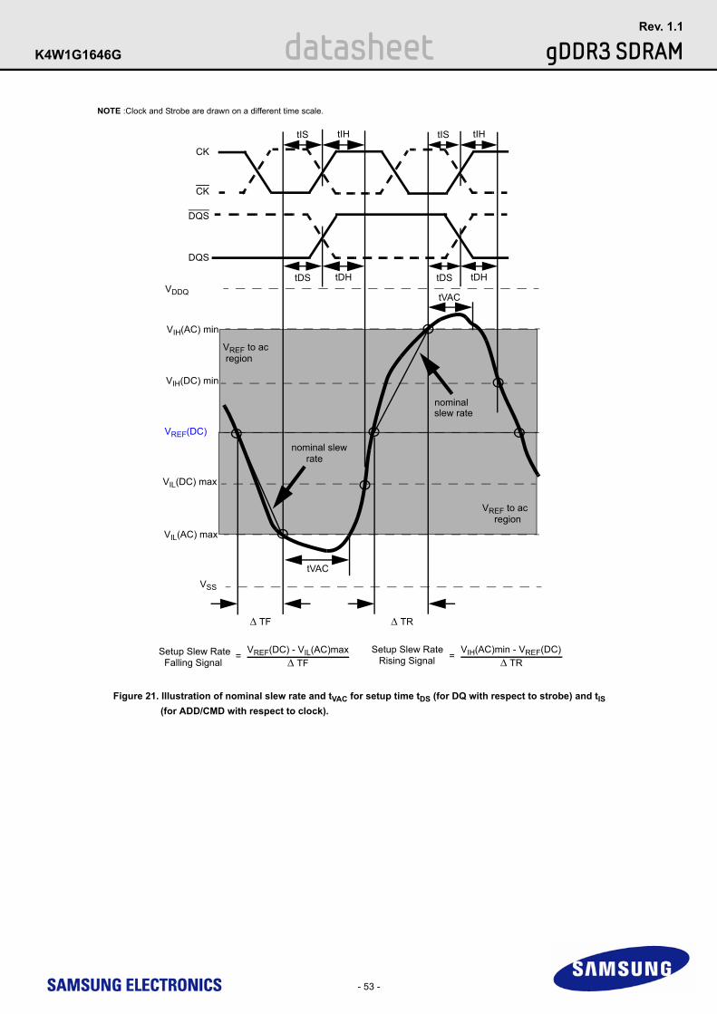
- 53 -
datasheet gDDR3 SDRAMRev. 1.1
K4W1G1646G
Figure 21. Illustration of nominal slew rate and tVAC for setup time tDS (for DQ with respect to strobe) and tIS (for ADD/CMD with respect to clock).
VSS
CK
CK
tDS tDH
Setup Slew RateSetup Slew RateRising SignalFalling Signal
Δ TF Δ TR
VREF(DC) - VIL(AC)maxΔ TF
=VIH(AC)min - VREF(DC)
Δ TR=
VDDQ
VIH(AC) min
VIH(DC) min
VREF(DC)
VIL(DC) max
VIL(AC) max
nominal slewrate
nominalslew rate
VREF to ac region
VREF to ac region
tIS tIH
tDS tDH
tIS tIH
tVAC
tVAC
NOTE :Clock and Strobe are drawn on a different time scale.
DQS
DQS

- 54 -
datasheet gDDR3 SDRAMRev. 1.1
K4W1G1646G
Figure 22. Illustration of nominal slew rate for hold time tDH (for DQ with respect to strobe) and tIH (for ADD/CMD with respect to clock).
VSS
CK
CK
Hold Slew RateHold Slew Rate Falling SignalRising Signal
Δ TR Δ TF
VREF(DC) - VIL(DC)maxΔ TR
= VIH(DC)min - VREF(DC)Δ TF
=
VDDQ
VIH(AC) min
VIH(DC) min
VREF(DC)
VIL(DC) max
VIL(AC) max
nominalslew rate
nominalslew rate
dc to VREF region
tIS tIH tIS tIH
dc to VREFregion
NOTE :Clock and Strobe are drawn on a different time scale.
tDS tDH tDS tDH
DQS
DQS

- 55 -
datasheet gDDR3 SDRAMRev. 1.1
K4W1G1646G
Figure 23. Illustration of tangent line for setup time tDS (for DQ with respect to strobe) and tIS (for ADD/CMD with respect to clock)
VSS
Setup Slew Rate
Setup Slew Rate
Rising Signal
Falling Signal
Δ TF
Δ TR
tangent line[VREF(DC) - VIL(AC)max]Δ TF
=
tangent line[VIH(AC)min - VREF(DC)]Δ TR
=
VDDQ
VIH(AC) min
VIH(DC) min
VREF(DC)
VIL(DC) max
VIL(AC) max
tangent
tangent
VREF to ac region
VREF to ac region
line
line
nominal line
nominal line
CK
CK
tIS tIH tIS tIH
tVAC
NOTE :Clock and Strobe are drawn on a different time scale.
tDS tDH tDS tDH
DQS
DQS
tVAC

- 56 -
datasheet gDDR3 SDRAMRev. 1.1
K4W1G1646G
Figure 24. Illustration of tangent line for hold time tDH (for DQ with respect to strobe) and tIH (for ADD/CMD with respect to clock)
VSS
Hold Slew Rate
Δ TFΔ TR
tangent line [ VIH(DC)min - VREF(DC) ]Δ TF
=
VDDQ
VIH(AC) min
VIH(DC) min
VREF(DC)
VIL(DC) max
VIL(AC) max
tangent
tangentdc to VREF region
dc to VREF region
line
linenominal line
nominal line
Falling Signal
Hold Slew Rate tangent line [ VREF(DC) - VIL(DC)max ]Δ TR
= Rising Signal
CK
CK
tIS tIH tIS tIH
NOTE :Clock and Strobe are drawn on a different time scale.
tDS tDH tDS tDH
DQS
DQS

- 57 -
datasheet gDDR3 SDRAMRev. 1.1
K4W1G1646G
15.4 Data Setup, Hold and Slew Rate Derating :For all input signals the total tDS (setup time) and tDH (hold time) required is calculated by adding the data sheet tDS(base) and tDH(base) value (see Table 54) to the Δ tDS and ΔtDH (see Table 55) derating value respectively. Example: tDS (total setup time) = tDS(base) + ΔtDS.Setup (tDS) nominal slew rate for a rising signal is defined as the slew rate between the last crossing of VREF(DC) and the first crossing of VIH(AC)min. Setup (tDS) nominal slew rate for a falling signal is defined as the slew rate between the last crossing of VREF(DC) and the first crossing of VIL(AC)max (see Figure 25). If the actual signal is always earlier than the nominal slew rate line between shaded ’VREF(DC) to ac region’, use nominal slew rate for derating value. If the actual signal is later than the nominal slew rate line anywherebetween shaded ’VREF(DC) to ac region’, the slew rate of a tangent line to the actual signal from the ac level to dc level is used for derating value (see Figure 27).Hold (tDH) nominal slew rate for a rising signal is defined as the slew rate between the last crossing of VIL(DC)max and the first crossing of VREF(DC). Hold (tDH) nominal slew rate for a falling signal is defined as the slew rate between the last crossing of VIH(DC)min and the first crossing of VREF(DC) (see Figure ). If the actual signal is always later than the nominal slew rate line between shaded ’dc level to VREF(DC) region’, use nominal slew rate for derating value. If the actual signal is earlier than the nominal slew rate line anywhere between shaded ’dc to VREF(DC) region’, the slew rate of a tangent line to the actual signal from the dc level to VREF(DC) level is used for derating value (see Figure 28).
For a valid transition the input signal has to remain above/below VIH/IL(AC) for some time tVAC (see Table 56).
Although for slow slew rates the total setup time might be negative (i.e. a valid input signal will not have reached VIH/IL(AC) at the time of the rising clock transition) a valid input signal is still required to complete the transition and reach VIH/IL(AC).For slew rates in between the values listed in the tables the derating values may obtained by linear interpolation.These values are typically not subject to production test. They are verified by design and characterization.
[ Table 54 ] Data Setup and Hold Base-Values
NOTE : AC/DC referenced for 1V/ns DQ-slew rate and 2 V/ns DQS slew rate)
[ Table 55 ] Derating values for gDDR3-1333/1600 tDS/tDH - (AC150)
NOTE : 1. Cell contents shaded in red are defined as ’not supported’.
[ Table 56 ] Derating values for gDDR3-1866/2133 tDS/tDH - (AC135)
NOTE : 1. Cell contents shaded in red are defined as ’not supported’.
[ps] gDDR3-1333 gDDR3-1600 gDDR3-1866 gDDR3-2133 referencetDS(base) AC150 30 10 - - VIH/L(AC)tDS(base) AC135 - - 0 -15 VIH/L(AC)tDH(base) DC100 65 45 20 5 VIH/L(DC)
ΔtDS, ΔtDH Derating in [ps] AC/DC based1
DQS,DQS Differential Slew Rate4.0 V/ns 3.0 V/ns 2.0 V/ns 1.8 V/ns 1.6 V/ns 1.4V/ns 1.2V/ns 1.0V/ns
ΔtDS ΔtDH ΔtDS ΔtDH ΔtDS ΔtDH ΔtDS ΔtDH ΔtDS ΔtDH ΔtDS ΔtDH ΔtDS ΔtDH ΔtDS ΔtDH
DQSlewrateV/ns
2.0 75 50 75 50 75 50 - - - - - - - - - -1.5 50 34 50 34 50 34 58 42 - - - - - - - -1.0 0 0 0 0 0 0 8 8 16 16 - - - - - -0.9 - - 0 -4 0 -4 8 4 16 12 24 20 - - - -0.8 - - - - 0 -10 8 -2 16 6 24 14 32 24 - -0.7 - - - - - - 8 -8 16 0 24 8 32 18 40 340.6 - - - - - - - - 15 -10 23 -2 31 8 39 240.5 - - - - - - - - - - 14 -16 22 -6 30 100.4 - - - - - - - - - - - - 7 -26 15 -10
ΔtDS, ΔtDH Derating in [ps] AC/DC based1
DQS,DQS Differential Slew Rate4.0 V/ns 3.0 V/ns 2.0 V/ns 1.8 V/ns 1.6 V/ns 1.4V/ns 1.2V/ns 1.0V/ns
ΔtDS ΔtDH ΔtDS ΔtDH ΔtDS ΔtDH ΔtDS ΔtDH ΔtDS ΔtDH ΔtDS ΔtDH ΔtDS ΔtDH ΔtDS ΔtDH
DQSlewrateV/ns
2.0 68 50 68 50 68 50 - - - - - - - - - -1.5 45 34 45 34 45 34 53 42 - - - - - - - -1.0 0 0 0 0 0 0 8 8 16 16 - - - - - -0.9 - - 2 -4 2 -4 10 4 18 12 26 20 - - - -0.8 - - - - 3 -10 11 -2 19 6 27 14 35 24 - -0.7 - - - - - - 14 -8 22 0 30 8 38 18 46 340.6 - - - - - - - - 25 -10 33 -2 41 8 49 240.5 - - - - - - - - - - 29 -16 37 -6 45 100.4 - - - - - - - - - - - - 30 -26 38 -10

- 58 -
datasheet gDDR3 SDRAMRev. 1.1
K4W1G1646G
[ Table 57 ] Required time tVAC above VIH(AC) {blow VIL(AC)} for valid DQ transition
Slew Rate[V/ns]tVAC[ps] gDDR3-1333/1600 (AC150) tVAC[ps] gDDR3-1866
(AC135)tVAC[ps] gDDR3-2133
(AC135)min max min max min max
>2.0 175 - 114 - 89 -2.0 170 - 109 - 86 -1.5 167 - 66 - 41 -1.0 163 - TBD - TBD -0.9 162 - TBD - TBD -0.8 161 - TBD - TBD -0.7 159 - TBD - TBD -0.6 155 - TBD - TBD -0.5 155 - TBD - TBD -
<0.5 150 - TBD - TBD -

- 59 -
datasheet gDDR3 SDRAMRev. 1.1
K4W1G1646G
Figure 25. Illustration of nominal slew rate and tVAC for setup time tDS (for DQ with respect to strobe) and tIS (for ADD/CMD with respect to clock).
VSS
CK
CK
tDS tDH
Setup Slew RateSetup Slew RateRising SignalFalling Signal
Δ TF Δ TR
VREF(DC) - VIL(AC)maxΔ TF
=VIH(AC)min - VREF(DC)
Δ TR=
VDDQ
VIH(AC) min
VIH(DC) min
VREF(DC)
VIL(DC) max
VIL(AC) max
nominal slewrate
nominalslew rate
VREF to ac region
VREF to ac region
tIS tIH
tDS tDH
tIS tIH
tVAC
tVAC
NOTE :Clock and Strobe are drawn on a different time scale.
DQS
DQS

- 60 -
datasheet gDDR3 SDRAMRev. 1.1
K4W1G1646G
Figure 26. Illustration of nominal slew rate for hold time tDH (for DQ with respect to strobe) and tIH
(for ADD/CMD with respect to clock).
VSS
CK
CK
Hold Slew RateHold Slew Rate Falling SignalRising Signal
Δ TR Δ TF
VREF(DC) - VIL(DC)maxΔ TR
= VIH(DC)min - VREF(DC)Δ TF
=
VDDQ
VIH(AC) min
VIH(DC) min
VREF(DC)
VIL(DC) max
VIL(AC) max
nominalslew rate
nominalslew rate
dc to VREF region
tIS tIH tIS tIH
dc to VREFregion
NOTE :Clock and Strobe are drawn on a different time scale.
tDS tDH tDS tDH
DQS
DQS

- 61 -
datasheet gDDR3 SDRAMRev. 1.1
K4W1G1646G
Figure 27. Illustration of tangent line for setup time tDS (for DQ with respect to strobe) and tIS (for ADD/CMD with respect to clock)
VSS
Setup Slew Rate
Setup Slew Rate
Rising Signal
Falling Signal
Δ TF
Δ TR
tangent line[VREF(DC) - VIL(AC)max]Δ TF
=
tangent line[VIH(AC)min - VREF(DC)]Δ TR
=
VDDQ
VIH(AC) min
VIH(DC) min
VREF(DC)
VIL(DC) max
VIL(AC) max
tangent
tangent
VREF to ac region
VREF to ac region
line
line
nominal line
nominal line
CK
CK
tIS tIH tIS tIH
tVAC
NOTE :Clock and Strobe are drawn on a different time scale.
tDS tDH tDS tDH
DQS
DQS
tVAC

- 62 -
datasheet gDDR3 SDRAMRev. 1.1
K4W1G1646G
Figure 28. Illustration of tangent line for hold time tDH (for DQ with respect to strobe) and tIH (for ADD/CMD with respect to clock)
VSS
Hold Slew Rate
Δ TFΔ TR
tangent line [ VIH(DC)min - VREF(DC) ]Δ TF
=
VDDQ
VIH(AC) min
VIH(DC) min
VREF(DC)
VIL(DC) max
VIL(AC) max
tangent
tangentdc to VREF region
dc to VREF region
line
linenominal line
nominal line
Falling Signal
Hold Slew Rate tangent line [ VREF(DC) - VIL(DC)max ]Δ TR
= Rising Signal
CK
CK
tIS tIH tIS tIH
NOTE :Clock and Strobe are drawn on a different time scale.
tDS tDH tDS tDH
DQS
DQS

- 67 -
datasheet gDDR3 SDRAMRev. 1.1
K4W1G1646G
16. Functional Description
Figure 29. Simplified State Diagram
16.1 Simplified State Diagram
Self
IdleZQ
Bank
Precharging
Power
Writing
ACT
ReadA
Read
SRE
REF
PDE
PDX
PDX
PDE
Write
Automatic Sequence
Command Sequence
ReadAWriteARead
PRE, PREA
Refreshing
Refreshing
Down
PowerDown
Active
ReadA
Reading
WriteA
Active
Precharge
ReadingWriting
Activating
SRX
ReadWrite
Calibration
CKE_L
CKE_L CKE_L
PRE, PREA PRE, PREA
Write
WriteA
InitializationResetProcedure
PowerOn
PowerApplied
RESETfrom any
state
MRS, MPR,Write
Leveling
MRSZQCL
ZQCL, ZQCS
[ Table 62 ] State Diagram Command Definitions
NOTE : This simplified State Diagram is intended to provide an overview of the possible state transitions and the commands to control them. In particular, situations involving more than one bank, the enabling or disabling of on-die termination, and some other events are not captured in full detail.
Abbreviation Function Abbreviation Function Abbreviation Function
ACT Activate Read RD,RDS4, RDS8 PDE Enter Power-down
PRE Precharge Read A RDA,RDAS4, RDAS8 PDX Exit Power-down
PREA Precharge All Write WR, WRS4, WRS8 SRE Self-Refresh entry
MRS Mode Register Set Write A WRA,WRAS4, WRAS8 SRX Self-Refresh exit
REF Refresh RESET Start RESET procedure MPR Multi Purpose Register
ZQCL ZQ Calibration Long ZQCS ZQ Calibration Short - -

- 68 -
datasheet gDDR3 SDRAMRev. 1.1
K4W1G1646G
16.2 Basic Functionality The gDDR3 SDRAM is a high-speed CMOS, dynamic random-access memory internally configured as a eight-bank DRAM. The gDDR3 SDRAM uses a 8n prefetch architecture to achieve high-speed operation. The 8n prefetch architecture, with an interface designed to transfer two data words per clock cycle at the I/O pins. A single read or write access for the gDDR3 SDRAM consists of a single 8n-bit wide, four clock data transfer at the internal DRAM core and two corresponding n-bit wide, one-half clock cycle data transfers at the I/O pins. Read and write operation to the gDDR3 SDRAM are burst oriented, start at a selected location, and continue for a burst length of four or eight in a pro-grammed sequence. Operation begins with the registration of an Active command, which is then followed by a Read or Write command. The address bits registered coincident with the Active command are used to select the bank and row to be accessed (BA0-BA2 select the bank; A0-A15 select the row). The address bits registered coincident with the Read or Write command are used to select the starting column location for the burst operation, determine if the auto precharge command is to be issued (via A10/AP), and the select BC4 or BL8 mode ’on the fly’ (via A12) if enabled in the mode register. Prior to normal operation, the gDDR3 SDRAM must be powered up and initialized in a predefined manner. The following sections provide detailed infor-mation covering device reset and initialization, register definition, command descriptions and device operation.
16.3 RESET and Initialization Procedure
16.3.1 Power-up Initialization SequenceThe following sequence is required for POWER UP and Initialization.
1. Apply power and attempt to maintain RESET below 0.2*VDD (all other inputs may be undefined). RESET needs to be maintained for minimum 200us with stable power. CKE is pulled “ Low” anytime before RESET being de-asserted (min. time 10ns). The power voltage ramp time between 300mV to VDD min must be no longer than 200ms; and during the ramp, VDD>VDDQ and VDD -VDDQ<0.3volts.• VDD and VDDQ are driven from a single power converter output, AND• The voltage levels on all pins other than VDD,VDDQ,VSS,VSSQ must be less than or equal to VDDQ and VDD on one side and must be larger than or
equal to VSSQ and VSS on the other side. In addition, VTT is limited to 0.95V max once power ramp is finished, AND• Vref tracks VDDQ/2. or• Apply VDD without any slope reversal before or at the same time as VDDQ• Apply VDDQ without any slope reversal before or at the same time as VTT & Vref.• The voltage levels on all pins other than VDD,VDDQ,VSS,VSSQ must be less than or equal to VDDQ and VDD on one side and must be larger than or
equal to VSSQ and VSS on the other side. 2. After RESET is de-asserted, wait for another 500us until CKE becomes active. During this time, the DRAM will start internal initialization; this will be
done independently of external clocks. 3. Clocks (CK, CK) need to be started and stabilized for at least 10ns or 5tCK (which is larger) before CKE goes active. Since CKE is a synchronous sig-
nal, the corresponding setup time to clock (tIS) must be met. Also a NOP or Deselect command must be registered (with tIS set up time to clock) before CKE goes active. Once the CKE registered “High” after Reset, CKE needs to be continuously registered “High” until the initialization sequence is finished, including expiration of tDLLK and tZQinit.
4. The gDDR3 SDRAM keeps its on-die termination in high-impedance state as long as RESET is asserted. Further, the SDRAM keeps its on-die termi-nation in high impedance state after RESET deassertion until CKE is registered HIGH. The ODT input signal may be in undefined state until tIS before CKE is registered HIGH. When CKE is registered HIGH, the ODT input signal may be statically held at either LOW or HIGH. If RTT_NOM is to be enabled in MR1 and the on-die termination is required to remain in the high impedance state, the ODT input signal must be statically held LOW. In all cases, the ODT input signal remains static until the power up initialization sequence is finished, including the expiration of tDLLK and tZQinit.
5. After CKE is registered high, wait minimum of Reset CKE Exit time, tXPR, before issuing the first MRS command to load mode register. (tXPR=Max(tXS, 5tCK)]
6. Issue MRS Command to load MR2 with all application settings. (To issue MRS command for MR2, provide “Low” to BA0 and BA2, “High” to BA1.) 7. Issue MRS Command to load MR3 with all application settings. (To issue MRS command for MR3, provide “Low” to BA2, “High” to BA0 and BA1.) 8. Issue MRS Command to load MR1 with all application settings and DLL enabled. (To issue “DLL Enable “command, provide “Low” to A0, “Low” to A0,
“High” to BA0 and “Low” to BA1-BA2) 9. Issue MRS Command to load MR0 with all application settings and “DLL reset”. (To issue DLL reset command, provide “High” to A8 and “Low” to BA0-
2).10. Issue ZQCL command to starting ZQ calibration11. Wait for both tDLLK and tZQ init completed12. The gDDR3 SDRAM is now ready for normal operation.

Figure 30. RESET and Initialization Sequence at Power-on Ramping
Figure 31. RESET procedure at Power stable condition
- 69 -
datasheet gDDR3 SDRAMRev. 1.1
K4W1G1646G
NOTE :1) From time point ‘Td’ until ‘Tk’, NOP or DES commands must be applied between MRS and ZQCL commands
16.3.2 Reset Initialization with Stable PowerThe following sequence is required for RESET at no power interruption initialization.1. Asserted RESET below 0.2 * VDD anytime when reset is needed (all other inputs may be undefined). RESET needs to be maintained for minimum 100
ns. CKE is pulled "LOW" before RESET being de-asserted (min. time 10 ns).2. Follow Power-up Initialization Sequence step 2 to 11.3. The Reset sequence is now completed, gDDR3 SDRAM is ready for normal operation.
NOTE :1) From time point ‘Td’ until ‘Tk’, NOP or DES commands must be applied between MRS and ZQCL commands
VDD/VDDQ
CK,CK
RESET
Tc . Td . Te . Tf . . Th . Ti . Tj . TkTg
tCKSRX
Ta . Tb
CKE
200 us 500 us
10 ns tIS
*) MRS
MR2
MRS
MR3
MRS
MR1
MRS
MR0
ZQCL
tXPR**
tIStMRD tMRD tMRD
tMOD
CMD
BA[2:0]
tIS
ODT
DRAM_RTT
tDLLK
Static LOW in case RTT_Nom is eanbled at time Tg, otherwise static HIGH or LOW
tZQinit
1) VALID
VALID
VALID
tIS
VDD/VDDQ
CK,CK
RESET
Tc . Td . Te . Tf . . Th . Ti . Tj . Tk .TgTa . Tb
CKE
100 ns 500 us
10 ns tIS
1) MRS
MR2
MRS
MR3
MRS
MR1
MRS
MR0
ZQCL
tXPR
tIStMRD tMRD tMRD
CMD
BA[2:0]
tIS
ODT
DRAM_RTT
tCKSRX
tMOD tZQin
tDLLK
Static LOW in case RTT_Nom is eanbled at time Tg, otherwise static HIGH or LOW
1) VALID
VALID
VALID

- 70 -
datasheet gDDR3 SDRAMRev. 1.1
K4W1G1646G
16.4 Register Definition
Figure 33. tMOD Timing
Figure 32. tMRD Timing
16.4.1 Programming the Mode Registers
For application flexibility, various functions, features, and modes are programmable in four Mode Registers, provided by the gDDR3 SDRAM, as user defined variables and they must be programmed via a Mode Register Set (MRS) command. As the default values of the Mode Registers (MR#) are not defined, contents of Mode Registers must be fully initialized and/or re-initialized, i.e., written, after power up and/or reset for proper operation. Also the contents of the Mode Registers can be altered by re-executing the MRS command during normal operation. When programming the mode registers, even if the user chooses to modify only a sub-set of the MRS fields, all address fields within the accessed mode register must be redefined when the MRS com-mand is issued. MRS command and DLL Reset do not affect array contents, which means these commands can be executed any time after power-up without affecting the array contents.
The mode register set command cycle time, tMRD is required to complete the write operation to the mode register and is the minimum time required between two MRS commands shown in Figure 32
The MRS command to Non-MRS command delay, tMOD, is required for the DRAM to update the features, except DLL reset, and is the minimum time required from an MRS command to a non-MRS command excluding NOP and DES shown in Figure 33
CK
CK
T0 T1 T2 Ta0 Ta1 Tb0 Tb1 Tb2 Tc0 Tc1 Tc2
VALID VALID VALID MRS NOP/DES NOP/DES MRS NOP/DES NOP/DES VALID VALIDCommand
VALID VALID VALID VALID VALID VALID VALID VALID VALID VALID VALIDAddress
CKE
Settings Old Settings Updating Settings New Settings
VALID VALID VALIDODT
VALID VALID VALID VALID VALID VALID VALID VALID VALID VALID VALIDODT
RTT_Nom ENABLED prior and/or after MRS command
RTT_Nom DISABLED prior and after MRS command
tMRD tMOD
ODTLoff + 1
Time Break Don’t Care
CK
CK
T0 T1 T2 Ta0 Ta1 Ta2 Ta3 Ta4 Tb0 Tb1 Tb2
VALID VALID VALID MRS NOP/DES NOP/DES NOP/DES NOP/DES VALID VALIDCommand
VALID VALID VALID VALID VALID VALID VALID VALID VALID VALID VALIDAddress
CKE
Settings Old Settings Updating Settings New Settings
VALID VALID VALIDODT
VALID VALID VALID VALID VALID VALID VALID VALID VALID VALID VALIDODT
RTT_Nom ENABLED prior and/or after MRS command
RTT_Nom DISABLED prior and after MRS command
tMOD
ODTLoff + 1
Time Break Don’t Care
NOP/DES

- 71 -
datasheet gDDR3 SDRAMRev. 1.1
K4W1G1646G
15.4.1 Programming the Mode Registers (Cont) The mode register contents can be changed using the same command and timing requirements during normal operation as long as the DRAM is in idle state, i.e., all banks are in the precharged state with tRP satisfied, all data bursts are completed and CKE is high prior to writing into the mode register. If the RTT_NOM feature is enabled in the Mode Register prior and/or after an MRS Command, the ODT Signal must continuously be registered LOW ensuring RTT is in an off State prior to the MRS command. The ODT Signal may be registered high after tMOD has expired. If the RTT_NOM Feature is disabled in the Mode Register prior and after an MRS command, the ODT Signal can be registered either LOW or HIGH before, during and after the MRS command. The mode registers are divided into various fields depending on the functionality and/or modes.
16.4.2 Mode Register MR0
Figure 34. MR0 Definition
The mode register MR0 stores the data for controlling various operating modes of gDDR3 SDRAM. It controls burst length, read burst type, CAS latency, test mode, DLL reset, WR and DLL control for precharge power down, which include various vendor specific options to make gDDR3 SDRAM useful for various applications. The mode register is written by asserting low on CS, RAS, CAS, WE, BA0,BA1 and BA2, while controlling the states of address pins according to the Figure below.
NOTE :*1 : BA2 and A13~A15 are RFU and must be programmed to 0 during MRS.*2 : WR(write recovery for autoprecharge)min in clock cycles is calculated by dividing tWR(in ns) by tCK(in ns) and rounding up to the next integer: WRmin[cycles] =
Roundup(tWR[ns]/tCK[ns]). The WR value in the mode register must be programmed to be equal or larger than WRmin. The programmed WR value is used with tRP to determine tDAL.
*3 : The table only shows the encodings for a given Cas Latency. For actual supported Cas Latency, please refer to speedbin tables for each frequency*4 : The table only shows the encodings for Write Recovery. For actual Write recovery timing, please refer to AC timingtable*5 : RFU(Reserved for Future Use)*6 : CL16 is used for gDDR3 1Gb S-die at 2400Mbps operation.
16.4.2.1 Burst Length, Type and OrderAccesses within a given burst may be programmed to sequential or interleaved order. The burst type is selected via bit A3 as shown in Figure 34. The ordering of accesses within a burst is determined by the burst length, burst type, and the starting column address as shown in Table 63. The burst length is defined by bits A0-A1. Burst length options include fixed BC4, fixed BL8, and ’on the fly’ which allows BC4 or BL8 to be selected coincident with the reg-istration of a Read or Write command via A12/BC.
Address Field
A7 mode
0 Normal
1 Test
A3 Read Burst Type
0 Nibble Sequential
1 Interleave
A8 DLL Reset
0 No
1 Yes
Mode Register 0
BA1 BA0 A11 A10 A9 A8 A7 A6 A5 A4 A3 A2 A1 A0
0 TM CAS Latency RBTDLL 0*1 WR
Write recovery for autoprechargeA11 A10 A9 WR(cycles)
0 0 0 16*2
0 0 1 5*2
0 1 0 6*2
0 1 1 7*2
1 0 0 8*2
1 0 1 10*2
1 1 0 12*2
1 1 1 14*2
A15 ~ A13
0 BL
A1 A0 BL
0 0 8 (Fixed)
0 1 4 or 8(on the fly)
1 0 4 (Fixed)
1 1 Reserved
BA2
0*1
BA1 BA0 MRS mode
0 0 MR0
0 1 MR1
1 0 MR2
1 1 MR3
A12
PPD
A12 DLL Control for Pre-charge PD
0 Slow exit (DLL off)
1 Fast exit (DLL on)
CAS Latency
A6 A5 A4 A2 Latency
0 0 0 0 Reserved
0 0 1 0 5
0 1 0 0 6
0 1 1 0 7
1 0 0 0 8
1 0 1 0 9
1 1 0 0 10
1 1 1 0 11
0 0 0 1 12
0 0 1 1 13
0 1 0 1 14
0 1 1 1 Reserved for 15*5
1 0 0 1 16*6
1 0 1 1 Reserved
1 1 0 1 Reserved
1 1 1 1 Reserved
CL

- 72 -
datasheet gDDR3 SDRAMRev. 1.1
K4W1G1646G
[ Table 63 ] Burst Type and Burst Order
NOTE : 1. In case of burst length being fixed to 4 by MR0 setting, the internal write operation starts two clock cycles earlier than for the BL8 mode. This means that the starting point for
tWR and tWTR will be pulled in by two clocks. In case of burst length being selected on-the-fly via A12/BC, the internal write operation starts at the same point in time like a burst of 8 write operation. This means that during on-the-fly control, the starting point for tWR and tWTR will not be pulled in by two clocks.
2. 0...7 bit number is value of CA[2:0] that causes this bit to be the first read during a burst.3. T: Output driver for data and strobes are in high impedance.4. V: a valid logic level (0 or 1), but respective buffer input ignores level on input pins.5. X: Don’t Care.
16.4.2.2 CAS LatencyThe CAS Latency is defined by MR0(bits A4-A6) as shown in Figure 34. CAS Latency is the delay, in clock cycles, between the internal Read command and the availability of the first bit of output data. gDDR3 SDRAM does not support any half clock latencies. The overall Read Latency (RL) is defined as Additive Latency (AL) + CAS Latency (CL); RL = AL + CL. For more information on the supported CL and AL settings based on the operating clock fre-quency, refer to " Standard Speed Bins" on each component datasheet. For detailed Read operation refer to "READ Operation" on page 92
16.4.2.3 Test ModeThe normal operating mode is selected by MR0(bit A7 = 0) and all other bits set to the desired values shown in Figure 34. Programming bit A7 to a ’1’ places the gDDR3 SDRAM into a test mode that is only used by the DRAM Manufacturer and should NOT be used. No operations or functionality is guar-anteed if A7 = 1.
16.4.2.4 DLL ResetThe DLL Reset bit is self-clearing, meaning it returns back to the value of ’0’ after the DLL reset function has been issued. Once the DLL is enabled, a subsequent DLL Reset should be applied. Any time the DLL reset function is used, tDLLK must be met before any functions that require the DLL can be used (i.e. Read commands or ODT synchronous operations).
16.4.2.5 Write RecoveryThe programmed WR value MR0(bits A9, A10, and A11) is used for the auto precharge feature along with tRP to determine tDAL WR(write recovery for auto-precharge)min in clock cycles is calculated by dividing tWR(in ns) by tCK(in ns) and rounding up to the next integer: WRmin[cycles] = Roundup(tWR[ns]/tCK[ns]). The WR must be programmed to be equal or larger than tWR(min).
16.4.2.6 Precharge PD DLLMR0 (bit A12) is used to select the DLL usage during precharge power-down mode. When MR0(A12 = 0), or "slow-exit", the DLL is frozen after entering precharge power-down (for potential power savings) and upon exit requires tXPDLL to be met prior to the next valid command. When MR0(A12 = 1), or "fast-exit", the DLL is maintained after entering precharge power-down and upon exiting power-down requires tXP to be met prior to the next valid com-mand.
BurstLength
READ/WRITE
StartingColumn
ADDRESS(A2,A1,A0)
burst type = Sequential(decimal)
A3 = 0
burst type = Interleaved(decimal)
A3 = 1Notes
4Chop
READ
0 0 0 0,1,2,3,T,T,T,T 0,1,2,3,T,T,T,T 1, 2, 3
0 0 1 1,2,3,0,T,T,T,T 1,0,3,2,T,T,T,T 1, 2, 3
0 1 0 2,3,0,1,T,T,T,T 2,3,0,1,T,T,T,T 1, 2, 3
0 1 1 3,0,1,2,T,T,T,T 3,2,1,0,T,T,T,T 1, 2, 3
1 0 0 4,5,6,7,T,T,T,T 4,5,6,7,T,T,T,T 1, 2, 3
1 0 1 5,6,7,4,T,T,T,T 5,4,7,6,T,T,T,T 1, 2, 3
1 1 0 6,7,4,5,T,T,T,T 6,7,4,5,T,T,T,T 1, 2, 3
1 1 1 7,4,5,6,T,T,T,T 7,6,5,4,T,T,T,T 1, 2, 3
WRITE 0,V,V 0,1,2,3,X,X,X,X 0,1,2,3,X,X,X,X 1, 2, 4, 5
1,V,V 4,5,6,7,X,X,X,X 4,5,6,7,X,X,X,X 1, 2, 4, 5
8READ
0 0 0 0,1,2,3,4,5,6,7 0,1,2,3,4,5,6,7 2
0 0 1 1,2,3,0,5,6,7,4 1,0,3,2,5,4,7,6 2
0 1 0 2,3,0,1,6,7,4,5 2,3,0,1,6,7,4,5 2
0 1 1 3,0,1,2,7,4,5,6 3,2,1,0,7,6,5,4 2
1 0 0 4,5,6,7,0,1,2,3 4,5,6,7,0,1,2,3 2
1 0 1 5,6,7,4,1,2,3,0 5,4,7,6,1,0,3,2 2
1 1 0 6,7,4,5,2,3,0,1 6,7,4,5,2,3,0,1 2
1 1 1 7,4,5,6,3,0,1,2 7,6,5,4,3,2,1,0 2
WRITE V,V,V 0,1,2,3,4,5,6,7 0,1,2,3,4,5,6,7 2, 4

Figure 35. MR1 Definition
- 73 -
datasheet gDDR3 SDRAMRev. 1.1
K4W1G1646G
16.4.3 Mode Register MR1The Mode Register MR1 stores the data for enabling or disabling the DLL, output driver strength, Rtt_Nom impedance, additive latency, Write leveling enable, TDQS enable and Qoff. The Mode Register 1 is written by asserting low on CS, RAS, CAS, WE, high on BA0 and low on BA1 and BA2 while con-trolling the states of address pins according to the Figure below.
* 1 : BA2 and A8, A10 and A13 ~ A15 are RFU and must be programmed to 0 during MRS
Mode Register 1
Address FieldBA1 BA0 A11 A10 A9 A8 A7 A6 A5 A4 A3 A2 A1 A0
0 AL0*1 0*1
A15 ~ A13
1 Rtt_Nom
A0 DLL Enable
0 Enable
1 Disable
BA2
0*1
A12
NOTE : RZQ=240ohms
A5 A1 Output Driver Impedance Control
0 0 RZQ/6
0 1 RZQ/7
1 0 Reserved
1 1 Reserved
D.I.C DLL
NOTE :RZQ=240ohms
*3 : In Write leveling Mode (MR1[bit7] = 1) with MR1[bit12]=1, all RTT_Nom settings are allowed; in Write Leveling Mode (MR1[bit7] = 1) with MR1[bit12]=0, only RTT_Nom settings of RZQ/2, RZQ/4 and RZQ/6 are allowed
*4 : If RTT_Nom is used during Writes, only the values RZQ/2,RZQ/4 and RZQ/6 are allowed
A9 A6 A2 Rtt_Nom*3
0 0 0 Rtt Nom disabled
0 0 1 RZQ/4
0 1 0 RZQ/2
0 1 1 RZQ/6
1 0 0 RZQ/12*4
1 0 1 RZQ/8*4
1 1 0 Reserved
1 1 1 Reserved
A7 Write leveling enable
0 Disabled
1 Enabled
A4 A3 Additive Latency
0 0 0 (AL disabled)
0 1 CL-1
1 0 CL-2
1 1 Reserved
*2: Outputs disabled - DQs, DQSs, DQSs.
A12 Qoff *2
0 Output buffer enabled
1 Output buffer disabled *2
Qoff LevelTDQS 0*1 Rtt_Nom D.I.C
A11 TDQS enable
0 Disabled
1 Enabled
Rtt_Nom
BA1 BA0 MRS mode
0 0 MR0
0 1 MR1
1 0 MR2
1 1 MR3

- 74 -
datasheet gDDR3 SDRAMRev. 1.1
K4W1G1646G
16.4.3.1 DLL Enable/DisableThe DLL must be enabled for normal operation. DLL enable is required during power up initialization, and upon returning to normal operation after having the DLL disabled. During normal operation (DLL-on) with MR1(A0 = 0), the DLL is automatically disabled when entering Self-Refresh operation and is automatically re-enabled upon exit of Self- Refresh operation. Any time the DLL is enabled and subsequently reset, tDLLK clock cycles must occur before a Read or synchronous ODT command can be issued to allow time for the internal clock to be synchronized with the external clock. Failing to wait for syn-chronization to occur may result in a violation of the tDQSCK, tAON or tAOF parameters. During tDLLK, CKE must continuously be registered high. gDDR3 SDRAM does not require DLL for any Write operation. For more detailed information on DLL Disable operation refer to "DLL-off Mode" on page 80
The direct ODT feature is not supported during DLL-off mode. The on-die termination resistors must be disabled by continuously registering the ODT pin low and/or by programming the RTT_Nom bits MR1{A9,A6,A2} to {0,0,0} via a mode register set command during DLL-off mode.
The dynamic ODT feature is not supported at DLL-off mode. User must use MRS command to set Rtt_WR, MR2{A10, A9}={0,0}, to disable Dynamic ODT externally.
16.4.3.2 Output Driver Impedance ControlThe output driver impedance of the gDDR3 SDRAM device is selected by MR1(bits A1 and A5) as shown in Figure 35
16.4.3.3 ODT Rtt ValuesgDDR3 SDRAM is capable of providing two different termination values (Rtt_Nom and Rtt_WR). The nominal termination value Rtt_Nom is programmed in MR1. A separate value (Rtt_WR) may be programmed in MR2 to enable a unique RTT value when ODT is enabled during writes. The Rtt_WR value can be applied during writes even when Rtt_Nom is disabled.
16.4.3.4 Additive Latency (AL)Additive Latency (AL) operation is supported to make command and data bus efficient for sustainable bandwidths in gDDR3 SDRAM. In this operation, the gDDR3 SDRAM allows a read or write command (either with or without auto-precharge) to be issued immediately after the active command. The com-mand is held for the time of the Additive Latency (AL) before it is issued inside the device. The Read Latency (RL) is controlled by the sum of the AL and CAS Latency (CL) register settings. Write Latency (WL) is controlled by the sum of the AL and CAS Write Latency (CWL) register settings. A summary of the AL register options are shown in Table 64
[ Table 64 ] Additive Latency (AL) Settings
NOTE : AL has a value of CL - 1 or CL - 2 as per the CL values programmed in the MR0 register.
16.4.3.5 Write levelingFor better signal integrity, gDDR3 memory module adopted fly by topology for the commands, addresses, control signals and clocks. The fly by topology has benefits from reducing number of stubs and their length but in other aspect, causes flight time skew between clock and strobe at every DRAM on DIMM. It makes it difficult for the Controller to maintain tDQSS, tDSS and tDSH specification. Therefore, the gDDR3 SDRAM supports ’write leveling’ fea-ture to allow the controller to compensate for skew. See "Write Leveling" on page 84. for more details.
16.4.3.6 Output DisableThe gDDR3 SDRAM outputs may be enabled/disabled by MR1(bit A12) as shown in Figure 35. When this feature is enabled (A12 = 1), all output pins (DQs, DQS, DQS, etc.) are disconnected from the device removing any loading of the output drivers. This feature may be useful when measuring module power for example. For normal operation, A12 should be set to ’0’.
A4 A3 AL
0 0 0 (AL Disabled)
0 1 CL - 1
1 0 CL - 2
1 1 Reserved

- 75 -
datasheet gDDR3 SDRAMRev. 1.1
K4W1G1646G
16.4.3.7 TDQS, TDQSTDQS (Termination Data Strobe) is a feature of X8 gDDR3 SDRAM that provides additional termination resistance outputs that may be useful in some system configurations.
TDQS is not supported in X4 or X16 configurations. When enabled via the mode register, the same termination resistance function is applied to the TDQS/TDQS pins that is applied to the DQS/DQS pins.
In contrast to the RDQS function of DDR2 SDRAM, TDQS provides the termination resistance function only. The data strobe function of RDQS is not pro-vided by TDQS.
The TDQS and DM functions share the same pin. When the TDQS function is enabled via the mode register, the DM function is not supported. When the TDQS function is disabled, the DM function is provided and the TDQS pin is not used. Table 65 for details.
The TDQS function is available in X8 gDDR3 SDRAM only and must be disabled via the mode register A11=0 in MR1 for X4 and X16 configurations.
[ Table 65 ] TDQS, TDQS Function Matrix
NOTE :1. If TDQS is enabled, the DM function is disabled.2. When not used, TDQS function can be disabled to save termination power.3. TDQS function is only available for x8 DRAM and must be disabled for x4 and x16.
MR1(A11) DM / TDQS NU / TDQS
0 (TDQS Disabled) DM Hi-Z
1 (TDQS Enabled) TDQS TDQS

Figure 36. MR2 Definition
- 76 -
datasheet gDDR3 SDRAMRev. 1.1
K4W1G1646G
16.4.4 Mode Register MR2The Mode Register MR2 stores the data for controlling refresh related features, Rtt_WR impedance, and CAS write latency. The Mode Register 2 is writ-ten by asserting low on CS, RAS, CAS, WE, high on BA1 and low on BA0 and BA2, while controlling the states of address pins according to the table below.
Mode Register 2
Address FieldBA1 BA0 A11 A10 A9 A8 A7 A6 A5 A4 A3 A2 A1 A0
1
A15~ A13
0 0*1
BA2
0*1
A12
PASR*2
A2 A1 A0 Partial Array Self Refresh (Optional)
0 0 0 Full Array
0 0 1 HalfArray (BA[2:0]=000,001,010, & 011)
0 1 0 Quarter Array (BA[2:0]=000, & 001)
0 1 1 1/8th Array (BA[2:0] = 000)
1 0 0 3/4 Array (BA[2:0] = 010,011,100,101,110, & 111)
1 0 1 HalfArray (BA[2:0] = 100, 101, 110, &111)
1 1 0 Quarter Array (BA[2:0]=110, &111)
1 1 1 1/8th Array (BA[2:0]=111)
* 1 : BA2, A5, A8, A11 ~ A15 are RFU and must be programmed to 0 during MRS.* 2 : The Rtt_WR value can be applied during writes even when Rtt_Nom is disabled. During write leveling, Dynamic ODT is not available.
SRF ASR CWL
A5 A4 A3 CAS write Latency (CWL)
0 0 0 5 (tCK(avg)≥2.5ns)
0 0 1 6 (2.5ns >tCK(avg)≥1.875ns)
0 1 0 7 (1.875ns>tCK(avg)≥1.5ns)
0 1 1 8 (1.5ns>tCK(avg)≥1.25ns)
1 0 0 9 (1.25ns>tCK(avg)≥1.07ns)
1 0 1 10 (1.07ns>tCK(avg)≥0.935ns)
1 1 0 11 (0.935ns>tCK(avg)≥0.833ns)
1 1 1 12 (0.833ns>tCK(avg)≥0.75ns)
A7 Self-refresh temperature range(SRT)
0 Normal operating temperature range
1 Extend temperature self-refresh (Optional)
0*1Rtt_WR
A10 A9 Rtt_WR*2
0 0 Dynamic ODT off (Write does not affect Rtt value)
0 1 RZQ/4
1 0 RZQ/2
1 1 Reserved
BA1 BA0 MRS mode
0 0 MR0
0 1 MR1
1 0 MR2
1 1 MR3
A6 Auto Self-refresh (ASR)
0 Manual SR reference (SRT)
1 ASR enable (Optional)

Figure 37. MR3 Definition
- 77 -
datasheet gDDR3 SDRAMRev. 1.1
K4W1G1646G
16.4.4.1 Partial Array Self-Refresh (PASR)Optional in gDDR3 SDRAM: Users should refer to the DRAM component data sheet and/or the DIMM SPD to determine if gDDR3 SDRAM devices sup-port the following options or requirements referred to in this material. If PASR (Partial Array Self-Refresh) is enabled, data located in areas of the array beyond the specified address range shown in Figure 36 will be lost if Self-Refresh is entered. Data integrity will be maintained if tREFI conditions are met and noSelf-Refresh command is issued.
16.4.4.2 CAS Write Latency (CWL)The CAS Write Latency is defined by MR2 (bits A3-A5), as shown in Figure 36. CAS Write Latency is the delay, in clock cycles, between the internal Write command and the availability of the first bit of input data. gDDR3 SDRAM does not support any half clock latencies. The overall Write Latency (WL) is defined as Additive Latency (AL) + CAS Write Latency (CWL); WL = AL + CWL. For more information on the supported CWL and AL settings based on the operating clock frequency, refer to "Standard Speed Bins" on each component datasheet. For detailed Write operation refer to "WRITE Operation" on page 103
16.4.4.3 Auto Self-Refresh (ASR) and Self-Refresh Temperature (SRT)Optional in gDDR3 SDRAM: Users should refer to the DRAM component data sheet and/or the DIMM SPD to determine if gDDR3 SDRAM devices sup-port the following options or requirements referred to in this material. For more details refer to ’Extended Temperature Usage’ gDDR3 SDRAM’s must support Self-Refresh operation at all supported temperatures. Applications requiring Self-Refresh operation in the Extended Temperature Range must use the optional ASR function or program the SRT bit appropriately.
16.4.4.4 Dynamic ODT (Rtt_WR)gDDR3 SDRAM introduces a new feature "Dynamic ODT’. In certain application cases and to further enhance signal integrity on the data bus, it is desir-able that the termination strength of the gDDR3 SDRAM can be changed without issuing an MRS command. MR2 Register locations A9 and A10 config-ure the Dynamic ODT settings. In Write leveling mode, only RTT_Nom is available. For details on ODT operation, refer to "Dynamic ODT" on page 124.
16.4.5 Mode Register MR3The Mode Register MR3 controls Multi purpose registers. The Mode Register 3 is written by asserting low on CS, RAS, CAS, WE, high on BA1 and BA0, while controlling the states of address pins according to the table below.
16.4.5.1 Multi-Purpose Register (MPR)The Multi Purpose Register (MPR) function is used to Read out a predefined system timing calibration bit sequence. To enable the MPR, a MODE Regis-ter Set (MRS) command must be issued to MR3 Register with bit A2 = 1. Prior to issuing the MRS command, all banks must be in the idle state (all banks precharged and tRP/tRPA met). Once the MPR is enabled, any subsequent RD or RDA commands will be redirected to the Multi Purpose Register. When the MPR is enabled, only RD or RDA commands are allowed until a subsequent MRS command is issued with the MPR disabled (MR3 bit A2 = 0). Power-Down mode, Self-Refresh, and any other non-RD/RDA command is not allowed during MPR enable mode. The RESET function is supported dur-ing MPR enable mode. For detailed MPR operation refer to "Multi Purpose Register" on page 88.
Mode Register 3
Address FieldBA1 BA0 A11 A10 A9 A8 A7 A6 A5 A4 A3 A2 A1 A0
1
A15 ~ A13
1 0*1
BA2
0*1
A12
MPR AddressA1 A0 MPR location
0 0 Predefined pattern*2
0 1 RFU
1 0 RFU
1 1 RFU
MPR OperationA2 MPR
0 Normal operation*3
1 Dataflow from MPR
MPR Loc MPR
* 1 : BA2, A3 - A15 are RFU and must be programmed to 0 during MRS.* 2 : The predefined pattern will be used for read synchronization. * 3 : When MPR control is set for normal operation, MR3 A[2]=0, MR3 A[1:0] will be ignored
BA1 BA0 MRS mode
0 0 MR0
0 1 MR1
1 0 MR2
1 1 MR3

- 78 -
datasheet gDDR3 SDRAMRev. 1.1
K4W1G1646G
17. gDDR3 SDRAM Command Description and Operation
17.1 Command Truth Tablea) Note 1,2,3 and 4 apply to the entire Command truth table(b) Note 5 applies to all Read/Write commands.[BA=Bank Address, RA=Row Address, CA=Column Address, BC=Burst Chop, X=Don’t care, V=Valid]
[ Table 66 ] Command Truth Table
NOTE :1. All gDDR3 SDRAM commands are defined by states of CS, RAS, CAS, WE and CKE at the rising edge of the clock. The MSB of BA, RA, and CA are device density and configuration dependant2. RESET is Low enable command which will be used only for asynchronous reset so must be maintained HIGH during any function.3. Bank addresses (BA) determine which bank is to be operated upon. For (E)MRS BA selects an (Extended) Mode Register4. “V” means “H or L (but a defined logic level)” and “X” means either “defined or undefined (like floating) logic level” 5. Burst reads or writes cannot be terminated or interrupted and Fixed/on the fly BL will be defined by MRS6. The Power Down Mode does not perform any refresh operations.7. The state of ODT does not affect the states described in this table. The ODT function is not available during Self Refresh. 8. Self refresh exit is asynchronous.9. VREF(Both VREFDQ and VREFCA) must be maintained during Self Refresh operation. VrefDQ supply man be turned OFF in system during Self Refresh operation, provided
that VrefDQ is valid and stable prior to CKE going back High and that first Write operation may not occur earlier than 512nCK after exit from Self Refresh.10. The No Operation command should be used in cases when the gDDR3 SDRAM is in an idle or a wait state. The purpose of the No Operation command (NOP) is to prevent the gDDR3 SDRAM from registering any unwanted commands between operations. A No Operation command will not terminate a previous operation that is still executing, such as a burst read or write cycle.11. The Deselect command performs the same function as a No Operation command. 12. Refer to the CKE Truth Table for more detail with CKE transition
Function AbbreviationCKE
CS RAS CAS WEBA0
-BA2
A13-
A15
A12/
BC
A10/
AP
A0-
A9,A11NOTEPrevious
CycleCurrent Cycle
Mode Register Set MRS H H L L L L BA OP CodeRefresh REF H H L L L H V V V V VSelf Refresh Entry SRE H L L L L H V V V V V 7,9,12
Self Refresh Exit SRX L HH V V V X X X X X
7,8,9,12L H H H V V V V V
Single Bank Precharge PRE H H L L H L BA V V L VPrecharge all Banks PREA H H L L H L V V V H VBank Activate ACT H H L L H H BA Row Address (RA)Write (Fixed BL8 or BL4) WR H H L H L L BA RFU V L CAWrite (BL4, on the Fly) WRS4 H H L H L L BA RFU L L CAWrite (BL8, on the Fly) WRS8 H H L H L L BA RFU H L CAWrite with Auto Precharge(Fixed BL8 or BL4)
WRA H H L H L L BA RFU V H CA
Write with Auto Precharge(BL4, on the Fly)
WRAS4 H H L H L L BA RFU L H CA
Write with Auto Precharge(BL8, on the Fly)
WRAS8 H H L H L L BA RFU H H CA
Read (Fixed BL8 or BL4) RD H H L H L H BA RFU V L CARead (BL4, on the Fly) RDS4 H H L H L H BA RFU L L CARead (BL8, on the Fly) RDS8 H H L H L H BA RFU H L CARead with Auto Precharge(Fixed BL8 or BL4)
RDA H H L H L H BA RFU V H CA
Read with Auto Precharge(BL4, on the Fly)
RDAS4 H H L H L H BA RFU L H CA
Read with Auto Precharge(BL8, on the Fly)
RDAS8 H H L H L H BA RFU H H CA
No Operation NOP H H L H H H V V V V V 10Device Deselected DES H H H X X X X X X X X 11ZQ calibration Long ZQCL H H L H H L X X X H XZQ calibration Short ZQCS H H L H H L X X X L X
Power Down Entry PDE H LL H H H V V V V V
6,12H V X X X X X X X
Power Down Exit PDX L HL H H H V V V V V
6,12H X X X X X X X X

- 79 -
datasheet gDDR3 SDRAMRev. 1.1
K4W1G1646G
17.2 Clock Enable (CKE) Truth Table(a) Note 1~7 apply to the entire Command truth table(b) For Power-down entry and exit parameters See 17.17, ?$paratext>,? on page 113(c) CKE low is allowed only if tMRD and tMOD are satisfied
[ Table 67 ] CKE Truth Table
NOTE : 1. CKE (N) is the logic state of CKE at clock edge N; CKE (N–1) was the state of CKE at the previous clock edge.2. Current state is defined as the state of the gDDR3 SDRAM immediately prior to clock edge N3. COMMAND (N) is the command registered at clock edge N, and ACTION (N) is a result of COMMAND (N), ODT is not included here4. All states and sequences not shown are illegal or reserved unless explicitly described elsewhere in this document5. The state of ODT does not affect the states described in this table. The ODT function is not available during Self Refresh6. CKE must be registered with the same value on tCKEmin consecutive positive clock edges. CKE must remain at the valid input level the entire time it takes to achieve the
tCKEmin clocks of registeration. Thus, after any CKE transition, CKE may not transition from its valid level during the time period of tIS + tCKEmin + tIH.7. DESELECT and NOP are defined in the Command truth table8. On Self Refresh Exit DESELECT or NOP commands must be issued on every clock edge occurring during the tXS period. Read or ODT commands may be issued only after
tXSDLL is satisfied.9. Self Refresh mode can only be entered from the All Banks Idle state.10. Must be a legal command as defined in the Command Truth Table.11. Valid commands for Power Down Entry and Exit are NOP and DESELECT only.12. Valid commands for Self Refresh Exit are NOP and DESELECT only.13. Self Refresh can not be entered while Read or Write operations. See Figure 17.16 and Figure 17.17 for a detailed list of restrictions. 14. The Power Down does not perform any refresh operations. 15. “X” means “don’t care (including floating around VREF)” in Self Refresh and Power Down. It also applies to Address pins16. VREF (Both VREFDQ and VREFCA) must be maintained during Self Refresh operation. VrefDQ supply man be turned OFF in system during Self Refresh operation, provided
that VrefDQ is valid and stable prior to CKE going back High and that first Write operation may not occur earlier than 512nCK after exit from Self Refresh.17. If all banks are closed at the conclusion of the read, write or precharge command, then Precharge Power Down is entered, otherwise Active Power Down is entered18. ‘Idle state’ means that all banks are closed(tRP,tDAL,etc. satisfied) and CKE is high and all timings from previous operations are satisfied
(tMRD,tMOD,tRFC,tZQinit,tZQoper,tZQCS,etc)as well as all SRF exit and Power Down exit parameters are satisfied (tXS,tXP,tXPDLL,etc)
17.3 No OPeration (NOP) CommandThe No OPeration (NOP) command is used to instruct the selected gDDR3 SDRAM to perform a NOP (CS LOW and RAS, CAS, and WE HIGH). This prevents unwanted commands from being registered during idle or wait states. Operations already in progress are not affected.
17.4 Deselect CommandThe DESELECT function (CS HIGH) prevents new commands from being executed by the gDDR3 SDRAM. The gDDR3 SDRAM is effectively dese-lected. Operations already in progress are not affected.
Current State 2CKE Command (N) 3
RAS, CAS, WE, CSAction (N) 3 NOTEPrevious Cycle 1
(N-1)Current Cycle 1
(N)
Power DownL L X Maintain Power-Down 14, 15
L H DESELECT or NOP Power Down Exit 11, 14
Self RefreshL L X Maintain Self Refresh 15, 16
L H DESELECT or NOP Self Refresh Exit 8, 12, 16
Bank(s) Active H L DESELECT or NOP Active Power Down Entry 11, 13, 14
Reading H L DESELECT or NOP Power Down Entry 11, 13, 14, 17
Writing H L DESELECT or NOP Power Down Entry 11, 13, 14, 17
Precharging H L DESELECT or NOP Power Down Entry 11, 13, 14, 17
Refreshing H L DESELECT or NOP Precharge Power Down Entry 11
All Banks IdleH L DESELECT or NOP Precharge Power Down Entry 11,13, 14, 18
H L REFRESH Self Refresh Entry 9, 13, 18
For more details with all signals See Table 66 "Command Truth Table" on page 78 10

Figure 38. DLL-off mode READ Timing Operation
- 80 -
datasheet gDDR3 SDRAMRev. 1.1
K4W1G1646G
17.5 DLL-off ModegDDR3 DLL-off mode is entered by setting MR1 bit A0 to "1"; this will disable the DLL for subsequent operations until A0 bit set back to "0" The MR1 A0 bit for DLL control can be switched either during initialization or later. Refer to"Input clock frequency change" on page 83.
The DLL-off Mode operations listed below are an optional feature for gDDR3. The maximum clock frequency for DLL-off Mode is specified by the param-eter tCKDLL-OFF. There is no minimum frequency limit besides the need to satisfy the refresh interval, tREFI.
Due to latency counter and timing restrictions, only one value of CAS Latency (CL) in MR0 and CAS Write Latency (CWL) in MR2 are supported. The DLL-off mode is only required to support setting of both CL=6 and CWL=6.
DLL-off mode will affect the Read data Clock to Data Strobe relationship (tDQSCK), but not the Data Strobe to Data relationship (tDQSQ, tQH). Special attention is needed to line up Read data to controller time domain.
Comparing with DLL-on mode, where tDQSCK starts from the rising clock edge (AL+CL) cycles after the Read command, the DLL-off mode tDQSCK starts (AL+CL - 1) cycles after the read command. Another difference is that tDQSCK may not be small compared to tCK (it might even be larger than tCK) and the difference between tDQSCKmin and tDQSCKmax is significantly larger than in DLL-on mode.
The timing relations on DLL-off mode READ operation have shown at following Timing Diagram (CL=6, BL=8):
NOTE : The tDQSCK is used here for DQS, DQS and DQ to have a simplified diagram; the DLL_off shift will affectboth timings in the same way and the skew between all DQ and DQS, DQS signals will still be tDQSQ.
CK
CK
DQSdiff_DLL_on
T0 T1 T2 T3 T4 T5 T6 T7 T8 T9 T10 T11
RD
ABA
CMD
DQ_DLL_onQA0 QA1 QA2 QA3 QA4 QA5 QA6 QA7
RL=AL+CL=6 (CL=6, AL=0)CL=6
RL (DLL_off) = AL + (CL-1) = 5
QA0 QA1 QA2 QA3 QA4 QA5 QA6 QA7
QA0 QA1 QA2 QA3 QA4 QA5 QA6 QA7
tDQSCK(DLL_off)_min
tDQSCK(DLL_off)_max
DQSdiff_DLL_off
DQ_DLL_off
DQSdiff_DLL_off
DQ_DLL_off

- 81 -
datasheet gDDR3 SDRAMRev. 1.1
K4W1G1646G
17.6 DLL on/off switching procedure
Figure 39. DLL Switch Sequence from DLL-on to DLL-off
gDDR3 DLL-off mode is entered by setting MR1 bit A0 to "1"; this will disable the DLL for subsequent operations until A0 bit set back to "0".
17.6.1 DLL "on" to DLL "off" Procedure To switch from DLL "on" to DLL "off" requires the frequency to be changed during Self-Refresh outlined in the following procedure:
1. Starting from Idle state (All banks pre-charged, all timings fulfilled, and DRAMs On-die Termination resistors, RTT, must be in high impedance state before MRS to MR1 to disable the DLL.)
2. Set MR1 bit A0 to "1" to disable the DLL.3. Wait tMOD.4. Enter Self Refresh Mode; wait until (tCKSRE) is satisfied.5. Change frequency, in guidance with "Input clock frequency change" on page 836. Wait until a stable clock is available for at least (tCKSRX) at DRAM inputs.7. Starting with the Self Refresh Exit command, CKE must continuously be registered HIGH until all tMOD timings from any MRS command are satisfied.
In addition, if any ODT features were enabled in the mode registers when Self Refresh mode was entered, the ODT signal must continuously be regis-tered LOW until all tMOD timings from any MRS command are satisfied. If both ODT features were disabled in the mode registers when Self Refresh mode was entered, ODT signal can be registered LOW or HIGH.
8. Wait tXS, then set Mode Registers with appropriate values (especially an update of CL, CWL and WR may be necessary. A ZQCL command may also be issued after tXS)
9. Wait for tMOD, then DRAM is ready for next command.
NOTE :1. Starting with Idle State, RTT in Hi-Z state2. Disable DLL by setting MR1 Bit A0 to 13. Enter SR4. Change Frequency5. Clock must be stable tCKSRX6. Exit SR7. Update Mode registers with DLL off parameters setting8. Any valid command
CK
CK
T0 T1 Ta0 Ta1 Tb0 Tc0 Td0 Td1 Te0 Te1
CKE
ODT
Tf0
VALID
MRS(2) VALID SRE(3) NOP SRX(6) MRS(7) NOP VALID(8)Command NOP
(1) tMOD tCKSRE (4) tCKSRX(5) tXS tMOD
tCKESR
VALID(8)
ODT : Static LOW in case RTT_Nom and RTT_WR is enabled, otherwise staitc Low or HighTime Break Don’t Care

Figure 40. DLL Switch Sequence from DLL-off to DLL-on
- 82 -
datasheet gDDR3 SDRAMRev. 1.1
K4W1G1646G
17.6.2 DLL "off" to DLL "on" ProcedureTo switch from DLL "off" to DLL "on" (with required frequency change) during Self-Refresh:
1. Starting from Idle state (All banks pre-charged, all timings fulfilled and DRAMs On-die Termination resistors (RTT) must be in high impedance state before Self-Refresh mode is entered.)
2. Enter Self Refresh Mode, wait until tCKSRE satisfied.3. Change frequency, in guidance with "Input clock frequency change" on page 834. Wait until a stable clock is available for at least (tCKSRX) at DRAM inputs.5. Starting with the Self Refresh Exit command, CKE must continuously be registered HIGH until tDLLK timing from subsequent DLL Reset command is
satisfied. In addition, if any ODT features were enabled in the mode registers when Self Refresh mode was entered, the ODT signal must continuously be registered LOW until tDLLK timings from subsequent DLL Reset command is satisfied. If both ODT features are disabled in the mode registers when Self Refresh mode was entered, ODT signal can be registered LOW or HIGH.
6. Wait tXS, then set MR1 bit A0 to "0" to enable the DLL.7. Wait tMRD, then set MR0 bit A8 to "1" to start DLL Reset.8. Wait tMRD, then set Mode Registers with appropriate values (especially an update of CL, CWL and WR may be necessary. After tMOD satisfied from
any proceeding MRS command, a ZQCL command may also be issued during or after tDLLK.)9. Wait for tMOD, then DRAM is ready for next command (Remember to wait tDLLK after DLL Reset before applying command requiring a locked DLL!).
In addition, wait also for tZQoper in case a ZQCLcommand was issued.
NOTE :1. Starting with Idle State2. Enter SR3. Change Frequency4. Clock must be stable tCKSRX5. Exit SR6. Set DLL on by MR1 A0=07. Update Mode registers8. Any valid command
CK
CK
T0 Ta0 Ta1 Tb0 Tc0 Tc1 Td0 Te0 Tf1 Tg0
CKE
ODT
Th0
VALID
NOP SRE(2) SRX(5) MRS(7) MRS(8) VALID(9)MRS(6)
(1) DOTLoff + 1 x tCK (3) tCKSRX(4) tXS tMRD
tCKESR
ODT : Static LOW in case RTT_Nom and RTT_WR is enabled, otherwise staitc Low or HighTime Break Don’t Care
Command NOPtDLLK
tMRD

Figure 41. Change Frequency during Precharge Power-down
- 83 -
datasheet gDDR3 SDRAMRev. 1.1
K4W1G1646G
17.7 Input clock frequency changeOnce the gDDR3 SDRAM is initialized, the gDDR3 SDRAM requires the clock to be "stable" during almost all states of normal operation. This means once the clock frequency has been set and is to be in the "stable state", the clock period is not allowed to deviate except for what is allowed for by the clock jitter and SSC (spread spectrum clocking) specifications.
The input clock frequency can be changed from one stable clock rate to another stable clock rate under two conditions:(1) Self-Refresh mode and (2) Precharge Power-down mode. Outside of these two modes, it is illegal to change the clock frequency.
For the first condition, once the gDDR3 SDRAM has been successfully placed in to Self-Refresh mode and tCKSRE has been satisfied, the state of the clock becomes a don’t care. Once a don’t care, changing the clock frequency is permissible, provided the new clock frequency is stable prior to tCKSRX. When entering and exiting Self-Refresh mode for the sole purpose of changing the clock frequency, the Self-Refresh entry and exit specifications must still be met as outlined in See Figure 17.16. The gDDR3 SDRAM input clock frequency is allowed to change only within the minimum and maximum oper-ating frequency specified for the particular speed grade. Any frequency change below the minimum operating frequency would require the use of DLL_on- mode -> DLL_off -mode transition sequence, refer to "DLL on/off switching procedure" on page 81
The second condition is when the gDDR3 SDRAM is in Precharge Power-down mode (either fast exit mode or slow exit mode). If the RTT_NOM feature was enabled in the mode register prior to entering Precharge power down mode, the ODT signal must continuously be registered LOW ensuring RTT is in an off state. If the RTT_NOM feature was disabled in the mode register prior to entering Precharge power down mode, RTT will remain in the off state. The ODT signal can be registered either LOW or HIGH in this case.. A minimum of tCKSRE must occur after CKE goes LOW before the clock frequency may change. The gDDR3 SDRAM input clock frequency is allowed to change only within the minimum and maximum operating frequency specified for the particular speed grade. During the input clock frequency change, ODT and CKE must be held at stable LOW levels. Once the input clock frequency is changed, stable new clocks must be provided to the DRAM tCKSRX before Precharge Power-down may be exited; after Precharge Power-down is exited and tXP has expired, the DLL must be RESET via MRS. Depending on the new clock frequency additional MRS commands may need to be issued to appropriately set the WR, CL, and CWL with CKE continuously registered high. During DLL re-lock period, ODT must remain LOW and CKE must remain HIGH. After the DLL lock time, the DRAM is ready to operate with new clock frequency. This process is depicted in Figure 41 below.
NOTE :1. Applicable for both SLOW EXIT and FAST EXIT Precharge Power-down2. tAOFPD and tAOF must be statisfied and outputs High-Z prior to T1; refer to ODT timing section for exact requirements3. If the RTT_NOM feature was enabled in the mode register prior to entering Precharge power down mode, the ODT signal must continuously be registered LOW ensuring RTT is in an off state, as shown in Figure 41. If the RTT_NOM feature was disabled in the mode register prior to entering Precharge power down mode, RTT will remain in the off state. The ODT signal can be registered either LOW or HIGH in this case.
T0 T1 T2 Ta0 Tb0 Tc0 Tc1 Td0 Td1 Te0 Te1CK
ADDR
CMD
tCH
tAOFPD / tAOF
CKtCL
tCK
CKE
tIH tIS
tCKSRE
tCKE
tIH
tIS
tCHb tCLb
tCKb
tCKSRX
tCHb tCLb
tCKb
tCHb tCLb
tCKb
NOP NOP NOP NOP NOP MRS NOP VALID
DLL RESET VALID
ODTtIS
tIHtXP
DQS
DQSHigh-Z
DQ High-Z
DM
Enter PRECHARGEPower-Down Mode
FrequencyChange
Exit PRECHARGEPower-Down Mode
tDLLK
DON’T CARE
Previous clock frequency New clock frequency

Figure 42. Write leveling concept
- 84 -
datasheet gDDR3 SDRAMRev. 1.1
K4W1G1646G
17.8 Write LevelingFor better signal integrity, gDDR3 memory module adopted fly by topology for the commands, addresses, control signals and clocks. The fly by topology has benefits from reducing number of stubs and their length but in other aspect, causes flight time skew between clock and strobe at every DRAM on DIMM. It makes it difficult for the Controller to maintain tDQSS, tDSS and tDSH specification. Therefore, the controller should support ’write leveling’ in gDDR3 SDRAM to compensate the skew.
The memory controller can use the ’write leveling’ feature and feedback from the gDDR3 SDRAM to adjust the DQS - DQS to CK - CK relationship. The memory controller involved in the leveling must have adjustable delay setting on DQS - DQS to align the rising edge of DQS - DQS with that of the clock at the DRAM pin. DRAM asynchronously feeds back CK - CK, sampled with the rising edge of DQS - DQS, through the DQ bus. The controller repeatedly delays DQS - DQS until a transition from 0 to 1 is detected. The DQS - DQS delay established though this exercise would ensure tDQSS specification. Besides tDQSS, tDSS and tDSH specification also needs to be fulfilled. One way to achieve this is to combine the actual tDQSS in the application with an appropriate duty cycle and jitter on the DQS - DQS signals. Depending on the actual tDQSS in the application, the actual values for tDQSL and tDQSH may have to be better than the absolute limits provided in the chapter "AC Timing Parameters" in order to satisfy tDSS and tDSH specification. A conceptual timing of this scheme is shown in Figure 42.
DQS/DQS driven by the controller during leveling mode must be terminated by the DRAM based on ranks populated. Similarly, the DQ bus driven by the DRAM must also be terminated at the controller.
One or more data bits should carry the leveling feedback to the controller across the DRAM configurations X4, X8, and X16. On a X16 device, both byte lanes should be leveled independently. Therefore, a separate feedback mechanism should be available for each byte lane. The upper data bits should provide the feedback of the upper diff_DQS(diff_UDQS) to clock relationship whereas the lower data bits would indicate the lower diff_DQS(diff_LDQS)to clock relationship.
17.8.1 DRAM setting for write leveling & DRAM termination function in that modeDRAM enters into Write leveling mode if A7 in MR1 set "High" and after finishing leveling, DRAM exits from write leveling mode if A7 in MR1 set "Low" (Table 68). Note that in write leveling mode, only DQS/DQS terminations are activated and deactivated via ODT pin not like normal operation (Table 69).
[ Table 68 ] MR setting involved in the leveling procedure
[ Table 69 ] DRAM termination function in the leveling mode
NOTE : In Write Leveling Mode with its output buffer disabled (MR1[bit7] = 1 with MR1[bit12] = 1) all RTT_Nom settings are allowed; in Write Leveling Mode with its output buf-fer enabled (MR1[bit7] = 1 with MR1[bit12] = 0) only RTT_Nom settings of RZQ/2, RZQ/4 and RZQ/6 are allowed.
Function MR1 Enable Disable
Write leveling enable A7 1 0
Output buffer mode (Qoff) A12 0 1
ODT pin @DRAM DQS/DQS termination DQs termination
De-asserted Off Off
Asserted On Off
T0 T1 T2 T3 T4 T5 T6 T7
Tn T0 T1 T2 T3 T4 T5 T6
Souce
Destination
CK
CK
diff_DQS
CK
CK
diff_DQS
diff_DQS
DQ
DQ
o or 1 0 0 0
Push DQS to capture 0-1transition
0 or 1 11 1

Figure 43. Timing details of Write leveling sequence [DQS-DQS is capturing CK-CK low at T1 and CK-CK high at T2]
- 85 -
datasheet gDDR3 SDRAMRev. 1.1
K4W1G1646G
17.8.2 Procedure DescriptionThe Memory controller initiates Leveling mode of all DRAMs by setting bit 7 of MR1 to 1. With entering write leveling mode, the DQ pins are in undefined driving mode. During write leveling mode, only NOP or DESELECT commands are allowed, as well as an MRS command to change Qoff bit (MR1[A12]) and an MRS command to exit (MR1[A7]). Upon exiting write leveling mode, the MRS command performing the exit (MR1[A7]=0) may also change MR1 bits of A12-A11, A9, A6-A5 and A2-A1, Since the controller levels one rank at a time, the output of other ranks must be disabled by setting MR1 bit A12 to 1. The controller may assert ODT after tMOD, at which time the DRAM is ready to accept the ODT signal.The Controller may drive DQS low and DQS high after a delay of tWLDQSEN, at which time DRAM has applied on-die termination on these signals. After tDQSL and tWLMRD, controller provides a single DQS, DQS edge which is used by the DRAM to sample CK driven from controller. tWLMRD(max) timing is controller dependent. DRAM samples CK status with rising edge of DQS and provides feedback on all the DQ bits asynchronously after tWLO timing. There is a DQ output uncertainty of tWLOE defined to allow mismatch on DQ bits; there are no read strobes (DQS/DQS) needed for these DQs. Controller samples incoming DQ and decides to increment or decrement DQS delay setting and launches the next DQS/DQS pulse after some time, which is controller dependent. Once a 0 to 1 transition is detected, the controller locks DQS delay setting and write leveling is achieved for the device.Figure 43 describes the timing diagram and parameters for the overall Write Leveling procedure.
NOTE *:1. DRAM has the option to drive leveling feedback on a prime DQ or all DQs. If feedback is driven only on one DQ, the remaining DQs must be driven low, as shown in above Figure, and maintained at this state through out the leveling procedure.2. MRS : Load MR1 to enter write leveling mode3. NOP : NOP or deselect4. diff_DQS is the differential data strobe (DQS-DQS). Timing reference points are the zero crossings. DQS is shown with solid line, DQS is shown with dotted line5. CK/CK : CK is shown with solid dark line, where as CK is drawn with dotted line.6. DQS, DQS needs to fulfill minimum pulse width requirements tDQSH(min) and tDQSL(min) as defined for regular Writes; the max pulse width is system dependent
T1 T2tWLH
tWLS
tWLH
tWLS
(3)(2)
MRS NOP NOP NOP NOP NOP NOP NOP NOP NOP NOP NOP
tWLDQSEN tDQSL(6) tDQSH(6) tDQSL(6) tDQSH(6)
tWLMRD tWLO tWLO
tWLO
tWLO tWLOE
tWLMRD tWLO
tWLO tWLOE
tWLOE
tWLO
tWLO
CK(5)
CK
COMMAND
ODT
diff_DQS(4)
One Prime DQ:
Prime DQ(1)
Late Remaining DQs
Early Remaining DQs
All DQs are Prime:
Late Prime DQs(1)
Early Prime DQs(1)
tMOD

Figure 44. Timing details of Write leveling exit
- 86 -
datasheet gDDR3 SDRAMRev. 1.1
K4W1G1646G
17.8.3 Write Leveling Mode Exit
The following sequence describes how the Write Leveling Mode should be exited:1.After the last rising strobe (see ~T111) edge, stop driving the strobe signals (see ~T128). Note: From now on, DQ pins are in undefined driving mode,
and will remain undefined, until tMOD after the respective MR command (see T145).2.Drive ODT pin low (tIS must be satisfied) and keep it low. (see T128).3.After the RTT is switched off, disable Write Level Mode via MR command (see T132).4. After tMOD is satisfied (T145), a any valid command may be registered. (MR commands may already be issued after tMRD (see T136).
CK
CK
CMD
ODT
WLoff
DQS_DQS
T111 T112 T116 T128 T131 T132 T136 T145
BA tIS
RTT_DQS_DQS
ODTLoff
valid
valid
valid
valid
RTT_DQ
DQs result = 1
tWLO + tWLOE
tMOD
tMRD
MR1

- 87 -
datasheet gDDR3 SDRAMRev. 1.1
K4W1G1646G
17.9 Extended Temperature UsageThe following sequence describes how Write Leveling Mode should be exited:1.After the last rising strobe (see ~T111) edge, stop driving the strobe signals (see ~T128). Note: From now on, DQ pins are in undefined driving mode,
and will remain undefined, until tMOD after the respective MR command (T145).2.Drive ODT pin low (tIS must be satisfied) and keep it low. (see T128).3.After the RTT is switched off, disable Write Level Mode via MR command (see T132).4. After tMOD is satisfied (T145), a any valid command may be registered. (MR commands may already be issued after tMRD (T136).
[ Table 70 ] Mode Register Description
17.9.1 Auto Self-Refresh mode - ASR Mode (optional)gDDR3 SDRAM provides an Auto Self-Refresh mode (ASR) for application ease. ASR mode is enabled by setting MR2 bit A6=1b and RR2 bit A7=0b. The DRAM will also manage Self-Refresh entry in either the Normal or Extended (optional) Temperature Ranges. In this mode, the DRAM will also man-age Self-Refresh power consumption when the DRAM operating temperature changes, lower at low temperatures and higher at high temperatures.If the ASR option is not supported by the DRAM, MR2 bit A6 must be set to 0b.If the ASR mode is not enabled (MR2 bit. A6=0b), the SRT bit(MR2 A7) must be manually programmed with the operating temperature range required during Self-Refresh operation.Support of the ASR option does not automatically imply support of the Extended Temperature Range and Auto Self-Refresh option availability.
17.9.2 Self-Refresh Temperature Range - SRTSRT applies to devices supporting Extended Temperature Range only. If ASR = ’0’, the Self-Refresh Temperature (SRT) Range bit must be programmed to guarantee proper self-refresh operation. If SRT = ’0’, then the DRAM will set an appropriate refresh rate for Self-Refresh operation in the Normal Tem-perature Range. If SRT = ’1’ then the DRAM will set an appropriate, potentially different, refresh rate to allow Self-Refresh operation in either the Normal or Extended Temperature Ranges. The value of the SRT bit can effect self-refresh power consumption, please refer to the IDD table for details.
For parts that do not support the Extended Temperature Range, MR2 bit A7 must be set to ’0’ and the DRAM should not be operated outside the Normal Temperature Range.Please refer to the component data sheet and/or the DIMM SPD for Extended Temperature Range availability.
[ Table 71 ] Self-Refresh mode summary
Field Bits Description
ASR MR2(A6)
Auto Self-Refresh (ASR) (Optional)When enabled, gDDR3 SDRAM automatically provides Self-Refresh power management functions for all sup-ported operating temperature values. If not enabled, the SRT bit must be programmed to indicate TOPER during subsequent Self-Refresh operation.0 = Manual SR Reference (SRT)1 = ASR enable (optional)
SRT MR2(A7)
Self-Refresh Temperature (SRT) RangeIf ASR = 0, the SRT bit must be programmed to indicate TOPER during subsequent Self-Refresh operationIf ASR = 1, SRT bit must be set to 0b0 = Normal operating temperature range1 = Extended (optional) operating temperature range
MR2 A[6] MR2 A[7] Self-Refresh operation Allowed Operating Temperature Range for Self-Refresh Mode
0 0 Self-refresh rate appropriate for the Normal Temperature Range Normal (0 - 85 °C)
0 1
Self-refresh rate appropriate for either the Normal or Extended Temperature Ranges. The DRAM must support Extended Temperature Range. The value of the SRT bit can effect self-refresh power consumption, please refer to the IDD table for details.
Normal and Extended (0 - 95 °C)
1 0ASR enabled (not supported). Self-Refresh power consumption is tempera-ture dependent
Normal (0 - 85 °C)
1 0ASR enabled (not supported). Self-Refresh power consumption is tempera-ture dependent
Normal and Extended (0 - 95 °C)
1 1 Illegal
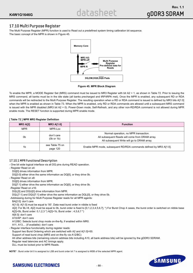
Figure 45. MPR Block Diagram
- 88 -
datasheet gDDR3 SDRAMRev. 1.1
K4W1G1646G
17.10 Multi Purpose RegisterThe Multi Purpose Register (MPR) function is used to Read out a predefined system timing calibration bit sequence.The basic concept of the MPR is shown in Figure 45.
To enable the MPR, a MODE Register Set (MRS) command must be issued to MR3 Register with bit A2 = 1, as shown in Table 72. Prior to issuing the MRS command, all banks must be in the idle state (all banks precharged and tRP/tRPA met). Once the MPR is enabled, any subsequent RD or RDA commands will be redirected to the Multi Purpose Register. The resulting operation when a RD or RDA command is issued is defined by MR3 bits A[1:0] when the MPR is enabled as shown in Table 73. When the MPR is enabled, only RD or RDA commands are allowed until a subsequent MRS command is issued with the MPR disabled (MR3 bit A2 = 0). Power-Down mode, Self-Refresh, and any other non-RD/RDA command is not allowed during MPR enable mode. The RESET function is supported during MPR enable mode.
[ Table 72 ] MPR MR3 Register Definition
17.10.1 MPR Functional Description- One bit wide logical interface via all DQ pins during READ operation.- Register Read on x4: DQ[0] drives information from MPR. DQ[3:0] either drive the same information as DQ[0], or they drive 0b.- Register Read on x8: DQ[0] drives information from MPR. DQ[7:1] either drive the same information as DQ[0], or they drive 0b. -Register Read on x16: DQL[0] and DQU[0] drive information from MPR. DQL[7:1] and DQU[7:1] either drive the same information as DQL[0], or they drive 0b. -Addressing during for Multi Purpose Register reads for all MPR agents: BA[2:0]: don’t care A[1:0]: A[1:0] must be equal to ’00’. Data read burst order in nibble is fixed A[2]: For BL=8, A[2] must be equal to 0b, burst order is fixed to [0,1,2,3,4,5,6,7], *) For Burst Chop 4 cases, the burst order is switched on nibble base
A[2]=0b, Burst order: 0,1,2,3 *) A[2]=1b, Burst order : 4,5,6,7 *) A[9:3]: don’t care A10/AP: don’t care A12/BC: Selects burst chop mode on-the-fly, if enabled within MR0. A11, A13,... (if available): don’t care- Regular interface functionality during register reads: Support two Burst Ordering which are switched with A2 and A[1:0]=00. Support of read burst chop (MRS and on-the-fly via A12/BC) All other address bits (remaining column address bits including A10, all bank address bits) will be ignored by the gDDR3 SDRAM. Regular read latencies and AC timings apply. DLL must be locked prior to MPR Reads.
NOTE* : Burst order bit 0 is assigned to LSB and burst order bit 7 is assigned to MSB of the selected MPR agent.
MR3 A[2] MR3 A[1:0] Function
MPR MPR-Loc
0b don’t care(0b or 1b)
Normal operation, no MPR transaction.All subsequent Reads will come from DRAM array.
All subsequent Write will go to DRAM array.
1b see Table 75 on
page 120 Enable MPR mode, subsequent RD/RDA commands defined by MR3 A[1:0].
Memory Core
MR3 A2:MPR-off Multi Purpose
RegisterPre-defined data for
DQ,DM,DQS,DQS Pads
MPR R Reads

- 89 -
datasheet gDDR3 SDRAMRev. 1.1
K4W1G1646G
17.10.2 MPR Register Address DefinitionTable 73 provides an overview of the available data locations, how they are addressed by MR3 A[1:0] during a MRS to MR3, and how their individual bits are mapped into the burst order bits during a Multi Purpose Register Read.
[ Table 73 ] MPR MR3 Register Definition
NOTE : Burst order bit 0 is assigned to LSB and the burst order bit 7 is assigned to MSB of the selected MPR agent.
17.10.3 Relevant Timing ParametersThe following AC timing parameters are important for operating the Multi Purpose Register: tRP, tMRD, tMOD, and tMPRR. For more details refer to "Electrical Characteristics & AC Timing for gDDR3-800 to gDDR3-1600" on each component datasheet.
17.10.4 Protocol ExampleProtocol Example (This is one example) : Read out predetermined read-calibration pattern.Description: Multiple reads from Multi Purpose Register, in order to do system level read timing calibration based on predetermined and standardized pat-tern.
Protocol Steps:- Precharge All.- Wait until tRP is satisfied.- MRS MR3, Opcode "A2 = 1b" and "A[1:0] = 00b" Redirect all subsequent reads into the Multi Purpose Register, and load Pre-defined pattern into MPR.- Wait until tMRD and tMOD are satisfied (Multi Purpose Register is then ready to be read). During the period MR3 A2 =1, no data write operation is allowed.- Read: A[1:0] = ’00’b (Data burst order is fixed starting at nibble, always ’00b’ here) A[2] = ’0’b (For BL=8, burst order is fixed as 0,1,2,3,4,5,6,7) A12/BC = 1 (use regular burst length of 8) All other address pins (including BA[2:0] and A10/AP): don’t care
MR3 A[2] MR3 A[1:0] Function Burst Length Read AddressA[2:0] Burst Order and Data Pattern
1b 00b
Read PredefinedPattern for System
Calibration
BL8 000b Burst order 0,1,2,3,4,5,6,7
Pre-defined Data Pattern [0,1,0,1,0,1,0,1]
BC4 000bBurst order 0,1,2,3
Pre-defined Data Pattern [0,1,0,1]
BC4 100b Burst order 4,5,6,7
Pre-defined Data Pattern [0,1,0,1]
1b 01b RFU
BL8 000b BL8 000b Burst order 0,1,2,3,4,5,6,7
BC4 000b BC4 000b Burst order 0,1,2,3
BC4 100b BC4 100b Burst order 4,5,6,7
1b 10b RFU
BL8 000b BL8 000b Burst order 0,1,2,3,4,5,6,7
BC4 000b BC4 000b Burst order 0,1,2,3
BC4 100b BC4 100b Burst order 4,5,6,7
1b 11b RFU
BL8 000b BL8 000b Burst order 0,1,2,3,4,5,6,7
BC4 000b BC4 000b Burst order 0,1,2,3
BC4 100b BC4 100b Burst order 4,5,6,7

Figure 47. MPR Readout of predefined pattern, BL8 fixed burst order, back-to-back readout
Figure 46. MPR Readout of predefined pattern, BL8 fixed burst order, single readout
- 90 -
datasheet gDDR3 SDRAMRev. 1.1
K4W1G1646G
Readout of predefined pattern for system read calibration with BL8 (RL=5tCK, Fixed Burst order and Single Readout)
NOTE :1) RD with BL8 either by MRS or On the fly2) Memory Controller must drive Low on A[2:0]
Readout of predefined pattern for system read calibration with BL8 (RL=5tCK, Fixed Burst order and Back-to-Back Readout)
NOTE :1) RD with BL8 either by MRS or On the fly2) Memory Controller must drive Low on A[2:0]
T0CK
CMD
tRP
PRE MRS
T5 T17 T18 T19 T20 T21 T22 T23 T24 T25 T26 T27 T28 T29 T30 T31
CK
RD1) MRS
BA 3 V 3
A[1:0] 0 02) V
A[2] 1 02) 0
A[9:3] 00 V 00
A10,AP 0 V 0
A[11] 0 V 0
A12,BC# 0 V 0
A[15:13] 0 V 0
1
DQS,DQS
DQs
tMOD
tMRD tMRD
tMPRR
RL=5
T0CK
CMD
tRP
PRE MRS
CK
RD1) MRS
BA 3 V 3
A[1:0] 0 02) V
A[2] 1 02) 0
A[9:3] 00 V 00
A10,AP 0 V 0
A[11] 0 V 0
A12,BC# 0 V 0
A[15:13] 0 V 0
1
DQS,DQS
DQs
tMOD
tMRD
tMPRR
RL=5
RD1)
V
02)
02)
V
V
V
V
V
tCCD
tMRD
RL=5
T5 T17 T18 T19 T20 T21 T22 T23 T24 T25 T26 T27 T28 T29 T30 T31

Figure 49. MPR Readout of predefined pattern, BC4, upper nibble then lower nibble
Figure 48. MPR Readout predefined pattern, BC4, lower nibble then upper nibble
- 91 -
datasheet gDDR3 SDRAMRev. 1.1
K4W1G1646G
Readout of predefined pattern for system read calibration with BC4(RL=5tCK, First Lower Nibble than Upper Nibble)
NOTE :1) RD with BL4 either by MRS or On the fly2) Memory Controller must drive Low on A[2:0]3) A[2]=0 selects lower 4 nibble bits 0...34) A[2]=1 selects upper 4 nibble bits 4...7
Readout of predefined pattern for system read calibration with BC4(RL=5tCK, First Upper Nibble than Lower Nibble)
NOTE :1) RD with BL4 either by MRS or On the fly2) Memory Controller must drive Low on A[2:0]3) A[2]=0 selects lower 4 nibble bits 0...34) A[2]=1 selects upper 4 nibble bits 4...7
T0CK
CMD
tRP
PRE MRS
T5 T17 T21 T22 T23 T24 T25 T26 T27 T28 T29
CK
RD1) MRS
BA 3 V 3
A[1:0] 0 02) V
A[2] 1 03) 0
A[9:3] 00 V 00
A10,AP 0 V 0
A[11] 0 V 0
A12,BC# 0 V 0
A[15:13] 0 V 0
1
DQS,DQS
DQs
tMOD
tMRD
tMPRR
RL=5
RD1)
V
02)
14)
V
V
V
V
V
tCCD
tMRD
RL=5
T0CK
CMD
tRP
PRE MRS
Tm T7 T21 T22 T23 T24 T25 T26 T27 T28 T29
CK
RD1) MRS
BA 3 V 3
A[1:0] 0 02) V
A[2] 1 14) 0
A[9:3] 00 V 00
A10,AP 0 V 0
A[11] 0 V 0
A12,BC# 0 V 0
A[15:13] 0 V 0
1
DQS,DQS
DQs
tMOD
tMRD
tMPRR
RL=5
RD1)
V
02)
0 3)
V
V
V
V
V
tCCD
tMRD
RL=5

- 92 -
datasheet gDDR3 SDRAMRev. 1.1
K4W1G1646G
17.11 ACTIVE CommandThe ACTIVE command is used to open (or activate) a row in a particular bank for a subsequent access. The value on the BA0-BA2 inputs selects the bank, and the address provided on inputs A0-A15 selects the row. This row remains active (or open) for accesses until a precharge command is issued to that bank. A PRECHARGE command must be issued before opening a different row in the same bank.
17.12 PRECHARGE CommandThe PRECHARGE command is used to deactivate the open row in a particular bank or the open row in all banks. The bank(s) will be available for a sub-sequent row activation a specified time (tRP) after the PRECHARGE command is issued, except in the case of concurrent auto precharge, where a READ or WRITE command to a different bank is allowed as long as it does not interrupt the data transfer in the current bank and does not violate any other timing parameters. Once a bank has been precharged, it is in the idle state and must be activated prior to any READ or WRITE commands being issued to that bank. A PRECHARGE command is allowed if there is no open row in that bank (idle state) or if the previously open row is already in the pro-cess of precharging. However, the precharge period will be determined by the last PRECHARGE command issued to the bank.
17.13 READ Operation
Figure 50. READ Burst Operation RL = 5 (AL = 0, CL = 5, BL8)
Any system or application incorporating random access memory products should be properly designed, tested and qualified to ensure proper use or access of such memory products. Disproportionate, excessive and/or repeated access to a particular address or addresses may result in reduction of product life.
17.13.1 READ Burst OperationDuring a READ or WRITE command, gDDR3 will support BC4 and BL8 on the fly using address A12 during the READ or WRITE (AUTO PRECHARGE can be enabled or disabled).A12 = 0, BC4 (BC4 = burst chop, tCCD = 4)A12 = 1, BL8A12 is used only for burst length control, not as a column address.
NOTE :1. BL8, RL = 5, AL = 0, CL = 5.2. DOUT n = data-out from column n.3. NOP commands are shown for ease of illustration; other commands may be valid at these times.4. BL8 setting activated by either MR0[A1:0 = 00] or MR0[A1:0 = 01] and A12 = 1 during READ command at T0.
NOTE :1. BL8, RL = 9, AL = (CL - 1), CL = 5.2. DOUT n = data-out from column n.3. NOP commands are shown for ease of illustration; other commands may be valid at these times.
READ
CK
CK
CMD
DQS
DQS
DoutDQ2
T0 T1 T3 T4 T5 T6T2 T7 T8 T9 T10
NOP NOP NOP NOP NOP NOP NOP NOP NOP NOP
BankADDRESS
tRPRE tRPST
n + 1Dout
nDoutn + 2
Doutn + 3
Doutn + 4
Doutn + 5
Doutn + 6
Doutn + 7
Col n
CL = 5
RL = AL + CL
READ
CK
CK
CMD
DQS
DQS
DoutDQ2
T0 T1 T3 T4 T5 T6T2 T7 T8 T9 T10
NOP NOP NOP NOP NOP NOP NOP NOP NOP NOP
BankADDRESS
n + 1Dout
nDoutn + 2
Col n
AL = 4
RL = AL + CL
CL = 5
tRPRE

Figure 51. READ Burst Operation RL = 9 (AL = 4, CL = 5, BL8)
Figure 52. Read Timing Definition
- 93 -
datasheet gDDR3 SDRAMRev. 1.1
K4W1G1646G
4. BL8 setting activated by either MR0[A1:0 = 00] or MR0[A1:0 = 01] and A12 = 1 during READ command at T0.
17.13.2 READ Timing DefinitionsRead timing is shown in Figure 52 and is applied when the DLL is enabled and locked.Rising data strobe edge parameters:- tDQSCK min/max describes the allowed range for a rising data strobe edge relative to CK, CK.- tDQSCK is the actual position of a rising strobe edge relative to CK, CK.- tQSH describes the DQS, DQS differential output high time.- tDQSQ describes the latest valid transition of the associated DQ pins.- tQH describes the earliest invalid transition of the associated DQ pins.Falling data strobe edge parameters:- tQSL describes the DQS, DQS differential output low time.- tDQSQ describes the latest valid transition of the associated DQ pins.- tQH describes the earliest invalid transition of the associated DQ pins.- tDQSQ; both rising/falling edges of DQS, no tAC defined.
CK
CK
DQS
DQS
Rising StrobeRegion
tDQSCK,MIN
tDQSCK,MAX
Rising StrobeRegion
tDQSCK,MIN
tDQSCK,MAX
tDQSCKtDQSCK
tQSH tQSL
tQSH
tDQSQ tDQSQ
tQSH
AssociatedDQ Pins

Figure 53. Clock to Data Strobe Relationship
- 94 -
datasheet gDDR3 SDRAMRev. 1.1
K4W1G1646G
17.13.2.1 gDDR3 Clock to Data Strobe relationshipClock to Data Strobe relationship is shown in Figure 53 and is applied when the DLL is enabled and locked.Rising data strobe edge parameters:- tDQSCK min/max describes the allowed range for a rising data strobe edge relative to CK, CK.- tDQSCK is the actual position of a rising strobe edge relative to CK, CK.- tQSH describes the data strobe high pulse width.Falling data strobe edge parameters:- tQSL describes the data strobe low pulse width.tLZ(DQS), tHZ(DQS) for preamble/postamble (see 17.13.2.3 and Figure 55)
NOTE : 1. Within a burst, rising strobe edge is not necessarily fixed to be always at tDQSCK(min) or tDQSCK(max). Instead, rising strobe edge can vary between tDQSCK(min) and
tDQSCK(max).2. Notwithstanding note 1, a rising strobe edge with tDQSCK(max) at T(n) can not be immediately followed by a rising strobe edge with tDQSCK(min) at T(n+1). This is because
other timing relationships (tQSH, tQSL) exist: if tDQSCK(n+1) < 0: tDQSCK(n) < 1.0 tCK - (tQSHmin + tQSLmin) - |tDQSCK(n+1)| 3. The DQS, DQS differential output high time is defined by tQSH and the DQS, DQS differential output low time is defined by tQSL.4. Likewise, tLZ(DQS)min and tHZ(DQS)min are not tied to tDQSCKmin (early strobe case) and tLZ(DQS)max and tHZ(DQS)max are not tied to tDQSCKmax (late strobe
case).5. The minimum pulse width of read preamble is defined by tRPRE(min).6. The maximum read postamble is bound by tDQSCK(min) plus tQSH(min) on the left side and tHZDSQ(max) on the right side.7. The minimum pulse width of read postamble is defined by tRPST(min).8. The maximum read preamble is bound by tLZDQS(min) on the left side and tDQSCK(max) on the right side.
CLK
DQS
CLK
tLZ(DQS)min
tRPREDQS
Early Strobe
tDQSCK (min)
tQSH
tDQSCK (min) tDQSCK (min) tDQSCK (min)tHZ(DQS)min
tRPST
DQS tLZ(DQS)max
tRPRE
DQS
Late Strobe
tDQSCK (max) tDQSCK (max) tDQSCK (max) tDQSCK (max)tHZ(DQS)max
tRPST
Bit 0 Bit 1 Bit 2 Bit 3 Bit 4 Bit 5 Bit 6 Bit 7
Bit 0 Bit 1 Bit 2 Bit 3 Bit 4 Bit 5 Bit 6 Bit 7
RL measuredto this point
tQSL tQSH tQSL tQSH tQSL
tQSH tQSL tQSH tQSL tQSH tQSL

Figure 55. tLZ and tHZ method for calculating transitions and endpoints
Figure 54. Data Strobe to Data Relationship
- 95 -
datasheet gDDR3 SDRAMRev. 1.1
K4W1G1646G
17.13.2.2 gDDR3 Data Strobe to Data relationshipThe Data Strobe to Data relationship is shown in Figure 54 and is applied when the DLL is enabled and locked.Rising data strobe edge parameters:- tDQSQ describes the latest valid transition of the associated DQ pins.- tQH describes the earliest invalid transition of the associated DQ pins.Falling data strobe edge parameters:- tDQSQ describes the latest valid transition of the associated DQ pins.- tQH describes the earliest invalid transition of the associated DQ pins.tDQSQ; both rising/falling edges of DQS, no tAC defined
NOTE : 1. BL = 8, RL = 5 (AL = 0, CL = 5)2. DOUT n = data-out from column n.3. NOP commands are shown for ease of illustration; other commands may be valid at these times.4. BL8 setting activated by either MR0[A1:0 = 00] or MR0[A1:0 = 01] and A12 = 1 during READ command at T0.5. Output timings are referenced to VDDQ/2, and DLL on for locking.6. tDQSQ defines the skew between DQS,DQS to Data and does not define DQS, DQS to Clock.7. Early Data transitions may not always happen at the same DQ. Data transitions of a DQ can vary (either early or late) within a burst.
17.13.2.3 tLZ(DQS), tLZ(DQ), tHZ(DQS), tHZ(DQ) CalculationtHZ and tLZ transitions occur in the same access time as valid data transitions. These parameters are referenced to a specific voltage level which speci-fies when the device output is no longer driving tHZ(DQS) and tHZ(DQ), or begins driving tLZ(DQS), tLZ(DQ). Figure 55 shows a method to calculate the point when device is no longer driving tHZ(DQS) and tHZ(DQ), or begins driving tLZ(DQS), tLZ(DQ) by measuring the signal at two different voltages. Theactual voltage measurement points are not critical as long as the calculation is consistent. The parameters tLZ(DQS), tLZ(DQ), tHZ(DQS), and tHZ(DQ) are defined as singled ended.
T0 T1 T2 T3 T4 T5 T6 T7 T8 T9 T10CK
CK
READ NOP NOP NOP NOP NOP NOP NOP NOP NOP NOP
Bank
COMMAND
ADDRESS
Doutn
Doutn + 1
tDQSQ (max)
tLZ(DQ)min
tDQSQ (max) tRPST
tHZ(DQ)max
tQH
Data Valid
Doutn + 1
Doutn + 2
Doutn + 3
Doutn + 4
Doutn + 5
Doutn + 7
Doutn + 6
Doutn + 2
Doutn + 3
Doutn + 4
Doutn + 5
Doutn + 7
Doutn + 6
Data Valid
Doutn
Doutn
tRPRE tQH
DQSDQS
DQ (Last data valid)
DQ(First data no longer valid)
All DQs Collectively Doutn+1
Doutn+2
Doutn+3
Doutn+4
Doutn+5
Doutn+6
Doutn+7
tQSH tQSL
T1
T2
VOH + x mV
VOH + 2x mV
VOL + 2x mV
VOL + x mV
tLZ
tLZ(DQS),tLZ(DQ)
T2
T1
VTT + 2x mV
VTT + x mV
VTT - x mV
VTT - 2x mV
tLZ(DQS), tLZ(DQ) begin point = 2*T1-T2 tHZ(DQS), tHZ(DQ) end point = 2*T1-T2
CK
CK
tHZ(DQS), tHZ(DQ) with BL8: CK - CK rising crossing at RL + 4 nCKtHZ(DQS), tHZ(DQ) with BC4: CK - CK rising crossing at RL + 2 nCK
tLZ(DQS): CK - CK rising crossing at RL - 1tLZ(DQ): CK - CK rising crossing at RL
tHZ
CK
CK
tHZ(DQS),tHZ(DQ)

Figure 57. Method for calculating tRPST transitions and endpoints
Figure 56. Method for calculating tRPRE transitions and endpoints
- 96 -
datasheet gDDR3 SDRAMRev. 1.1
K4W1G1646G
17.13.2.4 tRPRE CalculationMethod for calculating differential pulse widths for tRPRE.
17.13.2.5 tRPST CalculationMethod for calculating differential pulse widths for tRPST.
CK
CK
DQS
VTT
VTT
DQS
Single ended signal, provided as background information
Single ended signal, provided as background information
0DQS - DQS Resulting differential signal, relevant for tRPRE specification
tA tB
t2
tRPRE
tRPRE_end
VTTtC tD
t1
tRPRE_begin
CK
CK
DQS
VTT
VTT
DQSVTT
Single ended signal, provided as background information
Single ended signal, provided as background information
0DQS - DQS Resulting differential signal, relevant for tRPST specification
tA
tB
tDtC
t1
tRPST
t2
tRPST_begintRPST_end
TD_TRPST_DEF

Figure 59. READ (BC4) to READ (BC4)
Figure 58. READ (BL8) to READ (BL8)
- 97 -
datasheet gDDR3 SDRAMRev. 1.1
K4W1G1646G
NOTE : 1. BL8, RL = 5 (CL = 5, AL = 0)2. Dout n (or b) = data-out from column n (or column b).3. NOP commands are shown for ease of illustration ; other commands may be valid at these times.4. BL8 setting activated by either MR0[A1:0=00] or MR0[A1:0 = 01]and A12 = 1 during READ commands at T0 and T4.
NOTE : 1. BL4, RL = 5 (CL = 5, AL = 0)2. Dout n (or b) = data-out from column n (or column b).3. NOP commands are shown for ease of illustration ; other commands may be valid at these times.4. BL8 setting activated by either MR0[A1:0=00] or MR0[A1:0 = 01]and A12 = 0 during READ commands at T0 and T4.
READ
CK
CK
CMD
DQS
DQS
DoutDQ2
T0 T3 T5 T6 T8T4 T9 T12 T13 T14
NOP READ NOP NOP NOP NOP NOP NOP NOP NOP
BankADDRESS
tRPRE
n + 1Dout
nDoutn + 2
Doutn + 3
Doutn + 4
Doutn + 5
Doutn + 6
Doutn + 7
Col n
RL = 5
BankCol b
Doutb + 5
Doutb
Doutb +6
Doutb + 7
RL = 5
tRPST
T7
READ
CK
CK
CMD
T0 T3 T5 T6 T7 T8T4 T9 T10 T11 T12
NOP READ NOP NOP NOP NOP NOP NOP NOP NOP
BankADDRESS Col nBankCol b
DQS
DQS
DoutDQ2
tRPRE
n + 1Dout
nDoutn + 2
Doutn + 3
RL = 5
RL = 5
tRPST
Dout
tRPRE
b + 1Dout
bDoutb + 2
Doutb + 3
tRPST

Figure 60. Nonconsecutive READ (BL8) to READ (BL8)
- 98 -
datasheet gDDR3 SDRAMRev. 1.1
K4W1G1646G
NOTE : 1. BL8, RL = 5 (CL = 5, AL = 0), tCCD=52. Dout n (or b) = data-out from column n (or column b). 3. NOP commands are shown for ease of illustration ; other commands may be valid at these times.4. BL8 setting activated by either MR0[A1:0=00] or MR0[A1:0 = 01] and A12 = 1 during READ commands at T0 and T5.5. DQS-DQS is held logic low at T9.
n+2
NOP
T2 T3 T5 T6 T7 T8T4 T9 T10 T11 T12
NOP NOP READ NOP NOP NOP NOP NOP NOP NOP
BankCol n
BankCol b
T13 T14
NOP NOP
RL=5RL=5
Doutn
Doutn+1
Dout Doutn+3
Doutn+4
Doutn+5
Doutn+6
Doutn+7
Doutb
Doutb+2
Doutb+3
Doutb+1
Doutb+4
Doutb+5
Doutb+6
Doutb+7
tRPRE tRPST
tCCD=5
T1T0
READ NOP
CK
CK
COMMAND2
ADDRESS3
DQS, DQS5
DQ4

Figure 62. READ (BC4) to WRITE (BC4) OTF
Figure 61. READ (BL8) to WRITE (BL8)
- 99 -
datasheet gDDR3 SDRAMRev. 1.1
K4W1G1646G
NOTE : 1. BL8, RL = 5 (CL = 5, AL = 0), WL = 5 (CWL = 5, AL = 0)2. Dout n = data-out from column, DIN b = data-in from column b. 3. NOP commands are shown for ease of illustration ; other commands may be valid at these times.4. BL8 setting activated by either MR0[A1:0=00] or MR0[A1:0 = 01]and A12 = 1 during READ commands at T0 and WRITE command at T6.
NOTE : 1. BL4, RL = 5 (CL = 5, AL = 0), WL = 5 (CWL = 5, AL = 0)2. Dout n = data-out from column, DIN b = data-in from column b. 3. NOP commands are shown for ease of illustration ; other commands may be valid at these times.4. BL4 setting activated by either MR0[A1:0=00] or MR0[A1:0 = 01]and A12 = 1 during READ commands at T0 and WRITE command at T4.
READ
CK
CK
CMD
DQS
DQS
DoutDQ2
T0 T3 T5 T6 T9T4 T10 T11 T12 T13
NOP NOP NOP WRITE NOP NOP NOP NOP NOP NOP
BankADDRESS
tRPRE
n + 1Dout
nDoutn + 2
Doutn + 3
Doutn + 4
Doutn + 7
Col n
RL = 5
BankCol b
WL = 5
tRPST
T7
READ to WRITE Command Delay = RL + tCCD + 2tCK - WL
DINb b + 1 b + 3b + 2 b + 4
DIN DIN DIN DIN
tWPRE
tBL = 4 clocks
b + 5DIN
READ
CK
CK
CMD
T0 T3 T5 T6 T8T4 T9 T10 T11 T12
NOP WRITE NOP NOP NOP NOP NOP NOP NOP NOP
BankADDRESS Col nBankCol b
T7
READ to WRITE Command Delay = RL + tCCD/2 + 2tCK - WL tBL = 4 clocks
DQS
DQS
DoutDQ2
tRPRE
n + 1Dout
nDoutn + 2
Doutn + 3
RL = 5 WL = 5
tRPST tWPRE tWPST
DINb + 1
DINb
DINb + 2
DINb + 3

Figure 64. READ (BC4) to READ (BL8) OTF
Figure 63. READ (BL8) to READ (BC4) OTF
- 100
datasheet gDDR3 SDRAMRev. 1.1
K4W1G1646G
NOTE : 1. RL = 5 (CL = 5, AL = 0)2. Dout n (or b) = data-out from column n (or column b).3. NOP commands are shown for ease of illustration ; other commands may be valid at these times.4. BL8 setting activated by either MR0[A1:0=00] and A12 = 1 during READ commands at T0. BC4 setting activated by either MR0[A1:0=01] and A12 = 0 during READ commands at T4.
NOTE : 1. RL = 5 (CL = 5, AL = 0)2. Dout n (or b) = data-out from column n (or column b).3. NOP commands are shown for ease of illustration ; other commands may be valid at these times.4. BC4 setting activated by either MR0[A1:0=00] and A12 = 1 during READ commands at T0. BL8 setting activated by either MR0[A1:0=01] and A12 = 0 during READ commands at T4.
READ
CK
CK
CMD
DQS
DQS
DoutDQ2
T0 T3 T5 T6 T8T4 T9 T10 T11 T12
NOP READ NOP NOP NOP NOP NOP NOP NOP NOP
BankADDRESS
tRPRE
n + 1Dout
nDoutn + 2
Doutn + 3
Doutn + 4
Doutn + 5
Doutn + 6
Doutn + 7
Col n
RL = 5
BankCol b
Doutb + 1
Doutb
Doutb + 2
Doutb +3
RL = 5
tRPST
T7
tCCD
READ
CK
CK
CMD
T0 T3 T5 T6 T7 T8T4 T9 T10 T11 T12
NOP READ NOP NOP NOP NOP NOP NOP NOP NOP
BankADDRESS Col nBankCol b
DQS
DQS
DoutDQ2
tRPRE
n + 1Dout
nDoutn + 2
Doutn + 3
RL = 5
RL = 5
tRPST
Dout
tRPRE
b + 1Dout
bDoutb + 2
Doutb + 3
Doutb + 4
Doutb + 5
Doutb + 6
tCCD

Figure 66. READ (BL8) to WRITE (BC4) OTF
Figure 65. READ (BC4) to WRITE (BL8) OTF
- 101
datasheet gDDR3 SDRAMRev. 1.1
K4W1G1646G
NOTE : 1. RL = 5 (CL = 5, AL = 0), WL = 5 (CWL -1, AL = 0)2. Dout n = data-out from column, DIN b = data-in from column b. 3. NOP commands are shown for ease of illustration ; other commands may be valid at these times.4. BC4 setting activated by either MR0[A1:0=00] and A12 = 0 during READ commands at T0. BL8 setting activated by either MR0[A1:0=01] and A12 = 1 during WRITE commands at T4.
NOTE : 1. RL = 5 (CL = 5, AL = 0), WL = 5 (CWL = 5, AL = 0)2. Dout n = data-out from column, DIN b = data-in from column b. 3. NOP commands are shown for ease of illustration ; other commands may be valid at these times.4. BL8 setting activated by either MR0[A1:0=00] and A12 = 1 during READ commands at T0. BC4 setting activated by either MR0[A1:0=01] and A12 = 0 during WRITE commands at T6.
READ
CK
CK
CMD
DQS
DQS
DoutDQ2
T0 T3 T5 T6 T8T4 T9 T10 T12 T13
NOP WRITE NOP NOP NOP NOP NOP NOP NOP NOP
ADDRESS
tRPRE
n + 1Dout
nDoutn + 2
Doutn + 3
RL = 5WL = 5
tRPST
T7
READ to WRITE Command Delay = RL + tCCD/2 + 2tCK - WL
DINb b + 1 b + 3b + 2 b + 6 b + 7
DIN DIN DIN DIN DIN
tWPRE
tBL = 4 clocks
BankCol n
BankCol b
tWPST
READ
CK
CK
CMD
DQS
DQS
DoutDQ2
T0 T4 T6 T7 T9T5 T10 T11 T12 T13
NOP NOP WRITE NOP NOP NOP NOP NOP NOP NOP
ADDRESS
tRPRE
n + 1Dout
nDoutn + 2
Doutn + 3
RL = 5 WL = 5
tRPST
T8
READ to WRITE Command Delay = RL + tCCD + 2tCK - WL
DINb b + 1 b + 3b + 2
DIN DIN DIN
tWPRE
tBL = 4 clocks
BankCol n
BankCol b
tWPST
Doutn + 4
Doutn + 5
Doutn + 6
Doutn + 7

Figure 68. READ to RRECHARGE, RL=8, AL=CL-2, CL=5, tRTP=6, tRP=5
Figure 67. READ to PRECHARGE, RL=5, AL=0, CL=5, tRTP=4, tRP=5
- 102
datasheet gDDR3 SDRAMRev. 1.1
K4W1G1646G
17.13.3 Burst Read Operation followed by a PrechargeThe minimum external Read command to Precharge command spacing to the same bank is equal to AL + tRTP with tRTP being the Internal Read Com-mand to Precharge Command Delay. Note that the minimum ACT to PRE timing, tRAS, must be satisfied as well. The minimum value for the Internal Read Command to Precharge Command Delay is given by tRTP.MIN = max(4 x nCK, 7.5 ns). A new bank active command may be issued to the same bank if the following two conditions are satisfied simultaneously:1. The minimum RAS precharge time (tRP.MIN) has been satisfied from the clock at which the precharge begins.2. The minimum RAS cycle time (tRC.MIN) from the previous bank activation has been satisfied.
Examples of Read commands followed by Precharge are show in Figure 67 and Figure 68.
NOTE : 1. RL = 5 (CL = 5, AL = 0)2. DOUT n = data-out from column n.3. NOP commands are shown for ease of illustration; other commands may be valid at these times.4. The example assumes tRAS.MIN is satisfied at Precharge command time (T5) and that tRC.MIN is satisfied at the next Active command time (T10).
NOTE : 1. RL = 8 (CL = 5, AL = CL - 2)2. DOUT n = data-out from column n.3. NOP commands are shown for ease of illustration; other commands may be valid at these times.4. The example assumes tRAS.MIN is satisfied at Precharge command time (T10) and that tRC.MIN is satisfied at the next Active command time (T15)
NOP
CK
CK
CMD
DQS
DQS
DQ
T0 T1 T5 T6 T7 T8 T9 T10 T11 T12
READ NOP PRE NOP NOP NOP NOP ACT NOP NOP
Ban a,Col n
DINn
DINn + 1
DINn + 2
DINn + 3
DINn + 4
DINn + 5
DINn + 6
DINn + 7
Bank a,(or all)
Bank a,Row bAddress
tRTP tRP
RL = AL + CL
DQ DINn
DINn + 1
DINn + 2
DINn + 3
DQS
DQS
BL4 Operation :
BL8 Operation :
NOP
CK
CK
CMD
DQS
DQS
DQ
T0 T1 T4 T8 T9 T10 T11 T12 T13
READ NOP NOP PRE NOP NOP NOP ACT
Ban a,Col n
DINn
DINn + 1
DINn + 2
DINn + 3
DINn + 4
DINn + 5
DINn + 6
DINn + 7
Bank a,Row bAddress
tRTP
CL = 5
DQ DINn
DINn + 1
DINn + 2
DINn + 3
DQS
DQS
BL4 Operation :
BL8 Operation :
AL = CL-2 = 3
Bank a,(or all)
tRTP
T15
NOP NOP

- 103
datasheet gDDR3 SDRAMRev. 1.1
K4W1G1646G
17.14 WRITE Operation
17.14.1 gDDR3 Burst OperationDuring a READ or WRITE command, gDDR3 will support BC4 and BL8 on the fly using address A12 during the READ or WRITE (AUTO PRECHARGE can be enabled or disabled).A12 = 0, BC4 (BC4 = burst chop, tCCD = 4)A12 = 1, BL8A12 is used only for burst length control, not as a column address.
17.14.2 WRITE Timing Violations
17.14.2.1 MotivationGenerally, if timing parameters are violated, a complete reset/initialization procedure has to be initiated to make sure the DRAM works properly.However, it is desirable for certain minor violations that the DRAM is guaranteed not to "hang up" and errors be limited to that particular operation. (for ref-erence: add more motivation here later, or refer to the "Read Synchronization" section if available) For the following, it will be assumed that there are no timing violations w.r.t. to the Write command itself (including ODT, etc.) and that it does satisfy all timing requirements not mentioned below.
17.14.2.2 Data Setup and Hold ViolationsShould the data to strobe timing requirements (tDS, tDH) be violated, for any of the strobe edges associated with a write burst, then wrong data might be written to the memory location addressed with this WRITE command. In the example (Figure 69 on page 104), the relevant strobe edges for write burst A are associated with the clock edges: T5, T5.5, T6, T6.5, T7, T7.5, T8, T8.5.Subsequent reads from that location might result in unpredictable read data, however the DRAM will work properly otherwise.
17.14.2.3 Strobe to Strobe and Strobe to Clock ViolationsShould the strobe timing requirements (tDQSH, tDQSL, tWPRE, tWPST) or the strobe to clock timing requirements (tDSS, tDSH, tDQSS) be violated, for any of the strobe edges associated with a Write burst, then wrong data might be written to the memory location addressed with the offending WRITE com-mand. Subsequent reads from that location might result in unpredictable read data, however the DRAM will work properly otherwise.In the example (Figure 69 on page 104) the relevant strobe edges for Write burst A are associated with the clock edges: T4, T4.5, T5, T5.5, T6, T6.5, T7, T7.5, T8, T8.5 and T9. Any timing requirements starting or ending on one of these strobe edges need to be fulfilled for a valid burst.For Write burst B the relevant edges are T8, T8.5, T9, T9.5, T10, T10.5, T11, T11.5, T12, T12.5 and T13. Some edges are associated with both bursts.
17.14.2.4 Write Timing ParametersThis drawing is for example only to enumerate the strobe edges that "belong" to a Write burst. No actual timing violations are shown here. For a valid burst all timing parameters for each edge of a burst need to be satisfied (not only for one edge - as shown).

Figure 69. gDDR3 Write Timing Definition & Parameters
- 104
datasheet gDDR3 SDRAMRev. 1.1
K4W1G1646G
NOTE : 1. BL8, WL = 5 ( AL = 0, CWL = 5) 2. DIN n = data-in from column n 3. NOP commands are shown for ease of illustration ; other commands may be valid at these times.4. BL8 setting activated by MR0[A1:0=10] or MR0[A1:0 = 01] and A12 = 1 during WRITE commands at T0.5. tDQSS must be met at each rising clock edge.
17.14.3 Write Data MaskOne write data mask (DM) pin for each 8 data bits (DQ) will be supported on gDDR3 SDRAMs, consistent with the implementation on DDR2 SDRAMs. It has identical timings on write operations as the data bits as shown in Figure 69, and though used in a unidirectional manner, is internally loaded identically to data bits to ensure matched system timing. DM is not used during read cycles for any bit organizations including x4, x8, and x16, however, DM of x8 bit organization can be used as TDQS during write cycles if enabled by the MR1[A11] setting. See Figure 16.4.3.7 for more details on TDQS vs. DM opera-tions.
WRITE
CK
CK
CMD
DQS
DQS
DQ2
T0 T1 T3 T4 T5 T6T2 T7 T8 T9 Tn
NOP NOP NOP NOP NOP NOP NOP NOP NOP NOP
BankADDRESS
tWRITE(min)tDQSS
Col n
WL = AL + CWL
tDSH tDSH tDSH tDSH
tDQSH(min)
tDQSL
tDSS
tDQSH tDQSL tDQSH
tDSS
tDQSL tDQSH tDQSL tDQSH
tDSS tDSS
tWPST(min)
tDQSL(min)
tDSS
DINn
DINn + 2
DINn + 3
DINn + 4
DINn + 6
DINn + 7
tDQSS(min)
tWRITE(min)tDSH
tDQSH(min)
tDQSL
tDSS
tDQSH tDQSL tDQSH tDQSL tDQSH tDQSL tDQSH
tWPST(min)
DINn
DINn + 2
DINn + 3
DINn + 4
DINn + 6
DINn + 7
DQS
DQS
DQ2
tDQSS(min)
DQS
DQS
DQ2
tDQSS(min)
tDSH tDSH tDSH
tDSS tDSS tDSS tDSS
tDQSL(min)
tWRITE(min)tDSH
tDQSH(min)
tDQSL
tDSS
tDQSH tDQSL tDQSH tDQSL tDQSH tDQSL tDQSH
DINn
DINn + 2
DINn + 3
DINn + 4
DINn + 6
DINn + 7
tDQSL(min)
tDSS tDSS tDSS tDSS
tWPST(min)tDSH tDSH tDSH
tDQSS
DM
DM
DM

Figure 70. Method for calculating tWPRE transitions and endpoints
Figure 71. Method for calculating tWPST transitions and endpoints
- 105
datasheet gDDR3 SDRAMRev. 1.1
K4W1G1646G
17.14.4 tWPRE CalculationMethod for calculating differential pulse widths for tWPRE is shown in Figure
17.14.5 tWPST CalculationMethod for calculating differential pulse widths for tWPST is shown in Figure
CK
CK
VTT
Resuiting differential signal rele-veant for tWPRE specification t2
tWPRE_end
t1tWPRE_begin
DQS - DQS 0V
CK
CK
VTT
Resuiting differential signal rele-veant for tWPST specification t2
tWPRE_endt1
tWPSTDQS - DQS 0V
tWPST_begin

Figure 73. WRITE Burst Operation WL=9 (AL=CL-1, CWL=5, BL8)
Figure 72. WRITE Burst Operation WL=5 (AL=0, CWL=5, BL8)
- 106
datasheet gDDR3 SDRAMRev. 1.1
K4W1G1646G
NOTE : 1. BL8, WL = 5, AL = 0, CWL = 5 2. DIN n = data-in from column n. 3. NOP commands are shown for ease of illustration ; other commands may be valid at these times.4. BL8 setting activated by either MR0[A1:0=00] or MR0[A1:0=01] and A12 = 1 during WRITE commands at T0.
NOTE : 1. BL8, WL = 9, AL = (CL - 1), CL = 5, CWL = 5 2. DIN n = data-in from column n. 3. NOP commands are shown for ease of illustration ; other commands may be valid at these times.4. BL8 setting activated by either MR0[A1:0=00] or MR0[A1:0=01] and A12 = 1 during WRITE commands at T0.
WRITE
CK
CK
CMD
DQS
DQS
DQ2
T0 T1 T3 T4 T5 T6T2 T7 T8 T9 T10
NOP NOP NOP NOP NOP NOP NOP NOP NOP NOP
BankADDRESS
tWPRE tWPST
Col n
WL = AL + CWL
DINn
DINn + 1
DINn + 2
DINn + 3
DINn + 4
DINn + 5
DINn + 6
DINn + 7
WRITE
CK
CK
CMD
DQS
DQS
DQ2
T0 T1 T3 T4 T5 T6T2 T7 T8 T9 T10
NOP NOP NOP NOP NOP NOP NOP NOP NOP NOP
BankADDRESS
tWPRE
Col n
AL = 4
WL = AL + CWL
CWL = 5
DINn + 1
DINn
DINn + 2
DINn + 3

Figure 76. WRITE (BC4) OTF to PRECHARGE Operation
Figure 75. WRITE (BC4) to PRECHARGE Operation
Figure 74. WRITE (BC4) to READ (BC4) Operation
- 107
datasheet gDDR3 SDRAMRev. 1.1
K4W1G1646G
NOTE : 1. BC4, WL = 5, RL = 0 2. DIN n = data-in from column n ; Dout b = data-out from column b.3. NOP commands are shown for ease of illustration ; other commands may be valid at these times.4. BC4 setting activated by MR0[A1:0=10] during WRITE commands at T0 and READ command at Tn.5. tWTR controls the write to read delay to the same device and starts with the first rising clock edge after the last write data shown at T7.
NOTE :1. BC4, WL = 5, RL = 5.2. DIN n = data-in from column n; DOUT b = data-out from column b.3. NOP commands are shown for ease of illustration; other commands may be valid at these times.4. BC4 setting activated by MR0[A1:0 = 10] during WRITE command at T0.5. The write recovery time (tWR) referenced from the first rising clock edge after the last write data shown at T7. tWR specifies the last burst write cycle until the precharge command can be issued to the same bank.
NOTE :1. BC4 OTF, WL = 5 (CWL = 5, AL = 0)2. DIN n (or b) = data-in from column n.3. NOP commands are shown for ease of illustration; other commands may be valid at these times.4. BC4 OTF setting activated by MR0[A1:0 = 01] and A12 = 0 during WRITE command at T0.5. The write recovery time (tWR) starts at the rising clock edge T9 (4 clocks from T5).
WRITE
CK
CK
CMD
DQS
DQS
DQ2
T0 T1 T3 T4 T5 T6T2 T7 T8 T9 Tn
NOP NOP NOP NOP NOP NOP NOP NOP NOP READ
BankADDRESS
tWRITE tWPST
Col n
WL = 5
tWTR5
BankCol b
RL = 5
DINn + 1
DINn
DINn + 2
DINn + 3
WRITE
CK
CK
CMD
DQS
DQS
DQ2
T0 T1 T3 T4 T5 T6T2 T7 T8 T9 Tn
NOP NOP NOP NOP NOP NOP NOP NOP NOP PRE
BankADDRESS
tWRITE tWPST
Col n
WL = 5
tWR5
DINn + 1
DINn
DINn + 2
DINn + 3
WRITE
CK
CK
CMD
DQS
DQS
DQ2
T0 T1 T5 T6 T7 T9T4 T11 Ta0 Ta1 T14
NOP NOP NOP NOP NOP NOP NOP PRE NOP NOP
BankADDRESS
tWRITE tWPST
Col n
WL = 5
tWR5
DINn + 1
DINn
DINn + 2
DINn + 3
4 clocks
VALID

Figure 78. WRITE (BC4) to WRITE (BC4) OTF
Figure 77. WRITE (BL8) to WRITE (BL8)
- 108
datasheet gDDR3 SDRAMRev. 1.1
K4W1G1646G
NOTE : 1. BL8, WL = 5(CWL = 5, AL = 0) 2. DIN n (or b) = data-in from column n (or column b.)3. NOP commands are shown for ease of illustration ; other commands may be valid at these times.4. BL8 setting activated by either MR0[A1:0=00] or MR0[A1:0=01] and A12 = 1 during WRITE commands at T0 and T45. The write recovery time(tWR) and write timing parpmeter (tWTR) are referenced from the first rising clock edge after the last write data shown at T13.
NOTE : 1. BC4, WL = 5(CWL = 5, AL = 0) 2. DIN n (or b) = data-in from column n (or column b.)3. NOP commands are shown for ease of illustration ; other commands may be valid at these times.4. BC4 setting activated by MR0[A1:0=01] and A12 = 0 during WRITE commands at T0 and T45. BC4 setting activated by MR0[A1:0=01] and A12 = 0 during WRITE commands at T0 and T4
WRITE
CK
CK
CMD
DQS
DQS
DINDQ2
T0 T1 T5 T9 T10 T11 T12 T13 T14
NOP WRITE NOP NOP NOP NOP NOP NOP NOP NOP
BankADDRESS
tWPRE tWPST
n + 1DIN
nDINn + 2
DINn + 7
DINb
DINb + 1
DINb + 2
DINb + 3
Col n
WL = 5
tCCD
T4
BankCol b
DINb + 4
DINb + 5
DINb + 6
WL = 5
tBL = 4 clocks
tWR
tWTR
DINb + 7
WRITE
CK
CK
CMD
DQS
DQS
DINDQ2
T0 T1 T5 T7 T8 T9 T10 T11 T12
NOP WRITE NOP NOP NOP NOP NOP NOP NOP NOP
BankADDRESS
tWPRE tWPST
n + 1DIN
nDINn + 2
DINn + 7
Col n
WL = 5
tCCD
T4
WL = 5
tBL = 4 clocks
BankCol b
T6
DINb
DINb + 1
DINb + 2
DINb + 3
tWPREtWPST

Figure 81. WRITE (BC4) to READ (BC4)
Figure 80. WRITE (BC4) to READ (BC4/BL8) OTF
Figure 79. WRITE (BL8) to READ (BC4/BL8)OTF
- 109
datasheet gDDR3 SDRAMRev. 1.1
K4W1G1646G
NOTE : 1. RL = 5 (CL = 5, AL = 0), WL = 5 (CWL = 5, AL =0) 2. DIN n = data-in from column n Dout = data-in from column b.3. NOP commands are shown for ease of illustration ; other commands may be valid at these times.4. BL8 setting activated by either MR0[A1:0=00] or MR0[A1:0=01] and A12 = 1 during WRITE commands at T0. READ command at T11 can be either BC4 or BL8 depending on MR0[A1 : 0] and A12 status at T13.
NOTE : 1. RL = 5 (CL = 5, AL = 0), WL = 5 (CWL =5, AL = 0)2. DIN n = data-in from column n; DOUT b = data-out from column b.3. NOP commands are shown for ease of illustration; other commands may be valid at these times.4. BC4 setting activated by MR0[A1:0 = 01] and A12 = 0 during WRITE command at T0. READ command at T11 can be either BC4 or BL8 depending on A12 status at T13.
NOTE :1. RL = 5 (CL = 5, AL = 0), WL = 5 (CWL =5, AL = 0)2. DIN n = data-in from column n; DOUT b = data-out from column b.3. NOP commands are shown for ease of illustration; other commands may be valid at these times.4. BC4 setting activated by MR0[A1:0 = 10].
WRITE
CK
CK
CMD
DQS
DQS
DINDQ2
T0 T1 T5 T9 T10 T11 T12 T13 T14
NOP WRITE NOP NOP NOP NOP NOP NOP NOP NOP
BankADDRESS
tWPRE tWPST
n + 1DIN
nDINn + 2
DINn + 7
Col n
WL = 5
T4
BankCol b
tWTR
RL =5
WRITE
CK
CK
CMD
DQS
DQS
DINDQ2
T0 T1 T5 T7 T10 T11 T12 T13
NOP WRITE NOP NOP NOP NOP NOP NOP NOP NOP
Bank
ADDRESS
tWPRE
n + 1DIN
nDINn + 2
DINn + 3
Col n
WL = 5
tWTR
T4
BankCol b
T6
tWPST
T9
tBL = 4 clocks
RL =5
WRITE
CK
CK
CMD
DQS
DQS
DQ2
T0 T1 T5 T6 T7 T8T4 T10 T11 T12 T14
NOP NOP NOP NOP NOP NOP NOP PRE NOP NOP
BankADDRESS
tWRITE tWPST
Col n
WL = 5
tWTR
DINn + 1
DINn
DINn + 2
DINn + 3
BankCol b
RL = 5

Figure 83. WRITE (BC4) to WRITE (BL8) OTF
Figure 82. WRITE (BL8) to WRITE (BC4) OTF
- 110
datasheet gDDR3 SDRAMRev. 1.1
K4W1G1646G
NOTE : 1. WL = 5 (CWL = 5, AL = 0)2. DIN n (or b) = data-in from column n (or column b).3. NOP commands are shown for ease of illustration; other commands may be valid at these times.4. BL8 setting activated by MR0[A1:0 = 01] and A12 = 1 during WRITE command at T0. BC4 setting activated by MR0[A1:0 = 01] and A12 = 0 during WRITE command at T4.
NOTE : 1. WL = 5 (CWL = 5, AL = 0)2. DIN n (or b) = data-in from column n (or column b).3. NOP commands are shown for ease of illustration; other commands may be valid at these times.4. BC4 setting activated by MR0[A1:0 = 01] and A12 = 0 during WRITE command at T0. BL8 setting activated by MR0[A1:0 = 01] and A12 = 1 during WRITE command at T4.
WRITE
CK
CK
CMD
DQS
DQS
DINDQ2
T0 T1 T5 T9 T10 T11 T12 T13 T14
NOP WRITE NOP NOP NOP NOP NOP NOP NOP NOP
BankADDRESS
tWPRE tWPST
n + 1DIN
nDINn + 2
DINn + 7
DINb
DINb + 1
DINb + 2
DINb + 3
Col n
WL = 5
tCCD
T4
WL = 5
tBL = 4 clocks
tWR
tWTR
BankCol b
WRITE
CK
CK
CMD
DQS
DQS
DINDQ2
T0 T1 T5 T7 T8 T9 T13 T14
NOP WRITE NOP NOP NOP NOP NOP NOP NOP
BankADDRESS
tWPRE tWPST
n + 1DIN
nDINn + 2
DINn + 3
Col n
WL = 5
tCCD
T4
WL = 5
tBL = 4 clocks
BankCol b
T6
DINb
DINb + 1
DINb + 7
tWPREtWPST
tWR
tWTR
NOP
DINb + 2

Figure 86. Pulling-in Refresh-Commands (Example)
Figure 85. Postponing Refresh - Commands (Example)
Figure 84. Refresh Command Timing
- 111
datasheet gDDR3 SDRAMRev. 1.1
K4W1G1646G
17.15 Refresh Command
The Refresh command (REF) is used during normal operation of the gDDR3 SDRAMs. This command is non persistent, so it must be issued each time a refresh is required. The gDDR3 SDRAM requires Refresh cycles at an average periodic interval of tREFI. When CS, RAS and CAS are held Low and WE High at the rising edge of the clock, the chip enters a Refresh cycle. All banks of the SDRAM must be precharged and idle for a minimum of the precharge time tRP(min) before the Refresh Command can be applied.The refresh addressing is generated by the internal refresh controller. This makes the address bits "Don’t Care" during a Refresh command. An internal address counter supplies the addresses during the refresh cycle. No control of the external address bus is required once this cycle has started.When the refresh cycle has completed, all banks of the SDRAM will be in the precharged (idle) state. A delay between the Refresh Command and the next valid command, except NOP or DES, must be greater than or equal to the minimum Refresh cycle time tRFC(min). Note that the tRFC timing param-eter depends on memory density.In general, a Refresh command needs to be issued to the gDDR3 SDRAM regularly every tREFI interval. To allow for improved efficiency in scheduling and switching between tasks, some flexibility in the absolute refresh interval is provided. A maximum of 8 Refresh commands can be postponed during operation of the gDDR3 SDRAM, meaning that at no point in time more than a total of 8 Refresh commands are allowed to be postponed. In case that 8 Refresh commands are postponed in a row, the resulting maximum interval between the surrounding Refresh commands is limited to 9 x tREFI (see Figure 85). A maximum of 8 additional Refresh commands can be issued in advance ("pulled in"), with each one reducing the number of regular Refresh commands required later by one. Note that pulling in more than 8 Refresh commands in advance does not further reduce the number of regular Refresh commands required later, so that the resulting maximum interval between two surrounding Refresh commands is limited to 9 x tREFI(see Figure 86). At any given time, a maximum of 16 REF commands can be issued within 2 x tREFI. Self-refresh Mode may be entered with a maximum of eight Refresh commands being postponed. After exiting Self-Refresh Mode with one or more Refresh commands postponed, additional Refresh commands may be postponed to the extent that the total number of postponed Refresh commands (before and after the Self-Refresh) will never exceed eight.
NOTE : 1. Only NOP/DES commands allowed after Refresh command registered until tRFC.Min expires.2. Time interval between two Refresh commands may be extended to a maximum of 9 x tREFI
T0 T1 Ta0 Ta1 Tb0 Tb1 Tb2 Tb3
CK
CMD
CK
REF NOP NOP
tRFC
Tc0 Tc1 Tc2
REF NOP NOP VALID VALID VALID VALID REF VALID VALID VALID
tRFC,MINtREFI (max. 9 x tREFI)
DRAM Must be idle DRAM Must be idle
Tc3
VALID
DRAM must be ide TIME BREAK DON’T CAREDRAM must be ide
a) Postponing Refresh Commands (Example)
9 x tREFI
tREFI
8 REF-Commands postponed
ttRFC
b) Pulling-in Refresh Commands (Example)
9 x tREFI
tREFI
8 REF-Commands pulled-in
t

Figure 87. Self-Refresh Entry/Exit Timing
- 112
datasheet gDDR3 SDRAMRev. 1.1
K4W1G1646G
17.16 Self-Refresh OperationThe Self-Refresh command can be used to retain data in the gDDR3 SDRAM, even if the rest of the system is powered down. When in the Self-Refresh mode, the gDDR3 SDRAM retains data without external clocking. The gDDR3 SDRAM device has a built-in timer to accommodate Self-Refresh opera-tion. The Self-Refresh-Entry (SRE) Command is defined by having CS, RAS, CAS, and CKE held low with WE high at the rising edge of the clock.
Before issuing the Self-Refresh-Entry command, the gDDR3 SDRAM must be idle with all bank precharge state with tRP satisfied. Also, on-die termina-tion must be turned off before issuing Self-Refresh-Entry command, by either registering ODT pin low "ODTL + 0.5tCK" prior to the Self-Refresh Entry command or using MRS to MR1 command. Once the Self-Refresh Entry command is registered, CKE must be held low to keep the device in Self-Refresh mode. During normal operation (DLL on), MR1(A0 = 0), the DLL is automatically disabled upon entering Self-Refresh and is automatically enabled (including a DLL-Reset) upon exiting Self-Refresh.
When the gDDR3 SDRAM has entered Self-Refresh mode, all of the external control signals, except CKE and RESET, are "don’t care". For proper Self-Refresh operation, all power supply and reference pins (VDD, VDDQ, VSS, VSSQ, VRefCA and VRefDQ) must be at valid levels. VrefDQ supply man be turned OFF in system during Self Refresh operation, provided that VrefDQ is valid and stable prior to CKE going back High and that first Write operation may not occur earlier than 512nCK after exit from Self Refresh.The DRAM initiates a minimum of one Refresh command internally within tCKE period once it enters Self-Refresh mode.
The clock is internally disabled during Self-Refresh Operation to save power. The minimum time that the gDDR3 SDRAM must remain in Self-Refresh mode is tCKE. The user may change the external clock frequency or halt the external clock tCKSRE after Self-Refresh entry is registered, however, the clock must be restarted and stable tCKSRX before the device can exit Self-Refresh operation.
The procedure for exiting Self-Refresh requires a sequence of events. First, the clock must be stable prior to CKE going back HIGH. Once a Self-Refresh Exit command (SRX, combination of CKE going high and either NOP or Deselect on command bus) is registered, a delay of at least tXS must be satisfied before a valid command not requiring a locked DLL can be issued to the device to allow for any internal refresh in progress. Before a command which requires a locked DLL can be applied, a delay of at least tXSDLL and applicable ZQCAL function requirements (TBD) must be satisfied.
Before a command that requires a locked DLL can be applied, a delay of at least tXSDLL must be satisfied. Depending on the system environment and the amount of time spent in Self-Refresh, ZQ calibration commands may be required to compensate for the voltage and temperature drift as described in "ZQ Calibration Commands" on page 119. To issue ZQ calibration commands, applicable timing requirements must be satisfied (See Figure 101, "ZQ Cal-ibration Timing", on page 119)
CKE must remain HIGH for the entire Self-Refresh exit period tXSDLL for proper operation except for Self-Refresh re-entry. Upon exit from Self-Refresh, the gDDR3 SDRAM can be put back into Self-Refresh mode after waiting at least tXS period and issuing one refresh command (refresh period of tRFC). NOP or deselect commands must be registered on each positive clock edge during the Self-Refresh exit interval tXS. ODT must be turned off during tXS-DLL.
The use of Self-Refresh mode introduces the possibility that an internally timed refresh event can be missed when CKE is raised for exit from Self-Refresh mode. Upon exit from Self-Refresh, the gDDR3 SDRAM requires a minimum of one extra refresh command before it is put back into Self-Refresh Mode.
NOTE : 1. Only NOP or DES commands2. Valid commands not requiring a locked DLL3. Valid commands requiring a locked DLL
T0 T1 Tc1Tc0T2 Ta0 Tb0 Td0 Te0 Tf0
tIS tCPDED tCKSRE tCKSRX
tCKESR
ODTL
NOP SRE NOP SRX NOP(1) VALID(2) VALID(3)
VALID
VALIDVALID
CK
CK
CKE
ODT
COMMAND
ADDR
tRP
Enter Self Refresh Exit Self Refresh
tXS
tXSDLL
tIS
DON’T CARE TIME BREAK
VALIDVALID

- 113
datasheet gDDR3 SDRAMRev. 1.1
K4W1G1646G
17.17 Power-Down Modes
Figure 88. Active Power-Down Entry and Exit Timing Diagram
17.17.1 Power-Down Entry and ExitPower-down is synchronously entered when CKE is registered low (along with NOP or Deselect command). CKE is not allowed to go low while mode reg-ister set command, MPR operations, ZQCAL operations, DLL locking or read / write operation are in progress. CKE is allowed to go low while any of other operations such as row activation, precharge or auto-precharge and refresh are in progress, but power-down IDD spec will not be applied until finishingthose operations. Timing diagrams are shown in Figure 88 through Figure 100 with details for entry and exit of Power-Down.
The DLL should be in a locked state when power-down is entered for fastest power-down exit timing. If the DLL is not locked during power-down entry, the DLL must be reset after exiting power-down mode for proper read operation and synchronous ODT operation. DRAM design provides all AC and DC tim-ing and voltage specification as well proper DLL operation with any CKE intensive operations as long as DRAM controller complies with DRAM specifica-tions.
During Power-Down, if all banks are closed after any in progress commands are completed, the device will be in precharge Power-Down mode; if any bank is open after in progress commands are completed, the device will be in active Power-Down mode.
Entering power-down deactivates the input and output buffers, excluding CK, CK, ODT, CKE and RESET. To protect DRAM internal delay on CKE line to block the input signals, multiple NOP or Deselect commands are needed during the CKE switch off and cycle(s) after, this timing period are defined as tCPDED. CKE_low will result in deactivation of command and address receivers after tCPDED has expired.
[ Table 74 ] Power-Down Entry Definitions
Also, the DLL is disabled upon entering precharge power-down (Slow Exit Mode), but the DLL is kept enabled during precharge power-down (Fast Exit Mode) or active power-down. In power-down mode, CKE low, RESET high and a stable clock signal must be maintained at the inputs of the gDDR3 SDRAM, and ODT should be in a valid state but all other input signals are "Don’t Care" (If RESET goes low during Power-Down, the DRAM will be out of PD mode and into reset state.) CKE low must be maintained until tCKE has been satisfied. Power-down duration is limited by 9 times tREFI of the device.
The power-down state is synchronously exited when CKE is registered high (along with a NOP or Deselect command).CKE high must be maintained until tCKE has been satisfied. A valid, executable command can be applied with power-down exit latency, tXP and/or tXP-DLL after CKE goes high. Power-down exit latency is defined at AC spec table of component data sheet.
Active Power Down Entry and Exit timing diagram example is shown in Figure 88. Timing Diagrams for CKE with PD Entry, PD Exit with Read and Read with Auto Precharge, Write, Write with Auto Precharge, Activate, Precharge, Refresh, and MRS are shown in Figure 89 through Figure 97. Additional clar-ifications are shown in Figure 98 through Figure 100.
NOTE : VAL command at T0 is ACT, NOP, DES or Precharge with still one bank remaining open after completion of precharge command.
Status of DRAM MRS bit A12 DLL PD Exit Relevant Parameters
Active (A bank or more Open) Don’t Care On Fast tXP to any valid command
Pre Charged (All banks Precharged) 0 Off Slow
tXP to any valid command. Since it is in precharge state, com-mands here will be ACT, AR, MRS/EMRS, PR or PRAtXPDLL to commands who need DLL to operate, such as RD, RDA or ODT control line.
Pre Charged (All Banks Precharged) 1 On Fast tXP to any valid command
CK
CK
T0 T1 Tn Tn + 1 Tx Ty
CMD
tCPDED
tIH
CKE
tIS
tIH
tIS
tPD
VAL NOP NOP NOP NOP NOP NOP NOP VALD NOP NOP
tCKEmin
NOP
tXP

Figure 91. Power-Down Entry after Write
Figure 90. Power-Down Entry After Write with Auto Precharge
Figure 89. Power-Down Entry after Read and Read with Auto Precharge
- 114
datasheet gDDR3 SDRAMRev. 1.1
K4W1G1646G
CK
CK
T0 T1 T2 T3 T4 T5 T6 T7 T8 T9 T10 T11 T12 Tn
CMD RD/RDA NOP NOP
BA Valid
CKE
DQ_BL8 Q0
tCPDEDtRDPDENtIS
tCKEQ1 Q2 Q3 Q4 Q5 Q6 Q7
DQ_BL4 Q0 Q1 Q2 Q3
CK
CK
T0 T1 T4 T5 T6 T7 T8 T9 T10 T14 T15 T16 T17 T18
CMD WRA NOP
BA Valid
CKE
DQ_BL4
tCPDED
tWRAPDEN
tIS
tCKE
DQ_BL8
Tn
WRWL=5
D0 D1 D2 D3 D4 D5 D6 D7
D0 D1 D2 D3
WR is programmed though MRSStart Internal Precharge
NOP NOP
CK
CK
T0 T1 T2 T3 T4 T5 T6 T7 T8 T9 T10 T11 T12 T13
CMD WR
BA Valid
CKE
DQ_BL8
tCPDED
tWRPDEN
tIS
tCKE
DQ_BL4
T14
tWRWL=5
D0 D1 D2 D3 D4 D5 D6 D7
D0 D1 D2 D3
Tn
NOP NOP

Figure 95. Active Command to Power-Down Entry
Figure 94. Refresh Command to Power-Down Entry
Figure 93. Precharge Power-Down (Slow Exit Mode) Entry and Exit
Figure 92. Precharge Power-Down (Fast Exit Mode) Entry and Exit
- 115
datasheet gDDR3 SDRAMRev. 1.1
K4W1G1646G
CK
CK
T0 T1 Tn Tn+1
CKE
tCPDED
Tx Ty
tIH
tIS
tIH
tIS
tCKEmin tCKEmin
CMD VALID NOPNOP NOP NOP NOPNOP NOPNOPNOPNOP
tXP
CK
CK
T0 T1 Tn Tn+1
CKE
tCPDED
Tx Ty
tIH
tIS
tIH
tIS
tCKEmin tCKEmin
CMD NOP NOPNOP NOP NOP VALIDNOP NOPNOPNOPNOP
tXP
NOP
tXPDLL
CK
CK
CKE
tCPDED
tIS
tREFPDEN
CMD NOPREF NOP
T0 T1 T2 T3 T4 T5 T6 T7 T8 T9 T10 T11 T12 T13 T14
CK
CK
CKE
tCPDED
tIS
CMD NOPACT NOP
T0 T1 T2 T3 T4 Tn+1 Tn+2 End
tCKEtACTPDEN

Figure 97. MRS Command to Power-Down Entry
Figure 96. Precharge/Precharge all Command to Power-Down Entry
- 116
datasheet gDDR3 SDRAMRev. 1.1
K4W1G1646G
CK
CK
CKE
tCPDED
tIS
CMD NOPPR or PRA NOP
T0 T1 T2 T3 T4 Tn+1 Tn+2 End
tCKEtACTPDEN
CK
CK
CKE
tCPDED
tIS
tMRSPDEN
CMD NOPMRS NOP
T0 T1 T2 T3 Tn Tn+1 Tn+2 Tn+3 Tn+4 Tn+5 Tn+6 Tn+7
NOPNOP NOP

Figure 98. Power-Down Entry/Exit Clarifications - Case1
Figure 99. Power-Down Entry/Exit Clarifications - Case2
- 117
datasheet gDDR3 SDRAMRev. 1.1
K4W1G1646G
17.17.2 Power-Down clarifications - Case 1When CKE is registered low for power-down entry, tPD(min) must be satisfied before CKE can be registered high for power-down exit. The minimum value of parameter tPD(min) is equal to the minimum value
CASE 1 : When CKE registered low for PD Entry, tCKE must be satisfied before CKE can be registered high as PD ExitCASE 1a : After PD Exit, tCKE must be satisfied before CKE can be registered low again.
17.17.3 Power-Down clarifications - Case 2For certain CKE intensive operations, for example, repeated ’PD Exit - Refresh - PD Entry’ sequence, the number of clock cycles between PD Exit and PD Entry may be insufficient to keep the DLL updated. Therefore the following conditions must be met in addition to tCKE in order to maintain proper DRAM operation when the Refresh command is issued between PD Exit and PD Entry. Power-down mode can be used in conjunction with the Refresh command if the following conditions are met: 1) tXP must be satisfied before issuing the command. 2) tXPDLL must be satisfied (referenced to the regis-tration of PD Exit) before the next power-down can be entered. A detailed example of Case 2 is shown in Figure 99.
CASE 2 : For certain CKE intensive operations, for example, repeated "PD Exit - Refresh - PD Entry" sequence, the number of clock cycles between PD Exit and PD Entry may be insufficient to keep the DLL updated. Therefore the following conditions must be met in addition to tCKE in order to maintain proper DRAM operation when Refresh command is issued in bet ween PD Exit and PD Entry.
Power down mode can be used in conjunction with Refresh command if the following conditions are met:
1. tXP must be satisfied before issuing the command2. tXPDLL must be satisfied (referenced to registration of PD exit) before next power down can be entered.
CK
CK
T0 T1 Tn Tn + 1 Tx Ty
CMD
tCKE
tIH
CKE
tIS
tIH
tIS
NOP NOP NOP NOP NOP NOP NOP NOP NOP NOP NOP
Enter Power Down
tCKE
tCPDED
Enter Power Down
CK
CK
T0 T1 Tn Tn + 1 Tx Ty
CMD
tIH
CKE
tIS
tIH
tIS
NOP NOP NOP NOP NOP NOP NOP REN NOP NOP NOP
Enter Power Down
tXPDLL min tCPDED
Enter Power Down
tCKE tCKE

Figure 100. Power-Down Entry/Exit Clarifications - Case3
- 118
datasheet gDDR3 SDRAMRev. 1.1
K4W1G1646G
17.17.4 Power-Down clarifications - Case 3If an early PD Entry is issued after a Refresh command, once PD Exit is issued, NOP or DES with CKE High must be issued until tRFC(min) from the Refresh command is satisfied. This means CKE can not be registered low twice within a tRFC(min) window. A detailed example of Case 3 is shown in Figure 100.
CASE 3 : If an early PD Entry is issued after Refresh command, once PD Exit is issued, NOP or DES with CKE High must be issued until tRFC from the Refresh command is satisfied. This means CKE can not be registered low twice within tRFC window.
CK
CK
T0 T1 Tn Tn + 1 Tx Ty
CMD
tIH
CKE
tIS
tIH
tIS
Ref NOP NOP NOP NOP NOP NOP REN NOP NOP NOP
Enter Power Down
tXP min tCPDED
Enter Power Down
tCKE
tRFC min
tCKE min

- 119
datasheet gDDR3 SDRAMRev. 1.1
K4W1G1646G
17.18 ZQ Calibration Commands
17.18.1 Calibration Description
Figure 101. ZQ Calibration Timing
ZQ Calibration command is used to calibrate DRAM Ron & ODT values over PVT. gDDR3 SDRAM needs longer time to calibrate Ron & ODT at initializa-tion and relatively smaller time to perform periodic calibrations.
ZQCL command is used to perform the initial calibration during power-up initialization sequence. This command may be issued at any time by the control-ler depending on the system environment. ZQCL command triggers the calibration engine inside the DRAM and once calibration is achieved the cali-brated values are transferred from calibration engine to DRAM IO which gets reflected as updated Output Driver and ODT values.
The first ZQCL command issued after reset is allowed a timing period of tZQinit to perform the full calibration and the transfer of values. All other ZQCL commands except the first ZQCL command issued after RESET is allowed a timing period of tZQoper.
ZQCS command is used to perform periodic calibrations to account for VT variations. A shorter timing window is provided to perform the calibration and transfer of values as defined by timing parameter tZQCS. One ZQCS command can effectively correct a minimum of 0.5 % (ZQCorrection) of RON and RTT impedance error within 64 nCK for all speed bins assuming the maximum sensitivities specified in the ’Output Driver Voltage and Temperature Sen-sitivity’ and ’ODT Voltage and Temperature Sensitivity’ tables. The appropriate interval between ZQCS commands can be determined from these tables and other application-specific parameters. One method for calculating the interval between ZQCS commands, given the temperature (Tdriftrate) and volt-age (Vdriftrate) drift rates that the SDRAM is subject to in the application, is illustrated. The interval could be defined by the following formula:
where TSens = max(dRTTdT, dRONdTM) and VSens = max(dRTTdV, dRONdVM) define the SDRAM temperature and voltage sensitivities.
For example, if TSens = 1.5% / °C, VSens = 0.15% / mV, Tdriftrate = 1 °C / sec andVdriftrate = 15 mV / sec, then the interval between ZQCS commands is calculated as:
No other activities should be performed on the DRAM channel by the controller for the duration of tZQinit, tZQoper or tZQCS. The quiet time on the DRAM channel helps in accurate calibration of Ron and ODT. Once DRAM calibration is achieved, the DRAM should disable ZQ current consumption path to reduce power.
All banks must be precharged and tRP met before ZQCL or ZQCS commands are issued by the controller.See "[BA=Bank Address, RA=Row Address, CA=Column Address, BC#=Burst Chop, X=Don’t Care, V=Valid]" on page 78 for a description of the ZQCL and ZQCS commands.
ZQ calibration commands can also be issued in parallel to DLL lock time when coming out of self refresh. Upon Self-Refresh exit, gDDR3 SDRAM will not perform an IO calibration without an explicit ZQ calibration command. The earliest possible time for ZQ Calibration command (short or long) after self refresh exit is tXS.
In systems that share the ZQ resistor between devices, the controller must not allow any overlap of tZQoper or tZQinit or tZQCS between the devices.
17.18.2 ZQ Calibration Timing
NOTE : ODT must be disabled during calibration procedure*1: All devices connected to DQ bus should be high impedance during calibration
17.18.3 ZQ External Resistor Value and Tolerance and Capacitive loadingIn order to use the ZQ Calibration function, a 240 ohm +/- 1% tolerance external resistor must be connected between the ZQ pin and ground. The single resistor can be used for each SDRAM or one resistor can be shared between two SDRAMs if the ZQ calibration timings for each SDRAM do not overlap. The total capacitive loading on the ZQ pin must be limited. (See "Input/Output Capacitance" on component datasheet)
ZQCorrection(TSens x Tdriftrate) + (VSens x Vdriftrate)
(1.5 x 1) + (0.15 x 15)
0.5 = 0.133 128ms~~
tZQinit or tZQoper
NOP Valid CMD NOPZQCL
CK
CK
CMD Valid CMDZQCS
A10=HA10 A10=L
Don’t careADDR Don’t care
CKE
Hi-ZDQ Bus*1Activities Hi-Z Activities
tZQCS

Figure 102. Functional Representation of ODT
- 120
datasheet gDDR3 SDRAMRev. 1.1
K4W1G1646G
18. On-Die Termination (ODT)ODT (On-Die Termination) is a feature of the gDDR3 SDRAM that allows the DRAM to turn on/off termination resistance for each DQ, DQS, DQS and DM for x4 and x8 configuration (and TDQS, TDQS for X8 configuration, when enabled via A11=1 in MR1) via the ODT control pin. For x16 configuration, ODT is applied to each DQU, DQL, DQSU, DQSU, DQSL, DQSL, DMU and DML signal via the ODT control pin. The ODT feature is designed to improve sig-nal integrity of the memory channel by allowing the DRAM controller to independently turn on/off termination resistance for any or all DRAM devices. More details about ODT control modes and ODT timing modes can be found further down in this document :
- The ODT control modes are described in 3.1.- The ODT synchronous mode is described in 3.2- The dynamic ODT feature is described in 3.3- The ODT asynchronous mode is described in 3.4- The transitions between ODT synchronous and asynchronous are described in 3.4.1 through 3.4.4
The ODT feature is turned off and not supported in Self-Refresh mode.A simple functional representation of the DRAM ODT feature is shown in Figure 102.
The switch is enabled by the internal ODT control logic, which uses the external ODT pin and other control information, see below. The value of RTT is The switch is enabled by the internal ODT control logic, which uses the external ODT pin and other control information, see below. The value of RTT is determined by the settings of Mode Register bits (see Figure 35 on page 73 and Figure 36 on page 76). The ODT pin will be ignored if the Mode Regis-ters MR1 and MR2 are programmed to disable ODT and in self-refresh mode.
18.1 ODT Mode Register and ODT Truth TableThe ODT Mode is enabled if either of MR1 bits A2 or A6 or A9 are non zero. In this case, the value of RTT is determined by the settings of those bits (see Figure 35 on page 73).
Application: Controller sends WR command together with ODT asserted.- One possible application: The rank that is being written to provides termination.- DRAM turns ON termination if it sees ODT asserted (except ODT is disabled by MR).- DRAM does not use any write or read command decode information.- The Termination Truth Table is shown in Table 75.
[ Table 75 ] Termination Truth Table
ODT pin DRAM Termination State
0 OFF
1 ON, (OFF, if disabled by MR1 {A9, A6, A2} and MR2 {A10, A9} in general)
RTTToothercircuitylikeRCV, ...
ODT VDDQ/2
SwitchDQ, DQS, DM, TDQS

- 121
datasheet gDDR3 SDRAMRev. 1.1
K4W1G1646G
18.2 Synchronous ODT ModeSynchronous ODT mode is selected whenever the DLL is turned on and locked. Based on the power-down definition, these modes are:- Any bank active with CKE high- Refresh with CKE high- Idle mode with CKE high- Active power down mode (regardless of MR0 bit A12)- Precharge power down mode if DLL is enabled during precharge power down by MR0 bit A12.
The direct ODT feature is not supported during DLL-off mode. The on-die termination resistors must be disabled by continuously registering the ODT pin low and/or by programming the RTT_Nom bits MR1{A9,A6,A2} to {0,0,0} via a mode register set command during DLL-off mode.
In synchronous ODT mode, RTT will be turned on ODTLon clock cycles after ODT is sampled high by a rising clock edge and turned off ODTLoff clock cycles after ODT is registered low by a rising clock edge. The ODT latency is tied to the write latency (WL) by: ODTLon = WL - 2; ODTLoff = WL - 2 .
18.2.1 ODT Latency and Posted ODTIn Synchronous ODT Mode, the Additive Latency (AL) programmed into the Mode Register (MR1) also applies to the ODT signal. The DRAM internal ODT signal is delayed for a number of clock cycles defined by the Additive Latency (AL) relative to the external ODT signal. ODTLon = CWL + AL - 2; ODTLoff = CWL + AL - 2. For details, refer to gDDR3 SDRAM latency definitions.
[ Table 76 ] ODT Latency
18.2.2 Timing ParametersIn synchronous ODT mode, the following timing parameters apply (see Figure 103 on page 122):
ODTLon, ODTLoff, tAON,min,max, tAOF,min,max.
Minimum RTT turn-on time (tAONmin) is the point in time when the device leaves high impedance and ODT resistance begins to turn on. Maximum RTT turn on time (tAONmax) is the point in time when the ODT resistance is fully on. Both are measured from ODTLon.
Minimum RTT turn-off time (tAOFmin) is the point in time when the device starts to turn off the ODT resistance.Maximum RTT turn off time (tAOFmax) is the point in time when the on-die termination has reached high impedance.Both are measured from ODTLoff.
When ODT is asserted, it must remain high until ODTH4 is satisfied. If a Write command is registered by the SDRAM with ODT high, then ODT must remain high until ODTH4 (BL = 4) or ODTH8 (BL = 8) after the Write command (see Figure 104 on page 122). ODTH4 and ODTH8 are measured from ODT registered high to ODT registered low or from the registration of a Write command until ODT is registered low.
Symbol Parameter gDDR-1066 gDDR3-1333 gDDR3-1600 gDDR3-1866 gDDR3-2133 gDDR3-2400 Unit
ODTLon ODT turn on Latency WL - 2.0 = CWL + AL - 2.0tCK
ODTLoff ODT turn on Latency WL - 2.0 = CWL + AL - 2.0

Figure 104. Synchronous ODT example with BL=4, WL=7
Figure 103. Synchronous ODT Timing Example for AL=3; CWL=5; ODTLon=AL+CWL-2=6.0; ODTLoff=AL+CWL-2=6
- 122
datasheet gDDR3 SDRAMRev. 1.1
K4W1G1646G
T0 T1 T2 T3 T4 T5 T6 T7 T8 T9 T10 T11 T12 T13 T14 T15 T16
CK/CK
ODT
DRAM_RTT
T17 T18
CMD
tAON min
tAON max
ODTH4, min
IntODT
AL = 3 AL = 3
ODTLon = CWL + AL - 2 ODTLoff = CWL + AL - 2
tAOF min
tAOF max
RTT_NOR
CWL - 2
TD_ODT_Sync-120
T0 T1 T2 T3 T4 T5 T6 T7 T8 T9 T10 T11 T12 T13 T14 T15 T16
CK/CK
ODT
DRAM_RTT
T17 T18
CMD
tAON min
tAON max
ODTH4
RTT_NOR
tAOF max
TD_ODT_ODTH - 120
WRS4
ODTH4
ODTH4
ODTLoff = WL - 2 ODTLoff = WL - 2
ODTLon = WL - 2ODTLon = WL - 2
tAOF min
tAOF min
tAON max
tAON min
RTT_NOR
tAOF max

Figure 105. ODT must be disabled externally during Reads by driving ODT low.
- 123
datasheet gDDR3 SDRAMRev. 1.1
K4W1G1646G
ODT must be held high for at least ODTH4 after assertion (T1); ODT must be kept high ODTH4 (BL = 4) or ODTH8 (BL = 8) after Write command (T7 ). ODTH is measured from ODT first registered high to ODT first registered low, or from registration of Write command with ODT high to ODT registered low. Note that although ODTH4 is satisfied from ODT registered high at T6 ODT must not go low before T11 as ODTH4 must also be satisfied from the regis-tration of the Write command at T7.
18.2.3 ODT during Reads:As the gDDR3 SDRAM can not terminate and drive at the same time, RTT must be disabled at least half a clock cycle before the read preamble by driving the ODT pin low appropriately. RTT may nominally not be enabled until one clock cycle after the end of the post-amble as shown in the example below. As shown in Figure 105 below at cycle T15, DRAM turns on the termination when it stops driving which is determined by tHZ. If DRAM stops driving early (i.e tHZ is early) than tAONmin timing may apply. If DRAM stops driving late (i.e tHZ is late) than DRAM complies with tAONmax timing. Note that ODT may be disabled earlier before the Read and enabled later after the Read than shown in this example in Figure 105.
(example: CL=6; AL=CL-1=5; RL=AL+CL=11; CWL=5; ODTLon=CWL+AL-2=8; ODTLoff=CWL+AL-2=8)
diff_CK
CMD
RL = AL + CL
tAOF max
CKE
DRAM_ODT
RD
T0 T1 T2 T3 T4 T5 T6 T7 T8 T9 T10 T11 T12 T13 T14 T15 T16 T17 T18
Addr A
ODTLoff = WL - 2 = CWL + AL - 2
ODTLon = WL - 2 = CWL + AL - 2
tAOFmin
RTT_NOR
tAONmin
RTT_NOR
DQSdiff
QA0 QA1 QA2 QA3 QA4 QA5 QA6 QA7DQ

- 124
datasheet gDDR3 SDRAMRev. 1.1
K4W1G1646G
18.3 Dynamic ODTIn certain application cases and to further enhance signal integrity on the data bus, it is desirable that the termination strength of the gDDR3 SDRAM can be changed without issuing an MRS command. This requirement is supported by the "Dynamic ODT" feature as described as follows:
18.3.1 Functional Description:The Dynamic ODT Mode is enabled if bit (A9) or (A10) of MR2 is set to ’1’. The function is described as follows:• Two RTT values are available:RTT_Nom and RTT_WR. - The value for RTT_Nom is preselected via bits A[9,6,2] in MR1 - The value for RTT_WR is preselected via bits A[10,9] in MR2• During operation without commands, the termination is controlled as follows; - Nominal termination strength RTT_Nom is selected. - Termination on/off timing is controlled via ODT pin and latencies ODTLon and ODTLoff.• When a write command (WR, WRA, WRS4, WRS8, WRAS4, WRAS8)is registered, and if Dynamic ODT is enabled, the termination is controlled as follows: - A latency ODTLcnw after the write command, termination strength RTT_WR is selected. - A latency ODTLcwn8 (for BL8, fixed by MRS or selected OTF)or ODTLcwn4 (for BC4, fixed by MRS or selected OTF) after the write command, termination strength RTT_Nom is selected. - Termination on/off timing is controlled via ODT pin and ODTLon, ODTLoff.Table 77 shows latencies and timing parameters which are relevant for the on-die termination control in Dynamic ODT mode.
The dynamic ODT feature is not supported at DLL-off mode. User must use MRS command to set Rtt_WR, MR2{A10,A9}={0,0}, to disable Dynamic ODT externally.When ODT is asserted, it must remain high until ODTH4 is satisfied. If a Write command is registered by the SDRAM with ODT high, then ODT must remain high until ODTH4 (BL = 4) or ODTH8 (BL = 8) after the Write command (see Figure 104) ODTH4 and ODTH8 are measured from ODT registered high to ODT registered low or from the registration of a Write command until ODT is registered low.
[ Table 77 ] Latencies and timing parameters relevant for Dynamic ODT
NOTE : tAOF,nom and tADC,nom are 0.5 tCK (effectively adding half a clock cycle to ODTLoff, ODTcnw and ODTLcwn)
Name and Description Abbr. Defined from Define to Definition for all gDDR3 speed bins Unit
ODT turn-on Latency ODTLonregistering external ODT signal high
turning termination on ODTLon = WL - 2 tCK
ODT turn-off Latency ODTLoffregistering external ODT signal low
turning termination off ODTLoff = WL - 2 tCK
ODT Latency for changing from RTT_Nom to RTT_WR
ODTLcnwregistering external write command
change RTT strength from RTT_Nom to RTT_WR
ODTLcnw = WL - 2 tCK
ODT Latency for change from RTT_WR to RTT_Nom (BL = 4)
ODTLcwn4registering external write command
change RTT strength from RTT_WR to RTT_Nom
ODTLcwn4 = 4 + ODTLoff tCK
ODT Latency for change from RTT_WR to RTT_Nom (BL = 8)
ODTLcwn8registering external write command
change RTT strength from RTT_WR to RTT_Nom
ODTLcwn8 = 6 + ODTLoff tCK(avg)
minimum ODT hold time after ODT assertion
ODTH4 registering ODT high ODT registered low ODTH4 = 4 tCK(avg)
minimum ODT hold time after Write (BL = 4)
ODTH4registering Write with ODT high
ODT registered low ODTH4 = 4 tCK(avg)
minimum ODT hold time after Write (BL = 8)
ODTH8registering Write with ODT high
ODT registered low ODTH8 = 6 tCK(avg)
RTT change skew tADCODTLcnwODTLcwn
RTT validtADC(min) = 0.3 * tCK(avg)tADC(max) = 0.7 * tCK(avg)
tCK(avg)

Figure 107. Dynamic ODT : Behavior without write command, AL=0, CWL=5
Figure 106. Dynamic ODT : Behavior with ODT being asserted before and after the write, example for BC4(via MRS or OTF), AL=0, CWL=5
- 125
datasheet gDDR3 SDRAMRev. 1.1
K4W1G1646G
18.3.2 ODT Timing DiagramsThe following pages provide exemplary timing diagrams as described in Table 78:
[ Table 78 ] Timing Diagrams for "Dynamic ODT"
Figure Description
Figure 106 Dynamic ODT: Behavior with ODT being asserted before and after the write.
Figure 107 Dynamic ODT: Behavior without write command, AL = 0, CWL = 5.
Figure 108 Dynamic ODT: Behavior with ODT pin being asserted together with write command for a duration of 6 clock cycles.
Figure 109Dynamic ODT: Behavior with ODT pin being asserted together with write command for a duration of 6 clock cycles, example for BC4 (via MRS or OTF), AL = 0, CWL = 5.
Figure 110 Dynamic ODT: Behavior with ODT pin being asserted together with write command for a duration of 4 clock cycles.
T0 T1 T2 T3 T4 T5 T6 T7 T8 T9 T10 T11 T12 T13 T14 T15 T16
CK/CK
ODT
DRAM_RTT
T17 T18
CMD WRS4
ODTLcnw
tAON max
tAON min
ODTH4, minODTH4, min
ODTLon ODTLoff
RTT_Nom RTT_WR RTT_Nom
tADC min tADC mintAOF min
tADC max tADC max tAOF max
ODTLcwn4
DQS/DQS
DQ D2D0 D1 D3
WL
T0 T1 T2 T3 T4 T5 T6 T7 T8 T9 T10 T11 T12 T13 T14 T15 T16
CK/CK
ODT
RTT
T17 T18
CMD
tAON max
tAON min
ODTH4, min
ODTLon ODTLoff
tAOF min
tAOF max
DQS/DQS
DQ
RTT_Nom

Figure 110. Dynamic ODT : Behavior with ODT pin being asserted together with write command for a duration of 4clock cycles,
Figure 109. Dynamic ODT : Behavior with ODT pin being asserted together with write command for a duration of 6clock cycles,
Figure 108. Dynamic ODT : Behavior with ODT pin being asserted together with write command for a duration of 6clock cycles,
- 126
datasheet gDDR3 SDRAMRev. 1.1
K4W1G1646G
example for BL8 (via MRS or OTF), AL=0, CWL=5
example for BC4 (via MRS or OTF), AL=0, CWL=5
example for BC4 (via MRS or OTF), AL=0, CWL=5
T0 T1 T2 T3 T4 T5 T6 T7 T8 T9 T10 T11 T12 T13 T14 T15 T16
CK/CK
ODT
RTT
T17 T18
CMD
tADC max
ODTLcnw
ODTLoff
tAOF min
tAOF max
DQS/DQS
DQ
RTT_WR
WRS8
ODTH8, min
tAON min
ODTLcwn8
WL
D6D4 D5 D7D2D0 D1 D3
T0 T1 T2 T3 T4 T5 T6 T7 T8 T9 T10 T11 T12 T13 T14 T15 T16
CK/CK
ODT
RTT
T17 T18
CMD
tADC max
ODTLcnw
ODTLoff
tADC min
tADC max
DQS/DQS
DQ
RTT_WR
WRS4
ODTH4, min
tAON min
ODTLcwn4
WL
D2D0 D1 D3
ODTLon
tAOF min
tAOF max
RTT_Nom
T0 T1 T2 T3 T4 T5 T6 T7 T8 T9 T10 T11 T12 T13 T14 T15 T16
CK/CK
ODT
RTT
T17 T18
CMD
tADC max
ODTLcnw
ODTLoff
tAOFmin
tAOF max
DQS/DQS
DQ
RTT_WR
WRS4
ODTH4, min
tAON min
ODTLcwn4
WL
D2D0 D1 D3
ODTLon

- 127
datasheet gDDR3 SDRAMRev. 1.1
K4W1G1646G
18.4 Asynchronous ODT modeAsynchronous ODT mode is selected when DRAM runs in DLLon mode, but DLL is temporarily disabled (i.e. frozen) in precharge power-down(by MR0 bit A12). Based on the power down mode definitions, this is currently Precharge power down mode if DLL is disabled during precharge power down by MR0 bit A12.In asynchronous ODT timing mode, internal ODT command is NOT delayed by Additive Latency (AL) relative to the external ODT command. In asynchronous ODT mode, the following timing parameters apply tAONPD,min, max, tAOFPD,min,max.Minimum RTT turn-on time (tAONPDmin)is the point in time when the device termination circuit leaves high impedance and ODT resistance begins to turn on. Maximum RTT turn on time(tAONPDmax)is the point in time when the ODT resistance is fully on. tAONPDmin and tAONPDmax are measured from ODT being sampled high.
Figure 111. Asynchronous ODT Timing on gDDR3 SDRAM with fast ODT transition: AL is ignored
Minimum RTT turn-off time (tAOFPDmin) is the point in time when the devices termination circuit starts to turn off the ODT resistance. Maximum ODT turn off time (tAOFPDmax) is the point in time when the on-die termination has reached high impedance. tAOFPDmin and tAOFPDmax are measured from ODT being sampled low.
In Precharge Power Down, ODT receiver remains active, however no Read or Write command can be issued, as the respective ADD/CMD receivers may be disabled.
[ Table 79 ] Asynchronous ODT Timing Parameters for all Speed Bins
18.4.1 Synchronous to Asynchronous ODT Mode Transition
[ Table 80 ] ODT timing parameters for Power Down (with DLL frozen)entry and exit transition period
Symbol Description min max Unit
tAONPD Asynchronous RTT turn-on delay (Power-Down with DLL frozen) 2 8.5 ns
tAOFPD Asynchronous RTT turn-off delay (Power-Down with DLL frozen) 2 8.5 ns
Description min max
ODT to RTT turn-on delaymin{ODTLon *tCK + tAONmin; tAONPDmin} max{ODTLon *tCK + tAONmax; tAONPDmax}
min{ (WL - 2.0) *tCK + tAONmin; tAONPDmin} max{ (WL - 2.0) *tCK + tAONmax; tAONPDmax}
ODT to RTT turn-off delaymin{ODTLoff *tCK + tAOFmin; tAOFPDmin} max{ODTLoff *tCK + tAOFmax; tAOFPDmax}
min{ (WL - 2.0) *tCK + tAOFmin; tAOFPDmin} max{ (WL - 2.0) *tCK + tAOFmax; tAOFPDmax}
tANPD WL - 1
T0 T1 T2 T3 T4 T5 T6 Ti Ti+1 TI+2 Ti+3 Ti+4 Ti+5 Ti+6 Ta Tb Tc
CK
CKE
ODT
DRAM_RTT
tIHtIS
RTT_NOR
tAONPD max
tAONPD mix
tIHtIS
tAOFPD mix
tAOFPD maxTD_ODT_Async

Figure 112. Synchronous to asynchronous transition after Refresh command (AL=0; CWL=5; tANPD=WL-1=4)
- 128
datasheet gDDR3 SDRAMRev. 1.1
K4W1G1646G
18.4.2 Synchronous to Asynchronous ODT Mode Transition during Powerdown Entryif DLL is selected to be frozen in Precharge Power Down Mode by the setting of bit A12 in MR0 to "0" there is a transition period around power down entry, where the gDDR3 SDRAM may show either synchronous or asynchronous ODT behavior.This transition period ends when CKE is first registered low and starts tANPD before that. If there is a Refresh command in progress while CKE goes low, then the transition period ends tRFC after the Refresh command. tANPD is equal to ( WL-1 ) and is counted (backwards)from the clock cycle where CKE is first registered low.The transition period begins with the starting point of tANPD and terminates at the end point of tCPDED(min) as shown in Figure 112. If there is a Refresh command in progress while CKE goes low, then the transition period ends at the later one of tRFC(min) after the Refresh command and the end point of tCPDED(min) as shown in Figure 113. Please note that the actual starting point at tANPD is excluded from the transition period, and the actual end point at tCPDED(min) and tRFC(min), respectively, are included in the transition period.ODT assertion during the transition period may result in an RTT change as early as the smaller of tAONPD min and (ODTLon * tCK + tAONmin) and as late as the larger of tAONPD max and (ODTLoff * tCK + tAONmax). ODT de-assertion during the transition period may late as the larger of tAOFPD max and (ODTLoff * tCK + tAOFmax). Note that, if AL has a large Value, the range where RTT is uncertain becomes quite large. it shows the three different cases: ODT_A, synchronous behavior before tANPD; ODT_B has a state change during the transition period; ODT_C shows a state change after the transition period.
diff_CK
CMD NOP NOP
PD entry transition period
tANPD
tRFC
ODTL
tAOF max
tAOF min
ODTLoff + tAOFDmaxtAOFPD max
ODTLoff + tAOFmintAOFPD min
RTT
RTT
tAOFPD_max
tAOFPD_min
CKE
ODT_A_sync
DRAM_RTT_A_sync
ODT_B_tran
DRAM_RTT_B_tran
ODT_C_async
DRAM_RTT_C_async
REF

Figure 113. Synchronous to asynchronous transition after Refresh command (AL=0; CWL=5; tANPD=WL-1=4)
- 129
datasheet gDDR3 SDRAMRev. 1.1
K4W1G1646G
CK
tRFC(min)
NOP
CK
T0 T1 T2 T3 T4 T5 T6 T7 T8 T9 T10 T11 T12 T13 Ta0 Ta1 Ta2 Ta3
CKE
REF NOP NOP NOP NOP NOP NOP NOPCMD
Last sync. ODT
Sync. or async. ODT
RTT
tANPDtCPDEDmin
PD entry transition period
tAOFmin
RTT
ODTLoff tAOFmaxODTLoff + tAOFPD min
tAOFPD max
RTTRTT
ODTLoff
tAOFPDmin
ODTLoff + tAOFPD max
First async. ODT
RTTRTT
tAOFPDmin
ODTLoff + tAOFPD max

Figure 114. Asynchronous to synchronous transition during Precharge Power Down
- 130
datasheet gDDR3 SDRAMRev. 1.1
K4W1G1646G
18.4.3 Asynchronous to Synchronous ODT Mode Transition during Power-Down ExitIf DLL is selected to be frozen in Precharge Power Down Mode by the setting of bit A12 in MR0 to "0", there is also a transition period around power down exit, where either synchronous or asynchronous response to a change in ODT must be expected from the gDDR3 SDRAM. This transition period starts tANPD before CKE is first registered high, and ends tXPDLL after CKE is first registered high. tANPD is equal to max{ODT-Loff, ODTLon} and is counted from the clock cycle where CKE is first registered high.
ODT assertion during the transition period may result in an RTT change as early as the smaller of tAONPD min and (ODTLon * tCK + tAONmin) and as late as the larger of tAFOPD max and (ODTLon * tCK + tAONmax). ODT de-assertion during the transition period may result in an RTT change as early as the smaller of tAOFPD min and (ODTLoff * tCK + tAOFmin) and as late as the larger of tAOFPD max and (ODTLoff * tCK + tAOFmax).
Note that, if AL has a large Value, the range where RTT is uncertain becomes quite large. Figure 114 shows the three different cased: ODT_C, asynchro-nous response before tANPD: ODT_B has a state change of ODT during the transition period; ODT_A shows a state change of ODT after the transition period with synchronous response.
(with DLL frozen) exit (CL=6; AL=CL-1; CWL=5; tANPD=WL-1=9)
T4
diff_CK
CMD
PD exit transition periodtANPD tXPDLL
tAOFPD min
CKE
ODT_C_async
DRAM_RTT_C_saync
ODT_B_tran
NOP NOP
tAOFPD max
T0 T3 T9T5 T6 T7 T8 T14T13 T15 T16 T24T22 T23 T25 T26 T27 T28
ODTLoff + tAOFmin
ODTLoff + tAOFmax
tAOFPD min
ODTLoff
DRAM_RTT_B_tran
ODT_A_async
DRAM_RTT_A_async
tAOFPD max
RTT
T29 T30 T31 T32 T33 T34 T35
RTT
tAOFmin
tAOFmax

Figure 115. Transition period for short CKE cycles with entry and exit period overlapping
- 131
datasheet gDDR3 SDRAMRev. 1.1
K4W1G1646G
18.4.4 Asynchronous to Synchronous ODT Mode during short CKE high and short CKE low periodsIf the total time in Precharge Power Down state or Idle state is very short, the transition periods for PD entry and PD exit may overlap. In this case the response of the gDDR3 SDRAMs RTT to a change in ODT state at the input may be synchronous OR asynchronous from the start of the PD entry transi-tion period to the end of the PD exit transition period (even if the entry period ends later than the exit period).
If the total time in Idle state is very short, the transition periods for PD exit and PD exit and PD entry may overlap. In this case the response of the gDDR3 SDRAMs RTT to a change in ODT state at the input may be synchronous OR asynchronous from the start of the PD exit transition period to the end of the PD entry transition period. Note that, it is assumed that there was no Refresh command in progress when Idle state was entered.
(AL=0, WL=5, tANPD=WL-1=4)
diff_CK
CMD
tRFC
CKE
REF NOPNOP NOP NOP
tANPD
PD entry transition period
PD exit transition period
tANPD tXPDLL
short CKE low transition period
CKE
tANPDtANPD
short CKE high transition period
TD_ODT_shortCKE