
IPT Tutorial - PCIM 2015
237
Fundamentals and Multi-Objective Design of Inductive Power Transfer Systems Roman Bosshard & Johann W. Kolar Power Electronic Systems Laboratory ETH Zurich, Switzerland
-
Upload
khangminh22 -
Category
Documents
-
view
3 -
download
0
Transcript of IPT Tutorial - PCIM 2015

1/185
Fundamentals and Multi-Objective Designof Inductive Power Transfer Systems
Roman Bosshard & Johann W. KolarPower Electronic Systems Laboratory
ETH Zurich, Switzerland

2/185
ACKNOWLEDGEMENT
The authors would like to express their sincere appreciation to ABB Switzerland Ltd. for the support of research on IPT that lead to the results presented in this Tutorial
The authors also acknowledge thesupport of CADFEM (Suisse) AGconcerning the ANSYS software

3/185
Agenda
14 slides 45 slides 68 slides 24 slides 12 slides
Introduction
Fundamentals:Isolated DC/DC IPT
System Components& Design Considerations
Power ElectronicsConcept for 50 kW
Summary& Conclusions
Multi-ObjectiveOptimization
23 slides
SlideDownload

4/185
IntroductionFeatures & LimitationsPotential ApplicationsExisting Industry Solutions
5/185
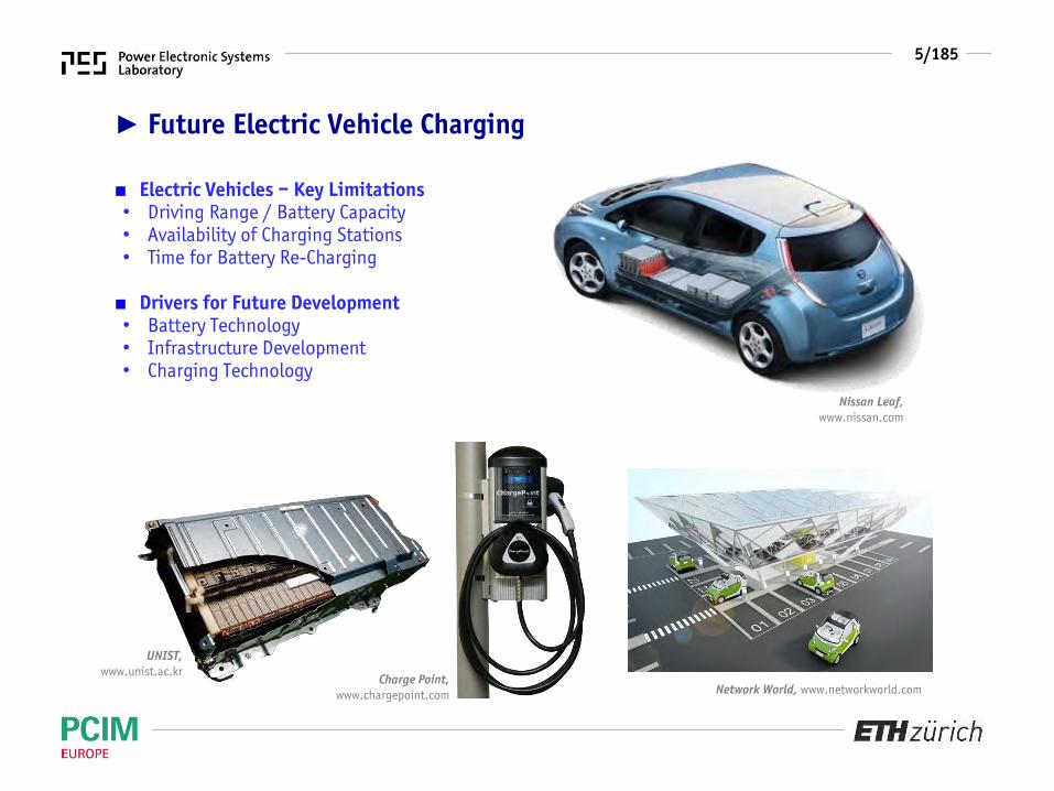
► Future Electric Vehicle Charging
■ Electric Vehicles – Key Limitations• Driving Range / Battery Capacity• Availability of Charging Stations• Time for Battery Re-Charging
■ Drivers for Future Development• Battery Technology• Infrastructure Development• Charging Technology
Nissan Leaf, www.nissan.com
UNIST, www.unist.ac.kr
Charge Point, www.chargepoint.com Network World, www.networkworld.com
6/185
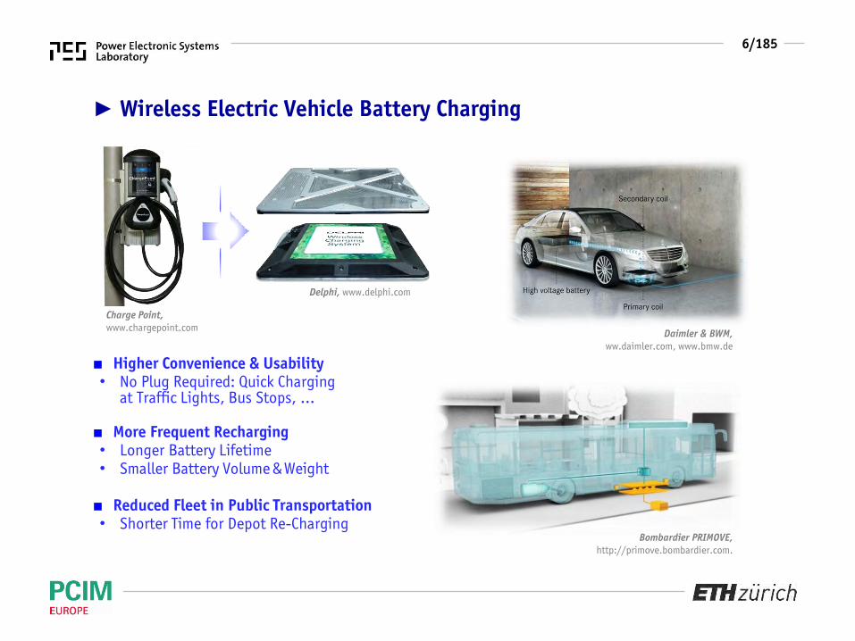
► Wireless Electric Vehicle Battery Charging
■ Higher Convenience & Usability• No Plug Required: Quick Charging
at Traffic Lights, Bus Stops, …
■ More Frequent Recharging• Longer Battery Lifetime• Smaller Battery Volume &Weight
■ Reduced Fleet in Public Transportation• Shorter Time for Depot Re-Charging
Bombardier PRIMOVE, http://primove.bombardier.com.
Delphi, www.delphi.com
Daimler & BWM, ww.daimler.com, www.bmw.de
Charge Point, www.chargepoint.com
7/185
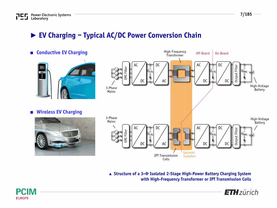
► EV Charging – Typical AC/DC Power Conversion Chain
■ Conductive EV Charging
■ Wireless EV Charging
▲ Structure of a 3-Φ Isolated 2-Stage High-Power Battery Charging Systemwith High-Frequency Transformer or IPT Transmission Coils
8/185
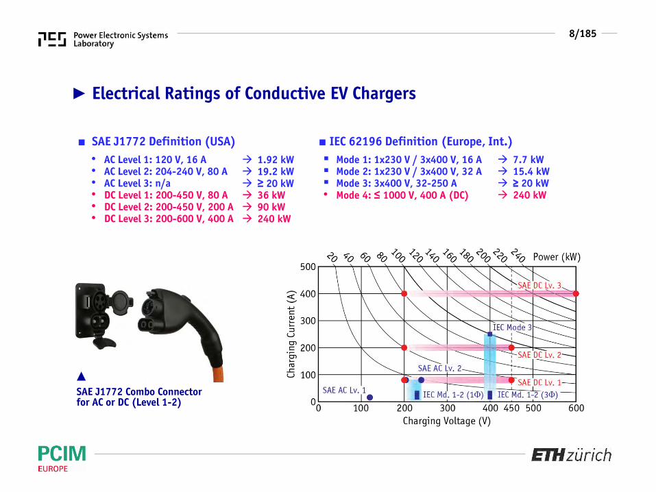
► Electrical Ratings of Conductive EV Chargers
■ SAE J1772 Definition (USA)• AC Level 1: 120 V, 16 A• AC Level 2: 204-240 V, 80 A• AC Level 3: n/a• DC Level 1: 200-450 V, 80 A• DC Level 2: 200-450 V, 200 A• DC Level 3: 200-600 V, 400 A
1.92 kW 19.2 kW ≥ 20 kW 36 kW 90 kW 240 kW
■ IEC 62196 Definition (Europe, Int.) Mode 1: 1x230 V / 3x400 V, 16 A Mode 2: 1x230 V / 3x400 V, 32 A Mode 3: 3x400 V, 32-250 A• Mode 4: ≤ 1000 V, 400 A (DC)
7.7 kW 15.4 kW ≥ 20 kW 240 kW
SAE J1772 Combo Connectorfor AC or DC (Level 1-2)
►
9/185
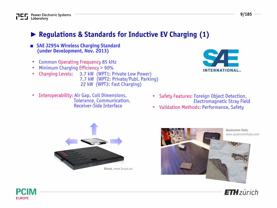
► Regulations & Standards for Inductive EV Charging (1)■ SAE J2954 Wireless Charging Standard
(under Development, Nov. 2013)
• Common Operating Frequency 85 kHz• Minimum Charging Efficiency > 90%• Charging Levels: 3.7 kW (WPT1: Private Low Power)
7.7 kW (WPT2: Private/Publ. Parking)22 kW (WPT3: Fast Charging)
• Interoperability: Air Gap, Coil Dimensions,Tolerance, Communication,Receiver-Side Interface
Brusa, www.brusa.eu
Qualcomm Halo,www.qualcommhalo.com
• Safety Features: Foreign Object Detection,Electromagnetic Stray Field
• Validation Methods: Performance, Safety
10/185
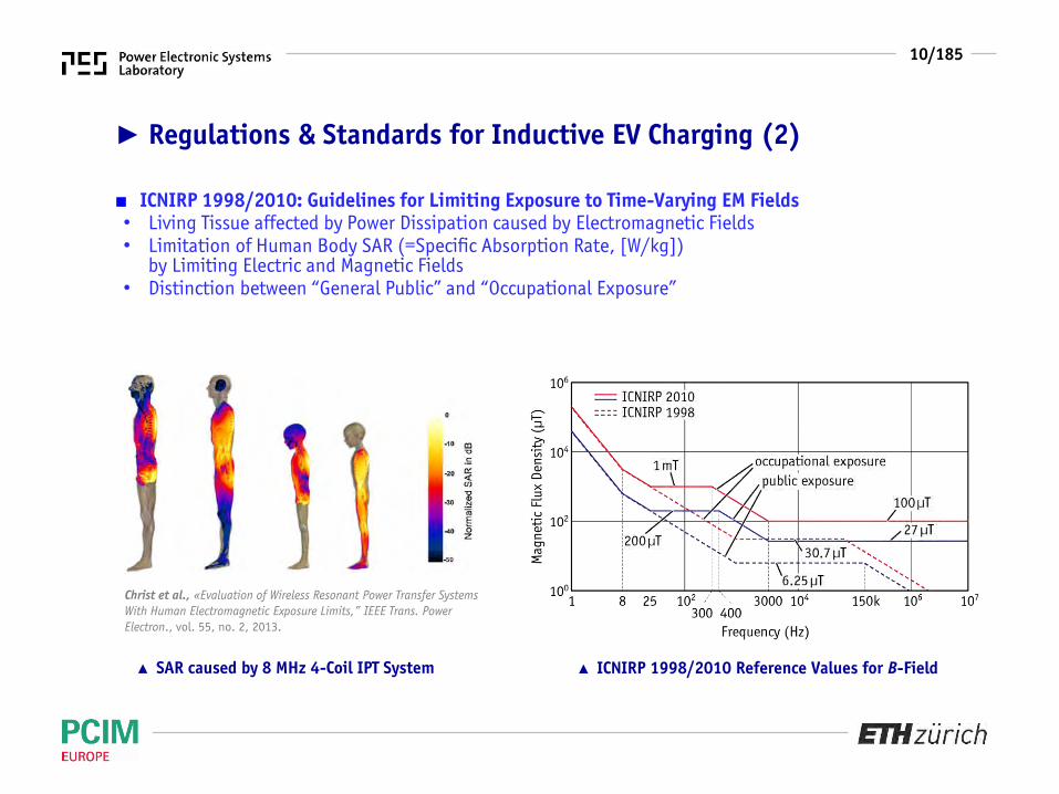
► Regulations & Standards for Inductive EV Charging (2)
■ ICNIRP 1998/2010: Guidelines for Limiting Exposure to Time-Varying EM Fields• Living Tissue affected by Power Dissipation caused by Electromagnetic Fields• Limitation of Human Body SAR (=Specific Absorption Rate, [W/kg])
by Limiting Electric and Magnetic Fields• Distinction between “General Public” and “Occupational Exposure”
Christ et al., «Evaluation of Wireless Resonant Power Transfer Systems With Human Electromagnetic Exposure Limits,” IEEE Trans. Power Electron., vol. 55, no. 2, 2013.
▲ ICNIRP 1998/2010 Reference Values for B-Field▲ SAR caused by 8 MHz 4-Coil IPT System

11/185
► EV Battery Charging: Key Design Challenges■ Conductive Isolated On-Board
EV Battery Charger:• Charging Power 6.1 kW• Efficiency > 95%• Power Density 5 kW/dm3
• Spec. Weight 3.8 kW/kg
Engineering Goal:Design Competitive IPT System
■ High Power Density (kW/dm2, kW/kg)• High Ratio of Coil Diameter / Air Gap• Heavy Shielding & Core Materials
■ Low Magnetic Stray Field Bs < Blim• Limited by Standards (e.g. ICNIRP)• Eddy Current Loss in Surrounding Metals
■ High Magnetic Coupling• Physical Efficiency Limit def. by k• Sensitivity to Coil Misalignment
Lexus, www.lexus.com, 2014
B. Whitaker et al. (APEI),«High-Density, High-Efficiency,Isolated On-Board Vehicle BatteryCharger Utilizing SiC Devices,”IEEE Trans. Power Electron.,vol. 29, no. 5, 2014.

12/185
Realization Examples

13/185
► IPT for Industry Automation Applications
■ Industry Automation & Clean-Room Technology• Automatic Guided & Monorail Transportation Vehicles• Stationary/Dynamic Charging in Closed Environment• Key Features: Wireless, Maintenance-Free, Clean & Safe
▲ Ceiling-Mounted Monorail Transportation System▲ Wireless Powered Floor Surface ConveyorsConductix-Wampfler, www.conductix.ch (1.11.2014),
«Product Overview: Inductive Power Transfer»
14/185
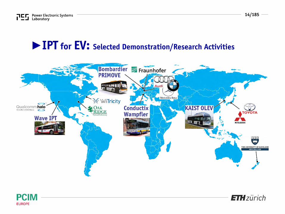
►IPT for EV: Selected Demonstration/Research Activities

15/185
►IPT Public Transportation Systems
Conductix-WampflerIPT Charge
BombardierPRIMOVE
KAISTOn-Line EV
Wave IPT
Location Genoa (IT)Hertogenbosch (NL)
Augsburg, Braunschweig, Mannheim (DE)Lommel (BE)
Seoul, Daejeon,Yeosu, Gumi (KR)
Salt Lake City, McAllenMonterey-Salinas,Lancaster (USA)
Year 2002 - 2012 2010 - 2015 2010 - 2015 2014 - 2015
Air Gap Approx. 4 cm Approx. 4 cm Up to 20 cm Up to 20 cm
Power Up to 60 kW 150-200 kW 3-100 kW 50 kW
Details • Coil Lowered to Groundat Bus Stations
• Charging Efficiency > 90%• ICNIRP 1998 Compliant• 50% Red. Battery Capacity(240120 kWh)
• Coil Lowered to Groundat Bus-Stations
• Reduced Number ofFleet Vehicles
• Extended Battery Life• Lower Total Cost
• Electrified Track forIn-Motion Charging
• ICNIRP 1998 Compl.• 30% Reduced
Battery Weight• Reduced Number of
Fleet Vehicles
• Wireless Charging atBus-Stations withoutLowering the Coil
• Charging Efficiency > 90%• ICNIRP Compliant

16/185
► Historic Background: Medical Applications
■ Electro-Mechanical Heart Assist Devices• Percutaneous Driveline Major Cause of Lethal Infections• Transcutaneous Power Supply for Heart Assist Devices• No Reliable and Medically Certified Solution Exists
O. Knecht, R. Bosshard, and J. W. Kolar,“Optimization of Transcutaneous Energy
Transfer Coils for High Power Medical Applications,” in Proc. Workshop on
Control and Modeling for Power Electron.
(COMPEL), 2014.
J. C. Schuder, “Powering an artificial heart: birth of the inductively coupled-
radio frequency system in 1960,” Artificial Organs, vol. 26, no. 11, pp. 909–915, 2002.
17/185
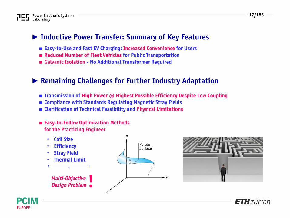
► Inductive Power Transfer: Summary of Key Features
► Remaining Challenges for Further Industry Adaptation
■ Transmission of High Power @ Highest Possible Efficiency Despite Low Coupling■ Compliance with Standards Regulating Magnetic Stray Fields■ Clarification of Technical Feasibility and Physical Limitations
■ Easy-to-Follow Optimization Methodsfor the Practicing Engineer
■ Easy-to-Use and Fast EV Charging: Increased Convenience for Users■ Reduced Number of Fleet Vehicles for Public Transportation■ Galvanic Isolation - No Additional Transformer Required
!
• Coil Size• Efficiency• Stray Field• Thermal Limit
Multi-ObjectiveDesign Problem
18/185
Fundamentals:Isolated DC/DC IPT
Transformer EquivalentSeries Resonant TopologiesZero-Voltage SwitchingInductive Power Transfer

19/185
► Isolated DC/DC-Converter for Conductive EV Charging
■ Soft-Switching DC/DC-Converterwithout Output Inductor
• Galvanic Isolation• Minimum Number of Components• Clamped Voltage across Rectifier
■ Constant Switching Frequency ofFull-Bridge Inverter on Primary
• di/dt given by Voltage Levels& Transformer Stray & Magn. Induct.
▲ Isolated DC/DC Converter Topology with MF Transformer
I. D. Jitaru, «A 3 kW Soft-Switching DC-DC Converter,” Proc. IEEE APEC, pp. 86-92, 2000.
▲ Realization Example (1 kW Module, Rompower)▲ Schematic Converter Waveforms(i1-i2 not to Scale)

20/185
► Transition to IPT System (1)
■ Airgap in the Magnetic Path• Reduced Primary & Secondary Induct.• Higher Magnetizing Current• Reduced Magnetic Coupling k• Load Dependency of Output Voltage
due to Non-Dissipative Inner Resist.
▲ Converter Output Characteristics▲ Schematic Converter Waveformsfor OP1 and OP2 (i1-i2 not to Scale)
v𝐼2,dc =𝑈1,dc
𝑛8𝐿σ𝑓s1 −
𝑈2,dc
𝑈1,dc
2

21/185
► Characterization of the Transformer■ Transformer Differential Equations
■ Measurement of the Three (!) Parameters L1, L2 and M
■ General Equivalent Circuit Diagram
■ Definitions:
𝑢1 = 𝐿1
d𝑖1d𝑡
− 𝑀d𝑖2d𝑡
𝑢2 = 𝑀d𝑖1d𝑡
− 𝐿2
d𝑖2d𝑡
1)
𝐿1 =1
𝜔
𝑈1
𝐼1 𝑖2 = 0
2)
𝐿2 =1
𝜔
𝑈2
𝐼2 𝑖1 = 0
3)
𝑀 =1
𝜔
𝑈2
𝐼1 𝑖2 = 0
𝑢1 𝑡 = 𝐿1 − 𝑀d𝑖1d𝑡
+ 𝑀d
d𝑡𝑖1 − 𝑖2
𝑢2 𝑡 = 𝑀d
d𝑡𝑖1 − 𝑖2 − 𝐿2 − 𝑀
d𝑖2d𝑡
Note: No Explicit Dependencyon N1, N2 (Unknown inGeneral Case)
Coupling Factor 𝑘 =𝑀
𝐿1𝐿2, Stray Factor σ = 1 – k2
Ideal: k = 1, σ = 0.

22/185
► Transformer Equivalent Circuits (1)■ Introduction of a General Transformation Ratio n
• 4 Degrees of Freedom (Lσ1, Lσ2, Lh, n), butonly 3 Transformer Parameters (L1, L2, M)
• Assume n as given and Calculate RemainingParameters (Lσ1, Lσ2, Lh)
■ Simplified Circuit Diagrams for Specific Values of n

23/185
► Transformer Equivalent Circuits (2)■ Direct Measurement of Transformer Equivalent Circuit Parameters
■ Measurement 1: Secondary-Side Terminals Shorted
■ Measurement 2: Secondary-Side Terminals Open
■ Measurement 3: Primary-Side Terminals Open
𝐿σ =1
𝜔
𝑈1
𝐼1 𝑢2 = 0
𝐿1 =1
𝜔
𝑈1
𝐼1 𝑖2 = 0
𝐿h = 𝐿1 − 𝐿σ
𝑛 = 𝑈1
𝑈2 𝑖1 = 0
24/185
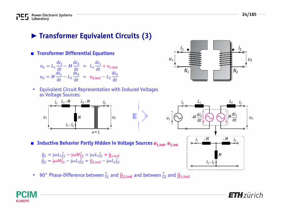
► Transformer Equivalent Circuits (3)
■ Transformer Differential Equations
• Equivalent Circuit Representation with Induced Voltagesas Voltage Sources:
■ Inductive Behavior Partly Hidden in Voltage Sources u1,ind, u2,ind
• 90° Phase-Difference between 𝑖1 and 𝑢2,ind and between 𝑖2 and 𝑢1,ind
𝑢1 = 𝐿1
d𝑖1d𝑡
− 𝑀d𝑖2d𝑡
= 𝐿1
d𝑖1d𝑡
+ 𝑢1,ind
𝑢2 = 𝑀d𝑖1d𝑡
− 𝐿2
d𝑖2d𝑡
= 𝑢2,ind − 𝐿2
d𝑖2d𝑡
𝑢1 = j𝜔𝐿1 𝑖1 − j𝜔𝑀 𝑖2 = j𝜔𝐿1
𝑖1 + 𝑢1,ind
𝑢2 = j𝜔𝑀 𝑖1 − j𝜔𝐿2 𝑖2 = 𝑢2,ind − j𝜔𝐿2
𝑖2

25/185
► Transition to IPT System (2)
■ Airgap in the Magnetic Path• Reduced Primary & Secondary Induct.• Higher Magnetizing Current• Reduced Magnetic Coupling k• Load Dependency of Output Voltage
due to Non-Dissipative Inner Resist.
▲ Effects of an Air Gap in the Transformer▲ Schematic Converter Waveformsfor OP1 and OP2 (i1-i2 not to Scale)
uLσ
𝑳𝛔 = 𝟏 − 𝒌𝟐 𝑳𝟏, 𝑳𝐡 = 𝒌𝟐𝑳𝟏, 𝒏 = 𝒌 𝑳𝟏/𝑳𝟐

26/185
▲ Converter Output Characteristics
uLσuLσ
► Transition to IPT System (3)
■ Airgap in the Magnetic Path• Reduced Primary & Secondary Induct.• Higher Magnetizing Current• Reduced Magnetic Coupling k• Load Dependency of Output Voltage
due to Non-Dissipative Inner Resist.
▲ Effects of an Air Gap in the Transformer𝑳𝛔 = 𝟏 − 𝒌𝟐 𝑳𝟏, 𝑳𝐡 = 𝒌𝟐𝑳𝟏, 𝒏 = 𝒌 𝑳𝟏/𝑳𝟐

27/185
► Resonant Compensation of Stray Inductance (1)
𝒁𝐬 = 𝐣𝝎𝑳𝐬 +𝟏
𝐣𝝎𝑪𝐬+ 𝑹𝒂𝒄 = 𝐣(𝝎𝑳𝐬 −
𝟏
𝝎𝑪𝐬)
≈ 𝟎
𝒁𝐬: Cap. 𝒁𝐬 = 𝟎 𝒁𝐬: Ind.
𝒁𝐬𝒁𝐬𝒁𝐬
𝝎 = 𝝎𝐬 𝝎 = 𝝎𝐬 𝝎 = 𝝎𝐬
𝑪𝐬 < 𝑪𝐬,𝐨𝐩𝐭 𝑪𝐬 = 𝑪𝐬,𝐨𝐩𝐭 𝑪𝐬 > 𝑪𝐬,𝐨𝐩𝐭
𝝎𝐬 =𝟏
𝑳𝐬𝑪𝐬
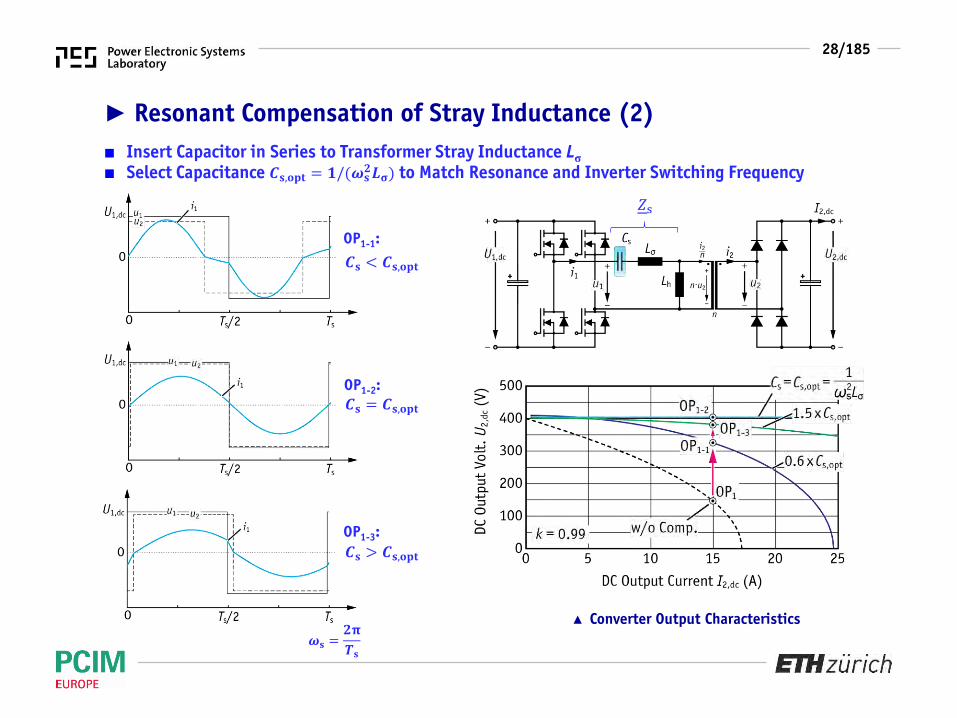
28/185
► Resonant Compensation of Stray Inductance (2)■ Insert Capacitor in Series to Transformer Stray Inductance Lσ■ Select Capacitance 𝑪𝐬,𝐨𝐩𝐭 = 𝟏/(𝝎𝐬
𝟐𝑳𝛔) to Match Resonance and Inverter Switching Frequency
▲ Converter Output Characteristics
𝑪𝐬 < 𝑪𝐬,𝐨𝐩𝐭
𝑪𝐬 = 𝑪𝐬,𝐨𝐩𝐭
𝑪𝐬 > 𝑪𝐬,𝐨𝐩𝐭
OP1-1:
OP1-2:
OP1-3:
𝝎𝐬 =𝟐𝛑
𝑻𝐬
𝑍s

29/185
► Resonant Compensation of Stray Inductance (3)■ Insert Capacitor in Series to Transformer Stray Inductance Lσ■ Select Capacitance 𝑪𝐬,𝐨𝐩𝐭 = 𝟏/(𝝎𝐬
𝟐𝑳𝛔) to Match Resonance and Inverter Switching Frequency
𝑪𝐬 < 𝑪𝐬,𝐨𝐩𝐭
𝑪𝐬 = 𝑪𝐬,𝐨𝐩𝐭
𝑪𝐬 > 𝑪𝐬,𝐨𝐩𝐭
▲ Bode Diagram for Different Selectionsof the Compensation Capacitance Cs
OP1-1:
OP1-2:
OP1-3:
𝑅ac ≈ 0
𝝎𝐬 =𝟐𝛑
𝑻𝐬
𝒁𝐬
30/185
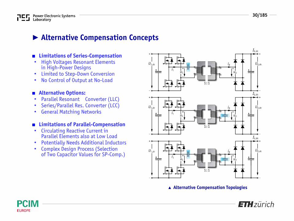
► Alternative Compensation Concepts
■ Limitations of Series-Compensation• High Voltages Resonant Elements
in High-Power Designs• Limited to Step-Down Conversion• No Control of Output at No-Load
■ Alternative Options:• Parallel Resonant Converter (LLC)• Series/Parallel Res. Converter (LCC)• General Matching Networks
■ Limitations of Parallel-Compensation• Circulating Reactive Current in
Parallel Elements also at Low Load• Potentially Needs Additional Inductors• Complex Design Process (Selection
of Two Capacitor Values for SP-Comp.)
▲ Alternative Compensation Topologies

31/185
► Fundamental Frequency Approximation (1)■ Nearly Sinusoidal Current Shape Despite Rectangular Voltage Waveforms• Resonant Circuit Acts as Bandpass-Filter on Inverter Output Voltage Spectrum
■ Consider only Switching Frequency Components:• Fundamentals of u1, u2, i1, i2• Power Transfer Modeled with Good Accuracy
as
Fundamental Frequency Model!
𝑃 =
𝑛=1
∞
𝑈1(𝑛)𝐼1(𝑛) cos 𝜙𝑛
≈ 𝑈1(1)𝐼1(1) cos 𝜙1

32/185
► Fundamental Frequency Approximation (2)■ Replace Rectifier and Load I2,dc by Power Equivalent Resistance RL,eq
■ Fundamental Frequency Equivalent Circuit
𝑅L,eq = 𝑈2(1)
𝐼2(1)
≈
4π 𝑈2,dc
π2 𝐼2,dc
=8
π2
𝑈2,dc2
𝑃2
𝑈1(1) =4
π𝑈1,dc
• Simplified Circuit Analysis & ApproximatePower Loss Calculations
R. Steigerwald, “A comparison of half-bridge resonant converter topologies,”
in IEEE Trans. Power Electron.,vol. 3, no. 2, 1988.

33/185
► Resonant Circuit Transfer Characteristics (1)■ Load-Independent Output Voltage due to Series Resonant Compensation• Except for a (Small) Voltage Drop on Winding Resistances R1,R2
■ Close to Ohmic Input Impedancedue to Large Mutual Inductance
• Necessary Condition for MinimumInput Current Max. Efficiency!
▲ Voltage Transfer Ratio at k = 0.99
𝑍s = 0𝝎 = 𝝎𝐬
𝑍in
34/185
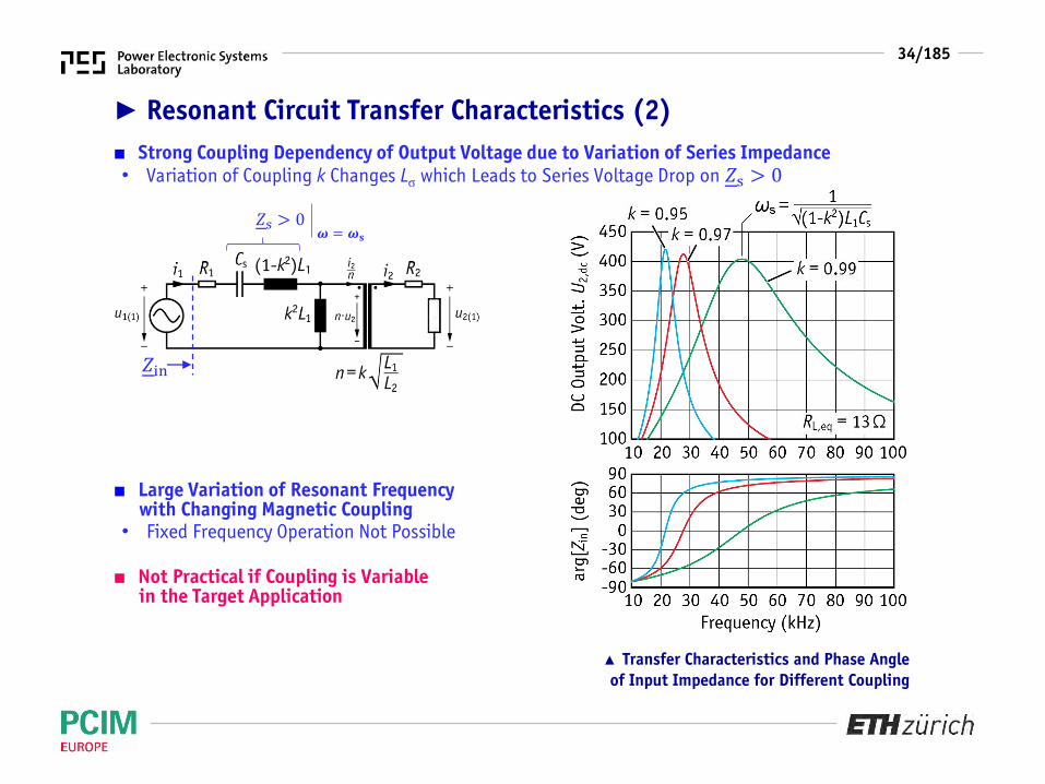
► Resonant Circuit Transfer Characteristics (2)■ Strong Coupling Dependency of Output Voltage due to Variation of Series Impedance• Variation of Coupling k Changes Lσ which Leads to Series Voltage Drop on 𝑍s > 0
■ Large Variation of Resonant Frequencywith Changing Magnetic Coupling
• Fixed Frequency Operation Not Possible
■ Not Practical if Coupling is Variablein the Target Application
▲ Transfer Characteristics and Phase Angleof Input Impedance for Different Coupling
𝑍s > 0𝝎 = 𝝎𝐬
𝑍in
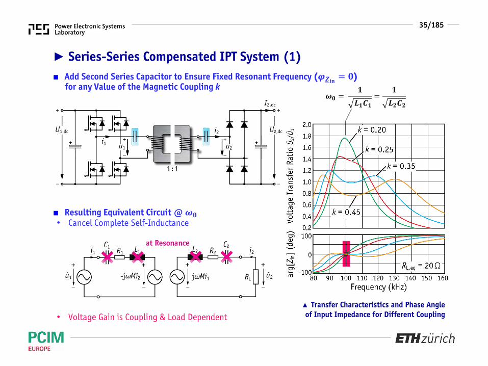
35/185
► Series-Series Compensated IPT System (1)■ Add Second Series Capacitor to Ensure Fixed Resonant Frequency (𝝋𝒁𝐢𝐧
= 𝟎)for any Value of the Magnetic Coupling k
■ Resulting Equivalent Circuit @ 𝝎𝟎• Cancel Complete Self-Inductance
• Voltage Gain is Coupling & Load Dependent▲ Transfer Characteristics and Phase Angleof Input Impedance for Different Coupling
𝝎𝟎 =𝟏
𝑳𝟏𝑪𝟏
=𝟏
𝑳𝟐𝑪𝟐

36/185
► Series-Series Compensated IPT System (2)■ Resonant Frequency (𝝋𝒁𝐢𝐧
= 𝟎) is Indepenent of Magnetic Coupling and of Load• Necessary Condition for Minimum Input Current Max. Efficiency!
■ Resulting Equivalent Circuit @ 𝝎𝟎• Cancel Complete Self-Inductance
• Voltage Gain is Coupling & Load Dependent
▲ Transfer Characteristics and Phase Angleof Input Impedance for Different Loads
𝝎𝟎
𝟏 − 𝒌
𝝎𝟎 =𝟏
𝑳𝟏𝑪𝟏
=𝟏
𝑳𝟐𝑪𝟐

37/185
► Properties of the Series-Series Compensation (1)■ Operation at Resonant Frequency 𝝎𝐬 =
𝝎𝟎
𝟏 − 𝒌
▲ Output Voltage Û2 is Indepndentof Load Resistance at 𝝎𝐬𝑪𝟐
′ =𝑪𝟐
𝒏𝟐= 𝑪𝒔
𝑳𝟐
𝑳𝟏
𝝎𝐬𝟏𝟐 =
𝟏
𝑪𝟏𝑳𝟏(𝟏 − 𝒌)
𝝎𝐬𝟐𝟐 =
𝟏
𝑪𝟐𝑳𝟐(𝟏 − 𝒌)
𝝎𝐬 =𝝎𝟎
𝟏 − 𝒌
𝒖𝟐 = 𝒖𝟏
𝑳𝟐
𝑳𝟏
■ Load-Independent Output Voltage• Still Coupling Dependent• Inductive Input Impedance

38/185
► Properties of the Series-Series Compensation (2)■ Operation at Resonant Frequency 𝝎𝟎 =
𝟏
𝑳𝟏𝑪𝟏
=𝟏
𝑳𝟐𝑪𝟐
▲ Phase Angle of Input Impedance for VaryingLoad (top) and Coupling (bot.)
𝒁𝐢𝐧 = −𝐣𝝎𝟎𝑴 +𝐣𝝎𝟎𝑴 ⋅ 𝑹𝐋,𝐞𝐪 − 𝐣𝝎𝟎𝑴
𝐣𝝎𝟎𝑴 + 𝑹𝐋,𝐞𝐪 − 𝐣𝝎𝟎𝑴
■ Purely Ohmic Input ImpedanceFor any Load & Coupling𝒁𝐢𝐧 =
𝝎𝟎𝟐𝑴𝟐
𝑹𝐋,𝐞𝐪 𝒌 = 𝟎 → 𝒁𝐢𝐧 = 𝟎
𝑹𝐋,𝐞𝐪 = 𝟎 → 𝒁𝐢𝐧 = ∞
𝐚𝐫𝐠 𝒁𝐢𝐧 = 𝟎
39/185
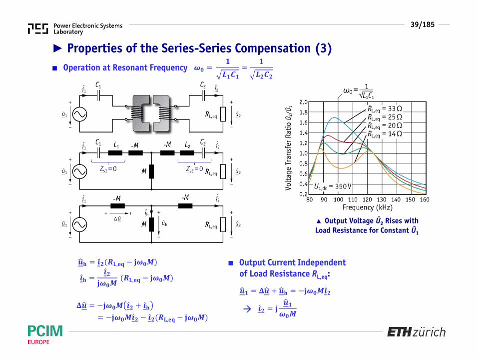
► Properties of the Series-Series Compensation (3)■ Operation at Resonant Frequency 𝝎𝟎 =
𝟏
𝑳𝟏𝑪𝟏
=𝟏
𝑳𝟐𝑪𝟐
▲ Output Voltage Û2 Rises withLoad Resistance for Constant Û1
𝒖𝐡 = 𝒊𝟐(𝑹𝐋,𝐞𝐪 − 𝐣𝝎𝟎𝑴) ■ Output Current Independentof Load Resistance RL,eq: 𝒊𝐡 =
𝒊𝟐
𝐣𝝎𝟎𝑴(𝑹𝐋,𝐞𝐪 − 𝐣𝝎𝟎𝑴)
𝚫 𝒖 = −𝐣𝝎𝟎𝑴 𝒊𝟐 + 𝒊𝐡
= −𝐣𝝎𝟎𝑴 𝒊𝟐 − 𝒊𝟐(𝑹𝐋,𝐞𝐪 − 𝐣𝝎𝟎𝑴)
𝒖𝟏 = 𝚫 𝒖 + 𝒖𝐡 = −𝐣𝝎𝟎𝑴 𝒊𝟐
𝒊𝟐 = 𝐣 𝒖𝟏
𝝎𝟎𝑴
40/185
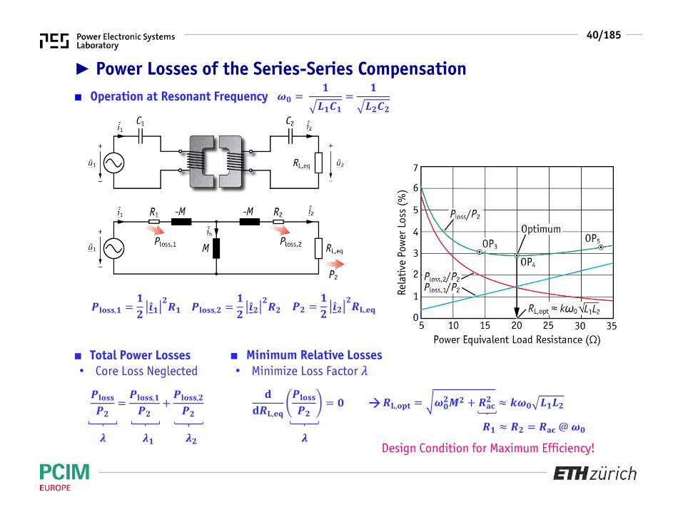
► Power Losses of the Series-Series Compensation■ Operation at Resonant Frequency 𝝎𝟎 =
𝟏
𝑳𝟏𝑪𝟏
=𝟏
𝑳𝟐𝑪𝟐
𝑷𝐥𝐨𝐬𝐬,𝟏 =𝟏
𝟐 𝒊𝟏
𝟐𝑹𝟏 𝑷𝐥𝐨𝐬𝐬,𝟐 =
𝟏
𝟐 𝒊𝟐
𝟐𝑹𝟐 𝑷𝟐 =
𝟏
𝟐 𝒊𝟐
𝟐𝑹𝐋,𝐞𝐪
𝑷𝐥𝐨𝐬𝐬
𝑷𝟐=
𝑷𝐥𝐨𝐬𝐬,𝟏
𝑷𝟐+
𝑷𝐥𝐨𝐬𝐬,𝟐
𝑷𝟐
𝝀 𝝀𝟏 𝝀𝟐
■ Total Power Losses• Core Loss Neglected
■ Minimum Relative Losses• Minimize Loss Factor 𝜆
𝑹𝐋,𝐨𝐩𝐭 = 𝝎𝟎𝟐𝑴𝟐 + 𝑹𝐚𝐜
𝟐 ≈ 𝒌𝝎𝟎 𝑳𝟏𝑳𝟐
𝐝
𝐝𝑹𝐋,𝐞𝐪
𝑷𝐥𝐨𝐬𝐬
𝑷𝟐= 𝟎
𝝀Design Condition for Maximum Efficiency!
𝑹𝟏 ≈ 𝑹𝟐 = 𝑹𝐚𝐜 @ 𝝎𝟎

41/185
► Series-Series Comp. for Maximum Efficiency■ Current 𝑰𝟐 Constant Indep. of 𝑹𝐋,𝐞𝐪: Current Source Characteristic @ Resonance
OP3
OP4
OP5

42/185
► Efficiency Limit of IPT Systems
■ Condition for Minimum Total Coil Losses: 𝑹𝐋,𝐨𝐩𝐭 ≈ 𝒌𝝎𝟎 𝑳𝟏𝑳𝟐
■ Efficiency Limit of IPT Systems
Figure-of-Merit = 𝒌 𝑸𝟏𝑸𝟐 = 𝒌𝑸
K. van Schuylenbergh andR. Puers, Inductive Powering:
Basic Theory and Application to Biomedical Systems, 1st ed.,
Springer-Verlag, 2009.
𝜼𝐦𝐚𝐱 =𝒌𝟐𝑸𝟏𝑸𝟐
𝟏 + 𝟏 + 𝒌𝟐𝑸𝟏𝑸𝟐
𝟐
𝑘 = 𝐿h/ 𝐿1𝐿2 …. Magnetic Coupling 𝑄 = 𝜔𝐿/𝑅ac …. Coil Quality Factor
▲ Efficiency Limit of IPT Systems(Coil Losses Only, Core Neglected)

43/185
► FOM = Quality Factor x Magnetic Coupling
■ «Highly Resonant Wireless Power Transfer»• Operation of «High-Q Coils» at Self-Resonance• Compensation of Low k with High Q:
High Freedom-of-Position• High Frequency Operation (kHz ... MHz)
■ Intelligent Parking Assistants for EV• Maximize k by Perfect Positioning• Camera-Assisted Positioning Guide• Achieve up to 5 cm Parking Accuracy
WiTricity, www.witricity.com (13.11.2014).Toyota, www.toyota.com, (18.11.2014).
44/185
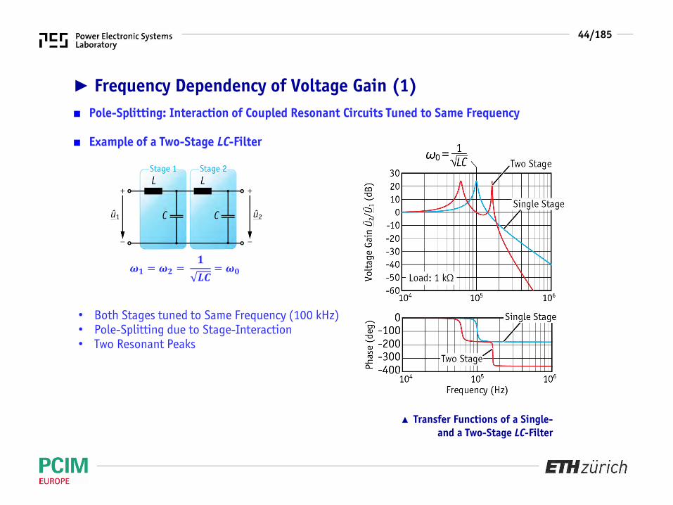
► Frequency Dependency of Voltage Gain (1)■ Pole-Splitting: Interaction of Coupled Resonant Circuits Tuned to Same Frequency
■ Example of a Two-Stage LC-Filter
• Both Stages tuned to Same Frequency (100 kHz)• Pole-Splitting due to Stage-Interaction• Two Resonant Peaks
▲ Transfer Functions of a Single-and a Two-Stage LC-Filter
𝝎𝟏 = 𝝎𝟐 =𝟏
𝑳𝑪= 𝝎𝟎
45/185
► Frequency Dependency of Voltage Gain (2)■ Example of SS-Compensated IPT System
■ Pole Splitting due to Interaction ofTransmitter & Receiver Resonant Circuit
• Magnetic Coupling Determines the Strength ofTransmitter/Receiver Interaction
• Non-Monotonic Phase Behavior May Lead to Hard-Switching
■ Can be Avoided by Design with ModifiedDesign Rule for Receiver Reactance:
• Loss-Increase Typically below 5%• Inductive Behavior Ensured for 𝜔sw > 𝜔0
𝝎𝟏 = 𝝎𝟐 =𝟏
𝑳𝑪= 𝝎𝟎
▲ Voltage Transfer Functions and Phase ofInput Impedance of an IPT System
𝑹𝐋
𝝎𝟎 𝑳𝟏𝑳𝟐 𝐬𝐮𝐛𝐨𝐩𝐭
≈ 𝟕𝟎. . 𝟖𝟎% ⋅ 𝒌𝐦𝐚𝐱

46/185
► High Efficiency Operation of Inverter Stage (1)
■ Zero-Voltage Switching• Sufficient Load-Current to
(Dis-) Charge Charge-EquivalentMOSFET Capacitance
▲ Phase Angle of Input Impedancefor Different Loads
hard
hard
OFF
ON
OFF
ON
ZVS
ZVSZCS
𝝎𝐬𝐰 < 𝝎𝐫𝐞𝐬
𝝎𝐬𝐰 > 𝝎𝐫𝐞𝐬
𝝎𝐫𝐞𝐬 𝝎𝐬𝐰 = 𝝎𝐫𝐞𝐬 + 𝚫𝝎𝐙𝐕𝐒

47/185
► High Efficiency Operation of Inverter Stage (2)
■ Zero-Voltage Switching• Sufficient Load-Current to
(Dis-) Charge Charge-EquivalentMOSFET Capacitance CQeq
• CQeq Differs Significantly fromEnergy Eq. Capacitance CEeq
▲ Typical Datasheet Values of a Power MOSFET (Infineon)
𝑪𝑸𝐞𝐪 =𝑸(𝑼𝟏,𝐝𝐜)
𝑼𝟏,𝐝𝐜=
𝟎
𝑼𝟏,𝐝𝐜 𝑪 𝒗 𝐝𝒗
𝑼𝟏,𝐝𝐜,
𝑪𝑬𝒆𝒒 =𝑬(𝑼𝟏,𝐝𝐜)
𝟏𝟐
𝑼𝟏,𝐝𝐜𝟐
= 𝟎
𝑼𝟏,𝐝𝐜 𝒗 ⋅ 𝑪 𝒗 𝒅𝒗
𝟏𝟐
𝑼𝟏,𝐝𝐜𝟐
48/185
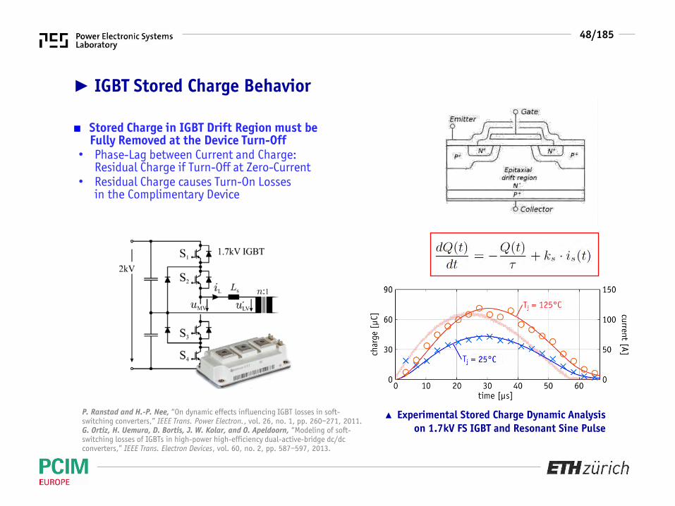
► IGBT Stored Charge Behavior
■ Stored Charge in IGBT Drift Region must beFully Removed at the Device Turn-Off
• Phase-Lag between Current and Charge:Residual Charge if Turn-Off at Zero-Current
• Residual Charge causes Turn-On Lossesin the Complimentary Device
▲ Experimental Stored Charge Dynamic Analysison 1.7kV FS IGBT and Resonant Sine Pulse
P. Ranstad and H.-P. Nee, “On dynamic effects influencing IGBT losses in soft-switching converters,” IEEE Trans. Power Electron., vol. 26, no. 1, pp. 260–271, 2011.G. Ortiz, H. Uemura, D. Bortis, J. W. Kolar, and O. Apeldoorn, “Modeling of soft-switching losses of IGBTs in high-power high-efficiency dual-active-bridge dc/dc converters,” IEEE Trans. Electron Devices, vol. 60, no. 2, pp. 587–597, 2013.
49/185
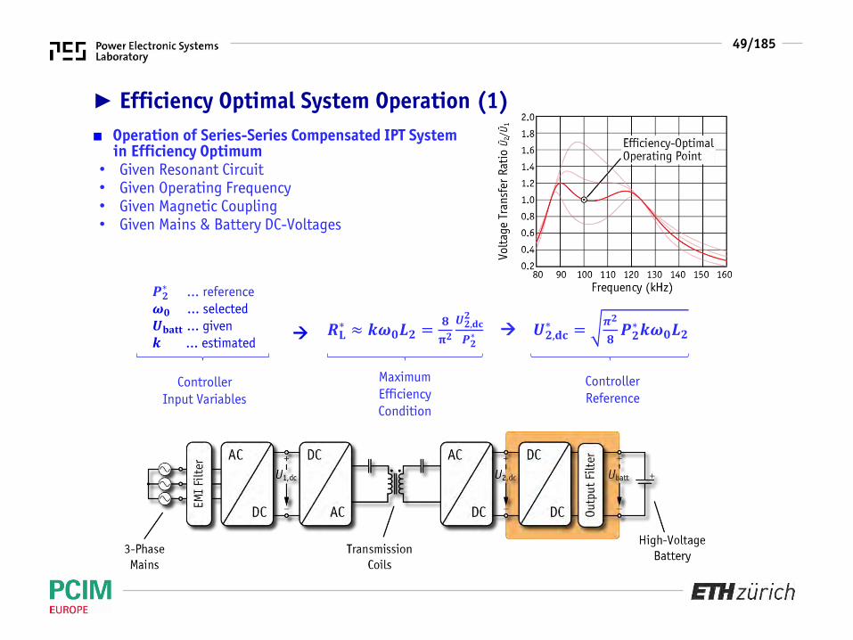
► Efficiency Optimal System Operation (1)■ Operation of Series-Series Compensated IPT System
in Efficiency Optimum• Given Resonant Circuit• Given Operating Frequency• Given Magnetic Coupling• Given Mains & Battery DC-Voltages
𝑹𝐋∗ ≈ 𝒌𝝎𝟎𝑳𝟐 =
𝟖
𝛑𝟐
𝑼𝟐,𝐝𝐜𝟐
𝑷𝟐∗ 𝑼𝟐,𝐝𝐜
∗ =𝝅𝟐
𝟖𝑷𝟐
∗𝒌𝝎𝟎𝑳𝟐
MaximumEfficiencyCondition
ControllerReference
𝑷𝟐∗ … reference
𝝎𝟎 … selected𝑼𝐛𝐚𝐭𝐭 … given𝒌 … estimated
ControllerInput Variables

50/185
► Receiver Electronics – Potential Solutions (1)■ Regulation of Receiver-Side DC-Link Voltage with DC/DC Converter
■ Prototype SiC-Converter for50kW IPT (Receiver Side)
• Efficiency 98%, 9.2kW/dm3
51/185
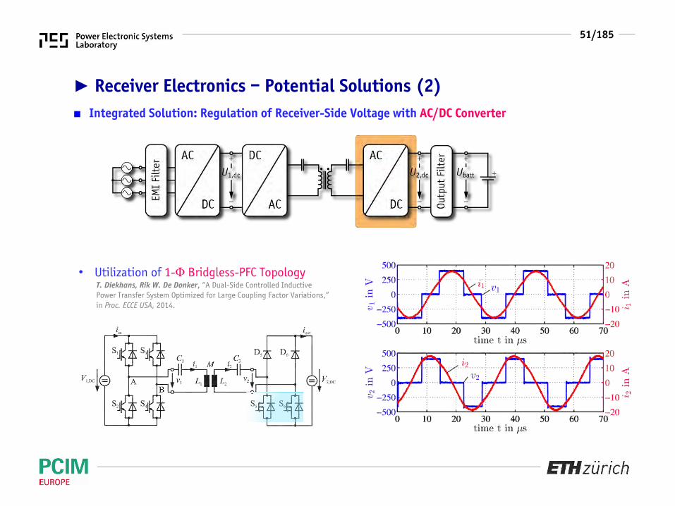
► Receiver Electronics – Potential Solutions (2)■ Integrated Solution: Regulation of Receiver-Side Voltage with AC/DC Converter
• Utilization of 1-Φ Bridgless-PFC TopologyT. Diekhans, Rik W. De Donker, “A Dual-Side Controlled Inductive Power Transfer System Optimized for Large Coupling Factor Variations,”in Proc. ECCE USA, 2014.

52/185
► Control Diagram for Efficiency Optimal Operation
𝑹𝐋∗ ≈ 𝒌𝝎𝟎𝑳𝟐 =
𝟖
𝛑𝟐
𝑼𝟐,𝐝𝐜𝟐
𝑷𝟐∗ 𝑼𝟐,𝐝𝐜
∗ =𝝅𝟐
𝟖𝑷𝟐
∗𝒌𝝎𝟎𝑳𝟐
MaximumEfficiencyCondition
ControllerReference
𝑷𝟐∗ … reference
𝝎𝟎 … selected𝑼𝐛𝐚𝐭𝐭 … given𝒌 … estimated
ControllerInput Variables
Voltage Step-Up or Step-Down

53/185
► Transmitter Electronics – Potential Solutions (1)
■ Receiver Voltage U2,dc used for Optimal Load Matching Power Regulation by Adjustment of U1,dc using Characteristic
■ 1st Option: Cascaded AC/DC, DC/DC Conversion
■ Transmitter-Side DC/DC Converter• No Isolation Needed• Identical to Receiver-Side?
■ 3-Phase Mains Interface (Boost-Type)• Power Factor Correction of Phase Current• Standard Solutions Exist in Industry
𝑃2 =8
π2
𝑈1,dc ⋅ 𝑈2,dc
𝜔0𝑘 𝐿1𝐿2
54/185
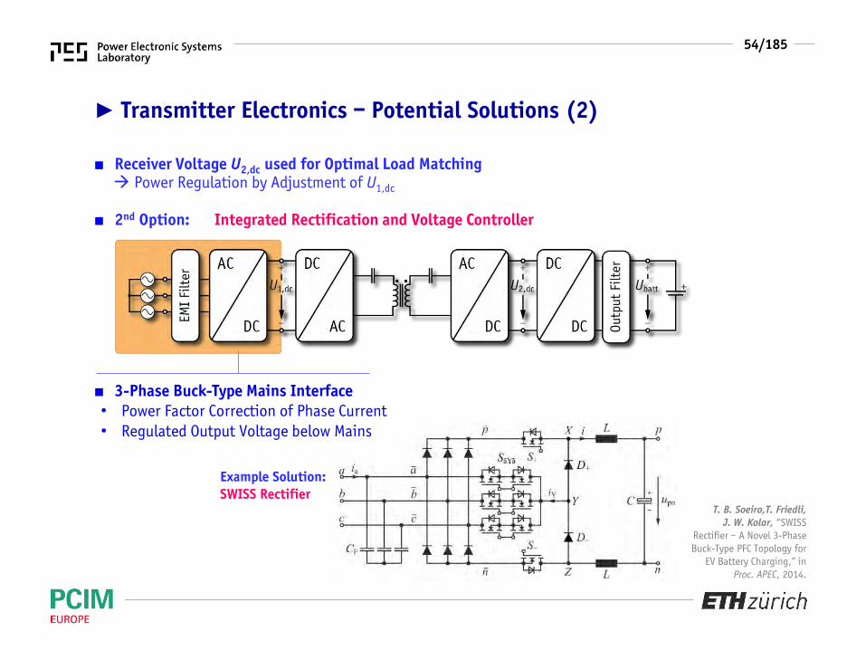
► Transmitter Electronics – Potential Solutions (2)
■ Receiver Voltage U2,dc used for Optimal Load Matching Power Regulation by Adjustment of U1,dc
■ 2nd Option: Integrated Rectification and Voltage Controller
■ 3-Phase Buck-Type Mains Interface• Power Factor Correction of Phase Current• Regulated Output Voltage below Mains
T. B. Soeiro,T. Friedli,J. W. Kolar, “SWISS
Rectifier – A Novel 3-Phase Buck-Type PFC Topology for
EV Battery Charging,” in Proc. APEC, 2014.
Example Solution:SWISS Rectifier

55/185
► Alternative Control Concepts for Series Resonant Converters
■ Degrees-of-Freedom for the Control• Inverter Switching Frequency• Duty Cycle of Inverter Output Voltage• DC-Link Voltage (with Front-End DC/DC Conv.)
■ Common Control Concepts• I) Frequency Control @ Fixed Duty Cycle• II) Duty Cycle Control @ Fixed Frequency• III) Combined Duty Cycle & Frequency Control
▲ Increase of Switching Frequency Above ResonantFrequency adds Series Voltage Drop
I)
II)
III)
Fixed Phase-Diff.for Ensuring ZVS

56/185
► Frequency Control @ Fixed Duty Cycle
■ Control Switching Frequency of InverterStage to Regulate Output Power
• Switching above Resonant PointReduces Transmitted Output Power
■ Main Disadvantages:• Operation Requires Reactive Power• Increased RMS-Current in Transmitter Coil• Large Frequency Variation• Operation at Efficiency Optimum Only
at Maximum Output Power
▲ Operating Points shown on Resonant Curves
▲ Increase of Switching Frequency Above ResonantFrequency adds Series Voltage Drop

57/185
► Self-Oscillating (or Dual) Control Method■ Dual Control of Phase-Shift and Frequency• Reduced Amplitude of Voltage Fundamental• Smaller Frequency Variation• Guaranteed ZCS/ZVS-Operation with
Appropriately Selected αZVS
■ Main Disadvantages:• Operation Requires Reactive Power• Increased RMS-Current in Transmitter Coil
CurrentZero-Crossing
J. A. Sabate, M. M. Jovanovic, F. C. Lee, andR. T. Gean, “Analysis and design-optimization of LCC resonant inverter for high-frequency AC distributed power system,” in IEEE Trans. Ind. Electron., vol. 42, no. 1, pp. 63–71, 1995.

58/185
► Comparison of Control Methods (1)■ Frequency Control Methods have (almost) Load-Independent Transmitter Current
■ Reduction in Transmitter Current I1Leads to Over-All Loss ReductionDespite Increased I2 due to Lower U2,dc
■ Large Reduction of Power Lossesin Partial-Load Condition with VC
• Reduced Transmitter-Coil RMS-Current• Decreasing instead of Constant I2R
Losses in Coils/Caps/Switches
VC … DC-Link Voltage Control(Optimal Load Matching)
FC … Frequency ControlDC … Dual/Self-Osc. Control
R. Bosshard, J. W. Kolar and B. Wunsch, “Control Method for Inductive Power Transfer with High
Partial-Load Efficiency and Resonance Tracking,”IEEE IPEC/ECCE Asia, 2014.
▲ For 5 kW IPT Prototype Presented Later

59/185
► Comparison of Control Methods (2)■ Frequency Control Methods have (almost) Load-Independent Transmitter Current
■ Large Reduction of Power Lossesin Partial-Load Condition with VC
• Reduced Transmitter-Coil RMS-Current• Decreasing instead of Constant I2R
Losses in Coils/Caps/Switches
■ Extremely Flat Efficiency Curveeven at Low Output Power forVoltage Control Method withOptimum Load Matching
VC … DC-Link Voltage ControlFC … Frequency ControlDC … Dual/Self-Osc. Control
R. Bosshard, J. W. Kolar and B. Wunsch, “Control Method for Inductive Power Transfer with High
Partial-Load Efficiency and Resonance Tracking,”IEEE IPEC/ECCE Asia, 2014.
▲ For 5 kW IPT Prototype (Shown in Later Sections)

60/185
Components Modeling &Multi-Objective System
Optimization

61/185
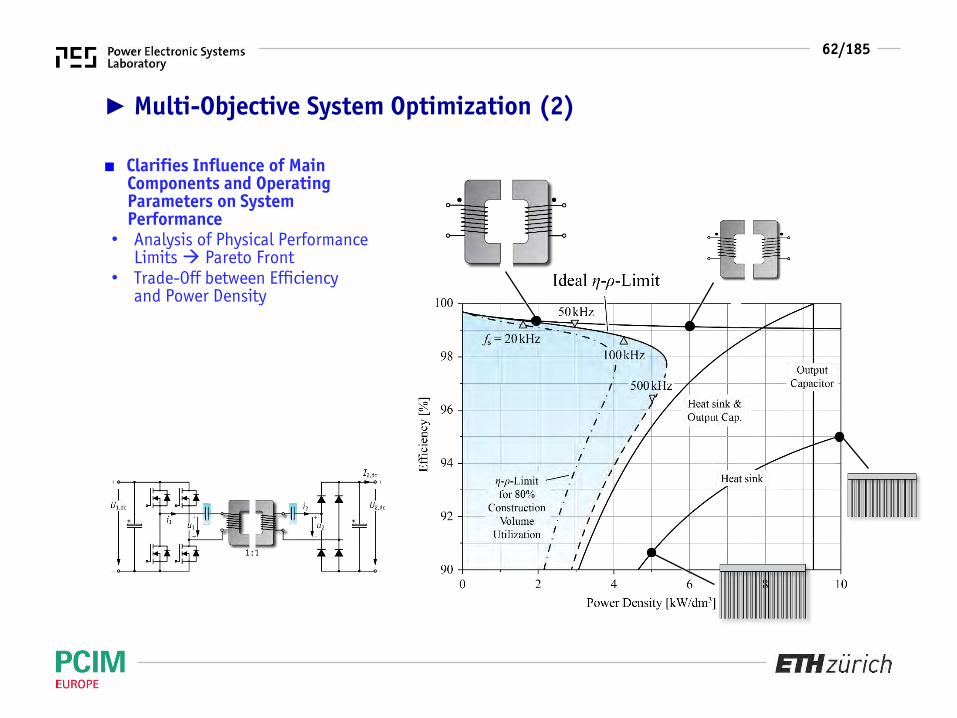
► Multi-Objective System Optimization (2)■ Mapping of System Design Space into System Performance Space• Requires Accurate Models for All Main System Components• Allows Sensitivity & Trade-Off Analysis
62/185
► Multi-Objective System Optimization (2)
■ Clarifies Influence of MainComponents and OperatingParameters on SystemPerformance
• Analysis of Physical PerformanceLimits Pareto Front
• Trade-Off between Efficiencyand Power Density

63/185
System Components andDesign Considerations
Coil ModelingResonant CapacitorsMagnetic Shielding
64/185
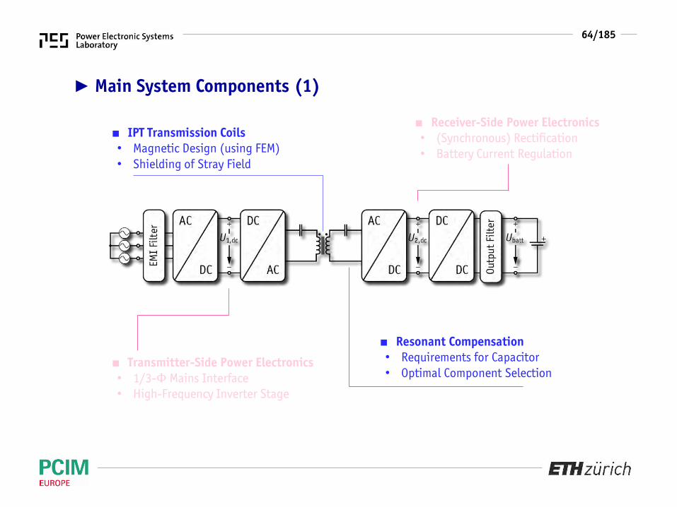
► Main System Components (1)
■ Receiver-Side Power Electronics• (Synchronous) Rectification• Battery Current Regulation
■ Transmitter-Side Power Electronics• 1/3-Φ Mains Interface• High-Frequency Inverter Stage
■ IPT Transmission Coils• Magnetic Design (using FEM)• Shielding of Stray Field
■ Resonant Compensation• Requirements for Capacitor• Optimal Component Selection

65/185
► Main System Components (2)
■ Receiver-Side Power Electronics• (Synchronous) Rectification• Battery Current Regulation
■ Transmitter-Side Power Electronics• 1/3-Φ Mains Interface• High-Frequency Inverter Stage
■ IPT Transmission Coils• Magnetic Design (using FEM)• Shielding of Stray Field
■ Resonant Compensation• Requirements for Capacitor• Optimal Component Selection

66/185
Transmission Coil:Coil Geometry Options
67/185
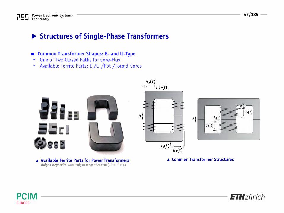
► Structures of Single-Phase Transformers
■ Common Transformer Shapes: E- and U-Type• One or Two Closed Paths for Core-Flux• Available Ferrite Parts: E-/U-/Pot-/Toroid-Cores
▲ Common Transformer Structures▲ Available Ferrite Parts for Power TransformersHuigao Megnetics, www.huigao-magnetics.com (18.11.2014).

68/185
► Classification of IPT Coil Geometries (1)
E-Type IPT Coils
■ E-Core Transformer• Flux Divided to Two Equal Loops• 2x Thickness for Central Leg■ E-Type IPT Coil• Flux Divided to Two Equal Loops• Max. Coupling for Certain Ratio of
Core Size Compared to Winding Diam.
69/185
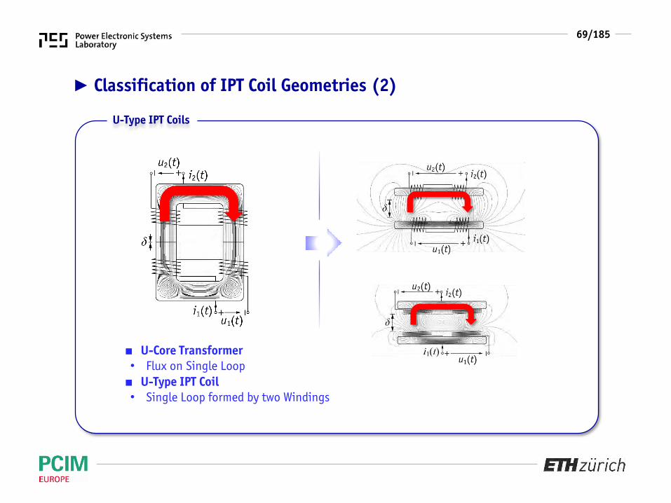
U-Type IPT Coils
► Classification of IPT Coil Geometries (2)
■ U-Core Transformer• Flux on Single Loop■ U-Type IPT Coil• Single Loop formed by two Windings
70/185
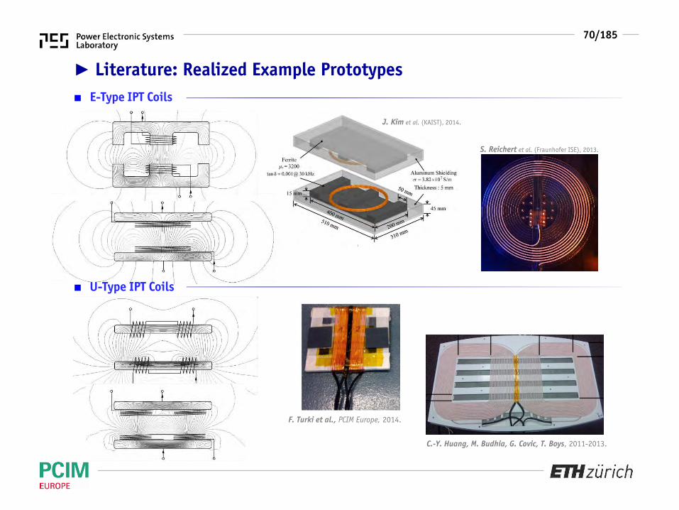
J. Kim et al. (KAIST), 2014.
S. Reichert et al. (Fraunhofer ISE), 2013.
► Literature: Realized Example Prototypes■ E-Type IPT Coils
■ U-Type IPT Coils
F. Turki et al., PCIM Europe, 2014.
C.-Y. Huang, M. Budhia, G. Covic, T. Boys, 2011-2013.

71/185
► Coil Geometry Optimization (1)
■ Conceptual Analysis with Reluctance Model
■ Maximize Figure-of-Merit kQ:
■ Approximations:• Core Reluctance Small (high Permeability)• Only Air Gap in Central Leg Considered,
Side Legs have small Reluctance (large Area)
𝒌 =𝝍𝐡
𝝍𝛔 + 𝝍𝐡∝
𝑹𝛔
𝑹𝛅 + 𝑹𝛔
J. Kim et al. (KAIST), 2014.

72/185
► Coil Geometry Optimization (2)
■ Conceptual Analysis with Reluctance Model
■ Maximize Figure-of-Merit kQ:
■ Reluctance: Approximate Scaling Law
𝒌 =𝝍𝐡
𝝍𝛔 + 𝝍𝐡∝
𝑹𝛔
𝑹𝛅 + 𝑹𝛔
𝑹𝛅 ≈𝜹
𝛍𝟎𝑨𝐜∝
𝜹
𝛍𝟎 𝒓𝟐
𝑹𝛔 ≈ 𝒓
𝛍𝟎 ⋅ 𝟐𝛑 𝒓𝒉≈ const.
J. Kim et al. (KAIST), 2014.

73/185
► Coil Geometry Optimization (3)
■ Conceptual Analysis with Reluctance Model
■ Maximize Figure-of-Merit kQ:
■ Reluctance: Approximate Scaling Law
𝒌 =𝝍𝐡
𝝍𝛔 + 𝝍𝐡∝
𝑹𝛔
𝑹𝛅 + 𝑹𝛔
J. Kim et al. (KAIST), 2014.
▲ FEM-Calculated Coupling for Three Exemplary Coil Geometries
Maximize Coil Area for High Coupling! Fully Utilize Available Construction Volume Best Choice for Geometry is Application Specific!
𝑹𝛅 ≈𝜹
𝛍𝟎𝑨𝐜∝
𝜹
𝛍𝟎 𝒓𝟐
𝑹𝛔 ≈ 𝒓
𝛍𝟎 ⋅ 𝟐𝛑 𝒓𝒉≈ const.
74/185
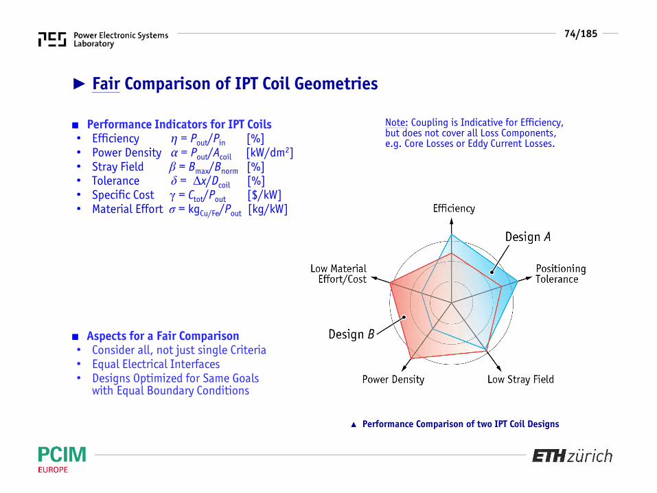
► Fair Comparison of IPT Coil Geometries
■ Performance Indicators for IPT Coils• Efficiency η = Pout/Pin [%]• Power Density α = Pout/Acoil [kW/dm2]• Stray Field β = Bmax/Bnorm [%]• Tolerance δ = Δx/Dcoil [%]• Specific Cost γ = Ctot/Pout [$/kW]• Material Effort σ = kgCu/Fe/Pout [kg/kW]
■ Aspects for a Fair Comparison• Consider all, not just single Criteria• Equal Electrical Interfaces• Designs Optimized for Same Goals
with Equal Boundary Conditions
Note: Coupling is Indicative for Efficiency,but does not cover all Loss Components,e.g. Core Losses or Eddy Current Losses.
▲ Performance Comparison of two IPT Coil Designs

75/185
Designed IPTDemonstrator Systems
76/185
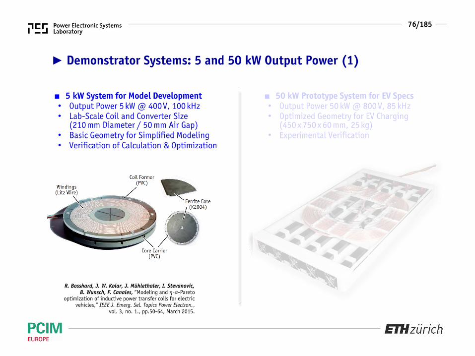
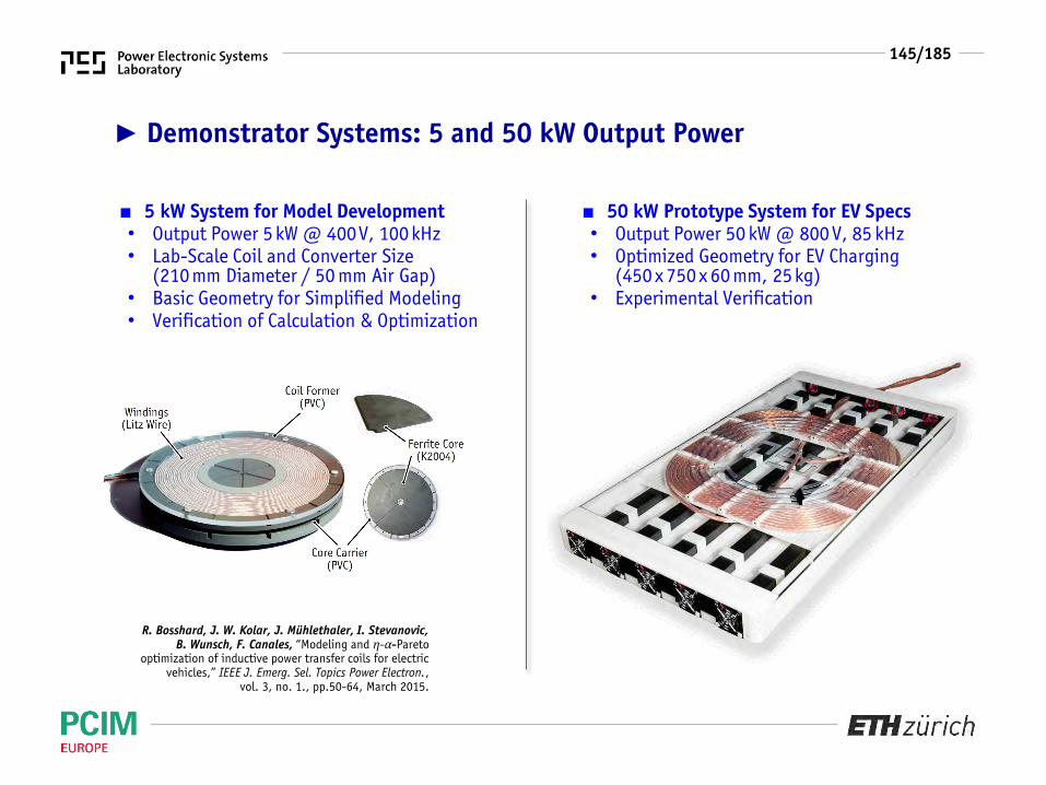
► Demonstrator Systems: 5 and 50 kW Output Power (1)
■ 5 kW System for Model Development• Output Power 5kW @ 400V, 100kHz• Lab-Scale Coil and Converter Size
(210mm Diameter / 50 mm Air Gap)• Basic Geometry for Simplified Modeling• Verification of Calculation & Optimization
■ 50 kW Prototype System for EV Specs• Output Power 50 kW @ 800 V, 85 kHz• Optimized Geometry for EV Charging
(450x 750x 60 mm, 25kg)• Experimental Verification
R. Bosshard, J. W. Kolar, J. Mühlethaler, I. Stevanovic, B. Wunsch, F. Canales, “Modeling and η-α-Pareto
optimization of inductive power transfer coils for electric vehicles,” IEEE J. Emerg. Sel. Topics Power Electron.,
vol. 3, no. 1., pp.50-64, March 2015.

77/185
► Demonstrator Systems: 5 and 50 kW Output Power (2)
■ 5 kW System for Model Development• Output Power 5kW @ 400V, 100kHz• Lab-Scale Coil and Converter Size
(210mm Diameter / 50 mm Air Gap)• Basic Geometry for Simplified Modeling• Verification of Calculation & Optimization
R. Bosshard, J. W. Kolar, J. Mühlethaler, I. Stevanovic, B. Wunsch, F. Canales, “Modeling and η-α-Pareto
optimization of inductive power transfer coils for electric vehicles,” IEEE J. Emerg. Sel. Topics Power Electron.,
vol. 3, no. 1., pp.50-64, March 2015.
■ 50 kW Prototype System for EV Specs• Output Power 50 kW @ 800 V, 85 kHz• Optimized Geometry for EV Charging
(450x 750x 60 mm, 25kg)• Experimental Verification
78/185
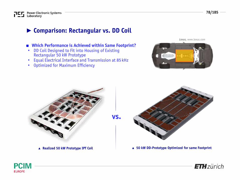
► Comparison: Rectangular vs. DD Coil
■ Which Performance is Achieved within Same Footprint?• DD Coil Designed to Fit into Housing of Existing
Rectangular 50 kW Prototype• Equal Electrical Interface and Transmission at 85kHz• Optimized for Maximum Efficiency
vs.
▲ Realized 50 kW Prototype IPT Coil ▲ 50 kW DD-Prototype Optimized for same Footprint
Lexus, www.lexus.com

79/185
► Rectangular vs. DD Coil – Coupling■ Evaluation of Magnetic Coupling for Ideal and Misaligned Coil Positions• 3D-FEM Simulation Results in Frequency Domain
■ Rectangular and DD Coil AchieveEqual Coupling at Ideal Positioning
■ Coil Positioning Tolerance:• DD-Coil Better in x-Direction• Rect.-Coil Better in y-Direction

80/185
► Rectangular vs. DD Coil – Core Losses■ DD has Higher Flux Density in Central Cores• High Core Losses in Coil Center due to High Ampère-Turns• Additional Core Elements Required to Reduce Flux Density• No Additional Eddy-Current Shield on Top/Bottom Needed
▲ FEM Simulation Results without (left) and with (right) additional coresfor flux density / core loss reduction in coil center
2x Ampère-Turnsin Coil Center
Additional Coresare Needed

81/185
► Rectangular vs. DD Coil – Total Losses
■ DD has Higher Core Losses in Central Core Elements due to High Core Flux Density• But does not Require Additional Eddy-Current Shield that is used in Rectangular Design• Power Losses in Remaining Parts are Comparable, Since Coupling is almost Equal
Efficiency of Rectangular and DD Coil is very Similar Additional Cores were needed for DD, Higher Weight: +1.2kg / +5%

82/185
► Rectangular vs. DD Coil – Stray Field■ Magnetic Stray Field in at Given Reference Position (1m Distance)• Note: Coils are Designed for Same Operating Frequency
■ Intuitive Explanation:• Structural Integration
of Return Path for Flux

83/185
► Summary of Comparison Results
■ Magnetic Coupling for Equal Coil Size• Double-D and Rectangular Coil Reach Equal Coupling• Decrease of Coupling at Misalignment shows no Clear Winner
(DD better in x-Direction, Rect. Better in y-Direction)
■ Power Losses and Efficiency• Power Losses in DD are higher due to Core Losses• Remaining Loss Components are Similar
■ Material Effort/Cost• Additional Cores were Required for DD• Eddy Current Shield needed for Rect.
■ Stray Field• Double-D has Lower Stray Field
than Rectangular Coil
Will be Experimentally Verified!
84/185
Coil Modeling:High-Frequency Winding Losses

85/185
► Winding Loss Calculation – Skin Effect
■ Frequency Dependent Current Distribution in Single Solid Conductor
𝑷𝐬𝐤𝐢𝐧 = 𝑭𝐑 𝒇 ⋅ 𝑹𝐃𝐂 ⋅ 𝑰𝟐
J. Mühlethaler, “Modeling and multi-objective optimization of inductive power components,”
Ph.D. dissertation, Swiss Federal Institute of Technology (ETH)
Zurich, 2012.

86/185
► Winding Loss Calculation – Proximity Effect
■ Frequency Dependent Current Distribution in Neighboring Solid Conductors
𝑷𝐩𝐫𝐨𝐱 = 𝑮𝐑 𝒇 ⋅ 𝑹𝐃𝐂 ⋅ 𝑯𝒆𝟐
J. Mühlethaler, “Modeling and multi-objective optimization of inductive power components,”
Ph.D. dissertation, Swiss Federal Institute of Technology (ETH)
Zurich, 2012.
87/185
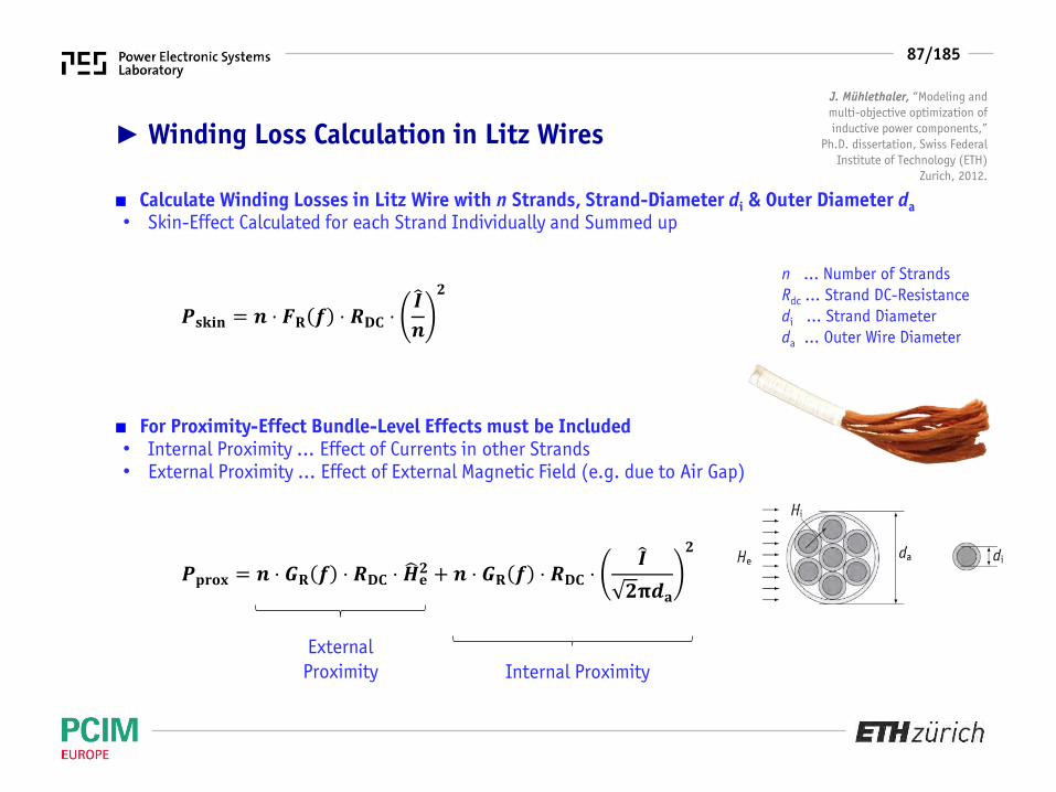
► Winding Loss Calculation in Litz Wires
■ Calculate Winding Losses in Litz Wire with n Strands, Strand-Diameter di & Outer Diameter da• Skin-Effect Calculated for each Strand Individually and Summed up
■ For Proximity-Effect Bundle-Level Effects must be Included• Internal Proximity … Effect of Currents in other Strands• External Proximity … Effect of External Magnetic Field (e.g. due to Air Gap)
𝑷𝐬𝐤𝐢𝐧 = 𝒏 ⋅ 𝑭𝐑 𝒇 ⋅ 𝑹𝐃𝐂 ⋅ 𝑰
𝒏
𝟐n … Number of StrandsRdc … Strand DC-Resistancedi … Strand Diameterda … Outer Wire Diameter
𝑷𝐩𝐫𝐨𝐱 = 𝒏 ⋅ 𝑮𝐑 𝒇 ⋅ 𝑹𝐃𝐂 ⋅ 𝑯𝐞𝟐 + 𝒏 ⋅ 𝑮𝐑 𝒇 ⋅ 𝑹𝐃𝐂 ⋅
𝑰
𝟐𝛑𝒅𝐚
𝟐
ExternalProximity Internal Proximity
J. Mühlethaler, “Modeling and multi-objective optimization of inductive power components,”
Ph.D. dissertation, Swiss Federal Institute of Technology (ETH)
Zurich, 2012.

88/185
► Comparison: Solid Wire vs. Litz Wire
■ Power Loss per 1m of Solid or Litz Wire at Î = 1 A with Hext = 0 A/m• Only Internal Proximity Effect (no External Field)
■ If Litz Wire is Operated far from “intended” Operating Frequency, Solid Wire can becomeBetter Option due to Internal Proximity Effect in Litz Wire Bundles
J. Mühlethaler, “Modeling and multi-objective optimization of inductive power components,”
Ph.D. dissertation, Swiss Federal Institute of Technology (ETH)
Zurich, 2012.

89/185
► Example 1: Transformer Winding Losses
■ Power Loss Calculation for Transformer with Litz Wire Windings• External Magnetic Field (Simplified):
• AC-Resistance of Single Turn of Primary Winding:
• Equations for FR and GR from Literature, e.g.:
𝑯𝐞,𝐑𝐌𝐒 ≈
𝑵𝐩𝑰𝐩,𝐑𝐌𝐒
𝒃𝐜∙𝒌𝐩 − 𝟏 𝟐
𝒌𝐩,𝐦𝐚𝐱… 𝐩𝐫𝐢𝐦𝐚𝐫𝐲 𝐬𝐢𝐝𝐞: 𝒌𝐩 = 𝟏, 𝟐, 𝟑
𝑵𝐬𝑰𝐬,𝐑𝐌𝐒
𝒃𝐜∙𝒌𝐬 − 𝟏 𝟐
𝒌𝐬,𝐦𝐚𝐱… 𝐬𝐞𝐜𝐨𝐧𝐝𝐚𝐫𝐲 𝐬𝐢𝐝𝐞: 𝒌𝐬 = 𝟏, 𝟐
𝑹𝐃𝐂 ≈𝟒𝑵𝒍𝐚𝐯𝐠
𝝈𝛑𝒅𝐂𝐮𝟐
𝑹𝐀𝐂,𝐭𝐮𝐫𝐧(𝒌) =𝑹𝐃𝐂
𝑵∙ 𝟐𝑭𝐑 + 𝟐𝑮𝐑 ∙
𝑵
𝒃𝐜∙𝟐𝒌 − 𝟏
𝟐𝒌𝐦𝐚𝐱
𝟐
J. Mühlethaler, “Modeling and multi-objective optimization of inductive power components,” Ph.D. dissertation, Swiss Federal Institute of Technology (ETH) Zurich, 2012.
𝑯𝒆𝐝𝒍 = 𝑵𝑰
90/185
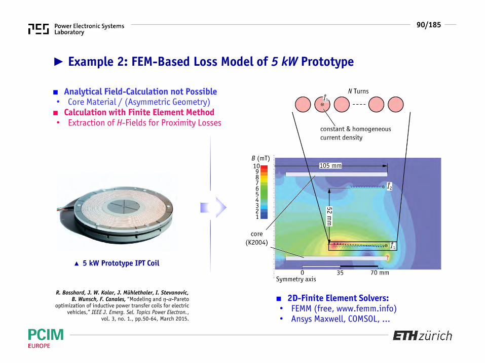
► Example 2: FEM-Based Loss Model of 5 kW Prototype
■ Analytical Field-Calculation not Possible• Core Material / (Asymmetric Geometry)■ Calculation with Finite Element Method• Extraction of H-Fields for Proximity Losses
■ 2D-Finite Element Solvers:• FEMM (free, www.femm.info)• Ansys Maxwell, COMSOL, …
▲ 5 kW Prototype IPT Coil
R. Bosshard, J. W. Kolar, J. Mühlethaler, I. Stevanovic, B. Wunsch, F. Canales, “Modeling and η-α-Pareto
optimization of inductive power transfer coils for electric vehicles,” IEEE J. Emerg. Sel. Topics Power Electron.,
vol. 3, no. 1., pp.50-64, March 2015.
91/185
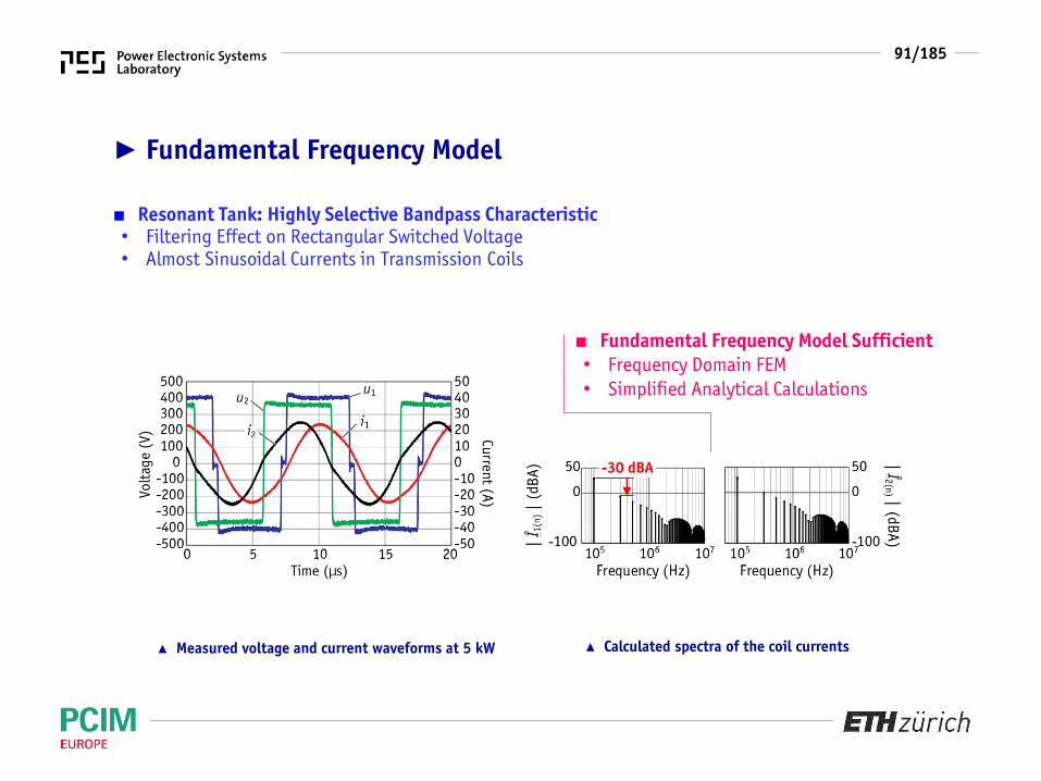
► Fundamental Frequency Model
■ Resonant Tank: Highly Selective Bandpass Characteristic• Filtering Effect on Rectangular Switched Voltage• Almost Sinusoidal Currents in Transmission Coils
-30 dBA
▲ Calculated spectra of the coil currents
■ Fundamental Frequency Model Sufficient• Frequency Domain FEM• Simplified Analytical Calculations
▲ Measured voltage and current waveforms at 5 kW

92/185
► High-Frequency Copper Losses in Litz Wire
■ Skin-Effect Calculated Analytically (as for Transformer)
■ Proximity-Effect Calculation with External Magnetic Field from FEM Results
𝑷𝐬𝐤𝐢𝐧 = 𝒏 ⋅ 𝑭𝐑 𝒇 ⋅ 𝑹𝐃𝐂 ⋅ 𝑰
𝒏
𝟐
𝑷𝐩𝐫𝐨𝐱 = 𝒏 ⋅ 𝑮𝐑 𝒇 ⋅ 𝑹𝐃𝐂 ⋅ 𝑯𝐞𝟐 + 𝒏 ⋅ 𝑮𝐑 𝒇 ⋅ 𝑹𝐃𝐂 ⋅
𝑰
𝟐𝛑𝒅𝐚
𝟐
ExternalProximity Internal Proximity
■ Extracted from FEM Results• Evaluation in Center-Point of Each
Turn to Isolate External Field
n … Number of StrandsRdc … Strand DC-Resistancedi … Strand Diameterda … Outer Wire Diameter

93/185
► Example 3: Analytical Loss Model of 50 kW Prototype
■ 3D Coil Design w/o Symmetry• Resolution of Winding Details requires
Long Simulation Time• Winding Modeled as Box for accurate Field
Calculation on Outside (Core Loss, Stray)• Magnetic Field inside Box Incorrect
▲ 50 kW Prototype IPT Coil ▲ 3D-FEM Model of Tx and Rx Coil

94/185
► Measurement of Inductance & Coupling■ Verification of Inductance Calculation• Excitation with Linear Amplifier (6 Apk, 85kHz)• Inductance Measured with Power Analyzer
and with Impedance Analyzer• Induced Voltage Measured with Diff. Probe
■ Measured: L1 = 66.3 uH, k = 0.230■ Calculated: L1 = 67.6 uH, k = 0.233
High Accuracy Despite Simplifications!
▲ Yokogawa WT3000
▲ 50 kW Prototype IPT Coil ▲ 3D-FEM Model of Tx and Rx Coil

95/185
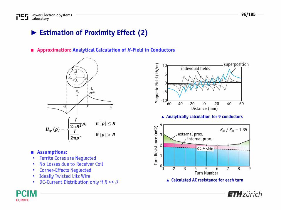
► Estimation of Proximity Effect (1)
■ H-Field Inside Conductors is Needed to Estimate Proximity Effect• Not Available if Winding Modeled as “Box”
▲ 2D-FE Simulation of Field in Cut Plane
■ Approximation with 2D-Cut Plane
𝑷𝐩𝐫𝐨𝐱,𝐞𝐱𝐭 = 𝒏 ⋅ 𝑮𝐑 𝒇 ⋅ 𝑹𝐃𝐂 ⋅ 𝑯𝐞𝟐
Unknown!
96/185
► Estimation of Proximity Effect (2)
■ Approximation: Analytical Calculation of H-Field in Conductors
■ Assumptions:• Ferrite Cores are Neglected• No Losses due to Receiver Coil• Corner-Effects Neglected• Ideally Twisted Litz Wire• DC-Current Distribution only if R << δ
𝑯𝝋 (𝝆) =
𝑰
𝟐𝛑𝑹𝟐𝝆, 𝐢𝐟 𝝆 ≤ 𝑹
𝑰
𝟐𝛑𝝆, 𝐢𝐟 |𝝆| > 𝑹
▲ Analytically calculation for 9 conductors
▲ Calculated AC resistance for each turn

97/185
► Estimation of Proximity Effect (3)
■ Comparison to 2D-FEM Simulation Including Core
▲ 2D-FE Simulation with Core Rods for Comparison
▲ Comparison of analytical calculation and FEM Simulation
■ Core has only Minor Effect on Fields■ Approximation with 2D-Calculation
to Estimate External Field
𝑷𝐩𝐫𝐨𝐱,𝐞𝐱𝐭 = 𝒏 ⋅ 𝑮𝐑 𝒇 ⋅ 𝑹𝐃𝐂 ⋅ 𝑯𝐞𝟐
Calculated!
98/185
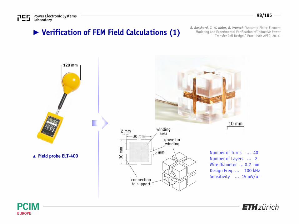
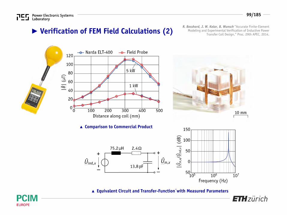
► Verification of FEM Field Calculations (1)
▲ Field probe ELT-400
R. Bosshard, J. W. Kolar, B. Wunsch “Accurate Finite-Element Modeling and Experimental Verification of Inductive Power
Transfer Coil Design,” Proc. 29th APEC, 2014.
Number of Turns … 40Number of Layers … 2Wire Diameter … 0.2 mmDesign Freq. … 100 kHzSensitivity … 15 mV/uT
120 mm
99/185
► Verification of FEM Field Calculations (2)R. Bosshard, J. W. Kolar, B. Wunsch “Accurate Finite-Element
Modeling and Experimental Verification of Inductive Power Transfer Coil Design,” Proc. 29th APEC, 2014.
▲ Comparison to Commercial Product
▲ Equivalent Circuit and Transfer-Function¨with Measured Parameters

100/185
► Verification of FEM Field Calculations (3)
■ Probe for Magnetic Field Measurements• Optimized for 100 kHz, High Accuracy• Sensitivity: 14.5 mV/µT @ 100 kHz• Accuracy: < 5% Error (Comp. to ELT-400)• Size: 30x30x30 mm
▲ Measured stray field @ 5 kW
▲ Custom field probe for verification
R. Bosshard, J. W. Kolar, B. Wunsch “Accurate Finite-Element Modeling and Experimental Verification of Inductive Power
Transfer Coil Design,” Proc. 29th APEC, 2014.

101/185
Frequency Effectsin Non-Ideal Litz Wire

102/185
► Copper Losses in Litz Wire – Asymmetric Twisting (1)■ Case study: Litz wire (tot. 9500 strands of 71µm each) with 10 sub-bundles ■ Current distribution in internal litz wire bundles depends strongly on interchanging strategy
■ Total copper losses for 10bundles: 438W
G. Ortiz, M. Leibl, J. W. Kolar,“Medium Frequency Transformers
for Solid-State Transformer Applications — Design and
Experimental Verification”, 2013.
▲ 166 kW/20 kHz Transformer

103/185
► Copper Losses in Litz Wire – Asymmetric Twisting (2)■ Case study: Litz wire (tot. 9500 strands of 71µm each) with 10 sub-bundles ■ Current distribution in internal litz wire bundles depends strongly on interchanging strategy
■ Total copper losses for 10bundles: 438W■ Total copper losses for 8 bundles: 353W
G. Ortiz, M. Leibl, J. W. Kolar,“Medium Frequency Transformers
for Solid-State Transformer Applications — Design and
Experimental Verification”, 2013.
▲ 166 kW/20 kHz Transformer

104/185
► Copper Losses in Litz Wire – Termination
G. Ortiz, M. Leibl, J. W. Kolar,“Medium Frequency Transformers
for Solid-State Transformer Applications — Design and
Experimental Verification”, 2013.
▲ Termination of Litz Wire Bundelswith Common-Mode Chokes
Best Option
105/185
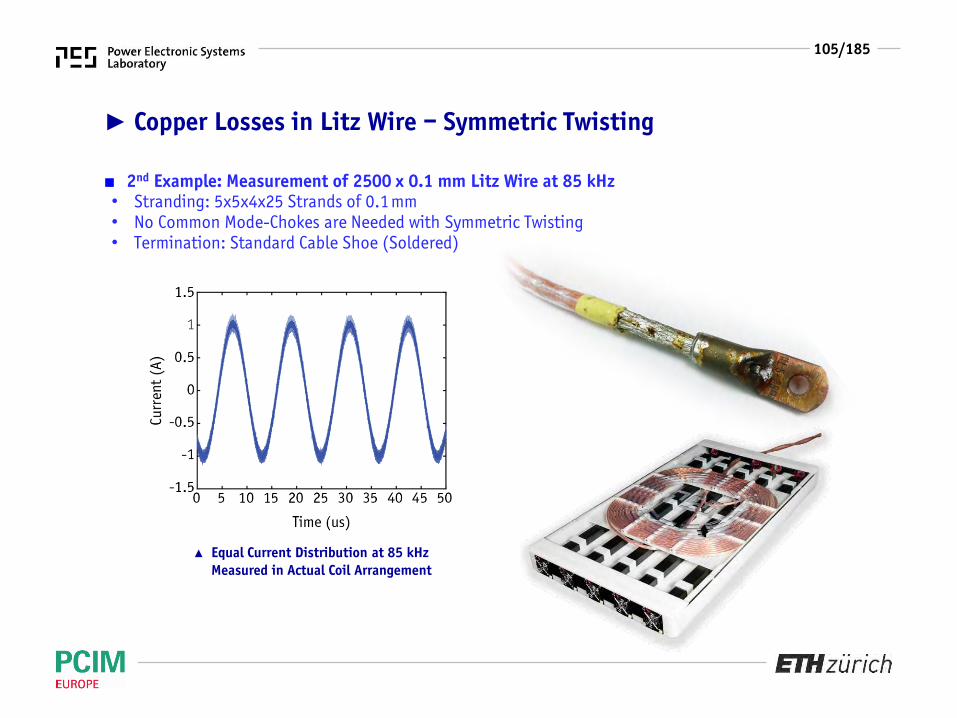
► Copper Losses in Litz Wire – Symmetric Twisting
■ 2nd Example: Measurement of 2500 x 0.1 mm Litz Wire at 85 kHz• Stranding: 5x5x4x25 Strands of 0.1mm• No Common Mode-Chokes are Needed with Symmetric Twisting• Termination: Standard Cable Shoe (Soldered)
▲ Equal Current Distribution at 85 kHzMeasured in Actual Coil Arrangement

106/185
Coil Modeling:High-Frequency Core Losses
107/185
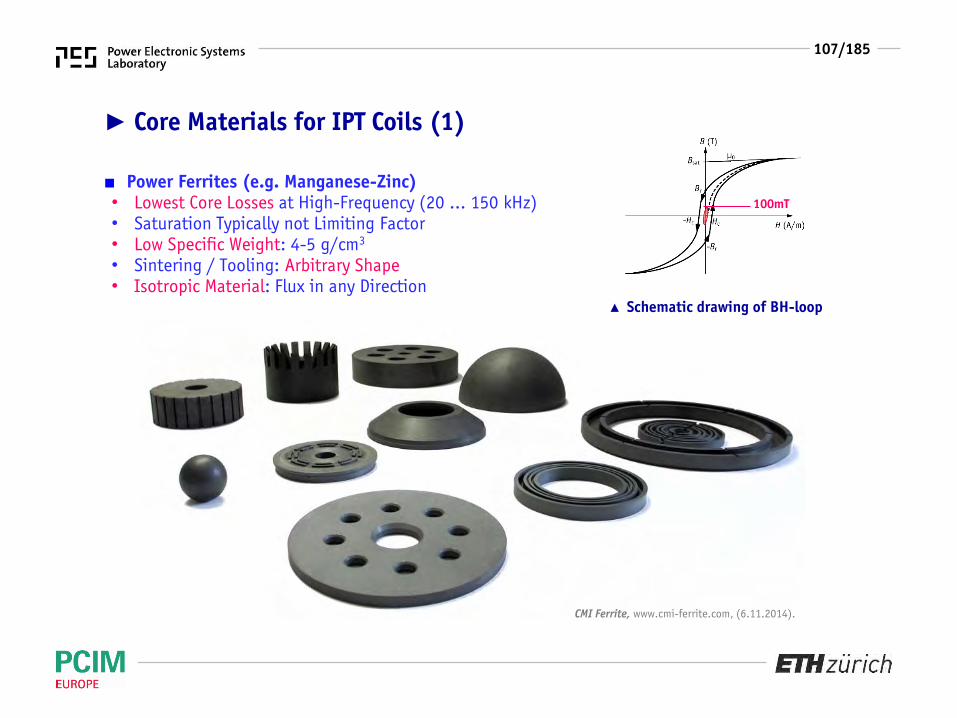
► Core Materials for IPT Coils (1)
■ Power Ferrites (e.g. Manganese-Zinc)• Lowest Core Losses at High-Frequency (20 … 150 kHz)• Saturation Typically not Limiting Factor• Low Specific Weight: 4-5 g/cm3
• Sintering / Tooling: Arbitrary Shape• Isotropic Material: Flux in any Direction
CMI Ferrite, www.cmi-ferrite.com, (6.11.2014).
▲ Schematic drawing of BH-loop
100mT

108/185
► Core Materials for IPT Coils (2)
■ Tape Wound Cores• Custom Shapes with Tape Winding• High Losses at Frequency > 20..50 kHz• Higher Specific Weight: 7-8 g/cm3
• Anisotropic: Orthogonal Flux Causes Losses(Similarly: Litz-Wire and no Foil-Windings!)
B. Cougo, J. Mühlethaler, J. W. Kolar, “Increase of Tape Wound Core Losses due to Interlamination Short Circuits
and Orthogonal Flux Components”, 2011.
Tape wound core
Ferrite core
109/185
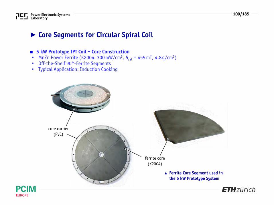
► Core Segments for Circular Spiral Coil
■ 5 kW Prototype IPT Coil – Core Construction• MnZn Power Ferrite (K2004: 300 mW/cm3, Bsat = 455mT, 4.8g/cm3)• Off-the-Shelf 90°-Ferrite Segments• Typical Application: Induction Cooking
▲ Ferrite Core Segment used in the 5 kW Prototype System

110/185
► Core Loss Calculation – General
■ Calculation of Core-Loss Density According to Current Waveform
Sinusoidal
DC Current +HF Ripple
Non-Sinusoidal AC Current
Sinusoidal Current +HF Ripple
Major Loop
Minor Loop
J. Mühlethaler, “Modeling and multi-objective optimization of inductive power components,”
Ph.D. dissertation, Swiss Federal Institute of Technology (ETH)
Zurich, 2012.
Steinmetz Equation Sinusoidal w/o DC-Offset
Generalized Versions of the Steinmetz Equation (iGSE, i2GSE) Arbitrary Waveform & DC-Offset
Relaxation Effects
Superposition of Losses due to Minor and Major Loops
111/185
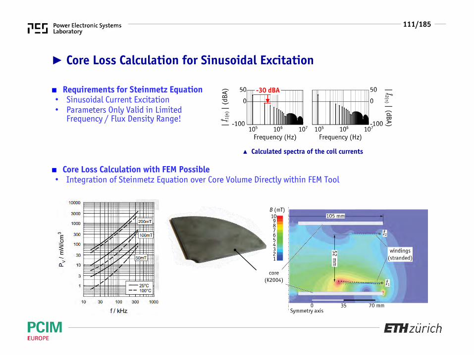
► Core Loss Calculation for Sinusoidal Excitation
■ Requirements for Steinmetz Equation• Sinusoidal Current Excitation• Parameters Only Valid in Limited
Frequency / Flux Density Range!
■ Core Loss Calculation with FEM Possible• Integration of Steinmetz Equation over Core Volume Directly within FEM Tool
-30 dBA
▲ Calculated spectra of the coil currents
112/185
Thermal Modeling
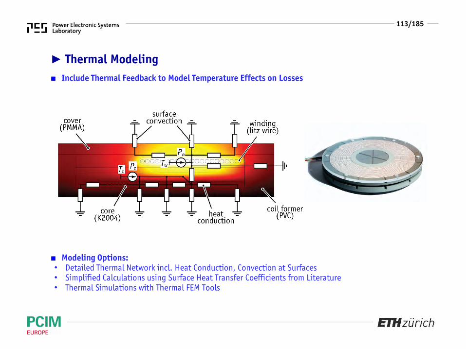
113/185
► Thermal Modeling■ Include Thermal Feedback to Model Temperature Effects on Losses
■ Modeling Options:• Detailed Thermal Network incl. Heat Conduction, Convection at Surfaces• Simplified Calculations using Surface Heat Transfer Coefficients from Literature• Thermal Simulations with Thermal FEM Tools

114/185
► Experimental Verification for 5 kW Prototype
■ Temperature Measurements forVerification of Thermal FEM Results
• Accuracy: < 5% Error ofSteady-State Temperature
• Surface-Related Power Losses of upto 0.2W/cm2 with Forced Air Cooling
▲ Thermal Simulation of 5 kW Prototype Coil
▲ Thermal Measurements with Thermocouples(with/without Forced Air Cooling)
www.fluke.com
115/185
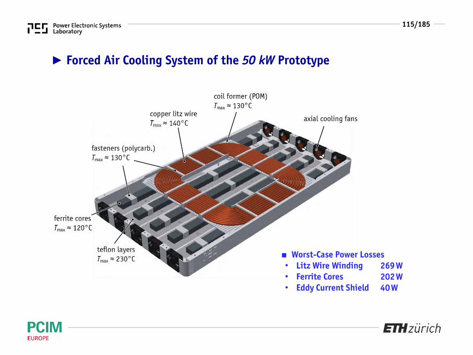
► Forced Air Cooling System of the 50 kW Prototype
■ Worst-Case Power Losses• Litz Wire Winding• Ferrite Cores• Eddy Current Shield
269W202W40W

116/185
► Estimation of Heat Transfer Coefficient
■ Emprical Equation for Surface Heat TransferCoefficient:
▲ Axial cooling fan for active coolingof the windings and core elements
▲ Heat Transfer Coefficient Estimated fromFan Characteristics of AUB0524VHD
𝒉𝒗 ≈ 𝑪𝝀𝐟
𝒅
𝒖∞𝒅
𝒗𝐟
𝒏
𝑷𝒓𝐟𝟏/𝟑
𝝀𝐟, 𝒗𝐟, 𝑷𝒓𝐟 … conductivity, viscosity, Prantl number𝒖∞ … fluid velocity𝒅 … component height𝑪, 𝒏 … empirical geometry parameters
(C = 0.102, n = 0.675)
A. Van den Bossche and V. C. Valchev, Inductors and transformers for power electronics.
New York: Taylor & Francis, 2005.
10x

117/185
► Thermal Design with 3D-FEM
■ Heat Transfer in Solids with Estimated Coeff.• 30 W/m2K … active cooled surfaces• 7.5 W/m2K … convective cooled surfaces
■ Parameter Sweep in FEM Tool• Heat Transfer Coefficient• Loss Safety Factor: Psim = msafety·Pcalc
Design is Feasible at Surface-RelatedPower Loss 0.2 W/cm2 with Active Cooling
T (°C)Tamb = 40°C
▲ 3D-FEM Thermal Simulation: Results of Parameter Sweep

118/185
Resonant Capacitors

119/185
► Resonant Capacitors: Component Selection (1)
■ Polypropylene Film Capacitors for Resonant Applications• Low tan(δ) Low High-Frequency Losses• Low Parasitic Inductance and ESR• Least Affected by Temperature/Frequency/Humidity
▲ Datasheet Values of tan(δ) in Funciton ofFrequency for EPCOS Film Capacitors
Polypropylene
EPCOS, Film Capacitors Data Handbook, 2009.
MK/F * … Metallized Plastic Film / Metal Foil**T … Polyester**P … Polypropylene**N … Polyethylene Naphthalate

120/185
► Resonant Capacitors: Component Selection (2)
■ Polypropylene Film Capacitors for Resonant Applications• Low tan(δ) Low High-Frequency Losses• Low Parasitic Inductance and ESR• Least Affected by Temperature/Frequency/Humidity
▲ Typical Material Characteristics for Film Capacitors (EPCOS)
EPCOS, Film Capacitors Data Handbook, 2009.
Polypropylene

121/185
► Capacitor Service Life vs. Temperature & Voltage
■ Service-Life of Film Capacitors Strongly Depends onOperating Temperature and Voltage Utilization
TDK/EPCOS Product Profile, Film Capacitors for Industrial Applications, 2012.
𝒕𝐥𝐢𝐟𝐞 𝑻, 𝑽 = 𝒕𝐥𝐢𝐟𝐞,𝟎 ⋅𝟏
𝛑𝐓⋅
𝟏
𝛑𝐕
▲ Service Life vs. Operating Temperature for DifferentLevels of Voltage Utilization
▲ Arrhenius Law (Exponential Func.)

122/185
► High-Power Polypropylene Film Capacitors
■ 50 kW IPT – Capacitor Requirements• > 100Arms / 3..4kVrms / 20..150kHz
■ Tangent-Delta: 1/1000 - 1/700■ High Power Density: 5.95 kVAr/cm3
■ Active Cooling: Water / Air @ 35% Power■ Typical Application: Induction Heating
▲ CSP 120-200 Polypropylene Film Capacitor(1.1 kVpk / 100 Arms / 1 MHz @ full power)
▲ Induction Heating System (www.celem.com)

123/185
► Resonant Capacitor Module for 50 kW
■ Rated Current■ Operating Frequency■ Physical Dimensions■ Power Density■ Efficiency @ 50kW
100Arms85kHz5x12x38cm, 2.6kg22kW/l, 19kW/kg98.9%
◄ Capacitor Module: 5 Devices in Series, Forced-AirCooling System

124/185
► Capacitor Module Cooling System■ Forced-Air Cooling Required for Resonant Capacitors at 50 kW Operation• Aluminum Extrudend Fin Heatsink Mounted to Capacitor Terminals
■ Rated Current■ Operating Frequency■ Tangent-Delta■ Power Losses
100Arms85kHz1.5‰314 W

125/185
► Mounting of Capacitor Module on IPT Coil
■ Compact Realization as IntegratedIPT Coil & Capacitor Module
■ Close Placement of Components toLimit EMI due to HF-Coil Current

126/185
Magnetic Shielding
127/185
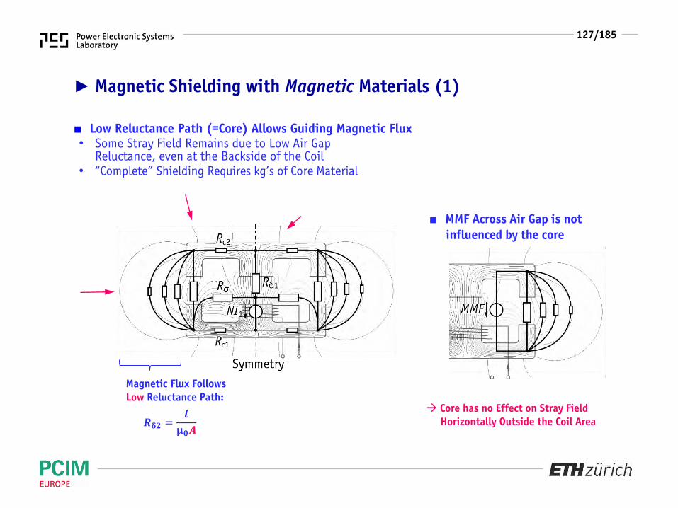
► Magnetic Shielding with Magnetic Materials (1)
■ Low Reluctance Path (=Core) Allows Guiding Magnetic Flux• Some Stray Field Remains due to Low Air Gap
Reluctance, even at the Backside of the Coil• “Complete” Shielding Requires kg’s of Core Material
Magnetic Flux FollowsLow Reluctance Path:
Core has no Effect on Stray FieldHorizontally Outside the Coil Area𝑹𝛅𝟐 =
𝒍
𝛍𝟎𝑨
■ MMF Across Air Gap is notinfluenced by the core

128/185
► Magnetic Shielding with Magnetic Materials (2)
■ Save Weight, Use High Permeability Material (µr > 10’000)?• Machine Steel & Amorphous Iron: High Frequency Losses• Permalloy: Strong Frequency Dependency and Low Saturation
H. W. Ott, Noise Reduction Techniques in Electronic Systems, 2nd ed.,Wiley- Interscience, New York, 1988.
▲ Frequency dependency of ferromagnetic materialsC. Paul, “Shielding,“ in Introduction to Electromagnetic Compatibility,2nd ed., Jon Wiley & Sons, Hoboken, 2006, ch. 10, sec. 4, pp. 742-749.
▲ High-Permeability Material Attracts Magnetic Field
vOperatingFrequency
129/185
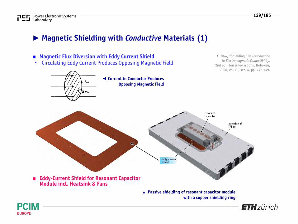
► Magnetic Shielding with Conductive Materials (1)
■ Magnetic Flux Diversion with Eddy Current Shield• Circulating Eddy Current Produces Opposing Magnetic Field
■ Eddy-Current Shield for Resonant CapacitorModule incl. Heatsink & Fans
C. Paul, “Shielding,“ in Introduction to Electromagnetic Compatibility,
2nd ed., Jon Wiley & Sons, Hoboken, 2006, ch. 10, sec. 4, pp. 742-749.
◄ Current in Conductor ProducesOpposing Magnetic Field
▲ Passive shielding of resonant capacitor modulewith a copper shielding ring

130/185
► Magnetic Shielding with Conductive Materials (2)
■ Magnetic Flux Diversion with Eddy Current Shield• Create a Field-Free Space Around Capacitor Module
▲ FE-Calculated Field and Power Loss at 50 kW

131/185
Multi-Objective Optimizationof High-Power IPT Systems
Requirements & LimitsOptimization MethodTrade-Off Analysis
132/185
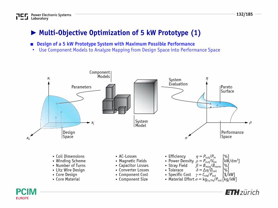
► Multi-Objective Optimization of 5 kW Prototype (1)■ Design of a 5 kW Prototype System with Maximum Possible Performance• Use Component Models to Analyze Mapping from Design Space into Performance Space

133/185
► Multi-Objective Optimization of 5 kW Prototype (2)■ Design Process Taking All Performance Aspects into Account
■ System Specification• Input Voltage 400 V• Battery Voltage 350 V• Output Power 5 kW• Air Gap 50mm
■ Constraints / Side Conditions• Thermal Limitations [°C]• Stray Field Limitations [µT]• Max. Construction Vol. [m3]• Switching Frequency [kHz]
R. Bosshard, J. W. Kolar, J. Mühlethaler, I. Stevanovic, B. Wunsch, F. Canales, “Modeling and η-α-Pareto
optimization of inductive power transfer coils for electric vehicles,” IEEE J. Emerg. Sel. Topics Power Electron.,
vol. 3, no. 1., pp.50-64, March 2015.
■ System Performance• Efficiency η = Pout/Pin [%]• Power Density α = Pout/Acoil [kW/dm2]• Stray Field β = Bmax/Bnorm [%]

134/185
η-α-Pareto Optimization

135/185
► η-α-Pareto Optimization – Results (1)
■ Evaluation of Design Options in an Iterative Procedure• Evaluation of FEM/Analytical Models for Power Losses,
Thermal Constraints, Stray Fields, etc.• Iterative Parameter / Grid Search for a
Given Design Space
■ Degrees-of-Freedom:• Coil Dimensions• Litz Wire Dimensions• Number of Turns• Operating Frequency
▲ Efficiency vs. Power Density of >12kIPT Coils with 5 kW Output Power
Design Space
Performance
Component Models
System Model

136/185
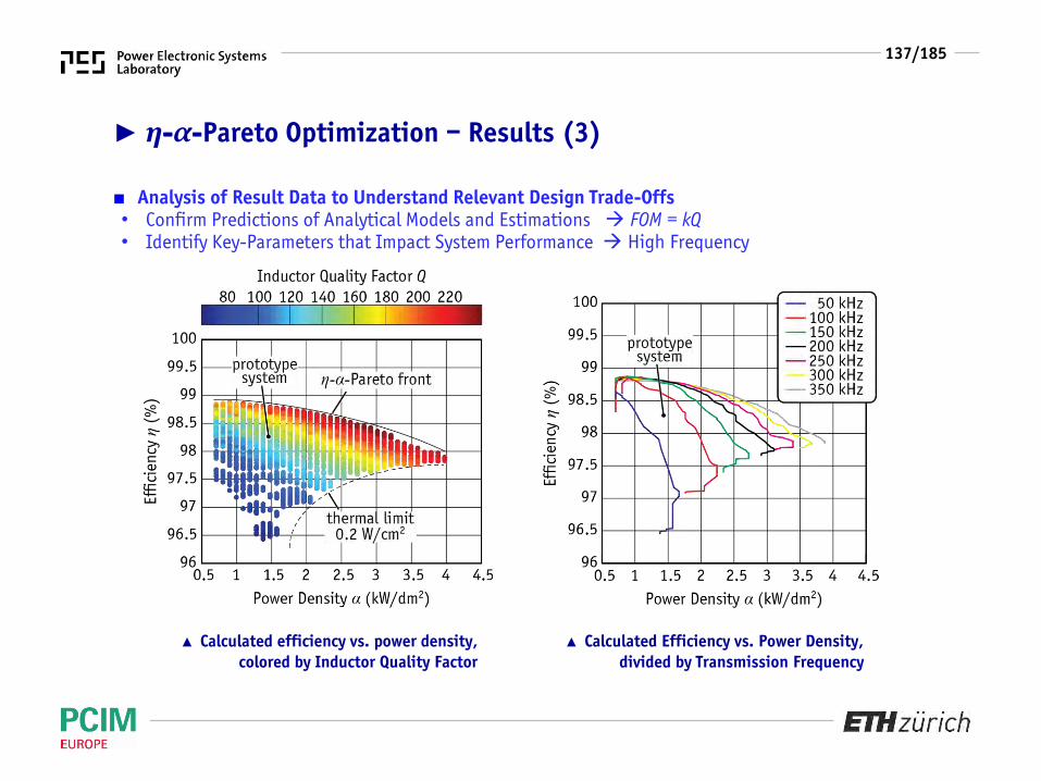
► η-α-Pareto Optimization – Results (2)
■ Analysis of Result Data to Understand Relevant Design Trade-Offs• Confirm Predictions of Analytical Models and Estimations FOM = kQ• Identify Key-Parameters that Impact System Performance High Frequency
▲ Trade-Off Analysis with Result Data: Effect of Quality Factor and Magnetic Coupling
137/185
► η-α-Pareto Optimization – Results (3)
■ Analysis of Result Data to Understand Relevant Design Trade-Offs• Confirm Predictions of Analytical Models and Estimations FOM = kQ• Identify Key-Parameters that Impact System Performance High Frequency
▲ Calculated Efficiency vs. Power Density,divided by Transmission Frequency
▲ Calculated efficiency vs. power density,colored by Inductor Quality Factor
138/185
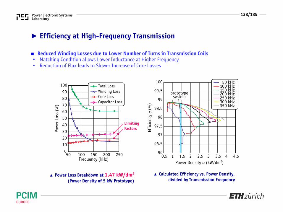
► Efficiency at High-Frequency Transmission
■ Reduced Winding Losses due to Lower Number of Turns in Transmission Coils• Matching Condition allows Lower Inductance at Higher Frequency• Reduction of Flux leads to Slower Increase of Core Losses
▲ Power Loss Breakdown at 1.47 kW/dm2
(Power Density of 5 kW Prototype)
LimitingFactors
▲ Calculated Efficiency vs. Power Density,divided by Transmission Frequency

139/185
► Selected Design for 5 kW Prototype System
■ Selection of Transmission Frequency• Significant Improvements up to 100 kHz• Standard Power Electronics Design (5kW)• Litz Wire (630 x 71 µm) is Standard Product
■ 5 kW Prototype IPT System• Coil Diameter 210 mm• Trans. Frequency 100 kHz• Trans. Efficiency 98.25% @ 52 mm Air Gap• Power Density 1.47 kW/dm2
• Stray Field 26.16 µT
▲ Power Loss Breakdown at 1.47 kW/dm2
(Power Density of 5 kW Prototype)
140/185
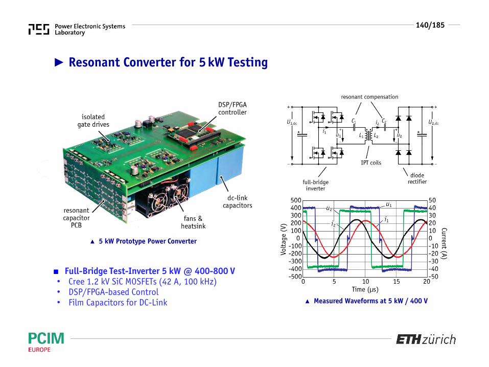
► Resonant Converter for 5 kW Testing
■ Full-Bridge Test-Inverter 5 kW @ 400-800 V• Cree 1.2 kV SiC MOSFETs (42 A, 100 kHz)• DSP/FPGA-based Control• Film Capacitors for DC-Link ▲ Measured Waveforms at 5 kW / 400 V
▲ 5 kW Prototype Power Converter
141/185
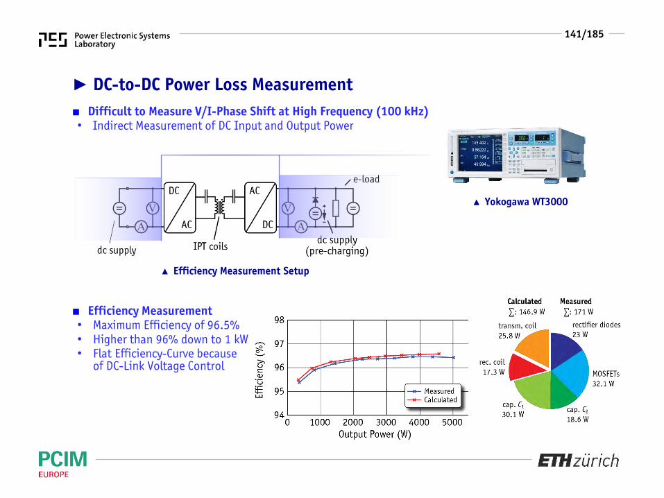
► DC-to-DC Power Loss Measurement■ Difficult to Measure V/I-Phase Shift at High Frequency (100 kHz)• Indirect Measurement of DC Input and Output Power
■ Efficiency Measurement• Maximum Efficiency of 96.5%• Higher than 96% down to 1 kW• Flat Efficiency-Curve because
of DC-Link Voltage Control
▲ Efficiency Measurement Setup
▲ Yokogawa WT3000

142/185
► High-Frequency Transmission & Stray Field
■ Higher Transmission Frequency Leads to Lower Stray Field• High Frequency Transmit Lower Energy
per Cycle for same Power
• Scaling Law:
• Trade-Off: Frequency vs. Field
■ Alternatives for Lower Stray Field:• Smaller Coils: “Shielding by Distance”
(but: Losses, Misalignment)• Shielding of Coils & of Objects/People
in Environment of Transmission System
▲ Calculated efficiency vs. stray fieldat 30 cm distance from coil center
𝑈L = 𝑁d𝜙
d𝑡= 𝑁𝜔 𝜙 ∝ 𝜔 𝐵

143/185
► Limiting Factors for High-Frequency Design■ Litz Wires
■ Power Electronics
■ Converter & Coil Parasitics
– High Manufacturing Cost of Litz Wire– Difficult Handling and Reliability of very
Thin Strands under Mechanical Stress– Decreasing Copper Filling-Factor
– Low-ESR / High-Power Resonant Capacitors– Low-Loss (Wide Bandgap) Semiconductors– Fast Switching for Low (ZVS) Losses
– Stray Inductance of Layout & Device Packages– Coil Self-Capacitance ( Include in Models)– Sensitive Tuning of Resonant Circuit
144/185
Application to Designof 50 kW Prototype System
145/185
► Demonstrator Systems: 5 and 50 kW Output Power
■ 5 kW System for Model Development• Output Power 5kW @ 400V, 100kHz• Lab-Scale Coil and Converter Size
(210mm Diameter / 50 mm Air Gap)• Basic Geometry for Simplified Modeling• Verification of Calculation & Optimization
■ 50 kW Prototype System for EV Specs• Output Power 50 kW @ 800 V, 85 kHz• Optimized Geometry for EV Charging
(450x 750x 60 mm, 25kg)• Experimental Verification
R. Bosshard, J. W. Kolar, J. Mühlethaler, I. Stevanovic, B. Wunsch, F. Canales, “Modeling and η-α-Pareto
optimization of inductive power transfer coils for electric vehicles,” IEEE J. Emerg. Sel. Topics Power Electron.,
vol. 3, no. 1., pp.50-64, March 2015.

146/185
► Optimization of the 50 kW Prototype System
■ Selection of Coil Geometry• Rectangular Coil Shape given by EV Application• Size Chosen to Fully Utilize Available Coil Area• E-Type Coil Geometry for Low Stray Field
■ Optimization Problem:3D-FEM Simulations take 10x Longer than 2D-FEM
• Simulation Time up to 30mins (96GB RAM, 16 CPUs)• «Brute-Force» Parameter Sweeps no Longer Useful

147/185
► Iterative IPT Coil Optimization
■ Iterative Procedure with Reduced Numberof Evaluated Design Configurations
• Change only one Parameter at a Time(Instead of all Possible Combinations)
■ Exploit Condition for Pareto-Optimal Designs:
𝑹𝐋∗ =
𝟖
𝛑𝟐
𝑼𝟐,𝐝𝐜𝟐
𝑷𝟐≈ 𝒌𝝎𝟎𝑳𝟐
MaximumEfficiencyCondition

148/185
► Parameter Optimization
■ List of Parameter Variations• Coil Dimensions• Type of I-Cores• Etc.
SoftwareInterfaces
■ Fully Parameterized 3D-FEM Model• All Geometry Variables can be Accessed
and Changed via Software Interface
■ Calculation of Coupling & Inductance(Simulation with prelim. Test Currents)■ Calculation of Actual Coil Currents
& Number of Turns for 50 kW@ 800 V and 85 kHz ■ Calculation Fields and Power
Losses at Actual Operating Point

149/185
► Effect of the Transmission Frequency (1)
■ Parameter Sweep Over Transmission Frequency• Decreasing Power Losses in the Transmission Coils• Reasons: Lower Inductance & Flux, Fewer Turns/Shorter Wires• Significant Improvements up to approx. 50 kHz
▲ Calculated Coil Losses in Function of theTransmission Frequency of the Designs
150/185
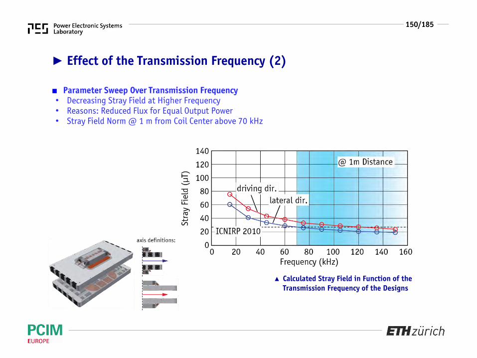
► Effect of the Transmission Frequency (2)
■ Parameter Sweep Over Transmission Frequency• Decreasing Stray Field at Higher Frequency• Reasons: Reduced Flux for Equal Output Power• Stray Field Norm @ 1 m from Coil Center above 70 kHz
▲ Calculated Stray Field in Function of theTransmission Frequency of the Designs

151/185
► Selected Transmission Frequency
■ Decreasing Losses (Significant up to 40 kHz)■ Stray Field Norm met above 70 kHz■ Up-Coming SAE Standard J2954 Suggests 85 kHz
Selected Frequency: 85 kHz
■ Immediate Implication:• Use Latest SiC-MOSFET Technology
for the Inverter-Stage• Design and Layout of Power Electronics
is Crucial for the IPT System
▲ FEM Calculation Results

152/185
► 50 kW IPT: Prototype Hardware
50 kW @ 800V, 85kHz96.5%41 x 76 x 6cm24.6kg
■ Calculated Performance• Output Power• Max. DC/DC-Efficiency• Coil Dimensions• Coil + Cap. Weight

153/185
► Estimated DC-to-DC Performance
■ Calculated Performance• Output Power• Maximum Efficiency• Coil Dimensions• Weight (Coil + Cap)• Power Density
▲ Calculated efficiency over output power forcontrol with variable DC-link voltage
50kW95.2% … 96.5%41x76x6cm25.7kg2.7kW/l, 1.9 kW/kg

154/185
Power ElectronicsConcept for 50 kW
System TopologyIPT Coil Interface3-Φ PFC Rectifiers

155/185
► Main System Components
■ Receiver-Side Power Electronics• (Synchronous) Rectification• Battery Current Regulation
■ Transmitter-Side Power Electronics• 1/3-Φ Mains Interface• High-Frequency Inverter Stage
■ IPT Transmission Coils• Magnetic Design (using FEM)• Shielding of Stray Field
■ Resonant Compensation• Requirements for Capacitor• Optimal Component Selection

156/185
► Back-to-Back IPT Test Bench
■ Test Setup for High-Power Back-to-Back 50 kW Operation• Direct DC-to-DC Power Loss Measurements at DC Power-Supply• Experimental Evaluation of Different Control Options• Design & Evaluation of Different Coil Designs

157/185
► Design Concept for 50 kW Prototype System
■ Ripple Cancellation by Parallel Interleaving• 3 x 20kW DC/DC-Converter Modules• Each Module has 2 Interleaved and
Magnetically Coupled Stages
■ Modular Design allows Disabling Stagesat Low Output Power Fully Benefit from High Partial-Load
Efficient IPT Concept

158/185
► Interleaved DC/DC-Converter with Coupled Inductors■ 180°-Interleaved Switching (shown for Buck-Mode)
■ Direct Coupled Inductor• Flux due to Common-Mode Voltage• DC-Flux Energy Storage• Reduction of Current-Ripple Requires
More Stored Magnetic Energy
■ Inverse Coupled Inductor• Flux due to Differential-Mode Voltage• No DC-Flux No Stored Energy• Reduction of Current-Ripple does not
Require Net Energy Storage
▲ Simulated Voltage and Flux Waveforms

159/185
► Separation of CM/DM Current Ripples■ Common-/Differential-Mode Equivalent Circuits
■ Separate Design of CM/DM Current Ripples usingDedicated Magnetic Devices
▲ Calculated Inductor/Output Current Ripple
▲ Simulated Inductor/Output Current

160/185
► Component Volume and Power Losses■ Compact Design of the Inductors• Helical Winding for High Filling Factor• Amorphous Iron Core with Gap for DCI• Nano-Crystalline Core w/o Gap for ICI• Switching Frequency 50 kHz,
10% Output Current Ripple 300 µH vs. 600 µH
■ Significantly Reduced Total MagneticsVolume (DCI+ICI) in Comparison to TwoSeparate, Uncoupled Inductors

161/185
► Inverter-Stage Using Parallel-Connected SiC-Devices■ Mainly Conduction Losses in Inverter Stage due to ZVS• Multiple SiC-Devices in Parallel for Rds(on)-Reduction• Single Gate-Drive for all Devices for Minimum Complexity
■ Test-Bench for Evaluation of• Switching Performance of Paralleled Devices• HF-Design of Power PCB and Device-Current Sharing
▲ Bridge Topology with 3 SiC MOSFETDevices Connected in Parallel
▲ 85 kHz Switching Test Bench (SiC Full-Bridge)

162/185
► Gate-Drive Concept for 3 Parallel-Connected Devices
■ Half-Bridge SiC-Driver PCB• One Driver IC for all 3 Parallel Devices,
Separate Gate Resistors for each Device• Synchronous Turn-On w/o Gate-Oscillation
▲ Zero-Voltage Turn-Off Transition▲ Half-Bridge Gate Driver PCB for 3 Parallel
MOSFETs on each Gate

163/185
► 60 kW SiC Power Converter■ Efficiency 98%, Power Density 9.2 kW/l, Forced-Air Cooled
164/185
3-Φ PFC Rectifier Systems
J. W. Kolar, T. Friedli, The Essence of Three-Phase PFC Rectifier Systems - Part
I, IEEE Transactions on Power Electronics, Vol. 28, No. 1, pp. 176-198, January 2013.
T. Friedli, M. Hartmann, J. W. Kolar, The Essence of Three-Phase PFC Rectifier Systems - Part II, IEEE
Transactions on Power Electronics, Vol. 29, No. 2, February 2014.

165/185
● Boost Type● Buck Type
VB ........... Output VoltageVN,ll,rms ... RMS Value of
Mains Line-to-Line Voltage
3-Φ AC/DC Power Conversion
● Wide Input/Output Voltage Range – Voltage Adaption● Mains Side Sinusoidal Current Shaping / Power Factor Correction
■ Basis Requirement for EV Charging / IPT Front End Converter Stages

166/185
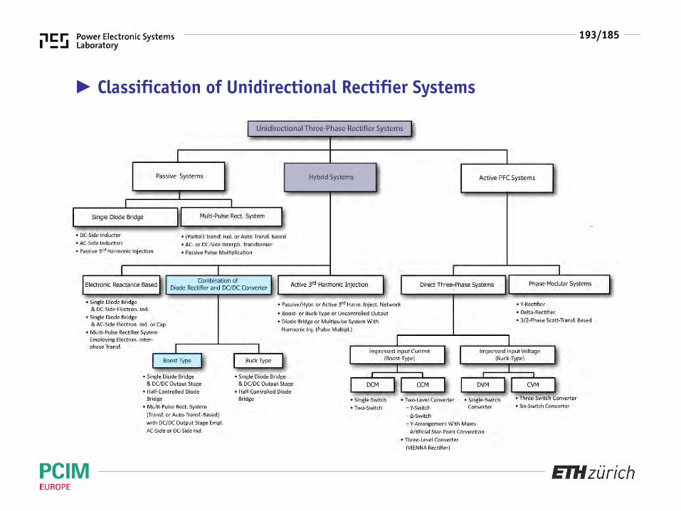
► Classification of General Unidirectional 3-Φ Rectifier Systems

167/185
■ Phase-Modular Systems
● Passive Rectifier Systems - Line Commutated Diode Bridge/Thyristor Bridge - Full/Half Controlled- Low Frequency Output Capacitor for DC Voltage Smoothing- Only Low Frequency Passive Components Employed for Current
Shaping, No Active Current Control- No Active Output Voltage Control
● Hybrid Rectifier Systems - Low Frequency and Switching Frequency Passive Components and/or- Mains Commutation (Diode/Thyristor Bridge - Full/Half Controlled)
and/or Forced Commutation- Partly Only Current Shaping/Control and/or Only Output Voltage Control- Partly Featuring Purely Sinusoidal Mains Current
● Active Rectifier Systems - Controlled Output Voltage- Controlled (Sinusoidal) Input Current- Only Forced Commutations / Switching Frequ. Passive Components
- Only One Common Output Voltage for All Phases- Symmetrical Structure of the Phase Legs - Phase (and/or Bridge-)Legs Connected either in Star or Delta
► Classification of Unidirectional Rectifier Systems
■ Direct Three-Phase Syst.
- Phase Rectifier Modules of Identical Structure- Phase Modules connected in Star or in Delta- Formation of Three Independent Controlled DC Output Voltages
168/185
Evaluation ofBoost-Type Systems
169/185
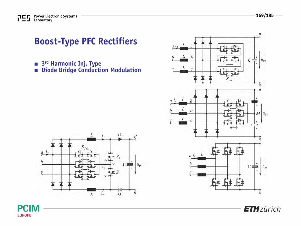
Boost-Type PFC Rectifiers
■ 3rd Harmonic Inj. Type■ Diode Bridge Conduction Modulation

170/185
Vienna Rectifier vs. Six-Switch Rectifier
Boost-
!

171/185
Comparison ofBuck-Type Systems

172/185
Buck-Type PFC Rectifiers
■ 3rd Harmonic Inj. Type■ Diode Bridge Cond. Modulation

173/185
SWISS Rectifier vs. Six-Switch Rectifier
!

174/185
Summary: UnidirectionalPFC Rectifier Systems

175/185
Boost-Type
Buck-Type
Buck+Boost-Type
+ Controlled Output Voltage+ Low Complexity + High Semicond. Utilization+ Total Power Factor λ ≈ 0.95– THDI ≈ 30%
► Block Shaped Input Current Rectifier Systems

176/185
Boost-Type
UnregulatedOutput
+ Controlled Output Voltage+ Relatively Low Control Complexity + Tolerates Mains Phase Loss– 2-Level Characteristic– Power Semiconductors Stressed with Full
Output Voltage
+ Controlled Output Voltage+ 3-Level Characteristic+ Tolerates Mains Phase Loss+ Power Semicond. Stressed with Half
Output Voltage– Higher Control Complexity
+ Low Current Stress on Power Semicond.+ In Principal No DC-Link Cap. Required+ Control Shows Low Complexity– Sinusoidal Mains Current Only for Const.
Power Load– Power Semicond. Stressed with Full
Output Voltage– Does Not Tolerate Loss of a Mains Phase
► Sinusoidal Input Current Rectifier Systems (1)
Boost-Type

177/185
Buck-Type
Buck+Boost-Type
+ Allows to Generate Low Output Voltages+ Short Circuit Current Limiting Capability– Power Semicond. Stressed with LL-Voltages– AC-Side Filter Capacitors / Fundamental
Reactive Power Consumption
+ See Buck-Type Converter+ Wide Output Voltage Range+ Tolerates Mains Phase Loss, i.e. Sinusoidal
Mains Current also for 2-Phase Operation– See Buck-Type Converter (6-Switch Version
of Buck Stage Enables Compensation of AC-Side Filter Cap. Reactive Power)
► Sinusoidal Input Current Rectifier Systems (2)

178/185
Conclusions & OutlookSummary of Key ResultsAdvantageous ApplicationsKey Challenge

179/185
► Key Figures of Designed Transmission Systems■ 5 kW Prototype System
■ 50 kW Prototype System
50 kW @ 800V, 85kHz96.5% (calculated)41 x 76 x 6cm24.6 kg
2.0 kW/kg1.6 kW/dm2
2.7 kW/dm3
52 g/kW160 g/kW9.4 mm2/kW
• Output Power• DC/DC-Efficiency• Coil Dimensions• Weight Coil + Cap.
• Spec. Weight• Area-Rel. Power Dens.• Power Density• Spec. Copper Weight• Spec. Ferrite Weight• Spec. SiC-Chip Area
5 kW @ 400V, 100kHz96.5% @ 52mm (measured)210mm x 30 mm2.3kg
2.2 kW/kg1.47 kW/dm2
4.8 kW/dm3
43 g/kW112 g/kW
• Output Power• DC/DC-Efficiency• Coil Dimensions• Weight Coil + Cap.
• Spec. Weight• Area-Rel. Power Dens.• Power Density• Spec. Copper Weight• Spec. Ferrite Weight

180/185
Σ Inductive Power Transferfor EV Charging
■ Resonant Circuit Design• Compensation Topology• Impedance Matching
■ Coil Design & Optimization• Magnetic Modeling & Design• Multi-Objective Optimization
■ Modulation & Control Scheme• Active Load Matching• High Partial-Load Efficiency
■ Power Electronic Converter• High Frequency Capability• Coil, Battery & Mains Interfaces
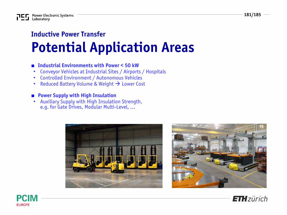
181/185
■ Industrial Environments with Power < 50 kW• Conveyor Vehicles at Industrial Sites / Airports / Hospitals• Controlled Environment / Autonomous Vehicles• Reduced Battery Volume & Weight Lower Cost
■ Power Supply with High Insulation• Auxiliary Supply with High Insulation Strength,
e.g. for Gate Drives, Modular Multi-Level, …
Potential Application AreasInductive Power Transfer
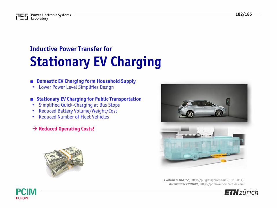
182/185
■ Domestic EV Charging form Household Supply• Lower Power Level Simplifies Design
■ Stationary EV Charging for Public Transportation• Simplified Quick-Charging at Bus Stops• Reduced Battery Volume/Weight/Cost• Reduced Number of Fleet Vehicles
Reduced Operating Costs!
Stationary EV ChargingInductive Power Transfer for
Bombardier PRIMOVE, http://primove.bombardier.com.Evatran PLUGLESS, http://pluglesspower.com (6.11.2014).

183/185
■ Compliance with Field-Exposure Standards at High Power Levels• High Frequency for High Power Transfer Where is the Limit?• Include Modifications on Vehicle Chassis?• Positioning of the Coil: On the Floor / the Roof?
Key ChallengeInductive Power Transfer
▲ Field Values are Limiting Factor at High Power▲ Include Chassis Modifications in Design
& Re-Consider Coil Positioning

184/185
… the Hype Cycle
IPT for stationaryEV charging
IPT for dynamicEV charging
IPT for industryautomation
ApplicationsInductive Power Transfer
185/185
Thank You!Questions?
187/185
► Further Information■ Appendix 1: Comments on Dynamic IPT Charging■ Appendix 2: 3-Φ PFC Rectifier Systems
■ List of Key Publications (click title to view online)
• R. Bosshard, J. W. Kolar, J. W. Mühlethaler, I. Stevanovic, B. Wunsch, F. Canales, “Modeling and η-α-Pareto optimization of inductive power transfer coils for electric vehicles,” IEEE J. Emerg. Sel. Topics Power Electron., vol. 3, no. 1., pp.50-64, March 2015.
• R. Bosshard, J. W. Kolar, B. Wunsch, “Control Method for Inductive Power Transfer with High Partial-Load Efficiency and Resonance Tracking,” Proc. Int. Power Electron. Conf. - ECCE Asia (IPEC 2014), May 2014.
• R. Bosshard, J. W. Kolar, B. Wunsch, “Accurate Finite-Element Modeling and Experimental Verification of Inductive Power Transfer Coil Design,” Proc. 29th Appl. Power Electron. Conf. and Expo. (APEC 2014), March 2014.
• R. Bosshard, J. Mühlethaler, J. W. Kolar, I. Stevanovic, “Optimized Magnetic Design for Inductive Power Transfer Coils,” Proc. 28th Appl. Power Electron. Conf. and Expo. (APEC 2013), March 2013.
• R. Bosshard, U. Badstübner, J. W. Kolar, I. Stevanovic, “Comparative Evaluation of Control Methods for Inductive Power Transfer,” Proc. Int. Conf. on Renewable Energy Research and Appl. (ICRERA 2012), November 2012.
• R. Bosshard, J. Mühlethaler, J. W. Kolar, I. Stevanovic, “The ƞ-α-Pareto Front of Inductive Power Transfer Coils,” Proc. Annu. Conf. IEEE Ind. Electron. Soc. (IECON 2012), October 2012.
• J. W. Kolar, T. Friedli, “The Essence of Three-Phase PFC Rectifier Systems - Part I,” IEEE Trans. Power Electron., vol. 28, no. 1, pp. 176-198, January 2013.
• T. Friedli, M. Hartmann, J. W. Kolar, “The Essence of Three-Phase PFC Rectifier Systems - Part II”, IEEE Trans. Power Electron., vol. 29, no. 2, February 2014.
■ Contact Information• Roman Bosshard: [email protected]• Johann W. Kolar: [email protected]

188/185
Appendix 1:
Comments onDynamic IPT Charging
189/185
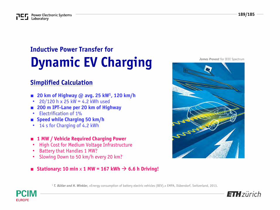
Simplified Calculation
■ 20 km of Highway @ avg. 25 kW1, 120 km/h• 20/120 h x 25 kW = 4.2 kWh used■ 200 m IPT-Lane per 20 km of Highway• Electrification of 1%■ Speed while Charging 50 km/h• 14 s for Charging of 4.2 kWh
■ 1 MW / Vehicle Required Charging Power• High Cost for Medium Voltage Infrastructure• Battery that Handles 1 MW?• Slowing Down to 50 km/h every 20 km?
■ Stationary: 10 min x 1 MW = 167 kWh 6.6 h Driving!
Dynamic EV ChargingInductive Power Transfer for
James Provost for IEEE Spectrum
1 T. Bütler and H. Winkler, «Energy consumption of battery electric vehicles (BEV),» EMPA, Dübendorf, Switzerland, 2013.

190/185
■ Large & Expensive Installationvs. Improving Battery Technology
■ Medium-Voltage Supply & Distribution of Power along 1% of all Highways
■ Efficiency of Dynamic IPTvs. Increasing Energy Cost?
■ Possible Applications:• Electrification @ Traffic Lights, Bus Stops, …• Transportation Vehicles @ Industrial Sites
Dynamic EV ChargingInductive Power Transfer for

191/185
Appendix 2:
3-Φ PFC Rectifier Systems
J. W. Kolar, T. Friedli, The Essence of Three-Phase PFC Rectifier
Systems - Part I, IEEE Transactions on Power Electronics, Vol. 28, No. 1, pp.
176-198, January 2013.
T. Friedli, M. Hartmann, J. W. Kolar,The Essence of Three-Phase PFC Rectifier Systems - Part II, IEEE Transactions on
Power Electronics, Vol. 29, No. 2, February 2014.

192/185
Hybrid 3-Φ Boost-Type PFC Rectifier Systems
3rd Harmonic Injection Rectifier
193/185
► Classification of Unidirectional Rectifier Systems
194/185
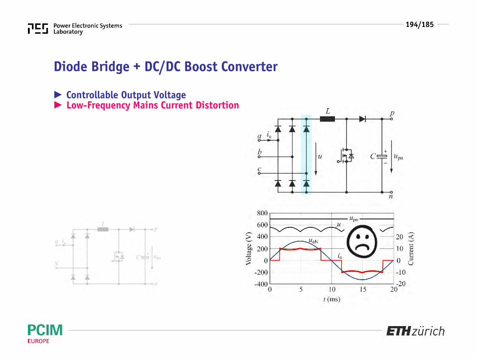
Diode Bridge + DC/DC Boost Converter
► Controllable Output Voltage► Low-Frequency Mains Current Distortion
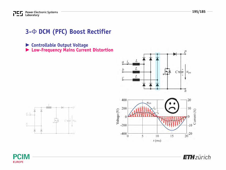
195/185
3-Φ DCM (PFC) Boost Rectifier
► Controllable Output Voltage► Low-Frequency Mains Current Distortion

196/185
► Classification of Unidirectional Rectifier Systems
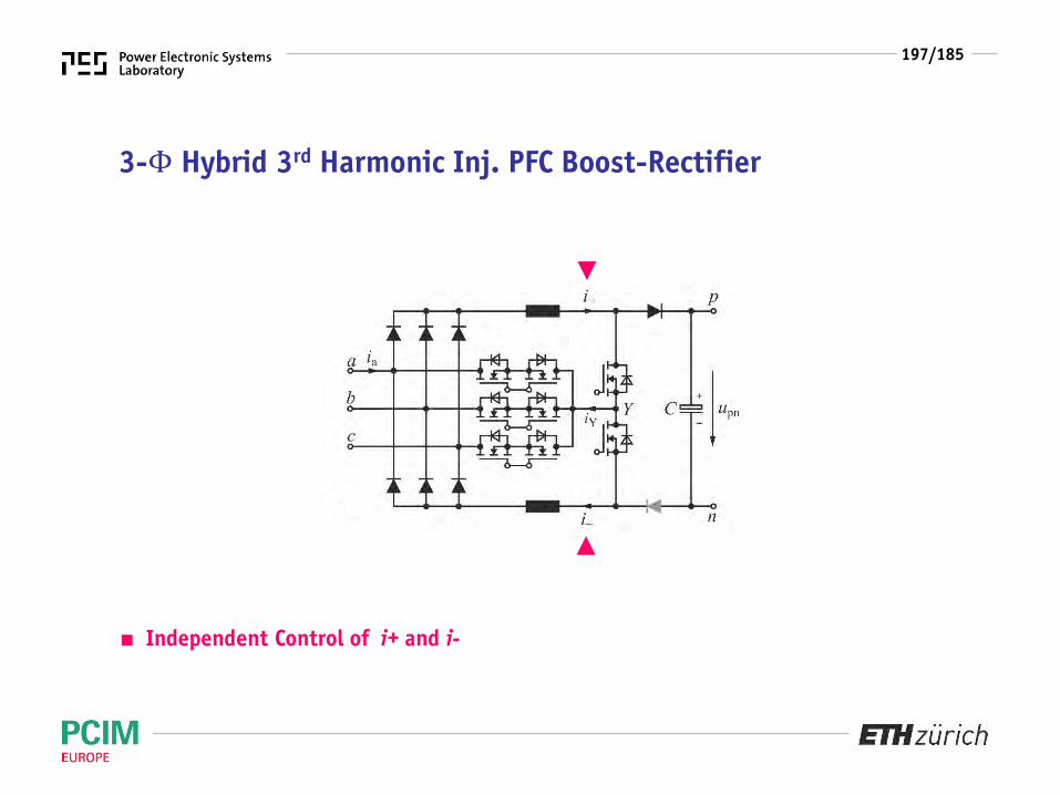
197/185
3-Φ Hybrid 3rd Harmonic Inj. PFC Boost-Rectifier
■ Independent Control of i+ and i-
◄
◄

198/185
■ Sinusoidal Control of i+ and i- and iY
au
ai G u
ci G u
cubu
( )b a c bi G u u G u
3-Φ Hybrid 3rd Harmonic Inj. PFC Boost-Rectifier

199/185
au
cubu
■ Sinusoidal Mains Current Control Limited to Ohmic Mains Behavior■ Output Voltage Control High Minimum Output Voltage Level
3-Φ Hybrid 3rd Harmonic Inj. PFC Boost-Rectifier

200/185
■ Sinusoidal Mains Current Requires Constant Power Load PO= const. NO (!) Output Voltage Control
pnut
3-Φ Active Filter Type PFC Rectifier

201/185
Active 3-Φ Boost-Type PFC Rectifier Systems
Δ-Switch RectifierVienna-Rectifier
Six-Switch Rectifier

202/185
► Classification of Unidirectional Rectifier Systems

203/185
Δ-Switch Rectifier
■ Modulation of Diode Bridge Input Voltages / Conduction States■ Derivation of 3-Φ Topology Phase-Symmetry / Bridge-Symmetry

204/185
Δ-Switch Rectifier
■ Output Voltage Control■ Sinusoidal Mains Current Control■ Φ = (-30°,+30°)

205/185
Vienna Rectifier
■ Replace Δ-Switch by Y-Switch■ Connect Y-Switch to Output Center Point■ Maximum Phase/Bridge Symmetry
■ Output Voltage Control■ Sinusoidal Mains Current Control■ Φ = (-30°,+30°)

206/185
► Three-Level Characteristic
Vienna Rectifier
+ Low Input Inductance Requ. + Low Switching Losses, + Low EMI– Higher Circuit Complexity – Control of Output Voltage Center Point Required
► Difference of Mains Voltage (e.g. ua) and Mains Frequency Comp. of VoltageFormed at Rectifier Bridge Input (e.g. ) Impresses Mains Current (e.g. ia)
δ typ. 0,1°… 0,3°

207/185
Control Structure
■ Output Voltage Control & Inner Mains Current Control & NPP Control
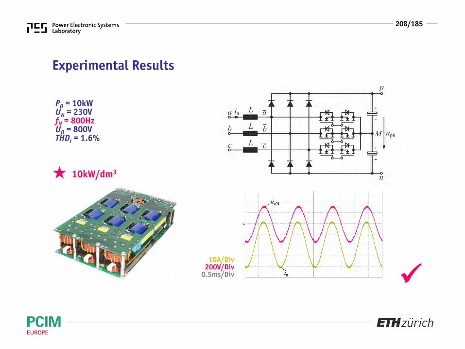
208/185
PO = 10kWUN = 230VfN = 800HzUO = 800VTHDi = 1.6%
Experimental Results
10A/Div200V/Div
0.5ms/Div
10kW/dm3

209/185
Fully-Controlled (Six-Switch) Bridge Rectifier
■ Output Voltage Control Phase- & Bridge-Symmetry Sinusoidal Mains Current Control Φ = (-180°,+180°) – Bidirectional (!)

210/185
– Unidirectional– Bidirectional
3-Φ Buck-TypePFC Rectifier Systems

211/185
► Classification of Unidirectional Rectifier Systems

212/185
Active 3-Φ Buck-Type PFC Rectifier Systems
Three-Switch RectifierSix-Switch Rectifier
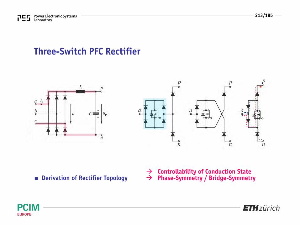
213/185
Controllability of Conduction State■ Derivation of Rectifier Topology Phase-Symmetry / Bridge-Symmetry
Three-Switch PFC Rectifier
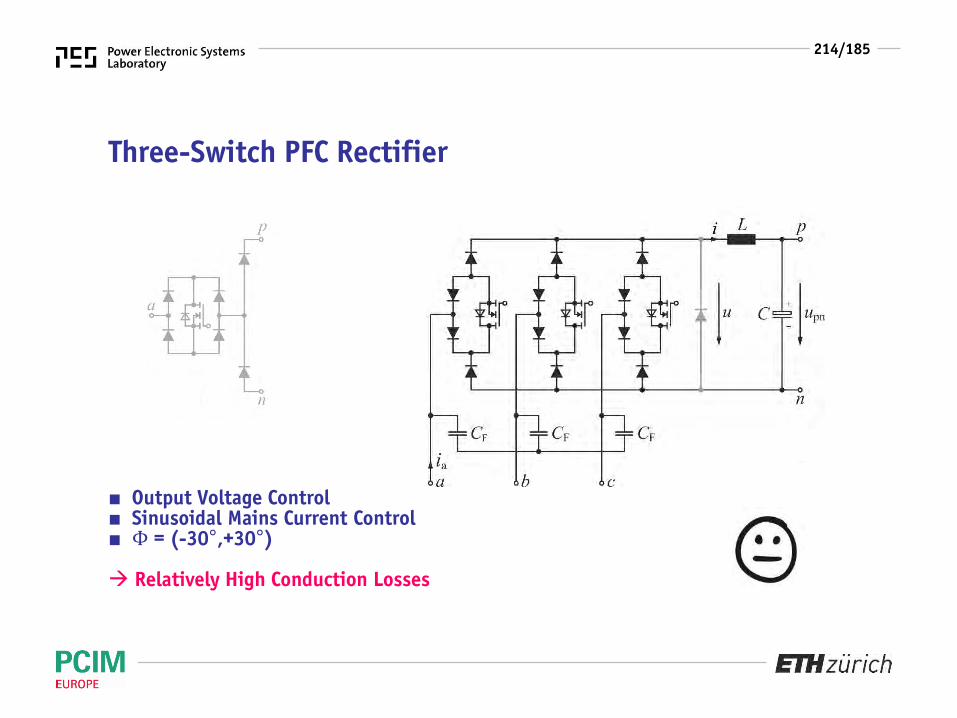
214/185
Three-Switch PFC Rectifier
■ Output Voltage Control■ Sinusoidal Mains Current Control■ Φ = (-30°,+30°)
Relatively High Conduction Losses

215/185
Six-Switch PFC Rectifier
■ Output Voltage Control■ Sinusoidal Mains Current Control■ Φ = (-90°,+90°)
Controllability of Conduction State Phase-Symmetry / Bridge-Symmetry

216/185
● Consider 60°-Wide Segment of the Mains Period; Suitable Switching States Denominated by (sa, sb, sc)
● Clamping and “Staircase-Shaped” Link Voltage in Order to Minimize the Switching Losses
(111) (110) (100)
(101) (011) also: (010)(011)
► Modulation Scheme
- Assumption:
- Phase c for etc.
- Phase a for ,
● Clamping to Phase with Highest Absolute Voltage Value, i.e.

217/185
► Input Current and Output Voltage Formation
● Output Voltage is Formed by Segments of theInput Line-to-Line Voltages
● Output Voltage Shows Const. Local Average Value
- Output Voltage Formation:
- Assumption:

218/185
■ Output Voltage Control & Inner Output Current Control
Control Structure

219/185
■ Ultra-Efficient Demonstrator System
► Experimental Results
ULL = 3 x 400 V (50 Hz)Po = 5 kWUo = 400 Vfs = 18 kHzL = 2 x 0.65 mH
= 98.8% (Calorimetric Measurement)
220/185
3rd Harmonic Inj. Buck-Type PFC Rectifier Systems
SWISS Rectifier
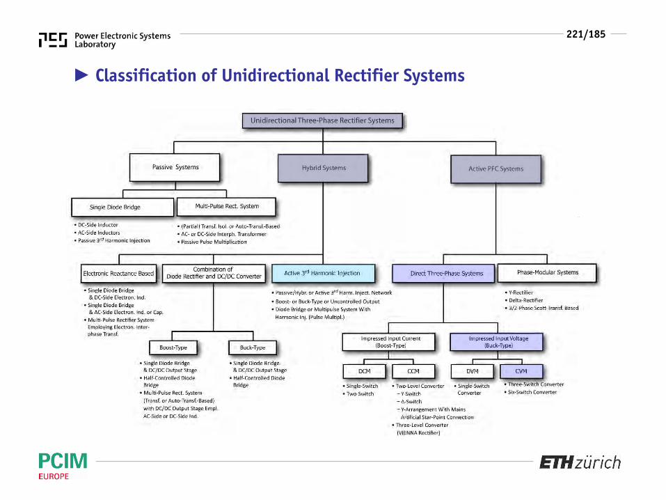
221/185
► Classification of Unidirectional Rectifier Systems
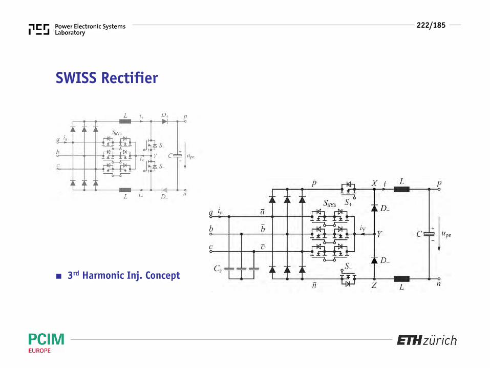
222/185
SWISS Rectifier
■ 3rd Harmonic Inj. Concept

223/185
SWISS Rectifier
■ Output Voltage Control■ Sinusoidal Current Control

224/185
SWISS Rectifier
■ Output Voltage Control■ Sinusoidal Current Control
Low Complexity
225/185
Bidirectional PFC Rectifier Systems• Boost-Type Topologies• Buck-Type Topologies

226/185
Boost-Type Topologies

227/185
► Classification of Bidirectional Boost-Type Rectifier Systems

228/185
► Derivation of Two-Level Boost-Type Topologies
● Output Operating Range

229/185
► Derivation of Three-Level Boost-Type Topologies
● Output Operating Range
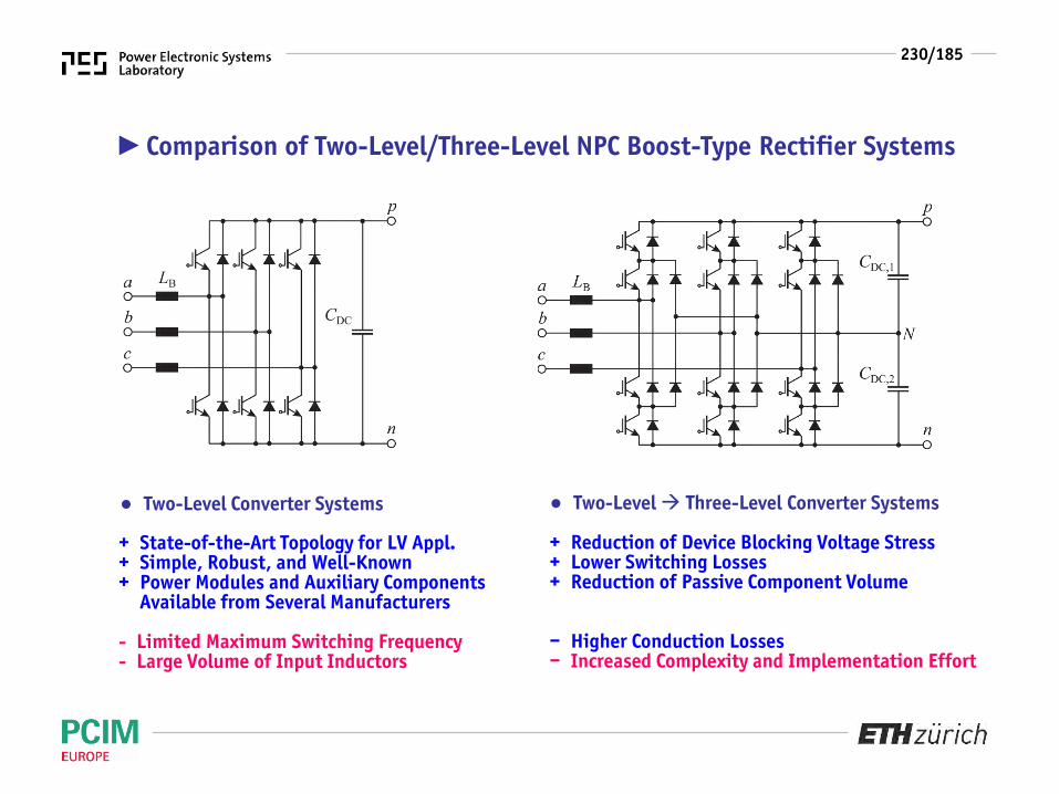
230/185
● Two-Level Three-Level Converter Systems
+ Reduction of Device Blocking Voltage Stress+ Lower Switching Losses+ Reduction of Passive Component Volume
– Higher Conduction Losses– Increased Complexity and Implementation Effort
+ State-of-the-Art Topology for LV Appl.+ Simple, Robust, and Well-Known+ Power Modules and Auxiliary Components
Available from Several Manufacturers
- Limited Maximum Switching Frequency- Large Volume of Input Inductors
►Comparison of Two-Level/Three-Level NPC Boost-Type Rectifier Systems
● Two-Level Converter Systems
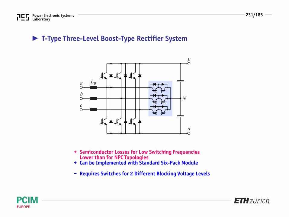
231/185
+ Semiconductor Losses for Low Switching FrequenciesLower than for NPC Topologies
+ Can be Implemented with Standard Six-Pack Module
– Requires Switches for 2 Different Blocking Voltage Levels
► T-Type Three-Level Boost-Type Rectifier System

232/185
► Multi-Level Topologies are Commonly Used for Medium Voltage Applications but GainSteadily in Importance also for Low-Voltage Renewable Energy Applications
– More Semiconductors– More Gate Drive Units– Increased Complexity– Capacitor Voltage Balancing Required– Increased Cost
+ Losses are Distributed over Many Semicond.Devices; More Even Loading of the Chips Potential for Chip Area Optimization for PureRectifier Operation
+ High Efficiency at High Switching Frequency+ Lower Volume of Passive Components
● Moderate Increase of the Component Countwith the T-Type Topology
► Pros and Cons of Three-Level vs. Two-Level Boost-Type Rectifier Systems
Consideration for 10kVA/400VAC RectifierOperation; Min. Chip Area, Tj,max= 125°C

233/185
Buck-Type Topologies

234/185
● System also Features Boost-Type Operation
● Output Operating Range
►Derivation of Unipolar Output Bidirectional Buck-Type Topologies
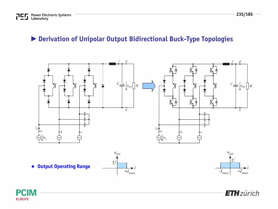
235/185
►Derivation of Unipolar Output Bidirectional Buck-Type Topologies
● Output Operating Range
236/185
Thank you!

237/185
received his M.Sc. and Ph.D. degree (summa cum laude / promotio sub auspiciis praesidentis rei publicae) from the University ofTechnology Vienna, Austria. Since 1984 he has been working as an independent international consultant in close collaboration withthe University of Technology Vienna, in the fields of power electronics, industrial electronics and high performance drives. He hasproposed numerous novel converter topologies and modulation/control concepts, e.g., the VIENNA Rectifier, the SWISS Rectifier, theDelta-Switch Rectifier, the isolated Y-Matrix AC/DC Converter and the three-phase AC-AC Sparse Matrix Converter. Dr. Kolar haspublished over 450 scientific papers at main international conferences, over 180 papers in international journals, and 2 book chapters.Furthermore, he has filed more than 110 patents. He was appointed Assoc. Professor and Head of the Power Electronic SystemsLaboratory at the Swiss Federal Institute of Technology (ETH) Zurich on Feb. 1, 2001, and was promoted to the rank of Full Prof. in2004. Since 2001 he has supervised over 60 Ph.D. students and PostDocs.
The focus of his current research is on AC-AC and AC-DC converter topologies with low effects on the mains, e.g. for data centers,More-Electric-Aircraft and distributed renewable energy systems, and on Solid-State Transformers for Smart Microgrid Systems. Furthermain research areas are the realization of ultra-compact and ultra-efficient converter modules employing latest power semiconductortechnology (SiC and GaN), micro power electronics and/or Power Supplies on Chip, multi-domain/scale modeling/simulation and multi-objective optimization, physical model-based lifetime prediction, pulsed power, and ultra-high speed and bearingless motors. He hasbeen appointed an IEEE Distinguished Lecturer by the IEEE Power Electronics Society in 2011.He received 9 IEEE Transactions Prize Paper Awards, 8 IEEE Conference Prize Paper Awards, the PCIM Europe Conference Prize PaperAward 2013 and the SEMIKRON Innovation Award 2014. Furthermore, he received the ETH Zurich Golden Owl Award 2011 for Excellencein Teaching and an Erskine Fellowship from the University of Canterbury, New Zealand, in 2003.He initiated and/or is the founder/co-founder of 4 spin-off companies targeting ultra-high speed drives, multi-domain/levelsimulation, ultra-compact/efficient converter systems and pulsed power/electronic energy processing. In 2006, the European PowerSupplies Manufacturers Association (EPSMA) awarded the Power Electronics Systems Laboratory of ETH Zurich as the leading academicresearch institution in Power Electronics in Europe.Dr. Kolar is a Fellow of the IEEE and a Member of the IEEJ and of International Steering Committees and Technical Program Committeesof numerous international conferences in the field (e.g. Director of the Power Quality Branch of the International Conference on PowerConversion and Intelligent Motion). He is the founding Chairman of the IEEE PELS Austria and Switzerland Chapter and Chairman of theEducation Chapter of the EPE Association. From 1997 through 2000 he has been serving as an Associate Editor of the IEEE Transactionson Industrial Electronics and from 2001 through 2013 as an Associate Editor of the IEEE Transactions on Power Electronics. Since 2002he also is an Associate Editor of the Journal of Power Electronics of the Korean Institute of Power Electronics and a member of theEditorial Advisory Board of the IEEJ Transactions on Electrical and Electronic Engineering.
AboutJohann W. Kolar (F’10)

238/185
received the M.Sc. degree from the Swiss Federal Institute of Technology (ETH) Zurich, Switzerland, in 2011. During his studies, he focused on power electronics, electrical drive systems, and control of mechatronic systems. As part of his M.Sc. degree, he participated in a development project at ABB Switzerland as an intern, working on a motor controller for traction converters in urban transportation applications. In his Master Thesis, he developed a sensorless current and speed controller for a ultrahigh-speed electrical drive system with CELEROTON, an ETH Spin-off founded by former Ph.D. students of the Power Electronic Systems Laboratory at ETH Zurich.
In 2011, he joined the Power Electronic Systems Laboratory at the Swiss Federal Institute of Technology (ETH) Zurich, where he is currently pursuing the Ph.D. degree. His main research area is inductive power transfer systems for electric vehicle battery charging, where he published five papers at international IEEE conferences and one paper in the IEEE Journal of Emerging and Selected Topics in Power Electronics.
AboutRoman Bosshard (S’10)