Plasma Potential Enhancement by RF Heating Near the Ion Cyclotron Frequency
Upload
independentCategory
view
1download
0
Sadhana Vol. 30, Part 1, February 2005, pp. 21–46. © Printed in India
Ion cyclotron resonance heating system on Aditya
D BORA 1, SUNIL KUMAR1, RAJ SINGH1, S V KULKARNI1,A MUKHERJEE1, J P SINGH1, RAGURAJ SINGH1, S DANI1,A PATEL1, SAI KUMAR1, V GEORGE1, Y S S SRINIVAS1,P KHILAR1, M KUSHWAH1, P SHAH1, H M JADAV1,RAJNISH KUMAR1, S GANGOPADHYAY1, H MACHHAR1,B KADIA 1, K PARMAR1, A BHARDWAJ1, SURESH ADAV1,D RATHI1 and D S BHATTACHARYA2
1Institute for Plasma Research, Bhat, Gandhinagar 382 428, India2Variable Electron Cyclotron Centre, Kolkata, Indiae-mail: [email protected]
MS received 26 August 2003; revised 4 May 2004
Abstract. An ion cyclotron resonance heating (ICRH) system has been designed,fabricated indigenously and commissioned on Tokamak Aditya. The system hasbeen commissioned to operate between 20·0 and 47·0 MHz at a maximum powerof 200 kW continuous wave (CW). Duration of 500 ms is sufficient for operationon Aditya, however, the same system feeds the final stage of the 1·5 MW ICRHsystem being prepared for the steady-state superconducting tokamak (SST-1) fora duration of 1000 s. Radio frequency (RF) power (225 kW) has been generatedand successfully tested on a dummy load for 100 s at 30·0 MHz. Lower powershave been coupled to Aditya in a breakdown experiment. We describe the systemin detail in this work.
Keywords. Tokamak; ICRH; radio frequency, magnetosonic wave, secondharmonic heating.
1. Introduction
A tokamak is a magnetically confined device with high temperature plasma to reach ignitionfor the generation of thermonuclear power. The plasma of a tokamak cannot be heated toignition using ohmic heating alone, since joule-heating efficiency decreases with increasein plasma temperature and the maximum value of plasma current is limited by the onset ofmagneto-hydrodynamic instabilities that terminate the discharge. Auxiliary heating thereforeis essential to achieve the goal.
Radio frequency (RF) heating of tokamak plasmas is one of the most successful auxiliaryheating schemes at present. Different frequency ranges have been tried in different experi-ments. Ion cyclotron resonance frequency (ICRF) range has been very successfully used upto multi-megawatt power levels in tokamaks.
21

22 D Bora et al
Fast magnetosonic waves (compressional Alfven waves) do not resonate at the cyclotronfrequency, but propagate above and below this frequency. The fast waves are right-circularlypolarized and do not couple energy to the ions in a purely single species plasma. However, inthe presence of a minority species, very efficient heating has been observed. Three regimeshave been found that enable efficient coupling of RF energy to the ions. They are as follows.
(i) Minority fundamental heating,(ii) ion–ion hybrid heating, and
(iii) second harmonic heating of a single species plasma.
Power absorbed to the plasma particles varies from machine to machine. Till now themaximum absorbed power in the ion cyclotron frequency range is 24 MW, while 32 MW waslaunched from the generator (JET result).
An auxiliary RF heating system to raise the plasma temperature at the ion cyclotron reso-nance frequency has been commissioned on Tokamak Aditya (Bhatt et al 1989). The auxiliarylaunched power (of the electromagnetic waves) must eventually be transferred to the bulk ofthe plasma and ultimately to the fuel-ion components of the plasma if fusion reactions areto take place. Thermalization of the external energy usually takes place through collisionalprocesses. The injected fast particles or the particles accelerated by the electromagnetic fieldtransfer their energy to the plasma background through collisions. In the case of wave heating,this process occurs indirectly through waves (Alfven, lower-hybrid etc) or particle (Landau,cyclotron) resonances that are basically non-collisional processes. These non-collisional pro-cesses cause velocity space diffusion of the particle that is counterbalanced by the collisionsthat tend to restore a Maxwellian distribution. Wave heating methods can create very ener-getic particles for which collisions are negligible. In such cases the magnetic field should bevery strong to confine energetic particles.
Among all wave-heating schemes, ion cyclotron frequency heating (ICRH) appears to bemost attractive both in terms of physics and technology. First significant experimental resultson plasma heating by wave coupling in the ion cyclotron frequency range were obtained in1974 in TM1-RF (Vdovin et al 1974) and in ST tokamak (Adam et al 1974) where appreciableheating of a deuterium plasma was observed for frequencies in the vicinity of ω = 2�D ,where ω is launched frequency and �D denotes cyclotron frequency for deuterium plasma.
The system is broadly divided into the following sub-systems:
• Radio frequency (RF) generator• Transmission line• Interface• Antenna• Electrical DC power supplies• Data acquisition and control (DAC) system.
In this paper, we describe the subsystems that constitute the ICRH system on Aditya. Thesecond section of this report is a description on indigenously built 200 kW RF generator. Italso presents the necessary operating source frequency depending on the toroidal magneticfield and requirement of RF power to raise plasma temperature. Detailed design of variouscomponents of transmission line is presented in § 3. Section 4 discusses the design of thevacuum transmission line, called interface. High power fast wave antenna design is describedin § 5. This section also deals with thermal loads on antenna during operation, impuritygeneration and electromagnetic stresses due to plasma disruption. Different kinds of DC

Ion cyclotron resonance heating system on Aditya 23
Table 1. Operating frequencies vs. magneticfields.
Gas used: H2
BT (T) 0·75 0·9 1·0 1·22fCH (MHz) 22·8 27·4 30·4 36·5
power supplies required for 200 kW modular RF generator are described in § 6. Section 7discusses data acquisition and control for the ICRH system. Initial experimental results onplasma load are reported in § 8.
2. RF generator
Requirements for RF generators for fusion research include high power, long pulse durationand reliability. The design of the RF generator is based on the requirements for heating plasmaswith various ion species, plasma parameters and magnetic fields.
The required frequency f is considered keeping in mind the toroidal magnetic field at theplasma centre. In Aditya tokamak the field value is varied between 0·75 T and 1·2 T. Table 1shows the operating frequencies for different magnetic fields.
Minimum power requirement is estimated to fix output power from the RF generator. Fromthe consideration of the power balance equation, the expected plasma temperature (Dolan1982) is,
0·024〈n(Te + Ti)〉/τE = (Pin − Pr)/Vp.
Assuming Pr ≈ 0·3Pin and Ti ≈ 0·4Te we get,
〈Te〉 = (0·7PinτE)/(0·034〈n20〉Vp).
We have calculated energy confinement time using ITER89-P L-mode scaling (Uckan et al1990) and is given by:
τE = 0·048I 0·85〈n20〉0·1a0·3R1·2o A0·5
i P −0·5in κ0·5
x B0·2,where,
τE = energy confinement time (s), Vp = plasma volume = 2π2a2R\κ(m3),Te = electron temperature (keV), Pin = input power = POH + Paux (MW),POH = ohmic power = VloopIp (MW), Paux = auxiliary power (MW),Pr = radiative power (MW), andτE = 3·9 ms, Te = 432 eV, Ti = 173 eV,
where, Paux = 0·2 MW and POH = 0·2 MW.Thus, to raise the temperature at least by 0·4 keV and maintain it at that level, we fix the
RF power requirement at 200 kW. Hence, the RF generator for ICRH system on Aditya isdesigned to fulfill the specifications given in table 2.
The ICRH generator (figure 1) for Aditya consists of a low power oscillator, RF switch,modulator switch, RF attenuator, three stages of solid state low power amplifiers, three stages

24 D Bora et al
Table 2. Specifications for the RF generator forAditya ICRH system.
Parameter ICRH system specifications
CWRF power 200 kW (max)Radio frequencies 20 to 40·0 MHzHarmonic content −30 dBcRF pulse duration 100 ms
of power grid and tube high power amplifiers. All the stages of the generator are designed tocover 20 to 40 MHz frequency range for the Aditya ICRH experiments.
One additional chain that covers 22·8 to 45·6 ± 1 MHz is designed to drive the 1·5 MWoutput final stage of the SST-1 ICRH CW RF generator. The same also acts as a spare for theAditya ICRH generator. A description of each section of the 200 kW RF generator is givenin the next section.
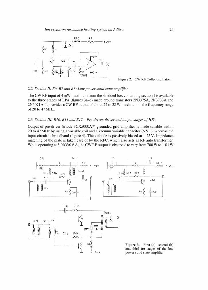
2.1 Section I: B1, B2 B3, B4 and B5 – CWRF oscillator, buffer, RF switch, modulator andattenuator
The tunable Collpit oscillator (figure 2) using a transistor 2N2222A gives out CW RF of 4 mWmax within 20 to 47 MHz by means of a variable parallel plate capacitor. In-built closed loopbuffer AD9630 at the output provides constant load and stability to the oscillator. The surfacemountable RF switch PSW1111, the modulator switch PSW1111 and the RF attenuator PAS-3 from mini-circuits are used in series along with the CW RF oscillator on the same PCB.The RF switch PSW-1111 needs +5 V to switch ON with rise/fall time of less than 4 µs. RFattenuator PAS-3 acts to vary the output power of the oscillator from 0·5 mw to 4·0 mw byusing a 0–20 mA DC current source. It controls the amplified output power within 10 dB.Another buffer amplifier AD9360 is used on the same PCB to minimize the effects of loading.
Figure 1. Schematic of ICRH generator in Aditya.
Ion cyclotron resonance heating system on Aditya 25
Figure 2. CW RF Collpi oscillator.
2.2 Section II: B6, B7 and B8: Low power solid state amplifier
The CW RF input of 4 mW maximum from the shielded box containing section I is availableto the three stages of LPA (figures 3a–c) made around transistors 2N3375A, 2N3733A and2N5071A. It provides a CW RF output of about 22 to 28 W maximum in the frequency rangeof 20 to 47 MHz.
2.3 Section III: B10, B11 and B12 – Pre-driver, driver and output stages of HPA
Output of pre-driver (triode 3CX5000A7) grounded grid amplifier is made tunable within20 to 47 MHz by using a variable coil and a vacuum variable capacitor (VVC), whereas theinput circuit is broadband (figure 4). The cathode is passively biased at +25 V. Impedancematching of the plate is taken care of by the RFC, which also acts as RF auto transformer.While operating at 3·0 kV/0·6 A, the CW RF output is observed to vary from 700 W to 1·0 kW
Figure 3. First (a), second (b)and third (c) stages of the lowpower solid state amplifier.

26 D Bora et al
Figure 4. Circuit diagram for pre-driver and driver stages.
with efficiency ∼ 48%, gain ∼ 15·5 dB in class AB mode for an input varying from 20 to24 W at different frequencies in between 20 and 47 MHz.
Output circuit of the driver (triode 3CW30000H7) grounded grid amplifier is made tun-able within 20 to 47 MHz by using a variable coil and a VVC whereas the input circuit isbroadband (figure 4). The cathode is passively biased at +50 V. Impedance matching of theplate is taken care of by the RFC, which also acts as RF transformer. While operating at6·0 kV/3·5 A, the CW RF output is observed varying from 9 kW to 15 kW with efficiency∼ 50%, gain ∼ 15·0 dB in class AB mode for an input varying from 700 W to 1·0 kW atdifferent frequencies between 20 and 47 MHz.
The output stage of the Aditya ICRH generator or driver stage of the SST-1 ICRH generatorfor up to 46·6 MHz (figure 5) uses tetrode 4CM300000GA. The output cavity is tunablewith a movable-shorting plunger. Plate blocking 4 kpF capacitor is a array of eight 500pFcapacitors. The output resistance of 238� to 358� is matched to 50� with a series coupledVVC. Distributed components are used for making input and output cavities. The screengrid is kept at the RF ground and control grid at DC ground. The T-section transmission linenetwork matches the 50� with input impedance of 6·25� to 10� at a maximum of 10 kW.It uses a shunt VVC of 100 to 1000 pF to cancel the reactive part. This stage is tested at13 kV/22 A with CWRF input of ∼ 10 kW. Output power ∼ 200 kW/10 S is observed at29 MHz against the tunable range of 20–47 MHz (figure 6). RF power stability of 0·1% for500 ms is observed in 200 kW stage.
All the stages have intensive cooling to accommodate for CW operation. The filament for allthe stages is cooled using high-pressure blowers. Maximum capacity blower is attached with200 kW stage. Ait at 200 cfm at 30◦C is forced through the socket in the 200 kW stage froma high-pressure blower at a backpressure of 250 MWG. Anodes for the 20 kW and 200 kWstages are cooled using forced water. For full-rated anode dissipation of 20 kW and 200 kW,35 lpm and 150 lpm of water at 40◦ C inlet temperature are passed through the anode coolerjackets respectively.

Ion cyclotron resonance heating system on Aditya 27
Figure 5. Circuit diagram for output stage ofAditya ICRH generator.
A dummy load of 1·5 MW/50 � (Thomcast made) serves as the load for testing the 200 kWamplifier. The power dissipated in the dummy load can be determined on a calorimetricbasis by means of thermometers incorporated in the soda water circuit and the soda waterflowmeter. The most important component in the closed soda water circuit is the resistanceelement, which in conjunction with the screens, gives a constant impedance over 30 Hz to100 MHz frequency range. The soda water circuit is thermostatically controlled by means ofa motor-driven regulating valve built in the cooling circuit, such that the mean temperatureof the soda water remains constant. Main specifications for the dummy load are as follows.
Maximum power dissipation: 1·5 MWResistance: 50 ohms, asymmetricalFrequency range: 30 Hz–100 MHzCooling circuit: 1·5 MWSWR (at operating temperature) up to: 26 MHz ≤ 1·1
100 MHz ≤ 1·2Flow rate: 60 m3/hPump consumption: 6·5 kWTotal quantity of soda water: 1500 l (approx.)
No extra lead inductance is included in the dummy load connection during amplifier testing.RF generator may radiate undesired electromagnetic (EM) energy if it is not properly
shielded. This EM radiation may interfere with other sensitive devices, systems and equip-ments, which in turn show malfunctioning. Electromagnetic interference can occur via con-ducted or radiated interference. The conducted interference is due to power line, signal lineetc. passing in the vicinity of the RF generator, which is avoided by using RF filters andfeedthroughs connected to the cables coming in and out of the generator rack. The radiatedinterference is due to EM fields through space. This being a source of EM interference, all thestages of the 200 kW RF generator are shielded by using shielded enclosure. Three sides ofthe enclosure are brazed/welded to avoid RF leakage and the front side of the enclosure is kept

28 D Bora et al
Figure 6. Test results for 200 kW amplifier at 29 MHz. (a) Power output (shot No. 28, at 29 MHz),(b) Test results of 200 kW amplifier at 29 MHz, (c) Plate voltage (shot No. 28, at 29 MHz), (d) Platecurrent (shot No. 28, at 29 MHz), (e) S.G. & C.G. voltages (shot No. 28, at 29 MHz), (f) S.G. current(shot No. 28, at 29 MHz).
in spring-loaded contact for necessary servicing. Output cavity resonator for 200 kW stage,which is fabricated locally, is made using double-shielded enclosure. Radiation level is mon-itored during the testing period, which is always in the acceptable range, around 1 mW/cm2
at 1 m distance from the generator.
3. Transmission line
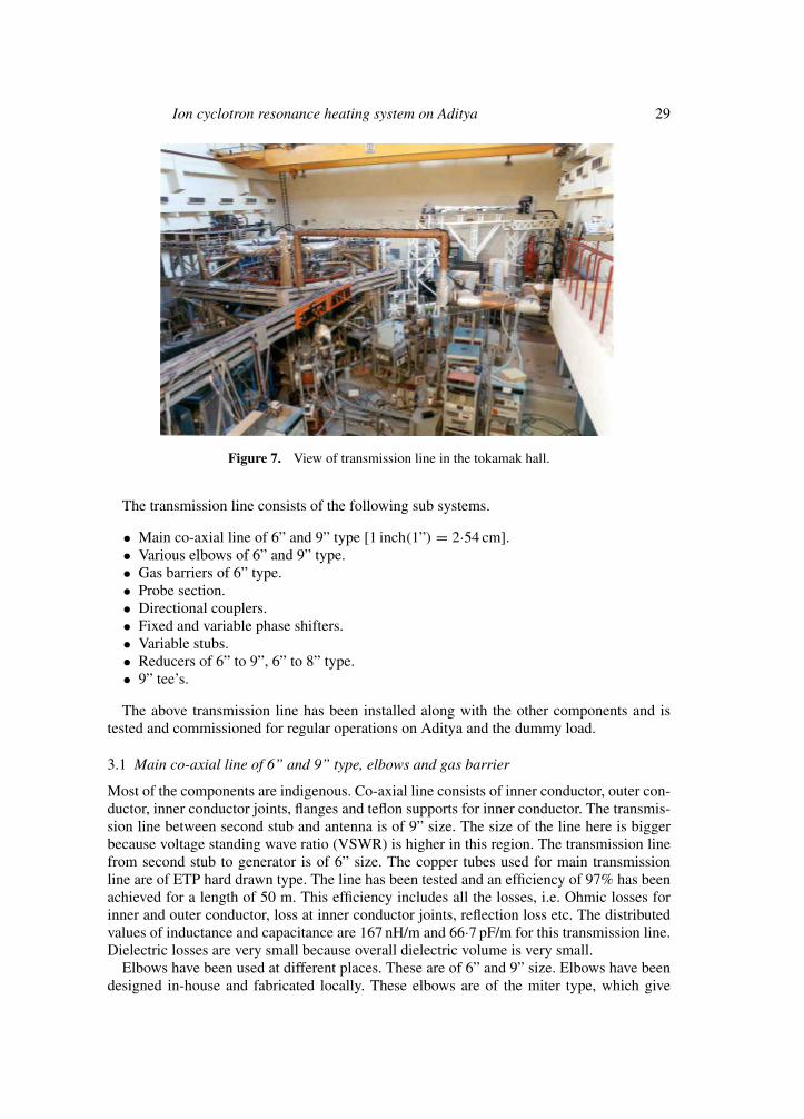
RF transmission line is used to transfer RF power from the RF generator to the antennaplaced inside the tokamak vessel. The approximate length of the transmission line from theRF generator to antenna placed in Tokamak Aditya in the experimental hall is about 53 m.At the end of the transmission line, 97% transmission with 3% insertion loss is observed. Aview of the transmission line in the tokamak hall is shown in figure 7.
Ion cyclotron resonance heating system on Aditya 29
Figure 7. View of transmission line in the tokamak hall.
The transmission line consists of the following sub systems.
• Main co-axial line of 6” and 9” type [1 inch(1”) = 2·54 cm].• Various elbows of 6” and 9” type.• Gas barriers of 6” type.• Probe section.• Directional couplers.• Fixed and variable phase shifters.• Variable stubs.• Reducers of 6” to 9”, 6” to 8” type.• 9” tee’s.
The above transmission line has been installed along with the other components and istested and commissioned for regular operations on Aditya and the dummy load.
3.1 Main co-axial line of 6” and 9” type, elbows and gas barrier
Most of the components are indigenous. Co-axial line consists of inner conductor, outer con-ductor, inner conductor joints, flanges and teflon supports for inner conductor. The transmis-sion line between second stub and antenna is of 9” size. The size of the line here is biggerbecause voltage standing wave ratio (VSWR) is higher in this region. The transmission linefrom second stub to generator is of 6” size. The copper tubes used for main transmissionline are of ETP hard drawn type. The line has been tested and an efficiency of 97% has beenachieved for a length of 50 m. This efficiency includes all the losses, i.e. Ohmic losses forinner and outer conductor, loss at inner conductor joints, reflection loss etc. The distributedvalues of inductance and capacitance are 167 nH/m and 66·7 pF/m for this transmission line.Dielectric losses are very small because overall dielectric volume is very small.
Elbows have been used at different places. These are of 6” and 9” size. Elbows have beendesigned in-house and fabricated locally. These elbows are of the miter type, which give

30 D Bora et al
better VSWR. The impedance offered by elbows is of the order of 49·2 ohm at 40 MHz forboth 6” and 9” type. Two gas barriers have been put in the line in order to pressurise the line.These gas barriers are of 6” type and can go upto 3 bar of gauge pressure. These are of the50 ohm type. Gas barriers have been designed at IPR and fabricated in IPR workshop. Theyhave been successfully tested at 220 kW CW.
3.2 Probe section
Twenty probes have been mounted on a section of transmission line of length 3·75 m. Thissection is used to find the VSWR curve. This curve helps in determining the plasma impedance.The number of probes have been chosen as 20 in order to get fairly good replica of theVSWR curve. The probes have been tested for both capacitive as well as inductive loads. Themeasurements have an error of the order of 8–10%.
3.3 Directional coupler
Two directional couplers have been used in order to find reflected and incident power, one onthe side of the load while the other one is on the side of the generator. Both are of 6” type. Thesedirectional couplers use current loops in order to pick up the signal giving the informationon power. Indigenously made directional couplers have been calibrated for different valuesof known loads at different frequencies. A maximum error of about 12% has been measured.The results have been shown in figure 8.
3.4 Variable phase shifter
There is one variable phase shifter of 3·0-m phase shifter length. The co-axial line size usedis 9”. It is motor driven and is controlled by DAC system. Appropriate signal is sent fromDAC to move it to required position. It has 50-ohm characteristic impedance. It has been putabout 8·5 m from antenna. This is the optimized position for 20–47 MHz frequency range.The probe section has been put between phase shifter and antenna.
Figure 8. Calibration results for directional coupler.

Ion cyclotron resonance heating system on Aditya 31
Figure 9. Variation of stub susceptance at 30 MHz.
3.5 Tee
Tees are used to connect stubs to the main transmission line. There are two tees of 12” armlength each inserted into the line. The tees are of 9” type and 50 ohm characteristic impedance.
3.6 Variable stub
Two variable stubs are used. One has a variable length of 3·0 m, while the other has variablelength of 1·5 m variable. Both the stubs are motor-driven and are controlled by DAC system.The stubs are of 9” size. The minimum lengths that can be achieved by these stubs are 20 cmand 30 cm for 3·0 m and 1·5 m stub lengths respectively. Variation of the observed value ofsusceptance in comparison to the theoretical value at 30·0 MHz is shown in figure 9. Frequencytuning along with the variable stub gives an improvement in the matching. The results areshown for matching at 40·0 MHz with variable stub, which improves when frequency tuningis performed (see figure 10).
Figure 10. Improvement in impedance matching by frequency tuning at 40·0 MHz.

32 D Bora et al
Figure 11. VSWR measurement for 6”–9” step reducer at various frequencies.
The characteristic impedance of the line is about 49·6 ohm at 36·5 MHz. The plasma loadvaries from 1·0 ohm to 10 ohm for the resistive part and 50 ohm to 200 ohm for reactive part.This impedance has been matched with a 50-ohm line over the 20–40 MHz frequency band.The separation between two stubs has been kept to 1/8λ for measuring all the values ofimpedance offered by plasma with minimum variation in stub length. Different stub matchinghas been tested for 3” size stubs. Matching up to 0·7 ohm was done satisfactorily but belowthis value it was found difficult to match.
3.7 Step reducers
The transmission line consists of 6” and 9” sections and the interface is of 8” type, hencetransformer sections required are 6” to 9” and 6” to 8” types. The variation of VSWR for6”–9” type is shown in figure 11. These transformers are of step reducer type. These valuesare for 50 ohm characteristic impedance.
4. Interface
To connect the antenna to the transmission line, an intermediate line section called the interfaceis mounted. It has two major tasks: to take up the thermal expansion between the vacuumchamber and the fixed transmission line, and to provide separation between the vacuum of thetorus and the pressurized section of the transmission line with two RF vacuum feedthroughs.Mechanical support to the antenna is also provided with the help of the interface. The interfacevolume is separately evacuated with the help of a turbomolecular pump of capacity 2200 l/s.The ultimate vacuum in this section achieved is ∼ 1 × 10−−8 torr. The coaxial line of theinterface is designed as a tight vacuum line, a combination of an 8-inch and a 5-inch line. Theinner and outer conductors, which are UHV compatible, comprise various seamless SS304Ltubes. Inner surfaces of outer conductors and outer surfaces of inner conductors are coatedwith silver (∼ 50 µ) to reduce RF loss. The most critical items of the interface are as follows.
1) To provide 5 cm radial movement, finger contact joints on the inner conductor and twobellows in the outer conductor are used. One bellow is part of a vacuum encasement while
Ion cyclotron resonance heating system on Aditya 33
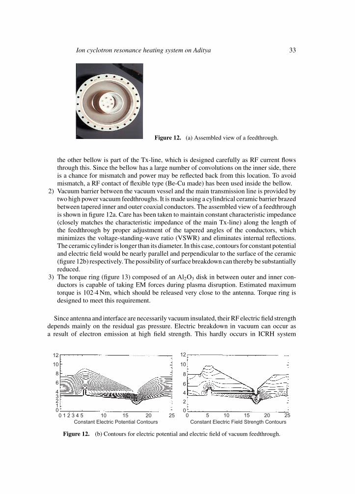
Figure 12. (a) Assembled view of a feedthrough.
the other bellow is part of the Tx-line, which is designed carefully as RF current flowsthrough this. Since the bellow has a large number of convolutions on the inner side, thereis a chance for mismatch and power may be reflected back from this location. To avoidmismatch, a RF contact of flexible type (Be-Cu made) has been used inside the bellow.
2) Vacuum barrier between the vacuum vessel and the main transmission line is provided bytwo high power vacuum feedthroughs. It is made using a cylindrical ceramic barrier brazedbetween tapered inner and outer coaxial conductors. The assembled view of a feedthroughis shown in figure 12a. Care has been taken to maintain constant characteristic impedance(closely matches the characteristic impedance of the main Tx-line) along the length ofthe feedthrough by proper adjustment of the tapered angles of the conductors, whichminimizes the voltage-standing-wave ratio (VSWR) and eliminates internal reflections.The ceramic cylinder is longer than its diameter. In this case, contours for constant potentialand electric field would be nearly parallel and perpendicular to the surface of the ceramic(figure 12b) respectively. The possibility of surface breakdown can thereby be substantiallyreduced.
3) The torque ring (figure 13) composed of an Al2O3 disk in between outer and inner con-ductors is capable of taking EM forces during plasma disruption. Estimated maximumtorque is 102·4 Nm, which should be released very close to the antenna. Torque ring isdesigned to meet this requirement.
Since antenna and interface are necessarily vacuum insulated, their RF electric field strengthdepends mainly on the residual gas pressure. Electric breakdown in vacuum can occur asa result of electron emission at high field strength. This hardly occurs in ICRH system
Figure 12. (b) Contours for electric potential and electric field of vacuum feedthrough.

34 D Bora et al
Figure 13. A view of the assembled torque ring inside the interface.
components since the electric fields are kept far below critical values by an adequate design. Bycareful design, discharges along the insulator surfaces are avoided at the vacuum feedthroughs.Electric breakdown may occur for the Pachen limit for self-sustaining discharges, which can-not be avoided by designing alone, since during the RF operation, sufficient amount of gascan be released from the surfaces to allow breakdown. The surfaces of all metals and ceram-ics normally adsorb sufficient gas to achieve high pressure. Gas can be desorbed by surfaceheating due to RF losses and multipactor discharges during which the absorbed gas is releasedby bombarding the walls with electrons.
RF system is usually conditioned by applying low power short pulses for few hours. Bakingat 100◦C of the interface components is possible as vacuum seals can withstand such temper-ature. Ten pulses that comprise 100 ms ON time and 50 ms OFF time, are usually used forconditioning of Aditya interface and antenna structure. Typical conditioning scenario using6·9 kW of RF power is shown in figure 14.
5. Antenna
Antenna and the interface described above are capable of handling 200 kW of RF power at20–40 MHz. The aim is to heat via the 2nd harmonic of the majority species and pre-ionizationfor a wide band of frequency range (20–40 MHz).
Fast magnetosonic wave heating scheme is adopted for heating Aditya plasma, since it hasseveral promising damping mechanisms. The antenna is a very sensitive part of any RF systemsince it has to launch the desired wave structure and constitute the interface with the plasma.For excitation of fast magnetosonic wave inside the plasma, it is necessary to create either a
Figure 14. Conditioning of Aditya interface.

Ion cyclotron resonance heating system on Aditya 35
toroidal component of the RF magnetic field or a poloidal component of the RF electric fieldnear the plasma boundary. Poloidal antennae in form of loops or half-loops are widely usedto excite the fast wave. ICRH antenna impedance is very sensitive to plasma density at theedge of the plasma that may vary with many parameters, such as antenna–plasma distance,MHD activity, plasma density and transition of the plasma to H-mode.
A powerful 3D code BRACC (BRussels Antenna Coupling Code) (Koch et al 1986) isused to study the antenna plasma coupling efficiency and propagation characteristics insidethe plasma volume. Percentage of absorbed power to different plasma species is determinedusing SWHAP (Simulator of Waves in Hot Anisotropic Plasmas) code (Van Eester 1992).The antenna is designed to launch 200 kW of RF power to ohmically heat the Aditya plasmato 400 eV (Mukherjee et al 1997). Major and minor radii for Aditya tokamak are 75 cm and25 cm respectively. Main poloidal limiters are kept at ±25 cm to limit the plasma. The ICRHantenna is placed at the low field side in the shadow region of the poloidal limiter to avoid heavyconducted heat load from the plasma. A fast wave antenna mounted inside Aditya vacuumvessel is shown in figure 15. It consists of central conductor, return conductor (basically theback plate of the antenna box), electrostatic screen (Faraday Shield) and side limiters thatprotect the antenna system from energetic particles. They are appropriately shaped to makethe particle flux density uniform.
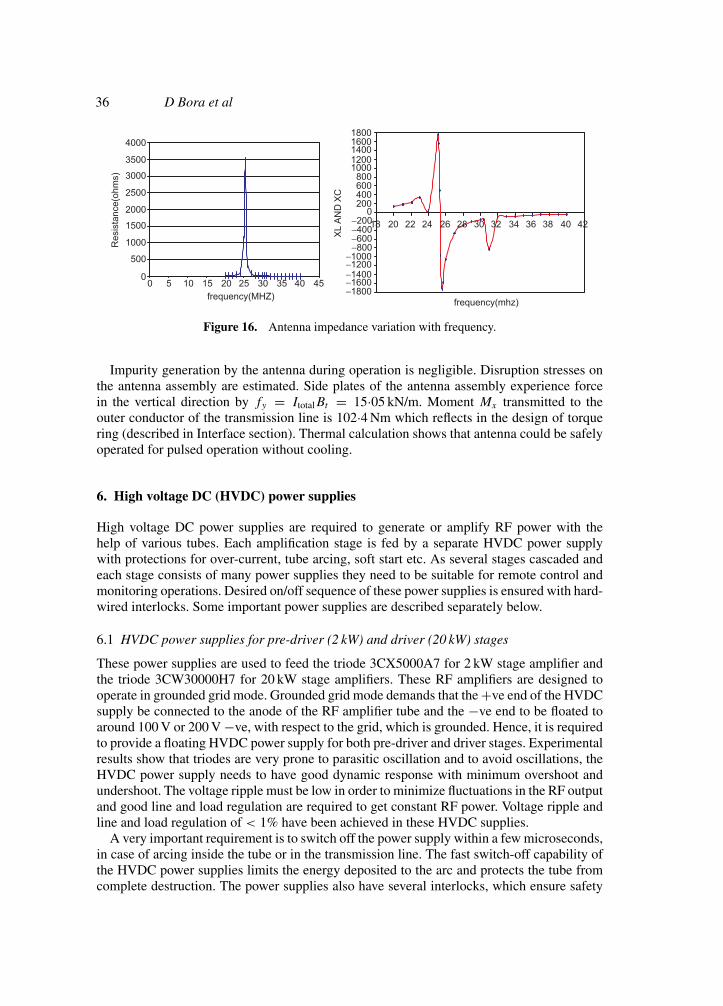
The impedance of the antenna has an important effect on its efficiency and maximum power.Active component of the impedance is made of loss resistance, Rl and load resistance, RL.For efficient operation, RL > Rl . RL is a function of the antenna aspect ratio l/w, whichis kept at 3 for Aditya antenna, corresponding to a power density of 0·66 kW/cm2. Reactivecomponent of the impedance determines the voltages on the antenna and on the input line.Peak RF power fed to the antenna depends on the maximum voltage that can be handled bythe antenna. Variation of antenna impedance with frequency is shown in figure 16. A figureof merit called antenna coupling efficiency η gives the ratio of the power effectively coupledto the plasma to the power coupled to the antenna. Calculated η at 21·7 MHz(Bt = 0·7 T)
and 30·4 MHz(Bt = 1·0 T) are 76 and 79% respectively.
Figure 15. Antenna mounted inside Aditya vacuum vessel.
36 D Bora et al
Figure 16. Antenna impedance variation with frequency.
Impurity generation by the antenna during operation is negligible. Disruption stresses onthe antenna assembly are estimated. Side plates of the antenna assembly experience forcein the vertical direction by fy = ItotalBt = 15·05 kN/m. Moment Mx transmitted to theouter conductor of the transmission line is 102·4 Nm which reflects in the design of torquering (described in Interface section). Thermal calculation shows that antenna could be safelyoperated for pulsed operation without cooling.
6. High voltage DC (HVDC) power supplies
High voltage DC power supplies are required to generate or amplify RF power with thehelp of various tubes. Each amplification stage is fed by a separate HVDC power supplywith protections for over-current, tube arcing, soft start etc. As several stages cascaded andeach stage consists of many power supplies they need to be suitable for remote control andmonitoring operations. Desired on/off sequence of these power supplies is ensured with hard-wired interlocks. Some important power supplies are described separately below.
6.1 HVDC power supplies for pre-driver (2 kW) and driver (20 kW) stages
These power supplies are used to feed the triode 3CX5000A7 for 2 kW stage amplifier andthe triode 3CW30000H7 for 20 kW stage amplifiers. These RF amplifiers are designed tooperate in grounded grid mode. Grounded grid mode demands that the +ve end of the HVDCsupply be connected to the anode of the RF amplifier tube and the −ve end to be floated toaround 100 V or 200 V −ve, with respect to the grid, which is grounded. Hence, it is requiredto provide a floating HVDC power supply for both pre-driver and driver stages. Experimentalresults show that triodes are very prone to parasitic oscillation and to avoid oscillations, theHVDC power supply needs to have good dynamic response with minimum overshoot andundershoot. The voltage ripple must be low in order to minimize fluctuations in the RF outputand good line and load regulation are required to get constant RF power. Voltage ripple andline and load regulation of < 1% have been achieved in these HVDC supplies.
A very important requirement is to switch off the power supply within a few microseconds,in case of arcing inside the tube or in the transmission line. The fast switch-off capability ofthe HVDC power supplies limits the energy deposited to the arc and protects the tube fromcomplete destruction. The power supplies also have several interlocks, which ensure safety

Ion cyclotron resonance heating system on Aditya 37
Table 3. Functional requirements of HVDC power supplies.
Parameters 2 kW stage power supply 20 kW stage power supply
Supply type Floating FloatingVoltage range 1 kV to 4 kV 8 kVCurrent 1 Amp 6 AmpSwitch off time 2 µ Sec. < 2 µ Sec.
of the tube and operating personnel. They can be operated and monitored locally or remotelyfrom the central control system.
The operating parameters of the power supplies are listed in table 3.
6.2 HVDC power supply for output (200 kW) stage
This HVDC power supply is used to feed the plate of 200 kW RF generator, i.e the tetrode4 CM 300000GA. This tetrode tube also operates in grounded grid mode. Therefore, a floatingHVDC power supply is used for the 200 kW stage as well.
The first requirement of the HVDC power supply is to provide different DC voltages ina specified range of 8–15 kV. Another important requirement is that the power supply mustbe able to give adequate protection to the tube during arcing. The size of the filter capacitorsmust be optimized in order to have minimum stored energy, low ripple and good regulation.The power supply system as a whole should have high reliability to deliver RF power.
Table 4 gives the absolute maximum ratings and typical operating parameters of the tetrodetube used for the 200 kW RF generator. An existing HVDC power supply from M/s BrentfordCo., England is used for this purpose. Some modifications as listed below have been includedin an existing power supply, to make it suitable for the 200 kW RF generator.
(a) 11 kV AC voltage variation system: This system provides a continuously variable AC inputto the HVDC power supply. The motorized remotely controlled system enables smoothincrease of plate voltage to the required operating level.
(b) Control scheme modification: Continuously variable input of 0 to 11 kV enables soft charg-ing of the filter capacitors. Hence, the redundant pre-charging circuit of the capacitors,to avoid high inrush currents at the time of switching, and related interlocks are removedfrom the circuit.
(c) Current monitoring and interlock: Pulse current transformer (pulse CT) and Hall effectDC current transducer (DCCT) are used for monitoring and interlock purposes. Pulse CT
Table 4. Absolute maximum ratings of HVDC power supply.
Parameters Absolute maximum values Typical operating parameters
DC plate voltage 15 kV 12 kVDC plate current 40 amps 30 ampsPlate dissipation 300 kW 95 kWGrid dissipation 2 kW 600 WScreen dissipation 5 kW 4 kW

38 D Bora et al
Figure 17. Test setup for 200 kW stage.
provides effective protection for fast-rising over-current faults such as arc faults. For over-current faults of slow rise pulse CT protection alone is inadequate. Therefore, a DCCT(figure 17) is used for effective protection for slow rising and sustained over-current faultsthat can occur during long duration shots. DCCT signal is also used by the DAC systemfor the beam current monitoring.The current signal is processed by the electronic circuitry. The circuit, optimised for mini-mum delay and reliability, is developed in-house. In the event of over-current detection, itgives a TTL high output and also operates a relay. TTL output is used for the triggering ofcrowbar and relay contacts interlocked to trip the AC input to the power supply by openingVCB. A delay of 15 µs for crowbar signal and 80 ms for actual 11 kV input interruptionis achieved (figure 18b). Block diagram of the electronic circuit is given in figure 18a.
(d) Crowbar: When conventional power supplies feed high power microwave tubes, a reliablecrowbar protection system, tested separately to limit the energy, must be used to assure
Figure 18. (a) The circuit can generate a crowbar trigger for hard wired external faults, like arc inthe transmission line, lon pump over-current etc. through data acquisition control system.

Ion cyclotron resonance heating system on Aditya 39
Figure 18. (b) Oscillogramshowing delay between currentthrough wire (bottom) and crow-bar current: CH1 (bottom): I (wire):0·01 V/amp; CH2 (top): I (crowbar):0·025 V/amp.
the tube safety. Crowbar protection for the tetrode is provided with the help of a singleignitron (NL8900). Wire-burn test to assure fault energy of less than 10-joule is performedsuccessfully (figure 18c).
6.3 Filament power supplies for RF 2, 20, and 200 kW stage generators
The filament is used to heat the cathode of the tetrode, which in turn emits electrons. Thecold resistance of the filament is very low. Therefore, if the full-rated voltage is applied tothe filament instantly, the resultant surge current may burn out the filament. Filament repairinvolves 50% cost of the tube. Therefore, damage to the filament is one of the most criticalfailures of the tube.
The filament voltage of 2 and 20 kW stages is raised to its full-rated value in steps usingresistors and timer circuits. These filament power supplies are housed as an integral part ofrespective HVPS.
Figure 18. (c) Oscillogram show-ing current through wire (bottom)and total currents (ignitron current)CH1 (bottom): I (wire): 0·01 V/Amp;CH2(top):I(total):0·025 V/amp.

40 D Bora et al
The filament supply of 200 kW stage is rated for 18 V ACrms and 430Arms. The voltage israised to its full-rated value in a ramp fashion. The voltage raising ramp rate is kept at 5 V/min.The change in the filament voltage changes the output RF power. Hence, it is required tokeep the filament voltage within ±3% of its operating value. This means that the filamentvoltage must be regulated to a high precision. Over-voltage, under-voltage, over-current andsurge-current protections have to be inherent qualities of the power supply. This filamentpower supply has to be floated over the high voltage power supply of the tube. Therefore, it isrequired to isolate the filament power supply system from HVDC power supply of the plate.During idle condition of the tube (when the tube is not delivering RF power), the filamentvoltage has to be reduced to some lower value and held there instead of switching it off. Thisavoids frequent switching of the filament and increases filament life.
6.4 Screen grid power supply for 200 kW stage (1000 VDC, 1 amp)
The screen grid of the 200 kW stage RF amplifier is positively biased in order to minimizethe secondary emission. Therefore, the screen bias voltage is +ve DC voltage with respectto cathode. Usually the screen voltage is kept at a fixed point, for a particular operatingpoint of the amplifier. However, the amplifier may need different screen voltages for differentoperating point. The screen grid power supply must have low voltage ripple in order to haveminimum fluctuation in the RF output power.
In addition to over-voltage and over-current protections, the power supply is protected forplate voltage failure. A plate voltage of ∼ 4 kV is required to switch the screen grid powersupply ON. Plate voltage falling below this settable value initiates trip of the power supply.An internal thyristor crowbar is interlocked with HVPS crowbar to limit the tube arc faultenergy and to protect the screen grid.
6.5 Control grid power supply for 200 kW stage (0 to −350 VDC, 1 amp)
The control grid of the RF amplifier needs to be biased at different DC voltages. In order tokeep the amplifier in the cut-off mode (non-conducting) the control grid is kept at high negativevoltage with respect to the cathode typically at −350 V. To make the amplifier conduct, thecontrol grid voltage is gradually reduced, typically to −280 V.
The most important feature of this control grid power supply is that it is never intentionallytripped. If the control grid voltage becomes zero, with other voltages at their respectivelevels, then thermal run away of the amplifier occurs and this in turn may damage the tetrodepermanently. Whenever over-voltage or over-load fault occurs, an audio alarm is activatedand at the same time a relay is switched for interlocking purpose.
6.6 Data acquisition and control
DAC can control all the HVDC power supplies, through signals like raise, lower, start/stopetc. Output voltage and current of HVDC power supplies for 2, 20 and 200 kW stages aremonitored during the RF pulse and can be graphically displayed for analysis.
The 200 kW stage filament, screen grid and control grid power supplies are also controlledby start/stop signal and their status and screen grid current are monitored.
7. Data acquisition and control (DAC) system
To analyse the system performance it is essential to monitor, acquire different system parame-ters along with an interlocking system to operate the system in failsafe manner. ICRH system

Ion cyclotron resonance heating system on Aditya 41
has its own data acquisition and control (DAC) system to execute the task of data archiving,monitoring, interlocking and control. The analysis of acquired data takes place in off-shotmode. There is off-shot control of the tuning element for maximum coupling of RF power inplasma during subsequent shots.
ICRH DAC system consists of microcontroller based multifunction I/O (MIO) modules.All the modules are connected in mulitdropped RS485 network which is ultimately connectedto a PC via RS 485 interface card in ISA bus. Signals from different subsystem undergo signalconditioning and are fed to the MIO modules. Signals are digitized in MIO and used for thepurpose of data acquisition, which is done by external trigger or by S/W trigger in the MIOmodules.
Two stubs, one fixed phase shifter and one variable phase shifter are connected to trans-mission line to match impedance between load (antenna) and generator. Twenty-two probesignals are used to calculate VSWR from which variable length of stubs and phase shifter arecalculated and changed using position controllers which are connected to host computer viaRS-485 network using other port.
MIOs are distributed physically in Aditya hall and in RF-lab control room. The essenceof distribution is that MIOs in the hall can handle the signals from ICRH subsystems housedin the hall such as transmission line, interface section, plasma edge diagnostics. The MIOsin the RF lab take care of the signals from DC power supplies of the RF generator, RFpower signals from different stages of the RF generator, cooling channels and SPDT switch.Interconnections between MIO/DIO are shown in figure 19.
There are total 8 MIOs and one DIO in ICRH DAC system. DIO controls the MIO activityand also offer facility of interlocking, monitoring of the connected signals. Each MIO has 8AI/P, 2 AO/P, 8 DI/P (7 I/P and 1 “low pulse” for external triggering at MIO), 8 DO/P, 4 linesfor serial communication and power supplies (±12 V and +5 V).
ICRH DAC system operates in two different modes: (i) Stand-alone mode and (ii) master–slave mode. In stand-alone mode ICRH DAC system operates independently and the RFgenerator is connected to the matched (dummy) load. In this mode, the RF generator dumpsthe power in the dummy load. DAC system gives the S/W trigger to take RF shots and dataarchiving for pre-defined time is executed.
In master–slave mode, the RF system is connected to the Aditya plasma and ICRH DACsystem operates in slave mode with the Aditya control system. After checking of variousrequired power supplies and cooling system status, ICRH DAC system sends a READY signalto Aditya control system to trigger ICRH DAC system for data acquisition and taking RFshot. The archiving duration is predefined in ICRH DAC system. The setting of shot durationis provisional, like duration could be set by Aditya timer or through ICRH DAC system timer.
At present Aditya control system gives a trigger that is opto-isolated. With respect to thistrigger an adjustable delayed trigger is generated and fed to the DIO terminal # 47 termed“Trigger from Aditya”. This trigger activates all the MIO data acquisition and generates apulse of predefined time (“post-trigger” time) duration at DIO terminal # 66. This pulse isfed to the LPA. Pre- and post-trigger time duration has to be set before pressing the “Start”button and wait for the Aditya trigger to work.
7.1 Interlock circuit
There are three levels of interlock circuit used in ICRH system.
(1) RF interlock: There is a hardwired interlock circuit, which takes care of the tetrode safety.The fault signals from field first conditioned with the help of signal processing and isolation

42 D Bora et al
Figure 19. MIO/DIO connection diagram.
cards and bifurcated. One of which is taken to the MIO terminal for monitoring and theother is taken to interlocking circuit.Interlocking circuit accepts the TTL level signals. All the fault signals are normally TTL“L”. At fault condition the level of the signal goes “H” which turns Off the RF switchwithin 10 µs and switches off the DC supplies of the tube in parallel. Figures 20a andfigures 20b describe the schematic circuit diagrams. Inputs to the Interlock card are:
• Screen grid On/Off• Control grid On/Off• Control grid UV• Control grid OC• Filament On/Off• VCB on/off• Water flow in 200 kW• Pre-driver stage TRIP• Driver stage ready
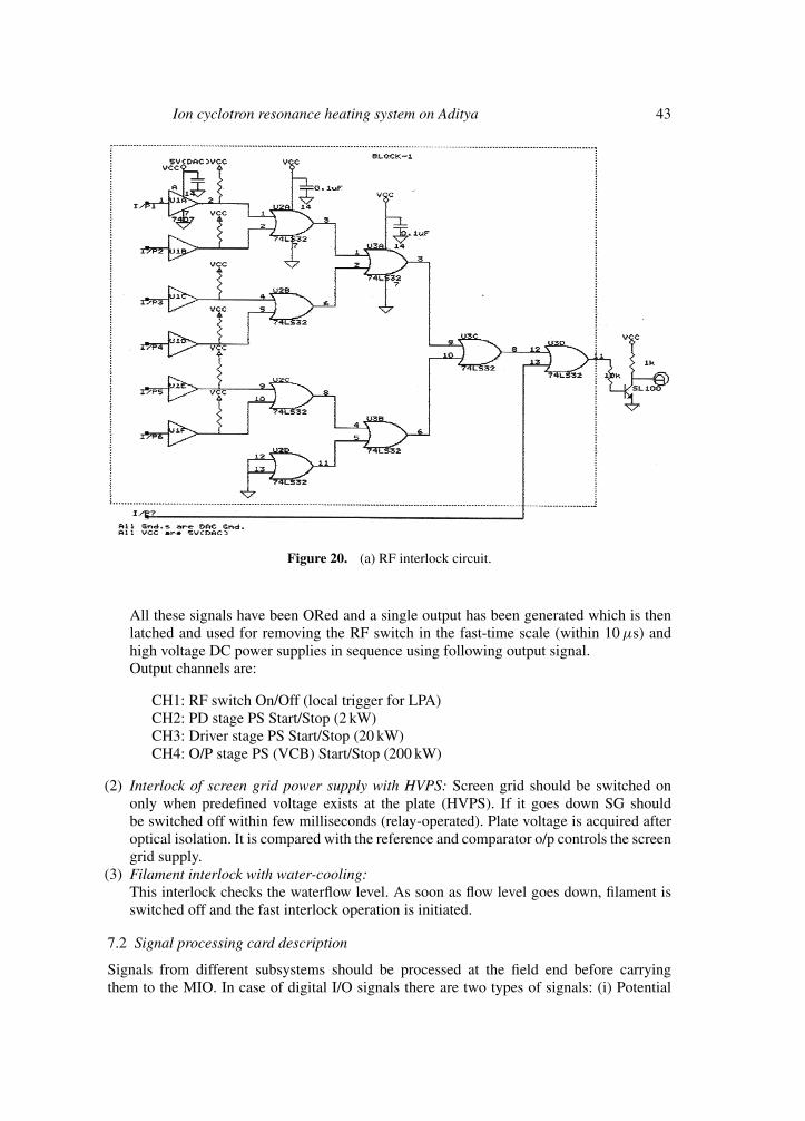
Ion cyclotron resonance heating system on Aditya 43
Figure 20. (a) RF interlock circuit.
All these signals have been ORed and a single output has been generated which is thenlatched and used for removing the RF switch in the fast-time scale (within 10 µs) andhigh voltage DC power supplies in sequence using following output signal.Output channels are:
CH1: RF switch On/Off (local trigger for LPA)CH2: PD stage PS Start/Stop (2 kW)CH3: Driver stage PS Start/Stop (20 kW)CH4: O/P stage PS (VCB) Start/Stop (200 kW)
(2) Interlock of screen grid power supply with HVPS: Screen grid should be switched ononly when predefined voltage exists at the plate (HVPS). If it goes down SG shouldbe switched off within few milliseconds (relay-operated). Plate voltage is acquired afteroptical isolation. It is compared with the reference and comparator o/p controls the screengrid supply.
(3) Filament interlock with water-cooling:This interlock checks the waterflow level. As soon as flow level goes down, filament isswitched off and the fast interlock operation is initiated.
7.2 Signal processing card description
Signals from different subsystems should be processed at the field end before carryingthem to the MIO. In case of digital I/O signals there are two types of signals: (i) Potential
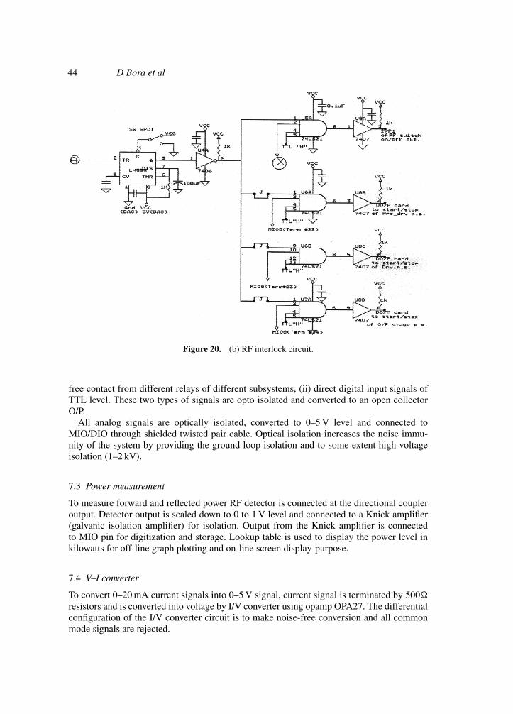
44 D Bora et al
Figure 20. (b) RF interlock circuit.
free contact from different relays of different subsystems, (ii) direct digital input signals ofTTL level. These two types of signals are opto isolated and converted to an open collectorO/P.
All analog signals are optically isolated, converted to 0–5 V level and connected toMIO/DIO through shielded twisted pair cable. Optical isolation increases the noise immu-nity of the system by providing the ground loop isolation and to some extent high voltageisolation (1–2 kV).
7.3 Power measurement
To measure forward and reflected power RF detector is connected at the directional coupleroutput. Detector output is scaled down to 0 to 1 V level and connected to a Knick amplifier(galvanic isolation amplifier) for isolation. Output from the Knick amplifier is connectedto MIO pin for digitization and storage. Lookup table is used to display the power level inkilowatts for off-line graph plotting and on-line screen display-purpose.
7.4 V–I converter
To convert 0–20 mA current signals into 0–5 V signal, current signal is terminated by 500�
resistors and is converted into voltage by I/V converter using opamp OPA27. The differentialconfiguration of the I/V converter circuit is to make noise-free conversion and all commonmode signals are rejected.

Ion cyclotron resonance heating system on Aditya 45
Figure 21. Impedance matching on Aditya using twenty probes and directional coupler at load end.
8. Preliminary results and conclusion
Antenna system is matched with RF generator using matching unit comprising stubs andphase shifters. Twenty voltage probes are placed in between the antenna system and thematching unit where VSWR is quite high. RF power coupled to the antenna has been opti-mized at 25·5 MHz. This is done off-line based on the signal obtained from the direc-tional coupler positioned at load end and the signals from the twenty probes to measure theVSWR.
Antenna current is measured using a calibrated current loop placed at the back of theantenna box. Antenna current for a 100 ms typical shot is shown in figure 22.
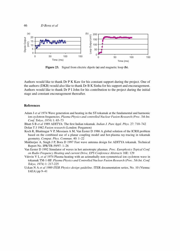
A probe assembly consisting of electric dipoles, magnetic loops, Langmuir probes andcapacitive probe is placed inside the Aditya vacuum chamber through the radial port. Thisassembly can be moved by 50 mm to scan mainly the SOL region. RF electric and magneticfield components are measured using dipoles and magnetic loops. A typical shot for dipoleand loop is shown in figure 23. The same heating system is used to experiment on plasmabreakdown and pre-ionization to help ohmic breakdown.
In conclusion, a 200 kW plasma heating system at 20–47 MHz has been successfully com-missioned on Tokamak Aditya and initial experiments have started. The generator has beenoperated at full power for 10 s on water dummy load.
Figure 22. Typical antenna current monitoredusing non-standard C.T.
46 D Bora et al
Figure 23. Signal from electric dipole (a) and magnetic loop (b).
Authors would like to thank Dr P K Kaw for his constant support during the project. One ofthe authors (DKB) would also like to thank Dr B K Sinha for his support and encouragement.Authors would like to thank Dr P I John for his contribution to the project during the initialstage and constant encouragement thereafter.
References
Adam J et al 1974 Wave generation and heating in the ST-tokamak at the fundamental and harmonicion cyclotron frequencies. Plasma Physics and controlled Nuclear Fusion Research (Proc. 5th Int.Conf. Tokyo, 1974) 1: 65–73
Bhatt S B et al 1989 ADITYA: The first Indian tokamak. Indian J. Pure Appl. Phys. 27: 710–742Dolan T J 1982 Fusion research (London: Pergamon)Koch R, Bhattnagar V P, Messiaen A M, Van Eester D 1986 A global solution of the ICRH problem
based on the combined use of a planar coupling model and hot-plasma ray-tracing in tokamakgeometry. Comput. Phys. Commun. 40: 1–22
Mukherjee A, Singh J P, Bora D 1997 Fast wave antenna design for ADITYA tokamak. TechnicalReport No. IPR/TR-59/97: 1–26
Van Eester D 1992 Simulator of waves in hot anisotropic plasmas. Proc. Europhysics Topical Conf.on Radio Frequency Heating and current Drive, EPS Conference Abstracts 16E: 129
Vdovin V L et al 1974 Plasma heating with an azimuthally non-symmetrical ion cyclotron wave intokamak TM-1-HF. Plasma Physics and Controlled Nuclear Fusion Research (Proc. 5th Int. Conf.Tokyo, 1974) 1: 217-225
Uckan N A et al 1989 ITER Physics design guideline. ITER documentation series, No. 10 (Vienna:IAEA) pp 9–41
Copyright © 2022 FDOKUMEN