
Investigations of a THGEM-based imaging detector
22
Investigations of a THGEM-based imaging detector M. Cortesi a* , R. Alon a , R. Chechik a , A. Breskin a , D. Vartsky b , V. Dangendorf c a Department of Particle Physics, Weizmann Institute of Science, 76100 Rehovot, Israel b Soreq NRC, 81800 Yavne, Israel c Physikalisch Technische Bundesanstalt (PTB), Bundesalle 100, 38116, Braunschweig, Germany E-mail: [email protected] ABSTRACT: We present the results of our recent studies on a Thick Gas Electron Multiplier (THGEM)-based imaging detector prototype. It consists of two 100x100 mm 2 THGEM electrodes in cascade, coupled to a resistive anode. The event location is recorded with a 2D double-sided readout electrode equipped with discrete delay-lines and dedicated electronics. The THGEM electrodes, produced by standard printed-circuit board and mechanical drilling techniques, a 0.4 mm thick with 0.5 mm diameter holes spaced by 1 mm. Localization resolutions of about 0.7 mm (FWHM) were measured with soft x-rays, in a detector operated with atmospheric-pressure Ar/CH 4 ; good linearity and homogeneity were achieved. We describe the imaging-detector layout, the resistive-anode 2D readout system and the imaging properties. The THGEM has numerous potential applications that require large-area imaging detectors, with high-rate capability, single-electron sensitivity and moderate (sub-mm) localization resolution. KEYWORDs: X-ray detectors, Gaseous detectors, Electron multipliers (gas), Charge transport and multiplication in gas. * Corresponding author.
-
Upload
michiganstate -
Category
Documents
-
view
2 -
download
0
Transcript of Investigations of a THGEM-based imaging detector

Investigations of a THGEM-based imaging detector
M. Cortesia*, R. Alona, R. Chechika, A. Breskina, D. Vartskyb, V. Dangendorfc
a Department of Particle Physics, Weizmann Institute of Science,76100 Rehovot, Israel
b Soreq NRC,81800 Yavne, Israel
c Physikalisch Technische Bundesanstalt (PTB),Bundesalle 100, 38116, Braunschweig, GermanyE-mail: [email protected]
ABSTRACT: We present the results of our recent studies on a Thick Gas Electron Multiplier(THGEM)-based imaging detector prototype. It consists of two 100x100 mm2 THGEMelectrodes in cascade, coupled to a resistive anode. The event location is recorded with a 2Ddouble-sided readout electrode equipped with discrete delay-lines and dedicated electronics.The THGEM electrodes, produced by standard printed-circuit board and mechanical drillingtechniques, a 0.4 mm thick with 0.5 mm diameter holes spaced by 1 mm. Localizationresolutions of about 0.7 mm (FWHM) were measured with soft x-rays, in a detector operatedwith atmospheric-pressure Ar/CH4; good linearity and homogeneity were achieved. We describethe imaging-detector layout, the resistive-anode 2D readout system and the imaging properties.The THGEM has numerous potential applications that require large-area imaging detectors,with high-rate capability, single-electron sensitivity and moderate (sub-mm) localizationresolution.
KEYWORDs: X-ray detectors, Gaseous detectors, Electron multipliers (gas), Charge transportand multiplication in gas.
* Corresponding author.

– 1 –
Contents
1. Introduction 12. The THGEM imaging detector prototype 23. The readout electrode and electronics 5
3.1 Optimization studies of the readout electrode 53.2 The readout electronics 9
4. Results 104.1 Gain uniformity and energy resolution 104.2 Imaging linearity and homogeneity 124.3 Spatial resolution and CTF 144.4 Digital noise 17
5. Summary and discussion 18
1. Introduction
Position-sensitive gaseous detectors are widely employed in particle physics and numerousother fields. With these, sub-millimetre localization properties in the detection of ionizingradiation, neutrons and soft x-rays are routinely achieved [1]. Moreover, following the verysuccessful era of wire chambers, resistive-plate chambers and others, there have been manyattempts to further improve the operational conditions and performance of gaseous detectors.Specifically, a variety of micro-pattern detectors, produced by state-of-the-art industrialtechniques, has been proposed and is already in use in numerous radiation-detection fields [1,2]. One of the most successful of these techniques is the Gas Electron Multiplier (GEM) [3], inwhich the multiplication occurs within tiny holes. Such hole-multiplication gives rise toconfined avalanches and reduced secondary effects; high gains can thus be reached bycascading several GEM elements [4], resulting in single-electron detection sensitivities, asdemonstrated in gaseous photomultipliers [5]. In addition to high gain, fast response and truepixelated radiation localization, GEMs have high counting-rate capability, superior to that ofwire chambers [1].
In this contest, the thick GEM-like gaseous electron multiplier (THGEM) [6-11], precededby the “optimized GEM” [12] and "large electron multiplier" (LEM) [13], is one of the mostrecent developments in gaseous hole-multipliers. The THGEM is cost-effectively fabricatedfrom double-clad G-10 plates, using standard printed-circuit board (PCB) techniques; it consistsof mechanically drilled holes with chemically etched rims around each hole. The rim is crucialto significantly reduce the probability of gas breakdowns, resulting in high gains [8, 9].THGEMs may be fabricated from a large variety of insulating materials. Due to theirmechanical robustness, such devices may be produced to cover very large areas. The operation

– 2 –
mechanism and properties of the THGEM at atmospheric and at low gas pressures weredescribed in detail in [8, 9]. An electric potential applied between the THGEM electrodesestablishes a strong dipole electric field within the holes, giving rise to efficient focusing ofionization electrons into the holes and their multiplication in a gas avalanche process. Theresulting electron avalanche might be collected on an anode or transferred to successivemultiplier elements. The THGEM can operate in a large variety of gases; in some of thesemultiplication factors of 105 with a single THGEM and 107 with a cascaded double THGEMconfiguration, were achieved at atmospheric pressure [8]. The avalanche process is fast, with atypical rise-time of several nanoseconds, and the rate capability is in the range of MHz/mm2 [8]at gains of 104.
2. The THGEM imaging detector prototype
The double-THGEM imaging detector investigated in the present work is schematically shownin Fig. 1. It consists of a metallized-Mylar drift-cathode foil and two THGEMs coupled incascade to a resistive anode; the latter was made of a > 2 M /square graphite lacquer layersprayed on a G10 substrate. A double-sided strip readout electrode is placed behind theresistive-anode plate.
Figure 1. Schematic view of the position sensitive THGEM detector assembly. Radiation inducedelectrons are multiplied in a cascade within the THGEM holes; the resulting charge is collected onto ahighly-resistive anode. The moving charge in the induction gap induces a localized signal at a position-
encoding readout electrode.
Fig. 2 shows photographs of the THGEM and the readout electrodes. The THGEMelectrodes employed in this work have holes of diameter 0.5 mm arranged in a hexagonalpattern, with a pitch of 1 mm; the etched rim around each hole is 0.1 mm. The thickness of theplate is 0.4 mm. The detector was located within a stainless steel vessel, 20 cm in diameter, that

– 3 –
incorporates a 50 m thick Mylar window. It was operated under continuous gas flow, at 1atmosphere of Ar/CH4, (95:5); the spacers between electrodes assured efficient gas exchangealso in the amplification region. The radiation-conversion and drift gap above the first THGEMmultiplier was 10 mm wide, while the transfer and induction gaps were 2 and 1 mm wide,respectively; the drift (EDrift), transfer (ETran) and induction fields (EInd) were set at 1, 3.5 and 4.5kV/cm, respectively. The position readout was realized by induced signal recording through theresistive anode onto a dedicated readout board, using delay-line encoding [14 - 19].
Figure 2. The THGEM and the double-sided readout electrode with pad-strips coupled to a discrete-element delay-line.
The resistive anode technique allowed for spreading of the induced signal on the readoutelectrode such that the geometrical size of the induced charge matches the width of the readout-strip pitch. This readout technique also permits for a galvanic decoupling between themultiplication stage and the readout electrode board. Thus, the resistive anode can be operatedat high voltage while the readout board is maintained at ground potential. The low-capacitivecoupling between resistive anode and readout board also protects the readout electronics fromeventual spurious discharges in the detector [14].
The induced signals were collected on a double-sided X-Y readout electrode, structuredwith diamond-shape pads printed on both sides of a standard 0.5 mm thick printed-circuit-board(PCB) (Fig. 2). The pads are interconnected with strips running in orthogonal directions (X andY) on each of the two board faces, with a pitch of 2 mm. The strips on each side of the board arecoupled to a discrete delay-line circuit (Fig. 2) [14].
The pad electrode and the readout elements are shown schematically in figure 3. Theprinted diamond-shaped pads are geometrically designed such that equal charge is induced onboth PCB sides and they are non-overlapping in order to reduce the capacitive coupling.
The avalanche location is derived from the time difference between induced signalspropagating along the discrete LC delay-line circuit. The latter is composed of 52 LC cells (Fig.3) with an inductance of L=290 nH and a capacitance of C=27 pF per cell; the corresponding

– 4 –
delay is 1.4 ns/mm; the total delay for each coordinate is thus 140 ns and the nominalimpedance is Z = 103 .
Figure 3. Schematic view of the readout electrode and the discrete-element LC delay-line circuit.
The detector was irradiated with 6 and 8keV x-rays from a 55Fe source, as well as an x-raygenerator driven Cu-fluorescence source. Metal masks were placed in front of the detector forthe imaging studies. In the localization-resolution measurements the distance between thedetector and the x-ray source (1 mm in diameter) was 70 cm. The mask was positioned about 20mm away from the drift cathode.
All THGEM electrodes were biased with independent high-voltage power supplies (CAENN471A) through 20 M serial resistors. The signals from the electrodes which are not at groundpotential were capacitively decoupled from the high voltage. Signals from the electrodes of thesecond THGEM were fed to charge and current preamplifiers, providing the integrated chargesignal and a fast common trigger for the position measurements and for coincidence and TOFexperiments. For measurement of the total charge, the electron multiplication factor (gain) andthe energy resolution, a charge-sensitive preamplifier (ORTEC 124 with a sensitivity of 275mV/pC) and a shaping amplifier (ORTEC 572A) were used. A current-sensitive preamplifier(VV44, MPI Heidelberg) and a shaping amplifier (Ortec 570) were employed for the pulse-
– 5 –
shape processing of the ‘fast’ component of the signals. The pulse-height spectra were analyzedby means of a multi-channel analyzer (Amptek MCA8000A).
3. The readout electrode and electronics
3.1 Optimization studies of the readout electrode
The position signals of the imaging THGEM detector were encoded with a pad-structuredreadout (R/O) electrode introduced by Eland et al [20] and Jagutzki et al. [21]. In previousworks these electrodes were manufactured on thin Cu-clad Kapton foils. More rigid andeconomical R/O boards can be manufactured by the standard printed circuit (PCB) technique. Inthis case, the modified geometry required optimization of the readout strip/pad structures toensure equal charge sharing and minimal cross-talk between both sides of the R/O electrodes.
a) Optimization of the induced charge amplitudes on the electrode front and back sidesThe optimal geometry for the R/O electrode is the one with equal signal amplitudes induced onits front and back sides (i.e. signal amplitude ratio of front to back: Vf /Vb = 1). The front sidedenotes here the one closer to the resistive anode. The copper structure on the front side causespartial shielding of the board back side to the charge moving within the induction gap. Hence,the pads on the front side need to be smaller than those on the back side, to allow better signaltransmission.
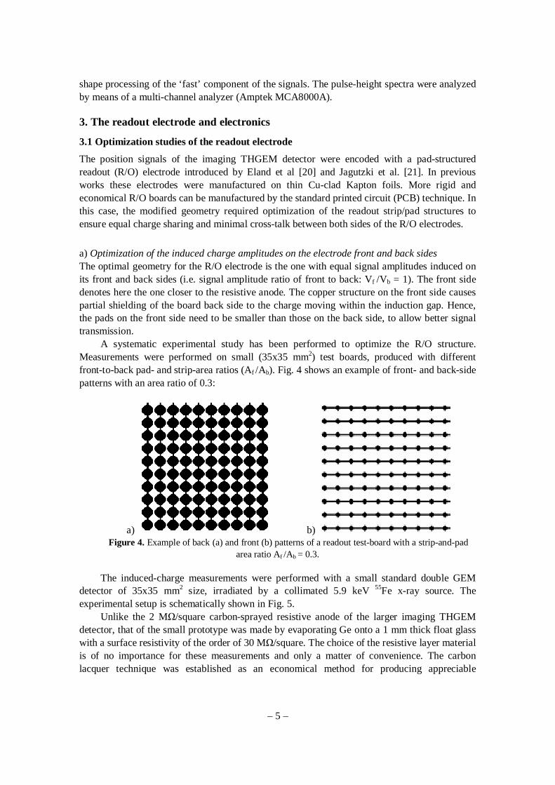
A systematic experimental study has been performed to optimize the R/O structure.Measurements were performed on small (35x35 mm2) test boards, produced with differentfront-to-back pad- and strip-area ratios (Af /Ab). Fig. 4 shows an example of front- and back-sidepatterns with an area ratio of 0.3:
a) b)Figure 4. Example of back (a) and front (b) patterns of a readout test-board with a strip-and-pad
area ratio Af /Ab = 0.3.
The induced-charge measurements were performed with a small standard double GEMdetector of 35x35 mm2 size, irradiated by a collimated 5.9 keV 55Fe x-ray source. Theexperimental setup is schematically shown in Fig. 5.
Unlike the 2 M /square carbon-sprayed resistive anode of the larger imaging THGEMdetector, that of the small prototype was made by evaporating Ge onto a 1 mm thick float glasswith a surface resistivity of the order of 30 M /square. The choice of the resistive layer materialis of no importance for these measurements and only a matter of convenience. The carbonlacquer technique was established as an economical method for producing appreciable

– 6 –
quantities of large-area gas detectors [19]. The Ge-layers, on the other hand, developed forapplication in ultra-high vacuum devices, where high purity of the materials is mandatory [21].As shown in Fig. 5, the distance (d) of the readout electrode to the Ge-layer could be varied.The induced signals on both sides of the readout electrode were recorded with a fastpreamplifier; the amplitudes of the signals were analyzed with a digital oscilloscope (TektronixTDS 3052A).
Figure 5. Measurement setup for optimizing the charge-amplitude distribution: a small test detectorwith two standard GEMs is irradiated with a collimated 55Fe source. A Ge resistive anode deposited on
glass is coupled to a readout board, placed at a distance (d) from the Ge-film face.
Figs. 6a and 6b respectively show the two-sided readout board and an example of signalsfrom its front (Vf) and back sides (Vb). The amplitude ratios (Vf /Vb) were obtained by averagingthe measured amplitudes of 20 events for each R/O board, interchanging the linear amplifiersbetween both sides after each sequence of 10 measurements, to compensate for their differentgains. The amplitude ratio was measured for a Ge-anode-to-R/O board distances of d = 1 mm.

– 7 –
Figure 6a. Readout scheme for the amplitude ratios of the readout board
Figure 6b. Typical signals recorded from both faces of the board (see Fig. 6a). The amplitudes areindicated on the right side of the figure.
Fig. 7 shows the results for all measured R/O boards, for d = 1 mm (see Fig. 5). Theoptimal value (Vf /Vb = 1) at d = 1 mm was obtained at an area ratio Af /Ab = 0.27. It is notexpected that the amplitude sharing will depend significantly on the distance between resistiveanode and R/O board. This was confirmed by a measurement at d = 2.6 mm, in which equalamplitude sharing was obtained at the value Af /Ab = 0.27 as well.
0.0 0.5 1.0 1.5 2.0 2.50
1
2
3
4
5
Cha
rge
ratio
: (Q
front/Q
back
)
Ratio of areas: (Af / Ab)
d =1mm
Figure 7. Results of measured charge-amplitude ratios, in the setup of Fig. 5, as function of theratios of the areas covered by the pads and strips on the front (Af) and back (Ab) sides of the investigated
readout boards.

– 8 –
b) Optimization of the radial spread of the induced chargeAn important factor governing the localization properties is the avalanche-induced radial chargespread. A too large spread leads to broadened signals at the output of the delay lines. Thiscauses a reduction of the signal–to-noise ratio and a deterioration of the position resolution. Onthe other hand, a radial charge spread whose full width at half maximum (FWHM) is narrowerthan the pitch of the R/O strips causes modulation of the position response by the discretestructure of the R/O board. To obtain the highest position resolution without such modulation,the radial spread of the induced charge should be close to the pitch of the R/O strips [22]. Dueto the highly-localized nature of the avalanche, this requirement is sometimes difficult toachieve in GEM detectors with direct charge readout. With the method of induced-chargereadout via a resistive anode, the radial extension of the induced charge is principallydetermined by the distance between the resistive anode and the R/O board, and can thus beeasily tailored to the needs of the R/O method.
For practical reasons (ease of manufacture, size of standard surface-mount devices (SMD)used for delay lines) we have chosen R/O boards with a pitch of 2 mm, requiring a similarFWHM radial charge spread. We have experimentally derived the radial charge distribution onthe R/O board for two resistive film to board distances d1 = 1 mm and d2 = 2.6 mm. Theexperimental set-up is the same as used above for measuring the amplitude ratios (see Fig. 5).The readout method is shown in Fig. 8. The front-side of the R/O electrode was split; a centralstrip was connected to a fast linear preamplifier (PA1), the other strips being interconnected andfed to a second preamplifier (PA2). At the back side, all strips were interconnected into a thirdpreamplifier (PA3).
Figure 8. Schematic drawing of the readout circuit for measuring the radial charge distribution.
A well collimated 55Fe x-ray source was displaced, with about 1 m precision, orthogonalto the strips; the amplitude of the fast current signals of PA1 – 3 were recorded in 500 m stepswith a fast digital oscilloscope (similar to Fig. 6b).
To reduce statistical fluctuations for each source position, the amplitude ratios of 12 eventswere measured for each location and averaged. Fig. 9a, 9b respectively show the amplituderatios (VPA1/VPA3) of the central forward-side strip signal to that of the back side, as function ofthe x-ray source location, for distances d = 1, 2.6 mm.

– 9 –
16 18 20 22 24
0
20
40
60
80
100
120
140
160re
lativ
e ch
arge
/ %
position / mm
Experiment (d=1.0 mm)
Point charge fit (df=1.1 mm)
2 mm
14 16 18 20 22 24 260
10
20
30
40
50
60
5.6 mm
rela
tive
char
ge /
%
position / mm
Experiment (d=2.6 mm)
Point charge fit (df=2.8 mm)
Figure 9. Projected radial distribution of the induced charge signal at a) 1 mm and b) 2.6 mm distancebetween resistive anode and RO electrode. The curves present fits of the experimental data using
Lapington’s model (see text).
Following Lapington's considerations [23], the mechanism for charge induction viacapacitive coupling between the localized event charge on the resistive layer and the readoutelectrodes, causes the induced charge footprint to be spread in a very well defined manner. Theresulting radial charge distribution is defined by:
r1
(r2 + a2)3/2 (1)
where r is the induced charge at horizontal distance r from the point charge and a is thedistance between the point charge and the pick up electrode. The line in Fig. 9 presents a fit ofthe experimental data with the 1-dimensional projections of this distribution for 2 distances d.The distance df in the fit was used as a free parameter and the resulting values for df are ingood accordance to the real distance in the experiment. The FWHM of the projected radialspread of the induced charge distribution is 2.0 and 5.6 mm for a distance between resistiveanode and pick up electrode of 1.0 and 2.6 mm, respectively. For a R/O board with strips of 2mm pitch the optimum spacing is therefore of the order d = 1 mm.
3.2 The readout electronicsFig. 10 shows the scheme of the R/O electronics of the 100 x 100 mm2 double-THGEMimaging detector. The data acquisition (DAQ) hardware is based on the 8-channel Time-to-Digital Converter (TDC) chip F1 and the ATMD board [24]. The system also comprises aCharge-to-Time Converter (QTC), based on LeCroy’s MTQ300A-chip [25].
This module also permits measuring the avalanche charge behind the last THGEM (afterpulse shaping with a Timing Filter Amplifier (TFA)). Events are stored in the PC memory withthe corresponding position and time signals.
The signals from the ends of each delay-line and the “common start” signal from the lastTHGEM cathode were amplified by fast linear amplifiers (VV46, MPI-Heidelberg). Theamplified position signals were delayed by 60 ns and fed to an ORTEC CF934 ConstantFraction Discriminator (CFD). The common signal was discriminated by a Canberra 1428 CFDand used as common start for the TDC. The slow (TTL) output of the CFD "enabled" the gate of
a) b)

– 10 –
the ORTEC CFD and allowed valid signals from the delay-lines to pass. The outputs of the CFDwere used as "stop" signals for the TDC. The data acquisition software, a modified version ofCAMDA [26], calculated the position coordinates and performed a plausibility check on themeasured timing signals (comparison of time-sums). Valid data were accumulated in histogramsand/or stored as list-mode files in the PC memory.
Figure 10. Schematic view of the DAQ system.
The result of the digitalization process is an image of 800x800 pixels; each pixel has alinear extension of 125 m. The images are stored with high dynamic range (4 Byte integers /pixel). However, for visualization of the image on the screen, these high-dynamic-range imageswere compressed to 8-bit gray-level images.
4. Results
The performance of the THGEM imaging detector was characterized through the analysis of thecharge signal, namely gain uniformity and energy resolution, and the measurements of someparameters as the integral non-linearity (INL), the homogeneity and the digital noise. Thecharacterization of the imaging detector response in terms of spatial resolution, or moreprecisely in terms of spatial frequency response, was computed by the determination of thepoint spread function (PSF) and the contrast transfer function (CTF). From CTF the limitingspatial resolution was calculated.
4.1 Gain uniformity and energy resolutionThe gain uniformity of the cascaded THGEM detector was investigated with a collimated 5.9keV 55Fe x-ray source, 1 mm2 in diameter. The active area was irradiated in 15 mm steps in bothdirections, for a total of 25 measurement points across the detector. The charge signal wasderived from the cathode of the second THGEM. Fig. 11 shows examples of gain curves in

– 11 –
Ar/CH4 (95:5) and in Ar/CO2 (70:30) at atmospheric pressure, obtained at the center of theactive area.
800 1000 1200 1400 1600 1800 2000102
103
104
105
Ar/CO2(30%)Ar/CH4(5%)
Abs
olut
e ef
fect
ive
gain
VHole [Volt]
Double THGEMAtm. Pressure5.9 keV (55Fe)
Figure 11. Absolute effective gain obtained at the center of the active area of 10x10 double-THGEMmultipliers, measured with 5.9 keV x-ray (55Fe) in Ar/CH4 (95:5) and in Ar/CO2 (70:30), at atmospheric
pressure.
As shown in Fig. 12a, for a potential difference (Vhole) of 1220 V applied to bothTHGEMs, the absolute effective gain is rather uniform with an average value of 7x10³; for 5.9keV photons this corresponds to an average avalanche size of the order of 2x10⁶ electrons. Theoverall measured gain variation is 10% FWHM. A typical energy spectrum of the 55Fe source isshown in Fig. 12b; the energy resolution of the photo-peak is of the order of 21% (FWHM),typical for gas avalanche detectors.
3.0x10³ 6.0x10³ 9.0x1030
2
4
6
8
10
10% FWHM
No.
of p
oint
s
GainFigure 12a. Gain distribution of a collimated 5.9 keV 55Fe source over the sensitive area of the
cascaded THGEM detector, measured at 25 points across its area in Ar/5%CH4; Vhole = 1220 V for eachTHGEM.

– 12 –
Figure 12b. Typical pulse-height distribution of the collimated source; the energy resolution is 21%(FWHM).
4.2 Imaging linearity and homogeneityThe image linearity and the homogeneity of the imaging system response were assessed byinvestigating the Gaussian fit of some pinholes’ image projections (Fig. 13b). The pinholes wereof 1 mm diameter, drilled into a 1 mm thick brass mask (Fig 13a). The detector was uniformlyirradiated by characteristic K-shell fluorescence photons from a Cu-target (8 keV), excited by awell collimated intense bremsstrahlung-spectrum from an X-ray generator with a Mo anode.
Figure 13a. X-ray transmission image of a mask with 1 mm diameter pinholes, recorded with theTHGEM imaging detector. The projection profile of the selected area is shown in Fig. 13b.

– 13 –
0 10 20 30 40 50 60 70 80 90 1000
10
20
30
40
50
60
70
80
90
100
Cou
nts
Projection (mm)
3 mm
Figure 13b. Raw data projections of some of the pinhole images marked in Fig. 13a.
The effects induced on the image by distortions can be characterized by the integral non-linearity (INL). INL is defined as the deviation of the measured holes’ centroid from their reallocations. Geometrical distortions represent a deviation from rectilinear projection (Fig. 13c).They may arise from several effects, such as defects on the grid cathode or signal deformationas they propagate along the delay line. Specifically, alteration of the signal shape and its risetime depend on the amplitude of the signal (SNR), preamplifier cross talk, capacitive cross talkbetween read-out electrodes and asymmetry of induced signal on front and back. We measuredan average INL value lower than 0.1% over the full image range of 100 mm.
0 10 20 30 40 50 60 70 80 90-0.2
-0.1
0.0
0.1
0.2
INL
(%)
Hole Position (mm)
Figure 13c. Computation of the INL (integral nonlinearity) along the selected image projection.

– 14 –
4.3 Spatial resolution and CTF
The point spread function (PSF) of the imaging detector was obtained by means of the edgespread function (ESF) technique [27]. The ESF was measured by irradiating the edge of a 1 mmthick Aluminium plate (see 2D image in Fig. 14a) and extracting a projection of the edge profilefrom the image data (Fig. 14b).
Figure 14a. A 2D image of a knife-edge obtained with the THGEM imaging detector, irradiated with abroad Cu X-ray beam.
0 10 20 30 40 50 60 70 800
10
20
30
40
50
60
70
80
90
100
X Coordinate (mm)
Brig
htne
ss (G
ray
Leve
l)
Figure 14b. The edge spread function along the x coordinate (blue dots). The red curve is a fit with asuitable model function.

– 15 –
In order to eliminate fluctuations resulting from the digital noise, we fitted the edge profilewith an empirical function which models the ESF with adequate accuracy. The empirical modelfunction used is given by the following equation [28]:
ESF(x) = a0 +a1
1 + exp(–a2(x – a3)) (2)
where a0 is related to the transmission of the Al plate, a1 is the brightness of the fullirradiated sensitive area, a2 is the steepness of the edge function (related to the spatial resolutionof the imaging system) and finally a3 is the centroid of the edge function (see Fig. 14b).
The determination of the PSF was obtained in a straightforward way by simplydifferentiating the empirical model of the fitted ESF. Consequentially, the derived FWHM ofthe resulting PSF, which is a direct manifestation of the intrinsic spatial resolution of thesystem, is then given by:
FWHM =3.53a2
(3)
To check the consistency of our estimate of the spatial resolution, the PSF and its FWHMwere determined by two different modalities (Fig. 15): from the numerical differentiation of themeasured ESF (blue line), and the differentiation of the suggested empirical model (red line).There is good agreement between the measured PSF and the one obtained from the empiricalmodel calculations. Nevertheless the direct analysis of the raw data, fitted with a Gaussianfunction distribution, has large fluctuations due to the digital noise (Fig. 15). Therefore, therelated Gaussian fitting and the resultant spatial resolution has a larger uncertainty.
35 40 45 50-5
0
5
10
15
20
PSF
X Coordinate (mm)
PSF Raw Data PSF Empirical model
~0.7 mm FWHM
Figure 15. Results of the PSF determination along the x-coordinate using the differentiation of raw data(solid line) and the differentiation of the empirical model results (dashed line).
The spatial resolution derived via the “measured” PSF, from raw data analysis, has aFWHM value of 0.71±0.05 mm, while the empirical model analysis reveal a FWHM value of0.67±0.02 mm.
The result of imaging masks with a rectangular transmission profile at differentfundamental frequencies is a frequency-dependent variation of the modulation depth (ContrastTransmission) in the images [29]. The CTF approaches a value of 100% at very low spatial

– 16 –
frequencies, corresponding to a wide spacing period, and gradually drops with increasing spatialfrequency. In general, 100% contrast represents an image of regular periodic structure of whiteand black lines, while 0% contrast is manifested by gray bars that merge into a gray backgroundof the same intensity. When the contrast value reaches zero, the image becomes uniformly grayand remains so for all higher spatial frequencies.
The specimen modulation (contrast), M( ), for patterns at different frequencies, canbe defined as:
M( ) =I(max) - I(min) I(max) + I(min) (4)
where is the spatial frequency of the grating specimen, I(max) is the maximum intensitytransmitted by a repeating structure (grating) and I(min) is its minimum intensity. The contrasttransfer function (CTF) is defined as the modulation depth of the image (Mi) divided by themodulation depth of the stimulus (Mo), as shown in the following equation:
CTF( ) =Mi( )Mo( ) (5)
The CTF is normalized to unity at the lowest spatial frequency, where the imaging systemtransfers the maximal contrast.
We have irradiated a brass mask placed in front of the THGEM detector, composed ofdifferent frequency periodic line gratings, using the Cu-fluorescence photon beam. The 2Dmask image is shown in Fig. 16a; the projected distributions of the mask image are shown inFig. 16b. The calculated CTF is shown in Fig. 17. The limiting spatial resolution, defined as thefrequency at which the CTF drops to 10% of its maximal value, is of the order of 1.25 lp/mm,corresponding to a wave length of 0.8 mm.
Figure 16. The imaging detector X-ray image of a 2D mask, used for the CTF evaluation (a) and therelated projection of the selected area (b).

– 17 –
Figure 17. The contrast transfer function obtained from the mask image of Fig.16.
The image distortions at the extremities of the sensitive area of the detector, resulting in aslight increase of the INL (see Fig 13c), are due to the rather close irradiation geometry. Noticethat the source-to-mask distance was only 70 cm in our experiments; the mask had a step-likeprofile with 2 cm thickness in the center and 1 cm at the edge, causing a partial shadowingeffect on the edge of the detector's sensitive area. Finally, the optical magnification, defined asthe ratio between the apparent size of an object (in our case the pinhole) and its true size, isanother factor which might have influenced the performance of the imaging system. The linear-optical magnification, in the case of a point-like source, depends only on the source-objectdistance and object-conversion gap; in our case the linear optical magnification effect, estimatedto be of the order of 1.036, is rather small.
4.4 Digital noise
Electronic imaging, like all imaging techniques, is always affected by blur and noise. The noiseessentially arises due to processes which precede the production, capture, conversion andinterpretation of the real source signal. The quantification of the noise is crucial for the analysisand optimization of an imaging systems’ performance. For this reason we have determined theintrinsic signal-to-noise ratio of our imaging system the analysis of a flat-field image (Fig. 18a),obtained while irradiating the detector with a homogeneous (“flat”) 8 keV photon beam. Theimage was recorded for 300 minutes of irradiation at intensities around 1 kHz/mm2. The imageappears to be homogeneous across the entire sensitive area, which also reflects the gainhomogeneity previously discussed; the small slab in the lower part of the image is due to adefect of the resistive anode.

– 18 –
a) b)
Figure 18. Flat-field image recorded by homogenous detector irradiation (a) and the histogram of thegray-level distribution of the flat-field image (b). See text.
Fig 18b shows the distribution of the flat image pixel contents. The average pixel contentis A = 175 (gray level) with a standard deviation of = 25, corresponding to an average spreadof about 14% (1 std. dev.). In terms of signal-to-noise ratio:
SNR = 20 log10
A = 16.9 dB (6)
The resulting digital noise is not due to counting statistics (which, by itself, would result inan average spread of only = 5% per pixel). It is rather due to nonlinearities in the delay linereadout (variation of the L’s and C’s of the delay line, see Fig. 3), cross talk of the readoutchannels and nonlinearities of the TDC. The digital SNR appears to be uniform across thesensitive detector area, with a slight degradation towards the image edge. This effect isessentially due to distortions of the electric fields near the edge of the THGEM electrodes. Also,position sensitive gain variations in the detector lead to degradation of the general performanceof the imaging system, however, image processing can largely correct these defects and restoreimage uniformity almost to the quantum noise limit.
5. Summary and discussion
In view of the many possible potential applications of THGEM-based imaging detectors, wehave extensively studied the localization properties and quality of imaging a 2D 10x10 cm2
detector prototype, that operates in Ar/5%CH4 at atmospheric pressure and room temperature.An energy resolution of 21% FWHM was measured for 5.9 keV X-rays with a detector
gain of 6x10³. The gain uniformity was within ~10% over the detector’s 10x10 cm2 sensitivearea. The performance of the imaging system was determined by invoking the common transfertheory tools (PSF and CTF), and digital SNR. For low energy x-rays the average intrinsic widthof the PSF over the entire sensitive area is about 0.7 mm (FWHM), using a THGEM electrodewith 0.5 mm hole diameter, 1 mm hole spacing and a readout electrode with a pitch of 2 mm.
The development of large area position-sensitive detectors is motivated in particle physicsby the quest for rare events, to be discriminated against an extremely high background [1]. Inthe case of detecting charged particles, a very high position resolution could be achieved, as, forexample, in tracking measurements: ~ 12 m localization resolution was achieved withmicromegas [30] and ~ 40 m with the GEM [31]. Although the high granularity of micro-

– 19 –
pattern detectors plays an important role in these applications, offering excellent positionresolution properties, there still remains a serious problem of discharges which cause criticaldamage to electrodes. Conversely, THGEM-based detectors may become an attractivealternative solution for numerous applications, where large-area radiation imaging detectorswith modest (sub-mm) position resolution [9] are required. They are robust-element, self-supporting, and can be economically produced with simple printed-board techniques. They arecapable of reaching single- or few-electron detection sensitivities, even for fluxes approachingseveral MHz mm2 [9]. Potential applications are: UV photon detectors (e.g. with CsIphotocathode) [7], particle tracking, (e.g. large-area muon trackers), sampling elements incalorimetry, x-ray imaging etc. THGEM multipliers coupled to solid radiation converters can beapplied to neutron detection [14]. Feasibility studies of THGEM elements in cryogenic DarkMatter detectors are in progress, using low-radioactivity material substrates [32].
References
[1] F. Sauli, Micro-pattern gas detectors, NIM A477(2002), 1.
[2] A. Oed, Micro pattern structures for gas detectors, NIM A471 (2001), 109.
[3] F. Sauli, GEM: A new concept for electron amplification in gas detectors, NIM, A386 (1997), 531.
[4] F. Sauli, T. Meinschad, L. Musa, L. Ropelewski, Photon detection and localization with GEM, IEEENuclear Science Symposium (Rome, 2004) Volume 1,12 - 15.
[5] D. Mörmann, M. Balcerzyk, A. Breskin, R. Chechik, B. K. Singh and A. Buzulutskov, GEM-basedgaseous photomultipliers for UV and visible photon imaging, NIM A504 (2003), 93-98.
[6] R. Chechik, A. Breskin, C. Shalem, D. Mormann, Thick GEM-like hole multipliers: properties andpossible applications, NIM A535 (2004) 303-308.
[7] R. Chechik, A. Breskin, C. Shalem, Thick GEM-like multipliers – a simple solution for large areaUV-RICH detectors, NIM A 553 (2005) 35–40.
[8] C. Shalem, R. Chechik, A. Breskin, K. Michaeli, Advances in Thick GEM-like gaseous electronmultipliers—Part I: atmospheric pressure operation, NIM A558 (2006) 475-489.
[9] C. Shalem, R. Chechik, A. Breskin, K. Michaeli, N. Ben-Haim, Advances in Thick GEM-likegaseous electron multipliers—Part II: low pressure operation, NIM A558 (2006) 468-474.
[10] M. Cortesi, R. Chechik, A. Breskin, G. Guedes, V. Dangendorf, D. Vartsky, D. Bar, Advances inimaging THGEM-based detectors, NIM A572 (2007) 175-176.
[11] R. Oliveira, V. Peskov, F. Pietropaolo and P. Picchi, First tests of thick GEMs with electrodes madeof a resistive kapton, NIM A, in press.
[12] L. Periale, V. Peskov, P. Carlson, T. Francke, P. Pavlopoulos, P. Picchi and F. Pietropaolo, Detectionof the primary scintillation light from dense Ar, Kr and Xe with novel photosensitive gaseousdetectors, NIM A478 (2003) 377-383.
[13] P. Jeanneret, Time Projection Chambers and detection of neutrinos, PhD thesis, NeuchâtelUniversity, 2001.

– 20 –
[14] V. Dangendorf, G. Laczko, M. Reginatto D. Vartsky, M. Goldberg, I. Mor, A. Breskin, R. Chechik:Detector for time-of-flight fast-neutron radiography 1. Neutron counting gas detector, NIM A542(2005) 197-205.
[15] O. Jagutzki, J. S. Lapington, L. B. C Worth, U. Spillmann, V. Mergel, H. Schmidt-Böcking,Position sensitive anodes for MCP read-out using induced charge measurement, NIM. A477 (2002)256.
[16] M. S. Dixit, J. Dubeau, J. P. Martin C. K. Sachs, Position sensing from charge dispersion in micro-pattern gas detectors with a resistive anode, NIM A518 (2004) 721.
[17] R. Baur, A. Drees, P. Fischer, P. Glässel, D. Irmscher, A. Pfeiffer, A. Schön, C. Schwick, H.J.Specht, S. Tapprogge, The pad readout of the CERES RICH detectors, NIM A355 (1995) 329.
[18] G. Battistoni, P. Campana, V. Chiarella, U. Denni, E. Iarocci, G. Nicoletti, Resistive CathodeTransparency, NIM A202 (1982) 459.
[19] M. Shoa, Weizmann Institute of Science (Israel), Resistive anodes for the Atlas TGC, privatecommunication 2003, see also S. Tanaka, Techniques developed for the ATLAS TTGC, H.ATL-MUON- 2004- 015, (muon-2004-015.pdf).
[20] J. H. D. Eland, Simple two-dimensional position-sensitive detector with short dead-time forcoincidence experiments, Meas. Sci. Technol. 5, (1994) 1501.
[21] O. Jagutzki, J. U. Spillmann, L. Spielberger, V. Mergel, K. Ullmann-Pfleger, M. Grewing, H.Schmidt-Böcking, A position- and time-sensitive photon-counting detector with delayline read-out,Proc. SPIE 3764, 61 (1999).
[22] Th. Wilpert, MsC Thesis, TU-Berlin (2001)198X
[23] J.S. Lapington, J. Howorth and J. Milnes, Procs. SPIE Vol 5881 (2005), p 61-70 ISSN 0277-786X,
[24] ACAM-Messelectronic GmbH, http://ww.acam.de.
[25] MQT300A, CHARGE-TO-TIME CONVERTER, LeCroy 1999, http://www.lecroy.com/.
[26] CAMDA, A small CAMAC Data Acquisition System, Herbert Stelzer, GSI Darmstadt, Germany.
[27] Sitter, D.N., Goddard, J.S., and Ferrell, R.K., Method for the measurement of the modulation transferfunction of sampled imaging systems from bar-target patterns, Applied Optics, volume 34 (1995)746-751.
[28] V. J Lehr, J B Sibarita, J M Chassery, Image restoration in X-ray microscopy: PSF determinationand biological applications, IEEE Trans on Image Processing, 7(2) (1998) 258-263.
[29] J. W. Coltman, The Specification of Imaging Properties by Response to a Sine Wave Target, Journalof the Optical Society of America (1954), Vol. 44, No. 6, pp. 468-471.
[30] G. Charpak J. Derré, Y. Giomataris and Ph. Rebourgeard, Micromegas, a multipurpose gaseousdetector, NIM A478, (2002) 26.
[31] S. Bachmann, A. Bressan, S. Kappler, B. Ketzer, M. Deutel, L. Ropelewski, F. Sauli and E. Schulte,Development and applications of the gas electron multiplier, NIM A471, (2001) 115.
[32] M. Gai, D. N. McKinsey, K. Ni, D. A. R. Rubin, T. Wongjirad, R. Alon, A. Breskin, M. Cortesi, J.Miyamoto, Toward Application of a Thick Gas Electron Multiplier (THGEM) Readout for a Dark

– 21 –
Matter Detector, to be published in the Proceedings of the 23rd Winter Workshop on NuclearDynamics, Big Sky, Montana (2007).