Investigation of the Effect of Various Dyes on OLEDs ...
93
Islamic University of Gaza ا ا- ة Deanery of Graduate Studies ت ارادة ا Faculty of Science م ا آPhysics Department ء ا Investigation of the Effect of Various Dyes on OLEDs Electroluminescence BY Hussam Sabri Musleh Gaza Palestine Supervised By Dr. Taher El-Agez Assistant Prof. of Physics "A Thesis Submitted in Partial Fulfillment of the Requirements for the Degree of Master of Science (M.Sc.) in Physics" 1430 ه ــ- 2009 م
-
Upload
khangminh22 -
Category
Documents
-
view
0 -
download
0
Transcript of Investigation of the Effect of Various Dyes on OLEDs ...

Islamic University of Gaza ا ة-ا
Deanery of Graduate Studies دة ارات ا
Faculty of Science مآ ا
Physics Department ء! ا
Investigation of the Effect of Various Dyes on
OLEDs Electroluminescence
BY
Hussam Sabri Musleh
Gaza
Palestine
Supervised By
Dr. Taher El-Agez
Assistant Prof. of Physics
"A Thesis Submitted in Partial Fulfillment of the Requirements for
the Degree of Master of Science (M.Sc.) in Physics"
م2009 -ــ ه1430

II
ABSTRACT
In this work, five sets of samples have been prepared and studied. Every
sample represents an Organic Light Emitting Diode OLED. We used Poly(9-
vinylcarbazole) (PVK) doped with different dyes (R6G, Alq3, carbocyanine,
oxadiazole and fluroscein) 2% concentration. The measurements include I-V
characteristics and variation of relative light intensity with the driving voltage. The
variation of relative light intensity with the current and the conduction mechanism
have been studied.
The I-V characteristics are that of typical diode because the current increase
exponentially with applied voltage. I-V characteristics and relative light intensity-
voltage curves have approximately the same shape for the same sample. It is
observed that, the lowest value of threshold voltage TV was for (ITO/PVK R6G
(blend)/Al) sample and the highest was for ITO/PVK 1,2,4 oxadiazole(blend)/Al)
sample (see table( .4 1)). In general, the values obtained for TV are lower than those
reported for conventional organic light emitting diode.
Electroluminescence-voltage characteristics curve reveals that the sample
(ITO/PVK 1,2,4 oxadiazole(blend)/Al) is best sample exhibiting the maximum
brightness which is achieved at an operating voltage of 10 V. By plotting the current-
voltage curves in logarithmic scale, we ensured that the mechanism of conduction is
ohmic at low voltage for all samples and at high voltage, space charge limiting
conduction (SCLC) in most samples. Current-voltage in logarithmic scale curves
demonstrate three regions for ITO/PVK R6G (blend)/Al, ITO/PVK
carbocyanine(blend)/Al, ITO/PVK 1,2,4 oxadiazole(blend)/Al and four regions for
ITO/PVK / Alq3 /Al (double layer), ITO/PVK fluroscein (blend)/Al. The thicknesses
of thin films were measured using homemade variable angle spectroscopic
ellipsometer (VASE) .
We also deposited thin film of PVK (48 nm) on Si substrate, and another thin
film (18 nm) of Alq3 on Si substrate. We plot the variation of the refractive index of

III
a Alq3 and PVK films with the variation of wavelength (visible spectrum). Finally,
the experimental values of three Cauchy parameters (A, B, C) were calculated using a
Matlab code.

IV
ا ا
ودرا ت ات ها ا #ي )'$& %$#ء . ! $' *$+ ,آ '
OLED .*#$$.0/و3#اص ا14 )$$$$// 5#$$ ا$$/3 ام 7$$دة '$$ &$$9 electroluminescence وه$$
PVK ،;$$$$$$$$$$$$$$$< ,BC(dyes $$$$$$$$$$$$$$$,7 $$$$$$$$$$$$$$$'#/7 )R6G Alq3$$$$$$$$$$$$$$$=غ % 2)$$$$$$$$$$$$$$$<= ا/$$$$$$$$$$$$$$$
,carbocyanine,1,2,4,oxadiazole, fluroscein( ، /$را D$7 $آ $EF' درا وE ا9/#ت ا را '%
G=Hا IJ<= 47 اءة ا.Kة ا L EF' Mو آ IJا درا N اK.ءة ا<= 47 . آ ا وأ5
%/ر 47 ا%#=Hا ر5/P#%ا D( EF/ر واا N IJ% =Hا ر5/P.
ا3$#اص %#B$% ا,*$ I-VوE وR أن E 4R$س #B$% ا/$ر ا$</ $7 $HوT9#$ أن .
7I-V !5= % ا#ا9 ة) اK.ءة ا<= -اIJ ( و7 0Vا WX انC5 . $E د$J5أ $ $Eو
وآ$$ MT9#$$ أن اIR $$E$$ %/=$$ آ$$ن $$ ا$$ . IRTV threshold voltage $$' $$0$$ ا/=$$
(ITO/PVK R6G (blend)/Al) ا واآ= IR %/= آن
(ITO/PVK 1,2,4 oxadiazole(blend)/Al) ) ول R 4R) (4.1 )را !$ا D$7 $Eا $E و ه$
Hا W$$( $$I%' ل#Z$$$$ ا 5!$$ و!$$ و.$$; اL D$$( $$EF$$ ة اK.$$ءة ا$$<= واIJ$$ أن ا$$ ا/$$
(ITO/PVK 1,2,4 oxadiazole(blend)/Al) $تا D$7 $هP 47 Xر!( =>X إ.ءة أ'H; أ
$$' =>$$X إ.$$ءة و$$ ا/Cآ$$ D$$7 أن ا/#B$$ دا$$ R$$4 ا$$ت '$$ ا910V ، $$IJ$$& آ$$ن I$$ ا'%$$
ا$ $ن ا/#Z$5 $B=[ $=\ ا$ت $ ohmic اW3\ ه# $%' G$=Hا $IJا $E 4$W و'$ 7
و ذG$5< D' M ر$ 7$ت ا/$ر واspace charge limiting conduction ، $IJ)\ اا9
=Hا ,S1ت %ت ا و! ا9/#ت ه` current-voltage in logarithmic)/ ر5_ ا%#Pر5/
S3, S4 $$97ا $$+F+ three region) ( D$$/ا four 7ا9$$ 4 !$$ ا9/$$#ت '%$$ S2, S5 أ$$7 $$
regions) .( ت )/3 اما \( M سE Mآ
homemade variable angle spectroscopic ellipsometer (VASE) .
D7 GEء رVP 3= 5 D7 ا<%0#ن PVK وأا L ق# Si D7 أ GEء رVPو Alq3
5 أي D7 ا<%0#ن L 3 #ق= Si 4$7 D/!(>$ا D$/ا W 0<رX177 ا N و ذM را
R#$$ل ا#$$Hاλ $$ يا $$( 400-650 nm) $$ 9$$<ب ا!$$ . %$$#ء ا*$$ $$+ Cauchy
parameters (A, B, C) _7X( 3 ام/( Matlab code ) ول R dX4.3ا( .

V
إهداء
إيل والدي و والدتيإيل والدي و والدتيإيل والدي و والدتيإيل والدي و والدتي
""""بلسمبلسمبلسمبلسم""""ابنتي ابنتي ابنتي ابنتي و و و و زوجتي العزيزة زوجتي العزيزة زوجتي العزيزة زوجتي العزيزة إيلإيلإيلإيل

VI
ACKNOWLEDGMENTS
All gratitude is due to God almighty who has ever guided and
helped me to bring forth to light this thesis. I wish to express my
deep gratitude and thanks to my supervisor Dr. Taher El-Agez, for
suggesting the problems discussed in the thesis, for his continuous
encouragement and invaluable help during my research. I am also
grateful Dr. Ahmed Tayyan for his assistance in some discussion and
helpful guidance throughout this work. I am also very grateful to
my family for their encouragement.

VII
CONTENTS

VIII
CONTENTS
CHAPTER ONE
Introduction
1.1 Introduction 2
1.2 Types of Polymer Molecular Structures 2
1.2.1 Homopolymers 2
1.2.2 Copolymers 4
1.3 Conjugated Polymers 5
1.4 Molecular Orbitals 7
1.4.1 Singlet State 8
1.4.2 Doublet State 8
1.4.3 Triplet State 8
1.5 The Internal Energy of Molecules 8
1.6 Absorption Processes 8
1.7 Fluorescence and Phosphorescence 9
1.7.1 Fluorescence 9
1.7.2 Phosphorescence 10
1.8 Exciton 11
1.8.1 Classification of Excitons 11
1.9 Energy Transfer 13
1.9.1 Fǒrster (Singlet- Singlet) Transfer 13
1.9.2 Dexter (singlet- singlet or triplet-triplet) Transfer 13
II AbstractEnglish
IV AbstractArabic
V DeductionArabic VI Acknowledgments
VII Contents
XI List of Tables
XI List of Figures
XV List of Symbols and Abbreviations
XVII List of Appendixes

IX
1.10 Poly (N-Vinylcarbazole) (PVK) 14
1.10.1 Carbazole 14
1. 10.2 Poly (9-Vinylcarbazole) 16
1.10.3 Indium Tin Oxide (ITO) 16
CHAPTER TWO
Organic Light Emitting Diodes (OLEDs)
2.1 Introduction 18
2.2 Mechanism of Light Emitted From an OLED 18
2.3 Conduction 22
2.3.1 Space Charge Limited Current (SCLC) 22
2.3.1 Mott's Gurney Steady State Space-Charge-Limited
Current (SCLC) 22
CHAPTER THREE
Experimental Techniques
3.1. Introduction 27
3.2. Sample Preparation 27
3.2.1. Etching of ITO Substrates 27
3.2.2. Spin Coating 28
3.2.3. Thermal Vacuum Evaporation of Organic materials and
Cathode
28
3.3. Experimental Setup 31
3.3.1. Samples 31
3.3.2. Experimental Procedure 32
3.4. Ellipsometry 35
3.4.1. Introduction 35
3.4.2 Typical Components of an Ellipsometer 37

X
3.4.3. Rotating Analyzer Ellipsometer (RAE) 38
3.3.4. Reflection and Transmission by a Single Film 40
3.4.5. Thickness Calculation by Using An Ellipsometer 41
3.4.6. Cauchy's Equation 43
CHAPTER FOUR
Results and Discussion
4.1 Introduction 45
4.2 Results and Discussion 45
4.2.1 DC I-V Characteristic Curves 51
4.2.2 Variation of Relative Intensity with the Driving voltage 53
4.2.3 Variation of Relative Intensity with Increasing the
Current
55
4.2.4 Conduction Mechanism 57
4.3 Ellipsometry Measurements 60
4.3.1 Thickness and Refractive Index Determination 66
4.3.2 The Optical Parameters of Thin Films 64
Conclusion 65
Appendixes 67
Appendix (A) 68
Appendix (B) 70
References 72

XI
LIST OF TABLES
Table
No. Title of Table
Page
No.
1.1
The HOMO/LUMO of some organic compounds used in
OLEDs fabrication 5
2.1 The work function Φ of some materials 20
3.1 The name and the structure of all samples 31
4.1 Experimental values of threshold voltage for five samples 52
4.2 Experimental values of slope for each region of Current-
voltage of the five OLED samples in logarithmic scale 58
4.3 The values of A, B, and C in Cauchy relation for Alq3 film
on Si wafer and PVK film on Si wafer 64
LIST OF FIGURES
Figure
No. Name of Figure
Page
No.
1.1 Linear Polymers 3
1.2 Branched polymer 3
1.3 Crosslinked ( three dimensional)polymer 3
1.4 The three types of molecular structure 4
1.5 Branched copolymer 4
1.6
Representative −π conjugated polymers in their pristine form (a)
Polyacetylene, (b) Polyphenyl, (c) Polythiophene (d)
Polyphenylenevinyle, (e) Polypyrrole, and (f)
Polythienylenevinylene
6

XII
1.7 Energy diagram for the hydrogen molecule 7
1.8
Perrin-Jablonski diagram and illustration of the relative positions
of absorption, fluorescence and phosphorescence spectra 11
1.9
The spatial discrimination of excitons (a) Wannier exciton, (b)
Frenkel exciton 12
1.10
describe Fǒrster (singlet) transfer, (a) The initial state, (b) the
final state 13
1.11
Diagrammatic representation of Dexter energy transfer, (a) the
initial state, (b) The final state 14
1.12
The structure of, (a) Carbazole,(b) N-vinylcarbazole, (c) and
Poly(N-vinylcarbazole) 15
2.1 Alq3 and Diamine molecular structures 19
2.2 The first OLED which was fabricated by C.W Tang and VanSlyke 19
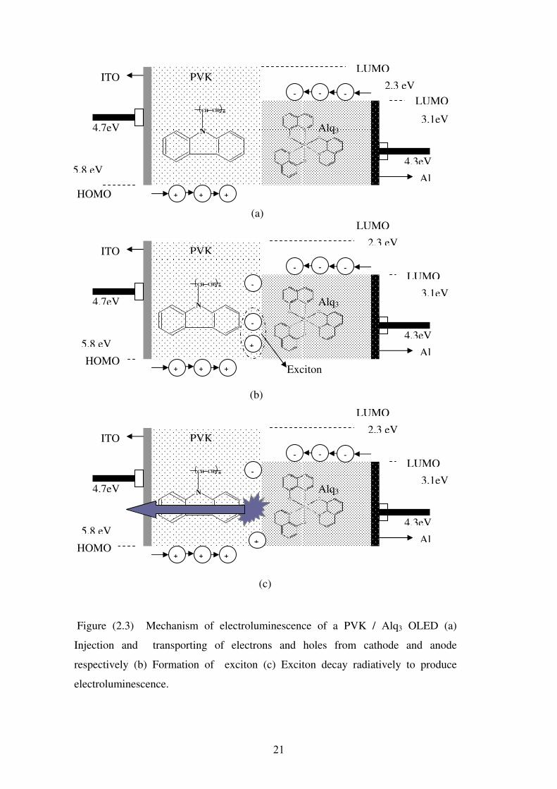
2.3
Mechanism of electroluminescence of a PVK / Alq3 OLED
(a) Injection and transporting of electrons and holes from cathode
and anode respectively (b) Formation of singlet exciton (c) Exciton
decay radiatively to produce electroluminescence.
21
2.4
Current density J of dielectric sample with permittivity ε and
thickness d in the x-direction. 23
3.1 Spin coating steps (a) Dispensing, (b) Spreading, and (c) Drying 29
3.2 A schematic setup of thermal evaporator 30
3. 3 Shadow mask is placed on top of ITO substrate 31
3.4
Typical structure of (a) A single layer OLED sample, and (b) A
double layer OLED sample 33
3.5 Top view of a sample with anode and cathode contacts shown 34
3.6 The experimental setup used in measurements 34
3.7 Ellipsometer in common form 35
3.8 Schematic depiction of an ellipsometic set-up 35
3.9 Geometry of the elliptically polarized light 35
3.10 Multiple reflection and transmission by a thin film 40
4.1
Four characteristics curves of S1, (a) Current-voltage
characteristics, (b) Relative intensity-voltage characteristics, (c)
Relative intensity-current characteristics, (d) Current-voltage in
46

XIII
logarithmic scale
4.2
Four characteristics curves of S2, (a) Current- voltage
characteristics, (b) Relative intensity-voltage characteristics, (c)
Relative intensity-current characteristics, (d) Current-voltage in
logarithmic scale
47
4.3
Four characteristics curves of S3, (a) Current- voltage
characteristics, (b) Relative intensity-voltage characteristics, (c)
Relative intensity-current characteristics, (d) Current-voltage in
logarithmic scale
48
4.4
Four characteristics curves of S4, (a) Current- voltage
characteristics, (b) Relative intensity-voltage characteristics, (c)
Relative intensity-current characteristics, (d) Current-voltage in
logarithmic scale
49
4.5
Four characteristics curves of S5, (a) Current- voltage
characteristics, (b) Relative intensity-voltage characteristics, (c)
Relative intensity-current characteristics, (d) Current-voltage in
logarithmic scale
50
4.6
The current voltage characteristics of the S1, S2, S3, S4 and S5
samples 52
4.7
Electroluminescence-voltage characteristics of the S1, S2, S3, S4
and S5 samples 54
4.8 The variation of Electroluminescence with current 56
4.9 Current-voltage of the five OLED samples in logarithmic scale 59
4.10
Variation of the refractive index for 18 nm Alq3 film on Si
wafer as a function of wavelength (visible spectrum) at 75o angle
of incidence
60
4.11
Psi as a function of λ from 400 to 700 nm for 18nm Alq3 film
on Si wafer and 75o angle of incidence
61
4.12
Delta as a function of λ from 400 to 700 nm for 18nm PVK film
on Si wafer and 75o angle of incidence
61
4.13
Variation of the refractive index for a 48 nm PVK film on Si
wafer as a function of wavelength (visible spectrum) at 75o angle
of incidence
62

XIV
4.14
Psi as a function of λ from 400 to 700 nm for 48 nm PVK film
on Si wafer and 75o angle of incidence
62
4.15
Delta as a function of λ from 400 to 700 nm for 48 nm PVK film
on Si wafer and 75o angle of incidence
63
4.16
Delta-Psi for 48 nm PVK film on Si wafer and 75o angle of
incidence 63

XV
LIST OF SYMBOLES AND ABBREVIATIONS
Alq3: 8-hydroxyquinoline aluminum.
Aqua Regia acid : (20% HCL, 5 % HNO3).
CT: charge Transfer.
DIW: Deionized water.
)(xE : electrical field intensity.
iE : quantized internal energy.
ETL: electron transport layer.
FPD: flat panel display.
HTL: hole transport layer.
HOMO: highest occupied molecular orbital.
h : Planck's constant.
k : Boltzman's constants.
N : charge density .
J : current density.
drJ : drift current.
dfJ : diffusion current.
ITO: indium tine oxide.
LUMO: lowest unoccupied molecular orbital.
OLED: organic light emitting diode.
PVK: Poly (9-Vinylcarbazole).
PPV: Poly(p-phenylene vinylene).
PFO: Polyfluorene.
RG6: Rhodamine 6G.
S: singlet state.
S: total electron spin angular momentum.
SCLC: Space Charge Limited Conduction.
T: triplet state.
TPD: (N,N_-diphenyl-N,N_-bis(3-methyl-phenyl)-(1,1_-biphenyl)- 4,4_-diamine).
THF: tetrahydrofloren.

XVI
ψ : the change in amplitude difference.
∆ : the change in phase difference.
e: electric charge.
µ : charge mobility.
D: diffusion constant.
ε : electrical permittivity.
sr : Fresnel's reflection coefficient for S-component.
pr : Fresnel's reflection coefficient for P-component.
Φ : work function.
χ 2 : the smaller difference between the calculated ),( calccalc ∆ψ and the measured
),( expexp ∆ψ .
TV : threshold voltage.

XVII
LIST of APPENDIXES
Appendix
No.
Name of Appendix Page
No.
Appendix(A)
Mott's Gurney Steady State Space-Charge-Limited
Current (SCLC) 68
Appendix(B)
Multiple reflection and transmission by a thin film 70

Chapter One
Introduction

2
1.1 Introduction
The name of a polymer is usually derived from the name of a monomer by
adding the prefix (poly). A polymer is a large molecule of many repeated units linked
together to form a large chain. The first semi-synthetic polymer produced was
Bakelite in 1909, and it followed by the first synthetic fiber, rayon, which was
developed in 1911 [1,2,3]. The number of repeating units in the chain is called the
degree of polymerization "n". The mass of a monomeric unit "M" multiplied by "n"
gives the molecular mass of the polymer Mpol such that.
Mpol = n M (1.1)
The degree of polymerization may vary through a wide range, from a few
units to 100,000 units. Polymers with high degree of polymerization are called high
polymers, but polymers which have low degree of polymerization are called
oligomers [2]. If only one type of monomer is employed to form the polymer, the
resulting molecule is called homopolymer. A Copolymer is obtained when two or
more monomers are used to form a polymer [1,2].
1.2 Types of Polymer Molecular Structures
There are two main types of polymer molecular structures, homopolymers and
copolymers.
1.2.1 Homopolymers
Homopolymers are polymers that consist of identical monomers. The
molecular structure of homopolymers can be categorized into three main types: linear,
branched, and Crosslinked (three dimensional) structure.
(a) Linear Polymer
Linear polymers are polymers with long chains, characterized by high degree
of symmetry [3]. The main difference in linear polymer properties results from how
the atoms and chains are linked together in space. Polymers that have one dimensional
structure will have different properties than those that have two dimensional or three
dimensional structure [1]. Denoting a monomeric residue by P, one would write the
formula of linear polymer as shown in Figure (1.1).

3
Figure (1.1) Linear Polymers.
(b) Branched Polymer
A branched polymer is a long chain with side branches (side chains), the
number and length of which may be very large [3]. This type is also known as a two
dimensional polymers. A branched polymer is depicted in Figure(1.2) [2].
Figure (1.2) Branched polymer.
(c) Crosslinked Polymer
Crosslinked polymers consist of long chains connected up into a three
dimensional network by chemical crosslink. Crystalline diamond and epoxy are good
examples of three dimensional polymers. This structure offers low shear and good
lubricating properties [1,4]. Figure(1.3). illustrates the structure of Crosslinked
polymers.
Figure (1.3) Crosslinked ( three dimensional polymer).

4
1.2.2 Copolymers
Copolymers are polymers with at least two different types of monomers.
Copolymers may be linear (random, alternating and block copolymer), branched or
crosslinked molecule consisting of identical or different atoms. Linear copolymers in
which the units of each form are fairly long with continuous sequences (blocks) are
known as block copolymers as shown in Figure (1.4). A branched copolymers has a
long chain of monomers of one kind in their main backbone and monomers of
another type in their side branches. The structures of branched copolymers are shown
in Figure (1.5) [1,2].
Figure (1.5) Branched copolymers
(a)
(b)
(c)
Figure (1.4) The three types of molecular structure (a) Linear random copolymer,
(b) Linear alternating copolymer, and (c) Linear block copolymer.

5
1.3 Conjugated Polymers
Conjugated polymers are polymeric compounds rich in electrons. The
backbone of conjugated polymers consists of alternative double and single bonds at
the same time. This alternativity plays an important role in the conductivity of the
polymers [6]. The first and the simplest conjugated polymer is "polyacetylene" (CH)x.
Examples of conjugated polymers are polyacetylene, poly(p-phenylenevinylene),
polyphenyl, polythienylenevinylene, polypyrrole, and polythienylenevinylene. The
structures of these polymers are depicted in Figure (1.6).
Table (1.1) The HOMO/LUMO of some organic compounds used in OLEDs
fabrication.
LUMO
(eV )
HOMO
(eV ) Symbol chemical formula
Compound
2.3 5.8 PVK Poly (9-Vinylcarbazole)
3.1 5.8 Alq3 8-hydroxyquinoline aluminum
2.4 5.4 TPD
(N,N_-diphenyl-N,N_-bis(3-
methyl-phenyl)-(1,1_-
biphenyl)- 4,4_-diamine)
2.7 5.2 PPV Poly(p-phenylene vinylene)
2.9 5.8 PFO Polyfluorene
1.7 4.7 1,2,4 Triazole 1,2,4 Triazole
The main characteristics in conjugated polymers are their low bandgap
between highest occupied molecular orbital (HOMO) and lowest unoccupied
molecular orbital (LUMO). When a molecule absorbs light of suitable wavelength, an
electron is excited from its HOMO to the LUMO. Bandgaps in materials can be
expressed by the energy difference between HOMO and LUMO levels. The HOMO
and LUMO of some organic compounds used in OLEDs fabrication are listed in
Table (1.1) [6, 7].

6
n
(a)
n
(b)
S n
(c)
n
(d)
N
H
(e)
S
(f)
Figure (1.6) Representative −π conjugated polymers in their pristine form (a)
Polyacetylene, (b) Polyphenyl, (c) Polythiophene (d) Polyphenylenevinyle, (e)
Polypyrrole, and (f) Polythienylenevinylene.

7
1.4 Molecular Orbitals
Molecular orbitals are formed by overlap of atomic orbitals. Every electron in
a molecular orbital has a particular energy state. For example, in hydrogen molecule
H2, the energy of electron in bonded molecular orbital (BMO) is less than its energy
in atomic orbital s1Ψ . In contrast, the energy of an electron in antibonding molecular
orbital is greater than its energy in atomic orbital. Figure (1.7). illustrates the energy
diagram for molecular and atomic orbitals for hydrogen molecule H2. There are two
electrons with opposite spins placed in the bonding molecular orbital. Also, in the
atomic orbitals one electron has spin up and the other has spin down. However the
total energy of the two electrons together in (BMO) is less than that in atomic orbitals
[8]. The energy of molecularΨ orbital which has two electrons is lower than energy of
*
moleculerΨ orbital which has no electrons. For example, when the hydrogen molecule
absorbs enough energy of a photon in high energy (ultraviolet), then the molecule is
excited and the electron occupies the antibonding orbital. This case is called the
excited state of the hydrogen molecule [8,9].
Figure (1.7) Energy diagram for the hydrogen molecule.
H
H
Atomic orbitals
s1ψ
*ψ
Energy
H2
s1ψ
Molecular
Molecular
ψ
Antibonding MO
Bonding MO

8
1.4.1 Singlet State
In this case there are one pair of electrons in the molecular orbital, one is spin
up (+1/2) and the other is spin down (–1/2), this means that the total electron spin
angular momentum S= s1 + s2= –1/2 + 1/2 =0. In general the multiplicity = (2x S)
+1= 1 "singlet".
1.4.2 Doublet State
When the electron in molecular orbitals is not paired (one electron) this
means that the total spin S= s1 =1/2 and the multiplicity = (2 x1/2) + 1 = 2
"doublet". The hydrogen atom is a good example for doublet state.
1.4.3 Triplet State
In triplet state there are two "spin-up" electrons. i.e. two electrons of the same
spin, +1/2 and +1/2. Total electron spin angular momentum, S=1and the multiplicity
= (2 x1) +1=3 "triplet".
1.5 The Internal Energy of Molecules
The molecular internal energy of a molecule in the electronic state is the sum
of the rotational, vibrational and electronic energy transitions. The internal energy
intE of a molecule in its electronic ground or excited state can be expressed by the
following equation:
rotvibel EEEE ++=int (1.2)
where elE is the electronic energy, vibE is the vibrational energy and rotE is the
rotational energy [10].
1.6 Absorption Processes
When the molecule absorbs external energy of a photon ( λ/hcE = ) of

9
suitable λ . where h is Planck's constant, c is the speed of light and λ is the
wavelength, the molecule becomes excited. Each one of the electronic states (ground
or excited) has a number of vibrational and rotational levels. This energy
approximately equals the energy difference between the ground state and the excited
state equivalent to energy difference between HOMO and LUMO molecular states. In
general, molecules absorb wide range of wavelengths, a broad band rather than one
single wavelength. In the absorption process the transitions from ground state S0 to
the first and second excited singlet state S1, S2 are allowed, but the direct transition
from the ground state S0 to the triplet state T1 is forbidden [10,11].
1.7 Fluorescence and Phosphorescence
Luminescence is the emission of light. It is emitted after the electrons return
from the first excited singlet state S1, and the first excited triplet state T1 to the ground
state S0 and loses its excited energy as fluorescence and phosphorescence,
respectively.
1.7.1 Fluorescence
Absorption of UV or visible radiation of suitable λ by a molecule leads to
excitation. The electrons jump to the different vibrational states in S1. The electrons
in S1 can then undergo vibrational relexations and return to the main excited
electronic levels then return to S0 giving luminescence known as fluorescence. The
life time of electrons in S1 between 10-9
to 10-7
second, which is a very short time.
But, when the molecule absorbs energy less than the difference energy between the
ground state and the first excited state, the energy is used in making vibrations and
rotations of the molecule in the ground state with radiationless process. The quantum
yield (for fluorescence) depends on the ratio of the number of emitted photons and the
number of absorbed photons. Let *A be the excited state of the molecule, the
following equation represents the fluorescence emitted from the excited molecule.
νhAA +→* (1.3)
where A represents the molecule after losing the energy and ν is the frequency of
the emitted radiation. The amount of radiation emitted as fluorescence is lower than
the average amount absorbed by a molecule, because part of the energy was used in
making vibrations and relaxations of electrons to main electronic level [12,13].

10
1.7.2 Phosphorescence
When the electrons are in the excited state S1, they may be transferred by
intersystem crossing ISC to reach one of vibrational levels of the first excited triplet
state T1. Some vibrational relaxations occur, then the electron undergoes a second
flip in spin and returns to the ground state S0 with luminescence emission. This
phenomena is known as phosphorescence. The life time of triplet state is nearly equal
10-4
s to several seconds. The transition between triplet state and the ground state is
called Singlet-Triplet transition which is less probable than Singlet-Singlet
transition. Various radiation and radiationless transitions which occur in molecules
are shown in Perrin-Jablonski diagram in the Figure (1.8) [12]. State S0 is the ground
state, S1 is the first excited singlet state, S2 is the second excited singlet state. IC is the
internal conversion, which is transitions between states with the same spin. For
example the transition between S2 to any vibrational level in S1. ( 12 SS → , 01 SS → ).
ISC is the intersystem crossing, where the transition between the states with different
spins occurs. Phosphorescence dyes possess strong intersystem crossing (ISC) from
the excited singlet state to the triplet state ( 11 TS → ). Little or no fluorescence is
observed in these materials.
Singlet–singlet absorption results in the transition from the singlet ground state
of the molecule into the singlet excited state ( nSS →0 ) and leads to the UV/VIS
absorption spectrum. The analogous triplet absorption takes place in the transition
from the lowest triplet state of the molecule to a higher state ( nTT →0 ), thus leading
to the triplet-triplet absorption spectrum. In general the transition between energy
states with the same multiplicity is allowed and exhibits radiation, but the transition is
not allowed when the transition between energy states has different multiplicity, this
is called the spin conservation rule[10]. In general phosphorescence is distinguished
from fluorescence by the speed of electronic transition that generates luminescence.
Both processes require the relaxation of an excited state to the ground state.
Fluorescence and Phosphorescence materials are very important to improve the
efficiency of OLEDs luminescence, because the main characteristics of OLEDs
luminescence depend on these materials [13].

11
Figure (1.8) Perrin-Jablonski diagram and illustration of the relative positions of
absorption, fluorescence and phosphorescence spectra.
1.8 Exciton
The exciton is defined as a combination of an electron and a hole. The exciton
is treated in calculations as a chargless moving particle which is able to diffuse and
carry excitation energy. It behaves like a neutral particle moving through media. An
exciton may decay and emit luminescence with radiative decay, or decay without
luminescence [14,15,16].
1.8.1 Classification of Excitons
There are two main types of excitons, Wannier excitons and Frenkel
excitons [14]. Each type has specific characteristics, e.g. localization, binding energy
and radius of exciton (distance between hole and electron).
Wannier excitons has a radius much larger than the lattice spacing (constant distance
between unit cells in crystal lattice). It is found in dense media like crystals and
inorganic semiconductors. The binding energy (between hole and electron) of
Wannier exciton on the order 0.1 eV. The size of exciton in this case is larger than
other exciton such as Frenkel exciton.
Frenkel exciton is found in the materials which have very small dielectric constant ε
such that in organic semiconductors. It is a highly localized exciton and the coulomb's
interaction force between hole and electron is very strong, so the exciton tends to be

12
much smaller. The binding energy of Wannier exciton about 1.0 eV. Figure (1.9).
illustrates a Wannier exciton and a Frenkel exciton [14,16].
Molecule + -
Hole
Electron
Exciton
+
-
Hole
Electron
Molecule
Exciton
(a)
(b)
Figure (1.9) The spatial discrimination of excitons (a) Wannier exciton, (b) Frenkel
exciton.

13
1.9 Energy Transfer
There are two main forms of energy transfer mechanisms, Fǒrster and Dexter
mechanisms, both of them are non radiative energy transfer. The basic mechanism of
Fǒrster and Dexter transfer in light emitting diode (OLED) can be illustrated with two
organic materials, one a net electron donor (D) and the other an acceptor (A).
1.9.1 Fǒrster (Singlet- Singlet) Transfer
Fǒrster transfer is (singlet-singlet) radiationless transfer process, which,
therefore, does not involve emission of the light from the donor molecule at any stage.
Fǒrster transfer occurs in very short time less than 10-9
second. There is a Columbic
interaction of the dipoles of two molecules, excited doner molecule D* and the
acceptor of the excited molecules A. The movement of the excited electron on the
donor molecule creates an oscillating dipole. Figure (1.10). shows the Fǒrster transfer
[16,17].
Figure (1.10) Fǒrster (singlet) transfer, (a) The initial state, (b) The final state.
1.9.2 Dexter (singlet- singlet or triplet-triplet) Transfer
The most common exciton is the so called Dexter exciton which is a strongly
bound, electron-hole pair usually localized on a single molecule. The mechanism of
the Dexter transfer is an electron exchange (tunneling) process. Where the donor
excited electron in the excited state (jump) to the excited state of the acceptor A and
Doner*
Accepter Doner Accepter*
Coloumbic interaction
force
(a) (b)

14
one of the electron in the ground state of the acceptor A jumps to the ground state of
the donor molecule D as shown in Figure(1.11). The two exchanges may occur either
simultaneously, or one after the other. The rate of Dexter mechanism transfer is also
exponentially dependent on the distance between the donor and the acceptor. In
Dexter transfer singlet- singlet or triplet-triplet transitions are allowed, 25% of the
formed excitons will be singlets and 75% will be triplets. This is because the triplet
state has three spin projections (MS = 0, ±1) and the singlet has only one (MS = 0)
[16,17].
Figure (1.11) Diagrammatic representation of Dexter energy transfer, (a) The initial
state, (b) The final state.
1.10 Poly N-Vinylcarbazole (PVK)
1.10.1 Carbazole
Carbazole is an aromatic tricyclic compound which was discovered in 1872
by Graebe and Glaser from the coal tar [19]. A high number of carbazole monomers
linked together will form poly(vinylcarbazole) compound. The chemical structure of
carbazole is illustrated in Figure 1.12(a). Pure carbazole is a white crystalline
organic material which has melting point of 246 0C
, and 167.2 g/mole molecular
weight. Carbazole has high boiling point compared with many of organic materials
[14]. It is an electroluminescent material. Carbazole emits strong fluorescence and
long phosphorescence by exciting with enough energy (ultraviolet) [19,20].
Doner*
Accepter Doner Accepter*
(a) (b)

15
N
H
(a)
N
(b)
N
CH CH2 n
(c)
Figure (1.12) The structure of, (a) Carbazole,(b) N-vinylcarbazole, (c)
and Poly(N-vinylcarbazole).

16
1.10.2 Poly (9-Vinylcarbazole)
Poly(9-vinylcarbazole) (PVK) is tricyclic organic polymeric material which is
transparent plastic material. The softening point of PVK is nearly a 175 0C and glass
transition temperature (Tg) is at 2110C. The chemical structure of PVK is illustrated
in Figure 1.12(c). the solubility of PVK is very strong in alcohol, ether and THF.
Usually PVK films are deposited by spin coating. It has good optical properties, PVK
has a strong photoconductive and electroluminescence properties. It has a high
refractive index ~1.69 in the visible region. Electrically, PVK is an insulator in dark
but under the ultraviolet radiation, it exhibits electro-conductivity. Commercially
PVK is used as a paper capacitor, in OLEDs, data storage, sensors and transistors. In
OLEDs, PVK is used as a hole transport material[20].
1.11 Indium Tin Oxide (ITO)
Indium tin oxide (ITO, or tin-doped indium oxide) is a mixture of indium
oxide (In2O3) and tin oxide, typically 90% In2O3, 10% SnO2 by weight. Most of ITO
coated glass is available in surface resistivities from 5 Ω / to 1000 Ω /. ITO is
used widely for optoelectronic devices because it exhibits a good electrical
conductivity with high transparency in the visible range. ITO electrodes are used in
interesting applications such as heat reflecting mirrors, high temperature gas sensors,
thin film solar cells and OLEDs. In addition it can be used as a positive electrode in
flat panel displays. The deposition of ITO on a flat glass substrate is achieved by
using sputtering or spray techniques. Sputtering involves knocking an atom or a
molecule out of the target material by accelerated ions from an excited plasma, then
depositing ITO thin film onto high quality glass substrates [21].

17
Chapter Two
Organic Light Emitting Diodes
(OLEDs)

18
2.1 Introduction
In this chapter we present an introduction to OLEDs and an overview of
emission mechanism of light from an OLED . Then, we shall discuss and derive
ohmic and Space Charge Limiting (SCLC) conduction models which may take
place during operation.
An OLED consists of thin films of electroluminescent organic layers (single or
multiple layers) sandwiched between two electrodes. By applying a suitable voltage,
electroluminescence is emitted through the transparent electrode. The first OLED
was prepared in 1987 by C.W Tang and Van Slyke [22]. This device consists of two
layers, the first layer was an aromatic diamine which acts as a hole transport layer
(HTL). The second layer was an emissive layer 8-hydroxyquinoline aluminum
(Alq3). The chemical structure of diamine and (Alq3) are illustrated in Figure (2.1).
The structure of the first OLED is depicted in Figure (2.2) where the anode is an
Indium-Tin-Oxide (ITO) film deposited onto glass substrate. The ITO electrode is a
transparent electrode that transmits light emitted from the device. The other electrode
is usually an aluminum layer which acts as the cathode of the device. Other materials
such as Ag, Mg and Ag/Mg(alloy) may be used as a cathode [22,23].
Many conjugated polymers are used in OLEDs fabrication to exhibit
electroluminescence with different colors [23].
2.2 Mechanism of Light Emission From an OLED
An OLED is a device which consists of one or more organic thin films
sandwiched between two electrodes. The transparent electrode is an ITO anode with
a work function that is higher than that of the cathode. The work function of ITO is
equal to 4.7eV while the work function of Al is equal to 4.3 eV. This difference in
work functions creates potential and energy difference between the two electrodes.
The work function of some materials used in OLEDs fabrication is tabulated in Table
(2.1) [24,25]. When a suitable bias is applied between the two electrodes of the
OLED, holes are ejected from the anode (source of holes) into the highest occupied
molecular orbital (HOMO) of the hole transport layer (HTL). In the opposite
electrode, electrons are ejected from the cathode into the lowest unoccupied molecular
orbital (LUMO) of the electron transport layer (ETL).

19
Figure (2.1) Alq3 and diamine molecular structures.
Figure (2.2) The first OLED which was fabricated by C.W Tang and VanSlyke.
The electrons and holes transport in the organic material and recombine to create a
lot of excitons. Some of the excitons decay radiatively to give electroluminescence
and others decay with radiationless process. The recombination of holes and electrons
is responsible for the OLED light output in the ETL near the ETL/HTL interface.
Figure (2.3) presents the mechanism of electroluminescence emitted from an OLED.
A lot of enhancements can be done to increase the internal quantum efficiency
of OLED performance. The internal quantum efficiency is defined as the ratio of the
Glass substrate
Mg/Ag (Cathode)
Alq3
Diamine
ITO (Anode)

20
number of photons produced within the device to the number of electrons flowing
from the external voltage. To achieve an efficient luminescence, it is necessary to
have a good balance of electrons and holes within the emissive layer. A hole blocking
thin film is deposited under the electron injection layer to increase the population of
holes in the emissive layer. Dopping of the emitter layer with an organic dye
molecules allows energy to transfer from the emitter molecule (host) to the dye
molecule (guest) in order to increase the luminance efficiency or to tune the
wavelength λ of the emitted electroluminescence [22]. The efficiency of the device
not only depends on the electrical and optical properties of materials but also depends
on the device structure single or multi layers. The performance of double layer OLED
is better than that of single layer. This behavior is attributed to the long time spent by
the charge carriers (electrons and holes) in the polymeric layers which increases the
creation the excitons inside polymeric layers. In the single layer, most of holes and
electrons have less chance to stay inside the polymeric layers. This facilitates the
motion of holes to cathode and the motion of the electrons to anode [24].
Table (2.1) The work function Φ of some materials.
Work Function Φ (eV) Material
4.70 ITO
4.30 Al
4.29 LiF
2.87 Ca
5.00 C
5.10 Au
3.66 Mg
4.26 Ag
21
4.3eV
4.7eV
ITO
HOMO
LUMO
LUMO
Al
2.3 eV PVK
5.8 eV
Alq3 3.1eV
+ + +
-
N
CH CH2 n
- -
4.3eV
4.7eV
ITO
HOMO
LUMO
LUMO
Al
2.3 eV PVK
5.8 eV
Alq3 3.1eV
+ + +
-
N
CH CH2 n
- -
-
-
+
Exciton
4.3eV
4.7eV
ITO
HOMO
LUMO
LUMO
Al
2.3 eV PVK
5.8 eV
Alq3 3.1eV
+ + +
-
N
CH CH2 n
- -
-
(a)
(b)
(c)
Figure (2.3) Mechanism of electroluminescence of a PVK / Alq3 OLED (a)
Injection and transporting of electrons and holes from cathode and anode
respectively (b) Formation of exciton (c) Exciton decay radiatively to produce
electroluminescence.
+

22
2.3 Conduction
2.3.1 Space Charge Limited Current ( SCLC )
Space Charge Limited Current (SCLC) occurs when the current is limited by
the space charges. The occurrence of space charge limited current requires that at least
one contact has good injecting properties to provide an inexhaustible carrier reservoir.
SCLC in a device can occur if at least one contact is able to inject more carriers than
the metal has in thermal equilibrium without carriers injection. When the equilibrium
charge concentration (before charge injection) is negligible compared to the injected
charges concentration this will form a space charge cloud near the injection electrode.
In general, the DC current of device can be divided into two main regimes, ohmic
regime and space charge regime. In the ohmic regime, the current is linearly
proportional to the electric field [26,27] as shown in equation (2.1).
EJ ∝ ( 2.1 )
In the second regime (SCLC), the current is proportional to the square of the electric
field
2EJ ∝ ( 2.2)
2.3.2 MOTT- Gurney Steady-State Space- Charge-Limited Conduction
Model
The Mott-Gurney expression for (SCLC) was developed for a constant
mobility. Verifying the SCLC region is an essential part of our experimental
methodology fragment [27,28]. The space charge limited conduction current density
J in a dielectric sample is proportional to the a square of the applied voltage V. A
special case arises when the current is limited by the space charges. This means that
the density of free carriers injected into the active region is larger than the number of
acceptor levels. The entire current only comes from the diffusion of carriers. In other
words, the current is caused by the large gradient of density of free carriers.

23
Figure (2.4) Current density J of dielectric sample with permittivity ε and
thickness d in the x-direction.
The drift current (rdJ ) is related to the electric field ( in x-direction) by
vNeJdr = (2.3)
where
)(v xEµ= (2.4)
substituting from equation(2.4) into equation(2.3), fdJ becomes
)(xENeJrd µ= (2.5)
and the diffusion current ( dfJ ) is given by [29,30]
where J is the current per unit cross-sectional area, N is charge density, e
is the electronic charge, v is the drift velocity, E(x) is the electrical field in the x-
direction, µ
is the charge mobility,
and D is the diffusion constant of electrons in
sec
2m .
The total current density J is given by
Ndx
dDeJdf = (2.6)
0 d x
v
Dielectric sample
E(x)

24
Ndx
dDexENeJ P += )(µ (2.7)
The exact theory of SCLC is rather complicated. The simplified theory neglects the
diffusion current. So, the current density is given by equation (2.5) and the Poisson
equation (in x- direction) can be expressed as
Ne
xEdx
d
ε=)( (2.8)
where ε is electrical permittivity of the media.
substituting equation (2.8) into equation (2.5) we get
)()( xEdx
dxEJ Pεµ= (2.9)
After some manipulation (see appendix A)
( ) 9
8)( 2
32
3
0
κκεµ
−+== ∫ dJ
dxxEV
d
(2.10)
we may have two cases
• Case one, for
d<<κ equation (2.10) becomes
2
3
9
8d
JV
εµ= (2.11)
squaring both sides
3
2
8
9
d
VJ SCL µε= (2.12)
Equation (2.12) shows Space Charge Limited regime.
where, V is the applied voltage, and d is the thickness of the layer.

25
• Case two, for d>>κ equation (2.10) becomes
d
VNeJ ohm µ= (2.13)
Equation (2.12) show that, in space charge limiting conduction there is a limit to the
maximum amount of positive or negative charge that can be injected to the device.
But in ohmic conduction, there is no barrier to the injection of charge into organic
film as described in equation (2.13) [29,30,31].

26
Chapter Three
Experimental Techniques

27
3.1 Introduction
This chapter explains the different experimental techniques involved in the
fabrication of OLEDs which are studied in this work. It includes description of
etching ITO substrates followed by spin coating. A cathode is then deposited by
thermal vacuum evaporation using shadow mask as shown in Figure (3.3). A
homemade variable angle spectroscopic ellipsometer (VASE) was used to determine
the thickness and the refractive index (n) of the organic thin films.
3.2 Sample preparation
3.2.1 Etching of ITO Substrates
The starting substrates consist of ITO coated glass sheets (7.5cm x 2.5cm)
were purchased from delta technologies, USA. A digital multimeter (Fluke77) was
used to determine the conductive surface of ITO substrate. Each sheet was cut into
small pieces with dimensions 2.5 cm x 2.5 cm by using diamond scribe. Every sample
was arranged in an 4 x 4 array of devices. The ITO substrates (electrodes) were
cleaned thoroughly by wiping each electrode surface by a cotton pad wetted with
acetone. Then, an electric tape is stuck at the conductive side of the ITO coated glass
substrate. ITO electrodes were then etched to form the desired pattern by immersing
them in a Aqua-Regia acid (solution of 20% HCl and 5% HNO3) for 15 minutes at
60 °C. A digital multimeter (Fluke77) was used to measure the resistance of the
etched regions of the ITO substrates. Very high resistance must be recorded if the
etching procedure is successful in removing all the ITO onto etched regions of the
glass substrates. After etching, the tape was removed and the patterned samples were
rinsed in DI water to remove away the leftover acids. The etched ITO plates were then
rubbed with a lens paper to remove tape residue. Upon completing the etching
process, the substrate must be cleaned using DC arc plasma for 8 minutes [23].

28
3.2.2 Spin Coating
Spin coating is a technique widely used to deposit thin films of organic
materials on top of flat substrate using a spin coater. In general, a spin coater consists
of a table, which has very smooth surface, mounted on very fast motor with multi-
angular speed. The thickness of the film depends on the rotational speed, viscosity,
surface tension, drying rate, percent of the solids, and spin time. In spin coating
technique, the solution must be homogenous, have no solid species, and the substrate
must be clean.
There are three steps to do spin coating. The first step is fixing a clean
substrate horizontally on to the center of the bench of spin coater clip and an amount
of a polymer solution is placed on the substrate to be coated. In the second step, the
substrate is rotated at a constant rate to achieve the final speed in order to spread the
fluid by centrifugal force. Rotation is continued for known time and the fluid being
spun off the edges of the substrate, until the desired film thickness is achieved. In the
third step, the solvent usually volatiles and the solution condenses in a form of thin
film on the substrate surface. The main three steps of spin coating process are
depicted in Figure (3.1). During the spinning process, care must be taken to
obtain a dust free film. The film thickness is controlled using different speeds. Thin
films require high spin speed and long spin time but thicker films require short spin
time and low spin speed [32].
3.2.3 Thermal Vacuum Evaporation of Organic and Cathode Layers
The deposition of the organic layers and the cathode of each samples
are performed in a vacuum chamber by heating the materials electrically in vacuum
until evaporation. A schematic setup of the thermal evaporator is depicted in Figure
(3.2). The glass substrate is mounted to a holder with ITO substrate facing a basket in
which the organic material is placed for thermal evaporation. The ITO substrate must
be mounted as quickly as possible after the cleaning and etching procedures to avoid
contamination with dust particles. Edwards Diffstak 100 water-cooled diffusion pump
was used to pump down the chamber to a low pressure of about 10-5
torr range.

29
ω
ω
(a)
(b)
(c)
Figure (3.1) Spin coating steps (a) Dispensing, (b) Spreading, and (c) Drying.

30
After reaching a suitable pressure, indicated by the monitor, the hot resistance
could be switched on for a suitable time to evaporate the material inside the boat. The
shadow mask, which has 5 fingers as shown in Figure (3.3), is used in order to define
four separate cathode contact to the OLED. Aluminum is used to make the electrodes
in our samples. It is deposited by thermal evaporation deposition technique. After the
chamber reaches vacuum pressure about 10-5
torr. The aluminum is heated until fusion,
using electrical current passing through tungsten coil for one minute. When the
evaporation is completed, the diffusion pump is closed and the sample is removed
outside the bell jar. We used aluminum as the cathode of OLED samples due to its
stability compared with calcium or magnesium [33,34].
Figure (3.2) A schematic setup of thermal evaporator
Material to be
evaporated
Bell
jar
Vacuum
system
Power
supply
Hot coil
Substrate
Metal vapor

31
3.3 Experimental Setup
3.3.1 Samples
Five OLED samples were prepared in this work. One of these samples
consists
of a double layer ITO/PVK/ Alq3 /Al. The other OLEDs are single layer type doped
with various dyes. These samples are listed in table ( 3.1).
Table (3.1) The name and the structure of all samples.
Structure of the sample
Sample name
ITO/PVK R6G (blend)/Al S1
ITO/PVK / Alq3 /Al (double layer) S2
ITO/PVK carbocyanine(blend)/Al S3
ITO/PVK 1,2,4 oxadiazole(blend)/Al S4
ITO/PVK fluroscein (blend)/Al S5
Shadow
mask ITO patterned
Figure (3.3) Shadow mask is placed on top of ITO substrate
32
3.3.2 Experimental Procedure
The general structure of the single layer samples is (ITO/doped polymer
film/Al). An amount of 300 mg of Poly(9-vinylcarbazole) with an average molecular
weight of 11x105 ( purchased from Sigma-Aldrich, USA) was dissolved in 150 CC
THF. A 2% by weight of the dye was added to the solution. PVK and the dopants
were weighted by using a sensitive electrical balance (sartorious AG Goettingen
model BA1105) with a resolution of 10-4
gm. Poly(9-vinylcarbazole) was dissolved
in a proper amount of organic solvent such as THF. The desired weight concentration
of the dopants were then added to the solution. The solution was then stirred
thoroughly and filtered. For the single layer samples, few drops of the blend solution
were spun at 1750 rpm for one minute to form thin film on the etched ITO.
For the double layer sample, the Alq3 layer was deposited on the PVK film
using thermal vacuum evaporation at 1.7x10⁻⁵
torr in low rate deposition condition
for one minute. The samples were then stored in an oven at 80oC under vacuum for
one day. Aluminum cathode was deposited using thermal vacuum evaporation
technique at 1x10⁻⁵
torr for one minute also. Five wires were connected to the
electrodes using silver paste. The side view of the sample with anode and cathode is
depicted in Figure (3.5). The film thickness of the organic film was measured using a
calibrated homemade variable angle spectroscopic ellipsometer (VASE). Figure (3.6)
depicts the experimental setup arrangement.

33
(a)
Glass
substrate
Contact to Al
electrode
Contact to
ITO
electrode
ITO
Polymer &
dye (blend layer)
Al
electro
de
Figure (3.4) Typical structure of (a) a single layer OLED sample,
and (b) a double layer OLED sample.
(b)
Glass
substrate
Contact to Al
electrode
Contact to
ITO
electrode
ITO
Dye
Polymer layer
Al
electrode

34
ITO anode
Emissive
area
Silver
paste
Al
cathode
Figure (3.5) Top view of a sample with anode and cathode contacts shown.
Figure (3.6) The experimental setup used in measurements.
Sample
Current
amplifier
Voltage
amplifier
Computer
PMT
Data q
uistio
n
card

35
3.4 Ellipsometry
3.4.1 Introduction
Ellipsometry is an optical sensitive technique for investigating the dielectric
properties (refractive index N ) and the thickness of thin films. It has applications in
many fields such as semiconductors, electronics, optics, and industrial applications.
An ellipsometer measures the changes of polarization state of light, when reflected
from a sample. A conventional ellipsometer consists of a light source, a polarizer, an
analyzer, and a detector. Figure (3.7) shows the components of an ellipsometer in
common form [35,36, 37].
The principle of operation of an ellipsometer is illustrated by the schematic
drawing of the ellipsometer in the Figure (3.7). The incident light is linearly polarized
with finite electric field components pE and sE in the direction parallel and
perpendicular to the plane of incidence respectively. Upon reflection, the polarization
state of the S and P components of the electric field will change. The reflected light
becomes elliptically polarized as shown in Figure (3.9) [38,39].
Figure (3.7) Ellipsometer in common form.
Sample Linear
Polarized
light
Monochromater
Analyzer
PMT
Elliptically
polarized light
unpolarized
light
Polarizer
oφ

36
Figure (3.9) Geometry of the elliptically polarized light
sr
pr
ψ
Figure (3.8) Schematic depiction of an ellipsometic set-up
Thin film
Substrate
Plane of
incidence
Ep Ei
ES Er
oφ

37
Consider the reflected −P polarization rpδ and the reflected −S polarization
rsδ . We can define the parameter ∆ as
rsrp δδ −=∆ (3.1)
which represents the change in phase difference that occurs upon reflection. It can has
the value from 0o to 360
o. The amplitudes of both the parallel and the perpendicular
components pr and sr (see equations 3.10, 3.12) change upon reflection. The ratio of
the absolute value of amplitudes of outgoing wave for the parallel component and the
absolute value of amplitude of the outgoing wave for the perpendicular component is
called ψtan such that
= −
s
p
r
r1tanψ (3.2)
Ellipsometer measures two values, the change in amplitude difference ψ , and
the change in phase difference ∆ .
These two values are related to the ratio of Fresnel's reflection coefficients,
pr and sr for P and S components of polarized light, respectively. The
ellipsometric parameters ψ and ∆ can be directly inverted to give both real and
imaginary parts of the complex refractive index, n and κ respectively. This can be
done using the fundamental ellipsometric equation
∆== i
s
pe
r
r)tan(ψρ (3.3)
where ρ is the complex ratio of the reflection coefficients
3.4.2 Typical Components of an Ellipsometer
(a) Light Source
An ellipsometer requires a light source laser or a lamp. Laser is intense and
collimated beam with small spot size; however laser is considered as a single
wavelength light source. This means that spectroscopic ellipsometry can not be
studied using laser source. Therefore, spectroscopic ellipsometry requires a broad
spectrum of wavelengths in order to achieve spectroscopic measurements.

38
(b) Monochromator
Monochromator is a Greek word, which means single color. It is an optical
device that transmits selectable narrow band of wavelengths of light chosen from a
wider range of wavelengths of light. Monochromators have wide usage in many
optical systems such as ellipsometers and spectrophotometers.
(c) Polarizer/Analyzer
The most important optical element in making an ellipsometer is the
polarizer. It is used in two different ways, polarizer and analyzer. A polarizer is a
device that converts an unpolarized (mixed of polarized ) light into a beam of defined
polarization state. On the other hand, the analyzer is a polarizer that is used to convert
elliptically polarized light into linearly polarized light or to determine the polarization
state of the beam [38,39].
(d) Detectors
The purpose of the detector is to measure the intensity of light passing though
the analyzer. A photomultiplier tube (PMT) is one of the most sensitive detectors, that
allows to measure very low levels of light. It can detect ultraviolet, visible, and near
infrared radiation. In general, every PMT has nine electrodes. Every electrode is
called a dynode, which operates at a constant high voltage. A PMT consists mainly
of light sensitive photo-cathode, that generates electrons when photons strikes the
cathode. These electrons are directed to the positively biased dynodes. Every electron
strikes the charged dynode creates several electrons, which are collected by the
following dynode. The output of a PMT is converted to a current which depends on
the intensity of light striking the photocathode [39].
3.4.3 Rotating Analyzer Ellipsometer (RAE)
RAE consists of a cascaded components of a light source, a polarizer, a
sample, an analyzer, a detector, and a computer. In RAE, the polarizer is fixed, while
the analyzer rotates continually during the measurements. The state of polarization
before striking the sample is linear and is elliptical upon reflection. The polarization
state of reflected light becomes linear after passing in the rotating analyzer. The

39
direction of polarization varies in time at the detector which measures the intensity as
a function of time.
The PMT detects sinusoidally time dependent varying intensity I(t). It records
different intensity at different states of polarization [40,41]. A Fourier analysis of the
sine wave can be used to find the values of the ellipsometric parameters
)]2sin()2cos(1[)( 0 ttxItI ωβωα ++= (3.4)
where, oI is the average intensity, βα , are the Fourier coefficients of the intensity
andω is the angular frequency of the motor.
The Fourier coefficients of the intensity are related to the ellipsometric parameters ψ
and ∆ by
P
P22
22
tantan
tantan
+
−=
ψ
ψα (3.5)
P
P22 tantan
tan.cos.tan.2
+
∆=
ψ
ψβ (3.6)
where P is the fixed polarizer angle
The ellipsometric parameters ψ and ∆ can be written as
Ptan1
1tan
α
αψ
−
+= (3.7)
−=∆
P
P
tan
tan
1cos
2α
β
(3.8)
After that, ψ and ∆ can be inverted using statistical calculations to find the
thickness and index of the thin film. Least –Square Approximation and quadratic
equation methods are important methods used to calculate the thickness and the
refractive index of thin films.

40
3.4.4 Reflection and Transmission by a Single Film
Consider a thin film of thickness d deposited on a substrate. A plane
polarized beam is incident at the interface between the air ( medium (0)) and the film
(medium (1)), as shown in Figure (3.10). The light will suffer multiple reflections and
transmissions. A phase difference is added when light travels between the upper and
lower surfaces of thin film. It can be expressed by the following equation
)cos(2 11 φλ
πβ Nd
= (3.9)
where d is the thickness of the thin film, 1φ is the angle of refraction, 1N is the
complex refractive index of the thin film, and λ is the wavelength of the incident
light beam.
Figure (3.10) Multiple reflection and transmission by a thin film.
According to Figure (3.11), the complex Fresnel's reflection and transmission
coefficients of this system are given by [38,40]
)exp(1
)exp(
1201
1201
β
β
irr
irrr
pp
pp
p+
+=
(3.10)
Medium(0) with
refractive index
(N0) 0φ
rφ
2φ
Air
Film
Substrate
d
Medium(1) with
refractive index
(N1)
Medium(2) with
refractive index
(N2)
1φ

41
)exp(1
)exp(
1201
1201
β
β
irr
ittt
p
pp
p+
=
(3.11)
)exp(1
)exp(
1201
1201
β
β
irr
irrr
ss
ss
s+
+=
(3.12)
)exp(1
)exp(
1201
1201
β
β
irr
ittt
s
sss
+=
(3.13)
where pr is the complex reflection coefficient for the P polarization, sr is the
complex reflection coefficient for the S polarization, pt is the complex transmission
coefficient for the P polarization and st is the complex transmission coefficient for
the S polarization respectively. For more details see appendix (B).
3.4.5 Thickness and Index Calculations Using An Ellipsometer
(a) Quadratic Equation Method
Quadratic equation method was driven by Samuel S.So in 1976 [41]. By
substituting Fresnel's coefficients pr and sr into equation (3.3), we get
( )( )( )( )ββ
ββ
ρi
ss
i
pp
i
ss
i
pp
errerr
errerr
12011201
12011201
1
1
++
++= (3.14)
0)0101()1212)1212(0101(2
))0101(1212( =−+−+−+− prsri
eprsrsrprprsri
esrprsrpr ρβ
ρρβ
(3.15)
Assume that
A= ( ))( 01011212 spsp rrrr − ,
B= ( )psspps rrrrrr 121212120101 )( −+− ρρ ,
C= ( )ps rr 0101 −ρ ,

42
and βie=Τ
Then, equation (3.15) can be simplified to give a quadratic equation as
02 =++Τ CBTA (3.16)
The solutions of quadratic equation have the next form
A
ACBBeT i
2
42 −±−== β (3.17)
from equation (3. 9)
( ))cos(2 11 φπ
λβ
Nd = (3.18)
Substituting from equation (3.17) into equation (3.18) the thickness of the
film can be written in term of 1, NT and 1φ as
( ))cos(2
ln
11 φπ
λ
Ni
Td = (3.19)
(b) Least –Square Approximation
There are many methods used to determine the optical parameters of thin film.
The common technique is the least square approximation. The principle of (least
square approximation) is finding the smallest sum of the square of the differences
between the ordinates of the function and the given point set. The main idea in this
method is to minimize the difference between the calculated ),( calccalc ∆ψ and the
measured ),( expexp ∆ψ .The smallest the difference χ is the better fit. χ is given by
2
1exp
,
exp
2
1exp
,
exp2
1
1
1
1∑∑
= ∆=
∆−∆
−−+
−
−−=
n
i i
iicalcn
i i
iicalc
mnmn δδ
ψψχ
ψ
(3.20)
where n is the number of the experimental observation points, m is the number of fit
parameters that completely characterized the sample under test, exp
,iψδ is the

43
measurement uncertainty of ψ and exp
,i∆δ is the measurement uncertainty of ∆ [40]. A
home Matlab subroutine was used to determine the refractive index and the thickness
of the thin film of some samples.
3.5 Cauchy's Equation
Cauchy's equation is a solution of non-homogeneous second order differential
wave equation in electromagnetic theory which is known as Lorentz model. Cauchy's
equation is used to describe the normal dispersion of dielectric materials in the visible
wavelength region. It is an empirical relationship between the refractive index and
the wavelength of light which uses in transparent material.
42)(
λλλ
CBAn ++= (3.21)
where A, B and C are called Cauchy's constants. In some references Cauchy's
constants may be written in term of ( 1n , 2n , 3n ), where ( 1n , 2n , 3n ) are three
different values of refractive index in three different wavelengths, which are
characteristic of transparent materials. To plot the Cauchy curve, it is necessary to
find three different values of n for three different values of s,λ . Cauchy constants
can be determined for a transparent material by fitting the equation using suitable
software program [42].

44
Chapter Four
Results and Discussion

45
4.1 Introduction
In this chapter, we present the results and discussion of our work on five
different OLED samples. These results include the I-V characteristic curves, the
dependence of light intensity on voltage and current, and the conduction mechanism.
The organic material is Poly-(9-Vinylcarbazole) which acts as a hole transport layer,
doped with various dyes (8-hydroxyquinoline aluminum (Alq3), rhodamine 6G, 1,3,4-
oxadiazole, carbocyanine, and fluroscein). The relative light intensity was measured
using a PMT (photomultiplier tube) for all samples biased over the full range of
voltages from 0 to 9 volts. Finally, additional ellipsometry measurements that include
optical parameters of thin films will be reported. The data was recorded and saved as
an ASCII file, analyzed and plotted using Origin 5.0 from Microcal Software, Inc.
Electrical measurements where conducted at room temperature and in nitrogen
chamber in order to prevent oxidation. The driving voltages and the currents were
obtained and measured using a MetraByte's Das-20 data acquisition card interfaced
with a personal computer. The output of the PMT was amplified then collected by the
same data acquisition card.
4.2 Results and Discussion
Figure (4.1) through Figure (4.5) depict the various characteristics of the five
samples under study. The current-voltage characteristics, relative light intensity-
voltage characteristics, relative light intensity-current characteristics, and current-
voltage in logarithmic scale are shown in these figures.

46
(a) (b)
0 2 4 6 8 10 12
0.005
0.010
0.015
0.020
0.025
0.030
Rel
ativ
e li
ght
inte
nsi
ty (
a.u
.)
Current (mA)
(c) (d)
Figure (4.1) Four characteristics curves of S1, (a) Current- voltage
characteristics, (b) Relative light intensity-voltage characteristics, (c) Relative
light intensity-current characteristics, (d) Current-voltage in logarithmic scale.
0 1 2 3 4 5 6 7 8
0.005
0.010
0.015
0.020
0.025
0.030
Rel
ativ
e li
ght
inte
nsi
ty (
a.u)
Voltage (V)
0.1 1
1E-5
1E-4
1E-3
0.01
D
C
B
A
Slope =1.1
Slope =4.3
Slope =1.5
Curr
ent
(A)
Voltage (V)
0 1 2 3 4 5 6
0
2
4
6
8
10
12
VT = 4.1 volt
Curr
ent
(mA
)
Voltage (V)

47
Figure (4.2) Four characteristics curves of S2, (a) Current- voltage
characteristics, (b) Relative light intensity-voltage characteristics, (c) Relative
light intensity-current characteristics, (d) Current-voltage in logarithmic scale.
(a)
(b)
(c) (d)
0 1 2 3 4 5 6 7 80
2
4
6
8
10
VT = 6.1 volt
PVK Thickness = 482 A0
Alq3 Thickness = 180 A
0
Cu
rren
t (m
A)
Voltage (V)
1 2 3 4 5 6 7 8
0.005
0.010
0.015
0.020
0.025
Rel
ativ
e li
gh
t in
ten
sity
(a.
u)
Voltage (V)
2 3 4 5 6 7 8 9 10
0.005
0.010
0.015
0.020
0.025
Rel
ativ
e li
gh
t in
ten
sity
(a.
u.)
Current (mA)
0.1 1
1E-5
1E-4
1E-3
0.01ESlope =3.7
Slope =1.3
Slope =2.2
Slope =1.2
D
C
B
A
Cu
rren
t (A
)
Voltage (V)

48
(a) (b)
(c) (d)
Figure (4.3) Four characteristics curves of S3, (a) Current- voltage
characteristics, (b) Relative light intensity-voltage characteristics, (c) Relative
light intensity-current characteristics, (d) Current-voltage in logarithmic scale.
1 2 3 4 5 6 7 8
0.005
0.010
0.015
0.020
0.025
Rel
ativ
e li
gh
t in
ten
sity
(a.
u.)
Voltage (V)
0 1 2 3 4 5 6 7 8 9
2
4
6
8
10
12
14
VT = 7.6 volt
Cu
rren
t (m
A)
Voltage (V)
0.1 1 10
1E-6
1E-5
1E-4
1E-3
0.01
Slope=10.8
Slope=0.7
Slope=1.2
D
C
B
A
Cu
rren
t (A
)
Voltage (V)
1 2 3 4 5 6 7 8 9 10 11 12 13 14
0.00
0.02
0.04
0.06
0.08
0.10
Rel
ativ
e li
gh
t in
tensi
ty (
a.u
.)
Current (mA)

49
0.1 1 10
1E-5
1E-4
1E-3
0.01
D
E
C
B
A
Slope=3.9
Slope=1.1
Slope=1.6
Slope=1.1
Curr
ent
(A)
Voltage (V)
(a) (b)
(c) (d)
Figure (4.4) Four characteristics curves of S4, (a) Current- voltage characteristics,
(b) Relative light intensity-voltage characteristics, (c) Relative light intensity-
current characteristics, (d) Current-voltage in logarithmic scale.
0 2 4 6 8 10
0
2
4
6
8
10
12
14
16
18
VT = 8 volt
Cu
rren
t (m
A)
Voltage (V)
0 1 2 3 4 5 6 7 8 9 10 11
0.05
0.10
0.15
0.20
Rela
tive
lig
ht
inte
nsity (
a.u
.)
Voltage (v)
0 2 4 6 8 10 12 14 16 18
0.00
0.02
0.04
0.06
0.08
0.10
0.12
Rel
ativ
e li
gh
t in
ten
sity
(a.
u.)
Current (mA)

50
(a) (b)
(c) (d)
Figure (4.5) Four characteristics curves of S5, (a) Current- voltage characteristics,
(b) Relative light intensity-voltage characteristics, (c) Relative light intensity-current
characteristics, (d) Current-voltage in logarithmic scale.
0 1 2 3 4 5 6 7 8
2
4
6
8
10
VT= 6.2 V
Curr
ent
(mA
)
Voltage (V)
0 1 2 3 4 5 6 7 8
0.01
0.02
0.03
0.04
0.05
0.06
0.07
0.08
Rel
ativ
e li
ght
inte
nsi
ty (
a.u.)
Voltage (V)
0 2 4 6 8 10
0.01
0.02
0.03
0.04
0.05
0.06
0.07
Rel
ativ
e li
gh
t in
tensi
ty (
a.u
.)
Current
0.1 1
1E-4
1E-3
0.01E
Slope=1.0
Slope=0.4
Slope=14.0
Slope=1.8
D
CB
A
Curr
ent (A
)
Voltage (V)

51
4.2.1 DC I-V Characteristic Curves
The forward bias was obtained when the transparent electrode was positively
biased and the aluminum electrode was negatively biased. The non-linearity is
frequent in I-V characteristics for all samples. The current passing through a
sample is due to the injection of the charges from the electrodes. A comparison
between the current-voltage characteristics of the these samples from sample1 through
sample5 (S1, S2, S3, S4 and S5) is depicted in Figure (4.6). DC I-V plots have been
shown to be useful in establishing the current transport physics of OLED samples.
These I-V characteristics show an exponential increase of current with the applied
voltage, which is similar to a typical diode characteristic curve [43]. Under forward
DC bias, the current increases slowly with increasing of voltage. Threshold voltage,
TV , is an important parameter characterizing the operation of OLEDs. In general it is
the voltage at which the OLED begins to emits light. At certain higher voltage, which
is the threshold voltage, the current increases sharply. The threshold voltages TV were
estimated by linearly extrapolating the I-V curves back to the voltage axis [44]. The
curves represent S3 and S4 show a slow increase of the current at lower voltage,
however in samples S1, S2 and S5 , remarkable increase in current at the same voltage.
I-V curves of the five OLED samples can be classified into two sets.
In set one, which includes S1, S2 and S5. The current clearly appears at low
applied voltage, however in set two which includes S3 and S4, the current appears at
higher voltage. The sharp increase at low voltage in S1, S2 and S5 may be referred to
the leakage current, which is linearly dependent on the applied voltage. The leakage
current observed properly due to movement of Al atoms inside the organic layer
toward the ITO electrode. The movement of Al atoms towards the other electrode will
increase the leakage current. This leads to low brightness of the OLED sample
[45,46]. Back to the Figure (4.6), it was found that TV of about 4.1V, 6.1 V and 6.2 V
for S1, S2, and S5, respectively.
In set two which includes S3 and S4, the leakage current is not appear
evidently and TV takes larger values, between (7.6 and 8 volt). In general the values
of TV are lower than the values of TV reported for conventional organic light emitting

52
diode [46]. In general, the values of TV for all samples are located between (4.0 and
8 volt). These values from I-V curves are reported in table (4.1).
Figure (4.6) The current voltage characteristics of the S1, S2, S3, S4 and
S5 samples.
Table (4.1) Experimental values of threshold voltage for five samples
S5 S4 S3 S2 S1 OLED sample
6.2 8.0 7.6 6.1 4.1 (volt)TV
0 1 2 3 4 5 6 7 8 9 10 11
0.002
0.004
0.006
0.008
0.010
0.012
0.014
0.016
0.018
S4
S3
S5
S2
S1
Curr
ent
(mA
)
Voltage (V)

53
4.2.2 Variation of Relative Light Intensity with the Driving Voltage
The variation of the electroluminescence EL versus applied DC voltage of the
five samples is depicted in Figure (4.7). It is clear from the Figure that the EL
increases with increasing the forward bias voltage. At low voltages no EL is emitted.
At certain higher voltage threshold voltage TV , EL starts to emit. The EL can be
clearly observed by the naked eye in dark environment, when the applied voltage
exceeds TV . The improved performance of S3 and S4 over that of other samples( S1, S2
and S5 ) is clearly observed in Figure (4.7). The reason for this improved performance
maybe referred to the better balance in the number of injected holes and electrons in
emissive layers in the S3 and S4 samples compared to other samples.
The sample S1 exhibits EL at 4.1 V, and maximum brightness is achieved at an
operating voltage of 5.5 V while the sample S4 exhibits EL at 8 V and maximum
brightness is achieved at an operating voltage of 10 V. In general, the emitted EL
becomes detectable at almost the same bias as these obtained from I-V characteristics
measurements. It is clear from Figure (4.7) that sample S4 exhibits the highest value
of the electroluminescence at the operating voltage nearly 10 volt.

54
Figure (4.7) Electroluminescence-voltage characteristics of the S1, S2,
S3, S4 and S5 samples.
0 1 2 3 4 5 6 7 8 9 10
0.00
0.03
0.06
0.09
0.12
0.15
0.18
0.21
S5
S4
S3
S1
S2
Rel
ativ
e li
ght
inte
nsi
ty (
a.u.)
Voltage(V)

55
4.2.3 Variation of Relative Light Intensity with Increasing the
Current
Figure(4.8) illustrates that the variation of the electroluminescence EL with
current. It is clear that some samples exhibit linear growth relationships between EL
and current, as reported in literature for OLEDs with spin coating deposition [47]. It
also shows that the leakage current clearly appears in S1, S2 and S5 samples. The
largest leakage current occurs in S2 sample equal to 5.4 mA. On the other hand, the
leakage currents in the S1 and S5 samples are 3.8 mA and 2.9 mA, respectively.
Dramatic increases of sample S5 relative light intensity exhibits at 3 mA, and
then the relation between relative light intensity and current becomes linear
relationship.
At low currents passing through the samples S1 and S2 there is no increase in
relative light intensity. However, at higher currents, the rate of relative light intensity
is higher than that at lower currents. Samples S1 and S2 exhibit that, the relative light
intensities increase sharply with increasing injected current at 4mA and 5mA respectively. It
is clear from Figure (4.8). that the leakage current becomes visible in the low parts of
(S1, S2, S5).

56
0 2 4 6 8 10 12 14 16
0.02
0.04
0.06
0.08
0.10
0.12
S1
S2
S5
S4
S3
Rel
ativ
e li
ght
inte
nsi
ty (
a.u.)
Current (mA)
Figure (4.8) The variation of Electroluminescence with current.
57
4.2.4 Conduction Mechanism
Figure (4.9) shows the dependence of the current I on the voltage V in the
natural logarithmic scale. Three (or four) regions can be seen in the current-voltage
curve. These curves exhibit non-linear relationship. It is seen that the characteristics
are distributed in three regions (marked AB, BC, and CD) as shown in samples S1 and
S3. Four regions (marked AB, BC, CD, and DE) as shown in samples S2, S4 and
S5, which depicted in Figure (4.9). [31]. These different regions have different slopes
which implies that the I-V relation (in the natural logarithmic scale) in type mVI α
where m is the slope of curve. Ohmic conduction at low voltage and space charge
limited current SCLC at higher voltage can be expected from Figure ( 4.9).
In the first region ( curves AB), slopes of all samples for region (AB)
approximately equal unity, indicating that the conduction mechanism is ohmic. This
also means that at very low voltages the current is directly proportional to the applied
voltage. Beyond the ohmic region to the electroluminescence threshold, the
dependence of the current on the voltage follows a power low ( mVI α ). In ohmic
conduction the sample behaves as a large resistor. This mechanism is probably due to
the density of majority carriers (electrons) injected into the organic layer is negligible
in comparison to thermally generated charge carriers. In this case the current density
ohmJ is given by
d
VnqJ qohm µ= (4.1)
where q is the electronic charge, qµ is the electron mobility, V is the applied
voltage, and d is the thickness of polymer layer [48].
Table (4.2) shows that S2 has the largest slope in (BC) region which has a
value nearly equal 2.2, and the lowest slop appear in S5 which has a value nearly
equal 0.4 for the same region. For the other samples of the same region, the slope
varies between 0.7 and 1.6.

58
In the third region (CD) for S5 the slope approaches to 2 which indicates that
the current I depends quadratically on the voltage V. This behavior is a characteristic
for space charge limited current (SCLC) in which SCLCJ is given by
3
2
8
9
d
VJ SCLC εµ= . (4.2)
SCLC of S5 in (CD) region can occur if at least one electrode ( Al or ITO) layer is
able to inject more carriers than the material has in thermal equilibrium without
carrier injection [31,48]. This means the thermally generated charge contribution is
negligible. However, the lowest slope for S4 is about 1.1, this means the conduction is
ohmic at this region of S4, but the largest slope is nearly equal 10.3 for S3.
In the fourth region (DE), after the traps are filled, the current increases and
the slope increases to the higher value [31]. All values of the slope for each reigns are
tabulated in table (4.2).
Table (4.2) Experimental values of slope for each region of current-voltage
of the five OLED samples in logarithmic scale
S5
S4
S3
S2
S1
The slope
1.0 1.1 1.2 1.2 1.1
A-B
0.4 1.6 0.7 2.2 1.5
B-C
1.8 1.1 10.8 1.3 4.3
C-D
D-E ــــــــــ 3.7 ــــــــــ 3.9 14.0

59
Figure (4.9) Current-voltage of the five OLED samples in logarithmic scale
0.1 1 10
1E-5
1E-4
1E-3
0.01
B
B
C
C
C
C
C
DDDD
D EE E
S3
S5
S4
S2
S1
BB
AA
A
A
ACurr
ent
(A)
Voltage (V)

60
4.3 Ellipsometry Measurements
4.3.1 Thickness and Refractive Index Determination
Ellipsometric data were taken at an angle of incidence equal to 75o
at room
temperature. The data were analyzed and plotted using Origin 5.0 from Microcal
Software, Inc. These curves include the variation of the real part of refractive index
of (Alq3 and PVK) thin films with visible spectrum of wavelengths, the variation of
the change in amplitude difference Ψ with respect to the wavelengths λ, the variation
of the change in phase difference ∆ with respect to the wavelength λ and the relation
between the change in phase difference ∆ with respect to the change in amplitude
difference Ψ.
Figure (4.10) Variation of the refractive index of a 18 nm Alq3 film on
Si substrate with wavelength (visible spectrum) at 75o angle of
incidence
450 475 500 525 550 575 600 625 650
1.29
1.30
1.31
1.32
1.33
1.34
1.35
1.36
1.37
1.38
λ ( nm )
n

61
Figure (4.11) Psi as a function of λ from 400 to 700 nm for 18 nm
Alq3 film on Si wafer at 75o angle of incidence.
Figure (4.12) Delta as a function of λ from 400 to 700 nm for
18 nm Alq3 film on Si wafer at 75o angle of incidence.
400 450 500 550 600 650 700
6
8
10
12
14
16
18
20
ψ
(deg)
λ (nm)
400 450 500 550 600 650 700
85
90
95
100
105
110
∆
(deg)
λ (nm )

62
Figure (4.13) Variation of the refractive index of 48 nm PVK film on
Si wafer with wavelength (visible spectrum) at 75o angle of incidence
Figure (4.14) Psi as a function of λ from 400 to 700 nm for 48 nm
PVK film on Si wafer at 75o angle of incidence.
4 0 0 4 5 0 5 0 0 5 5 0 6 0 0 6 5 0 7 0 0
2 0
2 5
3 0
3 5
4 0
4 5
ψ
(d e g )
λ (n m )
4 0 0 4 5 0 5 0 0 5 5 0 6 0 0 6 5 0
1 .6 9
1 .7 0
1 .7 1
1 .7 2
1 .7 3
1 .7 4
1 .7 5
1 .7 6
λ (n m )
n

63
Figure (4.15) Delta as a function of λ from 400 to 700 nm for 48 nm
PVK film on Si wafer at 75o angle of incidence.
Figure (4.16) Delta-Psi for 48 nm PVK film on Si wafer at 75o angle
of incidence.
4 0 0 4 5 0 5 0 0 5 5 0 6 0 0 6 5 0 7 0 0
5 5
5 6
5 7
5 8
5 9
6 0
6 1
6 2
6 3
∆
(d eg )
λ (n m )
5 6 5 7 5 8 5 9 6 0 6 1 6 2 6 3
2 5
3 0
3 5
4 0
∆
(d e g )
ψ (d e g )

64
4.3.2 The Optical Parameters of Thin Films
We used a homemade variable angle spectroscopic ellipsometer VASE at 75o
angle of incidence, at room temperature. Refractive index for Alq3, PVK and the
thickness can be calculated using VASE technique. The following equation is an
equation which describes the behavior of refractive index as a function of wavelength
λ . It is known as Cauchy's equation (see section 3.3.5).
42)(
λλλ
CBAn ++= (4.3)
where A, B and C are called Cauchy's constants.
Table 4.3. The values of A, B, and C in Cauchy relation for Alq3 film on Si wafer
and PVK film on Si wafer.
C B A Sample
14108915.0 × 7103739.0 ×− 339.1 Alq3 film on Si wafer
14106267.0 × 710416.0 ×− 753.1 PVK film on Si wafer
(a) Cauchy relation of a Alq3 film (18 nm) on Si wafer with wavelength (visible
spectrum) at 75o angle of incidence
4
14
2
7 108915.0103739.0339.1)(
λλλ
×+
×= −n
(b) Cauchy relation of a PVK film (48 nm) on Si wafer with wavelength (visible
spectrum) at 75o angle of incidence.
4
14
2
7 106267.010416.0753.1)(
λλλ
×+
×= −n

65
CONCLOUSION
In this work, we conducted several measurements on five sets of samples (S1
through S5 ) with different structure and composition as described in section 3.3.1.
Among these measurements are DC I-V characteristics of Poly(9-vinylcarbazole) film
doped with different dyes, the variation of relative intensity with increasing the
current and variation of relative intensity with the driving voltage. All electrical
measurements were conducted at room temperature and in nitrogen chamber in order
to prevent oxidation.
These I-V curves show an exponential increase of current with the applied
voltage, which is similar to a typical diode characteristics. The smallest value of
threshold voltage TV was in (ITO/PVK R6G (blend)/Al) sample and the largest
value was in (ITO/PVK 1,2,4 oxadiazole(blend)/Al) sample ( see table (4.1)). In
general the values of TV are lower than the values of TV reported for conventional
organic light emitting diode.
It was found that the sharp increase of current clearly appears at low applied
voltage in (ITO/PVK R6G (blend)/Al), (ITO/PVK/Alq3/Al) and (ITO/PVK fluroscein
(blend)/Al) samples. The sharp increase may be referred to the leakage current. In
(ITO/PVK carbocyanine(blend)/Al) and (ITO/PVK 1,2,4 oxadiazole(blend)/Al)
samples, the current appears at higher voltage.
We found that, at low applied voltage, the current is directly proportional to
the applied voltage, this means that the conduction mechanism is ohmic. The current
density –voltage dependence was found to obey the following relation,
d
VnqJ ohm µ=
At higher applied voltage, we found that the current depends quadratically on
the voltage in most samples. This indicated that the conduction in these films obeys
space charge limiting current. The current density– voltage dependence in these films
was found to obey the following relation,
3
2
8
9
d
VJ εµ=

66
By using an ellipsometer, we found that the thickness of Alq3 and PVK layers
equal to 18 nm and 48 nm respectively. We plotted the variation of the refractive
index curves of Alq3 and PVK thin films on Si as a function of wavelength (visible
spectrum) at 75o angle of incidence. The variation of the refractive index of Alq3 and
PVK thin films with wavelength (visible spectrum) were plotted using Origin 5.0
from Microcal Software, Inc. These curves show that refractive index–wavelength
dependence obey Cauchy relation. We calculated the values of three parameters A,
B, and C in Cauchy relation for Alq3 film on Si wafer and PVK film on Si wafer, as
tabulated in table (4.3).
Finally, for other developments and improvements of this work we recommend
the following:
1. Clean room condition for preventing the dust from incoming into the sample
during preparing.
2. Providing technique for controlling and measuring the thickness of thin film
layer and cathode layer.
3. providing means for measuring the wavelength of the emitted
electroluminescence.
4. More work is needed to reduce the threshold voltage TV of these devices using
multilayers.
5. More efforts must be done to improve the performance of these devices by
varying the dopant concentrations and incorporating additional electron
transport layers.

67
APPENDIXES

68
Appendix (A)
MOTT- Gurney Steady-State Space- Charge-Limited Conduction Model
)()( xEdx
dxEJ εµ= (1.A)
By integration with respect to x
dxdx
xdExEJdx
x x)(
)(0 0
∫ ∫= εµ (2.A)
then
( )κεµ
+= 2
2EJx (3.A)
εµ
κ )(2)(
+=
xJxE (4.A)
Derive the previous equation with respect to x
2
1
2
1
1
2
)(
+
=
∂
∂
x
J
x
xE
κεµ (5.A)
2
1
2
1
0
1
2
)(
=
∂
∂
= κεµ
J
x
xE
x
(6.A)
At the boundary contacts
ε
eNE x =
∂
∂=0 (7.A)
Equating equation (6.A) and equation (7.A)
µ
ε222 eN
Jk = (8.A)
where κ is the integration constant.
For a device of thickness d

69
( )
+== ∫∫
dd
xJ
xdxEV00
2)()( κ
εµ (9.A)
+= ∫
d
xdxJ
V0
2
1
)()(2
κεµ
(10.A)
−+= 2
3
2
3
)()3
2(
2κκ
εµd
JV
(11.A)
( ) 9
82
32
3
κκεµ
−+= dJ
V
(12.A)

70
Appendix (B)
Reflection and Transmission by a Single Film
.....)4exp()2exp( 10121012011012011 +−+−+= ββ itrrrtitrtrr o (1.B)
( )....)2exp()2exp(1)2exp( 2
121012101012011 +−+−+−+= βββ irrirritrtrr o (2.B)
where t is the transmission coefficient and r is the reflection coefficient
From Tayler expansion
...211
1+++=
−zz
z
, for 1<z
let )exp(1210 βirrz = and substituting from previous sequence into equation ( 2.B)
)2exp(1
)2exp(
1201
10120101
β
β
irr
itrtrr
−−
−+=
(3.B)
After some treatments
))2exp(1(
)2exp()(
1210
100110011201
β
β
irr
irrttrrr
−−
−−+=
(4.B)
Appling the stock's relation ( ,0110 rr −= 2
011001 1 rtt −= ) in equation (4.B) will given
( )β
β
irr
ittrrr
2exp(1
)2exp()1(
1201
2
01
2
011210
−+
−++−+=
(5.B)
Finally
)2exp(1
)2exp(
1201
1201
β
β
irr
irrr
−+
−+= (6.B)
For P and S polarizations

71
)2exp(1
)2exp(
1201
1201
β
β
irr
irrr
pp
pp
p−+
−+=
(7.B)
)2exp(1
)2exp(
1201
1201
β
β
irr
irrr
ss
ss
s−+
−+=
(8.B)
Equations(7.B), and equation (8.B) are called Fresnel's equation for reflectance.
Similarly, the total complex transmission coefficient is
.....)6exp()4exp()2exp( 121012101201121012011201 +−+−++−= βββ itrrrrtitrrtittt
(9.B)
After some treating the complex transition coefficient can be derive as:
)2exp(1
)2exp(
1201
1201
β
β
irr
ittt
−+
−=
(10.B)
For P and S polarizations
)2exp(1
)2exp(
1201
1201
β
β
irr
ittt
p
pp
p−+
−=
(11.B)
)2exp(1
)2exp(
1201
1201
β
β
irr
ittt
s
sss
−+
−=
(12.B)
Equation (11.B) and equation (12.B) are called Fresnel's equation for transmission.

72
REFERENCES

73
REFERENCES
[1] A. Tag, Physical Chemistry of Polymer, Translation from Russian by David
Sobolev and Nicholas Bobrov, Mir publishes, Moscow, 2ed
edition (1978).
[2] R. J. Young, Introduction to Polymers, Chapman and Hall Poub. Co., new
York, 2ed
edition (1998).
[3] T. A. Geissman, Principles of Organic Chemistry, McGraw-Hill pub.Co., New
York, 2ed
edition (1977).
[4] H. Wittcoff, B. Reuben, Industrial Organic Chemicals, McGraw-
Hill pub.Co., New York, 2ed
edition (2002)
[5] M G Arora, M Singh, Polymer Chemistry, World Scientific Publishing
Company, Columbia (2002)
[6] R. Friend, R. Gymer, J. Burroughes, "Electroluminescence in Conjugated
Polymers", Macmillan Magazines, 397, 14, 121-128 (1999).
[7] C. Chiang; Y.Park; A. Sharakawa, " Conjugated Polymer", Phys.Rev. Lett.
73, 108–110 (1998).
[8] R. Fessen den & Joan S. Fessenden, Organic Chemistry, University of
Montana, 2ed
edition (2001).
[9] C. Wayne and R.P. Wayne, Photochemistry, Oxford Press University
(1996).
[10] I. G. Csizmadia, Theory and Practice of MO Calculations on Organic
Molecules,
Elsevier pub.Co., Amsterdam (1976).
[11] J.R. Lakowicz, Principles of Fluorescence Spectroscopy, Plenum Press, New
York (1983).
[12] T. W. Graham Solomons, Craig B. Fryhle, Organic Chemistry, Wily pub.Co.,
New York 3ed
Edition (1984)
[13] P. W. Atkins and R. S. Friedman, Molecular Quantum Mechanics, Oxford
University Press, 3ed
edition (1999).
[14] M. A. Baldo, M. E. Thompson and S. R. Forrest1," Phosphorescent Materials
for Application to Organic Light Emitting Devices". Pure Appl. Chem., 71,
11-18 (1999).

74
[15] M. Pope and C.E. Swenberg," Electronic Processes in Organic Crystals and
Polymers", Phys. Rev. 59, 4449 (1995).
[16] N. Tessler, Organic Semiconductors and Devices, Technion institute, Haifa
(1999).
[17] Peumans, Bulovic, and Forrest.," Exciton Diffusion", Appl. Phys. Lett. 76,
38- 48 (2000).
[18] M. Fox, Optical Properties of Solids, Oxford University Press (2001).
[19] F.W.Billmryer, Textbook of Polymer Science, 2ed
edition, Wiley, New York
(1984).
[20] W. Rasmussen, Novel Carbazole Based Methacrylates,
Acrylates, and Dimethacrylates to Produce High Refractive Index Polymers,
Ph.D., Virginia Polytechnic Institute and State University,Virginia (2002).
[21] Tadatstugu Minamin, "New n-Type Transparent Conducting Oxides", MRS
Bulletin,38-39 (2000).
[22] D. Ammermann, A. Blhler, W. kowlsky, Device Structures and Material
Organic Light Emitting Diodes, Institute für- Hochfrequenztechnik, Tu., 9-12
(1996).
[23] Ph. R. Draviam, Masters Thesis, Characterization of Organic Light Emitting
Diodes Using an Aluminum/Rare-Earth Sulfide Bilayer Cathode, Master of
Science Thesis, University OF Cincinnati (2005).
[24] Jinkoo Chung, Beomark Chio, and Hong H. Lee, "Polyaniline and PVK
Blends as for Blue Light-Emitting Diodes" , Appl. Phys. Lett., 24, 14 3646
(1999).
[25] S.M.Sze, Physics of Semiconductor Devices, 2ed
edition, Wiley&sons,
(1999).
[26] R. Muller and T. I.Kamins, Device electronics for integrated Circuits, 2ed
edition, Wiley & sons (1997).
[27] W. Brutting, S. Berleb, "Space Charge Conduction With A field and
Temperature Dependent Mobility in Alq Light- Emitting Devices",Synth.
Met., 122, 99- 109(2001).
[28] Y. Pereezant, Electrical Properties of Contact Region of Polymeric
Semiconductor Devices, Master thesis, Technion–Israel Institute of
Technology, Haifa (2004).
[29] R .Coelho, Physics of Dielectrics for The Engineer, Pub. Co., Amsterdam

75
(1997).
[30] P. W. M. Blom, M. J. M. dejong, J. J. M. Vleggar, Electron and Hole
Transport
in Poly ( 9-phenylene vinylene ) Devices, Appl. Phys. Lett., 68, 23 ,3304-
3308 (1996).
[31] Sh. Wagle and Vinay Shirodkal, SCLC in Thin Film Al/Sb2PbSe7/Al, Braz. J.
Phys., 2 Sǎo Paulo (2000).
[32] Ch. Scott, Overview of Spin Coating, Department of Material Science and
Engineering, Massachusetts Institute of technology, Tokyo (2000).
[33] K. Garre, Investigation of the Use of Rare-Earth Sulfide Thin Film as Efficient
Cathodes in Organic Light Emitting Diodes, Master of Science thesis,
University OF Cincinnati, Cincinnati (2004).
[34] S. Akcay, "Building Light Emitting Devices Based on Polymeric substrates",
College of William and Marry, REU Summer Program, National Science
Foundation,Ohio (2000).
[35] J. Kraus and Daniel Fleisch, Electromagnetic, Mc Graw-Hill, London (1999).
[36] P. Lorrin and Dale Corson, Electromagnetic Fields and Waves, New York
(1999).
[37] F.G.Smith and J.H.Thomson, Optics, The Manchester Physics Series,
Chichester
Wiley&, 2nd
edition (1988).
[38] H. G.Tompkins, A User's Guide to Ellipsometry, Academic Press, INC., 1st
edition, Boston (1993).
[39] R.M.A. Azzam, and N.M. Bashara, Ellipsometry and Polarized Light, North
Holland Press, New York,1st edition (1993).
[40] T. M. ElAgez, Characterization of A rotating Polarizer and Analyzer
Ellipsometer, for The Study of The Plasma Polymerized Film, PhD. Thesis,
University of Missouri, Kansas City (1999).
[41] S. Samuel, "An Absorbing Surface Film on An Absorbing Substrate With or
Without An Intermediate Surface Layer", Surface Science 56, 97-108 (1976)
[42] F.A.Jenkins and H.E White, Fundamental of Optics, McGraw-Hill, Inc., New
York, 4th
edition (1981).
[43] S. Ouro Djobo, J.C Bernede, S Marsillac," Poly ( N-vinylcarbazole) (PVK)
76
Deposited for Light Emitting Diodes Thin Films Structures", Synthetic Metals,
122, 31-133 (2001).
[44] B. J. Norris, Low Cost Deposition Methods for Transparent Thin-Film
Transistors, Ph.D. Thesis, Oregon State university, Corvallis ( 2003).
[45] M. Stössel, A. G. Seimens, G. Wittmann, K. Heuser, J. Blässing, and M. Proc.
Inbasekaran, SPIE, 4105 (2001).
[46] J. Kima, Sokwon Noha, Kwanju Kimb, Sung-Taek Lima, Dong-Myung Shina,
Synthetic Metals 117, 227-228 (2001).
[47] C.H. Leea, G.W. Kanga, J.W. Jeona, "Blue Electroluminescence and Dynamics
of Charge Carrier Recombination in A vacuum-Deposited Poly(p-phenylene)
Thin Film", Thin Solid Films 363, 306-309 (2000).
[48] F. Michelotti, F. Borghese, M. Bertolotti, "Alq3/PVK Hetrojunction
Electroluminescent Devices", Synthetic Metals, 111, 112, 105–108 (2000).