Introduction to Amplitude Modulation - Courses
18
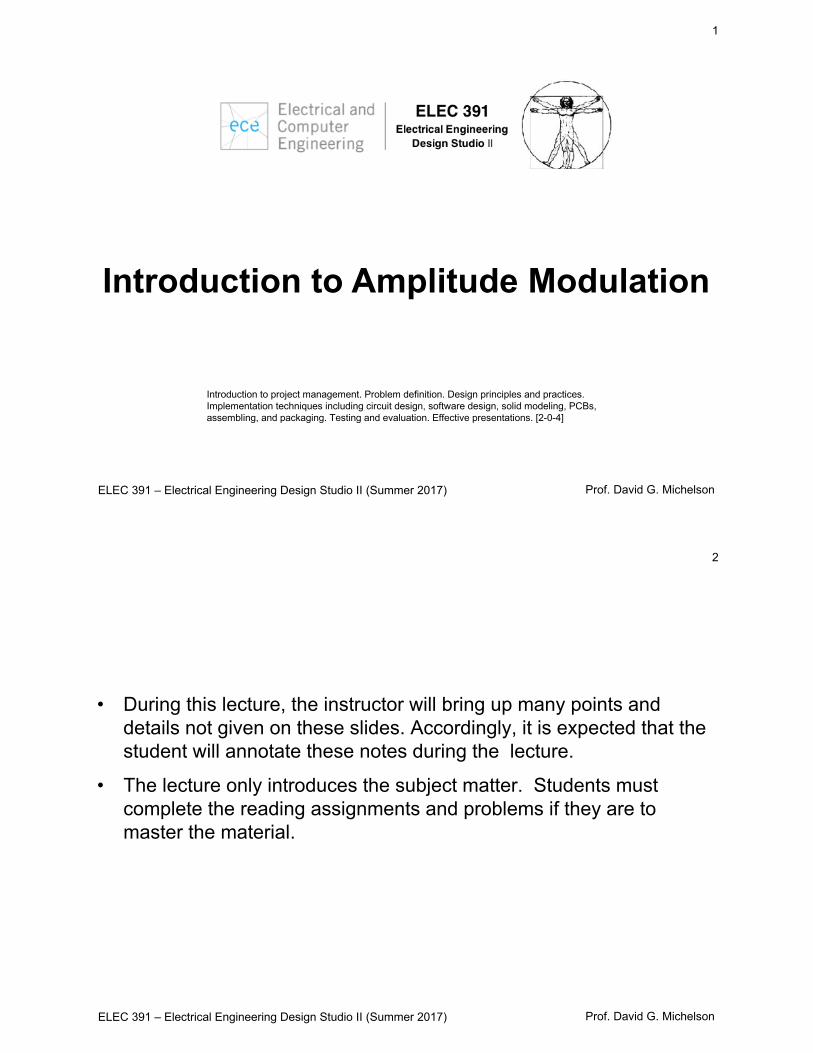
Prof. David G. Michelson ELEC 391 – Electrical Engineering Design Studio II (Summer 2017) 1 Introduction to Amplitude Modulation Introduction to project management. Problem definition. Design principles and practices. Implementation techniques including circuit design, software design, solid modeling, PCBs, assembling, and packaging. Testing and evaluation. Effective presentations. [2-0-4] Prof. David G. Michelson ELEC 391 – Electrical Engineering Design Studio II (Summer 2017) 2 • During this lecture, the instructor will bring up many points and details not given on these slides. Accordingly, it is expected that the student will annotate these notes during the lecture. • The lecture only introduces the subject matter. Students must complete the reading assignments and problems if they are to master the material.
-
Upload
khangminh22 -
Category
Documents
-
view
5 -
download
0
Transcript of Introduction to Amplitude Modulation - Courses
Prof. David G. MichelsonELEC 391 – Electrical Engineering Design Studio II (Summer 2017)
1
Introduction to Amplitude Modulation
Introduction to project management. Problem definition. Design principles and practices. Implementation techniques including circuit design, software design, solid modeling, PCBs, assembling, and packaging. Testing and evaluation. Effective presentations. [2-0-4]
Prof. David G. MichelsonELEC 391 – Electrical Engineering Design Studio II (Summer 2017)
2
• During this lecture, the instructor will bring up many points and details not given on these slides. Accordingly, it is expected that the student will annotate these notes during the lecture.
• The lecture only introduces the subject matter. Students must complete the reading assignments and problems if they are to master the material.

Prof. David G. MichelsonELEC 391 - Electrical Engineering Design Studio II (Summer 2017)
3
Introduction
• Although many more complicated modulation schemes have been developed during the past century, amplitude modulation is still widely used for broadcast radio, amateur radio, television (video), and aeronautical communications.
• Its chief advantages are simplicity, low cost and bandwidth efficiency.
• Its main disadvantages are susceptibility to noise and interference and, in certain variants, poor power efficiency due to the presence of a large unmodulated carrier.
• Given an operational AM transmitter, how would you determine the bandwidth, modulation index, and efficiency of the signal that it is emitting? Use a spectrum analyzer, of course!
Prof. David G. MichelsonELEC 391 - Electrical Engineering Design Studio II (Summer 2017)
4
Objectives
Upon completion of this briefing, you will be able to:• Describe and derive the basic principles, advantages, and
disadvantages of DSB-SC modulation and demodulation.• Describe and derive the basic principles, advantages, and
disadvantages of DSB-LC modulation and demodulation.• Describe and derive the basic principles, advantages, and
disadvantages of SSB and quadrature multiplexing• Explain how frequency mixers may be applied in RF systems.• Describe frequency mixer performance at the system level.• Be prepared to complete the major project with skill and
efficiency.
Prof. David G. Michelson
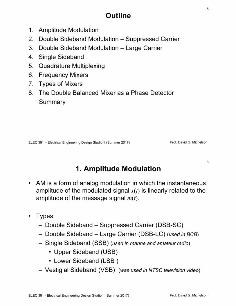
Outline
1. Amplitude Modulation 2. Double Sideband Modulation – Suppressed Carrier3. Double Sideband Modulation – Large Carrier4. Single Sideband 5. Quadrature Multiplexing6. Frequency Mixers 7. Types of Mixers8. The Double Balanced Mixer as a Phase Detector
Summary
ELEC 391 – Electrical Engineering Design Studio II (Summer 2017)
5
Prof. David G. MichelsonELEC 391 - Electrical Engineering Design Studio II (Summer 2017)
6
1. Amplitude Modulation
• AM is a form of analog modulation in which the instantaneous amplitude of the modulated signal x(t) is linearly related to the amplitude of the message signal m(t).
• Types:– Double Sideband – Suppressed Carrier (DSB-SC)– Double Sideband – Large Carrier (DSB-LC) (used in BCB)
– Single Sideband (SSB) (used in marine and amateur radio)
• Upper Sideband (USB)• Lower Sideband (LSB )
– Vestigial Sideband (VSB) (was used in NTSC television video)
Prof. David G. MichelsonELEC 391 - Electrical Engineering Design Studio II (Summer 2017)
7
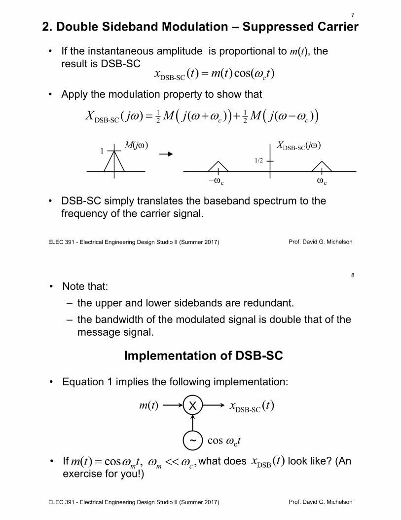
2. Double Sideband Modulation – Suppressed Carrier
• If the instantaneous amplitude is proportional to m(t), the result is DSB-SC
• Apply the modulation property to show thatDSB-SC( ) ( )cos( )cx t m t tw=
( ) ( )1 1DSB-SC 2 2( ) ( ) ( )c cX j M j M jw w w w w= + + -
• DSB-SC simply translates the baseband spectrum to the frequency of the carrier signal.
M(jw) XDSB-SC(jw)
wc-wc
11/2
Prof. David G. MichelsonELEC 391 - Electrical Engineering Design Studio II (Summer 2017)
8
• If what does look like? (An exercise for you!)
• Note that:– the upper and lower sidebands are redundant.– the bandwidth of the modulated signal is double that of the
message signal.
• Equation 1 implies the following implementation:
Implementation of DSB-SC
( ) cos , ,m m cm t tw w w= << DSB( )x t
Xm(t)
~
DSB-SC( )x t
cos wct

Prof. David G. MichelsonELEC 391 - Electrical Engineering Design Studio II (Summer 2017)
9
Demodulation of DSB-SC Signals
• The nature of DSB-SC modulation suggests a strategy for demodulation:
X
~
DSB-SC( )x t
cos wct
ˆ ( )m tLow PassFilter
• Questions:– What does this process look like in the frequency domain?– What should the cut-off frequency of the low pass filter be?– What happens if there is a frequency or phase offset
between the LOs in the modulator and demodulator?
( )m t¢
Prof. David G. MichelsonELEC 391 - Electrical Engineering Design Studio II (Summer 2017)
10
Demodulation of DSB-SC Signals - 2
M'DSB-SC(jw)
wc-wc
1/2
2wc-2wc
1/4 1/4
( ) ( )cos( )cos( )c cm t m t t tw w¢ =
( ) ( )1 1 14 2 4'( ) ( 2 ) ( ) ( 2 )c cM j M j M j M jw w w w w w= + + + -
• Given m'(t), can you derive the above expression for M'(jw) ?• What if m'(t) = m(t) cos (ωct) cos (ωct+f) ?

Prof. David G. MichelsonELEC 391 - Electrical Engineering Design Studio II (Summer 2017)
11
3. Double Sideband Modulation – Large Carrier
• A DSB-LC modulated signal results if a carrier signal is added to a DSB-SC modulated signal.
XDSB-LC(jw)
wc-wc
– What is the advantage of adding a carrier?– How large should the carrier be?– How can one add a carrier?– What are the disadvantages of adding a carrier?
Prof. David G. MichelsonELEC 391 - Electrical Engineering Design Studio II (Summer 2017)
12
Demodulation of DSB-LC Signals
• The strategy that we developed for demodulating DSB-SC signals will apply to DSB-LC signals if we also apply a DC block at the output.
• It will still suffer from the problems associated with all synchronous demodulators:– complexity (and cost)– sensitivity to phase and frequency offsets between the
LOs in the modulator and demodulator• DSB-LC offers an alternative: envelope detection.
X
~
DSB-LC ( )x t
cos ωct
m!(t)Low Pass
Filtercf. and
Prof. David G. MichelsonELEC 391 - Electrical Engineering Design Studio II (Summer 2017)
13
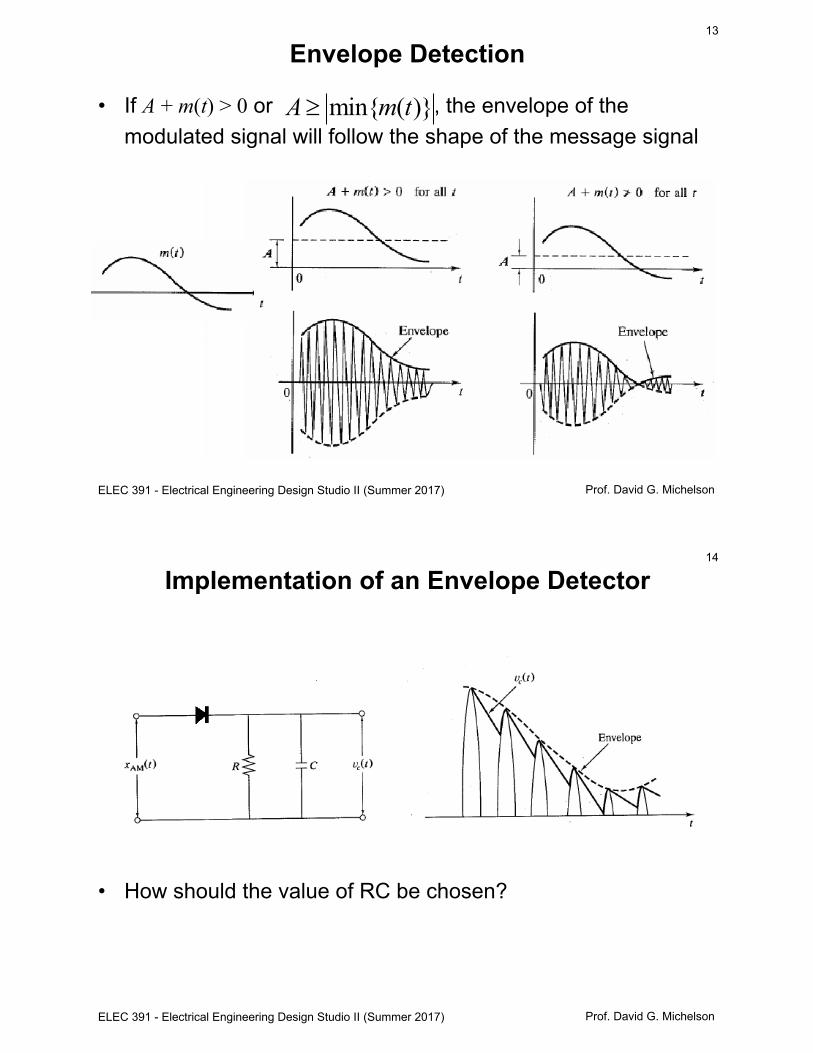
Envelope Detection
• If A + m(t) > 0 or , the envelope of the modulated signal will follow the shape of the message signal
min{ ( )}A m t³
Prof. David G. MichelsonELEC 391 - Electrical Engineering Design Studio II (Summer 2017)
14
Implementation of an Envelope Detector
• How should the value of RC be chosen?

Prof. David G. MichelsonELEC 391 - Electrical Engineering Design Studio II (Summer 2017)
15
Implementation of DSB-LC Modulators
• The expression for DSB-LC signals suggests two possible implementations of DSB-LC modulators:
Xm(t)
~
DSB-LC ( )x t
cos ωct
+
+m(t)
+_
DSB-LC ( )x t
A
X
cos ωct
A
Can you show that these are
mathematically equivalent?
~
Prof. David G. MichelsonELEC 391 - Electrical Engineering Design Studio II (Summer 2017)
16
DSB-LC with Single-tone Modulation
i For single - tone modulation, m(t) = am cosωmt.
i The modulation index is given by
µ =|min{m(t)}
A=
am
Ai Thus, m(t) = am cosωmt = µ Acosωmt
and
xDSB−LC (t) = [A + m(t)]cosω ct
= A[1+ µ cosωmt]cosω ct

Prof. David G. MichelsonELEC 391 - Electrical Engineering Design Studio II (Summer 2017)
17
Modulation Index• Exercise: Given an AM signal that has been modulated by a
single tone (i.e., a cosine signal), and values for Vmax and Vmin, derive an expression for the modulation index µ.
Vmax
Vmin
Vmax
Vmin = 0
µ = 0.5
µ = 1
Prof. David G. MichelsonELEC 391 - Electrical Engineering Design Studio II (Summer 2017)
18
Efficiency of DSB-LC
• The efficiency of a DSB-LC system is the percentage of the power carried by the sidebands,
100%.s
t
PP
h = ´
• Can you show that2
2 100%2µhµ
= ´+
?

Prof. David G. MichelsonELEC 391 - Electrical Engineering Design Studio II (Summer 2017)
19
Prof. David G. MichelsonELEC 391 - Electrical Engineering Design Studio II (Summer 2017)
20
4. Single Sideband
• By eliminating one of the redundant sidebands, the bandwidth of a DSB-SC signal can be cut in half.
• The result is called single sideband or SSB.• Removing a sideband is easier said than done!• Using a bandpass filter is the most obvious approach, but
requires extremely sharp (and expensive filters) but other methods (one due to Hartley, another to Weaver) are possible.
Prof. David G. MichelsonELEC 391 - Electrical Engineering Design Studio II (Summer 2017)
21
Demodulation of Single Sideband Signals
• Depending upon which sideband is selected, an SSB signal is described as being USB (upper sideband) or LSB (lower sideband).
• The complexity of the modulator is one limitation of conventional SSB.
• Another is the need for a synchronous demodulator (identical to that used for DSB-SC) to recover the message signal.
• In the 1950’s, engineers developed a more complicated form of SSB called compatible SSB that can be demodulated using an envelope detector.
• It has not been widely used in practice, however.
Prof. David G. MichelsonELEC 391 - Electrical Engineering Design Studio II (Summer 2017)
22
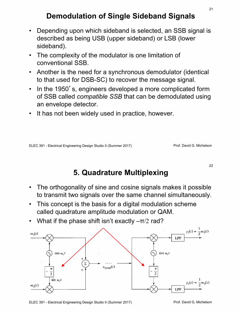
5. Quadrature Multiplexing
• The orthogonality of sine and cosine signals makes it possible to transmit two signals over the same channel simultaneously.
• This concept is the basis for a digital modulation scheme called quadrature amplitude modulation or QAM.
• What if the phase shift isn’t exactly –π/2 rad?

Prof. David G. MichelsonELEC 391 - Electrical Engineering Design Studio II (Summer 2017)
23
6. Frequency Mixers
• The ideal mixer is a device that multiplies two time harmonic (or alternating current) input signals:
• If the inputs are sinusoids, the ideal mixer output is:
X
V2
V1(t) V0(t) = V1(t) V2(t)
( )
0 1 1 2 2
1 21 2 2 1
cos cos
cos( ) cos( )2
V A t A t
A A t t
w w
w w w w
=
= - + +
Prof. David G. MichelsonELEC 391 - Electrical Engineering Design Studio II (Summer 2017)
24
Applications of Frequency Mixers
X
cos ω0t+f
cos ω0tX
~ cos ω0t
cos ω1t
X
±
k cos ω0tcos ω0t
Frequency conversion Phase detection
RF attenuation

Prof. David G. MichelsonELEC 391 - Electrical Engineering Design Studio II (Summer 2017)
25
7. Mixer Types
• In the remainder of this briefing, we consider two aspects of mixers:– system-level parameters– implementation details
• There are two basic types of passive mixers:– single balanced– double balanced
• Double balanced mixers generally offer far better performance than single balanced mixers.
• The most obvious difference: double balanced mixers offer high isolation between ports.
Prof. David G. MichelsonELEC 391 - Electrical Engineering Design Studio II (Summer 2017)
26
Measuring Mixer Performance
• Conversion Gain is a measure of the efficiency of the mixer in providing frequency translation between the input RF signal and a single sideband of the output IF signal.
• 50 W on all ports• LO drive level as
specified by the vendor A typical test set up
IF, SSB
RFconv
PG
P=
Prof. David G. MichelsonELEC 391 - Electrical Engineering Design Studio II (Summer 2017)
27
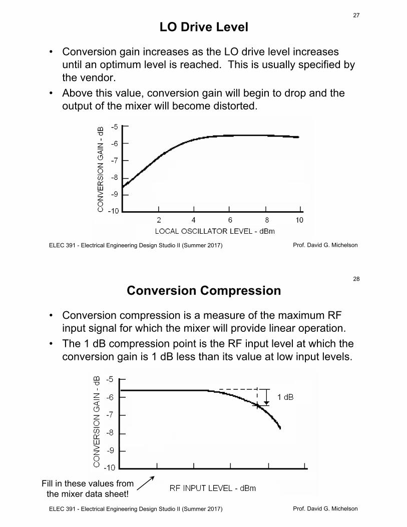
LO Drive Level
• Conversion gain increases as the LO drive level increases until an optimum level is reached. This is usually specified by the vendor.
• Above this value, conversion gain will begin to drop and the output of the mixer will become distorted.
Prof. David G. MichelsonELEC 391 - Electrical Engineering Design Studio II (Summer 2017)
28
Conversion Compression
• Conversion compression is a measure of the maximum RF input signal for which the mixer will provide linear operation.
• The 1 dB compression point is the RF input level at which the conversion gain is 1 dB less than its value at low input levels.
Fill in these values from the mixer data sheet!
Prof. David G. MichelsonELEC 391 - Electrical Engineering Design Studio II (Summer 2017)
29
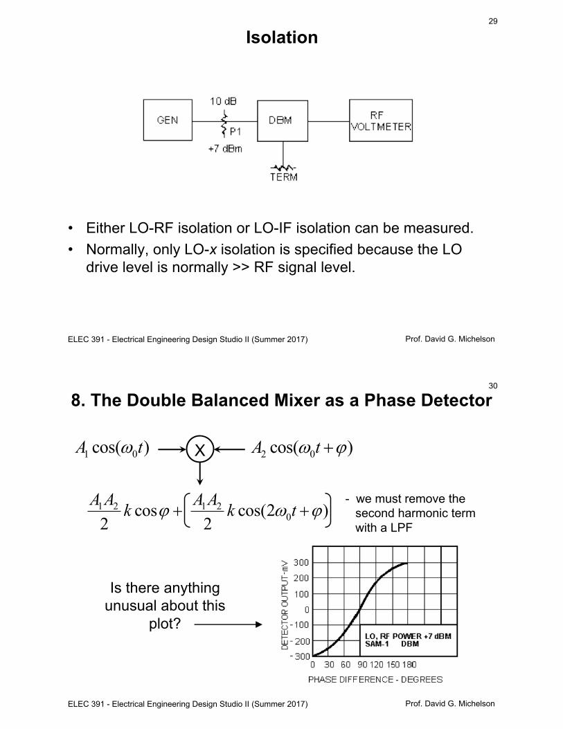
Isolation
• Either LO-RF isolation or LO-IF isolation can be measured.• Normally, only LO-x isolation is specified because the LO
drive level is normally >> RF signal level.
Prof. David G. MichelsonELEC 391 - Electrical Engineering Design Studio II (Summer 2017)
30
8. The Double Balanced Mixer as a Phase Detector
X 2 0cos( )A tw j+
1 2 1 20cos cos(2 )
2 2A A A Ak k tj w j + +
1 0cos( )A tw
Is there anything unusual about this
plot?
- we must remove the second harmonic term with a LPF

Prof. David G. MichelsonELEC 391 - Electrical Engineering Design Studio II (Summer 2017)
31
Parameters of a Phase Detector
• For the SAM-1 on the previous slideM = 300 mV/4 dBm = 43
• Not bad for a DBM, but a ‘good” phase detector might have a figure-of-merit of > 100
• Other parameters of interest:• DC Offset – the voltage present when: (1) only one signal
is present or (2) the two RF signals are in quadrature• Frequency Range –such that M > 0.75 Mmax
• Scale Factor – Phase detector output (mV/deg)
maximum DC voltage at the IF port (mV)Figure of Merit ( ) = RF drive power (dBm)
M
Prof. David G. MichelsonELEC 391 - Electrical Engineering Design Studio II (Summer 2017)
32
Inside a Double-Balanced Mixer
• Where there is no IF signal, isolation between the LO and RF ports is very high.
• If a DC voltage is applied to the IF port, two of the diodes in the ring will start to conduct.

Prof. David G. MichelsonELEC 391 - Electrical Engineering Design Studio II (Summer 2017)
33
• Suppose we apply a DC voltage to the IF port• As IIF increases, rd will drop and port isolation will drop• If IIF reverses polarity, the phase of the RF output will shift by
180 degrees. (Why?)
Applying a DC voltage to the IF port
Prof. David G. MichelsonELEC 391 - Electrical Engineering Design Studio II (Summer 2017)
34
• Here, the insertion gain is (approximately) proportional to the DC drive current while the phase (0 or 180 deg) depends upon the polarity of the drive signal.
• This behaviour suggests that a double-balanced mixer could be used as– an RF switch– an RF attenuator– a BPSK modulator
• Analysis of a four-diode switching mixer as an RF multiplier is a little more complex – a topic best left to fourth year or graduate courses in RF Electronics.
Prof. David G. MichelsonELEC 391 - Electrical Engineering Design Studio II (Summer 2017)
35
Summary
• Many types of Amplitude Modulation have been devised: DSB-SC, DSB-LC, SSB, and VSB
• The design engineer must trade off simplicity and cost against the need to improve efficiency and reduce bandwidth.
• Frequency mixers are extremely versatile components that can be used as amplitude modulators, phase detectors, RF attenuators, digital modulators.
• In ELEC 411, you’ll find that they’re also a key component in superheterodyne receivers.
• Double-balanced mixer offer much better performance than singe-balanced mixers.
• Care must be taken to ensure that the RF and LO drive levels fall in the range appropriate for the mixer being used.