Intel® Stratix® 10 Configuration User Guide
254
Intel ® Stratix ® 10 Configuration User Guide Updated for Intel ® Quartus ® Prime Design Suite: 21.2 Subscribe Send Feedback UG-S10CONFIG | 2021.06.21 Latest document on the web: PDF | HTML
-
Upload
khangminh22 -
Category
Documents
-
view
1 -
download
0
Transcript of Intel® Stratix® 10 Configuration User Guide

Intel® Stratix® 10 Configuration User Guide
Updated for Intel® Quartus® Prime Design Suite: 21.2
SubscribeSend Feedback
UG-S10CONFIG | 2021.06.21Latest document on the web: PDF | HTML

Contents
1. Intel® Stratix® 10 Configuration User Guide.......................................................................................................................... 61.1. Intel® Stratix® 10 Configuration Overview....................................................................................................................... 6
1.1.1. Configuration and Related Signals.......................................................................................................................91.1.2. Intel Download Cables Supporting Configuration in Intel Stratix 10 Devices............................................................ 10
1.2. Intel Stratix 10 Configuration Architecture......................................................................................................................121.2.1. Secure Device Manager................................................................................................................................... 13
2. Intel Stratix 10 Configuration Details...................................................................................................................................192.1. Intel Stratix 10 Configuration Timing Diagram................................................................................................................ 192.2. Configuration Flow Diagram......................................................................................................................................... 242.3. Device Response to Configuration and Reset Events.........................................................................................................262.4. Additional Clock Requirements for HPS, PCIe, eSRAM, and HBM2 ..................................................................................... 272.5. Intel Stratix 10 Configuration Pins.................................................................................................................................29
2.5.1. SDM Pin Mapping............................................................................................................................................292.5.2. MSEL Settings................................................................................................................................................ 312.5.3. Device Configuration Pins for Optional Configuration Signals................................................................................. 32
2.6. Configuration Clocks....................................................................................................................................................462.6.1. Setting Configuration Clock Source....................................................................................................................462.6.2. OSC_CLK_1 Clock Input...................................................................................................................................47
2.7. Maximum Configuration Time Estimation........................................................................................................................49
3. Intel Stratix 10 Configuration Schemes................................................................................................................................523.1. Avalon-ST Configuration.............................................................................................................................................. 52
3.1.1. Avalon-ST Configuration Scheme Hardware Components and File Types ................................................................ 543.1.2. Enabling Avalon-ST Device Configuration............................................................................................................553.1.3. The AVST_READY Signal ................................................................................................................................. 563.1.4. RBF Configuration File Format...........................................................................................................................583.1.5. Avalon-ST Single-Device Configuration...............................................................................................................593.1.6. Debugging Guidelines for the Avalon-ST Configuration Scheme............................................................................. 633.1.7. IP for Use with the Avalon-ST Configuration Scheme: Intel FPGA Parallel Flash Loader II IP Core............................... 64
3.2. AS Configuration.......................................................................................................................................................1013.2.1. AS Configuration Scheme Hardware Components and File Types ......................................................................... 103
Contents
Intel® Stratix® 10 Configuration User Guide Send Feedback
2
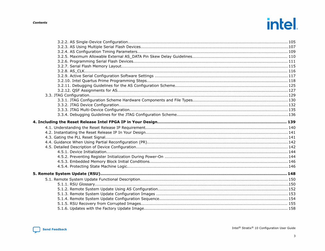
3.2.2. AS Single-Device Configuration....................................................................................................................... 1053.2.3. AS Using Multiple Serial Flash Devices..............................................................................................................1073.2.4. AS Configuration Timing Parameters................................................................................................................ 1093.2.5. Maximum Allowable External AS_DATA Pin Skew Delay Guidelines....................................................................... 1103.2.6. Programming Serial Flash Devices................................................................................................................... 1113.2.7. Serial Flash Memory Layout............................................................................................................................1153.2.8. AS_CLK....................................................................................................................................................... 1163.2.9. Active Serial Configuration Software Settings ................................................................................................... 1173.2.10. Intel Quartus Prime Programming Steps......................................................................................................... 1183.2.11. Debugging Guidelines for the AS Configuration Scheme.................................................................................... 1253.2.12. QSF Assignments for AS...............................................................................................................................127
3.3. JTAG Configuration....................................................................................................................................................1293.3.1. JTAG Configuration Scheme Hardware Components and File Types.......................................................................1303.3.2. JTAG Device Configuration..............................................................................................................................1323.3.3. JTAG Multi-Device Configuration......................................................................................................................1353.3.4. Debugging Guidelines for the JTAG Configuration Scheme...................................................................................136
4. Including the Reset Release Intel FPGA IP in Your Design................................................................................................. 1394.1. Understanding the Reset Release IP Requirement.......................................................................................................... 1404.2. Instantiating the Reset Release IP In Your Design..........................................................................................................1414.3. Gating the PLL Reset Signal........................................................................................................................................1414.4. Guidance When Using Partial Reconfiguration (PR).........................................................................................................1424.5. Detailed Description of Device Configuration................................................................................................................. 142
4.5.1. Device Initialization....................................................................................................................................... 1444.5.2. Preventing Register Initialization During Power-On ............................................................................................1444.5.3. Embedded Memory Block Initial Conditions.......................................................................................................1464.5.4. Protecting State Machine Logic........................................................................................................................146
5. Remote System Update (RSU)............................................................................................................................................ 1485.1. Remote System Update Functional Description..............................................................................................................150
5.1.1. RSU Glossary................................................................................................................................................1505.1.2. Remote System Update Using AS Configuration.................................................................................................1525.1.3. Remote System Update Configuration Images ..................................................................................................1535.1.4. Remote System Update Configuration Sequence................................................................................................1545.1.5. RSU Recovery from Corrupted Images............................................................................................................. 1555.1.6. Updates with the Factory Update Image........................................................................................................... 158
Contents
Send Feedback Intel® Stratix® 10 Configuration User Guide
3
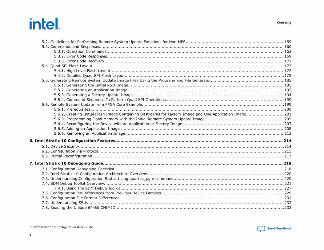
5.2. Guidelines for Performing Remote System Update Functions for Non-HPS......................................................................... 1595.3. Commands and Responses......................................................................................................................................... 160
5.3.1. Operation Commands.................................................................................................................................... 1625.3.2. Error Code Responses....................................................................................................................................1695.3.3. Error Code Recovery......................................................................................................................................171
5.4. Quad SPI Flash Layout...............................................................................................................................................1725.4.1. High Level Flash Layout................................................................................................................................. 1725.4.2. Detailed Quad SPI Flash Layout.......................................................................................................................178
5.5. Generating Remote System Update Image Files Using the Programming File Generator...................................................... 1855.5.1. Generating the Initial RSU Image.................................................................................................................... 1855.5.2. Generating an Application Image.....................................................................................................................1925.5.3. Generating a Factory Update Image.................................................................................................................1945.5.4. Command Sequence To Perform Quad SPI Operations........................................................................................ 199
5.6. Remote System Update from FPGA Core Example..........................................................................................................1995.6.1. Prerequisites................................................................................................................................................ 2005.6.2. Creating Initial Flash Image Containing Bitstreams for Factory Image and One Application Image............................ 2015.6.3. Programming Flash Memory with the Initial Remote System Update Image........................................................... 2055.6.4. Reconfiguring the Device with an Application or Factory Image............................................................................2075.6.5. Adding an Application Image ......................................................................................................................... 2085.6.6. Removing an Application Image...................................................................................................................... 212
6. Intel Stratix 10 Configuration Features.............................................................................................................................. 2146.1. Device Security.........................................................................................................................................................2146.2. Configuration via Protocol...........................................................................................................................................2156.3. Partial Reconfiguration...............................................................................................................................................217
7. Intel Stratix 10 Debugging Guide....................................................................................................................................... 2187.1. Configuration Debugging Checklist.............................................................................................................................. 2187.2. Intel Stratix 10 Configuration Architecture Overview...................................................................................................... 2207.3. Understanding Configuration Status Using quartus_pgm command.................................................................................. 2207.4. SDM Debug Toolkit Overview...................................................................................................................................... 221
7.4.1. Using the SDM Debug Toolkit.......................................................................................................................... 2277.5. Configuration Pin Differences from Previous Device Families............................................................................................2297.6. Configuration File Format Differences...........................................................................................................................2317.7. Understanding SEUs..................................................................................................................................................2327.8. Reading the Unique 64-Bit CHIP ID..............................................................................................................................232
Contents
Intel® Stratix® 10 Configuration User Guide Send Feedback
4
7.9. E-Tile Transceivers May Fail To Configure...................................................................................................................... 2327.10. Understanding and Troubleshooting Configuration Pin Behavior......................................................................................233
8. Intel Stratix 10 Configuration User Guide Archives............................................................................................................ 235
9. Document Revision History for the Intel Stratix 10 Configuration User Guide.................................................................... 236
Contents
Send Feedback Intel® Stratix® 10 Configuration User Guide
5
1. Intel® Stratix® 10 Configuration User Guide
1.1. Intel® Stratix® 10 Configuration Overview
All Intel® Stratix® 10 devices include a Secure Device Manager (SDM) to manage FPGA configuration and security. The SDMprovides a failsafe, strongly authenticated, programmable security mode for device configuration. Previous FPGA familiesinclude a fixed state machine to manage device configuration.
The Intel Quartus® Prime software also provides flexible and robust security features to protect sensitive data, intellectualproperty, and the device itself under both remote and physical attacks. Configuration bitstream authentication ensures thatthe firmware and configuration bitstream are from a trusted source. Encryption prevents theft of intellectual property. TheIntel Quartus Prime software also compresses FPGA bitstreams, reducing memory utilization such as the on-board quad SPIflash device that is storing the FPGA bitstreams.
Intel describes configuration schemes from the point of view of the FPGA. Intel Stratix 10 devices support active and passiveconfiguration schemes. In active configuration schemes the FPGA acts as the master and the external memory acts as a slavedevice. In passive configuration schemes an external host acts as the master and controls configuration. The FPGA acts as theslave device. All Intel Stratix 10 configuration schemes support design security and partial reconfiguration. All Intel Stratix 10active configuration schemes support remote system update (RSU) with quad SPI flash memory. To implement RSU in passiveconfiguration schemes, an external controller must store and drive the configuration bitstream.
Intel Stratix 10 devices support the following configuration schemes:
• Avalon® Streaming (Avalon-ST)
• JTAG
• Configuration via Protocol (CvP)
• Active Serial (AS) normal and fast modes
UG-S10CONFIG | 2021.06.21
Send Feedback
Intel Corporation. All rights reserved. Intel, the Intel logo, and other Intel marks are trademarks of Intel Corporation or its subsidiaries. Intel warrants performanceof its FPGA and semiconductor products to current specifications in accordance with Intel's standard warranty, but reserves the right to make changes to anyproducts and services at any time without notice. Intel assumes no responsibility or liability arising out of the application or use of any information, product, orservice described herein except as expressly agreed to in writing by Intel. Intel customers are advised to obtain the latest version of device specifications beforerelying on any published information and before placing orders for products or services.*Other names and brands may be claimed as the property of others.
ISO9001:2015Registered

Table 1. Intel Stratix 10 Configuration Scheme, Data Width, and MSEL
Configuration Scheme Data Width (bits) MSEL[2:0]
Passive
Avalon-ST
32(1) 000
16(1) 101
8 110
JTAG 1 111
Configuration via Protocol (CvP) x1, x2, x4, x8, x16 lanes 001(2)
ActiveAS - fast mode 4(1) 001
AS - normal mode 4(1) 011
Avalon-ST
The Avalon-ST configuration scheme is a passive configuration scheme. Avalon-ST is the fastest configuration scheme for IntelStratix 10 devices. Avalon-ST configuration supports x8, x16, and x32 modes. The x16 and x32 bit modes use general-purpose I/Os (GPIOs) for configuration. The x8 bit mode uses dedicated SDM I/O pins.
Note: The AVST_data[15:0], AVST_data[31:0], AVST_clk, and AVST_valid use dual-purpose GPIOs. You can use these pinsas regular I/Os after the device enters user mode.
Avalon-ST supports backpressure using the AVST_READY and AVST_VALID pins. Because the time to decompress theincoming bitstream varies, backpressure support is necessary to transfer data to the Intel Stratix 10 device. For moreinformation about the Avalon-ST refer to the Avalon Interface Specifications.
JTAG
You can configure the Intel Stratix 10 device using the dedicated JTAG pins. The JTAG port provides seamless access to manyuseful tools and functions. In addition to configuring the Intel Stratix 10, you use the JTAG port for debugging with Signal Tapor the System Console tools.
(1) This configuration scheme is not supported for Intel Stratix 10 GX 10M devices.
(2) Before you can use CvP you must configure either the periphery image or full image configuration via the AS scheme. Then you canconfigure the core image using CvP.
1. Intel® Stratix® 10 Configuration User Guide
UG-S10CONFIG | 2021.06.21
Send Feedback Intel® Stratix® 10 Configuration User Guide
7
The JTAG port has the highest priority and overrides the MSEL pin settings. Consequently, you can configure the Intel Stratix10 device over JTAG even if the MSEL pins specify a different configuration scheme unless you disabled JTAG for securityreasons.
CvP
CvP uses an external PCIe* host device as a Root Port to configure the Intel Stratix 10 device over the PCIe link. You canspecify up to a x16 PCIe link. Intel Stratix 10 devices support two CvP modes, CvP initialization and CvP update.
Note: Typically, the data rate of the device's internal configuration data path, not the PCIe link width, limits the configuration datarate. The maximum data rate depends on the PCIe generation and number of lanes.
CvP initialization process includes the following two steps:
1. During the board power up, the CvP uses quad SPI memory in AS x4 mode to configure the FPGA with the peripheryimage to enable CvP interface that includes the PCIe IP. The PCIe link training establishes the PCIe link of the CvP PCIe IPbefore the core fabric configures.
2. The host device uses the CvP PCIe link to configure your design in the core fabric.
CvP update mode updates the FPGA core image using the PCIe link already established from a previous full chip configurationor CvP initialization configuration. After the Intel Stratix 10 enters user mode, you can use the CvP update mode toreconfigure the FPGA fabric. This mode has the following advantages:
• Allows to change core algorithms logic blocks.
• Provides a mechanism for standard updates as a part of a release process.
• Customizes core processing for different components that are part of a complex system.
For Intel Stratix 10 SoC devices, CvP is only supported in FPGA configuration first mode.
For more information refer to the Intel Stratix 10 Configuration via Protocol (CvP) Implementation User Guide.
1. Intel® Stratix® 10 Configuration User Guide
UG-S10CONFIG | 2021.06.21
Intel® Stratix® 10 Configuration User Guide Send Feedback
8
AS Normal Mode
Active Serial x4 or AS x4 or Quad SPI is an active configuration scheme that supports flash memories capable of three- andfour-byte addressing. Upon power up, the SDM boots from a boot ROM which uses three-byte addressing to load theconfiguration firmware from the Quad SPI flash. After the configuration firmware loads, the Quad SPI flash operates usingfour-byte addressing for the rest of the configuration process. This mode supports the following third-party flash devices:
• Micron MT25QU128, MT25QU256, MT25QU512, MT25QU01G, MT25QU02G
• Macronix MX25U128, MX25U256, MX25U512, MX66U512, MX66U1G, MX66U2G
Refer to the Supported Flash Devices for Intel Stratix 10 Devices for complete list of supported flash devices.
AS Fast Mode
The only difference between AS normal mode and fast mode is that this mode does not delay for 10 ms before beginningconfiguration. Use this mode to meet the 100 ms of link up requirement for PCIe or for other systems with strict timingrequirements.
In AS fast mode, the power-on sequence must ensure that the quad SPI flash memory is out of reset before the SDM becausethe Intel Stratix 10 device accesses flash memory immediately after exiting reset. The power supply must be able to providean equally fast ramp up for the Intel Stratix 10 device and the external AS x4 flash devices. Failing to meet this requirementcauses the SDM to report that the memory is missing. Consequently, configuration fails.
Refer to the Intel Stratix 10 Device Family Pin Connection Guidelines and AN692: Power Sequencing Considerations for IntelCyclone® 10 GX, Intel Arria® 10, and Intel Stratix 10 Devices for additional details.
Related Information
• Avalon Interface Specifications
• Device Configuration - Support Center
• Intel Stratix 10 Configuration via Protocol (CvP) Implementation User Guide
• Intel Stratix 10 Device Datasheet (Core and HPS)
• Supported Flash Devices for Intel Stratix 10 Devices
1.1.1. Configuration and Related Signals
The following figure shows the configuration interfaces and configuration-related device functions. Pins shown in dark blue usededicated SDM I/Os. Pins shown in black use general purpose I/Os (GPIOs). Pins shown in red are dedicated JTAG I/Os.
1. Intel® Stratix® 10 Configuration User Guide
UG-S10CONFIG | 2021.06.21
Send Feedback Intel® Stratix® 10 Configuration User Guide
9

You specify SDM I/O pin functions using the Device ➤ Configuration ➤ Device and Pin Options dialog box in the IntelQuartus Prime software.
Figure 1. Intel Stratix 10 Configuration Interfaces
nCONFIGnSTATUSCONF_DONEINIT_DONEOSC_CLK_1MSEL[2:0]
TCKTDOTMSTDI
DIRECT_TO_FACTORY
VCCFUSEWR_SDMVCCBAT
Intel Stratix 10 FPGA
Avalon-ST x8
CvP
AS x4 (QSPI)Configuration
Control
JTAG
RemoteSystem
Update (RSU)
Security
PWRMGT_SDAPWRMGT_SCL
PWRMGT_ALERTSmartVID
SelectOne
Avalon-ST x16 or x32
Legend
Fixed PinsGPIO and Dual Purpose
Configuration Specific or Dedicated
Power Rails
This user guide discusses most of the interfaces shown in the figure. Refer to the separate Intel Stratix 10 Configuration viaProtocol (CvP) Implementation User Guide and Intel Stratix 10 Power Management User Guide for more information aboutthose features.
Related Information
• SDM Pin Mapping on page 29
• Intel Stratix 10 Configuration via Protocol (CvP) Implementation User Guide
• Intel Stratix 10 Power Management User Guide
1.1.2. Intel Download Cables Supporting Configuration in Intel Stratix 10 Devices
Intel provides the following cables to download your design to the Intel Stratix 10 device on the PCB. Download cablessupport prototyping activity by providing detailed debug messages via Intel Quartus Prime Programmer. You must use Inteldownload cables for advanced debugging using the Signal Tap logic analyzer or the System Console tools.
1. Intel® Stratix® 10 Configuration User Guide
UG-S10CONFIG | 2021.06.21
Intel® Stratix® 10 Configuration User Guide Send Feedback
10

Table 2. Intel Stratix 10-Supported Download Cable Capabilities
Download Cable Protocol Support Intel Stratix 10 Device Cable Connection to PCB
Intel FPGA Download Cable II (formerly the USB-BlasterII)
JTAG, AS 10-pin female plug3M Part number: 2510-6002UB
Intel FPGA Ethernet Cable (formerly the EthernetBlaster II)
JTAG, AS 10-pin female plug
The Intel FPGAs and Programmable Devices / Download Cables provides more information about the download cables andincludes links to the user guides for all cables listed in the table above.
1. Intel® Stratix® 10 Configuration User Guide
UG-S10CONFIG | 2021.06.21
Send Feedback Intel® Stratix® 10 Configuration User Guide
11
1.2. Intel Stratix 10 Configuration Architecture
The Secure Device Manager (SDM) is a triple-redundant processor-based module that manages configuration and the securityfeatures of Intel Stratix 10 devices. The SDM is available on all Intel Stratix 10 FPGAs and SoC devices.
The block diagram below provides an overview of the Intel Stratix 10 configuration architecture which includes the followingblocks:
• SDM: More information about the SDM is contained in later sections.
• Configuration network: The SDM uses this dedicated, parallel configuration network to distribute the configurationbitstream to Local Sector Managers (LSMs). You cannot access this network.
• LSMs: The LSM is a microprocessor. Each configuration sector includes an LSM. The LSM parses configuration bitstreamand configures the logic elements for its sector. After configuration, the LSM performs the following functions:
— Monitors for single event upsets at the sector level
— Processes responses to single event upsets (SEUs)
— Performs integrity checks in user mode
• Other sub-systems:
— Hard processor system (HPS)
— High Bandwidth Memory (HBM2)
— Transceiver tiles
1. Intel® Stratix® 10 Configuration User Guide
UG-S10CONFIG | 2021.06.21
Intel® Stratix® 10 Configuration User Guide Send Feedback
12
Figure 2. Intel Stratix 10 Configuration Architecture Block Diagram
ConfigurationSector
ConfigurationSector
Configurable Network Interface
SDM Pins
Secure Device Manager
Dual Purpose I/O
Intel Stratix 10 FPGA
Intel Stratix 10 Blocks(All Family Variants)
ConfigurationSector
ConfigurationSector
Configuration Network
Local SectorManager (LSM)
Local SectorManager (LSM)
Local SectorManager (LSM)
Local SectorManager (LSM)
1.2.1. Secure Device Manager
The SDM comprises peripherals, cryptographic IP and sensors, boot ROM, triple-redundant lockstep processors, and otherblocks shown the block diagram below. The SDM performs and manages the following security functions:
• Configuration bitstream authentication: During the configuration state, the SDM authenticates the Intel-generatedconfiguration firmware and configuration bitstream, ensuring that configuration bitstream is from a trusted source. AllIntel Stratix 10 support authentication.
• Encryption: Encryption protects the configuration bitstream or confidential data from unauthorized third-party access.
• Side channel attack protection: Side channel attack protection guards AES Key and confidential data under non-intrusiveattacks.
• Integrity checking: Integrity checking verifies that an accidental event has not corrupted the configuration bitstream. Thisfunction is active, even if you do not enable authentication.
1. Intel® Stratix® 10 Configuration User Guide
UG-S10CONFIG | 2021.06.21
Send Feedback Intel® Stratix® 10 Configuration User Guide
13

The following security features are available in Intel Stratix 10 devices that support advanced security. Devices with advancedsecurity enabled can only load firmware shipped with Intel Quartus Prime Pro Edition software. Intel recommends Intel Stratix10 devices with a -BK ordering part number (OPN) suffix for use with the black key provisioning feature.
Table 3. Supported Security Features in Intel Stratix 10 Devices
Intel Stratix 10 Authentication Advanced Security
GX Yes -AS suffix devices
GX 10M Yes No
SX Yes -AS suffix devices
MX Yes -AS suffix devices
TX Yes -AS suffix devices
DX Yes Yes
1. Intel® Stratix® 10 Configuration User Guide
UG-S10CONFIG | 2021.06.21
Intel® Stratix® 10 Configuration User Guide Send Feedback
14
Figure 3. SDM Block Diagram
Secure Device Manager
JTAG
SmartVID
Avalon-STSink
AS
MCU MCU MCU
AES 256
SHA 256/384
ECDSA 256/384
Decompression
Temperature
Voltage
Peripherals
Lockstep Processors
Crypto IP
Sensors
Reserved for PUF
BBRAM
Key Vault
ConfigurationNetworkInterface
FuseJTAG Pins
SDM Pins
To ConfigurationSectors for
FPGA configuration
Dual-Purpose I/O Pins
PCIeHard IP
PCIeLink
SDMCommunication
Hub
FPGA Core
HPSMailbox
Boot ROM
SEU Detection
Chip ID
Serial Flash Mailbox Client IP
Partial Reconfiguration (PR) IP
OCRAM
Hard IPin SDM
ExternalHard IP
Soft IP
Legend
External PR Controller IP
Temperature Sensor IP
Voltage Sensor IP
Here is an overview of the additional functions the SDM controls:
• SDM uses temperature sensor for SmartVID feature to communicate to the external PMBus voltage regulator when youselect -V devices.
• The AES/SHA and other Crypto Accelerator blocks implement secure configuration and boot.
• The Key Vault provides volatile and non-volatile cryptographic key storage. To mitigate potential side-channel attacks,crypto functions that use keys require a special hardware storage mechanism.
1. Intel® Stratix® 10 Configuration User Guide
UG-S10CONFIG | 2021.06.21
Send Feedback Intel® Stratix® 10 Configuration User Guide
15

• The AS enables active configuration schemes via dedicated SDM pins.
• The Avalon-ST x8 configuration scheme uses SDM I/O pins. The Avalon-ST x16 and x32 configuration schemes usededicated SDM I/O pins and dual-purpose I/O pins. Refer to the SDM Pin Mapping for more information.
• To reduce configuration file size and support smaller memory sizes, and enable faster configuration, the Intel QuartusPrime software compresses the configuration data. All Intel Stratix 10 devices compress the configuration bitstream. Thisfeature is always enabled. When specifying an encrypted configuration bitstream, the Intel Quartus Prime Pro Editionsoftware compresses the configuration bitstream before encryption.
• A specific PCIe block included in the Intel Stratix 10 device supports CvP.
Related Information
• SDM Pin Mapping on page 29
• Intel Stratix 10 Device Feature Status DescriptionFor information about security features that are currently supported and security features that are planned to besupported in the future.
• Intel Stratix 10 Device Security User GuideFor information about currently supported security features.
• Intel Stratix 10 Power Management User Guide
1.2.1.1. Restricting Security Features
Attention: The -V device does not support device attestation and anti-tamper security features. If you are using these security features,you must select a non-V device.
For a non-V device, when you use attestation and/or anti-tamper security features, you cannot use the conditional public keyentry or the owner root key virtual fusing security features. Similarly, if you need to use conditional public key entry and/orthe virtual fusing, you cannot turn on device attestation and/or anti-tamper security features in your design.
Table 4. Available Security Features for a Non-V Device
Security Features Attestation / Anti-Tamper
On Off
Conditional public key entry Not supported Supported
Owner root key virtual fusing Not supported Supported
1. Intel® Stratix® 10 Configuration User Guide
UG-S10CONFIG | 2021.06.21
Intel® Stratix® 10 Configuration User Guide Send Feedback
16

If you need to turn on or off the anti-tamper or attestation features in your design, you do not need to recompile your design.You can regenerate the .sof file by selecting the Intel Quartus Prime Pro Edition Processing ➤ Start ➤ Start Assemblermenu.
1.2.1.2. Updating the SDM Firmware
When you generate a configuration bitstream using the File ➤ Programming File Generator menu item, the bitstreamassembler adds all firmware (including the SDM firmware) that matches the Intel Quartus Prime Pro Edition Release to thebitstream generated from the .sof.
Depending on the configuration scheme you specify the resulting file can be in any of the following formats:
• Raw Binary File, .rbf
• Programmer Object File, .pof
• JTAG Indirect Configuration, .jic
• Raw Programming Data, .rpd
• Jam*Standard Test and Programming Language (STAPL) STAPL, .jam
• Jam Byte Code, .jbc
For more information about the output file types, refer to the Intel Quartus Prime Pro Edition User Guide: Programmer.
Newer versions of the Intel Quartus Prime software typically include new or updated SDM features implemented in firmware.When regenerating your configuration bitstream, Intel recommends using the latest version of the Intel Quartus Prime ProEdition Software which includes the latest firmware. You do not need to recompile your .sof to use the firmware from anewer version of the Intel Quartus Prime Pro Edition Software. You can simply regenerate your configuration bitstream withthe new version of the Programming File Generator.
Related Information
Intel Quartus Prime Pro Edition User Guide: ProgrammerFor information about the programming file generator output file types.
1.2.1.3. Specifying Boot Order for Intel Stratix 10 SoC Devices
For Intel Stratix 10 SoC devices you can specify the configuration order, choosing either the FPGA First or the Hard ProcessorSystem (HPS) First options.
1. Intel® Stratix® 10 Configuration User Guide
UG-S10CONFIG | 2021.06.21
Send Feedback Intel® Stratix® 10 Configuration User Guide
17
When you select the FPGA First option, the SDM fully configures the FPGA, then configures the HPS SDRAM pins, loads theHPS first stage boot loader (FSBL) and takes the HPS out of reset. In this mode the fabric begins functioning just before theHPS exits reset. Note that FPGA First option does not allow FPGA reconfiguration by using HPS. This user guide defines a statewhen the FPGA is functional. Configuration and initialization are complete.
When you select the HPS First option, the SDM first configures the HPS SDRAM pins, loads the HPS FSBL and takes the HPSout of reset. Then the HPS configures the FPGA I/O and FPGA fabric at a later time. The HPS First option has the followingadvantages:
• Minimizes the amount of SDM flash memory required.
• Minimizes the amount of time it takes for the HPS software to be up and running.
• Supports FPGA reconfiguration while the HPS is running.
For more information about specifying configuration order refer to the FPGA Configuration First Mode and HPS Boot First Modechapters in the Intel Stratix 10 SoC FPGA Boot User Guide.
Related Information
• FPGA Configuration First Mode
• HPS Boot First Mode
1. Intel® Stratix® 10 Configuration User Guide
UG-S10CONFIG | 2021.06.21
Intel® Stratix® 10 Configuration User Guide Send Feedback
18

2. Intel Stratix 10 Configuration Details
2.1. Intel Stratix 10 Configuration Timing Diagram
Figure 4. Power-On, Configuration, and Reconfiguration Timing Diagram
nCONFIG
nSTATUS
CONF_DONE
INIT_DONE
nINIT_DONE
MSEL[2:0]
Data[<n>-1:0](Generic)
AVST_READY (Avalon ST only)
AVST_VALID (Avalon ST only)
AS_CS0 (AS only)
Configuration_State
Power_Supply_Status[7:0]
GPIO Status
Power-On Reset
User Mode
Reconfiguration Triggered Reconfiguration
Idle Configuration Initialization User Mode Idle Configuration
Sample
Power On SDM Start Device Clean
Group 1Supply Up
Group 2Supply Up
Group 3Supply Up
Tri-Stated with Weak Pull-Up User Defined
1
2
3
4
5
1
3 5
4
2
(weak int/ext pullup)
(internal signal)
Tri-Stated with Weak Pull-Up
Initialization User Mode
User Defined
...
...
... ...
... ...
...
...
UG-S10CONFIG | 2021.06.21
Send Feedback
Intel Corporation. All rights reserved. Intel, the Intel logo, and other Intel marks are trademarks of Intel Corporation or its subsidiaries. Intel warrants performanceof its FPGA and semiconductor products to current specifications in accordance with Intel's standard warranty, but reserves the right to make changes to anyproducts and services at any time without notice. Intel assumes no responsibility or liability arising out of the application or use of any information, product, orservice described herein except as expressly agreed to in writing by Intel. Intel customers are advised to obtain the latest version of device specifications beforerelying on any published information and before placing orders for products or services.*Other names and brands may be claimed as the property of others.
ISO9001:2015Registered
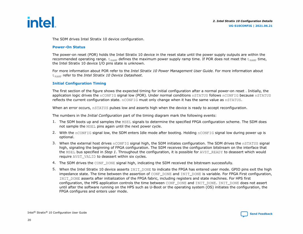
The SDM drives Intel Stratix 10 device configuration.
Power-On Status
The power-on reset (POR) holds the Intel Stratix 10 device in the reset state until the power supply outputs are within therecommended operating range. tRAMP defines the maximum power supply ramp time. If POR does not meet the tRAMP time,the Intel Stratix 10 device I/O pins state is unknown.
For more information about POR refer to the Intel Stratix 10 Power Management User Guide. For more information abouttRAMP refer to the Intel Stratix 10 Device Datasheet.
Initial Configuration Timing
The first section of the figure shows the expected timing for initial configuration after a normal power-on reset . Initially, theapplication logic drives the nCONFIG signal low (POR). Under normal conditions nSTATUS follows nCONFIG because nSTATUSreflects the current configuration state. nCONFIG must only change when it has the same value as nSTATUS.
When an error occurs, nSTATUS pulses low and asserts high when the device is ready to accept reconfiguration.
The numbers in the Initial Configuration part of the timing diagram mark the following events:
1. The SDM boots up and samples the MSEL signals to determine the specified FPGA configuration scheme. The SDM doesnot sample the MSEL pins again until the next power cycle.
2. With the nCONFIG signal low, the SDM enters Idle mode after booting. Holding nCONFIG signal low during power up isoptional.
3. When the external host drives nCONFIG signal high, the SDM initiates configuration. The SDM drives the nSTATUS signalhigh, signaling the beginning of FPGA configuration. The SDM receives the configuration bitstream on the interface thatthe MSEL bus specified in Step 1. Throughout the configuration, it is possible for AVST_READY to deassert which wouldrequire AVST_VALID to deassert within six cycles.
4. The SDM drives the CONF_DONE signal high, indicating the SDM received the bitstream successfully.
5. When the Intel Stratix 10 device asserts INIT_DONE to indicate the FPGA has entered user mode. GPIO pins exit the highimpedance state. The time between the assertion of CONF_DONE and INIT_DONE is variable. For FPGA First configuration,INIT_DONE asserts after initialization of the FPGA fabric, including registers and state machines. For HPS firstconfiguration, the HPS application controls the time between CONF_DONE and INIT_DONE. INIT_DONE does not assertuntil after the software running on the HPS such as U-Boot or the operating system (OS) initiates the configuration, theFPGA configures and enters user mode.
2. Intel Stratix 10 Configuration Details
UG-S10CONFIG | 2021.06.21
Intel® Stratix® 10 Configuration User Guide Send Feedback
20
The entire device does not enter user mode simultaneously. Intel requires you to include reset release as described in the Including the Reset Release Intel FPGA IP in Your Design on page 139. Use the nINIT_DONE output of the Reset ReleaseIntel FPGA IP to hold your application logic in the reset state until the entire FPGA fabric is in user mode. Failure to includethis IP in your design may result in intermittent application logic failures.
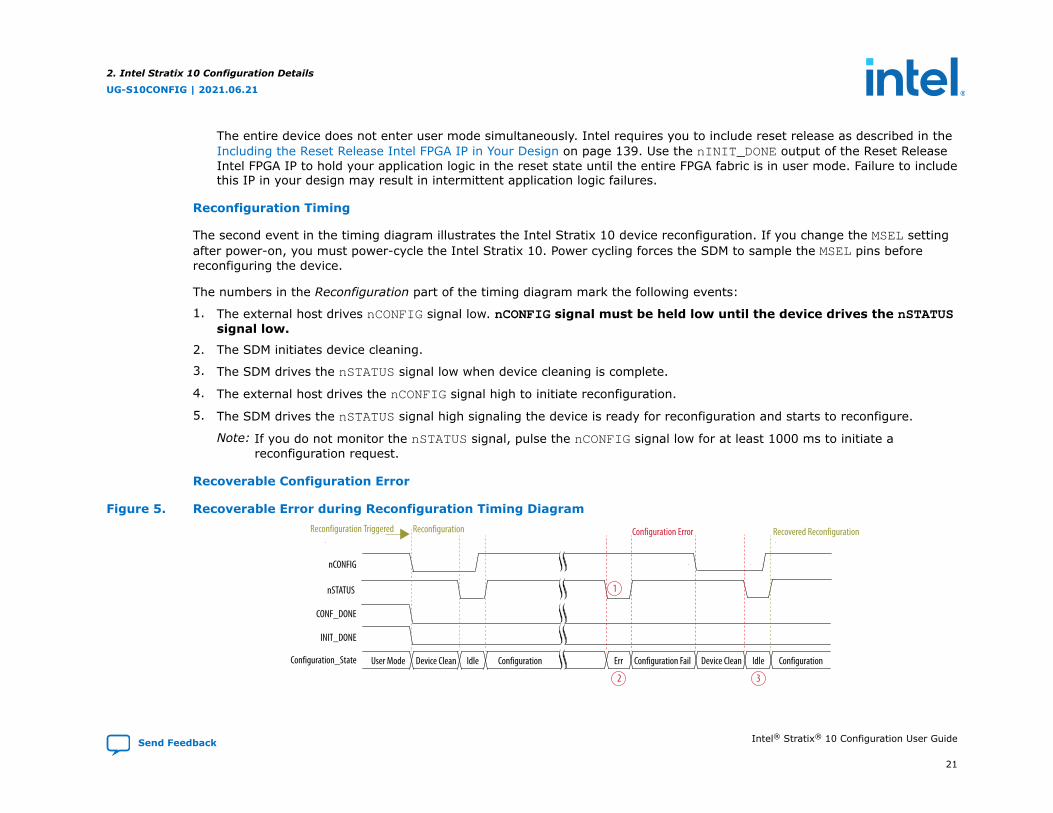
Reconfiguration Timing
The second event in the timing diagram illustrates the Intel Stratix 10 device reconfiguration. If you change the MSEL settingafter power-on, you must power-cycle the Intel Stratix 10. Power cycling forces the SDM to sample the MSEL pins beforereconfiguring the device.
The numbers in the Reconfiguration part of the timing diagram mark the following events:
1. The external host drives nCONFIG signal low. nCONFIG signal must be held low until the device drives the nSTATUSsignal low.
2. The SDM initiates device cleaning.
3. The SDM drives the nSTATUS signal low when device cleaning is complete.
4. The external host drives the nCONFIG signal high to initiate reconfiguration.
5. The SDM drives the nSTATUS signal high signaling the device is ready for reconfiguration and starts to reconfigure.
Note: If you do not monitor the nSTATUS signal, pulse the nCONFIG signal low for at least 1000 ms to initiate areconfiguration request.
Recoverable Configuration Error
Figure 5. Recoverable Error during Reconfiguration Timing Diagram
nCONFIG
nSTATUS
CONF_DONE
INIT_DONE
Configuration_State
Configuration Error
Configuration Err Configuration Fail IdleUser Mode IdleDevice Clean ConfigurationDevice Clean
Reconfiguration Triggered Reconfiguration Recovered Reconfiguration
1
2 3
2. Intel Stratix 10 Configuration Details
UG-S10CONFIG | 2021.06.21
Send Feedback Intel® Stratix® 10 Configuration User Guide
21
The numbers in the Configuration Error part of the timing diagram mark the following events:
1. The SDM drives nSTATUS signal low for a period of time specified in the Intel Stratix 10 Device Datasheet to indicate arecoverable configuration error. The Intel Stratix 10 device may not assert CONF_DONE indicating that device did notreceive the complete configuration bitstream. The device does not assert INIT_DONE indicating that the configuration didnot complete successfully. nCONFIG should continue to be driven high until after nSTATUS has returned back to highstate.
If an error occurs during JTAG configuration, the SDM does not change the state of the nSTATUS signal. You can monitorthe error messages that the Intel Quartus Prime Pro Edition Programmer generates for error reporting.
2. The SDM enters the error state.
3. The SDM enters the idle state if the nCONFIG signal drives to low. The device is ready for reconfiguration by driving a lowto high transition on nCONFIG. You can also power cycle the device by following the device power down sequence.
Note: The nCONFIG signal can only change levels when it has the same value as nSTATUS. This restriction means thatwhen nSTATUS = 1, nCONFIG can transition from 1 to 0. When nSTATUS = 0, nCONFIG can transition from 0 to 1.Apart from error reporting, nSTATUS only changes to follow nCONFIG.
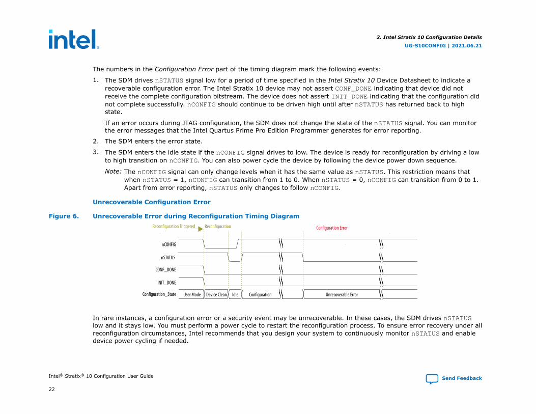
Unrecoverable Configuration Error
Figure 6. Unrecoverable Error during Reconfiguration Timing Diagram
nCONFIG
nSTATUS
CONF_DONE
INIT_DONE
Configuration_State
Configuration Error
Configuration Unrecoverable ErrorUser Mode IdleDevice Clean
Reconfiguration Triggered Reconfiguration
In rare instances, a configuration error or a security event may be unrecoverable. In these cases, the SDM drives nSTATUSlow and it stays low. You must perform a power cycle to restart the reconfiguration process. To ensure error recovery under allreconfiguration circumstances, Intel recommends that you design your system to continuously monitor nSTATUS and enabledevice power cycling if needed.
2. Intel Stratix 10 Configuration Details
UG-S10CONFIG | 2021.06.21
Intel® Stratix® 10 Configuration User Guide Send Feedback
22
Note that in the case of an anti-tamper event or a double bit ECC error in the SDM RAM, nSTATUS is also asserted low andstays low.
Related Information
• Quad SPI Flash Layout on page 172For information about storing firmware, configuration, and application data in flash devices.
• Intel Stratix 10 Device DatasheetFor the following timing diagrams that define set-up, hold, and propagation delay timing parameters: AS ConfigurationSerial Output Timing Diagram, AS Configuration Serial Input Timing Diagram, and Avalon ST Configuration TimingDiagram.
• Intel Stratix 10 Power Management User Guide
• Should clocks and resets in user logic be gated until the configuration process is completed in Intel Stratix 10?
2. Intel Stratix 10 Configuration Details
UG-S10CONFIG | 2021.06.21
Send Feedback Intel® Stratix® 10 Configuration User Guide
23
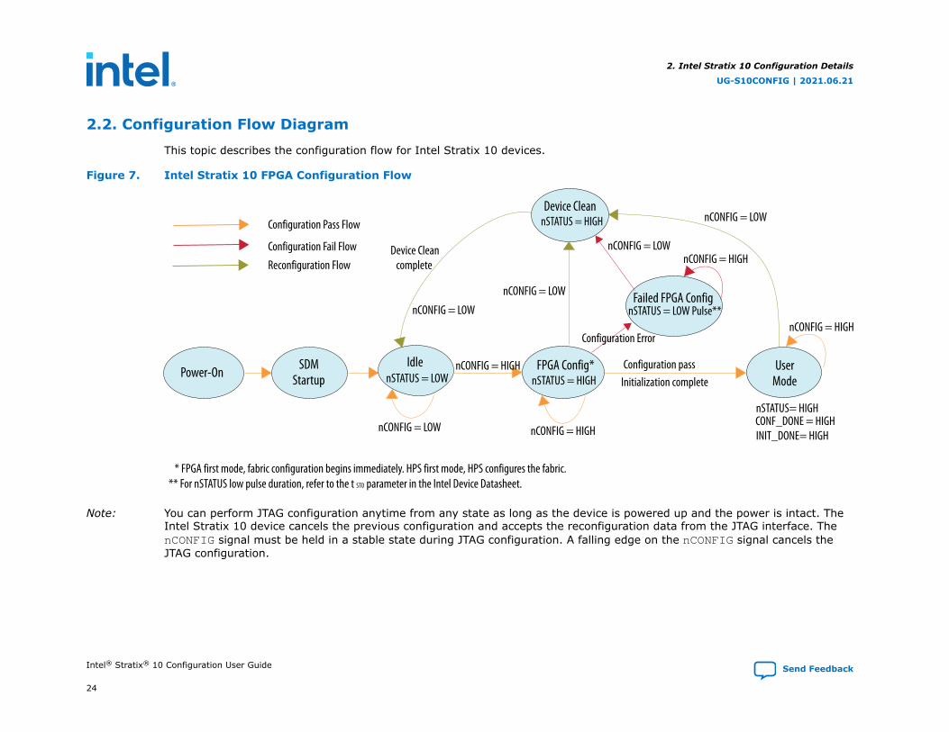
2.2. Configuration Flow Diagram
This topic describes the configuration flow for Intel Stratix 10 devices.
Figure 7. Intel Stratix 10 FPGA Configuration Flow
nCONFIG = LOW
Power-OnIdle FPGA Config*
Failed FPGA Config
SDMStartup
Device Clean
UserMode
complete
Configuration pass
nCONFIG = LOW
nCONFIG = LOWDevice Clean
Configuration Pass Flow
Configuration Fail FlowReconfiguration Flow
nSTATUS= HIGH
nSTATUS = LOW
nSTATUS = HIGH
CONF_DONE = HIGHINIT_DONE= HIGH
* FPGA first mode, fabric configuration begins immediately. HPS first mode, HPS configures the fabric.** For nSTATUS low pulse duration, refer to the t STO parameter in the Intel Device Datasheet.
nCONFIG = HIGHnSTATUS = HIGH
Configuration Error
nSTATUS = LOW Pulse**nCONFIG = LOW
Initialization complete
nCONFIG = LOW
nCONFIG = HIGH
nCONFIG = HIGH
nCONFIG = HIGH
Note: You can perform JTAG configuration anytime from any state as long as the device is powered up and the power is intact. TheIntel Stratix 10 device cancels the previous configuration and accepts the reconfiguration data from the JTAG interface. ThenCONFIG signal must be held in a stable state during JTAG configuration. A falling edge on the nCONFIG signal cancels theJTAG configuration.
2. Intel Stratix 10 Configuration Details
UG-S10CONFIG | 2021.06.21
Intel® Stratix® 10 Configuration User Guide Send Feedback
24
Power-On
• The Intel Stratix 10 power supplies follow the guidelines in the Power-Up Sequence Requirements for Intel Stratix 10Devices section of the Intel Stratix 10 Power Management User Guide.
• A device-wide power-on reset (POR) asserts after the power supplies reach the correct operating voltages. The externalpower supply ramp must not be slower than the minimum ramping rate until the supplies reach the operating voltage.
• During power-on stage, internal circuitry pulls the SDM_IO0, SDM_IO8, and SDM_IO16 low internally. Internal circuitrypulls the remaining SDM_IO pins to a weak high.
• After POR, internal circuitry also pulls all GPIO pins to a weak high until the device enters user mode.
SDM Startup
• The SDM samples the MSEL pins during power-on.
• If MSEL is set to JTAG, the SDM remains in the Startup state.
• The SDM runs firmware stored in the on-chip boot ROM and enters the Idle state until the host drives nCONFIG high. Thehost should not drive nCONFIG high before all clocks are stable.
Idle
• The SDM remains in IDLE state until the external host initiates configuration by driving the nCONFIG pin from low to high.Alternatively, the SDM enters the idle state after it exits the error state.
FPGA Configuration
• After the SDM receives a configuration initiation request (nCONFIG = HIGH), the SDM signals the beginning ofconfiguration by driving the nSTATUS pin high.
• Upon receiving configuration data, the SDM performs authentication, decryption and decompression.
• The nCONFIG pin remains high during configuration and in user mode. The host monitors the nSTATUS pin continuouslyfor configuration errors.
• The power management activity is ongoing during the device configuration. For more information, refer to the IntelStratix 10 Power Management User Guide.
• The SDM drives the CONF_DONE pin high after successfully receiving full bitstream.
• The CONF_DONE pin signals an external host that bitstream transfer is successful.
2. Intel Stratix 10 Configuration Details
UG-S10CONFIG | 2021.06.21
Send Feedback Intel® Stratix® 10 Configuration User Guide
25

Failed FPGA Configuration
• A low pulse on the nSTATUS pin indicates a configuration error.
• An internal device wipe occurs followed by errors requiring reconfiguration.
• After a low pulse indicating an error, configuration stops. The nSTATUS pin remains high.
• Following an error, the SDM drives nSTATUS low after the external host drives nCONFIG low.
• The device enters Idle state after the nSTATUS pin recovers to initial pre-configuration low state.
User Mode
• The SDM drives the INIT_DONE pin high after initializing internal registers and releases GPIO pins from the highimpedance state. The device enters user mode. After CONF_DONE asserts and before INIT_DONE asserts, parts of thedevice start to enter user mode. The assertion of INIT_DONE indicates that the entire device entered user mode. Intelrequires you to include the Reset Release in your design. Use the nINIT_DONE output of the Reset Release Intel FPGA IPto hold your application logic in the reset state until the entire FPGA fabric is in user mode. Failure to include this IP inyour design may result in intermittent application logic failures.
• The nCONFIG pin should remain high in user mode.
• You may re-configure the device by driving nCONFIG pin from low to high.
Device Clean
• In the Device Clean state the design stops functioning.
• Device cleaning zeros out all configuration data.
• The Intel Stratix 10 device drives CONF_DONE and INIT_DONE low.
• The SDM drives the nSTATUS pin low when device cleaning completes.
Related Information
• Booting and Configuration in the Intel Stratix 10 Hard Processor System Technical Reference Manual
• Intel Stratix 10 Power Management User Guide
2.3. Device Response to Configuration and Reset Events
The following table summarizes the device response to various external configuration and reset events.
2. Intel Stratix 10 Configuration Details
UG-S10CONFIG | 2021.06.21
Intel® Stratix® 10 Configuration User Guide Send Feedback
26

Note: HPS_COLD_nRESET is a SDM input pin that manages the HPS reset.
Table 5. Device Response Due To Configuration and Reset EventsEvents marked by a tick (√) require reset initiated by provided reset type.
Action Reset Type
Power Cycle nCONFIG HPS_COLD_nRESET
Wipe the FPGA √ √ —
Sample MSEL pins √ — —
Read fuses √ — —
Run the SDM boot ROM code √ — —
Reset the SDM √ — —
Reset the HPS √ √ √
Note: When using QSPI, you can use Remote System Update (RSU) to load a specific image with the same device responses asnCONFIG.
Related Information
• Power-Up Sequence Requirements for Intel Stratix 10 Devices
• Intel Stratix 10 Power Management User Guide
2.4. Additional Clock Requirements for HPS, PCIe, eSRAM, and HBM2
The Intel Stratix 10 device has specific clock requirements for PCIe, HPS EMIF, eSRAM, and the High Bandwidth Memory(HBM2) IP. These clock requirements must be met before the FPGA configuration begins.
FPGA Configuration
To avoid configuration failures, the Intel Stratix 10 device requires clocks for the PCIe, HPS EMIF, eSRAM, the HBM2 IP, and allE-tile transceiver reference clocks. You must provide a free-running, stable reference clock to these blocks beforeconfiguration begins and throughout the entire user mode. The clock frequencies must match the frequency settings specifiedin the Intel Quartus Prime software during configuration. Stopping the reference clock during the user mode may result in a
2. Intel Stratix 10 Configuration Details
UG-S10CONFIG | 2021.06.21
Send Feedback Intel® Stratix® 10 Configuration User Guide
27
functional failure. This reference clock is in addition to the configuration clock requirements for an internal or externaloscillator described in OSC_CLK_1 Requirements on page 47. These blocks and their specific clock names are as listedbelow.
• HBM2: pll_ref_clk and ext_core_clk
• eSRAM: CLK_ESRAM_[0,1]p and CLK_ESRAM_[0,1]n
• HPS: HPS_OSC_CLK, when HPS enabled (3)
• HPS EMIF: pll_ref_clk
• L- and H-tile PCIe channels: REFCLK_GXB
• E-tile: REFCLK_GXE
In the Intel Stratix 10 TX/MX devices, when using PRESERVE_UNUSED_XCVR_CHANNEL_QSF assignment to protectunused channels by enabling transceiver circuits, you must provide a free-running and stable reference clock to thetransceiver circuit.
Note: The transceiver power supplies must be at nominal levels for successful configuration. You can use the VCC and VCCP powersupplies for limited transceiver channel testing. Designs that include many transceivers require an auxiliary power supply tooperate reliably.
Intel Quartus Prime Pro Edition software allows you to configure the HPS prior the FPGA configuration. To enable this option,select HPS First in the Assignments ➤ Device ➤ Device and Pin Options ➤ Configuration ➤ HPS/FPGAConfiguration order dialog box.
HPS First Configuration
Intel Stratix 10 devices have the option of booting the HPS before configuring the FPGA core logic. This method is known asthe HPS first configuration. When you choose this option in the Intel Quartus Prime Pro Edition software, the following clocksmust be operational prior to the FPGA I/O, HPS I/O, and HPS boot, also called a phase 1 configuration:
• HPS reference clock: HPS_OSC_CLK
• HPS EMIF (when in use): pll_ref_clk
• E-tile transceivers: REFCLK_GXE
(3) If you use the FPGA to HPS free clock as the HPS PLL reference clock, the HPS_OSC_CLK clock may not be required.
2. Intel Stratix 10 Configuration Details
UG-S10CONFIG | 2021.06.21
Intel® Stratix® 10 Configuration User Guide Send Feedback
28
The remaining clocks specified in the FPGA Configuration on page 27 must be fully operational prior the FPGA core logicconfiguration, also called phase 2 configuration. For more information on HPS boot first mode, refer to the Intel Stratix 10SoC FPGA Boot User Guide.
Related Information
Intel Stratix 10 SoC FPGA Boot User GuideInformation on HPS First boot flow overview.
2.5. Intel Stratix 10 Configuration Pins
The Intel Stratix 10 device uses SDM_IO pins for device configuration. Control of SDM I/O pins passes from internal FPGAcircuitry, to the Boot ROM, and finally to the value your application logic specifies.
1. After power-on, SDM I/O pins 0, 8, and 16 have weak pull-downs. All other SDM I/O pins have weak pull-ups. (Theseinitial voltage levels ensure correct operation during initialization. For example, for Avalon-ST configuration SDM_IO8 isthe Avalon-ST ready signal which should not be asserted until the device reaches the FPGA Configuration state.)
2. The Boot ROM samples MSEL to determine the configuration scheme you specified and drives pins required for thatconfiguration scheme. SDM I/O pins not required for your configuration scheme remain weakly pulled up.
3. In approximately 10 ms the SDM I/O pins take on the state that your design specifies.
4. After device cleaning, the SDM reads pin information from firmware and restores the pin states that your design specifies.If you reconfigure the device, the SDM uses the updated pin information when initializing the device.
2.5.1. SDM Pin Mapping
You can use SDM I/O pins for configuration and other functions such as power management and SEU detection. You specifySDM I/O pin functions using the Assignments ➤ Device ➤ Device and Pin Options dialog box in the Intel Quartus Primesoftware.
Fixed SDM I/O Pin Assignments for Avalon-ST x8 and AS x4
The Avalon-ST x8 and AS x4 configuration schemes use the dedicated SDM I/O pin assignments listed in in the table below.Use the assignments in this table for MSEL and AVSTx8_DATA0 to AVSTx8_DATA8 and AS x4.
2. Intel Stratix 10 Configuration Details
UG-S10CONFIG | 2021.06.21
Send Feedback Intel® Stratix® 10 Configuration User Guide
29
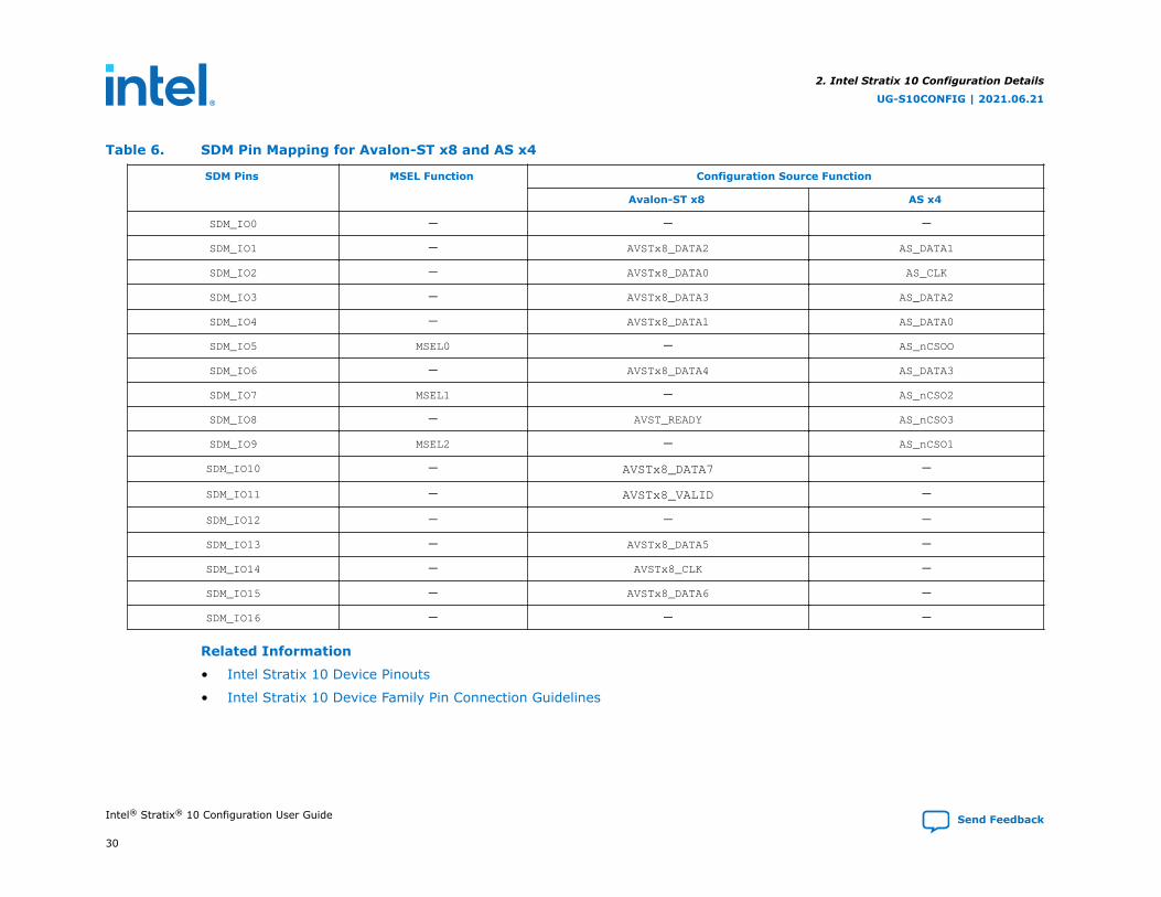
Table 6. SDM Pin Mapping for Avalon-ST x8 and AS x4
SDM Pins MSEL Function Configuration Source Function
Avalon-ST x8 AS x4
SDM_IO0 — — —
SDM_IO1 — AVSTx8_DATA2 AS_DATA1
SDM_IO2 — AVSTx8_DATA0 AS_CLK
SDM_IO3 — AVSTx8_DATA3 AS_DATA2
SDM_IO4 — AVSTx8_DATA1 AS_DATA0
SDM_IO5 MSEL0 — AS_nCSOO
SDM_IO6 — AVSTx8_DATA4 AS_DATA3
SDM_IO7 MSEL1 — AS_nCSO2
SDM_IO8 — AVST_READY AS_nCSO3
SDM_IO9 MSEL2 — AS_nCSO1
SDM_IO10 — AVSTx8_DATA7 —
SDM_IO11 — AVSTx8_VALID —
SDM_IO12 — — —
SDM_IO13 — AVSTx8_DATA5 —
SDM_IO14 — AVSTx8_CLK —
SDM_IO15 — AVSTx8_DATA6 —
SDM_IO16 — — —
Related Information
• Intel Stratix 10 Device Pinouts
• Intel Stratix 10 Device Family Pin Connection Guidelines
2. Intel Stratix 10 Configuration Details
UG-S10CONFIG | 2021.06.21
Intel® Stratix® 10 Configuration User Guide Send Feedback
30

2.5.2. MSEL Settings
After power-on MSEL[2:0] pins specify the configuration scheme for Intel Stratix 10 devices. Use 4.7-kΩ resistors to pull theMSEL[2:0] pins up to VCCIO_SDM or down to ground as required by the MSEL[2:0] setting for your configuration scheme.
Figure 8. MSEL Pull-Up and Pull-Down Circuit Diagram
RUP
VCCIO_SDM
MSEL[0]
4.7kΩ RDN
MSEL[0]
4.7kΩ OR
Table 7. MSEL Settings for Each Configuration Scheme of Intel Stratix 10 Devices
Configuration Scheme MSEL[2:0]
Avalon-ST (x32) 000
Avalon-ST (x16) 101
Avalon-ST (x8) 110
AS (Fast mode – for CvP)(4) 001
AS (Normal mode)(5) 011
JTAG only(6) 111
You must also specify the configuration scheme on the Configuration page of the Device and Pin Options dialog box in theIntel Quartus Prime Software.
(4) If you use AS Fast mode, you must ramp all power supplies to the recommended operating condition within 10 ms. This ramp-uprequirement ensures that the AS x4 device is within its operating voltage range when the Intel Stratix 10 device begins to access it.
(5) If you use AS Normal mode, you must fully ramp the VCCIO_SDM supply to the recommended operating condition within 10 ms.
(6) JTAG configuration works with any valid MSEL settings, unless disabled for security.
2. Intel Stratix 10 Configuration Details
UG-S10CONFIG | 2021.06.21
Send Feedback Intel® Stratix® 10 Configuration User Guide
31

Figure 9. Specify Configuration Scheme to Specify MSEL Value
Configuration Scheme
2.5.3. Device Configuration Pins for Optional Configuration Signals
All configuration schemes use the same dedicated pins for the standard control signals shown in the Intel Stratix 10Configuration Timing Diagram. Many other optional configuration signals do not have dedicated pin assignments.
Device Configuration Pins without Fixed Assignments
Note: Although the CONF_DONE and INIT_DONE configuration signals are not required, Intel recommends that you use thesesignals as an indicator to ensure that configuration is successful. The SDM drives the CONF_DONE signal high aftersuccessfully receiving full bitstream. The SDM drives the INIT_DONE signal high to indicate the device is fully in user mode.These signals are important when debugging configuration.
Table 8. Available SDM I/O Pin Assignments for Configuration Signals that Do Not Use Dedicated SDM I/O Pins
Signal Names
Configuration Scheme
Avalon-ST AS x4
x8 x16 x32
PWRMGT_SCL SDM_IO0 SDM_IO0
SDM_IO14
SDM_IO0
SDM_IO14
SDM_IO0
SDM_IO14
PWRMGT_SDA SDM_IO12
SDM_IO16
SDM_IO11
SDM_IO12
SDM_IO16
SDM_IO11
SDM_IO12
SDM_IO16
SDM_IO11
SDM_IO12
SDM_IO16
PWRMGT_ALERT SDM_IO0
SDM_IO9
SDM_IO12
SDM_IO0
SDM_IO9
SDM_IO12
SDM_IO0
SDM_IO12
SDM_IO0
SDM_IO12
continued...
2. Intel Stratix 10 Configuration Details
UG-S10CONFIG | 2021.06.21
Intel® Stratix® 10 Configuration User Guide Send Feedback
32
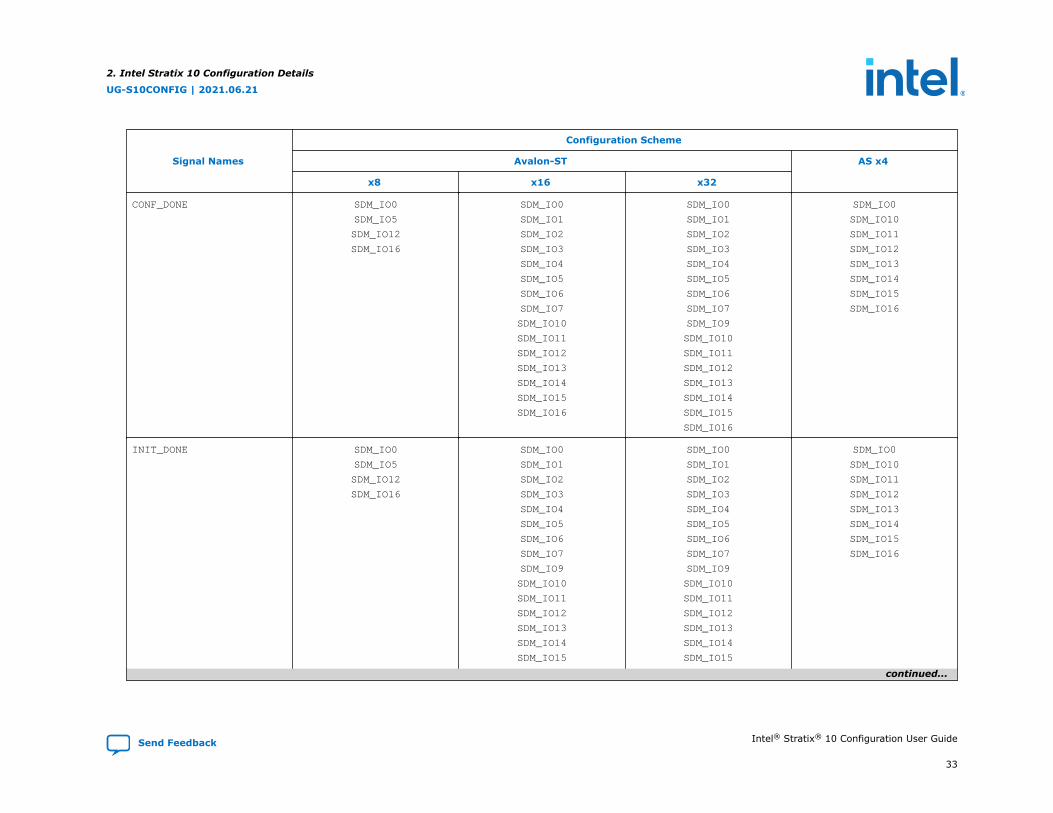
Signal Names
Configuration Scheme
Avalon-ST AS x4
x8 x16 x32
CONF_DONE SDM_IO0
SDM_IO5
SDM_IO12
SDM_IO16
SDM_IO0
SDM_IO1
SDM_IO2
SDM_IO3
SDM_IO4
SDM_IO5
SDM_IO6
SDM_IO7
SDM_IO10
SDM_IO11
SDM_IO12
SDM_IO13
SDM_IO14
SDM_IO15
SDM_IO16
SDM_IO0
SDM_IO1
SDM_IO2
SDM_IO3
SDM_IO4
SDM_IO5
SDM_IO6
SDM_IO7
SDM_IO9
SDM_IO10
SDM_IO11
SDM_IO12
SDM_IO13
SDM_IO14
SDM_IO15
SDM_IO16
SDM_IO0
SDM_IO10
SDM_IO11
SDM_IO12
SDM_IO13
SDM_IO14
SDM_IO15
SDM_IO16
INIT_DONE SDM_IO0
SDM_IO5
SDM_IO12
SDM_IO16
SDM_IO0
SDM_IO1
SDM_IO2
SDM_IO3
SDM_IO4
SDM_IO5
SDM_IO6
SDM_IO7
SDM_IO9
SDM_IO10
SDM_IO11
SDM_IO12
SDM_IO13
SDM_IO14
SDM_IO15
SDM_IO0
SDM_IO1
SDM_IO2
SDM_IO3
SDM_IO4
SDM_IO5
SDM_IO6
SDM_IO7
SDM_IO9
SDM_IO10
SDM_IO11
SDM_IO12
SDM_IO13
SDM_IO14
SDM_IO15
SDM_IO0
SDM_IO10
SDM_IO11
SDM_IO12
SDM_IO13
SDM_IO14
SDM_IO15
SDM_IO16
continued...
2. Intel Stratix 10 Configuration Details
UG-S10CONFIG | 2021.06.21
Send Feedback Intel® Stratix® 10 Configuration User Guide
33

Signal Names
Configuration Scheme
Avalon-ST AS x4
x8 x16 x32
SDM_IO16 SDM_IO16
CVP_CONFDONE Not supported Not supported Not supported SDM_IO0
SDM_IO10
SDM_IO11
SDM_IO12
SDM_IO13
SDM_IO14
SDM_IO15
SDM_IO16
SEU_ERROR SDM_IO0
SDM_IO5
SDM_IO7
SDM_IO9
SDM_IO12
SDM_IO16
SDM_IO0
SDM_IO1
SDM_IO2
SDM_IO3
SDM_IO4
SDM_IO5
SDM_IO6
SDM_IO7
SDM_IO9
SDM_IO10
SDM_IO11
SDM_IO12
SDM_IO13
SDM_IO14
SDM_IO15
SDM_IO16
SDM_IO0
SDM_IO1
SDM_IO2
SDM_IO3
SDM_IO4
SDM_IO5
SDM_IO6
SDM_IO7
SDM_IO9
SDM_IO10
SDM_IO11
SDM_IO12
SDM_IO13
SDM_IO14
SDM_IO15
SDM_IO16
SDM_IO0
SDM_IO10
SDM_IO11
SDM_IO12
SDM_IO13
SDM_IO14
SDM_IO15
SDM_IO16
HPS_COLD_nRESET SDM_IO0
SDM_IO5
SDM_IO7
SDM_IO9
SDM_IO12
SDM_IO0
SDM_IO1
SDM_IO2
SDM_IO3
SDM_IO4
SDM_IO0
SDM_IO1
SDM_IO2
SDM_IO3
SDM_IO4
SDM_IO0
SDM_IO10
SDM_IO11
SDM_IO12
SDM_IO13
continued...
2. Intel Stratix 10 Configuration Details
UG-S10CONFIG | 2021.06.21
Intel® Stratix® 10 Configuration User Guide Send Feedback
34

Signal Names
Configuration Scheme
Avalon-ST AS x4
x8 x16 x32
SDM_IO16 SDM_IO5
SDM_IO6
SDM_IO7
SDM_IO9
SDM_IO10
SDM_IO11
SDM_IO12
SDM_IO13
SDM_IO14
SDM_IO15
SDM_IO16
SDM_IO5
SDM_IO6
SDM_IO7
SDM_IO9
SDM_IO10
SDM_IO11
SDM_IO12
SDM_IO13
SDM_IO14
SDM_IO15
SDM_IO16
SDM_IO14
SDM_IO15
SDM_IO16
Direct to Factory Image Not applicable Not applicable Not applicable SDM_IO0
SDM_IO10
SDM_IO11
SDM_IO12
SDM_IO13
SDM_IO14
SDM_IO15
SDM_IO16
DATA UNLOCK SDM_IO0
SDM_IO5
SDM_IO7
SDM_IO9
SDM_IO12
SDM_IO16
SDM_IO0
SDM_IO1
SDM_IO2
SDM_IO3
SDM_IO4
SDM_IO5
SDM_IO6
SDM_IO7
SDM_IO9
SDM_IO10
SDM_IO11
SDM_IO12
SDM_IO13
SDM_IO0
SDM_IO1
SDM_IO2
SDM_IO3
SDM_IO4
SDM_IO5
SDM_IO6
SDM_IO7
SDM_IO9
SDM_IO10
SDM_IO11
SDM_IO12
SDM_IO13
SDM_IO0
SDM_IO10
SDM_IO11
SDM_IO12
SDM_IO13
SDM_IO14
SDM_IO15
SDM_IO16
2. Intel Stratix 10 Configuration Details
UG-S10CONFIG | 2021.06.21
Send Feedback Intel® Stratix® 10 Configuration User Guide
35
Signal Names
Configuration Scheme
Avalon-ST AS x4
x8 x16 x32
SDM_IO14
SDM_IO15
SDM_IO16
SDM_IO14
SDM_IO15
SDM_IO16
Note: Intel recommends that you assign the CONF_DONE and INIT_DONE pins to SDM I/O pins 0 or 16. These pins have weakinternal pull-downs resistors. If you cannot use these pins, Intel recommends that you include external 4.7-kΩ pull-downresistors to avoid false signaling.
Related Information
• Intel Stratix 10 Power Management User GuideFor more information about PWRMGT_SCL, PWRMGT_SDA, and PWRMGT_ALERT signals.
• Intel Stratix 10 Configuration via Protocol (CvP) Implementation User GuideFor more information about the CVP_CONFDONE signal.
• Intel Stratix 10 SEU Mitigation User GuideFor more information about the SEU_ERROR signal.
• Intel Stratix 10 SoC FPGA Boot User GuideFor more information about the HPS_COLD_nRESET signal.
2.5.3.1. Specifying Optional Configuration Pins
You enable and assign the SDM I/O pins using the Intel Quartus Prime software.
Complete the following steps to assign these additional configuration pins:
1. On the Assignments menu, click Device.
2. In the Device and Pin Options dialog box, select the Configuration category and click Configuration Pins Options.
3. In the Configuration Pin window, enable and assign the configuration pin that you want to include in your design.
2. Intel Stratix 10 Configuration Details
UG-S10CONFIG | 2021.06.21
Intel® Stratix® 10 Configuration User Guide Send Feedback
36
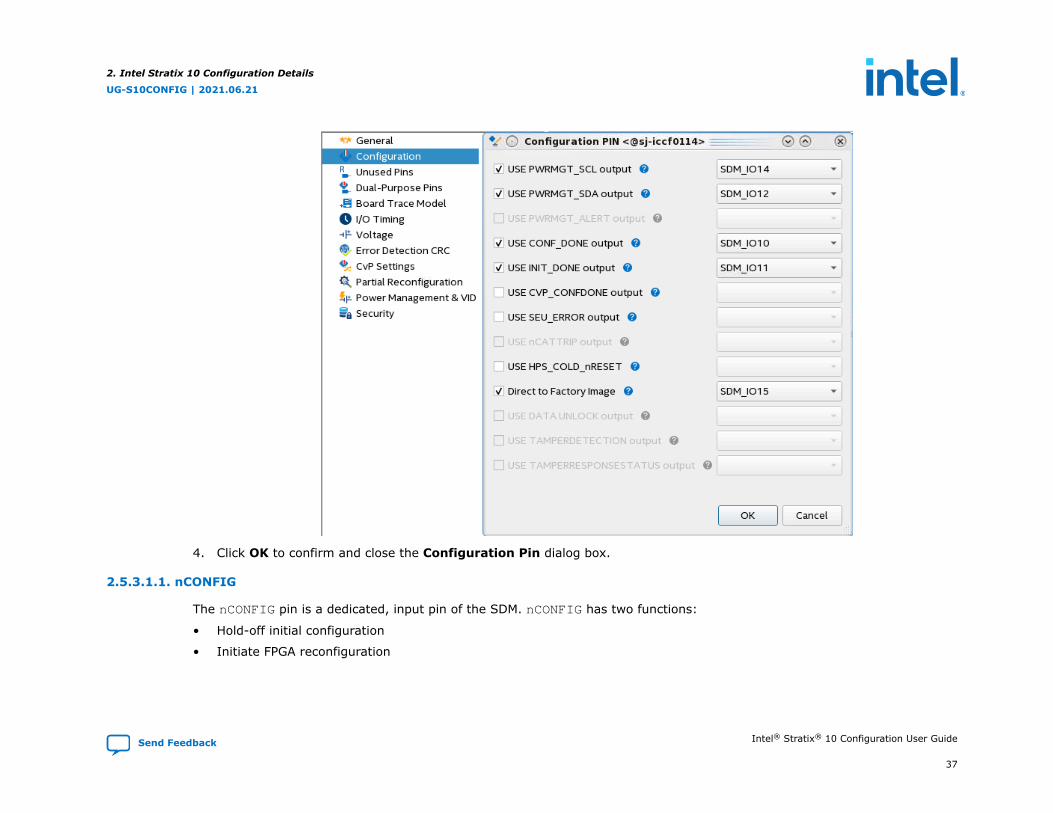
4. Click OK to confirm and close the Configuration Pin dialog box.
2.5.3.1.1. nCONFIG
The nCONFIG pin is a dedicated, input pin of the SDM. nCONFIG has two functions:
• Hold-off initial configuration
• Initiate FPGA reconfiguration
2. Intel Stratix 10 Configuration Details
UG-S10CONFIG | 2021.06.21
Send Feedback Intel® Stratix® 10 Configuration User Guide
37

The nCONFIG pin transition from low to high signals a configuration or reconfiguration request. The nSTATUS pin indicatesdevice readiness to initiate FPGA configuration.
The configuration source can only change the state of the nCONFIG pin when it has the same value as nSTATUS. When theIntel Stratix 10 device is ready it drives nSTATUS to follow nCONFIG.
The host should drive nCONFIG low to initiate device cleaning. Then the host should drive nCONFIG high to initiateconfiguration. If the host drives nCONFIG low during a configuration cycle, that configuration cycle stops. The SDM expects anew configuration cycle to begin.
2.5.3.1.2. nSTATUS
nSTATUS has the following two functions:
• To behave as an acknowledge for nCONFIG.
• To behave as an error status signal. It is important to monitor nSTATUS to identify configuration failures.
Note: nSTATUS does not go low for PR failures or failures using the JTAG configuration scheme.
Generally, the Intel Stratix 10 device changes the value of nSTATUS to follow the value of nCONFIG, except after an error. Forexample, after POR, nSTATUS asserts after nCONFIG asserts. When the host drives nCONFIG high, the Intel Stratix 10 devicedrives nSTATUS high.
In previous device families the deassertion of nSTATUS indicates the device is ready for configuration. For Intel Stratix 10devices, when using Avalon-ST configuration scheme, after the Intel Stratix 10 device drives nSTATUS high, you must alsomonitor the AVST_READY signal to determine when the device is ready to accept configuration data.
nSTATUS asserts if an error occurs during configuration. The pulse ranges from 0.5 ms to 10 ms.
nSTATUS assertion is asynchronous to data error detection. Intel Stratix 10 devices do not support the auto-restartconfiguration after error option.
Previous device families implement the nSTATUS as an open drain with a weak internal pull-up. Intel Stratix 10 always drivesnSTATUS. Consequently, you cannot wire OR an Intel Stratix 10 nSTATUS signal with the nSTATUS signal from earlier devicefamilies.
nSTATUS must be pulled high externally and the SDM must sample nSTATUS high when VCCIO_SDM ramps up to therecommended operating voltage.
2. Intel Stratix 10 Configuration Details
UG-S10CONFIG | 2021.06.21
Intel® Stratix® 10 Configuration User Guide Send Feedback
38

2.5.3.1.3. CONF_DONE and INIT_DONE
For Intel Stratix 10 devices, both CONF_DONE and INIT_DONE share multiplexed SDM_IO pins.
Previous device families implement the CONF_DONE and INIT_DONE pins as open drains with a weak internal pull-up. TheCONF_DONE signal indicates that the configuration bitstream is received successfully. The INIT_DONE pin indicates that thedevice operates within the design.
In the current implementation, you cannot wire an Intel Stratix 10 CONF_DONE or INIT_DONE signal with the nSTATUS signalfrom previous device families. Otherwise, CONF_DONE and INIT_DONE behave as these signals behaved in earlier devicefamilies. If you assign CONF_DONE and INIT_DONE to SDM_IO16 and SDM_IO0, weak internal pull-downs pull these pins lowat power-on reset. Ensure you specify these pins in the Intel Quartus Prime Software or in the Intel Quartus Prime settingsfile, (.qsf). CONF_DONE and INIT_DONE are low prior to and during configuration. CONF_DONE asserts when the devicefinishes receiving configuration data. INIT_DONE asserts when the device enters user mode.
Note: The entire device does not enter user mode simultaneously.Intel recommends that you include the Including the ResetRelease Intel FPGA IP in Your Design on page 139 to hold your application logic in the reset state until the entire FPGA fabricis in user mode.
CONF_DONE and INIT_DONE are optional signals. You can use these pins for other functions that the Intel Quartus Prime ProEdition Device and Pin Options menu defines.
Related Information
• SDM Pin Mapping on page 29
• Specifying Optional Configuration Pins on page 36
2.5.3.1.4. SDM_IO Pins
Intel Stratix 10 devices include 17 SDM_IO pins that you can configure to implement specific functions such as CONF_DONEand INIT_DONE. The chosen function must follow the GX, MX, TX, and SX Device Family Pin Connections Guidelines . Theconfiguration bitstream controls the pin locations for the SDM_IO pins.
Internal Intel Stratix 10 circuitry pulls SDM_IO0, SDM_IO8 and SDM_IO16 weakly low through a 25 kΩ resistor. Internal IntelStratix 10 circuitry pulls all other SDM_IO pins weakly high during power-on.
2. Intel Stratix 10 Configuration Details
UG-S10CONFIG | 2021.06.21
Send Feedback Intel® Stratix® 10 Configuration User Guide
39
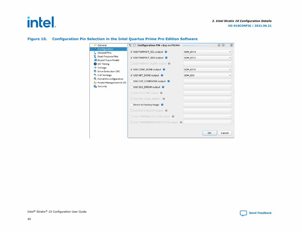
Figure 10. Configuration Pin Selection in the Intel Quartus Prime Pro Edition Software
2. Intel Stratix 10 Configuration Details
UG-S10CONFIG | 2021.06.21
Intel® Stratix® 10 Configuration User Guide Send Feedback
40

Figure 11. Fitter Report and SDM_IO Pin Reporting
Related Information
SDM Debug Toolkit Overview on page 221
2.5.3.2. Enabling Dual-Purpose Pins
AVST_CLK, AVST_DATA[15:0], AVST_DATA[31:16], and AVST_VALID are dual-purpose pins. Once the device enters usermode these pins can function either as GPIOs or as tri-state inputs.
If you use these pins as GPIOs, make the following assignments:
2. Intel Stratix 10 Configuration Details
UG-S10CONFIG | 2021.06.21
Send Feedback Intel® Stratix® 10 Configuration User Guide
41
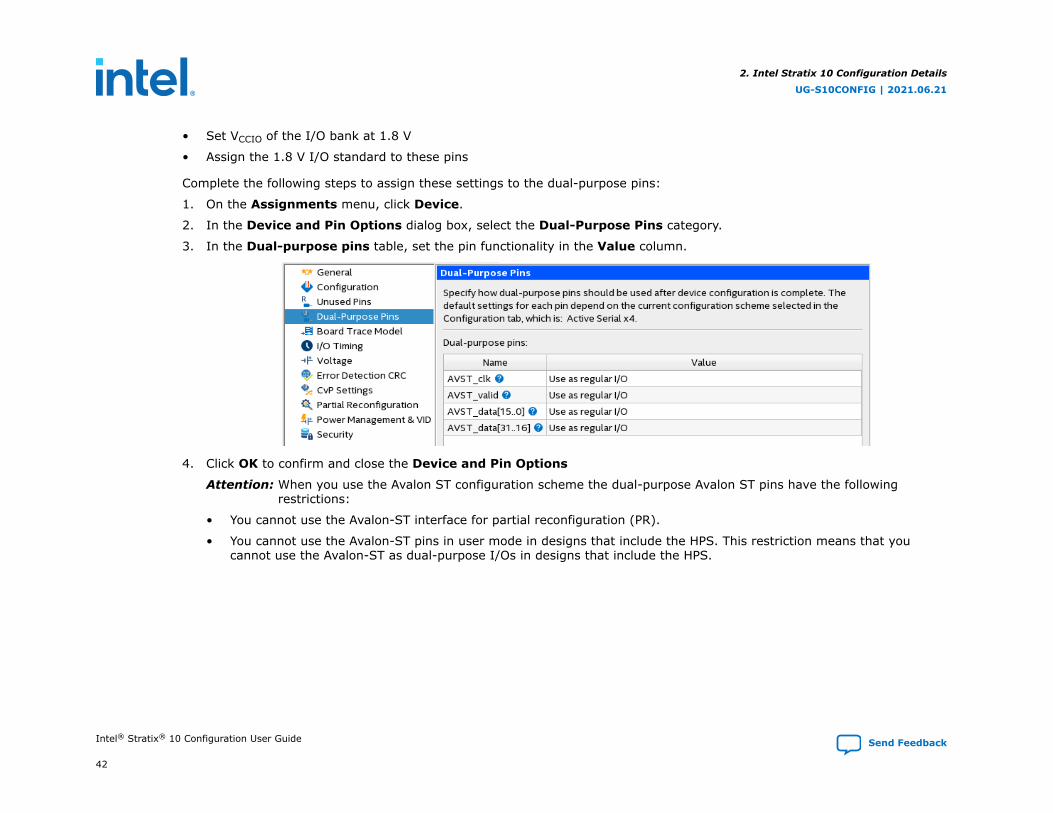
• Set VCCIO of the I/O bank at 1.8 V
• Assign the 1.8 V I/O standard to these pins
Complete the following steps to assign these settings to the dual-purpose pins:
1. On the Assignments menu, click Device.
2. In the Device and Pin Options dialog box, select the Dual-Purpose Pins category.
3. In the Dual-purpose pins table, set the pin functionality in the Value column.
4. Click OK to confirm and close the Device and Pin Options
Attention: When you use the Avalon ST configuration scheme the dual-purpose Avalon ST pins have the followingrestrictions:
• You cannot use the Avalon-ST interface for partial reconfiguration (PR).
• You cannot use the Avalon-ST pins in user mode in designs that include the HPS. This restriction means that youcannot use the Avalon-ST as dual-purpose I/Os in designs that include the HPS.
2. Intel Stratix 10 Configuration Details
UG-S10CONFIG | 2021.06.21
Intel® Stratix® 10 Configuration User Guide Send Feedback
42
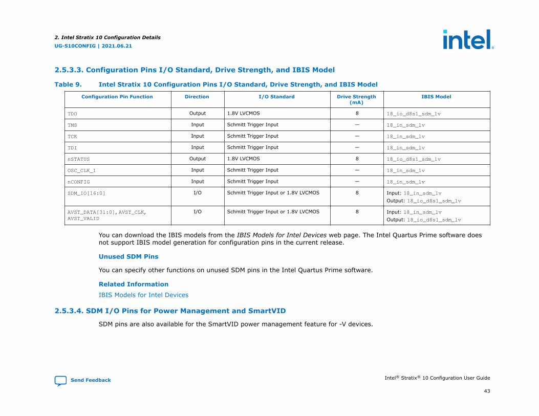
2.5.3.3. Configuration Pins I/O Standard, Drive Strength, and IBIS Model
Table 9. Intel Stratix 10 Configuration Pins I/O Standard, Drive Strength, and IBIS Model
Configuration Pin Function Direction I/O Standard Drive Strength(mA)
IBIS Model
TDO Output 1.8V LVCMOS 8 18_io_d8s1_sdm_lv
TMS Input Schmitt Trigger Input — 18_in_sdm_lv
TCK Input Schmitt Trigger Input — 18_in_sdm_lv
TDI Input Schmitt Trigger Input — 18_in_sdm_lv
nSTATUS Output 1.8V LVCMOS 8 18_io_d8s1_sdm_lv
OSC_CLK_1 Input Schmitt Trigger Input — 18_in_sdm_lv
nCONFIG Input Schmitt Trigger Input — 18_in_sdm_lv
SDM_IO[16:0] I/O Schmitt Trigger Input or 1.8V LVCMOS 8 Input: 18_in_sdm_lvOutput: 18_io_d8s1_sdm_lv
AVST_DATA[31:0], AVST_CLK,AVST_VALID
I/O Schmitt Trigger Input or 1.8V LVCMOS 8 Input: 18_in_sdm_lvOutput: 18_io_d8s1_sdm_lv
You can download the IBIS models from the IBIS Models for Intel Devices web page. The Intel Quartus Prime software doesnot support IBIS model generation for configuration pins in the current release.
Unused SDM Pins
You can specify other functions on unused SDM pins in the Intel Quartus Prime software.
Related Information
IBIS Models for Intel Devices
2.5.3.4. SDM I/O Pins for Power Management and SmartVID
SDM pins are also available for the SmartVID power management feature for -V devices.
2. Intel Stratix 10 Configuration Details
UG-S10CONFIG | 2021.06.21
Send Feedback Intel® Stratix® 10 Configuration User Guide
43
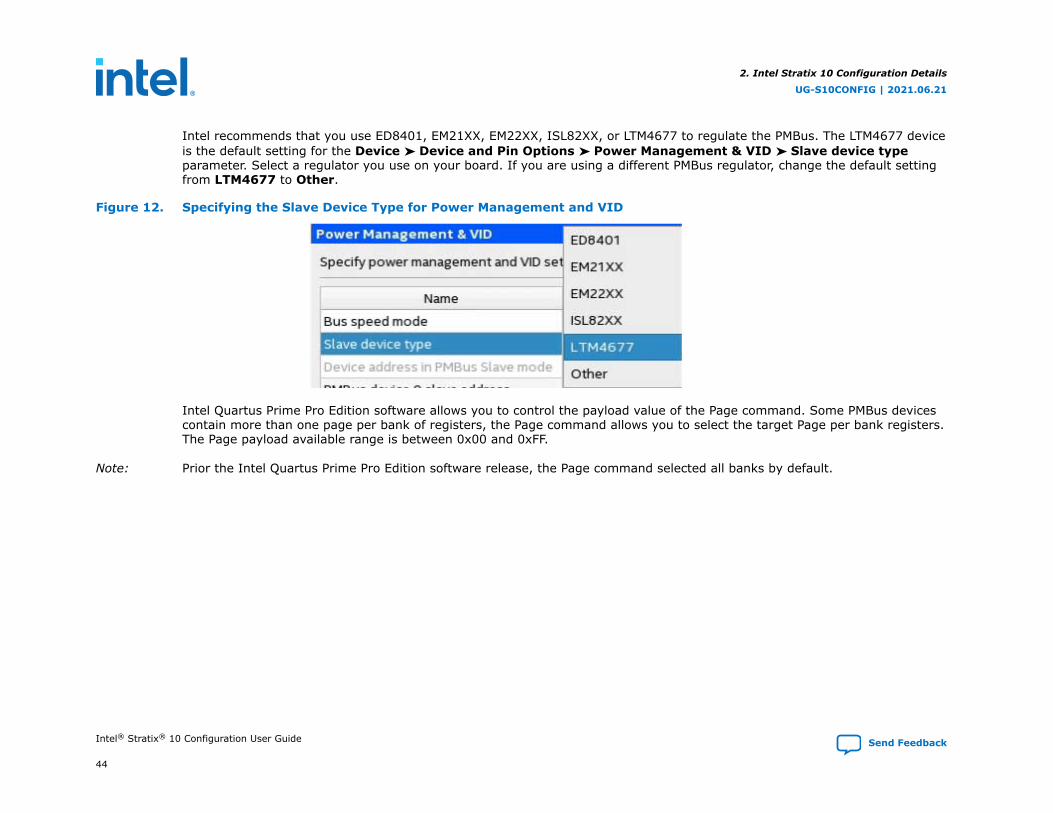
Intel recommends that you use ED8401, EM21XX, EM22XX, ISL82XX, or LTM4677 to regulate the PMBus. The LTM4677 deviceis the default setting for the Device ➤ Device and Pin Options ➤ Power Management & VID ➤ Slave device typeparameter. Select a regulator you use on your board. If you are using a different PMBus regulator, change the default settingfrom LTM4677 to Other.
Figure 12. Specifying the Slave Device Type for Power Management and VID
Intel Quartus Prime Pro Edition software allows you to control the payload value of the Page command. Some PMBus devicescontain more than one page per bank of registers, the Page command allows you to select the target Page per bank registers.The Page payload available range is between 0x00 and 0xFF.
Note: Prior the Intel Quartus Prime Pro Edition software release, the Page command selected all banks by default.
2. Intel Stratix 10 Configuration Details
UG-S10CONFIG | 2021.06.21
Intel® Stratix® 10 Configuration User Guide Send Feedback
44

Figure 13. Specifying the Page Command Setting
Refer to the Intel Stratix 10 Power Management User Guide for more information about the pin assignments and PMBussetting.
Related Information
Intel Stratix 10 Power Management User Guide
2. Intel Stratix 10 Configuration Details
UG-S10CONFIG | 2021.06.21
Send Feedback Intel® Stratix® 10 Configuration User Guide
45

2.5.3.5. Specifying Pins for Partial Reconfiguration (PR)
The partial reconfiguration signals use GPIO pins.
The following signals control partial reconfiguration in Intel Stratix 10 devices:
• PR_REQUEST
• PR_READY
• PR_ERROR
• PR_DONE
Connect these partial reconfiguration signals to the Partial Reconfiguration External Configuration Controller Intel FPGA IP.
Related Information
Creating a Partial Reconfiguration Design
2.6. Configuration Clocks
2.6.1. Setting Configuration Clock Source
You must specify the configuration clock source by selecting either the internal oscillator or OSC_CLK_1 with the supportedfrequency. By default, the SDM uses the internal oscillator for device configuration. Specify an OSC_CLK_1 clock source forthe fastest configuration time.
Complete the following steps to select the configuration clock source:
1. To specify OSC_CLK_1 as the clock source, on the Assignments menu, click Device.
2. In the Device and Pin Options dialog box, select the General category.
3. Specify the configuration clock source from the Configuration clock source drop down menu.
2. Intel Stratix 10 Configuration Details
UG-S10CONFIG | 2021.06.21
Intel® Stratix® 10 Configuration User Guide Send Feedback
46

4. Click OK to confirm and close the Device and Pin Options.
2.6.2. OSC_CLK_1 Clock Input
OSC_CLK_1 Requirements
When you drive the OSC_CLK_1 input clock with an external clock source and enable OSC_CLK_1 in the Intel Quartus Primesoftware, the device loads the majority of the configuration bitstream at 250 MHz. Intel Stratix 10 devices include an internaloscillator in addition to OSC_CLK_1 which runs the configuration process at a frequency between 170-230 MHz.Intel Stratix 10 devices always use this internal oscillator to load the first section of the bitstream, approximately 200 kilobyte(KB). The SDM can use either clock source for the remainder of device configuration. If you use the internal oscillator, you canleave the OSC_CLK_1 unconnected. If you use transceivers, you must provide an external clock to this pin.
When you specify OSC_CLK_1 for configuration, the OSC_CLK_1 clock must be a stable and free-running clock.
When you specify AS configuration scheme and nCONFIG is pull high, the SDM starts the configuration once the device exitsthe POR state. Ensure the OSC_CLK_1 clock is available before SDM starts to load the bitstream from the quad SPI flash oryou need to supply a stable free-running clock before/at the same time VCCIO_SDM ramps up to the typical voltage level.
2. Intel Stratix 10 Configuration Details
UG-S10CONFIG | 2021.06.21
Send Feedback Intel® Stratix® 10 Configuration User Guide
47

Note: Device configuration may fail under the following conditions when you select the OSC_CLK_1 as the clock source forconfiguration:
• You fail to drive the OSC_CLK_1 pin or the OSC_CLK_1 is not stable and free running due to an interruption or afrequency change.
• You drive the OSC_CLK_1 pin at an incorrect frequency. Select one of the following input reference clock frequencies todrive the OSC_CLK_1 pin:
— 25 MHz
— 100 MHz
— 125 MHz
The Intel Stratix 10 device multiplies the OSC_CLK_1 source clock frequency to generate a 250 MHz clock for configuration.Using an OSC_CLK_1 source enables the fastest possible configuration. Refer to Setting Configuration Clock Source forinstructions setting this frequency using the Intel Quartus Prime Software.
Configuration Clock Requirements for Reconfiguration Without Power Cycling the Device
When you specify OSC_CLK_1 for configuration and reconfigure without powering down the Intel Stratix 10 device, the devicecan only reconfigure with OSC_CLK_1. In this scenario, OSC_CLK_1 must be a free-running clock.
Configuration Clock Requirements for Configuration After Powering Cycling the Device
After a power-down, when you specify OSC_CLK_1 for configuration, the Intel Stratix 10 device uses the internal oscillator toload the first section of the bitstream and OSC_CLK_1 for the remainder.
Related Information
• L- and H-Tile Transceiver PHY User Guide
• E-Tile Transceiver PHY User Guide
• Intel Stratix 10 External Memory Interfaces IP User Guide
2. Intel Stratix 10 Configuration Details
UG-S10CONFIG | 2021.06.21
Intel® Stratix® 10 Configuration User Guide Send Feedback
48

2.7. Maximum Configuration Time Estimation
Hyper Initialization is an option that can be enabled or disabled through the setting in the Intel Quartus Prime software toinitialize or reset the Intel Hyperflex™ registers to a known state at device configuration. By default, this option is off. Forinformation about register initialization, refer to Device Initialization on page 144. For more information about Intel Hyperflexregisters, refer to the Intel Hyperflex Architecture High-Performance Design Handbook.
The configuration time is the time estimated for the entire configuration state. For more information, refer to Figure 4 on page19.
The maximum configuration time is estimated when the device starts configuration until CONF_DONE is asserted to high.
Table 10. Maximum Configuration Time Estimation for Intel Stratix 10 Devices (Avalon-ST)
Note: Provided configuration times are based on the AVST_CLK = 125 MHz.
Variant Product Line Maximum Configuration Time (ms) [Hyper Initialization Off/Hyper Initialization On]
AVST ×8 (7) AVST ×16 (7) AVST ×32 (7)
ConfigurationClock Source:
Internal Oscillator
ConfigurationClock Source:OSC_CLK_1
(25/100/125MHz)
ConfigurationClock Source:
Internal Oscillator
ConfigurationClock Source:OSC_CLK_1
(25/100/125MHz)
ConfigurationClock Source:
Internal Oscillator
ConfigurationClock Source:OSC_CLK_1
(25/100/125MHz)
Intel Stratix 10 GX,SX, TX, MX, and
DX
GX 400, SX 400,TX 400
183/222 122/148 108/147 72/98 90/129 60/86
GX 650, SX 650 274/334 182/222 154/216 102/144 120/184 80/122
continued...
(7) The maximum configuration time does not include the time incurred from external storage and control logic, and transceivercalibration time.
2. Intel Stratix 10 Configuration Details
UG-S10CONFIG | 2021.06.21
Send Feedback Intel® Stratix® 10 Configuration User Guide
49
Variant Product Line Maximum Configuration Time (ms) [Hyper Initialization Off/Hyper Initialization On]
AVST ×8 (7) AVST ×16 (7) AVST ×32 (7)
ConfigurationClock Source:
Internal Oscillator
ConfigurationClock Source:OSC_CLK_1
(25/100/125MHz)
ConfigurationClock Source:
Internal Oscillator
ConfigurationClock Source:OSC_CLK_1
(25/100/125MHz)
ConfigurationClock Source:
Internal Oscillator
ConfigurationClock Source:OSC_CLK_1
(25/100/125MHz)
GX 850, GX 1100,SX 850, SX 1100,TX 850, TX 1100,
DX 1100
456/1,200 304/378 246/358 164/238 190/300 126/200
GX 1660, GX 2110,TX 1650, TX 2100,MX 1650, MX 2100,
DX 2100
754/852 502/568 394/496 262/330 214/316 142/210
GX 1650, GX 2100,GX 2500, GX 2800,SX 1650, SX 2100,SX 2500, SX 2800,TX 2500, TX 2800,
DX 2800
1,102/1,240 734/826 568/708 378/472 300/442 200/294
(7) The maximum configuration time does not include the time incurred from external storage and control logic, and transceivercalibration time.
2. Intel Stratix 10 Configuration Details
UG-S10CONFIG | 2021.06.21
Intel® Stratix® 10 Configuration User Guide Send Feedback
50

Table 11. Maximum Configuration Time Estimation for Intel Stratix 10 Devices (AS x4)
Note: Provided configuration times are based on the AS_CLK = 115 MHz for Internal Oscillator and AS_CLK = 125 MHz for OSC_CLK_1 (25/100/125MHz).
Variant Product Line Maximum Configuration Time (ms) [Hyper Initialization Off/HyperInitialization On]
AS ×4
Configuration Clock Source: InternalOscillator
Configuration Clock Source:OSC_CLK_1 (25/100/125 MHz)
Intel Stratix 10 GX, SX, TX, MX, and DX GX 400, SX 400, TX 400 408/447 272/298
GX 650, SX 650 568/630 378/420
GX 850, GX 1100, SX 850, SX 1100, TX850, TX 1100, DX 1100
900/1,012 600/674
GX 1660, GX 2110, TX 1650, TX 2100,MX 1650, MX 2100, DX 2100
1,432/1,534 954/1,022
GX 1650, GX 2100, GX 2500, GX 2800,SX 1650, SX 2100, SX 2500, SX 2800,
TX 2500, TX 2800, DX 2800
2,058/2,200 1,372/1,466
Related Information
• Intel Hyperflex Architecture High-Performance Design Handbook
• Device Initialization on page 144
• Intel Stratix 10 Device DatasheetFor more information about General Configuration Timing Specifications for Intel Stratix 10 devices.
• Intel Stratix 10 GX/SX Device OverviewFor more information about Intel Stratix 10 GX/SX variants.
• Intel Stratix 10 TX Device OverviewFor more information about Intel Stratix 10 TX variants.
• Intel Stratix 10 MX Device OverviewFor more information about Intel Stratix 10 MX variants.
• Intel Stratix 10 DX Device OverviewFor more information about Intel Stratix 10 DX variants.
2. Intel Stratix 10 Configuration Details
UG-S10CONFIG | 2021.06.21
Send Feedback Intel® Stratix® 10 Configuration User Guide
51
3. Intel Stratix 10 Configuration Schemes
3.1. Avalon-ST Configuration
The Avalon-ST configuration scheme replaces the FPP mode available in earlier device families. Avalon-ST is the fastestconfiguration scheme for Intel Stratix 10 devices. This scheme uses an external host, such as a microprocessor, MAX® II, MAXV, or Intel MAX 10 device to drive configuration. The external host controls the transfer of configuration data from externalstorage such as flash memory to the FPGA. The logic that controls the configuration process resides in the external host. Youcan use the PFL II IP with a MAX II, MAX V, or Intel MAX 10 device as the host to read configuration data from the flashmemory device and configure the Intel Stratix 10 device. The Avalon-ST configuration scheme is called passive because theexternal host, not the Intel Stratix 10 device, controls configuration.
Table 12. Avalon-ST Configuration Data Width, Clock Rates, and Data RatesMbps is an abbreviation for Megabits per second.
Protocol Data Width (bits) Max Clock Rate Max Data Rate MSEL[2:0]
Avalon-ST
32 125 MHz 4000 Mbps 000
16 125 MHz 2000 Mbps 101
8 125 MHz 1000 Mbps 110
Table 13. Required Configuration Signals for the Avalon-ST Configuration SchemeYou can use an 8-, 16-, or 32-bit Avalon-ST configuration data bus. You specify SDM I/O pin functions using the Device ➤ Device and Pin Options ➤Configuration dialog box in the Intel Quartus Prime software. For the Avalon-ST x16 and x32 configuration, you can reassign the GPIO, dual-purposeconfiguration pins for other functions in user mode using the Device ➤ Device and Pin Options ➤ Dual-Purpose Pins dialog box.
Signal Name Pin Type Direction Powered by
nSTATUS SDM I/O Output VCCIO_SDM
nCONFIG SDM I/O Input VCCIO_SDM
continued...
UG-S10CONFIG | 2021.06.21
Send Feedback
Intel Corporation. All rights reserved. Intel, the Intel logo, and other Intel marks are trademarks of Intel Corporation or its subsidiaries. Intel warrants performanceof its FPGA and semiconductor products to current specifications in accordance with Intel's standard warranty, but reserves the right to make changes to anyproducts and services at any time without notice. Intel assumes no responsibility or liability arising out of the application or use of any information, product, orservice described herein except as expressly agreed to in writing by Intel. Intel customers are advised to obtain the latest version of device specifications beforerelying on any published information and before placing orders for products or services.*Other names and brands may be claimed as the property of others.
ISO9001:2015Registered

Signal Name Pin Type Direction Powered by
MSEL[2:0] SDM I/O Input VCCIO_SDM
CONF_DONE(8) SDM I/O Output VCCIO_SDM
AVST_READY SDM I/O Output VCCIO_SDM
AVSTx8_DATA[7:0] SDM I/O Input VCCIO_SDM
AVSTx8_VALID SDM I/O Input VCCIO_SDM
AVSTx8_CLK SDM I/O Input VCCIO_SDM
AVST_DATA[31:0] GPIO, Dual-Purpose Input VCCIO
AVST_VALID GPIO, Dual-Purpose Input VCCIO
AVST_CLK GPIO, Dual-Purpose Input VCCIO
Refer to the Intel Stratix 10 Data Sheet for configuration timing estimates.
Note: Although the INIT_DONE configuration signal is not required for configuration, Intel recommends that you use this signal. TheSDM drives the INIT_DONE signal high to indicate the device is fully in user mode. This signal is important when debuggingconfiguration.
Note: If you create custom logic instead of using the PFL II IP to drive configuration, refer to the Avalon Streaming Interfaces in theAvalon Interface Specifications for protocol details.
Related Information
• Device Configuration Pins for Optional Configuration Signals on page 32
• SDM Pin Mapping on page 29
• Avalon Interface Specifications
• Intel Stratix 10 Device Data Sheet
• Intel Stratix 10 Device FeaturesFor a list of device features that are planned for future releases.
• Intel Stratix 10 Device Family Pin Connection Guidelines
(8) CONF_DONE is required if you are using the Intel FPGA Parallel Flash Loader II IP as the configuration host.
3. Intel Stratix 10 Configuration Schemes
UG-S10CONFIG | 2021.06.21
Send Feedback Intel® Stratix® 10 Configuration User Guide
53

3.1.1. Avalon-ST Configuration Scheme Hardware Components and File Types
You can use the following components to implement the Avalon-ST configuration scheme:
• A CPLD with PFL II IP and common flash interface (CFI) flash or Quad SPI flash memory
• A custom host, typically a microprocessor, with any external memory
• The Intel FPGA Download Cable II to connect the Intel Quartus Prime Programmer to the PCB.
The following block diagram illustrates the components and design flow using the Avalon-ST configuration scheme.
Figure 14. Components and Design Flow for .pof Programming
Quartus Software flow on PC
Quartus PrimeProgrammer
10 pin JTAG header
Intel FPGA Download Cable II
CFIIntel FPGA
SDMFlash
PCB
Quartus Prime: File Programming File Generator
Quartus Prime: File Start Compile
Quartus Prime: Tools Programming
Quartus PrimeProgramming File
Generator
Quartus PrimeCompilation
USB
CPLD with PFL II
Avalon-ST
SOF
POF
3. Intel Stratix 10 Configuration Schemes
UG-S10CONFIG | 2021.06.21
Intel® Stratix® 10 Configuration User Guide Send Feedback
54

Table 14. Output File Types
Programming File Type Extension Description
Programmer Object File .pof The .pof is a proprietary Intel FPGA file type. Use the PFL II IP core via a JTAG header to writethe .pof to an external CFI flash or serial flash device.
Raw Binary File .rbf You can also use the .rbf with the Avalon-ST configuration scheme and an external host such asa CPU or microcontroller.You can program the configuration bitstreams or data in the .rbf file directly into flash via athird-party programmer. Then, you can use an external host to configure the device with theAvalon-ST configuration scheme.
If you choose a third-party microprocessor for Avalon-ST configuration, refer to the Avalon Streaming Interfaces in the AvalonInterface Specifications for protocol details.
3.1.2. Enabling Avalon-ST Device Configuration
You enable the Avalon-ST device configuration scheme in the Intel Quartus Prime software.
Complete the following steps to specify an Avalon-ST interface for device configuration.
1. On the Assignments menu, click Device.
2. In the Device and Pin Options dialog box, select the Configuration category.
3. In the Configuration window, in the Configuration scheme dropdown list, select the appropriate Avalon-ST bus width.
4. Click OK to confirm and close the Device and Pin Options dialog box.
3. Intel Stratix 10 Configuration Schemes
UG-S10CONFIG | 2021.06.21
Send Feedback Intel® Stratix® 10 Configuration User Guide
55

3.1.3. The AVST_READY Signal
Before beginning configuration, trigger device cleaning by toggling the nCONFIG pin from high to low to high. This nCONFIGtransition also returns the device to the configuration state.
If you use the Parallel Flash Loader II Intel FPGA IP core as the configuration host, the AVST_READY synchronizer logic isincluded.
Figure 15. Monitoring the AVST_READY Signal and Responding to Backpressure
AVST_CLK
AVSTx8_READYor AVST_READY
AVSTx8_VALIDor AVST_VALID
AVSTx8_DATA[7:0AVST_DATA[15:0]AVST_data[31:0]]
must send no morethan 6 valid clocks afterready goes low
data0 data1 data2 data3
The configuration files for Intel Stratix 10 devices can be highly compressed. During configuration, the decompression of thebit stream inside the device requires the host to pause before sending more data. The Intel Stratix 10 device asserts theAVST_READY signal when the device is ready to accept data. The AVST_READY signal is only valid when the nSTATUS pin ishigh. In addition, the host must handle backpressure by monitoring the AVST_READY signal and may assert AVST_VALIDsignal any time after the assertion of AVST_READY signal. The host must monitor the AVST_READY signal throughout theconfiguration.
3. Intel Stratix 10 Configuration Schemes
UG-S10CONFIG | 2021.06.21
Intel® Stratix® 10 Configuration User Guide Send Feedback
56
The AVST_READY signal sent by the Intel Stratix 10 device to the host is not synchronized with the AVSTx8_CLK orAVST_CLK. To configure the Intel Stratix 10 device successfully, the host must adhere to the following constraints:
• The host must drive no more than six data words after the deassertion of the AVST_READY signal including the delayincurred by the 2-stage register synchronizer.
• The host must synchronize the AVST_READY signal to the AVST_CLK signal using a 2-stage register synchronizer. Here isRegister transfer level (RTL) example code for 2-stage register synchronizer:
always @(posedge avst_clk or negedge reset_n) begin if (~reset_n) begin fpga_avst_ready_reg1 <= 0; fpga_avst_ready_reg2 <= 0; else fpga_avst_ready_reg1 <= fpga_avst_ready; fpga_avst_ready_reg2 <= fpga_avst_ready_reg1; end end
Where:
— The AVST_CLK signal comes from either PFL II IP or your Avalon-ST controller logic.
— fpga_avst_ready is the AVST_READY signal from the Intel Stratix 10 device.
— fpga_avst_ready_reg2 signal is the AVST_READY signal that is synchronous to AVST_CLK.
You must properly constrain the AVST_CLK and AVST_DATA signals at the host. Perform timing analysis on both signalsbetween the host and Intel Stratix 10 device to ensure the Avalon-ST configuration timing specifications are met. Refer to theAvalon-ST Configuration Timing section of the Intel Stratix 10 Device Data Sheet for information about the timingspecifications.
Note: The AVST_CLK signal must run continuously during configuration. The AVST_READY signal cannot assert unless the clock isrunning.
Optionally, you can monitor the CONF_DONE signal to indicate the flash has sent all the data to FPGA or to indicate theconfiguration process is complete.
If you use the PFL II IP core as the configuration host, you can use the Intel Quartus Prime software to store the binaryconfiguration data to the flash memory through the PFL II IP core.
3. Intel Stratix 10 Configuration Schemes
UG-S10CONFIG | 2021.06.21
Send Feedback Intel® Stratix® 10 Configuration User Guide
57

If you use the Avalon-ST Adapter IP core as part of the configuration host, set the Source Ready Latency value between 1-6.
Avalon-ST x8 configuration scheme uses the SDM pins only. Avalon-ST x16 and x32 configuration scheme only use dual-purpose I/O pins that you can use as general-purpose I/O pins after configuration.
Related Information
• Avalon-ST Configuration Timing in Intel Stratix 10 Device Datasheet
• Avalon Interface Specifications
3.1.4. RBF Configuration File Format
If you do not use the Parallel Flash Loader II Intel FPGA IP core to program the flash, you must generate the .rbf file.
The data in .rbf file are in little-endian format
Table 15. Writing 32-bit DataFor a x32 data bus, the first byte in the file is the least significant byte of the configuration double word, and the fourth byte is the most significant byte.
Double Word = 01EE1B02
LSB: BYTE0 = 02 BYTE1 = 1B BYTE2 = EE MSB: BYTE3 = 01
D[7:0] D[15:8] D[23:16] D[31:24]
0000 0010 0001 1011 1110 1110 0000 0001
Table 16. Writing 16-bit DataFor a x16 data bus, the first byte in the file is the least significant byte of the configuration word, and the second byte is the most significant byte of theconfiguration word.
WORD0 = 1B02 WORD1 = 01EE
LSB: BYTE0 = 02 MSB: BYTE1 = 1B LSB: BYTE2 = EE MSB: BYTE3 = 01
D[7:0] D[15:8] D[7:0] D[15:8]
0000 0010 0001 1011 1110 1110 0000 0001
3. Intel Stratix 10 Configuration Schemes
UG-S10CONFIG | 2021.06.21
Intel® Stratix® 10 Configuration User Guide Send Feedback
58

3.1.5. Avalon-ST Single-Device Configuration
Refer to the Intel Stratix 10 Device Family Pin Connection Guidelines for additional information about individual pin usage andrequirements.
3. Intel Stratix 10 Configuration Schemes
UG-S10CONFIG | 2021.06.21
Send Feedback Intel® Stratix® 10 Configuration User Guide
59
Figure 16. Connections for Avalon-ST x8 Single-Device Configuration
Intel FPGAnCONFIGnSTATUSCONF_DONEINIT_DONEOSC_CLK_1
MSEL[2:0]
AVSTx8_DATA [7:0]AVSTx8_VALIDAVST_READY
AVSTx8_CLK
ConfigurationData Signals
ConfigurationControl Signals
Compact Flash Interface
External Compact Flash Memory
ADDR DATA
.rbf(little endian)
Control
CPLD / FPGA
External Host
fpga_clk
fpga_readyfpga_valid
fpga_conf_donefpga_nstatusfpga_nconfig
fpga_data [7:0]
Parallel Flash Loader II IPor
Microprocessor or
Custom Logic
10kΩ
MSEL
VCCIO_SDM
8
3
External Clock Source
(2)(1)
10kΩ
VCCIO_SDM
3. Intel Stratix 10 Configuration Schemes
UG-S10CONFIG | 2021.06.21
Intel® Stratix® 10 Configuration User Guide Send Feedback
60
Figure 17. Connections for Avalon-ST x16 Single-Device Configuration
Intel FPGAnCONFIGnSTATUSCONF_DONEINIT_DONEOSC_CLK_1
MSEL[2:0]
AVST_DATA [15:0]AVST_VALIDAVST_READY
AVST_CLK
ConfigurationData Signals
ConfigurationControl Signals
Compact Flash Interface
External Compact Flash Memory
ADDR DATA
.rbf(little endian)
Control
CPLD / FPGA
External Host
fpga_clk
fpga_readyfpga_valid
fpga_conf_donefpga_nstatusfpga_nconfig
fpga_data [15:0]
10kΩ
MSEL
VCCIO_SDM
16
3Parallel Flash Loader II IP
orMicroprocessor
orCustom Logic
External Clock Source (Optional)
(2)(1)
10kΩ
VCCIO_SDM
3. Intel Stratix 10 Configuration Schemes
UG-S10CONFIG | 2021.06.21
Send Feedback Intel® Stratix® 10 Configuration User Guide
61

Figure 18. Connections for Avalon-ST x32 Single-Device Configuration
Intel FPGAnCONFIGnSTATUSCONF_DONEINIT_DONEOSC_CLK_1
MSEL[2:0]
AVST_DATA [31:0]AVST_VALIDAVST_READY
AVST_CLK
ConfigurationData Signals
ConfigurationControl Signals
Compact Flash Interface
External Compact Flash MemoryADDR DATA
.rbf(little endian)
Control
CPLD / FPGA
External Host
fpga_clk
fpga_readyfpga_valid
fpga_conf_donefpga_nstatusfpga_nconfig
fpga_data [31:0]
10kΩ
MSEL
VCCIO_SDM
32
3
External Clock Source (Optional)
(2)(1)Parallel Flash Loader II IPor
Microprocessor or
Custom Logic
10kΩ
VCCIO_SDM
3. Intel Stratix 10 Configuration Schemes
UG-S10CONFIG | 2021.06.21
Intel® Stratix® 10 Configuration User Guide Send Feedback
62

Notes for Figure:
1. Refer to MSEL Settings for the correct resistor pull-up and pull-down values for all configuration schemes.
2. The synchronizers shown in all three figures can be internal if the host is an FPGA or CPLD. If the host is a microprocessor,you must use discrete synchronizers.
Related Information
• MSEL Settings on page 31
• Enabling Dual-Purpose Pins on page 41
• Intel Stratix 10 Device Family Pin Connection Guidelines
3.1.6. Debugging Guidelines for the Avalon-ST Configuration Scheme
The Avalon-ST configuration scheme replaces the previously available in fast passive parallel (FPP) modes. This configurationscheme retains similar functionality and performance. Here are the important differences:
• The Avalon-ST configuration scheme requires you to monitor the flow control signal, AVST_READY. The AVST_READYsignal indicates if the device can receive configuration data.
• The AVST_CLK and AVSTx8_CLK clock signals cannot pause when configuration data is not being transferred. Data is nottransferred when AVST_READY and AVST_VALID are low. The AVST_CLK and AVSTx8_CLK clock signals must runcontinuously until CONF_DONE asserts.
Debugging Suggestions
Review the general Configuration Debugging Checklist in the Debugging Guide chapter before considering these debuggingtips that pertain to the Avalon-ST configuration scheme.
• Only assert AVST_VALID after the SDM asserts AVST_READY.
• Only assert AVST_VALID when the AVST_DATA is valid.
• Ensure that the AVST_CLK clock signal is continuous and free running until configuration completes. The AVST_CLK canstop after CONF_DONE asserts. The initialization state does not require the AVST_CLK signal.
• If using x8 mode, ensure that you use the dedicated SDM_IO pins for this interface (clock, data, valid and ready).
• If using x16 or x32 mode, power the I/O bank containing the x16 or x32 pins (I/O Bank 3A) at 1.8 V.
• Ensure you select the appropriate Avalon-ST configuration scheme in your Intel Quartus Prime Pro Edition project.
3. Intel Stratix 10 Configuration Schemes
UG-S10CONFIG | 2021.06.21
Send Feedback Intel® Stratix® 10 Configuration User Guide
63
• Ensure the MSEL pins reflect this mode on the PCB.
• Verify that the host device does not drive configuration pins before the Intel Stratix 10 device powers up.
• Ensure nCONFIG remains high during the Avalon-ST configuration scheme.
• Verify that CONF_DONE and INIT_DONE pins correlate to the Intel Quartus Prime SDM I/O pins assignment and theboard-level connections.
• Ensure that during the power up, no external component drives the nSTATUS signal low.
Related Information
Intel Stratix 10 Debugging Guide on page 218
3.1.7. IP for Use with the Avalon-ST Configuration Scheme: Intel FPGA Parallel Flash Loader II IP Core
3.1.7.1. Functional Description
You can use the Parallel Flash Loader II Intel FPGA IP (PFL II) with an external host, such as the MAX II, MAX V, or Intel MAX10 devices to complete the following tasks:
• Program configuration data into a flash memory device using JTAG interface.
• Configure the Intel Stratix 10 device with the Avalon-ST configuration scheme from the flash memory device.
Note: Use the Parallel Flash Loader II Intel FPGA IP and not the earlier Parallel Flash Loader IP with the Avalon-ST configurationscheme in Intel Stratix 10 devices.
Note: The current implementation does not support programming two QSPI devices with two separate PFL images in a singleprogramming cycle. To program multiple QSPI devices, you must program each QSPI flash device with a single PFL imageseparately.
Note: The Parallel Flash Loader II Intel FPGA IP does not support HPS cold reset.
3.1.7.1.1. Generating and Programming a .pof into CFI Flash
The Intel Quartus Prime software generates the .sof when you compile your design. You use the .sof to generate the .pof.This process includes the following steps:
1. Generating a .pof for the PFL II IP using the Intel Quartus Prime File ➤ Programming File Generator.
2. Using the Intel Quartus Prime Programmer to write the Intel Stratix 10 device .pof to the flash device.
3. Intel Stratix 10 Configuration Schemes
UG-S10CONFIG | 2021.06.21
Intel® Stratix® 10 Configuration User Guide Send Feedback
64
Figure 19. Programming the CFI Flash Memory with the JTAG Interface
ExternalHost
CFI FlashMemory
Configuration Data
CommonFlashInterface
PFL II
Quartus PrimeSoftware
using JTAG
The PFL II IP core supports dual flash memory devices in burst read mode to achieve faster configuration times. You canconnect two MT28EW CFI flash memory devices to the host in parallel using the same data bus, clock, and control signals.Intel does not support connecting two of non-MT28W CFI flash memory devices to PFL II IP core in parallel. During FPGAconfiguration, the AVST_CLK frequency is four times faster than the flash_clk frequency.
3. Intel Stratix 10 Configuration Schemes
UG-S10CONFIG | 2021.06.21
Send Feedback Intel® Stratix® 10 Configuration User Guide
65

Figure 20. PFL II IP core with Dual MT28EW CFI Flash Memory DevicesThe flash memory devices must have the same memory density from the same device family and manufacturer.
CFI Compliant Flash External Host with PFL II IP Core Intel FPGA
CFI Compliant Flash
16
16
ADDR[24..0]NCE
NWENOE
DATA[15..0]
ADDR[24..0]NCE
NWENOE
DATA[15..0]
flash_addr[24..0]flash_nceflash_nweflash_noeflash_data[31..0] fpga_conf_done
fpga_nstatusfpga_nconfig
avst_dataavst_clk
CONF_DONEnSTATUSnCONFIGAVSTx8_DATA/AVST_DATAAVSTx8_CLK/AVST_CLK
avst_validavst_ready
AVSTx8_VALID/AVST_VALIDAVST_READY
10kΩ
VCCIO_SDM
10kΩ
VCCIO_SDM
Related Information
Intel Stratix 10 GX FPGA Development Kit
3. Intel Stratix 10 Configuration Schemes
UG-S10CONFIG | 2021.06.21
Intel® Stratix® 10 Configuration User Guide Send Feedback
66
3.1.7.1.2. Implementing Multiple Pages in the Flash .pof
The PFL II IP core stores configuration data in a maximum of eight pages in a flash memory block.
The total number of pages and the size of each page depends on the flash density. Here are some guidelines for storing yourdesigns to pages:
• Always store designs for different FPGA chains on different pages.
• You may choose store different designs for a FPGA chain on a single page or on multiple pages.
• When you choose to store the designs for a FPGA chain on a single page, the design order must match the JTAG chaindevice order.
Use the generated .sof to create a flash memory device .pof. The following address modes are available for the .softo .pof conversion:
• Block mode—allows you to specify the start and end addresses for the page.
• Start mode—allows you to specify only the start address. The start address for each page must be on an 8 KB boundary.If the first valid start address is 0×000000, the next valid start address is an increment of 0×2000.
• Auto mode—allows the Intel Quartus Prime software to automatically determine the start address of the page. The IntelQuartus Prime software aligns the pages on a 128 KB boundary. If the first valid start address is 0x000000, the next validstart address is an multiple of 0x20000.
3.1.7.1.3. Storing Option Bits
In addition to design data, the flash memory stores the option bits. You must specify the address for the options bits in twoplaces: the PFL II IP and in the option bits address of the flash memory device.
The option bits contain the following information:
• The start address for each page.
• The .pof version for flash programming. This value is the same for all pages.
• The Page-Valid bits for each page. The Page-Valid bit is bit 0 of the start address. The PLF II IP core writes this bitafter successfully programming the page.
You use the Programming File Generator dialog box to specify the Start address of the option bits. Specify your flashdevice using Add Device on the Configuration Tab of the Programming File Generator dialog box. Then click OPTIONSand EDIT to specify the Start address for the option bits. This Start address must match the address you specify for Whatis the byte address of the option bits, in hex? when specifying the PFL II IP parameters.
3. Intel Stratix 10 Configuration Schemes
UG-S10CONFIG | 2021.06.21
Send Feedback Intel® Stratix® 10 Configuration User Guide
67
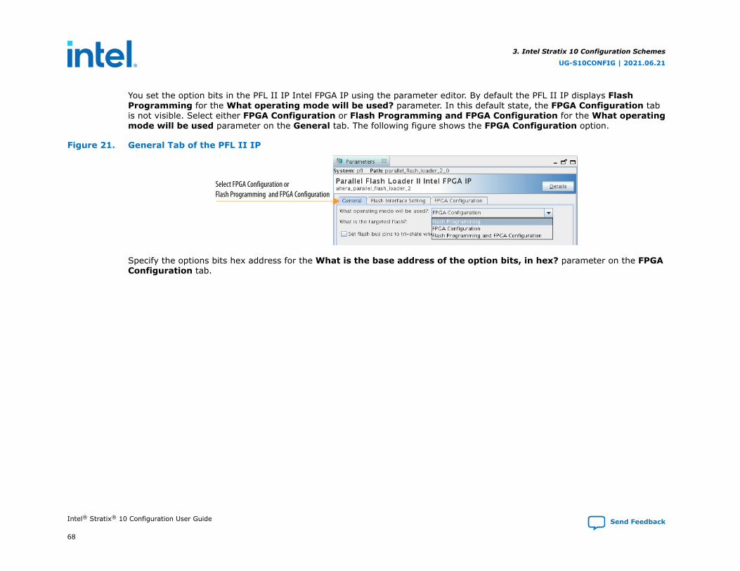
You set the option bits in the PFL II IP Intel FPGA IP using the parameter editor. By default the PFL II IP displays FlashProgramming for the What operating mode will be used? parameter. In this default state, the FPGA Configuration tabis not visible. Select either FPGA Configuration or Flash Programming and FPGA Configuration for the What operatingmode will be used parameter on the General tab. The following figure shows the FPGA Configuration option.
Figure 21. General Tab of the PFL II IP
Select FPGA Configuration orFlash Programming and FPGA Configuration
Specify the options bits hex address for the What is the base address of the option bits, in hex? parameter on the FPGAConfiguration tab.
3. Intel Stratix 10 Configuration Schemes
UG-S10CONFIG | 2021.06.21
Intel® Stratix® 10 Configuration User Guide Send Feedback
68
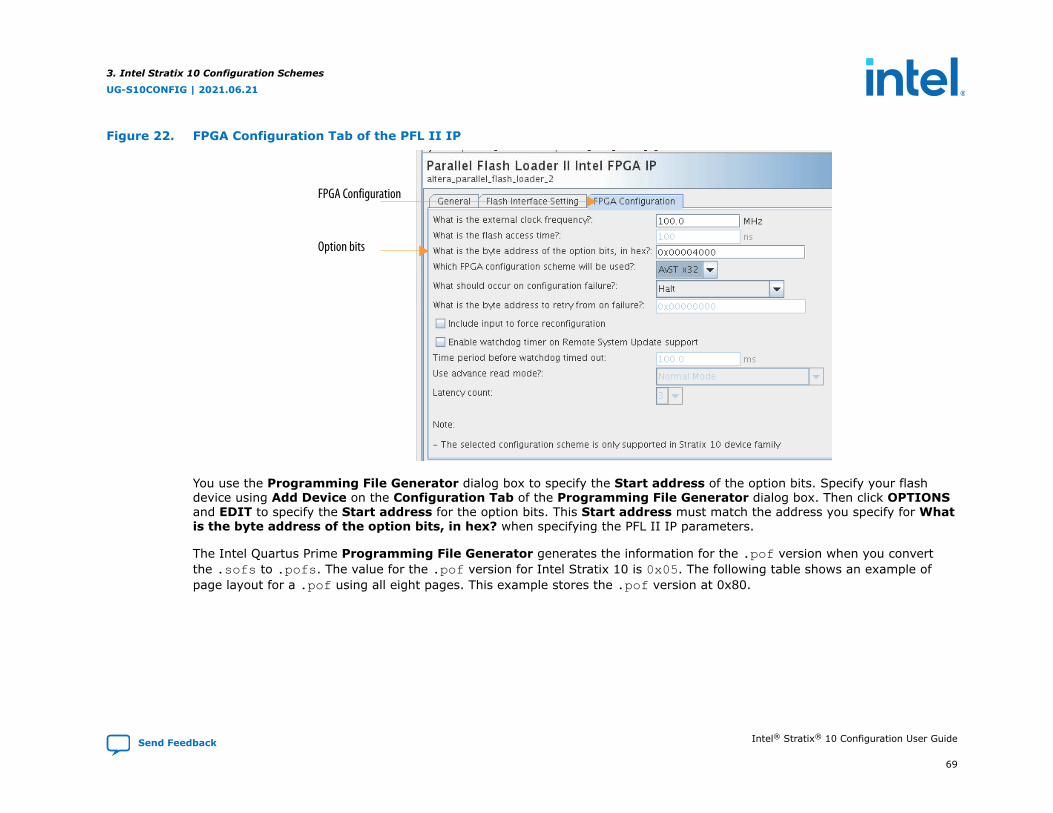
Figure 22. FPGA Configuration Tab of the PFL II IP
Option bits
FPGA Configuration
You use the Programming File Generator dialog box to specify the Start address of the option bits. Specify your flashdevice using Add Device on the Configuration Tab of the Programming File Generator dialog box. Then click OPTIONSand EDIT to specify the Start address for the option bits. This Start address must match the address you specify for Whatis the byte address of the option bits, in hex? when specifying the PFL II IP parameters.
The Intel Quartus Prime Programming File Generator generates the information for the .pof version when you convertthe .sofs to .pofs. The value for the .pof version for Intel Stratix 10 is 0x05. The following table shows an example ofpage layout for a .pof using all eight pages. This example stores the .pof version at 0x80.
3. Intel Stratix 10 Configuration Schemes
UG-S10CONFIG | 2021.06.21
Send Feedback Intel® Stratix® 10 Configuration User Guide
69

Table 17. Option Bits Sector Format
Sector Offset Value
0x00–0x03 Page 0 start address
0x04–0x07 Page 0 end address
0x08–0x0B Page 1 start address
0x0C–0x0F Page 1 end address
0x10–0x13 Page 2 start address
0x14–0x17 Page 2 end address
0x18–0x1B Page 3 start address
0x1C–0x1F Page 3 end address
0x20–0x23 Page 4 start address
0x24–0x27 Page 4 end address
0x28–0x2B Page 5 start address
0x2C–0x2F Page 5 end address
0x30–0x33 Page 6 start address
0x34–0x37 Page 6 end address
0x38–0x3B Page 7 start address
0x3C–0x3F Page 7 end address
0x40–0x7F Reserved
0x80(9) .pof version
0x81-0xFF Reserved
Caution: To prevent the PFL II IP core from malfunctioning, do not overwrite any information in the option bits sector. Always store theoption bits in unused addresses in the flash memory device.
(9) The .pof version occupies only one byte in the option bits sector.
3. Intel Stratix 10 Configuration Schemes
UG-S10CONFIG | 2021.06.21
Intel® Stratix® 10 Configuration User Guide Send Feedback
70
Related Information
PFL II Parameters on page 77
3.1.7.1.4. Verifying the Option Bit Start and End Addresses
You can decode the start and end address that you specified for each of the SOF page when converting a .sof to .pof filefrom the 32-bit value of the sector offset address. If you encounter a configuration error you can verify that the generatedbitstream addresses match the addresses you specified in the Intel Quartus Prime Software.
The following table shows the bit fields of the start address.
Table 18. Start Address Bit Content
Bit Width Description
31:11 21 Addressable start address
10:1 10 Reserved bits
0 1 Page valid bit• 0=Valid• 1=Error
Table 19. End Address Bit Content
Bit Width Description
31:0 32 Addressable end address
To restore the addresses:
• Start address—append 13'b0000000000000 to the addressable start address
• End address—append 2'b11 to the addressable end address
For a .pof that has two page addresses with the values shown in the following table.
Sector Offset Value
0x00 – 0x03 0x00004000
0x04 – 0x07 0x00196E30
0x08 – 0x0B 0x001C0000
3. Intel Stratix 10 Configuration Schemes
UG-S10CONFIG | 2021.06.21
Send Feedback Intel® Stratix® 10 Configuration User Guide
71

Sector Offset Value
0x0C – 0x0F 0x00352E30
For Page 0 if you append the start address bits[31:11] with 13'b0000000000000, the result is32'b00000000000000010000000000000000 = 0x10000.
If you append the end address 0x00196E0 with 2'b11, the result is 26'b00011001011011100011000011 = 0x65B8C3.
For Page 1 if you append the start address with 13'b0000000000000, the result is32'b0000000000011100000000000000000000 = 0x700000.
If you append end address 0x00352E30 with 2’b11, the result is 32'b00000000110101001011100011000011 =0xD4B8C3.
The start and end address must be correlated with the start and end address for each page printed in the .map file.
3.1.7.1.5. Implementing Page Mode and Option Bits in the CFI Flash Memory Device
The following figure shows a sample layout of a .pof with three pages. The end addresses depend on the density of the flashmemory device. For different density devices refer to the Byte Address Range for CFI Flash Memory Devices with DifferentDensities table below. The option bits follow the configuration data in memory.
3. Intel Stratix 10 Configuration Schemes
UG-S10CONFIG | 2021.06.21
Intel® Stratix® 10 Configuration User Guide Send Feedback
72

Figure 23. Implementing Page Mode and Option Bits in the CFI Flash Memory Device
Option Bits
Configuration Data (Page 2)
Configuration Data (Page 1)
Configuration Data (Page 0)
Page 2 Address + Page-ValidPage 1 Address + Page-ValidPage 0 Address + Page-Valid
End Address
0x000000
8 Bits
32 Bits
The following figure shows the layout of the option bits for a single page. Because the start address must be on an 8 KBboundary, bits 0-12 of the page start address are set to zero and are not stored in the option bits.
3. Intel Stratix 10 Configuration Schemes
UG-S10CONFIG | 2021.06.21
Send Feedback Intel® Stratix® 10 Configuration User Guide
73

Figure 24. Page Start Address, End Address, and Page-Valid Bit Stored as Option BitsThe Page-Valid bits indicate whether each page is successfully programmed. The PFL II IP core sets the Page-Valid bits after successfully programming the pages.
Bit 2...Bit 0Bit 7...Bit 3
Bit 7...Bit 0
Bit 7...Bit 0
Bit 7...Bit 0
Bit 7...Bit 0
Bit 7...Bit 0
Bit 7...Bit 0
Bit 7...Bit 1 Bit 0
0x002002
0x002003
0x002000
0x002001 Page Start Address [17:13]
Page Start Address [25:18]
Page Start Address [33:26]
Page End Address [9:2]
Page End Address [17:10]
Page End Address [25:18]
0x002004
0x002005
0x002006
Page End Address [33:26]
Page ValidReserved
Reserved
0x002007
(For flash byte addressing mode)
Table 20. Byte Address Range for CFI Flash Memory Devices with Different Densities
CFI Device (Megabit) Address Range
8 0x0000000–0x00FFFFF
16 0x0000000–0x01FFFFF
32 0x0000000–0x03FFFFF
64 0x0000000–0x07FFFFF
continued...
3. Intel Stratix 10 Configuration Schemes
UG-S10CONFIG | 2021.06.21
Intel® Stratix® 10 Configuration User Guide Send Feedback
74
CFI Device (Megabit) Address Range
128 0x0000000–0x0FFFFFF
256 0x0000000–0x1FFFFFF
512 0x0000000–0x3FFFFFF
1024 0x0000000–0x7FFFFFF
3.1.7.2. Designing with the PFL II IP Core for Avalon-ST Single Device Configuration
This section describes the procedures on how to use the PFL II IP core.
To target a MAX II, MAX V, or Intel MAX 10 device requires the use of Intel Quartus Prime Standard Edition whereas targetinga Intel Stratix 10 requires Intel Quartus Prime Pro Edition.
The process of creating the Avalon-ST single device configuration design targeting a MAX10/MAX V/MAX II device involvesthree steps.
1. Generate the AVST design for the MAX device with the default option address.
2. Create the Intel Stratix 10 .pof file in setting the appropriate option bits.
3. Regenerate the Parallel Flash Loader II Intel FPGA IP (PFL II) with the option bits used to generate the Intel Stratix10 .pof file and recompile the Intel MAX 10 design.
You can find a MAX V system design example that implements the PFL II IP for AVST x16 configuration mode in the installerpackage of the Intel Stratix 10 GX FPGA Development Kit.
3. Intel Stratix 10 Configuration Schemes
UG-S10CONFIG | 2021.06.21
Send Feedback Intel® Stratix® 10 Configuration User Guide
75

Figure 25. Process for Using the PFL IP CoreFigure shows the process for using the PFL IP core, using MAX II as an example.
Create a new MAX II design, instantiate the PFL Megafunction in
the MAX II design, and createPin Assignments
Add the MAX II .pof to the Quartus Prime Programmer
Add the flash .pof in the Quartus Prime Programmer
Program the MAX II and Flash Devices
MAX II configures the FPGA with theconfiguration data from the Flash Device
Compile andobtain the
FPGA .sof(s)
Convert to .pof for the
TargetedFlash
Compileand obtain
MAX II.pof
Add the .sof(s) for conversion to .pof
Create new FPGAdesigns
Create the optional Jam programming file
Related Information
Intel Stratix 10 GX FPGA Development Kit
3. Intel Stratix 10 Configuration Schemes
UG-S10CONFIG | 2021.06.21
Intel® Stratix® 10 Configuration User Guide Send Feedback
76
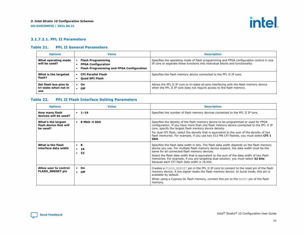
3.1.7.2.1. PFL II Parameters
Table 21. PFL II General Parameters
Options Value Description
What operating modewill be used?
• Flash Programming• FPGA Configuration• Flash Programming and FPGA Configuration
Specifies the operating mode of flash programming and FPGA configuration control in oneIP core or separate these functions into individual blocks and functionality.
What is the targetedflash?
• CFI Parallel Flash• Quad SPI Flash
Specifies the flash memory device connected to the PFL II IP core.
Set flash bus pins totri-state when not inuse
• On• Off
Allows the PFL II IP core to tri-state all pins interfacing with the flash memory devicewhen the PFL II IP core does not require access to the flash memory.
Table 22. PFL II Flash Interface Setting Parameters
Options Value Description
How many flashdevices will be used?
• 1–16 Specifies the number of flash memory devices connected to the PFL II IP core.
What's the largestflash device that willbe used?
• 8 Mbit–4 Gbit Specifies the density of the flash memory device to be programmed or used for FPGAconfiguration. If you have more than one flash memory device connected to the PFL II IPcore, specify the largest flash memory device density.For dual CFI flash, select the density that is equivalent to the sum of the density of twoflash memories. For example, if you use two 512-Mb CFI flashes, you must select CFI 1Gbit.
What is the flashinterface data width
• 8• 16• 32
Specifies the flash data width in bits. The flash data width depends on the flash memorydevice you use. For multiple flash memory device support, the data width must be thesame for all connected flash memory devices.Select the flash data width that is equivalent to the sum of the data width of two flashmemories. For example, if you are targeting dual solution, you must select 32 bitsbecause each CFI flash data width is 16 bits.
Allow user to controlFLASH_NRESET pin
• On• Off
Creates a FLASH_NRESET pin in the PFL II IP core to connect to the reset pin of the flashmemory device. A low signal resets the flash memory device. In burst mode, this pin isavailable by default.When using a Cypress GL flash memory, connect this pin to the RESET pin of the flashmemory.
3. Intel Stratix 10 Configuration Schemes
UG-S10CONFIG | 2021.06.21
Send Feedback Intel® Stratix® 10 Configuration User Guide
77

Table 23. PFL II Flash Programming Parameters
Options Value Description
Flash programming IPoptimization target
• Area• Speed
Specifies the flash programming IP optimization. If you optimize the PFL II IP core forSpeed, the flash programming time is shorter, but the IP core uses more LEs. If youoptimize the PFL II IP core for Area, the IP core uses fewer LEs, but the flashprogramming time is longer.
Flash programming IPFIFO size
• 16• 32
Specifies the FIFO size if you select Speed for flash programming IP optimization. The PFLII IP core uses additional LEs to implement FIFO as temporary storage for programmingdata during flash programming. With a larger FIFO size, programming time is shorter.
Add Block-CRCverificationacceleration support
• On• Off
Adds a block to accelerate verification.
Table 24. PFL II FPGA Configuration Parameters
Options Value Description
What is the externalclock frequency?
Provide the frequency of your external clock. Specifies the user-supplied clock frequency for the IP core to configure the FPGA. Theclock frequency must not exceed two times the maximum clock (AVST_CLK) frequencythe FPGA can use for configuration. The PFL II IP core can divide the frequency of theinput clock maximum by two.
What is the flashaccess time?
Provide the access time from the flash data sheet. Specifies the flash access time. This information is available from the flash datasheet.Intel recommends specifying a flash access time that is equal to or greater than therequired time.For CFI parallel flash, the unit is in ns. For NAND flash, the unit is in μs. NAND flash usespages instead of bytes and requires greater access time. This option is disabled for quadSPI flash.
What is the byteaddress of the optionbits, in hex?
Provide the byte address of the option bits. Specifies the option bits start address in flash memory. The start address must reside onan 8 KB boundary. This address must be the same as the bit sector address you specifiedwhen converting the .sof to a .pof.For more information refer to Storing Option Bits.
Which FPGAconfiguration schemewill be used?
• Avalon-ST x8• Avalon-ST x16• Avalon-ST x32
Specifies the width of the Avalon-ST interface.
What should occur onconfiguration failure?
• Halt• Retry same page• Retry from fixed address
Configuration behavior after configuration failure.
continued...
3. Intel Stratix 10 Configuration Schemes
UG-S10CONFIG | 2021.06.21
Intel® Stratix® 10 Configuration User Guide Send Feedback
78

Options Value Description
• If you select Halt, the FPGA configuration stops completely after failure.• If you select Retry same page, after failure, the PFL II IP core reconfigures the FPGA
with data from the page that failed.• If you select Retry from fixed address, the PFL II IP core reconfigures the FPGA a
fixed address.
What is the byteaddress to retry fromfailure
— If you select Retry from fixed address for configuration failure option, this optionspecifies the flash address the PFL II IP core to reads from.
Include input to forcereconfiguration
• On• Off
Includes the optional pfl_nreconfigure reconfiguration input pin to enablereconfiguration of the FPGA.
Enable watchdogtimer on RemoteSystem Updatesupport
• On• Off
Enables a watchdog timer for remote system update support. Turning on this optionenables the pfl_reset_watchdog input pin and pfl_watchdog_error output pin.This option also specifies the period before the watchdog timer times out. The watchdogtimer runs at the pfl_clk frequency.
Time period before thewatchdog timer timesout
— Specifies the time out period for the watchdog timer. The default time out period is 100ms.
Use advance readmode?
• Normal mode• Intel Burst mode• 16 byte page mode (GL only)• 32 byte page mode (MT28EW)• Micron Burst Mode (M58BW)
This option improves the overall flash access time for the read process during the FPGAconfiguration.• Normal mode—applicable for all flash memory• Intel Burst mode—Applicable for devices that support bursting. Reduces sequential
read access time• 16 byte page mode (GL only)—applicable for Cypress GL flash memory only• 32 byte page mode (MT28EW)—applicable tor MT28EW only• Micron Burst Mode (M58BW)—applicable for Micron M58BW flash memory onlyFor more information about the read-access modes of the flash memory device, refer tothe respective flash memory data sheet.
Latency count • 3• 4• 5
Specifies the latency count for Intel Burst mode.
3. Intel Stratix 10 Configuration Schemes
UG-S10CONFIG | 2021.06.21
Send Feedback Intel® Stratix® 10 Configuration User Guide
79
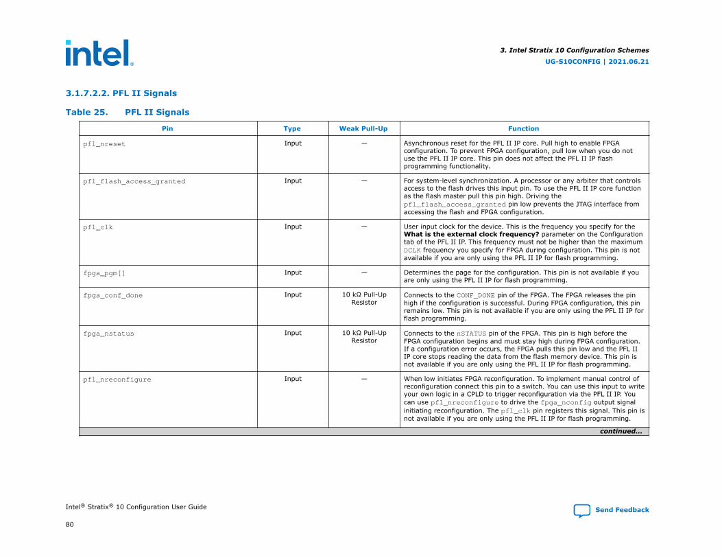
3.1.7.2.2. PFL II Signals
Table 25. PFL II Signals
Pin Type Weak Pull-Up Function
pfl_nreset Input — Asynchronous reset for the PFL II IP core. Pull high to enable FPGAconfiguration. To prevent FPGA configuration, pull low when you do notuse the PFL II IP core. This pin does not affect the PFL II IP flashprogramming functionality.
pfl_flash_access_granted Input — For system-level synchronization. A processor or any arbiter that controlsaccess to the flash drives this input pin. To use the PFL II IP core functionas the flash master pull this pin high. Driving thepfl_flash_access_granted pin low prevents the JTAG interface fromaccessing the flash and FPGA configuration.
pfl_clk Input — User input clock for the device. This is the frequency you specify for theWhat is the external clock frequency? parameter on the Configurationtab of the PFL II IP. This frequency must not be higher than the maximumDCLK frequency you specify for FPGA during configuration. This pin is notavailable if you are only using the PFL II IP for flash programming.
fpga_pgm[] Input — Determines the page for the configuration. This pin is not available if youare only using the PFL II IP for flash programming.
fpga_conf_done Input 10 kΩ Pull-UpResistor
Connects to the CONF_DONE pin of the FPGA. The FPGA releases the pinhigh if the configuration is successful. During FPGA configuration, this pinremains low. This pin is not available if you are only using the PFL II IP forflash programming.
fpga_nstatus Input 10 kΩ Pull-UpResistor
Connects to the nSTATUS pin of the FPGA. This pin is high before theFPGA configuration begins and must stay high during FPGA configuration.If a configuration error occurs, the FPGA pulls this pin low and the PFL IIIP core stops reading the data from the flash memory device. This pin isnot available if you are only using the PFL II IP for flash programming.
pfl_nreconfigure Input — When low initiates FPGA reconfiguration. To implement manual control ofreconfiguration connect this pin to a switch. You can use this input to writeyour own logic in a CPLD to trigger reconfiguration via the PFL II IP. Youcan use pfl_nreconfigure to drive the fpga_nconfig output signalinitiating reconfiguration. The pfl_clk pin registers this signal. This pin isnot available if you are only using the PFL II IP for flash programming.
continued...
3. Intel Stratix 10 Configuration Schemes
UG-S10CONFIG | 2021.06.21
Intel® Stratix® 10 Configuration User Guide Send Feedback
80
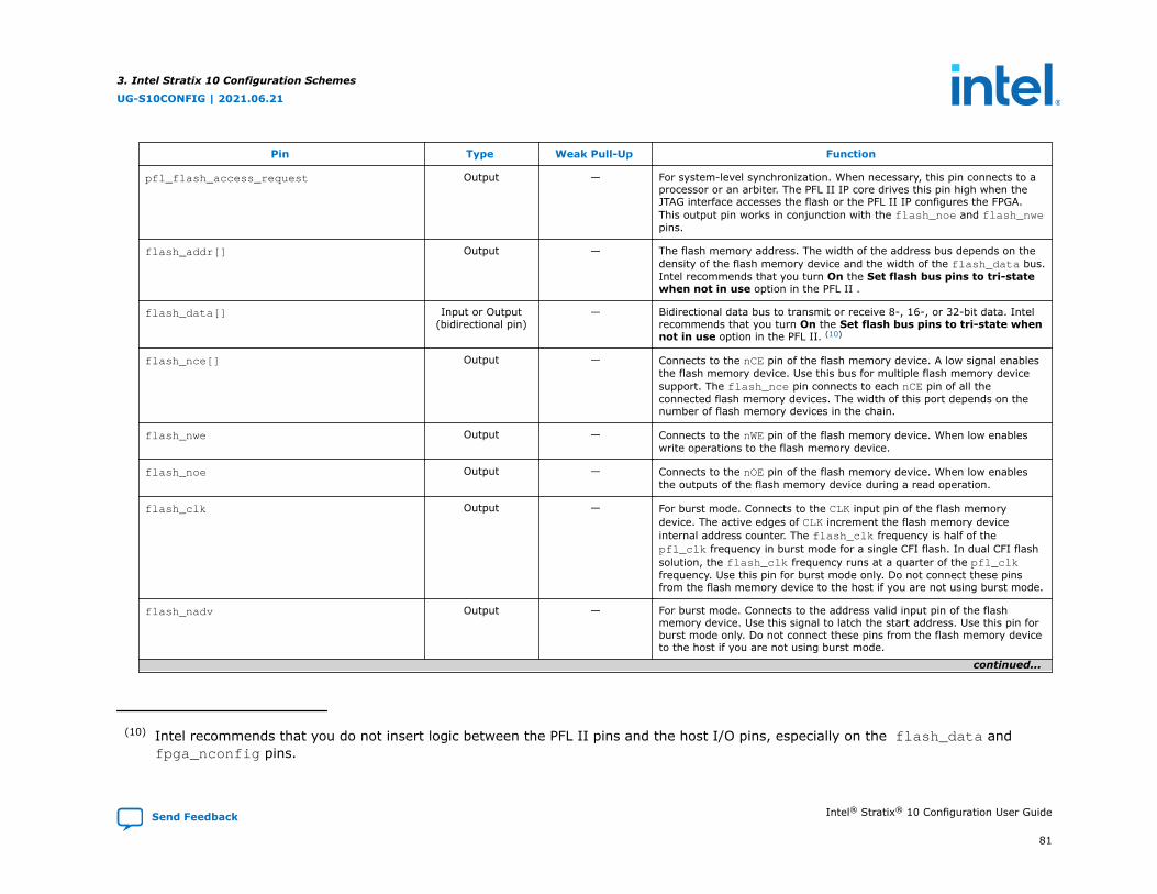
Pin Type Weak Pull-Up Function
pfl_flash_access_request Output — For system-level synchronization. When necessary, this pin connects to aprocessor or an arbiter. The PFL II IP core drives this pin high when theJTAG interface accesses the flash or the PFL II IP configures the FPGA.This output pin works in conjunction with the flash_noe and flash_nwepins.
flash_addr[] Output — The flash memory address. The width of the address bus depends on thedensity of the flash memory device and the width of the flash_data bus.Intel recommends that you turn On the Set flash bus pins to tri-statewhen not in use option in the PFL II .
flash_data[] Input or Output(bidirectional pin)
— Bidirectional data bus to transmit or receive 8-, 16-, or 32-bit data. Intelrecommends that you turn On the Set flash bus pins to tri-state whennot in use option in the PFL II. (10)
flash_nce[] Output — Connects to the nCE pin of the flash memory device. A low signal enablesthe flash memory device. Use this bus for multiple flash memory devicesupport. The flash_nce pin connects to each nCE pin of all theconnected flash memory devices. The width of this port depends on thenumber of flash memory devices in the chain.
flash_nwe Output — Connects to the nWE pin of the flash memory device. When low enableswrite operations to the flash memory device.
flash_noe Output — Connects to the nOE pin of the flash memory device. When low enablesthe outputs of the flash memory device during a read operation.
flash_clk Output — For burst mode. Connects to the CLK input pin of the flash memorydevice. The active edges of CLK increment the flash memory deviceinternal address counter. The flash_clk frequency is half of thepfl_clk frequency in burst mode for a single CFI flash. In dual CFI flashsolution, the flash_clk frequency runs at a quarter of the pfl_clkfrequency. Use this pin for burst mode only. Do not connect these pinsfrom the flash memory device to the host if you are not using burst mode.
flash_nadv Output — For burst mode. Connects to the address valid input pin of the flashmemory device. Use this signal to latch the start address. Use this pin forburst mode only. Do not connect these pins from the flash memory deviceto the host if you are not using burst mode.
continued...
(10) Intel recommends that you do not insert logic between the PFL II pins and the host I/O pins, especially on the flash_data andfpga_nconfig pins.
3. Intel Stratix 10 Configuration Schemes
UG-S10CONFIG | 2021.06.21
Send Feedback Intel® Stratix® 10 Configuration User Guide
81
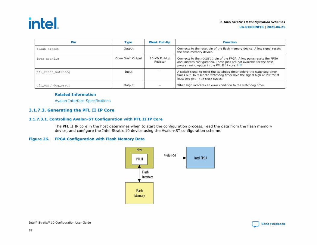
Pin Type Weak Pull-Up Function
flash_nreset Output — Connects to the reset pin of the flash memory device. A low signal resetsthe flash memory device.
fpga_nconfig Open Drain Output 10-kW Pull-UpResistor
Connects to the nCONFIG pin of the FPGA. A low pulse resets the FPGAand initiates configuration. These pins are not available for the flashprogramming option in the PFL II IP core. (10)
pfl_reset_watchdog Input — A switch signal to reset the watchdog timer before the watchdog timertimes out. To reset the watchdog timer hold the signal high or low for atleast two pfl_clk clock cycles.
pfl_watchdog_error Output — When high indicates an error condition to the watchdog timer.
Related Information
Avalon Interface Specifications
3.1.7.3. Generating the PFL II IP Core
3.1.7.3.1. Controlling Avalon-ST Configuration with PFL II IP Core
The PFL II IP core in the host determines when to start the configuration process, read the data from the flash memorydevice, and configure the Intel Stratix 10 device using the Avalon-ST configuration scheme.
Figure 26. FPGA Configuration with Flash Memory Data
Host
FlashMemory
Intel FPGA
FlashInterface
PFL IIAvalon-ST
3. Intel Stratix 10 Configuration Schemes
UG-S10CONFIG | 2021.06.21
Intel® Stratix® 10 Configuration User Guide Send Feedback
82

You can use the PFL II IP core to either program the flash memory devices, configure your FPGA, or both. To perform bothfunctions, create separate PFL II functions if any of the following conditions apply to your design:
• You modify the flash data infrequently.
• You have JTAG or In-System Programming (ISP) access to the configuration host.
• You want to program the flash memory device with non-Intel FPGA data, for example initialization storage for an ASSP.You can use the PFL II IP core to program the flash memory device for the following purposes:
— To write the initialization data
— To store your design source code to implement the read and initialization control with the host logic
3.1.7.3.2. Mapping PFL II IP Core and Flash Address
The address connections between the PFL II IP core and the flash memory device vary depending on the flash memory devicevendor and data bus width.
Figure 27. Flash Memory in 8-Bit ModeThe address connection between the PFL II IP core and the flash memory device are the same.
232221---210
PFL II232221---210
Flash Memory
address: 24 bits address: 24 bits
3. Intel Stratix 10 Configuration Schemes
UG-S10CONFIG | 2021.06.21
Send Feedback Intel® Stratix® 10 Configuration User Guide
83
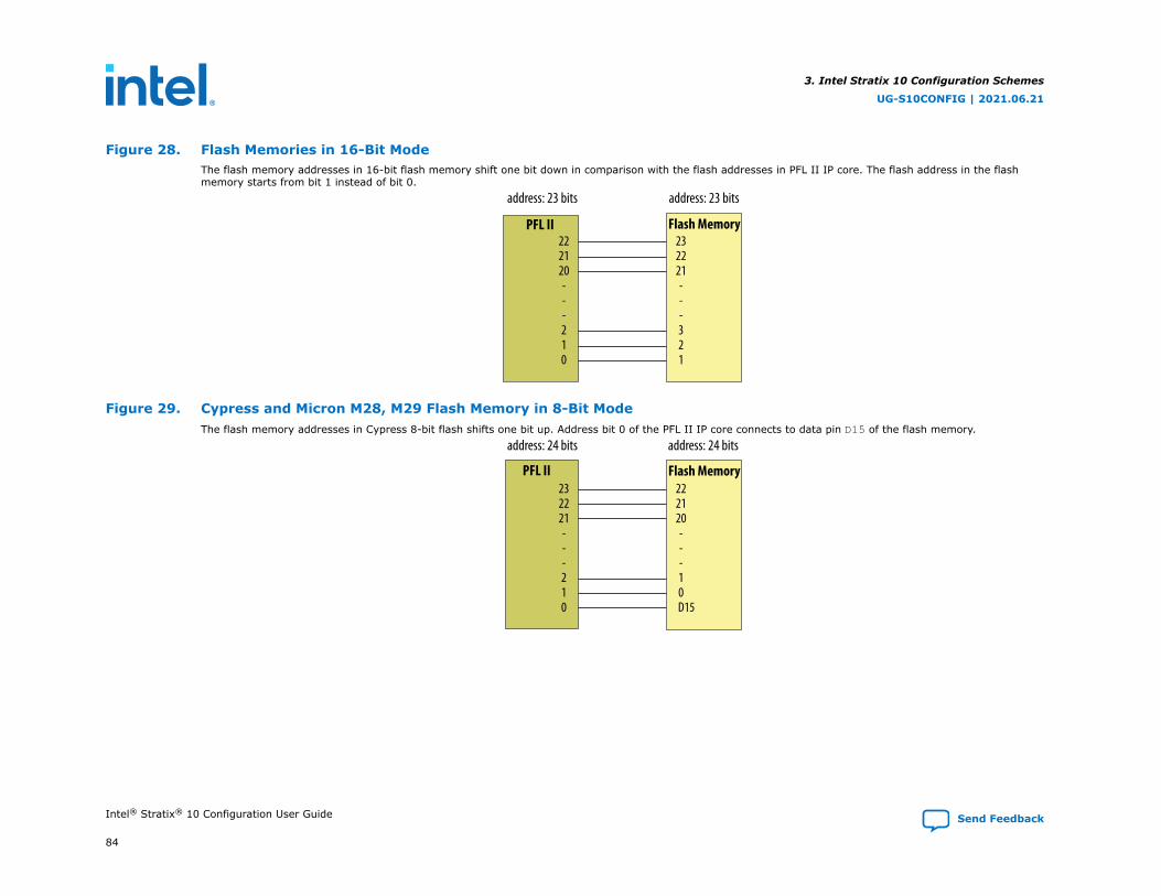
Figure 28. Flash Memories in 16-Bit ModeThe flash memory addresses in 16-bit flash memory shift one bit down in comparison with the flash addresses in PFL II IP core. The flash address in the flashmemory starts from bit 1 instead of bit 0.
222120---210
address: 23 bits
232221---321
address: 23 bits
PFL II Flash Memory
Figure 29. Cypress and Micron M28, M29 Flash Memory in 8-Bit ModeThe flash memory addresses in Cypress 8-bit flash shifts one bit up. Address bit 0 of the PFL II IP core connects to data pin D15 of the flash memory.
232221---210
address: 24 bits
222120---10
D15
address: 24 bits
PFL II Flash Memory
3. Intel Stratix 10 Configuration Schemes
UG-S10CONFIG | 2021.06.21
Intel® Stratix® 10 Configuration User Guide Send Feedback
84

Figure 30. Cypress and Micron M28, M29 Flash Memory in 16-Bit ModeThe address bit numbers in the PFL II IP core and the flash memory device are the same.
222120---210
address: 23 bits
222120---210
address: 23 bits
PFL II Flash Memory
3.1.7.3.3. Creating a Single PFL II IP for Programming and Configuration
Follow these steps to create a single PFL II IP instantiation for programming and configuration control:
1. In the IP Catalog locate the Parallel Flash Loader II Intel FPGA IP.
2. On the General tab for What operating mode will be used, select Flash Programming and FPGA Configuration.
3. In the same tab, for What is the targeted flash?, select CFI Parallel Flash.
4. Specify the parameters on the Flash Interface Settings tab:
a. Select 1 for a single flash device.
b. Select CFI 1 Gbit as the largest used flash device.
c. Select 16 bits for the flash interface data width.
5. Specify the parameters on the FPGA Configuration to match your design.
6. Compile and generate a .pof for the flash memory device. Ensure that you tri-state all unused I/O pins.
3.1.7.3.4. Creating Separate PFL II Functions
Follow these steps to create separate PFL II IP instantiations for programming and configuration control:
3. Intel Stratix 10 Configuration Schemes
UG-S10CONFIG | 2021.06.21
Send Feedback Intel® Stratix® 10 Configuration User Guide
85
1. In the IP Catalog locate the Parallel Flash Loader II Intel FPGA IP.
2. On the General tab for What operating mode will be used, select Flash Programming Only.
3. Intel recommends that you turn on the Set flash bus pins to tri-state when not in use.
4. Specify the parameters on the Flash Interface Settings and Flash Programming tabs to match your design.
5. Compile and generate a .pof for the flash memory device. Ensure that you tri-state all unused I/O pins.
6. To create a second PFL II instantiation for FPGA configuration, on the General tab, for What operating mode will beused, select FPGA Configuration.
7. Use this Flash Programming Only instance of the PFL II IP to write data to the flash device.
8. Whenever you must program the flash memory device, program the CPLD with the flash memory device .pof and updatethe flash memory device contents.
9. Reprogram the CPLD with the production design .pof that includes the configuration controller.
Note: By default, all unused pins are set to ground. When programming the configuration flash memory device throughthe host JTAG pins, you must tri-state the FPGA configuration pins common to the host and the configuration flashmemory device. You can use the pfl_flash_access_request and pfl_flash_access_granted signals of thePFL II block to tri-state the correct FPGA configuration pins.
3.1.7.4. Constraining the PFL II IP Core
You can specify many design constraints in Intel Quartus Prime project settings by editing the .sdc files.
3.1.7.4.1. PFL II IP Recommended Design Constraints to FPGA Avalon-ST Pins
Example 1. Create a pfl_clk clock and a generated AVST_CLK clock
Example below creates a pfl_clk clock running at 50 MHz, supplied by the clk_50m_sysmax input clock.
set pfl_clk_period 20.000create_clock -name {clk_50m_sysmax} -period $pfl_clk_period [get_ports {clk_50m_sysmax}]create_generated_clock -name AVST_CLK -source [get_ports {clk_50m_sysmax}] [get_ports {avst_clk}]
3. Intel Stratix 10 Configuration Schemes
UG-S10CONFIG | 2021.06.21
Intel® Stratix® 10 Configuration User Guide Send Feedback
86

Example 2. Set output delay for PFL II IP output pins
Example below sets the output delay for the AvST_DATA and AvST_VALID pins.
set avst_data_tracemax 0.250set avst_data_tracemin 0.000set avst_clk_tracemax 0.250set avst_clk_tracemin 0.000set fpga_Tsu 5.500set fpga_Th 0.000set fpga_out_max_dly [expr $avst_data_tracemax + $fpga_Tsu - $avst_clk_tracemin]set fpga_out_min_dly [expr $avst_data_tracemin - $fpga_Th - $avst_clk_tracemax]
set_output_delay -add_delay -max -clock [get_clocks {AVST_CLK}] $fpga_out_max_dly [get_ports {avst_d[*] avst_valid}]set_output_delay -add_delay -min -clock [get_clocks {AVST_CLK}] $fpga_out_min_dly [get_ports {avst_d[*] avst_valid}]
Example 3. Setting a false path
You can set the AVST_READY input pin to a false path since this pin is not synchronous to the AVST_CLK clock. The host mustsynchronize the AVST_READY signal to the AVST_CLK signal using a 2-stage register synchronizer.
set_false_path -from [get_ports {avst_ready}] -to *
3.1.7.4.2. PFL II IP Recommended Design Constraints for Using QSPI Flash
Example 4. Create a FLASH_CLK clock
Example below creates assigns QSPI flash clock pin (flash_dc1_ic0) to the flash clock.
create_generated_clock -name FLASH_CLK -source [get_ports {clk_50m_sysmax}] [get_ports {flash_dc1_io0}]
Example 5. Set output delay for PFL II IP output pins
Example below sets the output delay for the QSPI flash data and chip select pins.
#flash_dc1_io1/3/4/5 = QSPI flash data pins, #flash_dc1_io2 = QSPI flash chip select pinsset flash_data_tracemax 0.250set flash_data_tracemin 0.000set flash_clk_tracemax 0.250set flash_clk_tracemin 0.000set flash_Tsu 2.700set flash_Th 2.000set flash_out_max_dly [expr $flash_data_tracemax + $flash_Tsu - $flash_clk_tracemin]
3. Intel Stratix 10 Configuration Schemes
UG-S10CONFIG | 2021.06.21
Send Feedback Intel® Stratix® 10 Configuration User Guide
87

set flash_out_min_dly [expr $flash_data_tracemin - $flash_Th - $flash_clk_tracemax]
set_output_delay -add_delay -max -clock [get_clocks {FLASH_CLK}] $flash_out_max_dly [get_ports {flash_dc1_io1 flash_dc1_io3 flash_dc1_io4 flash_dc1_io5 flash_dc1_io2}]set_output_delay -add_delay -min -clock [get_clocks {FLASH_CLK}] $flash_out_min_dly [get_ports { flash_dc1_io1 flash_dc1_io3 flash_dc1_io4 flash_dc1_io5 flash_dc1_io2}]
Example 6. Set input delay for input pins
Example below sets the input delay for the QSPI flash data.
set flash_tco_max 7.000set flash_tco_min 1.000set in_max_dly [expr $flash_data_tracemax + $flash_tco_max + $flash_clk_tracemax]set in_min_dly [expr $flash_data_tracemin + $flash_tco_min + $flash_clk_tracemin]
set_input_delay -clock { FLASH_CLK } -max $in_max_dly [get_ports {flash_dc1_io1 flash_dc1_io3 flash_dc1_io4 flash_dc1_io5}]set_input_delay -clock { FLASH_CLK } -min $in_min_dly [get_ports {flash_dc1_io1 flash_dc1_io3 flash_dc1_io4 flash_dc1_io5}]
3.1.7.4.3. PFL II IP Recommended Design Constraints for using CFI Flash
Example 7. Create a FLASH_CLK clock
Example below assigns CFI flash clock pin (flash_clk) to the flash clock. You constrain the flash_clk pin only when usingburst mode.
create_generated_clock -name FLASH_CLK -source [get_ports {clk_50m_max5}] [get_ports {flash_clk}]
Example 8. Set output delay for output pins
Example below sets the output delay for CFI flash output pins.
set flash_data_tracemax 0.250set flash_data_tracemin 0.000set flash_clk_tracemax 0.250set flash_clk_tracemin 0.000set flash_Tsu 3.500set flash_Th 2.000set flash_out_max_dly [expr $flash_data_tracemax + $flash_Tsu - $flash_clk_tracemin]set flash_out_min_dly [expr $flash_data_tracemin - $flash_Th - $flash_clk_tracemax]
#Note: For normal mode, the clock is referred to input pfl_clk clock(clk_50m_max5) of PFL II IP. If burst mode is used, the clock is referred to flash clock of PFL II IP.
3. Intel Stratix 10 Configuration Schemes
UG-S10CONFIG | 2021.06.21
Intel® Stratix® 10 Configuration User Guide Send Feedback
88

set_output_delay -add_delay -max -clock [get_clocks {clk_50m_max5}] $flash_out_max_dly [get_ports {flash_nce[0] flash_nce[1] flash_noe flash_nwe flash_addr[*] flash_data[*]}]set_output_delay -add_delay -min -clock [get_clocks {clk_50m_max5}] $flash_out_min_dly [get_ports { flash_nce[0] flash_nce[1] flash_noe flash_nwe flash_addr[*] flash_data[*]}]#Only need to constraint flash_advn pin when using burst mode.set_output_delay -add_delay -max -clock [get_clocks { FLASH_CLK }] $flash_out_max_dly [get_ports {flash_nadv}]set_output_delay -add_delay -min -clock [get_clocks { FLASH_CLK }] $flash_out_min_dly [get_ports {flash_nadv}]
Example 9. Set input delay for input pins
Example below sets the input delay for CFI flash data.
# For Normal Modeset flash_noe_tracemax 0.250set flash_noe_tracemin 0.000set flash_tco_max 7.000set flash_tco_min 0.000set normal_in_max_dly [expr $flash_data_tracemax + $flash_tco_max + $ flash_noe_tracemax]set normal_in_min_dly [expr $flash_data_tracemin + $flash_tco_min + $ flash_noe_tracemin]
set_input_delay -clock { clk_50m_max5 } -max $normal_in_max_dly [get_ports {flash_data[*]}]set_input_delay -clock { clk_50m_max5 } -min $normal_in_min_dly [get_ports {flash_data[*]}]
# For Burst modeset flash_tco_max 5.500set flash_tco_min 2.000set burst_in_max_dly [expr $flash_data_tracemax + $flash_tco_max + $flash_clk_tracemax]set burst_in_min_dly [expr $flash_data_tracemin + $flash_tco_min + $flash_clk_tracemin]
set_input_delay -clock { FLASH_CLK } -max $burst_in_max_dly [get_ports {flash_data[*]}]set_input_delay -clock { FLASH_CLK } -min $burst_in_min_dly [get_ports {flash_data[*]}]
3.1.7.4.4. PFL II IP Recommended Constraints for Other Input Pins
Example 10. Set a false path for PFL II IP input pins
You can set the pfl_nreset input reset pin to a false path since this pin is asynchronous.
set_false_path -from [get_ports {pfl_nreset}] -to *
Example 11. Set input delay to PFL II IP input pins
Example below sets the input delay for the pfl_flash_access_granted pin.
3. Intel Stratix 10 Configuration Schemes
UG-S10CONFIG | 2021.06.21
Send Feedback Intel® Stratix® 10 Configuration User Guide
89
• You don't have to constraint the path when you use the device arbiter logic to control the pin,
• You don't have to constraint the path when not using the device arbiter logic or the external processor to control the pinand you loopback the pfl_flash_access_request signal to the pfl_flash_access_granted pin.
• You can constraint the path when a processor or an external device controls the pfl_flash_access_granted pin.
set_input_delay -clock {clk_50m_sysmax} -max [<pfl_flash_access_granted_tco_max> + <pfl_flash_access_granted_tracemax>] [get_ports {pfl_flash_access_granted}]set_input_delay -clock {clk_50m_sysmax} -min [<pfl_flash_access_granted_tco_min> + <pfl_flash_access_granted_tracemin>] [get_ports {pfl_flash_access_granted}]
Example 12. Set a false path for fpga_pgm[] input pin
You can set a false path to quasi-static signals such as reset and configuration signals (fpga_conf_done, fpga_nstatus)that are stable for a long periods of time.
set_false_path -from [get_ports {fpga_pgm[]}] -to *
Example 13. Set input delay to pfl_nreconfigure input pin
If you use the external component to drive this pin, you must set the input delay path to drive the pfl_nreconfigure pin.
set_input_delay -clock {clk_50m_sysmax} -max [<pfl_nreconfigure_tco_max> + <pfl_nreconfigure_tracemax>] [get_ports {pfl_nreconfigure}]set_input_delay -clock {clk_50m_sysmax} -min [<pfl_nreconfigure_tco_min> + <pfl_nreconfigure_tracemin>] [get_ports {pfl_nreconfigure}]
Example 14. Set input delay to pfl_reset_watchdog pin
If you use the external component to drive this pin, you must set the input delay path to drive the pfl_reset_watchdogpin.
set_input_delay -clock {clk_50m_sysmax} -max [$pfl_reset_watchdog_tco_max + $pfl_reset_watchdog_tracemax] [get_ports {pfl_nreconfigure}]set_input_delay -clock {clk_50m_sysmax} -min [$pfl_reset_watchdog_tco_min + $pfl_reset_watchdog_tracemin] [get_ports {pfl_nreconfigure}]
3. Intel Stratix 10 Configuration Schemes
UG-S10CONFIG | 2021.06.21
Intel® Stratix® 10 Configuration User Guide Send Feedback
90

3.1.7.4.5. PFL II IP Recommended Constraints for Other Output Pins
Example 15. Set output delay to PFL II IP output pins
Example below sets the output delay for the pfl_flash_access_request output pin.
• You don't have to constraint the path when this signal feeds arbiter logic or device tristate logic,
• You don't have to constraint the path when this signal feeds the pfl_flash_access_granted input pin while not usingthe device arbiter logic or the external processor.
• You can constraint the path when this signal feeds the processor or an external device controls.
set_output_delay -add_delay -clock [get_clocks { clk_50m_sysmax }] -max $flash_access_request_tracemax [get_ports {pfl_flash_access_request}]set_output_delay -add_delay -clock [get_clocks { clk_50m_sysmax }] -min $flash_access_request_tracemin [get_ports {pfl_flash_access_request}]
Example 16. Set output delay to flash_nreset output pin
The flash_nreset output pin is available in Burst mode only.
set_output_delay -add_delay -max -clock [get_clocks { FLASH_CLK }] $flash_out_max_dly [get_ports {flash_nreset}]set_output_delay -add_delay -min -clock [get_clocks { FLASH_CLK }] $flash_out_min_dly [get_ports {flash_nreset}]
Example 17. Set a false path for fpga_nconfig output pin
You can set the fpga_nconfig output pin to a false path since the nCONFIG is an asynchronous input pin..
set_false_path -from [get_ports {fpga_nconfig}] -to *
Example 18. Set output delay to pfl_watchdog_error output pin
• You don't have to constraint the path when the signal feeds the internal logic.
• You can constraint the path when signal feeds an external host.
set_output_delay -add_delay -clock [get_clocks { clk_50m_sysmax }] -max $pfl_watchdog_error_tracemax [get_ports {pfl_watchdog_error}]set_output_delay -add_delay -clock [get_clocks { clk_50m_sysmax }] -min $pfl_watchdog_error_tracemin [get_ports {pfl_watchdog_error}]
3. Intel Stratix 10 Configuration Schemes
UG-S10CONFIG | 2021.06.21
Send Feedback Intel® Stratix® 10 Configuration User Guide
91

3.1.7.5. Using the PFL II IP Core
3.1.7.5.1. Converting .sof to .pof File
You can use the Programming File Generator to convert the .sof file to a .pof. The Programming File Generatoroptions change dynamically according to your device and configuration mode selection.
View the video guide and complete the following steps to convert .sof file to a .pof:
1. Click File ➤ Programming File Generator.
2. For Device family select Intel Stratix 10.
3. For Configuration mode select Avalon-ST configuration scheme that you plan to use.
4. For Output directory, click Browse to select your output file directory.
5. For Name specify a name for your output file.
6. On the Output Files tab, enable the checkbox for generation of the file or files you want to generate.
7. Specify the Output directory and Name for the file or files you generate.
3. Intel Stratix 10 Configuration Schemes
UG-S10CONFIG | 2021.06.21
Intel® Stratix® 10 Configuration User Guide Send Feedback
92
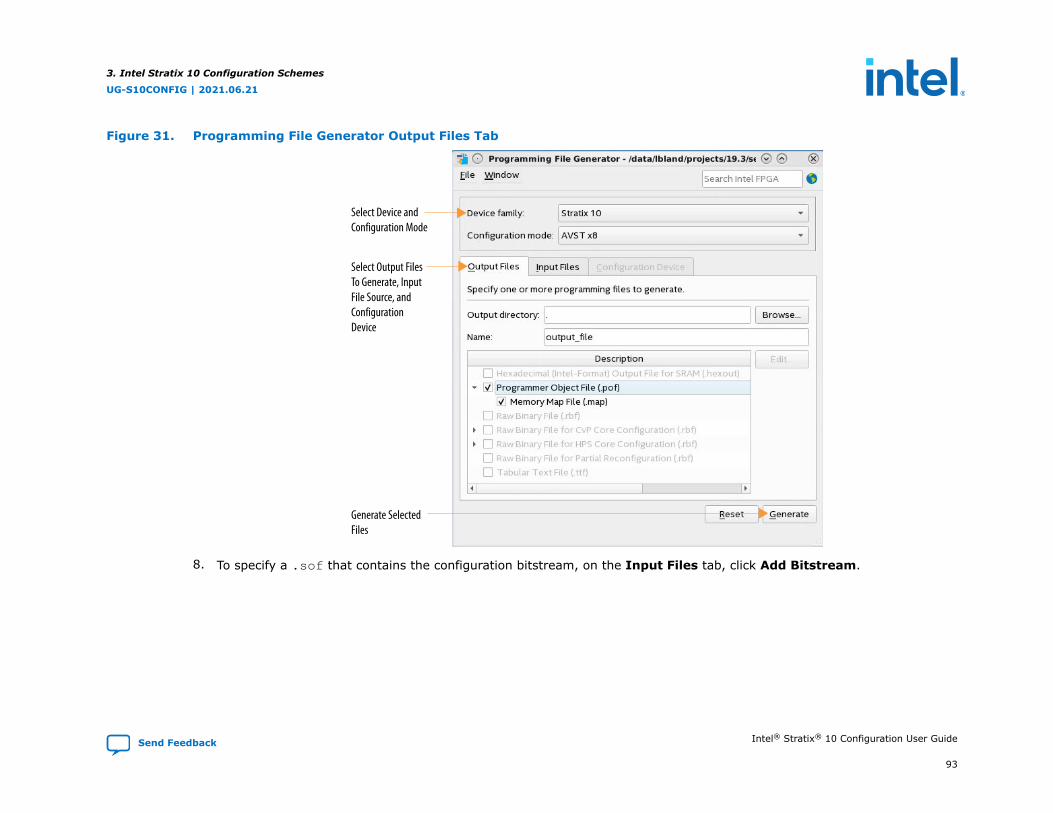
Figure 31. Programming File Generator Output Files Tab
Select Device andConfiguration Mode
Select Output FilesTo Generate, Input File Source, and Configuration Device
Generate SelectedFiles
8. To specify a .sof that contains the configuration bitstream, on the Input Files tab, click Add Bitstream.
3. Intel Stratix 10 Configuration Schemes
UG-S10CONFIG | 2021.06.21
Send Feedback Intel® Stratix® 10 Configuration User Guide
93

Figure 32. Input Files Tab
Input Files
9. To include raw data, click Add Raw Data and specify a Hexadecimal (Intel-Format) Output File (.hex) or binary (.bin)file. This step is optional.
10. On the Configuration Device tab, click Add device. The Add Device dialog box appears. Select your flash device fromthe drop-down list of available parallel flash devices.
11. Click OPTIONS and then Edit. In the Edit Partition dialog box specify the Start address of the Options in flashmemory. This address must match the address you specify for What is the byte address of the option bits, in hex?when specifying the PFL II IP parameters. Ensure that the option bits sector does not overlap with the configuration datapages and that the start address is on an 8 KB boundary.
3. Intel Stratix 10 Configuration Schemes
UG-S10CONFIG | 2021.06.21
Intel® Stratix® 10 Configuration User Guide Send Feedback
94
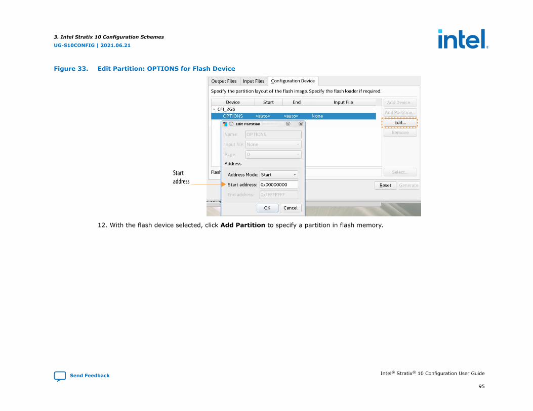
Figure 33. Edit Partition: OPTIONS for Flash Device
Startaddress
12. With the flash device selected, click Add Partition to specify a partition in flash memory.
3. Intel Stratix 10 Configuration Schemes
UG-S10CONFIG | 2021.06.21
Send Feedback Intel® Stratix® 10 Configuration User Guide
95

Figure 34. Add Flash Device and Partition
ConfigurationDevice
a. For Name select a Partition name.
b. For Input File specify the .sof.
c. From the Page dropdown list, select the page to write this .sof.
d. For Address mode select the addressing mode to use.
The following modes are available:
3. Intel Stratix 10 Configuration Schemes
UG-S10CONFIG | 2021.06.21
Intel® Stratix® 10 Configuration User Guide Send Feedback
96
• Auto— For the tool to automatically allocates a block in the flash device to store the data.
• Block—To specify the start and end address of the flash partition.
• Start—To specify the start address of the partition. The tool assigns the end address of the partition based on theinput data size.
e. For Block and Start options, specify the address information.
Related Information
Converting .sof to .pof file in the Parallel Flash Loader IIVideo showing how to convert a .sof file to a .pof file for Parallel Flash Loader II IP to configure the FPGA usingAvalon-STconfiguration mode.
3. Intel Stratix 10 Configuration Schemes
UG-S10CONFIG | 2021.06.21
Send Feedback Intel® Stratix® 10 Configuration User Guide
97
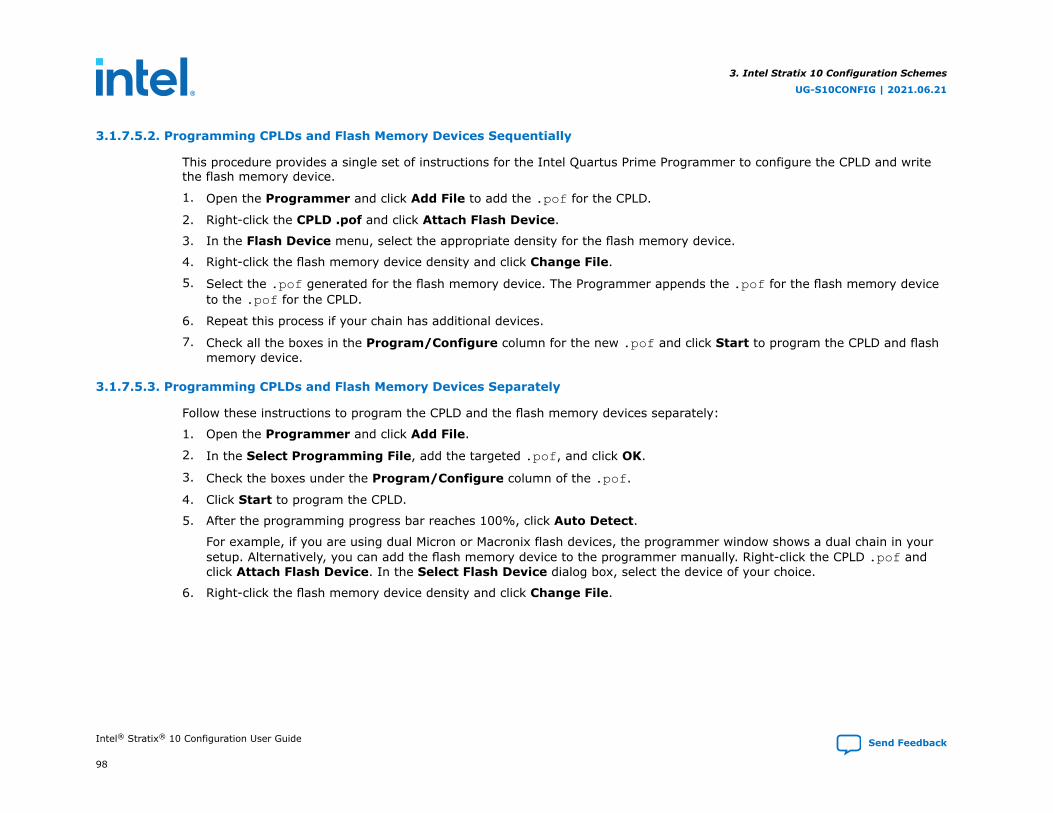
3.1.7.5.2. Programming CPLDs and Flash Memory Devices Sequentially
This procedure provides a single set of instructions for the Intel Quartus Prime Programmer to configure the CPLD and writethe flash memory device.
1. Open the Programmer and click Add File to add the .pof for the CPLD.
2. Right-click the CPLD .pof and click Attach Flash Device.
3. In the Flash Device menu, select the appropriate density for the flash memory device.
4. Right-click the flash memory device density and click Change File.
5. Select the .pof generated for the flash memory device. The Programmer appends the .pof for the flash memory deviceto the .pof for the CPLD.
6. Repeat this process if your chain has additional devices.
7. Check all the boxes in the Program/Configure column for the new .pof and click Start to program the CPLD and flashmemory device.
3.1.7.5.3. Programming CPLDs and Flash Memory Devices Separately
Follow these instructions to program the CPLD and the flash memory devices separately:
1. Open the Programmer and click Add File.
2. In the Select Programming File, add the targeted .pof, and click OK.
3. Check the boxes under the Program/Configure column of the .pof.
4. Click Start to program the CPLD.
5. After the programming progress bar reaches 100%, click Auto Detect.
For example, if you are using dual Micron or Macronix flash devices, the programmer window shows a dual chain in yoursetup. Alternatively, you can add the flash memory device to the programmer manually. Right-click the CPLD .pof andclick Attach Flash Device. In the Select Flash Device dialog box, select the device of your choice.
6. Right-click the flash memory device density and click Change File.
3. Intel Stratix 10 Configuration Schemes
UG-S10CONFIG | 2021.06.21
Intel® Stratix® 10 Configuration User Guide Send Feedback
98

Note: For designs with more than one flash device, you must select the density that is equivalent to the sum of thedensities of all devices. For example, if the design includes two 512-Mb CFI flash memory devices, select CFI 1 Gbit.
7. Select the .pof generated for the flash memory device. The Programmer attaches the .pof for the flash memory deviceto the .pof of the CPLD.
8. Check the boxes under the Program/Configure column for the added .pof and click Start to program the flashmemory devices.
Note: If your design includes the PFL II IP the Programmer allows you to program, verify, erase, blank-check, or examinethe configuration data page, the user data page, and the option bits sector separately. The programmer erases theflash memory device if you select the .pof of the flash memory device before programming. To prevent theProgrammer from erasing other sectors in the flash memory device, select only the pages, .hex data, and optionbits.
3.1.7.5.4. Defining New CFI Flash Memory Device
The PFL II IP core supports Intel- and AMD-compatible flash memory devices. In addition to the supported flash memorydevices, you can define the new Intel- or AMD-compatible CFI flash memory device in the PFL II-supported flash databaseusing the Define New CFI Flash Device function.
To add a new CFI flash memory device to the database or update a CFI flash memory in the database, follow these steps:
1. In the Programmer window, on the Edit menu, select Define New CFI Flash Device. The following table lists the threefunctions available in the Define CFI Flash Device window.
Table 26. Functions of the Define CFI Flash Device Feature
Function Description
New Add a new Intel- or AMD-compatible CFI flash memory device into the PFL II-supported flash database.
Edit Edit the parameters of the newly added Intel- or AMD-compatible CFI flash memory device in the PFL II-supported flash database.
Remove Remove the newly added Intel- or AMD-compatible CFI flash memory device from the PFL II-supported flash database.
2. To add a new CFI flash memory device or edit the parameters of the newly added CFI flash memory device, select New orEdit. The New CFI Flash Device dialog box appears.
3. In the New CFI Flash Device dialog box, specify or update the parameters of the new flash memory device. You canobtain the values for these parameters from the data sheet of the flash memory device manufacturer.
3. Intel Stratix 10 Configuration Schemes
UG-S10CONFIG | 2021.06.21
Send Feedback Intel® Stratix® 10 Configuration User Guide
99
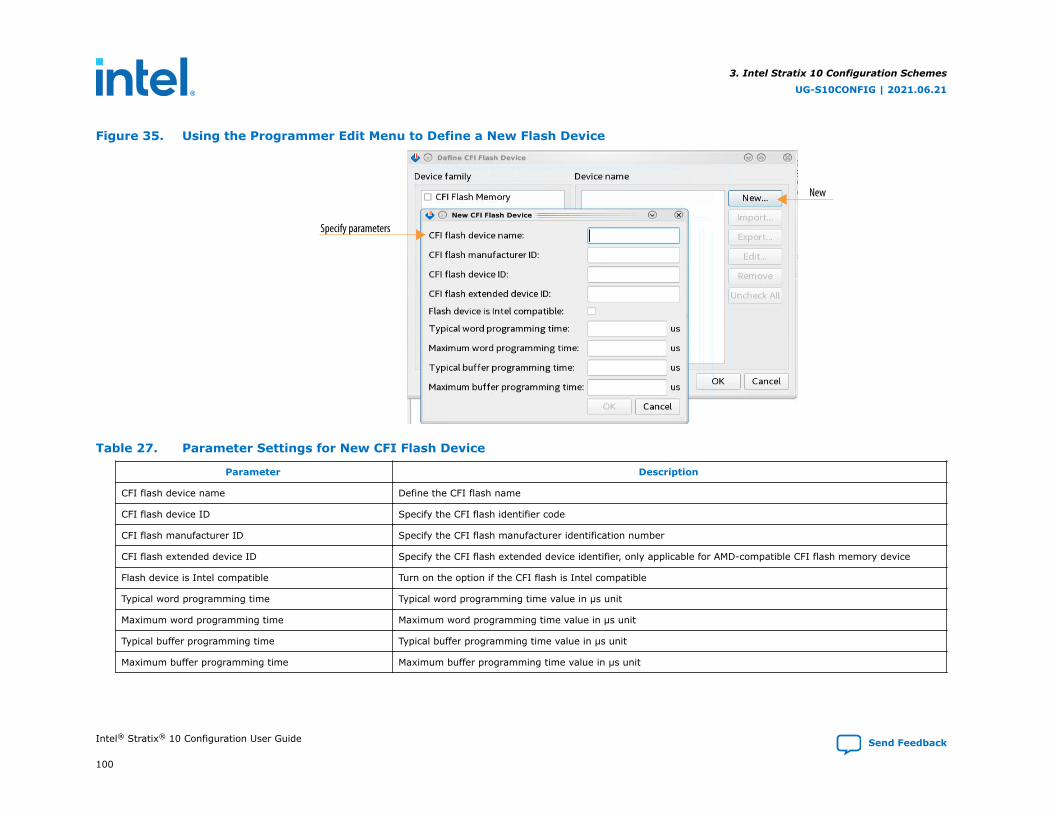
Figure 35. Using the Programmer Edit Menu to Define a New Flash Device
New
Specify parameters
Table 27. Parameter Settings for New CFI Flash Device
Parameter Description
CFI flash device name Define the CFI flash name
CFI flash device ID Specify the CFI flash identifier code
CFI flash manufacturer ID Specify the CFI flash manufacturer identification number
CFI flash extended device ID Specify the CFI flash extended device identifier, only applicable for AMD-compatible CFI flash memory device
Flash device is Intel compatible Turn on the option if the CFI flash is Intel compatible
Typical word programming time Typical word programming time value in µs unit
Maximum word programming time Maximum word programming time value in µs unit
Typical buffer programming time Typical buffer programming time value in µs unit
Maximum buffer programming time Maximum buffer programming time value in µs unit
3. Intel Stratix 10 Configuration Schemes
UG-S10CONFIG | 2021.06.21
Intel® Stratix® 10 Configuration User Guide Send Feedback
100
Note: You must specify either the word programming time parameters, buffer programming time parameters, or both. Donot leave both programming time parameters with the default value of zero.
4. Click OK to save the parameter settings.
5. After you add, update, or remove the new CFI flash memory device, click OK.
The Windows registry stores user flash information. Consequently, you must have system administrator privileges to store theparameters in the Define New CFI Flash Device window in the Intel Quartus Prime Pro Edition Programmer.
3.2. AS Configuration
In AS configuration schemes, the SDM block in the Intel Stratix 10 device controls the configuration process and interfaces.The serial flash configuration device stores the configuration data. During AS Configuration, the SDM first powers on with theboot ROM. Then, the SDM loads the initial configuration firmware from AS x4 flash. After the configuration firmware loads,this firmware controls the remainder of the configuration process, including I/O configuration and FPGA core configuration.Designs including an HPS, can use the HPS to access serial flash memory after the initial configuration.
Note: The serial flash configuration device must be fully powered up at the same time or before ramping up VCCIO_SDM of the IntelStratix 10 device. For more information about the power sequence, refer to the Intel Stratix 10 Power Management UserGuide.
Important: Do not reset the quad SPI flash when used as the configuration device and data storage device with FPGA. Resetting the quadSPI flash during the FPGA configuration and reconfiguration, or in the QSPI's READ/WRITE/ERASE operations, causesundefined behavior for quad SPI flash and the FPGA. To recover from the unresponsive behavior, you must power cycle yourdevice. To reset the quad SPI flash via the external host, you must first complete the FPGA configuration and reconfiguration,or a quad SPI operation, and only then toggle the reset. The quad SPI operation is complete when the exclusive access to thequad SPI flash is closed by issuing the QSPI_CLOSE command via the Mailbox Client Intel FPGA IP or CLOSE command viathe Serial Flash Mailbox Client Intel FPGA IP.
The AS configuration scheme supports AS x4 (4-bit data width) mode only.
Table 28. Intel Stratix 10 Configuration Data Width, Clock Rates, and Data Rates
Mode Data Width (bits) Max Clock Rate Max Data Rate MSEL[2:0]
Active Active Serial (AS) 4 125 MHz 500 MbpsFast mode - 001Normal mode - 011
3. Intel Stratix 10 Configuration Schemes
UG-S10CONFIG | 2021.06.21
Send Feedback Intel® Stratix® 10 Configuration User Guide
101

Table 29. Required Configuration Signals for the AS Configuration Scheme
Configuration Function Pin Type Direction Powered by
nSTATUS SDM I/O Output VCCIO_SDM
nCONFIG SDM I/O Input VCCIO_SDM
MSEL[2:0] SDM I/O Input VCCIO_SDM
CONF_DONE SDM I/O Output VCCIO_SDM
AS_nCSO[3:0] SDM I/O Output VCCIO_SDM
AS_DATA[3:0] SDM I/O Bidirectional VCCIO_SDM
AS_CLK SDM I/O Output VCCIO_SDM
Note: Although the CONF_DONE and INIT_DONE configuration signals are not required, Intel recommends that you use thesesignals. The SDM drives the CONF_DONE signal high after successfully receiving full bitstream. The SDM drives theINIT_DONE signal high to indicate the device is fully in user mode.These signals are important when debugging configuration.
MSEL Pin Function for the AS x4 Configuration Scheme
The SDM samples the MSEL pins immediately after power-on in the SDM Start state. After the SDM samples the MSEL pins,the MSEL pins become active-low chips selects. For AS x4 designs using one flash device, AS_nCSOO asserts low when theSDM starts to communicate with the QSPI flash. The remaining chip select pins, AS_nCSO1 - AS_nCSO3 deassert high.
Note: MSEL[0] and AS_nCSOO pins share the same SDM I/O. Refer to Table 6 on page 30 for more details.
Related Information
• Can I use 3rd party QSPI flash devices for Active Serial configuration of Intel Stratix 10 devices?
• Device Configuration Pins for Optional Configuration Signals on page 32
• SDM Pin Mapping on page 29
• AS Configuration Timing in Intel Stratix 10 DevicesFor timing parameter minimum, typical, and maximum values.
• Intel Stratix 10 Power Management User Guide
3. Intel Stratix 10 Configuration Schemes
UG-S10CONFIG | 2021.06.21
Intel® Stratix® 10 Configuration User Guide Send Feedback
102

3.2.1. AS Configuration Scheme Hardware Components and File Types
You use the following components to implement the AS configuration scheme:
• Quad SPI flash memory
• The Intel FPGA Download Cable II to connect the Intel Quartus Prime Programmer to the PCB.
For PCIe designs including the Configuration via Protocol (CvP), Intel recommends that you use Micron QSPI flash memory.When using the Micron QSPI flash memory, the boot ROM uses the AS x4 mode to load the initial configuration firmwarefaster to meet the PCIe wake-up time for host enumeration.
When using other flash memory types for PCIe designs, the boot ROM reads the firmware using AS x1 mode. Intelrecommends asserting the PERST# signal low for a minimum of 200 ms counting from the device exiting the power-on reset(POR) state. This ensures the PCIe endpoint enters the link training state prior to the PERST# signal deasserts.
The following block diagram illustrates the components and design flow using the AS configuration scheme.
3. Intel Stratix 10 Configuration Schemes
UG-S10CONFIG | 2021.06.21
Send Feedback Intel® Stratix® 10 Configuration User Guide
103
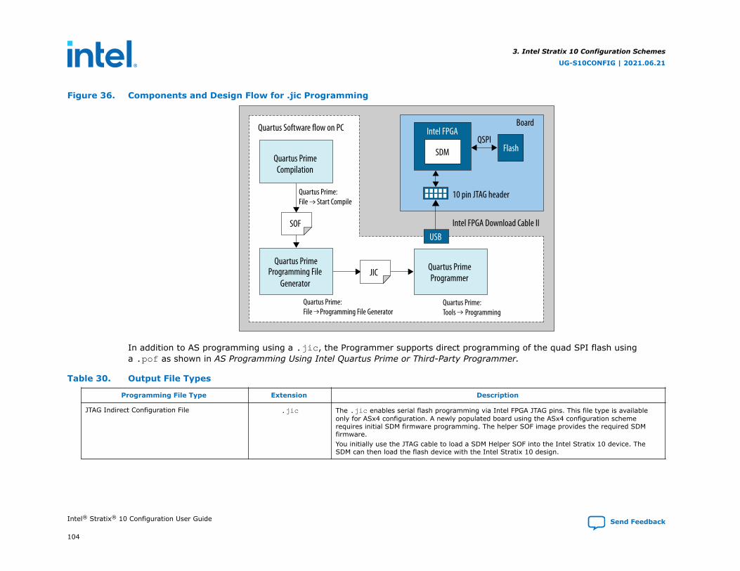
Figure 36. Components and Design Flow for .jic Programming
Quartus Software flow on PC
Quartus PrimeProgrammer
10 pin JTAG header
Intel FPGA Download Cable II
QSPIIntel FPGA
SDM Flash
Board
Quartus Prime: File Programming File Generator
Quartus Prime: File Start Compile
Quartus Prime: Tools Programming
Quartus PrimeProgramming File
Generator
Quartus PrimeCompilation
USBSOF
JIC
In addition to AS programming using a .jic, the Programmer supports direct programming of the quad SPI flash usinga .pof as shown in AS Programming Using Intel Quartus Prime or Third-Party Programmer.
Table 30. Output File Types
Programming File Type Extension Description
JTAG Indirect Configuration File .jic The .jic enables serial flash programming via Intel FPGA JTAG pins. This file type is availableonly for ASx4 configuration. A newly populated board using the ASx4 configuration schemerequires initial SDM firmware programming. The helper SOF image provides the required SDMfirmware.You initially use the JTAG cable to load a SDM Helper SOF into the Intel Stratix 10 device. TheSDM can then load the flash device with the Intel Stratix 10 design.
3. Intel Stratix 10 Configuration Schemes
UG-S10CONFIG | 2021.06.21
Intel® Stratix® 10 Configuration User Guide Send Feedback
104

Related Information
• Can I use 3rd party QSPI flash devices for Active Serial configuration of Intel Stratix 10 devices?
• Programming Serial Flash Devices using the AS Interface on page 111
3.2.2. AS Single-Device Configuration
Refer to the Intel Stratix 10 Device Family Pin Connection Guidelines for additional information about individual pin usage andrequirements.
3. Intel Stratix 10 Configuration Schemes
UG-S10CONFIG | 2021.06.21
Send Feedback Intel® Stratix® 10 Configuration User Guide
105

Figure 37. Connections for AS x4 Single-Device Configuration
Pin 1RUP RDN
RUP
TCKTDOTMSOPENTDI
GNDVCCIO_SDMOPENOPENGND GND
VCCIO_SDM
Intel FPGAnCONFIGnSTATUSCONF_DONEINIT_DONEOSC_CLK_1
MSEL[2:0]
AS_DATA[3:0]AS x4 Flash Memory
AS_CLKAS_nCSO[0]
Download cable 10 pin male header
DATA[3:0] DCLK
nCS0
ConfigurationControl Signals
OptionalMonitoring
10kΩ
Optional
ConfigurationData Signals
To JTAGHeader or
JTAG Chain
MSEL
VCCIO_SDM
3
4
TCKTDO
TDITMS
JTAGConfiguration
Pins
FPGAImage (.rpd)
3M Part number : 2510-6002UB
10kΩ
Related Information
• MSEL Settings on page 31
• Intel Stratix 10 Device Family Pin Connection Guidelines
3. Intel Stratix 10 Configuration Schemes
UG-S10CONFIG | 2021.06.21
Intel® Stratix® 10 Configuration User Guide Send Feedback
106
3.2.3. AS Using Multiple Serial Flash Devices
Intel Stratix 10 devices support one AS x4 flash memory device for AS configuration and up to three AS x4 flash memories foruse with HPS data storage. The MSEL pins operate as MSEL only during POR state. After the FPGA device enters user mode,you can repurpose the MSEL pins as chip select pins. You must to ensure appropriate chip select pin connections to theconfiguration AS x4 flash memory and the HPS AS x4 flash memory. Each flash device has a dedicated AS_nCSO pin butshares other pins.
Refer to the Intel Stratix 10 Device Family Pin Connection Guidelines for additional information about individual pin usage andrequirements.
3. Intel Stratix 10 Configuration Schemes
UG-S10CONFIG | 2021.06.21
Send Feedback Intel® Stratix® 10 Configuration User Guide
107

Figure 38. Connections for AS Configuration with Multiple Serial Flash Devices
Pin 1RUP RDN
RUP
TCKTDOTMSOPENTDI
GNDVCCIO_SDMOPENOPENGND GND
VCCIO_SDM
Intel FPGAnCONFIGnSTATUSCONF_DONEINIT_DONEOSC_CLK_1
MSEL[2:0]
DATA[3:0]
Config AS x4 Memory
CLKnCS0[0]
nCS0[1]nCS0[2]nCS0[3]
Download cable 10 pin male header (JTAG mode)
DATA[3:0] DCLK
CS
ConfigurationControl Signals
ConfigurationData Signals
OptionalMonitoring
10kΩ
Optional
HPS Data Signals
MSEL
VCCIO_SDM
3
4
To JTAG Headeror JTAG Chain
TCKTDO
TDITMS
JTAGConfiguration Pins
FPGAImage (.rpd)
HPS AS x4 MemoryDATA[3:0]
DCLK
CSHPS Data
3M Part number : 2510-6002UB
10kΩ
The following table shows the maximum supported AS_CLK frequency for a range of capacitance loading values when usingmultiple flash devices. The maximum AS_CLK frequency also depends on whether you use the OSC_CLK_1 or internaloscillator as the clock source.
3. Intel Stratix 10 Configuration Schemes
UG-S10CONFIG | 2021.06.21
Intel® Stratix® 10 Configuration User Guide Send Feedback
108
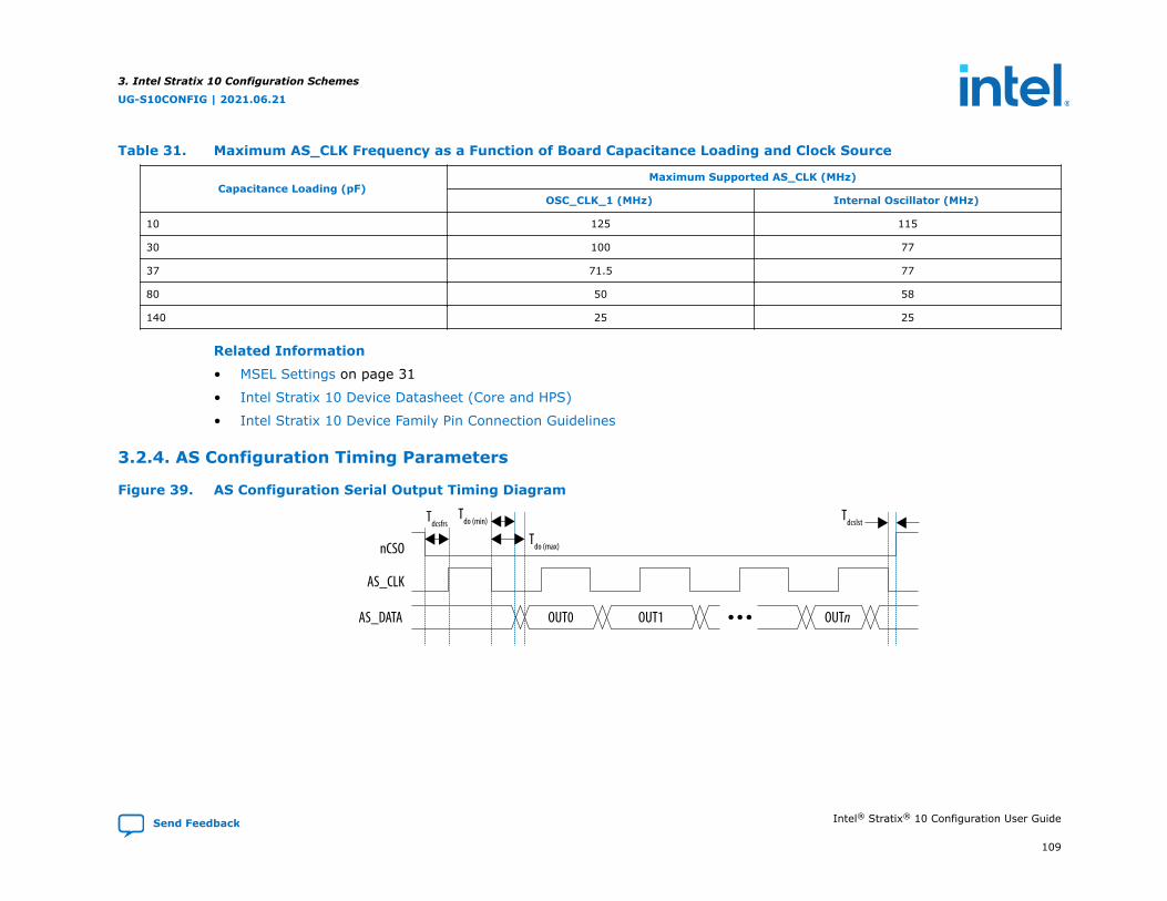
Table 31. Maximum AS_CLK Frequency as a Function of Board Capacitance Loading and Clock Source
Capacitance Loading (pF)Maximum Supported AS_CLK (MHz)
OSC_CLK_1 (MHz) Internal Oscillator (MHz)
10 125 115
30 100 77
37 71.5 77
80 50 58
140 25 25
Related Information
• MSEL Settings on page 31
• Intel Stratix 10 Device Datasheet (Core and HPS)
• Intel Stratix 10 Device Family Pin Connection Guidelines
3.2.4. AS Configuration Timing Parameters
Figure 39. AS Configuration Serial Output Timing Diagram
nCSO
AS_CLK
AS_DATA OUT0 OUT1 OUTn
TdcslstTdcsfrs
Tdo (max)
Tdo (min)
3. Intel Stratix 10 Configuration Schemes
UG-S10CONFIG | 2021.06.21
Send Feedback Intel® Stratix® 10 Configuration User Guide
109
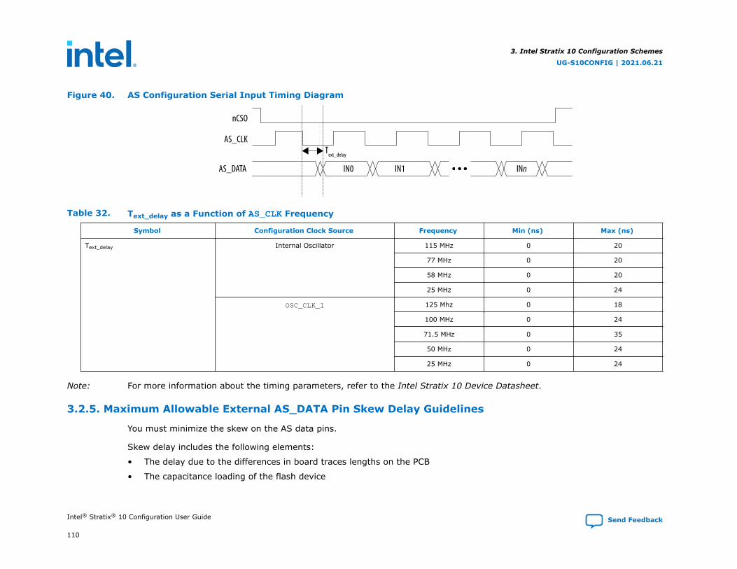
Figure 40. AS Configuration Serial Input Timing Diagram
nCSO
AS_CLK
AS_DATA IN0 IN1 INn
Text_delay
Table 32. Text_delay as a Function of AS_CLK Frequency
Symbol Configuration Clock Source Frequency Min (ns) Max (ns)
Text_delay Internal Oscillator 115 MHz 0 20
77 MHz 0 20
58 MHz 0 20
25 MHz 0 24
OSC_CLK_1 125 Mhz 0 18
100 MHz 0 24
71.5 MHz 0 35
50 MHz 0 24
25 MHz 0 24
Note: For more information about the timing parameters, refer to the Intel Stratix 10 Device Datasheet.
3.2.5. Maximum Allowable External AS_DATA Pin Skew Delay Guidelines
You must minimize the skew on the AS data pins.
Skew delay includes the following elements:
• The delay due to the differences in board traces lengths on the PCB
• The capacitance loading of the flash device
3. Intel Stratix 10 Configuration Schemes
UG-S10CONFIG | 2021.06.21
Intel® Stratix® 10 Configuration User Guide Send Feedback
110

The table below lists the maximum allowable skew delay depending on the AS_CLK frequency. Intel recommends that you toperform IBIS simulations to ensure that the skew delay does not exceed the maximum delay specified in this table.
Table 33. Maximum Skew for AS Data Pins in Nanoseconds (ns)
Symbol Description Frequency Min Typical Max
Text_skew Skew delay for AS_DATA for the AS_CLK frequency specified
125 MHz — — 4.00
115 MHz — — 4.20
100 MHz — — 5.0
<100 MHz — — 5.0
3.2.6. Programming Serial Flash Devices
You can program serial flash devices in-system using the Intel FPGA Download Cable II or Intel FPGA Ethernet Cable.
You have the following two in-system programming options:
• Active Serial
• JTAG
3.2.6.1. Programming Serial Flash Devices using the AS Interface
When you select AS programming the Intel Quartus Prime software or any supported third-party software programs theconfiguration data directly into the serial flash device.
You must set MSEL to JTAG. When MSEL is set to JTAG, the SDM tristates the following AS pins: AS_CLK, AS_DATA0-AS_DATA3, and AS_nCSO0-AS_nCSO3. The Intel Quartus Prime Programmer programs the flash memory devices via the ASheader. If you are using the Generic Serial Flash Interface Intel FPGA IP to write the flash memory the flash device must beconnected to GPIO to access the flash device.
Attention: When you power up the Intel Stratix 10 device with an empty serial flash device and use the AS interface to programthe .rpd file into this serial flash device, you must power cycle the Intel Stratix 10 device to configure the device from theflash successfully.
3. Intel Stratix 10 Configuration Schemes
UG-S10CONFIG | 2021.06.21
Send Feedback Intel® Stratix® 10 Configuration User Guide
111
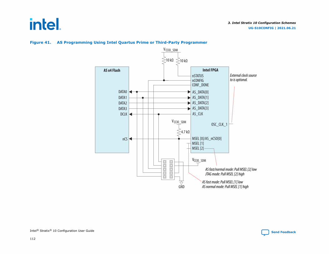
Figure 41. AS Programming Using Intel Quartus Prime or Third-Party Programmer
AS_DATA[0]
AS x4 Flash Intel FPGA
10 kΩ
nSTATUSnCONFIGCONF_DONE
OSC_CLK_1
DATA0DATA1DATA2DATA3
DCLK
nCS
AS_DATA[1]AS_DATA[2]AS_DATA[3]AS_CLK
4.7 kΩ
VCCIO_SDM
GND
VCCIO_SDM
VCCIO_SDM
10 kΩ
MSEL [0]/AS_nCSO[0]MSEL [1]MSEL [2]
AS fast mode: Pull MSEL [1] lowAS normal mode: Pull MSEL [1] high
AS fast/normal mode: Pull MSEL [2] lowJTAG mode: Pull MSEL [2] high
External clock sourceto is optional.
3. Intel Stratix 10 Configuration Schemes
UG-S10CONFIG | 2021.06.21
Intel® Stratix® 10 Configuration User Guide Send Feedback
112
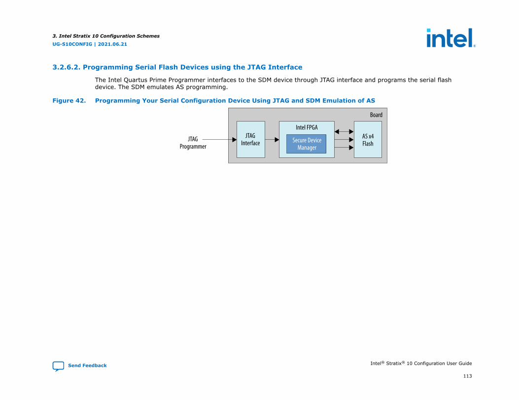
3.2.6.2. Programming Serial Flash Devices using the JTAG Interface
The Intel Quartus Prime Programmer interfaces to the SDM device through JTAG interface and programs the serial flashdevice. The SDM emulates AS programming.
Figure 42. Programming Your Serial Configuration Device Using JTAG and SDM Emulation of AS
Intel FPGA
Board
Secure DeviceManager
AS x4Flash
JTAGInterfaceJTAG
Programmer
3. Intel Stratix 10 Configuration Schemes
UG-S10CONFIG | 2021.06.21
Send Feedback Intel® Stratix® 10 Configuration User Guide
113
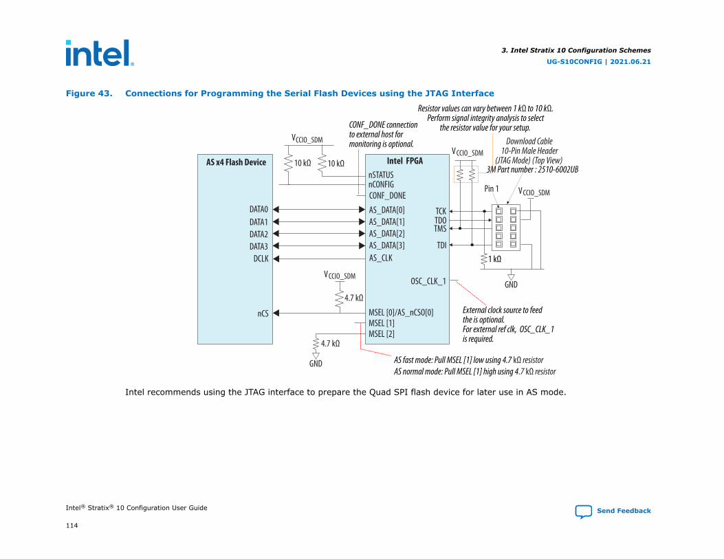
Figure 43. Connections for Programming the Serial Flash Devices using the JTAG Interface
Download Cable10-Pin Male Header
(JTAG Mode) (Top View)
TDI
TMSTDOTCK
Pin 1
1 kΩ
Resistor values can vary between 1 kΩ to 10 kΩ.Perform signal integrity analysis to select
the resistor value for your setup.
AS_DATA[0]
AS x4 Flash Device Intel FPGAnSTATUSnCONFIGCONF_DONE
OSC_CLK_1
DATA0DATA1DATA2DATA3
DCLK
nCS
AS_DATA[1]AS_DATA[2]AS_DATA[3]AS_CLK
4.7 kΩ
GND
GND
VCCIO_SDM
VCCIO_SDM
10 kΩ
VCCIO_SDM
10 kΩ
4.7 kΩ
VCCIO_SDM
MSEL [0]/AS_nCSO[0]MSEL [1]MSEL [2]
AS fast mode: Pull MSEL [1] low using 4.7 kΩ resistor AS normal mode: Pull MSEL [1] high using 4.7 kΩ resistor
External clock source to feedthe is optional.For external ref clk, OSC_CLK_1is required.
CONF_DONE connectionto external host formonitoring is optional.
3M Part number : 2510-6002UB
Intel recommends using the JTAG interface to prepare the Quad SPI flash device for later use in AS mode.
3. Intel Stratix 10 Configuration Schemes
UG-S10CONFIG | 2021.06.21
Intel® Stratix® 10 Configuration User Guide Send Feedback
114

This configuration scheme includes the following steps:
1. In the Intel Quartus Prime Programmer, select the JTAG programming mode and initiate programming by clicking Start.
2. The Programmer drives .jic configuration data to the board using the JTAG header connection.
3. The programmer first configures the SDM with configuration firmware. Then, the SDM drives configuration data from theprogrammer to the AS x4 flash device using SDM_IOs.
4. To use the Intel Stratix 10 device in AS mode after successful programming of the flash device, set the MSEL pins toeither AS fast or AS normal mode and power cycle the device.
The Intel Quartus Prime Programmer interfaces to the SDM device through JTAG interface and programs the serial flashdevice.
3.2.7. Serial Flash Memory Layout
Serial flash devices store the configuration data in sections.
The following diagram illustrates sections of a non-HPS Intel Stratix 10 configuration data mapping in a serial flash device.Refer to Intel Stratix 10 SoC FPGA Bitstream Sections of the HPS Technical Reference Manual for more information about flashmemory layout for HPS devices.
Figure 44. Serial Flash Memory Layout Diagram
Firmware sectionis static and
Quartus Primeversion dependent.
32’d256k
Start Address 32’d0
32’d512k
32’d768k
32’d1024k
End Address(Design dependent)
Dynamic Section (I/O Configuration)
Dynamic Section ( FPGA Core Configuration)
Firmware Section
Firmware Section
Firmware Section
Firmware Section
3. Intel Stratix 10 Configuration Schemes
UG-S10CONFIG | 2021.06.21
Send Feedback Intel® Stratix® 10 Configuration User Guide
115

If you use a third-party programmer to program an .rpd, ensure that the configuration data is stored starting from address 0of the serial flash device. If you use .jic or .pof files, the Intel Stratix 10 Programmer automatically programs theconfiguration data starting from address 0 of the serial flash device.
Intel currently support the following listed Supported Flash Devices for Intel Stratix 10
Related Information
Intel Stratix 10 SoC FPGA Bitstream Sections
3.2.7.1. Understanding Quad SPI Flash Byte-Addressing
At power-on the SDM operates from boot ROM. The SDM loads configuration firmware from Quad SPI flash using 3-byteaddressing. Once loaded, if the flash size is 256 Mb or larger, the SDM configures the Quad SPI flash to operate in 4-byteaddressing mode and continues to load the rest of the bitstream until configuration completes.
Intel Stratix 10 devices support the following third-party flash devices operating at 1.8 V:
• Macronix MX66U 512 Mb, 1 and 2 gigabits (Gb)
• Macronix MX25U 128 Mb, 256 Mb, and 512 Mb
• Micron MT25QU 128 Mb, 256 Mb, 512 Mb, 1 Gb, and 2 Gb
Micron and Macronix both offer Quad SPI memories a density range of 128Mb—2Gb.
3.2.8. AS_CLK
The Intel Stratix 10 device drives AS_CLK to the serial flash device. An internal oscillator or the external clock that drives theOSC_CLK_1 pin generates AS_CLK. Using an external clock source allows the AS_CLK to run at a higher frequency. If youprovide a 25 MHz, 100 MHz, or 125 MHz clock to the OSC_CLK_1 pin, the AS_CLK can run up to 125 MHz.
Set the maximum required frequency for the AS_CLK pin in the Intel Quartus Prime software as described in Active SerialConfiguration Software Settings on page 117. The AS_CLK pin runs at or below your selected frequency.
3. Intel Stratix 10 Configuration Schemes
UG-S10CONFIG | 2021.06.21
Intel® Stratix® 10 Configuration User Guide Send Feedback
116

Table 34. Supported Configuration Clock Source and AS_CLK Frequencies in Intel Stratix 10 DevicesThe table displays valid AS_CLK settings for the respective configuration clock source.
Configuration Clock Source AS_CLK Frequency (MHz)
Internal oscillator 255877115
OSC_CLK_1 (25/100/125 MHz) 2550
71.5100(11)
125(12)
Note: The configuration fails if the firmware receives bitstream with an invalid AS_CLK setting. For firmware in Intel Quartus Primesoftware version before 21.1, if AS_CLK is set incorrectly, the firmware defaults the AS_CLK frequency to 50 MHz to completethe AS x4 configuration.
3.2.9. Active Serial Configuration Software Settings
You must set the parameters in the Device and Pin Options of the Intel Quartus Prime software when using the ASconfiguration scheme.
To set the parameters for AS configuration scheme, complete the following steps:
1. On the Assignments menu, click Device.
2. In the Device and Pin Options select the Configuration category.
a. Select Active Serial x4 from the Configuration scheme drop down menu.
(11) The .sof files, generated with selected 108 MHz AS_CLK frequency in the earlier versions of Intel Quartus Prime software, default tothis frequency when you generate a programming file (.jic/.pof/.rbf/.rpd) using Intel Quartus Prime Programming FileGenerator version 21.1 or newer.
(12) The .sof files, generated with selected 133 MHz AS_CLK frequency in the earlier versions of Intel Quartus Prime software, default tothis frequency when you generate a programming file (.jic/.pof/.rbf/.rpd) using Intel Quartus Prime Programming FileGenerator version 21.1 or newer.
3. Intel Stratix 10 Configuration Schemes
UG-S10CONFIG | 2021.06.21
Send Feedback Intel® Stratix® 10 Configuration User Guide
117

Configuration
Configuration scheme
I/O voltage
Active serial clock source
b. Select Auto or 1.8 V in the Configuration device I/O voltage drop-down list.
c. Select the AS clock frequency from the Active serial clock source drop-down list.
3. Click OK to confirm and close the Device and Pin Options.
Related Information
Can I use 3rd party QSPI flash devices for Active Serial configuration of Intel Stratix 10 devices?
3.2.10. Intel Quartus Prime Programming Steps
3.2.10.1. Generating Programming Files using the Programming File Generator
By default, the Intel Quartus Prime Compiler's Assembler module generates the primary files required for device programmingat the end of full compilation. Primary programming files include the .sof, .pof, and .rpd. You can use the ProgrammingFile Generator to generate programming files for alternative device programming methods, such as the .jic for flashprogramming,.rbf for partial reconfiguration, or .rpd for third-party programmer configuration. The Programming FileGenerator supports Intel Stratix 10 and later devices. The legacy Convert Programming Files dialog box does not supportsome advanced programming features for Intel Stratix 10 and later devices.
3. Intel Stratix 10 Configuration Schemes
UG-S10CONFIG | 2021.06.21
Intel® Stratix® 10 Configuration User Guide Send Feedback
118
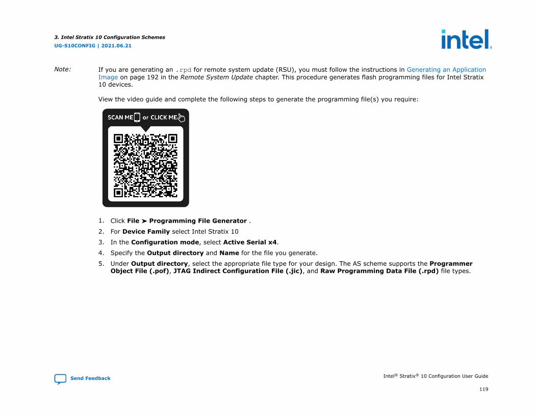
Note: If you are generating an .rpd for remote system update (RSU), you must follow the instructions in Generating an ApplicationImage on page 192 in the Remote System Update chapter. This procedure generates flash programming files for Intel Stratix10 devices.
View the video guide and complete the following steps to generate the programming file(s) you require:
1. Click File ➤ Programming File Generator .
2. For Device Family select Intel Stratix 10
3. In the Configuration mode, select Active Serial x4.
4. Specify the Output directory and Name for the file you generate.
5. Under Output directory, select the appropriate file type for your design. The AS scheme supports the ProgrammerObject File (.pof), JTAG Indirect Configuration File (.jic), and Raw Programming Data File (.rpd) file types.
3. Intel Stratix 10 Configuration Schemes
UG-S10CONFIG | 2021.06.21
Send Feedback Intel® Stratix® 10 Configuration User Guide
119

Figure 45. Programming File Generator Output Files
Device FamilyConfigurationMode
Output Directory
Name
Output Files Required
6. For the JTAG Indirect Configuration File (.jic) and Programmer Object File (.pof) you can turn on the MemoryMap File (.map). This option describes flash memory address locations.The Input Files tab is now available.
7. On the Input Files tab, click Add Bitstream and browse to your configuration bitstream.
3. Intel Stratix 10 Configuration Schemes
UG-S10CONFIG | 2021.06.21
Intel® Stratix® 10 Configuration User Guide Send Feedback
120
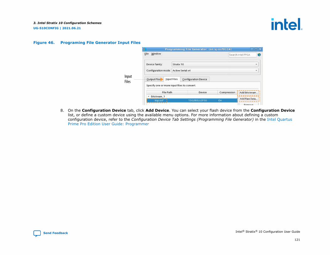
Figure 46. Programing File Generator Input Files
Input Files
8. On the Configuration Device tab, click Add Device. You can select your flash device from the Configuration Devicelist, or define a custom device using the available menu options. For more information about defining a customconfiguration device, refer to the Configuration Device Tab Settings (Programming File Generator) in the Intel QuartusPrime Pro Edition User Guide: Programmer
3. Intel Stratix 10 Configuration Schemes
UG-S10CONFIG | 2021.06.21
Send Feedback Intel® Stratix® 10 Configuration User Guide
121
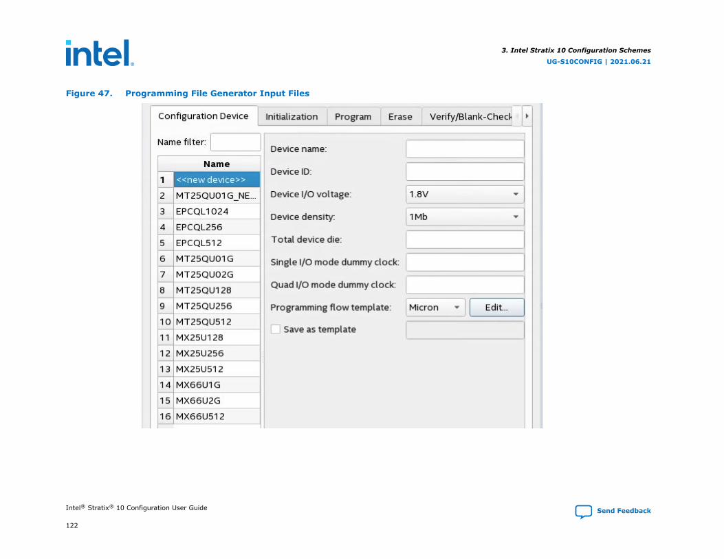
Figure 47. Programming File Generator Input Files
3. Intel Stratix 10 Configuration Schemes
UG-S10CONFIG | 2021.06.21
Intel® Stratix® 10 Configuration User Guide Send Feedback
122
Note: You do not need to specify the flash device for .rpd files because the .rpd format is independent of the flashdevice. In contrast, the .pof and .jic files include both programming data and additional data specific to theconfiguration device. The Intel Quartus Prime Programmer uses this additional data to establish communication withthe configuration device and then write the programming data.
9. Click Generate to generate the programming file(s).
a. You can optionally Click File ➤ Save As .. to save the configuration parameters as a file with the .pfg extension.The .pfg file contains your settings for the Programming File Generator. After you save the .pfg, you can use thisfile to regenerate the programming file by running the following command:
quartus_pfg -c <configuration_file>.pfg
Related Information
• Intel Quartus Prime Pro Edition User Guide: ProgrammerFor comprehensive information about programming file generation and conversion.
• Generating Programming Files using Programming File GeneratorVideo showing how to generate programming files using Programming File Generator
3.2.10.2. Programming .pof files into Serial Flash Device
To program the .pof into the serial flash device through the AS header, perform the following steps:
1. In the Programmer window, click Hardware Setup and select the desired download cable.
2. In the Mode list, select Active Serial Programming.
3. Click Auto Detect button on the left pane.
4. Select the device to be programmed and click Add File.
5. Select the .pof to be programmed to the selected device.
6. Click Start to start programming.
3. Intel Stratix 10 Configuration Schemes
UG-S10CONFIG | 2021.06.21
Send Feedback Intel® Stratix® 10 Configuration User Guide
123
3.2.10.3. Programming .jic files into Serial Flash Device
To program the .jic into the serial flash device through the JTAG interface, perform the following steps:
1. In the Programmer window, click Hardware Setup and select the desired download cable.
2. In the Mode list, select JTAG.
3. Select the device to be programmed and click Add File.
4. Select the .jic to be programmed to the selected device.
5. Click Start to start programming.
3. Intel Stratix 10 Configuration Schemes
UG-S10CONFIG | 2021.06.21
Intel® Stratix® 10 Configuration User Guide Send Feedback
124
3.2.11. Debugging Guidelines for the AS Configuration Scheme
The AS configuration scheme operation is like earlier device families. However, there is one significant difference. Intel Stratix10 devices using AS mode, try to load a firmware section from addresses 0, 256k, 512k and 768k in the serial flash deviceconnected to the CS0 pin.
If the configuration bitstream does not include a valid image, the SDM asserts an error by driving nSTATUS low. You canrecover from the error by reconfiguring the FPGA over JTAG, or by driving nCONFIG low.
SDM tristates AS pins, AS_CLK, AS_DATA0-AS_DATA3, and AS_nCSO0-AS_nCSO3, only when the device powers on if you setMSEL to JTAG. If MSEL is either AS fast or normal, the SDM drives the AS pins until you power cycle the Intel Stratix 10device. Unlike earlier device families, the AS pins are not tristated when the device enters user mode.
The AS configuration scheme has power-on requirements. If you use AS Fast mode, you must ramp all power supplies to therecommended operating condition within 10 ms. This ramp-up requirement ensures that the AS x4 device is within itsoperating voltage range when the Intel Stratix 10 device begins accessing the AS x4 device.
When using AS fast mode, all power supplies to the Intel Stratix 10 device must be fully ramped-up to the recommendedoperating conditions before the SDM releases from reset. To meet the PCIe 100 ms power-up-to-active time requirement forCvP, all the power supplies to the Intel Stratix 10 device must be at the recommended operating range within 10 ms.
Debugging Suggestions
Here are some debugging tips for the AS configuration scheme:
• Ensure that the boot address for your configuration image is correctly defined when generating the programming file forthe flash. The boot address defaults to 0 for AS configuration.
• Ensure that the design meets the power-supply ramp requirements for fast AS mode. If using fast mode, all powersupplies must ramp to the recommended operating condition within 10 ms.
• Ensure that the flash is powered up and ready to be accessed when the Intel Stratix 10 device exits power-on reset.
• If you are using an external clock source for configuration, ensure the OSC_CLK_1 pin is fed correctly, and the frequencymatches the frequency you set for the OSC_CLK_1 in your Intel Quartus Prime Pro Edition project.
• Ensure the MSEL pins reflect the correct AS configuration scheme.
3. Intel Stratix 10 Configuration Schemes
UG-S10CONFIG | 2021.06.21
Send Feedback Intel® Stratix® 10 Configuration User Guide
125
• If the AS configuration is failing due to a corrupt image inside the serial flash device and reprogramming does not resolvethe problem, you have two possible solutions depending on the components you are using for configuration:
— If you are using a third-party programmer to configure the flash directly from an AS or JTAG header as shown in Figure 41 on page 112 change the MSEL setting to JTAG. Setting MSEL to JTAG prevents the corrupt image fromloading automatically at power-on. Then, update the image in quad serial flash through the AS or JTAG header.
— If you are programming the flash device using the JTAG header as shown in Figure 42 on page 113, force thenCONFIG signal to low. When nCONFIG is low, the image cannot load from the quad SPI flash device. Then, updatethe image in quad serial flash through the JTAG header.
• If you are using AS x4 flash memories with AS Fast mode, you must ramp up all power supplies to the recommendedoperating condition within 10 ms. This ramp-up requirement ensures that the AS x4 device is within its operating voltagerange when the Intel Stratix 10 device begins to access it.
• Check endianness of the .rpd if using a third-party programmer to program Quad SPI device. You should generatethe .rpd as big endian.
• If you are using the OSC_CLK_1 clock source for configuration, ensure OSC_CLK_1 is free running and stable before SDMstarts to load a bitstream from the Quad SPI device. The SDM starts configuration after the device exits the POR state ifnCONFIG is held high.
• Try a lower AS clock frequency setting.
• Reconfiguration in AS mode may fail if a system asserts the external reset of the serial flash device used for configuration,before reconfiguration is triggered. Ensure you are not resetting the serial flash device prior to a reconfiguration.
• When you power up the Intel Stratix 10 with an empty serial flash device and use the AS interface to program the .rpdfile into this serial flash device, you must power cycle the Intel Stratix 10 device to configure the device from the flashsuccessfully
• If you drive nCONFIG signal using the external host, ensure it remains high during the AS x4 configuration scheme.
• If you pulse nCONFIG low for reconfiguration, ensure that the nSTATUS acknowledges nCONFIG. If nSTATUS does notfollow the nCONFIG signal, the FPGA may not exit power on reset state. You may need to power cycle the PCB.
• Ensure no external component drives the nSTATUS signal low during the power up.
Related Information
Intel Stratix 10 Debugging Guide on page 218
3. Intel Stratix 10 Configuration Schemes
UG-S10CONFIG | 2021.06.21
Intel® Stratix® 10 Configuration User Guide Send Feedback
126
3.2.12. QSF Assignments for AS
You can specify many Intel Quartus Prime project settings using Intel Quartus Prime Software GUI. The following assignmentsin the .qsf show typical settings for a Intel Stratix 10 device using AS configuration.
These settings are for a Intel Stratix 10 SmartVID device operating in PMBus slave mode which requires most of the SDM_IOpins. Refer to the Intel Stratix 10 Power Management User Guide for the PMBus constraints in master mode.
# Fitter Assignments# ==================set_global_assignment -name DEVICE 1SG280LU3F50E3VGset_global_assignment -name CONFIGURATION_VCCIO_LEVEL 1.8V
# SDM IO Assignments# ==================set_global_assignment -name USE_PWRMGT_SCL SDM_IO14set_global_assignment -name USE_PWRMGT_SDA SDM_IO11set_global_assignment -name USE_PWRMGT_ALERT SDM_IO12set_global_assignment -name USE_CONF_DONE SDM_IO16set_global_assignment -name USE_INIT_DONE SDM_IO0set_global_assignment -name USE_CVP_CONFDONE SDM_IO13set_global_assignment -name USE_SEU_ERROR SDM_IO10set_global_assignment -name SDM_DIRECT_TO_FACTORY_IMAGE SDM_IO15
# Configuration settings# ======================
# The following setting also supports Intel Stratix 10 devicesset_global_assignment -name STRATIXV_CONFIGURATION_SCHEME "ACTIVE SERIAL X4"set_global_assignment -name USE_CONFIGURATION_DEVICE ONset_global_assignment -name ERROR_CHECK_FREQUENCY_DIVISOR 256set_global_assignment -name GENERATE_PR_RBF_FILE ONset_global_assignment -name ENABLE_ED_CRC_CHECK ONset_global_assignment -name MINIMUM_SEU_INTERVAL 479
# SmartVID feature PMBus settings [Slave mode settings only]# ==========================================================set_global_assignment -name VID_OPERATION_MODE "PMBUS SLAVE"set_global_assignment -name PWRMGT_DEVICE_ADDRESS_IN_PMBUS_SLAVE_MODE 3F
You can also set the SDM_IO configuration pins using the Assignments ➤ Device ➤ Device and Pin Options ➤Configuration ➤ Configuration Pin Options.
3. Intel Stratix 10 Configuration Schemes
UG-S10CONFIG | 2021.06.21
Send Feedback Intel® Stratix® 10 Configuration User Guide
127
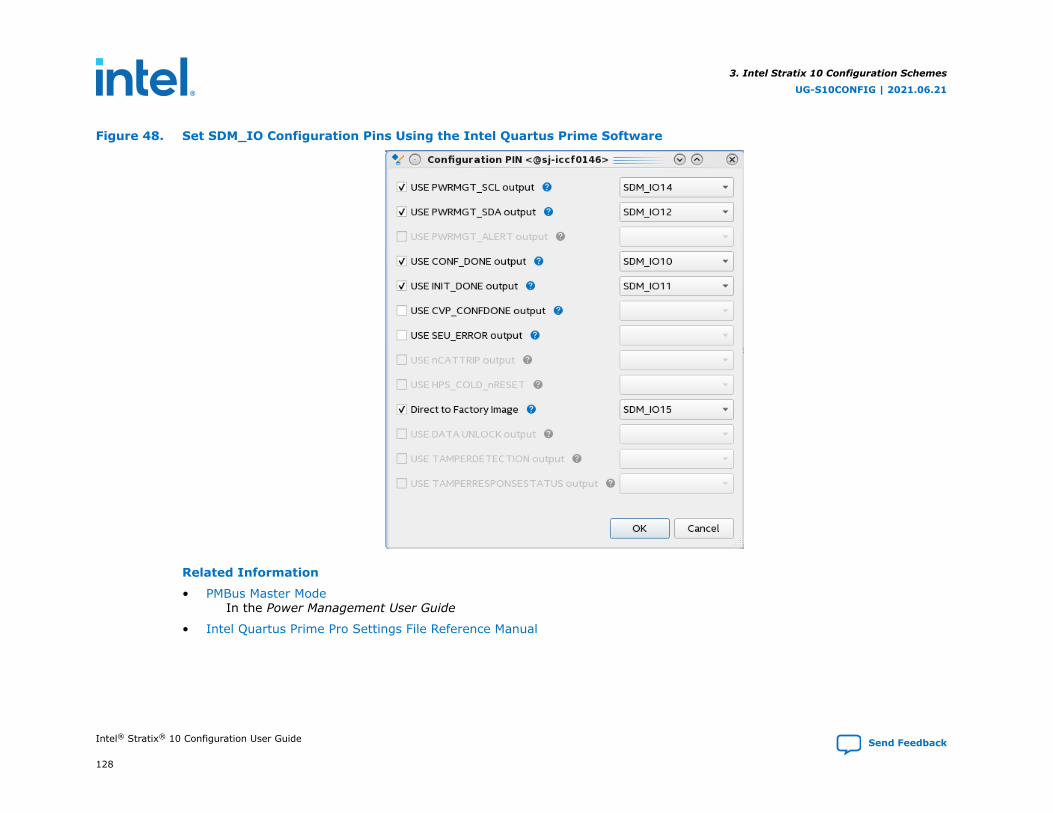
Figure 48. Set SDM_IO Configuration Pins Using the Intel Quartus Prime Software
Related Information
• PMBus Master ModeIn the Power Management User Guide
• Intel Quartus Prime Pro Settings File Reference Manual
3. Intel Stratix 10 Configuration Schemes
UG-S10CONFIG | 2021.06.21
Intel® Stratix® 10 Configuration User Guide Send Feedback
128
3.3. JTAG Configuration
JTAG-chain device programming is ideal during development. JTAG-chain device configuration uses the JTAG pins to configurethe Intel Stratix 10 FPGA directly with the .sof/.rbf file. Configuration using the JTAG device chain allows fasterdevelopment because it does not require you to program external flash memory. You can also use JTAG to reprogram if theimage stored in quad SPI memory. You can also use the JTAG configuration scheme to reprogram the quad SPI memory if thequad SPI content is corrupted or invalid.
The Intel Quartus Prime software generates a .sof/.rbf file containing the FPGA design information. You can usethe .sof/.rbf file with a JTAG programmer to configure the Intel Stratix 10 device. The Intel FPGA Download Cable II andthe Intel FPGA Ethernet Cable both can support the VCCIO_SDM supply at 1.8 V. Alternatively, you can use the JamSTAPLFormat File (.jam) or Jam Byte Code File (.jbc) for JTAG configuration.
Intel Stratix 10 devices automatically compress the configuration bitstream. You cannot disable compression in Intel Stratix10 devices.
Table 35. Intel Stratix 10 Configuration Data Width, Clock Rates, and Data RatesMbps is an abbreviation for Megabits per second.
Mode Data Width (bits) Max Clock Rate Max Data Rate MSEL[2:0]
Passive JTAG 1 30 MHz 30 Mbps 3'b111
Note: The JTAG port has the highest priority and overrides the MSEL pin settings. Consequently, you can configure the Intel Stratix10 device over JTAG even if the MSEL pin specify a different configuration scheme unless you disabled JTAG for securityreasons.
Table 36. Power Rails for the Intel Stratix 10 Device Configuration PinsYou can view the pin assignments for fixed pins in the Pin-Out File for your device. You specify SDM I/O pin functions using the Device ➤ Configuration ➤Device and Pin Options dialog box in the Intel Quartus Prime software. Intel Quartus Prime software enables the HPS secure debug by default.
Configuration Function Pin Type Direction Powered by
TCK Fixed Input VCCIO_SDM
TDI(13) Fixed Input VCCIO_SDM
continued...
(13) The JTAG pins can access the HPS JTAG chain in Intel Stratix 10 SoC devices.
3. Intel Stratix 10 Configuration Schemes
UG-S10CONFIG | 2021.06.21
Send Feedback Intel® Stratix® 10 Configuration User Guide
129
Configuration Function Pin Type Direction Powered by
TMS(13) Fixed Input VCCIO_SDM
TDO(13) Fixed Output VCCIO_SDM
nSTATUS SDM I/O Output VCCIO_SDM
nCONFIG SDM I/O Input VCCIO_SDM
MSEL[2:0] SDM I/O Input VCCIO_SDM
Note: Although the CONF_DONE and INIT_DONE configuration signals are not required, Intel recommends that you use thesesignals. The SDM drives the CONF_DONE signal high after successfully receiving full bitstream. The SDM drives theINIT_DONE signal high to indicate the device is fully in user mode.
Related Information
• Programming Support for Jam STAPL Language
• Device Configuration Pins for Optional Configuration Signals on page 32
• SDM Pin Mapping on page 29
• JTAG Configuration Timing in Intel Stratix 10 Devices
• Documentation: Pin-Out Files for Intel FPGA Devices
3.3.1. JTAG Configuration Scheme Hardware Components and File Types
The following figure illustrates JTAG programming. This is the simplest device configuration scheme. You do not have to usethe File ➤ Programming File Generator to convert the .sof file to a .pof.
3. Intel Stratix 10 Configuration Schemes
UG-S10CONFIG | 2021.06.21
Intel® Stratix® 10 Configuration User Guide Send Feedback
130
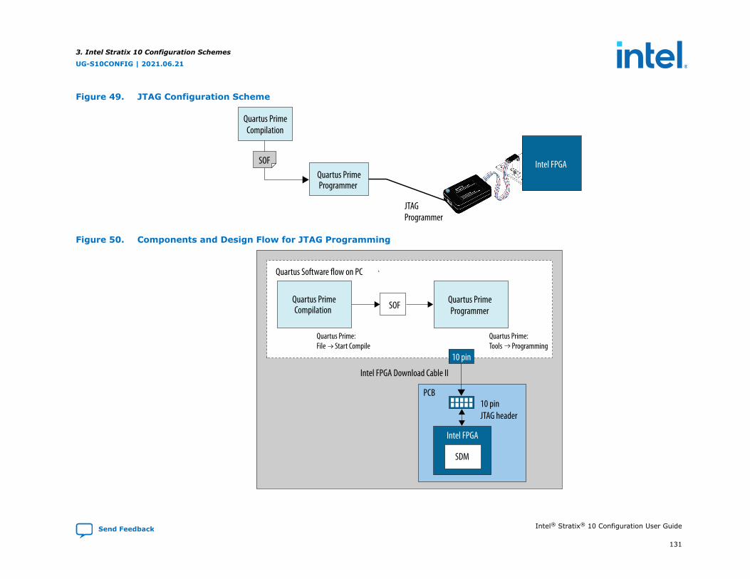
Figure 49. JTAG Configuration Scheme
Quartus PrimeCompilation
JTAGProgrammer
Quartus PrimeProgrammer
SOF Intel FPGA
Figure 50. Components and Design Flow for JTAG Programming
Quartus Software flow on PC
Quartus PrimeProgrammerSOF
10 pin JTAG header
Intel FPGA Download Cable II
Intel FPGA
SDM
PCB
Quartus Prime: File Start Compile
Quartus Prime: Tools Programming
Quartus PrimeCompilation
10 pin
3. Intel Stratix 10 Configuration Schemes
UG-S10CONFIG | 2021.06.21
Send Feedback Intel® Stratix® 10 Configuration User Guide
131
3.3.2. JTAG Device Configuration
To configure a single device in a JTAG chain, the programming software sets the other devices to bypass mode. A device inbypass mode transfers the programming data from the TDI pin to the TDO pin through a single bypass register. Theconfiguration data is available on the TDO pin one clock cycle later.
You can configure the Intel Stratix 10 device through JTAG using a download cable or a microprocessor.
3.3.2.1. JTAG Single-Device Configuration using Download Cable Connections
Refer to the Intel Stratix 10 Device Family Pin Connection Guidelines for additional information about individual pin usage andrequirements.
3. Intel Stratix 10 Configuration Schemes
UG-S10CONFIG | 2021.06.21
Intel® Stratix® 10 Configuration User Guide Send Feedback
132

Figure 51. Connection Setup for JTAG Single-Device Configuration using Download Cable
Intel FPGAnCONFIGnSTATUSCONF_DONEINIT_DONEOSC_CLK_1
MSEL[2:0]
TCKTDO
TDITMS
ConfigurationControl Signals
JTAGConfiguration
Pins
OptionalMonitoring
To JTAGHeader or
JTAG Chain
10kΩ
MSEL
VCCIO_SDM
3
Pin 1
Download cable 10 pin male header (JTAG mode)
RUP RDN
RUP
TCKTDOTMSOPENTDI
GNDVCCIO_SDMOPENOPENGND GND
VCCIO_SDM
10k Ω
Related Information
• Intel FPGA Download Cable II User Guide
• Intel Stratix 10 Device Family Pin Connection Guidelines
3. Intel Stratix 10 Configuration Schemes
UG-S10CONFIG | 2021.06.21
Send Feedback Intel® Stratix® 10 Configuration User Guide
133
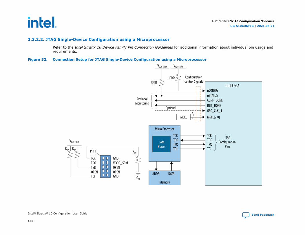
3.3.2.2. JTAG Single-Device Configuration using a Microprocessor
Refer to the Intel Stratix 10 Device Family Pin Connection Guidelines for additional information about individual pin usage andrequirements.
Figure 52. Connection Setup for JTAG Single-Device Configuration using a Microprocessor
Pin 1RUP RDN
RUP
TCKTDOTMSOPENTDI
GNDVCCIO_SDMOPENOPENGND GND
VCCIO_SDM
Intel FPGAnCONFIGnSTATUSCONF_DONEINIT_DONEOSC_CLK_1
MSEL[2:0]
TCK
ADDR DATA
Memory
Micro Processor
TDO
TDITMS
TCKTDO
TDITMS
ConfigurationControl Signals
JTAGConfiguration
Pins
OptionalMonitoring
10kΩ
Optional
MSEL
VCCIO_SDM
3
JAMPlayer
10kΩ
VCCIO_SDM
3. Intel Stratix 10 Configuration Schemes
UG-S10CONFIG | 2021.06.21
Intel® Stratix® 10 Configuration User Guide Send Feedback
134

Related Information
Intel Stratix 10 Device Family Pin Connection Guidelines
3.3.3. JTAG Multi-Device Configuration
You can configure multiple devices in a JTAG chain. Observe the following pin connections and guidelines for this configurationsetup:
• One JTAG-compatible header connects to several devices in a JTAG chain. The drive capability of the download cable is theonly limit on the number of devices in the JTAG chain.
• If you have four or more devices in a JTAG chain, buffer the TCK, TDI, and TMS pins with an on-board buffer. You can alsoconnect other Intel FPGA devices with JTAG support to the chain.
3. Intel Stratix 10 Configuration Schemes
UG-S10CONFIG | 2021.06.21
Send Feedback Intel® Stratix® 10 Configuration User Guide
135

3.3.3.1. JTAG Multi-Device Configuration using Download Cable
Figure 53. Connection Setup for JTAG Multi Device Configuration using Download Cable
Pin 1
1 kΩ
10 kΩ
TMS TCK
TDITDO
nSTATUSnCONFIG
MSEL[2:0]CONF_DONE
TMS TCK
TDI TDO
nSTATUSnCONFIG
MSEL[2:0]CONF_DONE
Intel FPGA Intel FPGA Intel FPGA
TMS TCK
TDI TDO
nSTATUSnCONFIG
MSEL[2:0]CONF_DONE
Download cable10-pin male header
(JTAG mode)
Resistor values can vary between 1 kΩ to 10 kΩ.Perform signal integrity to select the resistor
value for your setup.
For JTAG configuration only:Connect MSEL [2:0] of Intel FPGA devices to VCCIO_SDM through 4.7 k Ω external pull-up resistor.For JTAG in conjunction with another configuration scheme:Connect MSEL [2:0] of Intel FPGA devices based on the non-JTAG configuration scheme.
GND
VCCIO_SDM
VCCIO_SDM
VCCIO_SDM
VCCIO_SDM
10 kΩ 10 kΩ
VCCIO_SDM
10 kΩ 10 kΩ
VCCIO_SDM
10 kΩ
3.3.4. Debugging Guidelines for the JTAG Configuration Scheme
The JTAG configuration scheme overrides all other configuration schemes. The SDM is always ready to accept configurationover JTAG unless a security feature disables the JTAG interface. JTAG is particularly useful in recovering a device that may bein an unrecoverable state reached when trying to configure using a corrupted image.
3. Intel Stratix 10 Configuration Schemes
UG-S10CONFIG | 2021.06.21
Intel® Stratix® 10 Configuration User Guide Send Feedback
136
An nCONFIG falling edge terminates any JTAG access and the device reverts to the MSEL-specified boot source. nCONFIGmust be stable during JTAG configuration. nSTATUS follows nCONFIG during JTAG configuration. Consequently, nSTATUS alsomust be stable.
Unlike other configuration schemes, nSTATUS does not assert if an error occurs during JTAG configuration. You must monitorthe error messages that the Intel Quartus Prime Pro Edition Programmer generates for error reporting.
Note: For Intel Stratix 10 SX devices when you choose to configure the FPGA fabric first, the JTAG chain has no mechanism toredeliver the HPS boot information following a cold reset. Consequently, you must reconfig the device with the .sof file oravoid cold resets to continue operation.
Debugging Suggestions
Here are some debugging tips for JTAG:
• Verify that the JTAG pin connections are correct.
• If JTAG configuration is failing, check that the FPGA has successfully powered up and exited POR. One strategy is to checkthe hand shaking behavior between nCONFIG and nSTATUS by driving nCONFIG low and ensuring that nSTATUS alsogoes low.
• Verify that the nCONFIG pin does not change state during JTAG configuration.
• Another way to determine whether the device has exited the POR state is to use the Intel Quartus Prime Programmer todetect the device. If the programmer can detect the Intel Stratix 10 device, it has exited the POR state.
• If you are using an Intel FPGA Download Cable II, reduce the cable clock speed to 6 MHz.
• If you have multiple devices in the JTAG chain, try to disconnect other devices from the JTAG chain to isolate the IntelStratix 10 device.
• If you specify the OSC_CLK_1 as the clock source for configuration, ensure that OSC_CLK_1 is running at the frequencyyou specify in the Intel Quartus Prime software.
• For designs including the High Bandwidth Memory (HBM2) IP or any IP using transceivers, you must provide a freerunning and stable reference clock to the device before device configuration begins. All transceiver power supplies mustbe at the required voltage before configuration begins.
3. Intel Stratix 10 Configuration Schemes
UG-S10CONFIG | 2021.06.21
Send Feedback Intel® Stratix® 10 Configuration User Guide
137
• When the MSEL setting on the PCB is not JTAG, if you use the JTAG interface for reconfiguration after an initialreconfiguration using AS or the Avalon-ST interface, the .sof must be in the file format you specified in the Intel QuartusPrime project. For example, if you initially configure the MSEL pins for AS configuration and configure using the ASscheme, a subsequent JTAG reconfiguration using a .sof generated for Avalon-ST fails.
• Clearing the RSU_STATUS command after the JTAG reconfiguration depends on your Intel Quartus Prime software version.In earlier Intel Quartus Prime software versions, the RSU_STATUS is not cleared after the JTAG reconfiguration. Startingwith the Intel Quartus Prime 20.3 version, the system clears the RSU_STATUS after the JTAG reconfiguration.
• Ensure that during the power up, no external component drives the nSTATUS signal low.
Related Information
Intel Stratix 10 Debugging Guide on page 218
3. Intel Stratix 10 Configuration Schemes
UG-S10CONFIG | 2021.06.21
Intel® Stratix® 10 Configuration User Guide Send Feedback
138
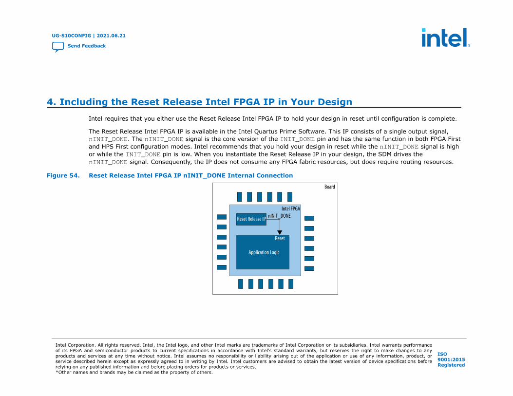
4. Including the Reset Release Intel FPGA IP in Your DesignIntel requires that you either use the Reset Release Intel FPGA IP to hold your design in reset until configuration is complete.
The Reset Release Intel FPGA IP is available in the Intel Quartus Prime Software. This IP consists of a single output signal,nINIT_DONE. The nINIT_DONE signal is the core version of the INIT_DONE pin and has the same function in both FPGA Firstand HPS First configuration modes. Intel recommends that you hold your design in reset while the nINIT_DONE signal is highor while the INIT_DONE pin is low. When you instantiate the Reset Release IP in your design, the SDM drives thenINIT_DONE signal. Consequently, the IP does not consume any FPGA fabric resources, but does require routing resources.
Figure 54. Reset Release Intel FPGA IP nINIT_DONE Internal Connection
Board
nINIT_DONE
Reset
Application Logic
Intel FPGA
Reset Release IP
UG-S10CONFIG | 2021.06.21
Send Feedback
Intel Corporation. All rights reserved. Intel, the Intel logo, and other Intel marks are trademarks of Intel Corporation or its subsidiaries. Intel warrants performanceof its FPGA and semiconductor products to current specifications in accordance with Intel's standard warranty, but reserves the right to make changes to anyproducts and services at any time without notice. Intel assumes no responsibility or liability arising out of the application or use of any information, product, orservice described herein except as expressly agreed to in writing by Intel. Intel customers are advised to obtain the latest version of device specifications beforerelying on any published information and before placing orders for products or services.*Other names and brands may be claimed as the property of others.
ISO9001:2015Registered

4.1. Understanding the Reset Release IP Requirement
Intel Stratix 10 devices use a parallel, sector-based architecture that distributes the core fabric logic across multiple sectors.Device configuration proceeds in parallel with each Local Sector Manager (LSM) configuring its own sector. Consequently,FPGA registers and core logic do not exit reset at exactly the same time, as has always been the case in previous families.
The continual increases in clock frequency, device size, and design complexity now necessitate a reset strategy that considersthe possible effects of slight differences in the release from reset. The Reset Release Intel FPGA IP holds a control circuit inreset until the device has fully entered user mode. The Reset Release FPGA IP generates an inverted version of the internalINIT_DONE signal, nINIT_DONE for use in your design.
After nINIT_DONE asserts (low), all logic is in user mode and operates normally. You can use the nINIT_DONE signal in oneof the following ways:
• To gate an external or internal reset.
• To gate the reset input to the transceiver and I/O PLLs.
• To gate the write enable of design blocks such as embedded memory blocks, state machine, and shift registers.
• To synchronously drive register reset input ports in your design.
Attention: When you instantiate Reset Release Intel FPGA IP in your design, the Intel Quartus Prime Fitter selects one Local SectorManager (LSM) to output the nINIT_DONE signal. Multiple instances results in some skew between the nINIT_DONE signals.
4. Including the Reset Release Intel FPGA IP in Your Design
UG-S10CONFIG | 2021.06.21
Intel® Stratix® 10 Configuration User Guide Send Feedback
140
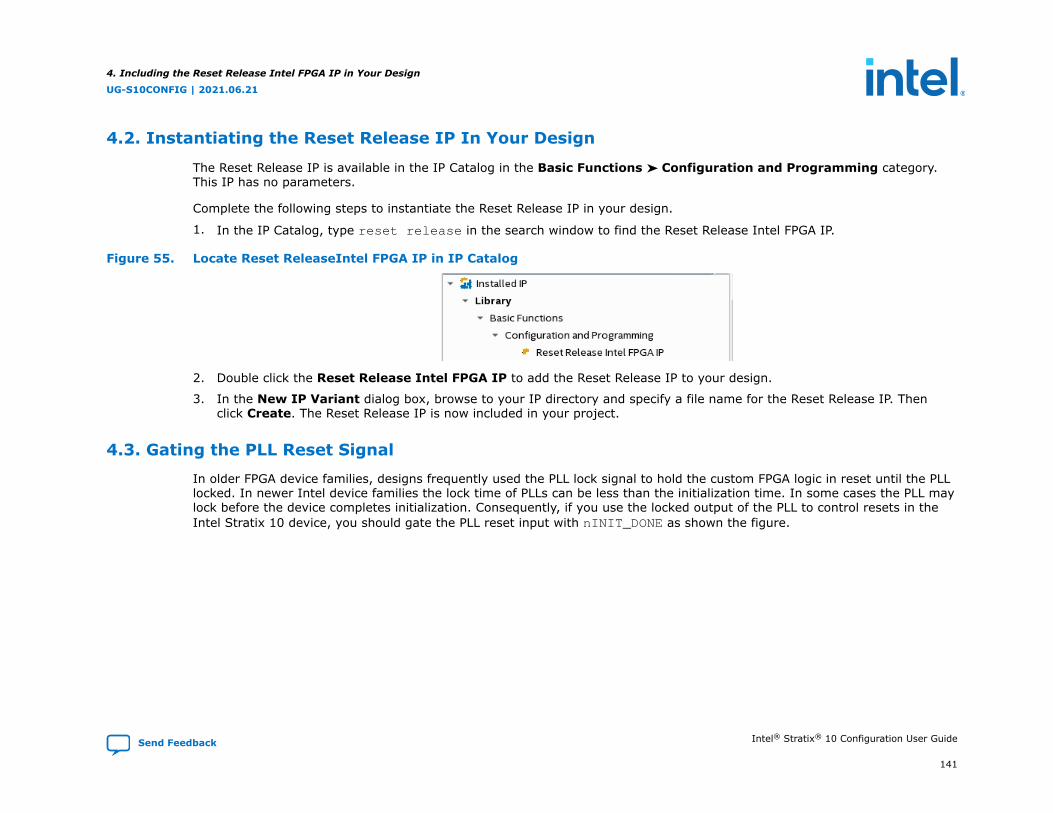
4.2. Instantiating the Reset Release IP In Your Design
The Reset Release IP is available in the IP Catalog in the Basic Functions ➤ Configuration and Programming category.This IP has no parameters.
Complete the following steps to instantiate the Reset Release IP in your design.
1. In the IP Catalog, type reset release in the search window to find the Reset Release Intel FPGA IP.
Figure 55. Locate Reset ReleaseIntel FPGA IP in IP Catalog
2. Double click the Reset Release Intel FPGA IP to add the Reset Release IP to your design.
3. In the New IP Variant dialog box, browse to your IP directory and specify a file name for the Reset Release IP. Thenclick Create. The Reset Release IP is now included in your project.
4.3. Gating the PLL Reset Signal
In older FPGA device families, designs frequently used the PLL lock signal to hold the custom FPGA logic in reset until the PLLlocked. In newer Intel device families the lock time of PLLs can be less than the initialization time. In some cases the PLL maylock before the device completes initialization. Consequently, if you use the locked output of the PLL to control resets in theIntel Stratix 10 device, you should gate the PLL reset input with nINIT_DONE as shown the figure.
4. Including the Reset Release Intel FPGA IP in Your Design
UG-S10CONFIG | 2021.06.21
Send Feedback Intel® Stratix® 10 Configuration User Guide
141

Figure 56. Using nINIT_DONE to Gate the PLL_Reset Signal
nCONFIG
nSTATUS
INIT_DONE
nINIT_DONE
PLL_Reset
Clock
PLL_Lock
Another alternative if you are using PLL_Lock in your reset sequence is to gate the PLL_Lock output with the nINIT_DONEsignal, (PLL_Lock && !nINIT_DONE).
4.4. Guidance When Using Partial Reconfiguration (PR)
The PR Region Controller IP provides reset logic that ensures that the static region of the device and the PR personas do notinteract during PR.
The Reset Release IP is only necessary to manage reset for full FPGA core configuration and subsequent full FPGA corereconfigurations. The Reset Release IP is not necessary to prevent interaction between the static and PR personas during thePR process. For more information about PR refer to the Intel Quartus Prime Pro Edition User Guide: Partial Reconfiguration.
Related Information
Creating a Partial Reconfiguration Design
4.5. Detailed Description of Device Configuration
Each Local Sector Manager (LSM) configures its own sector. A sector comprises multiple logic array block (LAB) rows. A logicalfunction can span multiple rows and multiple sectors.
4. Including the Reset Release Intel FPGA IP in Your Design
UG-S10CONFIG | 2021.06.21
Intel® Stratix® 10 Configuration User Guide Send Feedback
142
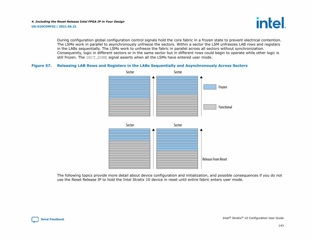
During configuration global configuration control signals hold the core fabric in a frozen state to prevent electrical contention.The LSMs work in parallel to asynchronously unfreeze the sectors. Within a sector the LSM unfreezes LAB rows and registersin the LABs sequentially. The LSMs work to unfreeze the fabric in parallel across all sectors without synchronization.Consequently, logic in different sectors or in the same sector but in different rows could begin to operate while other logic isstill frozen. The INIT_DONE signal asserts when all the LSMs have entered user mode.
Figure 57. Releasing LAB Rows and Registers in the LABs Sequentially and Asynchronously Across Sectors
Release From Reset
Sector Sector
Sector Sector
Frozen
Functional
The following topics provide more detail about device configuration and initialization, and possible consequences if you do notuse the Reset Release IP to hold the Intel Stratix 10 device in reset until entire fabric enters user mode.
4. Including the Reset Release Intel FPGA IP in Your Design
UG-S10CONFIG | 2021.06.21
Send Feedback Intel® Stratix® 10 Configuration User Guide
143
4.5.1. Device Initialization
The following steps summarize device initialization:
1. An external host drives a configuration request to the Secure Device Manager (SDM) by driving nCONFIG high. The SDMexits the IDLE state and signals the beginning of configuration by driving nSTATUS high and driving configuration data.
2. The SDM asserts CONF_DONE indicating that the Intel FPGA has successfully received all the configuration data.
3. The SDM uses the configuration logic to start non-gated clocks in the fabric. Intel Hyperflex registers begin shifting data.Consequently, the initial conditions of Intel Hyperflex registers can be random. Use the Disable Register Power-upInitialization setting in the Intel Quartus Prime Configuration dialog box to disable Intel Hyperflex register initializationduring power-on as explained below.
4. The SDM uses the configuration logic to enable and initialize user registers in the LABs, DSP, and embedded memoryblocks.
5. The SDM drives INIT_DONE to indicate that the device has fully entered user mode. The Reset Release IP assertsnINIT_DONE. Intel recommends that you use nINIT_DONE to gate your reset logic.
6. The FPGA is now in user mode and ready for operation.
4.5.2. Preventing Register Initialization During Power-On
If not held in reset, both ALM and Intel Hyperflex registers may lose their initial state if they initialize before their respectivesource.
You can prevent registers from initializing during power-on by enabling an option in the Intel Quartus Prime software.Complete the following steps to turn on this option:
1. On the Assignments menu select Device ➤ Device and Pin Options ➤ Configuration.
2. In the Configuration dialog box, turn on Disable Register Power-up Initialization.
4. Including the Reset Release Intel FPGA IP in Your Design
UG-S10CONFIG | 2021.06.21
Intel® Stratix® 10 Configuration User Guide Send Feedback
144

Figure 58. Disabling Register Initialization During Power-On
Turn On
4. Including the Reset Release Intel FPGA IP in Your Design
UG-S10CONFIG | 2021.06.21
Send Feedback Intel® Stratix® 10 Configuration User Guide
145

Note: Coming out of reset, you cannot rely on the value of registers with initial conditions unless you gate your system reset usingone of the following options:
• Designs that include the Reset Release IP must route nINIT_DONE to the system reset.
• Designs that do not include the Reset Release IP must route INIT_DONE to an external pin and feed INIT_DONE back intothe FPGA as an input to system reset.
4.5.3. Embedded Memory Block Initial Conditions
Initialized content of embedded memory blocks is stable during configuration. However, designs that contain logic to modifyembedded memory can result in spurious writes. Spurious writes can occur if you fail to gate the write enable with anappropriate reset.
4.5.4. Protecting State Machine Logic
To guarantee correct operation of state machines, your reset logic must hold the FPGA fabric in reset until the entire fabricenters user mode.
The following example shows how an inadequate reset strategy might result in an illegal state in a one-hot state machine. Inthis example, the design does not reset any of the state machine registers. The state machine design depends on registersentering an initial state. Without an adequate reset, this state machine begins operating when part of the device is active.Nearby logic included in the state machine remains frozen, before INIT_DONE asserts.
Figure 59. Partially Initialized Design - INIT_DONE = 0
O
ORegister A
Register B
Register C
Functional (Row N)
In Reset (Row N+1)
1
4. Including the Reset Release Intel FPGA IP in Your Design
UG-S10CONFIG | 2021.06.21
Intel® Stratix® 10 Configuration User Guide Send Feedback
146
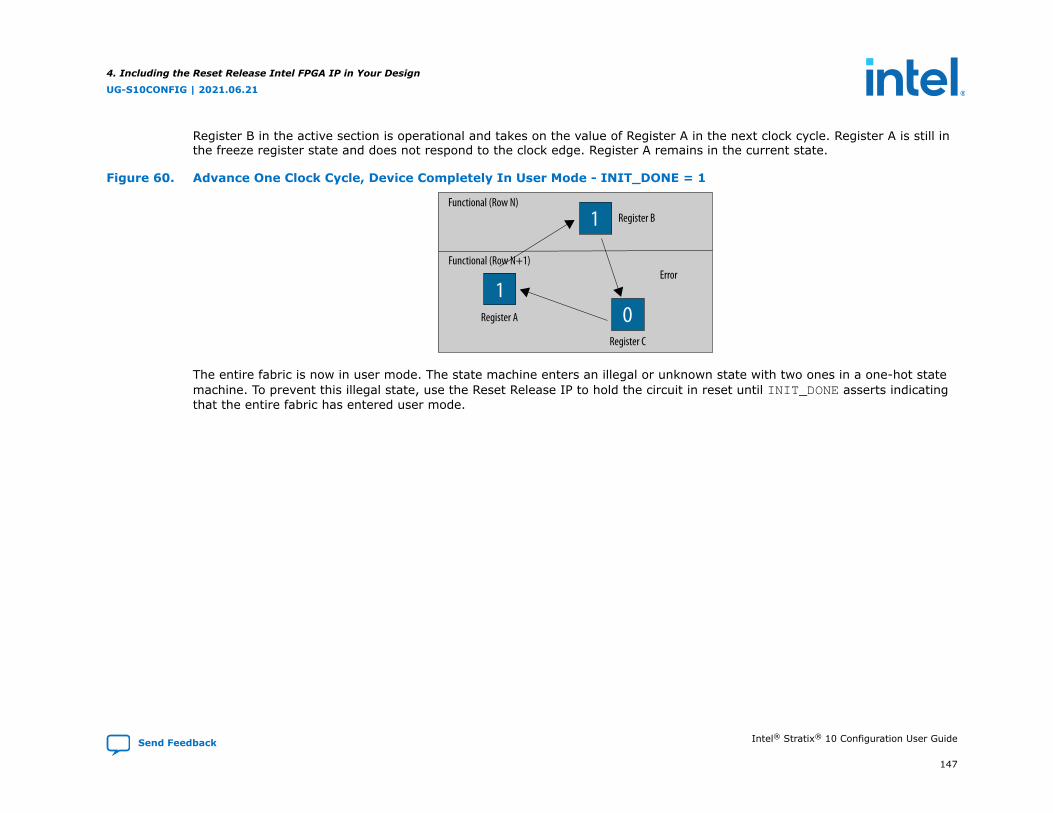
Register B in the active section is operational and takes on the value of Register A in the next clock cycle. Register A is still inthe freeze register state and does not respond to the clock edge. Register A remains in the current state.
Figure 60. Advance One Clock Cycle, Device Completely In User Mode - INIT_DONE = 1
1
ORegister A
Register B
Register C
Error
1
Functional (Row N)
Functional (Row N+1)
The entire fabric is now in user mode. The state machine enters an illegal or unknown state with two ones in a one-hot statemachine. To prevent this illegal state, use the Reset Release IP to hold the circuit in reset until INIT_DONE asserts indicatingthat the entire fabric has entered user mode.
4. Including the Reset Release Intel FPGA IP in Your Design
UG-S10CONFIG | 2021.06.21
Send Feedback Intel® Stratix® 10 Configuration User Guide
147
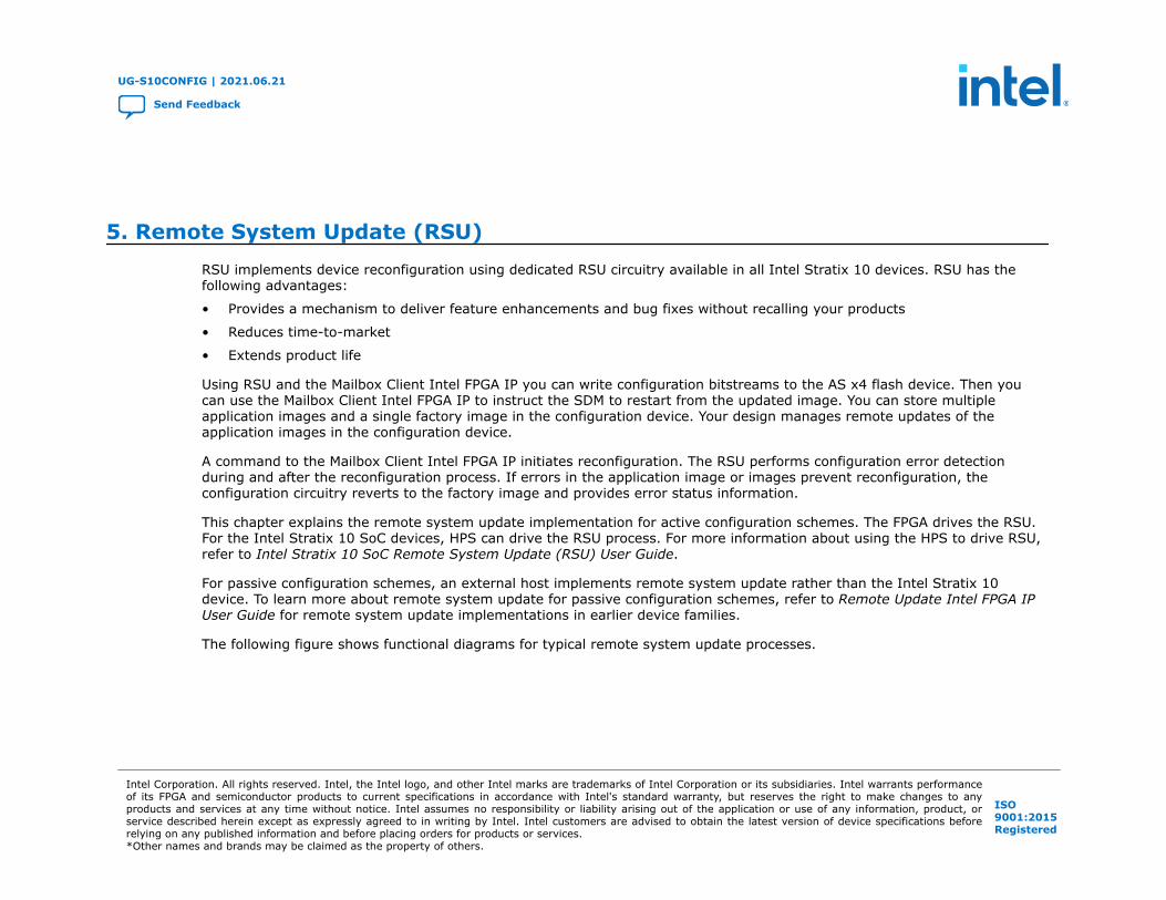
5. Remote System Update (RSU)RSU implements device reconfiguration using dedicated RSU circuitry available in all Intel Stratix 10 devices. RSU has thefollowing advantages:
• Provides a mechanism to deliver feature enhancements and bug fixes without recalling your products
• Reduces time-to-market
• Extends product life
Using RSU and the Mailbox Client Intel FPGA IP you can write configuration bitstreams to the AS x4 flash device. Then youcan use the Mailbox Client Intel FPGA IP to instruct the SDM to restart from the updated image. You can store multipleapplication images and a single factory image in the configuration device. Your design manages remote updates of theapplication images in the configuration device.
A command to the Mailbox Client Intel FPGA IP initiates reconfiguration. The RSU performs configuration error detectionduring and after the reconfiguration process. If errors in the application image or images prevent reconfiguration, theconfiguration circuitry reverts to the factory image and provides error status information.
This chapter explains the remote system update implementation for active configuration schemes. The FPGA drives the RSU.For the Intel Stratix 10 SoC devices, HPS can drive the RSU process. For more information about using the HPS to drive RSU,refer to Intel Stratix 10 SoC Remote System Update (RSU) User Guide.
For passive configuration schemes, an external host implements remote system update rather than the Intel Stratix 10device. To learn more about remote system update for passive configuration schemes, refer to Remote Update Intel FPGA IPUser Guide for remote system update implementations in earlier device families.
The following figure shows functional diagrams for typical remote system update processes.
UG-S10CONFIG | 2021.06.21
Send Feedback
Intel Corporation. All rights reserved. Intel, the Intel logo, and other Intel marks are trademarks of Intel Corporation or its subsidiaries. Intel warrants performanceof its FPGA and semiconductor products to current specifications in accordance with Intel's standard warranty, but reserves the right to make changes to anyproducts and services at any time without notice. Intel assumes no responsibility or liability arising out of the application or use of any information, product, orservice described herein except as expressly agreed to in writing by Intel. Intel customers are advised to obtain the latest version of device specifications beforerelying on any published information and before placing orders for products or services.*Other names and brands may be claimed as the property of others.
ISO9001:2015Registered
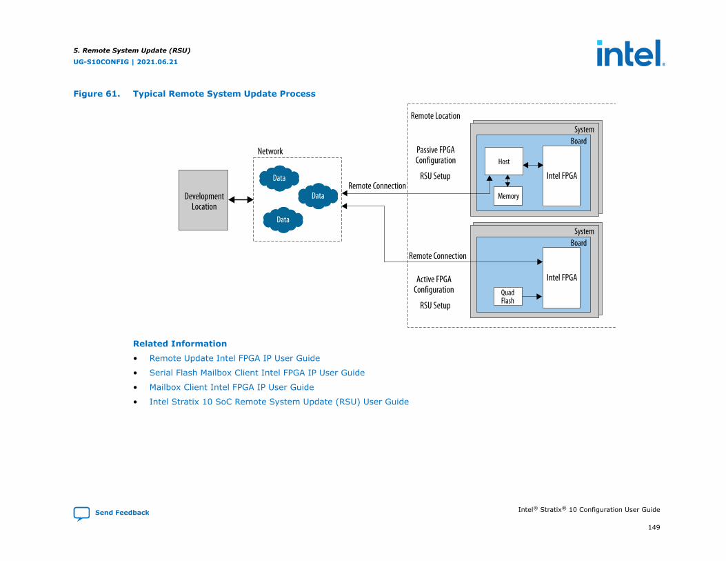
Figure 61. Typical Remote System Update Process
DevelopmentLocation
System
Remote Location
Network
RSU Setup
Active FPGAConfiguration
RSU Setup
Passive FPGAConfiguration
Board
Intel FPGA
Host
Memory
SystemBoard
QuadFlash
DataRemote Connection
Remote Connection
Data
Data
Intel FPGA
Related Information
• Remote Update Intel FPGA IP User Guide
• Serial Flash Mailbox Client Intel FPGA IP User Guide
• Mailbox Client Intel FPGA IP User Guide
• Intel Stratix 10 SoC Remote System Update (RSU) User Guide
5. Remote System Update (RSU)
UG-S10CONFIG | 2021.06.21
Send Feedback Intel® Stratix® 10 Configuration User Guide
149

5.1. Remote System Update Functional Description
5.1.1. RSU Glossary
Table 37. RSU Glossary
Term Meaning
Firmware Firmware that runs on SDM. Implements many functions including the functions listed here:• FPGA configuration• Voltage regulator configuration• Temperature measurement• HPS software load• HPS Reset• RSU• Read, erase, and program flash memory• Device security, including authentication and encryption
Decision firmware Firmware to identify and load the highest priority image. Previous versions of this user guide refer to decision firmwareas static firmware. Starting in version 19.1 of the Intel Quartus Prime software, you can use RSU to update thisfirmware.
Decision firmware data Decision firmware data structure containing the following information:• The Direct to Factory Image pin assignment.• PLL settings for the external clock source. This optional clock source drives OSC_CLK_1. For more information, refer
to OSC_CLK_1 Clock Input.• Quad SPI pins.
Configuration pointer block (CPB) A list of application image addresses in order of priority. When you add an image, that image becomes the highestpriority.
Sub-partition table (SPT) Data structure to facilitate the management of the flash storage.
Application image Configuration bitstream that implements your design. This image includes the SDM firmware.
Factory image The backup application image that the RSU loads when all attempts to load an application image fail.The factory image should provide enough functionality for the device to recover when all application images arecorrupt. Once the factory image loads, you can program new application images to replace the failing images.
continued...
5. Remote System Update (RSU)
UG-S10CONFIG | 2021.06.21
Intel® Stratix® 10 Configuration User Guide Send Feedback
150

Term Meaning
The SDM loads the factory image in the following circumstances:• You assign the Direct to Factory Image function to an SDM I/O pin and assert the pin after a power-on reset
or nCONFIG deassertion.• All SDM attempts to load the application images fail.• You make a request to the SDM to load the factory image.The configuration system treats the factory image in the same way as it does an application image.
Initial RSU flash image Contains the factory image, the application images, the decision firmware, and the associated RSU data structures.
Factory update image An image that updates the following RSU-related items in flash:• The factory image• The decision firmware• The decision firmware dataIntel recommends that your factory update image include the minimum amount of logic necessary to debugsuccessfully your design if your application image or images fail to load.
5. Remote System Update (RSU)
UG-S10CONFIG | 2021.06.21
Send Feedback Intel® Stratix® 10 Configuration User Guide
151
5.1.2. Remote System Update Using AS Configuration
Remote system update using AS configuration includes the following components:
• Your remote system update host design. The host can be custom logic, the HPS, or a Nios® II processor in the FPGA.
• One factory image.
• Flash memory for image storage.
• At least one application image.
• Designs that do not use the HPS as the remote system update host require an Mailbox Client Intel FPGA IP as shown inthe figure below. The Mailbox Client sends and receives remote system update operation commands and responses, suchas QSPI_READ and QSPI_WRITE.
Figure 62. Intel Stratix 10 Remote System Update Components
System
Intel FPGA
FlashMemory
JTAGInterface
Mailbox Client IP
Avalon-MM Interface
FPGA Fabric
User Logic
RSU HostController
Secure Device Manager(SDM)
Board
External RSU Host
Logic
5. Remote System Update (RSU)
UG-S10CONFIG | 2021.06.21
Intel® Stratix® 10 Configuration User Guide Send Feedback
152
Attention: Starting in version 19.2 of the Intel Quartus Prime software, a restriction applies to the following mailbox client IPs thataccess the SDM mailbox over an Avalon Memory-Mapped (Avalon-MM) interface:
• Temperature Sensor
• Voltage Sensor
• Chip ID
• Serial Flash Mailbox Client
• Mailbox Client IP
• Advanced SEU Detection IP
• Partial Reconfiguration IP
If you use the Mailbox IP in designs compiled in Intel Quartus Prime Pro Edition software version 19.2 or later, you must onlyuse SDM firmware starting from version 19.2 or later to configure the FPGA.
Related Information
Mailbox Client Intel FPGA IPUser Guide
5.1.3. Remote System Update Configuration Images
Intel Stratix 10 devices using remote system update require the following configuration images:
• A Factory image—This image includes logic to implement the following functions:
— Your design-specific logic to obtain new application images
— Your design-specific logic to request reconfiguration using a specific application image
— Image storage in flash memory
• Application image—contains logic to implement the custom application. The application image must also contain logic toobtain new application images and store the images in the flash memory.
Depending on the storage space of your flash memory, Intel Stratix 10 remote system update supports one factory image andup to 507 application images. The Quartus Programming File Generator only supports up to seven remote system updateimages. However, you can add more images using the Mailbox Client IP or Serial Flash Mailbox Client IP with the device inuser mode.
5. Remote System Update (RSU)
UG-S10CONFIG | 2021.06.21
Send Feedback Intel® Stratix® 10 Configuration User Guide
153
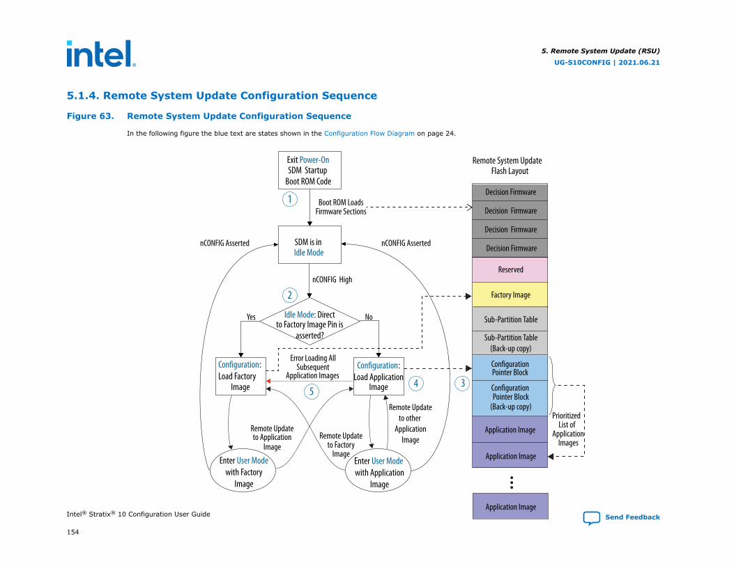
5.1.4. Remote System Update Configuration Sequence
Figure 63. Remote System Update Configuration Sequence
In the following figure the blue text are states shown in the Configuration Flow Diagram on page 24.
SDM Firmware LoadsDynamic Firmware
Section (I/O Configuration) Factory Image
Exit Power-OnSDM Startup
Boot ROM Code
Remote System UpdateFlash Layout
Boot ROM LoadsFirmware Sections
Configuration: Load Factory
Image
Enter User Modewith Factory
Image
SDM is in Idle Mode
Idle Mode: Directto Factory Image Pin is
asserted?
NoYes
nCONFIG Asserted
Decision Firmware
Decision Firmware
Decision Firmware
Decision Firmware
Sub-Partition Table
Configuration Pointer Block
Remote Updateto Factory
Image
Remote Updateto other
ApplicationImage
PrioritizedList of
ApplicationImages
Remote Updateto Application
Image
Reserved
Application Image
Application Image
Configuration Pointer Block
Application Image
Error Loading AllSubsequent
Sub-Partition Table(Back-up copy)
Configuration:Load Application
Image
Enter User Mode with Application
Image
Application Images
(Back-up copy)
1
2
345
nCONFIG High
nCONFIG Asserted
5. Remote System Update (RSU)
UG-S10CONFIG | 2021.06.21
Intel® Stratix® 10 Configuration User Guide Send Feedback
154
Reconfiguration includes the following steps:
1. After the device exits power-on-reset (POR), the boot ROM loads flash memory from the first valid decision firmware fromone of the copies at addresses 0, 256 K, 512 K, or 768 K to initialize the SDM. The same configuration firmware is presentin each of these locations. This firmware is part of the initial RSU flash image. ( Refer to Step 2 of Guidelines forPerforming Remote System Update Functions for Non-HPS on page 159 for step-by-step details for programming theinitial RSU flash image into the flash.)
2. The optional Direct to Factory pin controls whether the SDM firmware loads the factory or application image. You canassign the Direct to Factory input to any unused SDM pin. The SDM loads the application image if you do not assign thispin.
3. The configuration pointer block in the flash device maintains a list of pointers to the application images.
4. When loading an application image, the SDM traverses the pointer block in reverse order. The SDM loads the highestpriority image. When image loading completes, the device enters user mode.
5. If loading the newest (highest priority) image is unsuccessful, the SDM tries the next application image from the list. Ifnone of the application loads successfully, the SDM loads the factory image.
6. If loading the factory image fails, you can recover by reprogramming the quad SPI flash with the initial RSU flash imageusing the JTAG interface.
Note: You must keep nCONFIG high until the device enters the user mode.
• Keep the nCONFIG signal high after the device powers up and throughout the entire device configuration to load anapplication or factory image.
• Keep the nCONFIG signal high during the remote update to other application image or factory image by using theRSU_IMAGE_UPDATE command.
You drive nCONFIG low only when the device is in user mode to trigger the reconfiguration.
5.1.5. RSU Recovery from Corrupted Images
When an RSU fails, the Mailbox Client Intel FPGA IP RSU_STATUS command provides information about the currentconfiguration status, including the currently running image and most recent failing image. The rsu1.tcl script implementsthe RSU_STATUS commands. You can download the rsu1.tcl script from the following web page. Under DeviceConfiguration Support Center, click Advanced Configuration Features, click the triangle next to Remote SystemUpgrade to expand this section, then click Example of Tcl Script.
5. Remote System Update (RSU)
UG-S10CONFIG | 2021.06.21
Send Feedback Intel® Stratix® 10 Configuration User Guide
155
The following example illustrates recovery from a corrupted image:
Multiple Corrupted Images
If the flash memory includes multiple corrupted images, the RSU_STATUS only reports status for the highest priority failingimage. The following example illustrates this procedure.
• The flash memory includes the following four images, in order of priority:
1. Application Image3 (highest priority)
2. Application Image2
3. Application image1
4. Application image0 (lowest priority)
• Application Image3, Application Image2, and Application Image1 are corrupted.
• RSU_STATUS includes the following information:
— Current_Image: Application Image0
— Highest priority failing image, State, Version, Error location, Error details: records informationfor Application Image3 which is the highest priority failing image.
5. Remote System Update (RSU)
UG-S10CONFIG | 2021.06.21
Intel® Stratix® 10 Configuration User Guide Send Feedback
156

Figure 64. Multiple Corrupt Images
Factory ImageAddress Offset 1MB + 64 KB
Application Image0Address Offset <N> * 64 KB
Application Image1 - CorruptAddress Offset <M> * 64 KB
Application Image2 - CorruptAddress Offset <O> * 64 KB
Current Image
Last Failing ImageHighest PriorityFailing Image
Application Image3 - CorruptAddress Offset <P> * 64 KB
Related Information
• Operation Commands on page 162
• Supported Flash Devices for Intel Stratix 10 Devices
5. Remote System Update (RSU)
UG-S10CONFIG | 2021.06.21
Send Feedback Intel® Stratix® 10 Configuration User Guide
157
5.1.6. Updates with the Factory Update Image
In rare instances you may need to update flash memory with a new factory image and the associated decision firmware anddecision firmware data.
An update may be required for the following reasons:
• If there are vulnerabilities in the firmware
• If there are errors in the firmware or in the factory image
Intel provides a safe solution for you to update the factory image and the associated decision firmware and decision firmwaredata remotely. The update process stores multiple copies of critical data so that if power is lost or the update is disrupted, thedevice is still able to restart and continue the update. The update continues automatically when power is restored. Here arethe steps to perform the update:
1. Generate the factory update image using the Programming File Generator. The image contains the new factory Image,decision firmware, and decision firmware data.
2. Program the factory update image, (*.rpd) to an empty partition slot starting from a new sector boundary in the flashdevice.
3. Trigger reconfiguration to load the update image from the starting address using one of the following methods:
— Trigger reconfiguration using the RSU_IMAGE_UPDATE command. You don't need to update CPB0 and CPB1.
— Trigger reconfiguration by pulsing the nCONFIG signal and power cycling the device. Write the factory update imagestart address in both CPB0 and CPB1. After factory image updates, the SDM automatically removes the address fromCPB0 and CPB1.
4. The updated image performs the following operations:
a. Erases and replaces the previous decision firmware and decision firmware data in the flash device.
b. Reprograms the new factory image in the flash device.
c. After the update completes, the updated image removes itself from the CPB and loads the application image or thefactory image if an application image is not available.
5. If the update process used an application slot, you must restore the application image by writing the applicationimage .rpd to the application slot and the CPB.
5. Remote System Update (RSU)
UG-S10CONFIG | 2021.06.21
Intel® Stratix® 10 Configuration User Guide Send Feedback
158
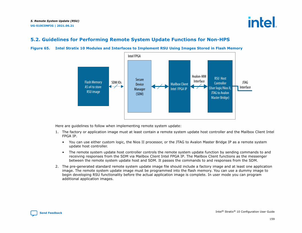
5.2. Guidelines for Performing Remote System Update Functions for Non-HPS
Figure 65. Intel Stratix 10 Modules and Interfaces to Implement RSU Using Images Stored in Flash Memory
Intel FPGA
SecureDevice
Manager(SDM)
Flash Memory AS x4 to store
RSU image
Avalon-MMInterface
Mailbox Client Intel FPGA IP
RSU HostController
(User logic/Nios II, JTAG to AvalonMaster Bridge)
JTAGInterface
SDM IOs
Here are guidelines to follow when implementing remote system update:
1. The factory or application image must at least contain a remote system update host controller and the Mailbox Client IntelFPGA IP.
• You can use either custom logic, the Nios II processor, or the JTAG to Avalon Master Bridge IP as a remote systemupdate host controller.
• The remote system update host controller controls the remote system update function by sending commands to andreceiving responses from the SDM via Mailbox Client Intel FPGA IP. The Mailbox Client functions as the messengerbetween the remote system update host and SDM. It passes the commands to and responses from the SDM.
2. The pre-generated standard remote system update image file should include a factory image and at least one applicationimage. The remote system update image must be programmed into the flash memory. You can use a dummy image tobegin developing RSU functionality before the actual application image is complete. In user mode you can programadditional application images.
5. Remote System Update (RSU)
UG-S10CONFIG | 2021.06.21
Send Feedback Intel® Stratix® 10 Configuration User Guide
159

• Refer to Generating Remote System Update Image Files Using the Programming File Generator on page 185 for thestep by step process to generate the standard and single remote system update image files using the programmingfile generator.
3. The remote system update requires you to use the AS x4 configuration scheme to configure the FPGA with the pre-generated remote system update image.
4. Once the device enters user mode with either the factory image or an application image, the remote system update hostcan perform the following remote system update operations:
a. Reconfiguring the device with an application or factory image:
i. From factory image to an application image or vice versa
ii. From an application image to another application image
b. Erasing the application image
c. Adding an application image
d. Updating an application or factory image
Related Information
• Intel Stratix 10 SoC Development Kit User Guide
• Mailbox Client Intel FPGA IP User Guide
5.3. Commands and Responses
The host controller communicates with the SDM using command and response packets via the Mailbox Client Intel FPGA IP.
The first word of the command and response packets is a header that provides basic information about the command orresponse.
Block Diagram
The following figure illustrates the role of the Mailbox Client Intel FPGA IP in a Intel Stratix 10 design. The Mailbox Client IPenables communication with the SDM to access quad SPI flash memory and system status.
5. Remote System Update (RSU)
UG-S10CONFIG | 2021.06.21
Intel® Stratix® 10 Configuration User Guide Send Feedback
160

Mailbox Client Role
SDMCommunication
Hub
MailboxDriver
SecureDevice
Manager
Hard IP
Controller
FIFO
FIFOJTAG toAvalon Master
Mailbox Client Intel FPGA IP
Soft IP
Avalon MMInterface
IRQ
Intel FPGA IP
Host Controller
Nios IIProcessor
Ethernet IP
PCIe Hard IP
Custom Logic
Host System
PC Running System Console
Figure 66. Command and Response Header Format
LengthID 0 0 Command/Error Code
012345678910111213141516171819202122232425262728293031
Reserved
Note: The LENGTH field in the command header must match the command length of corresponding command. Your client must readall the response words, even if your client does not interpret all the response words.
The following table describes the fields of the header command.
Table 38. Command and Response Header Description
Header Bit Description
Reserved [31:28] Reserved.
ID [27:24] The command ID. The response header returns the ID specified in the command header. Refer toOperation Commands for command descriptions.
0 [23] Reserved.
continued...
5. Remote System Update (RSU)
UG-S10CONFIG | 2021.06.21
Send Feedback Intel® Stratix® 10 Configuration User Guide
161
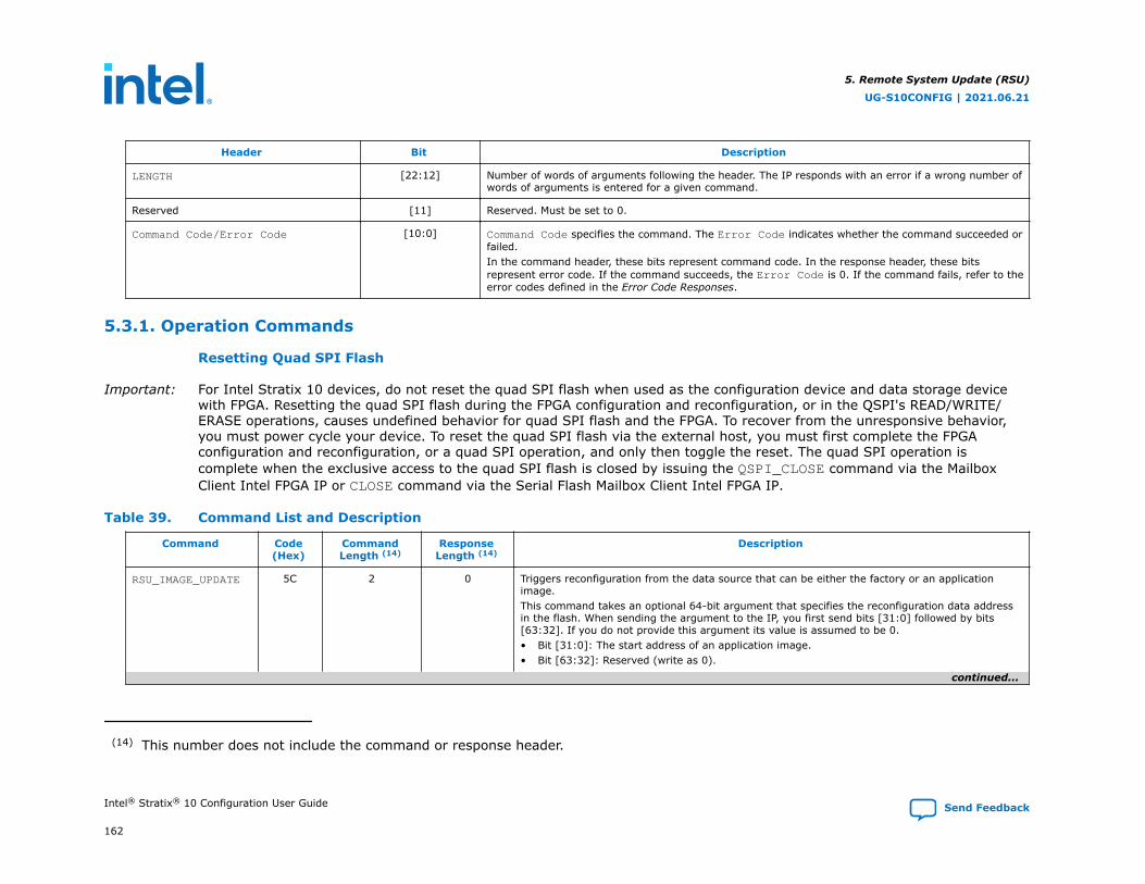
Header Bit Description
LENGTH [22:12] Number of words of arguments following the header. The IP responds with an error if a wrong number ofwords of arguments is entered for a given command.
Reserved [11] Reserved. Must be set to 0.
Command Code/Error Code [10:0] Command Code specifies the command. The Error Code indicates whether the command succeeded orfailed.In the command header, these bits represent command code. In the response header, these bitsrepresent error code. If the command succeeds, the Error Code is 0. If the command fails, refer to theerror codes defined in the Error Code Responses.
5.3.1. Operation Commands
Resetting Quad SPI Flash
Important: For Intel Stratix 10 devices, do not reset the quad SPI flash when used as the configuration device and data storage devicewith FPGA. Resetting the quad SPI flash during the FPGA configuration and reconfiguration, or in the QSPI's READ/WRITE/ERASE operations, causes undefined behavior for quad SPI flash and the FPGA. To recover from the unresponsive behavior,you must power cycle your device. To reset the quad SPI flash via the external host, you must first complete the FPGAconfiguration and reconfiguration, or a quad SPI operation, and only then toggle the reset. The quad SPI operation iscomplete when the exclusive access to the quad SPI flash is closed by issuing the QSPI_CLOSE command via the MailboxClient Intel FPGA IP or CLOSE command via the Serial Flash Mailbox Client Intel FPGA IP.
Table 39. Command List and Description
Command Code(Hex)
CommandLength (14)
ResponseLength (14)
Description
RSU_IMAGE_UPDATE 5C 2 0 Triggers reconfiguration from the data source that can be either the factory or an applicationimage.This command takes an optional 64-bit argument that specifies the reconfiguration data addressin the flash. When sending the argument to the IP, you first send bits [31:0] followed by bits[63:32]. If you do not provide this argument its value is assumed to be 0.• Bit [31:0]: The start address of an application image.• Bit [63:32]: Reserved (write as 0).
continued...
(14) This number does not include the command or response header.
5. Remote System Update (RSU)
UG-S10CONFIG | 2021.06.21
Intel® Stratix® 10 Configuration User Guide Send Feedback
162
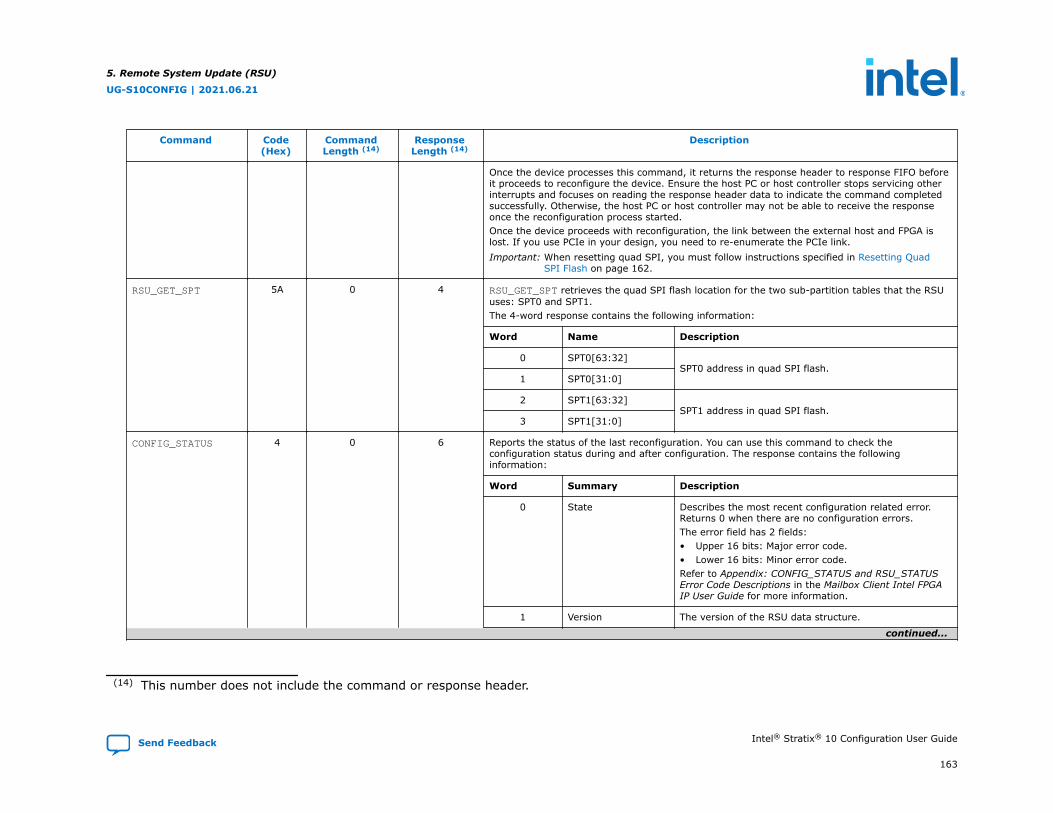
Command Code(Hex)
CommandLength (14)
ResponseLength (14)
Description
Once the device processes this command, it returns the response header to response FIFO beforeit proceeds to reconfigure the device. Ensure the host PC or host controller stops servicing otherinterrupts and focuses on reading the response header data to indicate the command completedsuccessfully. Otherwise, the host PC or host controller may not be able to receive the responseonce the reconfiguration process started.Once the device proceeds with reconfiguration, the link between the external host and FPGA islost. If you use PCIe in your design, you need to re-enumerate the PCIe link.Important: When resetting quad SPI, you must follow instructions specified in Resetting Quad
SPI Flash on page 162.
RSU_GET_SPT 5A 0 4 RSU_GET_SPT retrieves the quad SPI flash location for the two sub-partition tables that the RSUuses: SPT0 and SPT1.The 4-word response contains the following information:
Word Name Description
0 SPT0[63:32]SPT0 address in quad SPI flash.
1 SPT0[31:0]
2 SPT1[63:32]SPT1 address in quad SPI flash.
3 SPT1[31:0]
CONFIG_STATUS 4 0 6 Reports the status of the last reconfiguration. You can use this command to check theconfiguration status during and after configuration. The response contains the followinginformation:
Word Summary Description
0 State Describes the most recent configuration related error.Returns 0 when there are no configuration errors.The error field has 2 fields:• Upper 16 bits: Major error code.• Lower 16 bits: Minor error code.Refer to Appendix: CONFIG_STATUS and RSU_STATUSError Code Descriptions in the Mailbox Client Intel FPGAIP User Guide for more information.
1 Version The version of the RSU data structure.
continued...
(14) This number does not include the command or response header.
5. Remote System Update (RSU)
UG-S10CONFIG | 2021.06.21
Send Feedback Intel® Stratix® 10 Configuration User Guide
163

Command Code(Hex)
CommandLength (14)
ResponseLength (14)
Description
2 Pin status • Bit [31]: Current nSTATUS output value (active low)• Bit [30]: Detected nCONFIG input value (active low)• Bit [29:3]: Reserved• Bit [2:0]: The MSEL value at power up
3 Soft function status Contains the value of each of the soft functions, even ifyou have not assigned the function to an SDM pin.• Bit [31:6]: Reserved• Bit [5]: HPS_WARMRESET• Bit [4]: HPS_COLDRESET• Bit [3]: SEU_ERROR• Bit [2]: CVP_DONE• Bit [1]: INIT_DONE• Bit [0]: CONF_DONE
4 Error location Contains the error location. Returns 0 if there are noerrors.
5 Error details Contains the error details. Returns 0 if there are noerrors.
RSU_STATUS 5B 0 9 Reports the current remote system upgrade status. You can use this command to check theconfiguration status during configuration and after it has completed. This command returns thefollowing responses:
Word Summary Description
0-1 Current image Flash offset of the currently running application image.
2-3 Failing image Flash offset of the highest priority failing applicationimage. If multiple images are available in flash memory,stores the value of the first image that failed. A value ofall 0s indicates no failing images. If there are no failingimages, the remainder of the remaining words of thestatus information do not store valid information.
continued...
(14) This number does not include the command or response header.
5. Remote System Update (RSU)
UG-S10CONFIG | 2021.06.21
Intel® Stratix® 10 Configuration User Guide Send Feedback
164
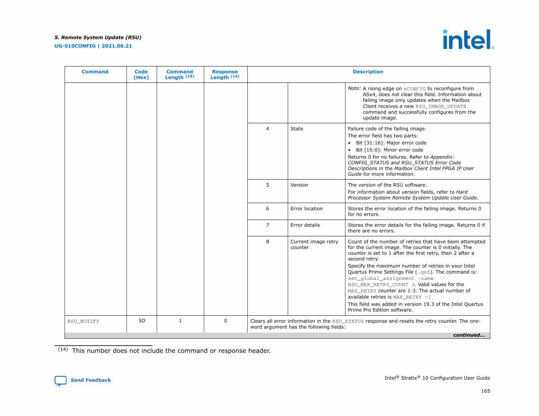
Command Code(Hex)
CommandLength (14)
ResponseLength (14)
Description
Note: A rising edge on nCONFIG to reconfigure fromASx4, does not clear this field. Information aboutfailing image only updates when the MailboxClient receives a new RSU_IMAGE_UPDATEcommand and successfully configures from theupdate image.
4 State Failure code of the failing image.The error field has two parts:• Bit [31:16]: Major error code• Bit [15:0]: Minor error codeReturns 0 for no failures. Refer to Appendix:CONFIG_STATUS and RSU_STATUS Error CodeDescriptions in the Mailbox Client Intel FPGA IP UserGuide for more information.
5 Version The version of the RSU software.For information about version fields, refer to HardProcessor System Remote System Update User Guide.
6 Error location Stores the error location of the failing image. Returns 0for no errors.
7 Error details Stores the error details for the failing image. Returns 0 ifthere are no errors.
8 Current image retrycounter
Count of the number of retries that have been attemptedfor the current image. The counter is 0 initially. Thecounter is set to 1 after the first retry, then 2 after asecond retry.Specify the maximum number of retries in your IntelQuartus Prime Settings File (.qsf). The command is:set_global_assignment -nameRSU_MAX_RETRY_COUNT 3. Valid values for theMAX_RETRY counter are 1-3. The actual number ofavailable retries is MAX_RETRY -1This field was added in version 19.3 of the Intel QuartusPrime Pro Edition software.
RSU_NOTIFY 5D 1 0 Clears all error information in the RSU_STATUS response and resets the retry counter. The one-word argument has the following fields:
continued...
(14) This number does not include the command or response header.
5. Remote System Update (RSU)
UG-S10CONFIG | 2021.06.21
Send Feedback Intel® Stratix® 10 Configuration User Guide
165
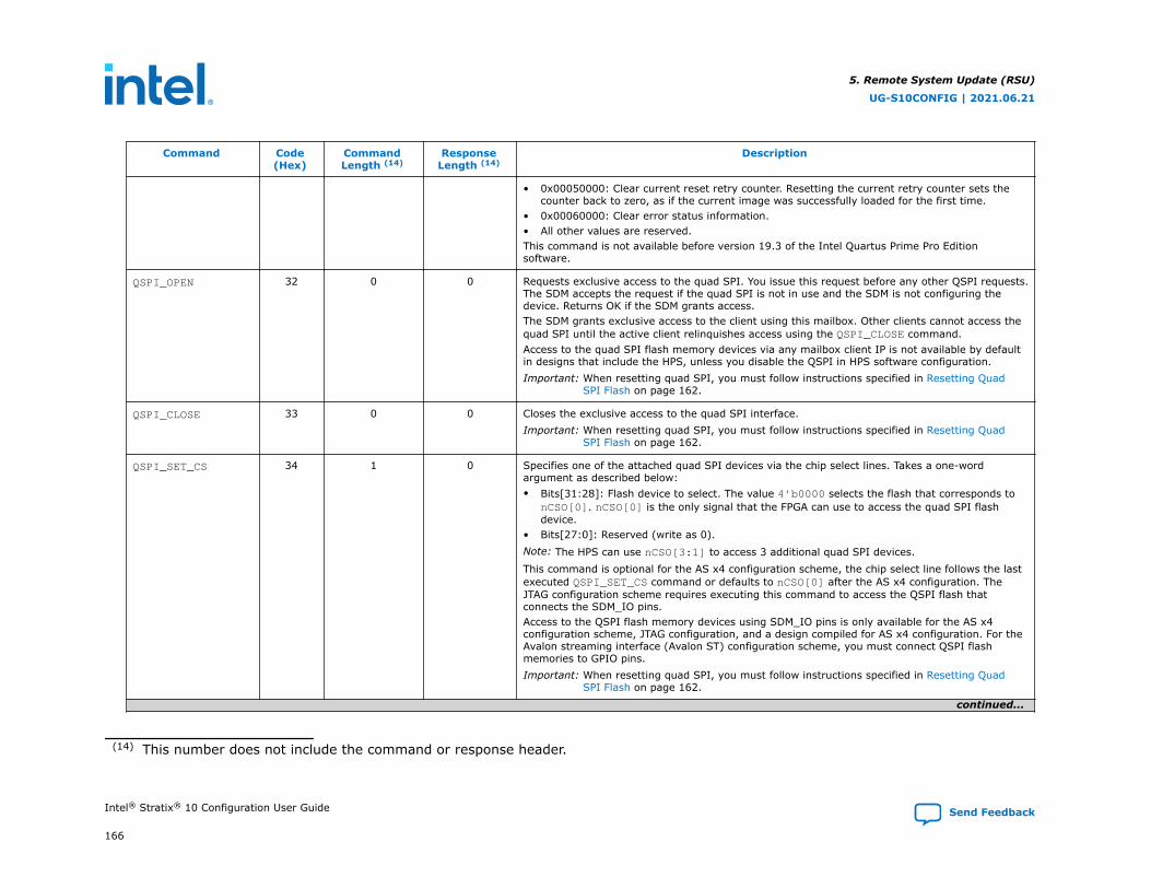
Command Code(Hex)
CommandLength (14)
ResponseLength (14)
Description
• 0x00050000: Clear current reset retry counter. Resetting the current retry counter sets thecounter back to zero, as if the current image was successfully loaded for the first time.
• 0x00060000: Clear error status information.• All other values are reserved.This command is not available before version 19.3 of the Intel Quartus Prime Pro Editionsoftware.
QSPI_OPEN 32 0 0 Requests exclusive access to the quad SPI. You issue this request before any other QSPI requests.The SDM accepts the request if the quad SPI is not in use and the SDM is not configuring thedevice. Returns OK if the SDM grants access.The SDM grants exclusive access to the client using this mailbox. Other clients cannot access thequad SPI until the active client relinquishes access using the QSPI_CLOSE command.Access to the quad SPI flash memory devices via any mailbox client IP is not available by defaultin designs that include the HPS, unless you disable the QSPI in HPS software configuration.Important: When resetting quad SPI, you must follow instructions specified in Resetting Quad
SPI Flash on page 162.
QSPI_CLOSE 33 0 0 Closes the exclusive access to the quad SPI interface.Important: When resetting quad SPI, you must follow instructions specified in Resetting Quad
SPI Flash on page 162.
QSPI_SET_CS 34 1 0 Specifies one of the attached quad SPI devices via the chip select lines. Takes a one-wordargument as described below:• Bits[31:28]: Flash device to select. The value 4'b0000 selects the flash that corresponds to
nCSO[0]. nCSO[0] is the only signal that the FPGA can use to access the quad SPI flashdevice.
• Bits[27:0]: Reserved (write as 0).Note: The HPS can use nCSO[3:1] to access 3 additional quad SPI devices.This command is optional for the AS x4 configuration scheme, the chip select line follows the lastexecuted QSPI_SET_CS command or defaults to nCSO[0] after the AS x4 configuration. TheJTAG configuration scheme requires executing this command to access the QSPI flash thatconnects the SDM_IO pins.Access to the QSPI flash memory devices using SDM_IO pins is only available for the AS x4configuration scheme, JTAG configuration, and a design compiled for AS x4 configuration. For theAvalon streaming interface (Avalon ST) configuration scheme, you must connect QSPI flashmemories to GPIO pins.Important: When resetting quad SPI, you must follow instructions specified in Resetting Quad
SPI Flash on page 162.
continued...
(14) This number does not include the command or response header.
5. Remote System Update (RSU)
UG-S10CONFIG | 2021.06.21
Intel® Stratix® 10 Configuration User Guide Send Feedback
166

Command Code(Hex)
CommandLength (14)
ResponseLength (14)
Description
QSPI_READ 3A 2 N Reads the attached quad SPI device. The maximum transfer size is 4 kilobytes (KB) or 1024words.Takes two arguments:• The quad SPI flash address (one word). The address must be word aligned. The device returns
the 0x1 error code for non-aligned addresses.• Number of words to read (one word).When successful, returns OK followed by the read data from the quad SPI device. A failureresponse returns an error code.For a partially successful read, QSPI_READ may erroneously return the OK status.Note: You cannot run the QSPI_READ command while device configuration is in progress.Important: When resetting quad SPI, you must follow instructions specified in Resetting Quad
SPI Flash on page 162.
QSPI_WRITE 39 2+N 0 Writes data to the quad SPI device. The maximum transfer size is 4 kilobytes (KB) or 1024 words.Takes three arguments:• The flash address offset (one word). The write address must be word aligned.• The number of words to write (one word).• The data to be written (one or more words).A successful write returns the OK response code.To prepare memory for writes, use the QSPI_ERASE command before issuing this command.Note: You cannot run the QSPI_WRITE command while device configuration is in progress.Important: When resetting quad SPI, you must follow instructions specified in Resetting Quad
SPI Flash on page 162.
QSPI_ERASE 38 2 0 Erases a 4/32/64 KB sector of the quad SPI device. Takes two arguments:
continued...
(14) This number does not include the command or response header.
5. Remote System Update (RSU)
UG-S10CONFIG | 2021.06.21
Send Feedback Intel® Stratix® 10 Configuration User Guide
167
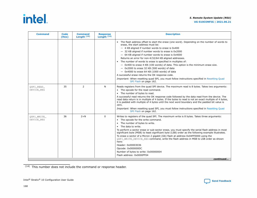
Command Code(Hex)
CommandLength (14)
ResponseLength (14)
Description
• The flash address offset to start the erase (one word). Depending on the number of words toerase, the start address must be:— 4 KB aligned if number words to erase is 0x400— 32 KB aligned if number words to erase is 0x2000— 64 KB aligned if number words to erase is 0x4000Returns an error for non-4/32/64 KB aligned addresses.
• The number of words to erase is specified in multiples of:— 0x400 to erase 4 KB (100 words) of data. This option is the minimum erase size.— 0x2000 to erase 32 KB (500 words) of data— 0x4000 to erase 64 KB (1000 words) of data
A successful erase returns the OK response code.Important: When resetting quad SPI, you must follow instructions specified in Resetting Quad
SPI Flash on page 162.
QSPI_READ_DEVICE_REG
35 2 N Reads registers from the quad SPI device. The maximum read is 8 bytes. Takes two arguments:• The opcode for the read command.• The number of bytes to read.A successful read returns the OK response code followed by the data read from the device. Theread data return is in multiple of 4 bytes. If the bytes to read is not an exact multiple of 4 bytes,it is padded with multiple of 4 bytes until the next word boundary and the padded bit value iszero.Important: When resetting quad SPI, you must follow instructions specified in Resetting Quad
SPI Flash on page 162.
QSPI_WRITE_DEVICE_REG
36 2+N 0 Writes to registers of the quad SPI. The maximum write is 8 bytes. Takes three arguments:• The opcode for the write command.• The number of bytes to write.• The data to write.To perform a sector erase or sub-sector erase, you must specify the serial flash address in mostsignificant byte (MSB) to least significant byte (LSB) order as the following example illustrates.To erase a sector of a Micron 2 gigabit (Gb) flash at address 0x04FF0000 using theQSPI_WRITE_DEVICE_REG command, write the flash address in MSB to LSB order as shownhere:Header: 0x00003036Opcode: 0x000000DCNumber of bytes to write: 0x00000004Flash address: 0x0000FF04
continued...
(14) This number does not include the command or response header.
5. Remote System Update (RSU)
UG-S10CONFIG | 2021.06.21
Intel® Stratix® 10 Configuration User Guide Send Feedback
168

Command Code(Hex)
CommandLength (14)
ResponseLength (14)
Description
A successful write returns the OK response code. This command pads data that is not a multipleof 4 bytes to the next word boundary. The command pads the data with zero.Important: When resetting quad SPI, you must follow instructions specified in Resetting Quad
SPI Flash on page 162.
QSPI_SEND_DEVICE_OP
37 1 0 Sends a command opcode to the quad SPI. Takes one argument:• The opcode to send the quad SPI device.A successful command returns the OK response code.Important: When resetting quad SPI, you must follow instructions specified in Resetting Quad
SPI Flash on page 162.
For CONFIG_STATUS and RSU_STATUS major and minor error code descriptions, refer to Appendix: CONFIG_STATUS andRSU_STATUS Error Code Descriptions in the Mailbox Client Intel FPGA IP User Guide.
Related Information
• Mailbox Client Intel FPGA IP User Guide: CONFIG_STATUS and RSU_STATUS Error Code DescriptionsFor more information about the CONFIG_STATUS and RSU_STATUS error codes.
• Intel Stratix 10 Hard Processor System Remote System Update User GuideFor more information about version fields.
5.3.2. Error Code Responses
Table 40. Error Codes
Value (Hex) Error Code Response Description
0 OK Indicates that the command completed successfully.A command may erroneously return the OK status if a command, such as QSPI_READ is partially successful.
1 INVALID_COMMAND Indicates that the currently loaded boot ROM cannot decode or recognize the command code.
3 UNKNOWN_COMMAND Indicates that the currently loaded firmware cannot decode the command code.
4 INVALID_COMMAND_PARAMETERS Indicates that the command is incorrectly formatted. For example, the length field setting in header is not valid.
continued...
(14) This number does not include the command or response header.
5. Remote System Update (RSU)
UG-S10CONFIG | 2021.06.21
Send Feedback Intel® Stratix® 10 Configuration User Guide
169
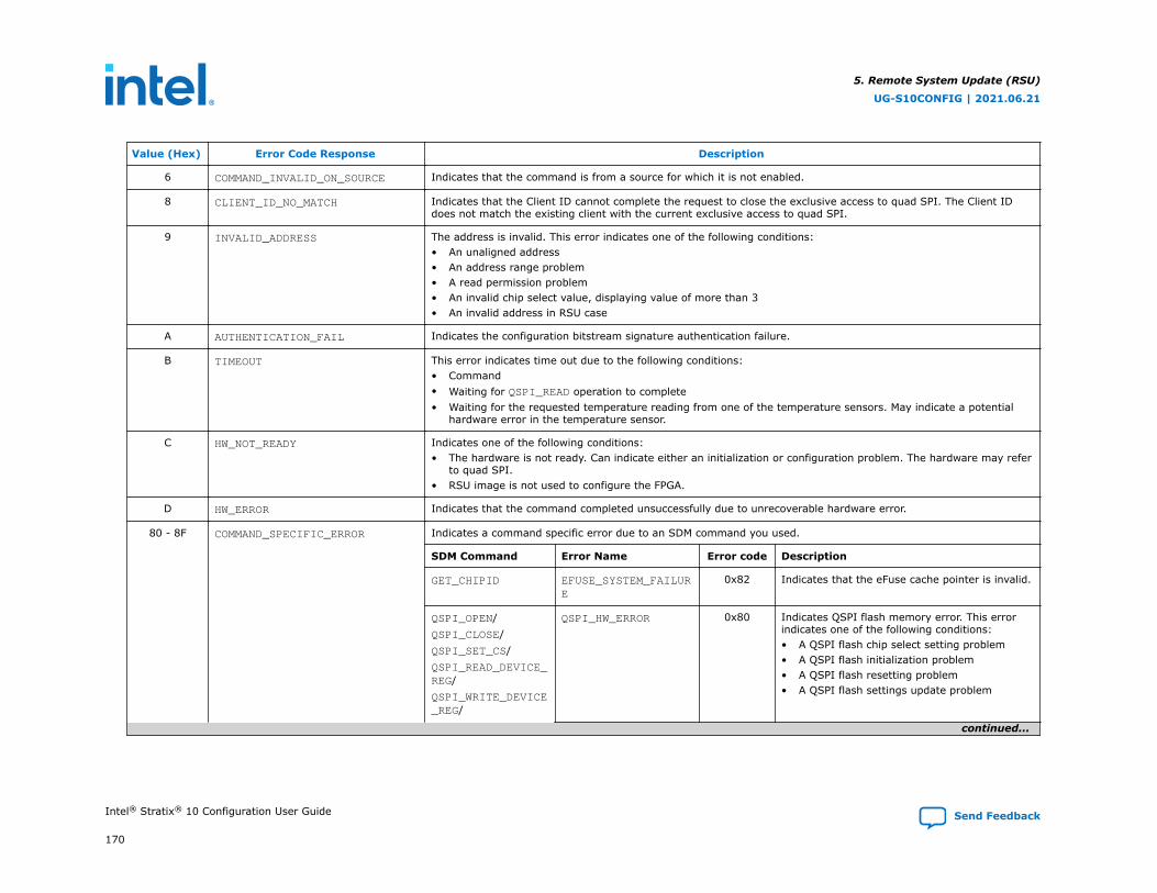
Value (Hex) Error Code Response Description
6 COMMAND_INVALID_ON_SOURCE Indicates that the command is from a source for which it is not enabled.
8 CLIENT_ID_NO_MATCH Indicates that the Client ID cannot complete the request to close the exclusive access to quad SPI. The Client IDdoes not match the existing client with the current exclusive access to quad SPI.
9 INVALID_ADDRESS The address is invalid. This error indicates one of the following conditions:• An unaligned address• An address range problem• A read permission problem• An invalid chip select value, displaying value of more than 3• An invalid address in RSU case
A AUTHENTICATION_FAIL Indicates the configuration bitstream signature authentication failure.
B TIMEOUT This error indicates time out due to the following conditions:• Command• Waiting for QSPI_READ operation to complete• Waiting for the requested temperature reading from one of the temperature sensors. May indicate a potential
hardware error in the temperature sensor.
C HW_NOT_READY Indicates one of the following conditions:• The hardware is not ready. Can indicate either an initialization or configuration problem. The hardware may refer
to quad SPI.• RSU image is not used to configure the FPGA.
D HW_ERROR Indicates that the command completed unsuccessfully due to unrecoverable hardware error.
80 - 8F COMMAND_SPECIFIC_ERROR Indicates a command specific error due to an SDM command you used.
SDM Command Error Name Error code Description
GET_CHIPID EFUSE_SYSTEM_FAILURE
0x82 Indicates that the eFuse cache pointer is invalid.
QSPI_OPEN/QSPI_CLOSE/QSPI_SET_CS/QSPI_READ_DEVICE_REG/QSPI_WRITE_DEVICE_REG/
QSPI_HW_ERROR 0x80 Indicates QSPI flash memory error. This errorindicates one of the following conditions:• A QSPI flash chip select setting problem• A QSPI flash initialization problem• A QSPI flash resetting problem• A QSPI flash settings update problem
continued...
5. Remote System Update (RSU)
UG-S10CONFIG | 2021.06.21
Intel® Stratix® 10 Configuration User Guide Send Feedback
170

Value (Hex) Error Code Response Description
QSPI_SEND_DEVICE_OP/QSPI_READ
QSPI_ALREADY_OPEN 0x81 Indicates that the client's exclusive access toQSPI flash via QSPI_OPEN command is alreadyopen.
100 NOT_CONFIGURED Indicates that the device is not configured.
1FF ALT_SDM_MBOX_RESP_DEVICE_ BUSY
Indicates that the device is busy due to following use cases:• RSU: Firmware is unable to transition to different version due to an internal error.• HPS: HPS is busy when in HPS reconfiguration process or HPS cold reset.
2FF ALT_SDM_MBOX_RESP_NO_VALID_RESP_AVAILABLE
Indicates that there is no valid response available.
3FF ALT_SDM_MBOX_RESP_ERROR General Error.
5.3.3. Error Code Recovery
The table below describes possible steps to recover from an error code. Error recovery depends on specific use case.
Table 41. Error Code Recovery for known Error Codes
Value Error Code Response Error Code Recovery
4 INVALID_COMMAND_PARAMETERS Resend the command header or header with arguments with corrected parameters.For example, ensures that the length field setting in header is sent with the correct value.
6 COMMAND_INVALID_ON_SOURCE Resend the command from valid source such as JTAG, HPS, or core fabric.
8 CLIENT_ID_NO_MATCH Wait for the client who opened the access to quad SPI to complete its access and then closes the exclusiveaccess to quad SPI.
9 INVALID_ADDRESS Possible error recovery steps:For QSPI operation:• Send command with a valid chip select.• Send command with a valid QSPI flash address.For RSU: Send command with a valid start address of the factory image or application.
B TIMEOUT Possible recovery steps:For QSPI operation: Check signal integrity of QSPI interfaces and attempt command again.For HPS restart operation: Retry to send the command again.
continued...
5. Remote System Update (RSU)
UG-S10CONFIG | 2021.06.21
Send Feedback Intel® Stratix® 10 Configuration User Guide
171

Value Error Code Response Error Code Recovery
C HW_NOT_READY Possible recovery steps:For QSPI operation: Reconfigure the device via source. Ensure that IP used to build your design allows access tothe QSPI flash.For RSU: Configure the device with RSU image.
80 QSPI_HW_ERROR Check the QSPI interface signal integrity and to ensure the QSPI device is not damaged.
81 QSPI_ALREADY_OPEN Client already opened QSPI. Continue with the next operation.
82 EFUSE_SYSTEM_FAILURE Attempt reconfiguration or power cycle. If error persists after reconfiguration or power cycle, the device may bedamaged and unrecoverable.
100 NOT_CONFIGURED Send a bitstream that configures the HPS.
1FF ALT_SDM_MBOX_RESP_DEVICE_ BUSY Possible error recovery steps:For QSPI operation: Wait for ongoing configuration or other client to complete operation.For RSU: Reconfigure device to recover from internal error.For HPS restart operation: Wait for reconfiguration via HPS or HPS Cold Reset to complete.
5.4. Quad SPI Flash Layout
5.4.1. High Level Flash Layout
5.4.1.1. Standard (non-RSU) Image Layout in Flash
In the standard (non-RSU) case, the flash contains four firmware images and the application image. To guard against possiblecorruption, there are four redundant copies of the firmware. The firmware contains a pointer to the location of the applicationimage in flash.
5. Remote System Update (RSU)
UG-S10CONFIG | 2021.06.21
Intel® Stratix® 10 Configuration User Guide Send Feedback
172
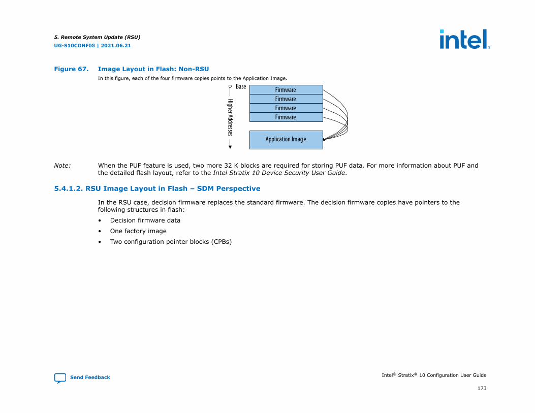
Figure 67. Image Layout in Flash: Non-RSUIn this figure, each of the four firmware copies points to the Application Image.
FirmwareFirmwareFirmwareFirmware
Application Image
Higher Addresses
Base
Direct to FactoryDirect to Factory
Note: When the PUF feature is used, two more 32 K blocks are required for storing PUF data. For more information about PUF andthe detailed flash layout, refer to the Intel Stratix 10 Device Security User Guide.
5.4.1.2. RSU Image Layout in Flash – SDM Perspective
In the RSU case, decision firmware replaces the standard firmware. The decision firmware copies have pointers to thefollowing structures in flash:
• Decision firmware data
• One factory image
• Two configuration pointer blocks (CPBs)
5. Remote System Update (RSU)
UG-S10CONFIG | 2021.06.21
Send Feedback Intel® Stratix® 10 Configuration User Guide
173

Figure 68. RSU Image Layout in Flash : SDM PerspectiveIn this figure:
• Each of the Decision Firmware copies point to the Factory Image and both Pointer Block 0 and Pointer Block 1.
• Both Pointer Block 0 and Pointer Block 1 point to Application Images.
Decision FirmwareDecision FirmwareDecision FirmwareDecision Firmware
Pointer Block 0 Pointer B lock 1
Factory Image
Application Image 1
Application Image 2
Higher Addresses
Base
Decision Firmware Data
Can be updated only through an update imageCan be written directly
Note: When the PUF feature is used, two more 32 K blocks are required for storing PUF data. For more information about PUF andthe detailed flash layout, refer to the Intel Stratix 10 Device Security User Guide.
5. Remote System Update (RSU)
UG-S10CONFIG | 2021.06.21
Intel® Stratix® 10 Configuration User Guide Send Feedback
174
The decision firmware data stores basic settings, including the following:
• The clock and pins that connect to quad SPI flash memory
• The Direct to Factory Image pin that forces the SDM to load the factory image
Note: You can set this pin on the following menu in the factory image project: Assignments ➤ Device ➤ Device andPin Options ➤ Configuration ➤ Configuration Pin Options
• The max_retry parameter value.
The max_retry value, stored as an 8-bit value at address 0x10018C in flash, is the only accessible field from thedecision firmware data structure. The value in flash is max_retry - 1. That is, a value of zero means each image istried just once. Modification of the max_retry value directly in the bitstream stored in flash is typically used by RSU viaHPS. For more information, refer to Intel Stratix 10 Hard Processor System Remote System Update User Guide.
The pointer blocks contain a list of application images to try until one of them is successful. If none is successful, the SDMloads the factory image. To ensure reliability, the pointer block includes a main and a backup copy in case an update operationfails.
Both the factory image and the application images start with firmware. First, the decision firmware loads the firmware. Then,that firmware loads the rest of the image. These implementation details are not shown in the figure above. For moreinformation, refer to the Application Image Layout section.
Related Information
• Application Image Layout on page 183
• Intel Stratix 10 Hard Processor System Remote System Update User Guide
5.4.1.2.1. Firmware Version Information
The Intel Quartus Prime firmware version is stored as a 32bit value at offset 0x420 in the following:
• Decision firmware (each of the four copies),
• Application images,
• Factory update images,
• Decision firmware update images,
• Combined application images.
The format for the version field is described below:
5. Remote System Update (RSU)
UG-S10CONFIG | 2021.06.21
Send Feedback Intel® Stratix® 10 Configuration User Guide
175

Table 42. Firmware Version Fields
Bit Field Bits Description
version_major 31:24 Major release number for Intel Quartus Prime. Example: set to 20 for release 20.1.
version_minor 23:16 Minor release number for Intel Quartus Prime. Example: set to 1 for release 20.1.
version_update 15:8 Update release number for Intel Quartus Prime. Example: set to 2 for release 20.1.2
reserved 7:0 Set to zero
Both U-Boot and LibRSU enable the decision firmware versions to be queried. For examples on querying the decision firmwareversion for both U-Boot and Linux, refer to the Remote System Update Example section. The decision firmware version mustfirst be queried in U-Boot for the value to be available in Linux.
5.4.1.3. RSU Image Layout – Your Perspective
The sub-partition table (SPT) is used for managing the allocation of the quad SPI flash.
The Intel Quartus Prime Programming File Generator creates the SPT when creating the initial manufacturing image. Toensure reliable operation, the Programming File Generator creates two copies of the sub-partition table and the configurationpointer block, SPT0 and SPT1 and CPB0 and CPB1
The initial RSU image stored in flash typically contains the following partitions:
Table 43. Typical Sub-Partitions of the RSU Image
Sub-partition Name Contents
BOOT_INFO Decision firmware and decision firmware data
FACTORY_IMAGE Factory Image
SPT0 Sub-partition table 0
SPT1 Sub-partition table 1
CPB0 Pointer block 0
CPB1 Pointer block 1
P1 Application image 1
P2 Application image 2
5. Remote System Update (RSU)
UG-S10CONFIG | 2021.06.21
Intel® Stratix® 10 Configuration User Guide Send Feedback
176

Figure 69. RSU Image Layout - Your PerspectiveIn this figure:
• SPT0 and SPT1 point to everything:
— BOOT_INFO
— Factory Image
— Pointer Block 0 and Pointer Block 1
— All Application Images
• Pointer Block 0 and Pointer Block 1 point to all Application Images
BOOT_INFO
Factory Image
Sub Partition Table 0 Sub Partition Table 1
Pointer Block 0Pointer Block 1
Application Image 0
Application Image 1
Higher Addresses
base
Can only be updated through an update image
Can be written directlySDM does not use
Note: When the PUF feature is used, two more 32 K blocks are required for storing PUF data. For more information about PUF andthe detailed flash layout, refer to the Intel Stratix 10 Device Security User Guide.
5. Remote System Update (RSU)
UG-S10CONFIG | 2021.06.21
Send Feedback Intel® Stratix® 10 Configuration User Guide
177
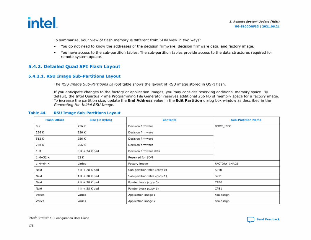
To summarize, your view of flash memory is different from SDM view in two ways:
• You do not need to know the addresses of the decision firmware, decision firmware data, and factory image.
• You have access to the sub-partition tables. The sub-partition tables provide access to the data structures required forremote system update.
5.4.2. Detailed Quad SPI Flash Layout
5.4.2.1. RSU Image Sub-Partitions Layout
The RSU Image Sub-Partitions Layout table shows the layout of RSU image stored in QSPI flash.
If you anticipate changes to the factory or application images, you may consider reserving additional memory space. Bydefault, the Intel Quartus Prime Programming File Generator reserves additional 256 kB of memory space for a factory image.To increase the partition size, update the End Address value in the Edit Partition dialog box window as described in theGenerating the Initial RSU Image.
Table 44. RSU Image Sub-Partitions Layout
Flash Offset Size (in bytes) Contents Sub-Partition Name
0 K 256 K Decision firmware BOOT_INFO
256 K 256 K Decision firmware
512 K 256 K Decision firmware
768 K 256 K Decision firmware
1 M 8 K + 24 K pad Decision firmware data
1 M+32 K 32 K Reserved for SDM
1 M+64 K Varies Factory image FACTORY_IMAGE
Next 4 K + 28 K pad Sub-partition table (copy 0) SPT0
Next 4 K + 28 K pad Sub-partition table (copy 1) SPT1
Next 4 K + 28 K pad Pointer block (copy 0) CPB0
Next 4 K + 28 K pad Pointer block (copy 1) CPB1
Varies Varies Application image 1 You assign
Varies Varies Application image 2 You assign
5. Remote System Update (RSU)
UG-S10CONFIG | 2021.06.21
Intel® Stratix® 10 Configuration User Guide Send Feedback
178
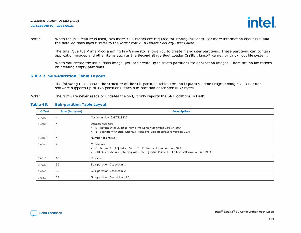
Note: When the PUF feature is used, two more 32 K blocks are required for storing PUF data. For more information about PUF andthe detailed flash layout, refer to the Intel Stratix 10 Device Security User Guide.
The Intel Quartus Prime Programming File Generator allows you to create many user partitions. These partitions can containapplication images and other items such as the Second Stage Boot Loader (SSBL), Linux* kernel, or Linux root file system.
When you create the initial flash image, you can create up to seven partitions for application images. There are no limitationson creating empty partitions.
5.4.2.2. Sub-Partition Table Layout
The following table shows the structure of the sub-partition table. The Intel Quartus Prime Programming File Generatorsoftware supports up to 126 partitions. Each sub-partition descriptor is 32 bytes.
Note: The firmware never reads or updates the SPT, it only reports the SPT locations in flash.
Table 45. Sub-partition Table Layout
Offset Size (in bytes) Description
0x000 4 Magic number 0x57713427
0x004 4 Version number:• 0 - before Intel Quartus Prime Pro Edition software version 20.4• 1 - starting with Intel Quartus Prime Pro Edition software version 20.4
0x008 4 Number of entries
0x00C 4 Checksum:• 0 - before Intel Quartus Prime Pro Edition software version 20.4• CRC32 checksum - starting with Intel Quartus Prime Pro Edition software version 20.4
0x010 16 Reserved
0x020 32 Sub-partition Descriptor 1
0x040 32 Sub-partition Descriptor 2
0xFE0 32 Sub-partition Descriptor 126
5. Remote System Update (RSU)
UG-S10CONFIG | 2021.06.21
Send Feedback Intel® Stratix® 10 Configuration User Guide
179

Starting with Intel Quartus Prime Pro Edition software version 20.4, the SPT header contains a CRC32 checksum that iscomputed over the whole SPT. The value of the CRC32 checksum filed itself is assumed as zero when the checksum iscomputed. Refer to Application Image Layout on page 183 for the algorithm used to compute the CRC32 checksum. Thechecksum is provided as a convenience so that SPT corruptions can better be detected by HPS software. By default thefeature is turned off.
Each 32-byte sub-partition descriptor contains the following information:
Table 46. Sub-partition Descriptor Layout
Offset Size Description
0x00 16 Sub-partition name, including a null string terminator
0x10 8 Sub-partition start offset
0x18 4 Sub-partition length
0x1C 4 Sub-partition flags
Two flags are currently defined:
• System set to 1: Reserved for RSU system. For partition offset value, refer to Table 44 on page 178.
• Read only set to 1: The system protects partition against direct writes.
The Intel Quartus Programming File Generator sets these flags as follows at image creation time, then they are not changedafterward:
Table 47. Flags Specifying Contents and Access
Partition System Read Only
BOOT_INFO 1 1
FACTORY_IMAGE 1 1
SPT0 1 0
SPT1 1 0
CPB0 1 0
continued...
5. Remote System Update (RSU)
UG-S10CONFIG | 2021.06.21
Intel® Stratix® 10 Configuration User Guide Send Feedback
180

Partition System Read Only
CPB1 1 0
P1 0 0
P2 0 0
5.4.2.3. Configuration Pointer Block Layout
The configuration pointer block contains a list of application image addresses. The SDM tries the images in sequence until oneof them is successful or all fail. The structure contains the following information:
Table 48. Pointer Block Layout
Offset Size (in bytes) Description
0x00 4 Magic number 0x57789609
0x04 4 Size of pointer block header (0x18 for this document)
0x08 4 Size of pointer block (4096 for this document)
0x0C 4 Reserved
0x10 4 Offset to image pointers (IPTAB)
0x14 4 Number of image pointer slots (NSLOTS)
0x18 8 Reserved
0x20 (IPTAB)(15) 8 First (lowest priority) image pointer slot (IPTAB)
8 Second (2nd lowest priority) image pointer slot
8 …
8 Last (highest priority) image pointer
The configuration pointer block can contain up to 508 application image pointers. The actual number is listed as NSLOTS. Atypical configuration pointer block update procedure consists of adding a new pointer and potentially clearing an older pointer.Typically, the pointer block update uses one additional entry. Consequently, you can make 508 updates before the pointer
(15) The offset may vary in future firmware updates.
5. Remote System Update (RSU)
UG-S10CONFIG | 2021.06.21
Send Feedback Intel® Stratix® 10 Configuration User Guide
181

block must be erased. The erase procedure is called pointer block compression. This procedure is power failure safe, as thereare two copies of the pointer block. The copies are in different flash erase sectors. While one copy is being updated the othercopy is still valid.
5.4.2.4. Modifying the List of Application Images
The SDM uses the configuration pointer block to determine priority of application images.
The pointer block operates by taking into account the following characteristics of quad SPI flash memory:
• On a sector erase, all the sector flash bits become 1’s.
• A program operation can only turn 1’s into 0’s.
The pointer block contains an array of values which have the following meaning:
• All 1’s – the entry is unused. The client can write a pointer to this entry. This is the state after a quad SPI erase operationoccurs on the pointer block.
• All 0’s – the entry has been previously used and then canceled.
• A combination of 1's and 0's – a valid pointer to an application image.
When the configuration pointer block is erased, all entries are marked as unused. To add an application image to the list, theclient finds the first unused location and writes the application image address to this location. To remove an application imagefrom the list, the client finds the application image address in the pointer block list and writes all 0's to this address.
If the configuration pointer block runs out of space for new application images, the client compresses the pointer block bycompleting the following actions:
1. Read all the valid entries from the configuration
2. Erase the pointer block
3. Add all previously valid entries
4. Add the new image
When using HPS to manage RSU, both the U-Boot and LIBRSU clients implement the block compression. For designs thatdrive RSU from FPGA logic, you can implement pointer block compression many different ways, including Nios II code, ascripting language, or a state machine.
Pointer block compression does not occur frequently because the pointer block has up to 508 available entries.
5. Remote System Update (RSU)
UG-S10CONFIG | 2021.06.21
Intel® Stratix® 10 Configuration User Guide Send Feedback
182

There are two configuration pointer blocks: a primary (CPB0) and a backup (CPB1). Two blocks enable the list of applicationimages to be protected if a power failure occurs just after erasing one of them. When a CPB is erased and re-created, theheader is written last. The CPB header is checked prior to use to prevent accidental use if a power failure occurred. For moreinformation, refer to the Configuration Pointer Block Layout topic. When compressing, the client compresses (erases andrewrites) the primary CPB completely. Once the primary CPB is valid, it is safe to modify the secondary CPB. When rewriting,the magic number at the start of a CPB is the last word written in the CPB. (After this number is written only image pointerslot values can be changed.)
When the client writes the application image to flash, it ensures that the pointers within the main image pointer of its firstsignature block are updated to point to the correct locations in flash. When using HPS to manage RSU, both the U-Boot andLIBRSU clients implement the required pointer updates. For more information, refer to the Application Image Layout section.
Related Information
• Configuration Pointer Block Layout on page 181
• Application Image Layout on page 183
5.4.2.5. Application Image Layout
The application image comprises SDM firmware and the configuration data. The configuration data includes up to foursections. The SDM firmware contains pointers to those sections. The table below shows the location of the number of sectionsand the section pointers in a application image.
Table 49. Application Image Section Pointers
Offset Size (in bytes) Description
0x1F00 4 Number of sections
…
0x1F08 8 Address of 1st section
0x1F10 8 Address of 2nd section
0x1F18 8 Address of 3rd section
0x1F20 8 Address of 4th section
…
0x1FFC 4 CRC32 of 0x1000 to 0x1FFB
5. Remote System Update (RSU)
UG-S10CONFIG | 2021.06.21
Send Feedback Intel® Stratix® 10 Configuration User Guide
183
The section pointers must match the actual location of the FPGA image in flash. Two options are available to meet thisrequirement:
• You can generate the application image to match the actual location in quad SPI flash memory. This option may not bepractical as different systems may have a different set of updates applied, which may result in different slots beingsuitable to store the new application image.
• You can generate the application image as if it is located at address zero, then update the pointers to match the actuallocation.
— In Intel Quartus Prime software version 21.1 or later, a Use relative address option is the default option to generatea single application bitstream. You do not have to specify the start address since you can program the image to anyavailable location in the QSPI flash memory. To load the image, you must correctly point to the starting address of thestored image in the flash memory.
If you choose to disable this option, unselect the Use relative address checkbox and provide the Start address forthe image in flash memory. For more information, refer to Generating an Application Image.
When using the HPS to manage RSU, both U-Boot and LIBRSU clients implement the below procedure to relocate applicationimages targeting address zero in the actual destination slot address.
The procedure to update the pointers from an application image created for INITIAL_ADDRESS to NEW_ADDRESS is:
1. Create the application image, targeting the INITIAL_ADDRESS.
2. Read the 32-bit value from offset 0x1F00 of the application image to determine the number of sections.
3. For <s>= 1 to number_of_sections:
a. section_pointer = read the 64-bit section pointer from 0x1F00 + (s * 8)
b. Subtract INITIAL_ADDRESS from section_pointer
c. Add NEW_ADDRESS to section_pointer
d. Store updated section_pointer
4. Recompute the CRC32 for addresses 0x1000 to 0x1FFB. Store the new value at offset 0x1FFC. The CRC32 value must becomputed on a copy of the data using the following procedure:
a. Swap the bits of each byte so that the bits occur in reverse order and compute the CRC.
b. Swap the bytes of the computed CRC32 value to appear in reverse order.
c. Swap the bits in each byte of the CRC32 value.
d. Write the CRC32 value to flash.
5. Remote System Update (RSU)
UG-S10CONFIG | 2021.06.21
Intel® Stratix® 10 Configuration User Guide Send Feedback
184
Note: The factory update image has a different format, which requires a different procedure for the pointer updates. When using theHPS to manage RSU, both U-Boot and LIBRSU clients implement this procedure for relocating the factory update image.
Note: The combined application image has a different format, with no pointers that need to be relocated. The image can be placedunmodified in flash at any address.
Related Information
• Generating a Factory Update Image on page 194
• Generating an Application Image on page 192
5.5. Generating Remote System Update Image Files Using the Programming File Generator
Use the Intel Quartus Prime Programming File Generator tool to generate the Intel Stratix 10 remote system update flashprogramming files.
5.5.1. Generating the Initial RSU Image
Follow below steps to generate the initial RSU Image.
For generic applications, you can generate the initial image using the .sof file.
For security application when you need to generate a signed or encrypted .rbf file, you need to first generate .rbf file froma .sof file, and only then generate the initial RSU image from the .rbf file. Refer to Intel Stratix 10 Device Security UserGuide for more information about the generation of the signed or encrypted .rbf file.
Important: You must update the decision firmware (CMF) in the Intel Quartus Prime software version 21.1 or later if you want to use anRSU image generated with Intel Quartus Prime software version 20.4 or prior along with any factory or application image(s)generated in Intel Quartus Prime software version 21.1 or later. For more information, refer to Updating Decision Firmware onpage 191.
Related Information
• Intel Stratix 10 Device Security User Guide
• Updating Decision Firmware on page 191
5. Remote System Update (RSU)
UG-S10CONFIG | 2021.06.21
Send Feedback Intel® Stratix® 10 Configuration User Guide
185
5.5.1.1. Generating the Initial RSU Image Using .sof Files
View the video guide and complete the following steps to generate the initial RSU image:
1. On the File menu, click Programming File Generator.
2. Select Intel Stratix 10 from the Device family drop-down list.
3. Select the configuration scheme from the Configuration mode drop-down list. The current Intel Quartus Prime onlysupports remote system update feature in Active Serial x4.
4. On the Output Files tab, assign the output directory and file name.
5. Select the output file type.
Select the following file types for AS x4 configuration mode:
• JTAG Indirect Configuration File (.jic)/Programmer Object File (.pof)
• Memory Map File (.map)
• Raw Programming File (.rpd)
6. On the Input Files tab, click Add Bitstream, select the factory image .sof file and click Open. Repeat this step for theapplication image .sof.
7. On the Configuration Device tab, click Add Device, select your flash memory and click OK. The Programming FileGenerator tool automatically populates the flash partitions.
5. Remote System Update (RSU)
UG-S10CONFIG | 2021.06.21
Intel® Stratix® 10 Configuration User Guide Send Feedback
186

8. Select the FACTORY_IMAGE partition and click Edit.
9. In the Edit Partition dialog box, select your factory image .sof file in the Input file drop-down list and click OK.
Note: You must assign Page 0 to Factory Image. Intel recommends that you let the Intel Quartus Prime software assignthe Start address of the FACTORY_IMAGE automatically by retaining the default value for Address Mode which isAuto. From the Address Mode drop down list, select Block to set an End address value for the FACTORY_IMAGE.The Programming File Generator reserves and assigns the start and end flash addresses to store BOOT_INFO,SPT0, SPT1, CPB0, and CPB1.
10. Select the flash memory and click Add Partition.
11. In the Add Partition dialog box, select for application image .sof file from the Input file drop-down list, assign thepage number.
12. Repeat this step for additional application images and click OK. You can add up to seven partitions for seven applicationimages. The page 1 application image is the highest priority, and the page 7 image is the lowest priority.
13. For .jic files,
Click Select at the Flash loader, select your device family and device name, and click OK.
14. Click Generate to generate the remote system update programming files. After generating the programming file, you canproceed to program the flash memory.
Note: The generated .jic file contains only the initial flash data. If a remote host updates the initial flash image and thenthe application performs a verify operation, the verify operation fails. Verification fails because the verify operationcompares the updated image to the initial flash data. If you want to verify the updated flash image, you read backthe updated image from flash and compare it to the expected .rpd file.
You can use the programmer to examine the flash content and compare it to the new flash image .rpd.
Note: If you plan to update the factory image, Intel recommends reserving an additional 64 KB space for possibleexpansion of the factory image. Complete the following steps to reserve extra space for updates to the factoryimage:
a. Identify the new end address by adding 64 KB to the existing END ADDRESS of the FACTORY_IMAGE. The endaddress is available in the .map file. For example, if the current end address is 0x00423FF, the new end address is0x00523FF .
b. Repeat the steps to regenerate the new .jic file. On the Configuration Device tab, select the FACTORY_IMAGEpartition and click Edit. In the Edit Partition dialog box, under the Address Mode drop down list, select Block toset the new End address value for the FACTORY_IMAGE.
5. Remote System Update (RSU)
UG-S10CONFIG | 2021.06.21
Send Feedback Intel® Stratix® 10 Configuration User Guide
187
c. You can optionally Click File ➤ Save As .. to save the configuration parameters as a file with the .pfg extension.The .pfg file contains your settings for the Programming File Generator. After you save the .pfg, you can use thisfile to regenerate the programming file by running the following command:
quartus_pfg -c <configuration_file>.pfg
The .pfg file is actually an XML file which you can edit to replace absolute file paths with relative file paths. You cannotedit the.pfg file for other reasons. You can open and edit the .pfg in the Programming File Generator.
Note: If you are using HPS to drive the remote system update, follow the information in the Intel Stratix 10 Hard Processor SystemRemote System Update User Guide.
Related Information
• Generating The Initial Remote System Update (RSU) ImageVideo showing how to generate the RSU image.
• Intel Stratix 10 Hard Processor System Remote System Update User GuideFor information about remote system update (RSU).
5.5.1.2. Generating the Initial RSU Image Using .rbf Files
Follow these steps to generate the initial RSU image using .rbf file:
1. Run the following command to generate a .rbf file from a factory or application image file (.sof).
quartus_pfg -c factory.sof factory.rbfquartus_pfg -c app1.sof app1.rbfquartus_pfg -c app2.sof app2.rbf
2. Run the following command to generate a boot .rbf file from a factory image file (.sof)
quartus_pfg -c factory.sof boot.rbf -o rsu_boot=ON
3. On the File menu, click Programming File Generator.
4. Select Intel Stratix 10 from the Device family drop-down list.
5. Select the configuration scheme from the Configuration mode drop-down list. The current Intel Quartus Prime onlysupports remote system update feature in Active Serial x4.
6. On the Output Files tab, assign the output directory and file name.
5. Remote System Update (RSU)
UG-S10CONFIG | 2021.06.21
Intel® Stratix® 10 Configuration User Guide Send Feedback
188
7. Select the output file type.
Select the following file types for AS x4 configuration mode:
• Raw Programming File (.rpd)
8. On the Input Files tab, click Add Bitstream, select the factory image .rbf file and click Open. Repeat this step for theapplication image .rbf.
9. On the Configuration Device tab, click Add Device, select your flash memory and click OK. The Programming FileGenerator tool automatically populates the flash partitions.
a. Assign boot.rbf to the BOOT_INFO partition.
b. Assign factory.rbf to the FACTORY_IMAGE partition.
c. Assign app1.rbf and app2.rbf to the P1 and P2 respectively.
Note: P1 and P2 are user-defined partition names.
10. If you generate the .jic file, select the Flash Loader. On the Configuration Device tab, select Flash Loader, clickSelect. Select device family and device name. Click OK.
11. Click Generate to generate the remote system update programming files. After generating the programming file, you canproceed to program the flash memory.
5. Remote System Update (RSU)
UG-S10CONFIG | 2021.06.21
Send Feedback Intel® Stratix® 10 Configuration User Guide
189

5. Remote System Update (RSU)
UG-S10CONFIG | 2021.06.21
Intel® Stratix® 10 Configuration User Guide Send Feedback
190
5.5.1.3. Updating Decision Firmware
This section describes scenario when you must update the decision firmware in flash memory.
The RSU image consists of decision firmware, factory image, application image 1, and application image 2. Starting with IntelQuartus Prime software version 21.1, if you use an RSU image generated prior to Intel Quartus Prime software version 21.1,you must update the decision firmware with the Intel Quartus Prime software version 21.1 or later if you plan to deployfactory or application images from Intel Quartus Prime software version 21.1 or later.
You can choose to only update decision firmware or update decision firmware along with the factory image.
• To update decision firmware and the factory image, run the following command to generate the RSU image:
quartus_pfg –c <input.sof> <output.rpd> -o mode=ASx4 -o rsu_upgrade=ON
• To update decision firmware only, run the following command to generate the RSU image:
quartus_pfg –c <input.sof> <output.rpd> -o mode=ASx4 -o rsu_upgrade=ON -o firmware_only=ON
You can also use a combined application image to update decision firmware or decision firmware data in flash. For moreinformation, refer to the Combined Application Images section in the Intel Stratix 10 Hard Processors System Remote SystemUpdate User Guide.
Typically, you update the decision firmware after the .rpd file is created as described in the Updates with the Factory UpdateImage.
Related Information
Intel Stratix 10 Hard Processor System Remote System Update User Guide
5. Remote System Update (RSU)
UG-S10CONFIG | 2021.06.21
Send Feedback Intel® Stratix® 10 Configuration User Guide
191
5.5.2. Generating an Application Image
You can generate the RSU image from the command line directly, by running the quartus_pfg with the following arguments:
quartus_pfg -c fpga.sof application.rpd -o mode=ASX4 -o start_address=<address> -o bitswap=ON
Note: If you selected Use relative address option, specifying start_address is optional.
Note: The rsu1.tcl script that Intel provides performs the bit swap operation. Consequently, if you are using this script, setbitswap=OFF in the command above.
Alternatively, you can use the Intel Quartus Prime Pro Edition Programming File Generator to generate the .rpd image bycompleting the following procedure:
1. On the File menu, click Programming File Generator.
2. Select Intel Stratix 10 from the Device family drop-down list.
3. Select the configuration mode from the Configuration mode drop-down list. The current Intel Quartus Prime onlysupports remote system update feature in Active Serial x4.
4. On the Output Files tab, assign the output directory and file name.
5. Select the output file type.
Select the following file types for AS x4 configuration mode:
• Raw Programming File (.rpd)
6. In Intel Quartus Prime software version 20.4 or earlier, click the Edit… button and assign the Start address for theimage in flash memory. This Start address must match the starting address of the target partition in flash memory. Ifthe address is incorrect, the image does not load successfully when you trigger an update with this image.
In Intel Quartus Prime software version 21.1 or later, a Use relative address option is the default option to generate asingle application bitstream. You do not have to specify the start address since you may program the image to anyavailable location in the QSPI flash memory. To load the image, you must correctly point to the starting address of thestored image in flash memory.
If you choose to disable this option, unselect the Use relative address checkbox. You must provide the Start addressfor the image in flash memory.
5. Remote System Update (RSU)
UG-S10CONFIG | 2021.06.21
Intel® Stratix® 10 Configuration User Guide Send Feedback
192
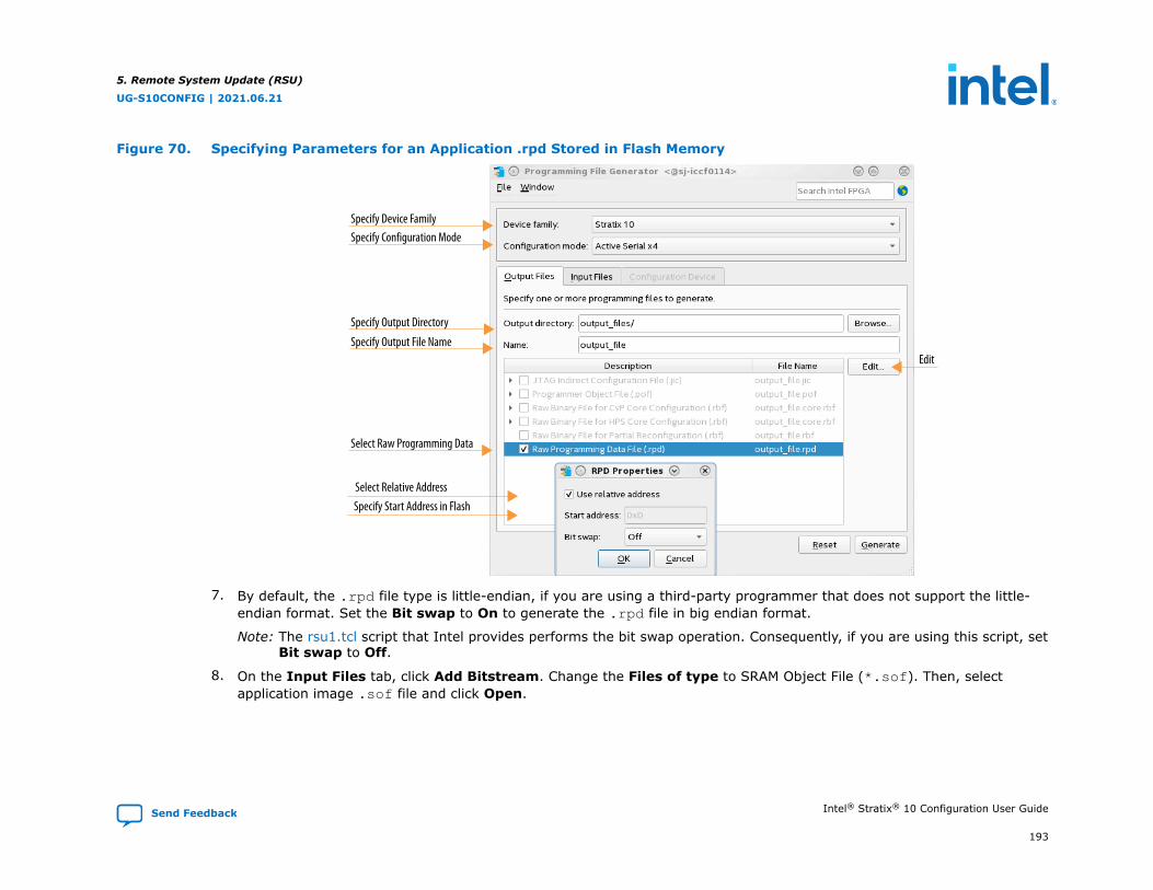
Figure 70. Specifying Parameters for an Application .rpd Stored in Flash Memory
Specify Configuration Mode
Select Raw Programming Data
Specify Output Directory
Specify Output File Name
Specify Device Family
Select Relative Address
Edit
Specify Start Address in Flash
7. By default, the .rpd file type is little-endian, if you are using a third-party programmer that does not support the little-endian format. Set the Bit swap to On to generate the .rpd file in big endian format.
Note: The rsu1.tcl script that Intel provides performs the bit swap operation. Consequently, if you are using this script, setBit swap to Off.
8. On the Input Files tab, click Add Bitstream. Change the Files of type to SRAM Object File (*.sof). Then, selectapplication image .sof file and click Open.
5. Remote System Update (RSU)
UG-S10CONFIG | 2021.06.21
Send Feedback Intel® Stratix® 10 Configuration User Guide
193
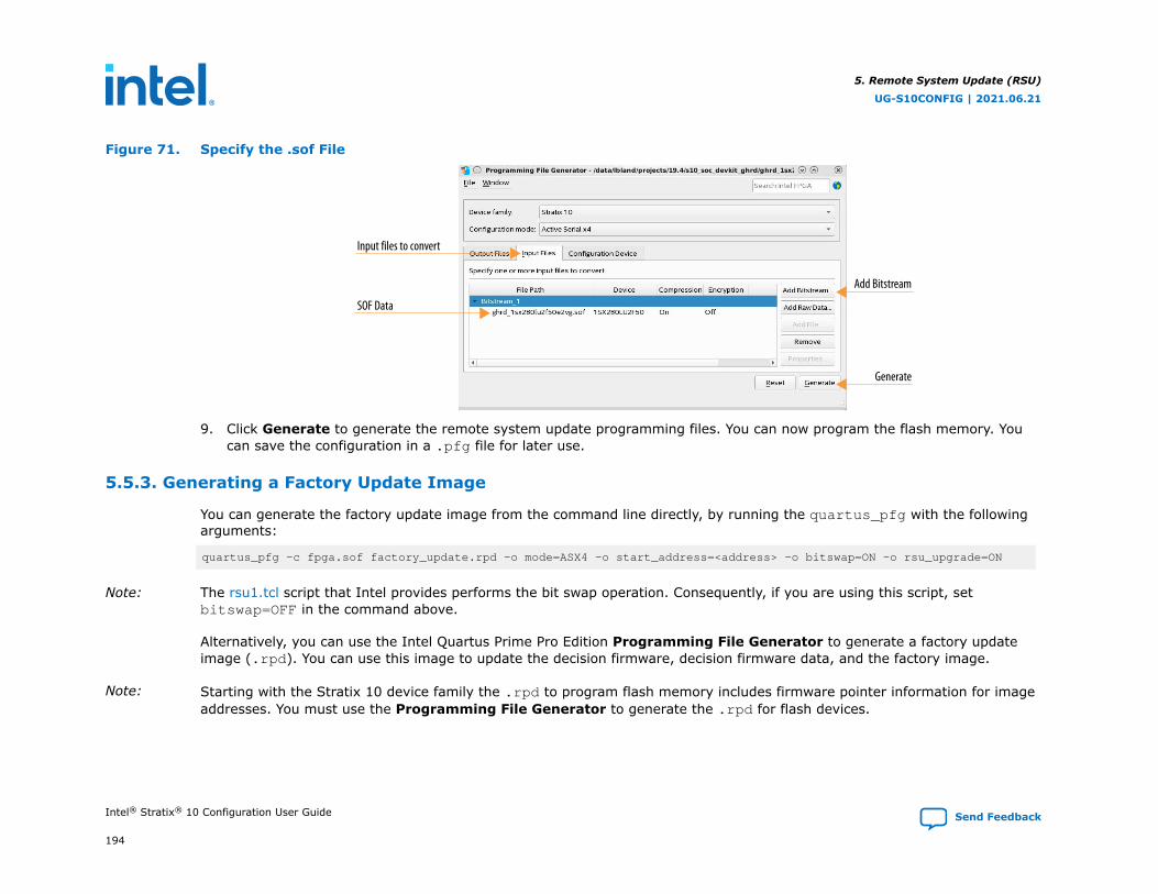
Figure 71. Specify the .sof File
SOF Data
Add Bitstream
Input files to convert
Generate
9. Click Generate to generate the remote system update programming files. You can now program the flash memory. Youcan save the configuration in a .pfg file for later use.
5.5.3. Generating a Factory Update Image
You can generate the factory update image from the command line directly, by running the quartus_pfg with the followingarguments:
quartus_pfg -c fpga.sof factory_update.rpd -o mode=ASX4 -o start_address=<address> -o bitswap=ON -o rsu_upgrade=ON
Note: The rsu1.tcl script that Intel provides performs the bit swap operation. Consequently, if you are using this script, setbitswap=OFF in the command above.
Alternatively, you can use the Intel Quartus Prime Pro Edition Programming File Generator to generate a factory updateimage (.rpd). You can use this image to update the decision firmware, decision firmware data, and the factory image.
Note: Starting with the Stratix 10 device family the .rpd to program flash memory includes firmware pointer information for imageaddresses. You must use the Programming File Generator to generate the .rpd for flash devices.
5. Remote System Update (RSU)
UG-S10CONFIG | 2021.06.21
Intel® Stratix® 10 Configuration User Guide Send Feedback
194
1. On the File menu, click Programming File Generator.
2. Select Intel Stratix 10 from the Device family drop-down list.
3. Select the configuration mode from the Configuration mode drop-down list. The current Intel Quartus Prime onlysupports the RSU feature in the Active Serial x4 configuration mode.
4. On the Output Files tab, assign the Output directory and Name.
5. Select the .rpd output file type.
6. Click the Edit… button and assign the Start address for the factory update image in flash memory. You do not have tocreate a separate partition for the factory update image. The factory update image typically includes the minimumamount of logic necessary to successfully debug your design if your application image fails to load. Consequently theStart address can be the sector boundary of unused space in flash memory. This Start address must match the startingaddress of the target sector in flash memory. If the address is incorrect, the image does not load when the host tries touse this image as a backup image.
Note: If unused space is not available, you can use an application image space other than application image 1. In thiscase after the update operation completes you must restore the application image by writing the associatedapplication image (.rpd) to the application slot.
5. Remote System Update (RSU)
UG-S10CONFIG | 2021.06.21
Send Feedback Intel® Stratix® 10 Configuration User Guide
195
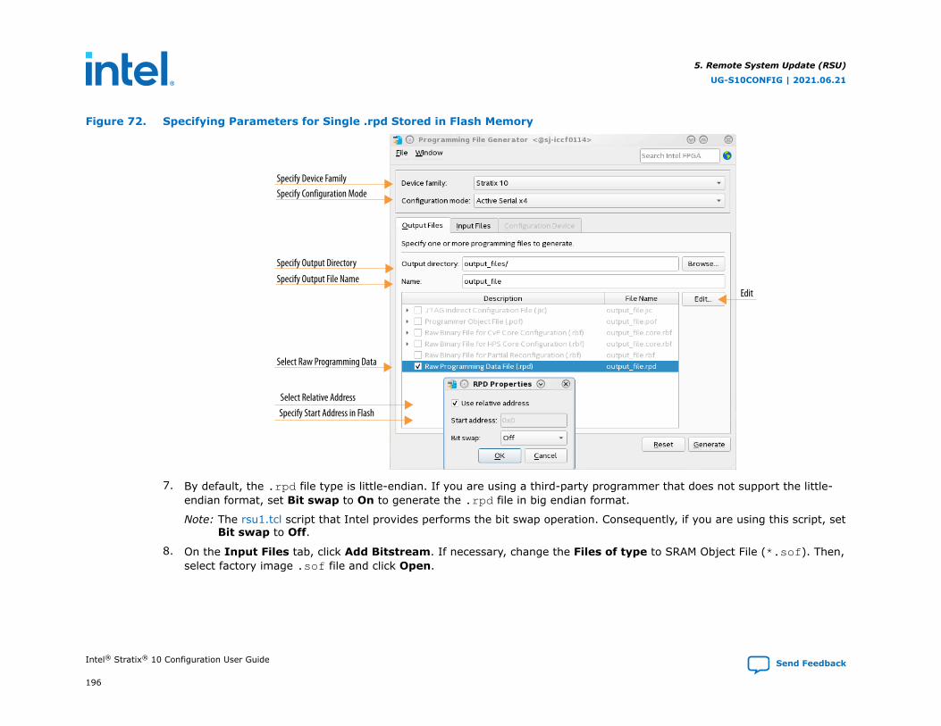
Figure 72. Specifying Parameters for Single .rpd Stored in Flash Memory
Specify Configuration Mode
Select Raw Programming Data
Specify Output Directory
Specify Output File Name
Specify Device Family
Select Relative Address
Edit
Specify Start Address in Flash
7. By default, the .rpd file type is little-endian. If you are using a third-party programmer that does not support the little-endian format, set Bit swap to On to generate the .rpd file in big endian format.
Note: The rsu1.tcl script that Intel provides performs the bit swap operation. Consequently, if you are using this script, setBit swap to Off.
8. On the Input Files tab, click Add Bitstream. If necessary, change the Files of type to SRAM Object File (*.sof). Then,select factory image .sof file and click Open.
5. Remote System Update (RSU)
UG-S10CONFIG | 2021.06.21
Intel® Stratix® 10 Configuration User Guide Send Feedback
196
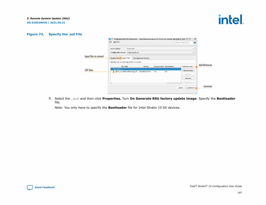
Figure 73. Specify the .sof File
SOF Data
Add Bitstream
Input files to convert
Generate
9. Select the .sof and then click Properties. Turn On Generate RSU factory update image. Specify the Bootloaderfile.
Note: You only have to specify the Bootloader file for Intel Stratix 10 SX devices.
5. Remote System Update (RSU)
UG-S10CONFIG | 2021.06.21
Send Feedback Intel® Stratix® 10 Configuration User Guide
197
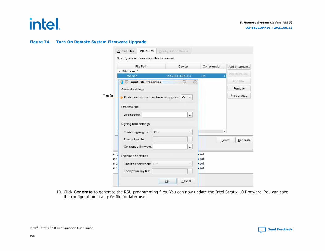
Figure 74. Turn On Remote System Firmware Upgrade
Turn On
10. Click Generate to generate the RSU programming files. You can now update the Intel Stratix 10 firmware. You can savethe configuration in a .pfg file for later use.
5. Remote System Update (RSU)
UG-S10CONFIG | 2021.06.21
Intel® Stratix® 10 Configuration User Guide Send Feedback
198

5.5.4. Command Sequence To Perform Quad SPI Operations
Here is the recommended command sequence to access quad SPI flash memory or perform an RSU update operation.
Refer to Table 39 on page 162 for more information about these commands.
1. Request exclusive access to the AS x4 interface: QSPI_OPEN.
2. Specify a quad SPI flash chip: QSPI_SET_CS*. This command is optional for the AS x4 configuration scheme andmandatory for JTAG configuration schemes.
3. Perform the desired operation or operations. The following operations are available: QSPI_READ, QSPI_WRITE,QSPI_ERASE, QSPI_READ_DEVICE_REG, QSPI_WRITE_DEVICE_REG, QSPI_SEND_DEVICE_OP, andRSU_IMAGE_UPDATE.
4. Close exclusive access to the AS x4 interface: QSPI_CLOSE.
5.6. Remote System Update from FPGA Core Example
This section presents a complete remote system update example, including the following steps:
1. Creating the initial remote system update image (.jic) containing the bitstreams for the factory image and oneapplication image.
2. Programming the flash memory with the initial remote system update image that subsequently configures the device.
3. Reconfiguring the device with an application or factory image.
4. Creating a single remote system update (.rpd) containing the bitstreams to add an application image in user mode.
5. Adding an application image.
6. Removing an application image.
5. Remote System Update (RSU)
UG-S10CONFIG | 2021.06.21
Send Feedback Intel® Stratix® 10 Configuration User Guide
199
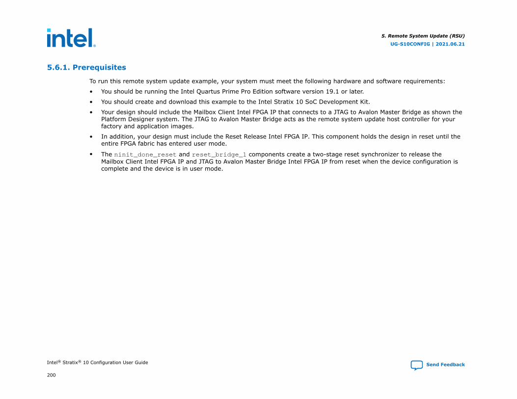
5.6.1. Prerequisites
To run this remote system update example, your system must meet the following hardware and software requirements:
• You should be running the Intel Quartus Prime Pro Edition software version 19.1 or later.
• You should create and download this example to the Intel Stratix 10 SoC Development Kit.
• Your design should include the Mailbox Client Intel FPGA IP that connects to a JTAG to Avalon Master Bridge as shown thePlatform Designer system. The JTAG to Avalon Master Bridge acts as the remote system update host controller for yourfactory and application images.
• In addition, your design must include the Reset Release Intel FPGA IP. This component holds the design in reset until theentire FPGA fabric has entered user mode.
• The ninit_done_reset and reset_bridge_1 components create a two-stage reset synchronizer to release theMailbox Client Intel FPGA IP and JTAG to Avalon Master Bridge Intel FPGA IP from reset when the device configuration iscomplete and the device is in user mode.
5. Remote System Update (RSU)
UG-S10CONFIG | 2021.06.21
Intel® Stratix® 10 Configuration User Guide Send Feedback
200
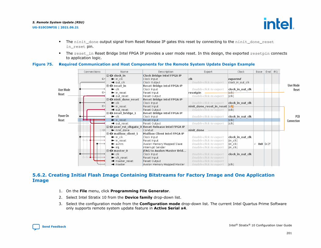
• The ninit_done output signal from Reset Release IP gates this reset by connecting to the ninit_done_resetin_reset pin.
• The reset_in Reset Bridge Intel FPGA IP provides a user mode reset. In this design, the exported resetpin connectsto application logic.
•Figure 75. Required Communication and Host Components for the Remote System Update Design Example
PCBConnection
User ModeResetUser Mode
Reset
Power OnReset
5.6.2. Creating Initial Flash Image Containing Bitstreams for Factory Image and One ApplicationImage
1. On the File menu, click Programming File Generator.
2. Select Intel Stratix 10 from the Device family drop-down list.
3. Select the configuration mode from the Configuration mode drop-down list. The current Intel Quartus Prime Softwareonly supports remote system update feature in Active Serial x4.
5. Remote System Update (RSU)
UG-S10CONFIG | 2021.06.21
Send Feedback Intel® Stratix® 10 Configuration User Guide
201
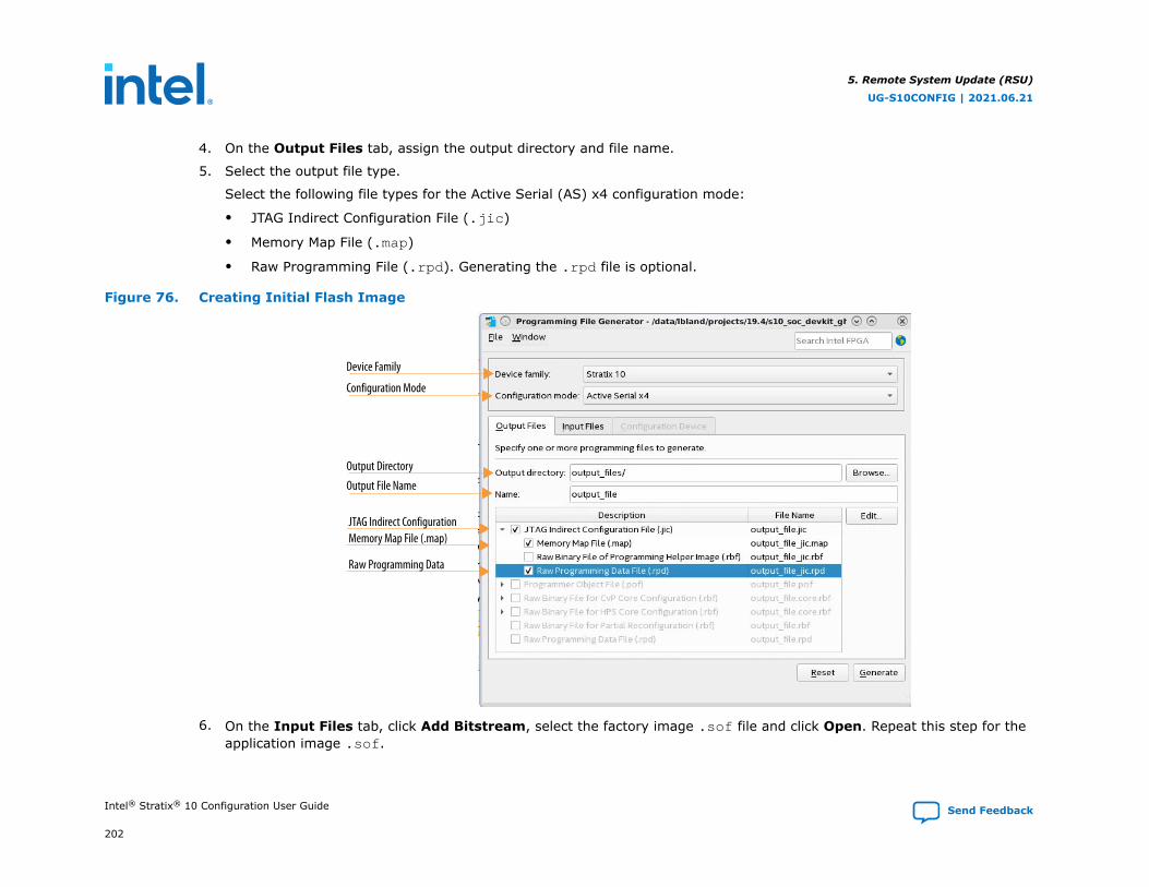
4. On the Output Files tab, assign the output directory and file name.
5. Select the output file type.
Select the following file types for the Active Serial (AS) x4 configuration mode:
• JTAG Indirect Configuration File (.jic)
• Memory Map File (.map)
• Raw Programming File (.rpd). Generating the .rpd file is optional.
Figure 76. Creating Initial Flash Image
Configuration Mode
Raw Programming Data
Output Directory
Output File Name
Device Family
JTAG Indirect ConfigurationMemory Map File (.map)
6. On the Input Files tab, click Add Bitstream, select the factory image .sof file and click Open. Repeat this step for theapplication image .sof.
5. Remote System Update (RSU)
UG-S10CONFIG | 2021.06.21
Intel® Stratix® 10 Configuration User Guide Send Feedback
202

a. Bitstream_1 is the bitstream for factory image.
b. Bitstream_2 is the bitstream for application image.
Figure 77. Input Files Tab: Specifying the .sof
Add Bitstream
Input Files
7. On the Configuration Device tab, click Add Device, select MT25QU02G flash memory and click OK. The ProgrammingFile Generator tool automatically populates the flash partitions.
8. Select the FACTORY_IMAGE partition and click Edit.
9. On the Edit Partition dialog box, select Bitstream_1 as the factory image .sof in the Input file drop-down list. Keepthe default settings for the Page and Address Mode. Click OK.
10. Select the MT25QU02G flash memory and click Add Partition.
11. In the Add Partition dialog box, select Bitstream_2 for the application image .sof in the Input file drop-down list.Assign Page: 1.Keep the default settings for Address Mode. Click OK.
12. For Flash loader click Select. Select Intel Stratix 10 from Device family list. Select 1SX280LU2 for the Device name.Click OK.
13. Click Generate to generate the remote system update programming files. The Programming File Generator generates thefollowing files:
a. Initial_RSU_Image.jic
b. Initial_RSU_Image_jic.map
5. Remote System Update (RSU)
UG-S10CONFIG | 2021.06.21
Send Feedback Intel® Stratix® 10 Configuration User Guide
203
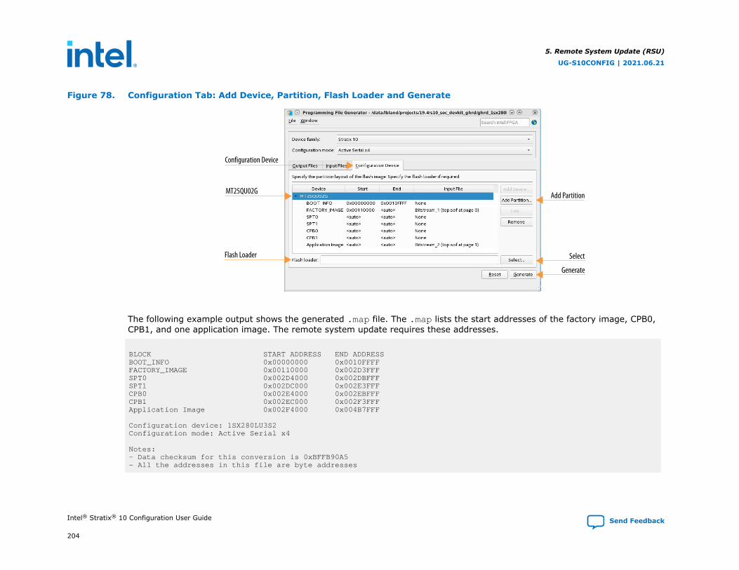
Figure 78. Configuration Tab: Add Device, Partition, Flash Loader and Generate
MT25QU02G
Configuration Device
Flash Loader
Add Partition
Select
Generate
The following example output shows the generated .map file. The .map lists the start addresses of the factory image, CPB0,CPB1, and one application image. The remote system update requires these addresses.
BLOCK START ADDRESS END ADDRESSBOOT_INFO 0x00000000 0x0010FFFFFACTORY_IMAGE 0x00110000 0x002D3FFFSPT0 0x002D4000 0x002DBFFFSPT1 0x002DC000 0x002E3FFFCPB0 0x002E4000 0x002EBFFFCPB1 0x002EC000 0x002F3FFFApplication Image 0x002F4000 0x004B7FFF
Configuration device: 1SX280LU3S2Configuration mode: Active Serial x4
Notes:- Data checksum for this conversion is 0xBFFB90A5- All the addresses in this file are byte addresses
5. Remote System Update (RSU)
UG-S10CONFIG | 2021.06.21
Intel® Stratix® 10 Configuration User Guide Send Feedback
204
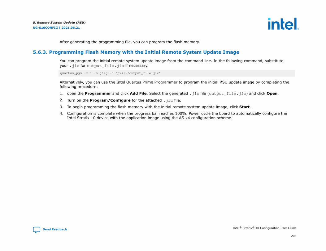
After generating the programming file, you can program the flash memory.
5.6.3. Programming Flash Memory with the Initial Remote System Update Image
You can program the initial remote system update image from the command line. In the following command, substituteyour .jic for output_file.jic if necessary.
quartus_pgm -c 1 -m jtag -o "pvi;./output_file.jic"
Alternatively, you can use the Intel Quartus Prime Programmer to program the initial RSU update image by completing thefollowing procedure:
1. open the Programmer and click Add File. Select the generated .jic file (output_file.jic) and click Open.
2. Turn on the Program/Configure for the attached .jic file.
3. To begin programming the flash memory with the initial remote system update image, click Start.
4. Configuration is complete when the progress bar reaches 100%. Power cycle the board to automatically configure theIntel Stratix 10 device with the application image using the AS x4 configuration scheme.
5. Remote System Update (RSU)
UG-S10CONFIG | 2021.06.21
Send Feedback Intel® Stratix® 10 Configuration User Guide
205

Figure 79. Programming the Flash Memory with the Initial RSU Image
5. Remote System Update (RSU)
UG-S10CONFIG | 2021.06.21
Intel® Stratix® 10 Configuration User Guide Send Feedback
206

Note: This example does not assign the Direct to Factory Image pin. Consequently, the Programmer configures thedevice with the application image. The application image is the default image if the design does not use the Directto Factory Image pin.
5. Use the RSU_STATUS command to determine which bitstream image the Programmer is using as shown in the followingexample:
a. In the Intel Quartus Prime software, select Tools ➤ System Debugging Tools ➤ System Console to launch thesystem console.
b. In the Tcl Console pane, type source rsu1.tcl to open the example of Tcl script to perform the remote systemupdate commands. Refer to the Related Information for a link to rsu1.tcl.
c. Type the rsu_status command to report the current remote system update status. You can retrieve the currentrunning image address from the remote system update status report. The current image address must match thestart address for the application image printed in the .map file.
Figure 80. Running Tcl Commands Available in rsu1.tcl
source rsu1.tclrsu_status
Related Information
rsu1.tcl
5.6.4. Reconfiguring the Device with an Application or Factory Image
The following steps describe the process to reconfigure the device with a different application image or the factory imageusing operation commands after the device is in user mode.
1. The remote system update host sends the RSU_IMAGE_UPDATE command to perform the remote system update to thenew application image or factory image.
a. For example, in the Tcl console of the System Console, type the following command to initiate a remote systemupdate to the factory image.
i. rsu_image_update 0x00110000
5. Remote System Update (RSU)
UG-S10CONFIG | 2021.06.21
Send Feedback Intel® Stratix® 10 Configuration User Guide
207
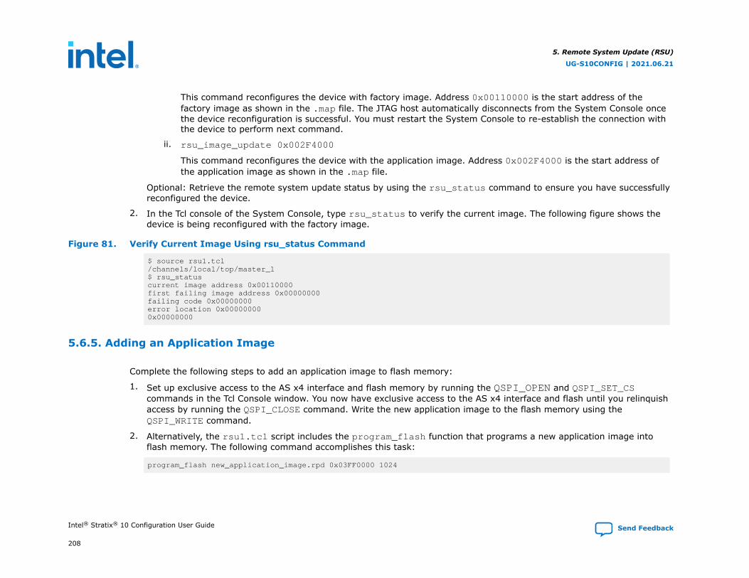
This command reconfigures the device with factory image. Address 0x00110000 is the start address of thefactory image as shown in the .map file. The JTAG host automatically disconnects from the System Console oncethe device reconfiguration is successful. You must restart the System Console to re-establish the connection withthe device to perform next command.
ii. rsu_image_update 0x002F4000
This command reconfigures the device with the application image. Address 0x002F4000 is the start address ofthe application image as shown in the .map file.
Optional: Retrieve the remote system update status by using the rsu_status command to ensure you have successfullyreconfigured the device.
2. In the Tcl console of the System Console, type rsu_status to verify the current image. The following figure shows thedevice is being reconfigured with the factory image.
Figure 81. Verify Current Image Using rsu_status Command
$ source rsu1.tcl/channels/local/top/master_1$ rsu_statuscurrent image address 0x00110000first failing image address 0x00000000failing code 0x00000000error location 0x000000000x00000000
5.6.5. Adding an Application Image
Complete the following steps to add an application image to flash memory:
1. Set up exclusive access to the AS x4 interface and flash memory by running the QSPI_OPEN and QSPI_SET_CScommands in the Tcl Console window. You now have exclusive access to the AS x4 interface and flash until you relinquishaccess by running the QSPI_CLOSE command. Write the new application image to the flash memory using theQSPI_WRITE command.
2. Alternatively, the rsu1.tcl script includes the program_flash function that programs a new application image intoflash memory. The following command accomplishes this task:
program_flash new_application_image.rpd 0x03FF0000 1024
5. Remote System Update (RSU)
UG-S10CONFIG | 2021.06.21
Intel® Stratix® 10 Configuration User Guide Send Feedback
208
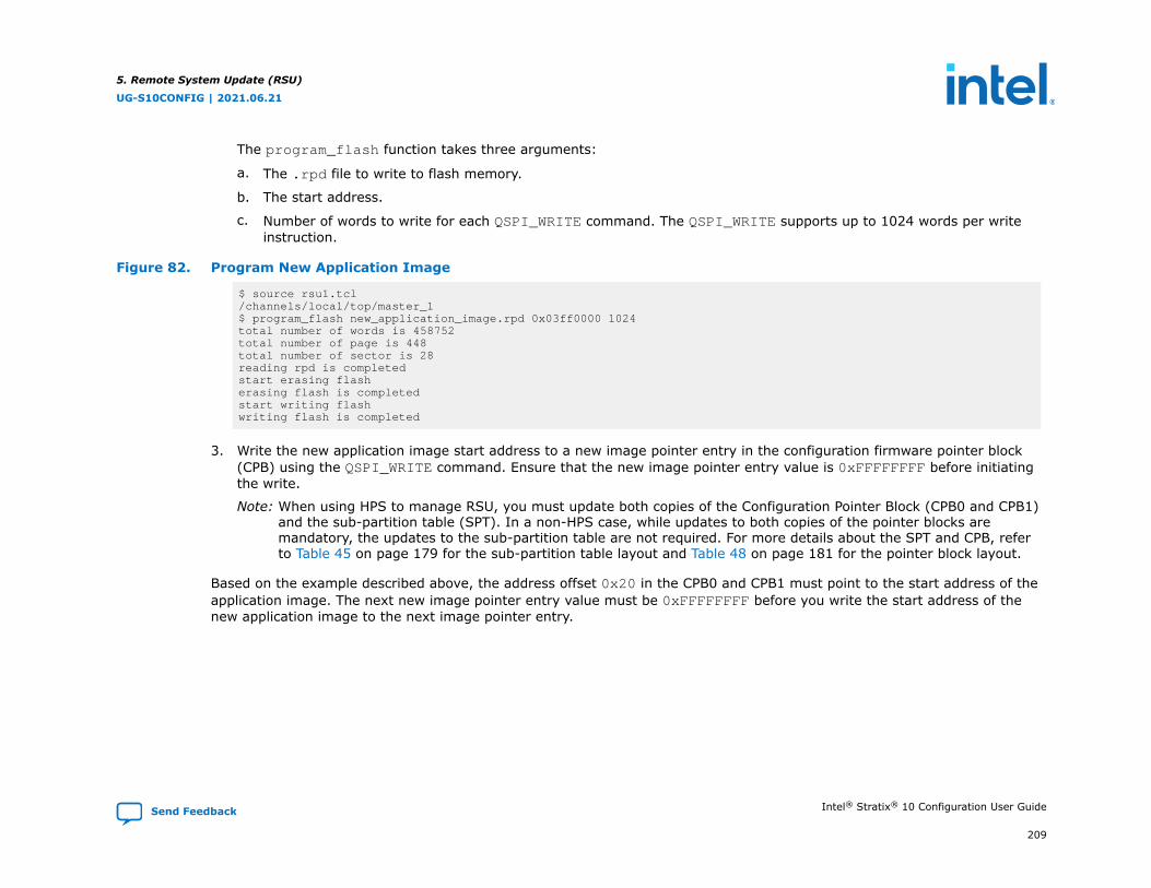
The program_flash function takes three arguments:
a. The .rpd file to write to flash memory.
b. The start address.
c. Number of words to write for each QSPI_WRITE command. The QSPI_WRITE supports up to 1024 words per writeinstruction.
Figure 82. Program New Application Image
$ source rsu1.tcl/channels/local/top/master_1$ program_flash new_application_image.rpd 0x03ff0000 1024total number of words is 458752total number of page is 448total number of sector is 28reading rpd is completedstart erasing flasherasing flash is completedstart writing flashwriting flash is completed
3. Write the new application image start address to a new image pointer entry in the configuration firmware pointer block(CPB) using the QSPI_WRITE command. Ensure that the new image pointer entry value is 0xFFFFFFFF before initiatingthe write.
Note: When using HPS to manage RSU, you must update both copies of the Configuration Pointer Block (CPB0 and CPB1)and the sub-partition table (SPT). In a non-HPS case, while updates to both copies of the pointer blocks aremandatory, the updates to the sub-partition table are not required. For more details about the SPT and CPB, referto Table 45 on page 179 for the sub-partition table layout and Table 48 on page 181 for the pointer block layout.
Based on the example described above, the address offset 0x20 in the CPB0 and CPB1 must point to the start address of theapplication image. The next new image pointer entry value must be 0xFFFFFFFF before you write the start address of thenew application image to the next image pointer entry.
5. Remote System Update (RSU)
UG-S10CONFIG | 2021.06.21
Send Feedback Intel® Stratix® 10 Configuration User Guide
209
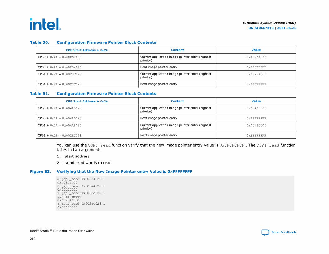
Table 50. Configuration Firmware Pointer Block Contents
CPB Start Address + 0x20 Content Value
CPB0 + 0x20 = 0x002E4020 Current application image pointer entry (highestpriority)
0x002F4000
CPB0 + 0x28 = 0x002E4028 Next image pointer entry 0xFFFFFFFF
CPB1 + 0x20 = 0x002EC020 Current application image pointer entry (highestpriority)
0x002F4000
CPB1 + 0x28 = 0x002EC028 Next image pointer entry 0xFFFFFFFF
Table 51. Configuration Firmware Pointer Block Contents
CPB Start Address + 0x20 Content Value
CPB0 + 0x20 = 0x004A0020 Current application image pointer entry (highestpriority)
0x004B0000
CPB0 + 0x28 = 0x004A0028 Next image pointer entry 0xFFFFFFFF
CPB1 + 0x20 = 0x004A8020 Current application image pointer entry (highestpriority)
0x004B0000
CPB1 + 0x28 = 0x002EC028 Next image pointer entry 0xFFFFFFFF
You can use the QSPI_read function verify that the new image pointer entry value is 0xFFFFFFFF . The QSPI_read functiontakes in two arguments:
1. Start address
2. Number of words to read
Figure 83. Verifying that the New Image Pointer entry Value is 0xFFFFFFFF
$ qspi_read 0x002e4020 10x002f4000$ qspi_read 0x002e4028 10xffffffff% qspi_read 0x002ec020 1ISR is empty0x002f40000% qspi_read 0x002ec028 10xffffffff
5. Remote System Update (RSU)
UG-S10CONFIG | 2021.06.21
Intel® Stratix® 10 Configuration User Guide Send Feedback
210
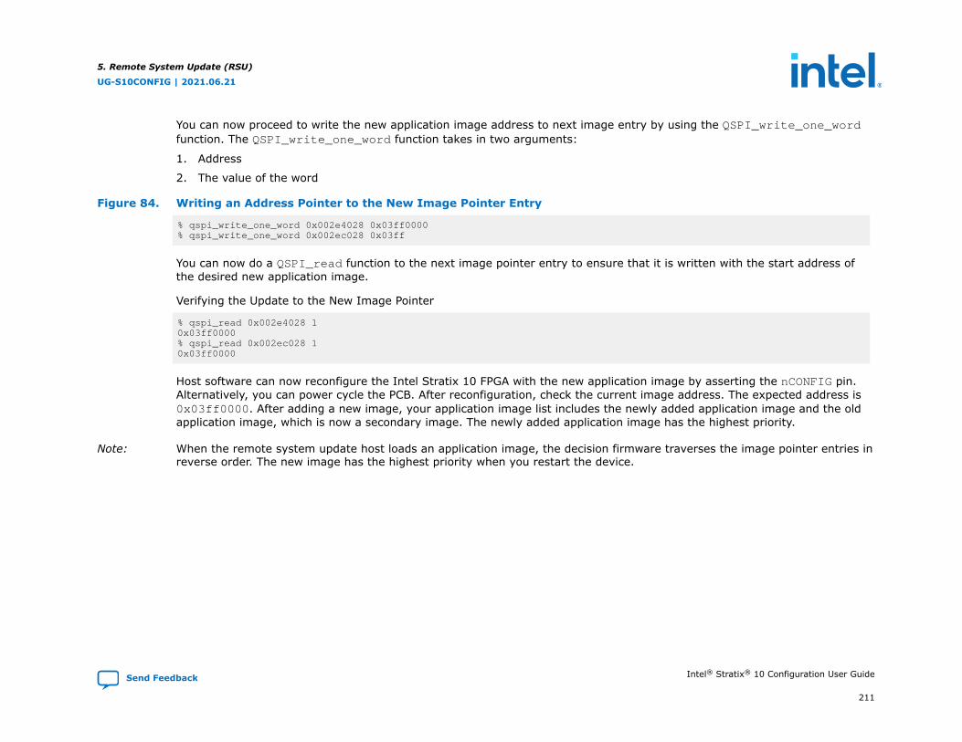
You can now proceed to write the new application image address to next image entry by using the QSPI_write_one_wordfunction. The QSPI_write_one_word function takes in two arguments:
1. Address
2. The value of the word
Figure 84. Writing an Address Pointer to the New Image Pointer Entry
% qspi_write_one_word 0x002e4028 0x03ff0000% qspi_write_one_word 0x002ec028 0x03ff
You can now do a QSPI_read function to the next image pointer entry to ensure that it is written with the start address ofthe desired new application image.
Verifying the Update to the New Image Pointer
% qspi_read 0x002e4028 10x03ff0000% qspi_read 0x002ec028 10x03ff0000
Host software can now reconfigure the Intel Stratix 10 FPGA with the new application image by asserting the nCONFIG pin.Alternatively, you can power cycle the PCB. After reconfiguration, check the current image address. The expected address is0x03ff0000. After adding a new image, your application image list includes the newly added application image and the oldapplication image, which is now a secondary image. The newly added application image has the highest priority.
Note: When the remote system update host loads an application image, the decision firmware traverses the image pointer entries inreverse order. The new image has the highest priority when you restart the device.
5. Remote System Update (RSU)
UG-S10CONFIG | 2021.06.21
Send Feedback Intel® Stratix® 10 Configuration User Guide
211
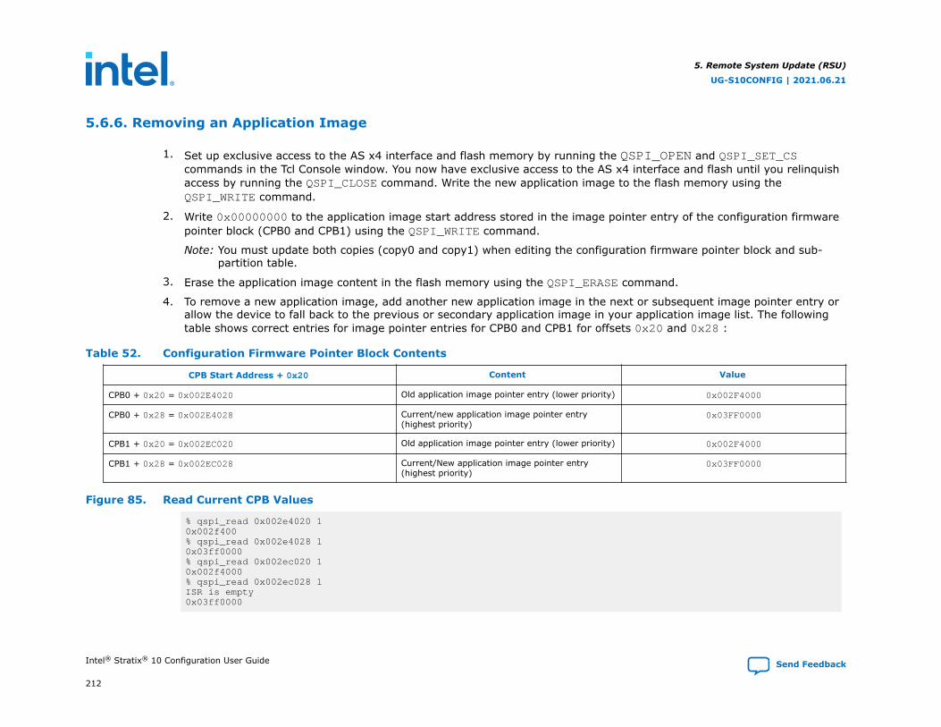
5.6.6. Removing an Application Image
1. Set up exclusive access to the AS x4 interface and flash memory by running the QSPI_OPEN and QSPI_SET_CScommands in the Tcl Console window. You now have exclusive access to the AS x4 interface and flash until you relinquishaccess by running the QSPI_CLOSE command. Write the new application image to the flash memory using theQSPI_WRITE command.
2. Write 0x00000000 to the application image start address stored in the image pointer entry of the configuration firmwarepointer block (CPB0 and CPB1) using the QSPI_WRITE command.
Note: You must update both copies (copy0 and copy1) when editing the configuration firmware pointer block and sub-partition table.
3. Erase the application image content in the flash memory using the QSPI_ERASE command.
4. To remove a new application image, add another new application image in the next or subsequent image pointer entry orallow the device to fall back to the previous or secondary application image in your application image list. The followingtable shows correct entries for image pointer entries for CPB0 and CPB1 for offsets 0x20 and 0x28 :
Table 52. Configuration Firmware Pointer Block Contents
CPB Start Address + 0x20 Content Value
CPB0 + 0x20 = 0x002E4020 Old application image pointer entry (lower priority) 0x002F4000
CPB0 + 0x28 = 0x002E4028 Current/new application image pointer entry(highest priority)
0x03FF0000
CPB1 + 0x20 = 0x002EC020 Old application image pointer entry (lower priority) 0x002F4000
CPB1 + 0x28 = 0x002EC028 Current/New application image pointer entry(highest priority)
0x03FF0000
Figure 85. Read Current CPB Values
% qspi_read 0x002e4020 10x002f400% qspi_read 0x002e4028 10x03ff0000% qspi_read 0x002ec020 10x002f4000% qspi_read 0x002ec028 1ISR is empty0x03ff0000
5. Remote System Update (RSU)
UG-S10CONFIG | 2021.06.21
Intel® Stratix® 10 Configuration User Guide Send Feedback
212
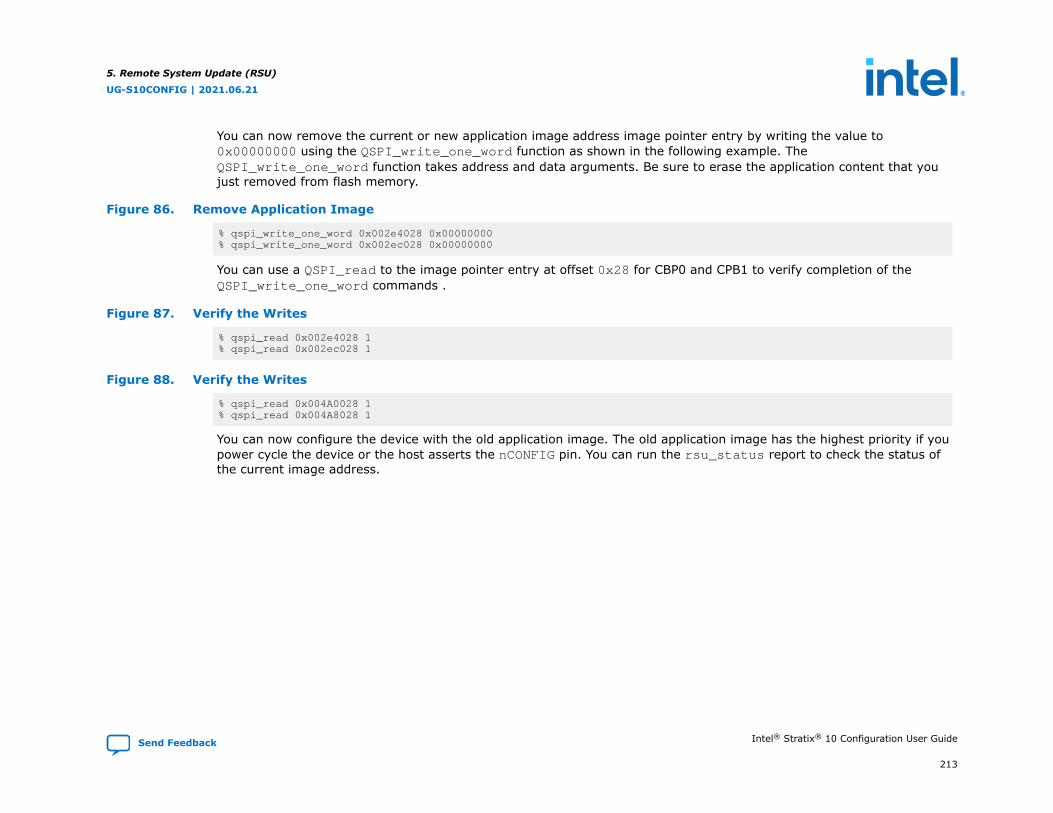
You can now remove the current or new application image address image pointer entry by writing the value to0x00000000 using the QSPI_write_one_word function as shown in the following example. TheQSPI_write_one_word function takes address and data arguments. Be sure to erase the application content that youjust removed from flash memory.
Figure 86. Remove Application Image
% qspi_write_one_word 0x002e4028 0x00000000% qspi_write_one_word 0x002ec028 0x00000000
You can use a QSPI_read to the image pointer entry at offset 0x28 for CBP0 and CPB1 to verify completion of theQSPI_write_one_word commands .
Figure 87. Verify the Writes
% qspi_read 0x002e4028 1% qspi_read 0x002ec028 1
Figure 88. Verify the Writes
% qspi_read 0x004A0028 1% qspi_read 0x004A8028 1
You can now configure the device with the old application image. The old application image has the highest priority if youpower cycle the device or the host asserts the nCONFIG pin. You can run the rsu_status report to check the status ofthe current image address.
5. Remote System Update (RSU)
UG-S10CONFIG | 2021.06.21
Send Feedback Intel® Stratix® 10 Configuration User Guide
213

6. Intel Stratix 10 Configuration Features
6.1. Device Security
Note: Contact your Intel sales representative for more information about the device security support in Intel Stratix 10 devices.
The Intel Stratix 10 device provides the following flexible and robust security features to protect sensitive data and intellectualproperty:
• User image authentication and encryption
• Public-Key based authentication
• Advanced Encryption Standard (AES)-256 Encryption
• JTAG Disable
• JTAG Debug Disable/Enable
• Side channel protection
Related Information
• Intel Stratix 10 Device FeaturesFor a list of device features that are planned for future releases.
• Intel Stratix 10 Device Security User GuideFor details on security features.
UG-S10CONFIG | 2021.06.21
Send Feedback
Intel Corporation. All rights reserved. Intel, the Intel logo, and other Intel marks are trademarks of Intel Corporation or its subsidiaries. Intel warrants performanceof its FPGA and semiconductor products to current specifications in accordance with Intel's standard warranty, but reserves the right to make changes to anyproducts and services at any time without notice. Intel assumes no responsibility or liability arising out of the application or use of any information, product, orservice described herein except as expressly agreed to in writing by Intel. Intel customers are advised to obtain the latest version of device specifications beforerelying on any published information and before placing orders for products or services.*Other names and brands may be claimed as the property of others.
ISO9001:2015Registered
6.2. Configuration via Protocol
The CvP configuration scheme creates separate images for the periphery and core logic. You can store the periphery image ina local configuration device and the core image in host memory, reducing system costs and increasing the security for theproprietary core image. CvP configures the FPGA fabric through the PCI Express* (PCIe) link and is available for Endpointvariants only.
6. Intel Stratix 10 Configuration Features
UG-S10CONFIG | 2021.06.21
Send Feedback Intel® Stratix® 10 Configuration User Guide
215
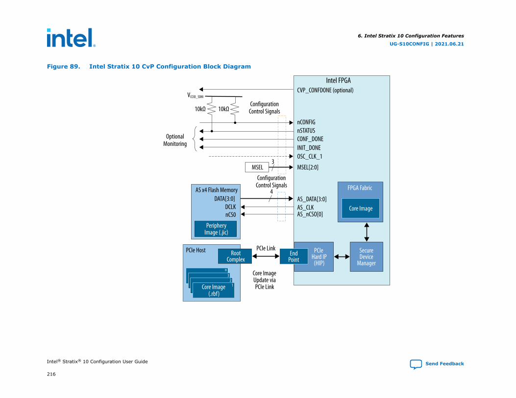
Figure 89. Intel Stratix 10 CvP Configuration Block Diagram
Intel FPGA
nCONFIGnSTATUSCONF_DONEINIT_DONEOSC_CLK_1
MSEL[2:0]
AS_DATA[3:0]AS_CLKAS_nCSO[0]
ConfigurationControl Signals
ConfigurationControl Signals
OptionalMonitoring
10kΩ
MSEL
VCCIO_SDM
AS x4 Flash MemoryDATA[3:0]
DCLKnCS0
PCIe Link
Core ImageUpdate viaPCIe Link
3
4
PeripheryImage (.jic)
PCIe Host
Core Image(.rbf)
12
3n
EndPoint
Core Image
PCIe Hard IP
(HIP)
SecureDevice
Manager
FPGA Fabric
RootComplex
CVP_CONFDONE (optional)
10kΩ
6. Intel Stratix 10 Configuration Features
UG-S10CONFIG | 2021.06.21
Intel® Stratix® 10 Configuration User Guide Send Feedback
216
The CvP configuration scheme supports the following modes:
• CvP Initialization Mode:
In this mode an external configuration device stores the periphery image and it loads into the FPGA through the ActiveSerial x4 (Fast mode) configuration scheme. The host memory stores the core image and it loads into the FPGA throughthe PCIe link.
After the periphery image configuration completes, the CONF_DONE signal goes high and the FPGA starts PCIe linktraining. When PCIe link training completes, the PCIe link transitions to the Link Training and Status State Machine(LTSSM) L0 state and then through PCIe enumeration. The PCIe host then configures the core through the PCIe link. ThePCIe reference clock must be running for the link for link training.
After the core image configuration is complete, the CvP_CONFDONE pin (if enabled) goes high, indicating the FPGA hasreceived the full configuration bitstream over the PCIe link. INIT_DONE indicates that configuration is complete.
• CvP Update Mode:
CvP update mode is a reconfiguration scheme that uses the PCIe link to deliver an updated bitstream to a target deviceafter the device enters user mode. The periphery images which includes the PCIe link remains active, allowing CvP updateto use this link to reconfigure the core fabric. In this mode, the FPGA device initializes by loading the full configurationimage from the external local configuration device to the FPGA or after CvP initialization.
You can perform CvP update on a device that you originally configure using CvP initialization or any other configurationscheme.
Related Information
Intel Stratix 10 Configuration via Protocol (CvP) Implementation User Guide
6.3. Partial Reconfiguration
Partial reconfiguration (PR) allows you to reconfigure a portion of the FPGA dynamically, while the remaining FPGA designcontinues to function. You can define multiple personas for a region in your design, without impacting operation in areasoutside this region. This methodology is effective in systems with multiple functions that time-share the same FPGA deviceresources. PR enables the implementation of more complex FPGA systems.
Related Information
Intel Quartus Prime Pro Edition User Guide: Partial Reconfiguration
6. Intel Stratix 10 Configuration Features
UG-S10CONFIG | 2021.06.21
Send Feedback Intel® Stratix® 10 Configuration User Guide
217
7. Intel Stratix 10 Debugging GuideThis section describes best practices in debugging configuration issues on SDM devices. View the video guide below for aquick walk-through.
7.1. Configuration Debugging Checklist
Work through this checklist to identify issues that may result in operational failures.
UG-S10CONFIG | 2021.06.21
Send Feedback
Intel Corporation. All rights reserved. Intel, the Intel logo, and other Intel marks are trademarks of Intel Corporation or its subsidiaries. Intel warrants performanceof its FPGA and semiconductor products to current specifications in accordance with Intel's standard warranty, but reserves the right to make changes to anyproducts and services at any time without notice. Intel assumes no responsibility or liability arising out of the application or use of any information, product, orservice described herein except as expressly agreed to in writing by Intel. Intel customers are advised to obtain the latest version of device specifications beforerelying on any published information and before placing orders for products or services.*Other names and brands may be claimed as the property of others.
ISO9001:2015Registered

Table 53. General Configuration Debugging Checklist
Checklist Item Complete?
1 Verify that the Vcc ,Vccp ,Vccio_sdm Vccpt ,Vcceram, Vccadc supplies are in the proper range by using SDM Debug Toolkit. ☐
2 Verify that all configuration resistors are correctly connected (MSEL, nCONFIG, nSTATUS, CONF_DONE, INIT_DONE,PWRMGT_SDA, PWRMGT_SCL).
☐
3 Verify that you are following the correct power-up and power-down sequences. ☐
4 Verify that the SDM I/Os assignments are correct by checking the Intel Quartus Prime Compilation QSF and Fitter reports. ☐
5 For SmartVID devices (-V), ensure that all PMBus pins are connected to Intel Stratix 10 device. ☐
6 Verify that SmartVID settings follow the recommendations in the Intel Stratix 10 Power Management User Guide ☐
7 Verify that the Intel Stratix 10 -V device has its own voltage regulator module for VCC and VCCP. ☐
8 After configuration are the nCONFIG, nSTATUS, CONF_DONE, and INIT_DONE pins high? Use the SDM Debug Toolkit todetermine these levels.
☐
9 Is the SDM operating Boot ROM code or configuration firmware?Use the SDM Debug Toolkit to answer this question.
☐
10 Are the MSEL pins correctly connected on board?Use the SDM Debug Toolkit to answer this question.
☐
11 For designs that use transceivers, HBM2, PCIe, or EMIF, are the reference clocks stable and free running before configurationbegins?
☐
12 Verify that selected clocks match the frequency setting specified in the Intel Quartus Prime software during configuration. ☐
13 Does your design include the Reset Release IP? ☐
14 To avoid configuration failures, disconnect the PMBus regulator’s JTAG download cable before configuring Intel Stratix 10 -Vdevices.
☐
15 If the SDM Debug Toolkit is not operational, verify that the Intel Stratix 10 device has exited POR by checking nCONFIG,nSTATUS, CONF_DONE and INIT_DONE pins using an oscilloscope.
☐
16 Is the configuration clock source chosen appropriately? You can use an internal oscillator or the OSC_CLK_1 pin. ☐
17 For designs driving the OSC_CLK_1 pin is the frequency 25, 100, or 125 MHz? ☐
continued...
7. Intel Stratix 10 Debugging Guide
UG-S10CONFIG | 2021.06.21
Send Feedback Intel® Stratix® 10 Configuration User Guide
219

Checklist Item Complete?
18 For Intel Stratix 10 SX parts ensure that the HPS and EMIF IOPLL reference clocks are stable and free running beforeconfiguration begins. The actual frequency should match the setting specified in Platform Designer.
☐
19 Are proper slave addresses set for the PMBus voltage regulator modules using the Intel Quartus Prime Software? ☐
20 For designs that use 3 V I/0, verify that the transceiver tiles are powered up before configuration begins. ☐
Related Information
• Debugging Guidelines for the Avalon-ST Configuration Scheme on page 63
• Debugging Guidelines for the AS Configuration Scheme on page 125
• Debugging Guidelines for the JTAG Configuration Scheme on page 136
• Intel Stratix 10 Power Management User Guide
7.2. Intel Stratix 10 Configuration Architecture Overview
Intel Stratix 10 devices employ a new configuration architecture. The Secure Device Manager (SDM), a dedicated hardprocessor, controls and monitors all aspects of device configuration from device power-on reset. This configurationarchitecture differs from previous Intel FPGA device families where state machines control configuration.
There are important differences between Intel Stratix 10 and previous device families with respect to available configurationmodes, configuration pin behavior, and connection guidelines. In addition, the bitstream format is different. Knowing aboutthese differences and how these pins behave can help you understand and debug configuration issues.
7.3. Understanding Configuration Status Using quartus_pgm command
You can read the device configuration status from the command line directly. In the following command, specify the cableindex and the JTAG chain device index to obtain the configuration status.
quartus_pgm -c <cable index> -m jtag -device=<device order in jtag chain> -status
7. Intel Stratix 10 Debugging Guide
UG-S10CONFIG | 2021.06.21
Intel® Stratix® 10 Configuration User Guide Send Feedback
220

The following example output shows the device status with cable index set to 1 and the second device selected as thetargeted device in the JTAG chain after a successful configuration.
quartus_pgm -c 1 -m jtag -device=2 -status
Info (21597): Response of CONFIG_STATUS Device is running in user mode 00006000 RESPONSE_CODE=OK, LENGTH=6 00000000 STATE=IDLE 00000000 Version C000000F MSEL=JTAG, nSTATUS=1, nCONFIG=1 00000003 CONF_DONE=1, INIT_DONE=1, CVP_DONE=0, SEU_ERROR=0 00000000 Error location 00000000 Error details
7.4. SDM Debug Toolkit Overview
You launch the Intel Stratix 10 SDM Debug Toolkit from the System Console in the Intel Quartus Prime software, Tools ➤System Debugging Tools ➤ System Console ➤ Intel Stratix 10 Debug Toolkit.
The SDM Debug Toolkit provides access to current status of the Intel Stratix 10 device. To use these commands you musthave a valid design loaded that includes the module that you intend to access. The SDM Debug Toolkit includes the four tabs:
Configuration StatusThe Read Configuration Status option provides the current value of MSEL, Configuration Pin Values, and Chip ID. Thefollowing information would be useful for debugging with the help of Intel: State, Error Location, and Error Detail.
7. Intel Stratix 10 Debugging Guide
UG-S10CONFIG | 2021.06.21
Send Feedback Intel® Stratix® 10 Configuration User Guide
221
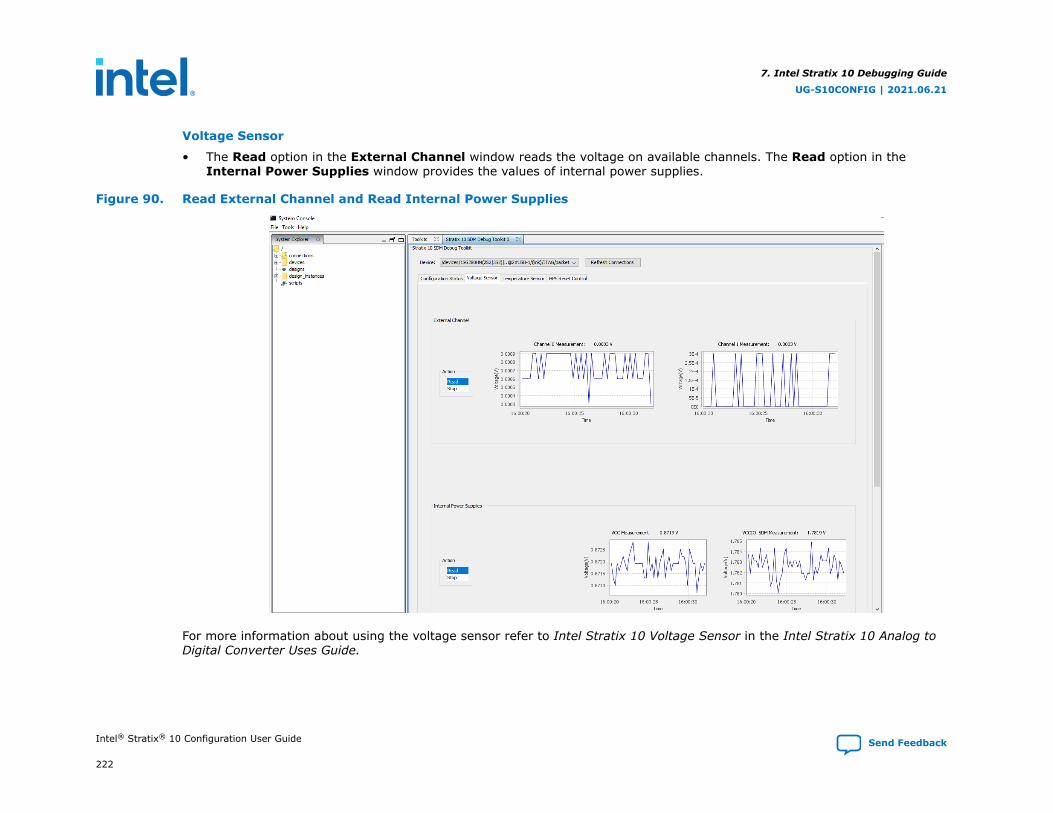
Voltage Sensor
• The Read option in the External Channel window reads the voltage on available channels. The Read option in theInternal Power Supplies window provides the values of internal power supplies.
Figure 90. Read External Channel and Read Internal Power Supplies
For more information about using the voltage sensor refer to Intel Stratix 10 Voltage Sensor in the Intel Stratix 10 Analog toDigital Converter Uses Guide.
7. Intel Stratix 10 Debugging Guide
UG-S10CONFIG | 2021.06.21
Intel® Stratix® 10 Configuration User Guide Send Feedback
222

Temperature Sensor
• Read option reads the temperature in Celsius of the Intel Stratix 10 device, the HSSI channels, and the UIB_TOP andUIB_BOTTOM. The Universal Interface Bus (UIB) blocks are general-purpose SiP interfaces for HBM2.
Figure 91. Temperature Measurements
7. Intel Stratix 10 Debugging Guide
UG-S10CONFIG | 2021.06.21
Send Feedback Intel® Stratix® 10 Configuration User Guide
223

HPS Reset ControlProvides the following two options to reset the HPS: Release HPS from Reset option and HPS Cold Reset.
Figure 92. HPS Reset Options
Refresh Connections
HPS Reset Control
7. Intel Stratix 10 Debugging Guide
UG-S10CONFIG | 2021.06.21
Intel® Stratix® 10 Configuration User Guide Send Feedback
224
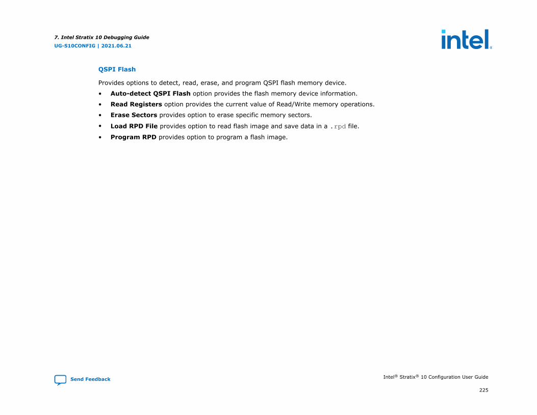
QSPI Flash
Provides options to detect, read, erase, and program QSPI flash memory device.
• Auto-detect QSPI Flash option provides the flash memory device information.
• Read Registers option provides the current value of Read/Write memory operations.
• Erase Sectors provides option to erase specific memory sectors.
• Load RPD File provides option to read flash image and save data in a .rpd file.
• Program RPD provides option to program a flash image.
7. Intel Stratix 10 Debugging Guide
UG-S10CONFIG | 2021.06.21
Send Feedback Intel® Stratix® 10 Configuration User Guide
225
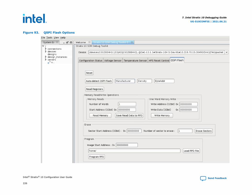
Figure 93. QSPI Flash Options
7. Intel Stratix 10 Debugging Guide
UG-S10CONFIG | 2021.06.21
Intel® Stratix® 10 Configuration User Guide Send Feedback
226
Related Information
Voltage SensorFor information about the external channel inputs to the voltage sensor multiplexer.
7.4.1. Using the SDM Debug Toolkit
To use the Intel Stratix 10 SDM Debug Toolkit, bring up the System Console in the same version of the Intel Quartus Primesoftware that you used to configure the Intel Stratix 10 device.
Complete the following steps to become familiar with the Intel Stratix 10 SDM Debug Toolkit:
1. In a Nios II command shell, type the following command:
% system-console
2. Under Intel Stratix 10 SDM Debug Toolkit click Launch.
3. Verify that the Intel FPGA Download Cable II connects to the PC and the 10-pin JTAG header connects to the Intel Stratix10 device.
4. In the Intel Stratix 10 SDM Debug Toolkit, click Refresh Connections. The Refresh Connections is above the tabs inthe SDM Debug Toolkit GUI.
5. On the Configuration Status tab, click Read Configuration Status. The following figure shows the ConfigurationStatus after a successful read. For information about decoding the State output value, refer to the CONFIG_STATUScommand.
7. Intel Stratix 10 Debugging Guide
UG-S10CONFIG | 2021.06.21
Send Feedback Intel® Stratix® 10 Configuration User Guide
227

Figure 94. Read Configuration Status Command
Refresh Connections
7. Intel Stratix 10 Debugging Guide
UG-S10CONFIG | 2021.06.21
Intel® Stratix® 10 Configuration User Guide Send Feedback
228
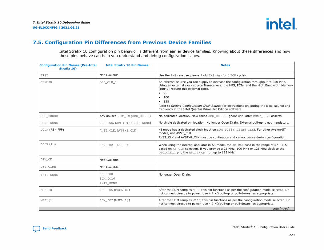
7.5. Configuration Pin Differences from Previous Device Families
Intel Stratix 10 configuration pin behavior is different from earlier device families. Knowing about these differences and howthese pins behave can help you understand and debug configuration issues.
Configuration Pin Names (Pre-IntelStratix 10)
Intel Stratix 10 Pin Names Notes
TRST Not Available Use the TMS reset sequence. Hold TMS high for 5 TCK cycles.
CLKUSR OSC_CLK_1 An external source you can supply to increase the configuration throughput to 250 MHz.Using an external clock source Transceivers, the HPS, PCIe, and the High Bandwidth Memory(HBM2) require this external clock.• 25• 100• 125Refer to Setting Configuration Clock Source for instructions on setting the clock source andfrequency in the Intel Quartus Prime Pro Edition software.
CRC_ERROR Any unused SDM_IO (SEU_ERROR) No dedicated location. Now called SEU_ERROR. Ignore until after CONF_DONE asserts.
CONF_DONE SDM_IO5, SDM_IO16 (CONF_DONE) No single dedicated pin location. No longer Open Drain. External pull-up is not mandatory.
DCLK (PS - FPP) AVST_CLK, AVSTx8_CLK x8 mode has a dedicated clock input on SDM_IO14 (AVSTx8_CLK). For other Avalon-STmodes, use AVST_CLK.AVST_CLK and AVSTx8_CLK must be continuous and cannot pause during configuration.
DCLK (AS) SDM_IO2 (AS_CLK) When using the internal oscillator in AS mode, the AS_CLK runs in the range of 57 - 115based on AS_CLK selection. If you provide a 25 MHz, 100 MHz or 125 MHz clock to theOSC_CLK_1 pin, the AS_CLK can run up to 125 MHz.
DEV_OE Not Available
DEV_CLRn Not Available
INIT_DONE SDM_IO0
SDM_IO16
INIT_DONE
No longer Open Drain.
MSEL[0] SDM_IO5 (MSEL[0]) After the SDM samples MSEL this pin functions as per the configuration mode selected. Donot connect directly to power. Use 4.7 KΩ pull-up or pull-downs, as appropriate.
MSEL[1] SDM_IO7 (MSEL[1]) After the SDM samples MSEL, this pin functions as per the configuration mode selected. Donot connect directly to power. Use 4.7 KΩ pull-up or pull-downs, as appropriate.
continued...
7. Intel Stratix 10 Debugging Guide
UG-S10CONFIG | 2021.06.21
Send Feedback Intel® Stratix® 10 Configuration User Guide
229

Configuration Pin Names (Pre-IntelStratix 10)
Intel Stratix 10 Pin Names Notes
MSEL[2] SDM_IO9 (MSEL[2]) After the SDM samples MSEL, this pin functions as per the configuration mode selected. Donot connect directly to power. Use 4.7 KΩ pull-up or pull-downs, as appropriate.
NSTATUS nSTATUS No longer Open Drain. Intel recommends a 10 KΩ pull-up to VCCIO_SDM.
NCE Not Available Multi-device configuration is not supported.
NCEO Not Available Multi-device configuration is not supported.
DATA[31:0] (PP32/PP16) AVST_DATA[31:0] Avalon-ST x8 uses SDM pins for data pins.
DATA[7:0] (PP8) SDM _IO pins (AVSTx8_DATAn)
nCSO[2:0] SDM_IO8 (AS_nCSO3)SDM_IO7 (AS_nCSO2)SDM_IO9(AS_nCSO1) SDM_IO5 (AS_nCSO0)
Intel Stratix 10 supports up to 4 cascaded AS devices
nIO_PULLUP Not Available Use a JTAG instruction to invoke.
AS_DATA0_ASDO SDM_IO4 (AS_DATA0)
AS_DATA[3:1] SDM_IO6 (AS_DATA3)SDM_IO3 (AS_DATA2)SDM_IO1 (AS_DATA1)
Unlike earlier device families, the AS interface does not automatically tristate at power-on.When you set MSEL to JTAG, the SDM drives the AS_CLK, AS_DATA0-AS_DATA3, andAS_nCSO0-AS_nCSO3, MSEL pins until POR.
PR_REQUEST GPIO* No dedicated location.
PR_READY GPIO* No dedicated location.
PR_ERROR GPIO* No dedicated location.
PR_DONE GPIO* No dedicated location.
CVP_CONFDONE Any unused SDM_IO CVP_CONFDONE
Related Information
Setting Configuration Clock Source on page 46
7. Intel Stratix 10 Debugging Guide
UG-S10CONFIG | 2021.06.21
Intel® Stratix® 10 Configuration User Guide Send Feedback
230

7.6. Configuration File Format Differences
Detailed information about the configuration file format is proprietary. This topic explains the general structure anddifferences from previous device families.
The configuration file format differs significantly from previous device families. The configuration bitstream begins with a SDMfirmware section. The SDM loads the boot ROM firmware during power-on reset. Design sections for I/O configuration, HPSboot code (if applicable), and fabric configuration follow the firmware section. Configuration begins after the SDM boot ROMperforms device consistency checks.
Figure 95. Example of an Intel Stratix 10 Configuration Bitstream Structure
Firmware SectionFirmware section
Quartus Primeversion dependent
Design Section (IO Configuration)
Design Section(FPGA Core Configuration)
Design Section(HPS boot code)
The firmware section is not part of the .sof file. The Intel Quartus Prime Pro Edition Programmer adds the firmware tothe .sof. The programmer adds the firmware when configuring an Intel Stratix 10 device or when it converts the .sof toanother format. The version of firmware that the Programmer adds depends on the version of the Programmer you are using.
7. Intel Stratix 10 Debugging Guide
UG-S10CONFIG | 2021.06.21
Send Feedback Intel® Stratix® 10 Configuration User Guide
231
7.7. Understanding SEUs
SEUs are rare, unintended changes in the state of an FPGA's internal memory elements caused by cosmic radiation effects.The change in state is a soft error and the FPGA incurs no permanent damage. Because of the unintended memory state, theFPGA may operate erroneously until background scrubbing fixes the upset.
The Intel Quartus Prime software offers several features to detect and correct the effects of SEU, or soft errors, and tocharacterize the effects of SEU on your designs. LSM firmware provides SEU single bit error correction and multi-bit errordetection per LSM. Additionally, some Intel FPGAs contain dedicated circuitry to help detect and correct errors.
For more information about SEUs, refer to Intel Stratix 10 SEU Mitigation User Guide.
Related Information
Intel Stratix 10 SEU Mitigation User Guide
7.8. Reading the Unique 64-Bit CHIP ID
The Chip ID Intel FPGA IP in each Intel Stratix 10 device stores a unique 64-bit chip ID. After the Chip ID Intel FPGA IPreceives a valid clock input and readid signal the chip ID is available on the chip_id[63:0] output port. You can read thechip ID using the JTAG interface. The chip ID may be useful for debugging. For more information about the chip ID refer tothe Chip ID Intel FPGA IP User Guide.
Related Information
Chip ID Intel FPGA IP User Guide
7.9. E-Tile Transceivers May Fail To Configure
Making the PRESERVE_UNUSED_XCVR_CHANNEL assignment to completely unused E-tile transceivers may cause configurationfailures in Intel Stratix 10 TX or MX devices.
The Intel Quartus Prime Programmer detects an internal error and fails to configure your device under the followingconditions:
• You have made the PRESERVE_UNUSED_XCVR_CHANNEL assignment to an entire unused E-tile.
• Your design does not provide a reference clock to this unused E-tile.
7. Intel Stratix 10 Debugging Guide
UG-S10CONFIG | 2021.06.21
Intel® Stratix® 10 Configuration User Guide Send Feedback
232

The reference clock is necessary to generate a pseudo-random data signal to prevent the transceiver from degrading overtime. You must instantiate at least one dummy channel in the E-tile using the Native PHY IP GUI. Provide this channel at leastone reference clock. All preserved channels in a single E-tile can use the same reference clock.
When your design uses some channels in an E-tile, you can use the per-pin PRESERVE_UNUSED_XCVR_CHANNEL QSFassignment to preserve only the channels in the E-tile that you intend to use. If you never intend to use a channel, youshould not add the per-pin PRESERVE_UNUSED_XCVR_CHANNEL QSF assignment.
Here are some examples of PRESERVE_UNUSED_XCVR_CHANNEL QSF assignments.
#Global QSF assignmentset_global_assignment -name PRESERVE_UNUSED_XCVR_CHANNEL ON
#Per-pin QSF assignment set_instance_assignment -name PRESERVE_UNUSED_XCVR_CHANNEL ON -to AA75
Related Information
Unused Transceiver ChannelsFor more detailed information about preserving unused transceiver channels in E-tile devices.
7.10. Understanding and Troubleshooting Configuration Pin Behavior
Configuration typically fails for one of the following reasons:
• The host times outs
• A configuration data error occurs
• An external event interrupts configuration
• An internal error occurs
7. Intel Stratix 10 Debugging Guide
UG-S10CONFIG | 2021.06.21
Send Feedback Intel® Stratix® 10 Configuration User Guide
233

Here are some very common causes of configuration failures:
• Check OSC_CLK_1 frequency. It must match the frequency you specified in the Intel Quartus Prime Software and theclock source on your board.
• Ensure a free running reference clock is present for designs using transceivers, PCIe, or HBM2. These reference clocksmust be available until the device enters user mode.
• For designs using the HPS and the external memory interface (EMIF), ensure that the EMIF clock is present.
• For designs using SmartVID (-V devices), ensure that this feature is set-up and operating correctly. Ensure that thevoltage regulator supports SmartVID.
Here are some debugging suggestions that apply to any configuration mode:
• To rule out issues with OSC_CLK_1 select the Internal Oscillator option in the Intel Quartus Prime.
• Try configuring the Intel Stratix 10 device with a simple design that does not contain any IP. If configuration via a non-JTAG scheme fails with a simple design, try JTAG configuration with the MSEL pins set specifically to JTAG.
The following topics describe the expected behavior of configuration pins. In addition, these topics provide some suggestionsto assist in debugging configuration failures. Refer to the separate sections on each configuration scheme for debuggingsuggestions that pertain to a specific configuration scheme.
Related Information
• Debugging Guidelines for the Avalon-ST Configuration Scheme on page 63
• Debugging Guidelines for the AS Configuration Scheme on page 125
• Debugging Guidelines for the JTAG Configuration Scheme on page 136
7. Intel Stratix 10 Debugging Guide
UG-S10CONFIG | 2021.06.21
Intel® Stratix® 10 Configuration User Guide Send Feedback
234

8. Intel Stratix 10 Configuration User Guide ArchivesIf an Intel Quartus Prime version is not listed, the user guide for the previous Intel Quartus Prime version applies.
Intel Quartus PrimeVersion
User Guide
21.1 Intel Stratix 10 Configuration User Guide
20.4 Intel Stratix 10 Configuration User Guide
20.3 Intel Stratix 10 Configuration User Guide
20.2 Intel Stratix 10 Configuration User Guide
20.1 Intel Stratix 10 Configuration User Guide
19.4 Intel Stratix 10 Configuration User Guide
19.3 Intel Stratix 10 Configuration User Guide
19.2 Intel Stratix 10 Configuration User Guide
19.1 Intel Stratix 10 Configuration User Guide
18.1 Intel Stratix 10 Configuration User Guide
18.0 Intel Stratix 10 Configuration User Guide
17.1 Intel Stratix 10 Configuration User Guide
UG-S10CONFIG | 2021.06.21
Send Feedback
Intel Corporation. All rights reserved. Intel, the Intel logo, and other Intel marks are trademarks of Intel Corporation or its subsidiaries. Intel warrants performanceof its FPGA and semiconductor products to current specifications in accordance with Intel's standard warranty, but reserves the right to make changes to anyproducts and services at any time without notice. Intel assumes no responsibility or liability arising out of the application or use of any information, product, orservice described herein except as expressly agreed to in writing by Intel. Intel customers are advised to obtain the latest version of device specifications beforerelying on any published information and before placing orders for products or services.*Other names and brands may be claimed as the property of others.
ISO9001:2015Registered
9. Document Revision History for the Intel Stratix 10 Configuration User Guide
Document Version Intel QuartusPrime Version
Changes
2021.06.21 21.2 Made the following changes:• Added a CvP-related note in the Intel Stratix 10 Configuration Overview.• Revised block diagram descriptions in the Intel Stratix 10 Configuration Architecture.• Revised Secure Device Manager. Added recommendation to use -BK ordering part number suffix for Intel Stratix 10
devices with the black key provisioning feature.• Added new section: Restricting Security Features• Revised Intel Stratix 10 Configuration Timing Diagram.
— Added a note in the Reconfiguration Timing section.— Re-ordered sections for clarity.
• Revised Intel Stratix 10 Configuration Flow Diagram section.— Renamed Power Up section to Power-On to align the description with the figure.— Merged Configuration Start and Configuration Pass sections into the FPGA Configuration section.— Renamed Configuration Error section to Failed FPGA Configuration.— Minor Re-ordered sections for clarity.— Removed JTAG Configuration section. Reposition the existing JTAG configuration note.— Moved device response content to a new section: Device Response to Configuration and Reset Events.
• Revised text and figure in SDM I/O Pins for Power Management and SmartVID• Revised OSC_CLK_1 requirements in OSC_CLK_1 Clock Input• Added new PFL II IP-related topics:
— PFL II IP Recommended Constraints for Other Input Pins— PFL II IP Recommended Constraints for Other Output Pins
• Revised AS_CLK topic:— Updated OS_CLK_1 description in the Supported Configuration Clock Source and AS_CLK Frequencies in Intel Stratix
10 Devices table. Added table's description.— Added note to clarify configuration behavior for invalid AS_CLK setting.
• Reworded attention note in the Remote System Update Using AS Configuration section.
continued...
UG-S10CONFIG | 2021.06.21
Send Feedback
Intel Corporation. All rights reserved. Intel, the Intel logo, and other Intel marks are trademarks of Intel Corporation or its subsidiaries. Intel warrants performanceof its FPGA and semiconductor products to current specifications in accordance with Intel's standard warranty, but reserves the right to make changes to anyproducts and services at any time without notice. Intel assumes no responsibility or liability arising out of the application or use of any information, product, orservice described herein except as expressly agreed to in writing by Intel. Intel customers are advised to obtain the latest version of device specifications beforerelying on any published information and before placing orders for products or services.*Other names and brands may be claimed as the property of others.
ISO9001:2015Registered
Document Version Intel QuartusPrime Version
Changes
• Revised the steps for image update in the Updates with the Factory Update Image section.• Revised Command List and Description table. Updated description for:
— RSU_STATUS
— QSPI_OPEN
— QSPI_SET_CS
— QSPI_ERASE
• Revised RSU Image Layout in Flash - SDM Perspective. Updated max_retry parameter value description.• Revised step 2 in the Command Sequence To Perform Quad SPI Operations. The QSPI_SET_CS* command is optional for
the AS x4 configuration and mandatory for the JTAG configuration scheme.• Added new topic: Firmware Version Information• Clarified usage of Use relative address option in the Application Image Layout and Generating an Application Image
sections.• Revised Updating Decision Firmware. Added statement about updating decision firmware using a combined application
image.• Added a new video guide about debugging SDM-related configuration issues in Intel Stratix 10 Debugging Guide.• Updated the following figures and diagrams:
— Intel Stratix 10 Configuration Interfaces— Power-On, Configuration, and Reconfiguration Timing Diagram— Recoverable Error during Reconfiguration Timing Diagram— Intel Stratix 10 FPGA Configuration Flow— SDM I/O pins selection in the Specifying Optional Configuration Pins section— Configuration Pin Selection in the Intel Quartus Prime Pro Edition Software— Dual-purpose pins selection in the Enabling Dual-Purpose Pins section— Specifying the Slave Device Type for Power Management and VID— Specifying the Page Command Setting— Configuration clock source selection in the Setting Configuration Clock Source section— AS configuration scheme setting in the Active Serial Configuration Software Settings section
• Corrected minor errors and spelling mistakes.
2021.03.29 21.1 Made the following changes:
continued...
9. Document Revision History for the Intel Stratix 10 Configuration User Guide
UG-S10CONFIG | 2021.06.21
Send Feedback Intel® Stratix® 10 Configuration User Guide
237
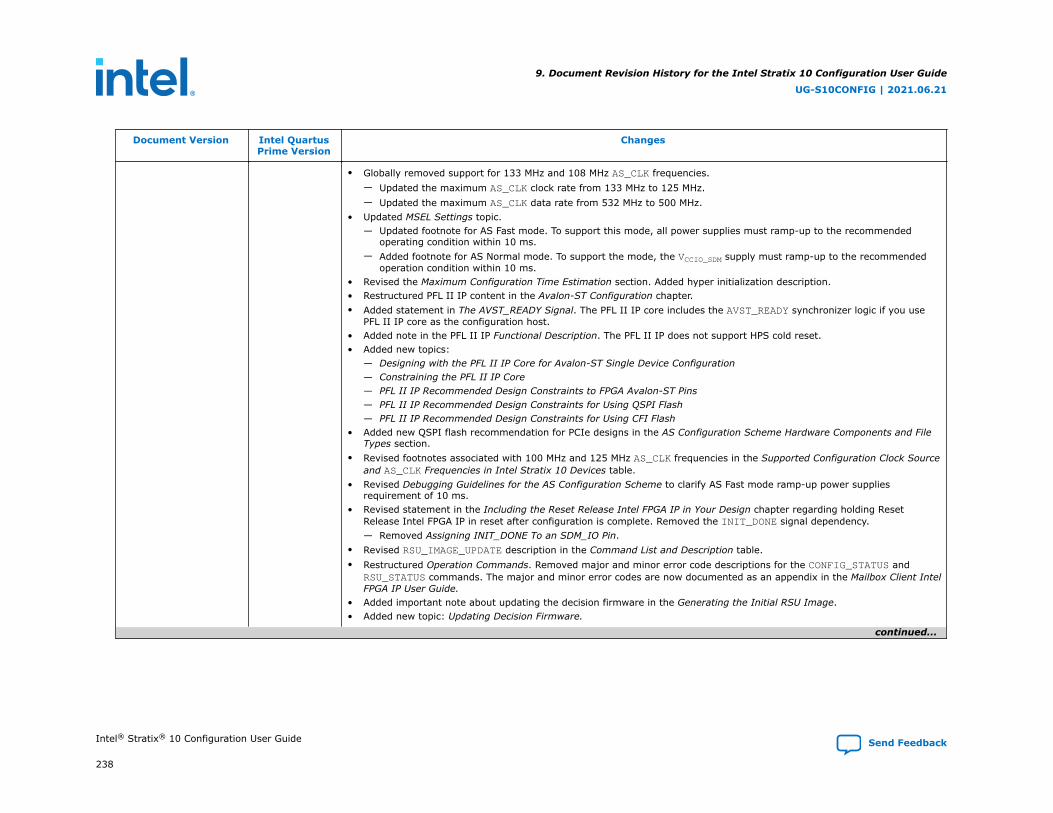
Document Version Intel QuartusPrime Version
Changes
• Globally removed support for 133 MHz and 108 MHz AS_CLK frequencies.— Updated the maximum AS_CLK clock rate from 133 MHz to 125 MHz.— Updated the maximum AS_CLK data rate from 532 MHz to 500 MHz.
• Updated MSEL Settings topic.— Updated footnote for AS Fast mode. To support this mode, all power supplies must ramp-up to the recommended
operating condition within 10 ms.— Added footnote for AS Normal mode. To support the mode, the VCCIO_SDM supply must ramp-up to the recommended
operation condition within 10 ms.• Revised the Maximum Configuration Time Estimation section. Added hyper initialization description.• Restructured PFL II IP content in the Avalon-ST Configuration chapter.• Added statement in The AVST_READY Signal. The PFL II IP core includes the AVST_READY synchronizer logic if you use
PFL II IP core as the configuration host.• Added note in the PFL II IP Functional Description. The PFL II IP does not support HPS cold reset.• Added new topics:
— Designing with the PFL II IP Core for Avalon-ST Single Device Configuration— Constraining the PFL II IP Core— PFL II IP Recommended Design Constraints to FPGA Avalon-ST Pins— PFL II IP Recommended Design Constraints for Using QSPI Flash— PFL II IP Recommended Design Constraints for Using CFI Flash
• Added new QSPI flash recommendation for PCIe designs in the AS Configuration Scheme Hardware Components and FileTypes section.
• Revised footnotes associated with 100 MHz and 125 MHz AS_CLK frequencies in the Supported Configuration Clock Sourceand AS_CLK Frequencies in Intel Stratix 10 Devices table.
• Revised Debugging Guidelines for the AS Configuration Scheme to clarify AS Fast mode ramp-up power suppliesrequirement of 10 ms.
• Revised statement in the Including the Reset Release Intel FPGA IP in Your Design chapter regarding holding ResetRelease Intel FPGA IP in reset after configuration is complete. Removed the INIT_DONE signal dependency.— Removed Assigning INIT_DONE To an SDM_IO Pin.
• Revised RSU_IMAGE_UPDATE description in the Command List and Description table.• Restructured Operation Commands. Removed major and minor error code descriptions for the CONFIG_STATUS and
RSU_STATUS commands. The major and minor error codes are now documented as an appendix in the Mailbox Client IntelFPGA IP User Guide.
• Added important note about updating the decision firmware in the Generating the Initial RSU Image.• Added new topic: Updating Decision Firmware.
continued...
9. Document Revision History for the Intel Stratix 10 Configuration User Guide
UG-S10CONFIG | 2021.06.21
Intel® Stratix® 10 Configuration User Guide Send Feedback
238
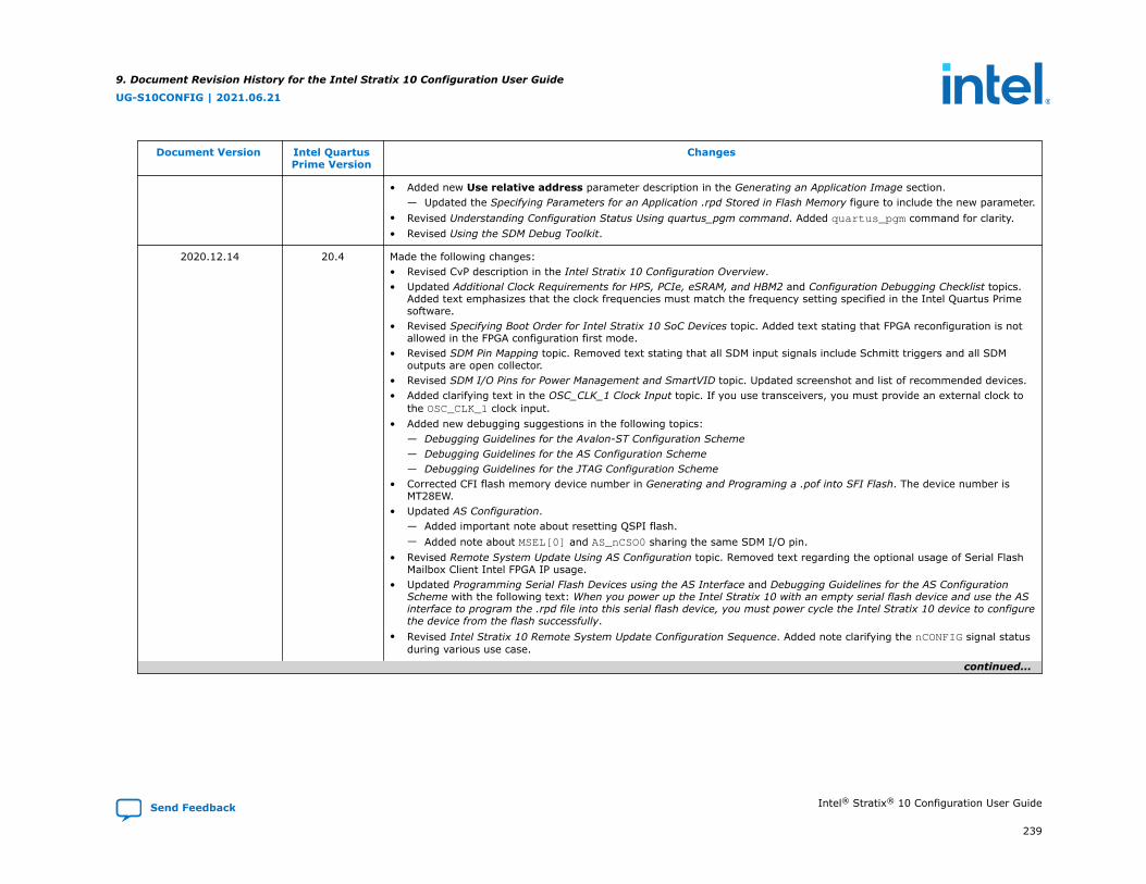
Document Version Intel QuartusPrime Version
Changes
• Added new Use relative address parameter description in the Generating an Application Image section.— Updated the Specifying Parameters for an Application .rpd Stored in Flash Memory figure to include the new parameter.
• Revised Understanding Configuration Status Using quartus_pgm command. Added quartus_pgm command for clarity.• Revised Using the SDM Debug Toolkit.
2020.12.14 20.4 Made the following changes:• Revised CvP description in the Intel Stratix 10 Configuration Overview.• Updated Additional Clock Requirements for HPS, PCIe, eSRAM, and HBM2 and Configuration Debugging Checklist topics.
Added text emphasizes that the clock frequencies must match the frequency setting specified in the Intel Quartus Primesoftware.
• Revised Specifying Boot Order for Intel Stratix 10 SoC Devices topic. Added text stating that FPGA reconfiguration is notallowed in the FPGA configuration first mode.
• Revised SDM Pin Mapping topic. Removed text stating that all SDM input signals include Schmitt triggers and all SDMoutputs are open collector.
• Revised SDM I/O Pins for Power Management and SmartVID topic. Updated screenshot and list of recommended devices.• Added clarifying text in the OSC_CLK_1 Clock Input topic. If you use transceivers, you must provide an external clock to
the OSC_CLK_1 clock input.• Added new debugging suggestions in the following topics:
— Debugging Guidelines for the Avalon-ST Configuration Scheme— Debugging Guidelines for the AS Configuration Scheme— Debugging Guidelines for the JTAG Configuration Scheme
• Corrected CFI flash memory device number in Generating and Programing a .pof into SFI Flash. The device number isMT28EW.
• Updated AS Configuration.— Added important note about resetting QSPI flash.— Added note about MSEL[0] and AS_nCSO0 sharing the same SDM I/O pin.
• Revised Remote System Update Using AS Configuration topic. Removed text regarding the optional usage of Serial FlashMailbox Client Intel FPGA IP usage.
• Updated Programming Serial Flash Devices using the AS Interface and Debugging Guidelines for the AS ConfigurationScheme with the following text: When you power up the Intel Stratix 10 with an empty serial flash device and use the ASinterface to program the .rpd file into this serial flash device, you must power cycle the Intel Stratix 10 device to configurethe device from the flash successfully.
• Revised Intel Stratix 10 Remote System Update Configuration Sequence. Added note clarifying the nCONFIG signal statusduring various use case.
continued...
9. Document Revision History for the Intel Stratix 10 Configuration User Guide
UG-S10CONFIG | 2021.06.21
Send Feedback Intel® Stratix® 10 Configuration User Guide
239
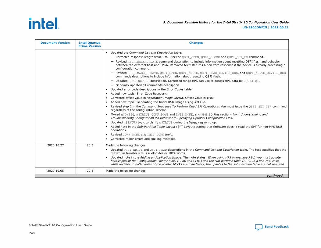
Document Version Intel QuartusPrime Version
Changes
• Updated the Command List and Description table:— Corrected response length from 1 to 0 for the QSPI_OPEN, QSPI_CLOSE and QSPI_SET_CS command.— Revised RSU_IMAGE_UPDATE command description to include information about resetting QSPI flash and behavior
between the external host and FPGA. Removed text: Returns a non-zero response if the device is already processing aconfiguration command.
— Revised RSU_IMAGE_UPDATE, QSPI_OPEN, QSPI_WRITE, QSPI_READ_DEVICE_REG, and QSPI_WRITE_DEVICE_REGcommands descriptions to include information about resetting QSPI flash.
— Updated QSPI_SET_CS description. Corrected range HPS can use to access HPS data tonCSO[3:0].— Generally updated all commands description.
• Updated error code descriptions in the Error Codes table.• Added new topic: Error Code Recovery.• Corrected offset value in Application Image Layout. Offset value is 1F00.• Added new topic: Generating the Initial RSU Image Using .rbf File.• Revised step 2 in the Command Sequence To Perform Quad SPI Operations. You must issue the QSPI_SET_CS* command
regardless of the configuration scheme.• Moved nCONFIG, nSTATUS, CONF_DONE and INIT_DONE, and SDM_IO Pins sections from Understanding and
Troubleshooting Configuration Pin Behavior to Specifying Optional Configuration Pins.• Updated nSTATUS topic to clarify nSTATUS during the VCCIO_SDM ramp up.• Added note in the Sub-Partition Table Layout (SPT Layout) stating that firmware doesn't read the SPT for non-HPS RSU
operations.• Revised CONF_DONE and INIT_DONE topic.• Corrected minor errors and spelling mistakes.
2020.10.27 20.3 Made the following changes:• Updated QSPI_WRITE and QSPI_READ descriptions in the Command List and Description table. The text specifies that the
maximum transfer size is 4 kilobytes or 1024 words.• Updated note in the Adding an Application Image. The note states: When using HPS to manage RSU, you must update
both copies of the Configuration Pointer Block (CPB0 and CPB1) and the sub-partition table (SPT). In a non-HPS case,while updates to both copies of the pointer blocks are mandatory, the updates to the sub-partition table are not required.
2020.10.05 20.3 Made the following changes:
continued...
9. Document Revision History for the Intel Stratix 10 Configuration User Guide
UG-S10CONFIG | 2021.06.21
Intel® Stratix® 10 Configuration User Guide Send Feedback
240

Document Version Intel QuartusPrime Version
Changes
• Added Intel Stratix 10 GX 10M device limitation in the Secure Device Manager section. The Intel Stratix 10 GX 10M devicesupports authentication, but not advanced security.
• Updated the Additional Clock Requirement for HPS, PCIe, eSRAM, and HBM2 section.— Added HPS_OSC_CLK clock in the FPGA Configuration topic.— Added new topic: HPS First Configuration.
• Added new video guides for the following sections:— Converting .sof to .pof File— Generating Programming Files using the Programming File Generator— Generating the Initial RSU Image
• Globally corrected the AS_nCSO pin name.• Globally removed dual-purpose text from the MSEL pin type description. After power on reset, the MSEL pins can be
repurposed as chip select pins. However, you cannot reuse the MSEL pins for other purpose.• Removed anti-tamper description from the OSC_CLK_1 Requirements and Device Security sections. The anti-tamper
feature is not available in the Intel Quartus Prime software version 20.3.• Added note on using the Parallel Flash Loader to program multiple QSPI flash device in the IP for Use with the Avalon-ST
Configuration Scheme: Intel FPGA Parallel Flash Loader II IP Core: Functional Description section.• Added new recommendation on clearing the RSU_STATUS command after the JTAG reconfiguration in the Debugging
Guidelines for the JTAG Configuration Scheme section.• Removed outdated text from the Understanding the Reset Release IP Requirement section. The text stated that an Intel
Quartus Prime Pro Edition legality check prevents you from instantiating more than one instance of the Reset Release IntelFPGA IP.
• Updated the Error Codes table. Added new error code responses:— HW_ERROR
— COMMAND_SPECIFIC_ERROR
• Added Page command support in the SDM I/O Pins for Power Management and SmartVID section.
2020.08.28 20.2 Made the following changes:• Added clarifying note for the Intel Stratix 10 GX 10M device support in the Intel Stratix 10 Configuration Scheme, Data
Width, and MSEL table.— Intel Stratix 10 GX 10M devices don't support the Avalon-ST x32, Avalon-ST x16, AS - fast mode, and AS - normal
mode configuration schemes.• Removed outdated note specific to the MSEL pins from the Avalon-ST Single-Device Configuration section.• Removed obsolete AN 891 link in the Including the Reset Release Intel FPGA IP in Your Design section. The specified
section already includes the AN 891 content.
2020.06.30 20.2 Made the following changes:
continued...
9. Document Revision History for the Intel Stratix 10 Configuration User Guide
UG-S10CONFIG | 2021.06.21
Send Feedback Intel® Stratix® 10 Configuration User Guide
241
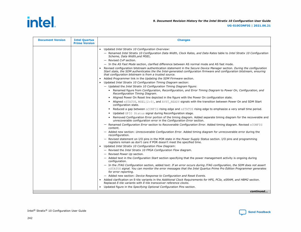
Document Version Intel QuartusPrime Version
Changes
• Updated Intel Stratix 10 Configuration Overview:— Renamed Intel Stratix 10 Configuration Data Width, Clock Rates, and Data Rates table to Intel Stratix 10 Configuration
Scheme, Data Width,and MSEL.— Revised CvP section.— In the AS Fast Mode section, clarified difference between AS normal mode and AS fast mode.
• Revised configuration bitstream authentication statement in the Secure Device Manager section. During the configurationStart state, the SDM authenticates the the Intel-generated configuration firmware and configuration bitstream, ensuringthat configuration bitstream is from a trusted source.
• Added Programmer link in the Updating the SDM Firmware section.• Updated Intel Stratix 10 Configuration Timing Diagram section:
— Updated the Intel Stratix 10 Configuration Timing Diagram figure:• Renamed figure from Configuration, Reconfiguration, and Error Timing Diagram to Power On, Configuration, and
Reconfiguration Timing Diagram.• Aligned Power On Reset line depicted in the figure with the Power On configuration state.• Aligned nSTATUS, MSEL[2:0], and AVST_READY signals with the transition between Power On and SDM Start
configuration state.• Reduced a gap between nCONFIG rising edge and nSTATUS rising edge to emphasize a very small time period.• Updated GPIO Status signal during Reconfiguration stage.• Removed Configuration Error portion of the timing diagram. Added separate timing diagram for the recoverable and
unrecoverable configuration error in the Configuration Error section.— Renamed Configuration Error section to Recoverable Configuration Error. Added timing diagram. Revised nCONFIG
content.— Added new section: Unrecoverable Configuration Error. Added timing diagram for unrecoverable error during the
reconfiguration.— Revised statement on I/O pins in the POR state in the Power Supply Status section. I/O pins and programming
registers remain as don't care if POR doesn't meet the specified time.• Updated Intel Stratix 10 Configuration Flow Diagram:
— Revised the Intel Stratix 10 FPGA Configuration Flow diagram.— Revised Power Up section.— Added text in the Configuration Start section specifying that the power management activity is ongoing during
configuration.— In the JTAG Configuration section, added text: If an error occurs during JTAG configuration, the SDM does not assert
nSTATUS signal. You can monitor the error messages that the Intel Quartus Prime Pro Edition Programmer generatesfor error reporting.
— Added new section: Device Response to Configuration and Reset Events.• Added clarification on E-tile variants in the Additional Clock Requirements for HPS, PCIe, eSRAM, and HBM2 section.
Replaced E-tile variants with E-tile transceiver reference clocks.• Updated figure in the Specifying Optional Configuration Pins section.
continued...
9. Document Revision History for the Intel Stratix 10 Configuration User Guide
UG-S10CONFIG | 2021.06.21
Intel® Stratix® 10 Configuration User Guide Send Feedback
242
Document Version Intel QuartusPrime Version
Changes
• Updated OSC_CLK_1 Clock Input:— Added text: When you specify OSC_CLK_1 for configuration, the OSC_CLK_1 clock must be a stable and free-running
clock..— Removed .qsf file example. Use the Intel Quartus Prime Pro Edition GUI to specify frequencies.— Expanded topic to include additional usage requirements.
• Added new topic: Maximum Configuration Time Estimation.• Removed the following sections from the Avalon-ST Configuration scheme:
— QSF Assignment for Avalon-ST x8— QSF Assignment for Avalon-ST x16— QSF Assignment for Avalon-ST x32
• Updated AS Configuration section:— Revised Required Configuration Signals for the AS Configuration Scheme table. Removed outdated table description.— Revised AS_nCSO statement in the MSEL Pin Function for the AS x4 Configuration Scheme section.— Corrected OSC_CLK_1 frequency from 80 MHz to 71.5 MHz in the Maximum AS_CLK Frequency as a Function of Board
Capacitance Loading and Clock Source and the Supported Configuration Clock Source and AS_CLK Frequencies in IntelStratix 10 Devices table.
— Added new table: Text_delay as a Function of AS_CLK Frequency in the AS Configuration Timing Parameters section.— Added notes in the Supported configuration clock source and AS_CLK Frequencies in Intel Stratix 10 Devices table
clarifying that you observe a lower AS_CLK frequency when accessing the flash during user mode.— Revised step describing the programming file(s) generation in the Generating Programming Files using the
Programming File Generator. Added command to save the programming file.• Removed guidelines related to SD/MMC device configuration in the following sections:
— Removed SD/MMC flash memories support in the Intel Stratix 10 Configuration Overview section.— Removed SD/MMC configuration scheme from the Intel Stratix 10 Configuration Data Width, Clock Rates, and Data
Rates table.— Removed SD/MMC interface from the Intel Stratix 10 Configuration Interfaces figure.— Removed SD/MMC block from the SDM Block Diagram figure and the corresponding description.— Removed SD/MMC x4/x8 configuration scheme from the MSEL Settings for Each Configuration Scheme of Intel Stratix
10 Devices table.— Removed SD/MMC text from the CLIENT_ID_NO_MATCH description in the Error Codes table.
• Updated the JTAG Configuration section to include .rbf file as supported option to configure FPGA using the Intel QuartusPrime Programmer.
• Updated recommendations on how to debug the OSC_CLK_1 clock based configuration in the Debugging Guidelines for theAS Configuration Scheme topic.
• Removed UNKNOWN_BR error from the Error Codes table.• Removed PUF data from flash memory section and figures. For more information, refer to the Intel Stratix 10 Device
Security User Guide.
continued...
9. Document Revision History for the Intel Stratix 10 Configuration User Guide
UG-S10CONFIG | 2021.06.21
Send Feedback Intel® Stratix® 10 Configuration User Guide
243
Document Version Intel QuartusPrime Version
Changes
• Revised step on selecting factory and application images in the Generating the Initial RSU Image and the Creating InitialFlash Image Containing Bitstreams for Factory Image and One Application Image sections.
• Revised flash offset for factory image, sub-partition tables, pointer blocks, and application images in the Flash Sub-Partitions Layout table.
• Added guidance on increasing the reserved memory space for factory and application images in the RSU Sub-PartitionsLayout section. Revised flash offsets in the Flash Sub-Partitions Layout table.
• Revised System and Read only flag description in the Flags Specifying Contents and Access table.• Added note and offset for the first image pointer slot in the Pointer Block Layout table. The offset is 0x20.• Revised item 2 in the General Configuration Debugging Checklist table. Added PWRMGT_SDA and PWRMGT_SCL resistors.• Added new topic: Understanding Configuration Status using quartus_pgm Command.• Updated SDM Debug Toolkit:
— Added temperature sensor image in the Temperature Sensor section.— Added new QSPI Flash section.
• Corrected minor errors and spelling mistakes.
2020.04.13 20.1 Made the following changes:• Added PUF data to figures illustrating the layout of flash memory.• Added the following additional case to the to the reasons that configuration using the OSC_CLK_1 pin might fail: You have
enabled the Anti-tamper response security setting on the Assignments ➤ Device ➤ Device and Pin Options ➤Security ➤ Anti-Tamper tab. The anti-tamper functionality requires you to use the internal oscillator for configuration.
• Added notes in the Generating an Application Image and Generating a Factory Update Image topics, that the rsu1.tclscript turns on bit swap when generating the .rpd file. Consequently, if you are using rsu1.tcl, you should leave bitswap off when generating the .rpd file.
• Removed the following statement from the Application Image Layout topic: By default the first 16 bytes of the applicationimage starting at address offset 0x1FC0 are 0. However you can use these 16 bytes to store a Version ID to identify yourapplication image. This feature is not supported.
• Corrected minor errors and spelling mistakes.
2020.03.06 19.4 Made the following change:• Corrected the output IBIS model in the Intel Stratix 10 Configuration Pins I/O Standard, Drive Strength, and IBIS Model
table. The output IBIS model is 18_io_d8s1_sdm_lv.
2019.12.16 19.4 Made the following changes:
continued...
9. Document Revision History for the Intel Stratix 10 Configuration User Guide
UG-S10CONFIG | 2021.06.21
Intel® Stratix® 10 Configuration User Guide Send Feedback
244
Document Version Intel QuartusPrime Version
Changes
• Added a new chapter covering the Reset Release Intel FPGA IP and why it must be included in your design.• Added the following components to the Required Communication and Host Components for the Remote System Update
Design Example figure:— Reset Release Intel FPGA IP— 3 Reset Bridge Intel FPGA IPs
• Added the following text to the OSC_CLK_1 Clock Input topic: When you specify OSC_CLK_1 for configuration andreconfigure without powering down the Intel Stratix 10 device, the device can only reconfigure with OSC_CLK_1. In thisscenario, OSC_CLK_1 must be a free-running clock.
• Added the following text to the definition of the Failing image field of the RSU_STATUS command:Note: A rising edge on nCONFIG to reconfigure from ASx4, does not clear this field. Information about failing image only
updates when the Mailbox Client receives a new RSU_IMAGE_UPDATE command and successfully configures fromthe update image.
• Added the following restriction to the definition of QSPI_SET_CS: Access to the QSPI flash memory devices using SDM_IOpins is only available for the AS x4 configuration scheme, JTAG configuration, and a design compiled for ASx4configuration. For the Avalon ST configuration scheme, you must connect QSPI flash memories to GPIO pins.
• Updated the final suggestion in Debugging Guidelines for the JTAG Configuration Scheme topic, to the following: When theMSEL setting on the PCB is not JTAG, if you use the JTAG interface for reconfiguration after an initial reconfiguration usingAS or the Avalon-ST interface, the .sof must be in the file format you specified in the Intel Quartus Prime project. Forexample, if you initially configure the MSEL pins for AS configuration and configure using the AS scheme, a subsequentJTAG reconfiguration using a .sof generated for Avalon-ST fails.
• Annotated the figures illustrating RSU in the Remote System Update from FPGA Core Example chapter.
2019.10.07 19.3 Made the following changes:• Corrected definition of RSU_STATUS command. This command has 9, not 10 words.• Added E-Tile Transceivers May Fail To Configure to the Debugging chapter.• Revised the Modifying the List of Application Images topic.
2019.09.30 19.3 Made the following changes:• Added the an eighth word to the to the RSU_STATUS response: Word 8: Current image retry counter.• Added new field to the 5th word of the RSU_STATUS response. This field specifies the source of a reported error.• Added RSU_NOTIFY to the available operation commands.• Changed the number of images that the Programming File Generator supports from 3 to 7.• Corrected the definition of word 2 of the RSU_STATUS response. A value of all 0s indicates no failing image.• Removed write restrictions for lower addresses in flash memory. (The device firmware must still reside at address 0x0.• Changed the err status pulse range from 1 ms ±50% to 0.5 ms to 10 ms.• Removed the SDM Firmware state from the Intel Stratix 10 FPGA Configuration Flow diagram. This state is part of the
FPGA Configuration state.• Added statement that when using using the Generic Serial Flash Interface Intel FPGA IP to write the flash memory the
flash device must be connected to GPIO pins.
continued...
9. Document Revision History for the Intel Stratix 10 Configuration User Guide
UG-S10CONFIG | 2021.06.21
Send Feedback Intel® Stratix® 10 Configuration User Guide
245

Document Version Intel QuartusPrime Version
Changes
• Updated recommendations on how to debug a corrupt configuration bitstream for the AS x4 configuration scheme in theDebugging Guidelines for the AS Configuration Scheme topic.
• Updated figures that show optional SDM I/O pin assignments. There are additional optional SDM I/O pins in 19.3• Renamed the following components:;
— Reset Release Intel Stratix 10 FPGA IP to Reset Release Intel FPGA IP— Mailbox Client Intel Stratix 10 FPGA IP to Mailbox Client Intel FPGA IP— Intel Stratix 10 Serial Flash Mailbox Client Intel FPGA IP to Serial Flash Mailbox Client Intel FPGA IP— Partial Reconfiguration External Configuration Controller Intel Stratix 10 FPGA IP to Partial Reconfiguration External
Configuration Controller Intel FPGA IP— Corrected the signal name in The AVST_READY Signal topic: The device can starting sending data when AVST_READY
asserts.— Added note that the Avalon ST x32 configuration scheme is limited to 3, DDR x72 DDR external memory interfaces.
The Avalon ST x8 and x16 configuration schemes can support up to 4, x72 DDR external memory interfaces.• Corrected minor errors and typos.
2019.07.19 19.2 Made the following changes:• Corrected numbers on Configuration, Reconfiguration, and Error Timing Diagram timing diagram. The number 3 now
labels the nCONFIG rising edge. Renumbered associated text under the Initial Configuration Timing heading.• In the Additional Clock Requirements for HPS, PCIe, eSRAM, and HBM2 topic, removed the following items from the list of
components requiring a free-running clock before configuration begins:— EMIF— E-Tile transceiverNote: HPS EMIF retains this requirement.
2019.07.08 19.2 Made the following changes:
continued...
9. Document Revision History for the Intel Stratix 10 Configuration User Guide
UG-S10CONFIG | 2021.06.21
Intel® Stratix® 10 Configuration User Guide Send Feedback
246

Document Version Intel QuartusPrime Version
Changes
• Revised and reorganized all topics covering configuration pin assignments:— Clarified the behavior of the MSEL pins in AS x4 mode.— Added information about the SDM_IO pin states during power-on and after device cleaning to the Intel Stratix 10
Configuration Pins topic.— Created separate topics covering partial configuration and SmartVID signals.
• Made the following changes to the RSU chapter:— Added the following topics:
• RSU Glossary• Standard (non-RSU) Flash Layout• RSU Flash Layout – SDM Perspective• RSU Flash Layout – Your Perspective• Detailed Quad SPI Flash Layout• Sub-partitions Layout• Sub-Partition Table Layout• Pointer Block Layout• Modifying the List of Application Images• Application Image Layout
— The static firmware has been replaced by decision firmware.— The update image now includes the factory image, the decision firmware and the decision firmware data.— The QSPI_ERASE command is now 4 KB aligned. The number of words to erase must be a multiple of 1024.— Added definitions of major and minor error codes for RSU_STATUS and CONFIG_STATUS.
• Added footnote explaining that before you can use CvP you must configure either the periphery image or the full image viathe AS configuration scheme. Then, you can configure the core image using CvP.
• Added recommendation to use the Analog Devices LTM4677 device to regulate the PMBus for SmartVID devices. You setthis parameter here: Device ➤ Device and Pin Options ➤ Power Management & VID ➤ Slave device type.
• Added two restrictions to the dual-purpose use of Avalon-ST pins. For more information, refer to the Enabling Dual-Purpose Pins topic.
• Corrected maximum speed and data rate in the Intel Stratix 10 Configuration Data Width, Clock Rates, and Data Ratestable. The Max Clock Rate is 33 MHz. The Max Data Rate is 33 Mb.
• Updated the Intel Stratix 10 Reset Release IP to include reference to the new An 891: Using the Reset Release FPGA IP.Removed recommendation to gate Intel Hyperflex registers using the nINIT_DONE signal.
• Added the eSRAM clocks to the list of free-running clocks that must be stable before configuration begins.• Added Attention warning that designs including the Intel Stratix 10 Mailbox Client FPGA IP using Intel Quartus Prime
Programmer 19.2 or later whose .sof was generated in Intel Quartus Prime Programmer 19.1 or earlier must beregenerate the .sof.
continued...
9. Document Revision History for the Intel Stratix 10 Configuration User Guide
UG-S10CONFIG | 2021.06.21
Send Feedback Intel® Stratix® 10 Configuration User Guide
247

Document Version Intel QuartusPrime Version
Changes
• Added 10 kΩ pull-up resistor to nCONFIG in the following figures:— Connections for Avalon-ST x8 Single-Device Configuration— Connections for Avalon-ST x16 Single-Device Configuration— Connections for Avalon-ST x32 Single-Device Configuration— PFL II IP core with Dual CFI Flash Memory Devices
• Removed discrete synchronizers for the AVST_READY signal in the following figures:— Connections for Avalon-ST x8 Single-Device Configuration— Connections for Avalon-ST x16 Single-Device Configuration— Connections for Avalon-ST x32 Single-Device ConfigurationIf necessary, you can implement synchronizers in the host controller if the host is an FPGA or CPLD. Validation has shownthat external synchronizers are not required.
• Made a global change recommending that you use the newer Intel Quartus Prime Programming File Generator insteadof the legacy Intel Quartus Prime Convert Programming Files conversion program to generate programming files.Changed all file conversion topics to use the Programming File Generator.
• Revised all topics providing steps for file conversion to use Programming File Generator instead of the legacy ConvertProgramming Files dialog box.
• Clarified statement on quad SPI flash byte addressing: The SDM configures the Quad SPI flash device to operate using 4-byte addressing if the flash size in 256 MB or greater.
• Corrected flash memory sizes in Understanding Quad SPI Flash Byte-Addressing topic. All sizes in in megabits or gigabits,not megabytes or gigabytes.
• Generalized Figure 2. Intel Stratix 10 Configuration Architecture Block Diagram. This figure no longer lists specific variantsof Intel Stratix 10 device.
• Corrected Step 3 in the Initial Configuration Timing description. The step should say, with nConfig low, the SDM entersIdle mode after booting.
• Corrected the Intel Stratix 10 FPGA Configuration Flow diagram. The transition between FPGA Config* and User Modeshould say INIT_DONE = HIGH.
• Corrected the following statement in the Debugging Guidelines for the JTAG Configuration Scheme topic: An nSTATUSfalling edge terminates any JTAG access and the device reverts to the MSEL-specified boot source. nSTATUS must bestable during JTAG configuration.. In both sentence, nSTATUS should be nCONFIG.
• Removed pin assignments for CVP_CONFDONE for the Avalon-ST in the Available SDM I/O Pin Assignments forConfiguration Signals that Do Not Use Dedicated SDM I/O Pins table. CvP does not the support Avalon-ST x8 configurationscheme in Intel Stratix 10 devices.
2019.04.10 19.1 Updated the transceiver reference clocks.
2019.04.01 19.1 Made the following additions and enhancements:
continued...
9. Document Revision History for the Intel Stratix 10 Configuration User Guide
UG-S10CONFIG | 2021.06.21
Intel® Stratix® 10 Configuration User Guide Send Feedback
248
Document Version Intel QuartusPrime Version
Changes
• Added Intel Stratix 10 Reset Release IP. Use the nINIT_DONE output of this IP to hold your application logic in reset untilthe entire FPGA fabric enters user mode.
• Added Configuration Scheme Components and File Types topics illustrating the software flow and programming fileoutputs for the AS, Avalon-ST, and JTAG programming schemes.
• Added the following topics to the Stratix 10 Configuration Debugging Guide chapter:— Debugging Checklist— SDM Debug Toolkit Overview— Using the SDM Debug Toolkit— Reading the Unique 64-Bit CHIP ID— Understanding SEUs
• Added Maximum Allowable External AS_DATA Pin Skew Delay Guidelines topic.• Added Generating an Update Image for Static Firmware and Factory Image topic.• Added topics covering SDM_IO pin assignments and QSF settings for the Avalon-ST x8, x16, x32, and AS configuration
schemes.• Added note in the Avalon-ST Configuration Timing topic. This note covers special requirements for driving configuration
data Avalon-ST x16 and x32 configurations.• Added the following signals to the Intel Stratix 10 Configuration Timing Diagram: nINIT_DONE, Data<n>-1:0],
AVST_READY, AVST_VALID, and AS_CS0.• Added a 10K Ω pull-up resistor to nCONFIG and corrected file type for flash image in the following figures:
— Connections for AS x4 Single-Device Configuration— Connections for AS Configuration with Multiple Serial Flash Devices— Connections for Programming the Serial Flash Devices using the JTAG Interface
• Added the IBIS model name to the Intel Stratix 10 Configuration Pins I/O Standard and Drive Strength table. Renamedthis table Configuration Pins I/O Standard, Drive Strength, and IBIS Model.
• Added Updating the SDM Firmware topic in the Intel Stratix 10 Configuration Overview chapter.• Added the following guidance in Debugging Guidelines for the JTAG Configuration Scheme topic: When you use the JTAG
interface for reconfiguration after an initial reconfiguration using AS or the Avalon-ST interface, the .sof must be in thefile format you specified in the Intel Quartus Prime project.
• Added the following signals to the list of device configuration pins that do not have fixed assignments:— CONF_DONE
— INIT_DONE
— HPS_COLD_nRESET
• Improved definitions of programming file output types.• Edited Using the PFL II IP Core for clarity and style. Added many screenshots illustrating the step to complete a task.• Updated the supported flash memory devices and supported SD* card types in the Intel Stratix 10 Configuration Overview
topic.
continued...
9. Document Revision History for the Intel Stratix 10 Configuration User Guide
UG-S10CONFIG | 2021.06.21
Send Feedback Intel® Stratix® 10 Configuration User Guide
249

Document Version Intel QuartusPrime Version
Changes
• Updated the SDM Pin Mapping table to include the following:— Avalon-ST x16, and x32 configuration scheme— Pins for SmartVID
• Added definition of the GETDESIGN_HASH command to the Mailbox Client Intel Stratix 10 FPGA IP Command List andDescription table.
• Renamed the topic title Commands and Error Codes to Commands and Responses.• Updated the descriptions for Length and Command Code/Error Code in the Mailbox Client Intel Stratix 10 FPGA IP
Command and Response Header Description table.• Added PLL reference clock requirement to the Additional Clock Requirements for Transceivers, HPS, PCIe, High Bandwidth
Memory (HBM2) and SmartVID topic.• Updated the Generating a Single RSU Image topic to clarify that the .rpd for Intel Stratix 10 devices now includes
firmware pointer information for image addresses and is not compatible with earlier generation methods.• Removed a note in Remote System Upgrade Configuration Images topic, saying that the application image is optional and
can be added later. The initial RSU setup requires both a factory image and an application image.• Added the following note to the Configuration Firmware Pointer Block (CPB) topic:
Note: Application images must align to partition boundaries in the flash device. If an application image is less than a fullpartition, the rest of the sector cannot be used.
• Added a new topic RSU Recovery from Corrupted Images that explains how the SDM recovers from attempts to loadcorrupted images.
• Added 71.5 MHz as a supported frequency for the OSC_CLK_1 for AS configuration.• Added description of optional 16-byte .rpd Version ID to the Remote System Upgrade Flash Device Layout topic.• Removed Supported Flash Devices appendix. This appendix has been replace by the following web page Supported Flash
Devices for Intel Stratix 10 Devices which provides more information about flash devices for different purposes.• Removed references to P30 and P33 flash memory devices. These CFI flash devices are no longer available.Made the following corrections:• Corrected the following statement: Because Intel Stratix 10 devices operate at 1.8 volt and all SD MMC I/Os operate
between 2.7 - 3.6 volts, an intermediate voltage level translator is necessary for SD cards. This statement is only true forSD cards.
• Corrected the value of MSEL for Avalon-ST x16 configuration in Table 1 and Table 9. The correct value is 101.• Corrected PFL II IP core with Dual P30 or P33 CFI Flash Memory Devices figure. The nCONFIG signal should not have a
pulldown resistor.• Removed the statement that Remote system upgrade cannot use partial reconfiguration (PR) images for the application
image from the Remote System Upgrade Using AS Configuration topic. Remote system upgrade does support PR.• In the Mailbox Client Intel Stratix 10FPGA IP Command List and Description table, for CONFIG_STATUS, corrected the size
of MSEL. MSEL is 3 bits.• Corrected the end address in step 14a of Generating a Standard RSU Image. It should be 0x00523FF.• Corrected the definition of QSPI_ERASE. The number of words to erase must be a multiple of 4000 (hexadecimal) words.
continued...
9. Document Revision History for the Intel Stratix 10 Configuration User Guide
UG-S10CONFIG | 2021.06.21
Intel® Stratix® 10 Configuration User Guide Send Feedback
250
Document Version Intel QuartusPrime Version
Changes
• Changed Number of Commands and Number of Responses to Command Length and Response Length in the Mailbox ClientIntel Stratix 10 FPGA IP Command List and Descriptions (RSU Functions for Non-HPS Variants) table.
• Corrected the fields of the RSU_STATUS command. The Last failing image field should be called the Firstfailing image. This field reports the flash offset of the first failing application image.
• In the Remote System Upgrade Flash Memory Layout table, changed the amount of reserved flash memory image from64k to 256k.
2018.11.02 18.1 Updated Figure 39: Intel Stratix 10 Modules and Interfaces to Implement RSU Using Images Stored in Flash Memory toexclude SD and MMC memory. These memory types are not supported in the current release.
2018.10.23 18.1 Added the following statement to the description of Avalon-ST Configuration Timing topic: The AVST_READY signal is onlyvalid when the nSTATUS pin is high.
2018.10.10 18.1 Made the following changes:• Changed the number of remote system upgrade images supported from more than 500 to 507 in Remote System Upgrade
Configuration Images.• Updated the last two entries in the Configuration Firmware Pointer Block Format table.
2018.10.04 18.1 Made the following changes:• Corrected statement in the Remote System Upgrade topic. A command to the Mailbox Client Intel Stratix 10 FPGA Mailbox
Client IP Core initiates reconfiguration.• Corrected the Intel Stratix 10 Remote System Upgrade Components figure and Related Information link. The mailbox
component is the Mailbox Client Intel Stratix 10 FPGA IP Core.
2018.09.21 18.1 Made the following changes:• Added new chapter, Remote System Upgrade• Added new chapter, Intel Stratix 10 Debugging Guide• Added separate Debugging Guidelines topics in the Avalon-ST, AS, and JTAG configuration scheme sections.• Significantly expanded Stratix 10 Configuration Overview Configuration Overview chapter.• Added Additional Clock and SmartVID Requirements for Transceivers, HPS, PCIe , High Bandwidth Memory (HBM2) and
SmartVID topic.• Expanded OSC_CLK_1 Clock Input topic to include additional usage requirements.• Added AS Using Multiple Serial Flash Devices topic.• Added numerous screenshots illustrating Intel Quartus Prime Pro Edition procedures.• Improved many figures illustrating configuration schemes.• Added the fact that you must have system administrator privileges to define a new flash device in the Defining New CFI
Flash Memory Device topic.• Added MT28EW to the list of PFL II flash devices supported.
continued...
9. Document Revision History for the Intel Stratix 10 Configuration User Guide
UG-S10CONFIG | 2021.06.21
Send Feedback Intel® Stratix® 10 Configuration User Guide
251

Document Version Intel QuartusPrime Version
Changes
• Moved almost all of the material describing the PFL II flash from an appendix to the Intel Stratix 10 ConfigurationSchemes chapter.
• Edited entire document for clarity and style.• Corrected minor errors and typos.
2018.05.07 18.0 • Removed Estimating the .qek Active Serial Configuration Time section.• Updated the OSC_CLK_1 supported frequency.• Added selecting flash loader step to Generating Programming Files using Convert Programming Files.• Added a note to TCK, TDI, TMS, and TDO stating that they are available for HPS JTAG chaining in SoC devices.• Removed instruction to drive nCONFIG low from POR in the following diagrams:
— Connections for AS x4 Single-Device Configuration— Connection Setup for AS Configuration with Multiple EPCQ-L Devices— Connection Setup for Programming the EPCQ-L Devices using the JTAG Interface
• Added a note in OSC_CLK_1 Clock Input stating that reference clocks to EMIF and PCIe IP cores must be stable and freerunning.
• Removed .ekp file from Overview of Intel Quartus Prime Supported Files and Tools for Configuration and Programmingfigure.
• Updated the Configuring Intel Stratix 10 Devices using AS Configuration section title to Generating and Programming ASConfiguration Programming Files.
• Updated Configuration Schemes and Features Overview in Intel Stratix 10 Devices table:— Added a note stating to contact sales representative for more information about support readiness.— Added a note stating to contact sales representative for more information about flash support other than EPCQ-L
devices.• Removed NAND configuration support.• Updated Configuration Sequence in Intel Stratix 10 Devices figure by adding a looped flow arrow during Idle state.• Updated the MSEL note in Intel Stratix 10 Device Configuration Pins table.• Added a note to recommend OSC_CLK_1 for configuration clock source in OSC_CLK_1 Clock Input.• Updated CvP data width and maximum data rate in Configuration Schemes and Features Overview in Intel Stratix 10
Devices table.• Removed the multiple EPCQ-L configuration device support.
9. Document Revision History for the Intel Stratix 10 Configuration User Guide
UG-S10CONFIG | 2021.06.21
Intel® Stratix® 10 Configuration User Guide Send Feedback
252
Date Version Changes
November 2017 2017.11.09 • Removed link to the Configuration via Protocol (CvP) Implementation User Guide.• Updated titles for Device Security, Partial Reconfiguration, and Configuration via Protocol.
November 2017 2017.11.06 • Updated Option Bits Sector Format table.• Updated a step in Setting Additional Configuration Pins.• Added Converting .sof to .pof File and Programming CPLDs and Flash Memory Devices.• Updated the .pof version value in Storing Option Bits.• Added information about restoring start and end address for option bits in Restoring Option Bit
Start and End Address.• Added note about pull-down resistor is recommended for CONF_DONE and INIT_DONE pins in
Additional Configuration Pin Functions.• Added new subsection Multiple EPCQ-L Devices Support.• Added Configuration Pins I/O Standard and Drive Strength table.• Updated information about maximum additional data words when using 2-stage register
synchronizer.• Updated the equation for minimum AS configuration time estimation.• Added RBF Configuration File Format section explaining the format of the .rbf file.• Updated Configuration Sequence to state that a firmware which is part of the configuration data if
loaded in the device initially.• Updated description for Number of flash devices used parameter in the PFL II Flash Interface
Setting Parameters table.• Updated Configuration via Protocol overview and added link to the Configuration via Protocol (CvP)
Implementation User Guide.• Updated Partial Reconfiguration overview and added link to the Creating a Partial Reconfiguration
Design chapter of the Handbook Volume 1: Design and Compilation.• Updated Design Security Overview descriptions.• Added note for Partial Reconfiguration feature and link to Partial Reconfiguration Solutions IP User
Guide in Intel Stratix 10 Configuration Overview.• Removed SDM pin notes in Intel Stratix 10 Configuration Overview.• Updated internal oscillator's AS_CLK frequency in Supported configuration clock source and AS_CLK
Frequencies in Intel Stratix 10 Devices table.
May 2017 2017.05.22 • Updated Connection Setup for Programming the EPCQ-L Device using the AS Interface figure.• Updated guideline to program the EPCQ-L device in Programming EPCQ-L Devices using the Active
Serial Interface.
April 2017 2017.04.10 • Updated note for AS Fast Mode in MSEL Settings for Each Configuration Scheme of Devices table.• Added note to Configuration via Protocol recommending user to use AS x4 fast mode for CvP
application.• Updated instances of Spansion to Cypress.
continued...
9. Document Revision History for the Intel Stratix 10 Configuration User Guide
UG-S10CONFIG | 2021.06.21
Send Feedback Intel® Stratix® 10 Configuration User Guide
253

Date Version Changes
•• Updated note and description in Configuration Overview.• Removed AS x1 support.• Added Connection Setup for SD/MMC Single-Device Configuration figure.• Updated Connections for AS x4 Single-Device Configuration, Connection Setup for AS Configuration
with Multiple EPCQ-L Devices, Connection Setup for Programming the EPCQ-L Devices using theJTAG Interface, Connection Setup for NAND Flash Single-Device Configuration, and ConnectionSetup for SD/MMC Single-Device Configuration to include note about nCONFIG test point.
• Added note in Avalon-ST Configuration stating that AVST_CLK should be continuous.
February 2017 2017.02.13 • Updated Configuring Stratix 10 Devices using AS Configuration section and subsections toinclude .jic for AS configuration scheme.
• Added Programming .jic files into EPCQ-L Device.• Updated the SDM description.• Updated SDM block diagram by adding Mailbox block and note for Avalon-ST x8 configuration
scheme.• Updated Configuration Sequence Diagram.• Updated configuration sequence descriptions.• Updated Avalon-ST Bus Timing Waveform figure.• Added note to Avalon-ST in Stratix 10 Configuration Overview table.• Updated ASx4 max data rate in Stratix 10 Configuration Overview table.• Removed Configurable Node subsection.
December 2016 2016.12.09 • Updated max data rate for ASx1.• Updated the Configuration Sequence in Stratix 10 Devices figure.• Updated configuration sequence description.• Added JTAG configuration sequence description.• Added Parallel Flash Loader II IP core.
October 2016 2016.10.31 Initial release
9. Document Revision History for the Intel Stratix 10 Configuration User Guide
UG-S10CONFIG | 2021.06.21
Intel® Stratix® 10 Configuration User Guide Send Feedback
254