
Integration of a polarizable interface for electrophoretic ...
138
HAL Id: tel-02417045 https://tel.archives-ouvertes.fr/tel-02417045 Submitted on 18 Dec 2019 HAL is a multi-disciplinary open access archive for the deposit and dissemination of sci- entific research documents, whether they are pub- lished or not. The documents may come from teaching and research institutions in France or abroad, or from public or private research centers. L’archive ouverte pluridisciplinaire HAL, est destinée au dépôt et à la diffusion de documents scientifiques de niveau recherche, publiés ou non, émanant des établissements d’enseignement et de recherche français ou étrangers, des laboratoires publics ou privés. Integration of a polarizable interface for electrophoretic separation in a microfluidic device Qiongdi Zhang To cite this version: Qiongdi Zhang. Integration of a polarizable interface for electrophoretic separation in a microfluidic device. Biophysics. Université Paris Saclay (COmUE), 2018. English. NNT: 2018SACLS577. tel- 02417045
-
Upload
khangminh22 -
Category
Documents
-
view
2 -
download
0
Transcript of Integration of a polarizable interface for electrophoretic ...

HAL Id: tel-02417045https://tel.archives-ouvertes.fr/tel-02417045
Submitted on 18 Dec 2019
HAL is a multi-disciplinary open accessarchive for the deposit and dissemination of sci-entific research documents, whether they are pub-lished or not. The documents may come fromteaching and research institutions in France orabroad, or from public or private research centers.
L’archive ouverte pluridisciplinaire HAL, estdestinée au dépôt et à la diffusion de documentsscientifiques de niveau recherche, publiés ou non,émanant des établissements d’enseignement et derecherche français ou étrangers, des laboratoirespublics ou privés.
Integration of a polarizable interface for electrophoreticseparation in a microfluidic device
Qiongdi Zhang
To cite this version:Qiongdi Zhang. Integration of a polarizable interface for electrophoretic separation in a microfluidicdevice. Biophysics. Université Paris Saclay (COmUE), 2018. English. �NNT : 2018SACLS577�. �tel-02417045�

Integration of a polarizable interface for electrophoretic
separation in a microfluidic device
Thèse de doctorat de l'Université Paris-Saclay préparée à l’Université Paris-Sud
École doctorale n°575: Electrical, optical, bio-physics and engineering (EOBE)
Spécialité de doctorat: électronique et optoélectronique, nano- et microtechnologies
Thèse présentée et soutenue à Orsay, le 17 décembre 2018, par
Qiongdi Zhang Composition du Jury: Philippe Lecoeur Professeur, Université Paris-Sud (- Centre de Nanosciences et de Nanotechnologies-CNRS) Président
Gaëlle Lissorgues Professeur, ESIEE Paris Rapporteur
Philippe Bergonzo V.P. Seki Diamond Systems Professeur invité, University College London Rapporteur
Pierre Joseph Chargé de Recherche, Laboratoire d’Analyse et d’Architecture des Systèmes-CNRS Examinateur
Wilfried Uhring Professeur, Université de Strasbourg (- Laboratoire ICube) Examinateur
Ming Zhang MCF, Université Paris-Sud (- Centre de Nanosciences et de Nanotechnologies-CNRS) Directrice de thèse Anne-Marie Haghiri-Gosnet Directrice de Recherche, Centre de Nanosciences et de Nanotechnologies -CNRS Co-encadrante
Antoine Pallandre Professeur, Université Paris-Sud (- Laboratoire de Chimie Physique-CNRS) Co-encadrant
NN
T :
20
18
SA
CLS
577


Université Paris-Saclay
Espace Technologique / Immeuble Discovery
Route de l’Orme aux Merisiers RD 128 / 91190 Saint-Aubin, France
Titre : Intégration d’une interface polarisable pour la séparation électrophorétique dans un dispositif
microfluidique
Mots clés : CNx, interface polarisable, transistor fluidique, microfluidique, flux électroosmotique
Résumé : L’électrophorèse est une technique
puissante permettant de séparer des biomarqueurs
présents dans les liquides biologiques.
L’électrophorèse de zone libre transporte des
molécules en milieu liquide sous l’influence de
deux contributions : le flux électrophorétique et le
flux électroosmotique (EOF). C’est ce dernier flux
EOF qui permet d’optimiser la résolution analytique
de la séparation et donc de simplifier le mélange
avant sa détection. Notre équipe a développé un
contrôle en temps réel de l’EOF en intégrant une
interface polarisable diélectrique dans un dispositif
microfluidique. Le carbone amorphe azoté (CNx
avec x=15%) a été choisi comme ce matériau.
Comme le CNx ne peut pas être déposé directement
sur un substrat de verre à cause de sa faible
adhérence, deux matériaux différents ont été
proposés comme couche d’accroche : le carbure de
silicium (SiC) et le platine (Pt). Nous avons tout
d’abord optimisé l’adhésion entre le film CNx et la
couche d’accroche SiC par différentes procédures
de fabrication. Cependant, en raison d’une faible
adhérence, le film CNx s’est rapidement décollé en
électrolyte liquide. Par contre, nous avons prouvé
que certaines architectures hybrides incluant du Pt
dans la couche d’accroche sont incroyablement
robustes. Même après deux mois dans une solution
millimolaire de KCl, le CNx adhérait toujours au
verre sans aucune trace de délamination. Ce
dispositif a fourni aussi une grande fenêtre de
polarisabilité (de -1V à +1V). Nous avons enfin
développé une architecture hybride « couche
d’accroche isolée/couche électriquement polarisable
/électrodes de grille enterrées/ polymère » afin
d’éviter toute perte faradique dans l’électrolyte
liquide ou vers les circuits conducteurs du
dispositif. A l’issue de ces travaux, nous pensons
être en mesure de proposer un composant fluidique
complexe et robuste qui permet une modulation en
temps réel de l’EOF lors de migrations
électrophorétiques.
Title : Integration of a polarizable interface for electrophoretic separation in a microfluidic device
Keywords : CNx, polarizable interface, fluidic transistor, microfluidic, electroosmotic flow
Abstract : Electrophoresis is currently an efficient
way to separate precious biomarkers from complex
mixtures. It takes place to transport molecules under
two contributions: the electrophoretic flow and the
electroosmotic flow (EOF). The latter allows to
optimize the analytical resolution of the separation.
Our team has developed a real-time dynamic
control of the EOF by integrating a dielectric
polarizable interface in the microfluidic device.
Amorphous carbon nitride (CNx with x=15%) has
dielectric properties and was chosen to be the
polarizable interface. Since it cannot be deposited
directly onto glass substrate, we have proposed and
studied two different materials as the sticking
underlayer: silicon carbide (SiC) and platinum (Pt).
In the case of SiC, we have optimized the adhesion
between CNx film and SiC underlayer through
different fabrication procedures.
However, due to poor adhesion, CNx film
delaminated into liquid electrolyte quickly.
Compared to SiC, Pt is a good sticking underlayer
for CNx. It was found out that even after two
months in KCl solution, CNx still stuck robustly to
Pt. Meanwhile, the device provided a large window
of polarizability (from -1V to +1V). Finally, to
avoid any faradic loss in the liquid electrolyte or
towards the conductive circuitry of the device, we
have developed a sticking underlayer/electrically
polarizable/polymeric hybrid architecture. This
architecture appears to be the most robust existing
polarizable interface for strong and long-term
adhesion onto glass substrates.


Acknowledgements
Firstly, I would like to thank all members of the committee: Mme. Gaëlle Lissorgues and M. Philippe
Bergonzo who accepted to read my PhD manuscript and give advice; M. Pierre Joseph, M. Wilfried
Uhring and M. Philippe Lecoeur who accepted to join my PhD defense and judge my work.
Secondly, I would like to give my sincere gratitude to my three supervisors: Mme. Ming Zhang who
accepted me in this work and supported me behind all the time; Mme. Anne-Marie Haghiri-Gosnet
who accepted me in a superb clean room to have experiments, guided my way forward and lit the
pathway all along; M. Antoine Pallandre who was always be my technique advisor and my inspiring
mentor, and who spent a lot of time on correcting my manuscript.
I am grateful to the clean room engineers who helped me a lot in the microfabrication and gave me so
much useful advice, they are M. Abdou Harouri and M. Laurent Couraud. I would like also express my
deep appreciation to my friends and colleagues for their support and comprehension: Xuan, Fatima,
Alisier, Julie, Mery, Lyas, and Bacem. All the members of my team and the C2N clean room are also
deeply acknowledged for their kind guidance.
Thank you ANR Labex LaSIPS for the financial support. And thank you C2N for the facilities and
equipment support.
And last but by no means least I would like to express my deepest love to all my family members, to
whom have always been there for me: Mum, Dad, Meemaw, and Cheri, your continuous support has
made everything possible for me.
Thank you!


Abstract
Medical check-up and diagnostics require multiplexed sample treatments and high-resolution
separations. After the separation steps, a sensitive detection of the biomarkers has to be carried out.
One way to efficiently separate precious biomarkers from complex mixtures that are currently used by
biochemists is electrophoresis. Electrophoresis takes place to transport molecules under two
contributions: the electrophoretic mobility that is directly related to the ratio between weight and
charge of molecules and the electroosmotic mobility that allows to optimize the analytical resolution
of the separation. Most of the time analysts modulate electroosmotic flow (EOF) by adjusting pH of
solution, or changing the ionic strength of buffer, or just using surface treatments. All these methods
aim to tune the electrostatic charge state of the solid/liquid interface and to limit unspecific adsorption
inside the microfluidic channel. However, these strategies cannot lead to real-time surface charge
adjustment. Therefore, in our microfluidic transistor, a dielectric polarizable interface is integrated in
order to achieve a dynamic control of the EOF. Such polarizable gate allows a real-time modulation of
the zeta potential at the solid/liquid electrolyte interface under the application of low voltage. This
fluidic transistor with its integrated gate voltage is thus engineered for a fast and efficient control of
EOF independently from the electrophoretic field. Amorphous carbon nitride (CNx with x=15%) has
been chosen to be the dielectric polarizable material for the gate. Since the CNx cannot be deposited
directly on glass substrate, two different materials have been proposed and studied as sticking
underlayer: silicon carbide (SiC) and platinum (Pt). In this work, we have studied the behavior of CNx
film deposited on these two different materials for different architectures of the device. Due to poor
adhesion between CNx and SiC, CNx film quickly delaminated into the liquid electrolyte. Compared to
SiC, Pt is a good sticking underlayer for CNx that was found to be incredibly robust. Even after two
months in KCl solution, CNx still adhered to Pt without any delamination. Moreover, to avoid any
faradic loss in the liquid electrolyte or towards the conductive circuitry of the device, we have
developed a hybrid architecture with polymeric insulating pads at the two extremities of the CNx gate
electrode. This sticking layer/electrically polarizable/polymeric hybrid architecture appears to be the
most robust existing polarizable interface for strong and long-term adhesion onto glass substrates.


I
Contents Chapter 0: General Introduction ............................................................................................................. 1
REFERENCES: ...................................................................................................................................... 2
Chapter 1: Background Introduction ....................................................................................................... 3
1.1. Overview .............................................................................................................................. 3
1.2. Microfluidic Separation ....................................................................................................... 3
1.2.1. Capillary Electrophoresis ......................................................................................... 3
1.2.2. Electroosmotic Flow and Zeta-Potential ................................................................. 5
1.3. Flow FET and Microfluidic Wheatstone Bridge ................................................................... 9
1.3.1. From MIE-FFET to PI-FFET ....................................................................................... 9
1.3.2. Microfluidic Wheatstone Bridge ........................................................................... 12
1.3.3. Polarizable Interface and Polarizability Window ................................................... 16
1.4. Conclusions ........................................................................................................................ 17
REFERENCES: .................................................................................................................................... 17
Chapter 2: Simplification of EOF Measurement Equipment ................................................................. 23
2.1. Overview ............................................................................................................................ 23
2.2. Theoretical Analysis ........................................................................................................... 24
2.2.1. Adder ..................................................................................................................... 24
2.2.2. Voltage Follower .................................................................................................... 25
2.2.3. Regulator ............................................................................................................... 26
2.3. Simulation, Fabrication and Experimental Validation ....................................................... 26
2.3.1. Simulation .............................................................................................................. 27
2.3.2. PCB Fabrication ...................................................................................................... 29
2.3.3. PCB Experimental Validation ................................................................................. 30
2.4. Conclusions ........................................................................................................................ 32
REFERENCES: .................................................................................................................................... 32
Chapter 3: Device Fabrication and Experimental System ..................................................................... 34

II
3.1. Overview ............................................................................................................................ 34
3.2. Step-by-Step Fabrication Processes for Microfluidic Devices ........................................... 36
3.2.1. Typical Microfabrication Processes of PI-FFET on Glass Substrate ....................... 36
3.2.2. Two Microstructuring Methods of Microfluidic Channels .................................... 41
3.2.3. Integration of PI-FFET and Microchannels ............................................................ 44
3.3. Description for Experimental System ................................................................................ 45
3.3.1. Experimental Bench ............................................................................................... 45
3.3.2. Step-by-Step Experimental Description ................................................................ 46
3.4. Conclusions ........................................................................................................................ 49
REFERENCES: .................................................................................................................................... 50
Chapter 4: Experimental Work .............................................................................................................. 55
4.1. Overview ............................................................................................................................ 55
4.2. Experiment 1: Insulating SiC Sticking Underlayer and Its Adhesion Optimizations .......... 55
4.2.1. Aims of Experiment 1 ............................................................................................ 55
4.2.2. Experiment 1.1: Choice of SiC as Sticking Underlayer ........................................... 55
4.2.3. Experiment 1.2: Adhering Optimization by Short Piranha Treatment .................. 61
4.2.4. Experiment 1.3: Adhering Optimization by Investigating CNx Deposition
Conditions .............................................................................................................................. 70
4.2.5. Experiment 1.4: Adhering Investigation by Introducing Post-annealing after CNx
Deposition ............................................................................................................................. 73
4.2.6. Experiment 1.5: Sheet Resistance Measurements of CNx by 4-point Probes
Method 75
4.2.7. Experiment 1.6: First Measurement of EOF and Polarizability Window ............... 76
4.2.8. Conclusions ............................................................................................................ 78
4.3. Experiment 2: Choice of Metallic Pt as Sticking Underlayer ............................................. 79
4.3.1. Aims of Experiment 2 ............................................................................................ 79
4.3.2. Experiment 2.1: Amazing Adhering Aging of Pt as Sticking Underlayer ................ 79
4.3.3. Experiment 2.2: Analyses of CNx Deposited onto Pt Sticking Underlayer ............ 85

III
4.3.4. Conclusions ............................................................................................................ 90
4.4. Experiment 3: New Role of CNx — An Insulating Layer .................................................... 90
4.4.1. Aims of Experiment 3 ............................................................................................ 90
4.4.2. Experiment 3.1: Isolation and Polarization Together in One-Layer CNx ............... 90
4.4.3. Experiment 3.2: Isolation and Polarization Separated in Two-Layer CNx ............. 93
4.4.4. Conclusions ............................................................................................................ 95
4.5. Experiment 4: Innovative Configuration Avoiding Any Unwanted Electric Contact and CNx
Detachment ................................................................................................................................... 95
4.5.1. Aims of Experiment 4 ............................................................................................ 95
4.5.2. Experiment 4.1: Employment of Absolutely Insulating Si3N4 Material ................. 95
4.5.3. Experiment 4.2: Employment of Relatively Insulating SiC Material ...................... 98
4.5.4. Conclusions ............................................................................................................ 99
4.6. Conclusions ...................................................................................................................... 100
REFERENCES: .................................................................................................................................. 100
Chapter 5: General Conclusion and Future Work ............................................................................... 102

IV

V
Abbreviations
AC alternating current
AFM atomic force microscopy
CCD charge-coupled device
CE capillary electrophoresis
COC cyclic olefin copolymer
COP cyclic olefin polymer
DC direct current
EBPVD electron-beam physical vapor deposition
EDL electrical double layer
EDS energy-dispersive X-ray spectroscopy
EOF electroosmotic flow
EP electrophoresis
FET field effect transistor
FFET flow field effect transistor
HMDS hexamethyl disilazane
HPCE high performance capillary electrophoresis
IC integrated circuit
IPA isopropyl alcohol
LOC lab-on-a-chip
MEMS micro-electro-mechanical systems
MIE metal-isolator-electrolyte
µFWB microfluidic Wheatstone bridge
µTAS micro total analysis system
NEMS nano-electro-mechanical systems

VI
Opamp operational amplifier
PC polycarbonate
PCB printed circuit board
PDMS poly (dimethyl siloxane)
PEEK polyether-ether-ketone
PET poly (ethylene terephthalate)
PI polarizable interface
PIA particle image anemometry
PMMA poly (methyl methacrylate)
POC point-of-care
PS polystyrene
PVC polyvinyl chloride
PVD physical vapor deposition
RF radio frequency
RIE reactive-ion etching
ROI region of interest
RPM revolutions per minute
UV ultraviolet
XPS X-ray photoelectron spectroscopy

1
Chapter 0: General Introduction
For decades, benefitting from the advances in micro-electro-mechanical systems (MEMS), nano-
electro-mechanical systems (NEMS) and integrated circuit (IC) industries technologies, microfluidic
technology has become an important tool for chemical, biological and medical researches. Meanwhile,
capillary electrophoresis (CE) is a high-performance separation method for those analytical studies in
liquid. One way to further improve this analytical method concerns the ability to control the
electroosmotic flow (EOF) that competes with the electrophoretic flow. To achieve a dynamic real-
time manipulation of the EOF, a gate electrode that is similar to the gate in electronics was integrated
into a microfluidic device, called “flow field effect transistor” (FFET) [1]. Researchers have then
developed different FFET variants. Among them, our team designed a polarizable interface FFET (PI-
FFET) that integrated a polarizable material (CNx) as the gate of the device [2]. On the other hand,
printed circuit board (PCB) technology has greatly reduced the space and weight of ICs. By combining
a functional PCB with the PI-FFET device, it will be one day possible to realize a portable, space-saving,
efficient and mass-production microfluidic separation analytical device. Before that, an urgent
problem to be solved concerns the robustness of the transistor itself. In contact with aqueous liquids
we observed delamination of the PI from the substrate. Indeed, the older generation of PI-FFET lasted
no more than ten days. It is too short and its performances were not reliable after few days. In other
words, the choice of the building materials and the architecture of the PI-FFET has to be fully thought
over and it was the aim of this project.
Amorphous carbon nitride (CNx with x = 15%) as a dielectric polarizable material has rarely been
studied to be integrated in a complex microfabricated device. As a pioneer to use such a material as
gate material, along my PhD work, I have studied the way to improve its adhesion ability to the glass
substrate. I have thus studied the roles of various factors of environment, of the fabrication process
and of the material itself on CNx adhesion stability. I have also developed specific fabrication processes
to integrated at the glass/CNx interface different underlayers.
The whole manuscript is divided into five sections.
Chapter 1 mainly introduces the background of microfluidic separation and the methods to improve it.
The first Flow FET device is described as well as the birth of our PI-FFET device. Chapter 1 also gives a
glance at the design structure and the EOF measurement method of the PI-FFET.
Chapter 2 simply presents a simplification of the EOF measurement equipment. It was done during the
1st year of my PhD to replace two classical electronic voltage followers by a small light printed circuit
board (PCB). Theoretical analysis, design and simulation, as well as fabrication and experimental
validation of this PCB card are presented successively.
Chapter 3 illustrates the whole fabrication process of PI-FFET device and the whole experimental bench
set-up in detail.

2
Chapter 4 reports all my experimental studies with the three different configurations of the PI-FFET,
each of them performing various testing to improve progressively CNx adhesion.
Chapter 5 as the last section gives a concise conclusion of my three-year PhD thesis work. I also add
recommendations for future work.
REFERENCES:
[1] R. B. M. Schasfoort, S. Schlautmann, J. Hendrikse, and A. van den Berg, “Field-effect flow
control for microfabricated fluidic networks,” Science, vol. 286, pp. 942-945, 1999.
[2] A. Plecis, J. Tazid, A. Pallandre, P. Martinhon, C. Deslouis, Y. Chen, and A-M. Haghiri-Gosnet,
“Flow field effect transistors with polarizable interface for EOF tunable microfluidic separation
devices,” Lab Chip, vol. 10, pp. 1245-1253, 2010.

3
Chapter 1: Background Introduction
1.1. Overview
In this chapter, the background around separation using electrophoresis is given as introduction. First
of all, capillary electrophoresis is presented, in which the electroosmotic flow (EOF) plays an important
role. Second, two major concepts related to the EOF, (i) the surface charge and (ii) the electrical double
layer are presented successively. It allows us to define the zeta-potential, an essential factor for
electroosmotic phenomenon. By controlling this zeta-potential, analysts can manipulate the EOF in
order to better control separation and its resolution. Later, a dynamic mode to control zeta-potential,
the first Flow Field Effect Transistor (FFET) designed by a team in Netherlands, is discussed and
followed by an introduction of our polarizable interface FFET, which overcomes some disadvantages
of the previous one. At the end of this chapter, an H-shaped microfluidic Wheatstone bridge (µFWB)
device is presented in detail.
1.2. Microfluidic Separation
As indicated by its name, microfluidics is a technology that manipulates small amounts of fluids (10-9
to 10-18 L) in channels with dimensions from tens to hundreds of micrometers [1, 2]. It has been widely
used during the last tenth years for various applications: chemical analysis, molecular analysis,
biodefence, molecular biology, medical diagnosis, even microelectronics engineering, and etc. [2-4].
By integrating microfluidic components onto a single chip, it has contributed to advances of lab-on-a-
chip (LOC) devices [5], micro total analysis system (µTAS) [6], and point-of-care (POC) diagnostic
devices [3, 7]. In a word, microfluidics provides a rapid, efficient, inexpensive, and portable way for
universal analysis.
Microfluidic handling on-a-chip consists of sample preparation (including purification,
preconcentration and labeling), separation, and detection [8]. In the field of separation based on
microfluidic system, various techniques have been developed and explored [9, 10]. For example,
continuous hydrophoretic techniques [8], such as gel electrophoresis [11, 12] and electrophoresis [13-
17]; and utilized external force techniques [18], like acoustophoresis [19-24], dielectrophoresis [25-32],
magnetophoresis [33-38], mechanical forces [39-42], and optophoresis [43-45]. In my thesis, I will
mainly present the free zone capillary electrophoresis separation and its improvement by a better
control of the electroosmotic flow.
1.2.1. Capillary Electrophoresis
Before introducing more specifically free zone electrophoresis on-a-chip, let us briefly understand
what is the general principle of electrophoresis from an experimental point of view. Under the
application of an electric field, the charged particles move towards the electrode of opposite charge,
so it is called electrophoresis. The electrophoretic phenomenon was first discovered by Russian
professor F.F. Reuss at Moscow State University in 1807 [46]. Electrophoretic technique uses different
moving velocities of charged particles in an electric field to achieve their separation. This method was
invented by a Swedish researcher A.W.K. Tiselius in 1936. He designed and manufactured a moving

4
boundary electrophoresis instrument “Tiselius apparatus” that separated successfully three kinds of
globulins from serum albumin of horse [47].
Capillary electrophoresis (CE), also called high performance capillary electrophoresis (HPCE), is a new
type of liquid phase electrokinetic separation technology with submillimeter diameter capillaries as
separation channels and high voltage DC electric field as driving force. Nowadays, miniaturized CE
technology has already attracted lots of attentions. It has been used in various fields in laboratories
and industries, owing to its fabulous advantages, such as its portability, low cost, reduction of sample
consumption, fast analysis, and low voltage power supply [48]. So, how does the separation in
miniaturized CE system happen?
Figure 1.1: Two opposite forces acting on a positive ion as it moves through a microfluidic channel,
subjected to an electric field.
Figure 1.1 shows a positive ion placed in microfluidic channel under the influence of an electric field.
Two forces act on the ion: the electrophoretic driving force Fep that is given by the product of the ion
valence z, elementary charge e, and electric field strength E, as shown in Formula 1-1:
𝑭𝒆𝒑 = 𝑧𝑒𝑬 (1-1)
and the Stokes’ drag force Fdrag that is opposite to the former [49]. According to the Stokes’s law, it is
described as Formula 1-2:
𝑭𝒅𝒓𝒂𝒈 = −6𝜋𝜂𝑟𝒗𝒆𝒑 (1-2)
where η is the fluid viscosity, r is the effective radius of the ion, vep is the electrophoretic migration
velocity. It should be noted that in this model the ion is a small spherical particle and it moves at a
steady state velocity after a short period in a laminar flow.
For aqueous solutions containing ionic compounds, for example KCl salt in water, ion hydration always
occurs. Ion hydration refers to a physical interaction between an ion and a neutral molecule that has
a dipole, essentially as an electrostatic attraction: a cation attracts the partially negative end of a
neutral polar molecule (K+ with oxygen atom of water molecule), while an anion attracts the partially
positive end (Cl- with hydrogen atom of water) [50]. There are two combination methods of ion-dipole
interaction: either in the form of ion pairs, or one ion surrounded by a tightly bound atomic layer of
several water molecules. Due to this, the effective radius of the ions is not the ionic radius but the
hydrated radius.
After a few microseconds, the two forces are balanced, i.e. Fep + Fdrag = 0, thus the ion moves at a
constant velocity. Then the electrophoretic migration velocity is obtained as shown in Formula 1-3:

5
𝒗𝒆𝒑 = 𝑧𝑒𝑬
6𝜋𝜂𝑟 (1-3)
Since vep can also be expressed by the product of the mobility and electric field strength, then the
electrophoretic mobility can be given as Formula 1-4:
µ𝑒𝑝 = 𝑧𝑒
6𝜋𝜂𝑟 (1-4)
From Formula 1-3 and 1-4, it can be seen that both the electrophoretic velocity and mobility are
proportional to the ionic charge, and inversely proportional to the hydrated radius, i.e. relating to the
ionic radius, considering that the fluid viscosity and the electric field strength are fixed. Therefore,
when different ionic species migrate through the same solution and are subjected to the same electric
field, due to different sizes and charges of particles, they have different mobilities, i.e. different
velocities, and eventually they separate. Except this electrophoretic velocity, there is another velocity
in CE system that should be considered, the electroosmotic flow (EOF) of the buffer solution.
1.2.2. Electroosmotic Flow and Zeta-Potential
Before introducing EOF, let us first familiarize with two concepts: the surface charge and the double
layer.
Figure 1.2: Model of the EDL for fused-silica based substrate. The first compact layer is the Stern
layer, the second diffuse layer is the Gouy-Chapman layer. Together, they form the electrical double
layer.
When a solid contacts to a liquid, its surface is not always neutral. Depending on the solid property
and pH value of liquid, the surface could be positively or negatively charged. It is called surface
ionization. Let us describe for example the case of fused-silica capillary, the material commonly used
in CE system. When it is filled with a buffer solution at pH value greater than three, the silanol (Si-OH)
groups that attach to the interior wall of capillary are ionized to negatively charged silanoate (Si-O-)
groups [51]. This kind of surface ionization in capillary can be enhanced by flushing basic solution such
as NaOH or KOH through the channel before introducing buffer solution [52].
In the case mentioned-above, the cations of the buffer solution will be attracted to those negatively
charged silanoate groups, and then form a compact inner layer on the capillary interior wall, which is
also called “Stern layer” or compact layer. Because the density of cations at the inner layer is not large
enough to neutralize all the negative charges on the capillary surface, an outer diffuse layer is formed
by cations and a few anions [53]. This layer is also called “Gouy-Chapman layer” or mobile layer. Thus,
a diffuse double layer, i.e. electrical double layer (EDL) is formed, as represented in Figure 1.2.

6
The first EDL model was proposed by Helmholtz in 1853 [54]. In his model, the EDL was considered as
a monolayer with counter ions on the surface and the potential dropped rapidly across the EDL. This
model was too simple to explain the electrokinetic phenomenon. Later in the year between 1910 and
1913, Gouy and Chapman improved Helmholtz’s model and proposed the Gouy-Chapman model [55,
56]. It was the first time that the diffuse layer was introduced in EDL, and the potential dropped in an
exponential way. In 1924, Stern combined the two previous models and then introduced a double-
layer in the EDL [53]. The first layer was called “Stern layer”, as already mentioned above. In this layer,
the change of potential was similar to the one in the Helmholtz model, while the second layer was
similar to the diffuse layer in the “Gouy-Chapman” model, in which potential varies in an exponential
way. The potential between these two layers was referred to as the zeta-potential.
In an electric field, the cations inside the mobile layer are pulled in the direction of cathode. Due to
the ion hydration, also said ion solvation, when solvated cations move, they take along the surrounding
water molecules, dragging the bulk buffer solution migrating together with the mobile layer due to the
frictional forces [57, 58]. This dragging flow is called the electroosmotic flow. It is believed that EOF
occurs due to the interaction between the charged ions on the surface of channel and the buffer
solution [59].
The electroosmotic mobility can be defined by the Smoluchowski equation [60], as shown in Formula
1-5:
µ𝑒𝑜𝑓 = 𝜀0𝜀𝑟𝜁
𝜂 (1-5)
where ε0 is the permittivity of vacuum, εr is the relative permittivity of the buffer solution, ζ is the zeta-
potential. As the electroosmotic velocity is the product of its mobility and the electric field strength,
similar to Formula 1-3, thus, it can be described as Formula 1-6 as follow:
𝒗𝒆𝒐𝒇 = µ𝑒𝑜𝑓𝑬 = 𝜀0𝜀𝑟𝜁𝑬
𝜂 (1-6)
By combining the electrophoretic migration and the electroosmotic migration, Formula 1-7 shows the
effective velocity of an analyte in an electric field:
𝒗𝒆𝒇𝒇 = 𝒗𝒆𝒑 + 𝒗𝒆𝒐𝒇 = (µ𝑒𝑝 + µ𝑒𝑜𝑓)𝑬 = (𝑧𝑒
6𝜋𝜂𝑟+
𝜀0𝜀𝑟𝜁
𝜂) 𝑬 (1-7)

7
Figure 1.3: Velocity profiles for the pumped flow (left) and the electroosmotic flow (right).
The velocity profile of EOF is different to the pressure-driven laminar flow (Poiseuille flow), as shown
in Figure 1.3. Compared to the latter, the EOF profile is flat, plug-like, and has narrow band-broadening.
That means, it has less variation in its velocity profile when passing through the detection window.
This is a great advantage for CE system because all pressure differences during electrophoretic
separation should be eliminated at thus limits the band-broadening coming from the laminar parabolic
profile [61, 62]. The resolution factor Rs gives a link between EOF and the quality of separation, as
described in Formula 1-8 [63, 64]:
𝑅𝑠 = 𝐴(µ𝑎−µ𝑏)
√(µ𝑎+µ𝑏)/2−µ𝑒𝑜𝑓 (1-8)
where A is a constant, µa and µb are electrophoretic mobilities of two analytes injected in the
microchannel. This formula quantifies the ability to distinguish two successive peaks of analytes that
the electroosmotic mobility µeof fits to the averaged electrophoretic mobility of the analytes [63, 64].
Figure 1.4: The order of EOF separation of charged and neutral analytes in a fused-silica capillary
channel according to their size and electrical charge.
Since electroosmosis often occurs along with electrophoresis, and the EOF of buffer solution is
generally five to seven times greater than the electrophoretic flow of analytes, as long as the channel
is long enough, all analytes can be separated in the end. Figure 1.4 illustrates the separation. Assuming
in fused-silica capillary, cations move towards the cathode and can be separated firstly with the aid of

8
the EOF, whereas anions move back towards the anode, counter to the EOF, thus separated at last.
The multiply charged cations migrate most quickly while the multiply charged anions migrate most
slowly. The neutral analytes have no electrophoretic mobility so they move with buffer solution driven
by EOF mobility and are separated after cations. Therefore, a separation of sample is achieved. It
should be noted that only the electrophoretic force acts to separate analytes.
Figure 1.5: Possible reasons for EOF instability (image derived from [65]).
Modulation of the EOF allows optimizing a high analytical resolution separation that outperforms the
traditional free zone CE [63, 64]. However, control of the EOF is not easy, since it depends on several
parameters. Figure 1.5 presents those possible reasons that may affect the EOF [65]. It can be seen
that the instability of the EOF comes from two main factors: the zeta-potential and the viscosity. The
latter depends on the temperature and buffer composition, which is normally stable as long as the
power is not too high. While the former, greatly depending on surface charge, is the key role to be
manipulated. It should be noted that despite buffer concentration being another important factor for
the zeta-potential, however, it can be easily kept constant [65]. Besides, working with low buffer
concentration has few influences on the change of the absolute permittivity (product of the
permittivity of vacuum and the relative permittivity as shown in Formula 1-5), i.e. the dielectric
constant [65]. Therefore, the optimization and enhancement of separation resolution is dominated by
the zeta-potential, i.e. the charge density of the channel wall. Several methods have been reported to
adjust pH value of buffer solution [66-68], and to modify buffer solution [66, 69]. Analysts also used
surface treatments such as polymer coating, self-assembled monolayer, etc. [70, 71]. However, all of
these methods are non-dynamic and they are optimized for one kind of separation. Thus, scientists
started to find a dynamic method to modify the zeta-potential by using an external electric field [72,
73].

9
1.3. Flow FET and Microfluidic Wheatstone Bridge
In 1999, the team of A. van den Berg first developed a microdevice named “flowFET” [72]. The interest
was to control variation of zeta-potential in real time by adding an external gate electrode. They were
able to generate electric field strength of 1.5x10⁸ V/m by applying a voltage of 50V over the channel.
And they also demonstrated a greater control of EOF at lower pH values of 3.5 and 4.5. Later in 2005,
the same team improved the Flow FET (FFET) device to stop and even reverse the direction of EOF,
and they showed an almost linear relation between the applied gate voltage and zeta-potential [73].
Based on their concept, our team has also proposed and developed a novel FFET microdevice with an
electrically polarizable interface in direct contact with the electrolyte [64]. This configuration allowed
a control of zeta-potential under several volts, thus at very low gate voltages compared to previous
results, probing thus the concept of EOF control by polarizable interface.
1.3.1. From MIE-FFET to PI-FFET
Figure 1.6: The classical MIE-FFET. (A)- The configuration. (B)- The simplified model of EDL. (C)- The
three-capacitor model representing the substrate/electrolyte interface. From (A) to (C): images taken
from [64]. (D)- The photograph of two MIE-FFETs integrated with a channel junction (left) and the
SEM image of this channel junction (right), images taken from [72]. (E)- The photograph of the final
device, image taken from [73].

10
Figure 1.6A shows the configuration of the conventional metal-insulator-electrolyte (MIE)-FFET [64]. It
can be seen that this configuration is analogous to that of the solid-state field-effect transistor (FET) in
microelectronics, where the perpendicular field generated by the gate electrode manipulates electric
current. In this layout, the two electrodes at the both ends of channel play similarly to the source and
drain electrodes in FET and the third gate electrode attached to the outside of the channel wall
manipulates the EOF [72]. Noted that Vgate is the applied gate voltage and Vext is the external transverse
voltage, i.e. electrophoretic voltage to perform electrophoresis. In this single gate electrode
configuration, a non-homogeneous surface charge distribution along the x-axis is observed. The
simplified model of EDL of the MIE-FFET is presented in Figure 1.6B [64]. Its corresponding three-
capacitor model is represented in Figure 1.6C [64]. Here, V is the gate electrode potential depending
on applied gate voltage Vgate, Ψ is the surface potential of the insulator surface, φ is the electrolyte
potential. The potential distribution in the insulator can be represented as a linear drop across it, which
means that the field effect is proportional to the insulator thickness and to Vgate.
The three capacitances are: Ci capacitance of the insulator; Cs capacitance of the Stern layer; and Cedl
capacitance of the EDL. The value of Ci can be approximated by Formula 1-9:
𝐶𝑖 = 𝜀0𝜀𝑟𝐴
𝑑=
𝜀𝐴
𝑑 (1-9)
where ε is the absolute permittivity of material, i.e. the dielectric constant, A is the electrode area, and
d is the thickness of the insulating layer. It is undoubted that the thicker the layer is, the lower is its
capacitance. The Stern capacitance is often neglected because it is only significant in the electrical
circuit for solutions with large electrolyte concentrations or for dilute media with large polarization
[73]. Besides, it is much larger than Ci and Cedl since the Stern layer has only a few Å and the EDL has a
few tens of nanometers, while insulator is much thicker (Cs > Cedl > Ci) [64, 72]. The value of Cedl can be
simplified and described by Formula 1-10 [73, 74]:
𝐶𝑒𝑑𝑙 = 228𝑧√𝑐 cosh(19.5𝑧𝜁) (1-10)
where z is the ion valence, c is the electrolyte concentration. This formula is only valid for dilute
aqueous solutions at 25°C.
Therefore, the variation of zeta-potential can be induced by the gate voltage Vgate as given in Formula
1-11 [73]:
𝛥𝜁 = 𝐶𝑖
𝐶𝑒𝑑𝑙 (𝑉𝑔𝑎𝑡𝑒 − 𝜑) (1-11)
From the Formula 1-11, it is clear that the zeta-potential variation is proportional to the insulator
capacitance and the gate voltage, and inversely proportional to the EDL capacitance. Taking account
of Ci, its increase corresponds to a high dielectric constant for a very thin insulator. Meanwhile, to keep
the gate voltage low, an extremely thin wall (<1 µm) is also required [72]. Thus, the insulating material
should have a high value of electrical breakdown strength. However, considering about Cedl that also
depends on zeta-potential, the relation between Δζ and Vgate is more complicated.
Figure 1.6D and E exhibit the photographs of the first MIE-FFET device (Figure 1.6D) and the second
improved device (Figure 1.6E) respectively. These devices have demonstrated ability to control the

11
zeta-potential by tuning the external perpendicular gate field, resulting in a fast and dynamic
manipulation.
Figure 1.7: The PI-FFET developed by our team. (A)- The configuration. (B)- The simplified layout of
EDL. (C)- The two-capacitor model representing the substrate/electrolyte interface. (D)- The
photograph of the final device. Images taken from [64].
Figure 1.7 shows the polarizable interface based FFET designed by our team and called PI-FFET [64]. Its
configuration is illustrated in Figure 1.7A. As it can be seen, there is no insulator; the commanded layer
is directly immerged into the electrolyte. The control of zeta-potential is achieved by applying a
potential difference between these two layers. This potential difference between the electrolyte
potential φ and the control gate electrode V is called over-potential γ (= V-φ), and the variation of γ
(Δγ) allows the variation of zeta-potential (Δζ). To get such Δζ, the commanded layer should be
polarizable, called “polarizable interface”.
Figure 1.7B and C represent the simplified layout of the PI-FFET configuration and its two-capacitor
model respectively [64]. Since there are no insulating layer, the surface potential is equal to the gate
electrode potential (Ψ = V). Meanwhile, there is no more insulator capacitance Ci. Thus, the variation
of induced zeta-potential can be given as Formula 1-12 [64]:
𝛥𝜁 (𝛾) = 𝐶𝑠
𝐶𝑠+𝐶𝑒𝑑𝑙(𝛾) (1-12)
Due to the Stern capacitance that is larger than EDL capacitance, the Formula 1-12 can be simplified
and approximated by Formula 1-13 [64]:

12
𝛥𝜁 (𝛾) ≈ 𝛾 (1-13)
Since the over-potential is controlled by applying a voltage difference with the nearest external
electrode called ΔVgate, the Formula 1-13 can be modified by Formula 1-14 [64]:
𝛥𝜁 (𝑥) ≈ 𝛥𝑉𝑔𝑎𝑡𝑒 (1-14)
which means, as long as the gate voltage remains within the admissible potential window, the zeta-
potential, i.e. the manipulation of EOF only depends on the experimental gate voltage, the external
longitudinal electric field is independent to this control and does not influence it, so as to the other
factors.
Based on this concept, our team has designed, fabricated and experimented the PI-FFET device, as
shown in Figure 1.7D. Compared to the MIE-FFET, PI-FFET overcame the difficulties met with the
former: as dual gate electrodes integrated at both ends of channel wall, the surface charge along the
channel is more homogeneous; as no insulator existing in PI-FFET, there is no risk of breaking the
insulator (insulating layer becomes porous and current leakages occur with the MIE-FFET
configuration); as the ratio of the insulator capacitance to the EDL capacitance is very small (cause of
layer thickness), MIE-FFET requires large gate voltage according to Formula 1-11. With this PI-FFET
device, our team has successfully tuned zeta-potential in a large potential window with very low gate
voltages from -2V to +2V [64].
1.3.2. Microfluidic Wheatstone Bridge
Figure 1.8: The analogy of microflows to electrical currents. (A)- Pressure-driven Poiseuille flow and its
analogy to electrical current. (B)- Electroosmosis-driven plug-like flow and its analogy to electrical
current. (C)- The analogy of the mixture flows. Image taken from [63].

13
The measurement of EOF in such a PI-FFET device is performed by using a H-shaped fluidic network,
called “microfluidic Wheatstone bridge (µFWB)”, a configuration designed by our team more than a
decade ago [75]. The conception was inspired based on an analogy of microflows to electrical currents
as shown in Figure 1.8 [63].
There are two typical flow profiles existing in rectangular microchannels: the Poiseuille flow and the
electroosmotic flow. The former is a pressure-driven flow with a parabolic velocity profile, which can
be seen in Figure 1.3. This kind of flow is valid at low Reynold’s number (laminar flows). It can thus be
considered as incompressible Newtonian fluid and the average flow rate J can therefore be expressed
by Navier-Stokes equations [76]. The analogy of Poiseuille flow to electrical current can be illustrated
as shown in Figure 1.8A [63]. The pressure P1 generated by pumps or syringe can be considered as a
voltage source, the mass P0 can be equivalent to the atmospheric pressure, the flow rate J corresponds
to the generated current. In this case, there is no electric field thus no electrical current injected across
the channel. The second flow is the electroosmosis-driven flow with a plug-like velocity profile (see
Figure 1.3). The analogy of electroosmotic flow to electrical current is displayed in Figure 1.8B [63].
There is no driven pressure, the electroosmotic flow can thus be modeled by a current source,
producing a flow rate J (the EOF Jeof) that only depends on zeta-potential ζ and injected electrical
current I, as described by Formula 1-15 [75]:
𝐽𝑒𝑜𝑓 = 𝜎 𝜀0𝜀𝑟𝜁
𝜂 𝐼 (1-15)
where σ, ε0εr and η is the conductivity, permittivity and viscosity of the solution respectively that
normally do not change. Figure 1.8C shows the superimposition of Poiseuille flow and EOF, in which
the total flow rate is the sum of two, resulting in a zero-net flow. As the outlet is plugged (like open
switch in electrical system), a counter flow Jp is generated. Due to the mass conservation, Jp = -Jeof [63].

14
Figure 1.9: The analogy of µFWB to electrical Wheatstone bridge. (A)- The general analogy. (B)- The
analogy in EOF mode, under electric field, leading to the fluidic resistance calibration. (C)- The
analogy in Poiseuille mode without electric field, leading to the Poiseuille calibration. Image taken
from [63].
Based on the above analogy, our H-shaped µFWB system was designed as shown in Figure 1.9 [63].
The left figure in part A shows the configuration of the H-shaped µFWB device, Figure 1.9A illustrates
the analogy between the µFWB and the electrical Wheatstone bridge.

15
Before measurements of EOF, two calibrations should be done. These calibrations are shown in Figure
1.9B and C respectively [63]. When an electric field is applied in the central channel (part B), the
generated EOF causes four Poiseuille flows in four arms (side channels), proportional to the EOF flow
rate Jeof, following Formula 1-16 [75]:
𝐽𝑒𝑜𝑓 = 𝛼𝑖𝐽𝑖 (𝑖 = 1,2,3,4) (1-16)
where Ji is the side flow rate of each arm, αi is the corresponding proportionality factor and it can be
described as Formula 1-17 [75]:
𝛼𝑖 = 𝑓(𝑔1, 𝑔2, 𝑔3, 𝑔4) (1-17)
where gi (i = 1,2,3,4) is the relative fluidic conductance values that can be calculated as Formula 1-18
[75]:
𝑔𝑖 = 𝑅𝑝
𝑅𝑖 (𝑖 = 1,2,3,4) (1-18)
i.e. the ratio of the fluidic resistance of the central channel Rp to that of each arm Ri.
The first calibration corresponds to the fluidic resistance calibration as shown in Figure 1.9B. According
to the Formula 1-16, we have three equations of the form of Jeof = αi (g1, g2, g3, g4) Ji with five unknown
parameters (Jeof, g1, g2, g3, g4). It should be noted that Ji of each side channel could be measured. Also,
according to the flow conservation, one flow rate of the side channel can be expressed by another
three, for example J4 = J1 + J3 – J2. However, this is not enough for us to calculate EOF. Thus, we need a
second calibration, i.e. the Poiseuille calibration, described in Figure 1.9C [63].
During this second calibration, no electric field is applied in the central channel. Instead, a pressure
gradient is applied in the device, in which the flow rate of each arm depends on the fluidic resistance,
just like in an electrical circuit where current depends on the resistance. Similarly to the first calibration,
we obtain three equations of Ip = f (g1, g2, g3, g4, Ii), where Ip is the flow rate crossing central channel
and Ii is the measured flow rate of each side channel. Thus, the only unknown is Ip. In total, for the six
equations with six unknowns, we can solve all the parameters: Jeof, Ip, g1, g2, g3, g4, expressed by J1, J2,
J3, J4 and I1, I2, I3, I4. The proportionality factor α1, α2, α3, α4 can also be expressed by Ji and Ii. It is
important that the four fluidic resistances should be different to make sure that flow can pass through
the central channel, otherwise this H-shaped µFWB is worthless. That is why two of the side arms are
designed to have restriction channel (see Figure 3.3B).
After these two calibrations, EOF flow rate Jeof in the central channel can be simply deduced by only
measuring flow rate Ji in one of four arms. This H-shaped µFWB device is an indirect method to
measure EOF. It has several advantages: first, the calibrations can check out the presence of any fluid
leakage or channel clogging; second, this indirect flow rate measurement in lateral arms can avoid any
influence of unknown electrophoretic velocity because there is no electric field there; third, this is a
highly effective method, the calibration could be performed 8 times within 10mn, and the EOF
measurement could be achieved every 30s with a great accuracy [75].

16
1.3.3. Polarizable Interface and Polarizability Window
Figure 1.10: Schemes of two behaviors of the interface ideally non-polarizable (left) and polarizable
(right), image taken from [77].
When two electrodes are placed in a liquid electrolyte and applied by a potential difference, two
behaviors exist: either the charge transfer takes place immediately at the solid-liquid interface and the
electrons can be transferred from one electrode to the other by the ionic carriers of liquid; or the
charge transfer does not take place at the interface but instead by the accumulation of charges at the
solid-liquid interface. The former is called ideally non-polarizable interface (see left image of Figure
1.10 [77]), resulting in immediately electrochemical reaction and faradic current, while the latter is
called ideally polarizable interface (see right image of Figure 1.10 [77]), resulting in purely capacitive
behavior and no charges transfer, in other word, no faradic current.
Figure 1.11: The faradic current curve under function of over-potential for a symmetric interface.
The window of polarizability is a limited range of over-potential γ where the faradic current cannot be
observed with a weak linear dependence [77]. In a case of symmetric interface, this faradic current can
be described as Formula 1-19 [77]:

17
𝐼𝐹 = 𝐼0 sinh(𝛾
𝛾0) (1-19)
where I0 is the typical surface current, γ0 is the energy barrier potential. The polarizability window is
the area that γ varies within γ0, as shown in Figure 1.11. However, in reality, this window is rarely
symmetric due to the electrochemical reactions, such as the reduction and the oxidation. Moreover,
changes in liquid electrolyte will also influence on the polarizability window, like adding another
electrolyte or diluting the electrolyte.
1.4. Conclusions
This chapter gives an overview of the thesis background, from the basic of the CE to the birth of the
µFWB that has improved CE technology. During the last ten years, the µFWB configuration has been
developed and improved to better adapt to hydrodynamics and electrodes implantation. In my thesis
work, I used the 3rd generation of this device that will be explained and detailed in Chapter 3. And I
mainly concentrated my work about the adhesion ability of the polarizable interface (a CNx film that
was few studied in the world) on two major sticking underlayers (SiC and Pt) for three different PI-FFET
configurations, as well as some microfluidic experiments to study PI-FFET.
REFERENCES:
[1] Q. Zhang, M. Zhang, L. Djeghlaf, J. Bataille, J. Gamby, A-M. Haghiri-Gosnet, and A. Pallandre,
“Logic digital fluidic in miniaturized functional devices: Perspective to the next generation of
microfluidic lab-on-chips,” Electrophoresis, vol. 38, pp. 953-976, 2017.
[2] G. M. Whitesides, “The origins and the future of microfluidics,” Nature, vol. 442, pp. 368-373,
2006.
[3] N-T. Nguyen, M. Hejazian, C. H. Ooi, and N. Kashaninejad, “Recent advances and future
perspectives on microfluidic liquid handling,” Micromachines, vol. 8, pp. 186-206, 2017.
[4] N-T. Nguyen and S. T. Wereley, “Fundamentals and applications of microfluidics,” Artech
House, London, UK, 2002.
[5] N-T. Nguyen, S. A. M. Shaegh, N. Kashaninejad, and D-T. Phan, “Design, fabrication and
characterization of drug delivery systems based on lab-on-a-chip technology,” Adv. Drug Deliv.
Rev., vol. 65, pp. 1403-1419, 2013.
[6] D. R. Reyes, D. Iossifidis, P-A. Auroux, and A. Manz, “Micro total analysis systems. 1.
Introduction, theory, and technology,” Anal. Chem., vol. 74, pp. 2623-2636, 2002.
[7] W. Jung, J. Han, J-W. Choi, and C. H. Ahn, “Point-of-care testing (POCT) diagnostic systems
using microfluidic lab-on-a-chip technologies,” Microelectron. Eng., vol. 132, pp. 46-57, 2015.
[8] M. Sonker, V. Sahore, and A. T. Woolley, “Recent advances in microfluidic sample preparation
and separation techniques for molecular biomarker analysis: A critical review,” Anal. Chim.
Acta, vol. 986, pp. 1-11, 2017.

18
[9] K. K. R. Tetala and M. A. Vijayalakshmi, “A review on recent developments for biomolecule
separation at analytical scale using microfluidics devices,” Anal. Chim. Acta, vol. 906, pp. 7-21,
2016.
[10] J. V. Pagaduan, V. Sahore, and A. T. Woolley, “Applications of microfluidics and microchip
electrophoresis for potential clinical biomarker analysis,” Anal. Bioanal. Chem., vol. 407, pp.
6911-6922, 2015.
[11] S. M. Shameli and C. L. Ren, “Microfluidic two-dimensional separation of proteins combining
temperature gradient focusing and sodium dodecyl sulfate-polyacrylamide gel
electrophoresis,” Anal. Chem., vol. 87, pp. 3593-3597, 2015.
[12] R. Wu, Y. P. Seah, and Z. Wang, “Microfluidic chip for stacking, separation and extraction of
multiple DNA fragments,” J. Chromatogr. A, vol. 1437, pp. 219-225, 2016.
[13] E. A. Redman, N. G. Batz, J. S. Mellors, and J. M. Ramsey, “Integrated microfluidic capillary
electrophoresis-electrospray ionization devices with online MS detection for the separation
and characterization of intact monoclonal antibody variants,” Anal. Chem., vol. 87, pp. 2264-
2272, 2015.
[14] P. Batalla, A. Martin, M. A. Lopez, M. C. Gonzalez, and A. Escarpa, “Enzyme-based microfluidic
chip coupled to graphene electrodes for the detection of d-amino acid enantiomer-
biomarkers,” Anal. Chem., vol. 87, pp. 5074-5078, 2015.
[15] J. V. Pagaduan, M. Ramsden, K. O’Neill, and A. T. Woolley, “Microchip immunoaffinity
electrophoresis of antibody-thymidine kinase 1 complex,” Electrophoresis, vol. 36, pp. 813-
817, 2015.
[16] V. Sahore, S. Kumar, C. I. Rogers, J. K. Jensen, M. Sonker, and A. T. Woolley, “Pressure-actuated
microfluidic devices for electrophoretic separation of pre-term birth biomarkers,” Anal.
Bioanal. Chem., vol. 408, pp. 599-607, 2016.
[17] F. Lin, S. Yu, L. Gu, X. Zhu, J. Wang, H. Zhu, Y. Lu, Y. Wang, Y. Deng, and L. Geng, “In situ photo-
immobilized pH gradient isoelectric focusing and zone electrophoresis integrated two-
dimensional microfluidic chip electrophoresis for protein separation,” Microchim. Acta, vol.
182, pp. 2321-2328, 2015.
[18] A. J. Laki, “Microfluidic particle separation techniques for biomedical use,” PhD thesis,
Pazmany Peter Catholic University, 2015.
[19] J. Shi, S. Yazdi, S-C. S. Lin, X. Ding, I-K. Chiang, K. Sharp, and T. J. Huang, “Three-dimensional
continuous particle focusing in a microfluidic channel via standing surface acoustic waves
(SSAW),” Lab Chip, vol. 11, pp. 2319-2324, 2011.
[20] J. Shi, H. Huang, Z. Stratton, Y. Huang, and T. J. Huang, “Continuous particle separation in a
microfluidic channel via standing surface acoustic waves (SSAW),” Lab Chip, vol. 9, pp. 3354-
3359, 2009.

19
[21] J. Nam, H. Lim, D. Kim, and S. Shin, “Separation of platelets from whole blood using standing
surface acoustic waves in a microchannel,” Lab Chip, vol. 11, pp. 3361-3364, 2011.
[22] T. Laurell, F. Petersson, and A. Nilsson, “Chip integrated strategies for acoustic separation and
manipulation of cells and particles,” Chem. Soc. Rev., vol. 36, pp. 492-506, 2007.
[23] J. Shi, X. Mao, D. Ahmed, A. Colletti, and T. J. Huang, “Focusing microparticles in a microfluidic
channel with standing surface acoustic waves (SSAW),” Lab Chip, vol. 8, pp. 221-223, 2008.
[24] T. Franke, S. Braunmuller, L. Schmid, A. Wixforth, and D. A. Weitz, “Surface acoustic wave
actuated cell sorting (SAWACS),” Lab Chip, vol. 10, pp. 789-794, 2010.
[25] Y. Li, C. Dalton, H. J. Crabtree, G. Nilsson, and K. V. I. S. Kaler, “Continuous dielectrophoretic
cell separation microfluidic device,” Lab Chip, vol. 7, pp. 239-248, 2007.
[26] A. Valero, T. Braschler, A. Rauch, N. Demierre, Y. Barral, and P. Renaud, “Tracking and
synchronization of the yeast cell cycle using dielectrophoretic opacity,” Lab Chip, vol. 11, pp.
1754-1760, 2011.
[27] M. J. Hilhorst, G. W. Somsen, and G. J. de Jong, “Capillary electrokinetic separation techniques
for profiling of drugs and related products,” Electrophoresis, vol. 22, pp. 2542-2564, 2001.
[28] H-H. Cui, J. Voldman, X-F. He, and K-M. Lim, “Separation of particles by pulsed
dielectrophoresis,” Lab Chip, vol. 9, pp. 2306-2312, 2009.
[29] S-I. Han, S-M. Lee, Y-D. Joo, and K-H. Han, “Lateral dielectrophoretic microseparators to
measure the size distribution of blood cells,” Lab Chip, vol. 11, pp. 3864-3872, 2011.
[30] M. D. Vahey and J. Voldman, “Emergent behavior in particle-laden microfluidic systems
informs strategies for improving cell and particle separations,” Lab Chip, vol. 11, pp. 2071-
2080, 2011.
[31] L. Wang, L. A. Flanagan, N. L. Jeon, E. Monuki, and A. P. Lee, “Dielectrophoresis switching with
vertical sidewall electrodes for microfluidic flow cytometry,” Lab Chip, vol. 7, pp. 1114-1120,
2007.
[32] H-S. Moon, K. Kwon, S-I. Kim, H. Han, J. Sohn, S. Lee, and H-I. Jung, “Continuous separation of
breast cancer cells from blood samples using multi-orifice flow fractionation (MOFF) and
dielectrophoresis (DEP),” Lab Chip, vol. 11, pp. 1118-1125, 2011.
[33] H. Lee, J. Jung, S-I. Han, and K-H. Han, “High-speed RNA microextraction technology using
magnetic oligo-dT beads and lateral magnetophoresis,” Lab Chip, vol. 10, pp. 2764-2770, 2010.
[34] F. Shen, H. Hwang, Y. K. Hahn, and J-K. Park, “Label-free cell separation using a tunable
magnetophoretic repulsion force,” Anal. Chem., vol. 84, pp. 3075-3081, 2012.
[35] T. Zhu, R. Cheng, S. A. Lee, E. Rajaraman, M. A. Eiteman, T. D. Querec, E. R. Unger, and L. Mao,
“Continuous-flow ferrohydrodynamic sorting of particles and cells in microfluidic devices,”
Microfluid Nanofluidics, vol. 13, pp. 645-654, 2012.

20
[36] A. I. Rodriguez-Villarreal, M. D. Tarn, L. A. Madden, J. B. Lutz, J. Greenman, J. Samitier, and N.
Pamme, “Flow focusing of particles and cells based on their intrinsic properties using a simple
diamagnetic repulsion setup,” Lab Chip, vol. 11, pp. 1240-1248, 2011.
[37] D. Robert, N. Pamme, H. Conjeaud, F. Gazeau, A. Iles, and C. Wilhelm, “Cell sorting by
endocytotic capacity in a microfluidic magnetophoresis device,” Lab Chip, vol. 11, pp. 1902-
1910, 2011.
[38] N. Pamme and C. Wilhelm, “Continuous sorting of magnetic cells via on-chip free-flow
magnetophoresis,” Lab Chip, vol. 6, pp. 974-980, 2006.
[39] P. Bhardwaj, P. Bagdi, and A. K. Sen, “Microfluidic device based on a microhydrocyclone for
particle-liquid separation,” Lab Chip, vol. 11, pp. 4012-4021, 2011.
[40] D. Huh, J. H. Bahng, Y. Ling, H-H. Wei, O. D. Kripfgans, J. B. Fowlkes, J. B. Grotberg, and S.
Takayama, “Gravity-driven microfluidic particle sorting device with hydrodynamic separation
amplification,” Anal. Chem., vol. 79, pp. 1369-1376, 2007.
[41] R. Gorkin, J. Park, J. Siegrist, M. Amasia, B. S. Lee, J-M. Park, J. Kim, H. Kim, M. Madou, and Y-
K. Cho, “Centrifugal microfluidics for biomedical applications,” Lab Chip, vol. 10, pp. 1758-
1773, 2010.
[42] S. Haeberle, T. Brenner, R. Zengerle, and J. Ducree, “Centrifugal extraction of plasma from
whole blood on a rotating disk,” Lab Chip, vol. 6, pp. 776-781, 2006.
[43] H. Zhang, E. Tu, N. D. Hagen, C. A. Schnabel, M. J. Paliotti, W. S. Hoo, P. M. Nguyen, J. R.
Kohrumel, W. F. Butler, M. Chachisvillis, and P. J. Marchand, “Time-of-flight optophoresis
analysis of live whole cells in microfluidic channels,” Biomed. Microdevices, vol. 6, pp. 11-21,
2004.
[44] B. S. Zhao, Y-M. Koo, and D. S. Chung, “Separations based on the mechanical forces of light,”
Anal. Chim. Acta, vol. 556, pp. 97-103, 2006.
[45] T-H. Wu, Y. Chen, S-Y. Park, J. Hong, T. Teslaa, J. F. Zhong, D. D. Carlo, M. A. Teitell, and P-Y.
Chiou, “Pulsed laser triggered high speed microfluidic fluorescence activated cell sorter,” Lab
Chip, vol. 12, pp. 1378-1383, 2012.
[46] F. F. Reuss, “Sur un nouvel effet de l’électricité galvanique,” Mémoires de la Société Impériale
des Naturalistes de Moscou, vol. 2, pp. 327-337, 1809.
[47] A. Tiselius, “A new apparatus for electrophoretic analysis of colloidal mixtures,” Trans. Faraday
Soc., vol. 33, pp. 524-531, 1937.
[48] D. Janasek, J. Franzke, and A. Manz, “Scaling and the design of miniaturized chemical-analysis
systems,” Nature, vol. 442, pp. 374-380, 2006.
[49] H. Bruus, “Theoretical microfluidics,” Oxford University Press, Oxford, UK, 2008.
[50] “Ion-Dipole Forces,” https://www.chem.purdue.edu/gchelp/liquids/iondip.html.

21
[51] M. X. Zhou and J. P. Foley, “Quantitative theory of electroosmotic flow in fused-silica capillaries
using an extended site-dissociation-site-binding model,” Anal. Chem., vol. 78, pp. 1849-1858,
2006.
[52] D. R. Baker, “Capillary electrophoresis,” Wiley-Interscience, New York, USA, 1995.
[53] O. Z. Stern, “Theory of the electrical double layer,” Electrochem, vol. 30, pp. 508-516, 1924.
[54] H. L. F. von Helmholtz, “Ueber einige Gesetze der Vertheilung elektrischer Ströme in
körperlichen Leitern mit Anwendung auf die thierisch-elektrischen Versuche,” Annalen der
Physik, vol. 165, pp. 211-233, 1853.
[55] L. G. Gouy, “Sur la constitution de la charge électrique à la surface d’un électrolyte,” J. Phys.
Theor. Appl., vol. 9, pp. 457-468, 1910.
[56] D. L. Chapman, “A contribution to the theory of electrocapillarity,” Philos. Mag., vol. 25, pp.
475-481, 1913.
[57] M. Smoluchowski, “Elektrische endosmose und strömungsströme,” Handbuch der Elektrizität
und des Magnetismus, vol. 2, pp. 366-428, B. GRAETZ, Leipzig, 1914.
[58] C. Gerthsen, H. O. Kneser, and H. Vogel, “Physik,” 16th Edition, Springer Berlin, Germany, 1989.
[59] A. Manz, C. S. S. Effenhauser, N. Burggraf, D. J. Harrison, K. Seiler, and K. Fluri, “Electroosmotic
pumping and electrophoretic separations for miniaturized chemical analysis systems,” J.
Micromech. Microeng., vol. 4, pp. 257-265, 1994.
[60] A. Sze, D. Erickson, L. Ren, and D. Li, “Zeta-potential measurement using the Smoluchowski
equation and the slope of the current-time relationship in electroosmotic flow,” J. Colloid
Interface Sci., vol. 261, pp. 402-410, 2003.
[61] E. K. Zholkovskij, A. E. Yaroshchuk, J. H. Masliyah, and J. D. Ribas, “Broadening of neutral solute
band in electroosmotic flow through submicron channel with longitudinal non-uniformity of
zeta potential,” Colloids Surf. A, vol. 354, pp. 338-346, 2010.
[62] E. K. Zholkovskij and J. H. Masliyah, “Influence of cross-section geometry on band broadening
in plug-flow microchannels,” Chem. Eng. Sci., vol. 61, pp. 4155-4164, 2006.
[63] A. Pallandre, “Intégration du transistor fluidique à effet de champs et à interface polarisable
dans un pont de Wheatstone,” HDR, Université Paris-Sud, 2015.
[64] A. Plecis, J. Tazid, A. Pallandre, P. Martinhon, C. Deslouis, Y. Chen, and A-M. Haghiri-Gosnet,
“Flow field effect transistors with polarizable interface for EOF tunable microfluidic separation
devices,” Lab Chip, vol. 10, pp. 1245-1253, 2010.
[65] L. Baur, C. S. van de Griend, and H. Wätzig, “Electroosmotic flow variations caused by the
volatility of buffer components: diagnosis and therapy,” J. Chromatogr. A, vol. 979, pp. 97-103,
2002.

22
[66] W. Schüetzner and E. Kenndler, “Electrophoresis in synthetic organic polymer capillaries:
variation of electroosmotic velocity and zeta potential with pH and solvent composition,” Anal.
Chem., vol. 64, pp. 1991-1995, 1992.
[67] M. A. Hayes, I. Kheterpal, and A. G. Ewing, “Effects of buffer pH on electroosmotic flow control
by an applied radial voltage for capillary zone electrophoresis,” Anal. Chem., vol. 65, pp. 27-
31, 1993.
[68] B. J. Kirby and E. F. Hasselbrink Jr., “Zeta potential of microfluidic substrates: 1. Theory,
experimental techniques, and effects on separations,” Electrophoresis, vol. 25, pp. 187-202,
2004.
[69] A. Varenne and S. Descroix, “Recent strategies to improve resolution in capillary
electrophoresis: A review,” Anal. Chim. Acta, vol. 628, pp. 9-23, 2008.
[70] E. A. S. Doherty, R. J. Meagher, M. N. Albarghouthi, and A. E. Barron, “Microchannel wall
coatings for protein separations by capillary and chip electrophoresis,” Electrophoresis, vol. 24,
pp. 34-54, 2003.
[71] A. Pallandre, B. de Lambert, R. Attia, A. M. Jonas, and J-L. Viovy, “Surface treatment and
characterization : perspectives to electrophoresis and lab-on-chips,” Electrophoresis, vol. 27,
pp. 584-610, 2006.
[72] R. B. M. Schasfoort, S. Schlautmann, J. Hendrikse, and A. van den Berg, “Field-effect flow
control for microfabricated fluidic networks,” Science, vol. 286, pp. 942-945, 1999.
[73] E. J. van der Wouden, T. Heuser, D. C. Hermes, R. E. Oosterbroek, J. G. E. Gardeniers, and A.
van den Berg, “Field-effect control of electro-osmotic flow in microfluidic networks,” Colloids
Surf. A, vol. 267, pp. 110-116, 2005.
[74] A. J. Bard and L. R. Faulkner, “Electrochemical methods,” John Wiley & Sons, New York, USA,
1980.
[75] A. Plecis and Y. Chen, “Microfluidic analogy of the Wheatstone bridge for systematic
investigations of electro-osmotic flows,” Anal. Chem., vol. 80, pp. 3736-3742, 2008.
[76] G. Desmet and G. V. Baron, “Chromatographic explanation for the side-wall induced band
broadening in pressure-driven and shear-driven flows through channels with a high aspect-
ratio rectangular cross-section,” J. Chromatogr. A, vol. 946, pp. 51-58, 2002.
[77] A. Plecis, “Etude et contrôle de la charge de surface dans les dispositifs micro/nanofluidiques :
nouveaux outils pour les sciences séparatives,” PhD thesis, Université Paris-Sud, 2008.

23
Chapter 2: Simplification of EOF Measurement Equipment
2.1. Overview
In the early Section 1.3.1, we have presented the polarizable interface flow field effect transistor (PI-
FFET) designed by our team (Figure 1.7A). An ideal polarizable interface fluidic transistor should have
no electrochemical reactions, such as electronic transfer or faradic current from solid to the electrolyte,
which is normally caused by reduction or oxidation of chemical substance at the electrode [1, 2]. As
we have already known that the over-potential γ is a potential difference between the electrolyte
potential φ and the control gate voltage V (see details in Section 1.3.1). As long as it remains within a
potential window |γ|<γ0, the faradic current could be negligible [3]. The factor γ0 is called the faradic
over-potential, depending on the conduction layer-electrolyte couple [4]. Therefore, to avoid such
electrochemical reactions, we have integrated two electrolyte measuring electrodes, i.e. reference
electrodes near to the entrance and the exit of the central channel, aiming to precisely measure the
electrolyte potential φ at both ends of the fluidic transistor in order to accurately apply the control
gate voltage V on the two PI-FFET control electrodes, i.e. gate electrodes, thus making sure that |V-φ|
= |γ|<γ0, as illustrated in Figure 2.1 [5].
Figure 2.1: The simplified electronic configuration of the PI-FFET, image taken from [5].
The outermost pair of electrodes provides the transverse electrophoretic field. Two voltage followers
circled in yellow were two big equipments in the past, as shown in Figure 3.8 of Section 3.3.1. In this
chapter, we will present a small portable printed circuit board (PCB) that replaces these two big heavy
boxes.

24
2.2. Theoretical Analysis
Figure 2.2: The electronic conception of the voltage follower (above) and its electronic model (below).
The conception of the voltage follower is shown in the image above of Figure 2.2. The electrophoretic
field is applied by a +15V/ground source meter unit or power supply unit with low current. V1 and V4
represent the voltage of the electrolyte that the two followers read about, while V2 and V3 represent
the voltage employed on the gate electrodes according to V1 and V4 respectively. The difference
between V1 and V2 or V4 and V3 should remain within the potential window, which is from -3.5V to
+3.5V of this device [6]. To be on the safe side, ΔV is chosen within -1V/+1V. Such voltage follower is
very simple in electronic model, as shown in image below of Figure 2.2: four voltage followers without
gain, two adders, and one regulator. In the following part, we will introduce design of each part.
2.2.1. Adder
Figure 2.3: The electronic circuit schema of the adder.

25
The adder is designed based on negative feedback non-inverting amplifier, one kind of the operational
amplifiers (opamp). An ideal negative feedback opamp has following properties: the input impedance
is infinite so that the current between the inverting input and the non-inverting input is approximately
to zero [7]; the output impedance approaches to zero so that the output voltage is nearly constant;
the value of inverting input equals to that of non-inverting input. According to these properties, the
electronic circuit schema of adder can be designed as shown in Figure 2.3.
According to Millman’s theorem [8], we have Equation 2-1 and 2-2:
V+ = 𝛥𝑉
𝑅1 +
𝑉𝑖𝑛𝑅2
1
𝑅1 +
1
𝑅2
(2-1)
V- = 0
𝑅3 +
𝑉𝑜𝑢𝑡𝑅4
1
𝑅3 +
1
𝑅4
(2-2)
Also V+ = V-, then we have Equation 2-1 equaling to Equation 2-2, after simplifying, we obtain Equation
2-3:
𝛥𝑉×𝑅2 + 𝑉𝑖𝑛×𝑅1
𝑅2 +𝑅1 =
𝑉𝑜𝑢𝑡×𝑅3
𝑅4 +𝑅3 (2-3)
As we want Vin + ΔV = Vout, to achieve this, R1 = R2 = R3 = R4.
2.2.2. Voltage Follower
Figure 2.4: The electronic circuit schema of the voltage follower.
The voltage follower is also based on negative feedback non-inverting opamp, its electronic schema is
presented in Figure 2.4. In this case, we have V+ = Vin, V- = Vout, as V+ = V-, then we get Vout = Vin, with
gain = 1. It indeed follows the input voltage. The reason of using no-gain follower before the adder is
to reduce the influence of fluctuant potential of electrolyte, providing a more constant input to the
adder. Similarly, adding follower after the adder makes sure that any unstable fluctuant output will
not affect the voltage applied on the gate electrode.

26
2.2.3. Regulator
Figure 2.5: The electronic circuit schema of the regulator.
The regulator is inspired by voltage divider, i.e. potential divider. As the name implies, it distributes
the input voltage among components [9]. The electronic schema of regulator is illustrated as Figure
2.5. The voltage sources are fixed to +15V/-15V not only for the regulator but also for all the opamps,
agreeing with the voltage of the electrophoretic field. As we want the output voltage ΔV range from -
1V to +1V, the distribution of resistances should be like Equation 2-4:
𝑅2
𝑅1+𝑅2 =
1
15 (2-4)
thus, we have R1 = 14R2. The output is a potentiometer, by regulating its resistance distribution, we
will obtain different output voltages.
2.3. Simulation, Fabrication and Experimental Validation
Based on the mentioned-above structures, the whole electronic schema was finished and simulated
on NI Multisim™, then the real device was packaged on Altium Designer® and fabricated in a company
in Shenzhen, China. Table 1 gives a list of all the components.
Table 1: List of components of the PCB card.
Components Manufacturers Manufacturer
References Prices (€)/piece
Opamp AD711KN Analog Devices AD711KNZ 6.53
Opamp AD712JN Analog Devices AD712JNZ 4.8
Potentiometer 10kΩ Bourns 3682S-1-103L 31.68
Resistance CMS 10kΩ TE Connectivity CRG1206F10K 0.004
Resistance CMS 715Ω Panasonic ERA3AEB7150V 0.068
Capacitor ceramic 100nF KEMET C0603C104K3RACTU 0.013
Capacitor tantalum 1µF AVX TAJB105K035RNJ 0.301

27
2.3.1. Simulation
Figure 2.6: The complete simulation circuit of the PCB card.
The schema of the complete simulation circuit is shown in Figure 2.6, where the power supply of the
device, the regulator, the voltage followers, and the adders are represented in black, green, purple
and red circles respectively. The input voltages V1 and V4 are drawn in green lines, the output voltage
ΔV of regulator is in blue line, and the output voltages of adder V2 and V3 are drawn in yellow lines.

28
Figure 2.7: The results of simulation on one of the oscilloscopes, where V1 + ΔV = V2. From top to
bottom: ΔV = +1V, 0V, -1V. Blue line: ΔV. Red line: V1. Green line: V2.
The simulation was performed on software NI Multisim™, Figure 2.7 displays the results of one
oscilloscope. Top, middle, and bottom images show the case that ΔV (blue line) = +1V, 0V, and -1V
respectively. In all the cases, V1 (red line) + ΔV = V2 (green line) was validated. The other oscilloscope
showed the same results. This simulation showed a good working status of the PCB card.

29
2.3.2. PCB Fabrication
Figure 2.8: The complete electronic circuit of the PCB card.
Figure 2.9: The top side (left) and bottom side (right) of the schema of package.
The package of the circuit was realized on software Altium Designer®. Figure 2.8 shows the whole
electronic circuit of the PCB card, similarly to the schema of simulation. V1, V4 and V2, V3 represent
the corresponding reference electrodes and gate electrodes of Figure 2.2. Figure 2.9 gives a glance at
the schema of package.

30
Figure 2.10: The fabricated PCB device with 5 cm of each side. Left: top view. Right: side view.
Figure 2.10 shows the fabricated and installed PCB card. The total device is applied by +15V/-15V
power supply. The potentiometer is regulated by four buttons in the range of 00, 01, 02, …, 98, 99. As
we want ΔV vary like: -1V, -0.8V, -0.6V, -0.4V, -0.2V, 0V, 0.2V, 0.4V, 0.6V, 0.8V, 1V, the adjustment of
potentiometer should be: 99, 90, 80, 70, 60, 50, 40, 30, 20, 10, 00. V1, V4 and V2, V3 represent the
reference voltages and gate voltages respectively. The dimension of the PCB is 5 cm by 5 cm, and the
fabrication price of single piece is 20 yuan (~2.5 euros), including the delivery fee from China to France.
2.3.3. PCB Experimental Validation
The experimental validation of the PCB card consists of three parts: the range of its linearity that reads
about the potential of electrolyte through reference electrodes then gives an adding voltage ΔV on the
gate electrodes; the response time of circuit to achieve add operation; and the linearity of
potentiometer.

31
Figure 2.11: The results of range of linearity of the PCB when ΔV = -1V (top) and +1V (bottom)
respectively. X-axis indicates the input voltage on reference electrode V1 and V4, Y-axis indicates the
output voltage on gate electrode V2 (red line) and V3 (blue line) correspondingly.
Figure 2.11 shows the results of range of linearity. I have done three measurements of ΔV set to -1V,
0, and +1V respectively. For each value of ΔV, I changed input voltage of reference electrode V1 and
V4, and measured output voltage of gate electrode V2 and V3 correspondingly. V1 (or V4) varied from
-15V to +15V with an interval of 1V. When ΔV = -1V (top image), both V2 (= V1+ΔV) and V3 (= V4+ΔV)
varied from -13V to +14V. When ΔV = +1V (bottom image), both V2 and V3 varied from -14V to +13V.
Although the PCB cannot reach to +16V or -16V when ΔV = +1V or -1V, this range of linearity has been
good enough for the EOF measurement, because the potential of electrolyte is normally inferior to
+15V and superior to -15V. It can also be seen that the PCB works symmetrically.
Figure 2.12: The result of response time of the PCB card with ΔV = -1V. Orange line indicates the input
signal. Blue line indicates the output signal.
Figure 2.12 shows the response time of the PCB card. A square signal with amplitude of 10Vpp and
frequency of 1KHz was given to the input V1 and V4, I set ΔV = -1V and +1V separately, and I measured
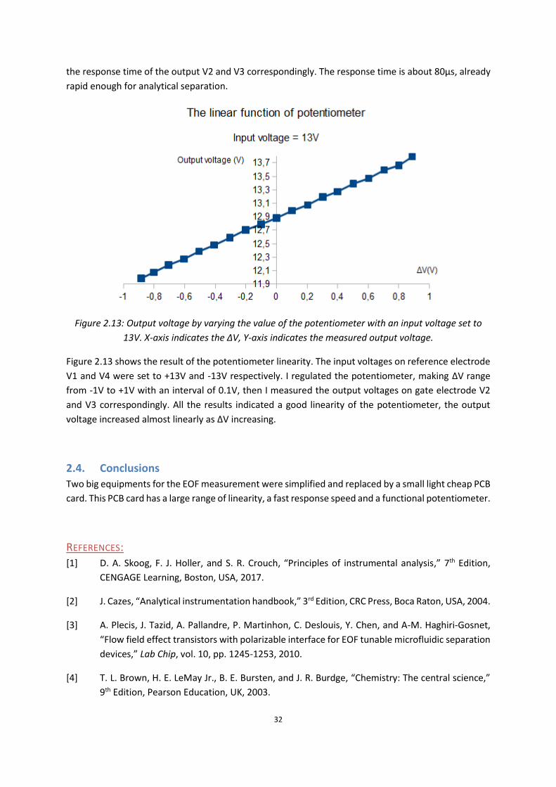
32
the response time of the output V2 and V3 correspondingly. The response time is about 80µs, already
rapid enough for analytical separation.
Figure 2.13: Output voltage by varying the value of the potentiometer with an input voltage set to
13V. X-axis indicates the ΔV, Y-axis indicates the measured output voltage.
Figure 2.13 shows the result of the potentiometer linearity. The input voltages on reference electrode
V1 and V4 were set to +13V and -13V respectively. I regulated the potentiometer, making ΔV range
from -1V to +1V with an interval of 0.1V, then I measured the output voltages on gate electrode V2
and V3 correspondingly. All the results indicated a good linearity of the potentiometer, the output
voltage increased almost linearly as ΔV increasing.
2.4. Conclusions
Two big equipments for the EOF measurement were simplified and replaced by a small light cheap PCB
card. This PCB card has a large range of linearity, a fast response speed and a functional potentiometer.
REFERENCES:
[1] D. A. Skoog, F. J. Holler, and S. R. Crouch, “Principles of instrumental analysis,” 7th Edition,
CENGAGE Learning, Boston, USA, 2017.
[2] J. Cazes, “Analytical instrumentation handbook,” 3rd Edition, CRC Press, Boca Raton, USA, 2004.
[3] A. Plecis, J. Tazid, A. Pallandre, P. Martinhon, C. Deslouis, Y. Chen, and A-M. Haghiri-Gosnet,
“Flow field effect transistors with polarizable interface for EOF tunable microfluidic separation
devices,” Lab Chip, vol. 10, pp. 1245-1253, 2010.
[4] T. L. Brown, H. E. LeMay Jr., B. E. Bursten, and J. R. Burdge, “Chemistry: The central science,”
9th Edition, Pearson Education, UK, 2003.

33
[5] A. Pallandre, “Intégration du transistor fluidique à effet de champs et à interface polarisable
dans un pont de Wheatstone,” HDR, Université Paris-Sud, 2015.
[6] J. Gamby, “Stratégies de transduction en puces microfluidiques pour applications
bioanalytiques,” HDR, Sorbonne Université, 2014.
[7] P. Horowitz and W. Hill, “The art of electronics,” Cambridge University Press, Cambridge, UK,
1989.
[8] J. Millman, “Microelectronics: Digital and analog circuits and systems,” McGraw-Hill, USA,
1979.
[9] “Voltage divider,” https://en.wikipedia.org/wiki/Voltage_divider.

34
Chapter 3: Device Fabrication and Experimental System
3.1. Overview
The microfluidic fabrication is a long, complex and uncertain process. First, many of the fabrication
methods require special equipment in cleanroom facilities, which can take advantages from the advent
and the advance of IC and MEMS miniaturization technology [1]. Second, different fabrication methods
can directly affect different end devices performances and behaviors. It has been proved in literatures
that the zeta-potential and the EOF measurements (and thus the EOF mobility) can vary according to
fabrication methods [2, 3]. Moreover, the microfluidic fabrication faces numerous difficulties
concerning materials, which is the case about polarizable material studied in this thesis. For these
reasons, the fabrication processes play very important role in the microfluidic technology.
A wide range of materials have been used for microfluidic devices [4, 5], from conventional hard
materials, i.e. silicon-based materials [4-8], to soft materials, i.e. polymer-based materials [3, 5, 6, 9-
11]. One should also note that more recently new materials have emerged from innovative hydrogel
[12-18] and paper-based materials [19-23] to hybrid and composite materials [24-27].
The polymer-based materials, being the most-commonly used nowadays for microfluidic devices, offer
a great flexibility [28, 29], a rapid fabrication and an inexpensive cost. According to their physical
properties, they can be classified into three groups [5]: the elastomers, the thermosets, and the
thermoplastics.
The elastomer is a sort of polymers with viscoelasticity, low Young’s modulus and high failure strain
[30]. It consists of cross-linked polymer chains in which those covalent cross-linkages make the
elastomer stretch or compress under external force and return to the original shape when the force is
removed [5, 30]. The most popular elastomer used in microfluidics is polydimethylsiloxane (PDMS) [31,
32].
PDMS is a flexible polymer with high elasticity, allowing easy and low-cost microfabrication [33]. Due
to its low surface free energy, PDMS behaves itself in a hydrophobic way for which there is no need of
any surface pretreatments [9]. Moreover, PDMS exhibits a high biocompatibility, which makes it
broadly used in bio-related researches. However, there are notable limitations of PDMS, the two most
major problems are its permeation of gases and adsorption of samples. Because of a porous matrix of
Si-O backbones covered with alkyl groups in PDMS, water evaporation happens through PDMS channel
walls [34], which leads to a change in concentration of solution and let it be restricted for aqueous
solutions [35]. The contamination of PDMS is nonnegligible, such as the absorption of small
hydrophobic molecules into channel walls and adsorption of biomolecules onto channel surfaces [5].
These influence biological results and more often surface treatments are needed [36, 37]. Moreover,
since those adsorbed molecules are difficult to be removed which makes PDMS a disposable material
[38]. Another inconvenience of PDMS concerns the difficulty to integrate electrodes directly on its
surface, particularly in our case.
The thermoset is an irreversible material when heated or radiated [39], which means it cannot be
reshaped once cured. Thermosets (e.g. SU-8 photoresist and polyimide) have some good properties,
such as stability at high temperatures, resistance to most solvents, and good optical transparency [5],

35
meaning that they can be adapted for the fabrication of microfluidic channels [29, 40], and even more
for the true 3D microfabrication of high-aspect ratio and free-standing structures [41, 42]. As every
coin has two sides, thermosets are less served to flexible configuration because of its high stiffness and
the microfabrication by thermosets costs a lot.
Unlike the thermoset, the thermoplastic can be reshaped multiple times by reheating after being cured
[5]. Typical thermoplastic materials are: PMMA; PEEK; PS; PC; PET; PVC; etc. [6, 10, 11, 29, 43]. In
contrast with PDMS, these materials have a low permeability to gas even if they exhibit a better solvent
compatibility [5].
Aside from the organic polymers mentioned above, cyclic olefin copolymer (COC) or cyclic olefin
polymer (COP) is a relatively new class of amorphous polymers used in a vast range of applications [44].
Owing to its excellent chemical resistance, it is a popular material for lab-on-a-chip that I have also
used as microfluidic channels during my internship at Institute Curie [5, 45, 46].
Before the polymer-based materials, the silicon-based materials such as silica or glass have also been
largely used for the first-generation of microfluidic devices thank to the development of micro- and
nano-technologies in the semiconductor industry [47, 48]. Despite that the silica or glass microchip
fabrication often needs very strict environments such as clean room, and high temperature and
pressure for bonding, the specific properties of glass like thermostability, organic solvent compatibility,
gas impermeability, and especially simple metal depositing make it still popular in microfluidics [49,
50]. Silicon is one material which was used as substrate for a long time in micro/nanoelectronics,
however, it is opaque and not insulating. For all these reasons, for my thesis, we chose bare borosilicate
glass as our microchip substrate.
Glass is an amorphous material with many advantages: first it is highly non-reactive to a variety of
aggressive chemicals, such as acids, aggressive bases like NaOH and KOH, and alcohols [51, 52], which
make it usable in biological and chemical experimental apparatus [7, 8]; second it is optically
transparent, which is very good for the optical detection [53]; third it has high thermoconductivity and
stable electroosmotic mobility on its surface [5]; finally since it is an insulating material, electrodes can
be deposited directly on its surface. Table 2 shows the advantages and disadvantages of each material
that has been described in this introduction.

36
Table 2: Summary of advantages and disadvantages of common materials for microfluidics.
Advantages Disadvantages
PDMS High elasticity Low costs
Low surface free energy High biocompatibility
Gas permeation Sample adsorption
Difficult electrodes integration Organic solvents incompatibility
Thermosets High temperature stability Solvents resistance
Optically transparent 3D microfabrication
High-aspect ratio structure Free-standing structure
Irreversible High stiffness
High costs
Thermoplastics Reversible and reshaped Gas impermeability
Solvents compatibility
Bad contact with other surface
COC/COP Excellent chemical resistance
Silicon Thermostability Organic solvent compatibility
Gas impermeability
Clean room needs High temperature and pressure
bonding High costs
Opaque Semiconductor
Glass Aggressive chemical resistance Optically transparent
High thermoconductivity Stable electroosmotic mobility on surface
Electrically insulating
Special etching needs [54]
This chapter started with a presentation of typical microfabrication processes for our microchip, then
followed by a description of experimental system including the bench, the microchip installation, the
measure launching, and the data analysis.
3.2. Step-by-Step Fabrication Processes for Microfluidic Devices
The fabrication of the whole microfluidic chip has three steps: the microfabrication of PI-FFET on the
glass substrate; the fabrication of the fluidic microchannels based on PDMS or Dry film resist; and the
bonding of these two parts for sealing the fluidic device.
3.2.1. Typical Microfabrication Processes of PI-FFET on Glass Substrate
The PI-FFET device consists of three different layers: a sticking underlayer, an electronic circuit layer,
and a top polarizable layer. Thus, the total fabrication process needs three lithography steps with
alignment, deposition of materials (metals and CNx) and resist lift-off respectively.

37
Figure 3.1: Top view photographs and micrographs of three layers. (A)- Optical micrograph of the
sticking underlayer. (B)- Photograph of the electronic circuit layer. (C)- Zoom of three pairs of
electrodes. (D)- Zoom of the right center part of the microfabricated substrate.
Figure 3.1 shows the designs of each layer from the sticking underlayer to the electronic circuit channel
and the final top polarizable interface. Figure 3.1A displays the structure of the sticking underlayer,

38
which is very simple, just a rectangle pattern. The length and width of it are 2400 µm and 250 µm
(masque 1) respectively. The pattern of the top polarizable CNx layer has the same rectangle except
its length and width are bigger, being 2411 µm and 250 µm (masque 2) (see Figure 3.1D where CNx
appears in dark tan). Figure 3.1B illustrates the configuration of the electronic level. It has a
symmetrical structure based on three pairs of electrodes: 1 and 1’ for the electrophoretic electrodes,
2 and 2’ for the reference electrodes, 3 and 3’ for the gate electrodes. These six electronic pads
converge to the center of the design, as marked in red in Figure 3.1B. Figure 3.1C is a zoomed
photograph of the red part, which can be observed more clearly. The first pair of electrodes concerns
the electrophoretic electrodes, appearing as three-meniscus shape. These electrodes allow applying
an electric field and thus modulating the electrophoretic voltage. Concerning the second pair of
electrodes named reference electrodes, as their name implies, their function is to adjust the
overvoltage of the gate electrodes by precisely measuring the potential of the electrolyte. The last pair
of electrodes are the working electrodes, named gate electrodes, which modulate the surface charge
of the CNx film, thus controlling the electroosmotic flow. Finally Figure 3.1D shows the zoom of right
side of the electronic channel and depositions of the sticking underlayer (dark blue) and the CNx film
(dark tan) in the center, together forming the polarizable interface. Noted that the gate electrode is
sandwiched between the sticking underlayer and the CNx layer.
Figure 3.2: Cross-sectional description in 10 steps of the microfabrication of PI-FFET on glass
substrate. 1- Piranha cleaning of the glass substrate. 2- Spin coating of the photoresist AZ 5214. 3- UV

39
insolation of AZ 5214. 4- Flood exposure (no mask) of AZ 5214. 5- Development of AZ 5214. 6- RIE of
the residual resist. 7- Sticking underlayer deposition by sputtering. 8- Lift-off of the photoresist. 9-
Repeat from step 2 to 8 for the electronic circuit layer deposition. 10- Repeat from step 2 to 8 for the
polarizable layer deposition.
A step-by-step fabrication process is presented as follow:
1. The first step is substrate cleaning (see step 1 of Figure 3.2). First, the substrate is put into a beaker
with one third of acetone then the beaker is put in an ultrasonic machine with parameters of 37
kHz, 30% power, under the clean-room temperature during 3 minutes. This step is used to remove
the inorganic residues on the substrate. Then, the substrate is taken out and rinsed by isopropanol
and dried by nitrogen N2 gas. Later, the piranha solution is prepared with a mixture of 95% sulfuric
acid (H2SO4) and 30% hydrogen peroxide (H2O2) in a proportion of 3:1 V/V (in our case). Noted that
the solution should always be prepared in the order of H2SO4 followed by H2O2 to favor the
apparition of heat from the exothermic mixing reaction. The substrate is put into this piranha
solution for 20 minutes, then rinsed by deionized water for 10 minutes, dried by N2 at last. This
piranha step is to clean organic residues off glass substrate. Unlike chromic acid solution, piranha
solution does not contaminate glassware with heavy metal ions [55].
2. The second step is photoresist spin coating (see step 2 of Figure 3.2). Generally, photoresists can
be classified to three types: positive, negative and reversible. The positive photoresist is the one
that the exposed areas are dissolved in the development solution, copying the same pattern of
the mask, like AZ9260, S1805, S1828, etc. On the contrary, the negative photoresist is the one that
the exposed areas are almost insoluble in developer because of the crosslinking, transforming a
reversal pattern of the mask to the sample, such as maN2405, nLof2070, SU8, etc. As the name
implies, the reversible photoresist is the one with the property to change its polarity after
annealing or an irradiation flood. For example, the resist AZ 5214 E, which is the most commonly
used reversible photoresist in our lab and basically for lift-off technique. Prior to spin coating, 5
minutes of dehydration bake for the clean substrate is necessary to avoid the surface moisture,
which often allows the developer penetrating the photoresist/substrate interface and
undercutting the photoresist pattern [56, 57]. The AZ 5214 is deposited to the center of rotating
substrate, and the spin performs with a fixed program, which sets the final coating thickness and
allows a homogenous photoresist. Here, the spin rotates during 30s with a speed of 4000 rpm and
an acceleration of 2000 rpm. The final thickness of AZ 5214 depends on its viscosity, around 1.4
µm thick in our case. Then the resist is baked during 1mn 30s at 125°C on hot plate to drive off
residual solvents and solidify the photoresist film.
3. The third step is the first insolation (see step 3 of Figure 3.2). SUSS MicroTec MJB4 mask aligner is
employed for the optical lithography. After exposure under a 320 nm wavelength ultraviolet (UV)
light for 5s (corresponding to an energy of 10 mW/cm2), the substrate is then taken to the second
bake, named “reversal-bake”, during 2mn at 125°C. This step is important, because it makes the
exposed areas crosslink and insoluble in developer and no longer light sensitive, whereas, the
unexposed areas remain as a normal positive photoresist [58].
4. The fourth step is the second insolation, named “flood” (see step 4 of Figure 3.2). It is a kind of
insolation without any mask. The duration of flood step is 60s with the same energy as the first
one. After the flood exposure, the unexposed areas during the first lithography are dissolved in
developer while the exposed areas remain onto the substrate.

40
5. The fifth step is the development (see step 5 of Figure 3.2). The developer for AZ 5214 is AZ MIF
826 and the duration ranges from 20s to 2mn, depending on the quality of developer and the
complexity of pattern. As a result, a negative image of the mask pattern is reproduced on the
substrate.
6. The sixth step is the reactive-ion etching (RIE) (see step 6 of Figure 3.2). It is a kind of dry etching
generated by chemically reactive plasma and produces a directionally and anisotropically etching
profile. This process is provided by NEXTRAL NE100 in our lab and is effectuated by a program
“OxyAlu” with SF6/O2 gas flow for 30s. The aim is to remove the probable residual photoresist.
7. The seventh step is the sticking underlayer deposition (see step 7 of Figure 3.2). Here, it is
considered to be SiC. This step is realized by Plassys MPS800 through sputtering, a kind of physical
vapor deposition (PVD). The SiC film is deposited with a power of 500W, a pressure of 1Pa and a
speed of 2.27 Å/s during 1mn 21s, allowing a thickness around 20 nm.
8. The last step to finish the deposition of sticking underlayer is lift-off process (see step 8 of Figure
3.2). It is to remove the rest of photoresist by using acetone solution. The detailed operation is to
leave the substrate in acetone solution for half an hour, then finished by ultrasonic oscillation. The
duration depends on the progress of lift-off, which should be checked out under the optical
microscope from time to time.
9. The ninth step is the repeat from step 2 to 8 except for the deposition of step 7, it is the electronic
circuit layer to be deposited at this time (see step 9 of Figure 3.2). The layer consists of a 5 nm
sticking film of Ti and a 25 nm conductive film of Pt. The deposition is effectuated by Alcatel
SCM600 through electron-beam physical vapor deposition (EBPVD).
10. The last step for the microfabrication of the PI-FFET is the final deposition of the polarizable
interface, i.e. the CNx layer (see step 10 of Figure 3.2). This step also repeats from step 2 to 8
except step 7, which is replaced by the CNx layer. The CNx deposition is also effectuated by
sputtering, unlike the SiC film is deposited under pure argon (Ar) gas, the carbon film is doped with
nitrogen (N2) under a mixture gas of Ar and N2. The N2/(N2+Ar) ratio of gas, i.e. ratio of pressure or
of flow in this equipment, is suggested to be 14.9:100. However, it is often calculated to be around
20% at the final deposited film. This proportion makes the CNx film work as dielectric. The final
fabricated pattern is shown in the last photograph of Figure 3.2.

41
3.2.2. Two Microstructuring Methods of Microfluidic Channels
In this section, two methods for the microchannel structuring are presented successively.
Figure 3.3: Top view photographs and micrograph of microchannel design. (A)- Photograph of total
view of microfluidic channels. (B)- Zoom of the central channel. (C)- Optical micrograph of the central
channel.
Figure 3.3A shows the total design of the microfluidic channels. As it can be seen, it is a symmetric
pattern with four branches and four reservoirs at the corner, as well as one central channel (circled in
red rectangle). Those reservoirs are connected to the external cannula and pipe connectors to let the
liquid circulate through the microchannels. The six pads surrounding the channels are prepared to
connect the external electronic instrumentation (power supply units and voltage followers). The red
parts in Figure 3.3B indicate two restrictions of microfluidic branch with a width of only 80 µm,
compared to the normal branch having 200 µm width channels. These restrictions can provide
different fluidic resistance and allow to determine the fluidic resistance of central channel. Figure 3.3C
zooms in the central channel, the two round reservoirs superpose on the three-meniscus shaped
electrophoretic electrodes in Figure 3.1C.
Fabrication Processes of Microchannels Based on PDMS
A common method to mold microfluidic channels in PDMS is to create a mold from a photoresist, for
example, the SU-8 family on silicon wafer. SU-8 is a negative photoresist, which means the exposed
areas remain. Figure 3.4 illustrates the fabrication steps for the creation of a SU-8 mold and a PDMS-
based microfluidic channels [59].

42
Figure 3.4: Cross-sectional description in 6 steps of the fabrication of PDMS-based microfluidic
channels. 1- Piranha cleaning of the Si wafer. 2- Spin coating of the photoresist SU-8 2050. 3- UV
insolation of SU-8 2050. 4- Development of SU-8 2050. 5- PDMS pouring, degassing, and curing. 6-
PDMS peeling and the final created PDMS-based microfluidic channel.
1. The first step is Si wafer cleaning by piranha solution to remove any surface contamination (see
step 1 of Figure 3.4) that has been detailed in Section 3.2.1.
2. The second step is to deposit the photoresist SU8 2050 in a homogenous way by spin coating (see
step 2 of Figure 3.4). The spin speed is 2700 rpm during 30s with an acceleration of 2000 rpm,
determining a layer thickness of 40 µm, i.e. the thickness of SU-8 mold directly determines the
microfluidic channel depth. Then, the wafer is soft baked at 65°C during 2mn and at 95°C during
7mn to remove the solvents in the resist and to relax the polymeric matrix.
3. The third step is the insolation by UV light through a mask that defines the mold pattern (see step
3 of Figure 3.4). The duration of the exposure lasts for 25s. Before the development, a hard bake
is applied (see above step 2).
4. The fourth step is the development of SU-8 by its proper developer for about 2mn 30s, then rinsing
it by isopropanol (see step 4 of Figure 3.4). It results in SU-8 mold more mechanically and
chemically robust [60].
5. The PDMS is prepared in advance: the PDMS elastomer and a curing agent are mixed together at
a ratio of 9:1 w/w. The proportion of curing agent determines the elastic and mechanical
properties of PDMS, the more curing agent is the less elastic is PDMS. The mixture is placed in a
centrifuge machine following 3mn rotation to have adequately mixing. Then the PDMS mixing is
poured onto the SU-8 mold. Because the mixture of PDMS often introduces bubbles that must be
removed before curing. Thus, the total mold is placed in a glass desiccator connected to a
membrane vacuum pump to degas bubbles. After degassing, the mold and the liquid PDMS are
put into oven at 60°C for one night to let the mixture crosslinking. Therefore, a PDMS mold is
finished (see step 5 of Figure 3.4).
6. The sixth step is to peel off PDMS mold from SU-8 master (see step 6 of Figure 3.4). Thus, a real
PDMS-based microfluidic channel is then created.

43
Fabrication Processes of Microchannels Based on Dry Film
Dry film is a negative dry photoresist with a thickness of 35 µm that means the depth of microfluidic
channel is 35 µm. It is a three-layer film with two transparent protective films and one blue
photosensitive film. The structuring of dry film-based microchannels is descripted in Figure 3.5.
Figure 3.5: Cross-sectional description in 4 steps of the fabrication of dry film-based microfluidic
channels, following the tenth step of Figure 3.2. 1- Deposition of dry film by a laminator. 2- UV
insolation of dry film. 3- Development of dry film. 4- Annealing of dry film. 5- Photograph of the
laminator ©PEAK POUCH LAMINATORS. 6- Micrograph of the fabricated dry film-based microfluidic
channel.
1. The first step is the dry film lamination (see step 1 of Figure 3.5), which is done by PEAK POUCH
LAMINATORS Peak High Speed PHS-330 laminator, as shown in Figure 3.5-5. The deposition is
performed under a temperature of 100°C with a median speed. One of transparent films is peeled
off, the photosensitive blue film is deposited onto microfabricated PI-FFET substrate, then the
whole substrate is put into the laminator. Once the deposition is finished, the dry film is soft baked
on a hot plate at 90°C during 5mn.
2. The second step is the UV exposure with wavelength of 320 nm, power of 10 mW/cm2 during 9s
(see step 2 of Figure 3.5). Then second transparent film on the other side is peeled off and the dry
film is hard baked (see above step 1).

44
3. The third step is the dry film development by 8.5 g/L Na2CO3 solution (see step 3 of Figure 3.5).
The duration of development depends on the disappearance of blue microchannels, which can be
observed directly by eyes, a typical duration of 2mn is generally sufficient.
4. The last step is the dry film annealing (see step 4 of Figure 3.5). The dry film is placed in oven at
200°C for at least one hour. The change of dry film color occurs after annealing from blue to yellow
green, if not, the annealing time is not sufficient.
3.2.3. Integration of PI-FFET and Microchannels
The integration of PI-FFET and microfluidic channels has two distinct routes, depending on what kind
of material will be used to define the microfluidic network (PDMS-based or dry film-based). Figure 3.6
describes both two routes.
Figure 3.6: Cross-sectional descriptions and photographs of the integration of the PI-FFET and the
PDMS-based (A and B)/dry film-based (C to F) microfluidic channels. (A, E)- PDMS bonding to glass
substrate by oxygen plasma. (B)- Top view photograph of the final PDMS-based microdevice. (C)-
Photograph of the mold for micro-sandblasting. (D)- Glass hood bonding to dry film by press. (F)- Top
view photograph of the final dry film-based microdevice. The green paths in (B) and (F) indicate the
fluidic channels.
In the case of PDMS, first of all, the cured PDMS is cut and pierced by a punch for inlets/outlets
formation. After rinsing and drying the substrate and PDMS piece by isopropanol, an oxygen plasma is
applied to active the silanol groups on the PDMS surface [61], allowing a permanent bonding between
PDMS and glass substrate (see Figure 3.6A). This step is performed in NANONEX CORPORATION Ultra-
100 plasma cleaner/coater in our lab. After finishing plasma, the PDMS piece is aligned and bonded to
the substrate under optical binoculars. This alignment is often difficult and requires high precision
because the central channel of PDMS has to be exactly superposed onto the polarizable interface of

45
substrate. After that, six electronic pins are welded to the corresponding pads on the substrate and
fixed by LOCTITE® EA 3430 epoxy adhesive. Figure 3.6B shows the final fabricated microfluidic device.
In the case of dry film, at first, a new glass substrate is sandblasted according to the pattern on the
mold (see Figure 3.6C). The micro-sandblasting is a delicate operation where a stream of abrasive
material is propelled from the machine under high pressure and grinds or shapes a pattern on a surface.
Here, the abrasive material is glass beads with a diameter from 30 to 45 µm, it is also called micro-
sandblasting. This sandblasted glass substrate is a hood to close the open microchannel of dry film.
Figure 3.6D shows the bonding of dry film to the glass substrate effectuated by Specac® manual and
hydraulic press under 100°C, 3 tons for more than one hour. Noted that before bonding, all the holes
of the glass substrate should be aligned with the dry film. After that, four pierced PDMS pieces are
bonded by oxygen plasma to the top of the hood, and aligned to the four inlets/outlets of microfluidic
channels (see Figure 3.6E). At last, Figure 3.6F shows the final fabricated dry film-based microfluidic
device with electronic pins.
3.3. Description for Experimental System
3.3.1. Experimental Bench
Figure 3.7: Total view photographs of the experimental bench. (A)- Inverted optical microscope. (B, C)-
CCD camera and its power supply. (D)- Chip holder. (E)- Matlab® command interface. (F)- Fluid
multiplexer and pressure controller. (G, H)- Footswitch and hand throttle.
Figure 3.7 shows the total view of the experimental bench. Figure 3.7A is an inverted optical
microscope that often allows experts to observe the fluorescent targets. Figure 3.7B and C together
constitute the CCD camera, which is sensitive and responds to the light, converting the video signal to
the digital signal. The CCD camera is often used in the photometry, here we use it to observe and
measure the speed of the fluorescent beads. Figure 3.7D shows the chip holder on the microscope and

46
the connected microfluidic device. The window in Figure 3.7E presents the command interface, which
was coded and enslaved by Matlab®. This greatly facilitates the fluid management and allows the beads
speed measurement and the data acquisition automatically. Figure 3.7F presents the fluid multiplexer
and the pressure controller. This system controls the fluid circulation in the microfluidic channels
through hydraulic pressure. The footswitch in Figure 3.7G and the hand throttle in Figure 3.7H together
constitute the external system to simplify the manipulation. The former allows to manage the fluid
circulation by feet: “flush” (the liquid enters to the microchannels by one side, for example, either
through reservoir 1 and 2 thus reservoir 3 and 4 will be the outlets or the opposite situation seeing in
Figure 3.3), “equilibrium” (the liquid enters to all the four entrances in the same time with the same
pressure), and “stop” (no liquid flowing in the channels). The hand throttle offers the possibility to
manually modify the value of pressure in real time.
Figure 3.8: Photographs of the external electronic equipment. (A)- Generator for the electrophoretic
field. (B, C)- Two old generation followers and the power supply to adjust the Vgate (two channels in
the same source meter unit).
As the measurement takes place under the electrophoretic field (an electric field providing a voltage
of +15V), thus, a generator is employed to this function (as shown in Figure 3.8A). Figure 3.8B and C
show the two followers and its power supply. The follower is connected between the reference
electrode and the gate electrode, its function is to modify the potential on the gate electrode in terms
of the potential regarding to liquid potential measured by the reference electrode. This relation
between the liquid potential and the Vgate is crucial to avoid electrochemical reactions in the separation
channel.
3.3.2. Step-by-Step Experimental Description
The experimental manipulation consists of three parts: the installation of the microfluidic device that
includes the preparation of the fluorescent beads and the connection to the external cannula and pipes;
the experimental launching on Matlab® and the way of measurement; the data treatment and analysis.

47
Figure 3.9: Description of the experimental schema.
Figure 3.9 shows the simplified schema of the experimental setup. The air is pushed into the pressure
controller driving out the millimolar aqueous KCl solution flowing in one of the channels of multiplexer.
Two outlets of the multiplexer are connected to the four reservoirs of the device. The liquid enters into
one side of channels and flows out of another side, i.e. two reservoirs at left or at right, this is “flush”
mode. Whereas, the same pressure can also be applied at the four reservoirs of the microfluidic bridge,
it is the “equilibrium” mode. The fluidic path is colored in blue. The red and black path represent the
voltage and the mass applied to the device respectively, providing an electric field to realize the
electrophoresis on the polarizable surface at the central channel. Two followers are connected to the
reference and gate electrodes as colored in green.
Microfluidic Chip Installation
The microfluidic device installation consists of two steps: the installation onto chip holder and the
injection of fluorescent beads. The following steps describe the microfluidic chip installation.
1. First of all, we prepare two bottles, one of deionized water, and another of aqueous KCl solution
with a molarity of 10-3M (the concentration can be changed). The molar mass of KCl is 74.5 g/mol,
so to have 500 mL of 10-3M, we need 37.25 mg of dry KCl powder to be dissolved in 500 mL of
deionized water.
2. Second, the microfluidic device is installed onto the chip holder and fixed by scotch tapes. After
evacuating the air bubbles in both cannula and pipes, the device is connected to them one by one
under the function of “flush” phase. Thus, both four cannulas are inserted to the holes of PDMS
and the liquid can thus flow into the microfluidic channels. Normally, the insertion of cannula is
often along with the generation of air bubbles at the inlets, therefore, a program named
“bubbleout.m” was designed to evacuate these bubbles, which consists of 2 cycles of “equilibrium”
and 1 cycle of “flush”, working one after the other successively until all the bubbles are evacuated.
3. Then, we replace the deionized water by KCl solution carefully and prepare the fluorescent beads.
The recipe is 10 mL of KCl 10-3M, plus 150 µL of fluorescent polystyrene microspheres FX100 with

48
diameter of 1 µm, plus 200 µL of TWEEN® 20 nonionic detergent (an aqueous solution containing
0.5% of tween V/V) for a stable mixture by reducing the particles adsorption on the glass substrate
surface. Once the beads are prepared, they are then injected into one side of the cannula inlets by
syringe, here for example, the reservoirs 1 and 2 in Figure 3.3A. Then, a “flush” phase is applied to
branches 1 and 2 to push the beads flow into the channels. When we observe that fluorescent
beads are inside the bridge, and after checking that there are no air bubbles under inverted
microscope, we can launch the EOF measurement. There is a little tip to identify if there were small
bubbles in the microfluidic device or not: when applying “equilibrium” phase, if the beads move,
that means that there are bubbles inside, and the moving direction helps to find the location of
the bubbles by simply following the beads in the fluidic network.
Experimental Launching
Figure 3.10: Picture of the experimental Matlab graphic user interface.
Figure 3.10 shows the experimental manipulating interface, which is a program based on Matlab® to
simplify the manipulation of measurement. The following steps indicate the launching process.
1. First of all, initiating the program by clicking the “Initialization”, when it turns to green, meaning
that the program can be settled and all instruments communicated with PC are ready.
2. In the window of “Electrophoresis”, setting the electrophoresis voltage to be 15V. For the rest two
parameters, they can be remained as default.
3. Then passing to the window of “Transistor”. The number of measurements is normally to be 5. The
gate voltage can be changed between -1V/+1V manually at each measurement. Noted that, if we

49
use the PCB card mentioned-above in Chapter 2, we do not need to modify the value of gate
voltage in this window because the PCB card will take place its function.
4. The window of “Pressure Controller” shows the value of pressure applied, which can be controlled
by the hand throttle. And in the window of “Save”, we can note down the “File name” that the
results can be saved automatically.
5. After confirming all the numbers, clicking “Pressure” to apply 300 mbar. And applying “equilibrium”
phase to remain a hydrodynamically stable state. Then, choosing a region of interest (ROI),
normally, it is in an area of restriction channel. At last, clicking “EOF measure”, the measurement
of the speed of the fluorescent beads will be effectuated automatically and successively, allowing
the calculation of the EOF.
Briefly, the EOF measurement includes two steps. The first step is two calibrations. The fluidic
resistance calibration is achieved firstly. In this calibration, it measures the velocity of fluid in each arm
of the µFWB (see Figure 1.9B of Section 1.3.2), the results are stored in Matlab file. Then it repeats the
same way in the second Poiseuille calibration, all the steps aim to determine the proportionality factor
αi (i = 1, 2, 3, 4) of each arm. Then, we can choose one arm of the µFWB to perform the EOF
measurement.
Data Treatment
The method used to measure the flow rate of beads is particle image anemometry (PIA) that can
determine flow rate within a few milliseconds. It has been coded to perform a full frame cross-
correlation algorithm of the successive CCD images of the fluorescent beads in motion [62]. The
determined flow rate will be expressed in pixel/s that we should convert it to µm/s. It is easily done
after a scale calibration with microscope and Image J analysis of the CCD image. Precisely, measuring
the length of one of the channels in µm under microscope and its corresponding length in pixel that is
determined by Image J software. Thus, the flow rate in µm/s can be studied.
Formula 3-1 gives the calculation of the EOF mobility. It is automatically performed by our Matlab code
after storing and analyzing a series of CCD image. vi is the flow rate measured by PIA. l is the length of
the central channel that can be measured under microscope. ΔV is the value of the electrophoretic
voltage chosen by experimenter. Among these four parameters, αi, l and ΔV are fixed. The aim is to
modify the gate voltage and obtain its corresponding vi. After calculating µeof, the result will be a curve
of µeof under the function of Vgate.
µ𝑒𝑜𝑓 = 𝛼𝑖×𝑣𝑖×𝑙
𝛥𝑉 (3-1)
3.4. Conclusions
This chapter first presented different materials for the microfluidic, among them we chose glass
because it is optically transparent, electrically insulating, and chemically resistant. Then it described
typical fabrication process of the PI-FFET in detail, of which the CNx is the essential core of the
configuration as it plays as the polarizable interface. The chapter also presented two ways to create
the microfluidic channels: PDMS and dry film. The latter is a new technology used on our device, which
was under testing by one of the postdoc students when I arrived in our team. At the end, this chapter
presented the total experimental bench and the computer interface behind the EOF measurement

50
manipulation. The hand throttle, the footswitch and the Matlab code together facilitate the control of
liquid, as well as the acquisition and the treatment of data.
REFERENCES:
[1] S-S. Li and C-M. Cheng, “Analogy among microfluidics, micromechanics, and microelectronics,”
Lab Chip, vol. 13, pp. 3782-3788, 2013.
[2] A. P. Lewis, “An investigation into separation enhancement methods for miniaturized planar
capillary electrophoresis devices,” PhD thesis, University of Southampton, 2013.
[3] Z. F. Wang, Y. X. Wu, and K. Puttachat, “Electroosmosis flow (EOF) mobility measurement in
polymer micro channels,” SIMTech technical reports, 2009.
[4] H. Becker and A. Manz, “Miniaturized chemical analysis systems-materials and bonding,” in IEE
Colloquium on Assembly and Connections in Microsystems, London, UK, 1997.
[5] K. Ren, J. Zhou, and H. Wu, “Materials for microfluidic chip fabrication,” Acc. Chem. Res., vol.
46, pp. 2396-2406, 2013.
[6] M. Pumera, A. Merkoçi, and S. Alegret, “New materials for electrochemical sensing VII.
Microfluidic chip platforms,” TrAC, vol. 25, pp. 219-235, 2006.
[7] A. Berthold, F. Laugere, H. Schellevis, C. R. de Boer, M. Laros, R. M. Guijt, P. M. Sarro, and M.
J. Vellekoop, “Fabrication of a glass-implemented microcapillary electrophoresis device with
integrated contactless conductivity detection,” Electrophoresis, vol. 23, pp. 3511-3519, 2002.
[8] A. Berthold, L. Nicola, P. M. Sarro, and M. J. Vellekoop, “Glass-to-glass anodic bonding with
standard IC technology thin films as intermediate layers,” Sens. Actuator A-Phys., vol. 82, pp.
224-228, 2000.
[9] J. Monahan, A. A. Gewirth, and R. G. Nuzzo, “A method for filling complex polymeric
microfluidic devices and arrays,” Anal. Chem., vol. 73, pp. 3193-3197, 2001.
[10] M. Pumera, “Analysis of explosives via microchip electrophoresis and conventional capillary
electrophoresis: A review,” Electrophoresis, vol. 27, pp. 244-256, 2006.
[11] H. Mühlberger, H. Wonhee, A. E. Guber, V. Saile, and W. Hoffmann, “Polymer lab-on-a-chip
system with electrical detection,” IEEE Sens. J., vol. 8, pp. 572-579, 2008.
[12] A. M. Ghaemmaghami, M. J. Hancock, H. Harrington, H. Kaji, and A. Khademhosseini,
“Biomimetic tissues on a chip for drug discovery,” Drug Discov. Today, vol. 17, pp. 173-181,
2012.
[13] P. Domachuk, K. Tsioris, F. G. Omenetto, and D. L. Kaplan, “Bio-microfluidics: Biomaterials and
biomimetic designs,” Adv. Mater., vol. 22, pp. 249-260, 2010.
[14] L. G. Griffith and M. A. Swartz, “Capturing complex 3D tissue physiology in vitro,” Nat. Rev.
Mol. Cell Biol., vol. 7, pp. 211-224, 2006.

51
[15] N. W. Choi, M. Cabodi, B. Held, J. P. Gleghorn, L. J. Bonassar, and A. D. Stroock, “Microfluidic
scaffolds for tissue engineering,” Nat. Mater., vol. 6, pp. 908-915, 2007.
[16] M. W. Tibbitt and K. S. Anseth, “Hydrogels as extracellular matrix mimics for 3D cell culture,”
Biotechnol. Bioeng., vol. 103, pp. 655-663, 2009.
[17] G. Y. Huang, L. H. Zhou, Q. C. Zhang, Y. M. Chen, W. Sun, F. Xu, and T. J. Lu, “Microfluidic
hydrogels for tissue engineering,” Biofabrication, vol. 3, pp. 012001, 2011.
[18] A. Khademhosseini, J. P. Vacanti, and R. Langer, “Progress in tissue engineering,” Sci. Am., vol.
300, pp. 64-71, 2009.
[19] A. W. Martinez, S. T. Phillips, M. J. Butte, and G. M. Whitesides, “Patterned paper as a platform
for inexpensive, low-volume, portable bioassays,” Angew. Chem. Int. Ed., vol. 46, pp. 1318-
1320, 2007.
[20] A. W. Martinez, S. T. Phillips, E. Carrilho, S. W. Thomas, H. Sindi, and G. M. Whitesides, “Simple
telemedicine for developing regions: Camera phones and paper-based microfluidic devices for
real-time, off-site diagnosis,” Anal. Chem., vol. 80, pp. 3699-3707, 2008.
[21] X. Li, D. R. Ballerini, and W. Shen, “A perspective on paper-based microfluidics: Current status
and future trends,” Biomicrofluidics, vol. 6, pp. 011301, 2012.
[22] A. W. Martinez, S. T. Phillips, and G. M. Whitesides, “Three-dimensional microfluidic devices
fabricated in layered paper and tape,” PNAS Proc. Natl. Acad. Sci. U.S.A., vol. 105, pp. 19606-
19611, 2008.
[23] R. Derda, S. K. Y. Tang, A. Laromaine, B. Mosadegh, E. Hong, M. Mwangi, A. Mammoto, D. E.
Ingber, and G. M. Whitesides, “Multizone paper platform for 3D cell cultures,” PLoS One, vol.
6, pp. e18940, 2011.
[24] H. Wu, B. Huang, and R. N. Zare, “Generation of complex, static solution gradients in
microfluidic channels,” J. Am. Chem. Soc., vol. 128, pp. 4194-4195, 2006.
[25] J. H. Zhou, H. Yan, Y. Z. Zheng, and H. K. Wu, “A gold nanocrystal/poly(dimethylsiloxane)
composite for plasmonic heating on microfluidic chips,” Adv. Mater., vol. 24, pp. 94-98, 2012.
[26] D. J. Beebe, J. S. Moore, J. M. Bauer, Q. Yu, R. H. Liu, C. Devadoss, and B. H. Jo, “Functional
hydrogel structures for autonomous flow control inside microfluidic channels,” Nature, vol.
404, pp. 588-590, 2000.
[27] R. G. Blazej, P. Kumaresan, and R. A. Mathies, “Microfabricated bioprocessor for integrated
nanoliter-scale sanger DNA sequencing,” PNAS Proc. Natl. Acad. Sci. U.S.A., vol. 103, pp. 7240-
7245, 2006.
[28] E. Sollier, C. Murray, P. Maoddi, and D. Di Carlo, “Rapid prototyping polymers for microfluidic
devices and high pressure injections,” Lab Chip, vol. 11, pp. 3752-3765, 2011.

52
[29] H. Becker and C. Gäertner, “Polymer microfabrication technologies for microfluidic systems,”
Anal. Bioanal. Chem., vol. 390, pp. 89-111, 2007.
[30] “Elastomer,” https://en.wikipedia.org/wiki/Elastomer.
[31] J. C. Mcdonald and G. M. Whitesides, “Poly(dimethylsiloxane) as a material for fabricating
microfluidic devices,” Acc. Chem. Res., vol. 35, pp. 491-499, 2002.
[32] A. D. Stroock and G. M. Whitesides, “Controlling flows in microchannels with patterned surface
charge and topography,” Acc. Chem. Res., vol. 36, pp. 597-604, 2003.
[33] J. C. Mcdonald, D. C. Duffy, J. R. Anderson, D. T. Chiu, H. K. Wu, O. J. A. Schueller, and G. M.
Whitesides, “Fabrication of microfluidic systems in poly(dimethylsiloxane),” Electrophoresis,
vol. 21, pp. 27-40, 2000.
[34] R. Mukhopadhyay, “When PDMS isn’t the best,” Anal. Chem., vol. 79, pp. 3248-3253, 2007.
[35] J. U. Shim, G. Cristobal, D. R. Link, T. Thorsen, Y. W. Jia, K. Piattelli, and S. Fraden, “Control and
measurement of the phase behavior of aqueous solutions using microfluidics,” J. Am. Chem.
Soc., vol. 129, pp. 8825-8835, 2007.
[36] A. Paguirigan and D. Beebe, “From the cellular perspective: Exploring differences in the cellular
baseline in macroscale and microfluidic cultures,” Integr. Biol., vol. 1, pp. 182-195, 2009.
[37] J. Zhou and A. E. N. Voelcker, “Recent developments in PDMS surface modification for
microfluidic devices,” Electrophoresis, vol. 31, pp. 2-16, 2010.
[38] W. K. T. Coltro, S. M. Lunte, and E. Carrilho, “Comparison of the analytical performance of
electrophoresis microchannels fabricated in PDMS, glass, and polyester-toner,”
Electrophoresis, vol. 29, pp. 4928-4937, 2008.
[39] “Thermosetting polymer,” https://en.wikipedia.org/wiki/Thermosetting_polymer.
[40] R. J. Jackman, T. M. Floyd, R. Ghodssi, M. A. Schmidt, and K. F. Jensen, “Microfluidic systems
with on-line UV detection fabricated in photodefinable epoxy,” J. Micromech. Microeng., vol.
11, pp. 263-269, 2001.
[41] H. Sato, H. Matsumura, S. Keino, and S. Shoji, “An all SU-8 microfluidic chip with built-in 3D
fine microstructures,” J. Micromech. Microeng., vol. 16, pp. 2318-2322, 2006.
[42] Y. Z. Zheng, W. Dai, D. Ryan, and H. K. Wu, “Fabrication of freestanding, microperforated
membranes and their applications in microfluidics,” Biomicrofluidics, vol. 4, pp. 036504, 2010.
[43] “Thermoplastic,” https://en.wikipedia.org/wiki/Thermoplastic.
[44] “Cyclic olefin copolymer,” https://en.wikipedia.org/wiki/Cyclic_olefin_copolymer.
[45] P. Nunes, P. Ohlsson, O. Ordeig, and J. Kutter, “Cyclic olefin polymers: Emerging materials for
lab-on-a-chip applications,” Microfluid Nanofluidics, vol. 9, pp. 145-161, 2010.

53
[46] I. Hernandez-Neuta, I. Pereiro, A. Ahlford, D. Ferraro, Q. Zhang, J-L. Viovy, S. Descroix, and M.
Nilsson, “Microfluidic magnetic fluidized bed for DNA analysis in continuous flow mode,”
Biosens. Bioelectron., vol. 102, pp. 531-539, 2018.
[47] D. R. Reyes, D. Iossifidis, P. A. Auroux, and A. Manz, “Micro total analysis systems. 1.
Introduction, theory, and technology,” Anal. Chem., vol. 74, pp. 2623-2636, 2002.
[48] G. M. Whitesides, “The origins and the future of microfluidics,” Nature, vol. 442, pp. 368-373,
2006.
[49] B. K. H. Yen, A. Günther, M. A. Schmidt, K. F. Jensen, and M. G. Bawendi, “A microfabricated
gas-liquid segmented flow reactor for high-temperature synthesis: The case of Cd-Se quantum
dots,” Angew. Chem. Int. Ed., vol. 44, pp. 5447-5451, 2005.
[50] P. J. A. Kenis, R. F. Ismagilov, S. Takayama, G. M. Whitesides, S. L. Li, and H. S. White,
“Fabrication inside microchannels using fluid flow,” Acc. Chem. Res., vol. 33, pp. 841-847, 2000.
[51] C. Lin, G. Lee, Y. Lin, and G. Chang, “A fast prototyping process for fabrication of microfluidic
systems on soda-lime glass,” J. Micromech. Microeng., vol. 11, pp. 726-732, 2001.
[52] A. Grosse, M. Grewe, and H. Fouckhardt, “Deep wet etching for fused silica glass for hollow
capillary optical leaky waveguides in microfluidic devices,” J. Micromech. Microeng., vol. 11,
pp. 257-262, 2001.
[53] Y. Jeong, S. Kim, K. Chun, J. Chang, and D. S. Chung, “Methodology for miniaturized CE and
insulation on a silicon substrate,” Lab Chip, vol. 1, pp. 143-147, 2001.
[54] X. Mu, Q. L. Liang, P. Hu, K. N. Ren, Y. M. Wang, and G. A. Luo, “Laminar flow used as liquid
etch mask in wet chemical etching to generate glass microstructures with an improved aspect
ratio,” Lab Chip, vol. 9, pp. 1994-1996, 2009.
[55] “Piranha solution,” https://en.wikipedia.org/wiki/Piranha_solution.
[56] “Lithography Process Overview,” http://www.imicromaterials.com/technical/lithography-
process-overview.
[57] R. R. Dammel, “Diazonaphthoquinone-based resists,” 5th printing, vol. TT11, SPIE Optical
Engineering Press, Bellingham, Washington, U.S.A., 1993.
[58] “AZ 5214 E Image Reversal Photoresist,” http://dvh.physics.illinois.edu/pdf/AZ5214E.pdf.
[59] A. Pallandre, “Intégration du transistor fluidique à effet de champs et à interface polarisable
dans un pont de Wheatstone,” HDR, Université Paris-Sud, 2015.
[60] F. Ru and J. F. Richard, “Influence of processing conditions on the thermal and mechanical
properties of SU8 negative photoresist coatings,” J. Micromech. Microeng., vol. 13, pp. 80-88,
2003.

54
[61] R. S. Martin, A. J. Gawron, S. M. Lunte, and C. S. Henry, “Dual-electrode electrochemical
detection for poly(dimethylsiloxane)-fabricated capillary electrophoresis microchips,” Anal.
Chem., vol. 72, pp. 3196-3202, 2000.
[62] A. Plecis, L. Malaquin, and Y. Chen, “A particle image anemometry technique for the non-
invasive, quick determination of average flow rates in microchannels,” Proc. MicroTAS, 2007.

55
Chapter 4: Experimental Work
4.1. Overview
In this chapter, we will present the improvement of CNx adhesion to two major sticking underlayers:
SiC and Pt, this will be seen in Experiment 1, 2 and 3. In Experiment 4 and 5, we will show a new
architecture that improves greatly the adhesion issues. The last Experiment 6 gives a summary of the
behavior of CNx onto different dielectric and metallic materials.
4.2. Experiment 1: Insulating SiC Sticking Underlayer and Its Adhesion
Optimizations
4.2.1. Aims of Experiment 1
The primary aim of Experiment 1 was to investigate the stability of sticking underlayer silicon carbide
(SiC) for CNx and its adhesion optimizations. Four consecutive tests were performed through various
aging experiments including silicon nitride (Si3N4) compared testing, piranha etching testing, variation
of deposition parameters and annealing at high temperature testing. Measurements of sheet
resistance of CNx film over time and in different environments have also been done.
4.2.2. Experiment 1.1: Choice of SiC as Sticking Underlayer
The first experiment was to study the behavior of a thin CNx film (~100 nm) deposited directly on clean
glass substrate (see Figure 4.1). Without any sticking underlayer, CNx began to detach just one day
after the deposition, observing black dendritic structures. It is worthwhile to note that Figure 4.1 only
shows a part of 2-inch sample while these detachments behaved in the same way on the other parts.
Therefore, two materials were chosen to be sticking underlayer.
Figure 4.1: Optical microscope picture showing a part of the CNx deposition directly on glass
substrate after one day in air at clean-room temperature.
Silicon carbide (SiC) is a semiconductor with a wide bandgap (2.0 eV ≤ Eg ≤ 7.0 eV) and good tolerance
for high temperature, high pressure and friction, it also has a good chemical passivation [1, 2]. While
silicon nitride (Si3N4) is an insulating material which can be lifted off as good as SiC, however, it is

56
transparent as thin film, making lithography alignment difficult. Nevertheless, two adhesion tests were
still effectuated between SiC and Si3N4.
Figure 4.2: (A)- Photographs of CNx deposited on Si3N4 sticking underlayer after 5 days in air at room
temperature, the red part circles the boundary between detached part and adhered part. (B)-
Photography of CNx deposited on SiC sticking underlayer after 5 days in air at clean-room
temperature.
Figure 4.2 shows the behaviors of CNx film deposited on Si3N4 (Figure 4.2A) and SiC (Figure 4.2B)
sticking underlayers. The samples were first deposited by very thin film (~20 nm) of Si3N4 and SiC
respectively, then a film of CNx (~100 nm under the same conditions for Si3N4 and SiC). Later, the two
samples were placed in air at clean-room temperature for five days. The cracking and detachment of
the CNx-on-Si3N4 film were evident and expanding, while the adhesion of CNx-on-SiC film was instead
qualitatively good. To continue investigating the quality of the interfaces between thin layers, a H-
shape architecture was fabricated.
Figure 4.3: Top view of the processes to fabricate the H-shape architecture by achieving multiple lift-
off. 1- The cleaning process of glass substrate which was detailed in Section 3.2.1. 2- The 20 nm SiC
sputtering deposition. 3- The 20 nm Si3N4 sputtering deposition in parallel. 4- The 20 nm CNx
sputtering deposition across over two parallel films. The letters are given to point out a specific
location later in the discussion.

57
Sample 1 was fabricated based on a 2-inch glass substrate, seeing in Figure 4.3. Three depositions were
effectuated on one device to have a good comparison: first was the SiC film deposition (deep blue
rectangle in Figure 4.3-2); then the Si3N4 deposition which was in parallel to it (light blue in Figure 4.3-
3); the CNx film was at last deposited simultaneously across over both the SiC film and the Si3N4 film in
the same time, forming a H-shape configuration and allowing us to confidently relate the differences
in the CNx film properties to the sticking underlayers and not to the CNx deposition parameters. The
thickness of these three films was 20 nm.
Figure 4.4: Top view micrographs of the total H-shape architecture (A) and after three weeks in air at
clean-room temperature (B).
Figure 4.4A shows the top view of the Sample 1 just after the fabrication. In the horizontal direction,
the top layer is Si3N4 film while the bottom one is SiC film. The CNx film is in vertical. Noted that there
are five spots (a, b, c, d, e) to be observed: spot a is the part that CNx was deposited directly on glass
substrate, spot b is SiC deposited on glass, spot c is CNx deposited on SiC, spot d is Si3N4 deposited on
glass, and spot e is CNx deposited on Si3N4. Figure 4.4B shows the same part of Sample 1 but after 3
weeks in air at clean-room temperature. It is interesting to see that the levels of CNx film detachment
on different materials (on the same device and under the exact same environment) were totally
different. The local surface morphology and the surface mechanical property of the deposited films
were studied before any CNx detachment by means of phase-imaging AFM (PI-AFM). A Veeco
Instruments Nanoman DI 3100 AFM was employed for these analyses in our clean room.
PI-AFM is one of the extensions of regular tapping mode AFM. The phase imaging refers to recording
the phase shift signal when the probe taps slightly on the sample surface. It can be regarded as a delay
in the mechanical oscillation of the cantilever. The nature of phase imaging is the measurement of
energy dissipation during the contact between the tip and the sample [3]. The phase shift signal
changes to be registered as bright and dark regions in phase images when the probe encounters
different areas. Because phase images often produce extraordinary contrast of the variations in
composition, adhesion, friction, viscoelasticity, etc. that the phase contrast becomes one of the most

58
commonly used technique to study the mechanical properties of the films [4]. Elastic interactions
between tip and sample indicate that the regions are much more crystalline or harder, leading to less
phase shift and appear much brighter in phase images [5, 6]. While the inelastic interactions describe
more amorphous or softer regions that appear much darker in phase images [7].

59

60
Figure 4.5: AFM analysis images of five local surfaces of the deposited films before any CNx
detachment. (A)- 1 µm by 1 µm topography (left) and phase (right) images of CNx on glass. (B, C)- 1
µm by 1 µm topography (left) and phase (right) images of (B) SiC on glass and (C) CNx on SiC. (D, E)- 1
µm by 1 µm topography (left) and phase (right) images of (D) Si3N4 on glass and (E) CNx on Si3N4.
Figure 4.5 displays representative images of topography and phase obtained for a CNx film deposited
onto SiC, Si3N4 films and glass substrate. Each measurement is presented as a pair of images, the left
one represents the topography, and the right one shows the phase image, they were recorded
simultaneously. Figure 4.5A shows the CNx film deposited directly onto glass substrate, it can be seen
that the CNx film consists of a lot of very small grains that have an important polydispersity and appear
heterogeneous. The phase image of Figure 4.5A follows this variation. Figure 4.5B displays the bare SiC
film deposited onto glass substrate, the feature indicates the hard grain cores surrounded by softer
periphery that can also be seen in its phase image. The image on the left-hand side of Figure 4.5C
shows the topography of a CNx film deposited onto the SiC film. The topography images of Figure 4.5B
and C are fundamentally quite similar as the CNx film follows partially the topography of the SiC film.
However, the phase image of Figure 4.5C clearly shows that the CNx film is more homogenous because
there is less variation in the phase shift signal between the cores and the periphery of individual grains.
Taken together, we may conclude that the CNx film was deposited on the top of each SiC grain in a
relatively uniform way. Figure 4.5D shows the topography (left-hand side) and the phase image (right-
hand side) of Si3N4 film deposited onto glass substrate. Compared to previous images, the Si3N4 film
appears much smaller grains than those of SiC and CNx films. Moreover, its phase image indicates
greater contrast between hard grain cores and their peripheries, which reflects the roughness of the
surface or local variation of the composition of the film. From Figure 4.5E it can be seen that the CNx
on Si3N4 follows the morphology of the previous one, and there is a good correlation between the
topography and the phase image. Furthermore, if we compare two phase images of part C and E, it is
no doubt that the CNx on Si3N4 looks much more heterogenous than the CNx on SiC. This difference
probably explains the different adhesions of CNx film on these two sticking underlayers.
This Experiment 1.1 verified that the CNx film detached from glass substrate very soon, around one
day after deposition. The adhesion is prolonged when the CNx film deposited onto sticking underlayers.
According to the results and AFM analyses of Sample 1, both of the SiC, Si3N4 and CNx films exhibited
a grainy surface microstructure with important polydispersity and density. On the contrary, the SiC
material was a better choice as a robust sticking underlayer for CNx. Further to this, the cleaning or
the treatment of the sticking layer prior to the deposition of CNx may have a significant effect over the
quality of the structure made of superposed thin layers. We will try to optimize such treatment at the
surface of the sticking layer to improve the global robustness of the fluidic transistor in the next section.

61
4.2.3. Experiment 1.2: Adhering Optimization by Short Piranha Treatment
The aim of Experiment 1.2 was to see how different durations of piranha treatment for SiC film surface
influenced on the adhesion of CNx onto SiC, as piranha mixture often effected on the thickness and
the roughness of common micro- and nano- fabrication materials [8]. In this experiment, three
independent tests were performed progressively.
Figure 4.6: Top view of the processes to fabricate Sample 2. 1- The cleaning process of glass
substrate. 2- The 20 nm SiC sputtering deposition. 3- The short piranha treatment on SiC film surface.
4- The 20 nm CNx sputtering deposition on the SiC film with a half shift.
Figure 4.6 shows the fabrication processes of Sample 2 on a 2-inch glass substrate. The total fabrication
consisted of two depositions: first was the 20 nm SiC film deposition (deep blue rectangle in Figure 4.6-
2); second was the 20 nm CNx film deposition (tan rectangle in Figure 4.6-4) on a half of SiC film, before
which a short piranha etching (Figure 4.6-3) was performed. Four samples were prepared with
different durations of piranha etching: without piranha, 10s, 20s, and 30s of piranha respectively.
The film roughness and properties were determined by means of AFM. For each sample, the first
roughness analysis was carried out on area a of Figure 4.6-4 just after the SiC film deposition. After
piranha treatment, the second analysis was carried out on area b. The third scanning was performed
on area c after the CNx deposition.

62
Figure 4.7: AFM analysis images of the sample without piranha (A, B, C) and the top view micrograph
after one day in air at clean-room temperature (D). (A)- 1 µm by 1 µm topography image of the SiC
film on the glass substrate. (B,C)- 1 µm by 1 µm topography (B) and phase (C) images of the CNx film
on the SiC sticking underlayer. (D)- Top view micrograph of the total sample after one day in air.
Figure 4.7 shows the images of the sample without piranha. Figure 4.7A displays the topography of the
SiC film deposited on glass substrate, of which the calculated root mean square (rms) value was 1.19
nm. Figure 4.7B and C are the topography (B) and phase (C) images of the CNx deposited on the SiC
film, it can be seen that there is a good correlation between them. However, compared to Figure 4.5C,
this time was less homogenous. This phenomenon probably came from the contaminations before or
during the CNx deposition. Nevertheless, this did not influence the testing because the comparison
between the roughness of surface for different time of piranha treatment was the most important.
Figure 4.7D shows that the CNx film (the rectangle in the left with lots of black spots) begins to detach
from both glass substrate and the SiC film only one day after the deposition.

63
Figure 4.8: AFM analysis images of the sample with 10s piranha etching (A, B, C) and the top view
micrograph after three weeks in air at clean-room temperature (D). (A)- 1 µm by 1 µm topography
(left) and phase (right) images of the SiC film on the glass substrate before piranha etching. (B)- 1 µm
by 1 µm topography (left) and phase (right) images of the SiC film on the glass substrate after 10s
piranha etching. (C)- 1 µm by 1 µm topography (left) and phase (right) images of the CNx film on the
SiC sticking underlayer. (D)- Top view micrograph of the CNx onto glass (dark area) and SiC (light
area) after three weeks in air.

64
Figure 4.8 presents the AFM images and the total view of the sample with 10s piranha bath on the SiC
surface. Figure 4.8A shows the topography (left-hand) and phase (right-hand) images of the SiC on
glass before piranha treatment, it can be seen that the surface of the SiC film is quite heterogeneous
with some peaks reaching to 14.5 nm. The root mean square value was calculated to be 1.26 nm.
However, after 10s of piranha etching, the surface became much more homogenous as seen in
topography (left) of Figure 4.8B, and the roughness value decreased to 0.606 nm. From the phase
image (right) of Figure 4.8C, in which the CNx film deposited onto the SiC film, the CNx grains become
much smaller and have less contrast compared to what we observed in Figure 4.7. Both indicated that
the piranha etching made the SiC surface smoother. Figure 4.8D shows the view of the CNx onto glass
and SiC after three weeks, it seems like 10s-piranha etching enhance the adhesion between CNx and
SiC.

65
Figure 4.9: AFM analysis images of the sample with 20s piranha etching (A, B, C) and the top view
micrograph after three weeks in air at clean-room temperature (D). (A)- 1 µm by 1 µm topography
(left) and phase (right) images of the SiC film on the glass substrate before piranha etching. (B)- 1 µm
by 1 µm topography (left) and phase (right) images of the SiC film on the glass substrate after 20s
piranha etching. (C)- 1 µm by 1 µm topography (left) and phase (right) images of the CNx film onto
the SiC sticking underlayer. (D)- Top view micrograph of the CNx onto glass (dark area) and SiC (light
area) after three weeks in air.
Figure 4.9 presents nearly the same experiment except that the piranha etching time was 20s. If we
compare the topography (left) and phase (right) images of Figure 4.9A and B, it is clear that before
piranha (A) the SiC surface consisted of relatively big grains surrounded by soft periphery. Whereas,
after 20s piranha treatment (B), these grains became smaller and seemed to be greatly etched.
Moreover, from the phase image of Figure 4.9B, there is a huge contrast compared to what can be
seen in Figure 4.8B. This indicated that 20s piranha etching was much stronger than 10s one, which
could also be reflected in the root mean square value of the SiC surface that decreased from 1.11 nm
to 0.379 nm. Figure 4.9D shows areas of the CNx film deposited on the glass substrate and on the SiC
film after three weeks in air. Compared to the surface shown in Figure 4.8D, these detached spots were
bigger but with less density.

66

67
Figure 4.10: AFM analysis images of the sample with 30s piranha etching (A, B, C) and the top view
micrograph after three weeks in air at clean-room temperature (D). (A)- 1 µm by 1 µm topography
(left) and phase (right) images of the SiC film on the glass substrate before piranha etching. (B)- 1 µm
by 1 µm topography (left) and phase (right) images of the SiC film on the glass substrate after 30s
piranha etching. (C)- 1 µm by 1 µm topography (left) and phase (right) images of the CNx film on the
SiC sticking underlayer. (D)- Top view micrograph of the CNx onto glass (dark area) and SiC (light
area) after three weeks in air.
Figure 4.10 shows the AFM analysis results of the sample with 30s piranha etching. An additional ten
seconds did not change a lot the roughness value that was calculated to be 0.587 nm, and before
etching the value was 1.39 nm. Both 20s or 30s piranha offered a significant smoothening of the SiC
surface. Figure 4.10D tells that there is no big difference between 20s and 30s piranha treatment.
Despite that after the piranha treatment, the SiC surface was smoothened. However, it was hard to
say whether it came from the chemical effect or the thermic effect, since the piranha mixture
generated a mass of heat (exothermic reaction). Further to this, an extra experiment was performed.
Two clean substrates were prepared with a SiC-deposition in the same conditions. Then one was taken
for a 30s piranha etching with a temperature measurement of the bath. The other was baked in an
oven during one hour at the maximal measured temperature of the piranha bath. After that we
compared again their roughness values. It should be paid attention that the temperature of piranha
solution was not stable at the beginning, it increased rapidly up to 80°C few seconds after doing the
mixture between peroxide water and sulfuric acid. To assure the repeatability of the piranha treatment,
we decided to put the sample in the beaker when the piranha solution attained to 80°C.

68
Figure 4.11: 1 µm by 1 µm AFM topography (left) and AFM phase (right) images of the SiC film on the
glass substrate after 30s piranha etching at 80°C (A) and 1h annealing at 80°C (B).
Figure 4.11 shows the AFM analysis topography (left-hand) and phase (right-hand) images of the two
samples: Figure 4.11A for the one with piranha and Figure 4.11B for the one with annealing. By
comparing the two topography images, it can be seen that the piranha solution indeed etched the SiC
grains (A) because they appear smaller than what can be observed on the sample after annealing at
80°C (B). Although we could not get any other information from the phase images, however, the
calculations of root mean square value turned to be 0.476 nm for 30s piranha etching while 1.06 nm
for 80°C annealing. As the roughness values were around 1.1 to 1.3 nm before any treatment, this
result probably explained the cause of the smoothening of SiC surface: both the chemical effect
(piranha etching) and the thermic effect modified the topography of the surface, whereas, the former
was more essential than the latter. This conclusion will also be confirmed in the following part.

69
Figure 4.12: Tilted SEM micrographs of the SiC-film surfaces without any treatment (left), with
piranha etching during 30s at 80°C (middle) and with annealing during 1h at 80°C (right).
Figure 4.12 displays three representative scanning electron microscope (SEM) images of different
treatments of the SiC film surface. The left image shows the morphology of the SiC surface without any
treatment, the left above area is the contact metallic pad. It can be seen those little grains of SiC on
the surface. Compared to it, the morphology of the right image appears smoother due to one-hour
annealing at 80°C in the oven. Nevertheless, the surface is still rougher than the middle one, where
the surface was etched by piranha for 30s at about 80°C. These three images confirmed once again the
conclusion obtained above that piranha etching had a great influence to lower the surface roughness.
To further investigate this influence on the CNx adhesion in KCl solution, another experiment was
carried out below.
Figure 4.13: Top view photographs (A, B, C, D) of the CNx polarizable films (marked in blue rectangle)
of four samples. From (A) to (D) are: no piranha etching, 10s etching, 20s, and 30s respectively. (E, F)-
Micrographs of the CNx film of the samples with (E) 20s piranha etching and (F) 30s correspondingly.
Noted that all the samples were immersed in the same 10-3M KCl solution at clean-room temperature
for three days.
Further experiments were performed to see the aging of adhesion between the SiC sticking underlayer
and the CNx film in aqueous KCl environment. Four samples were prepared with the same
configuration as described in the Figure 3.2 of Section 3.2.1. Once after the deposition of CNx, the total
microfabricated substrates were immersed in KCl solution with concentration of 10-3M during three
days. The reason of testing in KCl was that the KCl solution plays as the reference electrolyte for the
microfluidic transistor polarization study. As it can be seen in Figure 4.13, for the sample without
piranha etching (A) and only 10s etching (B) of the SiC film surface, there was no CNx film remained.

70
Whereas, for the sample of 20s piranha (C), the CNx film remained in the end. Thus, behind the
roughness evolution, this observation demonstrates that this surface treatment was better than others.
The cracks observed on the surface of the film in Figure 4.13E can be attributed to the permeation of
the salt solution (after the test in KCl). Figure 4.13D and F shows an interesting phenomenon with the
one of 30s etching, the entire CNx film detached from one side and ended at the other side. This may
explicate that the adhesion problem between CNx and SiC did not come from the CNx film itself but
from the adhesion properties of the interface at the molecular level. To conclude, these results are
coherent with the previous part of this manuscript: a 20s piranha treatment provided the smoothest
SiC surface for a longer adhesion time of this bi-layered structure.
Table 3: Comparison of calculated root mean square (Rrms) of SiC surfaces before and after different
piranha treatments.
Roughness Rrms (nm) Before piranha
treatment After piranha
treatment Etching proportion
No piranha 1.19 1.19 0%
Piranha 10s 1.26 0.606 52%
Piranha 20s 1.11 0.379 66%
Piranha 30s 1.39 0.587 58%
Table 4: Comparison of calculated root mean square (Rrms) of SiC surfaces between chemical and
thermic effect.
Roughness Rrms (nm)
No piranha no annealing 1.238
Piranha treatment 30s with 80°C 0.476
Annealing 1h with 80°C 1.06
The Experiment 1.2 demonstrated that a short piranha treatment (20s) indeed contributed to a better
adhesion between the CNx polarizable film and the SiC sticking underlayer. According to the AFM
analyses that the results were summarized in Table 3 and Table 4, the 20s piranha treatment reduced
the surface roughness, with an etching proportion of 65.856% (((1.11-0.379)/1.11) x100%), while the
others did not make such a significance. The Table 4 also presented the change of roughness that was
mostly influenced by piranha (chemical effect), but in lower proportion by thermic effect.
4.2.4. Experiment 1.3: Adhering Optimization by Investigating CNx Deposition Conditions
Generally, the amorphous carbon nitride (CNx) film on sticking underlayers was prepared by radio
frequency magnetron cathodic sputtering from a carbon target in a plasma of an Ar/N2 mixture. The
total gas pressure during deposition procedure was 0.4 Pa (3.0 mTorr) with 14.9% of N2. The magnetron
power was set to 200W for 13mn40s. With this set of sputtering parameters, the final thickness of the
deposit was expected to be approximately 100 nm. In this section, we investigated the effect of
deposition parameters such as RF power and gas pressure on the adhesion resistance property of CNx
thin films, prepared by RF magnetron sputtering.
First of all, let us review some knowledge about the sputtering deposition.

71
Sputtering deposition is one of the physical vapor deposition (PVD) technologies. It defines as the
energetic particles, usually argon gas ions bombard the surface of target (or source), because that the
bombardment energy is greater than the surface binding energy, thus, the atoms on the surface would
be ejected and deposited onto the substrate. The nature of sputtering is an exchange of momentum
between the ions and atoms on the surface of target due to collisions. Conventional sputtering is
always performed in a vacuum condition full of noble gases (do not react to the target), by applying
high voltage, the gases are ionized, forming an ions flow to hit the cathodic target. The advantage of
sputtering is that it can realize the film deposition of high melting point materials at low temperature
environment.
There are a lot of types of sputtering, among them, the magnetron sputtering promotes the sputter
yield by introducing a magnetic field on the surface of cathodic target. Its principle can be expressed
as follow: under the function of electric field, the collisions between electrons and argon atoms happen
on the path of electrons moving towards the substrate. These collisions ionize argon atoms and
produce new electrons. While the electrons continue moving toward the substrate, the argon ions are
accelerated and move towards the target, bombarding it with high energy and generating secondary
electrons. Because of the correlation of the electric field and magnetic field, the secondary electrons
are forced to have E x B drift, prolonged their paths and tied to the vicinity of the target surface. This
increases the collision probability between electrons and argon atoms, thus, realizing high speed
deposition. The secondary electrons will be deposited onto the substrate in the end when they run out
of their energies. And due to their basically low energy, the temperature of substrate could be
maintained at a lower level. The advantages of magnetron sputtering are: high speed deposition, low
working pressure, low substrate temperature, and large area deposition.
The magnetron sputtering could be classified to DC (direct current) and RF (radio frequency) methods.
In RF magnetron sputtering, an AC (alternating current) system replaces DC system, because its
frequency is around 5-30 MHz (13.56 MHz internationally used frequency), so called radio frequency.
Normally, DC magnetron sputtering cannot be employed for depositing insulating materials, because
the positive ions would accumulate on the cathodic target surface and lead to the increase of surface
potential, that would finally repel bombarding positive ions and stop sputtering. Therefore, RF
magnetron sputtering is designed to overcome this problem. Since the positive and negative polarity
of the AC system alternates, when the target is in the positive half cycle, the electrons flow towards
target surface, neutralize the positive charge accumulated on the surface, and gather electrons. This
causes the surface to exhibit a negative bias, resulting in attraction of positive ions to bombard the
target in the negative half cycle, thus achieving continuous sputtering. RF magnetron sputtering is
suitable not only for metal targets, but also for insulating targets. Another advantage is that is able to
produce self-bias effect. Taken together, RF magnetron sputtering allows a high speed, low
temperature and pressure, and no limit of materials deposition.
Theoretically speaking, the power is greater, the sputtering rate is higher, thus the deposited film is
less uniform. On the other hand, the gas pressure is higher, the deposition velocity is faster, resulting
in a less uniform film; meanwhile the chamber is less vacuum, thereby the probability of contamination
is larger, and the deposited film is less compact. To verify whether the power and pressure effect on
the CNx film or not, an experiment was carried out as bellow.

72
The fabrication of Sample 3 was based on the typical fabrication process of PI-FFET as described in
Figure 3.2 of Section 3.2.1, except an extra 20s piranha treatment was applied before CNx deposition.
There were totally five samples, each sample was given different deposition condition. After the
deposition, all samples were immersed in 10-3M KCl solution for four days, in clean-room. The
observations under optical microscope were systematically done.
Figure 4.14: Top view micrographs of CNx polarizable films with different RF magnetron sputtering
deposition conditions. (A)- 200W of power and 0.4 Pa of gas pressure. (B)- 220W and 0.4 Pa. (C)-
240W and 0.4 Pa. (D)- 200W and 0.6 Pa. (E)- 200W and 0.8 Pa. Noted that all the samples were
immersed in the same 10-3M KCl solution at clean-room temperature for four days.
Figure 4.14 shows different situations of the CNx films under different deposition conditions after four
days in KCl solution. Figure 4.14A, B and C compared different RF powers for sputtering deposition

73
with the same gas pressure 0.4 Pa. From A to C were: 200W, 220W and 240W, respectively. Both of
them show detachments of the CNx, and it occurred always from the edges of central channel to
progress toward the center. This can be explained that the CNx film was a little bit larger than that of
the sticking underlayer, thus some parts of the CNx adhered to the glass substrate, which had less
adhesion resistance to the CNx. It was evident that increment of applied power led to poorer adhesion
quality, this may be due to an increase of the substrate temperature with increasing power [9], and
the difference of coefficient of thermal expansion and contraction of the CNx comparted to the sticking
underlayer.
Comparing Figure 4.14A, D and E that shared the same power but different gas pressures: 0.4 Pa, 0.6
Pa and 0.8 Pa respectively, it was clearly seen that the CNx films in Figure 4.14D and E detached totally,
except the portions left on the gate electrodes. It revealed that an increment of pressure hindered a
good adhesion between the CNx and the sticking underlayer.
Table 5: Measurement comparison of the CNx film thickness with different deposition conditions.
Thickness (nm) 200W 220W 240W
0.4 Pa 100 120 140
0.6 Pa 110
0.8 Pa 120
Measurements of the CNx film thickness for each sample were also effectuated, which was shown in
Table 5. The going up of power and gas pressure increases the CNx film thickness.
In this section, the CNx films under various deposition conditions of RF power and gas pressure were
deposited on SiC sticking underlayer by using RF magnetron sputtering method. Based on the
Experiment 1.3, the optimal deposition conditions of CNx film regarding to RF power and gas pressure
were 200W and 0.4 Pa, respectively. It can be seen that the CNx adhesion resistance was much affected
by changes in sputtering power. An increment in power and pressure caused a degradation of CNx thin
layer. However, properties of CNx film not only depended on sputtering power and gas pressure, but
also related to other parameters such as N/C ratio, target to substrate distance, the nature of the
target and the substrate, even the cleanliness of the vacuum chamber. To fully understand the relation
between the deposition parameters and the final CNx properties, all of these parameters need to be
investigated. Besides, only three sets of power and pressure were not enough to explain those effects,
further study with a series numbers should be completed. Last but not least, AFM and SEM could be
employed to observe roughness and particle morphology and size of CNx film under different
deposition conditions, X-ray photoelectron spectroscopy (XPS) and Auger electron spectroscopy could
be applied to analyze chemical composition of CNx, infrared spectroscopy could be used to study
chemical bonding inside CNx, even nanoindentation system could reveal the studying of CNx
mechanical properties [10, 11].
4.2.5. Experiment 1.4: Adhering Investigation by Introducing Post-annealing after CNx Deposition
Residual stress often exists inside thin film after deposition, normally, the stress relief is a thermo-
mechanical process. However, the reaction rate is quite slow at room temperature. In order to
accelerate this release, an annealing process is introduced. In metallurgy and materials engineering,
annealing is a heat treatment process that not only changes the microstructure of a material and

74
thereby changes mechanical properties such as hardness and ductility, but also eliminates residual
stress, reduces deformation and crack tendency, uniforms material structure and composition, as well
as minimizes interfacial reactions between film and its substrate for a better adhesion [12-14].
Four chemical clean 2-inch glass substrates were prepared for thin layer deposition. Two had only one
layer of 100 nm CNx deposited directly on substrate, while other two had a sticking underlayer of 20
nm SiC deposited before CNx. After depositions, I took one sample of each set for an annealing of one
hour at 450°C. Then all of them were put in aqueous environment (deionized water) to observe their
adhesion aging.
Figure 4.15: Micrographs (A, B, C) and photograph (D) of post-annealing control experiments. (A)-
CNx deposited onto SiC without post-annealing, five days after in deionized water. (B)- CNx deposited
onto SiC with one-hour post-annealing at 450°C, one day after in deionized water. (C)- CNx deposited
onto glass substrate without post-annealing, one day after in deionized water. (D)- CNx deposited
onto glass substrate with one-hour post-annealing at 450°C, the photography was taken right after
the immersion in deionized water.
Figure 4.15 shows the adhesion aging results without post-annealing (A and C) and with annealing (B
and D). Figure 4.15A and B represent deposited CNx onto a SiC sticking underlayer. Without annealing
and after five days in deionized water, several individual detaching grains appeared in CNx film (A).
However, after one-hour annealing at 450°C and only one day in deionized water, the detaching grains
grew up and clustered (B). The cracks observed in the film may be due to the difference of coefficient
of thermal expansion and contraction of CNx and substrate. Those little black spots in Figure 4.15B also
shows that a lot of detachments in the film were happening. Curiously it is found that post-annealing
did not make adhesion better but worse. The glass transition temperature of the glass substrate is

75
below the room temperature and the glass is probably relaxing too much and this molecular motion is
probably responsible for the poor adhesion of the thin film. The same phenomenon can also be seen
in Figure 4.15C and D. Both represent CNx deposited directly onto glass substrate, in which Figure
4.15C shows the behavior of CNx just one day in deionized water without doing annealing. Compared
to Figure 4.15A, the detaching grains were bigger and heavier that once again confirms how important
is the sticking underlayer. However, with a post-annealing and without sticking underlayer, the CNx
film cannot bear in deionized water for even a moment, it detached as soon as it hit the water, no CNx
left at all (see Figure 4.15D).
The post-annealing temperature for CNx is set to be 450°C for the first test. In fact, we did not know
the adequate temperature for CNx, 450°C was only appropriate for SiC. Based on the Experiment 1.4,
a post-annealing of 450°C did not improve the adhesion quality but it was worse. However, we did not
know if it was because this CNx material has a relaxing temperature far away from 450°C. To further
clarify the effect of annealing on CNx, a series numbers of temperature should be set along with
observations of morphology by SEM and AFM, as well as measurements of residual stress and strain
distribution in CNx film [13, 15].
4.2.6. Experiment 1.5: Sheet Resistance Measurements of CNx by 4-point Probes Method
Sheet resistance is a measure of film resistance with a uniform thin (normally <1 µm) thickness. Four-
point probes method is mainly used for accurate measurement of resistance value by avoiding contact
resistance, however it could also be used in sheet resistance measurement [16, 17]. In a regular three-
dimensional conductor, it is acknowledged that the resistance can be described as:
𝑅 = 𝜌𝐿
𝐴 = 𝜌
𝐿
𝑊𝑡 (4-1)
where R is the resistance (in Ω), ρ is the resistivity (in Ω٠m), L is the length of film (in m), A is the cross-
sectional area (in m²) of film and can be split into the width W (in m) and the sheet thickness t (in m).
If we combine the resistivity with the thickness, Formula 4-1 can then be written as:
𝑅 = 𝜌
𝑡
𝐿
𝑊= 𝑅𝑠
𝐿
𝑊 (4-2)
where Rs is the sheet resistance, which can also be described as:
𝑅𝑠 = 𝜌
𝑡 (4-3)
According to Formula 4-3, the unit of sheet resistance should be ohms (Ω), however, its common unit
is “ohms per square” (denoted as Ω/□). This is exclusively used for sheet resistance that considers film
as a two-dimensional system, which is equivalent to the concept of resistivity used in three-
dimensional system.
In Experiment 1.5, three sets of measurement of sheet resistance were effectuated by 4-point probes
method. Three chemically clean glass substrates were first used to deposit a 20 nm rectangle SiC thin
film, and the measurements of sheet resistance of SiC film of three samples were recorded. Then all
the samples received a 100 nm CNx thin film, which has the exact same shape and size as the first SiC
film, and a second measurement of CNx sheet resistance of three samples was done. After two days
placed in air, or in deionized water, or in 10-3M KCl solution, respectively, a third measurement of CNx
sheet resistance of each sample was effectuated. The experiment gave a comparison to see how sheet

76
resistance of CNx changed over time and how different environments influenced on this parameter.
Noted that all the measurements were carried out at clean-room temperature to avoid any
temperature influence. Table 6 gives a summary of the measurement results.
Table 6: Summary of sheet resistance measurements of CNx film.
Sheet resistance (MΩ) In air In deionized water In KCl solution
SiC 1.085*103 1.107*103 1.157*103
CNx 20.377 16.474 30.897
CNx after 2 days in different
environments 24.525 22.562 52.272
The sheet resistance of SiC film was really great and ranged from 1 GΩ to 1.2 GΩ that explained exactly
the insulating status of SiC. Whereas the results of CNx film varied a lot, from 16 MΩ to 30 MΩ. The
reason may come from operational deviation. Even though the deviations existed, the third set of
measurement still reflected the environmental evolution of the assembly. After two days in air, the
sheet resistance of CNx increased 17%, this may be explained by detachments of CNx film. Similarly,
the one in deionized water led to even bigger increase, which reached to 27%, accompanying with an
even worse deformation of film. Compared to the first two samples, the third one in KCl solution had
the worst situation and the greater increment of resistance, reaching to 41%. Therefore, we may say:
the changing of CNx sheet resistance was directly correlated to film degradation.
4.2.7. Experiment 1.6: First Measurement of EOF and Polarizability Window
In Experiment 1.6, a completely fabricated dry film based microdevice (as shown in Figure 3.6F of
Section 3.2.3) was connected to the experimental bench and had a first EOF measurement. The two
former followers (as shown in Figure 3.8B of Section 3.3.1) were replaced by the designed and
fabricated electronic card (as shown in Figure 2.10 of Section 2.3.2). Later, a measurement of the
polarizability window was performed on a Metrohm Autolab instrument potentiostat-galvanostat.
Figure 4.16: Relative EOF measurement curve under function of gate voltage in 10-3M KCl electrolyte.
0,00E+00
1,00E+02
2,00E+02
3,00E+02
4,00E+02
5,00E+02
6,00E+02
-1 -0,5 0 0,5 1
Rel
ativ
e EO
F ve
loci
ty (
pix
el/s
)
ΔV (V)
Relative EOF velocity under function of Vgate

77
Figure 4.16 shows the first measurement of EOF modulation with the integrated polarizable CNx gate
in an asymmetric PI-FFET microfluidic device. The measurement was performed under fluid pressure
of 300 mbar, electrophoretic voltage of 20V and aqueous KCl solution concentration of 10-3M. The
relative EOF flow curve was coming from the measurement of the relative velocity of the fluorescent
beads in unit of pixel/s, and modulated under function of gate voltage (Vgate) with ΔV ranging from -1V
to +1V. Because of degradations of CNx thin layer in liquid electrolyte, only one cycle of measurements
was successfully carried out.
Figure. 4.17: Polarizability window of CNx film deposited onto SiC sticking underlayer.
Figure 4.17 presents the polarizability window of CNx film deposited onto SiC sticking underlayer (see
architecture of Figure 3.2). It can be seen that all the curves are asymmetric, this is due to the different
nature of electrochemical reactions that occur at the anode and cathode. The limit of the polarizability
window at the anode is the oxidation of Cl- ions, i.e. release of Cl2 gases. While the limitation at the
cathode is the reduction of water, i.e. release of H2 gases. The chemical reaction equations can be
expressed as follow:
2𝐾𝐶𝑙 + 2𝐻2𝑂 → 2𝐾𝑂𝐻 + 𝐻2 ↑ +𝐶𝑙2 ↑ (Equation 4-1)
2𝐶𝑙− − 2𝑒− = 𝐶𝑙2 ↑ (Equation 4-2)
2𝐻+ + 2𝑒− = 𝐻2 ↑ (Equation 4-3)
where Equation 4-1 represents the total reaction, Equation 4-2 represents the oxidation, Equation 4-3
represents the reduction. It can also be seen that the concentration of KCl solution is smaller, the
window is broader.

78
Figure 4.18: SEM micrographs of the CNx film deposited onto SiC film. (A)- Adhered area. (B)-
Detached area. (C)- Interface between two areas.
The adhesion ability of the SiC sticking underlayer is too weak and CNx can only remain a little time in
KCl electrolyte. However, interestingly it was found that even in detached area of CNx film (see Figure
4.18B), those grains of CNx were compact to each other. We did not observe evident crack on the
detached sheet compared to well stuck area (see Figure 4.18A). Figure 4.18C shows the interface
between the stuck and detached areas. It can be seen that such a detachment did not influence the
continuity of CNx film itself, which was also reflected in Figure 4.13F.
Table 7: EDS analyzed chemical composition of good and degraded areas of CNx film.
Mass proportion (%) C N O
Good area 48.12 6.67 48.14
Degraded area 46.75 41.13 12.12
To further understand the chemical composition of the good area and degraded area of CNx, an
energy-dispersive X-ray spectroscopy (EDS) analysis was employed. A selected good status area had a
composition of 48.12% of C, 6.67% of N and 48.14% of O, whereas a degraded area had 46.75% of C,
41.13% of N and 12.12% of O (see Table 7). The proportion of C did not change a lot. However, the
concentration of N increased greatly in bad area while the one of O reduced a lot. Well, it is still hard
to say if there was a direct correlation between the measured concentration and the adhesion quality
since oxygen can leave the thin CNx layer as a consequence of the detachment.
4.2.8. Conclusions
In Experiment 1 we studied the behavior of CNx film deposited onto a SiC sticking underlayer. To have
a better adhesion, the fabrication process should be: 20s piranha etching before deposition of CNx,
200W and 0.4Pa for the deposition parameters, no post-annealing after the deposition. We also
realized the first measurement of EOF that was stopped due to current leakages. The polarizability
window limited for CNx onto SiC. Thus, to have a long-term adhesion, we proposed another material
that will be presented in the following section.

79
4.3. Experiment 2: Choice of Metallic Pt as Sticking Underlayer
4.3.1. Aims of Experiment 2
The primary aim of Experiment 2 was to look for other materials that could work as the sticking
underlayer to place CNx film onto glass substrate. Such a material should have the following capability:
it can stick to both glass substrate and CNx film in a robust way (liquid and air aging tests at least for
three days). Thus, all common materials used for microfabrication will be tested. They can be classified
into two classes: the dielectrics and the metals. At the end, we will explain why we chose Pt as the
sticking underlayer.
4.3.2. Experiment 2.1: Amazing Adhering Aging of Pt as Sticking Underlayer
Testing of Dielectric Materials
Six different dielectric materials have been tested in both air and KCl solution. They were: SiC, Si3N4,
Al2O3, TiO2, ZnO, and MgO. The first two materials have already been detailed in Section 4.2.2. The
three middle materials of the list are transparent when deposited in very thin film. A pre-deposition of
SiC film (20 nm) was employed to have a reference. The last one: MgO had a pre-deposition of Nb film
(20 nm). All of the materials were deposited to target a thickness about 20 nm. The final CNx film was
110 nm thick. At last, TiO2 was used to replace SiC sticking underlayer (see more details in Section
4.2.7), and have been used to measure polarizability windows.
Table 8: Behaviors of CNx film deposited onto different dielectric materials in air.
Behaviors Materials
Aging in air (after three months) Degradation micrographs
Si3N4
SiC

80
Al2O3
SiC/Al2O3
Table 9: Behaviors of CNx film deposited onto different dielectric materials in 10-3M KCl solution.
Behaviors Materials
Aging in KCl Degradation micrographs
ZnO
Lasting one hour
SiC/ZnO
Lasting one day

81
TiO2
Six months later in air
SiC/TiO2
Detaching at once
MgO
Detaching at once
Table 8 and Table 9 show CNx film deposited on different dielectric materials. In Table 8, those
materials had generally bad adhesion with CNx. They cannot last even in air. The pictures show the
behavior after three months, when the degradation has already begun. For example, Al2O3 started its
delamination on the 23rd day. The materials in Table 9 show a long-lasting time (more than three
months) in air. Unfortunately, all of them cannot last in KCl solution more than one day.

82
Figure 4.19: Polarizability window of CNx film deposited onto TiO2 sticking underlayer.
A measurement of polarizability window of CNx film deposited onto TiO2 sticking underlayer was
performed, as shown in Figure 4.19. Compared to that based on SiC (Section 4.2.7), this one is more
symmetric and has a larger polarizability window.
Testing of Metallic Materials
Nine different metals were tested in air or KCl solution: Al, Cr, Nb, Ni, Pd, Ti, Ag, Au, and Ge. The last
three metals of this list needed a 5 nm layer of Ti because they cannot stick directly to the glass. All of
them were deposited with a 20 nm thickness prior to the final 110 nm CNx deposition.
Table 10: Behaviors of CNx film deposited onto different metals in air.
Behaviors Materials
Aging in air (after three months) Degradation micrographs
Al

83
Nb
Ti
Ti/Au
Similar to Table 8, the metals in Table 10 cannot remain stable in air. Photographs show their status
after three months. For both Al and Au, the degradation begun on the 20th day, while the situation was
better for Ti and Nb.

84
Table 11: Behaviors of CNx film deposited onto different metals in 10-3M KCl solution.
Behaviors Materials
Aging in KCl Degradation micrographs
Ti/Ge
Detaching at once
Pd
Detaching at once
Ti/Ag
Lasting one day
Ni
Lasting three days

85
Cr
Long lasting
Ti/Pt
Long lasting
Table 11 presents only the metals which have already passed the three-month air aging. For both Ge
and Pd, once touched by KCl solution, they instantly degraded. The Ge underlayer remained onto the
glass substrate, but not the Pd one. We cannot assert that Pd had bad adhesion to CNx, maybe by itself
it just cannot stick to glass in aqueous environment. A SEM micrograph also reflected one of the
degradations on the surface. Ag and Ni were better than the former materials. A few degradations
appeared just one day after in KCl for Ag; and the same situation was observed for Ni after three days
in liquid. At the end, the only two materials that could stay steady in air and in liquid electrolyte were
Cr and Pt.
A lot of materials have been tested in air and in KCl solution before being considered to be the
underlayer part of the flow FET. It seems that the dielectrics are worse than the metals. Among the
tested metals, only Cr and Pt have no adhesion issue with CNx. First, we refused to have any conducting
material as a sticking layer to avoid the risk of short-cut and faradic loss in the fluidic component.
However, after 6 months in air and another 2 months in KCl solution, the CNx still stuck well to Pt. To
further understand qualitatively and quantitatively, a series of analyses was performed in the next
section.
4.3.3. Experiment 2.2: Analyses of CNx Deposited onto Pt Sticking Underlayer
In Experiment 2.2, a cross configuration was designed to investigate the behavior of CNx deposited
onto a Pt sticking underlayer.

86
Figure 4.20: Top view of the fabrication processes of the cross thin layered Sample 3. 1- The cleaning
process. 2- The 5/25 nm Ti/Pt physical vapor deposition. 3- The 20 nm CNx sputtering deposition. 4-
Optical micrograph of the fabricated device.
Sample 3 was fabricated based on a 2-inch glass substrate (see Figure 4.20). Two depositions were
effectuated on one glass wafer to have a good comparison: first one was a 5/25 nm Ti/Pt film
deposition on glass (black rectangle in Figure 4.20-2); second one was a perpendicular 20 nm CNx film
deposition over it (tan rectangle in Figure 4.20-3), forming a cross configuration as shown in Figure
4.20-4.

87
Figure 4.21: 1 µm by 1 µm AFM topography (left) and AFM phase (right) images of Pt area (A) and
CNx onto Pt area (B).
Figure 4.21 displays representative images of topography and phase of a CNx film deposited onto Pt.
Each measurement presented topography and phase image simultaneously. Figure 4.21A shows the
area marked as “a” (see Figure 4.20-3), which was a bare Pt film onto Ti. Figure 4.21B shows the area
“b” (see Figure 4.20-3), where CNx was deposited onto Pt. Both of the topographies (left-hand) present
the homogenous hard grain cores surrounded by soft peripheries. And both of the phase images (right-
hand) follow this morphology. If we compared Figure 4.21A to Figure 4.5B (SiC onto glass) and Figure
4.5D (Si3N4 onto glass), it can be seen that, the grains of Pt film are smaller and much homogenous.
Similarly, CNx onto Pt appeared much uniform than that in Figure 4.5C (CNx onto SiC) and Figure 4.5E
(CNx onto Si3N4). The root mean square roughness of Pt film was measured to be 0.462 nm. It was
much smaller than the roughness of SiC surface without piranha treatment (as shown in Table 3). To
conclude, Pt film drastically enhances CNx film adhesion onto glass substrate and the surface exhibits
a low roughness.
Figure 4.22: Tilted SEM micrographs of the CNx/Pt interface.

88
SEM observations have also been done to study the interface between CNx and Pt film. In parallel an
EDS analysis of chemical composition of different areas has also been carried out. Figure 4.22 shows
two SEM images of the interface between CNx and Pt films.
Table 12: EDS analyzed chemical composition of three different areas of Sample 3.
Mass proportion (%) C N O Na Si Ti Pt
Pt onto Ti-glass substrate area 0 0 24.77 0 13.54 2.37 59.32
CNx onto glass substrate area 8.9 8.37 55.75 0 26.98 0 0
CNx onto Pt area 7.71 3.27 24.51 2.55 11.17 0 50.78
Three EDS analyses were performed on these areas: Pt onto Ti and glass substrate, CNx onto glass
substrate, and CNx onto Pt. The results were shown in Table 12. Since the effective depth of detection
by EDS is in the range of hundreds of nanometers to a few micrometers, and for our sample the
maximal thickness was around 40 nm, thus, it came up with such a result: in the area of Pt onto Ti and
glass substrate, Pt was the most composed element, meanwhile titanium, oxygen and silicon were also
detected because of the Ti and glass substrate. As the same reason, only carbon, nitrogen, oxygen and
silicon were measured in the area of CNx onto glass substrate. However, in the area that CNx was
deposited onto Pt, sodium was also detected. To explain, there are two possible reasons, either sodium
took place of titanium (for same reason, the analysis confused these two elements); or the analyzed
area was contaminated by sodium during the clean room process. Besides, the proportion of carbon
was only around 8%, for a carbon doped nitrogen film, it was really strange.

89
Figure 4.23: XPS analyzed curves of carbon 1s, nitrogen 1s, and oxygen 1s respectively.
X-ray photoelectron spectroscopy (XPS) was employed to precisely analyze the composition of CNx
onto Pt since it is a surface chemical analysis technique. XPS measures the kinetic energy and number
of electrons escaping from 1 nm to 10 nm below the surface of the illuminated material by X-rays. Five
different areas of CNx deposited onto Pt have been analyzed by XPS, the results were shown in Figure
4.23. All the four detected area had an atomic proportion of each element being 9% of oxygen, 31% of
nitrogen, and 60% of carbon, except one area had a little difference being 8% of oxygen, 32% of
nitrogen and the same proportion of carbon. It was obvious that carbon was the most concentrated
element in CNx film and the ratio of nitrogen to as-deposited material was around 30%, which was
higher than what we wanted. Indeed, we know that the 14.9% that makes CN14.9% behave like a
dielectric and also exhibit a large polarizable window (over ±3V). The undesirable C/N ratio going
together with the appearance of oxygen may be due to the contaminated chamber and/or target of
the deposition machine. This high concentration in nitrogen is disturbing since it may affect the
adhesion between SiC underlayer and CNx film. Besides, the small polarizable window and the
dielectric property for such a rich nitrogen CNx is not suitable to fabricate a transistor.

90
4.3.4. Conclusions
The Experiment 2 showed a remarkable adhesion ability of sticking underlayer Pt. As we can see from
Figure 3.2-10 in Section 3.2.1, if Pt replaces SiC as the underlayer, it will short-cut the two gate
electrodes. To avoid this problem, two novel transistor architectures will be presented in the next
section.
4.4. Experiment 3: New Role of CNx — An Insulating Layer
4.4.1. Aims of Experiment 3
The primary aim of Experiment 3 was to solve the contact problem between Pt sticking underlayer and
gate electrodes. Thus, two architectures were designed: the first one has only one layer of CNx that is
sandwiched between the underlayer and the electrodes; the second one has two CNx layers, one plays
as an insulating layer another plays as a polarizable layer. In this section, both of them will be
investigated successively.
4.4.2. Experiment 3.1: Isolation and Polarization Together in One-Layer CNx
In the Experiment 3.1, the CNx film is not only a simple polarizable interface but it is also used as an
insulating layer.
Figure 4.24: Cross-sectional fabrication processes of Sample 4. 1- Ti/Pt sticking underlayer deposition.
2- CNx polarizable and isolating layer deposition. 3- Ti/Pt electronic circuit layer deposition. 4- Si3N4
isolating layer deposition.
Figure 4.24 shows the fabrication processes of Sample 4. As we can see in step 1, a layer of Ti (5 nm)/Pt
(5 nm) replaced the former SiC sticking underlayer. The CNx film (around 130 nm) in step 2 was a little
bit larger than the underlayer thus it covered totally the underlayer and thus avoided its contact to the

91
electrodes on the top (see step 3). The current shortcut between the reference and gate electrodes
would also happen because those gate electrodes were exposed to the electrolyte, therefore, another
insulating cover was necessary. Here, we used Si3N4 material to realize this function, since it is
absolutely insulating and optically transparent for a thickness of 40 nm.
Figure 4.25: Figure explaining of the first main problem in the fabrication process of Sample 4. (A)-
The profile of configuration. (B)- The inconsistent measured profile (due to an over-etch of CNx
because we used the RIE prior to the electrode deposition). (C)- SEM micrograph of the interface
between CNx surface and gate electrode. (D)- The expected and measured profile after skipping RIE
step.
Sample 4 was never used for EOF measurement or polarizability window testing due to a series of
problems during its fabrication. The first main problem was the measured profile being inconsistent
with what we expected. Figure 4.25 describes this phenomenon. As we can see, Figure 4.25A shows
the profile of configuration, the measurement effectuated by profilometer Dektak® began from flag A
to flag B. Theoretically, the measured profile in Figure 4.25B should be the same as Figure 4.25A, which
meant following the yellow dash line where the gate electrode located. On the contrary, it went down
almost 40 nm instead of going up. It was counterfactual that the relative height of electrode was lower
than CNx film. And the only possible reason came from the 60s RIE before electrode deposition. The
RIE plasma etched too much CNx. Figure 4.25C confirmed this hypothesis. The black area represented
CNx while the white area was Pt. It can be seen that the Pt entered into CNx area, which meant that
the CNx had been etched before depositing electrode. Technical data displays that the etching rate of
SF6/O2 plasma is 35 nm/min, so our hypothesis seems to be the good one. A control experiment was

92
performed in the same process with the exception of the RIE step just before electrode deposition. At
this time, the measured profile shown in Figure 4.25D was definitely corresponding to what it should
be. Therefore, the first problem was settled.
Figure 4.26: Optical micrographs of Sample 4 and its second problem. (A)- Top view of central channel
and its potential fracture at the edge. (B)- Image of a broken gate electrode. (C)- Image of a
continuous gate electrode after a deposition with a tilt of the substrate.
Since a part of gate electrode was deposited on a cliff of 130 nm in height, there was a great possibility
that a fracture will happen because of the height difference (see red circles in Figure 4.26A). Actually,
it did happen. A resistance measure between two points in Figure 4.26B shows a value of 450 kΩ. For
such a good conductor as platinum, without any discontinuity in the conductive circuit, the 450 kΩ
value is too high. The solution is to have a tilt during the electrode deposition. Figure 4.26C displays a
photograph with a tilt of 20° (between the target and the source). The measured resistance was too
small to be read, it means that we finally have a continuous conductive circuit. Thus, the second
problem was settled too.
The Experiment 3.1 presented one-layer CNx working as an insulating and polarizable layer at the same
time. During the experiment, two major problems have been technically solved. However, when I did
those experiments at that time, our laboratory did not have such machine that could deposit with a
tilt. So, I had to go to another laboratory to use their machine. The cost and loss of time were so high
that I decided to try another configuration. This ultimate configuration has a two-layer CNx structure,
as described below.

93
4.4.3. Experiment 3.2: Isolation and Polarization Separated in Two-Layer CNx
In Experiment 3.2, a new configuration was designed to have two layers of CNx, one functioned as an
insulating layer and another worked for polarization. Measurements of polarizability window and EOF
with this configuration have also been done.
Figure 4.27: Cross-sectional view of fabrication processes of Sample 5. 1- Ti/Pt sticking underlayer
deposition. 2- The first deposition of CNx layer for isolation. 3- Ti/Pt electronic circuit layer deposition.
4- The second deposition of CNx layer for polarization.
The fabrication process of Sample 5 was described in Figure 4.27. Compared to the fabrication process
of Sample 4, there was no big difference except the first deposition of fine CNx film (about 20 nm)
played as an insulating layer. The electrodes were deposited onto it. The second CNx film was much
thicker than the first one, reaching about 120 nm.

94
Figure 4.28: Major reasons that blocked EOF measurement. (A)- Detachment of the CNx underlayer
contacting to glass substrate. (B)- Break of the gate electrode at the edge of the central channel. (C)-
Detaching progress of the CNx polarizable layer. (D)- Formation of bubble due to the electrochemical
reactions.
EOF and polarizability window measurements were performed on Sample 5. However, the
experiments cannot remain long time because two different aspects. First, the area that the CNx
underlayer contacting to glass substrate detached (see arrows in Figure 4.28A), this problem led to
two major consequences: the gate electrode broke at the edge of central channel (see arrow in Figure
4.28B); the current leakage occurred between Pt underlayer and reference electrodes that will cause
Joule effect and further degrade this CNx underlayer. Second, the polarizable CNx layer on the top
detached as time goes by (see Figure 4.28C). This one led to the current leakage between reference
and gate electrodes that will excite the electrochemical reaction and produce bubble formation (see
Figure 4.28D), in the end, it will cause further degradation of the CNx polarizable interface.
Figure 4.29: Polarizability window of Sample 5.

95
Figure 4.29 shows the polarizability window of this architecture. The concentration of KCl solution was
10-2M. It confirmed that the CNx interface could nearly polarize within a range of -1V/+1V.
4.4.4. Conclusions
Two architectures were designed and tested to avoid any unwanted electric contact between Pt
sticking underlayer and the gate electrodes, where a CNx thin layer also worked as an insulating one.
Experiment 3 showed that the two-layer CNx architecture provided a large polarizability window.
However, as long as the contact between CNx and glass exists, the delamination of CNx film would
never stop. For this reason, a new configuration will be presented in the next section.
4.5. Experiment 4: Innovative Configuration Avoiding Any Unwanted Electric
Contact and CNx Detachment
4.5.1. Aims of Experiment 4
An innovative configuration was designed to avoid any unwanted electric contact as mentioned-above
in Section 4.4. Owing to the success of Pt underlayer and the resulted good robustness of the thin layer
assembly, we will keep using Pt. In Experiment 4, we will present a feasible, practical and reproducible
fabrication and characterization pathway. Two materials were used for the testing: Si3N4 as an absolute
insulating, and SiC that is a relative insulating material.
4.5.2. Experiment 4.1: Employment of Absolutely Insulating Si3N4 Material
Figure 4.30: Cross-sectional view of the fabrication process of Sample 6. 1- Ti/Pt sticking underlayer
deposition. 2- Insulating bars deposition. 3- Insulating circuit layer deposition. 4- Ti/Pt electronic
circuit layer deposition. 5- CNx polarizable layer deposition. 6- “Bars on top” configuration.
Figure 4.30 presents the fabrication process of Sample 6. The first step was always the deposition of
5/10 nm Ti/Pt sticking underlayer. While the two little insulating bars in the second step was a new
structure, its aim was to avoid the contact between the underlayer and the conducting liquid
electrolyte. These two bars were designed to be only 10 µm in width because that was the exact

96
distance between the edge of reference electrode and the border of underlayer. That meant it would
be better to deposit half of bar on the central channel and another half on the glass substrate, and this
could be realized by the SUSS MicroTec MJB4 aligner. The thickness of bars was 20 nm. Here, we chose
Si3N4 material, whereas in the Experiment 4.2 it would be replaced by SiC. During the fabrication, we
tried two different orders in the process of deposition: either as shown in Figure 4.30, the deposition
was done just after underlayer deposition, we call them “bars underneath”. The other pathway was:
the bars deposition was carried out during the last step, after CNx layer deposition, we call them “bars
on top”. In this section, we will discuss about both situations. The third step was the deposition of
another insulating layer, this layer shared the same configuration of the electronic circuit (same mask).
Its function was to avoid the contact between the underlayer and the gate electrodes. Its thickness
was around 20 nm. Just after the insulating layer deposition, the electronic circuit deposition was done.
The last step was the deposition of the CNx layer. The last figure shows the situation that the bars were
deposited at the end.
Here, we introduce “bars on top” first.
Figure 4.31: Optical micrographs of Si3N4-based insulating “bars on top”. (A)- Top view of the right
entrance of the central channel of the Wheatstone bridge before connecting the electronic source
meter units. (B)- After a polarization attempt in 10-3M KCl solution.
The insulating bars were deposited after CNx deposition with a 29 nm thickness (see Figure 4.31A).
Half of the bar was on the CNx layer and another half was on the glass with a height difference of 120
nm. Such structure was very fragile, especially in the liquid electrolyte. Figure 4.31B confirmed this
thought, once the device was connected to electronic instrumentation and immersed in KCl solution,
the bar on the top was destroyed. The only remaining insulating part was directly on the glass. More
disturbing was that the CNx layer and the Si3N4/Pt gate electrode also detached. This phenomenon is
a combination of several reasons: First, because the charge permeability of the fragile insulating bars
was too high, electrolyte ions penetrated into the structure continuously. These leaking currents led
to a shortcut between electrodes and the conductive Pt underlayer. This mess was a result of the
charge permeation into solid state insulators and the poor adhesion between CNx and Si3N4 in liquid
electrolyte; Second, the detachment occurred at the contact surface between CNx and Si3N4; Third,
the Joule effect caused by shortcut aggravated this degradation; Fourth, potential applied to the gate
electrode (-2V to +2V) was larger than its tolerance (-1V to +1V) and reduction-oxidation reactions took
place.

97
Now we will talk about “bars underneath”.
Figure 4.32: Optical micrographs of Si3N4-based insulating “bars underneath” and its voltammogram.
(A)- Deposition of two bars just after the lift-off of the sticking underlayer. (B)- Top view of the left
entrance of the central channel of the Wheatstone bridge. (C)- Measured result of polarizability
window in 10-3M KCl solution (the measured surface area is 6.0275*10-3cm2).
Figure 4.32A shows the deposition of insulating bars onto the underlayer. Figure 4.32B shows the final
microfabricated central channel. Compared to the structure “bars on top”, this one was much firmer
since there was a smaller height difference. Moreover, the contact area between CNx and Si3N4 was
reduced. A measurement of polarizability window is presented in Figure 4.32C with 10-3M KCl solution.
The voltammogram shows a large and symmetric window of polarizability (from -1.5V to +1.5V).
However, working with the Si3N4 was also limited, since the same situation happened as mentioned
for “bars on top”.
The Experiment 4.1 presented an innovative architecture: the gate electrodes are buried and the CNx
layer should not detach because it is directly onto the Pt sticking underlayer. However, the Si3N4
insulating caps were permeable to the charge and let current leakage took place and destroyed the
component. Thus, in the next section, we will introduce SiC to replace Si3N4.

98
4.5.3. Experiment 4.2: Employment of Relatively Insulating SiC Material
In the Experiment 4.2, we will come back to SiC material, this material was disappointing as an
intermediate sticking layer in Section 4.2. Here, we are eager for evaluating its insulating capacity.
Figure 4.33: Optical micrographs of SiC-based insulating “bars on top”. (A)- Top view of the right
entrance of the central channel of the Wheatstone bridge. (B)- Bubbles formation during the EOF
measurement in 10-3M KCl solution.
In the case of “bars on top”, the device also encountered current leakage phenomenon. In Figure 4.33A,
the area on the top of central channel has already begun to detach. Once again, the charge permeation
of the bars was too high to avoid the shortcut (see Figure 4.33B). The device was used for EOF
measurement in 10-3M KCl solution, however the experiment was forced to stop because of bubble
generation.

99
Figure 4.34: Micrographs of SiC-based insulating “bars underneath” before (A) and after (B)
experiment, and the voltammetry results of polarizability window (C).
On the contrary, the “bars underneath” configuration based on SiC insulating caps was much better.
The bar (marked in red rectangle) was deposited and sandwiched very well between underlayer and
CNx film before experiment (see Figure 4.34A). The bar remained even after the end of the experiment
(see Figure 4.34B), a whole day lasting in liquid electrolyte. However, the measurement results of
polarizability window (see Figure 4.34C) was not quite large as that in Figure 4.32C.
4.5.4. Conclusions
The novel design of Experiment 4 is mainly reflected in two aspects: first, by adding an insulating layer
under the electronic circuit layer, the undesirable current leakages and shortcut are avoided. Besides,
the CNx film has no need to play as insulating and to be larger than the sticking underlayer. In other
words, it shares the same size as the latter that avoids to touch the glass substrate, reducing adhesion
issues; Second, by adding an extra pair of bars at the extremity of the central channel, the unwanted
shortcut between the two extremities of the transistor is also stop. Under the scenario, we have tried
two materials with two different process orders for the deposition of bars: “bars underneath” worked
better than “bars on top”; CNx on SiC was better than on Si3N4. The architecture based on Si3N4 has a
larger window of polarizability than that on SiC. Such a result cannot satisfy our curiosity: is there a
material that could better realize the function of the bars and provide a large range of polarizability
window at the same time? Is there any chemical modification of the CNx during the microfabrication
process? Driven by this thought, our attention is turned to those photoresists as potential insulators.
Therefore, in Annex A, an investigation based on the integration of photosensitive resin will be
presented.

100
4.6. Conclusions
Firstly, we investigated CNx polarizable layer deposited onto a SiC sticking underlayer. After some
improvements, we finally got the first measurement of EOF. Meanwhile, this architecture presented
an asymmetric and narrow polarizability window. Secondly, we tested CNx deposited onto Pt sticking
underlayer. The good point was that after several months in KCl solution, the CNx film still adhered
firmly onto the glass. To avoid any electric shortcut through this metallic underlayer, we designed and
fabricated a series of samples. The last challenge in the flow FET fabrication was to introduce two
insulating bars at both extremities of this Pt conductive underlayer. And we gave a pathway to have a
robust component architecture. The integration of polymers as the two insulating bars will be detailed
in Annex.
REFERENCES:
[1] “Silicon carbide,” https://en.wikipedia.org/wiki/Silicon_carbide.
[2] J. B. Casady and R. W. Johnson, “Status of silicon carbide (SiC) as a wide-bandgap
semiconductor for high-temperature applications: a review,” Solid State Electron, vol. 39, pp.
1409-1422, 1996.
[3] P. Eaton and P. West, “Atomic force microscopy,” Oxford university press, Oxford, UK, 2010.
[4] J. Tamayo and R. Garcia, “Deformation, contact time, and phase contrast in tapping mode
scanning force microscopy,” Langmuir, vol. 12, pp. 4430-4435, 1996.
[5] S. N. Magonov and D. H. Reneker, “Characterization of polymer surfaces with atomic force
microscopy,” Annu. Rev. Mater. Sci., vol. 27, pp. 175-222, 1997.
[6] K. D. O’Neil and O. A. Semenikhin, “AFM phase imaging of electropolymerized polybithiophene
films at different stages of their growth,” J. Phys. Chem. C, vol. 111, pp. 14823-14832, 2007.
[7] J. C. Byers, P. Tamiasso-Martinhon, C. Deslouis, A. Pailleret, and O. A. Semenikhin, “Atomic
force microscopy studies of carbon nitride (CNx) films deposited on a conducting polymer
substrate,” J. Phys. Chem. C, vol. 114, pp. 18474-18480, 2010.
[8] M. Holmes, J. Keeley, K. Hurd, H. Schmidt, and A. Hawkins, “Optimized piranha etching process
for SU8-based MEMS and MOEMS construction,” J. Micromech. Microeng., vol. 20, pp. 115008-
115016, 2010.
[9] H. Kakati, A. R. Pal, H. Bailung, and J. Chutia, “The influence of RF power and gas pressure on
the surface characteristics of aluminium oxide deposited by RF magnetron sputtering plasma,”
J. Phys. Conf. Ser., vol. 208, pp. 012102-012106, 2010.
[10] A. Chaoumead, Y-M. Sung, and D-J. Kwak, “The effects of RF sputtering power and gas pressure
on structural and electrical properties of ITiO thin film,” Adv. Cond. Matter Phys., vol. 2012,
2012.

101
[11] D. Li, S. Lopez, Y. W. Chung, M. S. Wong, and W. D. Sproul, “Ionized magnetron sputter
deposition of amorphous carbon nitride thin films,” J. Vac. Sci. Technol. A, vol. 13, pp. 1063-
1066, 1995.
[12] P. Yang, S. C. H. Kwok, R. K. Y. Fu, Y. X. Leng, J. Wang, G. J. Wan, N. Huang, Y. Leng, P. K. Chu,
“Structure and properties of annealed amorphous hydrogenated carbon (a-C:H) films for
biomedical applications,” Surf. Coat. Technol., pp. 747-751, 2004.
[13] Y. Fu, H. Du, S. Zhang, and Y. Gu, “Stress and surface morphology of TiNiCu thin films: effect of
annealing temperature,” Surf. Coat. Technol., vol. 198, pp. 389-394, 2005.
[14] V. Kulikovsky, V. Vorlicek, R. Ctvrtlik, P. Bohac, L. Jastrabik, and H. Lapsanska, “Effect of air
annealing on mechanical properties and structure of amorphous B4C films,” Surf. Coat.
Technol., vol. 205, pp. 4052-4057, 2011.
[15] H. F. Poulsen, J. A. Wert, J. Neuefeind, V. Honkimaki, and M. Daymond, “Measuring strain
distributions in amorphous materials,” Nat. Mater., vol. 4, pp. 33-36, 2005.
[16] “Sheet resistance,” https://en.wikipedia.org/wiki/Sheet_resistance.
[17] “Four-terminal sensing,” https://en.wikipedia.org/wiki/Four-terminal_sensing.

102
Chapter 5: General Conclusion and Future Work
Chapter 1 introduced the concept of the capillary electrophoresis. This bibliographic part shows that
real-time control by integrating a fluidic transistor in the separation channel is advantageous for high
resolution separations. Based on the novel concept of flow field effect transistor (FFET) device made
of polarizable interface (PI) in direct contact with the liquid electrolyte, we integrated such transistors
in microfluidic Wheatstone bridges (µFWB) to measure the EOF modulation. CNx was chosen to be the
polarizable material. Therefore, the aim of this thesis was to find the most robust microfabricated
assembly to integrate CNx thin film onto a microfluidic channel. We had to improve the adhesion of
the polarizable interface onto the glass and to protect the gate electrodes from any possible shortcut
or faradic loss to avoid the destructive reduction-oxidation reactions. It was the necessary conditions
to obtain a robust and functional fluidic component.
Chapter 2 has presented the design, fabrication and experimental validation of a PCB card. It replaced
the former two heavy electronic boxes necessary to modulate EOF. This strategy allows us to drastically
miniaturize the gate voltage controllers and we should be able to integrate such small electronic card
with the fluidic network in order to build hybrid microelectronic/microfluidic device in the near future.
Chapter 3 gave an overview of the whole fabrication process. It included the PI-FFET fabrication,
microfluidic channel fabrication, and sealing of the microfluidic chip. The whole automated
experimental characterization set-up used for EOF measurement was also described. All the electronic,
optic and fluidic instrumentations were presented. This complex instrumental bench includes specific
experimental launching procedures with a Matlab program and automated data processing for real
time EOF measurements.
Chapter 4 described the core of my experimental work. First of all, we studied CNx films deposited
onto SiC sticking layer. After several improvements, the first EOF modulation measurement was
obtained. Then we studied CNx deposited onto a Pt underlayer, this metal was selected because it
provides a robust adhesion between the CNx and the glass. We designed two architectures of PI-FFET
to avoid unwanted faradic exchanges between the conductive Pt underlayer and the PI-FFET
electrodes. In the first architecture, CNx was not only the polarizable layer but also the insulating layer.
This design prolonged lifetime of device but it was not enough. Thus, a novel hybrid architecture was
designed by integrating polymeric insulating pads at the two extremities of the transistor. This design
avoided faradic loss in liquid electrolyte as well as faradic current into the electronic circuit of the
device.
In summary, this thesis includes a large number of significant studies followed by aging experiments
and characterizations. It highlights the possibility to perform an efficient EOF modulation via PI-FFET
device during electrophoresis. Unfortunately, PhD work has a limited duration and late we found a
way to introduce insulating polymer caps as mentioned-above but this additional step led to CNx
surface contamination. Nevertheless, seeking for another photoresist or using RIE as a final step must
be evaluated. We also know that several polarization cycles of the interface prior to any separation
may improve the CNx surface state, it is another possible outlook. We believe this sticking
layer/electrically polarizable/polymeric hybrid architecture will be the most robust existing polarizable
transistor for strong and long-term adhesion onto glass substrates. Further chemical characterizations

103
have to be done at each step of the microfabrication process. We have to protect the CNx layer from
any possible contamination that limits the chemical evolution of this crucial interface.
From a personal point of view, this three-year PhD work allowed me to acquire a lot of knowledges
and technique skills. Because microfluidic is a multidisciplinary field, it was a real challenge and I hope
this important period of scientific career will help me to keep an open mind and vision for my future.

104

105

106

107
Annex: Investigation of Insulating Photosensitive Resins
Seven photosensitive resins in our lab were chosen to be tested to evaluate their adhesion abilities.
They were: positive photoresists AZ 9260, S 1805, S 1828; negative photoresists maN 2405, nLof 2070,
SU8 2002; and reversable photoresist AZ 5214. These resins were inherently insulating polymers. The
photoresist that was ultimately selected must be available to fulfil three requirements simultaneously
before it can be used: adhering firmly to glass, platinum, and CNx. Therefore, the primary process was
designed as shown in Figure A1.
Figure A1: Process of Experiment 5 for each photoresist.
Each photoresist must undertake a series of tests. First, it was deposited onto bare glass substrate, one
sample was left in the air and the other was immersed inT 10-3M KCl solution. If it could bear both
situations, then passing to the second step: deposition onto Pt underlayer. The testing repeated in the
same way until reaching to the third step. If the photoresist deposited onto CNx could still have good
adhesion in both air and KCl solution, then this resin was qualified for our device. In the following
experiments, the duration in air and KCl was set to three days.

108
Testing of Positive Photoresists
Figure A2: Optical micrograph of the testing pattern with different sizes of square.
Three positive photoresists were tested successively with the pattern shown in Figure A2. There are
four different sizes of square, among them the largest size is 280 µm by 280 µm, while the smallest
size is 38 µm by 38 µm.
Figure A3: Optical micrographs of AZ 9260 deposited onto glass substrate in both air and KCl solution.
(A)- Picture taken just after development. (B)- Picture taken after three days in air in clean-room
environment. (C)- Picture taken after extra three days in 10-3M KCl electrolyte in clean-room
environment. (D)- Zoom of picture after three days in KCl.

109
AZ 9260 positive photoresist belongs to AZ® 9200 family, which is designed for a higher resolution thick
resist requirement [1]. The film thickness and resolution of AZ 9260 product on Si wafer with set
program in our lab could reach to 8 µm and less than 5 µm respectively. The adhesion ability testing
of AZ 9260 was performed on glass substrate, the results are shown in Figure A3. Figure A3-A illustrates
a picture of well-done development. And after three days in the air, these patterns still attached firmly
to glass (see Figure A3-B). Then we put the sample in 10-3M KCl solution. After another three days, as
we can see the arrows in Figure A3-C and D, these patterns began to detach from substrate. Due to
the behavior of AZ 9260, there was no need to continue on Pt and CNx film.
Figure A4: Optical micrographs of S 1805 deposited onto glass substrate in both air and KCl solution.
(A)- Picture taken just after development. (B)- Picture taken after three days in air in clean-room
environment. (C)- Picture taken after just one extra day in 10-3M KCl electrolyte in clean-room
environment.
Both S 1805 and S 1828 resists belong to the Dow® MICROPOSIT™ S1800™ G2 positive photoresists
series that is employed for advanced IC device fabrication satisfying the microelectronic industries’
requirements [2]. The S1800 series have excellent adhesion to Si wafer, but in our case, we tested it
on glass substrate. The results shown in Figure A4 presented bad adhesion between these two
materials. Figure A4-A shows a good status just after development, however after three days in air,
those smaller patterns detached and moved because of air flow, as indicated by the black arrows in
Figure A4-B. After another one day in KCl aqueous electrolyte, the whole film of resist degraded (see
Figure A4-C). It’s obviously that the photoresist S 1805 cannot adhere to glass substrate during
microfluidic experiments.

110
Compared to S 1805, S 1828 had a much thicker film (about 2.4 µm) under the same spin-coating
condition, while the former was 450 nm. Based on the results of S 1805, we introduced “primer” in the
following experiments.
Some substrate surfaces, most notable Si and SiO2 are naturally hydrophilic. Unless this water layer is
removed before spin-coating the resist, it will cause delamination of the photosensitive film or etch
undercutting. To prevent photoresist delamination during development or wet etching, the hydrophilic
surface must be converted to a hydrophobic state, for which we often prime substrate for
“dehydration bake” or “soft bake” before spin-coating photoresist. But this is not enough for some
resists that badly adhere to some substrates typically SiO2 and glass, as the adhesion of resists onto
different kind of substrates may vary [3]. To solve this issue, applying HMDS becomes a common
method to turn the surface in a hydrophobic state [4]. HMDS or called “primer”, is one of the best-
known chemical pretreatments for enhancing photoresist adhesion to silicon, glass, quartz and other
difficult surfaces [5]. The principle of HMDS work is very simple, the Si atoms of HMDS fragment
chemically bond to the O atoms of oxidized surface under heating and accompanied by releasing
ammonia (NH3); the methyl groups (-CH3) of HMDS then form a hydrophobic surface [6]. Usually, HMDS
works as vapor phase, but it is sometimes applied in liquid phase too, as with spin-coating. In this case,
the results are often less predictable because having an optimum monolayer of HMDS is difficult [4].
After resist coating and during soft bake, this thick HMDS releases a lot of NH3 gases, which diffuse into
the substrate-near resist and partially crosslink it [6]. As a consequence, the development rate
decreases, as well as the resolution, and the resist profile is deteriorated [6]. To reduce this
deterioration, it would be better that having a soft bake at 110 to 120°C before resist coating. Another
error should be avoided is “over-priming”, which means the surface becomes excessively hydrophobic
[4]. In this case, the photoresist will not cover the whole surface. Bubbles and voids are generated and
trapped at the resist/substrate interface, leading to surface contamination and generation of pattern
defects [4]. Primer could improve the adhesion whereas it may also contaminate the surface chemistry
of the CNx.
Figure A5: Optical micrographs of S 1828 deposited onto glass substrate in air and KCl solution
successively. (A)- Picture of the sample with primer treatment before spin-coating the resist and after
three days in air and another three days in 10-3M KCl electrolyte in clean-room environment. (B)-
Picture of the sample without primer and just after its development.

111
Owing to primer employment, the resist S 1828 remained on the glass substrate after three days in air
and even another three days in KCl solution, as it was demonstrated in Figure A5-A. However, if we did
not use primer, the resist cannot undertake even during development (see Figure A5-B).
Testing of Negative Photoresists
Three negative photoresists were tested successively with the same pattern as shown in Figure A2.
Figure A6: Optical micrographs of maN 2405 deposited onto glass substrate in air and KCl solution
successively. (A)- Picture of the sample without primer and just after its development. (B)- Picture of
the sample including primer treatment after three days in air and another three days in 10-3M KCl
electrolyte in clean-room environment.
The maN 2405 resist belongs to the ma-N 2400 negative photoresist family. It is well suited for
electron-beam lithography as it has excellent pattern resolution of downing to 30 nm. And it also has
good thermal stability [7]. The maN 2405 is a thin resist, by using our program, its thickness could down
to 420 nm. Like S1800™ series, maN 2405 adhered badly to glass substrate, which can be seen in Figure
A6-A. However, by coating a layer of primer, after three days in air and another three days in KCl
solution, it still adhered well to glass as seen in Figure A6-B.
The nLof 2070 resists is one of the members in AZ® nLOF 2000 negative photoresist series, which are
designed for lift-off technique. This kind of resist has some remarkable properties, for example, it has
very high thermal stability up to temperature of 250°C and more; it also has high chemical stability
against many organic solvents and strong alkaline media; finally, it is electron-beam sensitive that can
be applied to e-beam lithography [8]. The thickness of the series varies a lot, in our lab, the nLof 2070
has a thickness of 5 µm.

112
Figure A7: Optical micrographs of nLof 2070 deposited onto glass substrate in both air and KCl
solution. (A)- Picture taken just after development. (B)- Picture taken after three days in air in clean-
room environment. (C)- Picture taken after another three days in 10-3M KCl electrolyte in clean-room
environment.
Figure A7-A shows a photograph of developed sample, Figure A7-B shows the status of this sample
after three days in air. In both pictures, the resist stuck well to glass. However, after three days in KCl
solution, it began to degrade. We see a distortion of the patterns in Figure A7-C. Noted that the resist
was negative, so the square patterns were holes.
SU-8 series is an epoxy-based negative photoresist, mainly used in the microfluidics for PDMS replica
fabrication [9]. There are several types, here we used SU8 2000. Compared to SU8 3000, the former
has much constraint, less viscosity, and less air bubble generation during the spin-coating. In the same
series of SU8 2000, there are also different types: SU8 2002, SU8 2005, SU8 2050, and etc. These last
numbers indicate different thickness of SU8 film. For example, the number “2” in 2002 means the
thickness is around 2 to 4 µm with a classic and defined spin-coating. In this experiment campaigned
with SU8 2002, we obtained a film thickness of 1.25 µm.

113
Figure A8: Optical micrographs of SU8 2002 deposited onto glass substrate in both air and KCl
solution. (A)- Picture taken just after development of the sample without primer. (B)- Picture taken
after development of the sample with primer. (C)- Photograph of large stable grids after three days in
air and 10-3M KCl electrolyte successively in clean-room environment. (D)- Photograph of narrow
spaces in the same condition as (C).
The mask we used was different to the previous one, it was designed by different sizes of squares
pattern. Thus, the pattern after development will have different widths of grids (see Figure A8). Similar
to the previous resists, SU8 2002 adhered awfully to glass substrate. The behavior of the resist without
primer is shown in Figure A8-A. It can be seen that some grid patterns have not been developed enough.
On the other side, some others have been over-developed and they started delamination. To improve
the adhesion strength, we lithographed the pattern with primer. Figure A8-B presents the resist with
a pre-coating of primer, this picture was taken just after development. Most of the patterns were fine,
except some of them got rounded borders. Either these parts were over-primed, or they were over-
developed. Figure A8-C and D display the resist with primer after three days in air and KCl successively.
For the pattern of large grids (C), the resist was in good status. Whereas, for the one of narrow spaces
(D), the resist started to degrade.

114
Testing of Reversable Photoresist AZ 5214 E
Figure A9: Optical micrographs of AZ 5214 E deposited onto glass substrate followed by air and KCl
solution aging in clean room. (A)- Picture taken just after development. (B)- Picture taken three days
after in air. (C)- Picture taken another three days after in 10-3M KCl electrolyte.
The AZ® 5214 E is a reversable photoresist commonly used for the lift-off, it has been detailed in
Section 3.2.1. In this experiment, we wanted to test it in a positive way. The thickness of the resist was
about 1 µm. As this resist was the most commonly used during my thesis work onto glass substrate, I
expected that it will have a good adhesion, as shown in Figure A9-A and B. The former shows the case
just after development and the latter displays that after three days in air. However, after we put the
sample in KCl aqueous solution for another three days, almost all the square patterns detached (see
Figure A9-C).
Based on the experiments, there was no photoresist that could undertake in KCl electrolyte without
primer. In short, almost all the resists had good adhesion thank to the primer deposition. We chose
one of them to be assembled on Pt and CNx. The primer coating and the positive resist S 1828 stuck
well to Pt and CNx film in the air even after a three-month aging. The next question is: do the primer
indeed contaminate the surface of the CNx polarizable layer? This issue may result in a change of the
electroosmotic flow and/or charge permeation at the liquid solid interface. Therefore, a chemical
analysis of the CNx after a primer treatment was done by XPS. The result showed a percentage of atom
of the primer: 62% of O, 30% of Si, 4% of C, 1.5% of K, 1.4% of Na, 0.5% of Ti, 0.4% of Zn, and 0.2% of
N. Further XPS analyses should be performed to compare the chemical compositions with the previous
component. Such composition to our knowledges is not suited for large polarizability window. We have

115
to find a way to fully remove residual traces of primer. This is the only way to introduce resists to build
the insulating bars in the component nanofabrication. The final insulating step of the flow FET
transistor with polymers could be a success by finishing the fabrication process with a short RIE plasma.
It will attack the CNx surface faster than the rest of the component and thus could finally provide a
clean CNx interface.
Table 13: UV lithography process of different photoresists.
Resists
Processes
Positive Negative Reversal
AZ 9260
S 1805 S 1828 maN 2405
nLof 2070
SU8 2002 AZ 5214 E
Spin-coating
Speed (rpm) 2400 4000 4000 4000 4000 4000 4000
Acceleration (rpm)
300 2000 2000 2000 2000 2000 2000
Duration (s) 60 30 30 30 30 30 30
Thickness 8 µm 450 nm 2.4 µm 420 nm
5 µm 1.25 µm 1.4 µm
1st annea-
ling
Temperature (°C)
110 125 125 90 105 65 then
95 125
Duration (s) 480 60 60 90 90 60 then
120 90
Expo-sure
Power (mW) 10 10 10 10 10 10 10
Duration (s) 130 10 70 40 34 15
(without filter)
17
2nd annea-
ling
Temperature (°C)
None None None None 105
65 then 95
None Duration (s) 90
60 then 120
Develop-ment
Developer
AZ 400K: water = 1:4
MF26A MF26A MF26A MF26A SU-8
developer AZ MIF
826
Duration (s) 360 30 70 20 40 85 30
Rinsing Solution Water Water Water Water Water IPA Water
Table 14: Adhesion capability of different photoresists onto glass substrate.
Conditions Resists
Without primer With primer
In the air In KCl solution In the air In KCl solution
Positive
AZ 9260 Yes No Unknown
S 1805 No No Unknown
S 1828 No No Yes Yes
Negative
maN 2405 No No Yes Yes
nLof 2070 No No Yes No
SU8 2002 No No Yes It depends
Reversal AZ 5214 E Yes No Unknown

116
Table 13 shows a summary of UV lithography processes of different photoresists. Table 14 presents
the adhesion capability of different photoresists in various cases “without primer” or “with primer”
onto glass substrate, three days in the air and another three days in 10-3M KCl solution. From this table,
the liquid KCl aging is selective regarding to air aging. Except two resists of AZ family, most of the resists
did not last on the substrate without primer treatment. However, after introducing the primer, most
of them remained stable in air and liquid.
REFERENCES:
[1] “AZ® 9200-Series,” https://www.microchemicals.com/products/photoresists/az_9260.html.
[2] “Dow®MICROPOSIT™S1800™,” http://www.capitolscientific.com/Dow-Electronic-Materials-
MICROPOSIT-S1805-Positive-Photoresist-Multipurpose-g-Line-and-Broadba_2.
[3] “Adhesion promoter HMDS and diphenylsilanedio (AR 300-80),”
http://www.allresist.com/process-chemicals-adhesion-promoter-hmds-and-
diphenylsilanedio/.
[4] “Photoresist adhesion and HMDS (hexamethyldisilazane) processing,”
http://www.imicromaterials.com/index.php/technical/HMDS.
[5] “MCC primer 80/20,” http://microchem.com/products/images/uploads/Rev.1-
MCC_Primer_80-20.pdf.
[6] “HMDS,” https://www.microchemicals.com/products/adhesion_promotion/hmds.html.
[7] “ma-N 2400,” http://microchem.com/PDFs_MRT/ma-N%202400%20overview.pdf.
[8] “AZ® nLOF 2000 Serie,”
https://www.microchemicals.com/products/photoresists/az_nlof_2070.html.
[9] “SU-8,” http://microchem.com/Prod-SU8_KMPR.htm.

117
List of publications
Posters of Conference:
1. Q. Zhang, M. Zhang, A. Pallandre, L. Djeghlaf, and A-M. Haghiri-Gosnet, “Integration of a
miniaturized electronic interface for a lab-on-a-chip bearing micro-fluidic transistors,” 19th
Journées Nationales du Réseau Doctoral en Micro-nanoélectronique (JNRDM), Toulouse,
France, 2016.
2. Q. Zhang, M. Zhang, A. Pallandre, L. Djeghlaf, and A-M. Haghiri-Gosnet, “Lab-on-a-chip bearing
a micro-fluidic transistor for surface state biasing,” 11th Colloque National du Groupement de
Recherche (GdR) System-on-Chip & System-in-Package (SoC-SiP), Nantes, France, 2016.
3. Q. Zhang and M. Zhang, “Lab-on-a-chip bearing a micro-fluidic transistor for surface state
biasing,” 20th Journées Nationales du Réseau Doctoral en Micro-nanoélectronique (JNRDM),
Strasbourg, France, 2017.
4. Q. Zhang, A. Pallandre, A-M. Haghiri-Gosnet, and M. Zhang, “Characterizations of polarizable
interface CNx adhering to different sticking underlayers in micro-fluidic device,” 13th Colloque
National du Groupement de Recherche (GdR) System on Chip - Systèmes embarqués et Objets
Connectés (SoC2), Paris, France, 2018.
5. Q. Zhang, L. Djeghlaf, M. Zhang, A. Pallandre, and A-M. Haghiri-Gosnet, “Integration of
polarizable CNx microelectrodes in a microfluidic flow-FET device,” 44th International
Conference on Micro and Nanoengineering (MNE), Copenhagen, Denmark, 2018.
Article Review:
1. Q. Zhang, M. Zhang, L. Djeghlaf, J. Bataille, J. Gamby, A-M. Haghiri-Gosnet, and A. Pallandre,
“Logic digital fluidic in miniaturized functional devices : Perspective to the next generation of
microfluidic lab-on-chips,” Electrophoresis, vol. 38, pp. 953-976, 2017.

Résumé
Les examens médicaux et les diagnostics se basent souvent sur de l’analyse de traces à partir de
mélanges biologiques plus ou moins complexes. Les méthodologies qui sont employées nécessitent ou
nécessiteraient des traitements d'échantillons multiplexés suivis de séparations à haute résolution en
amont des étapes de détection visant l’identification-quantification de biomarqueurs.
L'électrophorèse est une technique puissante permettant de séparer des biomarqueurs présents dans
les liquides biologiques. L'électrophorèse de zone libre transporte des molécules en milieu liquide sous
l’influence de deux contributions : la mobilité électrophorétique directement liée au rapport
poids/charge des molécules séparées et la mobilité électroosmotique (EOF), qui n’est que le
mouvement du liquide provoqué par la migration des ions du tampon. C’est ce dernier flux EOF qui
permet d'optimiser la résolution analytique de la séparation et donc de simplifier le mélange avant sa
détection. La plupart du temps, les analystes modulent le flux EOF en ajustant le pH de la solution, ou
en modifiant la force ionique du tampon ou en utilisant simplement des traitements de surface
(monocouches auto-assemblées, surfactants, polymères, matériaux sol-gel, etc.). Toutes ces méthodes
visent à ajuster l'état de charge électrostatique de l'interface à l'intérieur du canal microfluidique tout
en réussissant parfois une réduction de l’adsorption non spécifique des analytes. Cependant, ces
stratégies ne permettent pas d’ajuster en temps réel la charge de surface qui est directement reliée
au flux EOF. Notre transistor microfluidique, qui possède une interface polarisable diélectrique peut
contrôler dynamiquement le flux EOF. Ce concept repose sur une modulation en temps réel du
potentiel zêta au niveau de l'interface solide/électrolyte avec une tension de l’ordre du volt en
intégrant deux électrodes de grille externes, permettant un ajustement analogique de l’EOF et ceci
indépendamment du champ transverse électrophorétique. Le carbone amorphe azoté (CNx avec x =
15% mol/mol) a été choisi comme matériau polarisable diélectrique. Comme le CNx ne peut pas être
déposé directement sur un substrat de verre à cause de sa faible adhérence, deux matériaux différents
ont été proposés comme couche d’accroche : le carbure de silicium (SiC) et le platine (Pt). Dans ce
travail, nous avons étudié le comportement de films de CNx déposés sur ces deux matériaux différents
et pour des architectures différentes. Nous avons observé une faible adhésion du CNx sur le SiC (les
couches minces en CNx se sont rapidement décollées dans l'électrolyte liquide). Par contre, le Pt s’est
révélé être une bonne couche d’accroche pour le CNx. Nous avons prouvé que certaines architectures
hybrides incluant du Pt dans la couche d’accroche sont incroyablement robustes. Même après deux
mois dans une solution millimolaire de KCl, le CNx adhérait toujours au verre sans aucune trace de
délamination. Cependant le Pt étant un excellent conducteur, ce type de couche d’accroche peut alors
court-circuiter l’électrolyte liquide sur plusieurs centaines de microns annulant ainsi tous les bénéfices
du transistor fluidique. Pour donc éviter toute perte faradique dans l'électrolyte liquide ou vers les
circuits conducteurs du dispositif, nous avons développé une architecture hybride intégrant des blocs
isolants polymères aux deux extrémités du transistor. Nous pensons que cette architecture « couche
d’accroche isolée/couche électriquement polarisable/électrodes de grille enterrées/polymère »
constitue le transistor fluidique existante le plus robuste. En effet, la génération précédente atteignait
péniblement une durée de vie d’une dizaine de jours. A l’issue de ces travaux, nous pensons être en
mesure de proposer un composant fluidique complexe et robuste qui permet une modulation en
temps réel de la charge de surface lors de migrations électrophorétiques.

CNx déposé sur SiC couche d’accroche diélectrique
Nous avons d’abord étudié le comportement du film de CNx déposé sur la couche d’accroche
diélectrique de SiC. Nous avons effectué plusieurs expériences sur le processus de fabrication afin
d’améliorer leur adhésion. La vue en coupe transversale du transistor fluidique fabriqué total est
illustrée à la Figure 1. La fabrication consiste en trois fois de lithographie UV, de dépôt et de lift-off.
Figure 1: La vue en coupe transversale du transistor fluidique fabriqué total.
Les résultats des expériences ont montré que pour obtenir une meilleure adhérence, le procédé de
fabrication devait être le suivant: 20s piranha etching en surface de SiC avant le dépôt de CNx, 200W
et 0,4 Pa comme puissance de pulvérisation et pression de gaz pour les paramètres du dépôt, et sans
recuit après le dépôt. Nous avons également réalisé une mesure de la modulation du EOF basée sur
cette architecture, comme illustré à la Figure 2. Même si elle a été arrêtée en raison de fuites de
courant.
Figure 2: La courbe de mesure de la modulation du EOF en fonction de la tension de grille dans un
électrolyte de 10-3M KCl.

La fenêtre de polarisabilité de cette architecture a également été mesurée (voir la Figure 3). On peut
voir que toutes les courbes sont asymétriques, ceci est dû à la nature différente des réactions
électrochimiques qui se produisent à l'anode et à la cathode.
Figure 3: La fenêtre de polarisabilité du film CNx déposée sur la couche d’accroche SiC.
Les deux pics apparaissent dans le rouge et le bleu foncé indique la réduction du dioxygène. Les raisons
peuvent venir de deux possibilités. Le premier est la dissolution de l'oxygène gazeux dans la solution
de KCl non saturée d'argon. Le second est la présence de O dans le film CNx, ce qui peut être démontré
à la Figure 4. Cette apparence de O et le rapport indésirable C/N peuvent être dus à la contamination
de la chambre et/ou de la cible de la machine de dépôt. Cela peut affecter l'adhésion entre la couche
d’accroche SiC et la couche polarisable CNx.
Figure 4: La courbe analysée par XPS sur carbone 1s, azote 1s et oxygène 1s.

CNx déposé sur Pt couche d’accroche métallique
En raison du dépôt de CNx sur Pt qui a démontré une capacité d’adhésion durable (6 mois à l’air et 2
mois dans solution de KCl sans dégradation du CNx), nous avons choisi le Pt comme la couche
d’accroche. En raison de sa propriété conductrice, afin d'éviter tout court-circuit électrique à travers
cette couche d’accroche métallique, nous avons conçu et fabriqué une série d'échantillons.
Figure 5: La vue en coupe transversale de l’architecture CNx à deux couches.
La Figure 5 illustre l'architecture CNx à deux couches. Comme son nom l'indique, il existe deux couches
de CNx. La première inférieure fonctionne comme une couche isolante pour isoler la couche
d’accroche conductrice et les deux électrodes à grille. Le second supérieure sert de couche polarisable.
Figure 6: La fenêtre de polarisabilité du film CNx de l’architecture CNx à deux couches.

Nous n’avons effectué qu’une seule mesure de sa fenêtre de polarisabilité, comme le montre la Figure
6. Nous pouvons le voir, elle nous a fourni une plage symétrique allant de -1 à + 1V. Cependant, comme
le film de CNx était plus grand que la couche d’accroche, la zone dans laquelle le CNx et le substrat de
verre en contact s’est détachée pas à pas et a entraîné des fuites de courant. Ainsi, une nouvelle
architecture avec deux barres isolantes intégrées aux extrémités de la couche polarisable centrale a
été conçue et fabriquée comme le montre la Figure 7.
Figure 7: La vue en coupe transversale de l'architecture à deux barres isolantes.
Cette architecture à deux barres nous a fourni une fenêtre de polarisabilité plus grande et plus
symétrique allant de -1,5 à +1,5 V par rapport à celles précédentes (voir la Figure 8). De plus, il n'y a
plus de décollement du film CNx du substrat du transistor dans l'air.
Figure 8: La fenêtre de polarisabilité du film CNx de l’architecture à deux barres isolantes.
En résumé, cette thèse comprend un grand nombre d'études significatives suivies d'expériences de
vieillissement et de caractérisations. Il met en évidence la possibilité d'effectuer une modulation
efficace du EOF via un dispositif PI-FFET pendant l'électrophorèse. Malheureusement, le travail de
thèse a une durée limitée et nous avons trouvé tardivement un moyen d'introduire des barres en
polymère isolant, mais cette étape supplémentaire a conduit à une contamination de la CNx surface
(voir la Figure 9).

Figure 9: La vue en coupe transversale de l'architecture à barres isolantes en polymère.
Néanmoins, la recherche d'une autre polymère ou l'utilisation du RIE comme étape finale doit être
évaluée. Nous savons également que plusieurs cycles de polarisation de l’interface avant toute
séparation peuvent améliorer l’état de surface de CNx, c’est une autre perspective possible. Nous
pensons que cette architecture hybride "couche d’accroche isolée/couche électriquement
polarisable/électrodes de grille enterrées/polymère sera le transistor polarisable existant le plus
robuste pour une adhérence forte et à long terme sur des substrats en verre. Des caractérisations
chimiques supplémentaires doivent être effectuées à chaque étape du processus de microfabrication.
Nous devons protéger la couche CNx de toute contamination éventuelle qui limite l'évolution chimique
de cette interface cruciale.