IMO SD1 Series - Inverter Drive Supermarket
100
Instruction Manual Torque Vector Drive IMO SD1 Series (0.4-110kW) CAUTION Thank you for purchasing your IMO SD1 inverter. • This product is designed to operate a three-phase induction motor. Read through this instruction manual and be familiar with the handling procedure for correct use. • Improper handling might result in incorrect operation, a shortened life, or even a failure of this product as well as the motor. • Deliver this manual to the end user of this product. Keep this manual in a safe place until this product is discarded. • For optional accessories, refer to the instruction and installation manuals for that optional device. ! IMO Precision Controls Ltd. SD1-MANUAL
-
Upload
khangminh22 -
Category
Documents
-
view
3 -
download
0
Transcript of IMO SD1 Series - Inverter Drive Supermarket

Instruction Manual
Torque Vector Drive
IMO SD1 Series(0.4-110kW)
CAUTION Thank you for purchasing your IMO SD1 inverter.
• This product is designed to operate a three-phase induction motor. Read through this instruction manual and be familiar with the handling procedure for correct use.
• Improper handling might result in incorrect operation, a shortened life, or even a failure of this product as well as the motor.• Deliver this manual to the end user of this product. Keep this manual in a safe place until this product is discarded.• For optional accessories, refer to the instruction and installation manuals for that optional device.
!
IMO Precision Controls Ltd. SD1-MANUAL

Copyright © 2017 IMO Precision Controls Ltd
All rights reserved.
No part of this publication may be reproduced or copied without prior written permission from IMO Precision Controls Ltd.
All products and company names mentioned in this manual are trademarks or registered trademarks of their respective holders.
The information contained herein is subject to change without prior notice for improvement.
SD1 Series Inverters Table of Contents
Table of Contents
1 Safety Precautions 41.1 Safety Definition 41.2 Warning Symbols 41.3 Safety Guidelines 41.3.1 Delivery & Installation 51.3.2 Commissioning & Operating 51.3.3 Maintenance & Replacement of Components 51.3.4 Commissioning & Operating 52 Product Overview 62.1 Quick Start-Up 62.1.1 Unpacking Inspection 62.1.2 Application 62.1.3 Environment 62.1.4 Installation 62.1.5 Basic Commissioning 72.2 Product Specification 72.3 Name Plate 82.4 Type Designation Key 92.5 Rated Specifications 92.6 Construction Diagram 103 Installation Guidelines 123.1 Mechanical Installation 123.1.1 Installation Environment 123.1.2 Installation 133.2 Electrical Installation 143.2.1 Installation 143.2.2 Main Circuit Terminals 143.2.3 Wiring of Terminals in Main Circuit 153.2.4 Control Circuit Wiring Diagram 163.2.5 Control Circuit Terminals 163.2.6 Control Circuit Definitions 173.2.7 Input/Output Signal Connection Figure 183.2.8 Internal C3 Filter Link 183.3 STO (Safe Torque Off) Function Overview 193.3.1 Logic table for STO function 193.3.2 Description of STO Channel Delay 193.3.3 Pre-check for STO Installation 203.3.4 Control Terminal Function 203.3.5 Control circuit showing STO function 203.3.6 Control Terminal Diagram 203.3.7 STO Function Parameter Table 213.3.8 STO Alarm 213.4 Layout Protection 233.4.1 Short-Circuit Conditions 233.4.2 Protecting the Motor and Motor Cables 233.4.3 Implementing a Bypass Connection 234 Keypad Operation 244.1 Keypad Introduction 244.2 Keypad Display 264.2.1 Stop Mode Parameter 264.2.2 Run Mode Parameters 264.2.3 Fault Status 264.2.4 Function Codes Editing 264.2.5 Function Codes Editing Example 264.2.6 Setting Password 274.2.7 Function Code Status Monitoring 275 Function Code 28
6 Fault Finding 646.1 Maintenance Intervals 646.1.1 Cooling Fan 656.1.2 Capacitors 666.1.3 Power Cable 676.2 Fault Solution 676.2.1 Alarm and Fault Indications 676.2.2 How to Reset 676.2.3 Fault Instruction and Solution 676.2.4 Other Status 697 Communication Protocol 707.1 Modbus Protocol Introduction 707.2 Application of the Inverter 707.2.1 2 Wire RS485 707.2.2 RTU Mode 727.3 RTU Command Code 737.3.1 Command Code:03H 737.3.2 Command Code:06H 747.3.3 Command Code 08H for Diagnosis 757.3.4 Command Code: 10H, Continuous Writing 767.3.5 Data Address Definition 777.3.6 Fieldbus Ratio Values 797.3.7 Fault Message Response 807.3.8 Example of Writing and Reading 81Appendix A Technical Data 84A.1 Ratings 84A.1.1 Capacity 84A.2 Power Supply 84A.3 Cables 85A.3.1 Power cables 85A.3.2 Control cables 85A.4 Breaker and Electromagnetic Contactor 86A.5 CE 86A.5.1 European EMC Directive 86A.6 EMC Regulations 87A.6.1 Category C2 87A.6.2 Category C3 87Appendix B Dimension Drawings 88B.1 External Keypad Structure 88B.2 Inverter Chart 89Appendix C Options and Parts 93C.1 Peripheral Component Wiring 93C.2 Reactors 94C.2.1 Input Reactor 94C.2.2 Output Reactor 94C.3 Filter 95C.3.1 C3 Filter Type Instruction 95C.3.2 C3 Filter 95C.3.3 Installation Instruction for C3 Filter 95C.3.4 C2 Filter Type Instruction 96C.3.5 C2 filter 96C.4 Braking Components 96C.4.1 Select the braking components 96C.4.2 Placing the brake resistor 98Appendix D Further Information 98D.1 Product and Service Inquiries 98D.2 Document Library 98

4SD1 Series Inverters Safety Precautions
1 Safety Precautions
1.1 Safety Definition
Danger: Failure to follow the safety instructions in this manual may result in serious physical injury or even death.
Warning: Failure to follow the safety instructions in this manual may result in damage to the equipment.
Competent Personnel: People intending upon working on this device should be appropriately qualified in electrical safety, should be in receipt of the relevant safety certification and be familiar with all of the steps and requirements of installing, commissioning, operating and maintenance of the device.
1.2 Warning Symbols
Symbols Name Instruction Abbreviation
Danger Danger Serious physical injury or even death may result if the relevant precautions are not taken
Warning Warning Physical injury or damage to the device(s) may result if the relevant precautions are not taken
Do Not Touch Electrostatic Discharge
Damage to the printed circuit board may result if the relevant precautions are not taken
Heat Excessive Heat The exterior of the device(s) may become hot. Do not touch
NOTE NOTE Physical injury may result if the relevant precautions are not taken NOTE
1.3 Safety Guidelines• Only persons with the relevant qualifications and training are authorised to operate the device.• Do not perform any wiring, inspection or component changes when the power supply is connected.
Ensure the power supply is disconnected before wiring or any inspection takes place, and always wait for at least the appropriate designated time, or until the DC bus voltage is less than 36V. See table below for waiting times:
• Do not carry out any unauthorised refitting of the inverter; otherwise fire, electric shock or other serious injury may occur
• The base of the heatsink may become hot during operation. To avoid burns and/or other injury, do not touch
• The electrical parts and components used in the inverter are electrostatic. Take the appropriate precautions to avoid electrostatic discharge during operation
Inverter Module Minimum Waiting Time1PH 200V 0.4kW-2.2kW 5 minutes3PH 200V 0.4kW-7.5kW 5 minutes3PH 380V 0.75kW-110kW 5 minutes
Please read this manual carefully and follow all safety precautions before moving, installing, operating and servicing the inverter. Failure to follow these instructions may result in damage to the equipment, physical injury or even death. Electrical equipment should be installed, operated, service and maintained only by competent personnel. No responsibility is assumed by IMO Precision Controls Ltd for an consequences arising out of the use of this product.
The warning symbols alert you to the conditions which can result in serious injury or death and/or damage to the equipment, and provides advice on how to avoid potential danger. The following warning symbols are used in this manual:
5SD1 Series Inverters Safety Precautions
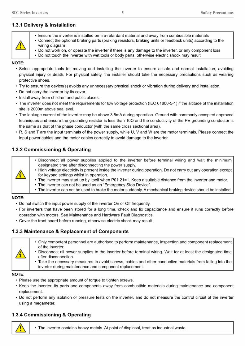
1.3.1 Delivery & Installation
• Ensure the inverter is installed on fire-retardant material and away from combustible materials• Connect the optional braking parts (braking resistors, braking units or feedback units) according to the
wiring diagram• Do not work on, or operate the inverter if there is any damage to the inverter, or any component loss• Do not touch the inverter with wet tools or body parts, otherwise electric shock may result
NOTE:• Select appropriate tools for moving and installing the inverter to ensure a safe and normal installation, avoiding
physical injury or death. For physical safety, the installer should take the necessary precautions such as wearing protective shoes.
• Try to ensure the device(s) avoids any unnecessary physical shock or vibration during delivery and installation.• Do not carry the inverter by its cover.• Install away from children and public places.• The inverter does not meet the requirements for low voltage protection (IEC 61800-5-1) if the altitude of the installation
site is 2000m above sea level.• The leakage current of the inverter may be above 3.5mA during operation. Ground with commonly accepted approved
techniques and ensure the grounding resistor is less than 10Ω and the conductivity of the PE grounding conductor is the same as that of the phase conductor (with the same cross sectional area).
• R, S and T are the input terminals of the power supply, while U, V and W are the motor terminals. Please connect the input power cables and the motor cables correctly to avoid damage to the inverter.
1.3.2 Commissioning & Operating
• Disconnect all power supplies applied to the inverter before terminal wiring and wait the minimum designated time after disconnecting the power supply.
• High voltage electricity is present inside the inverter during operation. Do not carry out any operation except for keypad settings whilst in operation.
• The inverter may start up by itself when P01.21=1. Keep a suitable distance from the inverter and motor.• The inverter can not be used as an “Emergency Stop Device”.• The inverter can not be used to brake the motor suddenly. A mechanical braking device should be installed.
NOTE:• Do not switch the input power supply of the inverter On or Off frequently.• For inverters that have been stored for a long time, check and fix capacitance and ensure it runs correctly before
operation with motors. See Maintenance and Hardware Fault Diagnostics.• Cover the front board before running, otherwise electric shock may result.
1.3.3 Maintenance & Replacement of Components
• Only competent personnel are authorised to perform maintenance, inspection and component replacement of the inverter.
• Disconnect all power supplies to the inverter before terminal wiring. Wait for at least the designated time after disconnection.
• Take the necessary measures to avoid screws, cables and other conductive materials from falling into the inverter during maintenance and component replacement.
NOTE:• Please use the appropriate amount of torque to tighten screws.• Keep the inverter, its parts and components away from combustible materials during maintenance and component
replacement.• Do not perform any isolation or pressure tests on the inverter, and do not measure the control circuit of the inverter
using a megameter.
1.3.4 Commissioning & Operating
• The inverter contains heavy metals. At point of displosal, treat as industrial waste.

6SD1 Series Inverters Installation Guidelines
2 Product Overview2.1 Quick Start-Up
Check the following:
2.1.1 Unpacking Inspection
1. Remove SD1 from packaging and verify there is no damage.
2. Verify the specification of the inverter is as specified (see section 2.4). If not, contact your supplier.
3. Check to ensure that the accessories (including the Instruction Manual and Keypad) found inside the box are present and correct. If not, contact your supplier.
4. Verify that the inverter is compatible with mains supply voltage.
Check the following before initial use of the inverter:
2.1.2 Application
1. Check the suitability of the load type to verify that there will be no overloading of the inverter during use.
2. Check the actual current of the motor is less than the rated current of the inverter.
3. Check the control accuracy of the load is within the specification of the inverter.
4. Ensure the incoming supply voltage is matched to the rated voltage of the inverter.
Check the following before actual installation and usage of the inverter:
2.1.3 Environment
1. Check the ambient operating temperature of the inverter is below +40°C. Derate 1% for every additional 1°C above to a maximum temperature of 50°C (see Appendix A).NOTE: The ambient temperature refers to the air temperature inside the enclosure.
2. Check the ambient temperature of the inverter during operation is above -10°C. If not, consider additional heater.NOTE: The ambient temperature refers to the air temperature inside the enclosure.
3. Check the altitude of the installation site is below 1000m. Derate 1% for every additional 100m (see Appendix A).
4. Check the humidity of the installation site is below 90% and condensation is not present. If present, install anti- condensation heaters.
5. Ensure the drive is kept from direct sunlight and foreign objects can not enter the inverter. Use additional protective measures as required.
6. Check there is no conductive dust or flammable gas in the installation area. Use additional protective measures as required.
Check the following after installation:
2.1.4 Installation
1. Check the input and output cables meet the load rating of the inverter (see Appendix C.3).
2. Check the inverter accessories are correctly installed. The installation cables should meet the specification of all ancilliary components, including AC and DC reactors, input and output filters, braking units and braking resistors.
3. Check the inverter is installed on or near non-flammable materials and heat generating accessories, for example reactors and brake resistors, are away from flammable materials.
4. Check all control cables and power cables are run separately and the routing complies with EMC guidelines.
5. Check all grounding systems are properly grounded according to the requirements of the inverter.
6. Ensure the free space around the inverter is in accordance with the Instruction Manual.

7
7. Check the installation conforms to the Instruction Manual. The drive must be installed in an upright position.
8. Check the external connection terminals are fastened with the correct torque.
9. To avoid the risk of short circuit, check there are no screws, cables and other conductive items left in the inverter and refit all covers before use.
SD1 Series Inverters Installation Guidelines
Complete the basic commissioning as follows before operation:
2.1.5 Basic Commissioning
1. Autotune. If possible, de-couple from the motor load to start dynamic autotune. Static autotune is also available.
2. Adjust the ACC/DEC time as required for the application.
3. Check the rotation direction is as required. If not, make the necessary changes to the motor or control wiring.
4. Set all control parameters as required before operation.
2.2 Product Specification
Function Specification
Power Input
Input Voltage (V)AC 1PH 200V (-15%)~240V (+10%)AC 3PH 200V (-15%)~240V (+10%)AC 3PH 380V (-15%)~440V (+10%)
Input Current (A) Refer to the rated value
Input Frequency (Hz) 50Hz or 60Hz Allowed Range: 47~63Hz
Power Output
Output Voltage (V) 0~Input Voltage
Output Current (A) Refer to the rated value
Output Power (kW) Refer to the rated value
Output Frequency (Hz) 0~400Hz
Technical Control Feature
Control Mode SVPWM, SVC
Motor Asynchronous Motor
Adjustable Speed Ratio Asynchronous Motor 1:100 (SVC)
Speed Control Accuracy ± 0.2% (SVC)
Speed Fluctuation ± 0.3% (SVC)
Torque Response <20ms (SVC)
Torque Control Accuracy 10%
Starting Torque 0.5Hz/150% (SVC)
Overload Capability150% of rated current: 1 minute
180% of rated current: 10 seconds200% of rated current: 1 second
Running Control Feature
Frequency Setting MethodDigital, analogue, pulse frequency,
multi-step speed running, simple PLC, PID, MODBUS comms. Shift between the set combination and set channel.
Auto-Adjustment of the Voltage Automatic Voltage Regulation. Compensates for supply voltage transients
Fault Protection Provide comprehensive fault protection functions: Overcurrent, Overvoltage, Undervoltage, Overheating, Phase Loss, Overload etc.
Start After Speed Tracking Provides smooth ramping during start up

8SD1 Series Inverters Installation Guidelines
Function Specification
Peripheral Interface
Analogue Input 1 (AI2) 0~10V/0~20mA and 1 (AI3) -10~10V
Analogue Output 2 (AO1, AO2) 0~10V/0~20mA
Digital Input 4 standard inputs, (Max. frequency: 1kHz)1 high speed input, (Max. frequency: 50kHz)
Digital Output 1 Y1 terminal output
Relay Output
2 programmable relay outputsRO1A NO, RO1B NC, RO1C common terminalRO2A NO, RO2B NC, RO2C common terminal
Contact capacity: 3A/250VAC
Others
Mounting Method Wall and rail mountable
Ambient Operating Temperature -10~50°C, derate 1% for every additional 1°C when above 40°C
DC Reactor Standard internal DC reactor for the inverters (≥18.5kW)
Installation Mode
Wall and rail installation of inverters (1PH/200V, 3PH/380V, ≤2.2kW and 3PH/200V, ≤0.75kW)
Wall and flange installation of the inverters (3PH/380V, ≥4kW and 3PH/200V, ≥1.5kW
Braking Unit Standard for inverters ≤37kW, optional for inverters of 45~110kW
Protection LevelIP20
Note: Plastic cased inverter should be installed in a metal distribution cabinet, which conforms to IP20 (top surface conforms to IP3X)
Cooling Fan cooling
Braking Unit Built-in
EMC Filter
Internal C3 filters for inverters 3PH/380V, ≥4kW and 3PH/200V, ≥1.5kW.Optional external filters to meet the requirement of IEC61800-3 C2,
IEC61800-3 C3For drives >4kW, if internal C3 filter is required, fit supplied jumper link to
EMC/J10 observing all safety precautions
Safety All SD1 Inverters comply to CE and are marked accordinglySTO function to SIL level 2/3 (see specification table for more details)
2.3 Name Plate
Figure 2-1: Name Plate
NOTE: This is the example for standard products. And the CE/IP20 will be marked according to the actual product.

9SD1 Series Inverters Installation Guidelines
The model designation contains information on the inverter. The user can find the model designation on the model designation label attached to the inverter or the simple name plate.
2.4 Type Designation Key
SD1 - 2.5A - 21
Figure 2-2: Product Type
Key No. Detailed Description Detailed ContentProduct Abbreviation Product Abbreviation SD1 = Series Name
Rated Power Rated Output Current 2.5A = 2.5Amps continuous rating
Voltage Degree Supply Voltage21: AC 1PH 200V (-15%)~240V (+10%)23: AC 3PH 200V (-15%)~240V (+10%)43: AC 3PH 380V (-15%)~440V (+10%)
2.5 Rated Specifications
Model Voltage Degree Rated Output Power (kW)
Rated Input Current (A)
Rated Output Current (A)
Weight (kg)
STO Function
SD1-2.5A-21Single phase
200V
0.4 6.5 2.5 0.9 SIL2SD1-4.2A-21 0.75 9.3 4.2 0.9 SIL2SD1-7.5A-21 1.5 15.7 7.5 1.2 SIL2SD1-10A-21 2.2 24 10 1.2 SIL2SD1-2.5A-23
Three phase 200V
0.4 3.7 2.5 1.0 SIL2SD1-4.2A-23 0.75 5 4.2 1.0 SIL2SD1-7.5A-23 1.5 7.7 7.5 3.1 SIL3SD1-10A-23 2.2 11 10 3.1 SIL3SD1-16A-23 4 17 16 3.1 SIL3SD1-20A-23 5.5 21 20 5.58 SIL3SD1-30A-23 7.5 31 30 5.83 SIL3SD1-2.5A-43
Three phase 380V
0.75 3.4 2.5 1.0 SIL2SD1-4.2A-43 1.5 5.0 4.2 1.0 SIL2SD1-5.5A-43 2.2 5.8 5.5 1.0 SIL2SD1-9.5A-43 4 13.5 9.5 3.1 SIL3SD1-14A-43 5.5 19.5 14 3.1 SIL3
SD1-18.5A-43 7.5 25 18.5 5.58 SIL3SD1-25A-43 11 32 25 5.58 SIL3SD1-32A-43 15 40 32 5.83 SIL3SD1-38A-43 18.5 47 38 9.0 SIL3SD1-45A-43 22 51 45 9.0 SIL3SD1-60A-43 30 70 60 15.5 SIL3SD1-75A-43 37 80 75 15.5 SIL3SD1-92A-43 45 98 92 25 SIL3SD1-115A-43 55 128 115 25 SIL3SD1-150A-43 75 139 150 25 SIL3SD1-180A-43 90 168 180 45 SIL3SD1-215A-43 110 201 215 45 SIL3

10SD1 Series Inverters Installation Guidelines
2.6 Construction DiagramBelow is the layout figure of the inverter (three phase 380V, ≤2.2kW). NOTE: Example below is the 0.75kW SD1
Figure 2-3: Product Construction (three phase 380V, ≤2.2kW)
Serial No. Name Illustration
1 External Keypad Port Connection for the external keypad
2 Port cover Protects the external keypad port
3 Cover Protects the internal parts and components
4 Hole for the sliding cover Fix the sliding cover using a screw (provided in accessory bag)
5 Gland plate Protect the inner components and fix the cables of the main circuit
6 Name plate Refer to section 2.3 for detailed information
7 Potentiometer Refer to section 4
8 Control terminals Refer to section 3.2 for detailed information
9 Main circuit terminals Refer to section 3.2 for detailed information
10 Screw hole Fix the fan cover using a screw (provided in accessory bag)
11 Cooling fan Refer to section 6 for detailed information
12 Fan cover Protects the fan
13 Barcode The same as the barcode on the name plateNOTE: The barcode is located under the removable cover.
NOTE: In above figure, the screws required for 4 and 10 are provided with packaging and specific installation depends on the requirements of customers.

11SD1 Series Inverters Installation Guidelines
Below is the layout figure of the inverter (three phase 380V, ≤4kW). NOTE: Example below is the 4kW SD1.
Figure 2-4: Product Construction (three phase 380V, ≥4kW)
Serial No. Name Illustration
1 External Keypad Port Connect the external keypad
2 Cover Protects the internal parts and components
3 Keypad Refer to the section 4
4 Cooling fan See section 6 for detailed information
5 Name plate See section 2.3 for detailed information
6 Side cooling vent cover Optional cooling vent cover for higher IP protection. Derate appropriately if fitted
7 Control terminals See section 3.2 for detailed information
8 Main circuit terminals See section 3.2 for detailed information
9 Gland plate Used to protect power and control cabling
10 Name plate Refer to section 2.4
11 Barcode The same as the barcode on the name plate

12SD1 Series Inverters Installation Guidelines
3 Installation Guidelines
3.1 Mechanical Installation
This chapter explains the mechanical installation and electrical installation
3.1.1 Installation EnvironmentTo ensure full performance and the long term reliability of the inverter please adhere to the following:
• See section 1 for all safety precautions.• Only competent personnel are authorised to perform actions described in this chapter. Please follow the
instructions in Safety Precautions. Ignoring these may cause damage to the equipment, physical injury or even death.
• Ensure the power supply of the inverter is disconnected during this procedure. Please wait the required discharge time in accordance with the table in section 1.3.
• The installation and wiring of the inverter should comply with local and national electrical code requirements and regulations at the installation site.
Environment Conditions
Environment Temperature
-10°C~+50°C, and the temperature changing rate is less than 0.5°C/minute. If the ambient temperature of the inverter is above 40°C, derate 1% for every additional 1°C.It is not recommended to use the inverter if the ambient temperature is above 50°C.To protect the integrity of the device, do not use the inverter in environment with frequent ambient temperature changes.Provide adequate cooling to maintain ambient temperature within specification when inverter is mounted inside an enclosure.Ensure the inverter is not operated below the minimum specified temperature.
Humidity RH ≤90% Non-condensing
Storage temperature -40°C~+70°C, with temperature changing rate less than 1°C/minute.
Running environment condition
The installation site of the inverter should: Not be near any electromagnetic radiation source and kept away from contaminative air, such as corrosive gas, oil mist and flammable gas; Ensure foreign objects, such as metal powder, dust, oil, water can not enter the inverter (do not install the inverter on the flammable materials such as wood); keep away from direct sunlight, oil mist, steam and vibration.
Altitude Below 1000m Derate 1% for every additional 100m above 1000m
Vibration ≤ 5.8m/s2 (0.6g)
Installation direction The inverter should be installed on an upright position to ensure sufficient cooling effect.
NOTE: • SD1 series inverters should be installed in a clean and ventilated environment as per enclosure classification. • Cooling air must be clean, free from corrosive materials and/or electrically conductive dust.

13SD1 Series Inverters Installation Guidelines
The inverter may be installed on any vertical surface or in a cabinet.The inverter should be installed in the vertical upright position. Check the installation site per the requirements below. Refer to chapter Dimension Drawings in the appendix for frame details.
3.1.2 Installation
(1) Wall and rail mounting for the inverters (single phase 200V/three phase 380V, ≤2.2kW and three phase 200V, ≤0.75kW)
a) Wall Mounting b) Rail Mounting
Figure 3-1: InstallationNOTE: the minimum space of A and B is 100mm (if H is 36.6mm and W is 35.0mm.)
(2) Wall and flange mounting for the inverters (three phase 380V, ≥4kW and three phase 220V, ≥1.5kW)
a) Wall Mounting b) Flange MountingFigure 3-2: Installation
• Ensure the inverter is securely fitted so that it will not fall causing injury or damage.

14SD1 Series Inverters Installation Guidelines
3.2 Electrical Installation
3.2.1 Installation
NOTE: • Fuses, braking resistor, input reactor, input filter, output reactor, output filter are optional parts. Please refer to
Appendix C for detailed information. • Remove the yellow warning labels of PB, (+) and (-) on the terminals before connecting the braking resistor to ensure
proper connection.
3.2.2 Main Circuit Terminals
Figure 3-4: 1PH main circuit terminals (single phase)
Figure 3-3: Connection diagram of main circuit

15SD1 Series Inverters Installation Guidelines
Figure 3-5: 3PH main circuit terminals (200V, ≤0.75kW, and 380V, ≤2.2kW)
Figure 3-6: 3PH main circuit terminals (200V, ≤1.5kW, and 380V, 4-22kW)
Figure 3-7: 3PH main circuit terminals (30-37kW)
Figure 3-8: 3PH main circuit terminals (45-110kW)
Terminal Function
L, N Single phase AC input terminals which are connected to the power supply
R, S, T Three phase AC input terminals which are connected to the power supply
PB, (+) External dynamic braking resistor terminal
(+), (-) Input terminal of the DBU or DC bus
U, V, W Three phase AC output terminals which are connected to the motor
PE Protective grounding material
NOTE: • Do not use asymmetric motor cables. If there is a symmetrically grounding conductor in the motor cable in addition to
the conductive shield, connect the grounding conductor to the grounding terminal at the inverter and motor ends.• Route the motor cable, input power cable and control cables separately.
3.2.3 Wiring of Terminals in Main Circuit
1. Connect the grounding conductor of the input power cable to the ground terminal of the inverter (PE) using a ring type connector. Connect the phase conductors to L1, L2 and L3 terminals and fasten.
2. Strip the motor cable and connect the shield to the ground terminal of the inverter using a ring type connector. Connect the phase conductors to U, V and W terminals and fasten.
3. If required, connect the optional brake resistor with a shielded cable to the designated position by the same procedures in the previous step.
4. Secure all cables outside the inverter using suitable fasteners and strain relief.

16SD1 Series Inverters Installation Guidelines
Figure 3-9: Wiring of control circuit
3.2.5 Control Circuit Terminals
Figure 3-10: Connection terminal diagram for inverters ≤2.2kW
3.2.4 Control Circuit Wiring Diagram
Figure 3-11: Connection terminal diagram for inverters ≥ 4kW
+10V
AI2
AI3
GND
AI2V I
COM/GND
COM
+24V
Open collector input optional
High speed pulse input collector
Multi-function input terminal 4
Multi-function input terminal 3
Multi-function input terminal 2
Multi-function input terminal 1
PWCOM
HDI
S4
S3
S2
S1
V I
V I
AO2
AO1 AO1
COM
AO2
COM
Analog output0-10V/0-20mA
Analog output0-10V/0-20mA
Y1
COMY1 output
Relay 2 output
RS485 communicationShield layerTwisted pair
485+
485-
COM/GND
RO1A
RO1B
RO1C
RO2A
RO2B
RO2C
Relay 1 output
H1
H2
+24V
Safety state feedback
S2
S1
Safety switch
Open circuitSafety controller
Safety input
Relay 2 output only available on SD1 inverters > 2.2kW
AO2 output only available on SD1 inverters > 2.2kW

17SD1 Series Inverters Installation Guidelines
Type Terminal Name Function Description Technical Specifications
Communication485+
RS485 communications RS485 communication interface 485-
Digital Input/Output
S1
Digital Input
1. Internal impedance:3.3kΩ2. 12~30V voltage input is available
3. These terminals are the dual-direction input 4. Max. input frequency:1kHz
S2S3S4
HDI High Frequency Input Channel
Terminal for high frequency (pulse) input. Max. input frequency:50kHz
Duty cycle:30%~70%
PW Digital Power SupplyTo provide the external digital power supply
Voltage range: 12~30V
Y1 Digital OutputTransistor output
(Contact capacity: 50mA/30V)
24V Power Supply
+24V
24V Power Supply
Internal 24V±10% power supply. (maximum load 200mA)
Used as an operation power supply for digital input and output or external sensor power supply
COM
Analogue Input/Output
+10V External 10V Reference Power Supply
10V reference power supply for external potentiometerMax. output current: 50mA
Potentiometer rating: 5kΩ aboveA12
Analogue Input
1. Input range: AI2 voltage and current can be selected: 0~10V/0~20mA; AI3: -10V~+10V. 2. Input impedance: voltage input:
20kΩ; current input: 500Ω.3.Voltage or current input can be
set by dip switch.4. Resolution: Minimum AI2/AI3 is 10mV/20mV when 10V
corresponds to 50Hz.
A13
GND Analogue Reference Ground Analogue Reference Ground
AO1Analogue Output
1. Output range:0~10V or 0~20mA2. Voltage or current output is selected by jumpers or
dip switch. 3. Deviation ±1%,25°C when full range.4. Only AO1 for SD1 inverters ≤ 2.2kW.
AO2 As above. Please note only AO2 for SD1 inverters > 2.2kW.
STO function input
24V-H1 STO input 1 1. Safety torque stop (STO) redundant input, externally connected to NC contact, STO acts when the contact is open,
and the drive stops output;2. The safe input signal cable should be shielded with max.
length 25m. 3. When employing STO function, please disconnect the shorting
link on the terminals shown in fig 3.10 and fig 3.11.24V-H2 STO input 2
Relay Output
RO1A Relay 1 NO Contact RO1 relay output, RO1A NO, RO1B NC, RO1C common terminal
Contact capacity: 3A/250VACOnly RO1 for inverters ≤ 2.2kW (two contacts)
RO1B Relay 1 NC Contact
RO1C Relay 1 Common Contact
RO2A Relay 2 NO Contact RO2 relay output, RO2A NO, RO2B NC, RO2C common terminal
Contact capacity: 3A/250VACPlease note only RO2 for SD1 inverters > 2.2kW.
RO2B Relay 2 NC Contact
RO2C Relay 2 Common Contact
3.2.6 Control Circuit Definitions

18SD1 Series Inverters Installation Guidelines
Figure 3-13: NPN modes
If the signal is from NPN transistor, please set the jumper link between +24V and PW as below according to the used power supply.
If the signal is from PNP transistor, please set the jumper link as below according to the used power supply.
Figure 3-14: PNP modes
Figure 3-12: Jumper Link
Use jumper link to set NPN mode or PNP mode and the internal or external power supply. The default setting is NPN internal mode.
3.2.7 Input/Output Signal Connection Figure
3.2.8 Internal C3 Filter Link For drives >4kW, if internal C3 filter is required, fit supplied jumper link to EMC/J10 observing all safety precautions.
Figure 3-15: C3 Filter Jumper Link
Terminal connections for >4kW

19SD1 Series Inverters Installation Guidelines
3.3 STO (Safe Torque Off) Function Overview
Reference standards: IEC 61508-1, IEC 61508-2, IEC 61508-3, IEC 61508-4, IEC 62061, ISO 13849-1, IEC 61800-5-2The STO function can be used where main power of the drive is on to prevent unexpected start. The function cuts off the drive signal to disable the drive output, thus preventing motor from unexpected start (refer to below figure). After enabling STO function, short-time operations and/or maintenance on non-electrical parts can be conducted.
Input states and corresponding faults of STO function:
3.3.1 Logic table for STO function
STO input state Corresponding STO faultH1, H2 opens simultaneously Triggers STO function, the drive stopsH1, H2 closes simultaneously Drive operates normally
Either H1 or H2 opens or closes
Trigger STL1/STL2/STL3 fault, fault code:38: Safety circuit of channel 1 is abnormal (STL1)39: Safety circuit of channel 2 is abnormal (STL2)40: Channel H1 and H2 become abnormal simultaneously (STL3)
STO channel trigger and indication delay time:
3.3.2 Description of STO Channel Delay
STO mode STO trigger and indication delay 1)2)
STO fault: STL1 Trigger delay<10msIndication delay<280ms
STO fault: STL2 Trigger delay<10msIndication delay<280ms
STO fault: STL3 Trigger delay<10msIndication delay<280ms
STO fault: STO Trigger delay<10msIndication delay<100ms
1) STO trigger delay = the delay between triggering STO and cutting off drive output 2) STO indication delay= the delay between triggering STO and indicating STO output state
Figure 3-16: STO schematic
20SD1 Series Inverters Installation Guidelines
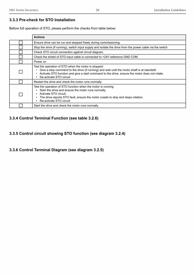
Before full operation of STO, please perform the checks from table below:
3.3.3 Pre-check for STO Installation
Actions
Ensure drive can be run and stopped freely during commissioning.Stop the drive (if running), switch input supply and isolate the drive from the power cable via the switch Check STO circuit connection against circuit diagram.Check the shield of STO input cable is connected to +24V reference GND COM Power onTest the operation of STO when the motor is stopped:
• Give a stop command to the drive (if running) and wait until the motor shaft is at standstill.• Activate STO function and give a start command to the drive, ensure the motor does not rotate.• De-activate STO circuit
Restart the drive and check the motor runs normallyTest the operation of STO function when the motor is running:
• Start the drive and ensure the motor runs normally.• Activate STO circuit.• The drive reports STO fault, ensure the motor coasts to stop and stops rotation.• Re-activate STO circuit
Start the drive and check the motor runs normally
3.3.4 Control Terminal Function (see table 3.2.6)
3.3.5 Control circuit showing STO function (see diagram 3.2.4)
3.3.6 Control Terminal Diagram (see diagram 3.2.5)

21
1. When P11.16 is set to 1, the STO alarm is locked. As shown in below fig 3-17, When H1 and H2 are ‘OFF’ during operation (safety function is required), the drive enters safety mode and stops output. STO alarm will only clear when reset is activated. External run command needs to be reset for the drive to run again.
Figure 3-17
SD1 Series Inverters Installation Guidelines
3.3.7 STO Function Parameter Table
Function Code Name Detailed Instruction of Parameters Default
Value Modify
P06.01 Y1 output selection 0: Invalid1: In operation……25: Reserved26: DC bus voltage build-up is completed27: STO action28~30: Reserved
27
P06.03 Relay RO1 output selection 1
P06.04 Relay RO2 output selection 5
P07.27 Current fault type 0: No fault1: Inverter unit U phase protection (OUt1)……35: Maladjustment fault (STo)36: Underload fault (LL)37: Safety torque stop (STO)38: Channel 1 safety circuit is abnormal (STL1)39: Channel 2 safety circuit is abnormal (STL2)40: Channel H1 and H2 become abnormal simultaneously (STL3)41: Safety code FLASH CRC check fault (CrCE)
P07.28 Type of the previous 1 fault
P07.29 Type of the previous 2 faults
P07.30 Type of the previous 3 faults
P07.31 Type of the previous 4 faults
P07.32 Type of the previous 5 faults
P11.16 Extension function selection
0x000~0x211LED ones: Automatic frequency downgrade at voltage drop0: Automatic frequency downgrade at voltage drop is invalid1: Automatic frequency downgrade at voltage drop is validLED tens: The second ACC/DEC time selection0: The second ACC/DEC time detection selection is invalid1: The second ACC/DEC time detection selection is valid, when the operation is above P08.36, ACC/DEC time is switched to the second ACC/DEC timeLED hundreds: STO function selection0: STO alarm lockedAlarm lock means when STO appears, reset is a must after state recovery.1: STO alarm unlockedSTO alarm unlocked means when STO appears, STO alarm will disappear automatically after state recovery.Note: STL1~STL3 are fault lock and cannot be reset
0x100
3.3.8 STO Alarm

22
1. 2. When the hundreds of P11.16 is set to 2, the STO alarm will not be locked. As shown in below Figure 3-18, alarm non-
lock means when STO appears, the STO alarm will disappear automatically after state restoration, which requires no reset action. After reset of external running command, the inverter will execute run command again.
Figure 3-18
SD1 Series Inverters Installation Guidelines
STL1 fault (the hundreds of P11.16 is set to 1)
As shown in below fig 3-19, when the hardware circuit of safety circuit H1 is OFF while that of H2 signal is ON, namely, when H1 is OFF during operation (safety function is activated), the drive enters safety mode and stops output, overriding any run signal. STL1 is displayed and alarm is locked, ignoring both run reset and trip reset until the cause of the fault is rectified.
Figure 3-19STL 2 fault (the hundreds of P11.16 is set to 1)
As shown in below fig 3-20, when the hardware circuit of safety circuit H1 is ON while that of H2 signal is OFF, namely, when H1 is ON during operation (safety function is required), the drive enters safety mode and stops output, overriding any run signal. STL2 is displayed and alarm is locked, ignoring both run reset and trip reset until the cause of the fault is rectified.
Figure 3-20

23SD1 Series Inverters Installation Guidelines
3.4 Layout Protection
3.4.1 Protect the Inverter and Input Power Cable in Short-Circuit ConditionsProtect the inverter and input power cables with fuses (shown below) in case of short circuit occurrence or thermal overload.
Figure 3-21: Fuse Configuration
NOTE: Select the fuse as specified in the manual. The fuse will protect the input power cable from damage in short-circuit conditions. It will protect the surrounding devices should the inverter have a short circuit condition.
3.4.2 Protecting the Motor and Motor Cables The inverter protects the motor and motor cables in case of a short-circuit condition as long as the motor cable is specified according to the rated current of the inverter. No additional protection devices are required.
• If the inverter is connected to multiple motors, a separate thermal overload switch or a circuit breaker must be used for protecting each cable and motor. These devices may require a separate fuse to cut off the short-circuit current.
3.4.3 Implementing a Bypass Connection It is necessary to set power frequency and variable frequency conversion circuits for the assurance of continuous normal work of the inverter if faults occur in some significant situations. In some special situations, for example, if it is only used in soft start, the inverter can be converted into power frequency running after starting however some corresponding bypass should be added.
• Never connect the supply power to the inverter output terminals U, V and W. Power line voltage applied to the output can result in permanent damage to the inverter.
If frequent switching is required, employ mechanically connected switches or contactors to ensure the motor terminals are not connected to the AC power line and inverter output terminals simultaneously.

24SD1 Series Inverters Keypad Operation Procedure
4 Keypad Operation4.1 Keypad IntroductionThe keypad is used to control SD1 series inverters, read the status data and adjust parameters.
Figure 4-1: Fixed keypad Figure 4-2: External keypad NOTE: 1. The fixed keypad is standard for all inverters up to 2.2kW. External Keypad is supplied fitted to ≥4kW inverters as
standard.2. Optional external keypad with copy function is available.
Serial No Name Description
1 Status LED
LED off means that the inverter is in the stopped state; LED flashing means the inverter is in the parameter autotune
status; LED on means the inverter is running.
FWD/REV LED LED off means the inverter is in forward rotation state; LED
on means the inverter is in reverse rotation state
LED for keypad operation, terminals operation and remote communication control
LED off means that the inverter is in the keypad operation status; LED flashing means the inverter is in terminal
operation status; LED on means the inverter is in remote communication control status.
LED for faults LED on when the inverter is in fault status; LED off in normal
status; LED flashing means the inverter is in the pre-alarm status.
2 Unit LED
Refers to the current unit displayed
Hz Frequency Unit
RPM Rotating Speed Unit
A Current Unit
% Percentage
V Voltage Unit
RUN/TUNE
TRIP
FWD/REV
LOCAL/REMOT

25
Serial No Name Description
3Code
Displaying Zone
5-figure LED display indicates various monitoring data and alarm code such as set frequency and output frequency.
4 Buttons
Programming Key 1) Access programming mode2) Exit
Entry Key 1) Enter the parameter subgroup2) Confirm parameters
UP Key Up
DOWN Key Down
Right Shift Key1) Monitor values2)Move cursor right to select the displaying parameter in stopping and running mode.
Run Key Enable run signal from keypad
Stop/Reset Key 1) Enable stop from keypad. Refer to P07.042) Reset alarm fault
Quick Key The function of this key is programmed by function code P07.02.
5Analogue Potenti-ometer
AI1, When the external common keypad (without the function of parameter copy) is valid, the difference between the local keypad AI1 and the external keypad AI1 is: When the external keypad AI1 is set to the Min. value, the local keypad AI1 will be valid and P17.19 will be the voltage of the local keypad AI1; otherwise, the external keypad AI1 will be valid and P17.19 will be the voltage of the external keypad AI1. Note: If the external keypad AI1 is frequency reference source, adjust the local potentiometer AI1 to 0V/0mA before starting the inverter.
6 Keypad Port
External keypad port. When the external copy keypad is connected, the local keypad LED is off; When the external standard keypad is connected, the local and external keypad LEDs are
on.Note: Only the optional external copy keypad can store parameters.
SD1 Series Inverters Keypad Operation Procedure

26SD1 Series Inverters Keypad Operation Procedure
4.2 Keypad Display The keypad display status of SD1 Series inverters is divided into stopped state, running state, function code editing state and fault alarm status, etc.
Figure 4-2: Displayed Status
4.2.1 Stop Mode Parameter When the inverter is in the stopped state, the keypad will display stopped parameters which is shown in figure 4-2.In the stopped state, various parameters can be displayed. Select the parameters to be displayed by P07.07. See the instructions of P07.07 for the detailed definition of each parameter. In the stopped state, there are 14 stopping parameters can be selected to be displayed. They are: set frequency, bus voltage, input terminals status, output terminals status, PID set value, PID feedback, torque set value, AI1, AI2, AI3, HDI, PLC and the current stage of preset speeds, pulse counting value, length value. P07.07 can select the parameter to be displayed by bit and »/SHIFT can shift the parameters from left to right, QUICK/JOG (P07.02=2) can shift the parameters form right to left.
4.2.2 Run Mode Parameters After the inverter receives valid running command, the inverter will enter the running state and the keypad will display the running parameters. RUN/TUNE LED on the keypad is on, while the FWD/REV is determined by the current running direction which is shown as figure 4-2.In the running state, there are 24 parameters can be selected to be displayed. They are: running frequency, set frequency, bus voltage, output voltage, output torque, PID given, PID feedback, input terminals state, output terminals state, torque set value, length value, PLC and the current stage of preset speeds, pulse counting value, AI1, AI2, AI3, HDI, percentage of motor overload, percentage of inverter overload, ramp given value, linear speed, AC input current. P07.05 and P07.06 can select the parameter to be displayed by bit and »/SHIFT can shift the parameters form left to right, QUICK/JOG (P07.02=2) can shift the parameters from right to left.
4.2.3 Fault StatusIf the inverter detects a fault signal, it will enter the fault pre-alarm display status. The keypad will display the fault code by flashing. The TRIP LED on the keypad is on, and the fault reset can be operated by the STOP/RST on the keypad, control terminals or communication commands.
4.2.4 Function Codes Editing In the stopped, running or fault state, press PRG/ESC to enter the editing state The editing status is displayed on two levels of menu, and the order is: function code group/function code number→function code parameter, press DATA/ENT into the displayed status of function parameter. Press DATA/ENT to save the parameters or press PRG/ESC to escape.
See section 5 for detailed function codes.
4.2.5 Function Codes Editing Example The inverter has three levels menu, which are: 1. Group number of function code (first-level menu) 2. Tab of function code (second-level menu) 3. Set value of function code (third-level menu)

27SD1 Series Inverters Keypad Operation Procedure
Remarks: Press both the PRG/ESC and the DATA/ENT to return to the second-level menu from the third-level menu. Pressing DATA/ENT will save the set parameters into the control panel, and then return to the second-level menu with shifting to the next function code automatically; while pressing PRG/ESC will return to the second-level menu without saving the parameters.Under the third-level menu, only flashing digits can be changed. If digits are not flashing, possible reasons could be:1) Function code is not a modifiable parameter, such as a monitoring parameter.2) Function code is not a modifiable in running state, but modifiable in stop state.Example: Set function code P00.01 from 0 to 1.
Figure 4-3: Diagram of modifying parameters
4.2.6 Setting Password SD1 Series inverters provide password protection function. P07.00 is used to set the password. Entering P07.00 displays “00000”. change this value to a numeric password of your choice. Exiting will automatically activate password. On the next power cycle, the password will be required to access parameters. Pressing PRG/ESC will display “0.0.0.0.0”, enter password to access parameters.To cancel password, enter the password to access parameters. Set P07.00 to “00000” and save with DATA/ENT this will cancel password function.To reset the password, see function code P00.18
Figure 4-4: Diagram of password setting
4.2.7 Function Code Status Monitoring Parameter group P17 allows monitoring of various values and conditions of the inverter. See diagram of status monitoring below.
Figure 4-5: Diagram of status monitoring

28SD1 Series Inverters Function Codes
5 Function Code The function parameters of SD1 Series inverters have been divided into 30 groups (P00~P29) according to the function, of which P18~P28 are reserved. Each function group contains certain function codes applying 3-level menus. For example, “P08.08” means the eighth function code in the P8 group function, P29 group is factory reserved. See table below:
For ease of function codes setting, the function menu is constructed in 3 levels: Group, sub group and data value setting. See table below:
1. “ ”: indicates the set value of the parameter can be modified in stop and running state;2. “ ”: indicates the set value of the parameter can not be modified in the running state;3. “ ”: indicates the value of the parameter is the display value which can not be modified.
Function Code Name Detailed Instruction of Parameters Default
Value Modify
P00 Group: Basic Function Group
P00.00 Speed control mode
0: SVC 0No encoders required. Suitable in applications which require low frequency, high torque for high accuracy of rotating speed and torque control. Relative to mode 1, it is more suitable for the applications which need low power.1: SVC 1 Suitable in high performance applications with the advantage of high accuracy of rotating speed and torque. Encoder not required. 2: SVPWM controlSuitable in applications which do not require high control accuracy, such as pump and fan applications.
1
1. Below is the instruction of the function lists: The first column “Function code”: codes of function parameter group and parametersThe second column “Name”: full name of function parametersThe third column “Detailed illustration of parameters”: Detailed instruction of the function parametersThe fourth column “Default value”: the original factory set value of the function parameterThe fifth column “Modify”: the modifying character of function codes (the parameters can be modified or not and the modifying conditions), below are the instructions:
Group Sub Group Description Examples of FunctionsP00 P00.00 – P00.18 Basic parameters Run command type, Max frequency, ramp timesP01 P01.00 – P01.25 Start/Stop control DC injection braking, coast to stop, delay start, auto restartP02 P02.00 – P02.26 Motor 1 settings Motor ratings, kW, Current, speedP03 P03.00 – P03.27 Vector control Torque vector control settingsP04 P04.00 – P04.33 V/F control Torque boost, slip compensation, V/F curveP05 P05.00 – P05.54 Input terminals Set function of digital inputs S1-S4P06 P06.00 – P06.26 Output terminals Set function of relay, transistor and analogue outputsP07 P07.00 – P07.56 Keypad/HMI settings Set user password, quick key function and displayP08 P08.00 – P08.51 Enhanced functions Jog, cooling fan and dynamic braking functionsP09 P09.00 – P09.16 PID control settings PID, SV and feedback source settingsP10 P10.00 – P10.37 Pre-set speeds & PLC Pre-set speed values & PLC selectionP11 P11.00 – P11.15 Protective functions Set protective function trip/output levelsP13 P13.13 – P13.15 Control parameters of SM Current braking settingsP14 P14.00 – P14.08 Comms settings Baud rate, check bits and other MODBUS/RS485 settingsP17 P17.00 – P17.39 Monitoring Monitor live values of inverter during operationP29 Reserved Reserved

29SD1 Series Inverters Function Codes
Function Code Name Detailed Instruction of Parameters Default
Value Modify
P00.01 Run command channel
Selects the run command method of the inverter. Settings include: start, stop, forward/reverse rotation, jog and fault reset.0: Keypad running command method (“ LOCAL/REMOT ” light off)Run command control by RUN , STOP/RST on the keypad. Set the multi-function key QUICK/JOG to FWD/REVC shifting function (P07.02=3) to change the run direction; press RUN and STOP/RST simultaneously in running state for coast to stop. 1: Terminal run command method (“ LOCAL/REMOT ” flashing)Run command control for forward rotation, reverse rotation and forward jog and reverse jog by digital inputs S1-S42: Communication running command method (“ LOCAL/REMOT ” on);The running command is controlled via communication.
0
P00.03 Max. output frequency
This parameter is used to set the maximum output frequency of the inverter. Frequency setting, acceleration and deceleration times are directly related to this parameter. Setting range: P00.04~400.00Hz
50.00Hz
P00.04 Frequency high limit
Sets the high frequency limit which is lower than or equal to the maximum frequency. Setting range: P00.05~P00.03 (Max. output frequency)
50.00Hz
P00.05 Frequency low limit
Sets the low frequency limit.The inverter runs at the lower limit frequency if the set frequency is lower than the lower limit.Note: Max. output frequency ≥ high limit frequency ≥ Low limit frequencySetting range:0.00Hz~P00.04 (high limit of the running frequency)
0.00Hz
P00.06“A” frequency
command selection
Note: ”A” frequency and “B” frequency can not set to the same frequency input method. The frequency source can be set by P00.09.0: Keypad data setting Modify the value of function code P00.10 (set the frequency by keypad) to modify the frequency by the keypad. 1: Analogue AI1 setting (corresponding keypad potentiometer)2: Analogue AI2 setting (corresponding terminal AI2)3: Analogue AI3 setting (corresponding terminal AI3)Set the frequency by analogue input terminals. SD1 Series inverters provide 3 channels analogue input terminals as the standard configuration, of which AI1 is adjusting through analogue potentiometer, while AI2 is the voltage/current option (0~10V/0~20mA) which can be selected by jumpers; while AI3 is voltage input (-10V~+10V).Note: when analogue AI2 select 0~20mA input, the corresponding voltage of 20mA is 10V. 100.0% of the analogue input setting corresponds to the maximum frequency (function code P00.03) in forward direction and -100.0% corresponds to the maximum frequency in reverse direction (function code P00.03) 4: High-speed pulse HDI settingThe frequency is set by high-speed pulse terminals. SD1 Series inverters provide 1 high speed pulse input as the standard configuration. The pulse frequency range is 0.00~50.00kHz. 100.0% of the high-speed pulse input setting corresponds to the maximum frequency in forward direction (function code P00.03) and -100.0% corresponds to the maximum frequency in reverse direction (function code P00.03).Note: The pulse setting can only be input by multi-function terminals HDI. Set P05.00 (HDI input selection) to high speed pulse input, and set P05.49 (HDI high speed pulse input function selection) to frequency setting input.5: Simple PLC program settingThe inverter runs at simple PLC program mode when P00.06=5 or P00.07=5. Set P10 (simple PLC and multi-step speed control) to select the running frequency running direction, ACC/DEC time and the keeping time of corresponding stage. See the function description of P10 for detailed information. 6: Multi-step speed running settingThe inverter runs at multi-step speed mode when P00.06=6 or P00.07=6. Set P05 to select the current running step, and set P10.nn to select the current running frequency. The multi-step speed has the priority when P00.06 or P00.07 does not equal to 6, but the setting stage can only be the 1~15 stage. The setting
0
P00.07“B” frequency
command selection
2

30SD1 Series Inverters Function Codes
Function Code Name Detailed Instruction of Parameters Default
Value Modify
cont. Stage is 1~15 if P00.06 or P00.07 equals to 6. 7: PID control setting The running mode of the inverter is process PID control when P00.06=7 or P00.07=7. It is necessary to set P09. The running frequency of the inverter is the value after PID effect. See P09 for the detailed information of the preset source, preset value and feedback source of PID. 8: MODBUS communication setting The frequency is set by MODBUS communication. See P14.nn for detailed information.9~11: Reserved
P00.08
B frequency command reference selection
0: Maximum output frequency, 100% of B frequency setting corresponds to the maximum output frequency 1: A frequency command, 100% of B frequency setting corresponds to the maximum output frequency. Select this setting if it needs to adjust on the base of A frequency command.
0
P00.09 Combination of setting source
0: Sets A as frequency command1: Sets B as frequency command2: Sets A + B as frequency command3: Sets A – B as frequency command4: Sets highest value of A & B as frequency command5: Sets lowest value of A & B as frequency commandNote: The combination setting can be switched by P05 (terminal function)
0
P00.10 Keypad set frequency
Sets the initial frequency value for A & B when in keypad control.Setting range: 0.00 Hz~P00.03 (the max. frequency) 50.00Hz
P00.11 ACC time 1 ACC1: Time (secs) to ramp up to max. frequency (P00.03) from 0HzDEC1: Time (secs) to down from max .frequency (P00.03) to 0Hz(SD1 Series inverters have four groups of ACC/DEC time which can be selected by P05. The factory default ACC/DEC time of the inverter is the first group.)Setting range of P00.11 and P00.12:0.0~3600.0s
Depends on model P00.12 DEC time 1
P00.13 Running direction selection
0: The inverter runs in the forward direction. FWD/REV indicator is off.1: The inverter runs in the reverse direction. FWD/REV indicator is on. The motor rotation direction can be changed by QUICK/JOG on the keypad. Refer to parameter P07.02.Note: Factory reset returns motor direction to default.Check direction of motor is correct before running after reset.2: Forward run only. Prevents motor running in reverse direction.
0
P00.14 Carrier frequency setting
Relationship table of the motor type and carrier frequency:
High carrier frequency provides ideal current waveform, low current harmonic wave and motor noise. However, high carrier frequency increases the losses, inverter temperature and the impact to the output capacity. Earth leakage and electrical magnetic interference will also increase. Output derating required for higher carrier frequency.Too low carrier frequency will cause unstable running, lower torque and current surge. The default factory setting is optimum for most conditions. Derate 10% for each additional 1Kz above default setting. Setting range:1.0~15.0kHz
Depends on model
Carrier Frequency
RFI Noise
Earth Leakage
Heat Generation
1 kHz
4 kHz
8 kHz
High
Low
Low
High
Low
High
Motor Type Factory Setting of Carrier Frequency0.4~11kW 8kHz15~110kW 4kHz

31SD1 Series Inverters Function Codes
Function Code Name Detailed Instruction of Parameters Default
Value Modify
P00.15 Motor parameter autotune
0: No operation 1: Rotation autotuning (motor de-coupled from load)Comprehensive motor parameter autotune It is recommended to use rotation autotuning when high control accuracy is needed. 2: Static autotune 1 (full autotune); When the motor can not be de-coupled form the load. The autotuning for the motor parameter will impact the control performance.3: Static autotune 2 (autotune part parameters); when the current motor is motor 1, autotune P02.06, P02.07, P02.08
0
P00.16 AVR function selection
0: Invalid 1: Valid during the whole procedure The auto-adjusting function of the inverter can reduce the instability on the output voltage of the inverter in case of bus voltage fluctuation.
1
P00.18 Factory reset
0: No operation 1: Restore the default value2: Clear fault records 3: Lock all function codes Note: The function code will restore to 0 after completing the reset.Restoring to the default value will cancel the user password, please use this function with caution.
0
P01 Group: Start-up and Stop Control
P01.00 Start mode
0: Start-up from starting frequency P01.011: Start-up after DC braking: start the motor from the starting frequency after DC braking (set the parameter P01.03 and P01.04). It is suitable in the cases where reverse rotation may occur due to low inertia load during starting.2: Start after speed tracking 13: Start after speed tracking 2The direction and speed will be tracked automatically for the smooth starting of the motor. Suitable for applications with reverse rotation when starting a heavy load.This function is only available for the inverters ≥4kW.
0
P01.01Starting
frequency of start-up
Starting frequency at start up. See P01.02 for detailed information. Setting range: 0.00~50.00Hz 0.50Hz
P01.02Delay time of the
starting frequency
Set correct starting frequency to increase the torque of the inverter during starting. During the delay time the inverter will not run to set frequency until the starting frequency has been reached. The starting frequency is not limited in the lower limit frequency.
Setting range: 0.0~50.0s
0.0s
P01.03 Braking current before starting
The inverter performs DC braking at the braking current set before starting and accelerate after the DC braking time. If the DC braking time is set to 0, the DC braking is invalid. Higher braking current create higher braking torque. The DC braking Current is a percentage of the inverter rated current.Setting range of P01.03: 0.0~100.0%Setting range of P01.04: 0.00~50.00s
0.0%
P01.04 Braking time before starting 0.0s
fmax
Frequency f
Time t
f1
t1f1 set by P01.01t1 set by P01.02

32SD1 Series Inverters Function Codes
Function Code Name Detailed Instruction of Parameters Default
Value Modify
P01.05 ACC/DEC selection
Acceleration and deceleration modes 0: Linear typeThe output frequency increases or decreases linearly.
1: S curve, the output frequency will increase or decrease according to the S curveS curve is generally used on the applications of gradual starting and stopping, such as elevators.
0
P01.06ACC time of the
first step of S curve
0.0~50.0s
0.1s
P01.07DEC time of the final step of S
curve0.1s
P01.08 Stopping method
0: Ramp to stop: Inverter decelerates the motor to stop at the pre-set deceleration time.1: Coast to stop: Inverter output inhibited and motor coasts to stop. stopping time determined by inertia of load
0
P01.09 DC braking start frequency
Starting frequency of DC braking determined by P01.09.
Delay time before DC braking: Inverters inhibits the output before starting DC braking. After this delay time, the DC braking will be started to prevent over-current fault caused by DC braking at high speed.DC braking current: the value of P01.11. Higher braking current creates higher braking torque. The DC braking current is a percentage of the inverter rated current.
DC braking invalid if P01.12 set to 0.
Setting range of P01.09: 0.00Hz~P00.03 (the Max. frequency)Setting range of P01.10: 0.00~50.00sSetting range of P01.11: 0.0~100.0%Setting range of P01.12: 0.00~50.00s
0.0Hz
P01.10 DC braking delay time 0.00s
P01.11 DC braking current 0.0%
P01.12 DC braking time 0.00s

33SD1 Series Inverters Function Codes
Function Code Name Detailed Instruction of Parameters Default
Value Modify
P01.13Delay time of
FWD/REV rotation
Sets a delay time when switching FWD/REV rotation. Set the switching action by P01.14, which is as the table below:
Setting range: 0.0~3600.0s
0.0s
P01.14Switching action between FWD/REV rotation
Set the threshold point of the inverter:0: Switch after zero frequency1: Switch after the starting frequency 2: Switch after the speed reach P01.15 and delay for P01.24
0
P01.15 Stopping speed 0.00~100.00Hz 0.50Hz
P01.16 Detection of stopping speed
0: Detect at the setting speed 1: Detect at the feedback speed (only valid for vector control) 1
P01.17 Detection time of feedback speed
When P01.16=1, the actual output frequency of the inverter is less than or equal to P01.15 and is detected during the time set by P01.17, the inverter will stop; otherwise, the inverter stops in the time set by P01.24.
Setting range: 0.00~100.00s (only valid when P01.16=1)
0.50s
P01.18
Terminalrunning
protection on power-up
When the run command method is the terminal control, the system will detect the status of the run terminal during power-up. 0: If terminal run command is detected on power-up, the inverter will not run until the command is cleared and re-instigated 1: If terminal run command is detected on power-up, the inverter will run automatically.Note: Function setting 1: should be selected with caution.
0
P01.19 Hibernation function setting
This function code determines the running status of the inverter when the set frequency is lower than the lower-limit. 0: Run at the lower-limit frequency1: Stop2: Hibernation The inverter will coast to stop when the set frequency is lower than the lower-limit. If the set frequency remains above the lower limit and lasts for the time set by P01.20, the inverter will return to the running state automatically.
0
P01.20 Hibernation delay time
This function code determines the hibernation delay time. When the running frequency of the inverter is lower than the lower limit, the inverter will stop to stand by. When the set frequency remains above the lower limit and it lasts for the time set by P01.20, the inverter will run automatically.
0.0s

34SD1 Series Inverters Function Codes
Function Code Name Detailed Instruction of Parameters Default
Value Modify
cont
Setting range: 0.0~3600.0s (valid when P01.19=2)
P01.21 Auto restart after power off
This function sets the restart operation after power off0: Disabled 1: Enabled, if the starting criteria is met, the inverter will run automatically after waiting for the time defined by P01.22.
0
P01.22 Autostart delay time
The function sets the auto restart delay time.
Setting range: 0.0~3600.0s (valid when P01.21=1)
1.0s
P01.23 Start delay time
The function determines the brake release after run command is given, and the inverter is in a stand-by status and waits for the delay time set by P01.23Setting range: 0.0~60.0s
0.0s
P01.24 Delay of the stopping speed Setting range: 0.0~100.0s 0.0s
P01.25 0Hz output
Select the 0Hz output of the inverter.0: Output without voltage1: Output with voltage2: Output at the DC braking current
0
P02 Group: Motor 1
P02.01Rated power of asynchronous
motor0.1~3000.0kW Depends
on model
P02.02Rated frequency of asynchronous
motor0.01Hz~P00.03 50.00Hz
P02.03Rated speed of asynchronous
motor1~36000rpm Depends
on model
P02.04Rated voltage of asynchronous
motor0~1200V Depends
on model
P02.05Rated current of asynchronous
motor0.8~6000.0A Depends
on model
P02.06Stator resistance of asynchronous
motor0.001~65.535Ω Depends
on model

35SD1 Series Inverters Function Codes
Function Code Name Detailed Instruction of Parameters Default
Value Modify
P02.07Rotor resistance of asynchronous
motor0.001~65.535Ω Depends
on model
P02.08
Leakage inductance of asynchronous
motor
0.1~6553.5mH Depends on model
P02.09
Mutualinductance of asynchronous
motor
0.1~6553.5mH Depends on model
P02.10Non-load current of asynchronous
motor 0.1~6553.5A Depends
on model
P02.11
Magnetic saturation
coefficient 1 for iron core of AM1
0.0~100.0%
80.0%
P02.12
Magnetic saturation
coefficient 2 for iron core of AM1
0.0~100.0% 68.0%
P02.13
Magnetic saturation
coefficient 3 for iron core of AM1
0.0~100.0% 57.0%
P02.14
Magnetic saturation
coefficient 4 for iron core of AM1
0.0~100.0% 40.0%
P02.26Motor overload
protection selection
0: No protection1: Standard motor (with low speed compensation). Because the heat- releasing effect of the standard motors will be less, the corresponding electric heat protection will be adjusted accordingly. The low speed compensation characteristic mentioned here means reducing the threshold of the overload protection of the motor whose running frequency is below 30Hz. 2: Frequency conversion motor (without low speed compensation). Because the heat-releasing of specific motors is not impacted by the rotation speed, it is not necessary to adjust the protection value during low-speed running.
2
P02.27Motor overload
protectioncoefficient
Duration of motor overload M = Iout/ (In*K) In is the rated current of the motor, Iout is the output current of the inverter and K is the motor protection coefficient. So, the higher the value of K , the smaller the value of M . When M =116%, the fault will be reported after 1 hour, when M =200%, the fault will be re-ported after 1 minute, when M>=400%, the fault will be reported instantly.
Setting range: 20.0%~120.0%
100.0%

36SD1 Series Inverters Function Codes
Function Code Name Detailed Instruction of Parameters Default
Value Modify
P02.28Correction
coefficient of motor 1 power
Correct the power displaying of motor 1. Only impact the displaying value other than the control performance of the inverter. Setting range: 0.00~3.00
1.00
P03 Group: Vector Control
P03.00Speed loop proportional
gain1
The parameters P03.00~P03.05 only apply to vector control mode. Below the switching frequency 1 (P03.02), the speed loop PI parameters are: P03.00 and P03.01. Above the switching frequency 2 (P03.05), the speed loop PI parameters are: P03.03 and P03.04. PI parameters are gained according to the linear change of two groups of parameters. As shown as below:
PI has a close relationship with the inertia of the system. Adjust on the base of PI according to different loads to meet various demands. The setting range of P03.00 and P03.03: 0~200.0The setting range of P03.01 and P03.04: 0.000~10.000sThe setting range of P03.02: 0.00Hz~P00.05The setting range of P03.05: P03.02~P00.03
20.0
P03.01 Speed loop integral time1 0.200s
P03.02 Low switchingfrequency 5.00Hz
P03.03Speed loop
proportional gain 2
20.0
P03.04 Speed loop integral time 2 0.200s
P03.05 High switchingfrequency 10.00Hz
P03.06 Speed loop output filter 0~8 (corresponds to 0~28/10ms) 0
P03.07
Compensation coefficient of vector control
electromotion slipSlip compensation coefficient is used to adjust the slip frequency of the vector control and improve the speed control accuracy. Adjusting the parameter correctly can give steady state speed stabilitySetting range:50%~200%
100%
P03.08
Compensation coefficient of vector control
brake slip
100%
P03.09Current loop percentage coefficient P
Note:These two parameters adjust the PI adjustment parameter of the current loop which affects the dynamic response speed and control accuracy directly. Generally, users do not need to change the default value;Only apply to the vector control mode without PG 0 (P00.00=0).Setting range:0~65535
1000
P03.10Current loop
integral coefficient I
1000
P03.11 Torque setting method
Torque setting options:0: Torque control is invalid 1: Keypad setting torque(P03.12)2: Analogue AI1 setting torque3: Analogue AI2 setting torque4: Analogue AI3 setting torque5: Pulse frequency HDI setting torque6: Multi-step torque setting7: MODBUS communication setting torque 8~10: Reserved Note: Setting mode 2~7, 100% corresponds to 3 times of the motor rated current
0
P03.12 Keypad setting torque Setting range: -300.0%~300.0% (motor rated current) 50.0%
P03.13 Torque given filter time 0.000~10.000s 0.100s

37SD1 Series Inverters Function Codes
Function Code Name Detailed Instruction of Parameters Default
Value Modify
P03.14
Setting source of forward rotation
upper-limit frequency in
torque control
0: keypad setting upper-limit frequency (P03.16 sets P03.14, P03.17 sets P03.15)1: Analogue AI1 setting upper-limit frequency 2: Analogue AI2 setting upper-limit frequency3: Analogue AI3 setting upper-limit frequency4: Pulse frequency HDI setting upper-limit frequency5: Multi-step setting upper-limit frequency6: MODBUS communication setting upper-limit frequency7~9: Reserved Note: setting method 1~9, 100% corresponds to the maximum frequency
0
P03.15
Setting source of reverse rotation
upper-limit frequency in
torque control
0
P03.16
Torque control forward rotation
upper-limit frequency keypad
defined value This function is used to set the upper limit of the frequency. P03.16 sets the value of P03.14; P03.17 sets the value of P03.15.Setting range:0.00 Hz~P00.03 (the Max. output frequency)
50.00 Hz
P03.17
Torque control reverse rotation
upper-limit frequency keypad
defined value
50.00 Hz
P03.18Upper-limit
setting of driving torque
This function code is used to select the driving and braking torque upper-limit setting source selection.0: Keypad setting upper-limit frequency (P03.20 sets P03.18 and P03.21 sets P03.19)1: Analogue AI1 setting upper-limit torque 2: Analogue AI2 setting upper-limit torque3: Analogue AI3 setting upper-limit torque4: Pulse frequency HDI setting upper-limit torque5: MODBUS communication setting upper-limit torque6~8: ReservedNote: Setting mode 1~8,100% corresponds to three times of the motor current.
0
P03.19Upper-limit
setting of braking torque
0
P03.20Electromotion
torque upper-limit keypad setting
The function code is used to set the limit of the torque. Setting range:0.0~300.0% (motor rated current)
180.0%
P03.21Braking torque
upper-limit keypad setting
180.0%
P03.22
Weakening coefficient in
constant power zone
The usage of motor in weakening control. Function code P03.22 and P03.23 are effective at constant power. The motor will enter into the weakening state when the motor runs at rated speed. Change the weakening curve by modifying the weakening control coefficient. The bigger the weakening control coefficient is, the steeper the weak curve is.Setting range of P03.22:0.1~2.0Setting range of P03.23:10%~100%
0.3
P03.23
The lowest weakening point
in constant power zone
20%
P03.24 Max. voltage limitP03.24 set the Max. Voltage of the inverter, which is dependent on the site supply voltage Setting range:0.0~120.0%
100.0%
P03.25 Pre-exciting time
Pre-activate the motor when the inverter starts up. Build up a magnetic field inside the motor to improve the torque performance during the starting process. Setting time:0.000~10.000s
0.300s
P03.26 Weakening proportional gain 0~8000 1200

38SD1 Series Inverters Function Codes
Function Code Name Detailed Instruction of Parameters Default
Value Modify
P03.27Speed display
selection in vector control
0: Display the actual value1: Display the setting value 0
P04 Group: SVPWM Control
P04.00 V/F curve setting
These function codes define the V/F curve of SD1 Series motor 1 to meet the need of different loads.0: Straight line V/F curve; applying to the constant torque load 1: Multi-point V/F curve 2: 1.3th power low torque V/F curve3: 1.7th power low torque V/F curve4: 2.0th power low torque V/F curveCurves 2~4 apply to the torque loads such as fans and water pumps. Users can adjust according to the features of the loads to get the best performance.5: Customized V/F (V/F separation); in this mode, V can be separated from F and F can be adjusted through the frequency given channel set by P00.06 or the voltage given channel set by P04.27 to change the characteristic of the curve. Note: Vb in the below picture is the motor rated voltage and Fb is the motor rated frequency.
0
P04.01 Torque boost Torque boost applies a higher voltage to motor at start up to create high starting torque. Set the voltage level in P04.01 and the cut of point in P04.02. At the cut off point the voltage will return to the linear V/F level.Setting P04.01 to 0.0 selects auto torque boost
The setting range of P04.01:0.0%:(automatic) 0.1%~10.0%The setting range of P04.02:0.0%~50.0%
0.0%
P04.02 Torque boost cut off point 20.0%
P04.03 V/Ffrequency point 1
When P04.00 =1, the user can set V//F curve through P04.03~P04.08.
0.00Hz
P04.04 V/Fvoltage point 1 0.0%
P04.05 V/Ffrequency point 2 0.00Hz
P04.06 V/Fvoltage point 2 0.0%

39SD1 Series Inverters Function Codes
Function Code Name Detailed Instruction of Parameters Default
Value Modify
P04.07 V/Ffrequency point 3
V/F is generally set according to the load of the motor. Note: V1<V2<V3, f1<f2<f3. Too high low frequency voltage will heat the motor excessively or damage. Overcurrent stall or overcurrent protection may occur. The setting range of P04.03: 0.00Hz~P04.05The setting range of P04.04, P04.06 and P04.08: 0.0%~110.0% (rated motor voltage)The setting range of P04.05: P04.03~ P04.07The setting range of P04.07: P04.05~P02.02 (rated motor voltage frequency)
0.00Hz
P04.08 V/Fvoltage point 3 0.0%
P04.09 V/F slip compensation gain
Slip compensation is used to correct motor rotational speed lost under load. The slip compensation value can be calculated using the formula below: Δf=fb-n*p/60Of which, fb is the rated frequency of the motor, its function code is P02.02; n is the rated rotating speed of the motor and its function code is P02.03; p is the pole pair of the motor. 100.0% corresponds to the rated slip frequen-cyΔf.Setting range:0.0~200.0%
100%
P04.10Low frequency vibration control
factorIn the SVPWM control mode, current fluctuation may occur to the motor on certain frequencies, especially large power motors. The motor may run unstably or overcurrent may occur. These conditions can be rectified by adjusting these parameters.
The setting range of P04.10:0~100The setting range of P04.11:0~100The setting range of P04.12:0.00Hz~P00.03(the Max. frequency)
10
P04.11High frequency vibration control
factor10
P04.12 Vibration control threshold 30.00Hz
P04.26Energy-saving
operation selection
0: No operation 1: Automatic energy-saving operationMotor on the light load conditions, automatically adjusts the output voltage to save energy
0
P04.27 Voltage Setting channel
Select the output setting method at V/F curve separation. 0: Keypad setting voltage: the output voltage is determined by P04.28.1: AI1 setting voltage2: AI2 setting voltage3: AI3 setting voltage4: HDI setting voltage5: Multi-step speed setting voltage;6: PID setting voltage;7: MODBUS communication setting voltage;8~10: ReversedNote: 100% corresponds to the rated voltage of the motor.
0
P04.28 Keypad setting voltage
The function code is the voltage digital set value when the voltage setting method is selected as “keypad selection” The setting range:0.0%~100.0%
100.0%
P04.29 Voltage increasing time
Voltage increasing time is the time when the inverter accelerates from minimum output voltage to maximum output voltage.Voltage decreasing time is the time when the inverter decelerates from the maximum output voltage to the minimum output voltage.Setting range:0.0~3600.0s
5.0s
P04.30 Voltage decreasing time 5.0s

40SD1 Series Inverters Function Codes
Function Code Name Detailed Instruction of Parameters Default
Value Modify
P04.31 Maximum output voltage
Set the upper and lower limit of the output voltage. The setting range of P04.31: P04.32~100.0%(the rated voltage of the motor)The setting range of P04.32:0.0%~ P04.31(the rated voltage of the motor)
100.0%
P04.32 Minimum output voltage 0.0%
P04.33
Weakening coefficient in
constant power zone
Adjust the output voltage of the inverter in SVPWM mode when weakening.Note: Invalid in the constant torque mode.
The setting range of P04.33:1.00~1.30
1.00
P05 Group: Input Terminals
P05.00 HDI input selection
0: HDI is high pulse input. See P05.49~P05.541: HDI is switch input 0
P05.01 S1 terminals function selection
Note: S1~S4, HDI are the upper terminals on the control board and P05.12 can be used to set the function of S5~S80: No function 1: Forward rotation operation 2: Reverse rotation operation3: 3-wire control operation 4: Forward jog5: Reverse jog6: Coast to stop 7: Fault reset 8: Operation pause 9: External fault input 10: Increasing frequency setting (UP)11: Decreasing frequency setting (DOWN)12: Cancel the frequency change setting 13: Shift between A setting and B setting14: Shift between combination setting and A setting 15: Shift between combination setting and B setting 16: Preset speed terminal 1 17: Preset speed terminal 218: Preset speed terminal 319: Preset speed terminal 420: Preset speed pause21: ACC/DEC time 122: ACC/DEC time 223: Simple PLC stop reset 24: Simple PLC pause 25: PID control pause26: Traverse Pause (stop at current frequency)27: Traverse reset (return to centre frequency)28: Counter reset 29: Torque control prohibition 30: ACC/DEC prohibition31: Counter trigger32: Reserved
1
P05.02 S2 terminals function selection 4
P05.03 S3 terminals function selection 7
P05.04 S4 terminals function selection 0
P05.05 S5 terminals function selection 0
P05.06 S6 terminals function selection 0
P05.07 S7 terminals function selection 0
P05.08 S8 terminals function selection 0
P05.09 HDI terminals function selection 0

41SD1 Series Inverters Function Codes
Function Code Name Detailed Instruction of Parameters Default
Value Modify
cont 33: Cancel frequency34: DC brake 35: Reserved36: Shift the command to the keypad 37: Shift the command to the terminals 38: Shift the command to the communication 39: Pre-magnetized command 40: Clear the power 41: Keep the power 42~60: Reserved 61: PID pole switching 62~63: Reserved
P05.10Polarity
selection of the input terminals
The function code is used to set the polarity of the input terminals.Set the bit to 0, the input terminal is anode. Set the bit to 1, the input terminal is cathode.
The setting range:0x000~0x1FF
0x000
P05.11 Switch filter timeSet the sample filter time of S1~S4 and HDI terminals. If there is interfer-ence present, increase this parameter. 0.000~1.000s
0.010s
P05.12 Virtual terminals setting
0x000~0x1FF (0: Disabled, 1: Enabled)BIT0: S1 virtual terminalBIT1: S2 virtual terminalBIT2: S3 virtual terminalBIT3: S4 virtual terminalBIT4: S5 virtual terminalBIT5: S6 virtual terminalBIT6: S7 virtual terminalBIT7: S8 virtual terminalBIT8: HDI virtual terminal
0x000
P05.13 Terminals control running mode
Set the operation mode of the terminals control 0:2-wire control 1, comply the enable with the direction. This mode is widely used. It determines the rotation direction by the defined FWD and REV terminals command.
1:2-wire control 2; Separate the enable from the direction. FWD defined by this mode is the enabling ones. The direction depends on the status of the defined REV.
0
BIT8 BIT7 BIT6 BIT5 BIT4HDI S8 S7 S6 S5BIT3 BIT2 BIT1 BIT0S4 S3 S2 S1

42SD1 Series Inverters Function Codes
Function Code Name Detailed Instruction of Parameters Default
Value Modify
cont 2:3-wire control 1; Sin is the enabling terminal on this mode, and the run-ning command is caused by FWD and the direction is controlled by REV. Sin is natural closed.
The direction control is as below during operation:
3:3-wire control 2; Sin is the enabling terminal on this mode, and the running command is caused by SB1 or SB3 and both control the running direction. NC SB2 generates the stop command.
0
Note: for the 2-wire running mode, when FWD/REV terminal is valid, the inverter stops because of the stopping command from other sources, even the control terminal FWD/REV keeps valid; the inverter won’t work when the stopping command is cancelled. Only when FWD/REV is relaunched, the inverter can start again. For example, the valid STOP/RST stop when PLC signal cycles stop, fixed-length stop and terminal control (see P07.04).
Sln REV Previous Direction
Current Direction
ON OFF à ONForward ReverseReverse Forward
ON ON à OFFReverse ForwardForward Reverse
ON à OFFON
Decelerate to StopOFF
Sln FWD REV Direction
ON OFF à ONON ForwardOFF Reverse
ONON
OFF à ONForward
OFF Reverse
ON à OFF Decelerate to Stop

43SD1 Series Inverters Function Codes
Function Code Name Detailed Instruction of Parameters Default
Value Modify
P05.14S1 terminal switching on delay time
Sets the switching delay time of programmable digital inputs.
Setting range:0.000~50.000s
0.000s
P05.15S1 terminal switching off delay time
0.000s
P05.16S2 terminal switching on delay time
0.000s
P05.17S2 terminal switching off delay time
0.000s
P05.18S3 terminal switching on delay time
0.000s
P05.19S3 terminal switching off delay time
0.000s
P05.20S4 terminal switching on delay time
0.000s
P05.21S4 terminal switching off delay time
0.000s
P05.30HDI terminal switching on delay time
0.000s
P05.31HDI terminal switching off delay time
0.000s
P05.32 Lower limit of AI1 AI1 is set by the analogue potentiometer, AI2 is set by control terminal AI2 and AI3 is set by control terminal AI3. The function code defines the relationship between the analogue input voltage and its corresponding set value. If the analogue input voltage beyond the set minimum or maximum input value, the inverter will count at the minimum or maximum one. When the analogue input is the current input, the corresponding voltage of 0~20mA is 0~10V.In different cases, the corresponding rated value of 100.0% is different. See the application for detailed information. The figure below illustrates different applications:
Input filter time: this parameter is used to adjust the sensitivity of the ana-logue input. Increasing the value correctly can reduce the interference of the analogue input, but reduces the sensitivity of the analogue input.
0.00V
P05.33Corresponding setting of the
lower limit of AI10.0%
P05.34 Upper limit of AI1 10.00V
P05.35Corresponding setting of the
upper limit of AI1100%
P05.36 AI1 input filter time 0.100s
P05.37 Lower limit of AI2 0.00V
P05.38Corresponding setting of the
lower limit of AI20.0%
P05.39 Upper limit of AI2 10.00V
P05.40Corresponding setting of the
upper limit of AI2100.0%
P05.41 AI2 input filter time 0.100s
P05.42 Lower limit of AI3 -10.00V

44SD1 Series Inverters Function Parameters
Function Code Name Detailed Instruction of Parameters Default
Value Modify
P05.43Corresponding setting of the
lower limit of AI3
Note: AI1 supports 0~10V input and AI2 supports 0~10V or 0~20mA input, when AI2 selects 0~20mA input, the corresponding voltage of 20mA is 10V. AI3 can support the output of -10V~+10V.
The setting range of P05.32:0.00V~P05.34The setting range of P05.33: -100.0%~100.0%The setting range of P05.34: P05.32~10.00VThe setting range of P05.35: -100.0%~100.0%The setting range of P05.36:0.000s~10.000sThe setting range of P05.37:0.00V~P05.39The setting range of P05.38: -100.0%~100.0%The setting range of P05.39: P05.37~10.00VThe setting range of P05.40: -100.0%~100.0%The setting range of P05.41:0.000s~10.000sThe setting range of P05.42: -10.00V~P05.44The setting range of P05.43: -100.0%~100.0%The setting range of P05.44: P05.42~P05.46The setting range of P05.45: -100.0%~100.0%The setting range of P05.46: P05.44~10.00VThe setting range of P05.48:0.000s~10.000s
-100.0%
P05.44 Middle value of AI3 0.00V
P05.45Corresponding
middle setting of AI3
0.0%
P05.46 Upper limit of AI3 10.00V
P05.47Corresponding setting of the
upper limit of AI3100.0%
P05.48 AI3 input filter time 0.100s
P05.50 Lower limit frequency of HDI 0.000kHz~P05.52 0.000kHz
P05.51Corresponding
setting of HDI low frequency setting
-100.0%~100.0% 0.0%
P05.52 Upper limit frequency of HDI P05.50~50.000kHz 50.000kHz
P05.53
Corresponding setting of upper
limit frequency of HDI
-100.0%~100.0% 100.0%
P05.54 HDI frequency input filter time 0.000s~10.000s 0.100s
P06 Group: Output Terminals
P06.01 Y1 output selection
0: Invalid 1: In operation 2: Forward rotation operation 3: Reverse rotation operation 4: Jog operation 5: The inverter fault 6: Frequency degree level FDT17: Frequency degree level FDT28: Frequency arrival9: Zero speed running10: Upper limit frequency arrival 11: Lower limit frequency arrival 12: Ready for operation 13: Pre-magnetizing 14: Overload pre-alarm 15: Underload pre-alarm 16: Completion of simple PLC stage 17: Completion of simple PLC cycle 18: Setting count value arrival 19: Defined count value arrival 20: External fault valid 21: Reserved22: Running time arrival 23: MODBUS communication virtual terminals output 24~25: Reserved26: Establishment of DC bus voltage 27~30: Reserved
0
P06.03 Relay RO1 output selection 1
P06.04 Relay RO2 output selection 5

45SD1 Series Inverters Function Parameters
Function Code Name Detailed Instruction of Parameters Default
Value Modify
P06.05Polarity selection
of output terminals
The function code is used to set the polarity of the output terminal.
Setting range: 0~F
0
P06.06 Y1 open delay time Setting range: 0.000~50.000s 0.000s
P06.07 Y1C off delay time Setting range: 0.000~50.000s 0.000s
P06.10 RO1 switching on delay time
Sets the switching delay time of programmable relays
The setting range :0.000~50.000sNote: P06.08 and P06.08 are valid only when P06.00=1.
0.000s
P06.11 RO1 switching off delay time 0.000s
P06.12 RO2 switching on delay time 0.000s
P06.13 RO2 switching off delay time 0.000s
P06.14 AO1 output selection
0: Running frequency 1: Setting frequency 2: Ramp reference frequency 3: Running rotation speed 4: Output current (relative to 2 times of the rated current of the inverter)5: Output current (relative to 2 times of the rated current of the motor)6: Output voltage 7: Output power 8: Set torque value 9: Output torque 10: Analogue AI1 input value 11: Analogue AI2 input value 12: Analogue AI3 input value 13: High speed pulse HDI input value 14: MODBUS communication set value 115: MODBUS communication set value 216~21: Reserved 22: Torque current (corresponds to 3 times of the rated current of the motor)23: Ramp reference frequency (with sign)24~30: Reserved
0
P06.15 AO2 output selection 0
P06.17 Lower limit of AO1 output
Sets the minimum, maximum and filter times for Analogue outputs When the analogue output is set for current, 1mA equals to 0.5V.In different cases, the corresponding analogue output of 100% of the output value is different. Please refer to each application for detailed information.
0.0%
P06.18Corresponding
AO1 output to the lower limit
0.00V
Setting RO2 RO1 Y2 Y10123456789ABCDEF
Positive Logic Negative Logic

46SD1 Series Inverters Function Parameters
Function Code Name Detailed Instruction of Parameters Default
Value Modify
P06.19 Upper limit of AO1 output
Setting range of P06.17: -100.0%~ P06.19Setting range of P06.18:0.00V~10.00V Setting range of P06.19: P06.17~100.0%Setting range of P06.20:0.00V~10.00VSetting range of P06.21:0.000s~10.000sSetting range of P06.22: -100.0%~ P06.24Setting range of P06.23:0.00V~10.00VSetting range of P06.24: P06.22~100.0%Setting range of P06.25:0.00V~10.00VSetting range of P06.26:0.000s~10.000s
100.0%
P06.20Corresponding
AO1 output to the upper limit
10.00V
P06.21 AO1 output filter time 100%
P06.22 Lower limit of AO2 output 0.100s
P06.23Corresponding
AO2 output to the lower limit
0.00V
P06.24 Upper limit of AO2 output 100.0%
P06.25Corresponding
AO2 output to the upper limit
10.00V
P06.26 AO2 output filter time 0.000s
P07 Group: Human Machine Interfaces
P07.00 User’s password
0~65535SD1 Series inverters provide password protection function. P07.00 is used to set the password. Entering P07.00 displays “00000”. change this value to a password of your choice. Exiting will automatically activate password. On the next power cycle password, will be required to access parameters. Pressing PRG/ESC will display “0.0.0.0.0”, enter password to access parameters.To cancel password, enter the password to access parameters. Set P07.00 to “00000” and save with DATA/ENT this will cancel password function.Note: Restoring to the default value can clear the password, please use it with caution.
0.100s
P07.01 Parameter copy
0: No operation1: Upload the inverter parameters to keypad2: Download the keypad parameters to inverter (including motor parameters)3: Download the keypad parameters to inverter (excluding the motor parameters)4: Download the keypad parameters to inverter (only for the motor parameters)Note: The parameter display will return to 0 after copying. P07.29 is not included in copying.
0
P07.02 Key function selection
Ones: QUICK/JOG key function0: Null1: Jog2: Switch display status via shift key3: Switch between FWD/REV rotation4: Clear UP/DOWN setting5: Coast to stop6: Switch running command ref. mode in order7: Quick commission mode (based on non-default parameter) tens:0: keys unlocked1: Lock all keys 2: Lock part of the keys (lock PRG/ESC key only)
0x01
P07.03
QUICK/JOG the shifting sequence
of running command
When P07.02=6, set the switching sequence of run command method0: Keypad control→terminals control →communication control 1: Keypad control←→terminals control2: Keypad control←→communication control3: Terminals control←→communication control
0

47SD1 Series Inverters Function Parameters
Function Code Name Detailed Instruction of Parameters Default
Value Modify
P07.04 STOP/RST stop function
Select the stop function by STOP/RST . STOP/RST is effective in any state for the keypad reset. 0: Valid for the keypad control 1: Valid for keypad and terminals control 2: Valid for keypad and communication control3: Valid for all control modes
0
P07.05Displayed
parameters 1 of running status
0x0000~0xFFFFBIT0: running frequency (Hz on)BIT1: set frequency (Hz flashing)BIT2: bus voltage (Hz on)BIT3: output voltage (V on)BIT4: output current (A on)BIT5: running rotation speed (rpm on)BIT6: output power (% on)BIT7: output torque (% on)BIT8: PID reference (% flashing)BIT9: PID feedback value (% on)BIT10: input terminals status BIT11: output terminals statusBIT12: torque set value (% on)BIT13: pulse counter value BIT14: reserved BIT15: PLC and the current step of multi-step speed
0x03FF
P07.06Displayed
parameters 2 of running status
0x0000~0xFFFFBIT0: analogue AI1 value (V on)BIT1: analogue AI2 value (V on)BIT2: analogue AI3 value (V on)BIT3: high speed pulse HDI frequency BIT4: motor overload percentage (% on)BIT5: the inverter overload percentage (% on)BIT6: ramp frequency given value (Hz on)BIT7: linear speedBIT8: AC inlet current (A on)BIT9~15: reserved
0x0000
P07.07The parameter selection of the
stop status
0x0000~0xFFFFBIT0: set frequency (Hz on, frequency flashing slowly)BIT1: bus voltage (V on) BIT2: input terminals status BIT3: output terminals statusBIT4: PID reference (% flashing) BIT5: PID feedback value (% flashing)BIT6: torque reference (% flashing)BIT7: analogue AI1 value (V on) BIT8: analogue AI2 value (V on)BIT9: analogue AI3 value (V on)BIT10: high speed pulse HDI frequency BIT11: PLC and the current step of multi-step speed BIT12: pulse counters BIT13~BIT15: reserved
0x00FF
P07.08 Frequency display coefficient
0.01~10.00Displayed frequency=running frequency x P07.08 1.00
P07.09 Speed display coefficient
0.1~999.9%Mechanical rotation speed =120*displayed running frequency x P07.09/motor pole pairs
100.0%
P07.10Linear speed
displayed coefficient
0.1~999.9%Linear speed= Mechanical rotation speed x P07.10 1.0%
P07.11Rectifier bridge
module temperature
-20.0~120.0°C
P07.12Convertering
module temperature
-20.0~120.0°C
P07.13 Software version 1.00~655.35

48SD1 Series Inverters Function Parameters
Function Code Name Detailed Instruction of Parameters Default
Value Modify
P07.14 Local accumulative running time 0~65535h
P07.15 High bit of power consumption
Display the power used by the inverter. The power consumption of the inverter =P07.15*1000+P07.16Setting range of P07.15: 0~65535 kWh (*1000) Setting range of P07.16: 0.0~999.9 kWhP07.16 Low bit of power
consumption
P07.17 Reserved Reserved
P07.18 The rated power of the inverter 0.4~3000.0kW
P07.19 The rated voltage of the inverter 50~1200V
P07.20 The rated current of the inverter 0.1~6000.0A
P07.21 Factory bar code 1 0x0000~0xFFFF
P07.22 Factory bar code 2 0x0000~0xFFFF
P07.23 Factory bar code 3 0x0000~0xFFFF
P07.24 Factory bar code 4 0x0000~0xFFFF
P07.25 Factory bar code 5 0x0000~0xFFFF
P07.26 Factory bar code 6 0x0000~0xFFFF
P07.27 Current fault type 0: No fault 1: OUt12: OUt23: OUt34: OC15: OC26: OC37: OV18: OV29: OV310: UV11: Motor overload (OL1)12: The inverter overload (OL2)13: Input side phase loss (SPI)14: Output side phase loss (SPO)15: Overheat of the rectifier module (OH1)16: Overheat fault of the inverter module (OH2)17: External fault (EF)18: RS485 communication fault (CE)19: Current detection fault (ItE)20: Motor antotune fault (tE)21: EEPROM operation fault (EEP)22: PID response offline fault (PIDE)23: bCE24: Running time arrival (END)25: Electrical overload (OL3)26: PCE27: UPE28: DNE29~31: Reserved32: ETH133: ETH234: Speed deviation fault (dEu)35: Maladjustment (STo)36: Underload fault (LL)37: Safety torque stop (STO)38: Channel 1 is abnormal (STL1)39: Channel 2 is abnormal (STL2)40: Channel H1 and H2 become abnormal simultaneously (STL3)41: Safety code FLASH CRC check fault (CrCE)
P07.28 Previous fault type
P07.29 Previous 2 fault type
P07.30 Previous 3 fault type
P07.31 Previous 4 fault type
P07.32 Previous 5 fault type

49SD1 Series Inverters Function Parameters
Function Code Name Detailed Instruction of Parameters Default
Value Modify
P07.33 Current fault running frequency 0.00Hz
P07.34Ramp reference
frequency at current fault
0.00Hz
P07.35 Output voltage at the current fault 0V
P07.36 Output current at the current fault 0.0A
P07.37Current bus
voltage at the current fault
0.0V
P07.38The Max.
temperature at the current fault
0.0°C
P07.39Input terminals status at the current fault
0
P07.40Output terminals
status at the current fault
0
P07.41Reference
frequency at previous fault
0.00Hz
P07.42Ramp reference
frequency at previous fault
0.00Hz
P07.43 Output voltage at previous fault 0V
P07.44The output current at
previous fault0.0A
P07.45 Bus voltage at previous fault 0.0V
P07.46The Max.
temperature at previous fault
0.0°C
P07.47Input terminals
status at previous fault
0
P07.48Output terminals status at previous
fault0
P07.49Reference
frequency at previous 2 faults
0.00Hz
P07.50Ramp reference
frequency at previous 2 faults
0.00Hz
P07.51 Output voltage at previous 2 faults 0V
P07.52 Output current at previous 2 faults 0.0A

50SD1 Series Inverters Function Parameters
Function Code Name Detailed Instruction of Parameters Default
Value Modify
P07.53 Bus voltage at previous 2 faults 0.0V
P07.54Max. temperature
at previous 2 faults
0.0°C
P07.55Input terminals
status at previous 2 faults
0
P07.56Output terminals status at previous
2 faults0
P08 Group: Enhanced Functions
P08.00 ACC time 2
Refer to P00.11 and P00.12 for detailed definition. SD1 Series define four groups of ACC/DEC times which can be selected by P5 group. The first group of ACC/DEC times is factory default. Setting range:0.0~3600.0s
Depends on model
P08.01 DEC time 2 Depends on model
P08.02 ACC time 3 Depends on model
P08.03 DEC time 3 Depends on model
P08.04 ACC time 4 Depends on model
P08.05 DEC time 4 Depends on model
P08.06 Jogfrequency
Sets the reference frequency for jog. Setting range: 0.00Hz ~P00.03 (the Max. frequency) 5.00Hz
P08.07 Jog ACC time Sets jog acceleration time to max frequency (P00.03) from 0HzSets jog deceleration time from max (P00.03) to 0HzSetting range:0.0~3600.0s
Depend on model
P08.08 Jog DEC time Depend on model
P08.09 Jump frequency 1 Allows 3 frequency jump values to be set to avoid mechanical resonance. Function invalid when all jump settings are “0” (default).
Setting range: 0.00~P00.03 (the Max. frequency)
0.00Hz
P08.10 Jump frequency range 1 0.00Hz
P08.11 Jump frequency 2 0.00Hz
P08.12 Jump frequency range 2 0.00Hz
P08.13 Jump frequency 3 0.00Hz
P08.14 Jump frequency range 3 0.00Hz

51SD1 Series Inverters Function Parameters
Function Code Name Detailed Instruction of Parameters Default
Value Modify
P08.15 Traverse range This function applies to the industries where traverse and convolution function are required such as textile and chemical fibre. The traverse function means that the output frequency of the inverter is fluctuated with the set frequency as its centre. The route of the running frequency is illustrated as below, of which the traverse is set by P08.15 and when P08.15 is set as 0, the traverse is 0 with no function.
Traverse range: The traverse running is limited by upper and lowfrequency. The traverse range relative to the centre frequency: traverse range AW=centre frequency×traverse range P08.15.Sudden jump frequency=traverse range AW×sudden jump frequency ranges P08.16. When run at the traverse frequency, the value which is relative to the sudden jump frequency. The raising time of the traverse frequency: The time from the lowest point to the highest one.The declining time of the traverse frequency: The time from the highest point to the lowest one.The setting range of P08.15: 0.0~100.0%(relative to the set frequency)The setting range of P08.16: 0.0~50.0%(relative to the traverse range)The setting range of P08.17: 0.1~3600.0sThe setting range of P08.18: 0.1~3600.0s
0.0%
P08.16 Sudden jump frequency range 5.0s
P08.17 Traverse boost time 0V
P08.18 Traverse declining time 5.0s
P08.25 Setting counting value
The counter works by the input pulse signals of the HDI terminals.When the counter achieves a fixed number, the multi-function output terminals will output the signal of “fixed counting number arrival” and the counter go on working; when the counter achieves a setting number, the multi-function output terminals will output the signal of “setting counting number arrival”, the counter will clear all numbers and stop to recount before the next pulse.The setting counting value P08.26 should be no more than the setting counting value P08.25.The function is illustrated as below:
Setting range of P08.25: P08.26~65535Setting range of P08.26:0~P08.25
0
P08.26 Given counting value 0
P08.27 Drive running timer
When the accumulative running time reaches the set time, the multi-function digital output terminals will output the signal of “running time arrival”.Setting range:0~65535min
0m
P08.28 Time of fault reset
Set the fault reset time by selecting this function. If the reset time exceeds this set value, the inverter will stop for the fault and wait to be cleared. Setting range of P08.28:0~10
The interval between the time when the fault occurs and the time when the reset action occurs.Setting range of P08.29:0.1~100.0s
0
P08.29Interval time of automatic fault
reset1.0s

52SD1 Series Inverters Function Parameters
Function Code Name Detailed Instruction of Parameters Default
Value Modify
P08.30Frequency
decreasing ratio in drop control
The output frequency of the inverter changes as the load. And it is mainly used to balance the power when several inverters drive one load. Setting range: -50.00Hz~50.00Hz
0.0V
P08.32 FDT1 frequency detection level
Sets the frequency detection level for digital outputs. When FDT detection level is reached, or exceeded the digital output switches on. When frequency drops below the FDT retention the output is switched off. Below is the waveform diagram:
Setting range of P08.32: 0.00Hz~P00.03(the Max. frequency)Setting range of P08.33 and P08.35: 0.0~100.0%Setting range of P08.34: 0.00Hz~P00.03(the Max. frequency)
50.00Hz
P08.33 FDT1 retention detection level 5.0%
P08.34 FDT2 frequency detection level 50.00Hz
P08.35 FDT2 retention detection level 5.0%
P08.36 Frequency arrival detection level
When the output frequency is within or above the range of the set fre-quency, the digital output switches on. See the diagram below for detailed information:
Setting range:0.00Hz~P00.03 (the Max. frequency)
0.00Hz
P08.37 Energy Braking enable
This parameter is used to control the internal braking unit. 0: Disabled 1: EnabledNote: Only applied to internal braking unit.
0
P08.38 Energy braking threshold voltage
Setting range: 200.0~2000.0V To prevent settting the value too high, set per recommended setting range in table below:Note: Default settings are optimum, caution required if changes are made.
220V voltage: 380.0V
380V voltage:700.0V
Voltage 220V 380VRange 375~400V 685~750V

53SD1 Series Inverters Function Parameters
Function Code Name Detailed Instruction of Parameters Default
Value Modify
P08.39 Cooling fan running mode
0: Fan runs according to drive temperature. 1: Fan runs continuously 0
P08.40 PWM selection
0x000~0x0021LED ones: PWM mode selection 0: PWM mode 1, three-phase modulation and two-modulation 1: PWM mode 2, three-phase modulationLED tens: low-speed carrier frequency limit mode0: Low-speed carrier frequency limit mode 1, the carrier frequency will limit to 1k or 2k if it exceeds 2k at low speed 1: Low-speed carrier frequency limit mode 2, the carrier frequency will limit to 4k if it exceeds 4k at low speed 2: No limit
0x01
P08.41 Over commission selection
LED ones0: Invalid1: ValidLED tens (for factory commissioning)0: Light overcommission; in zone 11: Heavy overcommission; in zone 2The default value of the inverters of 1PH 200V/3PH 380V (≤2.2kW) and 3PH 200V (≤0.75kW) is 00; The default value of the inverters of 3PH 380V (≥4kW) and 3PH 200V (≥1.5kW) is 01.
0x00
0x01
P08.42 Keypad data control setting
0x0000~0x1223LED ones: frequency enable selection 0: Both ˄/˅ keys and analogue potentiometer adjustments are valid 1: Only ˄/˅ keys adjustment is valid2: Only analogue potentiometer adjustments are valid3: Neither ˄/˅ keys nor digital potentiometer adjustments are valid LED tens: frequency control selection0: Only valid when P00.06=0 or P00.07=01: Valid for all frequency setting methods2: Invalid for multi-step speed when multi-step speed has the priority LED hundreds: action selection during stopping0: Setting is valid 1: Valid during running, cleared after stopping 2: Valid during running, cleared after receiving the stop commandLED thousands: ˄/˅ keys and analogue potentiometer integral function0: The Integral function is valid 1: The Integral function is invalid
0x0000
P08.43Integral ratio of the keypad potentiometer
0.01~10.00s 0.10s
P08.44UP/DOWN
terminals control setting
0x00~0x221LED ones: frequency control selection0: UP/DOWN terminals setting valid 1: UP/DOWN terminals setting valid LED tens: frequency control selection 0: Only valid when P00.06=0 or P00.07=0 1: All frequency types are valid 2: When the multi-step has priority, it is invalid to the multi-step LED hundreds: action selection when stop 0: Setting valid 1: Valid during running, clear after stop2: Valid during running, clear after receiving the stop commands
0x000
P08.45UP terminals
frequency changing ratio
0.01~50.00s 0.50 s
P08.46DOWN terminals
frequency changing ratio
0.01~50.00s 0.50 s

54SD1 Series Inverters Function Parameters
Function Code Name Detailed Instruction of Parameters Default
Value Modify
P08.47 Action selection at power loss
0x000~0x111LED ones: Action selection when power off. 0: Save when power off 1: Clear when power off LED tens: Action selection when MODBUS set frequency off 0: Save when power off1: Clear when power offLED hundreds: The action selection when other frequency set frequency off0: Save when power off1: Clear when power off
0x000
P08.48High bit of
original power consumption
This parameter is used to set the original value of the power consumption. The original value of the power consumption =P08.48*1000+ P08.49Setting range of P08.48: 0~59999 kWh (k) Setting range of P08.49:0.0~999.9 kWh
0 kWh
P08.49Low bit of original
power consumption
0.0 kWh
P08.50Magnetic flux
braking coefficient
This function code is used to enable magnetic flux. 0: Invalid. 100~150: Higher coefficient value gives greater braking torque. This inverter can slow down the motor by increasing the magnetic flux. The energy generated by the motor during braking can be transformed into heat energy by increasing the magnetic flux. The inverter monitors the status of the motor continuously even during the magnetic flux period. The magnetic flux can be used to brake the motor and speed changes. Other advantages include: Rapid braking after at stop command. Cooling is more efficient. The current of the stator rather than the rotor increases during magnetic flux braking, while the cooling of the stator is more effective than the rotor.
0
P08.51Input power factor of the
inverter
This function code is used to adjust the displayed current of the AC input side. Setting range:0.00~1.00
0.56
P09 Group: PID control
P09.00 PID reference source
When the frequency command selection (P00.06, P00. 07) is 7 or the voltage setting channel selection (P04.27) is 6, the running mode of the inverter is in PID control.This parameter determines the set point during PID control.0: Keypad digital given (P09.01)1: Analogue channel AI1 given 2: Analogue channel AI2 given3: Analogue channel AI3 set4: High speed pulse HDI set 5: Preset speed set 6: MODBUS communication set7~9: Reserved The setting target of PID control is relative, 100% of the setting equals to 100% of the response of the controlled system.The system is calculated according to the relative value (0~100.0%).Note: Preset speed setting is selected by P10
0
P09.01 Keypad PID preset
When P09.00=0, set the parameter whose basic value is the feedback value of the system. The setting range: -100.0%~100.0%
0.0%
P09.02 PID feedback source
Select the PID source by the parameter. 0: Analogue input AI1 feedback 1: Analogue input AI2 feedback2: Analogue input AI3 feedback
0

55SD1 Series Inverters Function Parameters
Function Code Name Detailed Instruction of Parameters Default
Value Modify
cont 3: High speed HDI feedback4: MODBUS communication feedback5~7: ReservedNote: The reference source and the feedback source can not coincide, otherwise, PID can not control effectively.
P09.03 PID output feature
0: PID output is positive: when the feedback signal exceeds the PID refer-ence value, the output frequency of the inverter will decrease to balance the PID. For example, the strain PID control during wrapup1: PID output is negative: When the feedback signal is stronger than the PID reference value, the output frequency of the inverter will increase to balance the PID. For example, the strain PID control during wrapdown.
0
P09.04 Proportional gain (Kp)
The function is applied to the proportional gain P of PID input. P determines the strength of the whole PID adjuster. The parameter of 100 means that when the offset of PID feedback and given value is 100%, the adjusting range of PID adjustor is the Max. frequency (ignoring integral function and differential function).The setting range:0.00~100.00
1.00
P09.05 Integral time(Ti)
This parameter determines the speed of PID adjustor to carry out integral adjustment on the deviation of PID feedback and reference. When the deviation of PID feedback and reference is 100%, the integral adjustor works continuously after the time (ignoring the proportional effect and differential effect) to achieve the Max. Frequency (P00.03) or the Max. Voltage (P04.31). Shorter the integral time, stronger is the adjustment Setting range: 0.00~10.00s
0.10s
P09.06 Differential time(Td)
This parameter determines the strength of the change ratio when PID adjustor carries out integral adjustment on the deviation of PID feedback and reference. If the PID feedback changes 100% during the time, the adjustment of integral adjustor (ignoring the proportional effect and differential effect) is the Max. Frequency (P00.03) or the Max. Voltage (P04.31). Longer the integral time, stronger is the adjustment. Setting range: 0.00~10.00s
0.00s
P09.07 Sampling cycle (T)
This parameter refers to the sampling cycle of the feedback. The modulator calculates in each sampling cycle. The longer the sampling cycle, the slower the response is. Setting range: 0.001~10.000s
0.100 s
P09.08 PID control deviation limit
The output of PID system is relative to the maximum deviation of the closed loop reference. As shown in the diagram below, PID adjustor stops working during the deviation limit. Set the function correctly to adjust the accuracy and stability of the system.
Setting range:0.0~100.0%
0.0%
P09.09 Output upper limit of PID
These parameters are used to set the upper and lower limit of the PID adjustor output. 100.0 % corresponds to Max. Frequency or the Max. Voltage of (P04.31) Setting range of P09.09: P09.10~100.0%Setting range of P09.10: -100.0%~P09.09
100.0%
P09.10 Output lower limit of PID 0.0%

56SD1 Series Inverters Function Parameters
Function Code Name Detailed Instruction of Parameters Default
Value Modify
P09.11 Feedback offline detection value
Sets the PID feedback offline detection value, when the detection value is smaller than or equal to the feedback offline detection value, and the lasting time exceeds the set value in P09.12, the inverter will report “PID feedback offline fault” and the keypad will display PIDE.
Setting range of P09.11: 0.0~100.0%Setting range of P09.12: 0.0~3600.0s
0.0%
P09.12 Feedback offline detection time 1.0s
P09.13 PID adjustment selection
0x00~0x11LED ones:0: Keep on integral adjustment when the frequency achieves the upper and low limit; the integration shows the change between the reference and the feedback unless it reaches the internal integral limit. When the trend between the reference and the feedback changes, it needs more time to offset the impact of continuous working and the integration will change with the trend. 1: Stop integral adjustment when the frequency reaches the upper and low limit. If the integration keeps stable, and the trend between the reference and the feedback changes, the integration will change with the trend quickly. LED tens:0: The same with the setting direction; if the output of PID adjustment is different from the current running direction, the internal will output 0 forcedly. 1: Opposite to the setting direction LED hundreds: 0: Limit to the maximum frequency1: Limit to A frequencyLED thousands: 0: A+B frequency, buffer ACC/DEC is invalid for the main reference A frequency source 1: A+B frequency, buffer ACC/DEC is valid for the main reference A frequency source and the ACC/DEC is determined by time 4 of P08.04
0x0001
P09.14Proportional gain at low frequency
(Kp)0.00~100.00 1.00
P09.15 PID command of ACC/DEC time 0.0~1000.0s 0.0s
P09.16 PID output filter time 0.000~10.000s 0.000s
P10 Group: Simple PLC and Multi-step Speed Control
P10.00 Simple PLC means
0: Stop after one cycle. The inverter requires new run command after completing the cycle. 1: Run at the final value after one cycle. The drive will give signal and continue to run at last frequency. 2: Cycle running. The inverter will continue to run until receiving a stop command.
0
P10.01 Simple PLC memory selection
0: Power loss without memory 1: Power loss memory; PLC record the running state and frequency at power loss.
0
% Sensor

57SD1 Series Inverters Function Parameters
Function Code Name Detailed Instruction of Parameters Default
Value Modify
P10.02 Multi-step speed 0
100.0% of the frequency setting corresponds to the Max. Frequency P00.03. When selecting simple PLC running, set P10.02~P10.33 to define the running frequency and direction of all stages. Note: The symbol of multi-step determines the running direction of simple PLC. The negative value means reverse rotation.
Preset speeds are in the range of --fmax~fmax and it can be selected by the combination of Preset terminals 1~4, corresponding to the speed 0 to speed 15.
When S1=S2=S3=S4=OFF, the frequency input method is selected via code P00.06 or P00.07. Preset speeds take priority over all other input reference methods.16 preset speeds can be set via the combination code of S1, S2, S3, and S4.The start-up and stopping of preset speed running is determined by func-tion code P00.06, the relationship between S1, S2, S3, S4 terminals and preset speed is as follows:
0.0%
P10.03 The running time of stage 0 0.0s
P10.04 Multi-step speed 1 0.0%
P10.05 The running time of stage 1 0.0s
P10.06 Multi-step speed 2 0.0%
P10.07 The running time of stage 2 0.0s
P10.08 Multi-step speed 3 0.0%
P10.09 The running time of stage 3 0.0s
P10.10 Multi-step speed 4 0.0%
P10.11 The running time of stage 4 0.0s
P10.12 Multi-step speed 5 0.0%
P10.13 The running time of stage 5 0.0s
P10.14 Multi-step speed 6 0.0%
P10.15 The running time of stage 6 0.0s
P10.16 Multi-step speed 7 0.0%
P10.17 The running time of stage 7 0.0s
P10.18 Multi-step speed 8 0.0%
P10.19 The running time of stage 8 0.0s
P10.20 Multi-step speed 9 0.0%
P10.21 The running time of stage 9 0.0s
P10.22 Multi-step speed 10 0.0%
P10.23 The running time of stage 10 0.0s
P10.24 Multi-step speed 11 0.0%
P10.25 The running time of stage 11 0.0s
P10.26 Multi-step speed 12 0.0%
S1 OFF ON OFF ON OFF ON OFF ONS2 OFF OFF ON ON OFF OFF ON ONS3 OFF OFF OFF OFF ON ON ON ONS4 OFF OFF OFF OFF OFF OFF OFF OFF
Preset-Speed 0 1 2 3 4 5 6 7

58SD1 Series Inverters Function Parameters
Function Code Name Detailed Instruction of Parameters Default
Value Modify
P10.27 The running time of stage 12
Setting range of P10. (2n,1<n<17): -100.0~100.0%Setting range of P10. (2n+1, 1<n<17):0.0~6553.5s(min)
Note: preset speeds can be set using any combination of digital inputs S1~S5. The table above is example only.
0.0s
P10.28 Multi-step speed 13 0.0%
P10.29 The running time of stage 13 0.0s
P10.30 Multi-step speed 14 0.0%
P10.31 The running time of stage 14 0.0s
P10.32 Multi-step speed 15 0.0%
P10.33 The running time of stage 15 0.0s
P10.34Simple PLC 0~7 stage ACC/DEC time selection
Below is the detailed instruction:
After the users select the corresponding ACC/DEC time, the combining 16 binary bit will change into decimal bit, and then set the corresponding function codes. Setting range: -0x0000~0xFFFF
0x0000
P10.35Simple PLC 8~15 stage ACC/DEC time selection
0x0000
P10.36 PLC restart mode
0: Restart from the first stage; stop during running (cause by the stop command, fault or power loss), run from the first stage after restart. 1: Continue to run from the stop frequency; stop during running (cause by stop command and fault), the inverter will record the running time automatically, enter the state after restart and continue running at the setting frequency.
0
P10.37 Multi-step time unit selection
0: Seconds; the running time of all stages is counted by seconds1: Minutes; the running time of all stages is counted by minutes 0
S1 OFF ON OFF ON OFF ON OFF ONS2 OFF OFF ON ON OFF OFF ON ONS3 OFF OFF OFF OFF ON ON ON ONS4 ON ON ON ON ON ON ON ON
Preset-Speed 8 9 10 11 12 13 14 15
Function code Binary bit Step ACC/
DEC 0ACC/
DEC 1ACC/
DEC 2ACC/
DEC 3
P10.34
BIT1 BIT0 0 00 01 10 11
BIT3 BIT2 1 00 01 10 11
BIT5 BIT4 2 00 01 10 11
BIT7 BIT6 3 00 01 10 11
BIT9 BIT8 4 00 01 10 11
BIT11 BIT10 5 00 01 10 11
BIT13 BIT12 6 00 01 10 11
BIT15 BIT14 7 00 01 10 11
P10.35
BIT1 BIT0 8 00 01 10 11
BIT3 BIT2 9 00 01 10 11
BIT5 BIT4 10 00 01 10 11
BIT7 BIT6 11 00 01 10 11
BIT9 BIT8 12 00 01 10 11
BIT11 BIT10 13 00 01 10 11
BIT13 BIT12 14 00 01 10 11
BIT15 BIT14 15 00 01 10 11

59SD1 Series Inverters Function Parameters
Function Code Name Detailed Instruction of Parameters Default
Value Modify
P11 Group: Protective Parameters
P11.00 Phase loss protection
0x00~0x11LED ones:0: Input phase loss software protection disable 1: Input phase loss software protection enableLED tens:0: Output phase loss protection disable1: Output phase loss protection enableLED hundreds:0: Input phase loss hardware protection disable 1: Input phase loss hardware protection enable
0x10
P11.01
Frequency reduction at
instantaneous power loss
0: Enabled1: Disabled 0
P11.02
Frequency reduction at
instantaneous power loss
Setting range: 0.00Hz/s~P00.03 (the Max. frequency)After the power loss of the grid, the bus voltage drops to the instantaneous frequency-reduction point, the inverter begins to decrease the running frequency at P11.02 allowing the inverter to regenerate power. The regen-erated power can maintain the bus voltage to ensure a rated running of the inverter until the recovery of power.
Note: 1. Adjust the parameter correctly to avoid stopping caused by inverter protection during the switching of the grid. 2. Prohibit the input phase loss protection to enable this function.
10.00Hz/s
P11.03 Overvoltage stall protection
0: Disabled 1: Enabled
1
P11.04 Overvoltage stall voltage protection
120~150%(standard bus voltage) (380V) 136%
120~150%(standard bus voltage) (200V) 115%
P11.05 Current limit action
When actual increasing ratio is less than the ratio of output frequency during acceleration of large load. It is necessary to take measures to avoid overcurrent fault and inverter trip.During the running of the inverter, this function will detect the output current and compare it with the limit level defined in P11.06. If it exceeds the level, the inverter will run at stable frequency during acceleration, or the inverter will derate to run at constant speed. If it exceeds the level continuously, the output frequency will continue to decrease to the lower limit. If the output current is detected to be lower than the limit level, the inverter will accelerate to run.
0x01
P11.06 Automatic current limit level G: 160.0%
P11.07The decreasing
ratio during current limit
10.00 Hz/s
Voltage degree 220V 380V 660VFrequency-decreasing point at sudden power loss 260V 460V 800V

60SD1 Series Inverters Function Parameters
Function Code Name Detailed Instruction of Parameters Default
Value Modify
cont
Setting range of P11.05:0: current limit invalid 1: current limit valid 2: current limit is invalid during constant speedSetting range of P11.05:0x00~0x12Setting range of P11.06:50.0~200.0%Setting range of P11.07:0.00~50.00Hz/s
P11.08Overload
pre-alarm of the motor/ inverter
The output current of the inverter or motor is above P11.09 for longer than detection time P11.10, overload pre-alarm will be output.
Setting range of P11.08: Enable and define the overload pre-alarm of the inverter or motor. Setting range: 0x000~0x131LED ones:0: Overload pre-alarm of motor, comply with the rated current of the motor 1: Overload pre-alarm of inverter, comply with the rated current of the inverterLED tens:0: The inverter continues to run after underload pre-alarm 1: The inverter continues to run after underload pre-alarm and stops after overload fault2: The inverter continues to run after overload pre-alarm and stops after underload fault3. The inverter stops when overloading or underloading.LED hundreds:0: Continuous detection1: Detection during runningSetting range of P11.09: P11.11~200%Setting range of P11.10: 0.1~3600.0s
0x000
P11.09Overload
pre-alarm test level
150%
P11.10Overload pre-alarm
detection time1.0s
P11.11Detection level
of the underload pre-alarm
If the inverter current or the output current is lower than P11.11, and exceeds detection time P11.12, the inverter will output underload pre-alarm. Setting range of P11.11: 0~P11.09Setting range of P11.12: 0.1~3600.0s
50%
P11.12Detection time
of the underload pre-alarm
1.0s
P11.13Output terminal action selection
during fault
Select the action of fault output terminals on undervoltage and fault reset.0x00~0x11LED ones:0: Action under fault undervoltage1: No action under fault undervoltageLED tens:0: Action during the automatic reset 1: No action during the automatic reset
0x00

61SD1 Series Inverters Function Parameters
Function Code Name Detailed Instruction of Parameters Default
Value Modify
P11.14 Speed deviation detection
0.0~50.0%Set the speed deviation detection time. 10.0%
P11.15 Speed deviation detection time
This parameter is used to set the speed deviation detection time.
Setting range of P11.15: 0.0~10.0s
0.5s
P11.16
Automatic frequency-
decreasing at voltage drop
0x000~0x111LED ones: Automatic frequency downgrade at voltage drop0: Automatic frequency downgrade at voltage drop is invalid1: Automatic frequency downgrade at voltage drop is validLED tens: The second ACC/DEC time selection0: The second ACC/DEC time detection selection is invalid1: The second ACC/DEC time detection selection is valid, when the operation is above P08.36, ACC/DEC time is switched to the second ACC/DEC timeLED hundreds: STO function selection0: STO alarm lockedAlarm lock means when STO appears, reset is a must after state recovery.1: STO alarm unlockedSTO alarm unlocked means when STO appears, STO alarm will disappear automatically after state recovery.Note: STL1~STL3 are fault lock and cannot be reset
0x00
P13 Group: Control parameters of SM
P13.13 Braking current of short circuit
After the inverter starts, when P01.00=0, set P13.14 to non-zero value and begin short circuit braking. After the inverter stops, when the operation frequency is less than P01.09, set P13.15 to non-zero value and begin stopping short-circuit braking and then DC braking.Setting range of P13.13: 0.0~150.0%(inverters)Setting range of P13.14: 0.00~50.00s
0.0%
P13.14 Braking retention time of starting 0.00s
P13.15 Braking retention time of stopping 0.00s
P14 Group: Serial Communication
P14.00Local
communication address
The setting range:1~247 When the master is writing the frame, the communication address of the slave is set to 0; the broadcast address is the communication address. All slaves on the MODBUS fieldbus can receive the frame, but the slave doesn’t answer.The communication address of the drive is unique in the communication net. This is the fundamental for the point to point communication between the upper monitor and the drive. Note: The address of the slave cannot set to 0.
1
P14.01 Communication baud ratio
Set the digital transmission speed between the upper monitor and the inverter. 0: 1200BPS1: 2400BPS2: 4800BPS3: 9600BPS4: 19200BPS5: 38400BPS6: 57600BPSNote: The baud rate between the upper monitor and the inverter must be the same. Otherwise, the communication is not applied. Higher baud rate increases communication speed.
4

62SD1 Series Inverters Function Parameters
Function Code Name Detailed Instruction of Parameters Default
Value Modify
P14.02 Digital bit checkout
The data format between the upper monitor and the inverter must be the same or communication error will occur.0: No check (N,8,1) for RTU1: Even check (E,8,1) for RTU2: Odd check (O,8,1) for RTU3: No check (N,8,2) for RTU4: Even check (E,8,2) for RTU5: Odd check (O,8,2) for RTU6: No check (N,7,1) for ASCII7: Even check (E,7,1) for ASCII8: Odd check (O,7,1) for ASCII9: No check (N,7,2) for ASCII10: Even check (E,7,2) for ASCII11: Odd check (O,7,2) for ASCII12: No check (N,8,1) for ASCII13: Even check (E,8,1) for ASCII14: Odd check (O,8,1) for ASCII15: No check (N,8,2) for ASCII16: Even check (E,8,2) for ASCII17: Odd check (O,8,2) for ASCII
1
P14.03 Communication answer delay
0~200msIt means the interval time between the interval time when the drive receives the data and sent it to the upper monitor. If the answer delay is shorter than the system processing time, then the answer delay time is the system processing time, if the answer delay is longer than the system processing time, then after the system deal with the data, waits until achieving the answer delay time to send the data to the upper monitor.
5
P14.04Communication overtime fault
time
0.0(invalid),0.1~60.0sWhen the function code is set as 0.0, the communication overtime parameter is invalid. When the function code is set as non-zero, if the interval time between two communications exceeds the communication overtime, the system will report “485 communication faults” (CE).
0.0s
P14.05 Transmission fault processing
0: Alarm and stop freely 1: No alarm and continue to run 2: No alarm and stop according to the stop means (only under the communication control)3: No alarm & stop according to the stop means (under all control modes)
0
P14.06 Communication processing
0x00~0x11LED ones:0: Write with response: the inverter will respond to all reading and writing commands of the upper monitor. 1: Write without response: the inverter only responds to the reading command other than the writing command of the drive. The communication efficiency can be increased by this method. LED tens:(reserved)0: Communication encrypting valid1: Communication encrypting invalid
0x00
P14.07 Reserved
P14.08 Reserved
P17 Group: Monitoring Function
P17.00 Setting frequency Display current set frequency of the inverterRange: 0.00Hz~P00.03
P17.01 Output frequency Display current output frequency of the inverterRange: 0.00Hz~P00.03
P17.02 Ramp reference frequency
Display current ramp reference frequency of the inverterRange: 0.00Hz~P00.03
P17.03 Output voltage Display current output voltage of the inverterRange: 0~1200V

63SD1 Series Inverters Function Parameters
Function Code Name Detailed Instruction of Parameters Default
Value Modify
P17.04 Output current Display current output current of the inverterRange: 0.0~5000.0A
P17.05 Motor speed Display the rotation speed of the motor. Range: 0~65535RPM
P17.06 Torque current Display current torque current of the inverter Range: 0.0~5000.0A
P17.07 Magnetized current
Display current magnetized current of the inverterRange: 0.0~5000.0A
P17.08 Motor power Display current power of the motor. Setting range: -300.0%~300.0% (the rated current of the motor)
P17.09 Output torque Display the current output torque of the inverter. Range: -250.0~250.0%
P17.10The motor frequency evaluation
Evaluate the motor rotor frequency on open loop vectorRange: 0.00~ P00.03
P17.11 DC bus voltage Display current DC bus voltage of the inverterRange: 0.0~2000.0V
P17.12 Switch input terminals status
Display current Switch input terminals status of the inverterRange: 0000~00FF
P17.13 Switch output terminals status
Display current Switch output terminals status of the inverterRange: 0000~000F
P17.14 Digital adjustment
Display the adjustment through the keypad of the inverter. Range: 0.00Hz~P00.03
P17.15 Torque referenceDisplay the torque reference, the percentage to the current rated torque of the motor.Setting range: -300.0%~300.0% (the rated current of the motor)
P17.16 Linear speed Display the current linear speed of the inverter. Range: 0~65535
P17.17 Reserved
P17.18 Counting value Display the current counting number of the inverter. Range: 0~65535
P17.19 AI1 input voltage Display analogue AI1 input signal Range: 0.00~10.00V
P17.20 AI2 input voltage Display analogue AI2 input signalRange: 0.00~10.00V
P17.21 AI3 input voltage Display analogue AI2 input signalRange: -10.00~10.00V
P17.22 HDI input frequency
Display HDI input frequencyRange: 0.00~50.00kHz
P17.23 PID reference value
Display PID reference valueRange: -100.0~100.0%
P17.24 PID feedback value
Display PID feedback valueRange: -100.0~100.0%
P17.25 Power factor of the motor
Display the current power factor of the motor.Range: -1.00~1.00
P17.26 Current running time
Display the current running time of the inverter. Range:0~65535min
P17.27
Simple PLC and the current stage of the multi-step
speed
Display simple PLC and the current stage of the multi-step speedRange: 0~15

64SD1 Series Inverters Fault Tracking
Function Code Name Detailed Instruction of Parameters Default
Value Modify
P17.28 ASR controller output
The percentage of the rated torque of the relative motor, display ASR controller outputRange: -300.0%~300.0% (the rated motor current)
P17.29 Reserved
P17.30 Reserved
P17.31 Reserved
P17.32 Magnetic flux linkage
Display the magnetic flux linkage of the motor. Range: 0.0%~200.0%
P17.33 Exciting current reference
Display the exciting current reference in the vector control mode. Range: -3000.0~3000.0A
P17.34 Torque current reference
Display the torque current reference in the vector control mode.Range: -3000.0~3000.0A
P17.35 AC input current Display the input current in AC side. Range: 0.0~5000.0A
P17.36 Output torqueDisplay the output torque. Positive value is in the driving torque state, and negative value is in the braking torque state. Range: -3000.0Nm~3000.0Nm
P17.37 Motor overload counting 0~100 (OL1 when 100)
P17.38 PID output Display PID output-100.00~100.00%
P17.39 Reserved
6 Fault Finding6.1 Maintenance IntervalsIf installed in an appropriate environment, the inverter requires very little maintenance. The table lists the routine maintenance intervals recommended by IMO.
Checking Part Checking Item Checking Method Criteria
Ambient environment
Check the ambient temperature, humidity and vibration and ensure there is
no dust, gas, oil fog and water drop.
Visual examinationand instrument
test Conforming to the manual
Ensure there are no tools or other foreign or dangerous objects Visual examination There are no tools or
dangerous objects.
Voltage Ensure the main circuit and control circuit are normal.
Measurement by multi-meter Conforming to the manual
KeypadEnsure the display is clear and legible Visual examination The characters are
displayed normally.
Ensure the characters are displayed correctly Visual examination Conforming to the manual
Main Circuit Commonly Used
Ensure screws are tightened securely Tighten to correct torque NA
Ensure there is no distortion, cracks, damage or discolouration caused by over-
heating and aging to the machine and insulator.
Visual examination NA
Ensure there is no dust or dirt Visual examinationNote: Discolouration of
copperwork is normal and does not represent a fault.

65SD1 Series Inverters Fault Tracking
Checking Part Checking Item Checking Method Criteriacont
Conductor leads
Ensure there is no distortion or discolouration of the conductors caused
by overheating.Visual examination NA
Ensure that there are no cracks or discolouration of the protective layers. Visual examination NA
Terminals seat Ensure there is no leakage Visual examination NA
Filter capacitors
Ensure there is no weeping, discoloura-tion, cracks and case expansion. Visual examination NA
Ensure the safety valve is in the right place.
Estimate the usage time according to the
maintenance or measure the static capacity.
NA
If necessary, measure the static capacity. Measure the capacity by instruments.
The static capacity is above or equal to the original value *0.85.
Resistors
Ensure there is no damage caused by overheating.
Smelling and visual examination NA
Ensure the resistor is not open circuit. Visual examination. measure with multi-meter.
The resistors are in ±10% of the standard value.
Transformers and reactors
Ensure there is no abnormal vibration, noise or aroma.
Listening, smelling and visual examination. NA
Electromagnetic contactors and
relays
Ensure there is no vibration noise where drive is installed. Listen. NA
Ensure the contactor is in good working condition. Visual examination NA
Control Circuit PCB and plugs
Ensure there are no loose screws and contacts. Tighten to correct torque NA
Ensure there is no aroma or discolouration.
Smell and visual examination NA
Ensure there are no cracks, damage distortion or rust. Visual examination NA
Ensure there is no leakage or distortion of the capacitors.
Visual examination or estimate the usage time
according to the maintenance information
NA
Cooling System
Cooling Fan
Estimate whether there is abnormal noise and vibration.
Listening and Visual examination or rotate
manually.Stable rotation
Check fan is secure in housing. Tighten if loose. NA
Ensure there is no discolouration caused by overheating.
Visual examination or estimate the usage time
according to the maintenance information.
NA
Ventilation duct Check for debris or foreign object in the cooling fan air vent. Visual examination. NA
6.1.1 Cooling FanThe inverter’s cooling fan has a minimum life span of 25,000 operating hours. The actual life span depends on the inverter usage and ambient temperature. The operating hours can be found through P07.14 (accumulative hours of the inverter).

66SD1 Series Inverters Fault Tracking
Fan failure can be predicted by the increasing noise from the fan bearings. If the inverter is operated in a critical part of a process, fan replacement is recommended once these symptoms appear. Replacement fans are available from IMO.
• Read and follow the instructions in chapter Safety Precautions. Ignoring the instructions would cause physical injury, death or damage to the equipment.
1. Stop the inverter and disconnect it from the AC power source and wait for minimum time designated on the inverter. 2. Lever the fan holder off the drive frame with a screwdriver and lift the hinged fan holder slightly upward from its front edge.3. Disconnect the fan cable. Remove the installation bracket.4. Installation is opposite of removal procedure. Pay attention the air direction of the inverter and the fan as the figure below
Figure 6-1: Fan installation of the inverters 1PH, 200V, ≤2.2kW
Figure 6-1: Fan installation of the inverters 3PH, 380V, ≥4kW
6.1.2 CapacitorsReforming the capacitorsThe DC bus capacitors must be reformed according to the instruction below if the inverter has been stored for a long period. The storage time is counted from the date of manufacture.
Time Operational PrincipleStorage time less than 1 year Operation without charging
Storage time 1-2 years Connect with the power for 1 hour before first ON command
Storage time 2-3 years
Use power surge to charge for the inverter • Add 25% rated voltage for 30 minutes • Add 50% rated voltage for 30 minutes • Add 75% rated voltage for 30 minutes• Add 100% rated voltage for 30 minutes
Storage time over 3 years
Use power surge to charge for the inverter • Add 25% rated voltage for 2 hours • Add 50% rated voltage for 2 hours• Add 75% rated voltage for 2 hours• Add 100% rated voltage for 2 hours

67SD1 Series Inverters Fault Tracking
The method of using power surge to charge for the inverter: Correct selection of power surge depends on the supply power of the inverter. Single phase 200V AC/2A power surge applied to the inverter with single/three-phase 200V AC as its input voltage. The inverter with single/three-phase 200V AC as its input voltage can apply Single phase 200V AC/2A power surge (L+ to R and N to S or T). All DC bus capacitors charge at the same time because there is one rectifier. High-voltage inverter needs enough voltage (for example, 380V) during charging. The small capacitor power (2A is sufficient) can be used because the capacitor nearly does not require current when charging. Change electrolytic capacitors
• Read and follow the instructions in chapter Safety Precautions. Ignoring the instructions may cause physical injury, death or damage to the equipment.
Change electrolytic capacitors if the working hours of electrolytic capacitors in the inverter are above 35000. Please contact IMO for detailed instruction.
6.1.3 Power Cable
• Read and follow the instructions in chapter Safety Precautions. Ignoring the instructions may cause physical injury, death or damage to the equipment.
1. Stop the drive and disconnect it from the power line. Wait for the minimum time designated on the inverter. 2. Check the tightness of the power cable connections.3. Restore power.
6.2 Fault Solution
• Only competent personnel are authorised to maintain the inverter. Read the safety instructions in chapter Safety precautions before working on the inverter.
6.2.1 Alarm and Fault IndicationsFault is indicated by LEDs. See Operation Procedure. When TRIP light is on, an alarm or fault message on the panel display indicates abnormal inverter status. Using the information given in this chapter, most alarm and fault cause can be identified and corrected. If not, contact IMO.
6.2.2 How to Reset The inverter can be reset by pressing the keypad key STOP/RST , through digital input, or by power cycling. When the fault has been cleared, the motor can be restarted.
6.2.3 Fault Instruction and Solution Do as the following after the inverter fault: 1. Check the keypad functions correctly. 2. If no fault found check group P07 and the corresponding parameter fault code to confirm the trip status. 3. Check the following table for possible cause and solutions. 4. Perform appropriate actions the remedy the fault5. Reset or power cycle the drive. Ensure it is safe to run the drive before operating.
Fault Code Fault Type Possible Cause SolutionsOUt1 IGBT Ph-U fault • Acceleration time too short
• IGBT module fault• Misaction caused by interference• The connection of motor cables loose or incorrect• Grounding poor connection.
• Increase Acc time• Change the power unit• Check the power cables• Inspect external equipment and
eliminate interference
OUt2 IGBT Ph-V fault
OUt3 IGBT Ph-W fault

68SD1 Series Inverters Fault Tracking
Fault Code Fault Type Possible Cause Solutions
OC1 Over-current during acceleration
1. Acceleration or deceleration is too fast. 2. Supply voltage too low3. The power of the inverter is too low. 4. Load transients are abnormal.5. Short circuit or output phase loss. 6. Strong external interference. 7. Overvoltage stall protection is not open.
1. Increase the ACC time2. Check the input power3. Select inverter with a larger power 4. Check if load is short circuit (grounding short circuit or the wire short circuit) or the rotation is not smooth. 5. Check the output configuration. 6. Check if there is strong interference. 7. Check the settings of relative function codes.
OC2 Over-current during deceleration
OC3 Over-current at constant speed
OV1 Over-voltage during acceleration 1. Input voltage is abnormal.
2. Voltage regeneration.3. No braking components.4. Braking energy is not open
1. Check the input power2. Check if the DEC time of the load is too short or the inverter starts during rotation 3. Install braking components.4. Check the setting of relative function codes.
OV2 Over-voltage during deceleration
OV3 Over-voltage at constant speed
UV DC bus Under-voltage
1. Supply voltage too low.2. Overvoltage stall protection is not open.
1. Check the input power of the supply line.2. Check the setting of relative function codes.
OL1 Motor overload1. Supply voltage too low.2. Overload current setting incorrect. 3. Motor stall or load transients are too strong
1. Check the input supply voltage 2. Reset to the rated current of the motor3. Check the load and adjust the torque level
OL2 Inverter overload
1. Acceleration time too short.2. Reset the rotating motor 3. Supply voltage too low. 4. Load too high. 5. Closed loop vector control, incorrect setting
1. Increase the ACC time2. Avoid the restarting after stopping. 3. Check the power of the supply line4. Select higher rated inverter.5. Select correct size motor.
OL3 Electrical overload The inverter will report overload pre-alarm according to the set value.
Check the load and the overload pre-alarm point.
SPI Input phase loss Phase loss or fluctuation of input R, S, T 1. Check input power 2. Check installation distribution
SPO Output phase loss U, V, W phase loss input (or serious asymmetrical three phase of the load)
1. Check the output distribution 2. Check the motor and cable
OH1 Rectify overheat
1. Air duct jam or fan damage 2. Ambient temperature is too high. 3. Running time in overload is too long.
1. Refer to the overcurrent solution 2. Clear blocked air vent or change the fan 3. Reduce the ambient temperature 4. Check and reconnect5. Change the power6. Change the power unit7. Change the main control panel
OH2 IGBT overheat
EF External fault SI External fault trip operated. Check the external device connected to input S1~S4
CE Communication error
1. Baud rate setting is incorrect. 2. Wiring fault.3. Communication address is incorrect.4. RFI noise.
1. Set correct baud rate 2. Check the communication connection wiring. 3. Set correct communication address.4. Check earthing connections and cable screening.
ItE Current detection fault
1. Poor connection of control board.2. Assistant power is bad 3. Board components failure. 4. The modifying circuit is abnormal.
1. Check the connector and re connect.2. Change the board3. Change the main control panel

69SD1 Series Inverters Fault Tracking
Fault Code Fault Type Possible Cause Solutions
tE Autotuning fault
1. Mismatch between inverter and motor ratings. 2. The rated parameter of the motor does match the motor rating.3. The offset between the parameters from autotune and the standard parameter is to large. 4. Autotune overtime
1. Change the inverter mode 2. Set the rated parameter according to the motor name plate 3. Remove motor load.4. Check the motor connection and set the parameter.5. Check if the upper limit frequency is above 2/3 of the rated frequency.
EEP EEPROM fault1. Error of controlling the write and read of the parameters 2. Damage to EEPROM
1. Press STOP/RST to reset2. Change the main control board.
PIDE PID feedback fault 1. PID feedback offline2. PID feedback source disappear
1. Check the PID feedback signal2. Check the PID feedback source
bCE Braking unit fault 1. Braking circuit fault or damaged cabling. 2. insufficient capacity of external braking resistor.
1. Check the braking unit and install correct cabling2. Increase the braking resistor capacity.
END Time reach of factory setting
The actual running time of the inverter is above the internal setting running time.
Reset required. Return to IMO for reset.
PCE Keypad communication error
Keypad poor connection or offline.Keypad cable is too long or RFI noise.Part of the communication circuits of the keypad or main board are faulty
Check keypad cable and ensure good connection. Check the environment and eliminate the RFI source;Change hardware and contact IMO
UPE Parameter upload error
Keypad poor connection or offline;Keypad cable is too long or RFI noise.Part of the communication circuits of the keypad or main board faulty
Check the environment and eliminate the RFI source.Change hardware and contact IMO
DNE Parameter download error
Keypad poor connection or offline.Keypad cable is too long and there is strong RFI noise.Data storage error in keypad
Check the environment and eliminate the RFI source;Change hardware and contact IMOBackup data in the keypad again
ETH1 Grounding shortcut fault 1
1.Output of the inverter is short circuit with ground 2.Fault in the current detection circuit3.Motor power and inverter power settings mismatched.
1.Check connection of motor2.Change the board3.Change the main control panel4.Reset the correct motor parameterETH2 Grounding shortcut
fault 2
LL Electronic underload fault
Inverter will report the underload pre-alarm according to the set value.
Check the load and the underload pre-alarm point.
STO Safe torque off STO function operates normally
STL1 Channel H1 abnormal Fault or internal hardware circuit fault occurred to H1 channel
STL2 Channel H2 abnormal Fault or internal hardware circuit fault occurred to H2 channel
STL3Channel H1 and H2
abnormal simultaneously
Fault or internal hardware circuit fault occurred to H1 and H2 channels simultaneously
CrCE Safe code FLASH CRC check fault Error occurred to STO safe code FLASH CRC check
6.2.4 Other Status
Fault Code Fault Type Possible Cause SolutionsPoFF System power off System power off or low DC voltage Check the supply voltage

70SD1 Series Inverters Communication Protocol
7 Communication Protocol7.1 Modbus Protocol IntroductionModbus protocol is a software protocol and common language which is applied in the electrical controllers. With this protocol, the controller can communicate with other devices via network (the channel of signal transmission or the physical layer, such as RS485), and with this industrial standard, the controlling devices of different manufacturers can be connected to an industrial network for the convenience of being monitored. There are two transmission modes for Modbus protocol: ASCII mode and RTU (Remote Terminal Units) mode. On one Modbus network, all devices should select same transmission mode and their basic parameters, such as baud rate, digital bit, check bit, and stopping bit should be identical. Modbus network is a controlling network with single-master and multiple slaves, which means that there is only one device performs as the master and the others are the slaves on one Modbus network. The master means the device which has active talking right to send a message to Modbus network for the controlling and inquiring to other devices. The slave means the passive device which sends data message to the Modbus network only after receiving the controlling or inquiring message (command) from the master (response). After the master sends message, there is a period of time for the controlled or inquired slaves to respond, which ensure there is only one slave sends message to the master at a time for the avoidance of singles impact.Generally, the user can set PC, PLC, IPC and HMI as the masters to realize central control. Setting certain device as the master is a promise other than setting by a bottom or a switch or the device has a special message format. For example, when the upper monitor is running, if the operator clicks sending command bottom, the upper monitor can send command message actively even it can not receive the message from other devices. In this case, the upper monitor is the master. And if the designer makes the inverter send the data only after receiving the command, then the inverter is the slave. The master can communicate with any single slave or with all slaves. For the single-visiting command, the slave should feedback a response message; for the broadcasting message from the master, the slave does not need to feedback the response message.
7.2 Application of the InverterThe Modbus protocol of the inverter is RTU mode and the physical connection is 2-wire RS485.
The interface of 2-wire RS485 works on semi-duplex and its data signal applies differential transmission which is called balance transmission, too. It uses twisted pairs, one of which is defined as A (+) and the other is defined as B (-). Generally, if the positive electrical level between sending drive A and B is between +2~+6V, it is logic “1”, if the electrical level is among -2V~-6V; it is logic “0”.485+ on the terminal board corresponds to A and 485- to B.Communication baud rate means the binary bit number in one second. The unit is bit/s (bps). The higher the baud rate is, the quicker the transmission speed is and the weaker the anti-interference is. If the twisted pairs of 0.56mm (24AWG) is applied as the communication cables, the Max. Transmission distance is as below:
7.2.1 2-Wire RS485
Baud Rate
Max. Transmission Distance
Baud Rate
Max. Transmission Distance
Baud Rate
Max. Transmission Distance
Baud Rate
Max. Transmission Distance
2400 BPS 1800m 4800
BPS 1200m 9600 BPS 800m 19200
BPS 600m
It is recommended to use shielded cables and make the shield layer the ground. In the cases with less devices and shorter distance, it is recommended to use 120Ω terminating resistor as the performance will be weakened if the distance increase even though the network can perform well without load resistor.
7.2.1.1 Single application Figure 7-1 is the site Modbus connection figure of single inverter and PC. Generally, the computer does not have RS485 interface, the RS232 or USB interface of the computer should be converted into RS485 by converter. Connect the A terminal of RS485 to the 485+ terminal of the inverter and B to the 485- terminal. It is recommended to use the shield twisted pairs.

71SD1 Series Inverters Communication Protocol
When applying RS232-RS485 converter, if the RS232 interface of the computer is connected to the RS232 interface of the converter, the wire length should be as short as possible within the length of 15m. It is recommended to connect the RS232-RS485 converter to the computer directly. If using USB-RS485 converter, the wire should be as short as possible, too. Select a right interface to the upper monitor of the computer (select the interface of RS232-RS485 converter, such as COM1) after the wiring and set the basic parameters such as communication baud rate and digital check bit to the same as the inverter.
Figure 7-1: RS485 physical connection in single application
7.2.1.2 Multi-applicationsIn real multi-applications, the daisy chain connection and star connection are commonly used.Daisy chain connection is required in the RS485 industrial fieldbus standards. The two ends are connected to terminal resistors of 120Ω which is shown as figure 7-2.
Figure 7-2: Daisy chain connection applications
Figure 7-3 is the star connection. Terminal resistor should be connected to the two devices which have the longest distance. (1# and 15#device)
Figure 7-3: Star connection
It is recommended to use shield cables in multiple connection. The basic parameter of the devices, such as baud rate and digital check bit in RS485 should be the same and there should be no repeated address.

72SD1 Series Inverters Communication Protocol
In one-character frame, the digital bit takes effect. The start bit, check bit and end bit is used to send the digital bit right to the other device. The digital bit, even/odd checkout and end bit should be set as the same in real application. The Modbus minimum idle time between frames should be no less than 3.5 bytes. The network device is detecting, even during the interval time, the network bus. When the first field (the address field) is received, the corresponding device decodes next transmitting character. When the interval time is at least 3.5 byte, the message ends.The whole message frame in RTU mode is a continuous transmitting flow. If there is an interval time (more than 1.5 bytes) before the completion of the frame, the receiving device will renew the uncompleted message and suppose the next byte as the address field of the new message. As such, if the new message follows the previous one within the interval time of 3.5 bytes, the receiving device will deal with it as the same with the previous message. If these two phenomena all happen during the transmission, the CRC will generate a fault message to respond to the sending devices.The standard structure of RTU frame:
7.2.2 RTU Mode
7.2.2.1 RTU communication frame format If the controller is set to communicate by RTU mode in Modbus network every 8bit byte in the message includes two 4Bit hex characters. Compared with ACSII mode, this mode can send more data at the same baud rate.Code system · 1 start bit· 7 or 8 digital bit, the minimum valid bit can be sent firstly. Every 8-bit frame includes two hex characters (0...9, A... F) · 1 even/odd check bit . If there is no checkout, the even/odd check bit does not exist.· 1 end bit (with checkout), 2 Bit (no checkout)Error detection field· CRCThe data format is illustrated as below: 11-bit character frame (BIT1~BIT8 are the digital bits)
Start Bit BIT1 BIT2 BIT3 BIT4 BIT5 BIT6 BIT7 BIT8 Check Bit End Bit
10-bit character frame (BIT1~BIT7 are the digital bits)
Start Bit BIT1 BIT2 BIT3 BIT4 BIT5 BIT6 BIT7 Check Bit End Bit
START T1-T2-T3-T4(transmission time of 3.5 bytes)ADDR Communication address: 0~247(decimal system) (0 is the broadcast address)
CMD 03H: read slave parameters06H: write slave parameters
DATA (N-1)…
DATA (0)
The data of 2*N bytes are the main content of the communication as well as the core of data exchanging
CRC CHK low bitDetection value: CRC (16BIT)
CRC CHK high bitEND T1-T2-T3-T4 (transmission time of 3.5 bytes)
7.2.2.2 RTU communication frame error checkout Various factors (such as RFI noise) may cause error in the data transmission. For example, if the sending message is a logic “1”, A-B potential difference on RS485 should be 6V, but it may be -6V because of electromagnetic interference, and then the other devices take the sent message as logic “0”. If there is no error checkout, the receiving devices will not find the message is wrong and they may give incorrect response which cause serious result. Hence the checkout is essential to the message. The theme of checkout is that: the sender calculates the sending data per a fixed formula, and then send the result with the message. When the receiver gets this message, they will calculate another result according to the same method and compare it with the sent message. If two results are the same, the message is correct. If not, the message is incorrect. The error checkout of the frame can be divided into two parts: the bit checkout of the byte and the whole data checkout of the frame (CRC check).

73SD1 Series Inverters Communication Protocol
Bit checkout of the byteThe user can select different bit checkouts or non-checkout, which impacts the check bit setting of each byte.The definition of even checkout: add an even check bit before the data transmission to illustrate the number of “1” in the data transmission is odd number or even number. When it is even, the check byte is “0”, otherwise, the check byte is”1”. This method is used to stabilize the parity of the data. The definition of odd checkout: add an odd check bit before the data transmission to illustrate the number of “1” in the data transmission is odd number or even number. When it is odd, the check byte is “0”, otherwise, the check byte is”1”. This method is used to stabilize the parity of the data. For example, when transmitting “11001110”, there are five “1” in the data. If the even checkout is applied, the even check bit is “1”; if the odd checkout is applied; the odd check bit is “0”. The even and odd check bit is calculated on the check bit position of the frame. And the receiving devices also carry out even and odd checkout. If the parity of the receiving data is different from the setting value, there is an error in the communication.CRC check The checkout uses RTU frame format. The frame includes the frame error detection field which is based on the CRC calculation method. The CRC field is two bytes, including 16 figure binary values. It is added into the frame after calculated by transmitting device. The receiving device recalculates the CRC of the received frame and compares them with the value in the received CRC field. If the two CRC values are different, there is an error in the communication. During CRC, 0*FFFF will be stored. And then, deal with the continuous 6-above bytes in the frame and the value in the register. Only the 8Bit data in every character is effective to CRC, while the start bit, the end and the odd and even check bit is ineffective. The calculation of CRC applies the international standard CRC checkout principles. When the user is editing CRC calculation, he can refer to the relative standard CRC calculation to write the required CRC calculation program.
Here provided a simple function of CRC calculation for the reference (programmed with C language): unsigned int crc_cal_value (unsigned char *data_value, unsigned char data_length)int i;unsigned int crc_value=0xffff; while(data_length--) crc_value^=*data_value++; for(i=0;i<8;i++) if(crc_value&0x0001)crc_value=(crc_value>>1)^0xa001; else crc_value=crc_value>>1; return(crc_value);In ladder logic, CKSM calculated the CRC value according to the frame with the table inquiry. The method is advanced with easy program and quick calculation speed. But the ROM space the program occupied is huge. Hence use it with caution according to the program required space.
7.3 RTU Command Code and Communication Data Illustration
7.3.1 Command Code:03H
03H (correspond to binary 0000 0011), read N words (Word) (the Max. continuous reading is 16 words) Command code 03H means that if the master read data from the inverter, the reading number depends on the “data number” in the command code. The Max. Continuous reading number is 16 and the parameter address should be continuous. The byte length of every data is 2 (one word). The following command format is illustrated by hex (a number with “H” means hex) and one hex occupies one byte. The command code is used to read the working stage of the inverter.For example, read continuous 2 data content from0004H from the inverter with the address of 01H (read the content of data address of 0004H and 0005H), the frame structure is as overleaf:

74SD1 Series Inverters Communication Protocol
RTU master command message (from the master to the inverter)
START T1-T2-T3-T4 ADDR 01HCMD 03H
High bit of the start address 00HLow bit of the start address 04H
High bit of data number 00HLow bit of data number 02H
CRC low bit 85HCRC high bit CAH
END T1-T2-T3-T4
T1-T2-T3-T4 between START and END is to provide at least the time of 3.5 bytes as the leisure time and distinguish two messages for the avoidance of taking two messages as one message. ADDR = 01H means the command message is sent to the inverter with the address of 01H and ADDR occupies one byteCMD=03H means the command message is sent to read data from the inverter and CMD occupies one byte“Start address” means reading data from the address and it occupies 2 bytes with the fact that the high bit is in the front and the low bit is in the behind. “Data number” means the reading data number with the unit of word. If the “start address’ is 0004H and the “data number” is 0002H, the data of 0004H and 0005H will be read. CRC occupies 2 bytes with the fact that the high bit is in the front and the low bit is in the behind.RTU slave response message (from the inverter to the master)
START T1-T2-T3-T4 ADDR 01HCMD 03H
Byte number 04HData high bit of address 0004H 13HData low bit of address 0004H 88HData high bit of address 0005H 00HData low bit of address 0005H 00H
CRC CHK low bit 7EHCRC CHK high bit 9DH
END T1-T2-T3-T4
The meaning of the response is that: ADDR = 01H means the command message is sent to the inverter with the address of 01H and ADDR occupies one byteCMD=03H means the message is received from the inverter to the master for the response of reading command and CMD occupies one byte“Byte number” means all byte number from the byte (excluding the byte) to CRC byte (excluding the byte). 04 means there are 4 byte of data from the “byte number” to “CRC CHK low bit”, which are “digital address 0004H high bit”, “digital address 0004H low bit”, “digital address 0005H high bit” and “digital address 0005H low bit”.There are 2 bytes stored in one data with the fact that the high bit is in the front and the low bit is in the behind of the mes-sage, the data of data address 0004H is 1388H, and the data of data address 0005H is 0000H.CRC occupies 2 bytes with the fact that the high bit is in the front and the low bit is in the behind.
06H(correspond to binary 0000 0110), write one word(Word)The command means that the master write data to the inverter and one command can write one data other than multiple dates. The effect is to change the working mode of the inverter. For example, write 5000 (1388H) to 0004H from the inverter with the address of 02H, the frame structure is as overleaf:
7.3.2 Command Code:06H

75SD1 Series Inverters Communication Protocol
RTU master command message (from the master to the inverter)
START T1-T2-T3-T4 ADDR 02HCMD 06H
High bit of writing data address 00HLow bit of writing data address 04H
High bit of data content 13HLow bit of data content 88H
CRC CHK low bit C5HCRC CHK high bit 6EH
END T1-T2-T3-T4
RTU slave response message (from the inverter to the master)
START T1-T2-T3-T4 ADDR 02HCMD 06H
High bit of writing data address 00HLow bit of writing data address 04H
High bit of data content 13HLow bit of data content 88H
CRC CHK low bit C5HCRC CHK high bit 6EH
END T1-T2-T3-T4
Note: section 10.2 and 10.3 mainly describe the command format, and the detailed application will be mentioned in 10.8 with examples.
7.3.3 Command Code 08H for DiagnosisMeaning of sub-function codes
Sub-function Code Description0000 Return to inquire information data
For example: The inquiry information string is same as the response information string when the loop detection to address 01H of driver is carried out.The RTU request command is:
START T1-T2-T3-T4ADDR 01HCMD 08H
High bit of sub-function code 00HLow bit of sub-function code 00H
High bit of data content 12HLow bit of data content ABH
CRC CHK low bit ADHCRC CHK high bit 14H
END T1-T2-T3-T4

76SD1 Series Inverters Communication Protocol
The RTU response command is:
START T1-T2-T3-T4ADDR 01HCMD 08H
High bit of sub-function code 00HLow bit of sub-function code 00H
High bit of data content 12HLow bit of data content ABH
CRC CHK low bit ADHCRC CHK high bit 14H
END T1-T2-T3-T4
Command code 10H means that if the master writes data to the inverter, the data number depends on the “data number” in the command code. The Max. continuous reading number is 16. For example, write 5000(1388H) to 0004H of the inverter whose slave address is 02H and 50(0032H) to 0005H, the frame structure is as below:
The RTU request command is:
7.3.4 Command Code: 10H, Continuous Writing
START T1-T2-T3-T4 (transmission time of 3.5 bytes)ADDR 02HCMD 10H
High bit of write data 00HLow bit of write data 04H
High bit of data number 00HLow bit of data number 02H
Byte number 04HHigh bit of data 0004H 13HLow bit of data 0004H 88HHigh bit of data 0005H 00HLow bit of data 0005H 32H
Low bit of CRC C5HHigh bit of CRC 6EH
END T1-T2-T3-T4 (transmission time of 3.5 bytes)
The RTU response command is:
START T1-T2-T3-T4 (transmission time of 3.5 bytes)ADDR 02HCMD 10H
High bit of write data 00HLow bit of write data 04H
High bit of data number 00HLow bit of data number 02H
Low bit of CRC C5HHigh bit of CRC 6EH
END T1-T2-T3-T4 (transmission time of 3.5 bytes)
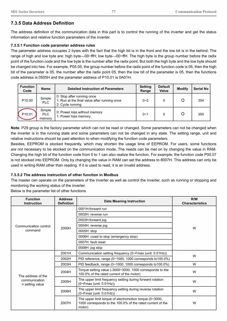
77SD1 Series Inverters Communication Protocol
The address definition of the communication data in this part is to control the running of the inverter and get the status information and relative function parameters of the inverter.
7.3.5 Data Address Definition
7.3.5.1 Function code parameter address rulesThe parameter address occupies 2 bytes with the fact that the high bit is in the front and the low bit is in the behind. The range of high and low byte are: high byte—00~ffH; low byte—00~ffH. The high byte is the group number before the radix point of the function code and the low byte is the number after the radix point. But both the high byte and the low byte should be changed into hex. For example, P05.05, the group number before the radix point of the function code is 05, then the high bit of the parameter is 05, the number after the radix point 05, then the low bit of the parameter is 05, then the functions code address is 0505H and the parameter address of P10.01 is 0A01H.
Function Code Name Detailed Instruction of Parameters Setting
RangeDefault Value Modify Serial No
P10.00 Simple PLC
0: Stop after running once1: Run at the final value after running once2: Cycle running
0~2 0 354
P10.01Simple PLC
memory
0: Power loss without memory1: Power loss memory 0~1 0 355
Note: P29 group is the factory parameter which can not be read or changed. Some parameters can not be changed when the inverter is in the running state and some parameters can not be changed in any state. The setting range, unit and relative instructions should be paid attention to when modifying the function code parameters. Besides, EEPROM is stocked frequently, which may shorten the usage time of EEPROM. For users, some functions are not necessary to be stocked on the communication mode. The needs can be met on by changing the value in RAM. Changing the high bit of the function code from 0 to 1 can also realize the function. For example, the function code P00.07 is not stocked into EEPROM. Only by changing the value in RAM can set the address to 8007H. This address can only be used in writing RAM other than reading. If it is used to read, it is an invalid address.
7.3.5.2 The address instruction of other function in Modbus The master can operate on the parameters of the inverter as well as control the inverter, such as running or stopping and monitoring the working status of the inverter. Below is the parameter list of other functions
Function Instruction
Address Definition Data Meaning Instruction R/W
Characteristics
Communication control command 2000H
0001H:forward run
W
0002H: reverse run0003H:forward jog 0004H: reverse jog 0005H: stop 0006H: coast to stop (emergency stop)0007H: fault reset0008H: jog stop
The address of the communication n setting value
2001H Communication setting frequency (0~Fmax (unit: 0.01Hz)) W
2002H PID reference, range (0~1000, 1000 corresponds to100.0%)2003H PID feedback, range (0~1000, 1000 corresponds to100.0%) W
2004H Torque setting value (-3000~3000, 1000 corresponds to the 100.0% of the rated current of the motor) W
2005H The upper limit frequency setting during forward rotation (0~Fmax (unit: 0.01Hz)) W
2006H The upper limit frequency setting during reverse rotation (0~Fmax (unit: 0.01Hz)) W
2007HThe upper limit torque of electromotion torque (0~3000, 1000 corresponds to the 100.0% of the rated current of the motor)
W

78SD1 Series Inverters Communication Protocol
Function Instruction
Address Definition Data Meaning Instruction R/W
Characteristicscont 2008H The upper limit torque of braking torque (0~3000, 1000
corresponds to the 100.0% of the rated current of the motor)
W2009H
Special control command word Bit0~1: =00: motor 1 =01: motor 2 =10: motor 3 =11: motor 4Bit2: =1 torque control prohibit =0: torque control prohibit invalid Bit3: =1 power consumption clear =0: no power consumption clearBit4: =1 pre-exciting =0: pre-exciting prohibition Bit5: =1 DC braking =0: DC braking prohibition
200AH Virtual input terminal command, range: 0x000~0x1FF W200BH Virtual input terminal command, range: 0x00~0x0F W
200CHVoltage setting value (special for V/F separation)(0~1000, 1000 corresponds to the 100.0% of the rated voltage of the motor)
W
200DH AO output setting 1(-1000~1000, 1000 corresponds to 100.0%) W
200EH AO output setting 2(-1000~1000, 1000 corresponds to 100.0%) W
SW 1 of the inverter 2100H
0001H:forward running
R0002H:forward running0003H: stop 0004H: fault 0005H: POFF status
0006H: pre-exciting status
SW 1 of the inverter 2101H
Bit0: =0: bus voltage is not established =1: bus voltage is established Bi1~2: =00: motor 1 =01: motor 2 =10: motor 3 =11: motor 4Bit3: =0: asynchronous motor =1: synchronous motor Bit4: =0: pre-alarm without overload =1: overload pre-alarmBit5~ Bit6: =00: keypad control =01: terminal control=10: communication control
R
Fault code of the inverter 2102H See the fault type instruction RIdentifying code of the
inverter 2103H SD1-----0x0106 R
Operation frequency 3000H Range: 0.00Hz~P00.03 RSetting frequency 3001H Range: 0.00Hz~P00.03 R
Bus voltage 3002H Range: 0~2000V ROutput voltage 3003H Range: 0~1200V ROutput current 3004H Range: 0.0~3000.0A R
Operation speed 3005H Range: 0~65535RPM ROutput power 3006H Range: -300.0~300.0% ROutput torque 3007H Range: -250.0~250.0% R
Close loop setting 3008H Range: -100.0%~100.0% RClose loop feedback 3009H Range: -100.0%~100.0% R
PID setting 3008H -100.0~100.0% (unit: 0.1%) RPID feedback 3009H -100.0~100.0% (unit: 0.1%) R
Input IO 300AH 000~1FFInput IO 300BH 000~1FF
AI 1 300CH Range: 0.00~10.00V RAI 2 300DH Range: 0.00~10.00V RAI 3 300EH Range: 0.00~10.00V R

79SD1 Series Inverters Communication Protocol
Function Instruction
Address Definition Data Meaning Instruction R/W
CharacteristicsAI 4 300FH Range: -10.00~10.00V R
Read high speed pulse 1 input 3010H Range: 0.00~50.00kHz R
Read high speed pulse 2 input 3011H Reserved R
Read current step of the multi-step speed 3012H Range: 0~15 R
External length 3013H Range: 0~65535 RExternal counting value 3014H Range: 0~65535 R
Torque setting 3015H -300.0~300.0%(Unit: 0.1%) RInverter code 3016H R
Fault code 5000H R
R/W characteristics means the function is with read and write characteristics. For example, “communication control com-mand” is writing characteristic and control the inverter with writing command (06H). R characteristic can only read other than write and W characteristic can only write other than read. Note: when operating on the inverter with the table above, it is necessary to enable some parameters. For example, the operation of running and stopping, it is necessary to set P00.01 to communication running command channel and set P00.02 to MODBUS communication channel. And when operate on “PID given”, it is necessary to set P09.00 to “MODBUS communication setting”.The encoding rules for device codes (corresponds to identifying code 2103H of the inverter)
Code High 8 Bit Meaning Code Low 8 Position Meaning01 SD1 Series Vector Inverter 06 SD1 Series Vector Inverter
Note: the code is consisted of 16 bit which is high 8 bits and low 8 bits. High 8 bits mean the motor type series and low 8 bits mean the derived motor types of the series. For example, 0110H means SD1 Series vector inverters.
The communication data is expressed by hex in actual application and there is no radix point in hex. For example, 50.12Hz can not be expressed by hex so 50.12 can be magnified by 100 times into 5012, so hex 1394H can be used to express 50.12.A non-integer can be timed by a multiple to get an integer and the integer can be called fieldbus ratio values. The fieldbus ratio values are referred to the radix point of the setting range or default value in the function parameter list. If there are figures behind the radix point (n=1), then the fieldbus ratio value m is 10n. Take the table as the example:
7.3.6 Fieldbus Ratio Values
Function Code Name Detailed Instruction of Parameters Setting
RangeDefault Value Modify Serial
No
P01.20Hibernation
restore delay time
0.0~3600.0s (valid when P01.19=2) 0.0~3600.0 0.0s 39
P01.21 Restart after power off
0: Disable1: Enable 0~1 0 40
If there is one figure behind the radix point in the setting range or the default value, then the fieldbus ratio value is 10. if the data received by the upper monitor is 50, then the “hibernation restore delay time” is 5.0 (5.0=50÷10).If Modbus communication is used to control the hibernation restore delay time as 5.0s. Firstly, 5.0 can be magnified by 10 times to integer 50 (32H) and then this data can be sent.
01 06 01 14 00 32 49 E7inverteraddress
read command
parametersaddress
datanumber CRC check

80SD1 Series Inverters Communication Protocol
After the inverter receives the command, it will change 50 into 5 according to the fieldbus ratio value and then set the hibernation restore delay time as 5s.Another example, after the upper monitor sends the command of reading the parameter of hibernation restore delay time, if the response message of the inverter is as following:
01 03 02 00 32 39 91inverteraddress
read command
2 bytesdata
parameterdata CRC check
Because the parameter data is 0032H (50) and 50 divided by 10 is 5, then the hibernation restore delay time is 5s.
There may be fault in the communication control. For example, some parameter can only be read. If a writing message is sent, the inverter will return a fault response message. The fault message is from the inverter to the master, its code and meaning is as below:
7.3.7 Fault Message Response
Code Name Meaning
01H Illegal commandThe command from master can not be executed. The reason maybe:1. This command is only for new version and this version can not realize.2. Slave is in fault status and can not execute it.
02H Illegal data address Some of the operation addresses are invalid or not allowed to access. Especially the combination of the register and the transmitting bytes are invalid.
03H Illegal valueWhen there are invalid data in the message framed received by slave.Note: This error code does not indicate the data value to write exceed the range, but indicate the message frame is an illegal frame.
04H Operation failed The parameter setting in parameter writing is invalid. For example, the function input terminal can not be set repeatedly.
05H Password error The password written to the password check address is not same as the password set by P7.00.
06H Data frame error In the frame message sent by the upper monitor, the length of the digital frame is incorrect or the counting of CRC check bit in RTU is different from the lower monitor.
07H Written not allowed.
It only happens in write command, the reason maybe:1. The written data exceeds the parameter range.2. The parameter should not be modified now.3. The terminal has already been used.
08H The parameter can not be modified during running
The modified parameter in the writing of the upper monitor can not be modified during running.
09H Password protection When the upper monitor is writing, or reading and the user password is set without password unlocking, it will report that the system is locked.
The slave uses functional code fields and fault addresses to indicate it is a normal response or some error occurs (named as objection response). For normal responses, the slave shows corresponding function codes, digital address or sub- function codes as the response. For objection responses, the slave returns a code which equals the normal code, but the first byte is logic 1.For example: when the master sends a message to the slave, requiring it to read a group of address data of the inverter function codes, there will be following function codes: 0 0 0 0 0 0 1 1 (Hex 03H) For normal responses, the slave responds the same codes, while for objection responses, it will return: 1 0 0 0 0 0 1 1 (Hex 83H) Besides the function codes modification for the objection fault, the slave will respond a byte of abnormal code which defines the error reason. When the master receives the response for the objection, in a typical processing, it will send the message again or modify the corresponding order. For example, set the “running command channel” of the inverter (P00.01, parameter address is 0001H) with the address of 01H to 03, the command is as following:
01 06 00 01 00 03 98 0Binverteraddress
read command
parameteraddress
parameterdata CRC check

81SD1 Series Inverters Communication Protocol
But the setting range of “running command channel” is 0~2, if it is set to 3, because the number is beyond the range, the inverter will return fault response message as below:
01 86 04 43 A3inverteraddress
abnormal response code
faultcode CRC check
Abnormal response code 86H means the abnormal response to writing command 06H; the fault code is 04H. In the table above, its name is operation failed and its meaning is that the parameter setting in parameter writing is invalid. For example, the function input terminal can not be set repeatedly.
Refer to section 7.4.1 and 7.4.2 for the command format.
7.3.8 Example of Writing and Reading
7.3.8.1 Example of reading command 03H Read the status word 1 of the inverter with the address of 01H (refer to table 1). From the table 1, the parameter address of the status word 1 of the inverter is 2100H.The command sent to the inverter:
01 03 21 00 00 01 8E 36inverteraddress
read parameter
parameteraddress
datanumber CRC check
If the response message is as below:
01 03 02 00 03 F8 45inverteraddress
read command
datanumber
datacontent CRC check
The data content is 0003H. From the table 1, the inverter stops. Watch “the current fault type” to “the previous 5 times fault type” of the inverter through commands, the corresponding function code is P07.27~P07.32 and corresponding parameter address is 071BH~0720H(there are 6 from 071BH).The command sent to the inverter:
03 03 07 1B 00 06 B5 59inverteraddress
read command
startaddress
total 6parameters CRC check
If the response message is as below:
03 03 0C 00 23 00 23 00 23 00 23 00 23 00 23 5F D2inverteraddress
read command
previous 2 fault type
previous 3 fault type
CRC check
bytenumber
current fault type
previous fault type
previous 4 fault type
previous 5 fault type
See from the returned data, all fault types are 0023H (decimal 35) with the meaning of maladjustment (STo).
7.3.8.2 Example of writing command 06H Make the inverter with the address of 03H to run forward. See table 1, the address of “communication control command” is 2000H and forward running is 0001. See the following table:

82SD1 Series Inverters Communication Protocol
03 06 20 00 00 01 42 28inverteraddress
write command
parameteraddress
forwardrunning CRC check
Function Instruction
Address Definition Data Meaning Instruction R/W
Characteristics
Communication control command 2000H
0001H: forward run
W
0002H: reverse run0003H: forward jog0004H: reverse jog0005H: stop0006H: coast to stop (emergency stop)0007H: fault reset0008H: jog stop0009H: pre-exciting
The command sent by the master:
If the operation is successful, the response may be as below (the same with the command sent by the master):
03 06 20 00 00 01 42 28inverteraddress
write command
parameteraddress
forwardrunning CRC check
Set the Max. Output frequency of the inverter with the address of 03H as100Hz.
Function Code Name Detailed Instruction of Parameters Setting Range Default
Value Modify Serial No
P00.03 Max. output frequency P00.04~600.00Hz (400.00Hz) 10.00~600.00 50.00Hz 3
See the figures behind the radix point, the fieldbus ratio value of the Max. output frequency (P00.03) is 100. 100Hz timed by 100 is 10000 and the corresponding hex is 2710H.The command sent by the master:
03 06 00 03 27 10 62 14inverteraddress
write command
parameteraddress
forwardrunning CRC check
If the operation is successful, the response may be as below (the same with the command sent by the master):
03 06 00 03 27 10 62 14inverteraddress
write command
parameteraddress
forwardrunning CRC check
Note: the blank in the above command is for illustration. The blank can not be added in the actual application unless the upper monitor can remove the blank by themselves.
7.3.8.3 Example of continous writing command10H Example 1: make the inverter whose address is 01H run forward at 10Hz. Refer to the instruction of 2000H and 0001. Set the address of “communication setting frequency” is 2001H and 10Hz corresponds to 03E8H. See the following table.

83SD1 Series Inverters Communication Protocol
Set P00.01 to 2 and P00.06 to 8.The command sent to the inverter:
01 10 20 00 00 02 04 00 01 03 E8 3B 10inverteraddress
continuous writing
command
parameter address
datanumber CRC check
Example 2: set the ACC time of 01H inverter as 10s and the DEC time as 20s
01 10 20 00 00 02 4A 08inverteraddress
continuous writing
command
parameteraddress
datanumber CRC check
If the response message is as below:
Function Instruction
Address Definition Data Meaning Instruction R/W
Characteristics
Communication control command 2000H
0001H: forward run
W/R
0002H: reverse run0003H: forward jog0004H: reverse jog0005H: stop0006H: coast to stop (emergency stop)0007H: fault reset0008H: jog stop
Address of the communication setting
2001H Communication setting frequency (0~Fmax unit: 0.01Hz)W/R
2002H PID given, range (0~1000, 1000 corresponds to100.0%)
bytenumber
forwardrunning
10Hz
Function Code Name Detailed Instruction of Parameters Default
Value Modify
P00.11 ACC time 1 ACC time means the time taken to accelerate from 0Hz to the Max. One (P00.03).DEC time means the time taken to decelerate from Max. Output frequency to 0Hz (P00.03).Goodrive300 series inverters define four groups of ACC/DEC time which can be selected by P05. The factory default ACC/DEC time of the inverter is the first group.Setting range of P00.11 and P00.12:0.0~3600.0s
Depends on model
P00.12 DEC time 1 Depends on model
The corresponding address of P00.11 is 000B, the ACC time of 10s corresponds to 0064H, and the DEC time of 20s corresponds to 00C8H.The command sent to the inverter:
01 10 00 0B 00 02 04 00 64 00 C8 F2 55inverteraddress
continuous writing
command
parameter address
datanumber CRC check
bytenumber
10s 20s
01 10 00 0B 00 02 30 0Ainverteraddress
continuous writing
command
parameteraddress
datanumber CRC check
If the response message is as below:
Note: The space between above commands is for instruction and there is no space between the commands during actual applications.

84SD1 Series Inverters Appendix A
Common communication fault Common communication faults: no response to the communication or the inverter returns abnormal fault.The possible reason for no response to the communication:Selecting wrong serial interface, for example, if the converter is COM1, selecting COM2 during the communicationThe baud rate, digital bit, end bit and check bit are not the same with the inverter + and - of RS485 are connected in reverse. The 485-wire cap on the terminal board of the inverter is not plug in. the wire cap in behind the terminal arrangement.
Appendix A Technical DataA.1 Ratings
Inverter sizing is based on the rated motor current and power. To achieve the rated motor power given in the table, the rated current of the inverter must be higher than or equal to the rated motor current. Also the rated power of the inverter must be higher than or equal to the rated motor power. The power ratings are the same regardless of the supply voltage within one voltage range.Note:1. The maximum allowed motor shaft power is limited to 1.5*PN. If the limit is exceeded, motor torque and current are automatically restricted. The function protects the input bridge of the drive against overload.2. The ratings apply at ambient temperature of 40°C.3. It is important to check that in common DC systems the power flowing through the common DC connection does not exceed PN.A.1.2 DeratingThe load capacity decreases if the installation site ambient temperature exceeds 40°C, the altitude exceeds 1000 meters or the switching frequency is changed from 4 kHz to 8, 12 or 15 kHz.A.1.2.1 Temperature deratingIn the temperature range +40°C…+50°C, the rated output current is decreased by 1% for every additional 1°C. Refer to the below list for the actual derating.
A.1.1 Capacity
A.1.2.2 Altitude deratingThe device can output rated power if the installation site below 1000m. The output power decreases if the altitude exceeds 1000 meters. Below is the detailed decreasing range of the derating:
A.2 Power Supply
• Check the voltage rating of the inverter complies with the supply power voltage.

85SD1 Series Inverters Appendix A
Select the input power and motor cables according to local regulations.Note: A separate PE conductor is required if the conductivity of the shielded cable is not sufficient.
A.3.1 Power cables
A.3 Cables
All analogue control cables and the cable used for the frequency input must be shielded. Relay cables need to be braided metallic screen.Note: Run analogue and digital signals separately.
A.3.2 Control cables
Check the insulation of the input power cable according to local regulations before connecting to the drive.
Model
Recommended Cable Size (mm2)
ConnectingCable Size (mm2) Terminal
Screw
TighteningTorque(Nm)RST
PERST
P1 (+) PEUVW UVW
SD1-2.5A-21 1.5 1.5 1~4 1~4 1~4 M3 0.8SD1-4.2A-21 1.5 1.5 1~4 1~4 1~4 M3 0.8SD1-7.5A-21 2.5 2.5 1~4 1~4 1~4 M3 0.8SD1-10A-21 2.5 2.5 1~4 1~4 1~4 M3 0.8SD1-2.5A-23 1.5 1.5 1-1.5 1-1.5 1-1.5 M3 0.8SD1-4.2A-23 1.5 1.5 1-1.5 1-1.5 1-1.5 M3 0.8SD1-7.5A-23 2.5 2.5 1.5~6 2.5~6 2.5~6 M4 1.13SD1-10A-23 2.5 2.5 1.5~6 2.5~6 2.5~6 M4 1.13SD1-16A-23 2.5 2.5 1.5~6 2.5~6 2.5~6 M4 1.13SD1-20A-23 4 4 4~10 4~10 4~10 M5 2.3SD1-30A-23 6 6 4~10 4~10 4~10 M5 2.3SD1-2.5A-43 1.5 1.5 1-1.5 1-1.5 1-1.5 M3 0.8SD1-4.2A-43 1.5 1.5 1-1.5 1-1.5 1-1.5 M3 0.8SD1-5.5A-43 1.5 1.5 1-1.5 1-1.5 1-1.5 M3 0.8SD1-9.5A-43 2.5 2.5 2.5~6 2.5~6 2.5~6 M4 1.13SD1-14A-43 2.5 2.5 2.5~6 2.5~6 2.5~6 M4 1.13
SD1-18.5A-43 4 4 4~10 4~10 4~10 M5 2.3SD1-25A-43 6 6 4~10 4~10 4~10 M5 2.3SD1-32A-43 6 6 4~10 4~10 4~10 M5 2.3SD1-38A-43 10 10 10~16 10~16 10~16 M5 2.3SD1-45A-43 16 16 10~16 10~16 10~16 M5 2.3SD1-60A-43 25 16 25~50 25~50 16~25 M6 2.5SD1-75A-43 25 16 25~50 25~50 16~25 M6 2.5SD1-92A-43 35 16 35~70 35~70 16~35 M8 10SD1-115A-43 50 25 35~70 35~70 16~35 M8 10SD1-150A-43 70 35 35~70 35~70 16~35 M8 10SD1-180A-43 95 50 70~120 70~120 50~70 M12 35SD1-215A-43 120 70 70~120 70~120 50~70 M12 35
Note: 1. It is appropriate to use the recommended cable size under 40°C and rated current. The wiring distance should be no more than 100m.2. Terminals P1, (+), PB and (-) connects the DC reactor options and parts.

86
A.5 CE
The EMC Directive defines the requirements for immunity and emissions of electrical equipment used within the European Union. The EMC product standard (EN 61800-3:2004) covers requirements stated for drives. See section EMC regulations.
A.5.1 Compliance with the European EMC Directive
The CE mark is attached to the drive to verify that the drive follows the provisions of the European Low Voltage (2006/95/EC) and EMC Directives (2004/108/EC).
SD1 Series Inverters Appendix A
A.4 Breaker and Electromagnetic Contactor It is recommended that to protect the installation, a fuse of the appropriate rating is utilised.Select a breaker (MCCB) which matches the rated capacity of the inverter. The capacity of the inverter should be 1.5-2 times the rated current.
• Due to the inherent operating principle and construction of circuit breakers, hot ionized gases may escape from the breaker enclosure in case of a short-circuit. To ensure safe use, always follow the manufacturer’s instructions.
It is necessary to install the electromagnetic contactor in the input side to control the switching on and off safety of the main circuit. It can switch off the input power supply when system faults.
Model Fuse (A) Breaker (A) The rated working current of the contactor (A)
SD1-2.5A-21 10 10 9SD1-4.2A-21 16 16 12SD1-7.5A-21 25 25 25SD1-10A-21 50 40 32SD1-2.5A-23 6 6 9SD1-4.2A-23 10 10 9SD1-7.5A-23 16 16 12SD1-10A-23 25 25 18SD1-16A-23 35 32 25SD1-20A-23 35 32 32SD1-30A-23 50 63 50SD1-2.5A-43 6 6 9SD1-4.2A-43 10 10 9SD1-5.5A-43 10 10 9SD1-9.5A-43 25 25 25SD1-14A-43 35 32 25
SD1-18.5A-43 63 40 38SD1-25A-43 63 63 50SD1-32A-43 63 63 50SD1-38A-43 100 100 65SD1-45A-43 100 100 80SD1-60A-43 125 125 95SD1-75A-43 150 160 115SD1-92A-43 150 200 170SD1-115A-43 200 200 170SD1-150A-43 250 250 205SD1-180A-43 325 315 245SD1-215A-43 350 350 300

87SD1 Series Inverters Appendix A
EMC product standard (EN 61800-3:2004) specifies the EMC requirements. First environment: domestic environment (includes establishments connected to a low-voltage network which supplies buildings used for domestic purposes).Second environment includes establishments connected to a network not directly supplying domestic premises. Four categories of the inverter: Inverter of category C1: inverter of rated voltage less than 1000 V and used in the first environment.Inverter of category C2: inverter of rated voltage less than 1000 V other than pins, sockets and motion devices and intended to be installed and commissioned only by a professional electrician when used in the first environment.Note: IEC/EN 61800-3 in EMC standard doesn’t limit the power distribution of the inverter, but it defines the upstage, installation and commission. A competent person with necessary skills in installing and/or commissioning power drive systems, including their EMC aspects.Inverter of category C3: inverter of rated voltage less than 1000 V and used in the second environment other than the first oneInverter of category C4: inverter of rated voltage more than 1000 V or the nominal current is above or equal to 400A and used in the complicated system in second environment
The emission limits are complied with the following provisions:1. The optional EMC filter is selected according to the options and installed correctly.2. The motor and control cables are selected as specified in this manual.3. The drive is installed according to the instructions given in this manual.
A.6 EMC Regulations
• In a domestic environment, this product may cause radio inference, in which case supplementary mitigation measures may be required.
The immunity performance of the drive complies with the regulations of IEC/EN 61800-3, second environment.The emission limits are complied with the following provisions:1. The optional EMC filter is selected according to the options and installed correctly.2. The motor and control cables are selected as specified in this manual.3. The drive is installed according to the instructions given in this manual.
• A drive of category C3 is not intended to be used on a low-voltage public network which supplies domestic premises. Radio frequency interference is expected if the drive is used on such a network.
A.6.1 Category C2
A.6.2 Category C3

88SD1 Series Inverters Appendix B
Appendix B Dimension Drawings
B.1 External Keypad Structure
Note: The external keypad is optional for the inverters (≤2.2kW) and the standard keypad of inverters (≥4kW) can be used as the external keypad.The keypad can be mounted externally on optional mounting bracket (max cable length 40 meters).
Dimension drawings of the SD1 Series are shown below. The dimensions are given in millimeters and inches.

89SD1 Series Inverters Appendix B
B.2 Inverter Chart
Wall mounting of 0.75~2.2kW inverters
Model W1 W2 H1 H2 D1 D2 Installation Hole (d)
SD1-2.5A-21 80.0 60.0 160.0 150.0 123.5 120.3 5SD1-4.2A-21 80.0 60.0 160.0 150.0 123.5 120.3 5SD1-7.5A-21 80.0 60.0 185.0 175.0 140.5 137.3 5SD1-10A-21 80.0 60.0 185.0 175.0 140.5 137.3 5SD1-2.5A-23 80.0 60.0 185.0 175.0 140.5 137.3 5SD1-4.2A-23 80.0 60.0 185.0 175.0 140.5 137.3 5SD1-2.5A-43 80.0 60.0 185.0 175.0 140.5 137.3 5SD1-4.2A-43 80.0 60.0 185.0 175.0 140.5 137.3 5SD1-5.5A-43 80.0 60.0 185.0 175.0 140.5 137.3 5
Rail mounting of inverters of 1PH 200V/3PH 380V (≤2.2kW) and 3PH 200V (≤0.75kW)Dimension (unit: mm)

90SD1 Series Inverters Appendix B
Model W1 H1 H3 H4 D1 D2 Installation Hole (d)
SD1-2.5A-21 80.0 160.0 35.4 36.6 123.5 120.3 5SD1-4.2A-21 80.0 160.0 35.4 36.6 123.5 120.3 5SD1-7.5A-21 80.0 185.0 35.4 36.6 140.5 137.3 5SD1-10A-21 80.0 185.0 35.4 36.6 140.5 137.3 5SD1-2.5A-23 80.0 185.0 35.4 36.6 140.5 137.3 5SD1-4.2A-23 80.0 185.0 35.4 36.6 140.5 137.3 5SD1-2.5A-43 80.0 185.0 35.4 36.6 140.5 137.3 5SD1-4.2A-43 80.0 185.0 35.4 36.6 140.5 137.3 5SD1-5.5A-43 80.0 185.0 35.4 36.6 140.5 137.3 5
Wall mounting of 3PH 380V 4~37kW and 3PH 200V 1.5~7.5 kW inverters Wall mounting of 3PH 380V 45~75kW inverters
Wall mounting of 3PH 380V 90~110kW inverters Dimension (unit: mm)

91
Wall mounting of 3PH 380V 45~75kW inverters
SD1 Series Inverters Appendix B
Flange mounting of 3PH 380V 4~75kW and 3PH 200V 1.5~7.5kW inverters
Model W1 W2 W3 H1 H2 D1 D2 Installation Hole
SD1-7.5A-23 146.0 131.0 — 256.0 243.5 167.0 84.5 6SD1-10A-23 146.0 131.0 — 256.0 243.5 167.0 84.5 6SD1-16A-23 146.0 131.0 — 256.0 243.5 167.0 84.5 6SD1-20A-23 170.0 151.0 — 320.0 303.5 196.3 113.0 6SD1-30A-23 170.0 151.0 — 320.0 303.5 196.3 113.0 6SD1-9.5A-43 146.0 131.0 — 256.0 243.5 167.0 84.5 6SD1-14A-43 146.0 131.0 — 256.0 243.5 167.0 84.5 6
SD1-18.5A-43 170.0 151.0 — 320.0 303.5 196.3 113.0 6SD1-25A-43 170.0 151.0 — 320.0 303.5 196.3 113.0 6SD1-32A-43 170.0 151.0 — 320.0 303.5 196.3 113.0 6SD1-38A-43 200.0 185.0 — 340.6 328.6 184.3 104.5 6SD1-45A-43 200.0 185.0 — 340.6 328.6 184.3 104.5 6SD1-60A-43 250.0 230.0 — 400.0 380.0 202.0 123.5 6SD1-75A-43 250.0 230.0 — 400.0 380.0 202.0 123.5 6SD1-92A-43 282.0 160.0 226.0 560.0 542.0 238.0 138.0 9SD1-115A-43 282.0 160.0 226.0 560.0 542.0 238.0 138.0 9SD1-150A-43 282.0 160.0 226.0 560.0 542.0 238.0 138.0 9SD1-180A-43 338.0 200.0 — 554.0 535.0 329.2 — 9.5SD1-215A-43 338.0 200.0 — 554.0 535.0 329.2 — 9.5
Flange mounting of 3PH 380V 90~110kW inverters Dimension (unit: mm)

92SD1 Series Inverters Appendix B
Model W1 W2 W3 W4 H1 H2 H3 H4 D1 D2 Installation Hole Screw
SD1-7.5A-23 170.2 131 150 9.5 292 276 260 6 167 84.5 6 M5SD1-10A-23 170.2 131 150 9.5 292 276 260 6 167 84.5 6 M5SD1-16A-23 170.2 131 150 9.5 292 276 260 6 167 84.5 6 M5SD1-20A-23 191.2 151 174 11.5 370 351 324 12 196.3 113 6 M5SD1-30A-23 191.2 151 174 11.5 370 351 324 12 196.3 113 6 M5SD1-9.5A-43 170.2 131 150 9.5 292 276 260 6 167 84.5 6 M5SD1-14A-43 170.2 131 150 9.5 292 276 260 6 167 84.5 6 M5
SD1-18.5A-43 191.2 151 174 11.5 370 351 324 12 196.3 113 6 M5SD1-25A-43 191.2 151 174 11.5 370 351 324 12 196.3 113 6 M5SD1-32A-43 191.2 151 174 11.5 370 351 324 12 196.3 113 6 M5SD1-38A-43 266 250 224 13 371 250 350.6 20.3 184.6 104 6 M5SD1-45A-43 266 250 224 13 371 250 350.6 20.3 184.6 104 6 M5SD1-60A-43 316 300 274 13 430 300 410 55 202 118.3 6 M5SD1-75A-43 316 300 274 13 430 300 410 55 202 118.3 6 M5SD1-92A-43 352 332 306 13 580 400 570 80 238 133.8 9 M8SD1-115A-43 352 332 306 13 580 400 570 80 238 133.8 9 M8SD1-150A-43 352 332 306 13 580 400 570 80 238 133.8 9 M8SD1-180A-43 418.5 361 389.5 14.2 600 559 370 108.5 329.5 149.5 9.5 M8SD1-215A-43 418.5 361 389.5 14.2 600 559 370 108.5 329.5 149.5 9.5 M8
Note: The installation bracket is optional

93SD1 Series Inverters Appendix C
Appendix C Options and Parts
C.1 Peripheral Component Wiring
This chapter describes how to select the options and parts of SD1 Series.
Below is the peripheral component wiring of SD1 Series inverters.
Pictures Name Descriptions Reference
External keypadWhen the external keypad is valid, local keypad is off; when local keypad is valid, both local and external keypads are on.
SD1-KP
External Keypad with Copy Function
When the external keypad with copy function is valid, local keypad is off; when local keypad is valid, both local and external keypads are on.
SD1-KP-CPY

94SD1 Series Inverters Appendix C
Pictures Name Descriptions Reference
CablesTo supply motor and control, cables should be correctly specified and installed as per recommendation.
See Appendix A.3
Breaker
Prevent from electric shock and protect the power supply and the cables system from overcurrent when short circuits occur. (Please select the breaker with the function of reducing high order harmonic and the rated sensitive current to 1 inverter should be above 30mA).
See Appendix A.4
Input reactorThis device is used to improve the power factor of the input side of the inverter and control the higher harmonic current.
See Appendix C.2
Input filter
Control the electromagnetic interference generated from the inverter, please install close to the input terminal side of the inverter.
See Appendix C.3
Braking resistors
Shorten the DEC time.Only braking resistors are needed for mod-els less than 45Kw, larger models require brake chopper.
See Appendix C.4
Output filterReduces the RFI noise from the output side of the inverter. Install close to the output terminals of the inverter.
Please call IMO
Output reactor
Extends the effective transmitting distance of the inverter to control the high voltage transients when switching on/off the IGBT of the inverter.
See Appendix C.2
Note: The derate voltage of the input reactor is 2%±15%. The derate voltage of the output reactor is 1%±15%. Above options are external.
C.2 Reactors
Transient high currents to the input power circuit may cause damage to the rectifying components. It is recommended to use AC reactor in the input side for the avoidance of high-voltage transients of the power supply and improvement of power factor.
If the distance between the inverter and the motor is longer than 50m, frequent overcurrent protection trips may occur due to inverter because of high leakage current caused by parasitic capacitance effects from the long cables to the ground. To avoid damage of the motor insulation, it may be necessary to add reactor compensation. If the distance between the inverter and motor is 50~100m, see the table below for model selection; if it exceeds 100m, consult with IMO technical support.
C.2.1 Input Reactor
C.2.2 Output Reactor

95SD1 Series Inverters Appendix C
C.3 FilterC.3.1 C3 Filter Type InstructionThe following is an example of the filter type instruction for SD1-RC3-10
Character Designation Detaield InstructionSD1 Inverter series
RFC3 Filter category10A Rated curent
C.3.2 C3 FilterExternal C3 filers are optional for SD1 Series inverters of 1PH 200V/3PH 380V (≤2.2kW) and 3PH 200V (≤0.75kW). The inverters of 3PH 380V (≥4kW) and 3PH 200V (≥1.5kW) have the embedded C3 filers which can be selected to connect by J10 (J10 is packed with the manual).The input RFI filter can decrease RFI noise of the inverter to the surrounding equipments. Output RFI filter can decrease the radio noise cause by the cables between the inverter and the motor and leakage current of the conducting wires.Our company configured some filters for the convenient of the users.
Model Input FilterSD1-2.5A-21
SD1-RFC3-10
SD1-4.2A-21SD1-7.5A-21SD1-10A-21SD1-2.5A-23SD1-4.2A-23SD1-2.5A-43
SD1-RFC3-7SD1-4.2A-43SD1-5.5A-43
Note: 1. The input RFI meet the requirement of C3 after adding input filters.2. Above options are external; the customer should indicate when purchasing.
C.3.3 Installation Instruction for C3 Filter
The installation procedures for C3 filter are as below:1. Connect the filter cable to the corresponding input terminal of the inverter according to the label;2. Fix the filter onto the inverter with M3*10 screws (as shown in above picture).

96SD1 Series Inverters Appendix C
C.4 Braking Components C.4.1 Select the braking componentsIt is recommended to use braking resistor or braking chopper when the motor is required to stop rapidly or the motor is driven by a high inertia load. The motor will become a generator if its rotating speed is higher than the corresponding speed of the reference frequency, thus, the inertial energy of the motor and load return to the inverter and charge the capacitors in the main DC circuit. When the voltage increases above the limit, damage may occur to the inverter. It is necessary to apply braking chopper/resistor to prevent over voltage trips.
C.3.4 C2 Filter Type Instruction The following is an example of the filter type instruction for SD1-RFC2-10
Character Designation Detaield InstructionSD1 Inverter series
RFC2 Filter category (C2)10A Rated curent
C.3.5 C2 Filter
Model Input FilterSD1-2.5A-21
SD1-RFC2-10SD1-4.2A-21SD1-7.5A-21SD1-10A-21SD1-2.5A-23
SD1-RFC2-7SD1-4.2A-23SD1-7.5A-23
SD1-RFC2-16SD1-10A-23SD1-16A-23
SD1-RFC2-32SD1-20A-23SD1-30A-23 SD1-RFC2-45SD1-2.5A-43
SD1-RFC2-7SD1-4.2A-43SD1-5.5A-43SD1-9.5A-43
SD1-RFC2-16SD1-14A-43
SD1-18.5A-43SD1-RFC2-32
SD1-25A-43SD1-32A-43
SD1-RFC2-45SD1-38A-43SD1-45A-43
SD1-RFC2-65SD1-60A-43SD1-75A-43
SD1-RFC2-100SD1-92A-43SD1-115A-43
SD1-RFC2-150SD1-150A-43SD1-180A-43
SD1-RFC2-240SD1-215A-43
The optional C2 filter can be mounted externally to provide the C2 RFI emmission requirements.
• When installing C2 filter, EMC/J10 jumper must be removed.

97SD1 Series Inverters Appendix C
• Only competent personnel are authorised to design, install, commission and operate on the inverter. • Follow the instructions in “warning” during working. Physical injury, death or serious damage may occur. • Only competent personnel are authorised to install. Damage to the inverter or braking options and parts may
occur. Read the instructions carefully before connecting braking resistors or brake choppers to inverter.• Do not connect the braking resistor with other terminals except for PB and (-). Do not connect the braking
unit with other terminals except for (+) and (-). Damage to inverter, braking circuit or fire may occur.
• Connect the braking resistor or braking unit with the inverter according to the diagram. Incorrect wiring may cause damage to the inverter or other devices.
SD1 Series inverters have internal braking units.
Model Type of braking unit
Braking resistor at 100% of the
braking torque (Ω)
The absorbed power of the braking resistor Min.braking
resistor (Ω)10% braking 50% braking 80% braking
SD1-2.5A-21
Internal brakingunit
361 0.06 0.30 0.48 42SD1-4.2A-21 192 0.11 0.56 0.90 42SD1-7.5A-21 96 0.23 1.10 1.80 30SD1-10A-21 65 0.33 1.70 2.64 21SD1-2.5A-23 653 0.11 0.56 0.9 100SD1-4.2A-23 326 0.23 1.13 1.8 100SD1-7.5A-23 122 0.6 3 4.8 80SD1-10A-23 122 0.6 3 4.8 80SD1-16A-23 89.1 0.75 4.13 6.6 60SD1-20A-23 65.3 1.13 5.63 9 47SD1-30A-23 32 2.25 11.3 18 23SD1-2.5A-43 653 0.11 0.56 0.90 100SD1-4.2A-43 326 0.23 1.13 1.80 100SD1-5.5A-43 222 0.33 1.65 2.64 54SD1-9.5A-43 122 0.6 3 4.8 80SD1-14A-43 89.1 0.75 4.13 6.6 60
SD1-18.5A-43 65.3 1.13 5.63 9 47SD1-25A-43 44.5 1.65 8.25 13.2 31SD1-32A-43 32.0 2.25 11.3 18 23SD1-38A-43 27 3 14 22 19SD1-45A-43 22 3 17 26 17SD1-60A-43 17 5 23 36 17SD1-75A-43 13 6 28 44 11.7SD1-92A-43 10 7 34 54 6.4SD1-115A-43 8 8 41 66 6.4SD1-150A-43 6.5 11 56 90 6.4SD1-180A-43 5.4 14 68 108 4.4SD1-215A-43 4.5 17 83 132 4.4
Note: Select the resistor and power of the braking chopper according to the data in the table.The braking resistor may increase the braking torque of the inverter. The resistor power in the above table is designed on 100% braking torque and 10% braking duty. Higher wattage resistors can be used for higher braking duty. Calculate resistor rating according to braking requirement.
• Ensure minimum resistance as per table above.
• For frequent braking i.e. more than 10%, increase power accordingly.

98
Address any inquiries about the product to your supplier, quoting the model and serial number of the unit.
SD1 Series Inverters Appendix D
C.4.2 Placing the brake resistorUse shielded cables for braking resistor cables.Braking resistors become hot, ensure they are located in open area for cooling.
Only external braking resistor is needed in SD1 Series.
• The materials near the brake resistor must be non-flammable. The surface temperature of the resistor is high. Air flowing from the resistor is of hundreds of degrees Celsius. Protect the resistor against contact.
Appendix D Further InformationD.1 Product and Service Inquiries
D.2 Document LibraryManuals and other product documents in PDF format on the Internet. Go to www.imopc.com
Torque Vector Inverter
SD1 Series
Instruction Manual
1st Edition, Feb 2017
© IMO Precision Controls Ltd
The purpose of this instruction manual is to provide accurate information in handling, setting up and operating of the SD1 series of inverters. Please feel free to send your comments regarding any errors or omissions you may have found, or any suggestions you may have for generally improving the manual.In no event will IMO Precision Controls Ltd. be liable for any direct or indirect damages resulting from the application of the information in this manual.

IMO Precision Controls Ltd.1000 North Circular Road, London NW2 7JP, United KingdomPhone: +44 (0) 20 8452 6444 Fax: +44 (0)20 8450 2274Web: www.imopc.com
Ref: MAN-SD1-0217v1