IEEE-ISIEA-4L-Shiny
6
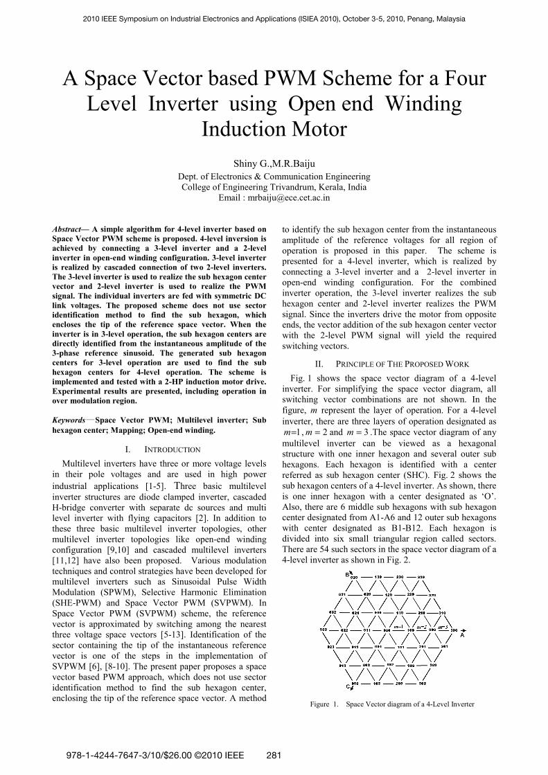
A Space Vector based PWM Scheme for a Four Level Inverter using Open end Winding Induction Motor Shiny G.,M.R.Baiju Dept. of Electronics & Communication Engineering College of Engineering Trivandrum, Kerala, India Email : [email protected] Abstract— A simple algorithm for 4-level inverter based on Space Vector PWM scheme is proposed. 4-level inversion is achieved by connecting a 3-level inverter and a 2-level inverter in open-end winding configuration. 3-level inverter is realized by cascaded connection of two 2-level inverters. The 3-level inverter is used to realize the sub hexagon center vector and 2-level inverter is used to realize the PWM signal. The individual inverters are fed with symmetric DC link voltages. The proposed scheme does not use sector identification method to find the sub hexagon, which encloses the tip of the reference space vector. When the inverter is in 3-level operation, the sub hexagon centers are directly identified from the instantaneous amplitude of the 3-phase reference sinusoid. The generated sub hexagon centers for 3-level operation are used to find the sub hexagon centers for 4-level operation. The scheme is implemented and tested with a 2-HP induction motor drive. Experimental results are presented, including operation in over modulation region. Keywords —Space Vector PWM; Multilevel inverter; Sub hexagon center; Mapping; Open-end winding. I. INTRODUCTION Multilevel inverters have three or more voltage levels in their pole voltages and are used in high power industrial applications [1-5]. Three basic multilevel inverter structures are diode clamped inverter, cascaded H-bridge converter with separate dc sources and multi level inverter with flying capacitors [2]. In addition to these three basic multilevel inverter topologies, other multilevel inverter topologies like open-end winding configuration [9,10] and cascaded multilevel inverters [11,12] have also been proposed. Various modulation techniques and control strategies have been developed for multilevel inverters such as Sinusoidal Pulse Width Modulation (SPWM), Selective Harmonic Elimination (SHE-PWM) and Space Vector PWM (SVPWM). In Space Vector PWM (SVPWM) scheme, the reference vector is approximated by switching among the nearest three voltage space vectors [5-13]. Identification of the sector containing the tip of the instantaneous reference vector is one of the steps in the implementation of SVPWM [6], [8-10]. The present paper proposes a space vector based PWM approach, which does not use sector identification method to find the sub hexagon center, enclosing the tip of the reference space vector. A method to identify the sub hexagon center from the instantaneous amplitude of the reference voltages for all region of operation is proposed in this paper. The scheme is presented for a 4-level inverter, which is realized by connecting a 3-level inverter and a 2-level inverter in open-end winding configuration. For the combined inverter operation, the 3-level inverter realizes the sub hexagon center and 2-level inverter realizes the PWM signal. Since the inverters drive the motor from opposite ends, the vector addition of the sub hexagon center vector with the 2-level PWM signal will yield the required switching vectors. II. PRINCIPLE OF THE PROPOSED WORK Fig. 1 shows the space vector diagram of a 4-level inverter. For simplifying the space vector diagram, all switching vector combinations are not shown. In the figure, m represent the layer of operation. For a 4-level inverter, there are three layers of operation designated as 1 m= , 2 m = and 3 m = .The space vector diagram of any multilevel inverter can be viewed as a hexagonal structure with one inner hexagon and several outer sub hexagons. Each hexagon is identified with a center referred as sub hexagon center (SHC). Fig. 2 shows the sub hexagon centers of a 4-level inverter. As shown, there is one inner hexagon with a center designated as ‘O’. Also, there are 6 middle sub hexagons with sub hexagon center designated from A1-A6 and 12 outer sub hexagons with center designated as B1-B12. Each hexagon is divided into six small triangular region called sectors. There are 54 such sectors in the space vector diagram of a 4-level inverter as shown in Fig. 2. Figure 1. Space Vector diagram of a 4-Level Inverter 2010 IEEE Symposium on Industrial Electronics and Applications (ISIEA 2010), October 3-5, 2010, Penang, Malaysia 978-1-4244-7647-3/10/$26.00 ©2010 IEEE 281
-
Upload
sep11-insiteadd-ons-courtyarddesign -
Category
Documents
-
view
1 -
download
0
Transcript of IEEE-ISIEA-4L-Shiny
A Space Vector based PWM Scheme for a Four Level Inverter using Open end Winding
Induction Motor Shiny G.,M.R.Baiju
Dept. of Electronics & Communication Engineering College of Engineering Trivandrum, Kerala, India
Email : [email protected]
Abstract— A simple algorithm for 4-level inverter based on Space Vector PWM scheme is proposed. 4-level inversion is achieved by connecting a 3-level inverter and a 2-level inverter in open-end winding configuration. 3-level inverter is realized by cascaded connection of two 2-level inverters. The 3-level inverter is used to realize the sub hexagon center vector and 2-level inverter is used to realize the PWM signal. The individual inverters are fed with symmetric DC link voltages. The proposed scheme does not use sector identification method to find the sub hexagon, which encloses the tip of the reference space vector. When the inverter is in 3-level operation, the sub hexagon centers are directly identified from the instantaneous amplitude of the 3-phase reference sinusoid. The generated sub hexagon centers for 3-level operation are used to find the sub hexagon centers for 4-level operation. The scheme is implemented and tested with a 2-HP induction motor drive. Experimental results are presented, including operation in over modulation region.
Keywords—Space Vector PWM; Multilevel inverter; Sub hexagon center; Mapping; Open-end winding.
I. INTRODUCTION Multilevel inverters have three or more voltage levels
in their pole voltages and are used in high power industrial applications [1-5]. Three basic multilevel inverter structures are diode clamped inverter, cascaded H-bridge converter with separate dc sources and multi level inverter with flying capacitors [2]. In addition to these three basic multilevel inverter topologies, other multilevel inverter topologies like open-end winding configuration [9,10] and cascaded multilevel inverters [11,12] have also been proposed. Various modulation techniques and control strategies have been developed for multilevel inverters such as Sinusoidal Pulse Width Modulation (SPWM), Selective Harmonic Elimination (SHE-PWM) and Space Vector PWM (SVPWM). In Space Vector PWM (SVPWM) scheme, the reference vector is approximated by switching among the nearest three voltage space vectors [5-13]. Identification of the sector containing the tip of the instantaneous reference vector is one of the steps in the implementation of SVPWM [6], [8-10]. The present paper proposes a space vector based PWM approach, which does not use sector identification method to find the sub hexagon center, enclosing the tip of the reference space vector. A method
to identify the sub hexagon center from the instantaneous amplitude of the reference voltages for all region of operation is proposed in this paper. The scheme is presented for a 4-level inverter, which is realized by connecting a 3-level inverter and a 2-level inverter in open-end winding configuration. For the combined inverter operation, the 3-level inverter realizes the sub hexagon center and 2-level inverter realizes the PWM signal. Since the inverters drive the motor from opposite ends, the vector addition of the sub hexagon center vector with the 2-level PWM signal will yield the required switching vectors.
II. PRINCIPLE OF THE PROPOSED WORK Fig. 1 shows the space vector diagram of a 4-level
inverter. For simplifying the space vector diagram, all switching vector combinations are not shown. In the figure, m represent the layer of operation. For a 4-level inverter, there are three layers of operation designated as
1m= , 2m = and 3m = .The space vector diagram of any multilevel inverter can be viewed as a hexagonal structure with one inner hexagon and several outer sub hexagons. Each hexagon is identified with a center referred as sub hexagon center (SHC). Fig. 2 shows the sub hexagon centers of a 4-level inverter. As shown, there is one inner hexagon with a center designated as ‘O’. Also, there are 6 middle sub hexagons with sub hexagon center designated from A1-A6 and 12 outer sub hexagons with center designated as B1-B12. Each hexagon is divided into six small triangular region called sectors. There are 54 such sectors in the space vector diagram of a 4-level inverter as shown in Fig. 2.
Figure 1. Space Vector diagram of a 4-Level Inverter
2010 IEEE Symposium on Industrial Electronics and Applications (ISIEA 2010), October 3-5, 2010, Penang, Malaysia
978-1-4244-7647-3/10/$26.00 ©2010 IEEE 281

(1)
The steps involved in the proposed Space Vector
PWM scheme are • Identification of Sub hexagon center
containing the tip of the reference space vector.
• Mapping to 2-level to determine the duration of switching vectors.
• Generation of actual switching vectors by adding the sub hexagon center vector with the mapped 2-level PWM signal.
In the proposed method, no sector identification
methods are used to determine the sector which encloses the tip of the reference space vector. Instead, the sub hexagon centers are directly determined from the instantaneous amplitude of the 3-phase reference sinusoid.
A. Identification of Sub hexagon Center(SHC) For explaining the principle of the proposed scheme,
consider a reference space vector OX shown in Fig. 3.
The tip of the reference vector OX can be in any one
of the 54 sectors. As can be seen from Fig. 3, the space vector diagram of 4-level inverter consists of 3 layers of operation. The layers are designated as 1m= , 2m = and
3m = . The layer of operation, m can be calculated using the equation [7]
As shown in Fig. 3, when 1m= , the inverter is operating as a 2-level inverter. In 2-level operation mode, the tip of the reference vector is confined to the inner sub hexagon (sector 1 to sector 6). In 2-level operation mode, the sub hexagon center is taken as the vector located at ‘O’. In 3-level operation mode ( 2m = ), the tip of the reference vector can lie in any one of the sectors from 7 to 24. In this mode of operation, the sub hexagon center is identified directly from the instantaneous amplitude of the 3-phase reference sinusoid. If the tip of the reference vector lies in the outermost layer (sector 25 to 54), it is 4-level operation ( 3m = ). For 4-level operation, the sub hexagon centers are determined by using a simple method proposed in this paper. If the reference vector lies outside all the hexagons, the inverter will be operating in over modulation region. In Fig. 3 shown, the tip of the reference vector OX lies in sector 30, which shows 4-level operation.
To realize the reference vector OX, we have to switch three vectors located at vertices which enclose the tip of reference space vector OX. Out of these three vertices, one vertex is identified as the sub hexagon center. Once the sub hexagon center is identified, the next step is to find the duration of switching vectors. This can be achieved by the principle of mapping. In mapping, the identified sub hexagon center is shifted to coincide with the center ‘O’ of the inner hexagon using proper coordinate transformation [6,13]. For the reference vector OX, the sub hexagon center identified is the vector located at vertex B4. In the proposed work, the sub hexagon center is generated without using any sector identification method. The mapped reference vector is designated as OX’ and it lies in sector 1 of the inner sub hexagon. Now the duration of the switching vectors can be determined by using the conventional equations for 2-level inverter [14].
Generation of Sub hexagon Center for 3-level operation If layer of operation 2m = , the tip of the reference
vector lies in the middle sub hexagon, which implies 3-level operation. For 3-level operation, the sub hexagon center is directly identified from instantaneous amplitude of the 3 -phase reference sinusoid [15].
Fig. 4 illustrates the scheme for finding the sub hexagon center. Let Va , Vb and Vc represent the instantaneous amplitude of the 3-phase reference sinusoid. The sub hexagon centers of the middle sub hexagon are determined from the instantaneous amplitude of Va , Vb and Vc . If the magnitude of the sine wave is positive, it is represented as “1” and if the magnitude is negative, it is represented as “0”.
Figure 2. Diagram showing Sub hexagon centers and Sectors of a 4-level inverter
Figure 3. Diagram showing Reference space vector OX and Mapped vector OX’
m a x31 in t
2 1D Cj Vm V
n
⎧ ⎫⎛ ⎞⎪ ⎪⎜⎨ ⎬⎟⎜ ⎠⎪ ⎪⎝ ⎭⎩
= +−
282
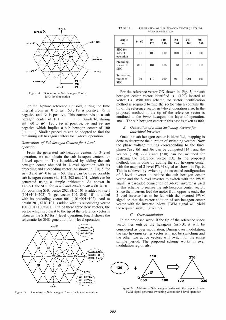
For the 3-phase reference sinusoid, during the time interval from 0tω = to 60tω = , Va is positive, Vb is negative and Vc is positive. This corresponds to a sub hexagon center of 101 ( + − + ). Similarly, during
60tω = to 120tω = , Va is positive, Vb and Vc are negative which implies a sub hexagon center of 100 ( + − − ). Similar procedure can be adopted to find the remaining sub hexagon centers for 3-level operation.
Generation of Sub hexagon Centers for 4-level operation
From the generated sub hexagon centers for 3-level operation, we can obtain the sub hexagon centers for 4-level operation. This is achieved by adding the sub hexagon center obtained in 3-level operation with its preceding and succeeding vector. As shown in Fig. 5, for
3m = and 0tω = to 60tω = , there can be three possible sub hexagon centers viz. 102, 202 and 201, which can be generated using a simple arithmetic. As shown in Table-1, the SHC for 2m = and 0tω = to 60tω = is 101. For obtaining SHC vector 202, SHC 101 is added to itself (101+101=202). To get vector 102, SHC 101 is added with its preceding vector 001 (101+001=102). And to obtain 201, SHC 101 is added with its succeeding vector 100 (101+100=201). Out of these three new vectors, the vector which is closest to the tip of the reference vector is taken as the SHC for 4-level operation. Fig. 5 shows the schematic for SHC generation for 4-level operation.
TABLE I. GENERATION OF SUB HEXAGON CENTER(SHC) FOR 4-LEVEL OPERATION
Angle ωt 0 - 60 60 -
120 120 -180
180 - 240
240 - 300
300 – 360
SHC for 3-level operation
101 100 110 010 011 001
Preceding vector of SHC
001 101 100 110 010 011
Succeeding vector of SHC
100 110 010 011 001 101
For the reference vector OX shown in Fig. 3, the sub
hexagon center vector identified is (120) located at vertex B4. With this scheme, no sector identification method is required to find the sector which contains the tip of the reference vector in 4-level operation also. In the proposed method, if the tip of the reference vector is confined to the inner hexagon, the layer of operation,
1m= . The sub hexagon center in this case is taken as 000.
B. Generation of Actual Switching Vectors for Individual Inverters
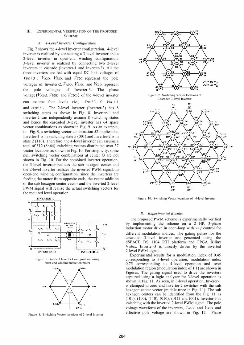
Once the sub hexagon center is identified, mapping is done to determine the duration of switching vectors. Now the phase voltage timings corresponding to the three phases gaT , gbT and gcT can be computed [14], and the vectors (120), (220) and (230) can be switched for realizing the reference vector OX. In the proposed method, this is done by adding the sub hexagon center with the mapped 2-level PWM signal as shown in Fig. 6. This is achieved by switching the cascaded configuration of 3-level inverter to realize the sub hexagon center vector and the 2-level inverter to switch with the PWM signal. A cascaded connection of 3-level inverter is used in this scheme to realize the sub hexagon center vector. Since the inverters feed the motor from opposite ends, the 2-level inverter has to be fed with the inverted PWM signal so that the vector addition of sub hexagon center vector with the inverted 2-level PWM signal will yield the required switching vectors.
C. Over modulation In the proposed work, if the tip of the reference space
vector lies outside the hexagons ( 3),m > it will be considered as over modulation. During over modulation, the sub hexagon center vector will not be switching and the other two active vectors will switch for the entire sample period. The proposed scheme works in over modulation region also.
Figure 4. Generation of Sub hexagon Center for 3-level operation
Figure 5. Generation of Sub hexagon Center for 4-level operation Figure 6. Addition of Sub hexagon center with the mapped 2-level
PWM signal generates switching vectors for 4-level operation
283
III. EXPERIMENTAL VERIFICATION OF THE PROPOSED SCHEME
A. 4-Level Inverter Configuration Fig. 7 shows the 4-level inverter configuration. 4-level
inverter is realized by connecting a 3-level inverter and a 2-level inverter in open-end winding configuration. 3-level inverter is realized by connecting two 2-level inverters in cascade (Inverter-1 and Inverter-2). All the three inverters are fed with equal DC link voltages of
3/DCV . A2O,V B2O,V and C2OV represent the pole voltages of Inverter-2. A3O',V B3O',V and C3O'V represent the pole voltages of Inverter-3. The phase voltage A2A3, B2B3(V V and C2C3)V of the 4-level inverter can assume four levels viz., 3,/DCV− 0, 3/DCV and 2 3/DCV . The 2-level inverter (Inverter-3) has 8 switching states as shown in Fig. 8. Inverter-1 and Inverter-2 can independently assume 8 switching states and hence the cascaded 3-level inverter has 64 space vector combinations as shown in Fig. 9. As an example, in Fig. 9, a switching vector combination 52 implies that Inverter-1 is in switching state 5 (001) and Inverter-2 is in state 2 (110). Therefore the 4-level inverter can assume a total of 512 (8×64) switching vectors distributed over 37 vector locations as shown in Fig. 10. For simplicity, some null switching vector combinations at center O are not shown in Fig. 10. For the combined inverter operation, the 3-level inverter realizes the sub hexagon center and the 2-level inverter realizes the inverted PWM signal. In open-end winding configuration, since the inverters are feeding the motor from opposite ends, the vector addition of the sub hexagon center vector and the inverted 2-level PWM signal will realize the actual switching vectors for the required level operation.
B. Experimental Results The proposed PWM scheme is experimentally verified
by implementing the scheme on a 2 HP, 3-phase induction motor drive in open-loop with /v f control for different modulation indices. The gating pulses for the cascaded 3-level inverter are generated using the dSPACE DS 1104 RTI platform and FPGA Xilinx Virtex. Inverter-3 is directly driven by the inverted 2-level PWM signal.
Experimental results for a modulation index of 0.45 corresponding to 3-level operation, modulation index 0.75 corresponding to 4-level operation and over modulation region (modulation index of 1.1) are shown in Figures. The gating signal used to drive the inverters captured using a logic analyzer for 3-level operation is shown in Fig. 11. As seen, in 3-level operation, Inverer-1 is clamped to zero and Inverter-2 switches with the sub hexagon center vector (middle trace in Fig. 11). The sub hexagon centers can be identified from the Fig. 11 as (101), (100), (110), (010), (011) and (001). Inverter-3 is switching with the inverted 2-level PWM signal. The pole voltage waveform of the inverters, A2OV and A3O'V and effective pole voltage are shown in Fig. 12. Phase
Figure 7. 4-Level Inverter Configuration, using open-end winding induction motor
Figure 9. Switching Vector locations of Cascaded 3-level Inverter
Figure 10. Switching Vector locations of 4-level Inverter
Figure 8. Switching Vector locations of 2-level Inverter
284
voltage A2A3V and motor current for A-Phase are shown in Fig. 13 and Fig. 14. The gating signals used to drive the inverters for 4-level operation are shown in Fig. 15. The combined switching of Inverter-1 and Inverter-2 realizes the sub hexagon center in this level of operation. The pole voltage waveforms of the inverters are shown in Fig. 16. The upper trace shows the pole voltage of inverter-2, middle trace shows the pole voltage of inverter-3 and lower trace shows the effective pole voltage, which is similar to the pole voltage of any 4-level inverter. Phase voltage and motor current for A-Phase are shown in Fig. 17. Experimental results for over modulation region (modulation index=1.1) are also shown. As shown in Fig. 18, the gating signals for driving the inverters show less switching for over modulation region, since only the vectors in the periphery of the outer hexagon are switched in this case. Pole voltages are shown in Fig. 19. Phase voltage and motor current are in A-Phase are shown in Fig. 20.
Figure 11. Gating Signal for Inverters for 3- level Operation. Upper Three Traces for Inverter-1, Middle Three Traces for Inverter-2
and Lower Three Traces for Inverter-3 (Modulation index 0.45)
Figure 12. Experimental waveforms of Pole Voltage for Modulation index 0.45
Upper Trace Pole Voltage of Inverter-2(VA2O) Middle Trace Pole Voltage of Inverter-3 (VA3O’)
Lower Trace Effective Pole Voltage (VA2O - VA3O’),using MATH subtraction feature of the scope.
Scale: X-axis: 5 ms/div; Y-axis: 40V/div
Figure 13. Experimental waveform of Phase Voltage for Modulation index 0.45 Scale: X-axis: 10ms/div; Y-axis: 20V/div
Figure 14. Experimental waveform of Motor Current for Modulation index 0.45
Scale: X-axis: 10ms/div; Y-axis: 500mA/div
Figure 15. Gating Signal for Inverters for 4- level Operation. Upper Three Traces for Inverter-1, Middle Three Traces for Inverter-2
and Lower Three Traces for Inverter-3 (Modulation index 0.75)
Figure 16. Experimental waveforms of Pole Voltage for Modulation index 0.75
Upper Trace Pole Voltage of Inverter-2(VA2O) Middle Trace Pole Voltage of Inverter-3 (VA3O’)
Lower Trace Effective Pole Voltage (VA2O - VA3O’), using MATH subtraction feature of the scope.
Scale: X-axis: 2.5 ms/div; Y-axis: 40V/div
Figure 17. Experimental waveform of Phase Voltage and Motor Current for
Modulation index 0.75 Scale: Voltage: X-axis: 5ms/div; Y-axis: 40V/div
Current: Y-axis: 1A/div
285
IV. CONCLUSION A simple Space vector PWM scheme for a 4-level
inverter is proposed. The scheme does not use any sector identification method to find the sub hexagon center, which encloses the tip of the reference space vector. A method to identify the sub hexagon center from the instantaneous amplitude of the reference voltage for all regions of operation is proposed.
In the proposed scheme, 4-level inverter is realized by a 3-level inverter and a 2-level inverter in open-end
winding configuration. 3-level inverter is realized by cascaded connection of two 2-level inverters and the 3-level inverter is used to realize the sub hexagon center vector. The 2-level inverter realizes the inverted PWM signal. The individual inverters are fed with symmetric DC link voltages. The scheme is implemented and tested with a 2-HP induction motor drive and experimental results are presented, including operation in over modulation region.
REFERENCES [1] A. Nabae, I.Takahashi and H. Akagi, “A New Neutral Point
Clamped PWM Inverter”, IEEE Transactions on Industry Applications, vol.1A-17, No.5, September/October 1981, pp 518-523.
[2] Jih - Sheng Lai and Fang Zheng Peng, “Multilevel Converters - A New Breed of Power Converters”, Proc. IAS’95 Conf., pp 2348-2356.
[3] N.Celanovic and Dushan Boroyevich, “ A Fast Space-Vector Modulation Algorithm for Multilevel Three-Phase Converters” IEEE Transactions on Industry Applications, vol.37,No.2, March/April 2001, pp 637-641.
[4] Gautam Sinha and Thomas A Lipo, “A Four Level Rectifier – Inverter System for Drive Applications”, ”, IEEE Transactions on Industry Applications, vol.30, , July/August 1994, pp 938-944.
[5] Heinz Willi Van Der Broeck, Hans-Christoph Skudelny, and Georg Viktor Stanke, “ Analysis and Realization of a Pulsewidth Modulator Based on Voltage Space Vectors”, IEEE Transactions on Industry Applications, vol.24, No.1, January/February 1988, pp 142-150.
[6] Anish Gopinath, Aneesh Mohamed A.S and M.R.Baiju, “ Fractal Based Space Vector PWM for Multilevel Inverters – a Novel Approach”, IEEE Transactions on Industrial Electronics, vol.52,No. 4, April 2009, pp 1230-1238.
[7] Aneesh Mohamed A.S, Anish Gopinath and M.R.Baiju, “ A Simple Space Vector PWM Generation for any General N-Level Inverter”, IEEE Transactions on Industrial Electronics, vol.56,No. 5, May 2009, pp 1649-1656.
[8] P.F Seixas, M.A. Severo Mendes, P.Donoso Garcia, A.M.N. Lima, “ A Space Vector PWM Method for Three-Level Voltage Source Inverters”, Proc. APEC, vol.1, 2000, pp 549-555.
[9] Shivkumar E.G, Gopakumar. K, Sinha S.K, Andre Pittet, and Ranganathan V.T,” Space Vector PWM control of dual inverter fed open- end winding induction motor drive”, Proc. Applied Power Electronics Conf (APEC), 2001, pp 399-405.
[10] Shivkumar E.G, Somasekhar V.T, Krushna K, Mohapatra K, Gopakumar. K, Umanand L, and S.K. Sinha,” A multi level space phasor based PWM strategy for an open- end winding induction motor drive using two inverters with different DC link voltages”, Proc. IEEE PEDS 2001, pp 169-175.
[11] V.T.Somasekhar and K.Gopakumar, “ Three Level Inverter Configuration Cascading Two Two Level Inverters”, IEE Proc.- Electr.Power Appl., vol.150, No.3,May 2003, pp 245-254.
[12] V.T.Somasekhar, K.Gopakumar, M.R.Baiju, Krishna K Mohapatra and L.Umanand “A Multilevel Inverter Sysyem for an Induction Motor With Open-end Windings”, IEEE Transactions on Industrial Electronics, vol.52,No. 3, June 2005, pp 824-836.
[13] Jae Hyeong Seo,Chang Ho Choi and Dong Seok Hyun, “ A New Simplified Space Vector PWM Method for Three-Level Inverters”, IEEE Transactions on Power Electronics, vol.16,No.4, July 2001, pp 545-550.
[14] Joohn-Sheok Kim, Seung-Ki Sul “ A Novel Voltage Modulation Technique of the Space Vector PWM”, IPEC Yokohama-95, pp 742-747.
[15] S.Srinivas and V.T.Somasekhar, “Space vector based PWM switching strategies for a three - level dual-inverter fed open end winding induction motor drive and their comparative evaluation” IET- Electr.Power Appl., Vol 2, No. 1, January 2008, pp 19-31.
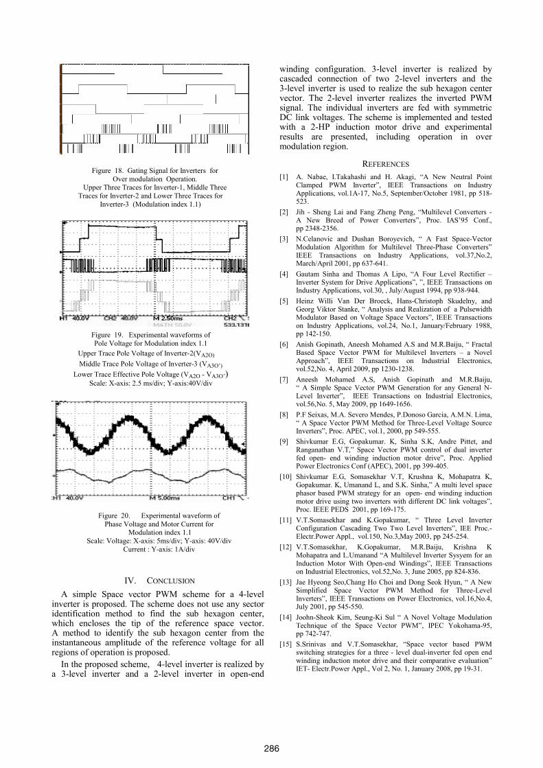
Figure 18. Gating Signal for Inverters for Over modulation Operation.
Upper Three Traces for Inverter-1, Middle Three Traces for Inverter-2 and Lower Three Traces for
Inverter-3 (Modulation index 1.1)
Figure 19. Experimental waveforms of Pole Voltage for Modulation index 1.1
Upper Trace Pole Voltage of Inverter-2(VA2O) Middle Trace Pole Voltage of Inverter-3 (VA3O’)
Lower Trace Effective Pole Voltage (VA2O - VA3O’)
Scale: X-axis: 2.5 ms/div; Y-axis:40V/div
Figure 20. Experimental waveform of Phase Voltage and Motor Current for
Modulation index 1.1 Scale: Voltage: X-axis: 5ms/div; Y-axis: 40V/div
Current : Y-axis: 1A/div
286