High Grade and Industrial Technologies - FTP Directory Listing
123
From Design to Production Oil Drilling Industry Defence Railways Space Aeronautics Medical www.microspire.c m Wound Magnetics Experts High Grade and Industrial Technologies High Grade and Industrial Technologies ® ®
-
Upload
khangminh22 -
Category
Documents
-
view
0 -
download
0
Transcript of High Grade and Industrial Technologies - FTP Directory Listing

From Design to Production
Oil Drilli
ng
Industry
Defence
Railways
Space Aeronautics
Medical
www.microspire.c m
Wo u n d M a g n e t i c s E x p e r t s
High Gra
de and Industri
al Technologies
High Gra
de and Industri
al Technologies
® ®

132
67
8
54
9
13
1112
15
1617
22
2119
20
23
18
24
25
2526
27
28
3130
29
10
14
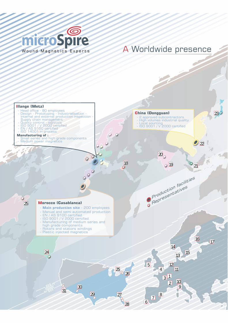
Morocco (Casablanca)- Main production site - 200 employees- Manual and semi automated production- EN / AS 9100 certified- ISO 9001 / V 2000 certified- Manufacturing of medium series and
high grade components- Rotors and stators windings- Plastic injected magnetics
Illange (Metz)- Head office - 80 employees- Design - Prototyping - Industrialisation -
Internal and external production inspection -Supply chain management
- Quality control - logistics- ISO 9001 / V 2000 certified- EN / AS 9100 certified- ISO 14001 in processManufacturing of :- Small series and high grade components- Medium power magnetics
China (Dongguan)- 2 approved subcontractors- High volumes industrial quality- Local sourcing- ISO 9001 / V 2000 certified
Wo u n d M a g n e t i c s E x p e r t s A Worldwide presence

Wo u n d M a g n e t i c s E x p e r t s Locations
France (Illange)
Morocco (Casablanca)
China (Dongguan)
Wo u n d M a g n e t i c s E x p e r t s
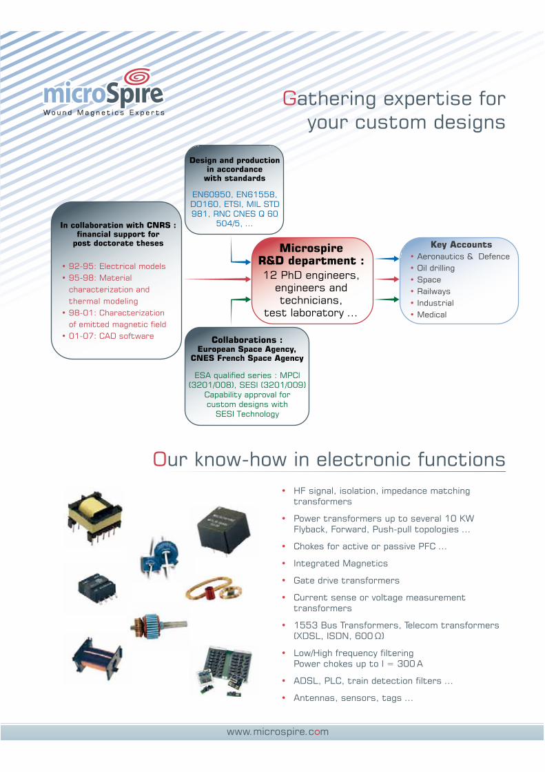
MicrospireR&D department :12 PhD engineers,
engineers andtechnicians,
test laboratory ...
Key Accounts• Aeronautics & Defence
• Space• Oil drilling
• Railways• Industrial• Medical
• 92-95: Electrical models
EN60950, EN61558,DO160, ETSI, MIL STD981, RNC CNES Q 60
504/5, ...
characterization and• 95-98: Material
thermal modeling• 98-01: Characterization
• 01-07: CAD softwareof emitted magnetic field
In collaboration with CNRS :financial support for
post doctorate theses
Design and productionin accordance
with standards
ESA qualified series : MPCI(3201/008), SESI (3201/009)
Capability approval forcustom designs with
SESI Technology
Collaborations :European Space Agency,
CNES French Space Agency
Gathering expertise foryour custom designs
Our know-how in electronic functions

Semi - Custom
Hig
h G
rade
Tec
hnol
ogie
sS
tand
ard
Tech
nolo
gies
CustomMagnetic cores and
FunctionsStandard magnetic cores
and Custom FunctionsComponents
Off The Shelves
COTS

Hig
h G
rade
Tec
hnol
ogie
sS
tand
ard
Tech
nolo
gies
Medium Power Engineering Support Flying / Custom terminations Dedicated Team
1°105
105 106 107
1°104
104
1°103
103100
MODULUS ZO from primary
Frequency (Hertz)
Mo
du
lus
(O
hm
s)
PHASE ZO from primary100
50
0
-50
-100100 103 104 105 106 107
Ph
as
e (
De
gre
es
)
Frequency (Hertz)
4 3 5p
rs3rsrs1
s1 600 s 1 s3 00m
5 01m 5u 5u
p
D
6
1 6p
5
1 p
3
3 7p
100
inf
1
F
F1
50mp4
Lp4
Lp3
0 5
Lp
5
Lp1
5
1
1
1 4p1
p
p3
r1
1 4p
60
1
5 3p
valeur efficace de ce courant :
ourant secondaire ui alent I
ou
ran
t se
con
dai
re
Ti e s
Ise I Ise I Is I dtT
T
αmax T

Wo u n d M a g n e t i c s E x p e r t s
Certifications
&
Qualifications
Wo u n d M a g n e t i c s E x p e r t s
EUROPEAN DIRECTIVESR.o.H.S. and W.E.E.E.

Wo u n d M a g n e t i c s E x p e r t s
Partnership

ContentsHigh Grade technologies
Custom Design Technologies
RF and Data Magnetics
Power Magnetics

Industrial TechnologiesCustom Designs
RF and Data Magnetics
Power Magnetics
Telecom Products
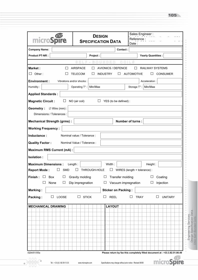
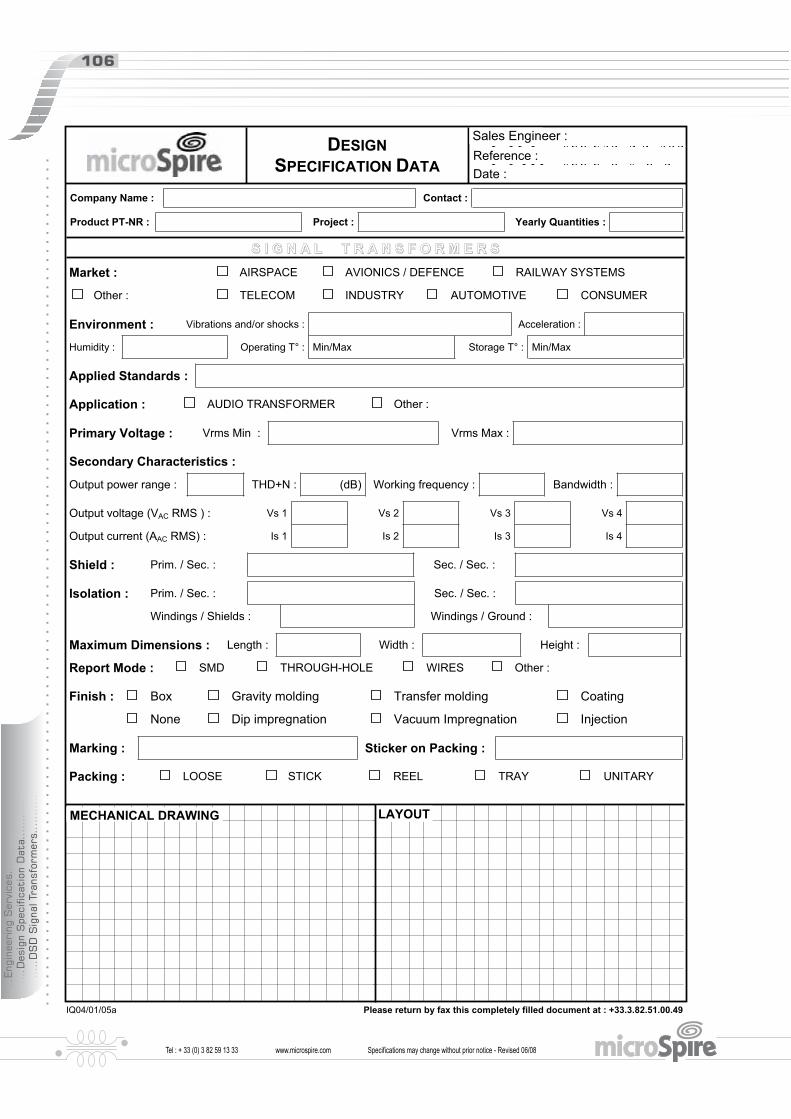
Engineering ServicesEngineering Services
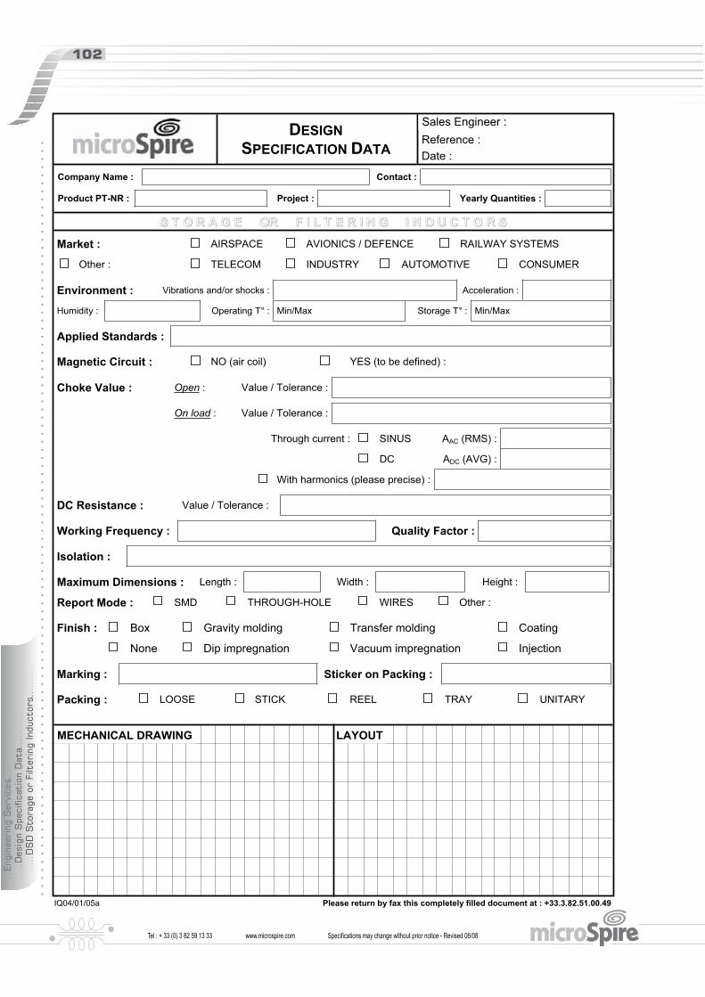
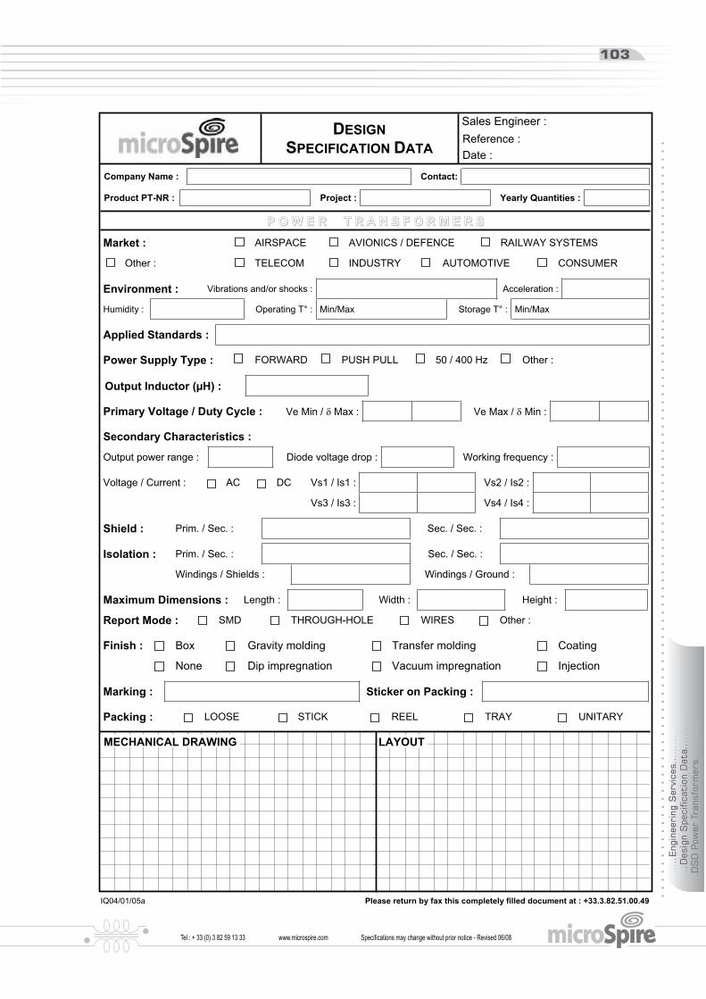
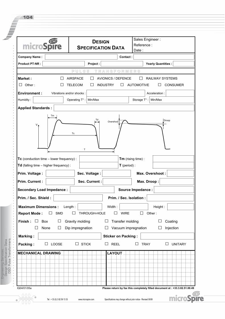
Design Specification Data


From Design to Production
www.microspire.c m
Wo u n d M a g n e t i c s E x p e r t s
High G
rade Technolo
gies
High G
rade Technolo
gies
®
®
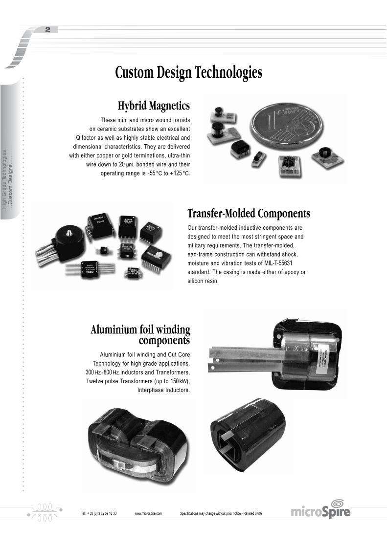
Custom Design Technologies
Hybrid Magnetics
Aluminium foil winding components
Transfer-Molded Components

Custom Design Technologies
Customized medium power EE core
Customized toroidal Inductors
Customized medium power C core Inductors

High Grade Custom Planar Magnetics
Construction
Electrical Data
SMPS Topologies
Mounting, Connections
glue
kapton
copper
copper
copper
kapton
kapton
kapton
ferritepins
ferrite
PCB
PCB
solder

Operations
OUT
PHASE I PHASE II and II' PHASE III and III'
IN OUT IN OUT IN
2d Bobbinxxx
turns
1st Bobbinxxx
turns
1
2
3
4
1
2
3
4
1
2
3
4
REAR SIDE
FRONT SIDE
1 2 3 2 1
Build-to-print Rotors and Stators manufacturing

SESI SMD Power Inductors and Transformers
The possible functions in the SESI design

Weight: 35 grams
Pad Layout (mm)SESI 22 WE
11.43(3 x 3.81)
MICROSPIRE
MB0XXXX-
Part Nber
YY/WW/M
26.0 MAX 3.0
4 1
85
26
Area forgluing
39.0
32.0
29.0
32.0
±0.4
36.0
0/+
1
Pin section2.0 x 0.30
13.30MAX
25.5
Shielded versions
Weight: 36 grams
Pad Layout (mm)
17.78(7 x 2.54)
MICROSPIRE
MB0XXXX-
Part Nber
YY/WW/M
26 MAX 1.3
8 1
169
26
Area forgluing
41.9
32.0
29.0
32.0
±0.4
SESI 22.1 WE
38.0
0/+
1
Pin section0.80 x 0.50 thick
25.5
2.50
13.30MAX
Weight: 16.5 grams
Pad Layout (mm)
15.24(8 x 1.905)
MICROSPIRE
MB0XXXX-
Part Nber
YY/WW/M
21.2 MAX 1.2
9 1
1810
Area forgluing
32.9
27.0
25.0
MA
X
26.0
MA
X
SESI 18.1 WE
31.9
MA
X
Pin section1 x 0.30
9.4MAX
Weight: 9.0 grams
Pad Layout (mm)SESI 15 WE
11.43(3 x 3.81)
22 M
AX MICROSPIRE
MB0XXXX-
Part Nber
YY/WW/M
17.3 MAX
17
2.2
4 1
85
13.3
Area forgluing
24.0
18.5
16.3
17.6
MA
X
8.80MAX
Pin section1.10 x 0.35
SESI Custom Technologies
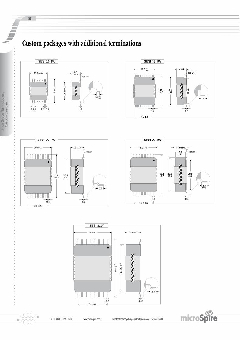
2
150 μm
29±0.5
25±0.2
19.3 +0-0.3 ≤ 9.0
23 ±
0.1
8 x 1.9
1.0 0.3
SESI 18.1W
36.5±0.5
30.8±0.4
29.0±0.4
2.5±0.2
11.9 MAX
8.8±0.1
180 μm
≤ 23.4
7 x 2.540.8 0.5
SESI 22.1W
39MAX
30.8±0.4
2.5
180 µm
25 MAX 12 MAX
8 x 2.28
0.8 0.5
SESI 22.2W
42.7
5 ±
0.3
2.6
34 MAX 14.5 MAX
7 x 3.81
0.9 0.45
SESI 32W
52.0
+1.5
-0
Custom packages with additional terminations
150 µm
1.4 +0.2-0.1
16.0 MAX
22
MA
X
8.0MAX
0.8 ±0.12.28
SESI 15.1W
0.4
16.5
MA
X
Ø M
AX
h MAX
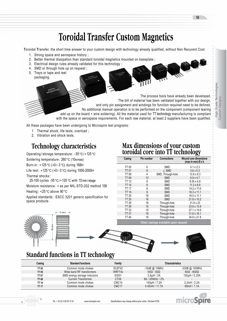
Toroidal Transfer Custom Magnetics
Technology characteristics
Standard functions in TT technology
Max dimensions of your custom toroidal core into TT technology
Typical Dimensions (mm)
Electrical Data ( 25°C )
2.80 MAX
1st significant figure (2 times wider)
2nd significant figure
Multiplier (nH)
2.16
MA
X
2.67 MAX
0.460.13
2.66
2.62.8
3.7
0.9
6
"S" Version
"A" Version
1 10 100
110
100
90
80
70
60
50
40
30
20
Frequency - MHz
100 µH to 180 nH
220-330-3
90 nH
1.1 to 1.8 µH
1.1 to 1.8 µH
560 to 820 nH
2.2 µH
470 to 680 nH
270 nH
Q vs frequency
Packaging
Chip Inductors - MPCI 10000 Series
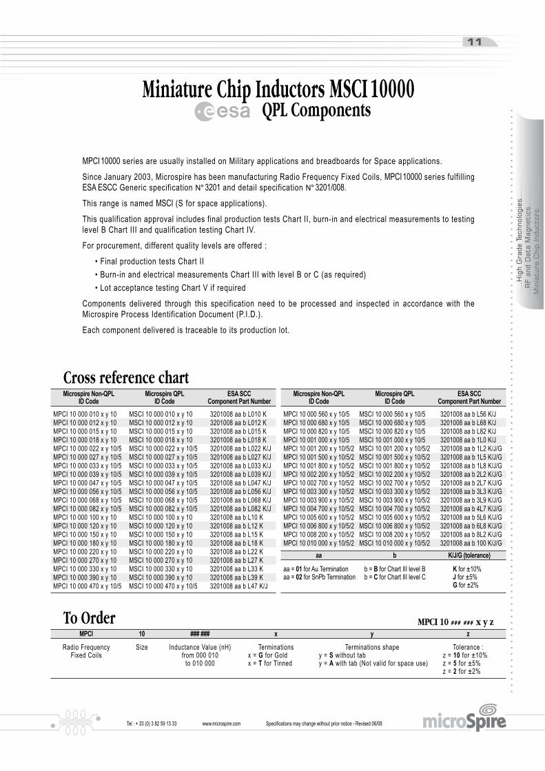
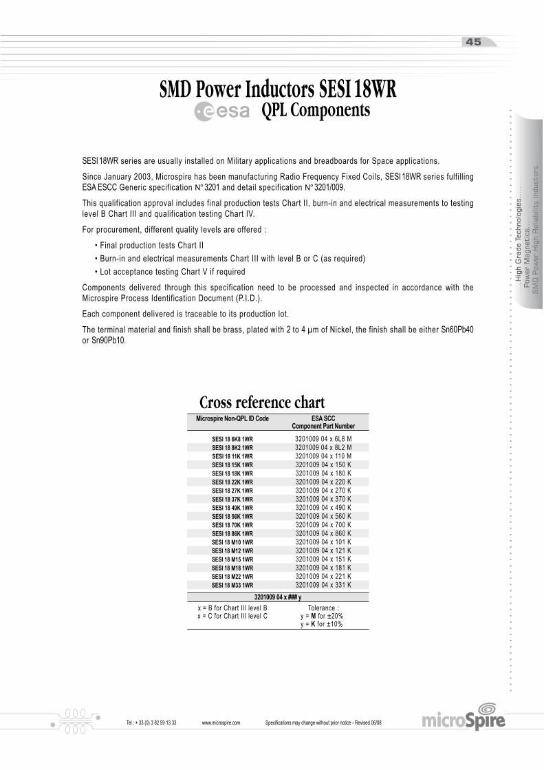
Cross reference chart
To Order MPCI 10 ### ### x y z
QPL ComponentsMiniature Chip Inductors MSCI 10000

Typical Dimensions (mm)
2.80 MAX2.41
2nd significant figure
Multiplier (nH)
2.54
MA
X
2.67 MAX
0.6
2.66
2.62.8
3.7
0.13
0.9
6
"S" Version
"A" Version
1st significant figure (2 times wider)80
70
60
50
40
30
20
10
1000 µH
390 µH
15 µH to
56 µH
Hµ 001 ot Hµ 28
101Frequency - MHz
Q vs frequency
Packaging
Electrical Data ( 25°C )
Chip Inductors - MPCI 12000 Series
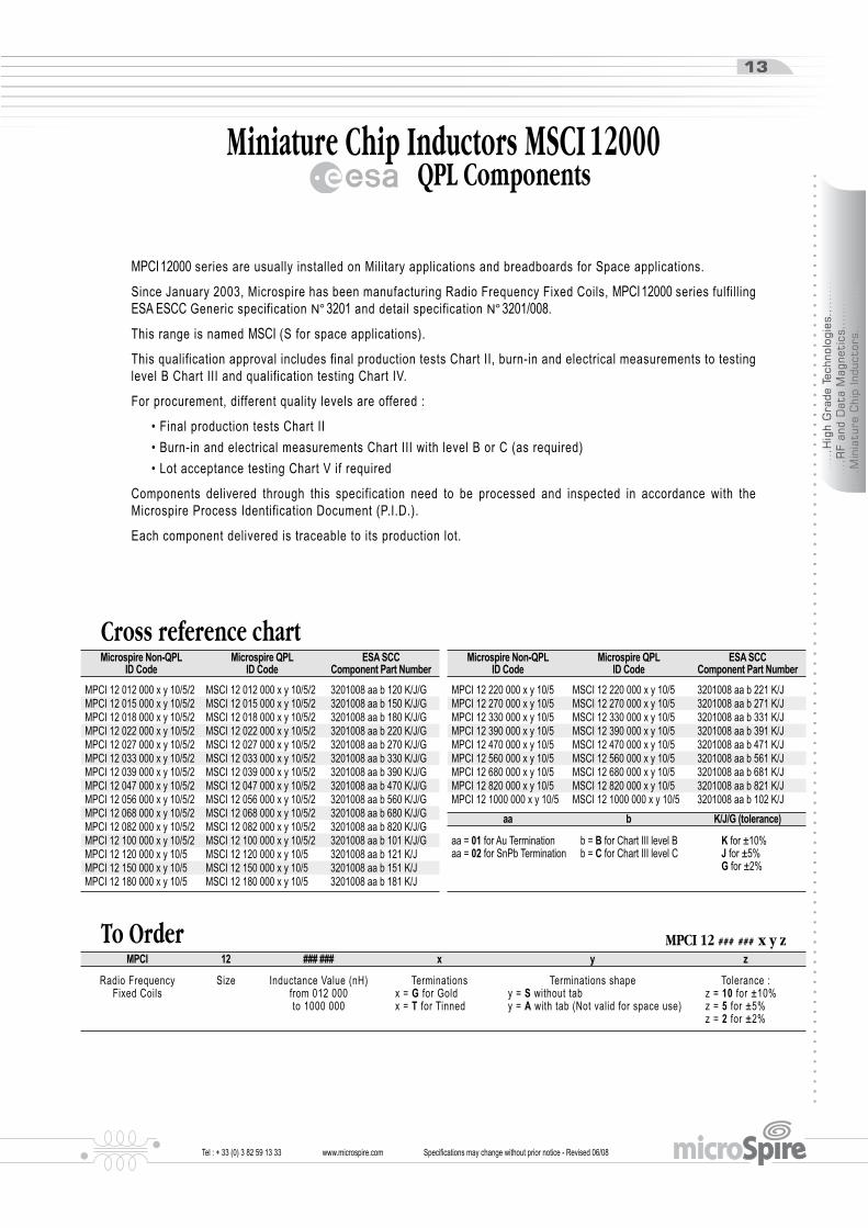
Cross reference chart
To Order MPCI 12 ### ### x y z
QPL ComponentsMiniature Chip Inductors MSCI 12000

Typical Dimensions (mm)
4.14 MAX
1st significant figure (2 times wider)
2nd significant figure
Multiplier (nH)
3.3
MA
X
3.38 MAX
0.64MAX
0.13
3.38
3.7
3
4.1
4 M
AX
4.2
1.85
"S" Version
"A" Version
1.02
100 µH
82 µH
33 µH
10 µH
330 nH
100 nH
82 nH
33 nH
10 nH
8.2 µH
3.3 µH
820nH
20
40
60
80
100
120
140
10001 3 5 10 30 50 100 300 500
Frequency - MHz
Q vs frequencyPackaging
Electrical Data ( 25°C )
Chip Inductors - MPCI 20000 Series

QPL ComponentsMiniature Chip Inductors MSCI 20000
Cross reference chart
To Order MPCI 20 ### ### x y z

100 µH
82 µH
33 µH
10 µH
330 nH
100 nH
82 nH
33 nH
10 nH
8.2 µH
3.3 µH
820nH
20
40
60
80
100
120
140
10001 3 5 10 30 50 100 300 500
Frequency - MHz
Connections
PCB Layout(suggested)
3.402.50
1st significant figure(2 times wider)
2nd significant figure
Multiplier (nH)
3.30
5.70
5
3.8
1
2
4.80
5.80
Chip Inductors - MPCI 233 Series
Electrical Data ( 25°C )
To Order MPCI 233 ### ### xy
Q vs frequencyTypical Dimensions(mm)
Packaging

MB4x xxx
1
3
6
4
1
2
3
6
4
Standard Center tap
1
2
3
6
5
4
Shielded Version
PackagingApplications
Connections
Typical Dimensions (mm)
10.1 ± 0.3
Surface-mount case WRFT4# ### 1S
6.9 +0.2 -0 0.15
5.5 ± 0.2
5.5 ± 0.2
Pin Section 0.7 x 0.3
4.5± 0.2
0.1 +0.2 -0
Pin Section 0.7 x 0.3
yywwP
Through-hole case WRFT4# ### 1P
7.62
90° 105°
5.5 ± 0.2
6.80 MAX
5.5 ± 0.2
4.5 ± 0.2
5.3 MAX
yywwP
yywwP
Pin 6 DOT
Weight :1 gram
6°
5
4
1°
2-CT
3
SMD shielded case WRFT4# ### 1Q
10.1 ± 0.3
7.10 MAX
3.556
PCB Layout (suggested)
1
2
3 4
5
6
1
2
3 4
5
6
12
6
1.78
1.1
1.78
7.62
Drill Diameter0.9 min.
Topview
1
2
3 4
5
6
1
2
3 4
5
6
12
6
1.78
1.1
1.78
7.62
Drill Diameter0.9 min.
Topview
11.0
1.10
7.20
3.556
Marking
Wide Band RF Transformers - WRFT 4x Series
Electrical Data (25°C)
To Order WRFT4 # ### 1x

2
8
7 6
5
3
41
Impe
danc
e (Ω
)
Frequency - MHz
HCESC10 xxx 1x10000
1000
100
10
1
0,1
0,011E+02 1E+03 1E+04 1E+05 1E+06 1E+07 1E+08
HCESC10 15KHCESC10 56KHCESC10 M47
Att
en
uati
on
(d
B)
30
35
25
20
15
10
5
0
HCESC10 xxx 1x
HCESC10 15K
HCESC10 56K
HCESC10 M47
Frequency - MHz
1E+04 1E+05 1E+06 1E+07 1E+08
Electrical Data ( 25°C )
To Order HCESC10 ### 1x
Typical Dimensions (mm)
4.50 MAX
Through-hole HCESC10 ### 1P
Surface-mount HCESC10 ### 1S
4.30 MAX
0.7 x 03
5.334
10
12.8
12.06 16 MAX
1 8
5 4 0.7
9.4
2
Connections
Packaging
Response Curves
Common-Mode Chokes - HCESC Series

Electrical Data
To Order DLEF42 020 1S Packaging
Application
Att
en
ua
tio
n (
dB
)
25
20
15
10
5
0
-5
COMMON MODE
DIFFERENTIAL MODE
Frequency - MHz
1E+05 1E+06 1E+07 1E+08 1E+09
Response Curves Typical Dimensions (mm)
10.1 ± 0.3
Surface-mount case
5.5 ± 0.2 5.5 ± 0.2
Pin Section 0.7 x 0.3
4.5± 0.2
6.9 +0.2 -0 0.15
0.1 +0.2 -0
1
2
3 4
5
6
12
6
1.78
1.1
Topview
1
2
3 4
5
6
12
6
1.78
1.1
Topview
yywwP
DL42
Marking
5
2
6
1
Standard
Connections PCB Layout(suggested)
Data Line EMI Filters - DLEF 42 Series

1
3
4
6
Electrical Data ( 25°C )
Ampl
itude
(dBm
)
Frequency - MHz
LOAD : 600 Ω @ 0 dBm
-2.0
-1.5
-1.0
-0.5
0.0
-2.5
-3.0
-3.5
-4.0
-4.5
-5.010 100 1000 10000 100000
Frequency Response Distorsion
Frequency - MHz
LOAD : 600 Ω @ 0 dBm
T.H
DIST
ORS
ION
+ NO
ISE
(dBm
)
-60
-50
-70
-80
-90
-100
-11010 1000 10000
Typical Dimensions (mm)
10.72.15 MAX1.5
12.7
0.4 0.7
7.1MAX
0.8
9.2MAX
1
3
4
6
2.54
18 MAX
MTLM 1234 Mil
13.7 MAX
2±0.3
10.5MAX
10.5MAX
1
3
4
6
15 MAX
MTLM 1234 MQShielded casing
PCB Layout(suggested - only MTLM 1234 Mil)
13.5
2.4
2.54
1.0
Connections
Application
Line-Matching Transformer - MTLM 1234 Mil

4
5
6
7
8
1
2
3
DBIT x 3 S
yywwP
Electrical Data ( 25°C )
To Order DBIT # 3S
Notes
Typical Dimensions(mm, top view)
Marking
Connections
MIL-STD 1553 Interface Transformers - DBIT x 3 S
18 4.5
5.082.54
1.5
PCB Layout (suggested)
16 5.25
26.5 MAX
2.5
-0
+0
.5
5.08 2.54
0.7
16
3.81 MAX
1
3 8
4
0.4
0.1
Packaging
WSo
P1 PoUnreeling

MIL-STD 1553 Interface Transformers - DBIT xx 4 S
4
8
1
2
3
5
7
1
2
3
A B
DBIT xx 4 S
yywwP
Typical Dimensions(mm, top view)
Marking
Connections
Electrical Data ( 25°C )
To Order DBIT ## 4S Notes
10.0
3.811.905
1.3
14.6
PCB Layout (suggested)
11.0
10.16
3.81
0.7
0.3
10
.16
± 0
.2
1.905
4.9
MA
X
< 150 µm 13.2 ± 0.40
3
1 8
4
Packaging
WSo
F
P1 PoUnreeling

4
5
6
7
8
1
2
3
DBIT x 5 S
yywwP
Typical Dimensions(mm, top view)
Marking
Connections
MIL-STD 1553 Interface Transformers - DBIT x 5 S
Electrical Data ( 25°C )
To Order DBIT # 5S
Notes
18 4.5
5.082.54
1.5
PCB Layout (suggested)
16
26.5 MAX
5.08
0.7
0.4
0.1
16
5 -0 +0.5 MAX
2.54
1
3 8
4
2.5
-0
+0
.5
Packaging
WSo
P1 PoUnreeling

Typical Dimensions (mm)
DBITx7P
2.54
11 ±
1
5.0
8
16
16
7.3 MAX
12.70
Pin Ø 0.65Electrolytic
tin plating
Top view
1
2
3 8
7
6
5
4
4
5
6
7
8
1
2
3
DBIT x 7 P
yywwP
Marking
Connections
MIL-STD 1553 Interface Transformers - DBIT x 7 P
NotesElectrical Data ( 25°C )
To Order DBIT # 7P

MIL-STD 1553 Interface Transformers - DBIT x 7 P10
NotesElectrical Data ( 25°C )
To Order DBIT # 7 P10
Typical Dimensions (mm)
DBITx7P10 Bottom view
2.54
17.0
5.0
8
16 ±
0.3
7.3 MAX
12.70
Pin Ø 0.50Electrolytic
tin plating
1 4
16 ±0.3
4
5
6
7
8
1
2
3
DBIT x 7 P10
yywwP
Marking
Connections

MIL-STD 1553 Interface Transformers - DBIT x 7 S
NotesElectrical Data ( 25°C )
To Order DBIT # 7 S
Packaging
WSo
P1 PoUnreeling
18 4.5
5.082.54
1.5
PCB Layout (suggested, DBIT x 7 S)
Typical Dimensions (mm)16
26.5 MAX
5.08
0.7
0.4
0.1
16
7.3MAX
2.54
1
3 8
4
2.5
-0 +
0.5
4
5
6
7
8
1
2
3
DBIT x 7 S
yywwP
Marking
Connections

4
5
6
7
8
1
2
3
DBIT 5 7 S400Top view
1.9
0.7
3.8
1
11.0
13.2 ± 0.40
7.5 MAX
Pin section:0.70 x 0.30 thick
1
3 8
4
DBIT 5 7 P400Top viewBottom view
10.1
6 ±
0.2
15.6
0
10.16
6.1
010.1
6
5
8 4
1 3
1
4
8
2
3
6
7
Pin Ø 0.65Electrolytic
tin plating
7.6
2
2.54
7.62
DBIT 5 7P400
yywwP
< 150 µm
Typical Dimensions (mm)
Connections
MIL-STD 1553 Interface Transformers - DBIT 5 7 x400
Electrical Data ( 25°C )
To Order DBIT 5 7x400
Notes
10.0
14.6
3.811.905
1.3
PCB Layout(suggested, DBIT 5 7 S400)
Packaging
WSo
P1 PoUnreeling
18.0
27.0
27
.0
1.5
//200.μm
25.2±0.50
7.50
1 2 3 4
5
6
7
891011
12
13
14
15
16
Pin section:0.7 x 0.4(width x thick)
Topview
5.08
16.0 ±0.20/square
10.16
≈19.025.2 ±0.50
2.5
-0 +
0.5
SBIT
x 7.5S
YYWW
4
5
6
7
8
(14)
(15)
(16)
(17)
(18)
(11)
(12)
(13)
1
2
3
Marking ConnectionsPCB Layout(suggested)
To Order SBIT # 7.5S Notes
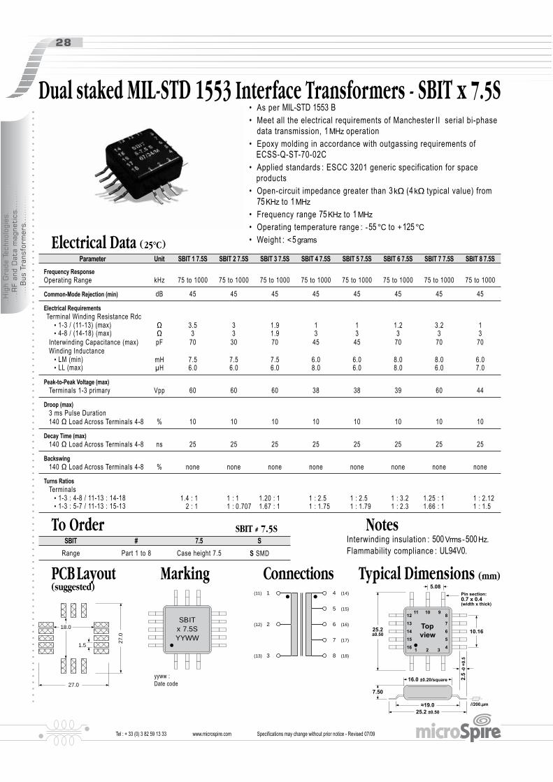
Dual staked MIL-STD 1553 Interface Transformers - SBIT x 7.5S
Electrical Data ( 25°C )
Typical Dimensions (mm)

Electrical Data ( 25°C )
pitch 2.54
12.70 mm ± 0.20
12.7
0 m
m ±
0.2
0
15.88 ± 0.20
1 2 3 4
5
6
7
8 11 12 13 14
15
16
17
18
15.8
8 ±
0.2
0
7.8
7 ±
0.2
0
0.65
11.8
0 ± 0
.30
Topview
SBITx 7.8PYYWW
4
5
6
7
8
(14)
(15)
(16)
(17)
(18)
(11)
(12)
(13)
1
2
3
Marking
ConnectionsPCB Layout(suggested)
To Order SBIT # 7.8P Notes
Typical Dimensions (mm)
Dual staked MIL-STD 1553 Interface Transformers - SBIT x 7.8P
4.0 ±0.18.00 ±0.1
12.0
±0
.3
5.5
0 ±
0.1
Unreeling
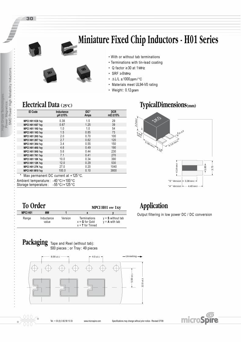
To Order MPCI H01 ### 1xy
Electrical Data ( 25°C )
Packaging
Application
Typical Dimensions (mm)
4.14 MAX
3.3
MA
X
3.38 MAX
0.64MAX
0.13
3.38 MAX
3.7
3
4.1
4 M
AX
4.40 MAX
1.8
5
"S" Version
"A" Version
1.02
1K0
Miniature Fixed Chip Inductors - H01 Series
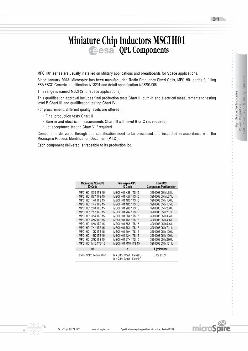
QPL ComponentsMiniature Chip Inductors MSCI H01

Typical Dimensions (mm)
3.40
2.503.
30
5.70
5
3.8
K38
PCB Layout (suggested)
4.80
5.80
To Order MPCI 233 H01 ### 1x
Electrical Data ( 25°C )
Application Packaging
Miniature Fixed Chip Inductors - 233 H01 Series

Electrical Data ( 25°C )
18
45 ESI 01
xxx 1x
yy/ww
3.50
9.50
1.1 1.1
7.9
13.9
W terminalsJ leaded
1-4
5-8
SMD Power Inductors - ESI 01
I
1 / f
I ripple
I ratedI peak
t
Notes
To Order ESI01 ### 1x
ConnectionsMarking Dimensions (mm)
PCB Layout (suggested)
7.50
7.40
5.334 = 3 x 1.778
8.50 MAX
0.80
2.0 Max , 1.50typ 0.10 +0.2 -0
8.40 MAX
12,5 ± 0,5
W terminalsJ leaded
9,20 ± 0,30
7.50 +0,3 -0
8.40 MAX
0.80
0.15
Packaging
F
WSo
P1 Po Unreeling
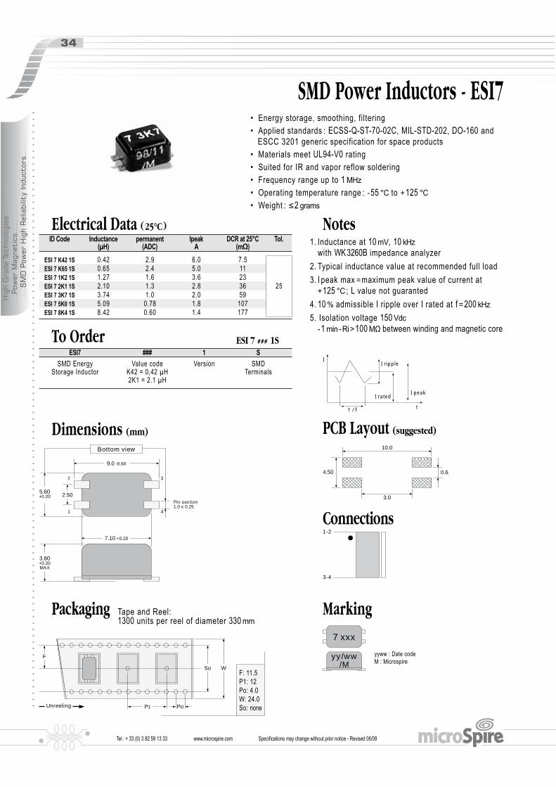
SMD Power Inductors - ESI7
Electrical Data ( 25°C )
To Order ESI 7 ### 1S
7 xxx
yy/ww/M
9.0 -0.60
7.10 +0.20
5.60+0.20
3.80+0.20MAX
2.50
1
2
4
3
Pin section1.0 x 0.25
Bottom view 10.0
3.0
4.50 0.6
1-2
3-4
I
1 / f
I ripple
I ratedI peak
t
Notes
Connections
Marking
Dimensions (mm) PCB Layout (suggested)
Packaging
F
WSo
P1 PoUnreeling

SE 9 xxx
xR yywwP
10.7MAX
13.4 MAX
0.9 to 1.3
2.9 x 0.25MAX
10.6 MAX
5.8MAX
8.4 14.4
3.0
I
1 / f
I ripple
I ratedI peak
t
To Order SESI 9 ### #WR
Electrical Data ( 25°C ) Notes
Connections Marking
Dimensions(mm, top view)
PCB Layout(suggested)
Packaging
SMD Power Inductors - SESI 9WR High Reliability Applications
F
WSo
P1 PoUnreeling

Electrical Data ( 25°C )
SE 91 xxx
xR yywwP
10.7MAX
13.4 MAX
0.9 to 1.3
1.5 x0.28MAX
10.6 MAX
5.8MAX
5.7
1
2
4
3
8.4 14.4
3.2
8.4
1
2
4
3
SMD Power Inductors - SESI 9.1WR High Reliability Applications
I
1 / f
I ripple
I ratedI peak
t
Notes
To Order SESI 9.1 ### #WR Connections Marking
Dimensions(mm, top view)
PCB Layout(suggested)
Packaging
F
WSo
P1 PoUnreeling

Cross reference chart
QPL ComponentsSMD Power Inductors SESI 9.1WR
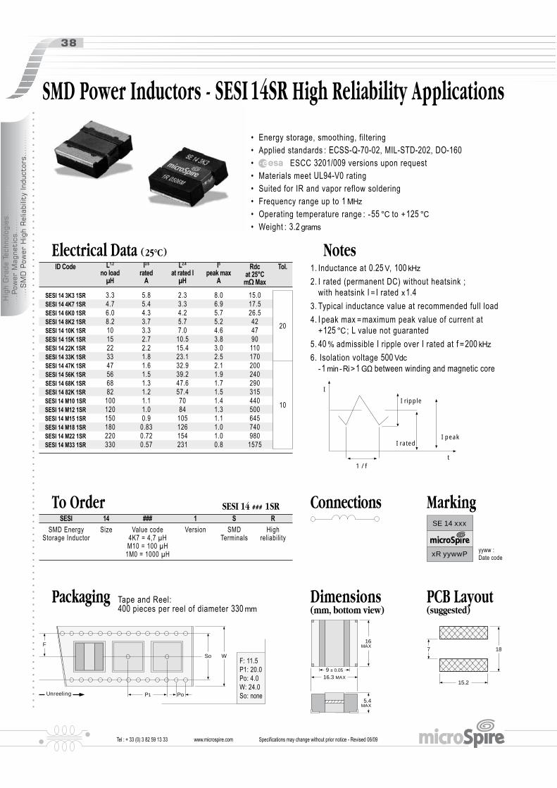
To Order SESI 14 ### 1SR
Electrical Data ( 25°C )
SE 14 xxx
xR yywwP
16MAX
16.3 MAX
5.4MAX
9 ± 0.05
7 18
15.2
Connections Marking
Dimensions(mm, bottom view)
SMD Power Inductors - SESI 14SR High Reliability Applications
I
1 / f
I ripple
I ratedI peak
t
Notes
PCB Layout(suggested)
Packaging
F
WSo
P1 PoUnreeling

Cross reference chart
QPL ComponentsSMD Power Inductors SESI 14SR
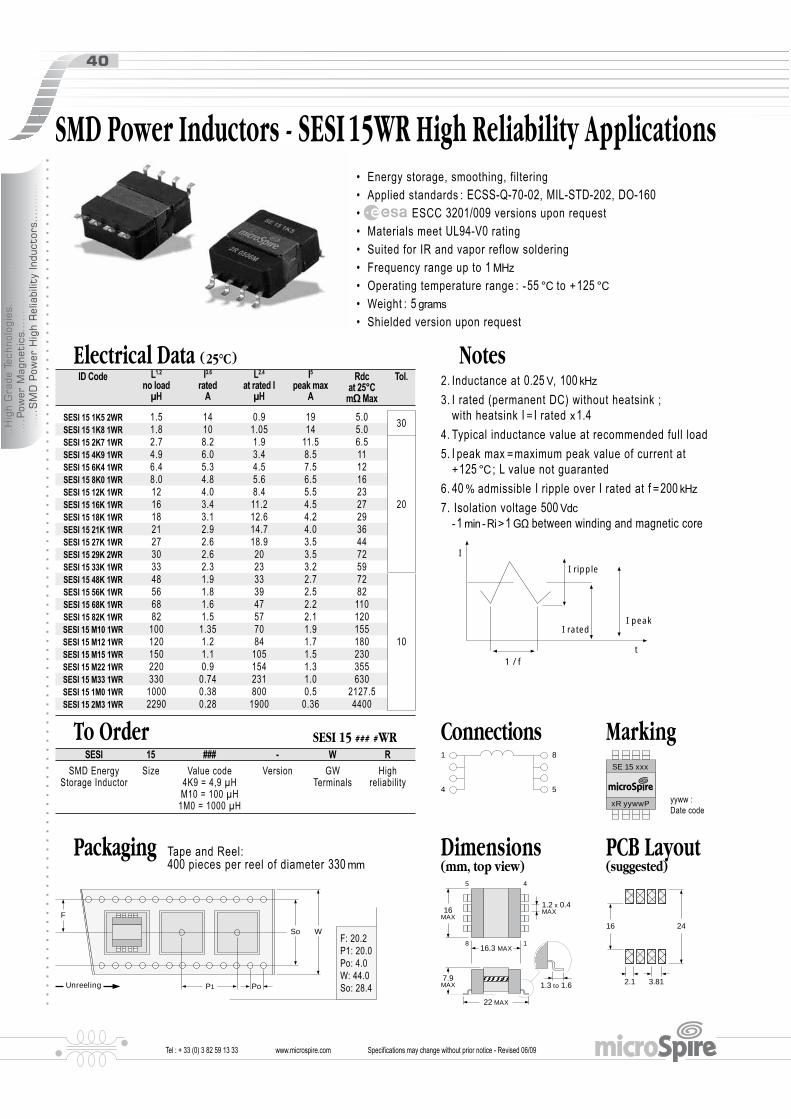
To Order SESI 15 ### #WR
Electrical Data ( 25°C )
I
1 / f
I ripple
I ratedI peak
t
SMD Power Inductors - SESI 15WR High Reliability Applications
SE 15 xxx
xR yywwP
1.3 to 1.6
16MAX
22 MAX
1.2 x 0.4MAX
16.3 MAX
7.9MAX
1
4
8
5
16 24
3.812.1
Connections Marking
Dimensions(mm, top view)
1
4
8
5
Notes
PCB Layout(suggested)
Packaging
F
WSo
P1 PoUnreeling

Cross reference chart
QPL ComponentsSMD Power Inductors SESI 15WR

Electrical Data ( 25°C )
To Order SESI 15 ### #SR
SMD Power Inductors - SESI 15SR High Reliability Applications
Notes
I
1 / f
I ripple
I ratedI peak
t
SE 15 xxx
xR yywwP
16MAX
16.3 MAX
7.4MAX
9 ± 0.05
7 18
15.2
Connections Marking
Dimensions(mm, bottom view)
PCB Layout(suggested)
Packaging
F
WSo
P1 PoUnreeling

Cross reference chart
QPL ComponentsSMD Power Inductors SESI 15SR

To Order SESI 18 ### #WR
Electrical Data ( 25°C )
SMD Power Inductors - SESI 18WR High Reliability Applications
I
1 / f
I ripple
I ratedI peak
t
SE 18 xxx
xR yywwP
1.3 to 1.6
19.8 MAX
26 MAX
2.1 x 0.4 MAX
22.0 ± 0.3
8.9MAX
1
4
8
5
21 28
3.813.0
Connections Marking
Dimensions(mm, top view)
1
4
8
5
Notes
Packaging PCB Layout(suggested)
F
WSo
P1 PoUnreeling
Cross reference chart
QPL ComponentsSMD Power Inductors SESI 18WR

To Order SESI 22 ### #WR
Electrical Data ( 25°C )
1.3 to 1.6
23.5MAX
35.3 MAX
2.1 x 0.45MAX
30.8 ± 0.4
12.2MAX
1
4
8
5
29.0
37.5
3.8
13
.0
Dimensions(mm, top view)
SMD Power Inductors - SESI 22WR High Reliability Applications
I
1 / f
I ripple
I ratedI peak
t
SE 22 xxx
xR yywwP
Connections
Marking
1
4
8
5
Notes
PCB Layout (suggested)
Packaging
F
WSo
P1 PoUnreeling

Cross reference chart
QPL ComponentsSMD Power Inductors SESI 22WR

To Order SESI 32 ### 1PR
Electrical Data ( 25°C )
18
169
33.5 MAX
3.81
3.5
0.9 x 0.45
42.5± 0.4
48.35
13.7MAX
48.3
5
26.67 MAX
Dimensions (mm)
SESI 32 xxx
xR yywwP
Marking1
8
16
9
Connections
SMD Power Inductors - SESI 32WR High Reliability Applications
I
1 / f
I ripple
I ratedI peak
t
Notes
Packaging
Applications
PCB Layout(suggested)

Electrical Data
134 2
865 7
Connections(Top view)
Differential Mode Chokes for DC/DC Embedded Applications DMC 22 xxx 1WR Series
DM22 xxx
xR yywwP
Marking
130µm
23.5 MAX
3 x 3.81
2.1 x 0.45 MAX
30.8± 0.4
35.3MAX
1.3 to 1.6
12.2MAX
1 4
8 5
Typical Dimensions(mm, top view)
Packaging
F
WSo
P1 PoUnreeling
29.0 37.5
3.813.0
PCB Layout(suggested)
CM 14 xxx
xR yywwP
1-2 5-6
7-83-4
14.0 ± 0.30Pin 1
20 0/1.0
12.4
± 0
.15
14.0
± 0
.30
3 x
3.1
75
1
45
8
1.2
x 0
.80
150 µm1.05 to 1.45
21.5
15.02.1
3.175
Electrical Data
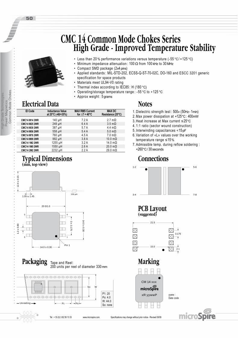
Typical Dimensions(mm, top view)
PCB Layout(suggested)
Marking
Connections
CMC 14 Common Mode Chokes SeriesHigh Grade - Improved Temperature Stability
Notes
Packaging
WSo
P1 PoUnreeling

Electrical Data
CMC 17 Common Mode Chokes SeriesHigh Grade - Improved Temperature Stability
CM
17 x
xx
xR
yyw
wP
1 8
54
17.0 ± 0.4 Pin 1
26.5 ± 0.5
15.4
± 0
.4
17.0
± 0
.4
3 x
3.8
1
1
45
8
1.2
x 0
.80
150 µm
1.5 to 2
28.0
20.0
2.2
3 x3.81
Typical Dimensions(mm, top view)
PCB Layout (suggested)
Marking
Connections
Notes
Packaging
WSo
P1 PoUnreeling

CMC17
0,01
0,1
1
10
100
0,01 0,1 1 10 100FREQUENCY (MHz)
30M
13M
5M8
1M2
2M6
M45
69M
IM
PE
DA
NC
E (
k)
ImpedanceCMC17
FREQUENCY (MHz)
AT
TE
NU
AT
ION
(d
B)
0
10
20
30
40
50
0,01 0,1 1 10 100
1M2
2M6
5M8
30M
13M
69M
M45
Attenuation
50Ω
50Ω
50Ω
SIN
Att. (dB) = 20 log 10
50ΩVTEST
VTEST
VDUAL
VREF
VREF
CMC
Attenuation Measurement Circuit
-80%
-60%
-40%
-20%
0%
20%
40%
60%
80%
100%
120%
-75 -50 -25 0 25 50 75 100 125 150 175
CMC17 range
Standard MnZn ferrite
High perm ferrite
Δ L
/L (
%)
Operating Temperature (°C)
Variation vs Temperature
CMC 17 Common Mode Chokes SeriesHigh Grade - Improved Temperature Stability

Derating CurvesCMC17 M45
Ambient temperature (°C)
Max a
llo
wab
le R
MS
cu
rren
t (A
)
2
6
10
14
18
25 35 45 55 65 75 85 95 105 115 125
ΔT = 80°CΔT = 70°C
ΔT = 90°C
ΔT = 50°C
ΔT = 40°C
ΔT = 60°C
ΔT = 20°C
ΔT = 10°C
ΔT = 30°C
Max a
llo
wab
le R
MS
cu
rren
t (A
)
Ambient temperature (°C)
CMC17 2M6
0
2
4
6
8
25 35 45 55 65 75 85 95 105 115 125
ΔT = 80°CΔT = 70°C
ΔT = 90°C
ΔT = 50°C
ΔT = 40°C
ΔT = 60°C
ΔT = 20°C
ΔT = 10°C
ΔT = 30°C
Max a
llo
wab
le R
MS
cu
rren
t (A
)
Ambient temperature (°C)
0
1
2
3
4
25 35 45 55 65 75 85 95 105 115 125
ΔT = 80°C
ΔT = 70°C
ΔT = 90°C
ΔT = 50°C
ΔT = 40°C
ΔT = 60°C
ΔT = 20°C
ΔT = 10°C
ΔT = 30°C
CMC17 13M
0
2
4
6
8
10
12
25 35 45 55 65 75 85 95 105 115 125
ΔT = 80°CΔT = 70°C
ΔT = 90°C
ΔT = 50°C
ΔT = 40°C
ΔT = 60°C
ΔT = 20°C
ΔT = 10°C
ΔT = 30°C
Max a
llo
wab
le R
MS
cu
rren
t (A
)
Ambient temperature (°C)
CMC17 1M2
Max a
llo
wab
le R
MS
cu
rren
t (A
)
Ambient temperature (°C)
0
1
2
3
4
5
6
25 35 45 55 65 75 85 95 105 115 125
ΔT = 80°CΔT = 70°C
ΔT = 90°C
ΔT = 50°C
ΔT = 40°C
ΔT = 60°C
ΔT = 20°C
ΔT = 10°C
ΔT = 30°C
CMC17 5M8M
ax a
llo
wab
le R
MS
cu
rren
t (A
)
Ambient temperature (°C)
CMC17 30M
0
0,5
1
1,5
2
2,5
3
25 35 45 55 65 75 85 95 105 115 125
ΔT = 80°CΔT = 70°C
ΔT = 90°C
ΔT = 50°C
ΔT = 40°C
ΔT = 60°C
ΔT = 20°C
ΔT = 10°C
ΔT = 30°C
Max a
llo
wab
le R
MS
cu
rren
t (A
)
Ambient temperature (°C)
CMC17 69M
0
0,5
1
1,5
2
25 35 45 55 65 75 85 95 105 115 125
ΔT = 80°CΔT = 70°C
ΔT = 90°C
ΔT = 50°CΔT = 40°C
ΔT = 60°C
ΔT = 20°C
ΔT = 10°C
ΔT = 30°C
CMC 17 Common Mode Chokes SeriesHigh Grade - Improved Temperature Stability
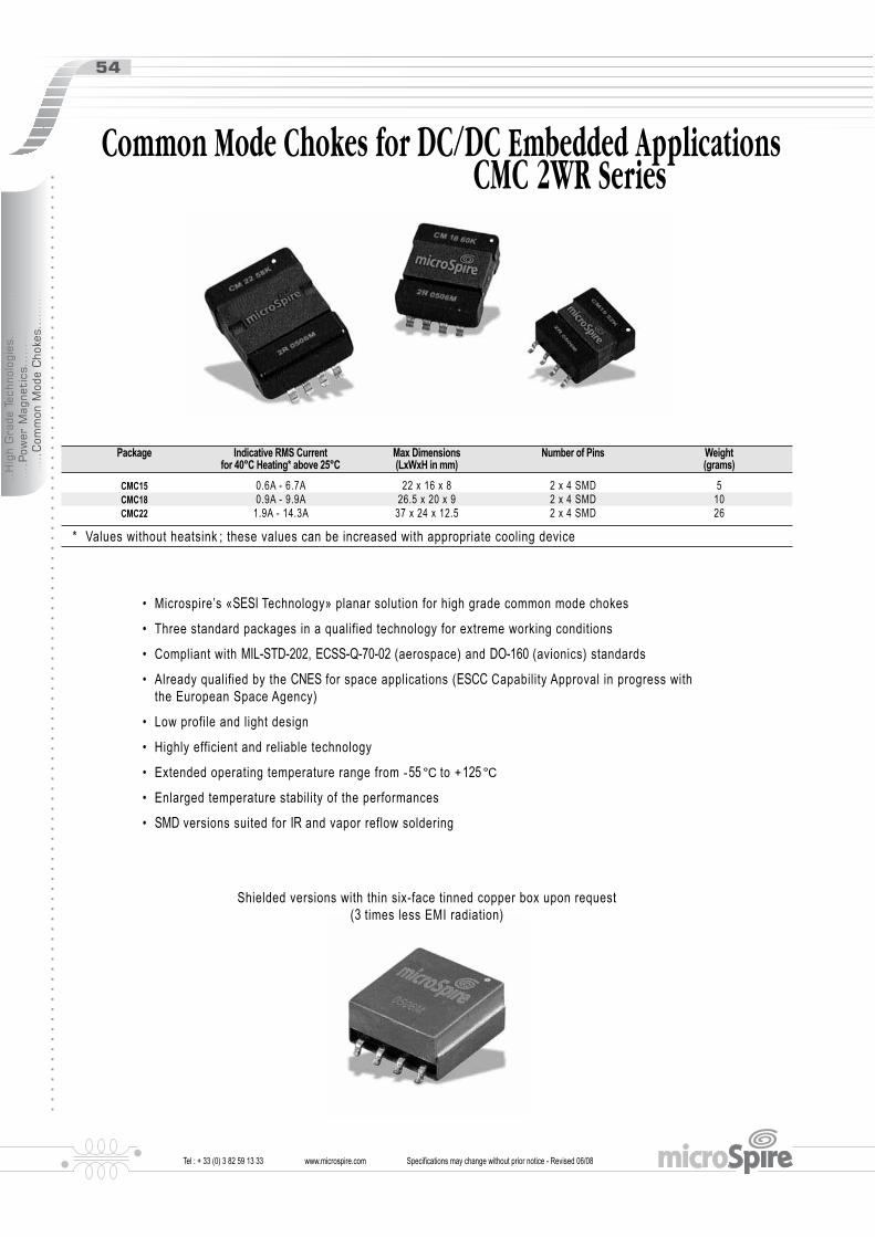
Common Mode Chokes for DC/DC Embedded Applications CMC 2WR Series

1.3 to 1.6
16 MAX
3 x 3.81
22MAX
1.2 x 0.4 MAX
16.3MAX
7.9MAX
1 4
8 5
130µm
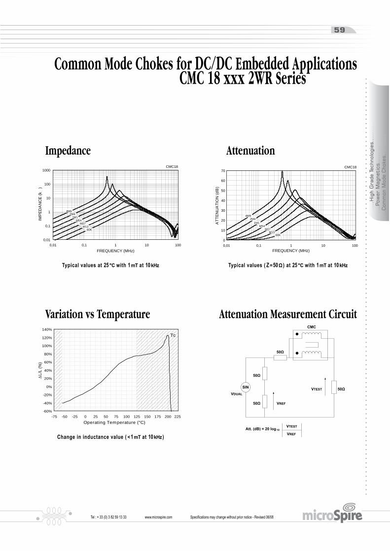
Electrical Data
Typical Dimensions(mm, top view)
CM15 xxx
xR yywwP
134 2
865 7
internal crossingfor correct connection
16 24
3.812.1
PCB Layout(suggested)
Connections(top view)
Common Mode Chokes for DC/DC Embedded Applications CMC 15 xxx 2WR Series
MarkingPackaging
F
WSo
P1 PoUnreeling
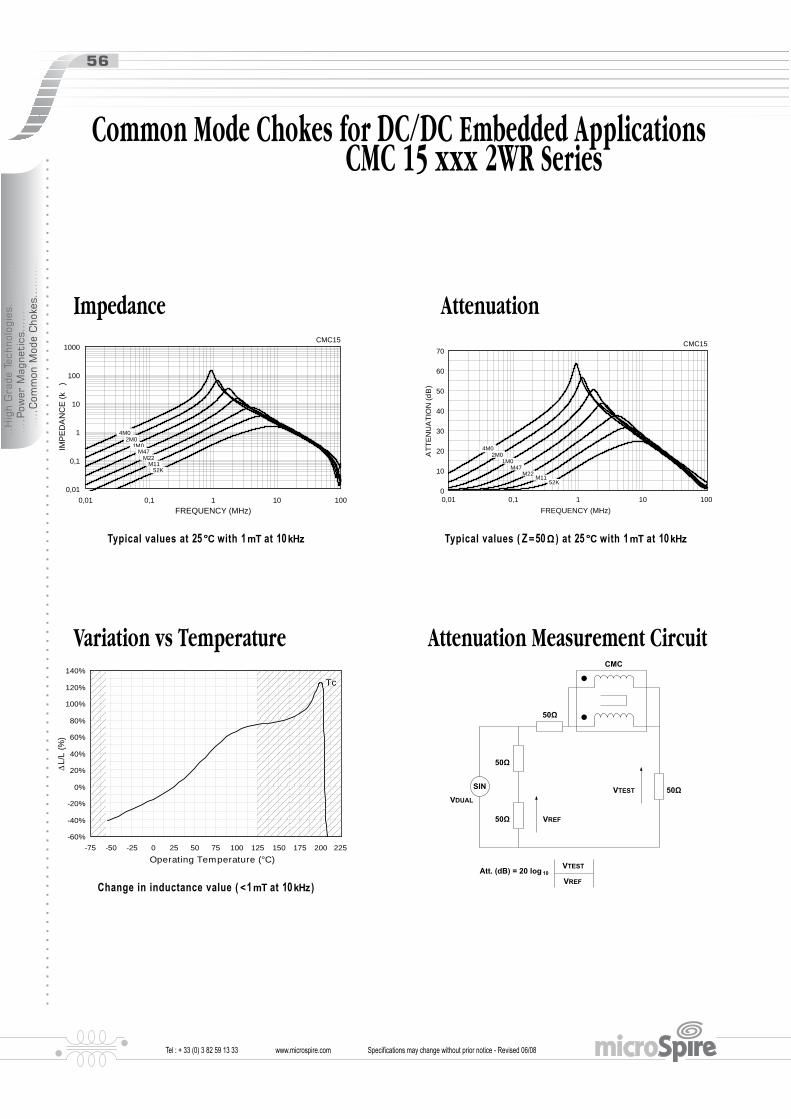
CMC15
0,01
0,1
1
10
100
1000
0,01 0,1 1 10 100
FREQUENCY (MHz)
IM
PE
DA
NC
E (
k)
2M01M0
M47
M11M22
52K
4M0
ImpedanceCMC15
0
10
20
30
40
50
60
70
0,01 0,1 1 10 100
FREQUENCY (MHz)
AT
TE
NU
AT
ION
(d
B)
2M01M0
M47
M11M22
52K
4M0
Attenuation
Attenuation Measurement Circuit
-60%
-40%
-20%
0%
20%
40%
60%
80%
100%
120%
140%
-75 -50 -25 0 25 50 75 100 125 150 175 200 225
Operating Temperature (°C)
ΔL
/L (
%)
Tc
Variation vs Temperature
Common Mode Chokes for DC/DC Embedded Applications CMC 15 xxx 2WR Series
50Ω
50Ω
50Ω
SIN
Att. (dB) = 20 log 10
50ΩVTEST
VTEST
VDUAL
VREF
VREF
CMC

Derating CurvesCMC15 52K
∆T = 80°C∆T = 70°C
∆T = 90°C
∆T = 50°C∆T = 40°C
∆T = 60°C
∆T = 20°C
∆T=10°C
∆T = 30°C
Ambient temperature (°C)
Max
allo
wab
le R
MS
curr
ent (
A)
0
3
6
9
12
25 35 45 55 65 75 85 95 105 115 125
∆T = 80°C∆T = 70°C
∆T = 90°C
∆T = 50°C∆T = 40°C
∆T = 60°C
∆T = 20°C
∆T=10°C
∆T = 30°C
0
1
2
3
4
5
25 35 45 55 65 75 85 95 105 115 125Ambient temperature (°C)
Max
allo
wab
le R
MS
curr
ent (
A)
CMC15 M22
CMC15 1M0
0
0,5
1
1,5
2
2,5
25 35 45 55 65 75 85 95 105 115 125Ambient temperature (°C)
Max
allo
wab
le R
MS
curr
ent (
A)
∆T = 80°C∆T = 70°C
∆T = 90°C
∆T = 50°C∆T = 40°C
∆T = 60°C
∆T = 20°C
∆T=10°C
∆T = 30°C
0
2,5
5
7,5
25 35 45 55 65 75 85 95 105 115 125Ambient temperature (°C)
Max
allo
wab
le R
MS
curr
ent (
A)
∆T = 80°C∆T = 70°C
∆T = 90°C
∆T = 50°C∆T = 40°C
∆T = 60°C
∆T = 20°C
∆T=10°C
∆T = 30°C
CMC15 M11
∆T = 80°C∆T = 70°C
∆T = 90°C
∆T = 50°C∆T = 40°C
∆T = 60°C
∆T = 20°C
∆T=10°C
∆T = 30°C
CMC15 M47
0
1
2
3
4
25 35 45 55 65 75 85 95 105 115 125Ambient temperature (°C)
Max
allo
wab
le R
MS
curr
ent (
A)
CMC15 2M0
0
0,5
1
1,5
25 35 45 55 65 75 85 95 105 115 125Ambient temperature (°C)
Max
allo
wab
le R
MS
curr
ent (
A) ∆T = 80°C
∆T = 70°C
∆T = 90°C
∆T = 50°C∆T = 40°C
∆T = 60°C
∆T = 20°C
∆T=10°C
∆T = 30°C
CMC15 4M0
0
0,2
0,4
0,6
0,8
1
25 35 45 55 65 75 85 95 105 115 125Ambient temperature (°C)
Max
allo
wab
le R
MS
curr
ent (
A) ∆T = 80°C
∆T = 70°C
∆T = 90°C
∆T = 50°C∆T = 40°C
∆T = 60°C
∆T = 20°C
∆T=10°C
∆T = 30°C
Common Mode Chokes for DC/DC Embedded Applications CMC 15 xxx 2WR Series

Electrical Data
130µm
19.8 MAX
3 x 3.81
2.1 x 0.4 MAX
22.0± 0.3
26MAX
1.3 to 1.6
8.7MAX
1 4
8 5
Typical Dimensions(mm, top view)
21 28
3.813.0
PCB Layout(suggested)
Common Mode Chokes for DC/DC Embedded Applications CMC 18 xxx 2WR Series
CM18 xxx
xR yywwP
Marking
134 2
865 7
internal crossingfor correct connection
Connections(top view)
Packaging
F
WSo
P1 PoUnreeling
CMC18
0,01
0,1
1
10
100
1000
0,01 0,1 1 10 100
FREQUENCY (MHz)
IM
PE
DA
NC
E (
k)
2M41M1
M54
M13M27
60K
4M9
ImpedanceCMC18
0
10
20
30
40
50
60
70
0,01 0,1 1 10 100
FREQUENCY (MHz)
AT
TE
NU
AT
ION
(d
B)
2M4
1M1M54
M13M27
60K
4M9
Attenuation
Attenuation Measurement Circuit
-60%
-40%
-20%
0%
20%
40%
60%
80%
100%
120%
140%
-75 -50 -25 0 25 50 75 100 125 150 175 200 225
Operating Temperature (°C)
ΔL
/L (
%)
Tc
Variation vs Temperature
Common Mode Chokes for DC/DC Embedded Applications CMC 18 xxx 2WR Series
50Ω
50Ω
50Ω
SIN
Att. (dB) = 20 log 10
50ΩVTEST
VTEST
VDUAL
VREF
VREF
CMC

Derating CurvesCMC18 60K
0
4
8
12
16
25 35 45 55 65 75 85 95 105 115 125Ambient temperature (°C)
Max
allo
wab
le R
MS
curr
ent (
A) ∆T = 80°C
∆T = 70°C
∆T = 90°C
∆T = 50°C∆T = 40°C
∆T = 60°C
∆T = 20°C
∆T=10°C
∆T = 30°C
CMC18 M27
0
2,5
5
7,5
25 35 45 55 65 75 85 95 105 115 125Ambient Temperature (°C)
Max
allo
wab
le R
MS
curr
ent (
A)
∆T = 80°C∆T = 70°C
∆T = 90°C
∆T = 50°C∆T = 40°C
∆T = 60°C
∆T = 20°C
∆T=10°C
∆T = 30°C
CMC18 1M1
0
1
2
3
25 35 45 55 65 75 85 95 105 115 125Ambient temperature (°C)
Max
allo
wab
le R
MS
curr
ent (
A) ∆T = 70°C
∆T = 90°C
∆T = 50°C∆T = 40°C
∆T = 60°C
∆T = 20°C
∆T=10°C
∆T = 30°C
∆T = 80°C
CMC18 M13
0
3
6
9
12
25 35 45 55 65 75 85 95 105 115 125Ambient temperature(°C)
Max
allo
wab
le R
MS
curr
ent (
A)
∆T = 80°C∆T = 70°C
∆T = 90°C
∆T = 50°C∆T = 40°C
∆T = 60°C
∆T = 20°C
∆T=10°C
∆T = 30°C
CMC18 M54
0
1
2
3
4
5
25 35 45 55 65 75 85 95 105 115 125Ambient temperature (°C)
Max
allo
wab
le R
MS
curr
ent (
A)
∆T = 80°C∆T = 70°C
∆T = 90°C
∆T = 50°C∆T = 40°C
∆T = 60°C
∆T = 20°C
∆T=10°C
∆T = 30°C
CMC18 2M4
0
0,5
1
1,5
2
25 35 45 55 65 75 85 95 105 115 125Ambient temperature (°C)
Max
allo
wab
le R
MS
curr
ent (
A)
∆T = 80°C∆T = 70°C
∆T = 90°C
∆T = 50°C∆T = 40°C
∆T = 60°C
∆T = 20°C
∆T=10°C
∆T = 30°C
CMC18 4M9
0
0,5
1
1,5
25 35 45 55 65 75 85 95 105 115 125Ambient temperature (°C)
Max
allo
wab
le R
MS
curr
ent (
A)
∆T = 80°C∆T = 70°C
∆T = 90°C
∆T = 50°C∆T = 40°C
∆T = 60°C
∆T = 20°C
∆T=10°C
∆T = 30°C
Common Mode Chokes for DC/DC Embedded Applications CMC 18 xxx 2WR Series

Electrical Data
Common Mode Chokes for DC/DC Embedded Applications CMC 22 xxx 2WR Series
134 2
865 7
internal crossingfor correct connection
Connections(top view)
CM22 xxx
xR yywwP
Marking
130µm
23.5 MAX
3 x 3.81
2.1 x 0.45 MAX
30.8± 0.4
35.3MAX
1.3 to 1.6
12.2MAX
1 4
8 5
Typical Dimensions(mm, top view)
Packaging
F
WSo
P1 PoUnreeling
29.0 37.5
3.813.0
PCB Layout(suggested)

CMC22
0,01
0,1
1
10
100
1000
0,01 0,1 1 10 100
FREQUENCY (MHz)
IM
PE
DA
NC
E (
k)
3M31M6
M74
M14M34
58K
ImpedanceCMC22
0
10
20
30
40
50
60
70
0,01 0,1 1 10 100
FREQUENCY (MHz)
AT
TE
NU
AT
ION
(d
B)
3M3
1M6M74
M14M34
58K
Attenuation
Attenuation Measurement Circuit
-60%
-40%
-20%
0%
20%
40%
60%
80%
100%
120%
140%
-75 -50 -25 0 25 50 75 100 125 150 175 200 225
Operating Temperature (°C)
ΔL
/L (
%)
Tc
Variation vs Temperature
Common Mode Chokes for DC/DC Embedded Applications CMC 22 xxx 2WR Series
50Ω
50Ω
50Ω
SIN
Att. (dB) = 20 log 10
50ΩVTEST
VTEST
VDUAL
VREF
VREF
CMC

Derating CurvesCMC22 58K
0
5
10
15
20
25
25 35 45 55 65 75 85 95 105 115 125Ambient temperature (°C)
Max
allo
wab
le R
MS
curr
ent (
A)
∆T = 30°C
∆T=10°C
∆T = 80°C∆T = 70°C
∆T = 90°C
∆T = 50°C∆T = 40°C
∆T = 60°C
∆T = 20°C
∆T = 80°C∆T = 70°C
∆T = 90°C
∆T = 50°C∆T = 40°C
∆T = 60°C
∆T = 20°C
∆T=10°C
∆T = 30°C
CMC22 M34
0
2
4
6
8
10
25 35 45 55 65 75 85 95 105 115 125Ambient temperature (°C)
Max
allo
wab
le R
MS
curr
ent (
A)
∆T = 80°C∆T = 70°C
∆T = 90°C
∆T = 50°C∆T = 40°C
∆T = 60°C
∆T = 20°C
∆T=10°C
∆T = 30°C
CMC22 1M6
0
1
2
3
4
5
25 35 45 55 65 75 85 95 105 115 125Ambient temperature (°C)
Max
allo
wab
le R
MS
curr
ent (
A)
CMC22 M14
0
3
6
9
12
15
25 35 45 55 65 75 85 95 105 115 125Ambient temperature (°C)
Max
allo
wab
le R
MS
curr
ent (
A)
∆T = 80°C∆T = 70°C
∆T = 90°C
∆T = 50°C∆T = 40°C
∆T = 60°C
∆T = 20°C
∆T=10°C
∆T = 30°C
∆T = 80°C∆T = 70°C
∆T = 90°C
∆T = 50°C∆T = 40°C
∆T = 60°C
∆T = 20°C
∆T=10°C
∆T = 30°C
CMC22 M74
0
2,5
5
7,5
25 35 45 55 65 75 85 95 105 115 125Ambient temperature (°C)
Max
allo
wab
le R
MS
curr
ent (
A)
∆T = 80°C∆T = 70°C
∆T = 90°C
∆T = 50°C∆T = 40°C
∆T = 30°C
∆T = 60°C
∆T = 20°C
∆T=10°C
CMC22 3M3
0
1
2
3
25 35 45 55 65 75 85 95 105 115 125Ambient temperature (°C)
Max
allo
wab
le R
MS
curr
ent (
A)
Common Mode Chokes for DC/DC Embedded Applications CMC 22 xxx 2WR Series

CMC22 58K
0
5
10
15
20
25
25 35 45 55 65 75 85 95 105 115 125Ambient temperature (°C)
Max
allo
wab
le R
MS
curr
ent (
A)
∆T = 30°C
∆T=10°C
∆T = 80°C∆T = 70°C
∆T = 90°C
∆T = 50°C∆T = 40°C
∆T = 60°C
∆T = 20°C
9.7A
13.7A
MAX OPERATING TEMP(GUARANTEED)
AREA WHERE OPERATINGTEMPERATURE IS > +125°C
EXTENDED LIFETIMEGUARANTEED AREA
Technical note - Appendix CMC 15 - 18 - 22 & CMC 17 Temperature Application

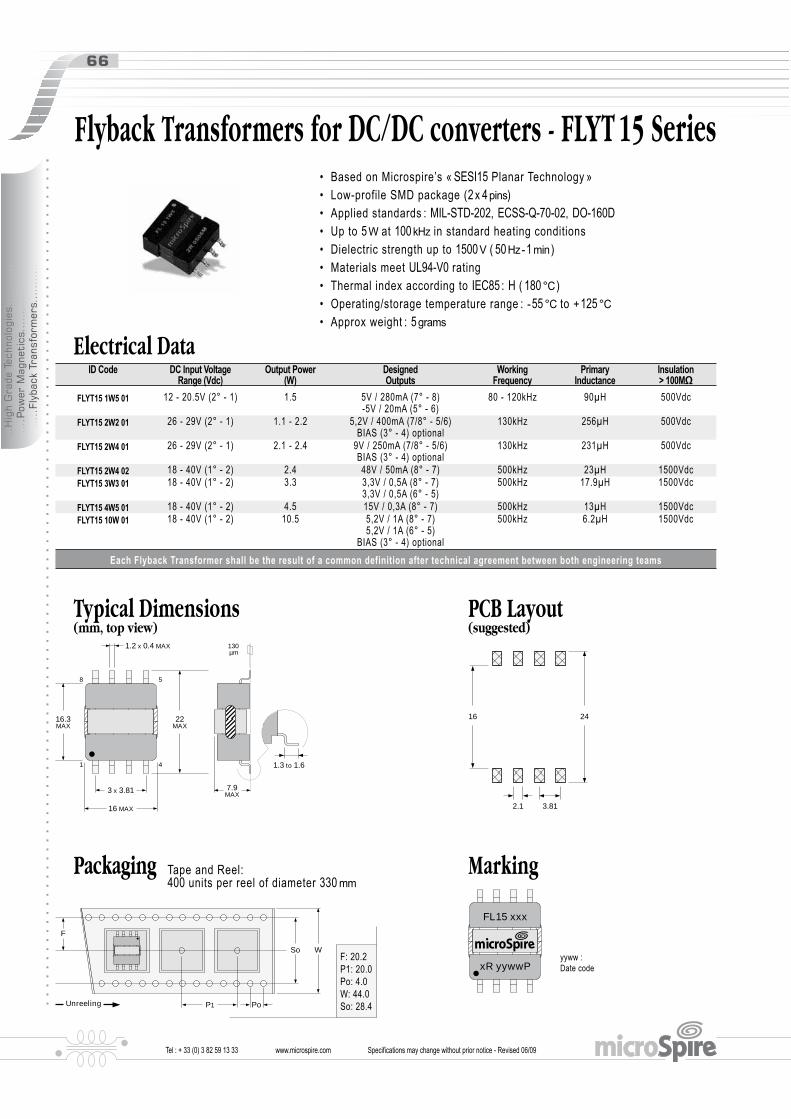
Flyback Transformers for DC/DC Embedded Applications FLYT Series
Electrical Data
Flyback Transformers for DC/DC converters - FLYT 15 Series
1.3 to 1.6
16 MAX
3 x 3.81
22MAX
1.2 x 0.4 MAX
16.3MAX
7.9MAX
1 4
8 5
130µm
Typical Dimensions(mm, top view)
FL15 xxx
xR yywwP
16 24
3.812.1
PCB Layout(suggested)
MarkingPackaging
F
WSo
P1 PoUnreeling

Electrical Data
Flyback Transformers for DC/DC converters - FLYT 18 Series
130µm
19.8 MAX
3 x 3.81
2.1 x 0.4 MAX
22.0± 0.3
26MAX
1.3 to 1.6
8.7MAX
1 4
8 5
Typical Dimensions(mm, top view)
21 28
3.813.0
PCB Layout(suggested)
FL18 xxx
xR yywwP
MarkingPackaging
F
WSo
P1 PoUnreeling

Electrical Data
Flyback Transformers for DC/DC converters - FLYT 22 Series
FL22 xxx
xR yywwP
Marking
130µm
23.5 MAX
3 x 3.81
2.1 x 0.45 MAX
30.8± 0.4
35.3MAX
1.3 to 1.6
12.2MAX
1 4
8 5
Typical Dimensions(mm, top view)
Packaging
F
WSo
P1 PoUnreeling
29.0 37.5
3.813.0
PCB Layout(suggested)

3.50
9.50
1.1 1.1
7.9
13.9
W terminalsJ leaded
1 8
4 5
CT
01
1
00
26
1J
y
y/w
w
6
8
2
4
5
7
1
3
SEC 1PRIM 1
SEC 2PRIM 2
Electrical Data ( 25°C )
Notes
Application
7.50
7.40
5.334 = 3 x 1.778
8.50 MAX
0.80
2.0 Max , 1.50typ 0.10 +0.2 -0
8.40 MAX
12,5 ± 0,5
W terminalsJ leaded
9,20 ± 0,30
7.50 +0,3 -0
8.40 MAX
0.80
0.15
PCB Layout (mm)
Connections Marking
Current sense Transformer - CT01 100 261x
6
8
2
4
5
7 Z load
1
3
6
8
2
4
5
7
1
3 Z load
To Order CT01 100 261 x Dimensions (mm)
Packaging
F
WSo
P1 Po Unreeling

CT 08 xxx
xR yywwP
Marking face
Dot for pin 1
Bottom View
15.80
3.00
8.70
1.40
3.8113.97
10.50
15.00
3 4
2
1
3
4
Marking face
Dot for pin 1
Bottom View
15.80
3.00
8.70
1.40
3.8113.97
10.50
15.00
3 4
2
1
3
4
Application Schem.n3 n1 n2
DTR L
iL IOUT
VOUTV
(-VD)
D
C
R
V2
V1
V3
Ve
Dm Tp
i1i3
VT
i2
RL
VOUT
CT08 200 221R
n3 n1 n2DTR L
iL IOUT
VOUTV
(-VD)
D
C
R
V2
V1
V3
Ve
Dm Tp
i1i3
VT
i2
RL
VOUT
CT08 200 221R
1 4
IIN
PRIM(Np)
SEC(Ns)
RL VOUT
2 3
1 4
IIN
PRIM(Np)
SEC(Ns)
RL VOUT
2 3
Electrical Data ( 25°C )
Marking
Notes
Connections
Typical Dimensions (mm)
Current Transformer for DC/DC ApplicationsCT08 200 221 PR

8.4 14.4
3.2
8.4
CT 91 xxx
xR yywwP
1
2
3
4
Z load
Electrical Data ( 25°C )
To Order CT91 ### 231 WR Notes
Application
I
Ipk
IDC
αT T
ΔI10.7MAX
13.4 MAX
0.9 to 1.3
1.5 x0.28MAX
10.6 MAX
5.8MAX
5.7
1
2
4
3
PCB Layout(suggested)
Connections
Dimensions(mm, top view)
Marking
Current sense Transformer, up to 10Apk - CT91 xxx 231 WR
Packaging
F
WSo
P1 PoUnreeling
16 24
14
5 8
3.812.0
CT 15 xxx
xR yywwP
1
3
8
7
2
4
6
5
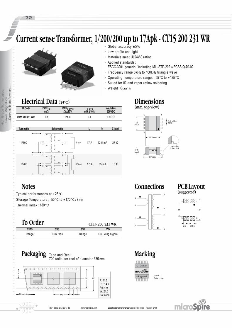
Electrical Data ( 25°C )
To Order CT15 200 231 WR
Notes
1.3 to 1.6
16MAX
22 MAX
1.2 x 0.4MAX
16.3 MAX
7.9MAX
1
4
8
5
PCB Layout(suggested)
Connections
Dimensions(mm, top view)
Marking
Current sense Transformer, 1/200/200 up to 17Apk - CT15 200 231 WR
Packaging
F
WSo
P1 PoUnreeling
6
5
2
4
8
7 Z load
1
3
6
5
2
4
8
7
1
3 Z load
Type B
Type A
3
PRIM SEC
2
4
1
3
PRIM SEC
4
2
1
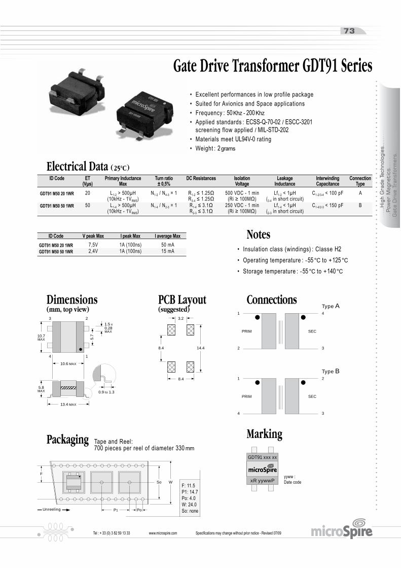
Connections
Electrical Data ( 25°C )
Notes
Gate Drive Transformer GDT91 Series
GDT91 xxx xx
xR yywwP
10.7MAX
13.4 MAX
0.9 to 1.3
1.5 x0.28MAX
10.6 MAX
5.8MAX
5.7
1
2
4
3
8.4 14.4
3.2
8.4
Marking
Dimensions(mm, top view)
PCB Layout(suggested)
Packaging
F
WSo
P1 PoUnreeling

1.3 to 1.6
16 MAX
3 x 3.81
22MAX
1.2 x 0.4 MAX
16.3MAX
7.9MAX
1 4
8 5
Notes
Dimensions (mm, top view) PCB Layout(suggested)
Connections
GDT 15 xxx
xR yywwP
Marking
Type B
Type A
7PRIM
SEC
8
2
1
7
PRIM SEC
8
2
1
5
SEC
6
4
3
16 24
3.812.1
Gate Drive Transformer GDT15 Series
Electrical Data ( 25°C )
Packaging
F
WSo
P1 PoUnreeling

From Design to Production
www.microspire.c m
Wo u n d M a g n e t i c s E x p e r t s
Industri
al Technolo
gies
Industri
al Technolo
gies
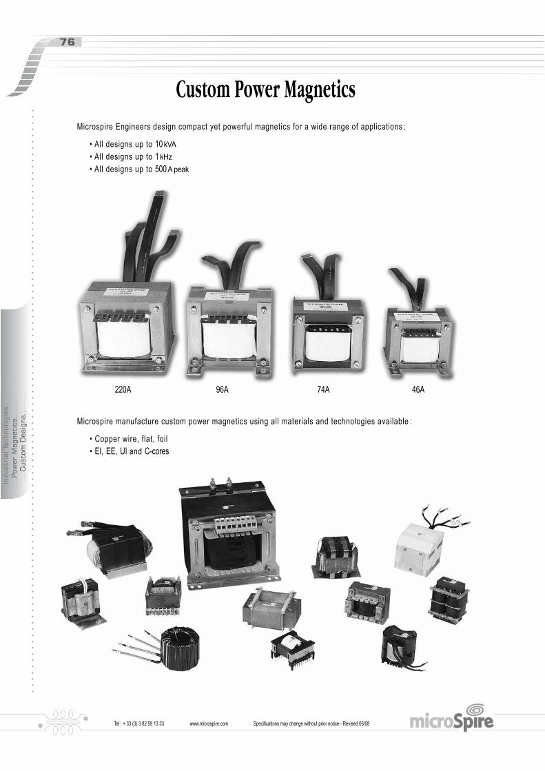
Custom Power Magnetics

EFD, ER and EP series
ETD Coils and Transformers
RM series
Planar Magnetics
Custom Power Magnetics

Current and Voltage Transformers
Electro-Magnetic Sensors
Self-Bonded Coils
Injection-Moulded Coils / Bobbin Coils
Custom bobbins

Electrical Data
Connections
Response Curves
Att
en
uati
on
(d
B)
Typical Attenuation versus Frequency on 50 OhmsDLEF1x 020 1S
25
20
15
10
5
0
-5
Frequency (Hz)
1E+05 1E+06 1E+07 1E+08 1E+09
@100mV
COMMON MODE
DIFFERENTIAL MODE
Typical Dimensions (mm)
7.8
8
5
1
4
5
3.81
5.4
7.4 max
4.3
5
0.4
1.21
cap
Bottom view
Top view
DLEF0x xxx xS
DLEF1x xxx xS
with cap
without cap
DLEFx2 xxx xS
DLEFx4 xxx xS
DLEFx3 xxx xS
6.2
1.21
0.8
2
Data Line EMI Filters - DLEF Series
Packaging
PCB Layout(suggested)

Electrical Data
Typical Impedance versus FrequencyESC11 xxx xS
10 000
1 000
100
10
1
0.1
0.01
1E+02 1E+03 1E+04 1E+05 1E+06 1E+07 1E+08
Frequency (Hz)
Mo
du
lus (
Oh
ms)
ESC11 15K
ESC11 56K
ESC11 M47
@ 100mV
@ 100mV
ESC11 15K
ESC11 56K
ESC11 M47
Typical Attenuation versus Frequency on 50 OhmsESC11 xxx xS
30
25
20
15
10
5
0
Att
en
uati
on
(d
B)
1E+04 1E+05 1E+06 1E+07 1E+08
Frequency (Hz)
7.8
8
5
1
4
5
3.81
5.4
7.4 max
4.3
5
0.4
1.21
cap
Bottom view
Top view
ESC0x xxx xS
ESC1x xxx xS
with cap
without cap
Connections
6.2
0.8
2
1.21
1
2
4
3
5
6
8
7
EMI Suppression Chokes - ESC Series
Packaging
PCB Layout(suggested)

Electrical Data
14
12.5 10.16
12.7 10
□ 0.5
3.5
Horizontal design ICMCxx xxx xH
5 6
1 10
9
14 10.16
7.62 15
□ 0.5
3.5
Vertical design ICMCxx xxx xV
5 6
1 10
Typical Dimensions (mm)
Symbols
Connections2-fold chokes ICMC12 xxx xx
1 10
65
4-fold chokes ICMC14 xxx xx
1 10
2 9
4 7
5 6
Common-Mode Chokes - ICMC Series
Measurement CircuitFrequency Response
Electrical Data
To Order LCMC 20 4M7 1S
MB08216-0
0
5
10
15
20
25
30
35
40
45
1E+02 1E+03 1E+04 1E+05 1E+06 1E+07 1E+08
Frequency (Hz)
Att
en
uati
on
(d
B)
Typical attenuation versus frequency on 50 Ohms
@100mV
LCMC 20 4M7 1S
VREF
VTEST
SINVDUAL
50 Ω
50 Ω
50 Ω
50 Ω
Typical Dimensions (mm) Connections
4
1 2
3
Pin 1 Identifier
4 x Ø 1.14 TYPContact surface
7.62 TYP
8.76± 0.25
10.16 ± 0.25
Bottom view
0.64
6.35max
6.22± 0.05
Marking
1 yywwP
LC 20 4M7
1
2
4
3
Line Common Mode Choke - LCMC

Electrical Data
Typical Dimensions (mm)
7.8
8
5
1
4
5
3.81
5.4
7.4 max
4.3
5
0.4
1.21
cap
Bottom view
Top view
WRFT0x xxx xS
WRFT1x xxx xS
with cap
without cap
Connections
8
5
1
4
8
6-7
5
1
4
Standard
Center tap
PRI
PRI PRI
6.2
0.8
2
1.21
Wide Band RF Transformers - WRFT Series
Packaging PCB Layout(suggested)

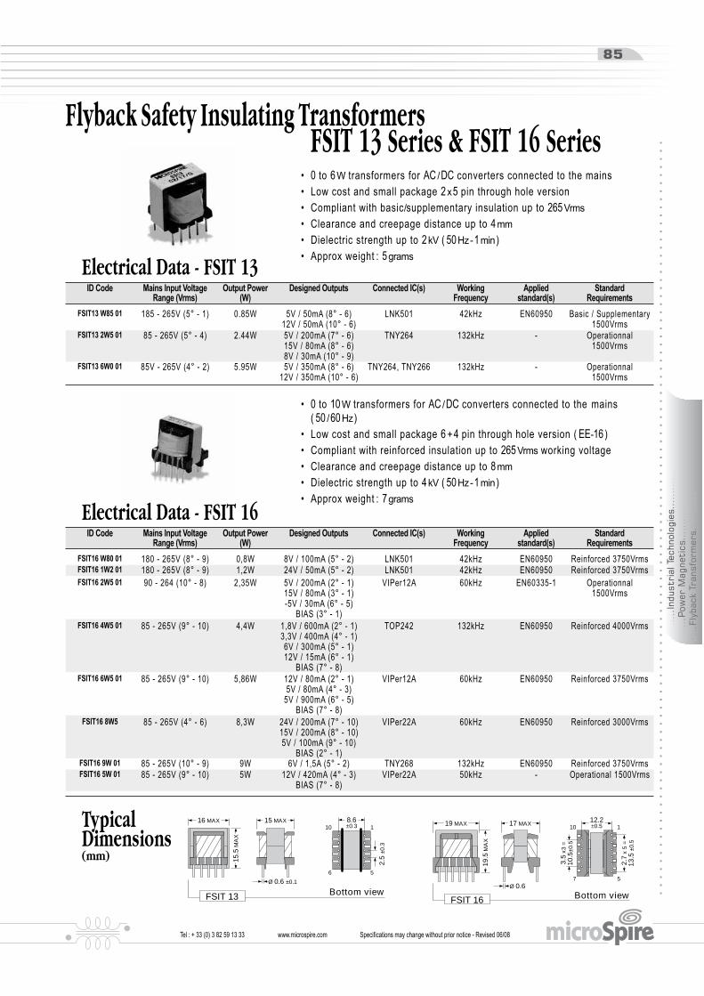
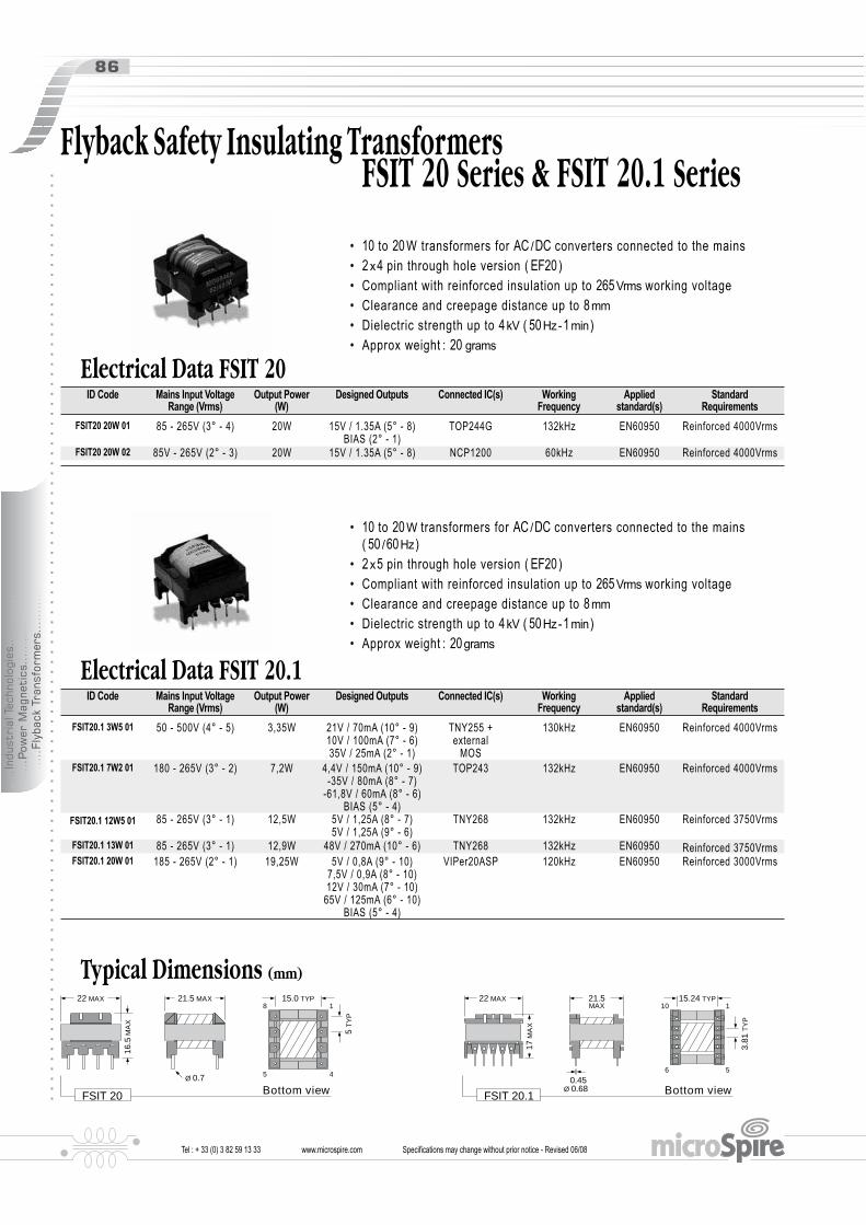
Flyback Safety Insulating Transformers FSIT Series
16 MAX
15.5
MA
X
15 MAX
Ø 0.6 ±0.1
10
6
1
5
Bottom view
8.6±0.3
2.5
±0
.3
FSIT 13 FSIT 16Bottom view
17 MAX
Ø 0.6
19 MAX
19.5
MA
X
10 1
7 5
2.7
x 5
=13.5
±0
.5
12.2±0.5
3.5
x3
=10.5
±0
.5
TypicalDimensions(mm)
FSIT 13 Series & FSIT 16 SeriesFlyback Safety Insulating Transformers
Electrical Data - FSIT 13
Electrical Data - FSIT 16
Electrical Data FSIT 20.1
Bottom viewFSIT 20
16.5
MA
X
5 4
22 MAX 21.5 MAX 15.0 TYP
Ø 0.7
8 1
5 T
YP
Bottom viewFSIT 20.1
6 5
15.24 TYP10 1
3.8
1 T
YP
17
MA
X
22 MAX
0.45Ø 0.68
21.5MAX
Typical Dimensions (mm)
FSIT 20 Series & FSIT 20.1 SeriesFlyback Safety Insulating Transformers
Electrical Data FSIT 20

TypicalDimensions(mm)
28 MAX 28.5 MAX
5.08TYP
20.32 TYP
Bottom View
5
110
6□ 0.7
20.5
MA
X
35.5 MAX 35.5 MAX
□ 0.7 25.4 TYP
Bottom View
1
67
135.08TYP
25.5
MA
X
FSIT 25 Series & FSIT 29 SeriesFlyback Safety Insulating Transformers
Electrical Data FSIT 25
Electrical Data FSIT 29

Electrical Data Connections
Typical Dimensions (mm)
a
3.5
bL
HW
1 2
4 3
3.5 H
L
W
1
2
3
4
8
7
6
5
b c
a
1 4
2 3
2 7
3 6
Applications
Common-Mode Chokes - CMESC 10-14

Electrical Data
a
3.5
bL
HW
1 2
4 3
Typical Dimensions (mm) Connections
1 4
2 3
Common-Mode Chokes - CMESC 17

Att. (dB) = 20 log 10TEST
REF
V
V
50Ω
SIN
50Ω
50Ω
50ΩVTEST
CMESC
VREF
VDUAL
CMC17
0,01
0,1
1
10
100
0,01 0,1 1 10 100FREQUENCY (MHz)
30M
13M
5M8
1M2
2M6
M45
69M
IM
PE
DA
NC
E (
k)
ImpedanceCMC17
FREQUENCY (MHz)
AT
TE
NU
AT
ION
(d
B)
0
10
20
30
40
50
0,01 0,1 1 10 100
1M2
2M6
5M8
30M
13M
69M
M45
Attenuation
Attenuation Measurement Circuit
-80%
-60%
-40%
-20%
0%
20%
40%
60%
80%
100%
120%
-75 -50 -25 0 25 50 75 100 125 150 175
CMESC17 range
Standard MnZn ferrite
High perm ferrite
Δ L
/L (
%)
Operating Temperature (°C)
Variation vs Temperature
CMESC 17 Common Mode Chokes SeriesImproved Temperature Stability

Typical Dimensions (mm - see tables)
D
W
1,5max
15±3
Toroidal Chokes - TC Series
Electrical Data

Electrical Data
Typical Dimensions (mm)
7 8
5 6
3 4
1 2
H
L
3.5 ±0.5I
a c
b
D
ConnectionsSeries
Differentialmode
STRAP
Parallel
7 8
65
3 4
21
IN OUT
7 8
65
3 4
21
IN+ IN-
OUT- OUT+
7 8
65
3 4
21
IN OUT
Symbols
Energy Storage Inductors - ESI Series

Electrical Data (25°C)
8.7 max
7max
4
6
3
1
150
150
B
A
Dot for Pin 1
3.70±0.2
Ht 5.33
8.30
1.0
3.50
9.505.30 3.00
34
0.6 ±0.1
NotesTypical Dimensions (mm)
Connections
A
B
1T
1
3
Z load
Current sense Transformer up to 2.2ACT05 xxx 231 W
Packaging
Ko
BoF
WSo
Ao
P1
Po

SMD Line-Matching Transformer - MTLM 1234
Connections
Frequency Response Distorsion
Dimensions (mm)
Electrical Data
Packaging7
1.80 1.25
9
13
2 x 2.54
1.70
1.8
11.2
5.08
1.25
1
3
6
4
-5.0
-4.5
-4.0
-3.5
-3.0
-2.5
-2.0
-1.5
-1.0
-0.5
0.0
10 100 1000 10000 100000
AMPLITUDE (dBm) LOAD : 600 Ω @ 0 dBm
FREQ (Hz)
-110
-100
-90
-80
-70
-60
-50
10 1000 10000
T.H. DISTORTION + NOISE (dBm) LOAD : 600 @ -10 dBm
FREQ (Hz)

Line-Matching Transformers - MTLM SeriesFeatures
Electrical Data
ApplicationsDimensions and Connections
1 3
6 4
7.62
18
18 12.7
14 MAX
0.5
3.5 min6
4
1
3Ø 0.6
1 3
6 4
7.62
18
18 12.7
5
0.5
3.5 min
14
6
4
1
3
5
Ø 0.6
15.2
14.9 10.166 10
1 5
10.16
3.5
13.2 Ø 0.6
6
10
1
5
6
10
10 6
1 5
1
5
13.7 13
12
2.54 1.27
20.32
3.175
1
8
4
23
25 15.24
Ø 0.65
5
8
1
4
3x5.08 3.5
17
4
8
1
22
26 15.24
5
3x5.08
1
4
8
5
23
150
150
600
3
16.5
Ø 0.7
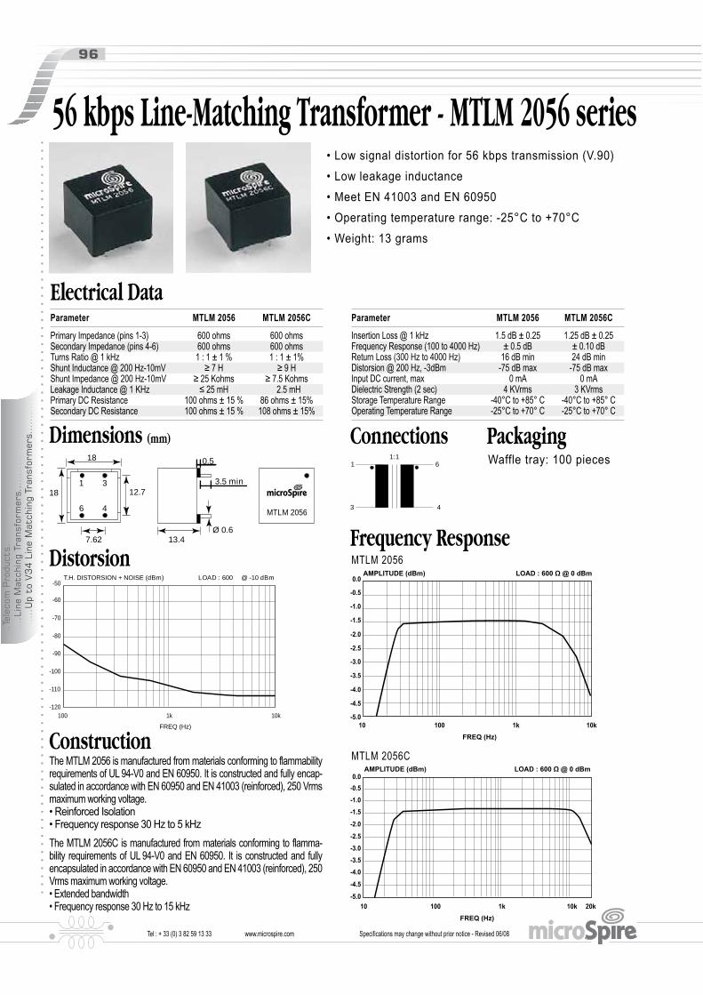
56 kbps Line-Matching Transformer - MTLM 2056 series
Dimensions (mm) Connections
Construction
Frequency ResponseDistorsion
Electrical Data
Packaging
1 3
6 4
7.62
18
18 12.7
13.4
0.5
3.5 min
Ø 0.6
MTLM 2056
6
4
1
3
1:1
-5.0
-4.5
-4.0
-3.5
-3.0
-2.5
-2.0
-1.5
-1.0
-0.5
0.0
10 100 1k 10k
AMPLITUDE (dBm) LOAD : 600 Ω @ 0 dBm
FREQ (Hz)
-120
-110
-100
-90
-80
-70
-60
-50
100 1k 10k
T.H. DISTORSION + NOISE (dBm) LOAD : 600 @ -10 dBm
FREQ (Hz)
-5.0
-4.5
-4.0-3.5-3.0-2.5
-2.0
-1.5-1.0-0.5 0.0
10 100 1k 20k10k
AMPLITUDE (dBm) LOAD : 600 Ω @ 0 dBm
FREQ (Hz)

From Design to Production
www.microspire.c m
Wo u n d M a g n e t i c s E x p e r t s
+-
C43.5p
r
rs2
rs1
Is1600k
Is21.2
Is
5.01m
25u
C5
-1.2p
C3
3.7p
100G
RinfE
E1F
F1
250m
Rp4
Lp4
92k
Lp3
20.5k
Lp2
2.5k
p1
5k
1
1
1.4
Rp3
5 95 105 115
T = 30°C
T=10
0°C
T = 40°C
T = 20°C
Engineerin
g Serv
ices

Electrical Modelling of Magnetics
1°105
105 106 107
1°104
104
1°103
103100
MODULUS ZO from primary
Frequency (Hertz)
Mo
du
lus
(O
hm
s)
PHASE ZO from primary100
50
0
-50
-100100 103 104 105 106 107
Ph
as
e (
De
gre
es
)
Frequency (Hertz)
Component optimisationthrough electrical model
Thermal characterizationof components/packages
CMC22 M27
0
5
10
15
20
25
25 35 45 55 65 75 85 95 105 115 125AMBIENT TEMPERATURE (°C)
MA
X A
LLO
WA
BLE
RM
S C
UR
REN
T (A
)
∆T = 30°C
∆T=10°C
∆T = 80°C∆T = 70°C
∆T = 90°C
∆T = 50°C∆T = 40°C
∆T = 60°C
∆T = 20°C
0
20
40
60
80
100
120
140
160
180
0,0 1,0 2,0 3,0 4,0 5,0 6,0
SESI 18 - TEMP INCREASE VS LOSSES
Total Losses (W)
ΔT
(°C
)
DT (°C) - 25°C
DT (°C) - 50°C
DT (°C) - 75°C
DT (°C) - 100°C
DT (°C) - 125°C
SESI 18 - EQUIVALENT THERMAL RESISTANCE
27
28
29
30
31
32
33
34
35
36
37
0,0 1,0 2,0 3,0 4,0 5,0 6,0
Total Losses (W)
Rth
(°C
/W)
RTH (°C/W) - 25°C
RTH (°C/W) - 50°C
RTH (°C/W) - 75°C
RTH (°C/W) - 100°C
RTH (°C/W) - 125°C
+-
C4 3.5p
rs3rs2rs1
Is1 600k Is2 1.2 Is3 200m
5.01m 25u 5u
C2
2.9p
C
D
C6
1.6p
C5
-1.2p
C3
3.7p
100G
Rinf
E
E1
F
F1
250mRp4
Lp4
92k
Lp3
20.5k
Lp2
2.5k
Lp1
2.5k
1
1
1.4Rp1
Rp2
Rp3
r1
124Rp
260k
C1A
B
5.3p
Engineering Services

ADSL Central Office Splitters
Public Telephone Filters
Train Detection Filters
Engineering ServicesHigh Performance Passive Filters

Component optimisationthrough 2D/3D simulation
Electromagnetic Characteristics of Magnetics
Engineering Services


Notes

www.microspire.c m