
Hardware description of multi-layer perceptrons with different abstraction levels
10
Hardware description of multi-layer perceptrons with different abstraction levels E.M. Ortigosa a, * , A. Can ˜as a , E. Ros a , P.M. Ortigosa b , S. Mota a , J. Dı ´az a a Department of Computer Architecture and Technology, ETS Ingenierı ´a Informa ´ tica, University of Granada, E-18071 Granada, Spain b Department of Computer Architecture and Electronics, University of Almerı ´a, E-04120 Almerı ´a, Spain Available online 27 April 2006 Abstract This paper presents different hardware implementations of a multi-layer perceptron (MLP) for speech recognition. When defining the designs, we have used two different abstraction levels: a register transfer level and a higher algorithmic-like level. The implementations have been developed and tested into reconfigurable hardware (FPGA) for embedded systems. We also present a comparative study of the costs for the two considered approaches with regards to the silicon area, speed and required computational resources. The research is completed with the study of different implementation versions with diverse degrees of parallelism. The final aim is the comparison of the methodologies applied in the two abstraction levels for designing hardware MLP’s or similar computational structures. Ó 2006 Elsevier B.V. All rights reserved. Keywords: FPGA; Hardware implementation; Multi-layer perceptron; Speech recognition 1. Introduction An Artificial Neural Network (ANN) is an information processing paradigm which mimics the way biological ner- vous systems process information. An ANN is configured through a learning process for a specific application, such as pattern recognition or data classification, and as in all biological systems, this learning process will require the adjustment of the synaptic connections between the neurons. ANNs implemented in software are becoming more and more appropriate for real-world applications [1,2]: Optical Character Recognition (OCR), data mining, image compression, medical diagnosis, Automatic Speech Recog- nition (ASR), etc. Currently, ANN hardware implementa- tions run in a few niche areas [3]: where very high performance is required (e.g., high-energy physics); in embedded applications of simple hardwired networks (e.g., speech recognition chips); and in neuromorphic sys- tems which directly implement a desired function (e.g., touchpad and silicon retinas). We studied the viability of implementation and efficien- cy of ANNs into reconfigurable hardware (FPGA) for embedded systems, such as portable real-time ASR systems for consumer applications, vehicle equipment (GPS naviga- tor interface), toys, aids for the disabled, etc. Among the different ANN models used for ASR, we focused on hard- ware implementation of a multi-layer perceptron (MLP). Recently, different authors have implemented several mod- els of ANNs on FPGA devices spurred on by the fast advances in this kind of technology [4–8]. We concentrated on a voice controlled phone dial system (this may be of interest to drivers to avoid distraction while driving). The chosen application provided us with the MLP parameters to be implemented and the word set of interest (numbers from 0 to 9). In recent years, FPGA technology has made very signif- icant advances, enabling the implementation of highly complex systems. The most widely used description lan- guages are VHDL and Verilog, but other higher-level 0141-9331/$ - see front matter Ó 2006 Elsevier B.V. All rights reserved. doi:10.1016/j.micpro.2006.03.004 * Corresponding author. Tel.: +34 958240460; fax: +34 958243226. E-mail address: [email protected] (E.M. Ortigosa). www.elsevier.com/locate/micpro Microprocessors and Microsystems 30 (2006) 435–444
Transcript of Hardware description of multi-layer perceptrons with different abstraction levels

www.elsevier.com/locate/micpro
Microprocessors and Microsystems 30 (2006) 435–444
Hardware description of multi-layer perceptrons withdifferent abstraction levels
E.M. Ortigosa a,*, A. Canas a, E. Ros a, P.M. Ortigosa b, S. Mota a, J. Dıaz a
a Department of Computer Architecture and Technology, ETS Ingenierıa Informatica, University of Granada, E-18071 Granada, Spainb Department of Computer Architecture and Electronics, University of Almerıa, E-04120 Almerıa, Spain
Available online 27 April 2006
Abstract
This paper presents different hardware implementations of a multi-layer perceptron (MLP) for speech recognition. When defining thedesigns, we have used two different abstraction levels: a register transfer level and a higher algorithmic-like level. The implementationshave been developed and tested into reconfigurable hardware (FPGA) for embedded systems. We also present a comparative study of thecosts for the two considered approaches with regards to the silicon area, speed and required computational resources. The research iscompleted with the study of different implementation versions with diverse degrees of parallelism. The final aim is the comparison ofthe methodologies applied in the two abstraction levels for designing hardware MLP’s or similar computational structures.� 2006 Elsevier B.V. All rights reserved.
Keywords: FPGA; Hardware implementation; Multi-layer perceptron; Speech recognition
1. Introduction
An Artificial Neural Network (ANN) is an informationprocessing paradigm which mimics the way biological ner-vous systems process information. An ANN is configuredthrough a learning process for a specific application, suchas pattern recognition or data classification, and as in allbiological systems, this learning process will require theadjustment of the synaptic connections between theneurons.
ANNs implemented in software are becoming more andmore appropriate for real-world applications [1,2]: OpticalCharacter Recognition (OCR), data mining, imagecompression, medical diagnosis, Automatic Speech Recog-nition (ASR), etc. Currently, ANN hardware implementa-tions run in a few niche areas [3]: where very highperformance is required (e.g., high-energy physics); inembedded applications of simple hardwired networks
0141-9331/$ - see front matter � 2006 Elsevier B.V. All rights reserved.
doi:10.1016/j.micpro.2006.03.004
* Corresponding author. Tel.: +34 958240460; fax: +34 958243226.E-mail address: [email protected] (E.M. Ortigosa).
(e.g., speech recognition chips); and in neuromorphic sys-tems which directly implement a desired function (e.g.,touchpad and silicon retinas).
We studied the viability of implementation and efficien-cy of ANNs into reconfigurable hardware (FPGA) forembedded systems, such as portable real-time ASR systemsfor consumer applications, vehicle equipment (GPS naviga-tor interface), toys, aids for the disabled, etc. Among thedifferent ANN models used for ASR, we focused on hard-ware implementation of a multi-layer perceptron (MLP).Recently, different authors have implemented several mod-els of ANNs on FPGA devices spurred on by the fastadvances in this kind of technology [4–8].
We concentrated on a voice controlled phone dial system
(this may be of interest to drivers to avoid distraction whiledriving). The chosen application provided us with the MLPparameters to be implemented and the word set of interest(numbers from 0 to 9).
In recent years, FPGA technology has made very signif-icant advances, enabling the implementation of highlycomplex systems. The most widely used description lan-guages are VHDL and Verilog, but other higher-level

Input: 10 vectors of 22 features
Word to be recognized
Output layer
Hidden Layer (24 neurons)
0 1 2 3 4 5 6 7 8 9
. . .
Connection weights
0.5
2 4 6
1
0 1 3 5–1–3 –2–4–5–6
a
b
Fig. 1. (a) Example of the MLP for isolated word recognition; (b) mostsignificant interval of the sigmoid activation function.
436 E.M. Ortigosa et al. / Microprocessors and Microsystems 30 (2006) 435–444
description languages such as System-C and Handel-C arebeing developed and currently constitute a valid alternativefor fast designs [9].
In this paper, we describe the design of the system at twoabstraction levels: a register transfer level (RTL) and ahigher algorithm-like level. As results depend on thedesigner’s skills, a comparison of the implementations ofthe system is seldom addressed [10,11]. The implementa-tions have been defined using VHDL and Handel-C,respectively. On the other hand, these types of comparisonsare of great interest to designers who have to choose ahardware description language for a system of great com-plexity. Hardware resource consumption and design timeare important factors to be taken into consideration. Thiscontribution also discusses these different factors in rela-tion to the design of a system for a real-world problemand evaluates the pros and cons of the different approachespresented.
The paper is organized as follows. Section 2 introducesthe MLP structure adapted for speech recognition applica-tions. In Section 3, both serial and parallel versions of theMLP are described using two different abstraction levels: aregister transfer level and a higher algorithmic level. Theseimplementations were defined using standard VHDL, asthe hardware description language, and Handel-C, as a sys-tem-level specification language. The results are summa-rized in Section 4, followed by the conclusions.
2. MLP and speech recognition
Automatic speech recognition is the process by which acomputer maps an acoustic speech signal to text [12]. Typ-ically, speech recognition starts with the digital sampling ofspeech. The raw sampled waveform is not suited as directinput for a recognition system. The commonly adoptedapproach is to convert the sampled waveform into asequence of feature vectors using techniques, such as filterbank analysis and linear prediction analysis. The next stageis the recognition of phonemes, groups of phonemes, orwords. This last stage is achieved in this work by ArtificialNeural Networks (ANNs) [13]. Other techniques can beused, such as Dynamic Time Warping (DTW) [14], HiddenMarkov Models (HMMs) [14], expert systems or combina-tions of them.
The most widely used neural classifier is the MLP, whichhas also been extensively analyzed and for which manylearning algorithms have been developed [15].
The multi-layer perceptron neural network model con-sists in a network of processing elements or nodes arrangedin layers. Typically, it requires three or more layers of pro-cessing nodes: an input layer which accepts the input vari-ables used in the classification procedure, one or morehidden layers, and an output layer with one node per class(Fig. 1a). The principle of the network is as follows: datafrom an input pattern are presented at the input layerand the network nodes perform calculations in the succes-sive layers until an output value is computed at each of the
output nodes. This output signal should indicate the appro-priate class for the input data, i.e., we expect to have a highoutput value on the correct class node and a low outputvalue on the rest of the nodes.
Every processing node in one particular layer is usuallyconnected to every node in the layers above and below it.The weighted connections define the behaviour of the net-work and are adjusted during training through a supervisedtraining algorithm called backpropagation [15].
In the ‘‘forward pass’’, an input pattern vector is pre-sented to the input layer. For successive layers, the inputto each node is the sum of the scalar products of the incom-ing vector components with their respective weights:
sumi ¼X
j
wijoutj; ð1Þ
where wij is the weight connecting node j to node i and outj
is the output from node j.

E.M. Ortigosa et al. / Microprocessors and Microsystems 30 (2006) 435–444 437
The output of a node i is outi = f (sumi), which is thensent to all nodes in the next layer. This continues throughall the layers of the network until the output layer is reachedand the output vector is computed. The function f denotesthe activation function of each node. A sigmoid activationfunction is frequently used Eq. (2). The most significantinterval of the sigmoid curve is illustrated in Fig. 1b.
f ðsumiÞ ¼1
1þ e�sumi: ð2Þ
3. Hardware implementations
In practice, there are a lot of applications which requireembedded processing in portable devices, and which arerestricted by very constraining features, such as low cost,low power, and reduced physical size. We have implement-ed a MLP-based system in hardware as speaker-indepen-dent isolated word recognition platform.
For our test bed application, we chose an MLP with 220data inputs (10 vectors of 22 features extracted from speechanalysis), and 10 output nodes in the output layer (corre-sponding to the 10 recognizable words). After testing differ-ent architectures, the best results (96.83% correctclassification) were obtained with 24 nodes in the hiddenlayer (Fig. 1a).
For the MLP implementation, we chose fixed pointcomputations with two’s complement representation anddifferent bit depths for the stored data (inputs, weights,outputs, activation function, etc). It is necessary to limitthe range of different variables:
• Inputs to the MLP and output of the activation func-tion: both of them must have the same range to easilymanage multiple-layers processing (we chose 8 bits).
• Weights (8 bits).• Inputs to the activation function: defined by a Look-Up-
Table (LUT) storing the useful values. Apparently, weneed 23 bits for the input of this function, but if weobserve the sigmoid waveform (Fig. 1b), most of the val-ues are repeated and only a small transition zone (�1%of values) needs to be stored.
After adopting all these discretization simplifications,our model stills achieves similar classification results. Forinstance, in a phoneme recognition application (not word
Multiplier (8 bits)
.txE
ngi
S
8
8
16
23
23
Fig. 2. Basic structure of
recognition), we obtained 69.33% of correct classificationswith a continuous model and 69.00% using the correspond-ing discrete model. The results of the hardware systemdiffer in less than 1% from the software full resolutionresults.
The main storage strategy is to use RAM modules sothat the inputs, the outputs, and the associated weights willbe stored in these RAM modules.
In the following subsections, both a serial and a parallelversion of the MLP architecture are described at two differ-ent abstraction levels.
3.1. Register transfer level
The register transfer level design of the MLP was imple-mented using standard VHDL as the hardware descriptionlanguage. Though this language allows three differentdescription levels, we implemented both serial and parallelarchitectures using RTL in order to compare them withthose obtained with a higher algorithmic-like level.
All the design processes have been carried out usingFPGA Advantage 5.3 tool, from Mentor Graphics [16], arobust HDL-based methodology for FPGA design.
In order to fix the architecture for the MLP described inSection 2, an analysis of the kind of operations and infor-mation processes is required. As can be seen in Eq. (1), thebasic computations of a single neuron are the multiplica-tion of the outputs from the connected neurons by theirassociated weights, and the summation of these multipliedterms. Fig. 2 describes the basic structure of the functionalunit (processing element) which performs these computa-tions. It comprises an 8-bit multiplier and a 23-bit accumu-lative adder. In order to connect the 16-bit multiplieroutput to the 23-bit adder input, a sign extension unithad to be introduced. Note that 23 bits are needed to accu-mulate the multiplication 220 inputs with their weights.
3.1.1. Serial versionThe serial architecture has been designed to estimate the
minimum area required to implement the MLP, althoughthis implies a large execution time. Therefore, this serialversion of the MLP consists in a single functional unit thatcarries out all the computations for every the neuron asshown in Fig. 3.
The inputs of the functional unit are both the synapticsignals and their associated weights, which have been
rot
alum
u ccA
Adder(23 bits)
23 23
the functional unit.

23
10
4
8
8
5
Inputbus
Outputbus
8
8
8
8
5
5
Functionalunit
Activationfunction
RAM outputs
(10)
RAMinputs
(220)
RAM hidden outputs
(24)
RAMweights
(220×24 +
24×10) A
D
A
D
A
D
A
DCounter
5 bits
Counter 8 bits
13
Fig. 3. Structure of the serial MLP.
438 E.M. Ortigosa et al. / Microprocessors and Microsystems 30 (2006) 435–444
stored in separate RAM modules. There is a single RAMmodule to store all the weights and two separate ones tostore the synaptic signals: one for the values of the inputlayer and another for the values of the hidden neurons.By separating the RAM modules, the MLP will be ableto read from the module associated with input layer andto write the output of the hidden neurons in the same clockcycle.
The output of the functional unit is connected to theactivation function module. The activation function outputis stored either in the hidden RAM or in the final neuronRAM, depending on the layer of the computed neuron.
The addressing RAM has been carried out by both 8-bitand 5-bit counters. The 8-bit counter addresses the synapticsignal RAM modules when reading them, and the 5-bitcounter addresses them when memory writing.
The 13-bit address of the weights RAM module is com-puted by merging the addresses of both the 5-bit and 8-bitcounters, so that the most significant bits of the mergedaddress correspond to those of the 5-bit counter (seeFig. 3).
The control unit associated to this data path has beendesigned as a finite–state machine, implementing thedetailed description of all necessary states, their outputsand transitions.
3.1.2. Parallel version
The proposed parallel architecture describes a kind of‘node parallelism’, in the sense that it requires onefunctional unit per neuron when working at a determinedlayer. With this strategy, all the neurons of a layer work
in parallel and therefore get their outputs simultaneously.This is not a fully parallel strategy because the outputsfor different layers are obtained in a serial manner.
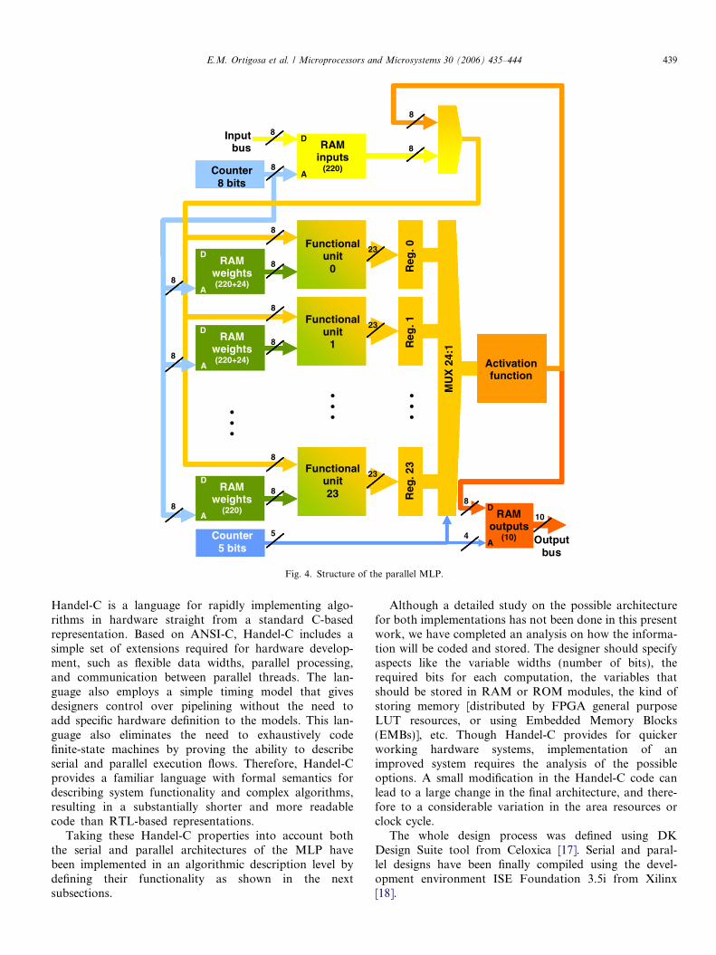
For our particular MLP, where 24 neurons exist at ahidden layer and 10 at the output layer, 24 functional unitsare required. All functional units will work in parallel whencomputing the outputs of the hidden layer, and only 10 ofthem will work when the output layer is computed. Fig. 4shows the basic structure of this parallel version.
Given that all functional units work in parallel for eachsynaptic signal, they need access to the associated weightssimultaneously, and hence, the weight RAM should be pri-vate for each one. For this reason, the 8-bit counter is usedto address 24 RAM modules containing 220 weights (asindicated in Fig. 4).
Since the data transmission between layers is serial,every functional unit will also need some local storage foroutput data. We decided to use 24 parallel registers insteadof the RAM module for the serial version, since this optionreduces the writing time. The data in these parallel registersare introduced to the single activation unit by a 24:1 mul-tiplexer whose select signals are the 5-bit counter outputs.The output of the activation unit is either used as a synap-tic signal for the 10 neurons at the final layer, or it is storedin the output RAM module. A new control unit has beendesigned for this parallel data path.
3.2. High description level
The high-level design of MLP was defined usingHandel-C [17] as a system-level specification language.
23
8
8
1:42 X
UM
Input bus
8
8
Functionalunit 23
Activationfunction
RAMinputs
(220)
32 .ge
R
RAM weights
(220) A
D
A
D
Counter 8 bits
8
23
8
8
Functionalunit
1
1 .ge
R
RAM weights (220+24)
A
23
8
8
Functionalunit
0
0 .ge
R
RAM weights (220+24)
A
D
8
8
5Counter 5 bits
D . . . . . .
. . .
8
8
10
4 Outputbus
8
RAM outputs
(10)A
D
Fig. 4. Structure of the parallel MLP.
E.M. Ortigosa et al. / Microprocessors and Microsystems 30 (2006) 435–444 439
Handel-C is a language for rapidly implementing algo-rithms in hardware straight from a standard C-basedrepresentation. Based on ANSI-C, Handel-C includes asimple set of extensions required for hardware develop-ment, such as flexible data widths, parallel processing,and communication between parallel threads. The lan-guage also employs a simple timing model that givesdesigners control over pipelining without the need toadd specific hardware definition to the models. This lan-guage also eliminates the need to exhaustively codefinite-state machines by proving the ability to describeserial and parallel execution flows. Therefore, Handel-Cprovides a familiar language with formal semantics fordescribing system functionality and complex algorithms,resulting in a substantially shorter and more readablecode than RTL-based representations.
Taking these Handel-C properties into account boththe serial and parallel architectures of the MLP havebeen implemented in an algorithmic description level bydefining their functionality as shown in the nextsubsections.
Although a detailed study on the possible architecturefor both implementations has not been done in this presentwork, we have completed an analysis on how the informa-tion will be coded and stored. The designer should specifyaspects like the variable widths (number of bits), therequired bits for each computation, the variables thatshould be stored in RAM or ROM modules, the kind ofstoring memory [distributed by FPGA general purposeLUT resources, or using Embedded Memory Blocks(EMBs)], etc. Though Handel-C provides for quickerworking hardware systems, implementation of animproved system requires the analysis of the possibleoptions. A small modification in the Handel-C code canlead to a large change in the final architecture, and there-fore to a considerable variation in the area resources orclock cycle.
The whole design process was defined using DKDesign Suite tool from Celoxica [17]. Serial and paral-lel designs have been finally compiled using the devel-opment environment ISE Foundation 3.5i from Xilinx[18].

440 E.M. Ortigosa et al. / Microprocessors and Microsystems 30 (2006) 435–444
3.2.1. Serial version
Only the functionality is necessary in the description ofthe serial MLP. To enable a comparative analysis, thisdescription should be identical to that of the RTL alreadydescribed in the previous section. Thus, the MLP computesthe synaptic signals for each neuron in the hidden layer byprocessing the inputs sequentially; and subsequently, theobtained outputs are similarly processed by the outputneurons.
From an algorithmic point of view, this functionaldescription implies the use of two different loops: onefor computing the results for neurons in the hiddenlayer, and another for neurons at the final layer. As anexample of the high-level description level reached whendesigning with Handel-C, the following shows theprogrammed code for the first loop, and its functionalitycorresponds to the kind of computation shown inEq. (1).
for (i=0; i<NumHidden; i++)
{Sum = 0;
for (j=0; j<NumInput; j++)
Sum += W[i][j]*In[j];
. . .}
where NumHidden is the number of neurons in the hid-den layer (24), NumInput is the number of inputs(220), W is the array containing the weight valuesrequired for processing the inputs and computing thesynaptic signals at hidden layer (24 · 220), In is thearray input, and Sum is a variable that stores theweighted (accumulated) sum of the multiplication ofthe inputs by their respective weights. From the code,it can easily be seen that all multiplications are beingcomputed sequentially.
3.2.2. Parallel version
As in the serial case, the functionality of the parallelversion is similar to that of RTL description, as all neu-rons belonging to the same layer compute their resultssimultaneously, in parallel. The only exception is theaccess to the activation function which is carried out ina serial manner.
The parallel designs were defined through the Han-del-C ‘‘par’’ directive, which forces the implementationof dedicated circuits, so that a defined part of an algo-rithm can be computed in parallel. In order to makeoptimal use of the ‘‘par’’ directive, we would need toidentify the set of computations and information trans-fers which can be done in parallel. For example, thedesigner would have to make sure that RAM modulesonly allow one location to be accessed in a single clockcycle.
Consequently, the serial loop shown in previous subsec-tion can be parallelized as:
par (i=0; i<NumHidden; i++)
Sum[i] = 0;
par (i=0; i<NumHidden; i++)
for (j=0; j<NumInput; j++)
Sum[i] += W[i][j]*In[j];
4. Results
The systems have been designed using the developmentenvironments FPGA advantage for the RTL version, andDK Design Suite for the higher algorithmic-like version.Then the designs have been translated into EDIF files,and finally, placed and routed in a Virtex-E 2000 FPGA,using the development environment ISE Foundation 3.5i.
The basic building block of the Virtex-E CLB (Configu-rable Logic Block) is the Logic Cell (LC) [19], which com-prises a 4-input function generator, carry logic, and astorage element. Each Virtex-E CLB contains four LCsorganized in two similar slices, and logic which combinesfunction generators to provide functions of five or sixinputs. Consequently, when estimating the number of sys-tem gates provided by a given device, each CLB countsas 4.5 LCs [19]. The 4-input function generator (includedin each LC) is implemented as 4-input LUTs. Each LUTcan provide a 16 · 1 synchronous RAM. Virtex-E alsoincorporates large Embedded Memory Blocks (EMBs)which complement the distributed RAM memory resourcesavailable in the CLBs.
The results of each implementation can be characterizedby the following parameters: number of slices, number ofEMBs RAM, maximum clock rate, and data throughput(Dt) as the number of evaluated input vectors per second(note that each vector consist of 220 components). In orderto make comparisons between the different implementa-tions easier, we have also estimated the number of systemgates while trying to represent the global hardware resourc-es (Hr) and the data throughput (Dt) of each approach.Furthermore, to better illustrate the trade-off between thesetwo characteristics, which can be adopted as a convenientdesign objective during the architecture definition process,we have evaluated the performance cost as Pc = Hr/Dt. Inthis way, we can evaluate how much hardware cost isrequired by a given performance.
For the hardware resources (Hr) estimation, the gatecounting used on Virtex-E devices is consistent with thesystem gate counting used on the original Virtex devices[19]. The basics of the system gates counting are as follows:each logic cell used as general logic is weighted as 12 systemgates, each logic cell used as distributed memory represents64 system gates (16 bits · 4 gates/bit), and finally, theresource cost for embedded memory adds up to 4 systemgates/bit.
Table 1 shows the implementation results obtained aftersynthesizing both serial and parallel versions of the MLPdefined at a RTL abstraction level.
As expected, results indicate that the serial version, withonly a functional unit, requires less area resources than the

Table 1Implementation characteristics of the designs with VHDL
MLP design Hardware resources Performance Performance cost (Pc)
# Slices # EMBs RAM # System gates Max. Freq. (MHz) # Cycles Dt (data/s) # System gates/Dt
Serial 1530 0 187677 24.7 5588 4440 42.27Parallel 3094 0 256581 20.2 278 74150 3.46
0,00,51,01,52,02,53,03,54,04,55,0
)s/atadk( tD
Serial
0
10
20
30
40
50
60
70
80
)s/atadk( tD
Parallel
Fig. 5. Data throughput (Dt) of the different evaluated designs.
E.M. Ortigosa et al. / Microprocessors and Microsystems 30 (2006) 435–444 441
parallel one, where a functional unit per hidden neuron wasincluded. In the parallel version, the data throughput (Dt)is 17 times higher, mostly due to the reduced number ofclock cycles needed for each input vector evaluation. In thisway, we are taking advantage of the inherent parallelism ofthe ANN computation scheme. After synthesizing thedesign, a slight difference can be observed in the maximumclock frequency, this is due to the different maximum com-binational paths of the two approaches.
Table 2 represents the results obtained after synthesizingthe serial and parallel versions of the MLP defined at analgorithmic-like description level (using Handel-C asHDL). As commented in Section 3.1.1, obtaining an effi-cient system requires a careful analysis of the possiblechoices. When defining the MLP, we had to decide howto store the data in RAM. Given the simplicity of Han-del-C when defining different implementation strategies,we chose to evaluate three different versions: (a) only usingdistributed RAM for the whole design; (b) the weightsassociated to synaptic signals (large array) make use ofEMBs RAM, while the remaining data are stored in a dis-tributed mode; (c) only requiring memory grouped inEMBs RAM modules.
Results in Table 2 show that, regardless of the distribu-tion memory option, the parallel version obviously requiresmore area resources than the serial one. As occurred in theVHDL system described above, the data throughput of theparallel versions is about 17 times higher than the serialapproaches.
Fig. 5 shows the results obtained for the data through-put. When considering the designs at the different abstrac-tion levels, we can observe that, although the RTL withVHDL achieves the best results, it just manages to
Table 2Implementation characteristics of the designs with Handel-C
MLP design Hardware resources Perf
# Slices # EMBs RAM # System gates Max
(a)Serial 2582 0 245268 19.7Parallel 6321 0 333828 17.2
(b)Serial 710 11 218712 16.1Parallel 4411 24 518928 16.7
(a)Serial 547 14 248996 15.3Parallel 4270 36 695380 15.4
(a) Only distributed RAM. (b) Both EMBs RAM and distributed RAM. (c) O
outperform the best version described at an algorithmic-like abstraction level, (1.24 and 1.21 times faster in theserial and the parallel versions, respectively). When consid-ering the different memory utilization strategies, the threeversions achieve similar data throughputs.
Fig. 6 shows how the performance cost (Pc) associatedto each design strategy at different abstraction levels is
ormance Performance cost (Pc)
. Freq. (MHz) # Cycles Dt (data/s) # System gates/Dt
5588 3535 69.38282 60968 5.48
5588 2671 81.86282 59326 8.75
5588 2733 91.07282 54692 12.71
nly EMBs RAM.

0
10
20
30
40
50
60
70
80
90
100
)setag·s/atad( cP
Serial
0
2
4
6
8
10
12
14
)setag·s/atad( cP
Parallel
Fig. 6. Performance cost (Pc) of the different evaluated designs.
0
2
46
8
10
1214
16
18
8 16 32 64 128
Number of hidden neurons
)secils K( secils fo reb
muN
HC (a)
HC (b)
HC (c)
0
20
40
60
80
100
120
140
160
8 16 32 64 128
Number of hidden neurons
MA
R sB
ME fo reb
muN
HC (a)
HC (b)
HC (c)
0
500
1000
1500
2000
2500
3000
8 16 32 64 128
Number of hidden neurons
)setagK( setag
metsys fo re bmu
N
HC (a)
HC (b)
HC (c)
c
b
a
Fig. 7. Scalability of the different approaches: (a) slices; (b) EMBs RAM;(c) system gates.
442 E.M. Ortigosa et al. / Microprocessors and Microsystems 30 (2006) 435–444
significantly different: the best design defined at an algo-rithmic level requires a performance cost approximately1.6 times higher than the RTL-based version.
The evaluated memory utilization strategies representdifferent consumptions of global hardware resources ascan be seen in Table 2. The most efficient is the option(a) of Handel-C which avoids using EMBs. This is sobecause the amount of data storage required by each hid-den neuron is small (approximately 50% of the capacityof a single EMB) and therefore, they are inefficiently usedby our system.
At an algorithmic-like abstraction level, we have easilyexplored different alternatives for the data storage. We onlyhad to specify which hardware resources are aimed for aconcrete data structure. On the other hand, at an RTLabstraction level, this study would require the definitionof specific circuits to interface the different types of memo-ry resources. Furthermore, we would also need to definethe characteristics of each memory circuit (bit width, num-ber of items of the data structure), whereas at a higherdescription level, all these features are linked to specificdata structures that, once defined, can be compiled usingdifferent hardware resources by just indicating it at theinstantiation command.
When comparing Tables 1 and 2 (Figs. 5 and 6), whereresults for a RTL and a higher-level description are shownrespectively, it can be seen that the RTL implementation isa more optimal approach for the final system. The serialand parallel RTL designs are approximately about 1.2times faster than the best higher-level designs. However,
one of the main advantages of the high-level descriptionis the reduction of design time for a system. Therefore,for our MLP designs, the design time for the serial casewhen using high-level description was about 10 times short-er than with the RTL one. In the parallel case, the designtime for the high level was relatively small (just enoughto introduce the ‘‘par’’ directives), while for the RTLdescription, a new architecture and control unit had to bedesigned; which implied a greater difference in the design-ing time. This is of critical importance when exploringdifferent alternatives for a specific system, as already shownin the several options of data storage described earlier.
We have also carried out a scalability study at a highabstraction level (Fig. 7). In order to obtain similar perfor-mance rates, we have used the embedded memory blocks(EMBs) inefficiently by trying to keep the parallel accesscapability to all hidden neurons. Thus, we can see how this

E.M. Ortigosa et al. / Microprocessors and Microsystems 30 (2006) 435–444 443
resource grows linearly with the size of the network(Fig. 7b). If we could afford a lower level of parallelism,this increment would be much less pronounced, since wecould fit a higher number of hidden neuron variables intoa single EMB. In all cases, the amount of slices also growslinearly with the network size (Fig. 7a), even when usingEMBs. This is due to the need for more general purposelogic to properly address the memory elements and the rep-lication of functional units. Finally, we observed that thedesign that uses only distributed memory also consumeshardware resources that increase linearly with the networksize, though the scalability in this case is limited to 64hidden neurons on the Virtex-E 2000 device. Nevertheless,this would not be the optimal device type to synthesize thisdesign because it does not use EMBs.
5. Discussion
In this paper, we have presented a design strategy fordifferent abstraction levels. A study on different alternativesof data storage and design scalability adopting an algorith-mic-like description language (Handel-C) has also been com-pleted. Finally, the paper also showed how a more efficientapproach can be designed at a RTL abstraction level. Thisillustrates how much performance and cost can be optimizedby addressing a low-level design in a later refining stage.
FPGA devices have evolved in recent years, not only inthe logic elements allocable in a single chip, but also in spe-cific purpose modules (embedded memory blocks, multipli-ers, and processors) which are already included in lastgeneration devices. This makes it difficult to choose thecharacteristics of the optimal device towards a goodtrade-off between performance and cost. In this contribu-tion we compared and evaluated different memory storagestrategies. Then, we translated all the different elementsinto a global characteristic, i.e., equivalent system gates.This allowed us to evaluate how much performanceimprovement we could gain with parallel computing in aMLP structure. By adopting this approach, we observedthat similar performances were obtained with differentmemory storage strategies. Using only distributed memoryseems to be the best option, since the EMBs are inefficientlyused to preserve the required parallelism by the MLP.Finally, we also showed the performance improvementobtained by designing at a lower abstraction level (RTL),which, in our approach, is about 1.2 times faster. Whenestimating how much hardware resources implicate theseperformance improvements, we confirmed that the optionwhich uses distributed memory resources is the one withless significant ‘‘performance cost’’ (Pc). In fact, the finaldesign done at low abstraction level (using VHDL) savedhardware resources significantly (about 30%) in compari-son to the equivalent approach defined at an algorithmic-like abstraction level.
All the different studies were addressed within a real-world application framework thus, obtaining the perfor-mance constraints. The neural networks-based speech
recognition system requires the parallel MLP implementa-tion of 24 hidden neurons. Although the study about thehardware resources consumption has a significant impacton the final product cost, any of the evaluated approacheswould fit the application driven performance specifications.For the speech recognition application, we obtained a cor-rect classification rate of 96.83% with a computation timearound 13–16 microseconds per sample, which fulfilled byfar the time restrictions imposed by the application. There-fore, the presented implementation can be seen as a low-cost design: the whole system, even the parallel version,would fit into a low-cost FPGA device and could beembedded in a portable speech recognition platform forvoice controlled systems.
A pipeline processing scheme, using one neural layer ineach stage, would lead to a faster approach. The processingbottleneck is imposed by the maximum neural fan in (220 ina hidden node) because it needs 220 multiplications. With apipeline structure, we can overlap the computation time ofthe hidden layer with the computation time of the outputlayer (24 multiplications per node), which would speedup the data path to a maximum of 10%. We did not studythe pipeline choice because our design already fulfills theapplication requirements, i.e., portability, low cost andcomputation time.
The comparative study between register transfer levelusing VHDL and a higher abstraction level with Handel-C as description languages sets an illustrative example.The two options led to very different design time vs. effi-ciency trade-offs. Although the final implementation char-acteristics depend on the designer’s skills, the use of analgorithmic-like abstraction level with Handel-C reducesthe design time by a factor of ten. Furthermore, with thismodular system in particular, the exploration of differentprocessing strategies (the serial and parallel approachesdescribed in Section 3.1) was straightforward while theVHDL approach required the design of a new control unit.
Acknowledgements
This work has been supported by CICYT TIC2002-00228, CICYT TIC2000-1348, and the EU project Spike-FORCE (IST-2001-35271). We thank the reviewers fortheir valuable and useful comments.
References
[1] B. Widrow, D. Rumelhart, M. Lehr, Neural networks: applications inindustry, business and science, Commun. ACM 37 (3) (1994).
[2] C.M. Bishop, Neural Networks for Pattern Recognition, OxfordUniversity Press, 1995.
[3] P. Ienne, T. Cornu, K. Gary, Special-purpose digital hardware forneural networks: an architectural survey, J. VLSI Signal Process. 13(1) (1996) 5–25.
[4] J. Zhu, P. Sutton, FPGA implementations of neural networks – asurvey of a decade of progress, Lect. Notes Compu. Sci. 2778 (2003)1062–1066.
[5] J. Zhu, G. Milne, B. Gunther, Towards an FPGA based reconfig-urable computing environment for neural network implementations,

444 E.M. Ortigosa et al. / Microprocessors and Microsystems 30 (2006) 435–444
in: Proceedings of 9th International Conference on Artificial NeuralNetworks, vol. 2, 1999, pp. 661–667.
[6] R.A. Goncalves, P.A. Moraes, J.M.P. Cardoso, D.F. Wolf, M.M.Fernandes, R.A.F. Romero, E. Marques, ARCHITECT-R: a systemfor reconfigurable robots design, in: ACM Symposium on AppliedComputing, Melbourne, USA, ACM Press, 2003, pp. 679–683.
[7] D. Hammerstrom, Digital VLSI for neural networks, in: M. Arbib(Ed.), The Handbook of Brain Theory and Neural Networks, seconded., MIT Press, 2003.
[8] C. Gao, D. Hammerstrom, S. Zhu, M. Butts, FPGA implementationof very large associative memories, in the book: FPGA Implemen-tations of Neural Networks, in: A.R. Omondi, J.C. Rajapakse (Eds.),Springer Berlin Heidelberg, New York, 2005.
[9] I. Page, Constructing hardware–software systems from a singledescription, J. VLSI Signal Process. 12 (1) (1996) 87–107.
[10] M. Mylonas, D.J. Holding, K.J. Blow, DES Developed In Handel-C,London Communications Symposium, University College London,2002.
[11] S.M. Loo, B. Earl Wells, N. Freije, J. Kulick, Handel C for rapidprototyping of VLSI coprocessors for real time systems, in: 34thSoutheastern Symposium on System Theory (SSST 2002), IEEEProceeding, 2002.
[12] L. Rabiner, B.H. Juang, Fundamentals of Speech Recognition,Prentice-Hall, 1993.
[13] R.P. Lippmann, Review of neural networks for speech recognition,Neural Comput. 1 (1) (1989) 1–38.
[14] X.D. Huang, Y. Ariki, M.A. Jack, Hidden Markov Models forSpeech Recognition, Edinburgh University Press, 1990.
[15] B. Widrow, M. Lehr, 30 years of adaptive neural networks:Perceptron, Madaline and Backpropagation, Proc. IEEE 78 (9)(1990) 1415–1442.
[16] Mentor Graphics, http://www.mentorg.com/.[17] Celoxica: Technical Library, http://www.celoxica.com/techlib/.[18] Xilinx, http://www.xilinx.com/.[19] Xilinx: Virtex-E Data Sheets, http://www.xilinx.com/support/
mysupport.htm#Virtex-E.