Grain Boundaries Electronic Ceramics - DTIC
385
AD-oA27 9 883 4-1 Grain Boundaries '1. and •. ~* Interfacial Phenomena in Electronic Ceramics VA.V i JUN Q 3 1994 S~Lionel M. Dein and Shin-ichi Hirano A, WD A This Document Contains Missing Page/s That Are t Unavailable In The Cf_3 6 • •' Original Document • °"• •"Volume 41
-
Upload
khangminh22 -
Category
Documents
-
view
4 -
download
0
Transcript of Grain Boundaries Electronic Ceramics - DTIC
AD-oA27 9 8834-1
Grain Boundaries
'1. and
•. ~* Interfacial Phenomena
in
Electronic Ceramics
VA.V i JUN Q 3 1994
S~Lionel M. Deinoand
Shin-ichi Hirano
A, WD A
This Document Contains
Missing Page/s That Are tUnavailable In The Cf_3 6
• •' Original Document• °"• •"Volume 41
Grain Boundariesand
Interfacial Phenomenain
Electronic CeramicsAccesiori For
NTIS CRA&IDTIC TAB D TIUnannounced 5 EILECTEJustification ..................... . JUN 0 3 1994
Distribution GAvailability Codes
s Avail and/orDist I-Special
94-16444ii~i~iuUMUIl3MUU\

Related titles published by the American Ceramic Society:
Experimental Techniques of Glass ScienceEdited by Catherine J. Simmons and Osama H. El-Bayoumi0 1993, ISBN 0-944904-58-0
Handbook on Characterization Techniques for the Solid-Solution InterfaceEdited by James H. Adair, Jon A. Casey, and Sridhar Venigalla0 1993, ISBN 0-944904-67-X
Ceramic Transactions, Volume 38: Advances in Ceramic-Matrix CompositesEdited by Narottam P. Bansal0 1993, ISBN 0-944904-69-6
Ceramic Transactions, Volume 36: Microwaves: Theory and Application inMaterials Processing If
Edited by David E. Clark, Wayne R. Tinga, and Joseph R. Laia, Jr.0 1993, ISBN 0-944904-66-1
Ceramic Transactions, Volume 34: Functionally Gradient MaterialsEdited by J. Birch Holt, Mitsue Koizumi, Toshio Hirai, and Zuhair A. MunirC 1993, ISBN 0-944904-64-5
Ceramic Transactions, Volume 31: Porous MaterialsEdited by Kozo Ishizaki, Laurel Sheppard, Shojiro Okada, Toyohiro Hamasaki,
and Ben Huybrechts0 1993, ISBN 0-944904-59-9
Ceramic Transactions, Volume 30: Nucleation and Crystallization in Liquidsand Glasses
Edited by Michael C. Weinberg0 1993, ISBN 0-944904-57-2
Ceramic Transactions, Volume 26: Forming Science and Technology for CeramicsEdited by Michael J. Cima0 1991, ISBN 0-944904-48-3
Ceramic Transactions, Volume 24: Point Defects and Related Properties of CeramicsEdited by Thomas 0. Mason and Jules L. Routbort0 1991, ISBN 0-944904-46-7
Ceramic Transactions, Volume 22: Ceramic Powder Science IVEdited by Shin-ichi Hirano, Gary L. Messing, and Hans Hausner0 1991, ISBN 0-944904-44-0
Advances in Ceramics, Volume 28: Failure Analysis of Brittle MaterialsEdited by V.D. Frechette0 1990, ISBN 0-944904-30-0
For information on ordering titles published by the American Ceramic Society,or to request a publications catalo, please call 614-890-4700, or write toCustomer Service Department, 735 Ceramic Place, Westerville, OH 43081.

Grain Boundariesand
Interfacial Phenomena
in
Electronic Ceramics
VAV
Edited by
Lionel M. LevinsonGeneral Electric Corporate Research and Development
Shin-ichi HiranoNagoya University
AVA
DTTCOO "T7' f
Volume 41
Published byThe American Ceramic Society
735 Ceramic PlaceWesterville, Ohio 43081

Proceedings of the International Symposium on Gran Boundaries and Interfacial Phenomena,presented at the PAC RIM Meeting, held in Honolulu, HI, November 8-10,1993.
Library of Congress Cataloging-in-Publication Data
International Symposium on Grain Boundaries and Interfacial Phenomenain Electronic Ceramics (1993: Honolulu, Hawaii)
Grain boundaries and interfacial phenomena in electronic ceramics/ edited by Lionel M. Levinson, Shin-ichi Hirano.
p. cm. - (Ceramic transactions, ISSN 1042-1122; v. 41)Poednsof the Internatioenal Symposium on Grain Boundaries andInterfacial Phenomena in Electronc Ceramics, held in Honolulu,Hawaii Nov. 7-10, 1993, in conjunction with the PAC RDA Meeting.
Includes index.ISBN 0-944904-73-41. Electronic ceramics-Surfaces-Congresses. 2. Grain
boundaries-Congresses. 3. Surface chemistry-Congresses.L Levinson, Lionel M. I1. Hirano, Shin'ichi, 1942-III. Title. IV. Series.TK7871.15.C4158 1993621381-dc2O 94-4933
CIP
Copyright © 1994, The American Ceramic Society. All rights reserved.
No part of this book may be reproduced, stored in a retrieval system, or transmitted inany form or by any means, electronic, mechanical, photocopying, microfilming,recording, or otherwise, without written permission from the publisher.
Permission to photocopy for personal or internal use beyond the limits of Sections 107and 108 of the U.S. Copyright Law is granted by the American Ceramic Society,provided that the base fee of US$5.00 per copy, plus US$.50 per page, is paid directly tothe Copyright Clearance Center, 27 Congress Street, Salem MA 01970, USA. The fee codefor users of the Transactional Reporting Service for Ceramic Transactions Volume 41 is 0-944904-73-4/94 $5.00+$.50. This consent does not extend to other kinds of copying, such
as copying for general distribution, for advertising or promotional purposes, or forcreating new collective works. Requests for special photocopying permission and reprintrequests should be directed to the Director of Publications, The American CeramicSociety, 735 Ceramic Place, Westerville OH 43081, USA.
This work relates to Department of Navy Grant N00014-93-1-0366 issued by the Office ofNaval Research. The United States Government has a royalty-free license throughout theworld in all copyrightable material contained herein.
Printed in the United States of America.
1 2 3 4-98 97 96 95 94
ISSN 1042-1122ISBN 0-944904-73-4

Contents
Preface ................................................................................................................... ix
OverviewGrain Boundary Segregation in Semiconducting Oxides ......................... 3
Yet-Ming Chiang and Jeri Ann S. Ikeda
Electrical Activity at Individual Grain Boundaries and Interfaces inSemiconducting Oxides ............................................................................... 19
H.L. Tuller and K-K. Baek
Chemically Induced Interface Migration in Oxides ................................ 35Jae Ho Jeon, Suk-Joong L. Kang, Sang Chul Han, and Duk Yong Yoon
Nano/Microstructure Design for Improving ThermoelectricCharacteristics of Porous Silicon Carbide ....................................................... 53
K. Koumoto, W.S. Seo, and C.H. Pai
Grain Boundary Characteristics in PZLT, GBBLC, and High-TcSuperconducting Ceramics and Their Relation to Properties ................ 65'
M.Y. Zhao, Z.W. Yin, and B.M. Xu
Ferrites and TitanatesGrain Boundary Microstructure and Magnetic Properties of Low-Temperature-Fired Ni-Zn-Cu Ferrite ........................................................ 81
Masayuki Fujimoto
Dependence of Magnetic Properties of (Co,Fe)30 4 Film onMicrostructure Control Through Phase Separation ................................. 93
Shin-ichi Hirano, Toshinobu Yogo, Ko-ichi Kikuta, and Hiroshi Yamamoto
Low-Temperature-Sintered Ferrite for Multilayer Chip Components ...... 101Jen-Yan Hsu, Wen-Song Ko, Hsiao-Miin Sung, Meei-Lin Suen, and Chi-Jen Chen
Influence of Process Parameters on Power Losses Minimum vs.Temperature of M n-Zn Ferrites ....................................................................... 111
MN. Tsay, C.S. Liu, M.J. Tung, and C.J. Chen
Grain Boundary Layered PTCR Ceramics Based on PbTiO 3-TiO2 .. . . . . ... 119M. Okada, M. Homma, and S. Iwashita
V

Grain Core-Grain Shell Structure in Nb-Doped BaiO3 CapacitorCeram ics ............................................................................................................. 129
X.Y. Song& D.R. Chen, and Z.W. Yin
The V-Shape Characteristics of (Pb0.6Sr0.4)T1O 3 Ceramics ........................... 135T.D. Tsai, C.T. Hu, and I.N. Lin
Effect of BN Addition on the Sintering and Electrical Properties ofY-Doped BaTiO 3 Ceramics ............................................................................. 145
Seh-Jin Park, Joon-Hyung Lee, and Sang-Hee Cho
Effects of Grain Boundary Structure on the Resistivity Phenomenonin Doped Ba 103 ..................................................... . .. . .. .. . .. .. . .. . .. .. .. . .. . .. . .. .. . . . 1. 53
R.C. Buchanan, R.D. Rosenman, and J. Kim
Microstructural and Compositional Analyses on Grain Boundaryof Low-Temperature-Sintered Pb(ZrTi)0 3 Ceramics .................................. 161
Dunzhuo Dong, Keryi Murakami, Nagaya Okada, and Shoji Kaneko
Particle Size Effect on the Room Temperature Structure of BariumTitanate ............................................................................................................... 169
B.D. Beg& E.R. Vance, D.J. Cassidy, I. Nowotny, and S. Blairs
Influence on the Grain Boundary Interfacial Trap Levels inBa0.76Sr0.24)TiO 3-Based PTCR Ceramics by Oxidative Annealing ............. 177
Myung Chul Kim, Soo Hyung Hur, and Soon Ja Park
Role o. Porosity on PTCR Characteristics of SemiconductingBaTiO 3 Ceram ics ................................................................................................ 185
Joon-Hyung Lee, Jeong-Joo Kim, and Sang-Hee Cho
Varistors and ConductorsInterface States at Grain Boundaries and Their Effects on the I-VCharacteristics in ZnO:.Pr Varistors-Theoretical Calculation ................... 195
Kazuo Mukae and Koichi Tsuda
Cryogenic Behavior of ZnO Varistors ............................................................ 207Lionel M. Levinson and William N. Schuttz
Modeling the Electrical Characteristics of Polycrystalline VaristorsUsing Individual Grain Boundary Properties .............................................. 217
Qinpgzhe Wen and David R. Clarke
VDR Effect in Bi-Diffused SrTiQ3-Based Ceramics ...................................... 231N. lchinose and M. Watanabe
vi
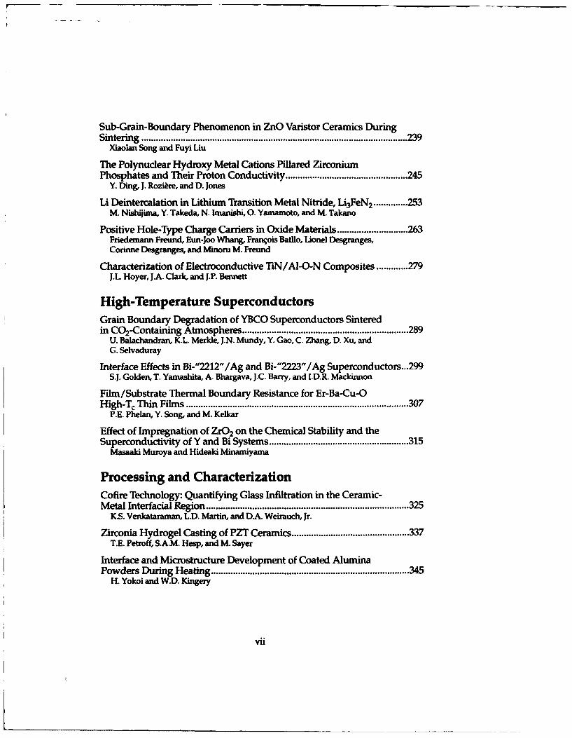
Sub-Grain-Boundary Phenomenon in ZnO Varistor Ceramics DuringSintering ............................................................................................................. 239
Xiaolan Song and Fuyi Liu
The Polynudear Hydroxy Metal Cations Pillared ZirconiumPhosphates and Their Proton Conductivity .................................................. 245
Y. Ding, J. Roziare, and D. Jones
Li Deintercalation in Lithium Transition Metal Nitride, Li3FeN2 ......... . . .. . 253M. Nishijima, Y. Takeda, N. Imanishi, 0. Yamamoto, and M. Takano
Positive Hole-Type Charge Carriers in Oxide Materials ............................. 263Friedemann Freund, Eun-Joo Whang, Francois Batilo, Lionel Desgranges,Corinne Desgranges, and Minoru M. Freund
Characterization of Electroconductive TiN /Al-O-N Composites ............. 279J.L. Hoyer, J.A. Clark, and J.P. Bennett
High-Temperature SuperconductorsGrain Boundary Degradation of YBCO Superconductors Sinteredin C0 2-Containing Atmospheres .................................................................... 289
U. Balachandran, K.L. Merkle, J.N. Mundy, Y. Gao, C. Zhang, D. Xu, andG. Selvaduray
Interface Effects in Bi-"2212"/Ag and Bi-"2223"/Ag Superconductors...299S.J. Golden, T. Yamashita, A. Bhargava, J.C. Barry, and I.D.R. Mackinnon
Film/Substrate Thermal Boundary Resistance for Er-Ba-Cu-OH igh-Tc Thin Film s ........................................................................................... 307
P.E. Phelan, Y. Song, and M. Kelkar
Effect of Impregnation of ZrO2 on the Chemical Stability and theSuperconductivity of Y and Bi Systems ......................................................... 315
Masaaki Muroya and Hideaki Minamiyama
Processing and CharacterizationCofire Technology: Quantifying Glass Infiltration in the Ceramic-Metal Interfacial Region .............................................................................. 325
KS. Venkataraman, L.D. Martin, and D.A. Weirauch, Jr.
Zirconia Hydrogel Casting of PZT Ceramics ................................................ 337T.E. Petroff, S.A.M. Hesp, and M. Sayer
Interface and Microstructure Development of Coated AluminaPowders During Heating ................................................................................. 345
H. Yokoi and W.D. Kingery
vii

High Q-Factor Tri-Plate Resonator with an Inner Conductor ofM elted Silver ...................................................................................................... 355
M. Kobayashi, K. Kawamura, and K. Suzuki
Sintering and Microstructure of Sr0.6Ba 0.4Nb2O6 Ceramics ........................ 63Junichi Takahashi, Shiro Nishiwaki, and Kohei Kodaira
Interfacial Phenomena and Dielectric Properties ofPb(Mg,/ 3Nb2/3)O3 Ceramics with Excess PbO ............................................ 371
K.H. Yoon, Y.S. Cho, D.H. Lee, and D.H. Kang
Characterization of Bridgman Crystal Growth Using RadiographicIm aging ............................................................................................................... 379
S.E. Sorokach, RT. Simchick, A.L. Fripp, W.J. Debnam, and P.G. Barber
Index ................................................................................................................... 387
Viio

pre face
This volume contains the proceedings of the International Symposium on GrainBoundaries and Interfadal Phenomena in Electronic Ceramics. held in HonoluluNovember 7-10, 1993, in conjunction with the PAC RIM Meeting. The meetingwas cosponsored by 10 ceramic societies and associations from countriesbordering the Pacific Ocean. The symposium participants included ceramistsfrom the United States, Japan, Korea, Taiwan, Canada, People's Republic ofChina, and India.The symposium cochairs were fortunate to have the support of an internationalorganizing committee: Janusz Nowotny (Australian Science and TechnologyOrganization, Australia), Soon Ja Park (Seoul National University, Korea),Michael Sayer (Queen's University, Canada), and Zhiwen Yin (Shanghai Instituteof Ceramics, China). We would also like to express our appreciation to thesymposium session chairs, R. Pohanka, M. Sayer, Z. Yin, and J. Nowotny, whoalso ably assisted in coordinating the manuscript reviews.
This symposium and therefore this proceedings was organized to bring togetherworldwide expertise in grain boundary and interfacial phenomena in electronicceramics. These issues are key to understanding technological advances in fieldsas diverse as ferroelectrics, sensors, PTCRs, packaging ceramics, varistors, thickfilms, magnetic ceramics, titanates, capacitors, and multilayer and compositematerials. Interfacial phenomena often determine the sintering and densificationbehavior of ceramics, as well as contact and joint functionality.Finally, it was the goal of the meeting organizers to bring together experts inthese various areas to provide a forum to promote the exchange of ideas that willoccur when workers in diverse materials concentrate on the common interfacialand grain boundary phenomena underlying their specialized applications.
Lionel M. LevinsonShin-ichi Hirano
ix

Overview

GRAIN BOUNDARY SEGREGATION IN SEMICONDUCTING OXIDES
Yet-Ming Chiang and ler Ann S. [keda'Dept. of Materials Science and Engineering, Massachusetts Institute of Technology,Cambridge, Massachusetts, USA
ABSTRACT
Solute and defect segregation at grain boundaries and surfaces in electroceramicsand other oxides controls a broad range of interfacial properties. Model experiments inacceptor- and donor-doped TiO2 show that in a semiconducting oxide with complex defectstructure, including mixed electronic and ionic compensation, the equilibrium space chargepotential corresponds to that expected from ionic space charge theory. As a result, thepotential and the interfacial density of charged defects can be quantitatively predicted onthe basis of lattice defect structure, and can be varied by control of doping, temperature,and oxygen activity. Implications of these results for the control of defect segregation atelectrically active grain boundaries in complex oxides are discussed.
INTRODUCTION
Semiconducting oxides are used in a broad range of applications in which thedefect chemistry of interfaces provide important chemical or electrical functionalities. Themost well-known of these are perhaps grain boundary barrier-layer electroceramics such aszinc oxide varistors and barium titanate positive-temperature-coefficient (PTC) resistors,but interfacial defect properties also play a critical role in oxides used for a variety of otherapplications, including for example catalysts and surface and heterojunction-based gas andchemical sensors. The high temperature properties of grain boundaries and surfaces areclearly important in microstructure development processes such as creep, sintering, andgrain growth as well. While the lattice defect properties of many of the importantsemiconducting oxides have been extensively studied, comparatively little is known abouttheir interfacial defect chemistry (which, in this context, includes the nonstoichiometry ofthe interface and near-interface region, as well as solute segregation).
The relationship between lattice defects and interfacial defects in ionic systems isin large part defined by the space-charge interaction. As first formulated by Frenkel [I],Lehovec [21, and Kliewer and Koehler [31, an ionic space charge results when the
* now at Norton Company, Worcester, Massachusetts
To the extent authorized under the laws of the United States of America, all copyright interests in this publication are the propertyof The American Ceramic Soci Any duplication, reproduction, or republication of this publication or any part thereof, withoutthe express written consent of The American Ceramic Society or fee paid to the Copyright Clearance Center, is prohibited.
Grain Boundaries and Interfacial Phenomena in Electronic Ceramics 3

formation of defects at the interface differs energetically from those in the bulk, resultingat equilibrium in a variation in ionic defect concentration at the interface, and acorresponding electrical potential difference between the interface and the bulk. Theinterface charge is balanced by an oppositely-charged space-charge layer penetrating thecrystal. The magnitude of the potential difference is determined by the formation energy oflattice defects at the interface, temperature and lattice defect concentration. Numerousstudies in alkali- and silver halides [4-7] leave little doubt as to the existence of the space-charge potential in simple ionic systems. In MgO, the segregation [81 and spatialdistribution [91 of aliovalent cations at grain boundaries likewise provide convincingevidence for a space-charge mode of segregation which is distinct from Gibbsianadsorption at the grain boundary. In more complex oxides, including MgAI2 04 [101,MnZn ferrites [II], SrTiO3 [12,131, and BaTiO3 f13-151, deviations in both cation andanion stoichiometry have been observed at grain boundaries and surfaces. In instanceswhere experimental procedures suggest a preservation of high temperature equilibrium,these seem clearly related to existence of a space charge However, a quantitativeinterpretation of the segregation in terms of the lattice defect structure has not beenachieved in these systems. Dynamic effects during processing causing redistribution ofsolutes and defects often complicate the picture, although such effects can be of criticalimportance in real electroceramic systems since they determine what is retained aftrcooling to room temperature.
In TiO2 (rutile phase), a system with defect properties which are representative ofa broad range of semiconducting oxides, a more systematic approach has been possible[16-18]. The ability to access a number of Brouwer defect regimes by varying doping,temperature, and oxygen activity, renders this system ideal for exploring the variation ininterfacial chemistry as a function of lattice defect chemistry. We have conductedsystematic studies of space charge segregation using model experiments in which theaccumulation of aliovalent solutes is measured. Observations of the variation in spacecharge potential with temperature and doping were recently reported 117-18]. Here webriefly review those results, and discuss new results on the P02 dependence of the spacecharge potential.
DEFECT AND SPACE CHARGE MODEL
The lattice nonstnichiometry of TiO 2 is well-characterized as a function oftemperature and oxygen activity, as are the regimes of crystallographic shear phase (CSP)and defect cluster formation. For simplicity we have concentrated efforts on the hightemperature (T>1473K), low defect concentration (8<0.005) regime within whichexperimental studies (summarized by Bursill et al. [19,20]) find CSP's as well as smallerdefect clusters to be absent. In this regime, transport properties have been found to bewell-described by dilute point-defect models (for recent reviews see refs. 19-22).
The defect model used here has been discussed in detail in ref. 17. In brief, defectchemical equilibrium constants from the literature have been used to calculate the latticeconcentrations of the relevant defects as a function of doping, temperature, and oxygenactivity. Some of the calculated results are shown in Fig 1(A) as plots of defectconcentrations against solute doping, for a temperature of 1350°C and air atmosphere.
Figure 1(B) shows a similar calculation plotted against oxygen partial pressure, ina material doped with 1% pentavalent donor (e.g., Nb5+, Ta5 +), at 1350°C. Together, afamily of curves of this type map the variation of point defect concentration with the
4 Grain Boundaries and Interfacial Phenomena in Electronic Ceramics

(A) (B)0T a 1350C 0I mole % Nb
0.25 - 025
-0.25 0 -0.25IT 135 * _50
"-LO -0.5 QO 0.5 1.0 1.5 -5.0 -2.5 0.0 2.5 50
-~ 0 0an .) n
P =
---- -- .... -/i
I i-10 -10 JELTIJ LTI1J
15v, 15-- 1.0 -0.5 0.0 0.5 1.0 1.5 -&.O -2.5 0.0 2.5 5.0
Net Donor Concentration (mole %) Log Po2 (PC)
Figure 1. Calculated lattice defect concentrations in T1O2 at 1350°C, plotted against (A)solute doping at constant P02 (air); and (1B) P02 at constant donor doping. Correspondingspace charge potential curves are shown above the respective diagrams.
important experimental variables of temperature, oxygen activity, and doping. The defectmodel includes six point defects: ATi' (substitutional trivalent acceptors), DTi"(substitutional pentavalent donors), Tii*'"', VTi'' n and p. Implicit is the assumption, inaccordance with recent analyses of literature data [21-231, that reduction is accommodatedby the formation of Tii .... at higher temperatures, and that the cation Frenkel is the lowest-energy intrinsic ionic defect mechanism in ideal, stoichiometric TiO2. Defect associationhas been assumed negligible at the temperatures and doping levels of interest, based onestimates of electrostatic binding energies [17,241. (Mhs is in large part due to thescreening afforded by the high dielectric constant of TiO2, &= 120.) The following quasi-chemical defect reactions and corresponding mass-action equilibrium constants arenecessary to solve for the lattice concentration of defects:
Reduction: Ti'i +200' =Ti-" +4e'-tO2(g) KI = [Tii'"'] n4 PO2 (1)
Oxidation: 02(g) =V; +20x +4h" K2 = [VTi.. p4 P02-1 (2)
Intrinsic electronicdefect formation: null = e'+ h" Ki = np (3)
Grain Boundaries and Interfacial Phenomena in Electronic Ceramics5
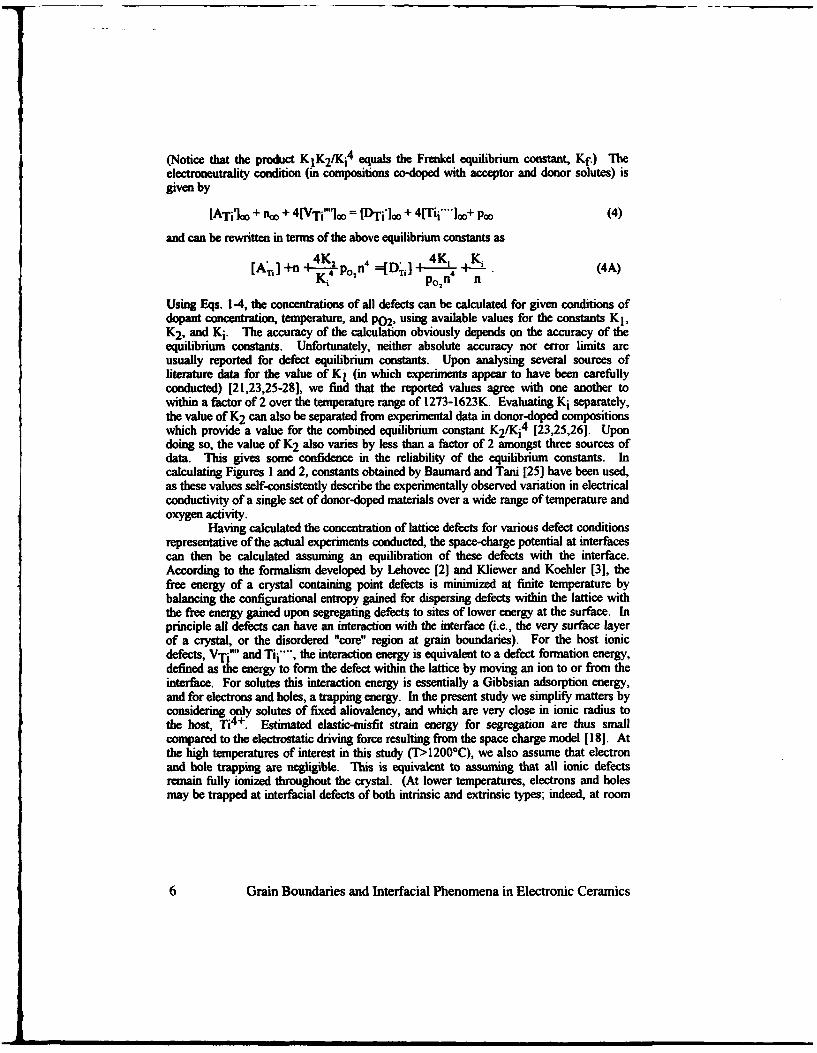
(Notice that the product KiK 2/Ki 4 equals the Frenkel equilibrium constant, Kf.) Theelectroneutrality condition (in compositions co-doped with acceptor and donor solutes) isgiven by
[ATi'100 + n.0 + 4 [VTi"].x = [DTi']• + 4[Tii'"']JO+ p. (4)
and can be rewritten in terms of the above equilibrium constants as
+4K2 4 =[~] 4K K[A' ],+n 4 p•K2 n + : (4A)
T Ki4 pon 4 n
Using Eqs. 1-4, the concentrations of all defects can be calculated for given conditions ofdopant concentration, temperature, and P02, using available values for the constants KI,K2, and Ki. The accuracy of the calculation obviously depends on the accuracy of theequilibrium constants. Unfortunately, neither absolute accuracy nor error limits areusually reported for defect equilibrium constants. Upon analysing several sources ofliterature data for the value of Ki (in which experiments appear to have been carefullyconducted) [21,23,25-28], we find that the reported values agree with one another towithin a factor of 2 over the temperature range of 1273-1623K. Evaluating Ki separately,the value of K2 can also be separated from experimental data in donor-doped compositionswhich provide a value for the combined equilibrium constant K2/Ki4 [23,25,261. Upondoing so, the value of K2 also varies by less than a factor of 2 amongst three sources ofdata. This gives some confidence in the reliability of the equilibrium constants. Incalculating Figures I and 2, constants obtained by Baumard and Tani [25] have been used,as these values self-consistently describe the experimentally observed variation in electricalconductivity of a single set of donor-doped materials over a wide range of temperature andoxygen activity.
Having calculated the concentration of lattice defects for various defect conditionsrepresentative of the actual experiments conducted, the space-charge potential at interfacescan then be calculated assuming an equilibration of these defects with the interface.According to the formalism developed by Lehovec [2] and Kliewer and Koehler [3], thefree energy of a crystal containing point defects is minimized at finite temperature bybalancing the configurational entropy gained for dispersing defects within the lattice withthe free energy gained upon segregating defects to sites of lower energy at the surface. Inprinciple all defects can have an interaction with the interface (i.e., the very surface layerof a crystal, or the disordered "core" region at grain boundaries). For the host ionicdefects, VTi"" and Tii"", the interaction energy is equivalent to a defect formation energy,defined as the energy to form the defect within the lattice by moving an ion to or from theinterface. For solutes this interaction energy is essentially a Gibbsian adsorption energy,and for electrons and holes, a trapping energy. In the present study we simplify matters byconsidering only solutes of fixed aliovalency, and which are very close in ionic radius tothe host, Ti4+. Estimated elastic-misfit strain energy for segregation are thus smallcompared to the electrostatic driving force resulting from the space charge model [181. Atthe high temperatures of interest in this study (T>1200*C), we also assume that electronand hole trapping are negligible. This is equivalent to assuming that all ionic defectsremain fully ionized throughout the crystal. (At lower temperatures, electrons and holesmay be trapped at interfacial defects of both intrinsic and extrinsic types; indeed, at room
6 Grain Boundaries and Interfacial Phenomena in Electronic Ceramics

temperature, it is this trapping which gives rise to grain boundary barriers inelectroceramics.)
With these simplifying assumptions, the space charge potential is determined bythe formation eneagy of the host ionic defects (SVTi and gTii), their lattice defectconcentration, and temperature. Choosing a reference point for the space charge potentialwhich is zero at the surface, the potential varies with distance as 4(x), reaching a bulkpotential value of +.. Upon minimizing the free energy of the defective crystal, thecondition of thermal equilibrium is one in which the concentration of each defect varieswith potential in the space charge layer as
[ýX V.Cepr-ze[O(x) -O 1 (5),~x)~f~oCXL kT I
where ni. is the lattice defect concentration (per cm3) and zre is the effective charge ofthe defecA. (Eq. 5 assumes that the Debye length of the space charge layer is sufficiently
large and the defect concentrations sufficiently small that a continuum description isapplicable. This seems to be a reasonable approximation for the present system [17,18].)Far from the interface, the host defects VTi"" and Tii ... are formed against a potentialvalue of #,0 and with an energy expenditure of gVT, or gTin, giving the latticeconcentrations:
[V =]o.•.exp -'9v., -'4e•j]. (6)
[Ti-I exp kT (7)
in which the concentrations are in mole fraction relative to the lattice density of Ti sites.Since the lattice concentrations are known from the defect model, the net potentialdifference between the interface and bulk, equivalent to +,, can be obtained directly.Using relations (5) and (6), the variation in space charge potential with lattice defectchemistry is shown at the top of Fig. 1 (in this example gvTi=2. 4 eV and gTi=2.1 eV).Notice that a "titration" of the potential from positive to negative, through an isoelectricpoint (zero potential difference), is expected as a function of lattice defect chemistry.Notice also that this isoelectric point falls very close to the stoichiometric point in thedefect diagrams (e.g., where [VTi""]=[Tii"']). However, the stoichiometric point and theisoelectric are not precisely coincident unless gVTi=gTii.
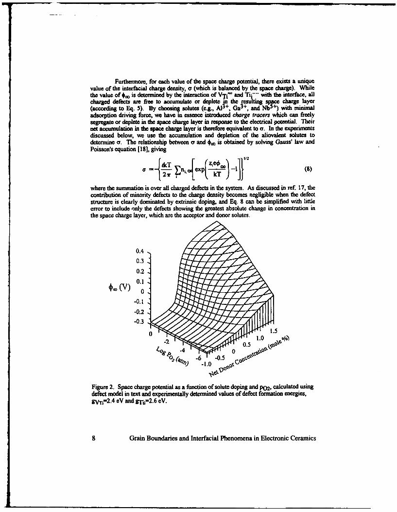
Combining results such as those shown in Fig. 1, a complete space chargepotential surface can be calculated as a function of the experimental variables, as shown inFig. 2. Here the variation in *oo with doping and oxygen activity has been calculated for atemperature of 1350*C; other surfaces result at other temperatures. These results give thedirect correspondence between the lattice defect chemistry of TiO2 and the space chargepotential. Notice that regimes of negative +,0 essentially correspond to where TiO2 -S isunderstoichiometric (oxygen deficient, 8>0), whereas regimes of positive +wcorrespond towhere the lattice is overstoichiometric (cation deficient, 8<0).
Grain Boundaries and Interfacial Phenomena in Electronic Ceramics 7
Furthermore, for each value of the space charge potential, there exists a uniquevalue of the interfacial charge density, a (which is balanced by the space charge). Whilethe value of +,, is determined by the interaction of VTi"" and Tii*... with the interface, allcharged defects are free to accumulate or deplete in the resulting space charge layer(according to Eq. 5). By choosing solutes (e.g., A13+, Ga 3 +, and Nb5+) with minimal
adsorption driving force, we have in essence introduced charge tracers which can freelysegregate or deplete in the space charge layer in response to the electrical potential. Theirnet accumulation in the space charge layer is therefore equivalent to c. In the experimentsdiscussed below, we use the accumulation and depletion of the aliovalent solutes todetermine a. The relationship between a and +,, is obtained by solving Gauss' law andPoisson's equation [181, giving
inJexpzle'0
where the summation is over all charged defects in the system. As discussed in ref. 17, thecontribution of minority defects to the charge density becomes negligible when the defectstructure is clearly dominated by extrinsic doping, and Eq. 8 can be simplified with littleerror to include only the defects showing the greatest absolute change in concentration inthe space charge layer, which are the acceptor and donor solutes.
0.4
0.3
0.2
M(V 0.10
-0.1
-0.2-0.3
0 1.5
. -4 0 0.5.00 c
Figure 2. Space charge potential as a function of solute doping and pO2, calculated usingdefect model in text and experimentally determined values of defect formation energies,gV-r=2.4 eV and gTi=2.6 eV.
8 Grain Boundaries and Interfacial Phenomena in Electronic Ceramics

EXPERIMENTS
We studied the grain boundary se abon in polycrystalline samples co-dopedwith Al3+ or Ga3+ as an acceptor and Nb-" as a donor, equilibrated under conditions oftemperature and oxygen partial pressure spanning the defect regimes shown in Figs. 1-3.Homogeneously doped TiO2 powders were prepared by coprecipitation from aqueouschloride solutions, and the compositions analysed using inductively coupled plasma (ICP)emission spectroscopy. Polycrystalline samples were sintered and annealed for severalhours at the desired temperatures, in air or CO/CO2 mixtures giving the desired oxygenpartial pressure, and quenched by rapidly withdrawing from the furnace hot zone to roomtemperature ambient gas. Quench rate experiments 118] showed that in donor-dopedcompositions, even leisurely cooling is sufficient to preserve the high temperature solutedistribution, while in acceptor-doped compositions, solute segregation during cooling mustbe taken into account due to much faster diffusion kinetics.
Segregation was studied using scanning transmission electron microscopy (STEM,Vacuum Generators model HBS). Conventional segregation profiles were obtained bystepping the -1 nm electron beam at close intervals across grain boundaries orientedparallel to the beam, accumulating point-by-point analyses of composition. These profilesprovided qualitative results showing solute segregation as well as depletion, and alsoprovide indications of the width of the segregated layers. For quantitative analyses ofspace charge, a different method was used in which the excess coverage of each aliovalentsolute, 17 (concentration per unit boundary area) was measured. Both segregation anddepletion (negative ri) were taken into account. The details of the method are discussedelsewhere [18]. In brief, a volume in the shape of a rectangular parallelepiped, containingthe grain boundary plane, is defined by rastering the nanometer-sized probe of the VacuumGenerators HB5 STEM across the surface of the specimen (Fig. 3).
electron beomdirection
groin boundary
ti
Figure 3. Schematic of STEM analysed volume used to measure grain boundary solutecoverage.
The scanned area (1.w) is made large enough with respect to the probe size and associatedbeam broadening (which is thickAess-dependent) that the incident electron intensity isuniform across the analysed volume, but small enough for a high sensitivity to anysegregated solute. The width w is chosen to be sufficiently large to include the boundaryand both space charge layers. Typical scanned areas were 26.5 x 34.0 nm or 13.3 x 17.0
Grain Boundaries and Interfacial Phenomena in Electronic Ceramics 9

rnm, in specimens of 60-150 nm thickness. Using energy-dispersive x-ray analysis (LinkSystems windowless detector), the excess solute concentrato within this volume ismeasured, using the grains on either side as internal standards (assumed to be of the ICP-analysed bulk composition). The excess (or deficit) concentration of each aliovalent soluteis related to its coverage by:
r, =Ci N-w (9)
where N is the cation site density in the lattice (3.21 x 1022 cm"3 for rutile). Formeasurement of interfacial coverage, this method gives both high precision (due to the easeof accumulating data for long times and good counting statistics) and high accuracy(assuming good compositional standards) since the an.iyzed volume need not bedeconvolved from the segregation profile. A number of interfacial segregation studies haverecently been performed using this method, including characterization of grain size-dependent segregation in TiO2 [291, the composition and "chemical width" of thin glassyfilms at grain boundaries in ruthenate thick-film resistors [301, and Bi solute coverage atZnO grain boundaries [31].
Assuming that all aliovalent solute segregation or depletion takes place in thespace-charge layers, and that the segregation is symmetric about the grain boundary plane,the boundary charge density compensating a single space charge layer, o, is one-half thetotal aliovalent solute coverage measured:
a -2 r, (10)
The electrical potential difference, • at the boundary in question is determined from themeasured value of o using Eq. 8, and the calculated defect concentrations.
TITRATION OF THE SPACE CHARGE POTENTIAL
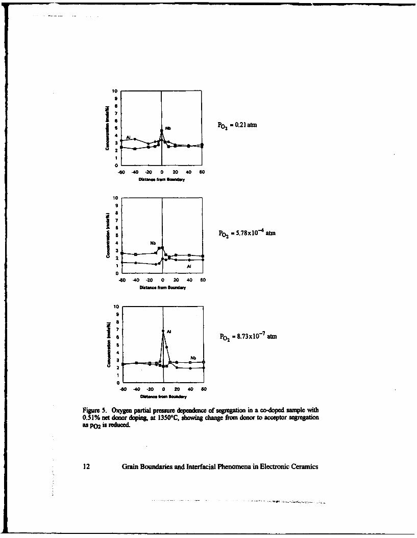
Segregation profiles showed that the segregation or depletion of aliovalent solutesvaried with dopant concentration, temperature, and oxygen activity, in agreement with thespace charge model. Figures 4 and 5 show examples where the effective charge of thesegregated solute has changed sign as each of the experimental variables are independentlyvaried, demonstrating a reversal in the sign of the space charge potential. In Fig. 4, thehorizontal sequence shows (A) the segregation of Al acceptor and depletion of Nb donorwhen the sample has a net acceptor doping, (B) no observed segregation at slight donordoping, near the isoelectric point, and (C) Nb segregation and Al depletion, when thesample has a net donor doping. This sequence represents a variation of +. from negativeto positive values, as shown in Fig. 1. Proceeding vertically from D-B-E, on the otherhand, the potential in a sample of constant composition is titrated from negative to positivewith decreasing temperature. In Fig. 5, a sample of fixed net donor level (0.51% Nb)shows reduced Nb segregation when the oxygen partial pressure is reduced from 0.21 atmto 5.8 x 10⁴ atm, and then a change to acceptor segregation (with slight donor depletionsew) as the p02 is further reduced to 8.7 x 10- atm. This sequence clearly demonstratesthe titration of #. from positive to negative sign with decreasing p02, as calculated in Fig.1(B).
10 Grain Boundaries and Interfacial Phenomena in Electronic Ceramics

D 11.45% %AI 1530C.49%Nb
3
15 A l-ic 1350C Nb-fich 1350"C
0 -A]0B 1350r ec
2 25- Nb
Nbt
o ..................... ..0-80 -4 0 0 40 800 ' E 42 0 'C.40 0 40 8
R
1 2 ~N
5- -4'0 0' 40 10
Distance from Boundary (nm)
Figure 4. Seregation profiles in co-doped TiO2 at 1350*C showing accumulation anddepletion of aliovalent solutes at grain boundaries in Ti0 2, and "titration" in the effectivecharge of the segregated solute as doping and temperature are varied.
Grain Boundaries and Interfacial Phenomena in Electronic Ceramics 11
10
I7
0460 -40 -20 0 20 40 60
1098-
SP 0 2 =0.78x1a atm
4 Nb
-40 -40 -20 0 20 40 60oms.e from ovmdWy
10
lOP 0 2 =8.73x0 atm
S
4
3 M
21 N
2
0-60 -40 -20 0 20 40 60
Ombmce from -WAdm,
Figure 5. Oxygen partial pressure dependence of segregation in a co-doped sample with0.5 1% net donor doping& at 1350-C, showing change from donor to acceptor segregationas P02 is reduced.
12 Grain Boundaries and Interfacial Phenomena in Electronic Ceramics

QUANTIFICATION OF SPACE CHARGE PARAMETERS
Quantitative measurasents of the space charge potential ar shown n Figs. 6 and7. In these rests, each datunm represents a single grain boundary, at which the net
acmlation of aliovalent solute was meassured and the potential calculated from Eq. 8.T boundaries were randomly selected with the only criterion being suitability for STEManalysis (i.e., the region was not overly thick, and the grain boundary could be tiltedparallel to the electron beam, with neither grain in a strongly ddifactig condition). Theresults are therefore representative of th distribution of boundaries in a polycrystal. In allsamples, an occasional boundary with virtually no detectable segregiton is observed.Thes are believed to be special boundaries of high coincidence misorientaions; in fact,one such boundary was found usmg high resolution transmissim electron microscopy to bea {101) twin boundary [18]. Even excluding these "special" boundaries, a significantvariation in +, from boundary to boundary is observed, which further analysis has shownlies outside the counting statistics errors of the measurements, and are probably related todetails of boundary structure.
1.0 T = 1350 °C
0-o5- 0
0.0
-0.5 ~ ANb)Ti02
I ~a (GaANbTi 2- 1.0 1 1
-1.0 -0.5 0.0 0.5 1.0 1.5Net Donor Concentration (mole %)
Figure 6. Space charge potential determined from aliovalent solute coverage at grainboundaries, ecudinmg "special" boundaries with virtually no segregation.
In acceptor-doped samples, a factor contributing to the larger spread in observedvalues is nonequilibrium segregation upon cooling. Thiis is particularly significant athigher acceptor concentrations, due to an increase in lattice diffusion rate. The a and +,,~values in acceptor-doped samples are therefore be regarded as upper limits. Upon fittingthe space charge model to the +w values in Fig. 6, we obtained a cation vacancy formationenergy, gV, of 2.4 eV and an upper limit to g'h of 2.6 cV. The sum of these yields a
Grain Boundaries and Interfacial Phenomena in Electronic Ceramics 13

Fr energy of :5.0 eV, which is in reasonable accord with results from Baumard andTani [25), Tani and Baumard [261, and Tuiler [23] of 4.4-4.6 cV, (Notice that whereasthe separate tens in Ef can be obtained from the space charge interaction, only the sum ofenergies is possible frm transport studi•s.) TIe appearance of the soeectric point in thedonor-doped regime (Figs. I and 6) is due to the contribution of native reduction to thedef�t ctur at high mperatumre; a slih donr dopig is necessary to compensate forthe dfects introduced by reduction. With icreasing temperature, or decreasing pO2,imnrsig amounts of lattice reduction cam the isoelectric to move to higher donor
0.4
0.3 .126%AI, 1.77%Nb
0.2 13500C
0.1
-0.1
-0.2
-0.3
-0.4
-0.5-10 -8 -6 -4 -2 0
Log P0 2 (atm)
Figure 7. Experimental and calculated results for the space charge potential as a functionof oxygen partial pressure, in a sample containing 0.5 1% net donor doping.
Results as a function of p2 (Fig. 7) also show the "titration" of the potential frompositive to negative values (for a donor doped sample) as predicted by the model (e.g., Fig.IB). With respect to the detailed fit betwecn model and data, it should first be noted thatsegregation of Al during cooling is likely for the sample annealed at the lowest p02. Thisis because the lattice is understoichiometric, as in the case of acceptor doped compositions.The two samples in Fig. 7 showing a near-zero and a positive potential are adequatelyquenched, however, and the model can be fitted to these data assuming a preservation ofhigh temperature equilibrium. The solid curve in Fig. 7 is calculated using the defectenergies and equilibrium constants which were discussed earlier. While it shows anoticeable discrepancy with the data, the variation in the parameters necessary to producea better fit is small. For example, the dashed curve shows a better fit obtained using afactor-of-5 lower value for the product of equilibrium constants, K2/Ki4 . Variability ofthis order in the equilibrium comstants would not be surprising (e.g., only a factor of 1.5eror in Y-.) If the equilibrium constants are not changed, a variation in the defectformation energies of -0.2 6V produces a similar result. These small variations in the
14 Grain Boundaries and Interfacial Phenomena in Electronic Ceramics

fining parameters notwithstndin the level of quantitative agreement between the modeland the data is excellent, and strongly supports the interpretation that the ionic spacecharge is the primary cause of the boundary segregtion. Limited observations of surfacesegregation in these samples using Auger electron spectroscopy are qualitatively consistentwith the STEM results for grai boundaries, suggesting that other types of interfaces, andperhaps dislocations as well, behave similarly.
IMPLICATIONS FOR ELECTROCERAMICS
The results illustrate a clear and quantitative link between a complex lattice defectchemistry and the space charge potential, suggesting that the defect chemistry of interfacesin semiconducting oxides can be predicted on the basis of lattice properties. in this modelsystem, despite high electronic carrier concentrations, it appears to be the equilibration ofionic defects with the interface which determines the interfacial &emistry. The results alsoimply that interfaces in semiconducting oxides will generally be nonstoichiometric. Ifvalences of cations and anions are indeed fixed, in the presence of a space charge potentialthe interfacial charge a is an ionic charge, and must arise from a grain boundarynonstoichiometry. Thus the potential surface in Fig. 3 also corresponds to a stoichiometrysurface for the interface. In the present system, regardless of whether the lattice defectstructure is varied as a consequence of changes in doping, temperature, or oxygen activity,understoichiometric TiO2 .8 (8>0) has an oxygen deficient interface, whileoverstoichiometric TiO2 .8 (8<0) has a cation deficient interface. An exactlystoichiometric interface can exist, but is a singularity in defect space and would seem to beof limited importance. This deviation in interfacial stoichiometry is much larger than theparallel variation in lattice nonstoichiometry. At the bulk defect concentrations andtemperatures examined in this study, the interfacial charge densities reach monolayerproportions [181, corresponding to interracial ionic defect concentrations (of unknownspecific identity) which are several tens of percent. It would be remarkable if such largechanges did not to have an impact on the physical structure of surfaces and grainboundaries, or their chemical and electronic properties. However, the details of theserelationships remain to be elucidated.
It is important to emphasize that the present results are concerned withequilibrium defect and solute distributions. YWe these have an obvious and directrelevance to high temperature equilibrium boundary phenomena, they are only one aspectof the complex defect behavior of electrically active boundaries. In a variety of
e mcs including ZaO varistors, BaTiO3 PTC thermistors, and soft magneticferrites, the optimization of boundary properties often involves both a high temperaturefiring step and a controlld, oxidative cooling step. While equilibrium segregation may beachieved during the former, nonequilibrium defect creation processes and additional solutesegregation are likely during the latter. In addition to segregation during cooling,exemplified by the acceptor-doped and reduced TiO2 studied here, demixing and defectformation processes can occur in the presence of local PO2 gradients. Oxidation-drivensolute segregation, which has been observed at TiO2 surhces [321, and cation vacancycreation at PTC boundaries [33] as the bulk strives towards a new defect equilibrium, aretwo specific processes of this kind. To fully understand the relationship betweeninterfacial defects and electrical properties, results suc as those discussed here combinedwith studies correlating additives with the appearance of specific interface states [341 areclearly necessary.
Grain Boundaries and Interfacial Phenomena in Electronic Ceramics 15
CONCLUSIONS
From defect and space-charge modeling and the quantitative measurement ofaliovalent solute segregation at grain boundaries, the functional dependence of the space-charge potential in TiO2 on lattice defect structure has been clarified. Throughout a broad
range of bulk defect conditions, an ionic space-charge is maintained. Correspondingly, itis inferred that the grain boundaries and surfaces of TiO2 are generally nonstoichiometric;and regardless of whether the lattice defect structure is varied as a consequence of changesin doping, temperature, or oxygen activity, understoichiometric TiO2 -8 (6>0) bears apositive interfacial charge, implying an oxygen deficiency at the interface, whileoverstoichiometric TiO2 .8 (8<0) bears a negative interfacial charge, i.e., a cationdeficiency at the interface. The interfacial and space charge defect densities are often alarge fraction of a monolayer. It is expected that such dramatic changes in interfacialdefect concentration have a significant influence on the electrical, chemical, and structuralcharacteristics of surfaces and grain boundaries, and that similar behavior occurs in othersemiconducting oxides.
AcknowledgmentsWe are grateful to Professors H.L. Tuller and J.B. Vander Sande, and Dr. A.J.
Garratt-Reed, for many useful discussions. The support of U.S. Department of EnergyGrant No. DE-FG02-87ER45307 and NSF/MRL Grant No. DMR 90-22933 isacknowledged.
References
1. J. Frenkel, Kinetic Theory of Liquids, Oxford University Press, New York, 1946.
2. K. Lehovec, "Space-Charge Layer and Distribution of Lattice Defects at theSurface of Ionic Crystals," J. Chem. Phys. 21 [7] 1123 (1953).
3. K.L. Kliewer and J.S. Koehler, "Space Charge in Ionic Crystals. I. GeneralApproach with Application to NaCI," Phys. Rev. 140 14A] A1226 (1965).
4. J.M. Blakely and S. Danyluk, "Space Charge Regions at Silver Halide Surfaces:Effects of Divalent Impurities and Halogen Pressure," Surf. Sci. 40 37 (1973).
5. S. Danyluk and J.M. Blakely, "Space Charge Regions at Silver Halide Surfaces:Experimental Results for Undoped AgCI," Surf Sci. 41 359 (1974).
6. M.F. Yan, R.M. Cannon, and H.K. Bowen, "Space Charge, Elastic Field, andDipole Contributions to Equilibrium Solute Segregation at Interfaces," J. Appl.Phys. 54 [2] 764 (1983).
7. R.A. Hudson, G.C. Farlow, and L.M. Slifkin, "Individual Formation Parametersof Charged Point Defects in Ionic Crystals: Silver Chloride," Phys. Rev. B 36 [914651 (1987).
8. J.R.H. Black and W.D. Kingery, "Segregation of Aliovalent Solutes Adjacent toSurfaces in MgO," J. Am. Cer. Soc. 62 [3-41 176 (1979).
16 Grain Boundaries and Interfacial Phenomena in Electronic Ceramics

9. Y.M. Chiang, A.F. Henriksen, W.D. Kingery, and D. Finello, "Characterization ofGrain-Boundary Segregation in MgO," J Am. Cer. Soc. 64 [7] 385 (1981).
10. Y.-M. Chiang and W.D. Kingery, "Grain Boundary Migration in NonstoichiometricSolid Solutions of Magnesium Aluminate Spinel: II, Effect of Grain BoundaryNonstoichiometry," J. Am. Cer. Soc. 73 [5] 1153-58 (1990).
11. Y.-M. Chiang and W.D. Kingery, "Grain Boundary Composition in MnZn Ferrites,"Advances in Ceramics. Vol. 6, edited by M.F. Yan and A.H. Heuer, pp. 300-311,The American Ceramic Society, Columbus, Ohio, 1983.
12. C.J. Peng and Y.-M. Chiang, "Grain Growth in Donor-Doped Strontium Titanate,"J Mat. Res., 5[61, 1237-45 (1990).
13. Y.-M. Chiang and T. Takagi, "Grain Boundary Chemistry of Barium Titanate andStrontium Titanate: I, High Temperature Equilibrium Space Charge," J Am.Ceram. Soc., 73[111], 3278-85 (1990).
14. Y.-M. Chiang and T. Takagi, "Grain Boundary Chemistry of Barium Titanate andStrontium Titanate: II, Origin of Electrical Barriers in Positive-Temperature-Coefficient Thermistors," J Am. Ceram. Soc., 731111, 3286-91 (1990).
15. S.B. Desu and D.A. Payne, "Interfacial Segregation in Perovskites: II, ExperimentalEvidence," J Am. Ceram. Soc., 73111], 3398-406 (1990).
16. J.A.S. Ikeda, Y.-M. Chiang and C.G. Madras, "Grain Boundary ElectrostaticPotential as a Function of Acceptor and Donor Doping in TiO2 ," pp. 341-8 inCeramic Transactions vol. 24: Point Defects and Related Properties of Ceramics,Ed. by T.O. Mason and J.L. Routbort, Am. Ceram. Soc., Cincinnati, OH, 1991.
17. J.A.S. Ikeda and Y.-M. Chiang, "Space Charge Segregation at Grain Boundaries inTitanium Dioxide: 1, Relationship between Lattice Defect Chemistry and SpaceCharge Potential," J Am. Ceram. Soc., 761101 2437-46 (1993).
18. J.A.S. Ikeda, Y.-M. Chiang, "Space Charge Segregation at Grain Boundaries inTitanium Dioxide: II, Model Experiments," J. Am. Ceram. Soc., 76110] 2447-59(1993).
19. L.A. Bursill, M.G. Blanchin, and D.J. Smith, "Precipitation in Non-StoichiometricOxides. II, {100) Platelet Defects in Reduced Rutiles," Proc. R Soc. Lond. A, 391,373-91 (1984).
20. L.A. Bursill, G.-J. Shen, D.J. Smith, and M.G. Blanchin, "Emergence of SmallDefect Contrast within HREM Images of Nonstoichiometric Rutile,"Ultramicroscopy, 13, 191-204 (1984).
21. J. Sasaki, N.L. Peterson and K. Hoshino, "Tracer Impurity Diffusion in Single-Crystal Rutile (TiO2.x)," J Phys. Chem. Solids 46 [11] (1985).
Grain Boundaries and Interfacial Phenomena in Electronic Ceramics 17
22. K. Hoshino, N.L. Peterson and C.L. Wiley, "Diffusion and Point Defects inTiO2.x," J Phys. Chem. Solids 46 1397 (1985).
23. H.L. Tuller, unpublished work.
24. J.A.S. Ikeda, "Grain Boundary Defect Chemistry and Electrostatic Potential inAcceptor- and Donor-Doped Titanium Dioxide," Ph.D. Thesis, MIT, Cambridge,Massachusetts, June 1992.
25. J.F. Baumard and E. Tani, "Thermoelectric Power in Reduced Pure and Nb-DopedTiO2 Rutile at High Temperature," Phys. Stat. Sol. A 39 373 (1977), and J.F.Baumard and E. Tani, "Electrical Conductivity and Charge Compensation in NbDoped TiO2 Rutile," J. Chem. Phys. 63 [31 857 (1977).
26. E. Tani and J.F. Baumard, "Electrical Properties and Defect Structure of RutileSlightly Doped with Cr and Ta," J Solid State Chem., 32, 105-113 (1980).
27. G. Levin and C.J. Rosa, "The Defect Structure, Nonstoichiometry and ElectricalConductivity of M02 Oxides Doped by Pentavalent Oxides, Part II: The DefectStructure z ad Electrical Conductivity of Pure and Doped TiO2 (Rutile) at 1273K,"Z Metallkde, 70, 646-652 (1979).
28. J.F. Marucco, J. Gautron, P. Lemasson, "Thermogravimetric and Electrical Study ofNon-stoichiometric Titanium Dioxide TiO2.x between 800 and 1 100'C," J. PhysChem. Solids 42 363 (1981).
29, C.D. Terwilliger, "Determination of Grain Boundary Properties in NanocrystallineMaterials," Ph. D. Thesis, MIT, Cambridge, Massachu ,ctts, September 1993.
30. Y.-M. Chiang, L.A. Silverman, R.H. French, and R.M. Cannon, "The Thin GlassFilm between Nanocrystalline Conductor Particles in Thick Film Resistors," toappear in J Am. Ceram. Soc..
31. J.-Q. Lee and Y.-M. Chiang, unpublished.
32. J.A.S. Ikeda, Y.-M. Chiang and B.D. Fabes, "Non-Equilibrium Surface Segregationin Al-doped TiO2 under an Oxidizing Potential: Effects on Redox Color-BoundaryMigration," J Am. Cer. Soc. [6] 1633 (1990).
33. ;. Daniels and R. Wemicke, "Defect Chemistry and Electrical Conductivity ofDoped Barium Titanate Ceramics: Part V. New Aspects of An Improved PTCModel," Philips Res. Repts., 31161, 544-59 (1976).
34. H.i,. Tuller and K.-K. Baek, these proceedings.
18 Grain Boundaries and Interfacial Phenomena in Electronic Ceramics

ELECTRICAL ACTIVITY AT INDIVIDUAL GRAIN BOUNDARIES AND INTERFACES INSEMICONDUCTING OXIDES
H.L. Tuller and K-K. BaekCenter for Materials Science & EngineeringMassachusetts Institute of TechnologyCambridge, MA 02139
ABSTRACT
Grain boundaries and other interfaces often control the electricalproperties of devices. A clearer understanding of the chemistry-structure-property correlations of such boundaries can be achieved by examiningindividual electrically active boundaries. Following a review of earlier suchwork, we report recent results on active boundaries isolated in ZnO ceramics byan in-diffusion method. Breakdown voltages and nonlinearity coefficients areexamined as a function of processing conditions and dopant types. DLTSmeasurements are used to identify interface states and other deep levels in thevicinity of the boundaries. Directions for future work are proposed.
INTRODUCTION
It is well known that the unique abilities of semiconductor electronics torectify, modulate, switch and amplify electrical signals derive from theexistence of many individual, highly controlled electrically active junctions. Themost important of these are the p-n, metal-semiconductor and metal-insulator-semiconductor (MIS) interfaces. In some applications, particularly solarphotovoltaic and display technologies, polycrystalline semiconductors areutilized which, by their nature, introduce additional interfaces, i.e. grainboundaries, some of which are electrically active. The electrical activity of theseboundaries and their dependence on processing conditions, even in silicon,remain poorly understood.
In contrast to conventional semiconductor technology, in which the use ofsingle crystalline semiconductors predominates, electro-ceramics, for historicand cost reasons, are largely polycrystalline. Consequently grain boundariesoften control the electronic properties of these devices. This can result inincreased resistance and non-ohmic behavior of the device as well as difficulty inreproducing desired device characteristics. Grain boundaries which block
To the extent authorized under the laws of the United States of America, alH copyright interests in this publication are the propertyof The American Ceramic Society. Any duplication, reproduction, or republication of this publication or any part thereofwitotthe express written consent of The Amercan Ceramic Society or fee paid to the Copyright Clearance Center, is prohibited.
Grain Boundaries and Interfacial Phenomena in Electronic Ceramics 19

electronic transport between the grains in negative temperature coefficient(NTC) thermistors, for example, are to be avoided. On the other hand,electrically active interfaces are essential to the operation of the ZnO varistor,the BaTiO3 positive temperature coefficient (PTC) thermistor, the SrTiO3barrier layer capacitor and the SnO2 gas sensor, to name a few.
While both electro-ceramic polycrystalline devices and integratedcircuits contain hundreds or thousands of individual boundaries, only inintegrated circuits, where one uses parallel planar processes, can manyjunctions be fabricated simultaneously with near identical characteristics. Inthe sintering processes used to make electro-ceramics, inhomogeneities are therule rather than the exception. Such materials are characterized by non-uniform grain size, porosity, second phase distribution, impurity segregationand grain-grain misorientation.
In this paper, we focus our attention on attempts to investigate individualelectrically active interfaces in ZnO-based structures with varistor-likeproperties. First, we summarize earlier investigations and comment on boththeir strengths and limitations. Then, we present some of our recent work onin-diffused structures which include some comnrehensive deep level transientspectroscopy (DLTS) data as a function of rK d-ants. Last, we conclude withsuggestions for future work.
VARISTOR CHARACTERISTICS
A varistor is a device whose resistance decreases sharply at acharacteristic breakdown potential. It may be used as an over-voltage protectiondevice when placed in parallel with the circuit to be protected. A schematic of theI-V characteristics of a varistor is presented in Fig. (1). One generallydistinguishes three regimes. At low voltage in the "prebreakdown regime"(Region I) the device shows ohmic-like characteristics with an effectiveresistivity of the order of 1010-1012 ohm-cm and a so-called"leakage current"which is thermally activated. In the vicinity of the breakdown voltage (RegimeII) the current increases orders of magnitude with small increases in voltage.The slope of this curve is given by the nonlinearity factor a with values between30-60 typical for commercial devices. Ultimately, the resistance of the deviceis limited by the resistivity of the grains leading to the "up-turn" regime(Region Ill) where the device is again ohmic. "Up-turn" refers to the shape ofthe curve when plotted on a V vs. I plot.
From both a theoretical and practical standpoint, one wishes to understandthe relationship betweeen the magnitude and temperature dependence of theleakage current, the breakdown voltage V8 , the non-linearity factor, a, thedevice stability and the chemistry and structure of the grain boundary.
Perhaps the most widely accepted model of the grain boundary junction isthe double back-to-back Schottky barrier model proposed by a number of
20 Grain Boundaries and Interfacial Phenomena in Electronic Ceramics
106
S HI
! c=d(Iogl1/d(IogV) II
DI
10 v 103log E (V/cm)
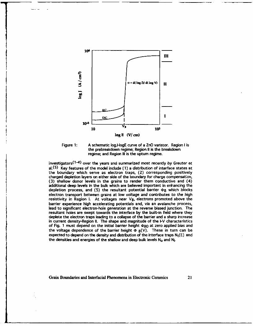
Figure 1: A schematic IogJ-IogE curve of a ZnO varistor. Region I isthe prebreakdown regime; Region II is the breakdownregime; and Region III is the upturn regime.
investigators( 1-4) over the years and summarized most recently by Greuter etal.( 5 ) Key features of the model include (1) a distribution of interface states atthe boundary which serve as electron traps, (2) corresponding positivelycharged depletion layers on either side of the boundary for charge compensat:on,(3) shallow donor levels in the grains to render them conductive and (4)additional deep levels in the bulk which are believed important in enhancing thedepletion process, and (5) the resultant potential barrier OB which blockselectron transport between grains at low voltage and contributes to the highresistivity in Region I. At voltages near VB, electrons promoted above thebarrier experience high accelerating potentials and, via an avalanche process,lead to significant electron-hole generation at the reverse biased junction. Theresultant holes are swept towards the interface by the built-in field where theydeplete the electron traps leading to a collapse of the barrier and a sharp increasein current density-Region I1. The shape and magnitude of the I-V characteristicsof Fig. 1 must depend on the initial barrier height 080 at zero applied bias andthe voltage dependence of the barrier height 0 B(V). These in turn can beexpected to depend on the density and distribution of the interface traps Nt(E) andthe densities and energies of the shallow and deep bulk levels No and Ni.
Grain Boundaries and Interfacial Phenomena in Electronic Ceramics 21

From a practical standpoint, three criteria, in addition to havingconductive grains, must be met in order for polycrystalline ZnO to exhibitdesireable varistor qualities. These include:
1. Deep donors, e.g. Mn2. Segregants, e.g. Bi, Pr3. Oxidative anneal
The obvious question which arises is how do these three factors influence thenature, density and distribution of interface and bulk states and in turn thebarrier dependence on applied voltage? We look to individual interfaces toclarify these issues.
SINGLE BOUNDARY STUDIES
The idealized polycrystalline varistor is shown schematically in Fig. 2ain which each small square symbolizes a grain and each gray region between thegrains, the depletion region. The dark strips at top and bottom of the figurerepresent the electrodes. The breakdown voltage per grain boundary is calculatedby dividing the measured breakdown voltage of the device by the number of grainboundaries in series between the electrodes. The latter number is commonlyobtained by dividing the device thickness D by the average grain size d.
However, it is difficult to understand the characteristics of a single grainboundary by measuring the overall electrical properties of a polycrystalline ZnOvaristor, as the actual varistor consists of numbers of grain boundaries withvarying characteristics connected, both in series and in parallel, thus formingrather complex three-dimensional networks.
(a) (b)
Figure 2 A schematic 2-dimensional diagram of an idealized ZnOpolycrystalline varistor (a) and realistic representationof the same ZnO varistor (b).
22 Grain Boundaries and Interfacial Phenomena in Electronic Ceramics

A more realistic representation of a varistor is given in Fig. 2b whichcontains a distribution of grain sizes and shapes. The current path, illustratedby the dashed line, intercepts four possibly unequal grain boundary barriers.One can easily imagine others which intercept six or seven boundaries.Obviously the overall electrical characteristics are not representative of anyindividual boundary and can, at best, be used to obtain some average picturewhich may, with the appropriate models, be used to ascertain the degree ofhomogeneity of the system.(2 )
An obvious way around these difficulties is to examine the properties ofindividual boundaries. Two general approaches have been taken to achieve thisgoal. The first involves interrogating individual boundaries in a polycrystallinemass by the use of micro-electrodes while the second requires the fabrication ofstructures which include only single active interfaces. These are reviewedbelow.
SINGLE GRAIN JUNCTION MEASUREMENT ON POLYCRYSTALLNE ZnO VARISTORS
Several studies have reported on the electrical characterization of singlegrain-to-grain junctions in polycrystalline ZnO varistors. Generally, threedifferent experimental approaches have been used to accomplish this purpose.The first involves achieving microcontacts on two adjacent grains with the helpof very sharp metallic needles (radius of curvature << 1mm) This arrangmentis illustrated on the upper part of Fig. (3). Varistor-like characteristics withbreadown voltages of 4V were reported by Einzinger( 6 ) using Bi-dopedScommercial ZnO varistors.
Figure 3 Microcontacts for single boundary I-Vmeasurements
Grain Boundaries and Interfacial Phenomena in Electronic Ceramics 23

In a related approach, varistor specimens with very large grain size(diameter of about 150 gm) were prepared to accommodate the microwelding oflead wires (diameter of about 25pm) on either side of single grain boundary on asurface treated polycrystalline varistor.(7 ) Single boundary I-V characteristicsI with maximum a of 45, and VB values of 3.1 V were obtained. A near zero voltagebarrier height (0BO) was estimated to be approximately 0.57 eV from thetemperature dependence of the leakage current.
In the second approach, improved electrical contacts are established byevaporating a pair of opposing aluminum(8 ) or gold( 9 ) electrodes on the polishedsurface of a polycrystalline varistor disk. (See the lower part of Fig. 3) Abreakdown voltage of -3.3V was obtained from the I-V characteristics at roomtemperature according to Mahan et al( 8 ) and 3.6 V according to Van Kemenade.( 9 )
Einzinger performed similar measurements with Cr and Au sputtered-electrodes but on thin polished sheets (-0.2mm) of commercial ZnO varistormaterial.( 1 0) The surrounding ZnO material was removed with a micro-manipulator to isolate a 'true' single boundary.. The I-V characteristics ofnominally second phase-free single boundaries were found to exhibit the welldefined vanstor behavior. Measurements taken on boundaries with and withoutBi-rich intergranular layers indicated that the intergranular layers have astrong deleterious effects on the degree of nonlinearity.
Most recently, Dunlop and Olsson( 1 1 ) reported single boundary DC I-Vmeasurements on boundaries which were also investigated by TEM. Thisrepresents the first report which attempts to characterize both the electrical andchemistry of a individual boundary. The study showed that a distribution of typesof boundaries with different I-V charcteristics and phase distributions exist inZnO varistors.
The microcontact method thus provides means, in principle, of studyingmany individual boundaries in a single device and thereby developing a statisticalbasis for understanding the overall characteristics of the device. Nevertheless, anumber of important limitations remain. First, it is difficult to control thechemistry of individual boundaries. Second, due to the contact method, there islimited ability to examine the electrical properties at elevated tempeature andcontrolled atmosphere. Finally, unless the specimens are thinned, the currentpathways remain difficult to control.
SYNTHETIC SINGLE BOUNDARY STUDIES
Thin Film Varistor
Some investigators have simulated a varistor structure by forming twolayer structures in which one layer is ZnO and the other, a material which istypically a second phase found at the triple point between grains.
24 Grain Boundaries and Interfacial Phenomena in Electronic Ceramics
Suzuoki et al( 1 2) studied a ZnO-Bi203 two-layer thin film varistorprepared by RF sputtering as a model system representing a single grainboundary in the ZnO varistor. The two-layer thin film structure showed highlynon-linear, asymmetical I-V characteristics whose nonlinearity coefficient forreverse bias equals or exceeds those of ZnO based varistors (maximum value of a- 60-90). The device, however, also exhibited a decrease in low voltageresistance after voltage application reflecting a degradation of the device.
A similar study of a thin film junction based on a ZnO-Pr/Co oxide two-layer thin film varistor has also been reported.( 3) The junction showed highlynonlinear I-V characteristics with a maximum value of a around 30, when theZnO layer was positively biased. The depletion region formed in the ZnO layeradjacent to the ZnO-PrCo oxide interface was attributed to be the main source ofthe electrical characteristics of the thin film junction.
The advantages of the thin film approach include the ability to readilyform single barriers and control the interfacial chemistry. However, thesestudies show that the junctions do not accurately replicate the ZnO grainboundary, the barriers tend to be unstable upon biasing and dopants tend tobecome volatile during fabrication.
Bi-Crystal Varistors
Among the possible approaches to study an individual grain boundary, aZnO bi-crystal with controlled dopants at the interface would appear to be themost ideal material for study. The inherent difficulties in fabricating such bi-crystals have, however, remained a major obstacle. Part of the difficulty isrelated to ZnO's high volatility, and high thermal expansion anisotropy. BecauseZnO sublimates at the melting temperature, techniques for ZnO bi-crystalfabrication based on melt growth methods cannot be utilized.
Bi-crystal-like structures have however been fabricated by utilizing lowmelting interlayers. Schwing et al( 1 4) fabricated such structures bysandwiching an intermediate layer of common varistor additives (Bi20 3 ,MnO2,Co 3 0 4 , and Cr203) between undoped ZnO single crystal plates. Themicrostructure of the "sandwiches" fired at 900C for 1 hour consisted of twosingle crystals well separated by a 5 lim thick intergranular layer. For thestructures fired at 1 100C, the microstructure was similar except that the ZnOsingle crystals were in direct contact at certain points along the interface. Thesandwiches fired at 900C in general exhibited superior varistor I-Vcharacteristics which was attributed directly to the presence of a continuousBi20 3 rich layer at the interface absent in specimens fired at 11 OOC. However,ac measurements showed that the potential barriers at the sandwich interfacewere due to depletion regions adjacent to the additive oxide interfacial layersrather than to the layer themselves, which were shown to have resistivitiesmuch lower than for those calculated for the depletion layers.
Grain Boundaries and Interfacial Phenomena in Electronic Ceramics 25

Summarizing the hi-crystal work, the approach enables the investigationof a single boundary with a simplified current pathway and well controlledinterfacial chemistry. However, since a continuous second phase at the interfaceis apparently necessary to obtain good varistor-like properties, the results maynot be representative of actual grain boundaries.
Surface In-Diffusion
Non-ohmic grain boundary properties can also be obtained by diffusingoxides such as 8i203 and/or Sb203 into the grain boundaries of undoped ZnO asfirst demonstrated by Matsuoka.( 5) This approach relies on the fact that thediffusion of ions is more rapid along the grain boundaries, and thus the grainboundaries act as short circuit paths for diffusion. Sukkar and Tuller(1 6)reported that single electrically active ZnO grain boundaries were successfullyprepared by using a surface in-diffusion method. In this technique, a "sandwich"composed of undoped polycrystalline ZnO discs with dopants added to the interfaceis sintered at1400-1440C for 12-24 hours. Dopants with different nominalconcentrations, either as single, double or triple additions were applied to theinterface. As a result, single electrically active grain boundaries weresuccessfully fabricated in Mn/Pr-, Co/Pr-, Mn/Co/Pr-doped ZnO samples.
Chiou et al( 1 7) also reported that low voltage ZnO varistors may befabricated by metal surface in-diffusion of Bi2 0 3 into a ZnO pellet predoped withtransition metal cations. In this case, the diffusion source was prepared bypressing the powder into a thin disc shape, and annealing at 950C-1 350C for 1hour. The prepared varistors showed a smaller non-linearity parameter (a max- 7-15) and a larger dielectric constant than commercial varistors.
The authors have followed on the work of Sukkar and Tuller by extendingthe r so called Surface In-Diffusion (SID) method to include more extensivecharacterization methods including DLTS and transmission electronmicroscopy.( 1 8) Sandwich structures including Pr/Co, Pr/Mn, Pr/Ni,Pr/Co/Mn, and Pr/Mn/Ni have been investigated.
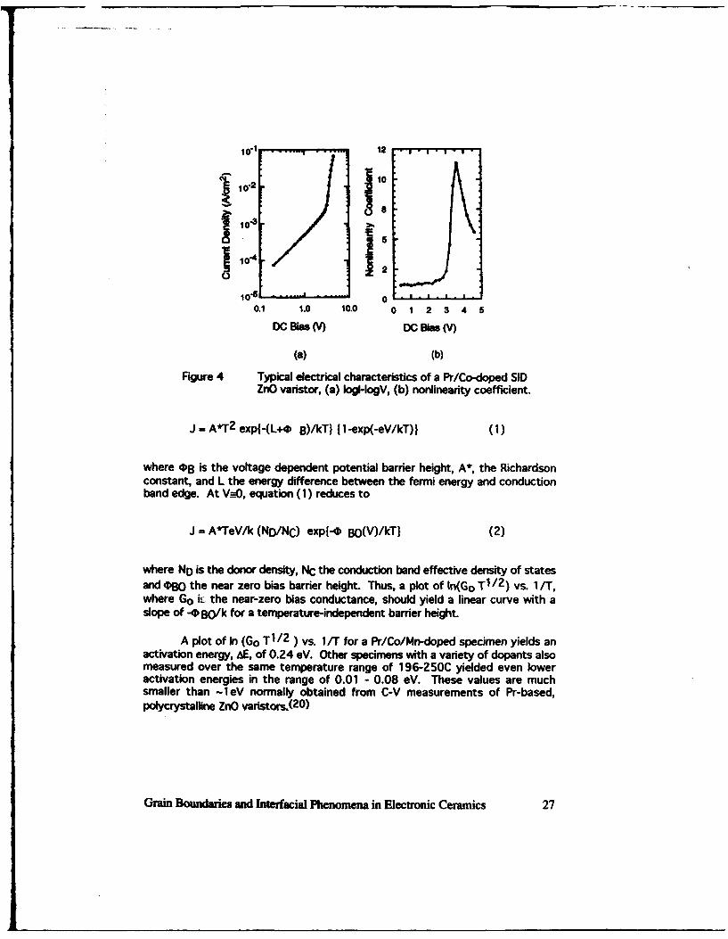
Typical I-V characteristics of a Pr/Co-doped SID sample at roomtemperature are shown in Fig. (4). Symmetric varistor like I-V characteristicswith a breakdown voltage of -3V were obtained. Also included is the incrementalnonlinearity coefficient (a). These I-V characteristics confirm that a singleelectrically active boundary is formed in the direction perpindicular to currentflow. Other SID specimens sometimes exhibit multiple active boundariesreflected in larger VB's. For evaluation of the potential barrier height ("•), themodified thermionic model based on the double-Schottky barrier model proposedby Pike and Seager(1 9) may be employed. The thermionic emission currentacross a single grain boundary potential barrier is given by
26 Grain Boundaries and Interfacial Phenomena in Electronic Ceramics
10-1 12 -
10-2 0
8
10-44
10"6 00.1 1.0 10.0 0 1 2 3 4 5
DC Bias (V) DC las (V)
(a) (b)
Figure 4 Typical electrical characteristics of a Pr/Co-doped SIDZnO varistor, (a) Iogl-logV, (b) nonlinearity coefficient.
J - A*T 2 exp{-(L+4b 8)/kTI 11 -exp(-eV/kT)} (1)
where 0• is the voltage dependent potential barrier height, A*, the Richardsonconstant, and L the energy difference between the fermi energy and conductionband edge. At V_=0, equation (1) reduces to
J = A*TeV/k (ND/NC) exp{l- Bo(V)/kT} (2)
where ND is the donor density, NC the conduction band effective density of statesand OBO the near zero bias barrier height. Thus, a plot of ln(Go T1 /2) vs. I /T,where Go ik the near-zero bias conductance, should yield a linear curve with aslope of -. BO/k for a temperature-independent barrier height.
A plot of In (Go T1 / 2 ) vs. I/T for a Pr/Co/Mn-doped specimen yields anactivation energy, AE, of 0.24 eV. Other specimens with a variety of dopants alsomeasured over the same temperature range of 196-250C yielded even loweractivation energies in the range of 0.01 - 0.08 eV. These values are muchsmaller than -1eV normally obtained from C-V measurements of Pr-based,polycrystalline ZnO varistors.(2 0)
Grain Boundaries and Interfacial Phenomena in Electronic Ceramics 27

One may evaluate the barrier height as a function of voltage at a giventemperature by rearrangement of equation (1);
46B (V) - kT In[ A*AT 2 ND/I NC I 11 - exp (-eV/kT)} (3)
where I and V are the measured currents and voltages, respectively and A thecross-sectional area.
Specimens with different dopants exhibit similar 0 B vs. V characteristicsas shown in Fig. (5). Generally, OB initially drops rapidly at low voltage (< 1V), then more slowly as the applied voltage increases and again more rapidly asthe voltage approaches the breakdown voltage. The Pr/Ni- and Pr/Co/Mn-dopedSID samples do not exhibit the sharp drop at -3V exhibited by the others.
Estimated 0BO values obtained from Fig. 5 range from 0.55 eV (Pr/Ni-doped SID sample) to 0.70 eV (Pr/Co/Mn-doped SID sample). These values aremuch larger than those estimated from the temperature dependent I-Vmeasurements and come much closer to the expected value of -1 eV. The resultsof the DC measurements are summarized in Table 1.
0.70 --- A--- Pr/Co/Mn
---- &- Pr/MnS .....-.... Pr/MNINi
0.50
0.40
... Pr/Co, Pr/Ni
0.30 •,- I •--- ,0 2 4 6 8
DC Bias(V)
Figure 5 Plot of fB vs. V, SID ZnO varistors at 20C.
28 Grain Boundaries and Interfacial Phenomena in Electronic Ceramics

IJ
Table I Summary of DC IV characteristics of SID samples
DnPmts J (leakage) VB mx A E* 0130(mA/cm_) Mv) _ _ (ev)
Pr/Co 0.5 3.0 11' 0.02 0.60Pr/Mn 0.015 4.0 9 0.08 0.65Pr/Ni 1.5 4.0 4 0.01 0.54Pr/Co/Mn 0.007 - 13 0.24 10.70Pr/Mn/Ni 0.5 3.8 5 0.02 0.57(*) :from thermionic model (V-constant)
(*) :from thermionic model (T-constant)
While the breakdown voltages of around 3-4 V indicate that singleelectrically active layers are formed in these specimens, the leakage currents inthe prebreakdown regime are much higher (by a factor of 1 0 2 -103) thanexpected from other studies of single barrier ZnO based varistors. (6-11) Thesefeatures, common to all SID samples regardless of the dopant type, suggest thatparallel leakage paths in the structure mask the true I-V characteristics of theelectrically active barriers formed therein.
To confirm this hypothesis, microcontact measurements were performedwhich showed that a certain fraction of the boundaries did not attain fullelectrical activity thereby forming "poor" barriers. In other words, each SIDsample apparently consists of varistor-like, electrically active barriers andnearly linear, resistive barriers connected in parallel. We suspect that the'poor' barriers are either due to a poor distribution of the dopants during theannealing steps, inhomogeneous oxygen distribution during the oxidation step ordegradation of some barriers due to inhomogeneous current flow. These featuresrequire further study.
The double Schottky barrier model relates the potential barrier height todensity of charges trapped in the localized interface states. Furthermore, thedensity and distribution of these interface states determine the voltagedependence of 0 B and thus the value of the non-linearity factor a.Characterization of these interface states, therefore, is required to properlyunderstand the electrical activity of the boundaries, and their dependence on theboundary chemistry and structure.
Deep Level Transient Spectroscopy (DLTS) measurements were carriedout for each SID sample from -1 960C to 4500C to determine the distribution ofinterface states. Higher temperatures were required for these specimens todetect emission rates from deep interface states (-1 eV) believed to exist in ZnOstructures.
Grain Boundaries and Interfacial Phenomena in Electronic Ceramics 29
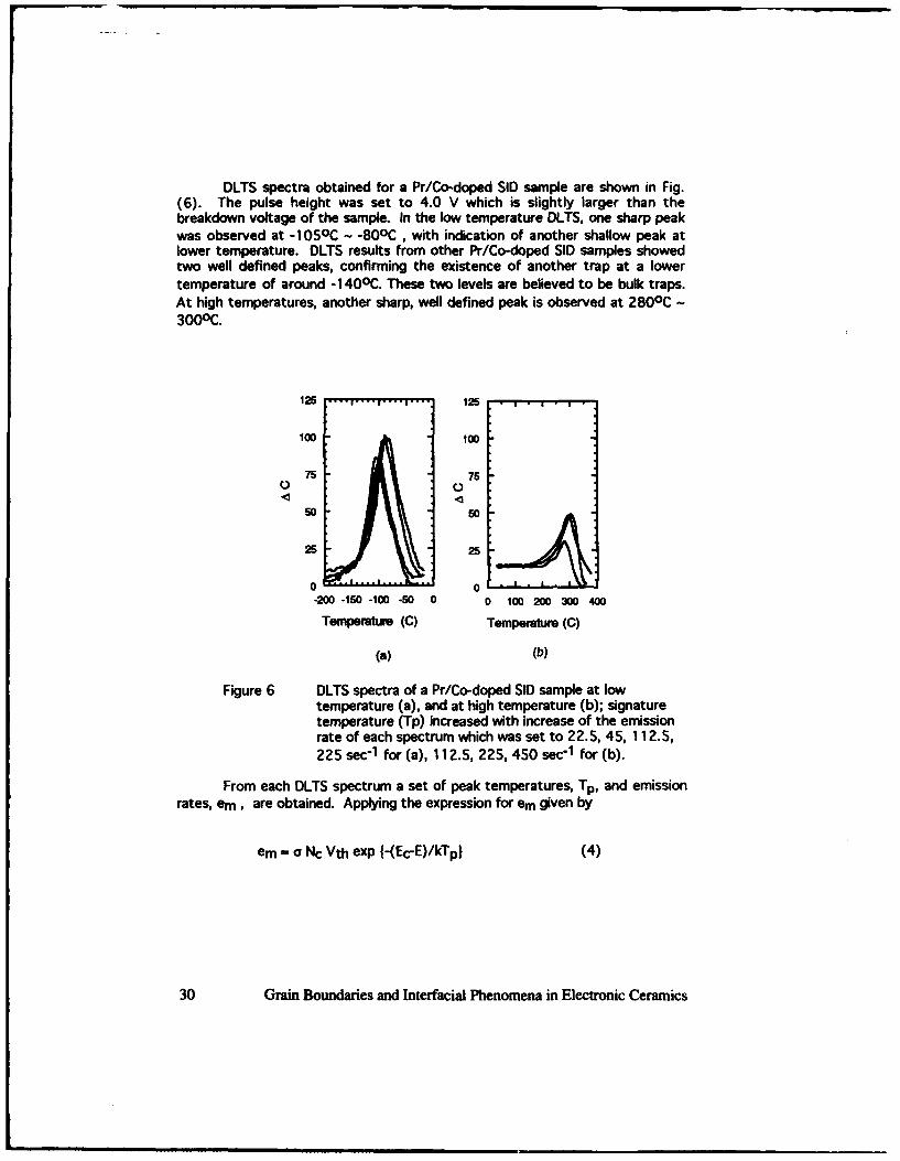
DLTS spectra obtained for a Pr/Co-doped SID sample are shown in Fig.(6). The pulse height was set to 4.0 V which is slightly larger than thebreakdown voltage of the sample. In the low temperature DLTS, one sharp peakwas observed at -105 0C - -80oC , with indication of another shallow peak atlower temperature. DLTS results from other Pr/Co-doped SID samples showedtwo well defined peaks, confirming the existence of another trap at a lowertemperature of around -1 40o0C. These two levels are believed to be bulk traps.At high temperatures, another sharp, well defined peak is observed at 2800 C -3000 C.
125 125
100 100
75 75
o o
so so
25 25
0 0-200-150-100-0 0 0 100 200 300 400
Temperature (C) Temperature (C)
(a) (b)
Figure 6 DLTS spectra of a Pr/Co-doped SID sample at lowtemperature (a), and at high temperature (b); signaturetemperature (Tp) increased with increase of the emissionrate of each spectrum which was set to 22.5, 45, 112.5,225 sec"1 for (a), 112.5, 225, 450 sec"1 for (b).
From each DLTS spectrum a set of peak temperatures, Tp, and emissionrates, em, are obtained. Applying the expression for em given by
em = Y Nc Vth exp {-(Ec-E)/kTp} (4)
30 Grain Boundaries and Interfacial Phenomena in Electronic Ceramics

the energy level of the trap, E, relative to the conduction band edge, EC can beobtained from a plot of In em vs. 1 /T. In this equation, a is the capture crosssection, Nc the effective density of states, and Vth the thermal velocity. A plot ofIn(erm Tp 2 ) vs. (Tp"1 ) derived from the DLTS spectra in Fig. (6) is shown inFig. (7). The resulting data fit the Arrhenius plot well. Overall, DLTSmeasurements on Pr/Co-doped samples showed that there are two separate bulkstates; El (- 0.27 eV), E2 (- 0.39 eV), and two interface states; E3 (= 0.62-0.7 eV), E4 (= 1.13 eV) in these materials.
8.5
- 7
8.0
6" 6 7.5
0.027e
E -0.27 Ov 7.0 E / 1. 13 v¢: 5
"6.5 "
5.0 5.5 6.0 6.5 1.7 1.8 1.9
IOOO/Tp (1/K)
(a) (b)
Figure 7 Plot of the emission rate as a function of signaturetemperature (Tp). From the DLTS spectra of the Pr/Co-doped SID sample at low temperature (a), and at hightemperature (b). See Fig. (6).
The other SID samples, with different dopants, also exhibited two or threewell defined DLTS peaks. The results of the DLTS measurement are summarizedin Fig. (8). Additional DLTS measurements with different pulse shape confirmedthat the deeper levels, E3 and E4 are interface levels,( 2 1 ) while E1 and E2 arebulk states. At least, on a preliminary basis, if we compare these results withthose of Table 1, the deep interface state, E4 (= 1.13 eV) seems to correlate witha high a value. Such results, however, require further study before suchconclusions can be confirmed.
In summary, while the in-diffusion process for forming individual activeboundaries, to date, suffers from leakage problems, it has provided theopportunity to obtain well defined DLTS spectra for a series of dopantcombinations. Such information about the interface state distributions allows formodeling of the I-V characteristics, which are now in progress. Further work isnecessary to refine the in-diffusion process to minimize or eliminate the high
Grain Boundaries and Interfacial Phenomena in Electronic Ceramics 31

1.4
1.2
" i •E4
W 0.80' o. • • E3
0- 0.4 - E2
LU '•- @ =- •El0.2
0 I I I
00
Figure 8 Trap energy levels obtained from DLTS measurements ofSID samples, where El and E2 are bulk traps, E3 and E4
are interface states.
leakage paths. Micro-electrodes, in combination with high resolution analyticaltools such as scanning transmission electron microscopy (STEM), applied to suchstructures, may provide the desired correlations between structure andproperties. Other approaches, such as fabrication of bi-crystal structuresprovide an additional important factor, i.e. control of boundary structure,assuming fabrication difficulties can be overcome. New instrumentation, whichenables fabrication of interfaces under highly controlled environments, e.g.molecular beam epitaxy (MBE), laser ablation, etc., hold out promise forfurther important advances in this field.
CONCLUSION
Single boundary studies promise to shed new light on the relationshipbetween boundary chemistry and structure and the resultant electricalproperties of grain boundaries. To be of the most significance however, theymust (1) be representative of boundaries in polycrystalline ceramics, 2)provide simple current pathways, 3) enable adequate control of loca! chemistryand structure as well as (4) microscopic analysis by high resolution analyticaltechniques.
32 Grain Boundaries and Interfacial Phenomena in Electronic Ceramics

ACKNOWLEDGEMENTS
The support of this work by the MIT Center of Materials Science andEngineering under Contract # DMR-9022933 is most appreciated.
REFERENCES
1. K. Eda, "Conduction mechanism of nonohmic ZnO ceramics", J. Appl. Phys. 49(1978) 2964-29.
2. G. D. Mahan, L. M. Levinson and H. R. Philipp, "Theory of conduction in ZnOvaristors", J. Appl. Phys. 50 (1979) 2799-2812.
3 P. L. Hower and T. K. Gupta, "A barrier model for ZnO varistors", J. Appl. Phys.50 (1979) 4847-4855.
4. G. E. Pike, "Electronic properties of ZnO varistors: a new model", in GrainBoundaries in Semiconductors, Ed. H. J. Leamy, G. E. Dike, and C. H. Seager,North-Holland, New York, (1982) 369-380.
5. F. Greuter, G. Blatter, F. Stucki and M. Rossinelli, "Conduction mechanism in ZnOvaristors: an overview", in Advances in Varistor Technology, Ed. L. M. Levinson,Am. Ceram. Soc., (1989) 31-53.
6. R. Einzinger, "Metal oxide varistor action - A Homojunction breakdownmechanism", App. Surf. Sci. 1 (1978) 329-340.
7. M. Tao, B. Ali, 0. Dorlanne and A. Loubiere, "Different 'single grain junctions'within a ZnO varistor", J. Appl. Phys. 61 (1987) 1562-1567.
8 G. D. Mahan, L. M. Levinson and H. R. Philipp, "Single grain junction studies ofZnO varistors- theory and experiment", App. Phys. Lett., 33 (1978) 830-832.
9. J. T. C. Van Kemenade and R. K. Eijnthoven, "Direct determination of barriervoltage in ZnO varistors", J. Appl. Phys. 50 (1979) 938-832.
10. R. Einzinger, "Grain boundary properties in ZnO varistors", in Advances inCeramics, vol.1, Ed. L. M. Levinson and D. C. Hill, Am. Ceram. Soc., Columbus, OH(1981) 359-374.
11. E. Olsson and G. L. Dunlop, "Characterization of individual interfacial barriers ina ZnO varistor material", J. Appl. Phys. 66 (1989) 3666-3675.
12. Y. Suzuoki, A. Ohki, T. Mizutani and M. leda, "Electrical properties of ZnO-Bi2O3thin film varistors", J. Phys. (D: Appl. Phys.), 20 (1987) 511-517.
13. H. Morooka, Y. Yano, and Y. Shirakawa, "Electrical properties of sputtered ZnO-PrCo oxide thin film varistors," Ceram. Bull. 69 (1990) 520.
14. U. Schwing and B. Hoffmann, "New approach to the measurement of the single-contact varistor", in Advances in Ceramics, vol.1, Ed. L M. Levinson and D. C.Hill, Am. Ceram. Soc., Columbus, OH (1981) 383-393.
15. M. Matsuoka, "Progress in research and development of ZnO varistors", inAdvances in Ceramics, vol.1, Ed. L. M. Levinson and D. C. Hill, Am. Ceram. Soc.,Columbus, OH (1981) 290-308.
Grain Boundaries and Interfacial Phenomena in Electronic Ceramics 33
16. .M.H. Sukkar and H.L. Tuller, "ZnO Interface Electrical Properties-Role of OxygenChemisorption," in Nonstoichiometric Compounds-Surfaces, Grain Boundaries,and Structural Defects, Eds., J. Nowotny and W. Weppner, Kluwer AcademicPubl., Dordrecht, The Netherlands (1989) 237-263.
17. B. -S. Chiou, T. -C. Chen and J. -G. Duh, "A ZnO varistor derived from metal oxidediffusion", J. Phys. (D ; Appl. Phys.), 22 (1989) 844-847.
18. I.G. Solorzano, J.B. VanderSande, K-K. Baek, and H.L. Tuller, "CompositionalAnalysis and High Resolution Imaging of Grain Boundaries in Pr-Doped ZnOCeramics," in the Proc. of The Symp. on Atomic Scale Imaging of Surfaces andInterfaces (Vol. 295), Eds., D.K. Biefelson, D.J. Smith, and D.S. Y. Tong,Materials Research Society, Pittsburgh, PA (1993) 189-194.
19. G. E. Pike and C. H. Seager, "The DC voltage dependence of semiconductor grainboundary resistance", J. Appl. Phys. 50 (1979) 3414-3422
20. K. Mukae and I. Nagasawa, "Effect of Pr oxide and donor concentration in the grainboundary region of ZnO varistors", in Advances in Ceramics, vol.1, Ed. L. M.Levinson and D. C. Hill, Am. Ceram. Soc., Columbus, OH (1981) 331-342.
21. K. Tsuda and K. Mukae, "Interface states of ZnO varistors", in High Tech Ceramics,Ed. P. Vincenzini, Elsevier Science Publishers B. V., Amsterdam, (1987) 1781-1790.
34 Grain Boundaries and Interfacial Phenomena in Electronic Ceramics

CHEMICALLY INDUCED INTERFACE MIGRATION IN OXIDES
Jac Ho Jeon and Suk-Joong L. Kang
Departmcnt of Ceramic Science and Engineering, Korea Advanced Institute of Science andTechnology, Taejon 305-701, Korea
Sang Chul Han and Duk Yong Yoon
Department of Materials Science and Engineering, Korea Advanced Institute of Scienceand Technology, Taejon 305-70 1, Korea
ABSTRACT
Grain boundaries and intergranular liquid films in metals and oxides migrate uponadding or removing solute atoms. Behind the migrating boundaries form new solidsolutions either enriched with or depleted of the solute atoms. The characteristics of theboundary migration behavior are described in Mo-Ni, alumina, and SrTiO3 as examples.Critical experiments with two solute species show that the driving force for the migrationstems from the coherency strain energy in the diffusion zone in front of the migratingboundaries. In SrTiO 3 doped with Nb2 0 5 and sintered in a reducing atmosphere, theliquid films formed by infiltrating with CuO, PbO, and Bi20 3 migrate during the heat-treatment in air. The driving force is attributed to the lattice parameter change associatedwith the formation of Sr ion vacancies and the change of Ti ion valency.
INTRODUCTION
During the processing of polycrystalline materials at high temperatures, solute atomsmay be added to or removed from them. During sintering, for instance, a specimen cangain some solute species from the surrounding atmosphere, or lose others by evaporation.The solute species can be deliberately added by coating the specimen surface before heat-treatment as in grain boundary diffusion studies. Under certain conditions the compositionchange can occur within solid solution ranges.
It has been commonly believed that such a composition change in a polycrystallinematerial will occur by grain boundary diffusion and symmetric lattice diffusion from the
To the extent authorized under the laws of the United States of America, all copyright interests in this publication are the propertyof The American Ceramic Sodc. Any duplication, reproduchion, or republication of this pbition or any part thereof, withoutthe express written consent of The Amercan Ceramic Society or fee paid to the Copyright = Center, is prohibited.
Grain Boundaries and Interfacial Phenomena in Electronic Ceramics 35

grain boundaries. But it was discovcred, initially in metals, that when polycrystallinespecimens were brought into contact with a solute source or sink, the grain boundariesmigrated, leaving behind them new solid solutions either enriched with or depleted of thesolute atoms. 12 The phenomenon has been referred to as chemically or diffusion inducedgrain boundary migration, and was observed to occur also in oxides and compounds.Intergranular liquid films were also observed to migrate under similar experimentalconditions.3-8 The liquid films can be present bctween the grains in liquid phase sinteredspecimens, or can be produced by partial melting. The liquid film migration (LFM) hasbeen extensively studied in metal and oxide specimens prepared by liquid phase sintering.
Various theories have been proposed for the driving force of this phenomenon.Hillert9,10 proposed, extending Sulonen's idea for discontinuous precipitation,]I thatsolute diffusion could occur in front of the migrating boundaries and the coherency strainenergy in the diffusion zone could drive the migration. Experiments in both metals andoxides showed that the driving force stemmed from the lattice parameter change withcomposition in agreement with the coherency strain hypothesis. 4"6.12"16 But recentobservations of the boundary migration induced by interstitial solute atoms indicate thatthe coherency strain theory may not apply generally. 17 ,18
In this report we will briefly review the observations of the chemically inducedinterface migration (CIIM) with examples in a metal and two oxides, and describe thecoherency strain model and its implications on the migration behavior. We will thenpresent the results of a recent study on the liquid film migration in SrTiO3 induced bydefects produced during oxidation. These results will be analyzed in terms of the coherencystrain model.
OBSERVATIONS IN METALS AND OXIDES
The chemically induced grain boundary migration was first observed by Rhines andMontgomery 19 in 1938 during the diffusion of Zn into Cu. The phenomenon wasrediscovered in 1970s by den Breeder in a Cr-W diffusion couple, 20 by Tu in a Pb-AgPddiffusion couple, 2 1 and by Hillert and Purdy during the diffusion of Zn from its vapor intoFe.22 Since then it has been observed to occur in many metal alloy systems, as listed in areview by Handwerker. 2 Because most of these observations were made with either solidor vapor solute sources in contact with polycrystallire specimens, the composition changesduring the boundary migration were difficult to control.
The chemically induced migration of intergranular liquid films was first observed byYoon and Huppmann3 during the sintcring of W grains separated by Ni melt films. It hasbeen extensively investigated in liquid phase sintered Mo-Ni alloys with various solutespecies. 4-6, 13 It was observed to occur also during partial melting. 23 ,24 The liquid phasesintered Mo-Ni specimens had typical microstructures of spherical Mo-Ni grainsseparated by either liquid films or grain boundaries from its neighbors.13 When thesintered specimen was heat-treated again after placing a compact of Co powder on its top,Co quickly dissolved and spread in the liquid matrix, and the intergranular liquid films and
36 Grain Boundaries and Interfacial Phenomena in Electronic Ceramics

grain boundaries migrated as shown in Fig. 1. The solid formed behind the migratingboundaries was more lightly etched than the initial solid formed during the liquid phasesintering treatment. Microprobe analysis across the region indeed showed that the newlyformed solid was uniformly enriched with about 0.9 at.% Co and slightly depleted of Ni.
There are numerous advantages in using the liquid phase as a medium for the solutesource as in these experiments. The liquid composition can be systematically varied byadding different solute species at varying concentrations, and because the solid formedduring sintering or heat-treatment has the composition in equilibrium with the liquidmatrix, the solid composition can be also varied systematically. It is thus possible to varysystematically the driving force for the migration as will be discussed shortly. Anotheradvantage is that each grain boundary or liquid film is in close contact with the liquidsolute source. In contrast, a solid or vapor solute source is in contact with a specimen onlyat its surface.
Initial attempts to observe the chemically induced interface migration in ceramicsystems by Handwerker el al.25 were not apparently successful. The first observation ofCIIM in an oxide was made during the sintering of PLZT.7 The driving force for themigration was attributed to the evaporation of PbO. Since then grain boundary migrationhas been observed in ZrO2-(CaO, MgO), 26 SrTiO3-(CaO, BaTiO3),15, 27 A120 3-(Fe20 3),
28 and A12 03-(Cr 2O3)29 where the solute species are shown in the parenthesis. Itwas also observed in other compounds such as CdS-(ZnCI2)30 and CaCO 3-(BaCO 3,SrCO3).3 1,32 The liquid film migration was observed in ZrO2 -(Y 20 3),33 ,34 ZrO2 -Y2 0 3-(MgO), 14 and MgO-V 2 05-(NiO, CoO) 35 as well as in PLZT.7
The grain boundary migration in A120 3 is shown in Fig. 2 as an example. 29
Commercially produced translucent A120 3 specimens were polished and thermally etchedto mark the initial grain boundaries. They were then heat-treated at 1500°C in air incontainers with A12 0 3-Cr 2O3 powder mixtures. The volatile Cr 2O3 in the surroundingatmosphere diffused along the grain boundaries, which migrated, leaving behind A120 3-Cr20 3 solid solutions. The composition profiles across the grain boundaries indeedshowed that the regions swept by the moving grain boundaries were enriched with Cr 20 3.The average migration distance initially increased linearly with the heat-treatment time,and the migration rate increased with the Cr 2 03 concentration in the A120 3-Cr 2O3 sourcepowder mixture. The observations at sections perpendicular to the specimen surfacesshowed that the migration was limited to layers of a few grains at the surface with themigration rate decreasing away from the surface. The segments of some grain boundarieswere observed to move in opposite directions as indicated by an arrow in Fig. 2.
DIFFUSIONAL COHERENCY STRAIN THEORY
Because new solid solutions that are close to equilibrium (in the presence of the solutesource) are formed during the boundary migration, the chemical free energy has beensuggested as the driving force for the migration. But the chemical free energy decreases inall equilibration processes, and hence the key question is whether the entire chemical free
Grain Boundaries and Interfacial Phenomena in Electronic Ceramics 37

Fig. I. The microstructure of S5Mo- Fig. 2. An A120 3 specimen heat-treatedI5Ni (wt%) alloy sintered at 1460*C for at 1500*C for 6 h with a "75 A12 03-20 h and heat-treated at 14600C for I h 25Cr 20 3 (wt%) powder mixture. (Theafter embedding in a Mo-Ni-Co powder grain boundaries were initially groovedmixture of 20 wt% Co. (The single and deeply by thermal etching.)double full arrows indicate the migratinggrain boundary and liquid film,respectively, and the dotted arrows 000 0 0+000indicate the initid boundary locations.) 0+ 00000
000energy is used to drive the boundary 0 0000+migration. As an attempt to resolve this, 0000Suloneni t and Hillert9,10 proposed the 0 0 0 1 0.000diffusional coherency strain model, initially 0 0 01for discontinuous precipitation. As O O O o
illustrated in Fig. 3, when a boundarymoves over a small distance, the new solid Fig. 3. 71w diffusional coherency strainenriched with the solute atoms behind the Fig. 3. h sonar c nyra inboudar wil b intialy oheent model of a boundary migrating to themoving b y right from its initial location indicated bywith the parent grain, but upon exceeding a a dotted line.critical thickness the coherency will bebroken, producing misfit dislocations at theinitial location. The growth of the new solid solution is thus identical to the epitaxialgrowth on a substrate. The growing solid will hence have the strain-free lattice parametera' corresponding to its composition C'. In front of the moving boundary, solute diffusioncan occur over a short distance, dissipating a large part of the chemical free energy. Thisfrontal diffusion layer can be so thin that it can remain coherent with the receding parentgrain, and the coherency strain energy can drive the atoms to jump across the boundary,which will move in the opposite direction as illustrated in Fig. 3. The solution of Fick'sdiffusion equations with a moving boundary shows 36 that the thickness of the frontaldiffusion layer will be approxinmtely equal to the ratio of the lattice diffusivity D to theboundary velocity v, and the values of D/v estimated for the observed migrations are often
38 Grain Boundaries and Interfacial Phenomena in Electronic Ceramics
considerably larger than the lattice spacings but small enough to maintain the coherency.The coherency strain theory can be applied to the liquid film migration in a
straightforward way. The rate can be described in terms of diffusion across a liquid filmbetween one interface in equilibrium with a strain-free solid and another in equilibriumwith a coherently strained solid.37- 8• The analysis shows that in the limit of small
coherency strain, most of the chemical free energy will be dissipated in the lattice diffusionin front of the moving boundary, and the limiting composition Cc of the coherent diffusionlayer at the boundary will be nearly equal to C' of the strain-free solid across the liquidfilm. Because the migration occurs by dissolution at the surface of the coherent diffusionlayer and reprecipitation at the surface of the growing strain-free solid, the driving force isequal to the coherency strain energy AGc,
AGC = VY62, (I)
where V is the molar volume, Y the oricntation dependent elastic constant, and 8 thecoherency strain. For a binary system, if Vegard's law applies,
a = q (CC-Co). (2)
where Co is the composition of the initial solid, and lj is the lattice misfit parameter,which is equal to the fractional lattice parameter change with composition. Because the
low strain limit applies to most of the solid solutions, as shown for a typical alloy, 39 C€
can be taken to be equal to C', which can be readily measured. The values of AGc canthen be estimated from Eq. (1).
On the other hand, the application of the coherency strain theory to the grain boundarymigration is not straightforward, because the limiting composition of the coherent layer atthe boundary cannot be determined in terms of thermodynamic principles. It can only beassumed in analogy to the liquid film that the relationship Cc=C' holds also for grainboundaries (in most solid solutions).
Critical tests for the coherency strain theory were performed in liquid phase sinteredMo-Ni alloys by Yoon and co-workers. 4 "6,13 If Vegard's law is valid in amulticomponent system with solute atoms indicated by i.
8 = ElliACi, (3)
where ACi is the concentration change of the ith solute species (assuming that the low
Grain Boundaries and Interfacial Phenomena in Electronic Ceramics 39

strain limit applies). For a ternary system with solute species I and 2,
8 = IntACi + 1l2AC2, (4)
This relationship shows the physically obvious possibility that in ternary system-as wellas in higher order systems-the magnitude and sign of 8 can be readily varied. Its valuecan be, in particular, reduced close to 0 even at(with) finite composition changes. Undersuch conditions, no migration of either liquid film or grain boundaries was observed inliquid phase sintered Mo-Ni alloys,5,13 demonstrating fairly definitively that the drivingforce for the migration arose from the diffusional coherency strain energy. A similarexperiment was performed on partially stabilized cubic ZrO2 .14 Such experiments onSrTiO3 will be described in the following section.
The other observed characteristics of CIIM were also shown to be consistent with thecoherency strain theory. In Cu-(Zn)40 and A120 3-(Fe 20 3)41 the migrations occurred tothe direction of the grains with larger Y in agreement with the prediction of the coherencystrain theory for the initiation of the migration. 37 The suppression of the migration at hightemperatures could be attributed to the coherency loss in the frontal diffusion zone becauseof high lattice diffusivity relative to the migration velocity,13,42 and the migration reversalwith increasing boundary curvature was also attributed to the same effect.4 3,44 Thefaceting of the migrating liquid films was observed to be in accord with the strain energyvariation arising from the elastic anisotropy, 39 but the faceting of the grain boundaries, asshown for example in Fig. 2, could not be explained on the basis of the coherency strainmodel.1,45-51
Although the coherency strain theory thus appears to be valid in general for the solidsolutions of substitutional atoms, recent observations of grain boundary migration inducedby interstitial atoms (0 in Ag 17 and C in Ni 18 ) at relatively high temperatures cast somedoubt on its generality. In these cases, the lattice diffusivities were so high that the lengthsof the frontal diffusion zones were estimated to exceed the critical values for coherencybreaking. The frontal diffusion implies, however, that the entire chemical free energycannot be the driving force for the migration.
BOUNDARY MIGRATION IN SrTiO3 INDUCED BY Ca and Ba
When sintered SrTiO3 specimens were heat-treated at 12000, 13000, and 1400*C incontact with BaTiO 3 or CaO powder. Yoon and co-workers 27 observed that the grainboundaries migrated, forming behind them SrTiO 3-BaTiO 3 or SrTiO 3-CaTiO 3 solidsolutions. Although the occurrence of the grain boundary migration and possiblyrecrystallization at a high temperature (1400°C) was clearly demonstrated, themicrostructures were not clear enough for a quantitative analysis of the observations.Because the lattice parameter increases or decreases upon replacing a part of Sr with Ba or
40 Grain Boundaries and Interfacial Phenomena in Electronic Ceramics

Ca, respectively, the migration was attributed to the compressive or tensile coherencystrain produced by the diffusion of Ba or Ca.
Subsequently, Yoon and Kang 15 attempted to test the coherency strain in SrTiO 3 byheat-treating sintered SrTiO3 specimens in contact with BaTiO 3-CaTiO 3 powder mixturesof varying concentration ratios. While the structures characteristic of chemically inducedgrain boundary were observed when the mole ratio of BaTiO 3 to CaTiO, deviated from 1,no migration occurred at the mole ratio of 1. Attributing the slight deviation of this valuefrom the estimated iso-lattice parameter diagram of this ternary system5 2 to the differencein the diffusivities of BaTiO3 and CaTiO 3, Yoon and Kang15 concluded that the resultsprovided an evidence for the coherency strain as the driving for the migration.
Although their interpretation of the observations is largely correct, it is difficult toachieve the condition of the nearly 0 coherency strain in such a ternary solid system ofcomplete mutual solubility, because the composition of the diffusion zone at the grainboundary is not fixed by any thermodynamic condition. This difficulty can be overcomeby using another phase (such as liquid) as a source of Ba and Ca. Therefore, CuO liquidwhich formed films between the SrTiO3 grains was used as a medium for supplyingBaTiO 3 and CaTiO3 at various concentrations.
In this experiment, the specimens were prepared by ball milling in ethylalcoholSrTiO 3 powder of about 99.8 w.t% purity to which 0.2 mol% Nb20 3 was added. Thecompacts were sintered in air at 1480*C for 5 h. The sintered specimens had densities ofabout 90 % with some pores within the grains as well as between the grains. They wereheat-treated again in air at 1300°C for 4 h after pasting powder mixtures of 8OCuO-20[xCaO-(i -x)BaO] in mol% on the flat surfaces with x =1. 0.7, 0.54, 0.5, 0.3. 0.25. 0.2,and 0. At this heat-treatment temperature the CuO-CaO-BaO mixtures are expected tomelt and quickly penetrate along the grain boundaries of the sintcred SrTiO3 specimens toform intergranular liquid films. With x=0, the liquid films migrated extensively as shownin Fig. 4(a). As x increased to 0.2 and 0.25, the migration rate decreased as shown in Fig.4(b), and with x=0.3 and 0.5, no migration occurred, with the initial sintered structureremaining intact as shown in Fig. 4(c). As x increased further to 0.54, 0.7, and 1, themigration rate increased again with x until with x=l, the migration was as extensive asthat shown in Fig. 4(a) with x=0.
The composition profiles (measured by wavelength dispersive microprobe analysis)across the migrating liquid films in the specimens with 8OCuO-2OCaO or 80CuO-2OBaOindeed confirmed that Ca or Ba partially replaced Sr in the regions swept by the liquidfilms as shown in Fig. 5. When the mixture contained both CaO and BaO, a part of Srwould have been replaced by both Ca and Ba. The Ca content in the newly foaned solidwith the 8OCuO-2OCaO mixture was about 17 at.% of the cation species, which was morethan twice larger than about 6.4 at.% for Ba with the 8OCuO-2OBaO mixture. Theseresults show that the solubility of Ca in SrTiO 3 in equilibrium with the CuO-rich liquid ismuch higher than that of Ba. Assuming that the Ca and Ba contents in the solid solutionswith SrTiO 3 increased linearly with their contents in the CuO-rich liquids, their valueswere estimated for various ratios of CaO/BaO in the liquid phase.
Grain Boundaries and Interfacial Phenomena in Electronic Ceramics 41

4-(a) 4-(b)
~40
30 o Sro Ca201 a Ti
10.4--(c)
Fig. 4. The microstructures of SrTiO 3 -specimens heat-treated at 1300TC for 4 h 5 0 5 10 15 20
in air after infiltrating with (a) 8OCuO- MI9tation Distance (pm)
20BaO (mol%), (b) 80CuO-5CaO- Fig. 5. The measured composition profile15BaO. and (c) 80 CuO-6CaO- l4BaO. across a migrating liquid film in a SrTiO 3
specimen heat-treated at 1300TC for 4 hin air after infiltrating with 80CuO-20CaO (mol%). (The dotted and full
Because the low strain limit is vertical lines, respectively, indicate theexpected to apply, the values of the initial and the final locations of the liquidcoherency strain 8 driving the migration for film.)various ratios of CaO/BaO can then beestimated from Eq. (4) using the measured q for Ca and Ba in SrTiO 3.52 This analysisshows that 8 will be 0 when x for the liquid mixture is 0.32. This falls between x=-0.3 and0.5 where no migration is observed. The rcsults thus show that whcn the coherency strainis reduced nearly to 0, the boundary migration does not occur in spite of the chemicalinstability in the system. The driving force for the migration therefore arises from thecoherency strain energy. The experimental scheme and analysis are identical to those used
42 Grain Boundaries and Interfacial Phenomena in Electronic Ceramics

Ifor the migrations in Mo-Ni5,13 and cubic ZrO2 .14 There may be a range of x (0.3 and0.5) for the absence of the migration, because a minimum driving force is required for afinite migration rate. t 3
There are intrinsic uncertainties in estimating 8 from Eq. (4). The values of q areobtained from the lattice parameter change with composition which has been measured atroom temperature. The values at the heat-treatment temperatures should be used, butusually they are not readily available. The composition change of the solid in the absenceof the migration can be only obtained by extrapolating the values measured when themigration occurs. Therefore, there is some uncertainty in the values of AC when themigration is very slow or absent. But for the migration in the presence of a liquid phase,there is in principle no limit to the accuracy that can be attained. In contrast, as notedearlier, when only solid sources are used for the grain boundaries in a system withunlimited solubility, the composition even at the junction between the source and the grainboundary is undetermined. Therefore, although the results obtained here with the CuO-rich liquid are similar to those obtained by Yoon and Kang15 with the solid source, there isa basic difference between the two experiments for the ultimate accuracy andreproducibility that can be obtained.
When the composition changes estimated for the absence of the migration di, notexactly correspond to 8=0, or, likewise, if the migration was observed even with 8estimated to be 0, it was suggested that other types of driving forces arising, for example,from space charge effect in oxides may also operate in addition to the coherency strainenergy. 14 ,15 If the total driving force AG, takes the form,
AGt = AG, + AG, (5)
with AG, representing the additional driving force, both AG; and AGQ will be greater than0. Then, with any combination of two solute species, of which each alone can induce themigration, the migration will always occur, unless both driving forces are simultaneouslyreduced to 0. Therefore, the absence of migration with certain combinations of two solutespecies shows that the there cannot be a driving force of significantly large magnitude inaddition to AG,.
The other possibility is that the additional energy appears in a form which is directlylinked to both the magnitude and sign of the coherency strain produced by each solutespecies. In such a case, AGc can be reduced by the additional energy effect, but asignificantly large driving force of such a form appears to be highly unlikely. Therefore, ifno boundary migration is observed under the condition that the coherency strain arisingfrom two solute species is close to 0, the result can be taken as an evidence that only thecoherency strain energy is the significant driving force. Any discrepancy is likely to bedue to the inherent uncertainties noted previously. In this sense, the results obtained byYoon and Kang"5 on the grain boundary migration with solid sources is still significant.
Grain Boundaries and Interfacial Phenomena in Electronic Ceramics 43

Because they showed that the migration did not occur under a certain combination of theconcentrations of two solute atoms, the coherency strain energy is likely to be the soledriving force for grain boundaries.
DEFECT INDUCED BOUNDARY MIGRATION IN SrTiO3
Grain boundary barrier layer capacitors are often made by sintering (Ba, Sr)TiO3with additives such as A1203 and SiO 2 to form a liquid phase. Small amounts of Nb 20 5 orLa2 03 are also added and reducing sintering atmospheres are used in order to makesemiconducting grains. In some processes 53 CuO, MnO 2, Te2 0 3, or Bi20 3 are infiltratedinto the grains boundaries of the sintered pieces in a subsequent heat-treatment in air toproduce insulating intergranular layers. It has been suggested 54 that defect diffusionlayers also form adjacent to the grain boundaries.
A careful observation of the microstructures of the boundary layer capacitorsproduced by these methods often show peculiar grain boundary structures dependingapparently on the etching condition.5 5 There are thick regions between the grains whichetch differently from the grains. Li and co-workers 56 indeed observed recently that theboundaries in SrTiO 3 sintcred with Nb 20 5 migrated during the infiltration with 5OPbO-45Bi2O3-5B 2 03 (%t%) melt. Detecting some Pb and Bi in the region swept by themoving boundaries, they suggested that the boundary migration was induced by thesesolute atoms. This suggestion was, however, puzzling, because neither Pb nor Bi wasknown to be soluble in SrTiOy3
In view of the possibly important effect of the boundary migration on the properties ofthis material, a systcmatnc study was undertaken to verify and characterize the boundarymigration. Thin disks of SrTiO3 with 0.2 mol% Nb 20 5 were prepared by sintering at1480°C for 5 h. Normally a flowing 5H2 -95N 2 atmosphere was used for the sintering,but for comparison some specimens were sintered in air. The sintered specimens wereinfiltrated with CuO, Bi2 0 3, PbO. or 50PbO-45Bi2 0 3-51B 20 3 (%,i%) by heat-treating at1200'C for I h in air. The sections perpendicular to the fiat surfaces were polished andetched in a 50H20-45HNO1-5SHF (vol%) solution for about 10 to 30 s.
After the infiltrating treatment, the liquid phases had penetrated along the grainboundaries to the interior of the specimens and the intergranular boundaries were observedto have migrated as shown in Fig. 6 at interior regions of the specimen infiltrated withCuO. These intergranular boundaries are likely to be thin liquid films as shown in earlierstudies.57 The migration appeared to be slightly more rapid near the surfaces of thespecimens which were in contact with the infiltrants. In Fig. 6(b) the segments of the sameboundaries migrated in opposite directions.
The boundary migration was observed also with PbO, Bi 20 1, and 5OPbO-45Bi2 O3-5B 20 3 infiltrants, and the migration behavior including the migration distances appearedto be independent of the type of the infiltrant material. The composition analysis wasperformed extensively across the migration regions with both wave length and energydispersive microprobe analysis, and no trace of any of the additive elements was found in
44 Giain Boundaries and Interfacial Phenomena in Electronic Ceramics

6-(a) 6-(b)
Fig. 6. Two different areas (a and b) at the interior of a SrTiO 3-0.2 mol% Nb2 05specimen sintered at 1480*C for 5 h in 5H2-95N 2 atmosphere and heat-treated at 12000C for I h in air after infiltrating with CuO. (The arrows indicate some of the initialboundary locations.)
the regions swept by the migratingboundaries. These observationsindicated that the migration was notinduced by the infiltrant materialscontrary to the suggestion of Li et al.56
Because these results were puzzling,the possibility of the migration inducedby defects associated with theatmosphere change from the sintering tothe infiltration treatments was explored.When both the sintering and infiltrationtreatments were done in air, the grain Fig. 7. A SrTiO 3-0.2 mol% Nb 205boundaries appeared to have been specimen sintered at 1480TC for 5 h in airinfiltrated with the liquids but did not and heat-treated at 12000C for I h in airshow the migration with any of the after infiltrating with CuO.infiltrants as shown, for example, in Fig.7. It was thus concluded that themigration was induced by the change from the reducing to the oxidizing atmosphere. Itappeared that with thin liquid films of the infiltrants between the grains, the migrationkinetics was enhanced, producing rapid migrations. When the specimens were heat-treatedwith the atmosphere change but without any infiltrants, no boundary migration wasobserved, probably because of the lower mobility of the grain boundaries than that of theliquid films. Previously, Yoon and co-workers15 also observed very slowv grain boundarymigration at 12000 C under probably much higher driving forces induced by BaTiO3 or
Grain Boundaries and Interfacial Phenomena in Electronic Ceramics 45

CaTiO3. It is possible that at higher temperatures even the grain boundaries will migrateat relatively high rates after the atmosphere change.
Even with the atmosphere change, no liquid film migration was observed if Nb 2O5was not added to the SrTiO3 powder before sintering. The driving force for the migrationthus appeared to arise from the defects associated with the Nb 2 0 5 additive and theatmosphere. When SrTiO 3 is doped with compounds such as La 2O3 or Nb2O5 , the chargecompensation mechanism is known to vary with atmosphere.98. 59 In a reducingatmosphere, the electronic compensation causes the oxide to become semiconducting witha reaction,
SrTiO3 +0.002 Nb, 0,-* SrTi4o0.o, 8Tio.• Nb,.*O03 + 0.004TiO, + 0.001O,(g)t. (6)
There is thus an excess TiO2, which is likely to remain at grain boundaries. In anoxidizing atmosphere the self-compensation occurs, causing the oxide to becomeinsulating. According to the results obtained by Cho,60 the likely reaction is,
SrTi4t+o.w.Ti,.•MNb.oýo0 3 + 0.0027i0, + 0.0010,(g)
-_ [o"o2 TIjo.•,,jNbo5. 03+0.002 SrTiO3, (7)
where - denotes Sr2+ vacancies. The TiO 2 and 02 will thus diffuse into and the SrTiO3out of the crystal lattice, producing 0.002 fraction of Sr 2+ vacancies and converting theTi3+ ions, which correspond to about 0.004 fraction of the Ti ions, to Ti4 +.
This reaction will cause a change of the lattice parameter, because the effective size ofan ion is usually different from that of its vacancy 6 l and the ionic radii of Ti3+ and Ti4+
have been reported to be 0.81 and 0.745 A, respectively. 62 The lattice parameters of thespecimens sintered in 5H 2-95N 2 and in air were measured by X-ray at room temperature.Although the resolution was about 104 A, no lattice parameter difference between the twospecimens could be measured. It thus appears that the lattice parameter change associatedwith the atmosphere change as measured at room temperature is quite small, but at theheat-treatment temperature (1200 0C) the lattice parameter change could be larger. Thusit could not be ruled out that the coherency strain energy in the frontal diffusion zonecaused by the defects was the driving force for the liquid film migration.
In order to test this possibility the SrTiO 3 specimens sintercd in 5H2-95N 2
atmosphere were heat-treated in air after infiltrating thcm with 80CuO-20lxCaO-(I-x)BaO] of varying x. The experiments were thus identical to those described in theprevious section except the atmosphere change between the sintering and the heat-treatment. In this case the migration was observed to occur at all values of x including
46 Grain Boundaries and Interfacial Phenomena in Electronic Ceramics
0.54 and 0.4, but no migration occurred at x=0.3. This observation that the migrationcould be stopped by introducing solute atoms of different sizes is significant, because itindicates that there is no driving force for the migration in addition to the coherency strainas discussed in the previous section.
CONCLUSIONS
In most of the previous studies, the migration of grain boundaries and intergranularliquid films was induced by the addition or removal of substitutional solute atoms. Manyof these systems formed solid solutions over wide composition ranges, and from themeasured variation of the lattice parameter with composition the magnitude and sign of thecoherency strain could be calculated. Using two solute species of different sizes, thecoherency strain energy was shown to be the driving force for the migration in a number ofsystems.
The interface migration induced by defects as describcd in this report for SrTiO 3 ismore complex, because the type and amount of the defects have to be first knownaccurately. The lattice parameter change associated with the defects has to be also knownto obtain the coherency strain. Often such data are not readily available. The diffusionalprocesses in the frontal coherent zones will be also complex. Nevertheless, the observationof LFM with the atmosphere change in SrTiO3 shows that CIIM is a general phenomenonwhich can occur in a variety of systems and conditions.
In various material processes ranging from welding and heat-treatment to sintering,CIIM is being found to be important for the microstructural and compositional changes.The liquid film migration in the processing of the boundary layer capacitor is one of theexamples.
ACKNOWLEDGMENT
This was supported in part by the Korea Science and Engineering Foundation throughthe Center for Interface Science and Engineering of Materials and by the Agency forDefense Development, Republic of Korea.
KEY WORDS
A120 3-Cr 2O3, SrTiO 3, grain boundary migration, liquid film migration, coherency strain,boundary layer capacitor
REFERENCES
'A. H. King, "Diffusion Induced Grain Boundary Migration," Inter. Met. Rev., 32[4]173-89 (1987).
Grain Boundaries and Interfacial Phenomena in Electronic Ceramics 47

2C. A. Handwerker, "Diffusion Induced Grain Boundary Migration in Thin Films";pp. 245-322 in Di/iusion phenomena in Thin Film and Microelectronic Materials. Editedby D. Gupta and P. S. Ho. Noyes Publications, Park Ridge, New Jersey, 1988.3D. N. Yoon and W. J. Huppmann, "Chemically Induced Driven Growth of TungstenGrains during Sintering in Liquid Nickel," Acta Metall., 27[6] 973-7 (1979).
4Y.-J. Baik and D. N. Yoon, "Migration of Liquid Film and Grain Boundary in Mo-Ni Induced by Temperature Change," Acda MeialL., 33[1011911-7 (1985).
5W.-H. Rhee, Y.-D. Song, and D. N. Yoon. "'A Critical Test for the Coherency StrainEffect on Liquid Film and Grain Boundary Migration in Mo-Ni-(Co-Sn) Alloy," AciaMetall., 35111 57-60 (1987).
6H.-K. Kang, S. Hackney, and D. N. Yoon, "Migration of Liquid Film and GrainBoundary in Mo-Ni Induced by W Diffusion," Acta Metall., 36131 695-9 (1988).
7j.-J. Kim, B.-M. Song, D.-Y. Kim, and D. N. Yoon, "Chemically Induced GrainBoundary Migration and Recrystallization in PLZT Ceramics," Am. Ceram. Soc. Bull.,65[1011 390-2 (1986).
8J.-W. Jeong, D. N. Yoon, and D.-Y. Kim, "Migration of intergranular Boundaries inCubic Zirconia-Yttria Induced by Magnesia Addition," J. Am. Ceram. Soc., 73 [71 2063-7 (1970)
9M. Hillert, "On the Theories of Growth during Discontinuous Precipitation,"Metall. Trans., 3[1 112729-41 (1972).
10M. Hillert, "On the Driving Force for Diffision Induced Grain BoundaryMigration," Scr. Metall., 17121 237-40 (1983).
11M. S. Sulonen, "On the Driving Force of Discontinuous Precipitation andDissolution," Acta Metall., 12161 749-53 (1964).
12D. N. Yoon, "Chemically Induced Interface Migration in Solids," Annu. Rev.Mater. Sci., 19, 43-58 (1989).
13W.-H. Rhee and D. N. Yoon, "The Grain Boundary Migration Induced byDiffusional Coherency Strain in Mo-Ni Alloy," Acta Metall., 37[I] 22 1-8 (1989).
14j.-W. Jeong, D. N. Yoon, and D.-Y. Kim, "'Chemically Induced Instability atInterfaces of Cubic ZrO2-Y 203 Grains in a Liquid Matrix," Acta Metall. Mater., 39[611275-9 (1991).
15K.-J. Yoon and S.-J. L. Kang, -Chemical Control of the Grain Boundary Migrationof SrTiO3 in the SrTiOj-BaTiO3 -CaTiO 3 System." J. Am. Ceram. Soc., 7616] 1641-4(1993).
16j.-H. Jeon and S. -J. L. Kang, "Effect of Sintering Atmosphere on InterfaceMigration of Nb-doped Strontium Titanate during Infiltration of Oxide Melts"unpublished work.
17C.-Y. Yoo, "Grain Boundary Migration Induced by Oxygen in Silver and ThermalEtching of Silver"; Ph.D. Thesis. Korea Advanced Institute of Science and Technology,Seoul, Korea, 1993.
18T.-W. Jang, "Grain Boundary Migration and Recrysallization in Nickel Induced byCarbon Addition"; M.S.Thcsis. Korea Advanced Institute of Science and Technology,
48 Grain Boundaries and Interfacial Phenomena in Electronic Ceramics

Seoul, Korea, 1993.19F. N. Rhinos and A. M. Montgomery, "A New Type of Structure in the Alpha
Copper-Zinc Alloy," Nature 141[31 413 (1938).20F. J. A. den Broeder, "Interface Reaction and a Special Forn cf Grain BoundaryDiffusion in the Cr-W System," Acda Metall., 20131 319-32 (1972).2 1K. N. Tu, "Kinetics of Thin-Film Reactions between Pb and AgPd Alloys," J Appl.Phys., 48181 3400-4 (1977).22M. Hillert and G. R. Purdy, "Chemically Induced Grain Boundary Migration," ActaMetall., 26121 333-40 (1978).23T. Muschik, W. A. Kaysscr. and T. Hehenkamp, "Melting of Cu-In Solid Solutionsat Small Superheating by Droplet Formation and Liquid Film Migration," Acta Metall.,37[21 603 (1989).
24R. G. Thompson, D. E. Mayo. and B. Radhakrishnan, "The Relationship between
Carbon Content, Microstructure, and Intergranular Liquation Cracking in Cast NickelAlloy 718,"Metall. Trans., 22A[21 557-67 (1991).
25C. A. Handwerker, R. L. Coble, and J. E. Blendell. "Diffusion-Induced GrainBoundary Migration and Discontinuous Precipitation Experiments in Ceramic Systems";pp.213-23 in Advances in Ceramics. vol 6, Character of Grain Boundaries. Edited by M.F. Yan and A. H Heuer. American Ceramic Society. Columbus, OH, 1983.
26E. P. Butler and A. H. Heuer, "Grain Boundary Phase Transformation duringAging of a Partially Stabilized ZrO2 -A Liquid Phase Analogue of Diffusion-InducedGrain Boundary Migration (DIGM),"J Am. ('cram. Soc., 68141 197-202 (1985).27K. -J. Yoon, D. N. Yoon, and S.-J. L. Kang, "'Chemically Induced Grain BoundaryMigration in SrTiO 3," Ceram. Int.. 16131 151-5 (1990).
28H.-Y. Lee and S.-J. L. Kang, "Chicnieally Induced Grain Boundary Migration andRecrystallization in A120 1," Acta Metall. Mater., 38171 1307-12 (1990).
29 S.-C. Han, "Chemically Induced Grain Boundary Migration in Alumina-Chromia";M.S.Thesis. Korea Advanced Institute of Science and Technology, Seoul, Korea, 1990.
3°y.-S. Yoo, "Chemically Induced Interface Migration in Cadmium-Sulfide System":M.S.Thesis. Korea Advanced Institute of Science and Technology, Seoul, Korea, 1989.
3I1. Evans, R. S. Hay. and N. Shimizu, "Diffusion Induced Grain BoundaryMigration in Calcite," Geology, 14111 60-3 (1986).
32 R. S. Hay and B. Evans, "Chemically Induced Migration in Low and High AngleCalcite Grain Boundaries," Adca Metall., 35181 2049-62 (1987).
33R. Chain, M. Ruhle, and A. H. Hcuer, "-Microstructural Evolution in ZrO2-I2 wt%Y2 0 Ceramics," J. Am. Ceram. Voc., 68191 427-31 (1985).
?4R. Chain, A. H. Heuer, and D. G. Brandon. "Phase Equilibration in ZrO2-Y 2 0 3Alloys by Liquid Film Migration.".J Am. C'eram. Voc., 69131 243-8 (1986).
35j. E. Blendell, C. A. Handwerker, C. A. Shoem, and N.-D. Dang, "Diffusion InducedInterface Migration in Ceramics"; pp. 541-8 in Ceramic Microstructures '86 Role ofInterfaces. Edited by J. A. Pask and A. G. Evans. Plenum Press, New York/London, U.K.1987.
Grain Boundaries and Interfacial Phenomena in Electronic Ceramics 49

36W. A. Tiller, K. A. Jackson, J. W. Rutter, and B. Chalmers, "The Redistribution of
Solute during the Solidification of Metals," Aeta Metali., 1171 428-37 (1953).37D. N. Yoon, J. W. Cahn, C. A. Handwerker, J. E. Blendcll, and Y.-J. Baik,
"Coherency Strain Induced Migration of Liquid Films through Solid"; pp. 19-31 inInterface Migration and Control of Microstructure. Edited by C. S. Pande, D. A. Smith,A. H. King, and J. Walter. American Society for Metals, Metals Park, OH, 1985.38C. A. Handwerker, J. W. Cahn, D. N. Yoon, and J. E. Blendell, "The Effect ofCoherency Strain on Alloy Formation : Migration of Liquid Films"; pp. 275-92 inDiffusion in Solid: Recent Developments. Edited by M. A. Dayananda and G. E. March.The Metallurgical Society, Warrendate, PA, 1985.
39y..j. Baik, J. K. Kim, and D. Y. Yoon, "The Effect of Elastic Anisotropy on theMigration of Intergranular Liquid Films and the Precipitation of a Liquid Phase in a Co-Cu Alloy," Acta Metall. Mater., 41181 2385-93 (1993).
40F. S. Chen, G. Dixit, A. J. Aldykiewicz. and A. H. King, "Bicrystal Studies ofDiffusion-Induced Grain Boundary Migration in Cu/Zn," Metall. Trans., 21A[91 2363-7(1990).4 1H.-Y. Lee, S.-J. L. Kang, and D. Y. Yoon, "The Effect of Elastic Anisotropy on theDirection and Faceting of Chemically Induced Grain Boundary Migration in A12 0 3 ," ActaMetall. Mater., 41181 2497-502 (1993).
42j. K. Kim and D. Y. Yoon, "The Suppression of Chemically Induced Liquid FilmMigration in Co-Cu at High Temperature," Acta Metall. Mater., in press.43y.-J. Baik and D. N. Yoon, "The Effect of Curvature on the Grain BoundaryMigration Induced by Diffusion Coherency Strain in Mo-Ni Alloy," Acta Metall., 3519]2265-71 (1987).
44L. Chongmo and M. Hillert, "'A Metallographic Study of Diffusion Induced GrainBoundary Migration in the Fe-Zn System," Acta Metali., 29[ 121 1949-60 (1981).
45 S.-C. Han, D. Y. Yoon, and M. Brun, "Migration of Grain Boundaries in AluminaInduced by Chromia Addition"; unpublished work.
46 M. A. Hofmnann, W. A. Kaysser. and G. Pctzow, "-Grain Boundary Migration inRecrystallized Mo Foils in the Presence of Ni," J. Phys. Colloq. C4, 4614] 545-52 (1985).
47S. A. Hackney, F. S. Biancaniello, D. N. Yoon, and C. A. Handwerker,"Observations on Crystal Defects Associated with Diftusion Induced Grain BoundaryMigration in Cu-Zn," Scr. Metall., 20161 937-42 (1986).48 F. S. Chen and A. H. King, "The Misorientation Dependence of Diffusion Induced
Grain Boundary Migration," Scr. Metall., 20110] 1401-4 (1986).49 R. Schmelzle, B. Giakupian, T. Muschik, W. Gust, and R. A. Fournelle, "Diffusion
Induced Grain Boundary Migration of Symmetric and Asymmetric <011>{011) TiltBoundaries during the Diffusion of Zn into Cu," Acta Metall. Mater., 40151 997-1007(1992).
50R. S. Hay and B. Evans, "The Coherency Strain Driving Force for CIGM in Non-Cubic Crystals:Comparison with In Situ Observations in Calcite," Acta Metall. Mater.,40[101 2581-93 (1992).
5 1F. S. Chen and A. H. King, "Misorientation Effects upon Diffusion Induced Grain
50 Grain Boundaries and Interfacial Phenomena in Electronic Ceramics

Boundary Migration in the Copper-Zinc System," Acta Metall., 36110] 2827-39 (1988).52M. McQuarrie, "Structural Behavior in the System (Ba, Ca, Sr)TiO 3 and Its
Relation to Ceramic Dielectric Characteristics," J. Am. Ceram. Soc., 381121 444-9 (1955).53A. Yamaji and S. Waku, "Studies on SrTiO3 Boundary Layer Dielectrics," Rev.
Electr. Commun. Lab., 20[7-81 747-63 (1972).54R. Wernicke, "Formation of Second-phase Layers in SrTiO3 Boundary Layer
Capacitors"; pp. 261-71 in Advances in Ceramics, Vol. 1, Grain Boundary Phenomena inElectronic Ceramics. Edited by L. M. Levinson. American Ceramic Socity, Columbus,Ohio, 198 1.
55G. Goodman, "Capacitor Based on Ceramic Grain Boundary Barrier Layers-aReview"; pp. 215-31 in Advances in Ceramics, Vol. 1, Grain Boundary Phenomena inEle-"'onic Ceramics. Edited by L. M. Levinson. American Ceramic Socity, Columbus,Ohio, 1981.56 L. T. Li, X. J. Zhou, X. L. Shi, and X. W. Zhang, "Study of Microstructure andProperties of SrTiO 3-based Grain Boundary Layer Capacitor"; pp 563-6 in AdvancedStructural Materials, Vol. 2. Edited by Y. F. Han. Elsevier Science Publishers,Amsterdam, 1991.
17M. Fujimoto and W. D. Kingery, "Microstructures of SrTiO1 Internal BoundaryLayer Capacitors during and after Processing and Resultant Electrical Properties," J. Am.Ceram. Soc., 68[41 169-73 (1985).
58N. G. Eror and U. Balachandran, "Self-Compensation in Lanthanum-dopedStrontium Titanate," J Solid State Chem., 40[ I] 85-91 (198 1).
59B. F. Flandermeyer, A. K. Aganral, H. U. Anderson, and M. M. Nasrallah,"Oxidation-Reduction Behavior of La-doped SrTiO3," J Mater. Sci., 19[81 2593-8(1984).
60S. G. Cho, "Microstructure and Electrical Properties of Undoped and Nb-dopedSrTiO 3" ; Ph. D. Thesis. Alfred University, New York, 1989.
61B. Henderson, "Some Experimental Techniques", pp. 29-52 in The Structures andProperties of Solids, vol 1, Defects in Crystalline Solids. Edited by B. R. Coles. Crane,Russak & Company, Inc., New York, 1972.
620. Muller and R. Roy, "Introduction"; pp. 1-14 in Crystal Chemistry of Non-Metallic Materials, vol 4, The Major Ternary Structural Families. Edited by R. Roy.Springer-Verlag, Berlin, 1974.
Grain Boundaries and Interfacial Phenomena in Electronic Ceramics 51

NANO/MICRO STRUCTURE DESIGN FOR IMPROVINGTHERMOELECTRIC CHARACTERISTICS OF POROUSSILICON CARBIDE
K. Koumoto, W. S. Seo
Department of Applied Chemistry, School of Engineering,
Nagoya University, Furo-cho, Chikusa-ku, Nagoya, 464-01 Japan
C. H. Pa,
Korea Academy of Industrial Technology,371-36, Garibong-dong, Guro-gu, Korea
Porous SiC has been proposed as a candidate material for high-temperature thermoelectric energy conversion. Nearly ideal nano/microstructure was deduced from our previous experimental work and weattempted to realize such a structure to improve its thermoelectricproperties by means of fine hollow particles synthesized by chemicalvapor deposition. Reaction sintering of polycarbosilane(PCS)-impregnated compacts of hollow particles gave rise to porousmicrostructures with the hollow shape remaining. The repetition of thePCS-impregnation and sintering process resulted in only a slightincrease in density but in a great improvement in thermoelectricproperties. Porous ceramics having various porosities were furtherfabricated by sintering the mixture of hollow particles and commercialpowder, showing bimodal grain size distributions. Both electrical andthermal conductivities as functions of porosity were successfullysimulated by a percolation theory, while Seebeck coefficient showed amaximum at specific porosity.
Introduction
Environmental destruction has become a crucial issue in aglobal scale, which is closely related to the manner of energyconsumption taken by the humankind. Mass production of
To the extent authorized under the laws of the United States of America, all copyright interests in this publication are the propertyof The American Ceramic Society. Any duplicati, reprduction, or republication of this publication or any part thereof, withoutthe express written consent of The American Ceramic ociety or fee paid to the Copyright Clearance Center, is prohibited,
Grain Boundaries and Interfacial Phenomena in Electronic Ceramics 53

carbon dioxide by consuming fossil fuels, for example, possiblyleads to a green-house effect, and by-products such as NOx andSOxcause acid rain. Accordingly, for the future insurance ofenergy utilization and environmental preservation, techno-logical development in suppressing the fossil fuel consumptionthrough improving the energy utilization efficiency is urgentlyrequired.
We have been attempting, from the standpoint of materialsscientists, to develop thermoelectric materials in order tocontribute to the improvement in efficiency of our energyutilization by means of the recovery of wasted heat which iswidely dispersed at various temperature levels. Especially,ceramic semiconductors have been investigated for thispurpose to be applied to high-temperature thermoelectricenergy conversion, since they have high thermal stability andcorrosion resistance, in general.
Recently, porous ceramics of silicon carbide have beenfound to show fairly good thermoelectric properties[1-31. Wehave pointed out that microstructural inhomogeneities havesignificant effects on their thermoelectric properties and nanoas well as micro structure control would be inevitable tofurther improve their thermoelectric figure of merit, Z, which isexpressed as
Z = Ga2 1c (1)where a denotes electrical conductivity, a Seebeck coefficient,and K thermal conductivity.
In this article, thermoelectric characteristics of porous P3-SiCceramics whose nano/micro structure was controlled by usingfine hollow particles of [-SI[4,51 will be presented anddiscussed in relation to their structure.
Nano/Micro Structure Design
Guiding principles so far obtained from our previousinvestigations[31 to improve thermoelectric energy conversionefficiency of n-type P3-SiC can be summarized as follows;
54 Grain Boundaries and Interfacial Phenomena in Electronic Ceramics

(1) High grain-to-grain connectivity should be achievedthrough grain growth to increase electrical conductivity,maintaining a porous structure to keep lw thermalconductivity,(2) Stacking faults should be eliminated to increase Seebeckcoefficient.
In Fig. 1 is shown the methodology to be taken in a normalsintering process. Namely, sintering temperature ought to beas high as possible to promote sufficient grain growth to occurand the powder compaction pressure should also be high tomake better grain-to-grain connectivity, while porous structureis maintained. Fortunately, such a procedure can be easilytaken for SiC to fabricate its porous bodies, since SiC is a well-known material hard to sinter densely with no additives undernormal pressures. In order to obtain high n-type conductivity,sintering is carried out under a N2 atmosphere so that nitrogen
atoms dissolve into SiC grains during sintering and behave aselectron donors.
These considerations would further lead us to construct animage of an ideal structure to realize optimum thermoelectriccharacteristics, and a model microstructure close to a possibly
Sintering Powder Compaction PorousTemperature Pressure Ceramics
Grain Size ri-oGaConnectivity'In
IStacking Faults *j Suppre;ssion of o6 ~aL Phase Transformation
Figure of Merit ( os-ýc
Fig. 1. Guiding principles for microstructure-control in porous
P-SiC ceramics.
Grain Boundaries and Interfacial Phenomena in Electronic Ceramics 55
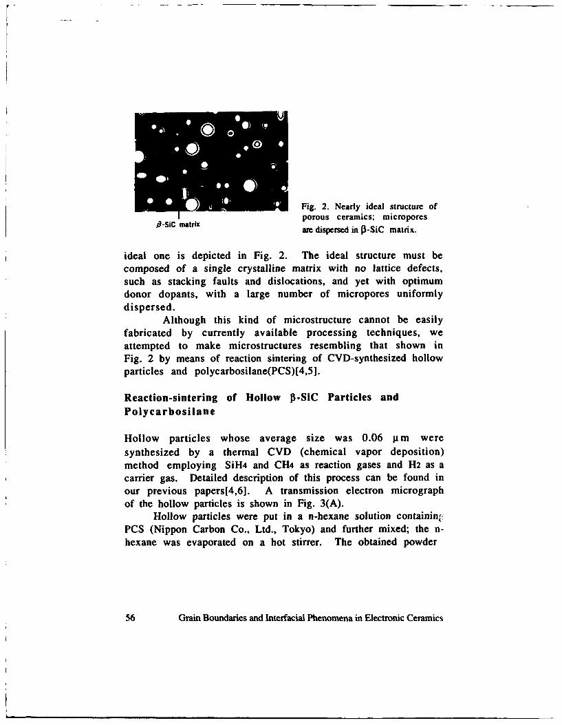
Fig. 2. Nearly ideal structure of
l-SiC matrix porous ceramics; microporesare dispersed in P3-SiC matrix.
ideal one is depicted in Fig. 2. The ideal structure must becomposed of a single crystalline matrix with no lattice defects,such as stacking faults and dislocations, and yet with optimumdonor dopants, with a large number of micropores uniformlydispersed.
Although this kind of microstructure cannot be easilyfabricated by currently available processing techniques, weattempted to make microstructures resembling that shown inFig. 2 by means of reaction sintering of CVD-synthesized hollowparticles and polycarbosilane(PCS)[4,51.
Reaction-sintering of Hollow J3-SiC Particles andPolycarbosilane
Hollow particles whose average size was 0.06 gtm were
synthesized by a thermal CVD (chemical vapor deposition)method employing SiH4 and CH4 as reaction gases and H2 as acarrier gas. Detailed description of this process can be found inour previous papers[4,61. A transmission electron micrographof the hollow particles is shown in Fig. 3(A).
Hollow particles were put in a n-hexane solution containin{PCS (Nippon Carbon Co., Ltd., Tokyo) and further mixed; the n-hexane was evaporated on a hot stiffer. The obtained powder
56 Grain Boundaries and Interfacial Phenomena in Electronic Ceramics

Fig. 3. TEM micrographs of (A) synthesized SiC hollow particles and (B)specimen S1 reaction-sintered at 1580'C for 3 h under N2.
was crushed, hydrostatically press-formed into a compact, andsintered at 1580 °C for 3 h under N2.
Variation of the composition ratio (weight ratio) of hollowparticles to PCS (1:1, 2:1, 4:1, 10:1) showed that the optimumratio to give the highest mechanical strength was 4:1 whensintered at 1400'C. Higher sintering temperature, for example1580*C, also gave improved mechanical strength, while thehollow shape of the particles was completely maintained (Fig.3(B)). However, the resultant sintered bodies always containedlarge cracks which must have been introduced as the paths forescaping gases produced by pyrolysis of PCS.
To impregnate these cracks with SiC and hence densify thematrix, the reaction-sintered body was further impregnatedwith PCS, followed by sintering at 1580'C for 3 h under N2, andthis process was repeated. Figure 4 shows the microstructuresof the specimens thus obtained for the initial weight ratio ofhollow particles to PCS of 4:1. Figure 4 shows that the cracksgradually disappeared with repetition of the impregnation-sintering process. The relative densities of
Grain Boundaries and Interfacial Phenomena in Electronic Ceramics 57

Fig. 4. SEM micrographs of the surfaces of specimens fabricated by (A)only reaction-sintering the 4:1 powder mixture (specimen Sl), (B) im-pregnating specimen SI with PCS. followed by sintering under thesame conditions (spcimen S2), and (C) further impregnating specimenS2 with PCS, followed by sintering (specimen S3).
specimens Si, S2, and S3 were 36.3%, 38.9%, and 40.4%,respectively.
Figure 5 shows the temperature dependences of theSeebeck coefficient, electrical conductivity, and power factorfor sintered bodies. The Seebeck coefficient was alwaysnegative, and as the temperature increased, its absolute valueincreased. The n-type semiconduction (negative Seebeckcoefficient) indicated that nitrogen has been incorporated intothe SiC lattice during sintering. The observed anomaloustemperature dependence of Seebeck coefficient has alreadybeen analyzed in terms of the phonon-drag effect[2]. That is, adecrease in the stacking fault density accompanied by graingrowth and crystallite growth[7] increased the phonon meanfree path, enhancing the phonon-drag effect, and hence leadingto an apparently larger Seebeck coefficient[3]. Actually, thecrystallite sizes calculated by the Scherrer equation for (111)
58 Grain Boundaries and Interfacial Phenomena in Electronic Ceramics
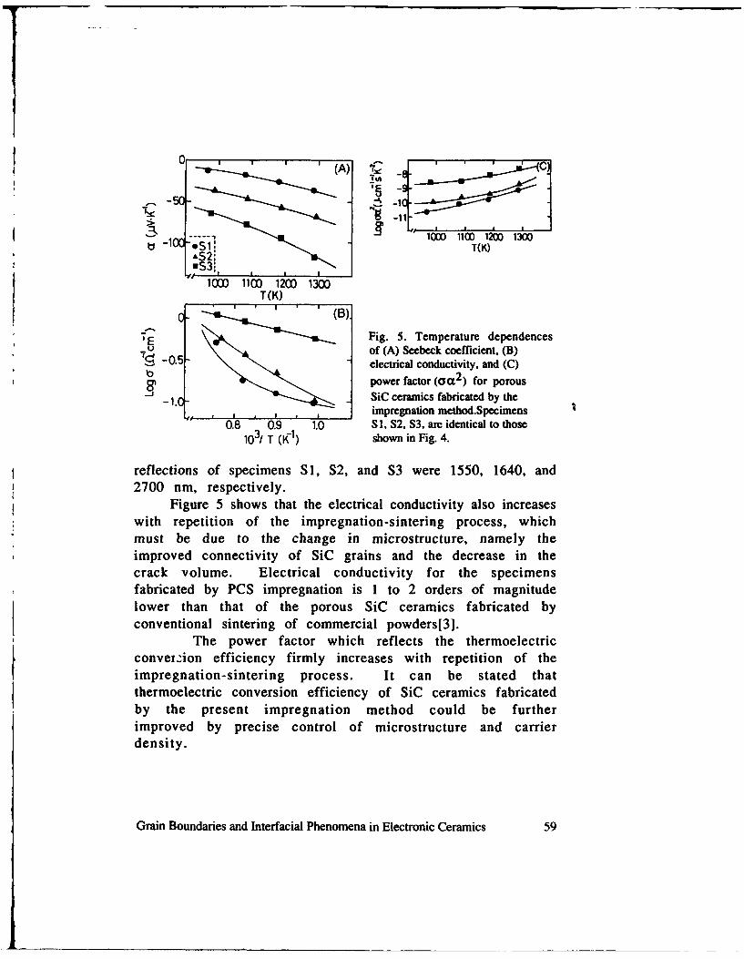
SIoiIA) .. C)
1--- 1 0 1200 1300
T(K)
_ " ' (B)
Fig. 5. Temperature dependencesU of (A) Seebeck coefficient, (B)
'ýg -0.5 electrical conductivity, and (C)b •power factor (OQ2) for porous
-1. .SiC ceramics fabricated by the* * * impregnation method.Specimens
0.8 0.9 1.0 S 1, S2, S3, are identical to those
103/ T (K1) shown in Fig. 4.
reflections of specimens Si, S2, and S3 were 1550, 1640, and2700 nm, respectively.
Figure 5 shows that the electrical conductivity also increaseswith repetition of the impregnation-sintering process, whichmust be due to the change in microstructure, namely theimproved connectivity of SiC grains and the decrease in thecrack volume. Electrical conductivity for the specimensfabricated by PCS impregnation is 1 to 2 orders of magnitudelower than that of the porous SiC ceramics fabricated byconventional sintering of commercial powders[3].
The power factor which reflects the thermoelectricconveizion efficiency firmly increases with repetition of theimpregnation-sintering process. It can be stated thatthermoelectric conversion efficiency of SiC ceramics fabricatedby the present impregnation method could be furtherimproved by precise control of microstructure and carrierdensity.
Grain Boundaries and Interfacial Phenomena in Electronic Ceramics 59

Sintering of the Mixture of Hollow Particles andCommercial Powder
The gas evolving during decomposition of PCS forms largecracks, and a very complicated troublesome procedure isneeded to fill them up with solid SiC in a reaction-sinteringmethod. Accordingly, in our next attempt, fine hollow particleswere simply mixed with commercial high-purity powder andwere sintered to porous bodies with various porosities.
In this section, thermoelectric properties of these porousceramics are discussed in relation to their microstructure. Ourpreliminary experimental work[3] indicated that the optimumfigure of merit is obtained when the powder compact issintered at and slightly above 20000 C under N2, so thatspecimens employed for discussion here were all obtained bysintering at 20000C for 3 h and further sin tred at 2100"C for 3h under N2.
High sintering temperatures presently employed caused thecollapse of hollow particles. Then, we expected that the hollowparticles would provide the initial packing state with a bimodalsize distribution of particles and the sintering process withmicropores, hence giving rise to very porous microstructureswith unique grain size distributions.
For the sintering process in SiC, it is widely accepted thatsurface diffusion controls the growth of intergranular necksleading to the grain coarsening[8]. Mass transport from thegrain surface to the neck via surface diffusion does not lead tothe shrinkage; in other words, the distance between the grainsstays unchanged and only pores grow larger. It is also knownthat stacking faults initially present in each grain becomeannihilated simultaneously with the grain growth duringsintering, which is controlled also by surface diffusion[5].Therefore, in the present case, collapse of the hollow particlesduring sintering would leave pores behind, resulting in graingrowth, increased porosity, and decreased stacking fault
60 Grain Boundaries and Interfacial Phenomena in Electronic Ceramics

20PmFig. 6. SEM micrographs of fracture surfaces of sintered specimens;initial contents of hollow particles are (A) 0 vol%, (B) 20 vol%, (C)55 vol%, and (D) 70 vol%.
density. The expected microstructure can be seen clearly inFig. 6 where SEM photographs of the fracture surfaces of thesintered specimens initially having various amounts of hollowparticles are shown.
Figure 6 reveals that the abnormal (exaggerated) graingrowth has taken place in all the specimens initially possessinghollow particles((b)-(e)) giving rise to bimodal grain sizedistributions. The average size of grains abnormally grownapparently decreased with increasing porosity, while thosesmall grains normally grown are all similar in size. Thisobservation can be rationalized as follows; the increase inporosity, especially the growth of large pores, would havesuppressed the contact between small grains and abnormally
Grain Boundaries and Interfacial Phenomena in Electronic Ceramics 61

grown grains inhibiting the mass transport via surfacediffusion.
Figure 7 shows electrical conductivity decreases withincreasing fractional porosity. In order to fully understand thechange in microstructure and electrical conductivity, thepercolation theory was applied to analyzing the data.
The generalized effective medium equation proposed byMclachlan[9,10] can be modified and expressed as;
Om/Oh = (l-f/fc)t (2)where f is the volume of the low-conductivity component andfc is the critical low-conductivity volume fraction at which thehigh-conductivity component first forms a continuouspercolation path across the medium. am is the conductivity ofthe medium itself and Oh is the conductivity of the high-conductivity component.
The solid line in Fig. 7 was obtained for the data acquired at700'C by a curve-fitting technique using Eq. (2). Theparameters oh, fc, and t to give the best-fit curve were 636Scm-1, o.9, and 2.0, respectively. In general, the value of t fora composite is most often found to lie in the universal range of1.65 to 2.0, though it is sometimes found to be somewhat belowthis range or often shows an excess value of 2.0 depending onthe microstructural morphology[9]. A rather large value of t(=2.0) obtained here would indicate that porous SiC ceramics
220 30SS.OOC o ,006C
1 0, X 601C X Wet7070 7020
120v 0 900t 0900C
- ~ e 1070 0, '
2006#2106C.6h.N2 0.10.hN
20.35 0.45 0.55 0.65 0.75 8.35 0,45 0.55 0.65 0.75
fractional porosity fractional porostty
Fig. 7. Electrical conductivity Fig. 8. Thermal conductivityvs. fractional porosity. vs. fractional porosity.
62 Grain Boundaries and Interfacial Phenomena in Electronic Ceramics

fabricated in this work have extraordinary geometries ofconducting matrices[9] possibly due to the presence of large
Figure 8 shows thermal conductivity obtained at 500-900'Cdecreases with increasing fractional porosity. The dashed linesare drawn through the measured points and the solid lineshows the fitting result for 700*C data obtained again using Eq.(2) with the following parameters; IC=73 W/mK, fc=0.9, t=2.0.The solid line is fairly well fitted with the measured data,indicating that the relationship between electrical conductivityor thermal conductivity and porosity can be expressed by asimilar equation. Then, the following relation would result;
Orm /CKin = m h / Kh (3)These results obviously suggest that the changes inmicrostructure and porosity during sintering have little effecton the ratio, o/K of 13-SiC. Therefore, to improve the figure ofmerit of [P-SiC maximization of Seebeck coefficient, a, bycontrolling the structure is inevitable.
As shown in Fig. 9, the absolute value of Seebeck coefficientincreases with increasing temperature in all cases, which isadvantageous for increasing the energy conversion efficiency athigh temperatures. It can also be seen in the figure thatSeebeck coefficient shows maximum values for the fractionalporosity of ca. 0.6. This result is very interesting because the
004
ý5 .200d' 2106"C. 6h, N2 2000 6 2100"C. 6h, 2.. 0-•
& 50 0: -X-- GO---"-•
-150 X G00 ' C 6 700*C6 700*C 0eo 8O.CaOwl C 0 900 C0 9006C
-0.3 0.4 0.5 0.6 0.7 0.3 0.4 0.5 0.6 0.7
fractional porosity fractional porosity
Fig. 9. Seebeck coefficient Fig. 10. Figure of meritvs. fraction porosity vs. fraction porosity
Grain Boundaries and Interfacial Phenomena in Electronic Ceramics 63
figure of merit depends on the porosity and moreover theSeebeck coefficient changes with the change in microstructuralfeatures. This is more fully discussed in our recent publication[11].
Figure 10 shows the calculated figures of merit for theporous SiC as functions of fractional porosity. Since a / icremains almost constant in spite of the change in porosity,maximum values of Z are found for the porosity giving rise tothe maximum Seebeck coefficients (ca. 0.6 fractional porosity).Through the present microstructure regulation, about twice aslarge a figure of merit as that commonly obtained by sinteringcommercial powders was realized. Since both a/ic and Seebeckcoefficient increase with increasing temperature acceleratingthe increase in the figure of merit, porous 1-SiC ceramics seem
to be highly potential for high-temperature thermoelectricenergy conversion.
References
[1] K. Koumoto, M. Shimohigoshi, S. Takeda, and H. Yanagida, J. Mat. Sci.Lett., 6, 1453(1987).[2] K. Koumoto, M. Shimohigoshi, S. Takeda, and H. Yanagida, Ceram.Trans., 2, 501(1989).[3] K. Koumoto, C. H. Pai, S. Takeda, and H. Yanagida, Proc. 8th ICT & 2ndECT, edited by H. and S. Scherrer, Nancy, France(1989)pp.107.[4] C. H. Pai, K. Koumoto, S. Takeda, and H. Yanagida, J. Mat. Sci., 24,3679(1989).[5] C. H. Pai, Y. Sasaki, K. Koumoto, and H. Yanagida, J. Am. Ceram. Soc.,74, 2922(1991).[6] K. Koumoto and C. H. Pai, Proc. 11th ICT, edited by K. R. Rao,University of Texas, Arlington, Texas(1992)pp.102.[7] W. S. Seo, C. H. Pai, K. Koumoto, and H. Yanagida, J. Ceram. Soc. Japan,99, 443(1991).[8] C. Greskovich and J. H. Rosolowski, J. Am. Ceram. Soc., 59, 336(1976).[91 N. Deprez and D. S. Mclachlan, Solid State Commun., 66, 869(1988).[101 D. S. Mclachlan, M. Blaszkiewicz, and R. E. Newnham, J. Am. Ceram.Soc., 73, 2187(1990).[III W. S. Seo, K. Watari, and K. Koumoto, Proc. 12th ICT, to be published.
64 Grain Boundaries and Interfacial Phenomena in Electronic Ceramics

GRAIN BOUNDARY CHARACTERISTICS IN PLZT, GBBLC AND HIGH T.SUPERCONDUCTING CERAMICS AND THEIR RELATION TOPROPERTIES
M. Y. Zhao, Z. W. Yin and B. M. XuShanghai Institute of Ceramics, Chinese Academy of Sciences, Shanghai 200050,China
ABSTRACTMany properties of functional ceramics are originated from their grain
boundary effects. In this paper, the authors summarized their works on the grainboundary characteristics and microstructures of different types of functionalceramics with emphasis on (1) transparent PLZT ferroelectric ceramics(insulator), (2) SrTiO3-based GBBLC ceramics (semiconductor) and (3) YBCOhigh 1T. superconducting ceramics. Experimental results showed that the differentgrain boundary characteristics or microstructures in these ceramics will give riseto big change in their properties, the electro-optic properties of PLZT ceramics,the barrier characteristics and dielectric properties of GBBLC and the currentdensity J. in YBCO superconducting ceramics.
Keywords: grain boundary, PLZT, GBBLC, YBCO
INTRODUCTION
The great influence of grain boundary of ceramic materials on their propertieswas a well-known fact to ceramic scientists for a long time. However, the greatmajority of ceramic materials contains certain amount of pores, impurities andglass phase, which gave difficulties to study the grain boundary effect of theseceramic materials. Besides, the experimental methods and equipments are alsoimportant, the rapid development of modem structural analysis instruments madethe research work becoming possible. In present paper, the authors summarizedtheirs works on the grain boundary characteristics and microstructures of threedifferent types of functional ceramics, namely transparent PLZT ferroelectricceramics, SrTiO3-based GBBLC ceramics and YBCO high T. superconductingceramics, and their relation to properties.
To the extent authorized under the laws of the United States of America, all copyright interests in this publication are the propertyof The American Ceramic Society. Any duplication, reproduction, or republication of this publication or any part thereof, withoutthe express written consent of The American Ceramic Society or fee paid to the Copyright Clearance Center, is prohibited.
Grain Boundaries and Interfacial Phenomena in Electronic Ceramics 65

TRANSPARENT PLZT FERROELECTRIC CERAMICS
Transparent PLZT ferroelectric ceramic materials are insulators, free of pores,very few impurities and can be considered as a single phase material. Their grainsare granular with good roundness. In certain range of their compositions, they areferroelectric or antiferroelectric, so, their properties are very sensitive to thechange of external conditions (temperature, stress, electric field etc). Therefore,the transparent PLZT ferroelectric ceramics is one of the most relevant materialto study the grain boundary effect in functional ceramics""41 .
Grain Boundary Structure Based on TEM Observation
Fig. I shows the HREM image photomicrographs taken near the grainboundary from a JEOL 200cx high resolution electron microscope. Most grainboundaries are very thin, about 6A (Fig. la). Some are only 2-3A. However, insome places, broader ones (dozens angstroms) can also be found as amorphousstructure (Fig. lb, segment c).
Figure 1 HREM image of two grains and their boundary(a)one grain along [111] and the other along [100](b)two grains both along [110]
The thin boundaries can be either coherent or incoherent. Fig. 2 demonstratesthe structure model of grain boundary of segment AB in Fig. lb. It belongs tocoherent boundary. There are shared atoms by the two adjacent grains. Thedistance between the shared atoms is 4 Ti-O octahedra in grain A or 3 Ti-0octahedra in grain B. However, the grain boundary shown in Fig. la belongs toincoherent one. It could be assumed that in ordinary case the grain boundaries inPLZT ceramics should be very fine, of the order of several angstroms. However,when impurities entered into the grain boundaries or triple junctions, second phase
66 Grain Boundaries and Interfacial Phenomena in Electronic Ceramics

formed and boundary broadened. The thin grain boundary structure of PLZTsexplains well why its cubic a phase has good transparency and why the domainsin ferroelectric • phase could penetrate the grain boundary from one grain to theother.
Grain
Grain A (1141
Figure 2 Atomic structure model of grain boundary of segment AB in Fig. l(b)
Grain Boundary Effect in PLZT Ce ý,
The PLZT composition 7.9/70/30 was selected for studying the grain boundaryeffect on the electro-optical properties of the transparent ceramics. Hot pressingin flowing oxygen atmosphere was used for making the transparent ceramic slugs.The grain-grown specimen at different grain sizes were prepared by reheating thehot-pressed slug in PbO atmosphere to 1340°C--1350°C for 72--168 hours. Fig.3shows the microphotographs of 7.9/70/30 PLZT ceramics after heat treatment andcompared with its original hot-pressed specimen. The image analyses andstereology studies on above specimens were carried out by means of a Quantimat900 Micro-Image Automatic Quantitative Analyzer made by CambridgeInstrument Ltd. The total interface area in unit volume of ceramic material, Svwas determined equal to 0.463mm2 /mm 3 for hot-pressed specimen as shown in
Grain Boundaries and Interfacial Phenomena in Electronic Ceramics 67

Fig. 3(a) and 0.160mm2/mm3 for heat treated specimen as shown in Fig. 3(b)respectively. Fig. 4 gives the longitudinal electric controlled light scattering atdifferent temperatures of the above two specimens. Fig. 4 tells us that the changeof grain size distribution of a ceramic material will certainly affect the propertiesof the material. The grains in hot-pressed PLZT ceramics are small, the
Figure 3 Microphotographs of 7.9/70/30 PLZT ceramics after heat treatment andcompared with its original hot-pressed specimen. (a) hot-pressed (b) hot-pressed,and heat treated at 1340°C for 72 hours.
I 0100-500 0 500 IO -1000 -500 0 500 I000
-100-500 o looo -I00 -50 0 500 tlow
-lO0-oo 5o OO 22.74-C W o1o
E (V/mm) E (Vimm)
Figure 4 The longitudinal electric controlled light scattering at differenttemperatures of the hot-pressed and grain-grown specimens of 7.9/70/30 PLZTceramics (a) hot-pressed, S,=0.463 mm 2/mm 3, (b)heat-treated,Sv=0.160mm2 /mm3
68 Grain Boundaries and Interfacial Phenomena in Electronic Ceramics

volumetric fraction of the grain boundary region is high, sometimes reaches 25%,even more of the total volume of the ceramic. High energy state in hot-pressedPLZT ceramics tends to block the development of macro-domain structure at itsferroelectric state, which results in less scattering at the domain walls and sogives lower contrast.
SINGLE-STEP, LOW-TEMPERATURE SINTERED SrTiO 3 GBBLCAPACITOR CERAMICS
SrTiO3 grain boundary barrier layer (GBBL) capacitors have been rapidlydeveloped in recent years because of their excellent properties. However, the two-step firing process and high sintering temperature (usually higher than 1400"C)not only increase the commercial cost of the capacitors, but also are the mainobstacles to fabricate monolithic GBBL capacitors","". The authors havefound('t1 31 that by doping a kind of sintering aid mainly consisting of Li2O andSiO2, SrTiO3 GBBL capacitors can be single-fired between 1100 and 1200°C inreducing atmosphere, which is favourable for fabricating monolithic GBBLcapacitors with base metal inner electrodes. Fig. 5 shows the schematic diagramof the microstructure development of this new kind of capacitor materials.
Li20+ SiC), reactive gri rowtliquid phase formed I I
su n /g~~ra ing o t n ri]
[microstructure of GBBLC was formed]
Figure 5 Schematic diagram of the microstructure development of the single-step,
low-temperature sintered SroiO3 GBBL capacitor materials
Grain Boundaries and Interfacial Phenomena in Electronic Ceramics 69

The Grain Boundary Characteristics of One-step, Low-temperature SinteredSrTiO'3 GBBL Capacitor Ceramics
Based on HREM, four different types of grain boundaries were observed inthe one-step, low-temperature sintered SrTiO3 GBBL capacitor ceramics namely(1) broad crystalline grain boundary, (2) broad non-crystalline grain boundary,(3) narrow non-crystalline grain boundary and (4) "clean" grain boundary. Theyare shown in Figure 6.
The width of grain boundary in Fig. 6(a) and (b) is in the range of 100--ioooA, close to that of two-step fired GBBL ceramics. The narrow non-crystalline grain boundary in Fig. 6(c), its width is several to ten angstroms andits structure is something like the grain boundary as shown in Fig. 1(a) for PLZT.The width of "clean" grain boundary as shown in Fig. 6(d) is only 2-3A, itsstructure is very similar to the coherent boundary of PLZT as shown in Fig. 2.
Figure 6 HREM image of two grains and their boundary(a)broad crystalline grain boundary(b)broad non-crystalline grain boundary(c)narrow non-crystalline grain boundary(d)"clean" grain boundary
70 Grain Boundaries and Interfacial Phenomena in Electronic Ceramics
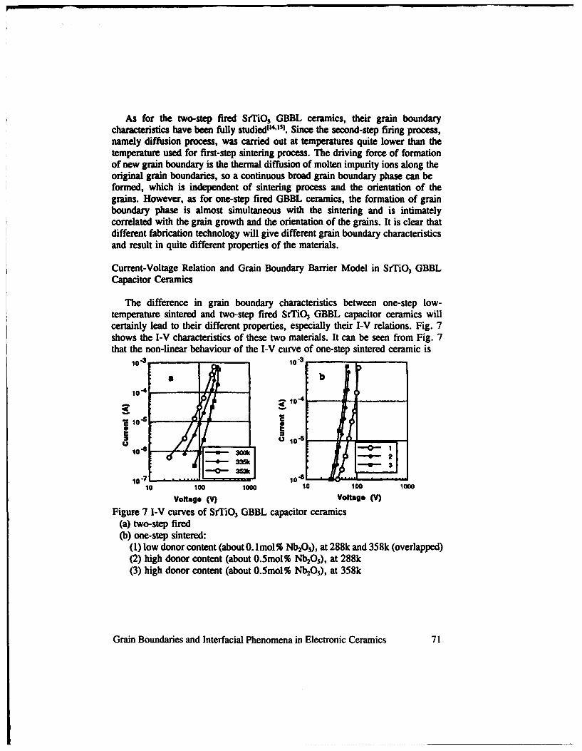
As for the two-step fired SrTiO3 GBBL ceramics, their grain boundarycharacteristics have been fully studied',"-'1. Since the second-step firing process,namely diffusion process, was carried out at temperatures quite lower than thetemperature used for first-step sintering process. The driving force of formationof new grain boundary is the thermal diffusion of molten impurity ions along theoriginal grain boundaries, so a continuous broad grain boundary phase can beformed, which is independent of sintering process and the orientation of thegrains. However, as for one-step fired GBBL ceramics, the formation of grainboundary phase is almost simultaneous with the sintering and is intimatelycorrelated with the grain growth and the orientation of the grains. It is clear thatdifferent fabrication technology will give different grain boundary characteristicsand result in quite different properties of the materials.
Current-Voltage Relation and Grain Boundary Barrier Model in SrTiO3 GBBLCapacitor Ceramics
The difference in grain boundary characteristics between one-step low-temperature sintered and two-step fired SrTiO3 GBBL capacitor ceramics willcertainly lead to their different properties, especially their I-V relations. Fig. 7shows the I-V characteristics of these two materials. It can be seen from Fig. 7that the non-linear behaviour of the I-V curve of one-step sintered ceramic is
10o 10
S10I£22
U 3 200k
10-7t . . 10-1 _ . .. ......-. I
10 100 1000 10 100 1000
Voltage (V) Voltage (V)
Figure 7 I-V curves of Srl'iO3 GBBL capacitor ceramics(a) two-step fired(b) one-step sintered:
(1) low donor content (about 0. lmol% Nb2O,), at 288k and 358k (overlapped)(2) high donor content (about 0.5mol% Nb 2O5), at 288k(3) high donor content (about 0.5mol% Nb 2O5), at 358k
Grain Boundaries and Interfacial Phenomena in Electronic Ceramics 71

more pronounced than that of two-step fired sample. For low donor contentsample, its I-V behaviour is independent on temperature. However, for highdonor content sample, its I-V curve moves to lower voltage side along with theincrease of the temperature.
One of the authors has systematically studied the grain boundary barrier andgrain boundary breakdown of the two-step fired SrTiO 3 GBBL capacitorceramicsil6l. They concluded that due to the presence of a continuous broad grainboundary phase in this material a model of grain boundary Schottky barrier withan intergranular insulating layer was proposed as shown in Fig. 8. With thismodel, the current-voltage relation and capacitance-voltage relation weretheoretically analyzed and derived. When using this model for GBBL capacitors
q# S 10.4
-'0- 300kT 10't 373k1q(#+bV) 423
10 100 1000- Volae6 (V)
Figure 8 Grain boundary Schottky Figure 9 I--V characteristics of ZnObarrier with an intergranular layer varistor
compared with the Schottky barrier model for ZnO varistor[1 7,'1 , two differentbreakdown mechanisms were found: the avalanche breakdown for the formerwhich is temperature dependent and the tunnelling breakdown for the latter whichis temperature independent. Fig. 9 shows the non-linear characteristics of a ZnOvaristor in breakdown region. As for the one-step, low-temperature sinteredGBBL capacitor ceramics, there are four different types of grain boundaries.Among them the broad crystalline or non-crystalline grain boundary phases playthe same role as that in the two-step fired materials. High donor contents is ofadvantage to broaden the grain boundaries, which makes these two types of grainboundary to dominate the properties of the material. However low donor contentis profitable to form the narrow and "clean" grain boundaries. The grainboundary structure and characteristics of these two types of grain boundary are
72 Grain Boundaries and Interfacial Phenomena in Electronic Ceramics

in YBCO ceramics perpendicular to the grain boundary and along the grainboundary are shown in Fig. 10. Fig. 10(a) shows that the profile taken across theboundary has a copper rich zone, which is typically asymmetry with respect tothe boundary plane. A composition profile obtained along the boundary is shownin Fig. 10(b). It showed that the most notable feature of the composition variationin the grain boundary is their regular oscillatory nature. These heterogeneitiesmight be an intrinsic feature of the boundary and would give a pronounced effecton the nature of electrical transport in polycrystalline YBCO superconductors.7 , , ,1, " , , 1: , , , T -T I , I -I -N
i (a) *~(b)
XXXXxX *XXXX 0 X o
C ' I 1
"_1 -0- a 2aoaoaaaoa~o 0 v a 7 o 1 -403 0W70001010i
o istance from Boundary (ha) Distance (nm)
Figure 10 Composition profile of grain boundaries in YBCO ceramicsp"(a) perpendicular to the boundary, (b) along a boundary
Many research groups have identified the grain boundary phases in YBCOceramics, including CuO, BaCuO2, Cu20, BaCO3 and Y203. They were presented
probably as a result of non-stoichiometry of the starting powder mixture orincorrect processing. Besides, other impurities, such as Sr, Zr or Al ions werealso found at highly misoriented grain boundaries. It is said thatr2' Cooper pairscan only tunnel over a nonsuperconducting region of 5 angstroms (parallel to thec-axis) and 20 angstroms (perpendicular to the c axis), so the impurity layersalong the grain boundaries with thickness more than 2GA would form weak links.
The anisotropy behaviour, especially the anisotropy of the current density inbulk YBCO superconductors is an important property and has been analyzed bymagnetization measurement and pulse method. Magnetization measurement forsingle crystal has shown a factor of 20 between Ic•" measured along the a-b plane(i.e. Cu-O plane) to that measured perpendicular to the a-b plane J ern]. V.Selvamanickamn and K. Salama studied'the intergrain transport current density andits anisotropy by the pulse method with the oriented-grain YBCO superconductingceramicsr"•. They were performed on the oriented-grain samples with thetransport current aligned at different angles to the a-b plane. Table 2 lists their
Grain Boundaries and Interfacial Phenomena in Electronic Ceramics 73

rather similar to the grain boundaries in ZnO varistors, so the Schottky barrier
play the important role on the properties of the materials.
YBCO HIGH T, SUPERCONDUCTING CERAMICS
The discovery of high T. superconducting oxides, such as YBCOsuperconductors has stimulated enormous research works because of theirpotentially immense technological applications. However, the use of bulk YBCOsuperconductors in high-current devices has met troubles due to the low transportcritical current density J, and its severe degradation in magnetic fields. Thelimited J, in YBCO superconducting ceramics has been attributed largely to theweak link behaviour of grain boundaries.
Critical Current De,,sity of Grains and Their Grain Boundaries
A direct measarement of the transport current density of individual grains andgrain boundaries in YBCO superconductors has been successfully made by P.Chaudhari et al as shown in Tabel 1191.
Table 1 Critical current density Jc of individual grains at 4.2-5K""9 !
Grain 1 Grain 2 Grain boundary (103A/cm2)
> 500 > 500 50> 100 70 18250 220 12390 130 3.1260 14 0.78.5 0.5 0.7
Weak Link Behaviour of Grain Boundary
The specific features of the grain boundary in YBCO ceramics which resultsin formation of weak links may be as follows: (1) composition variation at grainboundary regions, (2) segregation of second phase and other impurities at grainboundary areas, (3) anisotropy ---- high angle grain boundaries and (4) defectstructure at grain boundaries ---- microcracks, pores and dislocations.
The local composition profile variation within YBCO grain boundaries wasstudied by S. E. Babcock et alr20'. The composition profiles of grain boundaries
74 Grain Boundaries and Interfacial Phenomena in Electronic Ceramics

results. A current density anisotropy ratio (J0'/J') of 25 was estimated. Thus, thesevere anisotropy in conductivity would cause weak connections at high-anglegrain boundaries.
Table 2 Details of samples used in transport current anisotropy measurementsr 2
Angle between Room-temperature No. of grain Critical currentcurrent and a-b resistivity boundaries between density (A/cm2)plane (degree) (mflcm) current contacts (T=77K, H=0)
S...................................................................................................0 0.4 0 7500016 2.12 70 1800034 13.08 140 356070 25.96 260 3330
S................................................................................................
The defect structure of grain boundaries, such as microcracks, pores anddislocations are other factors to form weak linksc' 2 s51. Fig. I I shows the HREMimage of microcracks at the grain boundary region of YBCO ceramics and thewidth of the microcracks is in the range of 6-7nm. It was assumed that thepresence of microcracks were resulted from the severely anisotropic thermalexpansion along different crystallographic directions.
104
103
102l
101 - . •0 10 20 30 40 50
Amount of grains (%)
Figure 11 HREM image of micro- Figure 12 The correlation betweencracks at grain boundaries J, and amount of grains containing
cohercnt GBs in YBCO ceramics
Besides, the coherent grain boundaries with the intergranular region being 5--
Grain Boundaries and Interfacial Phenomena in Electronic Ceramics 75

10A and the influence of their amounts on J, have also been studied in detail bythe authorsr1 J. The result showed that the coherent grain boundary is narrow andstraight and no grain boundary phase presented. The authors found that thecoherent grain boundaries are frequently parallel to the a-b plane of the adjacentgrains. The critical current density J, of the ceramics will increase along with theincrease of the amount of grains containing coherent grain boundaries in thematerial as shown in Fig. 12.
REFERENCES
1. Z. W. Yin, X. M. He, C. E. Li, Z. Y. Wei, and H. Y. Ni, "Phase Transitionand Properties of 7.9/70/30 PLZT Ferroelectric Ceramic Materials", Proc. of theFirst China-US Seminar on Microstructure and Properties of Ceramic Materials,May, 1983, Science Press, Beijing, China, 410, 19842. B. H. Chu, H.K. Ngao, X. S. Zhen and Z. W. Yin, "Grain BoundaryPhenomena in PLZT Transparent Ferroelectric Ceramic Materials", ibid, 1923. Z. W. Yin, "Recent Development of PLZT Ceramics Research in ShanghaiInstitute of Ceramics", Proc. of ISAF'86, 8-11, June, 1986, Lehigh University,139-454. D. N. Huang, Z.W. Yin, and L. E. Cross, "Electrical Properties of GrainGrown PLZT Ceramics", ibid, 159-645. X. T. Chen, D, N, Huang and Z. W. Yin, "Optical and Electro-OpticalProperties of PLZT Ceramics with Different Grain Size", ibid, 62-656. Z. W. Yin, D. N. Huang, X. T. Chen, X. Q. Chen and X. L. Zhou,"Stereology Studies on Grain Growth of PLZT Ceramics", J. Inorg. Mat., 1 [2]97-101 (1986)7. Z. W. Yin, X. Y. Song and J. W. Feng, "Grain Boundary Structures in PLZTCeramics", Ferroelectrics, 94 [2] 269-274 (1989)8. Z. W. Yin, "Studies on Microstructure and Microproperties of PLZTCeramics", Ceramics International, 15 [41 311-15 (1989)9. P. C. Wang and Z. W. Yin, "Some Aspects of PLZT research in ShanghaiInstitute of Ceramics", Ferroelectrics, 123 [1-4] 131-130 (1992)10. G. Goodman, "Capacitors Based on Ceramic Grain Boundary Barrier Layers--A Review", pp. 215-31 in Advances in Ceramics, Vol. 1, Edited by L. M.Levinson. The American Ceramic Society, Columbus, Ohio, 198111. M. F. Yan and W. W. Rhode, "Ultrahigh Dielectric Capacitance in TiO2Ceramics", pp. 226-38 in Advances in Ceramics, Vol. 7, Edited by M. F. Yanand A. H. Heuer. The American Ceramic Society, Columbus, Ohio, 198312. B. M. Xu, H. Wang and Z. W. Yin, " Study on Sintering SrTiO3 GBBLCapacitors at Low Temperatures", J. Chin. Ceram. Soc., 19 [4] 354-360 (1991)
76 Grain Boundaries and Interfacial Phenomena in Electronic Ceramics

13. B. M. Xu, H. Wang and Z. W. Yin, "The Doping Analysis of SrTiO3 GBBLCapacitors Sintered at Low Temperatures%, J. Chin. Ceram. Soc., 20 [1] 16-22(1992)14. M. Fujimoto and W. D. Kingery, "Microstructure of SrTiO3 InternalBoundary Layer Capacitor During and After Processing and Resultant ElectricalProperties%, J. Am. Ceram. Soc., 68 [4] 169-73 (1985)15. N. Stenton and M. P. Harmer, "Electron Microscopy Studies of a StrontiumTitanate Based Boundary-Layer Material", pp. 156-65 in Ref. 1116. J. P. Zhong, H. Wang and Z. W. Yin, "The Grain Boundary Barrier ofSemiconducting Ceramics", Ferroelectrics, 101 81-86 (1990)17. 0. A. Clarke, "The Microstructural Location of the Intergranular Metal-Oxide Phase in a Zinc Oxide Varistor%, J. Appl. Phys., 49 [4] 2407-11 (1978)18. L. M. Levinson and H. R. Philipp, "The physics of Metal Oxide Varistors",J. Appl. Phy., 46 [2] 1332-40 (1975)19. P. Chaudhari, J. Mannhart, D. Dimos, C.C. Tsuei, J. Chi, M. M. Oprysko,and M. Scheuermann, "Direct Measurement of the Superconducting Properties ofSingle Grain Boundaries in YBa2Cu30 74 ", Phys. Rev. Lett. Vol. 60 [16] 1653-56(1988)20. S. E. Babcock and D. C. Larbalestier, "Evidence for Local CompositionVariations within YB2aCu307T Grain Boundaries", Appl. Phys. Lett., 55 [4] 392-95 (1989)21. S. L. Wen, "The Relationship of Atomic Structure with T, and Microstructurewith J, in High T, Superconductors". International Symposium on ElectronMicroscopy, Ed. Kehsim Kuo, Beijing, China, 1990, 31922. T. R. Dinger, T. K. Worthington, W. J. Gallagher and R. L. Sandatrom,"Direct Observation of Electronic Anisotropy in Single-Crystal Y 1Ba2Cu3OT7.",
Phys. Rev. Lett., 58 [25] 2687-94 (1987)23. V. Selvamanickam and K. Salama, "Anisotropy and Intergrain CurrentDensity in Oriented Grained Bulk YBa-Cu3O1 Superconductor", Appl. Phys.Lett., 57 [15] 1535-77 (1990)24. J. W. Feng, S. L. Wen, M. Y. Zhao and C. E. Li, "TEM Observation ofStructure Defects in Y(Eu)-Ba-Cu-O Superconductor", J. Chin. Ceram. Soc., 17(5) 462-66 (1989)25. S. Nakahara, G. J. Fisanick, M. F. Yan, R. B. VanDover and T. Boone,"Onthe Defect Structure of Grain Boundaries on Ba2YCu3O7.x", J. Crys. Growth, 85[2] 639-51 (1987)26. X. Y. Song, S. L. Wen, Z. X. Zhao, M. Y. Zhao, C. E. Li and D. L. Jin,"Effect of Microstructures on Properties of YBCO", Chin. Sci., 35A [8] 834-37(1992)
Grain Boundaries and Interfacial Phenomena in Electronic Ceramics 77
Ferrites and Titanates
GRAIN BOUNDARY MICROSTRUCTUREAND MAGNETIC PROPERTIES OF
LOW-TEMPERATURE-FIREDNI-ZN-CU FERRITE
Masayuki FujimotoTaiyo Yuden Co., Ltd.
1660 Kamisatomi, Haruna-machi, Gunma 370-33 Japan
Slowly cooled and rapidly cooled multilayer chip inductors each containing aAg internal electrode and low-temperature-fired Ni-Zn-Cu ferrite but exhibitingdifferent inductance were characterized using analytical electron microscopy. Elasticstrain fields were observed at the grain boundaries in the rapidly cooled sample,causing degradation of the inductance. The strain field arising from a decrease in theeffective permeability of the ferrite was found to be due to Cu precipitates. Theoccurrence of Cu metal precipitates at grain boundaries was dependent on the startingchemical composition, oxygen partial pressure, and thermal equilibrium during coolingafter the sintering.
i. INTRODUCTION
The multilayer chip inductor has many strong points. Besides its shapecompatibility with the chip resistor and multilayer chip capacitor, it has merits such asno need for core processing, potential of miniaturization, and no cross-talk due toleakage of magnetic flux because of circulation patterns set within magneticelements."'2 With these excellent characteristics, and with the development of highdensity surface mounting, it has been expanding its market in the field of not onlyconsumer electronics such as video cameras, liquid crystal TV's, and head-phonestereos, but also industrial devices such as hard disks, personal wirelesscommunication systems, and automobile telephones.
For constructing interna: circulation patterns in ferrite material, commonthrough-holes are made through ferrite green sheets of prescribed thickness and 3/4circular conductor pattern is printed, and simultaneously, the through-holes are filledwith conducting paste and adjacent 3/4 circular patterns are connected. By repeatingthis process, the prescribed internal circulation pattern (coil) is formed. To obtain a Q
To the extent authorized under the laws of the United States of America, all copyright interests in this publication are the propertyof The American Ceramic Society. Any duplication, reproduction, or republication of this publication or any part thereof, withoutthe express written consent of The American Ceramic ety or fee paid to the Copyright Clearance Center, is prohibited.
Grain Boundaries and Interfacial Phenomena in Electronic Ceramics 81

(quality fiactor; 1/tane') as high as inductor high-conductivity material must be used inthe internal circulation pattern. Silver is one of the best materials its properties includelow resistivity for Q value as high as for an inductor, low price compared with othernoble metals which can be used in mass-production, and sinterability under airatmosphere which allows for the use of simple sintering furnace without specificatmosphere such as N, or H, However its low melting point (960" C) prevents use ofconventional ferrite powder which requires high temperature for sintering (about1300'C). For decreasing the sintering temperature, not only non-stoichiometricstarting chemical composition with a small excess of Ni-Zn-Cu which is well know toimprove solid-phase sintering of ferrite using formation of oxygen vacancies as adittuision path, but also small-grain-size, high pure raw materials must be adopted.
It is also well known that the permeability of spinel ferrite is strongly affectedby the inner stress related to the microstructure, i.e., it is a somewhatmicrostructure-sensitive material.
In this study, high-resolution analytical electron microscopy (HR-AEM) wasused to characterize the grain boundary microstructure of multilayer chip inductors.Samples were prepared so as to minimize the residual stress of the internal electrodeand ferrite body, and to produce variations in the magnetic properties by altering thesintering process. Here, the relationship between the observed and analyzed grainboundary microstructures inducing inner stress and the resulting magnetic propertiesare reported.
U. EXPERIMENTAL
The raw materials, submicron-order Fe,O., NiO, ZnO and CuO powders, wereball-milled with distilled water with a starting chemical composition of(Ni0 ,Cu,._,,Zno.O)[Fe,O,.],, that is, a small excess of Ni-Zn-Cu chemicalcomposition (shortage of Fe2 •). A slurry was cast into a green sheet for fabrication ofmultilayer chip inductors. Common through-holes were made in the ferrite greensheets, and a 3/4 ch-cular pattern of the silver conductor paste was printed. At thesame time, silver paste was introduced into the through-hole to fill it and connect theadjacent 3/4 circular pattern by lamination, the laminated block was cut into chips. Thesamples were the sintered at 880'C under air atmosphere at different cooling rates,either slowly (-3000C/h) or rapidly (-900"C/h). Finally, silver external electrodes wereformed on both sides of the chips for electrical measurements.
82 Grain Boundaries and Interfacial Phenomena in Electronic Ceramics
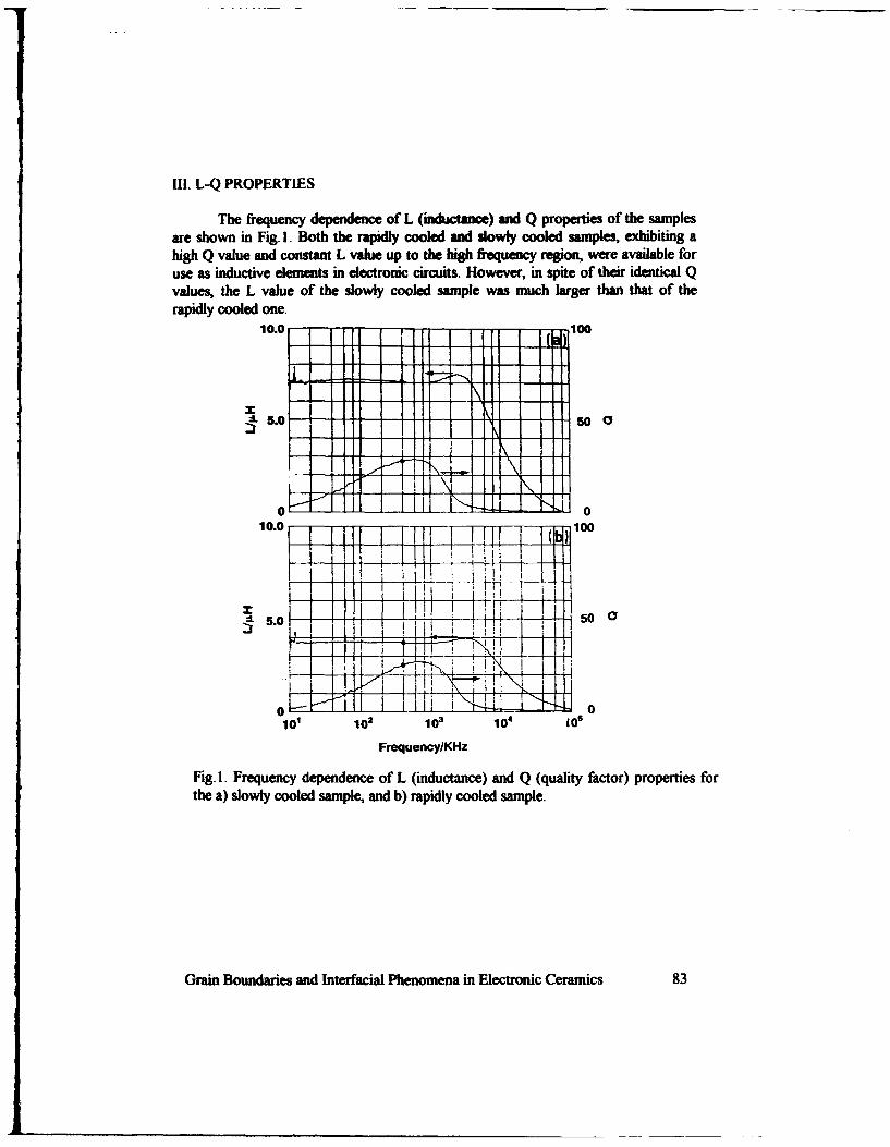
111. L-Q PROPERTIES
The frequency dependence of L (inductance) and Q properties of the samplesare shown in Fig. 1. Both the rapidly cooled and slowly cooled samples, exhibiting ahigh Q value and constant L value up to the high frequency region, were available foruse as inductive elements in electronic circuits. However, in spite of their identical Q
values, the L value of the slowly cooled sample was much larger than that of the
rapidly cooled one.10.0 l 100
~-5.0- 50I 0
10.0L - -J T 100:KiLLL- I I I I I I I a"" I I III I Ir i i
101 102 103 1°
Frequency/KMz
Fig. 1. Frequency dependence of L (inductance) and Q (quality factor) properties forthe a) slowly cooled sample, and b) rapidly cooled sample.
Grain Boundaries and Interfacial Phenomena in Electronic Ceramics 83

IV HR-AEM ANALYSIS
Figure 2 shows TEM bright-field images of the samples. Both the samples
show precipitates at the multiple grain junction with a pore. The rapidly quenchedsample showed a number of interference fringes near the grain boundaries, while theslowly cooled one did not. The small-sized fringes located near the grain boundarieswere obviously different from thickness extinction fringes, but similar to the contrastarising from elastic strain around coherent or incoherent precipitates.3? More preciseobservation revealed that the centers of the strain field image were not located on thegrain boundary but adjacent to it, and that the center line of the strain field images wasoriented in one direction, as if it had some crystallographic relationship with the matrixgrains (Fig. 3). Figure 4 shows a high-resolution image of the center of the strain fieldnear the edge of the specimen, which was thin enough for lattice image formation. Ablack swollen line about 5 nm long was clearly recognized between the spinel ferritelattices. Several similar swollen black lines were also observed at the other center ofthe strain field. EDX spectra were obtained from the center of the strain field locatedin a relatively thick region of the specimen (indicated by arrow in Fig.3), and in thematrix grain, respectively, and these are overlapped and compared in Fig. 5 Thespectra indicated a higher Cu concentration at the center of the interference fringe, andAg was not detectable. Therefore the observed black swollen lines were interstitial Cubetween the ferrite spinel lattices, which could be an intermediate stage between grainboundary segregation and precipitation. The equation for initial permeability of ferriteis usually expressed as follows, M
2
vi= aK+b~o
gi: initial permeability
M,: saturation magnetization
K: crystal magnetic anisotropy
1: magnetostriction constant
a: inner stress
a, b: constantThus the initial permeability is strong influenced by the inner stress, which can beinduced by exaggerated grain growth, or impurity precipitation at the grain boundaries
84 Grain Boundaries and Interfacial Phenomena in Electronic Ceramics

and inside the grains as inclusions. Therefore the degradation of inductance in therapidly cooled sample was most likely due to inner stress, , lattice distortioninduced by lattice interstitial-type Cu precipitation adjacent to the grain boundary.Whereas the spherical precipitates at the multiple grain junction with pores in thissample did not contribute to lattice distortion, since they were not located at the grainboundaries, multiple grain junctions with pores without the lattice distortion of ferritegrains did introduce inner stress. In addition, the pores themselves already play a partin reducing the initial permeability of ferrite as air gap, and thus the small precipitationof non-ferromagnetic or ferromagnetic materials; the precipitates do not change themagnetic properties.
Fig.2. TEM low-magnification bright field image of the a) slowly cooled sample, andb) rapidly cooled sample.
We carefully analyzed and characterized the precipitates at the multiple grainjunction in both of the samples using electron diffraction and EDX with HR-AEM. Anexample of a Cu precipitate at the multiple grain junction in the slowly cooled sampleis shown in Fig. 6. The difflraction pattern obtained from the precipitate and the
Grain Boundaries and Interfacial Phenomena in Electronic Ceramics 85

interpretation of the pattern are shown in Fig. 7. The diftlaction spots indicatingstrong intensity can be indexed as that of fc.c. metal Cu, and the spots indicatingweak intensity can be indexed as that of CuO. In addition, they were located along thesame line direction indicating a small lattice misfit, the diffraction spots of Cu andCu2O indicating an epitaxial growth-type crystallographic relationship,(1 0)Cu2O/(211)Cu. Since Cu2O epitaxial growth on Cu metal by oxidation wasreported previously in deposited Cu metal thin film, it could be deduced that the Cu 20layer was formed by oxidation of Cu metal precipitates.4 '3 The EDX spectrumobtained from the precipitate is shown in Fig.8, in comparison with the EDX spectrumfrom the matrix grain adjacent to the precipitate. In spite of the presence of a Cu L linepeak, no OKca peak was detected in the spectrum from the precipitate, whereas theOKct peak with Fe, Ni, Cu and Zn L line peaks were found in the spectrum from thegrain. The Cu2O oxidation layer on a Cu metal precipitate is very thin, as would beexpected from the diffraction spot intensity. Previously, we reported the existence ofa Cu metal Dh MTP (Decahedral Multiple Twined Particle) at the multiple grainjunction in low-temperature-fired ferrite with a multilayer chip inductor of Ni-Zn-Cusmall excess chemical composition.Y' Since MTP are not found in large crystals, theyare structural anomalies due to a size effect. The MTP occurring in the nucleationstage of crystal growth is not derived from the residue of non-reacted CuO after thecalcination process. The situation of Cu ions in calcined powder before the sinteringprocess is still not clear. However, considering the Ni-Zn-Cu ferrite general formulatogether with the tetrahedral site of Zn2 and octahedral site occupancy of Ni' andCu" in the spinel structure (the possibility of a small amount of Cu2" and Cu' transitionat high temperature being neglected), such as [Fe3" ,.Zn 2'"j [Fe3 I,..Ni2 'yCU 2•Fe1] 4
(x+y+z= 1.0) and a small excess of Ni-Zn-Cu starting chemical composition, theobserved MTP Cu should be precipitated from the Ni-Zn-Cu ferrite matrix during thecooling process after sintering, corresponding to a Cu solid solution with the ferrite. Ifthe CuO occupancy of the Fe3' site or Cu2" (or Ni2' and Zn2 ) site forms in the abovementioned spinel structure during the sintering process, then the negatively chargeddefect Cu,,' and VF."' will be formed, respectively, and the corresponding number ofpositively charged oxygen vacancies will be required to satisfy the site balance andcharge neutrality condition:
2CuO .6. 2CuFr' + 20o + Vo..CuO 27 Cu,., + O,, + 2V1,'" + 3Vo..
For the electrical compensation, oxygen vacancies could be formed, which wouldaccelerate grain growth working as part of the diffusion path. After sintering, and
86 Grain Boundaries and Interfacial Phenomena in Electronic Ceramics

during the cooling process, oxygen vacancies were preferentially filled with oxygen,and then Cu site would be rejected from the spinel structure as metal Cu precipitates,as follows,
2Cu1.,' + V,. + 1/20,(gas) 1,( 2Cu(precipitate) + 0,Cu,, + 3V.V + 3/20 2(gas) 0,1 Cu(precipitate) + 300.
In its initial stage, MTP formation occurred at the multiple grain junction.Furthermore, surface oxidation of Cu metal occurred with increasing oxygen partialpressure depending upon the temperature decrease during the cooling process aftersintering.
Fig.3. TEM bright-field image of interference fringes located adjacent to the grainboundary. The point of EDX chemical analysis is indicated by the arrow (left).
Fig.4. TEM high-resolution image of the center of interference fringes (right).
Grain Boundaries and Interfacial Phenomena in Electronic Ceramics 87

Fe
CU
Fe Ni Z Cu
4. 5.120 Rl5r.: 10.238 'Ke' 10.1704
Fig. 5. EDX spectra obtained from the center of interference fringes and the matrixgrain, respectively. The spectrum from the center (shaded) and the spectrum from thematrix (black) are overlapped and compared for differences in chemical composition.
Cu dis.olved into the grain at the start of the sintering process and precipitated duringthe cooling process. If the cooling process is a non-equilibrium state, i.e., rapid, thenthe precipitates cannot move to the multiple grain junction along the grain boundaryand are frozen at the grain boundary. The frozen precipitate causes the large latticedistortion, and as a result the L value of the sample is drastically reduced. In contrast,under equilibrium cooling, the precipitates move to the multiple grain junction with thepore, it does not distort the lattice, and the L value of the sample is not reduced. Thusthe cooling rate difference after sintering led to the large difference in L value betweenthe rapidly cooled and slowly cooled samples.
Thus the magnetic properties of low-temperature-fired Ni-Zn-Cu ferrite for amultilayer chip inductor strongly depend upon the control of Cu precipitationstemming from the Ni-Zn-Cu small excess in the starting chemical composition forimproving the sinterability.
88 Grain Boundaries and Interfacial Phenomena in Electronic Ceramics
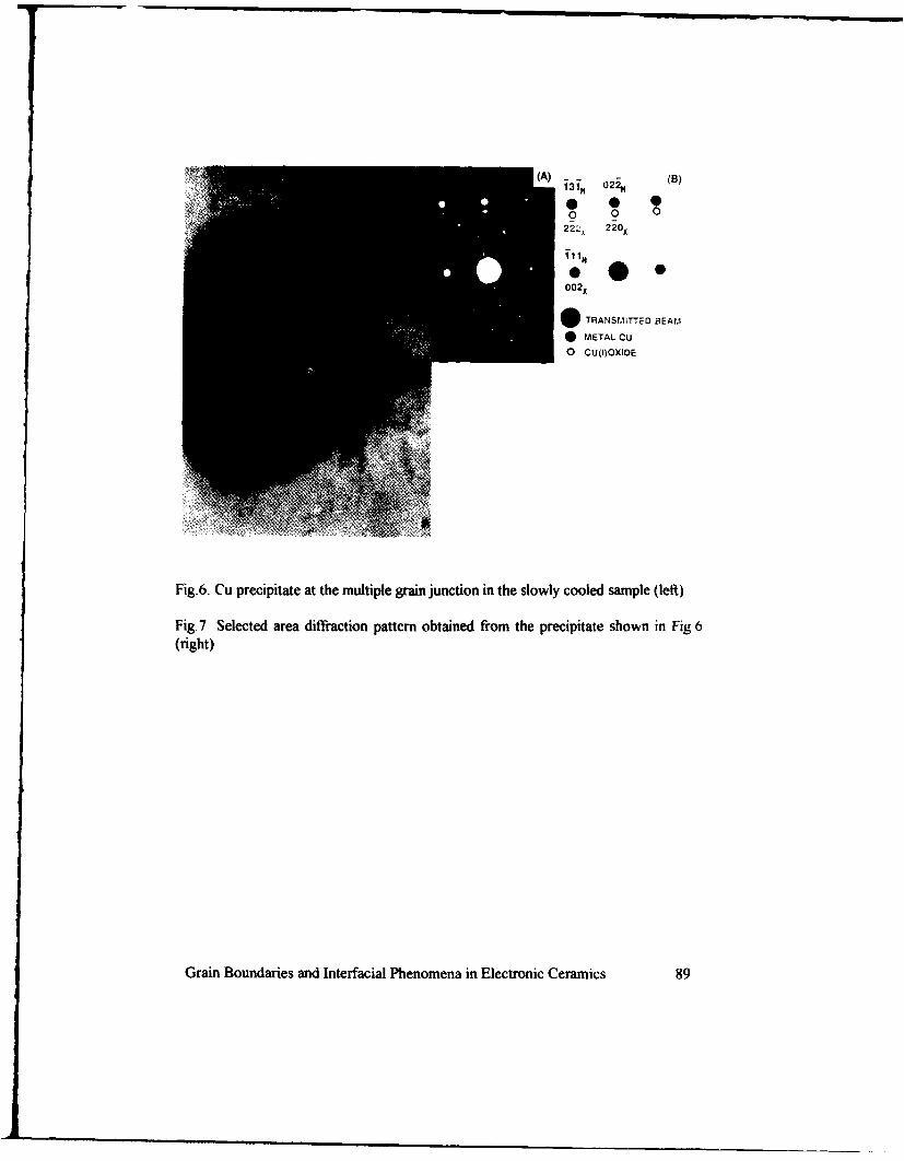
(A) 3 1n 022ý (B)
o 0 0222x 22•X
111H
002x
* TRANSMITTED BEAM
• METAL CU
0 CU(I)OXIDE
Fig.6. Cu precipitate at the multiple grain junction in the slowly cooled sample (left)
Fig.7 Selected area diffraction pattern obtained from the precipitate shown in Fig,6(right)
Grain Boundaries and Interfacial Phenomena in Electronic Ceramics 89

aia
cu
4- 0.140 z 10.-2W 1.4004
(b)
,4. ...4 • • -' -• -
Fig.8. EDX spetrum obtained from (a) the precipitate shown in Fig.6, and (b) matrixgrain.
90 Grain Boundaries and Interfacial Phenomena in Electronic Ceramics

V CONCLUSIONS
Slowly cooled and rapidly cooled multilayer chip inductors with an Ag internalelectrode and low-temperature-fired Ni-Zn-Cu ferrite exhibiting different inductancevalues were characterized.I. Elastic strain fields were observed at the grain boundaries in the rapidly cooledmultilayer chip inductor sample exhibiting degradation of inductance. The strain fielddecreasing the effective permeability of the Ni-Zn-Cu ferrite was due tointerstitial-type Cu precipitates.2. The Cu metal precipitates at the grain boundaries were due to the starting chemicalcomposition and the oxygen partial pressure and thermal equilibrium during coolingafter the sintering process.3, Control of the cooling process is one of the most important factors for obtainingoptimal magnetic properties of a multilayer chip inductor.
REFERENCES
1. T Nomura and M. Takaya, "Passive Components and Hybrid Technology,"HYBRIDS, 3 15-19 (1987).2. M. Takaya, A. Fujisawa, and Y. Mochizuki, "Development of Composite MultilayerHybrid Components," - Proc. ISHM '90, Tokyo, 747-751.3. A. Howie, RB. Nicholson, P.W Pashley, and N.J. Whelan, Elearott Abcrosvcopy ofihM (Crystal.s. Butterworths, London, 1965 (revised edition published by Krieger,New York, 1977), p258.4. 1. Homma and T Yoneoka, "Electron Diftraction Study of the Epitaxy of CuO onthe (0 11) Face of Cupper," J. Appl. Phys. 46 [4] 1459-1464 (1975).5. V.M. Castano and W. Krakow, "Observation of the Epitaxy, Oxidation and SurfaceStructure of Copper on Thin Gold Films by High Resolution Electron Microscopy,"Surface Sci. 191 45-65 (1987).6. M. Fujimoto, K. Hoshi, M. Nakazawa and S. Sekiguchi, "Cu Multiply TwinnedParticle Precipitation in Low-Temperature Fired Ni-Zn-Cu Ferrite, " Jpn. J. Appl.Phys., 32 [121 5532-5536 (1993).
Grain Boundaries and Interfacial Phenomena in Electronic Ceramics 91
DEPENDENCE OF MAGNETIC PROPERTIES OF (CoFe)304 FILMON MICROSTRUCTURE CONTROL THROUGH PHASESEPARATION
Shin-ichi Hirano, Toshinobu Yogo, Ko-ichi Kikutaand Hiroshi YamamotoDepartment of Applied Chemistry. School of Engineering, NagoyaUniversity, Furo-cho, Chikusa-ku. Nagoya 464-01, Japan
ABSTRACT
Homogeneous and dense (CoFe)304 films were synthesized onSiI(11) substrates by the sol-gel method througl metal-organic
compounds. (CoFe)304 films (Co:Fe=1: 1) were heat-treated at60000 within miscibility gap, resulting in the increase of thecoercive force through in-situ microstructure control by phaseseparation. Similar behavior was observed for (Co,Fe)304 fims(Co:Fe=2: 1), which undergo the spinodal decomposition at both6000C and 70000. The coercive force of the spinodallydecomposed films depended upon the m--icro structuredevelopment. The binodally decomposed films showed no increaseof coercive force with heat treatment.
INTRODUCTION
There are two types of phase separation behavior: The one isthe binodal decomposition, which can separate an uniform phase
To the extent authorized under the laws of the United States of America, all copyright interests in this publication are the propertyof The American Ceramic Society. Any duplication, rpouction, or republication of this publication or any part thereof, withoutthe express written consent of The Ameica CeaicScety or fee paid to the Copyright Clearance Center, is prohibited.
Grain Boundaries and Interfacial Phenomena in Electronic Ceramics 93

into an equilibrium twophases by the nucleation andgrowth process. The other is 14,0
the spinodal decomposition. inwhich there is no 12 PWS C.)thermodynamic barrier to the Udevelopment of a new phase. _S.
The spino daldecomposition proposed by '
Cahn et al 1 3 , is an interesting q-" .and promising method for the 6 - Xi~~ Twro Spk ss *in-situ microstructure control ( ; s s
of functional ceramics at the 4006 A 0.4 O 012 0o1
nanometer level. Several oxide Cation traction of Fe, F,(F*+Co)
systems, such as (Co.Fe)304system4 -6 , (Ti,Sn)02 system7 -9, Figure I Phase diagram of Co-Fe-O system
(M show the compositions andand (AICr)203 system'o, have temperatures of phase separation
been shown to decompose treatments in this work)
spinodaily.The spinel-structure region of (Co,Fe)304 system exhibits the
miscibility gap below the critical temperature which is about 850*C(Fig. 1). Takahashi et al. proposed that (CoFe)304 powder heat-treated within the miscibility gap was spinodally decomposed 4 -5
Recently, we could synthesize the (Co,Fe)304 films by a sol-gelmethod from metal-organic compounds6 . We calculated the locusof spinodal decomposition using the theory of Cook and Hilliard",as shown with doted line in Fig. 1. When the (Co,Fe)304 system isspinodally decomposed within the doted line shown in Fig. 1, theferni-magnetic phase (Fe-rich phase) and the non-magnetic phase(Co-rich phase) would be controlled at the nanometer level,resulting in the increase of the coercive force due to pinning of themovement of magnetic domain walls.
This paper describes the magnetic property changes of the(Co,Fe)304 films in relation to the development of the modulatedstructure due to the spinodal decomposition.
94 Grain Boundaries and Interfacial Phenomena in Electronic Ceramics
EXPERIMENTAL PROCEDURE
The coating solution for (Co.Fe)304 films was prepared asfollows: Cobalt(II) acetate 4-hydrate was dissolved in 2-methoxyethanol with 2-aminoethanol, which was added asstabilizing agent, and refluxed to form a stable cobalt-contaningsolution. Separately, iron(III) acetylacetonate was dissolved in 2-methoxyethanol with 2,4-pentane-dione (the stabilizing agent), andrefluxed to yield a stable iron-containing solution. These solutionswere mixed, and then refluxed to form a stable coordinationsolution. The concentration of the precursor solution wasadjusted to be about 0.1 mol/L.
Polished and rinsed Si(1 11) wafers were used as substrates.The gel films were prepared on Si(1 11) substrates through a dipcoating method. In order to form crystalline solid solution films,the gel films were heat-treated at 900°C for 20 hours in 02 flow.The dip coating-firing process was repeated several times toincrease the film thickness. Then, the solid solution films wereannealed in 02 flow at the temperature shown as E in Fig. 1 andthen quenched to room temperature.
The phases and the microstructure of the films were analyzed
by the X-ray diffraction method (XRD) using CuKa radiation with agraphite monochromator and TEM, respectively. Magneticproperties of the films were measured with a vibrating samplemagnetometer (VSM) with maximum applied field of 17.5kOe atroom temperature. Nickel metal was used to correct themagnetization. The coercive force (Hc), the saturationmagnetization (Is), and the remanence magnetization (Ir) wereevaluated from a hysteresis loop. Thermomagnetic curves weremeasured using a Faraday type magnetic balance (MB). Curietemperature (Tc) of the (Co,Fe)304 films was determined from thetemperature of zero magnetization. The temperature wascalibrated by Tc of Nickel metal.
RESULTS AND DISCUSSION
I

(1) (CoFe)304 (Co:Fe=l: 1) Films
The (CoFe)304 (Co:Fe=1:1) solid solution films were
synthesized at 9000C, and then subjected to the phase separation
treatment at 7000C and 6000C. Figures 2 and 3 show the changesof XRD profiles of the (Co.Fe)304 (Co:Fe=1:1) films with heattreatment time at 7000C and 6000C, respectively. Figure 2 revealsclearly that the films heat-treated at 700°C show the characteristicbehavior of the binodal decomposition, because no movement ofthe diffraction peak was observed after Co-rich phase appearedsuddenly for 22.5 hrs treatment. On the other hand, the filmsheat-treated at 600'C show the characteristic behavior of thespinodal decomposition as shown in Fig. 3. from the fact thatgradual separation of two side diffraction peaks of Co- and Fe-richphases was detected by XRD.
The changes of the coercive force along the longitudinaldirection of the (Co,Fe)304 (Co:Fe=l:1) films with heat treatmenttime at 7000 C and 6000 C are shown in Fig. 4. The coercive force ofthe binodally decomposed films heat-treated at 700*C wasconstant regardless of heat treatment time. However, the coerciveforce of the spinodally decomposed films heat-treated at 600°Cincreased remarkably with proceeding the spinodal decomposition.These phenomena prove that the microstructure developed by thespinodal decomposition leads to the increase of the coercive force,because the non-magnetic domains formed by the spinodaldecomposition contributes to the pinning of the movement ofmagnetic domain walls as reported6 .
Figure 5 shows the change of the thermomagnetic curves ofthe (CoFe)304 (Co:Fe=1: 1) films with heat treatment time at 7000Cin the binodal region. The curie temperature increased suddenlyfrom 370°C to 410°C for 22.5 hrs treatment, and then was keptconstant with further heat treatment. The result indicates thatthe non-magnetic phase nucleates evidently for about 22.5 hrs inthe solid solution.
96 Grain Boundaries and Interfacial Phenomena in Electronic Ceramics

311 311
Fe-frch Fe rich
31 co-rich 311 Co-ich 12 0h
__•___ __22-.5 ____,--._ _90h
7.5h15
Oh O
35 36 37 35 36 37CuKa, 20(d*g.) CuKa, 20(deg.)
Figure 2 Change of XRD profiles of (Co.Fe304 Figure 3 Change of XRD profiles of (Co.Fe)) 4films (Co:Fe=-I:1) on Si( 111) with films (Co:Fe=l:I) on Si(l I,'I wittannealing time at 700WC annealing time at 6000C(prefired at 9000 C for 20h.) (prefired at 900°C for 20h.)
2.o.
- 60h
'1 6
o 700m C 45h
1.0 22.5h
15h
7.5h
Oh0 2'0 440 60 80 100 120 __________
0 160 20 30 g00 500Annealing time, h Twi..ue c
Figure 4 Coercive force of (Co.Fe).i04 films Figure 5 Thermomagnetic curves of (Co.Fe)304(Co:Fe=1: 1) on SO(111) heat-treated films (Co:I'e=l 1] on SO(111) heat-for various times treated at 7000C for various times(prefired at 900*C for 20h.) (prefired at 900*C for 20h.)
Grain Boundaries and Interfacial Phenomena in Electronic Ceramics 97
(2) (CoFe)304 (Co:Fe=2: 1) Films
The (CoFe)304 (Co:Fe=2:1) solid solution films were preparedat 9000 C. and then subjected to the phase separation treatment at7000C and 6000C. Figures 6 and 7 show the changes of XRDprofiles of the (CoFe)304 (Co:Fe=2:1) films with heat treatmenttime at 7000C and 6000C, respectively. These figures indicate thatthe films heat-treated at 7000C and 6000C show the characteristicbehavior of the spinodal decomposition, revealing thecompositional changes of two phases.
The changes of the coercive force along the longitudinaldirection of the (Co,Fe)304 (Co:Fe=2:1) films with heat treatmenttime at 7000C and 6000C are shown in Fig. 8. The coercive forceincreases from 0.9 to 2.OkOe with heat treatment time at 7000Cand from 0.9 to 2.8kOe with heat treatment time at 6000C. Thesephenomena suggest that the modulated microstructure by thespinodal decomposition6 is effective to control the magneticproperties of the (CoFe)304 films, causing the pinning of themagnetic domain wall movement.
Figure 9 shows the change of the thermomagnetic curves ofthe (Co,Fe)304 (Co:Fe=2:1) films with heat treatment tirie at7000C. The curie temperature increased gradually from 2000C to4100C with proceeding the spinodal decomposition. Compared toFig.5, it is clear that the spinodal decomposition can bedistinguished from the binodal decomposition by the difference ofthe changes of the thremomagnetic curves.
CONCLUSION
Homogeneous and dense (CoFe)304 films were prepared onSi(II1) substrates by sol-gel method through metal-organiccompounds. The (CoFe)304 films heat-treated within spinodalline was found to be spinodally decomposed. The modulatedmicrostructure developed by the spinodal decomposition leads tothe increase of the coercive force due to pinning of the movementof magnetic domain walls.
98 Grain Boundaries and Interfacial Phenomena in Electronic Ceramics

311 311
Fe-ric? Co-rich Fe-rich Co-rich
60h 20h45h
90h
JIt 7.5h
_,
15h
OhOh
i_ I
I , I
35 36 37 35 36 37
CuKo. 20(d8o.) CuKot, 2e(deg.)
Figure 6 Change of XRD profiles of (Co.Fe)3O4 Figure 7 Change of XRD profiles of (Co.Fe)304
films (Co:Fe=2: 1) on Si( l 11) with films (Co:Fe=2: 1) on Si(l 11) with
annealing time at 700*C annealing time at 600'C
(prefired at 900*C for 20h.) (prefired at 900*C for 20h.)
3.0
00 C
for0-
6ariou
601
ra e a 0 ° o v -o sU e
415h1~5h30
Oh
0 20 40 60 80 100 120 0 100 200 300 400 bu00
Annealing time, h TemperCIure, 'C
Figure 8 Coercive force of (Co.Fe)304 films Figure 9 Thermomagnet-ic curves of (Co.Fe)3O4
(Co:Fea2. 11 on S~ill1) heat-treated films; (Co:Fe=-2: 1) on S~it 1) heat-
for various times treated at 7000C for various times
(prefired at 900*C for 20h.) (prefired at 900*C for 20h.)
"Grain Boundaries and Interfacial Phenomena in Electronic Ceramics 99

REFERENCES
1) J. W. Cahn and J. E. Hilliard, "Free Energy of a NonuniformSystem. I. Interfacial Free Energy," J. Chem. Phys., 28 121 258-67 (1958)
2) J. W. Cahn, "On Spinodal Decomposition," Acta. Met., 9 191795-801 (1961)
3) J. W. Cahn, "Spinodal Decomposition," Trans. AIME, 242 166-81 (1968)
4) M. Takahashi and M. E. Fine, "Coercive Force of SpinodallyDecomposed Cobalt Ferrite with Excess Cobalt," J. Am. Ceram.
Soc., 531111 633-34 (1970)5) M. Takahashi, J. R. C. Guimaraes and M. E. Fine, "Spinodal
Decomposition in the System CoFe204-Co304," J. Am. Ceram.
Soc., 54 161 291-95 (1971)6) S. Hirano, T. Yogo, K. Kikuta, E. Asai. K. Sugiyama and H.
Yamamoto, "Preparation and Phase separation Behavior of
(Co.Fe)304 Films," J. Am. Ceram. Soc., 76 [71 1788-92 (1993)7) V. S. Stubican and A. H. Schultz, "Spinodal Decomposition in
the System T102-SnO2." J. Am. Ceram. Soc., 51 151 290-91(1968)
8) T. C. Yuan and A. V. Virkar, "Kinetics of SpinodalDecomposition in the TiO2-SnO2 System : The Effect ofAliovalent Dopants," J. Am. Ceram. Soc., 71 [1] 12-21 (1988)
9) S. Hirano, T. Yogo, K. Kikuta. S. Arakawa, Y. Seki and K.Kawamoto, "Processing and Spinodal Decomposition of
(Ti,Sn)02 and Doped films," Ceram. Trans., 22 727-32 (1991)10)A. H. Schultz and V. S. Stubican, "Separation of Phases by
Spinodal Decomposition in the Systems A1203-Cr203 andA1203-Cr2O3-Fe2O3," J. Am Ceram. Soc., 53 1111613-16 (1970)
11) H. E. Cook and J. E. Hilliard, "A Simple Method of Estimatingthe Chemical Spinodal," Trans. AIME, 233 142-46 (1965)
100 Grain Boundaries and Interfacial Phenomena in Electronic Ceramics

Low Temperature Sintered Ferrite for Multilayer ChipComponents
Jen-Yan Hsu, Wen-Song Ko, Hsiao-Miin Sung, Meei-Lin Suen and Chi-Jen ChenMaterials Research Labs, Industrial Technology Research Institute, Hsinchu, Taiwan,R.O.C.
NiCuZn ferrite has been utilized as the material for multilayer chip inductors and chipbeads. BiO 3 and lead glass were introduced to the ferrite, respectively, to reduce thesintering temperature of the material to 8750C for co-firing with the printed internal con-ductor. However, the initial permeability and saturation induction degraded. The qualityfactor, Q, increased with the addition of either dopants. The additives formed a liquidphase in the grain boundaries and triple points to enhance the densification of the ferriteat lower temperatures. [key Word: ferrite, dopants, multilayer, chip components]
INTRODUCTION
Multilayer chip inductors and chip beads are the passive surface mount devices (SMD)which have increasingly been used in hybrid circuits for products such as video cameras,notebook computers, hard and floppy disk drives, cellular phones, ... and etc.[1,21 Theadvantage of these devices over the conventional coil-wound chip inductors is the excellentmagnetic shield because of their closed magnetic circuits.[3,4] Hence, electro-magnetic in-terference (EMI) from the devices to the other components in circuits is avoided. In addi-tion, the multilayer chip devices can be miniaturized to a much smaller size than theconventional chip coils, that enables their applications in the electronic circuits of higherdensity for compact electronic equipments.
Multilayer chip inductors and beads can be fabricated by either screen printing method[5]or lamination of green sheets[6]. The internal electric conductor which is connected amc ngthe ferrite layers is printed in a coil manner. Silver is suggested to be the conductor mate-rial because of its low resistivity, resulting in the components with higher quality factor,Q.[7] Furthermnre, the Ag paste is commercially available and lower cost than the Ag-Pdpaste.
NiCuZn ferrite is a relevant magnetic material for this component due to the better mag-netic properties at high frequencies and the capability of being sintered at lower tempera-tures (at about 1000°C or below) than NiZn ferrite. However, the melting point of Ag is961°C. It requires a further decrease in the sintering temperature of NiCuZn ferrite to be-low 900'C for preventing the Ag diffusion into the ferrite and causing the increase in
To the extent authorized under the laws of the United States of America, all copyright interests in this publication are the propertyof The American Ceramic Society. Any duplication, reproduction, or republication of this publication or any part thereof, withoutthe express written consent of The American Cera:ic Society or fee paid to the Copyright Clearance Center, is prohibited.
Grain Boundaries and Interfacial Phenomena in Electronic Ceramics 101

resistivity of the internal conductor. It was also reported that the diffused Ag will enhancethe densification of NiCuZn ferrite but provoke the Cu segregation from the ferrite, result-ing in the inferior magnetic properties of the material.[7]
The objective of this study is to introduce two additives of low melting point, namely,Bi203 and lead glass, into the NiCuZn ferrite, respectively, to promote the densification ofthe material at the aforementioned temperature range. The effect of the dopants on themagnetic properties of specimens was discussed and their microstmctures were character-ized and correlated to the fabrication parameters and properties.
EXPERIMENTAL PROCEDURES
The Fe2O3, NiO, CuO and ZnO powders were prepared as the compositions in Table I andmixed by ball milling. The mixed powders were calcined at 7500C and then added with thevarious amounts of the dopants (Table I). The composition of lead glass is PbO: 80-85wto, SiO2: 10-15 wt/o, B20,: 5-8 wt%, and A1203: 0-3 wt%. A centrifugal ball mill wasused to grind the aforementioned powder mixtures at 200 rpm for 1 hour. The averageparticle size of the ground powders was 1.5 ^m, measured by a particle size analyzer'.The powders were dried in an oven and then added with PVA for granulation. The pow-ders were then dry pressed into toroidal bodies.
Table I, Compositions of NiCuZn ferrite with and without dopants.
(wt%) Fe2O3 NiO ZnO CuO lead glass Bi2O3
No Dopant 65.51 8.91 18,29 7.9 0 0
NGI 64.86 8.82 18.11 7.82 1 0
NG2 62.99 8.57 17.59 7.6 4 0
NBI 63.97 8.64 17.91 7.71 0 1.95
NB2 62.56 8.47 17.57 7.56 0 4.29
The green specimens were sintered at various temperatures from 850 0C to 9500C, soakedfor 2 hours, and furnace cooled. The density of the sintered samples was measured by theArchimedean method. The magnetic properties, i.e., initial permeability (p), quality factor(Q), and saturation induction (B), were measured by the LCR meters2 and an AC B-Hhysteresis loop tracer', respectively. The B, values of the specimens were measured at 0.1Hz. The microstructure of the sintered specimens was characterized by SEW4 and TEM'
' Mastersizer E, Malvern Instruments, Ltd., Malvern, UK.2 Model 4284A and 4191A LCR Meters, Hewlette Packard, Rockaway, NJ3 Model AMH-20 Automatic Hysteresisgraph, Walker Scientific Inc., Worcerster, MA4 Model S-360, Cambridge Instrument Ltd., Cambridge, UK
102 Grain Boundaries and Interfacial Phenomena in Electronic Ceramics
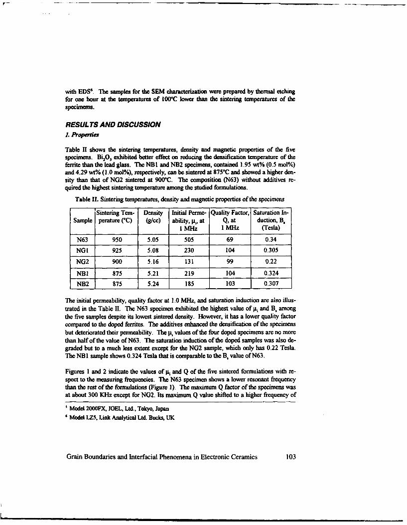
with EDS6 . The samples for the SEM characterization were prepared by thermal etchingfor one hour at the temperatures of 100*C lower than the sintering temperatures of thespecimems.
RESULTS AND DISCUSSION
L ProFe-pi
Table If shows the sintering temperatures, density and magnetic properties of the fivespecimens. Bi203 exhibited better effect on reducing the densification temperature of thefemte than the lead glass. The NBI and NB2 specimens, contained 1.95 wt% (0.5 mol%)and 4.29 wt% (1.0 tool%), respectively, can be sintered at 875*C and showed a higher den-sity than that of NG2 sintered at 900*C. The composition (N63) without additives re-quired the highest sintering temperature among the studied formulations.
Table II. Sintering temperatures, density and magnetic properties of the specimens
Sintering Tern- Density Initial Perme- Quality Factor, Saturation In-Sample perature (°C) (g/cc) ability, pi, at Q, at duction, B.
1 MHz 1 MHz (Tesla)
N63 950 5.05 505 69 0.34
NGI 925 5.08 230 104 0.305
NG2 900 5.16 131 99 0.22
NB1 875 5.21 219 104 0.324
NB2 875 5.24 185 103 0.307
The initial permeability, quality factor at 1.0 MHz, and saturation induction are also illus-trated in the Table II. The N63 specimen exhibited the highest value of li and B. amongthe five samples despite its lowest sintered density. However, it has a lower quality factorcompared to the doped ferrites. The additives enhanced the densification of the specimensbut deteriorated their permeability. The gi values of the four doped specimens are no morethan half of the value of N63. The saturation induction of the doped samples was also de-graded but to a much less extent except for the NG2 sample, which only has 0.22 Tesla.The NBI sample shows 0.324 Tesla that is comparable to the B, value of N63.
Figures I and 2 indicate the values of tt, and Q of the five sintered formulations with re-spect to the measuring frequencies. The N63 specimen shows a lower resonant frequencythan the rest of the formulations (Figure 1). The maximum Q factor of the specimens wasat about 300 KHz except for NG2. Its maximum Q value shifted to a higher frequency of
Model 2000FX, JOEL, Ltd., Tokyo, Japan'Model LZS, Link Analytical Ltd. Bucks, UK
Grain Boundaries and Interfacial Phenomena in Electronic Ceramics 103
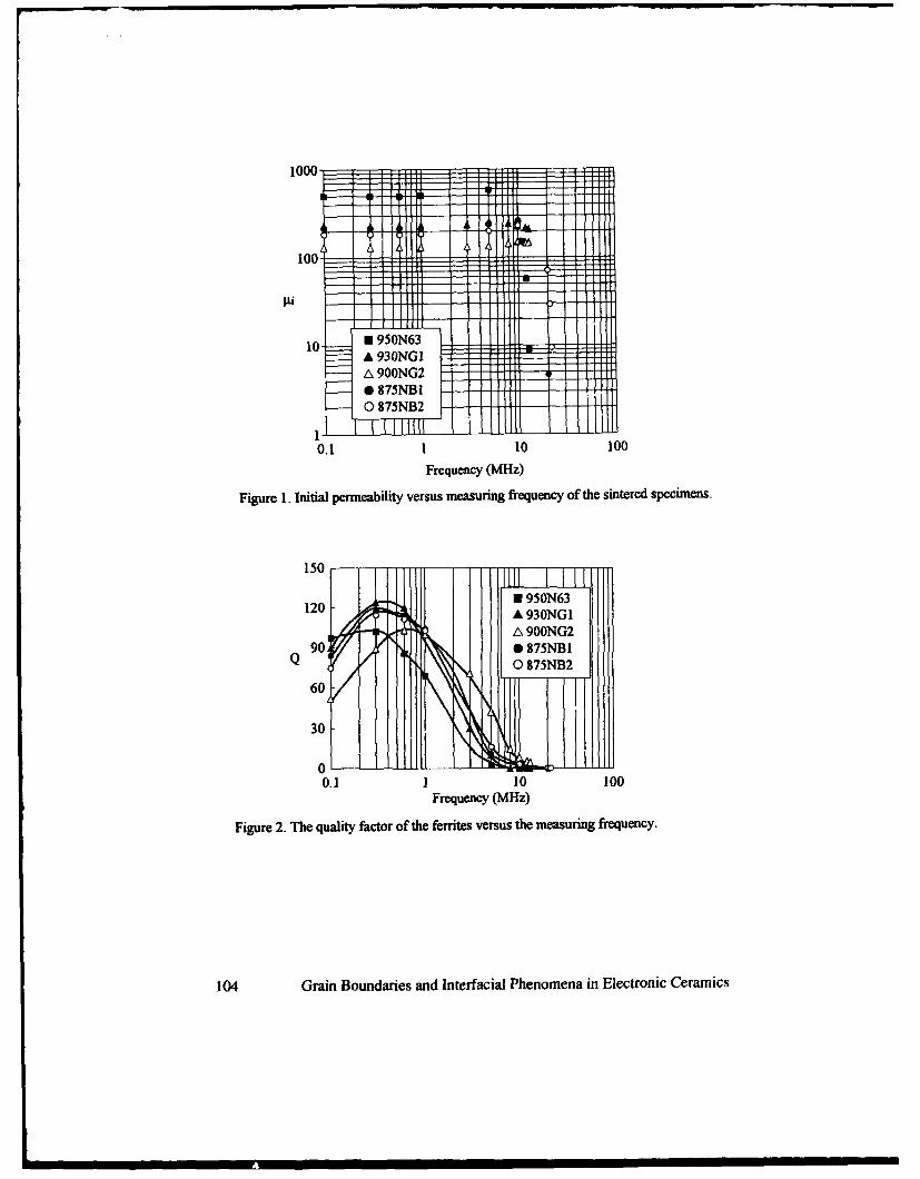
1000
0. P 1 10 10
100
0 950N63i12 930NG9I
AA 900NG29 875NBI
0 0875NB2
0.1 1 10 100
Frequency (MHz)
Figure 1. Thitial permeability versus measuring frequency of the sintered spe. mens.
150 i eIa i n El1 950N63
120 A 930NGI
SL\ 900NG2
Q90 0 • 875NBIQ\\• 0 875NB260
00.1 110 100
Frequency (MHz)
Figure 2. The quality factor of the ferrtes versus the measuring frequency.
104 Grain Boundaries and Interfacial Phenomena in Electronic Ceramics

II
600 KMz.
2. Mcrosrrucrure
The microstructure of N63 is shown in Figures 3. The grain size of this specimen vanesfrom less than 1 pm to more than 10 pin. The intragranular porosity was observed in thelarger grains. This is a typical microstructure for the iron-deficient ferrites, i.e., the molarcontent of Fe2O, is less than 50% in the ferrite composition. Since the anion vacancies,i.e., oxygen vacancies, in the lattice are formed so that it enhances the grain boundariesmovement during the sintering stage. The pores are easily to be trapped in the grain inte-rior during the grain growth.
With increasing amount of the lead glass in the composition, the intragranular porosity de-creased, as shown in Figure 4 and 5. Fewer entangled pores inside the grains were foundin the NG I specimen and no intragranular porosity in NG2. The average grain size of thesintered bodies also decreased with increasing amount of the lead glass content. Figure 5indicates that the grain size distribution of NG2 is narrow and no grains are larger than 10prm. By the SEM analysis, no grain boundary phases were observed in these twospecms.
In Figure 6, a bismuth-rich phase was observed in the grain boundaries of the NBI speci-men, identified by EDS. This spherical grain boundary phase is believed to precipitateduring the thermal etching process. Intragranular porosity is scarce and the grain size dis-tribution is narrow in this sample. The average grain size is about 5 pin.
Figures 7 and 8 illustrated the microstructures of NGI and NBI using TEM. A Pb-richphase was observed in the triple points of the grain boundaries in NGI, while a Bi-richphase distributed at triple points as well as the grain boundaries in NBI. The micro-chemistry of the specimens was characterized by an attached EDS. An even higher magni-fication, i.e., lattice images, may be required to analyze the distribution of the secondphases at the clean grain boundaries in both specimens.
3. Correlation
During the sintering stage, Bi203 and lead glass form liquid phases in the grain boundariesand triple points to promote the densification of specimens at lower temperatures, 8750C to9000C. The second phases obstructed the grain boundary movement and avoided the exag-gerated grain growth, resulting in the smaller grain size and elimination of the intragranu-lar porosity, as compared Figures 3 to 6. This effect was profound with increasing amountof the additives.
The highest initial permeability of N63 is attributed to the largest grain size among the fivespecimens. Though, the intragranular pores can pin on the domain wall and hinder its
Grain Boundaries and Interfacial Phenomena in Electronic Ceramics 105
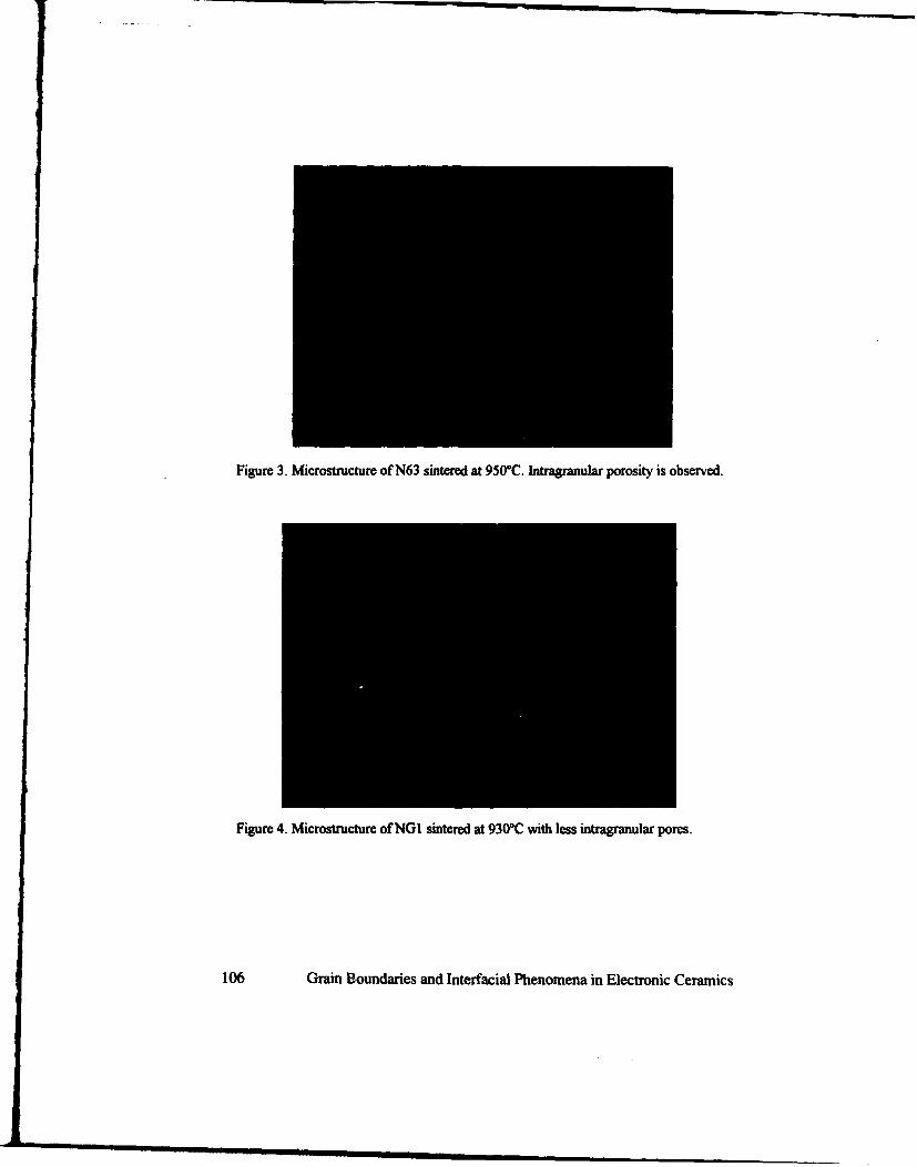
Figure 3. Microstructure of N63 sintered at 95MC. Intragranular porosity is observed.
Figure 4. Microstructure ofNGl sintered at 930t with less intragranular pores.
106 Grain Boundaries and Interfacial Phenomena in Electronic Ceramics

Figure 5. No pores arc inside the grains of NG4, sintered at 900"C. The grain size distri-bution is narrower than the previous two figures.
Figure 6. Microstructure of NBI sintered at 875-C. The spherical Bi-rich phase is ob-served in the grain boundaries. That is believed to form during the thermal etchingprocess.
Grain Boundaries and Interfacial Phenome' -A in Electronic Ceramics 107

Figure 7. Microstructure of NGI indicates the Pb-rich phase distributes in the triplepoints, as shown by the arrows.
Figure 8. Bi-rich second phase, indicated by the arrows, is observed in the grain bounda-ries and triple points.
108 Grain Boundaries and Interfacial Phenomena in Electronic Ceramics

movement, causing the deleterious permeability. It was reported[S] the distances betweenpores rather than grain size account for variations in permeability. Samples with Wiantgrains and included porosity still had higher pernmability than thie with normally growngrains, provided the distances between pores were the same. In addition, the nmnagetions, i.e., Bi, Pb2, Al3, Si+, and B+3, from the two additives may enter the crystal latticeof the ferrites and reduce the saturation magnetization, and hence the initialpenneabilities.[91
The four doped specimens ehibited higher quality factor than that of N63. It is believeddue to the higher resistivity of the material. The smaller grain size, i.e., more grainboundaries per unit volume, and the aforementioned grain boundary phases increased theresistivity of the specimens. Besides, the previous substituted nonmagnetic ions in the fer-rite lattices reduced the material conductivity.
SUMMARY
Bi120 demonstrated a better efficiency than the lead glass to reduce the sintering tem•pera-ture of the studied NiCuZn ferrites. With the addition of 0.5 mol% Bi203, the densificationtemperature of the ferrite was reduced from more than 9500C to 8750C. The initial perme-ability of the doped specimen was deteriorated, the saturation induction remained compa-rable, but the quality factor was improved compared to the formulation without anydopant. The variation in the magnetic properties was attributed to the microstructure al-teration and chemical modification of the formulation with respect to the addition of thesintering aids.
REFERENCES
"1. "In the Chips Component Makers Discover Smaller is Better," Jpn. Electronic Eng.,No. 5, 28-33, 1991.
2. "Key of the Portable - Packaging Technology," pp. 10-38 in Nikkei New Materials(Japanese), No. 116, June 22, 1992
3. M. Takaya, "The Multilayer Chip Inductor Features Innovative Design," Jpn. Elec-tronic Eng., 38-41, 1986.
4. T. Nomura and A. Nakano, "New Evolution of Ferrite for Multilayer Chip Compo-nents," pp. 1198-1201 in Proceedings of the 6th International Conference on Ferrites,ed. by T. Yamaguchi and M. Abe, The Japan Society of Powder and Powder Metal-lurgy, Tokyo and Kyoto, Japan, 1992.
5. A. Ono, T. Muruno and N. Kaihara, "The Technology of Electrode for Multilayer ChipInductor (I) Terminal Electrode," ibid, pp. 1206-1209.
Grain Boundaries and Interfacial Phenomena in Electronic Ceramics 109
p .... .. .. _ _

6. US Patet 4,543,553.
7. A. Nakano, H. Momoi, and T. Nomura, "Effect of Ago o Microstnactur of the LowTempenrt Sintered NiCuZn Femtes," pp. 1225-1228 in Proceedngs of the 6th In-ternatonal Conference on Ferrites, ed. by T. Yamaguchi and M. Abe, The Japan So-cey of Powder and Powder Metallurgy, Tokyo and Kyoto, Japan, 1992.
8. M. Drofenik and S. P. Besenicar, "Reexamination of the Grain Size/Permeability Rela-tion in High Permeability Mn-Zn Ferrites," Ceram. Bull, 65 [41 656-659, 1986.
9. A. Goldman, "Chemical Aspects of Ferrites," Chapter 3, pp. 87-114 in Modern FermteTechnology, Van Nostrand Remhold, New York, 1990.
110 Grain Boundaries and Interfacial Phenomena in Electronic Ceramics

Influence of Process Parameters on Power LossesMinimum Versus Temperature of Mn-Zn ferrites
M.J.Tsay*, C.S.Liu*, M.J.Tung, C.J.Chcn*
"* Materials Research Laboratorics,Industrial Technology Research Institute,
Hsinchu. 31015,TaiwanR.O.C.•* Department of Materials Science and Engineering,National Tsing Hua
University, HsinchuTaiwanR.O.C.
In the studywe found that the power losses minimum versus temperature for aselected composition of Mn-Zn ferrites can be adjusted by prcsintiering andsintering conditions. The results show that presintering condition effectivelyinfluence the minimum loss temperature and value of this minimum loss pointBesides, the minimum loss temperature is affected by oxidation degree duringsintering. Furthermore,the effect of additives with isovalent or aliovalent cationson minimum loss temperature was also studied. It is found that when MgO isadded to Mn-Zn ferrites containing CaO-SiO2,the minimum loss temperature canbe shifted to higher temperature as compared with ferrite with V20,. On theother hand, the effect of V20 5 on minimum loss temperature is opposite. That isto say,additives with different cation valence affect the minimum loss temperatureof Mn-Zn fcrrites. Thereforewe conclude that although the minimum losstemperature is naturally determined by a selected composition, process parametersstill play an important role to minimum loss temperature. (Key word: Mn-Znferrite,power Iossadditives~minimum loss~permeability)
I INTRODUCTION
In Mn-Zn ferrites for power supplies,low loss characteristics is of primeimportance. When it is used at high power the exothermic heat becomes aproblem The magnetic loss becomes minimum around the secondary maximumpeak temperature Ts of # i. Thusthe losses decrease as the temperature riseswhen a composition having a higher Ts than the operating temperature is selected.
To thekett auodrized under the laws of the United States of America, aD cprh•t inte t puc•mtim a•d The Ameiamn Camw Society. Any duplcmam reprdm or rembimdo of t publim or any puroheite tthe evyaeu written cmmut of n Amerimn Cerc Society orfee paid to theeCopyrit ance Centero wo
Grain Boundaries and Interfacial Phenomena in Electronic Ceramics 111

Therefore,our goal in this paper is to investigate the influence of processparameters on minimum loss temperature of Mn-Zn ferrites. Generally, the powerloss of Mn-Zn ferrites is dominated by hysteresis loss and eddy current loss aslong as operating frequency is lower than the rclaxtion frequency of walldisplacement.Lt. 21 When the operating frequency is high(>500kHz ), relaxationlosses nwat be taken into account. Based on the above background, the powerloss was measured below 500kHz in this study.
UI EXPERIMENTAL
Mn-Zn ferrite samples were prepared by conventional powder metallurgicalprocesses. Fe20 3,MnCO3,ZnO powders were weighed and mixed for 4 hrs,andthen dried and presinterecd The resulting powders, plus CaO-SiO 2,V 20 5,MgOwere milled in water for 40 mins. After dryingthc powders ame granulatedthrough 40-mesh sieve and pressed into toroids. A computer-controlled tubefurnace was used to regulate both firing temperature and oxygen partial pressure.The samples were sintered from 1250°C to 1300°C for 3 hrs and atmosphericconditions were controlled during cooling to maintain spinel phase equilibrium.The power loss was measured by an apparatus made by Ryowa company. That isto saypower loss was obtained by computing the digital data of primary excitingcurrent and secondary induced voltage detected from coils wound around atoroidal core under sinusoidal excitation. The excitation frequencies were below500 kHzand applied magnetic flux density was fixed at 200mT. Specimens wereplaced in a oven so that its temperature could be controlled. And opticalmicroscope was used to observe the microstructure and addition effect.
IM RESULTS AND DISCUSSION
It is well known that the minimum loss temperature decreased with increasing themeasured frequency.13,4! Figure 1 shows the relationship between power loss andtemperature at several frequencies. It is found that the minimum loss temperatureis shifted to 60*C,when measuring frequency is increased to 250kHz. In addition,minimum loss temperature is closely related to process parameters. CaO-SiO 2
was generally used as additives for Mn-Zn ferritests-61 to reduce the power loss athigh frequency. In Figure 2,it shows the effect of CaO-SiO 2 content ontemperature dependence of power loss of Mn-Zn ferrites. Both the power loss atlower temperature and minimum loss temperature become lowerwhen addition
112 Grain Boundaries and Interfacial Phenomena in Electronic Ceramics

amounts of CaO-SiO 2 is increased. The more CaO-SiO 2,the lower the power lossat lower temperature, On the other hand, the minimum loss temperature of Mn-Znferrites with less CaO-SiO2 content shifts higher. Especially, the power loss inthe high temperature region reduces obviously.
1SO ...0.t 1200 5000
l80 -eo 1100,EE 250o K*Ut 4500
S140 , 1000
S120- 0 4000
100.
70060 30
20 30 40 8i 60 70 80 90 100 110Temperature (CC)
Figure 1 Temperature dependence of power loss for samplesmeasured at various frequencies
950
900 - 4W0pm; 850 - ew wn
S800
750
0 7005 650
600o.550
450
20 30 40 50 60 70 80 90 100 110Temperature (*C)
Figure 2 Temperature dependence of power loss for samplescontaining CaO-SiO 2
Grain Boundaries and Interfacial Phenomena in Electronic Ceramics 113

Figure 3 clearly shows that Mn-Zn ferrites with less CaO-SiO2 can keep small
grainson the contrary abnormal grains are observed for sample with higher CaO-SiO2. From these resultswe can deduce that the resistivity of Mn-Zn ferrites with
higher CaO-SiO2 becomes lower at high temperature due to the abnormal graingrowth. This make the power loss at higher temperature increased obviously.But the hysteresis loss at low temperature can be lowered by the large grains.This is why the low power loss was obtained at the lower temperature for samplecontaining higher CaO-SiO 2.
Figure 3 Micrographs by OM for samples added with differentamounts of CaO-SiO2 (A)400ppm (B)600ppm
114 Grain Boundaries and Interfacial Phenomena in Electronic Ceramics

800
750 E low
~700-Sa8.50
OW
5O0
20 30 40 50 80 70 80 90 100 110Temperature (11C)
Figure 4 Temperature dependence of power loss for samplespresintered at various temperature
750 - 1O-
40 50 50 70 80 90 100 110 120
Temperature (*C)
Figure 5 Variation of intial permeability and power loss with temp-erature for samples sintered at different temperature
800 3750---- n~agom ee MM-X .. 3500
40 5o 60 70 60 90 100 110 120
Temperature (•C)Figure 6 Variation of inital permeability and power loss with temperature for
samples sintered at 12505C for 3hr but annealed oxygen partial
pressure with different time
Grain Boundaries and Interracial Phenomena in Electronic Ceramics 115

Presintering conditions determine the sinterability of Mn-Zn ferrites. Figure 4shows the influence of presintering temperature on temperaturt dependence ofpower loss. It is shown that the better the presintering temperature (850"C), thelower the minimum value of power loss, because samples with different sintereddensity and homogeniety were obtained from various presintering temperature.When we examine the minimum loss temperature,it is found that the minimumloss temperature is shifted to lower temperature for sample with lowerpresintering temperature. In figure 5,each sample was sintered at a differenttempcrature(1250°C - 1300°C )for 3hrs and equilibrated with the same oxygenpartial pressure(4%). It is found that the lower the sintering temperature, thehigher the minimum loss temperature, because when samples were sintered atdifferent temperature and equilibrated with the same oxygen partial pressure,samples sintered at higher temperature will have more Fe+2 content.is,9l Theseresults are compatiable with the g i-T curve in Figure 5. It is seen that thesecondary maximum peak is shifted to lower temperature for sample sintered at1300 TC due to the increase of Fc+2. Besides, Figure 6 shows the effect ofannealing time used to equilibrate the spinel phase on minimum loss temperature.It is observed that although the sintering time for each sample is equal,theminimum loss point is obviously influenced by annealing time. The shorterannealing time, the higher the minimum loss temperature. As decribed above,theminimum loss temperature is closely related to both the sintering temperature andannealing time. When an optimum sintering condition is selectedthe minimumloss temperature shifts higher and the minimum value remain low.
1200
.. 1100 - A
E 1000O
9oo-
0 w
a 8007W
50020 30 40 50 O0 70 80 90 100 110
Temperature ('C)Figure 7 Temperature dependence of power loss for samples
added with (A)CaO-SiO2 (B)CaO-SiO 2-MgO (C)CaO
-SiO 2 -V20 5
116 Grain Boundaries and Interfacial Phenomena in Electronic Ceramics
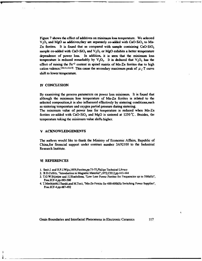
Figure 7 shows the effect of additives on minimum loss temperature. We selectedV20, and MgO as additivesthey are separately co-added with CaO-SiO 2 to Mn-
Zn ferrites. It is found that as compared with sample containing CaO-SiO 2
sample co-added with CaO-SiO2 and V20 5 or MgO exhibits a better temperature
dependence of power loss. In addition, it is seen that the minimum losstemperature is reduced remarkably by V205. It is deduced that V205 has the
effect of raising the Fe+2 content in spinel matrix of Mn-Zn ferritcs due to highcation valence.1°0 ,11, 12,131 This cause the secondary maximum peak of g i-T curve
shift to lower temperature.
IV CONCLUSION
By examining the process parameters on power loss minimum. It is found thatalthough the minimum loss temperature of Mn-Zn ferritcs is related to theselected compositionit is also influenced effectively by sintering conditionssuchas sintering temperature and oxygen partial pressure during sintering.The minimum value of power loss for temperature is reduced when Mn-Znferrites co-added with CaO-SiO 2 and MgO is sintered at 1250°C. Besides, thetemperature taking the minimum value shifts higher.
V ACKNOWLEDGEMENTS
The authors would like to thank the Ministry of Economic Affairs, Republic ofChina,for financial support under contract number 3A92100 to the IndustrialResearch Institute.
VI REFERENCES
1. SmiuJ. and H.P.J.Wijn,1959,Fcrrites,pp.73-75,Philips Technical Library2. B.D.Cullity, "Introduction to Magnetic Matcrial",1972,CH12,pp.443-4443. T.G.W.Stijntjes and JJ.Roelofsma, "Low Loss Power Fcrritcs for Frequencies up to 500kHz",
Proc.ICF-4,pp.493-5004. T.Mochizuki,I.Sasaki,and M.Torii, "Mn-Zn Fcrrite for 400-600kHz Switching Power Supplies",
Proc.ICF-4,pp.4S7-492
Grain Boundaries and Interfacial Phenomena in Electronic Ceramics 117

5. Taunco Akashi, "Effect of the addition of CaO amd Si0 2 on the Magnetic Characteristics and
Microstructures of Manganese-Zinc Ferrites (Mn 0 .68Zn0 .21F2.1 IO4+ )", Trans.Japan. I st.
Mct.2,pp. 171 (1961)6. I-Nan Lin,R.Mishraand G.Thomas, "CaO Segrcggation in Mn-Zn Ferrites", IEEE Trans.
Mag.MAG-18,pp. 1544-1546(1982)7. KLHaneda,E.BannaiH.Yamamura,A.Watanabe, and S.Shirasaki, "Oxygen Self-Diffusion and
Polycrystalline Zinc Ferrites", Proceeding of the Fourth Internatonal Conference OnFeMtes, Advances In Ceramics, Vol.15,16, Ed. by F. Y. Wang, The American CeramicSociety, Westerville, Ohio, 1984
8. P.E.C.Franken, "The Influence of the Grain Boundary on the Temperature Coefficient of Ti-Substituted Telecommunication Ferrites", IEEE Trans. Mag. MAG-14,pp.898-899(1978)
9. R.C.Sundall, Jr., B.B.Ghate, R.J.Holmes and C.E.Pass, "The Grain boundary Chemistry andMagnetic Properties of Mn 0.5Zn0 .4Fe2 .104", in Ceramic Vol.I: Grain Boundary Phenomena
in Electronic Ceramics, cd. L.M.Levinson, Amer. CcanLCos.Inc.,ColumbusOhiopp.502-511(1981)
10.P.E.Bongers, F.J.A.Den Broeger, J.P.M.Damcn, P.E.C.Franken and W.T.Stacy, "Defects, GrainBoundary Segreggration, and Second Phases of Ferrites in Relation to the MagneticProperties", in Ferrites Proc. International Conference, Japan(1980), pp.265-271
1 I.P.E.C.Franken and W.l.Stacy, "Examination of Grain Boundaries of Mn-Zn Ferrites by AESand TEM", J.AM.Ceram.63,pp.315-319(1980)
12.IHTsunnekaea, A.Nakata, T.Kamijo, and K.Okutani, "microstructure and Properties ofCommcrcial Grade Manganese Zinc Ferrites", IEEE Trans. Mag. MAG-5,pp.1855-1857(1979)
13.T.Akashi, "Precipitation in Grain Boundaries of Ferrites and Their Electrical Resistivities",Part II .NEC Reaserch and Development,8, pp.66-82(1970)
118 Grain Boundaries and Interfacial Phenomena in Electronic Ceramics

GRAIN BOUNDARY LAYERED PTCR CERAMICSBASED ON PbTiO.-TiO2
M.Okada, M.Homma, Dept.of Materials Science,Faculty of Engineering,Tohoku Univ.,Sendai,Japan
S. Iwashita,Seiko Epson Co, Suwa, Japan.
Abstract
Niobium doped PbTiO3 -TiO, ceramics show PTCR properties atthe Curie temperature of 490°C. A new type of PbTiO3-TiO,ceramics with the boundary layer structure is proposed. Themicrostructure where TiO2 grains are surrounded by the thinlayer of PbTiO3 , are prepared by painting PbO on the surface ofTiO. sintered bodies, followed by annealing, or by conventionalpowder techniques. Both techniques yield such a microstructurewith boundary layer of PbTiO,, which shows PTCR properties.Optimum amount of PbTiO3 at grain boundaries for yielding thegood PTCR properties, were studied.
Introduction
It is well known that semiconducting BaTiO3 ceramic showthe Positive Temperature Coefficient of Resistivity (PTCRproperties) above the Curie temperature (Tc=120°C). In order toexpand their high temperature applications, PTCR materials withhigh Curie temperature have been demanded. It was reported thatNb-doped PbTiO3 -TiO 2 composite ceramics showed PTCR properties atthe Curie temperature of PbTiO3 (490*C), which is the highesttemperature among those of available PTCR materials.' The Curietemperature of this system is controlled by the addition ofSrTiO, and CaTiO,. 2
It was also confirmed that the PTCR properties in PbTiO,-TiO,system was originated from the interface of PbTiO3 and TiOgrains in directly measuring the resistivity-temperaturecharacteristics of the PbTiO3-TiO2 interface by welding a fine Ptelectrode wire on the surface of each grain.' Based on thisobservation, a new type of PTCR ceramics with a boundary layerstructure is proposed as follows; since PTCR properties occur atthe interface between PbTiO3 and TiO, grains, it is expected that
To the extent authorized under the laws of the United Statm of America, aU cDpyr t intm ts in this pubication are the propertyof The American Ceramic Sode. Any duplication, reproduction, or repubication of this publication or any part thereoi withoutthe express writte cnsent of The Aercan Ceramic or paid to the Copyright Cearance Center, is prohibited.
Grain Boundaries and Interfacial Phenomena in Electronic Ceramics 119
j
the TiO: grains surrounded by the thin boundary layer of PbTiO,phases would enable to show PTCR properties. Then the purpose ofthe present investigations is to explore the possibility of theformation of PbTiO3-TiO2 PTCR ceramics with such boundary layerstructure.
Experimental Procedure
Approach for Formation of sL Structure
Figure 1 schematically illustrates two experimental methodsfor formation of Boundary Layered (BL) structure in PbTiO3-TiO,ceramics.(1) Painting of PbO on the surface of sintered TiO. bodies;The boundary layer of PbTiO, around TiO2 is formed by the samemethod used for the developments of BaTiO 3 boundary layercapacitor.' Because PbTiO3 is formed by the reaction; PbO+TiO2,PbTiO3, PbO coated on the surface of Nb-doped TiO2 samplediffuses into Tio, bodies through grain boundaries, particularlyabove 8830 C at which PbO becomes liquid.'(2) Conventional powder techniques; Decrease of the amount ofPbTiO3 in PbTiO3-TiO2 system will partially form the BL structureduring calcination and firing since PbTiO3 would be formed bythe reaction mentioned above.In controllinD che amount of PbO,the possibility for forming BL structure w-th the conventionalpowder techniques was studied.
Sample Preparations
The specimens were prepared from 99.89% PbO and 99.7% TiO,with 99.89% Nb,0 3 as the doping element.(1)Painting of PbO on the surface of TiO2 ; The green compacts of(Ti 0.994Nb,.00,)O, with a 10mm in diameter and 5mm in thickness,were sintered at 1000-1400*C for 2 hrs in air or Ar atmosphere(lstannealing). The PbO powders with about 200mg were painted onthe surface of the sintered TiO2 disks, which were furtherannealed at 900-1200°C for 18 hrs in Ar atmosphere(2nd annealing).(2) Conventional powders techniques; The nominal compositionsof the specimens are Pb(Tio.994Nb,.,,.)O,-(90-95mole%) (Ti 0 ,,,Nb 0 001)02.
The green compacts were put in the Al 203 crucible with (PbCO3 ) 2Pb(OH) 2-- 3ZrO, for creating PbO atmosphere. They were fired at 1000-1100*C for 2 hrs in Ar atmosphere without calcination.
Resistivity Measurements and Microstructural Observations
The microstructures of the samples were observed by usingtransmission electron microscopy. The microstructural constituent
120 Grain Boundaries and Interfacial Phenomena in Electronic Ceramics

was analyzed with Energy Dispersion X-ray(EDX) microanalysis.Thin foil specimens were prepared by ion-beam milling.
Using the two probe method, the resistivity of samples wasmeasured from room temperature to 600°C on heating at a rate of3*C/min in air. In-Ga alloys were used for the electrodes, whichwere covered with stainless steel sheets.
(a) Painting of PbOPbO
Boundary Layered (BL)
(b) Conventional Powder StructureTechniques Fig.1 Schematic illustration
how to prepare the BLstructure in PbTiO.-TiO2
system.
Results and Discussion
Formation of BL Structure by Painting and Diffusion of PbO
Figure 2 shows the relative sintered density of TiO. beforeand after 2nd annealing(at 1000lC for 2 hrs) with the increasedweight of sintered bodies (corresponding to the diffused amountof PbO) after 2nd annealing versus sintering temperatures ofTiO, where the theoretical density of the samples after 2ndannealing is assumed to be that of TiO2. The relative sintereddensity of TiO. increases with increasing sintering temperatures,specially up to 95% after sintering at 1300'C. The increased
weight of sintered bodies after 2nd annealing, decreased withincreasing sintering temperatures of TiO2. The high relativedensity of TiO, may make the diffusion of PbO along grainboundaries difficult.
Figure 3 shows the corresponding resistivity temperaturecharacteristics of TiO2 samples sintered at 1000C-1300C in air
Grain Boundaries and Interfacial Phenomena in Electronic Ceramics 121
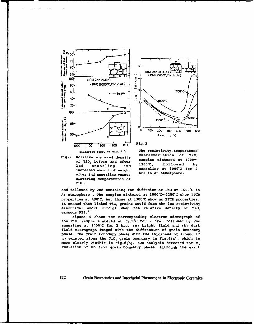
950
* rrr~TiO,( 2hr in Air)II: 85; ._ * PbO(1000°C,2hr in Ar)
10 TiO(2hr in Air) E 4
80o PbO (1000-C,2hr in Ar
P 602 -in Air 3 - 12000C
100
g-O ,
o -0, 10. 0 100 200 300 40 0 500 600
g 9 Temp. /1C
11ý6 00113.0,0 Fig. 31000 1100 1200 1300 0
Sintocing Tomp. of TiO, / "C The resistivity-temperaturecharacteristics of TiO1
Fig.2 Relative sintered density sape itered at 100'of TiO2 before and after samples sintered at 1000-
2nd annealing and 1300°C , followed byincreased amount of weight annealing at 1000°C for 2after 2nd annealing versus hrs in Ar atmosphere.sintering temperatures ofTiO2 .
and followed by 2nd annealing for diffusion of PbO at 1000°C inAr atmosphere . The samples sintered at 1000°C-1250*C show PTCRproperties at 490°C, but those at 13000C show no PTCR properties.It seemed that linked TiO2 grains would form the low resistivityelectrical short circuit when the relative density of TiO:exceeds 95%.3
Figure 4 shows the corresponding electron micrograph ofthe TiO. sample sintered at 12000C for 2 hrs, followed by 2ndannealing at 1000j C for 2 hrs, (a) bright field and (b) darkfield micrograph imaged with the diffraction of grain boundaryphase. The grain boundary phase with the thickness of around 12ran existed along the TiO2 grain boundary in Fig.4(a), which ismore clearly visible in Fig.8(b). EDX analysis detected the M.radiation of Pb from grain boundary phase. Although the exact
122 Grain Boundaries and Interfacial Phenomena in Electronic Ceramics

Fig.4 Transmission Electron Micrograph (TEM) of PbO painted TiO,samples annealed at 1000*C for 2 hrs.(a)bright field,(b)dark field imaged with diffracted beam of the grainboundary phase.
chemical composition of the thin layer of grain boundary phasecould not be determined, it is expected that the grain boundaryphase mainly consists of PbTiO,. This means that BL structure isformed by painting of PbO on the surface of TiO2 grains,followed by annealing.
Since PbTiO3 phase becomes liquid above 1280°C,5 the PbTiO.powders were painted on the surface of TiO. samples for theformation of BL structure. But it was observed that PbTiO3liquid phase did not diffuse along the grain boundary of TiO.grains. The wettability between PbTiO3 and TiO. phase turned outto be poor.
Formation of SL Structure by Conventional Powder Techniques
Figure 5 shows the resistivity temperature characteristicsof the (a)PbTiO,-90%TiO, and (b) PbTiO -95%TiO2 samples, whichshows PTCR properties when the sintering temperatures were1000C-1025'C. But, the samples sintered over 1050°C show noPTCR properties, which would be due to the formation ofelectrical short circuits of the linked TiO, as discussed above.
Figure 6 shows the relative sintered density, PTCR effects(log(pw//p.,.)) and resistivity at room temperature of thePbTiO,-(9095)moleTiO2 samples versus sintering temperatures.The relative sintered density increases with increasing sinteringtemperatures and becomes to be over 94% above 1050'C where noPTCR properties were observed. But the room temperature resistivitydecreases with increasing sintering temperatures.The PbTiO3-90%TiO. samples show higher PTCR properties than those ofPbTiO,-95%TiO. after sintering at 10000C.
Grain Boundaries and Interfacial Phenomena in Electronic Ceramics 123

(a) (b)
Pb(TawNbaM)O 7
- 90(TiuNbo*oOa Pb(TiaNba,)O,2hr inAr Non-Calcined --5(TiawNb =)Oz
E3r - E3 2hr inAr
S Non- Calcined2-2 - 9(~sNo.0
1OOU*U
1105 Co o~.!000- 1OOC0 00I
1025 IC
0 100 200 300 400 500 600 0 100 200 300 400 500 600
Temp. I IC Temp. I IC
Fig.5 The resistivity-temp. characteristics of PbTiO3-(90"
95)mole%TiO2 samples.(-I - 1 I
Pb( Tio iNbooos)0 I3- X (Tio,.Nbooom)Oz
Non- Calcined
m dE •--xZ90
0- Xig.6
The elaivesintered density,
Sresistivity at R.T. and PTCR
properties of PbTiO3-(90-95)%TiO2 samples versus
S.... . . . •sintering temp..
10 1025 1050 107 I
Sintertng 2MV. / °C
124 Grain Boundaries and Interfacial Phenomena in Electronic Ceramics

Figure 7 shows the electron micrograph of this samplesintered at 1000lC. The grain boundary phase with dark contrastwas observed. EDX analysis indicated that grain boundary phasewould be PbTiO3 phase. Although grain boundary phase was notenough to cover the TiO, grains, the BL structure was formed byconventional powder techniques. The reason why slight incrementof sintering temperatures formed the electrical short circuitmay be due to the lack of this total amount of PbTiO3 phasesalong grain boundaries of TiO2 grains. Total amount of PbTiO3grain boundary phase should increase from 10%, in improvingPTCR properties. Optimum amount of PbTiO3 was further studied asdiscussed below.
It was found that the TiO. grains surrounded by thinboundary layer of PbTiO3 enabled to show PTCR properties. Thegrain boundary layered PTCR ceramics were formed by the paintingmethod or conventional powder techniques in PbTiO,-TiO2 system.
Fig.7 TEN of PbTiO3-90%TiO2 samples sintered at 1000*C for 2hrs.(a)BF, (b)DF.
Improvements of Thermal Stability of PTCR Properties in BLStructure by Addition of SrTiO,
The disadvantage of these grain boundary layered PTCRceramics discussed above is their poor thermal stability. Theresistivity of the samples increases after increasing thetemperature above 5009C in air. It was reported that the thermalstability of PTCR properties in this system would be improvedby the addition of SrTiO3 to the system.2 In the next approach,the optimum composition for the stability of PTCR propertieswas studied in the range of (Pb,.,Sr*.1 )TiO,-(85-70)mole%TiO2 . Asa result, it was found that optimum composition was(Pbo,Sr 0 1 )TiO3-70mole%TiO 2
Grain Boundaries and Interfacial Phenomena in Electronic Ceramics 125

Figure 8 shows the resistivity temperature characteristicsof (Pb, ,Sr0, )TiO$-70mole%TiO 2 sintered at 965*C for 2 hr. in Ar,followed by annealing at 400 -600°C in air. The samples annealedat 400°C increase its resistivity on cooling after heating up to600*C. But those annealed at 500 0C and 600*C show almost nohysteresis on heating and cooling. The resistivity of thesamples at room temperature increases with increasing annealingtemperature. The addition of SrTiO, is very effective forstabilizing the PTCR properties in this system. The optimumcomposition of the PbTiO was 70mole% for the BL structure whichgave almost same PTCR properties as those reported in PbTiO3 -30mole%TiO: samples.
(PbasSro,)(Tio*uNb"o )03-70(TiasNbaoo2)Oz -
965*C.2hr in Ar
E 6000C•/'I
3-
Fig.8 The resistivity-temp.CL 00characteristics of
0 2(Pb,.,Sr,. )TiO,-70%TiO2
-5000C samples sintered at 2'hr. in Ar, followed by
1 •annealing at 400-600°C
- in air.S0 , i I I
0 100 200 300 400 500 600Temp. I OC
Conclusion
The grain boundary layered type PTCR ceramics was preparedby using the PbTiO3-TiO2 system. The BL structure in this systemwas formed by either painting of PbO on the surface of TiO2,following by annealing for diffusing PbO along grain boundariesof TiO2, or by conventional powder techniques. It was also foundthat the optimum composition which gave the good thermalstability of PTCR properties was (Pb,.,Sr..1 )TiO,-70mole%TiO2.
126 Grain Boundaries and Interfacial Phenomena in Electronic Ceramics

References1. N.Okada,T.Iijima,and M.Homma, *New Composite PTC
Materials Based on PbTiO3-TiO." Ceramics Microstructure *86,"Role of Interface", Edited by A. Pask and A.G.Evans, PlenumPublishing, (1988) P.697.
2. X.Okada,T.Iijimaand H.Homma,"Curie Temperature Controlof PbTiO,-TiO, PTCR Composite Ceramics by Addition of SrTi03 andCaTi03", Proceeding of Interntl. Institute for the Science ofSintering Symposium, Edited by Sigeru Somiya et al. ElsevierScience Publishers, (1988) P.884.
3. T.IijimaN.Okada,and M.Homma, "Nicrostructure-PTCRproperty Relationships in PbTiO3 -TiO, Ceramics", ISIJInternational, 29 (1989 P.229.
4. S.Waku, "Studies on the Boundary Layer CeramicCapacitor" Rov.Elect.Comm.,15,(1967) P. 689.
5. D.E.Rase,B.Jaffe,W.R.Cook and H.Yaffe, "PiezoelectricCeramics", Academic Press London/ New york, (1971), P.117
Grain Boundaries and Interfacial Phenomena in Electronic Ceramics 127
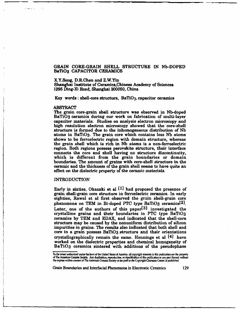
GRAIN CORE-GRAIN SHELL STRUCTURE IN Nb-DOPEDBaTiO3 CAPACITOR CERAMICS
X.Y.Song, D.LChen and Z.W.YinShanghai Institute of Ceramics,Chinese Academy of Sciences1295 Ding-Xi Road, Shanghai 200050, China
Key words: shell-core structure, BaTiO3 , capacitor ceramics
ABSTRACTThe grain core-grain shell structure was observed in Nb-dopedBaTiO3 ceramics during our work on fabrication of multi-layercapacitor materials. Studies on analysis electron microscopy andhigh resolution electron microscopy showed that the core-shellstructure is formed due to the inhomogeneous distribution of Nbatoms in BaTiO3. The grain core which contains less Nb atomsshows to be ferroelectric region with domain structure, whereasthe grain shell which is rich in Nb atoms is a non-ferroelectricregion. Both regions possess perovskite structure, their interfaceconnects the core and shell having no structure discontinuity,which is different from the grain boundaries or domainboundaries. The amount of grains with core-shell structure in theceramic and the thickness of the grain shell seems to have quite aneffect on the dielectric property of the ceramic materials.
INTRODUCTION
Early in sixties, Okazaki et al [1] had proposed the presence ofgrain shell-grain core structure in ferroelectric ceramics. In earlyeighties, Rawal et al first observed the grain shell-grain corephenomena on TEM in Bi-doped PTC type BaTiO3 ceramics[ 2].Later, one of the authors of this paper[3 ] investigated thecrystalline grains and their boundaries in PTC type BaTiO3ceramics by TEM and EDAX, and indicated that the shell-corestructure may be caused by the nonuniform distribution of siliconimpurities in grains. The results also indicated that both shell andcore in a grain possess BaTiO3 structure and their orientationscrystallographically remain the same. Hennings et al (41 haveworked on the dielectric properties and chemical homogeneity ofBaTiO3 ceramics sintered with additions of the pseudophase
To the extent authoized under the laws of the United States of America. all c.."gt interests in this publication are the propertyof The Anerican Ceramic Society. Anyduplication, repductio, or republication of this bi n or any part theeo, withotthe earess written consent of The Aei Ceramic Soieteor fee paid to the Copyrgt = Ce0nt, prohbited.
Grain Boundaries and Interfacial Phenomena in Electronic Ceramics 129

I F " -
"CdBi2Nb2O9" for materials showing the "X7R" dielectrictemperature characteristic. The results showed that theirmicrostructures exhibit the grain core-grain shell structure, andthe chemical inhomogeneity emerges during a process of reactiveliquid-phase sintering. The solution and precipitation process wasassumed as the formation mechanism of chemicallyinhomogeneous perovskites and the core-shell structure of grains.In recent years, during our work on fabrication of multi-layercapacitor materials, the grain core-grain shell structure was alsoobserved in Nb-doped BaTiO3 ceramics. In present paper, thecharacteristics of the grain core- grain shell structure of capacitortype BaTiO3 ceramics were studied by using AEM and HREM. Theeffect of shell-core structure on the dielectric properties of thecapacitor ceramics was also studied and discussed.
EXPERIMENT
The high-purity, fine grain BaTiO3 base material was prepared bydecomposition of barium oxaltitanate. Its grain size is smallerthan 0.5 grm. A specific amounts of Nb205, CoO and sinteringaid were added and conventional electronic ceramic fabricatingtechnology was used to make the multi-layer capacitor ceramics[51. Doping of Nb and Co plays the role respectively as donor andacceptor, which is of advantage to increase the insulatingresistance and decrease the dissipation factor tan8 of thematerials.Ceramic samples were cut to small disks of 3mm in diameter and25gm in thickness. Then they were thinned by an Argon ion beamtill a hole formed in the center. The fringe thickness of the holewas about several hundreds angstroms, which was suitable forelectron microscope observation. For all the observations a JEM-200CX AEM and HERM was used.
EXPERIMENTAL RESULTS AND DISCUSSION
Lots of electron microscope observations showed that the grain sizeof BaTiO3 ceramic samples prepared by above method is about 1limand certain amount of grains possess shell-core structure. TheTEM bright-field image and dark-field image of a typical shell-corestructure grain are shown in Fig.1.
130 Grain Boundaries and Interfacial Phenomena in Electronic Ceramics
p
Fig.1. TEM photomicrographs showing grain shell-graincore structure in BaTiO3 ceramics
(a) TEM bright-field image. c shows grain core,s grain shell.
(b) TEM dark-field image. The right part is the resultof corresponding selective electron diffractionpattern.
1. Characteristics of shell-core structure and their compositions
The shell-core structure of BaTiO3 grains in fact are composed oftwo different forms: the ferroelectric grain core with domainstructure and non-ferroelectric grain shell. The experimentalresults showed that the core and shell in BaTiO3 grains belong tosame crystalline structure, namely ABO3 perovskite structure.Their interface connects the core and shell and has no structurediscontinuity, which is different from the grain boundaries ordomain boundaries. The ferroelectric domain characterizing thegrain core is a tetragonal ferroelectric phase, whereas the non-ferroelectric grain shell is a paraelectric phase.The EDAX results on TEM indicate that the occurance of shell-curestructure in BaTiO3 grains is as a result of inhomogeneousdistribution of Nb doping as shown in Fig.2.
Grain Boundaries and Interfacial Phenomena in Electronic Ceramics 131

I j!, I I, !
S.. .. . .. , 1 . '- J . ..
Nb I'i Cu Cu 1'b Nb Nb |i C" CU Pb NIb
(a) Grain core region (b) Grain shell region
Fig.2. EDAX results of the grain in BaTiO3 ceramics(a) Grain core region(b) Grain shell region
The Ba peaks are coincided with the Ti peaksThe Cu peaks due to the Cu specimen grid
From Fig.2a , it shows the grain core is an almost pure BaTiO3phase, whereas from Fig.2b, it shows the grain shell is a Nb-richBa(TixNbl-x)03 phase. During sintering of the ceramics, the Nbions diffuse from the grain boundaries to the interior of the grains,however, the diffusion rate of Nb5 + ions in BaTiO3 grains is verylow [6], this would be the main reason of forming the shell-corestructure. The Curie temperature of pure BaTiO3 is about 120 Oc,therefore at room temperature it possesses tetragonal ferroelectricphase with domain structure. However, after incorporation ofdifferent amount of Nb5 + ions into the BaTiO3 lattice, their Curietemperatures will be drastically lowered accordingly [4]. In view ofNb 5 + ions to be concentrated at the grain shell, which makes theCurie temperature of the grain shell region below roomtemperature and possesses paraelectric phase at roomtemperature. This means that in Nb-doped BaTiO3 ceramics,thereappears a Ba(TixNb1-Y)03-BaTiO3 two-component compositesystem, where X represents different amount of Nb content andgives different Tc of thc new phase. Modification of the Nb contentin BaTiO3 will give different dielectric properties of the ceramicmaterials, which will be presented in the next section.
2. Effect of shell-core structure on property of the ceramicmaterials
Fig.3. shows the temperature dependence of capacitance of two Nb-doped BaTiO3 ceramic samples. The amount of Nb-doping in SX-2
132 Grain Boundaries and Interfacial Phenomena in Electronic Ceramics

sample is about 0.5 mol.%; whereas in SX-3 sample, more thantwice of this amount of Nb was doped. From Fig.3. it can be seenthat the temperature dependence of capacitance of SX-3 samplewith higher Nb content is better than that of SX-2 sample. TEMobservations also show that there are more shell-core structuregrains in SX-3 sample than in SX-2 sample. In the mean time,along with the flattening of the capacitance-temperature curve, theshell thickness of the shell-core grain becomes thicker.
CL 3000- SX-2 t.-23oo
., 2000- SX-3 1500
1000
-50 0 20 40 60 80 100 120Tenmperature ("C)
Fig.3. Temperature dependence of capacitance of twoNb-doped BaTiO3 ceramic samples
SX-2 sample: lower Nb contentSX-3 sample: higher Nb content
According to Lichtenecher [7], the dielectric constant k of theshell-core structure ceramics should follow the following formula
logk = V1 log kj + V2 logk2where V1, V2 and ki and k2 are respectively the volume fractionand dielectric constant of the shell and core. So, in BaTiO3ceramics, containing more the shell-core structure grains andthicker the shell thickness will increase the volume fraction of theparaelectric phase which results in decrease of the total amount ofthe spontaneous polarization vector in the material and leads todecrease the dielectric constant , This would be the reason whythe SX-3 sample has lower , value.Besides, Nb5 + ions in BaTiO3 will replace Ti4+ to form solidsolution. Though this replacement will not change the structureform of the original BaTiO3, however it will more or less distort thecrystalline lattice which will lead to shift the Curie peak to lower
Grain Boundaries and Interfacial Phenomena in Electronic L.,ramics 133
temperature and give effect on the dielectric property of the
ceramic material. Owing to that the volume fraction of shell-corestructure for different BaTiO3 grain is different, which will giverise to diffuse the Curie point to a broad temperature range, as aresult, to flatten the dielectric constant peak of the material.
CONCLUSION
1. In BaTiO3 capacitor ceramics, a certain amount of Nb dopingwill form grains with shell-core structure. The grain corecontains almost pure BaTiO3 ferroelectric phase with domainstructure, whereas the grain shell is composed of paraelectricBa(TixNbl-x)03 phase with higher Nb content.2. Both shell and core regions possess perovskite structure, theirinterface connects the core and shell having no structurediscontinuity, which is different from the grain boundaries ordomain boundaries.3. The amount of grains with shell-core structure in the ceramicand the thickness of the grain shell will play important role on thedielectric constant , and capacitance-temperature characteristicsof the capacitor ceramic materials.
REFERENCES
1. K.Okazaki and S.Kashiwabara, J.Jpn.Ceram.Soc 73(834):60,19652. B.S.Rawal and M.Kahn, Advances in Ceramics, Vol.1Columbus, Ohio, Am.Cer.Soc. Inc. 172, 19813. X.Y.Song, S.L.Wen and Y.Yao " AEM Study of PTC BaTiO3Ceramics" Jour. Chinese Cer. Soc. 17(1) p.59, 1989 in Chinese4. D.Hennings and Rosenstein " Temperature-stable DielectricsBased on Chemically Inhomogeneous BaTiO3" Jour. Amer. Cer.Soc. 67(4), P.249, 1984
5. D.R.Chen, M.G.Zhu and X.Y.Song "Sr-T Stability Principle ofNb205 and CoO Doped BaTiO3-Base Dielectric Ceramics"Electronic Devices and Materials 10(1), p.38, 199 1, in Chinese.6. W.R.Buessen "Effects of Grain Growth on the Distribution of Nbin BaTiO3 Ceramics" Jour. Amer. Cer. Soc. 54 (9), p.458, 19717. D.K.Lichtenecher, Physikal 2, 27, p.115. 1926
134 Grain Boundaries and Interfacial Phenomena in Electronic Ceramics

THE V-SHAPE CHARACTERISTICS OF (PBO.6SRO.4)TO3CERAMICS
T.D. Tsai-, C.T. Hu+ and I.N. Lin*+Dep. Mater. Sci. and eng. and Mater. Sci. CenterNational Tsing-Hua Univ. Taiwan R.O.C.
ABSTRACT(Pbl.,ar,)TiO3 ceramics which possess the
marvelous V-shape PTCR characteristics have beensuccessfully synthesized. The concentration of donorsneed to optimise the minimum resistivity (pi,) isaround 1.0 mol% y3+. The electrical properties ofthese materials vary systematically with the ratio ofPb/ar. The Curie temperature increases and theresistivity jump decreases markedly, while theresistivity drop varies insignificantly, with theincrease of Pb/Sr ratio. The behavior is similar forsamples sintered either at 12200C, 12406C or 12600Cfor I hr.
I. INTRODUCTION
The positive temperature coefficient ofresistivity (PTCR) of semiconducting barium titanatespecimen above the ferroelectric Curie temperature(Tj) was well known since 19551"2l. Much research hassince then been conducted on understanding theconduction mechanisms 13,41 and on developing variousapplications of these materials' t61. The ceramics inthe (Sr,Ba)TiO3 and (Pb,Ba)TiO3 series have been mostthoroughly developed with the Curie temperature inthe range -300C - 360°C1 .61 .
All of those PTCR ceramics possess a lowresistivity which is almost constant temperaturecoefficient of resistivity below T,. Recently,
To the extent autoized under the laws of the United Stats of America, all co t interests in this publication are the propertyof The American Ceramic Sociey. Ay duplication, reproduction, or republication of this publication or any part thereof, withoutthe express written consent of The Ameican Cermic Society or fee paid to the Copyright Clearance Center, is prohibited.
Grain Boundaries and Interfacial Phenomena in Electronic Ceramics 135

another PTCR materials with the behavior distinctlydifferent from the conventional p-T properties hasbeen discovered, that is, (Pb-,.Sr 1)TiO3 PTCRceramics"-'. They exhibit large negative temperaturecoefficient of resistivity (NTCR) below T, besidesthe ordinary PTCR characteristics above Curietemperature. It is called the V-shaped PTCR ceramics.
The synthesis of these materials is still verydifficult due to the lack of availability ofcomprehensive processing datum on (Pbl-,Sr,)TiO3 PTCRceramics. A systematic study on the synthesis of the(Pbl-,Sr,)TiO3 ceramics is, therefore, necessary. Thisresearch is aimed to investigate the effects of someprocessing parameters such as the concentration ofdonors and the ratio of Pb/Sr etc., on thedevelopment of both microstructure and electricalproperties of the (PbSrl-,)TiO3 PTCR ceramics.
II. 3XPERIKENTAL PROCEDURE
One of the problems encountered in theconventional method used for mixing the oxidepowders, such as ball milling, is the difficulty inhomogeneously dispersing a small amount ofsemiconductive dopants into the main constituents.For the purpose of improving uniformity in theincorporation of additives, the liquid form of donor,Y(NO3) 3"5H 20, was used. Significant improvements onthe microstructure and PTCR properties of the samplesare expected.
High purity PbO, TiO2, SrCO3 and 5 mole% Si02oxide powders were used as main constituents andsintering aid, respectively. The nominal compositionof the samples was (PbSr1_)Ti.0303 with x=0.5, 0.6 or0.7. The oxide powders were firstly wet mixed withdeionized water, in a plastic jar using plastic-coated iron balls, for 18 hrs. The solutioncontaining y3+ ions (derived from Y(N0 3) 3-5H 20), wasthen added into the pre-milled slurry, andmechanically stirred for 30 minutes. Drops of ammoniawere then added into the slurry to gradually adjustthe pH value to homogeneously precipitate out the y3+ions in the form of Y(OH) 3 until the pH value of theslurry was higher than 10. The completeness ofprecipitation was ensured by keeping the content ofy3+ ions in the as-filtrated solution below the
136 Grain Boundaries and Interfacial Phenomena in Electronic Ceramics

detecting sensitivity of the ICP-AES analyzer.The mixed powders derived from filtrated slurry
were dried with IR lamp, sieved through a 60 meshsieve and then calcined at 10500C for 1 hr in air.Green pellets of 10 mm diameter were formed buniaxial pressing with pressure either of 200 kg/cmor 400 kg/cm2 and then sintered at the temperaturevaried in the range from 1220-C to 1260 0 C for either0.5 hr or 1 hr, with the 300oC/hr heating and coolingrates in the stagnant air.
The phase constituents of the calcined powdersand the sintered specimens were analyzed using X-raydiffraction technique (Rigaku). The microstructuresof polished surfaces of specimens were examined usinga scanning electron microscope (SEM). The averagegrain size was estimated by the linear intersectionmethod. Electrodes were applied on both surfaces ofthe specimens by rubbing In-Ga alloy to achieve agood ohmic contact. DC resistivity was measured usingHP3457A multimeter in the temperature range from roomtemperature to 500 0 C.
III. RESULTS
Yttrium ions (y3+) ions were adapted in ourstudy as the semiconducting additives. In order tostudy the effect of donor concentration on thesemiconductivity of (Pb 06Sr 04)TiO3 materials, seriesof samples containing 5.0 mol% SiO2 and y3+ ionsconcentrations either of 0.5, 0.8, 1.0, 1.2 or 1.5mol% were prepared. They were pelletized with the 200kgcm2 pressure and then sintered at 1220 0 C for lhr.The p-T characteristics of these samples were shownin Fig.1 to indicate that the incorporation more than0.8 mol% of y3+ ions could efficiently convert thematerials into semiconductive and resulted inmarvelous PTCR properties. The samples which containy3+ ions less than 0.5 mol%, on the other hand,always exhibited high resistivity and no PTCRcharacteristics at all. The samples containing 0.8mol% y3+ possessed the most steep resistivity jumpabove T,, while those containing 1 mol% y3+ exhibitedthe lowest resistivity. Increasing the donorconcentration beyond the 1 mol% y3+ linearlyincreased the room temperature resistivity butmaintaining the Pl/Ri, ratio about the same order.
Grain Boundaries and Interfacial Phenomena in Electronic Ceramics 137

The corresponding microstructures indicated thatsimilar microstructures were obtained in samplescontaining 0.5, 0.8 or 1.0 mol% y3÷. The grain sizeslightly decreased when the y3÷ content was more than1.0 mol%, which was probably caused by the mechanismthat some of the excess y3÷ ions stayed at grainboundaries acting as the grain growth inhibitors(1 01 *.
The effect of Pb/Sr ratio in (Pb,.Sr,)TiO3: 1mole% y3+ materials on their electrical propertieswas then examined. The p-T characteristics of samplescontaining 5 mol% SiO2 and with Pb/Sr ratio equals to5/5, 6/4 and 7/3, which were labeled as L-50S, M-50Sand H-50S, respectively, were shown in Fig.2. Thosesamples were pressed with 400 kgci 2 pressure and thensintered at 12600C for 0.5hr with 3000C/hr coolingrate. The Curie temperature increased but theelectrical resistivity decreased as the Pb content in(Pb1,SrJ)TiO3 materials increased. Besides, the table1 indicated that the amount of Si02 content added inthese samples showed no effect on shifting T,temperature.
The resistivity jump, which is PTC=ip.-pi.1,decreased markedly but the resistivity drop, which isNTC=Ipi-p,I, varied insignificantly with Pb/Sr ratio(dotted line, Fig.3a). The positive and negativetemperature coefficient of resistivity (PTCR andNTCR), which was defined as
PTCR (NTCR) = log PT-g J , T=T,±2 0 °CT - Te
varied with the Pb/Sr ratio of the samples in asimilar manner as resistivity jump (PTC) andresistivity drop (NTC), respectively, as indicated bydotted lines in Fig.3b. The phenomena that theresistivity jump (PTC) and PTCR properties of thesesamples were lowered as Pb content increased, but theresistivity drop (NTC) and NTCR behavior wereinfluenced insignificantly by Pb/Sr ratio are thesame for the samples sintered at 1220 0 C or 12400C(Fig.3). Similar results have been reported for(SrBa)TiO3 and (PbBa)TiO3 PTCR ceramics1 I.
The X-ray diffraction patterns for the sinteredsamples with various Pb/Sr ratios (5/5, 6/4 and 7/3)were shown in Fig.4 to reveal that the materials wereof pure tetragonal perovskite phase and thetetragonality of the materials, i.e. the c/a ratio,
138 Grain Boundaries and Interfacial Phenomena in Electronic Ceramics
Licreased with the Pb content (Table I).Table I Curie Temperature and Lattice Parameters of
(PbxSr,.1 )TiO3 Materials
Pb/Sr Ratio Curie Temperature Lattice Parameters•C) T CO ao c/a
5/5 135.4 0 C 137.90C 3.954 3.910 1.0116/4 207.70C 203.80C 3.975 3.910 1.0177/3 262.20C 264.7 0 C 4.005 3.910 1.024
(1) SiO 2 = 2.5 molt; (2) SiO2 = 5.0 molt
IV. DISCUSSIONS
The behavior of (Pb 1 xSrj)TiO3 materials dopedwith donors (Y3+) is very different from that ofconventional PTCR ceramics, such as (Srj. 1Ba1)TiO3,BaTiO3 and (Pb 1.Ba,)Ti0 3 materials. The proportion ofdonor ions needed to convert the (Pb,-,Sr,) TiO3materials semiconducting is significantly larger thanthat for other series of PTCR ceramics, which isusually 0.3 moi% donors. No semiconducting propertiesare obtained when as much as 0.5 mol% Y¥f-ions havebeen added, even though the grain growth has alreadyoccurred. There are several possibility which couldprohibit the 0.5 mol% Y3+-doped materials fromsemiconducting: (1) the Y3+-ions have not yet beenincorporated into the (PbSr)Ti0 3 lattice; (2) largeproportion of y3+ ions were dissolved into the liquidphase so that not enough y3+ were incorporated intothe lattice; (3) the introducing of cationicvacancies such that the carriers provided by the y3+_ions are compensated; and (4) the Y3+ ionssimultaneously occupying the A-sites and B-sites of(Pb 1.-Sr,)Ti03 lattice and acting both as the donorsand acceptors.
Among the 4 possibilities, the last one seems tobe the most probable cause and the arguments are asfollows: The large granular structure shown in Fig.2arules out the first two possibilities, since thegrain boundaries will be pinned if the Y3+-ions are19.10,12-141
residing at grain boudaries ' • -. Moreover, sincethe optimum proportion of dopants is still only 1mol% y3+ even when as much as 10 mol% SiO2 are
Grain Boundaries and Interfacial Phenomena in Electronic Ceramics 139

included in (Pb1.,SrJ)TiO 3 materials as liquid phasesintering aids, the dissolving of ¥3+ ions in liquidphase is concluded to be not significant. The thirdpossibility is also not likely to occur to 0.5 mol%y34-doped materials, since cationic vacancies will beinduced only when the proportion of donors is so highthat electronic charge is highly imbalanced1t 5" 1.
The simultaneous generation of the donors andacceptors, on the other hand, is possible, since they34 ions with the size (0.893 A) can fit both A-sites(-1.20 A) and B-sites (0.68 A) lattices reasonablywell. The solubility of y 34 in B-site lattice is,however, expected to be much lower than that in A-site lattice due to the fact that larger strain willbe involved when Y3+ ions substituting B-sitecations. Further increase in the amount of y3+ ionswill thus only increase the A-site substitutionaldefects such that the materials become n-typesemiconducting. Similar phenomenon has been observedon BaTiO3 ceramics simultaneously doped with both theMg2+-ions and the Nbo+-ions""'1 , in which more than 0.3mol% Nb5 + ions are needed to convert the materialsinto semiconducting at the presence of Mg2+-ions. Itis concluded, therefore, that the y34 ions added intothe (Pb 1.,SrJ)TiO3 materials will initially occupy boththe A-site and B-site lattices such that theelectrons supplied by the donors are compensated. Thematerials are thus still possessing high resistivitywhen only small amount of y3+ are incorporated. They3+ ions will act as donors only when A-sitesubstitutions is significantly surpassing the B-sitesubstitutions.
V. CONCLUSION
The semiconductive (Pbl.-Sr,)TiO3 ceramics withlarge PTCR (>4 order) and significant NTCR (>2 order)characteristics have been successfully fabricated.The effects on microstructure and electricalproperties of some processing parameters areconcluded as follow:(1) (Pb 1_,SrJ)TiO3 ceramics could be converted intosemiconductive
by doping 1.0 mol% y+3 ions.(2) The Curie point could be shifted by adjustingthe Pb/Sr ratio.
140 Grain Boundaries and Interfacial Phenomena in Electronic Ceramics

IV. RUI3RUNCU
1. O.Saburi, J. Phys. Soc. Japan, 14(9], pp.1159-1174 (1959)
2. O.Saburi, J. Am. Ceram. Soc., 44[2], pp.54-63(1961)
3. W. Heywang, Solid-State Electronics, Vol.3,pp.51-58 (1961)
4. G.H.Jonker, Solid-State Electronics, Vol.7,pp.895-903 (1964)
5. E.Andrich, Electr. Appl., 26[3], pp.123-144(1965/66)
6. M.Kuwabara et.al., J. Am. Ceram. Soc., 66(11],pp.c214-c215 (1983)
7. Y.Hamata et.al., J. Electronics Jpn. (5], pp.33-35 (1988)
8. Y.Hamata et.al., Japanese pat.63-280401, Nov.17(1988)
9. H.F.Cheng, J. Appl. Phys., 66(3], pp.1382-1387(1989)
10. M.Drofenik et.al., Ceram. Bull., 63[5], pp.702-704 (1984)
11. H.F.Cheng et.al., J. Am. Ceram. Soc., 76[4],pp.827-832 (1993)
12. T.F.Lin et.al., J. Am. Ceram. Soc., 73[3],pp.531-536 (1990)
13. J.S.Choi et.al., J. Mat.Sci., Vol.27, pp.1285-1290 (1992)
14. W.Y.Howng et.al., Am. Ceram. Soc. Bull., 62[2],pp.231-233 (1983)
15. J.Daniels et.al., Philips Res. Repts, Vol.31pp.489-559 (1976)
16. J.Daniels et.al., Philips Tech. Rev., 38[3],pp.73-82 (1978/79)
17. B.S. Chiou, G.M. Gou, J. Mater. Sci., (1988)
Grain Boundaries and Interfacial Phenomena in Electronic Ceramics 141
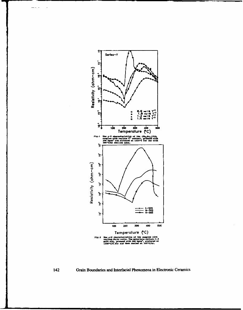
0SerIes-Y
E
U.°
Er.C "o
cc
0
e.8 ,,eiu 3*1.Semgmreasy-dS .2 tools Y*,3
.2. main y3
g .6 Din Y3
160 260 360 41 5NeTemperature tC)Fig. 1 TMe p4 ohacrateriatoas at the (Fb"8w.4Ti0,
eape ith warless T" cantont, press with00ko'and wintered at 1220tC for 1hM with
00*€Cir cool•.• feta..
E
E,L-
0o
--.-- L-SOS
-b- H-50S
10o 200 300 400 S00
Temperature (C)F7g.2 th p-T o-ractoristioe of the maples with
various b/Sr ratio. Tae aeriale contain S.0wi.5015si preess" with 200 k~ch'. wintered at12600C/O.Sblr and then Cooled at 300C/hhr.
142 Grain Boundaries and Interfacial Phenomena in Electronic Ceramics

(a) 6 s Isn SbO
0 PT 4 6. •, • 400 2h0ps_ j 24 /lh"
FTCR"No"
J.,
V5/5 64 773
do (b) (e So ivCt3
o M *n I4000 kgehC•+ /ho
00
PTCo 40 pkjan +1d
S• 't,01
NTCR .
CL-
I- *53A 6 04 7/3
Pb/Sr RatioFig. 3 variations of (a) the resistivity jum (P) and resistivity
"dc (Q) end (b) the texpereture coefficient of resistivity(Grai eod PIdr) with the Pb/Sr ratio.
ktrtgo" WWi k pmmdr.ansud-
M-6UP~d.-64 331 .3M 1.017
w40SMr,-/1 &9t 4.006 1.024
C I
2-ThetaFit. 4 1:. X3-r:r diSatiea Area te eM sstee .0
Grain Boundaries and Interfacial Phenomena in Electronic Ceramics 143

EFFECT OF BN ADDITION ON THE SINTERING AND ELECTRICALPROPERTIES OF Y-DOPED BaTiOs CERAMICS
Seh-Jin PARK, Joon-Hyung LEE and Sang-Hee CHO
Department of Inorganic Materials Engineering
Kyungpook National University, Taegu 702-701, Korea
ABSTRACTIn this study, the effect of BN addition on the sintering and electrical
properties of Y-doped BaTiO3 ceramics were examined. When BN is added toY-doped BaTiOs, BN decomposed to B203 liquid phase and N2 gas through BNoxidation. The B203-rich liquid phase lowered the starting temperature ofdensification below 10001C. Room temperature resistivity of Y-doped BaTiO3with addition of BN was decreased and the Curie temperature shifted to higher.These phenomena seem to result from the solid solution of B to Y-dopedBaTiO3.(Key Word) : BaTiO3, PTCR effect, BN, Curie temperature.
I. INTRODUCTIONBaTiO3 ceramics is one of the most widely used material as electroceramic
components such as dielectrics, capacitors and PTCR devices.1) Especially,when BaTiO3 is properly doped with La203 or Y203, it exhibits PTCR (PositiveTemperature Coefficient of Resistivity) anomaly near the Curie point, 2 -4) and itis used for a variety of purposes, including TV degaussers, temperature sensors,flow sensors, liquid-level sensors, and current-limiting applications. 5 -7 )
It is well known that the PTCR effect is greatly affected by the chemicaland physical properties of grain boundaries and microstructure of the sinteredbody,11-14) and this effect has long been established that BaTiO3 PTCRphenomena is a grain boundary resistive effect.'-10) The evidence comes from
numerous studies donor-doped single crystal, AC impedance method andcathodoluminescence technique.s. 10)
Besides, for the sintering of BaTiO3 system, relatively high temperature
To the extent authorized under the laws of the United States of America, al copyright interests in this publication are the propertyof The American Ceramic Society. Any duplication, reproduction, or republication of this publication or any part thereof, withoutthe express written consent of The American Ceramic Society or fee paid to the Copyright Clearance Center, is prohibited.
Grain Boundaries and Interfacial Phenomena in Electronic Ceramics 145

above 1350"C is needed. Therefore the low temperature sintering is highlyrecommended for financial standpoint. Small amount of impurity such as excess
TiO2, SiOz and A1203 are usually added to BaTiOs system for low temperaturesintering.5, 1 e) These kinds of impurities not only lower sintering temperaturebut also help the system acquire homogeneous microstructure, and improvereproducibility leading to positive property control.
In this study, effect of BN addition on the evolution of microstructure,
defect concentration of grain boundary, sintering and electrical properties ofY-doped BaTiO3 was studied. BN may help the sintering of Y-doped BaTiO3
by forming a liquid phase with oxidation, and act as a lubricant in the forming
process. 17 )
1. EXPERIMENTAL
Specimens were prepared by general ceramic forming process using reagentgrade chemicals, BaCOs, TiO2, BN and Y203. The weighed powders with
composition of (Bao.gg6Y0.004)TiOs were mixed together with ZrO2 balls in
ethyl alcohol for 28 hours, calcined at 1150"C in air for I hour. BN was added
to the mixture with different amounts(O--3.2 mol%) and ball-milled again for
several hours. The mixture was formed into a pellet by hydrostatic pressingwith a pressure of 98MPa. The pellet was sintered in air at 13501C for 1 hour
and cooled down in the furnace with cooling rate of 50C/h.Lattice parameter of the sintered specimen was measured by powder X-ray
diffraction patterns using CuKau radiation. The lattice parameters obtained from
these patterns were refined by the Cohen's method on an IBM computer.Sintering behavior was observed by a dilatometer with the same procedure ofsintering runs ; the samples were heated at 5"C/min. from room temperature to
1350"C and held at this temperature for 1 hour. Sintered densities weremeasured to 0001g. cm-3 using the Archimedes method with water as the
immersion medium. Al electrode was screened on both sides of sintered
samples. The DC resistivity versus temperature characteristics of the samples
were measured up to 250"C using two-probe method.
I. RESULTS AND DISCUSSIONFig.1 shows the variation of forming density with addition of BN. The
forming density increased greatly as BN was added up to 0.8 mol%, and thenslightly increased above 0.8 mol% of BN. It is well known that BN powder has
lubrication ability during forming process due to its hexagonal plate-like-shape
146 Grain Boundaries and Interfacial Phenomena in Electronic Ceramics
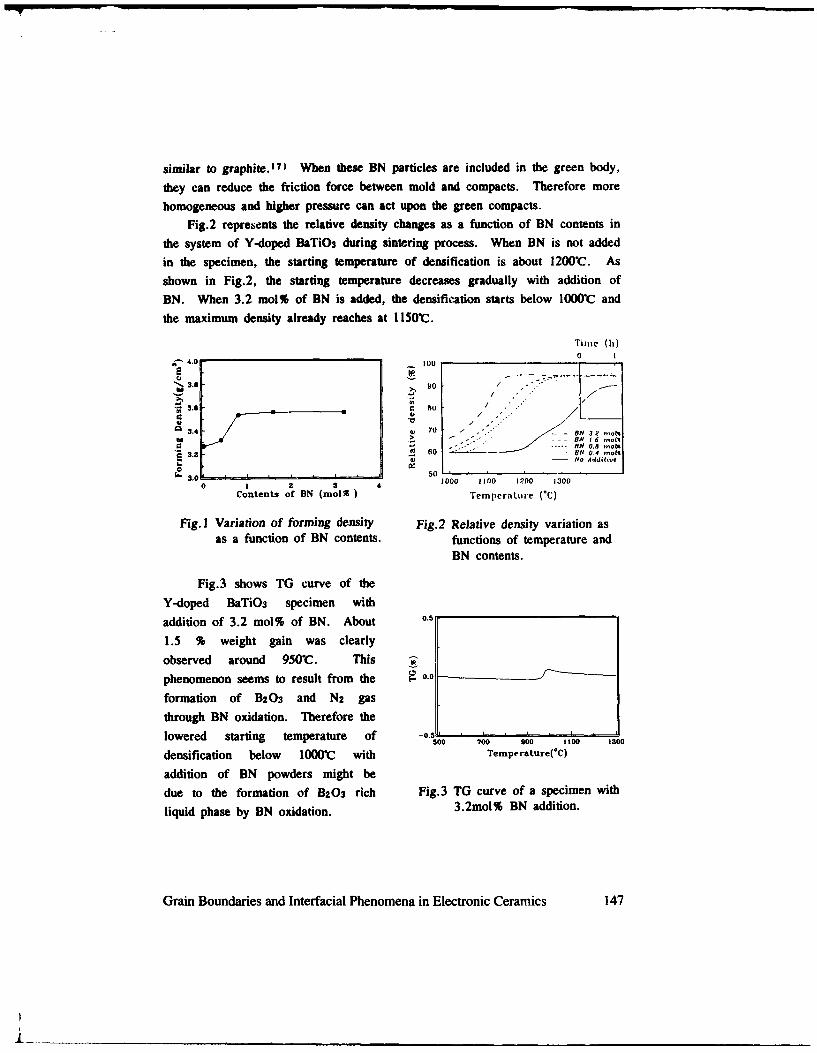
similar to graphite. 7M When these BN particles are included in the green body,
they can reduce the friction force between mold and compacts. Therefore more
homogeneous and higher pressure can act upon the green compacts.
Fig.2 represents the relative density changes as a function of BN contents in
the system of Y-doped BaTiOs during sintering process. When BN is not added
in the specimen, the starting temperature of densification is about 12001C. As
shown in Fig.2, the starting temperature decreases gradually with addition of
BN. When 3.2 mol% of BN is added, the densification starts below 10001C and
the maximum density already reaches at 11501C.
Tiine (h)0 1
3.6 - 90
U- a,/7.o
4 .) C: On
3.4 ON 70 . - - N 32 ",ot8- ' 1 -t 6 ,o
3. 1so 0. 4 x~f"" 3.2 5• 600 . ..- - ON 0.4 ,a olO
( - X o AddIt.S0 _____________0___,_,_,___,_,
0 1 2 3 lOGO ))o 1200 1300
Contents of BN (mo)1 ) Temperature (C)
Fig. I Variation of forming density Fig.2 Relative density variation asas a function of BN contents. functions of temperature and
BN contents.
Fig.3 shows TG curve of the
Y-doped BaTiO3 specimen with
addition of 3.2 mol% of BN. About
1.5 % weight gain was clearly
observed around 950"C. This
phenomenon seems to result from the E- 0.0
formation of BzO3 and N2 gas
through BN oxidation. Therefore the
lowered starting temperature of -50 0 .. . 130000 700 900 !11O00 10
densification below 1000C with Temperature(C)
addition of BN powders might be
due to the formation of B203 rich Fig.3 TG curve of a specimen with
liquid phase by BN oxidation. 3.2mol% BN addition.
Grain Boundaries and Interfacial Phenomena in Electronic Ceramics 147

Fig.4 a)SEM and b)its SCI photographs of 3.2 mol% BN added sample.
Fig.4 shows (a) SEM photography and (b) Sample Current Imagephotography using EPMA of sintered sample of 3.2 mol% BN addition,respectively. Since dark parts signify the existence of light atomic weight
material in Fig.4(b), it is quite possible that it includes B or/and 0 which haslight atomic weight among composing atoms. But the analysis shows the even
distribution of 0 atom in the sample. Therefore dark parts along the grain
boundaries are believed as the liquid phase composed of B-Ba-Ti-Y-O with large
amount of B.Fig.5 shows the variation of grain size of sintered samples as a function of
BN contents. As BN increases, grain size decreases. When small amount ofliquid phase forms due to the little addition of BN, grain growth rate increases.
25
98
95 I-i.
15 -
92.10 -
S. 89 •
0 ' 2 3 4 8 C'Contents of BN (mnol%) 0 1 2 3
Contents of BN (molV)
Fig.5 Variation of grain size as a Fig.6 Sintered density variation as afunction of BN contents. function of BN contents.
148 Grain Boundaries and Interfacial Phenomena in Electronic Ceramics

It is believed that pore pinning effect was eliminated by accelerated
densification. But when BN content increased, grain growth rate decreased due
to the enlargement of diffusion length by increased amount of liquid phase.
Fig.6 shows the sintered density of Y-doped BaTiOs as a function of BN
contents. As BN increases, the sintered density decreases. It is thought that
pores are formed by N2 gas formation during sintering.
Fig.7 represents the changes of room temperature resistivity of Y-doped
BaTiO3 with addition of BN component. As BN increases to 0.4 mol%, the
resistivity decreases drastically, and beyond that it decreases gradually. In thissystem, solid phase of Y-doped BaTiO3 and liquid phase of B203 rich
B-Ba-Ti-Y-O coexist. Generally, the resistivity of liquid phase, of which the
major component is B2O3, is very high. Therefore the liquid phase of
B-Ba-Ti-Y-O does not seem to contribute to the formation of conduction channel
when room temperature resistivity reduces. It seems that small amount of B
solute into the perovskite Y-doped BaTiO3.18) B as donors might lower room
temperature resistivity.
Fig.8 shows lattice constant measured by XRD. Lattice constant does not
vary to great extent although the BN contents vary. It seems that the change oflattice constant has not been observed when B÷3 ions occupy interstitial sitesbecause their ionic radii are too small(O.27A) to be detected by XRD.
10 3
V.4.60
4034.20
.to • L 4.0 0 --P - ------ --
,)3.80
, 3.60
10 03.2340 ~ 200 1 2 3 4 Contents of BN (mol%
Contents of BN (mol%)
Fig.7 Room temperature resistivity Fig.8 Lattice parameter variation asvariation as a function of BN a function of BN contentscontents.
Grain Boundaries and Interfacial Phenomena in Electronic Ceramics 149

Fig.9 represents PTCR properties
as functions of temperature and BN 10
contents. As BN increases, the room 2.-..
temperature resistivity of Y-doped to'
BaTiOs drastically decreased and the E i "'"
Curie temperature shifts to higher . to
temperature. These phenomena may -
result from the solid solution of B to o 102--
Y-doped BaTiOs. - N. ,ddst-..
0 100 200 3MO
W. CONCLUSIONS Temperature ("C)
Fig.9 Temperature - ResistivityWhen BN is added to the property as a function of BN
Y-doped BaTiOs sample, densification contents.
started at lower temperature than BN
omitted. From TG analysis, weight gain was observed around 9501C. This may
seem to result from the formation of B203-rich liquid phase and N2 gas through
BN oxidation. Judging from increase of Curie temperature and the decrease of
room temperature resistivity B may play role in donors by solution into Y-doped
BaTiO3.
REFERENCES
1. B.Jaffe, W.R.Cook Jr and H.Jaffe, Piezoelectric Ceramics, (Academic
Press Inc., 1971), pp.5 3 .
2. S.Ikegami and I.Ueda, "Semiconductive Single Crystal of BaTiO3 Reduced in
Hydrogen Atmosphere," J.Phys.Soc.Jpn., 1912], 159-166 (1964)
3. E.J.W.Verwey, P.W.Haaijman, F.C.Romeijn, and G.W.Van Oosterhout,
"Controlled Valency Semiconductors," Philips Res.Rep.,5[61, 173-187 (1950)
4. O.Saburi, "Properties of Semiconductive Barium Titanates," J.Phys.Soc.Jpn.,
1419], 1157-1174(1959)
5. E.Andrich,"Properties and Applications of PTC Thermistors," Electron.Appl.,
26[21 123-44 (1965/66)
150 Grain Boundaries and Interfacial Phenomena in Electronic Ceramics

6. E.Andrich,"PTC Thermistors as Self-Regulating Heating Elements," PhilipsTech.Rev., 30,170-77(1969)
7. H.Loebl and R.Rossgotterer,'Degaussing Circuits with PTC Resistors,"
Siemens Rev., 38[111] 520-23(1971)8. P.Gerthsen and B.Hoffman, "Current-Voltage Characteristics and Capacitance
of Single Grain Boundaries in Semiconducting BaTiOs Ceramics," Solid StateElectron., 16, 617-622(1973)
9. N.Nemoto and J.Oda, "Direct Examinations of PTC Action of Single GrainBoundaries in Semiconducting BaTiOs Ceramics," J.Am.Ceram.Soc., 6317-81,393-401 (1980)
10. H.jhrig and M.Kierk,"Visualization of the Grain Boundary Potential Barriersof PTC-Type BaTiO3 Ceramics by Cathodoluminescence in an Electron-Prove Microanalyzer," Appl.Phys.Lett.,35141307-309(1979)
11. M.F.Yan and A.H.Heuer, Additives and Interfaces in Electronic Ceramics,Advances in Ceramics Vol.7 (The American Ceramic Society, Inc., 1983),
pp.128-136.12. M.Kuwabara, Additives and Interfaces in Electronic Ceramics,
Advances in Ceramics Vol.7 (The American Ceramic Society, Inc., 1983),pp. 137-145.
13. M.Kuwabara, "Effect of Microstructure on the PTCR Effect inSemiconducting Barium Titanate Ceramics" J.Am.Ceram.Soc.,64[l1] 639-644
(1981)14. M.Kuwabara, "Influence of Stoichiometry on the PTCR Effect in Porous
Barium Titanate Ceramics," Comm.Am.Ceram.Soc., C-170-171 December
(1981)15. H.lhrig,"The Posotive Temperature Coefficient Resistivity of BaTiO3
Ceramics as a Function of the Amount of Titanium-Rich Second Phase,"Phys.Stat.Sol.(a)47, 437(1978)
16. Y.Matsuo, M.Fujimura, H.Sasaki, K.Nagase and S.Hayakawa,"Semiconducting BaTiOs With addition of Al2O3, SiO2, and TiO2," Ceram.Bull., 47[3] 292-297(1968)
17. Modern Ceramic Engineering 2nd edition, ed. by D.W.Richerson p 428
18. L.M.Castelliz and R.J.Routil,"The Effect of Boric Oxide on the Propertiesof Barium Titanate Based Ceramics," I.Canadian Ceram.Soc., 38, 69-74(1969)
Grain Boundaries and Interfacial Phenomena in Electronic Ceramics 151

EFFECTS OF GRAIN BOUNDARY STRUCTURE ON THERESISTIVITY PHENOMENON IN DOPED BaTiO 3
R.C. Buchanan, R.D. Roseman and J. Kim, Department of Materials Scienceand Engineering, University of Cincinnati, Cincinnati, OH 45221-0012
ABSTRACT
Polycrystalline, ferroelectric barium titanate (BaTiO 3) can be made highlyconducting through donor doping in low concentrations. The resistivitybehavior is dominated by the nature of the grain boundary lattice and domainstructure. In this investigation, the factors relating the observed resistivity tothe ferroelectric domain and grain boundary structure was achieved bycharacterization techniques using TEM, SEM and HREM. It was found thatstructural homogeneity and domain configuration near and across grainboundaries dominate the observed electrical behavior,
INTRODUCTION
BaTiO3 has an intrinsically high resistivity (1010 f.cm) whenprepared in an oxidizing atmosphere. Through controlled doping of the A-site perovskite lattice, for example using y3+ or La3+(< 0.3 mol %), n-typepolaron conduction can be obtained, generating resistivities <102 0-cm [I-
3]. An important aspect is the observed resistivity differences betweensamples under various heat treatment conditions. At temperatures below theferroelectric phase transformation (Tc), non-annealed samples exhibit asignificantly lower resistivity than samples which have been annealed(typically 10000- 1220*C for 30min-10hr) or slow cooled from the sinteringtemperature [4,5]. These differences have generally been attributed to: 1)Oxygen adsorption along the grain boundaries and diffusion into the graininterior, altering the defect structure [3,6,7]; 2) Time dependent gradient inacceptor barium and titanium vacancy diffusion processes [8-11]; 3) Acombination of these theories in which the vacancies are initially presentwithin a grain boundary space-charge layer and are activated when
To the extent authorized under the laws of the United States of America, all copyright interests in this publication are the propertyof The American Ceramic Society. Any duplication, reproduction, or republication of this publication or any part thereof, withoutthe express written consent of The American Ceramic Society or fee paid to the Copyright Clearance Center, is prohibited.
Grain Boundaries and Interfacial Phenomena in Electronic Ceramics 153

compensating defects in the grain boundary are neutralized by oxidation(12]; and, 4) The grain boundary potentials are a result of a shift fromelectronic to vacancy compensation induced by donor segregation, resultingin electron trap sites [ 13].
Factors which are generally left out of interpretations as to theconduction process between grains are [16]: 1) The lattice and domainstructural relationships between and internally within each grain; 2) Theactual mode of conduction and necessary elements involved in n-typepolaron conduction; and, 3) Generated internal stresses, derived from grain-to-grain structural constraints, modifying and creating potential barriersstructurally.
In polycrystalline samples the exact domain patterns and the state ofthe .,rriers themselves are complex [16,17]. In this study, directobservations of these type conducting ceramics by SEM and TEM have beenperformed in order to answer questions concerning alignment of theferroelectric domain and lattice structure at grain boundaries and theirrelationship to the conduction process.
EXPERIMENTAL
Donor-doped BaTiQ 3 samples were prepared by ball-milling highpurity BaTiO3 (Ba/Ti = 0.997) powders with trivalent dopant additions(La2O3, Y20 3 < 0.3 mol %) added as a nitrate solution. Milling was carriedout using ZrO2 balls in a solution of isopropyl alcohol / deionized water withfish oil added as a dispersant and a PVA - Carbowax solution added as abinder / lubricant. The dispersed slurry was spray-dried and the powderuniaxially pressed into discs. The heat treatment consisted of a nitrate,binder burnoff at 550°C / 30 min followed by sintering at 1350'C / 2h in airand either: a) cooled at 20°C / min, or b) slow cooled at 5°C / min with anadditional annealing step of 1220*C / 6h.
Resistance measurements were made on polished discs with Alevaporated electrodes, using a constant voltage source at 0.01 volts, in serieswith the sample and picoscale ammeter, between 250 and 2500C at 5oC /min. Foils for TEM analysis were prepared by mechanical grinding andpolishing of the samples to a thickness of 40- 90 pm and ion milling toperforation.
154 Grain Boundaries and Interfacial Phenomena in Electronic Ceramics

RESULTS AND DISCUSSION
In this study, all samples were processed under identical conditions,except for varying heat treatments. The bulk microstructures developed ineach case have similar average grain sizes of -25 gm, with an averagedensity of -93 % theoretical. Therefore, the bulk microstructures were notaffected by annealing and any variance in electrical properties are grain sizeindependent.
Figure 1 shows annealing effects on the minimum resistivity in lightlydonor doped BaTiO3. As seen, there is a linear increase in resistivity withtime at the anneal temperature of 12200C, independent of dopant type. Foran anneal treatment of 6 hrs, there is a I order of magnitude difference inresistivity. These effects are significant when designing sensors, such asPTCR, from these ceramics, as there is a trade off between maximum signalresponse (abrupt change in resistance near Tc) and accompanying lowestattainable resistivity. An abrupt and large resisitivity difference at Tcincreases with increasing time at anneal [4,5,16].
The polished and etched SEM micrographs of Figure 2 compare anunmodified BaTiO3 and a doped (0.24 mol % Y20 3) BaTiO 3 sample. Theunmodified sample (Figure 2A) shows the random domain alignment typicalof BaTiO 3. The n-type conducting, donor doped sample (Figure 2B) showsthe development of a domain structure that is uni-directional throughouteach individual grain. This type structure was also independent of heattreatment and occurred in every grain, but, the alignment of the c-axis fromgrain-to-grain was typically random. Therefore, the directionality of thedomain alignment between grains varied, resulting in orientational mismatchat adjoining grain boundaries.
The TEM image of Figure 3 shows a typical grain boundary in the Y-doped non-annealed samples. Domain widths (-0.8 gim) from the interior tothe grain boundaries are uniform and straight, no splitting or randomalignments are found up to the grain boundary. Across a grain boundary thedomains often meet and continue with only an angle change and align over alarge distance. The TEM image of Figure 4 shows a more complex grainboundary in the Y-doped annealed system. Regions of fine domain widths(-0.08 gim) in the near boundary regions are seen to coexist with regions inwhich no domains are found along with areas in which the domain structurecontinues unobstructed from the grain interior up to the grain boundary.Fine domain patterns can encompass areas as wide as 2 gim and extend intothe grain interior 1- 2 lim, before transforming into the coarse domainstructure. In these materials a variety of grain boundary situations are
Grain Boundaries and Interfacial Phenomena in Electronic Ceramics 155
encountered as all three type regions are randomly distributed along the
grain boundaries.Annealing or slow cooling from the sintering temperature allows for
cation diffusion and for rapid oxygen adsorption to occur. Acceptor anddonor states have been found to segregate to the grain boundaries, alongwith excess concentrations of dopants [12,13]. Diffusion and segregationeffects are considered to be the driving force for formation of the fine andno-domain regions. The more complex grain boundary structures of theannealed systems must also relate to the observed electrical behaviordifferences compared to the non-annealed, uniform domain structures.
Figure 5 shows HREM images of the immediate grain boundaries inthese systems, comparing boundary regions in which domains exist on bothsides (Figure 5A), and a boundary region between an area of no-domainacross from a domain region (Figure 5B). The grain boundary of Figure SAshows high coherency between grains and must be considered to be of a verylow potential barrier and is suggestive of an easy electron pathway. In theseboundaries (domain-to-domain) it is also important to note that nosegregated regions or large concentrations of defects are seen. Figure 5Bshows a more highly defective and incoherent grain boundary. Theseregions clearly show a regularly spaced defect in which the periodicity of thebarium and titanium atoms are disrupted along the grain boundary. Theincoherent boundaries reflect a greater potential barrier to electron flow.
The mode to electronic conduct;,an is considered to be along the uni-directional domain pathways, giving a channeling effect to the electronmobility. Where the interior coarse domain structure extends the length ofthe grains up to the grain boundaries, an electron pathway is generated fromgrain-to-grain whenever the alignment is advantageous. In the non-annealedmaterials, preferentially oriented, coherent boundaries with a minimumpotential barrier to electron flow are wide in extent, relating to the lowestresistivity materials. Higher resistivities found in the annealed systems are inpart due to the expected low electron mobility through the no-domainregions and corresponding incoherent grain boundaries. Electron transportacross grain boundaries is greatly inhibited for domain to no-domain regionsand for areas in which no domain regions are common to the boundary.Therefore, the concentration of areas in which electron flow is highlyprobable (i.e., preferential domain-to-domain alignment) is significantlyaffected by heat treatment. Annealing greatly reduces this grain boundaryconcentration, and must be a function of time at anneal.
156 Grain Boundaries and Interfacial Phenomena in Electronic Ceramics

CONCLUSIONS
The resistivity of these n-type conducting materials is closely relatedto the specific properties of grain boundaries and near boundary regions, inwhich the properties are different from the bulk. An important aspect of theuni-directional domain structure is the effect that it has on the grainboundary structure. Each grain is comprised of various potential barriers, ofwhich only certain preferentially aligned grain boundaries allow easyconduction across. A percolation of the conducting electrons along themutually interacting uni-directional domain pathways creates the lowresistivities. An important consideration is that not all boundaries areconducting, and limiting the concentration of conducting grain boundaryregions by annealing increases the resistivity below Tc.
REFERENCES
1. W. Heywang, "Semiconducting Barium Titanate," J. Mat. Sci., Vol. 6,pg. 1241-1226 (1971).2. B. Kulwicki, "PTC Materials Technology, 1955-1980," Grain BoundaryPhenomena in Electronic Ceramics, ed., L. Levinson, Advances in Ceramics,Vol. 1, pg. 138-154 (1981).3. G. H. Jonker, "Some Aspects of Semiconducting Barium Titanate," SolidState Electronics, Vol. 7, pg. 895-903 (1964).4. H. M. AI-Allak, G. J. Russell and J. Woods, "The Effect of Annealing onthe Characteristics of Semiconducting BaTiO3 Positive TemperatureCoefficient of Resistance Devices,"d. Phys., D. (London), Appl. Phys., Vol.20, No. 12, pp. 1645-51 (1987).5. R.D. Roseman, "Influence of Yttria and Zirconia on the PositiveTemperature Coefficient of Resistance in Barium Titanate Ceramics," M.S.Thesis, University of Illinois (1992).6. W. Heywang, "Resistivity Anomaly in Doped Barium Titanate," SolidState Electron, Vol. 3, pg 51 (1961).7. R. W. Newnham, "Structure-Property Relations in Electronic Ceramics,"J. Mat. Ed., Vol. 6, No. 5, pg. 806-839 (1984).8. J. Daniels and R. Wernicke, "Part V. New Aspects Of An Improved PTCModel," Phillips Research Reports, Vol. 31, pg. 544-559 (1976).9. G. V. Lewis and C. R. A. Catlow, "The PTCR Effect in BaTiO 3," Br.Ceram. Proc., Vol. 36, pg. 187-199 (1985).10. G. V. Lewis and C. R. A. Catlow, "Defect Studies of Doped andUndoped Barium Titanate Using Computer Simulation Techniques," J. Phys.Chem. Solids, Vol. 47, No. 1, pg 89-97 (1986).
Grain Boundaries and Interfacial Phenomena in Electronic Ceramics 157

11. H. M. Chan, M. P. Harmer and D. M. Smyth, "Compensating Defect inHighly Donor-Doped BaTiO3,* J. Am. Ceram. Soc., Vol. 69, No. 6, pg.507-510 (1986).12. Y. Chiang and T. Takagi, Grain-Boundary Chemistry of BariumTitanate and Strontium Titanate: 1, High Temperature Equilibrium SpaceCharge," J. Am. Cera. So., Vol. 73, No. 11, pg. 3278-3285 (1990).13. S. B. Desu and D. A. Payne, "Interfacial Segregation in Perovskites: Ill,Microstructure and Electrical Properties," J. Am. Ceram. Soc., Vol. 73, No.11, pg. 3407-3415 (1990).14. B. M. Kuiwicki and A. J. Purdes, "Diffusion Potentials in BaTiO3 andthe Theory of PTC Materials," Ferroectrics, Vol 1, No. 4, pg 253-263(1970).15. W. T. Peria, W. R. Bratschun and R. D. Fenity, "Possible Explanation ofPositive Temperature Coefficient in Resistivity of SemiconductingFerroelectrics," J. Am. Ceram. Soc., Vol. 44, No. 5, pg. 249-250 (1961).16. R.D. Roseman, "Domain And Grain Boundary Structural Effects OnThe Resistivity Behavior In Donor Doped, PTCR Barium Titanate," Ph.D.Thesis, University of Illinois (1993).17. H. B. Haanstra and H. Mhrig, "Transmission Electron Microscopy atGrain Boundaries of PTC-Type BaTiO3 Ceramics," J. Am. Ceram. Soc.,Vol. 63, No. 5-6, pg. 288-291 (1980).
13 0.12 Y
I' Sutr Temp:
10 Coolingl Rte:
a 0 24 I a
Ti.. (n) at Anndea (122rC)
Figure 1. Resistivity below Ti as a function of time at anneal (12200C), and
as a function of dopant type and concentration (mol %).
158 Grain Boundaries and Interfacial Phenomena in Electronic Ceramics
Figure 2. Polished and etched SEM micrographs comparing the domainstructures of. A) unmodified BaTiO3 and B) donor doped BaTiO3.
Figure 3. TEM image of non-annealed, donor doped BaTiO 3, showing uni-directional don ain structure extending from the grain interior up to the grainboundary.
Grain Boundaries and Interfacial Phenomena in Electronic Ceramics 159

~N1ER"
Figure 4. TEM image of annealed donor doped sample. A complex grainboundary structure in which a finer domain width along with regions of no-domain structure are found.
Figure 5. HREM images of the grain boundary, showing regions in which:(A) the domain structure is common to the boundary; and, (B) an area of no-domain across from a domain region.
160 Grain Boundaries and Interfacial Phenomena in Electronic Ceramics

MICROSTRUCTURAL AND COMPOSITIONAL ANAL YSES ONGRAIN BOUNDARY OF LOW- TEMPERATURE SINTERED
Pb(Zr,Ti)O3 CERAMICS
Dunzhuo Dong,' Kenji Murakami, 2 Nagaya Okada,2 and Shoji Kaneko3
'Graduate School of Electronic Science and Technology, 2 Research Institute ofElectronics, and 3 Department of Materials Science and Technology,
Shizuoka University, 3-5-1 Johoku, Hamamatsu 432, Japan
Abstract
The addition of the complex oxides, BiFeO3 and Ba(CuasWo.5)O , lowered thesintering temperature and improved the electricalproperties of O. 5wt% MnO2-addedPb(Zra53Ti a 7)0 3. The characterization of the ceramic bodies using DTA, XRD,SEM, TEM and EPMA suggests an existence of transient liquid phase in theceramics and this phase may play an important role for lowering the sinteringtemperature.
INTRODUCTION
Lowering the sintering temperature of Pb(Zr, Ti)O, ceramics has been attemptedto avoid the volatilization of PbO component which causes the compositionalfluctuation and the environmental contamination. Many researchers have reportedthe low temperature sintering of this ceramics by using the different methods suchas the adoptions of additives to form liquid phase"7) and to enhance solid statesintering,' 9) and fine grained powders as starting material'103) or the hot-pressingsintering'4). Smith et al. "5) have shown that the BiFeO3-Pb(Zr, Ti)0 3 system washot-pressed at a temperature between 750"C and 900"C. It has been also reportedthat another perovskite-type, Ba(Cu0Wo5)O3, was used to reduce the sinteringtemperature ef Pb(Fe0 sNb,5)O3 ceramics as well as to improve the dielectricproperties.'
6 )The authors have attempted a combined use of two additives, BiFeOa (abbreviatedas BF) and Ba(CuosW0 )O3(BCW), in 0.5wt% MnO 2-added Pb(Zr0.53Ti047)O3(PZT)ceramics and succeeded to lower its sintering temperature down to 935 C.17. 18)
To the extent authorized under the laws of the United States of America, all copyright interests in this publication are the propertyof The American Ceramic Society. Any duplication, reproduction, or republication of this publication or any part thereof, withoutthe express written consent of The American ceramic Society or fee paid to the Copyright Clearance Center, is prohibited.
Grain Boundaries and Interfacial Phenomena in Electronic Ceramics 161
Furthermore, the low-temperature sintered ceramics showed no deterioration ofthe dielectric and piezoelectric properties, and the addition of extra CuO resultedin the improvement of the piezoelectric properties.In this paper, the effects of two additives such as BF and BCW on the sinteringtemperature are discussed. The dielectric and piezoelectric properties of the PZTceramics, and the results of the microstructural and compositional analyses on thePZT ceramics are also described.
EXPERIMENTAL
Sample Preparation
The samples were prepared by using a conventional method of ceramic engineering.The commercially available Pb304, ZrO2, TiO 2,BaCO 3, CuO, W0 3, Bi 20 3, Fe 203and MnO2 (>99.0% purity) were used, and PZT and BCW were separatelysynthesized by heating the corresponding sources at 8700C for 2h followed bypulverizing. All PZT, BCW, Bi20 3, Fe 203 and CuO were weighed according tothe formula: (1-x-y)PZT-xBF-yBCW, and then mixed. Disk samples with 10 mmin diameter and 3 mm in thickness were formed at the pressure of 800 kg/cm 2 andsintered isothermally at a temperature between 870"C and 1250'C (a heating rateof 5"C/min) for 30 min. Electrical contacts were made with a silver paste. Thesilver coating was made on both sides of the sample and subseco, -itly fired at780"C for 20 min.
Measurement
The dielectric and piezoelectric properties of samples were measured after beingpolarized under 3-4 kV/mm bias at 120°C in a silicone oil bath for 15 min. Theelectromechanical characteristics were calculated from the resonancemeasurements,19) and the dielectric properties were examined by a LCR low-frequency bridge (1kHz). The bulk density, p (g/cm'), was measured by theArchimedes method using the following equation:
p = W1 / (W 2 -W 3 )where W,, W2 and W3 are the weights of the dry sample, of the same samplesaturated with water and of the same sample suspended in water, respectively.
Characterization
ARigaku RAD-B X-ray diffractometer (XRD) and a Shimadzu DT-30B differentialthermal analyzer (DTA) were used to determine the phase relations of sintered
162 Grain Boundaries and Interfacial Phenomena in Electronic Ceramics
1I
body. The morphology and the composition of the ceramics were analyzed by aJEOL JSM-T330A scanning electron microscope (SEM) and a Shimadzu EPMA-8705 electron probe microanalyzer (EPMA), respectively. The microstructurewas observed by a JEOL JEM-2000FX II transmission electron microscope (TEM).
RESULTS
The Effect of BiFeO 3 and Ba(Cu0.SW05)0 3 Addition
In order to determine the sintering temp-rature and time of the PZT ceramics, thebulk density of 0.90PZT-0.05BF-0.05BCW ceramics was measured as a functionof the sintering time (10-80 min) at different temperatures (880-940°C). Theresults indicate that the bulk density increases with the sintering time. A saturationeffect was observed after 30 min at each temperature, while the saturated valuereached maximum above 9350C. Thus, the optimum sintering temperature andtime were determined to be 9350C and 30 min, respectively. The sintering timewas fixed on 30 min throughout the present experiment.Firstly, the amount of BCW was fixed on 5 mol% as reported in the case ofPb(Fe05Nb05)03 ceramics.") The sintering temperature and electrical propertiesof the ceramics were measured as a function of the amount of BF added and theoptimum amount of BF was determined based on the minimum dissipation factor,tan 6, and maximum values of piezoelectric properties. Secondly, the amount ofBF was fixed on the above optimum amount. The amount of BCW was determinedin thesame way. As a result of this preparation procedure, the optimum compositionof the PZT ceramics with complex oxide additives was obtained to be 0.92PZT-0.05BF-0.03BCW (abbreviated as PZT-C) and the sintering temperature waslowered down to 9350 C. Finally, the effect of extra CuO addition was investigatedbecause the reaction of CuO in the synthesis of BCW was limited. The piezoelectricproperties were very sensitive to a small amount of CuO added, while the dielectricproperties were not changed. The results gave the PZT-C with 0.08 wt% CuO
Table I. Summary of the electrical properties of various PZT ceramics.
Sample Sintering ET3 31C0 tan 6 Tc Kp Q6 d33 Density
temp., time (%) (OC) (%) (X10"1 2C/N) (g/cm 3 )
PZT 1250°C, 30min 910 1.2 362 51.7 314 210 7.59
PZT-C 9350C, 30 min 847 1.1 290 41.0 670 201 7.65
PZT-C' 935°C, 30 min 850 1.0 290 47.0 950 236 7.66
Grain Boundaries and Interfacial Phenomena in Electronic Ceramics 163
(PZT-C'). Table I compares the sintering temperature and the electrical propertiesamong PZT, PZT-C and PZT-C' ceramics, where J3 3E0 is relative dielectricconstant, T, Curie point, K. electromechanical coupling factor, Q. mechanicalquality factor and d33 piezoelectric constant.
Characterization
The XRD pattern of PZT-C' ceramics corresponds completely to that ofPb(Zr0.52Ti048)O3 solid solution,20) as shown in Figure 1. Additional phasesoriginating from BF21 ), BCW2) or CuO23) were not observed. This observation isconsistent with the PZT-C ceramics. Figure 2 shows the SEM micrographs of thePZT and PZT-C' ceramics. The micrographs give clear images of grains in thesintered bodies. The PZT-C' ceramics is composed of dense grains with 2 gin to5 tLm in diameter. Surprisingly, the grain size of the PZT-C' is larger than that ofthe PZT ceramics in spite of the sintering temperature which is lowered to 935"Cfrom 1250"C.
0
0 PZT
'n"
C
0 0 0 j__oo
I I I I
10 20 30 40 50 60 70 80
2 e (deg.,Cu K.)
Figure 1 XRD pattern of PZT-C' ceramics.
The elemental analysis of the ceramics dsing EPMA indicated that no segregationof any element had occurred. Each element seems to distribute homogeneouslywithin a resolution of this method.Grain boundaries of the PZT-C' ceramics was observed by TEM and its micrographsare shown in Figure 3. The micrographs indicate again the 'dense grains. Moredetailed observation (Figure 3 (b)) suggests an existence of the isolatedmicrostructures at the grain boundaries. Furthermore, the qualitative analysis ofthe composition around the grain boundaries reveals that the lead ion becomes
164 Grain Boundaries and Interfacial Phenomena in Electronic Ceramics
(a) (b)
Figure 2 SEM micrographs of (a) PZT and (b) PZT-C' ceramics.
(a) (b)
Figure 3 TEM micrographs of PZT-C' ceramics. The grains are clearly imagedin (a) and the detailed microstructure of grain boundaries are shown in (b).
Grain Boundaries and Inm.facial Phenomena in Electronic Ceramics 165
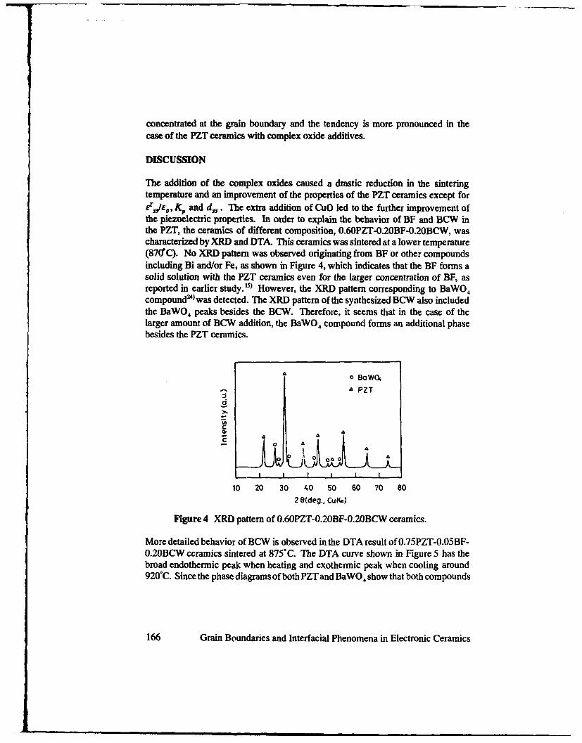
concentrated at the grain boundary and the tendency is more pronounced in the
case of the PZT ceramics with complex oxide additives.
DISCUSSION
The addition of the complex oxides caused a drastic reduction in the sinteringtemperature and an improvement of the properties of the PZT ceramics except forEr4•/s, K. and d3,. The extra addition of CuO led to the further improvement ofthe piezoelectric properties. In order to explain the behavior of BF and BCW inthe PZT, the ceramics of different composition, 0.60PZT-0.20BF-0.20BCW, wascharacterized by XRD and DTA. This ceramics was sintered at a lower temperature(87ffC). No XRD pattern was observed originating from BF or other compoundsincluding Bi and/or Fe, as shown in Figure 4, which indicates that the BF forms asolid solution with the PZT ceramics even for the larger concentration of BF, asreported in earlier study. ) However, the XRD pattern corresponding to BaWO 4compound') was detected. The XRD pattern of the synthesized BCW also includedthe BaWO4 peaks besides the BCW. Therefore, it seems that in the case of thelarger amount of BCW addition, the BaWO4 compound forms an additional phasebesides the PZT ceramics.
0 BaWO,
A PZT
R
C
A A
AA
0 ~ 0 0 A 0 AA
I I l I I I
10 20 30 40 50 60 70 80
2 e(deg., CuK&)
Figure 4 XRD pattern of 0.60PZT-0.20BF-0.20BCW ceramics.
More detailed behavior of BCW is observed in the DTA result of O.75PZT-0.05BF-0.20BCW ceramics sintered at 875°C. The DTA curve shown in Figure 5 has thebroad endothermic peak when heating and exothermic peak when cooling around920°C. Since the phase diagrams of both PZT and BaWO4 show that both compounds
166 Grain Boundaries and Interfacial Phenomena in Electronic Ceramics

V cooling
0W
AT
Q -
heatingC
500 700 900 1100
Temperature (OC)
Figure 5 DTA curves of powdered 0.75PZT-0.05BF-0.2GlBCW ceramics.
are thermally stable at a temperature between 500"C and 1200"C, this resultsuggests an existence of a different phase, besides the PZT, in the ceramics. Itcan be deduced that the PZT-C ceramics of the optimum amount of BF and BCWincludes the different phase besides the PZT, and that the phase forms the transientphase around 920"C. From the TEM observation, it is also suggested that thedifferent phase is formed at the grain boundaries and includes more lead ions thanthe grain which is enhanced by the addition of the complex oxides. Thus, thedifferent phase can become the transient liquid phase which may also promote thesolidification of the grains even at the lower sintering temperature resulting in thelarger grain size, as shown in Figure 2. Therefore, the sintering temperature ofthe PZT ceramics with the complex oxide is lowered mainly due to the existenceof this transient liquid phase.
CONCLUSION
The sintering temperature of the PZT ceramics is successfully lowered by theaddition of the complex oxides, BF and BCW, without the deterioration of electricalproperties. The XRD and DTA studies indicate that the reduction in this temperaturecan be related to the existence of the transient liquid phase. The microstructuraland compositional analyses reveal that the lead ion becomes concentrated at thegrain boundaries and the concentration is enhanced by the addition of the complexoxides. Therefore, the transient phase is formed at the grain boundaries andincludes more lead ions than the grains, which may also explain the larger grainsize at the lower sintering temperature.
Grain Boundaries and Interfacial Phenomena in Electronic Ceramics 167

Acknowledgments
The authors wish to thank the Hamamatsu Industrial Research Institute and theShimadzu Analytical Center for the EPMA measurements. The JEOL is alsogratefully acknowledged for the sample preparation of TEM.
References
1) D.E. Wittmer and R.C. Buchanan, J. Am. Ceram. Soc., 64,485-490 (1981).2) S. Takahashi, Jpn. J. AppI. Phys., 19, 771-772 (1980).3) S.Y. Cheng, S.L. Fu, C.C. Wei and G.M. Ke, J. Mater. Sci., 21,571-576 (1986).4) S.Y. Cheng, S.L. Fu and C.C. Wei, Ceram. Int'l, 13,223-231 (1987).5) Z. Gui, L. Li, S. Gao and X. Zhang, J. Am. Ceram. Soc., 72,486-491 (1989).6) Z. Gui, L. Li, S. Gao and X. Zhang, Ferroelectrics, 101, 93-99 (1990).7) L. Li, X. Zhang and J. Chai, Ferroelectrics, 101, 101-108 (1990).8) R.B. Atkin, R.L. Holman and R.M. Fulrath, J. Am. Ceram. Soc., 54, 113-115 (1971).9) P.G. Lecuta, F. Constantinescu and D. Brab, J. Am. Ceram. Soc., 68, 533-537 (1985).
10) G. Tomandl, A. Stiegelschmitt and R. Bihner, "Science of Ceramics", Vol. 14,305-308, Ed. by D. Tayler, The Institute of Ceramics, Stoke-on-Trent (1988).
11) J.F.F. Lozano, P. Durin and C. Moure, "Science of Ceramics", Vol. 14, 897-902, Ed.by D. Tayler, The Institute of Ceramics, Stoke-on-Trent (1988).
12) R. Ral, N.M. Gokhale, R. Krishnan and P. Ramakrishnan, J. Mater. Sci., 24, 2944-2916(1989).
13) T. Yamamoto, Am. Ceram. Soc. Bull., 71, 978-985 (1992).14) N.D. Patel and P.S. Nicholson, Am. Ceram. Soc. Bull., 65, 783-787 (1986).15) R.T. Smith, G. D. Achenbach, R. Gerson and W.J. James, J. Appl. Phys., 39,70-74(1968).16) K. Handa, T Watanabe, Y. Yamashita and M. Harata, IEEE Trans. Consum. Electron.,
CE-30, 342-347 (1984).17) D. Dong, M. Xiong, K. Murakami and S. Kaneko, Ferroelectrics, in press.18) D. Dong, K. Murakami, S. Kaneko and M. Xiong, '. Ceram. Soc. Jpn, 101,1090-1094
(1993).19) H. Jaffe, T. Kinsley, T.M. Lambert, D. Schwartz, E.A. Gerber and I.E. Fair, Proc.
IRE, 49,1161-1169 (1961).20) JCPDS File, Card No. 33-784.21) JCPDS File, Card No. 20-169.22) JCPDS File, Card No. 38-1378.23) JCPDS File, Card No. 5-0661.24) JCPDS File, Card No. 8-457.
168 Grain Boundaries and Interfacial Phenomena in E Ceramics
PARTICLE SIZE EFFECT ON THE ROOM TEMPERATURE STRUCTURE OF BARIUMTITANATE.
B.D. Begg, E.R. Vance, D.J. Cassidy, J.Nowotny and S. Blairs"ANSTO, Advanced Materials, Menai NSW 2234 Australia'UNSW, School of Materials Science and Engineering, Kensington NSW 2033 Australia
ABSTRACT
X-ray diffraction and electron microscopy indicated that BaTiO3 powders < 0.19 lim in size werefully cubic whilst those > 0.27 jim were completely tetragonal (within a 5 % detection limit forcubic material) at room temperature. The tetragonal to cubic transformation temperature wasfound to be 121 ± 30C by differential scanning calorimetry (DSC) for BaTiO 3 powders with aroom temperature (c/a) value > 1.006. No transformation could be detected using DSC for BaTiO3particles with a (c/a) ratio < 1.006 at room temperature. BaTiO3 powder with a particle size (0.19gtm) just too small to be tetragonal at room temperature remained cubic down to 80 K. It isconcluded that a model based on surface free energy, as previously discussed for the monoclinic totetragonal transformation at room temperature of fine ZrO2 particles, is consistent with theexperimental data.
INTRODUCTION
Many room temperature properties of BaTiO 3, such as permittivity and structure, are known tovary with grain size [ 1,2]. For instance the peak room temperature permittivity occurs for 0.8jim-sized grains, whilst the extent of tetragonal distortion is known to decrease with decreasingparticle size 12-4]. Opinions differ however over whether or not this is accompanied by a secondorthorhombic structure [31, and if this decrease in tetragonality leads ultimately to a completetransformation to a cubic 12,5] or "pseudocubic" structure (6] for particles below some critical size.Numerous other workers have reported the stabilisation of the cubic structure in fine grainedbarium titanate without detailing changes in tetragonality with particle size [7-13].
Two models have been proposed to describe the room temperature stabilisation of the cubicstructure in fine grained barium titanate. The first, a phenomenological surface layer model [71requires that a structural transition exists across a particle at room temperature, from an outer cubicsurface layer of a fixed thickness, to a tetragonal core, with a gradient of tetragonality existingbetween these regions. As the grain size decreases, the influence from the tetragonal core alsodiminishes, until only a stable cubic particle remains.
In the alternative pure phase model, no coexistence of the cubic and tetragonal structures or indeedany significant gradation of tetragonality occurs in any given crystal. Here, two mechanisms havebeen proposed to explain the room temperature stabilisation of the cubic structure, the first relatesto the strains imposed by the presence of lattice hydroxyl ions whilst the second concerns surfaceeffects, each will be dealt with below.
EXPERIMENTAL PROCEDURE
Two BaTiO 3 powders were examined. The first was a commercially prepared hydrothermal powderwhilst the second was hydrothermally grown in the present work to an average particle size (0.28
To the extent authorized under the laws of the United States of America, all copyright interests in this publication are the propertyof The American Ceramic Society. Any duplication, reproduction, or republication of thispublication or any part thereof, withoutthe express written consent of The American Ceramic Sorety or fee paid to the Copyright Clearance Center, is prohibited.
Grain Boundaries and Interfacial Phenomena in Electronic Ceramics 169

+ 0.05 gim). Here 0.03 moles each of a hydrolysed titanium alkoxide precursor and bariumhydroxide were added to 30 ml of demineralised/deionised water and placed inside a 71 ml unstirredpressure vessel and heated at 50C/min to a 3000C and held for 5 days. The sample was removedfrom the vessel after cooling and washed free of BaCO3 and unreacted Ba(OH)2.
Room temperature X-ray diffraction (XRD) of mainly the (002,200) and (004,400) reflections ofBaTiO3 was studied (Co Ka radiation). Low-temperature (80 K) XRD measurements of the samereflections were also performed. Certain XRD profiles were fitted using the XRAYFIT 287diffraction fitting program [14]. Particle sizes were determined with a JEOL JXA-840 scanningelectron microscope running at 15 keV. Fresh commercial hydrothermal BaTiO 3 powder was alsoexamined with a high-resolution JEOL 2000 FX transmission electron microscope run at 200keV. To obtain a representative average particle size and spread, at least 100 particles wereindividually measured with the aid of an image analysis program. Differential thermal and thermalgravimetric analysis (DTA/TGA), plus differential scanning calorimetry (DSC), were carried outon - 100 mg samples in air with a Setaram TAG-24 Thermal Analyser, using a-A120 3 as thereference material. A heating rate of 100C/min to 12000C was employed. DSC measurementswere made on commercial hydrothermal BaTiO 3 powders sintered in air at 9000C for 0.5, 3, 8, 15and 30 hours or 1200 0C for 0.5 hour. The closed nature of the DSC apparatus permitted a slowerheating rate of 50C/min to be used. Infrared emission spectra from the as-received commercial andlaboratory-grown hydrothermal BaTiO3 samples were collected at 1000C intervals between 3000Cand 7000C using a modified Digilab FTS-7 spectrometer over the range 4000 - 400 cm-t (nominalresolution of 4 cm-t).
RESULTS AND DISCUSSION
The as-received commercial hydrothermal powder (0.19 ± 0.05 jim) exhibited a symmetrical (200)XRD reflection, characteristic of a cubic structure (see figure 3 below). Sintering this commercialhydrothermal BaTiO 3 powder to larger particle sizes saw the development of an asymmetric(002,200) peak for a 0.27 ± 0.05 gim powder which indicated a slight tetragonal distortion (c/a =1.0045). As the particle size increased further (0.29 - 0.63 gtm) so too did the level of tetragonaldistortion, as seen by the increased splitting of the (002,200) tetragonal peaks.
Whilst the tetragonal distortion (c/a = 1.0045) in the 0.27 gim commercial hydrothermal BaTiO3powder may be seen in the asymmetry of the (002,200) reflections (figure 1), it would be difficulton first glance to exclude the presence of any cubic material in this powder. To determine whetheror not this 0.27 gim powder was completely tetragonal, the diffraction profile was fitted with two(002,200) tetragonal peaks (figure 1). It was assumed that the XRD powder sample was notpreferentially oriented in any manner and so the fitting parameters were constrained such that thearea of the (002) peak was half that of the (200) peak.
The excellent nature of the fit indicates that the 0.27 jim commercial hydrothermal BaTiO 3 powderwas totally tetragonal. Similarly the (202,220) reflections from the same powder were alsosuccessfully fitted in a constrained 2:1 ratio which confirmed the random orientation of the powder.
170 Grain Boundaries and Interfacial Phenomena in Electronic Ceramics

(200)
(002
52 52.3 52.6 52.9 53.2 53.5 53.8
2 theta
Figure 1. Comparison of the room temperature X-ray diffracrogram of (002,200) reflections fromcommercial hydrothermal BaTiO3 powder (c/a = 1.0045) of 0.27 prm particle size usingCo Kat radiation (solid line) with the fitted overall and deconvoluted (002,200)reflections (dotted lines) corresponding to a completely tetragonal powder. The areasof the fitted (002) and (200) peaks were constrained in a 1:2 ratio. All peaks includeKa 2 radiation.
The influence of particle size on the room temperature tetragonal distortion of barium titanate hasbeen summarised in figure 2. All commercial hydrothermal barium titanate powders sintered largerthan 0.27 gim were completely tetragonal although the extent of the tetragonal distortion variedwith particle size. Previously reported data are also shown [2-4j.
Large1.012-K Single
- ----- Crystal
1.01 . ..... .... ......
. ........ . .• . . ... i .J •...... i........... ..i ...Li ........ .. - .i .. iiii .... • - S n l
-- 0.006 Uchino et al............ A Ari :et al.
1 oo ............... ..T..--......... Present results1.003 . .... 3 ---3- S........ F ) •i••)?"° ) ) •...."...... ý ............... ..... re e tre ut
S.....• --:-i--.............. . . . ... e - ---- i i........ h i •.....1 je 6 iii . i i iii i .... i:ii
0.01 0.1 1 10
Particle Size (gim)
Figure 2. Comparison of the present room temperature tetragonality versus particle size resultsfor commercial hydrothermal barium titanate powder with those previously reported inthe literature [2-4.
Grain Boundaries and Interfacial Phenomena in Electronic Ceramics 171

The present results differ from those of Anliker et al. (4] who did not observe room temperaturestabilisation of the cubic form and from those of Arlt et al. [3] who reported the presence of theorthorhombic structure in fine-grained barium titanate. Our results however are essentiallyconsistent with those of Uchino et at. [2] who observed a similar trend of decreasing tetragonalitywith reducing particle size, with no evidence of the orthorhombic form, leading to the stabilisationof the cubic structure for particles smaller than 0.12 pim.
XRD of the (002,200) reflections from our (-0.28 jim) hydrothermally grown (titanium alkoxide-based) BaTiO3 powder showed that it was tetragonal with (c/a) = 1.0048. This result wasconsistent with the other results obtained from commercial hydrothermal BaTiO 3 powders (figure2).
The phenomenological surface layer model is now considered. The single-phase nature ofindividual commercial hydrothermal BaTiO 3 powders (whether totally cubic or completelytetragonal) appears to be in agreement with the proposed pure phase model. However if a cubicsurface layer was present, as required by the phenomenological surface layer model, the question ofits detection by XRD must be addressed. In the present work the diameter of the largest cubichydrothermal BaTiO 3 particles was 0.19 pm (see above). Thus the thickness of the proposed (71cubic surface layer would be 0.095 gim. Using a simple volume calculation (based on sphericalparticles and a cubic surface layer thickness of 0.095 jim), the proportion of cubic material in a0.6 gim BaTiO 3 powder, which the present XRD measurements indicate approaches fulltetragonality (c/a = 1.0099, figure 2), was calculated to be = 68 % cubic.
(200) (200)
I I
M (002) .' ,
52 52.3 52.6 52.9 53.2 53.5 53.8
2 theta
Figure 3. Comparison of room temperature X-ray diffractograms, (002,200) reflections, from0.61 jm commercial hydrothermal BaTiO3 powder (cda=1.0099, solid line) and (200)reflection from as-received 0. 19 pm cubic powder (dotted line) using Co Ka radiation.Both patterns have been stripped of the Ka 2 component. The greater width of thereflection for the cubic powder is due to particle size broadening.
The diffraction patterns from this 0.6 jim tetragonal powder and that of the 0.19 jim fully-cubichydrothermal material are shown in figure 3. The degeneracy of the symmetrical cubic structurecombined with its position between the split (002) and (200) tetragonal peaks should allow thecubic structure to be readily detected in the 0.6 gim powder if it were present at volume percentages>5%. Failure to observe a cubic component in samples > 0.19 jin in size indicates that the cubic
172 Grain Boundaries and Interfacial Phenomena in Electronic Ceramics

surface layer model as it stands is not a feasible explanation for room temperature stabilisation ofthe cubic structure. This however does not exclude the absolute existence of a cubic surface layer,but rather only limits its possible influence to the outer particle layers (- 5 nm). In thisconnection, it has been postulated from electrical measurements that structural reordering, inducedby changes of oxygen activity, takes place in the outermost layers of undoped BaTiO 3 115]however no effect was observed in parallel XRD measurements, so again the altered layer wouldhave to be very thin.
Possible mechanisms for the room temperature transformation are now discussed.i) Hydroxyl Ions. Room temperature stabilisation of the cubic structure in fine-grainedhydrothermally-prepared barium titanate has been attributed to lattice strains associated with partialretention of hydroxyl ions and their compensating cation vacancies [8). In the present study theconcentration of lattice hydroxyl ions was determined by FIIR and DTA/TGA. In situ FTIRmeasurements carried out on the as-received cubic commercial BaTiO3 sample between 300PC and7000C are shown in figure 4. The peak at a wavenumber of - 1400 cm-1 is characteristic ofcarbonate whilst the smaller peak at - 3500 cm-1 corresponds to hydroxyl ions. At 300DC thehydroxyl peak is set in a very broad background of hydrogen-bonded water. This broad backgroundis considerably reduced by 4000C and totally removed by 5000C. Carbonate is lost between6000C and 7000C whilst hydroxyl ions are lost between 4000C and 700CC.
Hydroxyl
CaIbonate Ions
6000C
500 1000 1500 2000 2500 3000 3500 4000
Wavenumber (cm- 1)
Figure 4. In situ FTIR analysis of the as-received commercial hydrothermal BaTi0 3 between3000C and 7000C.
To quantify these FTMR data, DTA/TGA analysis was carried out on the cubic commercialhydrothermal BaTiO 3 sample (which had subsequently been washed free of carbonate with nitricacid) to determine the weight loss between 400 and 7000C and therefore the concentration of latticehydroxyl ions. TGA analysis from this BaTiO 3 powder showed a 0.94 % weight loss between4000C and 7000C may be attributed to the loss of (1.8 %) lattice hydroxyl ions via the 20H --
H20(S) + 02- reaction.
In situ FTIR results from our (nitric acid washed) fresh tetragonal hydrothermally-prepared BaTiO3(alkoxide-based) sample indicated that it also contained a significant concentration of hydroxyl
Grain Boundaries and Interfacial Phenomena in Electronic Ceramics 173

ions, which were similarly removed from the lattice between 4000C and 7000C. TGA resultsindicated that the concentration of lattice hydroxyl ions was -2.5 %.
The ability to prepare a tetragonal hydrothermal barium titanate powder with a hydroxylconcentration exceeding that of the commercial cubic-stabilised material (2.5 % and 1.7 %respectively) indicates that hydroxyl ions and associated lattice strains (arising from compensatingcation vacancies) are not responsible for room temperature stabilisation of the cubic structure.Vivekandan and Kutty [8] had previously concluded that the stabilisation of the cubic structureresulted from the retention of lattice hydroxyl ions and their compensating cation vacancies,despite the fact that their powders remained cubic after the hydroxyl ions had been removed.
ii) Surface Effects. Surface tension is one size-related mechanism that has been proposed toexplain room temperature stabilisation of the cubic structure [2,5]. Here, internal hydrostaticpressure resulting from surface tension in a fine powder (< 0.1 gm) is thought to lower the Curiepoint to just below room temperature and thereby stabilise the cubic structure [2].
Uchino et al. [2] attempted to determine the Curie point of BaTiO3 using variable-temperatureXRD. XRD however is a difficult technique for determining the Curie point when, as in thepresent case, the tetragonal deformation below the Curie point is very small ((c/a) = 1.0025).Subjective judgments must be made to determine when slightly asymmetric peaks (angularsplitting A(20) = 0.120 for the (002,200) reflections) become sufficiently symmetrical to indicate acubic structure. This difficulty is compounded for very fine particles, notably those reputedlyexhibiting a drastic decrease in Curie point, where particle size-broadening of XRD peaks issignificant A(20) = 0.080 for the powder studied by Uchino et al. [2] and which exhibited asupposed Curie point of 750C.
In the present study, DSC measurements were made in an attempt to resolve the relationshipbetween Curie point and tetragonality (figure 5). The commercial hydrothermal BaTiO 3 powderswere sintered to different particle sizes and therefore to different room temperature tetragonalityratios (see figure 2).
Sc/a = 1.0100
c/a = 1.0094
c/a = 1.0091
cla = 1.0086
c/a = 1.0072
c/a = 1.0061
80 90 100 110 120 130 140 150
Temperature (DC)
Figure 5. DSC patterns showing transformation temperature of the tetragonal to cubictransformation in commercial hydrothermal-BaTiO3 as a function of tetragonality atroom temperature. Each trace has been offset to clarify the diagram.
174 Grain Boundaries and Interfacial Phenomena in Electronic Ceramics

These DSC results confirm that within experimental error the Curie point remains fixed at 121 ±30C for powders exhibiting a room temperature (c/a) > 1.006. Unfortunately the present DSCapparatus was not sufficiently sensitive to detect the transformation for materials with (c/,) <1.006. The drastic decrease in Curie point with reducing tetragonality reported by Uchino et al. [2]for (c/a) S 1.007 could not therefore be confirmed by this method.
Whilst the Curie point was independent of room temperature tetragonality (for powders with aroom temperature c/a > 1.006), the average enthalpy of the tetragonal to cubic transformation wasobserved to decrease with decreasing room temperature tetragonal distortion. Since all commercialhydrothermal samples with c/a > 1.0045 were completely tetragonal (figure 1), this decrease doesnot correspond to the proportion of tetragonal material in each sample. Rather it can only refer tothe energy required for the tetragonal to cubic transformation to occur, which decreases withdecreasing room temperature tetragonality. The transformation enthalpy for the powder with thelargest tetragonality ratio compared favourably with the documented value for the BaTiO3
tetragonal-cubic transformation [ 16].
A critical experiment to establish the role of surface tension in the room temperature stabilisationof the cubic structure (which Uchino et al. [2] did not carry out) was to determine whether theCurie point of cubic BaTiO3 with a particle size just too small to be tetragonal (in this case 0. 19
inm, figure 2) had been shifted to just below room temperature. Thus XRD at liquid nitrogentemperatures (80 K) was carried out on the as-received 0.19 gim commercially-prepared cubicBaTiO% powder and the material remained cubic. The Curie point for cubic BaTiO3 powder (with aparticle size just too small to be tetragonal) has not therefore merely been shifted to just belowroom temperature as proposed by the surface tension mechanism [2]; rather it has decreaseddrastically to below 80 K or it has vanished altogether.
Surface effects however have also been invoked for stabilising the tetragonal rather than themonoclinic structure at room temperature in very fine-grained zirconia by altering the relative freeenergies of the two structures [17]. The high specific surface area of very fine particles leads themto possess relatively large amounts of excess surface energy per unit volume when compared tolarge single crystals. This excess surface energy may differentially contribute to the relative freeenergies of the tetragonal and cubic structures and possibly lead to room temperature stabilisationof the cubic polymorph. The observed stabilisation of the cubic structure (for a powder _5 0.191km) and subsequent increase in tetragonal distortion with increasing particle size for commercialhydrothermal BaTiO 3 at room temperature (figure 2) may be interpreted in terms of the surfaceenergy mechanism.
CONCLUSIONS
The room temperature tetragonality of hydrothermal BaTiO 3 powders which were close to mono-sized was seen to decrease with decreasing particle size, leading to the stabilisation of the cubicstructure at room temperature for particles 0.19 uim in size and below. The single phase nature ofannealed commercial hydrothermal BaTiO3 samples irrespective of particle size indicated that thecubic-surface layer model was not appropriate. Whilst XRD is not sensitive enough to rule outthe absolute existence of a cubic-surface layer, it does limit its thickness to < 5 nm.
Hydroxyl ions do not appear to be responsible for stabilising the cubic structure. Present DSCmeasurements however indicated that the Curie point for powders with a room temperature (c/a) >1.006 remained fixed at 121± 30C. XRD of a commercial hydrothermal BaTiO3 powder just toosmall (0.19 gim) to be tetragonal at room temperature revealed that the cubic structure was stable
Grain Boundaries and Interfacial Phenomena in Electronic Ceramics 175

down to at least 80 K and had not merely been shifted to just below room temperature as proposedelsewhere [2]. Excess surface energy however provides a plausible free energy-based mechanism toexplain not only the room temperature stabilisation of the cubic structure in fine-grained BaTiO3but also the decreasing relationship between tetragonality and particle size.
ACKNOWLEDGMENTS
We wish to thank R.L. Davis for assistance with the I, -temperature X-ray diffractionexperiments, K. Finnie for the FTIR results and C.J. Ball f 'tance with XRD peak profilefitting.
REFERENCES
I. K. Kinoshita and A. Yamaji, "Grain-size effects on dielectric properties in barium titanateceramics", J. Appl. Phys., 47 [I] 371-73 (1976).
2. K. Uchino, E. Sadanaga and T. Hirose, "Dependence of he Crystal Structure on Particle Sizein Barium Titanate", J. Am. Ceram. Soc., 72 [8] 1551-58 (1989).
3. G. Arlt, D. Hennings and G. de With, "Dielectric properties of fine-grained barium titanateceramics", J. Appl. Phys., 58 [4] 1619-25 (1985).
4. M. Anliker, H.R. Brugger and W. Kanzig, "Das Verhalten von kolloidalen SeignetteelekrikaHI, Bariumtitanat BaTiO 3", H, .-. Phys. Actt., 27, 99-124 (1954).
5. K. Uchino, N. Lee, T.Toba, N. Usuki, H. Aburatani and Y. Ito, "Changes in the CrystalStructure of RF-Magnetron Sputtered BaTiO 3 Thin Films", J. Ceram. Soc. Japan, 100 [9]
1091-93 (1992).6. D. Hennings, "Barium Titanate Based Ceramic Materials for Dielectric Use", Int. J. High
Technology Ceramics, 3, 91-111 (1987).7. S. Malbe, J.C. Mutin and J.C. Niepce, "Distribution des param~tres de maille cristalline dans
des 6chantillons pulv~rulents de BaTiO3", J. Chim. Phys., 89, 825-43 (1992).8. R. Vivekanandan and T.R.N. Kutty, "Characterization of barium Titanate Fine Powders
Formed From hydrothermal Crystallization", Powder Technology 57, 181-92 (1989).9. F. Yen, C.T. Chang and Y. Chang, "Characterisation of Barium Titanyl Oxalate
Tetrahydrate", J. Am. Ceram. Soc., 73 [11] 3422-27 (1970).10. J.P. Coutures, P. Odier and C. Proust, "Barium Titanate Formation by Organic Resins
Formed with Mixed Citrate", J. Mater. Sci., 27 [7] 1849-56 (1992).11. J.M. Criado, M.J. Dianez, F. Gotor, C. Real, M. Mundi, S. Ramos and J. Del Cerro,
"Correlation between Synthesis Conditions, Coherently Diffracting Domain Size and CubicPhase Stabilisation in Barium Titanate", Ferroelectric Letters 14, 79-84 (1992).
12. S. Naka, F. Nakakita, Y. Suwa and M. Inagaki, "Change from Metastable Cubic to StableTetragonal Form of Submicron Barium Titanate", Bull. Chem. Soc. Jpn., 47 [5] 1168-71(1974).
13. G.H. Jonker and W. Noorlander, "Grain Size of Sintered Barium Titanate", pp. 255-64 inScience of Ceramics Vol 1. Edited by G.H. Stewart. Academic Press Inc., New York 1962.
14. R.W. Cheary and A. Coelho, "A fundamental parameters approach to X-ray line-profilefitting", J. Appl. Cryst., 25 [2] 109-21 (1992).
15. J. Nowotny and M. Sloma, "Surface Electrical Properties of BaTiO 3 at ElevatedTemperatures", Solid State Ionics 49, 129-133 [1991].
16. I. Barin, Thermochemical Data of Pure Substances, VCH, Weinheim, 1989.17. R.C. Garvie, "'The Occurrence of Metastable Tetragonal Zirconia as a Crystallite Size Effect",
J. Phys. Chem., 69 [4] 1238-43 (1965).
176 Grain Boundaries and Interfacial Phenomena in Electronic Ceramics

Influence on the Grain Boundary Interfacial Trap Levels in
(Bao. 6Sro.24)TiO3-based PTCR Ceramics by Oxidative Annealing
Myung Chul Kim, Soo Hyung Hur, Soon Ja Park* , Department of Materials
Science and Engineering, Kunsan National University, Kunsan 573-360,Korea,*Department of Inorgaric Materials Engineering, Seoul National
UniversitySeoul ,Korea
<ABSTRACT>
In order to investigate the grain boundary trap levels lTS(lsothermal
capacitance transient Spectroscopy) measurements were performed at the
temperature range of 25 tC and 50 tC for the slowly cooled (Bao. 76Sr 0.z4)Ti0a
based PTCR ceramics. The grain boundary resistivity was greatly increasei
by slowly oxidative cooling and the grain boundary interfacial traps .. "
-0.36, -0.43 and -0.46 eV below conduction band edge were evaluated, The
longer cooling schedule in air leaded to the deepening of trap levels and
the increase of trap populations in the grain boundary interface.
I.INTRODUCTION
BaTiO3 -based PTCR ceramics have been extensively used in the practical
applications such as thermistor and heater because of its outstanding
positive temperature coefficient of resistiity and the cause of
PTCR(Positive Temperature Coefficient of Resistivity) property has been
To the extent authorized under the laws of the United States of America, all copyright interests in this publication are the propertyof The American Ceramic Society. Any duplication, reproduction, or republication of this pulihation or any part thereof, withoutthe express written consent of The American Ceramic Society or tee paid to the Copyrnght Clearance Center, is prohibited.
Grain Boundaries and Interfacial Phenomena in Electronic Ceramics 177

inten sively investigated in the aspect of the grain boundary resistive
phenomena 13. The Heywang model, which is the most widely accepted one,
attributes this phenomena to the existence of a potential barrior arising
from the presence of a surface layer of acceptor states. This potential
barrior is due to the existence of back-to back double Schottky barriers
formed in the grain boundary interface2 and so these phenomena can be also
described by thermal emission of majority carrier model. The formation of
depletion layer at the grain boundary region is attributed to the
existence of carrior traps and the populations of traps at grain boundary
interfaces. In order to investigate the grain boundary trap levels
ICTS(Isothermal capacitance transient Spectroscopy) measurements were
performed at the temperature range of 25 1C and 50 1C for the
(Bao.7Sro.24)TiO 3-based PTCR ceramics slowly cooled down such as 30 C/hr,
201C/hr and 15 1C/hr, respectively.
2. EXPERIMENTAL PROCEDURE
Commercially available pure BaTiO3 powders* with 24 mol% SrC03**, 0.2 mol%
Sb2O3*, 0.04 mol% Mn0O , 0.2 molt Ti0 2 *, 0.2 mol% A12 03s, and 0.4molSiO" 2 **
were ball milled for 24 hrs in ethanol media by using polyethylene jar
and zirconia balls. The slurry was dried and powders were isostatically
pressed into a disk shape of 1/2 inch diameter. Sintering was performed
in a Pt boat with cover at 1320 IC for I hour in air after heating up at
600 "C/hr and then the cooling schedules were controlled at 100 1C/hr, 30
'C/hr, 20 1C/hr, 15 'C/hr and 10 IC/hr in air. The colors of sintered
ceramics were changed from black into brown according to the longer
cooling schedule. The average grain sizes were '.lS/m under optical
microscopy. The sintered pellets of 0.5mm thickness and 8mm diameter were
prepared for the measurement of R-T and ICTS spectra. As an ohmic contact
electrode material indium containing Ag paste*" was coated on both
surfaces of polished pellet. The grain boundary resistivity was evaluated
at 10 1C from Cole-Cole plot through the impedance measurement using
HP4192A impedance analyzer. Resistance - temperature curve was measured
0) HFBT-1, Fujitlitan Co., Japan *er) I e) Degussa Co., Gefnanys.) Purity 99.99 %, Aldrich Co., USA
178 Grain Boundaries and Interfacial Phenomena in Electronic Ceramics
j. , -r~=m -• m m mm m mmu m m mmm l u N m

using HP4140 picoammeter in a temperature programmable chamber.
The ICTS measurements were performed by using HP 4192A and the details
of ICTS measuring system is shown everywhere . ICTS is based on the
rapid detection of a capacitance with time after applying a pulse
injection, followed by emission or capture of electrons at the deep trap
levels. The temperature was controlled within 0.2 "C using a cryostat at
20 "C - 50 *C. Transient capacitance C(t) was measured at 1000 KHz under
zero biased state after applying -30 V DC bias during 30 seconds.
3. RESULTS AND DISCUSSION
The PTCR effects of (Bao. 7SSrO.Z4)TiOs based PTCR ceramic samples are
plotted in Fig.l. in which different cooling schedules are denoted. The
room temperature resistivity is greatly increased by the slower oxidative
cooling and as a while the resistivity jump becomes smaller. The increase
of the maximum(pin) and the minimum(p.in) resistivity resulted from
annealing treatment and the temperature(T..) at p.= was decreased. It
appears that the value of maximum resistivity is almost saturated at the
slow cooling rate(10 tC/hr) as shown in the relationship between P. and
T. of Fig.2.
12
10 0Z 100C/*GhrE 30'C/hr
V 20*C/hr
EE V 5*C/h,0 1091 C/hr
"0 a 30 C/hr °00 5 0 05 202C/hr
We mp.(Cv Te*C/h)
4o the R-0uvso i.l
000
Figure 1. R - T relationship in Figure 2. Maximum resistivity versus
(Ba-.7SSrO.24)TiO3 based PTCR ceramics temperature at the maximum resistivityfor the R-T curves of Fig.1.
Grain Boundaries and Interfacial Phenomena in Electronic Ceramics 179

According to Heywang , the resistivity obeys following equation:
p = Po exp(e~o/kT) (1)
where po is the grain resistivity, u a factor for geometrical
configuration, and k the Boltzman constant. For the Heywang model
explaining the presence of the two dimensional layer of acceptor states
at the grain boundary, the acceptors attract electrons from the bulk
resulting in a buildup of a potential barrior. This potential barrior is
described by
eN.2
(2)
8tot.Nd
where N, is the number of electrons trapped at the grain boundary. e the
electron charge, so the permittivity in free spade, to the permittivity in
the grain boundary region, and Nd the bulk charge carrier concentration.
Compared with the previously calculated PMX vs T. plots for the annealed
samples in BaTiO3 -PTCR ceramics by Al-Allak et. al,8 these (BaSr)TiO3 -
based PTCR samples show the higher acceptor concentrations and the higher
energy levels, indicative to the Mn doping effect.
1. 20.. 00:IIs- - I
S~-G C go
0 4 to is 10 25 30 IO zoo i0 40
Reol(Z) (ohm-cm) Reol(Z) (ohm-cm)
(A) (B)
180 Grain Boundaries and Interfacial Phenomena in Electronic Ceramics

32 "SW" 20C/hr 80000
I SO"~j C40004000 4-.0000
0 0000 20000 30000 40000 000 100000 1 40000
Roat(Z) (ohm-em) Reoo(Z) (ohm-cm)
(C) (D)
Figure 3. Cole-Cole plots for (BaO.76SrO.24)TiO3-based PTCR ceramics cooleddown with 100 "C/hr(A), 30 !C/hr(B), 20 "C/hr(C) and 15 "C/hr(D) in air.
The increase of room temperature resistivity with slow cooling is caused
by the increase of grain boundary resistivity as can be seen from
impedance plots of Fig.3. The grain boundary resistivity is evaluated as
24 .. cm (A) for the sample cooled down as 100 tC/hr, 4.32 KQ.cm (B) for
30 tC/hr, 45.98 k..cm (C) for 20 "C/hr and 156.43 kQ.cm (D) for 15 t
/hr.
20*C/hr 39C 15C/hr40.8 50ih
31C 42C
1 3 -0.6N 47C
340CC= 3
c, I 2 0.2
37C c.
0 0.0
-- 1 lI I 1 1 I -0.2 J l
-2 - 0 1 2 3 4 5 6 -2 0 2 4 0
LOG(Time/sec) LOG(rlme/sec)
Figure 4. Typical data S(t) ot ICTS signal analyzed from transientcapacitance data C(t) for the samples which are sintered at 1320"C for Ihour and cooled down at 20"C/hr(A) and 15 IC/hr(B) in air.
Grain Boundaries and Interfacial Phenomena in Electronic Ceramics 181

For the above all samples we could detect the existence of the grain
boundary traps which are characterized by the reverse change of transient
capacitance C(t) according to the voltage bias sign.4 Figure 4(A) and (B)
show the typical ICTS spectra S(t) for the samples which are slowly
cooled in oxidative atmosphere as 20 10/hr and 15 lC/hr. respectively. In
the temperature range of 20 1C to 50 C, the acceptor-like interface trap
levels are detected as like as can be conformed from the positive curve
of S(t). Time constant decreases with temperature increase due to the
thermally activated emission of carriers localized in trap centers and
the peak value of S(t) spectra also decreases, indicative to the decrease
of trap populations.
16
0 30*C/hr
0 20'C/hr
0.46 eV * I5*C/hi
14
N k- 03 eV
12 036eV
3.0 3.2 3.4 3.61/T(X10-
3) (1/K)
Figure 5. Arrhenius plots of ln(121) vs
1000/T for the samples cooled down at30 IC/hr, 20 "C/hr and 15 0/hr.
The Arrehnius plots of ln(rT') vs 1/T are derived from Fig.4 and the
slope of Fig.5 gives the activation energy levels of the localized trap.
The trap levels of -0.36 eV, -0.43 eV and -0.46 eV below conduction band
edge were evaluated at 25 IC - 40 IC for the samples at the cooling rate
of 30 t/hr. 20 IC/hr and 15 IC/hr, respectively. The changes of three
trap levels with cooling schedules in air show the deepening of trap
182 Grain Boundaries and Interfacial Phenomena in Electronic Ceramics
.t

levels and the increase of trap concentrations. It has been said'-' that
segregation of acceptor impurities followed by oxidation leads to the
insulating type beIavior at the grain boundary interface, that is, the
increase of grain boundary resistivity. There have been some reports
explaining the existence of acceptor segregation. Main Mn defect centers
in oxidized MnO doped BaTiO3 are known to be Mn 3 (3d3 ) and tn4"(3d4)
through the measurement of magnetic susceptability13 . Chiang et.al".
observed the segregation of acceptor Mn through STEM analysis in
Bal Nbo.0 JTi.0A4 no•..O and they said that this segregation is consistent
with the majority being of 4+ valence and a minor fraction being in a
more reduced acceptor state. Wakino et.al.14 confirmed that Mn ion in
BaTiO3 -PTCR ceramics acts as an acceptor which compensates the electron
provided by Nb through the ESR analysis. The deeper interface level
results from the severe oxidation treatment, leading to the formation of
oxidized defect centers such as Mntn'(Mn 3 ÷) or Mnri(Mn'). In relation with
the formation of 4 ep trap centers in the grain boundary, it may be said
that the competition between trap energy levels and trap populations
influences strongly the PTCR property.
4. CONCLUSION
Long annealing in air contributed to both the increase of energy levels
and the trap populations in the formation of the grain boundary
interfacial traps in (BaO. 76SrO. 2 )TiOs based PTCR ceramics. The trap levels
were evaluated as -0.36 eV, -0.43 eV and -0.46 eV below conduction band
edge for the samples cooled down as 30t/hr, 20 C/hr and 15 "C/hr in
air, respectively.
Grain Boundaries and Interfacial Phenomena in Electronic Ceramics 183

References
1. P.W. Haaijuan, R.W. Dam. and H.A.Klasens. "Method of Preparation ofSemiconducting Materials", Ger. Pat. No. 929350, June 19552. W.Heywang,*Barium Titanate as a Semiconductor with Blocking Layers".Solid-State Electronics, 3[I] 51-58(1961)3. B.Kulwicki, in Advances in Ceramics Vol.1, edited by L.M.Levinson, P138-54(1981)4. T. Maeda and M. Takata, "Detection and Characterization of Trap Centers inZnO Varistor by ICTS", Nippon Seramikusu Kyokai Ronbunshi, 97[10] 1119-28(1989)5. E.H.Han, M.C.Kim and S.J.Park,"Evaluation of Deep Trap Levels in ManganeseDoped PTCR Ceramics by ICTS",J.Mat.Sci.Lett.,l1[l] 1385-88 (1992)6. H.Okushi, "Localized States in Semiconductors studied by IsothermalCapacitance Transient Spectroscopy (in Japan), Electrochemical Laboratoryresearch report No 867, 3-43 (1986)7. W.Heywang, *Resistivity Anomaly in Doped Barium Titanate", J. Am. Ceram.Soc., 47[10] 484-90 (1964)8. H.M. AI-Allak, A.W.Brinkman, G.J.Russel, and J.Woods, "The Effect of Mn onthe Positive Temperature Coefficient of Resistance Charateristics of DonerDoped BaTi0 3 Ceramics", J. Appl. Phys., 63(9] 4530-35 (1988)9. D.Y. Wang and K. Umeya, "Spontaneous Polarization Screening Effect andTrap-State Density at Grain Boundaries of Semiconducting Barium TitanateCeramics", J.Am.Ceram.Soc., 74(2] 280-86 (1991)10. S.B.Desu and D.A.Payne, "Interfacial Segregation in Perovskite:11,Experimental Evidence", J.Am.Ceram.Soc., 73(111 3398-406 (1990)11. Y.M. Chiang and T.Takagi,"Grain-Boundary Chemistry of Barium Titanate andStrontium Titanate:I, High Temperature Equilibrium Space Charge",J.Am.Ceram.Soc., 73(111] 3278-85 (1990)12. J.Illingsworth. H.A. AI-Allak, A.W.Brinkman, and J.Woods," The Influenceof Mn on the Grain Boundary Potential Barrior Characteristics of Doner DopedBaTiOs Ceramics", J.Appl.Phys.. 67[4] 2088-92 (1981)13. H.Ihrig,"PTC Effect of BaTiO3 as a function of Doping with 3D Elements",J.Am.Ceram.Soc., 72[1] 148-51 (1981)14. K. Wakino, H.Takagi, H.Sano, K.Nishida, K.Tomono and Y.Sakabe, "Behavior
of Mn-ion on Electrical Conductivity of Nb-doped TiOz-based Ceramics", in
Ceram. Trans., vol.32 P129-137 (1992)
184 Grain Boundaries and Interfacial Phenomena in Electronic Ceramics

ROLE OF POROSITY ON PTCR CHARACTERISTICS OF
SEMICONDUCTING BaTiOs CERAMICS
Joon-Hyung LEE, Jeong-Joo KIM, and Sang-Hee CHODepartment of Inorganic Materials Engineering
Kyungpook National University, Taegu 702-701, Korea
ABSTRACTEffect of porosity on PTCR characteristics of semiconducting Y-doped BaTiOs
ceramics was studied. Porosity was controlled with the mixing of sieved PVA powderto calcined BaTiO3 powders. Specimens were sintered in Nz atmosphere after PVAburn out and then, heat treatment was carried out for various times in air at 1200"C.Defects concentrations of BaTiO3 specimens around grain boundary were examined byAuger Electron Spectroscopy(AES). PTCR characteristics were improved withincreasing of porosity and heat treatment time.
(Key Word) : PTCR characteristics, Porosity, Ti vacancy.
I. INTRODUCTIONSemiconducting donor-doped polycrystalline barium titanate, when properly doped
with La2O3 or YzOs, yields a PTCR (Positive Temperature Coefficient of
Resistivity) effect near the Curie temperature.'. 2) It has been well establishedthat anomaly of a grain-boundary resistivity with temperature triggers PTCReffect in barium titanate system. 3. 4 )
Some plausible theoretical models have been proposed. Heywangs) considered thegrain boundaries as strong space-charge layers, which form n-type Schottky doublebarriers with the acceptors located on the grain boundaries. In this case, the speciesof acceptors are thought to be adsorbed oxygen on the grain boundaries andresponsible for a sharp rise of barrier potential at Schottky double layer. On the
To the extent authorized under the laws of the United States of America, all copyright interests in this publication are the propertyof The American Ceramic Society. Any duplication, reproduction'or republication of this publication or any part thereof, withoutthe express written consent of The American Ceramic Society or fee paid to the Copyright Clearance Center, is prohibited.
Grain Boundaries and Interfacial Phenomena in Electronic Ceramics 185

other hand, Daniels et al.s. 7 ) proposed that the acceptor-acting Ba vacancies
appear along the grain boundaries during cooling process, and it can electrically
compensates the donors around the grain boundaries and then, potential barriers
form on the grain boundaries. They also found that the concentration of Ba
vacancies depends both on the oxygen partial pressure during sintering and on
the sintering temperature. Besides, according to previous studies, porous
semiconducting BaTiOs ceramics are known to yield large PTCR effectO.8 9 ) It
is thus believed that open pores can act as fast diffusion path of oxygen for
oxidizing the grain boundaries. Anyway, it is supposed that the PTCR effect is
strongly related to oxygen diffusion.
In this respect, we attempted to control the PTCR characteristics by
changing of porosity in BaTiO3 ceramics and also correlated the PTCR
characteristics with the grain boundary oxidation during heat treatment.
Ir. EXPERIMENTAL
An n-type BaTiO3 of composition (Bao. os9Y0. o04)TiO3 was prepared from
reagent-grade BaCO3, YZ03 and TiO2 powder. Two mol% of excess TiO2 was
added to promote densification and homogeneous microstructure.10) Powder
mixtures were prepared by ball-milling for 12 hours with a polyethylene jar and
ZrO2 balls in ethyl alcohol. Dried mixtures were calcined at 11501C for 1
hour, and then re-ground for 12 hours by ball-milling. For the formation of
artificial pores in the compacts, poly vinyl alcohol(PVA #1500) powder sieved
through #325 mesh was mixed with the calcined BaTiO3 powder. Total porosity
was controlled by the amount of PVA. The powders were isostatically pressed
into a disk type (diameter in 10 mm height in 3 mm) with a pressure of 120
MPa. Compacts were heated at 5501C for 5 hours in air for PVA burn out,
then sintered at 1380"C for 30 min with the heating rate of 300"C/h and nature
cooled to room temperature in N2. Heat treatment was carried out at 1200"C
for various times in air. Heating and cooling rate for heat treatment was 4001C
/h, respectively. The porosity and average grain size were determined by the
water immersion method and linear intercept method, respectively. Also, Auger
Electron Spectroscopy (Model Perkin Elmer PHI600SAM) was used to analyze
the variation in atomic concentration across the grain boundaries. Samples were
fractured in the AES instrument and analyzed inter-granular fractured part with
186 Grain Boundaries and Interfacial Phenomena in Electronic Ceramics

beam size of 7000A. The sputter rate was 68A/min with an Ar+ ion beamaccelerated through 3.5 kV. The PTCR characteristics of the specimens were
examined after In/Ga electroding.
I. RESULTS AND DISCUSSIONThe green density of compacts, the porosity, and the average grain size of
sintered specimens are listed in Table 1. The green density was measured after PVAburn out. The samples were devided into 4 groups by PVA content. The green
density decreased as PVA content increased due to large voids produced after PVAburn out. These large voids are hard to eliminate during sintering, and also lead tothe decrease of sintered density. The average grain size was not significantly changed
with PVA contents.
Table 1. Porosity and average grain size of sintered specimens.
Green Porosity in AverageDensity(%) Sintered Body(%) Grain Size(pm)
Group 1 58.9± 1.6 4.0±0.3 75.2Group 2 54.1±0.4 9.7±0.3 73.7Group 3 44.7±0.4 20.4±0.3 76.3Group 4 40.5±0.3 31.0±0.2 77.8
Fig. 1. Polishe4 microstructures of specimens sintered at 13801C for 30min.in Nz atmosphere with different porosity; a)4%, b)10%, c)20% and d)31%.
Grain Boundaries and Interfacial Phenomena in Electronic Ceramics 187

Fig. I shows the microstructures of sintered specimens as a function of PVA
contents. Small pores are uniformly distributed throughout all the specimens
regardless of the amount of PVA. However, the amount of large artificial pores
increased with the amount of PVA.
Generally, when sintered density reaches about 92-93% of theoretical density, all
pores in the specimen can be closed. In other words, open pores may be present
when the total porosity is more than 7---8%.13, 14) Therefore, it can be supposed
that the specimen as shown Fig. 1(a) has only closed pores, on the contrary, the
specimens as shown in Fig. 1(b), (c) and (d) contain some open pores.
Fig.2 shows the atomic concentration profiles of specimen a) sintered at
1380"C for 30 min. in N2 atmosphere and b) specimen heat treated at 12001C
for 1 hour in air. It was measured by AES from the grain boundary into the
bulk of the specimens. In sintered specimen, any concentration variation of
cation vacancy between grain boundary and grain interior could not be observed
as shown in Fig.2(a). But, when the specimen was heat treated in air, large
gradient of cation vacancy between grain boundary and grain interior was
revealed. Especially, the concentration of Ti vacancy was higher than that of
Ba in grain boundary region.
& 1.6 t 1.6
1.4 014) .4 4
1.2 1.2
S5 1.0 18 5 0 1.0
4 0.8 4 0.8
41 3) 0.40. 4)
-. /T( 0.6 43
1 0.2 0.2
I ' I ' 0.0 00 10 20 30 40 0 10 20 30 40
Sputter Time (min) Sputter Time (min)
Fig.2. Atomic concentration profile of a)specimen sintered at 13801C for 30min. in Nz, and b) specimen sintered at 1380C for 30 min. in N2 andheat treated at 1200"C for lh in air, measured by AES.
188 Grain Boundaries and Interfacial Phenomena in Electronic Ceramics
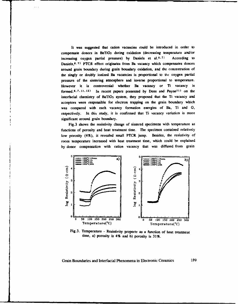
It was suggested that cation vacancies could be introduced in order to
compensate donors in BaTiOs during oxidation (decreasing temperature and/orincreasing oxygen partial pressure) by Daniels et al.6.7) According toDaniels, 6 .7) PTCR effect originates from Ba vacancy which compensates donors
around grain boundary during grain boundary oxidation, and the concentration of
the singly or doubly ionized Ba vacancies is proportional to the oxygen partial
pressure of the sintering atmosphere and inverse proportional to temperature.
However it is controversial whether Ba vacancy or Ti vacancy is
formed.7.11,12) In recent papers presented by Desu and Paynel") on the
interfacial chemistry of BaTiO3 system, they proposed that the Ti vacancy and
acceptors were responsible for electron trapping on the grain boundary which
was compared with each vacancy formation energies of Ba, Ti and 0,respectively. In this study, it is confirmed that Ti vacancy variation is more
significant around grain boundary.
Fig.3 shows the resistivity change of sintered specimens with temperature as
functions of porosity and heat treatment time. The specimen contained relatively
low porosity (4%), it revealed small PTCR jump. Besides, the resistivity of
room temperature increased with heat treatment time, which could be explained
by donor compensation with cation vacancy that was diffused from grain
to ,2 0 c . , oA a ) 0,t0 'c . ,oi, b );200"¢,f qlt" I b)0¢,t
QA" 200"c.20A U"10*.0
4 04
• 2 " 2
0 50 100 150 200 250 300 0 50 100 150 20C 250 300
Temperature(*C) Ternperature(°C)
Fig.3. Temperature - Resistivity property as a function of heat treatmenttime, a) porosity is 4% and b) porosity is 31%.
Grain Boundaries and Interfacial Phenomena in Electronic Ceramics 189
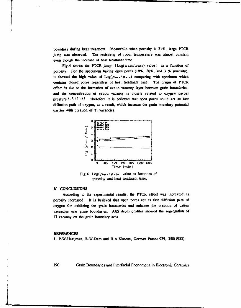
boundary during heat treatment. Meanwhile when porosity is 31%, large PTCR
jump was observed. The resistivity of room temperature was almost constant
even though the increase of heat treatment time.
Fig.4 shows the PTCR jump (Log(psax/pain) value] as a function of
porosity. For the specimens having open pores (10%, 20%, and 31% porosity),
it showed the high value of Log(psax/puin) comparing with specimen which
contains closed pores regardless of heat treatment time. The origin of PTCR
effect is due to the formation of cation vacancy layer between grain boundaries,
and the concentration of cation vacancy is closely related to oxygen partial
pressure. 6 7 10 1) Therefore it is believed that open pores could act as fast
diffusion path of oxygen, as a result, which increase the grain boundary potential
barrier with creation of Ti vacancies.
ZZI, 40
-~5 -AAhA" 20qKup 30%
Q 4
EQ 2
01
0 200 400 600 800 1000 1200
Time (min)
Fig.4. Log(pmax/pnin) value as functions ofporosity and heat treatment time.
F. CONCLUSIONS
According to the experimental results, the PTCR effect was increasad asporosity increased. It is believed that open pores act as fast diffusion path of
oxygen for oxidizing the grain boundaries and enhance the creation of cationvacancies near grain boundaries. AES depth profiles showed the segregation of
Ti vacancy on the grain boundary area.
REFERENCES1. P.W.Haaijman, R.W.Dam and H.A.Klasens, German Patent 929, 350(1955)
190 Grain Boundaries and Interfacial Phenomena in Electronic Ceramics
2. W.Heywang, "Resistivity Anomaly in Doped Barium Titanate," J.Am.Ceram.Soc., 47110] 484-490 (1964)
3. G.Goodman, "Electrical Conductivity Anomaly in Samarium-Doped BariumTitanate," J.Am.Ceram.Soc., 46111 48-54 (1963)
4. N.Nemoto and J.Oda, "Direct Examinations of PTC Action of Single GrainBoundaries in Semiconducting BaTiO3 Ceramics," J.Am.Ceram.Soc., 6317-81393-401 (1980)
5. W.Heywang, "Barium Titanate as a Semiconductor with Blocking Layers,"Solid State Electron., 311] 51-58 (1961)
6. J.Daniels and R.Werniche, "Part V, New Aspects of an Improved PTCModel," Philips Res.Rep., 31, 544-559 (1976)
7. J.Daniels, K.H.Hlirdtl, and R.Wernicke, "The PTC Effect of BariumTitanate," Philips Tech.Rev., 38[3] 73-82 (1978/79)
8. M.F.Yan and A.H.Heuer, Additives and Interfaces in Electronic Ceramics,Advances in Ceramics Vol.7 (The American Ceramic Society, Inc., 1983),pp.137-145.
9. M.Kuwabara, "Effect of Microstructure on the PTCR Effect in Semiconduc-ting Barium Titanate Ceramics" J.Am. Ceram.Soc.,641111 639-644 (1981)
10. T.Fukami, "BaTiOs Ceramic Semiconductors by Liquid Phase Sintering,"Abstr. Trans. Inst. Electron. and Comm. Engrs. Japan, 57[8] 31-32 (1974)
11. S.B.Desu and D.A.Payne,'Interfacial Segregation in Perovskite; I -IV,"J.Am.Ceram.Soc.,73(11 3391-3421 (1990)
12. Y.M.Chiang and T.Takagi,'Grain-Boundary Chemistry of Barium Titanateand Strontium Titanate: I,I[," J.Am.Ceram.Soc.,73[11] 3278-3291 (1990)
13. K.H.Hirdtl,"Gas Isostatic Hot Pressing Without Molds," Am.Ceram.Soc.Bull., 54121 201-207 (1975)
14. D.W.Budworth,"Theory of Pore Closure during Sintering," Trans.Brit.Ceram.Soc., 6911] 29-31 (1970)
Grain Boundaries and Interfacial Phenomena in Electronic Ceramics 191

Varistors and Conductors

INTERFACE STATES AT GRAIN BOUNDARIES AND THEIR EFFECTSON
THE I-V CHARACTERISTICS IN ZNO:PR VARISTORS- THEORETICAL CALCULATION -
Kazuo Mukae and Koichi TsudaFuji Electric Corporate Research and Development Ltd.
2-2-1, Nagasaka, Yokosuka, 240-01 JAPAN
ABSTRACT
Effects of the interface states on the applied voltage dependence of thedouble Schottky barrier(DSB) are theoretically discussed. Based on the simplifiedmodels of rectangular density distributions for the interface states, effects of theenergy level, density of states, and the distribution width of the interface states onthe applied voltage dependence of the DSB were quantitatively calculated. The I-V characteristics of DSB's were also calculated and the nonlinear I-V relationswere discussed. The nonlinear exponent was found to be determined mainly bythe barrier height and the total charge of the interface states. C-V characteristicsare also theoretically simulated. The observed ICTS spectra of the ZnO varistorshowed that the interface states were distributed monoenergetically and they fixedthe Fermi level. These results agreed with the calculated results.
1. INTRODUCTION
Ceramic semiconductors are widely applied to electronic devices such asthermistors, varistors, capacitors and sensors. Key functions of these devices areoften originated from the unique characteristics of the grain boundary. Recentinvestigations have indicated that the electric properties of the grain boundariesare related mainly to the double Schottky barrier(DSB) formed at the grainboundary.', 2 Therefore it is important to understand the precise role of the grainboundaries for development and improvement of these devices. AlthoughHeywang already explained the characteristics of PTC thermistors by the DSB3model in 1964 , there are still some quantitative discrepancies between theoreticalcalculations and the observed results. The most important reason for the discrep-ancies is the negligence of the change in the interface charge by an applied volt-age. The reported results of C-V characteristics of PTC thermistors showed thechange in the interface charge and the presence of the interface states above Fermilevel'. Therefore the precise analysis is important to understand the characteris-tics of a DSB. However few quantitative analyses have been reported about theTo the extent authorized under the laws of the United States of America, all cop t in t n t pbi n erty
of The American Ceramic Society. Any duplication, reproduction, or republication of this publication or any part thereof, withoutthe express written consent of The American Ceramic ,oiety or fee paid to the Copy t Clearance Center, is prohibited.
Grain Boundaries and Interfacial Phenomena in Electronic Ceramics 195

characteristics of the interface states and their influence to DSB properties. In thispaper the quantitative analysis of the applied voltage dependence of the interfacestates in a DSB is carried out by simplifying the density distribution of the inter-face states and the calculated results are compared with the observed results.
2. DOUBLE SCHOTrKY BARRIER
2.1 Formulation of Double Schottky Barrier
At the grain boundaries of ceramic semiconductors, there are many imper-fections such as crystal defects or inclusions. These imperfections often form theelectronic states at the grain boundaries. When these interface states are acceptors,they capture electrons from each grain of both sides resulting in the negativecharge of the interface of the grain boundaries. Because of the charge at the inter-face states, an electronic potential barrier is formed at the grain boundary asshown in Fig.1. When we denote -Q , N 1 and -q as the charge density of thegrain boundary, the donor concentration olf tfie semiconductor grains, the width ofthe depletion layer of a grain and electron charge, respectively, the followingequation can be obtained because the grain boundary charge should be compen-sated by that of depletion layers of both sides.
Qo=2 qNdlo (1)
The potential barrier can be expressed by the following equation if x is the posi-tion from the grain boundary and xJ x]l.
~+,'+ + 00
E+ o5d +o E, - Q,,v _ ---- ..... --- ...... ' - - F
Fig.1 Band structure of double Fig.2 Band structure of DSB withSchottky barrier, an applied voltage.
196 Grain Boundaries and Interfacial Phenomena in Electronic Ceramics
q2 N x2(
S
Since this electronic potential barrier is composed of two Schottky barrierssymmetrically connected with each other, we call this double Schottkybarrier(DSB). The barrier height at no applied voltage, ýo, is expressed by thefollowing equation.
q2Nd od _ 1o2= (3)
2es 0 8 EsNd
If D(E) is the distribution function of the density of the interface states, f(E) isFermi-Dirac distribution function, and E FB and E FGBO are the Fermi level of theinterface states and that when interface states are neutral, the interface charge, Qo,is obtained by the integration of the following equation.
Qo=q f F D(E)f(E)dE, (4)E FGBO
where
, 1
f(E)= (5)l+exp{(E-EF)/kT}
Therefore the actual DSB is determined by equations (2), (3), (4) and (5).
2.2 Applied Voltage Dependence of DSB
When a finite voltage is applied to a DSB regarding the left hand grain asnegative region, the shape of DSB changes as shown in Fig. 2. Since electrons areinjected into the interface states, the total depletion width becomes larger compen-sating the interface charge. The interface charge at V, Ov, is obtained by the nexteq. (6).
Ov=qNd(l +12), (6)
Grain Boundaries and Interfacial Phenomena in Electronic Ceramics 197

where
1 E= C (7)qzNd
2E1224 (8)q2Nd
If we define S, qV and qV2 as ratio of Q to Q0 , decrease in 0 and increase in ý2'respectively, the foillowing relations are oYotained.
S=Qv/Qo-- (9)
1 ~v+2 (io)1=0-V1+2 (11)
*2=40 +qV2 (12)
From the balance of electron injection and emission of the interface states, theFermi energy of the left grain is derived as approximately the same as that of theinterface states.
FGB=F (13)
3. CALCULATION OF VOLTAGE DEPENDENCE OF BARRIER HEIGHT5
From the eqs.(9) - (12), the applied voltage dependence of 0, can be de-rived as the following simple equation.
qV01$(-_-=-A•)20O (14)
4S%~
Therefore if we know S as a function of V eq.(14) can be calculated. However inthe actual case, dependence of S on V is rarely known because experimental
198 Grain Boundaries and Interfacial Phenomena in Electronic Ceramics

measurement of D(E) is difficult. Therefore we will simplify the D(E) and numer-
ically simulate the applied voltage dependence of 0, in the following discussion.
3.1 D(E)=O, E>E,,o (Heywang Model)
In this case, eq.(14) can be easily transformed to the next equation.
qVý1=(1 € _ 0(15)4f0
This equation shows well known parabolic decrease in barrier height and disap-pearance of f, at V=4, . Figure 3 shows this relation. Although f1 changes as V,it should be noted that the total depletion width, (l1+l), remains constant becauseof the constant interface charge. Consequently the capacitance of the DSB shouldbe kept constant.
3.2 Rectangular D(E)
When D(E) has a rectangular density distribution with a center at E +E_and 2AE width as shown below, S can be also calculated as a function of V.
4
1.2 -(c
3 . -0 . Be v 1 0 = 0 .8 e V - ( b )
02 - Ca) E~0S .. D(E)
0.2 (d)
V (V/Grain Boundary) V (V/Grain Boumary)
Fig.3 Dependence of t, and $2 on Fig.4 -V relation for D(E).applied voltage. t =0.8e-V. Q =6xl0' 2q/cm"(Heywang Model) IN= (a) 3X1O13/eV/cm 2
o •(b) 6x10¹²(c) 2X10 12
(d)O(Heywang Model)
Grain Boundaries and Interfacial Phenomena in Electronic Ceramics 199

D(E)=Do, (EFo+EO-AE<E<EFO+Eo+AE)
D(E)=O, (E<E Fo +Eo-AE, E>EFo+Eo+AE)
Until the Fermi level meets the bottom of the rectangle, the interface charge doesnot increase similar to Heywang Model, but at V=V where E =E +E -AE, elec-tron injection into the interface states begins. In this case, V can beoobtained asthe following equation from eq.(9).
qVo=4[ý 0-N1fo0{•-(E0 -AE)}] (16)
When the Fermi level reaches the top of rectangle where V=V the interfacestates are completely filled. Therefore, while Vo<V<Vr the interfdace charge, 0v,is expressed by the following equation.
Qv--Qo+qDo{qVI-(Eo-AE)l (17)
Therefore, the following relation can be obtained from eq.(9).
qD qDqv=g0o[I+{qV1_(EoAE)J _ -Q0 0 qV1)[I+{qV 1-(Eo-AE)}- Q o
(18)°
Although solution of eq.(18) for V. as a function of V cannot easily be obtained,one can obtain V1-V relation numerically. This numerical relation and eq.(14)enable simulation of 0 -V relation. Since the interface states are completely filledat V=V the interfacelcharge is kept constant above V>VF. Therefore VF and 01are expressed by the following equations.
qDo _2__OX_ qDoqVF=400(l+2AE---=-)-4 fo-(Eo+AE) J(1 +2AE- ) (19)
Qo QOqV
01=SS2(1 2) (20)4SF 20o
S =1 +qD 0 AE (21)0.
200 Grain Boundaries and Interfacial Phenomena in Electronic Ceramics
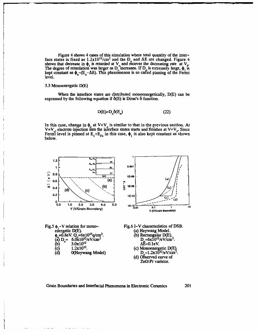
Figure 4 shows 4 cases of this simulation where total quantity of the inter-face states is fixed as 1.2x10¹²/cm 2 and the Do and AE are changed. Figure 4shows that decrease in f. is retarded at V and recover the decreasing rate at V_The degree of retardation was larger as D mincreases. If D is extremely large, O- iskept constant as $0 -(Eo-AE). This phenomenon is so calded pinning of the Fermilevel.
3.3 Monoenergetic D(E)
When the interface states are distributed monoenergetically, D(E) can beexpressed by the following equation if 8(E) is Dirac's 8 function.
D(E)=DPo(E) (22)
In this case, change in at V<V is similar to that in the previous section. AtV=V, electron injection into the inderface states starts and finishes at V=VF. SinceFermi level is pinned at Eo+EFo in this case, 01 is also kept constant as shownbelow.
1.2 ,.E,
1 ,b) 0.001l-
>0.8 O(E) I F-08-- (a) (a)
>-0.6 .2)()
"0 0.4 (....... ,I, 1E-09 - Wo.
0.2 - IE-12 C. -
005- • (d)
0.0 1.0 2.0 3.0 4.0 5.0 IE-15V (V/Grain Boundary) 0.01 0.1
V (V/Grain Boundary)
Fig.5 ýI-V relation for mono- Fig.6 I-V characteristics of DSB.energetic D(E). (a) Heywang Model.o =0.8eV. Q0 =6xlO12q/cm2. (b)Rectangular D(E).(a') Do= 6.0x10 12/eV/cm 2 D =6x10' 2/eV/cm 2.(b) 3.0x10 12 At=0.1eV.(c) 1.2x10 12 . (c) Monoenergetic D(E).(d) O(Heywang Model) D =-.2x1012/eV/cm 2.
(d) Ofserved curve ofZnO:Pr varistor.
Grain Boundaries and Interfacial Phenomena in Electronic Ceramics 201

(23)
qVF=4*oS 2-4Sr1/•o(*o-Ed (24)
Above V *1 again decreases as V increases. Three typical changes in areshown in Fig. 5.
In Table 1 calculated V0 and VF in three cases are summarized.
Table 1. Calculated V. and VF
NSb SF Do AEF V0 VF
(1012/cm 2) (1012/eV/cm2) (eV) (V) (V)
1.2 1.2 2.0 0.3 0.207 3.281.2 1.2 6.0 0.1 0.207 1.571.2 1.2 30 0.02 0.207 1.12
0.6 1.1 6.0 0.05 0.207 0.8241.2 1.2 6.0 0.1 0.207 1.5723.6 1.6 6.0 0.3 0.207 6.382
1.2 1.2 1.2 0 0.207 1.0163.0 1.5 3.0 0 0.207 2.7106.0 2.0 6.0 0 0.207 6.813
4. CALCULATION OF I-V CHARACTERISTICS
Current-voltage characteristics are calculated numerically on the basis ofthe thermoionic process expressed by the following equation where A is Ri-!hard-son constant and T is absolute temperature.
01I=AT1exp(- -1-) (25)
kT
Equation (25) gives I-V curves for three typical cases discussed above as shownin Fig. 6 in which an observed I-V curve of ZnO:Pr varistor is also indicated. Thetheoretical nonlinear exponent, a, is obtained from eq. (24) as the followingeq. (26) and (27). Equation (27) indicates that large 0 and large total charge at theinterface states will result in higher nonlinearity. All curves in Fig.6 exhibit non-linear characteristics. Calculated curves for rectangular and monoenergetic D(E)have larger a of 22 than that for Heywang Model. However that of the
202 Grain Boundaries and Interfacial Phenomena in Electronic Ceramics
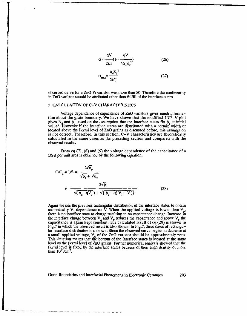
qV qV_k__ S-)_ (26)
a.= - (27)
2kT
observed curve for a ZnO:Pr varistor was more than 80. Therefore the nonlinearity
in ZnO varistor should be attributed other than fulfill of the interface states.
5. CALCULATION OF C-V CHARACTERISTICS
Voltage dependence of capacitance of ZnO varistors gives much informa-tion about the grain boundary. We have shown that the modified 1/C2-V plotgives N and 0 based on the assumption that the interface states fix at initialvalue6 . -Itowevoer if the interface states are distributed with a certain width orlocated above the Fermi level of ZnO grains as discussed before, this assumptionis not correct. Therefore, in this section, C-V characteristics are theoreticallycalculated in the same cases as the preceding section and compared with theobserved results.
From eq.(7), (8) and (9) the voltage dependence of the capacitance of aDSB per unit area is obtained by the following equation.
C/C° = 1iS 0
_(28)'/V€o -qV, ) + v¢{ 0o - -q(V - V )
Again we use the previous rectangular distribution of the interface states to obtainnumerically V dependence on V. When the applied voltage is lower than V,there is no inteAace state to charge resulting in no capacitance change. Increase inthe interface charge between V and V reduces the capacitance and above VF thecapacitance is again kept constant. Tge calculated result of eq.(28) is shown inFig.7 in which the observed result is also shown. In Fig.7, three cases of rectangu-lar interface distribution are shown. Since the observed curve begins to decrease ata small applied voltage, V0 of the ZnO varistor should be approximately zero.This situation means ihat the bottom of the interface states is located at the samelevel as the Fermi level of ZnO grains. Further numerical analysis showed that theFermi level is fixed by the interface states because of their high density of morethan 1013/cm 2.
Grain Boundaries and Interfacial Phenomena in Electronic Ceramics 203

6. ICTS MEASUREMENT
ICTS(Isothermal Capacitance Transient Spectroscopy) is an intensivemethod to investigate the interface states in ceramic semiconductors 7 . Thismethod gives the peak not only for the bulk traps in the grains but also for theinterface states at the grain boundaries. Figure 8 shows the observed ICTS peak ofa ZnO:Pr varistor8 generated by various height of the applied pulses. Although thevalue of the applied pulses are different, the position of the peaks did not change.This result indicates that the Fermi level of the interface states does not changewith the applied voltage. In addition, the calculated shape of the ICTS peak formonoenergetic interface states coincided with the observed peak. Consequentlywe can recognize that this observation agrees with the calculated results describedabove.
6. CONCLUSIONS
The applied voltage dependence of DSB was quantitatively simulated bysimplifying the density distribution of the interface states. The calculated resultsare compared with the observed results of I-V and C-V characteristics and ICTSmeasurement to obtain the following conclusions.
(1) The interface states retard the decrease in ý, and extremely high densi-ty interface states will fix the Fermi energy and (,.
(2) I-V characteristics are influenced not only by energy levels but also bytheir density and width of the energy distribution.
1.1 .(E-Ec) (eV)1 (a)1 ., -0.55 -0.62 -0.69 -0.76 -0M83 -0.90 -0.97
0.9 (b)o ..
0o.0 - W... .
0.7 20 -vt0.6
* I- 2 - :400.50 09 5 1 15 2 v,96ov
V (V/GRAIN) -3 T(=b T )c
Wl,= 2 0 Ns , "V
0.7 .1 v,=10ov
Fig.7 Calculated C/C _-V curve for .4 , I , I Irectangular D(E5). 10- 100 1o2 1o1
AE=0.1eV. E =0.2eV. rime (s )(a) D =0.6xvb /eV/cm 2
•iu6.0. Fig. ICTS spectra of ZnO varistorc) 60.0. by various height of pulse.
ý4)Observed curve.
204 Grain Boundaries and Interfacial Phenomena in Electronic Ceramics

(3) Although completion of electron charge into the interface states willproduce steep rise in current, its nonlinear exponent, a, is confined to 22 andother mechanism is needed for explanation of ZnO varistor.
(4) C-V characteristics are theoretically calculated. Comparison with theobserved result revealed that the interface states are located at the same level asFermi level of ZnO grains and that they are pinning the Fermi level.
(5) ICTS measurement of ZaO:Pr varistor showed that the Fermi level ofthe ZnO graias is fixed by the interface states and that the interface states are dis-tributed monoenergetically. These results agreed with the calculated results of theDSB structure.
7. REFERENCES
1 K.Mukae and I.Nagasawa,"Effect of Praseodymium Oxide and Donor Concen-tration in the Grain Boundary Region of ZnO Varistors", 331-342, "Advances inCeramics, Vol.1", Ed., L. M. Levinson, Am. Ceram. Soc., (1981).2 H.Ihrig, "Physics and Technology of PTC-type BaTiO Ceramics", 117-127,"Advances in Ceramics, Vol.7", Ed., M. F. Yan and A. 1A. Heuer, Am. Ceram.Soc., (1983).3 W.Heywang, "Resistivity Anomaly in Doped Barium Titanate",J.Am.Ceram.Soc., Vol.47, 484-90,1964.4 P.Gerthsen and B.Hoffmann, "Current-Voltage Characteristics and Capacitanceof Single Grain Boundaries in Semiconducting BaTiO 3 Ceramics", Solid-StateElectron., Vol.16, 617-22,1973.5 K.Mukae and K.Tsuda, "Effects of Interface States on Applied Voltage Depend-ence of Double Schottky Barrier(Part 1)", J.Ceram.Soc.Jpn., Vol.101, 1125-1130,1993.6 K.Mukae, K.Tsuda and I.Nagasawa, "Capacitance-vs-Voltage Characteristicsof ZnO Varistors", J.Appl.Phys., Vol.50, 4475-4476, 1979.7 T.Maeda and M.Takata, "Detection and Characterization of Trap Centers inZnO Varistor by ICTS", J.Ceram.Soc.Jpn,Vol.97, 1219-1227, 1989.8 K.Tsuda and K.Mukae, "Characterization of Interface States in ZnO Varistorsusing Isothermal Capacitance Transient Spectroscopy", J.Ceram.Soc.Jpn,Vol.100, 1239-1244, 1992.
Grain Boundaries and Interfacial Phenomena in Electronic Ceramics 205

CRYOGENIC BEHAVIOR OF ZnO VARISTORS
Uonel M. Levinson and William N. SchultzGE Corporate Research and DevelopmentP.O. Box 8, Schenectady, NY 12301
ABSTRACTBy controlling the ZnO grain doping it is possible to fabricate ZnO varistors withgood high-current nonlinearity at cryogenic (4.2 K) temperatures. We present herelow-temperature current-voltage and capacitance-dissipation data measured on ZnOvaristor ceramics having Al doping between zero and 1000 ppm atomic. Analysis ofthe data shows that adequate cryovaristor performance requires that the ZnOdoping level exceed a donor doping concentration of about 1018 electrons/cm3
(50 ppm atomic Al). This doping level corresponds to the Mott critical concentra-tion at which the activation energy for shallow donors tends toward zero; i.e., thedonor impurity band overlaps the bottom of the conduction band.
1. INTRODUCTION
Metal-oxide varistors used in surge arresters are ZnO-based ceramic semiconductordevices with highly nonlinear current-voltage characteristics similar to back-to-backZener diodes, but with much greater current, voltage, and energy-handling capa-bilities [1-4]. They are composed of ZnO (-95 mol%) plus a number of otheroxide additives (-5 mol%) and are produced by a sintering process that gives riseto a microstructure consisting of conducting ZnO grains (room temperature resis-tivity p-I ,l-cm), 10 pm in size, surrounded by thin insulating barriers. The dccurrent-voltage characteristics of a ZnO varistor at 77 K and for a small range oftemperatures near 300 K are shown in Figure 1. At very low applied electric fields,the varistor is highly resisti% -, and at room temperature (298 K) behaves essentiallyas a linear resistor of resistivity -1012 f-cm. In this region and in the prebreakdownregion that connects the linear characteristic to the highly nonlinear breakdownconduction process, the varistor exhibits a negative temperature coefficient ofresistance; that is, as temperature increases, the effective resistance decreases, re-sulting in higher varistor current for a given applied voltage. The 1V characteristicin the prebreakdown and linear regions is often described by an activation energy
To the extent authorized under the laws of the United States of America, all copyright interests in this publication are the propertyof The American Ceramic Society. Any duplication, reprouction, of republication of this publication or any part thereof, withoutthe written consent of The American Ceramic Society or fee paid to the Copyright Clearance Center, is prohibited.
Grain Boundaries and Interfacial Phenomena in Electronic Ceramics 207
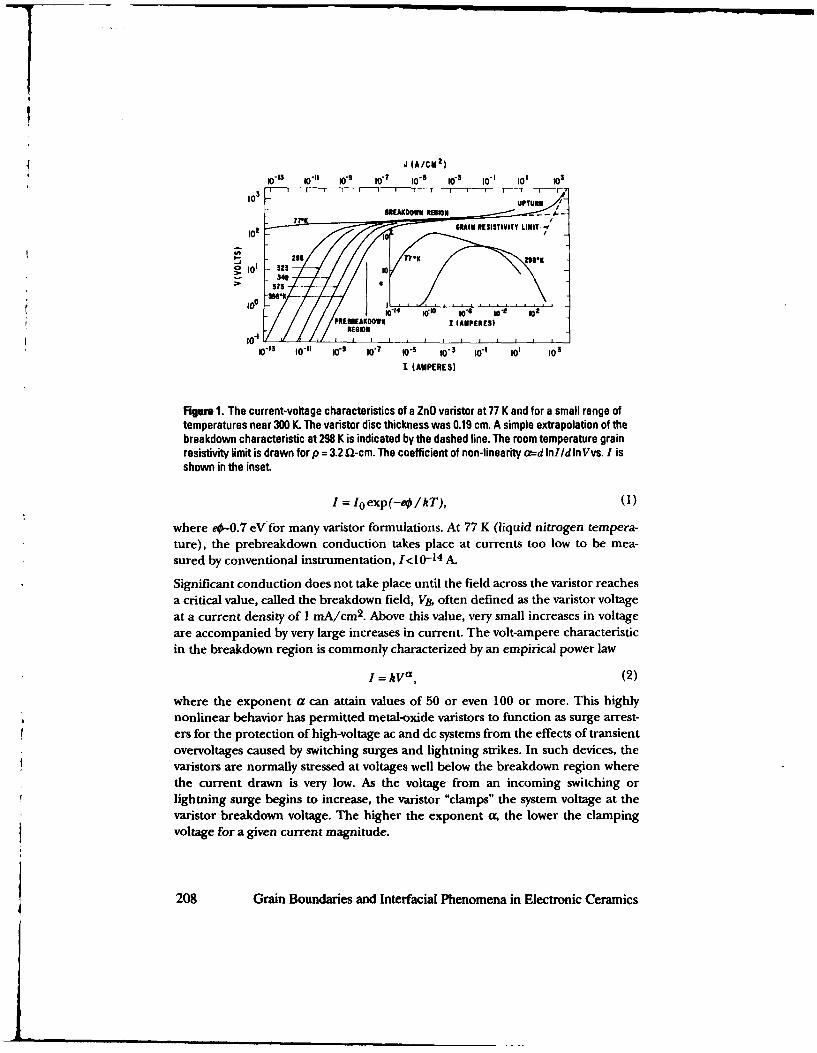
J (A/CM2)10"I oi 10 " i0t-7 I0"5 W3- i0"I io 0i
gO ~UPTURNBREAKDOWN IMON
1 GRAIN RESISTIVITY LIMIT-U.
lot 0
• 10, 323- 0" S 3"
10904 e0 o~o 0PREBREAKDOWR r (AMPERES)
REGION
10t 13 I0"11 I O9
I0o: 1-5 to" to, 0 1 0 3
1 (AMPERES)
Figure 1. The current-voltage characteristics of a ZnO varistor at 77 K and for a small range oftemperatures near 300 K. The varistor disc thickness was 0.19 cm. A simple extrapolation of thebreakdown characteristic at 298 K is indicated by the dashed line. The room temperature grainresistivity limit is drawn for p = 3.2 fl-cm. The coefficient of non-linearity a=d Inmld InVvs. I isshown in the inset.
I = I 0 exp(-eo /kT), (1)
where eo-0.7 eV for many varistor formulations. At 77 K (liquid nitrogen tempera-ture), the prebreakdown conduction takes place at currents too low to be mea-sured by conventional instrumentation, I<10- 14 A.
Significant conduction does not take place until the field across the varistor reachesa critical value, called the breakdown field, VB, often defined as the varistor voltageat a current density of 1 mA/cm2. Above this value, very small increases in voltageare accompanied by very large increases in current. The volt-ampere characteristicin the breakdown region is commonly characterized by an empirical power law
I = kVa, (2)
where the exponent a can attain values of 50 or even 100 or more. This highlynonlinear behavior has permitted metal-oxide varistors to function as surge arrest-ers for the protection of high-voltage ac and dc systems from the effects of transientovervoltages caused by switching surges and lightning strikes. In such devices, thevaristors are normally stressed at voltages well below the breakdown region wherethe current drawn is very low. As the voltage from an incoming switching orlightning surge begins to increase, the varistor "clamps" the system voltage at thevaristor breakdown voltage. The higher the exponent a, the lower the clampingvoltage for a given current magnitude.
208 Grain Boundaries and Interfacial Phenomena in Electronic Ceramics
For very high currents an upturn occurs in the volt-ampere characteristic, associ-ated with the finite resistivity of the grains themselves (Figure 1). This upturnderives from the voltage drop in the grains. The degree of upturn is of criticalimportance to the protective ability of the varistor material at high currents. Thegreater the upturn, the lower the exponent a and the poorer the protective level.Because the varistor grains consist of doped semiconducting ZnO, it is of interest toevaluate the temperature dependence of the varistor grain resistivity and its effecton varistor behavior at low temperatures.
2. CRYOVARISTORS
The initial measurements of the electrical response of varistor materials at cryogenictemperatures were made in our laboratory in the mid- to late-1970s. The first study[5] was performed to help understand varistor conduction behavior. This work alsorevealed that grain resistivity effects are enhanced at 4.2 K, severely limiting the low-temperature effectiveness of devices made with this early formulation.
A second study [61 quantitatively evaluated these low-temperature grain resistivityeffects through measurements of the frequency dependence of the dielectric, a-stant and dissipation factor. A loss peak and dispersion in E were identified asresulting from the two-phase structure of the ZnO varistor (insulating grain bound-aries and more conducting grains). We also were able to show that the grainresistivity in these early commercial varistors at 4.2 &, PZno-10 6 0-cm, could begreatly improved by minor variations in the varistor formulation.
More recently Lawless et al. [7,8] measured the electrical and thermal properties ofa cryovaristor sample and observed that the energy absorption capability of varistormaterials could be dramatically improved by operating the varistor at cryogenictemperatures. They recognized that for certain applications such cryogenic opera-tion was potentially practical and advantageous. They found that while the specificheat of varistor materials is small for T<100 K, it becomes significant for tempera-
tures above 100 K. Hence, the useful energy absorption capability is determinedover a temperature range (Tmax-100) K, where Tmax is the maximum temperatureat which the varistor is operable after absorption of the surge.
Since our early work [5,6] showed that varistors did not function well at highcurrents and low temperatures because of the high ZnO grain resistivity at cryo-genic temperatures, we have now evaluated the effect of varying the ZnO grainresistivity upon cryovaristor operation.
3. EXPERIMENTAL
Varistor samples were prepared for measurement at cryogenic temperatures bymilling oxide powders, pressing, and sintering. Preparation details are as follows:.
Grain Boundaries and Interfacial Phenomena in Electronic Ceramics 209

Varistor composition (mol%): ZnO = 97; Bi2 0 3 = 0.5; Co 20 3 = 0.5;
MnO 2 = 0.5; NiO = 1.0; Sb20 3 = 1.0; Cr0 3 = 0.5
Sintering conditions: 1200 *C, 1 hour.
Varistor discs of diameter 0.75 inch and thickness 0.050 inch were pressed at about4 kpsi and sintered in air in a muffle furnace. After firing, the varistors wereelectroded using an In-Ga eutectic alloy and characterized electrically at room
temperature, 77 K and 4.2 K. The 77 K and 4.2 K data were obtained by immersingthe devices in liquid nitrogen and liquid helium, respectively.
A series of varistor samples having the above composition and varying additional Aldopant content (added as the nitrate) were prepared. The ZnO powder used in thevaristor preparation as well as undoped fired samples were characterized analyti-cally using ICP emission spectroscopy to check for the possible presence of tracebackground donor dopants. Other than Al, the elements Ga and In are known
donor dopants for ZnO [9]. The trace element analysis (Table 1) indicates abackground donor dopant level of<10 ppm atomic for Al, Ga, and In. This value ismodest compared with the range of intentionally added Al doping (10 to 1000 ppmatomic in our samples). For Al doping >>10 ppm we can have confidence that theZnO donor doping is largely determined by the added Al.
Table 1. Trace Analysis of Some Dopants
(Data in ppm atomic; DL denotes detection limit)
Al Ga In U Na K
"Pure" ZnO <DL <DL 7 <DL 3 <DL
ZnO varistor withno added A[ <DL <DL 9 3 11 <DL
Detection limit (DL) 1 2 2 0.2 1 0.4
The current-voltage characteristic of the varistor samples was measured over acurrent range l0-9 A/cm2< I <10 A/cm2 . For currents over 3 mA/cm2 the datawere obtained using a Velonex 360 pulse generator with all data measured 40 Psafter pulse initiation. The values for 1<3 mA/cm2 were obtained using dc methods.
We have also measured the capacitance-dissipation behavior of the samples forfrequencies 102 Hz<f<2xl06 Hz. The data were obtained using HP 4274A and HP
4275A LCR meters.
4. RESULTS AND DISCUSSIONFigure 2 gives the dissipation (tano) vs frequency measured at room temperature,
77 K, and 4.2 K, for ZnO varistors with, respectively, no intentional Al-doping,
210 Grain Boundaries and Interfacial Phenomena in Electronic Ceramics

f 1.0 , , ,1.0 0K-0 (a) 30 ppm atomic Al doping, and-9- 77 .K 1000 ppm atomic Al doping. Al, Ga,and In are known trivalent dopants
0.6 " [9-11 ] that decrease the ZnO grain. resistivity at room temperature. We
0.4. have used Al doping to decrease theZnO resistivity. The relative dielec-0.2 0 tric constant, E for the samples of
00.00 10' 10' Figure 2 is given in Figure 3.1620 105 104 11s 10'a 107 Figures 2 and 3 at 4.2 K can be ana-
Frequency (Hz) lyzed quite straightforwardly in terms
1.0 ' of Maxwell-Wagner dispersion of aS4- 3 K mixed phase. In this case, the more
0.6- 4. resistive phase is the ZnO grainboundary and the more conducting
0.6s phase is the ZnO grain. This model
.1 is well known [12] and has been00.4- particularized for varistors [6]. Note
0.2 the large magnitude of the peak ofthe dissipation factor (tanb'0.6) in
o.o0: - Figures 2a and 2b. This Maxwell-102 103 l0 10 O 107 Wagner peak is quite different in
Frequency (Hz) origin from other small peaks in tanb
1.0- observed in ZnO varistors aroundI-,. - so K [(clI-0- 77 K room temperature [13,14].-0.8--• 77 K
0.8- w 4.2 KTo aaalyze the 4.2 K data of Fig-
S 1000IIpmAe Ai ures 2 and 3 it is useful to quotesome relations derived frcm the
a 0.4 Maxwell-Wagner analysis forcryovaristors [6]:
0.2 The peak frequency in the tanbvsf
0.0 P .. . . .. . curves is given by102 103 104 10s 10e 10/
Frequency (Hz) fm. _=(dl / d2 )1/ 2(l / 2r-oEP2 ) (3)
Figure 2. Dissipation (tanb) vs. frequency at 300 K, where subscript -" denotes the77 K, and 4.2 K for a varistor with (a) no intentionally grain boundary and subscript "2"added Al doping, (b) 30 ppm atomic added A[, denotes the grain, and e=8.5 is the(c) 1000 ppm atomic added Al. dielectric constant of ZnO.
Grain Boundaries and Interfacial Phenomena in Electronic Ceramics 211
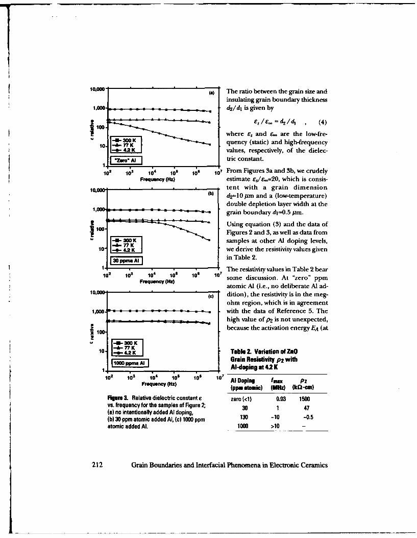
S10,0oo( The ratio between the grain size andinsulating grain boundary thickness
1,000- : :d 2 /dl is given by
le- - "d2 ./ , (4)0 where E, and C_ are the low-fre-
SI-m- 300 K Iquency (static) and high-frequency1O. -I6 77 KI-'- l 4.2 K Ivalues, respectively, of the dielec-
tric constant.
10; 108 104 10; 106 1;7 From Figures 3a and 3b, we crudelyFrequency (Hz) estimate es/ero=20, which is consis-
010,00_, • tent with a grain dimension(b) d2 -1O pm and a (low-temperature)
double depletion layer width at thegrain boundary dl=0.5 pm.
Using equation (3) and the data of100.- Figures 2 and 3, as well as data from
. 1-41- 300K I samples at other Al doping levels,10i.- 4.2 K we derive the resistivity values given
S30POPmel W 1 in Table 2.
1 The resistivity values in Table 2 bear102 103 1;4 1;5 106 io some discussion. At "zero" ppm
Frequency (Hz)F0,qe0c ) atomic Al (i.e., no deliberate Al ad-
1() dition), the resistivity is in the meg-ohm region, which is in agreement
1,000.-- with the data of Reference 5. TheA- . . . -high value of p2 is not unexpected,
Stbecause the activation energy EA (at
S-0- 300 KI.&. 77 K
10 I'- 0- 4.2 K Table 2. Variation of ZnO
0 Nm AlGrain Resistivity P2 withI OOppaA AI-dopino at 42 K
102 104 ;05 1'6 10710 f 1) Al Doping fmax P2Frequency (Hz) (ppm atomic) (MHz) (kW-cm)
Rgur 3. Relative dielectric constant e zero (<1) 0.03 1500vs. frequency for the samples of Figure 2; 30 1 47(a) no intentionally added Al doping,(b) 30 ppm atomic added Al, (c) 1000 ppm 130 -10 -0.5atomic added Al. 1000 >10 -
212 Grain Boundaries and Interfacial Phenomena in Electronic Ceramics

low concentrations) for most shallow donors in ZnO is in the 10- to 40-meV range[9], and thus these donor levels would be frozen out at 4.2 K. A doping level of1 ppm atomic corresponds to 5x10¹⁶ electrons/cm 3 (if completely activated). Liand Hagemark [15] similarly find that single crystals of ZnO with excess Zn dopingat the 1016 /cm 3 level have p-10 6 l-cm at 4 K.
As the donor density increases, however, we expect a decrease in the effectivedonor activation energy. The decrease of the activation energy with increasingdensity of donors can be related to an increase in the overlapping of the wavefunctions of the bound electrons. The impurity band formed in this way becomesbroader with increasing density of donors. The ionization energy of the donorsvanishes when the impurity band reaches the lower edge of the conduction band.
We can estimate the critical concentration Ne at which the donor ionization energyis expected to go to zero using the criterion of Mott [16] that
=3 15)4m A3 ao' 1
where A is a constant approximately equal to 3, and ao is the Bohr radius of ahydrogen-like orbit of the electron in the coulomb field of the donor ion. Since
ao = e(m / m*)aHl, (6)
where m* (=0.27 m) is the effective mass of the electron in ZnO [17], e=8.5, and aHis the hydrogen atom Bohr radius = 5.3 nm, we obtain
Nc = 2xl01 8cm-3. (7)
This value of Nc compares well with the data of Li and Hagemark [15], who findthat the activation energy EA--O as the doping approaches 2x20 18 /cm 3 , and thatp-10 3 fl-cm for single-crystal ZnO with excess Zn doping at the 1018/cm 3 level.Noting that a doping level of 1018 /cm 3 corresponds to about 50 ppm atomic, thevalues of p2 presented in Table 2 are consistent with the above.
We have also attempted to corroborate these estimates by pressing and sintering(at 1200 °C) the "pure" ZnO powder used to prepare all the varistors describedhere. Figure 4 gives the resistivity of the "pure"ZnO ceramic as a function oftemperature and doping. Note that careful precautions were taken to avoid con-tamination of the ZnO with the other additives (in particular Bi203) usually addedto varistors, and that the resistivity measurements were performed at a frequency of106 Hz to avoid contact impedance effects.
Grain Boundaries and Interfacial Phenomena in Electronic Ceramics 213

107,
1 o s ............4........ . .. ..... ....S1051S• l. 4 .
fie0 .. .................. ........ .................... ..... •.......................
a.10:1lO .. .. . .. ...-. F.gure 4. Variation with temperature and10 Al doping of the resistivity of "pure' ZnO10 ceramic material. Note that for 1000 ppm
10 100 1000 Al doping, cooling from liquid nitrogen toDoping (pp- A Q liquid helium hardly affects the resistivity.
The data of Figure 4 are in general agreement with the estimate of Ne=2x10 18/cm 3
shallow donor doping (AI-100 ppm atomic), as the level at which the activationenergy EA begins to tend to zero. Indeed, by the time the Al doping is 1000 ppmatomic, P4.2 K=P77 K and EA=0.Figure 5 gives current density vs. • pplied field data for the samples of Figures 2 and
3.* As expected, the greater the Al doping, the less the upturn; i.e., the more
nonlinear the behavior at high currents. It should be evident, however, that theresistivities of Table 2 are far too large to be consistent with the high-current dataof Figure 5. For example, from Figure 5a ("zero" doping), at a current of 10 A/cm2
the incremental field, AE, resulting from the upturn is about 3 kV/cm. (Thisestimate of AE is obtained by a rough linear extrapolation of the low-current datain the log-log plot to high currents.) Using this value of AE we would estimate agrain resistivity of 0.3 kil-cm, which is considerably less than the value in Table 2for the "zero" doping sample.
The reason for this discrepancy is not clear at present. We presume it results fromthe basic difference between capacitance-dissipation data obtained at low appliedfields and high-field effects arising during current-voltage measurements in varis-tors. These high fields could provide excess electrons in the ZnO grains, either viaimpact ionization or avalanche breakdown of neutral impurity levels, thereby de-creasing the effective ZnO grain resistivity.
REFERENCES[1] For a review of these devices, see T.K. Gupta, J. Am.Cer.So,. 73,1817
(1990); L.M. Levinson and H.R. Philipp, Bull Am. Cer.Soc. 65, 639(1986); H.R. Philipp and L.M. Levinson, 190 EOS/ESD SymposiumProceedings EOS-2, 26, 1981.
*Note that the pulse and dc data of Figure 5 are shifted in voltagebecause of effects such as the ac-dc shift and overshoot [181.
214 Grain Boundaries and Interfacial Phenomena in Electronic Ceramics

104 . . . ...... [2] E.C. Sakshaug, I.S. Kresge, andS.A. Miske, IEEE Tram. Power
ALDC APUIN 047K0 DC 0 •4,ul I • App. Sys. PAS-96, 1977, p. 647.
00 0 • j • ,' [3] G .D . M ahan , L .M . Levinson,2woAI0 A G.. LM
A and H.R. Philipp, AppL. Phys..2 0 0 A a Lett. 33,1978, p. 80.
AL A aaaa a [4] G.D. Mahan, L.M. Levinson,
AS • and H.R. Philippj AppL Phys.50, 1979, p. 2799,
103. [5] H.R. Philipp and L.M.109 10-7 10 10-3 10.1 101 Levinsonj Appl. Phys. 48,
Current Density (Aicm2) 1621 (1977).
1O4-. (b..[6] L.M. Levinson and H.R.C ,Pu, k•at; I Philippj Appl. Phys. 49, 6142
ADoc A Pulse, at (198)0 DC 0 Pu he,. t4.2K (1978).00 •• [7] W.N. Lawless, C.F. Clark, B.R.
0 A Patton, and F.S. Khanj AppL•" : i• ; •*• "-0 Phys. 64, 4223 (1988).
AA A A A [8] W.N. Lawless and T.K. Gupta,"A A a . J. Appl. Phys. 60, 607 (1986).
13 1 [9] G. Heiland, E. Mollwo, and F.St6ckmann, Solid State Physics,
10 "9 10-7 10-5 10 "3 10.1 101 Vol. 8, p. 193, F. Seitz and D .Current Denaity(A /¢m2) Turnbull, ed., Academic Press
0 .. . I I ' ' (1959).DC 0a Put"i (C) [10] T. Miyoshi, K_ Maeda, KI
* Dc A P. 4 Takahashi, and T. Yamazaki,I•o p , ,maKl Advances in Ceramics, Vol. 1,
L.M. Levinson, ed., p. 309,. •oAmerican Ceram ic Society
• 2 ( 1 9 8 1 ) .A " [11] W.G. Carlson and T.K. Gupta,
J. AppL Phys. 53, 5746 (1982).A03 [12] J. Volger in Progress in Semicon-
10 5 ductors, Vol. 4, p. 207, A.F.10-9 10 "' 10-5 10-3 10 "1 10 Gibson, ed., Wiley, New York
Current Density (Aem2) (1960).
Figure &. Current density vs. applied field at [13] L.M. Levinson and H.R.300 K, 77 K, and 4.2 K for a varistor with (a) no Philipp,J. Appl. Phys. 47, 1117intentionally added Al doping, (b) 30 ppm (1976).atomic added Al, (c) 1000 ppm atomic added Al.
Grain Boundaries and Interfacial Phenomena in Electronic Ceramics 215
IL

[14] L.M. Levinson and H.R. PhilippJ. Appl. Phys. 47, 3116 (1976).
[15] P.W. Li and K. I. Hagemarkj Solid State Chemistry 12, 371 (1975).
[16] N.F. Mort and W.D. Twose, Advances in Physics 10, 107 (1961).
[17) A.R. Hudson, Phys. Rev. 108, 222 (1957).
[18] H.R. Philipp and L.M. Levinson, Advances in Ceramics 1, 394 (1981).
216 Grain Boundaries and Interfacial Phenomena in Electronic Ceramics

MODELLING THE ELECTRICAL CHARACTERISTICS OFPOLYCRYSTALLINE VARISTORS USING INDIVIDUALGRAIN BOUNDARY PROPERTIES
Qingzhe Wen and David R. Clarke
Materials Department, College of Engineering,University of California, Santa Barbara, CA 93106
1. INTRODUCTION
Since the original publication [1], by Matsouka in 1971, demonstratingthat polycrystalline ZnO doped with additives, such as CoO, MnO,Bi20 3 and Sb20 3, can exhibit highly non-ohmic electrical characteristics,a voluminous literature has been generated. Although many of theessential ideas concerning the origin of the varistor behavior wereintroduced by Matsouka and others within a relatively short time, theliterature has continued to grow. Much of it has been concerned witheither detailing the electronic and defect mechanisms underlying thevaristor behavior or with specific ceramic processing findings. Inseeking an understanding of varistor behavior, the implicitassumption of much of this work has been that the electricalcharacteristics of a real, polycrystalline varistor can be determined byappropriate averaging once the characteristics of a single grainboundary are understood. However, observations of themicrostructure, particularly at high spatial resolution, reveal that themicrostructure can be quite complex. Second phases, such as spinel andvarious Bi20 3 polymorphs, each with a different thermal expansioncoefficient and electrical conductivity, are usually present. Also, abismuth-rich intergranular film has been reported at grain boundariesby many investigators as well as bismuth-rich segregation at othergrain boundaries. In addition, experimental measurements of thecurrent-voltage characteristics of individual grain boundaries revealthat there is a distribution in break-down voltage as well as variationsin the non-linear, varistor exponent [2-6]. Furthermore, since zinc
To the extent authorized under the laws of the United States of America, all cop•right interests in this publication are the propertyof The American Ceramic Society. Any duplication, reprlucion, or republication of this blication or any part thereof, withott he e rin c n o e can Ce•aui c Society or fee paid to the Copyright Cent, is prohibited.
Grain Boundaries and Interfacial Phenomena in Electronic Ceramics 217

__Bi2 03°
Bi Segregant
Figure 1 (a). Typical three-grain junction region in a commercialvaristor. The Bi20 3-rich second phase partially encroaches along thetwo-grain junctions thereby restricting current flow across theboundary. Transmission electron micrograph. (b) Representativemicrostructure of a varistor based on transmission electron microscopyobservations.
218 Grain Boundaries and Interfacial Phenomena in Electronic Ceramics

features of the microstructure consist of ZnO grains wet along thethree- and four-grain junctions by a bismuth oxide-rich phase withbismuth segregation along the majority of two-grain junctions [8-101.This is illustrated with the transmission electron micrographreproduced in figure la. Depending on the additives and the processingroutes used, there may also be spinel second phases at the multiplegrain junctions and the bismuth oxide rich phase may be partiallycrystallized to one or more of its polymorphs. The representativemicrostructure used to model these materials is shown in figure lb andconsists of equiaxed square grains with a second, insulating phase ateach corner. The array of non-linear junctions which will be used tocalculate the I-V characteristics of the material is the mathematicaldual of this square array and is thus also square array. This relationshipis shown in figure 2. Any number of grains can be included in thecomputation but present computer capacity limits us tomicrostructures of 30x30 grains.
GrainS '-• • "-• -• •Boundaries
_.,,- . - - Grain
Grain
A - Boundary
, - Resistor
Figure 2. Network model used to compute the varistorcharacteristics. The array of grain boundary resistors is thetopological dual of the microstructure of square grains. Theelectrical characteAstics of the individual grain boundariesare described in the text and are selected at random again asdescribed in the text.
Variations in the observed microstructures are incorporated in themodel microstructure by varying the electrical characteristics of
Grain Boundaries and Interfacial Phenomena in Electronic Ceramics 219
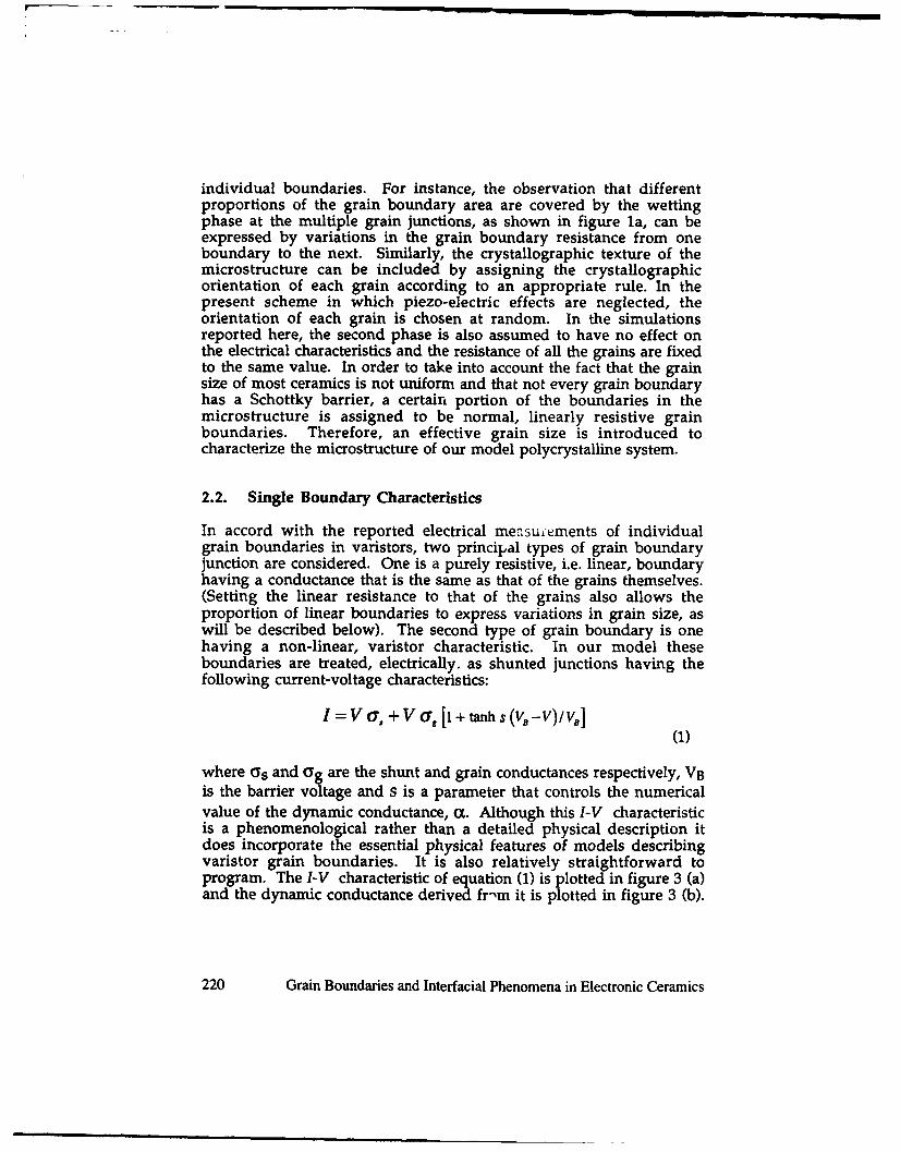
individual boundaries. For instance, the observation that differentproportions of the grain boundary area are covered by the wettingphase at the multiple grain junctions, as shown in figure la, can beexpressed by variations in the grain boundary resistance from oneboundary to the next. Similarly, the crystallographic texture of themicrostructure can be included by assigning the crystallographicorientation of each grain according to an appropriate rule. In thepresent scheme in which piezo-electric effects are neglected, theorientation of each grain is chosen at random. In the simulationsreported here, the second phase is also assumed to have no effect onthe electrical characteristics and the resistance of all the grains are fixedto the same value. In order to take into account the fact that the grainsize of most ceramics is not uniform and that not every grain boundaryhas a Schottky barrier, a certain portion of the boundaries in themicrostructure is assigned to be normal, linearly resistive grainboundaries. Therefore, an effective grain size is introduced tocharacterize the microstructure of our model polycrystalline system.
2.2. Single Boundary Characteristics
In accord with the reported electrical measuýements of individualgrain boundaries in varistors, two principal types of grain boundaryjunction are considered. One is a purely resistive, i.e. linear, boundaryhaving a conductance that is the same as that of the grains themselves.(Setting the linear resistance to that of the grains also allows theproportion of linear boundaries to express variations in grain size, aswill be described below). The second type of grain boundary is onehaving a non-linear, varistor characteristic. In our model theseboundaries are treated, electrically, as shunted junctions having thefollowing current-voltage characteristics:
I = V a, + V as 1 + tanhs(V,-V)/V
(1)
where as and Gg are the shunt and grain conductances respectively, VBis the barrier voltage and S is a parameter that controls the numericalvalue of the dynamic conductance, a. Although this I-V characteristicis a phenomenological rather than a detailed physical description itdoes incorporate the essential physical features of models describingvaristor grain boundaries. It is also relatively straightforward toprogram. The I-V characteristic of equation (1) is plotted in figure 3 (a)and the dynamic conductance derived fr'nm it is plotted in figure 3 (b).
220 Grain Boundaries and Interfacial Phenomena in Electronic Ceramics
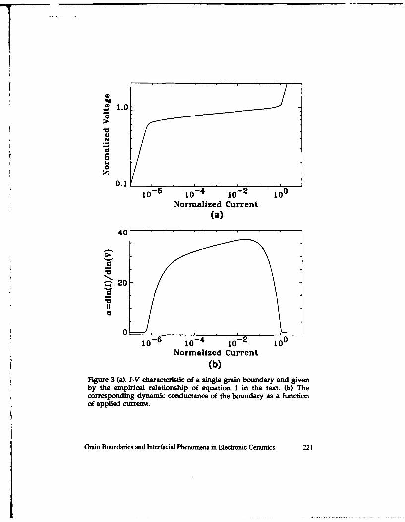
S1.07
0
, N
0.1
10-6 10- 4 10- 2 100Normalized Current
(a)
40
S20
II
10 -6 0-4 10-2 100
Normalized Current
(b)Figure 3 (a). I-V characteristic of a single grain boundary and givenby the empirical relationship of equation 1 in the text. (b) Thecorresponding dynamic conductance of the boundary as a functionof applied curremt.
Grain Boundaries and Interfacial Phenomena in Electronic Ceramics 221

The latter may be compared with the nonlinear exponent as a functionof junction voltage calculated by Mahan et al. from a modified back-to-back Schottky barrier model [Ill.
2.3. Calculation of the Polycrystailine I-V Curves.
In the third step, the overall electrical characteristics of thepolycrystalline microstructure are calculated. First, however, eachjunction in the microstructure is assigned either a linear or non-linearelectrical characteristic at random with a prescribed probability. Then,the barrier voltage of each non-linear junction is picked, again using arandom number generator, from a Gaussian distribution chosen torepresent the distribution of junction voltages observed in experiment.Having assigned the junction characteristics, current flow through thenetwork of junctions is computed. This corresponds to a bondpercolation model in which the individual bonds are either linear ornon-linear resistors, as distinct from usual percolation models inwhich each bond is a linear resistor [121.
The current flow through the network at a constant applied voltage iscomputed subject to the constraint *.tat current conservation ismaintained at each node (figure 2). This is invoked by applyingKirchoff s law to each node:
=0
where the subscripts i denote the node and j the adjacent local nodes.Equivalently, Kirchoff's law may be expressed in terms of the voltagesand conductances across each boundary:
V - Vi) =0(2)
The conductances of the individual boundaries are
io• for a resistive boundary
{+s I A)] for a nonlinear boundary
(3)
222 Grain Boundaries and Interfacial Phenomena in Electronic Ceramics

In the computations, a voltage source is applied across the networkwith ohmic contacts being established at both the top and bottom endsof the network by assigning the first and last row of boundaries as beingresistive. Periodic boundary conditions are also applied to the networkin the direction perpendicular to the applied voltage. For a system of Ngrains there are N separate Kirchoff's equations, from which thelectrical potential at each grain is solved numerically for each applied
voltage across the varistor. The total current through the network isthen calculated for each applied voltage. The dynamic conductance, orthe nonlinear index, a, is then calculated according to the definitiona=dln(I)/dln(V). In all the simulations reported here we have chosenthe following values of the parameters in equation 3: s=20, the ratio ofshunt to grain conductance, (as/ag = 10-6, the average of vB'i, VB =1and the conductance of the grains, ag =1, i.e. voltages are normalized toVB and currents are normalized to (YgVB.
3. RESULTS
3.1. Mixed Resistive and Non-linear Boundaries
We begin with a consideration of the effect of varying the proportion ofgrain boundaries that are simply resistive. Although this is a non-linear percolation problem, three limits are known apriori. Two aretrivial and correspond to the extremes in which the resistors are eitherall linear resistors or all non-linear resistors. The third corresponds tothe case in which the fraction of resistive bonds equals the percolationlimit, Pc, which for a two-dimensional array occurs at 0.5. (In three-dimensions on a simple cubic lattice Pc = 0.18.) The computed I-Vcharacteristics for these three cases are reproduced in figure 4. Whenthe proportion of resistive boundaries is less then the percolation limit,the overall electrical response is non-linear and the shape of both the I-V curve and the dynamic conductance are altered. This illustrated infigure 4 for a series of different concentrations of resistive junctionsand is compared with that of a purely non-linear array. Both themaximum value of the exponent and the ohmic region conductivityare decreased from that exhibited by the homogeneous non-lineararray, but the nonlinear character of the electrical response makesdetailed comparison difficult. To aid comparison, we introduce thefollowing parameters: am, the maximum value of the nonlinear index;Vm and Im the voltage and current at which the non-linear index isequal to am; AVm, the voltage range with a > am/ 2 ; and RL, the leakage
Grain Boundaries and Interfacial Phenomena in Electronic Ceramics 223

*k .....
C ................ .....0>, 10
P-.10 . •-a /../ .. - m
.1.. P-0.4S/ --- P=O.5o ~ ~ /P-0.45
1**'/' I, ,, ,
10-6 10-4 10- 2 100 102
Normalized Current
(a)
40
> 30
_"20 -\,
10
10- 6 10-4 10- 2 10 0 10 2
Normalized Current
(b)Figure 4 (a). Varistor characteristics as a function of the proportion,P, of linearly resistive grain boundaries. The curve for P = 0corresponds to a homogeneous array of identical non-linearboundaries whose individual I-V characteristic is shown in figure 3(a). (b) The dynamic conductances as a function of applied current.
224 Grain Boundaries and Interfacial Phenomena in Electronic Ceramics

resistance. These parameters correspond to those often used in thecharacterization of actual varistors.
Because of our choice that the resistance of the linear boundaries is thesame as that of the grains, the proportion of linear boundaries is also ameasure of the effective grain size and the grain size distribution.Since the type of boundary is chosen at random, clusters of grains, eachconnected by resistive boundaries, are formed. The size anddistribution of these clusters is a standard result in percolation theoryof random grain assignments [12]. Thus, the effective grain size, deff , isdefined as:
V V
(4)where n v is the number of grains in the v-th cluster and dv is theaverage size of the cluster of grains. Each of these is a function of theproportion P-Pc, where Pc is the percolation limit. The average grainsize as a function of the proportion of linear boundaries is shown infigure 5. The simulated results fit an empirical relationship:d¢j = d. (P, - P) 413
(5)where do has a value of 0.59, so that when P = 0 the effective grain sizecorresponds to the size of the grain size of the array.
8 " " ' " I . . ..I" ' " " I. . . .. . ." . ...,
S7 ...... 0
6 *-
54 . . ........ !.............. .. .. ..... . . . . . ...... .... . .... .. ....o
2 ............................................. ........ . .. ............S •........ ..... ....... "T"
0 ., , , .i . . . j . . . t . .. .........
0 . .0 0.1 0.2 0.3 0.4 0.5
PFigure 5. The effective grain size as a function of the proportion of resistiveboundaries. Since the resistance of the linear grain boundaries is chosen to bethe same as that of the grains, resistive boundaries are indistinguishable fromthe grains themselves. As a result the value of P also determines the grain sizedistribution.
Grain Boundaries and Interfacial Phenomena in Electronic Ceramics 225
I

From- the simulations, the maximum dynamic conductance, am, isfound to vary approximately linearly with the proportion of resistiveboundaries, Pc--P .The origin of this dependence is not presentlyunderstood in detail but from images in which the current flowthrough the network is calculated at successively greater values ofapplied voltage, we believe that this is a direct consequence of theredistribution of current due to a self-adjusting behavior of the non-linear junctions.
One feature of the dynamic conductance curves of figure 4 is that whenresistive boundaries are introduced into the network, the response athigh currents is reduced but also flattens to a relatively low value ofconductance. This is another consequence of combining non-linearities with the underlying percolation structure of the problem, inessence creating a voltage modulated percolation system. Thenonlinear boundaries in the system adjust their conductances inresponse to the applied voltages and hence the percolating structure ofthe system is also changing in response to the applied voltage. Thiseffect is most pronounced above breakdown but before the final upturnregion where the conductance corresponds to that of the grainsthemselves. We are not aware of whether this behavior has beenreported but as it is past the peak in dynamic conductance it mayhitherto have escaped notice.
3.2. Non-linear Boundaries with Distribution in Barrier Voltage
To account for the effect of a distribution of barrier voltages on theoverall varistor behavior, the barrier voltage, VB in equation (1) waschosen at random from a Gaussian distribution with a half-width of8VB. By introducing a distribution in the barrier voltage, the degree ofnon-linearity of the overall array is seen to be lessened and so thedynamic conductance is decreased. In addition, the breakdown is madeless abrupt and the leakage region conductance is decreased withincreasing 8VB/VB. These effects are illustrated in figure 6 fornormalized distribution half-widths 8VB/VB from 0 to 0.3. Thedependence of the maximum value of the dynamic conductance on thewidth of the distribution is shown in figure 7. Over the range ofdistribution widths explored, the maximum dynamic conductanceresults fit an exponential of the form:
a. = a. exp [- A(aVlV) 21
(6)
226 Grain Boundaries and Interfacial Phenomena in Electronic Ceramics

hI 3
30.
o
-%Vg 0.
Z - 61f/Ver. 0.3
10110-6 10-4 10-2 100 102
Normalized Current
(a)
40
> 30
S20
II10
1010-6 10-4 10-2 10 0 10 2
Normalized Current
(b)
Figure 6. (a) Varistor characteristics as a function of the width indistribution of grain boundary breakdown voltage. (b) Thecorresponding dynamic conductances.
Grain Boundaries and Interfacial Phenomena in Electronic Ceramics 227

where A is a constant. A similar dependence is observed for the voltageat which the maximum conductance occurs. Although the numericalvalues of the constants vary according to the proportion of resistiveboundaries, this exponential form fits all the simulation results wehave obtained.
3634- b...3 4 .................. ................... . .. ... . . . .'.. ".............. ...... i.......... ....... .. ..."
3 2 .............. ... ... ... ... . . ..... ...................... ".. A .... . .. .i ..... .............. .. .. .. . ..... .. •
3 0 . ............... : i.......... . . . . . ............... 77 ......... ." ". ..............30 .. .... .. ............ ... ; -. . ............... ... -- .......... ..32 .. ArP:
2 6 ...! .. ....P = . ............................................... ........ ...242 4 . ....... . . . . . . . ........ i.. ........ ........... . . . .............. ... . . . .. ...
22 ...0 0.05 0.1 0.15 0.2 0.25 0.3
8VB/VB
Figure 7. Variation in the maximum dynamic conductance with theboundary-to-boundary variation in breakdown voltage. The curves through thesimulation results are the exponential function of equation 6.
4. DISCUSSION
Although we have investigated a particularly simple model torepresent the behavior of varistors, the simulation of the I- Vcharacteristics reveal a number of important inter-relationshipsbetween microstructure, individual grain boundary electricalcharacteristics and the variations in breakdown voltage. Perhaps themost striking inter-relationship concerns the effect of variations ingrain size, represented by the proportion of linearly resistive grainboundaries. Grain size variations decrease the value of the breakdownvoltage and also the range of current over which dynamic conductancehas an appreciable value. The grain size variations also introduce anintermediate voltage "up-turn" before the on-set of an "upturn" givenfor a single grain boundary by the grain resistivity. A second inter-
228 Grain Boundaries and Interfacial Phenomena in Electronic Ceramics

relationship of importance to the design of varistors is the effect ofvariations in the break-down voltage, VB, from one boundary to thenext when the grain size is uniform. The simulations indicate thatvariations in breakdown voltage decrease both the value of themaximum dynamic conductance and the breakdown voltage makingthe on-set of non-linearity less abrupt. There is also a linearrelationship between the maximum value of the dynamic conductanceand the deviation of the proportion of linear boundaries from thepercolation threshold.
Since the simulations presented are two-dimensional rather thanthree-dimensional, it is likely that some of the functional dependenciesmeasured will differ from those presented here. However, in commonwith other percolation problems one can expect that the three-dimensional results will be related to those in two-dimensionsthrough an appropriate scaling. Thus, grain size variations andvariations in boundary-to-boundary breakdown voltage will still causedecreases in both the dynamic conductance and the polycrystallinebreakdown voltage, but the numerical values will be different.
ACKNOWLEDGEMENTS
This work was supported by the Department of Energy under grant DE-FG03-91ER45447.
REFERENCES
1. M. Matsuoka, "Nonohmic Properties of Zinc Oxide Ceramics",Japanese Journal of Applied Physics, 10 [6] 736-746 (1971).
2. R. Einzirger, "Grain Junction Properties of ZnO Varistors",Applications of Surface Science, 3, 390-408 (1979).
3. J. T. C. van Kemenade and R. K. Eijnthoven, "Direct Determinationof Barrier Voltage in ZnO Varistors", Journal of Applied Physics, 50 [2]938-941 (1979).
4. E. Olsson and G. L. Dunlop, 'The Effect of Bi203 Content on theMicrostructure and Electrical Properties of ZnO Varistor Materials",Journal of Applied Physics, 66 [91 4317-4324 (1989).
Grain Boundaries and Interfacial Phenomena in Electronic Ceramics 229

5. M. Tao, B. 0. Dorlanne and A. Loubiere, "Different Single GrainJunctions Within a ZnO Varistor", Journal of Applied Physics, 61 [411562-1567(1987).
6. J. Bernasconi, H. P. Klein, B. Knecht and S. Strassler, Journal ofElectronic Materials, 5,473 (1976).
7. C. S. Nichols and D. R. Clarke, "Critical Currents In InhomogeneousTriangular Josephson Arrays: A Model For PolycrystallineSuperconductors", Acta Metallurgica, 39 [51995-1002 (1991).
8. W. G. Morris and J. W. Calm, in Grain Boundaries in EngineeringMaterials, edited J. W. Walters et al. (Claitors Press, Baton Rouge, 1975).
9. D. R. Clarke, "Microstructural Location of the Intergranular Metal-Oxide Phase in a Zinc Oxdde Varistor", Journal of Applied Physics, 49 [412407-2411 (1978)
10. A. T. Santhanam, T. K. Gupta and W. G. Carlson, "MicrostructuralEvaluation of Multicomponent ZnO Ceramics", Journal of AppliedPhysics, 50 [21 852-859 (19-9).
11. G. D. Mahan, L. M. Levinson and H. R. Phillip, "Theory ofConduction in ZnO Varistors", Journal of Applied Physics, 50 (4], 2799-2812(1979)
12. D. Stauffer and A. Aharony, Introduction to Percolation Theory, Taylorand Francis, Washington (1992).
230 Grain Boundaries and Interfacial Phenomena in Electronic Ceramics
VDR EFFECT IN Bi DIFFUSED SrTiO, BASED CERAMICSN. lchinose and M. WatanabeWaseda University, Tokyo 169, Japan
ABSTRACT
VDR (voltage dependent resistor) effect in Bi diffusedceramics has been investigated. The semiconducting sampleswere prepared by reduction of sintered body in H2-Aratmosphere followed by partially reoxidizing in air and bydiffusing Bi2O3 in air. The height of a double Schottky typepotential barrier and the donor concentration in grains wereestimated using capacitance - voltage characteristics. Thebarrier height had a similar tendency to VDR effect with theannealing temperature. The formation of energy barriers wasstudied by means of ICTS(Isothermal Capacitance TransientSpectroscopy) measurement. It is found from thesemeasurements that there is a secondary phase in Bi diffusedSrTiO3 based ceramics. The VDI effect in this system may beexplained by the SIS (Semiconductor-Insulator-Semiconductor)model.
1. INTRODUCTION
SrTiO3 based ceramics have been widely used forelectronic applications as the internal boundary layercapacitors having high apparent permittivity and a lowdissipation factor. It has also been reported that sodium-thermally diffused SrTiO3 based boundary layer capacitors havethe non-ohmic behaviour of the voltage-currentcharacteristics.j 3) The voltage-current relation is oftendescribed by the empirical formula of I=KV%, where a is theexponent of the nonlinearity and varies with the appliedvoltage. This non-ohmic behaviour is caused by the depletionlayers near grain boundaries. Amongst various conductionmechanisms reported for the origin of the nonlinearity, themost prominent one is due to a double Schottky type potentialbarrier model. 4 ) Thus grain boundaries have play a significantrole in determining the flow of electron current.
It is well-known that the voltage-dependent resistor(VDR) effect depends upon the firing conditions of theceramics, particularly upon oxygen partial pressure. It hasbeen reported that the energy barriers are closely related to
To the extentauthorized under the aws of the United Statm ofAm ca, alcpyrght inte t bi are the p y
thexapem writte ament of TIe Anenean Cer C ty or fee p t the Copyright = Cne is probihed.
Grain Boundaries and Interfacial Phenomena in Electronic Ceramics 231
absorbed oxygen on grain surfaces, because the VDR effect isdegraded by heating in a reducing atmosphere and restored byreoxidation.5)
In the present study, the relation between the electronicstates at the grain boundaries and the VDR effect in the Bi-diffused SrTiO3 based ceramics compared with that of non-diffused ones. The Bi-diffused and non-diffused SrTiO3 basedsemiconducting samples were prepared by a reduction ofsintered bodies in H2 -Ar atmosphere followed by partialreoxidation in air as shown in Fig. 1.
The barrier height (0,) and donor concentration (Nd) inthe grains were estimated from capacitance-voltage charac-teristics of the samples according to the double Schottky typepotential barriers model. The interface states density (Ni)formed at grain boundaries were examined by means ofisothermal capacitance transient spectroscopy (ICTS).
2. EXPERIMENTAL
Nb2O, doped SrTiO3 based ceramics were prepared by theconventional ceramic processing as shown in Fig. 1. Themixture was calcined at 10001C for 3h in air, pelletized,pressed into disks of 18mm diameter x 3 am thickness under 1ton/cm2 , and then fired at 14601C for 3h in air. The sinteredsamples were reduced at 13001C for 3h in a H2/Ar=3:1atmosphere. The samples were partially reoxidized (sample A)or Hi-diffused (sample B) at 900 - 1300'C for 1h in air.
The element distributions at the grains and grainboundaries of the sample were examined with the help of anenergy dispersive X-ray microanalyzer (EDX). The samples werealso examined by X-ray diffraction using CuKa radiation.
The In-Ga alloy was pasted on both surfaces of thesamples to provide ohmic contact for the electrodes. DCvoltage-current characteristics were measured by a 2-terminalmethod using a DC power supply. AC voltage-currencharacteristics were measured at 50Hz using a curve tracer.Complex impedance plots and capacitance-voltagecharacteristics were measured by means of an impedanceanalyzer. ICTS measurements were also performed usingimpedance analyzer at room temperature.
3. RESULTS AND DISCUSSION
Figure 2 shows the EDX spectrum for sample B. Thesecondary phase is identified as Bi-diffused SrTiO3 . But forsample A , very little of secondary phase was found. Thereforethe secondary phase for sample B is considered to be caused bythe diffusion of Bi.
The semiconducting samples, as reduced in H2 -Aratmosphere, have low resistivities of about 2.0 - 2.5 Q-cm
232 Grain Boundaries and Interfacial Phenomena in Electronic Ceramics
and show ohmic behaviour. Partially reoxidized samples havehigher resistivities and show more non-ohmic behaviour asshown in Fig. 3. Nonlinear coefficient a vs. annealingtemperature is plotted in Fig. 4. Figure 5 gives compleximpedance plots at room temperature for sample A reoxidized at1000 - 1300T2 for lh in air. As shown in Fig. 5, the radii ofthe semicircles in these plots, which represent totalimpedance, become larger with increasing reoxidizing
temperature. This indicates that energy barriers,corresponding to the insulating part in n-i-n structure,become larger in portion to the amount of insulating layer.It is found in Fig. 6 that the insulating or secondary phaseis thicker than that of sample A. From these experiments,grain boundary structure for sample A and B may be describedin Fig. 7.
Figures 8 and 9 show diffusion layer width for sample Aand secondary phase width for sample B as a function ofannealing temperature, respectively. They were calculatedusing apparent permittivity according to Maxwell-Wagner modelof the mixed phase.
Annealing temperature-dependence of barrier height 4 , isshown in Fig. 10. These curves are similar to those of avalue in Fig. 4. Therefore, it is found in Fig. II thatrelation between barrier height (0 .) and nonlinear coeffi-cient (a) is linear. Figure 12 shows donor density Nd as afunction of annealing temperature. On the other hand,interface states density Ni is calculated by using thefollowing equation.
Ni = S (t) ... - K - Nd
where, S (t) ... is the maximum value of ICTS signal and K isconstant. Figure 13 represents annealing temperature depen-dence of interface states density. Using these data, Ni/Ndvs. annealing temperature is plotted in Fig. 14. These curvesare also similar to those of a and 0 . values.
Influence of annealing temperature on grain boundarybarrier for sample A and sample B is shown in Figures 15 and16, respectively.
4. CONCLUSION
The conclusion is as follows(1) There is secondary phase in Bi diffused SrTiO3 based
ceramics(2) The VDR effect in this system may be explained by the SIS
(Semiconductor-Insulator-Semiconductor) model(3) The barrier height (0 ,) and NI/Nd ratio show the similar
tendency to nonlinear coefficient (a) with the annealingtemperature
Grain Boundaries and Interfacial Phenomena in Electronic Ceramics 233

REFERENCES
1) N. Yamaoka, H. Masuyaaa and M. Fukui ; An. Ceram. Soc.Bull. 62 (1983) 698
2) D. Kaiino, J. Funayaaa and N. Yamaoka ; Jpn. J. Appl. Phys.24 Suppl. 24-3 (1985) 120
3) Y. Fujimoto, Y-M Chiang, A. Roshko and W. D. KingeryJ. Am. Ceram. Soc. 68 (1985) C-300
4) K. Hukae, K. Tsuda a-nd I. Nagasawa ; Jpn. J. Appl. Phys. 16(1977) 1361
5) Y. Nakano and.N. Ichinose ; J. Hater. Res. 5 (1990) 2910
1RAW MATERIALS1 SrTi03, Nb2O,. additives
IWEIGHI ING
MIX & MILLING milling for 24h in ethanolwith 3mmo alumina balls
L CALCINING at 1000OC for 3h in air
[ MILLIING in an agate moltar
GRANULATING 5wt% PVBin ethanol solution
PRESSING into 18mmO diameter
with 1000kg/cm2 pressure
SINTERING-- at 1460 'C for 3h in air
POLISHING with abrasive paper
IREDUCING at 1300C for 3h
in a HI/Ar=3:1 atmosphere
REOXIDIZING/] at go0-1300C for lh in air
Bi DIFFUSING
ELECTRODING In-Ga alloY
FMEASUREMENT
Fig. I Simplified flow diagram for fabrication SrTiO3 based ceramics
234 Grain Boundaries and Interfacial Phenomena in Electronic Ceramics

Le4 --0-
0.00 5.12 1023X-ray Energy (keW)
Fig. 2 EDX spectra of grain (broken line) andgrainboundary (solid line)
100 10
IO~ ow 8 O:as rewidzedSOOT 1800-C *:Bi diffused 0S,/
10-: o100
O 84 -0-,
C0300T 2 2
C 0Uz
o 900 1000 1100 1200 1300
10"100 10, 10 13 10( 105 10V Annealing Temp.(C)Voltage (cm) Fig. 4 Annealing Temperature dependence
Fig. 3 d.c.V-I characteristics for Sample B of Nonlinear Coefficient a
1.0 * 1.0
8 O1150C * - 0.8- 0.8 ;*1300-C .. •.1200* ••
0. -IO 0.6 :
9 .:1
04 10• *:1000C ••
NO.4 " "N 0. : .... :oc
' 0.2 *" '02
0o 0. 00. 1 00.0 02 OA 06 08 1.0 0.0 (Q2 0.4 Q6 0.8 1.0
Re Z (1OSQ.cm) Re Z (10SI.cm)
Fig. 5 Fig. 6Complex Impedance plots for Sample A Complex Impedance plots for Sample B(Annealed at 1000-1300'C for lh in air) (Annealed at 1000-13001C for lh in air)
Grain Boundaries and Interfacial Phenomena in Electronic Ceramics 235

ri nj (Smticudi~tive SrMi0)
(a)as-reduked SrTiOM
GBein hitd a hrt Trtin &r Ga ha Tr u7tat in a Grain hadNi ar
Diffusion Layer Diffusion Layer
GrainIG(Siconduct SMin ) I W1 tiTiO,)
(b)aS-reouidized SrTiO/ (c)Bi iediffused SrTiO2
didlýd2
Fig. 7 Grain Boundary Structure for Sample A and Sample B(after annealing)
10" 106 1 . 50 106
0- n o 30-- -7 1-
0
0
000 * 1
.2 00F 100 10 12013090 100 10 1 200
en~t z c7N. 0o-J '10, 0. -l
0i- -0: 1~0 -'-o0
10- 110 to~f C0900 1000 1100 1200 1300 Ln 0900 1000 1100 1200
Annealing Temp. (OC) Annealing Temp. MC)
Fig. 8 Fig. 9
Diffusion Layer Width as a function Second Phase Layer Width as a functionof Annealing Temperature (Sample A) of Annealing Temperature (Sample B)
236 Grain Boundaries and Interfacial Phenomena in Electronic Ceramics

1.0 - to -
> 0.8 o:M6,u• 0 0.8 o: 0
.006 - 8- ~ 0.60 000.o04
•0.4. •a o04
0.2Q02 Co0.20.0
0.0 ,900 1000 1100 1200 1300 0 2 4 6 8 10
Annealing Temp(*C) Nonlinear Coefficient: a
Fig.10 Annealing Temperature dependence Fig.11 Relation between Barrier Heightof Barrier Height * . and Nonlinear Coefficient
'• o •~ ~ o ", e~iieS10• •:m d~s~d • ' 1012 •e ,.
'EE
v- C _10,0
0.0 toc 0
-06.
000
90 00 100 10 301000 1100 1200 1300
Annealing Temp. (li e
.12 Annealing Temperature dependence Annealing Tempe. de
of Donor Density N. of Interface States Density N,
10.0:assedhe
8.0 -idfue
0 00
0S4.0 /2.0 0j" O\
0.0 11000 1100 1200 1300
Annealing Temp. (*C)
Fig.1L. Annealing Temperature dependence of N/1Nd
Grain Boundaries and Interfacial Phenomena in Electronic Ceramics 237

900*C 1000*C 1100" -
1200"C 1300"C
Fig. 15 Influence of Annealing Temperature on Grain Boundary Barrier(for Sample A)
9001C ,•• • 1000*C i
E. -EI i
W&UMM Lajr.Sqw1100 . F-. L& 1200%C
* - , I I
N I -Ii- . * Il
LAMf
Fig.16 Influence of Annealing Temperature on Grain Boundary Barrier(for Sample B)
238 Grain Boundaries and Interfacial Phenomena in Electronic Ceramics

SUB-GRAINBOUNDARY PHENOMENON IN ZnOVARISTOR CERAMICS DURING SINTERING
Xiaolan Song Fuyi Liu
Insulation Institute, Department of ElectricalEngineering, Xi'an Jiaotong University,
Xi'an, Shaanxi, P.R.C.
Abstract
In this paper, the development of ZnO grains in ZnO varistorceramics during sintering has been studied. It was found byscanning electron microscopy (SEM) that there is a sub-grainboundary phenomenon in the forming and development ofZnO grains. With sintering temperature rising, the size of ZnOgrains increases, in the meantime, the sub-grainboundaries tend todisappear and ZnO grains develop gradually into complete crystals.
Introduction
Zinc oxide varistor ceramics have high nonlinearity and largeenergy absorption capability. The electrical characteristics of ZnOvaristors are directly dependent on the microstructure. Otherproperties of polycrystalline ceramics also depend on themicrostructure, so that it is important to understand themicrostructural development of ZnO ceramics in a general sense.
To the extent authorized under the laws of the United States of America, all copyright interests in this publication are the propertyof The Amrecan Ceramic Sooety. Any duplication, reproduction, or republictihon of this publication or any part thereof, withoutthe express written consent of The American Ceramic Sodety or fee paid to the Copyright Clearance Center, is prohibited.
Grain Boundaries and Interfacial Phenomena in Electronic Ceramics 239

Grain growth in pure ZnO has been extensively investigated.'
The isothermal rate of grain growth can be expressed by thephenomenological kinetic grain growth equation:
G n = Dtexp(-E/RT)
where G is the average grain size at time t, D is a constant, n is the
kinetic grain growth exponent, E is the apparent activation energy,R is the gas constant, and T is the absolute temperature.Nicholson[1] was the first who studied the grain growth in ZnO. Hehas reported that n=3. Subsequently, many investigators from
different countries studied the grain growth in pure ZnO[2-4], thevalues of n reported in these studies were almost consistent, but the
activation energies for grain growth ranged from 213 to 409kcal/mol. Recently, the rate of grain growth in the ZnO-Bi2O3
system was studied. It was found that Bi2O3 increases the rate ofZnO grain growth[5]. Ying Chung[6] studied the influence of the3+
valence state of cobalt on ZnO grain growth, Co ions also increasethe rate of grain growth. He suggested that ZnO grain growth is
controlled by diffusion of zinc ions. The above investigations helpto understand the law of ZnO grain growth during sintering.
In this paper, we describe the development of ZnO grains
during sintering. It was found that there are irregular interfaces inZnO grains, which are analogous to grainboundaries betweengrains, called sub-grainboundaries here. Based on the observation
of sub-grainboundaries, an improved model of ZnO grain growth is
proposed.
Experimental Procedures
The compositions used in this work are ZnO with additives such
as Bi2O3, Sb2O3. The pure ZnO powder and additives were milled
240 Grain Boundaries and Interfacial Phenomena in Electronic Ceramics

by conventional techniques. Then, the powders were dried,
granulated and pressed into disks of 20mm in diameter and 2.0mm
in thickness. These pressed bodies were sintered at temperatures900 °C, 1000 °C, 1100 °C and quenched in air directly.
For microstructural observations, the surfaces of the sinteredsamples were lapped and polished to mirror like finish with fineabrasive papers and Cr203 paste on a wetted, rotating velvet. Aftercleaning, the specimens were etched in HF acid for an appropriate
time. The development of ZnO grains during sintering can beobserved by scanning electron microscopy, shown in Fig. 1. Toinvestigate the microstructure of ZnO grains, the above specimens
were observed again after having been etched in HCI acid forappropriate times. The results are shown in Fig.2.
Results and Discussion
By appropriate observation conditions, the results in Fig. 1 wereobtained. The results illustrate that at 9000C, there are only small,
original ZnO powders (<0.5pim) in the samples, not obvious ZnOgrains. At 1000°C, the morphology of ZnO grains has been
formed. However, ZnO grains are not crystals, there are manyirregular interfaces in these ZnO grains, called sub-grainboundariesin this paper. When the sintering temperature increases to 11000C,
sub-grainboundaries tend to disappear.The three-dimensional morphology of ZnO grains is shown in
Fig. 2. At 1000*C, it can be seen from Fig.2(a) that there areagglomerations of small grains. Therefore, it can be proposed that
sub-grainboundaries are the interfaces between small grains. At
1 100*C, small grains develop into large crystals, and many sub-grainboundaries disappear.
According to the above experimental results, ZnO grains are
formed at some higher temperature, at the same time, there are
Grain Boundaries and Interfacial Phenomena in Electronic Ceramics 241
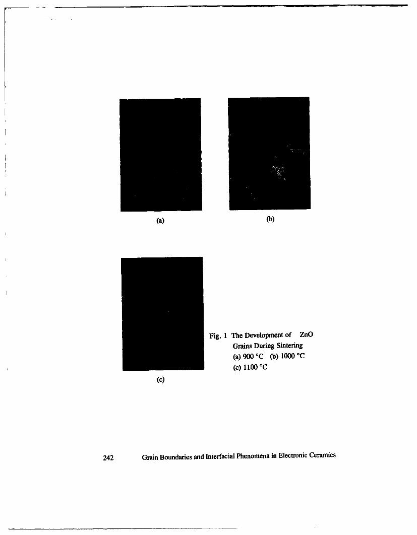
(a) (b)
Fig. 1 The Development of ZnO
Grains During Sintering
(a) 900 °C (b) 1000 -C
(c) 1100 °C
(c)
242 Grain Boundaries and Interfacial Phenomena in Electronic Ceramics

(a) (b)
Fig.2 Three-dimensional Morphology of ZnO Grains
(a) 1000 -C (b) 1100 -C
sub-grainboundaries in ZnO grains. At the beginning of graingrowth, original grains gathered together[7] under surface tension.
With sintering temperature increasing, bigger grains absorb smaller
ones in agglomerations, and develop into perfect crystals by ion
diffusion. Since crystal orientations between grains are different,
and there may be some additives between different grains,
interfaces between small grains can't disappear as soon as the
sintering temperature increases. This may result in the formation ofsub-grainboundaries in ZnO grains.
Based on the above experimental results and discussion, the
process of ZnO grain growth can be classified into two stages: oneis agglomeration of small original grains, the other is grain growth.
The forming mechanism of sub-grainboundaries and the effects
Grain Boundaries and Interfacial Phenomena in Electronic Ceramics 243
of them on the electrical properties of ZnO varistors will be studied
further.
Conclusion
By investigating the development of ZnO grains during sintering,it was found for the first time that there are sub-grainboundaries inZnO grains. With sintering temperature rising, sub-grainboundariestend to disappear. Based on the discovery of sub-grainboundaries,
an improved model of grain growth in ZnO varistor ceramics is
proposed in this paper, i.e., the development of ZnO grains can beclassified into two stages: one is the agglomeration of small original
grains, the other is grain growth.
References
[1]. G.C.Nicholson, J. Am. Ceram. Soc. 48, 214(1965).[2]. S.K. Dutta and R.M.Spriggs, "Grain Growth in Fully
Dense ZnO, J. Am. Ceram. Soc., 53[1], 61-62(1970).[3]. T.K.Gupta, "Inhibition of Grain Growth in ZnO", J. Am.
Ceram. Soc., 54[8], 413-414(1971).
[4]. T.Asokan and R.Freer, "Hot Pressing of Zinc Oxide
Varistor", Br. Ceram. Trans. J., 89, 8-12, 1990.
[5]. Tetsuya Senda and Richard C.Bradt, "Grain Growth in
Sintered ZnO and ZnO-Bi2O3 Ceramics", J. Am. Ceram. Soc.,73[1], 106-114(1990).
[6].Ying-Chung Chen etc., "Grain Growth and Electrical
Properties in ZnO Varistors with Various Valence States ofAdditions", Jpn. J. Appl. Phys., 30[1], 84-90(1991).
[7]. Xiaolan Song and Fuyi Liu, to be published.
244 Grain Boundaries and Interfacial Phenomena in Electronic Ceramics

THE POLYNUCLEAR HYDROXY METAL CATIONS PILLAREDZIRCONIUM PHOSPHATES AND THEIR PROTON CONDUCTIVITY
Y. Ding, J. Rozi~re, D. JonesLAMMI, URA 79-CNRS, Universit6Montpellier II, 34095 Montpellier, France
The treatment of alpha-zirconium hydrogenphosphate monohydratewith polynuclear metal cation sols in definite conditions resulted inthe increase of the interlayer distance to 9-20A. The pillared novelmaterials have the proton conductivity as high as 10- 2Scm-1 at20°C/100% RH. The structural and electrical characteristics werestudied using XRD and conductivity measurement.
1. INTRODUCTION
One of the important route by controlled mixing of ceramicparticles of nanometer scales has been used for developing new types ofmaterials with desired functionality. Layered structured materialsconsisting of thin crystalline layers with a thickness of molecular scalecan be regarded as the ideal composite matrix incorporating variousinserted ceramic sols as well as polar organic molecules. The reactionsto form such a layered composites are called intercalation reaction.
Zirconium phosphate, a two-dimensional layered materials, hasbeen studied extensively in the intercalation chemistry. It was also usedas the ceramic Nasicon precursor and gives the ceramics the highersodium conductivity[I]. Two hydrates of zirconiummonohydrogenphosphates, Zr(HPO4)2 are known: a monohydrate, cc,
and dihydrate, y. The a-phase has a layer structure consisting of layersof metal atoms in a plane bridged by phosphate groups above andbelow the plane of the metal atoms with the P-OH groups pointingbetween the layers. Protons in the interlayer can be exchanged withsmaller cations.
To whom correspondence should be addressed. Present address: School of ChemicalEngineering, Georgia Institute of Technology, Atlanta, Georgia 30332-0100, USA
To the extent authorized under the laws of the United States of America, all copyright interests in this publication are the propertyof The American Ceramic Society. Any duplication, reproduction, or republication of this publication or any part thereof, withoutthe express written consent of The American Ceramic Society or fee paid to the Copyright Clearance Center, is prohibited.
Grain Bound"aries and Interfacial Phenomena in Electronic Ceramics 245

Many metal cations are subject to hydrolysis because of a highelectronic charge or high charge density. Initial products of hydrolysiscan condense and polymerize to form polyvalent metal or polynuclearions, which are themselves colloidal. These larger size ceramic sols canbe exchanged with the interlayer cations of the zirconiummonohydrogenphosphates by first propping the interlayer with largerorganic polar molecules[2 ]. The similar research has been conducted asthe well known pillared clays which resulted in a new class of selectiveheterogeneous catalysts with stable structure by the calcination of theceramic sols pillared clays[3 -4]. However, Conductivity of the pillaredsystems of these types has not previously been concentrated, thoughthe likely high acidity of the galleried interlayer region offers excellentprospects of high ionic conductivity.
In this paper, we will brief out the intercalation reaction ofseveral ceramic sols into the interlayer of a-ZrP and give theconductivity research of the materials.
2. EXPERIMENTAL
oz-Zr(HPO4)2.H20 was prepared by the method of Clearfield andStynex[5] using a 12 mol-dm-3 phosphoric acid solution as the refluxmedium and refluxing for one week. The solid recovered was washedwith distilled water, dried in air and stored without special precautions.Expansion of a-Zr(HPO4)2.H20 was carried out using n-alkylamine ofchain length between 4 and 10 carbon atoms(or aminocaproic acid). Theresulting alkylammonium-intercalated phases are highly crystallineand have interlayer distance in agreement with literature values[6].
Zr(IV) is known to be hydrolyzed even in very acidic aqueoussolutions. Zirconium dichloride oxide aqueous solution, if not verydiluted, gives rise to the predominant tetrazirconium species[Zr4(OH)8(H20)16] 8 + 17 "8](abbreviated as Zr4). In a representativeexperiment, 0.1 M aqueous solution of ZrOC12:8H20 is aged for 5 daysat 50*C. Hydrolysis of aluminum trichloride was performed here usingthe alkylamine as that used to swell the phosphate layer. The PH of theaqueous solution of AIC13.6H20 is adjusted 4.1 to give a limpidsolution of Al:base ratio of 1:2 in which predominant species is so
246 Grain Boundaries and Interfacial Phenomena in Electronic Ceramics
called Keggion ions [A11304(OH)24-12H20] 7+(abbreviated as A113). Thesolution aged a week before use.
Ion-exchange of the alkylammonium ion in a-Zr(HPO4)2.H20for Zr4 and All3 were carried out by suspending I g of the intercalationcompound in a excess of above solution and refiuxing respectively 4and 5 days. The resulting materials were washed with distilled waterthree times ar-d were air dried.
X-ray diffraction powder experiments were recorded by multiple
scanning on an Philips diffractometer using Cu Ka radiation.Powder samples were pressed into pellets of about 1mm thick in
a 13mm diameter steel die under a pressure of 5ton/cm 2. Pellets werestored in dessicators over reservoirs containing sulfuric acid ofconcentrations corresponding to relative humidities, where they wereallowed to equilibrate for 4 days prior to use. The pellets weresubsequently mounted between the two platinum electrodes of a sealedcell. ac measurements were performed in the frequency range 5Hz-13MHz using a computer controlled Hewlett Packard 4192 impedanceanalyzer using an oscillating voltage of 1OOmV. dc measurement wereLarried out at Chemistry Department of Exeter University with avoltage from 0 to 500 mV applied at room temperature across the pelletin 25mV steps, and the current noted when stability was reached. Thesample was equilibrated with humidified hydrogen gas for 2 hoursprior to the experiment.
3. RESULTS AND DISCUSSIONS
Pillaring of the aluminum Keggion ion into a-ZrP was firstreported by Clearfield and Roberts in 1989[2]. Subsequently, Si sol wasreported to be inserted into the interlayer of the phosphate[ 9]. Thespecific objective of them is to achieve pillared layered solids havinghigh specific surface area. That was not a concern of the presentresearch where, on the contrary, "stuffing" of the interlayer space withhighly hydrated sols will contribute to the ionic conductivity. Jones,Leloup and Ding et al preliminary work[10] indicated that the hydrated
Al species pillared a-structured metal(IV) hydrogen phosphate cangreatly enhance the material conductivity. In their work, they foundthat the degree of crystallinity of the material formed after insertiondepends on the reflux times. Longer reflux times reduce the
Grain Boundaries and Interfacial Phenomena in Electronic Ceramics 247

crystallinity and increase the conductivity. Usually, the crystallinity ofthe material prepared is not satisfactory. The interlayer distance variesand is dependent on the chain-length of the pre-swell agent.
+
3 12.25 21.5 30.75 4020
(a)
P
+ +
3 12.25 21.5 30.75 40
20(b)
Fig.1. The XRD pattern of (a) (Zr4(OH)14(H20)10}2+ and (b) keggion
ions pillared a-ZrP
248 Grain Boundaries and Interfacial Phenomena in Electronic Ceramics
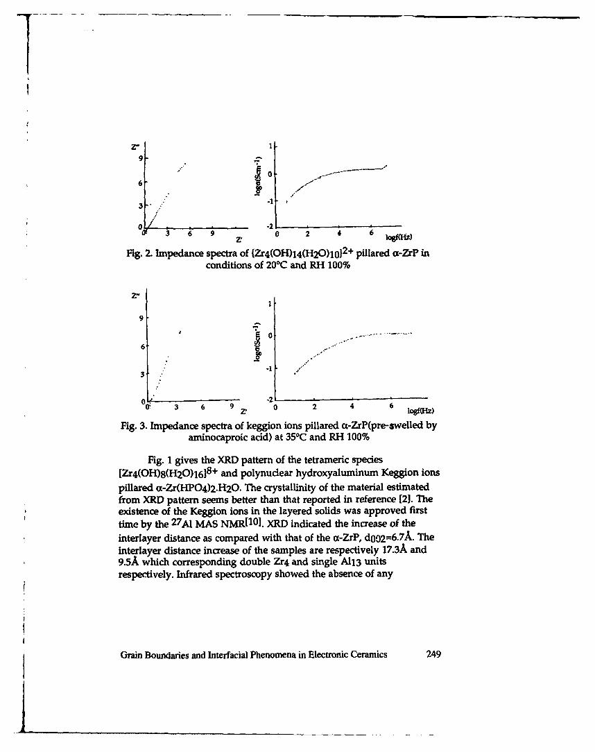
Z7
9-
6
3 -
0' -29F 3 6 9 0 2 4 6 109f")
Fig. 2. Impedance spectra of (Zr4(OH)14(H2O)1oJ 2 + pillared a-ZrP inconditions of 200C and RH 100%
9
60
3I
/1
o0 -2r 3 6 9 0 2 4 6 I go(i z)
Fig. 3. Impedance spectra of keggion ions pillared H-ZrP(pre-swelled byaminocaproic acid) at 350 C and RH 100%
Fig. I gives the XRD pattern of the tetrameric species[Zr4(OH)8(H2O)161 8 + and polynudlear hydroxyaluminum, Ieggion ionsPillared a-Zr(HPO4)2.H2O. The crystallinity of the material estimatedfrom XRD pattern seems better than that reported in reference [2]. Theexistence of the Keggion ions in the layered solids was approved firsttime by the 27 A1 MAS NM.R[1 0]. XRD indicated the increase of theinterlayer distance as compared with that of the ot-ZrP, d0 02=6.7A. Theinterlayer distance increase of the samples are respectively 173A and9.5A which corresponding double Zr4 and single A113 unitsrespectively. Infrared spectroscopy showed the absence of any
Grain Boundaries and Interfacial Phenomena in Electronic Ceramics 249

remaining organic matter, the ceramic sols completely displace thealkyammonium ions.
Fig. 2-3 are respectively the impedance spectra of the abovementioned two kinds of the pillared a-ZrP. The relationship betweenrelative humidity and ionic conductivity, and the relationship betweenconductivity and temperature of the Keggion ions pillared a-ZrP areschematically illustrated respectively in Fig. 4 and Fig. 5.
From Fig. 2-3, it can be seen that ac conductivity of ceramic solspillared a-ZrP enhanced two magnitude higher as compared withpristine ZrP which has a typical value at 25°C/60% RH of 8.10"6 Scm-1.The Zr4 pillared a-ZrP even show an ac conductivity of as high as1.52.10"2Scm"1 at 20*C/100% RH. Fig. 4 shows that the conductivity ofthe A113 pillared phosphate sample depends greatly and increase withrelative humidity. Fig. 5 shows the conductivity of the sampleincreases with the temperature in the definite region. No loss inconductivity due to the dehydration of the material up to 80'C.However, when the temperature is much higher, the conductivitydecreases sharply for the lost of water in the interlayer and the ceramicsols become to the ceramic oxide. The interlayer distance also decreasewhen the sample is heated at higher temperatures. The d002 spacing
24A of [Zr4(OH)8(H20)16] 8 + pillared a-ZrP decrease to 19A after thecalcination of the sample at 3000C for 2 hours. Because of the higherconductivity of the ceramic sols pillared a-ZrP but not ceramic oxidepillared a-ZrP, potential application of it at low temperature directmethanol fuel cell and electrochemical devices will be anticipated.
dc measurement indicated that A1-ZrP showed an ohmicresponse under controlled voltage conditions. The current decayedrapidly to zero after applying 500mV potential which demonstrating noelectronic conductivity. The dc conductivity measured is about thesame as the ac conductivity which support the idea that the chargecarriers are protons. Further proof is also given in reference[8]. Theproton conduction origin from, after exerting electric field on the bothside electrodes, the hydrolysis of the sols such as:
[A11304(OH)24.12H20]7+ -> [A11304(OH)27(H20)9]4+ + 3H+
The different method prepared ceramic sols pillared a-ZrP often
250 Grain Boundaries and Interfacial Phenomena in Electronic Ceramics

gives the different characteristics. If the a-ZrP is pre-swelled byaminocaproic acid instead of alkylamine, the A113 pillared phosphateshows a better crystallinity and much higher proton conductivity of thevalue 1.7-10"2 Scm"1 at 200C/100% RH (see Fig. 3) as compared with thatof butylamine pre-swelled a-ZrP whose proton conductivity is1.10-3Scm-1 at 200C/100RH condition(as shown in Fig. 4). Thephenomenon contradict with the point that less crystallinity willincrease the external surface area and will conducive to the increase inthe conductivity. Even the age time of the sol solution and the
10-2
1-3
10- "rr
L0. ... , 0n
2.8 3 3.2 3.4 3.6 3.8
1000/TFig. 4. Relationship of the conductivity of keggion ions
pillared a-ZrP with the temperature at RH 65%
10-2 . . . . . . ..
10-4
10-6
10-8 " - - . . . ,. . . .0 20 40 60 80 100
RH%Fig. 5. Relationship of the conductivity of keggion ions
pillared 0x-ZrP with the relative humidity at 20'C
Grain Boundaries and Interfacial Phenomena in Electronic Ceramics 251l
,I:' i -
refluxing temperature can greatly affect the crystallinity of the sampleprepared. We once worked at precisely controlled conditions to get thevery well crystallized A113 pillared a-ZrP[11]. The reasons for these arenot dearly understand and are currently being investigated. Anyway,the weak basic characteristic of aminocaproic acid compared withalkylamine will make it be easier displaced by ceramic sols and probablyplays an important role in the phenomenon. The aminocaproic acidpreswelled a-ZrP is also successfully be used as the precursor for theintercalation of larger organic molecules[121 .
4. CONCLUSIONSThe ceramic sols pillared a-ZrP shows a higher proton conductivity
of as high as 10-2Scm-1 magnitude at 20°C/100% RH. The presence ofclosely packed and a highly hydrated acidic ceramic sols in theinterlayer is suspected to supply a conduction way for protons.Different method prepared ceramic sols pillared a-ZrP gives differentconductivity. The samples prepared with the aminocaproic acidpreswelled a-ZrP seems to give a better proton conductivity.
REFERENCES[11 A. Clearfield, P. Jerus and J. M. Troup, Solid State Ionics, 5(1981)301.[2] A. Clearfield and B. D. Roberts, Inorg. Chem., 27(1989)3237.[31 F. Figueras, Catal. Rev., 30(1988)457.[41 M. L. Occelli and D. H. Finseth, J. Catalysis, 99(1986)316.[51 A. Clearfield, R. H. Blessing and J. A. Stynes, J. Inorg. Nuci. Chem.,30(1968)2249[6] U. Constantino, in Inorganic Ion Exchange Materials, ed. A.Clearfield(CRC Press, Boca Raton FL, 1982)p. 122.[71 Mdrtha Aberg and Julius Glaser, Inorg. Chim. Acta, 206(1993)53.[81 C. F. Baes, Jr and R. E. Mesmer, The Hydrolysis of cations, Wiley-Interscience, New York, !976, P. 152.[91 L. Li, X. ULu, Y. Ge, L. Li and J. Klinowski, J. Phys. Chem.,95(1991)5910.[10] D. J. Jones, J. M. Leloup, Y. Ding and J. Roziore, to be published inSolid State Ionics.[11] Y. Ding, D. J. Jones and J. Roziere, unpublished work.[121 Y. Ding, D. J. Jones and J. Rozi6re, to be published in J. Chem. Soc.,Chem. Commun..
252 Grain Boundaries and Interfacial Phenomena in Electronic Ceramics
LI DEINTERCALATION IN LITHIUM TRANSITION METALNITRIDE, Li3FeN2
M.Nishijima, Y.Takeda, N.Imanishi and O.YamamotoDepartment of Chemistry, Faculty of Engineering, Mie University,Kamihama-cho 1515, Tsu, Mie-ken, Japan
M.TakanoInstitute for Chemical Research, Kyoto University,Uji, Kyoto-fu 611, Japan
ABSTRACT
Li ion was easily deintercalated from Li 3FeN2 with one-dimensionalstructure forming Li 3_,FeN 2 in a range of 0•xl.0 in a Li/Li3FeN 2 cell.With increase of x, four kinds of phases (x=0, 0.5, 0.75 and 0.8-1.0)having orthorhombic symmetry sequentially appeared. Mbssbauer spectrasuggested that Li deintercalation oxidizes Fell' to FeIv. The Li/Li3FeN 2cell showed a good reversibility suggesting to be a good candidate for anelectrode for Lithium secondary battery.
INTRODUCTION
It is well known that Li3N has a high Li ion conductivity of about1X10- 2Scm-1 at room temperature, and numerous studies of this interestingmaterial as a solid electrolyte has been performed for last 10 years (1-3).However, Li3N has a low decomposition voltage (0.44V), which makes it diffi-cult to be used as an electrolyte for solid lithium battery.
In the systems of Li-metil-nitrogen, a series of nitrides belonging to a gener-al formula of LiU,_MN. (M: some elements of groups 3, 4 and some transitionmetals, n=2, 3) has been known for a long time (4-6). These nitrides show the
To the extent authorized under the laws of the United States of America, all a.cop ght interests in this publication are the propertyof The Amrican Ceramic Soiety. Any duplication, repoduction, or republication of this publication or any part thereof, withoutthe epress written consent of The American Cerami Society or fee paid to the Copyright Clearance Center, is prohibited.
Grain Boundaries and Interfacial Phenomena in Electronic Ceramics 253

anti-fluorite type structure (5) where LU ions occupy the positions of fluorine inCaF2 . As the fluorite structure has large lattice energy and shows high ionicconductivity, these nitrides make us expect the high stability and high Li ionconduction. In fact, Li-nitrides with 3rd and 4th group metals such as Li3BN2(7,8), Li3AIN2 (9) and Li3SiN2 (10) show high ionic conductivity, whose struc-tural and electrical properties have, therefore, been extensively studied as a solidelectrolyte for solid Ui secondary battery.
Studies of LiU._MN, containing transition metals such as Mn(1l), Fe (12),etc., have also been curried out, but these did not report the application forelectrolyte but only pure physical properties of these interesting compounds. Theintroduction of transition metals might yield electron conduction which spoilsthe properties as an electrolyte. This disadvantage could be turned into an advan-tage if they should work as an electrode for lithium secondary battery. Possiblyhigh lithium ion mobility originating in the fluorite structure and low reductionor oxidation potentials of transition metals may both facilitate Li deintercalationand subsequent Li intercalation in these nitrides. If such a reversibility can berealized, Li U_1MN, will be not only hopeful electrode candidates for Li sec-ondary battery but also exotic materials containing transition metals in unusualoxidation states such as Fel, Coo, which can not be prepared by other methods.
We tried to prepare this type of nitrides by reacting first transition metal ni-trides MNY (M=Ti, V, Cr, Mn, Fe, Co, Ni or Cu) and a lithium nitride U3 N. Wefound that Li3FeN 2 could be easily synthesized using a traditional ceramicmethod in a 1%H 2-99%N 2 stream and that it showed extremely smooth Lideintercalation and intercalation.
EXPERIMENTAL
U 3N and Fe4N (kindly offered by Nihon-shin-kinzoku Co. Ltd.) were usedas raw materials. U 3N was prepared by a reaction of extra-pure lithium sheetsand nitrogen at temperature between 80 and 150*C in a glass reactor, whoseformation was confirmed by X-ray diffraction (XRD) measurements and byweight increase also. Mixtures of Li3N and Fe4N were pressed into tablets of 8mm in diameter and 5 - 8 mm in thickness under a pressure of 3 MPa whichwere subsequently heated in an electrical furnace at 600°C for 12 hr in a 1%H2-
99%N2 stream. The heating rate was 100 C/min. Before firing, the furnace wasevacuated with a rotary pump to remove moisture, oxygen and CO2. PowderXRD measurements were performed on Rigaku RAD-RC (12kW) using
254 Grain Boundaries and Interfacial Phenomena in Electronic Ceramics

monochromated CuKa radiat;on. As the products were very hygroscopic, theywere protected against moisture during the XRD measurement by using a gas-tight holder filled with argon gas. A 7 pum thick aluminum window covered thesample holder plate in an arc.
For the electrochemical study aimed to obtain Li 3_,FeN 2 having various xvalues, single phase Li3FeN 2 was ground and mixed with acetylene-black(electron conductor) and Teflon (binder), and the mixture was pressed into atablet of 12 mm in diameter under a pressure of 1 MPa. A conventionalLi-coin-type cell was assembled using this tablet as a cathode, a Li sheet as ananode and LiCIO 4/PC+DME as an electrolyte. Li ion was deintercalated bydischarging the cell at 150 pAcm- 2.
All the treatments except for heating in a furnace and the discharge-chargeexperiments were carried out in an Ar-filled dry box.
Samples having various Li contents were measured by XRD. For a Reitveldanalysis the intensity data were collected at each 0.020 step width for 2 or 3seconds over a 20 range from 10 to 1000. A computer program (REITAN) wasused for a profile refinement calculation (13). 57Fe Mossbauer measurementswere performed at room temperature. The "Co/Rh source velocity was calibrat-ed by using pure iron metal as the standard material.
RESULT AND DISCUSSION
1. Synthesis and Li deintercalation
Gudat et al. (12) reported that Li3FeN2 was prepared from Fe metal andmolten Li in a N2 stream. But this method requires high purity N2 gas and aspecial furnace. As we wanted to use a conventional furnace, we chose Li3N andFe4N as starting materials. We found that Li3FeN2 could be easily prepared frommixtures of Fe4N and Li3N powder in a l%H 2-99%N 2 gas stream. Whencommercial N2 gas was used oxides and carbonates formed in stead of the ni-tride because of moisture, oxygen and CO2 contained as impurities in the N2 gas.
Starting mixing ratios, firing conditions and obtained phases are listed inTable 1. The starting moler ratio of 3.5:1 brings single phase Li3FeN2. TheXRD pattern agrees with that reported by Gudat et al. (12). Excess Li3N mighthave evaporated during the reaction. Most of lithium-containing nitrides havebeen prepared from Li-excess mixtures as reported, for example, by Formont etal. (6). The fact that when the heating rate was below 20 C/min, single phase
Grain Boundaries and Interfacial Phenomena in Electronic Ceramics 255
could not be obtained even if Tabbe 1the starting moler ratio was Radka Wedlaand pp M is hf, LN-Fe4 ý4 qsm.
3.5:1. It might be considered to u:ie Ram ThqL Md PMoMM
have resulted from such an C C/nib) M tW)
evaporation during heating. As 3.MI 10 600 12 U3 PN Mtdiscussed in the next section, 40.1 10 600 12 UPCM2+ w-e ovwn+ UN nce)however, we can not deny a 5.1 10 600 12 U FeN2+ unko" U Ku=,
3.5:1 10 500 12 U PeN + mnknown+Nab-tYpcpossibility of Fe deficiency 3.5:1 10 600 12 u3PeN2
such as Li3 FeyN2 3.5:1 10 700 12 Meltd to ue F3.5:1 100 600 12 1U FeN
We tried to use Fe metal 3.5:1 1 600 12 LUFeN+Na•--type+ukaoW
powder instead of Fc4N, butsingle phase could not beobtained under any condition listed in Table 1. Oxides on the iron metal surfacemay hinder the reaction.
Figure 1 shows the closed circuit voltage (CCV) and open circuit voltage(OCV) curves of the Li/Li3FeN2 cell for the charge direction (Li deintercalation)at a current density of 150 ILAcm-2. Both the CCV and OCV are very flat ina wide range (the 2.0potential only increases •by 30 mV from x=O to ..due to an overpotential
is very small. These0
properties of Li3FeN 2 >
are very characteristic 0.0 C .
and remarkable, and 0.0 0.5 1.0these are advantageous x in U3 _xFeN 2to practical use as an Fig. 1 Open circuit voltage and closed circuit voltage of LiU.zFcN 2.
electrode for Li cell. OCV;dot line, CCV;solid line (150pAcm-2)
X-ray diffraction patterns for various Li contents, x, are shown in Fig. 2. Theextraction of Li smoothly occurs up to x=1.0, however, in the range of x>1.0,the CCV suddenly increases, and XRD patterns become indistinct. These prob-ably resulted from a decomposition of Li3-xFeN 2.
Four distinct phases have been found to form for xs1l.0. All these phaseshave orthorhombic symmetry, ibam. In order of appearance, they are named asa-, f-, y- and b-phases. Lattice parameters of each phase are listed in Table II,and the variation of these parameters with total Li content is shown in Fig. 3.
256 Grain Boundaries and Interfacial Phenomena in Electronic Ceramics

The volume ratio of these phases was roughly estimated from the peak intensityas a function of total Li content as shown in Fig. 4.
Though the inhomogeneous reaction in the Li cell brings sometimes the coex-istence of a, P and y phases. A typical 2-phase reaction seems to occur on Lideintercalation up to x=0.75. For xO.75 each phase keeps its parameter valuesalmost constant, and the each solid solution range seems to be very narrow: thatis, x=O for a-phase, x--0.5 for P-phase, x=0.75 for y-phase. The lattice parame-ters, especially the b axis, decrease with a sequence of the phase transition.
4.9 -
0 0 0 0 5-9.5
9.
4.8-
-47 0 0 0
20 40 0.25 0.5 0.75 8A5
20/deg (C u Ka,) X in LU-,FeN.
Fig. 2 X-ray diffraction patterns of Li,_ FeN 2 .W 0~ o 0for various charge depths. b a0 A A A
c a x i a m m
Table 2 Fig. 3 Variation of the lattice parametersas a function of x in Li,_FeN2.
Lattice parameters of each phase
u-phase 4.8630(3) 9.6318(5) 4.7833(2)
[5-phase 4.830(3) 9.400(4) 4.714(3) 40.fo-phase 4.820(v ) 9.100(3) 4.750(2)as A A
d-phase 4.915(3) 8.604(7) 4.769(4) * "
0 0.25 0.5 0.75
X in Li6FFeN e
Fig. 4 Composition dependence ofphase pontent for the 90) .(FeN..
Grain Boundaries and Interfacial Phenomena in Electronic Ceramics 257

Fi. 5 Observed calaclated and difference plots of LiýFeN,.
Fig. 6 Crystal structu•e of UFcN2.
Table 3
Crystallographic data, atomic positions and displacement parameters of UiFeN 2 .
Space group /bamLattice constants(A) a=4.8630(3)
b=9.6381(5)c=4.7833(2)
D(gc--nf 2.96
Atom Wyckoff Occupancy x y z Uq(pmn)*position
U(1) 8g 1.0000 0.0000 0.7434(6) 0.2500 97(17)U(2) 4b 1.0000 0.5000 0.0000 0.0000 97(17)Fe 4a 0.856(3) 0.0000 0.0000 0.2500 41(4)N 8j 1.0000 0.2278(2) 0.8783(4) 0.0000 71(13)
2. Crystal structure and structure changes
To see the detailed structure changes, the XRD Reitveld refinement for eachphase was tried.
Single phase Li3FeN2 assumes orhtorhombic symmetry, space group barn.The XRD pattern for Reitveld refinement result is shown in Fig. 5 and thecrystallographic data are given in Table 3. As shown in Fig. 6, Li3FeN2 crystal-lizes in a distorted anti-fluorite structure, in which Fe4N tetrahedra sharingedges with each other form one dimensional chains to the c direction.
258 Grain Boundaries and Interfacial Phenomena in Electronic Ceramics
I|
In the present work, the single phase of Li3FeN 2 was synthesized from amixture of Li3N and FeN at a ratio of Li:Fe=3.5:1, not 3:1. As mentionedabove, we first thought that the difference between the formal composition andthe starting ratio was caused by evaporation of Lk3N during synthesis. Gudat etal. (12) also refined the structure by fixing the composition as Li3FeN2. But inour structure refinement, the fixation of the moler ratio at Li:Fe=3:1 did notbring a reasonable value of the reliability factor (R). When the Fe site occupancywas varied, it converged to 0.86 with a low R factor. This value agrees well withthe batch composition (Li:Fe=3.5:1=3:0.857), which suggests that the Fe site(4a)are considerably vacant or a substitution of Li for Fe at 4a site occurs rather thanthe Li evaporation.
Atomic distances shown in Table 4 agree Table 4well with Gudat's data, however, the composi-tion of our sample is most likely different Selected interatomicfrom the ideal one, Li3FeN2. distances (A)
The refinements for a, 0 and y phases didnot bring the reasonable R factors, because of Fe-N 2.00(2)the strong orientation and the existence as Li(1)-N 2.09(4)multiple phases. However, the phase changes 2.13(4)have been considered as below based on the Li(2)-N 2.13(3)OCV, CCV and XRD results.a). a - D (0--xý0.5)The change in lattice parameters from a to P3-phase is isotropic, though rela-
tively large. In this stage, the OCVcurve is perfectly flat suggesting that the difference in Gibbs Free energy is verylow.b). P - y (0.5_<_0.75)
As for the change from ai to P, the a and b parameters decrease, while the caxis increases. Because of a larger change in Gibbs free energy than that of a -0, the OCV has a step in this range.c). y - 6 (0.75-xg1.00)Though there is no change in space group, the a and c axes of the 6-phase
largely increases and the b axis decreases in comparison with those of phase y.Phase 6 exists as a monophasic solid solution for 0.75SX-_1.00.
As seen in Fig. 3, the b axis monotonically decreases with phase changes fromct-phase to 6-phase. This indicates that Li is deintercalated from (0 0 4) planes,that is, Li(1) is deintercalated dominantly.
Grain Boundaries and Interfacial Phenomena in Electronic Ceramics 259

As mentioned above, Li3-xFeN 2 decomposes at x>1.0. The decompositionalso occurs when the current density is increased. If the overpotential was veryhigh (if the current density was large), decomposition began at smaller x val-ues. The decomposition voltage was estimated to be about 1.5V.
3. M6ssbauer spectrum
M6ssbauer spectraof Li3x FeN 2 withvarious Li contentsmeasured at room x-0.2
temperature are shownin Fig. 7 and the Isomer
Shift (IS) and quadru- Ex=050pie splitting (QS) arelisted in Table V. For ,-
x=0.0, a single kind of T ... .. .quadruple doublet (IS = :- x-.75
0.0525 mim/s, QS =0.875 mm/s) assignedto Fern in low spin stateis observed. With =.-increasing x a newdoublet with a morenegative isomer shift I I I ,and a smaller quadruple -4 -2 0 2 4
splitting overlaps, and V (mrnis)
finally for x>0.75 it Fig. 7 Room temperature Mossbauer spectra of U3FeN 2.
becomes dominant.The shoulder appearing at the right of the quadrople peak for x>0.75 has as-
signed yet, which may be attribute to the decomposed by product brought byovercharge. This suggests that Li deintercalation oxidizes Fel' to Fe'v. Thecomputer peak fittings reveal that each phase has slightly different IS and QSvalue for both Fer and Felv. The magnetic susceptibility measurement ofLi3FeN2 by Gudat et al. (12) indicated that the Fem ions were in low spin state.The more negative value of IS (-0.22 mm/s) of Few in Li2FeN2 than the typicalvalues of -0.0 mm/s measured for oxides likes in SrFe4+O3(14), CaFe4+O3(15),
260 Grain Boundaries and Interfacial Phenomena in Electronic Ceramics
etc., is consistent with an assumption that the FeWv state in Li3-xFeN 2 is in lowspin state of de4dy°.
4. Li intercalation reactionThe discharge OCV and CCV curves for the samples charged to x=1.0 are
shown in Fig. 9. The potential difference between the charge and dischargecurves is small, indicating a high reversibility. In the XRD pattern of the fullydischarged sample, only the original phase (a phase) was seen. Li3FeN2 has thusbeen found to have high capacity of 260 mAhg-1.
CONCLUSION
Li3FeN2 was easily synthesized from a 3.5:1 mixture of Li3N and Fe4N byusing a traditional ceramic method in a 1%H2-99%N 2 stream. Li could be dein-tercalated forming Li3-xFeN 2 in a range of 0!_x•1.0. With increase of x, fourphases sequentially appeared. The OCV and CCV curves for both charge anddischarge directions were very flat and the overpotential was very low. Li3FeN 2has ideal properties as both a cathode and an anode for lithium secondary bat-tery.
REFERENCES1. A.Rabenau, Solid State Ionics, 6, 277(1982).2. T.Lapp, S.Skaarup and A.Hooper, Solid State Ionics, 11, 97(1983).3. P.M.Richards, J.Solid State Chem., 33, 127(1980).4. RJuza, H.H.Weber and E.Meyer-Simon, Z.Anorg.Allg.Chem., 48,273(1953).5. RMuza and F.Hund,Z.Anorg.Allg. Chem.,13,257(1948).6. M.Fromont, Rev.Chim.Niner., 259,447(1967).
7. H.Yamane, S.Kikkawa, H.Horiuchi and M.Koizumi, J.Solid State Chem., 65,6(1986).8. H.Yamane, S.Kikkawa and M.Koizumi, J.Solid State Chem., 71, 1(1987).9. H.Yamane, S.Kikkawa and M.Koizumi, Solid State Ionics, 15, 51(1985).10. H.Yamane, S.Kikawa and M.Koizumi, Solid State lonics, 25, 183(1987).11. RJuza, E.Anschutz and H.Puff, Angew.Chem., 71, 161(1959).12. A.Gudat, R.Kniep and A.Rabenau, J.Less-Common MeLt, 161, 31(1990).13. EIzumi, J.Mineral SocJpn., 17,37(1985).
14. J.B.MacChesney, R.C.Sherwood and J.F.Potter, J. Chem.Phys., 43,1907(1965).15. Y.Takeda, O.Naka, M.Takano, T.Shinjo, T.Takada and M.Shinada, Mat.Res.Bul.,
13,61(1978).
Grain Boundaries and Interfacial Phenomena in Electronic Ceramics 261

POSITIVE HOLE-TYPE CHARGE CARRIERS IN OXIDE MATERIALS
Friedemann Freund* . Eun-Joo Whang**, and Francois Batllo***,
Department of Physics, San Jose State UniversitySan Jose. CA 95192. USA
Lionel Desgranges and Corinne Desgranges,
Chimie-Physique des Solides. Ecole Centrale Pi.,s92295 Chitenay Malabry, France
and Minoru M. Freund
Department of Physics. University of CaliforniaBerkeley. CA 94370. USA
ABSTRACT
Defect electrons on the 02- sublattice. equivalent to 0- states, also known as oxygen-associated orpositive holes, are electronic defects in otherwise insulating oxide materials. Though extensivelystudied as radiation-induced, paramagnetic defects in a wide range of materials at low temperature,little was known until now about the occurrence of 0- in the technologically more important rangefrom 20-1000'C. We show that MgO single crystals of highest purity contain about 500 ppmperoxy-type (022-) defects, diamagnetic and electrically inactive, which release positive holes uponheating. We describe five experiments, each designed to address different aspects of the 0- defects:(1) electrical conductivity, (2) dielectric polarization, k3) magnetic susceptibility, (4) thermalexpansion, (5) refractive index. 0- charge carriers appear between 200-400'C. Their mobility is lowat first but increases rapidly above 450°C. They augment the dielectric polarization and give rise to apositive surface charge that increases between 450-750'C and then decreases. Between 200-300'Cthe 0- are still spin-coupled, probably in a bipolaronic state. Though the 0-/02- ratio is only1:1000, the 0- cause a uniform increase of the thermal expansion without strain-induced broadeningof the x-ray reflection. This suggests a high degree of delocalization of the 0- wave functions, equi-valent to a decrease in the average electron density on 02- anions and, hence, decreaseing ionicity ofthe Mg2+-02- bond. This is corroborated by the increase of the refractive increase by =0.5% andrecent chemical shift measurements of the 25Mg and 170 NMR signals which suggest increasingcovalency of the Mg 2+-0 2- bond with increasing temperature. 0- charge carriers may have far-reaching implications for the electric properties of otherwise highly insulating oxide materials.
mailing addres: NASA Ames Research Center.MS 239-4 Moffett Field. CA 94035now at the Department of Physics. Cornell University. Ithaca. NY 14853now at INTA. 2281 Calle de Luna. Santa Clara. CA. 95054
To the extent authorized under the laws of the United States of America, all copyright interests in this publication are the propertyof The American Ceramic Society. Any duplication, reproduction, or republication of this publication or any part thereof, withoutthe express written consent of The American Ceramic Society or fee paid to the Copyright Clearance Center, is prohibited.
Grain Boundaries and Interfacial Phenomena in Electronic Ceramics 263

I. INTRODUCTION
Our interest in MSO derives from the fact that it is well suited to serve as model material for the studyof impurities and point defects in oxide materials in general. Specifically, we try to understandelectronic defects that may occur in oxides and strongly affect their physical properties. Electronicdefects in highly insulating, wide band gap oxide materials are generally believed to be alwaysassociated with transition metal impurities. However, electronic defects occur in such oxides that areMo linked to transition metal impurities: defect electrons associated with the 02- sublattice. They havebeen variously called positive holes, oxygen-associated positive hole centers, or simply 0- states,and they have been known for years as radiation defects, introduced either intentionally or naturallyby x-ray, y-ray or a particle bombardment 1. Observable in many materials at low temperatures,primarily by means of electron spin resonance (ESR) spectroscopy 2, such radiation-induced 0- areunstable and generally anneal rather rapidly as the temperatures rise to room temperature or slightlyabove. The generation of such 0- may be considere a photoionization:
02-+ hv -* 0- + e- ()
Eq. (1) implies that, in order to generate 0-. the energy of the incident photon has to exceed the bandgap of MgO which is >8 eV 3. It may therefore come somewhat as a surprise to many that 0- statescan also be generated by simple heating to moderate temperatures. We shall show in this report thatMgO crystals of the nominal highest purity grades generate O-i. 'ie temperature interval 200-5000C.Obviously, these crystals contain some kind of dormant defect. tat release 0- without the help fromionizing radiation. The process is reversible upon cooling, suggesting that the O- return to a dormantstate. Defects that could potentially generate such 0- are self-trapped positive hole pairs, inactive atambient temperature but dissociating upon heating according to:
O;_ 4* - + 0- (2a)
Self-trapped positive hole pairs may also be described chemically as peroxy anions, O; . Since anMg 2+ vacancy is double negatively charged, two positive holes trapped on adjacent 02= sites wouldcompensate for these charges. Therefore, Mg 2+ vacancies are favorable sites for trapping twopositive holes, and an Mg 2+ vacancy - peroxy anion aggregate represents a neutral defect. Using theKroger point defect designation 4 where V"M represents the Mg2+ vacancy and where superscriptdot, prime and cross stand for positive, negaltve and neutral charges respectively, it is convenient towrite eq, (2a) as follows:
to. "VM8X ca [0o V- o'1K (2b)
Eq. (2b) indicates two positive holes decoupling their spins but remaining bound to the cationvacancy by Coulomb interaction: the initial step. If the dissociation proceeds further it becomes:
[OVMgO*IX 4 [o' V Mgl + 0' (2c)
264 Grain Boundaries and Interfacial Phenomena in Electronic Ceramics

where the new species 0 represents an unbound positive hole. Such an unbound 0- is a hole stateinjected into the 0 2p-dominated valence band 5. The braketed defects on the left and right hand sidesof eq. (2c) correspond to the Vo and V-centers, respectively, which have been known for some timefrom low temperature ESR studies of radiation-induced defects in the alkaline earth oxides 1. To ourknowledge, self-trapped positive hole pair defects, adjacent to a divalent cation vacancy, have neverbeen studied systematically, nor even proposed in the ceramic and material science literature.However, if they exist, they may have far-reaching consequences for the properties, electronic andothers, of highly insulating oxide materials.
2. EXPERIMENTAL PROCEDURES
We have carried out five experiments, each designed to address different physical properties broughtabout by the 0- states. Specifically we have measured:
(1) d.c. electrical conductivity,(2) dielectric polarization,(3) magnetic susceptibility,(4) thermal expansion by x-ray diffraction,(5) refractive index.
All measurements were done with nominally high purity MgO single crystals, grown by carbon arcfusion 6 and obtained from W. & C. Spicer Ltd., England. 4N-grade (99.99%) crystals contain tran-sition metal impurities at levels of =20 wt.-ppm (Cr+Mn+Ni), <30 wt.-ppm Fe. plus <50 wt.-ppm(AI+Si). The OH- concentration (not included in the nominal purity rating) is 10-100 per 106 02-.The d.c. conductivity measurements of 4N- and 3N-grade MgO crystals, about 10 x 10 x I mm,were carried out between 200-1000*C in Ar, using At electrodes in 2-electrode, 2-electrode + guard,and 2-electrode + 2-probe configurations, measuring currents and potentials with KEITHLEY 610Celectrometers 7. Below 500'C the conductivity was measured in a Faraday cage to reduce ambientnoise 9. The conductivity a can be written as the sum of all contributions from charge carriers i:
a = Y, oi exp [-Ei/kT] (3)
where Oo and E are the preexponential factor and activation energy, respectively, while k and T havetheir usual meaning as the Boltzmann constant and the absolute temperature in Kelvin. For thedielectric polarization measurements a newly developed technique was used, Charge DistributionAnalysis or CDA, which utilizes the effect that, when a dielectric is suspended, contact-free, in anelectric field gradient along an axis z, a force F, acts on it 9. 1o. This force depends upon the fieldgradient and the polarization P of the sample:
F z f' P -VEextdV) (4)
Vwhere the volume integral contains the sample but not the sources of the field. P contains at least fivecontributions arising from the electronic polarizibility, the ionic polarizibility, any local defects that
Grain Boundaries and Interfacial Phenomena in Electronic Ceramics 265
may rotate in the electric field or change their polarizibility, any space charges that are mobile in the
externally applied electric field, and surface charges:
P = Pei + Pion + Plocal + Pspace + Psurface
Bulk and surface contributions, Fy and FA, can be separated by measuring the force upon fieldgradient reversal, F+ and F . The sum Pei + Pion + Plocal + Pspace is invariant to reversal, whilePsurface is not, we o~tain exlpressions for the bulk and surface contributions, respectively:
F =(-( I - [(Pel + Pion + Plocal + Pspace)lVFexd (5a)
and F& 2 (F, - Fz+ J f(surface)Vex, dV (Sb)V
where e is the bulk dielectric constant and co the permitivity of vacuum. The factor E(e- 1 )/4x dropsout in the derivation of eq. (5b) because FA only refers to the surface charge layer. Using a PERKINELMER TGS-2 microbalance as a force measuring device and an axially symmetrical electric fieldgradient between a 2 mm diameter circular bias and a cylindrical ground electrode, 10 mm diameter,10 mm high, F- and F+ were measured between 25-850*C during repetitive heating and coolingcycles in high purity nitrogen. The magnetic susceptibility was measured between 25-8500C with aPRINCETON APPLIED RESEARCH Vibrating Sample Magnetometer, Model 4500, equipped witha high temperature BN probe and a 5.4 KGauss electromagnet. The measurements were conductedwith a 15.6 mm long, 4.8 mm diameter 4N-grade MgO crystal during heating/cooling at 40 C/min
under a few millitorr of He ". The intrinsic magnetic susceptibility of MgO, XMgO, is -10.6-10-6
emu/ mole and that of paramagnetic impurites is given as:
N J(J+l) e22(62X 3 kT (6)
where N is the number of paramagnetfc species, g their Landd factor, and g the Bohr magneton. 0-is a p5 ion with spin momentum S =., and a magnetic momentum L = + 1. Since ft shell is morethan half filled, J = S+L = . and the Landd factor, g = 3J(J+1) + S(S+I) - = , is 1 33Assuming a paramagnetic transitipn metal concentration of 50 ppm, the contribution is =0.2.10-6
emu/mole at 200'C, decaying as T.. The thermal expansion measurements were conducted with acleaved 4N-grade MgO plate, 10 x 10 x 0.2 mm, annealed at 8000 C, followed by slow cooling. Themeasurements were done during heating to and cooling from 8000 C at 10C/min using a speciallydesigned x-ray diffractometer at the Ecole Centralp Paris, France, equipped with a position-sensitive,multichannel detector. For the refractive index measurements a large, optically clear 3N-grade MgOsingle crystal was cut and polished into a prism with a 39055" angle. A 3N-grade crystal was chosenover one of the 4N-grade crystals because the latter tend to be cloudy due to minute cavities fornedduring cooling from the gas-saturated melt. The MgO prism was placed on an alumina support insidea tube furnace and heated in air. To minimize convection both ends of the tube were loosely closedwith fused silica windows. The furnace was mounted on a 40 cm diameter goniometer, and thetemperatures were adjusted manually between 25-800'C, using a Variac. The refractive index wasmeasured at the He-Ne laser wavelength of 603 nm by the method of minimum deviation.
266 Grain Boundaries and Interfacial Phenomena in Electronic Ceramics

3. RESULTS
3. 1 Electrical Conductivity
Fig. I summarizes the electrical conductivity of MgO. The bold solid line traces the high-temperature(HT) conductivity where the activation energy is about 2.4 eV, due to ionic diffusion 12-4. Anelectronic contribution may also be present, even in nominally pure MgO 13, but no explanation hasbeen offered except for the statement that the electronic charge carriers appear to be positive. While
-4 =4I lI l l I
o ooo o o. o0 0 0 10o888 8 8 8
24 0V
-10•
VC4-C I4
-160.5 1.0 1.5 2.0 2.5
31/T [10 K]
Fig. 1: The d.c. conductivity of MgO single crystals measured during heating/cooling cycles. Solidline: High temperature (I-IT) predominantly ionic conductivity (activation energy 2.4 eV);Dashed lines: low temperature (LT) conductivity during cooling. usually assigned to surfaceconduction (activation energy =1 eV); Large filled and open squares: conductivity duringheating with a sniall but reproducible maximum in region II and a rapid increase in regionIII; Small squares: LT branches measured during intermittent cooling, indicative of thegeneration of charge carriers characterized by the same I eV activation energy.
Grain Boundaries and Interfacial Phenomena in Electronic Ceramics 267

the HT conductivity can be followed down to -WO0 C, provided the sample is cooled slowly, italways changes into a low-temperature (LT) branch indicated by bold dotted lines. Two LT branchesare shown as examples. They are characterized by an activation energy of about I eV 16-18
The filled and open squares in Fig. I combine conductivity data obtained during detailed studies ofthe LT region . . Between 200-4000 C, when the conductivity was still in the 10-15-10"-14 it-1cm- 1
range, a weak maximum occurred which was reproducible with a time-dependent hysteresisbehavior. Above 4500C the conductivity rose steeply by several orders of magnitude, and a set of IeV branches were observed during intermittent cooling and reheating at 10°C/min. Upon coolingfrom above 900*C the conductivity followed approximately the bold solid and dotted lines. Afterannealing at room temperature the steeply rising section was reproduced. The I eV activation energyconstant slope branches obtained during intermitlant cooling suggest that they are caused by chargecarriers that are generated in increasing number.
The disadvantage of conductivity measurements is that it is not possible to determine the sign of thecharge carriers. Hall effect measurements 19. 20 are not possible with MgO single crystals, at leastnot in the temperature region of interest here, due to their low conductivity. Thermopotentialmeasurements which suggested positive charge carriers in the HT region 15 proved inconclusive inthe LT region. Because MgO is an insulator, mobile electronic charges are predicted to diffuse to thesurface, causing the surface to acquire a distinct charge 5. However, at the time when the con-ductivity measurements were made . no method existed to detect suchsurface charges.
32 Dielectric Polarization
In response to the need to measure surface charges a new technique was dPL',oped: ChargeDistribution Analysis. CDA provides unique information about bulk and surfce charges as brieflydiscussed above and elsewhere 9. 21. 10. Fig. 2 shows the bulk dielectric polarization FX(top) andsurface charge contribution FA (bottom) of a 4N-grade MgO single crystal as a function oftemperature between 100-6000 C, measur--d isothermally over 10 min at each of the indicatedtemperatures during stepwise heating at +50V and -50V. Three distinct regions can be identifiedwhich correlate with the regions I. I1, and Il in the d.c. conductivity plot in Fig. 1. Below 200'C Fyis temperature-independent such expected from the fact that the dielectric constant of a near-idealdielectric is essentially temperature-independent. The MgO surface is slightly negative as is shown byFA, consistentv. thermodynamic arguments 22. 23 derived from the differences in the free energiesof formation of c-.tion and anion vacancies in an ionic material such as MgO 24.
Between 200-4(00 C F- increases about 5-fold, very sluggishly at first, indicating that Plocal beginsto make a measurable contribution. Since there is only a minute increase in the d.c. conductivity asshown in Fig. 1, the contribution from Pspace appears to be negligible. The increase in Plocal impliesthat the MgO cyrstal cottains defects which are either dipolar and orient in the externally applied fieldor undergo a significant increase in polarizability. Fy seems to reach a steady state value around4000C. FA tends ever so slightly towards positive values between 200-400'C, indicating theappearance of at least some positive charge carriers. The sluggishness with which the polarizationreaches a steady state suggests that the the polarizable defects behave as a highly viscous jelly.
268 Grain Boundaries and Interfacial Phenomena in L ic Ceramics

36
121
20N i- 10 main
10 'S1s6 eo
35
30
i 25z
20
C4
-15N
If0 10
.5.
0 100 200 300 400 500 600o
Tempera C]
Fig. 2 F]p: Fl, representative of the bulk polarization obtained from F+ and F measurements at
+50V and -50V bias respectively. FE increases sluggishly between 200-400'C and morerapidly above 4500C, indicating the generation of mobile charges. Upon slow cooling theFI(T) curves are reversible, indicating that the mobile charges become re-trapped uponcooling. Bogom: FA, representative of the surface contribution, shows that, below 200°C,t~ie MgO surface is weakly negative, becomes weakly positive 200-4000 C and stronglypositive above 450°C. The charges which are generated in the bulk carry a positive sign. "
Grain Boundaries and Interfacial Phenomena in Electronic Ceramics 269

Between 450-6000 C F1 : increases 2-fold over the steady state value at 4000 C, e.g. 10-fold over the20-2000 C value. The response to the applied field is fast, suggesting highly mobile charge carrierswhich make a significant Pspv= contribution. Concurrently F, becomes strongly positive, confirmingthat the charge carriers are positive. Around 600 *C F: reaches a value which remains approximatelyconstant upon further heating to about 750-800*C. The decrease of FA between 525-5500C. thehighest temperature shown in Fig. 2 (bottom), is an artifact. Since the experimental proceedurerequires that F- and F+ be measured sequentially, the mobility of the charge carriers has to be takeninto account during data evaluation. In the case of a strong positive surface charge the response isfaster under negative bias than under positive bias. For the data shown in Fig. 2 (bottom) this effectwas not taken into account.
25
MgO: I, (T)oE 20S
z15
X 10 3
0 20V
10
I 110In
0104V
500 600 700 800 900 1000
Temperature [°C]
Fig. 3: FA as measured in another CDA experiment with MgO using bias voltages between 4-30V:The positive surface charge continues to increase to about 750-800C and then decreasesupon further heating.
270 Grain Boundaries and Interfacial Phenomena in Electronic Ceramics

Fig. 3 depicts a set of FA(T) values obtained in a separate run where FA is shown to becomeincreasingly positive up to 750-800*C and decreases only above 800*C. The decrease above 800WC isreversible, even during fast cooling at a rate of 10-20*C, provided that the sample was not heated fora very long time above 800°C. Below 7501C the reversibility upon cooling becomes rate-dependent.If cooling is fast, the positive surface charge may be frozen in, unless the crystal is annealed attemperatures above 200-400*C. Comparing the results from d.c. conductivity and dielectricpolarization experiments suggests that the observed effects are caused by the same defects and/orcharge carriers. The positive surface charge is consistent with the proposed appearance of O--typecharge carriers as formulated by eqs. 2a-c. However, in order to ascertain that these charge carriersare indeed positive holes, we need additional information such as may be obtained through improvedhigh temperature magnetic susceptibility measurements.
3.3 Magnetic Susceptibility
The results of our magnetic susceptibility measurement are shown in Fig. 4. MgO is diamagnetic withx = -10.6-10-6 emu/mole, and its diamagnetism is temperature-independent 25. Any contributionfrom 50 wt.-ppm paramagnetic transition metal imjpurities is less than +0.2-10-6 emu/mole above200*C, decreasing as l/T as indicated by eq. (6) 26. A peroxy anion represents two tightly spin-coupled 0-and is diamagnetic 27. The 0--O- bond is highly covalent, but not strong because theshort (1.5 A) bond distance results in a significant internuclear repulsion. Therefore, like the F-Fbond in molecular F2, the 0-O- bond easily dissociates. When this happens, the spins decouple.Therefore, if any paramagnetism apgears which increases with temperature. it can only be due toparamagnetic states related to the 02- sublattice. The only such species are 0- states. The opencircles in Fig. 4 show the paramagnetism measured during heating at 40 C/min. The data obtainedduring cooling are nearly identical. Paramagnetism appears around 300°C, increasing up to about500*C reaching a value of nearly +2.10-6 emu/mole over the diamagnetic baseline at -10.6.10-6
emu/mole. Above 500*C the paramagnetism decreases approximately as I/T. The solid line withopen triangles, which represents the contribution of paramagnetic species assuming no U/T decrease,can be viewed as the generation curve as a function of temperature. Assuming that the orbitalmoment of 0- in MgO is the same as that of free 0- (an upper limit) the 0- concentration has beenestimated to be of the order of I000 500 at.-ppm 11.
Comparing the magnetic susceptibility measurements with the CDA results reveals a potentiallyinteresting discrepancy. FL, the bulk polarization, began to increase around 200°C, suggestingdefects which become more polarizable. If we assume that 200TC mark the threshold for thedissociation of the self-trapped positive hole pair defects as described by eqs. 2a/b, the question iswhy the paramagnetic signal appears only around 300*C? A possible explanation is that, when thepositive hole pair begins to break up, the spins of the 0- still stay coupled, corresponding to abipolaronic state where two spins remain paired and, hence, diamagnetic, even though they are nolonger spatially close. Only when the mean thermal energy kT exceeds the spin-spin coupling will thebipolaron state break down and become paramagnetic. Eq. (7a) rewrites eq. (2b) with the electronspins. The left hand side represents the diamagnetic positive hole pair, while the center and the righthand side represent the progressive decoupling and transition to the paramagnetic state.
Grain Boundaries and Interfacial Phenomena in Electronic Ceramics 271

* 4
. .|
E m* 3
a. 2
E &oK 1I
C 10
E
C. 00 200 400 600 800 1000
Temperature [0C]
Fig. 4 Magnetic susceptibility X of MgO, intrinsically diamagnetic at -10.6 x I0" emu mole- 1,measured with a Vibrating Sample Magnetometer. Open circles: Measured data indicatingthe appearance of paramagnetism between 300-500 C. Dashed line: fr decay of X. Opentriangles: Calculated concentration of paramagnetic centers reaching saturation at 500-C.consistent with positive holes, 0. generated by peroxy dissociation.
[Io "lx [TOR V"k 1O]. [TO* V- TO'lx (7a)0 MM :diamagnetic bipolaron (diimagnetic) paramagtetic
The delay between the increase in the dielectric polarization, about 2000C, and the appearance of theparamagnetic signal, about 300°C, could therefore mean that the positive hole pairs remain spin-paired for about 100IC even though their chemical bond is already broken and their polarizibility hasincreased. In fact, to account for the large increase in Fy between 200-300'C as shown in Fig. 2b,the polarizibility of the 0- pairs must increase significantly, given that their concentration is probablyless than 500 at.-ppm. Such a large increase suggests that a high degree of delocalization of the 0-
272 Grain Boundaries and Interfacial Phenomena in Electronic Ceramics
wave functions, even though the associated spins still remain paired. When the concentration of theparamagnetic centers reaches saturation around 5000C, all 0--O- bonds are broken and their spinsfully decoupled. This implies that the positive hole pairs are completely dissociated with the numberof paramagnetic species remaining constant.
Mg*" T To.x [ " V*M8 , + 1'O" (7b)
Eq. (7b) describes the generation of unbound 0-, e.g. 0- that become mobile charge carriers 5. Thisis consistent with our d.c. conductivity and CDA results indicating a generation of mobile chargesabove 450°C which make a large Pspace contribution. As their mobility increases to 750-8000C, theMgO surface becomes ever more strongly positive.
3.4 Thermal Expansion
If there are defects in the MgO which undergo a sequence of dissociative transformations as describedby eqs. (2a-c) and eqs. (7a/b), we should also see their effect in the thermal expansion behavior. Wenote that, crystallizing the face-centered cubic, densely packed NaCI-type structure with no phasetransition, the thermal expansion of MgO must be monotonous 28. However, anomalies in thethermal expansion behavior of nominally high purity MgO crystals have already been reported earlier29.30. With a dilatometer the expansion Al/I, where I is the linear dimension of the sample, is the sunof the intrinsic lattice expansion plus any strain contribution that may arise from the presence ofdefects. By contrast, measuring the thermal expansion by x-ray diffraction gives the "true", intrinsiclattice expansion, while any strain contributions arising from defects lead to a broadening of the x-raydiffraction lines.
The results of our x-ray diffraction experiment are shown in Figs. 5a/b. The individual data points lieso close that they appear as a solid line. The results measured during heating and during cooling arenearly indistinguishable. Clearly, the thermal expansion behavior is anomalous between 200-500'C.Fig. 5b shows the expansion coefficient ot which increases at 200"C, the same temperature at whichthe dielectric polarization starts to increase. It then rises to a maximum around 400WC and decreases to500°C. Above 500'C cc continues to increase but with a different slope than below 2000C. There isno indication for strain-induced broadening of the x-ray reflection. Since the temperatures at whichthe cc anomaly begins and ends closely correspond to those identified in our d.c. conductivity.dielectric polarization and magnetic susceptibility measurements, we conclude that the bulk thermalexpansion of the MgO is controlled by the same defects. e.g. the 0- states.
This raises a very interesting question: How can defects which are present at a level of less than Io- 3
give rise to a uniform lattice expansion? One would expect that, when the peroxy defects decoupletheir spins and expand. they cause local strains. If these strains are large and far-reaching. they maylead to x-ray line broadening. The absence of such broadening implies that a strain-free expansion.A possible explanation is that the wave function associated with 0- is highly delocalized affecting alarge lattice volume, maybe as many as 1000 02- sites. In this case, the thermal expansion increasearound 200'C would mark a weakening of the ionic Mg 2 +-O2- bond, due to a slight decrease of theeffective electron density at the 02- anions resulting from the delocalization of the 0- wave function.
Grain Boundaries and Interfacial Phenomena in Electronic Ceramics 273
1400. Linear Thermal Expansion
LW' X-Ray Diffraction (400)
1200
1000, a 14.4 x 10
4~ 00400 - -
200
18,
•10.5 151
0
C0 17- _ _ _ __ _ _ __ _ _ __ _ _
20 o l o 2 0 s o 4 0 o o 0 o
uMgM14'
E 17-
(40
120.. 0 15 0 0040$060 0 0
Temperature [°C]
Fig. 5 T•: Thermal expansion of an MSO single crystal, measured by x-ray diffraction on the(004) line. Bottom: The linear thermal expansion coefficient undergoes a "wiggle" between200-500'C. The absence of strss-induced broadening suggests uniform lattice expansion.
274 Grain Boundaries and Interfacial Phenomena in Electronic Ceramics

3.5 Refraclive Index
In a non-absorbing medium the square of the refractive index is equal to the real part of the dielectricconstant: n2(w)= C'(0O), where €o is the frequency, - 1016 Hz in the optical region of the spectrum ie 920. Following the additivity rule for predominantly ionic materials, the sum of the polarizibility of theanions and of the cations determines n 31. In MgO, the large, polarizeable 02- dominate over thesmall, less polarizeable Mg 2+ 32. If the electron density of the 02- is decreased, due to 0-delocalization, the 02- polarizability and, hence, n will increase.
1.755
MgO D
1.750 Mg
S 1.745 I
"e , PrismCC 1.74 0 3 9 05 5 ,
1.735 1 , I0200 400 600 800
Temperature [°C]Fig. 6: At 3(00-40C°C the refractive index, measured with an MgO single cryst&J prism, exhibits a
sudden increase by as much as 0.5 %, suggesting an increase of the (Y- polarizability.
Fig. 6 depicts the results of three measurements of the refractive index of MgO between 20-730'C.The data shown by open triangles and circles were recorded during heating, those shown by opensquares during cooling. The solid and dotted lines are drawn to aid the eye. Fig. 6 shows howsharply the refractive index increases between 300-4001C. The magnitude of the anomaly is about
Grain Boundaries and Interfacial Phenomena in Electronic Ceramics 275

0.5%. much larger than the error, estimated to be -0.05%. When the anomaly begins and ends hasnot yet been acurately determined, but it seems to coincide with the appearance of the paramagneticsignal (see Experiment #3). Since the paramagnetic signal was interpreted as caused by thedecoupling of the 0- spins according to eq. (7b), we suggest that the increase in n is caused by thedelocalization of the 0- wave function as discussed above.
4. DISCUSSION
The self-trapped positive hole pair in an oxide iTatrix such as MgO appears to be a very interestingdefect. It can be described as a peroxy anion, 0-. occupying two adjacent 02- sites. If associatedwith an Mg 2 + vacancy, it is a neutral defect and should therefore be energetically rather favorable.Tightly coupled and diamagnetic at ambient temperatures, the self-trapped positive hole pair - cationvacancy aggregates are point defects and unlikely to have any significant consequence for the bulkand surface properties of oxide i i,•terials in which they occur. At the same time, self-trapped positivehole pairs represent a fundamentally new type of defect. However, they seem to have escaped theattention of researchers in the many studies of MgO and other alkaline earth oxides 33-35. 24. 1
The five independent experiments on which we report here provide evidence that, when the self-trapped positive hole pairs in MgO decouple their electron spins and dissociate in the temperatureinterval 200-5000 C, they begin to have a significant effect on the bulk and surface properties of thematerial. They dominate the d.c. electrical conductivity below 800'C. They give rise to a strongpositive surface charge, compensated by an internal negative space charge. They cause a magneticanomaly. They cause a thermal expansion anomaly. They cause a refractive index anomaly.Considering the low 0-concentration of probably less than 1000 at.-ppm. their effect on the physicalproperties of MgO is quite remarkable. The underlying common cause seems to be that, when theself-trapped positive hole pairs decouple, the Or wave functions spread out over a surprisingly largelattice volume, maybe as many as 1000 02- sites. This effectively lowers the electron density at each02- anion and thus decreases the ionicity of the Mg2+-02- bond. This conclusion appears to be
corraborated by a recent report on the temperature-induced shift of the 170 and 2 5 Mg nuclearmagnetic resonance (NMR) frequency in a 3N-grade MgO single crystal up to 1300'C -. The NMRfrequency is a sensitive measure of the electric field gradient at the site of the nucleus which, in turn,depends on the electron density in the outer shelis of the atoms and ions. In predominantly ionicmaterials like MgO, one expects that the electric field gradient at the nucleii decreases with increasingtemperature because, due to thermal expansion, the ions move apart. Hence, the 170 and 25 Mg NMRfrequencies should shift toward higher values. However, Fiske et al. 36 observe that the shift is inthe opposite direction and suggest that this as due to an increase in the covalency of the Mg 2+-02-
bond with increasing temperature. Since only a few data points were recorded below 800'C. it is notpossible at present to decide whether the shift reversal occurs in the 200-500°C interval.
Finally, we would like to point out that the study of the positive hole pairs in MgO. their transitionfrom a tightly coupled to a dissociated state may shed light on hole-type charge carriers in other oxidematerials, not the least in copper oxide-based ceramic superconductors. In this context the possibilityof an intermediate bipolaronic state which is highly delocalized but spin-coupled and diamagnetic,certainly deserves further attention.
276 Grain Boundaries and Interfacial Phenomena in Electronic Ceramics

Acknowledgment: This work was partially supported by NASA through the Cooperative Agreements NCC 2-"446 and NCC 2-572 with the SETI Institute. by the NATO Grant RG.89(A.79. and by the Petroleum Research Ftuad otthe American Chemical Society under Grant # 24335-AC5
REFERENCES
I Henderson. B.. and I. E. Wertz. Defects in the Alkaline Earth Oxide . (London: Taylor & Francis. 1977)
2 Griscont. D.L.. -Electron spin resonance." Glass: Sci. Technnl. 4B 11990): 151-251.
3 Daude. N.. C. Jouanin. and C. Gout. "Electronic band structure of magnesium and calcium oxides." EPbyRvB15 (1977): 2399-2405.
4 Krloger. F.A.. The Chemistry of Imoerfect Crystals. (nAmsterdanm: North-Holland. 19'
5 King. B.V.. and F. Freund. -'Surface charges and subsurface space charge distribution in magnesium oxidecontaining dissolved traces of water." Phys. Rev. B 29 1984: 5814-5824.
6 Butler. C.T., B.J. Sturm. and R.B. Qui:wc5. "Arc fusion growth and characterization of high-purity magnesniumnoxide single crystals. J. Cryst. Growth 8 t 1971): 197-204.
7 Kathrein. H.. and F. Freund. 'Electrical conductivity of magnesium oxide single crystals below 12(M) K.." LPhys. Chem. Solids 44 11983): 177-186.
8 Kathrein. H.. U. Knipping. and F. Freund. "'Atottic carbon in magnesium oxide. Part VI: Electrical
conductivity.." Mait Res. Bull. 15 )1980): 1393-1399.
9 Freund. F.. M.M. Freund, and F. Batilo. '-Critical review of electrical conductivity measutrements and chargedistribution analysis of Magnesium oxide." J. Geophys, Res. 98 .•993): 22.209-22.2:9.
10 Freund. M.M. F. Freund. and F. Batllo. "'Highly mobile oxygen holes in magnesium oxide.' Phys. Rev, Lett.
63.Nov. 6. 1989 )1989): 2096-2099.
11 Batllo. F.. R.C. LeRoy. K. Paruin. F. Freund. and M.M. Fretnd. -Positive hole centers in magne ;um oxide -
correlation between magnetic susceptibility, dielectric anomalies and electric conductivity.." J. Anpi. Phys. 69(1991): 6031-6033.
12 Wuensch. B.J.. S.C. Senken. F. Uchikoba. and H.I Yon. "'The mechanisms for self-diffusion in magnesium
oxide.." Ceranm. Trans. 24 (1991): 79-89.
13 Sempolinski. D.R.. and W.D. Kingery. "Ionic t.,,nductivity and magnesium vacancy mobility in MgO.'J. Anter.
Ceranm Soc. 63 )1980): 664-669.
14 Schmalzried. H.. 'Electrical conduction in magnesium oxide." J. Chem Phys. 33 (1960l: 940.
15 Sempolinski. D.R.. W.D. Kingery. and H.L. Tuller. "'Electronic conductivity of single crystal MgO.". Amer.
C 63 (1980): 669-675.
16 Lewis. T.J., and AJ. Wright. 'The electrical conductivity of MgO at low temperatures." Brit, J. Ann_ I. tsL
1 1968): 441-447.
17 Mitoff. S.P.. -'Electrical and ionic conductivity in single crystal MgO." Lhiini . 36 (19601: 1383-1389.
Grain Boundaries and Interfacial Phenomena in Electronic Ceramics 277
18 slitoff. S.P.. *'Electrical conductivity of single crystal of MgO." J. Chem. Phys. 31 (1959): 1261-1269.
19 Kittel. C.. Intreducti n to Solid State Physics. (Ne, York: J. Wiley & Sons, 19801 .
SAshcroft. N.W.. in,' N.D. Mermin. Solid State Physics. (Philadelphia. PA.: Holt-Saunders Publ.. 1976,.
21 Freund. M.M.. -Highly mobile holes in wide band gap oxide insulators.- Ph.D. Thesis. ETH. Zurich. 1990.
22 Kliewer. K. L.. and J.S. Koehler. "Space charge in ionic crystals. I. General approach with application to NaCI."
PhXs. Rev. A 140 (1965): 1226-1240.
23 Lehovec. K.. "Space-charge layer and distribution of lattice effects at the surface of ionic crystals." Chem,
Ehy- 21 1953): 1123-1128.
24 Mackrodt. W.C.. and R.F. Steward. -Defect properties of ionic solids: Ill. The calculation of the point-defect
structure of the alkaline earth oxides and CdO..- LJ.yC. 12 (19791: 5015-5036.
25 Cressy. N.F.. and H.F. Hameka. -Theoretical principles of diamagnetism.- Theory and Applications of MaleculaDiamsmeism- ed. N.L. Mulay and E.A. Boudreaux. (New York. NY: John Wiley. 1976) 29-58.
26 Mulay. L.N.. and E.A. Boudreaux. Theory and Application of Molecular Diamagnetism.. (New York: Wiley.
1976).
27 Cremer. D.. "General and theoretical aspects of the peroxide group.- The Chemistry of Functional Grous.eroxids. ed. ed. S. Patai. (New York. NY: Wiley & Sons. Publ.. 1983) 1-79.
28 Reeber. R.R.. and X. Goessel. "Themsal expansion and molar volume of MgO. pericla.e.' EOS Transaction Am.
Geophvs. Union 74 [161 t 1993): 162.
29 Wengeler. H.. and F. Freund. -Anomalous thermal expansion behavior of arc-fused magnesium oxide..- Ceram c
Forum Inetnhl. 58 (1981: 31-40.
30 Wengeler. H.. and F. Freund. "Atomic carbon in magnesium oxide. Part Ill: Anomalous thermal expansionbehavior.." Mat. Res, Bull. 15 (1980): 1241-1245.
31 Pachalis. E.. and A. Weiss. "Hartree-Fock-Roothan wavefunctions. electron densities, diamagnetic susceptibility.
dipole polarizability. and antishielding factor for ions in crystals.- Theoret. Chimn. Acta 13 (1969): 381-408.
32 Shannon. R.D.. and G.R. Rossman. -Dielectric constant of MgAI20 4 spinel and the oxide additivity rule..*"
J. Phys. Chem, Solids 52.9 (1991): 1055-1059.
33 Chen. Y.. and M.M. Abraham. "Trapped-hole centers in alkaline-earth oxides." J. Phvsl+ Chem, Solids 51.7
(19901: 747-764.
34 Harding. J.H.. "The calculation of free energies of point defects in ionic crystals."h ica 131 (1985): 13-26.
35 Sangster. MJ.L.. and D.K. Rowell. -Calculation of defect energies and volumes in some oxides.." Phil, Mag,44 (1981): 613-624.
36 Fiske. P.S.. J.F. Stebbins. and i. Farnan. **Oxygen diffusion and thermal expansion in MgO: A high T 170
NMR study.- EOS Trans. Amer. Geophys. Union 73.43 (1992): 595.
278 Grain Boundaries and Interfacial Phenomena in Electronic Ceramics

CHARACTERIZATION OF ELECTROCONDUCTIVE TiN/Al-O-N COMPOSITES
J. L. Hoyer, J. A. Clark, and J. P. BennettU. S. Department of the InteriorBureau of Mines
Tuscaloosa Research CenterP. 0. Box LTuscaloosa, AL 35486-9777
ABSTRACT
TiN/Al-O-N composites were produced at the U. S. Bureau of Mines bymixing TiN (0 to 35 wt pct) with equal weight ratios of AIN andA1 203. Mixtures were densified by pressureless sintering at1,850* C in a N2 atmosphere. Crystalline phases after densificationwere TiN, AIN, and AlON. The critical volume fraction and thepotential for a positive temperature coefficient of resistivity inTiN/Al-O-N composites has been investigated and related topercolation theory. Mechanical properties were also evaluated.Possible applications of these composites include switch contacts,compound sensors, and molten salt battery separators. Samplefabrication of some TiN/Al-O-N composites using electricaldischarge machining may also be possible.
INTRODUCTION
The need for engineering ceramics with high hardness, high strengthat elevated temperature, high toughness, and resistance tocorrosion has led to development of particulate composites such astitanium nitride (TiN)/aluminum oxynitride (AlON) spinel materials.Some particulate reinforced composites are formed from conductiveparticulates within an insulating matrix which allows manipulationof the composites' electrical characteristics as well. Suchelectroconductive particulate composite systems studied include TiNin a SiAlON matrix', TiB2 in a SiC matrix2 , and TiN in a Si 3N4matrix 3 .
An advantage of composites reinforced with an electricallyconductive phase is the possibility of using electrical discharge
To the extent authorized under the laws of the United States of America, aU copyright interests in this publication are the propertyof The American Ceramic Sodety. Any duplication, reproduction, or republication of this publication or any part thereof, withoutthe express written consent of The American Ceramic Society or fee paid to the Copyrigt =ace Center, is prohibited.
Grain Boundaries and Interfacial Phenomena in Electronic Ceramics 279

machining (EDM) to manufacture complex shapes. EDM can be appliedto ceramics if the electrical resistivity is below =100 0 cm4 .EDM is attractive for machining hard and brittle ceramics becauseno mechanical stress is placed on the workpiece. In addition, itgives an extremely fine surface finish. Materials tested for EDMapplications include conductive Si 3 N4 , SiC-TiB2 , and WC-Cocomposites4.
Limited information on the conductivity of materials in theTiN/AlN/A12 0 3 system is available. Shibuta, Sakai, and Yoshizumishowed that conductivity of titanium oxynitrides increased withsintering temperature and varied with composition, generallychanging with N/O ratio5 . A composite formed at 1,4000 C that was98 pct TiN had a conductivity of approximately 104 -I- . cm- 1 .
A1203-TiN composites were prepared by an in situ reaction betweenTiO2 and AlN by Mukerji and Biswas'. A composite formed from a 1:1molar ratio of TiO2 and AIN had a dc volume resistivity of 57 x 10-6
Q cm. They concluded that since the resistivity of the compositeapproaches that of TiN (53.9 X 10⁻⁶ 0 cm), the TiN phase iscontinuous and interconnected.
A general effective media equation has been used to describe avariable electrical resistivity phenomenon in non-ceramic compositesystems by McLachlan and others 7 . Using both carbon and graphitein epoxy and black iron oxide (Fe 3 0 4) in epoxy systems, this groupdemonstrated that composites consisting of conductive andnonconductive phases will exhibit a transition from more resistiveto less resistive behavior between 1 and 60 vol pct. The point atwhich this transition occurs has been identified as the "critical(percolation threshold) volume fraction ( At this threshold,the conductive material forms a conductive network throughout theinsulating matrix. Increased loading of the conductive phase pastthis percolation threshold does not significantly improve theconductivity of the composite. This is important if one isdeveloping a material for EDM and desires to add only as muchelectroconductive filler as necessary.
McLachlan and others also proposed that percolation may be inducedor influenced by a change in environment which in turn causesstresses in the composite. These stresses would induce apercolation effect by changing the connectivity of the conductivephase which will in turn change the electrical properties of thecomposite. Applications for such materials include thermistors,chemical sensors, and piezoresistors (conductors). Groups inEurope and Japan2' 3 , using a four probe dc technique, found that theresistivity of composites similar to the TiN/AI-O-N compositesexhibited a marked increase when the loading of the conductive
280 Grain Boundaries and Interfacial Phenomena in Electronic Ceramics

phase was decreased between 40 and 20 vol pct. This generallyagrees with the findings of McLachlan and others.
This paper presents the results of characterization ofelectroconductive TiN/AlON composites. Flexure strength, porosity,and hardness data were evaluated and the dc behavior of TiN/Al-O-Ncomposite materials was examined. The presence of a positivetemperature coefficient of resistivity (PTCR) in TiN/AI-O-Ncomposites was studied and related to the percolation theorydeveloped by McLachlan and others.
EXPERIMENTAL APPROACH
Five compositions (listed in table 1) were prepared for pressure-less sintering by mixing 700 g batches of the TiN-AIN-AIZO3 powders*in isopropyl alcohol using a Bureau-developed turbomill previouslydescribed8 . TiN content of the mixtures varied from 0 to 35 wt pctwith a constant weight ratio of AIN to A1203 . Billets were preparedby dry pressing the mixed powders into 8.25 diam piecesapproximately 1.6 cm thick at 27.6 MPa, followed by isostaticpressing at 276 MPa and firing at 1,850° C for 2 h in 34.5 KPa N.using a graphite heating element furnace.
Table 1. Room temperature physical and mechanical propertiesof TiN/Al-O-N composites with varying TiN content afterpressureless sintering at 1,8500 C in a N2 atmosphere
Physical property
Sample' Bulk Truedensity, density, Porosity, Hardness, MOR,
g/cm3 g/cm3 pct Gpa MPa
0-50-50 3.07 3.50 12.2 11.89 ND
20-40-40 3.23 3.70 12.8 8.47 283
25-37.5-37.5 3.48 3.83 9.1 10.12 288
30-35-35 3.32 3.87 13.2 8.78 270
35-32.5-32.5 3.37 3.93 14.2 7.48 241
1wt pct TiN-wt pct AiN-wt pct A120 3ND - Not determined
*Hermann Starck Grade B TiN and AIN and Baikowski CR6 A1203
Note: Reference to specific products does not implyendorsement by the U. S. Bureau of Mines.
Grain Boundaries and Interfacial Phenomena in Electronic Ceramics 281

Volume resistivity (p) was measured on 3.8 X 3.8 X 0.2 cm piecescut from sintered billets. The measurement method used was basedon ASTM D150, D257, and D1829. Samples were coated with gold thatserved as the conductive electrodes. The test apparatus was aguarded two probe configuration. The samples were then heated inair at 5* C/min and stabilized at the test temperature, a voltagewas applied for 60 s and the current measured and heated to thenext test temperature up to 316" C. Due to the effect of humidityand contamination below 100" C on p, data collection began at 116"C. Since the circuit configuration of the test apparatus limitedthe range of p measurements from 104 to 10"14 l-cm, p of conductivesamples was reported as <104.
Density, porosity, room temperature modulus of rupture (MOR) andhardness of the samples were measured. Bulk density of samples wasdetermined using Archimedes' method (samples submerged in mercury).True density was determined by grinding samples to a powder (-325mesh) to remove closed porosity, then determining the density ofthe powder using a He-pycnometer. Porosity was calculated usingthe bulk and true density as follows:
Porosity, pct = 4- d 1
where dt - true density (g/cm3) and db - bulk density (g/cm3 ).
Samples for hardness measurement and microstructure analysis werepolished to a 1/4-Mm diamond finish. Hardness was measured with aVicker's indenter using a 50 0 -g load. Five indentations were madeon each sample and the results averaged. Samples for X-raydiffraction (XRD) analysis were prepared by grinding portions ofeach sintered material to pass through a 325 mesh screen.
RESULTS AND DISCUSSION
The physical and mechanical properties of the compositions arelisted in table 1. Porosity values range from 9 to 14 pct for allcompositions. The hardness of the sample with no TiN was higherthan the values for other compositions. The room temperature MORwas in the mid 200 MPa range for all compositions containing TiN.Crystalline phases detected in all the sintered compositions wereAION and AIN. Crystalline TiN was present as such in allcompositions containing TiN.
Data are listed for p in table 2. The volume pct of TiN in asample was calculated based on the starting batch composition.
282 Grain Boundaries and Interfacial Phenomena in Electronic Ceramics

Porosity was included in the volume percent calculation because itwas treated as a nonLonductive phase in TiN/Al-O-N composites.Porosity increases the volume resistivity of the composites bypreventing the development of the conductive TIN network. For thesample with 22.6 vol pct TiN, p was below the limits of theinstrumentation, 4 log(O'cm) and is reported as < 4 log(fL.cm). Thesamples with 19.4, 16.5, and 12.4 vol pct TiN were resistive, withp ranging from 10.78 to 10.94 log(Ofcm). The sample whichcontained no TIN had a p of 12.55 log(O.cm).
Table 2. Volume resistivity of TiN/Al-O-N composites with varyingTIN content, represented in both weight and volume percents,after pressureless sintering at 1,850* C in a N2 atmosphere
TiN content Volume resistivityat 116° C,
Weight pct Volume pct log(O-cm)
0 0 12.55
20 12.4 10.94
25 16.5 10.86
30 19.4 10.78
35 22.6 < 4
From this data, two observations can be made. First, Dc for thiscompositional area is between 22.6 and 19.4 vol pct TiN. Thisagrees with the observation of McLachlan and others who stated thatthis transition occurs between 1 and 60 vol pct loading of theconductive phase. Second, once the material becomes moreresistive, p does not increase to a value equivalent to the samplewith no TiN. This indicates that the presence of TiN influencesthe resistivity even when volumes are below Oc.
Figure 1 is a plot of log(p) versus temperature for the compositesfrom 116° to 316* C. The sample containing 22.6 vol pct TiN wasconductive over the entire temperature range. The p of the sampleswith 19.4, 16.5, and 12.4 vol pct TIN follow the same trend. Theresistivity increases from 116* to 144° C, remains constant to 216'C, and gradually decreases to the value measured at 1160 C as thetemperature rises to 3160 C. The maximum p of the samplecontaining 19.4 vol pct TiN was 11.2 log(O.cm) and the minimum was10.7 log(O.cm). The sample with 16.5 vol pct TiN had a maximum pof 11.4 log(O'cm) and a minimum value of 10.8 log(O cm). Theincrease in p starting at 116° through 144° C was more noticeablein the composite containing 12.4 vol pct TiN. It rose from 10.9
Grain Boundaries and Interfacial Phenomena in Electronic Ceramics 283

log(n'cm) at 116* C to 11.6 log(f-cm) at 144' C. There was also asharper change from 216" to 238* C followed by a gradual decreaseto 11.1 log(i.cm) at 3161 C. The p in the sample with no TiNvacillated about 12.75 log(O.cm).
13 . 5 ' I ' I ' I '
4, 0 1% -
EU
0
10 51
116 166 216 266 A 1
TEMPEPATUPE. c
Figure 1. Log(p) versus temperature for TiN/Al-O-N composites withvarying TiN content after pressureless sintering at 1,850° C in N2 .
The increase in p with temperature in the sample containing 12.4vol pct TiN, may indicate the presence of a second PTCR effectoccurring between 0 and 12.4 vol pct TiN. McLachlan and others 7
demonstrated that when volume fraction of Fe 30 4 was near 0., p ofthe Fe 304 -epoxy composite decreased with the application of externalpressure. They attributed this decrease in p to the variance inthe relative volumes of the constituent phases which caused achange of Or. Based on this concept, a PTCR transition was expectedto occur in the 22.6 vol pct TiN sample, but was not detected.Even though 0. for the TiN/AlON composites occurs between TiNloadings ranging from 22.6 to 19.4 vol pct, perhaps 22.6 vol pctthe TiN was not close enough to Oc to trigger the PTCR effect overthe temperature range evaluated. Also, the presence of porosity inthe TiN/Al-O-N composite system may have contributed to the absenceof this phenomenon.
284 Grain Boundaries and Interfacial Phenomena in Electronic Ceramics

Previous research" has shown that TiN in pressurei - sinteredTiN/Al-O-N composites sinters poorly. Most porosity i iN/AI-O-Ncomposites is associated with the TiN phase. Table 3 listsaccepted values for the coefficient of linear thermal expansion ofthe three crystalline phases identified in the TiN/Al-O-Ncomposites. TiN expands about 1.5 times faster than AI-O-N.Therefore, it may be possible for TiN to preferentially fill thepore volume. If this were so, the relative volumetric compositionof the TiN/Al-O-N composite with 22.6 vol pct TiN would have beenaltered upon heating by creating a composite with less apparentporosity which would also have affected 0,. In addition, the lowresistance in the TiN/AI-O-N composite network could be maintainedbecause TiN grains on the periphery of pores would enter the porevolume and connect with one another.
Table 3. Reference data for the major crystalline phases inTiN/Al-O-N composites after pressureless sintering at
1,850° C in a N2 atmosphere
Material Density, CLTEI, SourceMaterial_ 9g/cm3 (in/in) x 10-(/°C Source
TiN 5.42 8.0 J. Euro. Cer. Soc.,v. 9, pp. 83-93,1992
AlON 3.60 5.2 J. Amer. Cer. Soc.,v. 71, No. 10, pp.807-12, 1988
AlN 3.26 4.1 Ceramic Source,(98 pct) v. 8, p. TD27, 1992-
1993
'CLTE - coefficient of linear thermal expansion
Evaluation of samples with lower porosity is needed to determine ifthe thermal expansion differences influence the electricalproperties of these materials. Additional research is necessary todetermine the 0. and to investigate the possibility of a second PTCRtransition in the TiN/Al-O-N composites between 12.4 and 0 vol pctTiN.
SUMMARY
The resistivity of TiN/Al-O-N composites was determined to bevariable and dependent on the volume of TiN (conductive phase) usedin their production. With strength values in the mid-200 MParange, composites containing 35 wt pct or more TiN may be suitablefor EDM applications. The critical volume fraction for these
Grain Boundaries and Interfacial Phenomena in Electronic Ceramics 285

composites appears to lie between 22.6 and 19.4 vol pct TiN. Thisresult agrees with the theory of McLachlan and others whichindicates that *, should be located between 1 and 60 vol pct of theconductive phase.
A mild PTCR was detected in the composite loaded with 12.4 vol pctTiN. This may indicate the presence of a second PTCR in compositescontaining between 0 and 12.4 vol pet TiN. A PTCR was expected,but not detected, in the composite loaded with 22.6 vol pet TiN.Further research is necessary to determine 0. and to investigate thepossibility of the occurrence of a second transition in theTiN/Al-O-N composites between 12.4 and 0 vol pct TiN.
REFERENCES
1. Hong, F., R. J. Lumby, and M. H. Lewis. TiN/Sialon Compositesvia In-Situ Reaction Sintering. J. Euro. Cer. Soc., v. 11, pp.237-239, 1993.
2. McMurty, C., W. Boecker, S. Seshaadri, J. Zanchi and J. Garnier.Microstructure and Material Properties of SiC-TiB2 ParticulateComposites. Am. Cer. Soc. Bull., v. 66, No. 2, pp. 325-9, 1987.
3. Bellosi, A., S. Guicciardi, and A. Tampieri. Development andCharacterization of Electroconductive Si 3N4-TiN Composites. J.Euro. Cer. Soc., v. 9, pp. 83-93, 1992.
4. Petrofes, N. F. and A. M. Gadalla. Electrical DischargeMachining of Advanced Ceramics. Am. Cer. Soc. Bull. v. 67, No.6, pp. 1048-1052, 1988.
5. Shibuta, D., Y. Sakai, and M. Yoshizumi. Sintering of TitaniumOxynitride Powder. Ceram. Trans., Ceramic Powder Science II,
Part B, ed. G. L. Messing, E. R. Fuller Jr., and H. Hausner, AmCeram. Soc., pp. 848-855, 1988.
6. Mukerji, J. and S. K. Biswas. Synthesis, Properties and
Oxidation of Alumina-Titanium Nitride Composites. J. Am. Ceram.Soc., v. 73, No. 1, pp. 142-145, 1990.
7. McLachlan, D. S., M. Blaszkiewicz, and R. E. Newnham.Electrical Resistivity of Composites. J. Am. Ceram. Soc., v.73, No. 8, pp. 2187-2203, 1990.
8. Hoyer, J. L., J. P. Bennett, K. J. Liles. Properties of
TiAlON/Spinel Ceramic Composites. Ceram. Eng. Sci. Proc., v.11, No. 9-10, pp. 1423-1439, 1990.
286 Grain Boundaries and Interfacial Phenomena in Electronic Ceramics

High-Temperature Superconductors

GRAIN BOUNDARY DEGRADATION OF YBCO SUPERCONDUCTORS SINTEREDIN C02-CONTAINING ATMOSPHERES
U. Balachandran. V. L. Merkle.+ and J. N. Mundy+Energy Technology Division. +Materials Science DivisionArgonne National Laboratory, Argonne, IL 60439
Y. GaoDepartment of Materials and Metallurgical EngineeringNew Mexico Institute of Mining and MetallurgySocorro, NM 87801
C. Zhang, D. Xu, and G. SelvadurayDepartment of Materials EngineeringSan Jose State University, San Jose, CA 95192
ABSTRACT
The transport critical current density (Jc) of YBCO superconductors decreasedwith increasing C02 partial pressure in the sintering atmosphere andultimately reached zero, even though magnetization measurements showed thatthe bulk of the samples with zero Jc remained superconducting. The micro-structure and composition of the samples was investigated by high-resolutiontransmission electron microscopy and secondary-ion mass spectroscopy(SIMS). Microbeam SIMS indicated carbon segregation at grain boundaries(GBs). Approximately 10% of the GBs was coated with a thin layer of a secondphase, deduced to be BaCuO2 and BaCu202. Near some grain boundaries, thestructure was tetragonal within several tens of nm of the boundaries.Degradation of Jc is discussed in terms of the partial pressure of C02 and theprocessing temperatures. Detailed examination of GB microstructures ispresented in this paper.
INTRODUCTION
A major limitation of bulk-processed YBa2Cu307-x (VBCO) superconductor forpractical applications is its very low value of the transport critical currentdensity (Jc). A possible cause of this problem is blockage of the superconductingcurrents across grain boundaries. One type of blockage is structuraldiscontinuity at grain boundaries (1,21. Another possible blockage is the
To the extent authorized under the laws of the United States of America, all copyright interests in this publication are the propertyof The American Ceramic Society. Any duplication, reproduction, or republication of this publication or any part thereof, withoutthe express written consent of The American Ceramic Society or fee paid to the Copyright Clearance Center, is prohibited.
Grain Boundaries and Interfacial Phenomena in Electronic Ceramics 289

presence of second phases at grain boundaries 13-51. Nakahara et al. 161 reportedthe presence of a few-angstrom-thick second phase at grain boundaries.By using scanning Auger microscopy. Verhoeven et al. 171 concluded that thesecond phase Is a BaCO3 and that the carbon contamination was not a product oforiginal processing. but a consequence of the environment.
The transition temperature (Tc), Jc, and the width of the superconductingtransition of YBCO are influenced by atmospheric contaminants such as C02and H20 (4.5.8-101. Two potential sources of C02 are present during YBCOprocessing. One source is the C02 contained in the oxygen gas used duringsintering and/or annealing. Another source is the C02 derived from thedecomposition of BaCO3 during the calcination step. Each source affects thequality of the final prodtict in different ways and can lead to a drop In Jc.
During calcination, the Y20 3 . BaCO3. and CuO powders react to form YBCO.When BaCO3 decomposes, C02 is released. The localized concentration of C02can quickly reach its equilibrium value, and stagnant regions of C02 can form,even in systems with flowing gases. This localized C02 pressure. depending onthe temperature and other thermodynamic conditions, can start otherdecomposition reactions, thereby forming undesired phases, which. in turn,contribute to reduce the Jc of the final product. A dynamic low-pressure vacuumcalcination technique has been developed by Balachandran et al. [11,121 toeffectively remove C02 from the reaction chamber during calcination ofprecursors to form YBCO.
The reaction of YBCO with C02 present in the sintering atmosphere has beenreported by several researchers 13-5.8,131. Gallagher et al. 181 reported that, at10000C in a 1% C02/99% 02 mixture, the YBCO phase was not decomposed,whereas in a 10% C02/90% 02 mixture, the YBCO phase was completelydecomposed to BaCO3. Y2Cu2O5, and CuO. FJellvag et al. [13] studied theinteraction between C02 and YBCO in a 0.1% C02/99.9% 02 mixture andreported that the reaction occurred in two steps: below 7300 C the reactionproducts were BaCO3, Y20 3 , and CuO, whereas above this temperature, theproducts were BaCO3, Y2Cu2O5, and CuO.
Because of limitations of the X-ray diffraction (XRD) technique, neitherGallagher et al. (81 nor FJellvag et al. 1131 were able to study the spatial origin ofthe reaction between YBCO and C02. which may be very important to the lowvalue of the Jc found in ceramic superconductors. Recently. Cooper et al. (141used in-situ electrical conductivity measurements to study the kinetics of YBCOdecomposition in a flowing 5% C02/95% 02 atmosphere at 8150C.
In this paper, we report on the degradation of the Jc of YBCO sintered in C02-containing atmospheres. The grain boundary microstructures and compo-sitions of the samples were investigated by transmission electron microscopyITEM), analytical electron microscopy (AEM), and secondary ion massspectroscopy (SIMS). The relationships between the properties and the partialpressure of C02 are discussed in terms of microstructural changes.
290 Grain Boundaries and Interfacial Phenomena in Electronic Ceramics

E•[•NWIzqAL
Phase-pure orthorhombic powders of YBCO were prepared by mixing andgrinding stoichlometric amounts of Y203. BaCO3, and CuO and then calciningin flowing oxygen at a reduced total pressure of -2 mm Hg at -8500 C; this wasfollowed by low-temperature annealing in ambient-pressure oxygen 111.121.The reduced pressure used in this process ensured the efficient removal of theC02 gas generated during the formation of the YBCO phase and resulted in theproduction of phase-pure orthorhombic powders. These powders were pressedinto small pellets and sintered for -5 h in a flowing C02/02 gas mixture at-1 atm. pressure. The portion of C02 in the mixtures was 0-5%. Four groups ofsamples were sintered at 910. 940, 970, or 10000C. Transition temperatures wereobtained by resistivity and magnetization techniques. A low-field rf SQUIDmagnetometer was used for the magnetization measurements. TEM specimendisks (3 mm in diameter) were cut from bulk samples and polished on 600-gridpaper in methyl alcohol to a thickness of-120 •im. The disks were dimpled fromboth sides to have a thin area -25 pm thick at the center. The final TEMspecimens were obtained by argon Ion-thinning in a liquid-nitrogen-cooledstage. TEM observations and AEM analysis were performed with a Philips 420at an operating voltage of 120 kV.
RESULTS AND DISCUSSION
The Jc values (at 77 K. self-field) decreased with decreasing sinteringtemperatures and increasing C02 content. The Je finally becomes zero at a C02partial pressure that is dependent on the sintering temperature. Resistivitymeasurements showed that the materials with Jc = 0 were semiconductive.Figure 1 summarizes these results and presents them in terms of the processingconditions, namely partial pressure of C02 and sintering temperature, that arenecessary for the production of superconductors. The solid line separates thestability regions of superconductors and semiconductors. Magnet;zationmeasurements for samples with Jc = 0 indicated that the major phase of thesesamples was still superconducting. The onset of superconductivity was almostthe same, -90 K, for all samples. The presence of CO2 was detrimental, despitethe fact that the major phases were still superconducting.
Figure 2 shows an example of resistivity-vs.-temperature and magnetization-vs.temperature curves for samples sintered at 9400C in pure 02 and in a 0.5%C02/99.5% 02 mixture. Resistivity and magnetization measurements ofsamples with high and zero Jc suggest a strong blockage of superconductingcurrent at the grain boundaries in the latter samples. A possible cause of theblockage could be a thin layer of a second phase at grain boundaries that formedduring sintering because of the reaction between YBCO and C02 in the gasatmosphere. This hypothesis was checked by TEM examination of severalsamples. Because the grain interiors are not degraded, a sharp change inmagnetization is seen at -90 K (Fig. 2b) in the samples that showedsemiconducting behavior in the resistivity measurements (Fig. 2a).
Grain Boundaries and Interfacial Phenomena in Electronic Ceramics 291

Phase-pure orthorhombic powders of YBCO were prepared by mixing andgrinding stoichiometric amounts of Y203, BaCO3. and CuO and then calciningin flowing oxygen at a reduced total pressure of -2 mm Hg at -850°C; this wasfollowed by low-temperature annealing in ambient-pressure oxygen 111,12).The reduced pressure used in this process ensured the efficient removal of theC02 gas generated during the formation of the YBCO phase and resulted in theproduction of phase-pure orthorhombic powders. These powders were pressedinto small pellets and sintered for -5 h in a flowing C02/02 gas mixture at- atm. pressure. The portion of C02 in the mixtures was 0-5%. Four groups ofsamples were sintered at 910, 940, 970. or 10000C. Transition temperatures wereobtained by resistivity and magnetization techniques. A low-field rf SQUIDmagnetometer was used for the magnetization measurements. TEM specimendisks (3 mm in diameter) were cut from bulk samples and polished on 600-gridpaper in methyl alcohol to a thickness of - 120 pm. The disks were dimpled fromboth sides to have a thin area -25 g~m thick at the center. The final TEMspecimens were obtained by argon ion-thinning in a liquid-nitrogen-cooledstage. TEM observations and AEM analysis were performed with a Philips 420at an operating voltage of 120 kV.
RESULTS AND DISCUSSION
The Jc values (at 77 K. self-field) decreased with decreasing sinteringtemperatures and increasing C02 content. The Jc finally becomes zero at a C02partial pressure that is dependent on the sintering temperature. Resistivitymeasurements showed that the materials with Jc = 0 were semiconductive.Figure 1 summarizes these results and presents them in terms of the processingconditions, namely partial pressure of C02 and sintering temperature, that arenecessary for the production of superconductors. The solid line separates thestability regions of superconductors and semiconductors. Magnetizationmeasurements for samples with Jc = 0 indicated that the major phase of thesesamples was still superconducting. The onset of superconductivity was almostthe same, -90 K. for all samples. The presence of C02 was detrimental, despitethe fact that the major phases were still superconducting.
Figure 2 shows an example of resistivity-vs.-temperature and magnetization-vs.temperature curves for samples sintered at 9400C in pure 02 and in a 0.5%C02/99.5% 02 mixture. Resistivity and magnetization measurements ofsamples with high and zero Jc suggest a strong blockage of superconductingcurrent at the grain boundaries In the latter samples. A possible cause of theblockage could be a thin layer of a second phase at grain boundaries that formedduring sintering because of the reaction between YBCO and C02 in the gasatmosphere. This hypothesis was checked by TEM examination of severalsamples. Because the grain interiors are not degraded. a sharp change inmagnetization is seen at -90 K (Fig. 2b) in the samples that showedsemiconducting behavior in the resistivity measurements (Fig. 2a).
Grain Boundaries and Interfacial Phenomena in Electronic Ceramics 291

Sintering Temperature (C)1000 970 940 910
-0.3
-1.3 - 5%semiconductor
-2.3 U • U 0.5%
.9o eq
-3.3 U 500ppm 0superconductor
-4.3 50ppm
-5.3 I0.97 1.00 1.03 1.06 1.09 1.12
I/T X 1000 (-C)
Figure 1 Stability of YBCO superconductor as a function of partial pressureof C02 (PCo2) and temperature.
The compositions at and near grain boundaries in aintered samples wereinvestigated by TEM in conjunction with energy dispersive spectroscopy (EDS).No evidence of second phases at grain boundaries was found in samples sinteredin pure 02. However, two distinct types of grain boundaries were observed in thesamples that were sintered in 0.5% C02/99.5% 02 mixture. Approximately 10%of the observed grain boundaries were found to be wet by a thin layer of a secondphase, as shown in Fig. 3. EDS spectra obtained from locations along thisboundary indicate that the composition of this layer was rich in Ba and Cu, butdepleted in Y, and was likely to be BaCu02. At some locations, this layer wasextremely rich in copper, and it is likely that the composition may be due to theeutectic reaction between BaCuO2 and CuO, in accordance with the phasediagram [151. The remaining boundaries (-90% of the boundaries) appearedquite sharp and contained no obvious evidence of second phases.
Because of the multitude of possible percolation paths, the value of Jc will notbecome zero if only 10% of the grain boundaries is coated with a second phase.Therefore, most of the grain boundaries must be resistive enough to block theflow of superconducting current across the boundaries. By careful study ofhigh-resolution electron microscopy (HREM) images, we found that thestructure near the sharp grain boundaries was not orthorhombic, buttetragonal, as shown in Fig. 4. The lattice fringes in the [0011 direction wereclearly observed, and it was found that the spacing c was 1.19 nm near the grain
292 Grain Boundaries and Interfacial Phenomena in Electronic Ceramics

20 ' • • , • 1.6
S(a) - 1.4
1.2
- 1.0
No.6
5 0.4
0.2
0 -0.050 100 150 200 250 300
T(K)
1.5. (b)
1.0-
0.5-
2-0.5 0.
70 80 90 100
T (K)
Figure 2 Resistivity vs. temperature (a), and magnetization vs.temperature (b). for two YBCO samples sintered at 940°C(Sample I sintered in pure 02; Sample 2, in 0.5% C02/99.5%02).
boundary. whereas in the region far from the grain boundary c was 1.17 run.From neutron diffraction data 1161, we know that a structure with c = 1.19 nm istetragonal and one with c = 1.17 urn is orthorhombic. Another indication of thepresence of a tetragonal structure is the termination of the twin structure, asmarked by PB (phase boundary) in Fig. 4. This can be taken as the signature ofthe demarcation line between the orthorhomblc and tetragonal structures,because the tetragonal structure has no twins.
Grain Boundaries and Interfacial Phenomena in Electronic Ceramics 293

Figure 3 TEM photomicrograph of grainboundary (GB) in YBCO sample sintered at9700 C in 0.596 C02/99.5% 02 atmosphere.
Figure 4 HREM image of grain boundary (GB)in YBCO sample sintered at 970°C in 0.5%C02/99.5% 02 atmosphere. The structure withlattice fringes of 1.19 Tim is tetragonal M andone with lattice fringes of 1.17 nm isorthorhombic (0). PB is the phase boundarybetween T and 0 structures.
A possible cause of the phase transformation from the orthorhombic to thetetragonal structure is the incorporation of carbon into the lattice because CO2is present in the sintering atmosphere 13-5]. Carbon diffuses into the lattice, andexpells oxygen in the orthorhombic structure, thus forming a tetragonalstructure. Secondary ion mass spectroscopy was used to detect the carbon
294 Grain Boundaries and Interfacial Phenomena in Electronic Ceramics

signal. The carbon maps obtained by SIMS show no carbon signal for thesample sintered In pure 02. but a strong carbon signal at grain boundary regionsof samples sintered in C02/02 mixtures [31; Fig. 4 Is a special example, with a
particularly large tetragonal region. We observed. in most cases, that suchtetragonal regions near grain boundaries vary from a few nanometers to severaltens of nanometers. Therefore, they were very difficult to detect and are notreadily identifiable in most boundaries. The width of these tetragonal regions ismuch larger than the coherence length of this material. Therefore, it isreasonable to conclude that these second phases block the passage ofsuperconducting current.
EDS also revealed the presence of precipitates of Y2BaCuO5 in samples sinteredin 0.5% C02/99.5% 02 mixture, as shown in Fig. 5. Based on the findings here,and the fact that the samples were phase-pure before they were sintered in a C02-containing atmosphere. It can be concluded that YBCO decomposes In thepresence of C02, yielding Y2BaCuO5, BaC03, BaCu02, and CuO. The decompo-sition products depend on temperature and partial pressure of C02 in thesintering atmosphere.
Our previous work indicates that the rate of reaction with CO2 can differ greatlyat various grain boundaries 141. For example, In some cases, the reaction juststarted at some grain boundaries, as shown in Fig. 6a. whereas the reaction wascomplete at other grain boundaries, as indicated in Fig. 6b. The reaction ratemay depend on grain boundary misorlentation. or on grain boundary type.However, it is not clear at this time which aspects of grain boundary geometry orcomposition are controlling the nucleation and growth of second phases. At lowpartial pressures of CO 2 (up to a few hundred parts per million), only a fractionof the grain boundaries may be modified sufficiently by such reactions to causeinterruption of the superconducting current. For samples sintered in 5%CO2/95% 02, the initial YBCO phase was completely decomposed and no super-conducting transition was observed. Both EDS and XRD showed that thedecomposition products were BaCO3 . CuO, and Y2 BaCuO5 .
CONCLUSIONS
YBCO samples react strongly with C0 2 in the sintering atmosphere, leading to adecrease in Jc- The tendency of the reaction depends on the sinteringtemperature, partial pressure of C02, and grain boundary structure. Increasingthe sintering temperatures raises the equilibrium partial pressure of C02. Up toa certain value of the C02 partial pressure, the YBCO samples gradually losetheir superconducting properties, although the major phase of these samples isstill superconducting. The second phases formed at the grain boundaries as aresult of the reaction of YBCO with C02 blocks the flow of superconductingcurrents. Carbon segregation near the grain boundary regions results in atransformation of the orthorhombic phase to the nonsuperconductingtetragonal phase. At a CO 2 level as high as 5%. the YBCO completelydecomposed to BaCO3 , Y2 BaCuO5 . and CuO.
Grain Boundaries and Interfacial Phenomena in Electronic Ceramics 295

Figure 5 TEM photomicrograph of YBCOsample stntered at 970°C In 0.5% C02/99.5%02 atmosphere. The second phases, markedS. were identified to be Y2BaCuO5.
oCMOKNOCW
Work supported by the U.S. Department of Energy. Energy Efficiency andRenewable Energy, as part of a program to develop electric power technoikgy,Basic Energy Sclences-Materials Science, under Contract W-31-109-Eng-38; andthe National Science Foundation (DMR88-09854) through the Science andTechnology Center for Superconductivity.
1. P. Chaudhari. J. Mannhart, D. Dimos. C. C. Tsuei, J. Chi, M. M. Oprysko,and M. Scheuermann. Direct measurement of the superconductingproperties of single grain boundaries in YBa2Cu307.x. Phys. Rev. Lett.,60,1653-1656, (1988).
2. D. Dimos, P. Chaudhari, J. Mannhart, and F. K. LeGoues, Orientationdependence of grain boundary critical currents in YBa2Cu307-xbicrystals, Phys. Rev. Lett., 61, 219-222, (1988).
3. Y. Gao. Y. UI. K L. Meride, J. N. Mundy, C. Zhang. U. Balachandran. andRI B. Poeppel, Jc degradation of YBa2Cu307.x superconductors sinteredIn C02/02. Mater. Left..9, 347-352, (1990).
4. Y. Gao, K L. Merkle. C. Zhang. U. Balachandran, and R B. Poeppel,Decomposition of YBa2Cu307_x during annealing in C02/02 mixtures,J. Mater. Res., 5, 1363-1367, (1990).
296 Grain Boundaries and Interfacial Phenomena in Electronic Ceramics
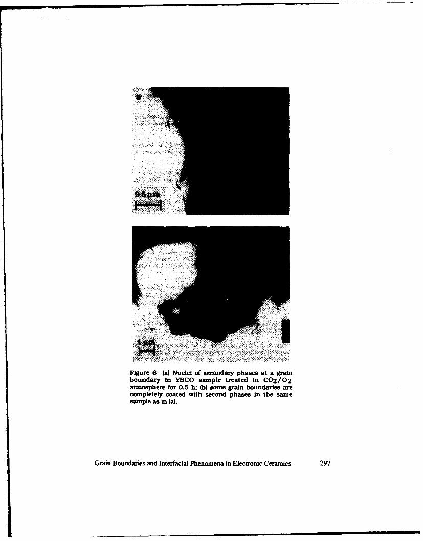
Figure 6 (a) Nuclei of secondary phases at a grainboundary in YBCO sample treated in C02/02atmosphere for 0.5 h: (b) some grain boundaries arecompletely coated with second phases in the samesample as in (a).
Grain Boundaries and Interfacial Phenomena in Electronic Ceramics 297

5. G. Selvaduray, C. Zhang. U. Balachandran, Y. Gao. K. L. Merkle, H. Shi.and R. B. Poeppel, Effect of C02 on the processing of Y-Ba-Cu-Osuperconductcm J. Mater. Res., 7. 283-291, (1992).
6. S. Nakahara. G. J. Fisanick, M. F. Yan. R. B. van Dover. T. Boone. andk. Moore. On the defect structure of grain boundaries in Ba2YCu307-x.J. Crystal Growth, 86. 639-651, (1987).
7. J. D. Verhoeven. A. J. Bevolo, R. W. McCallum, E. D. Gibson, and M. A.Noack, Auger study of grain boundaries in large-grained YBa2Cu3Ox,Appl. Phys. Letters, 52. 745-747. (1988).
8. PK. Gallagher. G. S. Grader, and H. M. OlByan. Some effects of C02. CO.and H20 upon the properties of YBa2Cu3O7, Mater. Res. Bull., 23, 149 1-1499. (1988).
9. E. K. Chang, E. F. Ezell, and M. J. Klrschner, The effect of C02 in theprocessing atmosphere of YBa2Cu3Ox, Supercond. Sc!. Technol., 8, 391-394. (1990).
10. T. B. Undemer. C. R Hubbard, and J. Brynestad. C02 solubility inYBa2Cu3O7-x. Phylca C, 167, 312-316. (1990).
11. U. Balachandran, R. B. Poeppel, J. E. Emerson, S. A. Johnson. M. T.Lanagan. C. A. Youngdahl. D. Shb. K. C. Goretta. and N. G. Eror. Synthesisof phase-pure orthorhombic YBa2Cu3Ox under low oxygen pressure,Mater. Lett.. S. 454-456, (1989).
12. U. Balachandran, F. B. Poeppel, J. E. Emerson. and S. A. Johnson,Calcination and solid state reaction of ceramic-forming components toprovide single-phase superconducting materials having fine particlesize, U.S. Patent 5,086,034, February 4, 1992.
13. H. FJellvag, P. Karen, A. KJekshus, P. Kofstad. and T. Norby, Carbon-atizatlon of YBa2Cu3O6+x. Acta Chem. Scand., A42. 178-184, (1988).
14. E. A. Cooper, A. K. Gangopadhyay, T. 0. Mason, and U. Balachandran,C02 decomposition kinetics of YBa2Cu3O7-x via in situ electricalconductivity measurements, J. Mater. Res.. 6. 1393-1397, (1991).
15. R. A. Laudise, L. F. Schneemeyer, and R. L. Barnes, Crystal growth of hightemperature superconductors-Problems, successes, opportunities.J. Cryst. Growth, 85,569-575, (1987).
16. J. D. Jorgensen, M. A. Beno, D. G. Hinks, L. Solderholm. K. J. Volin, R_ L.Hitterman, J. D. Grace, I. K. Schuller, C. U. Segre, K. Zhang, and M. S.Kleefisch, Oxygen ordering and the orthorhomblc-to-tetragonal phasetransition in YBa2Cu307.x, Phys. Rev. 36. 3608-3616, (1987).
298 Grain Boundaries and Interfacial Phenomena in Electronic Ceramics

INTERFACE EFFECTS IN Bi-"2212"/Ag AND Bi-"2223"/AgSUPERCONDUCTORS
S.J. Golden, T. Yamashita, A. Bhargava, J.C. Barry and I.D.R.Mackinnon, Centre for Microscopy and Microanalysis, The Universityof Queensland, Brisbane, Queensland 4072, Australia.
INTRODUCTION
The superconducting phases in the Bi-Sr-Ca-Cu-O system are someof the most promising materials for practical applications, especiallyfor wire, tape and coil fabrication [1-3]. In the so-called powder-in-tubetechnology a precursor powder is packed into a Ag tube and givenvarious thermo-mechanical heat treatments. Some of the wires withthe highest critical current density, for example 5 x 10⁴ A.cm-2 at 77Kand zero field [3], are made with a precursor to the "2223" phase whichconsists of the "2212" phase and non-superconducting phases. Afterprocessing the wire consists of a "2223" oxide core with a thickness inthe range 40-100gim with a well-aligned texture, encapsulated by a Agsheath. Thick films of the "2212" phase (10-601tm) on Ag are made bydoctor-blading or painting. The "2212"/Ag thick films are meltprocessed, with the "2212" phase crystallising from the melt duringslow cooling and forming well-aligned structures. Critical currentdensities of 2 x 10⁴ A.cm -2 (77K, OT) and 3 x 10⁵ A.cm-2 (4.2K, 2T) havebeen measured for "2212"/Ag thick films made in this way [4].
The use of Ag fulfills several requirements in these materials.However, the precise role of the Ag/superconductor interface in the"2212"/Ag system and in the "2223"/Ag system is not well established.In a number of studies it has been concluded that the Ag/oxideinterface plays a unique and important role with regard to "2212"texture formation in the melt-processed "2212"/Ag materials [5, 6].However other studies indicate that the main function of the Ag issimply geometrical and that texture formation can be explained byconsidering anisotropic growth of "2212" in a quasi two-dimensionalspace [7, 8].
To the extent authorized under the laws of the United States of America, all copyright interests in this publication are the propertyof The American Ceramic Socid Any duplication, reproduction, or republication of this publication or any part thereof, withoutthe express written coet American Cerac Society or fee paid to the Copyright Clearance Center, is prohibited.
Grain Boundaries and Interfacial Phenomena in Electronic Ceramics 299
EXPERIMENTAL
A "2212" powder was fabricated using the standard co-precipitationprocess and subsequent heat treatments up to temperatures of 870"Cfor 10 h. Ag foil substrates were coated on both sides with the "2212"powder by a painting technique utilising an HPMC binder. Totalthicknesses of up to 3 mm were deposited using a number of painting-drying repititions. After a burn-out heat treatment at 400°C the thickfilms were melt processed by heating at 890"C for 30 min., cooling at10"C/h to a temperature in the range 840"C-880°C where the sampleis held for 10 h. The sample was quenched into oil at the end of theisothermal treatment. Thick layers on MgO single-crystals were alsomelt-processed. Scanning electron microscopy was carried out oncross-sections of the thick films in addition to X-ray diffraction onplanes parallel to the substrate at varying distances from the substratesurface. A 1 prm diamond pad was used to remove the film from theupper surface.
For the study of the "2223"/Ag system a nitrate solution of cationcomposition Bi:Pb:Sr:Ca:Cu = 1.65:0.35:1.6:2:3 was made and an oxalateprecipitate was formed using oxalic acid. The oxalate was heated at800°C for 10 h with intermediate grinding and at 840"C for 2 h toproduce a powder consisting of "2212", CuO, Ca 2PbO4 and minoramounts of other phases. Thick films of this powder were depositedon Ag foil and (100}MgO substrates using the painting techniquedescribed above. The thick films were given isothermal heattreatments at temperatures ranging from 810°C to 880°C for 15 h. SEMand XRD were used to evaluate phase composition andmicrostructural variation as a function of distance frcm thesubstrate/film interface as described above.
RESULTS AND DISCUSSION
Melt-Processed "2212" on Ag and MgO Substrates
Thick films of "2212" on Ag and MgO were melt-processed using8901C, a cooling rate of 10°C/h to .850°C, followed by an anneal at8501C for 10 h and quenched to room temperature. The degree of c-axis orientation was measured by comparing the relative intensities ofthe (008) and (113) X-ray diffraction peaks from the "2212" layer.
300 Grain Boundaries and Interfacial Phenomena in Electronic Ceramics

1.0 E,a
o 0.9
• 0.8 0
• an Ag0• 0.7 a a
0.6 MgODistance, pm
0.50 1000 2000
Figure 1 Variation of degree of c-axis orientation with distance fromsubstrate interface in melt-processed "2212"/Ag and "2212"/MgO thickfilms.
"50tm "2212"/Ag
U~f . 2020 40 60
Figure 2 XRD trace of a 50pum thick layer of melt-processed "2212" onAg showing the high degree of c-axis orientation.
Grain Boundaries and Interfacial Phenomena in Electronic Ceramics 301

It was found that there was a definite variation of texture withdistance from the Ag/"2212" interface and MgO/"2212" interface asshown in figure 1. The region with good c-axis orientation (c-axisnormal to the substrate/"2212" interface) is confined to a region ofapproximately 50pom adjacent to the interface. Figure 2 shows the XRDtrace of the thick layer polished down to a thickness of approximately50gio for the Ag substrate. The XRD trace for the MgO case (for thesame thickness) resembled this one closely. Figure 3 shows an SEMimage of the fracture surface of melt-processed "2212" on MgO,illustrating the high degree of orientation adjacent to the substrate.These results do not support the view that the Ag/"2212' interfaceplays a unique texturing role [5, 6].
Figure 3 Fracture surface of the melt-processed "2212"/MgO showing
the high degree of texture adjacent to the interface.
Formation of "2223" on Ag and MgO Substrates
The formation of "2223" from the precursor was studied for arange of heat treatment temperatures for Ag and single crystal MgOsubstrates. In particular the phase evolution and microstructure wasstudied as a function of distance from the substrate/film interface foreach heat treatment. A comparison was made between the effect of thedifferent substrates. Figure 4 shows the evolution of "2223" as afunction of heat treatment temperature for material on MgOsubstrates.
302 Grain Boundaries and Interfacial Phenomena in Electronic Ceramics

1.0 - - , -A A A
AS0.8 A A
0.6
S0.4 -C14 A
- Ag MgO0.2 A
A A T('C)
0.0 " I . I .. . . .. I .u00 810 820 830 840 850 860 870
Figure 4 The variation of "2223" evolution vs. heat treatmenttemperature for MgO substrates (t=15 h). Also shown are the data forAg substrates for a film thickness of 100im.
The data was obtained by carrying out XRD on the top surface ofthe thick film. It was found that there was little dependence betweenthe phase evolution of "2223" and it's microstructure and depth fromthe MgO/BSCCO interface. The measured amount of "2223" as afunction of temperature, as shown in figure 4, was found to beindependent of distance from the interface. It was found that in thecase of MgO substrates there was no apparent bonding interactionbetween film and substrate, except for high heat treatmenttemperatures (T>845'C), where there was large-scale decomposition ofthe "2223" phase which formed.
In contrast, the "2223" phase evolution on Ag substrates wasstrongly dependent on distance from the Ag/BSCCO interface at mostof the heat treatment temperatures that were utilized. Figure 5 showsthe distance-dependent "2223" phase formation as a function of heattreatment temperature. The amount of "2223" formation at largedistances from the Ag interface were similar to those obtained on MgO(figure 4). However as the distance from the interface decreases there isa greatly enhanced "2223" evolution. This was observed fortemperatures exceeding 820"C.
Grain Boundaries and Interfacial Phenomena in Electronic Ceramics 303

I1.0
o 0.8 0 E3
0.6 0
o 0.4 - 825"C
0.2 0 0
000 0 0820"C
0.0 wD(m) 0 1000 2000
Figure 5 The variation of "2223" evolution vs. distance from substratein the case of "2223"/Ag at different heat treatment temperatures.
Thick films on Ag heat treated at 8201C and lower showed noenhanced "2223" evolution relative to the MgO case. The "2223"formation (for a distance from the substrate interface of 1001pm) vs.heat treatment temperature for the Ag substrate cdse has been plottedon figure 4. This dearly illustrates the effect of the Ag interface. Thereare two different temperature regimes with respect to "2223"formation adjacent to the Ag interface. The two temperature regimes,Ta820*C and T>825"C, can be explained by positing a temperaturedependent Ag/BSCCO interaction at the interface. Electron microscopystudies of thick film regions near the interface revealed significantdifferences in microstructure and composition for samples heattreated at 820°C and at 825°C and above. In the latter case oxideregions near the Ag interface without a distinct crystallinemorphology were rich in Cu relative to the "2223" type compositionintermixed with some plate-like particles of a Sr-deficient "2201"phase. A typical region is shown in figure 6. In some of these regions asignificant amount of Ag was also present
304 Grain Boundaries and Interfacial Phenomena in Electronic Ceramics
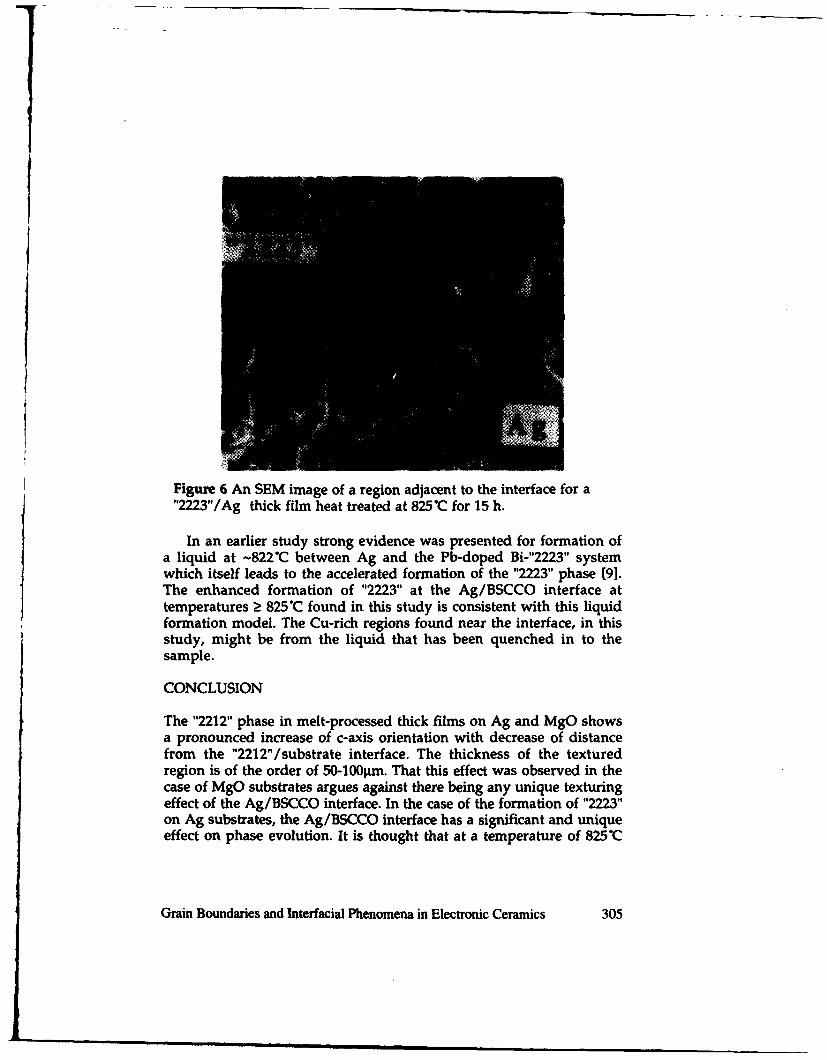
Figure 6 An SEM image of a region adjacent to the interface for a"2223"/Ag thick film heat treated at 8251C for 15 h.
In an earlier study strong evidence was presented for formation ofa liquid at -822°C between Ag and the Pb-doped Bi-"2223" systemwhich itself leads to the accelerated formation of the "2223" phase [9].The enhanced formation of "2223" at the Ag/BSCCO interface attemperatures > 825"C found in this study is consistent with this liquidformation model. The Cu-rich regions found near the interface, in thisstudy, might be from the liquid that has been quenched in to thesample.
CONCLUSION
The "2212" phase in melt-processed thick films on Ag and MgO showsa pronounced increase of c-axis orientation with decrease of distancefrom the "2212"/substrate interface. The thickness of the texturedregion is of the order of 50-100Lm. That this effect was observed in thecase of MgO substrates argues against there being any unique texturingeffect of the Ag/BSCCO interface. In the case of the formation of "2223"on Ag substrates, the Ag/BSCCO interface has a significant and uniqueeffect on phase evolution. It is thought that at a temperature of 825"C
Grain Boundaries and Interfacial Phenomena in Electronic Ceramics 305

and above a liquid is formed as a result of an interaction between theAg and some of the components in the BSCCO thick film whichpromotes the formation of the "2223" phase. This has significantramifications for processing of "2223"/Ag powder-in-tube materials.
ACKNOWLEDGEMENT
This work was supported by Syndicated R&D investment fundsthrough a partnership with Bankers Trust (Australia) and ComquestPty. Ltd.
REFERENCES
[1) High-field critical current densities in Bi2Sr2CalCu2O8 +x/Ag wires,K. Heine, J. Tenbrink and M. Thoner, Appl. Phys. Lett. 55 (1989) 2441-2443[2] Phase alignment in Ag-clad Bi-Sr-Ca-Cu-O (2:2:1:2) wires, R D. Ray IIand E.E. Hellstrom, Appl. Phys. Lett. 57 (1990) 2948-2950[3] Microstructures and Ic-B characteristics of Ag-sheathed Bi-basedsuperconducting wires, M. Ueyma, T. Hikata, T. Kato and K. Sato, Jpn.J. Appl. Phys. 30 (1991) L1384-L1386[41 Partial Melt Growth of Bi2Sr2CaCu20x Textured Tapes on Silver, J.Kase, K. Togano, H. Kumakura, D.R. Dietderich, N. Irisawa, T.Morimoto and H. Maeda, Jpn. J. Appl. Phys. 29 (1990) L1096-L1099[51 Textured thick films of Bi2Sr2CaCu2Ox, D.R. Dietderich, B.Ullmann, H.C. Freyhardt, J. Kase, H. Kumakura, K. Togano and H.Maeda, Jpn. J. Appl. Phys. 29 (1990) Ll100-1103[61 BiSrCaCu/Ag Superconducting Composite Tapes, H. Kumakura, K.Togano, D.R. Dietderich, H. Maeda, J. Kase and T. Morimoto,Supercond. Sci. Technol. 4 (1991) S157-159[71 Texture formation in Bi2Sr2CaCu2Ox/Ag tapes prepared by partialmelt process, T.D. Aksenova, P.V. Bratukhin, S.V. Shavkin, V.L.Melnikov, E.V. Antipova, N.E. Khlebova and A.K. Shikov, Physica C205 (1993) 271-279[81 Important considerations for processing Bi-based high-temeraturesuperconducting tapes and films for bulk applications, E.E. Hellstrom,Mater. Res. Bull. XVII (1992) 45-51[9] Use of a thermal gradient to study the role of liquid phase duringthe formation of Bismuth High Temperature Superconductors, P.E.D.Morgan, J.D. Piche and R.M. Housley, Physica C 191 (1992) 179-184
306 Grain Boundaries and Interfacial Phenomena in Electronic Ceramics
FILM/SUBSTRATE THERMAL BOUNDARY RESISTANCE FOREr-Ba-Cu-O HIGH-Tc THIN FILMS
P.E. Phelan, Y. Song', and M. KelkarDepartment of Mechanical Engineering, University of Hawaii at Manoa, 2540 Dole Street,302 Holmes Hall, Honolulu, Hawaii 96822 U.S.A.
ABSTRACTThe thermal boundary resistance between high-Tc thin films and their substrates is animportant property for optimal thermal design of high-Tc devices. However, fewmeasurements of this parameter have been conducted. In the present study, the thermalboundary resistance of two Er-Ba-Cu-O thin films-one deposited on MgO, and the otheron SrT0O3--is measured as a function of the substrate temperature. The results indicatea relatively large value of the resistance for the thicker film deposited on the SrTiO3substrate.
INTRODUCTIONThe thermal boundary resistance (Rb) between the film and the substrate can stronglyimpact applications of thin-film high-Tc superconductors (HTS). Any impediment to heatflow from the thin film can lead to temperature excursions that take the film from thesuperconducting state to the normal state, which in many cases results in device failure.It has been demonstrated that the bolometric response of HTS to incident radiationdepends on the magnitude of Rb, with regard to both the response time and thesensitivity [1,21. This result has also been shown from numerical simulations of thevoltage response [31, leading to the conclusion that Rb must be known for optimal thermaldesign of radiation detectors made from thin-film HTS [4]. The performance of otherhigh-Tc applications, such as light-activated switches, interconnects, flux-flow transistors,etc., also requires knowledge of Rb for their optimal thermal design.
Very few direct measurements of Rb between high-Tc films and their substrates havebeen carried out. To the authors' knowledge, only two such experiments have beenperformed. The first measured Rb for a Y-Ba-Cu-O film on a LaAIO3 substrate, and forseveral Y-Ba-Cu-O films on sapphire substrates, with intervening buffer layers of SrT1O3,MgO, LaAIO3, and/or CaTiO3 [5]. Their measured Rb varied between 0.7 x 10⁻³ and 1.3x 10⁻³ K cm2 W- 1 , and showed a weak or nonexistent dependence on temperature over
Department of Physics and Astronomy, University of Hawaii at Manoa, 2505 CorreaRoad, Watanabe Hall, Honolulu, Hawaii 96822 U.S.A.
To the extent authorized under the laws of the United States of America, a]l copyright interests in this publication are the propertyof The Amrin Ceramic Society. Any duplication, reproduction, or republication of this publication or any part thereof, withoutthe exprs writte nt of The American Ceramic Sodety or fee pid to the Copyright Clearce Cnter, isprohibied.
Grain Boundaries and Interfacial Phenomena in Electronic Ceramics 307
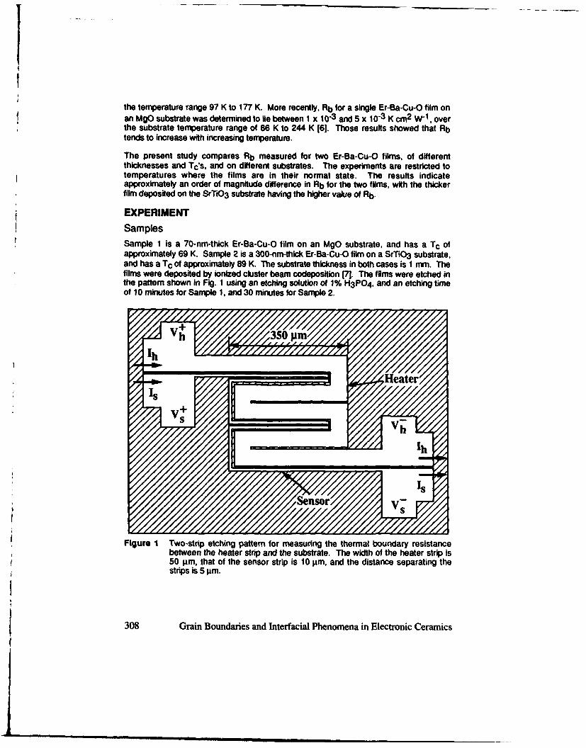
the temperature range 97 K to 177 K. More recently, Rb for a single Er-Ba-Cu-O film onan MgO substrate was determined to lie between 1 x 10⁻³ and 5 x 10⁻³ K cm2 W-1, overthe substrate temperature range of 86 K to 244 K (61. Those results showed that Rbtends to increase with increasing temperature.
The present study compares Rb measured for two Er-Ba-Cu-O films, of differentthicknesses and Tc's, and on different substrates. The experiments are restricted totemperatures where the films are in their normal state. The results indicateapproximately an order of magnitude difference in Rb for the two films, with the thickerfilm deposited on the SrTiO 3 substrate having the higher value of Rb.
EXPERIMENT
SamplesSample 1 is a 70-nm-thick Er-Ba-Cu-O film on an MgO substrate, and has a Tc ofapproximately 69 K. Sample 2 is a 300-nm-thick Er-Ba-Cu-O film on a SrTiO3 substrate,and has a Tc of approximately 89 K. The substrate thickness in both cases is 1 mm. Thefilms were deposited by ionized cluster beam codeposition (7]. The films were etched inthe pattern shown in Fig. 1 using an etching solution of 1% H3 PO4 , and an etching timeof 10 minutes for Sample 1, and 30 minutes for Sample 2.
Figure 1 Two-strip etching pattern for measuring the thermal boundary resistancebetween the heater strip and the substrate. The width of the heater strip is50 pmo, that of the sensor strip is 10 pmo, and the distance separating thestrips is 5 pm.
308 Grain Boundaries and Interfacial Phenomena in Electronic Ceramics
i ~~~ * Z I~U•amIl~ mm

| 30
Is : Sample 1 sensor ls25 lh Sample I heater
_ 2s Sample 2 sensor%woo 2h Sample 2 heater
; 15
1 "S10
4) 5 1lh
0[ h0 ' ' .. .. h.I.'.," ! " : " " . s I
0 50 100 150 200 250 300
Temperature (K)Figure 2 Electrical resistance calibration curves, taken under isothermal conditions.
Procedure
The experimental procedure is based on that described in 18], and has been fullydescribed in [6]. In brief, a large bias current Ih is passed through the strip labeled'heater' in Fig. 1, while a much smaller sensing current Is Is passed through the 'sensor.Both strips are maintained in the normal state. The Joule heating generated in the heaterresults in a temperature difference between it and the substrate immediately below. Onthe other hand, since Is is very small, the sensor temperature is nearly the same as thatof the substrate. Therefore, using curves fitted to the electrical resistance calibration datain Fig. 2 enables us to determine the temperature drop between the heater and thesubstrate from the measured electrical resistances of the strips. The strips' electricalresistances are measured using the four-point method. After reaching steady-state, Rb iscalculated from Rb = AT/q, where q is the heat flux from the heater into the substrate, andAT = Th - Ts, where Th is the heater temperature, and Ts is the sensor temperature.
The experiment was conducted for values of the heater current ranging from 8 to 20 mAdc. The sensor current source was a lock-in amplifier set at 47 Hz, and the currentmagnitude was typically about 5 pA ac. The temperature during the electrical resistance"calibration was measured with a diode sensor mounted on the Cu cold finger on whichthe sample was mounted. The experiments were carried out in a closed-cyclerefrigeration system, and the data were recorded with a computer-controlled dataacquisition system.
Grain Boundaries and Interfacial Phenomena in Electronic Ceramics 309
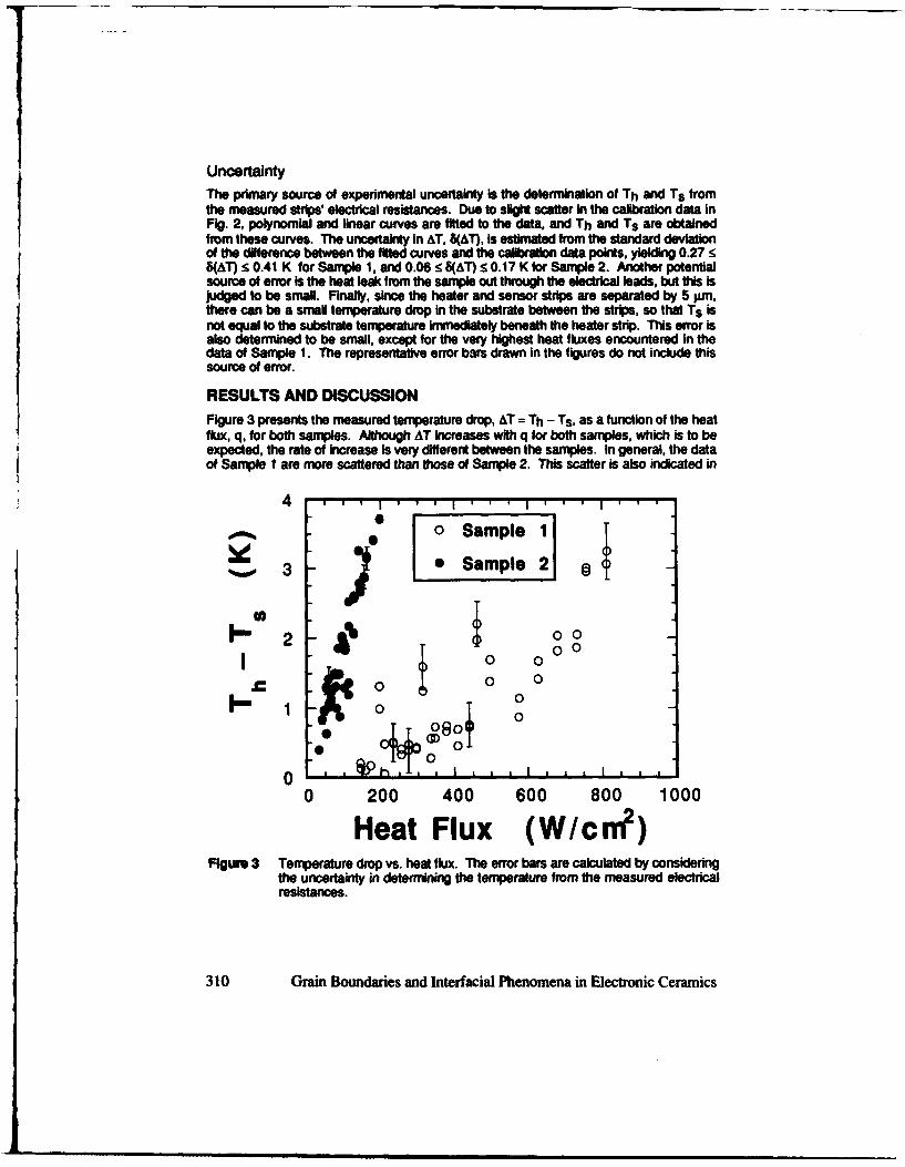
UncertaintyThe primary source of experimental uncertainty is the determination of Th and TS fromthe measured strips' electrical resistances. Due to slight scatter in the calibration data inFig. 2, polynomial and linear curves are fitted to the data, and Th and Ts are obtainedfrom these curves. The uncertainty in AT, 6(AT), is estimated from the standard deviationof the difference between the fitted curves and the calibration data points, yielding 0.27 <8(AT): 0.41 K for Sample 1. and 0.06 < 8(AT) s 0.17 K for Sample 2. Another potentialsource of error is the heat leak from the sample out through the electrical leads, but this Isjudged to be small. Finally, since the heater and sensor strips are separated by 5 ^un,there can be a small temperature drop in the substrate between the strips, so that Ts isnot equal to the substrate temperature immediately beneath the heater strip. This error isalso determined to be small, except for the very highest heat fluxes encountered In thedata of Sample 1. The representative error bars drawn In the figures do not include thissource of error.
RESULTS AND DISCUSSION
Figure 3 presents the measured temperature drop, AT = Th - Ts, as a function of the heatflux, q, for both samples. Although AT increases with q for both samples, which is to beexpected, the rate of increase is very different between the samples. In general, the dataof Sample I are more scattered than those of Sample 2. This scatter is also indicated in
i4
0 Sample 2 I
0Sample 2
2 o00
0 00 0
o o 0
0008
0 0 .
0 200 400 600 800 1000
Heat Flux (W/cni2 )Figure 3 Temperature drop vs. heat flux. The error bars are calculated by considering
the uncertainty in determining the temperature from the measured electricalresistances.
310 Grain Boundaries and Interfacial Phenomena in Electronic Ceramics

-1
Sample 2S10 .2 - sa
Sample 1 o o
"E lo-10"3%%MOO
Ref. [5] 0
I T1 . . . . . ,I . g I I I I & & I I . . . . . I . . . . .
80 110 140 170 200 230 260
T (K)Figure 4 Thermal boundary resistance vs. substrate temperature. The error bars,
which are too small to be visible for Sample 2, are calculated by consideringthe uncertainty in determining the temperature from the measured electricalresistances.
Fig. 4, which shows Rb as a function of Ts. Also included on this plot is one set of datafrom [5], which is for a YBa2Cu3O7-8 film or. a LaAIO3 substrate. Clearly, Rb for Sample2 is approximately one order of magnitude higher than Rb for Sample 1. The data forSample 2 are almost flat with respect to Ts, while those for Sample 1 show a slightincrease with increasing Ts. However, the greater uncertainty of the Sample 1 datamakes this trend questionable.
It is conceivable that the higher Rb for Sample 2, as compared to that for Sample 1, couldresult from the greater film thickness, which is 300 nm for Sample 2, as opposed to 70nm for Sample 1. The thermal resistance across the film can be estimated by dik, whered is the film thickness and k is the thermal conductivity in the transverse direction (normalto the film/substrate interface). Assuming k of each film is about 2 W m'lK" 1, thedifference in film thickness cannot account for the order-of-magnitude difference in Rb.However, k for each film may be different, since the microstructure of thin films can beaffected by the film thickness and choice of substrate. If so, this change in k should alsobe reflected in the films' electrical resistivities, which are plotted in Fig. 5. Theseresistivitles are for transport in the ab plane, rather than in the c direction, but it isanticipated that the transport properties in one direction should correlate with those of the
Grain Boundaries and Interfacial Phenomena in Electronic Ceramics 311

10 X 106"Is Sample 1 sensor Is
E lh Sample 1 heater8 29 Sample 2 sensor
C 2h :Sample 2 heater IK)6
II 4a2h
2
0
~ 0 50 100 150 200 250 300
Temperature (K)Figure 5 Electrical resistivity-vs. temperature, determined from the electrical resistance
calibration curves.
other. It is apparent from Fig. 5 that the resistivity of Sample 1, the thinner sample, isconsiderably higher than that of Sample 2. Since the Tc of this film is also relatively low(69 K), this sample either has a greater oxygen deficiency, or contains moremicrostructural damage. Thus, k of Sample 2 should not be much different than k ofSample 1, and therefore the difference in Rb in Fig. 4 is most probably not due to thedifferent film thermal resistances.
An interesting feature of Fig. 5 is that the electrical resistivities of the heater and sensorstrips for Sample 1 diverge from each other with increasing temperature, while those forSample 2 also diverge, but in general are much closer to each other. Since the strips in agiven sample are made from the same film, the differences must be due to the etchingprocess. The wider heater strips (50 pim in width) of each sample most likely provide abetter indication of the actual film resistivity. The narrower sensor strips (10 Rm in width)are more prone to damage induced by the etching process, and to the possibility that agrain boundary lies across the entire strip width. There may, therefore, beinhomogeneities along the sensor strips such that their electrical resistances, and thecorresponding sensor temperatures, are not truly quantities that are averaged across thesample area, but rather reflect more local properties.
It is also noteworthy that the film having the higher Tc, Sample 2, exhibits the larger Rb.The oxygen deficiency and microstructure of Sample 1 may play a role in reducing Rb.
312 Grain Boundaries and Interfacial Phenomena in Electronic Ceramics

However, until more samples are measured, no conclusions concerning these effects onRb can be made.
The predicted Rb from acoustic mismatch theory (AMT) [91 is about 10-5 cm2 K W-1 at100 K, and decreases with increasing temperature. This large difference between thepresent data and AMT is consistent with previous measurements on other film/substratesystems, for temperatures higher than about 60 K 181. Apparently, for the temperaturesexamined in this study, the phonon wavelengths are comparable to the lattice constants,so that the continuum assumption of AMT is invalid. At present, there is no existingtheory which can predict Rb at such film/substrate interfaces at the moderate cryogenictemperatures applicable for HTS.
CONCLUSIONSThe film/substrate thermal boundary resistance Rb for two Er-Ba-Cu-O high-Tc thin filmsis measured as a function of the substrate temperature. All the measurements arecarried out on normal-state films. The substrates and the film thicknesses differ betweenthe two samples. The results indicate that Rb is in excess of 10-3 cm2 K W" 1 , andgenerally is constant or increases slightly with increasing temperature. The magnitude ofRb differs by approximately an order of magnitude between the two samples, with the filmof greater thickness, higher Tc, and on a SrTiO3 substrate exhibiting the largest value ofRb.
ACKNOWLEDGMENTSThis material is based upon work supported by the National Science Foundation underGrant No. CTS93-07753. The authors also owe their gratitude to H. Ito and colleagues atMitsubishi Electric Co., along with Professor K. Hijikata of the Tokyo Institute ofTechnology, who furnished the high-Tc samples; Dr. Y. Kozono and olleagues at HitachiCo., who patterned the samples; and Professor J.R. Gaines of the University of Hawaii atManoa, who allowed us the use of his cryogenic laboratory facilities.
REFERENCES
[1) Carr, G.L., Quijada, M., Tanner, D.B., Hirschmugl, C.J., Williams, G.P., Etemad, S.,Dutta, B., DeRosa, F., Inam, A., Venkatesan, T., and Xi, X., "Fast bolometricresponse of high-Tc detectors measured with subnanosecond synchrotronradiation," Appl. Phys. Left. 57, no. 25, pp. 2725 - 2727 (1990).
12] Levey, C.G., Etemad, S., and Inam, A., "Optically detected transient thermalresponse of high-Tc epitaxial films," Appl. Phys. Left. 60, no. 1, pp. 126 - 128(1992).
[3] Chen, R.-C., Wu, J.-P., and Chu, H.-S., "Bolometric response of high-Tcsuperconducting detectors to optical pulses and continuous waves," ASME PaperNo. 93-HT-7, ASME National Heat Transfer Cont., Atlanta, Georgia, Aug. 8 - 11(1993).
[4) Zhang, Z.M., Frenkel, A., "Thermal and nonequilibrium responses ofsuperconductors for radiation detectors," ASME Winter Annual Meeting, NewOrleans, Louisiana, Nov, 28 - Dec. 3 (1993).
[5] Nahum, M., Verghese, S., Richards, P.L., and Char, K., "Thermal boundary
Grain Boundaries and Interfacial Phenomena in Electronic Ceramics 313

resistance for YBa2Cu3O7-56 films," Appl. Phys. Lett. 59, no. 16, pp. 2034 - 2036(1991).
[6] Phelan, P.E., Song, Y., Nakabeppu, 0., Ito, K., Hijikata, K., Ohmori, T., andTonkoshi, K., "Film/substrate thermal boundary resistance for an Er-Ba-Cu-0 high-Tc superconducting film," submitted to Journal of Heat Transfer (1993).
[71 Yamanishi, K., Yasunaga, S., Kawagoe, Y., Sato, K., and Imada, K., "Synthesis ofsuperconducting Y-Ba-Cu-0 thin films by ionized cluster beam codeposition,"Nuclear Instruments and Methods in Physics Research B37/38, pp. 930 - 934(1989).
[81 Swartz, E.T., and Pohl, R.O., "Thermal boundary resistance," Reviews of ModemPhysics 61, pp. 605 - 668 (1989).
[9] Little, W.A., "The transport of heat between dissimilar solids at low temperatures,"Can. J. Phys. 37, pp. 334 - 349 (1959).
314 Grain Boundaries and Interfacial Phenomena in Electronic Ceramics
EFFECT OF IMPREGNATION OF ZrO2 ON THE CHEMICAL STABILITYAND THE SUPERCONDUCTIVITY OF Y- AND Bi-SYSTErS
Nasaaki MUROYA and Hideaki NINAMIYAMAOsaka Electro-Communication University, 18-8, Hatsu-cho, Neyagawa, Osaka572, Japan
The results are given concerning the influence of impregnation of Zron chemical stability and superconductivity of YBa 2 (Cul-x - Zrx)307_y(123-system) and Bi .84 ZrxPbO. 34 Srl. 9 1 Ca2 .0 3 Cu3 . 0 6 0y (2223-system)superconductors, when the samples are contacted with the solutions ofacid(pH3), distilled water(pH5.6) and base(pH9), where x=O-0.35.
It is concluded that the low chemical stability was found in the caseof YBZCO, barium hydroxide and/or barium carbonate were precipitated intothe solutions, even though mechanical strength was increased byimpregnation of Zr, and the chemical stability of Bi-system is highcompared with that of the Y-system.
1. IntroductionIt is well known that Y-Ba-Cu-O(YBCO) and Bi-Pb-Sr-Ca-Cu-O(BPSCCO)
system compounds are those of high-Tc superconducting materials. Numerousinvestigators have demonstrated the studies of preparation and thesuperconductive characterization of these materials. When these materialsapplied to various cases, such as wires coils, sensors, electronic devicesand others, careful utilization of these materials is required to establishthe laws of chemical stability.
It has been indicated by several workers that no chemical stability ofY- and Bi-system superconductors, when which were exposed to water, werereported[I-3]. Those works indicated that the Y-system compounds aresensitive to water and decompose in water to CuO, Ba(O1) 2 and Y2 BaCu0 5 , andthen superconducting ability of the sample is down as a result of decompo-sition in superconducting phase. In the case of Bi-system, superconducting
To the extent authorized under the laws of the United States of America, all copyright interests in this publication are the propertyof The American Ceramic Sode. Any duplication, reproduction, or republication of this publication or any part thereof, withoutthe express written consent of The American Ceramic Society or fee paid to the Copyright Clearance Center, is prohibited.
Grain Boundaries and Interfacial Phenomena in Electronic Ceramics 315

I
grains were indeed stable, but nonsuperconducting grains were notablydegraded polycrystalline which was caused by the dissolution of Sr and Cafrom nonsuperconduting grains[4,51. The mechanical strength of Y- and Bi-system superconducting materials was found to be reinforced by adding theZr02 to those materials[6,7]. This result is in accord with expectationsbased on the chemical stability of the materials.
In this report, the chemical stability of the Y- and Bi-systemcompound prepared by our laboratory and the effect of impregnation of ZrO2on the chemical stability of these materials were detected by means ofchemical approach, XRD, XPS and FT-IR techniques, and the activationenergies of degradation in which these materials were obtained from thechemical process of solubility into water and solutions(acid and base).
2. ExperimentalPreparation of the YBCO and BPSCCO compounds and doping ZrO2 to these
compounds were as follow. l)Commercial special grade powders of Y2 03 , BaCO3 ,CuO and ZrO2 were weighed in mol ratio, Y:Ba:(Cul-x.Zrx)=1:2:3(x=O, 0.02,0.05, 0.08), and then mixed for lh. These mixed powders were pre-heated atthe temperature of 9500C for 15h in air and compressed by 32Ck ,/cm2 for20min after slowly cooled down under flowing I 1/min in 02, respectively.Discoidal specimens, with 20mm diameter anui about 3mm thickness, thusobtained from its procedure. These specimens were used for further heat-treated at 950°C for 24h in air and then these specimens were cooled downunder the condition of I I/min flow in 02, respectively. The specimensprepared by this procedure are so called as the YBCO(x=O) and asYBZCG(x=0.02-0.08). 2)Commercial powders of Bi2 03 , PbO, SrCO3 , CaCO3 , CuGand Zr02 were weigh in mol ratio, Bi:Zrx:Pb:Sr:Ca:Cu=l.84:x:0.34:1.91:2.03:3.06(x=0-0.35), and then mixed for lh. These mixed puwders were pre-heat-treated at 800°C for 12h in air and compressed by 3200kg/cm2 for 20minafter slowly cooled down, and further crush and mixing of these treatedspecimens were carried out. Once again these powders were compressed by thepressure mentioned above. The discoidal specimens(20mm diameter and about3n thickness) were used for further heat-treated at 8500C for 50h in airand then cooled down in air. These substances are so called as BPSCCO(x-O)and as BPSZCCO(x0. 15-0.35).
The discoidal specimens of Y- and Bi-systems were immersed to acid,neutral and base solutions, which were prepared with hydrochloric acid(pH3),distilled water(pH5.6) and sodium hydroxide(pH9), respectively. The
temperature of the solution was kept at 250, 350 and 45_±10C, through theall immersion experiments. The pH of the solutions was measuredcontinuously for 200min after the sample was immersed to its solution, and
316 Grain Boundaries and Interfacial Phenomena in Electronic Ceramics

data was recorded with a pH meter.Experimental procedures of X-ray diffraction(XRD), electrical
resistance, X-ray photoelectron spectroscopy(XPS) and infrared spectroscopy(FT-IR) were same as reported described elsewhere[8]. Mechanical hardnessof the sample was measured by using a shore type hardness tester.
3. Results and Discussion3.1. Y-System.
A typical splitting X-ray diffraction lines due to the orthorhombicBa2YCu307_y crystal phase were observed on the YBCO and also on theYBZCO(x=O.02-O.08). It usually appears that the crystal growth oforthorhombic phase has not undergone inhibition by the ZrO2 doping to theYBCO system compound. However, the superconducting properties of YBZCOspecimens are not clear from only diffraction pattern.
The relationshbp between Tc-end point temperature and Zr content forthe YBCO and the YBZCO specimens were shown in the curve A of Fig.l. Thecritical endpoint temperature(Tc-end) for the YBCO(x=O) is detected at 91°K.When the YBCO is contained the ZrO2 , the Tc-end is shifted to lower side at88-85K. It is thought that this effect results from the Culx/Zrx ratio wasdecreased with containing ZrO2 and the formations of 211-phase(Y2 BaCuO5 )and BaZrO3 in the 123-phase matrix.
The shore hardness of the specimens(YBCO and YBZCO) were measured, andthe results were shown to be the relation of Zr content in the curve A ofFig.2. The addition of ZrO2 results in an increase in hardness dependingdoped concentration. This is because they occasionally cause the packing
Zr Content x I BPSCCO Zr Content x / BPSCCO0 P0. 0.4 20C• 0.2 0.4
o 0 Zr-YBCO B.BPSCCO -100
. 10 /0
5 L-DPC V-
80 0.05 0.1 . 1
Zr Content x I YBCO Zr Content x / YBCO
Fig.l. Plot of the Tc-end point Fig.2. P A of the shore hardness
temperature against Zr content. and the residue against Zr content.
Grain Boundaries and Interfacial Phenomena in Electronic Ceramics 317

density of compressed sample becomes high by containing ZrO2 since BaZrO3filled in porous regions present in 123-phase matrix[6,7]. Such effect canbe expected to hold for chemical stability of the Zr-containigsuperconductor prepared in this work.
Fig.3 shows the variation of H+ concentrations in the solutions(initial pH3, 5.6 and 9) which contain the YBCO sample as a function ofelapse of the time. When the initial pH is 3, proton concentration of itssolution decreases progressively from pH3 to about 4 with the passage oftime until about 30min, the drastically decrease of proton concentration isindicated in time range from about 30 to 50min, and then the pH of its solu-tion becomes almost constant at about 11 after converted to alkaline side.The decrease of proton concentration in the solution was also found on thecases of pH 5.6 and 9. Analogous pH curve was observed on the Zr-containingsample(YBCO), but the time of elevation in the pH was delay. Since thereaction is hindered by the added substance it is said to be a depressivematerial which is Zr02 . After the acidic solution converted to alkalinestate, the precipitated product was produced in the solution for the bothsamples(YBCO and YBZCO). In the cases of any given pH value, the productsof about 18-12 mg per unit sample weight, g, were determined to be theresidue which was obtained by the heating at 170'C 2h of the product. Thequantity of product resulted from the YBZCO is less than that ofcomparative with the case of Zr-free sample. It is indicated that the YBCOand YBZCO specimens have been once accepted the chemical attack in thosesolutions. The magnitude of residue obtained from the precipitated productin pH3 solution against Zr-content was shown in curve C of Fig.2. When the
0o 0
• ~~o pH3.0,YBCO .. ..
v prig.0,YBCO |Yco . pH3.0'B3PSCCO4H.:PC O . ;.a._ , _
• " vpHg.0,BPSCCO•
10 0 3pscc0o
60 40'0 20€ 0••oElapse of time m rin binding energyI eVi Fig.3. Time dependence of pH in the Fig.4. XPS spectra of the residues
solutions contained the specimens obtained from precipetated product.such as YBCO and BPSCCO.
31a Grsin oufdam I ma IBed Pin Eleric C

Zr-free sample was contact with the solution, the magnitude of the residueis about 17.5mg/g. But the residue decreases with increasing Zr-content inthe case of Zr-containing samples. It is suggested that the chemicalstability of the specimen contained Zr is high compared with that of Zr-free specimen and doping of ZrO2 to YBCO contribute to prevent drasticallydegradation of the superconductor.
In order to known the composition of product precipitated in thesolution, XPS, XRD and FT-IR analysis of the residue were carried out.Fig.4 shows the XPS spectra for the residue produced from the YBCOspecimens. Core signals of Ba3d(3/2,5/2), BaMNN, Auger and Ols wereobserved, it is indicated that products in the solution are bariumhydroxide or barium carbonate. Same signals were also observed on the otherpH and the Zr-containing specimens.
The techniques of FT-IR and XRD have been used to examine thecomposition of the product, and FT-IR spectra were shown in Fig.5. Clearabsorption bands at 1462 and 857cm- 1 were found on the YBCO specimen, andthese absorption band are assigned to C03
2 - in inorganic carbonate. These*absorption bands were also observed on YBZC" .=0.02-0.08) specimens, andthose wave numbers are in agreement with that of BaCO3 powder. On the otherhand, the XRD patterns of the productproduced from the YBCO and the YBZCOspecimens are in agreement with that ofBaCO3. No existence of Cu-, Zr- and Y-compositions in products was revealed bythe detailed XPS, FT-IR and XRD j.
experiments. These results are indicatedthat the chemical species eluted from the B -. o.specimens(YBCO and YBZCO) in the solution -
is mainly barium, which formed hydroxide --- ----or carbonate in the solution. -.. 02
In the solutions, perhaps thereactions of ion exchange between proton 4000 3000 2000 o0and barium and then production of Ba(OH) 2 Wave number / cm-'occurred to be resulting from a proton Fig.5. FT-IR spectra of theattack to barium site of YBCO and/or YBZCO. residues obtained fromThe reaction process may be expressed precipitated product.chemically as hereunder.
2YBa 2 Cu3 07 + 3H2 0 -> 3Ba(OH) 2 + Y2 BaCuO5 + 5CuO + 0.502 (1)
Ba(OH) 2 + CO2 -> BaCO3 + H2 0 (2)
Grain Boundaries and Interfacial Phenomena in Electronic Ceramics 319

Since the pH elevation reflects the elution of barium, the activationenergy of this reaction can be determined by the experiments of temperaturedependence in the chemical treatment. The activation energy, E, can bedetermined by Arrhenius's plot which is corresponded to the plot of log kversus I/T, where T is absolute temperature, and k is rate constant derivedfrom reaction rate.
Fig.6 shows the Arrhenius's plot for the YBCO specimen. The slopesyield the E of I02(pH 3), 61(pH 5.6) and 16(pH 9) kJ/mol, and theseactivation energies, which depend on pH of the solutions, reported to datafor the Ba(OH) 2 production reaction. The plot of E against pH bear a linearrelationship to each other, as shows in Fig.6. The activation energy in thecase of initial acidic side is large than that of alkaline side. It isconsidered that the production reactionof Ba(OH) 2 occurred most readily at pH9.O
alkaline side because of the io _-
concentration of OH- ion is high in its pH56solution.
The activation energy for the °YBZCO specimen was slightly large than 9Pthat of the Zr-free specimen(YBCO). It ] 0
is suggested that the influence of Zr- Icontaining upon the chemical stabilityof Y-system is high. Moreover, thedegradation process of Y-system B3.I 3.2 3.3 3.4
compound in the solution is inhibited I/T .iO3 / YBCO
by the impregnation on ZrO2 to its Fig.6. Arrhenius's plot of YBCO
compound as find in Fig.2. and pH dependency of activationenergy.
3.2. Bi-SystemXRD and the temperature dependence of electrical resistance in the
BPSCCO and the BPSZCCO specimens were measured, respectively. Thediffraction pattern of BPSCCO specimen was indicated that the diffractionlines assigned to high-Tc(109K) phase of tetragonal crystal. When thesample(BPSCCO) is contained zirconium, Tc-end point at 109K was down tolower temperature side at 99K(BPSZCCO, x=0.35).
The hardnesses of the BPSCCO and the BPSZCCO specimens are shown incurve B of Fig.2. The hardness of the Zr contained specimen depend on theZr concentration and was increased with increasing the amount of ZrO2 , andTc endpoint temperature was decreased as shown in curve B of Fig.l. Whenthe BPSCCO is contained Zr and its compressed sample was heated in thisexperimental conditions, M(Sr,Ca)ZrO3 is formed, and its MZrO3 filled in
320 Grain Boundaries and Interfacial Phenomena in Electronic Ceramics

porous regions present in 2223-phase matrix. Therefore, the decrease ofmolar ratio in Sr and Ca lead to down Tc-end point temperature, and theenhancement of mechanically hardness is derived from the decrease inporosity as resulting from MZr0 3 was precipitated in pore.
pH of the solutions such as initial pH 3, 5.6 and 9 immersed BPSCCOspecimen were detected for elapse of the time, and the results were shownin Fig.3. The drastic change of initial pH 3 to alkaline side was occurred,that is, pH rise rapidly from about 60 min after specimen immersed in thesolution, and then pH of its solution becomes to approximately constant at11.5. When the temperature of this solution is elevated to 350 and 450C,starting point of elevation in pH was shifted to short time side. It isindicated that chemical process depend on the temperature. The change ofthe initial pH to alkaline side was also observed on the solution of pH 5.6.In both initial pH, the product was precipitated in the solution. On theother hand, pH of the solution in initial pH 9 is slightly increased withelapse of the time, but no large change of pH is observed. Furthermore,product was almost not precipitated in the solution of this pH. It issuggested that the chemical stability of the Bi-system superconductor ishigh compared with that of the Y-system.
In order to known the chemical composition of the product, XPS of theresidue was measured, and its spectra were shown in Fig.4. The signals ofSr(3p,3d), Ca2 p3/ 2 and Ols were determined on the residue. Those resultssuggested that the products were precipitated in the solutions as resultingfrom proton attacked to Sr and Ca sites of BPSCCO specimen. The chemicalcomposition of the product is presumably considered with hydroxide and/orcarbonate of Sr and Ca.
When the BPSCCO specimen contain as other component a small amount ofZrO2 , the amount of product in the solution was decreased compared with Zr-free sample, as shown in curve D of Fig.2. This means that the decrease ofelution of Sr and Ca is derived from the sureface of the 2223-phaseparticles was coated with MZrO3 composition which is only slightly solublein strong alcid but insoluble in water. Therefore, the chemical stability ofZr contained LPSZCCO is high compared with that of Zr-free.
It is considered that the chemical process of elution of Sr and Ca isthat analogous mechanism in the case of Y-system, since Sr and Ca were samegroup as that of Ba. But the activation process of the reaction is secondorder, and such a treatment is actually valid only in acidic solution.
4. ConclusionSuperconductors of Y- and Bi-system were prepared by method of solid
state reaction, and the chemical stability of those specimens was examined.
Grain Boundaries and Interfacial Phenomena in Electronic Ceramics 321

Critical temperature at 91 and 109K were detected on the Y- and Bi-systemspecimens, respectively. When these specimens were contained as othercomponents a small amount of ZrO2 , mechanical hardness of these specimenswere enhanced, and Tc of these specimen were shifted to lower temperatureside with few Kelvin degree. These were because they occasionally cause themolar ratio slightly changed with containing Zr and M(Ba,Sr,Ca)ZrO3 filledin porous regions present in matrix.
The YBCO and BPSCCO specimens were too chemically unstable fordistilled water and the solutions(acid and base). The chemical stability ofthe BPSCCO specimen was high compared with that of the YBCO. When the Y-and Bi-system specimens were contained as other components a small amountof ZrO2 , the chemical stability of these specimens was enhanced as aresults of the formation of M(Ba,Sr,Ca)ZrO3 and the decrease of porosity,that is, the dense samples were produced.
The authors would like to thank Messrs. Kazuhiko Yaguchi, HarunobuNakagawa, Takashi Ichikawa and Hideki Takei at Osaka Electro-CommunicationUniversity, for his many comments and experimental help during the courseof this work.
ReferencesI)M.F.Yan,R.L.Barns,H.M.O' Bryan,Jr.,P.K.Gallagher,R.C.Sherwood,S.Jin,Water
interaction with the superconducting YBa 2 Cu3O7 ,Appl.Phys.Lett.,51,532(1987).2)R.L.Barns,R.A.Laudise, Stability of superconducting YBa 2 Cu3 O7 in the
presence of water, Appl.Phys.Lett.,51,1373(1987).3)K.Kitazawa,K.Kishio,T.Hasegawa,O.Nakamura,J. shimoyama,N. Sugi,A.Ohtomo,
S.Yaegashi, K.Fueki, Resistivity Anomaly Near Room Temperature of Y-Ba-Cu-O and Related Oxide as Created by the Surface Effect of Water,Jpn.J.Appl.Phys.,26,L1979(1987).
4)K.Yoshikawa,M.Yoshida,M.Nakano, Degradation in Bi-Sr-Ca-Cu-O Thin FilmsExposed to Water, Jpn.J.Appl.Phys.,27,L2324 (1988).
5)W.Gao,J.Chen,C.Ow Yang,D.McNabb,J.Vander Sande, The stability of High-Tc BSCCO/Ag superconducting microcomposites in water, some iorganicsolutions and organic solvents, Phys.C193, 455(1992).
6)T.Oka,F.Ogasawara,Y.Itoh,M.Suganuma,U.Mizutani, Mechanical andSuperconducting Properties of Ag/YBCO Composite SuperconductorsReinforced by the Addition of Zr, Jpn.J.Appl.Phys., 29,1924(1990).
7)S.W.Filipczuk, On the degradation of YBa2Cu3O7_y by ZrO2 , Phys.C, 173,1(1991).
8)M.Muroya,EFFECT OF OXYGEN CONTENT ON XPS SPECTRA OF Ba2YCu 3 O7_yProceedings of Inter. Superconducting Electronic Conf. ( ISEC' 89), 1989,p. 139.
322 Grain Boundaries and Interfacial Phenomena in Electronic Ceramics

Processing and Characterization

COFIRE TECHNOLOGY: QUANTIFYING GLASS INFILTRATION INTHE CERAMIC-METAL INTERFACIAL REGION
K. S. Venkataraman, L. D. Martin, and D. A. Weirauch, Jr.Chemical Systems DivisionElectronic Packaging CenterAlcoa Technical CenterAlcoa Center, PA 15069
Abstract: Glass is a critical component in cofiling multilayer ceramic (MLC) packagesfor I) improving the sintering/shrinkage compatibility of the ceramic and the circuitmetal paste, 2) providing adhesion between the metal and the ceramic, 3) obtainingtighter dimensional control, and 4) providing hermeticity to the fired part. Quantify-ing the composition of the metal circuit lines in terms of glass, metal, and porosity assintering progresses is a necessary prelude for understanding glass infiltration in theglas-ceramic interfacial region, and its influence on the macroscopic response--warpage of the part, for example-during sintering This paper describes an image-analysis-based technique for quantifying the composition of the metal circuit lines interms of glass, metal, and porosity in SEM pictures Using the grey level differencesamong the three principal phases in the micrographs, the composition of the metalcircuitry near, and away from, the ceramic-metal (C-M) interfacial region was quan-tified and compared in several partially and fully sintered samples. This technique,being repeatable and reproducible, offers opportunities for obtaining a greater insightinto micrstructure evolution during sintering and its relation to dimensional control ofcomplex parts.
1. Inroduction: The bulk of the multilayer ceramic (MLC) housings for sili-con integrated circuits are made by sandwiching several layers of -250-progreen ceramic tapes on which are screen-printed individualized -20-pm elec-trical circuitry using metal powder-based thick-film inks. Upon sintering,both the ceramic and the metal powders in the multilayer package sinter anddensify simultaneously. Hence the term "cofire technology." Multilayercofire technology employs a wide variety of inorganic and organic materials,some of which are transients necessary for building the parts, while others arefunctionally important in the final package. Examples of the transient mate-rials: a) volatile solvents in the tape-making slurry and thick-film inks, andb) polymeric binders in the tape and the dried inks. Functionally importantmaterials in the alumina-based packages are powders of alumina and glass or
To the etet authoized under the laws of the United Staten of America, A co i•ht interests in this publication are the propertyof The American Ceramic Society. Any duplication, repoduction, or repWbliation of this pblicai or any part thereof, withoutthe express written consent of The American Ceramic Society or fee paid to the Copyrih = Center, is prohibited.
Grain Boundaries and Interfacial Phenomena in Electronic Ceramics 325

glass-forming components, and tungsten and/or molybdenum powders pro-viding the electrical circuitrly.
The focus of this paper is on quantifying the different stages in themicroetructural evolution of the alumina-tungsten system during sintering.Careful manipulation and control of the material system and its processingare essential for producing parts having tight dimensional control and hav-ing unique combinations of mechanical, electrical, and thermal properties.This combination makes ceramics the materials of choice in the majority ofMLC applications (Tummala 1988).
During sintering, if the ceramic components and the refractory metalpowders densify and shrink over temperature ranges and at rates that arewidely different from each other, the fired multilayer parts are likely to deve-lop camber (warpage), interlayer separations, or cracking within a layer.These defects, if severe enough, make the MLC parts unusable. The compo-nents of the material system in the MWC technology have different crystalstructures and melting points. Some are metal while others are nonmetals.Consequently, they have widely differing atomic mobilities and diffusivities.Because of these differences, the functional components (metals and the cer-amic) shrink/sinter over different temperature ranges, and at different rates.However, this incompatibility is typically compensated by kinetic effects suchthat it is still possible to make acceptable parts. For example, changing theparticle size distributions (PSDs) of the inorganic components, or the glasscontents in tapes and thick-film inks change the sintering/shrinkage kinetics.Such changes in the kinetic effects are often used to render the multicompo-nent material system more compatible during firing. These phenomena arewell recognized in the literature I Chance (1970), Piper (1983), Hodgkins (1983),Majumdar et al. (1986), BOrdia and Raj (1985), Pepin et al. (1989)].
Glass, an ubiquitous additive in thick-film inks and the tape, providesbonding and adhesion between the metal and the fired substrate [Cote andBouchard (1988)1, and prevents cracks and separations during sinteringW(epin (1989), Vest (1990), Tummala (1988)1. Because of the importance ofglass in the MLC technology, there is a need for a better understanding of therole of glass in 1) reducing the propensity for separations and camber, and 2)modifying the electrical properties of the circuitry (Gattuso, 1990). Despite thisneed., it appears that characterizing the ceramic-metal interfacial region as sin-tering progresses is not reported in the public literature, probably because ofthe time and efforts required, the uncertainty in obtaining definitive data,and the corporate reluctance to publish this information, even when avail-able.
Towards filling this need, we developed and evaluated an image-anal-ysis based technique discussed here for characterizing and quantifying themicrostructure evolution in the metal circuitry during sintering. This tech-
326 Grain Boundaries and Interfacial Phenomena in Electronic Ceramics
nique should lead to a better understanding of the relationship of mlcrostru-ctural evolution to 1) tungsten PSDs, pore size distribution in the metal linesand extent of glass infiltration, and 2) how it relates to macroscopic responses(camber and electrical resistance) of the MLC parts.
2. MaterIals: Experimental tungsten-based thick-film inks (Binder- an ethylcellulose) were prepared from metal powders with various PSDs and a rangeof glass contents. The particle size characteristics of the tungsten powdersused in the inks are in Table 1. These powders were mixed in the proportionsshown in Table 2 and made into 3 experimental circuit inks under otherwisestandardized conditions. Additional inks were prepared in which 15 v/o of aproprietary glass powder (a Ca-Mg-Al-Mo silicate) having a median particlesize of 1.5 pm was added in the ink formulation. The test pattern was a 3-layer laminate fabricated out of 250-pm thick proprietary alumina-glass greentape. The experimental circuit inks were screen-printed to -25-I1m thicknesson the top layer of the 3-layer sandwich. These test parts were fired in a redu-cing H-N-O atmosphere up to 13500C, 14500C, 1550 0C, and 16500C with a 1-minute hold at the peak temperature. In addition, parts were soaked at16500C for 1 hour.3. Sample Preparation for Image Analysis: The high porosity and weakmechanical strength of the samples sintered at temperatures below 15500Cmade it difficult to prepare metallographic sections. To overcome this prob-lem, the specimens were plated with electroless Ni before the polished sec-tions were prepared. The plating filled most of the porosity in the metalliza-tion layer and assisted in the image analysis described later. The sampleswere mounted flat with the surface metallization at the bottom. Since thesamples had cambered towards the ceramic side due to the greater extent ofceramic shrinkage, plane polishing into the bottom of the samples generateda polished section with the 10- to 14-micron thick metallization layer expand-ed to 200 to 600 microns from the ceramic-metal (C-M) interface to the freesurface. This yielded results similar to the tapered sections employed byPincus (1953) to examine ceramic-metal seals.
Aftei the standardized diamond polishing steps (using progressivelyfiner polishes up to 1-prm diamond dispersions), the specimens were polish-ed/etched for 45 seconds using colloidal silica. Our experience was that thesilica polishing/etching improved the quality of the images for analysis. Thecolloidal silica etches tungsten and highlights the interface between the glassand metal phases. Finally, the polished sections were gold-coated for enhanc-ing the interfaces between the phases--especially porosity--and to generate astronger signal for the SEM image. The samples were prepared in groups ofsix by firing temperature and time, ensuring that the plating and polishingwithin a single group would be the same.
Grain Boundaries and Interfacial Phenomena in Electronic Ceramics 327

4. The hIage Analyzer. The phases in the SEM images were quantified us-ing a Kevex Delta Class IM microanalyzer. This system processed the imagesacquired through the ISI-DS130 scanning electron microscope. The Robinsonback-scattered electron detector in the SEM utilized a variable potential on thecollection scintillator to enhance low-energy electron signals. This allowedthe use of a 10-keV operating voltage for the incident electron beam whichwas useful for distinguishing the glass phase from porosity in the presence oftungsten.
The combination of sample preparation procedure and the optimizedinstrument set points (operating voltage, beam current, spot size, sample tilt,the SEM's contrast and brightness, image density, image contrast, image acqu-isition, and time) were critical to the generation of images that could be ana-lyzed easily and reproducibly.
S. Fields for Image Analysis: The two regions of interest within the 15-gmmetallized layer in this study were the areas near the ceramic-metal (C-M)interface and the free surface. The C-M interfacial region is of interest fortracking the progress of glass infiltration into the metal layer, while thecharacteristics of the free surface are of interest for metal density, and theother downstream steps such as brazing and plating. Therefore two fields ofview, one near the C-M interface, and the other near the free surface werechosen in each specimen for analysis. The images were taken at 2000X magni-fication with an approximate area of 2000 Inn2. Each analyzed region was in-spected to ensure that the fields chosen were representative of the specimenat large.
The SEM picture of the composite part is given for some of the speci-mens analyzed. The various phases were color-tagged for the image analysis:Nickel (void phase in the original sample) was highlighted in green, the glassphase in red, while the tungsten was tagged in blue. These phases show upas the darker areas (with varying degrees of grey levels) in the binary phasesreproduced as black-and-white images in this paper. The image analyzerquantified the three phases in terms of area-% of the total pixels of the field ofview. Using the principles of stereology, it can be shown that for a system inwhich the different phases are distributed randomly and isotropically, area-%is equivalent to volume-%.
6. Results and Discussion: The SEM micrograph of Figure IA (upper left) isnear the free surface of the M-20-M40 ink with nog1iW added, after a 1 hrhold at 16500C. Individual phases are highlighted in Figures 1B to ID. Thedarker phase of the binary images is Nickel (originally voids) in Figure 1B,glass in Figure IC , and tungsten in Figure ID. The distribution of the threephases near the free surface of the metallized layer using the same ink asshown in Figure 1, but with the firing conditions changed to only an 1-minhold at 1450*C is shown in Figure 2. As in Figure 1, the dark phases in
328 Grain Boundaries and Interfacial Phenomena in Electronic Ceramics

Figures 2B and 2D are Ni (originally void) and tungsten, respectively. Figure2C is blank since no glass phase was detected in the specimen. The absence ofglass indicates that under these firing conditions no glass has yet infiltratedinto the free surface region from the C-M interface. By contrast, approximate-ly 75% of the volume between the tungsten particles is filled with glass after a1-hour hold at 1650VC (Figure IC).
The effect of a finer tungsten PSD is shown in Figure 3. Comparison ofFigure 3C (M-20 tungsten, 100% < 7 pmi) to Figure 2C (coarser M-20-M-40mixture, 100% < 15 pum) shows the differences in the microstructure--poresize distribution in particular-in the early stages of sintering (1-minute holdat 1450VO. The pore size distribution influences the capillary pressure, andconsequently the glass infiltration kinetics.
The effect of a 15 v/o glass addition to the finer M-20 ink formulationis shown in Figure 4 for the specimen fired to 14500C with 1-min hold time.A comparison of Figures 3 and 4 shows how glass addition to the ink formu-lated with the finer tungsten powder modifies the microstructure of the thecircuit metal layer.
The infiltration of glass during firing as a function of tungsten PSDand preexisting glass in the ink was studied by comparing the image analysisresults at the C-M interface to those at the free surface for the various firingconditions. This analysis was facilitated by reducing the phase composition toa void-free basis. This was necessary because the porosity of the circuit metalcontinuously changed during sintering on account of particle rearrangementand glass infiltration. Also, for quantifying changes in the glass content of thecircuit metal lines when the circuit ink was glass-free (compared to when theink was loaded with 15 v/o of glass) it was necessary to estimate the glass con-tent of the circuit metal on a pore-free basis.
In Table MI we see that for any given ink sintered to different tempera-tures, the tungsten and glass contents estimated in two fields (either close tothe C-M interface or the free surface) are statistically identical. For example,for the ink based on the 100% M-20 powder with 15 v/o glass sintered at1650WC with 1-min hold, the tungsten content near the free surface is 74 v/o &72 v/o, and glass content is 23 v/o & 22 v/o. For all other conditions also, theestimated composition in the two fields showed similar or even betteragreement. This strongly suggested that the technique was repeatable, andhence the numbers are reliable and therefore, can be used for quantifying thecomposition of the microstructure of the metal layers as sintering progressed.
7. Summary: Image analysis offers an elegant technique for quantifying themicrostructure evolution in the liquid-phase sintering of high-temperaturecofired systems. As described, this technique helps to study changes occurringin the volumetric compositions -alumina, glass, tungsten, and voids in the
Grain Boundaries and Interfacial Phenomena in Electronic Ceramics 329
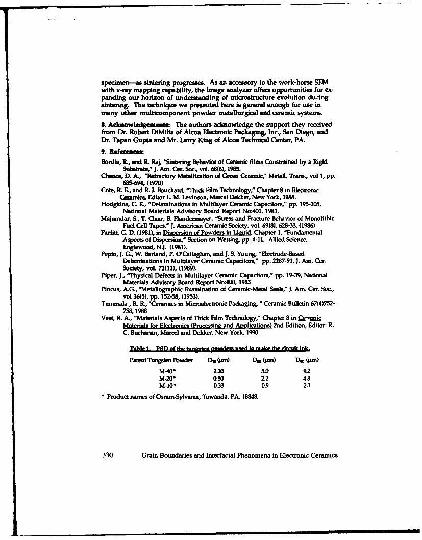
specimen--as sintering progresses. As an accessory to the work-horse SEMwith x-ray mapping capability, the image analyzer offers opportunities for ex-panding our horizon of understanding of microstructure evolution duringsintering. The technique we presented here is general enough for use inmany other multicomponent powder metallurgical and ceramic systems.
-& Ackmowledgements: The authors acknowledge the support they receivedfrom Dr. Robert DiMilia of Alcoa Electronic Packaging, Inc., San Diego, andDr. Tapan Gupta and Mr. Larry King of Alcoa Technical Center, PA.
9. ReferencesBordia, R., and R. Raj, "Sintering Behavior of Ceramic films Constrained by a Rigid
Substrate," J. Am. Cer. Soc., vol. 68(6), 1985.Chance, D. A., "Refractory Metallization of Green Ceramic," Metall. Trans., vol 1, pp.
685-694, (1970)Cote, R. E., and R. J. Bouchard, "Thick Film Technology," Chapter 8 in Electronic
Ceramics. Editor L M. Levinson, Marcel Dekker, New York, 1988.Hodgkins, C. E., "Delaminations in Multilayer Ceramic Capacitors," pp. 195-205,
National Materials Advisory Board Report No:400, 1983.Majumdar, S., T. Claar, B. Flandermeyer, "Stress and Fracture Behavior of Monolithic
Fuel Cell Tapes," J. American Ceramic Society, vol. 69[8], 628-33, (1986)Parfitt, G. D. (1981), in Dispersion of Powders in Liuid, Chapter 1, "Fundamental
Aspects of Dispersion," Section on Wetting, pp. 4-11, Allied Science,Englewood, N.J. (1981).
Pepin, J. G., W. Barland, P. O'Callaghan, and J. S. Young, "Electrode-BasedDelaminations in Multilayer Ceramic Capacitors," pp. 2287-91, J. Am. Cer.Society, vol. 72(12). (1989).
Piper, J., "Physical Defects in Multilayer Ceramic Capacitors," pp. 19-39, NationalMaterials Advisory Board Report No:400, 1983
Pincus, A.G., "Metallographic Examination of Ceramic-Metal Seals," J. Am. Cer. Soc.,vol 36(5), pp. 152-58, (1953).
Tummala, R. R., "Ceramics in Microelectronic Packaging, "Ceramic Bulletin 67(4)752-758, 1988
Vest, R. A., "Materials Aspects of Thick Film Technology," Chapter 8 in .rIm...jcMaterials for Electronics (Processing and Applications) 2nd Edition, Editor: R.C. Buchanan, Marcel and Dekker, New York, 1990.
Table 1. PSID of the buoifrn nowders tsed In make the uruiet ink.
Parent Tungsten Powder D10 (wm) DS (jAM) D90 (PrM)
M-40* 2.20 5.0 9.2M-20* 0.80 22 4.3M-10* 0.33 0.9 2.1
* Product names of Osram-Sylvania, Towanda, PA, 18848.
330 Grain Boundaries and Interfacial Phenomena in Electronic Ceramics

Tahle 2. Ulemtle of tungse powtders used t make 3 experimental rduilt inks.
M-10 M-20 M-40
Ink1 - 50% 50%Ink 2 10% 45% 45%ink3 - 100%
TableS. The •tugten~ and las wire n ts Ewe i-oid hbash) o the metal layers.
Near Free Surface Sintered at 1450C 1 rain% Tungslen %Gluas
Ink 100% M-20 Ink No GlawField 1 100 0Field 2 100 0
Ink: 100% M-20 ink with 15 v/o glass:Field 1 87 13Field 2 86 14
Near C-M intwrface Sinterd at 1550 1 rain
% Tungsten %cGlassInk: M-40.M-20.M-10 = 45:45:10 No glass:Field 1 88 12Field 2 91 9
Ink: M-40:M-20:M-10 = 45:45:10 with 15 v/o glass:Field 1 83 17Field 2 85 15
Near Free Surface Sintered at 1650*C 1 min
% Tungsten % GlassInk. 100% M-20 Ink No Glass:Field 1 78 22Field 2 78 22
Ink: 100% M-20 ink with 15 v/o glass:Field 1 74 26Field 2 72 28
Near C-M interface Sintered at 16500C 1 ri
% Tungsten % GlassInk: M-40(.M-20.M-10 = 45:45:10 No glass:Field 1 77 23Field 2 78 22
Ink: M-40:M-20.M-10 = 45:45:10 with 15 v/o glass:Field 1 70 30Filed 2 74 26
Grain Boundaries and Interfacial Phenomena in Electronic Ceramics 331

9,L
4,
i. r
4.
334ri onaisadItrailPeo eai lcrncCrmc
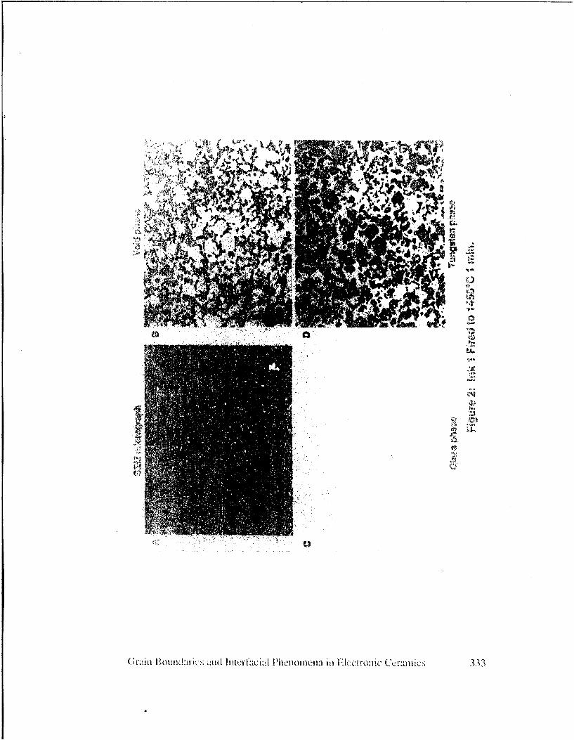
, •2
ii
(Gr:til Il-outdl~l.iki:ý'.; ••~ nld ,t•l'•i: Phu'loniela in• 1-lectro:nic ('cmllllc:l 331.

Ztt
ki~4
334 -Jj IU
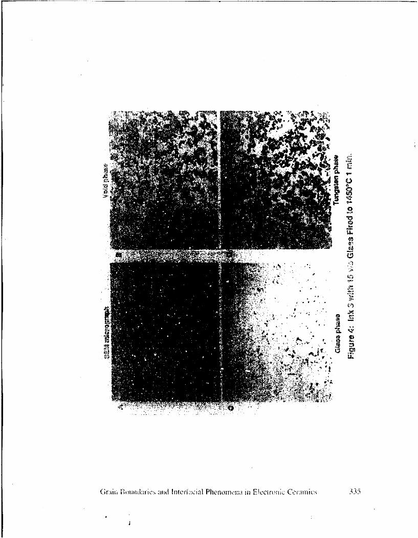
Vz I
t.
41"
Girzui. it )1,L Ul d lftiterlI .al Phienomcr.,nz in P ecirunic Cer~anr LNý 335

ZIRCONIA HYDROGEL CASTING OF PZT CERAMICS
T.E. Petroff, S.A.M. Hesp and M. Sayer
Departments of Chemistry and Physics,Queen's University, Kingston, Ontario, Canada, K7L 3N6.
ABSTRACT
Zirconium hydrogels have been used as a dispersing agent and binder for slip castingzirconia based ceramic powders. The method is capable of producing large, complexshapes with green body compacts which are tough enough for pre-sintering machiningor finishing. The technique is extended to lead zirconate titanate, where the hydrogelminimises changes to the grain boundaries. The hydrostatic figure of merit (&d,) for theslip cast, fired ceramics lie between 500 and 1300 xlO' 5 m2/N.
INTRODUCTION
Inorganic additives may be used to enhance the properties and processing of structuralceramics [1). The advantages of such inorganic dispersion aids and binders are that theydo not require burning out and that they are compatible with the base ceramic. One suchsystem is the addition of peptized, boehmite and amorphous alumina to alpha alumina [1].This results in excellent sintered zirconia ceramics with exceptional toughness andstrength. The unsintered bodies also display enhanced toughness to the point wheremachining is possible.
Another promising additive is zirconium hydrogel, polymeric Zr(OH)4, when slip castingzirconia or partially stabilized zirconia [2]. The additive behaves as an electrostericstabilizer to enhance the dispersion of the ceramic powder and is then able to react withthe ceramic and itself to act as an effective binder. Figure 1 displays the proposedstructure of the zirconium hydrogel. In solution, this material is able to either adsorb orchemisorb onto the surface of a ceramic particle as depicted in Figure 2a. Upon removalof the solvent, the chemisorption of the binder is accelerated, and the gel is able to reactwith itself via condensation reactions (Figure 2b). Removal of the solvent condenses the
To the extent authorized under the laws of the United States of America, all copyright interests in this publication are the propertyof The American Ceramic Society. Any duplication, reproduction, or republication of this publication or any part thereof, withoutthe express written consent of The American Ceramic Society or fee paid to the Copyright Clearance Center, is prohibited.
Grain Boundaries and Interfacial Phenomena in Electronic Ceramics 337

HOq OH • HOq OH O °HOq OH -OH
Zr Zr.O*NOH 1 * OHO.-" *** OHH0 0 **0--EX x x
Figure 1: Proposed structure of zirconium hydrogel
U .o • ,.... ., o I .... E O .j •• u , mo
" 5..""3 ... /O1 .. r .. .!v'm
partile, mtrix
0
no 00 . :M&%2cFigure 2a. Chemisorption of Figure 2b. Gelation of the hydrogel
hydrogel onto a to form a continuousparticle. matrix.
hydrogel to form a continuous matrix providing mechanical strength to the pre-sinteredbody. During sintering the hydrogel crystallizes at the grain boundaries to become partof the final body.
It is of interest to apply this technique to lead zirconate titanate (PZT) ceramics. Thispaper defines a fabrication method to obtain large bodies of PZT ceramics via a slipcasting process. The results show clear success in slip casting large, complex PZT
338 Grain Boundaries and Interfacial Phenomena in Electronic Ceramics

shapes which are piezoelectric on poling. While the full density has not yet beenachieved, the electrical properties are characteristic of a strongly bonded 3-0 composite,and this results in a hydrostatic response which is significantly improved over that of thefully dense ceramic.
At present, most PZT ceramics are produced by pressing powders into shapes which arethen consolidated by sintering. A typical process involves mixing PZT powders with apolymeric binder such as polyvinyl alcohol and uniaxially pressing the mixture intosimple shapes. The resulting bodies are burned out to remove the organic binder and arethen heated to sintering temperatures. The final ceramic shape can be obtained by cuttingor machining the crude, sintered material into the desired shape, electroding and poling.It is possible to cast PZT by conventional slip casting, but such methods often involveadding large amounts of organic additives which have to be distilled out of the materialprior to sintering. It is therefore often difficult to produce large but uniform ceramicbodies of complex shape using slip casting, and often significant post-sintering machiningis required.
The objective of this work was to make large ceramic PZT bodies without sacrificing thepiezoelectric response of the material. The ceramics were produced using a modified slipcasting method which utilizes inorganic, polymeric zirconium hydroxide as both thedispersing agent and binder. The green body shapes produced have enough green bodystrength to allow for some pre-sintering machining or finishing.
BACKGROUND
In a typical slip casting operation ceramic powders are dispersed into an aqueous solventand the resulting dispersion is milled for 24 to 48 hours. Dispersing agents are addedto facilitate the break up of soft agglomerates and to promote dispersion. A binder suchas polyvinyl alcohol or hydroxy methyl cellulose is added to give the cast, pre-sinteredbody some handling robustness. The resulting mixture or slip is transferred to a porousmould which serves to wick the solvent away and to give the body its shape. Removalof solvent results in the consolidation of the powder at the mould wall. The thicknessof the body is determined by the length of time the slip is allowed to stand in the mould.Excess slip is then poured away and the resulting body is removed when dry. In solidscasting, slip is not removed from the mould and the body dries as a solid shape. Thefinal ceramic is obtain in both cases by heating the body to sintering temperatures.
It has been observed that the toughness of the sintered ceramic is greatly enhanced whenusing inorganic additives. Kindl has reported that the alumina bodies prepared withadditions of peptized, boehmite and amorphous alumina are so tough that it is difficultto cut the material with a diamond saw [3]. The fracture surfaces reveal that the cracking
Grain Boundaries and Interfacial Phenomena in Electronic Ceramics 339
is intergranular as opposed to tranagranular as is normally observed in alumina. Enhancedtoughness is also observed with the zirconia work of Petroff et al [2,41. These resultsimply that the gel modifies crack propagation at the interface and that the addedtougnesas can be attributed to an amorphous layer which is chemically bonded to thecrystalline ceramic. The presence of this layer may or may not affect the electricalproperties of electric ceramics.
EXPERIMENTAL
The experiment was carried out in three stages. This paper focuses on the first twostages. The initial action was to determine the amount of zirconium hydrogel requiredto successfully slip cast PZT. The second was to modify the chemical composition ofthe PZT powder, if necessary, to identify and eliminate any processing problems. Thefinal step is to produce large, complex shapes of commercial quality.
Two different zirconium hydrogels were used. One was an experimental zirconiumhydrogel produced by Haldor Topsoe A/S of Copenhagen, Denmark; the conditions ofits preparation are proprietary. The other was produced at Queen's by the coprecipitationof ZrCI4 and Zr(CO,)2. The PZT powder used was attrition milled BM 400 provided byB.M. HiTech Inc. of Collingwood, Ontario.
PZT powder was mixed with varying amounts of Haldor Topsoe A/S and Queen'shydrogels. PZT powder, hydrogel and water were charged into a polyethylene bottle andthe pH adjusted by the addition of ammonium hydroxide or nitric acid. Grinding mediawas added and the samples were allowed to mill for 1 hr. The grinding media wasremoved and the resulting slip was poured into a plaster of paris mould in the shape ofa 2.5 cm diameter by 5 cm cylinder. The green body (of density 4.1 g/cm3) wasremoved from the mould within 20 min and allowed to dry over night in air. Finally,the sample was burned out at 900*C for 10 hr and then fired at 12601C with a I hr soak.The best perceived composition was scaled up to 1 kg PZT powder batches and thematerial was cast into a variety of shapes and sizes.
Cylinders from the second stage were cut into slices. The surfaces of some of the sliceswere viewed by an ElectroScan Model E-3 environmental scanning electron microscope.The others were silvered, poled at 35 KV/cm at 130MC in oil and their electricalproperties determined.
RESULTS AND DISCUSSION
The hydrogels were approximately 7 wt % solids for the Haldor Topsoe A/S material and14 wt % for the Queen's as determined by thermal gravimetric analysis. The zirconium
340 Grain Boundaries and Interfacial Phenomena in Electronic Ceramics

content was approximately 55 % by dry weight of the gel by neutron activation analysisfor both. The dry weight ratio of hydrogel added to PZT was 4.3 wt % resulting in anincrease of 0.36 at % in the zirconium content for the bulk powder.
There was no noticeable difference in the processing of the PZT slips at pH 4, 7 and 10.Therefore all subsequent samples were cast at pH 7 to reduce the likelihood of deleteriouschemical reactions with the plaster of paris mould. The ceramic loading of the slip thatproduced the best results was 70 % by weight. The cast samples could be removed fromtheir moulds within 20 min of casting. This time is short when compared to traditionalslip casting where the green body sits in the mould overnight.
Both the Haldor Topsoe A/S and the Queen's hydrogel produced green bodies that wererobust enough to allow some green state sanding or grinding. However, the samplesprepared using the Haldor Topsoe A/S hydrogel became soft and powdery after stage Iirrespective of the amount of gel added. Therefore the material appears to be ineffectiveas a binder for PZT even though it behaves as a dispersing aid and is able to form goodgreen bodies. Therefore these samples were not fired. The samples prepared using theQueen's hydrogel, on the other hand, produced calcined bodies that were similar to thosein the green state but with enhanced toughness to the point where they could be carvedwith a metal paint scraper. These samples were sintered to obtain the final ceramics.
Samples for electrical measurements were obtained by slicing up a slip cast and sinteredcylinder into discs 2.5mm thick using a diamond wheel cutter and electroding by silverscreen print. No problems were encountered on poling at 35 KV/cm.
The following electrical data was taken: dielectric constant f and loss at I KHz; radialcoupling factor kt determined from the radial resonant and anti-resonant frequencies; d33measured using a Berlincourt-type meter; and hydrostatic voltage coefficient g, using aSensor Technology (Collingwood, On) apparatus, Model 8809HE. The g& values werecalibrated against standard samples of known value of g.. The data measured for botha uniaxial pressed and sintered ceramic (reference) and the slip cast and sintered material(slip cast) is listed in Table 1. d, was calculated from g1 x f c..
The density of the sintered samples prepared by the slip casting process varied from 5.60to 6.80 g/cm3. This compares unfavourably to the theoretical density of PZT of 7.60g/cm3. Environmental scanning electron microscopy revealed a large number of voidsin the sintered ceramic possibly due to insufficient de-airing of the slip during castingthereby reducing the density of the material.
Grain Boundaries and Interfacial Phenomena in Electronic Ceramics 341

Table 1. Summary of the Electrical Data for the PZT Samples.
Slip castReference
__Sample 1 Sample 2 Sample 3
Density (g/cma) 7.40 6.80 6.00 5.60
Dielectric Constant 1239 1064 749 793(unpolarized material)
Dielectric Constant 1064 727 691 651(polarized material)
Radial Coupling Factor 0.61 0.30 0.29 0.18
Dielectric Loss 0.004 0.011 0.011 0.011
Charge co-efficient d3 285 217 234 187
& (10-3V.m/N) 4.0 8.4 9.0 15.0
& dh (1015m2/N) 150 450 500 1300
The bulk electrical properties are shown in Table 1. They are not comparable with thoseof pressed ceramic, however the hydrostatic figure of merit is significantly improved.It is of interest that the electrical parameters are close to those expected for a 3-0composite where single grains are strongly bonded. The high values of the hydrostaticcoefficient would be expected in such a structure.
Figure 3a compares the microstructure of the ceramic prepared by slip casting with that(Figure 3b) of similar material prepared by uniaxial pressing. Compared with thepressed sample, the grain growth in the slip cast sample is suppressed. Energy dispersiveX-ray analysis of the cut samples performed on a scanning electron microscope indicatethat there is no significant chemical difference between samples prepared by uniaxialpressing and by slip casting, and between their grain boundaries and their bulk. Therewas also no difference in the crystal structure of the bulk material as indicated by X-raydiffraction analysis. There is no deleterious affect of the addition of the hydrogel on thegrain structure of the material apart from the suppression of the grain growth.
The most significant outcome of this research is that very large PZT bodies (over 200 g)can be cast in near net shape and that the major part of the final shaping can beperformed on the green body. This can significantly reduce the amount of post-sintered
342 Grain Boundaries and Interfacial Phenomena in Electronic Ceramics

Figure 3a. Micrograph of a cut surface of a PZT sample prepared using themodified slip casting technique.
Figure 3b. Micrograph of a cut surface of a PZT sample prepared by uniaxialpressing.
Grain Boundaries and Interfacial Phenomena in Electronic Ceramics 343
machining necessary. For example in conventional processing, large, hollowhemispheres are obtained by uniaxial pressing a PZT disc to the appropriate size,sintering it and then machining the piece until the desired shape is obtained. Using themodified slip casting method, large, hollow hemispheres are obtained easily and inrelatively short time.
CONCLUSIONS
Large complex shapes of PZT can be fabricated using a modified slip casting method.No organic additives are required to form high strength green bodies. The density of theinitial samples prepared in this work have not been optimized and the bulk electricalconstants are therefore inferior to fully dense PZT. However significant levels ofpiezoelectric activity have been observed under normal poling conditions. The dielectricstrength of the sintered ceramic was sufficient to allow reliable poling at 35 kV/cm. Itshould be possible to increase the final density by subjecting the slip to reduced pressureor sonification. The hydrostatic figure of merit of these materials is 2-4 times higherthan that of dense PZT and the method may be important for this reason.
ACKNOWLEDGEMENTS
The authors thank B.M. HiTech Inc., Collingwood, Ontario, Haldor Topsoe A/S,Copenhagen, Denmark, Industrial Ceramics Ltd., Milton, Ontario, the Ontario Centrefor Materials Research, the Natural Sciences and Engineering Council of Canada and theXerox Research Centre of Canada for funding, materials and facilities. Experimentalassistance is appreciated from Dr. E.S. Prasad and K.I. Morton of B.M. HiTech Inc.,D. Misale of Industrial Ceramics Ltd., S. Sherrit and Dr. B. Mukherjee of the RoyalMiltary College of Canada, and L. Zou of Queen's University.
REFERENCES
[11 B. Kindl, D.J. Carlsson, Y. Deslandes and J.M. Hoddenbagh, Can.Ceram.Soc.,60 (1991) 53.
[21 T.E. Petroff, M. Sayer and S.A.M. Hesp, Colloid.Surf., 78 (1993) 235.
[31 Private communications with B. Kindl, Danish Ceramic Centre, Risoe NationalLaboratory, Roskilde, Denmark, (1993).
[41 T.E. Petroff, M. Sayer and B. Kindl, J.Can.Ceram.Soc. 61 (1992) 194.
[5) M.I.Miller and T.A.Henriquez, Proc. 1983 Ultrason. Symp. (1983) 977.
4 344 Grain Boundaries and Interfacial Phenomena in Electronic Ceramics
INTERFACE AND MICROSTRUCTURE DEVELOPMENT OF COATEDALUMINA POWDERS DURING HEATING
H. Yokoi" and W. D. KingeryDepartment of Materials Science and EngineeringUniversity of Arizona, Tucson, AZ 85721
ABSTRACT
Alumina powders coated with precursors of various metal oxides wereprepared. To characterize their interface and microstructure developmentduring heating, powder compacts quenched from elevated temperatures wereexamined by analytical transmission electron microscopy and field emissionscanning electron microscopy. The EM studies revealed that the aluminaparticle surfaces act as sites for heterogeneous nucleation. The final structureof the alumina simultaneously doped with cupric oxide and titania wasreached in the presence of a liquid phase but a large shrinkage occurredbefore the liquid formed. This phenomenon was explained from theviewpoint of a solid state reaction during heating.
INTRODUCTION
Powder coating is an attractive powder preparation technique becausewe can expect the fastest densification rate due to the maximized initialcontact between the ultrafine additive phase particles and the matrix phaseparticles and the uniform distribution of secondary phases in the finalstructure. Precursor coatings of TiO 2
1' 2 or ZrO23'4 on alumina have been
tested. However, the techniques for producing the uniform coating of theadditive phase on individual particles of the matrix phase have not been
"Present address: NGK Spark Plug Co., Ltd., Central Research Center,2808 Iwasaki, Komaki, Aichi 485, JAPAN
To the extent authorized under the laws of the United States of America, all copyright interests in this publication are the propertyof The American Ceramic Socit. Any duplication, reproduction, or republication of this publication or any part thereof, withoutthe express written consent of The American Ceramic Society or fee paid to the Copyright Clearance Center, is prohibited.
Grain Boundaries and Interfacial Phenomena in Electronic Ceramics 345

optimized, and also the nature and behavior of the coated phase have notbeen fully characterized. Furthermore, there is no research concerningdevelopment of int-rfaces between the coating layers and the core particlesand microstructures during heating.
In our laboratory, alumina powders coated with precursors of variousmetal oxides have been prepared by controlled hydrolysis of metal alkoxidesin a slurry of alumina. In this paper, the sintering behavior andmicrostructure development during heating of the systems of A120 3-TiO2 andA120 3-CuO-TiO2 are reported.
EXPERIMENTAL PROCEDURE
A high-purity ( > 99.99%) alumina with an average particle size of - 0.2jsm was used. The alumina powder coated with a precursor of 10 mol% TiO2(AlOT) was prepared by hydrolysis of Ti(OPr?)4 in a suspension of aluminausing a water/isopropanol solution (1/10 by volume). The alumina powdercoated with precursors of 5 mol% TiO2 and 5 mol% CuO (ASC5T) wasprepared by coprecipitation from Cu(NO 3)2 and Ti(OPri)4 in a suspension ofalurmina using a basic solution. Copper nitrate was used as a startingmaterial for CuO, since the dissolution of the copper alkoxides into commonorganic solvents was difficult.
The prepared powders were die-pressed under a compaction of 98MPa into pellets. The powder compacts were heated at 6000 - 1400*C for1 h in a furnace and rapidly quenched into liquid N2. The thickness of thespecimen was thin enough (0.2 mm) to satisfy Newtonian cooling in which thetemperature gradients within the specimen were negligible. Liquid N2 wasselected as a quenching medium because it gives a rapid initial cooling rate,but then slows the quench due to gas film formation around the specimen.'Therefore, thermal shock fracture was not a problem in this study.
The prepared powders and the sintered-quenched specimens wereexamined by TGA, DTA, XRD, XPS, FE-SEM, and analytical TEM.
RESULTS AND DISCUSSION
Figures 1 and 2 are FE-SEM micrographs showing morphology of "as-prepared" A1OT and A5C5T powders. In the AlOT powder, individual
346 Grain Boundaries and Interfacial Phenomena in Electronic Ceramics

Fig. 1. FE-SEM micrograph of "as-prepared" MOT powder.
Fig. 2. FE-SEM micrograph of "as-prepared" A1C5T powder.
Grain Boundaries and Interfacial Phenomena in Electronic Ceramics 347
alumina particles were uniformly coated with a 10-15 rn layer of very fineprecursors, while in the A5C5T powder, homogeneous mixing was achieved,but each alumina particle was not completely coated as shown in Fig. 2. Theheterogeneous deposition of precursors on individual alumina particles frommetal alkoxides can be attributed to the presence of electronegative alkoxygroups and positive metal atoms. The metal atoms are consequentlysusceptible to adsorption by oxygen atoms on the surface of alumina in thesuspension. In the subsequent hydrolysis process, the metal alkoxides on thesurface of alumina are nucleophilically attacked by water. The hydrolysismay contain steps of partial hydrolysis to form monomer -* polycondensation,finally resulting in external layers of precursors.
The DTA curve of the A5C5T powder is illustrated in Fig. 3. Anendothermic peak corresponding to liquid formation was observed at 925°C.On the other hand, the eutectic temperature of the A120 3-TiO2 is high. Thus,a liquid phase is not operative in the AMOT powder during sintering.
Figure 4 shows the shrinkage behavior of pure alumina (100A), theA10T, and the A5C5T powders. Since the green densities of the coatedpowders were lower than that of pure alumina, larger shrinkage occurred inthe coated powders. The shrinkage of the 100A started around 1000*C. Thesintering rate of alumina was accelerated by an addition of TiO 2 above1100TC. The most important aspect in this figure is that the large shrinkagetook place in the A5C5T before liquid formation, especially below 600°C(about 12 % at 600*C). The classic liquid phase sintering theory does notaccount for this low temperature process.
There are two critical points during heating in terms of microstructuralchange of alumina coated with the precursors of TiO 2. The first point is theheterogeneous nucleation of rutile on the surfaces of alumina, resulting inbreaking the precursor layers. This occurs below 900*C as shown in Fig. 5(HREM). Referring to the densification curve given in Fig. 4, the secondpoint is the start of accelerated densification which occurs at 1 1000C. Rutilenucleated on the surfaces of alumina starts diffusing into the alumina grainsat this temperature, which was confirmed by TEM-EDX. Consequently, theconcentration of the rate determining defects, [V~A'], is made higher. Thegrain coarsening rapidly occurred above 1200°C. The uniform spatialdistribution of fine TiO2 was achieved from the coated powders at a relativelylow temperature.
The XRD patterns of the ASC5T specimens heated at varioustemperatures are depicted in Fig. 6. The broad peaks of CuA120 4 wererecognized in the specimen sintered at 600*C, and they almost disappearedabove 1100 0C. It is thought that it was consumed for the liquid formation.The rutile existed in the sintered specimens over the whole temperature
348 Grain Boundaries and Interfacial Phenomena in Electronic Ceramics

0 200 400 60o 840 16000 120T.mUpratu.e (-C)
Fig. 3. DTA curve of the A5C5T powder.
25
+ c5"T A ROT
20 . 4 . +- 1 + + "
15-
+
S10-
6 0
0 i i ~~A .... A . I•i.•
4U am 8W0 10M 1200 14W IWOTEPE•nTLJ °C)
Fig. 4. Shrinkage behavior of pure alumina and the coated powders.
Grain Boundaries and Interfacial Phenomena in Electronic Ceramics 349
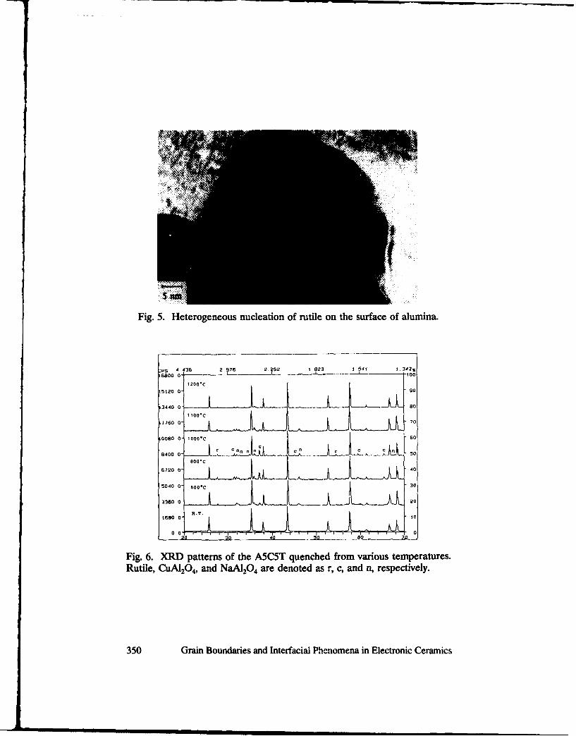
Fig. 5. Heterogeneous nucleation of rutile on the surface of alumina.
-PS 4 36 2976 2 J52 1 823 1 54f 1.343%
6800 0 - L - I "-001200*Cj
5s20 0- 90
13440 0 0--
1760 0- E "70
0060 0- 10600C 60
.40 r n n _ cn c c 5
80010
6720 0- '-40
5040 0- 600-C 30
33600- a ý±i -201680 01 R.. __ _ _ -°
--2_ 40 _
Fig. 6. XRD patterns of the AMC5T quenched from various temperatures.Rutile, CuAI20 4, and NaA120 4 are denoted as r, c, and n, respectively.
350 Grain Boundaries and Interfacial Phenomena in Electronic Ceramics

range. This implies that rutile crystallizes below 600*C. This temperatureis considerably lower than the reported crystallization temperature of rutile(900* - 10000C).' In addition, no anatase peaks were detected at thistemperature in the XRD studies. Therefore, it was assumed that theamorphous precursors on the surface of alumina directly crystallized to rutilewithout the crystallization of anatase although other researchers have statedthat the amorphous phase changes to the anatase crystal phase, then torutile.1 ,'6 The other very weak peaks in Fig. 6 were assigned to a NaAI20 8phase. The origin of the impurity sodium was the basic solution used toprecipitate Cu(OH)2.
The microstructure of the A5C5T sintered at 600*C is shown in Fig.7. At this temperature, neck growth has occurred (71.7 % of theoretical
Fig. 7. FE-SEM micrograph of the A5C5T sintered at 600'C for 1 h.
density). Obviously, the classic model of the liquid phase sintering in whichparticle rearrangement in the first stage is explained by formation andpenetration of a liquid phase cannot account for the sintering behavior of theA5C5T powder. In the very early stage of the sintering of the A5C5T, theamorphous Cu(OH)2 which was not adsorbed on the surface of alumina mayexhibit superplastic character to allow sliding and repacking of the aluminaparticles. In order for the neck formation and growth to occur, matter mustbe transferred to the neck region. The XRD evidence showed that the solid
Grain Boundaries and Interfacial Phenomena in Electronic Ceramics 351
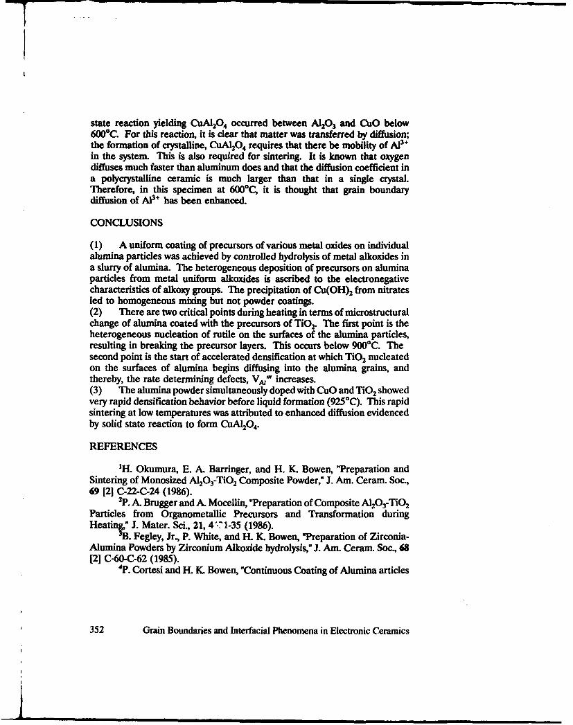
state reaction yielding CuAl20 4 occurred between AI20 3 and CuO below6000C. For this reaction, it is clear that matter was transferred by diffusion;the formation of crystalline, CuAl2O4 requires that there be mobility of Al3÷in the system. This is also required for sintering. It is known that oxygendiffuses much faster than aluminum does and that the diffusion coefficient ina polycrystalline ceramic is much larger than that in a single crystal.Therefore, in this specimen at 600*C, it is thought that grain boundarydiffusion of Al3* has been enhanced.
CONCLUSIONS
(1) A uniform coating of precursors of various metal oxides on individualalumina particles was achieved by controlled hydrolysis of metal alkoxides ina slurry of alumina. The heterogeneous deposition of precursors on aluminaparticles from metal uniform alkoxides is ascribed to the electronegativecharacteristics of alkoxy groups. The precipitation of Cu(OH)2 from nitratesled to homogeneous mixing but not powder coatings.(2) There are two critical points during heating in terms of microstructuralchange of alumina coated with the precursors of TiO.. The first point is theheterogeneous nucleation of rutile on the surfaces of the alumina particles,resulting in breaking the precursor layers. This occurs below 900*C. Thesecond point is the start of accelerated densification at which TiO2 nucleatedon the surfaces of alumina begins diffusing into the alumina grains, andthereby, the rate determining defects, VAI" increases.(3) The alumina powder simultaneously doped with CuO and TiO2 showedvery rapid densification behavior before liquid formation (925*C). This rapidsintering at low temperatures was attributed to enhanced diffusion evidencedby solid state reaction to form CuAl2 0 4.
REFERENCES
1H. Okumura, E. A. Barringer, and H. K. Bowen, "Preparation andSintering of Monosized A120 3-TiO2 Composite Powder," J. Am. Ceram. Soc.,69 [2] C-22-C-24 (1986).
2P. A. Brugger and A. Mocellin, "Preparation of Composite A120 3-TiO2Particles from Organometallic Precursors and Transformation duringHeating," J. Mater. Sci., 21, 4- 1-35 (1986).
3B. Fegley, Jr., P. White, and H. K. Bowen, "Preparation of Zirconia-Alumina Powders by Zirconium Alkoxide hydrolysis," J. Am. Ceram. Soc., 68[2] C-60-C-62 (1985).
4p. Cortesi and H. K. Bowen, "Continuous Coating of Alumina articles
352 Grain Boundaries and Interfacial Phenomena in Electronic Ceramics

with Alkoxide-Derived Zirconia Particles," Ceram. International, 15, 173-77(1989) 5D. P. Birnie, III and W. D. Kingery, "Quenching of Solid Samples forHigh Temperature Equilibrium Measurement," J. Mater. Sci., 20, 2193-98(1985).( 0. Yamaguchi and Y. Mukaida, "Formation and Transformation ofTiO 2 (Anatase) Solid Solution in the System TiO2-A120 3," J. Am. Ceram. Soc.,72 [2] 330-33 (1989).
Grain Boundaries and Interfacial Phenomena in Electronic Ceramics 353
HIGH Q-FACTOR TRI-PLATE RESONATOR WITH AN INNERCONDUCTOR OF MELTED SILVER
M.Kobayashi, K.Kawamura, and K.Suzuki
TDK CORPORATION570 Minami-hatori 2,Narita,Chiba,286 Japan
ABSTRACT
A tri-plate resonator has been developed, fabricated by a process in which thesilver inner conductor is melted. The measured Q-factor was 240 at 1.9GHz usinga dielectric with a QF product in the range of 2,000GHz. It is concluded that the Q-factor of the isolated silver conductor was 300 within 75% of the theoretical value.The reduction in Q is attributed to conductor loss associated with grain boundarieswithin the conductor. The melting conductor method has been extended to conven-tional microwave dielectrics to yield a maximum resonator Q-factor of 316 for adielectric material of 2mm thickness.
INTRODUCTION
Recently, cellular mobile communication systems are spreading rapidly. Inthese systems, small size and high performance dielectric resonators are required.Currently most mobile telephones employ coaxial resonators with a Q-factor ofapproximately 280 at 1.9GHz. A typical size of such a resonator is 2.5x2.5x5.Ommcausing the minimum size of a two pole band-pass filter to be greater than2.5x5.0x5.Omm. A technological objective for the realization of small sized de-vices has been the proposed use of tri-plate structures with a high Q co-fired innerconductor. A development of a very high Q tri-plate resonator by a new conductorforming process is reported in this paper.
Q-FACTOR ANALYSIS OF TRI-PLATE RESONATOR
As a first step the theoretical Q of a quarter wavelength tri-plate resonator wascalculated over the frequency range 1-5 GHz according to the incremental induc-tance rule.(1) The cross-section of a t-i-plate resonator, shown in Fig.1, illustratesan inner conductor sandwiched by the dielectric layers. Top and bottom surfacesare shielded by ground conductors.
The Q of the tri-plate resonator is expressed as follows.
To the extent authorized under the laws of the United States of America, all copyright interests in this publication are the propertyof The American Ceramic Society. Any duplication, reproduction, or republication of this publication or any part thereof, withoutthe express written consent of The American Ceramic Society or fee paid to the Copyright Clearance Center, is prohibited.
Grain Boundaries and Interfacial Phenomena in Electronic Ceramics 355

0.008
USvw O-ndu-(Ttim- -W SW dmt) 0.007 slow_ _ k.n 140
0006180
0.004
10004 0002MM .03 3W0
6nim 0.002 -odi5
o.ool IM ,o
Fig. 1 Cross-section 0 AN __ '- 2.00_
of resonator 0 1 2 3 4 sFmrquony (GHz)
Fig. 2 Q-factor analysis
(l/Q) Resonator = (1/Q) Conductor + (l/Q) Dielectrics ... (1)Q of the dielectric and conductor depend on frequency. Q of the conductor wascalculated using the conductivity of bulk silver. A glass base material utilized inthis simulation displayed a QF-product of 2000GHz, that is, the product of the ma-terial Q and its operating frequency in GHz is equal to 2000. The simulated Q of theresonator with dimensions given in Fig.1 is shown in Fig.2. This result shows thatthe maximum Q of the resonator, at 1.9GHz, is 300.
EXPERIMENTS
Resonator samples were made by green tape and thick film technology. Silverwas selected as the inner conductor because of its high conductivity with respect toother metals. All of the tri-plate resonator samples were designed according toFig. I and the length adjusted to correspond to a quarter wavelength resonator at aspecified frequency. The resonator Q was measured by a half power bandwidthmethod for a one port resonator.
MELTING CONDUCTOR METHOD
Improvements in resonator performance during this research are shown in Fig.3.At the outset we utilized conventional green tape and thick film technology usingsintered inner conductors. These resonators had only half of the simulated Q value.A relatively small increase in Q was observed for an increase in sintering tempera-ture up to the melting point of silver, abbreviated as m.p.. However, for samplessintered at the m.p. a remarkable increase of Q was observed. While the average Qwas approximately 175, some of the samples had a Q greater than 190. This higherQ was considered to be related to the bulk like behavior of the melted inner silverconductor. Above the m.p., the average value of Q increased with the sinteringtemperature. More than half of the samples sintered at 1020"C had a Q higher than200. Referring to Eq. (1), the contribution of the conductor to the measured Q of
356 Grain Boundaries and Interfacial Phenomena in Electronic Ceramics

Nw Melting Method0-factor of 300 is
26 ' expected.
Mal" POW Refinement of
220o -p~p~p.Melting Method
Igo Inner ConductorMethod
160
140 Conventional
Sintering Melting Thick Film120 ... ... .. Technology
mN 90o 92 940 m 0 1000 1020 1040
Firing Temperature ('C)Fig. 3 Improvement of Q-factor by melting inner conductor method
200 was estimated to be 250 which was 60% of the simulated value of 400 in Fig.2.In order to refine this melting method, several material parameters for conductor
paste were examined. Two important parameters were selected. The first was thesize and the morphology of the silver powder and the second was inorganic addi-tives. The metal content of the paste before the laminating process should be ashigh as possible, since, in the process of melting, the volume of the conductor isreduced. Thus, in the case of poor metal content paste, a certain number of voidswill remain beyond the m.p. of the conductor causing disconnection or pinching ofconductor. In a higher metal content paste, melted silver will fill the voids as if abulk silver plate was inserted. It is apparent from Fig.4a that only the paste madefrom large silver particles displays both higher Q and smaller Q variation betweensamples.
The amount of inorganic additives had to be reduced since most of them in-
220 - 280
(a) 210 -, -- 4- ll (b)200 --- - - -240
"170 U160 200 Sintering Temp
I i
140 - 98 o is 00Smnal Flake Large AddilNe (vl%)
Patfide PanwleFig. 4 Effect of conductor paste on Q-factor
(a) Particle size and shape (b) Additives
Grain Boundaries and Interfacial Phenomena in Electronic Ceramics 357

creased the resistivity of the conductor. Some additives increase the wettability ofmelted silver to dielectrics, and then they are expected to decrease the voids. Inspite of this advantage, it was necessary to minimize the additve content. Fig.4bclearly shows that the Q increased with decreasing the additives.
With the refinements of the paste parameters mentioned above, the best charac-terized Q of the resonator was 240. This means that the Q of the conductor wasabout 300 corresponding to 75% of the simulated value of 400.
Fig.5 is SEM photograph of the etched conductors. For the conductors sinteredbelow the m.p., grain boundaries remained within silver. When the sintering tem-
(a) Sintered at 940"C for 10min (b) Sintered at 1,000"C for 10min
Fig.5 Etched conductors below and above the melting point of Silver
perature was increased above the m.p., no grain boundaries were observed. Al-though both conductors seemed to be sintered densely, only the conductors sinteredabove the m.p. of silver have shown higher Q. Thus, we concluded that the grainboundary is one of the most important causes of resistivity at higher frequencies.
The maximum conductor Q of 300 was achieved applying the melting method.The deviation from the theoretical value of 400 could be caused by the morphologyof the melted inner conductor surface. Although the origin of the Q reduction wasrecognised, further refinement of the conductor surface was thought to be difficult.
EXTENSION FOR CONVENTIONAL MICROWAVE DIELECTRICS
Equation (1) indicates that a higher Q resonator can also be achieved with anincrease of dielectric Q. Some extensions of this melting method to conventionalmicrowave materials have been carried out. There are many high QF materials inconventional microwave dielectrics. Unfortunately, the sintering temperature ofthese dielectrics are much higher than the melting point of silver. In the sinteringprocess for glass based materials the dielectrics are sintered before the melting ofthe conductor. Thus, melted silver will not penetrate into the dielectrics. The poor
358 Grain Boundaries and Interfacial Phenomena in Electronic Ceramics

wettability of melted silver for ceramics would not bring about the penetration ofsilver into the ceramics, which would be a serious problem if it occurred.
Fig.6a is SEM photograph of the inner conductor sintered at 1320C. This di-electric composition was in the Ba-Nd-Bi-Ti system with e--93, QF=4000GHz.Although the dielectric started to sinter above 1150"C, melted silver did not pen-etrate into the dielectrics. The X-ray analysis, however, indicated the diffusion ofsilver as shown in Fig.6b. The X-ray count from the silver conductor was 12,000c/s, the silver concentration in the dielectrics close to the inner conductor was esti-mated to be 2.5wt%. This value suggests that a significant migration of silver undera high DC electric field will be observed in a lumped circuit element which woulddecrease the reliability of the element. However, in the case of distributed circuitselement, such as a tri-plate, a grounded inner conductor will prevent the occurrenceof DC field and there will be no migration. For the specific application of thismethod to a distributed circuit element, the diffusion of the silver would not be aserious problem. The calculated conductor Q of this resonator was 302 which isconsistent with the Q obtained with the glass base materials.
Fig.7 is the relative dielectric constant vs. QF map of conventional microwavedielectrics. Very high QF materials up to 300,000GHz are known. By using mate-
500,000 - Low Temp. Sintering MaterialBa(Mga)Os
100.000 _ o Nb)O,100,000__' .S Evaluated as
t; oo sc) T1r°03 Trin1ateResonator
Q, 300(1, C) Q; 31 1.360C) Conventional CeramiclOOOO lO4 26o 11,3o )•[
10,000 - 2- -
"LLU Evaluated asI0 ,•ONdaO Tn-plate Resonator
1,000 - 0 -: 26( 1.320"C)
500 .. . .
0 20 40 60 80 100
Relative Dielectric Constant
Fig. 7 Q-factor of t-i-plate resonator with conventional dielectrics
rials having QF value higher than 10,000GHz, the contribution of dielectric losswill be almost negligible. Thus, the Q of tri-plate resonators with high QF materialsof around 300 to 316 indicates that the Q values were defined only by the contribu-tion of the conductor Q itself. A level of silver diffusion was observed in all mate-rials, however, the concentration of silver near the conductor was at a much lowerlevel than that of Fig.6b.
Sintering of Ba(Mg,CoNb)03 at 1480"C, which is 500"C higher than the m.p.of silver, has shown that the concentration of silver at the metal-ceramics interfacewas only 1/10 that in Fig.6b. This difference may depend on the dielectric compo-sition, since the absence of bismuth in the later compositions may be a key factor.
Grain Boundaries and Interfacial Phenomena in Electronic Ceramics 359
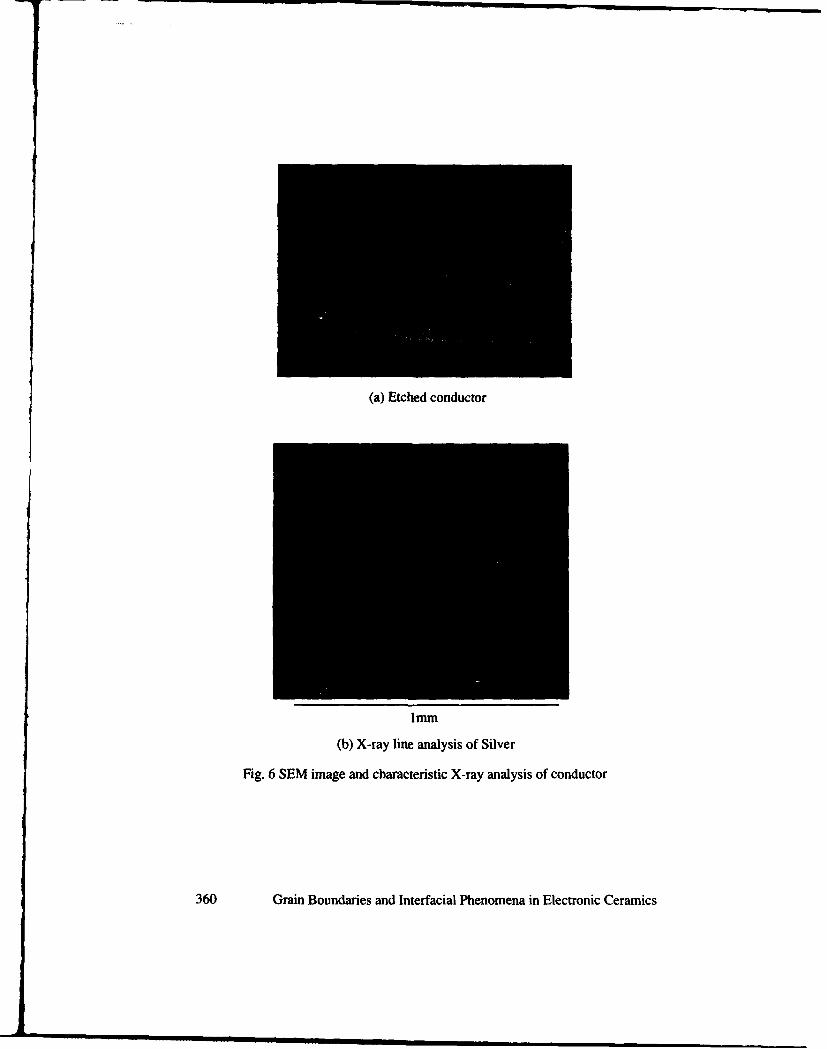
(a) Etched conductor
Imm
(b) X-ray line analysis of Silver
Fig. 6 SEM image and characteristic X-ray analysis of conductor
360 Grain Boundaries and Interfacial Phenomena in Electronic Ceramics

APPLICATIONS
Some successful applications of the melting conductor method are presented inFig.8a and 8b. By employing high Q resonators, a low insertion loss band-passfilter and very low consumption current VCO has been developed. Further devel-opment in refining this method will lead to enhanced performance and miniaturizedmicrowave devices.
45±0.3 04 12203 0dB .- ~ ISE:I I o, / - 111 d
0)D 7- 3.2±0.3- 0d
N N TDK 4 - ,dB - W
.200 B-PEAACTRIE. CI- -CTERIS
INPUT RETURN LOSS 8 J02417 I" " .5 1.0OUTPUT RETURN LOSSI 802-827 Fre] c1- V o5REJECTION 0 J 20 36 S ., ,(REJECIMN, I3 -s IW -'W-s -d/
Fig. 8a Application of this method to a bant pass filter
MECHNICL D/MNSQONS7.4TOP VIEW 4. Markng
M " P :OUTPUT Mak
3e rT1 Elecbodes
PKr: P -SuppTM : Mo WMio
BQIMMVIEVG: GND
,.X10 UNIT"-: ,LECTRICAL CHARACTERISTICS
PAHMAE I hi MIN TYP MAX IUNITTAX2.5 OSC FREQUENCY I824 B 36.5] 849] 1 WzSUPY VOTEI xl nla• V
otrpo POER, F I-S / 2 1 dam
SNRAIOatF,1140 45 atd
Fig. 8b Application of this method to a mutilleyer VCO
Grain Boundaries and Interfacial Phenomena in Electronic Ceramics 361

CONCLUSION
A series of firing temperatures from 900 to 1480"C were examined neglecting themelting point of silver. Resonators sintered at higher temperature than the silvermelting point displayed higher Q-factor approaching that of the theoretical value.A maximum Q-factor of 316 was obtained using dielectric material of 2mm inthickness.
A microstructure observation by SEM showed that the bulk material like struc-ture of the inner conductor was responsible for the higher Q-factor. A low lossband-pass filter and a low consumption current VCO, with a high C/N ratio, havebeen developed by employing P resonator fabricated by this method. A wide vari-ety of applications of this method are expected in the development of low lossmulti-layered integrated circuits.
ACKNOWLEDGMENT
The authors gratefully acknowledge Mr.T.Miura and Mr.T.Takahashi for theirhelpful discussions and microwave measurements. The authors also thankMr.S.Nakai and Mr.H.Ninomiya for designing and preparing the devices.
REFERENCE
(1) R.K.Hoffmann: Handbook of Microwave Integrated Circuits, ArtechHouse, New York, 1983.
362 Grain Boundaries and Interfacial Phenomena in Electronic Ceramics

SINTERING AND MICROSTRUCTURE OF Sr0.6Bao.4Nb2O 6
CERAMICS
Junichi TAKAHASHI, Shiro NISHIWAKI and Kohei KODAIRADept. of Applied Chemistry, Faculty of Engineering,Hokkaido University, Kita-ku, Sapporo 060, JAPAN
ABSTRACT
Highly densified Sr 0.6Ba0.4Nb20 6(SBN:60) ceramics were fabricated bypressureless sintering above 1350*C. The grain growth was considerablyinhibited for the SBN:60 samples sintered at 1350'C. Prolonged sinteringat 14000C drastically converted the microstructure of the sample fromuniform and small-grained microstructure to coarse-grained andmicrocracked one. Duplex microstructure was also observed in the initialstage of abnormal grain growth. The temperature dependence of thedielectric constant for the SBN:60 ceramics was affected not only bymicrostructure inhomogeneity but also by lattice strain induced fromcompositional fluctuation in the solid solution.
INTRODUCTION
As has been extensively studied for BaTiO 3 ceramics[1-51, micro-structure developed during sintering essentially affects the resultingdielectric properties of the product. It is, therefore, necessary to fullyunderstand the relationship between the microstructure and ferroelectricproperties for a selected material, and to establish the optimum procedurefor obtaining a ferroelectric with the desired property.
Sr,_Ba1Nb2O6(0.25<x<0.75;SBN:x) is a ferroelectric with tungstenbronze structure. A limited number of studies have been done for thefabrication of the SBN ceramics[6-9], comparing with the SBN singlecrystals. Particularly, little is known on microstructure evolution duringsintering and the resulting dielectric property change for the SBNceramics. The purpose of this study is to elucidate the densificationbehavior and closely associated microstructure development of the SBN:60
To the extent authorized under the laws of the United States of America, all copyright interests in this publication are the propertyof The American Ceramic Sodety. Any duplication, reproduction, or republication of this publication or any part thereof, withoutthe express written consent of The American Ceramic *ociety or fee paid to the Copyright Clearance Center, is prohibited.
Grain Boundaries and Interfacial Phenomena in Electronic Ceramics 363

ceramics. Furthermore, variations in the temperature dependence of thedielectric constant for the SBN:60 samples are correlated with themicrostructure evolution and lattice strain involved.
EXPERIMENTAL PROCEDURE
Starting powders for sintering were prepared by mechanical mixingof Nb20 5 and carbonates of Sr and Ba(purity;99.9%). The mixedpowders were calcined at 1000*-1300"C for 6h followed by grinding withsatellite mill. The pressureless sintering of green compacts(CIPped at1OOMPa) was conducted in air under various conditions. The density ofa sintered product was measured by Archimedes method. X-ray powderdiffractometry(Rigaku RINT2000) was used for phase identification, thecalculation of lattice parameter at room and elevated temperatures and theestimation of lattice strain. The microstructure of the thermally etchedsurface was observed with SEM(JEOL JSM-35CF). The dielectricconstant of the sintered sample was measured using a digital LCRmeter(YHP 4274A) as a function of temperature.
RESULTS AND DISCUSSION
Microstructure evolution during sintering
Figure 1 shows the densification behavior of SBN:60 ceramics.Densified body with more than 95% of theoretical density can beobtained by heating above 13500C. Isothermal density changes at 1350'Care indicated in Fig.2 as a function of sintering time.(It also includessome data obtained at 14000C.) Rapid densification occurs in an initialperiod of the sintering and the densification of SBN:60 is almostcompleted after heating for 2h. Typical microstructure of the sinteredSBN:60 samples is shown in Fig.3. Average grain sizes of those samplesare estimated to be -8pm and -1 lpm for the (A) and (B) sample,respectively. The grain growth rate at 1350°C is considerably low andcan be expressed by D' - Do' = Kt, where D is the instantaneousdiameter of the grains, D. the diameter at t=O, and K is constant. Forthe sample calcined at 1000'C, the uniform microstructure was drasticallychanged after heating for 24h.(Closed circles in Figs.1 and 2 show theoccurrence of abnormal grain growth in the sintered sample.) Morepronounced change in microstructure can be observed in sintering at1400'C. As shown in Fig.2, heating at 1400°C for 2h results in theproduction of almost fully densified sample with uniform microstructure.
364 Grain Boundaries and Interfacial Phenomena in Electronic Ceramics
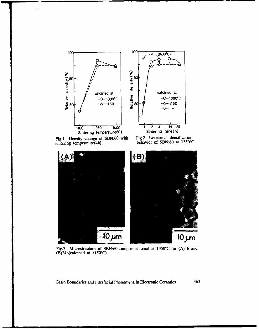
1 . .. V ....(1400C)
V
"a // calcined at I calcined at
.--- 10000C "- - 1000C
71080 -- , 1150 Z 1150-
9oc
I, , / I
1300 1350 1400 1 2 4 10 20Sintering ternperatureMC) Sintering time (h)
Fig.1 Density change of SBN:60 with Fig.2 Isothermal densificationsintering temperature(4h). behavior of SBN:60 at 13500C.
((B)
Fig.3 Microstructure of SBN:60 samples sintered at 1350°C for (A)4h and(B)24h(calcined at 1150TC).
Grain Boundaries and Interfacial Phenomena in Electronic Ceramics 365

Prolonged heating at 1400"C, however, converted the small-grainedsample to that consisting of very largely grown grains with a number ofmicrocracks via duplex microstructure. Figure 4 shows duplex structureobserved in the SBN:60 sample sintered at 1400"C for 4h. Huge grainswith pores entrapped inside the grains are embedded in a small-grainedmatrix. This kind of microstructure suggests that rapid grain growth suchas coalescence initiates at very localized region and propagates fastthrough the sample. Gazza[10] explained the duplex structure observedin hot-pressing of LiAI5 sO as microstructure resulting from liquid-phasesintering produced by a residual inhomogeneous impurity distribution. Infact, the close relationship between duplex structure and the formation ofliquid phase is confirmed in the present SrO-BaO-Nb 2O5 system. Figure5 shows the microstructure of samples which have compositions deviatingfrom stoichiometry ((Sro.6Bao.4)O:Nb 205=O.48:0.52 and 0.53:0.47 for theA- and B-composition, respectively) and were sintered at 1350'C for 4h.A phase diagram of the system SrO-BaO-Nb2O5 indicates the liquidphase formation at 1320'C for the A-composition. As expected, asimilar duplex structure to that of Fig.4 can be seen in the microstructureof the A-composition.(Fig.5(A))
There is another evidence indicating that local inhomogeneity incomposition might be responsible for duplex structure. Table 1 showsthe phase(s) present in calcined powders and also the results ofmicrostructure change with sintering time at 1400'C. It is found that adecrease in calcining temperature causes an appearance of duplexstructure in a shorter period of sintering time. Because the powderscalcined at 1000" and 1150'C are mixed-phase, they have muchopportunity to yield local inhomogeneity in the composition on sintering.Probably, after the SBN:60 solid solution is formed with a simultaneousprogress of sintering, a small amount of liquid phase which is derivedfrom residual inhomogeneity in the composition and localized at somegrain boundaries would cause inhomogeneous grain growth.
Variations in the temperature dependence of the dielectric constant
Figure 6 reveals changes in the dielectric constant accompanied withferroelectric phase transition for the SBN:60 ceramics sintered at 1400GC.A small-grained sample with 99% of theoretical density(sample-S) hasa maximum dielectric constant of about 4000 at Tc=67°C. On thecontrary, the samples having duplex structure(sample-D) and thoseconsisting of abnormally grown grains(sample-L) exhibit substantially
366 Grain Boundaries and Interfacial Phenomena in Electronic Ceramics

Fig.4 Duplex microstructure observed in the sample sintered at 14000Cfor 4h.
Fig.5 'Microstructure of the ceramics with the composition of (A)(SYO.6BaO.4)O:Nb2O5=0.48:0.52 and (B)0.53:0.47.
Grain Boundaries and Interfacial Phenomena in Electronic Ceramics 367

Table 1. Phase(s) present after calcining and microstructure developmentafter sintering at 1400'C.
Calcing Phase(s) Sintering at 1400"C-temperature(oC) 2h 4 1Oh 24h
1000 SN>>SBN N DP AB -
1150 SBN>SN N N DP AB1300 SBN N N N AB
SN;SrNb 20 6 s.s. SBN;Sro.6Bao4 Nb 2O6N;normal growth DP;duplex structure AB;abnormal growth
dielectric constant of the system. Information on the presence or absenceof the second phase(s) on the grain boundary is required for furtherdiscussion.
Figures 7 and 8 show the effect of lattice strain accommodatedinside the grains on the dielectric anomaly peak. Peak profiles of thesamples which were calcined at 1000'C and then sintered at 1350°C fordifferent duration, i.e., 2h and 10h, are given in Fig.7. A broadened andsomewhat suppressed peak is for the sample sintered for 2h. Bothsamples have nearly the same micro-structure. Then an attempt toevaluate the lattice strain which might be induced from incompletenessin the formation of the solid solution was made for the samples calcinedat 1000'C. In fig.8, PcosO is plotted against sinO where P3 is the linebroadening of the specifie,, ray diffraction peak at the Bragg angle0(radians). Maximum erm calculating P3cosO was estimated to be _+0.2 X IV-. Obviously, those samples include different amounts of thelattice strain, although their crystallite sizes converge on the fixed value.As the sintering proceeds, the lattice strain due to the variation of theinterplanar d spacing about its average value is lowered (indicated bydecreasing gradient of the lines). The sample calcined at 1300*C for 6hhas much less strain so that those sintered at 13500C for 4h and 24hshow the same temperature dependence of the dielectric constant. Thuscalcining conditions are also one of the important processing parametersfor fabricating the SBN:60 ceramics.
CONCLUSIONS
The SBN:60 ceramics were fabricated by pressureless sintering undervarious conditions. The densification of the ceramics became accelerated
368 Grain Boundaries and Interfacial Phenomena in Electronic Ceramics
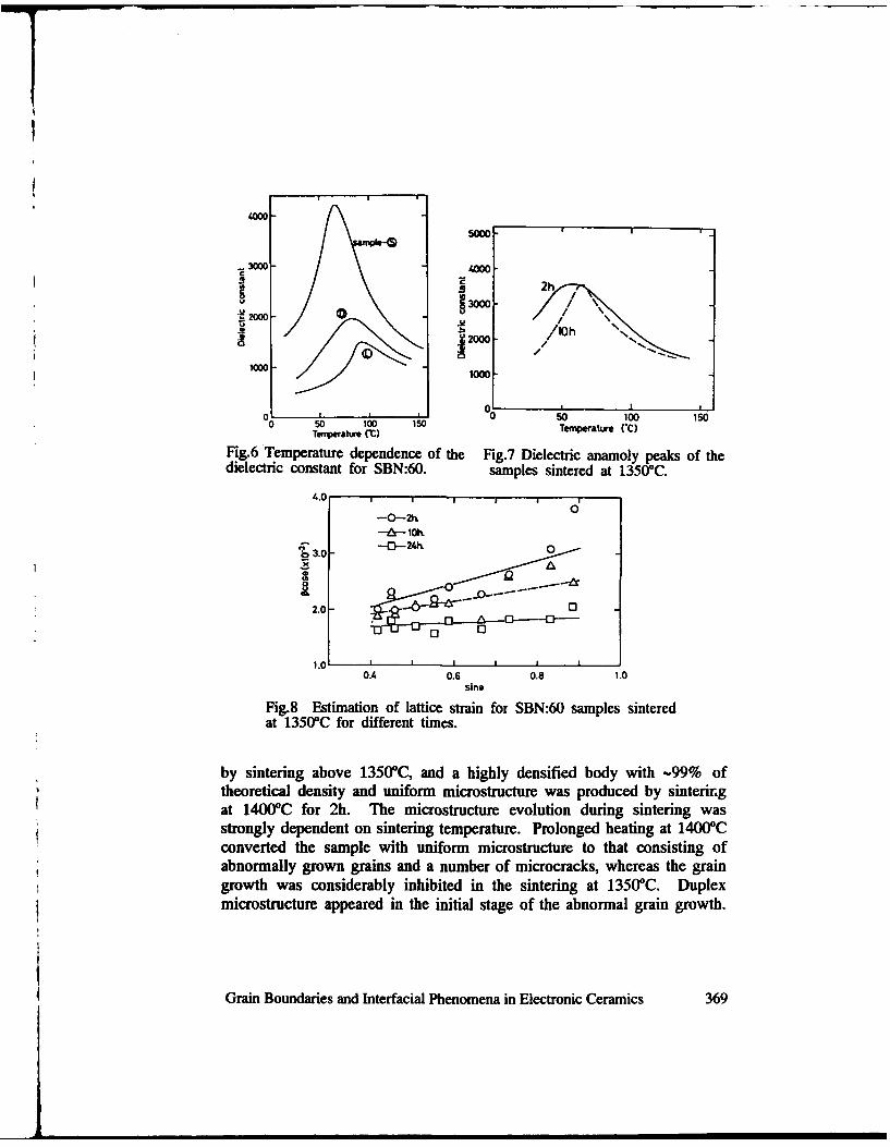
-I4000
5000
3000 4000
,30001,
4.0~~// h • ,
/10±2000 2000-
/ll \.
1000-Iooi
100
0 0 50.0 1.0 500 50 100 150 Tempe'tWue (-C)Tewpr~athx (t)
Fig.6 Temperature dependence of the Fig.7 Dielectric anamoly peaks of thedielectric constant for SBN:60. samples sintered at 1350*C.
4.0 f d times.0
-0--21%
2.0-
0
1.01I0.A 0.6 0.8 1.0
sine
Fig.B Estimation of lattice strain for SBN:60 samples sinteredat 13500C for different times.
by sintering above 13500C, and a highly densified body with -99% oftheoretical density and uniform microstructure was produced by sinteringat 1400°C for 2h. The microstructure evolution during sintering wasstrongly dependent on sintering temperature. Prolonged heating at 1400(Cconverted the sample with uniform microstructure to that consisting ofabnormally grown grains and a number of microcracks, whereas the graingrowth was considerably inhibited in the sintering at 13500C. Duplexmicrostructure appeared in the initial stage of the abnormal grain growth.
4 Grain Boundaries and Interfacial Phenomena in Electronic Ceramics 369

The substantial lowering in the dielectric maximum at Curie temperatureobserved in the coarse-grained sample could be closely related tomicrocracking in the sample. Because lattice strain induced from thecompositional fluctuation in the solid solution also affects the dielectricanomaly peak, an optimum calcining-sintering condition has to beselected to fabricate the SBN:60 ceramic with uniform microstructure andno compositional fluctuation.
ACKNOWLEDGMENTS
The authors wish to thank Y.Takano and T.Fujii for their experimentalassistance. This work was partially supported by Tokuyama ScienceFoundation.
REFERENCES
[1] G.H.Jonker and W.Noorlander, Science of Ceramics 1, ed. by G.H.Stewart, Academic Press, London(1962).
[21 N.C.Sharma and E.R.McCartney, The Dielectric Properties of Pure BariumTitanate as a Function of Grain Size, J.Austr.Ceram.Soc., 10, 16-20(1974).
[3] GArlt, D.Hennings and G.deWith, Dielectric Properties of Fine-GrainedBarium Titanate Ceramics, J.AppLPhys., 58, 1619-25(1985).
[4] A.J.BelI, AJ.Moulson and L.E.Cross, The Effect of Grain Size on thePermittivity of BaTiO3, Ferroelectrics, 54, 487-90(1984).
[5] Y.H.Hu, H.M.Chan, X.W.Zhang and M.P.Harmer, Scanning ElectronMicroscopy and Trasmission Electron Microscopy Study of FerroelectricDomains in Doped BaTiO3, J.Amer.Ceram.Soc., 69, 594-602(1986).
[6] K.Nagata, Y.Yamamoto, H.Igarashi and K.Okazaki, Properties of theHot-pressed Strontium Barium Niobate Ceramics, Ferroelectrics, 38,853-56(1981).
[7] A.Watanabe, H.Haneda, S.Matsuda and H.Yamamura, Preparation of theTranslucent Srl-Ba.Nb20 6 Ceramics, Ceramic Transactions, 1, 926-31(1988).
[8] N.S.VanDamme, A.E.Sutherland, L.Jones, K.Bridger and S.R.Winzer,Fabrication of Optically Transparent and Electrooptic Strontium BariumNiobate Ceramics, J.Amer.Ceram.Soc., 74, 1785-92(1991).
[9] S.B.Deshpande, H.S.Potdar, P.D.Godbole and S.K.Date, Preparation andFerroelectric Properties of SBN:50 Ceramics, JAmer.Ceram.Soc., 75,2581-85(1992).
[10] G.E.Gazza, Hot-pressing of LiAI5O8, JAmer.Ceram.Soc., 55, 172-3(1972).[11] T.Ota, J.Takahashi and I.Yamai, "Effect of Microstructure on the
Dielectric Property of Ceramics," in Electronic Ceramic Materials, ed. byJ.Nowotny, Trans Tech Pub., Switzerland, (1992)pp.185-246.
370 Grain Boundaries and Interfacial Phenomena in Electronic Ceramics
Interfacial Phenomena and Dielectric Properties ofPb(MgONb2)0 3 Ceramics with Excess PbO
K. H. Yoon, Y. S. Cho, D. H. Lee and D. H. Kang*Department of Ceramic Engineering, Yonsei University
Seoul 120-749, Korea
Interfacial phenomena and dielectric properties of lead magnesium niobateceramics have been studied as a function of excess PbO. With the addition ofexcess PbO up to 3 mol%, dielectric constant for the specimens sintered at9000 C increases due to increase in density and grain size by liquid phasesintering. Further additions of excess PbO bring PMN grains to rounded ones toreduce the interfacial energy, resulting in lower densities and inferior dielectricconstant. These results can be attributed to the formation of PbO rich phases andPb precipitates in the grain boundary regions.
INTRODUCTIONGenerally, it has been known that for dielectrics, discontinuities, pore andinclusions will perturb cooperative long range ordering processes and hinder thedevelopment of dielectric displacements[I]. Also a grain size dependence of thedielectric constant of BaTiO3-related capacitors has been reported in terms of theinternal stress generated at grain boundaries[21. For Pb(Mg1t3Nb25)O3 (PMNceramics, the increase in dielectric constant with increasing grain size wasexplained mainly by the reduction of grain boundaries with lower permittivity[3].Especially, as the beneficial effect of excess MgO or excess PbO on preparationand dielectric properties of PMN ceramics were widely investigated,microstructural features such as precipitates and solid second phase due to excess
• Department of Electronic Materials Engineering, The University of Suwon,
Suwon 445-743, Korea
To the extent authorized under the laws of the United States of America, all copyright interests in this publication are the propertyof The American Ceramic Society. Any duplication, reproduction, or republication of this publication or any part thereof, withoutthe express written consent of The American Ceramic Society or fee paid to the Copyright Clearance Center, is prohibited.
Grain Boundaries and Interfacial Phenomena in Electronic Ceramics 371

MgO and PbO comprising either glossy or crystalline materials should befrequently associated with grain boundary which serves to emphasize the isolationof graids from one another[4]. Chen et al suggested that the pyrochiore phase hada minimal direct effect on the dielectric constant and the degradation of it may have
been due to the presence of the semi-continuous secondary grain boundaryphases[5]. In this study, dependence of PMN microstructure on excess PbOaddition was investigated and especially, the grain boundary thickening effect on
the dielectric properties was discussed.
EXPERIMENTAL PROCEDURE
Lead magnesium mobate powders were prepared by molten salt synthesis(MSS). Reagent grade oxides, PbO, MgO and Nb205 were altogether mixed with0.635Li2SO4-0.365Na2SO4. The ratio of salt weight to raw materials weight was
0.5. It was determined experimentally as an optimum ratio in that with this ratio a
maximum perovskite phase was formed in the range of 6000C to 8500C. Thedifferent amounts of excess PbO ranging from 0 mol% to 10 mol % were added
before mixing. After milling with zirconia balls for 15h, the slurry was dried at1200C to remove alcohol. The dried powders were fired in covered alumina
crucibles at temperatures from 6000C to 850 0C for 2h. Sulfates were thenremoved by washing with deionized water several times until no free SO42 ions
were detected using a barium nitrate solution. The powders were finally dried at
1200C. After adding a 1.5 wt % polyvinyl alcohol (PVA) binder, the powders were
pressed into disks at 1500 kg/cm2. The pellets were buried in powders of the samecomposition to minimize PbO volatility and sintered in air at 900-C for 4h with aheating rate of 300 0C/h. The frctr surfaces of specimens were examined by
SEM (Scanninig Electron Microscopy, DS-130, Akashi Co., Japan) equipped withan energy dispersive X-ray analyzer, and further analyzed by TEM (TransmissionElectron Microscopy, CM-20, Philips, Netherlands). For dielectric measurements,
specimens were polished with alumina powder (3pm) and then heat-treated at7500 C after electroding with silver paste (4102, Ferro Co., U.S.A). Dielectricconstant and tan 5 were measured at I kHz using an LCR meter (AG4303, ANDOCo., Japan) with a cooling rate of 20C/min from I000 C to -800C.
372 Grain Boundaries and Interfacial Phenomena in Electronic Ceramics

RESULTS AND DISCUSSIONTable 1 shows the effect of excess PbO contents on relative density (%),
perovskite phase and maximum dielectric constant for the specimens sintered at
9000C for 4h. Compared to about 78.6% of the theoretical density for thespecimens sintered at 9000C for 4h without excess PbO, about 97% with 3 mol%excess PbO was obtained. The apparent decrease in relative density and perovskitephase content were accompanied by the further addition of excess PbO. Thesetrends could be identified by observing the microstructure of the fiacture surfacesof specimens as shown in Fig. 1. The specimens containing excess PbO showed adense microstructure with enlarged grains compared to those of no excess PbOadded specimens at the same temperature. This observation disagrees with thestudy of Wang et al[6]. They reported that the grain size of the PMN ceramicssintered at 12000C for 4h in the precalcined columbite method hardly increased bythe addition of excess PbO. They explained the opposite observation was due tothe difference in processing methods, i.e., calcining of mixed oxides method andcolumbite method. In fact, it should be considered the different sinteringtemperature as well as the different methods. At a low temperature of 9000 C,excess PbO as a sintering aid increased grain size and density. While at 12000C, itmay bring no significant effect on grain size and density because 12000C is nearthe saturation temperature.
Table 1. Characteristics of PMN ceramics sintered at 900*C, 4hr as a function ofexcess PbO.
PMN Relative Perovskite MaximumComposition Density Phase K
pure PMN 78.6% 96% 4700
3 mol% excess PbO 97% 97% 15000
5 mol% excess PbO 95% 97% 12000
10 mol% excess PbO 90.90%o 95% 8700
Grain Boundaries and Interfacial Phenomena in Electronic Ceramics 373
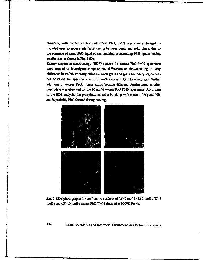
However, with further additions of excess PbO, PM grains were changed torounded ones to reduce interfaial energy between liquid and solid phase, due to
the presence of much PbO liquid phase, resulting in separating PMN grains havingsnaller size as shown in Fig. 1 (D).
Energy dispersive spectroscopy (EDS) spectra for excess PbO-PMN specimenswere studied to investigate compositional diffaences as shown in Fig. 2. Anydifference in Pb/Nb intensity ratios between grain and grain boundary region wasnot observed for spedmens with 3 mol% excess PbO. However, with furtheradditions of excess PbO, these ratios became different. Furthermore, anotherprecipitate was observed for the 10 rnol% excess PbO PMN specimens. Accordingto the EDS analysis, the precipitate contains Pb along with traces of Mg and Nb,and is probably PbO formed during cooling.
Fig. 1 SEM photographs for the fracture surfaces of(A) 0 mol% (B) 3 mol% (C) 5mol% and (D) 10 mol% excess PbO-PMN sintered at 9000C for 4h.
374 Grain Boundaries and Interfacial Phenomena in Electronic Ceramics

A.grain matrixo or (: V n ain boun 0: PbO precipitate
PbI I0Nb
~Mg 1
1. nW&0 10 rWk9 3.0
Fig. 2 EDS spectra for the 10 mol%/ excess PbO-PMN specimens sintered at9000C for 4h. ( A: grain matrix, o: grain boundary and 0: PbO precipitate)
The addition of excess PbO influenced the dielectric properties of the PMNceramics as shown in Table 1. When 3 mool% excess PbO added, the maximumdielectric constant increased significantly and reached about 15000 at 9000C.
However, further addition of excess PbO led to the lowering of the maximumdielectric constant at the same sintering condition. These results indicate that an
appropriate amount of excess PbO is necessary to optimize the dielectric properties
of the ceramics. Especially, the increase in dielectric constant can be explained bythe abrupt increases in grain size and density as reported by manyinvestigators[3,4]. However, its difficult to explain the difference of maximum
dielectric constant between the 3 mol% excess PbO and 5 mol% excess PbO PUNspecimens in terms of grain size, density and perovskite phase content due to their
similar values as shown in Table 1 and Fig. 1. Therefore, one possible explanationis that intergranular phases are responsille.
Evaluation of dielectric constant as a function of grain boundary thickness were
conducted using a simple series model and a logarithmic model for the mixing of
high and low permittivity phases[l]. The results indicate that, for PMN ceramics, aseries mixing model is more applicable and that other factors such as latticeimpurities may be also important in dielectric property[5]. According to series
mixing theory, the following equation can be applied:
DsI. De% + D*/KO (1)
Grain Boundaries and Interfacial Phenomena in Electronic Ceramics 375

where Ks is the dielectric constant of the sample, Kg the dielectric constant of the
perovskite PMN grain, Kg, the dielectric constant of the PbO solid solution in the
grain boundary, D, the thickness of the sample, Dg the thickness of the PMNgrains, and D, the thickness of the PbO grain boundary layers.
Compared to the temperature-independent Kgb of the PbO solid solution in thegrain boundary, Kg of the PMN grain is temperature dependent. That temperature
dependence can be calculated based on the compositional fluctuation model ofKirillov and Isupov[8]. Assuming K >> KOO, the plot of the reciprocal dielectric
constant(I/K) versus (T-T,)2 as a function of excess PbO at 1 kHz are shown in
Fig. 3. The nearly same slope for the given compositions indicates that the
temperature dependence of the PMN grains is not changed by the excess PbO. It is
suggested that the more excess PbO added, the thicker the grain boundary and thelower the dielectric constant. Assuming the Kg of the grains remains the same and
is not changed by the excess PbO, the average thickness of the PbO layer can be
estimated from Eq. (1), where K,,,, for PMN-STD and K, for PMN with excess
PbO. The Kn. of 20000 for PMN-STD was used to calculate the PbO grain
boundary layer in PMN ceramics[5,6]. If Kgb of 26 for PbO, and the grain sizes of
4 pgm and 3.8 pm for PMN specimens with 3 mol % and 5 mol% excess PbO,respectively, are used in Eq.(1), the calculated thickness of the PbO layer is each
17.2 and 32A. In fact, it was reported that despite of the stoichiometric PMN
sintered at 1200'C, the grain boundaries did not contain very thin intergranular
phases (10 to 20A), undetected by TEM[5].
4- A
AA A AonPbO
U 3OAAA * 3 mol% FboA 5 mot%~ PbO
*AN# RIO mo m0 PbO
2 4 8 10CT -To 6103
Fig. 3 1/K vs. (T - T0)2 as a function of amount of excess PbO.
376 Grain Boundaries and Interfacial Phenomena in Electronic Ceramics

Also, for the 3 morl% excess PbO PMN, any intergranular phase was notdetected by TEM analysis as shown in Fig. 4. Considering the thicker interlayervalue of the 5 meo% excess PbO PMN, it can be thought that a degrading of thedielectric constant with 5 mol% excess PbO is related to the grain boundarythickening effect by PbO rich solid solution phase.
With firther addition of excess PbO, the decrease of grain size was possiblyrelated to the increase of boundary thickness, W, resulting in the decrease in grainboundary mobility, B, according to the following equations[8];
B = (Cgb/kT)• (Q'SW) (2)v=B•F (3)
where, C8 is the grain boundary diffusion coefficient, Q1 is the atomic volume, S isthe boundary area, k is the Boltzman constant, F is the applied driving force and vis the boundary velocity. The decrease in grain boundary mobility brought areduction in the boundary velocity and led to the inhibition of grain growth.Consequently, the increase of PbO-rich boundary thickness as well as the decreaseof grain size resulted in the drastic decrease of dielectric constant for the 10 morl%
excess-PbO PMN.
Fig. 4 TEM photographs of the 3 mol% excess PbO-PMN specimens.
Grain Boundaries and Interfacial Phenomena in Electronic Ceramics 377

CONCLUSIONWith an addition of 3 mol% excess PbO in the MSS method, the PMN
specimens sintered at 9000C for 4 hr, showing clean grain boundary and highdensity, had a dielectric constant of 15000 at 1 kHz. The further addition of excessPbO caused inferior sinterability and low dielectric constant. The resultingdielectric constant partially depended on the volume of intergranular phase with
lower permittivity.
ACKNOWLEDGMENTThis work was supported by the Korea Science and Engineering Foundation.
REFERENCES1. D. A. Payne and L. E. Cross, "Microstructure-Property Relations for Dielectric
Ceramics," p.584-597 in Ceramic Microstructures '76, Edited by R. M. Fulrathand J. A. Pask, Westview Press, Boulder, CO, 1977.
2. W. R. Buessem, L. E. Cross, and A. K. Goswani, "Phenomenological Theory ofHigh Permittivity in Fine-Grained Barium Titanate," J. Am. Ceram. Soc., 49 (1)33-36 (1966).
3. S. L. Swartz, T. R. Shrout, W. A. Schulze, and L. E. Cross, "DielectricProperties of Lead-Magnesium Niobate Ceramics," J. Am. Ceram. Soc., 76 (5)311-315 (1984).
4. D. H. Kang and K. H. Yoon, "Dielectric Properties due to Excess PbO andMgO in Lead Magnesium Niobate Ceramics," Ferroelectrics, 87, 255-264(1988).
5. J. Chen, A. Gorton, H. M. Chan, and M. P. Harmer, "Effect of Powder Purityand Second Phases on the Dielectric Properties of Lead Magnesium NiobateCeramics," J. Am. Ceram. Soc., 69 (12) C303-C305 (1986).
6. H. C. Wang and W. A. Schulze, "The Role of Excess Magnesium Oxide or LeadOxide in Determining the Microstructure and Properties of Lead MagnesiumNiobate," J. Am. Ceram. Soc., 73 (4) 825-832 (1990).
7. V. V. Kirillov and V. A. Isupor, "Relaxation Polarization of Pb(Mglt3Nb253) 03- A Ferroelectric with a Diffused Phase Transition," Ferroelectrics, 5, 3-9(1973).
8. W. D. Kingery, "Introduction to Ceramics," 2nd ed., p.452-486, John Wiley and
Sons, New York, London, 1976.
378 Grain Boundaries and Interfacial Phenomena in Electronic Ceramics
CHARACTERIZATION OF BRIDGMAN CRYSTAL GROWTH USINGRADIOGRAPHIC IMAGING
S.E. Sorokach*, R.T. Simchick*, A.L. Fripp, W.J. Debnam and P.G. Barber"NASA Langley Research Center
Hampton, VA 23681
An x-ray imaging system was used to observe the melt-solid interface ofsemiconductor crystals during growth in a Bridgman furnace. X-rays penetratethe furnace and the crystal to reveal the shape and position of the interface as itgrows. This technique has been verified using thermocouple temperaturemeasurements. The two techniques will be compared and some of the inherentproblems of thermocouple measurements will be discussed.
INTRODUCTION
It is well known to crystal growers that the shape of the solid-liquidinterface and its position in the furnace affect the quality of the crystal.Semiconductor crystals grown in a vertical Bridgman furnace can undergothermal stress caused by a non-flat interface. This stress can result in theformation of dislocations, which conglomerate and produce low-angle grainboundaries instead of the desired single crystal [1]. Therefore several methodshave been used to characterize the shape and position of the interface.
One method used x-rays to penetrate the furnace and the crystal [2], buteach image during the growth took about eight minutes to develop and neededimage enhancement. However this method gave both interface position andshape. Another method involved taking a partially grown crystal andquenching it in water, which gave only one interface shape per run and wasdestructive to the crystal [3]. The Peltier pulsing technique [4] involvedpassing current through the sample during growth, which produced demarcation
"Lockheed Engineering and Sciences Co., Hampton, VA 23666
".Longwood College, Farmville, VA 23901
To the extent authorized under the laws of the United States of America, an copyright interests in this publication are the propertyof The American Ceramic Society. Any duplication, reproduction, or republication of this publication or any part thereof, withoutthe express written consent of The American Ceramic Society or fee paid to the Copyright Clearance Center, is prohibited.
Grain Boundaries and Interfacial Phenomena in Electronic Ceramics 379

lines for each pulse. This procedure is very time consuming since the crystalhas to be cut, polished and etched in order to see the lines, and the results arenot always predictable. Also, the position of the interface within the furnace ateach mark is not known. Ejim, Jesser and Fripp [5] used a technique whichwill be called "discontinuity in slope" to determine the position of the
interface. They used a quartz tube with a capillary in the center which allowedthem to run a thermocouple through the crystal. The temperature plotted versusdistance gives a change (discontinuity) in slope at the solid-liquid interface.This method gives the position of the interface but not the shape, and itassumes a perfect thermocouple.
The newest method [6] uses x-rays or gamma-rays to penetrate thefurnace and crystal and sends the image to a real time imaging system, whichthen sends the image to an image processor where it is seen on a standardtelevision screen. This method gives both interface position and shape inrealtime without disturbing or destroying the crystal. A schematic diagram ofthe realtime imaging system is shown in Fig. 1. The difference in densitiesbetween the solid and liquid phases shows up as a difference in imageintensity. This system allows for the visual radiographic interface using the x-ray imaging system position to be compared to the position obtained by thediscontinuity in slope, which will be referred to as the "thermal interface." Thediscontinuity is caused by the difference in thermal conductivity between thesolid and liquid phases, which produces a change in temperature gradient. Thispaper will describe the x-ray imaging system, verify the ability to measureinterface shape and position realtime, and compare the radiographic interfaceposition to the thermal interface.
Figure 1. Realtime Imaging System.
380 Grain Boundaries and Interfacial Phenomena in Electronic Ceramics
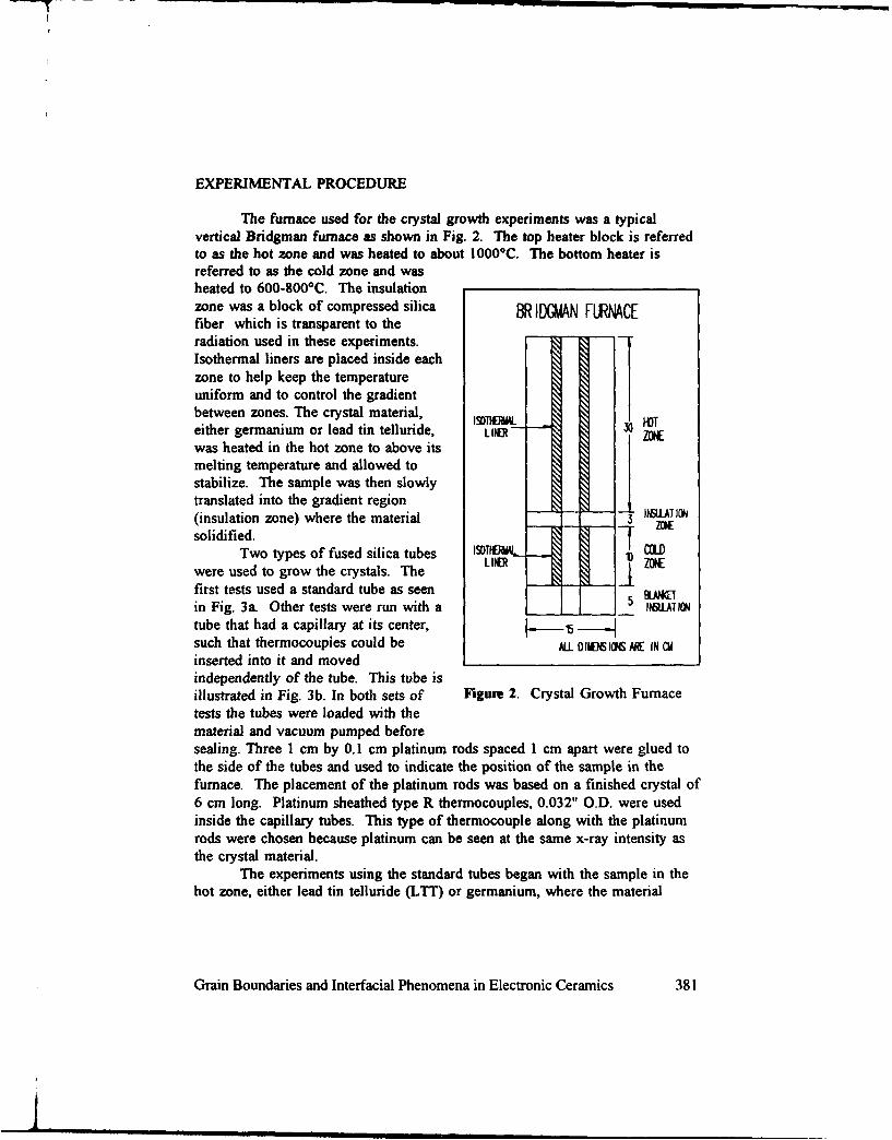
EXPERIMENTAL PROCEDURE
The furnace used for the crystal growth experiments was a typicalvertical Bridgman furnace as shown in Fig. 2. The top heater block is referredto as the hot zone and was heated to about 1 0000C. The bottom heater isreferred to as the cold zone and washeated to 600-800°C. The insulationzone was a block of compressed silica BR IDWMN FURMCEfiber which is transparent to theradiation used in these experiments.Isothermal liners are placed inside eachzone to help keep the temperatureuniform and to control the gradientbetween zones. The crystal material, ISDTUO HDTeither germanium or lead tin telluride, LINER_ ZONEwas heated in the hot zone to above itsmelting temperature and allowed tostabilize. The sample was then slowlytranslated into the gradient region(insulation zone) where the material ZONEATiO•solidified.
Two types of fused silica tubes IJST1EIML M-D
were used to grow the crystals. The LINR Z0 IE
first tests used a standard tube as seen IAWETin Fig. 3a. Other tests were run with a 5 I•MATIONtube that had a capillary at its center, - -such that thermocoupies could be ALL DIWIGIM ARE IN CMinserted into it and movedindependently of the tube. This tube isillustrated in Fig. 3b. In both sets of Figure 2. Crystal Growth Furnacetests the tubes were loaded with thematerial and vacuum pumped beforesealing. Three 1 cm by 0.1 cm platinum rods spaced 1 cm apart were glued tothe side of the tubes and used to indicate the position of the sample in thefurnace. The placement of the platinum rods was based on a finished crystal of6 cm long. Platinum sheathed type R thermocouples, 0.032" O.D. were usedinside the capillary tubes. This type of thermocouple along with the platinumrods were chosen because platinum can be seen at the same x-ray intensity asthe crystal material.
The experiments using the standard tubes began with the sample in thehot zone, either lead tin telluride (LTT) or germanium, where the material
Grain Boundaries and Interfacial Phenomena in Electronic Ceramics 381

melted and stabilized. X-rays wereused with germanium and gammarays were used with LTT, becausestronger radiation was needed to
L penetrate the LTI material. TheIt sample was then translated into the
cold zone at 1 cm/hr until itsolidified.
Data was recorded as follows.The images on the television monitorshowing the interface shape andposition were recorded at various
i times on floppy discs. These imagescould be recalled later and used forimage enhancement. The imageswere also recorded on a VCR. Tern-
Figure 3. a) S*nAard Sample. perature data was taken on anotherb). Capillary Sample. computer using the Keithley Series
500 data acquisition system. Theposition of the solid-liquid interface was determined vertically, with respect toa reference position in the insulation zone. Interface position was recorded byhand throughout the growth. If the interface was curved, the shape wasobtained by measuring the position at various points.
The ability to measure interface shape as seen on the monitor was veri-fied by using two different interpenetrating metal cylinders of different densi-ties. A copper cylinder with a convex end was placed on top of a brasscylinder with a concave end. Both cylinders were machined to specificdimensions on each end. The set of cylinders was placed in the center of theinsulation zone with the furnace at room temperature. Vertical position versusradial position data was taken with the x-ray imaging system, thus character-izing the shape of the copper and brass interface. Data was also taken with theinterface moved both up I cm and down 1 cm from the center of the insulationzone. This procedure was repeated with the copper cylinder having a concaveend on top of the brass having a convex end.
The realtime imaging system allowed the radiographic interface positionto be compared to the thermal interface position using the capillary tube shownin Fig. 3b. Experiments were performed with germanium since it is a singleelement with a constant melt temperature of 937*C. The sample was movedinto the cold zone such that half of it was solid and half liquid with the in-terface in the middle of the insulation zone. The sample was stationarythroughout the test. Or.ce the interface was established, the sheathed thermo-
382 Grain Boundaries and Interfacial Phenomena in Electronic Ceramics
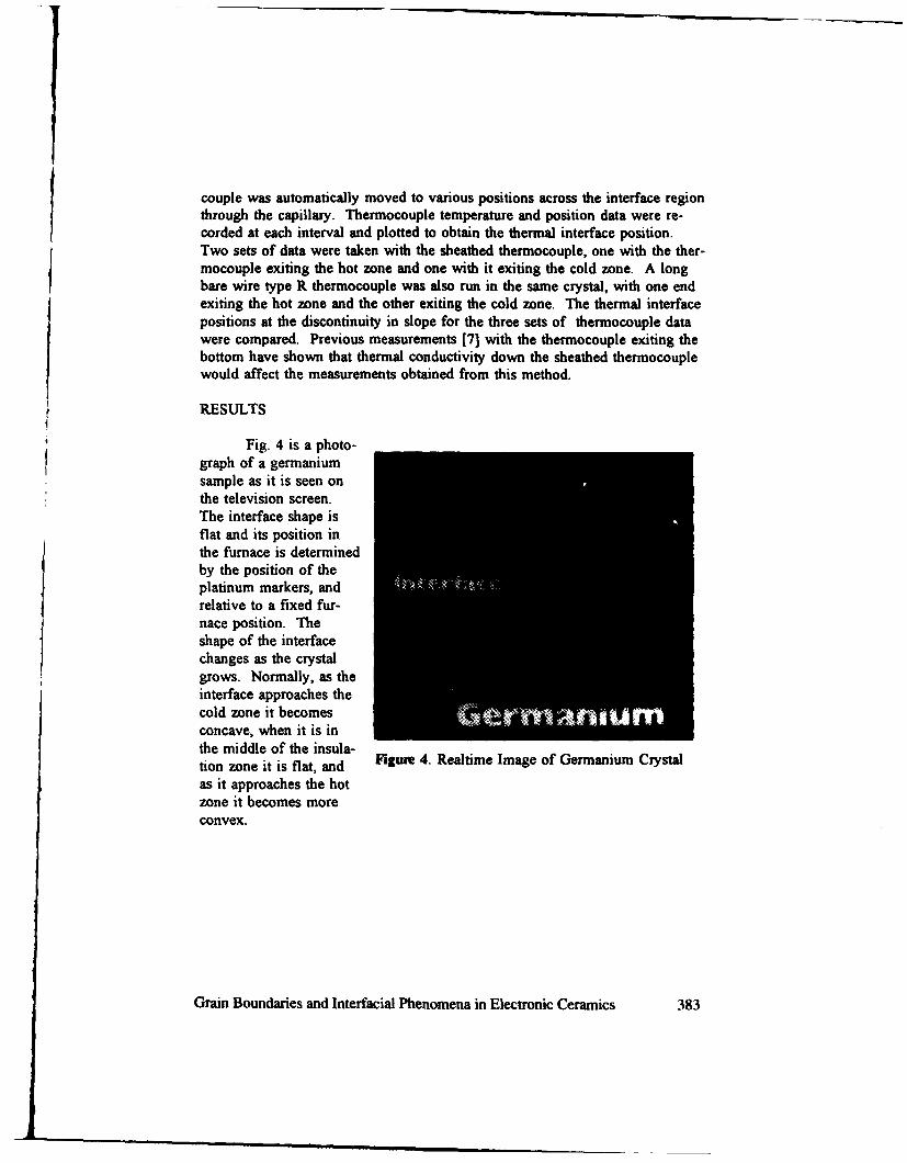
couple was automatically moved to various positions across the interface regionthrough the capillary. Thermocouple temperature and position data were re-corded at each interval and plotted to obtain the thermal interface position.Two sets of data were taken with the sheathed thermocouple, one with the ther-mocouple exiting the hot zone and one with it exiting the cold zone. A longbare wire type R thermocouple was also run in the same crystal, with one endexiting the hot zone and the other exiting the cold zone. The thermal interfacepositions at the discontinuity in slope for the three sets of thermocouple datawere compared. Previous measurements [7] with the thermocouple exiting thebottom have shown that thermal conductivity down the sheathed thermocouplewould affect the measurements obtained from this method.
RESULTS
Fig. 4 is a photo-graph of a germaniumsample as it is seen onthe television screen.
The interface shape isflat and its position inthe furnace is determinedby the position of theplatinum markers, andrelative to a fixed fur-nace position. Theshape of the interfacechanges as the crystalgrows. Normally, as theinterface approaches thecold zone it becomesconcave, when it is inthe middle of the insula-tion zone it is flat, and Pigure 4. Realtime Image of Germanium Crystalas it approaches the hotzone it becomes moreconvex.
Grain Boundaries and Interfacial Phenomena in Electronic Ceramics 383

0. Lead Tin Telluride
Interface Position vs Time-210 Germrnium
-4. Interface Position vs Time
£4
ZI1a0~
o 0a.- 14ýL -4
-00 -4
TIME (MIN.) -'% .•" "0 56 160 160 260 250 300 350
TIME (MIN.)
Figure 5. PbSnTe Interface Position Figure 6. Ge Interface Position vs.vs. Time Time
The interface movement relative to the bottom of the sample is the realgrowth rate, and the sample movement relative to the furnace is the pull rate.However, the interface movement relative to the fixed furnace position is theprimary interest because this is the deviation of growth rate from pull rate.Fig. 5 shows position of the interface relative to a fixed position in the furnaceduring growth of lead tin telluride. If the interface was curved, the position atthe middle was used. Note that theinterface moves down with respect tothe fixed furnace position. This means _
the growth rate was slower than the CUtranslation rate. Compare this data to j Cu °Fig. 6, which shows the interface posi-tion of germanium moving up duringgrowth, indicating that the growth rate °was faster than translation rate. The a
actual growth rate can be calculated -using the interface movement data and 2 CUthe translation rate. At one time it B
was assumed that the growth rate was • a , to , , 14 1,
equal to the translation rate, but these Radial Position (MM)
results prove this assumption to befalse.The results of the copper/rass Figure 7. Interface Shapes of the
interface tests are plotted in Fig. 7. Copper/Brass Cylinders
These shapes obtained from the
384 Grain Boundaries and Interfacial Phenomena in Electronic Ceramics

realtime imaging system compared favorably to the actual shapes of the cylin-ders. Therefore, the shapes seen on the monitor were verified.
Results from the capillary tube experiments are shown in Fig. 8, inwhich the tem-perature mea-surements ofthe three differ-ent sets of ex-periments are ,plotted relativeto the radio- 940 Melt Point
graphic inter- i 930
face position. aThe interface 020
temperatures 9 0ooooo Capillary TCfo al hre 1 from cold zonefor all three .0 910-• 1 00000 Bare Wire, one leg
runs are very 0 0 from each zone
close to the : ooo9 0 frcrnlhot zoneM -
0melt tempera- f h
ture, as seen by 890 1the discontinu- -Solid - - melt -
ity in s lo p e . e8 o0 . . . . . ' .1 . . . . i . I. . . . . . . . . . . . . .-20 -15 -10 -5 0 5 A0 15 20
However, the Distance From X-Ray Interface (mm)position of theinterface, labelsa,b,c, are not atthe radiographic Figure 8. Thermal Interface for the Three Sets of Datainterface (whichis at 0 mm.)When the sheathed thermocouple is coming up from the cold zone it marks thethermal interface 7 mm above the x-ray interface, coming down from the hotzone it is 3.9 mm below the x-ray interface, and the bare wire thermocoupleplaces it at 1 mm above the actual interface. These errors are due to thermalconductivity along the thermocouple, which acts as a heat source or sink.When the thermocouple coming up from the bottom is at the interface it readsaround 920°C instead of 937°C. In this case the thermocouple is acting as aheat sink. Coming down from the top, the thermocouple acts as a heat sourceand reads 939-943°C. The amount of error due to thermal conductivity de-pends on the total difference in temperature between the zone that the thermo-couple exits and the melt temperature. In one case it is comparing 10000 C to937 0C and in the other it is comparing 937°C to 800°C. In these measure-
Grain Boundaries and Interfacial Phenomena in Electronic Ceramics 385

ments, the greater difference with the thermocouple exiting the bottom results
in greater error in temperature reading.
DISCUSSION
The x-ray imaging system demonstrated that the interface position ofsemiconductor crystals could be obtained realtime. The position of the inter-face is used to calculate growth rate, and can now be calculated accurately us-ing this method. Along with obtaining the position realtime, this method gavethe shape of the interface, which was verified using the interpenetrating brassand copper cylinders.
It was discovered with this x-ray imaging system that the thermal inter-face position was in error due to thermal conductivity along the sheathedthermocouple. Also, the error was not the same with the thermocouple comingdown from the top as it was coming up from the bottom.
REFERENCES
1. K. Kinoshita and K. Sugii, J. Crystal Growth 71 (1985) 283-288.2. P.G. Barber, R.K. Crouch, A.L. Fripp, W.J. Debnam, R.F. Berry, and R.T.Simchick, J. Crystal Growth 74 (1986) 228-230.3. Y. Huang, W.I. Debnam and A.L. Fripp, J. Crystal Growth 104 (1990) 315-326.4. A. Murgai, H.C. Gatos and A.F. Witt, J. Electrochem. Soc. 123 (1976) 224.5. T.I. Ejim, W.A. Jesser, and A.L. Fripp, J. Crystal Growth 69 (1984) 509-514.6. R.T. Simchick, S.E. Sorokach, A.L. Fripp, W.J. Debnam, R.F. Berry andP.G. Barber, Advances in X-Ray Analysis 35 (1992) 1295-1300.7. J.A. Hubert, A.L. Fripp and C.S. Welch, J. Crystal Growth 131 (1993) 75-82.
386 Grain Boundaries and Interfacial Phenomena in Electronic Ceramics

INDEX
Activation energy of degradation, 315 Clark, J.A., 279
Additives, Ill Clarke, David R., 217
Ag, 299 (Co,Fe)30 4 films, 93Al doping, 207 Cofiring, 355
Alpha-zirconium hydrogen phosphate technology, 325
monohydrate, 245 Compositional analysis, 161
Alumina powders, coated, 345 Conductivity, 153
Analytical electron microscopy, 289 Cryogenic behavior, 207
Atmospheric contaminants, 289 Curie temperature, 145C-V characteristics, 195
Ba(Cu 0.5w05 )o3 161Back, K-K, 19 Debnam, W.J., 379
Balachandran, U., 289 Desgranges, Corinne, 263
Barber, P.G., 379 Desgranges, Lionel, 263
Barrier height, 231 Dielectric constant, temperature
Barry, J.C., 299 dependence, 363
BaTiO 3, 129, 145, 153, 169 Dielectric properties, 371
Batilo, Franqois, 263 Dielectric resonators, 355
Begg, B.D., 169 Ding, Y., 245
Bennett, J.P., 279 Dispersing agent, 337
Bhargava, A., 299 Dong, Dunzhuo, 161
Bi-diffused SrTiO 3-based ceramics, 231 Donor doping, 153
BiFeO3, 161 Dopants, 101
Bi-Sr-Ca-Cu-O system, 299 Double Schottky barrier, 195
Bi systems, 315 Dynamic conductance, 217
Binder, 337Blairs, S., 169 Electrical characteristics, 245
BN, 145 Electrical conductivity, 53
Boundary migration behavior, 35 Electrical discharge machining, 279
Bridgman furnace, 379 Electrically active boundaries, 19
Buchanan, R.C., 153 Electroceramics, 3Er-Ba-Cu-O, 307
Capacitor ceramics, 129 Excess PbO, 371
Carbon, 289Cassidy, D.J., 169 Ferrite, 101
Ceramic-metal interfacial region, 325 Freund, Friedemann, 263
Charge carriers, 263 Freund, Minoru M., 263
Chemical stability, 315 Fripp, A.L, 379
Chen, Chi-Jen, 101, 111 Fujimoto, Masayuki, 81
Chen, D.R., 129Chiang, Yet-Ming, 3 Gao, Y., 289
Chip components, multilayer, 101 GBBLC, 65
Cho, Y.S., 371 Glass infiltration, 325
Cho, Sang-Hee, 145, 185 Golden, S.J., 299
Grain Boundaries and Interfacial Phenomena in Electronic Ceramics 387
Grain boundary, 65, 161, 195, 289, 337 Kingery, W.D., 345layers, 119 Ko, Wen-Song, 101segregation, 3 Kobayashi, M., 355structure, 153 Kodaira, Kohei, 363
Grain growth, 363 Koumoto, K., 53
Han, Sang Chul, 35 Lattice strain, 363Hesp, S.AM., 337 Lead zirconate titanate, 337High-T. superconductors, 315 Lee, D.H., 371High-T, thin films, 307 Lee, Joon-Hyung, 145, 185Hirano, Shin-ichi, 93 Levinson, Lionel M., 207Hollow particles, 53 LiHomma, M., 119 deintercalation, 253Hoyer, J.L, 279 intercalation, 253Hsu, Jen-Yan, j.01 secondary battery, 253Hu, C.T., 135 Li3FeN2, 253Hur, Soo Hyung, 177 Lin, I.N., 135Hydrogels, 337 Liu, C.S., 111
Liu, Fuyi, 239
I-V characteristics, 195Ichinose, N., 231 Mackinnon, I.D.R., 299
Magnetic properties, 81, 93Ikeda, Jeri Ann S., 3 Martin, L.D., 325Image analysis, 325 Mechanical properties, 279Imanishi, N., 253 Melt-solid interface, 379In-diffusion method, 19 Merkle, K.L., 289Inductance, 81 Metal circuit, 325Interface, 299 Metal oxides, 345
development, 345 MgO, 263
migration, 35 Microstructural analysis, 161states, 195 Microstructure, 81, 363
Intergranular liquid films, 35 development, 345Isothermal capacitance transient Microwave dielectrics, 355
spectroscopy, 195, 231 Minamiyama, Hideaki, 315Iwashita, S., 119 Minimum loss, 111
Mn-Zn ferrite, 111Jeon, Jae Ho, 35 Modeling, 217Jones, D., 245 MNssbauer spectra, 253
Mukae, Kazuo, 195Kaneko, Shoji, 161 Mundy, J.N., 289Kang, D.H., 371 Murakami, Kenji, 161Kang, Suk-Joong L., 35 Muroya, Masaaki, 315Kawamura, K., 355Kelkar, M., 307 Ni-Zn-Cu ferrite, low-temperature-Kikuta, Ko-ichi, 93 fired, 81Kim, J., 153 Nishijima, M., 253Kim, Jeong-Joo, 185 Nishiwaki, Shiro, 363Kim, Myung Chul, 177 Nonflat interface, 379
388 Grain Boundaries and Interfacial Phenomena in Electronic Ceramics

Nonlinear varistor characteristics, 217 Schultz, William N., 207Non-ohmic electrical characteristics, 217 Seebeck coefficient, 53Nowotny, J., 169 Selvaduray, 0., 289
Semiconducting oxides, 19Okada, M., 119 Semiconductor crystals, 379Okada, Nagaya, 161 Semiconductor-insulator-semiconductorOxidative annealing, 177 model, 231Oxide materials, 263 Seo, W.S., 53Oxides, 35 Shape, 379
Shell-core structure, 129Pai, C.H., 53 SiC, 53Park, Seh-Jin, 145 Simchick, R.T., 379Park, Soon Ja, 177 Simulations, 217Particle size, 169 Sintering, 239, 325Pb(Mgl/3Nb2/3)O 3, 371 Slip casting, 337Pb/Sr ratio, 135 Sol-gel method, 93PbTiO 3-TiO 2, 119 Solid-state reaction, 345Pb(Zr,Ti)0 3 ceramics, 161 Song, Xiaolan, 239Percolation theory, 279 Song, X.Y., 129Permeability, 111 Song, Y., 307Petroff, T.E., 337 Sorokach, S.E., 379Phase separation, 93 Space charge, 3Phelan, P.E., 307 Spinodal decomposition, 93PLZT, 65 Strontium barium niobate, 363Polycrystalline ZnO, 217 Structure, 169, 245Polynuclear metal cation sols, 245 changes, 253Porosity, 185 room temperature, 169Porous ceramics, 53 Sub-grain boundaries, 239Position, 379 Suen, Meei-Lin 101Positive holes, 263 Sung, Hsiao-Miin, 101Positive temperature coefficient of Superconductors, 289, 299
resistivity (PTCR), 135, 279 Surge arresters, 207ceramics, 119 Suzuki, K, 355
(Ba 0.76,Sr0.24)TiO3-based, 177characteristics, 185 Takahashi, Junichi, 363effect, 145 Takano, M., 253
Power loss, 111 Takeda, Y., 253Proton conductivity, 245 Theoretical calculation, 195
Thermal boundary resistance, 307Q-factor, 355 Thermal conductivity, 53
Thermal design, 307Reaction rate, 289 Thermoelectric energy conversion, 53Reaction sintering, 53 Ti vacancy, 185Representative microstructure, 217 TiN/Al-O-N composites, 279Roseman, R.D., 153 TiO 2, 3Rozi~re, J., 245 Trap levels, 177
Tri-plate resonator. 355Sayer, M., 337 Tsai, T.D., 135
Grain Boundaries and Interfacial Phenomena in Electronic Ceramics 389

Tsay, M.J., I I ITsuda, Koichi, 195Tuller, H.L, 19Tung, M.J., IIITwin structure, 289
V-shape, 135Vance, E.R., 169Varistors, 217VDR effect, 231Venkataraman, K.S., 325Volume resistivity, 279
Watanabe, M., 231Weirauch, D.A., Jr., 325Wen, Qingzhe, 217Whang, Eun-Joo, 263
X-ray imaging system, 379Xu, B.M., 65Xu, D., 289
Y systems, 315Yamamoto, Hiroshi, 93Yamamoto, 0., 253Yamashita, T., 299YBCO, 65Yin, Z.W., 65, 129Yogo, Toshinobu, 93Yokoi, H., 345Yoon, Duk Yong, 35Yoon, K.H., 371
Zhang, C., 289Zhao, M.Y., 65
Zirconia, 337ZnO, 19
grains, 239:Pr varistors, 195varistors, 195, 207, 239
Zr2O doping, 315
390 Grain Boundaries and Interfacial Phenomena in Electronic Ceramics

![Kinetics of diffusion induced grain boundary migration of [100] twist boundaries in the Cu(Zn) system](https://static.fdokumen.com/doc/165x107/631c6051a906b217b906ec8b/kinetics-of-diffusion-induced-grain-boundary-migration-of-100-twist-boundaries.jpg)