
·GenRad - IET Labs
122
· GenRad GR1686 Digital Meter A INSTRUCTION MANUAL Pages only: part no. 1686-0150. Complete manual in labeled binder: Form 1686-01 00-A. )-/" i-1-
-
Upload
khangminh22 -
Category
Documents
-
view
0 -
download
0
Transcript of ·GenRad - IET Labs

·GenRad
GR1686 Digital
Capacitan~e Meter A
INSTRUCTION MANUAL
Pages only: part no. 1686-0150. Complete manual in labeled binder: Form 1686-01 00-A.
)-/" i-1-

Contents CONDENSED OPERATING INSTRUCTIONS
SPECIFICATIONS
INTRODUCTION- SECTION 1
INSTALLATION- SECTION 2
OPERATION - SECTION 3
THEORY - SECTION 4
SERVICE AND MAINTENANCE- SECTION 5
PARTS LISTS AND DIAGRAMS- SECTION 6
GR1686 Digital
Capacitance Meter A
©Gen Rad 1976 Concord, Massachusetts, U.S.A. 01742
Form 1686-0100-A September, 1976
10-0100

Condensed Operating Instructions
NOTE The 1686-Pl Test Fixture is by far the most convenient device for connecting the parts to be measured. Insertion of the OUT is as easy as child's play; true "Kelvin" connections are made automatically. All common shapes and sizes are accommodated; adaptors are used for axial-lead parts, no adaptors for radial-lead parts, "either way" for pigtail leads. Colored lights show GO/NO-GO results of main-instrument limit comparisons. System interface connectors handle bias and "start" circuitry. Refer to Figure 3-1. We highly recommend that you obtain this fixture.
To operate the 1686 Digital Capacitance Meter: a. Connect the cables and/or test fixture to the instru
ment (paragraph 3.1 ). If using externally connected equipment for control and/or data recording, refer to paragraph 2.4. Set the BIAS switch to OFF.
WARNING For safety of the operator, we recommend that external bias be limited to a maximum of 30 volts. If necessary, with suitable precautions, a maximum of 100 volts may be used. When greater than 30 volts is used, exercise great care to avoid dangerous electrical shock. Full bias voltage appears on test-lead or test-fixture terminals and on the leads of the component under test. Capacitors remain charged after measurement. The user must follow safe procedures to assure proper discharge of measured capacitors. See the WARNING in para 3.7. For safety, all personnel operating the instrument must be aware of the potential hazard involved in external biasing. Do not leave the instrument unattended with external bias applied.
b. On the rear panel, set the LINE VOLTAGE switch to match your measured power-line voltage; set the TEST VOLTAGE control fully cw.
c. Turn the POWER switch ON. Set the FREQUENCY switch for 1 kHz (or for the desired test frequency). Set the
RANGE switch to the applicable range, determined as follows. Express the desired midrange capacitance as 1 ox JJ.F. The range is x+5 for 1-kHz measurements; it is x+4 for 120-Hz (100-Hz) measurements. (See para 3.3.)
d. To use the limit comparator, set the HIGH- and/or LOW-LIMIT thumbwheel switches to the desired limit(s) and set the LIMIT switch to LIMIT. Otherwise flip this switch OFF.
e. Set the MODE switch to REPETITIVE, and adjust the interval as desired,, commonly about 0.5 s. For SINGLEMEASUREMENT MODE, refer to para 3.6.
f. Leave the BIAS switch OFF in general. However, to make measurements with bias, turn the BIAS switch to INTERNAL, or EXTERNAL, as appropriate. Refer to para 2.6 for details on supplying an external bias voltage. Be careful not to touch the lead or fixture terminals if a high external bias is applied to the instrument. See WARNING in para 3.7.
g. Insert a capacitor to be measured in the test fixture; or make the equivalent connections with the elementary test cable (para 3.1 ). Observe the CAPACITANCE display, range lights and D lights.
h. Adjust the RANGE, if required (para 3.3). Notice that the RANGE lights will guide you quickly to the optimum range.
i. To measure dissipation factor, turn the D dial until the D lamps change state. If D is of secondary ~mportance, leave the dial set to about .01 and watch the associated lamps for indication of a lossy capacitor.

Specifications
Ranges: Full-scale capacitance readings, accuracy multipliers (M), and applied voltage multipliers (A) are tabulated.
Switch Full scale· Full scale position at 1 kHz M at lowf M A
1 199.99 pF 3 1.999 nF 2 5 2 1999.9 pF 1 19.99 nF 1 1 3 19.999 nF 1 199.9 nF 1 1 4 199.99 nF 1 1.999 J.LF 1 1 5 1999.9 nF 1 19.99 J.LF 1 1 6 19.999 J,LF 1 199.9 J.LF 1 1 7 199.99 J,LF 3 1.999 mF 2 0.1 8 1999.9 J,LF 10 19.99 mF 3 0.1 9 199.9 mF 5 0.1 Note* (1000.0 mF) 5 0.1
•This extension of range 9 is useful even though range light indicates measurement exceeds full scale.
Range lights indicate correct range setting. Dissipation Factor: D = 0 to 10.
Accuracy: Basically 0.1% for 1-kHz measurements. 0.5% for lowfrequency measurements. For temp 15 to 35° C. relative humidity Oto 90%: CAPACITANCE error at 1 kHz:
±.1,0 _1 + 0 _2 D + Gfull scale D2
1% of + _01 % of l (M) ~ C d . 20 read1ng full seal~ ;
rea mg
CAPACITANCE error at 120Hz:
±.1(0.25 + 0 _2 D + Cfull scale D2
)% of_ + _05 % of l(M) ~ C d . 20 readmg full seal~
rea mg
also on range 9 only, add :
Creading . ± (25 ) % of readmg; 1 Farad
DISSIPATION FACTOR error:
±[.001 + .0002 Cfull scale + .05 D (1 +D)] M Creading
also, on range 9 only. for C up to 200 m F. add D error term of ±Creading/1 F. For C above 200 mF, D readout may be invalid. TEMPERATURE : for 6t°C above 35°C or below 15°C, increase multiplier M by factor (1 + 0.1 t.t) .
Speed: 250 msec, for complete measurement.
Display: CAPACITANCE: 4V. digits, LED display with decimal point and over-range indication. Full-scale reading 19999 at 1 kHz and 1999 at low freq. DISSIPATION FACTOR: colored lights indicate whether D is above or below dial setting. (Dial can be used to determine D.)
Applied Voltage (Variable): Max ac test voltage, applied to capacitor being measured, is 1 V x A. (A=Voltage multiplier; see Range table). Applied voltage is variable from max. to 1/20 max. Maximum power is 1/8 W.
Frequency: 1 kHz ±2% and 120 Hz, normally synchronized to 60-Hz power line (100Hz is the low frequency for 50-Hz line).
Bias: For capacitors, 2 V internal and 0 to 100 V external.
Measurement Mode: SINGLE: on command. REPETITIVE: adjustable rate, 0.25 s to 10 s per measurement. Previous readout is displayed during period of new measurement.
Data Outputs (TTL Logic): Open collector, active low. Each of the following outputs will sink 40 mA (max) from an external source of +30 V (max); low output= +0.4 V (max). BCD measurement value, decimal points, high D. reset, strobe, over-range.
Data Inputs: REMOTE START: A positive transition in< 1 J.LS, from 0 V < VL < 9.4 V to +2 V < VH < +30 V, initiates a measurement. LAMP TEST: A connection to ground lights all segments of the four principal digits of the LED display (8 8 8 8) to check operation.
Limit Comparator: CONTROLS: high- and low-limit digital switches. Limit enable/off toggle switch. DISPLAY LIGHTS: Go, high D, low, high. DATA OUTPUTS (TTL LOGIC): Open collector, active low. Each of the following outputs will sink 40 mA (max) from an external source of +30 V (max); low output= +0.4 V (max). Busy, go, high D, high limit, low limit, fail. SUPPLEMENTARY OUTPUTS: (Clamp), Th is line is to be tied to the external supply (+30 V max) to suppress inductive transients from external relay coils.
(Tone) To drive a miniature speaker (or headphone) tied between this output and ground. Signal gives 1 /4-sec audible burst (250-Hz tone) when measured value falls outside the selected high and low limits. (Not activated by D failures). (Interface) Lines for interfacing with a digital printer (i.e., GR 1785), a component sorter, a component handler for a specific application, and/or to interface with a multiple limit comparator. DATA INPUTS : (Remote Start) A positive transition of< 1 J.LS from OV < VL < 0.4V to +2V < VH < +30V initiates a measurement. (Limit Disable) Performs the same function as the toggle switch. VH input turns limit comparator off. Open circuit is equivalent to VL. which turns it on.
Environment: TEMPERATURE: 15 to 35°C normal operation. 0 to 50° operation at slightly reduced accuracy . -40 to + 75° storage. HUMIDITY : 0 to 95% at 35° C.
Supplied: Power cord, measurement cables, 30-pin and 36-pin connectors.
Available: Test fixture (with 4-terminal clips, start switch, and go/no-go lights for use with limit comparator). GR 1784 MultipleLimit Comparator for multiple category sorting. Standard capacitors.
Power: 90 to 127 or 180 to 253 V, 48 to 440 Hz, 40 W.
Mechanical: Bench or rack models. DIMENSIONS (wxhxd): Bench, 17.00x5.59x16.25 in. (432x142x413 mm); rack, 19.00x5.22x16.63 in. (483x133x422 mm). WEIGHT: 231b (10.5 kg) net, 321b (14.5 kg) shipping.
1686 Digital Capacitance Meter
60-Hz Line Freq (120-Hz Test), bench 50-Hz Line Freq (100-Hz Test), bench Rack Hardware Kit 1686-P1 Test Fixture with Kelvin Clips
Catalog Number
1686-9700 - 1686-9800
0480-9703 1686-9600
----

/" I ' \ .
Contents
CONDENSED OPERATING INSTRUCTIONS
SPECIFICATIONS
INTRODUC TION - SEC TION 1
INSTALLATION- SECTION 2
OPERATION - SECTION 3
THEORY - SECTION 4
SERVICE AN D MAINTENANCE - SECTION 5
PARTS LI STS AND DIAGRAMS ... SECTION 6
© GenRad 1976 Concord, Massachusetts, U.S .A . 01742
Form 1686-0lOO-A September. 19 7 6
10-0100
- - - ------- --- ---- ----- - - - -

Warranty
~GenRad------------~
This product is warranted to be free from defects in material and workmanship and, when properly used, will perform in accordance with specifications. Any GR-manufactured instrument, module, or part found not to meet this standard within a period of one year after original shipment will be repaired or replaced at no charge when returned to a GR service facility.
GR policy is to maintain repair capability for a period of ten years after the original shipment and to make this capability available at the then prevailing schedule of charges for any product returned to a GR service facility. Changes in the product not approved by GR shall void this warranty. GR is not liable for consequential damages.
This warranty is in lieu of all other warranties, expressed or implied, including, but not limited to, the implied warranties of merchantability and fitness for a particular purpose.
,
r
J

Introduction-Section 1
1.1 PURPOSE ......... . . 1-1 . 1-1 . 1-1 . 1-2 . 1-2 . 1-2
1.2 FUNCTIONAL DESCRIPTION . . . 1.3 GENERAL PHYSICAL DESCRIPTION 1.4 CONTROLS, INDICATORS, AND CONNECTORS 1.5 SYSTEMS . . 1.6 ACCESSORIES ........... .
1.1 PURPOSE
The 1686 Digital Capacitance Meter is an all solid-state instrument that automatically measures series capacitance at two frequencies, 1 kHz and 120 (or 1 00) Hz. These measurements can be made on command or repetitively, with measurement repetition interval variable between 0.25 s and 10 s. Results are displayed on a digital readout.
The basic accuracy is 0.1% + 2 counts for 1-kHz measurements and 0.25% + 1 count for low-frequency measurements. For 1-kHz measurements, the full-scale digital readout indication is 19999; for low-frequency operation it is 1999. The decimal point and units are also displayed.
The range is manually set. The meter measures capacitance from .01 pF (one digit) to 200,000 /lF (200 mF) or more and automatically indicates whether the range being used is optimum, too low, or too high.
The dissipation factor, D, is also indicated. The value of Dis obtained by a manual dial adjustment. However, if this dial is set to the desired D limit, there is an automatic indication if this limit is exceeded.
Data outputs are also furnished for the measured capacitance and whether the measured D is within the limit set at time of measurement, to allow data recording, limit comparison, or process control. A built-in, two-limit comparator facilitates go/no-go sorting. Multiple-limit comparators, data printers, card punches, and handlers are also available from GenRad, separately or as a system. The data output (digital signal) levels are standard TTL, open-collector, for total interface flexibility.
The instrument's analog circuit provides for low impedances to be measured by means of a four-terminal connection to the "unknown" capacitor being measured. (Impedances of test fixture and leads have a minimal effect.) Guarded, three-terminal measurements can also be made with negligible error, regardless of substantial stray capacitance to ground.
The analog-to-digital conversion of the measurement result is made by an ac-dc ratio meter capable of high accuracy and stability.
A built-in limit comparator is provided. It compares the measured capacitance and dissipation factor, D, with limits
you set on the front panel. Any upper and lower limits of C within the range of the meter can be selected on thumbwheel switches, up to 199.9 mF. Any upper limit of D can be set on the D dial.
The comparator is a module that enhances the operation of the meter, making it particularly useful for manual, semior fully-automatic selection and sorting applications, as well as intricate laboratory measurements. Visual indications of comparison results as well as respective control signals available for use by external equipment permit these various operations to be easily performed with a minimum of operator involvement.
Comparisons of quantities usually requiring laboratory techniques can also be easily made, such as: small impedance differences, semiconductor capacitances, capacitance drift with temperature, etc. And, with suitable recorders such as the G R 1785 Line Printer or other recorders, records of all types of data can be kept, including changes in measurements as a result of environmental effects.
A GR 1784 Multiple-Limit Comparator that makes comparisons of up to 4 pairs of limits is also available. See para 1.6.
1.2 FUNCTIONAL DESCRIPTION.
Refer to Section 4 for a general and detailed functional description of the instrument.
1.3 GENERAL PHYSICAL DESCRIPTION.
The instrument is supplied in a bench configuration. It can be set in a tilted position on a bench, for easy viewing of the front panel, by use of the bail under the front of the cabinet. For mounting in an EIA standard 19-inch relay rack, a kit of hardware is readily available and easy to use.
The 4 connections to the capacitor being measured, as well as data and control signal connections are made at 2 rear-panel connectors. A cable, supplied, connects to a test fixture or set of test leads (stackable, with alligator clips), also supplied.
INTRODUCTION 1-1

1 2 3 4 5
15 14 13 12 11 10 9 8
Figure 1-1. Front-panel controls and indicators..
The unit has its own power supply, including a 2-V internal bias supply for capacitors under test. The instrument requires ac power, 48 to 440Hz, and can be switched to accommodate line voltages of 90 to 127 V and 180 to 253 V, in 5 ranges selectable at the rear paneL Proper fuses for these ranges are provided in fuse holders on the rear paneL
In the center of the instrument are 2 large circuit boards, the bridge board across the bottom and the logic (control) board above, hinged for convenient access. Behind the limit comparator panel are 2 smaller boards for circuitry associated with it. The power supply is at the far left. Further details are given in Section 5.
Physical characteristics of the unit are described further in the specifications at the front of this manuaL Complete dimensions for the bench and rack ·mount configurations are given in Section 2.
1.4 CONTROLS, INDICATORS, AND CONNECTORS.
Figure 1-1 shows the front panel controls and indicators. Table 1-1 identifies them, with descriptions and functions. Similarly Figure 1-2 shows the rear panel; and Table 1-2 identifies and describes the rear-panel controls and connectors.
1.5 SYSTEMS.
Because additional equipment can expand the basic capabilities of most GR instruments, including this one, facilities are available to supply complete systems; inquiries are invited. Each system, custom tailored to individual
1-2 INTRODUCTION
requirements and including only equipment necessary to perform the required task, is completely assembled and checked as a unit. Generally, such systems have wide application and can be used for laboratory development, production monitoring, final quality assurance, production-lot sorting, incoming inspection, environmental testing, reliability evaluation, etc., typically providing semi- or fully automatic operation.
1.6 ACCESSORIES
1.6.1 Accessories Supplied.
Refer to Table 1-3 for a list of accessories supplied with the instrument. The test-fixture cable is always used, whether you have a test fixture (such as GR 1686-9600) or whether you use the elementary measurement cable to make bananaplug or alligator-clip connections to the capacitor being measured.
1.6.2 Recommended Test Fixture. Figure 1-3.
The GR 1686-9600 Test Fixture is highly recommended as an accessory. Employing Kelvin contacts for both radiallead and axial-lead components of all common sizes, it effectively and conveniently provides a 4-terminal measurement connection for components and parts under test. The fixture permits rapid manual measurements of components while providing high accuracy by reducing the effects of stray impedances on measurement accuracy.
The figure shows the fixture in use. It is cormected by cable to the rear-panel TEST FIXTURE connector. If you

Figure 1-1 Ref. No.
2
3
4
5
6
7
8
9
10
Name
POWER Switch, S504
DISSIPATION FACTOR dial (D dial), R501
CAPACITANCE display, 1685-4710
RANGE switch, S501
FREQUENCY switch, S502
HIGH LIMIT switch, S6 ... S10
LOW LIMIT switch, S1 . . . S5
HIGH light, DS4
LOW light, DS3
HIGH D light, DS2
Table 1-1
FRONT-PANEL CONTROLS AND INDICATORS
Type
Rotary switch; 2 positions: OFF, ON.
Continuously adjustable rotary dial and associated indicator lamps. Scale 0 to oo, with divisions from 0.001 to 20. (Green lamp DS504; red, DS503.)
Numerical readout, LED display, 4 Y:z digits.
Rotary switch with associated indicator lamps (DS502, left~; DS501, right+-). Positions 1 . . . 9.
Rotary switch; 2 positions; 1 kHz, 120Hz (or 100Hz).
Thumbwheel switch, 5 digits
Thumbwheel switch, 5 digits
Indicator lamp, red.
Indicator lamp, red.
Indicator lamp, white.
Function
ON applies power; OFF disconnects both wires of ac power line from internal circuit, including fuses.
Indicates dissipation factor Dover range 0 to 10, two ways: (1) Pass/fail. Dial is set to D limit and left there; lighted arrows indicate pass (green light) or fail (red light), for each measurement. (2) D measurement. After any measurement of C, the dial can be rotated to the point where the indication passes from one arrow to the other; corresponding dial reading is the measured D.
Gives visual indication of measured capacitance to 5 places at 1 kHz, to 4 places at low frequency. First digit becomes a blinking "E" if measured C C exceeds full scale for the range selected.
Selects 9 capacitance ranges; see Table 3-2. The lamps indicate that the correct range is set when both lamps are out. If one lamp is lit, turn the switch in the indicated direction to reach the proper range. In position 8 (or lower), the capacitance range is a decade higher for low-frequency measurement than for 1-kHz measurement. In position 9, only low-frequency measurement can be made; this range has (in addition to the normal decade in which the range lights stay out) an extension (higher) decade of capacitance that is useful even though the range light indicates~. There is no particular low-capacitance limit for range 1.
Selects the test frequency, as indicated. The lower frequency is normally twice the power-line frequency.
Selects the upper limit for comparison.
Selects the lower limit for comparison.
Lights if measured capacitance exceeds selected HIGH LIMIT.
Lights if measured capacitance falls below selected LOW LIMIT.
Lights if measured dissipation factor D exceeds the value set on the D dial at the time of measurement.
INTRODUCTION 1-3

Figure 1-1 Ref. No. Name
11 GO light, DS1
12
13
14
15
LIMIT/OFF switch, S11
BIAS switch, S503
MEASURING light
MEASUREMENT MODE control, S506/R500
Table 1-1 (Cont) FRONT-PANEL CONTROLS AND INDICATORS
Type
Indicator lamp, green.
Toggle switch, 2 positions.
Rotary switch; 3 positions; OFF, INTERNAL 2 V, EXTERNAL.
Red LED indicator, CR 1.
Continuously adjustable control with switch, labeled: SINGLE, REPET· ITIVE, 0.25 ... 10 s.
Function
Lights if measured parameters are within the limits (inclusively) as set by LIMIT switches and D dial, at time of measurement.
When set to LIMIT, enables limit comparator; OFF disables it.
When set to INTERNAL 2 V, furnishes 2-V bias for the capacitor under test. The EXTERNAL position allows an external bias voltage of up to 100 V to be applied to the capacitor under test, via the rear-panel TEST FIXTURE connector.
When illuminated, indicates meter is making a measurement.
When set to REPETITIVE and adjusted between 0.25 and 1 0 s, the meter makes repetitive measurements at approximately the indicated rate. If the switch is set to SINGLE, a single measurement is made, initiated by an external device such as a test future, component handler, recording device, etc. connected to the rear panel.
Figure 1-2. Rear-panel connectors and controls. (The cover is removed from item 4R.)
1-4 INTRODUCTION

Table 1-2
REAR-PANEL CONTROLS AND CONNECTORS
Figure 1-2 Rm.No. Name
1 R Comparator connector, labeled S05
2R TEST FIXTURE connector, S010
3R Power connector,
S504 (labeled 48-440 Hz)
Type
Socket, 24 contacts, accepts Cinch or Amphenol no. 57-30240.
Socket, 36 contacts,
accepts Cinch or Amphenol no. 57-3060.
Safety shrouded 3-wire plug conforming to International Technical Commission 320.
Function
Supplies results from the internal limit comparator to peripheral equipment such as parts handler and speaker. Accepts a start signal and comparator disable signal. (Refer to Section 2.)
Cable connection for test fixture, printer, and other peripheral equipment. (Refer to Section 2.)
Ac power input. Use appropriate power cord, with Belden SPH-386 socket or equivalent.
4 R Data output boardedge connector, L-S01
Set of 30 contacts on edge of Logic Board, recessed behind a cover plate.
Supplies measurement data, status and timing signals to (and accepts a start signal from) associated equipment such as multiple-limit comparator, parts handler, computer. (Refer to Section 2.)
5R Fuses, F 1 labeled
6R
7R
1 A, F2 labeled % A
LINE VOLTAGE switch, S505
TEST VOLTAGE control, R510
Fuse in S!Xtraction post holder.
Screwdriver operated rotary switch, 6 positions: 0 F F I 90-11 0 I 1 04-127 I 180-220, 194-236, 207-253 (no stops).
Screwdriver operated potentiometer. Max position is cw.
Short-circuit protection. The lower current fuse acts only on the 3 highest-voltage settings of the LINE VOLTAGE switch. Use Bussman type MDL or equivalent fuses.
Adapts power supply to line-voltage ranges as indicated.
Adjusts level of voltage applied to capacitor under test, from A (max, normal; see Table 3-2), continuously down to .05 A volts rms.
select SINGLE MEASUREMENT MODE, measurement is started when the bar across the front of the fixture is pressed down. Indicator lamps mo~nted on the fixture give GO/NO-GO indications (green and red lights) unless the limit comparator is turned 0 F F. For detai Is, refer to para 3.1.
checks, calibration and testing. Table 1-4 lists G R manufactured accessories available. Consult G R for other items available, such as component handlers, other data recorders, and environmental test equipment that can be supplied separately or on a system basis.
1.6.3 Other Accessories Available.
Other accessories that are available enhance this capacitance meter with data printing, card punching and externally applied bias voltages, and also aid in performing operational
NOTE Some of the standards shown in this table are recommended for calibration and other procedures in the service section. Refer to Table 5-1.
INTRODUCTION 1-5

Quantity
Table 1-3 ACCESSORIES SUPPLIED
Description
Power cord, 210 em (7ft) long, 3-wire AWG 18, with molded connector bodies. End with Belden SPH-386 socket fits instrument. Other end is stackable (hammerhead) conforming to ANSI standard C73.11-1966.
Measurement cable, 140 em (55 in.) long, with 36 pin connector at each end. Fits TEST FIXTURE connector.
Elementary measurement cable, 20 em (8 in.) long, fits the cable above, has 5 stackable banana plugs for connection to the capacitor being measured and ground, when a test fixture is not used.
Connector for your cable, 36-pin. Fits TEST FIXTURE connector. Cinch "Micro-ribbon" or Amphenol No. 57-30360. *
Connector for your cable, 30-pin. Fits board-edge contacts (S01) at rear of Logic Board. Interior portion of connector is Amphenol No. 225-21521-401-117. *
•For replacement, the commercially available part is recommended.
1-6 INTRODUCTION
- ~
\ i,~ J~ •is • ..... 4~·
~~~·~ <ll••~ !II ~~l'l{ll.ll(l UMO/
• • Figure 1-3. Test fixture in use, with adaptors for axiallead capacitors. The elementary test cable is shown at the left.
GR Part Number
4200-9625
1686-0291
1686-9602
4220-3036*
4230-1023

Name
Test Fixture
Data Printer
Multiple Limit Comparator
Standard Capacitor
Reference Standard Capacitor
Standard Capacitors
Decade Capacitor
Precision Decade Capacitor
Decade Capacitor
Precision Decade Capacitor
Rack Adaptor Set
Table 1-4 ACCESSORIES AVAILABLE
Type or Part No.
G R 1686-9600
GR 1785
GR 1784
GR 1417 Four-Terminal Capacitance Standard; 1 p.f to 1 F. Ratio accuracy: ±0.1 %.
GR 1404-A (1000 pF). 1404-B (100 pF). 1404-C (10 pF).
GR 1409-9706 (.001p.F) 1409-9712 (.01p.F) 1409-9720 (0.1p.F) 1409-9725 (1.0 p.F)
Accuracy ±.05% of nominal capacitance.
G R 1412-BC Decade Capacitor, 50 pF to L11115p.F, accuracy ±0.5% ±5 pF.
G R 1413; 0 to 1.11111 p.F, .05% basic-accuracy.
GR 1419-K; 100 pF to 1.10p.F, accuracy 0.5% .
GR 1423; 100pFto 1.111p.F, ±.05% basic accuracy.
G R 0480-9703
Function
Convenient 4-terminal test fixture for manually inserted axial-lead and radial-lead capacitors. Adjustable to accomodate all common sizes. Base contains start switch and supplementary GO/NO-GO lights.
Precise, compact, and economical means of recording measurement data. Has up to 21-column capacity with a printing rate of three lines per second minimum. A two-color ribbon can be controlled to print red or black on roll and/or fanfold paper.
Designed for use with the 1686 Digital Capacitance Meter, 1685 Digital Impedance Meter and 1683 Automatic RLC Bridge. Makes comparisons· with up to 4 pairs of limits, each containing a high and low value. Lamps (and electrical TTL open-collector, active-low outputs for external use) are furnished for high, low and go indicators for each set of limits. Indicator ramps and output signals are also furnished for priority sorting (indication of first "go" in set of 4 limit pairs), total limit failures, and loss-limit failures. Unit is also stackable, with all data available as output via a 50-pin connector and all comparison results on another connector.
Instrument check and test.
Instrument check, calibration, and test.
Instrument check and calibration.
Instrument check, calibration and test.
Instrument check, calibration and test.
Instrument check, calibration and test.
Instrument check, calibration and test.
Provides the hardware for mounting the instrument in a standard 19-in. rack. (Refer to Section 2.)
INTRODUCTION 1-7
..

Installation-Section 2 2.1 UNPACKING AND INSPECTION 2.2 DIMENSIONS. 2.3 MOUNTING 2.4 EXTERNAL-DATA CONNECTIONS 2.5 TEST-FIXTURE CONNECTIONS 2.6 EXTERNAL BIAS 2.7 POWER-LINE CONNECTION 2.8 LINE-VOLTAGE REGULATION 2.9 ENVIRONMENT. 2.10 STORAGE AND SHIPMENT.
2.1 UNPACKING AND INSPECTION.
If the shipping carton is damaged, ask that the carrier's agent be present when the instrument is unpacked. Inspect the instrument for damage (scratches, dents, broken knobs, etc.) If the instrument is damaged or fails to meet specifications, notify the carrier and the nearest GenRad field office. (See list at back of this manual). Retain the shipping carton and the padding material for the carrier's inspection.
2.2 DIMENSIONS.
Figure 2-1 shows the overall dimensions in bench- and rack-mount configurations.
2.3 MOUNTING.
The instrument is supplied in the bench configuration, i.e., in a cabinet with resilient feet for placement on a table and with a tilting feature for convenience. A conversion kit supplies the hardware for rack mounting, as described below.
2.3.1 Bench Mounting.
The bench cabinet is made of formed and welded 1/8-in. aluminum, finished in baked-on, medium gray crackle paint and has a bail to allow easy viewing of the instrument. The instrument is retained in the case by four rear-panel screws held in place by 0-rings to prevent loss. To remove the instrument from its case, loosen the four rear panel screws and withdraw the instrument. To insert the instrument into the case, carefully push it all the way into the case, making sure to keep all cables and connector-retainer clips clear of interference. Secure the four rear-panel screws.
2.3.2 Tilting.
A convenient bail can be pulled down to raise the front of the instrument and provide a better view of the frontpanel indicators. The bail is a LJ-shaped metal bar, with its ends retained and pivoted in the front feet, under the instrument. To tilt the instrument, pull down on the bail.
2-1 2-1 2-1 2-1 2-5 2-7 2-9 2-10 2-10 2-10
2.3.3 Rack Mounting. Figure 2-2.
To install the instrument in an EIA standard RS-310 19-in. relay rack with universal hole spacing, proceed as follows:
a. Obtain a GR 0480-9703 rack adaptor set. b. Disconnect any cabling from the rear panel of the
instrument. Loosen the 4 Phillips-head screws in the rear panel of the cabinet (the screws are held in place on the cabinet by rubber 0-rings to prevent loss), and slide the instrument out of the cabinet.
c. Push out the 4 knockouts (C), as shown in the figure. Use a punch or similar tool and push out from the inside of the cabinet.
d. If the instrument is to be mounted directly above another instrument, push out the 4 feet from the bottom of the cabinet.
e. Attach the rack adaptors (0) with the 4 screws (L) as shown.
f. Replace the instrument in the cabinet and secure in place with the Phillips-head screws.
g. Place the instrument in the rack and secure it with 4 dress-panel screws (N), inserted through holes in the handles, as shown. No rear support is necessary.
2.3.4 Reconversion to Bench Mounting.
To convert from rack to bench use, remove the rack adaptor hardware (brackets 0 and screws L, N) and replace the feet in the bottom of the cabinet. The rigid feet with slots go in the front positions, holding the bail for optional tilting.
2.4 EXTERNAL-DATA CONNECTIONS.
2.4.1 General.
The external-data connections are made via Data Output and Comparator Connectors. (Refer to para 1-4.) Each of them, in this order, are dealt with in the following paragraphs. If your peripheral equipment requires measurement results
INSTALLATION 2·1

BENCH
A = 387 mm = 15.25 in. B = 412 mm = 6.2 in. C = 133 mm = 5.22 in. D = 142 mm = 5.6 in. (At front, when tilted, D extends to 194 mm = 7.6 in.)
c=====JTl ~__lj r--432mm (17in.l---j I I BENCH
1 f FRONT PANEL c
J D
1
IT CLEARANCE FOR REAR CABLES
·L ~ll 1 r - TOP VIEW l J R
w t-=t-J f----483 mm (19 in.) ------1
RACK
FRONT PANEL f T
!
END VIEW
Figure 2-1. Dimensions of the instrument in bench and rack-mounting configurations.
Figure 2-2. Rack-mount assembly.
2-2 INSTALLATION
RACK
P = 500 mm = 20 in. a = 381 mm = 15.0 in. A = 422 mm = 16.6 in. S = 41 mm = 1.63in. T = 133 mm = 5.22 in.
END VIEW
•

in BCD form for printing, computation, or limit comparisons, refer to para 2.4.2. If it requires comparison results from the limit comparator within this instrument, refer to para 2.4.3.
NOTE External·data connections are NOT essential for operation. For initial setup and demonstration of the instrument, skip to para 2.5.
All data outputs (including limit-comparator outputs) are standard TTL (T2 L) logic, open·collector, active low. Each output is capable of sinking up to 40 mA, maximum, from an external source of up to +30 V. The low output is +0.4 V, maximum. Open·collector circuitry furnishes total inter· face flexibility. If Data Output signals are used to drive peri· pheral logic circuits, the user must add pull up resistors to the logic devices (if not already present). They are not required for the Limit Comparator outputs. Each set of output signals can be inverted (as a group) to be open·collector, active high, by a simple plug-in substitution of the output I C. For exam· pie, substitute a type 7407 hex buffer/driver for a type 7406 hex inverter buffer/driver or vice versa, if desired.
Provisions are made for two control inputs, remote start and lamp test. For the former, a positive step input initiates a measurement cycle; with 0 V < VL < 0.4 V and +2 V < VH < +30 V. (Open·circuit is equivalent to the VL input). A ground at the lamp·test input lights all segments of the four right hand digits of the CAPACITANCE display (8888), to check operation of the LED indicator. This lamp test does not check decimal points.
2.4.2 Data Output Connector, L-S01. Figure 2-3.
Output signals available at this board-edge connector allow the recording of measurement data by external data printers and recorders. Available data includes the capaci· tance readout numbers and location of decimal point, but not the units of capacitance. The connector also provides for the input of some control signals furnished by peripheral devices. Figure 2·3 shows the connector and lists its signals by corresponding pin numbers. Table 2-l is a more infor· mative listing, with brief descriptions of the signals. This information is useful as a guide in the assembly of a cable to tie into your peripheral equipment.
This cable connector (P/N 4230-1023), supplied with the meter, consists of a socket and cover assembly. The socket alone is commercially available (Amphenol no. 225-21521·401-117); it is a 15-position, 30·contact board·edge connector with solder terminals for connecting cable wires. The cover fits over the wiring side of the connector. It connects to S01, on the logic board, recessed in the_ instrument's rear panel. The connector is keyed so that it will seat pro· perly only if it is oriented properly on the circuit-board edge.
BCD DATA OUTPUTS PIN
Spill DATA 17 8
Most-significant DATA f6 8 14 digit DATA f5 4 M
DATA 14 2 D DATA 13 1 B
DATA f2 8 p DATA fi 4 L DATA fO 2 c DATA 9 1 A
DATA 8 8 N DATA 7 4 K DATA :§ 2 F DATA 5 1 1
Least-significant DATA 4 8 R digit DATA 3 4 J
DATA 2 2 H DATA 1 1 2
DECIMAL-POINT OUTPUTS*
4th decimal ADP 9 3rd decimal BOP 12 2nd decimal COP 13
*Examples of displays: 04.321 /lF (4th decimal point is lit), 0432.1 /lF (2nd decimal) .
SIGNAL OUTPUTS
STROBE (after measurement) E (overrange or error)
RESET
HID (high D,low Q)
SIGNAL INPUTS
L T (lamp test)
REMOTE START
GND (ground connections)
SPARES
INTERFACE 1
INTERFACE 2
Connected only for external applications, as required
PIN
3 4
10
11
6
7
s & 15
E
5
Figure 2-3. Data output board-edge connector, seen from rear of instrument.
INSTALLATION 2-3
..

Signal Name
BCD OAT A OUTPUTS*
STROBE*
INTERFACE 1, INTERFACE 2
L T (lamp test)*
REMOTE START
GND
• Negative true logic.
2-4 INSTALLATION
Table 2-1 SIGNALS AT THE DATA OUTPUT CONNECTOR, L-S01
Pin No.
As identified in Figure 2-3
9, 12, 13, respectively
3
4
11
E, 5, respectively
6
7
s. 15
Function and Description
Measurement data in BCD form. All data outputs are open-collector, active low. Details on logic levels are given in the text. If the test frequency is 1 kHz, the most significant digit (0 or 1) is on pin 8; if 120/100 Hz, on pin B.
Decimal-point indicator signals for display components DS4, DS3, & DS2 respectively. (For identity refer to footnote in Figure 2-3.) Logic 0 is active function. Refer to Table 3-2 for usage of decimal points for various ranges.
Transition to logic 0 indicates data is available for recording; the measurement has been made and the limit comparator in this instrument has made its comparison. Refer to timing diagram, Figure 6-9, if necessary.
Logic 0 indicates measured capacitance exceeds full scale on the selected range ( 19999 counts if test frequency is 1 kHz, 1999 counts if otherwise) and the letter E appears in spill-digit position (left) in CAPACITANCE display. Subsequent transition to logic 1 occurs when meter circuits reset for new measurement sequence (although previous displayed value remains displayed until just before STROBE occurs).
Logic 0 indicates measured dissipation factor exceeds setting of D dial (D limit); associated fail arrow is lighted (red).
Available connections for external equipment, to be used as required. Provide hardware connections between peripheral equipment connected to this Data Output connector and any connected to the Comparator connector, (with possibility of connection within this instrument). See also Table 2-2.
Input connection for testing the CAPACITANCE display. When this pin is grounded, the display should be 8888, to check operation of all segments of the four least-significant digits. Does not light the decimal points, nor the spill-digit.
Input connection for remotely starting a measurement sequence. Positive input step initiates measurement: 0 V < VL < 0.4 V to +2 V < VH < +30 V (Open circuit is equivalent to VL.) For use in single-measurement mode.
Ground-reference connections.

2.4.3 Comparator Connector, A-S05. Figure 2-4.
General. The Comparator connector, labeled S05 on the rear panel, is a 24-pin connector, as shown in the figure. The mating cable connector is Cinch or Amphenol 57-30240. (Refer to para 1.6.) Most of the signals at this connector are outputs from the built-in limit comparator. Because these signals are useful for automatic handling equipment, there is also provision for connecting a measurementstart (input) signal here. A key to pin numbers and functional descriptions are given in the list of signals, Table 2-2.
Comparator Outputs. The 6 main outputs are those driving inductive loads in the simplified circuitry of Figure 2-5. This represents a typical application, in which it is important to use the "clamp" connection, as explained below.
The clamp is a protective circuit, for use with inductive loads (such as relays) or when spikes are present, to prevent voltages from exceeding +30 V and reaching the breakdown voltage of the hex buffer-drivers that provide these output signals.
The clamp is internally connected to six diodes, whose anodes are tied, one each, to the six data-output lines. The line called "CLAMP" is to be tied to the external supply (+30 V, max.) to suppress inductive transients from external relay coils or similar devices.
CAUTION For proper operation, when using the clamp feature, use only one positive-voltage power supply for any or all 6 loads, keep its voltage at or below 30 V, and connect it directly to CLAMP.
1-a: <( N
1- w en - u w w <(
1- u u.. 0 <( a: ::;; w w 1-a: ~
w 0.. 0 ..J ::;; z <0
I~ <( w t.:l 0
<( ...J z z en u 0 t.:l 0 1-
!::: ::;; ..J
Figure 2-4. Comparator connector, S05, seen from rear of instrument.
For the 6 main outputs, the TTL open-collector feature allows high-voltage output for interfacing with high-level circuits (such as MOS) or for driving high-current loads, such as lamps or relays, up to 30 V. Three other outputs are also furnished: TONE, INTERFACE 1, and INTERFACE 2.
The audio output "TONE" can be used to drive a minia· ture speaker or headphone tied between this output and ground. The signal gives a 1 /4-s burst of 250-Hz frequency when the measured C value is outside the established limits.
The INTERFACE lines allow external devices such as printers, multiple-limit comparators, component handlers, etc. to be connected for specific applications. These lines can be tied internally to various control signals available on the comparator or logic boards in the instrument. The connections are also paralleled with 2 pins in the Data Output connector. Refer to the schematic drawings in Section 6, if necessary.
NOTE Two other outputs from the comparator are available on the TEST FIXTURE connector. They are PASS and FAIL (respectively the inverse of GO and of FAIL). See para 2.5.
Data Inputs. These 2 include REMOTE START, a signal that initiates a measurement cycle on a positive step input: 0 V < VL < +0.4 V to +2 V < VH < +30 V. (Open is equivalent to VL input.) The other input signal, LIMIT DISABLE, performs the same function as the LIMIT/OFF switch on · the front panel. Logic high (VH) turns the limit comparator off; open circuit or V L turns the comparator on.
2.4.4 Interchanging Active Levels.
The active levels of digital -logic output signals can be reversed by internal change. That is, active lows can be substituted for highs, and vice versa, by the substitution of 7407 hex buffer-drivers for 7406 hex inverter bufferdrivers, and vice versa. (For example, if you want the 6 main outputs from S05 to be active high and if you are not using the BCD data outputs from S01, the type 7407 on the comparator 'A' board, can be interchanged with any of the 3 type 7406's on the logic board. This will reverse the active outputs of the comparator board and certain outputs - not needed - from the logic board.) Full substitutions can be made to change all levels. In addition, type 7404, 7405, 7416, and 7417 IC packages can be substituted for any 7406 or 7407 output circuit.
2.5 TEST-FIXTURE CONNECTIONS. Figure 2-6.
The rear-panel connector labeled TEST FIXTURE makes connection, via cable, to the test fixture or equivalent devices. Typically, the cable is G R 1686-0291 and the test fixture, GR 1686-9600. (See para 1.6.) Instead of this test
INSTALLATION 2-5
..

Signal Name
CLAMP
HIGH*
HID*
INTERFACE 1, INTERFACE 2
REMOTE START
LIMIT DISABLE
TONE
GND
Table 2-2 SIGNALS AT THE COMPARATOR CONNECTOR, A-S05
Pin No.
5
13
14
17
15
16
2
19, 20, respectively
18
6
11' 12
Function and Description
A protective circuit. Connection to de power supply of devices (relays) driven by the 6 circuits shown in Figure 2-5 provides diode protection against damage by switching-transient voltage spikes. Connect to positive de supply, +30 V max.
Logic high (open collector) indicates meter and comparator busy. Goes high at time of reset and goes low when comparison completed (both low and high limits).
Logic low if measured Cis lower than low limit. LOW lamp lights at same time, FAIL output goes low, and GO lamp is held extinguished.
Logic low if measured Cis higher than high limit. HIGH lamp lights at the same time, FAIL output goes low, and GO lamp is held extinguished.
Logic low if measured dissipation factor exceeds D limit. Fail arrow (red) associated with D dial is also lit. The GO lamp is held extinguished.
Logic low if measured C a!ld D values are at or within limits established at time of measurement. Accordingly, the GO lamp is lit and the BUSY signal is logic low.
Logic low if measured C violates either of its 2 limits or D exceeds the D limit.
Connections for use with peripheral equipment to perform specific operations. They can be connected to various points in this instrument, as required. These interface lines lead between this connector and the Data Output connector. (See also Table 2-1.)
Input. Identical with REMOTE START at Data Output connector; see Table 2-1.
Performs same function as front-panel LIMIT/OFF switch. Logic high turns limit comparator off.
Audio output for use with external speaker or headphone connected between this and ground. Gives approximately 1 /4-s burst of 250-Hz tone when measured C value falls outside either or both limits. Not activated by high D.
Ground connections for both digital and analog signals at this connector.
0 These signals convey comparison results after BUSY goes to logic low.
2-6 INSTALLATION

30 V MAX
BUSY
GO
HID
HIGH
LOW
fAIL-r )
POSSIBLE PERIPHERAL
USE CLAMP If DRIVING INDUCTIVE LOADS. OR IF SPIKES ARE PRESENT, ANY VOLTAGE OUTPUT UP TO 30 v CAN BE USED. DO NOT USE NEGATIVE VOLTAGE.
USE ONLY ONE VOLTAGE LEVEL ·y" WHEN USING "CLAMP
L ~~~~E~I - ----- _j
Figure 2-5. Elementary circuitry for the 6 comparator output signals that can be used with the "clamp" function. The area enclosed in the dashed-line block is peripheral; area to left represents part of the Comparator A Board.
fixture, you can use the elementary measurement cable (supplied) or a more elaborate fixture, which could be part of automatic handling machinery.
The 5-terminal connections for the capacitor being measured are of primary importance- a "potential" and a "current" connection to each end of the capacitor and a ground. (The use of 5 terminals instead of only 2 has to do with eliminating the effects of cable and test-fixture "stray" impedances from the measurements; refer to para 3.1.) Also found on this connector are outputs for "pass" and "fail" lights, and input to start the measurement cycle if you are using single-measurement mode, input from an external bias voltage source, and a de output for possible use in active circuitry, Refer to Table 2-3.
For special equipment, the following connectors should be used. Mount an Amphenol No. 57-40360 connector on a test fixture, to receive the GR 1686-0291 cable. For a special cable, use an Amphenol No. 57-30360 cable connector (like the one supplied) to fit the TEST FIXTURE connector directly.
0 0 0 z z z u u
0 " " 0 " I ...J X z u z <( X
" "
0.. <I) ::' > 0 0.. ...J <I) "' I X -u <( <(
+ z
X 0.. u. " -<(
Figure 2-6. Test-fixture connector, S010, rear view.
2.6 EXTERNAL BIAS.
2.6.1 Application of Bias.
Figures 2-7, 2-8, 2-9.
Up to 100 V can be applied externally to the instrument, to bias the capacitor under test. As described above, the connections to the instrument are included in the TEST FIXTURE connector. In the typical situation, with a test fixture connected to that connector, the external bias power supply must be connected "through" the test fixture. If you are using the 1686-9600 Test Fixture, connect the bias power supply (with bias network described below) to the smaller connector on the fixture.
A low-impedance, regulated power supply is recommended as the external bias supply. It should have an output impedance low enough so that the applied ac test voltage will not be appreciably changed compared to the normal condition with the BIAS switch OFF. The output-impedance requirement depends on the measurement range being used, as illustrated. On range 1, the supply can have a rather high impedance. On the 5 middle ranges, the output impedance should be small compared to 10 ohms, and on ranges 7 ... 9, it should be small compared to 1 ohm. Of course, a low impedance can be used for all ranges. If a shunt capacitor is used to obtain this low impedance, its reactance can be as large a one-half the above values. Output impedance is generally not a problem for "hard-regulated" supplies. However, such supplies generally do not operate properly with reverse current flowing into them.
One method to prevent a negative de regulator current is to load the regulator with a bleeder resistor such that the de current is greater than the peak ac current (142 rnA). Refer to Figure 2-8. A bleeder current of at least 150 rnA is recommended; thus, with a given resistor, there is a minimum permissible bias voltage. Power dissipation in the bleeder sets a limit on the maximum voltage. In order to make a full range of bias voltages available, you need a set of bleeder resistors; Table 2-4 lists a possible set. However,
INSTALLATION 2-7

Table 2-3 SIGNALS AT THE TEST FIXTURE CONNECTOR, G-S010
Signal Name Pin No.
XHC 1 & 2
AGND 4
XHP 20
A'GND 22
XLC 17 & 18
CGND 14 & 15*
XLP 36
C'GND 33
BIAS+ 9
START 7
PASS 30
FAIL 28
+5V 26
BGND 11 & 12*
Function and Description
High, current connection (I+) to capacitor under test.
Shield for XHC.
High, potential connection (P+) from capacitor under test.
Shield for XHP.
Low, current connection {1-) to capacitor under test.
Shield for XLC. Guard. Ground return for external bias circuit. Generalpurpose analog ground.
Low, potential connection (P-) from capacitor under test.
Shield for XLP.
Connects external bias supply, positive side.
Negative step (typically by switch closure to 8 GND) starts a measurement cycle if instrument is in single-measurement mode.
Logic high if measured C and D values are at or within the limits established at time of measurement. Inverse of GO (Table 2-2). Will drive a lamp.
Logic high if measured C violates either of its 2 limits or D exceeds the D limit. Inverse of FAIL (Table 2-2). Will drive a lamp.
De bus providing +5 V (0.1 A max) for external circuitry.
Digital ground. Ground return for START, PASS, FAIL, and +5V.
"Pins 12 and 15 are NOT connected in the measurement cable 1686-0291.
for a fixed bias voltage, this method is simple and has the advantage of lower time delay than the method described below.
Table 2·4
BIAS-5UPPL Y BLEEDER RESISTOR
Resistance Bias rani!! Dissie!!tion 12 n 1.8to11V 10W 68 10.2 to 26 10
150 23 to 43 12 270 41 to 77 22 500 75 to 100 20
Another practical method is to use the circuit illustrated in Figure 2-9, where the ac current is attenuated before reaching the regulator, so that the de bleeder current can be substantially Jess. From the "ac voltage"
2-8 INSTALLATION
requirement, for Rs = 1 il, you need C >> 1.6 mF. At any one bias voltage, R2 is bounded by the "negative regulator current" requirement and its own dissipation limit; thus, wR 1 CE/0.15>R2 >E2/P. If you want E = 100 V, then wR 1 C > 3; and if you want any given value of R2 to be usable over a range of voltage, choose wR 1 C even larger. For example, take C = 6.8 mF and R1 = 1.5 il (or 4.7 mF and 2.2 il); then wR 1 C = 6.3 at 100Hz. If the power rating P of R2 is 5 W, then a set of 3 resistors R2 can be used for 3 ranges of bias voltage E as follows: R2 = 68,680,2200 il; for 1.7-18, 17·58, 53-100 V, respectively. If you prefer a single value of R2 , take Rt 45 times larger than the example above and use R2 = 2200 n for any bias in the range E = 1.2 to 100 V. (However, this simpler circuit will require a noticeably longer time to charge large capacitors.)
....

The instrument is fitted with a reliable power connector that is inconformance with the International Electrotechnical Commission publication 320. The 3 flat contacts are surrounded by a cylindrical plastic shroud that eliminates the possibility of electrical shock whenever the power cord is being unplugged from the instrument. In addition, the center ground pin is longer, which means that it mates first and disconnects last, ensuring user protection. This panel connector is a standard 3-pin grounding-type receptacle, the design of which has been accepted world wide for electronic instrumentation, and is rated for 250 Vat 6 A. It also meets requirements of Underwriter's Laboratories in the U.S. and the Canadian Standards Association. The receptacle accepts power cords fitted with the Belden type SPH-386 connector. Its G R part number is 4240-0210.
The associated power cord for use with that receptacle is G R part no. 4200-9625. It is a 21 0-cm (7-ft), 3-wire, 18-gauge cable with connector bodies molded integrally with the jacket. The connector at the power-line end is a stackable hammerhead design that conforms to the "Standard for Grounding Type Attachment Plug Caps and Receptacles," ANSI C73.11-1963.
2.8 LINE-VOLTAGE REGULATION.
The accuracy of measurements accomplished with precision electronic test equipment operated from ac line sources can often be seriously degraded by fluctuations in primary input power. Line-voltage variations of ±15% are commonly encountered, even in laboratory environments. Although most modern electronic instruments incorporate some degree of regulation, possible power-source problems
should be considered for every instrumentation setup. The use of line-voltage regulators between power lines and the test equipment is recommended as the only sure way to rule out the effects on measurement data of variations in line voltage.
The GR 1591 Variac® Automatic Voltage Regulator is a compact and inexpensive equipment capable of holding ac line voltage within 0.2% accuracy for input ranges of ±13%. It will assure, for example, that an instrument rated for 100-125 (or 200-250) V can be operated rei iably in
2-10 INSTALLATION
spite of varying input voltages in the range 85-135 (or 170-270) V. The 1 kVAcapacity of the GR 1591 will handle a rack full of solid-state instrumentation with no distortion of the input waveform. This rugged electromechanical regulator comes in bench or rack-mount versions, each with sockets for standard 2- or 3-wire instrument power cords.
2.9 ENVIRONMENT.
The 1686 Meter can be operated in bench- or rack-mount configurations. Keep it and all connections to the parts under test away from electromagnetic fields that may interfere with measurements.
Refer to the Specifications at the front of this manual for temperature and humidity tolerances.
2.10 STORAGE AND SHIPMENT.
2.10.1 Packaging.
To protect valuable electronic equipment during storage or shipment, always use the best packaging methods available. Your GR field office can provide packing material such as that used for original factory packaging. Contract packaging companies in many cities can provide dependable custom packaging on short notice. Here are two recommended packaging methods:
Rubberized Hair. Cover painted surfaces of instrument with protective wrapping paper. Pack instrument securely in strong corrugated container (350 lb/sq in. bursting test), with 2-in. rubberized hair pads placed along all surfaces of the instrument. Insert fillers between pads and container the ensure a snug fit. Mark the box "Delicate Instrument" and seal with strong tape or metal bands.
Excelsior. Cover painted surfaces of instrument with protective wrapping paper. Pack instrument in strong corrugated container (350 lb/sq in. bursting test) with a layer of excelsior about 6 in. thick, packed firmly against all surfaces of the instrument. Mark the box "Delicate Instrument" and seal with strong tape or metal bands.
2.10.2 Special Reshipment Instructions.
For service/repair shipment, refer to para 5.1.
•

RANGE SWITCH 5501
{___ \ I-+ .,....--------'\,"1\r-0 \7 RN G I
BIAS
R7 39 n
AS gn
R9 1n
RNG 7
L-----Q RNG'
SOlO
r AC CUR RE NT THROUGH CHAIN RE SISTORS
5 Vrms --son • 0 .1 Arms
Figure 2-7. External bias connection, with external bleeder resistor R used to prevent the ac current peak (142 mAl from momentarily reversing the current in the bias power supply.
E2 POWER=
R2
TO KEEP ACV CORRECT:
Zo <<As,
WHERE
POWER SUPPLY REGULATOR
As= R9 (1 n, THE CHAIN RESISTOR).
ISHUNT
RESISTOR!
TO PREVENT NEGATIVE REGULATOR CURRENT :
E .J2 ->--A . R2 10
Figure 2-8. Factors in the choice of bleeder resistor connected across the bias power supply to keep its electronic regulator in operation, for a limited range of voltage. Do not overlook the charge/discharge switch, external to the 1686.
WARNING Charged capacitors are hazardous. Be sure external bias supply and network do not endanger operator. Refer also to WARNING in Condensed Operating Instructions and para 3.7.3.
2.6.2 Discharge.
It is important to provide a discharge switch in the external bias circuit for discharging the capacitor under test and the capacitor "C" described above (if used).
DC POWER = E' R2
TO KEEP ACV CORRECT
1 ~<<As,
WHERE Rs = RS AND R9 OR JUST R9 (1 nl.
AI
R2
TO PREVENT NEGATIVE REGULATOR CURRENT
E .j2 --> ·-;::======== A
R2
lO .J 1 +w2 R1 2 C2
OR APPROXIMATELY
E .J2 -> A. R2 10 wRtC
Figure 2-9. Addition of a series resistor and shunt capacitor to the circuit of the previous figure enables the use of lower-power components. The switch shown previously is still required.
Perhaps turning off the bias power supply will do this, but it is generally necessary to have a sturdy switch, as shown in Figure 2-8.
c
There are several reasons for not using the BIAS switch on the front panel for discharging. Turning that switch from EXTERNAL to OFF when a large capacitor charged to high voltage is attached to the test fixture is liable to damage the internal-bias circuit components as well as the BIAS switch itself. However, as a safety precaution, the BIAS switch can be turned to OFF after the discharge has been accomplished, before the operator removes the capacitor from the test fixture. Refer to para 3.7.
2.7 POWER-LINE CONNECTION.
The power transformer primary windings can be switched, by means of the five-position switch on the rear panel, (Figure 1-2), to accept line voltages of 90-110, 104-127, 180-220, 194-236, or 207-253 V, alternating current, at a frequency of 50 to 60 Hz. Using a small screwdriver, set this switch to match the measured voltage of your power line.
Operation is satisfactory with power-line frequencies up to 440Hz, with lower line-voltage limits increased by 5%, or down to 45 Hz, with upper limits reduced by 5%. However, if the line frequency is much different from 60Hz (for the 1686-9700) or 50 Hz (for the 1686-9800}, some simple internal changes are required. Refer to para 3.5.
Be sure the fuses have the current ratings shown on the rear panel, regardless of your power-line voltage.
Connect the 3-wire power cable (P/N 4200-9625) to the line and to the power connector on the rear panel (Figure 1-2).
INSTALLATION 2-9
..

Operation- Section 3 3.1 CONNECTIONS . . . . . . . . . . 3.2 ELEMENTARY OPERATION . . . . . 3.3 CAPACITANCE RANGES AND DISPLAYS. 3.4 DISSIPATION-FACTOR DIAL AND LIGHTS 3.5 TEST FREQUENCY
3-1 3-6 3-6 3-7 3-7 3-8 3-8 3-9 3-10 3-13 3-14
3.6 MEASUREMENT MODE 3.7 APPLIED VOLTAGES. 3.8 LIMIT COMPARISON . 3.9 ACCURACY . . . . 3.10 TYPICAL USES WITH EXTERNAL DEVICES.
3.11 CORRECTION FOR CABLE ....
3.1 CONNECTIONS.
CAUTION
Be sure the Ll N E VOLTAGE switch on the rear panel is correctly set before connecting the power cord.
3.1.1 Power and Data Connections.
Connections for power, external control and for data outputs are described in Section 2. Para 3.5 gives details for changing the instrument's "low" test frequency. This is normally 120 or 100 Hz, synchronized to the power line (mains), depending on which version of the instrument you have. (Refer to listing at the end of specifications, at the front of this manual).
The rest of para 3.1 is concerned with connecting the
capacitor to be measured.
3.1.2 General-Purpose Test Fixture.
The G R 1686-P1 Test Fixture (catalog no. 1686-9600) is highly recommended for its convenience and reliability. It accommodates every common size of axial-lead and radiallead capacitor, with true 4-terminal connections made automatically. It also has colored lights to indicate go/no-go results (duplicating these on the 1686 front panel) and a "start" bar to press if you're using the single-measurement mode. Connect the fixture to the instrument and insert the capacitor under test as follows:
a. Plug the measurement cable 1686-0291 (supplied) -either end- into the TEST FIXTURE connector on the rear panel. Use the clips that are alongside the panel connector to secure the cable connector.
b. Connect the test fixture to the other end of that cable, similarly.
c. To connect radial-lead capacitors, insert one capacitor lead into each test slot, endwise (like pushing a 2-pin plug
into a socket).
d. Bias is applied, if you choose (with the BIAS switch), in the polarity labeled on the fixture. Refer to para 3. 7. Therefore, be sure to orient polarized capacitors accordingly.
WARNING- DANGER Electrical energy stored in charged capacitors can be dangerous to the operator. Full bias voltage appears on test-lead and test-fixture terminals and the leads of the capacitor under test when an external bias source is connected and the BIAS Switch is set to EXTERNAL. Never leave the instrument unattended with external bias applied.
Provide adequately for discharge in the external circuit, if you use external bias. (Refer to para 2.6.) Establish and follow safe procedures to assure proper discharge of measured capacitors and the bias circuit. Be sure all personnel operating the equipment are aware of the potential hazard involved in external biasing.
e. To connect axial-lead capacitors, insert the adaptors supplied with the test fixture, one into each slot, far enough apart to allow the body of the capacitor to come between them. Insert one lead of the capacitor into the slot of each adaptor, sidewise (like placing a matchstick between the blades of scissors). Observe the preceding comments about bias.
f. Observe the following information: The test fixture receives the capacitor leads with a wiping
action that cuts through a film of wax. However, avoid inserting dirty wires into the fixture.
The basic test slots accomodate a pair of parallel wires of any diameter from 0.25 mm (.01 in., AWG 30) to 1 mm (.04 in., AWG 18) spaced from 6 to 98 mm apart (0.23 to 3.9 in.) or equivalent strip conductors. Each wire must be at least 1 em long (O.A in.). The divider between the test
OPERATION 3-1
•

slots contains a shield, at guard (ground, bias zero) potential, with its edges slightly exposed.
The adaptors (for axial-lead components) accomodate wires of any diameter up to 1.5 mm (.06 in., AWG 15). The body of the capacitor that will fit between these adaptors can be up to 80 mm long and 44 mm diameter (3.1 x 1. 7 in.). Each wire must be at least 3 mm long (0.12 in.).
Measured values of electrically small capacitors depend somewhat on test-fixture geometry. Refer to "3-terminal use" in para 3.1.3.
3.1.3 Elementary Measurement Cable.
This short cable, 1686-9602, is supplied for general use if you do not have a test fixture and to accomodate any capacitor that does not readily fit the general-purpose test fixture. This cable is t,Aseful in early stages of developing a special test fixture or probe that you may need, a project that is beyond the scope of this manual. The 5 elementary terminals are explained and some uses of the cable outlined below. References to the bridge-circuit signal names can be better understood by reference to the theory, Section 4. Characteristics of multi-terminal capacitors are illustrated in following paragraphs.
Identification of Terminals. In Table 3-1, the 5 terminals are listed, each with the corresponding signal name as labeled in this instrument and the appearance of the cable tip.
Non-Critical Use, Moderate Capacitance. For common 2-terminal capacitors, with values in instrument ranges 4, 5, 6, the elementary measurement cable is easily connected by stacking its terminals as follows:
a. Plug the [I+] tip into the [P+], and connect the lat
ter, with or without a slip-on alligator clip, to one terminal (or lead) of the capacitor being measured.
b. Plug the [I-] tip into the [P-] and connect this similarly to the other terminal of the capacitor.
Table 3-1
MEASUREMENT TERMINALS
Terminal Cable Tip Signal Description Signal Name
I+ Red High, current connection. If bias used, WARNING: HAZ-ARD, both terminals with red plugs are positive with respect to 3 with black plugs. •
P+ Red & white High, potential connection. Bias hazard, when connected to 1+.
1- Black Low, current connection.
P- Black & white Low, potential connection.
G Black & green Guard connection; analog ground.
XHC
XHP
XLC
XLP
CGND
• Notice that, in use, I+ and P+ must be connected to one side of the capacitor being measured; 1- and P-, to the either side.
3-2 OPERATION
Three- Terminal Use, Small Capacitance. For capacitors that have 3 terminals (one being case, shield, or ground, see para 3.1.5), typically with capacitance values in ranges 1 ... 5, use this procedure:
a. Stack [I+] and [P+] as above and connect the latter to one insulated terminal of the capacitor being measured.
b. Stack [I-] and [P-] as above and connect to the other insulated terminal.
c. Connect the [G] tip to the case, shield, or ground terminal of the device being measured and to any nearby floating conductors including bench-top ground plane if there is one, not otherwise grounded.
NOTE Small-capacitance 2-terminal capacitors can be measured with high precision only if the effects of fringing and capacitances to conductors in the environment are brought under control. In practice, the test-fixture geometry must be carefully specified. The smaller the capacitance, the more difficult it is to maintain this geometry as required for precise, repeatable measurements.
Electrically small 2-terminal capacitors can best be measured in a guarded test fixture with specified geometry (see para 3.1.4). To approximate such definite geometric requirements with the elementary measurement cable, use a procedure like this:
Decide on a guard or ground-plane geometry that is reasonable in light of typicaf applications of the capacitor and can be specified for comparison and for other measurements. For example,·a cylindrical capacitor with axial leads, and a non-conducting outer surface can be laid directly on a ground plane, a flat metal sheet. (Lead geometry is important too; in this example, the leads should be straight and truly concentric.)
Decide on connector geometry that can be specified and conveniently kept unaltered as the measured capacitor is removed. Connect to the capacitor as in steps a and b above and to the ground plane as in step c. It may be necessary to apply a correction to the displayed capacitance to account for characteristics of this geometry (or· any test fixture).
"Zero" Correction for Cable Capacitance. The elementary measurement cable adds capacitance, effectively in parallel with the capacitor being measured, because shielding of the leads is imperfect. The 1686-9602 cable adds about 6 pF in a typical application, but because the physical arrangement and spacing of the cable branches and tips are significant, a correction should be determined for each measurement setup.
To measure the cable capacitance directly, first make the setup to measure a capacitor. (The measurement is then Cx + Cc. that is, the sum of the capacitance to he measured and the cable capacitance.) Then disconnect the stacked

combination of cable tips 1+/P+ from the capacitor terminal and hold them about 0.5 em from the capacitor terminal. Do this with a minimum of relocation of the cable branches. Ground yourself by touching the G terminal. The instrument now measures the cable capacitance Cc that should be sub· tracted from the previous result to obtain Cx. For a more detailed description of this procedure, refer to para 3.11.
Four-Terminal Use, Large Capacitance. For capacitors that have 4 terminals, typically with capacitance values in ranges 5 ... 9, connect the elementary measurement cable tips as follows:
1. [I+], red, to high current terminal 2. [P+], red & white, to high potential terminal 3. [I-], black, to low current terminal 4. [P-], black & white, to low potential terminal 5. [G], black & green, to capacitor case, if this 5th termi
nal is provided. Otherwise, the guard connection can be omitted.
NOTE Large-capacitance 2-terminal capacitors can be measured with high precision only if the effects of lead and contact impedances are brought under control. In practice, 4-terminal connections must be used and the geometry of the test leads specified.
Electrically large 2-terminal capacitors can best be measured if 2 connections to each terminal can be made very close to the capacitor body, at mechanically fixed, definable places (not at the ends of long insulated pigtails). The requirements can be met adequately with the elementary measurement cable as follows. Use a slip-on alligator-clip adaptor on each of the banana-plug tips if it is convenient.
a. Connect [P+] to one terminal or lead of the capacitor, close to its body.
b. Connect [I+] to the same terminal or lead, nearby, NOT to the other cable tip directly.
c. Connect [P-] to the other terminal or lead of the capacitor, close to its body.
d. Connect [I-] to the same terminal or lead, nearby, NOT to the other cable tip directly.
e. The guard connection is not needed for capacitance larger than 1 0 J.LF. (Nevertheless, connect [ G] to the frame or shield, if any exists that is NOT tied to either of the 2 main terminals.)
Figure 3-1 illustrates the use of this cable in making 4-terminal connections. Sketch "a" shows schematically that the 4 cable ·leads always join in 2 junctions (A, A'). It is essentially the device between these junctions (length R) that is being measured (Zx in a following discussion).
Sketch "b" shows the attachment of 4 measurementcable terminals (using alligator clips) to the 2 ends of an axial-lead capacitor. Notice that the "potential" connections are closer to the body of the capacitor than the "current" connections. This is the recommended arrangement (but
a
b
REO LEAD
WITH WHITE
BAND
c R£0 lEAn-
d
JACK -TOP BINDING POST WITH CLAMP AT BOTTOM FOR SPADE OR WIRE TERMINALS
JACK·TOP BINDING POST WITH REMOVABLE BANANA PLUGS BELOW
Figure 3-1. Four-terminal connections to a part being measured.
valid measurements can be made with one or both "current" connections closer to the body). The important points are :
1. Both I+ and P+ connect to one end, 2. Both 1- and P- connect to the other end, and 3. The instrument measures whatever is included
between the closest clip on one side of the capacitor and the closest clip on the other side.
Sketch "c" shows 4-terminal connection to 2 binding posts (of a capacitor not shown) . A short length of wire is clamped in each binding post and connection made by a "current" terminal (using an alligator clip) to each wire. The "potential" terminals of the measurement cable are plugged into the binding posts. Observe that the P+ (red & white) and I+ (red) terminals must connect togetherat the binding post that should be positive if bfas is used .
OPERATION 3-3
..

Sketch "d" shows 4-terminal connection to 2 binding posts (of a capacitor partly shown), these binding posts having attached plugs below. The potential terminals go into the tops of the binding posts, as mentioned above. The current terminals are easily attached to the plugs below either with the help of alligator clips as sketched or directly if convenient.
3.1.4 Two-Terminal Capacitors.
The concept of an ideal 2-terminal capacitor is well known and appropriate for capacitors of moderate electrical size (near 1 J,LF). However, physical devices and their connections to measuring equipment are liable to have stray impedances that must be recognized. In the following discussion, strays that could affect measurements by 0.1% are considered to be significant, because that is the basic accuracy of our measurements.
Shunt Capacitance or Terminal Capacitance. Whether the stray capacitance is primarily between terminals or from each terminal to some object (ground) in the environ· ment, it is probably significant for most capacitors smaller than 1 nF (.001 J,LF) and for many smaller than 10 nF (.01 J,LF). Therefore any measurements on ranges 1 ... 3 should be made with attention to the treatment of the guard connection, preferably in a test fixture. For in-circuit measurements, refer to para 3.1.5.
Any shunt capacitance as large as 0.1% of the principal value is significant and causes error in measuring an "ordinary" 2-terminal capacitor.
Series Impedance. Whether the series impedance is primarily in contact resistance, wire resistance, or inductance of connecting wires, it is probably significant for most capacitors larger than 10 J.LF measured at 100 Hz, or 1 J,LF measured at 1 kHz. Therefore, any measurements on ranges 6 ... 9 should be made with 4-terminal connections, even if the capacitor has only 2 terminals.
Coaxial capacitors. The coaxial capacitors are true 2-terminal devices that can be measured with very high precision even though electrically small. To measure them with this instrument would require a special test fixture, which itself would be a 3-terminal device. Description of such a fixture is beyond the scope of this manual.
3.1.5 Three-Terminal Capacitors. Figure 3-2.
Although an ideal capacitor has only 2 terminals, every physical capacitor has stray capacitance between each terminal and one or more conductors in the environment, generally including "ground". In order to be of any use, or to be measured, a capacitor must be reasonably close to such outside conductors, close enough so that these stray capacitances (if not rigidly controlled) cause errors in the measurement of small C values. One part of the approach to minimizing these errors is to make measuring equipment that is relatively insensitive to impedance between either of the 2
3-4 OPERATION
a
b
IRs
Figure 3-2. Three-terminal capacitor, with impedance Zx is shown at (a) by itself, at (b) connected to ideal voltage source and current meter, and at (c) connected to elements of the measurement circuit.
main terminals and a guard (ground) terminal. The other part is to make 3-terminal (guarded or shielded) capacitors. An electrically small 2-terminal capacitor has no intrinsically true value. (Because of strays, its value must be defined with respect to test-fixture geometry.) On the other hand, a shielded (3-terminal) capacitor has a true value that is easily defined, is practically independent of test-fixture geometry, but requires a 3-terminal bridge or measuring instrument to evaluate it.
A 3-terminal capacitor, represented by "a" in the figure, has a shielding enclosure around it. Zx represents the basic capacitor. ZA and Zs are stray capacitances from the terminals to the enclosure, which serves as guard. The structure is made so that the stray capacitance due to fields outside the enclosure between the terminals is negligible.
Sketch "b" illustrates how Zx can be measured. Voltage source E (having zero internal impedance) impresses E volts across Zx. No current flows through Zs, being shunted by the zero-impedance circuit that measures I coming through Zx. Of course, Zx = E/1.
Sketch "c" illustrates, in essence, how the 1686 circuit accomplishes the measurement. The voltage E across Zx is measured, via potential connections rather than at the source, so we have in effect a zero-impedance source of E volts. The voltage across Zs is kept practically zero by current feedback so we have in effect a zero-impedance shunt across it. The
..

output voltage from the amplifier "-K" is a measure of the current I. As before, Zx = E/1.
In-Situ measurements. A capacitor can be measured "in situ" (i.e., while connected in a passive network). with accuracy, under the following conditions. Refer to figure.
1. No significant current path in parallel with the branch to be measured Zx. (Any such path is included in the measurement.)
2. Impedance ZA is appreciably larger than the measuring-voltage source impedance, which depends on range as follows : for ranges 1 ... 9 source impedances are 47 k, 20 k, 2 k, 200,22, 10, 1, 1, and 1 n respectively.
3. Impedance Zs is 1000 X larger than the detector input impedance ( Rs/K). which depends on range as fol lows: for ranges 1 ... 9, input impedances are: 100, 100, 10,1,0.1 n,10m,1 m,and0.1 mn,respectively.
Notice that the in-situ circuit is a generalization of the 3-terminal-capacitor circuit. In general ZA and Zs are likely to contain resistors, inductors, and capacitors (not only stray capacitances). Therefore you need to verify that the above conditions are satisfied, even for large-valued capacitors.
3.1.6 Four-Terminal Capacitors. Figure 3-3.
Every physical capacitor, to be used or measured, must have connections (leads or wires). The ideal capacitor has 2 terminals, but if a real capacitor has 2 leads, they add impedance to the device. This series impedance causes errors and uncertainty in the measurement of large C values. One part of the approach to minimizing these errors is to make measuring equipment that (using 4 terminals) can measure the impedance between 2 junctions remote from the instrument. The other part is to make 4-terminal capacitors. Such capacitors have the 2 junctions built in (rather than being formed by clips or plugs as described in para 3.1.3), so they have easily defined "true" values, practically independent of test-fixture geometry, but require 4-terminal bridges or measuring instruments to evaluate them.
In the diagram, sketch "a" represents a capacitor with impedance Zx and leads with resistances R. (The lead self inductances, not shown, can be considered similarly.) If lead impedances are significant (and they are liable to be significant if Zx is 200 nor less) they introduce error and uncertainty.
Sketch "b" represents a 4-terminal capacitor with value Zx defined between 2 junctions. The impedances of the 4 leads are of secondary importance, so they can be extended beyond the 4 terminals, through cables (and a test fixture perhaps) to the measuring instrument.
Sketch "c" illustrates, in essence, the 1686 "potential" measuring circuit connected to such a 4-terminal capacitor. The differential amplifier draws no current through R2 and R4; therefore it measures the voltage E across Zx. The test signal is applied as shown in Figure 3-2, c, which also shows
a
I ) z,
b ,, Rl R2 Po
v- ., DIFFERENTIAL
') z, -o AMPLIFIER
R4 P-•A
Ez
R3
c 1- Q
-'-
Figure 3-3. Four-terminal network. In (a), Zx is the impedance to be measured, with test lead resistances R. In (b), 41eads are shown, a "current" pair and a "potential" pair. In (c), the potential pair is shown connected to a component of the measuring instrument.
how the current I through Zx is measured (using ampl ifier "-K".) As before, Zx = E/1.
Zx in general includes self inductance in the heart of the capacitor, inductance that is intrinsic and should be constant. However, mutual inductances are more elusive sources of error. They should be minimized within the 4-terminal capacitor by good design and in the test cable arrangement (or test fixture) by keeping the coupling between the current and potential leads as small as possible. The 1686 test cable has very low coupling because of the geometry of the leads in the cable. Additional inductance at the end of the leads can be reduced by keeping the loop formed by the current leads and the loop formed by the potential leads: 1) as small as possible, 2) separated from each other, and/or 3) at right angles to each other. (See para 3.9.6 and 3.9. 7).
If the leads are to be extended, the current leads should be twisted together, and the potential leads should be twisted together.
3.1.7 Five-Terminal Connections.
The 5 connections from the capacitance meter to the capacitor being measured are enumerated in para 3.1.3. Although they are not all necessary for every measurement, they should all be connected as a matter of course. Essentially, this means a 4-terminal connection to the capacitor
OPERATION 3-5
...

proper and a guard connect ion to the case . shield, ground , and/or test-fixture chassis. These 5 connections a re made conveniently and unobtrusively when you u se the 1686-9 600 Test Fixture.
3.1.8 Tiny Capacitors Without Leads.
Measurement of chip capacitors qu ickly and easily requires a test fixwre and/or pair of dual probes. Detai ls of their design are beyond the scope of th is manual. However the basic requi rements for connections and the importance of stray impedances vs the value of the capac itor being measured are exactly as discussed above.
3.2 ELEMENTARY OPERATION.
This is both the starting point for those unfamiliar with the instrument and a reminder fo r more experienced operators. These procedures are basic: and brief. For greater de ta il, refe r to whole of Sectio n 3 .
a. Set the controls init ially as foll ows; LINE VO LTAGE (rear). . to match your power line TEST VOLTAGE {rear)
MEASU REMENT MODE POWER . DISS IPATION FACTO R RANGE . FR EQUENCY BIAS LIMIT/OF F switch
max clockwise REPETI T IVE 0.25 s
ON .01
5 1 kHz
OF F . OF F
b. Insert the capacito r to be measured in the test fixture {or see para 3.1 ).
c. Turn the RANGE switch if necessary to ext inguish the associated indicators (a rrows).
d. Read the measured C on the digital CAPA CITANCE display.
e. Above the DISSI PATION FACTOR dia l read "sat isfactory" (green light) or "high 0" (red) with respect to the d ial setting.
3.3 CAPACITANCE RANGES AND DISPLAYS.
3.3.1 Ranges.
The 1686 Digital Capacitance Meter automatically shows wh ich range is suitable, by the 2 whit e a rrow-shaped indica· tors above the RANGE switch. Select the proper measure·
ment range by turning the RANGE switch in t he direct ion indicated by the arrows. Allow the instrument time for at least one measurement, so you can see the results. before turning this switch another step . Turn the switch until the lights extinguish. Th is sets the range so that the measure· ment result will be approximately between full scale and 1/ 10th of fu ll scale, for best resolution and accuracy.
Only occasionally, for values very close to full scale o r 1/ 10 of full scale, are these arrows liable to be in error. Best resolution is obta ined between 2000 and 19999 fo r
3-6 OPERATION
Tabl• 3-2
FULL..SCALE CAPACITANCE FOR EACH RANGE AND TEST FR EQUENCY ; MULTIPLIERS MAND A
Switch r-1 kHt---, r Low frec;Juency 1 posit ion Full-.le C M Fuii1Cale C M A
1 199.99 p F 3 1.999 nF 2 5 2 1999.9 p f 19.99 n F 3 19 .999 n F 199.9 nF
4 199.99 nF 1.999 p F 5 1999.9 nF 19.99 .uF 6 19.999 ,_. F 199.9 l'f
7 199.99 ,..F 1.999 mF 2 0. 1 8 1999.9 JJF 10 19.99 m F 3 0.1 9 199.9 m F 5 0.1
Note• (1000.0 mFI 5 0. 7
" T h is • xtenslo n of range 9 Is useful eve n tho ugh ran ge light lt~d lcetes me&S:I.Hemen t ex.c"e ds ivU 'c?~le . ·
1 kHz, and 200 and 1999 for 120-Hz test fr equency. An arrow may indica te that a measurement of 19995, for cxamr>le, should be made on the next range, when in fact the measurement is valid.
The range must be increased if possible whenever the letter E appears in the digital display. indicating that the measurement exceeds full scale. On Range 9 at 120Hz (100Hz), valid measurements are possible up to 5 times " full scale."
If you know the valve of the capacitor being measured or have a reason to select a particular range, refer to Table 3-2. This gives, for each range and test frequ ency , the fullscale capacitance that can be measured and multiplier~ M and A. Multiplier M appears in th e accuracv formula. (See para 3.9 and the Specifications.) Multiplier A gives the rela· tive level of the test voltage applied . (See para 3 .7 and the Specifications.) As given in the accuracy formula, accuracy on range 9 (and 9 extended) suffers from an error term
proportional to Cx. reaching 25%when Cx =1F.
3.3.2 Display$.
The main CAPACITANCE display is the digital readout, which is complete with decimal po int and units {shown by illuminated letters to the r ight of the digital window).
During measu rement {for about 250 ms) the small red MEASUREMENT light is on. When it goe$ out, the CAPA· CITANCE display is updated. Th is display remains un· changed unt il it is updated again, after the next measurement.
If the display is less than full scale, it is valid, even though a range-change a rrow may be lit. However, if the d isplay is less than l /10 full scale, you can obtain better resolution by switch ing to a lower range (if there is one). On range 1, measurements below 1/10 of full scale will not light a range· change arrow, because there is no lower range.

I
1 f the d isplay includes the letter E, at the left. it is in
valid (the measurement has exceeded full scale) except on
Range 9, for low-frequency measurements. To obtain a
valid measurement, turn the RANGE switch to a h igher range. (Occasionally the instrument may be·so far "off
range" that is does not "recover" promptly. Normal opera·
tion is most q uickly restored if you turn MEASUREMENT
MODE switch momentarily to SINGLE . then back to REP ETIT IVE.)
3.4 DISSIPATION-FACTOR DIAL AND UGHTS.
The dissipation-factor lights indicate immediately after
each measurement whether the measured capac itor is more
lossy (red light) or less lossy (green light) than the setting
o f the DISS IPATION -FACTOR dial. If you set the dial
p ro perly for the type of capacitor be ing measu red, th is
kind o f indication is usually adequate.
However. to measureD for each capacitor, sim ply turn
the dial (in the direction indicated by the associated light)
to the po int where the lights change. Read D fro m the dial
at that point. Notice that the instrument can be e ither
remeasuring the same capacitor. any number of t imes, or
holding the desired measurement while you determine 0 in this way. The d issipation-factor indicators rela te the
p revious measurement to the present-time setting of the
d ial. (In contrast, the HIGH D and GO lights of the limit
comparator rela te the previous measurement to the D dial
setti ng at the time of measurement.)
3.5 TEST FREQUENCY.
3.5.1 Frequency Selection.
Set the FREQUENCY switch to the d~ired test fr equency.
The choice of test frequency is often specified in formal
test procedures for capacitors. If not, the choice depends to some degree on the value to be measured.
In general, use 1 kHz fo r greatest accuracy unless the
capacitor being measured is liable to have a self resonance as low as 32kHz. (This will cause a 0.1·% error . For example,
a series inductance of .05 pH, wh ich can be exp ected in 5 em or 2 in. o f wire, w ill resonate with an ideal 500-pF capa
c itor at 32 kHz. However, for the same error contribution
at 100Hz, resonance at 3.2 kHz, the ideal capacitor is 100 times larger, i.e .• 50 mF.)
Select 120 Hz ( 100 Hz) for very large capacitors. In particular, the instrument requires this selection for a ll meas
urements above 2 mF (o n ranges 8, 9, and 9 extended).
Notice that the D of any capacitor depends on test frequency.
As shown in Table 3 ·2, a c:hange f rom 1 kHz to 120/100 Hz increases the full-scale C of any ra nge by a factor of 10 (while at the same time reducing resolution and accu racy}. See a lso PC!ra 3.9.
3.5.2 Changing the low Test.Frequency (120 or 100Hz).
The low test fr equency (selected when the FREQUENCY
switch on the front panel is not set to 1 kHz) is normally
120 Hz or 100Hz, as labeled, for instrumen t type number
1686-9700 or ·9800, respectively. Normally, the low fre·
quency is ~ynchronized with the power line (60Hz or 50 Hz, respectively). The choice between 120 and 100Hz and synchroniza tion to the power line can be implemented in
e ither instrument by changing a few connections on the
Bridge Board, as follows:
a. For 120Hz. insert (solde r) a jumper across R144 and
anothe r across A279. Fo r 100Hz. cut or remove these
jumpers. There is a pair o f holes in the circui t board for each jumper, which should be U-shaped, about 10 mm (0.4 in,}
between legs.
b . Fo r 120Hz, remove (lift o ut) a jumper between
WT33 and WT34 and another between WT35 and WT36.
For 100 Hz. ins en these jumpers. Each of t hese wire-tie
points is a slotted terminal that will receive and grip a wire
p ressed into the slo t (as one might press a pencil between
the blades of partly opened scisso rs). Each jumper should
be straight, about 15 mm (0.6 in. ) long.
c . For synchron ization, connect {leave connected) the
white-green-brown wire of the power-supply cable to WT7
at the left rear corner of the Bridge Board. For asynchronous
operation (test-freQuency accu racy about ±2%}. disconnect
this wire from WT7 and insulate the loose end.
NOTE
Be sure to disconnect th is wire if you have selected 120Hz and the power line is NOT 60 Hz or
if you have selected 100 Hz and it is NOT 50 Hz.
Refer to para 5.5 and 5.6 for disassembly p rocedures
and a n illustration o f the Bridge Board showing the perti·
nent locations.
3.5.3 Power-Line Frequency.
The instrument operates on ac power with a line fre
quency of 45 to 440Hz. (See para 2.7.) Most users have
either SQ. or 60-Hz power and are expected to purchase the corresponding instrument by type number (see above
and the listing with Specifications) or make the appro·
priate wiring changes to convert from one to the other. The changes have to do with test frequency and synch
ronizat ion. not the instrument's power supply. If your power line is neither 50 nor 60 Hz. ±2%, be sure to let
the instrument's oscillator run asynchronously {step c above).
OPERATION ~7

I
3.6 MEASUREMENT MODE.
3.6.1 Repetitive.
Select this mode, by turning the MEASUR EM ENT MODE
control away from the ccw position, and the in ~trument
will make one measurement after another endlessly at
intervals of 0.25 to 10 s per measurement. Select the desired interval by turning the control; an approximate scale is
provided on the front panel. A short interval is usually
preferred, especially if capacitor values are random unkno wns,
so the correct range can be selected quickly with the help
of the RANG E lights.
Use of a long measurement interval is appropriate in some
situations, such as measurement of capacitor that is changing. The measurements should be made at the desired rate for
record ing dat a. without the distraction o f extra measu re ·
ments between data points.
3.6.2 S ingle.
Select this mode by turning the MEASUREMENT MODE
control to the ccw stop and the instrument will make one
meas!Jrement per "start" command. This mode is convenient
to use when you have the 1686·9GOO Test Fixture because
you can start a measurement at an appropriate moment (aher the capacitor is in place) and the d isplay wi ll remain
fixed for observation and recording even while the capacitor
is being removed. There is a convenient "start" bar on this
test fixture and each of the 3 rear-panel connectors has a
"start" circuit. Refer to para 2.4 and 2.5.
3.7 APPLIED . VOLTAG ES.
3.7 .1 Test Voltage.
Maximum. Normal; automatically applied when the rear·
panel TEST VOLTAGE control is fully cw. This voltage is
A volts, where A is 5, 1, or 0.1 on ranges 1, 2 ... 6, or 7 ... 9
respectively. (See Table 3-2.)
Reduced. Optional; se lected when rear-panel TEST
VOLTAGE control is not f ully cw. Using that control, reduce
the level as desired on ranges 1 ... 6, as may~ necessary for
measurement of nonlinear components or may be requ ired by certain form al test procedures that res trict the signal
voltage applied to the capacitor under test. The reduced level
can be as low as 5% of maximum.
Operation at a low test voltage, however, results in a less
accurate measurement. Thus, the maximum signal level (control fully cw} should be used whenever possible. At
lower levels, the accuracy specification should be mult iplied by:
1/2 r, + maximum signal leve~ L actual signal level j
3-8 OPERATION
NOTE
Do not reduce the level appreciably on ranges 7 ... 9, because doing so can resul t in improper meter
operation. Normal test voltage is so small on
these ranges that reduction should rarely be
necessary. Always check that the TEST VOLT·
AGE adjustment is set for a maximum test
voltage level under normal conditions.
3.7 .2 Internal Bias Vol tage. figure 3-4.
The easiest way to apply bias to the capacitor being meas·
ured is to turn the BIAS switch to INTERNAL The 2·V bias is automatically applied; the polarity is indicated o n the
1686-9600 Test Fixture and tabulated in para 3.1.3. To discharge the capacitor v.llen internal bias is used, turn the
BIAS switc h slowly to OFF. No tice that both charge and discharge p rocesses require t ime , as explained below.
Charging Time for Internal Bias. The figure shows the
bias-supply switch configuration, with a capacitor (Cxl under
test in the circuit. This capacitor is connected to the internal
b ias supply when the BIAS switch is set to INTERNAL or
when the switch is already set to INTERNAL and the capaci·
tor is connected to test terminals. For caPC!citors under 20 p F. the charging time constant TC1 is less than 3 ms. the
voltage will be within 5% of the final value in a period of three time constants.
The fi gure also shows an approximation of the charging
time (TC2 ) when a capacitor greater than 20 JJ. F is connec
ted to the bias supply. As shown. the charging time using
the internal bias is TC2 = 72 (Cx + 2000) ps, for Cx in IJF.
The minimum time is 0.144 s, and the maximum can be
1.5 s for a 20,000·pF capacitor. However, for Cx < 20 JlF, the charging time is much less than this formula indicates
(because the internal capacitor Cs provides most of the charge}.
Discharging Internally Biased Capacirors. Internally
biased capacitors can be discharged within the instrument:
by slowly turning the BIAS switch to OFF. The switch connects a 1 o-n discharging resistor across C)( as you
rotate it from INTERNAL BIAS to OFF (between detent positions). The corresponding time constant is less than
(C)()(11 S1) + 3 ms, assuming the switch is turned off slowly, for range 7, 8, or 9. For example, (20,000 pFl (11 n} + 3 ms = 250 ms. Finally, in the OFF position, the switch connects a short c ircuit, which quickly completes
the discharge.
3.7.3 E)(ternal Bias Voltage.
For bias other than 2 V. use an external bias supply.
Refer to para 2.6 for a complete discussion of requirements,
including external AC circuitry and discharge provisions.

WAN(',J $WIt(.'"'
..C. l '>.'l'l ~~· . t0re: AI
.,..n )
')"'AM\ !
•• '"
t. ~ ..,.
I <:·J .. '
' "
TC1 ~ CHARG ING T IME CONSTANT IF Ca NOT APPRECIABLY DISCHARGED !Cx < 20~-'FI
TC1 ~ < 3m5
TC2 • CHARGING T IME CONSTANT OF Ce AND Cx
,. 72 n ICe+ Cxl • 72 12000 '"F + Cxl
Ce 2000 IJF Va- 2 V ~ • 2 V 2000 _~.~F + Cx
NOTE
Va < 1.98 V IF Cx < 20 I'F. SO THAT TC2 NOT IMPORTANT FOR VALUES UN DER 20 IJF.IF Cx c 2000 ~F. V8 • 1 V.
Figur• 3--4. Bi• cl rcuitTy •od. C.J>KitOf ch•rg~t-time fot mul•. Setw-11 INTERNAL •nd OFF positions of
th• BIAS twitch, the c.pecitOf being mN•urtM:I di•
cnarv- through • 1 o.n r•irtor.
WARNING Electric.! energy ston~d in cherged c.pa<:itoN c:.n be dangerous to the operator. Full bias voltage appears on teu-lead and ust-fixture tenninals and the leads of tfle capacitor under test when an external bias source is connected and the BIAS switch is set to EXTERNAL. Never
leave the instrument unattended with external bias applied.
Establish and follow safe procedures to assure proper discharge of measured capacitors and the bias circuit . Be sure all personnel operating the equipment are aware of the potential hazard involved in external biasing.
Do NOT use the BIAS switch to charge or dischasge capacitors with external bias. Use a switch in the external bias c ircuit , with a res istor that can dissipate the full amount of energy stored. Leave the BIAS switch set to EXTE ANAL while any external bias voltage is applied to the test circu it.
Do NOT raise the external bias level above 100 V, max. For safety, a limit of 30 V max is recommended.
Charging Time for External Bias. The time it takes to charge externally biased capacitors depends on the bias supply used. If the supply has zero internal resistance, then TC1 (see fi gure) will be less than 3 ms, up to 2000 pF, and less than 30 ms at 20,000 f..CF. Generally, TC2 "'(Cx) (1 i1) + 3ms, for ranges 7 ... 9.
If the supply has a capacitor output as shown in Figure 2·9, th en the charge time is the same as that of the internal supply, except TC2 "' R1 C. Similarly, Va: (C/C+Cx) (supply
voltage). If the supply is current-limited, t = Cx V /I max is added to the charging t ime.
Discharging Externally Biased Capacitors. Do not turn the BIAS switch t o OFF while an externally charged capacitor is connected to the instrument. This may damage it. The user should supply a switch or device to discharge the capacitors, as mentioned above. Also, observe the warning at the beginning of this paragraph.
3.8 LIMIT COMPARISON.
The limit comparator provides a convenient means for screening a lot of capacitors, to accept those with C values on or between 2 limits and D value below a limit, to reject those that fail any of the 3 limits. Proceed as follows. (It is helpful to first put one of the lot in the test fixture, select the appropriate range, and obtain a sample display).
a. Set the HIGH LIMIT thumbwheel switches to the highest acceptable C value as it would appear on the CAPACITANCE display. Disregard the decimal point. (Exam ple: if the largest acceptable capacitor would mea$· ure 150.00pF, settheHIGH LIMITto 15000.)
b. Set the LOW LIM IT thumbwheel switches to the low C limit, similarly, remembering that the range sw itch will NOT be changed during this set of measurements. (Example:
if the smallest acceptable capacitor would measure 017.00 p F, set the LOW LIMIT to 01700, compatible with the above example.)
c. Set the DISSIPATION FACTOR dial to the 0 limit (the largest acceptable value). See para 3.4.
d. Flip the LIMIT/OFF switch to LIMIT. e. After any measurement, observe the comparator
lights; GO indicates satisfaction of the limits; any of the
OPERATION 3-9

\
10
()1
o ther 3l igh ts, failure. (HIGH D means high dissipat ion fa ctor;
LOW, low capacitance: HIGH, h igh capaci tance.) If you
have the 1686·9600 Test Fixture, notice that its green ligh t,
GO, dupl icates the GO light on the 1686 f ront panel. The
red light, NO-GO, on th is tes t fi x ture sh ines when the measured capacitor "fails", regardless o f the limit fa iled.
3.9 ACCURACY.
The spec ified accuracy of the 1686 Digital Capaci tance
Meter is !Jiven in Specifications at the front o f this m anua l.
If the foll owing explanations, graphs, o r examples differ
from .the Speci ficat ions, assume the fa t ter to be correct (and t he following text to be in need of revision) .
To see a t a glance what accuracy can be expected w ith
various parame te rs, refer to the following graphs.
3. 9.1 A ccuracy vs Dissipat ion Factor Figures 3-5,3-6 .
The graphs of occuracy vs D show th at capacitance meas·
u rernent accuracy is a ffected only by D grea ter than 0 .1. For
negl igi ble D, these curves fla tten out at accuracy levels tha t
re flec t the ±2· o r :!:' 1· coun t uncer tainly in the digital readout
(.0 1% o f fu ll scale for 1 kHz, .0 5% of full scale for 120Hz)
and the fraction of readou!/full-sca le C. Thus (for l kHz
measuremen ts) the 2-count uncertainty, 'Which is .01 %
10 0
{ · O. •"- ! 0.0 1~ r ..,u Sc ••t t 0.1~ • crs o•'- ) , .., T ~
I I I I I I
I I I
1 (\
I I I
I/ I . I C ~I .. D>,.G/
• 10 PtRCEH T I or FUll so.u I
I I 0 ~
/ / L V C ~tADII•C. -- • \00 PfACfN I
OF FULL S.CA. t (
u 01
0. 1 coo:
~-.()()I 01 0.1
"NOTE : Multiply this &cc ur&cv s.<:•l• by M, wl>ich ;, 1 fo r m iddle ra nQes . S ooe Tobie 3·2 .
>.0
Fivure 3-5. C.P4Kitanc.e ·~uracy as a f unction of dissipatio n fac1or . ltMt frequ.., cy 1 kHz) .
100
of full scale adds only .0 1% to the u ncertainty of a fu ll·scale reading (a slight effect com pared to the basic 0 . 1% accuracy).
But the same uncertainty is 0 . 1% of a tenth-of-fu ll-scale
reading, in effect doubl ing the ''basic" num ber.
Notice tha t the purpose of these 2 graphs is to show the
effect o f D. p ri ncipally between 0.1 and 1.0. The effect o f
reading C less than full scale is better shown on another
graph ; see below.
~
" ~ "\
8 6
•
7
01 1.:1=
.....!...-. '--==r==-·~-- ·-=t· f.-- ·-. ...f.-+-f--· . · - - - f-.. - ·-f-·
., I I' r"
"' ' ' " ,,
r-- ....... ~ !'--.
"~·"91 1 I ki" ~ :-.. ~-, r......':IOih
~~ ~ R• "''I 2 R- 3
~ l20 H.1 ~ 120 11>
' ...... '· ' ........... r- r' r-.::: '---...... r--.' r--.. ~
~- - - ~ I ~ Fb""f': 2 ..... , R- 3 Aa"91' • ) ' HI I tt Ht
...... __ 1 kHl
1-~ r-- "i-r- ~--1
1 • 6 8 1 • 6 8 ,,,,
M[.ASUf" f O CAPAC il ANCf
Fi9Ure 3-7A. Accuracy as • fune1ion of rnenured QPKiu nce, fOI' e.ch range, f or low dissipation fae1or (below .03 ).
R.,.,. . 120 H>
r-.. .......
r--....
~ r--Ranot5 ...... I "HJ
-~- 1---2
~)16
3-10 OPERATION

(
(
~ u :r; .. e "' . ...
~ .. "'"' ~ -
10 0
"' .. ::> ~
~ ~ 1.0 .. z ..
3.9.2 Accuracy vs Capacitance, Range, and Test Frequency.
F~gure 3-7. ( · 0.1~' · .OS' I"'" X .rt · 0.10 ' · c• o·, ) •" I ·-,ocr
I I
J I I I
I I I
I c R(,t.01NC I • '0~~'E~CE114T I OJ 'Ull SC.t..ct/ I
~ / / -" u ,.
.! ~ 0.5 a. ~ D.•
.... /
Refer to the graph for a panoramic display of the overall
accuracy of C measurements (for small 0 ) over the entire multiple-range capacitance spectrum for this instrument. Th is graph illustrates, for example, that measurements of C less than 1/1 0 of full seale on any range are less accurate than the ~me measurement on a lower range (if any) . lt a lso illustrates wtly a test frequency of 1 kHz is generally pre
ferred . This graph does not include the effects of large 0 nor the error contributions described below.
10
Il l
~ 03
0.2
0 I .0001 .001 .01
i.-""' ~ •oo ,:i~O,:';G Of IUL~ SCAL£
tH 10 10.0
•NOTE : Multiply this • ccur• cv •cal• by M, which ;, 1 for Middle ••ng ... s- T eble 3-2.
Figure~- C.pecitan~ accuracy 8S • fui'ICtion of dilli· .,.tion factor(*' frequency 120 Hx).
I
• •
' "-• ... ..,.s "- ' ~ 120"' ' · 1l0Ht 1201<•
' •
' !'-... ..... r-..... ........ ............... -.....;::::
~
~ r- 11-1 ~- 5 ) .. Hl .... ..... 'lrHr ..... .... Ao-6
'i-t- ~ -2 . ~ .
,,, ~,
r--
3.9.3 Three-Terminal Circuit Errors.
In para 3.1.5, ZA and Zs represent stray or extraneous (in situ) impedances between each terminal of Zx that is being measured and guard (ground). We now consider the effect.s of these on accuracy.
High-side Impedance to Guard. ZA. if small enough, loads down me test-signal source and has the effect of reducing the test voltage. Thfl effect on accuracy is ttli5
factor:
J where R0 is the source impedance, wtlich depends on r1nge
as follows : for ranges 1 . .. 9, R0 ., 47 k, 20 k, 2 k, 200. 20, 8, 1, 1, and 1 .n. respective I y. For example, if Z A = R0 , this factor is 1.5; therefore if accuracy would otherwise be 0.2'Xo, the effect of ZA is to make accuracy 0.3%.
- 1-· .. It
v v
./'
"-"'" . " ~-120Hr v
~ ..... "'-' -""" II_ a 120Ht l lr111 .....
~ """' - 1-
........ ....... r- r-- ~ ........
111- 7 120Ht
......
2 • e a
IIIIIEASUIIED C"•.t..CtT.UOC[ _,,.
Figun 3-78. Aeeuracy ehan, eontinu.d from pen A.
OPERATION 3-11

I
Low-$ide lmp«iance to Guard. Zs, if small enough, shunts current •round the detector circuit, which has an input impe· dance of Rs/K. The effect on accuracy is this term:
Rs -- (100%)-
KZs
As wCs
K (100%)
For ranges 1 ... 9, Rs/K ::!! 100, 100, 10, 1, 0.1 n, 10m, 1 m, and 0.1 mn, respectively. For example, if Cs • 1000 pF, range 2 in use at 1 kHz. this term is .06%; therefore if accuracy would otherwise be 0.14%, the effect of Za is to make accuracy 0.2%. This effect is generally less of a problem at lower test frequencies.
3.9.4 Four-Terminal Circuit Errors.
In para 3.1.6, R 1 and R3 represent series impedances through which the test-signal current passes but which are not supposed to contribute voltage to the potential measuring circuit, a d ifferent ial ampl if ier. We now consider the effects of having R3 large enough to affect the accuracy of measure· ments. The voltage I R3 is a "common mode" voltage that ideally should have no effect on the measurement of E. but is in fact rejected by a finite factor, greater than 1000 for test frequency of 120 Hz.
Effect on D Measurement. Estimate the D error as follows. A1 reduced by the common-mode rejection factor "appears" to be in series with Zx. For example, if A3 = 1 n, I phantom resistor Of l mn (or less) is in series with the measured capacitor; if its reactance is 2 n. the effect of R3
is a dissipation factor of .0005; if the measured Dis .0015, there is a possible error of 33%; and finally, the effect of R3 can be subtracted, to yield a corrected D = .001. (This approximation is useful only if the effect of R3 is small compared to the measured D.)
The common-mode response of the differential amplifier is not only finite (though small), it is also pha$tl·Shifted. Thus, to include the worst case. one should use the magnitude of the impedance in the "R3 leg" for R3 (not only the resistance). For 0-accuracy estimates. assume the commonmode rejection factor is 1 000.
Effect on C MBawremtmt. Estimate the C error as follows. A reactance related to R3 (in a somewhat more complex way than above) "appears" to be in series with Zx. As a rule of thumb, for R3 use the magnitude of the impedance in the "R 3 leg'' and for the common·mode rejection factor use 1000 or 333, depending on whether the test frequency is the low frequency or 1 kHz, respectively. For example, if R) .. 1 n. at 1 kHz, I phantom reactance of 3 mn (or less) is in series with the measured capacitor; if its reactance is 2 n, the effect of A3 is a possible error of 0 .15%; finally, if the readout and accuracy (except for R3 ) is 70 pF ± 0.4 Yo, the effect of R3 can be included by writing 70 p.F ± 0.55%. The value of R3 for the 1686 instrument with the measure· ment cables supplied is 0.1 51. However, R3 could be larger in some test setups.
3-12 OPERATION
3.9.5 Corrections for Geometry.
Accuracy in measurement of electrically small 2-terminal capacitors reQuires close attention to the geometry of connections (preferably in a test fixture), as discussed in para 3.1 .3. One or both of the following corrections may be necessary, to maximize the usefulness and reproducibility of re~ults.
a. Correct the measured value of the capacitor under test by subtracting a "zero correction", i.e., a measurement made with the capacitor removed (test terminals, ground plane, fixture, etc. stationary). Be sure that there is a connection between I+ and P+ and •notMr between land P-. (If the 1686-9600 Test Fixture i5 used, put a short length of bare wire into each slot where capacitor leads normally go) .
b. If you are concerned about agreement between measurements made with more than one instrument, use the following GOrrection also. {A d ifferent correction is required for each type and physical size of capacitor. for each meas· tJring setup.) Obtain a known-valued capacitor, electrically the smallest available in the given type. (If you have no better way of determining its value. use an average of measurements by the best available methods.) With each instrument and measuring setup, measure this known capacitor (making the zero correction dttScribed above). Subtr&ct the known capacitance to obtain what we'll call "fixture correction." Now, for every capacitor of that physical type and size measured in this particular $etup, subtract this "fixture correction" as well as the "zero correction" .
3.9.6 Lead Inductance.
The inductance of Br'JY lead wires included as part of the measured capacitor (len"gth A A' or A in Figure 3·1) will ~use the measured capacitance to be larger than it would be ideally (with no inductance). The measured capacitance is C/ (1 - w 2 LC), where w =2m. Therefore, the corrHpond· ing accuracy term is 100%/((1/w2 LC) -1). This is significant only for very large values of C and/or extremely long leads.
3.9.7 Mutual Inductance in Cables.
The mutual inductance between the "current" circuit end the "potential" circuit has a similar effect on measurement of very large values of C. Measured capacitance (the displayed value) is C I (1- waMC). where M is the mutual
inductance, which can be either positive or negative. It is this phenomenon which accounts for much of the error in Range 8 at 1 kHz and Range 9 at low frequency. (See Fig· ure 3-7.)
A typical value on M is a fraction of +1 p.H, for this instrument with the recommended cable aoo test fixture. For exacting work, M of your equipment can be measured as follows. Using a standard capacitor of large, known value C, obtain the CAPACITANCE display, Cmeas· Then: M s
(1 - C/CmeasH1 I w~ C).

(
r
Knowing M, at least approximately, you can easily correct measurements of large capacitance to obtain more accurate values. The corrected value of Cis: Cmeas I (1 + w1 MCmeasl.
3.10 TYPICAl USES WITH EXTERNAl DEVICES.
Figure 3- 8 is a block diagram application drawing illus· trat ing the use of the rear·panel data and control signals in conjunction with external equipment. A digital printer is shown connected to the rear-panel connector of the main instrument, and a mechanical parts handler is shown con· nected to the rear-panel connector of the limit comparator "A" board.
The digital printer, in addition to the BCD and decimal point data input lines, has two additional input lines (for control) . plus one output line. One of these control inputs is the PRINT START command and the other is the RED SELECT line. The latter, when activated, causes the printer to print out in red (rather than black). The one printer out· put line, designated BUSY at the printer, is a line that goes high at the end of the print operation, signifying that the printer has finished printing the measurement value (PRINTER DONE).
The mechanical handler is a device designed (or purchased) by the user for use in an incoming inspection operation where many parts of the same value are to be measured and checked against the comparator high· and low-limit
------------------ --,
•••""-1 to&lllb ... LOC.tC: IIOAIIt )
t.••••t 1tK ~,., .. -. .~llrtff• ~lOVOv .. .._r..,n
... C*NICAL
I
~A'-TI MAiriiOl[.. t
,._ ~- Applic.tion in • tYmf'll wiUI • ,.ns t.ndter •nd printer.
I I
l.l ! I
values. The handler is shown receiving the comparator out· put data signals, as well as two control signals. BUSY and FATL.
Use of the REMOTE START, INTERFACE #1, INTERFACE #2. BUSY, and F AI L lines available at the rear are clearly illustrated. Switch S1 in the handler, labelled PAINT ALL/PRINT ON FAIL is strictly an optional feature.
The sequence of operations for the configuration shown would be as follows:
First, all BCD and decimal point data are produced on the 16861ogic board and impressed upon the data output lines. The FAIL, GO, HID. LOW, ant:t HIGH signals 1re then produced on the limit option " A" board.
Then signal BUSY is Issued from the limit option "A" board. This signal is used to start both the handler and the printer. The handler proceeds to mark or to sort the just· measured component into the correct line, and to begin moving a new component mechanically into place while the printer proceeds to print out the value of the compo· nent, depending upon the position of $Witch S1 and the state of the FA I L I ine trom the "A" board.
When the printer has completed its operation, it turns off transistor 01. And when the handler has finished its operation, it turns off transistor 02. Since the printer and the handler operate at independent rates, tramistors 01 and 02 will shut off at different times.'Therefore, the last one to turn off is the one that produces the low-to-high logic transition on the REMOTE START line required to initiate 1 new menurement.
Having initiated a new 1686 measurement cycle, the above sequence of operation is then automatically repeated. Note that the MODE swi~ch on ttle front panel of the 1686 must be in its SINGLE MEASUREMENT position in this application.
An altemattve configuration employing the GR 1784 Multiple Um·it Comparator is fast and convenient to use. It enables, for example, sorting of components into ±20%, ±10%, ±5%, and ±1% categories,~ desired. All of the signals required to run such a comparator are available from the OAT A OUTPUT connector. Figure 3-9 is a block dia· ~ram showing this configuration.
r-----'
... IOGl aOA RO AND t.OGtC I()A'tO
CO«<II•O"'fENT ... A"110l.[A
..... o SO.., Ell
MUllfl't..E \.l llli! 1T
COMPAAAJOA
F.,,. 3-8. E~l m.aitip!Himft am;per.tcw o~pplica tion.
OPERATION 3-13

I
3.11 CORRECTION FOR CABLE.
The elementary measurement cable adds capacitance in parallel with the OUT (because shielding of the leads is imperfect). The 168&9602 cable adds about 5 or 6 pF. Because the physical arrangement 11nd spacing of the cable branches and connectors is significant, a correction should be determined for each measurement setup. The following procedure applies to connection with a precision 3-terminal capacitor. GA 1404 or 1413, for example:
a. Install an adaptor, GR 874-02. on each of the two coaxial connectors, Land H, of the capacitor.
b. Connect cable branch G to the ground post of the "low" terminal adaptor. With a clip lead or plain wire, con· nect this point to the ground post of the "high" adaptor.
3-14 OPERATION
c. Connect cable branch P- to the main post of the "low"
adaptor and stack 1- on top of P-. as described above. Similarly, connect P+, with I+ stacked on top of it, to the main post of the " high"·adaptor.
d. Measure this total capacitance, the sum of the desired measurement and the cable capacitance, Cx + Cc-
e. Carefully lift the stacked pair of cable tips, 1+/P+,
from the "high" adaptor and hold them about 0.5 em (%in.) above the binding post where they were connected. Do NOT rearrange the cable branches or change their spacing more than is absolutely necessary to follow these directions. Hold the plastic tips (rather than the wires) and touch the guard (G) circuit firmly w ith a couple of fingers, to minimize the effect of capacitance in your body.
f. Measure the cable capacitance, Cc- Subtract this result from that of step d, to obtain the desired measurement, Cx-

.(
Theory-Section 4
4.1 INTRODUCTION . 4.2 CIRCUIT DESCRIPTIONS 4.3 LIMIT COMPARATOR 4.4 POWER SUPPLY
4.11NTRODUCTION.
The 1686 Digital Capacitance Meter measures series capacitance and diuipation factor, D at two frequencies: 1 kHz and 120 (or 100) Hz. With the front-panel MODE switch. the instrument can be controlled for measurement at intervals of 0.25 s to 10 s. The front-panel digital readout gives readings of C, and the front-panel dial reads D. A limit comparator is provided for making C-high and low and D· high com.parisons, furnishing pass-fail indications as well as indicating the limit(s) the measured capacitor exceeded in case of any fa ilure.
BIAS SWITCH
S50J
r---
' I
T O .O. l L rl5 v~ •5 \1 CIRCUITS
fREQUENCY $'WI1CH SS02
. 4·1 4-2
. 4-16
. 4-20
Figure 4-1 is a block diagram of the meter. The meter is comprised of an amplifier, or "half-bridge", circuit end an AC·DC ratio meter capable of high accuracy with good noise immunity. The ratio meter is a combination of a dual-slope integrator and an int~rating phase-sensitive detec· tor. The bridg_e and ratio meter circuitry is mounted on the 1686-4720 bridge board on the floor on the instrument. A logic board (P/N 1685-4700), located above the bridge board (on hinges that allow easy access to board compo
nents). furnishes all control and counting circuits for the ra tio meter.
I COWAIIATOR I I L--------..J I
OATA 01./TPVTS
I I I 168!!1.<1740 1--=-~ ~~;~~~W~E '~. I I
I I I
AC SOURCU
L __ ___ _
GUARD
AWLIFIER ( ''HAlF· IIIIDGE " t
nST FIXTURE CONNECTOR
AND SWITC>iiNO (NOT 'ART OF I AIOGE BOAR DI
~----~~ .... o PIAN(; ( CIIICV1T
1--=~
BR IDGE aOt.l\0
Fagur• 4·1. Dtgital Capeciunn Mt-tatr block dltor~m.
THEORY ~1

A power supply board (P/N 1686-4730) furnishes all
DC voltages to all the circuit boards, including the internal 2-V bias voltage for capacitors under test. The board is at the left front of the instrument, under a metal cover.
The bridge board contains:
1. A wien-bridge osci If a tor that produces a 1-kHz or 120- (or 100-) Hz, 5-V rms, maximum, a-c test signal.
2. A linear measurement circuit that has two arms. or networks. One of these detects the voltage across the part under test. The other has a ratio arm resistor of various decade values, selected by the RANGE switch, that produces '!J voltage directly proportional to the current through the part under test. For ac measurements, the signals are phaseshifted so that the outputs are inphase (actually- En and Ed are exactly 180° out of phase) when a pure reactance is being measured.
3. A ratio meter circuit that comprises a main AC-DC integrator and comparator, an auxiliary integrator, and a dual-slope integrator and comparator.
4. A circuit for detecting high and low dissipation fac· tor values for capacitors. The circuit is used 1n conjunction with the front-panel D dial, which sets the D limit, and with the D lights that indicate if the limit has been exceeded.
5. A range-finding circuit that detects ~verrange and underrange conditions and indicates these by illuminating the lamps associated with the.front·panel RANGE switch.
There is a small potentiometer board (P/N 1686-4740) mounted on the back of FREQUENCY switch S502. This board contains adjust&ble res istors used to calibrate the bridge at both test frequencies and to align the D measure· ment circuit. The resistors are factory adjusted.
The logic board contains: 1. A circuit that determines, by means of a one-shot
flip-flop and the front-panel MODE switch, the mode of measurement (single or repetitive) and the time interval (if repetitive}.
2. A circuit that produces 20 or 200 burst (SST) pulses for the ratio meter. The pulses are derived from the reference signal.
3. A circuit that produces the correction signal, CTN, if the main integrator output exceeds the established threshold.
4. A counter comprised of 4 decade stages and one flip· flop. The counter counts SST pulses; strobes denominator (CT'N) pulses, if any, into the third decade counter; and counts while up-count (UPC) and down-count (DNC) pulses, are produced, storing the counts, which are a measure of the value of the impedance under test.
5. A 61)-kHz oscillator that serves as a clock for the counter and for furnishing UPC and DNC timing pulses.
6. logic circuits that produce, under control of the above mentioned circuits, switching signals (UPC, DNC, SUD, STC) for the ratio meter.
1. Circuit that detects the count-complete signal (CP2) from the ratio meter.
4-2 THEORY
8. Quadruple bistable latches and 2 dual 4: 1 multiplexers that furnish data stored in the counter to the readout dis· play and to the rear-pane! DATA connector and the comparator.
9. Scan oscillator and associated flip-flops and IC gates that produce time-state and timing signals for reading out measurement data from the latches and multiplexers to the appropriate lighHmitting diode's (LEO's) in the readout dis· play . These same signals are furnished to the comparator, fOf various timing operations.
10. Transistor drivers for signals applied to all the read· out LED segments and for enabling the LED's.
11. Provision for supply ing instrument timing and status signals to peripheral items, including the limit comparator, and for accepting external control signals.
The power supply consists of a transformer and rect ifier assembly and a power supply board, P/N 1686-4730. The transformer is mounted at the left·hand rear of the instrument as viewed from the front. The rectifiers are mounted just to the rear of the board, in front of the transformer, on the transformer terminal boafd. The board is mounted in front of the transformer, under a metal cover. Three filter .capacitors are located beneath the circuit board. The power supply furnishes +5V and :tl 5V to all drcuit boards in the instrument.
The limit comparator is comprised of two circuit boards and a front-panel assembly. These units are installed separately in the unit. The front-panel assembly contains digit·switches, for establishing the high and low limits for comparison, and lamps that indicate the status of the comparisons.
The circuit boards are designated A and B (PIN's 1685-4750 and -4760, respectively). The B board contains four dual multiplexers that, under control of logic-board timing signal, switch tht status of the digit-switches, first the low-limit switches then the high·limit switches, to the A board where the switch senings are compared with the measured value.
The A board contains a number of timing circuits that sequentially compare each digit of the measured value with the BCD data from each limit comparator switch, beginning with the low-limit switch. When the measured value fails to compare with any limit digit , the appropriate lamp(s) light.
The comparator has provisions for furnishing status signals to peripheral equipment and allowing external con· nections to be made to the logic board for unique operations.
4.2 CIRCUIT DESCRIPTIONS.
4.2.1 General.
The following paragraphs contain descriptions of the 1686 circuits in the signal-flow order shown in Figure 4-2. To obtain a general overall view of how the instrument operates and how it functions in comparison to other bridges. refer to the diagram.

-~\ /
r-- -·-- --- -- -I I I ,. 1 J I I 1 1•cmc SOUftCI!I I tSff f•G • .t. J-1
I I
I I I
I
A~lr:e(Jt
CIACVIf C'"WAl' · l lli iOGf .. l tSU! J •GS.. .... ... .. ,.
. ! . ··-
FJlECXA'Jr.ICV
·-r--------- ------- ----- --------- --- -----, : ·Al··~~ I m ~ ~ [ID .~ .. 9. I : I ..so•• "" I I ' - --·---··· ... -I I
to uoo••'-• ...
..-ot.ttrLIXE-s AHOOIIIIVIIliS
-- - - -- - -- , f7 -~~):~~~-r---- -- u u ~;~-·~7.;.~-- -- -- -, ~--~~--------~--~ ~:~~~!AiliAlO~ !i&ra C5, 5rt5 i
I I
I I I I I I I I I I
I I L. c-;;;;.,- ,- - - - - - :- - -CT"- - r CJ"'ll ~ltrt 1$11t()ef' t
I ___ __ __ _ ,J
:PO Ott lOO
.... L- --- ------- - - - -- -, ~--I--
~ m 0 ::D -< ~ w
I I I 1 J
-•1 / ........_ ' · <.:~uu: I
AUXIlfA'lV I"T'f0111Ato-. t'Ofl IAJ•L·$-l~ Ot~Ati)JU.
OIIJt rJ.Ofll JC: COUN TS I l oG•(: t10A.t110
c•• - ----!..1 I, :-, . tCNI
, .. I
l«t~ IOA"O '" • ,.,,, ! ! :·. I I t - · I I
L---- --- ------ -- ------- --- -- -' '--- ------- -- - ---__ ____ __ ____ _______ _ J
Figure 4·2. Dltllited block d i1gram of the 1686 Digital Capeciu,_ Meter.
SEQUENCE OF Of'ERATION
1. St. 5 2, AND SJ CLOSE D (INITIAL CONDITIONS!. 2. PRESS MODE SWITCH ISTARTI. 3. DELAY AND CLEAR CIRCUITS (RESET!. 4. OPEN S1 AND S2 (BY MEANS OF SIGNAL STCI. 5. ·APPLY Nl BURST (BST I PULSES 120 FOR 120·Hl OPERATION; 200 FOR 1-kHzl TO S,., AND S,. .
. 6. IF CPI HIGH, APPLY N2 PULSE IS) CTN TO $o AND COUNT PULSES. (USE 'HUNDR EDS" DECADE COUN TER .I 7. COUNT BST PULSES WITH COUNTER. {USE 'UNITS' AND 'TENS' DECAOES.I 9. AFTER 20 OR 200 BST PULSES, OPEN S3. !'UNITS' AND 'TENS' DECADES AUTOMAT!CALL Y AESE T.J 9. CLOSE Sy FOR TIME IT TAKES COUNTER TO COUNT 100 UP-COUNT (UPC) PULSES. TIME=l00/60 kHz.
(DECADES 'UNIT' AND 'TENS' AUTOMATICALLY RESET.! 10. OPEN S., AND CLOSE Sz. 11. COUNTER COUNTS N3 DOWN·COUNT IONC) PULSES 160-kHz RATE I. 12. COUNT N3 PULSES UNTIL E0 CROSSES ZERO LEVEL (PRODUCES COUNT COMPLETE, CP2.1 13. STROBE COUNT OUT OF All COUNTERS INTO LATCHE:S AND THROUGH MULTIPLEXERS TO LEO
DISPLAY. THIS IS MEASUREMENT \lALUE . .
ALSO REFE R l'O T IMING DIAGRAM , FIGURE s-9.

4.2.2 Component Identification and Definitions.
Component ldtmtification. In the following paragraphs, references are made to components shown in the schematics. Since many of the logic integrated circuits referenced on the schematia have several components in a single package that has a single reference designator, it is necessary to use a scheme that identifies, where necessary , the particular circuit in the package. Packages are identified on the sche· matics either by numbers or by numbers preceeded with the letter U.
To identify most circuits in a package, the output pin or terminal is used in the text, in addition to the letter d~ignation. (For example, a NAND gate can be referenced IC5-9 or U5-9, where 5 is the package reference designator •nd 9 is the output terminal of a particular gate in the package.)
In the case of flip-flops (F-F's). the Q terminal is referenced to identify the particular F-F in the package. (For example, U8-6, where UB is the package designator and 6 is the 0 terminal of the particular F -F.) Reference desig · nators for other components such as transistors, resistors,
etc., are standard.
ON
R25 1-kHz AOJ
120 1100) Hz
•oPEN LINKS FOR 100 HZ
c
Logic Definitions. In the text, a "high" level (or a logic 1) is defined as positive TIL-compatible logic, +3.5V to +5V. Where open-collector circuits are used, the high, or logic 1, can be a maximum of 30 V (or +2 V < VH < +30 V).
A "low" (or logic 0) is approximately 0 V. Where open·
collector circuits are used, the low is 0 V < VL < 0.4 V, where the "open" is equivalent to VL.
4.2.3 Bridge Board.
General. Figure 4·2 is a fairly detailed block diagram of the instrument. This description follows the signal path shown in the Figure.
Oscillator snd De Source. Figure 4 -3 shoM the equiva· lent circuit of the Wien·bridge oscillator. The oscillator can
be considered to be two parts, a frequency~etermining net-. work (CA. Cs and RA), that supplies positive feedback to sus· tain oscillation, and a voltage divider (RF and RE) that fur· nishes negative feedback to stabilize the amplitude. The oscillator has two frequencies, 120 Hz (or 100 Hz) and 1 kHz, selected by means of front-panel FREQUENCY switch S502, which changes the values of AA and CA by switching
LEVEL ADJ.
POWER AMP
lwt3)
OUTPUT
~~
Fig"'• 4·3. ORHMtor equiOMient circui1.
4-4 THEORY

(
.( .,
d'"'' ~
in either 05 or 06, respectively. Figure 64 shows the connections. RF is a thermistor that adjusts itself to the value needed
· to maintain a constant amplitude. The circuit oscillates at frequency F = l/2'7r RC. R25 is a 1-kHz frequency adjustment. The oscillator can furnish low frequencies of either 120 or 100 Hz. The latter is obtained by removing the shorting wires
across R 144 and R279 to increase the resistance values. If the desired oscillator signal is twice the line frequency (50 or 60 Hz). the synchronization signal to WT7 should be
solder-<:onnected. tf the oscillator signal is not twice the line frequency the synchronization line should be disconnected, in which cue the frequency will be accurate to 1:2%.
The input to the power amplifier comprised of 01-04 is a 5-V, rms, 1 2Q-Hz or 1-kHz signal from the bridge oscillator. The amplifier can supply 0.1 A rms of current with low distortion. The circuit is short-<:ircuit proof.
The 5-V oscillator-amplifier output is applied to 9-position RANGE switch 5501 which divides the open-circu it signal level, to give 5 V on range 1, l V on ranges 2 ... 6, and 0.1 V on ranges 7 .•. 9. Series resistors are also added (R1-R6) to limit the short-<:ircuit current.
De Bias Circuit. As shown in the circuit schematic, Figure 6-4, the internal DC bias is derived from the instrument's DC power supply that furnishes +15 V to a voltage divider network on BIAS switch $503. The voltage divider is comprised of R 10 and R 11. There are 4-switch positions shown on the schematic. Switch position 3 supplies 2 V to the part under tut. Switch position 4 allows an external bias of up to 100 V to be applied to the part under test.
Switch position 1 removes the bias; switch position 2 is undetented and is used to discharge C502 when the switch is between positions 1 and 3.
Amplifier Ci~uit. The circuit contains amplifiers that furnish voltage outputs proportional to the voltage across and the current through the unknown, two phase-shift networks
: S501 CR51·R57l
for the ac measurements for bringing the signals in phase for purely reactive unknowns, and an AC-DC ratio meter that indicates the ratio of me vector components of two voltages obtained from the amplifiers. to obtain the desired measurement value.
The voltage and current-sensing amplifiers are illustrated in Figure 4-4. The circuit is described as a "half-bridge" because of the similarity in function to the unknown and ratio arms of a passive four·arm impedance bridge. The section that furnishes the output proportional to the voltage across the unknown can be considered the Zx arm; the section that furnishes a voltage that is propOrtional t(! the current through the unknown can be considered the R5 arm.
In addition to furnishing the voltage proportional to the current through the unknown, the Rs arm also furnishes a reference for the ratio meter for the capacitance measure· rnents (Reference signals are via the logic board.)
Figure 4-5 shows the ."half bridge" configuration for capacitance measurements. For capacitance measurements, the signals are phase shifted so that the signals are inphase. ( -E,.. and Ed are actually •xectly 1 eo• out of phue.)
Bandpass networks are used to perform the phase shifting.
lK1 i~ precise)
II< 2 is large )
Fi9ure 4~. Ba1ic "hlllf·bridfe" cont•ining two arms, Zx •nd Rs. /
E 1 • I ..,....L 1 ('-')jwRaCa lc:.lex
"LAG"
FigLM"e 4-5. S.ies capac:iaonca 11;1 brid9e configur11tion.
E2 • Enum
= -IRs 1cf lwl
Enum _ RsCx
~nom- RaCa
THEORY 4-5

I
Zx Arm. Figures 4·8 and 4-9 are more detailed equiva· lent diagrams of the Zx arm. A differ.ential amp I ifier com· prised of operational amplifiers U2 and U3 is employed to detect the voltage drop across the unknown. The gain of both amplifiers is determined by the resistors in their feedback network, as shown in Figure 4·8. Each input is amplified by the same factor (as determined by the resis·
tors), so that the output is proportional to the difference between the input voltages.
R, 9 K t K
R J
91(
10 K
Rs tiC
~
RANGES 1 ... 6: R1 R3 + R2 R1 + R3
R2 9.9 11
The attenuator, comptl$ed of components mounted on
RANGE switch S501. determine the amplifier'' overall gain, as shown in Figure 4·9. which identifies the components and illustrates how the gain i5 obtained for the various ranges.
NOTE Figu res 4-6 and 4-7 have been deleted rrom this manual.
R/10 W.9 K)
A 19 Kl
--0~
R1 (10 K) eol Af1 + Rs1 GAIN &f2
Rs,
As2 R/10 (1 Kl ~ At2 +A,
GAIN • e2 f\2
r------ ---- ---l I ATTENUATOR I I·~ P!OS~OI I
l I I( 10111 I
AANGES 1..... ! FIANCES 2 . 1 AANGES 7 ... 9 9K
1 K
I I I
1111 I RANCE '
I I I I I I
I I L ____ _______ __ .J
Rt1 + 1 9+0.9 --9- -As,
Rt2 + 1 10 + 1 11
f\2 _1_0_ 10
GAIN • 1 . I • 1011 1 • 1 - RANGES 2 ... I> GAIN • 1. 1 • 1/t I • O. l - RANG E 1 (iA I ... • 11 • 10111 •ID- AANG[S 7 ... ,
RANGES 7 ... 9:
R1 + R2R3
R1 R3 A2+R3 R4 + R5 R4 +AS At+ R3 '3 ·•1 RH~J
_.2 R5 AS
X A2 R2+R3 0.9 9.9 11 9
l.t
• 1.1
R1 )( R2
'3'"'19 -•2. 1 K --9 1 3- 1!t o:r -•2 1)1 9
•3 •1•1 -•2) 1.1
4-6 THEORY
•J- 1•1 -•2) 11
f )eW"e 4-9. Zx br id~~t erm end output etten ... tOf eq~tin141nt circuit.
i .•

(
(
There is a gain of 1 for the middle ranges (2 ... 6). a gain of . 0.1 for range 1, and a gain of 10 for ranges 7 .•. 9.
Rs Arm. As shown in Figure 4·1 0, the R5 arm is com· prised of operational amplifier U4 and a power amplifier comprised of transiuors 07·01 0. The arm resistance is selected by means of RANGE switch S50t, which switches in various values for R5 in the amplifier feedback loop. Table 4·11ists the resistors IR51·R57) in the ratio arm for the 9 instrument ranges.
ft,. VOLTAGE TO DIFFERENTIAl AMP E1 ~ lxZx z,. e UNKNOWN ZA • SHUNT RESISTANCE R, • RATIO ARM (SELECTED BY RANGE SWITCH)
Fitur• 4·10. R, 1trm ~.,;wlent circ:uit.
Tabl• 4·1 R1 VALUES AND DIFFERENTIAL AMP GAIN
Oiff~trenti•l
R•noe R..mor AmpG•In
l 1001cn 0.1 2 100kfl 3 10kn 4 , kfl , 5 100fl 6 10Sl , 7 100 10 8 1 n 10
9 0.1 n 10
U4 is folloWed by a push-pull, unity-gain power amplifier (07-010) required to obtain the higher currenu used on the lower impedance ranges. The.ratio-arm resistor, R5, and the differential amplifier gain determine the impedance range.
The bandpass network actJ to phase·shift the signals so that they are inphase when a pure reactance is being measured. Figure 4-5 shows the equivalent circuit. The
ratio of the transfer functions of these two circuits is jwR8 Ca• giving the required 90° phase shift. (Since only the ratio E1 /E1 is desired, the transfer functions of each separately is not critical.)
If the unknown capacitor in Figure 4·S has loss, and the effective series value of capacitance Cxs is desired, then the unknown in Figure 4-5 should be represented as a
Jeries resistance, R x· and a series capacitance, Cxs·
Then. jwCxs
jwAaCa f (w),
If Eapb is defined as the component of Ea inphase with Eb. then
It is easy to see that
E2 P2 AsCxs
E1P2 RaCa
Note that the f (w) terms cancel out. Thus, the series value of Cx is measured.
Ratio Meter. The principle of the ratio-meter operation is described below. Refer also to Figure 4·2 in this section of the manual. The meter makes a ratio measurement in two steps. First, the main integrator (U7) determines the first digits of the result by a pulse-counting technique; then the auxiliary integrator (US) and the dual-slope integrator (U10) determine the remaining lesser digits.
The main integrator is a combination of a phase-sensi· tive detector anct integrator. To start its operation, its capa· citor (C40 for 1-kHz; C40 and C41 for 120-Hz operation) is unshorted, and a train of pulses Nl (200 for 1-kHz, 20 for 120Hz) is applied to the switch {020) that connects the numerator voltage to the inpl.(t. These pulses are square waves inpha$e with the reference signal. Each pulse will cause an increue in the integrator output that is proportional to the size of the vector components of the numerator voltage, which is inphase with the reference.
THEORY 4-7

I
The output of the integrator is connec!ed to a comparator (U9l that is offset by a threshold voltage derived from
the denominator s igna l. Whenever this threshold level is
exceeded, the next pulse in the tra in is a lso applied to the
denominator switch 1021 )_At the end of the burst, a total of N2 denominator pulses will have ?een applied; the num
ber of pulses depends on the relative size of the numerator. At the end of the burst . the output ot the integrator,
which is termed the remainder voltage. is
E = N1 Enpr _ N2 Edpr 1
(l}
rem nR 1 Cl ft 1rR2C1E1f1
where Enpr and Edpr are the vecto r components of the
nu merator and denominator signals inphase with the refer
ence signal. and f 1 is the frequency Note the same capacitance appears for de res istance
measurements
N1En E rem = 2f"R"lc
N2Ed
2f R2 C {2)
where f is 1 kHz. Thus,
Erem • Edpr .
(3 )
The first term in this expression for the ratio is used to
determine the first d igits of the measurement. The count N2 is injected into the third digi t of the display counter,
thus giving a reading of N2x 100.
To determine the remainder count, the ratio Erem/Edpr
is taken into account. The value of Edpr is determined by the auxiliary integrator. U8, to which the burst of N 1 pulses
is applied. At the end of the burst. the integrator output
EdprN1 Eaux ; n A3 C2 f
1 '
or
Edpr "' 1TR3C2f 1 Eaux ·
Substituting this in (3)
Enpr
Edpr = N2 R1 -- ·-- + N t R2
A1C1 Erem
R3 C2 • Eaux
(4)
(5)
(6)
Erem/Eaux is measured in a dual-slope integrator (U10). Erem is applied to this integrator through R4 for time t 1 ,
which is the time for 100 cycles of the 60kHz (fll oscillator.
This t 1 = 1 00/f:~. and this produce~ an output voltage
Erem 100
4-8 THEORY
Eaux (of opposite sign) is then applied u'ltil the output of
the integrator is returned to zero. as determined by a comparator (U l lJ. The time it takes to return the output to
zero. t 2 • is determined by counting the cycles of f1 during
this period. This t 1 "' N3/f2 •
Since the positive (up) voltage due to Erem equals the
negative (down) voltage due to Eaux
Eaux N3 Erem (100)
C3 R5 f R4 f C3
or
Erem N3 A4
Eaux 1"0{) • R5
Substituting this in 16)
Ener N2 Rl C1 R 1 R4 N3 • R2
+ · ---Edpr ffi R3 C2 AS 100 (7)
The count, N3. is displayed as the last two bits of the display (which can spill into the more significant bits, if necessary) _
At 1kHz, Nl = 200. Cl Rl R4/R3 C2 RS = 1/100
and R1 / R2 = Y,
so that
100 N2 + N3 (8)
10000
and a full-scale reading is 19999.
And at 120Hz. N 1 "' 20, C1 R 1 R4/R3 C2 RS = 1/ 10,
so that
100N2+N3
1000
and a full-scale reading is 1999.
, (9)
An important advantage of this circuit is tha t the critical
main integrator uses the M~me capacitor (Cl l for integrating both the numerator Md denominator signals; therefore, it
need not be highly precise. The components (including that
of .C2l are important in determining the remainder count,
N3, as shown in equation 7 , but the N3 count is only a small percent of the total reading.
D Circuit. Figure 4-11 shows the equivalent 0 circuit. The circuit is comprised of a NAND gate and FET
switch; an inverting amplifier (U17); AC filte~; the front·
panel D potentiometer. R501, and associated filter net
work ; a comparator; and a bistable flip -flop comprised of
034-037 that controls the state of the front-panel 0 lamps.
The dissipation-factor is obtained by using the phase
angle difference, ¢,between the numerator and deoomina-

(
(
I
IIC ~ETWO"I\
~'TAN~1 0, ~ElWOIIK GIVES
.. e,__fl_
n -ON
e , ___ _. L--- OfF
Fieu,. 4·1 1. Simplified 0 circuit .
tor signals, as shown in Figure 6-4. Both of these signals are converted into pulses which are applied .to the NAND gate. This gives an output pulse whose length is proportional to the phase angle difteren~. If the phase angle, and not dissipation factor were desired, the RC network shown in Figure 4-11 would just comprise a resistor, which would pass a fixed current for the length of the phase-difference pulse. U17 and the RC network at its output would then filter the signal to give a DC current proportional to the phase angle (0) difference. Normally, this de current would be balanced by the DC current furnished from the D potentiometer to produce a high or low 'D' indication.
Since the measured value is dissipation factor, however, which i5 tan G, and not 0 in characteristic, and since it is desirable to have t he D meter scale nonlinear (approximately logarithmic over the middle part of the scale). an RC network is used at the input to U 17 instead of a single resistor so that the current flowing through the network is not constant, but time dependent. This gives greater sensitivity to low Dreading, and compresses the scale at high D readings.
Two input R C networks are used, one for each test f requency. Eech differs in the capacitor used, and the appropriate network is 5elected for the te~t frequency being used. The proper RC current-souret'! network and F ET gate is selected by means of front-panel PARAMETER switch
S502. When set to a 120-Hz position, for example, the switch furn ishes a negative voltage to wire-tie (WT) 27 and a positive voltage to WT25. The negative volta9e, which passes through diode CR33, holds FET 027 and, therefore, the 1-kHz section of the D circuit, turned off. A negative voltage is also·furnished by transistor 030, via diodes CR30 and CR31, to both 031 and 032. If 030 is turned on, the cathodes of CR30 and 31 will go to ground, and the FET that has the positive voltage appl ied to it via the PARAMETER switch will be turned on, since the F ET gate input will also go to ground. (The negative voltage already at the gate of 031 will remain negative, since the negative voltage is also applied to the anode of CR30 and cannot go to ground through the diode.)
Note thlt jumpers must~ •dded to the 120-Hz currentSOUT'ce network if the instrument is to be operated in the 100-Hz test frequency mode. (A efer to Section 2 of the manual .) •
To ensure that the circuit operates when the D factor is zero, the offsets (the 0 adjustmel"'ts) on the potentiometer board (PIN 1686-4 740) are adjusted slightly 10 that there is a minimum pulse at the FET gates. This allows the D
"The Jnsrrument Is pureha .. c:onneet.d tor • 50- or 60-H~ liM frequency and, th•.tcwe. 100. or 120-Hz t"elt freQuency, retpectJ,..Iy .
THEORY 4-9

I
switch to be adjusted through zero to a negative value to obtain a balance around zero for a capacitor with a D factor of zero. To do this, a certa in amount of pulse is required through the NAND and F ET gate so that the circuit can operate; the slight adju!>tment in lead or tag of the~ potentiometers will allow this to occur. The full -scale read ing is set by A236, which varies the voltage on the D potent iometer.
When the output of U18 is positive, which means that the input is negative and, therefore, the measured D exceeds the value set on the dia l, 034 is tumed on and 037 is turned off. 034 turns on 035, which causes approximately +5 V to be applied , via WT24, to lamp DS504, turning on the lamp. This indicates the dial should be set to a larger value if it is desired to obtain the exact reading. If the output of U18 is negative, indicat ing a positive input to U18 and, therefore, a setting on the dial larger than the measured value, 034 is turned oft and 0 37 is turned on. This, in turn, turns on 036 and lamp 05503 on the front panel. This indi· cates that the d ial should be set to a lower value if it is desired to obtain the exact reading.
It the exact setting is set on the dial, a slight amount of ac on the input U18 causes both D lamps to be illuminated.
Range Circuits. The range circuits.detect signal level$ that indicate that the range selected by means of the front· panel RANGE switch may either be too high or too low,
or is within the proper range. If the selected range is too
18.7 K
high or too low, the circuits furnish signal s that light direc· tion lamps on the front panel, to indicate the direction that the dial should be turned to obtain the correct range. To do this, a high-range detector and • low-range detector circuit are employed to $ense by means of comparing at a junction the de level of each "half-bridge" signal (en and edl· If signal en is greater than twice signal ed. the high-range lamp will light, indicating that the measurement is too high for the range and the range should be Increased . If signal en is less than 1/ 5th ed. the low-range lamp will light, indicating
the range should be decreased. Figure 4-12 shows the equiv!llent r•nge circuits. The
numerator and denominator signal are each applied to isolation ampl ifiers and summed in a weighted resistor network. The summing point is shunted to ground by an FET gate (044 ) driven by the refe rence signal. Thi~ results in phas~ detection of the signals.
The two signals are of opposite polarity; therefore, if
En/R 1 > Ed/R2, the output, e1 • will be po$itive, and the HI L lamp will light. The value of E0 / Ed at which this occurs de· pends on the ratio R 1 / R2, and is set just below a full-seale reading. If the HIL lamp is lit, it indicates a h igher range should be used.
The LOL lamp is actuated in the same manner if En/R3 < Ed/ R4 . R3 and R4 are chosen to light the lamp if the reading is just below t/lOth full scale, where a lower range should be used for better resolution.
AT FULL SCALE, BOTH CURRENTS ARE EQUAL :
Rl
) SUMMING JUNCTION
HIL
044
REF J"Ul
10 K
R2
10 K
R3
LOL
55.2 K 047
R4
REF
4-10 THEORY

(
'
The range lamps function continuously and do not require a start pulse. They are, however, only approximate. The actual digit.al reading may indicate that the range that is set is not ex~eded (no E readout), even though the HI L lamp is illuminated, or that a lower range is preferable (one reading less than 1/10th full scale). even though the LOL lamp is not illuminated.
Range 9 should not be used at t kHz. If one attempts to do so, there will be no units indicated for the CAPACITANCE d isplay.
RANGE and FREQUENCY Switches. Figure 6-8 is the schematic of the front-panel RANGE and FREQUENCY switches, S501 and S502 respectively. Figures 6-7 and 6-6 are the respective layout drawings of the switches.
$501 is a 9-position rotary switch having six wafers on "Which are mounted capacitors and resiuors. The layout drawings identify and show the locations of the components.
The schematic of the ratio meter and "half-bridge" circuits (Figure 6-4) shows the components and illustrates their functions in the circuits. Besides their main function of establishing the analog measurement, the RANGE and FREQUENCY switches are also used for other purposes. As shown in switch schematic, Figure S-8, the high and low range~irection lamps are activated (or disabled) via S502 and S501. Note thet for certain switch positions no range lamp(s) will li!t-t. In Figure 6-8, the RANGE switch is shown set to range 1; the FREQUENCY switch is shown set to 120Hz (100 H.z).
The range lamp indication that normally occurs to indicate that the measurement is less than 1/ 1 Oth full scale will not occur on range 1 (signal LOL is disabled at
S501l.
The +5 V used to illuminate the range direction lamps is applied to contact 201 F of S502. By tracing this signal through the various switch contacts, it will be seen that the range d irection lamps are held illuminated for the ranges mentioned above. For other ranges, the lamps are illuminated by signals LOL and HI L when the measurements are less than 0.1 full scale or within 5% full scale, respectively.
The Slime +5 V used to hold the lamps illuminated in ranges 1 and 9 is also used to activate the D-0 circuit by furnishing via contact 218F of S502, the +5 V to WT23 on the bridge board. An effective h igtl s ignal is applied
to WT9 on the bridge board by means of the same +5-V source. This selects the reference signal for the range circuits from the "lag" (numerator) section of the "half·bridge."
The decimal point selection for the readout display is made by means of 5501 and S502, as shown in Figure 6-8. A +S.V de signal is furnished over either line A, B or C to the logic board via connectors J502 and S02. Table 3-2. in Section 3 gives the decimal-point placement for each of the eight ranges for the selected ranges. Lines A. 8 and C
are for decimal points DP4, DP3 and DP2, respectively, as shown in Figure 6-11, the schematic diagram of the
display board. Lines A, B and Care also available at the rear-panel data output connector, L-S01, for use by uternal equipment.
S502 also selects the units symbol lamps for use with the RANGE switch. The switch also is used for the test-frequency selection, for D circuit freQuency selection, and for selection of an additional capacitor in the main inte· grator circuit, for the 120-Hz mode of operation.
When S502 is set to the 120-Hz position, a positive voltage is applied to WT's 8, 26, 1nd 13 to enable the 120-Hz (or 100-Hz) oscillator, enable the 120-Hz (or 100-Hz) section of the D circuit, and select the additional sampling capacitor in the integrator, respectively. These connections are a lso shown on the bridge board schematic.
When set to the 1-kHz position, the switch furnishes a positive voltage to WT's 6 and 27 to enable the 1-kHz oscillator and 1-kHz section of the D circuit. The alternate switch furnishes a negative voltage to the WT's not connected to the positive voltage.
Figure 6-5 shows the layout of the BIAS switch, S503 . . The switch schematic fs contained in the bridge board schematic, Figure 6-4.
4.2.4 logic Board.
General. The following is a description of the sequence of measurement operations, and includes primarily the operation of the logic circuit bo11rd, which furnishes the t iming and control signals for the measur~ents. Figure 4-2 is a block diagram of the ratio meter and a portion of the logic board circuitry. Included in the figure isa brief ie·
quence of operations of the unit. The following paragraphs expand on this brief description, to explain the reasons why and how the control signals produce this operational sequence for all measurements.
Refer to Figure 6-10 for the logic board schematic. It is
suggested that the reader also refer to the timing diagram of Figure 6-9. when reading the following description.
Reset, Burst and Time Signals. The logic circuit operation up through the period designated BURST at the top of Figure 6-9 is described in this paragraph. When power is initially applied to the instrument, transistor 027 turns on momenttrily. This triggers U38, which produces 1 R ESET pulse at U38-1 and U38-6 to initialize (reset) all logic storage elements.
When the START switch is pressed, one-shot IC38 is triggered by signal START at pin 4 . The one·shot produces a 15·ms pulse at pins 6 and 1 that is used to reset decade counters U2, U3, US, U13 and U26. These counters are used to count bu~t pulses (20 or 200), comparator pulses (CP1) tNt correct the integrator threshold, up-count (UPCI
and down-eount (ONC)·time pulses, and display, via their
THEORY 4-11

I
outputs which are applied to other devices, the value of the part under test . The CPl count X100 and DNC-time coun ts compris.e the value of the part under test.
IC38 can also be triggered by an external REMOTE START signal appl ied to its input pin No.3 via either the rear-panel MEASUREM ENT-DATA connector or the Limit Option module, allowing external devices to initiate meas· urements. Figure 6·1 0 shows the MODE switch set to SINGLE MEASUR EMENT. If repetitive measurements are being made (MODE switch set to REPETITIVE). timer
U39 will be triggered at pin 2. since its input at pin 4 is
switched to a logic 1 (hi9hl to enable U39 in this mode. The triggering will occur after data is made available for
display and/or recording. U39 is automatically re·triggered by pulse "SD3 after counters U2, U3, U8, U13 and U26 have achieved a new value and have s topped counting. U39 causes the output of NAND gate U16-8 to go low for a per iod deter mined by timing resistOI's A500 and 501 on the MOD E swit ch. The low (signal TIME) at the output of gate
Ut6 is applied to pin 5 of IC38, inhibiting U38. When signal TIME goes high after the controlled t ime {approximate ly 0.25 s min, 10 s max.}. the combinat ion of the low at pin 4
of U28 and the positive-going edge at pin 5 automatically tri~rs one-shot U28 to produce a RESET pulse at its pin 6 output (and a~ pulse at its pin 1 output), and a new measurement cycle is therefore automatically initiated .
The R"E'S"ET pulse from IC38, pin 1, holds STC low. but :~llc-ws STC to go high when it (RESET) goes high. (The 1nput to U37 ·12. designated CC on the timing diagram, stays high during the time period.) When STC goes high , it opens switches Sl and S2 shown in Figure 4 ·2 (023 and 024, respectively, in Figure 6-4}. These FET switches then remain open until the measurement is completed.
The RESET pulse from JC38 also sets cross-<:oupled flip· flop U29-6, which, at the end of the pulse, causes pin 9 of of J·K flip-flop U28 to go high and pin 12 to go low, allowincJ the next falling edge oj signal REF to change the state of U38. (Signal REF is the reference signal prod~ced by the oscillator on the 1685-4720 bridge board.)
The high now at pin 11 of U28 enables NAND gate U29· 11, allowing the next and subseQuent REF pulses to pass
through the gate as signal BST. The signal is then designated signal BST.
Signal BST, or "burst," ls fed back to the bridge board, via S02-C, where it is used as the pulse tra in for gating of the main AC-DC integrator ciret~it, as described in pan~graph 4.2.3.
The burst is 20 counts when making 120-Hz measurements and 200 counts (or pulses). when making 1-kHz measurements. These pulses must be counted. and decade counters U2 end U3 are employed for this purpose, as w ell as for other counting functions . Signal BST is applied to NAND gate U32·8. Since J-K flip-flo~ • 136 is held reset by the 0 output of J-K flip-flop U34-1 5, there is a high at pin 10 of U32. This allows BST pulses to pass and be counted by decade counter U3.
4-12 THEORY
For 120-Hz measurements, UJ counts 20 pulses. On the 10th and 20th pulses pin 11 goes low {goes high at the B
count and again at count 18). If measurements are being made at 120Hz, pin 5 of U37 is low, since the front-panel
FREQUENCY switch, shown connected to the base of 020, keeps 020 t urned off, which in turn keeps a high at pin 9 of U37. Since pin tO (signal Sl of U37 is high during this time, there is a low on pin 5 of U37. The output of the decade counter therefore does not pass through either U35·6 or U37 -6, but it causes U37-3 to go to 1 and U35·3 to go to 0. This clocks J-K flip·flop U34, c<~using its 0 output to
go to 1 at pin 11. On pulse 20. pin 11 of U3 again goes low. This results in pin 6 of U34 going low, causing U34 to change state a93in, its Q side going low. This in tum causes J-k flip -flop U34·15 to change state, its 0 output going high and its Ci output going low. Q going low resets crosscoupled f lip-flop U29 and J .. K fl ip-flop U28, which termi ·
nates the SST signal. It also causes flip-flops U34 to be dis· abled, s ince the J and K inputs are now 0, via signal S from U33-8. However, U34 remains in the same state until res.et at the start of a new measurement cycle.
Note that if the instrument was in the 1-kHz mode of operation , pin 5 of U37 would be high, since 020 would be
conducting. U37, under this condition, allows the output of the first decade counter, U3, to be coupled to U2. Since pin 5 of U37 is now high, pin 5 of U35 is al$0 high. The other input of this NAND gate is connected to pin 11 of U2, the output of the second decade of counting.
In the 1-kHz mode, U3 counts to 10, then U2 counts, via U37-6, until a count of 100 is reached, at which time J·K flip·flop U34 ·11 is set via U35·6· in a manner similar to that of the 120-Hz mode. The counting process continues in U2 and U3 until U2· t t again goes low (200 pulses have now been counted), thereby causing U34·11 to go low. This causes U34-15 to be set. The outputs at U34-15 and U34-14 perform the same functions descri~d in the previous paragraph .
After fu ll counts, the decade counters are back at their original states {reset state). so that there is no need to actually force a re$et in the counters. Note that U34 is reset by a low signal STC (see timing d iagram) at a time iOmewhat after BST is completed, but long before the start of a new measurement cycle (leading edge of the RESET signal).
During the time that the BST pul~ are being counted, CP1 pulses can be produced on the bridge board. depending on the value of the unknown. These pul~ are fed t o the logic board, which produces pulses, as shown in the timing diagram of figure 6·9.
Pulse CPl enables J·K flip·flop U28 that produces pulses P and ffi. Pulse CP1 is produced on the bridge board by the comparator ( U9) connected to the main AC· DC integrator . When the integra tor exceeds the e$tablished threshold level, as described in para. 4.2.3, pulse CP1 i.s produced by the comparator. CP1 ultimately produces a pulse (eT'Nl that is time-synchronized to the next BST pulse

£-~-
'( .. '
and is ted back to the main integrator to tum on an F ET gate (021) that samples the denominator signal (Ed) from the bridge circuit, to perform an arithmetic decision function by a fixed amount. The CTN pulse(s) is also counted by counter U8, via U31·3. which represents the third most significant digit of the readout display. Each CTN pul5e, therefore, has a value of 100 counts in the counter chain of U3, U2, UB, U13, and U26.
CPI going high asynchronously enables the J and K inputs of U28. U35-11, driven by U28·15.and U33-12, then pto·
duces the desired CTN pulse in time synchronization with a SST pul~. as mentioned above and as shown in Figure 6-9. CPI goes low as the result of the effect of CTN on the analog circuitry of the bridge board. (U7 slews, causing the output of comparator U9 to go low.)
This completes the description of logic circuit operation up through the time period d~ignated BURST (at the top of the timing diagram of Figure 6-9). At this point, the counter comprising U3, U2, UB. U13. and U26 is in the follow ing condition: U3 and U2 each contain zero, and the section UB, U 13, and U26 contains the count of the number of CPt (or CTN) pulses that have occurred.
The up-Oown integration portion of the measurement cycle is described next. (See interval designated INTEG RATE at the top of the t iming d iagram of F igure 6·9). Note that signal "S", going low at the end of the BURST, forces U37-8 high, thereby enabling U37·6 to pass pulses from U3·11 to U2 -14.
Counting Cycles of~ snd lJ1ij'C (fHz). Signal~ is a de logic signal established by a fixed count of 100 cycles of 60 kHz from U27 and is used to establish the fixed time (T 1 ) in which the gate (026) for the positive, variable slope of the remainder dual-slope integrator is closed (026 is on ). Signal DNC is a t ime-var iable pulse count for the fixed fall· ing slope of the integrator output. When the falling slope crosses the zero threshold, the count stops. and the pulses counted during this period, T 2 , together with the Pfevious CTN count, constitute the measurement result. DC logic signal l5NC enables F ET gate 027 of the integrator circuit .
Decade counters U3, U2, US and U13, and J-K fl ip-flop U26·15 keep count of the pulses that determine the UPC and erne time periods. U3 and U2 are only used for UPCtime counting. The J·K flip-flop indicates the "spill", or most-significant-digit +1 count. for the_ l·kHz measurement mode of operation, to indicate a 19999 count on the read· out d isplay.
Fort~ 120-Hz mode, pin 12 of counter U13 , which is the 1-count output of the counter, serves as the "spill" bit for a maximum count of 1999 on the display in this mode of operation.
At the conclusion of the BST count, J-K flip-flop U36 is enabled by J-K F-F's 34, which put a logic 1 on the reset (R} input of F·F36, allowing t he F-F to be synchronized and clocked by the next 60-kHz pulse from the oscillator, U27-6.
The falling edge of this pulse causes. the 0 side of U36 to go to 1. This enables NAND gate U32, which is also connected to the 60-kHz oscillator. This operation syncronizes the oscillator so that a full width 60-kHz pulse, and not part of a pulse , is passed through U32 to the deectcle counters.
F-F U36, when set, defines signal SUD as going high. This signal enables F-F U26, the UPC and DNC output NAND gates ( U31), and the CP2 (zero threshold crossover signal) input gate, U32-3. Signal SUD also turns on FET gate S3 shown in Figure 4·2 (028 in the schematic, Figure 6-4).
Signal UPC is forwarded to the bridge board and applied to F ET gate Sy {026 on the schematic) . The durat ion of the UPC pulse is determined by 100 counb of the 60·kHl., as counted by U3 and U2 . When the 100th pulse is counted, pin 11 of U! uoes low. Since pin 11 is connected to the clock input of F·F U26, and the J-K inputs of this flip-flop are enabled by ~\gnat SUD, which is now high, F-F U26 is set, its 0 output going to 1. This results in a number of things: It disables UPC NAND gate U31-11 (which was previously activated by the Q output of U26 and the 0 side of U36) and enables DNC NAND output gate U31 ·8, causing signal DNC to go low. It also enables the count-complete (CC) NAND gate (U32-6) and also allows the coupling of decade counter U2 to counter UB. through _NAND gate U31-6.
U31 -6 is enabled by the 0 side of U36, which goes high after pin 11 of U2 goes low. This particular negative-going edge of the tOOth UPC pulse at U2-11 does not introduce a count into U8. Immediately thereafter, however, U31-6 is enabled for counting DNC pulses from U2-11 . Note that U3 and U2 are automatically in their reset state at the conclusion of the 100th UPC pulse, ready to count DNC pulses (60-kHz pulses from U32-8).
When U26 is set, signal DNC, a de level, goes low at the output of U31-8 (TP13) . DN C stays low until the downward ramp of the integrator (U10) output crosses zero volts, at which t ime signal CP2 goes low, producing a count complete CCCI logic-low signal at U32-6. This DNC time period is designated T 1 in Figure 4 -2.
When CC goes low, the actual measurement process is completed, and the measured value is contained in counter chain U3, U2, US, U 13, and U26. No further counting will take place in this chain until a new measurement is. initiated. All of the remaining timing in Figure 6-9, and the remaining circuitry in Figure 6-10 is involved with the processing of the measured vallH!, synchronizing it with the display timing , comparfng it with the selected limits of the lim it option, etc.
The occurance of the negative edge of CC is, therefore, the point at which an entirely new seQuence of operations is initiated on the logic board.
Note that CC going low brings STC low via U37 -11 and U33-6. This closes S1 and S2 on the bridge board, thereby d ischarging C1 and C2 of Fig\ire 4-2 . Also, STC low resets F · F 's U34; and the resulting low at U34-15 resets U36 at
THEORY 4-13

was e . eo eg a us co §0 sow . t sns O:WlF€3 &52 .. Y f SV tr.at no furtner 60-kHz p>Jises can reach U3 ·14, th ereby terminating the counting process (note the resulting low of SUB in Figure 6-9).
Signal IT is also delivered to cross-coupled pair U1 6, which, when set, signifies that a new value (NV) is now pre$ent in the counter chain. Signal NV is actually set in time-synchronization with signal [IT, via Ul 6-11 (see Fig. 6-9), where the timing for m (and also (52, ro. and
04) originates from scan oscillator U27-8 (1 kHz) . (The 60-kHz from U27-6 and the 1-kHz from U27-8 are asynchronous with each other.) Signal NV is now used to enable the generation of strobe pulses SD3 (strobe data during time DJ) and SOL (strobe data in to Ia tches U 15,
U10, U9, U14 and U25J. When SOL goes high (U4·2, U4-4, U4·6, U4-10), the
measurement value contained in the BCD counter chain is strobed into latches U15, UlO, U9, U14, and U25 and is presented to the input3 of the two dual 4 :1 multiplexers, U20 and U23, ready for display. The BCD latch output is
~lso available for data output. (See U18, U19, and U22 at the lower right of Figure 6·1 0 .)
The proper BCD digit is passed from the latches to 7-segment decoder U24, via multiplexers U20 and U23, whose multiplexing control is derived from scan oscillator U27 -8 via U2 1. The outputs of U21 are also decoded in Ul 7 to produce the 4 time states designated rff. ID."''J'3, and 04 . (See Figure 6 ·9 and 6-10.) These time states are ultimately fed to 0\, 02, 03, and 04 to act ivate respective display digits 1, 2, 3, and 4. (Digit 4 is the least significant· right-most digit.)
Error Signal£. In the 120-Hz measurement mode (020 not conducting) , if a count> 2000 ONC pulses is achieved prior to CC going low, an over-range error, or 'E ', condition has occurred. In this case the spill digit, taken from pin 12 of counter U1 3 (which Is high for a count of 1999, and goes low for a count of 2000), causes ICS-8 to go from a low to a high condition. This in turn produces a negative· going edge at US-6 that sets and latches F-F U6, thereby producing signal Eat U6·15.
If measurements are being made in the 1-kHz mode (020 conducting). an over·range, or 'E', condition occurs when 20,000 is counted prior to CC going low. In this case the 5pill digit, occurring at U2& 15 (which is high for a count of 19,999, and goes low.for a count of 20,000), causes ICS-3 to go from a low to a high. As in the 120-Hz mode, signal E is again produced at U6-15. (See Note 2 of Figure 6-9.)
Signals E and E' are used for a number of different applications, as follows:
1. To produce an E readout in place of the spill , or 1, digit on the left-most readout display digit, through tranlistor drivers 024 and 011, which are turned on. (09 on, holds 010 off, to inhibit the display of spill 1.)
4-14 THEORY
UREMENT-DATA connector, for use by peripheral equip· ment to signal an over-range condition.
3. To fu rnish a high E signal for use by the optional limit comparator to signa! an overrange condition and
inhibit the comparison. (F-F U6-15 is reset at the start of a new measurement, disabling the overrange-inhibit condit ion .)
Display Readouts. As mentioned previously. the BCD counter chain U3, U2, US, U13 and U26·15 counts the DNC pulses until the zero crossover signal, CP2, occurs. After this, in time synchronization with the leading edge ot the first 04 pulse, which occurs after the negative edge of CP2, the contents of the counter are strobed into latches U9, U 10, U14, U 15 and cross·coupled pair U25' by pulse SOL. F·F 26·15 contains the spill digit for the 1·kHz
measurement mode. Cross-coupled flip-flop U25 , when set, turns on 022
di rectly. This causes 010 to be tur.ned on, activating the one-digit (spill) indicator. If, in thi$ case, the ONC count exceeds 19,999, the E signal is produced, as previously described, which causes 010 to be turned off by 09 and 011 to be turned on. This causes theE symbol to be dis· played in place of the " 1" digit. Note that the output of
pair U25 does not pass through multil;llexers U20 and U23. The BCD values stored in latches U9, UtO, U14 and U15
are presented to the inputs of dual 4 : 1 multiplexers U20 and U23, which comprise four 4 :1 multiplexers. The four outputs of each latch are applied to the 4 sections of the multiplexers, one output to each section . The multiplexers furnish 4 output signals simultaneously. corresponding to the 4 BCD bit outputs of a latch. The 4 multiplexers are strobed separately and sequentially by the states of address signals CTR 1 and CTR2, so that each numeral is displayed sequentially at the correct digit position of the readout d ispl ay . (The correct display d igi t is selected by decoding CTRl and CTR2 in U17 to produce signals t54, 03, 02, and 0'1, which are applied to digit drivers 04, 03, 02 , and 01, respectively .) The multiplexer output3 are
applied to BCD·to-seven·segment decoder/driver U24, which decodes the four inpvt3, 7{A), 1(8), 2(C). 6-(0),
as shown in the truth table below. Input pin 3 of the decoder is the lamp test (LTJ input, and pin 5 is the ripple blanking input {RBI). The latter pin is held at logical 1. at all times.
The decoder outputs for the desired numerals to be dis· played are logic O's. (Refer to Figure 6-1 0, which shows the association between the decoder letter-designated outputs and the display numeral.) When the output(s) go to 0 , the
associated transistors 012-018 are turned on, activating the letter-designated, or numeral-segment, lines.
Each line is appl ied to all LED's of the display. Therefore, it is necessary to enable a particular digit position at the appropriate time, as meotioned previously, to display the stored data correctly . The digit display order is 4 -3·2·1, as

i
I .. I ' ( ! '
£. , .
TRUTH T 48lE SNSU611, SN5U711, $N).U6A. SNU•1A
,.-----IN'Ull------,. r-----OUlrUTS ---'"'
C)t( IM.6\
00 fUN( liON 11 Ill 0 c I
Q I I 0 0 0 I I " 0 0 0 , I ~ 0 0 l I ~ 0 ()
' I • 0 I
5 I • 0 ' • I • 0 I
' I • 0 I
! I • I 0
• I • ' Q IC I • I 0
" I • I 0 ,, I • I ' I) I )( I 1
" I X I I I~ 1 • I I ,. X X • •
Ol t 1 c 0 0 l1 0 • • •
defined by signals r>4. 00, 02, and [ff from U 17. (See Figure 6-9.1 lines K4. K3, K2 and K 1 at S03 are activated in th is order. These lines strobe the cathodes of the asso· ciated LEO's.
I I
Q
0 I
I
0 0 I I
0 0 I
I
• 0
•
The timing established by F-F's U21, which produce signals CT R 1 and CT R 2. is shown in Figure 6-13, the comparator schematic diagram. F·F's U21 are simply wired as a divide-by-four count down pair.
In addition to producing signals that enable the appro· priate LED's, signals CiT thru 154 are also used for some other functions, as illustrated in timing diagram, Figure 6·9. Sig· nal 03 is applied, through inverter IC12·2. to NAND gate U 11-8. to produce strobe s ignal S03 (strobe data during D3 time). under the following conditi~ns. Since signal CC and Ul have set cross-coupled flip-flop U16, signal NV. is a logic 1 level at pin 11 of U11·8. F-F U6·11 was set (crt pin 7) when signal up-i:ount (UPC) went low during the count· ing of UPC pulses (Figure 6-91. U6 remains set, with its 0 output at a logic 1 level, enabling pin 9 of U 11·8 so that the next inverted D3 pulse can produce signal~-
F-F U6 gets reset when pulse 0'1 goes low. which occurs after In goes low. t52 is inverted and applied to gate U11· 12. Since a logic 1 level (signal NV) is applied to pin 2 of the gate, the next positive pulse from the scan oscillator (signal SCAN). which is one·half the pulse width of the "0" signals, causes the output of U 1 t -12 to go to 0 and reset F-F US-11. The flip-flop remains reset until a new measure· ment cycle occurs.
Signal m53 is applied to U39, triggering tne ~imer whicn. in the REPETITIVE MODE, produces a ''TIME" signal at U16·8. the duration of which is determined by timing resistors R500 and 502 on the MEASUREMENT MODE front-panel switch. Signal "TIME," while low. inhibits one· shot IC38. The positive-going trailing edge of signal TIME triggers one-shot U38 to initiate a new measurement se· quence. {See Note 3 in Figure 6-9.1 The duration of signal TIME is the time allowed for a value to be displayed and for a limit comparison to be made. This time can be varied, as desired, to al low data to be recorded, etc. T he time can be vari~ from approximately 1/4 s to 10 s.
~ 01/ 1 10 . ~ c ~ . I • 0 I 0 0 0 0 0 0 I
I I I 0 0 I I I I
0 I 0 0 I 0 0 I 0
' ' 0 0 0 ' ' 0 0 ' ' 0 0 I I 0 0
' ' c I 0 0 I 0 0 0 I I I 0 0 0 0 0 I I c 0 0 I 1 ' I
0 I 0 0 0 0 0 0 0 I I 0 0 0 I I 0 0 0 I I I l 6 0 I 0 I I I I 0 0 I I 0 0 I I 0 I ' I 0 0 I I Q I I 0 I 0 0 0 I I I 0 0 0 0 I I 1 I I I 1 I I X 0 I I I I I I 1
0 0 I I 1 I I I I
• I 0 0 0 0 0 0 0
Signal SD3 also serves as a strobe signal for external equipment to signify that data i~ available for recording, actuate handlers, etc.
Signals 04 and SOL are also forwarded, via S04, to the limit comparator to provide gating and timing signals for the comparator. At the time that.multiplexers U20 and U23 read out data for the selected digits, the data is al~ made available to the comparator. via S04. as signals AO thru A4, A4 being the "spill" digit for 1-kHz operation .
Decimal point indications for the readotJt display are established by the front-panel RANGE switch. The switch applies +5 V via 502·12·13, and -14 to the appropriate 75-fl·current limiting resistor, R56, R68 and R69. and to the readout digits via the approl)(iate dedmal -point line (DP2·DP4l. The switched +5 Vis also routed through tran· sistor drivers 023, 026. and 025 to the rear-panel OAT A con· nector, via non-inverting buffers U30-12, U30-8, and U30· 10, respectively. When the +5 Vis applied to one of the 3 transistors, the transi~tor is turned on, producing a low output at the DATA connector.
/
Ourput Signals. In addition to providing timing signals for the bridge board, signals produced on the logic board are also furnished to the optional limit comparator, if insta II ed, and to the rear-panel OAT A connector.
Limit Comparator Signals. The signals fumished to the limit comparator are shown at the top of Figure 13-10, at connector S04.
As described previously, signals AO thru A4 are the measurement-value data bits obtained from the multiplex· 81"$ when they are strobed at the desired time. Signals CTR 1 and CTR2. which are used on the logic board to establish the t iming of signals 01-04, are also supplied to the com· para tor where they are used to establish and initiate addi· tiona! sequenced timing events. For example, when CTR1 and CTR2 are both high on the comparator logic board (1685-4750) they signify that time state 1 {the time during which signal Dl is active) has just been completed and that time state 4 (defined by 04 active) is ju't beginn ing. See Figures 6·9 and the timing diagram on F;gure 6· 1 2.
THEORY 4-15

Signal-sDl at connector S04, as mentioned previously, defines that the measurement is completed and that data is now available for display. Timing signal 04 is also for· warded to the comparator, for gating purposes.
In addition. the overrange, or errOf', signai,"E''; scan oscil· latOf' signal "SCAN"; and the "RESET" signal are also supplied to the comparator. These signals Wet'"e described previously.
A signal designated OQL is also sent to the comparator via S04. This signal is a logic 11evel if the 0 measurement exceeds the selected limit determined by the setting of the front-panel 0 dial. Signal DOL is taken from the high-0 lamp.
The "REMOTE START" signal at S04 is an input signal from the comparator, the positive-going edge of which turns on 021 to initiate a new measurement at
U38. There are two other connections. These are designated
INTERFACE 1 and INTERFACE 2. These are through connections from S01 to S04 that allow peripheral equipment connected externally to the comparator. (e.g., a mechanical par~ handler) to interface directly to other peripheral. equipment; for example, a GR Type 1785 printer connected to the rear-panel OAT A output connector.
Output Data Connections. The data and control output signals available to run peripherial equipment and the con· trot-signal input provisions available from peripheral equip· ment are described in Section 2 of the manual.
Note that the BCD data outputs shown on the lower right on the schematic (Figure 6- t 01 are taken from latches U9, U10, U14, U15. and U25·2. Therefore, the least·signifi· cant-digit output at S01-2 is derived from U 15-5. and the most-significant-digit output at SOl-14 is taken from U14·16; the MS0+1 output is taken from U25·2. It is important to note that U18, Ul9, and U22 are plugged into sockets on the board, so that these IC's can be easily replaced if positive-true output logic levels are desire instead of the negative-true logic output supplied with the instrument. All DATA output lines are open-collector, with a 30-V breakdown limit.
4.3 LIMIT COM PARA TOR
4.3. 1 General
The optional limit Comparator is comprised of two circuit boards, the type 1685-4750 limit option board 'A' and the type 1685-4760 limit option board 'B'; a front-panel assembly; and various cables (both separate and attached to the front·panel assembly) that plug into the comparator boards and connectors mounted on the chasses. The cables interlace the panel, comp!lrator boards, and the meter logic and bridge boards. Figure 6·3 is a block diagram showing the interconnections between the comparator's components and the meter.
The general principle of the comparator is to take data from tf:te meter after the measurement is completed and
4-16 THEORY
~-----·--
then compare the data, first against the low limit (established by means of the comparator LOW LIMIT digi· $witches) and then against the high limit (established by means of the HIGH LIMIT switches).
The comparison is first made for the two-most·significant digits, MSD+l and MSD. This involves a 5-digit comparison for the first compare operation. Four-digit comparisons are made for the following 3·numeral comparisons (3 rightmost readout digits). Although comparisons are made for each digit, the results of the particular comparison are not used if a more significant digit is found to be outside the selected limits.) The comparisons are done during time state signals 04. 03, 02. and D 1, respectively. (These sig· nals, or time-states, are described in para. 4.2.4, and are shown in figures 6-9 and 6-12.1
Both the low·limit comparison and high-limit compari· sons are made even if the low·limit comparison, made firs( is unacceptable. Multiplexers on the 'B' board switch the selected high- and low-limit values to a 5-bit comparator on the 'A' board in which the limit comparisons are made. The central part of the limit-comparator option is the 5-bit TTL/MSI 9324 IC comparator. The IC makes the comparison for both tt"le low and high limits. with the correct limit data for each digit being switched to the IC comparator at the prqper time by the multiplexers.
4.3.2 Comparator Board B (P/N 1685-4760)
Figure 6· 13 shows the schematic of the '8' board and includes the wiring representations of the LOW· and HIGH· LIMIT front-panel digi-switches. including the BCD outputs (1-2-4-81 of each switch.
The board includes a pull-up resistor for each line, and 4 SN74 153 dual 4-line-to-1-line multiplexers that switch their inputs to the 5-bit comparator on the comparator 'A' board.
The leading edge of pulse SDL activates the comparatOf'. (See Figure 8· 12.) When SOL occurs, the output of cross· coupled pair ( U 15·11 (designated signal GATE I, enabies strobe pulses for comparator U2. These pulses, designated COMPARE, are initiated in time synchronization with the positive transitions of the SCAN signals. Details on the actual comparison operation are given further on in this paragraph.
Although U6 is enabled by the leading edge of"Sl5I, U6 will not change state until the next time~ goes low at U11-8. From the timing diagram, it is obvious that the first 4 of the 8 COMPARE pulses occur before U6 changes state (before signal COMP-4 goes high). Then the last 4 OOM· PARE pulses occur. Referring to Figure 6-13, the inputs to the multiplexers from the LOW-LIMIT digit-switches are selected when COMP-4 is low. (A low at pin 15 of each multiplexer enables input pins t 0,1 1 ,12, and 13.) Conversely. the inputs to the multiplexers from the HIGH LIMIT digit· switches are selected when COMP-4 is .low. (A low at pin 1 of each multiplexer enables input pins 6, 5, 4, and 3.t Figure 4·13 shows a functional block diagram of the multiplexer.

(
. ·-.. ( )
~l-OU
'" Jt--. .. •~· '-' _ _ o_•.._'•-·--~
'" ouuul
s••ou x;
~--o-',.."-'--~,, ... ,.,u>
From the timing diagram in Figure 6·12, it is clear that SOL goes low in time synchronization with CTR1 and CTlU going tow {during time state 4, when 04 is active). These two signals are applied to pins 14 and 2 of each multiple~Cer; when these two pins are low, multiplexer input pins 10 and 6 are selected. (The levels at pins 1 and 15 then determine which of the levels (pin 6 or 10) is passed to Ul.) Thus. the first digit to be multiplexed after the arrival of SO[ is the MSO from the LOW· LIMIT digit-switches. This MSD is strobed into the comparator {U2 on the 'A' board) by the first COMPARE pulse. As signals crR1 andTIR2 continue, successive digits from the lOW·LIMIT switches are selected, the LSD being strobed into the comparator by
the fourth COMPARE pulse. Signal COMP-4 changes state after the fourth COMPARE
pulse, 50 that the second time that nm andCT"FiYgo through their sequence to enable the multiplexers during
time periods D4, 03, D2, and D 1, respectively. the digits from the HIGH-LIMIT switches are selected (MSD first; LSD last). All 4 multiplexers are strobed in the same man· ner, providing four data outputs to the A board via U1.
Note that signals ~ and m2 are always in the proceu of exciting the multiplexers, so that the multiplexer5 are always producing an output of some type; however, in the absence of any COMPARE pulses, any such outputs are ineffective and produce no results.
The MSD+1 line from the digit·mitches (high and low) are not multiplexed. They are-applied directly to the 5-bit comparator (U2l via NAND gates U16·12 and U16·6, where they are strobed through only during time state 04.
4.3.3 Comparator Bo1rd A (PIN 1685-4750)
Inputs. Figure 6 -12 is the schematic of the A board. This board performs the comparison between the measured value and lhe high and low limits established by means of the nt$pective comparator digit-switches.
The RESET pulse that occurs at the beginning ·of a measurement sequence resets the board circuitry. After the component under test is measured, signal sr5l is produced on the meter's logic board. This signal strobes data stored in the decade counters into the associated latches for use by
multiplexers on the logic board. Signals CTRl and CTR2 on that board sequence the data out of 2 multiplexers similar to ones used on the comparator 8 board. This data is strobed out on 4 parallel lines. The data on the lines is the BCD equi· valent of one numeral of the display. The 4 NAND gates of each of the 4 multiplexer sections on the logic board are strobed sequentially, once each during times 04, D3, 02, and 01 by the various interactions of signals CTR1 and CTR2 as described previously . This provides BCD equivalents each time for one display digit, for a total of 4 digits.
In addition to ·furnishing these data to the readout dis· plays, the logic·board data are routed to the A board, via S04. over lines designated AO thru A3. Another tine. A4, is
the most-significant-digit +1 line. or "spill" line, taken from a cross·coupled F-F on the logic board. These lines
are applied to 5·bit comparator U2 on the A board. The lines from the low and high-limit multiplexers on
the B board are applied to pins BO thru B3 of the 5-bit co mparator , via connector S03. The MSD+l digits from the high· and low·limit digit-switches are applied to com· parator input 84, via NAND gates 1C16-12 and -6 and IC 1 5·3. These lines are not multiplexed, but are selected via the NAND gates by the same signals that enable the 8 -board mult iplexers for high· and low-limit comparisons, as described earlier.
Signal GATE enables one-shot IC12, which allows signal SCAN from the comparator logic board to produce pulses approximately 1 ps wide that are fed to U5-6 and U5-8. If there is no overrange condition (signal E low) and the limit comparator is not disabled either by its front-panel LIMIT-OFF enable-di$8ble switch or by a logic 1 applied to the rear-plinel connector LIMIT DISABLE pin, IC-5·8 enables the 5-bit comparator by applying a logic 0 pulse to pin 1 of U2. This is signal COMPARE shown in Figure 6-12. Eight COMPARE pulses are applie<i to the compara
tor, as described previously.
When the 5·bit comparator is enabled by the COMPARE pulses from gate IC5·8, corresponding digits of the measured·
value-data and the digit·switches data are com-pared with each ot~r in the I C.
Five-Bit Comparator. The 5-bit comparator is • Fair· child 9324 (or equivalent) high-speed expandable, 5·bit comparator that furnishes a comparison between two 5-bit words and gives three outputs: "less than .. , "greater than," and "equal to". A high level at pin 1 forces all three out· puts low. A low level enables the comparison function.
Figure 4·14 shows the schematic diagram of the comparator. The measured·value inputs come in on the "A" pins; the digit-switch limits come in on the "8" pins. Signal tinput (active low enable) is signet COMPARE, which
THEORY 4-17

0 .. r!l •• "' i ,
goes low eight times during a comparison . The first com· parison {dur ing 04 time) is a 5-bit comparison consisting of the MS0+1 d ig it and the 4 bits that comprise the MSD
Then 4·bit comparisons are made for the 3 remaining digits. (This makes a total of 4 comparisons for the low-level limit.) A comparison is then made in the same manner for the high limi t {regardless of whether the low-limit was acceptable or not) for a total of 4 high·l imit comparisons. or a total of 8 comparisons for the low and high limits.
The low-limit operation com pares A inputs (data) against the B (limits). normally to find if A is greater than B (A> 8). Then the high-limit comparison is made to find if A is less than B (A < B).
The A>B (pin 15) and A < B (pin 2) outputs of the com· parator are fed to 4 cross-coupled pairs via NAND gates U9· B. U10·8, U9-6, and U3-B. These gates feed, respectively, cross-coupled pairs U5-12 and U4·6, U10 ·11 and U10·3, U10·6 and U4 ·8, and U3-11 and U3-6. Outputs from these cross-coupled pairs are used to light appropriate lamps and produce status signals indicating the results of the compari· son process. Pins 2 and 15 of U2 normally reside at logic zero (low). A positive-going pulse occurs at pin 15 if A>B; a positive-going pu lse occurs at pin 2 if A< B. The width of the pulse is defined by the width of the COMPARE pulse at U2, pin 1.
The cross-coupled pairs d riven by the A> Band A < B outputs from U2 are mandatDfy in the circuit because U2 performs only a digit-by-d igi t comparison of its two BCD input numbers. Thus. if A=- 1.719 and B =- 1.284. and the values are compared from MSD to LSD (in t his order), the first (MSO} comparison will produce no pul se at either output of U2. The second digit comparison will obviously produce an A>B pulse, the third an A<B pulse, and the last (LSD) comparison an A>B pulse. Since an A > B output is produced prior to any A < B output. it clearly signifie$ that the overall number A is greater tnan the
number B. The cross-coupled pairs d riven by U2 store this type of information during the comparison process.
Low-Limit Comparison. The low-limit process can be
followed through on the logic diagram, Figure 6-12. At the beginning of a measurement sequence, the RESET pulse sets U4·6, Ul0-3. U4-8. and UJ-6 high . During the low· limit comparison, signal COMP-4 is low, inhibiting U9·8 and Ul0-8 , leaving only U9·6 and U3·8 capable of respond·
4-18 THEORY
0 0 0 • I'IN NU M 8E RS .. ••
ing to A>B and A<B output pulses from U2. Clearly, if an A>B pulse occurs before an A<B pulse, the low-going pulse produced at U3·8 sets cross-roupled pair U3·11 and U3·6, so that U3-6 goes low, thereby inhibiting any subsequent A<B pulse from getting through gate U9-6. (The crosscoupl ed pair driven by U9-6, when set, signifies that the overall number A i$ less than the number B, and that a lowlimit failure has in fact occured.) Thus. since the crosscoupled pair driven by U-96 cannot be set when A>B occurs
before A < B. the failure condition cannot be produced; the low-l imit comparison operation is a success.
If, however. an A<B pulse occurs before an A> B pulse, U9·6 goes low, setting cross-coupled pair U 1 0·6 and U4-8, to produce the low-limit failu re cond ition. Note that any subsequent A> 8 pulse from U2 will set cross-coupled pair U3-1 1 and U3-6. thereby preventing U9-6 from passing any more A<B pulses: however, this actio n is meaningless since the failure condition has already been prod\Jced .
High-Limit Comparison. The h igh·limit comparison opera· tion is performed in a manner similar to the low-limit com· parison. The only significant difference is that after the 4 low-li mit COMPAR E pulses, signal COMP-4 goes high. (There· fore. C0MP"'4 goes low.) Under these condit ions. NAND gates U9-6 and U3·8 are gated off, and NAND gates U9-8
and U10·8 are &riabled. The high-limit failure condition is produced by an A> B pulse occuring before an A< 8 pulse. and the status is stored in cross-coupled pair U5-12 and U4-6. Note that U5·12 has an additional input at pin 2. This in· put, from US-6, is normally de high, thereby enabling gate U5-12.1f there is an over-range condition, however, signal E. applied to the A board at S04, pin 4, from the logic board, 90es from a logic low to logic high. This action disables U5·8 via Ul-10. ~o that no COMPARE pulses can be produced.
However, a negative going pulse is produced at U5·6, which forces the high-limit fai lure condition to be set at U5-1 2 l'nd U4-6.
Result of rhe Compari$0n Process. Note that if neither a low-limit fa ilure condition or a high-limit failure condition is produced, U4-6 and U4-8 will reside high at the conclu·
sion of the overall comparison process; US-12 and Ul0-6 will be low . The results of the comparison process are fed from these 4 outputs to the various output functions of the board.

---·----·---·"
( ' ·
(
,{
~-- ····
Consider the function of one-shot US. A failure condi· t ion at U4·8 will produ~ a negative-going edge at UB-3; similarly, a fa ilure condition at U4-6 will produce a ne93tive· going edge at U84. In either case, one-shot U8 will be triggered, to produce an output pulse at UB-6 that enables U3 at pin 1 for approximately 0.25 s. During the 0.25 s, U3-3 delivers a 250-Hz signal ( 1 kHz -:- 4) to transistor 07. and subsequently to pin 6 of the rear·panel OtJtput connector (505) through a 10-.0, 1/2-W resistor. Pin 6 is intended to drive some type of audio alarm (e.g., a miniature a-n or 10-n speaker) connected between pin 6 and ground of the instrument. Thus, in a manual sorting operation where an operator may be test ing a large number of parts of the same value, the great percentage of which are good, the occasional failure will be vividly brought to attention so that the operator responds accordingly. The 10-fl. 1/2-W resistor feeding pin 6 renders the pin short-circuit proof to ground {i.e., prevents the burn-out of 071. Diode CR2 prevents any possibl e inductive transients at pin 6 from reach· ing and damaging transistor 07.
The "LLW"" and R'TGH output functions at the rear connector (at SOS pins 14 and 17 respectively), as well as the LOW and H IGH front-panel indicator lamps (DS3 and DS4), are activated in the following m anner . A low -limit failure produces a high at U10-6. This turns on 01, which brings 505, pin 14, low and lights the red LOW-LIMIT failure lamp on the front of the Limit Option module. Similarly, a high-limit failure sets U5-12 high, thereby turning on 02 to act ivate the HIGH output functions. Normally, on a failure, either a h igh-limit failure ore low limit failure is expected, but never both. However, both failure conditions can and will be produced if the low-limit value dialed in on the digit· switches is higher than the d ia led-in high-limit value, and the measured value lies in between these two limit val ues.
The results of the comparison process at U4-8 and U4 -6 are fed to two of the inputs to NAND gate U14·6. Therefore, if either of these lines is low, signifying a failure, the output of U14-6 will be a guaranteed high, thereby forcing Ul -610Y{ and ensuring that 04 is off. This inhibits the front-panel GO indicat.or lamp from being lit anc prevents the GTI output line at SOS pin 16 from going low. (A low signifies the "GO" condition - 0893tive·true logic.) The 04 output is also fed to the base of 09; if 04 is off, 09 is also tumed off. 09 drives the PASS lamp on the Pl test f ixture, via S06, pin 4, from the A board.
If, however, a failure condition is not produced, then U4-8 and U4·6 remain high at all times during and after the compere operation. Therefore, one-shot US never f ires, l!nd the inputs at U14-3 and U144 keep gate Ul4-6 in an enabled condition. Note that this does not produce a GO condition; it merely enables a GO condition. There are two other conditions that must be met befo re a GO condition can be produced (before Q4 can be turned on). First, the DOL line input to the board must be low. (A high, signifying a HID fa ilure on the bridge board , would turn on 05
via latch IC15-8, and, therefore. hold 04 turned off.) Second, if the above conditiom are met, 04 is allowed to turn o n via U14 -5 only after U6-8 g~ low I i.e., after signal DONE is produced -see the timing diagram in Figure 6 ·12) . T hus, only after the full completion of the comparison operation can a ' 'GO" indication, if any, be produced.
.Note that signal DOL, in addition t o operating 05, via latch IC15-8, also turns on 03 in the presence of a HID fau lt condition, thereby turning on the front-panel HI GH·D lam p IDS2) and bringing the rear-panel HID line low at 505, pin 15. Also note that the base of 03 is gated by the DONE signal, via U1 ·12. Therefore, even though the high-D information is available from the bridge board long before the compari$0n operation takes place, this information is not made available externally until the comparator results are also available.
An asynchronous failure condition, FAIL, (i.e., not gated by signal DONE) is available at rear-panel connector S05, pin 2 (a low signifies a failure condition); this signal (pro· duced at U14-B by a low on any one o f its 3 input lines) is also fed to 08 which, when turned on, lights the FAIL lamp on the Pl test fixture.
Output signal~ is normally high and goes low soon after signal DONE is produced (when both inputs to U7 -11 go high- see timing diagram) . Therefore , signaltiiTSY, when low (negative true). can be used to signal externally con· nected equipment that the results of the oomparison process are now complete and are available as de levels at t he rear
panel output connector, and that these signa ls will not change while BUSY is low. Signal BUSY is reset (goes high) when a new measurement sequence is initiated.
The line designated CLAMP, at 505, pin 5, is not an out· put signal. Pin 5 is to be tied to the V + terminal of an external voltage source, where this source Is the one used to power the relays that may be connected to SOS-14, 505·17, etc.
(The negative sid~ of the source is connected to instrument ground.) Refer to Section 2 for details.
Extf/fTNJI Sign11ls. Two connectors are available fOf the transfer of data and control signals between the comparator and external equipment devices. The PASS and FAIL signals are furnished to rear-panel TEST FIXTURE connector for use with t he Test Fixture PASS· FAIL indicator lamps (or other applicat ions, as desired; refer to Section 2) . The signals are not routed directly to S010 from the circuit board. They are routed via connector J06, on the side of the chassis.
Other signals are available via connector SOS at the rear of the comparator. The connector i5 a 24-pin Amphenol· type connector available to the user.
Most of the signals available via the connector were described in the previous paragraphs. Secti.on 2 contains a list of the signals and describes their functions. Details are also given on mating connectors.
Lines INTERFACE 1 and INTER FACE 2 at the rear· panel comparator co nnector comprise two independent copper
THEORY 4-19

paths between this comparator connector and the rear-panel connector of the main instrument. This provides a means whereby external equipment connected to each can directly interface with one another. A positive-going transition of
signal REMOTEST ART can be used as an alternate means to start a measurement operation vi.a an external device con · nected to comparator. The LIMIT DISABLE signal at S05.
pin 1, is an input signal to the A board which, when pulled high, tums on 06, thereby performing the same function as switch 511 in its OFF position -that is, inhibiting the generation of COMPARE pulses at U5·8.
4.4 POWER SUPPLY.
The instrument's power supply furnishes regulated +15
and - 15 V for the analog circuits and regulated +5 V for the logic circuits. The power supply is comprised of a trans· forme r rectifier bridge assem bly (5 V). mounted in the left rear of the chassis; 4 separate rectifiers on a transformer terminal board; a power supply board, P/N 1686·4730, con· taining two regulators; ( + 15 V and - 15 V); and a 5· V regu· iator . The power supply board is mounted in front of the transformer and rectifier (bridge) assembly, under a metal cover secured by 3 screws. The 5-V voltage regulator pack~ (U501 ), which is a part of the +5-V supply, is mounted on a heat sink at the rear of the chassis. The bridge recti· fier (CR501 -CR504 ) for the 5-V supply is mounted at the rear of the power supply board.
The rectifiers for the ± 15· V section of power supply are mounted on a terminal board assembly on top of the transformer, The assembly oontains rectifiers CR6-CR 10
and some resistors. Filter capacitors (C501, C503 , and C504 l for the supplies are below the power supply board.
A capacitor (C505) connected to the input of the 5·V
regulator and one (C506) connected to the output are soldered to the regulator-package pins,
The tapped power transformer (T 1) and associated selector switch permit selection of a wide range of operat· ing voltages. The switch positions and selections, in order, are OFF, 90-110 V, 104·127 V, 1BD-220 V. 194-236 V, end 207-253 V. Figure 4·15 shows the transformer configuration for each voltage range.
r--, I 110- I
ttOV 1 L __ ..,
r--, I ~~~I L __ ..J
A connection from a full-wave rectified output of the t ransformer is made to the oscillator on the bridge board. This is done via WT's 7 and 18 and allows synchronization of the oscillator with the line voltage, when the desired oscillator 120· or 100-Hz oscillator frequency is twice that of the line frequency.
Regulation for the +5-V supply is furnished by a National Semiconductor type LM 323K 3 -A. 5-V positive regulator, mounted on the heat sink at tile rear of the chassis. The regulator is a 3-terminal regulator and is virtually blowout proof; it provides current limiting, power limiting and thermal shutdown. A 1-1..1F _capacitor is used on the input, since the regulator is mounted more than 4 inches from the filter capacitor . A capacitor at the output reduces load transient spikes that may be aeated by fast switching logic; it also can swamp out stray load capacitance. Maximum output voltage is 5.25 V. minimum 4.75 V.
The main element in the ± 1 5 V supply is a Silcon General type SG3501 dual-polari ty tracking regulator that fumishes balanced ± 1 f>. V outputs. The regulator is factory·set and pro vides thermal shutdown, current limiting, and power lim iting. ·
The package regulates the negative voltage, and the posi· tive output tracks the negative . Negative regulation is accom· plished by providing a constant·voltage reference for the negative error amplifier in the package; the reference input to the positive error amplifier is grounded. This latter amplifier forces its other input, which is the center·tap between equal resistors. to also be at zero volts, thus reQuiring the positive output to be equal in magnitude but opposite in polarity to the negative output. The tracking will hold all the way from approximately 1 V above the reference voltage to a maximum value of about 2 V less than the input supply voltage.
Power transistors Q 1 and 02 are connected to the package, along with other c9mponents in the configuration shown in the schematic, to allow additional current handling capability. The 1 00-ohm base-to-emitter resistors. R 1 and R2. provide a path for the regulator standby current; base· to-ground capacitors C5 and C6 minimize the risk of oscillation. The WT's designated at the outputs of the sup· plies are located on the power supply board.
r--, I 207· r L.~_:'j
Figure 4 ·15. Elementary transformer primary 1chem.tic,
4-20 THEORY

J
Service and Maintenance-Section 5
5.1 GR FIELD SERVICE. 5.2 INSTRUMENT RETURN 5.3 REPAIR OF PLUG-IN BOARDS 5.4 MINIMUM-PERFORMANCE STANDARD 5.5 PARTS LOCATIONS AND TEST POINTS 5.6 REMOVAL-R EPLACEMENT PROCEDURES 5.7 REFERENCE DESIGNATIONS •
5-1 5-1 5-1 5-1 5-3
5-3 5-8 5-9 5-9 5-17
5.8 PERIODIC MAINTENANCE 5.9 CHECKS AND ADJUSTMENTS .
5.10 TROUBLE ANALYSIS •
WARNING Dangerous voltages are present inside the c:ase of this instrument. For safety, do not remove instrument from its case . Refer all servicing to qualified personnel.
5.1 GR FIELD SERVICE.
Our warranty (at the front of this manual) attests the quality of materials and workmanship in our products. When difficulties do occur, our service engineers will assist in any way possible. If the difficulty cannot be eliminated by use of the following seNice instructions, please write or phone the nearest GR service facility (see back page). giving full information of the t rouble and of steps taken to remedy it. Describe the instrument by type, serial, and ID numbers. (Refer to front and rear panels.)
5.2 INSTRUMENT RETURN.
Before returning an instrument to GenRad for service, please ask our nearest office for a "Returned Material" number. Use of this number in correspondence and on a tag t ied t o the instrument will ensure proper handling and identification. After the initial warranty period, p lease avoid unnecessary delay by indicat ing how payment will be made, i.e., send a purchase-order number.
For return shipment, please use packaging that is ade· quate to protect the instrument from damage, i.e., equivalent to the original packaging. Advice may be obtained from any G R office.
5.3 REPAIR OF PLUG-IN BOARDS.
This instruction manual contains sufficient information to allow the repail' of faulty c ircuit boards by an experienced, skillful e lectronic technician. If for any reason the boards cannot be repaired, the instrument or boards can be returned to GR for repair.
For prompt replacement of etched-circuit logic, d isplay and comparator board(s). a replacement can be ordered, and the faulty board returned atter receipt of the replacement. Contact your nearest GenRad Repair Fac ility (see last page), supplying them the type, serial number and identification number of the instrument; the board part number (refer to the parts list for the number; the number etched in the foil is generally NOT the part number) and letter designa· tion (if any); and a purchase order number. The P.O. number allows for billing if the unit is out of warranty and/or tor identification of the shipment. The repair facility will arrange for the prompt delivery of a replacement.
To p revent damage to the board. return thi! defective board in the packing supplied with the replacement (or equiva
lent protection). Please identify the return with the Return Material number on the tag supplied with the replacement and ship to the address indicated on the tag.
5.4 MINIMUM-PERFORMANCE STANDARDS.
5.4.1 General.
The following paragraphs contain information to determine that the 1686 is performir~g within specifications. The
procedures enable instrument-standard$ laboratorie!i and suitably equipped service facilities to perform checks at periodic intervals and after repair, to determine that the instrument is operating properly. These proce<lures are bench checks that can be done with the u_se of front-panel controls and externally available test points. (Instrument disassembly is neither required or recommended).
NOTE Allow tO minutes warm-up time before per· forming check and calibration procedures.
Table 5-1 lists the test equipment reQuired or recommended to perform the system minimum-performance
SERVICE &1

Table $-1
TEST EQUIPMENT
r .. trument Rtquiretnef't *'ec:ommended •
Standard upaci- 100 pF t.001% GR 1404-9702 (1404-BJ••
tors 1000pF t.001% GA 1404-9701 {1404-AI " •
.01 ,..F t.05% GR 1409-9712 (1409-LI"" O.l~JF t.05% GR 1409-9720 11409-T)••
1 I'F :t.OS% GR 1409-9725 {140S-Y)" •
Capac ita nee Four·terminel c:onne<::· GA 1417-9700"" standard tionJ . C valu.s in d&-
cade st~s from 1 ,..F to 1 F. Oirec:t-reedi ng accuracy t0.25% for frequencies of 100, 120, and 1000Hz. Ratio KCurec:y :tO.l %.
Decade resistor Upto 11 Mfl in1· n JttPS. Accuracy t,01 %, e•cept 1 n. which is 0.1 'lb. Known zero rBS isumce and calibration data on the 1-k, 1 Q-k, tOO-k, 1-M, and 1 o-Mn posi tions,
Adaptors 12 GA874®to binding reQuired) posts
Aesinon, 1 eech 100 n t10% 240 n .t10% 910 n t10% 1 kfl t10% 3.3 kn t10%
Capecitors, 1 eech 30 pF t5% 70pF .tS%
Oec:ad e capac i · Up to 1 .1.1F in 1-pF tor sttPS. ACQ.Irec:y;
0.05%
Variable auto· For po\11/efl ina, with
transformer mat~~rs, 0 to 140 V
Variable auto- Similar, 0 to 280 V transformer
Volt/ohm/ General purpoM meter
Digital voltmeter 0.1% accuracy or batter, general pur-pose
Oscilloscope SO mV /em Nnsitivity, 10 MHZ bandwidth,
Oscilloecope plu~- See ebow in
Frequency counter FreQuency nmge 100-Hz to l~kHz; •nsitivitY 10 mV rms; impedence 100 kn ; &digit reedout
• or equlvelent.
GA 1433·9733 (1433·HJ••
GA 0874-9870 (874-02)••
Oeaode retinance box muy be used.
GA 141>9700
GR Variac®wsMT3W
GR Variac W20HMT3A" " "
Weston 661
Data Preciaion 2440
Tektronix 547
Tektronilt 1 A 1
GR 1192
• • Flequlred for pera 5.C, e><c:.p1 the 1"17-9700 Is OPtiona l. • • •Omit If lnrtrurnt~n111 alw•v• uoed on line voltages len than 127 V.
S.2 SERVICE
checks, calibration procedures, a~d trouD!e analysis; Only the equipment indicated by double asterisk is required for the minimum performance checks. Trouble analysis should require only a DVM, oscilloscope, and possibly a frequency counter. However . all of the equipment listed in this table is required for a complete unit check and calibration.
Make the following checks using the standards listed in the table of test equipment, where applicable. Use the 1686·9602 Elementary Measu rement Cable, supplied, to connect directly lo each standard. Refer to para 3.1 for details on connections. Allow 10 minutes warm-up before making checks.
5.4.2 Capacitance Che<:k.
Make the checks listed in Table 5-2. Be sure to t ake into account the accuracy of the standards used to perform the checks. The tabulated low and high limits are the acceptable range of measurement readouts for C standards that have exactly nominal values. If, for example, your 1 OQ-j..tF standard has nominal value ±0.25%, the acceptable low and high limits of C readout are 100! 0.6, i.e., 099.4 and 100.6 pF.
Generally, it is preferable to use a standard whose value is known to considerably better accuracy than the specifi· cation of the instru ment being checked (the tan column in this table). It is not necessary that the standard C be exactly nominal. For example, a O.O l ·JJF standard capacitor can be
calibrated, i.e., measured on a precision bridge, such as the GR 1615 or 161 6. If you calibrate one to be 10.0031 nF ±50 ppm, then you can use it to check the 1686 fully to its specified accuracy at 1 kHz on Range 3. However, the acceptable low and high limits are increased by .003 nF in this example, from 9.988 and 10.012 nF to 9.991 and 10.015 nF, respectively . Because the recommended standard for large values of C contains a ratio transformer, some special comments are appropriate; see below.
NOTE On ranges 1, 2, and (usually) 3, it is necessary to subtract a ··~ero" correction from the CAPACITANCE display, to compensate for
cable capacitance. Refer to para 3.1 .3.
5.4.3 Optimal use of the 1417 Four-Terminal Capacitance Standard.
Although the d irect-reading accuracy of this C standard is poor compared to the instrument being checked, on ranges 5, 6, and 7, the ratios are much better (about ±.03%) at any given signal vol tage. Refer to the 1417 instruction manual for a procedure for obtaining precise values of high capacitance. In brief the essential steps are as follows:
a. Set the standard to 1 p.F and measure it accurately at each frequency of interest and several signal levels. (The capacitor has special terminals for a voltmeter.)

(
(
,
Teble 5-2
CAPACITANCE CHECK
FreqLJency (Hz) C St.nderd Renge Low limit High limit Acxur•ev !:t%} 1 k 100 pF 99.65 pF 100.35pF 0.35
120 1 nF 1 0.993 nF 1.007 nF 0.70 11< 1 nF 2 998.8 pF 1001.2pF 0.12
120 10 nF 2 09.965 I'IF 10.035 nF 0.35 1 k 10 nF 3 9.988 nF 10.012 nF 0.12
120 100 nF 3 099.65 nF 100.35 nF 0.35 1 k 100 nF .. 99.88 nF 100.12 nF 0 .12
120 1 J.IF .. 0.9965 JtF 1.0035 lJ.F 0.35 1 k 1 J.~ F 5 998.8 nF 1001.2 nF 0.12
120 10 pF 5 09.965J.IF 10.035~JF 0.35 1 k 10J.! F 6 9.988J.~F 10.012,.F 0.12
120 100Jt F 6 099.65 ~tF 100.35 J.lf 0.35 1 k lOO,.F 7 99.6S ,.F 100.35JJF 0.35
120 1 mF 1 0.992 mF 1.008 mF 0.75 t k 1 mF 8 0988.0 j.lf 10l2.0 ~o~F 1.20
120 tOmF 8 09.89 m F 10.11 mF 1.05 120 100 m F • 9 095.7 mF 104.3 mF 4.25
"This last ChKk cen ~ omltt•d, If th• C U•ndard I• not • v•llable .
b. Make a set of calibration curves of capacitance vs voltage. (The curve for 1 kHz is usually flat enough so that a single number is sufficient.)
c. For checking the 1686, set the C standard to the nominal value shown in Table &-2. measure the signal voltage on the standard during 1686 measurement, and determine a C correction from the calibration curve, as a percentage of 1 J.1 F.
d. The effective value of the C standard is the same percentage above or below its nominal setting. Use this e ffective value to determine low and high limits as described above.
6 .4.4 Oiuipation·F actor Check.
Make the checks listed in Table 5·3, by connecting {as a 2-terminal device to be measured} the decade resistor in series with the 0.1-pF standard capacitor. tn this check of D accuracy, the recommended standards are accurate enough so that it is not necessary to account for their 1ccuracy.
However, the measurement frequency generated in the 1686 should be measured at each setting of the F RE· OUENCY switch and if the error is 1% or more, the corresponding D values f rom Table &-3 corrected accordingly.
For example, if the " 1-kHz" frequency is 1010 Hz, 0 will · be 1% higher than is shown in the first 4 rows; the limits 4.5 and 15.5 should be corrected to 4.6 and 15.6, respectively.
Of course, if your instrument measures at 120Hz, ignore the 100-Hz portion of the table, and vice versa.
5.5 PARTS lOCATIONS AND TEST POINTS.
Most of the parts and internal adjustments are on the etched-circuit boards. Figures shown below identify the parts. Test points are on the circuit boards; the test points
are shown on the schematic diagrams and they are identified on the circuit boards by the designation TP.
Other points for monitoring signals are at wire-ties, identified on the schematics and circuit boards by the desig· nation WT. The legend on the schematic denotes if the wi re-tie called out on the schematic is located on the asso· ciated circuit board or on another board or chassis compo· nent. Wire-ties on chassis components are not identified in all cases. Use the schematic diagram to locate these ties.
Filter capacitors for the transformer assembly are located beneath the power supply board, on the left·hand side of
the instrument. Reference designations for test points, w ire ties, and
electrical parts generally include a prefix, before a hyphen, to indicate subassembly as follows: G, chassis; L, l09ic board; M, display botrd; P, bridge board: V, power supply; W, potentiometer asm; A, 8, comparator boards. Notice &l$0 that most of the chassis-mounted parts are numbered in the range 500 ... 599.
5.6 REMOVAL-REPLACEMENT PROCEDURES.
5.6.1 Chassis. Figures &-1, >2, 5-3
Turn off the power before removing or installing any parts. For chassis-removal procedures, refer to para 2.3.
WARNING When the instru~nt is energized, there are high voltages present at the power switch, transformer, and transformer •nd bridge 8$Mmbfy at the , .. , of the power supply board. under the power supply's protective cover. Hi~ voluges are also present at the terminals of filter ca~citou C501, C503 and C604, located tMineath the power supply board.
SERVICE 6-3

I
Table 5-3
DISSIPATION-FACTOR CHECK
,.....--- Dissipation Factor R•nv• Fr~uency Series A• Nominal low Limit High limit 4 1000Hz 15.92 kn 10. 4.5 15.5 4 1000 1592 n 1. 0.9 1.1 4 1000 159 n 0.1 0.093 0 .107 4 1000 16 n 0,01 0.008 0.012
3 120Hz 1 32.7 kn 10. 4.5 15.5 3 120 13.27 kn 1. 0.9 1.1 3 120 1327 n 0.1 0.093 0 .107 3 120 133 n 0.01 0.008 0.012
3 100Hz 159.2 kn 10. 4.5 15.5 3 100 15.92 kn 1. 0.9 1 '1 3 100 1592 n 0.1 0.093 0 .107 3 100 159 n O.Ql 0.008 O.Dl2
•connect 0.1·JJ F: s. t•nd•rd c e p•c itor tn series w ith • cc urare de c acta reslnor set to tabu· feted v• lue ot R.
CAUTION Make sure no fo reign matter, especially metal, falls on the bridge or logic boards when the chassis is out of the cabinet. This may short
. circuit board signal lines. Also, take care to prevent any short-circuit to the chassis by any test point that protrudes from the logic board close to its hinges. Carefully bend any test point that is liable to touch, before turning power on.
NOTE Keep POW ER O FF during d isassembly or reassembly.
5.6.2 logic Board.
For access below the logic board, remove the 4 screws from periphery of the board (2 on the r ight side and one each at the front and rear). The left side of the board is mounted on hinges. Push the board back toward the rear as far as it will go {1 em, 0.4 in .) and then swing the right side up with care that the attached display components a re free and clear. Be sure the board is kept back while being lowered again, to prevent bending the MEASUR lNG display light.
To remove this board. remove the 2 screws from the tear underside of the board. unplug the board from the ·connector J502, and disconnect the cable from l-S04 .
5 .6.3 Indicator Lamps.
If a front- panel lamp fails, carefully remove and replace it as follows:
a. With long-nose pliers (or a paper clip) lift the terminal end of the clip that retains the lamp in its socket; refer to
6-4 SERVICE
Figure 5·1 B. Remove the clip from the socket. b. Tip the chassis (front panel up) so the lamp drops out. c . For replacement, use Chicago Miniature lamp number
CM-377. General Electric type 377, or equivalent. (For conf irmation, see pans list in Section 6) .
d. To replace the clip on the socket, f irst put the hook end into the notch on the side of the socket; and then press the clip across the end of the lamp until the terminal end of the clip snaps into position.
To gain access to the limit-comparator indicato r lamps. carefully turn the instrument on its side. Replace the lamps as described above.
If necessary, replace e ither lamp in the 1686·9600 Test Fixture as fo llows:
a. Remove 4 screws and feet. Slide the cover off.
b. Remove 4 screws from comers of etched board and 3 from rear panel. l ift etched board assembly out carefully.
c . Unsolder 'and replace one indicator (LED) at a time, so that the spacer between them remains in position. The red indicator is Hewlett-Packard 5082·4650; the green, 5082-4950. (Confirm by reference to test.fixture instruction sheet.} Reassemble the test fixture.
5.6.4 Capacitance Display Digits.
The LED display can be checked by means of the lamp· test input at the rear-panel data output connecto r. SO 1; see para 2.4. Grounding this input circuit (L T, pin 6) will light all of the segments, causing the display to read 8888. The most-significant digit (the " tens-of-thousands" digit 1) will not be lit, however.
If a digit requires replacement, the d isplay b oard M can be removed from the logic board l-S03 by removing the two screws from the front of the board. The display board can be repl aced or the defective d igit can be removed from the

(
G - 1'1 TERM 1 !LEFT REAR)
••. TERM 18 (RIG~T fRONT!
II OARO, V
PINS 1 !REAR) - -15 I FRONT )
OAT A OUTPUT CONN ECTOR O N LOGIC 8 0ARO L
PINS 21 ••. 1 SCREW
COr.t PARATOR BOARDS:
figUre 5 -lA.Interior top view.lhowir>glogic Boud ILl. The G· prefix is undentood in front of 500-seria d•ivnators.
r !
l Figure 5-18. Lamp socket det.ails. 1 • Socket. 2 .. Terminal end of dip. 3 • ump. 4 • Shell contact. 5 • Hook.-:1 end of clip. 6"' Panel of instrument.
8 -$0) IVNOERI
B • $02 IUNOER)
8 • $01 IUNOI'Rl
SERVICE 6-5

I
P-C2
120/ 100 Ht
LINE SYNC
P · Wf7
JUMP£1'1 TIE POINTS
33. 3<4, 35. 36
P · R%6 1 ----
I' · S03
p . R191
(HIDDEN I
LOGIC BOARD L
5-6 SERVICE
I'·WT3 (1'11441
OS507
RATIO ·METER
CIACUIT
0$501
P - SOI
Fi<;lu" 5 ·2. Top view with Bridoe Soard (P) upo .. d by tilting Looic: Board Ill upwards.
P- R 1:18
BRIDGE BOARD, P
G-J600
(MOSTLY HIDDEN)
<l ·Sl . .. $5


I
board and replaced with a new one. To replace the board, follow the instructions given in para 5.3.
For replacement, the digital indicator ( 10 pins) must Qe umoldered from the board and the replacement must be soldered in its place. Take care not to damage the board or the indicator; make sure that none of th e tracks on the board are damaged or short-circuited. Replace with a Fairchild type FND 357 d igit al indicator.
If the light-emitting diode M·CR 1 mounted below the display requires replacement, carefully unsolder the fa ul ty diode and replace it with a Fairchild type FLV102 red light-emitting diode, or equivalent.
5.6.5 Limit Comparator.
To remove any parts of the limit comparator, observe how the parts are secured by retaining screws. Remove the 4 screws at corners of the B board and lift it aside. Disconnect the cables from the circuit boards. Figure 5·1 identifies the dual in-line connectors. To remove the A board, remove 4 corner screws and 4 screws around the rear-panel connec·
tor S05. Do not force the boa.rds to remove them. The front panel (switch· assembly) of the comparator
(with limit switch, 4 lights, and permanently fastened cables) is held by only 4 ~crews. Two of the$e are the smaller pair seen at the ri ght side, just behind the front panel. (Loosen the larger pair for clearance.) The other two are symmetrically located on the left of this assembly, pas.sing through the bracket that supports the FREQUENCY and BI AS switches. Remove the retaining screws and remove the assembly and associated cables.
5.6.6 Power Supply.
To gain access to the power supply and its components, remove the 3 screws from the protective cover on the left· hand side of the instrument; remove the cover. Power supply parts can be removed by unfastening the screws that secure the parts.
5.6. 7 Knobs and Switche$.
CAUTION Do not u se a screwdriver or other instrument to pry off the knob if it is tight. Do not lose the spring clip in the knob when it is removed.
To remove the knob from a ftont·panel control, either to replace one t hat has been damaged or to replace the
associated control, proceed as follows: a. Grasp the knob firmly with dry f ingers close to the
panel and pull the knob straight away from panel. b. Observe t he position of setscrew in bushing when the
control is fully ccw.
5-8 SERVICE
c. Release the setscrew with an Allen wrench; pull the bushing off the shaft.
NOTE To separate the bushing from the knob, if for any reason they should be combined off of the shaft, drive ·a machine tap a turn or two into the bushing to provide sufficient grip for easy separation. If the retention spring in the knob falls out, reinstall it in the interior notch w ith the small slit in the inner diameter of the wall.
d . If the switch is to be removed, remove the dress nut exposed after step c. (Also refer to instructions below, to gain access to the switches inside the instrument.)
Install the switches by reversing the removal procedure and performing the following steps to repl ace a knob:
a. Slip bushing on shaft and rotate to correct position as observed in disas~embly of knob.
b. Keep bushing away from panel by at least the thickness of a filing card. Pull it out farther if necessary to
prevent tip of shaft from protruding. c. Tighten the setscrew in the boshing. d. Pt~ knob on bushing with retention spring opposite
setscrew. e. Push knob on until it bottoms and pull it lightly, to
check that the retention spring is seated in groove in bushing.
5.6.8 Other Parts.
To gain access to various front-panel switches or parts of the switches, Jt may be necessary to loosen the bridge board at the bottom of the instrument. This will allow the board to be moved over to obtain space to work on the switches.
To do this, unplug the two ribbon cable assemblies from sockets S02 and SOJ on the bridge board. These are the ribbon cables connected to the switches. (Refer to Figure 5-2 for the locations.) Then carefully turn the instru· ment on its side and remove the 8 screws from the bottom of the bridge board. Only remove those screws that hold the board on the chassis brackets, i.e., the set of 8 similar screws at front, left, and right edges. This will allow the board to be moved a few inches away from the instrument, exposing the front·panel switches. Do not pull the board out too far, since the board is still connected to other cables that cannot be unplugged.
5.7 REFERENCE DESIGNATIONS.
Rete r to Section 6, if necessary, for a de~cription of the reference d esignators used on drawinQ5 and the instrument.

I
.---------------. :-·-:::-.-------··· ...
(
5.8 PERIODIC MAINTENANCE .
Keep the instrument cover, panels, controls and connec· tors clean and make sure connections to the instrument are clean. The limit-comparator digit-switches require special cleaning precautions. To prevent damage to the plastic parts used on the digit-switch assembly, it is· recommended that a solution of 40% isopropyl alcohol and 60% distilled water be used to clean the face of the switch. Freon TF can also be used. Wipe the switch face lightly using a 0-Tip, Kimwipe or soft cloth moistened in the cleaner approved for this application. If the alcohol and water mixture is used for cleaning, wipe the switch face dry immediately with a dry wiper. Do not blow the switch face dry or allow t he cleaner to run inside t h e switch.
To remove solder flux near Lexan plastic, isopropyl alcohol (99%} is recommended. Apply the solvent to the terminal area with a brush or O·Tip. Allow the solvent to act for 30 t o 60 sec· onds, using brushing action as required. Wipe the solvent and flux off with a clean O·Tip or Kimwipe . Repeat if necessary. Do not use excess solvent, and hold the assembly with the printed circuit boards oriented so the solvent will flow away from the switch.
5.9 CHECKS AND ADJUSTMENTS.
NOTE Perform the "Minimum-Performance Checks" first to determine whether complete recalibra· tion is required. Check and recalibrate on ly those areas that appear to be out of tolerance from the measurements made in the "Mini· mum-Performance" checks of para 5.4. Except for the non-powered checks (para 5.9:1, 5.9.2), provide at least 10 minutes warmup time before making any check or adjustment.
5 .9.1 Initial Checks.
Refer to para 5.6 for details as how to remove the assem· bly from the instrumel'lt case and how to gain access to the instrument's circuit boards.
To check whether the instrument (referred to below as "the 1686") is ready for application of ac power. proceed as follows:
a. Disconnect power cord from rear-panel power connec· tor. Turn the POWER switch ON.
b. Measure by ohmmeter the resistance across the power· connector inpot terminals. Note that the resistance increases as you rotate the LINE VOLTAGE switch (Table 5-4A). Rotate the switch through two sequences (one complete revolution) since there is no stop. There are two rotor posi· tions (180° apart) for each marked position.
c. Remove the fuse F1 {1A). Check by ohmmeter that there is a direct connection between the end terminal of the fuse holder (Ft ) and the corresponding terminal (L) of the power connector. (The terminal nearest the fuses.)
T•ble~A
OHMMETER MEASUREMENTS AT POWER CONNECTOR
(S5051 Lif'• s.iectOf Nomine I Sw. Po.ition R.;n.,_
OFF oa
90.110 4.80
104-127 5.s o 180-220 19.2 o 194-236 20.4 0
207·253 21.an
After this check, verify that the fuse is good and reinstall it in its holder.
d. Set : LINE VOLTAGE switch .. .. .... . 1~220. Remove fuse F2 (%A). With the ohmmeter check between the end terminal of the fuse holder (F2) and the same (l )
terminal of the power plug. The resistance should be between 8.8 and 1 1.3 ohms.
e. Verify that the fuse (F2l is good and reinstall it. Make certain the insulating boots cover the side terminals of both fuses.
f. Set: LINE VOLTAGE switch ... . ... ... .... . OFF. With the high ohmmeter range, measure between the center (ground) and each other terminal of the pov.<er plug. Verify that these are open circuits.
g. Set: LINE VOLTAGE switch ... .. ... 104-127. Measure:
1. Left terminal of power plug to chassis -- open circuit 2. Right terminal of power plug to chassis-- open circuit.
5.9.2 Power Supply Checks.
a. Connect the t 686 power connector via the power cord to the output of the 120-V metered autotransformer which is set to zero; connect this to a nominally 120-V ' source of acpower. Its meters should monitor line voltage and power supplied to the 1686.
b. Slowly increase the line '41oltage to 115 V. The line power must be between 32 and 38 W.
c. With the digital 'oiOitmeter {DVM), measure the 168~ 4730 power supply (V) board !Table 5-48. columns 1,2,3).
T.-,eS.B POWER SUPPLY OUTPUT CHECKS
Ref ... enc:e Ten Point VohrnetM ....,;110 Scope d~•Y
WT6 WT7 +4.'15 to +5.25 V I del <200 mV pk~k WT9 WT8 +14.5 to +15.5 V <30 mV WT9 WTlO - t-4.5 to-1.5.5 V <30 mV
d. With the oscilloscope, check the power-supply noise at the same test points (columns 1 ,2,4 of the same table). Obsen~e that there are no oscillations on the +15 and -15-V test points.
e. With the DVM connected as in step c, momrntarity short each power supply' to ground (one at a time), making sure that they turn back on.
SERVICE S.9

I
f. Slowly range the line voltage from 90 to 127 V (changing the LINE VOLTAGE switch S505 as required, at about 107 VI. Note that each of the 3 power·supply voltages (+5, +15. and -15} is constant within ±25 mV, over that range.
g. Do this step only if the 1686 is likely to be used with line voltage in the range 194 to 253 V. Connect the higher voltage autotransformer (initially set to zero) as in step a, to a nominally 240-V power source. With appropriate change in settings of the LINE VOLTAGE switch. range the line voltage from 180 to 253 V. The 3 power-supply outputs should be constant as in step f.
h. Set the line voltage to 115 V and the LINE VOLTAGE switch to 104-127. (Alternatively, use the available line voltage, measure it, and set the switch accordingly.} This will serve for the rest of para 5.9.
NOTE 1. Tolerances given in most of para 5.9 are
"tighter" than absolutely necessary to meet specified performance o(the instrument. The given tolerances indicate what is pre· ferred. Whenever reasonable, it is good prac· tice to make any adjustment to the center of the tolerable ran91!.
2. It is important to have calibrated standard capacitors and (if appropriate) to use the known values to modify th~ limits stated in these instructions. Example: if a "1000· pf" standard, known to be 1000.1 pF, is used in procedures that specify readings of 999.5 to 1000.5 pF, modify this require· ment to the range 999.6 to 1000.6 pF instead.
5.9.3 Oscillator Checks and Calibration. Figures 5·3, 5-4.
Make the following oscillator checks and adjustments, if necessary ;
a. Connect the measurement cab I e { 1686·0291) and elementary measurement cable (1686·9602) together and to the TEST FIXTURE connector. (See para 3.1.) Connect the+ current (+I) and+ potential (+P) leads (red) together at the end of the cable, and then connect the - current and - potential leads (black/white) together.
b. Connect an oscilloscope and a frequency counter both high leads to the plus (+I junction and both low (ground) leads to ground (black/green). Set the RANGE switch to 1. En$ure that the rear-panel TEST VOLTAGE control is set for a maximum test voltage (fully cw).
c. Set the FREQUENCY switch (S502) to 1 kHz, and MEASUREMENT MODE switch to REPETITIVE.
d. Verify on the counter that the frequency is 1 kHz ±1 Hz; and on the scope observe a clean sine wave. If necessary, adjust p. R 25 to obtain the correct frequency .
5-10 SERVICE
R18 0 0 R25
0 R236
0 R262
0
I FRONT
R92 8 R85
Fitl(lr• ~. Loc.tions of adjustnM~~b on Brid .. Board
IP), top •i•w. •Tilt the Logi.; Soarer fOI' •- to adjustments with asteri•b. The other adjuctmen11 are eccesaible from below 01' right aide.
e. Turn the FREQUENCY switch to 120Hz (100Hz). The frequency should be 120Hz± 0.2 Hz (or 100 i 0.2), being synchronized to the power line. The scope should show a clean sine wave.
f. Temporarily short-circuit P-WT7 to ground (P-WT1) . These are on the bridge board, left rear corner, eccessible from above or below. The frequency and waveform should hardly change; frequency tolerance, ±2 Hz.
g. Remove the short circuit, thus reestablishing synch· ronization.
h. Connect the DVM (high} to any terminal of the TEST VOLTAGE control (rear panel) ; connect the low to chassis ground. Be sure this control is set fully cw.
i. Set the FREQUENCY switch to 1 kHz and measure signal level. Adjust P·R18 if necessary, for a reading of 5.0 V± .05 V rms.
j. Set the FREQUENCY switch to 120Hz (100Hz}. The DVM should indicate 5 V ± 0.13 V rms.
k. Reconnect the DVM to measure the test voltage at the test terminals, that is. "high" to the plus (red) junction. "low" to the minus (black) junction at the end of the measurement cable.
I. Verify that the test voltage is within the limits 5hown in Table 5-4C. Disconnect the VTVM.

(
Tabl1 S-4C
TEST VOLT AGE R1nge Vol t 1ge ( rnw)
1 4.80 to 5.20 V 2 0.90 to 1.10 3 0.90101 .10 4 0.90 to 1.1 o 5 0.90 to 1.1 0 6 7 8 9
0.90 to 1.10 0.08 to 0.12 0.08 to 0.12 0.08 to 0.12
5.9.4 Capacitanc~Measurement Adjustments (t kHz).
To check and adjust the 1-kHz G bridge circuits: a.' Internal Zero. Set the 1686 RANGE switch to 5 and
set the FREQUENCY switch to 1 kHz. Connect measurement cables and make 2 separate junctions: positive (red lead$) and negative (black/white) as in step 5.9.3.a.
b. Connect the oscilloscope to P-TP6 , and set its VERT SENS control to .05 V/OIV and TIME control to 5 ms. P·TP6 is near the rear, to the right of a row of 7 wire ties (below the power plug and TEST VOLTAGE control).
c. Temporarily short-<:ircuit P-U14, pin 3, to ground. U14 is just to the rear of the right end of the metal reinforcing bar that crosses the middle of the board. (Its pin 3 connects to R120, a rather long res istor.) Ground to any point that connects with the broad ground planes on this board, such as WT2 near the left rear corner. Adjust R 128 so that the output at TP6, as seen on t he oscilloscope, is zero (no slope). Remove the short·drcuit from U14.
d. Remsinder Adjustment. Connect the 1686 as shown in Fig. 5-5. Set the "C" valve to 0.1 JJF and the 1686 to RANGE 6. Adjust W-R107 for a 1686 reading of 0.100; center the adjustment. (TheW Board is directly behind the FREQUENCY switch.)
e. AC Numerator Adjustment. Connect the 1686
as shown in Figure 5·6. Set the 1686 RANGE switch to 5. Observe display and adjust P-RBS
GA 1586 METER
if necessary so that the 1686 C display indicates 000.0, with a 30-pF capacitor connected and 000.1 with a 70-pF capacitor connected. Notice that it is possible for R191 to affect this adjustment. If R 191 is near one extreme, it will be impossible to complete this step. R191 will be set in step 5.9.6, g.
f. AC Denomin•tor Adjustment. Connec1 the 1686 as shown in Figure 5-5, with a decade capacitor for "C". Set the 1686 RANGE switch to 4 and the FREQUENCY switch
to 1 ~Hz. g. Set ''C" to 0.1 IJ.F. If necessary adjust P-R92 so that
the 1686 indicates the same value (100 nF) with the rearpanel TEST VOLTAGE control set for maximum and for minimum test voltage levels; return the control to the maximum-voltage position (fully cw); Disconnect the capacitor.
h. Set the RANGE switch to 9 and the FREQUENCY switch to 120Hz (100Hz). Make sure the BIAS switch is OFF. Separate the measurement-cable terminals and connect them to the 5 binding posts at the left of the 1417 Capacitance Standard (Posts labeled potential H, potential L, plain. current H, current l correspond to cable terminals P+, P-, ground. 1+, 1-, respectively.)
Set the CAPACITANCE of the 1417 to 100 mF. i. Observe display ancl readjust P-A92 if necessary so
that the 1686 indicates 100 mF ± 3% (300 counts). j. Reconnect the 1686, as shown in Figure 5-5. Connect
a O. l·~JF capacitance standard, for "C". using the G A 1409-T. Set the 1686 RANGE switch to 4 and FREQUENCY switch
to 1 kHz. k. Check that the 1686 indicates the same value (100 nF
nominal) with the rear-panel TEST VOLTAGE switch set for maximum and for minimum test voltages. Set the TEST VOLT AGE control for maximum teu voltage (fully cw).
I. Insert a 240.S'l resistor in ser i~ with the -I lead (at the capacitor "high" terminal}. Check that the C values measured witt) and without the 240.S'l resistor do not differ by more tha~ 0.2% (20 counts) . Remove the 24Q.S'l resistor.
~I
"C"
F~ 6-6. T-' •tup fOI' C·m.au .. m~~nt ~;hecks and adjustments. The upaciror is u.ualty • p!'Kision mndard. U..1686-0291 and 1686-9602 cabl• (supplied).
SERVICE 6-11

GR16&o
METER
+I
figure S-8. T•t .. tup fOf' C.meaurement chec:lu •nd edjiiUINflb not ~uirin111Undllrd upeeito,..
m. Low-D Ch~k. Observe display and adjust W·R105 if necessary so that the 1686 indicates the calibrated value of the 1409-T 0.1-JJF standard, with no resistor in series between the -1-P junction and the high terminal of the 1409 (see below} .
n. High·D Check. Insert a 3.3-kn resistor in series between the high side of the capacitance standard and the junction of the -1-P leads. Observe display and adjust W-R 110 if necessary so that the 1686 indicates the same calib rated "C" value (:t7 counts).
o. Because R 1 05 and, R 1 10 interact, repeat steps m and n until the readings are the same . Remove the 0.1-~F capacitor and the 3.3-kn resistor.
NOTE A "zero" correction is required for the cable, on ranges 1 ,2,3. Refer to para 5.4.2 and 3.1.3.
p. Set the 1686 RANGE switch to 1. Verify t hat FRE· QUE NCY switch is at 1 kHz. Connect the 1686 to the 1 oopF standard (GR 1404-8). The connectors on this Cillpacitor require the use of two adaptors (874·02, see Table S-1) in this application. Check that the l 686 indicates between 99.93 and 100.07 pF. If not, pad R279 (S501, 601 R to 603R) to obtain the correct reading. (To decrease reading, increase R279 resistance.) Notice that this resistor is mounted on the rear of the RANGE switch, above the leh strut, between the 1st and 3rd terminals, in parallel with a precision 1-kn resistor.
Q. Set RANGE switch to 2. Connect the 1686 to the 1404-A 1000-pF standard. The 1686 must indicate between 999.5 and 1000.5 pF. (See note in para 5.9.2.)
r. Set RANGE switch to 3. Connect the 1686 to the 1409-L 0.01-~F standard. The 1686 must indicate betwee n 9.995 and 10.005 n F.
s. Set RANGE switch to 4. Connect the 1686 to the 1409-T 0. 1·~-tF standard. The 1686 must indicate between 99.95 and 100.05 nF.
t. Set RANGE switch to 5. Connect the 1686 to the 1409-Y 1.0-s,~F standard. The 1686 must indicate (the cor· rected value of the 1409-Y) ±5 counts. Note the difference between the 1686 reading and the corrected value of t he standard capacitor.
5-12 SERVICE
u. Connect the 1686 to the 1417 high-capacitance standard Set the 1417 CAPACITANCE switch to 1 pF and the TEST FREQUENCY switch to t kHz. Determine the exact value of the 1417 at these setting.s by reading the 1686 di$play and correcting that by the difference noted in the preceding step.
Ex6mple: If the 1686 reading was 2 counts low in step t, add 2 counts to the present 1686 reading. If the reading is 1001 .5 n F, the exact value of the 1417 is 1001 .7 n F.
NOTE Refer to para 5.4.3 <tnd to the 1417 instruction sheet.
v. Set the 1686 RANGE switch to 6. Set the 1417 to the TO·JJ F position. The 1686 must indicate the corrected 1417 value ±5 counts.
Example: If the exact value of the 1417 was 1001.7 nF in tne preceding step, it is now 10.017 JJ F and readings in
the range 10.012 to 10.022 are satisfactory. w. Set the 1686 RANGE switch· to 7. Set the 1417 to the
100·JJF position. The 1686 must indicate the corrected 1417 value ±7 counts.
Example (continuation of previous example): For exact value of 100. 17 Sot F, readings in the range 1 00.1 0 to 100.24 are satisfactory.
Otherwise, change the value of P·R271 (nominally 510 knl. found between P-WT37 and WT38. To increase the readout, increase resistance; to decrease 1686 readout, decrease or pad R271. These wire ties are just to the leh of P-503 (about 15 em, 6 in., back of a point on the front panel below the CAPACITANCE display).
x. Set the 1686 RANGE switch to 8. Set the 1417 to the 1-mF position . The 1686 must indicate tbe corrected 1417 value ±50 counts.
Example (continued) : For exact value of 1001.71JF, readings in the range 996.7 to 1006.7 pF are satisfactory.
y. If you changed or padded R271, above, it is necessary to repeat all of para 5.9.4, so that all its requirements are met.
5.9.5 Capacitance-Measurement Adju,tments (120 or 100Hz).
To check and adjust the 120-Hz (1 00.Hz) C bridge circuits: a. Set 1686 RANGE switch to 3 and FREQUeNCY
switch to 120Hz (100Hz). Connect the 1686 as shown in F~gure 5·6.
b . Check that the 1686 indicates 000.0 with a 30-pF capacitor connected and 000.1 with a 70-pF capacitor connected.
c. Set the 1686 RANGE switch to 4 and the FRE· OUENCY switch to 120Hz.
d. Connect the 1 O(}.n F standard capacitor, as shown in Figure 5-5, without any resistor. Observe display and adjust W·A 106 if necessary so that the 1686 indicates 100.00 n F. Set A 106 in the center of the range over which this display is seen.

:( : '
e. Olange the 1686 RANGE to 3. Observe the display and adjust W-R104 if necessary so that the 1686 indicates the calibrated value of the 1409-T 0 .1-pF standard.
f. Add a 27-kU resistor in series between the high side of the o. HzF standard ~pacitor and the junction of the -1-P leads. Adjust W-R109 so the CAPACITANCE display is the callbrated value of the ttandard. The measured D should be approx 2.
g. Set the RANGE switch to 1. Connect the 1686 to the 1000.pF capacitance standard (1404-A). The 1686 must ~ndicate the corrected value of the standard± 5 counts. •
h. Set the RANGE switt:h to 2. Connect the 1686 to the 0.01-pF standard (1409-L). The 1686 must indicate the corrected value of the Stlndard :t 3 counts.•
i. Set the RANGE switch to 3. Connect the 1686to the 0.1 -pF standard (1409-T). The 1686 must indicate the corrected value of the standard,± 1 count. •
j. Set the RANGE switch to 4. Connect the 1686 to the 1-pF standard (1409-Y) . The 1686 must indicate the corrected value of the standard ± 3 counts. Note the difference between the 1686 reading and the corrected value of the standard capacitor.
k. Turn the BIAS OFF. Connect the 1686 to the 1417
n. Set the RANGE switch to 7. Set the 1417 to the t-mF position. The 1686 must indicate the corrected 1417 reading :t 6 counts.
o. Set the RANGE switch to B. Set the 1417 to the 1(}-mF position. The 1686 must indicate the corrected 1417 reading ± 5 counts.
p . Set the RANGE switch to 9 . Set the 1417 to the 10Q-mF position. The 1686 mu st indicate the 1417 reading :t 100 counts .
5.9.6 0-Measurement Chec:lu and Adjustments (1 kHz). Figure 5-7.
a. Set the 1686 RANGE switch to 2 and FREQUENCY switch to 1 kHz . Connec1 the 1686 to the 0 .01-j.IF standard 1409-L. Connect an oscilloscope to P·TP15 and set the scope time base to 0.1 ms/div. (TP15 is 3rd from the left in a row of 4 test points about 6 em (2 1/4 in.) back from the center of the stiffener across the Bridge Board.) If necessary, adjust the nearby R261 for a square wave as ~en on the scope. Disconnect oscilloscope from TP-15.
b. Set the 1686 RANGE switch to 3. Connect the 1686 as shown in the figure indicated above, so that both "R" and "C" are decade boxes, in series.
c. Set " C" to .01592pF and set "R" t o 10 !2. Measure capacitance standard. Set the 1417 switches to 1-p.F and 120-Hz dissipation factor and adjust W-R 113 if necessary to obtain (100Hz) positions. Determine the 1417 value by correcting aD reading of .001 (the point where both left and right the 1686 reading by the amount of the difference reading "D" lights blink) . determined in the previous step. (Refer to the calibration d . Change "R" to 50 U. Check for aD reading of .005 of the 1417 in ~ra 5.9.4 .) on 1686 D dial; if not correct. repeat the p rocedure starting
Exsmp/11: If the 1686 measurement of the 1409-Y (pre- at step c. Notice: There are two positions of A 113 that will
vious step) was 2 counts low, then the 1417 value is determined by adding 2 counts to the 1686 measurement of the 1417 (present step).
I. Set the RANGE switch to 5. Set the 1417 t o the 10-p.F position. The 1686 must indicate the corrected 1417 read ing :t 3 counts.
m. Set the RANGE switch to 6. Set the 1417 to the 100-.uF posit ion. The 1686 must indicate the corrected 1417 reading ± 3 counts.
GR 1686 METER
satisfy step c. Be sure to choose the one that also satisfies step d.
e. Set "R" to 20 kr! and adjust P· R236 if necemry for aD reading of 2.
f. Set ' 'A" to 100 r!; measure D and record the 0 dial reading.
g. Change tfie 1686 RANGE switch to position 4 and adjust P-R 191 if necessary for same D reading as in the pre· ceding step. Repeat steps b thru g.(These adjustments interact.)
GR 14JJ D--~D£CADE
" A" BOX
GR 1423 DECADE "C" BOX
•
Fitu.-. 6-'7. Te.t wtup for D·rr-..tement checks and adjuctrnen"IL Both NR" INid ... C'".,. u.ually clec:ade box-. U..1686-0291 and 1686-9602 ~- ~iadl.
SERVICE 5-13

See also para 5.9.4 "Numerator Adjustment'' for possible
interaction. h. Change the RANGE switch to position 3. Check several
D measurements for accuracy (to be within the specified limits) as tabulated in Table 5-5. For each row in the tabl e, set "A" as listed for " 1433". Notice that "C" should remain .01592 p F.
TebM 5-5
DISSIPATION·F"CTOA CHECKS. EXTENDED, 3 FREOUEIIICIES
GR 1433 S.ttiOII 0 Nominal Low limit HIGh Limit
10!2 .001 .000 .002 50n .005 .0035 . 0065
100!2 .01 .0082 .011 8 200n .02 .018 .022 soon .05 .046 .054
1k!2 0.1 .093 0.107 2k!2 0.2 0.187 0.213
5k!2 0.5 0.46 0.54 10 kfl 0.90 1.1 20k!2 2 1.7 2.3
100 kfl 10 4.5 15.5
i. T o take advantage of the setup, it may be convenient to check the operation of the "0 Limit" function of the comparator now. Refer to paTa 5.9.8.
5.9.7 D·Menurement Ctlec:lu and Adjustments (120Hz or 100Hz).
Use the same setup as before and perform the following steps:
a. Set the 1686 RANGE switch to 3 and the FREQUENCY switch to 120Hz (100Hz). Set ''R" to 10 n. If measurement frequency is 120Hz, set "C" to 0.1327 pF. If measurement frequency is 1 00 Hz, set "C" to 0.1692 J.t F.
b. Adjust W-R 1 t 2 if necessary for a D reading of .001 . (Set the D dial to .001 and adjust R112 for a balance as indicated by the green and red 0 lamps.)
c. Check several D measurements for accuracy (to be within the specified limibt as tabulated in Table 5-5.
5.9.8 Com~rator Checks.
I. Connect a 14 13 Decade Capacitor to the 1686 (as shown in Figure 5-5). Set the RANGE switch to 3, FA E· OUENCY to 1 kHt, MODE to REPETITIVE 0.6 s. DISSIPATION FACTOR dial to 0.1, and LIMIT/OFF switch to LIMIT.
~14 SERVICE
b. Low Limits. Set the HIGH LIMIT thumbwheel switch to 19000. Start with both LOW LIMIT thumbwheelswitch and decade ~pacitor at zero. The GO light should ilash every 0.5 s.
c. Check the 5th digit (LSD) by elternately edvancing the thumbwheel 1 step and then the 1-pF-per-step capacitor knob 1 step. Verify that the limit lights rapond as tabulated in Table 5-6, i.e.: HIGH and HIGH D remain off, GO lights when the CAPACITANCE d isplay is equal-to or greater-than the LOW LIMIT setting. LOW lights when the display is less than the limit.
d. Check the 4th digit similarly, advancing the 1(}pFper-step knob of the capacitor .
e. Check the 3rd, 2nd, and ht digits similarly. It may be necessary to set some of the less-significant digits to 1 on the capacitor to assure that the digit being checked on the 1686 CAPACITANCE display tracks with the digit being set on the capacitor. Noti~ that the 1st digit is either 0 or T; check it in all 5 positions labeled 0 as well 8$ all 5 positions labeled 1. as outlined in Table 5-7.
f. High Limits. Set the LOW LIM IT thumbwheel switch to zero. Start with both HIGH LIMIT thumbwheel switch and decade capacitor at zero. The GO light should flash l!'>lery 0.5 s.
g. Check the 5th and then the other digiti similarly to the procedure5 above. except advance the capacitor first, as shown in Tables 5-8, 5-9. GO should li~t when the CAPACITANCE d isplay is equal-to or less·than the HIGH LIMIT setting ; HIGH should light when the display is greater than the limit. After checking the 6th digit (LSD). set it to 9 on the limit switch, but 0 on the capacitor, to assure that the "go" conditions are met. while you check the higher digits.}
h. D Limit. Connect series "R" and "C", as in para 5.9.6. Set the HIGH LIMIT to 19000, LOW LIMIT to zero, " R" to 1 k11, and ''C" to .01592 J.t F. Rotate the D d ial through its range and verify the following: whenever the dial is below the measured dissipation factor (approx 0.1). the· HIGH D light of the compan1tor is on; whenever the D d!al indicates above the mealured 0, the GO light is on.
5.9.9 Final AccurKY Checks.
Make the accuracy checks in the Minimum Performance Standards, above (para 5.4.2, w ith tables). No adjustments should ~ neci!Uary, after you have completed the preceding parts of para 5.9.

(
Table 5·6 Table 6-41 COMPARATOR LOW·LIMJT CHECK
COMPA RA TOR HI G H·LIM IT CHECK 1686 Low limit ~wttch GR 1413 GO Lllmp LOW Limp 1686 High
00000 000000 pF ON Limit Switch GR 1413 GO Lamp HIGH Limp
00001 000000 pF ON 00000 OOOOOOpF ON
00001 000001 pF ON 00000 000001 pF ON 00002 000001pF ON 00001 000001 pF ON
00002 000002 pF ON 00001 000002 pF ON
00003 000002 pF ON 00002 000002 pF ON 00003 000003 pF ON 00002 000003 pF ON 00004 000003 pF ON 00003 000003 pF ON 00004 000004 pF ON 00003 000004 pF ON
00005 000004 pF ON 00004 000004 pF ON 00005 000005 pF ON 00004 000005 pF ON 00006 000005 pF ON 00006 000005pF ON 00006 000006 pF ON 00005 000006 pF ON 00007 000006 pF ON 00006 000006 pF ON 00007 000007 pF ON 00006 000007 pF ON 00008 000007 pF ON 00007 000007 pF ON
00008 000008 pF ON 00007 000008pF ON
00009 000008 pF ON 00008 000008 pF ON
( 00009 000009 pF ON 00008 000009 pF ON
00000 000009 pF ON 00009 000009 pF ON
00000 000000 pF ON 00009 000000 pF ON
T.t.la 5·7 Table 5 ·8 COMPARATOR LOW·LIMIT 1-kHz CHECK COMPARATOR HIGH LIMIT l·kfl CHECK
1686 Lovw Limit Swltc;h GR 1413 GO Limp LOW Lamp HIGH &..amp 1.686 Hivh ./
Limit Switch GR 1413 GO Lamp HIGH Limp
••ooooo 000000 pF ON ••ogggg 00009 pF ON ••yoooo 000000 pF ON ••o9999 10009pF ON ••toooo 010100 pF ON ••t9999 10009 pF ON ••toooo 020000 pF oN• 1119999 20009 pF oN•
00000 000000 pF ON 00009 00000 pF ON •The 1686 mvn show ERAOPI (E)
• • R•pe•t at lean five timet to cheek eac:h po.ltlon of swltch · l~ 21ro'o 5 one 's ). Rct•te left wn-1 of 1e86 LOW or HIGH LIM IT - ltc" (as • epplle•ble) thrcu9l'l Ita 1 0 po.ltlono.
SERVICE ~15

____________ ............ ..
Fault Instrument fails to operate in any mode of Qperation.
Instrument o pera tes for only certain paremeters and/or only c:enain ra nges.
Measurements slightly in~tccurate
Limit Comperator not operating Pf'Operly, but meter o perates properly.
Erro r reset tirm: too slow
No down-<:o unt pulse at L-TP3
No reset pul~ in repetitive mo de.
Only "hundreds" and above readout digits operable .
Only "uniu" and " tens" readout digits operable .
&-16 SERVICE
Tabl• 5-10
TAOU8Lf ANALYSIS
Probable Ceuse
Defective power supply, bridge-bo11rd oscillator: logic board BST .pulse circuitry '. oscillttors, or readout cir· cui try.
NOTE If fault appears to be one that affects timing or overall pe rfor mance of instrument, it is suggested rha t logic bo;lfd be checked us ing timing d iagram, Figure S-9. and IOSiiC OO.rd schamatic, Figure 6-10. Al$0 check that the O$cillator is opera! ing. (Signal . RE F will be Pf'esent.) If It appears that the fault is related to instr u· ment accuracy (slightly inaccurate read in!J$, fore ~mple) check the bridge board using the check and cali· bra tion procedures in pera 5.9.
No oscillator outPut for selecll~d per11meter, bridge section faulty . range circuitry faulty .
Bridge-board or oscillator out of adjustment or has failed part ,
Comparator boards and auemblies and/or interface signals. Qlble connections.
L-026 and S!SO<:iated circuitry
CP2 pulse stuck low (L-TP14)
CP:l pulse stuc~ high
Display or logic board mel · fu~ion or Cf'2 stuck low.
Brid~ eond logic board CP1 pulse circuitrv ; lcgie board F-F U26. gate5 U31 and/04' c;ounte rs.
Remedy Perform lamp test to 1ft ii readout display it working. If display is nol operating, check for power •upply or r..tout ci rcuit f11 ilure. Check at rear-panel SOl data output connector to see If ~rement data Is present. If it is, it will help isolate fault betweeo logic boerO counters and drivers and readout meter and its associated logic-boerd circuits. Check power supply output (para !>91 e nd/or voltages on logic board. Check O$Cillator output. if necesw ry, at C2 on the br idge board. If Pf'BSWI\, <:"-clr. t he inpuu end outputs of the logic board (timing (tiegrem, Fig. 6--91, pert icularv signals H F. ONC, CP1 (may not always be pr&sentland CP2. Check at both circ uit boards, If pretent, check logic board c:ounten and e.ssociAI~ latches and multiplexers. Also check 1igl'\8l SOL on logic boerd, which i• used to strobe data out of latchet. Refer to the diagram (Fig. S-4) showing the bl'iclge~rd 1ignal -~formt 104' each FREQUENCY mode of o peration, to
isolet e faults to the bridge-board circuitry.
Check the oscillator output at C2 (WTJ) on the bridge bollrd (or signal RE F on the legit board). Rafer to the bridge eontiguratic>n d iap"ms in Section 4 and Figure 6-4 showing the bridge-ooerd signal -wform. for each parameter. from these and tt>e ._,..metlf that;, faulty, check the approPf'ia te bridge arm(s) and peranwtar swi tch circuitry tO sae if sign110ls are pr ... nt. If not, cM<:k the companenu and connactions. Also ct..ck meesurernents on \18riou• ranaes to halp l110late faults to the range cir· cuitry on the RANGE switch. If 1 rano- is defectiw, refer t o the br idge board schematic cfoegram and RANGE switch layout diagram to identify and loeate componenu.
Aefer to paragraphs 5.4 end 5,9; use the pr~ura for the specific measurement parameter that is malfu~ioning.
After ensuri ng t hat all connections are secured (Figure 6-3). use the timing diagram on the com.-nnor 'A' bollrd (Figure 6 -12) end the IOjlic boerd schematic aod syt,.m timing diagr_am (Figure 6-91 to check the signals on and between the comparator boerds and innrument tx»rds. Signals between the comperatOI' and the instrument are via connector S04 on the logic board. Uoe the theory of operation, if nee8S:$ary, to determine the required stateS of other s ignals on the comparator boards. A•Place board (s) or feulty pert.
Shott-cin::oit TP-6 to ground; it nttet speeds up theo 026 I'TIIIY be leaking.
()leek end repeir BS$0cieted circuit.
Check and rapeir as110ciated circuit.
Perform lamp tnt to check display. Check logic board circuitry, pertieularfy inputs from the FREQUENCY switch b ignal ~on board) and associated g~m and flip-floP~ on board. Ana check "count" O$Cill1tor and associated circuits. Cheek "units" •nd "tens" de<3dtcounters .
Check circuitrv listed under "P<'obabl• cause ."

· ~ \
(
( )
Table 5·10 laont)
TROIJBLE ANALYSIS
Fault
Cert11in indiClltor temps do not operete .
5.10TROUBLE ANALYSIS.
Probllble C.uM
U.mp or lignal circuitry.
Table 5-10 listssome faults that might occur in the instrument, the probable cause, and gives suggestions on how to isolate the fault. This information will help isolate a fault to a general area on circuit boards or assemblies. Integrated circuits are mounted in sockets for easy replacement of defective parts. Use the following aids to help isolate the
fault to the part level. 1. Descriptions and simplified and equivalent draw ings
in Section 4 . 2. Adjustment and c.libration procedures in para 5 .9. 3. Timing and schematic drawings in Section 6. 4. Waveforms and voltage levels on drawings in Section 6. 5. Test points 01) the circuit boards. 6. Parts list in Section 6. For major types of faults where it appears that the instru·
ment is not just out of calibration or adjustment (as indi· cated perhaps by slightly inaccurate readings as opposed to very inaccurate measurements) , it is suggested that the following method be used to quickly check various parts of the instrument.
If a selection of various standards or components are available, make C measurements to see if the instrument operates in all ranges. If it operates in some ranges but not others, it may indicate that the bridge section or RANG E or FREQUENCY switches may not be operating properly but the osciflator and logic board circu its are tu nctioning properly. {T he check and calibration procedure in para 5.9 for the specific function and the bridge board waveform shown in Figure 6-4 can be used to isolate faults.)
The rear-panel data outputs can be checked to see if C8f'tain signals are present, indicating that the instrument's circuits are functioning. (For example, the RESET signal, data outputs, STROBE signal, etc.) The presence or absence of these signals will indic.te e minor or major failure and help determine where a fault may lie. Remote· start the instrument to see if it functions in this manner.
If no improvements are noted, check the oscillator output (para 5-9). Then, if necessary, check the logic ci rcuit·board signals. Use the t iming d iagram (Figure 6·9 ) and the logic circuit-board schematic {Figure &10) to check the logic board.
Use the rear-penel connector or logic-board test points, where applicable, to determine if the circuitry or l1mp is faulty. For example,the bridge <~nd logic board containJ a si9"ific:.ent amount of circuitry for high· d iu ipet ion factor mel$uremenu . Signal HID an be moni· t o red on the logic board or rear·panel detB output connector (S01l.
Set the instrument in the REPETITIVE mode of opera· tion and check all the signals to and from the logic board, as shown in figure 6-9. Test points are furnished at all
board inputs and outputs. If signal REF is missing, check the oscillator output.
Signal REF is derived f rom the oscillator and is routed via the bridge board to the logic board. where it it used to initiate most of the timing functions on the board and in
the instrument. The oscillator can be checked by connecting an oscillo·
scope to capacitor C2 on the bridge board. If the signal is
present, isolation of the fault can be made by further examination of the bridge board, using the bridge-board schematic and the bridge·board waveforms shown in Figure 6-4.
Atl the test points on the logic board should be checked. If any signal is missing, examination of the schematic diagrams and the circuitry associated with the signal will help determine the location of the fau lt.
In most cases it will be pos.sible to isolate faults bet· ween the bridge and logic boards and the comparator (if included in the instrument) in this manner.
If the instrument is making measurements but the differences in .. the measurement and actual component values are quite large, the fault may be in either the bridge or logic board, even if all the signals shown in Figure 6·9 are present. For example, the analog circuit could be
faulty, putting out a slope signal (CP2) sooner or later than normal. Or it could fail to produce signal CP1, or perhaps
produce too many CP 1 signals (Although it should be
noted that in some cases signal CP 1 may not bl! produced, depending on the value of the part under test. In some cases a range change will produce the signal and vf!fify its presence.) The logic board counting and associated circuits may be faulty, resulting in improper re.dings.
This will require further troubleshooting of the board. In any event. systematic checking such as described
abo...e w ill result in isolation of the malfunction. Use the equivalent d iagrams in Section • to determine the bridge configuratiQn~ for the variO\Js FREQUENCY switch set· t ings, if requ ired. Read Section 4 to obtain a good under· stand ing of how this complex inStrument operates. Use this information to aid in troubleshooting.
SERVICE &17

(
(
1.1 GENERAL.
Parts Lists and Diagrams-Section 6
~1 GENERAL • • • • • • 6 .2 REFERENCE DESIGNATIONS • •
Figure 8-1, Front.fnel View Identifying PittS Figure 8-2, R•r·Penel View ldentlfylflil Pttts Main lnrtrument A-.mbly Peru (G.fr.tlx) • Mec:hlnlc8l Pem . • • • • • Potentiorrwt.r Etc:hed.Cireult Boerd (P/N 1~7401 Layoot (W.pr.tixl Potentiometer Boerd P1rt1 Lift • • • . • • Figure 6-3, Meter end Limit CornpetatOI' lnt.-eotlnec:tlon Oiegqm Bridge Soard Peru Lbu • • • • • • • • • • Bridge Etched.Circult Board IP/N 1688-4720) layout (P-1)refixl • Figure 6-4, Bridge Board Schematic Di-ortm& • . Biu Switch Pans . • • • . . Figura 6-5, Bies Switch 5503 uvout Orewing Showing Peru . Figure ~. Freque ncy Switch S502 Leyout Drawing . Figure 6-7, Range Switch 5501 Leyaut Drawing
Switch P.,-u • Figure 6-S, Frequenc;v ~ Rtngt Switch• S502 and 5501 Schematic Diagram Figure 6-9, Syt t em Timi"!! Diegram . Federal Menuhocrurert' Codil • • • • • • • . logic Etched.Circuit Board {PIN 168&-4700) LAyovt (L-prefixl . Figure 6-10, Logic Boerd Schti'Tlltic Di8!Jflm Logie Board Parts • . • • • . . • . • Display Etchud.Circvit Boerd IP/N 168~710) Layout (M-prefild Figure 6-11, Display Boarc:~ Schematic Diagram • . Comparator Board 'A' Peru • . . Compan~tor Etched Circuit Board 'A' (P/N 1685--4750) Layoc.n (A-i)refix) Figure 6-12, C:lm~retor Boerd 'A' Schematic Diagram Comparator Board 'B' Pert1 • • . • C:lmptrttor Etched.Cireuit Board 'B' (P/N 168&-47601 uyout (B-1)reflx) Figure 8-13, Comper1tor Board 'B' Scflematlc OiaQI'llm Po- SuPPlY end Transformer end Bridve A"'/ Parts • • Transformer and Diode A.slembly (P/ N 1686-2020} LtrVOUt • . • Po-r SuPPly Etched.Circuit Boerd (P/N 1 686~730) Layout (Vof)t'efix) • Figura 6-14, Po- Supply, Transformer AMmbly, and Lina·Voltege Switch
Schematic Diagrem • • . • • • . • • Figura 8- 15, View of 1686·P1 Tert Fixturtldentifyiflil Parts • 1686-P1 Tert Fixture Parts. • . . • • • • • • •. ~· Tt~~t Fixture Cirwit 8oerd (P/N 1686-4790) Layout (Z.prefixl Figura 8-18, 1686-Pt Tert Fixture Schematic o~ .. m.
8-1 8-1 &-2 6-2 8-3 6-3 6-5
• 8-6 • &-5
6-3thNU • 6-7
6-7 thN 6-9 6-10 6-11 6-12 6-12 6-13 6-13 6-14 6-1-4 6-15 6-15 6-16 6-17 6-17 6-18 6-19 6-19 8-20 6-21 6-21 8-22 6-22 6-23
6-23 6-24 6-24 6-24 6-25
This section conain.s the parU lim, circuit·board layout diagramt and schematic and logic diagrams for the instnJ· ment. Section 4 contains functional diagrams of the various circuits shown in the schematic and logic diagrams. Section
... mbly 1re numbered aequentially, the numbers being preceeded by a letter designation th•t Identifies the com· ponent (A for resinor, C for c:ap.cltor,etc.). Each tssembly (tYpically • circuit board) has its own tequence of designltors \"Alich can be identified by using prefixes, such as L· for 5 contains photographs of the instrument, identifying various
parts. The heavy lines on drawings denote the major signal flow in the circuits and imtrument.
Reference designation usage is described in paragraph 6.2.
6.2 REFERENCE DESIGNATIONS.
Each component on an assembly is identified on equip·
ment and drawings by means of a reference designator com· prised of numbers and letters. Component tYpes on an
logic Board. Main-frame-mounted parts are identified by numbers
having three digits, the first of which is the number 5 (C501, R508, CR506. for example), and/o r a prefix, G·.
The designation WT (wire-tie point) replaces the cus· tomary AT (anchor terminal) designation. The purpose of other references and symbols is given on the drawings in 1his section.
PARTS & DrAG RAMS 6-1

2 3 4 5
\ \
Hi 15 14 13 12 11 10
F'llurl! f>.l . Frm1t·pllnl!l vie."'' idtntofyi'IQ parts.
}
Figvro 6· ~. Rn.11r·-panel Yiew. iduntifying pnru.
6 ·2 PARTS & DIAGRAMS

( MECHANICAL f'ARTS LIST
FltOHT PANEl
fl G ~T OESCitiPT ION • Glt PUT NO. FMC NO. MH,ft PAIH NO. 1 1 tt"'IB AS"tMEASUREHENT ~OE,S506(1t500
'INCLUOE$ 5520-5321 2•U5S SSZG-5321
1 ltETAINEit 52ZG-S40Z 24655 5Zl~H02 l l It NOI ASH. $50+ 5520-5321 24655 nzo-uu
INCL UDES l ltfTUNER .szzo-5402 2465.S 522G-540 2
) 1 CAiUNET AS" l6U-Z030 246SS l61S-Z030 ~ 1 CASKET S:Ul-3099 Z46SS SHl-)099
' 1 IIIINOOW ASM uas-ToH Z•USS 16115-7021 6 1 «NOB A$M,FitEOUENCY,SS02 ssou-5321 24655 5 500-5321
INCL UDES l RETAINER 522~5~2 246SS S22G-S..02
7 l SWITCH BRACKET ASM 1685-2050 246SS l68,S-20SQ 8 1 SWITCH ,THUMBWHEEl,HlCH LlMlT 0 S6-SlO 19lT-10l'- H65S 7917-1014 9 l SWITCH, THU .. BWHEEL,LOW LIMIT,Sl-SS 79l1-1014 24655 7917-1014
10 z H~OfR ,LAMP , L OW,HICH o OS3oOS~ 5600-10) 2 24655 5600-1032 11 1 HOLDER,LAMP, HI GH O,O S2 !5600- lO Zl 24655 560~1021 12 1 kOLOE~tlAMP,GO,OSl 5600-1035 24655 560~1035
ll l SwlTC HoTOGGLE, liMlT Off tSll 1910-0190 95Ho MTA-1060 14 1 ~HUB AS~,81A S ,S50) 5soo-sl21 2(t655 ssoo-s12.1
I NCLUOE S !I.E TA INcA 5220-~()2 2465S 5220-5 402
15 1 ~N08 ASM,RANGE,SS01 SSOO-Sit21 2~655 5SOG-H21 INCLUDES
l RE U IP~ER 5220-5401 2-~tfiSS 5220-HOl 16 1 I( NOS A SM, D oR 501 5520-5420 24655 5S2~H20
INCLUDES 1 R.ETAINEII. 5220-5401 24655 S22G-S401
( REAR PANEl
. Fl G QNT OEStltJ PT JOH'" CR lllUT NO. FMC NO. MFCOit PART NO. 1 1 CONNECTORtTEST FlXTUII.EoSOlO 4l30-4036 02660 57-~0360-· 2 1 DATA OUTPUT CO"N£CTOII.,L-S01 42lo-10Z3 24655 42)0-1023 .) 1 POST ,FUSE EXTAACTOR,l/2A,F2 nso-o1oo 75915 l-412-00<41 .. 1 SWlTCH,POWEII.,liNE VOLTAGE OFF ON,SSOS 1190-1082 246SS 1890-1082 5 1 POST,fUSE EXTRACTOR,l A,F l 5flSI.I-OlOO 75915 )42-004 6 1 CONHECTOR,POWER,Jl 4.Ho-n2lo 24655 lt24~0210 1 1 POTENTIO"ETERo TEST VOLTAGEoR510 605G-l300 24655 ooso-uoo 8 l CONNECTOR,COMPARATOR,$05 423G-<\02-41 02660 51-402<110
/
*Reference designator 15 qlven for
the electrical part a ssociated "'!'ith the
knob or other mechanical part, The G- pc-eflx Is understood.
(

---------·---.. ·-·-· ....... _ .. ----·--------------·· '
ELECTRICAL PARTS LIST
CHA SS I S HOUHTEO PAR TS
REFOES DESC RIPTION PART NO. f~C MFGR PART NUM8ER (G~ prefix)
c LO t AP MYL AR . 18 UF 5 PC T lOOV "o860-189 7 5f>28~ "'410P 0 .18 UF SPCT t SOl CAP ALUM Z2000UF lSV lo(o!i0-6509 56289 l&022lG01 5 t 502 CAP AlUM 2000 UF 6V 44S0-611)6 90 201 TT 20ZN0 06Ci l Cl P
' SOl CAP AlUM 9700 UF lOV 4(o50-651l 562119 )60972C03CI c S04 CAP ALUM 970 0 Vf l OY 4"oS0-6Hl 56289 l6D972CO)O c 505 CAP UNT 1.0 Uf 20PC f lSV 4450-.UUO 56 289 1S00105K0035A2 c 506 CAP TANT 6 . 8 UF ZOPCT 6V 41o50- 480 0 56289 1500685XU006l2 c 5l0 CAP TANT 180 UF 20PCT 6V lt(o50-5o1 7 56289 1 soo 18 7 I(0006R 2
CR s o 1 OJOOE BR I DGE 6081- 10 32 24655 6081-10)2 CR 502 0 100€ 8RIOGE 6081 -1032 24 65S 6081-lOll CR 503 DIODE BRIDGE 608 1 ~ 1032 24 o55 6081- h UZ CR SO(o OIOOE 8R I OGE 608 1- lOlZ 21o6 S5 6081-1032
OS S<l1 l A~P FlANGE 8ASE 6. ) V .1) 75A 1 0 01) 5600-0)1 9 71 h 'o (M-)77 OS 502 LA~P FlANGE USE 6 . 3v .075A 1000 5600-0319 1l11o4 CM- 377 OS 503 LAIIP FLANGE 6AS€ 6 . 3V . Q75A 1000 5600-0)19 1l11o4 Cl"'-171 OS 501t LA liP fLANGE BASE 6 . )V .Ol5A 1000 5600-0319 11744 Cl"'-317 OS 505 LAMP FLANGE BAH 6.3v .OTSA 1000 5600-03l9 71741. CM-377 OS 506 lAI"'P flANGE BASE 6 . 3V .01SA lUI)O 5<>00-0319 11144 CH-)77 OS 507 LAMP FLANGE 8A!>E o.Jv . 07SA 1000 5600-0319 71144 CH-177 OS 508 LAI'4P fL ANGE 8ASE 6.3V .075A 1000 5600-0319 7174 ... CM- 377
F' 1 FVSE SL0-8LOiol lA 250\1 5330·1~1.)0 H9l'J )lJ uo l F 2 FUSE SLQ-8LOW l/2A 250V SH0-1000 75'115 lll . SIW ~
J 1 RECEPTACLE POWER IEC ST O 6A 250\1 (o l.'o0- 0210 24 6S5 it240-02lv J soz CONNECTO~ PC 15 POS OR . 156 SP 4230-5230 0 2660 225-2152 1- 401-117 J SOl CONNECTOR 21 CONT .050 SP 60/80 4Z30-7100 0 692t1 A202-02 1 J 600 RECPT "lN HEX 5 CONT FEI"'ALE (o230-5405 02bou 126-2 16
,. 10 PLUG I'II C~O IUB 36 CONT MALE ~o22u·.3036 02661) 57-3Ul60 p 11 PLUG MICRO RJ8 36 CONT HALE 4220- 3036 02660 Sl-30360
R ~0 RES COMP 5.1 14 OHM SPC T 1/4oW 6099-5515 813't9 RC~U7G515J II. 249 RES COHP 10 I( SPCT l/4tw 6099-3105 8l3 1t 9 RC.ROnluJJ II. 250 RES C014.P 10 I( SPCT l/4W 6099-3105 1!11 34 'il RCR0 7C 103J II. sou POT CO~P KNOll I H lOPCT Sw 6045-5110 l4655 60(o5-5 1UI R 50 2 RES COMP 1.0 "' 5PCT 1/-'r W 60'09-5l05 8lH9 ~CR07G l 05J
II. 5 10 POT ww TR I'I lK OHM 10 PCT lT 6050-llOO 2iot655 60SU- LlOO
s so-. Swi TCH ROfA ~Y WAFER 7890- 6510 . .16 854 !I - 57U2-ul 7 s 50 5 SWITCH LI NE VOL TAGE SE LECTOR 1890-10112 2 4655 789(1- 10112 s SOC> POT COMP KN06 PI 20PCT sw 6U45-5 ll0 246!:15 60(o !> -511C.
so 10 RECPT IU(.RO RI B 36 CONT "r23u-'o036 02660 5 l- "r036()-9
v so 1 l C LINE A~ l 1"1323 5432-1048 1204(. lMl231<

ELECTRICAL PARTS LIST
( &aiDCE PC BOARD 'lte 1686-4720
UFOES DESCRIPTION PAtH NO. FMC MFCII PlAT HUM8E~ (P- prefix}
c 2 CAP .t.l u"' lZ5UF lOOV 44SG-6156 5628'f 410ll5Gl00GJ6 c 3 C&P A lUll! 500 UF ZOV 44SG-6020 56289 300507G020 c " CAP "'IC4 lOOOOPF lPCT lOOV 456G-0300 81)49 CM07f10lf c 5 CAP !HC& lOOOOPF lPCT lOOV 4560-0300 81149 CM07FlOlF c 6 CAP MICA lOOOOPF lPCT lOOV 456G-0300 8lH9 CMOTFlOU c 7 CAP CEll .) SO .01 UF. 20PCT lOOV •U00-6534 72982 llllAlOOYSF lUJ c 11 C&P CER .3SO 3300PF lOPCT lOOV 4lt00-652$ 729112 IU1Ml0065Ul2~
c 12 CAP cu .t so 330PF l 0"C T lOOV 440()-6441 72982 1111 l20G-l5A03llK c lS CAP tEA so olOUF 80/ZOPCT lOOV 440)-4100 72•UIZ 1131Ml0065ll04Z c 16 CAP tEA SO .tOUF I0/20PCT lOOV 41t03-4l00 72982 11311'1100651104! t 21 CAP "'ICA 20000PF lPCT lOOV 4560-~00 11349 C1'107F2.0Jf c: H CAPACIT~A .02 UF 0505-441) 14655 0505-4413 c 25 CAP MICA 324PF lPCT ~OOV 4 711>-0470 IU49 CM05FOJZ4FN c lO C&P MYLAR .lUF 10 PCT lOOV 486()-11250 562" 4109 0.1 UF lOPCT c 3Z C&P MY(AP .lUF 10 9CT 100~ 4860-8250 56289 410P 0.1 UF 10PCT t 35 tAP C£~ SO .lOUf 80/20PCT lOOV 4~03-4100 72982 1lllflllDD6511.04l c 36 CAP CEll SO .IOUF I0/ 20PC f 100V 4403-4100 7l9112 8UUH00651 IOU c )7 CAP CElt SO : tOUF II0/20PCT lOOV 440'3-4100 72982 111llM1006Sll04l c )II CAP CfR SO .10UF II0/20P(T 100~ 4403-4100 729112 flU UC100651104l c 19 CJP C:ER.lSSO 680 PF ~PCT 10011 .V.OG-MSO 729112 11111l10ZYS00681J c: leO CAP Pot Y .05Uf •O-O.SPCT lOOV 4!12-1202 H655 4872-1 202 c 41 CAP POLY 0.45UF 0.5PCT IOOV 4812-1212 24655 4872-1212 c lt2 CAP POlY 0.45UF 0.5PCT lOOV 48TZ-l2ll 24655 4872-121 2 c: 43 CAP CfR MONO 0.4TUF 20PCT 50~GP 4400-105.4 72982 81J1M0506510.T4M c lt4 C&P CElt I'IONO 0.47UF 20PCT SOIIGP 4400-2054 729112 lllHM059651~741C
c lt5 (&P MYLAR .lUF 10 PCT lOOV 411o0-11250 562119 410P 0.1 lW lOPtT c '50 CAP CER I'IONO 0.4 TUF 20PC T 50VGP 4400-2054 729112 8l31M05065l04 7~ c 51 CAP CE A IIIOHO O.UUF 20PCT 50YGP 4400-205~ 72982 1131M0506Sl~74M
c S4 CAP MICA ZOOOPF lPCT 50011 4710-2620 81)49 CM06f02000FH c '>5 CAP NI(A 1200PF lPCT 500~ 471D-l210 111H'I CM06FO 1Z2f" c 56 CAP NIC:A 1 200PF lPCT 50011 411D-1210 111149 CM06F0122FN c 57 CAP MICA lOOOOPF lPCT )00V 456()-0300 111349 CMOTFlOlF c 58 (AP MICA lOOOOPF lPCT lOOV 456D-0300 lllH~ C1'107F103F
{ c 59 CAP MICA 2000PF lPCT 500V 4710-2620 11134~ CM06F02000f'N ( 60 CAP CER MONO ·o. lUf 2DPCT SOVGP 41t00-2050 729112 lllll-M050-65l-l04M c &1 CAP T&~T 4.7 UF 20PCT SOV lt4'S0-4990 56289 1500~ l5X005De 2 ( 6Z CAP tEA IIIONO 0 .2ZUF 20PCT 5011GP 4400-2052 72982 8131-M050-6Sl-Z2~ c 63 CAP CEA .3 SO .01 UF ZOPCT lOOV 41tOD-6534 72982 811 UlOOY5f 103J c 64 CAP tEA .4 SO .ozz Uf 20PCT 100V 440D-65)6 7Z98Z lll1UOOYSF22 3J c 65 CAP TANT )) UF 20PCT 20V 4450•5613 56289 U003l6XOOZOR 2 c 101 C&P CEA .} so H"" 5PCT 100V 4400-6485 729112 lllOl A 100Y5f llOJ c 102 CAP CER .1 so 33PF SPCT lOOV 4400-64&5 1:!9112 110U 100Y5F 330J c 10) CAP CEA so 4.TPF SPCT 100V~030 Hll-2005 729112 810ll10081G419J c 104 CAP Celt ·1 so ))Pf 5"C T lOOV 41t00-M!S 729112 1110UlOOY5f330J c 105 C.lP CER .1 so HPF 5PCT 100~ 4'400-6485 72982 810U100Y5F330J c 106 C&P CEA .1 so llPF 5PCT lOOV 4400-64115 _..,f29112 1110 UlOOY5F 3JOJ c 107 C&P CfA .l so ))PF 5PC T lOOV 4'400-648S 72982 8101Al00Y5F330J c 108 CAP CElt .1 so l3PF 5PCT 10011 4400-6-4115 72982 lllOUlOOY5F3lOJ c 1oq CaP CER .1 so 33PF 5PCT 10011 4400-64!5 729112 8lOIAlOOY5F330J ( 110 CAP CElt .1 so 33PF 5PCT 100V 4400-6485 72982 8101 A 100Y5F 330J c 11 l CAP CEll • 1 so ))PF 5PC.T lOOV 4400-6485 12982 810 U lOOY SF nOJ c 112 CAP CEll. MONO O.lUF 20PCT SOYCP 4400-2050 72•112 11131-~050-651-10~ c lt3 C&P CER lo'ONO O.lUf 20PCT 50VGP noo-zoso 1'2982 8l31-~05o-.~l-l04M
c 111t CAP . CEk MQ~ijQ O.lUF ZOPCT 50VCP 4400-2050 729112 1113l-MOS0-6Sl-l04M c 115 CAP CER MO~O O.lUF 20PCT SOVCP 4400-2050 72982 813l-M05G-651-10~
c 11~ C&P CER fi40NO OolUF 20PCT SOVGP 4400-2050 72982 8131-~050-65l-10'4M ( 117 CAP CEA !'11011j0 O.lUf 20PCT SOVGP 4400-2050 729112 lllll-"050-651-lO'itM c 118 ClP CEll. MONO O.lUF ZOPCT SOVGP 4400-2050 72982 8lll-M050•65l-l04M c 119 C&P CER !'IO'tO O.lUf 20PC7 50VGP 4400-2050 12982 1113l-M050-6S1-104M c 120 C&P Cflt MONO O. HIF 20PCT 50VGP 440G-20SO 72982 813l-N050-6Sl-l04M c 12.1 Cl P CER MONO 0.1UF 20PCT 50VGP 4400-2050 Jl9112 lfll-M050-65l-104111 c 12:.> C &P CElt MO~O O.lUF ZOPCT 50VGP 4400-2050 72982 llll-MOS0-651-l04M c Ill CAP CER "'0'40 0.1UF 20PCT 50VGP 4400-2050 72982 8131-MOS0-651-104" c 1 Z4 (&1> CfR "'0~0 OolUF 20PCT SOVGP 4400-2050 729&2 llll•M050-651-l04M c 125 CAP Celt MONO O.lUF ZOPCT 50VGP '4-lt00-2050 129112 11131-MOS0-651-10~ c 126 C.&P CER MONO O .. lUF 20PCT 50VGP 440G-Z050 72982 8lll-M050-65J-104M c 127 CAP CER MONO o. llJF 20PCT 50VCP 4400-2050 7Z982 8131-MOS0-6Sl-l04M c 128 CAP CER IIONO O.lUF lOPCT 50V~P 4400-2050 72982 1113l-M050-651-l04M c 129 (AI> CER M0!\10 O.lUF ZOPCT SOVGP 4400-2050 72982 8131-"050-651-104111
I' c 130 CAP CER M014!l o.lUF 201>CT SOVGP 4400-2050 72982 113l-M050-65l-l04M
\.. c 131 CAP CEA I'IONO o.lUF 20PCT SOVGP 4400-2050 72982 8ll1-MOS0-651-10'4M c 133 CAP tEA HO!CO O.lUF 20PCT 50YGP 4'400-2050 7298Z 1113l-M050-65l-l04M ........, c 114 CAP C£11. MONO o.tUf 20PCT 50VGP 4400-2050 729~2 113l-M050-6Sl-IO~
PARTS & DIAGRAMS 1-3 il I
I

IIEFOES
c. c t t c. c c. c c c c c c. c c c c c c. c. c c c c c c c c. c. c c. c c. c. c.
CR (.I>
Cll. CR ( q
CCI. Cll CR Cll Cll Cll CR CA (II
(.II Cit CR Cit (II. (II CR (.A Cit C. A (.A CR CR CR Cll C. II CR CR CR u CR
135 116 137 ll8 13'1 l ~O
Ul HZ H 3 145 H6 h8 H 'l 150 l'Sl 1 52 153 1'S4 15'5 156 157 158 159 160 161 11> 2 163 164 165 11>6 167 16 8 a q 110 171
)
z ) .. 5 6 1 (4
9 10 12 n 14 15 16 zo 21 22 23 24 25 26 Z7 28 29 30 H 32 n )4 :n 36 )7 )8
39
ELECTRICAL PARTS LIST (mnt)
BRIDGE PC BOARD
DESCRIPTION
CAP CER ~~0 O.lUF ZOPCf 50VGP CAP CEA MONO O.l UF ZOP CT 50VG P CAP CfR MONO O.lUF ZOP CT 50VGP CAP C£R MO NO O.lUF ZOPCT 50VCP CAP CER MOHO Oo1UF 20PCT SOV~P CAP CEll MOHO O.IUF ZOPCT SOVGP CAP CEll ~OHO Oo1UF ZOPr.T SOV~P CAP CER MONO O.lUF ZOPCT SOVGP CAP C£R "ONO O.lUF 20PCT 50Vr.P CAP CER .3 SO .01 UF ZOPCT IOOV CAP CER .3 SQ .01 UF 20P(T lUOV CAP CFR .ZSQ tOOOPF lOPCT lOOV CAP CER ~NO 1Uf 20PCT 50VGP CAP C.E11.15S0 680 PF 5PCT 100V CAP CER .ZSO IOOOPF lOPCT lOOV CAP CfR MO~O . 1UF 20PCT 50VGP CAP C~P .l SO .01 UF ~OPCT 100V CAP TANT ~7 UF ZOP(.T ZOV CAP T&NT 47 UF 20PCT 20V CAP CEll MONO .00680~ lOPCT SOV OP CER "ONO O.lUF 20PCT SOYGP C. AP C£R .t SQ 270PF lOPC T 100V CAP CER .~ SQ .022 UF 20PCT IOOV CAP CER .3 SO .01 UF 20PCT lOOV CAP CElt • 3 SO .01 Uf ZOPrT IOOV CAP CER .lSQ 100 PF 5PC T lOOV CAP CE ll .1SO 100 PF SP(T 10~V CAP CER .~ SQ .022 UF 20PCT JOOV CAP CER .1 SO HPf 5P(T 100V CAP CER "ONO O.lUF 20PCT 50Vr,P CAP CEP ~~0 O.lUF ZOPC T SOVGP CAP CER . 1 SO ))PF SPCT IOOV (AP CER .2S Q 2700PF lOPCT IOOV CAP T&NT 10 UF 20PCT 20V CAP TA NT 10 U~ 20FCT 20V
DI ODE 1N459A 175PJV TR.025UA Sl DIODE IN459A 17SP!V IR.OZSUA Sl DIODE lN459l 17SPIV IR.02'5UA S! DIODE 1N459A 175PIV tR.025UA Sl O!nOE 1~459A 175PIV IR.025UA Sl DIOOE 1N4S9A 175P1Y JR.025UA Sl OIOOE IN4S'IA 175PtV tr..OZSUA SJ DIODE 1~459A 175PIV JK.025UA Sl DIODE 1N459A 175PJY JR.025Ul St DIODE lN459A 175PtV tR.025UA Sl DIODE 1N459A 175PlV lR.025UA 51 OlOOE )N459A 175P1V IR.025UA St DIODE 1N459l 175PJV IR.025UA St DIODE IN459A 17SPIV IR.OZ5UA Sl OtOOf. 1N4,9A 17SPIV IR.OZ5UA Sl DIODE ~~~59A 175PIV I•.025UA Sl DIODE 1N45.l 175PIV l~.025UA S! DI ODE lN45ql 175PlV JR.025UA Sl DIODE 1N459A \75PJY TR.D25UA S t O l O~E 1N459A 175PIV tR.025UA Sl DIODE 1Nl9\ 90PIV IR 1Z5VA GE DIODE l~459A l7SPJV IR.OZSUA St OlOOE 1N459l lTSPtV l ~ .025Ul Sl DIOD E 1N459A 175~1V 1~.0Z5UA Sl DIOD E 1N459A l75PJY lk.025UA Sl DI OD E IN459l 175PIV tR.OZ5Ul St DIODE 1~459l l75PIV lk.OZSUl ST DIODE 1N459A lT5PlV I•.OZSUA Sl DIODE 1N459A 175PIV 1R.02SUA St DJOOE 1N459A 175PIV IR.025UA St DIODE lN459A 175PIV JR.OZSUA St ZENER 1N748l J.9V 5PCT .4W ZE~ER 1N748A l.9V SPCT .4w ZENER 1N748A 3.9¥ 5PCT .4W ZENER lN748A 3.9V 5PCT .4W
P/N 1686-lt720
PART NO.
~400- 205 0 4~00-2050
4400 - 2050 H00-2050 4400 - 2050 o\400- 2050 4~00-~050
4400- 2050 4400-ZuSO 4400-65 34 4~1)0- 6 534 H00-6 5 1'1 H00- 2070 4400-6450 4400- 65 19 4~00-2070 ~400-6534 4~ 50- 5614 44 50-56 1"o H00-6356 Hl)t)- 21)50 4400-651 ~
4400 - 6536 "o'o()('I-65 H H00-65l'o 4400-64C.2 4~00-6'oC. ~
~401\- 1>5)6 4400-6485 H00-20 5 0 H00- 2050 4 4 00-64!15 ~400-6524
4450- '>100 445 0-SIOO
608 2-101 1 60 92-1011 6092-1011 608 ?- 1011 60112-1011 608 2-lO ll 608 2-\0 11 6082- 1011 608 2- 1011 601:12-1011 608 2-1011 6082-1011 60R2- 10ll 6082-1011 60112- 1011 6082-1011 6082-1011 6082-1011 6082-1011 608 2-1011 60 !12-1008 60!12-1011 6oez-1011 6082-1011 608 2- 10 I I 6082-1011 6082- 10 11 608 2-1011 608 2-10 11 6082-101 1 t.08 2-1011 6011~-1002
6083-100 2 6083-1002 608l-100 2
72911 2 72 982 72982 72982
·72 •82 729~ 2 72982 72'JII 2 729112 72982 72982 72Q82 72982 72992 72'182 72982 12'162 '>bZ 6<1 'Sbl 6<l 7 29~2 72 98 2 72982 72 9 82 72982 72'1'1 2 72Q82 729112 72 9 82 T2Q8l. 72962 H98Z 729R2 729 S2 'ih 21!Q 5&269
l44B 14433 )4433 1le4H t 4 4 n 14433 144H H433
"'1443 3 144)3 1lt433 l<1t4 'B 144 H l4<1t) 3 1~4))
l<1t~33 14~33
1HH l <lt4H l4t4)3 l44H 14433 144")3 14433 14433 14~33 144)) 144}) l~lt33 144H 14433 l<t4)3 H433 14H3 14433
PAPT NUNI!fR
81 ~ 1-~0 5~-651 - 1 04~ ~131-~0 50- 65 1 - 104~
8131-~~S0-&51-101~
8131-~050•65!-l04N 81Jl-~OS0-6S1•10~M
8131 -~05 0- 651-1~414 8l31-~0S&-~51-I~4M
"ll1-~0SO-t-.51-l~4~
8131-~050-6;1-104~ 81 t1AtOOY5F l03J 81l1A l•)OYSF 103J 8121"lll0t5ll02l( 8131-~05~-651-105¥
8ll1Al0ZY500b81J 81ZI"l0065ll021C 11131-~n~o-651-lo'i~
~~l1AIO~Y5~'l03J t 'iOD4 76,H•OZOI1? 1 S004 76l\CI020<'l Z 812l-"05t-W5R-47?~
Flll1-"05P-65l•l04M BI01AlOllbSl271• 6ll l lli00Y';~ £'23J
8111AlOOY5F lU)J 8li\Al00YSFIC3J Bl0 1A 100Y5Fl0\J Ill 101Al00Y5F 10 \J 8111Al00Y5F1HJ 810lt.lOOY5F 33 0J 8 131-~050- 6~ 1-104~ R13l- ~0 ~0 - 6 51•104~ 8101 Al 00Y 5F HOJ Al l l14l006 5127 2K l ~On lObltuOZOI' ? l50011)6X0020B2
1N to591l lN45'lA 1"145<1! \"14')9A lN45qt. J\j4S<H, 1 ... 459" IN459A l"'4!>9A IN45'H 1 "''+ 59l lN45Clt. l"'45<1A 1 \j4 5QA l"'~S9A 1Nit5QA 1N~S9A lt.j~5 9A
lN4'><1A 1"14S9A 1"1191 ~~~59l l"1459 l 1N4!i9A 1"1~594 lN~ SQ &
1N~59A 1N4'59A l"'459A 1N459A 1N4S'IA IN746A tN'148A PH48& tN7~8A

(
\ ,,
I
ltEFOES
0 1 Q 2 0 ) 0 4 0 5 Q 6 Q 7 o e Q 9 0 10 0 ll 0 12 0 1) 0 14 Q l s 0 16 Q zo Q 21 Q 22 0 23 Q 24 0 2S Q 26 0 21 Q 2B Q 30 o H Q 32 Q 34 Q 35 0 36 Q 37 0 18 0 19 0 ~0 Q 41 0 ~2
0 43 0 44 Q 45 () ~6
Q 47 o ~e Q ~oq
12 13 14 15 16 17 18 19 20 21 22 23 l4 2S 26 21 28 zq 41 -.z lt3 41o
~5 62 TO 71 72 13
TUitSI STOll. TIU14SISTOit TUHSISTOl TIUifSI STOl TitANS I STO~ TIU.ItS IS TOR. TUlliS! STOtt TU"'SISTOl TUNS I STOlt TIUitSt STOll TIUHSISTOit Tltllt St S TOR TIUif SIS TOit TUNSI STOA TltAI'CSISTOit TRAitS IS TOit TUNS! STOll. TRANSISTOft TRANSISTOR TIUNS1 STOlt TIUNSISTOit TUNS I S TQfl TIU.NSI STOlt TRANSISTOR TUNSISTOR TIU."'SISTOII. TRAH SIS TOR TRANS! STOR TR4NStS TOit TUNStST~ TII.ANS!STOit TUNS IS TQ4l. TRANSISTOR TRAI( SIS TOtt TRANS I STOlt TIU N S I STO!t TIU"'SISTOR TII.ANS IS TOR TUNSISTOR TUNSISTOR TRlNSISTOR TAA"'SISTOFI TRANSISTOR TUNSISTCIR
ELECTRICAL PARTS LIST (.:ont)
Sit I DCE PC 80 .&It 0
DES Cit JPT ION
2Nl46l 2'11901 ZN5189 2Nn06 E-113 E-lll ZN3467 2N3903 ZHn06 2NS189 ZN3906 Z"f3906 2N1906 ZN3906 lN1906 21113906 E-113 E-113 E-lll E-113 E-113 E-111 E-113 E-113 E-111 ZN3906 TJS-74t T! S-7io ZH3901 1N3906 2N3906 2N3903 2N3903 ZNH06 21'i3903 2N3906 2N3906 E-113 €-11) E-113 E-113 E-lll 2H3~06 2N)906
I'ART tolD .
82 10- 1233 11210-1132 821()-116) 8Zl0-ll12 ez 10-12z9 8llO-lZZ9 IIH0-1233 8210-lll2 ez 10-1112 8210-1163 8210-1112 8210-1112 8210-1112 8210-1112 8210-lHZ &210-1112 8210-1229 8210- 1229 8210-1229 8210-1229 8210-1229 8210-1229 8210- 1229 8210-1229 8 2 10-1229 8210-1112 11210-120.2 IIH0 -1202 8210- 1132 11210-1112 11210- \112 8210-1132 11210 - 1ll2 11210- lll2 112 10-1112 11210-llll 8210-1112 8210-1229 11210- 1229 8210-1229 8210-IZZ9 8210-1229 8 210- 1112 8210 - 1112
~~S CONP 10 OHM 5PCT 1/loW 6099-0105 RES CO~P 10 OHM SPCT I/4W 6099-0105 AES COMP ttl K 5PCT 1/loW 6099-3475 RES CO~P 3.0 K OHM 5PCT l/4W 6099- 2305 RES CONP ).0 K OHM 5PCT 1/4W 6099-2305 RES CO~P 47 K 5PCT l/4W 6099-3475 POT WW TRM 1K OM~ 10 PCT lT 6056-0138 THERMISTOR lOOK OHM ZOPCT 6740-2021 RES COMCO 1.5 K 5PCT l/4W 6099- 2155 RES COMP ZoO K OMM 5PCT l/4W 6099-2205 RES COMP 100 K 5PCT 1/~W 6099-lo105 RES ~LM 15.8K 1 PCT l/8W 6250-2158 RES FLM 15K 1 PCT 1/8W 6250-2150 POT WW TRM lK OHM 10 PCT IT 6056-0138 RES CO~P 100 K 5PCT 1/~M 60'99-4105 RES FLN l))K 1 PCT 1/IIW 6250-3 133 RES FlM 133~ l PCT 1/8W 6250-3133 RES COICP 10 1111 5PCT l/4W • 6099-6105 ~ES ~lM 1• 1110 PCT 50 PPIC l/IW 61~0-ZllO RES FLM lOK 1/10 PCT 50 PPM 1/IW 6190-5660 RES FLM ~ 1/10 PCT 50 PPM 1/IW 6190-5330 RES FLM 9K 1/10 PCT 50 PPM 1/IW 6190-5330 RES FlM lK 1/10 PCT 50 PI>M 1/BW 6190-2330 RES COMP 1.0 K 5PCT l/4W 6099-2105 •Es WW AX lEAO 27 OHM 5 PCT 5W 666G-02TS RES COMP 47 K 5PCT 1/4W 6099- )475 Rf.S CO~P 1.0 K 5PCT l/4W 6099- 2105 RES COMP 1.0 K 5PCT l/4W 6099-2105
04713 04713 ozn5 047U 17856 17856 OHl) 0471) 04713 o2ns 04713 04713 04113 04ll) 04713 047U 11856 17856 17856 178S6 17856 17856 17856 11856 ll856 0471) 012'95 01295 04713 01o7l3 04713 0471) 04713 04713 04713 04113 04713 17856 17856 17856 17856 17856 0~713 Olo713
81349 81149 8134'9 81149 81349 8lH9 24655 15801 81349 8\)4'9 81149 11349 81349 24655 81349 8134'9 111349 111349 15042 750-42 15042 75042 75042 81H9 15042 81349 81)4'9 111349
IIIFGR PART
ZN3<WIT 2N3903 2NS189 2N3906 E-ll) E-ln ZI'CH67 2N3903 2N)906 ZN5l89 2N3906 2N3906 ZH3906 ZN3906 2H)906 2HJ906 E-113 E-111 E-lll E-113 E-113 E-113 E-113 E-113 E-113 ZN3906 TIS-74 TIS-7~
ZN39Q3 ZNl906 lN3906 ZN3903 2N3903 2N3906 ZN1903 ZN3906 2N3906 E-ll3 E-ll3 E-113 E-lll E-111 2N3906 2'-13906
RCROTGlOOJ RCROTClOO.I RCROTC4HJ ltU07G302J II.CR07G302J ttCII.OTG473J 60So-oue 81-51'19 RCR07GlS2J RCII.07G202J ltCII.OTG104J ftHS50158ZF RH5501502F 60S6-0138 II.CR07Cl04J ltN5SOUHF IIN5S01Jl3F ttC.ROTG 106J
NUMBER
CEA 1 K O.lPCT T-2 CEA 10 ~ O.lPCT T-2 CE& 9 ~ O.lPCT T-2 CEA 9 K 0.1PCT T-z CEA 1 K 0.1PCT T-Z RCR07Gl0ZJ AS-S 11 OHM S9CT RCitOTG4HJ RCROTGlOZJ ftCROTGlOZJ

It HOE S
H 75 76 n 81 82 8)
114 115 116 117 118 89 90 91 92
IZO lll 122 12) 124 125 126 127 128 12 9 131 132 133 135 ll6 IH ))8 140 lltl 142 l'o ) llt4 1 50 152 153 1 55 156 157 1 58 159 160 Ul 16 2 163 164 165 166 161 170 171 17 2 173 114 uo 181 uz 18)
U4 1115 Ul' 190 Ul 191 193 195 196 197
ELECTRICAL PARTS LIST lcontl
8'- I OGE PC I!OARO
DES CitlPTION
~ES CO"P 47 ~ 5PCT l/4W RES WW AX lEAO 27 OHM 5 PCT 5W ltES WW MOLDED 3o0 0~ 10 PCT ZW ~ES WW MOlDED 3.0 OHM 10 PCT 2W RES FLM SK l1109CT 15PPM l/4W RES COMP ~0 K OHM 5PCT l/4W RES FLM 30K lflOPCT lSPP~ l/4W RES COMP ZZO M ZOPCT 1/2W POT CEitAM TRM lOOK OHM 10 PCTITS ltES flM 5~ 1/lOPCT SOPPM 1/SW RES COMP 30 K OHM 5PCT l/4W RES FLM lOK l/10PCT l5PPM I/4W RES flM IK l/10 PCT 50 PPM l/8W RES flM 9K 1/10 PCT 50 PPM l/8W RES COMP 220 M 20PCT lf2W POT CERAM TRM lOOK OHM 10 PCTlTS RES FLM 20~ 5/lOOPCT 15PPM 1/4W RES FLM 10~ 5/100PCT15PPM1/4W RES COMP 47 K SPCT l/4W RES COMP 47 K 5PCl 1/4W ~ES COMP 100 K 5PCT l/4W RES COMP 100 K SPCT 1/4W RES COMP 410 M 20PCT 1/~W RES COMP 39 K 5PCT 1/4W POT COMP T~~ lOOK OHM 20P(l lT RES Fl~ ~ZK 1 PCT l/4W RES FLM B4.5K l PCT 1/BW RES COMP ~7 K SPCT l/4W RES COMP 160 K O~M 5PC T l/4W RES CO~P 100 ~ SPCT l/4W RES fLM lO.OK l PCT 118W ~ES CO~ P 100 K 5PCT l/4W RES COMP 20 K OHM SPCT l/4W RES COMP 20 K OHM 5P(T 1/~W ~ES COMP 10 K ~PCT l/4W RES COMP lO K SPCT l/4W ~ES COMP 100 OHM SPCT l/4W RES COMP 27 K SPCT l/4W RES COMP 10 K SPCT l/4W RES COMP 10 K ~PCT l/4W RES COMP 10 K 5PCT l/4W RES COMP 20 K OHM SPCT l/4W RES CO~P 10 K 5PCT l/4W RES COMP 68 K 5PCT l/4W RES COM~ 16 K OHM 5PCT 1/4W RES COMP 10 K 5PCT l/4W RES COMP 68 K 5PCT 114W RES COMP 4.7 K 59CT l/4W RES COMP 10 K 5PCT 1/~W ltES COMP 68 K SPCT l/4W RES CO~P 20 X OHM 5PCT 1/4W RES COMP 10 K 5PCT l/4W RES COMP 68 K SPCT l/4~ RES CO~P 20 K OHM 5PCT 1f~W RES CONP 10 K 5PCT 114W RES COMP ]~0 K SPCT l/4W RES COMP 15 K SPCT l/4W RFS COMP ZOO K OHM 5PCT l / 4W Itt~ COM P 5.1 K OHM 5PCT lf4W lt~S COMP 10 K 5PCT l/4W RES COMP 100 OHM 5PCT l/4W RES COMP 100 K 5PCT 1/4W RES COMP 100 OHM 5PCT l / 4W RES COMP l~O K 5PCT l/4W RES COMP 510 OHM ~PCT 1/~W RES CO"'P ZOO K OHIII 5PCT 11~111 RES ~O~P 10 K SPCT l/4W POT COIIIP TRM lOOK OHM ZOPCT lT RES COIIIP 390 k 5PCT l/4W RES COMP 510 0~111 5PtT 1/~W RES tOMP 1.5 K OHM 5PCT li4W RES CO"'P 68 K SPCT l/4W RES COMP 10 K SPCT l/4W
PART NO.
609'f-)475 6660- 0275 676G-U09 616Q-9)0~
6U9-345Z 6099-H05 6619-)453 6100-722 8 60(t'9-0)01 6bl9- 1'730 6099-3)05 6619-3453 6190- 2330 6190-5330 bl00- 1228 60<t9-0l01 661 9- l4Sit 6619 - )4 50 6099-J~lS 6099-3415 60~9-4105
6099- 4105 6099- 7478 6099-))95 60lo0-1000 6350-3 40 2 6250-2845 b099-H75 6099 - 41 65 6099-4105 6250 -2100 6099-4105 6 099 -3205 6099-3205 6099- 3105 6099-3105 6099-1105 6099-'3275 6099- 3 105 6099- )105 6011~-) 105
6099- )205 1>099-3105 6099- lf>85 6099- l165 ·· 6099-:H 05 6099-l68S 6099- 2H 5 6099-310 5 6099- 3685 609~-3205 6099- 3105 60~9-3685 6099- )205 60~9- :UOS 6099- 4]95 6099- 3155 6099-~205
6099- 2515 6099- :nos 609~1105 609.-4105 6099-1105 609._4,,5 6099-1515 6099-4205 609.-3105 6040-1000 6099- 095 6099- 1515 6099-2755 6099-3685 609~-'HOS
FMC
81149 75042 75042 15042 24655 111)49 24655 81H<l 80294 24655 81149 24655 75042 150.2 81349 80294 2~655
24655 81H9 81349 81349 81349 81349 81)49 01121 81349 81149 81 ) 4 9 81349 81349 8l34'l 81349 Bl H'l 8134 9 81H9 81349 8134t9 8 13 4q 1.113~9
1.11)~9
813lo9 8lH9 81349 BlH9 81349 81149 Ill 349 81)49 81}49 lllH9 81)49 8U49 111+9 81H9 8134"l 813~9 81349 81)49 81349 8l)~q
11H9 11349 IU49 IU49 81349 11)49 81349 01121 81)49 11]49 11J49 8ll49 11)49
PART
P.CII.OlCto13J A S-5 21 OH~ '5PC T !WH 3 OHI" 1 Of'C T 8WH 3 OHI'I 10PCT 6619-)452 fi.Cfi.07Gl03J 6619-3~53 RCRZOG2Z7 ])Zqllt-10-10~
6619-lHO RCROlG30)J 6619-)~5) Cf.A l ~ O.l,CT T-2 CEA 9 K OolPCT T-2 RCIIZOGZ27 H29W-10-101t 6619-3454 6619-31t50 fi.CR07G4tHJ RCR01G~73J RCit07Gl04J RCII07C l04J RCfi.OlG4<!t7 RCR07G393J YRlO~III
fi.N6001t023F RN5508~52F
RCR07Glt73J RCR07C l6~J
RCR07Gl04J RN5501 002f PCfi.07Gl04oJ RCR07G203J RCR 07G203J RCR07C103J RCR07Gl03J IIU07Gl01J IICR.07G273J ltCROlC 103J IICR07Gl03J R<:R07GJ03J RCR07G203J RCit01Gl03J RCR01Gt>83J RCR07Gl63J RCROlG103J RCROlC683J RCR07C472J ltCR07Gl03J RCR07G6113J IICR07GZ03J IICII.07G103J ltCROlG.S3J llCII.O TG ZO 3 J RCR07Gl0 3J
· lCR07Gl9~J
RCR07GlSlJ RCIIIOTGZO~J f1CIIl07G51ZJ auo71a03J lttl~TG101J RCIIl07Gl04J RCROTG101J ttCtt07G394J llCII.07GS11J ll.CR07G204J lCA07Gl03J Yll04M llCROTG394J RCR01G511J JI.CR07G752J lCIROlG6t3J ltCtt07C103J
NOTE: Thls parts llst 1!11 continued on page 6-6
6-4 PARTS & DIAGRAMS

-·
PA~'f'O.e"
:=TEST FIXTUR~ /'"8{,·0240
5010·30 .( AI'SS YE :SOI0·2<f> .........,.._ ..••. __ _ $0/0·28 otlll 1 I !'AI[ f#
.SOIO·fl~/2. .. I I
S0/0·1~ I WH·RO-
WH·VT-SY-
•.5V
Wf6
·: 1.5V ro
wr14
.--· "6:1·0205
SW/ TC# 81?/ICkET /IsM I(J8~ ·Z050 7
1-+-~~
··--·-1---1
~ <:) " ll: ::..
~ ~ .... "
l!... ~ ~
't ~,().
~ <!; 'll
.. -
~
h TO WT7A
WH·t!R·Bir
_t:-s<>o~, '"'·""'
,--L so s' ___ J
c::.::: '~~~ ~ <t <:) .,. 1.> (\. ... () ~ ~ " ~ ..... ' ~ ' ~ 1.> • '
- ~ .... " ~ ii ~so~ ~:-::= :O~t-;lJ~••e~-oao7 /~6.5·~~0
LIMIT COMPA"'ATOR 60ifi'JP ~· IC..8<6- 4730 REGUlATOR
//68:J- 0200, WT7..+-
wT6..-+--
SO·I 168$· '1700
lOGIC
6so·4 ~nf!gou,
----------~L-~~--------~r--~r-~J~'~a&-0240 s "501 I RANGE
l I~ SO-l 1'1f:S
SSo<C. ~ I 50·2' I MEASUREMENT MOOE I ~ ------ SSOc
[FRF.QUE:NCY I I DISSIPATION ,:"ACTOR I I L-a · S0-3
1686·4nO SRIDGE
::'.!t'·~~::= .. ~ ·:: .~::: ..... -··~····\ ... -~--·-vt.ho--•~ ....... ~=..:..~::·:.:: .... -.:..;.~:.~ ·-::~~=· (-t'll•••t-............. •-·..c • .-..... ..-.. -.. \t "~" ( •• ,..,., ,,~
, ..... e-3.
l't!:: --·~-.... --L_-, • ..,..,_ ·-· ........ .... a( .. ~~~--·c·-··-c ... ._.. ....•.
·--'"•'-•c·~•·••·•-••• ~t(lllllllt.-«-
_____..-···-------....... ---··-.......... - .... . ~.._,_.. .. ____ . 1>--... - -·-.---·
_ ..... Umlt ~ Snt••-"'•d...,_
PARTS & DtACRAMS .5

BRIDGE BOARD SIGNAL NAMES
Signal Name Signal Location Signal Function REF TPI7 REFERENCE PULSE to lo~c board. I kHz for C-IK.
120 Hz·for C-120. Generates burs! pulse.
ST~ SOI-II START CO liNT. Enabh:s main dual slope integrator (U7) and denominator integxator (U8).
BST SOI ·2 BURST PULSES. 200 pulses for C·I K, 20 pulses for C-120. .Establish m~SW'ement time and gale input to integrators.
CPl U9-6 CLOCK PULSE l . Comparator output signifies threshold crossover. Generates C'i'N.
CfN SOI -l COUNT N. Determines the number of IOO's count to lo~c board. Enables Edn input to main dual slope integrator U7.
SUD SOI-13 START UP-DOWN. Enables up-down dual slope integrator (UlO) for remainder conversion (units and tens digits readout).
UPC SOI-1 4 UP CO UNT. Enables remainder input (Q 26) to up-d own integrator for a specified time ( I 00-count oscillator pulses) .
DNC SOI -12 DOWN COUNT. Enables denominator input (Q27) to up-down integrator for units and tens digits readout on logic board.
CP2 SOl-7 CLOCK PULSE 2. Comparator output signifies DNC complete (0-V threshold). End of measurement.
cc TP1 5 COUNT COMPLETE. End o[ measurement; en1bles NV flip-flop.
NV TP2 1 NEW VALUE. Signifies the new value is in counters U3 , U2, U8, U9, and U26.
SDL TP22 SET DATA LATCH. Loads counter outputs into latches Ul5, UJ 0, U9, Ul4, and U25.
Dl TP20 DIG IT I. Strobes LED Jeadout No. I.
D2 TPI 9 DIGIT 2. Strobes LED readout No.2.
D3 TP18 DIGIT 3. Strobes LED readout No.3.
04 TP17 DIGIT 4. Strobes LED readout No.4.
RESET TPI RESET. Clear counters and starts new measurement. ---
6-6 PARTS 8t DIAGRAMS

' t
{
.( _j
'·
ElECTRICAl. PARTS LIST
POT PC !OARO "fH 1616-4 740
REFOES DE SCill PTlDN PaRT NO. fMC MFGA PART CW- prefix)
R 104 POT ww Tkl4 lK OH14 10 coer ZOT 60!H-Z109 10294 'J005P-1-10Z R 105 POT w TRM 500 OH14 10 PCT 20T 6051-1509 10294 lOOSP-1•501 R 106 PDT w TltM lOIC OH14 10 PCT 20T 6051-1109 80294 3005P- l-l0l ll lOT POT ww TRM lOIC OMI4 10 PCT 20T 6051- )109 80294 JOOSP- 1-101 • 109 POT .... TRM 2K 0HI4 10 PCT 20T 6051-22~ 10294 3005P- 1-Z02 It 110 POT '"' TflM ZIC. OHM 10 PCT zot 6051-2209 1029~ lOO.SP-1•202 R 112 POT ww TIIM SK OHM 10 PCT ZOT 6051-ZS09 1029,. l005P-l-S02 R 113 POT ""' TRM ZIC. OHM 10 PCT 201 6051-2209 10294 lOOSP- 1- 202
,.,._tiometw bderd (WI .. yout, PIN 168~740. CSN figuR ~.1
NOTE: Ori~r.tion: Viewed from parts 1ide, Part nvmb~: Ret.r ~caption. Symbolism: Outlined aru • ~rt; bt.ek ckt ~ttern (if any)• pwts s4de, •rt .. o1her lide. Pins: Square pad.in ekt pattafn • colleetor, I·C pin 1, cathode (of diode), or + end (of c.paeitor) .
Nli"BER

~---------· -·---·--···-.. --.......... .
ELECTRICAL PARTS LIST loont)
tilt lOGE PC IOAI..O P /N 1686-o\ 720
RHOES DESCRIPTION PART NO. FMC MFGR P&RT HUMBEP.
• zoo II.ES COMP e.z K ~PCT 1/_.W 609<J-ZI25 81H9 II.CR07CI22J II. 201 II.ES COMP 611 ll 5PCT lfo\tll 60~-3685 8lH9 II.CR07G683J II. 202 RES CaMP 10 I( 5~T l/4W 6099-3105 81H9 lllCIIl07Cl03J
" 203 IllES COMP 100 ll 5PCT l/4W 6099-4105 81349 II.CR07G 104J
" zo .. RES f~M lO.C* 1 PtT lltW U5()-2100 11H9 II.N5SD1002F
• zos aes fLM l8.1K t PCT 1 /Ill 6250-ZUl 8ll49 II.N550U72F II. 206 aes COMP 100 Ill. 5PCT l/o\W 6099-o\105 lll49 aCA07Cl04J
• 207 us COMP 100 ll SPCT 1/o\W 6099-410, 11349 lCA07Gl04J ... 201 III.E S COMP 10 IC. S~T 11411 6099-:HOS 81149 It Cit 0 TG 10 3,1 It 209 us COMP 1.0 ll 5PCT 1/4W 6099-2105 tll49 RCII.07Cl02J It llO aes COMP 4. T K SPC.T l/4W 6099-2415 IU49 II.CitO TCU 2 J
• Zll us FLM lO.OK 1 PCT 1/IV 6250-2100 IU49 ltNS501002F
• ll2 ltES HM !15.~ 112PCT 1/IW 6251-2556 81)49 ltP455DSS620
• Zl3 11.£$ COMP 100 I( SPCT li4W 6099-•U05 81149 ltCit07G104J It Zl4 II.ES co..-P 100 ll SPCT 1/4W 6~9-410'5 11149 ltCR07CL04J
" ZlS RES C.OI'I~ 100 K 5PCT l/4W 6099-4105 IU49 ltCR07Cl04J
• Zl6 u:s COMP 10 I( SPCT 1/4W 6099-3105 81349 ltCR07Cl03J It 217 RES COI'IP 1.0 K 5PCT l/411 6099-2105 81349 ttCR07C102J It na ltES COMP 4.7 K 5PCT 11411 6099-2475 111349 lt(.fi.07G412 J II. Z21 us FLM l. 24K 1 PCT 1 IIW 6ZSO-l324 81349 II.N550lZ4lF Ill Zll II.ES FLIII 24.'91( 1 PCT liiW 62 50-224'9 11349 ltNS50 H92F It 221 -.es FLM 226K l PCT 1/IW 6250-)226 111349 ltNSS0226lF II. 224 RES Fllll 3.2411. l PCT 1/111 6250-1324 81)49 ltH550 l24lF II 225 lt.ES FlM 24.91( 1 PCT 1/IW 6250-224'9 llll49 RN5 50 Zt,.9ZF It 226 ltES FlM 226K 1 PCT 1/IIV 6250-3226 81H9 lt.N550226]F It 2l7 RES COJIIIP 100 K 5PCT 1/4W 6M9-4105 81349 ltCit07Cl04J It 228 RES COMP 10 I( 5PCT 1/4W 6099-1105 81349 ti.Cit07G103J It 211 ltES COI'IP ZOO K OH~ SPCT l/4W 6099-4205 11349 RCit07G204J
" 232 ltES HJIII ZOOK 1 PCT 1/IW 625[)-3200 IHH9 ltNS5D2003F It l)) II.ES FLM 49.91( 1 PCT 1/SW 6250-2499 81349 ltN550499 2f
" ZH llES FLI'I 49.91( 1 PCT 1/SW 6250-2499 11ll49 RN5'504992 F R l)S ltES COJIIIP 10 OHI'I SPCT 114W 6099-0105 11349 ltC1t07G 100J It Zl6 POT W TltM ZK OHI'I 10 " CT 1 T 6056-0140 z4e.ss 6056- 0140 Ill 2lll RES FLM 143K 1 f'CT ' 1/8W 6250-)lt,.] 81349 ltN550143lF
• Zl9 ltES FU• 49.9K l PCT liiiW 6250-2499 11349 RN550499ZF lit 240 RES co•P 4.7 K 5PCT l/4W 6099-2475 813"9 RtR07Glt7ZJ A 241 ltES COMP 47 I( SPCT l/4W 6099-3475 813"'9 RCROTG413J It 242 litES COMP 1 . 5 M SPCT l/4W 6099-5155 a1H9 ttCR07GlSSJ It ZH RES COMP 1.0 .. SPCT 114W 6099-2105 u:H9 RCR07C102J II. 2-\4 RES COI'IP 10 I( 5PCT l/4W 6099- ]105 81349 RCA07Gl03J l 245 lES COMP 10 ll SPCT 1/ 4W 6099-3105 81349 lCl07G10)J It 2~6 RES COMP 10 I( SPCT l/4W 6099-HOS 81H9 RCitOTClOlJ A 247 RES COJIIIP 1 . 0 I( 5PCT 1/4W 6099-2105 atH9 RCR07Gl02 J
" lU RES COJ•!P 47 I( 5PCT l/4W 6099-)475 11349 RCR07G4 73J
• 250 RES COMP 47 I( 5PCT 1/4W 6099-3475 111}49 RC1t07C473.J It .ZSl ltES COMP 47 K 5P.CT li4W 6099-3475 .111H9 ltCR07GH3J It 252 RES COI'IP 10 K 5PCT l/4W 6099-3105 / 81)"9 ltCR07Gl03J It 253 R.ES COMP 91 I( OHM SPCT l/4W 6099-3915 81349 ltCR07G913J It 254 R.ES COMP 1 . 2 .. 5PCT l/4W 6099-2125 111)4q ltCRD7G822J Ill 255 IllES COJIIIP 10 K 5PCT 1/4W 6099-3105 111349 ltCR07G10lJ Ill 256 us COMP 16 K 01-fM 5PCT l/4W 6099- 3165 81349 llCR07C16)J II 257 ltES tOI'IP 91 I( OHM SPCT 1 / "11 609-f-3915 11349 ltCR07G913J II. us llES COMP 10 ll 5PCT l/4W 6099-:no5 11149 IICROTGlOlJ It 259 RES C.OMP 20 I( OHM 5PCT l/4W 6099-1205 aU49 ACit07G20lJ It l60 RES COMP 100 K. SPCT l/4W 6099-4105 8l)49 ltCit07C104J It 261 POT COMP TltM lOOK OHM ZOPCT lT 60/t0-1000 01121 YRlO"M It 262 POT W TltM 20 OHM 10 PCT lT 6056-01 za 24655 6056-01211
• 263 ltES CDMP 100 I( 5"C T 1/4W 6099-4105 atH9 ACR07Gl0~J .. Zbc4 lES COI'IP 1.0 K 5PCT l/4W 6099-2105 ll'Hfl RCRD7Cl02J
• Z65 ltES C.DMP l.O • S_,tT li4W 6099-2105 1134'9 RCil01'Cl02J It 266 11.£$ COMP 1.0 f( 5PC T 11411 6099-2105 81349 II.Cit07Cl02J II. 261 RES COM' 1.0 I( 5PCT 1 /~W 609"1-2105 111349 ltCit07Gl02J
• 268 lES COMP 1.0 lit 5PCT 1/4W 6099-2105 8\349 II.C.It07Gl02J
• U't ltES COMP 20 K ()+tM 5PCT l/4W 6099-1205 81)4'9 RCAOTGZOJJ It no ltES VW ~OED l.S OHM 10 PCT 2W 616o-'915. 75042 8WH 1. 5 OH,. lOPCT It ZTI ltES 'COMP 510 K OHM SPC.l 1/4W 6099-4515 81349 RCROTCSl4J II 272 US COMP 4.7 K 5PCT li4W 6099-2475 lllJ.\9 ACR07C4T2J It zn RES CO,.P •• T f( 5PCT 1/4W 6099-l475 111).4'9 RC.R07G412J It 274 RES CDMP 4. 7 I( SPCT 1/4W 609"1-2475 81349 RCA07C472J
• 275 RES COI'IP 4. T I( 5PCT l/4W 60'99-2415 IU49 ltCR07G47 2 J It U7 RES COMP ZOO K OH,. SPCT li4W 6099-4205 8134'9 ltC1t07C 204J Ill na US COMP 5.1 ... OHI'I 5PCT l/4W 609'9-5515 11349 ttCR07G5lSJ
• ZT9 RES COMP l7 I( 5PtT 11411 6099-3275 11)49 ltCitOTGZHJ
I

ELECTRICAL PARTS LIST {cont)
{ 81HOGe PC BOARD PIN 1616-4720
•EFDES OESCRIPT!ON PaRT NO. FMC "FCII PUT NUMtlfll
Ill 250 US COMP z.o K OHM ~P(T l/4W 60q~-2Z05 51349 IICR07GZ02J It 2112 us COI'IP 220 I( 5PCT 1/o\W 6099-4225 51H9 RCR07GZHJ Ill 2114 IllES COI'IP 27 1'1 SP CT 1 / 4 W 6099-6275 111349 RCR07CZ16J
so 1 SOCKET CAeL E 14 COHT&C:T PC 7540-1815 71185 1 Jl-5 l-02-003 so 2 SOCII.ET CABLE 14 CONTACT PC 7540-1815 11185 lH-Sl-02-003 so ) SOCKET CA&LE 14 CONUC"T PC 7540 - 1&15 71785 1 H-S l-OZ-003
u 1 IC lii+EU uuou H32-l004 . 12040 lM30UH u 2 I C: liNEAl! UU05 5 432-1030 12{. ') lM308\ol u l I C: llNEU V1308 SHZ-1030 12040 lM308H v 4 r c UNEU UOOlA 5432-1004 U040 lMlO UH v s IC LINEA R l"JOU HH-1027 12040 UUOUH u 6 rc LINEAR li'OOIIA 54]2-1027 12040 UU08AH u T l C LINEAR LM3011A 5432-1027 12 040 li008AH u 8 IC ltNEU UOOlll 5432-1027 12040 UOOUH u 9 IC l fNE AR t.IOOIA 5432- 1004 l20olo0 UOOUH v 10 IC llNE,tR l1'4308l S4o3Z-1027 120olo0 li008AH u 11 IC LINEU ll'120 1 A 5432- 1045 12040 U120llH u 12 JC LINEU lM311 54)2-1023 lOZO.Io UOllH u 1) IC l TNEU Ul3 11 5B2-1023 1020olo U4lllH u 14 I C LrNE41t lM30U H32-10~ lZO.IoO UOOUH u 15 IC LINEAR lM201A H32-l0"-5 120'o 0 lll20 U H u 16 IC liNE"U lH30U H32-100~ 1201t0 lii301J.H u 17 IC liNEA~ li'OOlA H 3 z- 1 oo4 120olo0 UUOUH u 18 IC: llNEU ll"30ll S4 32-1004 1201t0 lM30)AH u l~ IC llNEAII lM30ll 5432- 1004 12040 tM30UH u 20 l CD SN7 ~lS13ZN 140 0 2 lN NANDSC:H ">olo31-8732 01295 SNHLS132N u 21 IC:O S~74lSl3ZN 140 0 ZlN NANDSCH S"-31-8132 012CJ5 SN74lSl32N
(
. '·_ g il' 1..:-

(
(
• a . a· . ~. ~ ! 0 ~ : . .
I.-
I I I I
' ' ' ' ' ' I
•' . ' ;. :• ' I
~
·~ :I • ; a
' I .
ol
~· ;I . ... ~ I
~ • •• ••
' I
' I
I
~f ; •t I
.. .. ~v
::::~' ••• u
!
~- - J~i . "' I ::
~ .. -
, . .. I
~I •I .I
-----=J -- -,
• .. ,. . .
. . •
! !~ .. . i .. .. . it~· :I .,t:
1 1 j t ! j

. a
' I Q
t ' I i
~
l ! .;
• I i it
I r· II ~ > ; p.: i i tl! I lsi
H" "1' ~d } ~~ ~1,;
~ ~
~ ~
g ·; • :
> ~1 -t : l ""' . ~ \ [ 1<' • I I I
<... rj-r :.: "'-.., 1 I I
~ ' ~ .
i ~ " "' 5 • ., .. "' "' ... • ..
il .. ____ _ ·····-·-·· ·-·- ---- -========:-:-::===== ------- - -··--··--· - - ···
I ,
/
-;::-~
! r ~· f f i I I r--2 --1 pi liJ 1\ p , .; '1 {l ~ Lil : n (1 , i • 1 I .. i
'> :.,:.
' , ..
0 .,!::I > ": ~
t- ~-j 1-;;--1 -i~ ~~~ 1-:'J-1
i ' 1
! a
; ! ! ! . : . ~ ; ' i i . i t
i • ; ~ i ~ ~ . ! : ! 3! ~ . . 3.: j .. G ! ·~

(
I • ;: '! : . . . a : : i .. ; l : e ! I 'I .. . . . t I '
! i .. •
~o-. - . • % : . r ~
i ! i t : ;
'i ¥[) ii: • a i •• . . .. ..
:: ..
•• ~"
~. : .
J () r • % 0
"
l 1

( • ~ IOOT.~Y -T(:M"-"'"" c:Qirilllhii.CTt'"'-
=~·: ... or-::·~':'.1:;.:_·:: , ... E·•••r•..,..,.a, ••oort·"'"" OU""' \14'111 tut..-r ... l• VO.. J.W.I I •P\..A..-.D ..... TRuC"'A(llle .oot ••v•CI NO'nl CC*t..CTI · ~JM"TCOif1AC"' CW .. ....,..
• .. ,\J'Tf~ 0'''C:IIIWCfiT,.,...,...IIt.LT
i.~..:O,.~=LJ:',.:" wl'.:~;r-;;1·~:.::;:=, f~l'"'\l'f'-=-t .. ....,..,. ....... , . ~OU""fAIMifrii,_(JIIf~NIL\'
~LI1'1: .. , . .. N(I Dl.o-Anc.t..CL..,._ .............. , • C tt()N . • CTtON ... AAll1 , ... L • 1
I> """'''"C:Wt.AMf ........ lo.. u:nt•.t41t. ~t. l?t.. -.ot~~CC'W

-------·-··----------·····-···-···- - ···-----·· .....
ELECTRICAL II'ARTS LIST
SWITCH AS" ,.,,. 1685-20"0
A!'OH OESCUPTIOH PAilT NO. (G- pre fix)
Ill lO RES Fl~ S)6 OH~ l PCT l/lW 64S<>-OS)6 Ill ll IllES VW "OLOEO 82 OHM 5 ~CT 2W 6T6o-0825 ll l6~ us COMP 10 OHM 5PCT 1/4111 60~9-0105
s so~ ·SIIIUCH llOTo\U olSM (BIAS SWITCH) T89o-562Z
F"C
8ll"9 75042 81349
24655
"FGA PlllT HU,.8Eil
llH4505360f 811H ez OM .. 59CT llCil07GlOOJ
l89o-5422
\ )
; ' r" ~ \ t." ~ J

0
0 ·-a o o ••• o !t!t • : •• •~·~&·-;.~~,,!~,.. .. ..,' ''!~-,.,.£~~ • . ,~ .... ...... + ·-f:'• ·t-..t:..._~,., ca • ! qJ g u& ~1 ~ '!!: ~
o T 0 Wi':~f~.._, •• \ \ ~ t ~...; \ '''"" ''~ I'• c:~; a~ ·· ••• · · · o:,:·'f, • .-..
l!~·il.'::::£.s:::;:.~; . .! •I{§ t'J~::.·; -~-:A" ;..Q•~-.2. • 0 ,,. 09"iJ?-' · · ":'b~ ~ o .A.~!t.,J(or• / t::".;;j l.o.---· - o
• .,.,, •• , t.Z• Jia ;., .. ~ . rr.:r!"" l • . ~ · ······Ill~ . ... 'tl ... .. 111••00 . • ll ~01 ~ .,....JUOU<...:L'Ij~O ~'\ · ~~ . • U1
4 0 'l II O [m.lofi.i!',lO I \,
•• •• • • • Go . . c-11 fll " ~ ~ o , .. f.lJ.:.!. • r . o caloe - · .. 'a!( " o -~• I .o~ D uno ell ,...,• ~ ... o... • 4- .0 c:a
o "'' o U11 .. V1DO • ot fr.• ~~ -~ ·~·• ~ • 4 o • ~~ · o.•~Ck ~ c4t · ·sn•
0
.el-f • ' t 0 o~•·o~o fi. O Ul ' ,' 1\ ,
~·t.· l:·~~~o ::.-~-~~-~.:-~_;:. ... . ":..- l·~ ·~· .. :t• · . _/ I fl rrt HI,. •:~~~· • ~'~.'];.:~·. 11-8 · -~u~·. o ' £, 8A.SE DIM>FVv~S
TH.,r.., • ... ,.. o o:- _. · · • • • • ~~~:;:'o;~;:;:o. .. o'm 0 ~ - o'40) 0 0 ,: • • t,~~ ! ~ 0 C3e 0,~ ~ 0~/'> IH
ll DA .._.so ,. e o'-. o ~.~lliQ<4 .,,.;-o --· ": '' l o , (, 0 ~e MV"<-(0° G•n 13 • 1~ d~ • • a~"' ... • '-..1 · • ....
0 ecn 0 o ~. J
O t,dt,.i 0 0 e .O ' . 1!!J C'ft 0 d '0t. :$,0, •1 ~;; ~.l, 10 <H·'· IO· U , .t. a,.,_,.~· .. . -· 0 ...... · • ~ ..-r. U\J • ~·""'I>.., . ·~ ·- JL .... ··- " ,l! , ._, 0,.... ... :z-.0 t. -: : fil..... 0 • .• J ··"~ •oiJ\M INOrOPI
u~ • · o~·., 0 • • M'l•v•~·· - •v'} ·· ·~· CJIIo ' 0 '1·•·'· '· , ,_.c3~* "'· • o o o',., , o • : :lin o •o•"'"·.o•o "-.. . ,._,G,,.,,, •.• ,,..,,•~
t&J .... , \or;o'..,. 0 o a . .,.,_,. ~0 ~00.. 0 • • I o.&lo~1l'•-•~ ~o't;r. O • • o'i'D1 0 0 0 ,., • O .... . l1 ~·fj tMTF(,;f\a.'TfO c.tACUn"~ ,. t..or ..... • · _, ., " .. ,,. r:/!, ~· ~
r1 1.fJ'l," 8 t •IIO TPI10 ~ D.,:.OWoai)O • o- 0' &v'oo .._ [ 3]~ 0 0IV' o '-' o'Ufio• • uto o...,o o~o ,(g 0 ~ &- C(, .,Do .om o . TPI~0o'bl]o: : (' '. :~-OJ ).:ouO.-.;.,.
L Q .• TP .. Orli:filO•O 01 , <--...
o - o .,.lj • <•" .• lP>'OO'U:iOJ• • • ·,!'_~,' .,. ~••·" ~ C1 CO + . .. • J 1t 0 0 • .. - 1 '5
, If{''' ot>~• o • - Rz•r o t.:> 0
T" T• f<>,:,~ ···~"·0•.,," 'Is ... :J II ~I&U-4120 ... ~1\f. ' ( l I I ' T .. 0 0
C8 '·• I 0 rJ. <00 Ill& 0 ~ ~ ~..,.., e . :--- .\ I o•o
0
.~.-A~;.;~~· ..... "''<-~~~:~r-· ~:··;: b ~ o C"' D • o )It,~ 0 0 - ~\Q
r :;: J .. ~a, ~~~~·:~~~ .:~~~Q 4 ,:;S _f1f.111 0 I ,_ 1 p 0 c/,.s: ~- O
. 0 0 Ort•··~ . ref:v:,•.;.t·~,.,• _.:. o
8+ 8 ' ..
l .. r~ ..•. . . yl~ ~03 ) + ~·~·
SOl ••••A•t1 · , . " --~o I .\ ·w o IH' o #f.l LS:t: + o o o : r.f' •• 'Ill ac. ' . .. :: :or- 0 ··~~ 6cr~: \\ ,~~GG: :" 0 Jr'll 0 • .4: 0 0 ~ II ::;,_a, 0 0 'o 0 0 0 '\-. . .,.. .. .... _('.../ o ~~t• o II o ~ c:.l
• I o lNit' '.?~=:d-.•'tll'Mo ~--~ • ...r.: o f l Rt~ ...... . . o.oo •} 0 • 0 lllel! • ' ~./
~~~ u·~ ~o;;..;_:;_~wrttt!tt . . ·''
0
0
0
0
..... \ :/ ... 07 Yo(-.. -- .. /. " •, .. ;o
00 "'" 0
0
----'------------------------------------------"- ,_, __ , .... ,.,_,. ,_ ..
.. ...... ---!'IN ·-~1~1..,....._
NOTE: O.IMrwlon: V- "-,..,.. oldlo, ,..,. ~: Ret. eo_..,.., s~: o..- ... • pon: -- ... ,,....... (If •vi • por• .;oo, •"" • ...,., - · PiM: ~ '*' '" ..,,.,....... • - · I·C .... 1, ...,_ ""diodol,.,..- •• , _ ._ ,_
t-,0 PA111li.01."0111AMS

(
Aot•fv tn•tcM R Cl•O' 'l afc Jhun-n • s v~ from {hf: pen~l ~nd of "'f sJ"'tf C. Tht ftr tl Oigit
Ot 1hc ~(Kt f'lufO~I , .lcr:r. 10 thtt W CtiUil .
TP\e •c••o" ~••rest tn.c p.tnt~ t l 1, {1'\e n•litt •ctton beck .s 2 . e:tc . Tke ne• t twoO d l9 1t1 refer 10 tM cor'HK1. Co-nt •<• 0 1 11 thl f tt" ll posttto n
clockw•111 from • Jl r u t 'loCUW lvsu• ll v I~ JCT.-w
llbow 1~ klc:e1;"9 kt oy). •"'<~ thot o uwr contKTI
.,.. numOrr.-Q teQye(\ti• Uv fOl . 0.3, 04 . etc l,
pQCM'd i"'SS clocfil...wi~r ef'Ou f'\d t"c • C' t iOt'l. A
.,ff iK F Of R ind ica t tl tn t t the con tee t " on IM f<onl 0( ,. .. ol \M -lion. IIICMCiiwfy .
S-503
S-503, I03R. S-S03, 107R S-503, 109R
TO TO TO
NOTE
I03R
'
s-so:,~ I07R s-so3, I09R S - 503 1 IIOR
Figure 6-4 contains the switch >Cht•nat ic.
0
B"( P..2.G9 BY ~II BY RIO
107~
\O~f\
03P..
I~OE.'Y- PIN FRONT \/lEW
PARTS 6 DIAGRAMS f-11
!.\

j
' ·.
(
BRAIDED CA6t.E'
/
Rotarv ...,itch • c t iont ... ~ thown M viewed from the ~,.,.1 • nd of th~ sh41h. The firll digit of the COOtK1 number refert to V.. •ction.
The • ctlon Merest the ~nel is 1, '"• ,.., • cti"" bklt is 2. etc . The ne~t rwo digiU ,.,,, to the coo tact. Contact 01 ~ the fifst positiOI'I clockwi• from a rtrut ac:rew (., .... lly the ICttW
ltboYe tile loc.ti"9 kay I, and rhe other eontK11 ••• numbtred •outntially 102. 03, 04, ttcl. poOCNdi"9 clockwi• around rhe •ction. A aufll• F or R indicates that tht contAct ;, on the front or rear of tht •ction, ,.~ti¥tly,
- L ~ij
-------·--- --LJr- -~40
BRikllk7 IIJ/TH Por 8DA1?1J
S502 TOP VIEW

l/A/Lt!:SS :SPI!CI~t~01 Mill(~ THE ~C~t.OW/11/l$ C0141N4CTIOJ4/$ CI.StN'~ t!.sM,.,•.!/0·2.4. INSC!I."'TJI! WITH I!!$MP~·.I4.
SS0/ 1 101~ TO SSOI,IO~F IIY ~z { •I02F,R ---------lOB')~ IJY ll7
IO!lt:' !CS'~ IJ't' At.3
105,:- - 107~ SY" ~-~ I07P' -----lt:>9;r IJY A"G
108'-lf --------lilt:' IJY" lUI 109,:- ---···----IDS -";At Ill I'"" •114 F,~ tJy ~,9 11/F 1/!JF TO 36011 IISF
117,:: "toz,:- lilY' ~~ • ~ol~- :)OfF IJYC~"'I(CArHDo£ TtJ.JO!F) o.Z041t Z.O:t.lt
.. ~OtJR :us II! • 2C711t __ .. __ :l.C,F IJ't' C~<f<)(clfTHODIJ. 7'0 .:!03,t:)
• .Zot;l!( --------- Z Itt. Ill !JOZ.A!. 40ZI"jll! 'TC .St>OI~ S'CZ.-;11! S'Y' ~~~· 304-R ----- "'O~FjAt---·····- SO-l~~ I!IY ;tCSS 30<PIC --... - .... - ···--4o(#,:;Jtl!..- -· ------ sa'-F;IC tJY' R54 3o'A? ---· ----4 O!IF,At ----- S"o~l'"j~ 1!11" ICS3 .3t.Zii!------41ZF;R---·--··· !:rtZ"'tiC I!JY 1?!>2. ~,.,_IC.. l-'l,:'jiC $J4F',IC IIY R!5t 3171C "'7Fj~ TO :S50/1 5J7F,<(' 8'1"~~7~11!58
• "''"'.c:; A( !Jtt;.A(
50S-=" •s-o7t: By' ~78 fi.Oit:',~ "'G-"" lJy' ~:t.80 tDoZR. · 6.17~ SY -'C-9-8 "CZII! (;O!JI<! SY 1!!49 c.o~IC r,o;l)l? 1!!'1" II! 5o 1{1 2.. 7 9 "0.3R. ---- t:.J(8t:' B'/ C 18
• 1/<# ,:- .,,.., II!
.Zo5F 30SF
55'011.ZI/F TO SS01_,311,t:"
l:ONNECT CABLE lGo6~·0Z.70 TO 5?01 A!> FOLLOwi=,;
Yt= WIRE: TO 5~01 .~17F eK WIRe, TO 5-,01 , ~t?F 8U \"IRE TO 5~01 ,<(,I{<.F RD WIRE: TO !)'SOl , 508R
CONNE.CT CO'"-ITACT 5?~1~(. ~14>00·10l:~5~ TO OHE END OF" .,.-1-!E i="Ot....L..OWI NG CONr-JE:CTO~ L..INK~ A.ND THe OTH~P\' ENO TO 5~1 A':> FOl.L..OW~ •
5080-t<:.o?? "TO ~501' 104"" ?080 -Go0';>7 To 5SOI , artF ">Ceo· ~'!>'!> TO !6?01 , 2.11 F"
?080 -~0?~ "TO S':>OI • <!~F ~f.I0-~054 "TO 5'>01, :1161"'
C ..... --.. I
78'KJ-6fio.2~ --
(lJ ro~,t:'ti!OAIT T'OREAil COAl·
N£C.TIOtJS ,MAKE I.(>()P ,AP,PROX AS SffDWIJ CIS!Ait:O
~SMW-30·20.
~~~--,,- ~t.ti'J - ........... ' / -'"':-----··-::..=:..:..:..:.... . ~-0/~ ......._ ·~
,-' ... ·· . -------- -......;:: // .. -·;.A.~-/ ----- ... . '-- . -~ ...........
7 ..;.... lilts$ '--Y' . . -:/ R.5 T ""-.
~Jt:,,:-_// -~
_MOCINT I(Z'73 A80VI! -t'!JC TO F4CII..!T"'TE' ~EMOY'AL IJY LAtt IF N~C~S3,11!'1'
~/ ~.-;::>;..--:-·-- (;---~~~
/ -.. _" 1/ -~ ')..-
// 417~ <---- ---- ---:-:---..: -(0,2.~ ...--'-!;' /;. '-:::-.:----~oi_.,--_-.._"'::: ' ·- '-- r-"
I ··-- >- ibc '· "-..'-. \ R55
F.._._,, Ra,.. -""" !11101 lo• .......... ~12 PARTS& DIAGRAMS

.~
W/L. W TI4 ---- ----
104~
~-- - ·---<>---- -
···-
.s soz .t./0~ 2.0'~ IJ!OH~
IIIA~"EJ -550/
NOT II : $"'17'01~~ S,t(OINIJ IN f~0/100'"-c. A'iD JltAA/f;~ ·l · I"'OSITI O IV$ .
"' "' "-~ /ZOHc
0-,
II(Ji•
v-- - .tOZ.Ifl
Jl04Jt. I ;U~II' (RANGEl 5501
L.Ot.-
- · u
·-0 I
1' .. -o
wr/1,.. o ·- · ·-· .0 IOGq
O:SSO/ O :S502.
.... RANGe D I "?E"CTION
t.lt:;#T.S
r ·-::·--- ----.. ---- ... ----.. ·----·: -- ·--. 12.0 1(11. IKHit
o--... t) 0.'>$0$
~~7r-·-o-
o-
-.J:
I
I I I
(I'IANG E l ll~lj 5 501 ~
o--
ti iiF
;L -- ~
<>---r I i tZOHJI. Z(J,~ )_!~
· --~
ZOI~ C~4/
f/01~
~otr O U 0 6 I :_r-,~ Jill~
WT~08
'1. -=-
UNIT LIGHTS
.,,q II(Jt'z.
z.tn
o_ '·~r;B~ ZlfJ/t r · · o <;' %06/ll
0- .
0..
0 .
0-.
o_ "0--· .....
.......... 0 . ' • o-- ..
--? ' •., ::_ t _J~O!-;f'O- .... -5501 __ _ __ _
... DECIMAL POINrS v60.t·tll
•C -v!JOZ•/4
" JITC.t ·l~
'1"0 J..O<itC 40-'t"tD
~ ~~
tMO~-'".t-10 550Z tOK f
:SIZF
~10~ .. ,.,.,.. 1.7 _,!1_-o ···lloO- ·-± • }ro•~to.:;e -~o 30!1~
--,.-r ~,t.J,.:Z6 ~Ill!
~REO. IJ~NCY' SE'L.. E C T I 0/\1
~=:::~:-L.::.=~,IIIC.. .,_..._,.,c--o ~-_, ............ ...... . .-c-•t....,~•••·• •-· ,. , -----
::..-:-,·.~ ... ::o:::.;.~~·:.:.~ .... . i.,,_,, ... ,·-···-·...c:• .................. . • .c: .. ...:.::0:.':-~0. .,'.:..;i;i ~?. ·~~.t:::::,
-~~" I'C•l l'tOOCII.OC: ...... ..... --· - · _...... ..... ~ un•• 4;" •-•~
~..,.,_.,"* ............. ._,. .,_.__ _. . .,.._ .. _ . .......,._ ... -(>..,_. .. - ... ~~ £>---_. . ................ -..,
,,.._..._,~ ... --Sti0211NfSII01--- ........
PARTS & DIAGRAMS &-13

IYII(
-JMm lt-+1--DISPLAY PREVIOUS VALUE =t
l •f(GAATl -L~ ; - S.TI Otf l i\TC .. _ OftC ~--- -SYIIC 1--- llt11 1 CGHPAitt ~··-------------i
DISPLAY NEW VALUE
t·-~tPaf ..f.-- rtHt. our (I I ~!r ,.x t>.t lllllfPifl t l \1 ICOI:J
n Nt
----...::-i~III (Sf t t-t IUIUl:....,
,,. wtllf'"'' -us
Jmn ,,.,, , .. trUJ
... (10)) .. , (fO~)
" ' (I?')
!!HI
l'!l1 ( ,, lTPI )
.... (""' .. n•••' lR · •t l)
• lfi'U '
R (I? I))
CP J: ( f'PI A,;
<t (fU!l
oc •• (JPU)
" tm 1l
., ( "' I I )
" """ 1T ( TPll)
w 0 ' 11}
sa. ,,.,., m ( 1?l))
,,..,., .... , .. ,,
r- ·- --""' (ll'l ,,
'"- 11'0\. I)
- (TPlJJ
I t I 'i :I 1! .. IS 16 I?· II
• I I 1
• I I ' )' - 0 I I : I 1 0 I II ,..:----F1~----il-------j_ I , : : ' I t • I ,, 10
c-r----1!-iilf-----+'-------- -r------r----'- ·· I I ! : o I r: II >J r -:--------~··~ ----~:~--~: ; ; ! , : :: 1 : ! : • I : : I I ' ,. -· ----·--- - : I !
- - - --' ' ...___I I I I · : ~-·-' .. "" .- -~--------;----; -_-_--:--.-~~~2:---_-_-_ -_ ---~ :--_-_-__ -_-_-_ -_-_-_-_-_-_-_ -_ -_-_-_- -------- ---_l tt-l . : ' • : ':' • :· _ _ _ ___ _ ______ l/lMJU
" ' ; ' : ' : : : ' ; :' .. ' ' : ' i , __ ____ __ _ c __ _ , ' • • · • , •' . :-um ' ' ' -,---r- • • ' • ,, • I , . , 1 j I • I : -,- ~· ·,- -~ ,. - - ...... u, .... l ( • _ : • r.Di ' ' ' . . ' ' -- - ' "' ~ ' : ' ' . ' ' ' ·' - --- -- .. ' ' w ' • • • ' l • • l " - -- -- - -I l orl
I
' ' ' ' ' . ' . . . ' >------+~ ' c . § : I o : ·--,-~-, I ' I : lt ~================-===-~· - I.___J • ' ' • 'I I I I I ' - ··-~·•-'- I ' ' ' l • ' ' ----.nnr - - • - _,., ~ : : 1--i--' _____: __ .--
: i - - _l.IUlJUl.I1J ..f_1I1fl ===tl j :jl j:tj·=~~~====r:===================;; . I T- ' . I ' :
f====================~;======d 1 ! : : : " ---l j ' -t-+4-:-: :: I
1 ' - . : ' : : :: ' , - ---- · -------- ' -"""""'' ' ' I I • • --- .... -~ -~-----~t---------------------========j'====~ f=~~--------------__ -_-_-_· --~-~-~-~-=---------=====r=J: : : i : : I,
L -- -- _ .. .... .!. _ _ L_ ,, : : 1 : t -- - - ·----- - -- - J - • -- '~"" lllt>'t•ur : ---+--:1-1-..1;.--;--.·--- -- :: ------------- -----------___ j _ -- - - ·
~ u ' . '
~~ r-- - ---u :~
...----
1 I
I I [~~~~~~~~~~==!f======================:::::::::::=J t ' - !I : I' '
:' 1 111 rt-_- _--__ ---_:_-_-_
I LIMIT OPTJqN TIMING
11 :
' ' I I I _
• ., t I ~~! I
. ' ~'"I . ( ICI[I ........ IMt( ~ lU!t:., ftc-1; ••ICJIC( Ml•tttD.I1 .. WDYJ WI.!L.I ot '"'*T-...11\IfiOW ., ,....., P'OI"'f ,. , ... . 1. M U&L.1W t1JC TMU , . ..,,, t Kt tAr. tctUit '" 6(111 2000 • 'U\SU t)f[ tanu ~~~ u CAll oc:c:lfl n s .. owtc uonn (_., ... cc .. coon t iWJ. ' ' u fMI .u
I (.(UIIt . lt'eRf ""<(- c.:s I,. OW . '"1 "' l!ll ll.l UW\f IIUa6.L.L.JJ!!· ). '"fl.-t'" tl &(tt'fAf(l t"f ftot( H(CATI'ft·COOJNC tK( ~ .. ,0,...,.£._ f'H( fiiii:CIIIf ~-. .. tl ''loiOOl'" \ WHCH ~i I • Tloff ... (.f, llll';[•• '01111 (111.
• · 10 (.OIIWJl WH«:• .... IWG 11ft M1 HP'a~~( .. I"T:to; / "!0 (~•:·T~ Mot(:' ...... lli"G l"'t Pt(A\U\(H(IIl\ • ......... ._ ....... ...,_.
/ ; -'c.. . '

( ~ '
~ ..
ElECTRICAl PARTS LIST
RANG£ SWITCH, SS OI SWITCH 4Sk PIN 1686-2030
REFOES OESC~lPTIO~ (G- preflx)
C 18 CAP CE~ CISC 510PF lUPCT 5DOV
R 1 It 2 R 3 A ~
A 5 A 1 A 8 R 9 R ~8
It so It 51 A 52 R 53 R 54o R 55 A 56 A 57 R 58 It 78 R 279 A 280
DIODE lN455 30PIV IR 30UA GE OtOOE 1N455 lOPIV IR 30VA GE
RES COHP ~7 K SPCT !/4W RES COMP 18 ~ 5PCT l/4W RES COMP 1.8 I(' SPCT 1/~W RES (OHP 180 OHM SPCT l/4W RES COMP 12 OHM SPCT l/4W RES ww ~OlOEO 39 OHM SPCT 2W RES COMP 9.1 OHM SPCT l/2W RES ww ~CLOED 1 OHM S PCT ZW RES FLM lK 1/10 PCT SO PPM l/8k RES FLM lK l/10 PCT ~0 PPM 1/SW RESISTOR AS~ 0.1 OHM O.ZSPCT RES GR 1.000 OHio! .02PCT lW ~ES GR 10.000 OHM .02PCT lw ~ES CR 100 OH~ .025 PCT lw RES CR lK OHM .oz PCT lW RES CR lOK (ito~M .02 PCT lW RES CR lOOK OHM .020 PCT lw RES COioiP 100 M 5PCT l/4W RE~ FlM 909 OHM 1 PCT 1/BW RES COHP 510 K OHM SPCT l/4w RES WW ~OLOEO !.5 OHM 10 PCl 2•
PART ~0.
bOB2-lU10 o08.2- 10iu
11>0 99- 31t7 ~ 6099-3185 6099-211!5 6099-llt!~
6099-0125 6lb0-0395 t.lf.lu-99 1~ Uco-c;lo 5 61·90-2330 &190- Z3JO l<dT-1180 6983-1006 691l3-2U05 &983-3000 698.3-ioOOO 6983- ~039 b98)-611..tll 6099-710~ C.2 50-0909 6099--4$15 676C-9159
FREQUENCY SWITCH, S502
fMC
1 2<;82
IHH9 81349 8131,9 81H<; 81349 75U~t2
61349 lSU-42 75042 7S042 l<t655 2<tb55 2lo655 2~tb55 21t65!> 2 4 655 21o655 813lo9 81349 8 131.9 7SC.t,2
SwiTCH 4SM P/N 1686-2120
REFOES OESCRIPTION (G- J)refix)
C 10 CAP MYlAR .18 UF SPCT lOOV C 510 CAP lANl 180 ~F 20PCT 6V
R 40 RES COMP 5.1 M OKM ~PCT l/4W R 21t9 RES COMP 10 K SPCT l/ioW R 2~0 k€S COMP 10 ~ SPCT l/4w
PART NO.
~560- 78'17 4.t,5U-5tol7
6099- ~Sl~ 6099- 3IO'S 1'>1.1~9 - :u OS
FMC
>6289 56269
8l349 8134CJ 81H9
Of310il2l5f OL5ll'-
ltC.RU7CH3J RCRO 7Cl8JJ RCR.u7Gltl2J f!I:R07c>l81J RCku7Gl21.1J 6WH 39 OHM SPC T RCR.lOG<,iRJJ 8iooH l OHM 5H.T CO 1 K v.lPCT f-2 C.fA 1 K O.lPCT T-2 1617-lltiU 6qa3-1Ut:~o
6C083-200S 6983-30\.IV 6 983-<ti>Ov 6983-503'1 698J-600(1 RCR07G l07J RIII55C9v9o~ "CR.u7C~l4J 8WH 1. 5 CH~ lOPCT
~FGR PARl
~~luP 0.18 UF 5PCT 1500 i.8 7 xc.uuol< 2
R(Rli7G!Il5J I<Ci.c.; 7G lt13J I!CRV7C>l03J
/ ~) ))
I
I
J
J .. ':'

I
Code
001>0 OCH"l 00111-4 OOJJ7 -lo -oo,v ·Hoot ~1 ,,,
013& o•m 0 1910 C2U t tat t 4 ~ -~,.
030<, Ol60I 03836 o:JI)) 0.11 ()oOCX»
-3 06Jll -·· (11<)711 ~ _,. OIQA ao>• CMl<l ~?·3
0717tl 0112> on•• 0)'2'61 07~
07:181 07-O>.,. Ol'S:I9 0 '1110 07Ml 0-aeno Qg? I J Dllll6J --7> --n .• ,)6 ,_ ,.l 1:1000 12<>16 ·-tMtJ 1'171
'*' .-.. 1-,_. 13103 1:1)1) ,.,. •••• 10433 ,_, ·-,.,. ··-1052 148:» t&l ,.
~~-... ,. .... ,,,., lao:J)
"'" ,..., ·-.. ,.. ..... ,_, tt11 J 17711 ,_, ·-tll2• ,.., *" Ill» .• ,. ...... , . .,. ttl7l ··-1Mn .... taJO• -,,_ 21l'M 21153
l0.71>
FEDERAL M.t.NUFACTURER 'S COOE From .F-al Supply Code for .._t.ctu._. c.talotint Handbcdos H4-1
(Nomo to Cod<lland H-4-2 (Coda to,...,.,., ... ou~tad lh<OUfh A..,..ll, u•ee.
Mai'>Ufac'lurer Coda ManliftctiH .. Codt ~l'tc1urer
Me(.o., E-.ct rO-I'Iio Co •• Ml. HMt>, S,..,l.._, PA 1 ~ )>3» ......_o._ ... ,......FJ.t; • • a..o-.,.CAt'2 t t2 111»$ ... .......,ea .. ..........,,CTa. t•o ~ .... . Cc .• ~.ll -.:ll 2»41 _...._. u .. ,.... .. (:::wp .• , ...... P.,i , IL IQ \l\ .,.,, ~,~_. ••A T IIC'tf.,._,. c. . .. .... -.....-. PA 11'0' .. ._ Ew.•M._ Co"'D •• u. .. ..-. C.A •oou '~ ........ Oootooo, ca--..... lloAirll., ltiQtiJ z., ........ c. .. --..n~ K-, NY 1CIIo4t ..,..,..,,_ Jfll .. ,. .................... OH .. , •• - ~ti.._...,.........,.,JIIIY J~ - Tllllllr...,a,~ ........... O".XD 1(-....,. tMat..,..k:., ...._.._,,,NY 1 tiiQ ,._
~I--'<. ............ c.... .. .. ,..... ... v 1:no\ 80030 ,...... ,.......,_, T..._, ON.,.. ............. ~ ....... ...... ~.""' 02, .. ,_
~ 1-.nrtc ...... o.... .• ~.o"""''' - VW..wiM., St.~,JIIO&,)l.
Alnll. '"'" M.rl....._,., ,. t11CI6 2.-.al I.M.C. T-.~HUt ..... _ .010> - ,...,._ 1:«1>--"'·""''a .. Akltoot P~«ft C.o., ., ... ,~. IIIlA 0141) ,_ -01-Co.c.-.IIMOIHI .OIU ......_,.,.....t:. ... ~.-........_ .. ,.o,1.f, AIIWI ... ~ Co.lf..-r:f"CCll"'la 01'-.. w.i ... ~-. WI &:11'CM ,.,.. 1 . a.• o ....... ..,.,..,.,.... O\l'JO
...,,. ......... '""" fi,_,.IM """", fl. 1013 t
Lit~ f ..... "iel '""··---f\o Mlh,(:.A to2t3 - .,._._" ~. 6llltC:... C... ..... CA.,.,.. -· ,..,...... ea,.., ~u. o.t _,, Tt_.. ,,.,._.....,__,, fAC., c:a.IM. TX ,., - ........... , ~. ,_ AhD, CA 01)04 - .. _. 01 Co. Ut-•· IN •71l02 A....,oe~~, , Corp., k0$f~. l l I t \0' _.,., lwy-n ..... C..., ._._ ... ...,O'OJJ - eo.w.,_ '-"'lort'D'Itl. lhC.,. ,........,., CA ~ .....,,_ l._,ltf'lial c.ot. ... c.k't' ~ 1......,.., CA 111'6 - --1-0...ll-. CAIIl>O - _, __ .. ___ Y .... HYIII:>Il
,., .. .... eo--. ............... y , ,.,_, -- ... ,.,. ~ ...... ()let ~. NJ ·~ __,,
·~ , .... c-....~'" P2•• f~t '-A Hie ,.. .._,101'\ Grow, tL «a.)
_,. . ........ .,...,.. _ .. y tcaot -J ~C:.-IN_ ..... y.,,, NY tCI)tO
~('-II,... C.. .. .............. IL Cltll ~· - .... Co..O..,IL- - __ c._ ... ....,. ... ,,""''
FMifu , O."-,..H.eciOll llllJ ~ l~C:... .. ~I'O, IItY 41J0 1 .,_
•·~~--~ •~·~~.CT.,.n ~ Jf'llt c. .. ~. MAtn,c2 ,..,., IC~'-r 61111 . Co .• lnc., ......,.., ..... Ol'ltl . ,~,, Q'"""llt t-..', \JIG ....... IL eolili o. 1. ~'-"' ,..,. .. s,.,.e..-. ,.." \l)OI .. ,. ~-. o. ......... o..a-: ,,,.,
~··· ..... c-. .. lt ..... ..., 0~ c;....,.WJ,.., \'~"''·NY 10?0t ,,.., , , ._ . ..... ,.Co_IM..,I....._...Iit • • NoM2Cit '"" W_l....._C.,I11C,OIO .. IOo, CT G177t .,..._,,.or~ ltea..,.a. w.wl-.ct, WA G\110 ~ _, ..... _c....-........ 101 ··- ... ......., .......... o.;r., ~ .. ....... Yarll, H'f 10001 aJ•' MIIIQ-1 ~Co.,-....,~-. IN4&lll 81l&O .;,.~rttA"'"f.ft~...._..,._,.-.,_
,........_ .. ,,~"'-C'Tt:ae1Cie _,, ~f,JN .. ~ ... Miit ...... ..... l ...._.,..,~,__.., .... ~ •• t•a...-;o. CAto:Mt
Oifi'ct.,...:C.C.. .• A...-C*OI"l,,.,'r tiiOl 02190 """• Co .. ~.tl-- tt711 Cot .... l~lo e-... .. v.-....._ lrtfV 101ot MrUOI'O._, .,.,.,,. • A2 -.ace .,_
frrillt.._ l Co .• IM •• ...-..., ..... C12tlt .,.,, ft~Co .. ,. ....... HYUA4 ~~ Mfl, S.YICa, Int •. ,.._., ...... .,. , ~A 0'1l1't ·-· ...,,.. twff~ • ....,ore.t:T ~ ··- ..,.,....w,.,... ~ .. w.....-~ . ... Ol''' T..,...;_, UKIII'D"'ot-l, ~-.'IIQ,., VT ('11)0\
_, " · CA • ...._ v.-. WY tOCOO D210 ,,._.. .. ftec.. "'-'tt .• E-..cw-.-. PA 1i.CW
c..,.,,, •• , Co. cJ ............. ...,<"CCIW '•"· ' l 101m ..... ,_." ·"'-""' Mtt. Co .. ........... ...... 1101 .. *"'l ,...-_ ,.I'\.,. • Modli+III'Wrl:.' )l.l , 1..a'orl, IH -.JIG V.tr'"- t.._.,..,, ti'C_0.~·Jl.. CA itJ11 - Moi\M , ~taft. ,.~ ., .. $M1-..c..,tt. M.,. ~. IL -.,a 66~-Ge~n Co.. " ec lford, I L " l Ot 13Cn1 -·-lcCo .. ............ .. ... lOl ._, ..._.. e CMwot•, ""-., ............ WA GnQJ .....,.. wt, .c.o., .......,..,.o.,. ...,,
.. _ SA.IIto~ Mtt. C..,~. NC , ,_,. ~o• ......_yt_ ~o Go .. .............. . IJIJ I WJOA
W,.lt,""'.-::1 f ... ..._ ...... I"'C., ...... ._. • ...,, .. A 01M O ... ,l, ......... , ....... -..c ............. "· u •. .a:Jr0' - 7) ~ ..... Co .• ·-~""~- ~~~~ ., ,,.... c::a..+ir. Cot~~ .• ~.OH .. IIO - ....... ~~~Go ... ....,._ A-.m.. liLA 0 \761 1)00:1 y.,. ~0 ...... ~. TX J\010 OittH•f'l Ca .. h.o.tw, CA 11101 Hl)O TMINI a I ft' Co .• t.........-. HJ 01101 llOOl ......,., ... _ ..... c. ........ GlltJ ~ , ..,., f£,W, • •• ~J • ..,..r.oo, wr ,,.., .. ,s li'LW. 1w.: .,(I,_.... .. OM,~.OM .. 11)
._. o.r. , •• ,. CA .• c..w-. ......... 02U7 C"-1 G~llll. Ot\1 of lncl~d'Y, CA It , ..,. - T~ ..... C... T-,CT Of?OO .,, .. V ....... I,...,~, ..... ~frl'd. JrU(»~ I
...,......,... Corti .. c~- C.itr. c.-. tol)O •tl3) t.NoA~C.. ....... Y.t.friY 1001? IUJII .._,.,..,.._.,.¥Ca .. 1M f~. CA t4101 ••• ,..hlld ~Ot ... YI'\ • ., v ...... c,t. t4040 .. - Ufth•-Cerr ,_...., C. •.. a.~. frw1,A aJ tO .. , .... ''-"4C Cotp .• "'·ft'M· ~· 1~ a.. ... ct. taro .. No. LM .,..._, CA IIOOT) a30IO Vin~e,_..,.....tC..,~. OH ... l~ .... • .,...,. GorP •• .....,....._,, NJ OX.t .,,....,, s...t~..-:terr,A.ri~OI' " ' •. ll.cxx>c 6)7.:) Wf•-~l~WJt. v..,.,.... NV tCIMO .,,.0 ~"""C..,_ Cort+ ........ Y4111"tr , NV 1CIOI ) ....,,. ~ .. ·r~t.C"T~ ..... ---~~~OM .......... Wd, fiii.JO)'OOJ ..... '""'~-~-~ ..... ,~ ....... f lwt•M: Co. ~.ll_,. ... , w • .,... •.-~ ,.._,_., hiJ Ol t t4 -:.; ~-·......,..co_._. ..... ,,.., c-..-~ .. - ... tA tcmO l OIC. ~ c.tc~ ... eo ....... .., .......... a:n a.2 - 70 ... -.. f•a_'M, h~~t ... I-~Oft .• IN 61'4101 & ... ~ lr'lt., .,.._ Yor~~r;, lr!IY 10003 101 .. .-.,. Md-.-... c. .. . ....,. JH- ,.
_, T.A . .... C.p _ U. .,...._, CA ~
._. ti'WIF~ft. o.t-, 111'111 ~·· ' ,_. A~t1.r I,... ........ ~ .. Me., OW..O, I l,. 10101 _ ,
~......-P~T~S.~. MA 07110 v .......... fl>roelwc:u eo... ,,..,,.. .... u• .. . """' 0 7• 17 7004.1 A,...,.,.Co~ ~CJty, "'-JCI~l - II.C.A . IO• .. c-.,. . • 0..1. --· IJ&J IYJG:lt G. l . *"IIIDf'll:l~ . •~•....,. ""v 1&)07 ,_, - ..... Co .. coo-, tL _...
_, "·' ·c. c.,. .• -" ........ .. y ,..,, e a I( ~u )«.., ...... ,~ . .. " 01 171 f117e ~~D .. ~"tftii •. C'T~) -.oo C...... l .. t i'W'bC. •• , .-.oll t-,11. N V l tn?
,_. ,frQor~tQ •~ •. ~,.,_, . ¥A Ott )I) ,,,'1'9 ~--- TNt,..,.._, (M11 .. CMNM- . MIL 021• ...... ~~I#IIL,~..,_.~,IL~
• ..,.._ kM•y Co .. F~1, IL 6to.l7 ,,.. c:.M.._ Co •• 0"'-' ,.,..., VA , ... , 8a210 O...W *'· a.tw-.. tnc.., ,,...,._ NJ .._,, ,..,..,._, ('-""'roll>cl, •~ .• Fre~ . ... 01701 h4(l0 •~ ..... eo .. -.: . ...-..wou•o? .... eo,,_, 0\111>~. ,......,.v.,~. t<. n&:m • ...,~CorP •. ,_,..,.._, CT 08867 71060 C'Tt c.or.-.. (.,.. ........ ,, ..,, IC a G .... <4 .. ...... Yen,"" 10001 C'Ti o l .. rn•. ~c . . ho~. 1"1 •6H 1 ,_
fTT.c.w-n 1'-Vk~ftC. •• '--'"•"" CA toOOl _, ...,,., C.Ot c-p., ~~. MA 01t tP
~ 1.,..,. Cotp., ....... I"Tfc:wd, C'J' Oll01 7141112 C .... C.... 6 Go .. ~. tL --..6 - u..-., .,,..,..,_eo .. o-~. '" ..01 Nor-.t~icl Co .. ~"" .. ... .,.~lit. UN 166?7 )IHIO c.-.,,...a,, '-'C ............... "IIJ212 .. 10 ·~~'~~"' 'rtt~CWfiW C.ll., ll.,.,, CT Dl11l N.1iofvl S....~or. S.~~<~W 0....., CA ~1 ,_
C.MINflal ~C.., 1M.. • ..._ VOI'It;, NY 100Cn C201 .... .., c..dtDt Co •• ~ ........... Ifill <lt.)OI lllaC1 ...... i( , ,.........,._1)1-1 C.:Wp., FI.-I\~. ft"' ' 1,... 7'l07 C:..0 C.l Co., II'IC. . .............. JU (QIIQ& ft»>)l ~,., .. ,....,co ... 'f.,.,.,...,..._., ,.,.,,~, , .... .,.... ~- ~.,..... v • . CA MO<e3 711211 ~ . ... C... .. I.,...,...,.. .• ,., 1.,,. _,. G..,... • ......, ..... ff'llt-~. IIUa..lfO .._..._, j ftC: .,. '--"• . l iUi• . WI s.Jii&l ,,,..., ...,...... .... ,.,.,_ ....... ~ ~. IL ...0 tMOO ~£-C....-.MACII111 " · C. A. ,. .............. --' O')OM. 11 716 0...0. - · ""-· ... ..,.
_, -·-c:.~ -....··1..,
~ Mtt. C. .. h w; ., O.... , IIOt Qlll·)() 1tC'l ~Co<~!. ~ ... - .CA -· "an c.. ...... , ,..,.~ v .... . ,. 1l.al o~ ,~,.,_ c.orc., he!<.-•. AZ •n:l .,,,. ,._,_..,;. ..... C. ... 'IIUII~tiC. CT 01721 ., .... l.'r.T, fc.tftel"l ......... WA .,.,0 Uft ....... C.,. .• WM.,.._.., lilA cQ l l ) nne c... • ..., • • ......, c. ................. . ...... G)J6J t\210 - ..... 0..-...... -... l-.ai'9Cr,ft eo,..,.,~-... ., ~3 mu ~'a. IIIC.,. ... ~ ...... .._,0,., ,,, - ..... eo .. -.IOJII'IIIOI T.,_.,.,~.,, ""·· O.IJ., 1' X ?17).4 .,,.,. 00ol40t Co. 1-ly•. NT 112ll 1141 7
-·-·-·'~'*· ... 9t , OII l)wtoM, T'"""'· NV tc•U n.v ............ ....,...., c;.,. ....... ". NJ 07 'Ot ··- ,..._, .,..._..~A~.MACGJ'Ol
~~R .... ~c;:o.,.,.,T~ . Ala7oa m• Dr1IU' ..... O. ... ~.IL.-:J:t ·' .... 0..... Ca., ......,., ..... CT •toe ~~-~~ .... f"'t.,llllr'ttoft.C1~' ~ ElNt , .. .,., Co.,llle.,W. .... NV,,_ 11$17
Oolo ·-· ... eoo.-. ... - . I ,T.T.~~. W . .-.,,_ lotllloc:l\. 'I.. ).)402 la:l$ b¥C. .. - ... - . ....... I Ita •o.c.... -c.. ... r ... ,_, w .. ~r..._, • Joh~ eo .. flla.lo • ' • · CA t+CD~ ,.,., ..... s .. liNt~ ........... flfJ OJCJI) ,,.,,.. -,__,.Owl>. c-... TX 71VQ ~~~,.·~~~rw::. ......... k, kJ07101 .,.., ( r lli 'T...,_....._.,.,.. .... I ... ,~A1.1) .,.,. .... -........Co,......_, T~.NY ttUJ Got~ (j, .... Wor~&. c.o.r-. ..... ,.., ,.lO 13446 ........ t...._....lc eo.. .. ._. ....... l l . t.tY 1•10~
·~·l· w..... y_. c. .. *""-~. tiV tK)t
............. [ N'I'O'fl. fl>/l. • .,.., '*" c.rt .... ~ Co .... . ....,.c~. ct 01\10 .,.,. .......,.... llfllc. .. r-~. IL I~o:rJ lMC"Ve (....b., l fllt ., kll Cow. CA • n HI l - • • ,....., ca_....., v-" . .,v 1000' -·· ~--. (#p .. -LI, N Y II)71 ~"' l.tTWM+1'11 c:...,_ ............ .. y 1 110'? , ... J., .D. I . ....,....c:..rp .. ...... ..-. wv 1 tJ'lt _.,.. -.-.-.--... .... 0-.........,. ............. 11'C . ................ (:A ..clil 73f)) -~-"--· ""0* ' f'lCI> IMJ:. --C... .. -.. toYI ... 1 I .T .T . ~•Ntuno~J,~. WA~IC' J4ll l ............. ltttwk Co~ T....._. .. J1U -.cD .,,. .._C.... ~-C... . C.\_, 0.,_, 1.-...,_..t C.. .. "-Y'Wd· YA Ot~ ·-· - .-.C'T-1 - -.....,. ce ..... .,,M.~OJ~g1 ~-~.~A( .. w ........... 5:1)01 ,_, __ .., eoo..-c.r..~. l\. _,. 82»2 ~~ ltc~. ,.,... ...... .....,_ . ..... 01aot ..._.,.._ l"''tr..,._ftl ~ ...... ~. 1 X )'1+101 1- - "' -.---.CT-10 .... 1116 c...._ c. . .t flitrall'wl.•""-.~. rA 1•'• .,..,.. h,. Mie Co .. tot..-,_., NC .,, , , .. ,0 ~eo .. t, .............. , .... ---Ca .. -... -...... I GelS OnriAI.._.,,. Ml!m 0"·· F.,m~. "' ..0)• --2 IIIC Dl•. o1 T ..... --·Ill 12101 .. I .. "-eo.c--..D~o.-.... m•• ~12-tot. .. LW,IJ&JV- .,.., .. ....,, l~t~tulc CDr ....... ..,..,_,, NY , .. , .. I .. ., .. ~ ...... IIJ .... ~.MJf1f101
·-- .. Co<Jo •. ~ •• l ..... -· Life.,.... l...._tt........,....,a.,...... Nv 11,.1 tol?l ........_.~ .. -...~.··'~ C.. IIIIC1,.,1c Otor., 0116C, ~..---., fill .-.ot - .._.c:..-.11·- ...., T.t L-...~,JI"t:)to:'l ......_" o.....-ac:- c:or. .. •~. c... 1 '104 .,..,. l·~. t .... O. ......... Il.IIX'II - D-e. .. ~.tL-Ie ..._~ Y,ie• ~. tllrC •• 1~""'-. IC ,_..l - Loo<l .... c.. . .... ,,.,,." - - l-C:..O.... IL ..xl 1.- ..... - .. CerP~-. ~·- ,. .. , .. ~ ·--·llc:Cirl,.~.-~ - ,_..,. ,..,_.WC..,.,. ........_,tlfH..-, ...... C.., OIIIH 0•., .......,.....,, NJ C.,. 1131t .................... -..., . ...... 1D1
_,. --C.-~ .... -z·-··.•• .. ~. CA.,..>o
_, .. ...,....,.,o. .. • .. ......_, ...,.ctwa . ,,, o..ttoye-.,, , .... ... -.. . •• _ ,
., ..... b . · · - ...... cr. •. (A.,.. - --l-C..-ooi. OH .. II4 .... ..... - .... Co.~, MAOII43 -lla, C:C.o .. '-•·CA- - .. .,_. T ... C..,. ........,., •• rinG _,.
CeM ....... ~O.. ........... IIIfY ,t:l17 ...... ~ ............ W.C. .. .. ....._, IN...-;l - 0.. .... c...,.<>;_, ~•. JL •n• •:n• V_. ,__..._.,..,CT,_.I IMflltt. ~ ... tot..,... ... Coro., IJfliiiDft•. CA .I J J' 17141 ~onfrllltMG.,....Co ... ~.--~~ - c....e..~ .............. HJ 01DCJ.J Votw'Gftia eo.-... ~ ....... ,,. nl• ~~ ......... NY tHai - - ..... eo.-.-.•L-c-...,. 0... ~ .. &. ,._.,'-"n,friJ Oltllt ,,., ,... _ _,11-Co .. T-.NJ- ., .. --Co .. T-.CT •>JO c-,...,.. 01001 (Dtp., 1.. ""'--"· NJ 0 74 '0 1n» f'MAt..L____.Clt,...._...,flreJO' I0l -7 .... -..l;a.,IN.,~ •• l ..... Z..... ~W"~IIflll'f,. Co •• ~. MA OtC.7 ,,.., ~~..,_.N&P.,.;.yc. .. ~. t"-'41570 - tu 0 0 ...,._,.1......._• 0.... ~.NV t4'-' &.~ ~ ..... Wf'~'. M4. OtiJO ,..,..., A.y.O·Y« C..,........,_, WI ~?Ql -· ........... ·---······~ ...... .,. •• .....,...,. ... Wo.ru, ,..~~o;.. .. ~.•L-34 11a0 1.111.w. [~~~ ~.ti.Jmtcn - ... ...._.._. C..- eo-.> .. ~. IL 10512 ,,.,. Ge.n.r .. ..,_~.(;orp. .. ~ ...... HV 1 ' 2t t - I ......_.,,.C..,.,~. fiY 1-... Lit .C. (_.,IOftia, .._,......,......, Jrt'r , .. .,., .. ._......,., HI . TtiOf M.a). [....,., tL .0110
_, . C.....,, lJIIC... ............. CA...010
• ..,... .... c._~. Jt., a1l0t ,.," ..... ,......__.,.,,._..._~. "-'A eDt .. ..,, Nw~ ..... !J ......... e.. C... N'Y ttloU llt.M.C .~.~V,..., , t&J~l - ....._.. c.... c._tt . ...,.. ..•. rA , ..,, . .. l - ····-··YII-,......_.~-. eo .. ...... , ,..., CTCIIICW) l'tSSl T..._411W'~ .......... ~.OH .. 101 -1) "-""' ................ -o. (A ... JDl L..o• ·'-"' f._,~ia.. w..-.~. NJ 07~ - " .C A. "-.. T ............. ....,...,_. kJ G?ml .. ,,., ....... 0....~"'~ . ..... 01~ UIO (....,OA_ Dt.~ AM~ lftt.. , ............... '4,, 33Q:I'1 711131 ...._I(~C.... ..... Y•k . NYtlt Ot - ~E~t..rt ......... friiiYt4011
S-14 PARTS & DIAGRAMS

I
(
NOTE: Orif:nt6tion: Viewed from parts side. PBrt num~r: Refer to caption. Symbolism : Outlined area • part; black cl<t pattern (if any) • parts side, gray • other side. Pins: Square pad hl ckt pattern= ~II ector, 1.(: pin 1, catt\ode (of diode). or + end (of capacitor) .
•
H •
•
0
• •
(,~·
TO ~1
• •
c. 1'·: 0

'
(
(
. i ;;
~
:.~i r.~. ,. . ~= I
.. ..
I I I • ! I : t l .\ I : : J 8
~-I·~·-··-t~ = ·! • . ... . ...... t !
~ ·~ t· Iii I~ !!
1__. .... .,. ----~ . · ·--···--··· - -
. . . . • ! - ~ i i i ! : 1i
. _ _. __ ·--r-r !
: q .::
.. I( .. 2 •
f < ~
.. . • ~
~ :
.... 0. ·:
t • .. .. ~
I • . . . .. w •
I -: . . 'f ~ ! ..
0· .... i:: j •• . . ,.. I .
·o· . ";' . - ..
r- ----' .. :: <l----....... ~ ···~~ c-----l: .... , ,:;~~~.
----l~ .. l.,:;~~. I
I'
I•
! 1 l 1 ! • l ...
ID .. ..

( ELECTRICAL PARTS LIST
LOGIC PC IIOUO ,,.. 1685- 4700
lEFOES OESCiliPTI OH '''" MO. ""c IIIFCOII. PA!tT NUIIIBU (L- prefix)
c 1 '" TANT 47 Uf ZOPCT 6V 445G-5500 56289 l!UI04 761t00068i c 2 CAP CE~ MelitO .047UF 20PCT 50VGP 44()0-2040 12982 8121H07~Z5~7~
c 3 tAP tEll MONO ZeZUF 20PCT SOVGP 440G-2080 72982 814l-M05G-651-225M c 4 CAP TANT ZZ UF 20PCT 15Y 445o-5300 5621!19 l5002Z6X0015"&Z c 5 CAP TANT 2.2 UF ZOPCT 201/ '"~4500 s•zn U00ll5ll0020A2 c 6 tAP CEll Dl SC .OlUf 10/ZoPt T 1001/ 4401-3100 72982 0805540Z5U00103Z c 7 ''" CEll OISC .01UF 80/ZOPCT 1001/ 4401-)100 12912 0805540Z5U00103Z c • CAP CEll DISC .OlUF 10120PCT 1001/ 4o(o01-:UOO 72982 0805540Z5U00103Z c 9 CAP CEll DISC .OlUF 80/ZoPCT lOOV 4401-)100 7l912 080554015U00103Z c 10 CAP CEll DISC .OlUF 80/20PCT lOOV 440t-:noo ll98Z 0805540l 5U001 O)l c 11 CAP CEll DISC .01UF 80/ZOPCT 1001/ 4401-1100 7291!12 0805540Z5U001D.3Z c 12 CAP CEll DISC .OlUF 80/ZOPCT 100V 4401-3100 729112 0805540Z5U00103Z c 1) CAP CER OJSC .OlUF 80/ZOPCT lOOV 4401-1100 72982 080~540tSU00103Z t 14 CAP CEll. DISC .01UF 10/ZOI>tT lOOV 4401-3100 72982 0105540Z500010ll t 1'5 CAP C~~ OJSC .OlUF 110/20PCT lOOV 4401-3100 72982 0805540Z5U00103Z c 16 c•P CEll DISC .01UF 10/ZOPCT lOOV •UOl-:HOO 72~1!12 08 05 540Z5UOO 1 0 U c 17 CAP CEA OISC .OlUF 80/20PCT 100V 4401-llOO 729112 0805540Z5U0010ll c 18 , ... CEll. OISC .OlUF 10120PCl 1001/ 4401-3100 729&2 0805540l5U0010>Z c 19 CAP tEA OJSC .OlUF 80/20PCT lOOV 4401-:HOO 72982 080~540Z5U00103Z
c 20 CAP CER DISC . 01UF 80/ZOPCT lOOV 4401-3100 72982 0105540Z5U00103Z t 21 cv tEll. DISC .OlUF 80/ZOPCT lOOY 4401-HOO '7l982 01105 54DZ5UOOl OH c 22 CAP CEll. DISC .OlUF 110/ZOPCT lOOV 4401-3100 12982 0805540ZSV00l03Z c 23 CAP CEll. DISC .OlUF $0120PCT lOOV 4401-:uoo 129&2 01105540Z5U00103l c 24 CAP CEll. OJSC .01UF 80/ZOPCT lOOV 4401-3100 7Z982 0805 5401 '5U001 03Z c 25 CAP CEll. OISC .01UF 80120PtT 100V 4401-3100 72982 0105540Z5U00103l c 26 t•P CEll. DISC .OlUF 80/ZOPCT lOOV o(o401-ll00 729!12 0805540ZSU00103l c 27 CAP tEA OISL .OlUF 80/20PCT lOOV 4401-'HOO 72'i82 0805540Z5U00103Z c 211 CAP CER MONO .01 UF lOPCT 50¥ •HOD-6)51 72982 8121-M05D-WSR-103K
f c 29 cu• CER OISC .OlUF 80/20PCT 100V 4401-3100 72'i82 080S540Z5U00103Z c )0 CAP CER "ONO 0.47UF 20PCT 50VG P 4400-2054 7Z'i82 a Ul"OS0651~ 74"
CR I 0100~ 1N4Ul 75PII/ IR.lUA 51 6082-1001 14433 1N)604 Cit 2 DIODE 1N415l 75PtV 111..\UA St 6082-1001 14433 1N3604
0 1 TRANS 1ST~ 2"12218 !1210-1028 01.713 2N2218 0 2 TRANSISTOR ZN221e 8210-1028 04113 2N22U 0 3 TRA~S t STOll. 2,.22111 8210-1028 04713 2H2211!1 Q 4 TUNS I STOll. 2N2218 82lo-1028 04713 ZN22U 0 5 TU.NSIST~ 21f4125 8210-1125 04713 2,...125 0 6 TUNS IS TO. 21f4125 8210-1125 04713 2N4125 0 7 TRANSt S TOR 2N4l25 8210-1125 04713 2N4125 0 8 TRA~SISTOR 2N4125 I!Zl0-1125 04713 ZN4125 0 9 TUNStSTOR ZN4125 8210-1125 CK713 2"14125 0 10 TUNSJS TOR 2N4125 8210-1125 0o(oJl) 2N~l25 0 11 TRANSISTOR 21112904 8210-1074 01.713 2N2'i04 0 12 TRANSISTOR 2~2904 8210-1074 04713 ZN2904 Q 13 TRANSISTOR 2Pf29a.. IIZl0-1074 04713 2N2904 0 14 TUNS I STOR 2N29a.. 821D-1074 04713 21112904 0 15 TUNSJSTOR 2N24J04 8210-1074 04113 2H2904 0 16 TRANSt ST~ 2N24J04 8210-1074 04113 Zfiil904 0 17 TUlliS I STOll. 2N2904 8210-1074 04713 2N2904 Q 18 lii.ANS 1 STOR 2N29a.. 8210-107-\ 0411) 2H2904 Q 19 TUNSJS'fOit 2N4lZ1 8210-1123 04713 2~123 0 zo TUI'«SrST~ 2NH14 ezto-to-.r 015011 2NHl4 0 Zl TII.AHSISTOR 2N3l9U 1121o-1092 03508 2H3191A Q 22 TUHSISTOA 2HHH 8210-1047 03508 2Nllt14 0 23 TRA"'SJSTOR. 2Nl414 8210-1047 OHOa 2N34H 0 24 JUNSISTOA 2N3414 8210-1047 OlS08 2N31t14 0 zs f~ANS ~ S Tot~ 2.HH14 121D-l047 01508 2N3414 0 26 THHSIST~ 29C3414 8210-1047 03508 ZIO<H~ 0 27 fii.AN SIS T~ 21113414 11210-1047 03508 2N3414
II 1 ll.fS COMP :nO OHM 5t'tT 114W 6099-1H5 11349 lllCII.07G33lJ It 2 RES COMP z.o I( OHM 5PCT l/411 6099-ZZOS 11349 RC1t07G202J
I II. 3 II.ES COMP 10 It SPCT l/4W 6099-3105 81349 RCR07C0103J
I · ( It 4 IllES COMP z.o It Ot1M St>CT 1/4W 6099-2205 81149 llltR07G202J
I It 5 II.ES COMP 1.5 I( SPCT 114W 6099-2155 81349 RCR07G152 J
• 6 RES COI'IP z.o I( OHM SPCT 114W t.099-ZZ05 81349 ltCil07C202J It 7 RES COMP 1.0 It 5PCT l/4W 6099-2105 81349 II.Cit0l'Cl02J It 8 It£$ COIIIP 100 0~ 5PCT 1/411 6099-1105 813~9 II.CR07G101J II. 9 ltES COI•IP z.O 1( OHM 5PCT 11411 6099-2205 8ll49 RCR07GZ02J It 10 US COMP 2.0 K OHM SPC T l/4W 6099-2205 81)49 RC1t07G202J
' / . / ,~-r: ; \( ~·

( £LECTRICAI.. PARTS LIST (cont)
LOGIC Pc aouo PIH 1685-•roo
~EFOES OESCRIPT1~ PA"T No: FMC · MfGR. PAitT NUMBER
R 11 RES COMP t.o ~< 5PCT lHW 60'l~2105 8U4~ RC1t07Gl02J It 12 RES COMP 10 I( 5PCT l/4W 60'l9-3105 etnq flCII.07Gl0lJ ll 13 ltES COIIIP 2.0 K OHJ14 5PtT l/4W 6099-2 205 81149 RCR07G20.ZJ It 14 lt"S COIIIP UO OHM 5PCT 1/411 60'"-1335 81)49 flCII.OlGH lJ
• 15 RES COIIIP 2.0 K OHM 5PCT 1/4W 6099-2205 81349 RCR07G202J It 16 RES CO~P 1.0 I( SPCT 1/411 6099-2105 81349 flCII.OlGlOZJ .. l1 R.ES COIIIP 10 I( 5PCT 1/411 6099-3105 81349 ltCfl07GIOlJ R 19 RES COIIIP 10 I( SPCT l/4W 6099-3105 1'11149 RCR07Gl0lJ It 20 RES COIIIP z.o I( OH1'4 , 5PCT l/411 6099-2205 81349 RCR.07G202J II. 21 RES CO~P 750 01<1111 5PCT l/4W 6099-1755 81349 llCR07G7SlJ
• 22 RES COMO 330 OHM 5PCT 1/4W 6099-1335 8lH9 ltCR07G331J R 23 RES CO~P 3)0 OHM SPCT l/4W 6099-13 35 81349 •c•o.rc;n tJ
"' 24 RES COMP 310 OHM 5PCT 1/411 6099-1335 81 H9 RCR07G3l1J It 25 RES COIIIP 330 OHM 5PCT 1/411 6099-1335 81149 RCR.07G331J
- 26 R.fS COIIIP HO OH~ 5PCT l/4W 60~9-1335 813~9 RCROlG)llJ ~ 27 RES tOIIIP HO OHM SPCT l/4W 6099-1))5 81349 RCR07G1llJ
" 28 RES CO"'P :uo OHI'I 5PCT 1/4W 6099-1335 81)49 1lCR07G311 J ft zq kES CO"'P 2.0 I( OHM 5PCT 1/~W 6099-2205 81349 ltCR0'7C202J ft 30 RES CO~P 1. 0 I( 5PCT 11411 6099-2105 81349 RCII.07G102J
"' ll RES COMP 1. 0 I( 5PCT l/4W 6099-2105 8ll49 RCR 07G102J
"' lZ RES COMP 1 .. 0 I( SPCT l/4W 6099-2105 81349 RCROTG102J II l3 RES CO"'P 1.0 I( SPCT 114W 6099-2105 81349 II.Cft07G102J
• )4 RES COio(P 1.0 ll SPCT l/4W 6099-2105 81 31t9 RCII.07Gl02J R lS RES C.OMP 1.o I( 5PCT 1/ltW 6099-2105 111349 II.CR07Gl02J It )6 RES COio(P 3.0 I( OHM 5PCT l/<rtW 6099-llOS 81H9 RCR07G302 J ~ l7 RES CO"'P 360 OHM SPCY l/4W 6099-1365 81H9 RCR07Gl61J It 3 8 ReS CO"'" 620 OHM SPCT l/4W 6099-1625 81149 R.CII.07G62lJ II. 39 liES COM P 620 OH"' 'JPCf l / 4W 6099- 16 25 81 3 49 RCR07G621J
' R 40 RES COMP 620 011114 5PCT l/oltW 6099-1625 8134 9 ftCR07G62lJ ( II 41 RES COMP 620 OHM 5PCT 1/<\W 6099-1625 81349 RCR07C621J ·, R 44 RES COMP 1.0 I( 5PCT llttW 6099-2105 81)49 RCR07Gl02J
R. 4 S RES CO~P 20 OHM 5PCT l/4oW 6099-0 205 81H9 ltC~07C:OZOOJ
R ~6 RES COMP 3q OHM 'JPCT 112.W 6100-0395 8134~ RCR 20Gl90J ~ ~7 ~es COMP 1.0 I( 5PCT l/4W 609~2105 81349 RCR07Gl02J II. 48 RES COM I> 10 I( SPC'T 1 14W 60~9-llOS 81349 RCR07Cl03J II. "'' Cl ES COMP 2.0 I( OH~ 5PCT l / 4W &099-2205 1'1 1H9 fl.(lt07C:0202J 1\ 50 IH') CO .. P 1.0 I( 5 ~C T lHW 6099-2[05 81349 ll CR07GlOlJ ~ 51 ~t:s CO~P 20 OHM 5PCT 1/<\W 6099-0205 81349 llCII.OlGZOOJ R 5 2 RES CO "'I> zo OH~ SPCT li4W 6099-0205 81]~9 II.CII.07C200J II. 53 RES COI'IP )9 OHM 5PCT 1/2 W 6 100-0395 Ill )49 II.Cil20G390J P. S<o RE S CIJMP 1. 0 I( 5PCT l/4tW 6099-2105 8l349 RCR0 7G l 02J 1\ 55 RES C(IMP 1.0 I( 5"CT 1/4W 6099-2105 81349 ltCR07Gl02J II. 56 I>E S COMP 75 OHt'l 5PCT l/4W 609~-0755 Ill )'.9 II. C~07GfSOJ
R 57 I( !~ CQ"'P z.o I( O H io< 5PCT l/4W 6099-2205 111349 RCROlGlOZJ It 58 RES COI'IP 2.0 I( Ot<f'l 5PC1' u-.w 6099- 220 5 e1H~ RCR 07G202J R 59 HS CO .. P z.o I( 04'"' 5PC T l/4W 6099-2205 8lH9 II.C1107C202J R bO RES COMP 2.0 I( OHM 5PCT l/4W b099-2205 8l:H9 RCII.07G202J It 6 1 RES CO~P 5.1 I( ()l-IM 5PCT l/4W 6099-2515 81149 II.CR07C512J II. 6 2 RES COMP 5. 1 I( OHM 5PCT 1/411 6099-2515 1113 .. 9 II.Cil0 7G5llJ It 63 RES COI'IP 20 OHIII SPCT l/4W 6099-0205 81349 ltCilO 7CZOOJ II. 64 HS COI'IP 20 OHM 5PCT 1/AtW 6099-0205 81349 RCilOlG200J It 65 RES COIIIP )9 OHM ~Pet 1/2'11 6100-0395 81349 'Cil20G390J
• 66 RES C01'4P 1.0 I( s.-c r tt4w 60'19-2105 l!llH9 RCR07Gl02J
"' 67 RES COI1P 1.0 I( SPCT 11411 6099- 2105 8lH9 llC1107Gl02J R 68 "es COIIIP 75 · OHM SPCT l/4\11 6099-0755 81349 RCR07GT50J
- 69 R.ES COMP 75 OHM 5PCT l/4W 6099-0755 IH349 ltCR07G1'50J It TO 1\ES COMP 20 ()+oiM 5PCT 1/<\V 6099-0205 1!11349 ltCR07C200J R H RES CQio(P 1.0 "' 5PCT l/4W 6099-2105 1!11149 llCtl07Gl0 2.J
" l2 stes COHP 20 OHM 5PCT l/ltW 6099-0205 8l149 llCR07G200.J ll 73 RES CO IIIP 39 OHM 5PCT l/2W 6100-0395 81349 II.CII.20GJ90J
• 14 1\ES COMP 1.0 tc: SPCT l/4W 6099-2105 81349 RCJil07Gl02J II. 1'5 RES COfoiP 1.0 I( 5PCT 1/4'11 6099-2105 8ll49 ltCR 07G 102J It 76 RES COMP 5.1 I( OHM SPCT 1/4W 6099-2Sl5 81349 RCR07GSl2J A 77 RES CO"'P z.o I( 01-11'1 5PCT 114'11 6099-2205 81349 RCR07C202J It 78 RES COMP 2.0 K OHI'I 5P( T 1/4'11 6099- 2205 81349 RCR07G202J
( R 79 RES CO~P ISO ')HM 'JPCT 11-~tll 6099-11 55 81 )49 llCR.07Gl51J R ao RES (.QII(P 15 OHM 5PCT l/4W 6099-0755 11349 RCI\OfG 7SDJ R ~~ RES COMP 10 i( 5PC T 1/ltW 6099-3105 81349 ltCil07Gl0l.J R 82 llfS COMP 10 K 5PCT 1/4\t 6099-3105 111349 IICR07Gl0lJ II 83 II.ES COIIIP 360 OHI'I SPCT l/4W 6099-1365 etH9 R. CII07G)61J It 8ft RES COHP 100 OHM 5PCT .l/4W 6099-1105 llll49 ltC1tO 7G lO 1 J It 85 RES COIIIP 1.0 I( SPCT 1/<\W 6099-2105 81)49 II.C.R.07Gl02J
(,t ~1 L )

I
ElECTRICAl PARTS LIST (contl
lQC; It " IOARD
llEFOES DESC•lPTJOH.
86 RES CO•P 2.0 K OHM 87 aES CO~P 2.0 K OHM 88 aES CO"P 2.0 K OHM 89 •ES CO~ P 2.0 K OH"
5PC T 114M SPCT 114W Sf'CT 1/~W SPCT l/4W
SO 4 SOClfT CAllE 16 CONTACT I'C SO 5 SOCKET Cl8lE 16 CO..TACT "
u u u u u u u u u u u u u u u u u u u u u u u u u u u u u u u u u u u IJ u u
1 2 3
• 5 6 a 9
10 11 12 D H 15 16 17 18 19 20 2l 22 23 24 l'5 26 27 28 29 10 )) 32 l3 H 35 36 37 38 39
IC DIGITAl SN7407~ lCD SN74lS90N OE OIY IY 1ZIIHCTR lCD SN74lS•ON OE DIY BY ll&INCTR IC OICITAL S~74LS04N JC DICJTAL SN74lSOON ICO SN7476N 160 2JK MASL FllfLOS JCO SN74LS90H DE OIY BY 128JNCTR ICO SN74LS75N 160 0 815 LATCH lCD SNT4lS75N 160 0 81S LATCH IC DIGITAL SN74LS10N IC DIGITAL SN74LS04N ICO SN7~LS90N DE DIY BY 128 INC TR lCO SN74LS75N 160 0 815 LATCH ICO . SNHtSHN 160 0 liS LATCH I C 0 IGt TA.L SN74lSOOH ICO SN74LSOlN Q 21N POS NAND Cl JCO SNl406N 140 HX INV COL )OV ICO SN7406N 140 HX INY COL 30V IC DIGITAL SN74LS153N ICO SN7476N 160 2JK ~ASl FltFlO lCD SN7406~ 140 HX INV tOL l OV IC DIGITAL SN74lSt5lN ICO ~317594 160 lSEG DECODE~ 0~ I C DIG ITAL SNHLSOON ICO S~7476N 160 2JK ~A SL FLIFLO !CO SN741JN 140 OU NAND SCHN T~
ItO SN74T6N 160 2JK "ASl FLIFLO lCO SN74LS13ZN 140 0 21N N&HDSCH IC DIGITAL SN7407N IC DIGITAL SN74LSOON IC DIGITAL SNT4LSOON IC DIGITAL S~T4lS04N ICO SNl476N 160 ZJ~ M&Sl FLIFlO IC DIGITAL SN7~LSOON ICO SN7476N 160 2JK MASl FLIFLO IC DIGITAL SN74lSOON ltD SNT4121N 140 MN-ST8l ML VII Jt LINEAR NE555
6-16 PARTS & DIAGRAMS
6099-2205 813~~ 60~9-2205 IU49 6099-2105 11)49 6099-2205 11349
•c•orGZ02J •ttt07G202J ltAOTG202J lltC"011;202J
1540-1117 71715 131•51-02-004 U4G-1817 llTI'5 UJ-51~2-~
5431-8107 5~Jl-8690 5431-8690 '5431-1604 5411-1600 5431-11176 '5.Ul-8690 5431-un 5431-8675 U :H-1610 '5431-8604 5431-8690 '5~31-1675 S~H-867'5 H31-1600 5431-1603 5431-8106 '5431-8106 5431-8753 543l-81l6 5431·8106 5431-8753 Hll-9627 Hll-8600 Hll-11176 5431-8113 5431-1176 51o3l-l!H2 5431-8107 5431-1600 51t31·1600 5431-8604 '5431-8176 5431-8600 5431-81 T6 Sit:H-8600 SHl-1021 5432-1040
01295 Ol295 01295 01295 01295 012~5 01295 01295 01295 01295 01295 01295 Oll95 01295 01295 01295 01295 01295 01295 01295 01295 01295 07263 01295 01295 01295 CHZ95 01295 01295 01295 01295 01295 01295 01295 01295 01295 01295 l8lZ4
SNH07H Stc74lS90N SNHLS90H SN74L$04fe SNhlSOON SNT~l6H
SNHl.S•Ofil SNT~$75111 SNT4t.SUfi SNl4lS10111 SH74lS04N SH74LS90H Sflll~S75N SHT4lS75N SN74lSOON SNHLSO)N SN7406H SNT406N SNHLS15JN
·SH7476N SIII7406N SIII14LS153N 9111594 StHUSOON SNH 76N SNT413N SN7476N $H14t SUZN SN1407N Sfii14LSOON SH74lSOON SN74lS04N SNT476N SN74LSOON SN7476,. SNHLSOON SN74121N NE55ST

~
~J U .
i
OPS ~ @
(j) ® a. b .. ..
R2 130n.
L!._
f---lo
II
7
® @
+EEJ + C Rl
51 1
051- u.
Btl ~
~ ..
r-
~ J sl i ' IJS3 W a r;o1 0 h-,, ·o
@ @ d c .. ..
~81 51 ~ ' D52. 2 ,.- - ·
7
G ~
t
~sl sl i DS/ 11-
~S 71 'C IJ
<D ~ •
{~
F"IIW-70 (eOTTOM VIEW)
IO Oa. 1(0 I 9 0t, 'o 2 8 De. ttl 3 7 DDt! eo ' OK .. D s
0..
ft:7b e~OCO.P.
L-----+-----~~~~--+-----~~--~--~----;--~
+ • + + ONL @
OP~
6> 1(1
~ OPJ G)
.K3 @
\,
t .. + + OP2 KZ OPI Kl (JI ®
........................ .. ,., c;,....c_n-...c:t ''""'"-111-•a.• o_.- . . .... . .. ~ ......... ,.-.... -....... ~ .. _. ... ". , ..... ..;.~::-:·~~!::!" ... ':..:.u ~~-~ ... ·.~~=· '"..-'-'" •••o .. "'lt •• -·•··• ... ••u.-••..,..-,..._. u••••.t • • • ·• o•c;
Q) ®
.,.. ...~·· -~-..._,.,.....-
~-··· ........ ........ ... - -ce-•-.c• ...... CI"''Jit'c-'"""'W'ftc ... ---•••••. ... -... ,..,.. ... .__ .... -... ... ......... c.-
--· .,....,.~,.~ ... ,..,....._ . ..,.__~ .............. _..__ .. ----o..-;""""' ___ .,..... ..... r>-_.,..,.....,......,.__.
.....,. .. ,,.o..._._......._...,...,_. PART$ a DIAGRAMS 6-17

ElECTRICAl PARTS LIST
DISPlAY PC eouo P/N 1485-4710
~EFOES OESC It I P Tt I')N PART NO. FMC MFGR PUT (M- prefix}
CR
OS OS OS OS OS
• It
• It It R It
l lEO REO FlVIOZ 6081t-l0~9 nus FLV102
1 INDICATOR DIGITAl .z7 CHUACTE:!tS HH-11l0 072b3 FN0-3S7 2 ol NOt CAlOR DIG !TAL .27 CHARlClERS 5<1,37-1210 07Z63 FIII0-3o;7 l 1111!>1 CAT Oil DIGITAl ·27 CHAR.ACTEilS 5437-12)0 07263 FND-357 4 INO!CAT041t 0JG1TAL . Zl tHliUtTUS 54)7-12)0 07263 FN0- )57 5 lltOJCATOI' DIGITAL .27 CHAUCTEI.S 5417-l.UO 07263 FN0-357
l RES COMP 150 OHM SPCT l/4'1 6099-1155 81)49 II C: R07G!SIJ l HS tOMP 150 OHM SP(T l/"1 6099-1155 81349 RC:It07G1'HJ l II.E S CONI> 150 OHI"' SPCT l/4111 6099-1155 81H9 RC:R07ftl51J 4 RE:S COMP 150 OH"' SPCT l/4'1 6099-1155 8131.9 RCR07(;~ 51J s RES COMP lSO OHM 5PCT l/4W 6099-llSS 81)1.9 RCR07c;l'>1J 6 RES CO I'll> 1 SO OHM '5PC.T 1/ .. W b09~-1155 lllH9 RC.Il 0 1C l S 1 J 1 RES CO I'll> lSO OHM SPCT l/ltW 6099Jil'55 1!1 )49 RCR07Gl51J
• CR/ •
NOTE: Orientation: Viewed from parts tide. Part number: Ret.r to caption. Symbo/iSfT1: Outlined area • part; black ckt pattern Hf any) • parts side, ,ay • qther side. Pins: Square p.ct in ckt p.nem • collector, 1-C ptn 1, c.thode (of diode). or+ end (of capacitor).
Dllptay etd>.d..c:irc:ui1 boent I PIN 1~-47101 layout.
III UM8ER
t - ..

ELECTRICAL PARTS LIST
{ Fed R.f 0• (A· prefi~) Oetcription GR Part No. MfiJCode MIIJ P.,t No.
COMPARATOR BOARD A (P(N 16854750} PARTS
CAPACITORS
Cl Tantalum, 47 uF ±20% 6 V 4450-5500 56:!89 I SOD476X0006B2 C2 Tantalum, 22 uF ±20%, 15 V 4450-5300 56289 I SOD226XOO I 582 C3 Ceramic, 100 pF ±5% 100 V 4410·1225 72982 8131,100 pF ±5% 100 V C4 thru Cll Ceramic, .01 uF +80-20% J 00 V 4401-3100 72982 805, .0 l uF +80-20%
DIODES
CR I thru CR!O JN645 6082·1016 14433 IN645
INTEGRATED CIRCUITS
Ul Digital, SN740SN 5431·8105 01295 SN7405N U2 Digital, 9324PC 5431·9650 07263 9324PC U3 and U4 Digital, SN7400N 5431-8100 01295 SN7400N us Digital, SN74l Of' 5431-8110 01295 SN7410N U6 Digital, SN7473~ 5431-81'73 01295 SN7473N U7 Digital, SN7400N 5431·81 00 01295 SN7400N us Digital, SN74121 N 5431~8021 01295 SN74121N U9 Digital, SS7420l' 5431-8120 01295 SN7420N UlO Digital, SN7400t\ 5431-8100 01295 SN7400N
( Ull Digital, SN7414N 5431-8114 01295 SN7414N Ul2 Digital, SN7 4121 N 5431-8021 01295 SN74121 N U13 Digital, SN7407N 543 I -8107 01295 SN7407N u 14 Digital, SN7410N 5431·8110 01295 SN7410N Ul5 Digital, SN7 400N 5431-8100 01295 SN7400N Ul6 Digital, SN7410N 5431·8110 01295 SN7410N
RESISTORS
Rl thru R3 Comp., 2 kilohms ±5% 1/4 W 6099-2205 01121 RCR07G202J R4 Comp., 20 kilohms ±5% 1/4 W 6099-320'5 OJ 121 RCR07G203J R5 Comp., 2 kilohms ±5% 1/4 W 6099-2205 01121 RCR07G202J R6 Comp., 1 kilohm ±5% 1/4 W 6099-2105 OJ I 21 RCR07GI02J R8 and R9 Comp., 10 ki1ohms ±5% 1/4 W 6099-31 OS 01121 RCR07GI03J RIO thru R12 Comp., 2 kilohms :!:5% 1/4 W 6099-2205 01121 RCR07G202J R13 Comp., 5.1 kilohms ±5% 1/4 W 6099·25 I 5 01121 RCR07G512J Rl4 Comp., I kilohm ±5% 1/4 W 6099-2105 01121 RCR07GI02J RIS Comp., 5. I kilohms ±5% 1/4 W 6099-25 IS 01121 RCR07G512J R17 Comp., 3.9 ldlohms ±5% 1/4 W 6099·2395 01121 RCR07G392J Rl8 and Rl9 Comp., J kilohm ±5% 1/4 W 6099·2105 01121 RCR07Gl02J R20 Comp., 5.1 kilohm ±5% 1/4 W 6099·2515 01121 RCR07G512J
(
! ; ):
-··

ELECTRICAL PARTS LIST
Fed R.t o- Deecript ion GR Pllf1 N o. MfoCod41 Mfv P•tNo.
RES ISTORS (cont)
R21 Comp., 620 ohms ±5% 1/4 W 6099·1625 OJ 121 RCR07G62 1J R22 Comp., I kilohm ±5% 1/4 W 6099-2 105 OJ 121 RCR07G l 02J R23 Comp., 820 ohms ±5% 1/4 W 6099-1825 01 12 1 RCR07G821 J R24 Comp., 5.1 kilohms ±5% 1/4 W 6099·2515 0 1121 RCR07G512J R25 Comp., I kilohm :tS% 1/ 4 W 6099-2 105 OJ 12 1 RCR07Gl02 J R26 Comp., 620 ohms ±5% l /4 W 6099-1625 OJ 121 RCR07G62IJ R27 Comp ., 820 ohms ±5% l / 4 W 6099-1825 01 121 RCR07G82 1J R2 8 Com p., 20 kilohm.s ±5% 1/4 W 609cp3205 01 121 RCR07G203J R29 Comp., 2 kilohms ~ 1/ 4 W 6099-2205 01121 RCR07G202J R30 Comp., 10 ohms ±5% 1/2 W 6 1 0()-.0 105 01121 RCR20GIOOJ R3 l Comp., 390 ohms ±5% 1/4 W 6099- 1395 OJ 121 RCR07G391J R32 Comp., 510 ohms ±5% 1/4 W 6099-15 15 OJ 121 RCR07G5 11J R33 Comp., 2 kiloh ms ±5% 1/ 4 W 6099·220 5 01121 RCR07G202J R34 Comp., 5 I 0 ohms ±5% 1/4 W 6099-1515 01121 RCR07G5JJ J R35 Comp., I kilohm ±5 % l/4 W 6099·2105 OJ 121 RCR07GI02J
SOCKETS
$03 and S04 Cable, 16-contact, PC 7540·1817 71785 133-5 I -02-<)06 S06 Cable, 16-contact, PC 7540-1817 71 785 133-51.{)2.{)06
TRA NSISTORS
Q I thru Q4 Type 2N3414 8210-1047 03508 2N34 J4 QS and Q6 T ype 2 N339 l A 8210· 1092 0 3508 2N339JA Q7 thru Q9 Type 2N2904 8210-1074 04713 2N2904
RECEPTACLES
S05 Micro, Ribbon 24-contact 4230-4024 02660 57-40240
DISPLAYBOARD(P/N 1685-47 10)PARTS /
INDICATORS
DS 1 thru DSS Digital 54 37-1230 07263 FND-70
DIODES
CR I Light-emitting, red 608 4-1099 13715 FLVI02.
RESISTORS
RJ thru R7 Comp., 150 ohms ± JO% 1/4 W ·6099-1159 01121 RCR07G ISIK
'8 PARTS & DIAGRAMS

(
> .. •
r--' ----1
.. ~ ••
! i -t:
.. i ..J . - -
.. ~ .. :!:•iag_,tt - li Iii : ~
c •so a• •ow.&. • '(0 c. r: "t~u.
ct·c01•"
••·soc 'II H'lOS 'll
!
11 • r
II .. ; i ..
Ot',OC t4A0.)
l'tot t:.W C'IO' !:!!2
It
" i a::
~ -.. .. ~
f
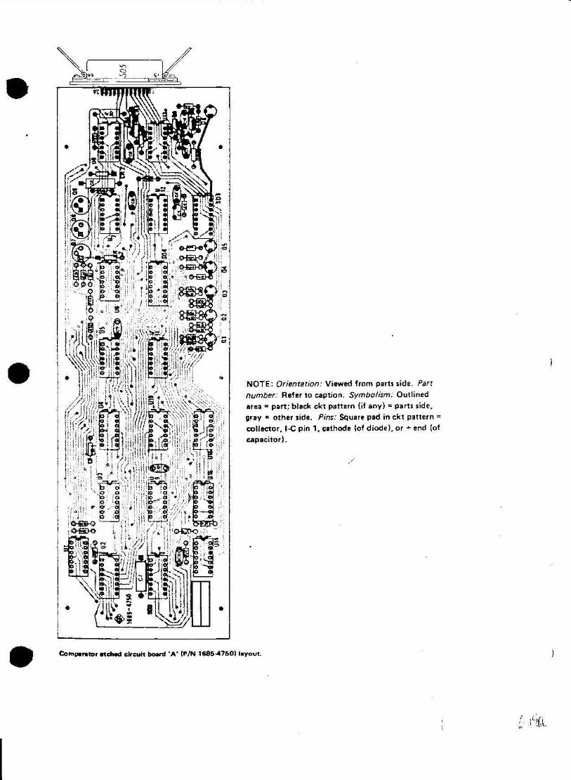
•
•
•
NOTE: Orientation: Viewed from parts side. Part number: Refer to caption. Symbolism: Outlined area"' part; black ckt pattern (if any)= parts side, gray .. other side. Pins: Square pad in ckt pattern = collector. 1-C pin 1. cathode lof diode). or + end (of capacitor) .
Co'"perator t1dMd circuit~ 'A' (P/N 1685~7501 layout.

1 ELECTRICAL PARTS LIST
Feel
R-'0.. o-:ription GR P.nNo. MftCode Mft P.t No.
SWlTCH BRACKET ASSEMBLY PARTS
Switch bracket Assembly Complete 1685-2050 24655 1685-2050
LAMPS
DSl thru DS4 6.3 v 5600~319 11144 CM·377
SWITCHES
Sl thru ss Thumbwhcel 7917-1014 24655 1917·1014
S6 thru SIO Thumbwheel 7917-1014 24655 7917-1014
Sll Toggle 7910-0790 95146 MTA-1060
... ··
(

ELECTRICAL PARTS LIST
Fld GR Pert No. Mft Cod.
COMPARATOR BOARD B (P/N 1685-4760) PARTS
CAPACITORS
C1 Tantalum, 47 uF ±20% 6 V C2 thru C4 Ceramic, .01 uF +80.20% 100 V
INTEGRATED CIRCUITS
U 1 Type SN7402N U2 thru US Type SN741S3N
RESISTORS
Rl thru R32 Comp., 2 kilohms ±5% 1/4 W
SOCKETS
SOl thru S03 DIP, 16-cont, PC
~20 PARTS & DIAGRAMS
4450·5500 56289
4401-3100 72982
5431·8102 01295
543 1·8053 01295
6099-2205 01121
7540-1817 71785
Mft P•tNo.
1 SOD476X0006B2
80S •. 01 uF +80.20%
SN7402N
SN74JS3N
RCR07G202J
133-51~2~6

(
(
j,C' "'• ' 's ... '
I
! '( i !
j ·'1
• •
~ l685-4760
B •
NOTE: OrientBtion: Viewed from parts side. Part number: Refer to caption. Symbolism: Outlined 1n11 • part; black ckt p;~ttem (if any ) • parts s ide, gray
• other side. Pins: SquaN pad in ckt plttern • collector, I·C pin 1, cathode (of diode), or • end (of capacitor).
•
'\,. , I t.·

=~-- ro •(I') (/)
~ . : : "' . J ...
( ~ '· ... . :
~·~-rl ''' .. '' ..,.,.
•
I I :
I
'
( ! ! :~ ~.
-
(
(11 .o (/) :v; ...
~ • ~ ll .. .. . . ~v
.. .. .I • .. .. •. .... l_j !
: ; I •••
-"'7:;'
~ :: :;~i
I ... ....
I r t
i
I i
I ll II ! !
i I
I I ;
! ;
! ' J ! i
i I ~ ... ; li= I i~ .. ;-.. I !
I I '-----"'-. -----~ 4---....
~ _ .. ,;,; -oooo ......
__ J
I t ~
1
1

f ELECTRICAL f'ARTS LIST
'· I"OWEtt SUPI"LY I"C aauo .. ,,.. 1616-~UO
ttEFOES OESCttt,TJON "AAT NO. ""' fiiFGII. "AttT ,.,. •• u (II- pr-efix)
c 1 CAP CER ICJNO lUf 20PCT 50VGP 440...2010 7ZCJU 1 131-NOS~Sl-10~ c z CAP CElt. MONO lUF 20f>CT ~ovc;, 4400-2070 12912 1131-MOS0-•51-lOSM c 3 CAP TAHT 1.0 Uf ZOPCT )5V 4450-UOO ,.219 1 SOD 10SXOOl5AZ c "· CAP TANT l•O UF ZOI'CT 3H 4uc.-uoo 562a9 1SOOL05.l0035AZ c 5 CAP TUH 1.0 UF 20PCT lSV 44s·o-.uoo 56219 U0010510015AZ c i) CAP TANT 1.0 UF 20PCl 35V 44SQ-<UOO 5t.289 1500 10S.l0035AZ c 1 CAP CER 01 SC • 0 1UF 80/ZOPC T 100V 44ill -J100 72982 OIOSS40Z5U0010U c 8 CAll' CEll. OJSC .OlUf 10/ZOPCT lOOV 44~1-UOO 72982 OIOSS40lSU00103l
Cfl. l RECT 1N4140 lOOPIV )A Sl Al.ll'l 6011-1014 144}) 1H4140 CR 2 RECT lN4140 lOOPIV )A Sl AU"! •ou-1014 l44U lHH40
nANSFORMEII. t 8R I D~E ASM PIN 1685-2020
lie FOES DESCRIPTION PART NO. ""'' MFGII. PlU NU!t8Eit.
CR 5 OIOOE RECTif'IEII. lN~OOl 6081-1001 14433 1Nlt003 (II. 6 OIOOF RECTI F I'= It \1~~003 60!1- 1001 14loJ3 lN4003 c- 1 OIOOE IHCT IF 1F.~ ll4~00l f>O!Jl-100 1 14433 114~003 CR 8 orooe REC1'1FtER 1N~003 6081-1001 14433 lN4003 (II 9 0100£ lN4~9A 1T5P1V tR . 025U4 sr 6011 Z-10ll 144)3 lN4~94
CR 10 OI OOE 1N4S9A tT~PIV tR.OZ5UA Sl 6082-1011 14ft)) 1N459A
~ 5 llf.S COM P 10 I( 5PCT lHW 6099-HOS 81H'il llCR07Gl03J It 6 II.B COJotP 1.0 K 5PtT 1/4W 6099-2105 81349 RCR07Cl02J
T TRANSfORM£• POWEll 04115-lo093 24655 04Ss-4~3
/
f.) ( {.~ 1.0· . •

6-22 PARTS & DIAGRAMS
€! ~5" 10~ e
Q) $15
oq&s- -1o93 (I> (, • ~~ ~
2$ $.110
3EV
4$-
<B
WTf 70 WT/1 6'1' C.-H (C A T7'1dPE ro wTf ) YY T f / 0 WT / 2. .8Y C,"f 7 (CATHDOE r, wn• } WTH 711 )'YT~ IJY C11£' (CA7/tdP~7tJ WTif) WT6' T() WT/2 BYCA'B{ C A 7hPPE TPWTIZ) IYT/2. 7tJ WT 17 8Y<A'IIJ (CATh'~O~ 7 d H'T/7) #'T /1 /d >I'T I J 8Y or 't / CAT.N~/M" Tl? WT/17) ;vr;3 T() I'YT 17 8Y /f!> W T I 7 T() W r I I? BY 1'1 ~
.···
Tral'ldorm.r end Diode .A.embly (P/N 1685-2020) ayout.

\_
i '
_, ___ .............. ----------- ··-· ..... ----·---------
__._ t-= -- ---..,.-1. - - -
NOTE ; Orientation: Viewed from parts side . Part number: Refer to caption. Symbolism: Outlined area • part; black c:kt pattern (if any ) ., parts side , gray • other side . Pins: Square pad in ckt pattern = collecto r, 1-C pin 1, cathode
(of diode). or+ end (of capaeitorl.
Po-r-cuPPIY botlrd (VII•yout, P/N 1686 .. 730.
,.... . .. I~ ...... ~- ' '

J W$. 1bC Vt E.W
~
--._
, ~ ___ .. _
0,0~"> ::; o' {?. ·;r;''" •J ~- . -~ _y.C:!l·~
IDA' .. O; <t't.O
.s '5o'S ~ f:"Aou-~
0
SJ04,, ~---,--------------~---
ns
... ..• '•'
,..., !Sibl!:
'S ~0 S" • "-I:"'"
Z o De:
0 0 0 0
I I
~
~
l I
..,.., .. ~,
r- --, ~D
lJAs• o'"""""'"" t/'111l4JfiJifT# D C.I~Cfii T .. r• orro... .,,,.,.,)
.f!J t/1, v-t,"~'
DN ~t ... R PI'IN~L r - - -~JL__, .. -~"
' r ( .,.:;, ;;
U" 'l' ~~ - .;.~ l~ WHo ··-··. ., ~~-= 0'4 c~
Wf&A
I I
Jl L -- --,
£Nt;>
0
i 0 0 ..
'"~' ., .... ~0 ·o• reo ·~· ~01 OF' I' ~ 7 4 ,o •i!7 tt:eo e~ca. ~ s ' =.tT o-· t/1/H
ss<>•
I POW~~ J ~ON
5'50'5
4-
oi>
c al\
C. lt'O _.,_ .f
l()O(
(.
I L ~ .. , l l '*i.:~.~-· :~, '"' ' ""'~· •uo I
I I I
1686-4730 REGUL ATOR BOARD
C7
· '~ ,,.,
..._.wrtl ...
" " ' I I (_•u I I I I I I I \ I I .. ~ .. ~
Cit~
A S M c~ .. -.too;a' I
I L_
If DA$1'1~0 CllflCUIT t!)CC~r /tJt:>• ~/tOM ,,.,. ... t!t6. V Sl>LI~ CJ/f,t;UIT ( SA~C >O'TA4oC:!: )
~=::-~:~~-" ,...,....._ ~...:.:=..:.::- -·.=~'!!- o:-:-:-..:. :r.-;::·:.~·~:r:-.c ....... -... ..... -.--~
~_._. __ ,. __ _ -··-- ~ ... ~ .... ~=":',!.. :;::..'::;.:::::-4 .. •<~- .... - .. ....... f~-· .. 1 -·--u'-
'"'
- ·--.-. ..,_,·-·--· ... __ -'--··~·, ...... -. ----c>--""·----· ~-·----· .. ~~14.-~,T---.-L-11,._ ___ _
PARTS a DIAGRAMS &-n

lll'FOES
c 1
c• 1 C:lt 2
p 1
" 2
Ill 1 Ill 2 Ill )
Ill 4 II. 5
s 1
,•
\
I
ELECTRICAL P'ARTS LIST (1010ntl
TEST f:IKTUIIIE '"' 1686-)090
DESCIIIfPTtOH PART NO. FMC MFGII
CAP cu f'IO"' O 0.1 Vf' lOPCT SOYGI' 4~-ZO!SO 7291-l 8131-MOS0-6~1-10~ . LED GillE EN 60U-1055 !1410 soaz-•no LEO RED 60U-1050 2UIO 50112- 4650
lt.~CPT MlCIIIO 111 ! 8 )6 CONT 4210-~)4 02660 5T-40360 aEti'T MtCIIIO IIIII 14 CONT UJ0-4014 02660 57-40140
RES CO IIIII' no !)Mill 51l>CT 1 f4W 6G99-1275 11)4'9 IIICII.07G271J IllES COMP 150 OHM !Sf>CT 1/4W 60'9<J- 1155 11)4'9 II.CII.07GU1J II.~S COMP 100 OHM SPCT 1 f4W ~0.,.~110" 81)49 II.CIIOJG101J IllES COMP 100 II. 5PCT 114W 6099-4105 11349 IIICII.07Gl04J Ill£'!> COI'IP 100 II; SPCT 114W 6099-4105 fll 34'9 lllCR0 7G l04J
SWITCH PUSHIIUTTON SPOT Tll~tS&O 01963 SJG-20P
Includes a ll the above Hated paru except awitch Sl and indicator diodes CRl and CR2.
ADAPTORS
For replacement of the adaptors (2 supplied), order GR part number 1686-1910.

r
I
s: 6
- i
+
.ADAPTJR
I I
I I
l o: 1:~
I ..
· -·-
--,
---· -_ _j
' • I ---=---- --~~- """":"'- ---- ·~: 7 ~- - ..
4-TE/fNIIAIAL C,IITAC T SE"T 'GO• INDIOITOR
......... ._11. a.-..,,.._., T_, • ••- ·
S'£~r/tMI 1·1 (1toAPToRs R£MOV£D)
8
(
B ; ~ .....
8 G
-I T-.fl-.. -"~ IZltow-t('/tl ,__.,_,._
t
~24 PARTS. DIAGRAMS

\, ,,. ... ·,
/686 -2050
(I+ ) PI , I ~ 2 ~~·-----..,..----,.
106~f ~4 • T£RMIAIAL ..-C-O#_i._A_C_T-,-S_E_T----.
1-r~- T- -r=--1 ....___-t-<1 g ~ I
I p~ I p. L_ ______ _l
( P+ ) PI., 2 0 ..... t-------....._ __ _. I+ -1
(!- ) Pt,17 ~ 18 llo----------------------------------'
R3 100 S?.
P2 ,14(-t5)
(START) pI' 7 .... f---------I...,.--'\IV'v~-:-6-----------"'111111111 p c' 12. (START)
Cl {S I O.lj-(F T
(DIG. ::aND) Pl 1 11 ~ lC: ••-----------'-----'---~--------•• p 2. ,10 ([)I(, (,t-Il>)
(BrAS) PI~~ 4------------------t-----------4 F 2) 2 (BIAS)
~----~------------~-----------"''IIIP~,a(ANA~ND)
( F"AJL) PI ,28------'\ R2 rso.n
Fitur. 6-16. GR 1686-f>l T-.t Fixtun~eh-ac.
PARTS & DIAGRAMS 6-25