Epitaxial CdSe-Au Nanocrystal Heterostructures by Thermal Annealing
Upload
independentCategory
view
3download
0
CERAMICSINTERNATIONAL
Available online at www.sciencedirect.com
http://dx.doi.org/0272-8842/& 20
nCorrespondinB. S. Abdur Rah
E-mail [email protected]
Please cite thisfield emission
Ceramics International ] (]]]]) ]]]–]]]www.elsevier.com/locate/ceramint
Short communication
Epitaxial zinc oxide, graphene oxide composite thin-films by laser techniquefor micro-Raman and enhanced field emission study
E. Manikandana,b,n, G. Kavithac, J. Kennedyd
aNano Research Centre, Department of Physics, B. S. Abdur Rahman University, Chennai, IndiabUNESCO-UNISA AFNET in Nanosciences/Nanotechnology Laboratories, Materials Research Department, iThemba LABS–National Research Foundation (NRF),
Pretoria, RSAcPG Research and Department of Physics, A. M. Jain College, Meenambakkam, University of Madras, Chennai, India
dNational Isotope Centre, GNS Science, Lower Hutt, New Zealand
Received 10 July 2014; received in revised form 22 July 2014; accepted 24 July 2014
Abstract
We made an attempt to form a high quality epitaxial zinc oxide, diamond-like-carbon and graphene oxide composite thin-film on devicesubstrate p-Si(1 0 0) using third-harmonic (Nd:YAG Ultraviolet) laser at single footstep. Pulsed laser deposition (PLD) technique using 366 nm(energy�150 mJ), vacuum 10�6 mbar has been used to grow these films in reactive gas oxygen with argon (O2|Ar) ambiance. Synthesized thin-films were investigated systematically by fingerprint technique of confocal micro-Raman and field emission studies. As synthesized pure ZnO,nanocomposite thin films like DLC/ZnO and GO/ZnO shows the enhanced field emission (F-E) performances in this present study.& 2014 Elsevier Ltd All rights reserved.
Keywords: Transition Metal Oxides; Nanocomposites; Thin-Films; Electrical Properties; Optical Microscopy
1. Introduction
In the past few decades, we have witnessed a reinforcementand subsequent rapid expansion in the research on metaloxides (MOs) like zinc oxide (ZnO) and carbon family as asemiconductor. ZnO nanowire/rod and graphene (carbon) aretwo of the most widely studied functional nanomaterials; bothof them are good candidates for the value added technologi-cally important applications like electrical and optical devicesfundamental information [1–6]. Due to the extremely largesurface areas and the pseudocapacitance rising from chargetransfer between the electrolyte and electrode through fastFaraday redox reaction, ZnO NW are promising in theapplication of supercapacitors [7–17]. On the other hand,
10.1016/j.ceramint.2014.07.12914 Elsevier Ltd All rights reserved.
g author at: Nano Research Centre, Department of Physics,man University, Chennai, India. Tel.: þ91 9884751467.sses: [email protected],c.in (E. Manikandan).
article as: E. Manikandan, et al., Epitaxial zinc oxide, graphene ostudy, Ceramics International (2014), http://dx.doi.org/10.1016/j.ce
graphene has extremely high electron mobility, excellent ratecapability, reversibility, energy storage, bio-medical and highchemical stability; it has improved field emission, electroche-mical performance compared with other carbon family materi-als such as activated carbon, diamond-like carbons (DLC),carbon nanotubes (CNTs), etc [18]. Despite its extraordinaryproperties, it is worth mentioning that the pure graphene is notworthy for practical functional applications because of its zeroband-gap, low carrier density and chemical inertness [19].However, the application of materials depends significantly on
their intrinsic properties. Hybridization of different materials offersa powerful way to enhance the application of graphene by enablingversatile and tailor-made properties with high performance farbeyond those of the individual materials. The perfect structure ofgraphene shows low chemical reactivity, therefore graphene oxide(GO), one of the derivatives of graphene that contains a range ofreactive oxygen functional groups, is considered to be a goodcandidate for chemical functionalization [4–5]. Diverse inorganicnanoparticles MOs such as SnO2, TiO2, WO3, V2O5, Fe2O4, CdS,
xide composite thin-films by laser technique for micro-Raman and enhancedramint.2014.07.129
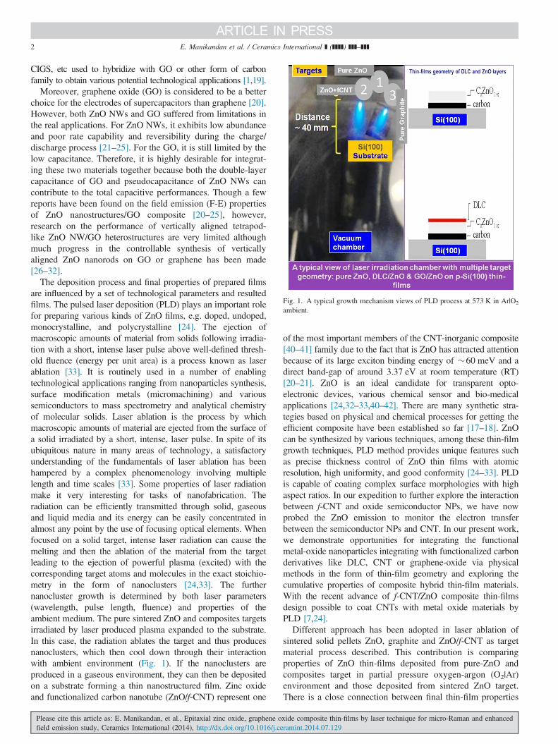
Fig. 1. A typical growth mechanism views of PLD process at 573 K in Ar|O2
ambient.
E. Manikandan et al. / Ceramics International ] (]]]]) ]]]–]]]2
CIGS, etc used to hybridize with GO or other form of carbonfamily to obtain various potential technological applications [1,19].
Moreover, graphene oxide (GO) is considered to be a betterchoice for the electrodes of supercapacitors than graphene [20].However, both ZnO NWs and GO suffered from limitations inthe real applications. For ZnO NWs, it exhibits low abundanceand poor rate capability and reversibility during the charge/discharge process [21–25]. For the GO, it is still limited by thelow capacitance. Therefore, it is highly desirable for integrat-ing these two materials together because both the double-layercapacitance of GO and pseudocapacitance of ZnO NWs cancontribute to the total capacitive performances. Though a fewreports have been found on the field emission (F-E) propertiesof ZnO nanostructures/GO composite [20–25], however,research on the performance of vertically aligned tetrapod-like ZnO NW/GO heterostructures are very limited althoughmuch progress in the controllable synthesis of verticallyaligned ZnO nanorods on GO or graphene has been made[26–32].
The deposition process and final properties of prepared filmsare influenced by a set of technological parameters and resultedfilms. The pulsed laser deposition (PLD) plays an important rolefor preparing various kinds of ZnO films, e.g. doped, undoped,monocrystalline, and polycrystalline [24]. The ejection ofmacroscopic amounts of material from solids following irradia-tion with a short, intense laser pulse above well-defined thresh-old fluence (energy per unit area) is a process known as laserablation [33]. It is routinely used in a number of enablingtechnological applications ranging from nanoparticles synthesis,surface modification metals (micromachining) and varioussemiconductors to mass spectrometry and analytical chemistryof molecular solids. Laser ablation is the process by whichmacroscopic amounts of material are ejected from the surface ofa solid irradiated by a short, intense, laser pulse. In spite of itsubiquitous nature in many areas of technology, a satisfactoryunderstanding of the fundamentals of laser ablation has beenhampered by a complex phenomenology involving multiplelength and time scales [33]. Some properties of laser radiationmake it very interesting for tasks of nanofabrication. Theradiation can be efficiently transmitted through solid, gaseousand liquid media and its energy can be easily concentrated inalmost any point by the use of focusing optical elements. Whenfocused on a solid target, intense laser radiation can cause themelting and then the ablation of the material from the targetleading to the ejection of powerful plasma (excited) with thecorresponding target atoms and molecules in the exact stoichio-metry in the form of nanoclusters [24,33]. The furthernanocluster growth is determined by both laser parameters(wavelength, pulse length, fluence) and properties of theambient medium. The pure sintered ZnO and composites targetsirradiated by laser produced plasma expanded to the substrate.In this case, the radiation ablates the target and thus producesnanoclusters, which then cool down through their interactionwith ambient environment (Fig. 1). If the nanoclusters areproduced in a gaseous environment, they can then be depositedon a substrate forming a thin nanostructured film. Zinc oxideand functionalized carbon nanotube (ZnO/f-CNT) represent one
Please cite this article as: E. Manikandan, et al., Epitaxial zinc oxide, graphene ofield emission study, Ceramics International (2014), http://dx.doi.org/10.1016/j.ce
of the most important members of the CNT-inorganic composite[40–41] family due to the fact that is ZnO has attracted attentionbecause of its large exciton binding energy of �60 meV and adirect band-gap of around 3.37 eV at room temperature (RT)[20–21]. ZnO is an ideal candidate for transparent opto-electronic devices, various chemical sensor and bio-medicalapplications [24,32–33,40–42]. There are many synthetic stra-tegies based on physical and chemical processes for getting theefficient composite have been established so far [17–18]. ZnOcan be synthesized by various techniques, among these thin-filmgrowth techniques, PLD method provides unique features suchas precise thickness control of ZnO thin films with atomicresolution, high uniformity, and good conformity [24–33]. PLDis capable of coating complex surface morphologies with highaspect ratios. In our expedition to further explore the interactionbetween f-CNT and oxide semiconductor NPs, we have nowprobed the ZnO emission to monitor the electron transferbetween the semiconductor NPs and CNT. In our present work,we demonstrate opportunities for integrating the functionalmetal-oxide nanoparticles integrating with functionalized carbonderivatives like DLC, CNT or graphene-oxide via physicalmethods in the form of thin-film geometry and exploring thecumulative properties of composite hybrid thin-film materials.With the recent advance of f-CNT/ZnO composite thin-filmsdesign possible to coat CNTs with metal oxide materials byPLD [7,24].Different approach has been adopted in laser ablation of
sintered solid pellets ZnO, graphite and ZnO/f-CNT as targetmaterial process described. This contribution is comparingproperties of ZnO thin-films deposited from pure-ZnO andcomposites target in partial pressure oxygen-argon (O2|Ar)environment and those deposited from sintered ZnO target.There is a close connection between final thin-film properties
xide composite thin-films by laser technique for micro-Raman and enhancedramint.2014.07.129
E. Manikandan et al. / Ceramics International ] (]]]]) ]]]–]]] 3
and PLD conditions. The formation of ZnO nanoparticles onCNT can be explained with plausible mechanism [24,34].
2. Experimental
2.1. Sample preparation
The target is typically prepared by mixing and isostaticallypressing metal-oxide powders with the desired proportions.Most PLD practitioners assume that the stoichiometric of thetarget is preserved in the process of vaporizing and condensingthe target material on the substrate provided certain minimumlaser fluencies is exceeded. In this work, we have chosen 5%f-CNT with ZnO and pure ZnO sintered solid target irradiatedby Nd:YAG (3rd harmonic UV laser 366 nm, �hυ=3.4 eV,repetition rate=10 Hz, pulse width τ=10 ns, optimized laserdeposition time and target to substrates (TSdistance=4 cm) withreactive gas (O2|Ar) were used to deposit on device Sisubstrate. The irradiation chamber gas pressure maintained at5� 10�6 mbar. A typical experimental realistic view of thePLD process and the growth mechanism were shown in theFig. 1 with three different sintered targets inside the carousel.The synthesized thin films like pure ZnO, DLC and GO NCs
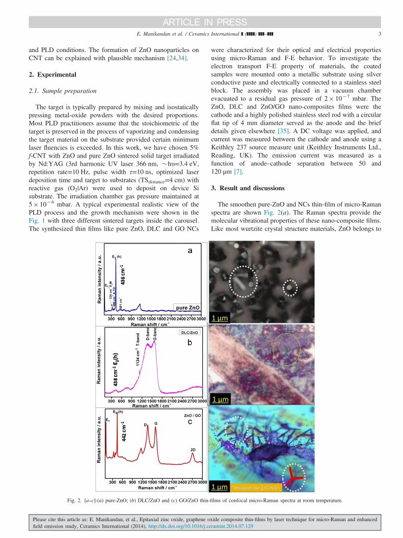
Fig. 2. [a–c]-(a) pure-ZnO; (b) DLC/ZnO and (c) GO/ZnO thin-
Please cite this article as: E. Manikandan, et al., Epitaxial zinc oxide, graphene ofield emission study, Ceramics International (2014), http://dx.doi.org/10.1016/j.ce
were characterized for their optical and electrical propertiesusing micro-Raman and F-E behavior. To investigate theelectron transport F-E property of materials, the coatedsamples were mounted onto a metallic substrate using silverconductive paste and electrically connected to a stainless steelblock. The assembly was placed in a vacuum chamberevacuated to a residual gas pressure of 2� 10�7 mbar. TheZnO, DLC and ZnO/GO nano-composites films were thecathode and a highly polished stainless steel rod with a circularflat tip of 4 mm diameter served as the anode and the briefdetails given elsewhere [35]. A DC voltage was applied, andcurrent was measured between the cathode and anode using aKeithley 237 source measure unit (Keithley Instruments Ltd.,Reading, UK). The emission current was measured as afunction of anode–cathode separation between 50 and120 μm [7].
3. Result and discussions
The smoothen pure-ZnO and NCs thin-film of micro-Ramanspectra are shown Fig. 2(a). The Raman spectra provide themolecular vibrational properties of these nano-composite films.Like most wurtzite crystal structure materials, ZnO belongs to
films of confocal micro-Raman spectra at room temperature.
xide composite thin-films by laser technique for micro-Raman and enhancedramint.2014.07.129
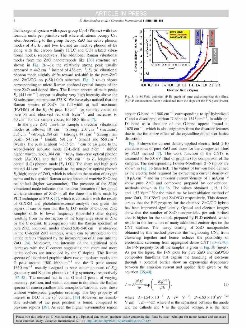
Fig. 3. [a–b]-Field emission (F-E) graph of pure and composite thin-films,(b) F-E enhancement factor β calculated from the slopes of the F-N plots (insert).
E. Manikandan et al. / Ceramics International ] (]]]]) ]]]–]]]4
the hexagonal system with space group C6v4 (P63mc) with twoformula units per primitive cell where all atoms occupy C3vsites. According to the group theory, ZnO has active phononmodes of A1, E1, and two E2, and an inactive phonon of B1
along with the carbon family [DLC and GO] related vibra-tional modes, respectively. The additional Raman vibrationalmodes from the ZnO nanotetrapods like [36] structure areshown in Fig. 2(a–c); the relatively strong peak usuallyappeared at 442 cm�1 instead of 436 cm�1. E2 (h) vibrationalphonon mode slightly shifts toward red-shift in the pure-ZnOand ZnO/GO on p-Si(1 0 0) substrate. Fig. 2 (a–c) showscorresponding to micro-Raman confocal optical images of thepure ZnO and doped films. The Raman spectra of main peaksE2 (441 cm�1) appear to display very high intensity above theSi-substrates temperature 573 K. We have also noticed that theRaman spectra of ZnO, the full-width at half maximum(FWHM) of the E2 (h) peak 10 cm–1 for samples coated onpure Si and observed red-shift 6 cm�1, and increases to40 cm–1 for the sample coated for NCs films [7].
In the pure ZnO thin-films sample molecular vibrationalmodes as follows: 101 cm�1 (strong), 207 cm�1 (medium),335 cm�1 (strong), 384 cm�1 (strong), 441 cm�1 (strong mainpeak), 541 cm�1 (small), 591 cm�1 (small) and 658 cm�1
(weak). The peak at about �335 cm�1 can be assigned to thesecond-order acoustic mode [2-E2(M)] and 5 cm�1 shiftedhigher wavenumber, 384 cm�1 to A1 transverse optical phononmode [A1(TO)], and that at �591 cm�1 to E1 longitudinaloptical (LO) phonon mode [E1(LO)]. The sharp and high peakaround 441 cm�1 corresponds to the non-polar optical phononE2(high) mode of ZnO, which is related to the motion of oxygenatoms and is a typical Raman active branch of wurtzite ZnO andred-shifted (higher wavenumber). The presence of the E2(h)vibrational mode indicates that the clear formation of hexagonalwurtzite structure of ZnO in all the three thin-films made byPLD technique at 573 K [7], which is consistent with the resultsof GIXRD and photoluminescence analysis (not given thispaper). It can be seen that the E1(LO) mode of C-doped ZnOsamples shifts to lower frequency (blue-shift) after dopingresulting from the destruction of the long-range order in ZnOby the C dopant. In comparison with the Raman spectrum ofpure ZnO, additional modes around 530–540 cm�1 is observedin the C-doped ZnO samples, which can be attributed to thelattice defects triggered by the incorporation of C ions into theZnO [24]. Moreover, the intensity of the additional peakincreases with the C content suggesting that more and morelattice defects are introduced by the C doping. The Ramanspectra of disordered graphite show two quite sharp modes, theG peak around 1580–1600 cm�1 and the D peak around1350 cm�1, usually assigned to zone center phonons of E2gsymmetry and K-point phonons of A1g symmetry, respectively[37–38]. The unusual fact is that G and D peaks, of varyingintensity, position, and width, continue to dominate the Ramanspectra of nanocrystalline and amorphous carbons, even thosewithout widespread graphitic ordering. The key property ofinterest in DLC is the sp3 content. [39] However, no remark-able red-shift of the peak position is found, compared toprevious reports [39]. As seen the higher wavenumber region
Please cite this article as: E. Manikandan, et al., Epitaxial zinc oxide, graphene ofield emission study, Ceramics International (2014), http://dx.doi.org/10.1016/j.ce
appear G-band �1580 cm�1 corresponding to sp2-hybridizedC and a disordered carbon D-band at 1345 cm�1. In addition,D0 band as a shoulder of the G-band appear around at1620 cm�1, which is also originates from the disorder featuresdue to the finite size effect of the crystalline domain or latticedistortion.Fig. 3 shows the current density-applied electric field (J-E)
characteristics of pure ZnO and those for the composites filmsby PLD method [7]. The work function of the CNTs isassumed to be 5.0 eV (that of graphite) for comparison of thesamples. The corresponding Fowler-Nordheim (F-N) plots areshown in Fig. 3b (inserted). The values of turn-on field definedas the electric field required for extracting a current density of10 μA.cm�2 and an emission current density of 1 mA.cm�2
show pure ZnO and composite prepared by conventionalmethods shown in Fig.3b. The values obtained 1.15, 1.29,and 1.52 Vμm�1for the thin-films by laser ablation method ofpure ZnO, DLC/ZnO and ZnO/GO respectively. This demon-strates that the F-E property for the obtained ZnO/GO hybridhas been improved significantly. Optical and electron imagesshow that the number of ZnO nanoparticles per unit surfacearea is higher for the sample prepared by PLD method, whichresults in the formation of many additional emitter tips on theCNT surface. The heavy coating of ZnO nanoparticlesobtained by this method prevents the neighboring CNT fromclustering together and hence reduces the possibility ofelectrostatic screening from aggregated dense CNT [30–32,40].The F-N property for all the samples is given in Fig. 3b (insert).As per the figure, the F-N plots for pure ZnO and ZnO/GOcomposites thin-films that explain the tunneling of electronsthrough a potential barrier show an exponential dependencebetween the emission current and applied field given by theequation [35,40].
J ¼ Aβ2E2
ϕexp � Bϕ3=2
βE
!: ð1Þ
where A=1.54� 10�6 A eV V�2, B=6.83� 103 eV�3/2
V μm�1, E==V/d, where d is the separation between the anodeand the cathode and V is the applied voltage, β is the field
xide composite thin-films by laser technique for micro-Raman and enhancedramint.2014.07.129
E. Manikandan et al. / Ceramics International ] (]]]]) ]]]–]]] 5
enhancement factor, and ϕ is the work function of emitters. TheFE enhancement factor β can be calculated from the slopes of theF-N plots. Generally, it has been identified that a significantincrease in field enhancement factor β is strongly ascribed to thegeometrical parameters of field emitter, mainly its surfacemorphology and high density of the substrate [35,40]. The βvalues calculated for various samples taking the work function(ϕ) of GO as 5.0 eV were 3.1� � 103, 6.1� � 103, and6.7� � 103 for pure ZnO and ZnO/GO composites fromconventional and PLD methods, respectively. The higher βvalues for the composite samples when compared to pure ZnOare attributed to the presence of nano-wire/rods shaped ZnOnanoparticles which act as additional independent emissioncenters other than the CNT tips. Ho et al. recently reportedsimilar observations on ZnO/CNT hybrids with different ZnOlayer density [40]. The ZnO/GO composite shows significantlyenhanced F-E when compared to its counterpart from conven-tional method which may be due to the increased number of ZnOnanoparticles that contributes to the local field strengthening andemission current. In this case, the electron transport channels onthe CNT surface are amplified by the presence of uniformlydispersed ZnO nanoparticles. The nanorods like ZnO particles onthe ZnO surface, can act as additional emission sites in addition tothe tip of GO [30–32] Moreover, similarity in the work functionof CNTs and ZnO makes it easier for electrons to diffuse tolayered carbon system resulting in high surface electron concen-tration. Hence, the deposited film shows good crystallinitywith uniform particles in the nano regime and will makefor future nano electronics, various chemical-physical gassensors, in composites, as catalytic supports, for storage andintercalation of metals, in membrane technology and separationscience too.
4. Conclusions
The pure ZnO, DLC/ZnO and GO/ZnO thin-films fabricatedon device substrate p-Si(1 0 0) NCs were effectively preparedby PLD method. Micro-Raman exhibits the characteristicsoptical and molecular properties along with the functionalitiesof carbon precursor vibrational modes. The growth mechan-isms of different tetrapods-like ZnO nanostructures wereobserved in the first time along with GO nanocompositethin-films on Si(1 0 0) made by PLD technique. Electricalstudy of F-E properties of the nanocomposite thin-films weremeasured and compared with pure ZnO. The field emissionenhancement property was higher for GO/ZnO and DLC layersthan the pure ZnO and enhancement factor β value was betterin GO/ZnO nanocomposite films. This is attributed to the factthat the composite has a higher number of ZnO nanoparticlesin the derivatives of few layered GO and thin carbon filmformation act as independent emitters besides the CNT tips.The results may strengthen and understanding for the hybridnanostructure formation with ZnO nanostructures and it mightprovide guidance for controlling sizes and shapes of differentnanomaterials for the future energy applications.
Please cite this article as: E. Manikandan, et al., Epitaxial zinc oxide, graphene ofield emission study, Ceramics International (2014), http://dx.doi.org/10.1016/j.ce
Acknowledgments
The author (E. M) would like to thank Prof. V. Ganasen,UGC DAE CSR, Indore, Dr. B.K. Panigrahi, Head, Accel-erator Group, IGCAR, Kalpakkam, India for fruitful discussionwith Dr. Bonex, Principal Scientist, National Centre forNanostructures Materials (NCNSM), DST/CSIR, Pretoria forhis constant support and my beloved Mr. Abdul Qadir,Chairman; Prof. J.A.K. Tareen, Vice Chancellor (V.C); Dean(School of Physical and Chemical Sciences) and Dean (A/R)of B. S. Abdur Rahman University for permitting to carry-outthe entire thin-film PLD work.
References
[1] T. Tite, C. Donnet, A.S. Loir, S. Reynaud, J.Y. Michalon, F. Vocanson,F. Garrelie, Graphene-based textured surface by pulsed laser depositionas a robust platform for surface enhanced Raman scattering applications,Appl. Phys. Lett. 104 (2014) 041912–041915.
[2] A.T.T. Koh, Y.M. Foong, D.H.C. Chua, Comparison of the mechanismof low defect few-layer graphene fabricated on different metals by PLD,Diam. Relat. Mater. 25 (2012) 98–104.
[3] S.R. Sarathkumar, H.N. Alshareef, Ultraviolet laser deposition ofgraphene thin-films without catalytic sacrificial layers, Appl. Phys. Lett.102 (2013) 012110–012112.
[4] V. Murugan, M.H. Lee, K. Karthikeyan, Y. Kyusik, Synthesis character-ization and electrochemical properties of functionalized graphene-oxide,Carbon 50 (2012) 4228–4238.
[5] K. Karthikeyan, V. Murugan, Y. Kyusik, S.J. Kim, The chemical andstructural analysis of graphene-oxide with different degrees of oxidation,Carbon 53 (2013) 38–49.
[6] J. Yu, P. Anetab, A.T.T. Koh, H.C.D. Chua, J. Wei, Enhanced electronemission from tetrahedral amorphous carbon capped carbon nanotubecore-shelled structure, Diam. Relat. Mater. 21 (2012) 37–41.
[7] E. Manikandan, V. Murugan, G. Kavitha, P. Babu, M. Maaza, Nano-flower rod wire-like structures of dual metal (Al and Cr) doped ZnO thin-films: structural, optical and electronic properties, Mater. Lett. 131 (2014)225–228.
[8] D. Kalpana, K.S. Omkumar, S.S. Kumar, N.G. Renganathan, A novelhigh power symmetric ZnO/carbon aerogel composite electrode forelectrochemical supercapacitor, Electrochim. Acta 52 (2006) 1309–1315.
[9] X.H. Xia, J.P. Tu, Y.Q. Zhang, X.L. Wang, H.J. Fan, High-quality metaloxide core/shell nanowire arrays on conductive substrates for electro-chemical energy storage, ACS Nano 6 (2012) 5531–5538.
[10] Y.L. Chen, Z.A. Hu, Y.Q. Chang, H.W. Wang, Z.Y. Zhang, Zinc oxide/reduced graphene oxide composites and electrochemical capacitanceenhanced by homogeneous incorporation of reduced graphene oxidesheets in zinc oxide matrix, J. Phys. Chem. C 115 (2011) 2563–2571.
[11] T. Lu, L. Pan, H. Li, G. Zhu, T. Lv, X. Liu, Z. Sun, Microwave-assistedsynthesis of graphene–ZnO composite for electrochemical supercapaci-tors, J. Alloy Compd. 509 (2011) 5488–5490.
[12] S. Bai, X.P. Shen, Graphene–inorganic composite, RSC Adv. 2 (2012)64–98.
[13] J. Qu, C.Q. Luo, Q. Cong, Synthesis of multi-walled carbon Nanotubes/ZnO composite using absorbent cotton, Nano-Micro Lett. 3 (2011)115–120.
[14] Y.G. Kim, R. Hadiyawarman, M.Y. Yoon, G.C. Kim, C.L. Liu Yi,Hydrothermally grown ZnO nanostructures on few-layer graphene sheets,Nanotechnology 22 (2011) 245603–245608.
[15] U. Alver, W. Zhou, A.B. Belay, R. Krueger, K.O. Davis, N.S. Hickman,Optical and structural properties of ZnO nanorods grown on grapheneoxide and reduced graphene oxide film by hydrothermal method, Appl.Surf. Sci. 258 (2012) 3109–3114.
[16] H.X. Chang, Z.H. Sun, K.Y. Ho, X.M. Tao, F. Yan, W.M. Kwok,Z.J. Zheng, A highly sensitive ultraviolet sensor based on a facile in situ
xide composite thin-films by laser technique for micro-Raman and enhancedramint.2014.07.129
E. Manikandan et al. / Ceramics International ] (]]]]) ]]]–]]]6
solution-grown ZnO nanorod/graphene heterostructure, Nanoscale 3(2011) 258–264.
[17] M.A. Correa-Duarte, N. Sobal, L.M. Liz, M. Marzán, Giersig, carbonnanotubes decorated with Pt nanocubes by a noncovalent functionaliza-tion method and their role in oxygen reduction, Adv. Mater. 16 (2004)2179–2183.
[18] X. Yan, B.-K. Tay, P. Miele, Field emission from ordered carbonnanotube-ZnO heterojunction arrays, Carbon 46 (2008) 753–758.
[19] J.Y. Pan, C.C. Zhu, Y.L. Gao, Enhanced field emission characteristics ofZnO mixed CNTs films, Appl. Surf. Sci. 254 (2008) 3787–3792.
[20] S. Zhang, N. Ali, Composite Thin-Films and Coatings: Processing,Properties and Performance, Imperial College Press, 2007, p. 1–10.
[21] Ü. Özgür, Y.I. Alivov, C. Liu, A. Teke, M.A. Reshchikov, A compre-hensive review of ZnO materials and devices, J. Appl. Phys. 98 (2005)041301–041401.
[22] P.X. Gao, Z.L. Wang, Nanoarchitectures of semiconducting and piezo-electric zinc oxide, J. Appl. Phys. 97 (2005) 044304–044309.
[23] O.K. Varghese, C.A. Grimes, Metal-oxide nanoarchitectures for environ-mental sensing, . 3 (2003) 277–293.
[24] E. Manikandan, M.K. Moodley, S.S. Ray, B.K. Panigrahi, R. Krishnan,N. Padhy, K.G.M. Nair, A.K. Tyagi, ZnO epitaxial thin-film depositedover carbon on various substrates by PLD technique, J. Nanosci.Nanotechnol. 10 (2010) 5602–5611.
[25] J. Kennedy, D.A. Carder, A. Markwitz, R.J. Reeves, Properties ofnitrogen implanted and electron beam annealed bulk ZnO, J. Appl. Phys.107 (2010) 103518–103522.
[26] R.-C. Wang, Y.-C. Chen, S.-J. Chen, Y.-M. Chang, Unusual functionaliza-tion of reduced graphene-oxide for excellent chemical surface-enhancedRaman scattering by coupling with ZnO, Carbon 70 (2014) 215–223.
[27] S.M. Jilani, T.D. Gamot, P. Banerji, S. Chakraborty, Studies on resistiveswitching characteristics of aluminum/graphene oxide/semiconductornonvolatile memory cells, Carbon 64 (2013) 187–196.
[28] J. Du, Y. Zhang, S. Deng, N. Xu, Z. Xiao, J. She, Z. Wu, H. Cheng,Correlation between topographic structures and local field emissioncharacteristics of graphene-sheet films, Carbon 61 (2013) 507–514.
[29] K.K. Chattopadhyay, D. Banerjee, N.S. Das, D. Sarkar, Easy synthesis ofamorphous graphene and related hybrids for cold cathode application,Carbon 72 (2014) 4–14.
Please cite this article as: E. Manikandan, et al., Epitaxial zinc oxide, graphene ofield emission study, Ceramics International (2014), http://dx.doi.org/10.1016/j.ce
[30] C. Wu, F. Li, Y. Zhang, T. Guo, Improving the field-emission of grapheneby depositing ZnO nanorods on its surface, Carbon 10 (2012) 3622–3626.
[31] R. Lv, F. Kang, D. Zhu, Y. Zhu, X. Gui, J. Wei, J. Gu, D. Li, K. Wang,D. Wu, Enhanced field-emission of open-ended, thin-walled CNTs filledwith ferromagnetic nanowires, Carbon 47 (2009) 2709–2715.
[32] N. Saurakhiya, Y.W. Zhu, F.C. Cheong, C.K. Ong, A.T.S. Wee, J.Y. Lin,C.H. Sow, PLD assisted patterning of aligned CNTs modified by focusedlaser beam for efficient field emission, Carbon 43 (2005) 2128–2133.
[33] D. Perez, L.J. Lewis, Ablation of solids under femtosecond laser pulses,Phys. Rev. Lett. 89 (2002) 255504–255508.
[34] B.Y. Zhu, H.I. Elim, Y.-L. Foo, T. Yu, Y. Liu, W. Ji, J.-Y. Lee, Z. Shen,A.-T. Shen, T.-S. Wee, J T-L Thong, C.-H. Sow, C.N.T. Multiwalled,Beaded with ZnO nanoparticles for ultrafast nonlinear optical switching,Adv. Mater. 18 (2006) 587–592.
[35] F. Fang, J. Kennedy, D.A. Carder, J. Futter, P. Murmu, A. Markwitz,Modulation of field emission properties of ZnO nanorods during arcdischarge, J. Nanosci. Nanotechnol. 10 (2010) 8239–8243.
[36] F.Z. Wang, Z.Z. Ye, D.W. Ma, L.P. Zhu, F. Zhuge, Novel morphologiesof ZnO Nanotetrapods, Mater. Lett. 59 (2005) 560–562.
[37] D.S. Knight, W.B. White, Characterization of diamond films by Ramanspectroscopy, J. Mater. Res. 4 (1989) 385–393.
[38] F. Tuinstra, J.L. Koening, Raman spectrum of graphite, J. Chem. Phys.53 (1970) 1126–1130.
[39] J. Robertson, Hard amorphous (diamond-like) carbons, Progr. Solid StateChem. 21 (1991) 199–333.
[40] Y.M. Ho, G.M. Yang, W.T. Zheng, Synthesis and field electron emissionproperties of hybrid CNTs and nanoparticles, Nanotechnology 19 (2008)065710–065716.
[41] B.N. Joshi, H. Yoon, S.-H. Na, J.-Y. Choi, S.S. Yoon, Enhancedphotocatalytic performance of graphene–ZnO nanoplatelet compositethin-films prepared by electrostatic spray deposition, Ceram. Int. 40 (2)(2014) 3647–3654.
[42] P.K. Kannan, R. Saraswathi, J.B.B. Rayappan, CO2 gas-sensing proper-ties of DC reactive magnetron sputtered ZnO thin-film, Ceram. Int. 40(2014) 13115–13122.
xide composite thin-films by laser technique for micro-Raman and enhancedramint.2014.07.129
Copyright © 2022 FDOKUMEN