Enhancement of the performance of GaP solar cells by embedded In(N)P quantum dots
7
journal homepage: www.elsevier.com/locate/nanoenergy Available online at www.sciencedirect.com RAPID COMMUNICATION Enhancement of the performance of GaP solar cells by embedded In(N)P quantum dots Yanjin Kuang a,n , Ke Sun b,c , Supanee Sukrittanon d , Ko Takabayashi e , Itaru Kamiya e , Nathan S. Lewis b,c,f,g , Charles W. Tu h a Department of Physics, University of California, San Diego, La Jolla, CA 92093, USA b Division of Chemistry and Chemical Engineering, California Institute of Technology, Pasadena, CA 91125, USA c Joint Center for Artificial Photosynthesis, California Institute of Technology, Pasadena, CA 91125, USA d Material Science and Engineering Program, University of California, San Diego, La Jolla, CA 92093, USA e Quantum Interface Laboratory, Toyota Technological Institute, Nagoya 468-8511, Japan f Beckman Institute and Molecular Materials Research Center, California Institute of Technology, Pasadena, CA 91125, USA g Kavli Nanoscience Institute, California Institute of Technology, Pasadena, CA 91125, USA h Department of Electrical and Computer Engineering, University of California, San Diego, La Jolla, CA 92093, USA Received 3 February 2015; received in revised form 18 May 2015; accepted 8 June 2015 Available online 17 June 2015 KEYWORDS Quantum dots; InNP; Solar cells; Indirect bandgap engineering; MBE Abstract Improving the utilization of solar spectra of wide bandgap semiconductors that can potentially provide enough free energy is one of the promising strategies for realizing efficient and spontaneous integrated conversion of solar energy to chemical fuels. We demonstrate herein that nitrogen doped InP quantum dots (QDs) embedded in wide bandgap GaP could improve the solar energy conversion performance. Photoelectrochemical experiments in contact with a nonaqueous, reversible redox couple indicated that the QD-embedded devices exhibited improved performance relative to devices without QDs, with short- circuit current densities increasing from 0.16 mA cm 2 for GaP-only devices to 0.23 and 0.29 mA cm 2 for InP and InNP QD-embedded devices, respectively. Additionally, the open-circuit voltages increased from 0.95 V for GaP-only devices to 1.11 and 1.14 V for InP and InNP QD-embedded devices, respectively, and the external quantum yield of the devices was also enhanced by the embedded QDs. The improvement is attributed to the absorption of sub-bandgap photons by the In(N)P QDs. & 2015 Elsevier Ltd. All rights reserved. http://dx.doi.org/10.1016/j.nanoen.2015.06.003 2211-2855/& 2015 Elsevier Ltd. All rights reserved. n Corresponding author. E-mail address: [email protected] (Y. Kuang). Nano Energy (2015) 15, 782–788
Transcript of Enhancement of the performance of GaP solar cells by embedded In(N)P quantum dots
Available online at www.sciencedirect.com
journal homepage: www.elsevier.com/locate/nanoenergy
Nano Energy (2015) 15, 782–788
http://dx.doi.org/12211-2855/& 2015 E
nCorresponding auE-mail address: y
RAPID COMMUNICATION
Enhancement of the performance of GaP solarcells by embedded In(N)P quantum dots
Yanjin Kuanga,n, Ke Sunb,c, Supanee Sukrittanond,Ko Takabayashie, Itaru Kamiyae, Nathan S. Lewisb,c,f,g,Charles W. Tuh
aDepartment of Physics, University of California, San Diego, La Jolla, CA 92093, USAbDivision of Chemistry and Chemical Engineering, California Institute of Technology, Pasadena, CA 91125,USAcJoint Center for Artificial Photosynthesis, California Institute of Technology, Pasadena, CA 91125, USAdMaterial Science and Engineering Program, University of California, San Diego, La Jolla, CA 92093, USAeQuantum Interface Laboratory, Toyota Technological Institute, Nagoya 468-8511, JapanfBeckman Institute and Molecular Materials Research Center, California Institute of Technology, Pasadena,CA 91125, USAgKavli Nanoscience Institute, California Institute of Technology, Pasadena, CA 91125, USAhDepartment of Electrical and Computer Engineering, University of California, San Diego, La Jolla, CA92093, USA
Received 3 February 2015; received in revised form 18 May 2015; accepted 8 June 2015Available online 17 June 2015
KEYWORDSQuantum dots;InNP;Solar cells;Indirect bandgapengineering;MBE
0.1016/j.nanoen.2lsevier Ltd. All rig
AbstractImproving the utilization of solar spectra of wide bandgap semiconductors that can potentially provideenough free energy is one of the promising strategies for realizing efficient and spontaneous integratedconversion of solar energy to chemical fuels. We demonstrate herein that nitrogen doped InP quantumdots (QDs) embedded in wide bandgap GaP could improve the solar energy conversion performance.Photoelectrochemical experiments in contact with a nonaqueous, reversible redox couple indicated thatthe QD-embedded devices exhibited improved performance relative to devices without QDs, with short-circuit current densities increasing from 0.16 mA cm�2 for GaP-only devices to 0.23 and 0.29 mA cm�2
for InP and InNP QD-embedded devices, respectively. Additionally, the open-circuit voltages increasedfrom 0.95 V for GaP-only devices to 1.11 and 1.14 V for InP and InNP QD-embedded devices, respectively,and the external quantum yield of the devices was also enhanced by the embedded QDs. Theimprovement is attributed to the absorption of sub-bandgap photons by the In(N)P QDs.& 2015 Elsevier Ltd. All rights reserved.
015.06.003hts reserved.
(Y. Kuang).
783Enhancement of the performance of GaP solar cells
Introduction Experimental
GaP is not commonly used as the base absorber in terrestrialphotovoltaic devices due to a bandgap (Eg=2.26 eV) that istoo large to absorb much of the solar spectrum, and becausethe indirect gap requires the use of a relatively thick layerof GaP (45 μm) for effective absorption of light, relative toGroup III–V semiconductors with direct bandgap. Never-theless, the large bandgap and the electron affinity level(3.8 eV) of GaP may prove useful in an integrated solar-fuelsdevice. Although the bandgap of GaP is considerably higherthan optimal for an efficient solar-driven water-splittingdevice [1], a tandem cell comprised of an n-GaP photoanodeand a photocathode such as p-Si [2], p-WSe2 [3], or p-Cu2O[4,5] may be useful for a solar-fuels device that couples thereduction of CO2 to a fuel with the oxidation of water toO2(g), because such multi-electron chemical reductionprocesses may involve larger catalytic overpotentials, andthus require higher overall photovoltages, than water-splitting devices. In addition, mass-transport limitationsrelated to the limited concentration of CO2 in the atmo-sphere may constrain the current density attainable for aCO2-reducing device to values compatible with thoseobtainable from light absorbers with larger bandgaps thanare optimal for solar-driven water splitting. Furthermore,GaP has a lattice constant very similar to that of Si (5.451 Åand 5.431 Å, respectively) [6], allowing the growth of highquality GaP on Si without anti-phase domains, through ao200 nm thick buffer layer. Optoelectronic devices have infact been fabricated using such a platform [6–9]. Thus, amonolithic tandem cell comprised of a catalyst-loaded Siphotocathode and an n-GaP photoanode, protected againstcorrosion and loaded with an oxygen-evolution catalyst,[10] could provide an implementation of a functioning solar-fuels device. Techniques that enhance the absorption of GaPwhile reducing the thickness required for effective absorp-tion of light, such as bandgap engineering [11,12] andnanostructuring [13], will increase the utility of GaP notonly for photoelectrochemical applications, but also forphotovoltaic and optoelectronic applications.
One technique for tailoring the optoelectronic propertiesof GaP-based devices is embedment of quantum dots (QDs)into GaP matrices. Self-assembled InP QDs can be fabricatedon GaP substrates via the coherent-island Stranski–Krastanovgrowth mode [14], and a light-emitting diode (LED) with anemission energy of �2 eV has been fabricated using thismaterials system [15]. The InP/GaP QD system has a bandalignment intermediate between types I and II [14], allow-ing further tailoring of the optoelectronic properties of theassembly through the incorporation of N into the QDs, toform dilute-nitride InNP QDs [16].
Herein we report the performance of a p-i-n GaP devicethat contains embedded InP and InNP QDs. The QDs werefabricated on n-GaP(100) substrates (n�1� 1018 cm�3) viathe self-assembly process using gas-source molecular-beamepitaxy (GSMBE). Embedment of InP and InNP QDs into GaPp-i-n cells increased the absorption and enhanced both theshort-circuit current density (Jsc) and the open-circuit vol-tage (Voc) of the resulting devices, relative to structures thatdid not have embedded QDs in the material.
Gas-source molecular beam epitaxy
A Varian Gen-II MBE system, modified to thermally crack gas-phase PH3 to P2 and H2, and GaP(001) substrates, were usedto fabricate all samples described in this work. Elemental Gaand In, solid Si, solid Be, and N radicals produced using radio-frequency plasma activation were used as Group III sources,n-type dopant, p-type dopant and N source, respectively. Thenative oxide was removed from semi-insulating GaP sub-strates using a P2 overpressure at �580 1C. For single-layer In(N)P QD samples prepared for optical-quality studies, a 200-nm thick GaP buffer layer was grown at a rate of 1 μm h�1
after desorption of the oxide layer. The growth was theninterrupted and the substrate temperature was lowered to440–480 1C. The temperature of the In Knudsen cell wasraised until a deposition rate of 0.1 monolayer s�1 (ML s�1),as calibrated by reflection high-energy electron-diffraction(RHEED) intensity oscillation, was reached [17]. For InNPQDs, the N plasma was activated and set to a plasma powerof 280 W using a N2 flow rate of 1.2 sccm before the InNP QDformation process. The InP (InNP) QD self-assembly processbegan when the In (In and N) shutters were opened. Whenthe InP (InNP) wetting layer exceeded the critical thickness,the InP (InNP) QDs self-assembled under a large compressivestrain. The formation of QDs was confirmed by a change inthe in-situ RHEED pattern from a streaky pattern to a chevronpattern, and was also confirmed by atomic-force microscopy(AFM) images of the uncapped QD samples. 2 ML of InP (InNP)was deposited in total for all samples in this study. Afterdeposition of the QDs, a 20 nm GaP cap layer was grown atthe temperature used for formation of the QDs to maintainthe QD morphology and prevent indium desorption (due to itshigher vapor pressure relative to gallium) during subsequenttemperature increase. Note that all of the QDs in this studyare smaller than 7 nm in height (Figure 2) and no QDs shouldbe exposed beyond the 20 nm GaP cap layer, which isconfirmed in situ by the recovery of the streaky RHEEDpattern during growth. An additional GaP cap layer, 30 nm inthickness, was grown at 580 1C on samples prepared forphotoluminescence (PL) studies. If no cap layer was grown ontop of the QDs, the QDs would oxidize once they are takenout of the vacuum chamber. This oxidation process degradesthe quality of the QDs and significantly reduces the PLintensity. The photo-excited carriers would also tend torecombine through the surface states (mostly from thedangling bonds) on the QDs through the Shockley–Read–Hallmechanism. This non-radiative recombination would quenchthe PL signal intensity. Moreover, the uncapped QDs see ahigh surface potential (atmosphere) which can result in ashift of the quantum confined energy level and hence a shiftof the PL peak position [18]. Therefore, a 50 nm-thickcapping layer was used throughout the optical and devicestudy to prevent device oxidation and degradation and tomaintain the optical response consistency. For the In(N)P QD-embedded GaP solar-cell devices, a 200 nm thick GaP layerwith a dopant concentration of n=1� 1018 cm�3 and anundoped 50 nm-thick GaP layer were grown after desorptionof the native oxide from the GaP(100) substrates (n�1� 1018

Y. Kuang et al.784
cm�3) at �580 1C, but before the growth of eight periods ofIn(N)P QDs. Each period of the QD structure consisted of a2 nm-thick delta-doped layer �1� 1011 cm�2, an In(N)P QDlayer grown at 460 1C, a 20 nm thick GaP cap layer grown at460 1C, and a 30 nm thick GaP cap layer grown at 580 1C (tosmoothen the surface for the subsequent period of QDgrowth). An undoped 50 nm thick GaP spacer layer wasgrown after the final period of QD growth, followed by a100 nm thick p-GaP layer (p=1� 1018 cm�3), and a p+-GaPcontact layer (p=3� 1018 cm�3) that was 50 nm in thickness.An identical GaP p-i-n structure without any embedded QDswas also grown as a reference. Previous studies showed thatrapid thermal annealing (RTA) improves the PL intensity byimproving the optical quality of samples, [17] so the cappedQD samples and QD devices used in this study were coveredby a GaP wafer (to protect the surface) and were annealed at800 1C for 30 s prior to characterization.
Atomic force microscopy and photoluminescencemeasurements
Ex situ atomic-force microscopy (AFM) studies were per-formed under a vacuum pressure of �10�3 Pa using thedynamic force microscopy mode (SII Nanotechnology,E-SWEEP) with a Si cantilever.
For photoluminescence (PL) measurements, the sampleswere cooled to 4 K in an evacuated cryostat. A continuous-wave 532 nm diode laser was used as an excitation sourceand the power density was set to �1 W cm�2. The PL wasdispersed by a monochromator (Princeton Instruments,SpectraPro 2300i) and detected by a cooled Si-CCD (Prince-ton Instruments, PIXIS 256).
Fabrication of electrodes and electrochemistry
The contact fabrication, chemical purification, and mea-surement methods have been described previously [19]. Thesubstrate with In as ohmic contact was attached to a coiled,tin-plated Cu wire using conductive Ag paint, and epoxy(Hysol 9460F) was used to seal, face-down, the assembly atthe end of a segment of glass tubing. The active area ofeach electrode was determined by the epoxy and measuredusing an optical scanner, with a typical value of 0.1–0.2 cm2.Electrodes were left at room temperature to dry overnight.Before loading into the glovebox for photoelectrochemicalmeasurement, the photoelectrodes were etched in a
Figure 1 Structures of GaP p-i-n devices (left) and
solution of 0.04% (v/v) Br2 in methanol (CH3OH, low water,J. T. Baker) for 15 s, followed by immersion in 1.0 M KOH(aq) for 30 s. The electrode was thoroughly rinsed withwater and CH3OH, then dried in a flow of N2(g), and quicklytransferred into a glovebox that was continually purgedwith ultra-high purity (UHP) Ar. Electrochemical data wereobtained using a Biologic SP200 potentiostat. The nonaqu-eous electrochemical solutions each contained 1.0 M LiClO4,0.5 mM ferrocenium, and 90 mM ferrocene. The electrolytesolution was rapidly stirred with a small, Teflon-covered stirbar. Illumination was provided with an ELH-type tungsten-halogen lamp. The light intensity was determined by the useof a Si photodiode (Thorlab) that was previously calibratedrelative to a secondary standard photodetector that wasNIST-traceable and calibrated at 100 mW cm�2 of Air Mass(AM) 1.5 illumination.
Electrodes were washed with CH3CN prior to transfer tothe electrolyte solutions. The working photoelectrodeswere oriented vertically facing downward toward theincident light, with the light intensity adjusted by use ofneutral density filters. To obtain the current density vs.potential (J–E) data, the potential was swept at a rate of40 mV s�1 in a three-electrode setup using a Pt mesh and aPt wire as the counter electrode and reference electrode,respectively. External quantum yield measurements usedthe same electrochemical setup as that used for thecollection of the J–E data. The J–E data were correctedfor the solution resistance loss calculated from extrapola-tion of the linear portion of the J–E data measured using Ptdisc electrode as a working electrode. The uncompensatedresistance was measured to be 0.0057 Ω cm2.
Results and discussion
Figure 1 presents a schematic illustration of the structuresof the GaP and QD-embedded GaP devices that werefabricated for photoelectrochemical studies. Eight periodsof In(N)P QDs were grown under high compressive strainwithin the undoped GaP layer of a GaP-based p-i-n struc-ture. Optical-quality samples that did not contain either thep-GaP buffer (p=1� 1018 cm�3) layer or the p+-GaP con-tact layer, and that contained only a single layer ofIn(N)P QDs, were used for photoluminescence studies.The formation of QDs was confirmed by a change in thein-situ reflection high-energy electron-diffraction (RHEED)pattern from a streaky pattern to a chevron pattern, and by
In(N)P QD-embedded GaP p-i-n devices (right).

Figure 2 AFM images of InP QDs (left) and In(N)P QD (right). Both images are squares with sides 1 μm in length.
Figure 3 PL spectra of InP QDs and InNP QDs at 4 K obtainedusing an excitation wavelength of 532 nm and a pumping energydensity of 1 W cm�2. Inset: band diagram of the In(N)P/GaPsystem. The solid black lines represent the Γ-derived valencebands. The dotted lines represent the X-derived band in GaP. Thesolid blue line represents the Γ-derived band without N and thegreen line represents the lower-energy band formed in InNP QDsafter N incorporation. The solid red arrow indicates the Γ–Γtransition while the dashed red arrow indicates the X–Γ transition.
785Enhancement of the performance of GaP solar cells
atomic-force microscopy (AFM) images of the uncapped QDsamples (Figure 2).
The AFM images were also used to calculate the densitiesand heights of the InP and InNP QDs. The densities of the InPand InNP QDs were 174720 μm�2 and 230734 μm�2,respectively. The heights of the InP and InNP QDs were4.571.1 nm and 5.871.3 nm, respectively. The presence ofa N plasma during the QD assembly process did not affectthe morphology significantly, although aggregated clusterswith diameters of �100 nm and heights of �30 nm werefound more frequently on InNP samples than on InP samples,possibly due to an increased rate of nucleation when thereactive N plasma was present.
Although such clusters are too large to contribute to theconfinement energy in the PL spectra, the PL was signifi-cantly modified by the addition of N into the QDs. Figure 3shows the PL spectra at 4 K for GaP samples embedded withInP QDs or InNP QDs, and the inset to Figure 3 shows aschematic band diagram for the In(N)P/GaP QD systembased on a published framework [20]. The PL was obtainedat 4 K to increase luminescence intensity and better resolvethe peak positions from InP QDs and InNP QDs. The PLintensity of the InNP QD-embedded samples was signifi-cantly higher than that of the InP QD-embedded samples, incontrast to the GaIn(N)As/GaAs system wherein PL intensitydecreases are associated with N incorporation due to N-related defects [21]. Compressively strained InP QDs havinga size comparable to the QDs embedded in the samplesdescribed herein are expected to have Γ-like quantum-confined conduction-band ground states lying at higherenergies than the X-band energy of the GaP matrix, causingelectrons to occupy states at the InP/GaP interface [20].Therefore, electrons tend to recombine with heavy holesinside the InP QDs in a spatially indirect way (dashed arrow,Figure 3 inset). However, localized states are formed duringthe incorporation of N into InNP QDs, [22] and the localizedstates hinder the thermalization of electrons into X-derivedinterface states prior to recombination. Electrons trappedat the Γ-like quantum-confined ground states (EInNP
� , solidgreen line, Figure 3 inset) and the N-related states lyingdirectly below (the exponential dilute-nitride band-tailstates, [23] green gradient, Figure 3 inset) can recombinewith the heavy holes within the QDs in a spatially direct way[24] (solid red arrow, Figure 3 inset), resulting in a blue-shifted PL peak and an increase in the recombinationefficiency [25]. The GaP matrix itself has an indirectbandgap and accordingly did not exhibit any appreciable PL.
The introduction of N into the QDs also significantlyaffected the photoelectrochemical performance of QD-embedded p-i-n GaP devices. Electrochemical measure-ments were performed using a three-electrode configura-tion using working electrodes constructed from the p-i-nGaP and In(N)P QD-embedded p-i-n GaP devices (such thatthe p+-GaP layer was in contact with the electrolytesolution), a Pt mesh as the counter electrode, and a Ptwire poised at the solution potential as the referenceelectrode. The electrodes were illuminated by an ELH-type tungsten-halogen lamp that was calibrated to provide100 mW cm�2 of AM 1.5 illumination at the surface of thesamples. Figure 4 shows the current-density versus potential(J–E) data for illuminated GaP and QD-embedded GaPphotoelectrodes in contact with a CH3CN solution thatcontained the kinetically facile one-electron ferrocenium-ferrocene (FeCp2
+/0) redox couple and LiClO4 as a supportingelectrolyte. The kinetically facile one-electron reversibleredox couple ensured that interfacial electron-transferprocesses were not rate-limiting and thus allowed

Figure 4 Current-density versus voltage (J–E) behavior of GaP(black), InP QD-embedded (red) and InNP QD-embedded (blue)electrodes in contact with a CH3CN solution containing the FeCp2
+/0
redox couple and 1.0 M LiClO4 as a supporting electrolyte. Illumi-nation was provided by an ELH-type tungsten-halogen lampcalibrated to provide 100 mW cm�2 of simulated AM 1.5 illumina-tion at the surface of the electrodes.
Table 1 Summary of short-circuit current densities(Jsc) and open-circuit voltages (Voc) measured for GaP(no QDs) and QD-embedded GaP devices in contact with anon-aqueous solution containing the FeCp2
+/0 redox cou-ple and LiClO4 as the supporting electrolyte.
Sample Jsc (mA cm�2) Voc (V)
No QDs 0.1670.01 0.9570.01InP QDs 0.2370.01 1.1170.01InNP QDs 0.2970.01 1.1470.01
Y. Kuang et al.786
measurement of the intrinsic energy-conversion propertiesof the photoelectrodes. All of the GaP and QD-embeddedGaP electrodes produced photocurrent densities o400 μAcm�2, which is low relative to the value of Jsc obtainedfrom other devices prepared using similar methods [26](�1 mA cm�2), because the electrodes were only 1 μmthick, and thus did not fully absorb the incident light. TheJsc of the illuminated GaP photoelectrode was �0.16 mAcm�2, while the InP QD-embedded GaP photoelectrodeexhibited Jsc�0.23 mA cm�2 and the InNP QD-embeddedGaP photoelectrode exhibited Jsc�0.29 mA cm�2. In theInAs QD-embedded GaAs system, intermediate-band absorp-tion from embedded QDs has been shown to produce anincrease in Jsc but reduces the open-circuit voltage (Voc)[27]. In contrast, Voc was improved for the QD-embeddedGaP photoelectrodes described herein, with InNP QD-embedded photoelectrodes yielding Voc=1.1470.01 V andInP QD-embedded photoelectrodes yielding Voc of1.1170.01 V, as compared to the GaP photoelectrode whichyielded Voc=0.9570.01 V. These results indicate that theembedment of the In(N)P QDs into the GaP matrix did notdegrade the quality of the solid/liquid or solid-state junc-tions in the system.
Voc is related to Jsc as follows:
Voc ¼nkBTq
lnJscJ0
þ1� �
;
where n is the ideality factor, kB is the Boltzmann constant,T is the absolute temperature, q is the unsigned charge ofan electron and J0 is the exchange current density of thediode. The embedment of In(N)P QDs into the GaP matrixled to an increase in both Jsc and Voc (Table 1). The increasein Voc, 0.16 V and 0.19 V for InP and InNP QDs, respectively,however, exceeded the increase that can be attributed
solely to the logarithmic contribution of the increased Jsc.When In(N)P QDs were embedded in the devices, mid-gaptraps were created in the space charge region. The QDs alsoinduce generation-recombination processes with sub-bandgap energies, as will be discussed later. These makethe In(N)P devices deviate substantially from the ideal diodewhere the ideality factor n=1 corresponds to radiationprocesses in the neutral charge region. Therefore weattribute the increase in Voc of In(N)P devices to bothincrease in Jsc and n.
Figure 5 shows the spectral response and externalquantum yield (Φext) measured for the devices. The InNPQD-embedded devices yielded higher Φext values than theGaP and InP QD-embedded GaP devices. At wavelengthso549 nm, for which the photon energies exceeded thebandgap of GaP, the InP QD-embedded device yielded aslightly smaller Φext relative to the GaP device, possiblyindicating that the InP QD embedment affected the qualityof the junction. However, the InNP QD-embedded deviceshowed unambiguously higher Φext. This behavior can beattributed to the reduced strain and better crystal quality inInNP QDs due to the smaller N atom size and N latticehardening effect [28]. Specifically, studies have shown thatthe N induced lattice hardening effect slows down latticemismatch related relaxation and improve optical perfor-mance of dilute nitrides. Such properties can also beattributed to the decreases in J0 in devices with InNP QDs.The Φext values of the QD-embedded GaP samples weresignificantly enhanced at wavelengths 4550 nm relative tothe GaP samples, and Φext for the InNP QD-embedded GaPsample showed a significant peak near 600 nm, in goodagreement with the PL data. Because the intensity of thesolar spectrum is stronger for the wavelengths in the regionabsorbed by the In(N)P QDs (�550–650 nm) than for wave-lengths in the region absorbed by the GaP matrix(o548 nm), the QDs significantly increase the amount ofsunlight absorbed by the devices. These results indicatethat the embedded QDs resulted in enhanced absorptionand in the increased Jsc value observed in the J–E data. TheGaP matrix itself, which was much thicker than the QDlayers, absorbed most of the photons with energies higherthan the bandgap of GaP, and thus the effect of QDembedment only becomes significant when the QDs absorbphotons with energies below the bandgap of GaP, whichotherwise would not be absorbed by the device.
The device design also contributes to the significantimprovement in performance observed for the QD-embedded GaP devices relative to GaP devices without
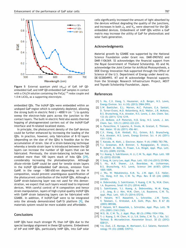
Figure 5 External quantum yield (Φext) of GaP, InP QD-embedded GaP, and InNP QD-embedded GaP samples in contactwith a CH3CN solution containing the FeCp2
+/0 redox couple and1.0 M LiClO4 as a supporting electrolyte.
787Enhancement of the performance of GaP solar cells
embedded QDs. The In(N)P QDs were embedded within anundoped GaP region which is completely depleted, allowingthe strong built-in electric field (�4000 V cm�1) to quicklysweep the electron–hole pairs across the junction to thecontact layers. The built-in electric field also assists thermalhopping of photogenerated carriers out of the In(N)P/GaPinterface and N-related localized states.
In principle, the photocurrent density of the GaP devicescould be further enhanced by increasing the loading of theQDs. In practice, however, only fabrication of 8–10 layers(depending on the size of the QDs) is feasible due to theaccumulation of strain. Use of a strain-balancing techniquewhereby a tensile strain layer is introduced between the QDlayers can increase the number of QD layers that can befabricated. Previously, the strain-balancing technique hasenabled more than 100 layers stack of InAs QDs [29],considerably increasing the photoabsorption. Althoughdilute-nitride GaNP could be used for tensile strain layersin the In(N)P QD-embedded GaP devices, emission fromGaNP, in the range �580–650 nm depending on the Ncomposition, would prevent unambiguous quantification ofthe photocurrent contribution of the In(N)P QDs. Although aGaNP strain-balancing layer was not used for this demon-stration, we expect that such layers would lead to improveddevices. With careful control of N composition and hencestrain manipulation, layers of high crystal quality In(N)P QDswith GaNP strain balancing layers can be fabricated withGSMBE. In addition, if In(N)P/GaP were to be integratedonto the already demonstrated GaP/Si platform [9], thematerials system would be more scalable and affordable.
Conclusions
InNP QDs have much stronger PL than InP QDs due to thespecial bandgap alignment in these QD systems. Embedmentof InP and InNP QDs, particularly InNP QDs, into GaP solar
cells significantly increased the amount of light absorbed bythe devices without degrading the quality of the junctions,and increases in both Jsc and Voc were observed for the QD-embedded devices. Embedment of InNP QDs within a GaPmatrix may increase the utility of GaP for photovoltaic andsolar fuels generation.
Acknowledgments
Material growth by GSMBE was supported by the NationalScience Foundation under Grant nos. DMR-0907652 andDMR-1106369. SS acknowledges the financial support fromthe Royal Government of Thailand Scholarship. KS and NLacknowledge the Joint Center for Artificial Photosynthesis, aDOE Energy Innovation Hub supported through the Office ofScience of the U.S. Department of Energy under Award no.DE-SC0004993. KT and IK acknowledge financial supportsfrom the Strategic Research Infrastructure Project, MEXTand Toyoaki Scholarship Foundation, Japan.
References
[1] S. Hu, C.X. Xiang, S. Haussener, A.D. Berger, N.S. Lewis,Energy Environ. Sci. 6 (10) (2013) 2984–2993.
[2] S.W. Boettcher, E.L. Warren, M.C. Putnam, E.A. Santori,D. Turner-Evans, M.D. Kelzenberg, M.G. Walter, J.R. McKone,B.S. Brunschwig, H.A. Atwater, N.S. Lewis, J. Am. Chem. Soc.133 (5) (2011) 1216–1219.
[3] J.R. McKone, A.P. Pieterick, H.B. Gray, N.S. Lewis, J. Am.Chem. Soc. 135 (1) (2012) 223–231.
[4] A. Paracchino, V. Laporte, K. Sivula, M. Gratzel, E. Thimsen,Nat. Mater. 10 (6) (2011) 456–461.
[5] C.X. Xiang, G.M. Kimball, R.L. Grimm, B.S. Brunschwig,H.A. Atwater, N.S. Lewis, Energy Environ. Sci. 4 (4) (2011)1311–1318.
[6] T. Katoda, M. Kishi, J. Electron. Mater. 9 (4) (1980) 783–796.[7] T.J. Grassman, M.R. Brenner, S. Rajagopalan, R. Unocic,
R. Dehoff, M. Mills, H. Fraser, S.A. Ringel, Appl. Phys. Lett.94 (23) (2009) 232106.
[8] Y.J. Kuang, S. Sukrittanon, H. Li, C.W. Tu, Appl. Phys. Lett. 100(5) (2012) 053108.
[9] Y. Song, M. Larry Lee, Appl. Phys. Lett. 103 (14) (2013) 251904.[10] S. Hu, M.R. Shaner, J.A. Beardslee, M. Lichterman,
B.S. Brunschwig, N.S. Lewis, Science 344 (6187) (2014)1005–1009.
[11] J. Wu, W. Walukiewicz, K.M. Yu, J.W. Ager, E.E. Haller,Y.G. Hong, H.P. Xin, C.W. Tu, Phys. Rev. B 65 (24) (2002)241303.
[12] A. Dobrovolsky, S. Sukrittanon, Y. Kuang, C.W. Tu, W.M. Chen,I.A. Buyanova, Small 10 (21) (2014) 4403.
[13] S. Sukrittanon, Y.J. Kuang, A. Dobrovolsky, W.-M. Kang,J.-S. Jang, B.-J. Kim, W.M. Chen, I.A. Buyanova, C.W. Tu,Appl. Phys. Lett. 105 (7) (2014) 07210.
[14] F. Hatami, W.T. Masselink, L. Schrottke, J.W. Tomm,V. Talalaev, C. Kristukat, A.R. Goñi, Phys. Rev. B 67 (8)(2003) 085306.
[15] F. Hatami, W.T. Masselink, L. Schrottke, Appl. Phys. Lett. 78(15) (2001) 2163–2165.
[16] W.G. Bi, C.W. Tu, J. Appl. Phys. 80 (3) (1996) 1934–1936.[17] Y.-J. Kuang, S.-W. Chen, H. Li, S.K. Sinha, C.W. Tu, J. Vac. Sci.
Technol. B: Microelectron. Nanometer Struct. 30 (2) (2012)02B121.
[18] Y.A. Ziad, J.E. Marega, M. Mortazavi, G.J. Salamo, Nanotech-nology 19 (33) (2008) 335712.
Y. Kuang et al.788
[19] S. Hu, C.-Y. Chi, K.T. Fountaine, M. Yao, H.A. Atwater,P.D. Dapkus, N.S. Lewis, C. Zhou, Energy Environ. Sci. 6 (6)(2013) 1879–1890.
[20] A.J. Williamson, A. Zunger, A. Canning, Phys. Rev. B 57 (8)(1998) R4253–R4256.
[21] M. Sopanen, H. Xin, C. Tu, Appl. Phys. Lett. 76 (8) (2000)994–996.
[22] P.R.C. Kent, A. Zunger, Phys. Rev. Lett. 86 (12) (2001)2613–2616.
[23] I. Buyanova, W. Chen, G. Pozina, J. Bergman, B. Monemar,H. Xin, C. Tu, Appl. Phys. Lett. 75 (4) (1999) 501–503.
[24] R. Kudrawiec, G. Sek, J. Misiewicz, L. Li, J. Harmand, Eur.Phys. J. Appl. Phys. 27 (1–3) (2004) 313–316.
[25] Y.J. Kuang, K. Takabayashi, S. Sukrittanon, J.L. Pan, I. Kamiya,C.W. Tu, Appl. Phys. Lett. 105 (17) (2014).
[26] C.R. Allen, J.-H. Jeon, J.M. Woodall, Sol. Energy Mater. Sol.Cells 94 (5) (2010) 865–868.
[27] C.G. Bailey, D.V. Forbes, S.J. Polly, Z.S. Bittner, Y. Dai,C. Mackos, R.P. Raffaelle, S.M. Hubbard, IEEE J. Photovolt. 2(3) (2012) 269–275.
[28] J. Schöne, E. Spiecker, F. Dimroth, A.W. Bett, W. Jäger, Appl.Phys. Lett. 92 (8) (2008) 081905.
[29] J. Inoue, T. Isu, K. Akahane, M. Tsuchiya, Appl. Phys. Lett. 89(15) (2006) 151117.
Yanjin Kuang received his Ph.D. degree inPhysics at the University of California, SanDiego (UCSD) in 2014 for his work on dilutenitride based intermediate band solar cellmaterials. Prior to his doctoral study, heobtained his M.S. degree and B.S. degreeboth in Physics at UCSD and at University ofScience and Technology of China. Hisresearch focuses on molecular beam epitaxyand optical and electrical characterization
of III–V semiconductor materials in thin film, nanowire and quantumdot structures.
Ke Sun obtained his Ph.D. degree in Elec-trical and Computer Engineering from theUniversity of California at San Diego in 2013for his work on synthesis/characterizationof nanomaterials and heterogeneous sur-face modification of Si for optoelectronicsand solar water splitting. He is currently aPostdoctoral Researcher at the Joint Centerof Artificial Photosynthesis (DOE EnergyInnovation Hub) under the supervision of
Professor Nathan Lewis at Caltech. He is continuously committed tosolar-fuel research. Specifically, he is focusing on development ofprotective coatings for unstable photoelectrodes in aqueous envir-onment, optimization of electrocatalyst loading, and optimizationof Si microwire-based photoelectrodes.
Supanee Sukrittanon is a Ph.D. candidate inthe Materials Science and Engineering Pro-gram at the University of California, SanDiego (UCSD). She also received her M.S.degree in the same program at UCSD. Priorto UCSD, she received her B.S. degree inPhysics at Chulalongkorn University in
Thailand. Her research focuses on III–Vsemiconductors, MBE growth, and opticaldevices.
Ko Takabayashi received his bachelor'sdegree in Materials Engineering from ToyotaTechnological Institute (TTI), Japan in 2013.He is currently pursuing master's program atTTI under the direction of Professor ItaruKamiya. From August to October in 2013 hewas a visiting student in Professor Tu's groupat University of California San Diego. Hiscurrent research is focused on the growth ofIII–V semiconductor nanostructures and
their nm-scaled characterization with Kelvin probe force micro-scopy combined with atomic force microscopy.
Itaru Kamiya received his BS, MS, and Ph.D.in Applied Physics from The University ofTokyo, Japan. He has been a Professor atToyota Technological Institute, Nagoya,Japan, since 2004. Prior to taking his pre-sent position, he headed the NanomaterialsLab at Mitsubishi Chemical Corporationafter working at RIKEN, Bellcore, ImperialCollege, and The University of Tokyo. Hisresearch interest lies in the growth of
semiconductor nanostructures using epitaxial and chemical techni-ques, and the optical & electronic properties of these materialsparticularly those related to surfaces and interfaces.
Dr. Nathan Lewis, George L. Argyros Profes-sor of Chemistry, has been on the faculty atthe California Institute of Technology since1988 and has served as Professor since 1991.He has also served as the Principal Investi-gator of the Beckman Institute MolecularMaterials Resource Center at Caltech since1992, is the Principal Investigator of theJoint Center for Artificial Photosynthesis,the DOE's $122 MM Energy Innovation Hub in
Fuels from Sunlight. Dr. Lewis received his Ph.D. in Chemistry fromthe Massachusetts Institute of Technology. He has been an Alfred P.Sloan Fellow, a Camille and Henry Dreyfus Teacher-Scholar, and aPresidential Young Investigator.
Charles Tu is a Distinguished Professor ofElectrical and Computer Engineering (ECE)at the UCSD Jacobs School of Engineering.He joined the UCSD faculty in 1988, and wasappointed Associate Dean of the JacobsSchool from 2004 to 2014, after servingfrom 1999 to 2003 as Chair of the ECEdepartment. Tu's research interests includenovel III–V compound semiconductor hetero-structures and nanostructures for electro-
nic, optoelectronic and photovoltaic devices. He was adistinguished member of AT&T Bell Laboratories technical stafffrom 1980 to 1988. He earned his Ph.D. in Engineering and AppliedScience from Yale University in 1978 and his B.Sc. (Hon.) in Physicsfrom McGill University in 1971.